 | –≠–ª–µ–∫—Ç—Ä–æ–Ω–Ω—ã–π –∫–æ–º–ø–æ–Ω–µ–Ω—Ç: UPD75236 | –°–∫–∞—á–∞—Ç—å:  PDF PDF  ZIP ZIP |

4-BIT SINGLE-CHIP MICROCOMPUTER
DESCRIPTION
The
µ
PD75236 is a microcomputer with a CPU capable of 1-, 4-, and 8-bit-wise data processing, a ROM, a
RAM, I/O ports, a fluorescent display tube (FIP
Æ
) controller/driver, A/D converters, a watch timer, a timer/pulse
generator capable of outputting 14-bit PWM, a serial interface and a vectored interrupt function integrated on a
single-chip.
The
µ
PD75236 has the more improved peripheral functions including the RAM capacity, FIP controller/driver
display capabilities, I/O ports, A/D converter and serial interface than those of the
µ
PD75216A.
The
µ
PD75236 is most suited for advanced and popular VCR timer and tuner applications, single-chip
configurations of system computers, advanced CD players and advanced microwave ovens.
The
µ
PD75P238 PROM product and various types of development tools (IE-75001-R, assemblers and others)
are available for evaluation in system development or small-volume production.
FEATURES
µ
PD75236
q
Built-in, large-capacity ROM and RAM
∑ Program memory (ROM): 16K
◊
8
∑ Data memory (RAM): 768
◊
4
q
I/O port: 64 ports (except FIP dedicated pins)
q
Minimum instruction execution time: 0.95
µ
s
(when operated at 4.19 MHz)
q
Instruction execution time varying function to
achieve a wide range of power supply voltages
q
Built-in programmable FIP controller/driver
∑ Number of segments: 9 to 24
∑ Number of digits: 9 to 16
q
8-bit A/D converter: 8 channels
q
Powerful timer/counter function: 5 channels
q
8-bit serial interface: 2 channels
q
Interrupt function with importance attached to
applications
q
Product with built-in PROM:
µ
PD75P238
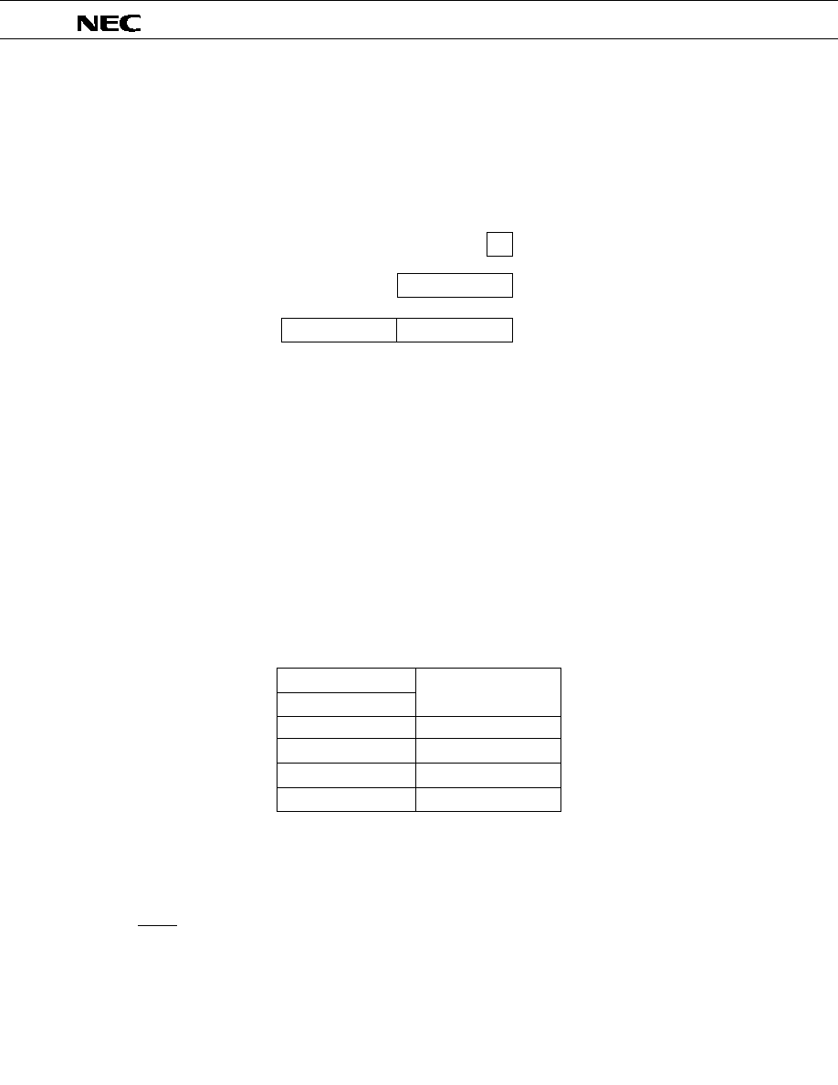
ORDERING INFORMATION
Ordering Code
Package
Quality Grade
µ
PD75236GJ-
◊◊◊
-5BG
94-pin plastic QFP (20
◊
20 mm)
Standard
MOS INTEGRATED CIRCUIT
DATA SHEET
The information in this document is subject to change without notice.
The mark 5 shows major revised points.
© NEC Corporation 1992
Document No.
IC-2677A
(O. D. No.
IC-8092A)
Date Published February 1993 P
Printed in Japan
Please refer to "Quality grade on NEC Semiconductor Devices" (Document number IEI-1209) published by
NEC Corporation to know the specification of quality grade on the devices and its recommended applications.

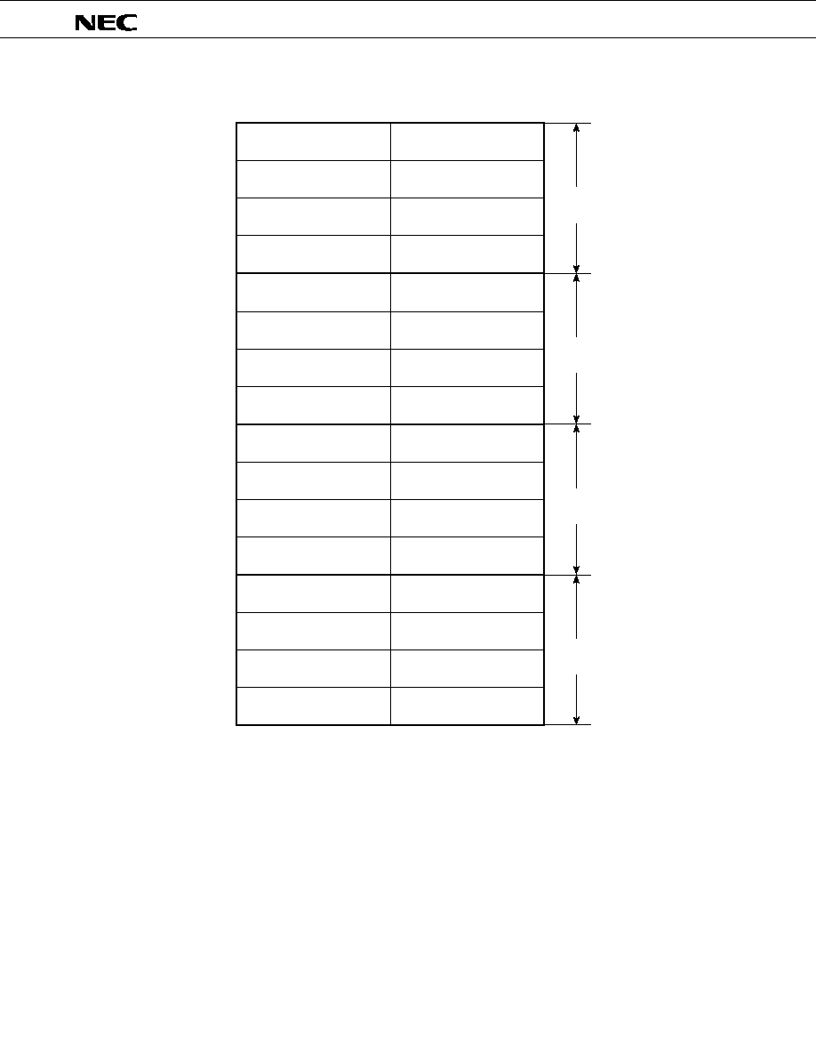
2
µ
PD75236
Item
Built-in memory capacity
I/O line
except FIP
dedicated pins
Instruction cycle
Fluorescent display
tube (FIP)
controller/driver
Timer/counter
Interrupt
Mask option
Operating temperature
range
Operating voltage
Package
LIST OF
µ
PD75236 FUNCTIONS
(
)
Function
ROM:
16256 x 8 bits, RAM:
768 x 4bits
q
q
Input pin
: 16
64 lines
q
q
Input/output pin : 24
q
q
Output pin
: 24
q
q
0.95
µ
s/1.91
µ
s/3.82
µ
s/15.3
µ
s
(when operated at 4.19 MHz)
q
q
122
µ
s (when operated at 32.768 kHz)
q
q
Number of segments : 9 to 24
q
q
Number of digits
: 9 to 16
q
q
Dimmer function
: 8 levels
q
q
Pull-down resistor mask option
q
q
Key scan interrupt generation enabled
q
q
Basic interval timer
: Watchdog timer applicable
q
q
Timer/event counter
5 channels
q
q
Watch timer
: Buzzer output enabled
q
q
Timer/pulse generator : 14-bit PWM output enabled
q
q
Event counter
q
q
SBI/3-wire type
q
q
3-wire type
q
q
Multi-interrupt enabled by hardware
q
q
Both-edge detection
q
q
External interrupt:
3 interrupts
q
q
Detected edge programmable (with noise
remove function)
q
q
Detected edge programmable
q
q
External test input:
1 input
q
q
Rising edge detection
q
q
Timer/pulse generator
q
q
Timer/event counter
q
q
Internal interrupt:
5 interrupts
q
q
Basic interval timer
q
q
Serial interface #0
q
q
Key scan interrupt
q
q
Internal test input:
2 inputs
q
q
Clock timer
q
q
Serial interface #1
q
q
Main system clock
: 4.19 MHz standard
q
q
Subsystem clock
: 32.768 kHz standard
q
q
High withstand voltage port
: Pull-down resistor or open-drain output
q
q
Ports 4 and 5
: Pull-up resistors
q
q
Port 7
: Pull-down resistor
≠40 to +85
∞
C
2.7 to 6.0 V (standby data hold: 2.0 to 6.0 V)
94-pin plastic QFP (20
◊
20 mm)
System clock oscillator
2 channels
Serial interface

3
µ
PD75236
AN0
AV
REF
AV
DD
V
DD
V
DD
X2
X1
IC
XT2
XT1
V
SS
S16/P100
S17/P101
S18/P102
S19/P103
S20/P110
S21/P111
S22/P112
S23/P113
S0/P120
S1/P121
S2/P122
S3/P123
S4/P130
S5/P131
S6/P132
S7/P133
S8/P140
S9/P141
V
LOAD
T15/S10/P142
T14/S11/P143
PH0/T13/S12/P150
PH1/T12/S13/P151
PH2/T11/S14/P152
T9
PH3/T10/S15/P153
T8
T7
T6
T5
T4
T3
T2
T1
T0
V
DD
V
DD
P83/SI1
P82/SO1
P81/SCK1
P80/PPO
P73
P72
P71
P70
P63
P62
P61
P60
P53
P52
P51
P50
V
SS
P43
P42
P41
P40
P33
P32
P31
P30
P23/BUZ
P22/PCL
P21
P20/PTO0
P13/TI0
P12/INT2
P11/INT1
P10/INT0
P03/SI0/SB1
P02/SO0/SB0
P01/SCK0
P00/INT4
RESET
AN7/P93
AN6/P92
AN5/P91
AN4/P90
AN3
AN2
AN1
AV
SS
1
2
3
4
5
6
7
8
9
10
11
12
13
14
15
16
17
18
19
20
21
22
23
24252627282930313233343536373839404142434445
4647
48
49
50
51
52
53
54
55
56
57
58
59
60
61
62
63
64
65
66
67
68
69
70
71
72
73
74
75
76
77
78
79
80
81
82
83
84
85
86
87
88
89
90
91
92
93
94
PIN ASSIGNMENTS
Note
Be sure to supply power to AV
DD
, V
DD
, V
SS
and AV
SS
pins (pin Nos. 3, 4, 5, 11, 30, 48, 65 and 87) .
Remarks
Connect the IC (Internally Connected) pin to GND.
µ
PD75236GJ-
◊◊◊
-5BG
4
µ
PD75236
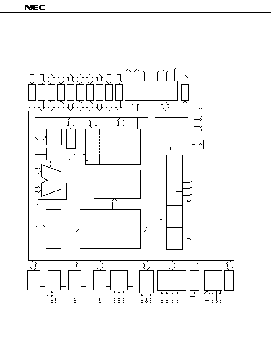
BLOCK DIAGRAM
*
PORT4 and PORT5 are 10 V middle-high voltage N-ch open-drain input/output ports.
PORT0
PORT1
PORT2
PORT3
PORT4
PORT5
PORT6
PORT7
PORT8
PORT9
4
4
4
4
4
4
4
4
4
4
P00-P03
P90-P93
P10-P13
P20-P23
P30-P33
P40-P43*
P50-P53*
P60-P63
P70-P73
P80-P83
FIP
CONTROLLER/
DRIVER
10
4
2
8
10
T0-T9
T10/S15/PH3/P153-
T13/S12/PH0/P150
T14/S11/P143-
T15/S10/P142
S0/P120-S9/P141
S16/P100-S23/P113
V
LOAD
P100-P153
PORT10-15 24
BASIC
INTERVAL
TIMER
INTBT
TIMER/EVENT
COUNTER
#0
WATCH
TIMER
INTT0
INTW
TIMER/PULSE
GENERATOR
INTTPG
SERIAL
INTERFACE0
INTCSI
SERIAL
INTERFACE1
INTERRUPT
CONTROL
COUNTER
EVENT
A/D
CONVERTER
BIT SEQ.
BUFFER(16)
TI0
TI0/P13
PTO0/P20
BUZ/P23
PPO/P80
SI0/SB1/P03
SO0/SB0/P02
SCK0/P01
SI1/P83
SO1/P82
SCK1/P81
INT0/P10
INT1/P11
INT2/P12
INT4/P00
TI0
8
AN0-AN3
AN4/P90-AN7/P93
AV
DD
AV
REF
AV
SS
PROGRAM
COUNTER (14)
ALU
CV
SP (8)
SBS (2)
BANK
GENERAL REG.
RAM
DATA MEMORY
768x4
DECODE
AND
CONTROL
ROM
PROGRAM
MEMORY
16256x8
CPU CLOCK
STAND BY
CONTROL
CLOCK
GENERATOR
SUB
MAIN
CLOCK
DIVIDER
XT1XT2 X1 X2
CLOCK
OUTPUT
CONTROL
PCL/P22
V
DD
V
SS
V
DD
RESET
fx/
N
2

5
µ
PD75236
CONTENTS
1.
PIN FUNCTIONS ......................................................................................................................................... 7
1.1
PORT PINS ........................................................................................................................................................... 7
1.2
NON-PORT PINS .................................................................................................................................................. 9
1.3
PIN INPUT/OUPUT CIRCUIT LIST ................................................................................................................... 11
1.4
RECOMMENDED CONNECTIONS OF
µ
PD75236 UNUSED PINS ............................................................... 15
2.
µ
PD75236 ARCHITECTURE AND MEMORY MAP................................................................................ 16
2.1
DATA MEMORY BANK CONFIGURATION AND ADDRESSING MODE ..................................................... 16
2.2
GENERAL REGISTER BANK CONFIGURATION ............................................................................................ 19
2.3
MEMORY MAPPED I/O .................................................................................................................................... 22
3.
INTERNAL CPU FUNCTIONS .................................................................................................................. 28
3.1
PROGRAM COUNTER (PC): 14 BITS .............................................................................................................. 28
3.2
PROGRAM MEMORY (ROM): 16256 WORDS
◊
8 BITS ............................................................................... 28
3.3
DATA MEMORY ................................................................................................................................................ 30
3.4
GENERAL REGISTER: 8
◊
4 BITS
◊
4 BANKS ............................................................................................... 32
3.5
ACCUMULATOR ............................................................................................................................................... 33
3.6
STACK POINTER (SP) AND STACK BANK SELECT REGISTER (SBS) ....................................................... 33
3.7
PROGRAM STATUS WORD (PSW): 8 BITS ................................................................................................... 36
3.8
BANK SELECT REGISTER (BS) ....................................................................................................................... 40
4.
PERIPHERAL HARDWARE FUNCTIONS ............................................................................................... 41
4.1
DIGITAL INPUT/OUTPUT PORTS ................................................................................................................... 41
4.2
CLOCK GENERATOR ........................................................................................................................................ 50
4.3
CLOCK OUTPUT CIRCUIT ................................................................................................................................ 58
4.4
BASIC INTERVAL TIMER ................................................................................................................................. 61
4.5
TIMER/EVENT COUNTER ................................................................................................................................ 63
4.6
WATCH TIMER .................................................................................................................................................. 69
4.7
TIMER/PULSE GENERATOR ........................................................................................................................... 71
4.8
EVENT COUNTER ............................................................................................................................................. 77
4.9
SERIAL INTERFACE .......................................................................................................................................... 79
4.10 A/D CONVERTER ........................................................................................................................................... 113
4.11 BIT SEQUENTIAL BUFFER: 16 BITS ............................................................................................................. 119
4.12 FIP CONTROLLER/DRIVER ............................................................................................................................ 119
5.
INTERRUPT FUNCTIONS ...................................................................................................................... 131
5.1
INTERRUPT CONTROL CIRCUIT CONFIGURATION ................................................................................... 131
5.2
INTERRUPT CONTROL CIRCUIT HARDWARE DEVICES ........................................................................... 133
5.3
INTERRUPT SEQUENCE ................................................................................................................................ 138
5.4
MULTI-INTERRUPT SERVICE CONTROL ..................................................................................................... 139
5.5
VECTOR ADDRESS SHARING INTERRUPT SERVICING .......................................................................... . 141
6.
STANDBY FUNCTIONS ......................................................................................................................... 142
6.1
STANDBY MODE SETTING AND OPERATING STATE .............................................................................. 142
6.2
STANDBY MODE RELEASE .......................................................................................................................... 144
6.3
OPERATION AFTER STANDBY MODE RELEASE ....................................................................................... 146

6
µ
PD75236
7.
RESET FUNCTIONS ............................................................................................................................... 147
8.
INSTRUCTION SET ................................................................................................................................ 150
8.1
CHARACTERISTIC INSTRUCTIONS OF
µ
PD75236 ..................................................................................... 150
8.2
INSTRUCTION SET AND OPERATION ......................................................................................................... 153
8.3
OPERATION CODES ....................................................................................................................................... 162
9.
MASK OPTION SELECTION ................................................................................................................. 168
10. APPLICATION BLOCK DIAGRAM ........................................................................................................ 169
11. ELECTRICAL SPECIFICATIONS ........................................................................................................... 170
12. CHARACTERISTIC CURVES (REFERENCE VALUES) ........................................................................ 183
13. PACKAGE INFORMATION ................................................................................................................... 184
14. RECOMMEDED SOLDERING CONDITIONS ....................................................................................... 185
APPENDIX A.
LIST OF
µ
PD75238 SERIES PRODUCT FUNCTIONS..................................................... 186
APPENDIX B.
DEVELOPMENT TOOLS ................................................................................................... 187
5

7
µ
PD75236
1.
PIN FUNCTIONS
1.1
PORT PINS (1/2)
P00
P01
P02
P03
P10
P11
P12
P13
P20
P21
P22
P23
P30
P31
P32
P33
P40 to P43
P50 to P53
P60
P61
P62
P63
P70
P71
P72
P73
Pin Name
I/O
After Reset
Input / Output
Circuit Type *1
Input/
output
*2
4-bit input port (PORT0).
Built-in pull-up resistor can be specified in 3-bit
units by software for P01 to P03.
4-bit input port (PORT1).
Built-in pull-up resistor can be specified in 4-bit
units by software.
Noise removing
function available
4-bit input/ output port (PORT2).
Built-in pull-up resistor can be specified in 4-bit
units by software.
◊
◊
B
F ≠ A
F ≠ B
M ≠ C
B ≠ C
E ≠ B
◊
Input
Input
Input
Input
Input
Input/
output
Programmable 4-bit input/ output port (PORT3).
Input/ output specifiable in 1-bit units.
Built-in pull-up resistor can be specified in 4-bit
units by software.
Input/
output
Input/
output
N-ch open-drain 4-bit input/output port (PORT4).
Pull-up resistor can be incorporated in 1-bit units
(mask option).
10 V withstand voltage with open drain.
N-ch open-drain 4-bit input/ output port (PORT5).
Pull-up resistor can be incorporated in 1-bit units
(mask option).
10 V withstand voltage with open drain.
Programmable 4-bit input/output port (PORT6).
Input/output specifiable in 1-bit units.
Built -in pull-up resistor can be specified in 4-bit
units by software.
q
q
High level
(when a pull-
up resistor is
incorporated)
or high
impedance
High level
(when a pull-
up resistor is
incorporated)
or high
impedance
Input
E ≠ C
◊
M
M
* 1.
Schmitt trigger inputs are circled.
2.
Can drive LED directly.
Function
Dual-
Function Pin
8-Bit
I/O
*2
*2
*2
*2
*2
q
q
Input/
output
Input/
output
4-bit input/output port (PORT7).
Built-in pull-down resistor can be incorporated in
1-bit units (mask option).
INT4
SCK0
SO0/SB0
SI0/SB1
INT0
INT1
INT2
TI0
PTO0
--
PCL
BUZ
--
--
--
--
--
--
--
--
--
--
--
--
--
--
Input
V
SS
level
(when a pull-
down resistor
is incorpo-
rated) or high
impedance
E ≠ C
V
8
µ
PD75236
Pin Name
I/O
8-Bit
I/O
Function
Dual-
Function Pin
After Reset
Input / Output
Circuit Type *
Input/
output
Input/
output
Input/
output
4-bit input port (PORT8)
4-bit input port (PORT9)
P-ch open-drain 4-bit high-voltage output port.
Pull-down resistor can be incorporated (mask
option).
P-ch open-drain 4-bit high-voltage output port.
Pull-down resistor can be incorporated (mask
option).
◊
Input
A
F
E
B
◊
Input
Y ≠ A
q
q
I ≠ F
P-ch open-drain 4-bit high-voltage output port.
Pull-down resistor can be incorporated (mask
option).
P-ch open-drain 4-bit high-voltage output port.
Pull-down resistor can be incorporated (mask
option).
q
q
P80
P81
P82
P83
P90
P91
P92
P93
P100
P101
P102
P103
P110
P111
P112
P113
P120
P121
P122
P123
P130
P131
P132
P133
P140
P141
P142
P143
P150
P151
P152
P153
PH0
PH1
PH2
PH3
P-ch open-drain 4-bit high-voltage output port.
Pull-down resistor can be incorporated (mask
option).
P142 and P143 can drive LED directly.
Input
PP0
SCK1
SO1
SI1
AN4
AN5
AN6
AN7
S16
S17
S18
S19
S20
S21
S22
S23
S0
S1
S2
S3
S4
S5
S6
S7
S8
S9
S10/T15
S11/T14
S12/T13/PH0
S13/T12/PH1
S14/T11/PH2
S15/T10/PH3
S12/T13/P150
S13/T12/P151
S14/T11/P152
S15/T10/P153
Input
Output
Output
Output
Output
Output
Output
Output
P-ch open-drain 4-bit high-voltage output port.
Pull-down resistor can be incorporated (mask
option).
These ports can drive LED directly.
P-ch open-drain 4-bit high-voltage output port.
Pull-down resistor can be incorporated (mask
option).
q
q
◊
1.1
PORT PINS (2/2)
*
Schmitt trigger inputs are circled.
I ≠ C
V
LOAD
level
(when a
pull-down
resistor to
V
LOAD
is
incorpo-
rated) or
high
impedance.
V
LOAD
level
(when a
pull-down
resistor to
V
LOAD
is in-
corporated),
V
SS
level
(when a
pull-down
resistor to
V
SS
is in-
corporated)
or high
impedance

9
µ
PD75236
1.2
NON-PORT PINS (1/2)
Pin Name
I/O
Dual-
Function Pin
Input / Output
Circuit Type *
T0 to T9
T10/S15 to
T13/S12
T14/S11
T15/S10
S0 to S3
S4 to S7
S8
S9
S16 to S19
S20 to S23
TI0
PTO0
PCL
BUZ
SCK0
SO0/SB0
SI0/SB1
Function
After Reset
Segment high-voltage output
pins.
These pins can be used as
PORT12 to PORT14 in the static
mode.
Output
I ≠ C
I ≠ F
V
LOAD
level
(when a
pull-down
resistor to
V
LOAD
is
incorpo-
rated), V
SS
level (when
a pull-down
resistor to
V
SS
is
incorpo-
rated) or
high
impedance
Segment high-voltage output
pins.
These pins can be used as
PORT10 and PORT11 in the
static mode.
--
PH3/P153 to
PH0/P150
P143
P142
P120 to
P123
P130 to
P133
P140
P141
P100 to P103
P110 to P113
P13
P20
P22
P23
P01
P02
P03
FIP controller/driver
output pins.
Pull-down resistor can
be incorporated in bit
units (mask option).
Digit/segment output dual-func-
tion high-voltage high-current
output pins. Extra pins can be
used as PORTH. These pins can
be used as PORT15 in the static
mode.
Digit output high-voltage high-
current output pins.
Digit/segment output dual-func-
tion high-voltage high-current
output pins. These pins can be
used as POTR14 in the static
mode.
V
LOAD
level
(when a
pull-down
resistor to
V
LOAD
is
incorpo-
rated) or
high
impedance.
Clock output pin
Fixed frequency output pin (for buzzer or system clock
trimming)
Input/
output
Input/
output
Serial clock input/output pin
Serial data output pin
Serial bus input/output pin.
Input/
output
Serial data input pin
Serial bus input/output pin.
Timer/event counter output pin
Output
Output
External event pulse input pin to timer/event counter #0
and event counter #1.
--
Input
Input
Input
Input
Input
Input
Input
B ≠ C
E ≠ B
E ≠ B
E ≠ B
F ≠ A
F ≠ B
M ≠ C
*
Schmitt trigger inputs are circled.
Output

10
µ
PD75236
1.2
NON-PORT PINS (2/2)
Edge-detected vectored interrupt
input pin (detected edge selection
possible)
Input
Edge-detected testable input pin
(rising edge detection)
Input
Input/
output
Output
Serial data output pin
B ≠ C
--
--
Input
--
Input
Input
--
Input
Output
--
--
--
Serial data input pin
Input
Analog input pin to A/D converter
A/D converter power supply pin
A/D converter reference voltage input pin
A/D converter reference GND potential pin
Main system clock oscillation crystal/ceramic connect
pin. An external clock is input to X1 and an antiphase
clock is input to X2.
Subsystem clock oscillation crystal connect pin. An
external clock is input to XT1 and XT2 is made open.
System reset input pin
Timer/pulse generator pulse output pin
--
GND potential pin
Positive power supply pin
FIP controller/driver pull-down resistor connect/power
supply pin
Input
INT4
INT0
INT1
INT2
SCK1
SO1
SI1
AN0 to AN3
AN4 to AN7
AV
DD
AV
REF
AV
SS
X1, X2
XT1
XT2
RESET
PP0
V
DD
(3 ≠ Pin)
V
SS
(2 ≠ Pin)
V
LOAD
P00
P10
P11
P12
P81
P82
P83
--
P90 to P93
--
--
--
--
--
P80
--
--
--
Dual-
Function Pin
Pin Name
I/O
Function
After Reset
Input / Output
Circuit Type *
*
Schmitt trigger inputs are circled.
Input
Edge-detected vectored interrupt input pin (valid for
detection of rising and falling edges)
B
B ≠ C
F
E
B
Y
Y ≠ A
--
Z
--
--
--
B
--
--
--
--
Clocked
Asynchronous
Asynchronous
Serial clock input/output pin
--
--
Input
Input
Input
--
--
--
--
--
--
--
Input
--
--
--

11
µ
PD75236
1.3
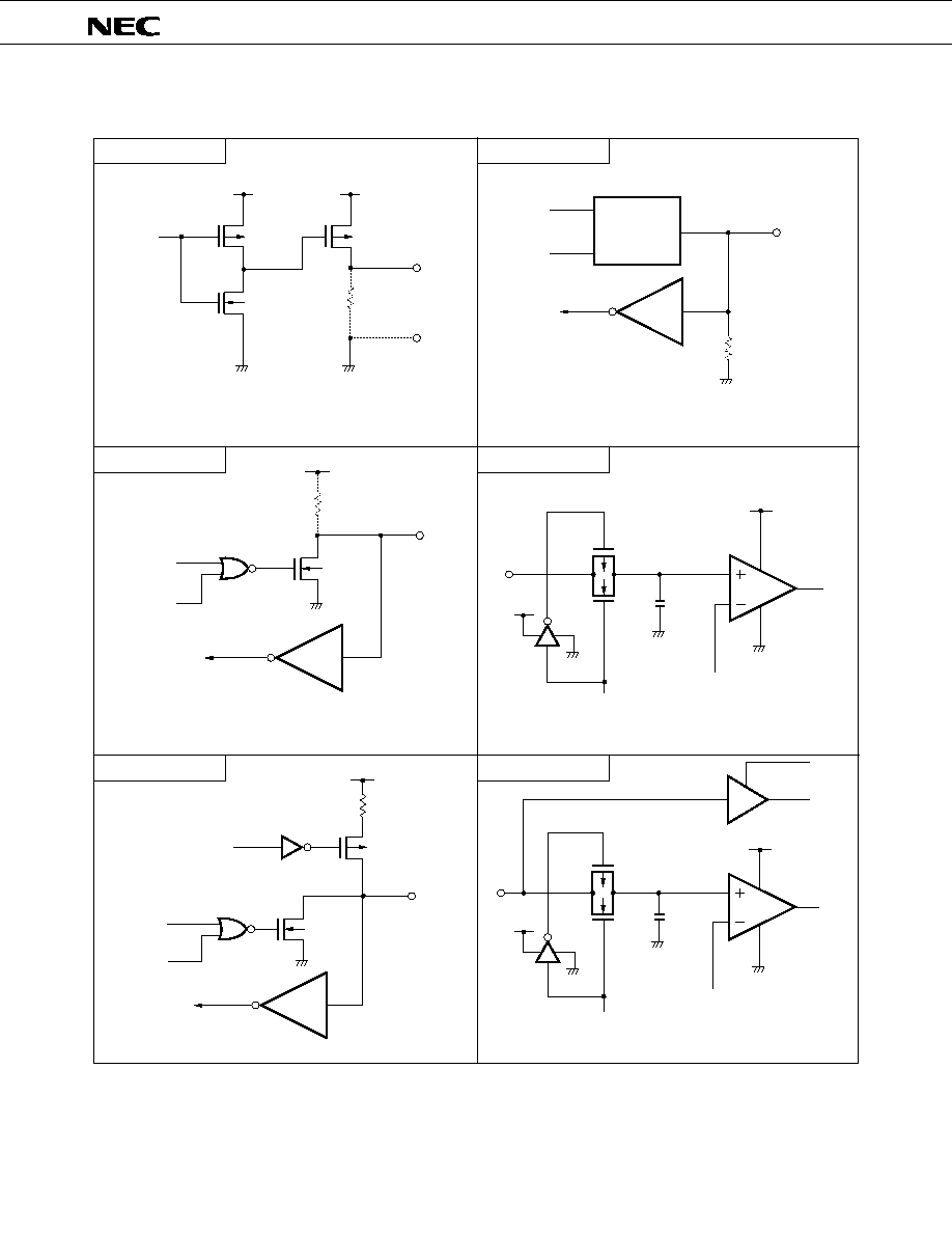
PIN INPUT/OUTPUT CIRCUIT LIST (1/4)
TYPE D
TYPE B-C
TYPE E-B
TYPE B
TYPE A
TYPE E
IN
V
DD
P-ch
N-ch
CMOS-Specified Input Buffer
IN
V
DD
P-ch
P.U.R
IN
P.U.R
enable
P.U.R:Pull-Up Resistor
Schmitt Trigger Input Having Hysteresis
Characteristics
V
DD
P-ch
N-ch
OUT
data
output
disable
Push-Pull Output which can be Set to Output High
Impedance (with Both P-ch and N-ch Set to OFF)
data
output
disable
Type D
IN/OUT
Type A
Schmitt Trigger Input Having Hysteresis
Characteristics
Input/Output Circuit Consisting of Type D
Push-Pull Output and Type A Input Buffer
output
disable
data
output
disable
Type D
Type A
V
DD
P-ch
P.U.R
IN/OUT
P.U.R:Pull-Up Resistor

12
µ
PD75236
TYPE F-B
TYPE F-A
TYPE I-C
TYPE E-C
Input/Output Circuit Consisting of Type
D Push-Pull Output and Type B Schmitt
Trigger Input
TYPE F-C
TYPE F
P.U.R
enable
data
output
disable
Type D
Type A
V
DD
P.U.R
P-ch
IN/OUT
P.U.R:Pull-Up Resistor
data
output
disable
Type D
IN/OUT
Type B
output
disable
(P-ch)
data
output
disable
output
disable
(N-ch)
P.U.R
enable
V
DD
P-ch
N-ch
Type B
IN/OUT
P-ch
P.U.R
V
DD
P.U.R:Pull-Up Resistor
P.U.R
enable
data
output
disable
Type D
Type B
IN/OUT
P-ch
P.U.R
V
DD
P.U.R:Pull-Up Resistor
1.3
PIN INPUT/OUTPUT CIRCUIT LIST (2/4)
P.U.R
enable
data
output
disable
Type D
Type B
IN/OUT
P-ch
P.U.R
V
DD
P.U.R:Pull-Up Resistor
data
V
DD
P-ch
N-ch
V
DD
P-ch
OUT
P.D.R
(Mask Option)
V
LOAD
P.D.R:Pull-Down Resistor
13
µ
PD75236
TYPE V
TYPE M-C
TYPE Y-A
TYPE I-F
TYPE Y
TYPE M
Middle-High Voltage
Input Buffer
V
DD
P.U.R
P-ch
IN/OUT
N-ch
P.U.R
enable
data
output
disabie
Type B
P.U.R:Pull-Up Resistor
IN
AV
DD
AV
SS
P-ch
N-ch
AV
SS
AV
DD
AV
SS
Reference Voltage
(from the Series Resistance
String Voltage Tap)
1.3
PIN INPUT/OUTPUT CIRCUIT LIST (3/4)
data
output
disable
V
DD
P.U.R
(Mask Option)
IN/OUT
N-ch
P.U.R:Pull-Up Resistor
data
V
DD
P-ch
N-ch
V
DD
P-ch
P.D.R
(Mask Option)
OUT
V
LOAD
P.D.R:Pull-Down Resistor
data
output
disable
Type D
Type A
IN/OUT
P.D.R
(Mask Option)
P.D.R:Pull-Down Resistor
IN
AV
DD
AV
SS
P-ch
N-ch
AV
SS
AV
SS
AV
DD
Sampling
C
Reference Voltage
(from the Series Resistance
String Voltage Tap)

14
µ
PD75236
1.3
PIN INPUT/OUTPUT CIRCUIT LIST (4/4)
AV
TYPE Z
ss

15
µ
PD75236
1.4
RECOMMENDED CONNECTIONS OF
µ
PD75236 UNUSED PINS
P00/INT4
P01/SCK0
P02/SO0/SB0
P03/SI1/SB1
P10/INT0 to P12/INT2
P13/TI0
P20/PTO0
P21
P22/PCL
P23/BUZ
P30 to P33
P40 to P43
P50 to P53
P60 to P63
P70 to P73
P80/PPO
P81/SCK1
P82/SO1
P83/SI1
P90/AN4 to P93/AN7
P100/S16 to P103/S19
P110/S20 to P113/S23
P120 to P123
P130 to P133
P140 to P143
P150 to P153
AN0 to AN3
AV
REF
AV
DD
AV
SS
XT1
XT2
V
LOAD
Pin
Connect to V
SS
Connect to V
SS
or V
DD
Input state : Connect to V
SS
or V
DD
Ouput state : Leave open
Connect to V
SS
Connect to V
DD
Connect to V
SS
Connect to V
SS
or V
DD
Leave open
Connect to V
SS
Recommended Connection
Connect to V
SS
Leave open
Connect to V
SS

16
µ
PD75236
2.
µ
PD75236 ARCHITECTURE AND MEMORY MAP
The
µ
PD75236 has the following three architectural features.
(a)
Data memory bank configuration
(b)
General register bank configuration
(c)
Memory mapped I/O
Each feature is outlined below.
2.1
DATA MEMORY BANK CONFIGURATION AND ADDRESSING MODE
As shown in Fig. 2-1, the
µ
PD75236 incorporates a static RAM (672 words
◊
4 bits) at addresses 000H to
19FH and 200H to 2FFH in the data memory space and a display data memory (96 words
◊
4 bits) at addresses
1A0H to 1FFH and peripheral hardware (input/output ports, timers, etc.) at addresses F80H to FFFH. For ad-
dressing of this 12-bit address data memory space, the memory bank has a configuration wherein the lower 8
bits are directly or indirectly specified by an instruction and the higher 4-bit address is specified by a memory
bank (MB).
A memory bank enable flag (MBE) and a memory bank select register (MBS) are incorporated to specify the
memory bank (MB) and addressing operations shown in Fig. 2-1 and Table 2-1 can be carried out. (MBS is a
register to select the memory bank and can set 0, 1, 2 and 15. MBE is a flag to determine whether the memory
bank selected by MBS should be validated or not. Since MBE is automatically saved/reset for interrupt or
subroutine processing, it can be freely set for either processing.)
For data memory space addressing, set MBE = 1 normally and manipulate the memory bank static RAM
specified by MBS. Efficient programming is possible by using the MBE = 0 or MBE = 1 mode for each program
processing.
Applicable Program Processing
q
q
Interrupt service
MBE = 0 mode
q
q
Processing of repeating built-in hardware manipulation and static RAM manipulation
q
q
Subroutine processing
MBE = 1 mode
q
q
Normal program processing

17
µ
PD75236
Fig. 2-1 Date Memory Configuration and Addressing Range in Each Addressing Mode
Addressing Mode
mem
mem. bit
@HL
@H+mem. bit
@DE
@DL
Stack
Address-
ing
fmem. bit
pmem.
@L
Memory Bank
Enable Flag
MBE
= 0
MBE
= 1
MBE
= 0
MBE
= 1
General
Register
Area
Data Area
Static RAM
(Memory Bank
0)
MBS
= 0
MBS
= 0
SBS
= 0
MBS
= 1
MBS
= 1
SBS
= 1
MBS
= 2
MBS
= 2
SBS
= 2
Display
Data
Memory
Area
Stack Area
Data Area
Static RAM
(Memory Bank
1)
Data Area
Static RAM
(Memory Bank
2)
Not Incorporated
Peripheral Hardware Area
(Memory Bank 15)
MBS
= 15
MBS
= 15
Remarks
--
:
Don't care
000H
01FH
020H
07FH
0FFH
100H
19FH
1A0H
1FFH
200H
2FFH
F80H
FC0H
FFFH
--
--
--
--
18
µ
PD75236
Table 2-1 Addressing Modes
Addressing Mode
Identifier
Address Specified
MBE = 0
Bit indicated by bit of address indicated by MB and mem, where :
When mem = 00H to 7FH, MB = 0
When mem = 80H to FFH, MB = 15
MBE = 1
MB = MBS
Address indicated by MB and mem, where :
MBE = 0
When mem = 00H to 7FH, MB = 0
When mem = 80H to FFH, MB = 15
MBE = 1
MB = MBS
Address indicated by MB and mem (mem is an even address), where:
MBE = 0
When mem = 00H to 7FH, MB = 0
When mem = 80H to FFH, MB = 15
MBE = 1
MB = MBS
Address indicated by MB and HL, where : MB = MBE∑ MBS
Address indicated by MB and HL, where : MB = MBE∑ MBS
HL+ automatically increments L register after addressing.
HL≠ automatically decrements L register after addressing.
Address indicated by DE of memory bank 0
Address indicated by DL of memory bank 0
Address indicated by MB and HL, where : MB = MBE∑ MBS
Bit 0 of L register is ignored.
Bit indicated by bit of address indicated by fmem, where:
FB0H to FBFH (interrupt-related hardware)
FF0H to FFFH (I/O port)
Bit indicated by the lower 2 bits of L register of the address indicated by the
higher 10 bits of pmem and the higher 2 bits of L register, where:
pmem = FC0H to FFFH
Bit indicated by bit of the address indicated by MB, H and the lower 4 bits of mem,
where: MB = MBE∑ MBS
Address indicated by SP of memory banks 0, 1 and 2 selected by SBS
mem.bit
mem
@HL
@HL+ @HL≠
@DE
@DL
@HL
fmem.bit
pmem.@L
@H + mem.bit
1-bit direct addressing
4-bit direct addressing
8-bit direct addressing
4-bit register indirect
addressing
8-bit register indirect
addressing
Bit manipulation
addressing
Stack addressing
As described in Table 2-1, direct and indirect addressing is possible for each of 1-bit, 4-bit and 8-bit data in
µ
PD75236 data memory manipulation. Thus, easy-to-understand programs can be created very efficiently.
fmem =

19
µ
PD75236
2.2
GENERAL REGISTER BANK CONFIGURATION
The
µ
PD75236 incorporates four register banks, each bank consisting of eight general registers, X, A, B, C,
D, E, H and L. This general register area is mapped at addresses 00H to 1FH of the memory bank 0 of the data
memory (refer to Fig. 2-2 General Register Configuration (4-Bit Processing)). A register bank enable flag (RBE)
and a register bank select register (RBS) are incorporated to specify the above general register banks. RBS is a
register to select a register bank and RBE is a flag to determine whether the register bank selected by RBS
should be validated or not. The register bank (RB) which is validated for instruction execution is given as
RB = RBE∑ RBS.
As described above, with the
µ
PD75236 having four register banks, programs can be created very efficiently
by using different register banks for normal processing and interrupt service as described in Table 2-2. (RBE is
automatically saved and set for interrupt service and automatically reset upon termination of the interrupt
service.)
Table 2-2 Recommended Use of Register Banks in Normal and Interrupt Routines
Normal processing
Use register banks 2 and 3 with RBE = 1.
Single interrupt service
Use register bank 0 with RBE = 0.
Double interrupt service
Use register bank 1 with RBE = 1. (It is necessary to save/reset RBS.)
Triple or more interrupt service
Save/reset registers by PUSH and POP.
Not only in 4-bit units, a register pair of XA, HL, DE or BC can transfer, compare, operate, increment or
decrement data in 8-bit units. In this case, register pairs with the reversed bit 0 of the register bank specified by
RBE∑ RBS can be specified as XA', HL', DE' and BC'. Thus, the
µ
PD75236 has eight 8-bit registers (refer to Fig. 2-
3 General Register Configuration (8-Bit Processing)).
20
µ
PD75236
Fig. 2-2 General Register Configuration (4-Bit Processing)
X
A
H
L
D
E
B
C
X
A
H
L
D
E
B
C
X
A
H
L
D
E
B
C
X
A
H
L
D
E
B
C
01H
00H
03H
02H
05H
04H
07H
06H
09H
08H
0BH
0AH
0DH
0CH
0FH
0EH
11H
10H
13H
12H
15H
14H
17H
16H
19H
18H
1BH
1AH
1DH
1CH
1FH
1EH
Register Bank 0
(RBE∑RBS = 0)
Register Bank 1
(RBE∑RBS = 1)
Register Bank 2
(RBE∑RBS = 2)
Register Bank 3
(RBE∑RBS = 3)

21
µ
PD75236
Fig. 2-3 General Register Configuration (8-Bit Processing)
XA
HL
DE
BC
XA'
HL'
DE'
BC'
00H
02H
04H
06H
08H
0AH
0CH
0EH
When RBE∑RBS = 0
XA'
HL'
DE'
BC'
XA
HL
DE
BC
00H
02H
04H
06H
08H
0AH
0CH
0EH
When RBE∑RBS = 1
XA
HL
DE
BC
XA'
HL'
DE'
BC'
10H
12H
14H
16H
18H
1AH
1CH
1EH
When RBE∑RBS = 2
XA'
HL'
DE'
BC'
XA
HL
DE
BC
10H
12H
14H
16H
18H
1AH
1CH
1EH
When RBE∑RBS = 3

22
µ
PD75236
Applicable Addressing Mode
Specify by direct addressing mem.bit with MBE = 0 or
(MBE = 1, MBS = 15)
Specify by direct addressing fmem.bit irrespective of
MBE and MBS
Specify by indirect addressing pmem.@L irrespective
of MBE and MBS
Specify by direct addressing mem with MBE = 0 or
(MBE = 1, MBS = 15)
Specify by register indirect addressing @HL with
(MBE = 1, MBS = 15)
Specify by direct addressing mem with MBE = 0 or
(MBE = 1, MBS = 15) (mem is an even address.)
Specify by register indirect addressing @HL with
MBE = 1 and MBS = 15 (L register contents are even.)
Applicable Hardware
All hardware devices enabled for bit
manipulation
IST0, IST1, MBE, RBE,
IE
◊◊◊
, IRQ
◊◊◊
, PORTn. 0 to 3
PORTn.
All hardware devices enabled for 4-bit
manipulation
All hardware devices enabled for 8-bit
manipulation
Bit manipulation
4-bit manipulation
8-bit manipulation
2.3
MEMORY MAPPED I/O
As shown in Fig. 2-1, the
µ
PD75236 employs the memory mapped I/O with the peripheral hardware includ-
ing input/output ports and timers mapped at addresses F80H to FFFH in the data memory space. Thus, there
are no special instructions to control the peripheral hardware and all operations are controlled by memory
manipulation instructions. (Some hardware control mnemonics are available to make the program easy to
understand.)
When operating the peripheral hardware, the addressing modes listed in Table 2-3 can be used.
Manipulate the display data memory, key scan register and port H mapped at addresses 1A0H to 1FFH by
specifying memory bank 1.
Table 2-3 Addressing Modes Applicable when Manipulating the
Peripheral Hardware at Addresses F80H to FFFH
Table 2-4 shows the
µ
PD75236 I/O map.
In the table, each item has the following meanings:
∑ Symbol ............. Name indicating the on-chip hardware address.
Can be described in the instruction operand column.
∑ R/W ................... Indicates whether the corresponding hardware is enabled for read/write.
R/W : Read/write enable
R
: Read only
W
: Write only
∑ No. of manipulatable bits ........ Indicates the number of applicable bits before operating the corre-
sponding hardware.
∑ Bit manipulated addressing .... Indicates the applicable bit manipulated addressing before operating
the applicable hardware.

23
µ
PD75236
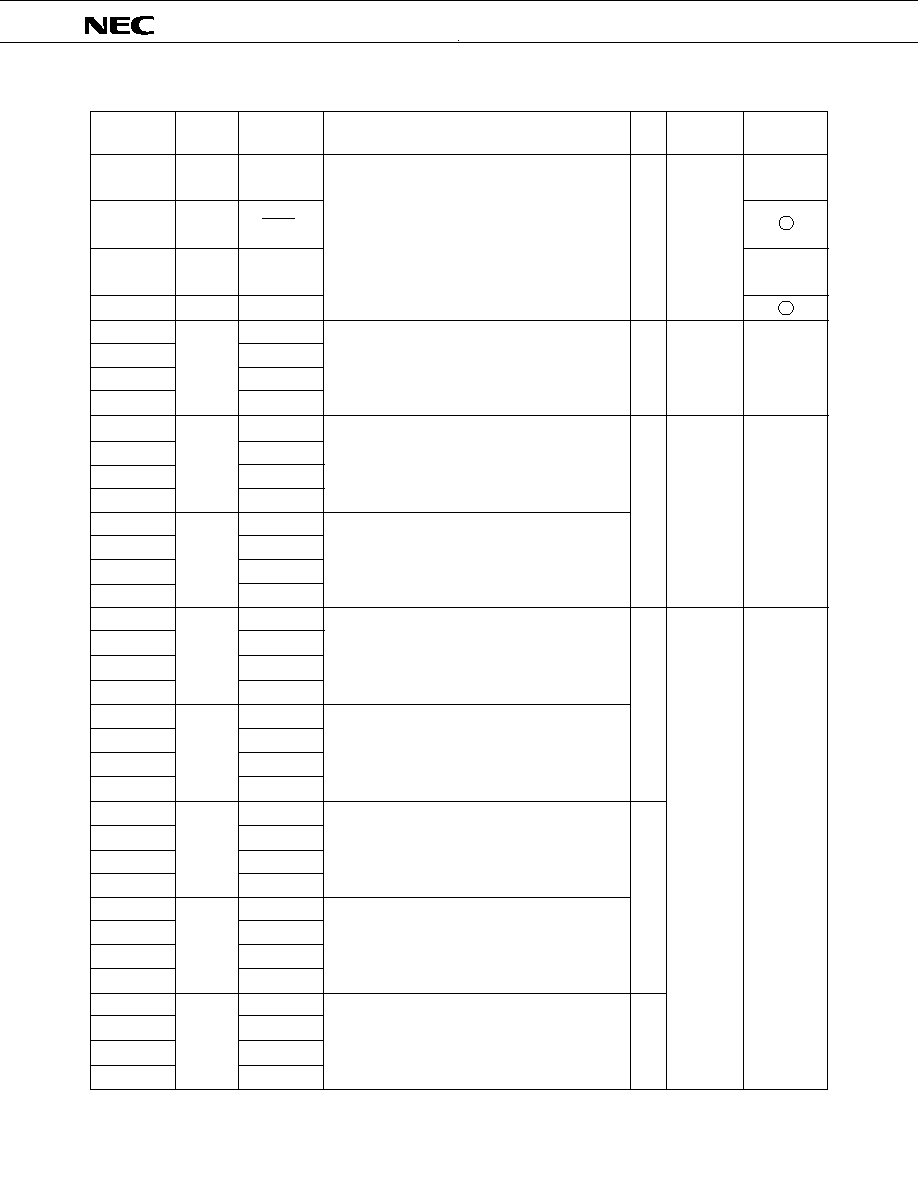
Table 2-4
µ
PD75236 I/O Map (1/5)
Address
R/W
No. of Manipulatable Bits
1 Bit
4 Bits
8 Bits
Remarks
F80H
F82H
F83H
F84H
F85H
F86H
F88H
F89H
F8AH
Stack pointer (SP)
Register bank select register (RBS)
Memory bank select register (MBS)
Stack bank select register (SBS)
Basic interval timer mode
register (BTM)
Basic interval timer (BT)
Display mode register (DSPM)
Dimmer select register (DIMS)
KSF
Digit select register
(DIGS)
R/W
R*1
R/W
W
R
W
W
R/W
Hardware Name (Symbol)
b3
b2
b1
b0
Be sure to write 0 to bit 0.
*2
Be sure to write 0 to
bits 3 and 2.
Only bit 3 is bit-manipula-
table.
Only bit 3 is bit-
testable.
--
--
--
--
v
v
--
--
--
v
v
--
q
q
q
q
q
q
q
q
--
q
q
q
q
q
q
Bit Manipulated
Addressing
q
q
q
q
--
--
q
q
--
--
--
mem.bit
mem.bit
F90H
F94H
F96H
F98H
Timer pulse generator mode
register (TPGM)
Timer pulse generator modulo
register L (MODL)
Timer pulse generator modulo
register H (MODH)
Watch mode register (WM)
W
R/W
R/W
W
v
v
--
--
--
v
v
--
--
--
q
q
q
q
q
q
q
q
mem.bit
5
Only bit 3 is bit-manipu-
latable.
* 1.
Can be read/written by the SEL instruction.
2.
Individually manipulatable as RBS and MBS by 4-bit manipulation.
Manipulatable as BS by 8-bit manipulation.

24
µ
PD75236
Table 2-4
µ
PD75236 I/O Map (2/5)
Address
R/W
No. of Manipulatable Bits
1 Bit
4 Bits
8 Bits
Remarks
FA0H
FA2H
FA4H
FA6H
FA8H
FABH
FACH
Hardware Name (Symbol)
b3
b2
b1
b0
Bit Manipulated
Addressing
q
q
--
q
q
q
q
q
q
--
q
q
Timer/event counter 0 mode
register (TM0)
TOE0
Timer/event counter 0 count
register (T0)
Timer/event counter 0 modulo
register (TMOD0)
Event counter mode register
(TM1)
Gate control register (GATEC)
Counter register (T1)
W
W
R
W
W
W
R
v
v
--
q
q
--
--
v
v
--
--
--
--
--
--
--
--
--
--
q
q
--
Only bit 3 is bit-manipulatable.
Only bit 3 is bit-manipulatable.

25
µ
PD75236
Table 2-4
µ
PD75236 I/O Map (3/5)
Address
R/W
No. of Manipulatable Bits
1 Bit
4 Bits
8 Bits
Remarks
Hardware Name (Symbol)
b3
b2
b1
b0
IST1
IST0
MBE
RBE
Bit Manipulated
Addressing
FB0H
FB2H
FB3H
FB4H
FB5H
FB7H
FB8H
FB9H
FBAH
FBBH
FBCH
FBDH
FBEH
FBFH
Program status word (PSW)
Interrupt priority select register (IPS)
Processor clock control register (PCC)
INT0 mode register (IM0)
INT1 mode register (IM1)
System clock control register (SCC)
IE4
IRQ4
IEBT
IRQBT
EOT
IEW
IRQW
IEKS
IRQKS
IETPG
IRQTPG
IRQT1
IET0
IRQT0
IECSI0 IRQCSI0
IE1
IRQ1
IE0
IRQ0
IE2
IRQ2
R/W
W
W
W
W
W
R/W
R/W
R/W
R/W
R/W
R/W
R/W
R/W
q
q
--
q
q
q
q
--
--
q
q
q
q
q
q
q
q
q
q
q
q
q
q
q
q
q
q
q
q
--
q
q
q
q
q
q
q
q
--
q
q
q
q
q
q
q
q
q
q
q
q
q
q
q
q
q
q
--
--
--
--
--
--
--
fmem.bit
Be sure to write 0 to bit 2.
Be sure to write 0 to bits 3, 2 and 1.
Only bits 3 and 0 are bit-manipulatable.
fmem.bit
FC0H
FC1H
FC2H
FC3H
FC8H
FC9H
FCCH
Bit sequential buffer 0 (BSB0)
Bit sequential buffer 1 (BSB1)
Bit sequential buffer 2 (BSB2)
Bit sequential buffer 3 (BSB3)
CSIM11 CSIM10
CSIE1
Serial I/O shift register (SI01)
R/W
R/W
R/W
R/W
W
W
R/W
q
q
q
q
q
q
q
q
--
q
q
--
q
q
q
q
q
q
q
q
--
--
--
q
q
q
q
q
q
q
q
5
5
5

26
µ
PD75236
Table 2-4
µ
PD75236 I/O Map (4/5)
Address
R/W
No. of Manipulatable Bits
1 Bit
4 Bits
8 Bits
Remarks
Hardware Name (Symbol)
b3
b2
b1
b0
Bit Manipulated
Addressing
FD0H
FD4H
FD6H
FD8H
FDAH
FDCH
Clock output mode register (CLOM)
Static mode register B (STATB)
Static mode register A (STATA)
SOC
EOC
A/D conversion mode register (ADM)
SA register (SA)
Pull-up register specification reg-
ister group A (POGA)
W
W
W
R/W
R
W
--
--
--
v
v
--
--
--
--
q
q
q
q
q
q
q
q
q
q
q
q
--
--
--
--
--
--
q
q
--
q
q
q
q
q
q
q
q
W
R/W
R/W
R/W
W
W
W
--
q
q
q
q
--
--
--
--
mem.bit
Write only in 8-bit
manipulation
mem.bit
Write only in 8-bit manipu-
lation
--
q
q
--
--
--
--
--
5
FE0H
FE2H
FE4H
FE6H
FE8H
FECH
Port mode register group A (PMGA)
Serial operating mode register (CSIM0)
CSIEO
COI
WUP
CMDD
RELD
CMDT
RELT
SBI control register (SBIC)
BSYE
ACKD
ACKE
ACKT
Serial I/O shift register 0 (SIO0)
Slave address register (SVA)
PM33
PM32
PM31
PM30
PM63
PM62
PM61
PM60
--
PM2
--
--
Port mode register group B (PMGB)
PM7
--
PM5
PM4

27
µ
PD75236
Table 2-4
µ
PD75236 I/O Map (5/5)
Address
R/W
No. of Manipulatable Bits
1 Bit
4 Bits
8 Bits
Remarks
Hardware Name (Symbol)
b3
b2
b1
b0
Bit Manipulated
Addressing
FF0H
Port 0 (PORT0)
R
q
q
q
q
FF1H
Port 1 (PORT1)
R
q
q
q
q
FF2H
Port 2 (PORT2)
R/W
q
q
q
q
FF3H
Port 3 (PORT3)
R/W
q
q
q
q
FF4H
Port 4 (PORT4)
R/W
q
q
q
q
FF5H
Port 5 (PORT5)
R/W
q
q
q
q
FF6H
Port 6 (PORT6)
R/W
q
q
q
q
FF7H
Port 7 (PORT7)
R/W
q
q
q
q
FF8H
Port 8 (PORT8)
R
q
q
q
q
FF9H
Port 9 (PORT9)
R
q
q
q
q
FFAH
Port 10 (PORT10)
W
q
q
q
q
FFBH
Port 11 (PORT11)
W
q
q
q
q
FFCH
Port 12 (PORT12)
W
q
q
q
q
FFDH
Port 13 (PORT13)
W
q
q
q
q
FFEH
Port 14 (PORT14)
W
q
q
q
q
FFFH
Port 15 (PORT15)
W
q
q
q
q
--
--
q
q
q
q
--
q
q
q
q
q
q
fmem.bit
pmem.@L
1A0H+4n
1A1H+4n
1BEH
1BFH
1C0H+4n
1C1H+4n
1C2H+4n
1C3H+4n
1FCH
1FDH
1FEH
1FFH
q
q
q
q
q
q
q
q
q
q
q
q
R/W
q
q
q
q
R/W
q
q
q
q
R/W
q
q
q
q
R/W
q
q
q
q
R/W
q
q
q
q
R/W
q
q
q
q
R/W
q
q
q
q
R/W
q
q
q
q
R/W
q
q
q
q
R/W
q
q
q
q
R/W
q
q
q
q
R/W
q
q
q
q
Display data memory: S16 to S23
(n = 0 to 15)
Key scan register (KS2)
Display data memory: S0 to S7
(n = 0 to 15)
Display data memory: S8 to S15
(n = 0 to 15)
Key scan register (KS0)
Key scan register (KS1)
Port H (PORTH)
mem.bit

28
µ
PD75236
3.
INTERNAL CPU FUNCTIONS
3.1
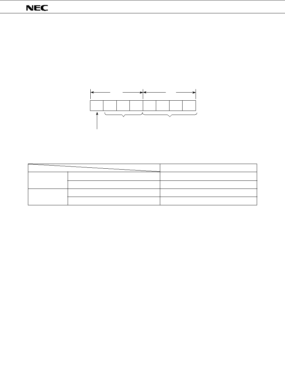
PROGRAM COUNTER (PC): 14 BITS
This is a 14-bit binary counter to hold the program memory address information.
Fig. 3-1 Program Counter Configuration
When RESET is input, the lower 6 bits at address 0000H and the contents at address 0001H of the program
memory are set to PC13 to PC8 and PC7 to PC0, respectively, and the PC is initialized.
3.2
PROGRAM MEMORY (ROM): 16256 WORDS
◊
8 BITS
This is a mask programmable ROM having a configuration of 16256 words
◊
8 bits to store programs, table
data, etc.
The program memory is addressed by the program counter. Table data can be referred to by the table
reference instruction (MOVT).
The branch range enabled by the branch and subroutine call instructions is shown in Fig. 3-2. The relative
branch instruction (BR $addr) enables branch to the [PC contents ≠15 to ≠1, +2 to +16] address irrespective of
the block boundary.
The program memory addresses are 0000H-3F7FH and the following addresses are especially assigned. (All
areas except 0000H and 0001H can be used as the normal program memory.)
∑ Addresses 0000 and 0001H
Vector address table for writing the program start address to be set upon RESET input and the RBE and
MBE set values. Can be reset and started at any address in a 16K space (0000H to 3F7FH).
∑ Addresses 0002 to 000FH
Vector address table for writing the program start address to be set by each vectored interrupt and the
RBE and MBE set values. Interrupt service can be started at any address in a 16K space (0000H to 3F7FH).
∑ Addresses 0020 to 007FH
Table area to be referred to by GETI instruction*.
*
GETI instruction is an instruction to realize any 2-byte/3-byte instruction or two 1-byte instructions with one
byte. It is used to decrease the number of program bytes. (Refer to 8.1 CHARACTERISTIC INSTRUCTIONS
OF
µ
PD75236.)
PC13
PC12
PC11
PC10
PC9
PC8
PC7
PC6
PC5
PC4
PC3
PC2
PC1
PC0

29
µ
PD75236
Fig. 3-2 Program Memory Map
Remarks
In all cases other than those listed above, branch to the address with only the lower 8 bits of the PC
changed is enabled by BR PCDE and BR PCXA instructions.
MBE RBE
MBE RBE
MBE RBE
MBE RBE
MBE RBE
MBE RBE
MBE RBE
MBE RBE
INTBT/INT4 Start Address
Internal Reset Start Address (Most Significant 6 Bits)
Internal Reset Start Address (Least Significant 8 Bits)
(Most Significant 6 Bits)
INTBT/INT4 Start Address
(Least Significant 8 Bits)
INT0 Start Address
(Most Significant 6 Bits)
INT0 Start Address
(Least Significant 8 Bits)
INTCSI0 Start Address
(Most Significant 6 Bits)
INTCSI0 Start Address
(Least Significant 8 Bits)
INTT0 Start Address
(Most Significant 6 Bits)
INTT0 Start Address
(Least Significant 8 Bits)
INTTPG Start Address
(Most Significant 6 Bits)
INTTPG Start Address
(Least Significant 8 Bits)
INTKS Start Address
(Most Significant 6 Bits)
INTKS Start Address
(Least Significant 8 Bits)
(Most Significant 6 Bits)
(Least Significant 8 Bits)
INT1 Start Address
INT1 Start Address
GETI Instruction Reference Table
0 0 0 2 H
0 0 0 4 H
0 0 0 6 H
0 0 0 8 H
0 0 0 A H
0 0 0 C H
0 0 0 E H
0 0 0 0 H
0 0 2 0 H
0 0 7 F H
0 0 8 0 H
0 7 F F H
0 8 0 0 H
0 F F F H
1 0 0 0 H
1 F F F H
2 0 0 0 H
2 F F F H
3 0 0 0 H
3 F 7 F H
CALLF
!faddr
Instruction
Entry Address
BRCB
!caddr
Instruction
Branch Address
BR !addr
Instruction
Branch Address
CALL !addr
Instruction
Branch Address
Branch/call
Address
by GETI
BR $addr1 Instruction
Relative Branch Address
(-15 to -1 and +2 to +16)
BRCB
!caddr Instruction
Branch Address
BRCB
!caddr Instruction
Branch Address
BRCB
!caddr Instruction
Branch Address

30
µ
PD75236
3.3
DATA MEMORY
The data memory consists of a static RAM and peripheral hardware.
The static RAM incorporates 512 words
◊
4 bits of memory banks 0 and 2, 160 words
◊
4 bits of memory
bank 1 and 96 words
◊
4 bits of memory bank 1 which also serves as a display data memory. It is used to store
process data and to serve as a stack memory for interrupt execution.
General registers, display data memory and various registers of peripheral hardware are mapped at particu-
lar addresses of the data memory and such data is manipulated by the general register and memory manipula-
tion instructions. (Refer to Fig. 2-1 Data Memory Configuration and Addressing Range in Each Addressing
Mode.)
All addresses (000H to 2FFH) of memory banks 0, 1 and 2 can be used as a stack area.
Although the data memory consists of one address and 4 bits, it can be manipulated in 8-bit units by the 8-
bit memory mainipulation instruction or in bit units by the bit manipulation instruction. Specify an even
address by the 8-bit manipulation instruction.
The display data memory area (1A0H to 1FFH) is made up as shown in Fig. 3-4.
Fig. 3-3 Data Memory Map
(32
◊
4)
256
◊
4
256
◊
4
(96
◊
4)
256
◊
4
128
◊
4
Data Memory
Memory Bank
0
1
2
15
Not Incorporated
F 8 0 H
F F F H
Peripheral Hardware Area
2 F F H
2 0 0 H
1 F F H
1 A 0 H
1 9 F H
1 0 0 H
0 F F H
0 2 0 H
0 0 0 H
General
Register
Area
Stack Area
Display
Data
Memory,
etc.
Data Area
Static RAM
(768
◊
4)
0 1 F H

31
µ
PD75236
Fig. 3-4 Display Data Memory Configuration
1 A 1 H
1 A 0 H
1 C 3 H
1 C 2 H
1 C 1 H
1 C 0 H
1 A 3 H
1 A 2 H
1 C 7 H
1 C 6 H
1 C 5 H
1 C 4 H
1 A 5 H
1 A 4 H
1 C B H
1 C A H
1 C 9 H
1 C 8 H
1 A 7 H
1 A 6 H
1 C F H
1 C E H
1 C D H
1 C C H
1 A 9 H
1 A 8 H
1 D 3 H
1 D 2 H
1 D 1 H
1 D 0 H
1 A B H
1 A A H
1 D 7 H
1 D 6 H
1 D 5 H
1 D 4 H
1 A D H
1 A C H
1 D B H
1 D A H
1 D 9 H
1 D 8 H
1 A F H
1 A E H
1 D F H
1 D E H
1 D D H
1 D C H
1 B 1 H
1 B 0 H
1 E 3 H
1 E 2 H
1 E 1 H
1 E 0 H
1 B 3 H
1 B 2 H
1 E 7 H
1 E 6 H
1 E 5 H
1 E 4 H
1 B 5 H
1 B 4 H
1 E B H
1 E A H
1 E 9 H
1 E 8 H
1 B 7 H
1 B 6 H
1 E F H
1 E E H
1 E D H
1 E C H
1 B 9 H
1 B 8 H
1 F 3 H
1 F 2 H
1 F 1 H
1 F 0 H
1 B B H
1 B A H
1 F 7 H
1 F 6 H
1 F 5 H
1 F 4 H
1 B D H
1 B C H
1 F B H
1 F A H
1 F 9 H
1 F 8 H
1 B F H
1BEH (KS2) IFFH (PORTH)
1FEH (KS1)
1 F D H
1FCH (KS0)
1 bit
4 bits
8 bits
No. of manipulatable bits
Remarks 1.
KS0, KS1 and KS2: Key scan register
2.
PORTH: High-voltage, high-current output port which also serves as digit output port

32
µ
PD75236
3.4
GENERAL REGISTER: 8
◊
4 BITS
◊
4 BANKS
The general registers are mapped at the special addresses of the data memory. There are 4-bank registers,
each bank consisting of eight 4-bit registers (B, C, D, E, H, L, X, A).
The register bank (RB) which becomes valid for instruction is given as
RB = RBE∑ RBS
(RBS = 0 to 3).
Each general register is operated in 4-bit units. BC, DE, HL and XA form register pairs and are used for 8-bit
manipulation. In addition to DE and HL, DL also makes up a pair and these three pairs can be used as a data
pointer.
The general register area can be accessed by address specification as a normal RAM whether or not it is
used as a register.
Fig. 3-5 General Register Configuraton
Fig. 3-6 Register Pair Configuration
A Register
X Register
L Register
H Register
E Register
D Register
C Register
B Register
0 0 0 H
0 0 1 H
0 0 2 H
0 0 3 H
0 0 4 H
0 0 5 H
0 0 6 H
0 0 7 H
Same
Configuration
as Bank 0
Same
Configuration
as Bank 0
Same
Configuration
as Bank 0
0 0 8 H
.........
0 0 F H
0 1 0 H
.........
0 1 7 H
0 1 8 H
.........
0 1 F H
3
Data Memory
0
Register Bank 0
Register Bank 1
Register Bank 2
Register Bank 3
3
0
3
0
3
0
3
0
3
0
3
0
3
0
3
0
B
D
H
X
C
E
L
A
1 Bank
Address
33
µ
PD75236
CY
Bit Accumulator
3.5
ACCUMULATOR
In the
µ
PD75236, A register and XA register pair function as an accumulator. The 4-bit data processing
instruction is executed mainly by A register and the 8-bit data processing instruction is executed mainly by XA
register pair.
For execution of the bit manipulation instruction, the carry flag (CY) functions as a bit accumulator.
Fig. 3-7 Accumulator
3.6
STACK POINTER (SP) AND STACK BANK SELECT REGISTER (SBS)
In the
µ
PD75236, the static RAM is used as a static memory (LIFO type) and the 8-bit register which holds
the start address information in the stack area is a stack pointer (SP).
The stack area is located at addresses 000H to 2FFH of memory banks 0, 1 and 2. Specify one memory bank
by a 2-bit SBS.
The SP is decremented prior to a write (save) to the stack memory and incremented after a read (restore)
from the stack memory. Set SBS by the 4-bit memory manipulation instruction. In this case, set the higher 2-
bits to 00.
The data to be saved/restored by each stack operation is shown in Figs. 3-9 and 3-10.
The SP initial value is set by the 8-bit memory manipulation instruction and the SBS initial value is set by
the 4-bit memory manipulation instruction and then the stack area is determined. The SP and SBS contents can
also be read.
Table 3-1 Stack Areas to be Selected by SBS
When the SP initial value is set to 00H, stack starts with the most significant address (nFFH) of the memory
bank (n: n = 0, 1, 2) specified by SBS.
The stack area is limited to the memory bank specified by SBS. When stack operation is further carried out
at address n00H, the address is reset to nFFH in the same bank. Linear stack past the memory bank boundary is
not possible without rewriting SBS.
Since RESET input makes the SP and SBS undefined, be sure to initialize the SP and SBS to any desired
value at the beginning of the program.
SBS
SBS1
SBS0
0
0
Memory bank 0
0
1
Memory bank 1
1
0
Memory bank 2
1
1
Setting disabled
Stack Area
-------------------------------
A
4-Bit Accumulator
X
A
8-Bit Accumulator

34
µ
PD75236
Fig. 3-8 Stack Bank Select Register Configuration
SP
SP
SP
SP7
SP6
SP5
SP4
SP3
SP2
SP1
SBS1
SBS0
F80H
F84H
SBS
000H
0FFH
100H
200H
2FFH
1FFH
SP
SBS
Memory Bank 0
Memory Bank 1
Memory Bank 2
Symbol
Address
Fixed to 0

35
µ
PD75236
Fig. 3-9 Data to be Saved into Stack Memory
Fig. 3-10 Data to be Restored from Stack Memory
*
PSW except MBE and RBE are not saved/restored.
Remarks
means undefined.
PSW
Stack
Lower Half of
Register Pair
Upper Half of
Register Pair
SP - 2
SP - 1
SP
SP - 6
SP - 5
Stack
PC11-PC8
0
0
PC13PC12
PC3-PC0
PC7-PC4
MBE RBE
SP - 4
SP - 3
SP - 2
SP - 1
SP
Stack
PC11-PC8
0
0
PC13PC12
PC3-PC0
PC7-PC4
IST1 IST0 MBE RBE
CY
SK2 SK1 SK0
PSW
Lower Half of
Register Pair
Upper Half of
Register Pair
Stack
SP
SP + 1
Stack
PC11-PC8
0
0
PC13PC12
PC3-PC0
PC7-PC4
MBE RBE
SP + 2
SP + 3
SP + 4
SP + 5
SP + 6
Stack
PC11-PC8
0
0
PC13PC12
PC3-PC0
PC7-PC4
IST1 IST0 MBE RBE
CY
SK2 SK1 SK0
SP
SP + 1
SP + 2
SP + 3
SP + 4
SP + 5
SP + 6
SP - 6
SP - 5
SP - 4
SP - 3
SP - 2
SP - 1
SP
PUSH Instruction
CALL, CALLA and CALLF
Instructions
Interrupt
POP Instruction
RET and RETS Instruction
RETI Instruction
*
*
SP
SP + 1
SP + 2
36
µ
PD75236
3.7
PROGRAM STATUS WORD (PSW): 8 BITS
The program status word (PSW) consists of various types of flags closely related to processor operation.
The PSW is mapped at addresses FB0H and FB1H in the data memory space and 4 bits at address FB0H can
be operated by the memory manipulation instruction. Normal data memory manipulation instructions cannot
be used at address FB1H.
Fig. 3-11 Program Status Word Configuration
Table 3-2 PSW Flag to be Saved/Restored in Stack Operation
CY
SK2
SK1
SK0
IST1
IST0
MBE
RBE
FB1H
FB0H
Address
Symbol
PSW
Manipulatable
Manipulatable by a
Dedicated Instruction
Flag to be Saved/Restored
During CALL/CALLF instruction execution
MBE and RBE saved
Upon hardware interruption
All PSW bits saved
During RET/RETS instruction execution
MBE and RBE restored
During RETI instruction execution
All PSW bits restored
Save
Restore
Non-Manipulatable

37
µ
PD75236
(1)
Carry flag (CY)
The carry flag is a 1-bit flag to store the overflow and underflow generate information when a carry
operation instruction (ADDC, SUBC) is executed.
It has the bit accumulator function to execute Boolean algebraic operations with the data memory
specified by the bit address and to store the result.
Carry flag manipulation is carried out using a dedicated instruction irrespective of other PSW bits.
When RESET signal is generated, the carry flag becomes undefined.
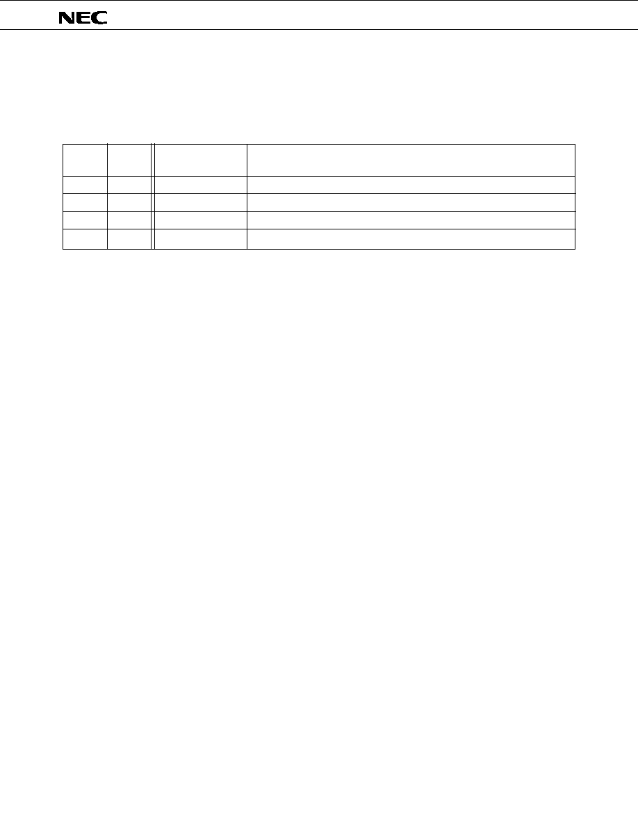
Table 3-3 Carry Flag Manipulation Instructions
Remarks
mem*.bit indicates the following three bit manipulated addressing operations.
∑ fmem.bit
∑ pmem.@L
∑ @H + mem.bit
(2)
Skip flags (SK2, SK1, SK0)
The skip flag is used to store the skipped state and is automatically set/reset when the CPU executes an
instruction.
The user cannot directly operate the skip flags as operands.
Instruction (Mnemonic)
Carry Flag Operation and Processing
SET1
CY
CLR1
CY
NOT1 CY
SKT
CY
MOV1
mem* .bit CY
MOV1 CY, mem* .bit
AND1 CY, mem* .bit
OR1 CY,
mem* .bit
XOR1 CY, mem* .bit
During interrupt execution
RETI
CY set (1)
CY clear (0)
CY contents invert
SKip if CY contents are 1
CY contents transfer to the specified bit
Specified bit contents transfer to CY
Specified bit contents ANDed/ORed/XORed with CY contents and
the results set to CY
Parallel save of other PSW bits and 8 bits to the stack memory
Restore from the stack memory in parallel to other PSW bits
---------------------------------------------------------------------------------------------------------------------------------------------------
Carry flag manipu-
lation dedicated
instruction
Bit transfer
instruction
Bit Boolean
instruction
Interrupt service
38
µ
PD75236
(3)
Interrupt status flags (IST1, IST0)
The interrupt status flag is a 2-bit flag to store the status of the processing currently being executed.
(Refer to Table 5-3 IST1 and IST0 Interrupt Servicing Status for details.)
Table 3-4 Interrupt Status Flag Directive Contents
The interrupt priority control circuit (see Fig. 5-1 Interrupt Control Circuit Block Diagram) identifies the
interrupt status flag contents and executes multiple interrupt control.
If the interrupt is acknowledged, the IST1 and IST0 contents are saved to the stack memory as part of
PSW and are automatically changed to the status higher by one level and the values prior to interruption
by RETI instruction are restored.
The interrupt status flag can be operated by the memory manipulation instruction and the processing
status being executed can be changed by program control.
Note
Before operating this flag, be sure to disable interruption by executing DI instruction and enable
interruption by execution EI instruction after operation.
IST 1
IST0
0
0
0
1
1
0
1
1
Servicing Contents and Interrupt Control
Normal program being executed. All interrupts acknowledgeable.
Low or high interrupt being executed. Only high interrupt acknowledgeable.
High interrupt being executed. All interrupts non-acknowledgeable.
Setting disable
Status of Processing
being Executed
Status 0
Status 1
Status 2
--

39
µ
PD75236
(4)
Memory bank enable flag (MBE)
This is a 1-bit flag to specify the mode to generate the address information of the most significant 4
bits of the 12 bits of the data memory address.
When this flag is set (1), the data memory address space is expanded and all data memory spaces
become addressible.
When this flag is reset (0), the data memory address space is fixed irrespectively of MBS setting. (See
Fig. 2-1 Data Memory Configuration and Addressing Range in Each Addressing Mode.)
When RESET input is applied, the bit 7 contents at address 0 of the program memory are set and the
MBE is automatically initialized.
In vectored interrupt service, the bit 7 contents of the corresponding vector address table are set and
the MBE status in the interrupt service is automatically set.
Normally, set MBE = 0 for interrupt service and use the static RAM of memory bank 0.
(5)
Register bank enable flag (RBE)
This is a 1-bit flag to determine whether or not the general register bank configuration should be
expanded.
When this flag is set (1), one general register can be selected from register banks 0 to 3 depending on
the register bank select register (RBS) contents.
When this flag is reset (0), register bank 0 is selected as a general register irrespective of the register
bank select register (RBS) contents.
Upon RESET input, the bit 6 contents at address 0 of the program memory are set and the flag is
automatically initialized.
When a vectored interrupt is generated, the bit 6 contents of the corresponding vector address table
are set and the RBE status in interrupt service is automatically set. Normally, set RBE = 0 for interrupt
service. Use register bank 0 for 4-bit operation and register banks 0 and 1 for 8-bit operation.

40
µ
PD75236
3.8
BANK SELECT REGISTER (BS)
The bank select register (BS) consists of a register bank select register (RBS) and a memory bank select
register (MBS). The RBS and MBS are used to specify the register bank and the memory bank to be used,
respectively.
The RBS and MBS are set by SEL RBn and SEL MBn instructions, respectively.
The BS can be saved/restored the stack area in 8-bit units by PUSH BS/POP BS instruction.
Fig. 3-12 Bank Select Register Configuration
(1)
Memory bank select register (MBS)
The memory bank select register in a 4-bit register to store the most significant 4-bit address informa-
tion of the data memory address (12 bits) and the memory bank to be accessed is specified by the MBS
contents. Banks 0, 1, 2 and 15 can be specified.
The MBS is set by SEL MBn instruction. (n = 0, 1, 2, 15)
The address range for MBE and MBS setting is shown in Fig. 2-1.
Upon RESET input, the MBS is initialized to "0".
(2)
Register bank select register (RBS)
The register bank select register is used to specify the register bank for use as a general register and
can set banks 0 to 3.
The RBS is set by SEL RBn instruction. (n = 0 to 3)
Upon RESET input, the RBS is initialized to "0".
Table 3-5 RBE, RBS and Register Banks to be Selected
Remarks
◊
:
Don't care
MBS3 MBS2
MBS1 MBS0
0
0
RBS1
RBS0
MBS
RBS
Address
Symbol
BS
F82H
3
2
1
0
0
0
0
◊
◊
Fixed to bank 0
0
0
Bank 0 selected
0
1
Bank 1 selected
1
0
Bank 2 selected
1
1
Bank 3 selected
RBS
Register Bank
RBE
1
0
0
Fixed to 0

41
µ
PD75236
4.
PERIPHERAL HARDWARE FUNCTIONS
4.1
DIGITAL INPUT/OUTPUT PORTS
The
µ
PD75236 employs the memory mapped I/O and all input/output ports are mapped in the data memory
space.
Fig. 4-1 Digital Port Data Memory Address
P03
P13
P23
P33
P43
P53
P63
P73
P83
P93
P103
P113
P123
P133
P143
P153
P02
P12
P22
P32
P42
P52
P62
P72
P82
P92
P102
P112
P122
P132
P142
P152
P00
P10
P20
P30
P40
P50
P60
P70
P80
P90
P100
P110
P120
P130
P140
P150
PORT0
PORT1
PORT2
PORT3
PORT4
PORT5
PORT6
PORT7
PORT8
PORT9
PORT10
PORT11
PORT12
PORT13
PORT14
PORT15
Symbol
FF0H
FF1H
FF2H
FF3H
FF4H
FF5H
FF6H
FF7H
FF8H
FF9H
FFAH
FFBH
FFCH
FFDH
FFEH
FFFH
Address
3
2
1
0
P01
P11
P21
P31
P41
P51
P61
P71
P81
P91
P101
P111
P121
P131
P141
P151

42
µ
PD75236
(1)
Digital input/output port configuration
The digital input/output port configurations are shown in Figs. 4-2 to 4-11.
(2)
Input/output mode setting
The input/output mode of each input/output port is set by the port mode register as shown in Fig. 4-12.
Each port acts as an input when the corresponding port mode register bit is "0" and as an output port
when the bit is "1".
Port mode register groups A and B each are set by the 8-bit memory manipulation instruction.
Upon RESET input, all bits of each port mode register are cleared to "0". Thus, the output buffer is
turned OFF and all the ports are set to the input mode.
(3) Digital input/output port operation
The operations of the port and pin for instruction execution vary, depending on the input/output mode
setting as shown in Table 4-1.
Table 4-1 Input/Output Port Operations for Input/Output Instruction Execution
Input Mode (Corresponding
Bit 0 of Mode Register)
[Output Buffer OFF]
Output Mode (Corresponding
Bit 1 of Mode Register)
[Output Buffer ON]
When 1-bit test instruction,
1-bit input instruction, 4-bit or 8-
bit instruction is executed
When 4-bit or 8-bit output
instruction is executed
When 1-bit output instruction* is
executed
Each pin data input
Accumulator data transfer to
output latch
Output latch contents become
undefined
Output latch contents input
Accumulator data output to
output pin
Output pin status change
according to instruction
*
SET1/CLR1/MOV1 PORTn.bit, CY, etc.
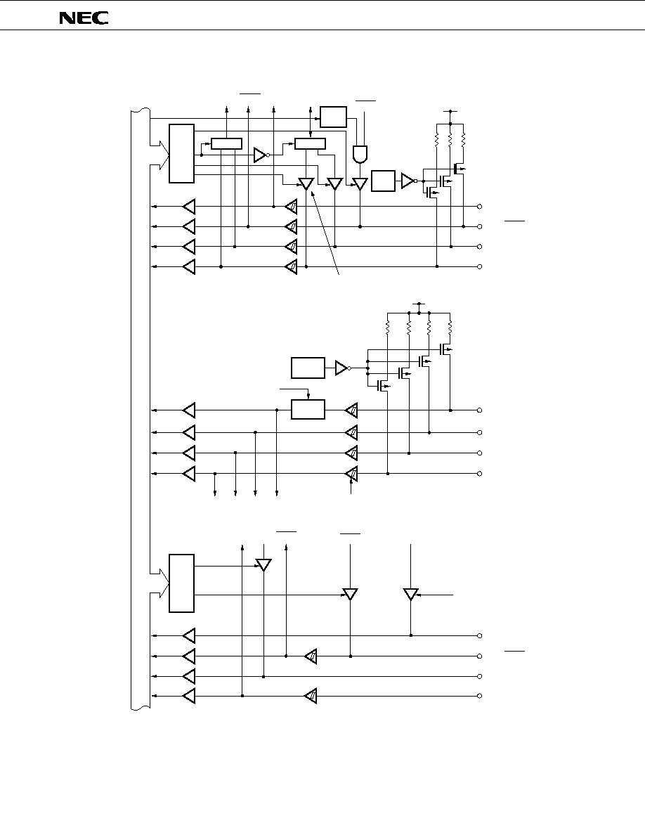
43
µ
PD75236
8
8
CSIM0
CSIM1
SI0 SCK0 INT4
SCK0
SO0
V
DD
P-ch
P00/INT4
P02/SO0/SB0
P03/SI0/SB1
P01/ SCK0
V
DD
P-ch
P10/INT0
P12/INT2
P13/TI0
TI0 INT2INT1 INT0
SI1 SO1 SCK1
SCK1
PPO
P80/PPO
P82/SO1
P83/SI1
P11/INT1
P81/ SCK1
Fig. 4-2 Port 0, 1 and 8 Configurations
Input Buffer
Pull-Up
Resistor
Input Buffer
or f
X
/
64
Bit 1
of
POGA
Internal Bus
Input buffer having
hysteresis characteristics
Internal
Input Buffer
Bit 0
of
POGA
Pull-Up
Resistor
Output buffer capable of
switching between push-
pull output and N-ch open
drain output
Noise
Eliminator
Selector
Selector
P01
Output
Latch
Internal
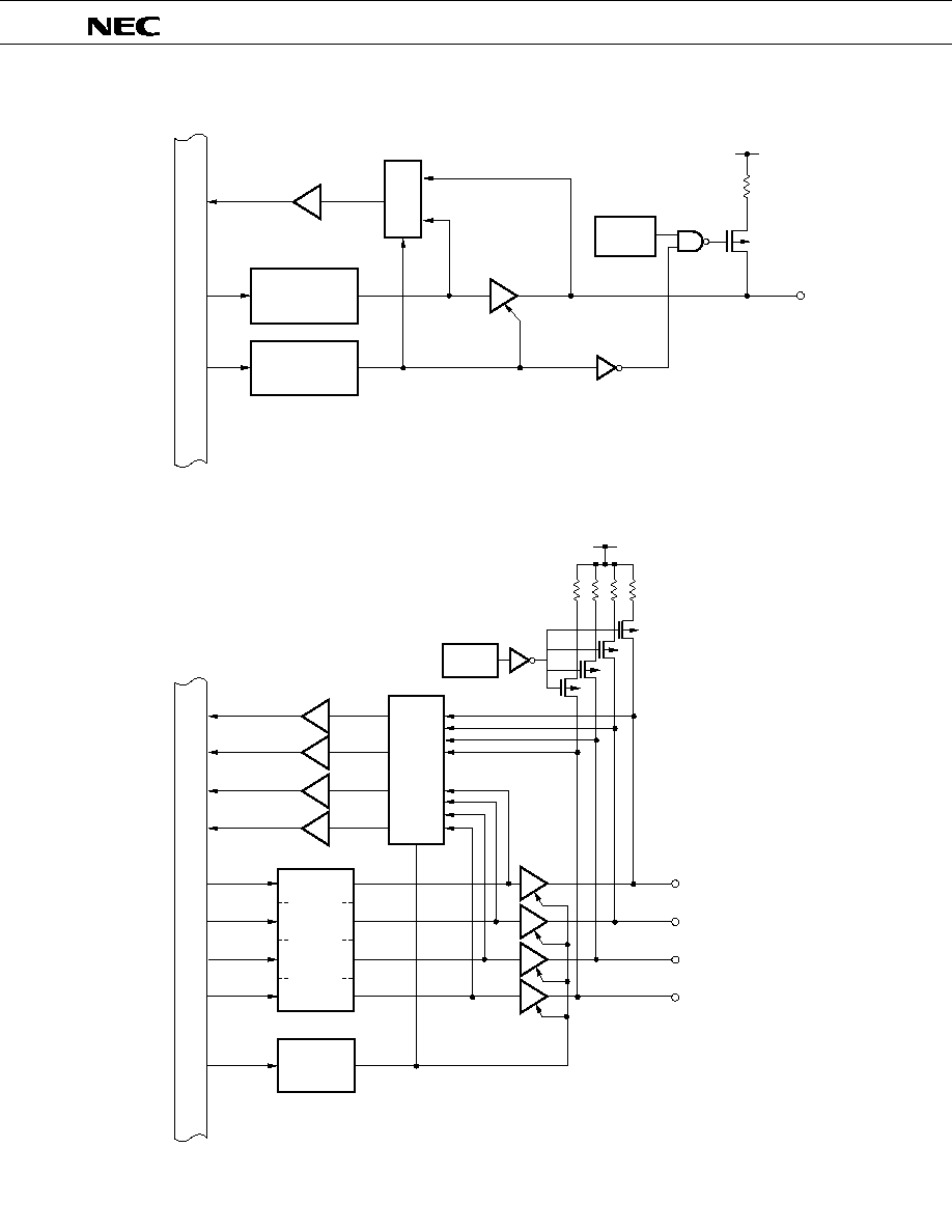
44
µ
PD75236
V
DD
P-ch
PMm=0
PMm=1
M
P
X
PMm
Pm0
Pm1
Pm2
Pm3
M
P
X
PMm n=0
PMm n=1
PMm n
Pm n
V
DD
P-ch
Fig. 4-3 Port 3n and Port 6n Configurations (n = 0 to 3)
Inter Buffer
Output Latch
Internal Bus
Corresponding Bit
of Port Mode
Register Group A
m = 3, 6
n = 0 to 3
(
)
Output Buffer
Bit m
of POGA
Pull-Up
Resistor
Fig. 4-4 Port 2 Configuration
Internal Bus
Input Buffer
Bit m
of POGA
Output
Latch
Corresponding Bit of
Port Mode Register
Group B (m = 2)
Output
Buffer
Pull-Up
Resistor

45
µ
PD75236
Fig. 4-5 Configurations of Ports 4 and 5
PMm=0
PMm=1
Pm0
Pm1
Pm2
Pm3
V
DD
PMm
M
P
X
Internal Bus
Corresponding Bit of Port
Mode Register Group B
(m = 4, 5)
N-ch Open Drain
Output Buffer
Output
Latch
Pull-Up
Resistor
Mask Option
Input Buffer

46
µ
PD75236
Fig. 4-6 Port 7 Configuration
M
P
X
PMm=0
PMm=1
Pm0
Pm1
Pm2
Pm3
PMm
Internal Bus
Output
Latch
Corresponding Bit of Port
Mode Register Group B
(m = 7)
Pull-Down
Resistor
Mask Option
Output Buffer
Input Buffer
Fig. 4-7 Port 9 Configuration
P90/AN4
P91/AN5
P92/AN6
P93/AN7
Internal Bus
Input Instruction
To A/D Converter
Input Buffer
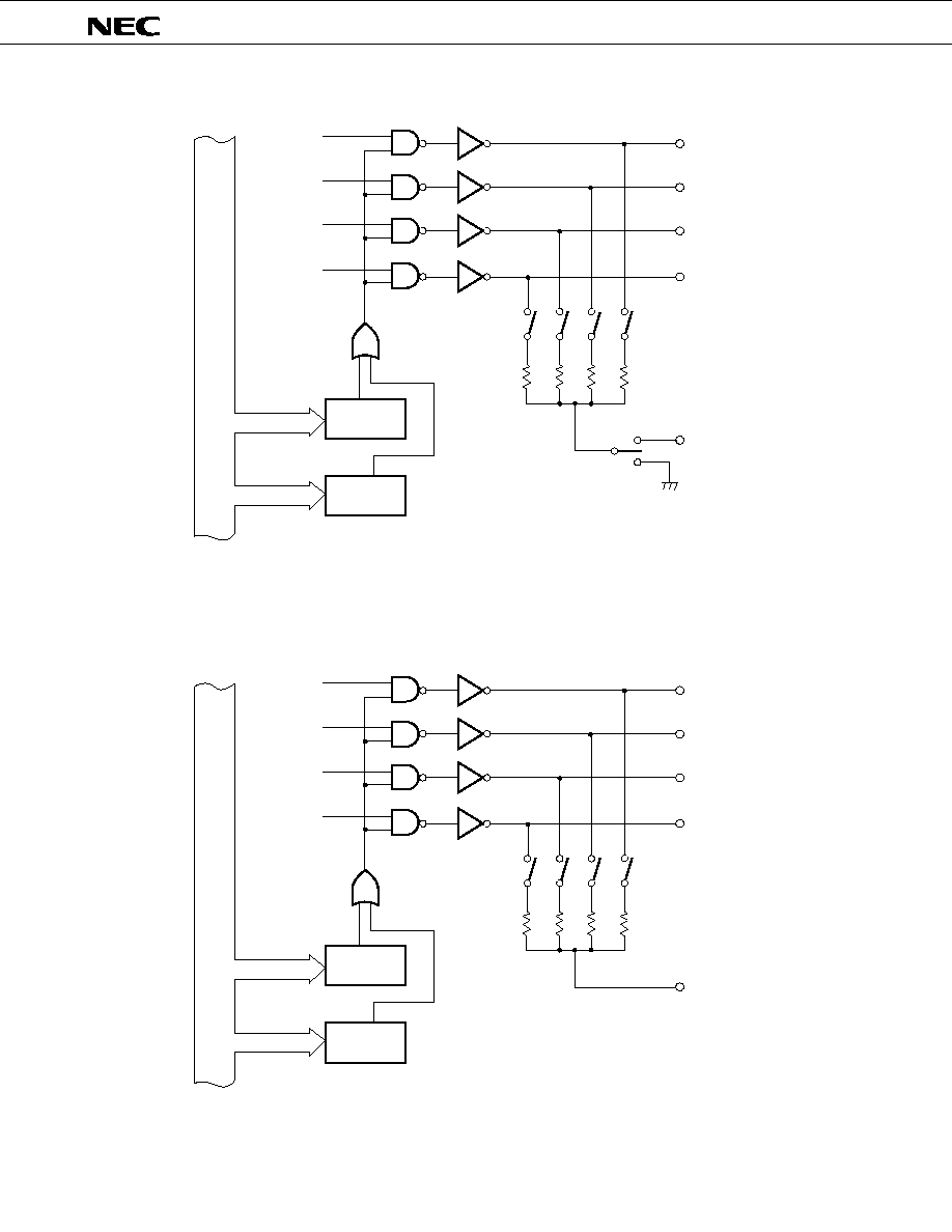
47
µ
PD75236
S
K
S
K+1
S
K+2
S
K+3
S
K
/Pm0
S
K+1
/Pm1
S
K+2
/Pm2
S
K+3
/Pm3
V
LOAD
STATB
DSPM
4
8
Fig. 4-8 Configurations of Ports 10 and 11
Remarks
1.
Port 10: K = 16, m = 10
2.
Port 11: K = 20, m = 11
Remarks
1.
Port 12: K = 0, m = 12
2.
Port 13: K = 4, m = 13
Fig. 4-9 Configurations of Ports 12 and 13
S
K
S
K
/Pm0
S
K+1
S
K+2
S
K+3
S
K+1
/Pm1
S
K+2
/Pm2
S
K+3
/Pm3
V
LOAD
STATA
DSPM
4
8
Internal Bus
Internal Bus
P-ch Open Drain
Output Buffer
Pull-Down
Resistor
Mask Option
(Simultaneously specified
for S16 to S23)
P-ch Open Drain
Output Buffer
Pull-Down
Resistor
Mask Option
Mask Option

48
µ
PD75236
M
P
X
V
LOAD
DIGS
STATA
DSPM.3
4
8
4
PH0PH2
PH1PH3
S15
S14
S13
S12
T13T11
T12T10
S13/T12/P151/PH1
S14/T11/P152/PH2
S15/T10/P153/PH3
S12/T13/P150/PH0
Fig. 4-10 Port 14 Configuration
S8
S9
S10
S11
M
P
X
4
8
4
DSPM.3
STATA
DIGS
V
LOAD
S8/P140
S9/P141
S10/T15/P142
S11/T14/P143
S15 S14
Internal Bus
Output
Buffer
P-ch Open Drain
Output Buffer
Pull-Down
Resistor
Mask Option
(for Each Pin)
*
*
*
Selector
Fig. 4-11 Configurations of Ports 15 and H
*
*
*
*
*
*
*
*
Output
Buffer
Internal Bus
*
Selector
P-ch Open Drain
Output Buffer
Pull-Down
Resistor
Mask Option
(for Each Pin)

49
µ
PD75236
Fig. 4-12 Port Mode Register Format
Port mode register group A
PM63
PM62
PM61
PM60
PM33
PM32
PM31
PM30
7
6
5
4
3
2
1
0
Address
FE8H
Symbol
PMGA
P3n and P6n Pin Input/Output
Specification (n = 0 to 3)
PM3n, PM6n
0
1
Input mode (output buffer OFF)
Output mode (output buffer ON)
Remarks
≠≠≠≠ : 0 or 1
(4)
Pull-up resistor register group A (POGA)
Pull-up resistor register group A is intended to specify pull-up resistors to be built in ports 0 to 3 and
port 6 (except P00). Fig. 4-13 shows the format.
Set "1" when a pull-up resistor is incorporated or "0" when it is not incorporated.
Note
Mask option by which pull-up resistors at ports 4 and 5 and pull-down resistors at port 7 and ports 10
to 15 can be incorporated bit-wise.
Fig. 4-13 Pull-Up Resistor Register Group A Format
PO6
PO3
PO2
PO1
PO0
7
6
5
4
3
2
1
0
Address
FDCH
Symbol
POGA
Port 0 (P01 to P03)
Port 1 (P10 to P13)
Port 2 (P20 to P23)
Port 3 (P30 to P33)
Port 6 (P60 to P63)
Symbol
PMGA
Remarks
≠≠≠≠ : 0 or 1
PM7
PM5
PM4
PM2
7
6
5
4
3
2
1
0
Address
FECH
Symbol
PMGB
Port n Input/Output Specification
(n = 2, 4, 5, 7)
PMn
0
1
Input mode (output buffer OFF)
Output mode (output buffer ON)
Symbol
PMGB
Port mode register group B
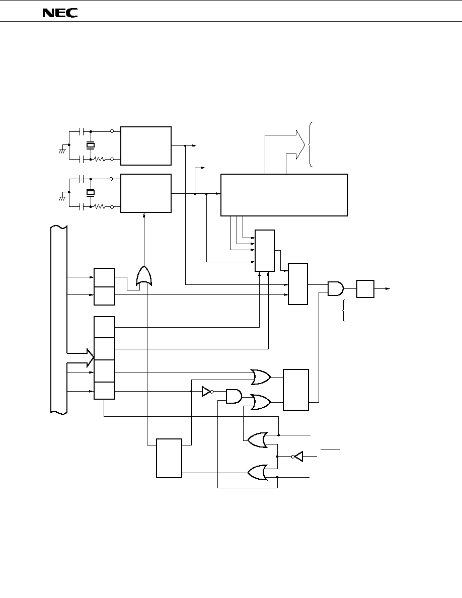
50
µ
PD75236
XT1
XT2
X1
X2
f
XT
f
X
SCC
PCC
HALT
STOP
HALT F/F
STOP F/F
4
Q
S
R
S
R
1/
4
1/ 1/ 1/
1/8~1/4096
2 4 16
SCC3
SCC0
PCC0
PCC1
PCC2
PCC3
Q
4.2
CLOCK GENERATOR
(1)
Clock generator configuration
The clock generator is a circuit to generate clocks to be supplied to the CPU and the peripheral hard-
ware. Its configuration is shown in Fig. 4-14.
Fig. 4-14 Clock Generator Block Diagram
∑ FIP Controller/Driver
∑ Basic Interval Timer
∑ Timer/Event Counter
∑ Serial Interface
∑ Watch Timer
∑ Clock Output Circuit
∑ INT0 Noise Eliminator
Frequency Divider
Timer/Pulse
Generator
Watch Timer
Subsystem
Clock
Generator
Mainsystem
Clock
Generator
∑ CPU
∑ INT0 Noise Eliminator
∑ Clock Output Circuit
Selector
Selector
*
Instruction execution
Remarks
1.
f
X
= Main system clock frequency
2.
f
XT
= Subsystem clock frequency
3.
= CPU clock
4.
PCC: Processor clock control register
5.
SCC: System clock control register
6.
1 clock cycle (t
CY
) of
is 1 machine cycle of an instruction. For t
CY
, see "AC Characteristics" in
11. ELECTRICAL SPECIFICATIONS.
PCC2 and PCC3
Clear
Oscilla-
tion
Stop
Frequency
Divider
Wait Release
Signal from BT
Standby Release Signal from
Interrupt control Circuit
RESET Signal
Internal Bus
*
*
5

51
µ
PD75236
(2)
Clock generator functions
The clock generator generates the following clocks and controls the CPU operating modes including the
standby mode.
∑ Main system clock : f
X
∑ Subsystem clock : f
XT
∑ CUP CLOCK :
∑ Clocks for peripheral hardware
The following clock generator operations are determined by the processor clock control register (PCC)
and the system clock control register (SCC):
(a)
Upon RESET input, the lowest speed mode (15.3
µ
s : at 4.19 MHz operation) of the main system
clock is selected. (PCC = 0, SCC = 0)
(b) One of the four-level CPU clocks can be selected by setting the PCC with the main system clock
selected. (0.95
µ
s, 1.91
µ
s, 3.82
µ
s, 15.3
µ
s : at 4.19 MHz operation)
(c)
Two standby modes, the STOP and HALT modes, are available with the main system clock se-
lected.
(d) The clock generator can be operated at an ultra-low speed and with low-level power consumption
(122
µ
s : at 32.768 KHz operation) by selecting the subsystem clock with SCC.
(e)
Main system clock oscilloation can be stopped by SCC with the subsystem clock selected. The
HALT mode can also be used but the STOP mode cannot be used. (Subsystem clock oscillation
cannot be stopped.)
(f)
Divided system clocks are supplied to the peripheral hardware. Subsystem clocks can be directly
supplied to the watch timer to that the timer function can be continued.
(g) When the subsystem clock is selected, the watch timer can operate normally. However, other
hardware cannot be used if the main system clock is stopped.

52
µ
PD75236
(3)
Processor clock control register (PCC)
The PCC is a 4-bit register to select the CPU clock
with the lower 2 bits and to control the CPU
operating mode with the higher 2 bits. (See Fig. 4-15.)
When bit 3 or 2 is set (1), the standby mode is set. If the standby mode is released by the standby
release signal, both bits are automatically cleared and the normal operating mode is set. (For details, refer
to 6. STANDBY FUNCTIONS.)
The lower 2 bits of the PCC are set by the 4-bit memory manipulation instruction (with the higher 2 bits
set to "0").
Bits 3 and 2 are reset "1" by the STOP and HALT instructions, respectively.
The STOP and HALT instructions can always be executed irrespective of the MBE contents.
The CPU clock selection is possible only when operated on the main system clock. When operated on
the subsystem clock, the lower 2 bits of PCC are invalidated and f
XT
/4 is set. The STOP instruction is also
enabled only when in operation with the main system clock.
RESET input clears PCC to "0".

53
µ
PD75236
0
0
1
1
0
0
1
1
Fig. 4-15 Processor Clock Control Register Format
Note
When using a value of f
X
such that 4.19 MHz < f
X
5 MHz, if the maximum speed mode:
= f
X
/4 (PCC1,
PCC0 = 11) is set as the CPU clock frequency, 1 machine cycle becomes less than 0.95
µ
s, with the
result that the specified MIN value of 0.95 cannot be observed.
Therefore, in this case, PCC1, PCC0 = 11 cannot be set. Use PCC1, PCC0 = 10 or 01 or 00. As a result,
the combination f
X
= 4.19 MHz, PCC = 11 is the selected maximum CPU clock speed (1 machine cycle =
0.95
µ
s). (See 11. ELECTRICAL SPECIFICATIONS "AC Characteristics".)
FB3H
PCC3
PCC2
PCC1
PCC0
PCC
3
2
1
0
SCC = 1
Values in parenthesis are when f
XT
= 32.768 kHz
SCC = 0
Values in parenthesis are when f
x
= 4.19 MHz
CPU Clock
Frequency
1 Machine Cycle
CPU Clock
Frequency
1 Machine Cycle
= f
X
/64
(65.5 kHz)
= f
X
/16
(262 kHz)
= f
X
/8
(524 kHz)
= f
X
/4
(1.05 MHz)
= f
XT
/4
(8.192 kHz)
15.3
µ
s
3.81
µ
s
1.91
µ
s
0.95
µ
s
0
1
0
1
Setting prohibited
= f
XT
/4
(8.192 kHz)
122
µ
s
122
µ
s
SCC = 1
Values in parenthesis are when f
XT
= 32.768 kHz
CPU Clock
Frequency
1 Machine Cycle
CPU Clock
Frequency
1 Machine Cycle
= f
X
/64
(76.7 kHz)
= f
X
/16
(307 kHz)
= f
X
/8
(614 kHz)
= f
XT
/4
(8.192 kHz)
13
µ
s
3.26
µ
s
1.63
µ
s
0
1
0
1
Setting prohibited
122
µ
s
When 4.19 MHz < f
X
5.0 MHz
= f
XT
/4
(8.192 kHz)
122
µ
s
Setting prohibited
Setting prohibited
CPU Clock Select Bit
when f
x
4.19 MHz
f
X
: Main system clock oscillator output frequency
f
XT
: Subsystem clock oscillator output frequency
0
0
1
1
0
1
0
1
Normal operating mode
HALT mode
STOP mode
Setting prohibited
Address
Symbol
SCC = 0
Values in parenthesis are when f
x
= 4.19 MHz
5
5
CPU Operating Mode Control Bit
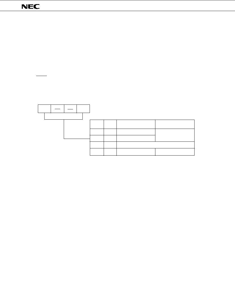
54
µ
PD75236
(4)
System clock control register (SCC)
The SCC is a 4-bit register to select the CPU clock
with the least significant bit and to control main
system clock oscillation stop with the most significant bit (refer to Fig. 4-16 System Clock Control Register
Format).
Although SCC.0 and SCC.3 are located at the same data memory address, both bits cannot be changed
simultaneously. Thus, SCC.0 and SCC.3 are set by the bit manipulation instruction. SCC.0 and SCC.3 can
always be bit manipulated irrespective of the MBE contents.
Main system clock oscillation can be stopped by setting SCC.3 only when in operation with the sub-
system clock. Oscillation when in operation with the main system clock is stopped by the STOP instruc-
tion.
RESET input clears SCC to "0".
Fig. 4-16 System Clock Control Register Format
FB7H
SCC3
SCC0
SCC
3
2
1
0
Address
Symbol
0
0
1
1
Main system clock
Subsystem clock
Subsystem clock
Oscillation enabled
Oscillation stop
System Clock
Selection
Main System Clock
Oscillation
Setting prohibited
SCC3
SCC0
Note
1. A maximum of 1/f
XT
is required to change the system clock. Thus, when stopping the main system
clock oscillation, change the clock to the subsystem clock and set SCC.3 following the passage of
more than the machine cycles described in Table 4-2.
2. The normal STOP mode cannot be set if oscillation is stopped by setting SCC.3 while in operation
with the main system clock.
3. If SCC.3 is set to "1", X1 input is internally short-circuited to V
SS
(GND potential) to suppress
crystal oscillator leakage. Thus, when using an external clock for the main system clock do not set
SCC.3 to "1".
4. When PCC = 0001B (
= f
X
/16 selected), do not set SCC.0 to "1". When switching from the main
system clock to the subsystem clock, do so after setting PCC to another value (PCC
0001B).
Do not set PCC = 0001B while in operation with the subsystem clock.
0
1
0
1

55
µ
PD75236
Note
When using a main system clock and subsystem clock oscillator, wire the crosshatched section in
Figs. 4-17 and 4-18 as follows to prevent any effect of the wiring capacity.
∑ Make the wiring as short as possible.
∑ Do not allow wiring to intersect with other signal conductors. Do not allow wiring to be near a line
through which varying high current flows.
∑ Set the oscillator capacitor grounding point to the same potential as that of V
SS
. Do not ground to a
ground pattern through which high current flows.
∑ Do not fetch signals from the oscillator.
The subsystem clock oscillator has a low amplification factor to maintain low current consumption
and is more likely to malfunciton due to noise than the main system clock oscillator. Thus, take extra
care when using a subsystem clock.
(5)
System clock oscillator
The main system clock oscillator oscillates with a crystal resonator (with a standard frequency of 4.19
MHz) or a ceramic resonator connected to the X1 and X2 pins.
External clocks can be input to this oscillator.
Fig. 4-17 External Circuit of Main System Clock Oscillator
(a) Crystal/ceramic Oscillation
(b) External clock
X1
X2
X1
X2
External
Clock
Crystal or
Ceramic
Resonator
µ
PD75236
µ
PD75236
Note
The STOP mode cannot be set while an external clock is input because the X1 pin is short-circuited to
V
SS
in the STOP mode.
The subsystem clock oscillator oscillates with a crystal resonator (with a standard frequency of 32.768
kHz) connected to the XT1 and XT2 pins.
External clocks can be input to this oscillator.
Fig. 4-18 External Circuit of Subsystem Clock Oscillator
(a) Crystal oscillation
(b) External clock
External
Clock
XT1
XT2
XT1
XT2
32.768 kHz
µ
PD75236
µ
PD75236
Leave open
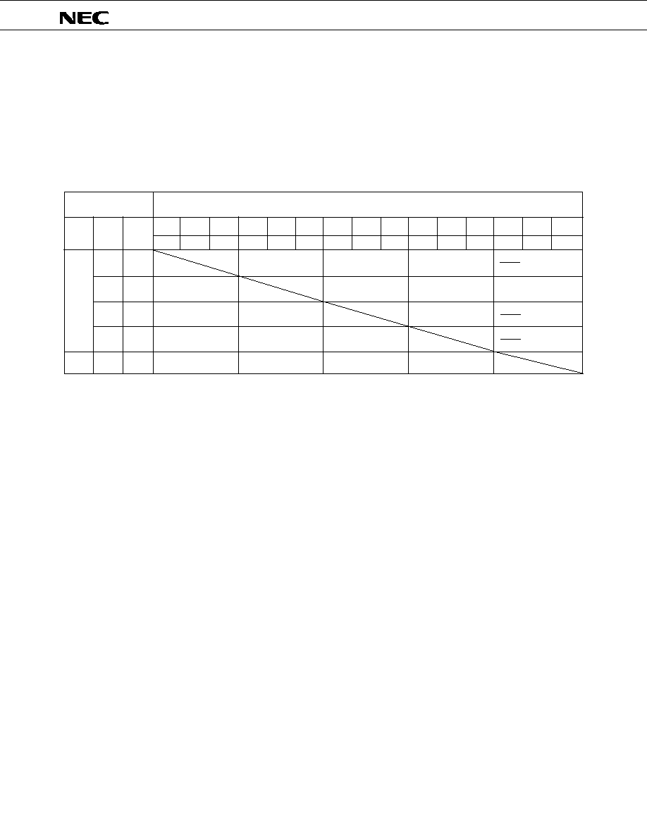
56
µ
PD75236
(6)
Time required for system clock and CPU clock switching
The system clock and the CPU clock can be switched to each other with the least significant bit of the
SCC and the lower 2 bits of the PCC. This switching is not executed just after register rewrite and opera-
tion continues with the previous clock during the specified machine cycle. Thus, to stop main system
clock oscillation, it is necessary to execute the STOP instruction or to set SCC.3 after the specified switch-
ing time.
Table 4-2 Maximum Time Required for System Clock and CPU Clock Switching
SCC
0
PCC
1
PCC
0
SCC0
0
PCC1
0
PCC0
0
0
0
1
1
◊
0
1
0
1
◊
4 machine cycle
8 machine cycle
16 machine cycle
1 machine cycle
SCC0
0
PCC1
0
PCC0
1
1 machine cycle
8 machine cycle
16 machine cycle
Setting prohibited
SCC0
0
PCC1
1
PCC0
0
1 machine cycle
4 machine cycle
16 machine cycle
1 machine cycle
1 machine cycle
4 machine cycle
8 machine cycle
1 machine cycle
SCC0
0
PCC1
1
PCC0
1
SCC0
1
PCC1
◊
PCC0
◊
Set Value before
Switching
Set Value after Switching
f
X
64f
XT
f
X
8f
XT
f
X
4f
XT
Setting prohibited
0
1
Remarks
CPU clock
is a clock to be supplied to the internal CPU of
µ
PD75236 and its inverse number is the
minimum instruction time (defined as "one machine cycle" in this manual).
Note
When PCC = 0001B (
= f
X
/16 selected), do not set SCC.0 to "1". When switching from the main
system clock to the subsystem clock, do so after setting PCC to another value (PCC
0001B).
Do not set PCC = 0001B while in operation with the subsystem clock.
machine cycle
machine cycle
machine cycle
57
µ
PD75236
f
X
f
X
f
XT
f
X
f
X
=4.19 MHz
f
XT
=32.768 kHz
(
)
(7)
System clock and CPU clock switching procedure
System clock and CPU clock switching is described referring to Fig. 4-19.
Fig. 4-19 System Clock and CPU Clock Switching
Commercial
Power Supply
ON
OFF
System Clock
CPU Clock
Internal Reset
Operation
V
DD
Pin Voltage
RES Signal
Wait (31.3 ms)
15.3
µ
s
0.95
µ
s
122
µ
s
0.95
µ
s
RESET input starts the CPU at the lowest speed (15.3
µ
s : at 4.19 MHz operation) of the main
system clock after the wait time (31.3 ms : at 4.19 MHz operation) for maintaining the oscillation
stabilize time.
The CPU rewrites the PCC and operates at its maximum available speed after the lapse of suffi-
cient time for the V
DD
pin voltage to increase to a voltage allowing the highest speed operation.
The CPU detects commercial power-off from the interrupt input (INT4 is effective), sets SCC.0 and
operates with the subsystem clock. (At this time, subsystem clock oscillation must have started
beforehand. ) After the passage of time required for the CPU clock to switch to the subsystem clock
(32 machine cycles), the CPU sets SCC.3 to stop main system clock oscillation.
After the CPU detects the commercial power restored from the interrupt, it clears SCC.3 and starts
main system clock oscillation. Following the passage of time required for oscillation stabilization, the
CPU clears SCC.0 and operates at its highest speed.
4

58
µ
PD75236
4.3
CLOCK OUTPUT CIRCUIT
(1)
Clock output circuit configuration
The clock output circuit is configured as shown in Fig. 4-20.
(2)
Clock output circuit functions
The clock output circuit is intended to generate clock pulses from the P22/PCL pin. It is used for remote-
controlled output or clock pulse supply to the peripheral LSI.
Follow the procedure below to generate clock pulses.
(a)
Select the clock output frequency. Do not output clocks.
(b) Write 0 to P22 output latch.
(c)
Set the port 2 input/output mode to `output'.
(d) Enable clock output.
Fig. 4-20 Clock Output Circuit Configuration
Remarks
The clock output circuit has such a configuration as to prevent pulses having short widths when
switching clock output enable/disable.
From Clock
Generator
Selector
Internal Bus
Output
Buffer
P22 Output
Latch
Port 2 Input/
Output Mode
Specification
Bit
PMGB Bit 2
CLOM
3
0
CLOM
1
CLOM
0
CLOM
PORT2.2
PCL/P22
f
x
/2
3
f
x
/2
4
f
x
/2
6
4

59
µ
PD75236
output* (1.05 MHz, 524 kHz, 262 kHz, 65.5 kHz)
f
X
/2
3
output (524 kHz)
f
X
/2
4
output (262 kHz)
f
X
/2
6
output (65.5 kHz)
CLOM3
0
CLOM 1 CLOM0
(3)
Clock output mode register (CLIM)
The CLOM is a 4-bit register to control clock output.
The CLOM is set by a 4-bit memory manipulation instruction. Data cannot be read from the CLOM.
Example
CPU clock
output from PCL/P22 pin
SEL
MB15
; or CLR1 MBE
MOV
A, #1000B
MOV
CLOM, A
RESET input clears the CLOM to 0 and disables clock output.
Fig. 4-21 Clock Output Mode Register Format
FD0H
CLOM
3
2
1
0
Address
Symbol
0
0
1
1
0
1
0
1
*
is a CPU clock to be selected by PCC.
0
1
Output disabled
Output enabled
Clock Output Frequency Select Bit
(when f
X
= 4.19 MHz)
Clock Output Enable/Disable Bit
Note
Be sure to write "0" to bit 2 of CLOM.
60
µ
PD75236
(4)
Example of application to remote-controlled output
The clock output function of the
µ
PD75236 can be applied to remote-controlled output. The carrier
frequency of remote-controlled output is selected by the clock frequency select bit of the clock output
mode register. Pulse output is enabled/disabled by controlling the clock output enable/disable bit by
software.
The clock output circuit has such a configuration as to prevent pulses having short widths when
switching clock output enable/disable.
Fig. 4-22 Remote-Controlled Output Application Example
CLOM.3
PCL Pin
Output

61
µ
PD75236
4.4
BASIC INTERVAL TIMER
(1)
Basic interval timer configuration
The basic interval timer configuration is shown in Fig. 4-23.
(2)
Basic interval timer functions
The basic interval timer has the following functions:
(a)
Interval timer operation to generate reference time (at any of four time intervals)
(b) Watchdog timer application to detect inadvertent program loop
(c)
Wait time select and count upon standby mode release
(d) Count contents read
Fig. 4-23 Basic Interval Timer Configuration
*
Instruction execution
Clear
Basic Interval Timer
(8-Bit Freqency Divider)
BT
Interrupt
Request
Flag
Vectored
Interrupt
Request
Signal
Clear
Set
Wait Release
Signal Upon
Standby Mode
Release
Internal Bus
From Clock
Generator
f
x
/2
5
4
f
x
/2
7
f
x
/2
9
f
x
/2
12
SET1
BTM3
BTM2
BTM1
BTM0
8
BT
IRQBT
BTM
3
MPX
*

62
µ
PD75236
(3)
Basic interval timer mode register (BTM)
The BTM is a 4-bit register to control basic interval timer operations.
The BTM is set by a 4-bit memory manipulation instruction.
Bit 3 can be set independently by a bit manipulation instruction.
When bit 3 is set "1", the basic interval timer contents and the basic interval timer interrupt request
flag (IRQBT) are simultaneously cleared (basic interval timer start).
RESET input clears the contents to "0" and sets the interrupt request signal generation interval time to
its maximum value.
Fig. 4-24 Basic Interval Timer Mode Register Format
BTM3
BTM2
BTM1
BTM0
F85H
BTM
3
2
1
0
Address
Symbol
Interrupt Interval Time
(Wait time upon standby
mode release)
f
XX
/2
12
(1.02 kHz)
f
XX
/2
9
(8.18 kHz)
f
XX
/2
7
(32.768 kHz)
f
XX
/2
5
(131 kHz)
0
0
1
1
0
1
0
1
0
1
1
1
2
20
/f
XX
(250ms)
2
17
/f
XX
(31.3 ms)
2
15
/f
XX
(7.82 ms)
2
13
/f
XX
(1.95 ms)
In all other cases
Setting prohibited
Input Clock
Specification
Remarks Values in parentheses at f
XX
= 4.19 MHz
Basic Interval Timer Start Control Bit
The basic interval timer is started (counter and interrupt request flag clear) by
writing "1".
When the timer starts operating, it is automatically reset "0".

63
µ
PD75236
(4)
Basic interval timer operation
The basic interval timer (BT) is always incremented by clocks from the clock generator and sets the
interrupt request flag (IRQBT) due to an overflow. BT count operation cannot be stopped.
Four interrupt generate intervals are available by setting the BTM (refer to Fig. 4-24 Basic Interval
Timer Mode Register Format).
The basic interval timer and the interrupt request flag can be cleared by setting bit 3 of the BTM (1)
(interval timer start instruction).
The count state can be read from the basic interval timer (BT) by the 8-bit manipulation instruction.
Data cannot be written to the BT.
Note
When reading the basic interval timer count contents, execute the read instruction twice and compare
the two read contents so as not to read unstable data undergoing count update. If the two values are
both acceptable, use the second read value as the correct one. If they differ completely, execute
reading again from the beginning.
To obtain the oscillation stabilize time from STOP mode release to system clock oscillation stabiliza-
tion, the wait function is available to stop CPU operation until the basic interval timer overflows.
Wait time after RESET input is fixed, however, if the STOP mode has been released by interrupt
generation, the wait time can be selected by BTM setting. In that case, the wait time is equal to the
interval time shown in Fig. 4-24.
BTM setting must be done before STOP mode setting. (For details, refer to 6 . STANDBY FUNCTIONS.)
4.5
TIMER/EVENT COUNTER
(1)
Timer/event counter functions
The timer/event counter has the following functions.
(a)
Program interval timer operation
(b) Output of square wave with any frequency to PTO0 pin
(c)
Event counter operation
(d) Output of N-divided TI0 pin input to PTO0 pin (frequency divider operation)
(e)
Serial shift clock supply to the serial interface circuit
(f)
Count state read function
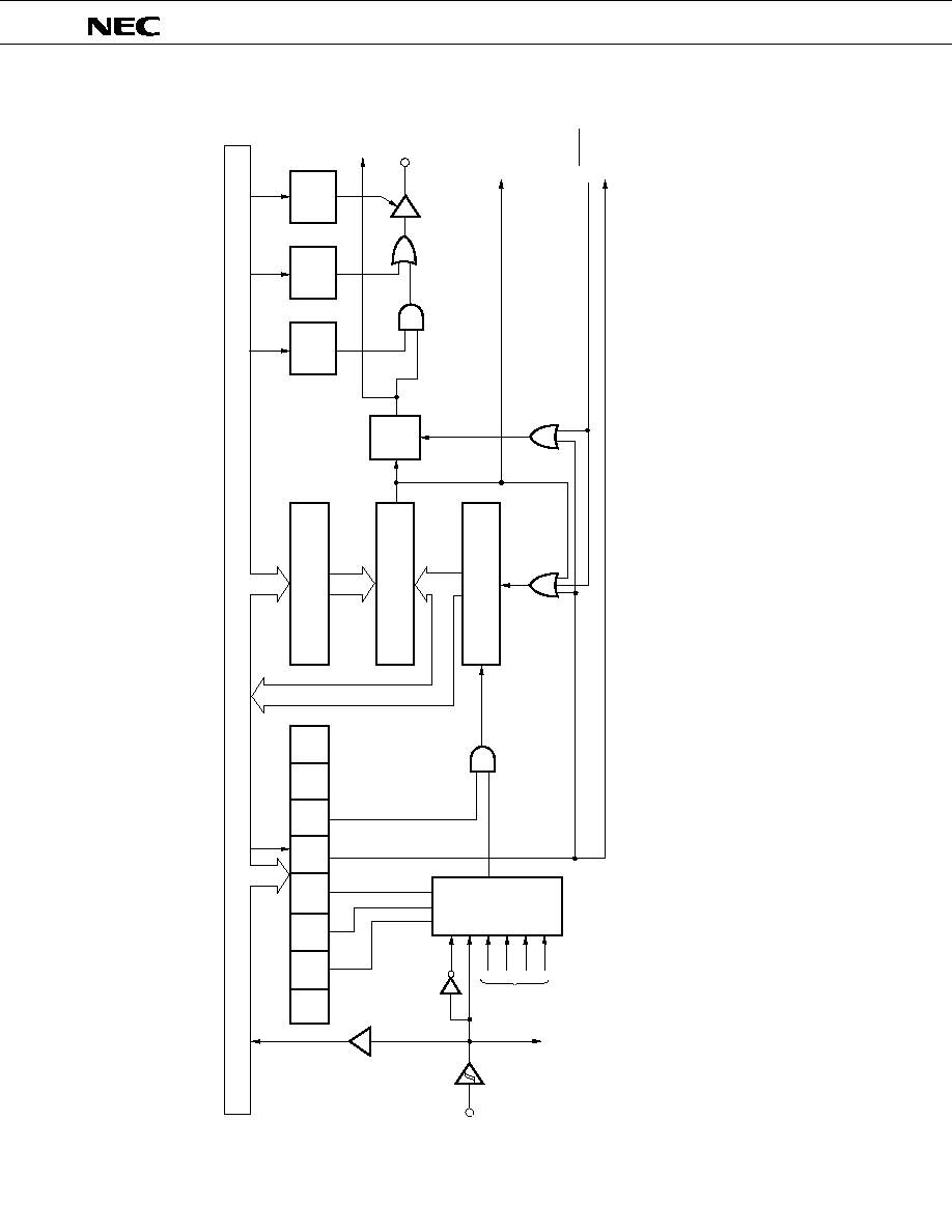
64
µ
PD75236
8
8
8
8
8
TM07TM06 TM05 TM04 TM03TM02 --
--
SET1
TM0
TMOD0
TOE0
PORT2.0
PORT1.3
P13/TI0
MPX
CP
T0
TOUT
F/F
P20/PTO0
RESET
INTT0
IRQT0
Fig. 4-25 Timer/Event Counter Block Diagram
Internal Bus
TO
Enable
Flag
P20
Output
latch
Port 2
Input
/Output
Mode
PGMB Bit 2
IRQT0
Set Signal
( )
Reset
Timer Operation Start
Output
Buffer
To Serial
Interface
* 1.
Instruction execution
2.
P13/TI0 pin is an external event pulse input pin which serves as timer/event counter and event counter.
Match
*2
From
Clock
Genera-
tor
Event
Counter #1
Input
Buffer
Modulo Register (8)
Comparator (8)
Count Register (8)
Clear
(Refer to Fig. 4-26)
IRQT0
Clear
Signal
*1

65
µ
PD75236
(2)
Timer/event counter mode register (TMO) and timer/event counter output enable flag (TOE0)
The timer/event counter mode register (TM0) is an 8-bit register to control the timer/event counter and
is set by an 8-bit memory manipulation instruction.
Fig. 4-27 shows the timer/event counter mode register format.
Bit 3 is a timer start command bit which can be set independently. When the timer starts operating, this
bit is automatically reset to "0".
RESET input clears all bits of the TM0 to 0.
The timer/event counter output enable flag (TOE0) controls enable/disable for output to the PTO0 pin in
the timer out F/F (TOUT F/F) state.
Fig. 4-26 shows the timer/event counter output enable flag format.
The timer out F/F (TOUT F/F) is an F/F which is reversed by a match signal transmitted from the com-
parator. The timer out F/F is reset by an instruction which sets bit 3 of the TM0.
RESET input clears TOE0 and TOUT F/F to 0.
Fig. 4-26 Timer/Event Counter Output Enable Flag Format
3
TOE0
0
1
Disabled
Enabled
Address
FA2H
Timer/Event Counter Output Enable Flag

66
µ
PD75236
Fig. 4-27 Timer/Event Counter Mode Register Format
TM06
TM05
TM04
TM03
TM02
7
6
5
4
3
2
1
0
Address
FA0H
Symbol
TM0
Count operation
Stop
(with count
contents held)
Count
operation
Writing "1" clears the counter and IRQT0 flag.
If bit 2 has been set (1), the counter operation starts.
TI0 input rising edge
TI0 input falling edge
f
X
/2
10
(4.09 kHz)
f
X
/2
8
(16.4 kHz)
f
X
/2
6
(65.5 kHz)
f
X
/2
4
(262 kHz)
Setting prohibited
0
0
0
0
1
1
0
0
1
1
1
1
0
1
0
1
0
1
TM06
TM05
TM04
Count Pulse (CP)
Remarks
Values at f
X
= 4.19 MHz are in parentheses.
0
1
Operating Mode
Timer Start Command Bit
Count Pulse (CP) Select Bit
In all other cases

67
µ
PD75236
MPX
(3)
Timer/event counter operating modes
The count operation stop mode and the count operating mode are available by setting the mode
register for the timer/event counter operation.
The following operations are enabled irrespective of the mode register setting:
(a)
TI0 pin signal input and test (Dual-function pin P13 input testable)
(b) Output of the timer out F/F state to PTO0
(c)
Modulo register (TMOD0) setting
(d) Count register (T0) read
(e)
Interrupt request flag (IRQT0) set/clear/test
(i)
Count operation stop mode
When TM0 bit 2 is 0, this mode is set. In this mode, count operation is not carried out because
count pulse (CP) supply to the count register is stopped.
(ii)
Count operating mode
When TM0 bit 2 is 1, this mode is set. The count pulse selected by bits 4 to 6 is supplied to the
count register and the count operation shown in Fig. 4-28 is carried out.
The timer operation is normally started by the following operations in the described order.
Set the number of counts to the modulo register (TMOD0).
Set the operating mode, count clock and start command to the mode register (TM0).
Set the modulo register by an 8-bit data transfer instruction.
Fig. 4-28 Operation in Count Operating Mode
TI0
Internal
Clock
Count Register
(T0)
Modulo Register
(TMOD0)
Comparator
CP
Clear
INTT0
(IRQT0 Set Signal)
TOUT
F/F
PTO0
To Serial Interface
(Channel 0)
{
Match
68
µ
PD75236
n + 1
(4)
Timer/event counter time setting
[Timer set time] (cycle) is obtained by dividing [Modulo register contents + 1] by [Count pulse fre-
quency] selected by timer mode register setting.
T (sec)
T (sec) : Timer set time (sec)
f
CP
(Hz) : Count pulse frequency (Hz)
n
: Modulo register value (n
0)
Once the timer is set, an interrupt request signal (IRQT0) is generated at the set intervals. Table 4-3
shows the resolutions with each count pulse of the timer/event counter and the maximum set time (with
FFH set to the modulo register).
Table 4-3 Resolution and Maximum Set Time (When Operated at 4.19 MHz)
=
f
CP
= (n + 1) ∑ (Resolution)
1
1
1
1
0
0
1
1
0
1
0
1
Resolution
Maximum Set Time
TM06 TM05 TM04
62.5 ms
15.6 ms
3.91 ms
977
µ
s
244
µ
s
61.1
µ
s
15.3
µ
s
3.81
µ
s
Mode Register
Timer Channel 0

69
µ
PD75236
128
f
X
f
XT
(32.768kHz)
f
W
(32.768kHz)
8
f
W
16
f
W
(4.096kHz)
2
14
f
W
2
7
f
W
(256 Hz:3.91ms)
2Hz
0.5sec
(
)
INTW
P23/BUZ
PORT2.3
WM
WM7
0
WM5 WM4
0
WM2
WM1
WM0
8
4.6
WATCH TIMER
(1)
Watch timer
The
µ
PD75236 incorporates one channel of watch timer having a configuration shown in Fig. 4-29.
(2)
Watch timer functions
(a)
Sets the test flag (IRQW) at 0.5 sec intervals.
The standby mode can be released by IRQW.
(b)
0.5 second interval can be set with the main system clock (4.1943 MHz) or subsystem
clock (32.768 kHz).
(c)
The fast mode enables to set 128-time (3.91 ms) interval useful to program debugging
and inspection.
(d)
The fixed frequencies (2.048 kHz, 4.096 kHz and 32.768 kHz) can be output to the P23/
BUZ pin for use to generate buzzer sound and trim the system clock oscillator frequency.
(e)
Since the frequency divider can be cleared, the watch can be started from zero second.
Fig. 4-29 Watch Timer Block Diagram
Remarks
Values at f
X
= 4.194304 MHz and f
XT
= 32.768 kHz are indicated in parentheses.
(32.768 kHz)
Internal Bus
Clear
From Clock
Generator
Selector
Selector
Frequency Divider
Selector
Bit 2 of PMGB
Port 2 Input/
Output Mode
Output Buffer
P23
Output Latch
(32.768 kHz)
)
(
IRQW
Set Signal

70
µ
PD75236
(3)
Watch mode register (WM)
The watch mode register (WM) is an 8-bit register to control the watch timer. Its format is shown in
Fig. 4-30.
The watch mode register is set by an 8-bit memory manipulation instruction. RESET input clears all
bits to "0".
Fig. 4-30 Watch Mode Register Format
7
6
5
4
3
2
1
0
Count Clock (f
W
) Select Bit
Operating Mode Select Bit
Watch Operation Enable/Disable Bit
BUZ Output Frequency Select Bit
*
Not supported with IE-75000-R
BUZ Output Enable/Disable Bit
WM7
0
WM5
WM4
0
WM2
WM1
WM0
WM
F98H
Address
Symbol
WM0
0
1
Subsystem clock: f
XT
selected
System clock divided output: selected
Normal watch mode : IRQW set at 0.5 sec
WM1
0
1
Fast watch mode
: IRQW set at 3.91 ms
WM2
0
1
Watch operation enabled
Watch operation stopped (frequency divider clear)
0
0
0
1
1
1
0
1
WM4
WM5
BUZ Output Frequency
f
W
/2
4
(2.048 kHz)
f
W
/2
3
(4.096 kHz) *
Setting prohibited
f
W
(32.768 kHz) *
WM7
0
1
BUZ output enabled
BUZ output disabled
f
X
128
f
W
2
7
f
W
2
14
(
)
)
(

71
µ
PD75236
4.7
TIMER/PULSE GENERATOR
(1)
Timer/pulse generator functions
The
µ
PD75236 incorporates one channel of timer/pulse generator which can be used as a timer or a
pulse generator. The timer/pulse generator has the following functions.
(a)
Functions available in the timer mode
∑ 8-bit interval timer operation (IRQTPG generation) enabling the clock source to be varied at 5
levels
∑ Square wave output to PPO pin
(b)
Functions available in the PWM pulse generate mode
∑ 14-bit accuracy PWM pulse output to the PPO pin (Used as a digital-to-analog converter and
applicable to tuning)
∑ Fixed time interval ( = 7.81 ms : at 4.19 MHz operation)
If pulse output is not necessary, the PPO pin can be used as a 1-bit output port.
Note
If the STOP mode is set while the timer/pulse generator is in operation, miss-operation may result.
To prevent that from occurring, preset the timer/pulse generator to the stop state using its mode
register.
2
15
f
X

72
µ
PD75236
(2)
Timer/pulse generator mode register (TPGM)
The timer/pulse generator mode register (TPGM) is an 8-bit register to control timer/pulse generator
operations. Its format is shown in Fig. 4-31.
The TPGM is set by the 8-bit memory manipulation instruction.
Bit 3 enables or disables the timer/pulse generator modulo register (MODH, MODL) contents to be
transferred (reloaded) to the modulo latch and can be manipulated individually.
The timer/pulse generator operation can be stopped and current consumption can be decreased by
setting the TPGM1 to "0".
RESET input clears all bits to "0".
Fig. 4-31 Timer/Pulse Generator Mode Register Format
Timer/Pulse Generator Operating Mode Select Bit
Timer/Pulse Generator Operation Enable/Disable Bit
Modulo Register Reload Enable/Disable Bit
PPO Output Latch Data
PPO Pin Output Select Bit Static/Pulse
PPO Pin Output Enable/Disable Bit
7
6
5
4
3
2
1
0
TPGM7
--
TPGM5
TPGM4 TPGM3
0
TPGM1 TPGM0
Address
Symbol
F90H
TPGM
PWM pulse generate mode selected
TPGM0
0
1
Timer mode selected
Timer/pulse generator operation stopped
TPGM1
0
1
Timer/pulse generator operation enabled
Modulo register reload disabled
TPGM3
0
1
Modulo register reload enabled
Output 0 to PPO output latch
TPGM4
0
1
Output 1 to PPO output latch
Static output from PPO pin
TPGM5
0
1
Pulse (square wave/PWM) output from PPO pin
PPO pin output disabled (high impedance)
TPGM7
0
1
PPO pin output enabled

73
µ
PD75236
(3)
Configuration and operation for use in the timer mode
The timer/pulse generator configuration for use in the timer mode is shown in Fig. 4-32.
The timer mode is selected by setting TPGM bit 0 to "1". In the timer mode, enable modulo register
reload by setting TPGM3 to "1".
In the timer mode, select the prescalar with modulo register L (MODL) and set the frequency or inter-
rupt interval set value to modulo register H (MODH). Start the timer by resetting the TPGM1 from 0 to 1.
The operation timing for MODH setting is shown in Fig. 4-33 and the frequency or interrupt interval
setting is shown in Table 4-4.
Square wave output or static output to the PPO pin can be switched. In the case of square wave output,
set TPGM5 to "1" and TPGM7 to "1".
Fig. 4-32 Block Diagram of Timer/Pulse Generator (Timer Mode)
Note
If the timer is stopped in the timer operating mode, the IRQTPG may be set because the T F/F is set.
Thus, when stopping the timer, do so with interruption disabled, and after the timer has stopped,
clear the IRQTPG.
8
8
MODL
MODH
TPGM3
8
8
1/2
f
X
TPGM1
CP
TPGM4TPGM5 TPGM7
PPO
INTTPG
Modulo Register L (8)
Modulo Register H (8)
(Set to "1")
Frequency
Divider
Modulo Latch H (8)
Comparator (8)
Prescalar Select Latch (5)
Count Register (8)
Clear
Clear
Match
T F/F
Output
Buffer
IRQTPG
Set Signal
(
)
Selector
Set
Internal Bus

74
µ
PD75236
6
5
4
3
2
1
0
0
0
0
0
1
0
0
0
0
0
1
0
0
0
0
0
1
0
0
0
0
0
1
MODL Bits 2 to 6
Interrupt Generate Interval
Square Wave Output Frequency
(f
X
= 4.19 MHz)
(f
X
= 4.19 MHz)
256( N+1)
f
X
=122
µ
s to 15.6 ms
f
X
128( N+1)
=61.0
µ
s to 7.81 ms
64( N+1)
32( N+1)
16( N+1)
f
X
f
X
f
X
=30.5
µ
s to 3.91 ms
=15.3
µ
s to 1.95 ms
=7.63
µ
s to 977
µ
s
f
X
256( N+1)
f
X
f
X
128( N+1)
64( N+1)
32( N+1)
16( N+1)
f
X
f
X
=64 Hz to 8 kHz
=128 Hz to 16 kHz
=256 Hz to 32 kHz
=512 Hz to 65 kHz
=1024 Hz to 131 kHz
CP
MODH
T F/F
(PPO)
0
1
2
N-1
N
0
N
0
N
0
N
Fig. 4-33 Timer Mode Operation Timing
Table 4-4 Modulo Register Setting
Note
1. Only the above values can be set to MODL. Be sure to set "0" to bits 0, 1 and 7.
2. N is the MODH set value. "0" cannot be set to N. Be sure to set a value in the range from 1 to 255
to N.
TPGM1 Set
IRQTPG
Generated
Count
Register

75
µ
PD75236
(4)
Configuration and operation for use in the PWM pulse generate mode
The timer/pulse generator for use in the PWM pulse generate mode is shown in Fig. 4-34.
The PWM pulse generate mode is selected by setting TPGM0 to "0". Pulse output is enabled by setting
TPGM5 and TPGM7 to "1". In the PWM mode, PWM pulse can be output from the PPO pin and the
IRQTPG can be set at the fixed interval (2
15
/f
X
= 7.81 ms : at 4.19 MHz operation).
The PWM pulse generated by the
µ
PD75236 is an active-low, 14-bit accuracy pulse. This pulse is
converted to an analog voltage by integrating it using an external low-pass filter and can be applied for
electronic tuning and DC motor control. (Refer to Fig. 4-35 Example of D/A Conversion Configuration with
µ
PD75236.)
The PWM pulse is generated by combining the fundamental period determined by 2
10
/f
X
(244
µ
s: at 4.19
MHz operation) and the sub period of 2
15
/f
X
(7.81 ms: at 4.19 MHz operation) and the time constant of the
external low-pass filter can be shortened.
The low-level width of the PWM pulse is determined by the 14-bit modulo latch value. The modulo
latch value is determined as a result of transfer of MODH 8 bits to the most significant 8 bits of the
modulo latch and MODL most significant 6 bits to the least significant 6 bits of the modulo latch.
The digital-to analog converted output voltage is given as
In the
µ
PD75236, all 14 bits can be transferred simultaneously to the modulo latch after correct data has
been written to MODH and MODL by the 8-bit manipulation instruction. This aims at preventing the PWM
from being generated with an unstable value in the process of modulo latch rewrite. This transfer is called
"reload" and is controlled by TPGM3.
Note
1. Setting "0" to modulo register H (MODH) disables the PWM pulse generator to operate normally.
Be sure to set to MODH a value in the range from 1 to 255.
2. When the least significant 2 bits of modulo register L (MODL) are read, an undefined value is read.
3. The fundamental period of the PWM pulse is 2
10
/f
X
(244
µ
s: at 4.19 MHz operation). If the module
latch is changed with a shorter period, the PWM pulse remains unchanged.
(5)
Static output to the PPO pin
If pulse output is not necessary, the PPO pin can be used for normal static output. In this case, set
output data to TPGM4 with TPGM5 and TPGM7 set to "0" and "1", respectively.
V
AN
= V
ref
◊
where V
ref
: External switching circuit reference voltage
Modulo latch value
2
14

76
µ
PD75236
f
x
TPGM1
TPGM3
8
8
MODH
MODL
(2)
MODH (8)
PPO
TPGM5
TPGM7
INTTPG
1/2
MODL
7-2
(6)
Fig. 4-34 Timer/Pulse Generator Block Diagram (PWM Pulse Generate Mode)
Fig. 4-35 Example of D/A Conversion Configuration with
µ
PD75236
µ
PD75236
Signal
Switching
Circuit
Low-Pass
Filter
(Analog Voltage)
Internal Bus
Modulo Register H (8)
Modulo
Register L (6)
Modulo Latch (14)
PWM Pulse Generator
Output Buffer
Frequency Divider
PPO
PWM
V
ref
V
AN
(IRQTPG Set Signal)
( =7.81 ms : at 4.19 MHz operation)
2
15
f
X
Selector

77
µ
PD75236
4.8
EVENT COUNTER
(1)
Event counter configuration
The event counter of the
µ
PD75236 incorporates a noise eliminator and has a configuration shown in
Fig. 4-36.
Fig. 4-36 Event Counter Block Diagram
Note
TI0/P13 pin is an external event pulse input pin which serves as timer/event counter #0 and event
counter #1.
(2)
Event counter functions
The event counter has the following functions.
(a)
Event counter operation
(b)
Count state read function
(c)
Count pulse edge specification
(d)
Noise eliminating function
Internal Bus
8-Bit Counter
Overflow Flag
Noise
Eliminator
Timer/Counter #0
Selector
Selector
TM1.2
TI0/P13
T1
IRQT1
GATEC.0
TM1.4
f
x
4
78
µ
PD75236
(3)
Event counter mode register
The event counter mode register (TM1) is an 8-bit register to control the event counter. Its format is
shown in Fig. 4-37.
TM1 is set by an 8-bit memory manipulation instruction.
Bit 3 is an event counter start bit and can be set independently. When the counter starts operating, bit 3
is automatically reset to "0".
Fig. 4-37 Event Counter Mode Register Format
Event Count Operation Enable/Disable Bit
Event Counter Start Command Bit
Count Pulse Edge Specification
(4)
Overflow flag (IRQT1)
The overflow flag is a flag which is set (1) by an overflow of the event counter count register and is
cleared (0) by a count operation start command.
(5)
Event counter control register (GATEC)
This is a register to select sampling with a sampling clock (f
X
/4). A pulse having a smaller width than
that of two sampling clock cycles (8/f
X
) is eliminated as noise by a noise eliminator and a pulse having a
width larger than that of the sampling clock is securely acknowledged as an interrupt signal.
Its format is shown in Fig. 4-38.
Fig. 4-38 Event Counter Control Register Format
7
6
5
4
3
2
1
0
0
0
0
TM14
TM13
TM12
0
0
Address
Symbol
TM1
FA8H
Count operation stopped (with count value held)
TM12
0
1
Count operation enabled
TM13
TI0 input rising edge
TM14
0
1
TI0 input falling edge
Writing "1" clears the counter and IRQT1 flag. If TM12 is "1", count
operation starts.
1
0
Symbol
Address
FABH
GATEC
3
2
1
0
0
0
0
GATEC0
Sampling by f
X
/4
No sampling
79
µ
PD75236
4.9
SERIAL INTERFACE
The
µ
PD75236 incorporates two channels of clocked 8-bit serial interfaces. Table 4-5 gives differences
between channel 0 and channel 1.
Table 4-5 Differences between Channels 0 and 1
Serial Transfer Mode and
Function
Channel 1
Channel 0
3-wire serial I/O
Clock selection
Transfer mode
Transfer end
flag
2-wire serial I/O
Serial bus interface
Serial transfer end flag (EOT)
f
X
/2
4
, f
X
/2
3
, TOUT F/F, external clock
f
X
/2
4
, f
X
/2
3
, external clock
MSB first/LSB first switchable
MSB first
Serial transfer end interrupt request
flag (IRQCSIO)
Use enabled
None

80
µ
PD75236
(1)
Serial interface (channel 0) functions
The following four modes are available for the
µ
PD75236 serial interface (channel 0).
The functions of each mode are outlined below.
∑ Operation stop mode
This is the mode used when no serial transfer is performed. Low power consumption operation is
possible in this mode.
∑ 3-wire serial I/O mode
8-bit data is transferred using three lines of serial clock (SCK0), serial output (SO0) and serial
input (SI0).
The 3-wire serial I/O mode enables simultaneous transmission/reception, thus shortening the data
transfer processing time.
Since the start bit of 8-bit data for serial transfer can be switched between MSB and LSB, channel
0 can be connected to a device having either start bit.
In the 3-wire serial I/O mode, channel 0 can be connected to the 75X series, 78K series and
various types of peripheral I/O devices.
∑ 2-wire serial I/O mode
8-bit data is transferred using two lines of serial clock (SCK0) and serial data bus (SB0 or SB1).
Communication is possible with two or more devices by controlling the level of output to the two
lines by software.
Since the output level of SCK0 and SB0 (or SB1) can be controlled by software, any transfer
format is applicable. Thus, the number of handshake lines previously required to connect two or
more devices can be decreased and so the input/output ports can be used efficiently.
∑ SBI mode (serial bus interface mode)
This mode enables communication with two or more devices with two lines of serial clock (SCK0)
and serial data bus (SB0 or SB1).
This mode is compliant with the NEC serial bus format.
In the SBI mode, the transmitter can output an "address" for selection of a serial communication
target device on the serial data bus, a "command" to provide instructions to the target device and
actual "data".
The receiver can distinguish between "address", "command" and "data" by hardware. As in the
2-wire serial I/O mode, this function enables the input/output ports to be used efficiently and the
serial interface control portions of any applied program to be simplified.
(2)
Serial interface (channel 0) configuration
Fig. 4-39 is a block diagram of serial interface (channel 0).

81
µ
PD75236
Fig. 4-39 Serial Interface (Channel 0) Block Diagram
8/4
8
8
8
CSIM0
SBIC
RELT
CMDT
CLR
SET
P03/SI0/SB1
P02/SO0/SB0
P01/SCK0
(8)
(8)
(8)
D
Q
ACKT
ACKE
BSYE
RELD
CMDD
ACKD
INTCSI0
fx/2
3
fx/2
4
fx/2
6
TOUT F/F
INTCSI0
Control Circuit
P01
Slave Address Register (SVA)
Busy
/Acknowledge
Output Circuit
Serial Clock Counter
Bus Release
/Command
/Acknowledge
Detector
Serial Clock
Control Circuit
Serial Clock
Selector
IRQCSI0
Set Signal
(from Timer/Event
Counter)
External SCK0
Output
Latch
Selector
Selector
Bit Test
Internal Bus
Address Comparator
Match
Signal
Bit Manipulation
SO0
Latch
Shift Register 0 (SIO0)
Bit Test

82
µ
PD75236
(3)
Serial interface (channel 0) register functions
(a)
Serial operating mode register 0 (CSIM0)
Fig. 4-40 shows a serial operating mode register 0 (CSIM0) format.
CSIM0 is an 8-bit register to specify the serial interface (channel 0) operating mode, serial clock
and the wake-up function.
An 8-bit memory manipulation instruction is used for CSIM0 operations. The higher 3 bits can be
manipulated in 1-bit units. Use each bit name for bit manipulation.
Read/Write operation is enabled/disabled depending on the bit (refer to Fig. 4-40). Bit 6 is only
enabled for test and the written data is invalidated.
RESET input clears all bits to 0.
Fig. 4-40 Serial Operating Mode Register 0 (CSIM0) Format (1/3)
Remarks
1.
(R): Read only
2.
(W): Write only
CSIE0
COI
WUP
CSIM04 CSIM03 CSIM02 CSIM01 CSIM00
7
6
5
4
3
2
1
0
Symbol
Address
CSIM0
FE0H
Serial Clock Select Bit (W)
Wake-Up Function Specify Bit (w)
Serial Interface Operating Mode Select Bit (W)
Signal (R) from Address Comparator
Serial Interface Operation Enable/Disable Specify Bit (W)
83
µ
PD75236
Serial Clock
CSIM01
CSIM00
0
0
1
1
0
1
0
1
3-Wire Serial I/O Mode
SBI Mode
2-Wire Serial I/O Mode
SCK0 Pin
Mode
Input
Output
f
X
/2
6
(65.5 kHz)
Input clock to SCK0 pin from outside.
Timer/event counter output (T0)
f
X
/2
4
(262 kHz)
f
X
/2
3
(524 kHz)
CSIM04
◊
0
1
0
1
CSIM03
0
1
1
CSIM02
0
1
0
1
Operating Mode
3-wire serial
I/O mode
SBI mode
2-wire serial
I/O mode
Bit Order of Shift Register 0
SIO0
7≠0
XA
(transferred with MSB first)
SIO0
0≠7
XA
(transferred with LSB first)
SIO0
7≠0
XA
(transferred with MSB first)
SIO0
7≠0
XA
(transferred with MSB first)
SO0 Pin Function
SO0/P02
(CMOS output)
SB0/P02
N-ch open drain
input/output
P02 input
SB0/P02
N-ch open drain
input/output
P02 input
SI0 Pin Function
SI0/P03
(input)
P03 input
SB1/P03
N-ch open drain
input/output
P03 input
SB1/P03
N-ch open drain
input/output
(
)
(
)
(
)
)
(
WUP
0
1
IRQCSI0 is set upon termination of serial transfer in each mode.
Used in SBI mode only. IRQCSI0 is set only when the address received after bus release matches the
slave address register data (wake-up state). SB0/SB1 is high impedance.
Fig. 4-40 Serial Operating Mode Register 0 (CSIM0) Format (2/3)
Serial Clock Select Bit (W)
Remarks
Values at f
X
= 4.19 MHz are in parentheses.
Serial Interface Operating Mode Select Bit (W)
Remarks
◊
: Don't care
Wake-Up Function Specify Bit (W)
Note
When WUP = 1 is set during BUSY signal output, BUSY is not released. In SBI, BUSY signal continues
to be output up to the falling edge of the next serial clock (SCK0) after BUSY release.
Ensure to set WUP = 1 after releasing BUSY and confirming that the SB0 (or SB1) pin has become high
level.
84
µ
PD75236
High-level output
Serial clock output
(high-level output)
Clear Condition (COI = 0)
Set Condition (COI = 1)
CSIEO
1
Shift Register 0 Operation
Serial Clock Counter
IRQCSI0 Flag
SO0/SB0, SI0/SB1 Pins
Shift operation disabled
Shift operation enabled
Clear
Count operation
Hold
Settable
Dedicated to port 0 functions
Functions in each mode and
operations with port 0
0
When the slave address register (SVA) data unmatches
the shift register 0 data.
When the slave address register (SVA) data matches
the shift register 0 data.
COI*
Fig. 4-40 Serial Operating Mode Register 0 (CSIMO) Format (3/3)
Signal(R) from Address Comparator
*
COI read is only valid before serial transfer and after its completion. Only undefined value is read during
transfer. The COI data written by an 8-bit manipulation instruction is ignored.
Serial Interface Operation Enable/Disable Specify Bit (W)
Remarks
1.
Each mode can be selected by setting CSIE0, CSIM03 and CSIM02.
CSIE0
CSIM03 CSIM02
Operating Mode
0
◊
◊
Operation stop mode
1
0
◊
3-wire serial I/O mode
1
1
0
SBI mode
1
1
1
2-wire serial I/O mode
2.
P01/SCK0 pin becomes as follows depending on the settings of CSIE0, CSIM01 and CSIM00.
CSIE0
CSIM01 CSIM00
P01/SCK0 Pin Status
0
0
0
Input port
1
0
0
High impedance
0
0
1
0
1
0
0
1
1
1
0
1
1
1
0
1
1
1

85
µ
PD75236
Remarks
3.
Clear CSIE0 during serial transfer using the following procedure.
Disable interrupt by clearing the interrupt enable flag.
Clear CSIE0.
z
Clear the interrupt request flag.
Example
1.
Select fx/2
4
for serial clock and generate serial interrupt IRQCSI0 upon termination of each serial
transfer and select a serial transfer mode in the SBI mode using the SB0 pin as serial data bus.
SEL
MB15
; or CLR1 MBE
MOV
XA, #10001010B
MOV
CSIM0, XA
; CSIM0
10001010B
2.
Enable serial transfer in accordance with the CSIM0 contents.
SEL
MB15
; or CLR1 MBE
SET1
CSIE0

86
µ
PD75236
(b)
Serial bus interface control register (SBIC)
Fig. 4-41 shows a serial bus interface control register (SBIC) format.
SBIC is an 8-bit register which consists of a serial bus control bit and flags indicating various
statuses of input data received from the serial bus.
SBIC is manipulated using a bit manipulation instruction.
It cannot be manipulated using a 4-bit or 8-bit manipulation instruction.
Read/Write operation enable/disable depends on the bit (refer to Fig. 4-41).
RESET input clears all bits to 0.
Note
Only the following bits can be used in the 3-wire and 2-wire serial I/O modes.
∑ Bus release trigger bit (RELT) ........ SO0 latch set
∑ Command trigger bit (CMDT) ........ SO0 latch clear
Fig. 4-41 Serial Bus Interface Control Register (SBIC) Format (1/3)
Remarks
1.
(R)
Only read
2.
(W)
Only write
3.
(R/W) Read/write enabled
BSYE
ACKD
ACKE
ACKT
CMDD
RELD
CMDT
RELT
7
6
5
4
3
2
1
0
Symbol
Address
SBIC
FE2H
Bus Release Trigger Bit (W)
Command Trigger Bit (W)
Bus Release Detect Flag (R)
Command Detect Flag (R)
Acknowledge Trigger Bit (W)
Acknowledge Enable Bit (R/W)
Acknowledge Detect Flag (R)
Busy Enable Flag (R/W)

87
µ
PD75236
Clearing Conditions (RELD = 0)
Setting Conditions (RELD = 1)
RELT
CMDT
RELD
Bus release signal (REL) detection
Clearing Conditions (CMDD = 0)
Setting Conditions (CMDD = 1)
CMDD
Command signal (CMD) detection
ACKT
ACKE
1
When set before termination of tr
ansfer
ACK is output in synchronization with the 9th clock of SCK0.
When set after termination of transfer
ACK is output in synchronization with SCK0 just after execution of a set
instruction.
4
Fig. 4-41 Serial Bus Interface Control Register (SBIC) Format (2/3)
Bus Release Trigger Bit (W)
Bus release signal (REL) trigger output control bit. When set (RELT = 1), SO0 latch is set (1) and then the RELT bit
is automatically cleared (0).
Note
Do not clear SB0 (or SB1) during serial transfer. Be sure to do so before transfer start or after transfer
end.
Command Trigger Bit (W)
Command signal (CMD) trigger output control bit. When set (CMDT = 1), SO0 latch is cleared (0) and then the
CMDT bit is automatically cleared (0).
Note
Do not clear SB0 (or SB1) during serial transfer. Be sure to do so before transfer start or after transfer
end.
Bus Release Detect Flag (R)
Transfer start instruction execution
RESET input
CSIE0 = 0 (refer to Fig. 4-40)
SVA and SIO0 mismatch upon address reception.
Command Detect Flag (R)
Transfer start instruction execution
Bus release signal (REL) detection
RESET input
CSIE0 = 0 (refer to Fig. 4-40)
Acknowledge Trigger Bit (W)
Setting this bit after termination of transfer outputs ACK in synchronization with the next SCK0. After output of ACK
signal, this bit is automatically cleared (0).
Note
1. Do not set (1) this bit during serial transfer.
2. ACKT cannot be cleared by software.
3. When setting ACKT, set ACKE = 0.
Acknowledge Enable Bit (R/W)
0
Automatic output of acknowledge signal (ACK) is disabled (output by ACKT enabled).
4

88
µ
PD75236
Fig. 4-41 Serial Bus Interface Control Register (SBIC) Format (3/3)
Acknowledge Detect Flag (R)
Transfer start instruction execution
RESET input
Busy Enable Bit (R/W)
0
Busy signal automatic output disabled
Busy signal output stopped at the falling edge of SCK0 just after clear instruction execution.
1
Busy signal output at the falling edge of SCK0 following the acknowledge signal.
Example
1.
Output the command signal.
SEL
MB15
; or CLR1 MBE
SET1
CMDT
2.
Identify the receive data type by testing RELD and CMDD for proper processing.
Set WUP = 1 for this interruput routine so that processing is carried out only in the case of a
match address.
SEL
MB15
SKF
RELD
; RELD test
BR
!ADRS
SKT
CMDD
; CMDD test
BR
!DATA
CMD : ....................................... ; Command interpret
DATE : ....................................... ; Data processing
ADRS : ....................................... ; Address decode
ACKD
Setting Conditions (ACKD = 1)
Clearing Condition (ACKD = 0)
Acknowledge signal (ACK) detection (at the rising edge of
SCK0)
BSYE

89
µ
PD75236
(c)
Shift register 0 (SIO0)
Fig. 4-42 shows a shift register 0 peripheral configuration. SIO0 is an 8-bit register which executes
parallel-to-serial conversion and carries out serial transmission/reception (shift operation) in synchro-
nization with a serial clock.
Serial transfer is started by writing data to SIO0.
In transmission, the data written to SIO0 is output to the serial output (SO0) or serial data bus
(SB0/SB1).
In reception, data is read from the serial input (SI0) or SB0/SB1 to SIO0.
This register can be read/written by an 8-bit manipulation instruction.
RESET input during operation makes the SIO0 value undefined. RESET input in the standby mode
holds the SIO0 value.
Shift operation stops after 8-bit transmission /reception.
Fig. 4-42 Shift Register 0 peripheral Configuration
SIO0 read and serial transfer start (write) are enabled at the following timings.
∑ Serial interface operation enable/disable bit (CSIE0) = 1 except when CSIE0 is set to "1"
after data write to the shift register.
∑ When the serial clock is masked after 8-bit serial transfer.
∑ When SCK0 is at a high level
Be sure to write/read data to SIO0 when SCK0 is at a high level.
In the 2-wire serial I/O or SBI mode, the data bus has a configuration that the input pins
serve as output pins and vice versa. Each output pin has an N-ch open drain configuration.
Thus, set FFH to SIO0 for the device for data reception.
Internal Bus
Address
Comparator
Shift
Register 0
Shift Clock
N-ch Open Drain Output
SO0 Latch
RELT
CMDT
SET
CLR
Q
D
CLK
BUSY/ACK
CSIM0

90
µ
PD75236
(d)
Slave address register (SVA)
The slave address register (SVA) has the following two functions.
Only write is enabled for the SVA by an 8-bit manipulation instruction.
RESET input makes the SVA value undefined. RESET input in the standby mode holds the SVA
value.
∑ Slave address detection
[SBI mode]
Use this mode to connect the
µ
PD75236 as a slave device to the serial bus. The SVA is an 8-bit
register for the slave to set the slave address value (own specification number). The master outputs
a slave address for particular slave selection to the connected slave. These two date (salve address
and SVA values output from the master) are compared by an address comparator. When they match,
the slave has been selected.
In this case, bit 6 (COI) of the serial operating mode register 0 (CSIM0) is set to "1".
Note
1. The slave selection or non-selection status is checked by detecting the matching of the slave
address received after bus release (RELD = 1).
Use the address match interrupt (IRQCSI0) to be normally generated with WUP = 1 to detect the
matching. Thus, detect selection or non-selection by slave address when WUP = 1.
2. If selection or non-selection is to be detected without using an interrupt when WUP = 0, do so by
transmitting/receiving the command preset by a program without using the method of detecting
address matching.
∑ Error detection
[2-wire serial I/O and SBI modes]
When an address, a command and data are to be transmitted using the
µ
PD75236 as the master
device or data is to be transmitted using the
µ
PD75236 as the slave device, the SVA detects errors.
(4)
Various types of signals
Table 4-6 gives a list of various types of signals. Figs. 4-43 to 4-48 show the various types of signals
and flag operation.

91
µ
PD75236
CMD signal is output to
indicate that transmit
data is an address.
i) Transmit data is an
address after REL
signal output
ii) No REL signal output.
Transmit data is a
command.
Completion of reception
Serial reception disabled
because of processing
Serial reception enabed
Signal Name
Output
Device
Timing Chart
Definition
Output
Condition
Effect on
Flag
Meaning of
Signal
Rising edge of SB0/SB1 when
SCK0 = 1
Falling edge of SB0/SB1 when
SCK0 = 1
Low≠level signal to be output
to SB0/SB1 during one-clock
period of SCK0 after comple-
tion of serial reception
[Synchronous busy signal]
Low≠level signal to be output
to SB0/SB1 following the
acknowledge signal
High- level signal to be output
to before serial transfer start
or after its compleltion
SCK0
SB0/SB1
SB0/SB1
D0
D0
9
ACK
BUSY
READY
READY
BUSY
ACK
SCK0
SB0/SB1
" H "
SCK0
SB0/SB1
" H "
[Synchronous Busy Output]
∑ RELT set
∑ CMDT set
ACKE = 1
ACKT set
∑ BSYE = 1
BSYE = 0
Execution of
an instruc-
tion for data
write to
SIO0
(transfer
start
command)
Table 4-6 Various Types of Signals in SBI Mode (1/2)
∑ RELD set
∑
CMDD clear
∑ CMDD set
∑ ACKD set
--
--
Master
Master
Master/
slave
Slave
Slave
Bus release
signal
(REL)
Command signal
(CMD)
Acknowledge
signal (ACK)
Busy signal
(BUSY)
Ready signal
(READY)

92
µ
PD75236
Table 4-6 Various Types of Signals in SBI Mode (2/2)
Signal Name
Output
Device
Timing Chart
Definition
Output
Condition
Effect on
Flag
Meaning of
Signal
* 1.
When WUP = 0, IRQCSI0 is always set at the rising edge of the 9th clock of SCK0.
When WUP = 1, an address is received. Only when the received address matches the slave adress register (SVA) value, IRQCSI0 is set at the
rising edge of the 9th clock of SCK0.
2.
Transfer starts after the BUSY state is changed to the READY state.
1
2
7
8
SCK0
SB0/SB1
SCK0
SB0/SB1
1
2
7
8
CMD
SCK0
SB0/SB1
1
2
7
8
REL CMD
1
2
7
8
9
10
SCK0
SB0/SB1
Execution of
an instruction
for data write
to SIO0 when
CSIE0 = 1
(serial
transfer start
command)*2
Synchronous clock to ouput
address, command, data, ACK
signal and synchronous BUSY
signal.
Address, command and data
are transferred by the first
eight clocks.
8-bit data to be transferred in
synchronization with SCK0
after output of REL and CMD
signals
8-bit data to be transferred in
synchronization with SCK0
after output of CMD signal
only without REL signal
output
8-bit data to be transferred in
synchronization with SCK0
without output of REL and
CMD signals
Timing of signal output
to the serial data bus
Address value of slave
device on the serial bus
Command and message
for the slave device
Numeric value to be
processed by a slave or
master device
IRQCSI0 set
(rising edge
of 9th clock)
*1
Serial clock
(SCK0)
Address
(A7 to 0)
Command
(C7 to 0)
Data
(D7 to 0)
Master
Master
Master
Master/
slave

93
µ
PD75236
6
7
8
9
SCK0
D2
D1
D0
SB0/SB1
ACKT
ACK
Set after completion of
transfer
ACK signal is output during
1-clock period just after
setting
When set during this period
SIO0
SCK0
RELD
CMDD
1
2
7
8
D7
D6
D1
D0
When the address matches
When the address does not match
Fig.4-43 RELT, CMDT, RELD and CMDD (Master) Operations
Fig. 4-44 RELT, CMDT, RELD and CMDD (Slave) Operations
FIg. 4-45 ACKT Operations
Note
Do not set ACKT just before termination of transfer.
Transfer Start
Directive
SO0 Latch
SIO0
SCK0
"H"
RELT
CMDT
RELD
CMDD
Write to SIO0
Transfer Start
Directive
SO0 Latch
RELT
(Master)
CMDT
(Master)
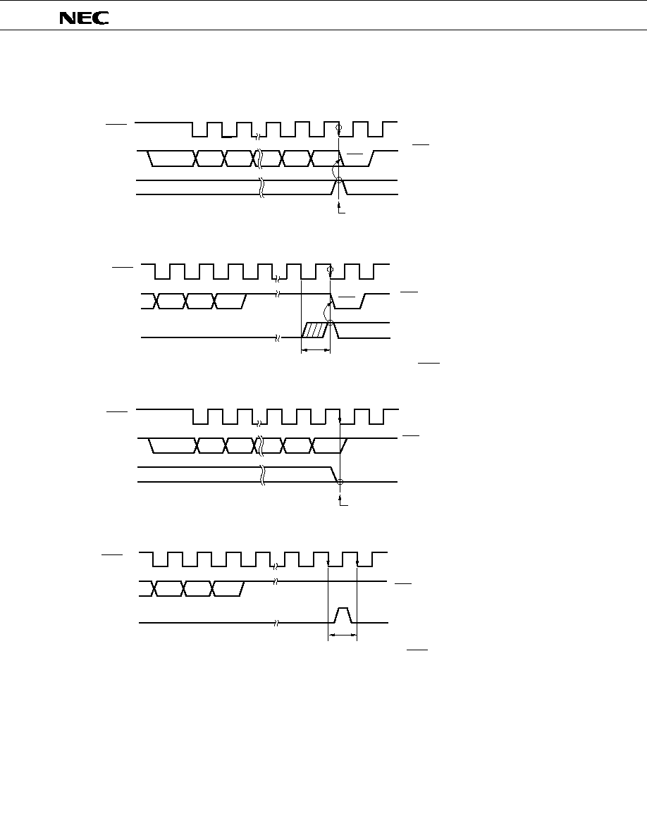
94
µ
PD75236
Fig. 4-46 ACKE Operation
(a)
When ACKE = 1 upon completion of transfer
(b)
When set after completion of transfer
(c)
When ACKE = 0 upon completion of transfer
(d)
When the ACKE = 1 period is short
1
2
7
8
9
SCK0
SB0/SB1
D7
D6
D2
D1
D0
ACK
ACKE
ACK signal is output
at the 9th clock
1
2
7
8
9
SCK0
SB0/SB1
ACKE
D7
D6
D2
D1
D0
ACK signal is not output
SCK0
SB0/SB1
ACKE
When set and cleared during this period
and ACKE=0 at the falling edge of ACK0
ACK signal is not output
When ACKE=1 at this point
When ACKE = 0 at this point
6
7
8
9
SCK0
SB0/SB1
ACKE
D2
D1
D0
ACK
ACK signal is output during
1-clock period just after
setting
When set during this period and ACKE=1
at the falling edge of the next SCK0.
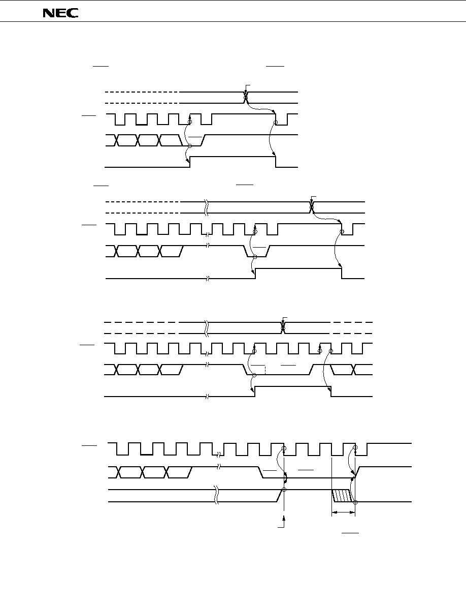
95
µ
PD75236
(c)
Clear timing with transfer start command during BUSY
(b)
When ACK signal is output after the 9th clock of SCK0
Fig. 4-48 BSYE Operation
Transfer Start
Transfer Start
Transfer Start
Directive
Transfer Start Directive
When BSYE=1
at this point
When reset during this
period and BSYE=0 at the
falling edge of SCK0
Fig. 4-47 ACKD Operations
(a)
When ACK signal is output during the 9th clock period of SCK0.
Transfer Start
Directive
6
7
8
9
SCK0
SB0/SB1
ACKD
D2
D1
D0
SIO0
ACK
6
7
8
9
SCK0
SB0/SB1
ACKD
SIO0
D2
D1
D0
ACK
6
7
8
9
SCK0
SB0/SB1
BSYE
ACK
BUSY
6
7
8
9
SCK0
SB0/SB1
ACKD
SIO0
D2
D1
D0
D7
D6
ACK
BUSY
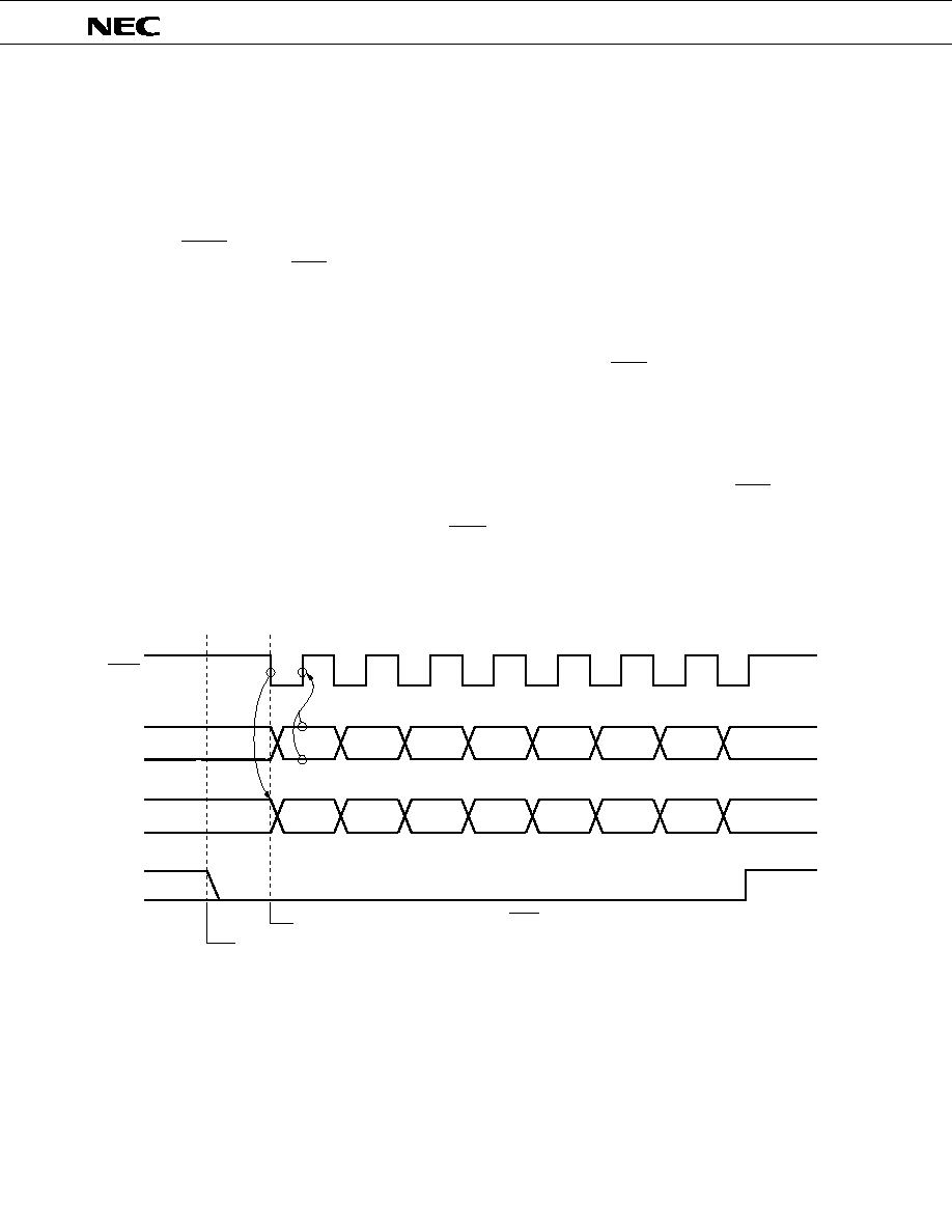
96
µ
PD75236
(5)
Serial interface (channel 0) operations
(a)
Operation stop mode
The operation stop mode is used when serial transfer is not carried out. Power consumption is
decreased in this mode.
In this mode, shift register 0 does not carry out shift operation and thus can be used as a normal
8-bit register.
RESET input sets the operation stop mode. The P02/SO0/SB0 pin and P03/SI0/SB1 pins are fixed to
the input port. P01/SCK0 can be used as an input port by setting serial operating mode register 0.
(b)
3-wire serial I/O mode operations
The 3-wire serial I/O mode allows connection with the methods employed with another 75X series
and 78K series.
Communication is carried out using three lines of serial clock (SCK0), serial output (SO0) and
serial input (SI0).
(i)
Communication
The 3-wire serial I/O mode is used for data transmission and reception in 8-bit units. Bit-wise data
transmission/reception is carried out in synchronization with the serial clock.
Shift operation of shift register 0 is carried out at the falling edge of serial clock (SCK0). Transmit
data is held at the SO0 latch and output from the SO0 pin. Receive data input to the SI0 pin is latched
to the shift register 0 at the rising edge of SCK0.
Shift register 0 operation automatically stops upon termination of 8-bit transfer and the interrupt
request flag (IRQCSI0) is set.
Fig. 4-49 3-Wire Serial I/O Mode Timing
SCK0
SI0
SO0
IRQCSI0
DO7
DO6
DO5
DO4
DO3
DO2
DO1
DO0
DI7
DI6
DI5
DI4
DI3
DI2
DI1
DI0
1
2
3
4
5
6
7
8
Transfer start at the falling edge of SCK0
Execution of data write instruction to SIO0
(Transfer Start Command)
End of Transfer

97
µ
PD75236
The SO0 pin serves as CMOS output to output the SO0 latch status. Thus, the SO0 pin output
status can be manipulated by setting the RELT and CMDT bits.
However, do not carry out this manipulation during serial transfer.
The SCK0 pin can control the output status by manipulating the P01 output latch in the output
mode (internal system clock mode) (refer to 4.9 (7) SCK0 pin output manipulation).
(ii)
MSB/LSB first switching
The 3-wire serial I/O mode has a function which allows MSB-first or LSB-first transfer to be
selected.
Fig. 4-50 shows shift register 0 (SIO0) and internal bus configurations. As shown in Fig. 4-50, MSB/
LSB can be reversed and read/written.
MSB/LSB first switching can be specified by bit 2 of serial operating mode register 0 (CSIM0).
Fig. 4-50 Transfer Bit Switching Circuit
First bit switching is realized by switching the bit order of data write to the shift register 0 (SIO0).
The SIO0 shift order remains the same.
Thus, switch the MSB/LSB first bit before writing data to the shift register 0.
SCK0
SO0
SI0
D
Q
7
6
1
0
Internal Bus
LSB First
MSB First
Read/Write Gate
Read/Write Gate
SO0 Latch
Shift Register 0 (SIO0)

98
µ
PD75236
SCK0
SB0/SB1
IRQCSI0
1
2
3
4
5
6
7
8
D7
D6
D5
D4
D3
D2
D1
D0
Execution of data write instruction to SIO0
(Transfer Start Command)
Transfer start at the falling edge of SCK0
End of Transfer
(c)
2-wire serial I/O mode operations
The 2-wire serial I/O mode can be applied to any communication format by program.
Communication is basically carried out using two lines of serial clock (SCK0) and serial data input/
output (SB0 or SB1).
(i)
Communication
The 2-wire serial I/O mode is used for data transmission and reception in 8-bit units. Bit-wise data
transmission/reception is carried out in synchronization with the serial clock.
Shift operation of shift register 0 is carried out at the falling edge of serial clock (SCK0). Transmit
data is held at the SO0 latch and output from the SB0/P02 (or SB1/P03) pin with MSB set as the first
bit. Receive data input from the SB0 (or SB1) pin at the SCK0 rising edge is latched to the shift
register 0.
Upon termination of 8-bit transfer, the shift register 0 operation automatically stops and the
interrupt request flag (IRQCSI0) is set.
Fig. 4-51 2-Wire Serial I/O Mode Timing
Since the pin specified for the serial data bus of the SB0 (or SB1) pin becomes an N-ch open drain
input/output, it must be pulled up externally.
Since the SB0 (or SB1) pin outputs the SO0 latch status, the SB0 (or SB1) pin status can be
manipulated by setting the RELT and CMDT bits.
However, do not carry out this operation during serial transfer.
The SCK0 pin can control the output status by manipulating the P01 output latch in the output
mode (internal system clock mode) (refer to 4.9 (7) SCK0 pin output manipulation).

99
µ
PD75236
(d)
SBI mode operations
SBI (serial bus interface) is a high-speed serial interface method compliant with the NEC serial bus
format.
SBI is a single master high-speed serial bus based on the format with bus configuration functions
added to the clocked serial synchronization I/O method so that communication can be carried out
with two or more devices using two signal conductors. Thus, the number of ports used and that of
wires on the board can be decreased for serial bus configuration with two or more microcomputers
and peripheral ICs.
Fig. 4-52 shows the SBI system configuration example.
Fig. 4-52 SBI System Configuration Example
Note 1.
Because in the SBI the serial data bus pin SB0 (or SB1) is an open drain output, the serial data bus
line is wired-OR. A pull-up resistor is necessary for the serial data bus line.
2.
For master/slave replacement, a pull-up resistor is necessary for SCK0 because serial clock line
(SCK0) input/output switching is executed asynchronously between the master and slave.
Address 1
Address 2
Address N
SB0 (AB1)
SCK0
SB0 (SB1)
SCK0
SB0 (SB1)
SCK0
SB0 (SB1)
SCK0
Slave IC
Slave CPU
Master CPU
µ
PD75236
Slave CPU
µ
PD75236

100
µ
PD75236
SCK0
SB0/SB1
8
9
A7
A0
ACK
BUSY
SCK0
SB0/SB1
SCK0
SB0/SB1
9
C7
C0
ACK
BUSY
READY
ACK
BUSY
READY
8
9
D7
D0
(i)
SBI functions
∑ Address/command/data identification
SBI distinguishes serial data between address, command and data.
∑ Chip select function by address
The master executes slave chip selection by address transmission.
∑ Wake-up function
The slave can easily make an address receive judgment (chip select judgment) using the wake-
up function (which can be set/cancelled by software).
When the wake-up function is set, an interrupt (IRQCSI0) is generated upon reception of a match
address. Thus, when communication is carried out with two or more devices, CPUs except the
selected slave can operate irrespective of serial communication.
∑ Acknowledge signal (ACK) control function
Acknowledge signal is controlled to confirm serial data reception.
∑ Busy signal (BUSY) control function
The busy signal is controlled to inform the slave busy status.
Fig. 4-53 SBI Transfer Timing
Bus Release
Signal
Command Transfer
Command Signal
Data Transfer
Address Transfer

101
µ
PD75236
(ii)
Communication
In the SBI, the master normally selects one slave device for communication target from among
two or more devices by outputting an "address" to the serial bus.
After the communication target device has been determined, serial communication is achieved
through command and data transmission/reception between the master and slave devices.
Figs. 4-54 to 4-57 show the timing charts of data communication.
In the SBI mode, shift operation of shift register 0 is carried out at the falling edge of serial clock
(SCK0) and transmit data is output from the SB0/P02 or SB1/P03 pin with MSB as the first bit. Receive
data input to the SB0 (or SB1) pin at the rising edge of SCK0 is latched to the shift register 0.

102
µ
PD75236
Fig. 4-54 Address Transmission from Master Device to Slave Device (WUP = 1)
1
2
3
4
5
6
7
8
9
A7
A6
A5
A4
A3
A2
A1
A0
BUSY
READY
WUP
0
ACK
Master Device Processing
(Transmitter Side)
Program Processing
Hardware Operation
Transfer Line
SCK0 Pin
SB0 Pin
Slave Device Processing
(Receiver Side)
Program Processing
Hardware Operation
Write
to SIO0
CMDT
Set
CMDT
Set
RELT
Set
Serial Transmission
Interrupt Servicing (Preparation for the Next Serial Transfer)
IRQCSI0 Generation
ACKD
Set
SCK0
Stop
Address
Serial Reception
CMDD
Set
CMDD
Clear
CMDD
Set
RELD
Set
IRQCSI0
Generation
ACK
Output
BUSY
Output
BUSY
Clear
BUSY
Clear
ACKT
Set
(When SVA = SIO0)

103
µ
PD75236
Fig. 4-55 Command Transmission from Master Device to Slave Device
1
2
3
4
5
6
7
8
9
C7
C6
C5
C4
C3
C2
C1
C0
BUSY
READY
ACK
Master Device Processing
(Transmitter Side)
Program Processing
Hardware Operation
Transfer Line
SCK0 Pin
SB0 Pin
Slave Device Processing
(Receiver Side)
Program Processing
Hardware Operation
CMDD
Set
Serial Reception
IRQCSI0
Generation
ACK
Output
BUSY
Output
BUSY
Clear
BUSY
Clear
ACKD
Set
Command
Analysis
SIO0
Read
CMDT
Set
Write
to SIO0
Serial Transmission
ACKD
Set
SCK0
Stop
IRQCSI0 Generation
Interrupt Servicing (Preparation for the Next Serial Transfer)
Command

104
µ
PD75236
Fig. 4-56 Data Transmission from Master Device to Slave Device
1
2
3
4
5
6
7
8
9
D7
D6
D5
D4
D3
D2
D1
D0
ACK
BUSY
READY
Master Device Processing
(Transmitter Side)
Program Processing
Hardware Operation
Transfer Line
SCK0 Pin
SB0 Pin
Slave Device Processing
(Receiver Side)
Program Processing
Hardware Operation
Serial Reception
IRQCSI0
Generation
BUSY
Clear
ACK
Output
BUSY
Output
BUSY
Clear
ACKT
Set
SIO0
Read
ACKD
Set
SCK0
Set
IRQCSI0 Generation
Interrupt Servicing (Preparation for the Next Serial Transfer)
Serial Transmission
Write
to SIO0
Data

105
µ
PD75236
Fig. 4-57 Data Transmission from Slave Device to Master Device5
1
2
3
4
5
6
7
8
9
1
2
D6
D7
D5
D4
D3
D2
D1
D0
D6
D7
ACK
BUSY
BUSY
READY
READY
Transfer Line
SCK0 Pin
SB0 Pin
Slave Device Processing
(Transmitter Side)
Program Processing
Hardware Operation
IRQCSI0
Generation
ACKD
Output
BUSY
Output
BUSY
Clear
Master Device Processing
(Receiver Side)
Program Processing
Hardware Operation
Write
to SIO0
BUSY
Clear
Serial Transmission
Write
to SIO0
IRQCSI0
Generation
ACK
Output
Serial
Reception
Receive Data Processing
ACKT
Set
SIO0
Read
FFH Write
to SIO0
FFH Write
to SIO0
Serial Reception
Data
SCK0
Stop

106
µ
PD75236
(6)
Transfer start in each mode
In each of the 3-wire and 2-wire serial I/O modes and the SBI mode, serial transfer is started by setting
transfer data to the shift register 0 (SIO0) under the following two conditions.
∑ Serial interface operation enable/disable bit (CSIE0) = 1
∑ The internal serial clock has stopped or SCK0 is at high level after 8-bit serial transfer.
Note
Transfer does not start if CSIE0 is set to "1" after data is written to the shift register 0.
Serial transfer automatically stops and the interrupt request flag (IRQCSI0) is set upon termination of 8-
bit transfer.
[2-wire serial I/O mode transfer start precautions]
Note
Because it is necessary to turn off the N-ch transistor upon data reception, write FFH to SIO0 in
advance.
[SBI mode transfer start precautions]
Note
1. Because it is necessary to turn off the N-ch transistor upon data reception, write FFH to SIO0 in
advance.
However, in the case of wake-up function specify bit (WUP) = 1, the N-ch transistor remains OFF.
Thus, it is not necessary to write FFH to SIO0 before reception.
2. If data is written to SIO0 when the slave is busy, the written data is not lost.
Transfer starts when the busy status is cancelled and the SB0 (or SB1) input becomes high level
(ready status).
Example
The RAM data specified by the HL register is transferred to SIO0 and simultaneously the SIO0 data
is fetched into the accumulator and serial transfer is started.
MOV
XA, @HL
; Transmit data is fetched from the RAM.
SEL
MB15
; or CLR1 MBE
XCH
XA, SIO0
; Transmit data is exchanged with receive data and transfer is started.
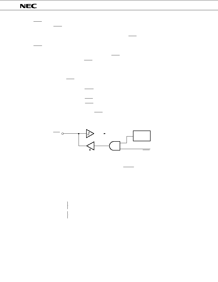
107
µ
PD75236
(7)
SCK0 pin output manipulation
Because the SCK0/P01 pin incorporates an output latch, static output is possible by software in addition
to normal serial clocks.
P01 output latch manipulation enables to set any number of SCK0 by software (SO0/SB0/SI0/SB1 pin is
controlled by the RELT and CMDT bits of SBIC).
SCK0/P01 pin output manipulation is described below.
Set the serial operating mode register 0 (CSIM0) (SCK0 pin: output mode, serial operation: enabled).
While serial transfer is stopped, SCK0 from the serial clock control circuit remains 1.
Manipulate the P01 output latch by a bit manipulation instruction.
Example
1 clock output to SCK0/P01 pin by software.
SEL
MB15
; or CLR1 MBE
MOV
XA,#10000011B
; SCK0(f
X
/2
3
), output mode
MOV
CSIM0,XA
CLR1
0FF0H.1
; SCK0/P01
0
SET1
0FF0H.1
; SCK0/P01
1
Fig. 4-58 SCK0/P01 Pin Configuration
The P01 output latch is mapped at bit 1 of address FF0H. RESET signal generation sets the P01 output
latch to "1".
Note
1. It is necessary to set the P01 output latch to 1 during normal serial transfer.
2. The P01 output latch address cannot be set by "PORT0.1" as shown below. Describe address
(0FF0H.1) directly for the operand.
However, it is necessary to preset MBE = 0 or (MBE = 1 and MBS = 15) for instruction execution.
CLR1
PORT0.1
SET1
PORT0.1
CLR1
0FF0H.1
SET1
0FF0H.1
P01/SCK0
SCK0
P01 Output
Latch
CSIEO=1 and CSIM01
and MCSIMO0 00
Address
FF0H.1
To Internal
Circuit
From Serial Clock
Control Circuit
CSIEO = 1 and CSIM01
and CSIM00
00
Use disabled
Use enabled

108
µ
PD75236
(8)
Serial interface (channel 1) functions
The following two modes are available to the
µ
PD75236 serial interface (channel 1).
The summary of each mode is shown below.
∑ Operation stop mode
The operation stop mode is used when serial transfer is not carried out. Power consumption is
decreased in this mode.
∑ 3-wire serial I/O mode
8-bit data transfer is carried out using three lines of serial clock (SCK1), serial output (SO1) and
serial input (SI1).
In the 3-wire serial I/O mode which enables simultaneous transmission and reception, the data
transfer rate is improved.
The first bit of 8-bit data for serial transfer is fixed to MSB.
In the 3-wire serial I/O mode, channel 1 can be connected to the 75X series, 78K series and various
types of peripheral I/O devices.
(9)
Serial interface (channel 1) configuration
Fig. 4-59 shows a serial interface (channel 1) block diagram.
5
109
µ
PD75236
Fig. 4-59 Serial Interface (Channel 1) Block Diagram
8
8
0
CSIM1
fx/2
3
fx/2
4
R
S
Q
P83/SI1
P82/SO1
P81/SCK1
bit0
7
SIO1
bit7
Internal Bus
SIO1 Write Signal
(Serial Start Signal)
Bit Mani-
pulation
Serial Operating Mode Register (8)
Bit Mani-
pulation
Serial Transfer
End Flag (EOT)
Serial
Clock
Selector
Set
Clear
Clear
Serial Clock
Counter (3)
Overflow
Shift Register 1 (8)
110
µ
PD75236
(10) Serial interface (channel 1) register functions
(a)
Serial operating mode register 1 (CSIM1)
Fig. 4-60 shows a serial operating mode register 1 (CSIM1) format.
CSIM1 is an 8-bit register to specify the serial interface (channel 1) operating mode and serial
clock.
It is manipulated by an 8-bit memory manipulation instruction. The higher 1 bit can be manipu-
lated bit-wise. Use each bit name for bit manipulation.
RESET input clears all bits to 0.
Fig. 4-60 Serial Operating Mode Register 1 Format
Serial Clock Select Bit (W)
Serial Interface Operation Enable/Disable Specify Bit (W)
CSIM11
CSIM10
Serial Clock 3-Wire Serial I/O Mode
SCK Pin Mode
0
0
External input clock to SCK1 pin
Input
0
1
Setting disabled
--
1
0
f
x
/2
4
(262 kHz)
1
1
f
x
/2
3
(524 kHz)
Shift Register 1 Operation
Serial Clock Counter
IRQCSI Flag
SO1 and SI1 Pins
0
Shift operation disabled
Clear
Hold
Dedicated to port 8 functions
1
Shift operation enabled
Count operation
Settable
Functions in each mode and operations with port 8
CSIE1
Remarks
Values at f
x
= 4.19 MHz are in parentheses.
Note
Be sure to write "0" to bits 2 to 6 of the serial operating mode register.
5
5
7
6
5
4
3
2
1
0
CSIE1
0
0
0
0
0
CSIM11 CSIM10
Address
FC8H
Symbol
CSIM1
Output

111
µ
PD75236
(b)
Shift register 1 (SIO1)
SIO1 is an 8-bit register which executes parallel to serial conversion and carries out serial trans-
mission/reception (shift operation) in synchronization with a serial clock.
Serial transfer is started by writing data to SIO1.
In transmission, the data written to SIO1 is output to the serial output (SO1). In reception, data is
read from the serial input (SI1) to SIO1.
This register can be read/written by an 8-bit manipulation instruction.
RESET input during operation makes the SIO1 value undefined. RESET input in the standby mode
holds the SIO1 value.
Shift operation stops after 8-bit transmission/reception.
SIO1 read and serial transfer start (write) are enabled at the following timings.
∑ Serial interface operation enable/disable bit (CSIE1) = 1 except when CSIE1 is set to "1" after
data write to the shift register.
∑ When the serial clock is masked after 8-bit serial transfer.
∑ When SCK1 is at a high level.
112
µ
PD75236
(11) Serial interface (channel 1) operations
(a)
Operation stop mode
The operation stop mode is used when serial transfer is not carried out. Power consumption is
decreased in this mode.
In this mode, shift register 1 does not carry out shift operation and thus can be used as a normal
8-bit register.
RESET input sets the operation stop mode. The P82/SO1 pin and P83/SI1 pin are fixed to the input
port. P81/SCK1 can be used as an input port by setting serial operating mode register 1.
(b)
3-wire serial I/O mode operations
The 3-wire serial I/O mode allows connection with the methods employed with another 75X series
and 78K series, etc.
Communication is carried out using three lines of serial clock (SCK1), serial output (SO1) and
serial input (SI1).
The 3-wire serial I/O mode is used for data transmission and reception in 8-bit units. Bit-wise data
transmission/reception is carried out in synchronization with the serial clock.
Shift operation of shift register 1 is carried out at the falling edge of serial clock (SCK1). Transmit
data is held at the SO1 latch and output from the SO1 pin.
Receive data input to the SI1 pin is latched to the shift register 1 at the rising edge of SCK1.
Shift register 1 operation automatically stops upon termination of 8-bit transfer and the serial
transfer end flag (EOT) is set.
Fig. 4-61 3-Wire Serial I/O Mode Timing
SCK1
SI1
SO1
EOT
DO7
DO6
DO5
DO4
DO3
DO2
DO1
DO0
DI7
DI6
DI5
DI4
DI3
DI2
DI1
DI0
1
2
3
4
5
6
7
8
Transfer start at the falling edge of SCK1
Execution of data write instruction to SIO1 (Transfer Start Command)
End of Transfer
113
µ
PD75236
4.10 A/D CONVERTER
The
µ
PD75236 incorporates an 8-bit accuracy A/D converter with 8-channel analog inputs (AN0 to AN7).
The A/D converter employs successive approximation.
(1)
A/D converter configuration
Fig. 4-62 shows an A/D converter configuration.
Fig. 4-62 A/D Converter Block Diagram
AN0
AN1
AN2
AN3
AN4
AN5
AN6
AN7
AV
ss
AV
REF
R/2
R
R
R
R/2
+
≠
8
8
0
ADM6 ADM5 ADM4 SOC
EOC
0
0
8
Internal Bus
Control Circuit
SA Register (8)
Comparator
Simple & Hold
Circuit
Tap Decoder
Multiplexer

114
µ
PD75236
(2)
A/D converter pin functions
(a)
AN0 to AN7
These are 8-channel analog signal input pins to the A/D converter. An analog signal to undergo
A/D conversion is input to these pins.
The A/D converter incorporates a sample hold circuit. The analog input voltage is internally held
during A/D conversion.
(b)
AV
REF
and AV
SS
The A/D converter reference voltage is input to these pins.
Signals input to AN0 to AN7 are converted to digital signals in accordance with the voltage
applied between AV
REF
and AV
SS
.
AV
SS
should always be set to the same voltage as V
SS
.
(c)
AV
DD
AV
DD
is a power supply pin for the A/D converter.
It should be set to the same voltage as V
DD
, even when the A/D converter is not used, or in
standby mode.
(3)
A/D conversion mode register
The A/D conversion mode register (ADM) is an 8-bit register for analog input channel selection,
conversion start command and conversion end detection (see Fig. 4-63).
The ADM is set by an 8-bit manipulation instruction. The bit 2 conversion end detection flag (EOC)
and the bit 3 conversion start command bit (SOC) can be manipulated in bit units.
RESET input initializes the ADM to 04H (only EOC is set to "1" and all other bits are cleared to "0").
5

115
µ
PD75236
0
Being converted
1
End of conversion
EOC
SOC
Setting this bit starts A/D conversion.
Upon conversion start, this bit is automati-
cally cleared.
ADM6
ADM5
ADM4
Analog Channel
0
0
0
AN0
0
0
1
AN1
0
1
0
AN2
0
1
1
AN3
1
0
0
AN4
1
0
1
AN5
1
1
0
AN6
1
1
1
AN7
7
6
5
4
3
2
1
0
0
ADM6
ADM5
ADM4
SOC
EOC
0
0
Symbol
ADM
Address
FD8H
Conversion End Detection Flag
Conversion Start Command Bit
Analog Channel Select Bit
Fig. 4-63 A/D Conversion Mode Register Format
Note
A/D conversion starts with a maximum delay of 2
4
/f
X
sec (3.81
µ
s: at 4.19 MHz operation) after SOC
setting (refer to 4.10 (5) A/D converter operations).

116
µ
PD75236
(4)
SA register (SA)
The SA register (Successive Approximation Register) is an 8-bit register to store the result of A/D
conversion by successive approximation.
The SA register is read by an 8-bit manipulation instruction. Data cannot be written to this register by
software.
RESET input sets the SA register to 7FH.
(5)
A/D converter operations
The analog input signal to undergo A/D conversion is specified by setting bits 6, 5 and 4 (ADM6, 5 and
4) of the A/D conversion mode register.
A/D conversion is started by setting (1) ADM bit 3 (SOC). SOC is automatically cleared (0) after the
setting. A/D conversion is executed using successive approximation by hardware and the 8-bit conversion
result data is stored into the SA register. Upon termination of conversion, bit 2 (EOC) of ADM is set (1).
Fig. 4-64 is an A/D conversion timing chart.
Use the A/D converter as follows.
Select the analog input channel (ADM 6, 5 and 4 setting).
Instruct A/D conversion start (SOC setting).
Wait for A/D conversion to terminate (wait for EOC to be set or wait with a software timer).
Read the A/D conversion result (SA register reading).
Note
1. and can be carried out simultaneously.
2. A maximum delay of 2
4
/f
X
sec (3.81
µ
s: at 4.19 MHz operation) occurs from A/D conversion start to
EOC clear after SOC setting. Thus, test EOC after the passage of time indicated in Table 4-11 after
SOC setting. Table 4-7 shows A/D conversion times as well.
Table 4-7 SCC and PCC Settings
SCC and PCC Set Value
A/D Conversion
Time
Wait not required
2 machine cycles
4 machine cycles
Wait not required
Wait time till EOC
test after SOC
setting
Wait time till the
end of A/D conver-
sion after SOC
setting
3 machine cycles
21 machine cycles
42 machine cycles
Wait not required
Conversion
operation
stopped
--
--
168/f
x
(40.1
µ
s : at 4.19
MHz operation)
Remarks
x : Don't care
SCC3
SCC0
PCC1
PCC0
0
0
0
0
1
0
1
1
0
1
◊
◊
1
◊
◊
◊
4

117
µ
PD75236
Fig. 4-64 A/D Conversion Timing Chart
(6)
Standby mode precautions
The A/D converter operates with the main system clock. Thus, the converter operation stops in the
STOP mode or in the HALT mode with the subsystem clock. In this case also, current flows to the AV
REF
pin. Thus, it is necessary to cut the current to decrease the power consumption of the whole system. The
P21 pin has a more improved driving capacity than any other port and so can directly supply a voltage to
the AV
REF
pin.
However, in this case, the actual AV
REF
voltage have no accuracy. Thus, the conversion value itself has
no accuracy and can only be used for relative comparison.
In the standby mode, power consumption can be decreased by generating a low level to P21.
The AV
DD
pin should be set to the same voltage as V
DD
in the standby mode.
Fig. 4-65 AV
REF
Pin Processing in Standby Mode
168/f
X
sec (40.1
µ
s: at 4.19 MHz operation)
AV
REF
AV
ss
AV
REF
V
DD
P21
V
DD
µ
PD75236
P-ch
Large
AV
REF
= V
DD
.
.
SOC
EOC
Previous Data
SA Register
Time until A/D
Conversion Start
(2 /f
X
◊
sec max.)
4
A/D Conversion
Undefined
Conversion Result
Sampling

118
µ
PD75236
(7)
Others and operating precautions
(a)
AN0 to AN7 input range
Use AN0 to AN7 input voltages in the specified range. If a voltage larger than V
DD
or smaller than
V
SS
is input (if in the absolute maximum range), the conversion value of the channel becomes
undefined and may affect the conversion values of other channels.
(b)
Countermeasures against noise
To maintain 8-bit accuracy, extra attention must be paid to noise in the AVREF and AN0 to AN7
pins. The higher the analog input source output impedance becomes the more the noise effect
becomes. To prevent that from occurring, mount C externally as shown in Fig. 4-66.
Fig. 4-66 Analog Input Pin Processing
(c)
AN4/P90 to AN7/P93 pins
Analog inputs AN4 to AN7 also serve as the input port (PORT9) pin.
Do not execute a PORT9 input instruction during A/D conversion with any one of AN4 to AN7
selected. The conversion accuracy may be deteriorated.
If a digital pulse is applied to a pin contiguous to the pin undergoing A/D conversion, the expected
A/D conversion value may not be obtained because of coupling noise.
Thus, do not apply pulses to such pins.
(d)
AV
DD
pin
AV
DD
pin should be set to the same voltage even when A/D converter is not used, or in standby
mode.
µ
PD75236
5
AV
REF
AV
DD
V
SS
V
DD
AV0 - AN7
AV
SS
V
DD
C = 100
≠ 1000pF
V
DD
If noise larger than V
DD
or smaller than V
SS
may be generated,
clamp with a diode having a small V
F
(0.3 V or less).
5
119
µ
PD75236
4.11 BIT SEQUENTIAL BUFFER ........... 16 BITS
The bit sequential buffer (BSB0 to BSB3) is a special data memory for bit manipulation.
Since this buffer can easily carry out bit manipulation by sequentially changing address and bit specifica-
tion, it is useful to process data having long bit lengths in bit units.
This data memory consists of 16 bits and can execute the pmem.@L addressing of bit manipulation instruc-
tions. Thus, it can indirectly specify bits with the L register. In this case, processing can be carried out by
sequentially shifting the specified bit by simply incrementing/decrementing the L register in the program loop.
Fig. 4-67 Bit Sequential Buffer Format
Remarks
In pmem.@L addressing, the specified bit shifts in accordance with the L register. The bit sequential
buffer can be operated irrespective of MBE or MBS specification.
Data manipulation is also possible by direct addressing. 1, 4 and 8-bit direct addressing can be combined
with pmem.@L addressing for applications to continuous 1-bit data input/output. In the case of 8-bit manipula-
tion, the most and least significant 8 bits each are manipulated by specifying BSB0 and BSB2, respectively.
4.12 FIP CONTROLLER/DRIVER
(1)
FIP controller/driver configuration
The
µ
PD75236 incorporates a display controller which automatically generates the digit and segment
signals by reading the display data memory contents by carrying out DMA operation and a high-voltage
output buffer which can directly drive the fluorescent display tube (FIP). The FIP controller/driver configu-
ration is shown in Fig. 4-68.
Note
The FIP controller/driver can only operate at high and intermediate speeds (PCC = 0011B or 0010B) of
the main system clock (SCC.0 = "0"). It may malfunction with any other clock or in the standby mode.
Thus, be sure to stop FIP controller operation (DSPM.3 = "0") and then shift the unit to any other clock
mode or the standby mode.
BSB3
BSB2
BSB1
BSB0
FC3H
FC2H
FC1H
FC0H
3
2
1
0
3
2
1
0
3
2
1
0
3
2
1
0
Address
Bit
Symbol
L=F
L Register
L=C L=B
L=7
L=8
L=3
L=4
L=0
DECS L
INCS L
120
µ
PD75236
Fig. 4-68 FIP Controller/Driver Block Diagram
4/8
4/8
4
4
4
8
8
8
8
10
12
4
4
4
4
4
4
2
10
2
2
4
2
10
8
10
INTKS
V
LOAD
T0-T9
S12/T13/P150/PH0-
S15/T10/P153/PH3
S10/T15/P142-
S11/T14/P143
S0/P120-
S9/P141
Internal Bus
Static
Mode
Register B
Display Data
Memory
(32
◊
4 Bits)
Key Scan
Register (KS2)
Segment Data
Latch (8)
High-Voltage
Output Buffer
S16/P100-
S23/P113
Selector
Selector
Segment Data Latch (16)
Display Data Memory (64
◊
4 Bits)
Key Scan Registers (KS0, KS1)
Port H
Digit Signal
Generator
IRQKS
Set
Signal
Key Scan Flag
(KSF)
Static
Mode
Register A
Key Scan
Flag (KSF)
Display
Mode
Register
Digit
Select
Register
Dimmer
Select
Register
High-Voltage Output Buffer

121
µ
PD75236
(2)
FIP controller/driver functions
The FIP controller/driver built in the
µ
PD75236 has the following functions:
(a)
Segment signal output (DMA operation) and automatic digit signal output are possible by auto-
matic read of display data.
(b)
The FIP with 9 to 24 segments and 9 to 16 digits (up to a total of 34 display outputs) can be
controlled using the display mode register (DSPM), digit select register (DIGS), static mode register A
(STATA) and static mode register B (STATB).
(c)
Output not used for dynamic display can be used for static output or output port.
(d)
8 brightness levels can be adjusted using the dimmer function.
(e)
Hardware is incorporated for key scan application.
∑ Key scan interrupt (IRQKS) generation (key scan timing detection)
∑ Key scan data output from segment output is possible with the key scan buffers (KS0, KS1 and
KS2).
(f)
High-voltage output pin (40 V) capable of directly driving FIP.
∑ Segment output pins (S0 to S9, S16 to S23) : V
OD
= 40 V, I
OD
= 3 mA
∑ Digit output pins (T0 to T15) : V
OD
= 40 V, I
OD
= 15 mA
(g)
Display output pin mask option
∑ T0 to T9 and S0 to S15 can incorporate a pull-down resistor in bit units to V
LOAD
.
∑ S16 to S23 can incorporate a pull-down resistor in bit units to V
LOAD
or V
SS
. Determine in 8-bit
units whether a pull-down resistor should be incorporated to V
LOAD
or V
SS
.
(3)
Display output function differences between
µ
PD75236 and
µ
PD75216A/
µ
PD75217
Table 4-8 shows display output function differences between
µ
PD75236 and
µ
PD75216A/
µ
PD75217.
Table 4-8 Display Output Function Differences between
µ
PD75236 and
µ
PD75236A/
µ
PD75217
High-voltage output
display
FIP output total : 34 outputs
Segment output : 9 to 24 outputs
Digit output
: 9 to 16 outputs
FIP output total : 26 outputs
Segment output : 9 to 16 outputs
Digit output
: 9 to 16 outputs
1A0H to 1FFH
S0 to S23 (PORT10 to PORT15)
Display data area
Output dual-function pin
1C0H to 1FFH
KS0 to KS2
Key scan register
S12 to S15 (PORTH)
KS0, KS1
µ
PD75236
µ
PD75216A, 75217

122
µ
PD75236
Fig. 4-69 FIP Controller Operation Timing
N
: Digit select register set value
T
DSP
: 1 display cycle
T
CYT
: Display period (T
CYT
= T
DSP
◊
(N + 2))
T
DIG
: Digit signal pulse width variable at 8 levels using a dimmer select register
= 244
µ
s: at 4.19 MHz operation or
2048
f
X
1024
= 489
µ
s: at 4.19 MHz operation
f
X
T
CYT
T
DSP
T
KS
T
DIG
T0
T1
T2
TN
Changeable any time
Key Scan Timing
IRQKS Generation
1 Display Cycle
Segment Data
Key Scan
Flag (KSF)

123
µ
PD75236
3
2
1
0
DSPM3 DSPM2 DSPM1 DSPM0
(4)
Display mode register (DSPM)
The display mode register (DSPM) is a 4-bit register to enable/disable display operation and to specify
the number of display segments. Its format is shown in Fig. 4-70.
The display mode register is set by the 4-bit memory manipulation instruction.
When setting the standby mode (STOP mode, HALT mode) or operating the DSPM with the subsystem
clock (f
XT
), stop the display operation by presetting DSPM.3 to "0".
RESET input clears all bits to "0".
Fig. 4-70 Display Mode Register Format
DSPM2 DSPM1 DSPM0
Number of Display Segments
0
0
0
9 segments (+ 8 segments)
0
0
1
10 segments (+ 8 segments)
0
1
0
11 segments (+ 8 segments)
0
1
1
12 segments (+ 8 segments)
1
0
0
13 segments (+ 8 segments)
1
0
1
14 segments (+ 8 segments)
1
1
0
15 segments (+ 8 segments)
1
1
1
16 segments (+ 8 segments)
Remarks
Values when S16 to S23 are set to the
dynamic mode by STATB are in parentheses.
0
Display stopped
1
Display enabled
Note
0 to 7 cannot be set in N.
(5)
Digit select register (DIGS)
The digit select register (DIGS) is a 4-bit register to specify the number of digits to be displayed. Its
format is shown in Fig. 4-71.
DIGS is set by the 4-bit memory manipulation instruction. The number of digits to be displayed can be
set in the range from 9 to 16 by DIGS setting.
The value of 8-digit or less cannot be selected.
RESET input initializes DIGS to "1000B" and selects 9-digit display.
Fig. 4-71 Digit Select Register Format
DIGS0 to 3 Set Value
No. of Digits to be Displayed
N ( = 8 to 15)
N + 1
Address
F88H
Symbol
DSPM
Display Segment Number Specify Bit
Display Operation Enable/Disable Bit
DSPM3
Symbol
DIGS
Address
F8AH
3
2
1
0
DIGS3
DIGS2
DIGS1
DIGS0

124
µ
PD75236
(6)
Dimmer select register (DIMS)
The dimmer select register (DIMS) is a 4-bit register to specify the digit signal cut width to prevent
display light emission from leaking and to maintain the dimmer (brightness adjustment) function. It is also
used to select the display cycle (T
DSP
).
The DIMS format is shown in Fig. 4-72.
The DIMS is set by the 4-bit memory manipulation instruction.
The display cycle of 489
µ
s: at 4.19 MHZ operation is normally selected with DIMS.0 set to "1" to
minimize light emission leakage. Because if the number of digits to be displayed increases, the display
period becomes equivalent to the commercial power supply frequency and display flickers, select 244
µ
s:
at 4.19 MH
Z
operation.
If any light emission leakage occurs, adjust the digit signal cut width with DIMS.1 to DIMS.3.
RESET input clears all bits to "0".
Fig. 4-72 Dimmer Select Register Format
DIMS3
DIMS2
DIMS1
DIMS0
Sets
f
X
1024
as one display cycle (1 cycle = 244
µ
s:4.19 MHz)
Sets
f
X
2048
as one display cycle (1 cycle = 489
µ
s:4.19 MHz)
DIMS3
DIMS2
DIMS1
Digit Signal Cut Width
0
0
0
1/16
0
0
1
2/16
0
1
0
4/16
0
1
1
6/16
1
0
0
8/16
1
0
1
10/16
1
1
0
12/16
1
1
1
14/16
Address
F89H
Symbol
DIMS
Digit Signal Cut Width Specify Bit
Display Cycle Specify Bit
DIMS0
1
0

125
µ
PD75236
(7)
Static mode register
The static mode register is intended to specify the static output/dynamic output of the segment output
pin.
There are two types of static mode registers: static mode register A, static mode register B. Figs. 4-73
and 4-74 show their formats, respectively.
These two types of static mode registers are set by an 8-bit manipulation instruction. RESET input
clears all bits to "0".
(a)
Static mode register A (STATA)
Static mode register A (STATA) is intended to specify the static output/dynamic output of the S0/
P120 to S15/P153/T10/PH3 pins.
Fig. 4-73 Static Mode Register A (STATA)
7
6
5
4
3
2
1
0
0
0
0
0
STATA3 STATA2 STATA1 STATA0
STATA3
STATA2
STATA1
STATA0
S0 to S15 Pins Output Status
S0 to S15 become dynamic output.
The numbers of segments and digits
are set by DSPM and DIGS.
S0 to S15 become static output.
Perform static data output using an
output instruction for ports 12 to 15.
These pins are not affected by the
DSPM.3 value.
Symbol
STATA
Address
FD6H
S0 to S15 Pin Stactic Output/Dynamic Output Select Bit
Note
It is not possible to set some of the S0 to S15 pins to dynamic output
and the remaining pins to static output.
0
0
0
0
1
1
1
1

126
µ
PD75236
(b)
Static mode register B (STATB)
Static mode register B (STATB) is intended to specify the static output/dynamic output of the S16/
P100 to S23/P113 pins.
Fig. 4-74 Static Mode Register B (STATB)
7
6
5
4
3
2
1
0
0
0
STATB5 STATB4
0
0
0
0
S16 to S23 Pin Static Output/Dynamic Output Select Bit
S16 to S23 Pins Output Status
Dynamic output. Dynamic output is generated in
accordance with 1A0H to 1BDH contents.
0
0
Static output. Perform static data output using an
output instruction for ports 10 and 11. These pins are
not affected by the DSPM.3 value.
1
1
Note
It is not possible to set some of the S16 to S23 pins to dynamic output
and the remaining pins to static output.
Symbol
STATB
Address
FD4H
STATB5
STATB4
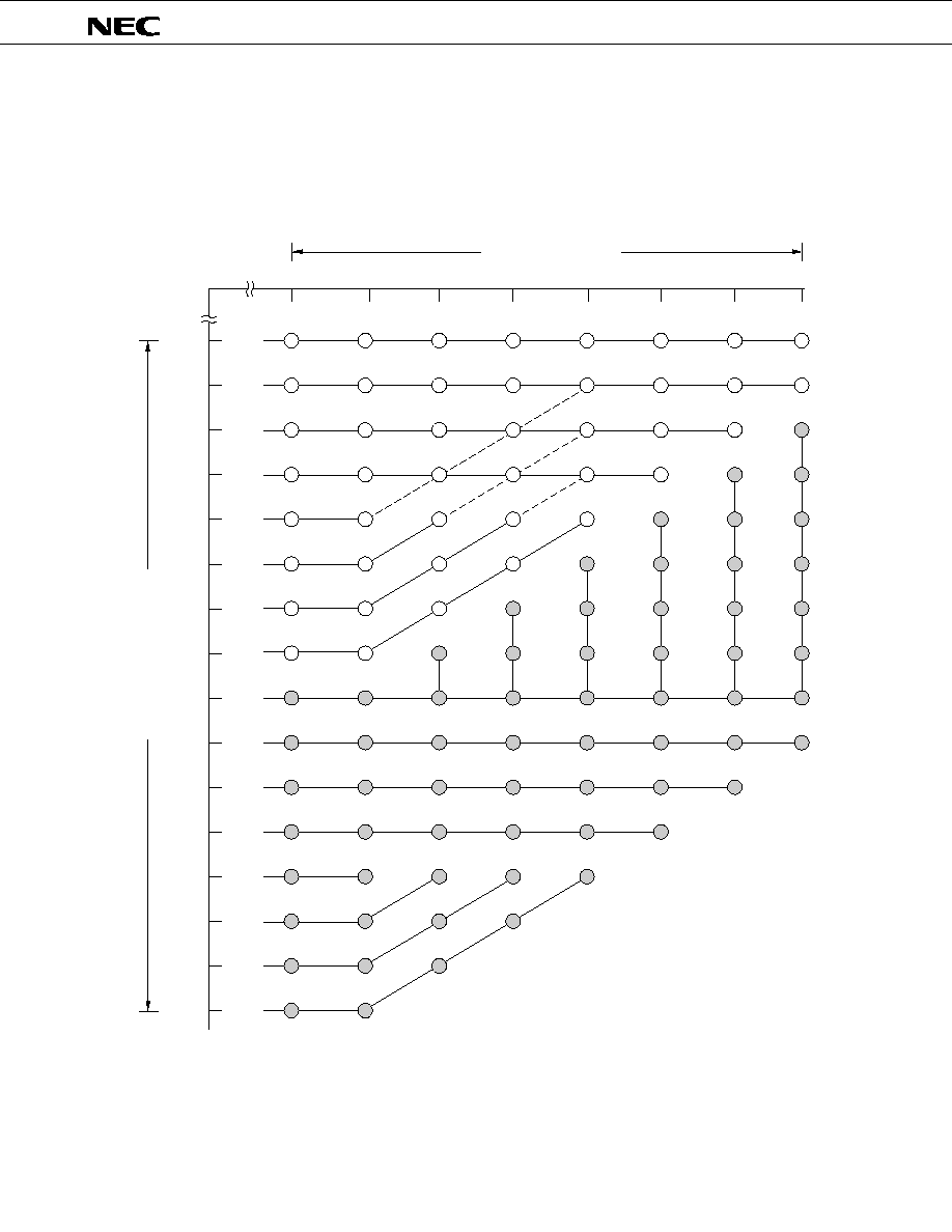
127
µ
PD75236
(8)
Display mode selection
The numbers of segments and digits which can be displayed using the built-in FIP controller/driver
depend on the display mode.
Fig. 4-75 shows a display mode selection diagram.
Fig. 4-75 Display Mode Selection Diagram
Remarks
The circled modes with shading are those expanded from the
µ
PD75216A and
µ
PD75217.
0
9
10
11
12
13
14
15
16
17
18
19
20
21
22
23
24
9
10
11
12
13
14
15
16
Digit Number Selection
9-Segment Mode
10-Segment Mode
11-Segment Mode
12-Segment Mode
13-Segment Mode
14-Segment Mode
15-Segment Mode
16-Segment Mode
17-Segment Mode
18-Segment Mode
19-Segment Mode
20-Segment Mode
21-Segment Mode
22-Segment Mode
23-Segment Mode
24-Segment Mode
Segment Number Selection

128
µ
PD75236
Key Scan Register
(9)
Display data memory
The display data memory is an area storing the displayed segment data and is mapped at addresses
1A0H to 1FFH of the data memory. Display data is automatically read by a display controller (DMA
operation). The areas not used for display can be used as normal data memory.
Display data operation is carried out by a data memory manipulation instruction. Data manipulation is
possible in 1, 4 and 8-bit units. Only even addressed can be specified for 8-bit manipulation instruction
execution.
Addresses 1FCH to 1FFH, 1BEH and 1BFH of the display data memory also serve as key scan registers
(KS0, KS1 and KS2).
Table 4-9 Data Memories which also Serve as Key Scan Registers
Data Memory which also
Serves as Key Scan Register
KS0
1FCH, 1FDH
KS1
1FEH, 1FFH
KS2
1BEH, 1BFH
Note
Extra caution is necessary when transferring a program developed for the
µ
PD75236 to one for the
µ
PD75216A and
µ
PD75217 because a maximum of 16 segments are displayed and no data memory is
incorporated at addresses (1A0H + 4n and 1A1H + 4n) in the case of the
µ
PD75216A and
µ
PD75217.

129
µ
PD75236
Fig. 4-76 Display Data Memory Contents and Segment Outputs
3
0 3
0 3
0 3
0 3
0 3
0
1A1H
1A0H
1C3H
1C2H
1C1H
1C0H
1A3H
1A2H
1C7H
1C6H
1C5H
1C4H
1A5H
1A4H
1CBH
1CAH
1C9H
1C8H
1A7H
1A6H
1CFH
1CEH
1CDH
1CCH
1A9H
1A8H
1D3H
1D2H
1D1H
1D0H
1ABH
1AAH
1D7H
1D6H
1D5H
1D4H
1ADH
1ACH
1DBH
1DAH
1D9H
1D8H
1AFH
1AEH
1DFH
1DEH
1DDH
1DCH
1B1H
1B0H
1E3H
1E2H
1E1H
1E0H
1B3H
1B2H
1E7H
1E6H
1E5H
1E4H
1B5H
1B4H
1EBH
1EAH
1E9H
1E8H
1B7H
1B6H
1EFH
1EEH
1EDH
1ECH
1B9H
1B8H
1F3H
1F2H
1F1H
1F0H
1BBH
1BAH
1F7H
1F6H
1F5H
1F4H
1BDH
1BCH
1FBH
1FAH
1F9H
1F8H
1BFH
1BEH(KS2)
1FFH
1FEH(KS1)
1FDH
1FCH(KS0)
T0
T1
T2
T3
T4
T5
T6
T7
T8
T9
T10
T11
T12
T13
T14
T15
Tks
KS0
KS1
KS2
S23S22 S21 S20 S19S18 S17 S16 S15S14 S13 S12 S11S10 S9 S8 S7 S6 S5 S4 S3 S2 S1 S0
T10T11 T12 T13 T14 T15
PH3PH2PH1PH0
24-Segment Mode
23-Segment Mode
22-Segment Mode
21-Segment Mode
20-Segment Mode
19-Segment Mode
18-Segment Mode
17-Segment Mode
16-Segment Mode
15-Segment Mode
14-Segment Mode
13-Segment Mode
12-Segment Mode
11-Segment Mode
10-Segment Mode
9-Segment Mode
Timing
Output
Display Data Memory
Key
Scan
Data
Segment
Output
Timing
Output
Port H
Output
(When specified by digit select register)
(When none of segment output and timing output are used)
Bit

130
µ
PD75236
(10) Key scan registers (KS0, KS1 and KS2)
The key scan registers (KS0, KS1 and KS2) are used to set the segment output data in the key scan
timing mapped in the part of the display data memory (addresses 1FCH, 1FDH, 1FEH, 1FFH, 1BEH and
1BFH).
KS0, KS1 and KS2 are 8-bit registers and are normally manipulated by an 8-bit manipulation instruction
(the lower 4 bits can be manipulated bit-wise or in 4-bit units).
Data set to KS0, KS1 and KS2 is output from the segment output pin at the key scan timing. During the
key scan timing the segment output data can be immediately changed by rewriting KS0, KS1 and KS2. Key
scan can be performed using the segment output.
(11) Key scan flag (KSF)
The key scan flag is set ("1") during the key scan timing and is automatically reset ("0") in all other
timings. The KSF is mapped at bit 3 of address F8AH and is bit-wise testable. No write is possible.
Whether the KSP is at the key scan timing can be checked by testing it. Thus, it is possible to check
whether key input data is correct or not.
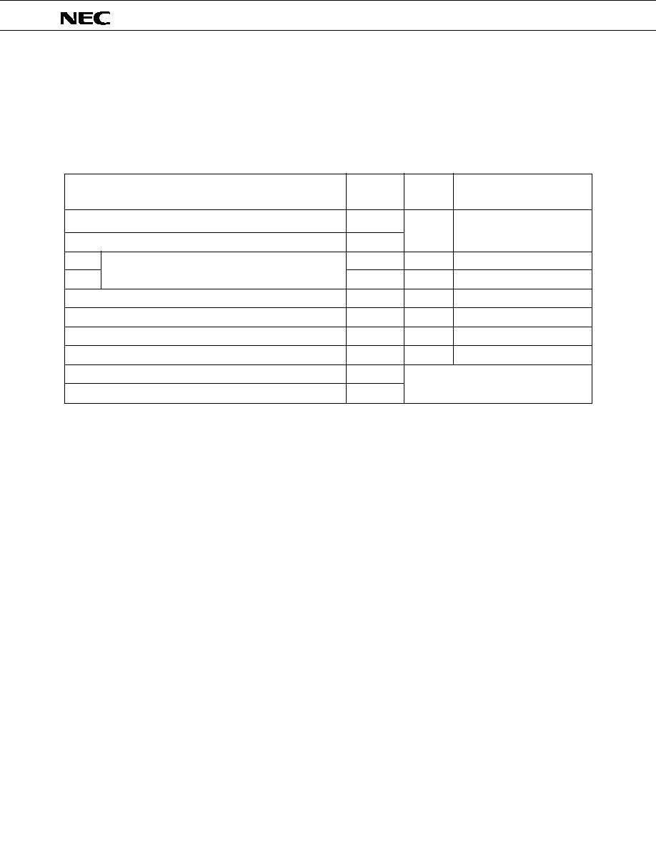
131
µ
PD75236
5.
INTERRUPT FUNCTIONS
The
µ
PD75236 has eight types of interrupt sources and can generate multiple interrupts with priority order.
It is also equipped with two types of test sources. INT2 is an edge detected testable input.
Table 5-1 Interrupt Source Types
* 1.
Interrupt order is priority order to be applied when two or more interrupt requests are generated simul-
taneously.
2.
These are test sources. They are affected by interrupt enable flags as in the case of interrupt sources, but
no vectored interrupt is generated.
The
µ
PD75236 interrupt control circuit has the following functions:
(a)
Hardware-controller vectored interrupt function which can control interrupt acknowledge with the
interrupt enable flag (IEXXX) and the interrupt master enable flag (IME).
(b)
Function of setting any interrupt start address.
(c)
Multiple interrupt function which can specify priority order with the interrupt priority select
register (IPS).
(d)
Interrupt request flag (IRQXXX) test function. (Interrupt generation can be checked by software.)
(e)
Standby mode release function. (Interrupt to be released by interrupt enable flag can be selected.)
5.1
INTERRUPT CONTROL CIRCUIT CONFIGURATION
The interrupt control circuit has a configuration shown in Fig. 5-1 and each hardware is mapped in the data
memory space.
Vectored Interrupt Request
Signal (Vector Table Address)
VRQ1 (0002H)
VRQ2 (0004H)
VRQ3 (0006H)
VRQ4 (0008H)
VRQ5 (000AH)
VRQ6 (000CH)
VRQ7 (000EH)
Interrupt
Order *1
1
2
3
4
5
6
7
Internal/
External
Internal
External
External
External
Internal
Internal
Internal
Internal
External
Internal
Interrupt Source
INTBT (Reference timer interval signal from the basic interval timer)
INT4 (Rising or falling edge detection)
INT0
INT1
INTCSI0 (Serial data transfer end signal)
INTT0 (Match signal from timer event/counter 0)
INTTPG (Match signal from timer/pulse generator)
INTKS (Key scan timing signal from display controller)
INT2 *2 (Rising edge detection)
INTW *2 (Signal from watch timer)
(Rising and falling detected edge selection)
Testable input signal (IRQ2 and IRQW set)
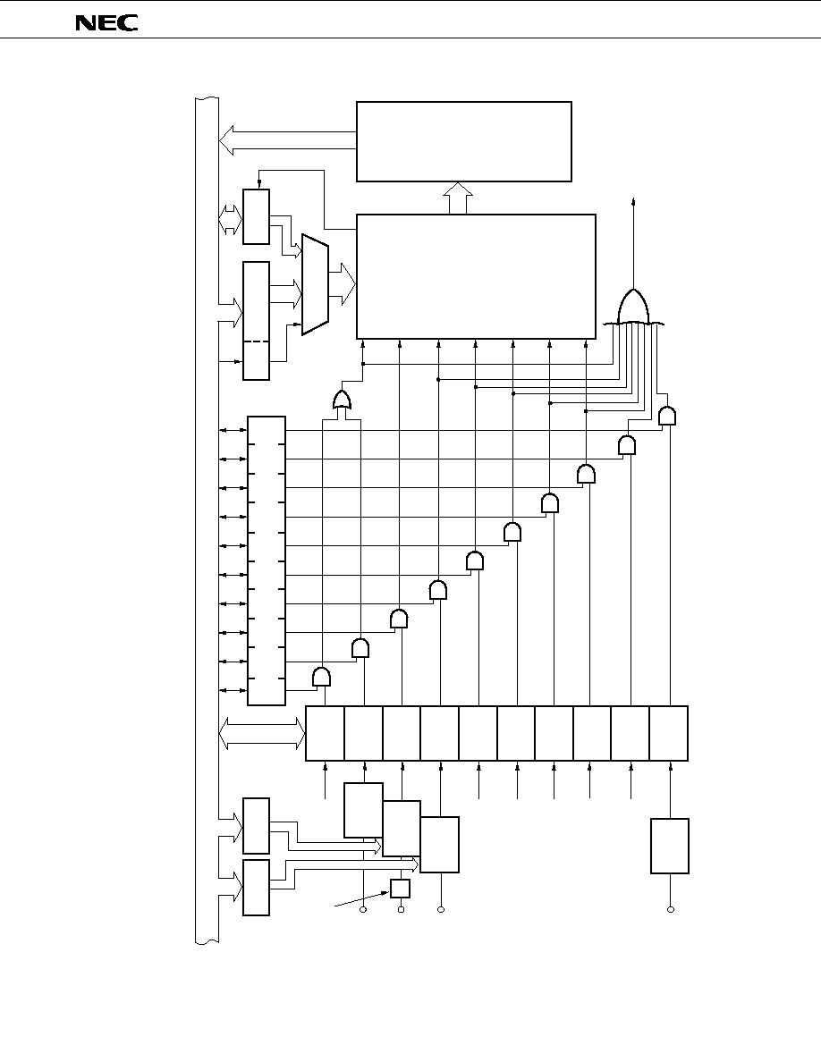
132
µ
PD75236
Fig. 5-1 Interrupt Control Circuit Block Diagram
2
2
4
2
IM1
IM0
(IME)
IPS
IST
INT
BT
INT4
P00
INT0
P10
INT1
/P11
INTCSI0
INTT0
INTTPG
INTKS
INTW
IRQBT
IRQ4
IRQ0
IRQ1
IRQCSI0
IRQT0
IRQTPG
IRQKS
IRQW
IRQ2
INT2
/P12
VRQ
n
Vector
Table
Address
Generator
Priority
Control
Circuit
Standby
Release
Signal
Decoder
Internal Bus
Interrupt Enable Flag (IEXXX)
Both Edge
Detector
Edge
Detector
Edge
Detector
Noise
Eliminator
Rising
Edge
Detector

133
µ
PD75236
5.2
INTERRUPT CONTROL CIRCUIT HARDWARE DEVICES
(1)
Interrupt request flag, interrupt enable flag
There are ten interrupt request flags (IRQXXX) corresponding to interrupt sources (interrupt :8, test :2)
as shown below.
INT0 interrupt request flag (IRQ0)
Serial interface interrupt request flag (IRQCSI0)
INT1 interrupt request flag (IRQ1)
Timer/event counter interrupt request flag (IRQT0)
INT2 interrupt request flag (IRQ2)
Timer/pulse generator interrupt request flag (IRQTPG)
INT4 interrupt request flag (IRQ4)
Key scan interrupt request flag (IRQKS)
BT interrupt request flag (IRQBT)
Watch timer interrupt request flag (IRQW)
Interrupt request flag is set to "1" at generation of an interrupt request and is automatically cleared
("0") upon execution of interrupt service. IRQBT and IRQ4 carry out clear operation differently because
they share the vector address. (See 5.5 VECTOR ADDRESS SHARING INTERRUPT SERVICE.)
There are ten interrupt enable flags (IEXXX) corresponding to interrupt request flags as shown below.
INT0 interrupt enable flag (IE0)
Serial interface interrupt enable flag (IECSI0)
INT1 interrupt enable flag (IE1)
Timer/event counter interrupt enable flag (IET0)
INT2 interrupt enable flag (IE2)
Timer/pulse generator interrupt enable flag (IETPG)
INT4 interrupt enable flag (IE4)
Key scan interrupt enable flag (IEKS)
BT interrupt enable flag (IEBT)
Watch timer interrupt enable flag (IEW)
When the contents of interrupt enable flag is "1", interrupt is enabled and when it is "0", interrupt is
disabled.
When the interrupt request flag is set and the interrupt enable flag has enabled interrupt, the vectored
interrupt request (VRQn) is generated.
This signal is also used to release the standby mode.
Both the interrupt request flag and interrupt enable flag are operated by the bit manipulation instruc-
tion and 4-bit memory manipulation instruction. They can be operated directly by the bit manipulation
instruction irrespective of MBE setting. The interrupt enable flag is operated by the EI IE
◊◊◊
and DI IE
◊◊◊
instruction. The SKTCLR instruction is normally used to test the interrupt request flag.
When the interrupt request flag is set by an instruction even if an interrupt has not been generated, the
vectored interrupt is executed in the same way as when an interrupt had been generated.
RESET input clears the interrupt request flag and the interrupt enable flag ("0") and disables all inter-
rupts.
5
5
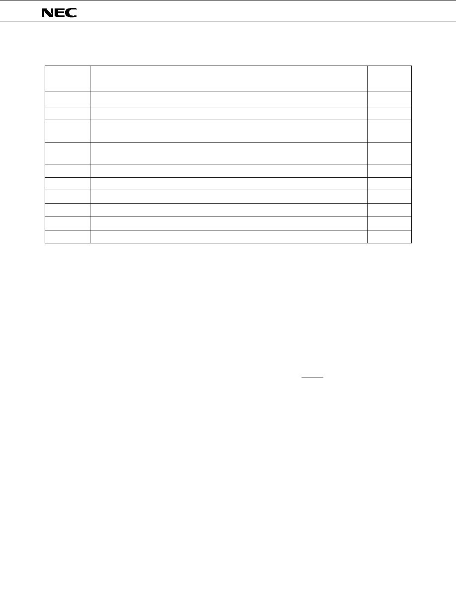
134
µ
PD75236
Table 5-2 Interrupt Request Flag Set Signals
(2)
Noise eliminator and edge detection mode register
INT0, INT1 and INT2 each have the configuration shown in Figs. 5-2 and 5-3 and serve as the external
interrupt input capable of selecting detected edges.
INT0 has a function of eliminating noise with sampling clock. Pulses having a shorter width than 2
sampling clock cycles* are eliminated as noise by noise eliminator.
However, pulses having a larger width than 1 sampling clock cycle may be acknowledged as an inter-
rupt signal depending on the sampling timing. Pulses having a larger width than 2 sampling clock cycles
are securely acknowledged as an interrupt signal.
INT0 has two sampling clocks,
and f
x
/64 and can select and use either clock. Selection is made by bit
3 (IM03) of the edge detection mode register (refer to Fig. 5-4).
IRQ2 is set by detecting the rising edge of INT2 pin input.
Edge detection mode registers (IM0 and IM1) to select detection edge have the format shown in Fig. 5-4.
IM0 and IM1 each are set by a 4-bit memory manipulation instruction. RESET input clears all bits to 0
and specifies INT0, INT1 and INT2 for the rising edge.
*
When sampling clock is
: 2t
CY
When sampling clock is fx/64 : 128/f
X
Note
1. Since INT0 samples by clock, it is not operated in the standby mode.
2. Pulses are input to the INT0/P10 pin serving as a port via the noise eliminator. Thus, input pulses
having two sampling clock cycles or larger.
Interrupt Request Flag Set Signal
Set by the reference time interval signal generated by the basic interval timer.
Set upon detection of the rising or falling edge of the INT4/PO0 input signal.
Set upon detection of the INT0/P10 pin input signal edge. The detected edge is selected
using the INT0 mode register (IM0).
Set upon detection of the INT1/P11 pin input signal edge. The detected edge is selected
using the INT1 mode register (IM1).
Set by the serial data transfer operation end signal of the serial interface.
Set by the match signal from the timer/event counter #0.
Set by the match signal from the timer/pulse generator.
Set by the key scan timing signal from the display controller.
Set by a signal from the watch timer.
Set upon detection of the rising edge of the INT2/P12 pin input signal.
Interrupt
Request Flag
IRQBT
IRQ4
IRQ0
IRQ1
IRQCSI0
IRQT0
IRQTPG
IRQKS
IRQW
IRQ2
Interrupt
Enable Flag
IEBT
IE4
IE0
IE1
IECSI0
IET0
IETPG
IEKS
IEW
IE2
5
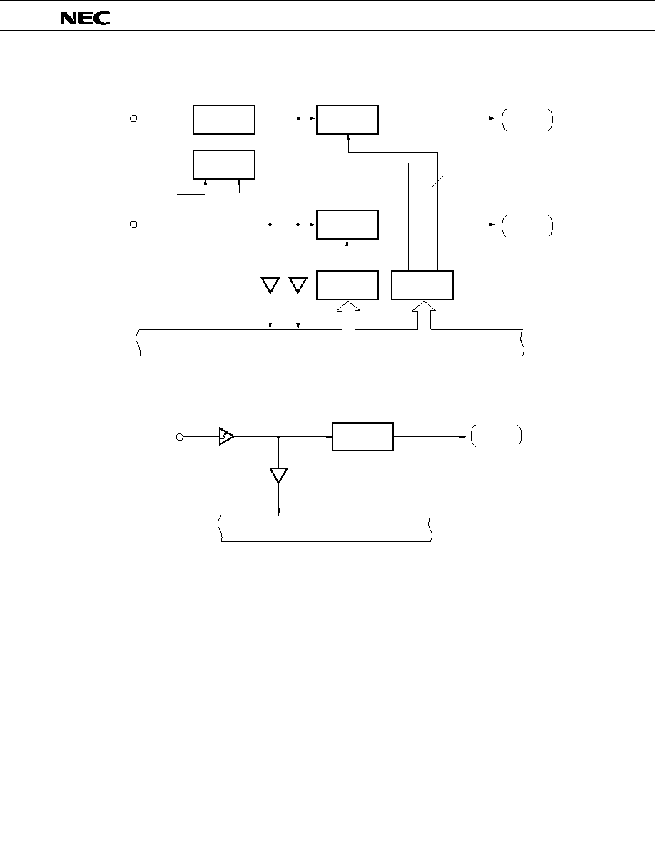
135
µ
PD75236
Fig. 5-2 INT0 and INT1 Configuration
Fig. 5-3 INT2 Configuration
INT0/ P10
INT0
IM01, IM00
IM03
IM10
IM1
IM0
4
4
64
f
X
INT1/ P11
2
INT2/P12
Noise
Eliminator
Edge
Detector
IRQ0
Set Signal
INT1
IRQ1
Set Signal
INT2
IRQ2
Set Signal
Rising
Edge Detector
Input Buffer
Internal Bus
Internal Bus
Input Buffer
Selector
Edge
Detector
136
µ
PD75236
Fig. 5-4 Edge Detection Mode Register Format
Note
If the edge detection mode register is changed, the interrupt request flag may be set. To prevent that
from occurring, disable interrupt and change edge detection mode register first, then enable interrup-
tion after clearing the interrupt request flag by the CLR1 instruction. If f
x
/64 has been selected as
sampling clock by changing IM0, it is necessary to clear the interrupt request flag 16 machine cycles
after the mode register has been changed.
0
0
Rising edge specification
0
1
Falling edge specification
1
0
Rising and falling edge specification
1
1
Ignored (interrupt request flag not set)
Detection Edge Specification
IM03
0
IM01
IM00
3
2
1
0
FB4H
IM0
Address
Symbol
Sampling Clock
0
(0.95, 1.91, 3.82, 15.3:
µ
s: at 4.19 MHz operation)
1
f
x
/64 (15.3
µ
s: at 4.19 MHz operation)
0
0
0
IM10
FB5
IM1
0
Rising edge specification
1
Falling edge specification

137
µ
PD75236
(3)
Interrupt priority select register (IPS)
The interrupt priority select register is used to select high interrupt enabled for multiple interrupt and is
specified by the least significant 3 bits.
Bit 3 is an interrupt master enable flag (IME) to specify whether all interrupts should be disabled or not.
The IPS is set by the 4-bit memory manipulation instruction and bit 3 is set/reset by the EI/DI instruc-
tion.
When changing the low-order 3 bit contents of IPS, it is necessary to do so with interrupt disabled (IME
= 0).
RESET input clears all bits to "0".
Fig. 5-5 Interrupt Priority Select Register
0
0
0
None of interrupts are made high interrupts.
0
0
1
VRQ1 (INTBT/INT4)
0
1
0
VRQ2 (INT0)
0
1
1
VRQ3 (INT1)
1
0
0
VRQ4 (INTCSI0)
1
0
1
VRQ5 (INTT0)
1
1
0
VRQ6 (INTTPG)
1
1
1
VRQ7 (INTKS)
High Interrupt Select
IPS3
IPS2
IPS1
IPS0
3
2
1
0
FB2H
IPS
Address
Symbol
Vectored interrupts on
the left are taken as
high interrupts.
All interrupts are disabled and vectored interrupt is not
started.
Interrupt enable/disable is controlled by the correspond-
ing interrupt enable flag.
Interrupt Mask Enable Flag (IME)
0
1

138
µ
PD75236
5.3
INTERRUPT SEQUENCE
If interrupt is generated, it is processed using the following procedure:
* 1.
IST1 and IST0 : Interrupt status flags (PSW bits 3, 2: Refer to Table 5-3 IST1 and IST0 Interrupt Servicing
Statuses).
2.
The start address of the interrupt service program and the MBE and RBE set values at the start of
interrupt are stored in each vector table.
NO
YES
NO
IME = 1
YES
NO
YES
NO
YES
YES
NO
*1
IST 1,0 = 00
Interrupt (INTXXX) generated
IRQXXX set
IEXXX set?
Is VRQn
a high interrupt?
*1
IST 1,0 = 00 or 01
Depends on the
instruction being
executed when
IRQn is set.
2 Machine
Cycles
PC and PSW contents are saved into the stack memory and the data *2 in
the vector table corresponding to the started VRQn is set to PC, RBE and
MBE.
IST0 and IST1 contents are changed from 00
to 01 or from 01 to 10.
Acknowledged IRQXXX is reset.
(If the interrupt source shares the vector address,
refer to 5.5 VECTOR ADDRESS SHARING
INTERRUPT SERVICING.)
Interrupt service program processing start
Selected
VRQn
Remaining
VRQn
If two or more VRQn have been gene-
rated simultaneously, one VRQn is se-
lected according to the interrupt order
shown in Table 5-1.
Reserved until
termination of
operation being
executed
Reserved
until IME is
set
Reserved until
IEXXX is set
Corresponding VRQn
generated
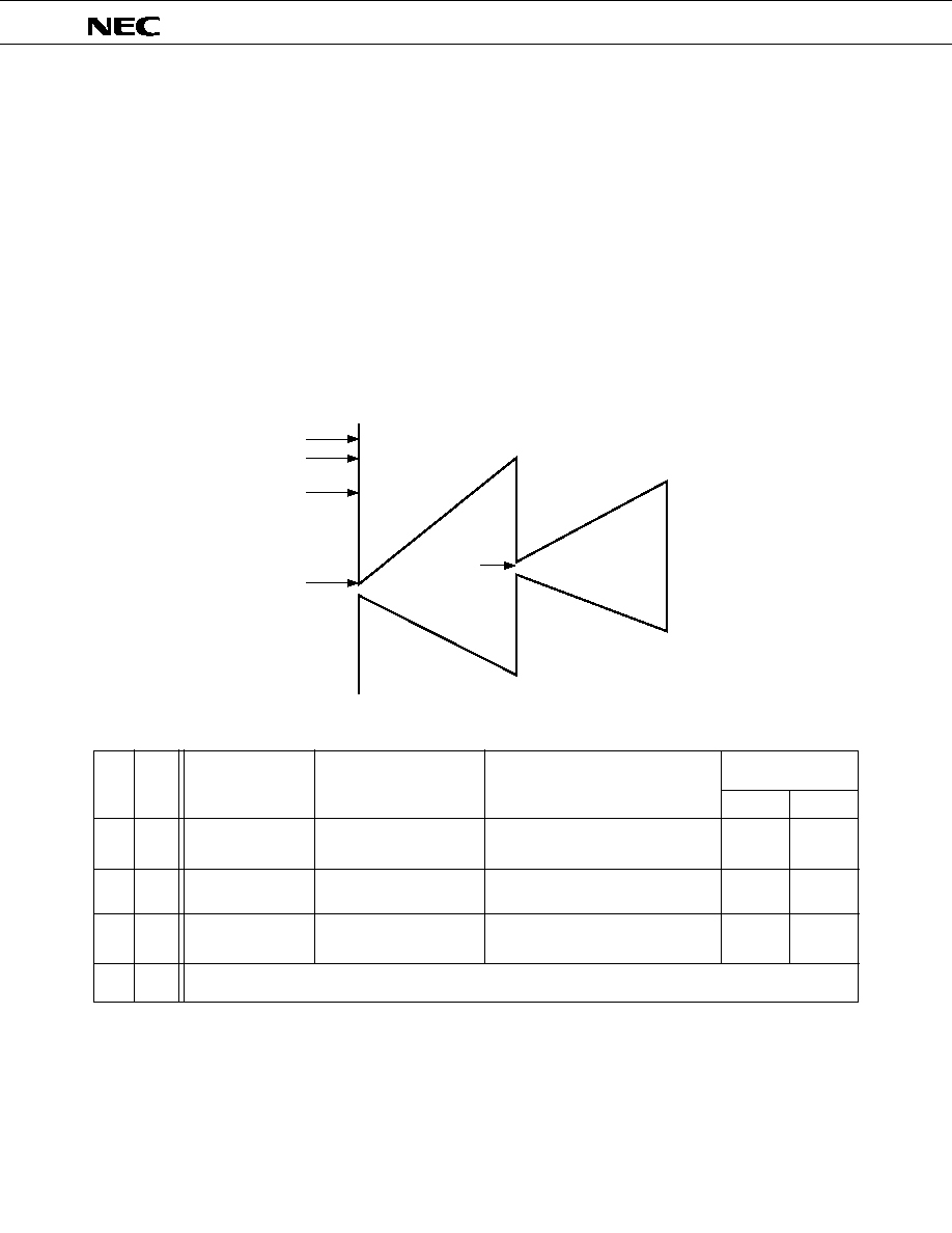
139
µ
PD75236
Table 5-3 IST1 and IST0 Interrupt Servicing Statuses
When an interrupt is acknowledged, IST1 and IST0 are saved into the stack memory together with other
PSW and is changed to a status higher by one level. When RET1 instruction is executed, the original IST1
and IST0 values are reset.
5.4
MULTI-INTERRUPT SERVICE CONTROL
The following two methods are available for the
µ
PD75236 to generate multi-interrupts.
(1)
Multi-interruption specifying high interrupt
This is a standard multi-interrupt method of the
µ
PD75236 in which one interrupt source is selected and
multi-interruption (dual interrupt) is enabled.
In other words, the high interrupt specified using the interrupt priority select register (IPS) is enabled
when the status of the operation being executed is 0 or 1. All other interrupts (low interrupts) are only
enabled when the status is 0. (Refer to Fig. 5-6 and Table 5-3.)
Fig. 5-6 Multi-Interruption by High Interrupt
Interrupt Disable
IPS Set
Interrupt Enable
Low or High
Interrupt Generated
High
Interrupt
Generated
Normal Processing
(Status 0)
Low or High
Interrupt
Servicing
(Status 1)
High Interrupt
Servicing
(Status 2)
After Interrupt
Acknowledgement
IST1
IST0
0
1
1
0
≠
≠
Interrupt Acknowledgeable
Interrupt Request
All interrupts acknowledgeable
Only high interrupt acknowledgeable
All interrupts not acknowledgeable
CPU Processing
Contents
Normal program being
processed
Low or high interrupt
being servicing
High interrupt being
servicing
Status of Servicing
being Executed
Status 0
Status 1
Status 2
IST1
IST0
0
0
0
1
1
0
1
1
Setting prohibited

140
µ
PD75236
(2)
Multi-interruption changing the interrupt status flag
As is clear from Table 5-3, multi-interrupt is enabled by changing the interrupt status flag using the
program. That is, multi-interrupt is enabled by changing IST1 and IST0 each to "0" using the interrupt
servicing program and setting status 0.
This method is used to enable multi-interrupt with two to more interrupts or multi-interruption with
triple or more interrupts.
Before changing IST1 and IST0, disable interruption by DI instruction.
Fig. 5-7 Multi-Interruption by Changing the Interrupt Status Flag
Interrupt Disable
IPS Set
Interrupt Enable
Low or High
Interrupt Generated
Interrupt
Disable
IST Change
Interrupt Enable
Low or High
Interrupt
Generated
Status 1
Status 0
Status 0
High
Interrupt
Generated
Status 1
Status 2
Normal Processing
(Status 0)
Single Interrupt
Dual Interrupt
Triple Interrupt

141
µ
PD75236
5.5
VECTOR ADDRESS SHARING INTERRUPT SERVICING
Since the INTBT and INT4 interrupt sources share the vector table, interrupt source selection is carried out
as follows:
(1)
When only one interrupt source is used
Among the two interrupt sources sharing the vector table, set the interrupt enable flag of the necessary
interrupt source ("1") and clear the other interrupt enable flag ("0"). In this case, an interrupt request is
generated by the enabled interrupt source (IEXXX=1). When the request is acknowledged, the correspond-
ing interrupt request flag is reset (as is the case with an interrupt not sharing the vector address).
(2)
When both interrupt sources are used
Set the interrupt enable flags corresponding to the two interrupt sources ("1"). In this case, the logical
sum of the interrupt request flags of the two interrupt sources becomes an interrupt request.
And, if an interrupt request by the setting of one or both interrupt request flags is acknowledged, none
of the interrupt request flag is reset.
Accordingly, it is necessary to check in the interrupt service routing by which interrupt source the
interrupt has been generated. It can be done by executing the DI instruction at the beginning of the
interrupt service routine and checking the interrupt request flag by the SKTCLR instruction.

142
µ
PD75236
STOP Mode
STOP instruction
Setting enabled only with main system
clock.
Oscillator stops only with main system
clock.
Operation enabled only when external
SCK0 input is selected for serial clock.
Operation enabled only when external
SCK1 input is selected for serial clock.
Operation stopped.
Operation enabled only when TI0 pin
input is specified for count clock.
Operation enabled only f
XT
is selected for
count clock.
Operation stopped.
Operation stopped.
Operation stopped.
HALT Mode
HALT instruction
Setting enabled with either main system
clock or subsystem clock.
Stops only with CPU clock
(Oscillation
continued).
Operation enabled when the main system
clock oscillates or with external SCK0.
Operation enabled only when the main
system clock oscillates.
Operation (IRQBT set at reference time
intervals).
Operation enabled.
Operation enabled.
Operation enabled only when the main
system clock oscillates.
Operation enabled only when the main
system clock oscillates.
Operation enabled only when the main
system clock oscillates.
Operating State
Operation disabled (display off mode set before disabling).
INT0 operation disabled.
INT1, INT2 and INT4 operation enabled.
Operation stopped.
Interrupt request signal or RESET input from operational hardware enabled by
interrupt enable flag.
6.
STANDBY FUNCTIONS
Two standby modes (STOP mode and HALT mode) are available for the
µ
PD75236 to decrease power
consumption in the program standby mode.
6.1
STANDBY MODE SETTING AND OPERATING STATE
Table 6-1 Operation Status in Standby Mode
Set instruction
System clock when set
Clock oscillator
Serial interface (channel 0)
Serial interface (channel 1)
Basic interval timer
Timer/event counter
Watch timer
Timer/pulse generator
Event counter
A/D converter
FIP controller/driver
External interrupt
CPU
Release signal

143
µ
PD75236
The STOP and HALT modes are set by STOP and HALT instructions, respectively. (The two instructions are
instructions to set PCC bit 3 and bit 2, respectively.)
When changing the CPU operation clock with the least significant 2 bits of PCC, a delay may result from
PCC rewrite to CPU clock change as shown in Table 4-1. Thus, when changing the operation clock before the
standby mode is set or the CPU clock after the standby mode is released, set the standby mode after the
passage of the machine cycle required for CPU clock change following PCC rewrite.
In the standby mode, the data of all registers and data memories which stop operating is held. Such units
include general registers, flag, mode registers and output latches.
Note 1.
When the STOP mode is set, X1 input is internally short-circuited to V
SS
(GND potential) to prevent
leakage from the crystal resonator unit. Thus, the use of STOP mode is prohibited in a system
using external clocks.
2.
Because the interrupt request signal is used to release the standby mode, the standby mode is
immediately released if there is an interrupt source with both the interrupt request flag and inter-
rupt enable flag set. Thus, the STOP mode is set to the HALT mode just after STOP instruction
execution. After waiting for the time period set by the BTM register, the operating mode is reset.

144
µ
PD75236
6.2
STANDBY MODE RELEASE
The STOP and HALT modes each are released upon generation of the interrupt request signal* enabled by
the interrupt enable flag or by RESET input. Fig. 6-1 shows release operation in each mode.
*
Except INT0 to INT2.
Fig. 6-1 Standby Mode Release Operation (1/2)
(a)
Release by RESET input in STOP mode
(b)
Release by interrupt generation in STOP mode
Remarks
The broken line shows the case in which the interrupt request which released the standby mode has
been acknowledged (IME = 1).
(c)
Release by RESET input in HALT mode
RESET
Signal
STOP Instruction
Operating
Mode
STOP Mode
HALT Mode
Operating
Mode
Oscillation
Oscillation Stop
Oscillation
Clock
Wait (Approx.
31.3 ms:4.19 MHz)
STOP Instruction
Standby Release Signal
Operating
Mode
STOP Mode
HALT Mode
Operating
Mode
Oscillation
Oscillation Stop
Oscillation
Clock
Wait (time set by BTM)
RESET
Signal
HALT Instruction
Operating
Mode
HALT Mode
Operating
Mode
Clock
Oscillation
Wait (Approx. 31.3
ms:4.19 MHz)

145
µ
PD75236
HALT Instruction
Standby
Release
Signal
Operating
Mode
Clock
HALT Mode
Operating Mode
Oscillation
a
V
ss
STOP Mode Release
X1 in Voltage
Waveform
BTM3
BTM2
BTM1
BTM0
≠
0
0
0
≠
0
1
1
≠
1
0
1
≠
1
1
1
In all other cases
Fig. 6-1 Standby Mode Release Operation (2/2)
Wait Time* (Values at f
XX
= 4.19 MHz are shown in parentheses)
Approx. 2
20
/f
XX
(approx. 250 ms)
Approx. 2
17
/f
XX
(approx. 31.3 ms)
Approx. 2
15
/f
XX
(approx. 7.82 ms)
Approx. 2
13
/f
XX
(approx. 1.95 ms)
Setting prohibited
*
Wait time does not include a time from STOP mode release to oscillation start.
(d)
Release by interrupt generation in HALT mode
Remarks
The broken line shows the case in which the interrupt request which released the standby mode has
been acknowledged (IME = 1).
The wait time upon STOP mode release does not include a time from STOP mode release to clock
oscillation start ("a" below) whether the STOP mode is released by RESET input or interrupt genera-
tion.
If the STOP mode has been released by interrupt generation, the wait time is determined by BTM
setting. (Refer to Table 6-2.)
Table 6-2 Wait Time Selection by BTM

146
µ
PD75236
6.3
OPERATION AFTER STANDBY MODE RELEASE
(1)
If the STOP mode has been released by RESET input, normal reset operation is carried out.
(2)
If the STOP mode has been released by interrupt generation, the bit 3 (IME) contents of the IPS deter-
mine whether a vectored interrupt should be executed when the CPU resumes instruction execution.
(a)
When IME = "0"
Execution is resumed with the instruction (NOP instruction) following standby mode setting after
the standby mode has been released. The interrupt request flag is held.
(b)
When IME = "1"
Vectored interrupt is executed following execution of two instructions after the standby mode has
been released. If the standby mode has been released by INTW (testable input), no vectored interrupt
is generated; so the same processing as with (a) is carried out.
147
µ
PD75236
7.
RESET FUNCTIONS
The reset signal (RES) generator has a configuration shown in Fig. 7-1.
Fig. 7-1 Reset Signal Generator
Reset operation is shown in Fig. 7-2.
The output buffer is turned OFF upon RESET input.
Table 7-1 shows each hardware status after reset.
Fig. 7-2 Reset Operation by RESET input
Table 7-1 shows each hardware status after reset.
RESET
Interrupt Reset Signal
(RES)
(31.3ms:4.19MHz)
Wait
RESET Input
Operating Mode or
Standby Mode
HALT Mode
Operating
Mode
Internal Reset Operation
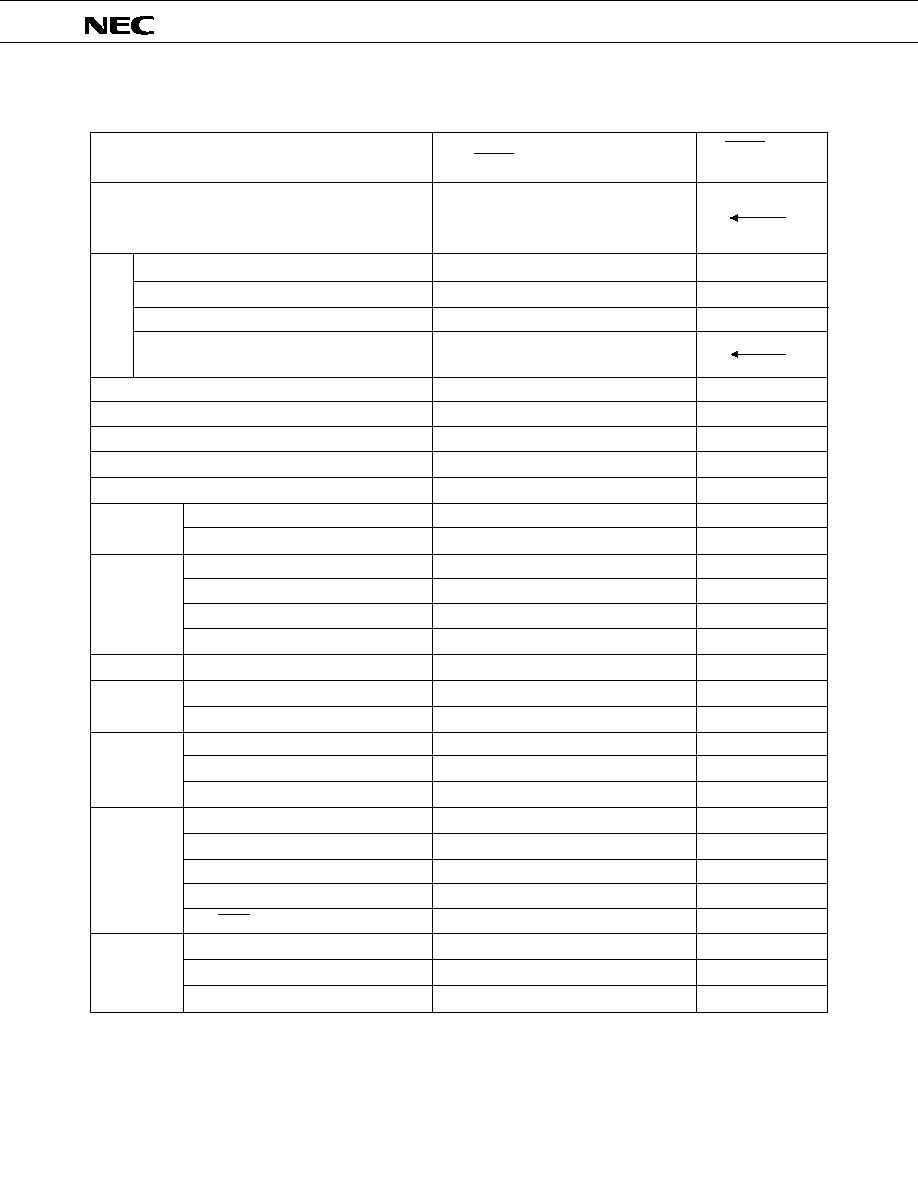
148
µ
PD75236
Table 7-1 Hardware Statuses after Reset (1/2)
RESET Input
in Operation
Undefined
0
0
Undefined
Undefined
0, 0
Undefined
Undefined
Undefined
0
0
FFH
0
0, 0
0
Hold
0
0
0
0
Undefined
0
0
Undefined
1
Undefined
0
0
RESET Input in Standby Mode
Sets the low-order 6 bits of program
memory address 0000H to PC13-8 and the
contents of address 0001H to PC7-0.
Hold
0
0
Sets bit 6 of program memory address
0000H to RBE and bit 7 to MBE.
Hold
Hold
0, 0
Undefined
Undefined
Undefined
0
0
FFH
0
0,0
0
Hold
0
0
0
0
Hold
0
0
Hold
1
Hold
0
0
Hardware
Program counter (PC)
Carry flag (CY)
Skip flag (SK0-SK2)
Interrupt status flag (IST1, IST2)
Bank enable flags
(MBE, RBE)
Data memory (RAM)
General registers (X, A, H, L, D, E, B, C)
Bank select registers (MBS, RBS)
Stack pointer (SP)
Stack bank select register (SBS)
Counter (BT)
Mode register (BTM)
Counter (T0)
Modulo register (TMOD0)
Mode register (TM0)
TOE0, TOUT F/F
Mode register (WM)
Modulo register (MODH, MODL)
Mode registet (TPGM)
Counter (T1)
Mode register (TM1)
Gate control register (GATEC)
Shift register (SIO0)
Operating mode register (CSIM0)
SBI control register (SBIC)
Slave address register (SVA)
P01/SCK0 output latch
Shift register (SIO1)
Operating mode register (CSIM1)
Serial transfer end flag (EOT)
PSW
Basic interval
timer
Timer/event
counter
Watch timer
Timer/pulse
generator
Event counter
Serial
interface
(channel 0)
Serial
interface
(channel 1)

149
µ
PD75236
Table 7-1 Hardware Statuses after Reset (2/2)
RESET Input
in Operation
04H (EOC = 1)
Undefined
Undefined
0
0
8H
Hold
OFF
0, 0
0
0
0
Reset
0
0
0, 0
OFF
Clear
0
0
OFF
0
Undefined
RESET Input in Standby Mode
04H (EOC = 1)
Undefined
Hold
0
0
8H
Hold
OFF
0, 0
0
0
0
Reset
0
0
0, 0
OFF
Clear
0
0
OFF
0
Hold
A/D converter
FIP controller/
driver
Clock
generator and
clock output
circuit
Interrupt
function
Digital port
Ports 10 to 15
Port H
Hardware
Mode register (ADM), EOC
SA register
Bit sequential buffer (BSB0 to BSB3)
Mode register (DSPM)
Dimmer select register (DIMS)
Digit select register (DIGS)
Display data memory
Output buffer
Static mode register (STATA, STATB)
Processor clock control register (PCC)
System clock control register (SCC)
Clock output mode register (CLOM)
Interrupt request flag (IRQ
◊◊◊
)
Interrupt enable flag (IE
◊◊◊
)
Interrupt master enable flag (IME)
INT0 and INT1 mode registers (IM0, IM1)
Output buffer (ports 2 to 7)
Output latch (ports 2 to 7)
Input/output mode register (PMGA, PMGB)
Pull-up resistor specify register (POGA)
Output buffer
Output latch
Output latch
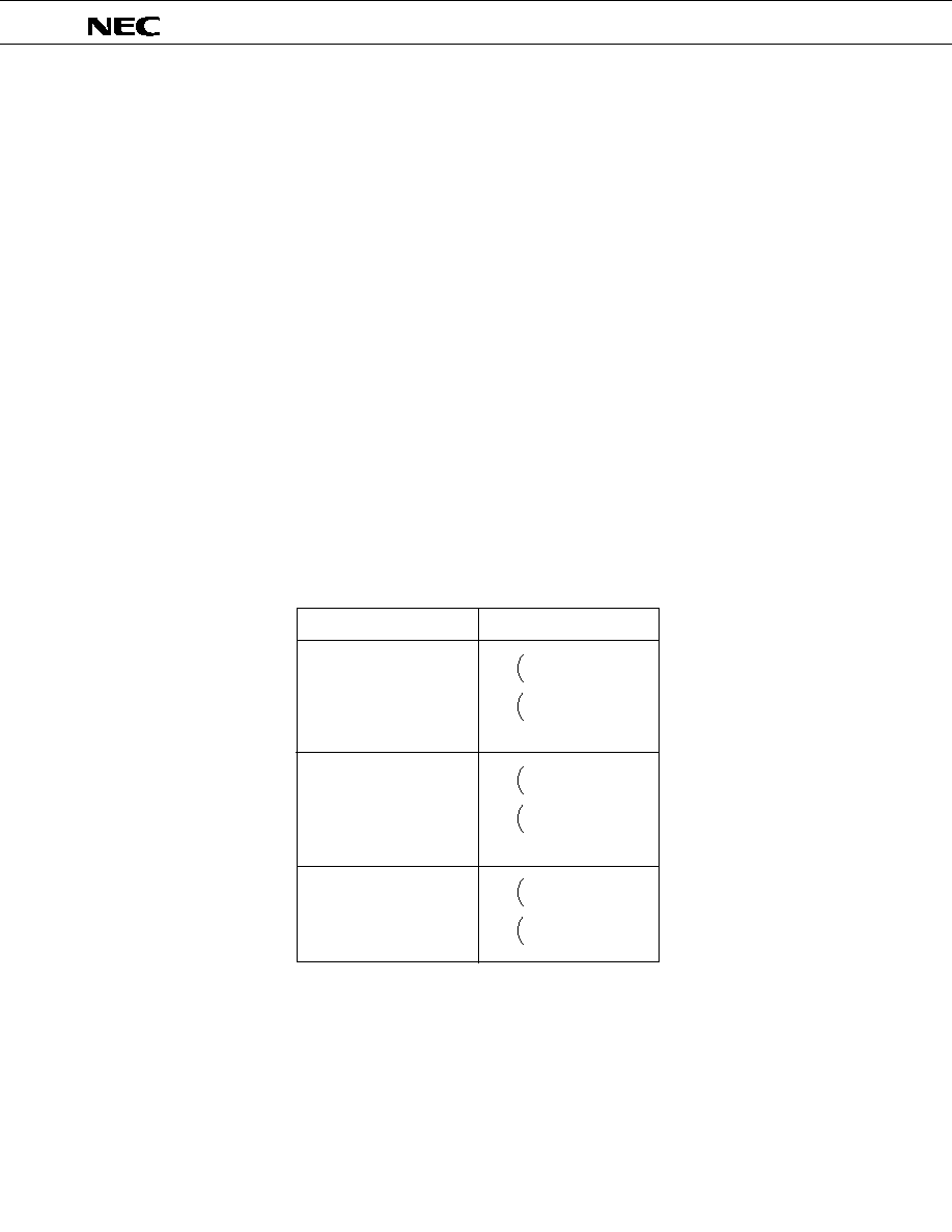
150
µ
PD75236
8.
INSTRUCTION SET
8.1
CHARACTERISTIC INSTRUCTIONS OF
µ
PD75236
(1)
GETI instruction
The GETI instruction is a 1-byte instruction to execute the following three types of operations by
referring to the 2-byte table in the program memory.
It can considerably help to decrease the number of program steps.
(a)
Subroutine call to 16K-byte space (0000H to 3F7FH) of table data as call instruction call address.
(b)
Branch to 16K-byte space (0000H to 3F7FH) of table data as branch instruction branch address
(c)
Execution of table data as 2-byte instruction (except BRCB and CALLF instructions)
(d)
Execution of table data as 1-byte instruction and 2 operation codes.
As shown in Fig. 3-2, the table addressed referred to by GETI instruction as 0020H to 007FH of the
program memory and data can be set in 48 tables.
When describing table addresses as operands, describe even addresses.
Note
1. 2-byte instructions which can be referred to by GETI instruction are limited to 2-machine cycle
instructions.
2. When referring to two 1-byte instructions by GETI instruction, combinations are limited as follows.
1st Byte Instruction
2nd Byte Instruction
INCS
L
DECS
L
INCS
H
DECS
H
INCS
HL
INCS
E
DECS
E
INCS
D
DECS
D
INCS
DE
INCS
L
DECS
L
INCS
D
DECS
D
MOV
A, @HL
MOV
@HL, A
XCH
A, @HL
MOV
A, @DE
XCH
A, @DE
MOV
A, @DL
XCH
A, @DL

151
µ
PD75236
Since the PC does not increment during execution of GETI instruction, it continues processing
with the address following GETI instruction.
If an instruction preceding the GETI instruction has the skip function, the GETI instruction is
skipped as is the case with all other 1-byte instructions. If the instruction referred to by the GETI
instruction has the skip function, an instruction following the GETI instruction is skipped.
When instructions having stack effects are referred to by the GETI instruction, the following
operations are carried out:
∑ If an instruction preceding GETI instruction also has the stack effects of the same group, the
execution of GETI instruction eliminates the stack effects and the instructions referred to are not
skipped.
∑ If an instruction following GETI instruction also has the stack effects of the same group, the stack
effects derived from the instructions referred to are valid and the following instruction is skipped.
(2)
Bit manipulation instruction
In addition to normal bit manipulation instructions (set and clear instructions), the bit test instruction,
bit transfer instruction and bit Boolean instructions (AND, OR, XOR) are available for the
µ
PD75236.
Manipulation bits are specified by bit manipulation addressing.
Three types of available addressing operations and bits manipulated by each addressing are shown
below.
Addressing
Specifiable Peripheral Hardware
Specifiable Bit Address Range
RBE/MBE/IST1, IST0/IE
◊◊◊
/IRQ
◊◊◊
FB0H to FBFH
PORT0 to 6
FF0H to FFFH
pmem.@L
PORT0,4
FC0H to FFFH
All peripheral hardware devices
All manipulatable bits of
enabled for bit manipulation
the memory bank specified by MB
◊◊◊
: 0, 1, 2, 3, 4, BT, T0, TPG, CSI0, KS, W
MB = MBE∑ MBS
fmem.bit
@H+mem.bit

152
µ
PD75236
(3)
Stack instructions
If the instructions of the same group of the following three instructions are stacked (set at two or
more continuous addresses) in the program, the stack instruction placed at the start point is ex-
ecuted. In the subsequent execution, one stack instruction is replaced with one NOP instruction.
Group A: MOV A, #n4,
MOV XA, #n8
Group B: MOV HL, #n8
(4)
Radix adjustment instructions
Radix adjustment instructions to adjust the result of 4-bit data addition or subtraction to any radix
is available for the
µ
PD75236.
When the radix to be adjusted is m.
∑ ADD
ADDS A, #16-m
ADDC A, @HL
ADDS A, #m
∑ Subtract
SUBC A, @HL
ADDS A, #m
Using the above combinations, the addition/subtraction result with the memory addressed by the
accumulator and register pair HL is adjusted to a m-ary radix. In the case of subtraction, m's complement
of the subtraction result is set to the accumulator. The overflow/underflow remains in the carry flag (in
these instruction combinations, the "ADDS A, #m" instruction skip function is disabled).

153
µ
PD75236
8.2
INSTRUCTION SET AND OPERATION
(1)
Operand identifier and description
Enter an operand in the operand column of each instruction using the description method relating to
the operand identifier of the instruction (refer to the assembler specifications for details). If more than one
description method is available, select one. Capital alphabetic letters, plus and minus signs are keywords.
Describe them as they are.
In the case of immediate data, describe appropriate numerical values or labels.
Symbols in the register and flag format diagrams in chapters 3 to 5 can be described as labels in place
of mem, fmem, pmem, bit, etc. (Available labels are limited for fmem and pmem. Refer to 8.1 (2) Bit
manipulation instruction.)
Identifier
Description Method
reg
X, A, B, C, D, E, H, L
reg 1
X, B, C, D, E, H, L
rp
XA, BC, DE, HL
rp1
BC, DE, HL
rp2
BC, DE
rp'
XA, BC, DE, HL, XA', BC', DE', HL'
rp'1
BC, DE, HL, XA', BC', DE', HL'
rpa
HL, HL+, HL-, DE, DL
rpa1
DE, DL
n4
4-bit immediate data or label
n8
8-bit immediate data or label
mem
8-bit immediate data or label*
bit
2-bit immediate data or label
fmem
FB0H to FBFH and FF0H to FFFH immediate data or labels
pmem
FC0H to FFFH immediate data or labels
addr
0000H to 3F7FH immediate data or labels
caddr
12-bit immediate data or label
faddr
11-bit immediate data or label
taddr
20H to 7FH immediate data (bit0 = 0) or label
PORTn
PORT0 to PORT15
IEXXX
IEBT, IECSI0, IET0, IETPG, IE0, IE1, IE2, IEKS, IEW, IE4
RBn
RB0 to RB3
MBn
MB0, MB1, MB2, MB15
*
For 8-bit data processing, only even addresses can be specified.

154
µ
PD75236
(2)
Legend for operation description
A
: A register; 4-bit accumulator
B
: B register
C
: C register
D
: D register
E
: E register
H
: H register
L
: L register
X
: X register
XA
: Register pair (XA); 8-bit accumulator
BC
: Register pair (BC)
DE
: Register pair (DE)
HL
: Register pair (HL)
XA'
: Expanded register pair (XA')
BC'
: Expanded register pair (BC')
DE'
: Expanded register pair (DE')
HL'
: Expanded register pair (HL')
PC
: Program counter
SP
: Stack pointer
SBS
: Stack bank select register
CY
: Carry flag; Bit accumulator
PSW
: Program status word
MBE
: Memory bank enable flag
RBE
: Register bank enable flag
PORTn : Port n (n = 0 to 15)
IME
: Interrupt master enable flag
IPS
: Interrupt priority select register
IE
◊◊◊
: Interrupt enable flag
RBS
: Register bank select register
MBS
: Memory bank select register
PCC
: Processor clock control register
∑
: Address and bit delimiter
(
◊◊
)
: Contents addressed by
◊◊
◊◊
H
: Hexadecimal data

155
µ
PD75236
(3)
Description of symbols in the addressing area column
* 1
MB = MBE∑MBS
(MBS = 0, 1, 2, 15)
* 2
MB = 0
* 3
MBE = 0 : MB = 0 (00H to 7FH)
MB = 15 (80H to FFH)
MBE = 1 : MB = MBS (MBS = 0, 1, 2, 15)
* 4
MB = 15, fmem = FB0H to FBFH,
FF0H to FFFH
* 5
MB = 15, pmem = FC0H to FFFH
* 6
addr = 0000H to 3F7FH
* 7
addr = (Current PC) ≠ 15 to (Current PC) ≠ 1,
(Current PC) + 2 to (Current PC) + 16
* 8
caddr = 0000H to 0FFFH
(PC
13, 12
= 00B) or
1000H to 1FFFH
(PC
13, 12
= 01B) or
2000H to 2FFFH
(PC
13, 12
= 10B) or
3000H to 3F7FH
(PC
13, 12
= 11B) or
* 9
faddr = 0000H to 07FFH
*10
taddr = 0020H to 007FH
Data Memory
Addressing
Program Memory
Addressing
Remarks 1.
MB indicates accessible memory bank.
2.
In *2, MB = 0 irrespective of MBE and MBS.
3.
In *4 and *5, MB = 15 irrespective of MBE and MBS.
4.
*6 to *10 indicate addressable areas.
(4)
Description of the machine cycle column
S indicates the number of machine cycles required for skip operation by an instruction having skip
function. The S value varies as follows:
∑ When not skipped .............................................................................. S = 0
∑ When 1-byte or 2-byte instructions are skipped ............................ S = 1
∑ When 3-byte instructions are skipped ............................................. S = 2
Note
GETI instruction is skipped in one machine cycle.
One machine cycle is equal to one cycle of CPU clock
and five time periods are available according
to PCC and SCC setting. (Refer to 4.2 (3) Processor clock control register (PCC).)
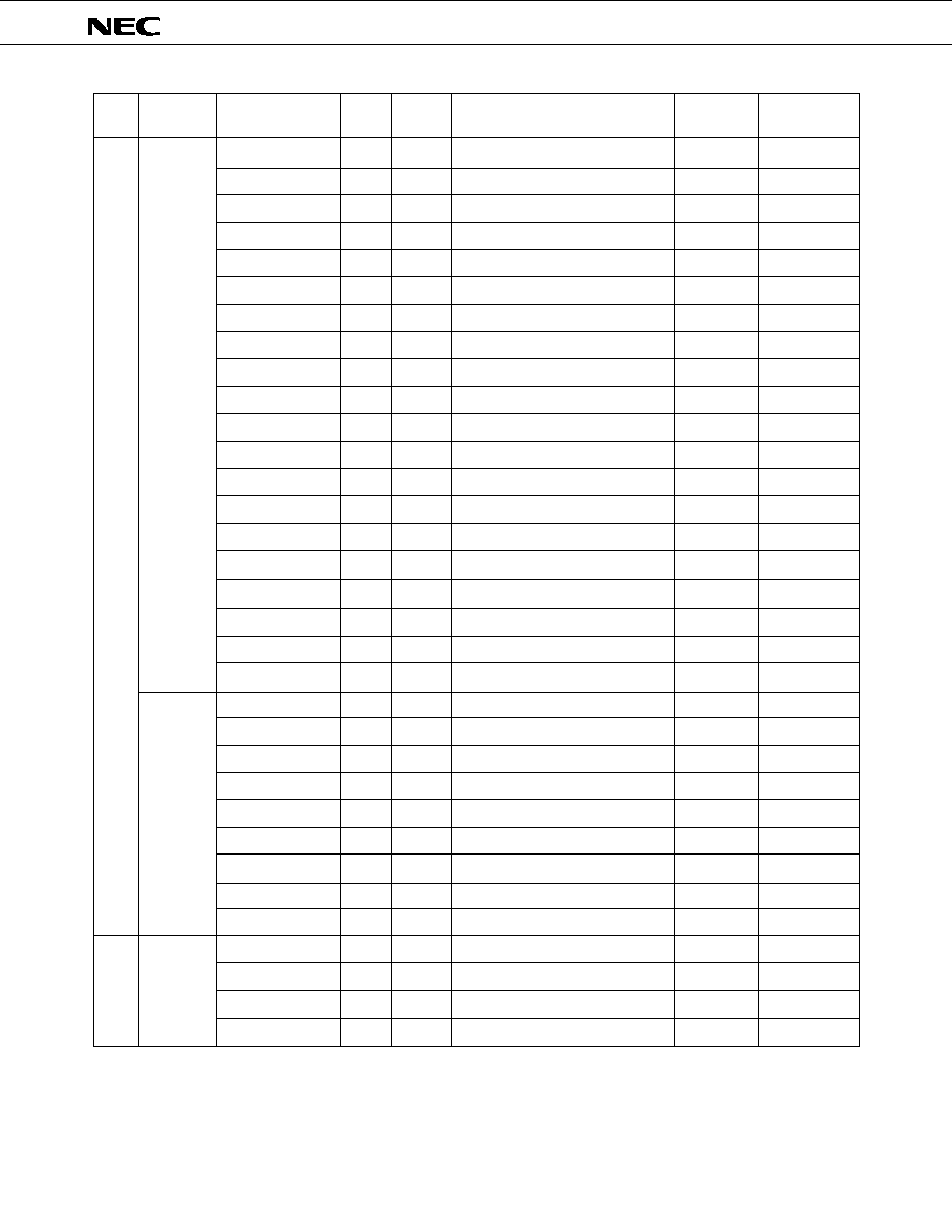
156
µ
PD75236
Note
Mnemonic
Operands
Machine
Cycle
Skip
Condition
Addressing
Area
Operation
No. of
Bytes
A, #n4
1
1
A
n4
Stack A
reg1, #n4
2
2
reg1
n4
XA, #n8
2
2
XA
n8
Stack A
HL, #n8
2
2
HL
n8
Stack B
rp2, #n8
2
2
rp2
n8
A, @HL
1
1
A
(HL)
*1
A, @HL+
1
2 + S
A
(HL), then L
L+1
*1
L = 0
A, @HL≠
1
2 + S
A
(HL), then L
L≠1
*1
L = FH
A, @rpa1
1
1
A
(rpa1)
*2
XA, @HL
2
2
XA
(HL)
*1
@HL, A
1
1
(HL)
A
*1
@HL, XA
2
2
(HL)
XA
*1
A, mem
2
2
A
(mem)
*3
XA, mem
2
2
XA
(mem)
*3
mem, A
2
2
(mem)
A
*3
mem, XA
2
2
(mem)
XA
*3
A, reg
2
2
A
reg
XA, rp'
2
2
XA
rp'
reg1, A
2
2
reg1
A
rp'1, XA
2
2
rp'1
XA
A, @HL
1
1
A
(HL)
*1
A, @HL+
1
2 + S
A
(HL), then L
L+1
*1
L = 0
A, @HL≠
1
2 + S
A
(HL), then L
L≠1
*1
L = FH
A, @rpa1
1
1
A
(rpa1)
*2
XA, @HL
2
2
XA
(HL)
*1
A, mem
2
2
A
(mem)
*3
XA, mem
2
2
XA
(mem)
*3
A, reg1
1
1
A
reg1
XA, rp'
2
2
XA
rp'
XA, @PCDE
1
3
XA
(PC
13≠8
+DE)
ROM
XA, @PCXA
1
3
XA
(PC
13≠8
+XA)
ROM
XA, @BCDE
1
3
XA
(BCDE)
ROM
*11
XA, @BCXA
1
3
XA
(BCXA)
ROM
*11
MOV
XCH
MOVT
Transfer
Table
reference
Note
Instruction Group

157
µ
PD75236
Mnemonic
Operand
Machine
Cycle
Skip
Condition
Addressing
Area
Operation
No. of
Bytes
CY, fmem.bit
2
2
CY
(fmem.bit)
*4
CY, pmem.@L
2
2
CY
(pmem
7-2
+L
3-2
.bit(L
1-0
))
*5
CY, @H+mem.bit
2
2
CY
(H+mem
3-0
.bit)
*1
fmem.bit, CY
2
2
(fmem.bit)
CY
*4
pmem.@L, CY
2
2
(pmem
7-2
+L
3-2
.bit(L
1-0
))
CY
*5
@H+mem.bit, CY
2
2
(H+mem
3-0
.bit)
CY
*1
A, #n4
1
1 + S
A
A+n4
carry
XA, #n8
2
2 + S
XA
XA+n8
carry
A, @HL
1
1 + S
A
A+(HL)
*1
carry
XA, rp'
2
2 + S
XA
XA+rp'
carry
rp'1, XA
2
2 + S
rp'1
rp'1+XA
carry
A, @HL
1
1
A, CY
A+(HL)+CY
*1
XA, rp'
2
2
XA, CY
XA+rp'+CY
rp'1, XA
2
2
rp'1, CY
rp'1+XA+CY
A, @HL
1
1 + S
A
A≠(HL)
*1
borrow
XA, rp'
2
2 + S
XA
XA≠rp'
borrow
rp'1, XA
2
2 + S
rp'1
rp'1≠XA
borrow
A, @HL
1
1
A, CY
A≠(HL)≠CY
*1
XA, rp'
2
2
XA, CY
XA≠rp'≠CY
rp'1, XA
2
2
rp'1, CY
rp'1≠XA-CY
A, #n4
2
2
A
A n4
A, @HL
1
1
A
A (HL)
*1
XA, rp'
2
2
XA
XA rp'
rp'1, XA
2
2
rp'1
rp'1 XA
A, #n4
2
2
A
A
n4
A, @HL
1
1
A
A
(HL)
*1
XA, rp'
2
2
XA
XA
rp'
rp'1, XA
2
2
rp'1
rp'1
XA
A, #n4
2
2
A
A
n4
A, @HL
1
1
A
A
(HL)
*1
XA, rp'
2
2
XA
XA
rp'
rp'1, XA
2
2
rp'1
rp'1
XA
A
1
1
CY
A
0
, A
3
CY, A
n-1
A
n
A
2
2
A
A
Note
1. Instruction Group
2. Accumulator manipulation
Bit transfer
Operation
Note 2
MOV1
ADDS
ADDC
SUBS
SUBC
AND
OR
XOR
RORC
NOT
Note 1

158
µ
PD75236
Mnemonic
Operands
Machine
Cycle
Skip
Condition
Addressing
Area
Operation
No. of
Bytes
reg
1
1 + S
reg
reg+1
reg = 0
rp1
1
1 + S
rp1
rp1+1
rp1 = 00H
@HL
2
2 + S
(HL)
(HL)+1
*1
(HL) = 0
mem
2
2 + S
(mem)
(mem)+1
*3
(mem) = 0
reg
1
1 + S
reg
reg≠1
reg = FH
rp'
2
2 + S
rp'
rp'≠1
rp' = FFH
reg, #n4
2
2 + S
Skip if reg = n4
reg = n4
@HL, #n4
2
2 + S
Skip if (HL) = n4
*1
(HL) = n4
A, @HL
1
1 + S
Skip if A = (HL)
*1
A = (HL)
XA, @HL
2
2 + S
Skip if XA = (HL)
*1
XA = (HL)
A, reg
2
2 + S
Skip if A = reg
A = reg
XA.rp'
2
2 + S
Skip if XA = rp'
XA = rp'
CY
1
1
CY
1
CY
1
1
CY
0
CY
1
1 + S
Skip if CY = 1
CY = 1
CY
1
1
CY
CY
Increment/decrement
Note
SET1
CLR1
SKT
NOT1
INCS
DECS
SKE
Compare
Carry flag
manipulation
Note
Instruction Group
159
µ
PD75236
Mnemonic
Operands
Machine
Cycle
Skip
Condition
Addressing
Area
Operation
No. of
Bytes
Note
Branch
Note
Instruction Group
SET1
CLR1
SKT
SKF
SKTCLR
AND1
OR1
XOR1
BRCB
BR
Memory bit manipulation
5
mem.bit
2
2
(mem.bit)
1
*3
fmem.bit
2
2
(fmem.bit)
1
*4
pmem.@L
2
2
(pmem
7-2
+L
3-2
.bit(L
1-0
))
1
*5
@H + mem.bit
2
2
(H+mem
3-0
.bit)
1
*1
mem.bit
2
2
(mem.bit)
0
*3
fmem.bit
2
2
(fmem.bit)
0
*4
pmem.@L
2
2
(pmem
7-2
+L
3-2
.bit(L
1-0
))
0
*5
@H+mem.bit
2
2
(H+mem
3-0
.bit)
0
*1
mem.bit
2
2 + S
Skip if (mem.bit) = 1
*3
(mem.bit) = 1
fmem.bit
2
2 + S
Skip if (fmem.bit) = 1
*4
(fmem.bit) = 1
pmem.@L
2
2 + S
Skip if (pmem
7-2
+L
3-2
.bit(L
1-0
)) = 1
*5
(pmem.@L) = 1
@H+mem.bit
2
2 + S
Skip if (H+mem
3-0
.bit) = 1
*1
(@H+mem.bit) = 1
mem.bit
2
2 + S
Skip if (mem.bit) = 0
*3
(mem.bit) = 0
fmem.bit
2
2 + S
Skip if (fmem.bit) = 0
*4
(fmem.bit) = 0
pmem.@L
2
2 + S
Skip if (pmem
7-2
+L
3-2
.bit(L
1-0
)) = 0
*5
(pmem.@L) = 0
@H+mem.bit
2
2 + S
Skip if (H+mem
3-0
.bit) = 0
*1
(@H+mem.bit) = 0
fmem.bit
2
2 + S
Skip if (fmem.bit) = 1 and clear
*4
(fmem.bit) = 1
pmem.@L
2
2 + S
Skip if (pmem
7-2
+L
3-2
.bit(L
1-0
))=1 and clear
*5
(pmem.@L) = 1
@H+mem.bit
2
2 + S
Skip if (H+mem
3-0
.bit)=1 and clear
*1
(@H+mem.bit)=1
CY, fmem.bit
2
2
CY
CY (fmem.bit)
*4
CY, pmem.@L
2
2
CY
CY (pmem
7-2
+L
3-2
.bit(L
1-0
))
*5
CY, @H+mem.bit
2
2
CY
CY (H+mem
3-0
.bit)
*1
CY, fmem.bit
2
2
CY
CY
(fmem.bit)
*4
CY, pmem.@L
2
2
CY
CY
(pmem
7-2
+L
3-2
.bit(L
1-0
))
*5
CY, @H+mem.bit
2
2
CY
CY
(H+mem
3-0
.bit)
*1
CY, fmem.bit
2
2
CY
CY
(fmem.bit)
*4
CY, pmem.@L
2
2
CY
CY
(pmem
7-2
+L
3-2
.bit(L
1-0
))
*5
CY, @H+mem.bit
2
2
CY
CY
(H+mem
3-0
.bit)
*1
PC
13-0
addr
(Optimum instruction is
addr
--
--
selected from among BR!
*6
addr, BRCB!caddr and
BR$addr1 by an assembler.)
$addr
1
2
PC
13-0
addr
*7
!addr
3
3
PC
13-0
!addr
*6
PCDE
2
3
PC
13-0
PC
13-8
+DE
PCXA
2
3
PC
13-0
PC
13-8
+XA
BCDE
2
3
PC
13-0
BCDE
BCXA
2
3
PC
13-0
BCXA
!caddr
2
2
PC
13-0
PC
13,12
+caddr
11-0
*8

160
µ
PD75236
Mnemonic
Operands
Machine
Cycle
Skip
Condition
Addressing
Area
Operation
No. of
Bytes
Note
(SP-5) (SP-6) (SP-3) (SP-4)
PC
13-0
!addr
3
4
(SP-2)
◊
,
◊
, MBE, RBE
*6
PC
13-0
addr, SP
SP-6
(SP-5) (SP-6) (SP-3) (SP-4)
PC
13-0
!faddr
2
3
(SP-2)
◊
,
◊
, MBE, RBE
*9
PC
13-0
0000, faddr, SP
SP-6
◊
,
◊
, MBE, RBE
(SP+4)
1
3
PC
13-0
(SP+1) (SP) (SP+3) (SP+2)
SP
SP+6
◊
,
◊
, MBE, RBE
(SP+4)
PC
13-0
(SP+1) (SP) (SP+3) (SP+2)
Unconditional
SP
SP+6
then skip unconditionally
◊
,
◊
, PC
13, 12
(SP+1)
1
3
PC
11-0
(SP) (SP+3) (SP+2)
PSW
(SP+4) (SP+5), SP
SP+6
rp
1
1
(SP≠1) (SP≠2)
rp, SP
SP≠2
BS
2
2
(SP≠1)
MBS, (SP-2)
RBS, SP
SP-2
rp
1
1
rp
(SP+1) (SP), SP
SP+2
BS
2
2
MBS
(SP+1), RBS
(SP), SP
SP+2
2
2
IME(IPS.3)
1
IE
◊◊◊
2
2
IE
◊◊◊
1
2
2
IME(IPS.3)
0
IE
◊◊◊
2
2
IE
◊◊◊
0
A, PORTn
2
2
A
PORTn
XA, PORTn
2
2
XA
PORTn+1, PORTn
PORTn, A
2
2
PORTn
A
PORTn, XA
2
2
PORTn+1, PORTn
XA
2
2
Set HALT Mode (PCC.2
1)
2
2
Set STOP Mode (PCC.3
1)
1
1
No Operation
Subroutine stack control
CALL
CALLF
RET
RETS
1
3 + S
RETI
PUSH
POP
EI
DI
IN
*
Interrupt
control
Input/output
CPU control
HALT
STOP
NOP
OUT
*
*
MBE = 0 or MBE = 1 and MBE = 15 must be set for execution of IN/OUT instruction
Note
Instruction Group

161
µ
PD75236
Mnemonic
Operands
Machine
Cycle
Skip
Condition
Addressing
Area
Operation
No. of
Bytes
Note
RBn
2
2
RBS
n (n = 0 to 3)
MBn
2
2
MBS
n (n = 0, 1, 2, 15)
∑ TBR instruction
PC
13-0
(taddr)
5-0
+(taddr+1)
∑ TCALL instruction
(SP-5) (SP-6) (SP-3) (SP-4)
PC
13-0
4
(SP-2)
◊
,
◊
, MBE, RBE
PC
13-0
(taddr)
5-0
+(taddr+1)
SP
SP-6
∑ (taddr) (taddr+1) instruction
Depends on
executed in the case of
instructions
instruction except TBR and
referred to.
TCALL instructions
Special
SEL
3
------------------------------------------------------------------
------------------------
------------------------------------------------------------------
------------------------
1
taddr
GET1 *
*10
*
TBR and TCALL instructions are assembled pseudo-instructions to define the GETI instruction table.
Note
Instruction Group
5
3

162
µ
PD75236
R
2
R
1
R
0
reg
0 0 0
A
0 0 1
X
0 1 0
L
0 1 1
H
1 0 0
E
1 0 1
D
1 1 0
C
1 1 1
B
reg
8.3
OPERATION CODES
(1)
Description of operation code symbols
P
2
P
1
P
0
reg-pair
0 0 0
XA
0 0 1
XA'
0 1 0
HL
0 1 1
HL'
1 0 0
DE
1 0 1
DE'
1 1 0
BC
1 1 1
BC'
reg1
rp'
rp'1
Q
2
Q
1
Q
0
addressing
0 0 1
@HL
0 1 0
@HL+
0 1 1
@HL≠
1 0 0
@DE
1 0 1
@DL
P
2
P
1
reg-pair
0 0
XA
0 1
HL
1 0
DE
1 1
BC
@rpa
rp2
rp1
rp
N
5
N
2
N
1
N
0
IE
◊◊◊
0 0 0 0
IEBT
0 0 1 0
IEW
0 0 1 1
IETPG
0 1 0 0
IET0
0 1 0 1
IECSI0
0 1 1 0
IE0
0 1 1 1
IE2
1 0 0 0
IE4
1 0 1 1
IEKS
1 1 1 0
IE1
In : Immediate data for n4 and n8
Dn : Immediate data for mem
Bn : Immediate data for bit
Nn : Immediate data for n and IE
◊◊◊
Tn : Immediate data for taddr
◊
1/2
An : Immediate data for [Relative address distance from branch destination address (2 to 16)]-1
Sn : Immediate data for one's complement of [Relative address distance from branch destination
address (15 to 1)]
@rpa1

163
µ
PD75236
(2)
Operation codes of bit manipulation addressing
*1 in the operand column indicates that the following three addressings are available.
∑ fmem.bit
∑ pmem.@L
∑ @H+mem.bit
The 2nd byte *2 of the operation code corresponding to the above addressing is shown below:
Bn :
Immediate data for bit
Fn :
Immediate data for fmem (indicating the low-order 4-bits of address)
Gn :
Immediate data for pmem (indicating the bits 5 to 2 of address)
Dn :
Immediate data for mem (indicating the low-order 4 bits of address)
*1
2nd Byte of Operation Code
Accessible Bits
1
0
B
1
B
0
F
3
F
2
F
1
F
0
Manipulatable bits of FB0H to FBFH
1
1
B
1
B
0
F
3
F
2
F
1
F
0
Manipulatable bits of FF0H to FFFH
pmem.@L
0
1
0
0
G
3
G
2
G
1
G
0
Manipulatable bits of FC0H to FFFH
Manipulatable bits of accessible
memory banks
fmem.bit
@H+mem.bit
0 0 B
1
B
0
D
3
D
2
D
1
D
0

164
µ
PD75236
A, #n4
0
1
1
1
I
3
I
2
I
1
I
0
reg1, #n4
1
0
0
1
1
0
1
0
I
3
I
2
I
1
I
0
1
R
2
R
1
R
0
rp, #n8
1
0
0
0
1
P
2
P
1
1
I
7
I
6
I
5
I
4
I
3
I
2
I
1
I
0
A, @rpa
1
1
1
0
0
Q
2
Q
1
Q
0
XA, @HL
1
0
1
0
1
0
1
0
0
0
0
1
1
0
0
0
@HL, A
1
1
1
0
1
0
0
0
@HL, XA
1
0
1
0
1
0
1
0
0
0
0
1
0
0
0
0
A, mem
1
0
1
0
0
0
1
1 D
7
D
6
D
5
D
4
D
3
D
2
D
1
D
0
XA, mem
1
0
1
0
0
0
1
0 D
7
D
6
D
5
D
4
D
3
D
2
D
1
0
mem, A
1
0
0
1
0
0
1
1 D
7
D
6
D
5
D
4
D
3
D
2
D
1
D
0
mem, XA
1
0
0
1
0
0
1
0 D
7
D
6
D
5
D
4
D
3
D
2
D
1
0
A, reg
1
0
0
1
1
0
0
1
0
1
1
1
1
R
2
R
1
R
0
XA, rp'
1
0
1
0
1
0
1
0
0
1
0
1
1
P
2
P
1
P
0
reg1, A
1
0
0
1
1
0
0
1
0
1
1
1
0
R
2
R
1
R
0
rp'1, XA
1
0
1
0
1
0
1
0
0
1
0
1
0
P
2
P
1
P
0
A, @rpa
1
1
1
0
1
Q
2
Q
1
Q
0
XA, @HL
1
0
1
0
1
0
1
0
0
0
0
1
0
0
0
1
A, mem
1
0
1
1
0
0
1
1 D
7
D
6
D
5
D
4
D
3
D
2
D
1
D
0
XA, mem
1
0
1
1
0
0
1
0 D
7
D
6
D
5
D
4
D
3
D
2
D
1
0
A, reg1
1
1
0
1
1
R
2
R
1
R
0
XA, rp'
1
0
1
0
1
0
1
0
0
1
0
0
0
P
2
P
1
P
0
XA, @PCDE
1
1
0
1
0
1
0
0
XA, @PCXA
1
1
0
1
0
0
0
0
XA, @BCDE
1
1
0
1
0
1
0
1
XA, @BCXA
1
1
0
1
0
0
0
1
CY,
1
1
0
1
1
1
1
0
1
2
1
, CY
1
0
0
1
1
0
1
1
2
MOV1
Operation Code
B
1
B
2
B
3
Mnemonic
Operands
Note
1. Instruction Group
2. Bit transfer
Note 2
XCH
MOVT
Table
reference
Transfer
MOV
Note 1
165
µ
PD75236
A, #n4
0
1
1
0
I
3
I
2
I
1
I
0
XA, #n8
1
0
1
1
1
0
0
1
I
7
I
6
I
5
I
4
I
3
I
2
I
1
I
0
A, @HL
1
1
0
1
0
0
1
0
XA, rp'
1
0
1
0
1
0
1
0
1
1
0
0
1
P
2
P
1
P
0
rp'1, XA
1
0
1
0
1
0
1
0
1
1
0
0
0
P
2
P
1
P
0
A, @HL
1
0
1
0
1
0
0
1
XA, rp'
1
0
1
0
1
0
1
0
1
1
0
1
1
P
2
P
1
P
0
rp'1, XA
1
0
1
0
1
0
1
0
1
1
0
1
0
P
2
P
1
P
0
A, @HL
1
0
1
0
1
0
0
0
XA, rp'
1
0
1
0
1
0
1
0
1
1
1
0
1
P
2
P
1
P
0
rp'1, XA
1
0
1
0
1
0
1
0
1
1
1
0
0
P
2
P
1
P
0
A, @HL
1
0
1
1
1
0
0
0
XA, rp'
1
0
1
0
1
0
1
0
1
1
1
1
1
P
2
P
1
P
0
rp'1, XA
1
0
1
0
1
0
1
0
1
1
1
1
0
P
2
P
1
P
0
A, #n4
1
0
0
1
1
0
0
1
0
0
1
1
I
3
I
2
I
1
I
0
A, @HL
1
0
0
1
0
0
0
0
XA, rp'
1
0
1
0
1
0
1
0
1
0
0
1
1
P
2
P
1
P
0
rp'1, XA
1
0
1
0
1
0
1
0
1
0
0
1
0
P
2
P
1
P
0
A, #n4
1
0
0
1
1
0
0
1
0
1
0
0
I
3
I
2
I
1
I
0
A, @HL
1
0
1
0
0
0
0
0
XA, rp'
1
0
1
0
1
0
1
0
1
0
1
0
1
P
2
P
1
P
0
rp'1, XA
1
0
1
0
1
0
1
0
1
0
1
0
0
P
2
P
1
P
0
A, #n4
1
0
0
1
1
0
0
1
0
1
0
1
I
3
I
2
I
1
I
0
A, @HL
1
0
1
1
0
0
0
0
XA, rp'
1
0
1
0
1
0
1
0
1
0
1
1
1
P
2
P
1
P
0
rp'1, XA
1
0
1
0
1
0
1
0
1
0
1
1
0
P
2
P
1
P
0
A
1
0
0
1
1
0
0
0
A
1
0
0
1
1
0
0
1
0
1
0
1
1
1
1
1
Note 1
Operation Code
B
1
B
2
B
3
Mnemonic
Operands
Operate
Note
1. Instruction Group
2. Accumulator manipulation
Note 2
RORC
NOT
ADDS
ADDC
SUBS
SUBC
AND
OR
XOR
166
µ
PD75236
reg
1
1
0
0
0
R
2
R
1
R
0
rp1
1
0
0
0
1
P
2
P
1
0
@HL
1
0
0
1
1
0
0
1
0
0
0
0
0
0
1
0
mem
1
0
0
0
0
0
1
0 D
7
D
6
D
5
D
4
D
3
D
2
D
1
D
0
reg
1
1
0
0
1
R
2
R
1
R
0
rp'
1
0
1
0
1
0
1
0
0
1
1
0
1
P
2
P
1
P
0
reg, #n4
1
0
0
1
1
0
1
0
I
3
I
2
I
1
I
0
0
R
2
R
1
R
0
@HL, #n4
1
0
0
1
1
0
0
1
0
1
1
0
I
3
I
2
I
1
I
0
A, @HL
1
0
0
0
0
0
0
0
XA, @HL
1
0
1
0
1
0
1
0
0
0
0
1
1
0
0
1
A, reg
1
0
0
1
1
0
0
1
0
0
0
0
1
R
2
R
1
R
0
XA, rp'
1
0
1
0
1
0
1
0
0
1
0
0
1
P
2
P
1
P
0
CY
1
1
1
0
0
1
1
1
CY
1
1
1
0
0
1
1
0
CY
1
1
0
1
0
1
1
1
CY
1
1
0
1
0
1
1
0
mem.bit
1
0
B
1
B
0
0
1
0
1 D
7
D
6
D
5
D
4
D
3
D
2
D
1
D
0
1
1
0
0
1
1
1
0
1
2
mem.bit
1
0
B
1
B
0
0
1
0
0 D
7
D
6
D
5
D
4
D
3
D
2
D
1
D
0
1
1
0
0
1
1
1
0
0
2
mem.bit
1
0
B
1
B
0
0
1
1
1 D
7
D
6
D
5
D
4
D
3
D
2
D
1
D
0
1
1
0
1
1
1
1
1
1
2
mem.bit
1
0
B
1
B
0
0
1
1
0 D
7
D
6
D
5
D
4
D
3
D
2
D
1
D
0
1
1
0
1
1
1
1
1
0
2
1
1
0
0
1
1
1
1
1
2
CY,
1
1
0
1
0
1
1
0
0
*2
CY,
1
1
0
1
0
1
1
1
0
*2
CY,
1
1
0
1
1
1
1
0
0
*2
Note
Operation Code
B
1
B
2
B
3
Mnemonic
Operands
Memory bit manipulation
INCS
DECS
SKE
SET1
CLR1
SKT
NOT1
SET1
CLR1
SKT
SKF
SKTCLR
AND1
OR1
XOR1
Carry flag
Increment/decrement
Compare
Note
Instruction Group
167
µ
PD75236
!addr
1
0
1
0
1
0
1
1
0
0
addr
0
0
0
0
A
3
A
2
A
1
A
0
1
1
1
1
S
3
S
2
S
1
S
0
!caddr
0
1
0
1
caddr
PCDE
1
0
0
1
1
0
0
1
0
0
0
0
0
1
0
0
PCXA
1
0
0
1
1
0
0
1
0
0
0
0
0
0
0
0
BCDE
1
0
0
1
1
0
0
1
0
0
0
0
0
1
0
1
BCXA
1
0
0
1
1
0
0
1
0
0
0
0
0
0
0
1
!addr
1
0
1
0
1
0
1
1
0
1
addr
!faddr
0
1
0
0
0
faddr
1
1
1
0
1
1
1
0
1
1
1
0
0
0
0
0
1
1
1
0
1
1
1
1
rp
0
1
0
0
1
P
2
P
1
1
BS
1
0
0
1
1
0
0
1
0
0
0
0
0
1
1
1
rp
0
1
0
0
1
P
2
P
1
0
BS
1
0
0
1
1
0
0
1
0
0
0
0
0
1
1
0
A, PORTn
1
0
1
0
0
0
1
1
1
1
1
1 N
3
N
2
N
1
N
0
XA, PORTn
1
0
1
0
0
0
1
0
1
1
1
1 N
3
N
2
N
1
N
0
PORTn, A
1
0
0
1
0
0
1
1
1
1
1
1 N
3
N
2
N
1
N
0
PORTn, XA
1
0
0
1
0
0
1
0
1
1
1
1 N
3
N
2
N
1
N
0
1
0
0
1
1
1
0
1
1
0
1
1
0
0
1
0
IE
◊◊◊
1
0
0
1
1
1
0
1
1
0
N
5
1
1 N
2
N
1
N
0
1
0
0
1
1
1
0
0
1
0
1
1
0
0
1
0
IE
◊◊◊
1
0
0
1
1
1
0
0
1
0
N
5
1
1 N
2
N
1
N
0
1
0
0
1
1
1
0
1
1
0
1
0
0
0
1
1
1
0
0
1
1
1
0
1
1
0
1
1
0
0
1
1
0
1
1
0
0
0
0
0
RBn
1
0
0
1
1
0
0
1
0
0
1
0
0
0
N
1
N
0
MBn
1
0
0
1
1
0
0
1
0
0
0
1 N
3
N
2
N
1
N
0
taddr
0
0
T
5
T
4
T
3
T
2
T
1
T
0
Note
Operation Code
B
1
B
2
B
3
Mnemonic
Operands
Branch
$addr1
(+16)
to
(+2)
(≠1)
to
(≠15)
BR
BRCB
BR
CALL
CALLF
RET
RETS
RETI
PUSH
POP
IN
OUT
EI
DI
HALT
STOP
NOP
SEL
GETI
Special
Interrupt control
Input/output
Subroutine stack control
Note
Instruction Group
CPU control
5

168
µ
PD75236
9.
MASK OPTION SELECTION
The
µ
PD75236 has the following mask options enabling or disabling on-chip components.
*
Select pull-down resistor incorporation to V
LOAD
or V
SS
in 8-bit units.
Note
In a system not using subsystem clocks, power consumption in the STOP mode can be decreased by
removing the feedback resistor from the oscillator.
Pin
Mask Option
P40 to P43
P50 to P53
P70 to P73
Pull-down resistor incorporation enabled bit-wise
S0/P120 to S3/P123
S4/P130 to S7/P133
S8/P140, S9/P141
S10/T15/P142, S11/T14/P143
S12/T13/P150/PH0 to S15/T10/P153/PH3
S16/P100 to S19/P103
S20/P110 to S23/P113
Deletion of sybsystem clock oscillator feedback
resistor possible
Pull-up resistor incorporation enabled bit-wise
Pull-down resistor incorporation to V
LOAD
enabled bit-wise
Pull-down resistor incorporation to V
LOAD
or V
SS
bit-wise *
XT1, XT2

169
µ
PD75236
LPF
INT4
PPO
AN
n
AN
n
PORT
n
SCK1
SO1
L
R
SO0
SCK0
PORT
n
BUZ
INT0
PORT7
S0-S17
T0-T15
X1
X2
XT1
XT2
BZ
(18
◊
4)
4.19 MHz
32.768 kHz
LED
OSD
Power Failure
Detection
Electronic
Tuner
Voice Lever
Timer
Tuner
System Computer
Remote Controlled Reception
Hsync Detection
Fluorescent
Display Panel (FIP)
18 Segments
◊
16 Digits
Key Matrix
Remote
Controlled
Signal
Mechanism
Piozoelectric
Buzzer
Servo
IC
Hsync Pulse
10. APPLICATION BLOCK DIAGRAM
µ
PD75236
Remarks
LPF
: Low Pass Filter
OSD
: On Screen Display
Hsync : Horizontal Synchronous
µ
PC1490

170
µ
PD75236
UNIT
RATING
Except ports 4 and 5
Pins except display output pins
Display output pins
1 pins except display output pins
S0 to S9, S16 to S23 1 pin
T0 to T15
1 pin
Total of pins except display output pins
Total of display output pins
1 pin
Total of ports
0, 2, 3 and 4
Total of ports
5 to 8
Plastic QFP
Pull-up resistor
Open-drain
Peak value
Effective value
Peak value
Effective value
Peak value
Effective value
( Ta = ≠40 to +70
∞
C )
( Ta = ≠40 to +85
∞
C )
V
V
V
V
V
V
V
mA
mA
mA
mA
mA
mA
mA
mA
mA
mA
mA
mW
mW
∞
C
∞
C
PARAMETER
SYMBOL
TEST CONDITIONS
UNIT
PARAMETER
CPU *1
Display controller
Time/pulse generator
Other hardware *1
V
V
V
V
6.0
6.0
6.0
6.0
*2
4.5
4.5
2.7
MIN.
MAX.
TEST CONDITIONS
POWER SUPPLY VOLTAGE RANGE (Ta = ≠40 to +85
∞
C)
* 1.
Except the system clock osccillator, display controller and timer/pulse generator.
2.
The power supply voltage range varies, depending on the cycle time. Refer to the description of
AC characteristics.
ABSOLUTE MAXIMUM RATINGS (Ta = 25
∞
C)
V
DD
V
LOAD
V
I1
V
I2
V
O
V
OD
I
OH
I
OL
P
T
T
opt
T
stg
Power supply
voltage
Input voltage
Output voltage
Output current
high
Output current
low
Total loss
Operating temperature
Storage temperature
11.
ELECTRICAL SPECIFICATIONS
Ports 4 and 5
≠0.3 to +7.0
V
DD
≠40 to V
DD
+0.3
≠0.3 to V
DD
+0.3
≠0.3 to V
DD
+0.3
≠0.3 to +11
≠0.3 to V
DD
+0.3
V
DD
≠40 to V
DD
+0.3
≠15
≠15
≠30
≠30
≠120
30
15
100
60
100
60
700
510
≠40 to +85
≠65 to +150
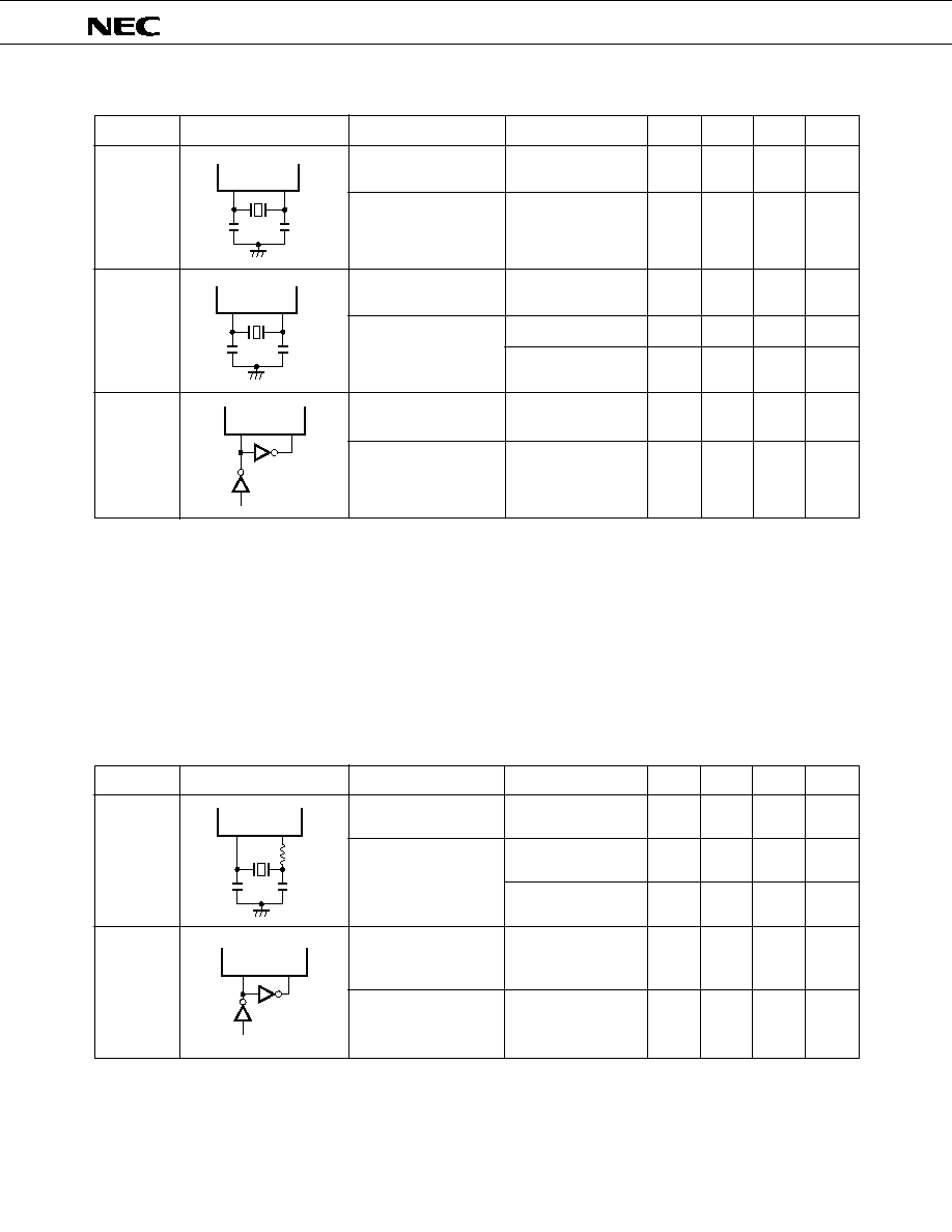
171
µ
PD75236
MAIN SYSTEM CLOCK OSCILLATOR CHARACTERISTICS (Ta = ≠40 to +85
∞
C, V
DD
= 2.7 to 6.0 V )
UNIT
MAX.
TYP.
UNIT
MAX.
TYP.
MIN.
PARAMETER
TEST CONDITIONS
MIN.
V
DD
= Oscillation
voltage range
After V
DD
reaches the
minimum value in
the oscillation
voltage range
V
DD
= 4.5 to 6.0 V
Oscillator frequency
(f
X
) *1
Oscillation
stabilization time *2
Oscillator frequency
(f
X
) *1
Oscillation stabilization
time *2
X1 input frequency
(f
X
) *1
X1 high and low level
widths (t
XH
, t
XL
)
X1
X2
C1
C2
X1
X2
C1
C2
* 1.
Oscillator characteristics only. Refer to the description of AC characteristics for details of instruction
execution time.
2.
Time required for oscillation to become stabilized after V
DD
application or STOP mode release.
3.
When oscillation frequency is " 4.19 < f
X
5.0 MHz ", do not select " PCC = 0011 " as instruction execution
time. If " PCC = 0011 " is selected, 1 machine cycle becomes less than 0.95
µ
s, with the result that the
specified MIN. value of 0.95
µ
s cannot be observed.
SUBSYSTEM CLOCK OSCILLATOR CHARACTERISTICS (Ta = ≠40 to +85
∞
C, V
DD
= 2.7 to 6.0 V)
* 1.
Oscillator characteristics only. Refer to the description of AC characteristics for instruction execution
time.
2.
Time required for oscillation to become stabilized after V
DD
application or STOP mode release.
XT1
XT2
C3
C4
R
PARAMETER
TEST CONDITIONS
Oscillator frequency
(f
XT
) *1
Oscillation stabilization
time *2
XT1 input frequency
(f
XT
) *1
XT1 high and low level
widths (t
XTH
, t
XTL
)
X1
X2
µ
PD74HCU04
XT1
XT2
5
RESONATOR RECOMMENDED CIRCUIT
RESONATOR RECOMMENDED CIRCUIT
2.0
2.0
2.0
100
Ceramic
resonator
Crystal
resonator
External
clock
4.19
5.0
4
5.0 *3
10
30
5.0
250
MHz
ms
MHz
ms
ms
MHz
ns
Crystal
resonator
External
clock
V
DD
= 4.5 to 6.0 V
32
32
5
32.768
1.0
35
2
10
100
15
kHz
s
s
kHz
µ
s

172
µ
PD75236
CAPACITANCE ( Ta = 25
∞
C, V
DD
= 0 V )
MAX.
Input capacitance
Output capacitance
(except display output)
Input /output
capacitance
Output capacitance
( display output )
15
15
15
35
pF
pF
pF
pF
UNIT
TEST CONDITIONS
SYMBOL
PARAMETER
MIN.
TYP.
C
I
C
O
C
IO
C
O
f = 1 MHz
Unmeasured pin returned to 0V
173
µ
PD75236
DC CHARACTERISTICS (Ta = ≠40 to 85
∞
C, V
DD
= 2.7 to 6.0 V)
UNIT
MIN.
PARAMETER
SYMBOL
TEST CONDITIONS
MAX.
TYP.
0.7 V
DD
0.8 V
DD
V
DD
≠0.4
0.65 V
DD
0.7 V
DD
0.7 V
DD
0.7 V
DD
0
0
0
V
DD
≠1.0
V
DD
≠0.5
V
DD
V
DD
V
DD
V
DD
V
DD
V
DD
10
0.3 V
DD
0.2 V
DD
0.4
2.0
0.4
0.5
0.2 V
DD
3
20
20
≠3
≠20
3
20
≠3
≠10
200
1000
135
80
300
70
60
V
V
V
V
V
V
V
V
V
V
V
V
V
V
V
V
µ
A
µ
A
µ
A
µ
A
µ
A
µ
A
µ
A
µ
A
µ
A
mA
mA
k
k
k
k
k
k
k
V
IH1
V
IH2
V
IH3
V
IH4
V
IH5
V
IL1
V
IL2
V
IL3
V
OH
V
OL
I
LIH1
I
LIH2
I
LIH3
I
LIL1
I
LIL2
I
LOH1
I
LOH2
I
LOL1
I
LOL2
V
DD
= 4.5 to 6.0 V
Pull-up resistor incorporated
Open-drain
Port 7
Input voltage high
Ports 4, 5
Except below
Ports 0, 1, RESET, P81, P83
X1, X2, XT1
Except below
Ports 0, 1 RESET, P81, P83
X1, X2, XT1
I
OH
= ≠1 mA
I
OH
= ≠100
µ
A
I
OL
= 15 mA
I
OL
= 1.6 mA
I
OL
= 400
µ
A
V
DD
= 4.5 to 6.0V
V
DD
= 2.7 to 6.0V
V
DD
= 4.5 to 6.0V
V
DD
= 4.5 to 6.0V
V
DD
= 2.7 to 6.0V
All output pins
except ports 4,
5 and P03
0.4
Ports 3, 4, 5
All output pins
SB0, SB1
Open-drain pull-up resis-
tance
1k
V
IN
= V
DD
Open-drain V
IN
= 10 V
Except below
X1, X2, XT1
Ports 4, 5
Except below
X1, X2, XT1
Except below
Ports 4, 5
Except below
Display output
V
IN
= 0 V
V
OUT
= V
DD
(Open-drain) V
OUT
= 10 V
V
OUT
= 0 V
V
OUT
= V
LOAD
= V
DD
≠35 V
Input Voltage low
Output voltage high
Output voltage low
Input leakage current
high
Input leakage current
low
Output leakage current
low
Output leakage current
high
≠5.5
≠22
80
50
40
40
≠3
≠15
20
20
25
15
30
15
10
V
DD
= 4.5 to 6.0 V
V
OD
= V
DD
≠2 V
V
DD
= 4.5 to 6.0 V
V
DD
≠V
LOAD
= 35 V
V
DD
= 5 V
±
10 %
V
DD
= 3 V
±
10%
V
DD
= 5 V
±
10%
V
DD
= 3 V
±
10%
I
OD
R
L
S0 to S9, S16 to S23
T0 to T15
Port 7
V
IN
= V
DD
R
P7
Display output
R
V1
R
V2
Ports 4 and 5
V
OUT
= V
DD
≠2.0
V
Display output current
Built-in pull-down
resistor (mask option)
Built-in pull-up resistor
Ports 0, 1, 2, 3,
and 6 (except
P00) V
IN
= 0 V

174
µ
PD75236
DC CHARACTERISTICS (Ta = ≠40 to 85
∞
C, V
DD
= 2.7 to 6.0 V)
UNIT
A/D CONVERTER CHARATERISTICS (Ta = ≠40 to +85
∞
C, V
DD
= 2.7 to 6.0 V, AV
SS
= V
SS
= 0 V, AV
DD
= V
DD
)
UNIT
MAX.
TYP.
MIN.
PARAMETER
SYMBOL
TEST CONDITIONS
Resolution
Absolute accuracy *1
Conversion time
Sampling time
Analog input voltage
Analog input impedance
AV
REF
current
t
CONV
t
SAMP
V
IAN
R
AN
I
AREF
≠10
Ta
+85
∞
C
≠40
Ta < ≠10
∞
C
bit
LSB
µ
s
µ
s
V
M
mA
8
±
1.5
±
2.0
168/f
x
44/f
x
AV
REF
2.0
*2
*3
8
1000
1.0
* 1.
Current flowing to the built-in pull-down (pull-up) resistor excluded.
2.
When operated in the high speed mode with the processor clock control register (PCC) set to 0011.
3.
When operated in the low speed mode with PCC = 0000.
4.
Subsystem clock oscillation included.
5.
When operated with subsystem clock with system clock control register (SCC) set to 1001 and the main
system clock stopped.
* 1.
Absolute accuracy with any quantization error (
±
1/2 LSB) excluded.
2.
Time until EOC = 1 after execution of conversion start instruction (when operated at f
X
= 4.19 MHz: 40.1
µ
s).
3.
Time until the end of sampling after execution of conversion start instruction (when operated at f
X
= 4.19
MHz: 10.5
µ
s).
Operating
mode
HALT mode
3
0.5
600
200
40
5
0.5
0.3
9
1.5
1800
600
120
15
20
10
5
mA
mA
µ
A
µ
A
µ
A
µ
A
µ
A
µ
A
µ
A
I
DD1
I
DD2
Operating
mode
HALT mode
V
DD
= 5 V
±
10%
VDD = 3 V
±
10%
Supply current *1
MAX.
TYP.
MIN.
SYMBOL
TEST CONDITIONS
PARAMETER
2.5 V
AV
REF
AV
DD
I
DD4
I
DD3
I
DD5
V
DD
= 5 V
±
10% *2
V
DD
= 3 V
±
10% *3
V
DD
= 5 V
±
10%
V
DD
= 3 V
±
10%
V
DD
= 3 V
±
10%
V
DD
= 3 V
±
10%
Ta = 25
∞
C
5
8
AV
SS
4.19 MHz
crystal
oscillation
C1 = C2 =
22 pF *4
XT1 = 0 V
STOP mode
32 kHz crystal
oscillation *5

175
µ
PD75236
AC CHARACTERISTICS (Ta = ≠40 to +85
∞
C , V
DD
= 2.7 to 6.0 V)
(1)
Basic operation
PARAMETER
SYMBOL
TEST CONDITIONS
MIN.
TYP.
MAX.
UNIT
V
DD
= 4.5 to 6.0 V
0.95
64
µ
s
3.8
64
µ
s
Operation with subsystem clock
114
122
125
µ
s
V
DD
= 4.5 to 6.0 V
0
1
MHZ
0
275
kHz
V
DD
= 4.5 to 6.0 V
0.48
µ
s
1.8
µ
s
INT0
*2
µ
s
INT1, 2, 4
10
µ
s
10
µ
s
f
TI
t
CY
t
TIH
,
t
TIL
t
INTH
,
t
INTL
t
RSL
CPU clock cycle time
(minimum instruction
execution time = 1
machine cycle) *1
Operation with main
system clock
TI0 input frequency
TI0 input high and low-
level widths
Interrupt input high and
low-level widths
RESET low-level width
Cycle Time t
CY
[
µ
s]
70
64
60
6
5
4
3
2
1
0.5
0
1
2
3
4
5
6
Operation Guaranteed
Range
t
CY
VS
V
DD
(Main System Clock in Operation)
Power Supply Voltage V
DD
[V]
* 1.
CPU clock (
) cycle time is determined by the
oscillator frequency of the connected resonator,
the system clock control register (SCC) and the
processor clock control register (PCC). The cycle
time t
CY
characteristics for power supply voltage
V
DD
when the main system clock is in operation
is shown below (see Fig.4-15 Processor Clock
Control Register Format).
2.
2t
CY
or 128/f
X
is set by interrupt mode register
(IM0) setting.
176
µ
PD75236
PARAMETER
SYMBOL
TEST CONDITIONS
MIN.
TYP.
MAX.
UNIT
V
DD
= 4.5 to 6.0 V
1600
ns
3800
ns
V
DD
= 4.5 to 6.0 V
(t
KCY
/2)-50
ns
(t
KCY
/2-150)
ns
150
ns
400
ns
V
DD
= 4.5 to 6.0 V
250
ns
1000
ns
(2)
Serial transfer operation
(a)
2-wire and 3-wire serial I/O mode (SCK...Internal clock output)
R
L
= 1 k
C
L
= 100 pF*
SCK cycle time
t
KCY1
t
KL1
t
KH1
SI setup time (to SCK
)
t
SIK1
t
KSI1
SI hold time (from SCK
)
t
KSO1
SO output delay time
from SCK
*
R
L
and C
L
are SO output line load resistance and load capacitance, respectively.
(b)
2-wire and 3-wire serial I/O mode (SCK...External clock input)
PARAMETER
SYMBOL
TEST CONDITIONS
MIN.
TYP.
MAX.
UNIT
V
DD
= 4.5 to 6.0 V
800
ns
3200
ns
V
DD
= 4.5 to 6.0 V
400
ns
1600
ns
100
ns
400
ns
V
DD
= 4.5 to 6.0 V
300
ns
1000
ns
R
L
= 1 k
C
L
= 100 pF*
SCK cycle time
t
KCY2
t
KL2
t
KH2
SI setup time (to SCK
)
t
SIK2
t
KSI2
SI hold time (from SCK
)
t
KSO2
SO output delay time
from SCK
*
R
L
and C
L
are SO output line load resistance and load capacitance, respectively.
SCK high and low level
widths
SCK high and low level
widths

177
µ
PD75236
(c)
SBI mode (SCK...Internal clock output (master))
PARAMETER
SYMBOL
TEST CONDITIONS
MIN.
TYP.
MAX.
UNIT
V
DD
= 4.5 to 6.0 V
1600
ns
3800
ns
V
DD
= 4.5 to 6.0 V
t
KCY
/2-50
ns
t
KCY
/2-150
ns
150
ns
t
KCY
/2
ns
V
DD
= 4.5 to 6.0 V
0
250
ns
0
1000
ns
t
KCY
ns
t
KCY
ns
t
KCY
ns
t
KCY
ns
R
L
= 1 k
C
L
= 100 pF*
t
KCY3
t
KL3
t
KH3
t
SIK3
t
KSI3
t
KSO3
SCK cycle time
SB0 and SB1 setup time (to SCK
)
SB0 and SB1 hold time (from SCK
)
SB0 and SB1 output
delay time from SCK
SCK high and low level
widths
SB0, SB1
from SCK
SCK from SB0, SB1
SB0 and SB1 low-level widths
SB0 and SB1 high-level widths
t
KSB
t
SBK
t
SBL
t
SBH
*
R
L
and C
L
are SO output line load resistance and load capacitance, respectively.
(d)
SBI mode (SCK...External clock output (slave))
PARAMETER
SYMBOL
TEST CONDITIONS
MIN.
TYP.
MAX.
UNIT
V
DD
= 4.5 to 6.0 V
800
ns
3200
ns
V
DD
= 4.5 to 6.0 V
400
ns
1600
ns
100
ns
t
KCY
/2
ns
V
DD
= 4.5 to 6.0 V
0
300
ns
0
1000
ns
t
KCY
ns
t
KCY
ns
t
KCY
ns
t
KCY
ns
R
L
= 1 k
C
L
= 100 pF*
t
KCY4
t
KL4
t
KH4
t
SIK4
t
KSI4
t
KSO4
SCK cycle time
SB0 and SB1 setup time (to SCK
)
SB0 and SB1 hold time (from SCK
)
SB0 and SB1 output
delay time from SCK
SCK high and low level
widths
SB0, SB1
from SCK
SCK
from SB0, SB1
SB0 and SB1 low-level widths
SB0 and SB1 high-level widths
t
KSB
t
SBK
t
SBL
t
SBH
*
R
L
and C
L
are SO output line load resistance and load capacitance, respectively.

178
µ
PD75236
AC Timing Test Points (Except X1 and XT1 Inputs)
0.8 V
DD
0.2 V
DD
0.8 V
DD
0.2 V
DD
Test Points
Clock Timing
1/f
XT
t
XTL
t
XTH
V
DD
- 0.5 V
0.4 V
XT1 Input
TI0 Timing
1/f
X
t
XL
t
XH
V
DD
- 0.5 V
0.4 V
X1 Input
1/f
TI
t
TIL
t
TIH
TI0

179
µ
PD75236
Serial Transfer Timing
3-wire serial I/O mode:
2-wire serial I/O mode:
t
KH1
t
KCY1
t
KL1
t
SIK1
t
KSI1
t
KSO1
SCK
SI
SO
Input Data
Output Data
t
KCY2
t
KL2
t
KH2
t
SIK2
t
KSO2
t
KSI2
SCK
SB0,1
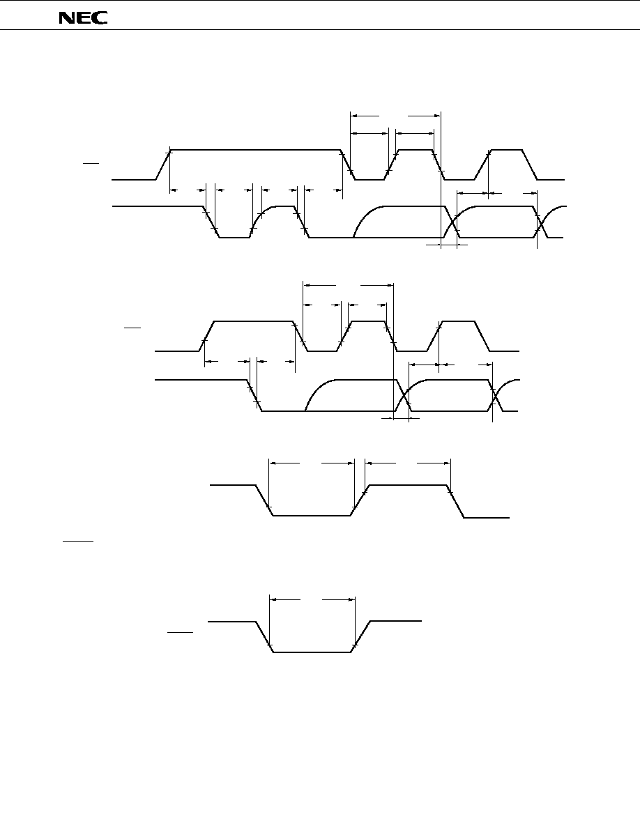
180
µ
PD75236
Serial Transfer Timing
Bus release signal transfer:
Command signal transfer:
Interrupt Input Timing
RESET Input Timing
SCK
t
KSB
SB0,1
t
SBK
t
KL3.4
t
KH3.4
t
KCY3.4
t
SIK3.4
t
KSI3.4
t
KSO3.4
INT0,1,2,4
t
INTL
t
INTH
t
KSB
SCK
SB0,1
t
SBL
t
SBH
t
SBK
t
KL3.4
t
KH3.4
t
KCY3.4
t
SIK3.4
t
KSI3.4
t
KSO3.4
RESET
t
RSL

181
µ
PD75236
2.0
6.0
V
V
DDDR
= 2.0V
0.1
10
µ
A
0
µ
s
Release by RESET
2
17
/f
X
ms
Release by interrupt request
*3
ms
DATA MEMORY STOP MODE LOW POWER SUPPLY VOLTAGE DATA RETENTION CHARACTERISTICS (Ta = ≠40
to +85
∞
C)
PARAMETER
SYMBOL
TEST CONDITIONS
MIN.
TYP.
MAX.
UNIT
Data retention power
supply voltage
Data retention power
supply current *1
t
SREL
t
WAIT
V
DDDR
I
DDDR
Release signal set time
Oscillation stabilization
wait time *2
Data Retention Timing (STOP Mode Release by RESET)
STOP Instruction Execution
V
DD
V
DDDR
Operating Mode
HALT Mode
STOP Mode
Data Retention Mode
t
WAIT
RESET
t
SREL
Internal Reset Operation
BTM3
BTM2
BTM1
BTM0
Wait Time (Values at f
X
= 4.19 MHz in parentheses)
--
0
0
0
2
20
/f
X
(approx. 250 ms)
--
0
1
1
2
17
/f
X
(approx. 31.3 ms)
--
1
0
1
2
15
/f
X
(approx. 7.82 ms)
--
1
1
1
2
13
/f
X
(approx. 1.95 ms)
* 1.
Current to the on-chip pull-up (pull-down) resistor is not included.
2.
Oscillation stabilization wait time is time to stop CPU operation to prevent unstable operation upon
oscillation start.
3.
According to the setting of the basic interval timer mode register (BTM) (see below).

182
µ
PD75236
Data Retention Timing (Standby Release Signal: STOP Mode Release by Interrupt Signal)
STOP Instruction Execution
V
DD
V
DDDR
Standby Release Signal
(Interrupt Request)
Operating Mode
HALT Mode
STOP Mode
Data Retention Mode
t
WAIT
t
SREL
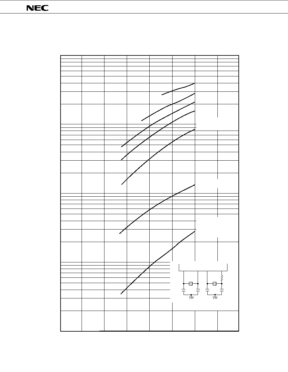
183
µ
PD75236
12. CHARACTERISTIC CURVES (REFERENCE VALUES)
I
DD
vs V
DD
(Main System Clock : 4.19 MHz)
Power Supply Current I
DD
(
µ
A)
5
5000
1000
500
100
50
10
5
1
0
1
2
3
4
5
6
7
30pF
30pF
22pF
22pF
4.19MHz
32.768kHz
330k
X1
X2 XT1
XT2
(Ta=25∞C)
PCC=0011
PCC=0010
PCC=0001
PCC=0000
Main System Clock
HALT Mode + 32 kHz
Oscillation
Subsystem Clock
Operating Mode
Main System Clock
STOP Mode + 32 kHz
Oscillation and
Subsystem Clock
HALT Mode
Crystal
Resonator
Crystal
Resonator
Power Voltage V
DD
(V)

184
µ
PD75236
13. PACKAGE INFORMATION
94 PIN PLASTIC QFP ( 20)
ITEM MILLIMETERS
INCHES
F
1
F
2
I
1.6
0.8
0.15
Q
0.063
0.031
0.006
S94GJ-80-5BG-3
NOTE
Each lead centerline is located within 0.15 mm (0.006 inch) of
its true position (T.P.) at maximum material condition.
C
20.0±0.2
0.787
M
0.15
0.006
0.1±0.1
0.004±0.004
+0.004
≠0.003
+0.009
≠0.008
A
23.2±0.4
0.913
H
0.35±0.10
0.014 +0.004
≠0.005
L
0.8±0.2
0.031 +0.009
≠0.008
N
0.10
0.004
P
3.7
0.146
S
4.0 MAX.
0.158 MAX.
+0.10
≠0.05
B
20.0±0.2
0.787+0.009
≠0.008
+0.017
≠0.016
J
0.8 (T.P.)
0.031 (T.P.)
R
5
∞
±5
∞
5
∞
±5
∞
D
23.2±0.4
0.913 +0.017
≠0.016
G
1
G
2
1.6
0.8
0.063
0.031
K
1.6±0.2
0.063±0.008
A
B
G
1
H
I
J
C
D
P
N
K
L
M
detail of lead end
F
2
F
1
M
71
72
47
94
24
23
48
1
G
2
S
Q
R
185
µ
PD75236
14.
RECOMMEDED SOLDERING CONDITIONS
The
µ
PD75236 should be soldered and mounted under the conditions recommended in the table below.
For soldering methods and conditions other than those recommended below, contact our salesman.
Table 14-1 List of Recommended Soldering Conditions
Table 14-2 Soldering Conditions
*
For the storage period after dry-pack decompression, storage conditions are max. 25
∞
C, 65% RH.
Note
Use of more than one soldering method should be avoided (except in the case of pin part heating).
Remarks
For details of recommended soldering conditions for the surface mounting type, refer to the docu-
ment "Semiconductor Device Mount Technology" (IEI-1207).
Product Name
Package
Recommended Condition Symbol
WS60-107-1
IR30-107-1
VP15-107-1
Pin part heating
µ
PD75236GJ-
◊◊◊
-5BG
94-pin plastic QFP
Recommended
Condition Symbol
Soldering Conditions
Solder bath temperature: 260
∞
C or less
Duration: 10 sec. max.
Number of times: Once
Time limit: 7 days* (thereafter 10 hours prebaking required at 125
∞
C)
Preheating temperature: 120
∞
C max. (package surface temperature)
Package peak temperature: 230
∞
C
Duration: 30 sec. max. (at 210
∞
C or above)
Number of times: Once
Time limit: 7 days* (thereafter 10 hours prebaking required at 125
∞
C)
Package peak temperature: 215
∞
C
Duration: 40 sec. max. (at 200
∞
C or above)
Number of times: Once
Time limit: 7 days* (thereafter 10 hours prebaking required at 125
∞
C)
Pin part temperature: 300
∞
C or less
Duration: 3 sec. max. (Per device side)
Soldering Method
Wave Soldering
Infrared reflow
VPS
Pin part heating
WS60-107-1
IR30-107-1
VP15-107-1
Pin part heating
5

186
µ
PD75236
APPENDIX A.
LIST OF
µ
PD75238 SERIES PRODUCT FUNCTIONS
Product Name
0.95
µ
s/1.91
µ
s/
15.3
µ
s
(Operation at
4.19 MHz)
0.95
µ
s/1.91
µ
s/
3.82
µ
s/15.3
µ
s
(Operation at
4.19 MHz)
Main system
clock selected
0.67
µ
s/1.33
µ
s/2.67
µ
s/10.7
µ
s
(Operation at 6.0 MHz)
Instruction cycle
Subsystem clock
selected
122
µ
s (Operation at 32.768 kHz)
Total
33
64
Input
8
16
Input/output
20: 8 for LED drive
24: 12 for LED drive
Ouptut
5
24
I/O line
FIP dual-function
pin included and
FIP dedicated pin
excluded
Item
µ
PD75217
µ
PD75236
µ
PD75237
µ
PD75238
µ
PD75P238
ROM
24448
◊
8
16256
◊
8
24448
◊
8
32640
◊
8
RAM
768
◊
4
1024
◊
4
A/D converter
None
8: 8-bit resolution
High-voltage output
26: 40 V max.
34: 40 V max.
No. of segments
9 to 16 segments
9 to 24 segments
No. of digits
9 to 16 digits
FIP controller/
driver
Timer
4 channels
5 channels
1 channel,
3-wire
Interrupt source
10
11
Operating temperature range
≠40 to +85
∞
C
≠40 to 70
∞
C
Operating voltage
2.7 to 6.0 V
SBI/3-wire
3-wire
2 channels
Serial interface
64-pin plastic
shrink DIP
64-pin plastic
QFP
94-pin plastic
QFP
94-pin ceramic
LCC with
window
Package
94-pin plastic QFP
5

187
µ
PD75236
APPENDIX B.
DEVELOPMENT TOOLS
The following development tools are available for the development of systems using the
µ
PD75236.
Language Processor
PROM Write Tools
OS
Supply Medium
Host Machine
3.5-inch 2HD
µ
S5A13RA75X
5-inch 2HD
µ
S5A10RA75X
PC-9800 series
MS-DOS
TM
Ver.3.10
to
Ver.3.30C
PC DOS
TM
(Ver.3.1)
IBM PC series
5-inch 2HC
µ
S7B10RA75X
PA-75P238GJ
Hardware
PROM programmer which can easily program representative 256K-bit to 1M-bit PROMs and
single-chip microcomputers with on-chip PROM from the keyboard or by remote control by
connecting a board provided and a separately sold socket board.
PROM programmer adapter for
µ
PD75P238 used in connection with PG-1500.
PG-1500 is connected to the host machine via serial and parallel interfaces to control the PG-
1500 on the host machine.
OS
Supply Medium
Host Machine
3.5-inch 2HD
µ
S5A13PG1500
5-inch 2HD
µ
S5A10PG1500
PC-9800 series
IBM PC series
5-inch 2HC
µ
S7B10PG1500
Software
PC DOS
(Ver.3.1)
Ordering Code
(Product Name)
Ordering Code
(Product Name)
5
RA75X
relocatable assembler
PG-1500
PG-1500 controller
MS-DOS
Ver.3.10
to
Ver.3.30C

188
µ
PD75236
Debugging Tools
Hardware
The IE-75000-R is an in-circuit emulator corresponding to the 75X series. Use the IE-75000-R
and emulation probe in combinations for the development of
µ
PD75236.
Debugging can be carried out efficiently by connecting the IE-75000-R to the host machine
and the PROM programmer.
The IE-75000-R-EM is an emulation board for the IE-75000-R and IE-75001-R. It is incorporated
in the IE-75000-R. Use the IE-75000-R-EM and IE-75000-R or IE-75001-R in combinations for the
evaluation of
µ
PD75236.
The IE-75001-R is an in-circuit emulator corresponding to the 75X series.
Use the IE-75001-R and emulation board IE-75000-R-EM which is sold separately, and
emulation probe in combinations for the development of
µ
PD75236. Debugging can be
carried out efficiently by connecting the IE-75001-R to the host machine and the PROM
programmer.
Emulation probe for
µ
PD75236,
µ
PD75237,
µ
PD75238 and
µ
PD75P238 (94-pin plastic QFP).
Used in combination with the IE-75000-R or IE-75001-R.
94-pin conversion socket EV-9200G-94 is also provided to facilitate connection with the user
system.
IE-75000-R *
IE-75000-R-EM
IE-75001-R
IE-9200G-94
Controls the IE-75000-R and IE-75001-R on the host machine with the IE-75000-R and IE-
75001-R, connected to the host machine via RS-232-C.
EP-75238GJ-R
OS
Supply Medium
Host Machine
3.5-inch 2HD
µ
S5A13IE75X
5-inch 2HD
µ
S5A10IE75X
PC-9800 series
PC DOS
(Ver.3.1)
IBM PC series
5-inch 2HC
µ
S7B10IE75X
Software
IE control program
*
Maintenance product
Ordering Code
(Product Name)
MS-DOS
Ver.3.10
to
Ver.3.30C

189
µ
PD75236
EP-75238GJ-R
+
PA-75P238GJ
PG-1500
PG-1500
Controller
IE-75000-R
IE-75001-R *1
IE-75000-R-EM
RS-232-C
*2
In-Circuit Emulator
Emulation Probe
User System
On-Chip
PROM Product
PROM Programmer
Programmer Adapter
Relocatable
Assembler
IE Control
Program
Host Machine
PC-9800 Series
IBM PC Series
Symbolic Debugging
Possible
Centronics I/F
PD75P238GJ/KF
µ
Development Tool Configuration
* 1.
The IE-75001-R does not incorporate the IE-75000-
R-EM (sold separately).
2.
EV-9200G-94

[MEMO]
No part of this document may be copied or reproduced in any form or by any means without the prior written
consent of NEC Corporation. NEC Corporation assumes no responsibility for any errors which may appear in this
document.
NEC Corporation does not assume any liability for infringement of patents, copyrights or other intellectual
property rights of third parties by or arising from use of a device described herein or any other liability arising
from use of such device. No license, either express, implied or otherwise, is granted under any patents, copyrights
or other intellectual property rights of NEC Corporation or others.
The devices listed in this document are not suitable for use in aerospace equipment, submarine cables, nuclear
reactor control systems and life support systems. If customers intend to use NEC devices for above applications
or they intend to use "Standard" quality grade NEC devices for applications not intended by NEC, please contact
our sales people in advance.
Application examples recommended by NEC Corporation
Standard :
Computer, Office equipment, Communication equipment, Test and Measurement equipment,
Machine tools, Industrial robots, Audio and Visual equipment, Other consumer products, etc.
Special
:
Automotive and Transportation equipment, Traffic control systems, Antidisaster systems,
Anticrime systems, etc.
M4 92.6
[MEMO]
No part of this document may be copied or reproduced in any form or by any means without the prior written
consent of NEC Corporation. NEC Corporation assumes no responsibility for any errors which may appear in this
document.
NEC Corporation does not assume any liability for infringement of patents, copyrights or other intellectual
property rights of third parties by or arising from use of a device described herein or any other liability arising
from use of such device. No license, either express, implied or otherwise, is granted under any patents, copyrights
or other intellectual property rights of NEC Corporation or others.
The devices listed in this document are not suitable for use in aerospace equipment, submarine cables, nuclear
reactor control systems and life support systems. If customers intend to use NEC devices for above applications
or they intend to use "Standard" quality grade NEC devices for applications not intended by NEC, please contact
our sales people in advance.
Application examples recommended by NEC Corporation
Standard :
Computer, Office equipment, Communication equipment, Test and Measurement equipment,
Machine tools, Industrial robots, Audio and Visual equipment, Other consumer products, etc.
Special
:
Automotive and Transportation equipment, Traffic control systems, Antidisaster systems,
Anticrime systems, etc.
FIP is a trademark of NEC Corporation.
MS-DOS
TM
is a trademark of Microsoft Corporation.
PC DOS
TM
is a trademark of IBM Corporation.
Æ
µ
PD75236