Document Outline
- COVER
- DESCRIPTION
- FEATURES
- APPLICATION
- ORDERING INFORMATION
- FUNCTIONAL OUTLINE
- 1. PIN CONFIGURATION (TOP VIEW)
- 2. BLOCK DIAGRAM
- 3. PIN FUNCTION
- 3.1 Port Pins
- 3.2 Pins Other than Port Pins
- 3.3 Pin Input/Output Circuits
- 3.4 Recommended Connection for Unused Pins
- 4. SWITCHING FUNCTION BETWEEN MK I MODE AND MK II MODE
- 4.1 Differences between Mk I Mode and Mk II Mode
- 4.2 Setting Method of Stack Bank Select Register (SBS)
- 5. MEMORY CONFIGURATION
- 6. PERIPHERAL HARDWARE FUNCTIONS
- 6.1 Digital Input/Output Ports
- 6.2 Clock Generator
- 6.3 Subsystem Clock Oscillator Control Functions
- 6.4 Clock Output Circuit
- 6.5 Basic Interval Timer/Watchdog Timer
- 6.6 Watch Timer
- 6.7 Timer/Event Counter
- 6.8 Serial Interface
- 6.9 LCD Controller/Driver
- 6.10 Bit Sequential Buffer ... 16 Bits
- 7. INTERRUPT FUNCTION AND TEST FUNCTION
- 8. STANDBY FUNCTION
- 9. RESET FUNCTION
- 10. MASK OPTION
- 11. INSTRUCTION SETS AND THEIR OPERATIONS
- 12. ELECTRICAL SPECIFICATIONS
- 13. PACKAGE DRAWINGS
- 14. RECOMMENDED SOLDERING CONDITIONS
- APPENDIX A uPD75316B, 753017 AND 75P3018 FUNCTION LIST
- APPENDIX B DEVELOPMENT TOOLS
- APPENDIX C RELATED DOCUMENTS
4-BIT SINGLE-CHIP MICROCONTROLLER
µ
PD753012, 753016, 753017
MOS INTEGRATED CIRCUIT
DESCRIPTION
The
µ
PD753017 is one of the 75XL series 4-bit single-chip microcontroller chips and has a data processing
capability comparable to that of an 8-bit microcontroller.
It has an on-chip LCD controller/driver with a larger ROM capacity and extended CPU functions compared with
the conventional
µ
PD75316B, and can provide high-speed operation. It can be supplied in a small plastic TQFP
package (12
◊
12 mm) and is suitable for small sets using LCD panels.
For details of functions refer to the following User's Manual.
µ
PD753017 User's Manual : U11282E
FEATURES
∑
Low voltage operation: V
DD
= 2.2 to 5.5 V
∑ Can be driven by two 1.5 V batteries
∑
On-chip memory
∑ Program memory (ROM):
12288
◊
8 bits (
µ
PD753012)
16384
◊
8 bits (
µ
PD753016)
24576
◊
8 bits (
µ
PD753017)
∑ Data memory (RAM):
1024
◊
4 bits
∑
Capable of high-speed operation and variable in-
struction execution time for power saving
∑ 0.95, 1.91, 3.81, 15.3
µ
s (at 4.19 MHz operation)
∑ 0.67, 1.33, 2.67, 10.7
µ
s (at 6.0 MHz operation)
∑ 122
µ
s (at 32.768 kHz operation)
∑
Internal programmable LCD controller/driver
∑
Small plastic TQFP (12
◊
12 mm)
∑ Suitable for small sets such as cameras
∑
One-time PROM:
µ
PD75P3018
APPLICATION
Remote controllers, camera-contained VCRs, cameras, gas meters, etc.
ORDERING INFORMATION
Part number
Package
µ
PD753012GC-XXX-3B9
80-pin plastic QFP (14
◊
14 mm)
µ
PD753012GK-XXX-BE9
80-pin plastic TQFP (fine pitch) (12
◊
12 mm)
µ
PD753016GC-XXX-3B9
80-pin plastic QFP (14
◊
14 mm)
µ
PD753016GK-XXX-BE9
80-pin plastic TQFP (fine pitch) (12
◊
12 mm)
µ
PD753017GC-XXX-3B9
80-pin plastic QFP (14
◊
14 mm)
µ
PD753017GK-XXX-BE9
80-pin plastic TQFP (fine pitch) (12
◊
12 mm)
Remark
XXX indicates a ROM code suffix.
In this document, unless otherwise specified, the description is made based on
µ
PD753017
as typical product.
The information in this document is subject to change without notice.
Document No. U10140EJ2V0DS00 (2nd edition)
Date Published December 1997 N
Printed in Japan
©
1995
DATA SHEET
The mark
shows major revised points.
2
µ
PD753012, 753016, 753017
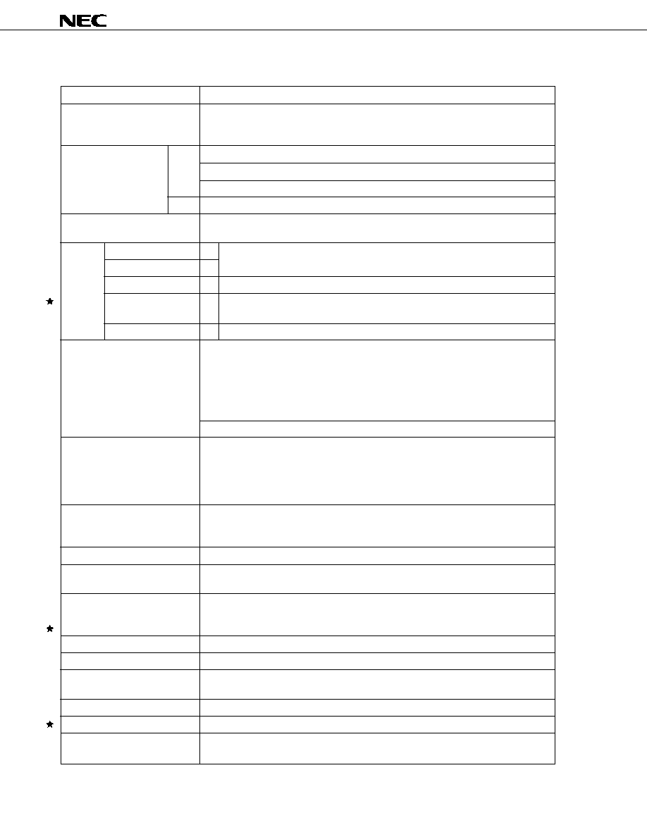
FUNCTIONAL OUTLINE
Parameter
Function
Instruction execution time
∑ 0.95, 1.91, 3.81, 15.3
µ
s (main system clock: at 4.19 MHz operation)
∑ 0.67, 1.33, 2.67, 10.7
µ
s (main system clock: at 6.0 MHz operation)
∑ 122
µ
s (subsystem clock: at 32.768 kHz operation)
On-chip memory
ROM
12288
◊
8 bits (
µ
PD753012)
16384
◊
8 bits (
µ
PD753016)
24576
◊
8 bits (
µ
PD753017)
RAM
1024
◊
4 bits
General-purpose register
∑ 4-bit operation: 8
◊
4 banks
∑ 8-bit operation: 4
◊
4 banks
Input/
CMOS input
8
On-chip pull-up resistors can be specified by using software: 23
output
CMOS input/output
16
port
CMOS output
8
Also used for segment pins
N-ch open-drain
8
Withstands 13 V, on-chip pull-up resistors can be specified by using mask
input/output
option
Total
40
LCD controller/driver
∑ Segment number selection
: 24/28/32 segments (can be changed to CMOS
output port in 4 time-unit; max. 8)
∑ Display mode selection
: Static
1/2 duty (1/2 bias)
1/3 duty (1/2 bias)
1/3 duty (1/3 bias)
1/4 duty (1/3 bias)
On-chip split resistor for LCD drive can be specified by using mask option
Timer
5 channels
∑ 8-bit timer/event counter: 3 channels (can be used for 16-bit timer/event counter,
carrier generator, or timer with gate)
∑ Basic interval timer/watchdog timer: 1 channel
∑ Watch timer: 1 channel
Serial interface
∑ 3-wire serial I/O mode ... MSB or LSB can be selected for transferring top bit
∑ 2-wire serial I/O mode
∑ SBI mode
Bit sequential buffer
16 bits
Clock output (PCL)
∑
, 524, 262, 65.5 kHz (main system clock: at 4.19 MHz operation)
∑
, 750, 375, 93.8 kHz (main system clock: at 6.0 MHz operation)
Buzzer output (BUZ)
∑ 2, 4, 32 kHz
(main system clock: at 4.19 MHz operation
or subsystem clock: at 32.768 kHz operation)
∑ 2.93, 5.86, 46.9 kHz (main system clock: at 6.0 MHz operation)
Vectored interrupts
External: 3, Internal: 5
Test input
External: 1, Internal: 1
System clock oscillator
∑ Ceramic or crystal oscillator for main system clock oscillation
∑ Crystal oscillator for subsystem clock oscillation
Standby function
STOP/HALT mode
Power supply voltage
V
DD
= 2.2 to 5.5 V
Package
∑ 80-pin plastic QFP (14
◊
14 mm)
∑ 80-pin plastic TQFP (fine pitch) (12
◊
12 mm)

3
µ
PD753012, 753016, 753017
CONTENTS
1.
PIN CONFIGURATION (TOP VIEW) ................................................................................................... 5
2.
BLOCK DIAGRAM ............................................................................................................................... 7
3.
PIN FUNCTION .................................................................................................................................... 8
3.1
Port Pins ...................................................................................................................................... 8
3.2
Pins Other than Port Pins ........................................................................................................ 10
3.3
Pin Input/Output Circuits ......................................................................................................... 12
3.4
Recommended Connection for Unused Pins ......................................................................... 14
4.
SWITCHING FUNCTION BETWEEN MK I MODE AND MK II MODE ...................................... 15
4.1
Differences between Mk I Mode and Mk II Mode .................................................................... 15
4.2
Setting Method of Stack Bank Select Register (SBS) ........................................................... 16
5.
MEMORY CONFIGURATION ............................................................................................................ 17
6.
PERIPHERAL HARDWARE FUNCTIONS ....................................................................................... 21
6.1
Digital Input/Output Ports ........................................................................................................ 21
6.2
Clock Generator ........................................................................................................................ 22
6.3
Subsystem Clock Oscillator Control Functions .................................................................... 23
6.4
Clock Output Circuit ................................................................................................................. 24
6.5
Basic Interval Timer/Watchdog Timer ..................................................................................... 25
6.6
Watch Timer .............................................................................................................................. 26
6.7
Timer/Event Counter ................................................................................................................. 27
6.8
Serial Interface .......................................................................................................................... 31
6.9
LCD Controller/Driver ............................................................................................................... 33
6.10 Bit Sequential Buffer ... 16 Bits ............................................................................................... 35
7.
INTERRUPT FUNCTION AND TEST FUNCTION ........................................................................... 36
8.
STANDBY FUNCTION ....................................................................................................................... 38
9.
RESET FUNCTION ............................................................................................................................ 39
10. MASK OPTION .................................................................................................................................. 42
11. INSTRUCTION SETS AND THEIR OPERATIONS ........................................................................ 43
12. ELECTRICAL SPECIFICATIONS ...................................................................................................... 55
13. PACKAGE DRAWINGS ..................................................................................................................... 68
14. RECOMMENDED SOLDERING CONDITIONS ................................................................................ 70

4
µ
PD753012, 753016, 753017
APPENDIX A
µ
PD75316B, 753017 AND 75P3018 FUNCTION LIST ................................................ 72
APPENDIX B DEVELOPMENT TOOLS ................................................................................................. 74
APPENDIX C RELATED DOCUMENTS ................................................................................................. 78

5
µ
PD753012, 753016, 753017
S12
S13
S14
S15
S16
S17
S18
S19
S20
S21
S22
S23
S24/BP0
S25/BP1
S26/BP2
S27/BP3
S28/BP4
S29/BP5
S30/BP6
S31/BP7
P60/KR0
X2
X1
IC
Note
XT2
XT1
V
DD
P33
P32
P31/SYNC
P30/LCDCL
P23/BUZ
P22/PCL/PTO2
P21/PTO1
P20/PTO0
P13/TI0
P12/INT2/TI1/TI2
P11/INT1
P10/INT0
P03/SI/SB1
1
2
3
4
5
6
7
8
9
10
11
12
13
14
15
16
17
18
19
20
60
59
58
57
56
55
54
53
52
51
50
49
48
47
46
45
44
43
42
41
80 79 78 77 76 75 74 73 72 71 70 69 68 67 66 65 64 63 62 61
21 22 23 24 25 26 27 28 29 30 31 32 33 34 35 36 37 38 39 40
COM0
COM1
COM2
COM3
BIAS
V
LC0
V
LC1
V
LC2
P40
P41
P42
P43
V
SS
P50
P51
P52
P53
P00/INT4
P01/SCK
P02/SO/SB0
S11
S10
S9
S8
S7
S6
S5
S4
S3
S2
S1
S0
RESET
P73/KR7
P72/KR6
P71/KR5
P70/KR4
P63/KR3
P62/KR2
P61/KR1
1. PIN CONFIGURATION (TOP VIEW)
∑
80-pin plastic QFP (14
◊
14 mm)
µ
PD753012GC-XXX-3B9, 753016GC-XXX-3B9,
µ
PD753017GC-XXX-3B9
∑
80-pin plastic TQFP (fine pitch) (12
◊
12 mm)
µ
PD753012GK-XXX-BE9, 753016GK-XXX-BE9,
µ
PD753017GK-XXX-BE9
Note Connect the IC (Internally Connected) pin directly to V
DD
.