
©
NEC Corporation 1991
Document No.
IC-2825A
(O. D. No.
IC-8270A)
Date Published December 1993 P
Printed in Japan
DATA SHEET
MOS INTEGRATED CIRCUIT
µ
PD75312(A), 75316(A)
The information in this document is subject to change without notice.
The mark 5 shows major revised points.
DESCRIPTION
The
µ
PD75316(A) is one of the 75X Series 4-bit single-chip microcomputer having a built-in LCD controller/
driver, and has a data processing capability comparable to that of an 8-bit microcomputer.
In addition to high-speed operation with 0.95
µ
s minimum instruction execution time for the CPU, the
µ
PD75316(A) can also process data in 1-, 4-, and 8-bit units. Therefore, as a 4-bit single-chip microcomputer
chip having a built-in LCD panel controller/driver, its data processing capability is the highest in its class in
the world.
Detailed functions are described in the following user's manual. Be sure to read it for designing.
µ
PD75308 User's Manual: IEM-5016
FEATURES
∑
Higher reliability than
µ
PD75316
∑
Internal memory
∑ Program memory (ROM)
: 16256
◊
8 bits (
µ
PD75316(A))
: 12160
◊
8 bits (
µ
PD75312(A))
∑ Data memory
: 512
◊
4 bits
∑
Capable of high-speed operation and variable instruction execution time to power save
∑ 0.95
µ
s, 1.91
µ
s, 15.3
µ
s (operating at 4.19 MHz)
∑ 122
µ
s (operating at 32.768 kHz)
∑
75X architecture comparable to that for an 8-bit microcomputer is employed
∑
Built-in programmable LCD controller/driver
∑
Clock operation at reduced power dissipation: 5
µ
A TYP. (operating at 3 V)
∑
Enhanced timer function (3 channels)
∑
Interrupt functions especially enhanced for applications, such as remote control receiver
∑
Pull-up resistors can be provided for 31 I/O lines
∑
Built-in NEC standard serial bus interface (SBI)
∑
Upgraded model of
µ
PD7514 (
µ
PD7500 Series)
∑
PROM version (
µ
PD75P316,
µ
PD75P316A) available
APPLICATIONS
Suitable for controlling automotive and transportation equipment.
The
µ
PD75316(A) is treated as the representative model throughout this document,
unless there are differences between
µ
PD75312(A) and
µ
PD75316(A) functions.
4-BIT SINGLE-CHIP MICROCOMPUTER

µ
PD75312(A), 75316(A)
2
ORDERING INFORMATION
Part Number
Package
Quality Grade
µ
PD75312GF(A)-xxx-3B9
80-pin plastic QFP (14
◊
20 mm)
Special
µ
PD75316GF(A)-xxx-3B9
80-pin plastic QFP (14
◊
20 mm)
Special
Remarks: xxx is ROM code number.
Please refer to "Quality Grade on NEC Semiconductor Devices" (Document Number IEI-1209)
published by NEC Corporation to know the specification of quality grade on the devices and its
recommended applications.
DIFFERENCE BETWEEN
µ
PD75316(A) and
µ
PD75316
Product
µ
PD75316(A)
µ
PD75316
Item
Quality Grade
Special
Standard
Directly Driving LED
Not offered
Offered
Absolute Maximum Ratings
Differ in high-level output currrent and low-level output
current
DC Characteristics
Differ in low-level output voltage
Electrical
Characteristics
µ
PD75312(A), 75316(A)
3
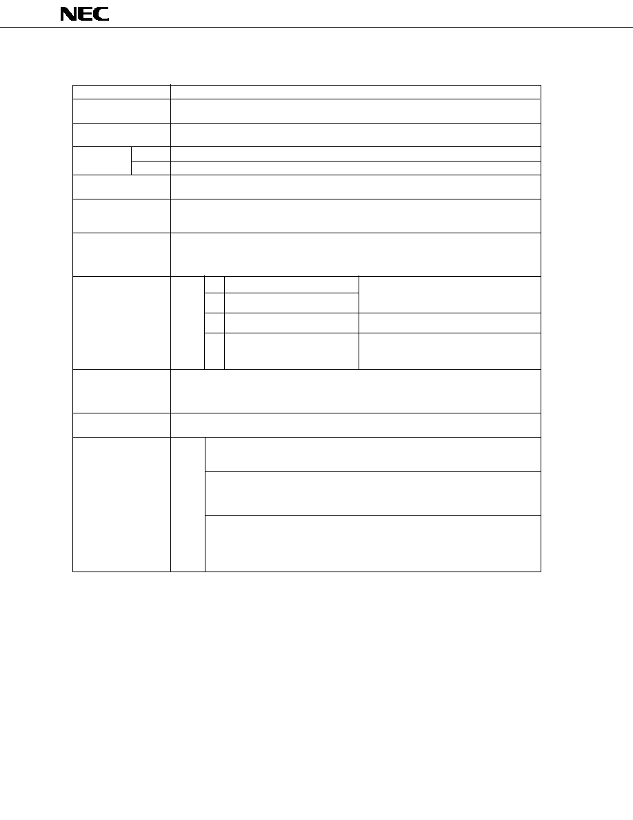
FUNCTIONAL OUTLINE (1/2)
Item
Function
Number of Basic
41
Instructions
Instruction Cycle
∑ 0.95
µ
s, 1.91
µ
s, 15.3
µ
s (Main system clock: operating at 4.19 MHz)
∑ 122
µ
s (Subsystem clock: operating at 32.768 kHz)
ROM
16256
◊
8-bit (
µ
PD75316(A)), 12160
◊
8-bit (
µ
PD75312(A))
RAM
512
◊
4 bits
General-Purpose
∑ 4-bit manipulation: 8 (B, C, D, E, H, L, X, A)
Registers
∑ 8-bit manipulation: 4
(
BC, DE, HL, XA)
Accumulator
∑ Bit accumulator (CY)
∑ 4-bit accumulator (A)
∑ 8-bit accumulator (XA)
Instruction Set
∑ Abundant bit manipulation instructions
∑ Efficient 4-bit data manipulation instructions
∑ 8-bit data transfer instructions
∑ GETI instruction executing 2-/3-byte instruction with a single byte
I/O Line
40
8
CMOS input pins
Pull-up by software is possible.
: 23
16
CMOS input/output pins
8
CMOS output pins
Also serve as segment pins
8
N-ch open-drain input/output
Withstand voltage: 10 V
Pull-up by mask option is possible.
: 8
LCD Controller/
∑ Segment number selection: 24/28/32 segments
Driver
(4/8 pins can also be used as bit ports.)
∑ Display mode selection: Static, 1/2 duty, 1/3 duty (1/2 bias), 1/3 duty (1/3 bias), 1/4 duty
∑ Dividing resistor for LCD driving can be built-in by mask option.
Supply Voltage
V
DD
= 2.7 to 6.0 V
Range
Internal
Memory
Timer
3 chs
∑ 8-bit timer/event counter
∑ Clock source: 4 steps
∑ Event count is possible
∑ 8-bit basic interval timer
∑ Reference time generation: 1.95 ms, 7.82 ms, 31.3 ms, 250 ms
(operating at 4.19 MHz)
∑ Can be used as watchdog timer
∑ Watch timer
∑ Generates 0.5-second time intervals
∑ Count clock source: Main system clock or subsystem clock (selectable)
∑ Watch fast forward mode (generates 3.9-ms time intervals)
∑ Buzzer output (2 kHz)
µ
PD75312(A), 75316(A)
4
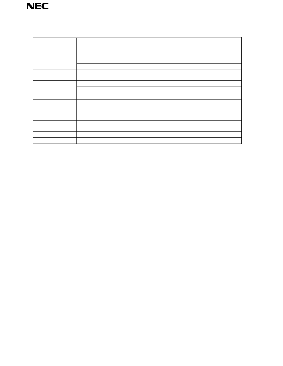
FUNCTIONAL OUTLINE (2/2)
Item
Function
8-bit Serial Interface
∑ Three modes:
∑ 3-line serial I/O mode
∑ 2-line serial I/O mode
∑ SBI mode
∑ LSB/MSB first selectable
Bit Sequential
Special bit manipulation memory: 16 bits
Buffer
∑ Ideal for remote controller
Clock Output
Timer/event counter output (PTO0): Output of square wave at specified frequency
Function
Clock output (PCL):
,
524, 262, 65.5 kHz (operating at 4.19 MHz)
Buzzer output (BUZ): 2 kHz (operating at 4.19 MHz or 32.768 kHz)
Vector Interrupt
∑ External: 3
∑ Internal: 3
Test Input
∑ External: 1
∑ Internal: 1
System Clock
∑ Ceramic/crystal oscillator circuit for main system clock oscillation: 4.194304 MHz
Oscillator Circuit
∑ Crystal oscillator circuit for subsystem clock oscillation: 32.768 kHz
Standby
STOP/HALT mode
Package
80-pin plastic QFP (14
◊
20 mm)

µ
PD75312(A), 75316(A)
5
CONTENTS
1.
PIN CONFIGURATION (Top View) ................................................................................................
7
2.
BLOCK DIAGRAM ...........................................................................................................................
8
3.
PIN FUNCTIONS ..............................................................................................................................
9
3.1
PORT PINS .............................................................................................................................................
9
3.2
NON PORT PINS ...................................................................................................................................
11
3.3
PIN INPUT/OUTPUT CIRCUITS ...........................................................................................................
13
3.4
RECOMMENDED PROCESSING OF UNUSED PINS ..........................................................................
15
3.5
NOTES ON USING THE P00/INT4, AND RESET PINS ......................................................................
16
4.
MEMORY CONFIGURATION ..........................................................................................................
16
5.
PERIPHERAL HARDWARE FUNCTIONS ........................................................................................
20
5.1
PORTS ....................................................................................................................................................
20
5.2
CLOCK GENERATOR CIRCUIT ............................................................................................................
21
5.3
CLOCK OUTPUT CIRCUIT ....................................................................................................................
22
5.4
BASIC INTERVAL TIMER .....................................................................................................................
23
5.5
WATCH TIMER ......................................................................................................................................
24
5.6
TIMER/EVENT COUNTER .....................................................................................................................
25
5.7
SERIAL INTERFACE ..............................................................................................................................
27
5.8
LCD CONTROLLER/DRIVER ..................................................................................................................
29
5.9
BIT SEQUENTIAL BUFFER ...................................................................................................................
31
6.
INTERRUPT FUNCTIONS ................................................................................................................
31
7.
STANDBY FUNCTIONS ..................................................................................................................
33
8.
RESET FUNCTION ...........................................................................................................................
34
9.
INSTRUCTION SET .........................................................................................................................
36
10. SELECTION OF MASK OPTION .....................................................................................................
42
11. ELECTRICAL SPECIFICATIONS ......................................................................................................
43
12. PACKAGE DRAWINGS ...................................................................................................................
55