
Printed in Japan
MOS INTEGRATED CIRCUIT
DATA SHEET
µ
PD75402A(A)
4 BIT SINGLE-CHIP MICROCOMPUTER
The
µ
PD75402A(A) is a CMOS single-chip microcomputer which uses the 75X series architecture. It operates
at high speed with a minimum instruction execution time of 0.95
µ
s.
The
µ
PD75P402 is also available for system development evaluation. It contains one-time PROM instead
of mask ROM used in the
µ
PD75402A(A).
The following user's manual describes the details of the functions of the
µ
PD75402A(A). Be sure to read
it before designing an application system.
µ
PD75402A User's Manual: IEU-644
FEATURES
∑
More reliable than the
µ
PD75402A
∑
High-speed operation with a minimum instruction execution time of 0.95
µ
s (when the microcomputer
operates at 4.19 MHz)
∑
Low voltage and low-speed instruction execution time of 15.3
µ
s (when the microcomputer operates at
4.19 MHz)
∑
Memory mapping by on-chip peripheral hardware
∑
NEC standard serial bus interface (SBI)
∑
8-bit basic interval timer (watchdog timer applicable)
∑
Interrupt function
∑
Three vectored interrupts (one external and two internal interrupts)
∑
One external test input
∑
Clock output function (remote controller output applicable)
∑
Capable of specifying the incorporation of 16 pull-up resistors by software
APPLICATIONS
Electronic units for automobiles, and suchlike
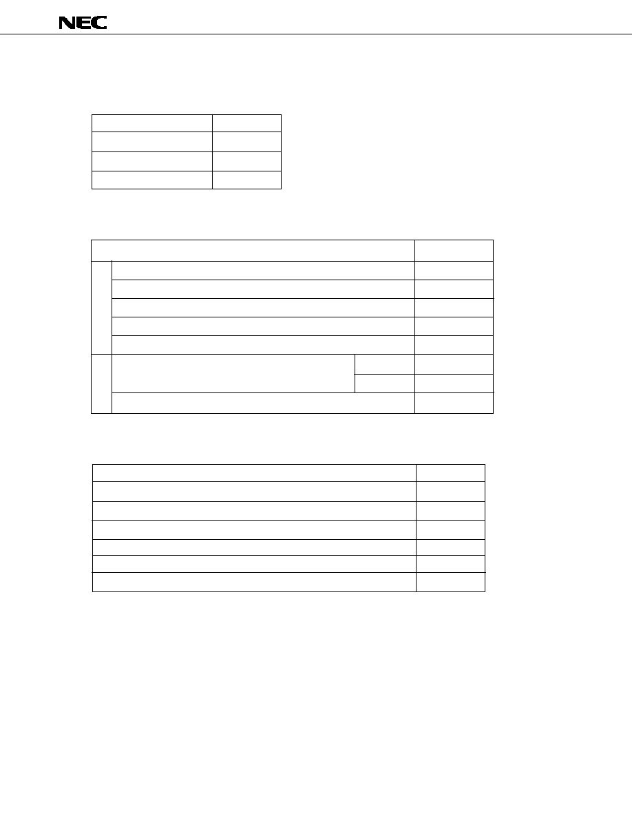
ORDERING INFORMATION
Part number
Package
Quality grade
µ
PD75402AC(A)-
◊◊◊
28-pin plastic DIP (600 mil)
Special
µ
PD75402ACT(A)-
◊◊◊
28-pin plastic shrink DIP (400 mil)
Special
µ
PD75402AGB(A)-
◊◊◊
-3B4
44-pin plastic QFP (10
◊
10 mm)
Special
Remark
◊◊◊
indicates the ROM code number.
Please refer to "Quality Grades on NEC Semiconductor Devices" (Document number IEI-1209) published by
NEC Corporation to know the specification of quality grade on the devices and its recommended applications.
The information in this document is subject to change without notice.
Major changes in this revision are indicated by stars (
) in the margins.
Document No.
IC-2841B
(O.D.No.
IC-8273B)
Date Published November 1993 P
©
1990
©
1
NEC CORPORATION 1991
2
µ
PD75402A(A)
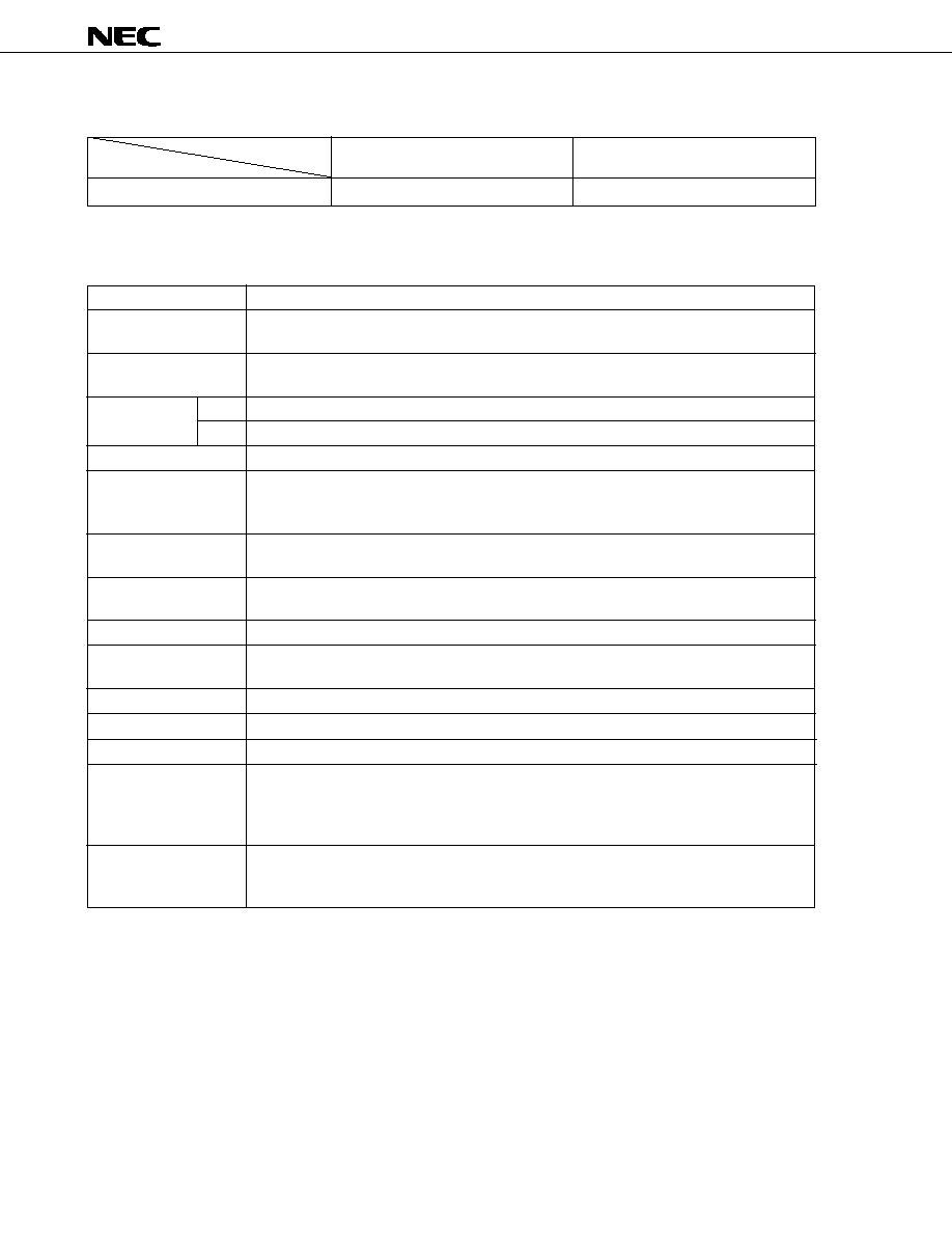
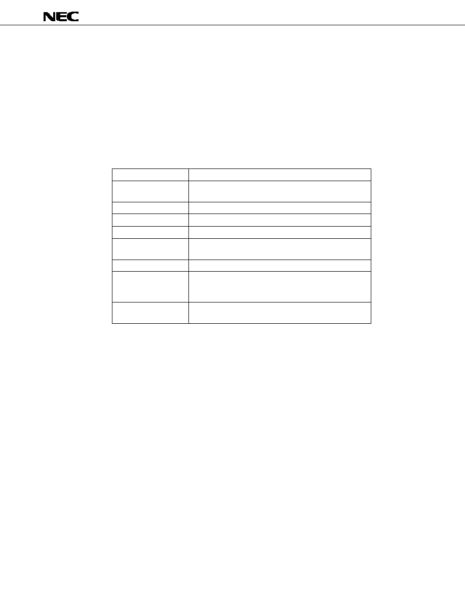
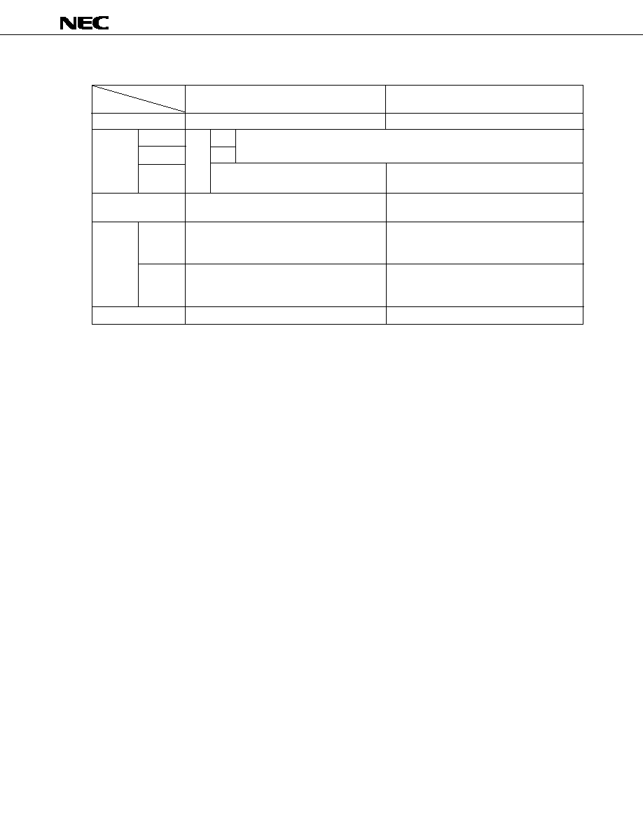
DIFFERENCES BETWEEN THE
µ
PD75402A(A) AND
µ
PD75402A
FUNCTIONAL OVERVIEW
Special
Standard
Item
Quality grade
Product
µ
PD75402A(A)
µ
PD75402A
Function
37
∑
0.95, 1.91, or 15.3
µ
s (when operating at 4.19 MHz)
∑
Switchable among three speeds
1920
◊
8 bits
64
◊
4 bits
4 bits
◊
4 or 8 bits
◊
2 (memory mapping)
∑
CMOS input ports
:
6 lines
∑
CMOS I/O ports
: 12 lines (8 lines can drive the LED directly.)
∑
N-ch open-drain I/O ports :
4 lines (All lines can drive the LED directly.)
∑
Capable of controlling the incorporation of 16 pull-up resistors by software
∑
Capable of controlling the incorporation of 4 pull-up resistors by mask option
∑
1.05 MHz, 524 kHz, or 65.5 kHz (when operating at 4.19 MHz)
∑
Applicable to remote controller output
8-bit basic interval timer (watchdog timer applicable)
∑
8 bits
∑
Two transfer modes (three-wire synchronous mode and SBI mode)
One external and two internal interrupts
One external input (See Chapter 6 for details.)
STOP/HALT mode
∑
Bit manipulation instructions (set, clear, test, and Boolean operation)
∑
1-byte relative branch instructions
∑
4-bit operation instructions (add, Boolean operation, and compare)
∑
4- and 8-bit transfer instructions
∑
28-pin plastic DIP (600 mil)
∑
28-pin plastic shrink DIP (400 mil)
∑
44-pin plastic QFP (10
◊
10 mm)
Item
Number of basic
instructions
Minimum instruction
execution time
ROM
RAM
General register
I/O line
Pull-up resistor
Clock output
Timer/counter
Serial interface
Vectored interrupt
Test input
Standby
Instruction set
Package
Built-in
memory

3
µ
PD75402A(A)
CONTENTS
1.
PIN CONFIGURATION (TOP VIEW) ......................................................................................
4
2.
BLOCK DIAGRAM ......................................................................................................................
6
3.
PIN FUNCTIONS .......................................................................................................................
7
3.1
PORT PINS .....................................................................................................................................
7
3.2
NON-PORT PINS ...........................................................................................................................
8
3.3
PIN INPUT/OUTPUT CIRCUITS ..................................................................................................
8
3.4
SELECTION OF A MASK OPTION ...........................................................................................
10
3.5
HANDLING UNUSED PINS .........................................................................................................
11
3.6
NOTES ON USING THE P00 AND RESET PINS .................................................................
11
4.
MEMORY CONFIGURATION ...................................................................................................
12
5.
PERIPHERAL HARDWARE FUNCTIONS ................................................................................
14
5.1
PORTS ..............................................................................................................................................
14
5.2
CLOCK GENERATOR ....................................................................................................................
15
5.3
CLOCK OUTPUT CIRCUIT ...........................................................................................................
16
5.4
BASIC INTERVAL TIMER ............................................................................................................
17
5.5
SERIAL INTERFACE ......................................................................................................................
18
6.
INTERRUPT FUNCTION ...........................................................................................................
20
7.
STANDBY FUNCTION ..............................................................................................................
22
8.
RESET FUNCTION ....................................................................................................................
23
9.
INSTRUCTION SET ...................................................................................................................
25
10. ELECTRICAL CHARACTERISTICS ...........................................................................................
29
11. PACKAGE DIMENSIONS ..........................................................................................................
38
12. RECOMMENDED SOLDERING CONDITIONS .........................................................................
42
APPENDIX A DIFFERENCES BETWEEN THE
µ
PD75402A(A) AND
µ
PD75P402 ...................
43
APPENDIX B DEVELOPMENT TOOLS .........................................................................................
44
APPENDIX C
RELATED DOCUMENTS ........................................................................................
45
5
4
µ
PD75402A(A)
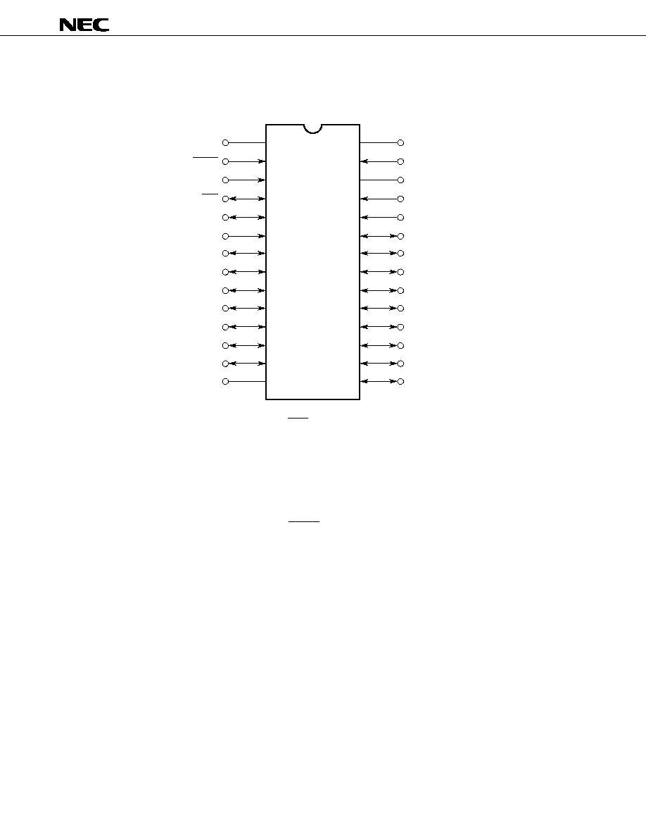
1. PIN CONFIGURATION (TOP VIEW)
28-pin plastic DIP (600 mil), 28-pin plastic shrink DIP (400 mil)
Note
NC
1
28
V
DD
RESET
2
27
X1
P00
3
26
X2
P01/SCK
4
25
P12 /INT2
P02/SO/SB0
5
24
P10/INT0
P03/SI
6
23
P23
P50
7
22
P22 /PCL
P51
8
21
P21
P52
9
20
P20
P53
10
19
P63
P30
11
18
P62
P31
12
17
P61
P32
13
16
P60
V
SS
14
15
P33
PD75402AC(A)/CT(A)-
µ
◊◊◊
P00 - P03
: Port 0
SCK
: Serial clock I/O
P10 and P12: Port 1
SO/SB0
: Serial output/input-output
P20 - P23
: Port 2
SI
: Serial input
P30 - P33
: Port 3
PCL
: Clock output
P50 - P53
: Port 5
INT0
: External vectored interrupt input
P60 - P63
: Port 6
INT2
: External test input
X1 and X2 : Oscillating pins
RESET
: Reset input
V
DD
: Power supply
V
SS
: Ground
NC
: No connection
Note When the
µ
PD75402A(A) shares the printed circuit board with the
µ
PD75P402, connect the NC pin
directly to the V
SS
pin.
5
µ
PD75402A(A)
44-pin plastic QFP (10
◊
10 mm)
P30
P01/SCK
1
33
P31
P00
2
32
P32
RESET
3
31
NC
NC
Note
4
30
V
SS
NC
5
29
NC
NC
6
28
NC
NC
7
27
P33
V
DD
8
26
P60
X1
9
25
P61
X2
10
24
NC
NC
11
23
12
44
13
43
14
42
15
41
16
40
17
39
18
38
19
37
20
36
21
35
22
34
P53
P52
P51
NC
NC
NC
NC
P50
P03/SI
P02/SO/SB0
NC
P62
P63
P20
P21
NC
V
SS
NC
P22/PCL
P23
P10/INT0
P12/INT2
PD75402AGB(A)-
◊◊◊
-3B4
µ
Note When the
µ
PD75402A(A) shares the printed circuit board with the
µ
PD75P402, connect the NC pin
(pin 30) directly to the V
SS
pin
.

6
µ
PD75402A(A)
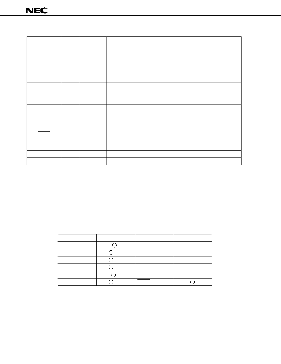
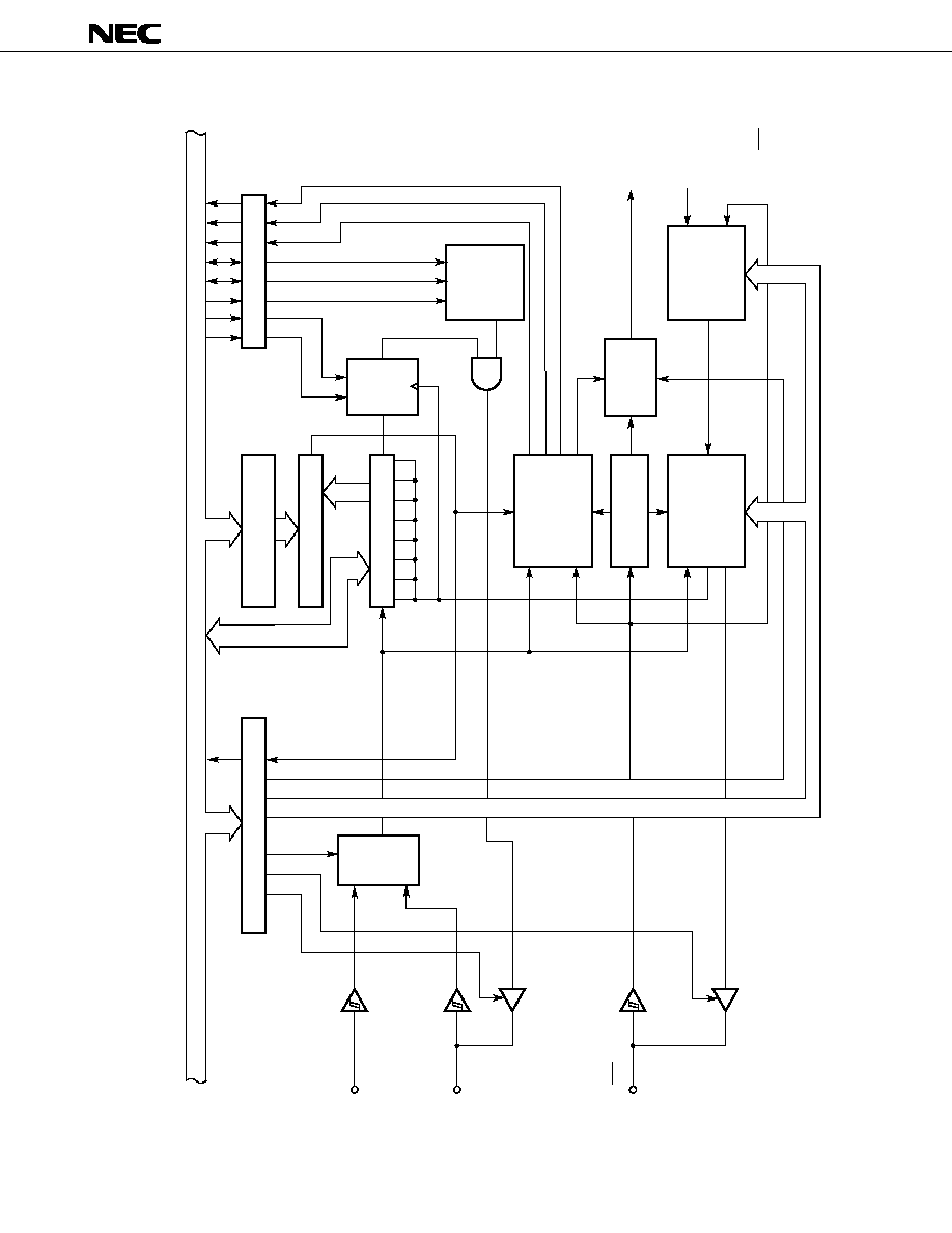
2. BLOCK DIAGRAM
Port 3
4
P30 - P33
Port 5
4
P50 - P53
Port 6
4
P60 - P63
Port 0
4
P00 - P03
Port 1
2
P10, P12
Port 2
4
P20 - P23
SP
CY
ALU
ROM
Program
memory
Program
counter (11)
1920
◊
8 bits
Decode
and
control
General register
RAM
Data memory
64
◊
4 bits
Basic
interval
timer
Serial
interface
Interrupt
control
INTBT
INTCSI
Clock
output
control
Clock
divider
Clock
generator
Standby
control
CPU
Clock
PCL
X1
X2
V
DD
V
SS
RESET
SI
SO/SB0
SCK
INT0
INT2
f
XX
/2
N

7
µ
PD75402A(A)
3. PIN FUNCTIONS
3.1 PORT PINS
Remarks 1. The
µ
PD75402A(A) cannot perform 8-bit I/O with two ports as a pair.
2. See Chapter 8 for each pin status during resetting.
Pin
P00
P01
P02
P03
P10
P12
P20
P21
P22
P23
P30 - P33
P50 - P53
P60 - P63
I /O
Input
I/O
I/O
Input
Input
I/O
I/O
I/O
I/O
Dual-
function pin
≠
SCK
SO/SB0
SI
INT0
INT2
≠
≠
PCL
≠
≠
≠
≠
Function
4-bit input port (port 0)
P01 to P03 allow the connection of built-in pull-up resistors to be
specified in units of three bits by software.
2-bit input port (port 1)
P10 connects with the built-in noise eliminator using a sampling clock.
P12 connects with the built-in noise eliminator using an analog delay.
P12 allows the connection of built-in pull-up resistor to be specified by
software.
4-bit I/O port (port 2)
Allow I/O specification in units of four bits.
Allow the connection of built-in pull-up resistors to be specified in
units of four bits by software.
Programmable 4-bit I/O port (port 3)
Allow I/O specification bit by bit.
Allow the connection of built-in pull-up resistors to be specified in
units of four bits by software.
Can directly drive LED.
4-bit N-ch open-drain I/O port (port 5)
Allow I/O specification in units of four bits.
Allow the connection of built-in pull-up resistors to be specified bit by
bit by mask option.
Can directly drive LED.
4-bit I/O port (port 6)
Allow I/O specification in units of four bits.
Allow the connection of built-in pull-up resistors to be specified in
units of four bits by software.
Can directly drive LED.
8
µ
PD75402A(A)
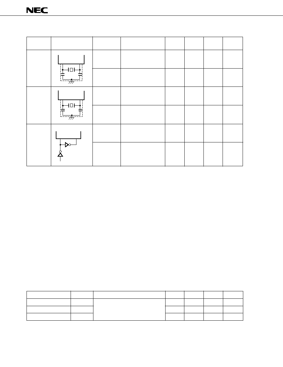
3.2 NON-PORT PINS
Remark See Chapter 8 for each pin status during resetting.
Note Connect the NC pin directly to the V
SS
pin when the
µ
PD75402A(A) shares the printed circuit board
with the
µ
PD75P402 in emulation.
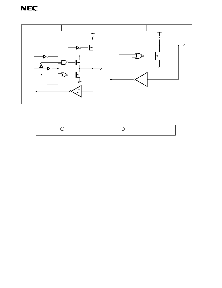
3.3 PIN INPUT/OUTPUT CIRCUITS
The I/O circuits of the
µ
PD75402A(A) are roughly shown on the next and subsequent pages.
Table 1-1 I/O Circuit Type of Pin
Remark The types in circles have a Schmitt-triggered input.
Pin
INT0
INT2
SI
SO
SCK
SB0
PCL
X1, X2
RESET
V
DD
V
SS
NC
Note
I /O
Input
Input
Input
I/O
I/O
I/O
I/O
Input
Input
≠
≠
≠
Dual-
function pin
P10
P12
P03
P02/SB0
P01
P02/SO
P22
≠
≠
≠
≠
≠
Function
Edge detection vectored interrupt request input pin (A detected edge
can be selected by the mode register.)
Connects with the built-in noise eliminator using a sampling clock.
Edge detection external test input pin (A rising edge is detected.)
Serial data input pin
Serial data output pin
Serial clock I/O pin
Serial bus I/O pin
Clock output pin
Pin for connection to a crystal/ceramic resonator for system clock
generation. An external clock is applied to X1, and its reverse phase to
X2.
System reset input pin, which connects with the built-in noise elimina-
tor using an analog delay.
Positive power supply pin
Ground potential pin
No connection
Pin
P00
P01 /SCK
P02 / SO / SB0
P03 / SI
P10 / INT0
P12 /INT2
Pin
P20, P21, and P23
P22 /PCL
P30 - P33
P50 - P53
P60 - P63
RESET
I/O type
E-B
E-B
M
E-B
I /O type
-A
-B
-C
-C
B
B
B
B
F
F
B

9
µ
PD75402A(A)
Type A (For type E-B)
CMOS input buffer
Schmitt trigger input with hysteresis
Push-pull output which can be set to high-impedance output
(off for both P-ch and N-ch)
P.U.R.: Pull-Up Resistor
P.U.R.: Pull-Up Resistor
Type B
Type E-B
Type B-C
Type D (For type E-B, F-A)
V
DD
IN
P-ch
N-ch
IN
IN
P-ch
P.U.R.
enable
P.U.R.
V
DD
V
DD
P-ch
N-ch
OUT
Data
Output
disable
P.U.R.
V
DD
P.U.R.
enable
P-ch
IN/OUT
Data
Output
disable
Type D
Type A
(1/2)
Type F-A
P.U.R.: Pull-Up Resistor
P.U.R.
V
DD
P.U.R.
enable
P-ch
IN/OUT
Data
Output
disable
Type D
Type B
10
µ
PD75402A(A)
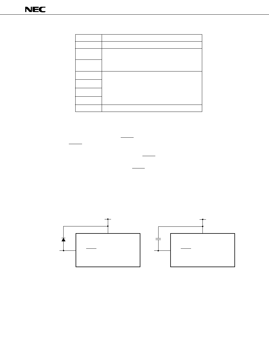
3.4 SELECTION OF A MASK OPTION
The following mask options are provided for pins:
1
Pull-up resistors connected
2
No pull-up resistors connected
(Either can be specified bit by bit.)
P50 - P53
Type F-B
Type M
P.U.R.: Pull-Up Resistor
P.U.R.: Pull-Up Resistor
V
DD
P-ch
N-ch
IN/OUT
V
DD
P-ch
P.U.R.
P.U.R.
enable
Output
disable
(P)
Data
Output
disable
Output
disable
(N)
N-ch
(Withstand
voltage:
+10 V)
IN/OUT
Data
V
DD
Output
disable
P.U.R.
enable
(Mask option)
Input buffer with an intermediate
withstand voltage of +10 V
(2/2)
11
µ
PD75402A(A)
3.5 HANDLING UNUSED PINS
Recommended connection method
Connected to the V
SS
pin
∑
When a pull-up resistor is contained
Connected to the V
DD
pin
∑
When a pull-up resistor is not contained
Connected to the V
SS
or V
DD
pin
∑
When a pull-up resistor is contained
Input mode
: Connected to the V
DD
pin
Output mode : Open
∑
When a pull-up resistor is not contained
Input mode
: Connected to the V
SS
or V
DD
pin
Output mode : Open
Open or directly connected to the V
SS
pin
Note
Pin
P00
P01 - P03
P10, P12
P20 - P23
P30 - P33
P50 - P53
P60 - P63
NC
∑
Connect a capacitor between the pin and V
DD
.
Note When the
µ
PD75402A(A) shares the printed circuit board with the
µ
PD75P402, connect the NC pin
directly to V
SS
pin.
3.6 NOTES ON USING THE P00 AND RESET PINS
The P00 and RESET pins have the test mode selecting function for testing the internal operation of the
µ
PD75402A(A) (IC test), besides the functions shown in Sections 3.1 and 3.2.
Applying a voltage exceeding V
DD
to the P00 and/or RESET pin causes the
µ
PD75402A(A) to enter the test
mode. When noise exceeding V
DD
comes in during normal operation, the device is switched to the test mode.
For example, when the wiring from the P00 or RESET pin is too long, noise voltage induced on the wiring
is applied to the pin, driving the voltage at the pin above V
DD
, which may cause malfunction.
When installing the wiring, lay the wiring in such a way that noise is suppressed as much as possible. If
noise yet arises, use an external part to suppress it as shown below.
∑
Connect a diode with low V
F
(0.3 V or lower)
between the pin and V
DD
.
V
DD
P00, RESET
V
DD
V
DD
P00, RESET
V
DD
Diode with
low V
F

12
µ
PD75402A(A)
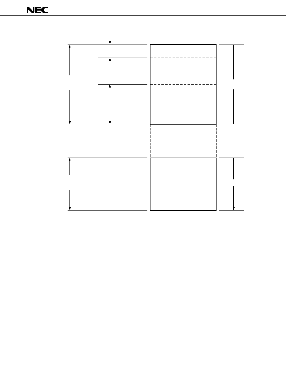
4. MEMORY CONFIGURATION
∑
Program memory (ROM): 1920
◊
8 bits (000H to 77FH)
∑ 000H and 001H : Vector table which contains the program start address after reset
∑ 002H to 009H
: Vector table which contains the program start addresses when interrupts occur
∑
Data memory
∑ Data area
: 64
◊
4 bits (000H to 03FH)
∑ Peripheral hardware area: 128
◊
4 bits (F80H to FFFH)
Fig. 4-1 Program Memory Map
0
0
0
0
0
0
0
0
0
0
0
0
0
0
0
0
0
0
0
0
7
6
5
4
3
Reset start address
(three high-order bits)
INTBT start address
(three high-order bits)
INT0 start address
(three high-order bits)
Reset start address (eight low-order bits)
INTBT start address (eight low-order bits)
INT0 start address (eight low-order bits)
INTCSI start address
(three high-order bits)
INTCSI start address (eight low-order bits)
Address
000H
001H
002H
003H
004H
005H
008H
009H
77FH
0
Entry address specified in
CALLF !faddr instruction
Branch address specified in
BRCB !caddr instruction
Relative branch address specified in
BR $addr instruction
≠15 to ≠1,
+2 to +16
13
µ
PD75402A(A)
Fig. 4-2 Data Memory Map
General register
area
Stack area
Data area
Static RAM
(64
◊
4)
Peripheral
hardware
area
000H
003H
004H
020H
03FH
F80H
FFFH
(4
◊
4)
(32
◊
4)
No memory
128
◊
4
Bank 0
(64
◊
4)
Bank 15

14
µ
PD75402A(A)
5. PERIPHERAL HARDWARE FUNCTIONS
5.1 PORTS
The
µ
PD75402A(A) has the following three types of I/O port:
∑ 6 CMOS input pins (PORT0 and PORT1)
∑ 12 CMOS I/O pins (PORT2, PORT3, and PORT6)
∑ 4 N-ch open-drain I/O pins (PORT5)
Total: 22 pins
Table 5-1 Functions of Ports
Note PORT3, PORT5, and PORT6 can directly drive the LED.
Port name
PORT0
PORT1
PORT3
Note
PORT2
PORT6
Note
PORT5
Note
Function
4-bit Input
4-bit I/O
4-bit I/O (N-ch
open-drain I/O
with a withstand
voltage of 10 V)
Remarks
Also used for SO/SB0, SI, SCK, INT0, and
INT2.
--
Port 2 is also used for PCL.
This port can incorporate a pull-up
resistor as a mask option bit by bit.
Operation and feature
Allows read and test at any
time regardless of the operation
modes of dual function pins.
Allows input or output mode
setting bit by bit.
Allows input or output mode
setting in units of 4 bits.
Allows input or output mode
setting in units of 4 bits.

15
µ
PD75402A(A)
5.2 CLOCK GENERATOR
Operation of the clock generator is specified by the processor clock control register (PCC).
The instruction execution time is variable.
∑ 0.95
µ
s, 1.91
µ
s, 15.3
µ
s (when f
XX
is 4.19 MHz.)
Fig. 5-1 Block Diagram of the Clock Generator
V
DD
X1
X2
System
clock
oscillator
f
XX
or f
X
Oscillation
stops.
1/16 to 1/512
Frequency divider
1/2 1/16
Selector
Frequency
divider
HALT flip-
flop
S
R
Q
RESET input rising edge
detection signal
RESET input falling
edge detection signal
Standby release signal
from interrupt control circuit
STOP flip-
flop
Q
S
R
All bits are
cleared.
PCC2 is
cleared.
HALT*
STOP*
PCC0
PCC1
PCC2
PCC3
4
Internal bus
PCC
∑
Basic interval timer (BT)
∑
Clock output circuit
∑
Serial interface
1/4
∑
INT0 noise eliminator
∑ CPU
∑
INT0 noise
eliminator
∑
Clock output
circuit
Remarks 1. f
XX
= Crystal/ceramic oscillated frequency
2. f
X
= External clock frequency
3.
= CPU clock
4. An asterisk (*) indicates instruction execution.
5. PCC: Processor clock control register
6. One clock cycle (t
CY
) of
is equal to one machine cycle of an instruction. See AC
characteristics of Chapter 10 for details of t
CY
.

16
µ
PD75402A(A)
5.3 CLOCK OUTPUT CIRCUIT
The clock output circuit, which outputs clock pulses from pin P22/PCL, is used for supplying clock pulses
for peripheral LSIs or for remote control output.
∑ Clock output (PCL): 1.05 MHz, 524 kHz, 65.5 kHz (when f
XX
is 4.19 MHz).
Fig. 5-2 shows the configuration of the clock output circuit.
Fig. 5-2 Configuration of the Clock Output Circuit
From the clock
generator
CLOM3 0
Selector
Output
buffer
Port 2 input/
output mode
specification bit
P22 output
latch
P22/PCL
Internal bus
4
f
XX
/2
6
PORT2.2
Bit 2 of PMGB
CLOM1 CLOM0 CLOM
Remark The clock output circuit is designed not to output high-frequency pulses when clock output is
switched between the enable and disable states.
17
µ
PD75402A(A)
5.4 BASIC INTERVAL TIMER
The basic interval timer provides the following functions:
∑ Interval timer operation that generates a reference time interrupt
∑ Can be used as a watchdog timer for detecting program crashes
∑ Reading the count value
Fig. 5-3 Configuration of the Basic Interval Timer
From the
clock
generator
f
XX
/2
5
f
XX
/2
9
MPX
BTM3
BTM2
1
1
BTM
4
8
Internal bus
Clear
Set
BT
Basic interval timer
(8-bit frequency divider)
BT
interrupt
request flag
IRQBT
Vectored
interrupt
request
signal
Clear

18
µ
PD75402A(A)
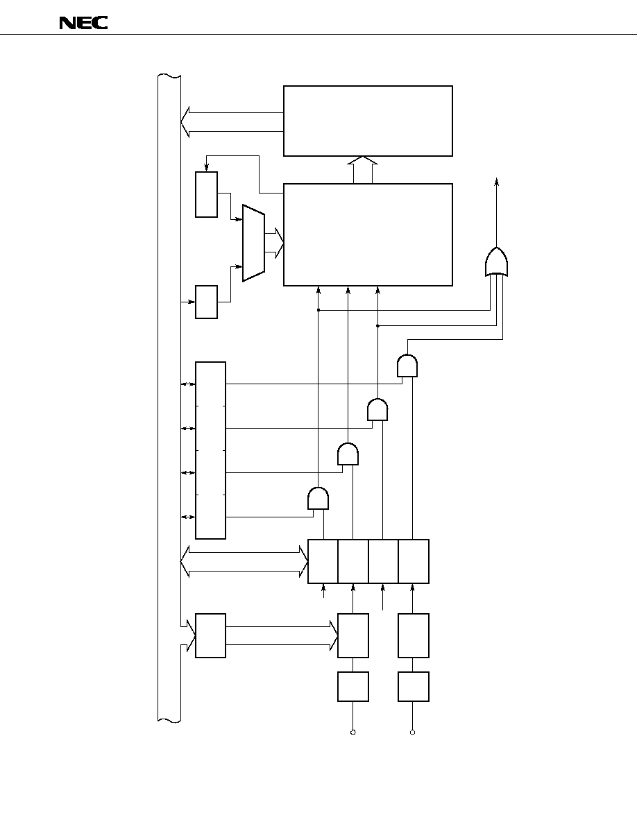
5.5 SERIAL INTERFACE
The serial interface has the following modes:
∑
Three-wire serial I/O mode (MSB is transferred first.)
∑
SBI mode (MSB is transferred first.)
The three-wire serial I/O mode enables connections to be made with the 75X series, 78K series, and many
other types of peripheral I/O devices.
The SBI mode enables communication with two or more devices.
19
µ
PD75402A(A)
Fig. 5-4 Block Diagram of the Serial Interface
8
Bit
test
CSIM
Selector
Internal bus
8
8
Slave address
register (SVA)
Address comparator
Shift register (SIO)
Bus-release/
command/
acknowledge
detector
Serial clock
counter
Serial clock
control
circuit
MPX
f
XX
/2
4
INTCSI
IRQCSI
Set signal
INTCSI
control
circuit
Busy/
acknowl-
edge
output
circuit
P03/SI
P02 /SO/SB0
P01/SCK
(8)
(8)
Match
signal
(8)
Bit manipulation
RELT
CMDT
SBIC
Bit test
SET CLR
D
Q
RELD
CMDD
ACKD
ACKT
ACKE
BSYE
SO
Iatch
External SCK

20
µ
PD75402A(A)
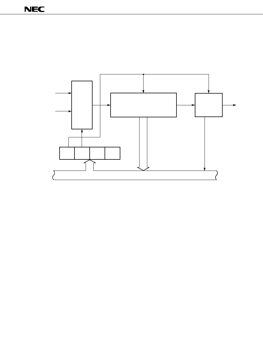
6. INTERRUPT FUNCTION
The
µ
PD75402A(A) has three interrupt sources and each of them has the interrupt vector table.
The
µ
PD75402A(A) is also provided with one edge-sensitive testable input signal.
When a vectored interrupt request is issued, the PC and PSW are saved in the stack, and the contents of
the vector table which corresponds to the issued vectored interrupt are set in the PC as a start address. The
program branches to the interrupt service routine. These operations are performed automatically by the
hardware.
The flag is set by detecting the edge of the testable input signal, but a vectored interrupt request is not
issued.
During execution of the interrupt service routine, the
µ
PD75402A(A) does not accept the other interrupt
requests. Unlike the other 75X series, the
µ
PD75402A(A) cannot handle multiple interrupts.
The interrupt control circuit of the
µ
PD75402A(A) has the following functions.
∑ Vectored interrupt function under hardware control which can determine whether to accept an interrupt
by an interrupt enable flag (IE
◊◊◊
) and an interrupt master enable flag (IME).
∑ Any interrupt start address can be set.
∑ Test function of an interrupt request flag (IRQ
◊◊◊
) (Software can confirm that an interrupt occurs.)
∑ Release of the standby (HALT) mode (An interrupt to be released by an interrupt enable flag can be selected
from interrupts other than INT0.)
21
µ
PD75402A(A)
Fig. 6-1 Block Diagram of Interrupt Control Circuit
Notes 1. Noise eliminator using the sampling clock
2. Noise eliminator using analog delay
3
IM0
INT
BT
INTCSI
INT0/
P10
INT2/
P12
IRQBT
IRQ0
IRQCSI
IRQ2
Rising edge
detection
circuit
Interrupt enable flag (IE
◊◊◊
)
IME
IST0
Decoder
VRQ1
VRQ2
VRQ3
Priority
control
circuit
Vector
table
address
generator
Standby release
signal
Edge
detection
circuit
Note 1
Note 2
22
µ
PD75402A(A)
7. STANDBY FUNCTION
To reduce the power consumption when the program is in the wait state, the
µ
PD75402A(A) has two standby
modes, STOP and HALT.
Table 7-1 Operation Statuses in the Standby Mode
Instruction to be used to
set mode
Clock generator
Basic interval
timer
Serial interface
Clock output
circuit
External
interrupt
CPU
Release signal
HALT mode
HALT instruction
Only the CPU clock (
) stops, but
oscillation continues.
Operates. (IRQBT is set at every refer-
ence time interval.)
Operable
Clocks other than CPU clock (
) can be
output.
INT2 pin is usable.
INT0 pin cannot be used.
RESET input or interrupt request signals
enabled by the interrupt enable flags
STOP mode
STOP instruction
Oscillation of the system clock stops.
Operation stops.
Operable only when the external SCK
input is selected for the serial clock.
Operation stops.
INT2 pin is usable.
INT0 pin cannot be used.
Operation stops.
RESET input
Opera-
tion
status

23
µ
PD75402A(A)
8. RESET FUNCTION
When a low level signal is input to the RESET input pin, the state changes to the system reset. Table 8-1
shows the statuses of the hardware.
When the RESET signal rises from the low level to the high level, the reset state is released. The three low-
order bits of the reset vector table whose address is 000H is set in bits 10 to 8 of the program counter (PC)
and the contents of the reset vector table whose address is 001H is set in bits 7 to 0 of the PC. The program
branches to that address and starts execution, i.e., the reset start address is programmable.
Initialize contents of registers in a program if necessary.
The RESET pin connects to the Schmitt-trigger circuit whose threshold level has hysteresis in the chip. This
pin is also connected to the noise eliminator using an analog delay to eliminate narrow noise and prevent
errors caused by noise. (See Fig. 8-1.)
For the power-on reset operation, be sure to allow sufficient time for oscillation to settle between power
on and acceptance of the reset signal (see Fig. 8-2).
Fig. 8-1 Acceptance of the Reset Signal
RESET
Analog
delay
Analog
delay
Analog
delay
Content of the reset
vector table is set
to the PC
(the initialization of the PC).
The instruction which
is stored at the reset
branch address is executed.
Elimination
as noise.
This low level
signal is accepted
as the reset signal.
The reset is
released.
Fig. 8-2 Power-On Reset Operation
V
DD
RESET
Oscillation
settling time
Analog
delay
The reset
is released.
Content of the reset vector
table is set to the PC
(the initialization of the PC).
The instruction which is stored
at the reset branch address is
executed.
24
µ
PD75402A(A)
Table 8-1 Hardware Statuses after Reset Operations
Hardware
Program counter (PC)
PSW
Carry flag (CY)
Skip flag (SK0 - SK2)
Interrupt status flag (IST0)
Stack pointer (SP)
Data memory (RAM)
General register (X, A, H, L)
RESET input during operations
Set the three low-order bits of
address 000H in program
memory in PC bits 10 to 8 and
set the contents of address
001H in PC bits 7 to 0.
Undefined
0
0
Undefined
Undefined
Undefined
Undefined
0
Undefined
0
0
Undefined
0
0
Reset (0)
0
0
0
Off
Cleared (0)
0
0
Used as inputs
∑
High level when pull-up
resistor is built in
∑
High impedance when
open drain is used in the
internal circuit
RESET input in standby mode
Set the three low-order bits of
address 000H in program
memory in PC
bits 10 to 8 and
set the contents of address
001H in PC bits 7 to 0.
Retained
0
0
Undefined
Retained
Note
Retained
Undefined
0
Retained
0
0
Retained
0
0
Reset (0)
0
0
0
Off
Cleared (0)
0
0
Used as inputs
∑
High level when pull-up
resistor is built in
∑
High impedance when
open drain is used in the
internal circuit
Counter (BT)
Mode register (BTM)
Shift register (SIO)
Operation mode register (CSIM)
SBI control register (SBIC)
Slave address register (SVA)
Processor clock control register
(PCC)
Clock output mode register
(CLOM)
Interrupt request flag (IRQ
◊◊◊
)
Interrupt enable flag (IE
◊◊◊
)
Interrupt master enable flag
(IME)
INT0 mode register (IM0)
Output buffer
Output latch
I /O mode register
(PMGA, PMGB)
Pull-up resistor specification
register (POGA)
P00 - P03, P10, P12, P20 - P23,
P30 - P33, P60 - P63
P50 - P53
Basic interval
timer
Serial
interface
Clock genera-
tor and clock
output circuit
Interrupt
Digital I/O
port
States of pins
Note Data in the data memory whose addresses are 38H to 3DH is not defined when the standby mode
is released by the RESET input signal.
25
µ
PD75402A(A)
9. INSTRUCTION SET
(1) Representation format and description method of operands
An operand is described in the operand field of each instruction according to the description method
corresponding to the operand representation format of the instruction refer to "RA75X Assembler Package
User's Manual, Language" (EEU-1363) for details. When two or more elements are described in the
description method field, select one of them. Upper-case letters, a number sign (#), and at mark (@), an
exclamation mark (!), and a dollar sign ($) are keywords, so they can be used without alteration.
Specify an appropriate numeric value or label for immediate data.
The symbols of registers and flags can be used as labels instead of mem, fmem, and bit (refer to the
"
µ
PD75402A User's Manual" (IEU-644) for details). Some labels, however, cannot be specified in fmem.
Note Only an even address can be written in mem when 8-bit data is processed.
(2) Legend
A
: A register, 4-bit accumulator
H
: H register
L
: L register
X
: X register
XA
: Register pair (XA), 8-bit accumulator
HL
: Register pair (HL)
PC
: Program counter
SP
: Stack pointer
CY
: Carry flag, bit accumulator
PSW
: Program status word
PORTn: Port n (n = 0 to 3, 5, 6)
IME
: Interrupt master enable flag
IE
◊◊◊
: Interrupt enable flag
PCC
: Processor clock control register
∑
: Address/bit delimiter
(
◊◊
)
: Contents addressed by
◊◊
◊◊
H
: Hexadecimal data
Representation format
reg
reg1
rp
n4
n8
mem
bit
fmem
addr
caddr
faddr
PORTn
IE
◊◊◊
Description method
X, A, H, L
X, H, L
XA, HL
4-bit immediate data or label
8-bit immediate data or label
8-bit immediate data or label
Note
2-bit immediate data or label
FB0H - FBFH/FF0H - FFFH immediate data or label
11-bit immediate data or label
11-bit immediate data or label
11-bit immediate data or label
PORT0 - PORT3, PORT5, PORT6
IEBT, IECSI, IE0, IE2

26
µ
PD75402A(A)
(3) Explanation of the symbols in the addressing area field
Remarks 1. MB indicates an accessible memory bank.
2. *4 to *7 indicate each addressable area.
(4) Explanation of the machine cycle field
S indicates the number of machine cycles required for a skip instruction to perform skipping. The following
shows the values of S.
∑
When the next instruction is not skipped, S is 0.
∑
When the next instruction is skipped, S is 1.
A machine cycle is equal to one cycle (= t
CY
) of CPU clock
. A PCC setting determines the machine cycle.
It can be set to one of three different periods.
MB = 0
MB = 0 (00H - 3FH)
MB = 15 (80H - FFH)
MB = 15, fmem = FB0H - FBFH or
FF0H - FFFH
addr = 000H - 77FH
addr = (Current PC) ≠ 15 to (Current PC) ≠ 1 or
(Current PC) + 16 to (Current PC) + 2
caddr = 000H - 77FH
faddr = 000H - 77FH
*1
*2
*3
*4
*5
*6
*7
Data memory
addressing
Program memory
addressing

27
µ
PD75402A(A)
Instruc-
tion
group
Transfer
instruc-
tion
Arithme-
tic/
logical
instruc-
tion
Accumu-
lator
manipu-
lation
instruc-
tion
Incre-
ment/
decre-
ment
instruc-
tion
Compari-
son
instruc-
tion
Carry flag
manipu-
lation
instruc-
tion
Mne-
monic
MOV
XCH
MOVT
ADDS
ADDC
AND
OR
XOR
RORC
NOT
INCS
DECS
SKE
SET1
CLR1
SKT
NOT1
Operand
A, #n4
XA, #n8
HL, #n8
A, @HL
@HL, A
A, mem
XA, mem
mem, A
mem, XA
A, @HL
A, mem
XA, mem
A, reg1
XA, @PCXA
A, #n4
A, @HL
A, @HL
A, @HL
A, @HL
A, @HL
A
A
reg
mem
reg
reg, #n4
A, @HL
CY
CY
CY
CY
Number
of
bytes
1
2
2
1
1
2
2
2
2
1
2
2
1
1
1
1
1
1
1
1
1
2
1
2
1
2
1
1
1
1
1
Skip
condition
String A
String A
String B
carry
carry
reg = 0
(mem) = 0
reg = FH
reg = n4
A = (HL)
CY = 1
Address-
ing area
*1
*1
*2
*2
*2
*2
*1
*2
*2
*1
*1
*1
*1
*1
*2
*1
Operation
A
n4
XA
n8
HL
n8
A
(HL)
(HL)
A
A
(mem)
XA
(mem)
(mem)
A
(mem)
XA
A
(HL)
A
(mem)
XA
(mem)
A
reg1
XA
(PC
10-8
+ XA)
ROM
A
A + n4
A
A + (HL)
A, CY
A + (HL) + CY
A
A
(HL)
A
A
(HL)
A
A
(HL)
CY
A
0
, A
3
CY, A
n≠1
A
n
A
A
reg
reg + 1
(mem)
(mem) + 1
reg
reg ≠ 1
Skip if reg = n4
Skip if A = (HL)
CY
1
CY
0
Skip if CY = 1
CY
CY
Ma-
chine
cycle
1
2
2
1
1
2
2
2
2
1
2
2
1
3
1 + S
1 + S
1
1
1
1
1
2
1 + S
2 + S
1 + S
2 + S
1 + S
1
1
1 + S
1

28
µ
PD75402A(A)
Instruc-
tion
group
Memory
bit
manipu-
lation
instruc-
tion
Branch
instruc-
tion
Subrou-
tine
stack
control
instruc-
tion
Interrupt
control
instruc-
tion
Input/
output
instruc-
tion
CPU
control
instruction
Mne-
monic
SET1
CLR1
SKT
SKF
SKTCLR
AND1
OR1
XOR1
BR
BRCB
CALLF
RET
RETS
RETI
PUSH
POP
EI
DI
IN
OUT
HALT
STOP
NOP
Number
of
bytes
2
2
2
2
2
2
2
2
2
2
2
2
≠
1
2
2
1
1
1
1
1
2
2
2
2
2
2
2
2
1
Skip
condition
(mem.bit) = 1
(fmem.bit) = 1
(mem.bit) = 0
(fmem.bit) = 0
(fmem.bit) = 1
Uncondition-
ally
Address-
ing area
*2
*3
*2
*3
*2
*3
*2
*3
*3
*3
*3
*3
*4
*5
*6
*7
Ma-
chine
cycle
2
2
2
2
2 + S
2 + S
2 + S
2 + S
2 + S
2
2
2
≠
2
2
2
3
3 + S
3
1
1
2
2
2
2
2
2
2
2
1
Operand
mem.bit
fmem.bit
mem.bit
fmem.bit
mem.bit
fmem.bit
mem.bit
fmem.bit
fmem.bit
CY, fmem.bit
CY, fmem.bit
CY, fmem.bit
addr
$addr
!caddr
!faddr
rp
rp
IE
◊◊◊
IE
◊◊◊
A, PORTn
PORTn, A
Operation
(mem.bit)
1
(fmem.bit)
1
(mem.bit)
0
(fmem.bit)
0
Skip if (mem.bit) = 1
Skip if (fmem.bit) = 1
Skip if (mem.bit) = 0
Skip if (fmem.bit) = 0
Skip if (fmem.bit) = 1 and clear
CY
CY
(fmem.bit)
CY
CY
(fmem.bit)
CY
CY
(fmem.bit)
PC
10-0
addr
(The assembler selects an
appropriate instruction from the
BRCB !caddr and BR $addr
instructions.)
PC
10-0
addr
PC
10-0
caddr
(SP ≠ 4)(SP ≠ 1)(SP ≠ 2)
0, PC
10-0
(SP ≠ 3)
0000
PC
10-0
faddr, SP
SP ≠ 4
◊
, PC
10-0
(SP)(SP + 3)(SP + 2)
SP
SP + 4
◊
, PC
10-0
(SP)(SP + 3)(SP + 2)
SP
SP + 4, then skip unconditionally
◊
, PC
10-0
(SP)(SP + 3)(SP + 2)
PSW
(SP + 4)(SP + 5), SP
SP + 6
(SP ≠ 1)(SP ≠ 2)
rp, SP
SP ≠ 2
rp
(SP + 1)(SP), SP
SP + 2
IME (IPS.3)
1
IE
◊◊◊
1
IME (IPS.3)
0
IE
◊◊◊
0
A
PORTn (n = 0 - 3, 5, 6)
PORT n
A (n = 2, 3, 5, 6)
Set HALT mode (PCC.2
1)
Set STOP mode (PCC.3
1)
No operation

29
µ
PD75402A(A)
10. ELECTRICAL CHARACTERISTICS
ABSOLUTE MAXIMUM RATINGS (T
a
= 25 ∞C)
Parameter
Supply voltage
Input voltage
Output voltage
High-level output
current
Low-level output
current
Operating
temperature
Storage tempera-
ture
Unit
V
V
V
V
V
mA
mA
mA
mA
mA
mA
mA
mA
mA
mA
∞C
∞C
Rated value
≠0.3 to +7.0
≠0.3 to V
DD
+ 0.3
≠0.3 to V
DD
+ 0.3
≠0.3 to +11.0
≠0.3 to V
DD
+ 0.3
≠15
≠30
30
15
20
10
100
60
100
60
≠40 to +85
≠65 to +150
Symbol
V
DD
V
I1
V
I2
V
O
I
OH
I
OL
Note
T
opt
T
stg
Conditions
Ports other than port 5
Port 5
Built-in pull-up resistor
Open drain
Each pin
Total of all output pins
One pin of port 0, 3, 5, or 6
One pin of port 2
Total of all pins of ports 0, 3,
and 5 (excl. P33)
Total of all pins of ports 2, 6,
and P33
Peak value
rms
Peak value
rms
Peak value
rms
Peak value
rms
Note Calculate rms with [rms] = [peak value]
◊
duty.
Caution Absolute maximum ratings are rated values beyond which some physical damages may be
caused to the product; if any of the parameters in the table above exceeds its rated value even
for a moment, the quality of the product may deteriorate. Be sure to use the product within the
rated values.
30
µ
PD75402A(A)
Resonator
Ceramic
resonator
Crystal
External
clock
Recommended
constant
Parameter
Oscillator
frequency
(f
XX
)
Note 1
Oscillation
settling time
Note 2
Oscillator
frequency
(f
XX
)
Note 1
Oscillation
settling time
Note 2
X1 input
frequency
(f
X
)
Note 1
X1 input
high/low
level width
(t
XH
, t
XL
)
CHARACTERISTICS OF THE OSCILLATION CIRCUIT (T
a
= ≠40 to +85 ∞C, V
DD
= 2.7 to 6.0 V)
Notes 1. The oscillator frequency and X1 input frequency indicate only the oscillator characteristics. See
the item of AC characteristics for the instruction execution time.
2. The oscillation settling time means the time required for the oscillation to settle after V
DD
is applied
or after the STOP mode is released.
3. When 4.19 MHz < f
X
5.0 MHz, do not select PCC = 0011 as the instruction execution time. When
PCC = 0011, one machine cycle falls short of 0.95
µ
s, the minimum value for the standard.
Caution When the clock oscillator is used, conform to the following guidelines when wiring at the
portions surrounded by dotted lines in the figures above to eliminate the influence of the wiring
capacity.
∑ The wiring must be as short as possible.
∑ Other signal lines must not run in these areas.
∑ Any line carrying a high fluctuating current must be kept away as far as possible.
∑ The grounding point of the capacitor of the oscillator must have the same potential as that
of V
SS
. It must not be grounded to ground patterns carrying a large current.
∑ No signal must be taken from the oscillator.
CAPACITANCE (T
a
= 25 ∞C, V
DD
= 0 V)
Unit
MHz
ms
MHz
ms
MHz
ns
Min.
2.0
2.0
2.0
100
Typ.
4.19
Max.
5.0
Note 3
4
5.0
Note 3
10
5.0
Note 3
250
Conditions
V
DD
= oscillation
voltage range
After V
DD
reaches
MIN. of the oscilla-
tion voltage range
V
DD
= 4.5 to 6.0 V
X1
X2
C1
C2
X1
X2
C1
C2
X1
X2
µ
PD74HCU04
Parameter
Input capacitance
Output capacitance
I/O capacitance
Symbol
C
IN
C
OUT
C
IO
Min.
Typ.
Max.
15
15
15
Unit
pF
pF
pF
Conditions
f = 1 MHz
0 V for pins other than pins to be
measured
5
31
µ
PD75402A(A)
V
DD
= 4.5 to 6.0 V, I
OH
= ≠1 mA
I
OH
= ≠100
µ
A
V
DD
= 4.5 to 6.0 V, I
OL
= 15 mA
V
DD
= 4.5 to 6.0 V, I
OL
= 1.6 mA
I
OL
= 400
µ
A
Pull-up resistor : 1 k
or
more V
DD
= 4.5 to 6.0 V
Other than X1 and X2
X1 and X2
Port 5 (open drain)
Other than X1 and X2
X1 and X2
Other than port 5
Port 5 (open drain)
DC CHARACTERISTICS (T
a
= ≠40 to +85 ∞C, V
DD
= 2.7 to 6.0 V)
Notes 1. This current excludes the current which flows through the built-in pull-up resistors.
2. Value when the processor clock control resistor (PCC) is set to 0011 and the
µ
PD75402A(A) is
operated in the high-speed mode
3. Value when the PCC is set to 0000 and the
µ
PD75402A(A) is operated in the low-speed mode
Parameter
High-level input
voltage
Low-level input
voltage
High-level output
voltage
Low-level output
voltage
High-level input
leakage current
Low-level input
leakage current
High-level output
leakage current
Low-level output
leakage current
Built-in pull-up
resistor
Power supply
current
Note 1
Symbol
V
IH1
V
IH2
V
IH3
V
IH4
V
IL1
V
IL2
V
IL3
V
OH
V
OL
I
LIH1
I
LIH2
I
LIH3
I
LIL1
I
LIL2
I
LOH1
I
LOH2
I
LOL
R
L1
R
L2
I
DD1
I
DD2
I
DD3
Conditions
Ports 2, 3, and 6
Ports 0 and 1, and RESET
Port 5
Built-in pull-up resistor
Open drain
X1 and X2
Ports 2, 3, 5, and 6
Ports 0 and 1, and RESET
X1 and X2
Ports 0, 2,
3, and 6
Ports 3, 5,
and 6
Ports 0, 2,
3, 5, and 6
SB0 (Open
drain)
V
IN
= V
DD
V
IN
= 10 V
V
IN
= 0 V
V
OUT
= V
DD
V
OUT
= 10 V
V
OUT
= 0 V
Ports 0, 1, 2, 3, and
6 (excl. P00 and
P10) V
IN
= 0 V
Port 5
V
OUT
= V
DD
≠ 2.0 V
4.19 MHz
crystal
resonance
C1 = C2 =
22 pF
STOP
mode
HALT
mode
T
a
= 25 ∞C
V
DD
= 5.0 V
±
10 %
Note 2
V
DD
= 3.0 V
±
10 %
Note 3
V
DD
= 5.0 V
±
10 %
V
DD
= 3.0 V
±
10 %
V
DD
= 5.0 V
±
10 %
V
DD
=
3.0 V
±
10 %
V
DD
= 5.0 V
±
10 %
V
DD
= 3.0 V
±
10 %
V
DD
= 5.0 V
±
10 %
V
DD
= 3.0 V
±
10 %
Typ.
0.6
40
40
2.5
0.5
500
150
0.5
0.1
0.1
Max.
V
DD
V
DD
V
DD
10
V
DD
0.3V
DD
0.2V
DD
0.4
2.0
0.4
0.5
0.2V
DD
3
20
20
≠ 3
≠ 20
3
20
≠ 3
80
300
70
60
8
1.5
1500
450
20
10
5
Unit
V
V
V
V
V
V
V
V
V
V
V
V
V
V
µ
A
µ
A
µ
A
µ
A
µ
A
µ
A
µ
A
µ
A
k
k
k
k
mA
mA
µ
A
µ
A
µ
A
µ
A
µ
A
Min.
0.7V
DD
0.8V
DD
0.7V
DD
0.7V
DD
V
DD
≠ 0.5
0
0
0
V
DD
≠ 1.0
V
DD
≠ 0.5
15
30
15
10
32
µ
PD75402A(A)
Typ.
Max.
32
32
Min.
0.95
3.8
10
10
Unit
µ
s
µ
s
µ
s
µ
s
µ
s
Note 2
AC CHARACTERISTICS (T
a
= ≠40 to +85 ∞C, V
DD
= 2.7 to 6.0 V, V
SS
= 0 V)
Notes 1. The cycle time of the CPU clock (
)
(minimum instruction execution time)
depends on the connected resonator
frequency and the setting of the proc-
essor clock control register (PCC).
The figure on the right side shows
the cycle time t
CY
characteristics for
the supply voltage V
DD
.
2. This value is 2t
CY
or 128/f
XX
according
to the setting of the interrupt mode
register (IM0).
Symbol
t
CY
t
INTH
, t
INTL
t
RSL
Parameter
CPU clock cycle time
Note 1
(minimum instruction execu-
tion time = one machine cycle)
Interrupt input high/low level
width
RESET low-level width
Conditions
V
DD
= 4.5 to 6.0 V
INT0
INT2
Guaranteed operating
range
40
32
7
6
5
4
3
2
1
0.5
0
1
2
3
4
5
6
Supply voltage V
DD
[V]
Cycle time t
CY
[ s]
t
CY
vs. V
DD
µ

33
µ
PD75402A(A)
Serial transfer operation
Three-wire serial I /O mode (SCK ∑∑∑ Internal clock output):
Note R
L
and C
L
are the resistance and capacitance of the SO output line load respectively.
Three-wire serial I/O mode (SCK ∑∑∑ External clock input):
Parameter
SCK cycle time
SCK high/low level
width
SI setup time
(referred to SCK
)
SI hold time
(referred to SCK
)
Delay from SCK
to
SO output
Note R
L
and C
L
are the resistance and capacitance of the SO output line load respectively.
Parameter
SCK cycle time
SCK high/low level
width
SI setup time
(referred to SCK
)
SI hold time
(referred to SCK
)
Delay from SCK
to
SO output
Symbol
t
KCY2
t
KL2
t
KH2
t
SIK2
t
KSI2
t
KSO2
V
DD
= 4.5 to 6.0 V
Conditions
V
DD
= 4.5 to 6.0 V
V
DD
= 4.5 to 6.0 V
R
L
= 1 k
,
C
L
= 100 pF
Note
Typ.
Max.
250
1000
Unit
ns
ns
ns
ns
ns
ns
ns
ns
Min.
1600
3800
t
KCY1
/2 ≠ 50
t
KCY1
/2 ≠ 150
150
400
0
0
Symbol
t
KCY1
t
KL1
t
KH1
t
SIK1
t
KSI1
t
KSO1
Min.
800
3200
400
1600
100
400
0
0
Typ.
Max.
300
1000
Unit
ns
ns
ns
ns
ns
ns
ns
ns
Conditions
V
DD
= 4.5 to 6.0 V
V
DD
= 4.5 to 6.0 V
R
L
= 1 k
,
C
L
= 100 pF
Note
V
DD
= 4.5 to 6.0 V

34
µ
PD75402A(A)
SBI mode (SCK ∑∑∑ Internal clock output (master)):
SBI mode (SCK ∑∑∑ External clock input (slave)):
Note R
L
and C
L
are the resistance and capacitance of the SO output line load respectively.
Min.
1600
3800
t
KCY3
/2 ≠ 50
t
KCY3
/2 ≠ 150
150
t
KCY3
/2
0
0
t
KCY3
t
KCY3
t
KCY3
t
KCY3
Parameter
SCK cycle time
SCK high/low level
width
SB0 setup time
(referred to SCK
)
SB0 hold time
(referred to SCK
)
Delay from SCK
to
SB0 output
Delay from SCK
to SB0
Delay from SB0
to SCK
SB0 low-level width
SB0 high-level width
Symbol
t
KCY4
t
KL4
t
KH4
t
SIK4
t
KSI4
t
KSO4
t
KSB
t
SBK
t
SBL
t
SBH
Symbol
t
KCY3
t
KL3
t
KH3
t
SIK3
t
KSI3
t
KSO3
t
KSB
t
SBK
t
SBL
t
SBH
Parameter
SCK cycle time
SCK high/low level
width
SB0 setup time
(referred to SCK
)
SB0 hold time
(referred to SCK
)
Delay from SCK
to
SB0 output
Delay from SCK
to SB0
Delay from SB0
to SCK
SB0 low-level width
SB0 high-level width
Typ.
Max.
250
1000
Unit
ns
ns
ns
ns
ns
ns
ns
ns
ns
ns
ns
ns
Conditions
V
DD
= 4.5 to 6.0 V
V
DD
= 4.5 to 6.0 V
V
DD
= 4.5 to 6.0 V
Conditions
V
DD
= 4.5 to 6.0 V
V
DD
= 4.5 to 6.0 V
R
L
= 1 k
,
C
L
= 100 pF
Note
V
DD
= 4.5 to 6.0 V
Min.
800
3200
400
1600
100
t
KCY4
/2
0
0
t
KCY4
t
KCY4
t
KCY4
t
KCY4
Typ.
Max.
300
1000
Unit
ns
ns
ns
ns
ns
ns
ns
ns
ns
ns
ns
ns

35
µ
PD75402A(A)
AC Timing Measurement Points (Excluding X1 Input)
Measurement
point
0.8V
DD
0.2V
DD
0.8V
DD
0.2V
DD
Clock Timing
t
XL
t
XH
1/f
X
X1 input
V
DD
≠ 0.5 V
0.4 V
Serial Transfer Timing
Three-wire serial I/O mode:
t
KL1
t
KCY1
t
SIK1
t
KH1
t
KSI1
t
KSO1
Input data
Output data
SCK
SI
SO

36
µ
PD75402A(A)
Serial Transfer Timing
Bus release signal transfer:
SCK
SB0
t
KSB
t
SBL
t
SBH
t
SBK
t
KL3, 4
t
KH3, 4
t
KCY3, 4
t
KSI3, 4
t
SIK3, 4
t
KSO3, 4
Command signal transfer:
SCK
SB0
t
KSB
t
KL3, 4
t
KH3, 4
t
KCY3, 4
t
KSI3, 4
t
SIK3, 4
t
KSO3, 4
t
SBK
Interrupt Input Timing
INT0, INT2
t
INTL
t
INTH
RESET Input Timing
RESET
t
RSL
37
µ
PD75402A(A)
Data Hold Timing (STOP Mode Release by RESET)
V
DD
RESET
V
DDDR
t
SRS
t
OS
STOP instruction execution
STOP mode
Data hold mode
HALT mode
Operating mode
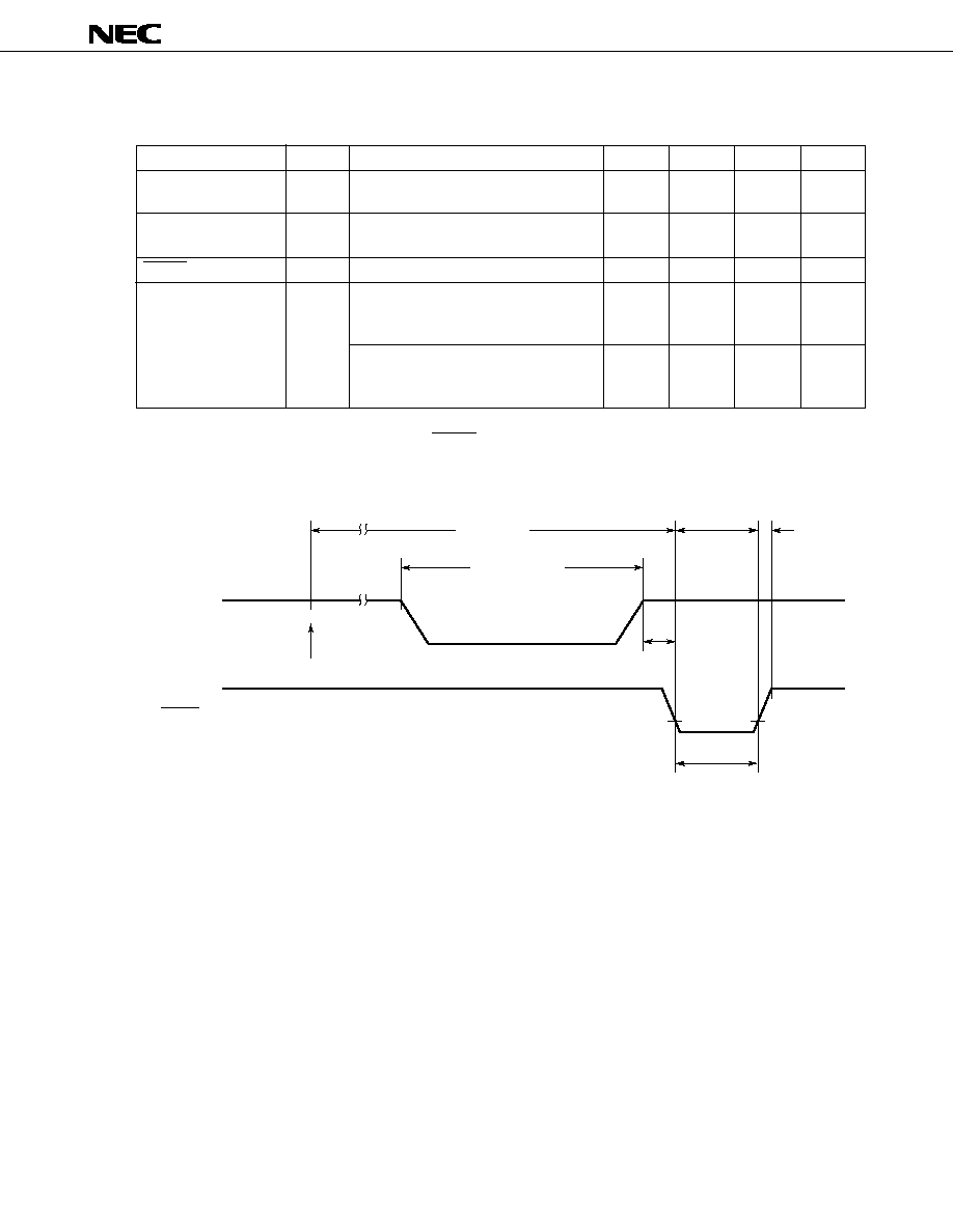
DATA HOLD CHARACTERISTICS AT LOW SUPPLY VOLTAGE IN DATA MEMORY STOP MODE
(T
a
= ≠40 to +85 ∞C)
Parameter
Data hold supply
voltage
Data hold supply
current
RESET setup time
Oscillation settling
time
Symbol
V
DDDR
I
DDDR
t
SRS
t
OS
Min.
2.0
0
Typ.
0.1
Max.
6.0
10
4
10
Unit
V
µ
A
µ
s
ms
ms
Conditions
V
DDDR
= 2.0 V
After V
DD
reaches the oscillation
voltage range when the ceramic
resonator is connected
After V
DD
reaches the oscillation
voltage range when the crystal is
connected
38
µ
PD75402A(A)
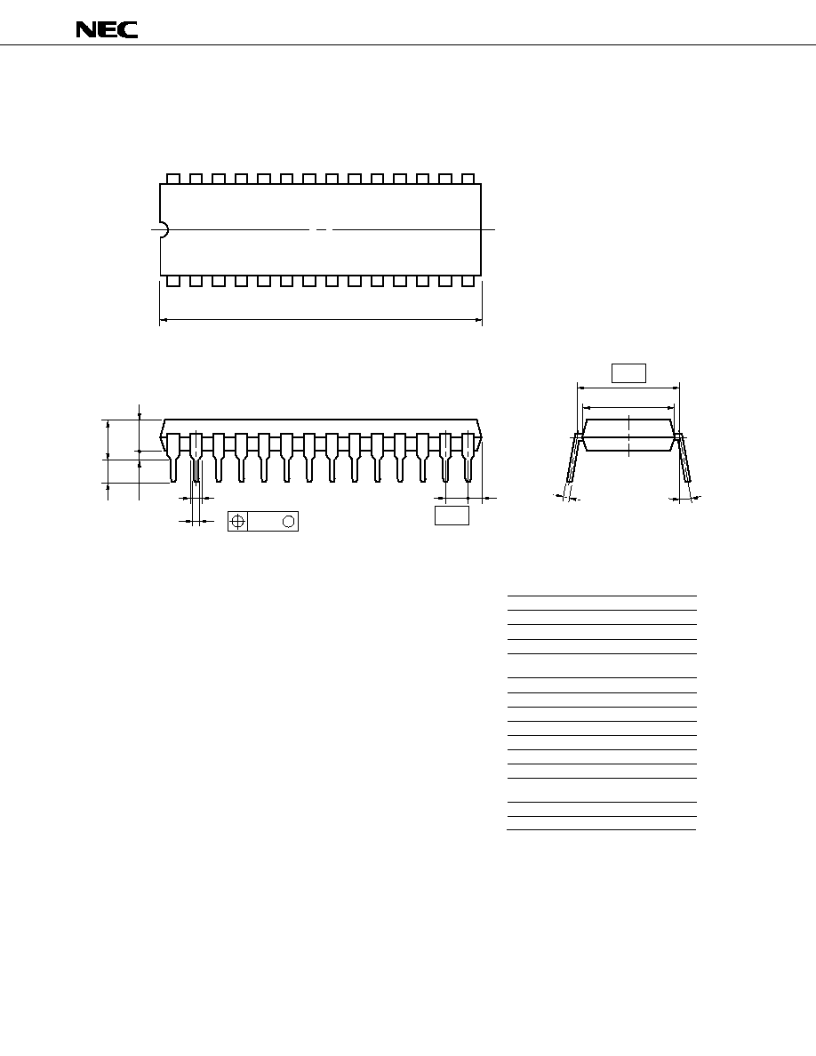
11. PACKAGE DIMENSIONS
28 PIN PLASTIC DIP (600 mil)
ITEM
MILLIMETERS
INCHES
A
B
C
F
G
H
I
J
K
38.10 MAX.
2.54 (T.P.)
3.6±0.3
0.51 MIN.
4.31 MAX.
2.54 MAX.
L
0.25
15.24 (T.P.)
5.72 MAX.
13.2
N
1.2 MIN.
1.500 MAX.
0.100 MAX.
0.047 MIN.
0.142±0.012
0.020 MIN.
0.170 MAX.
0.226 MAX.
0.600 (T.P.)
0.520
0.01
0.100 (T.P.)
P28C-100-600A1-1
D
0.50±0.10
0.020
M
0.25
0.010
+0.10
≠0.05
R
0
`
15
0
`
15
+0.004
≠0.005
+0.004
≠0.003
NOTES
Each lead centerline is located within 0.25 mm (0.01 inch)
of its true position (T.P.) at maximum material condition.
Item "K" to center of leads when formed parallel.
1)
2)
28
1
15
14
A
M
R
K
L
B
I
J
G
H
C
F
D
M
N
39
µ
PD75402A(A)
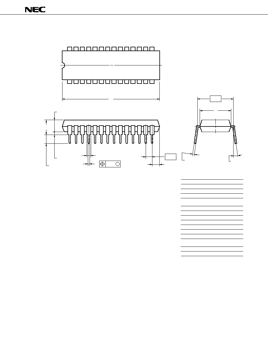
28PIN PLASTIC SHRINK DIP (400 mil)
ITEM MILLIMETERS
INCHES
NOTES
1) Each lead centerline is located within 0.17 mm (0.007 inch) of
its true position (T.P.) at maximum material condition.
N
0.17
0.007
A
28.46 MAX.
1.121 MAX.
B
2.67 MAX.
0.106 MAX.
F
0.9 MIN.
0.035 MIN.
G
3.2±0.3
0.126±0.012
J
5.08 MAX.
0.200 MAX.
K
10.16 (T.P.)
0.400 (T.P.)
C
1.778 (T.P.)
0.070 (T.P.)
D
0.50±0.10
0.020 +0.004
≠0.005
H
0.51 MIN.
0.020 MIN.
I
4.31 MAX.
0.170 MAX.
L
8.6
0.339
M
0.25
0.010 +0.004
≠0.003
+0.10
≠0.05
M
R
M
I
H
G
F
D
N
C
B
K
P28C-70-400A-1
R
0~15
∞
0~15
∞
2) ltem "K" to center of leads when formed parallel.
1
14
28
15
A
J
L
40
µ
PD75402A(A)
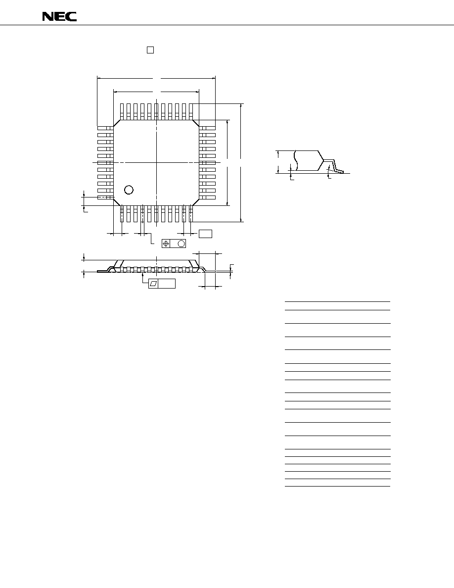
44 PIN PLASTIC QFP ( 10)
NOTE
Each lead centerline is located within 0.15 mm (0.006 inch) of
its true position (T.P.) at maximum material condition.
P44GB-80-3B4-3
ITEM
MILLIMETERS
INCHES
A
B
C
13.6±0.4
10.0±0.2
10.0±0.2
0.535
0.394
0.394
D
13.6±0.4
0.535
F
1.0
0.039
G
1.0
0.039
H
0.35±0.10
0.014
I
0.15
0.006
J
0.8 (T.P.)
0.031 (T.P)
K
1.8±0.2
0.071
L
0.8±0.2
0.031
M
0.15
0.006
N
0.10
0.004
P
2.7
0.106
Q
0.1±0.1
0.004±0.004
R
5∞±5∞
5∞±5∞
S
3.0 MAX.
0.119 MAX.
+0.017
≠0.016
+0.008
≠0.009
+0.008
≠0.009
+0.017
≠0.016
+0.004
≠0.005
+0.008
≠0.009
+0.009
≠0.008
+0.004
≠0.003
N
L
detail of lead end
G
M
I
J
H
A
F
M
Q
R
B
33
34
22
44
1
12
11
23
C
D
S
P
K
+0.10
≠0.05

41
µ
PD75402A(A)
PACKAGE DIMENSIONS OF THE 44-PIN CERAMIC QFP FOR ES (REF. DWG.) (UNIT: MM)
8.0
11.43
8.0
11.43
0.8
0.32
44
34
12
22
1
11
33
23
0.15
2.25
(Bottom)
Cautions 1.
Find the location of pin 1 by checking the location of pin 17, which is connected to the metal cap
.
2. The metal cap is connected to pin 17. The electrical level of the metal cap is V
SS
(GND).
3. The lead length has not been specified because leads are cut without any detailed specifications.

42
µ
PD75402A(A)
12. RECOMMENDED SOLDERING CONDITIONS
The following conditions shall be met when soldering the
µ
PD75402A(A).
For details of the recommended soldering conditions, refer to our document "SMD Surface Mount
Technology Manual" (IEI-1207).
Please consult with our sales offices in case other soldering process is used, or in case soldering is done
under different conditions.
Table 12-1 Soldering Conditions for Surface-Mount Devices
µ
PD75402AGB(A)-
◊◊◊
-3B4: 44-pin plastic QFP (10
◊
10 mm)
Caution Do not apply more than a single process at once, except for "Partial heating method."
Table 12-2 Soldering Conditions for Insertion-Mount Devices
µ
PD75402AC(A)-
◊◊◊
: 28-pin plastic DIP (600 mil)
µ
PD75402ACT(A)-
◊◊◊
: 28-pin plastic shrink DIP (400 mil)
Caution In wave soldering, apply solder only to the lead section. Care must be taken that jet solder does
not come in contact with the main body of the package.
Solder temperature: 260 ∞C or less
Flow time: 10 seconds or less
Terminal temperature: 260 ∞C or less
Flow time: 10 seconds or less
Wave soldering
(Only for leads)
Partial heating method
Soldering process
Soldering conditions
Peak package's surface temperature: 230 ∞C
Reflow time: 30 seconds or less (210 ∞C or more)
Number of reflow processes: 1
Peak package's surface temperature: 215 ∞C
Reflow time: 40 seconds or less (200 ∞C or more)
Number of reflow processes: 1
Solder temperature: 260 ∞C or less
Flow time: 10 seconds or less
Number of flow processes: 1
Preheating temperature: 120 ∞C max. (measured on the package
surface)
Terminal temperature: 300 ∞C or less
Flow time: 3 seconds or less (for each side of device)
Soldering process
Infrared ray reflow
VPS
Wave soldering
Partial heating method
Symbol
IR30-00-1
VP15-00-1
WS60-00-1
--
Soldering conditions
Notice
Other versions of the products are available. For these versions, the recommended reflow
soldering conditions have been mitigated as follows:
Higher peak temperature (235
∞
C), two-stage, and longer exposure limit.
Contact an NEC representative for details.
43
µ
PD75402A(A)
APPENDIX A DIFFERENCES BETWEEN THE
µ
PD75402A(A) AND
µ
PD75P402
16
(Pull-up resistors can be connected by software.)
22
6
12
V
PP
, PROM program-
ming pin
Quality grade
Not provided
2.7 to 6.0 V
-40 to +85 ∞C
Special
Electrical
charac-
teristics
Operating
supply
voltage
Operating
tempera-
ture
Provided
5 V
±
10 %
-10 to +70 ∞C
Standard
ROM
I/O ports
Input
I/O
N-ch I/O
Product
Item
Masked ROM
4 (Pull-up resistors can be connected by
mask option.)
µ
PD75402A(A)
One-time PROM
4 (No pull-up resistors can be connected.)
µ
PD75P402

44
µ
PD75402A(A)
APPENDIX B DEVELOPMENT TOOLS
The following development tools are provided for developing systems including the
µ
PD75402A(A)
In-circuit emulator for the 75X series
Emulation board for the IE-75000-R and IE-75001-R
Emulation probe for the
µ
PD75402AC(A) and
µ
PD75402ACT(A)
Emulation probe for the
µ
PD75402AGB(A). A 44-pin conversion socket, the EV-9200G-44,
is attached to the probe.
PROM programmer
PROM programmer adapter for the
µ
PD75P402C and
µ
PD75P402CT. Connected to the
PG-1500.
PROM programmer adapter for the
µ
PD75P402GB. Connected to the PG-1500.
IE-75000-R
Note 1
IE-75001-R
IE-75000-R-EM
Note 2
EP-75402C-R
EP-75402GB-R
PG-1500
PA-75P402CT
PA-75P402GB
EV-9200G-44
IE control program
PG-1500 controller
RA75X relocatable
assembler
Host machine
∑ PC-9800 series (MS-DOS
TM
Ver. 3.30 to Ver. 5.00A
Note 3
)
∑ IBM PC/AT
TM
(PC DOS
TM
Ver. 3.1)
Software
Notes 1. Maintenance service only
2. Not contained in the IE-75001-R
3. These software cannot use the task swap function, which is available in MS-DOS Ver. 5.00 and
Ver. 5.00A.
Remark
Refer to "75X Series Selection Guide" (IF-1027) for development tools manufactured by third parties.
Hardware
45
µ
PD75402A(A)
APPENDIX C RELATED DOCUMENTS
Documents related to the device
User's manual
Application note
75X series selection guide
Document name
Document No.
IEU-644
IEA-638
IF-1027
IE-75000-R/IE-75001-R User's Manual
IE-75000-R-EM User's Manual
EP-75402C-R User's Manual
EP-75402GB-R User's Manual
PG-1500 User's Manual
Document name
Document No.
EEU-1416
EEU-1294
EEU-701
EEU-702
EEU-1335
EEU-1346
RA75X Assembler Package User's Manual
Operation
Language
EEU-1363
EEU-1291
PG-1500 Controller User's Manual
Other related documents
Package Manual
SMD Surface Mount Technology Manual
Quality Grades on NEC Semiconductor Devices
NEC Semiconductor Device Reliability/Quality Control System
Electrostatic Discharge (ESD) Test
Guide to Quality Assurance for Semiconductor Devices
Document name
Document No.
IEI-1213
IEI-1207
IEI-1209
IEI-1203
IEI-1201
MEI-1202
Caution The above documents may be revised without notice. Use the latest versions when you design
an application system.
Hardware
Software
Documents related to development tools
5
46
µ
PD75402A(A)
Cautions on CMOS Devices
1
Countermeasures against static electricity for all MOSs
Caution
When handling MOS devices, take care so that they are not electrostatically charged.
Strong static electricity may cause dielectric breakdown in gates. When transporting
or storing MOS devices, use conductive trays, magazine cases, shock absorbers, or
metal cases that NEC uses for packaging and shipping. Be sure to ground MOS
devices during assembling. Do not allow MOS devices to stand on plastic plates or
do not touch pins.
Also handle boards on which MOS devices are mounted in the same way.
2
CMOS-specific handling of unused input pins
Caution
Hold CMOS devices at a fixed input level.
Unlike bipolar or NMOS devices, if a CMOS device is operated with no input, an
intermediate-level input may be caused by noise. This allows current to flow in the
CMOS device, resulting in a malfunction. Use a pull-up or pull-down resistor to hold
a fixed input level. Since unused pins may function as output pins at unexpected
times, each unused pin should be separately connected to the V
DD
or GND pin
through a resistor.
If handling of unused pins is documented, follow the instructions in the document.
3
Statuses of all MOS devices at initialization
Caution
The initial status of a MOS device is unpredictable when power is turned on.
Since characteristics of a MOS device are determined by the amount of ions im-
planted in molecules, the initial status cannot be determined in the manufacture
process. NEC has no responsibility for the output statuses of pins, input and output
settings, and the contents of registers at power on. However, NEC assures operation
after reset and items for mode setting if they are defined.
When you turn on a device having a reset function, be sure to reset the device first.

47
µ
PD75402A(A)
[MEMO]

µ
PD75402A(A)
MS-DOS
is a trademark of Microsoft Corporation.
PC/AT and PC DOS
are trademarks of IBM Corporation.
[MEMO]
No part of this document may be copied or reproduced in any form or by any means without the prior written consent
of NEC Corporation. NEC Corporation assumes no responsibility for any errors which may appear in this document.
NEC Corporation does not assume any liability for infringement of patents, copyrights or other intellectual property
rights of third parties by or arising from use of a device described herein or any other liability arising from use of
such device. No license, either express, implied or otherwise, is granted under any patents, copyrights or other
intellectual property rights of NEC Corporation or others.
The devices listed in this document are not suitable for use in aerospace equipment, submarine cables, nuclear
reactor control systems and life support systems. If customers intend to use NEC devices for above applications
or they intend to use "Standard" quality grade NEC devices for applications not intended by NEC, please contact
our sales people in advance.
Application examples recommended by NEC Corporation
Standard: Computer, Office equipment, Communication equipment, Test and Measurement equipment, Ma-
chine tools, Industrial robots, Audio and Visual equipment, Other consumer products, etc.
Special:
Automotive and Transportation equipment, Traffic control systems, Antidisaster systems, Anticrime
systems, etc.
M4 92. 6