Document Outline
- COVER
- FEATURES
- APPLICATIONS
- ORDERING INFORMATION
- Difference between uPD75430 x and uPD75430 x (A)
- Functional Outline
- 1. PIN CONFIGURATION (Top View)
- 2. BLOCK DIAGRAM
- 3. PIN FUNCTION
- 3.1 Port Pins
- 3.2 Non-port Pins
- 3.3 Pin Input/Output Circuits
- 3.4 Recommended Connections for Unused Pins
- 4. SWITCHING FUNCTION BETWEEN Mk I MODE AND Mk II MODE
- 4.1 Difference between Mk I and Mk II Modes
- 4.2 Setting Method of Stack Bank Select Register (SBS)
- 5. MEMORY CONFIGURATION
- 6. PERIPHERAL HARDWARE FUNCTIONS
- 6.1 Digital Input Ports
- 6.2 Clock Generator
- 6.3 Clock Output Circuit
- 6.4 Basic Interval Timer/Watchdog Timer
- 6.5 Timer/Event Counter
- 6.6 Serial Interface
- 6.7 Bit Sequential Buffer
- 7. INTERRUPT FUNCTION AND TEST FUNCTION
- 8. STANDBY FUNCTION
- 9. RESET FUNCTION
- 10. MASK OPTION
- 11. INSTRUCTION SETS
- 12. ELECTRICAL SPECIFICATIONS
- 13. CHARACTERISTICS CURVES (REFERENCE VALUES)
- 14. PACKAGE DRAWING
- 15. RECOMMENDED SOLDERING CONDITIONS
- APPENDIX A. COMPARISON OF FUNCTIONS AMONG uPD750004, 754304, AND 75P4308
- APPENDIX B. DEVELOPMENT TOOLS
- APPENDIX C. RELATED DOCUMENTS

4-BIT SINGLE-CHIP MICROCONTROLLER
The
Ķ
PD754304 is one of the "75XL Series" 4-bit single-chip microcontrollers with data processing capability
comparable to that of 8-bit microcontrollers. The
Ķ
PD754303(A) has a higher reliability than the
Ķ
PD754304.
The microcontrollers in the 75XL Series have expanded CPU functions than those of the 75X Series and can
operate at a voltage of as low as 1.8 V; therefore, they are ideal for battery-driven application systems.
As the one-time PROM version of the
Ķ
PD754304, the
Ķ
PD75P4308 is ideal for evaluation of a system under
development or for small-scale production of application systems.
Detailed information about functions can be found in the following document. Be sure to read the following
document before designing.
Ķ
PD754304 User's Manual: U10123E
FEATURES
∑
Low-voltage operation: V
DD
= 1.8 to 5.5 V
∑
Internal memory
Program memory (ROM):
2048
◊
8 bits (
Ķ
PD754302, 754302(A))
4096
◊
8 bits (
Ķ
PD754304, 754304(A))
Data memory (RAM): 256
◊
4 bits
APPLICATIONS
∑
Ķ
PD754302, 754302(A)
Cordless telephones, TVs, VCRs, audio systems, household appliances, office machines, etc.
∑
Ķ
PD754304, 754304(A)
Automotive appliance, etc.
The
Ķ
PD754302 and 754304 differ from the
Ķ
PD754302(A) and 754304(A) only in terms of their quality grade.
Unless otherwise specified, the
Ķ
PD754304 is treated as a representative model in this Data Sheet.
For the models other than the
Ķ
PD754304,
Ķ
PD754304 can be read as the other model name.
If different descriptions are made for the
Ķ
PD754302 and 754304, the (A) models correspond as follows:
Ķ
PD754302
Ķ
PD754302(A),
Ķ
PD754304
Ķ
PD754304(A)
MOS INTEGRATED CIRCUIT
The information in this document is subject to change without notice.
Document No. U10797EJ2V0DS00 (2nd edition)
Date Published November 1996 N
Printed in Japan
Ķ
PD754302,754304,754302(A),754304(A)
∑
Variable instruction execution time effective for high-
speed operation and power saving
0.95, 1.91, 3.81, or 15.3
Ķ
s (at 4.19 MHz)
0.67, 1.33, 2.67, or 10.7
Ķ
s (at 6.0 MHz)
∑
Internal serial interface (1 channel)
∑
Powerful timer function (3 channels)
∑
Inherits instruction set of existing 75X Series for easy
replacement
The mark shows major revised points.
©
1996
DATA SHEET

Ķ
PD754302, 754304, 754302(A), 754304(A)
2
ORDERING INFORMATION
Parts Number
Package
Quality Grade
Ķ
PD754302GS-
◊◊◊
36-pin plastic shrink SOP (300 mil, 0.8 mm pitch)
Standard
Ķ
PD754304GS-
◊◊◊
36-pin plastic shrink SOP (300 mil, 0.8 mm pitch)
Standard
Ķ
PD754302GS(A)-
◊◊◊
36-pin plastic shrink SOP (300 mil, 0.8 mm pitch)
Special
Ķ
PD754304GS(A)-
◊◊◊
36-pin plastic shrink SOP (300 mil, 0.8 mm pitch)
Special
Remark
◊
indicates a ROM code number.
Difference between
Ķ
PD75430
◊
and
Ķ
PD75430
◊
(A)
Parts Number
Ķ
PD754302
Ķ
PD754302(A)
Item
Ķ
PD754304
Ķ
PD754304(A)
Quality grade
Standard
Special
Please refer to "Quality Grades on NEC Semiconductor Devices" (Document No. C11531E) published by
NEC Corporation to know the specification of quality grade on the devices and its recommended applications.
Ķ
PD754302, 754304, 754302(A), 754304(A)
3
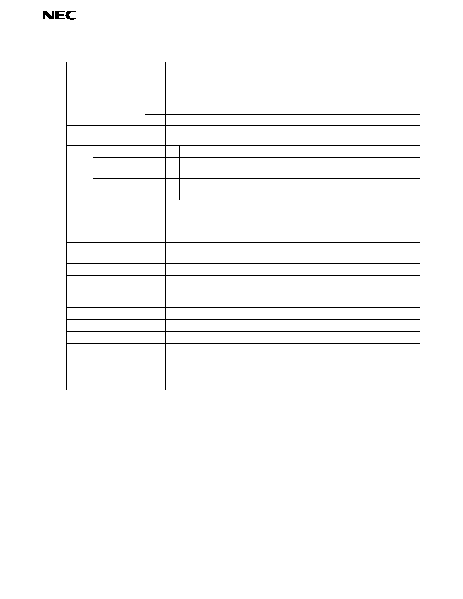
Functional Outline
Parameter
Function
Instruction execution time
∑ 0.95, 1.91, 3.81, 15.3
Ķ
s (@ 4.19 MHz with system clock)
∑ 0.67, 1.33, 2.67, 10.7
Ķ
s (@ 6.0 MHz with system clock)
On-chip memory
ROM
2048
◊
8 bits (
Ķ
PD754302)
4096
◊
8 bits (
Ķ
PD754304)
RAM
256
◊
4 bits
General-purpose register
∑ 4-bit operation: 8
◊
4 banks
∑ 8-bit operation: 4
◊
4 banks
Input/
CMOS input
8
On-chip pull-up resistors can be specified by software: 7
output
CMOS input/output
18
On-chip pull-up resistors can be specified by software: 18
port
N-ch open-drain
4
13 V withstand voltage. On-chip pull-up resistors can be specified by
input/output pins
mask option.
Total
30
Timer
3 channels
∑ 8-bit timer/event counter: 2 channels (16-bit timer/event counter)
∑ Basic interval timer/watchdog timer: 1 channel
Serial interface
∑ 3-wire serial I/O mode ... MSB or LSB can be selected for transferring top bit
∑ 2-wire serial I/O mode
Bit sequential buffer
16 bits
Clock output (PCL)
∑
, 524, 262, 65.5 kHz (@ 4.19 MHz with system clock)
∑
, 750, 375, 93.8 kHz (@ 6.0 MHz with system clock)
Vectored interrupts
External: 3, Internal: 4
Test input
External: 1
System clock oscillator
Ceramic or crystal oscillator
Standby function
STOP/HALT mode
Operating ambient
T
A
= ≠40 to +85 įC
temperature
Power supply voltage
V
DD
= 1.8 to 5.5 V
Package
36-pin plastic shrink SOP (300 mil, 0.8-mm pitch)

Ķ
PD754302, 754304, 754302(A), 754304(A)
4
CONTENTS
1.
PIN CONFIGURATION (Top View) ∑∑∑∑∑∑∑∑∑∑∑∑∑∑∑∑∑∑∑∑∑∑∑∑∑∑∑∑∑∑∑∑∑∑∑∑∑∑∑∑∑∑∑∑∑∑∑∑∑∑∑∑∑∑∑∑∑∑∑∑∑∑∑∑∑∑∑∑∑∑∑∑∑∑∑∑∑∑∑∑∑∑∑∑∑∑∑∑∑∑∑∑∑∑∑∑∑∑∑∑∑∑ 6
2.
BLOCK DIAGRAM ∑∑∑∑∑∑∑∑∑∑∑∑∑∑∑∑∑∑∑∑∑∑∑∑∑∑∑∑∑∑∑∑∑∑∑∑∑∑∑∑∑∑∑∑∑∑∑∑∑∑∑∑∑∑∑∑∑∑∑∑∑∑∑∑∑∑∑∑∑∑∑∑∑∑∑∑∑∑∑∑∑∑∑∑∑∑∑∑∑∑∑∑∑∑∑∑∑∑∑∑∑∑∑∑∑∑∑∑∑∑∑∑∑∑∑∑∑∑∑∑∑∑∑∑∑∑∑ 8
3.
PIN FUNCTION ∑∑∑∑∑∑∑∑∑∑∑∑∑∑∑∑∑∑∑∑∑∑∑∑∑∑∑∑∑∑∑∑∑∑∑∑∑∑∑∑∑∑∑∑∑∑∑∑∑∑∑∑∑∑∑∑∑∑∑∑∑∑∑∑∑∑∑∑∑∑∑∑∑∑∑∑∑∑∑∑∑∑∑∑∑∑∑∑∑∑∑∑∑∑∑∑∑∑∑∑∑∑∑∑∑∑∑∑∑∑∑∑∑∑∑∑∑∑∑∑∑∑∑∑∑∑∑∑∑∑∑∑ 9
3.1
Port Pins ∑∑∑∑∑∑∑∑∑∑∑∑∑∑∑∑∑∑∑∑∑∑∑∑∑∑∑∑∑∑∑∑∑∑∑∑∑∑∑∑∑∑∑∑∑∑∑∑∑∑∑∑∑∑∑∑∑∑∑∑∑∑∑∑∑∑∑∑∑∑∑∑∑∑∑∑∑∑∑∑∑∑∑∑∑∑∑∑∑∑∑∑∑∑∑∑∑∑∑∑∑∑∑∑∑∑∑∑∑∑∑∑∑∑∑∑∑∑∑∑∑∑∑∑∑∑∑∑∑∑∑∑∑ 9
3.2
Non-port Pins ∑∑∑∑∑∑∑∑∑∑∑∑∑∑∑∑∑∑∑∑∑∑∑∑∑∑∑∑∑∑∑∑∑∑∑∑∑∑∑∑∑∑∑∑∑∑∑∑∑∑∑∑∑∑∑∑∑∑∑∑∑∑∑∑∑∑∑∑∑∑∑∑∑∑∑∑∑∑∑∑∑∑∑∑∑∑∑∑∑∑∑∑∑∑∑∑∑∑∑∑∑∑∑∑∑∑∑∑∑∑∑∑∑∑∑∑∑∑∑∑∑∑∑∑ 10
3.3
Pin Input/Output Circuits ∑∑∑∑∑∑∑∑∑∑∑∑∑∑∑∑∑∑∑∑∑∑∑∑∑∑∑∑∑∑∑∑∑∑∑∑∑∑∑∑∑∑∑∑∑∑∑∑∑∑∑∑∑∑∑∑∑∑∑∑∑∑∑∑∑∑∑∑∑∑∑∑∑∑∑∑∑∑∑∑∑∑∑∑∑∑∑∑∑∑∑∑∑∑∑∑∑∑∑∑∑∑∑∑∑ 11
3.4
Recommended Connections for Unused Pins ∑∑∑∑∑∑∑∑∑∑∑∑∑∑∑∑∑∑∑∑∑∑∑∑∑∑∑∑∑∑∑∑∑∑∑∑∑∑∑∑∑∑∑∑∑∑∑∑∑∑∑∑∑∑∑∑∑∑∑∑∑∑∑∑∑∑∑∑∑∑∑ 13
4.
SWITCHING FUNCTION BETWEEN Mk I MODE AND Mk II MODE ∑∑∑∑∑∑∑∑∑∑∑∑∑∑∑∑∑∑∑∑∑∑∑∑∑∑∑∑∑∑∑∑∑∑∑∑∑∑∑∑∑∑∑∑∑∑∑∑ 14
4.1
Difference between Mk I and Mk II Modes ∑∑∑∑∑∑∑∑∑∑∑∑∑∑∑∑∑∑∑∑∑∑∑∑∑∑∑∑∑∑∑∑∑∑∑∑∑∑∑∑∑∑∑∑∑∑∑∑∑∑∑∑∑∑∑∑∑∑∑∑∑∑∑∑∑∑∑∑∑∑∑∑∑∑∑∑∑∑ 14
4.2
Setting Method of Stack Bank Select Register (SBS) ∑∑∑∑∑∑∑∑∑∑∑∑∑∑∑∑∑∑∑∑∑∑∑∑∑∑∑∑∑∑∑∑∑∑∑∑∑∑∑∑∑∑∑∑∑∑∑∑∑∑∑∑∑∑∑∑∑∑∑ 15
5.
MEMORY CONFIGURATION ∑∑∑∑∑∑∑∑∑∑∑∑∑∑∑∑∑∑∑∑∑∑∑∑∑∑∑∑∑∑∑∑∑∑∑∑∑∑∑∑∑∑∑∑∑∑∑∑∑∑∑∑∑∑∑∑∑∑∑∑∑∑∑∑∑∑∑∑∑∑∑∑∑∑∑∑∑∑∑∑∑∑∑∑∑∑∑∑∑∑∑∑∑∑∑∑∑∑∑∑∑∑∑∑∑∑∑∑∑ 16
6.
PERIPHERAL HARDWARE FUNCTIONS ∑∑∑∑∑∑∑∑∑∑∑∑∑∑∑∑∑∑∑∑∑∑∑∑∑∑∑∑∑∑∑∑∑∑∑∑∑∑∑∑∑∑∑∑∑∑∑∑∑∑∑∑∑∑∑∑∑∑∑∑∑∑∑∑∑∑∑∑∑∑∑∑∑∑∑∑∑∑∑∑∑∑∑∑∑∑∑∑∑ 20
6.1
Digital Input Ports ∑∑∑∑∑∑∑∑∑∑∑∑∑∑∑∑∑∑∑∑∑∑∑∑∑∑∑∑∑∑∑∑∑∑∑∑∑∑∑∑∑∑∑∑∑∑∑∑∑∑∑∑∑∑∑∑∑∑∑∑∑∑∑∑∑∑∑∑∑∑∑∑∑∑∑∑∑∑∑∑∑∑∑∑∑∑∑∑∑∑∑∑∑∑∑∑∑∑∑∑∑∑∑∑∑∑∑∑∑∑∑∑∑∑∑∑ 20
6.2
Clock Generator ∑∑∑∑∑∑∑∑∑∑∑∑∑∑∑∑∑∑∑∑∑∑∑∑∑∑∑∑∑∑∑∑∑∑∑∑∑∑∑∑∑∑∑∑∑∑∑∑∑∑∑∑∑∑∑∑∑∑∑∑∑∑∑∑∑∑∑∑∑∑∑∑∑∑∑∑∑∑∑∑∑∑∑∑∑∑∑∑∑∑∑∑∑∑∑∑∑∑∑∑∑∑∑∑∑∑∑∑∑∑∑∑∑∑∑∑∑∑∑ 21
6.3
Clock Output Circuit ∑∑∑∑∑∑∑∑∑∑∑∑∑∑∑∑∑∑∑∑∑∑∑∑∑∑∑∑∑∑∑∑∑∑∑∑∑∑∑∑∑∑∑∑∑∑∑∑∑∑∑∑∑∑∑∑∑∑∑∑∑∑∑∑∑∑∑∑∑∑∑∑∑∑∑∑∑∑∑∑∑∑∑∑∑∑∑∑∑∑∑∑∑∑∑∑∑∑∑∑∑∑∑∑∑∑∑∑∑∑∑∑ 22
6.4
Basic Interval Timer/Watchdog Timer ∑∑∑∑∑∑∑∑∑∑∑∑∑∑∑∑∑∑∑∑∑∑∑∑∑∑∑∑∑∑∑∑∑∑∑∑∑∑∑∑∑∑∑∑∑∑∑∑∑∑∑∑∑∑∑∑∑∑∑∑∑∑∑∑∑∑∑∑∑∑∑∑∑∑∑∑∑∑∑∑∑∑∑∑ 23
6.5
Timer/Event Counter ∑∑∑∑∑∑∑∑∑∑∑∑∑∑∑∑∑∑∑∑∑∑∑∑∑∑∑∑∑∑∑∑∑∑∑∑∑∑∑∑∑∑∑∑∑∑∑∑∑∑∑∑∑∑∑∑∑∑∑∑∑∑∑∑∑∑∑∑∑∑∑∑∑∑∑∑∑∑∑∑∑∑∑∑∑∑∑∑∑∑∑∑∑∑∑∑∑∑∑∑∑∑∑∑∑∑∑∑∑∑∑∑ 24
6.6
Serial Interface ∑∑∑∑∑∑∑∑∑∑∑∑∑∑∑∑∑∑∑∑∑∑∑∑∑∑∑∑∑∑∑∑∑∑∑∑∑∑∑∑∑∑∑∑∑∑∑∑∑∑∑∑∑∑∑∑∑∑∑∑∑∑∑∑∑∑∑∑∑∑∑∑∑∑∑∑∑∑∑∑∑∑∑∑∑∑∑∑∑∑∑∑∑∑∑∑∑∑∑∑∑∑∑∑∑∑∑∑∑∑∑∑∑∑∑∑∑∑∑∑∑∑ 27
6.7
Bit Sequential Buffer ∑∑∑∑∑∑∑∑∑∑∑∑∑∑∑∑∑∑∑∑∑∑∑∑∑∑∑∑∑∑∑∑∑∑∑∑∑∑∑∑∑∑∑∑∑∑∑∑∑∑∑∑∑∑∑∑∑∑∑∑∑∑∑∑∑∑∑∑∑∑∑∑∑∑∑∑∑∑∑∑∑∑∑∑∑∑∑∑∑∑∑∑∑∑∑∑∑∑∑∑∑∑∑∑∑∑∑∑∑∑∑∑ 29
7.
INTERRUPT FUNCTION AND TEST FUNCTION ∑∑∑∑∑∑∑∑∑∑∑∑∑∑∑∑∑∑∑∑∑∑∑∑∑∑∑∑∑∑∑∑∑∑∑∑∑∑∑∑∑∑∑∑∑∑∑∑∑∑∑∑∑∑∑∑∑∑∑∑∑∑∑∑∑∑∑∑∑∑∑∑∑∑∑∑∑∑ 30
8.
STANDBY FUNCTION ∑∑∑∑∑∑∑∑∑∑∑∑∑∑∑∑∑∑∑∑∑∑∑∑∑∑∑∑∑∑∑∑∑∑∑∑∑∑∑∑∑∑∑∑∑∑∑∑∑∑∑∑∑∑∑∑∑∑∑∑∑∑∑∑∑∑∑∑∑∑∑∑∑∑∑∑∑∑∑∑∑∑∑∑∑∑∑∑∑∑∑∑∑∑∑∑∑∑∑∑∑∑∑∑∑∑∑∑∑∑∑∑∑∑∑∑∑∑∑ 32
9.
RESET FUNCTION ∑∑∑∑∑∑∑∑∑∑∑∑∑∑∑∑∑∑∑∑∑∑∑∑∑∑∑∑∑∑∑∑∑∑∑∑∑∑∑∑∑∑∑∑∑∑∑∑∑∑∑∑∑∑∑∑∑∑∑∑∑∑∑∑∑∑∑∑∑∑∑∑∑∑∑∑∑∑∑∑∑∑∑∑∑∑∑∑∑∑∑∑∑∑∑∑∑∑∑∑∑∑∑∑∑∑∑∑∑∑∑∑∑∑∑∑∑∑∑∑∑∑∑∑ 33
10. MASK OPTION ∑∑∑∑∑∑∑∑∑∑∑∑∑∑∑∑∑∑∑∑∑∑∑∑∑∑∑∑∑∑∑∑∑∑∑∑∑∑∑∑∑∑∑∑∑∑∑∑∑∑∑∑∑∑∑∑∑∑∑∑∑∑∑∑∑∑∑∑∑∑∑∑∑∑∑∑∑∑∑∑∑∑∑∑∑∑∑∑∑∑∑∑∑∑∑∑∑∑∑∑∑∑∑∑∑∑∑∑∑∑∑∑∑∑∑∑∑∑∑∑∑∑∑∑∑∑∑∑∑∑∑ 36
11. INSTRUCTION SETS ∑∑∑∑∑∑∑∑∑∑∑∑∑∑∑∑∑∑∑∑∑∑∑∑∑∑∑∑∑∑∑∑∑∑∑∑∑∑∑∑∑∑∑∑∑∑∑∑∑∑∑∑∑∑∑∑∑∑∑∑∑∑∑∑∑∑∑∑∑∑∑∑∑∑∑∑∑∑∑∑∑∑∑∑∑∑∑∑∑∑∑∑∑∑∑∑∑∑∑∑∑∑∑∑∑∑∑∑∑∑∑∑∑∑∑∑∑∑∑∑∑ 37
12. ELECTRICAL SPECIFICATIONS ∑∑∑∑∑∑∑∑∑∑∑∑∑∑∑∑∑∑∑∑∑∑∑∑∑∑∑∑∑∑∑∑∑∑∑∑∑∑∑∑∑∑∑∑∑∑∑∑∑∑∑∑∑∑∑∑∑∑∑∑∑∑∑∑∑∑∑∑∑∑∑∑∑∑∑∑∑∑∑∑∑∑∑∑∑∑∑∑∑∑∑∑∑∑∑∑∑∑∑∑∑∑ 49
13. CHARACTERISTICS CURVES (REFERENCE VALUES) ∑∑∑∑∑∑∑∑∑∑∑∑∑∑∑∑∑∑∑∑∑∑∑∑∑∑∑∑∑∑∑∑∑∑∑∑∑∑∑∑∑∑∑∑∑∑∑∑∑∑∑∑∑∑∑∑∑∑∑∑∑∑∑∑∑ 61
14. PACKAGE DRAWING ∑∑∑∑∑∑∑∑∑∑∑∑∑∑∑∑∑∑∑∑∑∑∑∑∑∑∑∑∑∑∑∑∑∑∑∑∑∑∑∑∑∑∑∑∑∑∑∑∑∑∑∑∑∑∑∑∑∑∑∑∑∑∑∑∑∑∑∑∑∑∑∑∑∑∑∑∑∑∑∑∑∑∑∑∑∑∑∑∑∑∑∑∑∑∑∑∑∑∑∑∑∑∑∑∑∑∑∑∑∑∑∑∑∑∑∑∑∑∑ 63
15. RECOMMENDED SOLDERING CONDITIONS ∑∑∑∑∑∑∑∑∑∑∑∑∑∑∑∑∑∑∑∑∑∑∑∑∑∑∑∑∑∑∑∑∑∑∑∑∑∑∑∑∑∑∑∑∑∑∑∑∑∑∑∑∑∑∑∑∑∑∑∑∑∑∑∑∑∑∑∑∑∑∑∑∑∑∑∑∑∑∑∑∑ 64

Ķ
PD754302, 754304, 754302(A), 754304(A)
5
APPENDIX A. COMPARISON OF FUNCTIONS AMONG
Ķ
PD750004, 754304, AND 75P4308 ∑∑∑∑∑∑∑∑∑∑ 65
APPENDIX B. DEVELOPMENT TOOLS ∑∑∑∑∑∑∑∑∑∑∑∑∑∑∑∑∑∑∑∑∑∑∑∑∑∑∑∑∑∑∑∑∑∑∑∑∑∑∑∑∑∑∑∑∑∑∑∑∑∑∑∑∑∑∑∑∑∑∑∑∑∑∑∑∑∑∑∑∑∑∑∑∑∑∑∑∑∑∑∑∑∑∑∑∑∑∑∑∑∑∑∑∑∑∑∑∑ 67
APPENDIX C. RELATED DOCUMENTS ∑∑∑∑∑∑∑∑∑∑∑∑∑∑∑∑∑∑∑∑∑∑∑∑∑∑∑∑∑∑∑∑∑∑∑∑∑∑∑∑∑∑∑∑∑∑∑∑∑∑∑∑∑∑∑∑∑∑∑∑∑∑∑∑∑∑∑∑∑∑∑∑∑∑∑∑∑∑∑∑∑∑∑∑∑∑∑∑∑∑∑∑∑∑∑∑ 70