
4-BIT SINGLE-CHIP MICROCOMPUTER
µ
PD75516
MOS INTEGRATED CIRCUIT
DATA SHEET
© NEC Corporation 1989
Document No.
IC-2471D
(O. D. No.
IC-7580D)
Date Published November 1993 P
Printed in Japan
The mark 5 shows major revised points.
The information in this document is subject to change without notice.
DESCRIPTION
The
µ
PD75516 is a product in the 75X series(of 4-bit single-chip microcomputers). The 75X series has an
architecture which is comparable to that of 8-bit microcomputers.
The
µ
PD75516 possesses high class processing capacities as a 4-bit single-chip microcomputer with built-in
A/D converter and serial interface, including the capability to process data in lengths of 1, 4 and 8 bits in addition
to its high speed operation.
Details of functions are described in the User's Manual shown below. Be sure to read in design.
µ
PD75516 User's Manual: IEM≠5049
FEATURES
q
A large number of I/O Lines: 64 lines (Internal pull-up/pull- down resistor specifiable: 47)
q
Built-in 8-bit serial interface: 2 channels
Built-in NEC standard serial bus interface (SBI)
q
Built-in 8-bit AD converter: 8 channels
q
High speed operation and a instruction execution time variation function which is effective for saving power.
∑ 0.95
µ
s/1.91
µ
s/15.3
µ
s (at 4.19 MHz operation), 122
µ
s (at 32.768 kHz operation)
q
Program memory (ROM) capacity: 16256
◊
8 bits
q
Data memory (RAM) capacity: 512
◊
4 bits
q
Powerful timer function: 4 channels
∑ 8-bit timer/event counter
∑ Watch timer
∑ 8-bit basic interval timer
∑ Timer/pulse generator: 14-bit PWM with variable output
q
Ultra low power consumption clock operation is possible (5
µ
A TYP.: During operation at 3 V)
q
Devices with built-in PROM are available (
µ
PD75P516)
USES
VCRs and CD players, telephones, cameras, etc.

2
µ
PD75516
ORDERING INFORMATION
Ordering Code
Package
Quality Grade
µ
PD75516GF-
◊◊◊
-3B9
80-pin plastic QFP (14
◊
20 mm)
Standard
Remarks
"
◊◊◊
" means the specified ROM code.
Please refer to "Quality grade on NEC Semiconductor Devices" (Document number IEI-1209) published by
NEC Corporation to know the specification of quality grade on the devices and its recommended applications.
Item
On-chip memory
General registers
Instruction cycle
A/D converter
Timer/counters
Serial Interface
Vectored interrupt
Test input
Instruction set
System clock oscillator
Operating voltage
Package
LIST OF
µ
PD75516 FUNCTIONS
Function
(4 bits
◊
8 or 8 bits
◊
4)
◊
4 banks
∑ 0.95
µ
s/1.91
µ
s/15.3
µ
s (Main system clock: 4.19 MHz operation)
∑ 122
µ
s (Subsystem clock: 32.768 kHz operation)
8-bit resolution
◊
8 channels (successive approximation type)
∑ Operating voltage: V
DD
= 3.5 to 6.0 V
∑Timer/event counter
∑ Basic interval timer
∑ Timer/pulse generator (14-bit PWM output capability)
∑ Watch timer
∑ NEC standard serial bus interface (SBI)/3-wire SIO: 1 channel
∑ Normal clocked serial interface (3-wire SIO): 1 channel
External: 3, internal: 4
External: 1, internal: 1
∑ Bit data set/reset/test/Boolean operations
∑ 4-bit data transfer, operation, increment/ decrement, compare
∑ 8-bit data transfer, operation, increment/ decrement, compare
∑ Ceramic/crystal oscillator for main system clock oscillation: 4.19 MHz
∑ Crystal oscillator for subsystem clock oscillation: 32.768 kHz
V
DD
= 2.7 to 6.0 V
80-pin plastic QFP (14
◊
20 mm)
ROM 16256
◊
8 bits
RAM 512
◊
4bits
N-ch open-drain
input/output
Input/
output
ports
Total 64
CMOS input 16 (dual function and analog input as INT, SIO, PPO, software pull-up capability: 7)
CMOS input/output
28 (LED drive: 4)
∑ Software pull-up capability : 16
∑ Mask option pull-down capability: 4
2 channels
4 channels
20 (LED drive: 8; 10 V withstand voltage, mask option pull-up capability: 20)

3
µ
PD75516
CONTENTS
1.
PIN CONFIGURATION ................................................................................................................................ 4
2.
EXAMPLE OF SYSTEM CONFIGURATION ..............................................................................................5
3.
INTERNAL BLOCK DIAGRAM .................................................................................................................... 6
4.
PIN FUNCTIONS ......................................................................................................................................... 7
4.1
PORT PINS ........................................................................................................................................................... 7
4.2
NON-PORT PINS .................................................................................................................................................. 9
4.3
PIN INPUT/OUTPUT CIRCUIT LIST ................................................................................................................. 10
4.4
RECOMMENDED CONNECTIONS OF UNUSED PINS .................................................................................. 13
4.5
MASK OPTION SELECTION ............................................................................................................................. 14
5.
MEMORY CONFIGURATION ................................................................................................................... 15
6.
PERIPHERAL HARDWARE FUNCTIONS ................................................................................................. 18
6.1
PORTS ................................................................................................................................................................. 18
6.2
CLOCK GENERATOR ......................................................................................................................................... 19
6.3
CLOCK OUTPUT CIRCUIT ................................................................................................................................. 20
6.4
BASIC INTERVAL TIMER .................................................................................................................................. 21
6.5
WATCH TIMER ................................................................................................................................................... 22
6.6
TIMER/EVENT COUNTER ................................................................................................................................. 22
6.7
TIMER/PULSE GENERATOR ............................................................................................................................ 24
6.8
SERIAL INTERFACE ........................................................................................................................................... 25
6.9
A/D CONVERTER .............................................................................................................................................. 29
6.10 BIT SEQUENTIAL BUFFER ............................................................................................................................... 30
7.
INTERRUPT FUNCTIONS ......................................................................................................................... 31
8.
STANDBY FUNCTIONS ............................................................................................................................ 33
9.
RESET FUNCTIONS .................................................................................................................................. 34
10. INSTRUCTION SET ................................................................................................................................... 36
11. ELECTRICAL SPECIFICATIONS ............................................................................................................... 45
12. CHARACTERISTIC CURVES ..................................................................................................................... 59
13. PACKAGE INFORMATION ....................................................................................................................... 65
14. RECOMMENDED SOLDERING CONDITIONS ....................................................................................... 66
APPENDIX A. DEVELOPMENT TOOLS ........................................................................................................ 67
APPENDIX B.
RELATED DOCUMENTS ....................................................................................................... 68
4
µ
PD75516
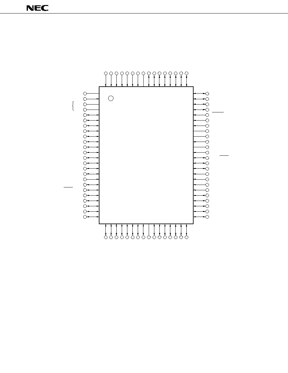
1.
PIN CONFIGURATION
*
Be sure to supply power to both V
DD
pins.
IC: Internally Connected (Connect to V
SS
directly.)
1
2
3
4
5
6
7
8
9
10
11
12
13
14
15
16
17
18
19
20
21
22
23
24
64
63
62
61
60
59
58
57
56
55
54
53
52
51
50
49
48
47
46
45
44
43
42
41
25 26 27 28 29 30 31 32 33 34 35 36 37 38 39 40
80 79 78 77 76 75 74 73 72 71 70 69 68 67 66 65
AV0
AV
REF
V
DD
V
DD
P113
P112
P111
P110
P103
P102
P101
P100
P93
P92
P91
P90
SI1/P83
SO1/P82
SCK1/P81
PPO/P80
KR7/P73
KR6/P72
KR5/P71
KR4/P70
P140
P141
P142
P143
RESET
X2
X1
IC
XT2
XT1
V
SS
P00/INT4
P01/SCK0
P02/SO0/SB0
P03/SI0/SB1
P10/INT0
P11/INT1
P12/INT2
P13/TI0
P20/PTO0
P21
P22/PCL
P23/BUZ
P30
AN1
AN2
AN3
AN4/P150
AN5/P151
AN6/P152
AN7/P153
AV
SS
P120
P121
P122
P123
P130
P131
P132
P133
KR3/P63
KR2/P62
KR1/P61
KR0/P60
P53
P52
P51
P50
V
SS
P43
P42
P41
P40
P33
P32
P31
*
µ
PD75516GF-
◊◊◊
-3B9
5
µ
PD75516
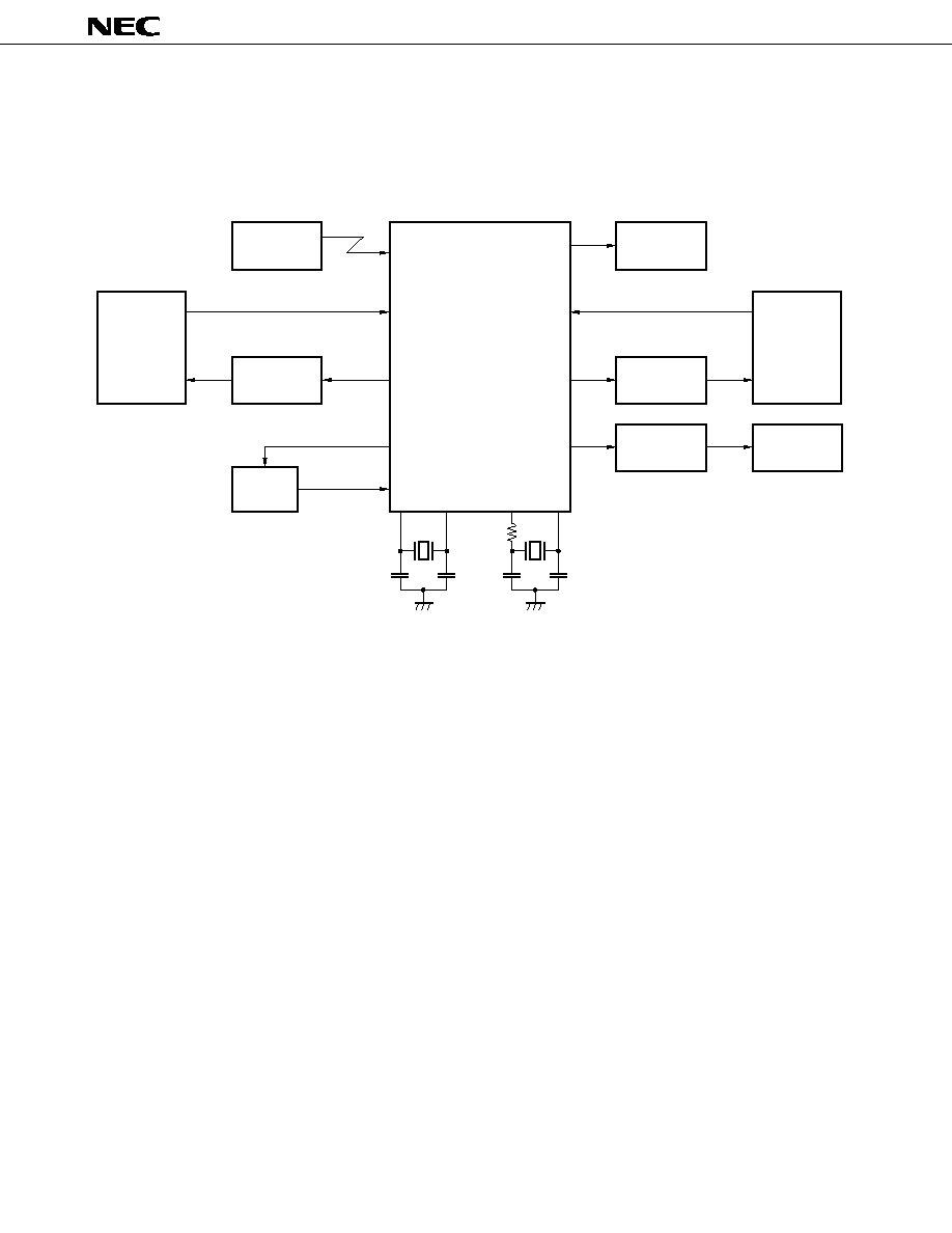
2.
EXAMPLE OF SYSTEM CONFIGURATION
VTR (Voltage Synthesizer Tuner)
µ
PD75516
INT0
Input Port
Output Port
Port4, 5
KR0≠KR7
System Clock
Watch Clock
SIO
Analog
Input
PPO
SIO
OSD
LPF
FIP Driver
FIP
Remote
Control IC
Key Matrix
Servo IC
Mechanism
Mechanism
Control
Tuner
Mechanism
Computer/
Timer