 | –≠–ª–µ–∫—Ç—Ä–æ–Ω–Ω—ã–π –∫–æ–º–ø–æ–Ω–µ–Ω—Ç: UPD75517A | –°–∫–∞—á–∞—Ç—å:  PDF PDF  ZIP ZIP |

Document No.
IC-3183
(O. D. No.
IC-8683
Date Published
November 1992 P
The information in this document is subject to change without notice.
DATA SHEET
MOS INTEGRATED CIRCUIT
µ
PD75517(A)
4 BIT SINGLE-CHIP MICROCOMPUTER
The
µ
PD75517(A) is a 75X series four-bit single-chip microcomputer which enables data processing
equivalent to that performed by an eight-bit microcomputer. It is a high-performance product, whose
minimum instruction execution time is 0.67
µ
s, shorter than 0.95
µ
s for the conventional
µ
PD75516. The ROM
and RAM capacities are also larger, and the throughput of the 75X series is further increased. The
µ
PD75517(A)
is suited to controllers of electric parts of automobiles.
FEATURES
∑
Higher reliable than the
µ
PD75517
∑
Capacities of program memory, ROM: 24448
◊
8 bits
∑
Capacity of data memory, RAM: 1024
◊
4 bits
∑
Function for specifying the instruction execution time (useful for high-speed operation and saving power)
∑ 0.67
µ
s/1.33
µ
s/2.67
µ
s/10.7
µ
s (when the main system clock operates at 6.0 MHz)
∑ 0.95
µ
s/1.91
µ
s/3.82
µ
s/15.3
µ
s (when the main system clock operates at 4.19 MHz)
∑ 122
µ
s (when the subsystem clock operates at 32.768 kHz)
∑
Built-in A/D converter operable on low voltage
∑ 8-bit resolution
◊
8 channels (Successive approximation system)
∑ V
DD
= 2.7 to 6.0 V
∑
Many I/O lines: 64
∑
Enhanced timer function: 4 channels
∑
Built-in 8-bit serial interface: Two channels
∑
Built-in NEC serial bus interface (SBI)
∑
Clock operable with ultra-low power consumption (when 5-
µ
A TYP. operates on 3 V.)
∑
Product with a built-in PROM available:
µ
PD75P518
APPLICATIONS
Controller of electric parts of automobiles
ORDERING INFORMATION
Part number
Package
Quality grade
uPD75517GF(A)-
◊◊◊
-3B9
80-pin plastic QFP (14 mm
◊
20 mm)
Special
Remark
◊◊◊
: Code number
Please refer to "Quality Grades on NEC Semiconductor Devices" (Document number IEI-1209) published by NEC
Corporation to know the specification of quality grade on the devices and its recommended applications.
Printed in Japan
NEC CORPORATION1992
ELECTRON DEVICE

2
µ
PD75517(A)
FUNCTIONS
ROM
RAM
24448
◊
8 bits
1024
◊
4 bits
(4-bit
◊
8 or 8-bit
◊
4)
◊
4 banks
∑ 0.67
µ
s/1.33
µ
s/2.67
µ
s/10.7
µ
s (At 6.0 MHz)
∑ 0.95
µ
s/1.91
µ
s/3.82
µ
s/15.3
µ
s (At 4.19 MHz)
∑ 122
µ
s (At 32.768 kHz)
64
16 (Shared with INT, SIO, PPO, and analog input. Seven lines can be pulled
up by software.)
28 (Four lines for LED driving)
∑ 16 lines can be pulled up by software.
∑ Four lines can be pulled down by the mask option.
20 (Eight lines for LED driving. Withstand voltage is 10 V. 20 lines can be
pulled up by the mask option.)
8-bit resolution
◊
8 channels (Successive approximation system)
∑ Capable of low-voltage operation: V
DD
= 2.7 to 6.0 V
Four channels
∑
Timer/event counter
∑
Basic interval timer
∑
Timer/pulse generator (14-bit PWM output enabled)
∑
Clock timer
Two channels
∑ NEC standard serial bus interface (SBI)/
three-wire SIO: One channel
∑ General clock synchronous serial interface
(three-wire SIO): One channel
∑
Vectored interrupt : Seven sources
(External: 3, internal: 4)
∑
Test input
: Two sources
(External: 1, internal: 1)
∑
Clock test flag is provided.
∑
Parallel edge detection flag for key scan input is provided.
∑ Set/reset/test/Boolean operation for bit data
∑ 4-bit data transfer, arithmetic/logical, increment/decrement, and comparison
instructions
∑ 8-bit data transfer, arithmetic/logical, increment/decrement, and comparison
instructions
∑ Ceramic/crystal oscillator for main system clock : 6.0 MHz, 4.19 MHz
∑ Crystal oscillator for subsystem clock
: 32.768 kHz
V
DD
= 2.7 to 6.0 V
80-pin plastic QFP (14
◊
20 mm)
Built-in memory
General registers
Instruction cycle
I/O ports
A/D converter
Timer/counter
Serial interface
Interrupt
Instruction set
System clock generator
Operating supply voltage
Package
Item
Functions
Total
Number of CMOS
input lines
Number of CMOS
I/O lines
Number of N-ch
open-drain I/O lines

3
µ
PD75517(A)
PIN CONFIGURATION (TOP VIEW)
IC: Internally connected. Connect the IC pin to V
SS
.
Note Be sure to supply power to both the V
DD
pins.
AN1
AN2
AN3
AN4/P150
AN5/P151
AN6/P152
AN7/P153
AV
SS
P120
P121
P122
P123
P130
P131
P132
P133
P140
P141
P142
P143
RESET
X2
X1
IC
XT2
XT1
V
SS
P00/INT4
P01/SCK0
P02/SO0/SB0
P03/SI0/SB1
P10/INT0
P11/INT1
P12/INT2
P13/ TI0
P20/PTO0
P21
P22/PCL
P23/BUZ
P30
1
2
3
4
5
6
7
8
9
10
11
12
13
14
15
16
17
18
19
20
21
22
23
24
64
63
62
61
60
59
58
57
56
55
54
53
52
51
50
49
48
47
46
45
44
43
42
41
80 79 78 77 76 75 74 73 72 71 70 69 68 67 66 65
25 26 27 28 29 30 31 32 33 34 35 36 37 38 39 40
AN0
AV
REF
V
DD
V
DD
P113
P112
P111
P110
P103
P102
P101
P100
P93
P92
P91
P90
SI1/P83
SO1/P82
SCK1/P81
PPO/P80
KR7/P73
KR6/P72
KR5/P71
KR4/P70
KR3/P63
KR2/P62
KR1/P61
KR0/P60
P53
P52
P51
P50
V
SS
P43
P42
P41
P40
P33
P32
P31
Note
PD75517GF(A)-
◊◊◊
-3B9
µ

4
µ
PD75517(A)
INTERNAL BLOCK DIAGRAM
TI0/P13
PTO0/P20
BUZ/P23
PPO/P80
SI0/SB1/P03
SO0/SB0/P02
SCK0/P01
SI1/P83
SO1/P82
SCK1/P81
INT0/P10
INT1/P11
INT2/P12
INT4/P00
KR0/P60
- KR7/P73
AN0 - AN3
AN4/P150
- AN7/P153
AV
REF
AV
SS
P00 - P03
P10 - P13
P20 - P23
P30 - P33
P40 - P43
Note
P50 - P53
Note
P60 - P63
P70 - P73
P80 - P83
P90 - P93
P100 - P103
P110 - P113
P120 - P123
Note
P130 - P133
Note
P140 - P143
Note
P150 - P153
4
4
4
4
4
4
4
4
4
4
4
4
4
4
4
4
Port 0
Port 1
Port 2
Port 3
Port 4
Port 5
Port 6
Port 7
Port 8
Port 9
Port 10
Port 11
Port 12
Port 13
Port 14
Port 15
Basic
interval
timer
INTBT
Timer/event
counter #0
INTT0
Watch timer
INTW
Timer/pulse
generator
INTTPG
Serial bus
interface 0
INTCSI0
Serial
interface 1
Interrupt
control
Bit seq.
buffer (16)
A/D
converter
Program counter (15)
ROM program memory
24448
◊
8 bits
ALU
CY
SP(8)
SBS(2)
Bank
Decode and
control
General register
RAM data memory
1024
◊
4 bits
f
X
/2
N
Clock output
control
PCL/P22
Clock divider
Clock generator
Sub
Main
Stand by
control
XT1 XT2 X1 X2
CPU clock
RESET
V
DD
V
SS
Note
Port 4, Port 5, Port 12, Port 13, and Port 14 are N-ch open-drain
I/O ports with a medium withstand voltage of 10 V.

5
µ
PD75517(A)
CONTENTS
1.
PIN FUNCTIONS ........................................................................................................................
7
1.1
PORT PINS ......................................................................................................................................
7
1.2
NON-PORT PINS ............................................................................................................................
9
1.3
PIN INPUT/OUTPUT CIRCUITS ....................................................................................................
10
1.4
CONNECTION OF UNUSED PINS ................................................................................................
13
1.5
SELECTION OF A MASK OPTION ................................................................................................
14
2.
ARCHITECTURE AND MEMORY MAP OF THE
µ
PD75517(A) ..............................................
15
2.1
DATA MEMORY BANK CONFIGURATION AND ADDRESSING MODES ................................
15
2.2
GENERAL REGISTER BANK CONFIGURATION ..........................................................................
19
2.3
MEMORY-MAPPED I/O .................................................................................................................
22
3.
INTERNAL CPU FUNCTIONS ....................................................................................................
27
3.1
PROGRAM COUNTER (PC) ...........................................................................................................
27
3.2
PROGRAM MEMORY (ROM) ........................................................................................................
27
3.3
DATA MEMORY (RAM) .................................................................................................................
29
3.4
GENERAL REGISTERS ...................................................................................................................
31
3.5
ACCUMULATORS ..........................................................................................................................
32
3.6
STACK POINTER (SP) AND STACK BANK SELECT REGISTER (SBS) .....................................
32
3.7
PROGRAM STATUS WORD (PSW) ..............................................................................................
35
3.8
BANK SELECT REGISTER (BS) .....................................................................................................
38
4.
PERIPHERAL HARDWARE FUNCTIONS ..................................................................................
39
4.1
DIGITAL I/O PORTS .......................................................................................................................
39
4.2
CLOCK GENERATOR ......................................................................................................................
51
4.3
CLOCK OUTPUT CIRCUIT .............................................................................................................
60
4.4
BASIC INTERVAL TIMER ...............................................................................................................
63
4.5
CLOCK TIMER .................................................................................................................................
67
4.6
TIMER/EVENT COUNTER .............................................................................................................
69
4.7
TIMER/PULSE GENERATOR .........................................................................................................
75
4.8
SERIAL INTERFACE (CHANNEL 0) ...............................................................................................
83
4.8.1
Serial Interface (Channel 0) Functions ........................................................................
84
4.8.2
Configuration of Serial Interface (Channel 0) ............................................................
84
4.8.3
Register Functions .........................................................................................................
86
4.8.4
Signals .............................................................................................................................
94
4.8.5
Serial Interface (Channel 0) Operation .......................................................................
100
4.8.6
Transfer Start in Each Mode ........................................................................................
110
4.8.7
Manipulation of SCK0 Pin Output ...............................................................................
111

6
µ
PD75517(A)
4.9
SERIAL INTERFACE (CHANNEL 1) ...............................................................................................
112
4.9.1
Serial Interface (Channel 1) Functions ........................................................................
112
4.9.2
Serial Interface (Channel 1) Configuration .................................................................
112
4.9.3
Register Functions .........................................................................................................
114
4.9.4
Serial Interface (Channel 1) Operation .......................................................................
115
4.10
A/D CONVERTER ...........................................................................................................................
117
4.11
BIT SEQUENTIAL BUFFER ............................................................................................................
124
5.
INTERRUPT FUNCTION ............................................................................................................ 125
5.1
CONFIGURATION OF THE INTERRUPT CONTROL CIRCUIT ....................................................
125
5.2
HARDWARE OF THE INTERRUPT CONTROL CIRCUIT ..............................................................
127
5.3
INTERRUPT SEQUENCE ................................................................................................................
134
5.4
MULTIPLE INTERRUPT PROCESSING CONTROL ......................................................................
135
5.5
VECTOR ADDRESS SHARE INTERRUPT PROCESSING ............................................................
137
6.
STANDBY FUNCTION ............................................................................................................... 138
6.1
SETTING OF STANDBY MODES AND OPERATION STATUSES .............................................
138
6.2
RELEASE OF THE STANDBY MODES .........................................................................................
139
6.3
OPERATION AFTER A STANDBY MODE IS RELEASED ............................................................
141
7.
RESET FUNCTION ..................................................................................................................... 142
8.
INSTRUCTION SET .................................................................................................................... 144
8.1
µ
PD75517(A) INSTRUCTIONS ......................................................................................................
144
8.2
INSTRUCTION SET AND ITS OPERATION ..................................................................................
147
8.3
INSTRUCTION CODES OF EACH INSTRUCTION .......................................................................
156
9.
ELECTRICAL CHARACTERISTICS ............................................................................................. 162
10. PACKAGE DIMENSIONS ........................................................................................................... 174
11. RECOMMENDED SOLDERING CONDITIONS ......................................................................... 175
APPENDIX A
SERIES PRODUCT FUNCTIONS ............................................................................ 176
APPENDIX B
DEVELOPMENT TOOLS ......................................................................................... 177

7
µ
PD75517(A)
1. PIN FUNCTIONS
1.1 PORT PINS (1/2)
Notes 1. The circuits enclosed in circles have a Schmitt-triggered input.
2. An LED can be driven directly.
P00
P01
P02
P03
P10
P11
P12
P13
P20
P21
P22
P23
P30
Note 2
P31
Note 2
P32
Note 2
P33
Note 2
P40-P43
Note 2
P50-P53
Note 2
P60
P61
P62
P63
P70
P71
P72
P73
INT4
SCK0
SO0/SB0
SI0/SB1
INT0
INT1
INT2
TI0
PTO0
≠
PCL
BUZ
≠
≠
≠
≠
≠
≠
KR0
KR1
KR2
KR3
KR4
KR5
KR6
KR7
◊
◊
◊
◊
r
r
With noise elimination function
4-bit input port (Port 0).
For P01 to P03, pull-up resistors can be
provided by software in units of 3 bits.
4-bit input port (Port 1).
Pull-up resistors can be provided by software
in units of 4 bits.
4-bit I/O port (Port 2).
Pull-up resistors can be provided by software
in units of 4 bits.
Programmable 4-bit I/O port (Port 3).
Input/output can be specified bit by bit.
Pull-up resistors can be provided by software
in units of 4 bits.
N-ch open-drain 4-bit I/O port (Port 4).
A pull-up resistor can be provided bit by bit
(mask option).
Withstand voltage is 10 V in open-drain mode.
N-ch open-drain 4-bit I/O port (Port 5).
A pull-up resistor can be provided bit by bit
(mask option).
Withstand voltage is 10 V in open-drain mode.
Programmable 4-bit I/O port (Port 6).
Input/output can be specified bit by bit.
Pull-up resistors can be provided by software
in units of 4 bits.
4-bit I/O port (Port 7).
Pull-up resistors can be provided by software
in units of 4 bits.
Also
used as
Pin name
I/O
B
F
- A
F
- B
M
- C
B
- C
E - B
E - C
M
M
F
- C
F
- A
8-bit I/O
Input
Input
Input
Input
High level
(when a pull-up
resistor is
provided) or
high impedance
High level
(when a pull-up
resistor is
provided) or
high impedance
Input
Input
When reset
Function
I
I
I/O
I/O
I/O
I/O
I/O
I/O
I/O
Note 1
circuit
type
8
µ
PD75517(A)
1.1 PORT PINS (2/2)
Note The circuits enclosed in circles have a Schmitt-triggered input.
◊
◊
◊
◊
◊
◊
◊
Function
Also
used as
Pin name
I/O
8-bit I/O
When reset
I/O
Note
circuit
type
Input
Low level (when
a pull-down
resistor is
provided) or
high impedance
Input
Input
High level
(when a pull-up
resistor is
provided) or
high impedance
High level
(when a pull-up
resistor is
provided) or
high impedance
High level
(when a pull-up
resistor is
provided) or
high impedance
Input
PPO
SCK1
SO1
SI1
≠
≠
≠
≠
≠
≠
AN4-AN7
I
I/O
I/O
I/O
I/O
I/O
I/O
I
P80
P81
P82
P83
P90-P93
P100-P103
P110-P113
P120-P123
P130-P133
P140-P143
P150-P153
E
F
E
B
V
E
E
M
M
M
Y - A
4-bit input port (Port 8).
4-bit I/O port (Port 9).
A pull-down resistor can be provided bit by bit
(mask option).
4-bit I/O port (Port 10)
4-bit I/O port (Port 11)
N-ch open-drain, 4-bit I/O port (Port 12).
Pull-up resistors can be provided bit by bit
(mask option).
Withstand voltage is 10 V in open-drain mode.
N-ch open-drain, 4-bit I/O port (Port 13).
Pull-up resistors can be provided bit by bit
(mask option).
Withstand voltage is 10 V in open-drain mode.
N-ch open-drain, 4-bit I/O port (Port 14).
Pull-up resistors can be provided bit by bit
(mask option).
Withstand voltage is 10 V in open-drain mode.
4-bit input port (Port 15)

9
µ
PD75517(A)
1.2 NON-PORT PINS
Notes 1. The circuits enclosed in circles have a Schmitt-triggered input.
2. Be sure to input V
SS
level to this pin.
Function
Also
used as
Pin name
I/O
I
O
O
O
I/O
I/O
I/O
I
I
I
I
I
I/O
O
I
I
I
≠
I
I
≠
I
O
≠
≠
≠
Synchronous
Asynchronous
Asynchronous
Edge detection vectored interrupt input pin
(The edge to be detected is selectable.)
Edge detection testable input pin
(An rising edge is detected.)
P13
P20
P22
P23
P01
P02
P03
P00
P10
P11
P12
P60-P63
P70-P73
P81
P82
P83
≠
P150-P153
≠
≠
≠
≠
≠
P80
≠
≠
≠
External event pulse input pin for the timer/event counter
Timer/event counter output pin
Clock output pin
Fixed frequency output pin (for buzzer or system clock
trimming)
Serial clock I/O pin
Serial data output pin or serial bus I/O pin
Serial data input pin or serial bus I/O pin
Edge detection vectored interrupt input pin (Either a rising
or falling edge is detected.)
Parallel-falling-edge-sensitive testable input pins
Parallel-falling-edge-sensitive testable input pins
Serial clock I/O pin
Serial data output pin
Serial data input pin
Analog input pins to A/D converter
A/D converter reference voltage input pin
A/D converter reference GND pin
Pin for connection to a crystal/ceramic resonator for main
system clock generation. When external clock is used, it is
input to X1, and its inverted signal is input to X2.
Pin for connection to a crystal resonator for subsystem
clock generation. When external clock is used, it is input to
XT1, and XT2 is left open.
System reset input pin
Timer/pulse generator pulse output pin
Positive power supply pin
Ground pin
Internally connected
Note 2
≠
Input
Input
Input
Input
Input
Input
≠
≠
≠
Input
Input
Input
Input
Input
≠
≠
≠
≠
≠
≠
Input
≠
≠
≠
TI0
PTO0
PCL
BUZ
SCK0
SO0/SB0
SI0/SB1
INT4
INT0
INT1
INT2
KR0-KR3
KR4-KR7
SCK1
SO1
SI1
AN0-AN3
AN4-AN7
AV
REF
AV
SS
X1, X2
XT1
XT2
RESET
PPO
V
DD
V
SS
IC
I/O
Note 1
circuit
type
When reset
B
- C
E - B
E - B
E - B
F
- A
F
- B
M
- C
B
B
- C
B
- C
F
- C
F
- A
F
E
B
Y
Y - A
Z
≠
≠
≠
B
E
≠
≠
≠

10
µ
PD75517(A)
1.3 PIN INPUT/OUTPUT CIRCUITS
Fig. 1-1 shows the input/output circuit of each
µ
PD75517(A) pin in a simplified manner.
Fig. 1-1 Pin Input/Output Circuits (1/3)
Type A
CMOS input buffer
Schmitt trigger input with hysteresis
Push-pull output which can be set to high-impedance output
(off for both P-ch and N-ch)
I/O circuit consisting of a push-pull output
of type D and an input buffer of type A
P.U.R.: Pull-Up Resistor
Type B
Type E
Type B - C
Type D
V
DD
IN
P-ch
N-ch
IN
IN
P-ch
P.U.R.
enable
P.U.R.
V
DD
V
DD
P-ch
N-ch
OUT
Data
Output
disable
IN/OUT
Data
Output
disable
Type D
Schmitt trigger input with hysteresis
P.U.R.: Pull-Up Resistor
P.U.R.
V
DD
Output
disable
P-ch
IN/OUT
Data
Output
disable
Type D
Type E - B
Type A
Type A

11
µ
PD75517(A)
Fig. 1-1 Pin Input/Output Circuits (2/3)
Type E - C
I/O circuit consisting of a push-pull output of type D
and a Schmitt-triggered input of type B
P.U.R.: Pull-Up Resistor
Type F
Type F - A
Type F - B
P.U.R.
V
DD
P.U.R.
enable
P-ch
IN/OUT
Data
Output
disable
Type D
IN/OUT
Data
Output
disable
Type D
P.U.R.: Pull-Up Resistor
P.U.R.
V
DD
P.U.R.
enable
P-ch
IN/OUT
Data
Output
disable
Type D
P.U.R.: Pull-Up Resistor
V
DD
P-ch
N-ch
IN/OUT
V
DD
P-ch
P.U.R.
P.U.R.
enable
Output
disable
(P-ch)
Data
Output
disable
Output
disable
(N-ch)
Type F - C
P.U.R.: Pull-Up Resistor
P.U.R.
V
DD
P.U.R.
enable
P-ch
IN/OUT
Data
Output
disable
Type D
Type M
P.U.R.: Pull-Up Resistor
N-ch
(Can sustain
+9 V)
IN/OUT
Data
V
DD
Output
disable
P.U.R.
(Mask option)
Middle-voltage input buffer
(Can sustain + 10 V)
Type B
Type A
Type B
Type B
Type B

12
µ
PD75517(A)
Fig. 1-1 Pin Input/Output Circuits (3/3)
Type V
Type M - C
Type Y
Type Z
Type Y - A
P.D.R.: Pull-Down Resistor
P.U.R.: Pull-Up Resistor
P.D.R.
(Mask option)
IN/OUT
Data
Output
disable
Type D
N-ch
P.U.R.
Data
Output
disable
P.U.R.
enable
V
DD
P-ch
IN/OUT
V
DD
V
DD
P-ch
AV
SS
N-ch
Sampl-
ing C
AV
SS
Reference voltage
(from voltage tap of
serial resistor string)
Input
enable
IN
V
DD
AV
SS
Sampl-
ing C
V
DD
AV
SS
IN
P-ch
N-ch
Reference voltage
(from voltage tap of
serial resistor string)
IN instruction
+
≠
Input
enable
AV
REF
Reference voltage
AV
SS
+
≠
Type A

13
µ
PD75517(A)
1.4 CONNECTION OF UNUSED PINS
Table 1-1 Recommended Connection of Unused Pins
To be connected to V
SS
To be connected to V
SS
or V
DD
To be connected to V
SS
Input state
: To be connected to V
SS
or V
DD
Output state : To be left open
To be connected to V
SS
or V
DD
Input state
: To be connected to V
SS
or V
DD
Output state : To be left open
To be connected to V
SS
To be connected to V
SS
or V
DD
To be left open
To be connected to V
SS
P00/INT4
P01/SCK0
P02/SO0/SB0
P03/SI1/SB1
P10/INT0-P12/INT2
P13/TI0
P20/PTO0
P21
P22/PCL
P23/BUZ
P30-P33
P40-P43
P50-P53
P60/KR0-P63/KR3
P70/KR4-P73/KR7
P80/PPO
P81/SCK1
P82/SO1
P83/SI1
P90-P93
P100-P103
P110-P113
P120-P123
P130-P133
P140-P143
P150/AN4-P153/AN7
AN0-AN3
XT1
XT2
AV
REF
AV
SS
IC
Pin name
Recommended connection

14
µ
PD75517(A)
1.5 SELECTION OF A MASK OPTION
The following mask options are provided for pins.
(1) Specification of built-in pull-up and pull-down resistors
Table 1-2 Selection of Pull-Up and Pull-Down Resistors
(2) Specification of built-in feed-back resistors for subsystem clock oscillation
Table 1-3 Selection of Feed-Back Resistors
Caution Even if built-in feed-back resistors are provided when no subsystem clock is used, operation is
not affected except increased power supply current I
DD
.
P40-P43,
P50-P53,
P120-P123,
P130-P133,
P140-P143
P90-P93
Pin name
2
No pull-up resistor provided
(Can be specified bit by bit.)
2
No pull-down resistor provided
(Can be specified bit by bit.)
1
Pull-up resistors provided
(Can be specified bit by bit.)
1
Pull-down resistors provided
(Can be specified bit by bit.)
Mask option
XT1, XT2
1
Feed-back resistors provided
(when a subsystem clock is used)
2
No feed-back resistors provided
(when no subsystem clock is used)
Mask option
Pin name

15
µ
PD75517(A)
2. ARCHITECTURE AND MEMORY MAP OF THE
µ
PD75517(A)
The
µ
PD75517(A) has three architectural features:
(a) Data memory bank configuration
(b) General register bank configuration
(c) Memory-mapped I/O
Each of these features is explained below.
2.1 DATA MEMORY BANK CONFIGURATION AND ADDRESSING MODES
As shown in Fig. 2-1, the data memory space of the
µ
PD75517(A) contains a static RAM (1024 words
◊
4
bits) at addresses 000H to 3FFH and peripheral hardware (such as I/O ports and timers) at addresses F80H to
FFFH. To address a 12-bit address in this data memory space, the
µ
PD75517(A) uses such a memory bank
configuration that the low-order eight bits are specified with an instruction directly or indirectly, and the high-
order four bits are used to specify a memory bank (MB).
To specify a memory bank (MB), a memory bank enable flag (MBE) and memory bank select register (MBS)
are contained, allowing the addressing indicated in Fig. 2-1 and 2-2 and Table 2-1. (The MBS is a register used
to select a memory bank, and can be set to 0, 1, 2, 3, or 15. The MBE is a flag used to determine whether a
memory bank selected using the MBS register is to be enabled. The MBE is automatically saved or restored
at the time of interrupt processing or subroutine processing, so that it can be freely set in interrupt processing
and subroutine processing.)
In addressing data memory space, the MBE is usually set to 1 (MBE = 1), and the static RAM in the memory
bank specified by the MBS is operated. However, the MBE = 0 mode or the MBE = 1 mode can be selected
for each step of program processing for more efficient programming.
The MBE and MBS are set as indicated below.
Example
SET1 MBE
; MBE
1
CLR1 MBE
; MBE
0
SEL MB0
; MBS
0
SEL MB1
; MBS
1
SEL MB15
; MBS
15
∑ Interrupt processing
∑ Processing that repeats internal hardware and static RAM operations
∑ Subroutine processing
∑ Usual program processing
MBE = 0 mode
MBE = 1 mode
Applicable program processing

16
µ
PD75517(A)
Fig. 2-1 Data Memory Organization and Addressing Range of Each Addressing Mode
Remark -- : Don't care
FF0H
FFFH
FB0H
FBFH
FC0H
F80H
3FFH
2FFH
300H
1FFH
200H
0FFH
100H
01FH
020H
07FH
000H
Addressing mode
mem
mem.bit
@HL
@H + mem.bit
@DE
@DL
Stack
address-
ing
fmem.bit
pmem.
@L
Memory bank enable flag
MBE
= 0
MBE
= 1
MBE
= 0
MBE
= 1
≠
≠
≠
≠
Data area
Static RAM
(memory bank 0)
Data area
Static RAM
(memory bank 1)
Data area
Static RAM
(memory bank 2)
Data area
Static RAM
(memory bank 3)
Stack area
Not contained
Peripheral hardware area
(memory bank 15)
MBS
= 0
MBS
= 0
SBS
= 0
MBS
= 1
MBS
= 1
SBS
= 1
MBS
= 2
MBS
= 2
SBS
= 2
MBS
= 3
MBS
= 3
SBS
= 3
MBS
= 15
MBS
= 15
General
resister
area

17
µ
PD75517(A)
Table 2-1 Addressing Modes
Bit specified by bit at the address specified by MB and mem. In this case:
When MBE = 0 and mem = 00H-7FH, MB = 0
When MBE = 0 and mem = 80H-FFH, MB = 15
When MBE = 1, MB = MBS
Address specified by MB and mem. In this case:
When MBE = 0 and mem = 00H-7FH, MB = 0
When MBE = 0 and mem = 80H-FFH, MB = 15
When MBE = 1, MB = MBS
Address specified by MB and mem (mem: even address). In this case:
When MBE = 0 and mem = 00H-7FH, MB = 0
When MBE = 0 and mem = 80H-FFH, MB = 15
When MBE = 1, MB = MBS
Address specified by MB and HL.
In this case, MB = MBE∑MBS
Address specified by DE in memory bank 0
Address specified by DL in memory bank 0
Address specified by MB and HL (with the L register holding an even number).
In this case, MB = MBE∑MBS
Bit specified by bit at the address specified by fmem. In this case:
fmem = FB0H-FBFH (interrupt-related hardware)
fmem = FF0H-FFFH (I/O port)
Bit specified by the low-order 2 bits of the L register at the address specified
by the high-order 10 bits of pmem and the high-order 2 bits of the L register.
In this case, pmem = FC0H-FFFH
Bit specified by bit at the address specified by MB, H, and the low-order 4 bits
of mem.
In this case, MB = MBE∑MBS
Address specified by SP in memory bank 0, 1, 2, and 3 selected by SBS
1-bit direct addressing
4-bit direct addressing
8-bit direct addressing
4-bit register indirect
addressing
8-bit register indirect
addressing
Bit manipulation
addressing
Stack addressing
mem.bit
mem
@HL
@HL+
@HL≠
@DE
@DL
@HL
fmem.bit
pmem.@L
@H+mem.bit
--
Representation
format
Specified address
Addressing mode

18
µ
PD75517(A)
As summarized in Table 2-1, the
µ
PD75517(A) allows both direct and indirect addressing in data memory
manipulation for 1-bit data, 4-bit data, and 8-bit data, so that very efficient and simple programming can be
performed.
Examples 1.
The 8-bit data of port 4 and port 5 are transferred to addresses 20H and 21H.
CLR1
MBE
; MBE
0
IN
XA, PORT4
; XA
Ports 5, 4
MOV
20H, XA
; (21H, 20H)
XA
2.
When P02 is 0, P33 is set.
SKT
PORT0.2
; Skip if bit 2 of port 0 is 1
SET1
PORT3.3
; Set bit 3 of port 3
3.
A different value is output to port 6, depending on the status of P10.
SKF
PORT1.0
; Skip if bit 0 of port 1 is 0
MOV
A, #1010B
; A
1010B (string effect)
MOV
A, #0101B
; A
0101B (string effect)
SEL
MB15
; or CLR1 MBE
OUT
PORT6, A
; Port 6
A
Fig. 2-2 Updating Static RAM Addresses
INCS D
DECS D
INCS L
DECS L
INCS D
DECS D
INCS E
DECS E
INCS H
DECS H
INCS L
DECS L
INCS H
DECS H
◊
0H
0
◊
H
F
◊
H
@DL
4-bit transfer
@DE
4-bit transfer
@HL
4-bit
manipulation
8-bit
manipulation
@H + mem.bit
Bit manipulation
Direct
addressing
Bit manipulation
4-bit
8-bit
◊
FH
DECS DE
INCS DE
DECS HL
INCS HL
Automatic
decrement
Automatic
increment

19
µ
PD75517(A)
2.2 GENERAL REGISTER BANK CONFIGURATION
The
µ
PD75517(A) contains four register banks, each consisting of eight general registers: X, A, B, C, D, E,
H, and L. These registers are mapped to addresses 00H to 1FH in memory bank 0 of the data memory. (See
Fig. 2-3.) To specify a general register bank, a register bank enable flag (RBE) and a register bank select register
(RBS) are contained. The RBS is a register used to select a register bank, and the RBE is a flag used to determine
whether a register bank selected using the RBS is to be enabled. The register bank (RB) enabled at instruction
execution is determined as RB = RBE∑RBS
As indicated in Table 2-2, the
µ
PD75517(A) enables the user to create programs in a very efficient manner
by selecting a register bank from the four register banks, depending on whether the processing is normal
processing or interrupt processing. (The RBE is automatically saved and set at the time of interrupt processing,
and is automatically restored upon completion of interrupt processing.)
Table 2-2 Example of the Use of Register Banks with Normal Routines and Interrupt Routines
The RBE and RBS are set as indicated below.
Example
SET1
RBE ; RBE
1
CLR1
RBE ; RBE
0
SEL
RB0 ; RBS
0
SEL
RB3 ; RBS
3
The general registers allow transfers, comparisons, arithmetic/logical operations, and increments and
decrements not only on a 4-bit basis, but also on an 8-bit basis with the XA, HL, DE, and BC register pairs.
In this case, the register pairs of the register bank that has the inverted value of bit 0 of a register bank specified
by RBE∑RBS can be specified as XA', HL', DE', and BC', thus providing eight 8-bit registers. (See Fig. 2-4.)
Example
SET1
RBE
; RBE
1
SEL
RB2
; RBS
2
MOV
XA, #18H ; XA
18H
ADDS HL, XA
; HL
HL+XA
SUBS
HL', XA
; HL'
HL'≠XA (HL' is HL of register bank 3)
INCS
HL
; HL
HL+1
MOV
XA, #00H ; XA
00H (string effect)
MOV
XA, #10H ; XA
10H (string effect)
Normal processing
Single interrupt processing
Dual interrupt processing
Multiple (triple or more) interrupt processing
Use register banks 2 and 3 with RBE = 1.
Use register bank 0 with RBE = 0.
Use register bank 1 with RBE = 1.
(In this case, the RBS needs to be saved and restored.)
Save the registers with PUSH or POP.

20
µ
PD75517(A)
Fig. 2-3 General Register Configuration (4-Bit Processing)
X
H
D
B
X
H
D
B
X
H
D
B
X
H
D
B
01H
03H
05H
07H
09H
0BH
0DH
0FH
11H
13H
15H
17H
19H
1BH
1DH
1FH
A
L
E
C
A
L
E
C
A
L
E
C
A
L
E
C
00H
02H
04H
06H
08H
0AH
0CH
0EH
10H
12H
14H
16H
18H
1AH
1CH
1EH
Register bank 0
(RBE∑RBS = 0)
Register bank 1
(RBE∑RBS = 1)
Register bank 2
(RBE∑RBS = 2)
Register bank 3
(RBE∑RBS = 3)

21
µ
PD75517(A)
Fig. 2-4 General Register Configuration (8-Bit Processing)
XA
HL
DE
BC
XA'
HL'
DE'
BC'
00H
02H
04H
06H
08H
0AH
0CH
0EH
When RBE∑RBS
= 0
XA'
HL'
DE'
BC'
XA
HL
DE
BC
00H
02H
04H
06H
08H
0AH
0CH
0EH
When RBE∑RBS
= 1
XA
HL
DE
BC
XA'
HL'
DE'
BC'
10H
12H
14H
16H
18H
1AH
1CH
1EH
When RBE∑RBS
= 2
XA'
HL'
DE'
BC'
XA
HL
DE
BC
10H
12H
14H
16H
18H
1AH
1CH
1EH
When RBE∑RBS
= 3

22
µ
PD75517(A)
2.3 MEMORY-MAPPED I/O
The
µ
PD75517(A) employs memory-mapped I/O, which maps peripheral hardware such as timers and I/O
ports to addresses F80H to FFFH in the data memory space as shown in Fig. 2-1. This means that there is no
particular instruction to control peripheral hardware, but all peripheral hardware is controlled using memory
manipulation instructions. (Some mnemonics for hardware control are available to make programs readable.)
To manipulate peripheral hardware, the addressing modes listed in Table 2-3 can be used.
Table 2-3 Addressing Modes Applicable to Peripheral Hardware
Fig. 2-5 summarizes the I/O map of the
µ
PD75517(A).
The items in Fig. 2-5 have the following meanings:
∑ Symbol:
Name representing the address of incorporated hardware, which can be coded in the operand
field of an instruction
∑ R/W
:
Indicates whether the hardware allows read/write operation.
R/W: Both read and write operations possible
R
: Read only
W
: Write only
∑ Number of manipulatable bits:
Indicates the number of bits that can be processed in hardware manipulation
: Bits can be manipulated on an indicated bit (1-, 4-, or 8-bit) basis.
: Particular bits can be manipulated. For these bits, see Remarks.
: Bits cannot be manipulated on an indicated bit (1-, 4-, or 8-bit) basis.
∑ Bit manipulation addressing:
Bit manipulation addressing applicable in hardware bit manipulation
Bit manipulation
4-bit manipulation
8-bit manipulation
Direct addressing mode specifying mem.bit with MBE = 0 or
(MBE = 1, MBS = 15)
Direct addressing mode specifying fmem.bit regardless of MBE
and MBS setting
Indirect addressing mode specifying pmem.@L regardless of
MBE and MBS setting
Direct addressing mode specifying mem with MBE = 0 or (MBE
= 1, MBS = 15)
Register indirect addressing mode specifying @HL with (MBE
= 1, MBS = 15)
Direct addressing mode specifying mem (even address) with
MBE = 0 or (MBE = 1, MBS = 15)
Register indirect addressing mode specifying @HL (with the L
register containing an even number) with (MBE = 1, MBS = 15)
All hardware allowing bit
manipulation
IST0, IST1, MBE, RBE, EOT,
IE
◊◊◊
, IRQ
◊◊◊
, PORTn.
◊
BSBn.
◊
PORTn.
◊
All hardware allowing 4-bit
manipulation
All hardware allowing 8-bit
manipulation addressing
Applicable addressing mode
Applicable hardware
≠

23
µ
PD75517(A)
Fig. 2-5
µ
PD75517(A) I/O Map (1/4)
Notes 1.
Can be operated separately as the RBS and MBS during 4-bit manipulation.
Can also be operated as the BS during 8-bit manipulation.
2.
TOE0: Timer/event counter 0 output enable flag (W)
R/W
≠
≠
W
≠
R/W
Address
b0
b1
b2
b3
F80H
F85H
F86H
F98H
FA0H
FA2H
FA4H
FA6H
TOE0
Note 2
R
W
W
W
R
W
≠
≠
≠
≠
≠
≠
≠
≠
≠
≠
≠
≠
≠
≠
≠
mem.bit
mem.bit
mem.bit
Remarks
Bit
manipulation
addressing
Bit 0 is fixed
to 0
Hardware name (symbol)
Number of bits that
Stack pointer (SP)
Basic interval timer mode register (BTM)
Basic interval timer (BT)
Clock mode register (WM)
Timer/event counter 0 mode register (TM0)
Timer/event counter 0 count register (T0)
Timer/event counter 0 modulo register (TMOD0)
Only bit 3
allows bit
manipulation.
Only bit 3 can
be manipulat-
ed
1 bit
4 bits
8 bits
F82H
F83H
F84H
Register bank select register
(RBS)
Memory bank select register
(MBS)
Bank select
register (BS)
Stack bank select register (SBS)
R/W
Bits 3 and 2
are always
set to 0.
R
Note 1
≠
≠
≠
≠
F90H
F94H
Timer pulse generator (TPGM)
mem.bit
Only bit 3 can
be manipulat-
ed
≠
W
≠
≠
F96H
Timer/pulse generator modulo register (MODL)
R/W
≠
≠
Timer/pulse generator modulo register (MODH)
R/W
≠
≠
≠
can be manipulated

24
µ
PD75517(A)
Fig. 2-5
µ
PD75517(A) I/O Map (2/4)
Remarks 1. IE
◊◊◊
: Interrupt enable flag
2. IRQ
◊◊◊
: Interrupt request flag
R/W
≠
R/W
Address
b0
b1
b2
b3
FB0H
FB2H
FB3H
FC0H
FC2H
FC3H
fmem.bit
mem.bit
pmem.@L
RBE
MBE
IST0
IST1
≠
≠
R
≠
≠
≠
≠
≠
≠
W
W
W
W
W
≠
≠
R/W
≠
R/W
R/W
R/W
≠
R/W
≠
R/W
fmem.bit
FB4H
FB5H
FB6H
FB7H
FB8H
FBAH
FBCH
FBDH
FBEH
FBFH
IE4
IRQ4
IEBT
IRQBT
IEW
IRQW
IET0
IRQT0
IECSI0
IRQCSI0
IE0
IRQ0
IE2
IRQ2
IE1
IRQ1
R/W
R/W
R/W
R/W
FC1H
Remarks
Bit
manipulation
addressing
Hardware name (symbol)
1 bit
4 bits
8 bits
Program status word (PSW)
Processor clock control register (PCC)
INT0 mode register (IM0)
INT1 mode resistor (IM1)
INT2 mode register (IM2)
System clock control register (SCC)
Bit sequential buffer 0 (BSB0)
Bit sequential buffer 1 (BSB1)
Bit sequential buffer 2 (BSB2)
Bit sequential buffer 3 (BSB3)
Manipulated
with EI/DI
instruction
Bit 2 is fixed
to 0
Bits 3, 2, and
1 are fixed to
0
Bits 3 and 2
are fixed to
0
Bits 2 and 1
are fixed to 0
≠
Interrupt priority select register (IPS)
W
FBBH
IETPG
IRQTPG
FB9H
EOT
R/W
R/W
≠
FC8H
Serial operation mode register 1 (CSIM1)
Only bit 7
allows bit
manipulation.
FCCH
Serial I/O shift register 1 (SIO1)
CSIE1
W
R/W
≠
≠
≠
≠
≠
mem.bit
Number of bits that
can be manipulated

25
µ
PD75517(A)
Fig. 2-5
µ
PD75517(A) I/O Map (3/4)
Note When developing a program, set 0 to the following two bits of the port mode register group C (PMGC):
FEEH, b0 (Equivalent to PM8)
FEFH, b3 (Equivalent to PM15)
For, while this port on the chip side is used for input only, the corresponding port on the emulator
is an I/O port.
W
R/W
Address
b0
b1
b2
b3
FD0H
FD8H
FDAH
≠
≠
≠
≠
W
≠
≠
R
W
FDCH
EOC
SOC
≠
≠
≠
b3: 1-bit write
b2: 1-bit read
W
R/W
FE0H
FE2H
FE4H
mem.bit
≠
≠
≠
W
FE6H
≠
≠
R/W
≠
≠
mem.bit
FE8H
FEEH
≠
W
≠
≠
W
≠
PM32
PM33
PM31
PM30
PM10
PM11
PM9
≠
Note
PM62
PM63
PM61
PM60
PM14
PM13
PM12
R/W
Remarks
Bit
manipulation
addressing
Hardware name (symbol)
1 bit
4 bits
8 bits
Clock output mode register (CLOM)
A /D conversion mode register (ADM)
SA register (SA)
Pull-up resistor specification register group A
(POGA)
Serial operation mode register 0 (CSIM0)
SBI control register (SBIC)
Serial I/O shift register 0 (SIO0)
Slave address register (SVA)
Port mode register group A (PMGA)
Port mode register group C (PMGC)
b6: 1-bit read
All bits allow
bit manipula-
tion only
≠
≠
≠
COI
CSIE0
WUP
RELD
CMDD
CMDT
RELT
ACKD
BSYE
ACKE
ACKT
FECH
≠
W
≠
PM2
≠
≠
≠
≠
PM7
PM5
PM4
Port mode register group B (PMGB)
≠
Note
Number of bits that
can be manipulated

26
µ
PD75517(A)
Fig. 2-5
µ
PD75517(A) I/O Map (4/4)
Note KR0 to KR7 are read-only. In 4-bit parallel input processing, PORT6 or PORT7 is specified.
R
R/W
Address
b0
b1
b2
b3
FF0H
FF1H
FF3H
fmem.bit
pmem.@L
FF5H
R
≠
KR2
KR3
KR1
KR0
FF2H
FF4H
FF6H
Note
FFBH
R/W
R/W
R/W
R/W
R/W
R
≠
≠
Remerks
Bit
manipulation
addressing
Hardware name (symbol)
1 bit
4 bits
8 bits
Port 0 (PORT0)
Port 1 (PORT1)
Port 3 (PORT3)
Port 5 (PORT5)
Port 2 (PORT2)
Port 4 (PORT4)
Port 11 (PORT11)
Port 6 (PORT6)
KR6
KR7
KR5
KR4
FF7H
Note
R/W
Port 7 (PORT7)
R/W
R/W
R/W
Port 9 (PORT9)
Port 8 (PORT8)
Port 10 (PORT10)
Port 15 (PORT15)
Port 13 (PORT13)
Port 12 (PORT12)
Port 14 (PORT14)
R
R/W
R/W
R/W
≠
≠
≠
FFAH
FF9H
FF8H
FFCH
FFDH
FFEH
FFFH
Number of bits that
can be manipulated

27
µ
PD75517(A)
3. INTERNAL CPU FUNCTIONS
3.1 PROGRAM COUNTER (PC): 15 BITS
The program counter is a 15-bit binary counter for holding program memory address information.
Fig. 3-1 Program Counter Format
Note that the reset start address must be set within a space of 16K bytes (0000H to 3FFFH). This is because
a RESET input sets the low-order six bits of program memory address 0000H in PC13 to PC8, and the contents
of address 0001H in PC7 to PC0, and 0 in PC14 for initialization.
3.2 PROGRAM MEMORY (ROM): 24448 WORDS
◊
8 BITS
The program memory is a mask-programmable ROM with a configuration of 24448 words
◊
8 bits for storing
programs, table data, and so forth.
Program memory is addressed by the program counter. Table data can be referenced using the table
reference instruction (MOVT).
Fig. 3-2 shows the allowable branch address ranges for the branch instructions and subroutine call
instructions. The whole-space branch instruction (BRA !addr1) and the whole-space call instruction (CALLA
!addr1) allow a direct branch throughout the whole space 0000H-5F7FH. The relative branch instruction (BR
$addr) allows a branch to addresses (PC - 15 to PC - 1 and PC + 2 to PC + 16) regardless of block boundaries.
The program memory is located at addresses 0000H to 5F7FH containing the following specially assigned
addresses. (All areas excluding 0000H and 0001H can be used as normal program memory.)
∑ 0000H to 0001H
Vector table for holding the RBE and MBE setting values and program start address at the time of a RESET
input. A reset start can be performed at an arbitrary address within a 16K-byte space (0000H to 3FFFH).
∑ 0002H to 000DH
Vector table for holding the RBE and MBE setting values and program start address at the time of each
vectored interrupt occurrence. Interrupt processing can be started at an arbitrary address within a 16K-
byte space (0000H to 3FFFH).
∑ 0020H to 007FH
Table area referenced by the GETI instruction
Note
Note The GETI instruction can represent an arbitrary 2-byte or 3-byte instruction or two 1-byte instructions
in 1 byte, thus reducing the number of program steps. (See Section 8.1.)
PC12
PC11
PC10
PC9
PC8
PC7
PC6
PC5
PC4
PC3
PC2
PC1
PC0
PC
PC13
PC14

28
µ
PD75517(A)
Fig. 3-2 Program Memory Map
Caution The start address of an interrupt vector shown above consists of 14 bits. So, the start address
must be set within a 16K-byte space (0000H to 3FFFH).
Remark In addition to the above, the BR PCDE and BR PCXA instructions can cause a branch to an address
with only the low-order 8 bits of the PC changed.
MBE
RBE
7
6
0000H
MBE
RBE
0002H
MBE
RBE
0004H
MBE
RBE
0006H
MBE
RBE
0008H
MBE
RBE
000AH
007FH
0080H
0020H
0FFFH
1000H
2FFFH
3000H
5F7FH
0
Internal reset start address (high-order 6 bits)
Internal reset start address (low-order 8 bits)
INTBT/INT4 start address (high-order 6 bits)
INTBT/INT4 start address (low-order 8 bits)
INT0 start address (high-order 6 bits)
INT0 start address (low-order 8 bits)
INT1 start address (high-order 6 bits)
INT1 start address (low-order 8 bits)
INTCSI0 start address
(high-order 6 bits)
INTCSI0 start address
(low-order 8 bits)
INTT0 start address (high-order 6 bits)
INTT0 start address (low-order 8 bits)
INTTPG start address (high-order 6 bits)
INTTPG start address (low-order 8 bits)
GETI instruction reference table
BR !addr
instruction
branch
address
CALL !addr
instruction
branch
address
Branch/call
address specified
in GETI
insturction
CALLF
!faddr
instruction
entry
address
BRCB
!caddr
instruction
branch
address
MBE
RBE
000CH
BRCB !caddr instruction
branch address
BRCB !caddr instruction
branch address
BRCB !caddr instruction
branch address
BRCB !caddr instruction
branch address
BRCB !caddr instruction
branch address
5000H
4FFFH
4000H
3FFFH
2000H
1FFFH
07FFH
0800H
BR BCDE
BR BCXA
branch address
BRA !addr
instruction
branch address
CALLA !addr
instruction branch
address
BR $addr
instruction
relative
branch address
(≠15 to ≠1,
+2 to +16)

29
µ
PD75517(A)
3.3 DATA MEMORY (RAM)
The data memory is divided into a data area and a peripheral hardware area as shown in Fig. 3-3.
The data memory consists of the following memory banks, with each bank made of 256 words
◊
4 bits:
∑ Memory banks 0, 1, 2, and 3 (data area)
∑ Memory bank 15 (peripheral hardware area)
Fig. 3-3 Data Memory Map
(32
◊
4)
Data memory
000H
01FH
020H
2FFH
300H
3 FFH
F80H
FFFH
256
◊
4
256
◊
4
128
◊
4
0
2
15
Stack
area
General
register
area
Data area
Static RAM
(1024
◊
4)
Peripheral
hardware area
Not contained
256
◊
4
256
◊
4
1
3
0FFH
100H
1FFH
200H
Memory bank

30
µ
PD75517(A)
(1) Data area
The data area consists of a static RAM, and is used for storing data and as stack memory for subroutine
and interrupt execution. The memory can hold data even if CPU operation is stopped in the standby mode,
so that it is suitable for holding memory contents with a battery for a long time. The data area can be
manipulated with memory manipulation instructions.
The static RAM is mapped in memory banks 0, 1, 2, and 3, with each made up of 256
◊
4 bits. Bank 0 is
used as a data area, but can also be used as a general register area (000H to 01FH).
Whole addresses of memory banks 0, 1, 2, and 3 (000H to 3FFH) can be used as a stack area.
The static RAM has a configuration of four bits per address. However, use of manipulation instructions
enables 1-, 4-, and 8-bit manipulation. Note that an even address must be specified in an 8-bit manipulation
instruction.
(a) General register area
The general register area can be manipulated with either general register manipulation instructions
or memory manipulation instructions. Up to 32 4-bit registers are available. Of the 32 general
registers, registers not used by the program can be used as a data area or stack area.
(b) Stack memory area
The stack area can be allocated within a bank with the stack pointer (SP). The bank for the stack area
is selected from the memory banks 0, 1, 2, and 3 with the stack bank select register (SBS). Stack area
can be used as a save area for subroutine or interrupt execution.
Use memory manipulation instructions to manipulate the stack bank select register (SBS) and the
stack pointer (SP).
(2) Peripheral hardware area
The peripheral hardware area is mapped at addresses F80H to FFFH of memory bank 15.
Memory manipulation instructions are used to manipulate the peripheral hardware area as well as the
static RAM area. Note that, however, the number of bits to be manipulated at a time varies according to
the individual addresses. Addresses to which no peripheral hardware is assigned cannot be accessed
since such address locations contain no data memory.

31
µ
PD75517(A)
3.4 GENERAL REGISTERS: 8
◊
4 BITS
◊
4 BANKS
The general registers are mapped to particular addresses in data memory. Four banks of registers are
provided, with each bank consisting of eight 4-bit registers (B, C, D, E, H, L, X, A).
The register bank (RB) to be enabled at the time of instruction execution is determined by
RB = RBE∑RBS: (RBS = 0 to 3)
Each general register allows 4-bit manipulation. In addition, BC, DE, HL, or XA serves as a register pair
for 8-bit manipulation. DL also makes a register pair as well as DE and HL; these three register pairs can be
used as data pointers.
A general register area can be addressed and accessed as normal RAM, regardless of whether it is used
as a register.
Fig. 3-4 General Register Format
Fig. 3-5 Register Pair Format
0
3
C
0
3
B
0
3
E
0
3
D
0
3
L
0
3
H
0
3
A
0
3
X
Address
000H
001H
002H
003H
004H
005H
006H
007H
008H
00FH
010H
017H
018H
01FH
A register
X register
L register
H register
E register
D register
C register
B register
Same as bank 0
Same as bank 0
Same as bank 0
∑∑∑∑∑∑∑∑∑∑∑
∑∑∑∑∑∑∑∑∑∑∑
∑∑∑∑∑∑∑∑∑∑∑
Data memory
0
3
Register bank 0
Register bank 1
Register bank 2
Register bank 3

32
µ
PD75517(A)
3.5 ACCUMULATORS
In the
µ
PD75517(A), the A register and the XA register pair function as accumulators. The A register is mainly
used for 4-bit data processing instructions, and the XA register pair is mainly used for 8-bit data processing
instructions.
For a bit manipulation instruction, the carry flag (CY) functions as a bit accumulator.
Fig. 3-6 Accumulators
3.6 STACK POINTER (SP) AND STACK BANK SELECT REGISTER (SBS)
The
µ
PD75517(A) uses static RAM as stack memory (LIFO scheme), and the 8-bit register holding the start
address of the stack area is the stack pointer (SP).
The stack area is located at addresses 000H to 3FFH in memory banks 0, 1, 2, and 3. Either of the memory
banks is selected according to the value of the 2-bit SBS. (See Table 3-1.)
Table 3-1 Stack Area to Be Selected by the SBS
The SP is decremented before a write (save) operation to stack memory, and is incremented after a read
(restoration) operation from stack memory. The SBS is set with a 4-bit memory manipulation instruction. Note
that the high-order two bits are always set to 00.
Fig. 3-8 and 3-9 show data saved to and restored from stack memory in these stack operations.
To place the stack area at a given location, the SP can be initialized with an 8-bit memory manipulation
instruction, and the SBS can be initialized with a 4-bit memory manipulation instruction. Both can be read
from as well.
When the SP is initialized to 00H, a stack operation starts at the high-order address (nFFH) of memory bank
(n) specified with the SBS.
A stack area must be within the memory bank specified with the SBS. If a stack operation exceeds address
n00H, the operation returns to address nFFH of the same bank. Stacking beyond memory bank boundaries
is enabled only by resetting the SBS.
A RESET signal occurrence causes the contents of the SP and the SBS to be undefined, so that the SP must
always be initialized to a desired value at the start of the program.
Bit accumulator
4-bit accumulator
8-bit accumulator
CY
A
A
X
SBS2
0
1
0
1
SBS
Memory bank 0
Memory bank 1
Memory bank 2
Memory bank 3
Stack area
- - - - - - - - - - - - - - - - - - - -
SBS1
0
0
1
1

33
µ
PD75517(A)
Fig. 3-7 Stack Pointer and Stack Bank Select Register Formats
Example
SP initialization
In this example, stack area is allocated in memory bank 2 and stack operation starts at address
2FFH.
SEL
MB15
; or CLR1 MBE
MOV A, #2
MOV SBS, A
; Specify memory bank 2 as a stack area
MOV XA, #00H
MOV SP, XA
; SP
00H
SP
SP
SP
SP
SP7
SP6
SP5
SP4
SP3
SP2
SP1
0
SBS0
SBS1
0
0
SP
SBS
Symbol
F80H
F84H
Address
SBS
0FFH
100H
000H
1FFH
200H
2FFH
300H
3FFH
Memory bank 0
Memory bank 1
Memory bank 2
Memory bank 3

34
µ
PD75517(A)
Fig. 3-8 Data Saved to Stack Memory
Fig. 3-9 Data Restored from Stack Memory
Note A PSW other than the MBE or RBE is not saved/restored.
Remark Data marked with * is undefined.
SP ≠ 6
0
SP ≠ 4
PC3 - PC0
PC7 - PC4
SP ≠ 2
IST1
CY
SP
SP ≠ 5
SP ≠ 3
SP ≠ 1
Stack
PC14 PC13 PC12
IST0
SK2
MBE
SK1
RBE
SK0
Interrupt
PSW
SP ≠ 6
PC11 - PC8
0
SP ≠ 2
SP
SP ≠ 5
SP ≠ 1
Stack
PC14 PC13 PC12
CALL, CALLA, or CALLF instruction
SP ≠ 2
Lower bits of pair register
Upper bits of pair register
SP
SP ≠ 1
Stack
PUSH instruction
SP ≠ 4
PC3 - PC0
PC7 - PC4
SP ≠ 3
*
*
MBE RBE
*
*
*
*
PC11 - PC8
Note
SP
0
SP + 2
PC3 - PC0
PC7 - PC4
SP + 4
IST1
CY
SP + 6
SP + 1
SP + 3
SP + 5
Stack
PC14 PC13 PC12
IST0
SK2
MBE
SK1
RBE
SK0
RETI instruction
PSW
SP
PC11 - PC8
0
SP + 4
SP + 6
SP + 1
SP + 5
Stack
PC14 PC13 PC12
RET or RETS instruction
SP
Lower bits of pair register
Upper bits of pair register
SP + 2
SP + 1
Stack
POP instruction
SP + 2
PC3 - PC0
PC7 - PC4
SP + 3
*
*
MBE RBE
*
*
*
*
PC11 - PC8
Note

35
µ
PD75517(A)
3.7 PROGRAM STATUS WORD (PSW): 8 BITS
The program status word (PSW) consists of various flags closely associated with processor operations.
The PSW is mapped to addresses FB0H and FB1H in the data memory space. The four bits at address FB0H
can be manipulated with a memory manipulation instruction.
Fig. 3-10 Program Status Word Format
Table 3-2 PSW Flags Saved/Restored in Stack Operation
RBE
MBE
IST0
IST1
SK0
SK1
SK2
CY
Address
Can be manipulated
by an instruction
specifically provided
for controlling this flag
Cannot be manipulated
Can be manipulated
Symbol
PSW
FB1H
FB0H
When CALL, CALLA, or CALLF instruction is executed
When hardware interrupt occurs
When RET or RETS instruction is executed
When RETI is executed
Save
Restore
MBE and RBE are saved.
All PSW bits are saved.
MBE and RBE are restored.
All PSW bits are restored.
Saved/restored flag

36
µ
PD75517(A)
(1) Carry flag (CY)
The carry flag is a 1-bit flag used to store overflow or underflow occurrence information when an arithmetic
operation with a carry (ADDC, SUBC) is executed.
The carry flag also has the function of a bit accumulator, and therefore can be used to store the result of
a Boolean operation performed on the CY and bit at a specified data memory bit address.
The carry flag is manipulated using special instructions, independently of the other PSW bits.
A RESET signal occurrence causes the carry flag to be undefined.
Table 3-3 Carry Flag Manipulation Instructions
Remark
mem*.bit represents the following three addressing modes:
∑
fmem.bit
∑
pmem.@L
∑
@H+mem.bit
Example
Bit 3 at address 3FH is ANDed with P33, then the result is output to P50.
MOV
H, #3H
; Set high-order 4 bits in register H
MOV1
CY, @H+0FH.3 ; CY
Bit 3 at 3FH
AND1
CY, PORT3.3
; CY
CY P33
MOV1
PORT5.0, CY
; P50
CY
(2) Skip flags (SK2, SK1, SK0)
The skip flags are used to store skip status, and are automatically set or reset when the CPU executes an
instruction.
The user cannot directly manipulate these flags as operands.
(3) Interrupt status flag (IST1, IST0)
The interrupt status flag is a 2-bit flag used to store the status of processing being performed. (For detailed
information, see Table 5-3.)
Instruction dedicated to
carry flag manipulation
Bit transfer instruction
Bit Boolean instruction
Interrupt handling
SET1 CY
CLR1 CY
NOT1 CY
SKT CY
MOV1 mem*.bit,CY
MOV1 CY,mem*.bit
AND1 CY,mem*.bit
OR1 CY,mem*.bit
XOR1 CY,mem*.bit
Interrupt execution
RETI
- - - - - - - - - - - - - - - - - - - - - - - - - - - - - - - - - - - - - - - - - - - - - - - - - - - - - - - - - - - - - - - - - - -
Sets CY to 1.
Clears CY to 0.
Inverts the contents of CY.
Skips if CY is set to 1.
Transfers the contents of CY to a specified bit.
Transfers the contents of a specified bit to CY.
ANDs, ORs, or XORs CY with the contents of a specified bit, then
sets the result in CY.
Saves CY and all other PSW bits to stack memory in parallel.
Restores CY together with the other PSW bits from stack memory.
Carry flag operation/processing
Instruction (mnemonic)

37
µ
PD75517(A)
Table 3-4 Information Indicated by the Interrupt Status Flag
The interrupt priority control circuit (see Fig. 5-1) checks this flag to control multiple interrupts.
The contents of the IST1 and IST0 are saved as part of the PSW to stack memory if an interrupt is accepted,
then are automatically set to a one-step higher status. The RETI instruction restores the contents present
before an interrupt occurs.
The interrupt status flag can be manipulated using a memory manipulation instruction, and the status of
processing being performed can be changed by program control.
Caution The user must always disable interrupts with the DI instruction before manipulating this flag,
and must enable interrupts with the EI instruction after manipulating this flag.
(4) Memory bank enable flag (MBE)
The memory bank enable flag is a 1-bit flag used to specify the address information generation mode for
the high-order four bits of a 12-bit data memory address.
When the MBE is set to 1, the data memory address space is expanded, allowing all data memory space
to be addressed.
When the MBE is reset to 0, the data memory address space is fixed, regardless of MBS setting. (See Fig.
2-1.)
A RESET signal occurrence automatically initializes the MBE by setting the MBE to the content of bit 7
at program memory address 0.
In vectored interrupt processing, the MBE is automatically set to the content of bit 7 in the vector address
table for servicing the interrupt.
Usually, the MBE is set to 0 in interrupt processing, and static RAM in memory bank 0 is used.
(5) Register bank enable flag (RBE)
The register bank enable flag is a 1-bit flag used to determine whether to expand the general register bank
configuration.
When the RBE is set to 1, a set of general registers can be selected from register banks 0 to 3, depending
on the setting of the register bank select register (RBS).
When the RBE is reset to 0, register bank 0 is always selected as general registers, regardless of the setting
of the RBS.
A RESET signal occurrence automatically initializes the RBE by setting the RBE to the content of bit 6 at
program memory address 0.
When a vectored interrupt occurs, the RBE is automatically set to the content of bit 6 in the vector address
table for servicing the interrupt. Usually, the RBE is set to 0 in interrupt processing. Register bank 0 is
used for 4-bit processing, and register banks 0 and 1 are used for 8-bit processing.
Normal program processing is being performed.
Any interrupts are acceptable.
A lower- or higher-priority interrupt is being serviced.
Higher-priority interrupts are acceptable.
A higher-priority interrupt is being serviced.
No interrupts are acceptable.
Not to be set
IST1
IST0
0
0
1
1
0
1
0
1
Status 0
Status 1
Status 2
--
Status of processing
being performed
Processing and interrupt control

38
µ
PD75517(A)
3.8 BANK SELECT REGISTER (BS)
The bank select register consists of a register bank select register (RBS) and memory bank select register
(MBS), which specify a register bank and memory bank to be used, respectively.
The RBS and MBS are set using the SEL RBn instruction and SEL MBn instruction, respectively.
The contents of BS can be saved to or restored from a stack area eight bits at a time by using the PUSH
BS/POP BS instruction.
Fig. 3-11 Bank Select Register Format
(1) Memory bank select register (MBS)
The memory bank select register is a 4-bit register used to store the high-order four bits of a 12-bit data
memory address. The contents of this register specify a memory bank to be accessed. Note, however,
that the
µ
PD75517(A) allows only memory banks 0, 1, 2, 3, and 15 to be specified.
The MBS is set with the SEL MBn instruction (n = 0, 1, 2, 3, 15)
Fig. 2-1 shows the range of addressing using MBE and MBS settings.
A RESET signal occurrence initializes the MBS to 0.
(2) Register bank select register (RBS)
The register bank select register specifies a register bank to be used as general registers; a register bank
can be selected from register banks 0 to 3.
The RBS is set with the SEL RBn instruction (n = 0 to 3).
A RESET signal occurrence initializes the RBS to 0.
Table 3-5 Register Bank to Be Selected with the RBE and RBS
Remark
◊
: Don't care
Symbol
BS
MBS3 MBS2 MBS1 MBS0
0
0
RBS1
RBS0
F83H
MBS
F82H
RBS
Address
Bank 0 is always selected.
Bank 0 is selected.
Bank 1 is selected.
Bank 2 is selected.
Bank 3 is selected.
RBS
RBE
Register bank
Always 0
0
1
3
0
0
2
0
0
1
◊
0
0
1
1
0
◊
0
1
0
1

39
µ
PD75517(A)
4. PERIPHERAL HARDWARE FUNCTIONS
4.1 DIGITAL I/O PORTS
The
µ
PD75517(A) employs memory-mapped I/O, enabling all I/O ports to be mapped to data memory space.
Fig. 4-1 Data Memory Address Assigned to Digital Port
Table 4-1 lists the I/O port manipulation instructions. These instructions provide a wide range of control
including 8-bit I/O and bit manipulation as well as 4-bit I/O.
Examples 1. Test the state of P13, then output different values to ports 4 and 5 according to the test result.
SKT
PORT1.3
; Skip if bit 3 of port 1 is 1
MOV XA, #18H
; XA
18H
Consecutive
MOV XA, #14H
; XA
14H
SEL
MB15
; or CLR1 MBE
OUT PORT4, XA ; Ports 5 and 4
XA
2. SET1 PORT4.@L
; Set the bit of ports 4 to 7 specified by the L register to 1
P03
P02
P01
PORT 0
FF0H
P00
3
2
1
0
Symbol
Address
P13
P12
P11
PORT 1
FF1H
P10
P23
P22
P21
PORT 2
FF2H
P20
P33
P32
P31
PORT 3
FF3H
P30
P43
P42
P41
PORT 4
FF4H
P40
P53
P52
P51
PORT 5
FF5H
P50
P63
P62
P61
PORT 6
FF6H
P60
P73
P72
P71
PORT 7
FF7H
P70
P83
P82
P81
PORT 8
FF8H
P80
P93
P92
P91
PORT 9
FF9H
P90
P103
P102
P101
PORT 10
FFAH
P100
P113
P112
P111
PORT 11
FFBH
P110
P123
P122
P121
PORT 12
FFCH
P120
P133
P132
P131
PORT 13
FFDH
P130
P143
P142
P141
PORT 14
FFEH
P140
P153
P152
P151
PORT 15
FFFH
P150

40
µ
PD75517(A)
Table 4-1 I/O Pin Manipulation Instructions
Notes 1. Before an instruction is executed, MBE must be set to 0, or MBS must be set to 15 when MBE
is 1.
2. The lower 2 bits of an address and a bit address are specified indirectly with the L register.
Port Port Port Port Port Port Port Port Port Port Port Port Port Port Port Port
0
1
2
3
4
5
6
7
8
9
10
11
12
13
14
15
IN A, PORTn
Note 1
r
IN XA, PORTn
Note 1
--
--
r
r
--
--
--
--
OUT PORTn.A
Note 1
--
--
r
--
r
--
OUT PORTn.XA
Note 1
--
--
r
r
--
--
--
--
SET1 PORTn.bit
--
--
r
--
r
--
SET1 PORTn.@L
Note 2
--
--
r
--
r
--
CLR1 PORTn.bit
--
--
r
--
r
--
CLR1 PORTn.@L
Note 2
--
--
r
--
r
--
SKT PORTn.bit
r
SKT PORTn.@L
Note 2
r
SKF PORTn.bit
r
SKF PORTn.@L
Note 2
r
MOV1 CY, PORTn.bit
r
MOV1 CY, PORTn.@L
Note 2
r
MOV1 PORTn.bit, CY
--
--
r
--
r
--
MOV1 PORTn.@L, CY
Note 2
--
--
r
--
r
--
AND1 CY, PORTn.bit
r
AND1 CY, PORTn.@L
Note 2
r
OR1 CY, PORTn.bit
r
OR1 CY, PORTn.@L
Note 2
r
XOR1 CY, PORTn.bit
r
XOR1 CY, PORTn.@L
Note 2
r

41
µ
PD75517(A)
(1) Types, features, and configurations of digital I/O ports
Table 4-2 lists the types of digital I/O ports.
Fig. 4-2 through 4-8 present the configurations of the ports.
Table 4-2 Types and Features of Digital Ports
Note This port can directly drive the LED.
P10 is also used as an external vectored interrupt input pin. This input is provided with a noise eliminator.
(See Section 5.2 for details.)
The use of pull-up resistors can be specified for ports 0 (excluding pin P00/INT4), 1 to 3, 6, and 7 by software.
Also used as INT4, SCK0, SO0/
SB0, and SI0/SB1.
Also used as INT0 to INT2, and
TI0.
Also used as PTO0, PCL, and BUZ.
--
The use of pull-up resistors can
be specified by mask options in
units of bits.
Also used as KR0 to KR3.
Also used as KR4 to KR7.
Also used as PPO, SCK1, SO1,
and SI1.
The use of a pull-down resistor
can be specified by a mask op-
tion in units of bits.
--
The use of pull-up resistors can
be specified by mask options in
units of bits.
Also used as AN4 to AN7.
Port name
Function
Operation and feature
Remarks
PORT0
PORT1
PORT2
PORT3
Note
PORT4
Note
PORT5
Note
PORT6
PORT7
PORT8
PORT9
PORT10
PORT11
PORT12
PORT13
PORT14
PORT15
4-bit input
4-bit I/O
4-bit I/O (N-chan-
nel open-drain 10 V)
4-bit I/O
4-bit input
4-bit I/O
4-bit I/O
4-bit I/O (N-chan-
nel open-drain 10 V)
4-bit input
Allows read and test at any time regardless of
the operation modes of dual function pins.
Allows input or output mode setting in units
of 4 bits.
Allows input or output mode setting in units
of 1 or 4 bits.
Allows input or output
mode setting in units
of 4 bits.
Allows input or output
mode setting in units
of 1 or 4 bits.
Allows input or output
mode setting in units
of 4 bits.
Allows read and test at any time regardless of
the operation modes of dual function pins.
Allows input or output mode setting in units
of 4 bits.
Allows input or output mode setting in units
of 4 bits.
Allows input or output mode setting in units
of 4 bits.
Allows read and test at any time regardless of
the operation modes of dual function pins.
Ports 4 and 5 may be
paired, allowing data
I/O in units of 8 bits.
Ports 6 and 7 may be
paired, allowing data
I/O in units of 8 bits.

42
µ
PD75517(A)
(2) Setting the I/O mode
As shown in Fig. 4-9, the I/O mode for each I/O port is set with the port mode register.
Each port functions as an input port when the corresponding bit of the port mode register is set to 0, and
functions as an output port when the same bit is set to 1.
An 8-bit memory manipulation instruction is used to set port mode register group A, B, or C.
The generation of a RESET signal clears all the bits of each port mode register to 0. This means that the
output buffers are set off and all ports function in the input mode.

43
µ
PD75517(A)
Fig. 4-2 Configuration of Ports 0, 1, and 8
Internal bus
8
CSIM0
Selector
Selector
P01
output
latch
Internal
SCK0
SI0
SCK0
SO0
INT4
V
DD
Pull-up
resistor
P-ch
P00/INT4
P01/SCK0
P02/SO0/SB0
P03/SI0/SB1
Bit 0 of
POGA
Input buffer
Output buffer which can
be switched to either
push-pull output or N-ch
open-drain output
Pull-up
resistor
V
DD
P-ch
P10/INT0
P11/INT1
P12/INT2
P13/ TI0
Bit 1 of
POGA
Input buffer
or f
X
/64
Noise elimination
circuit
Input buffer with hysteresis
TI0
INT2
INT1
INT0
Input buffer
8
CSIM1
P80/PPO
P81/SCK1
P82/SO1
P83/SI1
SI1
SO1 SCK1
Internal SCK1
PPO

44
µ
PD75517(A)
Fig. 4-3 Configuration of Ports 3n and 6n (n = 0 to 3)
Fig. 4-4 Configuration of Ports 2 and 7
Internal bus
Bit m of
POGA
Pull-up
resistor
P-ch
V
DD
Pmn
Input buffer
MPX
PMmn = 0
PMmn = 1
PMmn
Output latch
Bit of port mode register
group A
Output buffer
m = 3, 6
n = 0 to 3
Internal bus
Input buffer
MPX
Pm0
Pm1
Pm2
Pm3
PMm = 0
PMm = 1
PMm
Output
latch
Output
buffer
Bit of port mode
register group B or C (m = 2, 7)
P-ch
Bit m of
POGA
V
DD
Pull-up
resistor

45
µ
PD75517(A)
Fig. 4-5 Configuration of Ports 4, 5, 12, 13, and 14
Internal bus
Input buffer
MPX
V
DD
Pm0
Pm1
Pm2
Pm3
PMm = 0
PMm = 1
PMm
Output
latch
Pull-up resistor
(mask option)
Open-drain
output
buffer
Port mode registers
Bit of the group B (m = 4, 5): Ports 4 and 5
Bit of the group C (m = 4, 5, 6): Ports 12, 13, and 14

46
µ
PD75517(A)
Fig. 4-6 Configuration of Port 9
Internal bus
Bit 1 of port mode
register group C
PM9
Output
latch
Input buffer
Output buffer
MPX
PM9 = 1
PM9 = 0
P90
P91
P92
P93
Pull-down resistors
(mask option)

47
µ
PD75517(A)
Fig. 4-7 Configuration of Ports 10 and 11
Fig. 4-8 Configuration of Port 15
Internal bus
AN4/P150
AN5/P151
AN6/P152
AN7/P153
Input instruction
Input buffer
To A /D converter
Internal bus
Input buffer
MPX
Pm0
Pm1
Pm2
Pm3
PMm = 0
PMm = 1
PMm
Output
latch
CMOS output buffer
Bit of port mode
register group C (m = 10, 11)

48
µ
PD75517(A)
Fig. 4-9 Formats of Port Mode Registers
(a) Port mode register group A
(b) Port mode register group B
(c) Port mode register group C
Note To develop a program, these bits must be set to 0. They correspond to PM8 and PM15. While this
chip is an input-only device, an emulator has I/O ports.
PM63
PM62
PM61
PM60
PM33
PM31
PM32
PM30
7
6
5
4
3
1
2
0
FE8H
Address
PMGA
Symbol
P30 I/O specification
P31 I/O specification
P32 I/O specification
P33 I/O specification
P60 I/O specification
P61 I/O specification
P62 I/O specification
P63 I/O specification
PM14
PM13
PM12
PM11
PM9
PM10
7
6
5
4
3
1
2
0
FEEH
Address
PMGC
Symbol
Port 9 (P90 - P93) I/O specification
Port 10 (P100 - P103) I/O specification
Port 11 (P110 - P113) I/O specification
Port 12 (P120 - P123) I/O specification
Port 13 (P130 - P133) I/O specification
Port 14 (P140 - P143) I/O specification
0
1
Input mode (Output buffer off)
Output mode (Output buffer on)
Contents of specification
PM7
PM5
PM4
PM2
7
6
5
4
3
1
2
0
FECH
Address
PMGB
Symbol
Port 2 (P20-P23) I/O specification
Port 4 (P40-P43) I/O specification
Port 5 (P50-P53) I/O specification
Port 7 (P70-P73) I/O specification
--
--
--
--
--
Note
--
Note

49
µ
PD75517(A)
(3) Operation of digital I/O ports
When an instruction is executed, the operation of the port and pins depends on the I/O mode setting, as
listed in Table 4-3.
Table 4-3 I/O Port Operations by I/O Instructions
Note Instruction such as SET1 PORTn.bit or CLR1 PORTn.bit
Receives data on certain pins.
Transfers data in the accumulator to
the output latch.
The contents of the output latch are
undefined.
When a 1-bit test instruction,
4-, or 8-bit instruction is
executed
When a 4-, 8-bit output
instruction is executed
When a 1-bit output
instruction
Note
is executed
Receives the contents of the output
latch.
Outputs data in the accumulator to
output pins.
Changes the output pin state
according to the instruction.
Input mode
corresponding bit in
the mode register is 0
[Output buffer is off]
Input mode
corresponding bit in
the mode register is 1
[Output buffer is on]

50
µ
PD75517(A)
(4) Use of pull-up and pull-down resistors
Ports 0 (excluding pin P00/INT4), 1 to 3, 6, and 7 can be provided with pull-up resistors by software.
Ports 4, 5, and 12 to 14 can be provided with pull-up resistors by mask options. Port 9 can also be provided
with pull-down resistors by mask options.
Table 4-4 Specifying the Use of Pull-Up and Pull-Down Resistors
Note The P00 pin cannot be provided with a pull-up resistor.
Fig. 4-10 Format of the Register Group A Specifying the Use of Pull-Up Resistors
PO7
PO6
--
--
PO3
PO1
PO2
PO0
7
6
5
4
3
1
2
0
FDCH
Address
POGA
Symbol
0
1
No built-in pull-up resistor provided
Built-in pull-up resistor provided
Specification contents
Port 0 (P01 - P03)
Port 1 (P10 - P13)
Port 2 (P20 - P23)
Port 3 (P30 - P33)
Port 6 (P60 - P63)
Port 7 (P70 - P73)
Port (pin name)
Specifying the use of pull-up and pull-down resistor
Bit in POGA
The use of pull-up resistors is specified in units of 3 bits
by software.
The use of pull-up resistors is specified in units of 4 bits
by software.
The use of pull-up resistors is specified in units of bits
by mask options.
The use of pull-down resistors is specified in units of bits
by mask options.
bit 0
bit 1
bit 2
bit 3
bit 6
bit 7
--
--
Port 0 (P01-P03)
Note
Port 1 (P10-P13)
Port 2 (P20-P23)
Port 3 (P30-P33)
Port 6 (P60-P63)
Port 7 (P70-P73)
Port 4 (P40-P43)
Port 5 (P50-P53)
Port 12 (P120-P123)
Port 13 (P130-P133)
Port 14 (P140-P143)
Port 9 (P90-P93)
51
µ
PD75517(A)
4.2 CLOCK GENERATOR
(1) Configuration of the clock generator
The clock generator supplies various clock signals to the CPU and peripheral hardware. Fig. 4-11 shows
the configuration of the clock generator.
Fig. 4-11 Block Diagram of the Clock Generator
Note Instruction execution
Remarks 1. f
X
: Main system clock frequency
2. f
XT
: Subsystem clock frequency
3. PCC : Processor clock control register
4. SCC: System clock control register
Subsystem
clock generator
Main system
clock generator
Clock timer
∑
Basic interval timer (BT)
∑
Timer/event counter
∑
Serial interface
∑
Clock timer
∑
Clock output circuit
∑
A /D converter
1/8 to 1/4096
Frequency divider
Selec-
tor
Selec-
tor
Frequency
divider
CPU
clock
Oscillator
disable
signal
Internal bus
HALT
Note
STOP
Note
PCC2, PCC3
clear signal
Wait release signal from BT
Standby release signal from
interrupt control circuit
RESET signal
XT1
XT2
X1
X2
4
SCC
SCC3
SCC0
PCC
PCC0
PCC1
PCC2
PCC3
STOP F/F
Q
S
R
HALT F/F
S
Q
R
f
XT
f
X
1/2
1/16
1/4
1/4
Timer/pulse
generator

52
µ
PD75517(A)
(2) Functions of the clock generator
The clock generator generates the clock signals listed below, and controls the standby mode and other
CPU operation modes.
∑ Main system clock f
X
∑ Subsystem clock f
XT
∑ CPU clock
∑ Clocks for peripheral hardware
The operation of the clock generator is determined by the processor clock control register (PCC) and
system clock control register (SCC). The clock generator functions and operates as described below.
(a) The generation of a RESET signal selects the lowest-speed mode
Note 1
for the main system clock.
(PCC = 0, SCC = 0)
(b) When the main system clock is selected, the PCC can be set to select one of four CPU clocks
Note 2
.
(c) When the main system clock is selected, the two standby modes, STOP mode and HALT mode, are
available.
(d) The SCC can be set to select the subsystem clock for very low-speed, low-current operation (122
µ
s:
at 32.768 kHz). In this case, the PCC set value does not affect the CPU clock signal.
(e) When the subsystem clock is selected, main system clock generation can be stopped with the SCC.
In addition, the HALT mode can be used, but the STOP mode cannot be used. (Subsystem clock
generation cannot be stopped.)
(f)
Clocks for peripheral hardware are produced by dividing the main system clock signal. Only to the
watch timer, the subsystem clock can be directly supplied so that the watch and buzzer output
functions can operate continuously even in a standby mode.
(g) When the subsystem clock is selected, the watch timer can operate normally, but other hardware
cannot be used because they operate with the main system clock.
Notes 1. 10.7
µ
s (at 6.0 MHz) or 15.3
µ
s (at 4.19 MHz)
2. 0.67
µ
s, 1.33
µ
s, 2.67
µ
s, 10.7
µ
s (at 6.0 MHz), or 0.95
µ
s, 1.91
µ
s, 3.82
µ
s, 15.3
µ
s (at 4.19 MHz)

53
µ
PD75517(A)
(3) Processor clock control register (PCC)
The PCC is a 4-bit register for selecting a CPU clock with the low-order two bits and for selecting a CPU
operation mode with the high-order two bits. (See Fig. 4-12.)
When bit 3 or bit 2 is set to 1, the standby mode is set. When this is released by the standby release signal,
these bits are automatically cleared to return to the normal operation mode. (See Chapter 6 for detailed
information.)
A 4-bit memory manipulation instruction is used to set the low-order two bits of the PCC. (The high-order
two bits are set to 0.)
Bit 3 and bit 2 are set to 1 using the STOP instruction and HALT instruction, respectively.
The STOP instruction and HALT instruction can be executed regardless of MBE setting.
A CPU clock can be selected only when the main system clock is used for operation. When the subsystem
clock is selected for operation, the low-order two bits of the PCC are invalidated, and f
XT
/4 is automatically
set. The STOP instruction can be executed only when the main system clock is used for operation.
The generation of a RESET signal clears the PCC to 0.
Examples 1.
The machine cycle is set to 0.95
µ
s (at 4.19 MHz).
SEL
MB15
MOV A, #0011B
MOV PCC, A
2.
The STOP mode is set. (A STOP instruction or HALT instruction must always be followed
by an NOP instruction.)
STOP
NOP

54
µ
PD75517(A)
Fig. 4-12 Format of the Processor Clock Control Register
Remarks 1. f
X
: Output frequency from the main system clock oscillator
2.
f
XT
: Output frequency from the subsystem clock oscillator
Address
FB3H
3
2
1
0
PCC3
PCC2
PCC1
PCC0
Symbol
PCC
CPU clock selection bit
Operation with fx = 6.0 MHz
( ) indicates f
X
= 6.0 MHz
CPU clock frequency
= f
X
/64 (93.7 kHz)
1 machine cycle
1 machine cycle
SCC = 0
( ) indicates f
XT
= 32.768 kHz
SCC = 1
CPU clock frequency
= f
XT
/4 (8.192 kHz)
= f
X
/16 (375 kHz)
2.67 s
Not to be set
= f
X
/8 (750 kHz)
= f
X
/4 (1.5 MHz)
1.33 s
0.67 s
µ
µ
= f
XT
/4 (8.192 kHz)
122 s
µ
122 s
µ
0
0
1
0
0
1
1
1
Operation with f
X
= 4.19 MHz
( ) indicates f
X
= 4.19 MHz
CPU clock frequency
= f
X
/64 (65.5 kHz)
1 machine cycle
1 machine cycle
SCC = 0
( ) indicates f
XT
= 32.768 kHz
SCC = 1
CPU clock frequency
= f
XT
/4 (8.192 kHz)
= f
X
/16 (262 kHz)
= f
X
/8 (524 kHz)
= f
X
/4 (1.05 MHz)
1.91 s
15.3 s
µ
µ
122 s
µ
0
0
1
0
0
1
1
1
= f
XT
/4 (8.192 kHz)
122 s
µ
Normal operation mode
HALT mode
STOP mode
Not to be set
0
0
1
0
0
1
1
1
CPU operation mode control bits
10.7 s
µ
µ
3.82 s
µ
0.95 s
µ
Not to be set
µ
s
µ
s
µ
s
µ
s
µ
s
µ
s
µ
s
µ
s
µ
s
µ
s
µ
s
µ
s

55
µ
PD75517(A)
(4) System clock control register (SCC)
The SCC is a 4-bit register for selecting CPU clock
with the least significant bit and for controlling the
termination of main system clock generation with the most significant bit. (See Fig. 4-13.)
SCC.0 and SCC.3 are located at the same data memory address, but both bits cannot be changed at the
same time. Accordingly, SCC.0 and SCC.3 are set using bit manipulation instructions. SCC.0 and SCC.3
can be manipulated regardless of MBE setting.
Main system clock generation can be terminated by setting SCC.3 only when the subsystem clock is used
for operation. The STOP instruction must be used for generation termination when the main system clock
is used for operation.
The generation of a RESET signal clears the SCC to 0.
Fig. 4-13 Format of the System Clock Control Register
Cautions 1. A time period of up to 1/f
XT
is needed to change the system clock. This means that to
terminate main system clock generation, SCC.3 must be set when the machine cycles
indicated in Table 4-5 or more have elapsed after the clock is switched from the main system
clock to the subsystem clock.
2. When the main system clock is used for operation, setting SCC.3 to stop clock generation
does not enter the normal STOP mode.
3. When SCC.3 is set to 1, the X1 input pin is connected to V
SS
(GND electric potential) to
prevent leakage in the crystal oscillator. When an external clock is used as the main system
clock, never set SCC.3 to 1.
4. When the four bits of PCC are set to 0001B (
= f
X
/16), do not set SCC.0 to 1. Before switching
the main system clock to the subsystem clock, be sure to manipulate the PCC bits so other
than 0001B is set. When the system operates on the subsystem clock, the PCC bits must
also be other than 0001B.
Address
FB7H
SCC3
--
--
SCC0
Symbol
SCC
CPU clock frequency
Main system clock
Main system clock operation
Subsystem clock
Can oscillate
Subsystem clock
0
0
1
0
0
1
1
1
Oscillation stopped
SCC0
SCC3
Not to be set

56
µ
PD75517(A)
(5) System clock oscillator
The main system clock oscillator operates with a crystal (6.0 MHz standard) or ceramic resonator
connected to the X1 and X2 pins.
An external clock can also be input.
Fig. 4-14 External Circuitry for the Main System Clock Oscillator
(a) Crystal/ceramic oscillation
(b) External clock
The subsystem clock oscillator operates with a crystal resonator (32.768 kHz standard) connected to the
XT1 and XT2 pins.
An external clock can also be input.
Fig. 4-15 External Circuitry for the Subsystem Clock Oscillator
(a) Crystal oscillation
(b) External clock
A caution on connecting the oscillator is described on the next page.
X1
X2
PD75517(A)
X1
X2
PD75517(A
)
Crystal
oscillator
or ceramic
oscillator
External
clock
µ
µ
XT1
XT2
PD75517(A)
XT1
XT2
PD75517(A)
External
clock
32.768 kHz
Open
µ
µ

57
µ
PD75517(A)
Caution When the main system clock or subsystem clock oscillator is used, conform to the following
guidelines when wiring at the shaded portions of Fig. 4-14 and 4-15 to eliminate the influence
of the wiring capacity.
∑ The wiring must be as short as possible.
∑ Other signal lines must not run in these areas. Any line carrying a high fluctuating current
must be kept away as far as possible.
∑ The grounding point of the capacitor of the oscillator must have the same potential as that
of V
SS
. It must not be grounded to ground patterns carrying a large current.
∑ No signal must be taken from the oscillator.
When the subsystem clock is used, pay special attention to its wiring; the subsystem clock
oscillator has low amplification to minimize current consumption and is more likely to
malfunction due to noise than the main system clock oscillator.

58
µ
PD75517(A)
(6) Time required to change the system clock and CPU clock
The system clock and CPU clock can be changed by using the least significant bit of the SCC and the low-
order two bits of the PCC. This switching is not performed immediately after the contents of the registers
are rewritten, but the system operates with the previous clock for some machine cycles. Accordingly, after
this time period, the STOP instruction must be executed or SCC.3 must be set to 1 to terminate main system
clock generation.
Table 4-5 Maximum Time Required to Change the System Clock and CPU Clock
Remarks 1. Time enclosed in parentheses is required when f
X
= 6.0 MHz and f
XT
= 32.768 kHz.
2.
◊
: Don't care
3. CPU clock
is supplied to the CPU. The reciprocal of this frequency is a minimum instruction
time (defined as one machine cycle in this manual).
Caution When the four bits of PCC are set to 0001B (
= f
X
/16), do not set SCC.0 to 1. Before switching
the main system clock to the subsystem clock, be sure to manipulate the PCC bits so other than
0001B is set. When the system operates on the subsystem clock, the PCC bits must also be
other than 0001B.
PCC1
0
PCC0
0
SCC0
0
PCC1
0
PCC0
1
SCC0
0
PCC1
1
PCC0
0
SCC0
0
PCC1
1
PCC0
1
SCC0
1
PCC1
◊
PCC0
◊
Setting before
switching
Setting after switching
0
1
1 machine cycle
8 machine cycles
16 machine cycles
Not to be set
1 machine cycle
4 machine cycles
16 machine cycles
1 machine cycle
1 machine cycle
4 machine cycles
8 machine cycles
1 machine cycle
4 machine cycles
8 machine cycles
16 machine cycles
1 machine cycle
SCC0
0
f
X
/64f
XT
machine
cycles
(3 machine cycles)
Not to be set
f
X
/8f
X
T machine
cycles
(23 machine cycles)
f
X
/4f
X
T machine
cycles
(46 machine cycles)
PCC
0
PCC
1
SCC
0
0
1
0
1
◊
0
0
1
1
◊

59
µ
PD75517(A)
(7) Procedure for changing the system clock and CPU clock
The procedure for changing the system clock and CPU clock is explained using Fig. 4-16.
Fig. 4-16 Changing the System Clock and CPU Clock
1
The generation of a RESET signal starts CPU operation at the lowest speed of the main system
clock
Note 1
after a wait time
Note 2
for stable oscillation.
2
The PCC is rewritten for highest-speed operation after a time elapse which is sufficient for the voltage
on the V
DD
pin to be high enough for highest-speed operation.
3
The removal of commercial power is detected using, for example, an interrupt input (INT4 is useful),
then SCC.0 is set to operate with the subsystem clock. (In this case, the start of subsystem clock
generation must be confirmed beforehand.) After a time (32 machine cycles) required to switch to
the subsystem clock elapses, SCC.3 is set to terminate main system clock generation.
4
After detecting the input of commercial power by using an interrupt, SCC.3 is cleared to start main
system clock generation. After a time required for stable generation, SCC.0 is cleared to operate at
highest speed.
Notes 1. 10.7
µ
s (at 6.0 MHz) or 15.3
µ
s (at 4.19 MHz)
2. 21.8 ms (at 6.0 MHz) or 31.3 ms (at 4.19 MHz)
ON
OFF
Commercial
power
line voltage
V
DD
pin voltage
RESET signal
System clock
CPU clock
Wait (31.3 ms)
f
X
= 4.19 MHz
f
XT
= 32.768 kHz
f
X
15.3 s
µ
f
X
0.95 s
µ
f
XT
122 s
µ
f
X
0.95 s
µ
Internal reset
operation

60
µ
PD75517(A)
4.3 CLOCK OUTPUT CIRCUIT
(1) Configuration of the clock output circuit
Fig. 4-17 shows the configuration of the clock output circuit.
(2) Functions of the clock output circuit
The clock output circuit outputs a clock pulse signal on the P22/PCL pin for remote control or for supplying
clock pulses to a peripheral LSI device.
The procedure for outputting a clock pulse signal is as follows:
(a) Select a clock output frequency, and disable clock output.
(b) Write a 0 in the P22 output latch.
(c) Set the output mode for port 2.
(d) Enable clock output.
Fig. 4-17 Configuration of the Clock Output Circuit
Remark The clock output circuit is designed so that pulses with short widths do not appear in enabling
or disabling clock output.
From the clock
generator
CLOM
Selector
Output
buffer
Port 2 input/
output mode
specification bit
P22 output
latch
PCL/P22
Internal bus
4
f
X
/2
3
f
X
/2
4
f
X
/2
6
PORT2.2
Bit 2 of PMGB
CLOM0
CLOM1
0
CLOM3

61
µ
PD75517(A)
(3) Clock output mode register (CLOM)
The CLOM is a 4-bit register to control clock output.
The CLOM is set with a 4-bit memory manipulation instruction. No read operation is allowed on this
register.
Example
CPU clock
is output on the PCL/P22 pin.
SEL MB15 ; or CLR1 MBE
MOV A, #1000B
MOV CLOM, A
The generation of a RESET signal clears the CLOM to 0, disabling clock output.
Fig. 4-18 Format of the Clock Output Mode Register
Caution
Be sure to write a 0 in bit 2 of the CLOM.
Address
FD0H
3
2
1
0
CLOM0
Symbol
CLOM
Output
Note
(1.05 MHz, 524 kHz, 262 kHz, 65.5 kHz)
Output f
X
/2
3
(524 kHz)
Output f
X
/2
4
(262 kHz)
0
0
1
0
0
1
1
1
CLOM1
0
CLOM3
Output f
X
/2
6
(65.5 kHz)
(Frequency when f
X
= 4.19 MHz)
Note
is the CPU clock supply selected by PCC.
0
1
Output disable
Output enable
Clock output enable/disable bit
Output
Note
(1.50 MHz, 750 kHz, 375 kHz, 93.7 kHz)
Output f
X
/2
3
(750 kHz)
Output f
X
/2
4
(375 kHz)
Output f
X
/2
6
(93.7 kHz)
Clock output frequency selection bit
(Frequency when f
X
= 6.0 MHz)
0
0
1
0
0
1
1
1

62
µ
PD75517(A)
(4) Application to remote control output
The clock output function of the
µ
PD75517(A) is applicable to remote control output. The frequency of
the carrier for remote control output is selected by the clock frequency select bit of the clock output mode
register. Pulse output is enabled or disabled by controlling the clock output enable/disable bit by software.
The clock output circuit is designed so that pulses with short widths do not appear in enabling or disabling
clock output.
Fig. 4-19 Application to Remote Control Output
PCL pin output
CLOM3

63
µ
PD75517(A)
4.4 BASIC INTERVAL TIMER
(1) Configuration of the basic interval timer
Fig. 4-20 shows the configuration of the basic interval timer.
(2) Basic interval timer functions
The basic interval timer provides the following functions:
(a) Interval timer operation that generates a reference time interrupt
(b) Application of watchdog timer for detecting program crashes
(c) Selection of a wait time for releasing the standby mode, and counting
(d) Reading the count value
Fig. 4-20 Configuration of the Basic Interval Timer
Note
Instruction execution
From the clock
generator
Internal bus
4
f
X
/2
5
f
X
/2
7
f
X
/2
9
f
X
/2
12
MPX
Basic interval timer
(8-bit frequency divider circuit)
Clear signal
Clear signal
BT interrupt
request flag
Vectored
interrupt
request
signal
IRQBT
Wait release
signal for standby
release
Set
signal
BT
8
BTM3
BTM2
BTM1
BTM0
BTM
SET1
Note
3

64
µ
PD75517(A)
(3) Basic interval timer mode register (BTM)
BTM is a 4-bit register that controls operation of the basic interval timer.
The BTM contents are set by using a 4-bit memory manipulation instruction.
Bit 3 can be independently set using a bit manipulation instruction.
When bit 3 is set to 1, the contents of the basic interval timer are cleared, and the basic interval timer
interrupt request flag (IRQBT) is also cleared (to start the basic interval timer).
The generation of a RESET signal clears the contents to 0, and the longest interrupt request signal
generation interval time is set.
Examples 1.
Set the interrupt generation interval to 1.95 ms (4.19 MHz).
SEL
MB15
; or CLR1 MBE
MOV
A, #1111B
MOV
BTM, A
; BTM
1111B
2.
Clear BT and IRQBT (application of the watchdog timer)
SEL
MB15
; or CLR1 MBE
SET1
BTM.3
; Set bit 3 of BTM to 1
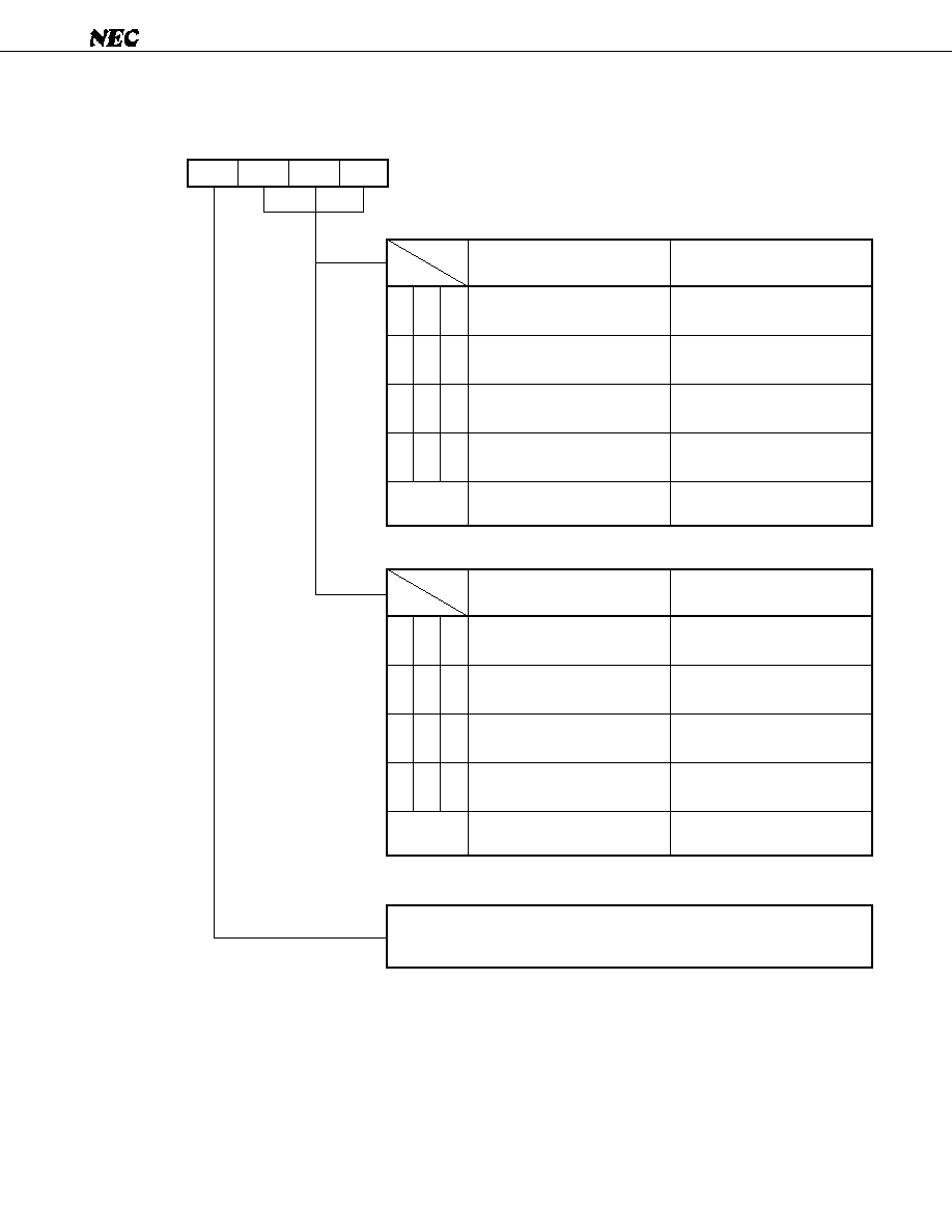
65
µ
PD75517(A)
Fig. 4-21 Format of the Basic Interval Timer Mode Register
Address
F85H
3
2
1
0
BTM3
BTM2
BTM1
BTM0
Symbol
BTM
Input clock specification
0
0
1
0
1
1
0
1
0
1
1
1
When "1" is written to this bit, the basic interval timer operation starts (the counter
and the interrupt request flag are cleared).
When the operation starts, this bit is automatically reset to 0.
Basic interval timer start control bit
Interrupt interval time
(wait time for releasing standby)
f
X
/2
12
(1.02 kHz)
f
X
/2
9
(8.18 kHz)
f
X
/2
7
(32.768 kHz)
f
X
/2
5
(131 kHz)
2
20
/f
X
(250 ms)
2
17
/f
X
(31.3 ms)
2
15
/f
X
(7.82 ms)
2
13
/f
X
(1.95 ms)
Not to be set
≠
Input clock specification
0
0
1
0
1
1
0
1
0
1
1
1
Other
setting
Interrupt interval time
(wait time for releasing standby)
f
X
/2
12
(1.46 kHz)
f
X
/2
9
(11.7 kHz)
f
X
/2
7
(46.9 kHz)
f
X
/2
5
(188 kHz)
2
20
/f
X
(175 ms)
2
17
/f
X
(21.8 ms)
2
15
/f
X
(5.46 ms)
2
13
/f
X
(1.37 ms)
Not to be set
≠
(Frequency when f
X
= 6.0 MHz)
(Frequency when f
X
= 4.19 MHz)
Other
setting

66
µ
PD75517(A)
(4) Operation of the basic interval timer
The basic interval timer (BT) is always incremented by the clock supplied from the clock generator, and
when it overflows, the interrupt request flag (IRQBT) is set. The count operation of BT cannot be stopped.
One of four interrupt generation intervals can be selected by setting BTM. (See Fig. 4-21.)
The basic interval timer and the interrupt request flag can be cleared by setting bit 3 of BTM to 1 (instruction
for starting as an interval timer).
The count status can be read by using an 8-bit manipulation instruction. No data can be loaded to the
timer.
Caution
When reading the count value of the basic interval timer, execute a read instruction twice so
that unstable data which has been counted will not be read. If the two read values are
reasonable, use the second one as the result. If the two read values are far apart, retry from
the beginning.
Example
Read the count value of BT.
SET1 MBE
SEL
MB15
MOV HL, #BT
; Set the BT address in HL
LOOP:
MOV XA, @HL
; First read
MOV BC, XA
MOV XA, @HL
; Second read
SKE
XA, BC
BR
LOOP
To allow the system clock to stabilize after releasing the STOP mode, a wait function is available which
stops the operation of the CPU until the basic interval timer overflows.
The wait time after generation of a RESET signal is fixed. On the other hand, a wait time can be selected
by setting BTM when releasing the STOP mode with an interrupt occurrence. In this case, the wait times
are the same as the interval times shown in Fig. 4-21. BTM must be set before the STOP mode is set. (For
details, see Chapter 6.)

67
µ
PD75517(A)
4.5 CLOCK TIMER
(1) Clock timer
The
µ
PD75517(A) contains one channel for a clock timer. Fig. 4-22 shows the configuration of the timer.
(2) Clock timer functions
(a) The clock timer sets the test flag (IRQW) every 0.5 seconds.
The standby mode can be released with IRQW.
(b) Either the main system clock or subsystem clock can produce 0.5-second intervals.
(c) The fast-forward mode produces an interval 128 times faster (3.91 ms), which is useful for program
debugging and testing.
(d) A fixed frequency (2.048 kHz) can be output to the P23/BUZ pin, so that it can be used for sounding
the buzzer and system clock frequency trimming.
(e) The frequency divider can be cleared, so the clock can start from zero seconds.
Caution
When the main system clock operates at 6.0 MHz, a time interval of 0.5 s cannot be produced.
Before producing this time interval, the main system clock must be changed to the subsystem
clock.
Fig. 4-22 Block Diagram of the Clock Timer
Remark The values in parentheses are for f
X
= 4.194304 MHz and f
XT
= 32.768 kHz
P23/BUZ
Internal bus
8
From the
clock
generator
f
X
128
(32.768 kHz)
f
XT
(32.768 kHz)
Selector
Frequency divider
Selector
INTW
IRQW
set signal
2 Hz
0.5 sec
WM7
0
0
0
0
WM2
WM1
WM0
P23 output
latch
Bit 2 of PMGB
PORT2.3
Output buffer
Clear signal
f
W
(32.768 kHz)
Port 2 input/
output mode
WM
f
W
2
7
(256 Hz: 3.91 ms)
f
W
2
14
f
W
16
(2.048 kHz)

68
µ
PD75517(A)
(3) Clock mode register
The clock mode register (WM) is an 8-bit register that controls the clock timer, and that is set with an
8-bit memory manipulation instruction. Fig. 4-23 shows the format.
The generation of a RESET signal clears all bits to 0.
Example
Use the main system clock (4.19 MHz) for setting time, and enable buzzer output.
CLR1
MBE
MOV
XA, #84H
MOV
WM, XA
; Set WM
Fig. 4-23 Format of the Clock Mode Register
Address
F98H
Symbol
WM
0
WM0
1
WM1
2
WM2
3
0
4
0
5
0
6
0
7
WM7
WM0
0
1
Selects divided system clock output:
Selects subsystem clock: f
XT
Count clock (fW) selection bit
WM1
0
1
Normal clock mode ( : sets IRQW at 0.5 s)
Advanced clock mode ( : sets IRQW at 3.91 ms)
Operation mode selection bit
WM2
0
1
Disables clock operation (clears the frequency dividing circuit)
Enables clock operation
Clock operation enable/disable bit
f
W
2
14
f
X
128
f
W
2
7
WM7
0
1
Disables BUZ output
Enables BUZ output
BUZ output enable/disable bit

69
µ
PD75517(A)
4.6 TIMER/EVENT COUNTER
(1) Configuration of the timer/event counter
The
µ
PD75517(A) contains one channel of timer/event counter, which is configured as shown in Fig.
4-24.
(2) Functions of the timer/event counter
The timer/event counter has the following functions.
(a) Programmable interval timer operation
(b) Output of a square wave at a given frequency to the PTO0 pin
(c) Event counter operation
(d) Frequency divider operation that divides TI0 pin input by N and outputs the result to the PTO0 pin
(e) Supply of serial shift clock signal to a serial interface circuit
(f)
Function of reading the state of counting
(3) Timer/event counter mode register (TM0) and timer/event counter output enable flag (TOE0)
The timer/event counter mode register (TM0) is an 8-bit register for controlling the timer/event counter.
Fig. 4-25 shows its format.
An 8-bit memory manipulation instruction is used to set the timer/event counter mode register.
Bit 3 is the timer start bit, and can be set independently of the other bits. Bit 3 is automatically reset to
0 when the timer starts operation.
Examples 1.
The timer is started in the interval timer mode with CP = 4.09 kHz.
SEL
MB15
; or CLR1 MBE
MOV
XA, #01001100B
MOV
TM0, XA
; TM0
4CH
2.
The timer is restarted according to the setting of the timer/event counter mode register.
SEL
MB15
; or CLR1 MBE
SET1
TM0.3
; TM0.bit3
1
The generation of a RESET signal clears all bits to 0.
The timer/event counter output enable flag (TOE0) enables or disables output of the timer out F/F (TOUT
F/F) status to the PTO0 pin.
The timer out F/F (TOUT F/F) is inverted by a match signal transmitted from the comparator.
The timer out F/F is reset when an instruction sets bit 3 of the timer mode register (TM0).
The generation of a RESET signal clears the TOE0 and TOUT F/F to 0.
70
µ
PD75517(A)
Fig. 4-24 Block Diagram of the Timer/Event Counter
Count register (8)
P13/
TI0
Note Instruction execution
MPX
Timer operation start signal
8
8
8
From the
clock
generator
Internal bus
TM06 TM05 TM04 TM03 TM02
PORT1.3
(See Fig. 4-11.)
Comparator (8)
Modulo register (8)
TO enable
flag
P20
output
latch
signal
Port 2
input/
output
mode
Clear signal
T0
TMOD0
Bit 2 of PGMB
P20/PTO0
Output
buffer
Reset
RESET
IRQT0 clear
signal
TOUT
F/F
TM0
SET1
Note
Input buffer
IRQT0
set signal
INTT0
PORT2.0
TOE0
To serial
interface
CP
Match
8
8

71
µ
PD75517(A)
Fig. 4-25 Format of the Timer/Event Counter Mode Register
Address
FA0H
7
6
5
4
--
Symbol
TM0
TM04
TM06
--
--
TM02
TM03
TM05
3
2
1
0
Operation mode
0
1
Count operation
Halts (retains
the contents of
counting)
Count
operation
Timer start specification bit
When "1" is written to this bit, the counter and the IRQT0
flag are cleared. Count operation starts if bit 2 has been
set to 1.
Count pulse (CP) select bit
(Frequency when f
X
= 6.0 MHz)
TM05
0
0
0
0
1
1
TM06
0
0
1
1
1
1
TM04
0
1
0
1
0
1
Count pulse (CP)
TI0 input rising edge
TI0 input falling edge
f
X
/2
10
(5.86 kHz)
f
X
/2
8
(23.4 kHz)
f
X
/2
6
(93.8 kHz)
f
X
/2
4
(375 kHz)
Other setting
Not to be set
TM05
0
0
0
0
1
1
TM06
0
0
1
1
1
1
TM04
0
1
0
1
0
1
Count pulse (CP)
TI0 input rising edge
TI0 input falling edge
f
X
/2
10
(4.09 kHz)
f
X
/2
8
(16.4 kHz)
f
X
/2
6
(65.5 kHz)
f
X
/2
4
(262 kHz)
Other setting
Not to be set
(Frequency when f
X
= 4.19 MHz)

72
µ
PD75517(A)
Fig. 4-26 Format of the Timer/Event Counter Output Enable Flag
(4) Operation mode of the timer/event counter
The timer/event counter operates in the count operation disable mode or in the count operation mode,
depending on the setting of the mode register.
The following operations are possible, regardless of the setting of the mode register:
1
P13/TI0 pin signal input and test
2
Output of the timer out F/F status to the PTO0
3
Setting of the modulo register (TMOD0)
4
Reading from the count register (T0)
5
Setting, clearing, and testing of the interrupt request flag (IRQT0)
(a) Count operation disable mode
This mode is set when bit 2 of TM0 is set to 0. In this mode, count operation is not performed because
count pulse (CP) supply to the count register is stopped.
Address
FA2H
TOE0
3
Timer/event counter output enable flag (W)
Disables
Enables
0
1

73
µ
PD75517(A)
(b) Count operation mode
This mode is set when bit 2 of TM0 is set to 1. In this mode, a count pulse signal selected with bits
4 to 6 is supplied to the count register for count operation as shown in Fig. 4-28.
Timer operation is usually started in the following steps:
1
A count value is set in the modulo register (TMOD0).
2
An operation mode, count clock, and start instruction are set in the mode register (TM0).
An 8-bit data transfer instruction is used to set the modulo register.
Caution A value other than 0 must be set in the modulo register.
Example The value 3FH is set in the modulo register of channel 0.
SEL
MB15
; or CLR1 MBE
MOV
XA, #3FH
MOV
TMOD0, XA
If the value set in the modulo register matches the contents of the count register, the match signal
is generated. Then, the TOUT F/F is inverted, and the counter register is cleared.
The interval time of the generation of the match signal is calculated as follows:
(Set value of the modulo register + 1)
◊
resolution
The resolution is 1/count pulse frequency.
Table 4-6 indicates the resolution and maximum set time (when FFH is set in the modulo register),
depending on a selected count pulse.
Table 4-6 Resolution and Maximum Set Time
(When f
X
= 6.0 MHz)
(When f
X
= 4.19 MHz)
Mode register
TM04
0
1
0
1
TM06
1
1
1
1
TM05
0
0
1
1
Maximum set time
43.7 ms
10.9 ms
2.73 ms
683
µ
s
Resolution
171
µ
s
42.7
µ
s
10.7
µ
s
2.67
µ
s
Timer channel 0
Mode register
TM04
0
1
0
1
TM06
1
1
1
1
TM05
0
0
1
1
Maximum set time
62.5 ms
15.6 ms
3.91 ms
977
µ
s
Resolution
244
µ
s
61.1
µ
s
15.3
µ
s
3.81
µ
s
Timer channel 0

74
µ
PD75517(A)
Fig. 4-27 Operation in the Count Operation Mode
Fig. 4-28 Timing of Count Operation
TI0
Count register
(T0)
Internal
clock
Comparator
Modulo register
(TMOD0)
TOUT
F/F
Clear
signal
Match
To CSI
(Only for channel 0)
PTO0
INTT0
(IRQT0 set signal)
CP
MPX
Match
Match
Timer start specification
Reset
0
1
2
n ≠ 1
n
0
1
2
n ≠ 1
n
0
1
2
3
4
n
Count register
Modulo register
Count pulse
(CP)
TOUT F/F

75
µ
PD75517(A)
4.7 TIMER/PULSE GENERATOR
(1) Timer/pulse generator functions
The
µ
PD75517(A) contains one channel for a timer/pulse generator that can be used as a timer or a pulse
generator. It has the following functions:
(a) Functions available when the timer/pulse generator is used in the timer mode
∑
8-bit interval timer operation using one of five clock sources (occurrence of IRQTPG)
∑
Square wave output to the PPO pin
(b) Functions available when the timer/pulse generator is used in the PWM pulse generation mode
∑
PWM pulse output to the PPO pin with an accuracy of 14 bits (applicable for electronic tuning when
used as an D/A converter)
∑
Generation of interrupts at regular intervals (2
15
/f
X
)
Note
Note 2
15
/f
X
= 5.46 ms (at 6.0 MHz) or 7.81 ms (at 4.19 MHz)
If pulse output is unnecessary, the PPO pin can be used as a 1-bit output port.
Caution
If the timer/pulse generator is operating when the STOP mode is set, it may malfunction. So
the timer/pulse generator must be disabled with the mode register in advance.

76
µ
PD75517(A)
(2) Timer/pulse generator mode register (TPGM)
The timer/pulse generator mode register (TPGM) is an 8-bit register that controls operation of the timer/
pulse generator. Fig. 4-29 shows the format of the register.
TPGM is set with an 8-bit memory manipulation instruction.
Bit 3 enables or disables the transfer (reloading) of the timer/pulse generator modulo register (MODH and
MODL) contents to the modulo latch. Bit 3 can be manipulated independently of the other bits.
By setting TPGM1 to 0, timer/pulse generator operation can be stopped to decrease current consumption.
The generation of a RESET signal clears all bits to 0.
Fig. 4-29 Format of Timer/Pulse Generator Mode Register
7
6
5
4
3
2
1
0
TPGM7
--
TPGM5 TPGM4 TPGM3
0
TPGM1 TPGM0
Address
F90H
Symbol
TPGM
0
1
TPGM0
Select PWM pulse generation mode
Select timer mode
Timer/pulse generator operation mode selection bit
0
1
TPGM1
Disable timer/pulse generator operation
Enable timer/pulse generator operation
Timer/pulse generator operation enable/disable bit
0
1
TPGM3
Disable reloading of modulo register
Enable reloading of modulo register
Modulo register reload enable/disable bit
0
1
TPGM4
Output 0 to PPO output latch
Output 1 to PPO output latch
PPO output latch data
0
1
TPGM5
Static output on PPO pin
Pulse output (square wave/PWM) on PPO pin
PPO pin output selection bit static/pulse
0
1
TPGM7
Disable output on PPO pin (high-impedance)
Enable output on PPO pin
PPO pin output enable/disable bit

77
µ
PD75517(A)
(3) Configuration and operation when the timer/pulse generator is used in the timer mode
Fig. 4-30 shows the configuration when the timer/pulse generator is used in the timer mode.
The timer mode is selected by setting bit 0 of TPGM to 1. In the timer mode, TPGM3 must be set to 1,
allowing a modulo register to be reloaded at any time.
In the timer mode, a prescaler is selected with the modulo register L (MODL), and a frequency or interrupt
interval value is set in the modulo register H (MODH). The timer starts when the TPGM1 is changed from
0 to 1.
Fig. 4-31 shows the operation timing for the MODH setting, and Table 4-7 shows the setting of a frequency
or interrupt interval.
The output to the PPO pin can be switched between the square wave output and static output. To output
a square wave, set TPGM5 and TPGM7 to 1.
Fig. 4-30 Block Diagram of the Timer/Pulse Generator (Timer Mode)
Internal bus
Modulo register L (8)
MODL
8
Modulo register H (8)
MODH
8
TPGM3
(Set to 1)
f
X
TPGM1
1/2
Frequency
divider
Prescaler select latch (5)
Modulo latch H (8)
Comparator (8)
Count register (8)
8
Clear
CP
Clear
Set
T F/F
Selec-
tor
TPGM4
TPGM5
TPGM7
INTTPG
IRQTPG
set signal
Output
buffer
PPO
Match
8

78
µ
PD75517(A)
Example
Set IRQTPG every 1.95 ms, and set the output high on the PPO pin.
CLR1
MBE
; or SEL MB15
MOV
XA, #00100000B
MOV
MODL, XA
MOV
XA, #0FFH
MOV
MODH, XA
MOV
XA, #10011011B
MOV
TPGM, XA
; Timer start, PPO
1
Caution
When the timer operating in the timer operation mode is stopped, IRQTPG may be set because
T F/F is set. So, the timer must be stopped with an interrupt being disabled, then IRQTPG must
be cleared.
Example
DI
CLR1
MBE
MOV
XA, #0
MOV
TPGM, XA
CLR1
IRQTPG
EI

79
µ
PD75517(A)
Fig. 4-31 Timer Mode Operation Timing
Table 4-7 Modulo Register Settings
(When f
X
= 6.0 MHz)
(When f
X
= 4.19 MHz)
Cautions 1. A value other than the above cannot be set in MODL. Bits 0, 1, and 7 must be set to 0.
2. N is the set value of MODH. 0 must not be set for N. Be sure to set a value from 1 to 255
for N.
N
0
1
2
N≠1
N
0
0
N
N
0
CP
T F/F
(PPO)
Count
register
MODH
Generate IRQTPG.
Set TPGM1.
6
0
0
0
0
1
5
0
0
0
1
0
4
0
0
1
0
0
3
0
1
0
0
0
2
1
0
0
0
0
MODL bits 2-6
Interrupt generation interval
(f
X
= 6.0 MHz)
Square wave output frequency
(f
X
= 6.0 MHz)
256 (N+1)/f
X
= 85.3
µ
s - 10.9 ms
128 (N+1)/f
X
= 42.7
µ
s - 5.46 ms
64 (N+1)/f
X
= 21.3
µ
s - 2.73 ms
32 (N+1)/f
X
= 10.7
µ
s - 1.37 ms
16 (N+1)/f
X
= 5.33
µ
s - 683
µ
s
f
X
/256 (N+1) = 91.6 Hz - 11.7 kHz
f
X
/128 (N+1) = 183 Hz - 23.4 kHz
f
X
/64 (N+1) = 366 Hz - 46.9 kHz
f
X
/32 (N+1) = 732 Hz - 93.8 kHz
f
X
/16 (N+1) = 1465 Hz - 188 kHz
6
0
0
0
0
1
5
0
0
0
1
0
4
0
0
1
0
0
3
0
1
0
0
0
2
1
0
0
0
0
MODL bits 2-6
Interrupt generation interval
(f
X
= 4.19 MHz)
Square wave output frequency
(f
X
= 4.19 MHz)
256 (N+1)/f
X
= 122
µ
s - 15.6 ms
128 (N+1)/f
X
= 61.0
µ
s - 7.81 ms
64 (N+1)/f
X
= 30.5
µ
s - 3.91 ms
32 (N+1)/f
X
= 15.3
µ
s - 1.95 ms
16 (N+1)/f
X
= 7.63
µ
s - 977
µ
s
f
X
/256 (N+1) =64 Hz - 8 kHz
f
X
/128 (N+1) = 128 Hz - 16 kHz
f
X
/64 (N+1) = 256 Hz - 32 kHz
f
X
/32 (N+1) = 512 Hz - 65 kHz
f
X
/16 (N+1) = 1024 Hz - 131 kHz

80
µ
PD75517(A)
(4) Configuration and operation when the timer/pulse generator is used in the PWM pulse generation mode
Fig. 4-32 shows the configuration when the timer/pulse generator is used in the PWM pulse generation
mode.
The PWM pulse generation mode is selected by setting TPGM0 to 0. TPGM5 and TPGM7 are set to 1 to
enable pulse output. In the PWM mode, the PWM pulse signal can be output on the PPO pin, and IRQTPG
can be set at intervals of a fixed time period (2
15
/f
X
= 5.46 ms: at 6.0 MHz or 2
15
/f
X
= 7.81 ms: At 4.19 MHz).
PWM pulses output by the
µ
PD75517(A) are active-low and have an accuracy of 14 bits. This pulse signal
is applicable for electronic tuning and control of a DC motor when it is integrated by an external low-pass
filter and is converted to analog voltage. (See Fig. 4-33.)
The PWM pulse signal is generated by combining the basic period determined by 2
10
/f
X
and the secondary
period by 2
15
/f
X
so that the time constant of the external low-pass filter can be decreased.
Table 4-8 lists the basic and secondary periods by oscillator frequency.
Table 4-8 Basic and Secondary Periods
The low-level width of a PWM pulse depends on the 14-bit modulo latch value. The upper 8 bits of the
modulo latch are transferred from the 8 bits of MODH, and the lower 6 bits of the latch are transferred
from the upper 6 bits of MODL.
When the PWM pulse signal is converted to analog form, the voltage level of the analog output is obtained
as follows:
Value of modulo latch
V
AN
= V
ref
◊
2
14
V
ref
: Reference voltage of external switching circuitry
To prevent an incorrect PWM pulse from being output by unstable modulo latch data being rewritten, the
µ
PD75517(A) allows correct data to be written in MODH and MODL beforehand with 8-bit manipulation
instructions, then in the 14-bit data which is to be transferred to the modulo latch at one time. This transfer
is referred to as reloading, and it is controlled by TPGM3. If TPGM3 is 0, reloading is disabled, and if it
is 1, reloading is enabled. Follow the procedure below to rewrite the modulo latch contents:
(i)
Clear TPGM3 to disable reloading.
(ii)
Change the MODH and MODL contents.
(iii)
Set TPGM3 to enable reloading.
Cautions 1.
If the modulo register H (MODH) is set to 0, the PWM pulse generator cannot function
normally. So be sure to set MODH to a value from 1 to 255.
2.
If the lower 2 bits of the modulo register L (MODL) is read, the read result is unpredictable.
3.
If the modulo latch is changed in a shorter period than the PWM pulse basic period
2
10
/f
X
(171
µ
s: at 6.0 MHz or 244
µ
s: at 4.19 MHz), PWM pulses do not change.
f
X
= 6.0 MHz
171
µ
s
5.46 ms
f
X
= 4.19 MHz
244
µ
s
7.81 ms
Basic period (2
10
/f
X
)
Secondary period (2
15
/f
X
)

81
µ
PD75517(A)
Example
Decrease analog output voltage to the lowest level, then increase it to the highest level.
CLR1
MBE
MOV
XA, #01H
MOV
MODH, XA
; MODH
01
MOV
XA, #00H
MOV
MODL, XA
; MODL
00
MOV
XA, #10101010B
MOV
TPGM, XA
; Enable PWM pulse output
∑
∑
∑
∑
∑
∑
∑
∑
∑
CLR1
TPGM.3
; Disable reloading
MOV
XA, #0FFH
MOV
MODH, XA
MOV
XA, #0FCH
MOV
MODL, XA
SET1
TPGM.3
; Enable reloading
(5) Static output to the PPO pin
When pulse output is unnecessary, the PPO pin can be used as normal static output. In this case, the output
data is set in TPGM4 with TPGM5 being set to 0 and TPGM7 to 1.

82
µ
PD75517(A)
Fig. 4-32 Block Diagram of the Timer/Pulse Generator (PWM Pulse Generation Mode)
Note
At 4.19 MHz: 2
15
/f
X
= 7.81 ms
Fig. 4-33 Sample Configuration of D/A Conversion Using
µ
PD75517(A)
Switching
circuit
Low-pass
filter
PWM
PPO
signal
V
AX
(analog voltage)
V
ref
PD75517 (A)
µ
Internal bus
Modulo register H (8)
MODH
8
TPGM3
f
X
TPGM1
1/2
PWM pulse generator
Selec-
tor
TPGM5
TPGM7
Output
buffer
PPO
Modulo register L (8)
MODL
8
Modulo latch (14)
MODH (8)
MODL
7-2
(6)
INTTPG
(IRQTPG set signal)
(2
15
/f
X
= 5.46 ms: 6.0 MHz)
Note
Frequency
divider

83
µ
PD75517(A)
4.8 SERIAL INTERFACE (CHANNEL 0)
The
µ
PD75517(A) has two channels of serial interface: Channel 0 and channel 1. Table 4-9 lists the
differences between channel 0 and channel 1.
Table 4-9 Differences between Channel 0 and Channel 1
Channel 1
Channel 0
Serial transfer mode, function
f
X
/2
4
, f
X
/2
3
, TOUT F/F, external clock
Start bit switchable: MSB/LSB
Serial transfer end interrupt request
flag (IRQCSI0)
Available
3-wire serial I/O
2-wire serial I/O
Serial bus interface (SBI)
Clock selection
Transfer method
Transfer end flag
f
X
/2
4
, f
X
/2
3
, external clock
Start bit: MSB
Serial transfer end flag (EOT)
Not available

84
µ
PD75517(A)
4.8.1 Serial Interface (Channel 0) Functions
The clock synchronous 8-bit serial interface is contained in the
µ
PD75517(A) and has four modes.
The functions of the four modes are outlined below.
∑
Operation halt mode
This mode is used when serial transfer is not performed. This mode reduces power consumption.
∑
Three-wire serial I/O mode
In this mode, 8-bit data is transferred through three lines: Serial clock (SCK0), serial output (SO0), and serial
input (SI0).
The three-wire serial I/O mode allows full-duplex transmission, so data transfer can be performed at higher
speed.
The user can choose 8-bit data transfer starting with the MSB or LSB, so devices starting with either the
MSB or LSB can be connected.
The three-wire serial I/O mode enables connections to be made with the 75X series, 78K series, and many
other types of peripheral I/O devices.
∑
Two-wire serial I/O mode
In this mode, 8-bit data is transferred through two lines: Serial clock (SCK0) and serial data bus (SB0 or
SB1). By controlling output levels on the two lines by software, communication with multiple devices is
enabled.
The output levels of SCK0 and SB0 (or SB1) can be controlled by software, so the user can match an arbitrary
transfer format. This means that a line that has been required for handshaking to connect multiple lines
can be eliminated for more efficient I/O port utilization.
∑
Serial bus interface (SBI) mode
In this mode, communication with multiple devices can be performed using two lines: Serial clock (SCK0)
and serial data bus (SB0 or SB1).
This mode conforms to the NEC serial bus format.
In this mode, the transmitter can output, on the serial data bus, an address for selecting a device subject
to serial communication, commands directed to the remote device, and data. The receiver can identify an
address, commands, and data from received data by hardware. This function enables more efficient I/O
port utilization as in the case of the two-wire serial I/O mode. In addition, this function can simplify the
serial interface control portion of an application program.
4.8.2 Configuration of Serial Interface (Channel 0)
Fig. 4-34 shows the block diagram of the serial interface (channel 0).

85
µ
PD75517(A)
Fig. 4-34 Block diagram of the Serial Interface (Channel 0)
Internal bus
8
8
8
8/4
P03/SI/SB1
P02/SO/SB0
P01/SCK0
(8)
f
X
/2
3
f
X
/2
4
f
X
/2
6
TOUT F/F
(from timer/event counter)
CSIM0
RELD
CMDD
ACKD
ACKT
ACKE
BSYE
RELT
CMDT
D
Q
SET CLR
(8)
(8)
SBIC
Bit
test
Slave address register (SVA)
Address comparator
Shift register (SIO0)
Coincidence
signal
Bit manipulation
SO0 latch
Bit test
Selec-
tor
Selec-
tor
Busy/
acknowledge
output circuit
Bus release/
command/
acknowledge
detection circuit
Serial clock
counter
Serial clock
control circuit
INTCSI0
control circuit
IRQCSI0
set signal
INTCSI0
P01
output latch
MPX
External SCK0

86
µ
PD75517(A)
4.8.3 Register Functions
(1) Serial operation mode register 0 (CSIM0)
Fig. 4-35 shows the format of serial operation mode register 0 (CSIM0).
CSIM0 is an 8-bit register which specifies a serial interface (channel 0) operation mode, serial clock, wake-
up function, and so forth.
CSIM0 is manipulated using an 8-bit memory manipulation instruction. The higher three bits can be
manipulated bit by bit. Each bit can be manipulated using its name.
Each bit may or may not allow read and/or write operation. (See Fig. 4-35.) Bit 6 allows bit test operation
only; any data written to this bit is invalid.
When the RESET signal is input, this register is set to 00H.
Fig. 4-35 Format of Serial Operation Mode Register 0 (CSIM0) (1/3)
Remark
(R) : Read only
(W) : Write only
CSIE0
COI
WUP
CSIM04 CSIM03
CSIM01
CSIM02
CSIM00
7
6
5
4
3
1
2
0
Address
CSIM0
Symbol
Serial clock selection bit (W)
FE0H
Serial interface operation enable/disable specification bit (W)
Serial interface operation mode selection bit (W)
Wake-up function specification bit (W)
Signal from address comparator (R)

87
µ
PD75517(A)
Fig. 4-35 Format of Serial Operation Mode Register 0 (CSIM0) (2/3)
Serial clock selection bit (W)
Note
The values in parentheses are for f
X
= 4.19 MHz or 6.0 MHz.
Serial interface operation mode selection bit (W)
Remark
◊
: Don't care
Wake-up function specification bit (W)
Caution When WUP = 1 is set during BUSY signal output, BUSY is not released. In the SBI mode, the
BUSY signal is output until the next falling edge of the serial clock (SCK0) appears after release
of BUSY is directed. Before setting WUP = 1, be sure to confirm that the SB0 (or SB1) pin is high
after releasing BUSY.
Serial clock
SBI mode
2-wire serial I/O mode
3-wire serial I/O mode
External clock applied to SCK0 pin
Time/event counter output (T0)
f
X
/2
4
(262 kHz or 375 kHz)
Note
f
X
/2
3
(524 kHz or 750 kHz)
Note
CSIM01
CSIM00
f
X
/2
6
(65.5 kHz or
93.8 kHz)
Note
SCK0 pin mode
0
0
1
1
0
1
0
1
Input
Output
Operation mode
CSIM04
CSIM03
CSIM02
Bit sequence of
shift register 0
SIO0
7-0
XA
(Transfer starting
with MSB)
SIO0
0-7
XA
(Transfer starting
with LSB)
SIO0
7-0
XA
(Transfer starting
with MSB)
SIO0
7-0
XA
(Transfer starting
with MSB)
SI0 pin function
0
1
1
0
1
0
1
◊
0
1
0
1
SO0 pin function
SO0/P02
(CMOS output)
SB0/P02
(N-ch open-drain
input/output)
P02 input
SB0/P02
(N-ch open-drain
input/output)
P02 input
SI0/P03
(Input)
P03 input
SB1/P03
(N-ch open-drain
input/output)
P03 input
SB1/P03
(N-ch open-drain
input/output)
3-wire serial I/O
mode
SBI mode
2-wire serial I/O
mode
Sets IRQCSI0 each time serial transfer is completed in each mode.
Used in the SBI mode only to set IRQCSI0 only when an address received after bus release matches
the data in the slave address register (wake-up state). SB0/SB1 goes to high-impedance state.
WUP
0
1

88
µ
PD75517(A)
Fig. 4-35 Format of Serial Operation Mode Register 0 (CSIM0) (3/3)
Signal from address comparator (R)
Note
COI can be read only before serial transfer is started or after serial transfer is completed. An
undefined value may be read during transfer.
COI data written by an 8-bit manipulation instruction is ignored.
Serial interface operation enable/disable specification bit (W)
Remarks 1. Each mode can be selected by setting CSIE0, CSIM03, and CSIM02.
2. The P01/SCK0 pin assumes the following state according to the setting of CSIE0, CSIM01, and
CSIM00:
Condition for being set (COI = 1)
When the slave address register (SVA) matches the
data of the shift register
COI
Note
Condition for being cleared (COI = 0)
When the slave address register (SVA) does not match
the data of the shift register
0
1
Serial clock counter
Cleared
Count operation
IRQCSI0 flag
Held
Can be set.
SO0/SB0, SI0/SB1 pin
Used only for port 0
Used in each mode as
well as for port 0
CSIE0
Shift register operation
Shift operation disabled
Shift operation enabled
CSIE0
0
1
1
1
CSIM03
◊
0
1
1
CSIM02
◊
◊
0
1
Operation mode
Operation halt mode
Three-wire serial I/O mode
SBI mode
Two-wire serial I/O mode
CSIE0
0
1
0
0
0
1
1
1
CSIM01
0
0
1
0
1
1
0
1
CSIM00
0
0
0
1
1
0
1
1
P01/SCK0 pin state
Input port
High impedance
High level output
Serial clock output (High level output)

89
µ
PD75517(A)
Remarks 3. When clearing CSIE0 during serial transfer, use the following procedure:
1
Disable interrupts by clearing the interrupt enable flag.
2
Clear CSIE0.
3
Clear the interrupt request flag.
Examples 1.
f
X
/2
4
is selected as the serial clock, serial interrupt IRQCSI0, is generated each time serial
transfer is completed, and serial transfer is performed in the SBI mode with the SB0 pin used
as the serial data bus.
SEL
MB15
; or CLR1 MBE
MOV XA, #10001010B
MOV CSIM0, XA
; CSIM0
10001010B
2.
Serial transfer dependent on the contents of CSIM0 is enabled.
SEL
MB15
; or CLR1 MBE
SET1 CSIE0

90
µ
PD75517(A)
(2) Serial bus interface control register (SBIC)
Fig. 4-36 shows the format of the serial bus interface control register (SBIC).
SBIC is an 8-bit register consisting of bits for controlling the serial bus and flags for indicating the states
of input data from the serial bus. SBIC is used mainly in the SBI mode.
SBIC is manipulated using a bit manipulation instruction. SBIC cannot be manipulated using a 4-bit or
8-bit memory manipulation instruction.
Each bit may or may not allow read and/or write operation. (See Fig. 4-36.)
When the RESET signal is input, this register is set to 00H.
Caution
Only the following bits can be used in the three-wire and two-wire serial I/O modes:
∑
Bus release trigger bit (RELT):
Sets the SO0 latch.
∑
Command trigger bit (CMDT):
Clears the SO0 latch.
Fig. 4-36 Format of Serial Bus Interface Control Register (SBIC) (1/3)
Remark
(R)
: Read only
(W)
: Write only
(R/W) : Read/write
BSYE
ACKD
ACKE
ACKT
CMDD
CMDT
RELD
RELT
7
6
5
4
3
1
2
0
Address
SBIC
Symbol
Bus release trigger bit (W)
FE2H
Command trigger bit (W)
Bus release detection flag (R)
Command detection flag (R)
Acknowledge trigger bit (W)
Acknowledge enable bit (R/ W)
Acknowledge detection flag (R)
Busy enable bit (R/ W)

91
µ
PD75517(A)
Fig. 4-36 Format of Serial Bus Interface Control Register (SBIC) (2/3)
Bus release trigger bit (W)
Caution Never clear SB0 (or SB1) during serial transfer. Be sure to clear SB0 (or SB1) before or after serial
transfer.
Command trigger bit (W)
Caution Never clear SB0 (or SB1) during serial transfer. Be sure to clear SB0 (or SB1) before or after serial
transfer.
Bus release detection flag (R)
Command detection flag (R)
Acknowledge trigger bit (W)
Cautions 1.
Never set ACKT before or during serial transfer.
2.
ACKT cannot be cleared by software.
3.
Before setting ACKT, set ACKE = 0.
Acknowledge enable bit (R/W)
Control bit for bus release signal (REL) trigger output.
By setting RELT = 1, the SO0 latch is set to 1. Then the RELT bit is automatically cleared to 0.
RELT
Condition for being set (RELD = 1)
The bus release signal (REL) is detected.
RELD
Condition for being cleared (RELD = 0)
1
The transfer start instruction is executed.
2
The RESET signal is entered.
3
CSIE0 = 0 (See Fig. 4-35.)
4
SVA does not match SIO0 when an address is
received.
Control bit for command signal (CMD) trigger output.
By setting CMDT = 1, the SO0 latch is cleared to 0. Then the CMDT bit is automatically cleared to 0.
CMDT
Condition for being set (CMDD = 1)
The command signal (CMD) is detected.
CMDD
Condition for being cleared (CMDD = 0)
1
The transfer start instruction is executed.
2
The bus release signal (REL) is detected.
3
The RESET signal is entered.
4
CSIE0 = 0 (See Fig. 4-35.)
When set after transfer, ACK is output in phase with the next SCK0. After ACK signal output, this bit is auto-
matically cleared to 0.
ACKT
Disables automatic output of the acknowledge signal (ACK). (Output by ACKT is possible.)
ACKE
0
1
When set before transfer
When set after transfer
ACK is output in phase with the 9th clock of SCK0.
ACK is output in phase with SCK0 immediately following set
instruction execution.

92
µ
PD75517(A)
Fig. 4-36 Format of Serial Bus Interface Control Register (SBIC) (3/3)
Acknowledge detection flag (R)
Busy enable bit (R/W)
Examples 1. A command signal is output.
SEL
MB15
; or CLR1 MBE
SET1
CMDT
2. RELD and CMDD are tested to identify the types of received data and the types of processing
accordingly.
By setting WUP = 1, this interrupt routine is processed only when an address match is found.
SEL
MB15
SKF
RELD
; RELD test
BR
!ADRS
SKT
CMDD
; CMDD test
BR
!DATA
CMD
:
∑ ∑ ∑ ∑ ∑ ∑ ∑ ∑ ∑
; Command analysis
DATA :
∑ ∑ ∑ ∑ ∑ ∑ ∑ ∑ ∑
; Data processing
ADRS :
∑ ∑ ∑ ∑ ∑ ∑ ∑ ∑ ∑
; Address decode
Condition for being set (ACKD = 1)
The acknowledge signal (ACK) is detected (in phase
with the rising edge of SCK0).
ACKD
Condition for being cleared (ACKD = 0)
1
The transfer start instruction is executed.
2
The RESET signal is entered.
1
The busy signal is automatically disabled.
2
Busy signal output is stopped in phase with the falling edge of SCK0 immediately after clear
instruction execution.
The busy signal is output after the acknowledge signal in phase with the falling edge of SCK0.
0
1
BSYE

93
µ
PD75517(A)
(3) Shift register (SIO0)
Fig. 4-37 shows the configuration of peripheral hardware of shift register 0. SIO0 is an 8-bit register which
performs parallel-serial conversion and serial transfer (shift) operation in phase with the serial clock.
Serial transfer is started by writing data to SIO0.
In transmission, data written to SIO0 is output on the serial output (SO0) or serial data bus (SB0/SB1). In
reception, data is read from the serial input (SI0) or SB0/SB1 into SIO0.
Data can be read from or written to SIO0 by using an 8-bit manipulation instruction.
When the RESET signal is entered during operation, the value of SIO0 is undefined. When the RESET signal
is entered in the standby mode, the value of SIO0 is preserved.
Shift operation is stopped after 8-bit transmission or reception is completed.
Fig. 4-37 Peripheral Hardware of Shift Register 0
The timing for reading SIO0 and start of serial transfer (writing to SIO0) is as follows:
∑ When the serial interface operation enable/disable bit (CSIE0) = 1. However, the case where CSIE0 is
set to 1 after data is written to the shift register 0 is excluded.
∑ When the serial clock is masked after 8-bit serial transfer
∑ SCK0 is high.
D
Q
SET
CLR
RELT
CMDT
CLK
BUSY/ACK
Internal bus
Address
comparator
Shift register (SIO0)
SO0 latch
Shift clock
N-ch open-drain output
CSIM0

94
µ
PD75517(A)
(4) Slave address register (SVA)
The slave address register (SVA) has the two functions described below.
SVA is manipulated using an 8-bit manipulation instruction. SVA allows only write operation.
When the RESET signal is entered, the value of SVA is undefined. However, the value of SVA is preserved
when the RESET signal is entered in the standby mode.
∑ Slave address detection
[In the SBI mode]
SVA is used when the
µ
PD75517(A) is connected as a slave device to the serial bus. SVA is an 8-bit
register for a slave to set its slave address (number assigned to it). The master outputs a slave address
to the connected slaves to select a particular slave. Two data values (a slave address output from the
master and the value of SVA) are compared with each other by the address comparator. If a match
is found, the slave is selected.
At this time, bit 6 (COI) of serial operation mode register 0 (CSIM0) is set to 1.
Cautions 1. Slave selection or nonselection state is detected by detecting a match for a slave address
received after bus release (in the state of RELD = 1).
For this match detection, an address match interrupt (IRQCSI0) generated when WUP is set
to 1 is usually used. So detect selection/nonselection state by slave address when WUP
is set to 1.
2. When detecting selection/nonselection state without using an interrupt when WUP is 0,
do not use the address match detection method. Instead, use transfer of commands set
in advance in a program.
∑ Error detection
[In the two-wire serial I/O mode or SBI mode]
SVA detects an error in either of the following cases:
∑ When addresses, commands, or data is transferred with the
µ
PD75517(A) operating as the master
∑ When data is transferred with the
µ
PD75517(A) operating as a slave
4.8.4 Signals
Table 4-10 lists signals. Fig. 4-38 to 4-43 show operations of signals and flags.

95
µ
PD75517(A)
Table 4-10 Various Signals (1/2)
SCK0
SB0 (SB1)
"H"
"H"
SCK0
SB0 (SB1)
Rising edge of SB0
(SB1) when SCK0 = 1
Falling edge of SB0
(SB1) when SCK0 = 1
Low level signal
output on SB0 (SB1)
during one SCK0 clock
cycle after serial
reception is completed
Low level signal
output on SB0 (SB1)
after acknowledge
signal
High level signal
output on SB0 (SB1)
before serial transfer
is started or after
serial transfer is
completed
Bus release signal
(REL)
Command signal
(CMD)
Acknowledge
signal
(ACK)
Busy signal
(BUSY)
Ready signal
(READY)
Output
device
Definition
∑ RELT is set.
∑ CMDT is set.
#
ACKE = 1
$
ACKT is set.
∑ BSYE = 1
#
BSYE = 0
$
Execution of
instruction to
write data to
SIO0 (Transfer
start request)
Condition for
output
∑ RELD is set.
∑ CMDD is clear-
ed.
∑ CMDD is set.
∑ ACKD is set.
Flag
operation
Meaning
of signal
Indicates that CMD
signal follows and
data transmitted is
address data.
(1)
(2)
Indicates completion
of reception.
Indicates that serial
transfer is disabled
because processing
is in progress.
Indicates that serial
transfar is enabled.
Signal name
Timing chart
READY
READY
ACK
SCK0
(SB1)
(SB1)
D0
D0
SB0
SB0
9
BUSY
ACK
BUSY
≠
≠
Master
Master
Master/
slave
Slave
Slave
Data transmitted
after REL signal
output is address.
(Data transmitted,
with REL signal
not being output,
is command.
1
2
1
2

96
µ
PD75517(A)
Table 4-10 Various Signals (2/2)
Synchronous clock for
outputting address/
command/data, ACK
signal, synchronous
BUSY signal, and so on.
Address/command/data
is output during first 8
clock cycles.
8-bit data transferred in
phase with SCK0 after
REL signal and CMD
signal output
8-bit data transferred in
phase with SCK0 after
only CMD signal is
output, with REL signal
not being output
8-bit data transferred in
phase with SCK0, with
neither REL signal nor
CMD signal being
output
Serial clock
(SCK0)
Address
(A7 - A0)
Command
(C7 - C0)
Data
(D7 - D0)
Output
device
Definition
Execution of
instruction to
write data to SIO0
when CSIE0 = 1
(serial transfer
start request)
Note 2
Condition for
output
IRQCSI0 is set (on
rising edge of 9th
clock)
Note 1
Flag
operation
Meaning
of signal
Timing of signal
output on serial data
bus
Address of slave
device on serial bus
Directions and
messages to slave
device
Data processed by
slave or master
Signal name
Timing chart
Master
Master
Master
Master/
slave
Notes 1. When WUP = 0, IRQCSI0 is always set on the 9th rising edge of SCK0.
When WUP = 1, IRQCSI0 is set on the 9th rising edge of SCK0 only if a received address matches the value of the slave address register (SVA).
2. If the BUSY state is present, data transfer is started after the READY state is set.
SCK0
SB0
(SB1)
1
2
7
8
9
10
SCK0
SB0
(SB1)
1
2
7
8
SCK0
SB0
(SB1)
1
2
7
8
CMD
REL
CMD
SCK0
SB0
(SB1)
1
2
7
8

97
µ
PD75517(A)
Fig. 4-38 Operations of RELT, CMDT, RELD, and CMDD (Master)
Fig. 4-39 Operations of RELT, CMDT, RELD, and CMDD (Slave)
Fig. 4-40 Operation of ACKT
Caution Do not set the ACKT until the transfer is completed.
SIO0
SCK0
SB0 (SB1)
RELT
CMDT
RELD
CMDD
Transfer start request
SIO0
SCK0
1
2
7
8
D7 D6 D1 D0
SO0 latch
RELT
(Master)
CMDT
(Master)
RELD
CMDD
Transfer start request
Write to SIO0.
When address match is found
When address mismatch is found
SCK0
6
7
8
9
D2 D1 D0
SB0 (SB1)
ACK
ACKT
ACK signal is output during first clock
cycle immediately after ACKT is set.
When set during this period

98
µ
PD75517(A)
Fig. 4-41 Operation of ACKE
(a) When ACKE = 1 at time of transfer completion
(b) When ACKE is set after transfer completion
(c) When ACKE = 0 at time of transfer completion
(d) When ACKE = 1 period is too short
SCK0
1
2
7
8
D7 D6 D2 D1
SB0/SB1
D0
9
ACK
ACKE
When ACKE = 1 at this point
The ACK signal is output
during the ninth clock
cycle
SCK0
6
7
8
9
D2 D1
D0
SB0/SB1
ACK
ACKE
The ACK signal is output
during the first clock cycle
immediately after ACKT is set.
When ACKE is set during this period and ACKE = 1 at
the falling edge of the next SCK0
SCK0
1
2
7
8
D7 D6 D2
D1
SB0/SB1
D0
9
ACKE
The ACK signal is not
output
When ACKE = 0 at this point
SCK0
D2 D1 D0
SB0/SB1
ACKE
The ACK signal is not
output
When ACKE is set or cleared during this period,
and ACKE = 0 at the falling edge of SCK0

99
µ
PD75517(A)
Fig. 4-42 Operation of ACKD
(a) When ACK signal is output during ninth SCK0 clock
(b) When ACK signal is output after ninth SCK0 clock
(c) Clear timing for case where start of transfer is requested during BUSY
Fig. 4-43 Operation of BSYE
SCK0
SB0/SB1
BSYE
9
BUSY
8
7
6
ACK
When BSYE = 1 at this point
When reset operation is executed during
this period and BSYE = 0 at the falling edge
of SCK0.
SIO0
SCK0
D2 D1 D0
SB0/SB1
ACKD
9
ACK
8
7
6
Transfer start request
Transfer start
SIO0
SCK0
D2 D1 D0
SB0/SB1
ACKD
9
BUSY
8
7
6
D7
ACK
Transfer start request
D6
SIO0
SCK0
9
8
D2 D1 D0
SB0/SB1
ACKD
7
6
ACK
Transfer start request
Transfer start

100
µ
PD75517(A)
4.8.5 Serial Interface (Channel 0) Operation
(1) Operation halt mode
The operation halt mode is used when serial transfer is not performed. This mode reduces power
consumption.
The shift register 0 does not perform shift operation in this mode, so the shift register can be used as a
normal 8-bit register. When the RESET signal is entered, the operation halt mode is set.
The P02/SO0/SB0 pin and P03/SI0/SBI pin function as input-only port pins. The P01/SCK0 pin can be used
as an input port pin by setting the serial operation mode register 0.
(2) Three-wire serial I/O mode operations
The three-wire serial I/O mode is compatible with other modes used in the 75X series,
µ
PD7500 series,
and 78K series.
Communication is performed using three lines: Serial clock (SCK0), serial output (SO0), and serial input
(SI0).
(a) Communication operation
The three-wire serial I/O mode transfers data, with eight bits as one block. Data is transferred bit by
bit in phase with the serial clock.
The shift register performs shift operation on the falling edge of the serial clock (SCK0). Transmit data
is latched on the SO0 latch, and is output on the SO0 pin. Receive data applied to the SI0 pin is latched
in the shift register 0 on the rising edge of SCK0.
When eight bits have been transferred, shift register 0 operation automatically terminates setting the
interrupt request flag (IRQCSI0).
Fig. 4-44 Timing of Three-Wire Serial I/O Mode
SCK0
SI0
IRQCSI0
1
SO0
2
3
4
5
6
7
8
DI0
DO0
DI1
DO1
DI2
DO2
DI3
DO3
DI4
DO4
DI5
DO5
DI6
DO6
DI7
DO7
Transfer is started in phase with falling edge of SCK0.
Execution of instruction that writes data to SIO0 (Transfer start request)
Completion of transfer

101
µ
PD75517(A)
The SO0 pin becomes a CMOS output and outputs the state of the SO0 latch. So the output state of
the SO0 pin can be manipulated by setting the RELT bit and CMDT bit.
However, this manipulation must not be performed during serial transfer.
The output state of the SCK0 pin can be controlled by manipulating the P01 output latch in the output
mode (internal system clock mode). (See Section 4.8.7.)
(b) Switching between MSB and LSB as the first transfer bit
The three-wire serial I/O mode has a function that can switch between the MSB and LSB as the first
bit of transfer.
Fig. 4-45 shows the configuration of shift register 0 (SIO0) and internal bus. As shown in Fig. 4-45,
read or write operation can be performed by switching between the MSB and LSB.
This switching can be specified using bit 2 of serial operation mode register 0 (CSIM0).
Fig. 4-45 Transfer Bit Switching Circuit
The first bit is switched by changing the order of data bits written to shift register 0 (SIO0). The shift
operation order of SIO0 is always the same.
Accordingly, the first bit must be switched between the MSB and LSB before writing data to the shift
register 0.
SCK0
7
6
Internal bus
1
0
LSB first
MSB first
SI0
D
Q
SO0
Read/write gate
Shift resister0 (SIO0)
SO0 latch
Read/write gate

102
µ
PD75517(A)
(3) Two-wire serial I/O mode
The two-wire serial I/O mode can be made compatible with any communication format by programming.
In this mode, communication is basically performed using two lines: Serial clock (SCK0) and serial data
input/output (SB0 or SB1).
(a) Communication operation
The two-wire serial I/O mode transfers data, with eight bits as one block. Data is transferred bit by
bit in phase with the serial clock.
The shift register 0 performs shift operation on the falling edge of the serial clock (SCK0). Transmit
data is latched on the SO0 latch, and is output on the SB0/P02 pin or SB1/P03 pin starting with the
MSB. Receive data applied to the SB0 pin or SB1 pin is latched in the shift register on the rising edge
of SCK0.
When eight bits have been transferred, shift register 0 operation automatically terminates setting the
interrupt request flag (IRQCSI0).
Fig. 4-46 Timing of Two-Wire Serial I/O Mode
The SB0 or SB1 pin becomes an N-ch open-drain I/O when specified as the serial data bus, so the
voltage level on that pin must be pulled up externally.
The state of the SO0 latch is output on the SB0 or SB1 pin, so the SB0 or SB1 pin output states can
be controlled by setting the RELT or CMDT bit.
However, this operation must not be performed during serial transfer.
The output state of the SCK0 pin can be controlled by manipulating the P01 output latch in the output
mode (internal system clock mode). (See Section 4.8.7.)
SCK0
SB0/SB1
IRQCSI0
1
2
3
4
5
6
7
8
D0
D1
D2
D3
D4
D5
D6
D7
Transfer is started in phase with falling edge of SCK0.
Execution of instruction that writes date to SIO0 (Transfer start request)
Completion of transfer

103
µ
PD75517(A)
(4) SBI mode operation
The SBI (serial bus interface) is a high-speed serial interface that conforms to the NEC serial bus format.
To allow communication with multiple devices on a single-master and high-speed serial bus using two
signal lines, the SBI has a bus configuration function added to the clock synchronous serial I/O method.
So the SBI can reduce ports and wires on boards when multiple microcomputers and peripheral ICs are
used to configure a serial bus.
Fig. 4-47 is an example of the SBI system configuration.
Fig. 4-47 Example of SBI System Configuration
Cautions 1. In the SBI mode, the serial data bus pin SB0 (or SB1) is an open-drain output. So the serial
data bus line is placed in the wired OR state. A pull-up resistor is required for the serial data
bus line.
2. To switch between the master and slave, a pull-up resistor is required also for the serial clock
line (SCK0), because SCK0 input/output switching is performed between the master and
slave asynchronously.
+V
DD
SCK0
SB0 (SB1)
Master CPU
SCK0
SB0 (SB1)
SCK0
SB0 (SB1)
SCK0
SB0 (SB1)
Serial data bus
Serial clock
Address 1
Slave CPU
Address 2
Slave CPU
Address N
Slave IC

104
µ
PD75517(A)
(a) SBI functions
∑
Address/command/data identification function
Serial data is classified into three types: Address, command, and data.
∑
Address-based chip select function
The master selects a chip by address transfer.
∑
Wake-up function
A slave can easily check address reception (for chip select identification) with the wake-up function.
This function can be set or released by software.
When the wake-up function is set, an interrupt (IRQCSI0) is generated when a match address is
received. For this reason, in communication with multiple devices, a CPU other than a selected
slave can operate independently of serial communication.
∑
Acknowledge signal (ACK) control function
The acknowledge signal, which is used to confirm the reception of serial data, can be controlled.
∑
Busy signal (BUSY) control function
The busy signal, which is used to post the busy state of a slave, can be controlled.

105
µ
PD75517(A)
Fig. 4-48 Timing of SBI Transfer
(b) Communication operation
In the SBI mode, the master usually selects a slave device to communicate with from multiple devices
by outputting the address of the slave in the serial bus.
After selecting a device to communicate with, the master exchanges commands and data with the
slave device, thus establishing serial communication.
Fig. 4-49 to 4-52 show the timing charts of data communication operations.
In the SBI mode, the shift register 0 performs shift operation on the falling edge of the serial clock
(SCK0). Transmit data is held on the SO0 latch, and is output on the SB0/P02 or SB1/P03 pin starting
with the MSB. Receive data applied to the SB0 (or SB1) pin is latched in the shift register 0 on the
rising edge of SCK0.
SCK0
A7
SB0/SB1
BUSY
8
9
A0
ACK
SCK0
C7
SB0/SB1
READY
9
C0 ACK
BUSY
SCK0
SB0/SB1
8
9
D7
READY
D0 ACK
BUSY
Address transfer
Bus release signal
Command transfer
Command signal
Data transfer

106
µ
PD75517(A)
Fig. 4-49 Address Transmission from Master Device to Slave Device (WUP = 1)
Program processing
Hardware operation
Program processing
SCK0 pin
1
2
3
4
5
6
7
8
9
SB0 pin
A7
Hardware operation
A6
A5
A4
A3
A2
A1
A0
ACK
READY
Address
Master device processing (transmitter)
Transfer line
Slave device processing (receiver)
Interrupt handling (preparation for next serial transfer)
Set
ACKD
Serial transmission
Generate
IRQCSI0
Clear
BUSY
Serial reception
Output
BUSY
Clear
BUSY
BUSY
Set
CMDT
Set
RELT
Set
CMDT
Write
to SIO0
Stop
SCK0
WUP
0
Set
ACKT
Set
CMDD
Clear
CMDD
Set
RELD
Set
CMDD
Generate
IRQCSI0
(When SVA = SIO0)
Output
ACK

107
µ
PD75517(A)
Fig. 4-50 Command Transmission from Master Device to Slave Device
Program processing
Hardware operation
Program processing
SCK0 pin
1
2
3
4
5
6
7
8
9
SB0 pin
C7
Hardware operation
C6
C5
C4
C3
C2
C1
C0
ACK
READY
Command
Master device processing (transmitter)
Transfer line
Slave device processing (receiver)
Interrupt handling (preparation for next serial transfer)
Serial transmission
Generate
IRQCSI0
Serial reception
Generate
IRQCSI0
Output
BUSY
Clear
BUSY
BUSY
Set
CMDT
Write
to SIO0
Set
ACKD
Stop
SCK0
Read
SIO0
Analyze
command
Set
ACKT
Clear
BUSY
Set
CMDD
Output
ACK

108
µ
PD75517(A)
Fig. 4-51 Data Transmission from Master Device to Slave Device
Program processing
Hardware operation
Program processing
SCK0 pin
1
2
3
4
5
6
7
8
9
SB0 pin
D7
Hardware operation
D6
D5
D4
D3
D2
D1
D0
ACK
READY
Data
Master device processing (transmitter)
Transfer line
Slave device processing (receiver)
Interrupt handling (preparation for next serial transfer)
Serial transmission
Generate
IRQCSI0
Serial reception
Generate
IRQCSI0
BUSY
Write
to SIO0
Set
ACKD
Stop
SCK0
Read
SIO0
Set
ACKT
Clear
BUSY
Output
BUSY
Output
ACK
Clear
BUSY

109
µ
PD75517(A)
Fig. 4-52 Data Transmission from Master Device to Slave Device
Program processing
Hardware operation
Program processing
SCK0 pin
1
2
3
4
5
6
7
8
9
1
2
SB0 pin
BUSY
READY
D7
Hardware operation
D6
D5
D4
D3
D2
D1
D0
ACK
BUSY
D7
D6
READY
Data
Master device processing (receiver)
Transfer line
Slave device processing (transmitter)
Write FFH
to SIO0
Read
SIO0
Set
ACKT
Receive data processing
Stop
SCK0
Serial reception
Generate
IRQCSI0
Output
ACK
Serial reception
Write
to SIO0
Write
to SIO0
Clear
BUSY
Serial transmission
Generate
IRQCSI0
Set
ACKD
Output
BUSY
Clear
BUSY
Write
FFH to
SIO0

110
µ
PD75517(A)
4.8.6 Transfer Start in Each Mode
In each of the three-wire serial I/O, two-wire serial I/O, and SBI modes, serial transfer is started by writing
transfer data in shift register 0 (SIO0). However, the following two conditions must be satisfied:
∑
The serial interface operation enable/disable bit (CSIE0) is set to 1.
∑
The internal serial clock is not operating after 8-bit serial transfer, or SCK0 is high.
Caution Transfer cannot be started by setting CSIE0 to 1 after writing data to the shift register 0.
When eight bits have been transferred, serial transfer automatically terminates setting the interrupt request
flag (IRQCSI0).
[In the two-wire serial I/O mode]
Caution The N-ch transistor needs to be turned off when data is received. So FFH must be written to SIO0
beforehand.
[In the SBI mode]
Cautions 1.
The N-ch transistor needs to be turned off when data is received. So FFH must be written
to SIO0 beforehand.
However, when the wake-up function specification bit (WUP) is set to 1, the N-ch transistor
is always off. So FFH need not be written to SIO0 beforehand for reception.
2.
If data is written to SIO0 when the slave is busy, the data is not lost.
Transfer is started when the busy state is released and input to SB0 (or SB1) goes high.
Example When RAM data specified by the HL register is transferred to SIO0, SIO0 data is loaded into the
accumulator at the same time, and serial transfer is started.
MOV
XA, @HL
; Extracts transmit data from RAM
SEL
MB15
; or CLR1 MBE
XCH
XA, SIO0
; Exchanges transmit data with receive data and starts transfer

111
µ
PD75517(A)
4.8.7 Manipulation of SCK0 Pin Output
The SCK0/P01 pin has a built-in output latch, so that this pin allows static output by software manipulation
in addition to normal serial clock output.
The number of SCK0s can be software-set arbitrarily by manipulating the P01 output latch. (The SO0/SB0/
SB1 pin is controlled by manipulating the RELT and CMDT bits of SBIC.)
The procedure for manipulating SCK0/P01 pin output is explained below.
1
Set serial operation mode register 0 (CSIM0) (SCK0 pin: output mode). When serial transfer is
halted, SCK0 from the serial clock control circuit is set to 1.
2
Manipulate the P01 output latch by using a bit manipulation instruction.
Example To output one clock cycle on the SCK0/P01 pin by software
SEL
MB15
; or CLR1 MBE
MOV
XA, #10000011B ; SCK0 (f
X
/2
3
), output mode
MOV
CSIM0, XA
CLR1
0FF0H.1
; SCK0/P01
0
SET1
0FF0H.1
; SCK0/P01
1
Fig. 4-53 SCK0/P01 Pin Circuit Configuration
The P01 output latch is mapped to bit 1 of address FF0H. A RESET signal sets the P01 output latch to 1.
Cautions 1.
During normal serial transfer, the P01 output latch must be set to 1.
2.
The P01 output latch cannot be addressed by specifying PORT0.1 (as described below). The
address of the latch (0FF0H.1) must be coded in the operand of an instruction directly.
However, MBE = 0 (or MBE = 1, MBS = 15) must be specified before the instruction is
executed.
CLR1 PORT0.1
Not allowed
SET1 PORT0.1
CLR1 0FF0H.1
Allowed
SET1 0FF0H.1
P01/SCK0
P01
output
latch
SCK0
To internal circuit
Address
FF0H.1
When CSIE0=1 and CSIM01
and CSIM00 are not 00
From the serial clock
control circuit

112
µ
PD75517(A)
4.9 SERIAL INTERFACE (CHANNEL 1)
4.9.1 Serial Interface (Channel 1) Functions
The
µ
PD75517(A) has two modes. The functions of the two modes are outlined below.
∑ Operation halt mode
This mode is used when serial transfer is not performed. This mode reduces power consumption.
∑ Three-wire serial I/O mode
8-bit data transfer is performed using three lines: Serial clock (SCK1), serial output (SO1), and serial input
(SI1).
The three-wire serial I/O mode allows full-duplex transmission, so data transfer can be performed at higher
speed.
Eight-bit data transfer always starts the MSB.
The three-wire serial I/O mode enables connections to be made with the 75X series, 78K series, and many
other types of peripheral I/O devices.
4.9.2 Serial Interface (Channel 1) Configuration
Fig. 4-54 shows the block diagram of the serial interface (channel 1).

113
µ
PD75517(A)
Fig. 4-54 Block Diagram of the Serial Interface (Channel 1)
8
8
Internal bus
Shift register 1 (8)
P83/SI1
bit 0
7
SIO1
Serial operation mode register 1 (8)
bit 7
0
CSIM1
P81/SCK1
R
S
Q
Serial clock
counter (3)
SIO1 write signal (serial start signal)
Overflow
Clear
MPX
Serial transfer
end flag (EOT)
Clear
Set
f
X
/2
3
f
X
/2
4
Bit manipulation
Bit
manipulation
P82/SO1

114
µ
PD75517(A)
4.9.3 Register Functions
(1) Serial operation mode register 1 (CSIM1)
Fig. 4-55 shows the format of serial operation mode register 1 (CSIM1).
CSIM1 is an 8-bit register which specifies a serial interface (channel 1) operation mode and serial clock.
CSIM1 is manipulated using an 8-bit memory manipulation instruction. Only the high-order one bit can
be manipulated independently. Each bit can be manipulated using its name.
When the RESET signal is input, this register is set to 00H.
Fig. 4-55 Format of Serial Operation Mode Register 1 (CSIM1)
Remark (W): Write only
Serial clock selection bit (W)
Note The values at 4.19 MHz and 6.0 MHz are indicated in parentheses.
Serial interface operation enable/disable specification bit (W)
Caution Be sure to write 0 in bits 2 to 6 of the serial operation mode register 1 (CSIM1).
CSIE1
0
0
0
0
CSIM11
0
CSIM10
7
6
5
4
3
1
2
0
Address
CSIM1
Symbol
Serial clock selection bit (W)
FC8H
Serial interface operation enable/disable specification bit (W)
Serial clock (3-wire serial I/O mode)
CSIM11
0
0
1
1
CSIM10
0
1
0
1
External clock applied to SCK1 pin
Not to be set
f
X
/2
4
(262 kHz or 375 kHz)
Note
f
X
/2
3
(524 kHz or 750 kHz)
Note
SCK1 pin mode
Input
Output
Serial clock counter
Cleared
Count operation
EOT flag
Held
Can be set.
SO1, SI1 pin
Used only for port 8
Used in serial interface as
well as for port 8
CSIE1
Shift register operation
Shift operation disabled
Shift operation enabled
0
1

115
µ
PD75517(A)
Example
To select f
X
/2
4
as the serial clock, and set the serial transfer end flag EOT to 1 each time serial
transfer terminates
SEL
MB15
; Or CLR1 MBE
MOV XA, #10000010B
MOV CSIM1, XA
; CSIM1
10000010B
(2) Shift register 1 (SIO1)
SIO1 is an 8-bit register which performs parallel-serial conversion and serial transfer (shift) operation in
phase with the serial clock.
Serial transfer is started by writing data to SIO1. The MSB is used as the first bit of transfer.
In transmission, data written to SIO1 is output on the serial output (SO1). In reception, data is read from
the serial input (SI1) into SIO1.
Data can be read from or written to SIO1 using an 8-bit manipulation instruction.
When the RESET signal is entered during operation, the value of SIO1 is undefined. When the RESET signal
is entered in the standby mode, the value of SIO1 is preserved.
Shift operation is stopped after 8-bit transmission or reception is completed.
The timing for reading SIO1 and start of serial transfer (writing to SIO1) is as follows:
∑ When the serial interface operation enable/disable bit (CSIE1) is set to 1. However, the case where CSIE1
is set to 1 after data is written to the shift register 1 is excluded.
∑ When the serial clock is masked after 8-bit serial transfer
∑ When SCK1 is high
4.9.4 Serial Interface (Channel 1) Operation
(1) Operation halt mode
The operation halt mode is used when serial transfer is not performed, which is set by setting 0 in CSIE1.
This mode reduces power consumption.
Shift register 1 does not perform shift operation in this mode, so the shift register can be used as a normal
8-bit register.
When the RESET signal is entered, the operation halt mode is set. The P82/SO1 pin and P83/SI1 pin
function as input-only port pins. The P81/SCK1 pin can be used as an input port pin by setting serial
operation mode register 1.

116
µ
PD75517(A)
(2) Three-wire serial I/O mode operations
The three-wire serial I/O mode is compatible with other modes used in the 75X series,
µ
PD7500 series,
and 78K series. This mode is set by setting CSIE1 to 1.
Communication is performed using three lines: Serial clock (SCK1), serial output (SO1), and serial input
(SI1).
The three-wire serial I/O mode transfers data with eight bits as one block. Data is transferred bit by bit
in phase with the serial clock.
Shift register 1 performs shift operation on the falling edge of the serial clock (SCK1). Transmit data is
latched on the SO1 latch, and is output on the SO1 pin. Receive data applied to the SI1 pin is latched in
the shift register 1 on the rising edge of SCK1.
When eight bits have been transferred, operation of shift register 1 automatically terminates setting the
serial transfer end flag (EOT).
Setting the serial transfer and flag (EOT) cannot release the standby function.
Fig. 4-56 Timing of the Three-Wire Serial I/O Mode
Example
To transfer the RAM data specified by the HL register pair to SIO1, load the SIO1 data to the
accumulator, and start serial transfer:
MOV
XA, @HL
; Fetch transmit data from RAM
SEL
MB15
; Or CLR1 MBE
XCH
XA, SIO1
; Exchange transmit data and receive data, and start transfer
SCK1
SI1
EOT
1
SO1
2
3
4
5
6
7
8
DI0
DO0
DI1
DO1
DI2
DO2
DI3
DO3
DI4
DO4
DI5
DO5
DI6
DO6
DI7
DO7
Transfer is started in phase with falling edge of SCK1.
Execution of instruction that writes data to SIO1 (Transfer start request)
Completion of transfer

117
µ
PD75517(A)
4.10 A/D CONVERTER
The
µ
PD75517(A) contains an 8-bit analog/digital (A/D) converter that has eight analog input channels (AN0
to AN7).
The A/D converter employs the successive-approximation method.
(1) Configuration of the A/D converter
Fig. 4-57 shows the configuration of the A/D converter.
Fig. 4-57 Block Diagram of the A/D Converter
Internal bus
8
+
≠
AN0
AN1
AN2
AN3
AN4
AN5
AN6
AN7
AV
REF
AV
SS
R
8
R
R/2
R/2
8
ADM
0
ADM1
EOC
SOC
ADM4
ADM5
ADM6
0
Control circuit
Multi-
plexer
Sample and hold circuit
Comparator
SA register (8)
Tap decoder
R

118
µ
PD75517(A)
(2) Pins of the A/D converter
(a) AN0 to AN7
AN0 to AN7 are the input pins for eight analog signal channels. Analog signals subject to A/D
conversion are applied to these pins.
The A/D converter contains a sample-and-hold circuit, and analog input voltages are internally
maintained during A/D conversion.
(b) AV
REF
, AV
SS
A reference voltage for the A/D converter is applied to these pins.
By using an applied voltage across AV
REF
and AV
SS
, signals applied to AN0 to AN7 are converted to
digital signals.
AV
SS
must be always V
SS
.
(3) A/D conversion mode register
The A/D conversion mode register (ADM) is an 8-bit register which operates as follows:
∑
Selects analog input channels.
∑
Selects comparator bias voltage.
Note
∑
Directs the start of conversion and detects the completion of conversion.
ADM is set with an 8-bit manipulation instruction.
Bit 2 (EOC) and bit 3 (SOC) can be manipulated on a bit-by-bit basis.
The generation of a RESET signal initializes ADM to 04H. That is, only EOC is set to 1, with all bits cleared
to 0.
Note If the reference voltage (AV
REF
) of the A/D converter does not exceed 0.65V
DD
, the accuracy of
conversion may be lowered. To correct such lowered accuracy, selecting comparator bias
voltage is provided.

119
µ
PD75517(A)
Fig. 4-58 Format of the A/D Conversion Mode Register
Caution A/D conversion is started a maximum of 2
4
/f
X
seconds (2.67
µ
s at f
X
= 6.0 MHz)
Note
after SOC
is set. (For details, see item (5).)
Note 2
4
/f
X
seconds = 3.81
µ
s for f
X
= 4.19 MHz
0
ADM6
ADM5
ADM4
SOC
ADM1
EOC
0
7
6
5
4
3
1
2
0
Address
ADM
Symbol
FD8H
End of conversion flag (R)
Start of conversion bit (W)
Analog channel selection bit (W)
EOC
SOC
0
1
Conversion under way
Conversion completed
Setting this bit starts conversion.
After conversion is started, the bit is reset
automatically.
ADM6
0
0
0
0
1
1
1
1
ADM5
0
0
1
1
0
0
1
1
ADM4
0
1
0
1
0
1
0
1
Analog channel
AN0
AN1
AN2
AN3
AN4
AN5
AN6
AN7
Comparator bias voltage selection
0
1
AV
REF
0.6V
DD
AV
REF
0.65V
DD
ADM1
Reamark This bit may be set to either 0 or 1 for
0.6V
DD
AV
REF
0.65V
DD
.

120
µ
PD75517(A)
(4) SA register (successive approximation register)
The SA register is an 8-bit register to hold the result of A/D conversion in successive approximation.
SA is read with an 8-bit manipulation instruction. No data can be written to SA by software.
The generation of a RESET signal makes SA undefined.
SA is mapped to address FDAH.
(5) A/D converter operation
Analog input signals subject to A/D conversion are specified by setting bits 6, 5, and 4 in the A/D conversion
mode register (ADM6, ADM5, and ADM4). Comparator bias voltage selection is specified by setting bit
1 in the A/D conversion mode register (ADM1).
A/D conversion is started by setting bit 3 (SOC) of ADM to 1. After that, SOC is automatically cleared to
0. A/D conversion is performed by hardware using the successive-approximation method. The resultant
8-bit data is loaded into the SA register. Upon completion of A/D conversion, ADM bit 2 (EOC) is set to 1.
Fig. 4-59 shows the timing chart of A/D conversion.
The A/D converter is used as follows:
1
Select analog input channels and comparator bias voltage (by setting ADM6, ADM5, ADM4, and
ADM1).
2
Direct the start of A/D conversion (by setting SOC).
3
Wait for the completion of A/D conversion (wait for EOC to be set or wait using a software timer).
4
Read the result of A/D conversion (read the SA register).
Cautions 1.
1
and
2
above can be performed at the same time.
2. There is a delay of up to 2
4
/f
X
seconds (f
X
= 6.0 MHz: 2.67
µ
s, or f
X
= 4.19 MHz: 3.81
µ
s) from
the setting of SOC to the clearing of EOC after A/D conversion is started. EOC must be tested
when a time indicated in Table 4-11 has elapsed after the setting of SOC. Table 4-11 also
indicates A/D conversion times.
Table 4-11 Setting of SCC and PCC
Note 40.1
µ
s for f
X
= 4.19 MHz
Remark
◊
: Don't care
SCC0
0
1
◊
PCC1
0
0
1
1
◊
◊
PCC0
0
1
0
1
◊
◊
Setting values of SCC, PCC
A/D conversion time
Wait time from SOC setting
to EOC test
168/f
X
s
Note
(28.0
µ
s/f
X
= 6.0 MHz)
Conversion stopped
Wait time from SOC setting
to A/D conversion comple-
tion
Waiting not required
1 machine cycle
2 machine cycles
4 machine cycles
Waiting not required
--
3 machine cycles
11 machine cycles
21 machine cycles
42 machine cycles
Waiting not required
--
SCC1
0
0
1

121
µ
PD75517(A)
Fig. 4-59 Timing Chart of A/D Conversion
Note 28
µ
s (for f
X
= 6.0 MHz) or 40.1
µ
s (for f
X
= 4.19 MHz)
Fig. 4-60 shows the relationship between analog input voltages and 8-bit digital data obtained by A/D
conversion.
Fig. 4-60 Relationship (Ideal) between Analog Input Voltages and Results of A/D Conversion
1
----
256
0
2
----
256
3
----
256
253
----
256
254
----
256
255
----
256
1 (
◊
AV
REF
)
00H
01H
02H
03H
FDH
FEH
FFH
Analog input voltage (V)
Digital conversion result
SOC
EOC
SA register
Previous data
Undefined
Result of conversion
Time elapsed before
A /D conversion starts
(Maximum of 2
4
/f
X
s)
Sampling time
A /D conversion
168/f
X
s
Note

122
µ
PD75517(A)
(6) Notes on the standby mode
The A/D converter operates with the main system clock. So its operation stops in the STOP mode, or when
the subsystem clock is used, in the HALT mode. A current flows through the AV
REF
pin even when the
A/D converter is stopped, so that the current must be stopped to reduce overall system power consump-
tion. Since the P113 pin has a higher drive capability than the other ports, it can supply voltage to the
AV
REF
pin directly.
In this case, however, the actual AV
REF
voltage does not provide precision. This means that the value
resulting from conversion does not provide precision and can be used only for relative comparison. In
the standby mode, outputting a low on the P113 can reduce power consumption.
Fig. 4-61 Reducing Power Consumption in the Standby Mode
Note The drive capability of P-ch is higher than that of other ports.
PD75517(A)
µ
V
DD
P-ch
Note
P113
AV
REF
AV
SS
AV
REF
= V
DD
.
.

123
µ
PD75517(A)
(7) Other notes on use
(a) AN0 to AN7 input range
Specified voltages must be applied to AN0 to AN7 inputs. If a voltage higher than V
DD
or lower than
V
SS
is applied even when the maximum absolute rating is not exceeded, the conversion result for an
associated channel becomes unpredictable. In addition, the conversion results for other channels
may be affected.
(b) Noise protection
To maintain 8-bit resolution, the user should pay attention to noise that may be applied to the AV
REF
,
and AN0 to AN7 pins. Noise adversely affects operation to a greater extent when the analog input
source has a higher output impedance. As shown in Fig. 4-62, a capacitor should be externally
connected.
Fig. 4-62 Analog Input Pin Connection
AN4/P150 to AN7/P153 pins
The analog input pins (AN4 to AN7) are also used for an input port (PORT15).
When any of AN4 to AN7 is selected for A/D conversion, no input instruction must be executed for
PORT15 during A/D conversion. Otherwise, the accuracy of conversion may deteriorate.
If a digital pulse signal is applied to a pin adjacent to a pin being used for A/D conversion, an expected
A/D conversion value may not be obtained because of coupling noise.
So no digital pulse signal should be applied to the adjacent pin being used for A/D conversion.
V
DD
AV
REF
, AN0 to AN7
AV
SS
V
SS
C
C = 100 ≠ 1000 pF
PD75517(A)
µ
If it is anticipated that noise voltages do not fall in the
range of V
SS
to V
DD
, clamp this point using a diode with
a low V
f
(not higher than 0.3 V).

124
µ
PD75517(A)
4.11 BIT SEQUENTIAL BUFFER: 16 BITS
The bit sequential buffer is special data memory for bit manipulations. In particular, the buffer allows bit
manipulations to be performed very easily by sequentially changing address and bit specifications. So the
buffer is useful in processing long data bit by bit.
This data memory consists of 16 bits, and allows pmem.@L addressing with a bit manipulation instruction
and also allows indirect bit specification using the L register. In this case, only by incrementing or
decrementing the L register in a program loop, the bit to be manipulated can be sequentially shifted for
continued processing.
Fig. 4-63 Format of the Bit Sequential Buffer
Remark In pmem.@L addressing, bit specification is shifted according to the L register.
Data can also be manipulated using direct addressing. The buffer can be used for applications such as
continuous 1-bit data input or output operations by combining direct 1-bit, 4-bit, and 8-bit addressing with
pmem.@L addressing. In 8-bit manipulation, the higher eight bits or lower eight bits can be manipulated by
specifying BSB0 or BSB2.
Example
The 16-bit data of BUFF1 and BUFF2 are output from bit 0 of port 3 in serial mode.
Program example
CLR1
MBE
MOV
XA, BUFF1
MOV
BSB0, XA
; Set BSB0, 1
MOV
XA, BUFF2
MOV
BSB2, XA
; Set BSB2, 3
MOV
L, #0
LOOP0:
SKT
BSB0, @L
; Test specified BSB bit
BR
LOOP1
NOP
; Dummy (timing adjustment)
SET1
PORT3.0
; Set bit 0 of port 3
BR
LOOP2
LOOP1:
CLR1
PORT3.0
; Clear bit 0 of port 3
NOP
; Dummy (timing adjustment)
NOP
LOOP2:
INCS
L
; L
L+1
BR
LOOP0
RET
3
2
1
0
3
2
1
0
3
2
1
0
3
2
1
0
BSB3
BSB2
BSB1
BSB0
FC3H
FC2H
FC1H
FC0H
L = F
L = C L = B
L = 8 L = 7
L = 4 L = 3
L = 0
DECS L
INCS L
Address
Bit
L register
Symbol

125
µ
PD75517(A)
5. INTERRUPT FUNCTION
The
µ
PD75517(A) has nine interrupt sources and can handle multiple interrupts with a priority.
The
µ
PD75517(A) is also provided with two features for accepting testable interrupts.
Table 5-1 Interrupt Sources
Notes 1. The priority is used when two or more interrupt requests are issued at a time.
2. See (3) in Section 5.2 for details on INT2.
The following functions are provided for the interrupt control circuit of the
µ
PD75517(A).
(a) Vectored interrupt function under hardware control which can determine whether to accept an interrupt
by an interrupt enable flag (IE
◊◊◊
) and the interrupt master enable flag (IME)
(b) Any interrupt start address can be set.
(c) Multiple interrupt function which can specify the priority by the interrupt priority specification register
(IPS)
(d) Test function of an interrupt request flag (IRQ
◊◊◊
)
(The software can confirm that an interrupt occurred.)
(e) Release of the standby mode (Interrupts released by an interrupt enable flag can be selected.)
5.1 CONFIGURATION OF THE INTERRUPT CONTROL CIRCUIT
The interrupt control circuit of the
µ
PD75517(A) is configured as shown in Fig. 5-1. Each hardware item
is mapped in the data memory space.
Vectored interrupt
request signal (vector
table address)
In/out
INTBT
(Reference time interval signal from basic
interval timer)
INT4
(Detection of both rising and falling edges)
INT0
(Rising/falling edge detection specification)
INT1
INTCSI0
(Serial data transfer completion signal)
INTT0
(Match signal between programmable timer/
counter count register and modulo register)
INTTPG
(Match signal from timer/pulse generator)
INT2
(Rising edge detection for an INT2 pin input
signal, or falling edge detection for either of
KR0 to KR7 pin input signals)
Note 2
INTW
(Signal from clock timer)
Interrupt source
In
Out
Out
Out
In
In
In
Out
In
Priority
Note 1
1
2
3
4
5
6
VRQ1 (0002H)
VRQ2 (0004H)
VRQ3 (0006H)
VRQ4 (0008H)
VRQ5 (000AH)
VRQ6 (000CH)
Testable input signal (Sets IRQ2 and IRQW.)

126
µ
PD75517(A)
Fig. 5-1 Block Diagram of Interrupt Control Circuit
2
IM2
2
2
IRQBT
IRQ4
IRQ0
IRQ1
IRQCSI0
IRQT0
IRQTPG
IRQW
IRQ2
INT
BT
INT4
/P00
INT0
/P10
INT1
/P11
INTCSI0
INTT0
INTTPG
INTW
INT2
/P12
Both-edge
detection
circuit
IM1
IM0
Edge
detection
circuit
Edge
detection
circuit
Note
Rising edge
detection
circuit
Falling edge
detection
circuit
KR0/P60
KR7/P73
Selec-
tor
IM2
Interrupt enable flag (IE
◊◊◊
)
4
IPS
2
IST
(IME)
Priority control circuit
Decoder
VRQn
Vector table
address
generator
Standby release signal
Internal bus
Note Noise eliminator

127
µ
PD75517(A)
5.2 HARDWARE OF THE INTERRUPT CONTROL CIRCUIT
(1) Interrupt request flag and interrupt enable flag
The following nine interrupt request flags (IRQ
◊◊◊
) corresponding to the interrupt sources are available.
INT0 interrupt request flag (IRQ0)
Serial interface interrupt request flag (IRQCSI0)
INT1 interrupt request flag (IRQ1)
Timer/event counter 0 interrupt request flag (IRQT0)
INT2 interrupt request flag (IRQ2)
Timer/pulse generator interrupt request flag (IRQTPG)
INT4 interrupt request flag (IRQ4)
Clock timer interrupt request flag (IRQW)
BT interrupt request flag (IRQBT)
The interrupt request flag is set to 1 when an interrupt request is issued, and is automatically cleared to
0 when the CPU is interrupted. Since the IRQBT and IRQ4 share the vector address, the clear operation
varies. (See Section 5.5.)
The following nine interrupt enable flags (IE
◊◊◊
) corresponding to the interrupt request flags are available.
INT0 interrupt enable flag (IE0)
Serial interface enable flag (IECSI0)
INT1 interrupt enable flag (IE1)
Timer/event counter 0 interrupt enable flag (IET0)
INT2 interrupt enable flag (IE2)
Timer/pulse generator interrupt enable flag (IETPG)
INT4 interrupt enable flag (IE4)
Clock timer interrupt enable flag (IEW)
BT interrupt enable flag (IEBT)
When an interrupt request flag is set, the interrupt enable flag corresponding to that interrupt request flag
enables the request interrupt. When an interrupt request flag is cleared, the interrupt enable flag
corresponding to that interrupt request flag disables the interrupt.
When an interrupt request flag is set and its corresponding interrupt enable flag enables the requested
interrupt, a vectored interrupt request (VRQn) is issued. This signal is also used for releasing the standby
mode.
The interrupt request flags and interrupt enable flags are manipulated with bit manipulating instructions
and 4-bit memory manipulation instructions. When a bit manipulation instruction is used, the flags can
always be manipulated directly irrespective of the MBE setting. The interrupt enable flags are manipulated
with EI IE
◊◊◊
and DI IE
◊◊◊
instructions. An SKTCLR instruction is normally used to test an interrupt request
flag.
Example EI
IE0
;Enables INT0.
DI
IE1
;Disables INT1.
SKTCLR IRQCSI0 ; Skips and clears the interrupt request flag if IRQCSI0 is 1.
When an interrupt request flag is set with an instruction, a vectored interrupt is executed irrespective of
whether an interrupt occurs.
When a RESET signal is generated, an interrupt request flag and its corresponding interrupt enable flag
are cleared and all interrupts are disabled.

128
µ
PD75517(A)
Table 5-2 Set Signals of Interrupt Request Flags
(2) Configurations of INT0, INT1, and INT4 pins
(a) As shown in Fig. 5-2 (a), INT0 is configured as an external interrupt pin that enables detection edge
selection.
In addition, the INT0 pin is provided with a noise elimination function using a sampling clock. The
noise eliminator eliminates pulses narrower than two-sampling-clock-cycle pulses (2t
CY
Note
or 128/
f
X
) as noise and accepts pulses wider than as interrupt signals.
INT0 has two sampling clocks
and f
X
/64, either of which can be selected according to bit 3 (IM03)
of the edge detection mode register (IM0).
Bits 0 and 1 (IM00 and IM01) of the edge detection mode register (IM0) are used to select a detection
edge.
Fig. 5-3 (a) shows the format of IM0. A 4-bit memory manipulation instruction is used to set IM0. A
RESET signal occurrence clears all bits to 0, and a rising edge is specified to be detected.
Note t
CY
represents a cycle time.
Cautions 1. Since the INT0 input is sampled with a clock, INT0 does not operate in a standby mode.
2. Input a pulse wider than two sampling clock cycles to the INT0/P10 pin. Otherwise, the
pulse is suppressed as noise by the noise eliminator when the pin is used as a port.
(b) As shown in Fig. 5-2 (b), INT1 is configured as an external interrupt pin that enables detection edge
selection.
The edge detection mode register (IM1) is used to select a detection edge.
Fig. 5-3 (b) shows the format of IM1. A 4-bit memory manipulation instruction is used to set IM1. A
RESET signal occurrence clears all bits to 0, and a rising edge is specified to be detected.
(c) As shown in Fig. 5-2 (c), INT4 is configured as an external interrupt pin that enables detection of both
rising and falling edges.
IEBT
IE4
IE0
IE1
IECSI0
IET0
IETPG
IEW
IE2
Set by a reference time interval signal from the basic interval timer.
Set by a detected rising or falling edge of an INT4/P00 pin input signal.
Set by a detected edge of an INT0/P10 pin input signal. The detection edge is specified
by the INT0 mode register (IM0).
Set by a detected edge of an INT1/P11 pin input signal. The detection edge is specified
by the INT1 mode register (IM1).
Set by a serial data transfer completion signal for the serial interface.
Set by a match signal from timer/event counter 0.
Set by a match signal from the timer/pulse generator.
Set by a signal from the clock timer.
Set by a detected rising edge of an INT2/P12 pin input signal, or a detected falling edge
of one of a KR0/P60-KR7/P73 pin input signals.
IRQBT
IRQ4
IRQ0
IRQ1
IRQCSI0
IRQT0
IRQTPG
IRQW
IRQ2
Set signal of interrupt request flag
Interrupt
enable flag
Interrupt
request flag

129
µ
PD75517(A)
Fig. 5-2 Configurations of INT0, INT1, and INT4 Pins
(a) Configuration of INT0
(b) Configuration of INT1
(c) Configuration of INT4
INT0/P10
IM01,IM00
fx/64
2
Internal bus
Noise elimination
circuit
Selector
Edge detection
circuit
IRQ0
set signal
INT0
IM03
IM0
4
Input buffer
Detection edge specification
Sampling clock selection
INT1/P11
IM10
Internal bus
IM1
4
Edge detection
circuit
IRQ1
set signal
INT1
Input buffer
Detection edge specification
INT4/P00
Internal bus
Both-edge
detection circuit
Input buffer
IRQ4
set signal
INT4

130
µ
PD75517(A)
Fig. 5-3 Format of Edge Detection Mode Registers
(a) INT0 edge detection mode register (IM0)
(b) INT1 edge detection mode register (IM1)
(c) INT2 edge detection mode register (IM2)
Caution Since changing or setting the edge detection mode register may set an interrupt request flag,
disable the interrupts before changing the edge detection mode register. Then clear the
interrupt request flag with a CLR1 instruction and enable the interrupts. When f
X
/64 is selected
as a sampling clock pulse in changing IM0, wait for 16 machine cycles after changing the mode
register and clear the interrupt request flag.
0
0
0
IM10
FB5H
IM1
0
1
Specifies rising edge.
Specifies falling edge.
IM03
0
IM01
IM00
3
1
2
0
FB4H
Address
IM0
Symbol
Sampling clock
0
0
1
1
0
1
0
1
0
1
Detection edge specification
Specifies rising edge.
Specifies falling edge.
Specifies both rising and falling edges.
Ignored (interrupt request flag is not set.)
f
X
/64 (at 10.7 s/6.0 MHz, or 15.3 s/4.19 MHz)
µ
µ
0
0
IM21
IM20
FB6H
IM2
IM21
0
0
1
1
IM20
0
1
0
1
INT2 interrupt source
Specifies rising edge of INT2 pin input.
Interrupt input pin
INT2 (1)
KR4 - KR7 (4)
KR2 - KR7 (6)
KR0 - KR7 (8)
Specifies falling edge of any of KR
◊
pin
inputs.

131
µ
PD75517(A)
(3) Configuration of INT2 and KR0 to KR7 (key interrupt) pins
Fig. 5-4 shows the configuration of INT2 and KR0 to KR7. IRQ2 is set in one of the following modes with
the edge detection mode register (IM2):
(a) Detection of a rising edge of the INT2 pin input
When a rising edge of the INT2 pin input is detected, IRQ2 is set.
(b) Detection of a falling edge of one of the KR0 to KR7 pin inputs (key interrupt)
One of the pins KR0 to KR7 is selected to be used for interrupt input with the edge detection mode
register (IM2). When a falling edge of one of input signals applied to the selected pin is detected, IRQ2
is set.
Example If KR4 to KR7 are selected, and the level of signals input to KR4 to KR7 are all high, a falling
edge appearing on any one of these inputs sets IRQ2.
Caution If any of the selected pins has been input a low-level signal, a falling edge appearing on
another pin does not set IRQ2.
Fig. 5-3 (c) shows the format of IM2. A 4-bit memory manipulation instruction is used to set IM2. A
RESET signal occurrence clears all bits to 0, and a rising edge is selected for INT2.

132
µ
PD75517(A)
Fig. 5-4 Configuration of INT2 and KR0 to KR7
INT2/P12
KR7/P73
KR6/P72
KR5/P71
KR4/P70
KR3/P63
KR2/P62
KR1/P61
KR0/P60
IM2
4
Input buffer
Internal bus
Selector
Rising edge
detection
circuit
Falling edge
detection
circuit
INT2
(IRQ2 set signal)

133
µ
PD75517(A)
(4) Interrupt priority specification register (IPS)
The interrupt priority specification register specifies an interrupt with a higher priority from multiple
interrupts using the low-order three bits.
Bit 3, interrupt master enable flag (IME), specifies whether to disable all interrupts.
The IPS is set with a 4-bit memory manipulation instruction. Bit 3 is set with an EI instruction and reset
with a DI instruction.
When a RESET signal is generated, all bits are cleared.
Caution Disable interrupts before setting the IPS.
Fig. 5-5 Interrupt Priority Specification Register
IPS0
IPS1
IPS2
IPS3
0
1
2
3
IPS
Symbol
FB2H
Address
0
0
0
0
0
1
0
1
0
0
1
1
1
0
0
1
0
1
1
1
0
1
1
1
0
1
High-order interrupt selection
All low-order interrupt
VRQ1 (INTBT/INT4)
VRQ2 (INT0)
VRQ3 (INT1)
VRQ4 (INTCSI0)
VRQ5 (INTT0)
VRQ6 (INTTPG)
This status is disabled.
The listed vectored
interrupts are treated
as high-order interrupts.
Interrupt master enable flag (IME)
All interrupts are disabled and no vectored interrupt is
activated.
The interrupt enable flag corresponding to an interrupt
request flag controls interrupt enabling/disabling.

134
µ
PD75517(A)
5.3 INTERRUPT SEQUENCE
The following flowchart shows the sequence of an interrupt.
Notes 1. IST1 and IST0: Interrupt status flags (Bits 3 and 2 of PSW. See Table 5-3.)
2. Each vector table must store the start address of the interrupt service program and the set values
of the MBE and RBE at the start of an interrupt.
NO
YES
YES
NO
YES
NO
NO
YES
NO
YES
Interrupt (INT
◊◊◊
) occurrence
IRQ
◊◊◊
setting
IE
◊◊◊
set?
Hold until IE
◊◊◊
is set.
Corresponding VRQn occurrence
IME = 1
Hold until IME
is set.
Is VRQn
high-order
interrupt?
Note 1
IST1, 0 = 00 or 01
Note 1
IST1, 0 = 00
If two or more VRQns occur,
select one VRQn according to
Table 5-1.
Selected
VRQn
Remaining
VRQns
Save contents of PC and PSW in stack memory and set data
Note 2
in vector table
corresponding to activated VRQn to PC, RBE, and MBE.
Change contents of IST0 and IST1 from 00 to 01
or from 01 to 10.
Reset accepted IRQ
◊◊◊
.
See Section 5.5 when those interrupt
sources share vector address.
Jump to the start address for processing the interrupt service program.
Hold until process-
ing being executed
is finished

135
µ
PD75517(A)
5.4 MULTIPLE INTERRUPT PROCESSING CONTROL
The
µ
PD75517(A) can handle multiple interrupts by either of the following methods.
(1) Multiple interrupt processing by a high-order interrupt
In this method, the
µ
PD75517(A) selects an interrupt source among multiple interrupt sources, enabling
double interrupt processing.
That is, the high-order interrupt specified by the interrupt priority specification register (IPS) is enabled
when the processing status is 0 or 1. Other interrupts (interrupts lower than the specified high-order
interrupt) are enabled only when the status is 0. (See Fig. 5-6 and Table 5-3.)
Fig. 5-6 Multiple Interrupt Processing by a High-Order Interrupt
Table 5-3 Interrupt Processing Statuses of IST1 and IST0
IST1 and IST0 are saved with the remaining PSW in the stack memory when an interrupt is accepted and
the status of IST0 and IST1 changes to a status one level higher. When an RETI instruction is executed,
the former values of IST0 and IST1 are returned.
Normal
processing
(Status 0)
Low- or high-order
interrupt processing
(Status 1)
High-order
interrupt
processing
(Status 2)
Interrupt is disabled.
IPS setting
Interrupt is enabled.
Low- or high-order
interrupt occurrence
High-order
interrupt
occurrence
IST1
IST0
CPU operation
Interrupts that can be accepted
IST0
IST1
0
0
1
1
0
1
0
1
Is processing the normal
program.
Is processing a low- or high-
order interrupt.
Is processing a high-order
interrupt.
All
Only high-order interrupts
No
1
0
≠
0
1
≠
Processing
status
After acceptance
Status 0
Status 1
Status 2
This status is disabled.

136
µ
PD75517(A)
(2) Multiple interrupt processing by changing the interrupt status flags
As shown in Table 5-3, changing the interrupt status flags with the program causes multiple interrupts
to be enabled. That is, when the interrupt processing program changes both IST1 and IST0 to 0 (status
0), multiple interrupt processing is enabled.
This method is used when two or more interrupts are to be enabled at a time or when the processing of
three or more interrupts is to be performed.
When changing IST1 and IST0, interrupts must be disabled beforehand with a DI instruction.
Fig. 5-7 Multiple Interrupt Processing by Changing the Interrupt Status Flags
Low- or high-order
interrupt occurrence
Normal processing
(status 0)
Single interrupt
Multiple interrupts
Interrupt is enabled.
Low- or high-order
interrupt occurrence
Interrupt is
disabled.
Modification
of IST
Interrupt is
enabled.
Status 1
Status 0
Status 0
Status 1
IPS setting
Interrupt is disabled.

137
µ
PD75517(A)
5.5 VECTOR ADDRESS SHARE INTERRUPT PROCESSING
Since interrupt sources INTBT and INT4 share the vector table, the following two cases must be considered.
(1) When using only one interrupt source
The interrupt enable flag corresponding to the required interrupt source of the two interrupt sources
sharing the vector table is set and the other interrupt enable flag is cleared. In this case, the enabled
interrupt source (IE
◊◊◊
= 1) issues an interrupt request. If this request is accepted, the corresponding
interrupt request flag is reset.
(2) When using both interrupt sources
The interrupt enable flags corresponding to the two interrupt sources are set. In this case, the logical and
of the interrupt request flags corresponding to the two interrupt sources is an interrupt request.
Even if one or both of the interrupt request flags are set and an interrupt request is accepted, neither of
the interrupt request flags is reset.
The interrupt service routine must therefore judge which interrupt source caused an interrupt. This is done
by executing a DI instruction at the beginning of the interrupt service routine and checking the interrupt
request flags with an SKTCLR instruction.
Remark When only one interrupt is enabled, its interrupt source can be clearly identified, so that the
interrupt request flag is reset by hardware at acceptance of the interrupt. However, when both
interrupts are enabled, the interrupt source cannot be identified, so that the interrupt request
flags cannot be reset by hardware. For this reason, the interrupt request flags are checked by
software to determine the interrupt source.
138
µ
PD75517(A)
6. STANDBY FUNCTION
To reduce the power consumption when the program is in the wait state, the
µ
PD75517(A) has two standby
modes, STOP and HALT.
6.1 SETTING OF STANDBY MODES AND OPERATION STATUSES
Table 6-1 Operation Statuses in the Standby Mode
Instruction for setting
System clock at setting
HALT instruction
This mode can be set when either the main
system clock or the subsystem clock is
used.
Only CPU clock
is stopped (with oscilla-
tion continued).
Operation is continued (to set IRQBT at
reference time intervals).
Operation is possible only when the main
system clock operates or external SCK0 is
used.
Operation is possible only when the main
system clock operates.
Operation is possible only when the main
system clock operates.
Operation is possible.
Operation is possible only when the main
system clock operates.
Operation is possible only when the main
system clock operates.
STOP mode
HALT mode
STOP instruction
This mode can be set only when the main
system clock is used.
Only the main system clock is stopped.
Operation is stopped.
Operation is possible only when external
SCK0 input is selected for the serial clock.
Operation is possible only when external
SCK1 input is selected for the serial clock.
Operation is possible only when TI0 pin
input is selected for the count clock.
Operation is possible only when f
XT
is se-
lected for the count clock.
Operation is stopped.
Operation is stopped.
Clock generator
Basic interval
timer
Serial interface
(Channel 0)
Serial interface
(Channel 1)
Timer/event
counter
Watch timer
A/D converter
Timer/pulse
generator
External interrupt
CPU
INT0 is disabled. INT1, INT2, and INT4 are enabled.
Operation is stopped.
Interrupt request signals transmitted from hardware, which are enabled by interrupt
enable flags, or RESET input.
Opera-
tion
status
Release signal

139
µ
PD75517(A)
A STOP instruction is used to set the STOP mode, and a HALT instruction is used to set the HALT mode.
(A STOP instruction sets bit 3 of PCC, and a HALT instruction sets bit 2 of PCC.) A STOP instruction or HALT
instruction must always be followed by an NOP instruction.
When changing a CPU operation clock pulse with the low-order two bits of PCC, a time lag may occur from
the time when PCC is rewritten to the time when the CPU clock signal is changed. When changing an operation
clock pulse before the standby mode or a CPU clock signal after the standby mode is released, it is necessary
to rewrite PCC and set the standby mode after the number of machine cycles required to change the CPU clock
pulse elapses.
In a standby mode, the contents of all registers and data memory that are stopped during the standby mode,
including general registers, flags, mode registers, and output latches, are retained.
Cautions 1. When the STOP mode is set, the X1 input is internally connected to GND (GND potential) to
suppress leakage at the crystal oscillator circuitry. This means that the STOP mode cannot
be used with a system that uses an external clock.
2. Reset all the interrupt request flags before setting the standby mode.
If an interrupt source whose interrupt request flag and interrupt enable flag are both set exists,
the initiated standby mode is released immediately after it is set (see Fig. 5-1). When the STOP
mode is set, however, the
µ
PD75517(A) enters the HALT mode immediately after the STOP
instruction is executed, then returns to the operation mode after the wait time specified by
the BTM register has elapsed.
6.2 RELEASE OF THE STANDBY MODES
The STOP mode and HALT mode are released by a RESET input or the generation of an interrupt request
signal that is enabled with the interrupt enable flag. Fig. 6-1 shows how the STOP and HALT modes are
released.

140
µ
PD75517(A)
STOP instruction
Standby
release
signal
Clock
Operating
mode
STOP mode
HALT mode
Operating
mode
No oscillation
Oscillation
Oscillation
Wait
(Time set by BTM)
HALT instruction
Standby
release
signal
Clock
HALT mode
Operating mode
Oscillation
Operating mode
Fig. 6-1 Standby Mode Release Operation
(a) Release of the STOP mode by RESET input
Note A wait time is 31.3 ms when operating at 4.19 MHz.
(b) Release of the STOP mode by the occurrence of an interrupt
Remark
The dashed line indicates the case where the interrupt request that releases the standby
mode is accepted.
(c) Release of the HALT mode by RESET input
Note A wait time is 31.3 ms when operating at 4.19 MHz.
(d) Release of the HALT mode by the occurrence of an interrupt
Remark
The dashed line indicates the case where the interrupt request that releases the standby
mode is accepted.
HALT instruction
RESET
signal
Clock
Operating
mode
HALT mode
Operating
mode
Oscillation
Wait
approximately
21.8 ms/6.0 MHz
Note
STOP instruction
Wait
approximately
21.8 ms/6.0 MHz
RESET
signal
Clock
Operating
mode
STOP mode
HALT mode
Operating
mode
No oscillation
Oscillation
Oscillation
Note

141
µ
PD75517(A)
The wait times used when the STOP mode is released do not include a time (a in Fig. 6-2) required before
clock generation is started following the release of the STOP mode, regardless of whether the STOP mode
is released by RESET signal input or the generation of an interrupt.
Fig. 6-2 Start of Clock Generation
When the STOP mode is released by the occurrence of an interrupt, a wait time is determined by BTM.
(See Table 6-2.)
Table 6-2 Selection of a Wait Time with BTM
(When f
X
= 4.19 MHz)
(When f
X
= 4.19 MHz)
Note This time does not include the time from the release of the STOP mode to the start of oscillation.
6.3 OPERATION AFTER A STANDBY MODE IS RELEASED
(1) If a standby mode is released by a RESET input, normal reset operation is performed.
(2) If a standby mode is released by the occurrence of an interrupt request, the interrupt master enable flag
(IME) determines whether to perform a vectored interrupt when the CPU resumes instruction execution.
(a) When IME = 0
After the standby mode is released, execution of an instruction is restarted immediately after the
instruction which set the standby mode.
The interrupt request flag is held.
(b) When IME = 1
After the standby mode is released, two instructions are executed, then a vectored interrupt is caused.
However, when the standby mode is released by INTW or INT2 (input of a testable signal), no vectored
interrupt is caused and the same processing as (a) above is performed.
a
STOP mode release
Wave-form
at the X1 pin
GND
BTM3
≠
≠
≠
≠
BTM2
0
0
1
1
BTM1
0
1
0
1
BTM0
1
1
1
1
Other than above
BTM3
≠
≠
≠
≠
BTM2
0
0
1
1
BTM1
0
1
0
1
BTM0
0
1
1
1
Other than above
Wait time
Note
. ( ) indicates the value for f
X
= 6.0 MH
z
Approx. 2
20
/f
X
(Approx. 175 ms)
Approx. 2
17
/f
X
(Approx. 21.8 ms)
Approx. 2
15
/f
X
(Approx. 5.46 ms)
Approx. 2
13
/f
X
(Approx. 1.37 ms)
Use prohibited
Wait time
Note
. ( ) indicates the value for f
X
= 4.19 MH
z
Approx. 2
20
/f
X
(Approx. 250 ms)
Approx. 2
17
/f
X
(Approx. 31.3 ms)
Approx. 2
15
/f
X
(Approx. 7.82 ms)
Approx. 2
13
/f
X
(Approx. 1.95 ms)
Use prohibited

142
µ
PD75517(A)
7. RESET FUNCTION
The
µ
PD75517(A) is reset by RESET signal input. When reset, the hardware is initialized as indicated in Table
7-1. Fig. 7-1 shows the timing of reset operation.
Fig. 7-1 Reset Operation by RESET Input
Note A wait time is 31.3 ms when operating at 4.19 MHz.
Table 7-1 Statuses of the Hardware after a Reset (1/2)
Note RESET signal input causes data at addresses 0F8H-0FDH in data memory to be undefined.
RESET input
Operation mode or
standby mode
HALT mode
Operation mode
Internal reset operation
Wait
(approximately 21.8 ms/6.0 MHz)
Note
Program counter (PC)
PSW
Data memory (RAM)
General registers (X, A, H, L, D, E, B, C)
Bank select register (MBS, RBS)
Stack pointer (SP)
Stack bank select register (SBS)
Basic interval
timer
Timer/event
counter
Timer/pulse
generator
Watch timer
Hardware
Low-order 6 bits at address 0000H
in program memory are set in PC
bits 13 to 8, and the data at address
0001H are set in PC bits 7 to 0.
Held
0
0
Bit 6 at address 0000H in pro-
gram memory is set in RBE, and
bit 7 is set in MBE.
Held
Note
Held
0, 0
Undefined
Undefined
Undefined
0
0
FFH
0
0, 0
Held
0
0
Low-order 6 bits at address 0000H
in program memory are set in PC
bits 13 to 8, and the data at address
0001H are set in PC bits 7 to 0.
Undefined
0
0
Bit 6 at address 0000H in pro-
gram memory is set in RBE, and
bit 7 is set in MBE.
Undefined
Undefined
0, 0
Undefined
Undefined
Undefined
0
0
FFH
0
0, 0
Held
0
0
Carry flag (CY)
Skip flags (SK0 to SK2)
Interrupt status flags (IST0, IST1)
Bank enable flags (MBE, RBE)
Counter (BT)
Mode register (BTM)
Counter (T0)
Modulo register (TMOD0)
Mode register (TM0)
TOE0, TOUT F/F
Modulo registers (MODH, MODL)
Mode register (TPGM)
Mode register (WM)
RESET input during operation
RESET input in a standby mode

143
µ
PD75517(A)
Table 7-1 Statuses of the Hardware after a Reset (2/2)
Hardware
Held
0
0
Held
1
04H (EOC = 1)
Undefined
0
0
0
Held
0
0
Reset (0)
0
0
0, 0, 0
Off
Clear (0)
0
0
Held
Serial bus inter-
face
(Channel 0)
A/D converter
Clock genera-
tor, clock out-
put circuit
Serial interface
(Channel 1)
Interrupt
Digital ports
Undefined
0
0
Undefined
1
04H (EOC = 1)
Undefined
0
0
0
Undefined
0
0
Reset (0)
0
0
0, 0, 0
Off
Clear (0)
0
0
Undefined
Shift register 0 (SIO0)
Operation mode register 0 (CSIM0)
SBI control register (SBIC)
Slave address register (SVA)
P01/SCK0 output latch
Mode register (ADM), EOC
SA register
Processor clock control register
(PCC)
System clock control register (SCC)
Clock output mode register (CLOM)
Shift register (SIO1)
Operation mode register 1 (CSIM1)
Serial transfer end flag (EOT)
Interrupt request flag (IRQ
◊◊◊
)
Interrupt enable flag (IE
◊◊◊
)
Interrupt master enable flag (IME)
INT0, INT1 and INT2 mode regis-
ters (IM0, IM1, IM2)
Output buffer
Output latch
I/O mode registers (PMGA, PMGB,
PMGC)
Pull-up resistor specification regis-
ter (POGA)
Bit sequential buffers (BSB0 to BSB3)
RESET input in a standby mode
RESET input during operation

144
µ
PD75517(A)
8. INSTRUCTION SET
8.1
µ
PD75517(A) INSTRUCTIONS
(1) GETI instruction
The GETI instruction references a two-byte table in the program memory and performs the following
three types of operations. This 1-byte instruction is very useful in reducing the number of program steps.
(a) A subroutine call is made to all the spaces, regarding data in a table as the call address of a call
instruction.
(b) A branch is made to all the spaces, regarding data in a table as the branch address of a branch
instruction.
(c) Data in a table is executed as a double-byte or 1-byte instruction.
The tables to be referenced by a GETI instruction are located at addresses 0020H to 007FH in the program
memory. That is, data can be set in up to 48 tables.
When describing a table address as an operand, describe an even address.
Cautions 1. A two-byte instruction which can be referenced by a GETI instruction must be a two-
machine-cycle instruction. (Except for the BRCB and CALLF instructions)
2. When referencing two 1-byte instructions with a GETI instruction, only the combinations
listed in the table below are valid.
3. Branch and subroutine instructions can be referenced by the GETI instruction only when
their destination addresses are in the 16K-byte space (0000H to 3FFFH). A branch or
subroutine instruction to an address from 4000H to 5F7FH cannot be referenced by the GETI
instruction.
Instruction of second byte
Instruction of first byte
MOV A,@HL
MOV @HL,A
XCH A,@HL
MOV A,@DE
XCH A,@DE
MOV A,@DL
XCH A,@DL
INCS
L
DECS
L
INCS
H
DECS
H
INCS
HL
INCS
E
DECS
E
INCS
D
DECS
D
INCS
DE
INCS
L
DECS
L
INCS
D
DECS
D

145
µ
PD75517(A)
Addressing
fmem.bit
pmem.@L
@H+mem.bit
Specifiable bit address range
FB0H to FBFH
FF0H to FFFH
FC0H to FFFH
All the bits of the memory bank specified by
MB (bit-manipulatable)
Specifiable peripheral hardware
RBE/MBE/IST1, IST0/EOT
IE
◊◊◊
/IRQ
◊◊◊
Port 0 to Port 15
BSB0
Ports 0, 4, 8, and 12
All the peripheral hardware (bit-
manipulatable)
Since PC does not increment the counter during execution of a GETI instruction, control returns to the
address next to the GETI instruction after the execution of the GETI instruction.
When the instruction before a GETI instruction has the skip function, the GETI instruction is skipped in
the same way as for other 1-byte instructions. When the instruction referenced by a GETI instruction has
the skip function, the instructions after the GETI instruction are skipped.
When a string effect instruction is referenced by a GETI instruction, the following results are obtained.
∑
When the group of the string effect instruction before the GETI instruction is the same as that of the
instruction referenced by the GETI instruction, the effect of the string effect instruction is canceled and
the referenced instruction is not skipped.
∑
When the group of the instruction after the GETI instruction is the same as that of the instruction
referenced by the GETI instruction, the effect of the string effect instruction caused by the referenced
instruction is valid and the instructions after the referenced instruction are skipped.
(2) Bit manipulation instructions
The
µ
PD75517(A) is provided with bit test instructions, bit transfer instructions, and bit Boolean instruc-
tions (AND, OR, and XOR) in addition to normal bit manipulation instructions (set instruction and clear
instruction). Manipulation bits are specified by bit manipulation addressing.
There are three types of bit manipulation addressing. The table below lists the bits manipulated by each
addressing.
◊◊◊
: 0, 1, 2, 4, BT, T0, W, CSI0, TPG
MB = MBE∑MBS

146
µ
PD75517(A)
(3) String effect instructions
When two or more instructions in the same group (group A or B) are placed at two or more string effect
addresses, the instruction placed at the start point of the string effect instructions is executed. After that,
each string effect instruction is executed as an NOP instruction.
Group A: MOV A, #n4, MOV XA, #n8
Group B: MOV HL, #n8
(4) Base conversion instruction
The
µ
PD75517(A) is provided with base conversion instructions to convert the results of addition and
subtraction of 4-bit data to a base-n number.
When a base-m number is to be obtained, the following combinations of instructions are used for
adjustment.
∑ For addition
ADDS A, #16-m
ADDC A, @HL
ADDS A, #m
∑ For subtraction SUBC A, @HL
ADDS A, #m
The result of adding or subtracting the contents of the accumulator and the memory addressed by the
HL register pair is converted to a base-m number. However, for subtraction, the complement of the
obtained result (base-m number) is set in the accumulator. An overflow or underflow is reflected in the
carry flag. (In the above combinations, the skip function of the ADDS A, #m instruction is prohibited.)

147
µ
PD75517(A)
8.2 INSTRUCTION SET AND ITS OPERATION
(1) Representation format and description method of operands
An operand is described in the operand field of each instruction according to the description method
corresponding to the operand representation format of the instruction. Refer to the assembler specifi-
cations for details. When two or more elements are described in the description method field, select one
of them. Uppercase letters, a plus sign (+), and a minus sign (-) are keywords, so they can be used without
alteration.
Specify an appropriate numeric value or label for immediate data.
Note Only even addresses can be specified for 8-bit data processing.
Representa-
tion format
reg
reg1
rp
rp1
rp2
rp'
rp'1
rpa
rpa1
n4
n8
mem
bit
fmem
pmem
addr
addr1
caddr
faddr
taddr
PORTn
IE
◊◊◊
RBn
MBn
X, A, B, C, D, E, H, L
X, B, C, D, E, H, L
XA, BC, DE, HL
BC, DE, HL
BC, DE
XA, BC, DE, HL, XA', BC', DE', HL'
BC, DE, HL, XA', BC', DE', HL'
HL, HL+, HL-, DE, DL
DE, DL
4-bit immediate data or label
8-bit immediate data or label
8-bit immediate data or label
Note
2-bit immediate data or label
FB0H-FBFH/FF0H-FFFH immediate data or label
FC0H-FFFH immediate data or label
0000H-3F7FH immediate data or label
0000H-5F7FH immediate data or label
12-bit immediate data or label
11-bit immediate data or label
20H-7FH immediate data (bit 0 = 0) or label
PORT0-PORT15
IEBT, IECSI0, IET0, IE0, IE1, IE2, IE4, IEW, IETPG
RB0-RB3
MB0, MB1, MB2, MB3, MB15
Description method

148
µ
PD75517(A)
(2) Legend
A
:
A register, 4-bit accumulator
B
:
B register, 4-bit accumulator
C
:
C register, 4-bit accumulator
D
:
D register, 4-bit accumulator
E
:
E register, 4-bit accumulator
H
:
H register, 4-bit accumulator
L
:
L register, 4-bit accumulator
X
:
X register, 4-bit accumulator
XA
:
Register pair (XA), 8-bit accumulator
BC
:
Register pair (BC), 8-bit accumulator
DE
:
Register pair (DE), 8-bit accumulator
HL
:
Register pair (HL), 8-bit accumulator
XA'
:
Extended register pair (XA')
BC'
:
Extended register pair (BC')
DE'
:
Extended register pair (DE')
HL'
:
Extended register pair (HL')
PC
:
Program counter
SP
:
Stack pointer
CY
:
Carry flag, bit accumulator
PSW
:
Program status word
MBE
:
Memory bank enable flag
RBE
:
Register bank enable flag
PORTn:
Port n (n = 0 to 15)
IME
:
Interrupt master enable flag
IPS
:
Interrupt priority specification register
IE
◊◊◊
:
Interrupt enable flag
RBS
:
Register bank select register
MBS
:
Memory bank select register
PCC
:
Processor clock control register
.
:
Address/bit delimiter
(
◊◊
)
:
Contents addressed by
◊◊
◊◊
H
:
Hexadecimal data

149
µ
PD75517(A)
(3) Explanation of the symbols in the addressing area field
Remarks 1.
MB indicates an accessible memory bank.
2.
For *2, MB is always 0 irrespective of MBE and MBS.
3.
For *4 and *5, MB is always 15 irrespective of MBE and MBS.
4.
*6 to *11 indicate each addressable area.
(4) Explanation of the machine cycle column
S represents the number of machine cycles required when a skip instruction with the skip function
performs a skip operation. S assumes one of the following values:
∑ When no skip operation is performed:
S = 0
∑ When a 1-byte instruction or 2-byte instruction is skipped: S = 1
∑ When a 3-byte instruction
Note
is skipped:
S = 2
Note 3-byte instruction: BR !addr, BRA !addr1, CALL !addr, and CALLA !addr1 instructions
Caution The GETI instruction is skipped in one machine cycle.
One machine cycle is equal to one cycle of the CPU clock, and three types of times are available for selection
according to the PCC setting.
MB = MBE∑MBS
(MBS = 0, 1, 2, 3, or 15)
MB = 0
MBE = 0: MB = 0 (00H-7FH)
MB = 15 (80H-FFH)
MBE = 1: MB = MBS (MBS = 0, 1, 2, 3, or 15)
MB = 15, fmem = FB0H-FBFH or
FF0H-FFFH
MB = 15, pmem = FC0H-FFFH
addr = 0000H-3F7FH
addr = (Current PC) - 15 to (Current PC) - 1 or
(Current PC) + 2 to (Current PC) + 16
caddr = 0000H-0FFFH (PC
14,13,12
= 000B) or
1000H-1FFFH (PC
14,13,12
= 001B) or
2000H-2FFFH (PC
14,13,12
= 010B) or
3000H-3FFFH (PC
14,13,12
= 011B) or
4000H-4FFFH (PC
14,13,12
= 100B) or
5000H-5F7FH (PC
14,13,12
= 101B)
faddr = 0000H-07FFH
taddr = 0020H-007FH
addr1 = 0000H-5F7FH
*1
*2
*3
*4
*5
*6
*7
*8
*9
*10
*11
Data memory
addressing
Program
memory
addressing

150
µ
PD75517(A)
Note Only lower three bits are valid in the B register.
1
2
2
2
2
1
2 + S
2 + S
1
2
1
2
2
2
2
2
2
2
2
2
1
2 + S
2 + S
1
2
2
2
1
2
3
3
3
3
A
n4
reg1
n4
XA
n8
HL
n8
rp2
n8
A
(HL)
A
(HL), then L
L + 1
A
(HL), then L
L - 1
A
(rpa1)
XA
(HL)
(HL)
A
(HL)
XA
A
(mem)
XA
(mem)
(mem)
A
(mem)
XA
A
reg
XA
rp'
reg1
A
rp'1
XA
A
(HL)
A
(HL), then L
L + 1
A
(HL), then L
L - 1
A
(rpa1)
XA
(HL)
A
(mem)
XA
(mem)
A
reg1
XA
rp'
XA
(PC
14-8
+DE)
ROM
XA
(PC
14-8
+XA)
ROM
XA
(B
2-0
+CDE)
ROM
XA
(B
2-0
+CXA)
ROM
*1
*1
*1
*2
*1
*1
*1
*3
*3
*3
*3
*1
*1
*1
*2
*1
*3
*3
*11
*11
String effect A
String effect A
String effect B
L = 0
L = FH
L = 0
L = FH
1
2
2
2
2
1
1
1
1
2
1
2
2
2
2
2
2
2
2
2
1
1
1
1
2
2
2
1
2
1
1
1
1
Transfer
instruc-
tion
A,#n4
reg1,#n4
XA,#n8
HL,#n8
rp2,#n8
A,@HL
A,@HL+
A,@HL-
A,@rpa1
XA,@HL
@HL,A
@HL,XA
A,mem
XA,mem
mem,A
mem,XA
A,reg
XA,rp'
reg1,A
rp'1,XA
A,@HL
A,@HL+
A,@HL-
A,@rpa1
XA,@HL
A,mem
XA,mem
A,reg1
XA,rp'
XA,@PCDE
XA,@PCXA
XA, @BCDE
Note
XA, @BCXA
Note
Number
of bytes
Machine
cycle
Operand
Mnemonic
Instruction
Operation
Address-
ing area
Skip
condition
MOV
XCH
MOVT

151
µ
PD75517(A)
Bit
transfer
instruc-
tion
Arithme-
tic/logical
instruc-
tion
MOV1
ADDS
ADDC
SUBS
SUBC
AND
OR
XOR
CY,fmem.bit
CY,pmem.@L
CY,@H+mem.bit
fmem.bit,CY
pmem.@L,CY
@H+mem.bit,CY
A,#n4
XA,#n8
A,@HL
XA,rp'
rp'1,XA
A,@HL
XA,rp'
rp'1,XA
A,@HL
XA,rp'
rp'1,XA
A,@HL
XA,rp'
rp'1,XA
A,#n4
A,@HL
XA,rp'
rp'1,XA
A,#n4
A,@HL
XA,rp'
rp'1,XA
A,#n4
A,@HL
XA,rp'
rp'1,XA
2
2
2
2
2
2
1
2
1
2
2
1
2
2
1
2
2
1
2
2
2
1
2
2
2
1
2
2
2
1
2
2
*4
*5
*1
*4
*5
*1
*1
*1
*1
*1
*1
*1
*1
carry
carry
carry
carry
carry
borrow
borrow
borrow
2
2
2
2
2
2
1 + S
2 + S
1 + S
2 + S
2 + S
1
2
2
1 + S
2 + S
2 + S
1
2
2
2
1
2
2
2
1
2
2
2
1
2
2
CY
(fmem.bit)
CY
(pmem
7-2
+L
3-2
.bit(L
1-0
))
CY
(H+mem
3-0
.bit)
(fmem.bit)
CY
(pmem
7-2
+L
3-2
.bit(L
1-0
))
CY
(H+mem
3-0
.bit)
CY
A
A + n4
XA
XA + n8
A
A + (HL)
XA
XA + rp'
rp'1
rp'1 + XA
A,CY
A + (HL) + CY
XA,CY
XA + rp' + CY
rp'1,CY
rp'1 + XA + CY
A
A - (HL)
XA
XA - rp'
rp'1
rp'1 - XA
A,CY
A - (HL) - CY
XA,CY
XA - rp' - CY
rp'1,CY
rp'1 - XA - CY
A
A
n4
A
A
(HL)
XA
XA
rp'
rp'1
rp'1
XA
A
A
n4
A
A
(HL)
XA
XA
rp'
rp'1
rp'1
XA
A
A
n4
A
A
(HL)
XA
XA
rp'
rp'1
rp'1
XA
Number
of bytes
Machine
cycle
Operand
Mnemonic
Instruction
Operation
Address-
ing area
Skip
condition

152
µ
PD75517(A)
RORC
NOT
INCS
DECS
SKE
SET1
CLR1
SKT
NOT1
A
A
reg
rp1
@HL
mem
reg
rp'
reg,#n4
@HL,#n4
A,@HL
XA,@HL
A,reg
XA,rp'
CY
CY
CY
CY
1
2
1
1
2
2
1
2
2
2
1
2
2
2
1
1
1
1
*1
*3
*1
*1
*1
reg = 0
rp1 = 00H
(HL) = 0
(mem) = 0
reg = FH
rp' = FFH
reg = n4
(HL) = n4
A = (HL)
XA = (HL)
A = reg
XA = rp'
CY = 1
Accumula-
tor manipu-
lation
instruction
Increment/
decrement
instruction
Compari-
son
instruction
Carry flag
manipula-
tion
instruction
CY
A
0
,A
3
CY, A
n-1
A
n
A
A
reg
reg + 1
rp1
rp1 + 1
(HL)
(HL) + 1
(mem)
(mem) + 1
reg
reg - 1
rp'
rp' - 1
Skip if reg = n4
Skip if (HL) = n4
Skip if A = (HL)
Skip if XA = (HL)
Skip if A = reg
Skip if XA = rp'
CY
1
CY
0
Skip if CY = 1
CY
CY
1
2
1 + S
1 + S
2 + S
2 + S
1 + S
2 + S
2 + S
2 + S
1 + S
2 + S
2 + S
2 + S
1
1
1 + S
1
Number
of bytes
Machine
cycle
Operand
Mnemonic
Instruction
Operation
Address-
ing area
Skip
condition

153
µ
PD75517(A)
Note Only lower three bits are valid in the B register.
Memory
bit
manipula-
tion
instruc-
tion
Branch
instruc-
tion
SET1
CLR1
SKT
SKF
SKTCLR
AND1
OR1
XOR1
BR
BRA
BRCB
mem.bit
fmem.bit
pmem.@L
@H+mem.bit
mem.bit
fmem.bit
pmem.@L
@H+mem.bit
mem.bit
fmem.bit
pmem.@L
@H+mem.bit
mem.bit
fmem.bit
pmem.@L
@H+mem.bit
fmem.bit
pmem.@L
@H+mem.bit
CY,fmem.bit
CY,pmem.@L
CY,@H+mem.bit
CY,fmem.bit
CY,pmem.@L
CY,@H+mem.bit
CY,fmem.bit
CY,pmem.@L
CY,@H+mem.bit
addr1
$addr
!addr
PCDE
PCXA
BCDE
Note
BCXA
Note
!addr1
!caddr
2
2
2
2
2
2
2
2
2
2
2
2
2
2
2
2
2
2
2
2
2
2
2
2
2
2
2
2
--
1
3
2
2
2
2
3
2
*3
*4
*5
*1
*3
*4
*5
*1
*3
*4
*5
*1
*3
*4
*5
*1
*4
*5
*1
*4
*5
*1
*4
*5
*1
*4
*5
*1
*11
*7
*6
*11
*11
*11
*8
(mem.bit) = 1
(fmem.bit) = 1
(pmem.@L) = 1
(@H+mem.bit) = 1
(mem.bit) = 0
(fmem.bit) = 0
(pmem.@L) = 0
(@H+mem.bit) = 0
(fmem.bit) = 1
(pmem.@L) = 1
(@H+mem.bit) = 1
2
2
2
2
2
2
2
2
2 + S
2 + S
2 + S
2 + S
2 + S
2 + S
2 + S
2 + S
2 + S
2 + S
2 + S
2
2
2
2
2
2
2
2
2
--
2
3
3
3
3
3
3
2
(The assembler selects an appropri-
ate instruction from the BR !addr, BRA
!addr1, BRCB !caddr, and BR $addr
instructions.)
Number
of bytes
Machine
cycle
Operand
Mnemonic
Instruction
Operation
Address-
ing area
Skip
condition
(mem.bit)
1
(fmem.bit)
1
(pmem
7-2
+L
3-2
.bit(L
1-0
))
1
(H+mem
3-0
.bit)
1
(mem.bit)
0
(fmem.bit)
0
(pmem
7-2
+L
3-2
.bit(L
1-0
))
0
(H+mem
3-0
.bit)
0
Skip if (mem.bit) = 1
Skip if (fmem.bit) = 1
Skip if (pmem
7-2
+L
3-2
.bit(L
1-0
)) = 1
Skip if (H+mem
3-0
.bit) = 1
Skip if (mem.bit) = 0
Skip if (fmem.bit) = 0
Skip if (pmem
7-2
+L
3-2
.bit(L
1-0
)) = 0
Skip if (H+mem
3-0
.bit) = 0
Skip if (fmem.bit) = 1 and clear
Skip if (pmem
7-2
+ L
3-2
.bit(L
1-0
)) = 1 and clear
Skip if (H+mem
3-0
.bit) = 1 and clear
CY
CY
(fmem.bit)
CY
CY
(pmem
7-2
+L
3-2
.bit(L
1-0
))
CY
CY
(H+mem
3-0
.bit)
CY
CY
(fmem.bit)
CY
CY
(pmem
7-2
+L
3-2
.bit(L
1-0
))
CY
CY
(H+mem
3-0
.bit)
CY
CY
(fmem.bit)
CY
CY
(pmem
7-2
+L
3-2
.bit(L
1-0
))
CY
CY
(H+mem
3-0
.bit)
PC
14-0
addr1
PC
14-0
addr
PC
14
0, PC
13-0
addr
PC
14-0
PC
14-8
+ DE
PC
14-0
PC
14-8
+ XA
PC
14-0
B
2-0
+ CDE
PC
14-0
B
2-0
+ CXA
PC
14-0
addr1
PC
14-0
PC
14,13,12
+ caddr
11-0

154
µ
PD75517(A)
Note MBE = 0, or MBE = 1 and MBS = 15 must be set when an IN/OUT instruction is executed.
Subrou-
tine stack
control
instruction
Interrupt
control
instruction
I/O
instruction
CPU
control
instruction
!addr
!addr1
!faddr
rp
BS
rp
BS
IE
◊◊◊
IE
◊◊◊
A,PORTn
XA,PORTn
PORTn,A
PORTn,XA
*6
*11
*9
Uncondition-
ally
3
3
2
1
1
1
1
2
1
2
2
2
2
2
2
2
2
2
2
2
1
4
3
3
3
3 + S
3
1
2
1
2
2
2
2
2
2
2
2
2
2
2
1
(SP-2)
◊
,
◊
,MBE,RBE
(SP-6)(SP-3)(SP-4)
PC
11-0
(SP-5)
0,PC
14
,PC
13
, PC
12
PC
14
0, PC
13-0
addr, SP
SP - 6
(SP-2)
◊
,
◊
,MBE,RBE
(SP-6)(SP-3)(SP-4)
PC
11-0
(SP-5)
0,PC
14
,PC
13
, PC
12
PC
14-0
addr, SP
SP - 6
(SP-2)
◊
,
◊
,MBE,RBE
(SP-6)(SP-3)(SP-4)
PC
11-0
(SP-5)
0,PC
14
,PC
13
, PC
12
PC
14-0
0000 + faddr, SP
SP - 6
PC
11-0
(SP)(SP+3)(SP+2)
◊
,PC
14
,PC
13
,PC
12
(SP+1)
◊
,
◊
,MBE,RBE
(SP+4)
SP
SP + 6
PC
11-0
(SP)(SP+3)(SP+2)
◊
,PC
14
,PC
13
,PC
12
(SP+1)
◊
,
◊
,MBE,RBE
(SP+4)
SP
SP + 6
then skip unconditionally
PC
11-0
(SP)(SP+3)(SP+2)
◊
,PC14,PC13,PC12
(SP+1)
PSW
(SP+4)(SP+5), SP
SP + 6
(SP-1)(SP-2)
rp, SP
SP - 2
(SP-1)
MBS, (SP-2)
RBS, SP
SP - 2
rp
(SP+1)(SP), SP
SP + 2
MBS
(SP+1), RBS
(SP), SP
SP + 2
IME(IPS.3)
1
IE
◊◊◊
1
IME(IPS.3)
0
IE
◊◊◊
0
A
PORTn (n=0-15)
XA
PORTn
+1
,PORTn (n=4,6)
PORTn
A (n=2-7,9-14)
PORTn
+1
,PORTn
XA (n=4,6)
Set HALT Mode (PCC.2
1)
Set STOP Mode (PCC.3
1)
No Operation
CALL
CALLA
CALLF
RET
RETS
RETI
PUSH
POP
EI
DI
IN
Note
OUT
Note
HALT
STOP
NOP
Number
of bytes
Machine
cycle
Operand
Mnemonic
Instruction
Operation
Address-
ing area
Skip
condition

155
µ
PD75517(A)
Note
The TBR and TCALL instructions are table definition assembler pseudo instructions of the GETI
instructions.
Special
instruc-
tion
SEL
GETI
Note
RBn
MBn
taddr
2
2
3
4
3
RBS
n (n=0-3)
MBS
n (n=0,1,2,3,15)
∑ For a TBR instruction
PC
13-0
(taddr)
4-0
+ (taddr+1)
PC
14
0
∑ For a TCALL instruction
(SP-5)(SP-6)(SP-3)(SP-4)
PC
14-0
(SP-2)
◊
,
◊
,MBE,RBE
PC
13-0
(taddr)
5-0
+ (taddr+1)
SP
SP-6 PC
14
0
∑ For an instruction other than TBR
and TCALL
(taddr)(taddr+1)
2
2
1
Depends
upon the
referenced
instruction.
*10
Number
of bytes
Machine
cycle
Operand
Mnemonic
Instruction
Operation
Address-
ing area
Skip
condition

156
µ
PD75517(A)
8.3 INSTRUCTION CODES OF EACH INSTRUCTION
(1) Explanations of the symbols for the instruction codes
I
n
:
Immediate data for n4 or n8
D
n
:
Immediate data for mem
B
n
:
Immediate data for bit
N
n
:
Immediate data for n or IE
◊◊◊
T
n
:
Immediate data for taddr
◊
1/2
A
n
:
Immediate data for the relative address distance (2 to 16) for the branch destination address minus
one
S
n
:
Immediate data for the ones complement of the relative address distance (15 to 1) for the branch
destination address
R
2
0
0
0
0
1
1
1
1
R
1
0
0
1
1
0
0
1
1
R
0
0
1
0
1
0
1
0
1
P
1
0
0
1
1
0
0
1
1
P
0
0
1
0
1
0
1
0
1
reg-pair
XA
XA'
HL
HL'
DE
DE'
BC
BC'
P
2
0
0
0
0
1
1
1
1
reg
reg1
rp'
rp'1
Q
1
0
1
1
0
0
Q
0
1
0
1
0
1
addressing
@HL
@HL+
@HL≠
@DE
@DL
Q
2
0
0
0
1
1
@rpa1
P
1
0
1
0
1
P
2
0
0
1
1
reg-pair
XA
HL
DE
BC
rp2
rp1
rp
N
5
0
0
0
0
0
0
0
1
1
N
2
0
0
0
1
1
1
1
0
1
N
1
0
1
1
0
0
1
1
0
1
N
0
0
0
1
0
1
0
1
0
0
IE
◊◊◊
IEBT
IEW
IETPG
IET0
IECSI0
IE0
IE2
IE4
IE1
@rpa
reg
A
X
L
H
E
D
C
B

157
µ
PD75517(A)
(2) Bit manipulation addressing instruction codes
*1 in the operand field indicates that there are three types of bit manipulation addressing, fmem.bit,
pmem.@L, and @H+mem.bit.
The table below lists the second byte *2 of an instruction code corresponding to the above addressing.
B
n
:
Immediate data for bit
F
n
:
Immediate data for fmem (Low-order four bits of address)
G
n
:
Immediate data for pmem (Bits 2 to 5 of address)
D
n
:
Immediate data for mem (Low-order four bits of address)
*1
fmem.bit
pmem.@L
@H+mem.bit
1
0
B
1
B
0
F
3
F
2
F
1
F
0
1
1
B
1
B
0
F
3
F
2
F
1
F
0
0
1
0
0
G
3
G
2
G
1
G
0
0
0
B
1
B
0
D
3
D
2
D
1
D
0
Second byte of instruction code
Accessible bits
FB0H - FBFH manipulatable bits
FF0H - FFFH manipulatable bits
FC0H-FFFH manipulatable bits
Manipulatable bits of accessible
memory bank

158
µ
PD75517(A)
Mnemonic
MOV
XCH
MOVT
MOV1
B
1
0
1
1
1 I
3
I
2
I
1
I
0
1
0
0
1
1
0
1
0
1
0
0
0
1 P
2
P
1
1
1
1
1
0
0 Q
2
Q
1
Q
0
1
0
1
0
1
0
1
0
1
1
1
0
1
0
0
0
1
0
1
0
1
0
1
0
1
0
1
0
0
0
1
1
1
0
1
0
0
0
1
0
1
0
0
1
0
0
1
1
1
0
0
1
0
0
1
0
1
0
0
1
1
0
0
1
1
0
1
0
1
0
1
0
1
0
0
1
1
0
0
1
1
0
1
0
1
0
1
0
1
1
1
0
1 Q
2
Q
1
Q
0
1
0
1
0
1
0
1
0
1
0
1
1
0
0
1
1
1
0
1
1
0
0
1
0
1
1
0
1
1 R
2
R
1
R
0
1
0
1
0
1
0
1
0
1
1
0
1
0
1
0
0
1
1
0
1
0
0
0
0
1
1
0
1
0
1
0
1
1
1
0
1
0
0
0
1
1
0
1
1
1
1
0
1
1
0
0
1
1
0
1
1
Transfer
instruc-
tion
B
3
B
2
I
3
I
2
I
1
I
0
1 R
2
R
1
R
0
I
7
I
6
I
5
I
4
I
3
I
2
I
1
I
0
0
0
0
1
1
0
0
0
0
0
0
1
0
0
0
0
D
7
D
6
D
5
D
4
D
3
D
2
D
1
D
0
D
7
D
6
D
5
D
4
D
3
D
2
D
1
0
D
7
D
6
D
5
D
4
D
3
D
2
D
1
D
0
D
7
D
6
D
5
D
4
D
3
D
2
D
1
0
0
1
1
1
1 R
2
R
1
R
0
0
1
0
1
1 P
2
P
1
P
0
0
1
1
1
0 R
2
R
1
R
0
0
1
0
1
0 P
2
P
1
P
0
0
0
0
1
0
0
0
1
D
7
D
6
D
5
D
4
D
3
D
2
D
1
D
0
D
7
D
6
D
5
D
4
D
3
D
2
D
1
0
0
1
0
0
0 P
2
P
1
P
0
*2
*2
Bit
transfer
instruction
Instruction code
Instruc-
tion
Operand
A, #n4
reg1, #n4
rp, #n8
A, @rpa
XA, @HL
@HL, A
@HL, XA
A, mem
XA, mem
mem, A
mem, XA
A, reg
XA, rp'
reg1, A
rp'1, XA
A, @rpa
XA, @HL
A, mem
XA, mem
A, reg1
XA, rp'
XA, @PCDE
XA, @PCXA
XA, @BCDE
XA, @BCXA
CY, *1
*1 , CY

159
µ
PD75517(A)
Instruction code
Mnemonic
ADDS
ADDC
SUBS
SUBC
AND
OR
XOR
RORC
NOT
Operand
A, #n4
XA, #n8
A, @HL
XA, rp'
rp'1, XA
A, @HL
XA, rp'
rp'1, XA
A, @HL
XA, rp'
rp'1, XA
A, @HL
XA, rp'
rp'1, XA
A, #n4
A, @HL
XA, rp'
rp'1, XA
A, #n4
A, @HL
XA, rp'
rp'1, XA
A, #n4
A, @HL
XA, rp'
rp'1, XA
A
A
B
1
0
1
1
0 I
3
I
2
I
1
I
0
1
0
1
1
1
0
0
1
1
1
0
1
0
0
1
0
1
0
1
0
1
0
1
0
1
0
1
0
1
0
1
0
1
0
1
0
1
0
0
1
1
0
1
0
1
0
1
0
1
0
1
0
1
0
1
0
1
0
1
0
1
0
0
0
1
0
1
0
1
0
1
0
1
0
1
0
1
0
1
0
1
0
1
1
1
0
0
0
1
0
1
0
1
0
1
0
1
0
1
0
1
0
1
0
1
0
0
1
1
0
0
1
1
0
0
1
0
0
0
0
1
0
1
0
1
0
1
0
1
0
1
0
1
0
1
0
1
0
0
1
1
0
0
1
1
0
1
0
0
0
0
0
1
0
1
0
1
0
1
0
1
0
1
0
1
0
1
0
1
0
0
1
1
0
0
1
1
0
1
1
0
0
0
0
1
0
1
0
1
0
1
0
1
0
1
0
1
0
1
0
1
0
0
1
1
0
0
0
1
0
0
1
1
0
0
1
Arithme-
tic/logical
instruc-
tion
B
3
Accumulator
manipulation
instruction
B
2
I
7
I
6
I
5
I
4
I
3
I
2
I
1
I
0
1
1
0
0
1 P
2
P
1
P
0
1
1
0
0
0 P
2
P
1
P
0
1
1
0
1
1 P
2
P
1
P
0
1
1
0
1
0 P
2
P
1
P
0
1
1
1
0
1 P
2
P
1
P
0
1
1
1
0
0 P
2
P
1
P
0
1
1
1
1
1 P
2
P
1
P
0
1
1
1
1
0 P
2
P
1
P
0
0
0
1
1 I
3
I
2
I
1
I
0
1
0
0
1
1 P
2
P
1
P
0
1
0
0
1
0 P
2
P
1
P
0
0
1
0
0 I
3
I
2
I
1
I
0
1
0
1
0
1 P
2
P
1
P
0
1
0
1
0
0 P
2
P
1
P
0
0
1
0
1 I
3
I
2
I
1
I
0
1
0
1
1
1 P
2
P
1
P
0
1
0
1
1
0 P
2
P
1
P
0
0
1
0
1
1
1
1
1
Instruc-
tion

160
µ
PD75517(A)
Instruction code
B
1
1
1
0
0
0 R
2
R
1
R
0
1
0
0
0
1 P
2
P
1
P
0
1
0
0
1
1
0
0
1
1
0
0
0
0
0
1
0
1
1
0
0
1 R
2
R
1
R
0
1
0
1
0
1
0
1
0
1
0
0
1
1
0
1
0
1
0
0
1
1
0
0
1
1
0
0
0
0
0
0
0
1
0
1
0
1
0
1
0
1
0
0
1
1
0
0
1
1
0
1
0
1
0
1
0
1
1
1
0
0
1
1
1
1
1
1
0
0
1
1
0
1
1
0
1
0
1
1
1
1
1
0
1
0
1
1
0
1
0 B
1
B
0
0
1
0
1
1
0
0
1
1
1
0
1
1
0 B
1
B
0
0
1
0
0
1
0
0
1
1
1
0
0
1
0 B
1
B
0
0
1
1
1
1
0
1
1
1
1
1
1
1
0 B
1
B
0
0
1
1
0
1
0
1
1
1
1
1
0
1
0
0
1
1
1
1
1
1
0
1
0
1
1
0
0
1
0
1
0
1
1
1
0
1
0
1
1
1
1
0
0
B
3
Operand
reg
rp1
@HL
mem
reg
rp'
reg, #n4
@HL, #n4
A, @HL
XA, @HL
A, reg
XA, rp'
CY
CY
CY
CY
mem.bit
*1
mem.bit
*1
mem.bit
*1
mem.bit
*1
*1
CY, *1
CY, *1
CY, *1
B
2
0
0
0
0
0
0
1
0
D
7
D
6
D
5
D
4
D
3
D
2
D
1
D
0
0
1
1
0
1 P
2
P
1
P
0
I
3
I
2
I
1
I
0
0 R
2
R
1
R
0
0
1
1
0 I
3
I
2
I
1
I
0
0
0
0
1
1
0
0
1
0
0
0
0
1 R
2
R
1
R
0
0
1
0
0
1 P
2
P
1
P
0
D
7
D
6
D
5
D
4
D
3
D
2
D
1
D
0
*2
D
7
D
6
D
5
D
4
D
3
D
2
D
1
D
0
*2
D
7
D
6
D
5
D
4
D
3
D
2
D
1
D
0
*2
D
7
D
6
D
5
D
4
D
3
D
2
D
1
D
0
*2
*2
*2
*2
*2
Incre-
ment/
decre-
ment
instruc-
tion
Compari-
son
instruc-
tion
Carry flag
manipu-
lation
instruc-
tion
Memory
bit
manipu-
lation
instruc-
tion
INCS
DECS
SKE
SET1
CLR1
SKT
NOT1
SET1
CLR1
SKT
SKF
SKTCLR
AND1
OR1
XOR1
Mnemonic
Instruc-
tion

161
µ
PD75517(A)
Mnemonic
BR
BRA
BRCB
CALL
CALLA
CALLF
RET
RETS
RETI
PUSH
POP
IN
OUT
EI
DI
HALT
STOP
NOP
SEL
GETI
Operand
!addr
$addr
PCDE
PCXA
BCDE
BCXA
!addr1
!caddr
!addr
!addr1
!faddr
rp
BS
rp
BS
A, PORTn
XA, PORTn
PORTn, A
PORTn, XA
IE
◊◊◊
IE
◊◊◊
RBn
MBn
taddr
B
1
1
0
1
0
1
0
1
1
0
0
0
0 A
3
A
2
A
1
A
0
1
1
1
1 S
3
S
2
S
1
S
0
1
0
0
1
1
0
0
1
1
0
0
1
1
0
0
1
1
0
0
1
1
0
0
1
1
0
0
1
1
0
0
1
1
0
1
1
1
0
1
0
0
1
0
1
1
0
1
0
1
0
1
1
1
0
1
1
1
0
1
1
0
1
0
0
0
1
1
1
0
1
1
1
0
1
1
1
0
0
0
0
0
1
1
1
0
1
1
1
1
0
1
0
0
1 P
2
P
1
1
1
0
0
1
1
0
0
1
0
1
0
0
1 P
2
P
1
0
1
0
0
1
1
0
0
1
1
0
1
0
0
0
1
1
1
0
1
0
0
0
1
0
1
0
0
1
0
0
1
1
1
0
0
1
0
0
1
0
1
0
0
1
1
1
0
1
1
0
0
1
1
1
0
1
1
0
0
1
1
1
0
0
1
0
0
1
1
1
0
0
1
0
0
1
1
1
0
1
1
0
0
1
1
1
0
1
0
1
1
0
0
0
0
0
1
0
0
1
1
0
0
1
1
0
0
1
1
0
0
1
0
0 T
5
T
4
T
3
T
2
T
1
T
0
B
3
Branch
instruc-
tion
Subrou-
tine stack
instruc-
tion
I/O
instruc-
tion
Interrupt
control
instruc-
tion
CPU
control
instruc-
tion
Special
instruc-
tion
addr
caddr
addr
addr1
addr1
(+16) to (+2)
(-1) to (-15)
faddr
B
2
0
0
0
0
0
0
0
1
0
0
0
0
0
0
0
0
0
0
0
0
0
0
0
1
0
1
0
0
0
0
0
0
0
1
0
0
1
0
0
0
0
0
0
1
1
1
0
0
0
0
0
1
1
0
1
1
1
1 N
3
N
2
N
1
N
0
1
1
1
1 N
3
N
2
N
1
N
0
1
1
1
1 N
3
N
2
N
1
N
0
1
1
1
1 N
3
N
2
N
1
N
0
1
0
1
1
0
0
1
0
1
0 N
5
1
1 N
2
N
1
N
0
1
0
1
1
0
0
1
0
1
0 N
5
1
1 N
2
N
1
N
0
1
0
1
0
0
0
1
1
1
0
1
1
0
0
1
1
0
0
1
0
0
0 N
1
N
0
0
0
0
1 N
3
N
2
N
1
N
0
Instruction code
Instruc-
tion

162
µ
PD75517(A)
9. ELECTRICAL CHARACTERISTICS
ABSOLUTE MAXIMUM RATINGS (T
a
= 25
∞
C)
Note Calculate rms with [rms] = [peak value]
◊
duty.
OPERATING SUPPLY VOLTAGE
Supply voltage
Ambient temperature
Supply voltage
Ambient temperature
Supply voltage
Ambient temperature
A/D converter
Timer/pulse
generator
Other circuits
Parameter
Symbol
V
DD
T
a
V
DD
T
a
V
DD
T
a
Conditions
Unit
V
∞C
V
∞C
V
∞C
Max.
6.0
+85
6.0
+85
6.0
+85
Min.
2.7
≠40
4.5
≠40
2.7
≠40
Parameter
Supply voltage
Input voltage
Output voltage
High-level output
current
Low-level output
current
Operating
temperature
Storage tempera-
ture
Unit
V
V
V
V
V
mA
mA
mA
mA
mA
mA
mA
mA
mA
mA
∞C
∞C
Rated value
≠0.3 to +7.0
≠0.3 to V
DD
+ 0.3
≠0.3 to V
DD
+ 0.3
≠0.3 to +13
≠0.3 to V
DD
+ 0.3
≠15
≠30
30
15
100
60
100
60
40
25
≠40 to +85
≠65 to +150
Symbol
V
DD
V
I1
V
I2
V
O
I
OH
I
OL
Note
T
opt
T
stg
Built-in pull-up resistor
Open drain
Ports other than ports 4, 5, and 12 to 14
Each pin
Total of all pins
Each pin
Total of all pins of ports 0, 2, 3,
and 4
Total of all pins of ports 5 to 11
Total of all pins of ports 12 to
14
Ports 4, 5,
and 12 to
14
Peak value
rms
Peak value
rms
Peak value
rms
Peak value
rms
Conditions

163
µ
PD75517(A)
CHARACTERISTICS OF THE MAIN SYSTEM CLOCK OSCILLATOR (T
a
= -40 to +85
∞
C, V
DD
= 2.7 to 6.0 V)
Notes 1.
The oscillator frequency and input frequency indicate only the oscillator characteristics. See the
item of AC characteristics for the instruction execution time.
2.
The oscillation settling time means the time required for the oscillation to settle after V
DD
is
applied or after the STOP mode is released.
CHARACTERISTICS OF THE SUBSYSTEM CLOCK OSCILLATOR (T
a
= -40 to +85
∞
C, V
DD
= 2.7 to 6.0 V)
Notes 1.
The oscillator frequency and input frequency indicate only the oscillator characteristics. See the
item of AC characteristics for the instruction execution time.
2.
The oscillation settling time means the time required for the oscillation to settle after V
DD
is
applied or after the STOP mode is released.
CAPACITANCE (T
a
= 25
∞
C, V
DD
= 0 V)
Recommended
constant
Ceramic
resonator
Crystal
resonator
External
clock
Oscillator
frequency
(f
X
)
Note 1
Oscillation
settling
time
Note 2
Oscillator
frequency
(f
X
)
Note 1
Oscillation
settling
time
Note 2
X1 input
frequency
(f
X
)
Note 1
X1 input
high/low
level width
(t
XH
, t
XL
)
MHz
ms
MHz
ms
ms
MHz
ns
6.2
4
6.2
10
30
6.2
500
1.0
1.0
1.0
81
4.19
V
DD
= oscillation
voltage range
After V
DD
reaches
Min. of the oscilla-
tion voltage range
V
DD
= 4.5 to 6.0 V
X1
X2
C1
C2
X1
X2
C1
C2
X1
X2
µ
PD74HCU04
Resonator
Parameter
Min.
Typ.
Max.
Unit
Conditions
Recommended
constant
kHz
s
s
kHz
µ
s
32.768
1.0
32
32
5
Oscillator
frequency
(f
XT
)
Note 1
Oscillation
settling
time
Note 2
XT1 input
frequency
(f
XT
)
Note 1
XT1 input
high/low
level width
(t
XTH
, t
XTL
)
Crystal
resonator
External
clock
V
DD
= 4.5 to 6.0 V
35
2
10
100
15
XT1
XT2
C3
C4
R
XT1
XT2
Open
Resonator
Parameter
Min.
Typ.
Max.
Unit
Conditions
Input capacitance
Output capacitance
I/O capacitance
15
15
15
pF
pF
pF
f = 1 MHz
0 V for pins other than pins to be
measured
C
I
C
O
C
IO
Conditions
Unit
Max.
Typ.
Min.
Symbol
Parameter

164
µ
PD75517(A)
DC CHARACTERISTICS (T
a
= -40 to +85
∞
C, V
DD
= 2.7 to 6.0 V)
Symbol
V
IH1
V
IH2
V
IH3
V
IH4
V
IL1
V
IL2
V
IL3
V
OH
V
OL
I
LIH1
I
LIH2
I
LIH3
I
LIL1
I
LIL2
I
LOH1
I
LOH2
I
LOL
R
U1
R
U2
R
D
Min.
0.7V
DD
0.8V
DD
0.7V
DD
0.7V
DD
V
DD
≠ 0.5
0
0
0
V
DD
≠ 1.0
V
DD
≠ 0.5
15
30
15
10
20
Typ.
0.4
40
40
70
Max.
V
DD
V
DD
V
DD
10
V
DD
0.3V
DD
0.2V
DD
0.4
2.0
0.4
0.5
0.2V
DD
3
20
20
≠3
≠20
3
20
≠3
80
300
70
60
140
Unit
V
V
V
V
V
V
V
V
V
V
V
V
V
V
µ
A
µ
A
µ
A
µ
A
µ
A
µ
A
µ
A
µ
A
k
k
k
k
k
V
DD
= 4.5 to 6.0 V, I
OL
= 15 mA
Open drain
Pull-up resistor: 1 k
or more
Other than X1, X2, and XT1
X1, X2, and XT1
Ports 4, 5, and 12 to 14
(open drain)
Other than X1, X2, and XT1
X1, X2, and XT1
Other than ports 4, 5, and 12
to 14
Ports 4, 5, and 12 to 14
(open drain)
Parameter
High-level input
voltage
Low-level input
voltage
High-level output
voltage
Low-level output
voltage
High-level input
leakage current
Low-level input
leakage current
High-level output
leakage current
Low-level output
leakage current
Built-in pull-up
resistor
Built-in pull-down
resistor
Ports 0, 1, 2, 3, 6, and
7 (excl. P00)
V
I
= 0 V
Ports 4, 5, and 12 to 14
V
O
= V
DD
≠ 2.0 V
V
O
= 2 V
Ports 2, 3, and 9 to 11, P80, and P82
Ports 0, 1, 6, 7, and 15, P81, P83, and RESET
X1, X2, and XT1
Ports 2 to 5 and 9 to 14, P80, and P82
Ports 0, 1, 6, 7, and 15, P81, P83, and RESET
X1, X2, and XT1
V
DD
= 4.5 to 6.0 V, I
OH
= ≠1 mA
I
OH
= ≠100
µ
A
Built-in pull-up resistor
Open drain
Ports 4, 5,
and 12 to 14
Conditions
Ports 3, 4,
and 5
V
DD
= 4.5 to 6.0 V, I
OL
= 1.6 mA
I
OL
= 400
µ
A
SB0 and
SB1
V
I
= V
DD
V
I
= 10 V
V
I
= 0 V
V
O
= V
DD
V
O
= 10 V
V
O
= 0 V
V
DD
= 5.0 V
±
10 %
V
DD
= 3.0 V
±
10 %
V
DD
= 5.0 V
±
10 %
V
DD
= 3.0 V
±
10 %
Port 9

165
µ
PD75517(A)
Notes 1.
This current excludes the current which flows through the built-in pull-up resistors.
2.
Value when the processor clock control register (PCC) is set to 0011 and the
µ
PD75517(A) is
operated in the high-speed mode
3.
Value when the PCC is set to 0000 and the
µ
PD75517(A) is operated in the low-speed mode
Parameter
Power supply
current
Note 1
Min.
mA
mA
µ
A
µ
A
mA
mA
µ
A
µ
A
µ
A
µ
A
µ
A
µ
A
µ
A
Conditions
Unit
Max.
Typ.
I
DD1
I
DD2
I
DD1
I
DD2
I
DD3
I
DD4
I
DD5
Symbol
Operation
mode
HALT
mode
Operation
mode
HALT
mode
Operation
mode
HALT
mode
4.5
0.6
700
250
3
0.55
600
200
40
5
0.5
0.3
13.5
1.8
2100
750
9
1.5
1800
600
120
15
20
10
5
6.0 MHz
crystal
resonance
C1 = C2
= 22 pF
4.19 MHz
crystal
resonance
C1 = C2
= 22 pF
32.768 kHz
crystal
resonance
XT1 = 0 V
STOP mode
V
DD
= 5 V
±
10 %
V
DD
=
3 V
±
10 %
T
a
= 25 ∞C
V
DD
= 5 V
±
10 %
Note 2
V
DD
= 3 V
±
10 %
Note 3
V
DD
= 5 V
±
10 %
V
DD
= 3 V
±
10 %
V
DD
= 5 V
±
10 %
Note 3
V
DD
= 3 V
±
10 %
Note 3
V
DD
= 5 V
±
10 %
V
DD
= 3 V
±
10 %
V
DD
= 3 V
±
10 %
V
DD
= 3 V
±
10 %

166
µ
PD75517(A)
AC CHARACTERISTICS (T
a
= -40 to +85
∞
C, V
DD
= 2.7 to 6.0 V)
(1) Basic operation
Notes 1. The cycle time (minimum instruction
execution time) depends on the con-
nected resonator frequency, the sys-
tem clock control register (SCC), and
the processor clock control register
(PCC). The figure on the next page
shows the cycle time t
CY
characteris-
tics for the supply voltage V
DD
during
main system clock operation.
2. This value becomes 2t
CY
or 128/f
X
ac-
cording to the setting of the interrupt
mode register (IM0).
Cycle time (minimum
instruction execution
time)
Note 1
TI0 input frequency
TI0 input high/low level
width
Interrupt input high/low
level width
RESET low level width
t
CY
f
TI
t
TIH
,
t
TIL
t
INTH
,
t
INTL
t
RSL
0.67
2.6
114
0
0
0.48
1.8
10
10
10
64
64
125
1
275
V
DD
= 4.5 to 6.0 V
122
Parameter
Typ.
Max.
Unit
Conditions
Symbol
µ
s
µ
s
µ
s
MHz
kHz
µ
s
µ
s
µ
s
µ
s
µ
s
µ
s
Operated by subsystem clock pulse
V
DD
= 4.5 to 6.0 V
V
DD
= 4.5 to 6.0 V
INT0
INT1, INT2, and INT4
KR0 to KR7
Note 2
Operated by main
system clock
pulse
Min.
Guaranteed operating
range
70
64
60
6
5
4
3
2
1
0.5
0
1
2
3
4
5
6
Supply voltage V
DD
[V]
Cycle time t
CY
[ s]
t
CY
vs V
DD
(When the main system clock is operating)
µ

167
µ
PD75517(A)
Symbol
t
KCY1
t
KL1
t
KH1
t
SIK1
t
KSI1
t
KSO1
Typ.
Min.
1600
1340
3800
2680
t
KCY
/2 ≠ 50
t
KCY
/2 ≠ 150
150
400
ns
ns
ns
ns
ns
ns
ns
ns
ns
ns
V
DD
= 4.5 to 6.0 V
250
1000
R
L
= 1 k
,
C
L
= 100 pF
Note
Max.
Conditions
V
DD
= 4.5 to 6.0 V f
X
= 4.19 MHz
V
DD
= 4.5 to 6.0 V f
X
= 6.0 MHz
f
X
= 4.19 MHz
f
X
= 6.0 MHz
V
DD
= 4.5 to 6.0 V
Unit
Parameter
SCK cycle time
SCK high/low level
width
SI setup time
(referred to SCK
)
SI hold time
(referred to SCK
)
SCK
SO output
delay time
Conditions
V
DD
= 4.5 to 6.0 V
V
DD
= 4.5 to 6.0 V
R
L
= 1 k
,
C
L
= 100 pF
Note
V
DD
= 4.5 to 6.0 V
Symbol
t
KCY2
t
KL2
t
KH2
t
SIK2
t
KSI2
t
KSO2
Min.
800
3200
400
1600
100
400
Typ.
Max.
300
1000
Unit
ns
ns
ns
ns
ns
ns
ns
ns
(2) Serial transfer
(a) Two-wire and three-wire serial I/O modes (SCK ... Internal clock output):
Note R
L
and C
L
are the resistance and capacitance of the SO output line load respectively.
(b) Two-wire and three-wire serial I/O modes (SCK ... External clock input):
Note R
L
and C
L
are the resistance and capacitance of the SO output line load respectively.
Parameter
SCK cycle time
SCK high/low level
width
SI setup time
(referred to SCK
)
SI hold time
(referred to SCK
)
SCK
SO output
delay time

168
µ
PD75517(A)
(c) SBI mode (SCK ... Internal clock output (master)):
Note R
L
and C
L
are the resistance and capacitance of the SO output line load respectively.
(d) SBI mode (SCK ... External clock input (slave)):
Note R
L
and C
L
are the resistance and capacitance of the SO output line load respectively.
SCK cycle time
SCK high/low level
width
SB0/SB1 setup time
(referred to SCK
)
SB0/SB1 hold time
(referred to SCK
)
SCK
SB0/SB1
output delay time
SCK
SB0/SB1
SB0/SB1
SCK
SB0/SB1 low level
width
SB0/SB1 high level
width
Symbol
Parameter
1600
1340
3800
2680
t
KCY
/2 - 50
150
t
KCY
/2
0
0
t
KCY
t
KCY
t
KCY
t
KCY
250
1000
Max.
ns
ns
ns
ns
ns
ns
ns
ns
ns
ns
ns
ns
ns
ns
Unit
V
DD
= 4.5 to 6.0 V f
X
= 4.19 MHz
V
DD
= 4.5 to 6.0 V f
X
= 6.0 MHz
f
X
= 4.19 MHz
f
X
= 6.0 MHz
V
DD
= 4.5 to 6.0 V
R
L
= 1 k
,
C
L
= 100 pF
Note
t
KCY3
t
KL3
t
KH3
t
SIK3
t
KSI3
t
KSO3
t
KSB
t
SBK
t
SBL
t
SBH
V
DD
= 4.5 to 6.0 V
Typ.
Conditions
Min.
t
KCY
/2 - 150
SCK cycle time
SCK high/low level
width
SB0/SB1 setup time
(referred to SCK
)
SB0/SB1 hold time
(referred to SCK
)
SCK
SB0/SB1
output delay time
SCK
SB0/SB1
SB0/SB1
SCK
SB0/SB1 low level
width
SB0/SB1 high level
width
Symbol
Parameter
800
3200
400
1600
100
t
KCY
/2
0
0
t
KCY
t
KCY
t
KCY
t
KCY
Min.
Typ.
300
1000
Max.
ns
ns
ns
ns
ns
ns
ns
ns
ns
ns
ns
ns
Unit
V
DD
= 4.5 to 6.0 V
V
DD
= 4.5 to 6.0 V
R
L
= 1 k
,
C
L
= 100 pF
Note
Conditions
t
KCY4
t
KL4
t
KH4
t
SIK4
t
KSI4
t
KSO4
t
KSB
t
SBK
t
SBL
t
SBH
V
DD
= 4.5 to 6.0 V

169
µ
PD75517(A)
(3) A/D converter (T
a
= -40 to +85
∞
C, V
DD
= 2.7 to 6.0 V, AV
SS
= V
SS
= 0 V)
Notes 1. Absolute accuracy excluding quantization error (
±
1/2 LSB)
2. 2.5 V
AV
REF
V
DD
ADM1 is set to 0 or 1 depending on the A/D converter reference voltage (AV
REF
) as follows:
When 0.6 V
DD
AV
REF
0.65 V
DD
, ADM1 can be set to either 0 or 1.
3. Time from the execution of a conversion start instruction till the end of conversion (EOC = 1)
(28.0
µ
s: f
X
= 6.0 MHz, 40.1
µ
s: f
X
= 4.19 MHz)
4. Time from the execution of a conversion start instruction till the end of sampling (7.33
µ
s: f
X
= 6.0 MHz, 10.5
µ
s: f
X
= 4.19 MHz)
Resolution
Absolute accuracy
Note 1
Conversion time
Note 3
Sampling time
Note 4
Analog input voltage
Analog input imped-
ance
V
AREF
current
Symbol
Parameter
8
A
VSS
Min.
Max.
Unit
t
CONV
t
SAMP
V
IAN
R
AN
I
AREF
8
1000
1.0
bit
LSB
µ
s
µ
s
V
M
mA
8
±
1.5
±
2.0
168/f
X
44/f
X
AV
REF
2.0
Typ.
Conditions
-10
Ta
+85∞C
-40
Ta < -10∞C
2.5 V
AV
REF
V
DD
Note 2
2.5 V
0.6V
DD
0.65V
DD
V
DD
(2.7 to 6.0 V)
ADM1 = 0
ADM1 = 1
AV
REF

170
µ
PD75517(A)
AC Timing Measurement Points (Excluding X1 and XT1 Inputs)
C
lock Timing
TI0 Timing
Measurement
point
0.8 V
DD
0.2 V
DD
0.8 V
DD
0.2 V
DD
t
XL
t
XH
1/f
X
X1 input
V
DD
≠ 0.5 V
0.4 V
t
XTL
t
XTH
1/f
XT
XT1 input
V
DD
≠ 0.5 V
0.4 V
t
TIL
t
TIH
1/f
TI
TI0
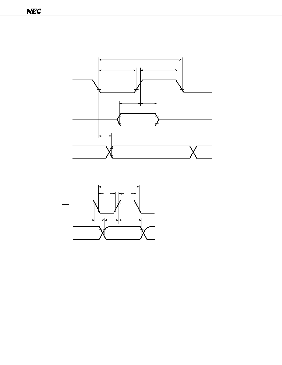
171
µ
PD75517(A)
Serial Transfer Timing
Three-wire serial I/O mode:
Two-wire serial I/O mode:
t
KL1
t
KCY1
t
SIK1
t
KH1
t
KSI1
t
KSO1
Input data
Output data
SCK
SI
SO
t
KCY2
t
KL2
t
KH2
t
KSI2
t
SIK2
t
KSO2
SCK
SB0 and SB1

172
µ
PD75517(A)
Serial Transfer Timing
Bus release signal transfer:
Command signal transfer:
Interrupt Input Timing
RESET Input Timing
INT0, INT1, INT2
and INT4
KR0-KR7
t
INTL
t
INTH
RESET
t
RSL
SCK
SB0 and SB1
t
KSB
t
KL3, 4
t
KH3, 4
t
KCY3, 4
t
KSI3, 4
t
SIK3, 4
t
KSO3, 4
t
SBK
SCK
SB0 and SB1
t
KSB
t
SBL
t
SBH
t
SBK
t
KL3, 4
t
KH3, 4
t
KCY3, 4
t
KSI3, 4
t
SIK3, 4
t
KSO3, 4

173
µ
PD75517(A)
DATA HOLD CHARACTERISTICS BY LOW SUPPLY VOLTAGE IN DATA MEMORY STOP MODE
(T
a
= -40 to +85
∞
C)
Notes 1.
Excluding the current which flows through the built-in pull-up resistors
2.
CPU operation stop time for preventing unstable operation at the beginning of oscillation
3.
This value depends on the settings of the basic interval timer mode register (BTM) shown below.
Data Hold Timing (STOP Mode Release by RESET)
Data Hold Timing (Standby Release Signal: STOP Mode Release by Interrupt Signal)
Parameter
Symbol
Min.
Typ.
Max.
Unit
Conditions
Data hold supply voltage
Data hold supply current
Note 1
Release signal setting time
Oscillation settling
time
Note 2
V
DDDR
I
DDDR
t
SREL
t
WAIT
2.0
0
X
0.1
2
17
/f
X
Note 3
6.0
10
V
µ
A
µ
s
ms
ms
V
DDDR
= 2.0 V
Release by RESET
Release by interrupt request
--
--
--
--
f
X
= 4.19 MHz
2
20
/f
X
(approx. 175 ms)
2
17
/f
X
(approx. 31.3 ms)
2
15
/f
X
(approx. 7.82 ms)
2
13
/f
X
(approx. 1.95 ms)
f
X
= 6.0 MHz
2
20
/f
X
(approx. 175 ms)
2
17
/f
X
(approx. 21.8 ms)
2
15
/f
X
(approx. 5.46 ms)
2
13
/f
X
(approx. 1.37 ms)
0
1
0
1
0
1
1
1
Wait time
BTM0
BTM1
0
0
1
1
BTM2
BTM3
RESET
V
DD
V
DDDR
t
SREL
t
WAIT
Internal reset operation
HALT mode
Operation
mode
STOP instruction execution
Data hold mode
STOP mode
Standby release signal
(Interrupt request)
V
DD
V
DDDR
t
SREL
t
WAIT
HALT mode
Operation
mode
STOP instruction execution
Data hold mode
STOP mode

174
µ
PD75517(A)
10. PACKAGE DIMENSIONS
PACKAGE DIMENSIONS OF 80-PIN PLASTIC QFP (14
◊
20) (UNIT: mm)
A
B
C
D
F
G
H
I
J
K
L
M
N
P
Q
R
S
23.6
±0.4
I M
80
25
24
C
F
G
H
J
S
D
Q
R
B
A
N
P
K
L
M
20.0
±0.2
14.00
±0.2
17.6
±0.4
1.0
0.8
0.35
±0.10
0.15
0.8 (T.P)
1.8
±0.2
0.8
±0.2
0.15
0.15
2.7
0.1
±0.1
0.1
±0.1
+0.10
≠0.05
3.0 MAX.
0.929
±0.016
0.795
0.551
0.693
±0.016
0.039
0.031
0.014
0.031 (T.P.)
+0.009
≠0.008
+0.009
≠0.008
+0.004
≠0.005
0.071
0.031
0.006
0.006
0.106
0.004
±0.004
+0.004
≠0.003
+0.008
≠0.009
+0.009
≠0.008
0.004
±0.004
0.119 MAX.
MILLIMETERS
ITEM
INCHES
P80GF-80-3B9-2E
NOTE
Each lead centerline is located within 0.15 mm
(0.006 inch) of its true position (T.P.) at maxi-
mum material condition.
Detail of lead end
65
64
41
40
1
0.006

175
µ
PD75517(A)
11. RECOMMENDED SOLDERING CONDITIONS
The following conditions must be met when soldering the
µ
PD75517(A).
Please consult with our sales offices in case other soldering process is used, or in case soldering is done
under different conditions.
Table 11-1 Recommended Soldering Conditions
Table 11-2 Soldering Conditions
Note Exposure limit before soldering after dry-pack package is opened. Storage conditions: 25
∞
C and
relative humidity at 65 % or less.
Caution Do not apply more than a single process at a time, except for "Partial heating method."
For more details, refer to our document "SMT MANUAL" (IEI-1207).
Symbol
WS60-162-1
IR30-162-1
VP15-162-1
Partial heating method
Part number
Package
µ
PD75517GF(A)-
◊◊◊
-3B9
80-pin plastic QFP (14 mm
◊
20 mm)
Soldering conditions
Soldering process
Symbol
Wave soldering
Infrared ray reflow
VPS
Partial heating method
WS60-162-1
IR30-162-1
VP15-162-1
Partial heating
method
Temperature in the soldering vessel: 260 ∞C or less
Soldering time: 10 seconds or less
Number of soldering processes: 1
Exposure limit
Note
: 2 days
(16 hours pre-baking is required at 125 ∞C afterwards)
Pre-heating temperature: 120 ∞C max.
(package surface temperature)
Peak package's surface temperature: 230 ∞C
Reflow time: 30 seconds or below (at 210 ∞C or more)
Number of reflow processes: 1
Exposure limit
Note
: 2 days
(16 hours pre-baking is required at 125 ∞C afterwards)
Peak package's surface temperature: 215 ∞C
Reflow time: 40 seconds or below (at 200 ∞C or more)
Number of reflow processes: 1
Exposure limit
Note
: 2 days
(16 hours pre-baking is required at 125 ∞C afterwards)
Terminal temperature: 300 ∞C or less
Flow time: 3 seconds or less (one side per device)

176
µ
PD75517(A)
APPENDIX A SERIES PRODUCT FUNCTIONS
Notes 1.
No mask option is provided for the
µ
PD75P516 and
µ
PD75P518.
2.
Only in the
µ
PD75P516 and
µ
PD75P518
µ
PD75517
µ
PD75517(A)
24448
µ
PD75516
µ
PD75516(A)
16256
µ
PD75P516
16256 (PROM)
Product
Item
µ
PD75P518
32640 (PROM)
ROM (bytes)
RAM (
◊
4 bits)
General register
Machine
cycle
I/O port
A/D converter
Operating
voltage
Timer/counter
Serial interface
Interrupt
Instruction set
Operating supply
voltage
Package
Main-
system
clock
Subsystem
clock
Total
CMOS
input
CMOS I/O
N-ch
open-
drain I/O
0.95
µ
s/1.91
µ
s/15.3
µ
s (at 4.19 MHz)
Note 1
1024
512
(4 bits
◊
8 or 8 bits
◊
4)
◊
4 banks
0.67
µ
s/1.33
µ
s/2.67
µ
s/10.7
µ
s (at 6.0 MHz)
0.95
µ
s/1.91
µ
s/3.82
µ
s/15.3
µ
s (at 4.19 MHz)
122
µ
s (at 32.768 kHz)
64
16 (Shared with INT and SIO. Seven lines can be pulled up by software)
28 (LED direct driving and shared with SIO and PPO)
∑ 16 lines can be pulled up by software.
∑ Four lines can be pulled down by the mask option.
20 (Eight lines for driving LEDs. Withstand
voltage is 10 V. 20 lines can be pulled up
by the mask option.)
∑ 8-bit resolution
◊
8 ch (successive approximation)
V
DD
= 2.7 to 6.0 V
V
DD
= 3.5 to 6.0 V
4 channels
∑ Timer/event counter
∑ Basic interval timer
∑ Timer/pulse generator (14-bit PWM output possible)
∑ Clock timer
2 channels
∑ NEC standard serial bus interface (SBI)/three-wire SIO : One channel
∑ General synchronous serial interface (three-wire SIO) : One channel
∑ Vectored interrupt: Seven sources (External: 3, Internal: 4)
∑ Test input:
Two sources
(External: 1, Internal: 1)
∑ Clock test flag is provided.
∑ Parallel-edge-sensitive flag for key scan input is provided.
∑ Set/reset/test/Boolean operation for bit data
∑ 4-bit data transfer, arithmetic/logical, addition/subtraction and comparison
∑ 8-bit data transfer, arithmetic/logical, addition/subtraction and comparison
2.7 to 6.0 V
4.75 to 5.5 V
∑ 80-pin plastic QFP
∑ 80-pin ceramic LCC with a window
Note 2
20 (Eight lines for driving LEDs. Withstand
voltage is 9 V. 20 lines can be pulled up by
the mask option.)

177
µ
PD75517(A)
APPENDIX B DEVELOPMENT TOOLS
The following development tools are provided for developing a system which employs the
µ
PD75517(A).
Language processor
PROM programming tools
RA75X relocatable assembler
OS
MS-DOS
TM
Ver. 3.10
to
Ver. 3.30C
PC DOS
TM
(Ver. 3.1)
Distribution media
3.5-inch 2HD
5-inch 2HD
5-inch 2HC
Part number
µ
S5A13RA75X
µ
S5A10RA75X
µ
S7B10RA75X
Hardware
Software
The PG-1500 PROM programmer is used together with an accessory board
and optional program adapter. It allows the user to program a single chip
microcomputer containing PROM from a standalone terminal or a host
machine. The PG-1500 can be used to program typical 256K-bit to 1M-bit
PROMs.
The PA-75P516GF is a dedicated PROM programmer for the
µ
PD75P516GF
and
µ
PD75P518GF. This programmer is connected to the PG-1500.
The PA-75P516K is a dedicated PROM programmer for the
µ
PD75P516K and
µ
PD75P518K. This programmer is connected to the PG-1500.
This program enables the host machine to control the PG-1500 through the
serial and parallel interfaces.
OS
MS-DOS
Ver. 3.10
to
Ver. 3.30C
PC DOS
(Ver. 3.1)
PG-1500
PA-75P516GF
PA-75P516K
PG-1500 controller
Distribution media
3.5-inch 2HD
5-inch 2HD
5-inch 2HC
Part number
µ
S5A13PG1500
µ
S5A10PG1500
µ
S7B10PG1500
Host machine
PC-9800 series
IBM PC series
Host machine
PC-9800 series
IBM PC series

178
µ
PD75517(A)
Debugging tools
Note
Maintenance service only
Remark
NEC is not responsible for the operation of any software unless it runs on a host machine with
the operating system listed above.
Hardware
Software
The IE-75000-R is an in-circuit emulator available for the 75X series. This
emulator is used together with the emulation probe to develop application
systems of the
µ
PD75517(A). For efficient debugging, the emulator is
connected to the host machine and PROM programmer.
The IE-75000-R-EM is an emulation board for the IE-75000-R and IE-75001-
R. The IE-75000-R contains the emulation board. The emulation board is
used together with the IE-75000-R or IE-75001-R to evaluate the
µ
PD75517(A).
The IE-75001-R is an in-circuit emulator available for the 75X series. This
emulator is used together with the IE-75000-R-EM
emulation board (option)
and emulation probe to develop application systems of the
µ
PD75517(A).
For efficient debugging, the emulator is connected to the host machine and
PROM programmer.
The EP-75516GF-R is an emulation probe for the
µ
PD755
◊◊
series. The
emulation probe is connected to the IE-75000-R or IE-75001-R when it is used.
A 80-pin conversion socket, the EV-9200G-80, attached to the probe facili-
tates the connection of the prove with the user system.
This program enables the host machine to control the IE-75000-R or IE-
75001-R through the RS-232-C interface.
IE-75000-R
Note
IE-75000-R-EM
IE-75001-R
EP-75516GF-R
EV-9200G-80
IE control program
Distribution media
3.5-inch 2HD
5-inch 2HD
5-inch 2HC
Part number
µ
S5A13IE75X
µ
S5A10IE75X
µ
S7B10IE75X
OS
MS-DOS
Ver. 3.10
to
Ver. 3.30C
PC DOS
(Ver. 3.1)
Host machine
PC-9800 series
IBM PC series

179
µ
PD75517(A)
The IE-75001-R does not contain the
IE-75000-R-EM (to be ordered).
For the PD75P518GF (one-time)
For the PD75P518K (with window)
User sysytem
Emulation probe
EP-75516GF-R
In-circuit emulator
IE-75000-R
IE-75001-R
Note 1
IE-75000-R-EM
Built-in PROM
µ
PD75P518GF
(one-time)
PD75P518K
(with window)
PROM programmer
PG-1500
Programmer adapter
PA-75P516GF
Note 2
PA-75P516K
Note 3
RS-232-C
Centronics interface
IE control
program
PG-1500
controller
Host machine
PC-9800 series
IBM PC series
(Symbolic debugging
is possible.)
Development tool configuration
µ
µ
µ
Relocatable
assembler
Notes 1.
2.
3.
80-pin conver-
sion socket
EV-9200G-80

µ
PD75517(A)
MS-DOS
TM
is a trademark of Microsoft Corporation.
PC DOS
TM
is a trademark of IBM Corporation.
[MEMO]
No part of this document may be copied or reproduced in any form or by any means without the prior written consent
of NEC Corporation. NEC Corporation assumes no responsibility for any errors which may appear in this document.
NEC Corporation does not assume any liability for infringement of patents, copyrights or other intellectual property
rights of third parties by or arising from use of a device described herein or any other liability arising from use of such
device. No license, either express, implied or otherwise, is granted under any patents, copyrights or other intellectual
property rights of NEC Corporation or others.
The devices listed in this document are not suitable for use in aerospace equipment, submarine cables, nuclear reactor
control systems and life support systems. If customers intend to use NEC devices for above applications or they
intend to use "Standard" quality grade NEC devices for applications not intended by NEC, please contact our sales
people in advance.
Application examples recommended by NEC Corporation
Standard: Computer, Office equipment, Communication equipment, Test and Measurement equipment, Ma-
chine tools, Industrial robots, Audio and Visual equipment, Other consumer products, etc.
Special:
Automotive and Transportation equipment, Traffic control systems, Antidisaster systems, Anticrime
systems, etc.
M4 92.6