Document Outline
- COVER
- DESCRIPTION
- FEATURES
- PIN CONFIGURATION (TOP VIEW)
- APPLICATIONS
- ORDERING INFORMATION
- BLOCK DIAGRAM OF uPD7564A
- 1. PIN FUNCTIONS
- 1.1 PORT FUNCTIONS
- 1.2 OTHER THAN PORTS
- 1.3 PIN MASK OPTION
- 1.4 CAUTION ON USE OF P00/INT0 PIN AND RESET PIN
- 1.5 PIN INPUT/OUTPUT CIRCUITS
- 1.6 RECOMMENDED CONNECTION OF UNUSED uPD7564A PINS
- 1.7 OPERATION OF INPUT/OUTPUT PORTS
- 2. INTERNAL BLOCK FUNCTIONS
- 2.1 PROGRAM COUNTER (PC): 10 BITS
- 2.2 STACK POINTER (SP): 6 BITS
- 2.3 PROGRAM MEMORY (ROM): 1024 WORDS x 8 BITS
- 2.4 GENERAL REGISTER
- 2.5 DATA MEMORY (RAM): 64 x 4 BITS
- 2.6 ACCUMULATOR (A): 4 BITS
- 2.7 ARITHMETIC LOGIC UNIT (ALU): 4 BITS
- 2.8 PROGRAM STATUS WORD (PSW): 4 BITS
- 2.9 SYSTEM CLOCK GENERATOR
- 2.10 CLOCK CONTROL CIRCUIT
- 2.11 TIMER/EVENT COUNTER
- 2.12 SERIAL INTERFACE
- 2.13 TEST CONTROL CIRCUIT
- 3. STANDBY FUNCTIONS
- 3.1 STOP MODE
- 3.2 CANCELLING THE HALT MODE
- 3.3 CANCELLING STOP MODE BY RESET INPUT
- 3.4 CANCELLING HALT MODE BY TEST REQUEST FLAG
- 3.5 CANCELLING HALT MODE BY RESET INPUT
- 4. RESET FUNCTIONS
- 4.1 DETAILS OF INITIALIZATION
- 5. uPD7564A INSTRUCTION SET
- 6. ELECTRICAL SPECIFICATIONS
- 7. CHARACTERISTIC CURVES
- 8. uPD7564A APPLIED CIRCUITS
- 9. PACKAGE INFORMATION
- 10. RECOMMENDED PACKAGING PATTERN OF SOP (REFERENCE) (UNIT: mm)
- 11. RECOMMENDED SOLDERING CONDITIONS
- APPENDIX A. COMPARISON BETWEEN SUB-SERIES PRODUCT FUNCTIONS
- APPENDIX B. DEVELOPMENT TOOLS
- APPENDIX C. RELATED DOCUMENTS
The mark 5 shows major revised points.
DESCRIPTION
The
µ
PD7564A is a 4-bit single-chip microcomputer with a small number of ports in a small package, which is
of low-order models,
µ
PD7554 and 7564 sub-series in the
µ
PD7500 series. With an on-chip serial interface, it per-
forms efficient dispersion processing of a system as a sub-CPU for the 75X series or 78k series.
The
µ
PD7564A has outputs to directly drive a triac and LEDs and allows selection among many types of input/
output circuits using their respective mask options, sharply reducing the number of external circuits required.
Details of functions are described in the User's Manual shown below. Be sure to read in design.
µ
PD7554, 7564 User's Manual: IEM-1111D
4-BIT SINGLE-CHIP MICROCOMPUTER
Document No.
IC-2401C
(O. D. No.
IC-7834C)
Date Published December 1994 P
Printed in Japan
µ
PD7564A, 7564A(A)
MOS INTEGRATED CIRCUIT
DATA SHEET
The information in this document is subject to change without notice.
FEATURES
∑
47 types of instructions
(Subset of
µ
PD7500H SET B)
∑
Instruction cycle
Ceramic oscillation : 2.86
µ
s
(in operation at 700 kHz, 5 V)
∑
Program memory (ROM) capacity: 1024
◊
8 bits
∑
Data memory (RAM) capacity: 64
◊
4 bits
∑
Test source: One external source and two internal
sources
∑
8-bit timer/event counter
∑
15 I/O lines (Total output current of all pins: 100 mA)
∑ Can directly drive a triac and a LED: P80 to P82
∑ Can directly drive LEDs: P100 to P103 and P110 to
P113
∑ Mask option function provided for every port
∑
8-bit serial interface
∑
Standby (STOP/HALT) function
∑
Low supply voltage data retaining function for data
memory
∑
Built-in ceramic oscillator for system clock
∑
Low power dissipation
∑
Single power supply (2.7 to 6.0 V)
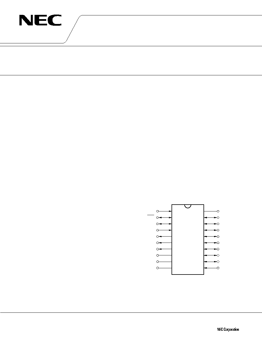
PIN CONFIGURATION (TOP VIEW)
1
2
3
4
5
6
7
8
9
10
20
19
18
17
16
15
14
13
12
11
V
SS
P113
P112
P111
P110
P103
P102
P101
P100
RESET
P00/INT0
P01/SCK
P02/SO
P03/SI
P80
P81
P82
CL2
CL1
V
DD
PD7564A
µ
APPLICATIONS
µ
PD7564A
: PPCs, printers, VCRs, audio equipments,
etc.
µ
PD7564A(A) : Automotive and transportation equip-
ments, etc.
The quality grade and absolute maximum ratings of the
µ
PD7564A and the
µ
PD7564A(A) differ.
Except where specifically noted, explanations here concern the
µ
PD7564A as a representative product.
If you are using the
µ
PD7564A(A), use the information presented here after the checking the func-
tional differences.
5
©
1994

2
µ
PD7564A, 7564A(A)
ORDERING INFORMATION
Ordering Code
Package
Quality Grade
µ
PD7564ACS-
◊◊◊
20-pin plastic shrink DIP (300 mil)
Standard
µ
PD7564AG-
◊◊◊
20-pin plastic SOP (300 mil)
Standard
µ
PD7564ACS(A)-
◊◊◊
20-pin plastic shrink DIP (300 mil)
Special
µ
PD7564AG(A)-
◊◊◊
20-pin plastic SOP (300 mil)
Special
Caution
Be sure to specify a mask option when ordering this device.
Remarks
"
◊◊◊
" is a ROM code number.
Please refer to "Quality grade on NEC Semiconductor Devices" (Document number IEI-1209) published by
NEC Corporation to know the specification of quality grade on the devices and its recommended applications.
5
5
3
µ
PD7564A, 7564A(A)
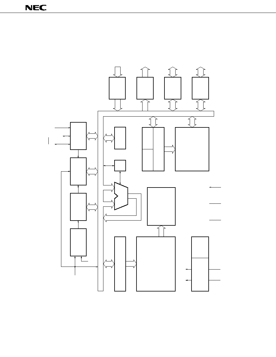
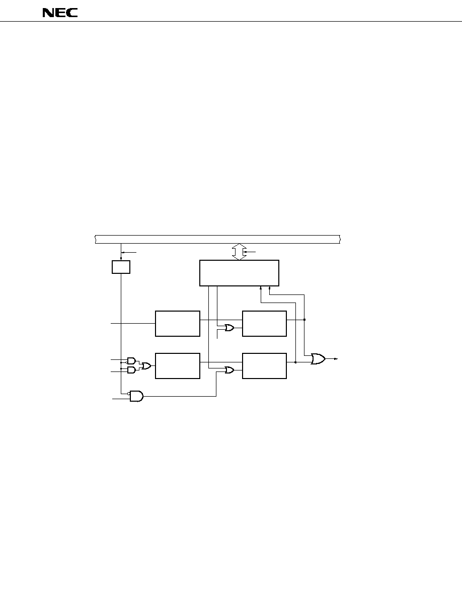
BLOCK DIAGRAM OF
µ
PD7564A
RESET
V
DD
V
SS
INSTRUCTION
DECODER
STANDBY
CONTROL
SYSTEM
CLOCK
GENERATOR
PROGRAM MEMORY
1024
◊
8 BITS
PROGRAM COUNTER (10)
P00/INT0
CL
CLOCK
CONTROL
TIMER/EVENT
COUNTER
TEST
CONTROL
SERIAL
INTERFACE
PORT0
BUFFER
PORT8
LATCH
BUFFER
PORT10
LATCH
BUFFER
PORT11
LATCH
BUFFER
4
P00≠P03
3
P80≠P82
4
P100≠P103
4
P110≠P113
A (4)
C
H (2)
L (4)
STACK POINTER (6)
DATA MEMORY
64
◊
4 BITS
ALU
INT0
P01/SCK
P03/SI
P02/SO
CL
CL1
CL2
CP
GENERAL REGISTERS

4
µ
PD7564A, 7564A(A)
CONTENTS
1.
PIN FUNCTIONS ......................................................................................................................................... 6
1.1
PORT FUNCTIONS ............................................................................................................................................... 6
1.2
OTHER THAN PORTS .......................................................................................................................................... 6
1.3
PIN MASK OPTION .............................................................................................................................................. 7
1.4
CAUTION ON USE OF P00/INT0 PIN AND RESET PIN ................................................................................... 7
1.5
PIN INPUT/OUTPUT CIRCUITS .......................................................................................................................... 8
1.6
RECOMMENDED CONNECTION OF UNUSED
µ
PD7564A PINS .................................................................. 11
1.7
OPERATION OF INPUT/OUTPUT PORTS ....................................................................................................... 11
2.
INTERNAL BLOCK FUNCTIONS ............................................................................................................ 13
2.1
PROGRAM COUNTER (PC): 10 BITS ................................................................................................................ 13
2.2
STACK POINTER (SP): 6 BITS .......................................................................................................................... 14
2.3
PROGRAM MEMORY (ROM): 1024 WORDS
◊
8 BITS ................................................................................... 15
2.4
GENERAL REGISTER ......................................................................................................................................... 15
2.5
DATA MEMORY (RAM): 64
◊
4 BITS ............................................................................................................... 16
2.6
ACCUMULATOR (A): 4 BITS ............................................................................................................................. 17
2.7
ARITHMETIC LOGIC UNIT (ALU): 4 BITS ........................................................................................................ 17
2.8
PROGRAM STATUS WORD (PSW): 4 BITS .................................................................................................... 17
2.9
SYSTEM CLOCK GENERATOR ......................................................................................................................... 18
2.10 CLOCK CONTROL CIRCUIT ............................................................................................................................... 19
2.11 TIMER/EVENT COUNTER ................................................................................................................................. 20
2.12 SERIAL INTERFACE ........................................................................................................................................... 21
2.13 TEST CONTROL CIRCUIT .................................................................................................................................. 23
3.
STANDBY FUNCTIONS ........................................................................................................................... 25
3.1
STOP MODE ........................................................................................................................................................ 25
3.2
CANCELLING THE HALT MODE ....................................................................................................................... 25
3.3
CANCELLING STOP MODE BY RESET INPUT ................................................................................................ 26
3.4
CANCELLING HALT MODE BY TEST REQUEST FLAG ................................................................................. 26
3.5
CANCELLING HALT MODE BY RESET INPUT ................................................................................................ 26
4.
RESET FUNCTIONS ................................................................................................................................. 27
4.1
DETAILS OF INITIALIZATION ........................................................................................................................... 27
5.
µ
PD7564A INSTRUCTION SET ............................................................................................................... 28
6.
ELECTRICAL SPECIFICATIONS .............................................................................................................. 33
7.
CHARACTERISTICS CURVES .................................................................................................................. 40
8.
µ
PD7564A APPLIED CIRCUITS ............................................................................................................... 43
9.
PACKAGE INFORMATION ....................................................................................................................... 45

5
µ
PD7564A, 7564A(A)
10. RECOMMENDED PACKAGING PATTERN OF SOP (REFERENCE) ..................................................... 49
11. RECOMMENDED SOLDERING CONDITIONS ....................................................................................... 50
APPENDIX A. COMPARISON BETWEEN SUB-SERIES PRODUCT FUNCTIONS..................................... 51
APPENDIX B. DEVELOPMENT TOOLS ........................................................................................................ 52
APPENDIX C. RELATED DOCUMENTS .......................................................................................................... 54
5

6
µ
PD7564A, 7564A(A)
1.
PIN FUNCTIONS
1.1
PORT FUNCTIONS
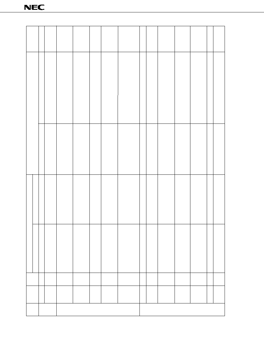
Pin Name
Input/Output
Dual-Function
Function
After RESET
Input/Output
Pin
Circuit
P00
Input
INT0
S
P01
Input/output
SCK
Input
X
P02
SO
W
P03
Input
SI
S
P80 to P82
Output
≠≠
O
P100 to P103
Input/output
≠≠
P
P110 to P113
Input/output
≠≠
1.2
OTHER THAN PORTS
Pin Name
Input/Output
Dual-Function
Function
After RESET
Input/Output
Pin
Circuit
INT0
Input
P00
Edge detection testable input pin (Rising edge)
S
SCK
Input/output
P01
Serial clock Input/output pin
Input
X
SO
Output
P02
Serial data output pin
Input
W
SI
Input
P03
Serial data input pin
Input
S
CL1
≠≠
CL2
RESET
R
V
DD
Positive power supply pin
V
SS
GND potential pin
4-bit input port (Port 0)
P00 serves also as a count clock (event pulse)
input.
3-bit output port (Port 8)
High current (15 mA), middle-high voltage (9 V)
output
4-bit I/O port (Port 10)
Middle-high current (10 mA), middle-high voltage
(9 V) input/output
4-bit I/O port (Port 11)
Middle-high current (10 mA), middle-high voltage
(9 V) input/output
High
impedance
High
impedance
or
high-level
output
Connection pin for ceramic oscillation ceramic
resonator
System reset input pin (high-level active)
A pull-down resistor can be incorporated using
the mask option.
7
µ
PD7564A, 7564A(A)
1.3
PIN MASK OPTION
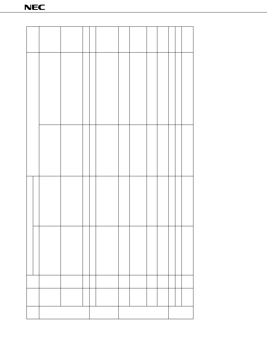
Each pin is provided with the following mask options which can be selected for each bit according to the purpose:
Pin Name
Mask Options
P00
No internally provided resistor Pull-down resistor internally provided Pull-up resistor internally provided
P01
No internally provided resistor Pull-down resistor internally provided Pull-up resistor internally provided
P02
No internally provided resistor Pull-down resistor internally provided Pull-up resistor internally provided
P03
No internally provided resistor Pull-down resistor internally provided Pull-up resistor internally provided
P80
N-ch open-drain output
CMOS (push-pull) output
P81
N-ch open-drain output
CMOS (push-pull) output
P82
N-ch open-drain output
CMOS (push-pull) output
P100
N-ch open-drain input/output
Push-pull input/output
N-ch open-drain + pull-up resistor built-in input/output
P101
N-ch open-drain input/output
Push-pull input/output
N-ch open-drain + pull-up resistor built-in input/output
P102
N-ch open-drain input/output
Push-pull input/output
N-ch open-drain + pull-up resistor built-in input/output
P103
N-ch open-drain input/output
Push-pull input/output
N-ch open-drain + pull-up resistor built-in input/output
P110
N-ch open-drain input/output
Push-pull input/output
N-ch open-drain + pull-up resistor built-in input/output
P111
N-ch open-drain input/output
Push-pull input/output
N-ch open-drain + pull-up resistor built-in input/output
P112
N-ch open-drain input/output
Push-pull input/output
N-ch open-drain + pull-up resistor built-in input/output
P113
N-ch open-drain input/output
Push-pull input/output
N-ch open-drain + pull-up resistor built-in input/output
RESET
Incorporating no pull-down resistor
Incorporating a pull-down resistor
There is no mask option for PROM products. For more information, see the
µ
PD75P64 Data Sheet (IC-2838).
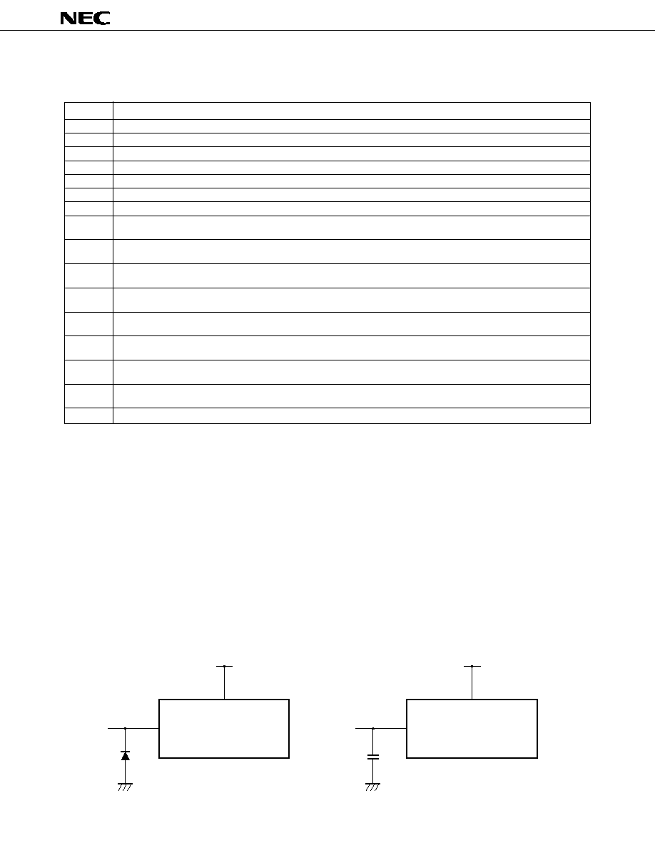
1.4
CAUTION ON USE OF P00/INT0 PIN AND RESET PIN
In addition to the functions shown in 1.1, 1.2 and 1.3, the P00/INT0 pin and RESET pin have a function for setting
the test mode in which the internal operation of the
µ
PD7564A is tested (IC test only).
When a potential greater than V
SS
is applied to either of these pins, the test mode is set. As a result, if noise
exceeding V
SS
is applied during normal operation, the test mode will be entered and normal operation may be
impeded.
If, for example, the routing of the wiring between the P00/INT0 pin and RESET pin is long, the above problem
may occur as the result of inter-wiring noise between these pins.
Therefore, wiring should be carried out so as to suppress inter-wiring noise as far as possible. If it is not possible
to suppress noise, anti-noise measures should be taken using external parts as shown in the figures below.
∑ Connection of diode with small V
F
between P00/
INT4/RESET pin and V
SS
∑ Connection of capacitor between P00/INT0/
RESET pin and V
SS
V
DD
V
DD
P00/INT0, RESET
V
SS
V
DD
V
DD
P00/INT0, RESET
V
SS
Diode
with
Small V
F
5
8
µ
PD7564A, 7564A(A)
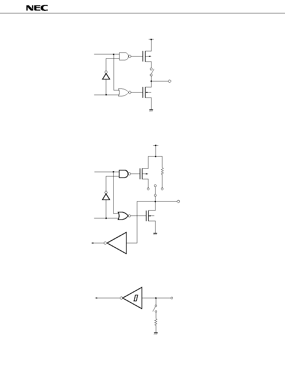
1.5
PIN INPUT/OUTPUT CIRCUITS
This section presents the input/output circuit for each pin of the
µ
PD7564A in a partly simplified format:
(1) Type A (for Type W)
V
DD
P≠ch
N≠ch
IN
Forming an input buffer conformable to the CMOS specification
(2) Type D (for Types W and X)
V
DD
P≠ch
N≠ch
OUT
data
output
disable
Forming a push-pull output which becomes high impedance (with both P-ch and N-ch off) in response to
RESET input
9
µ
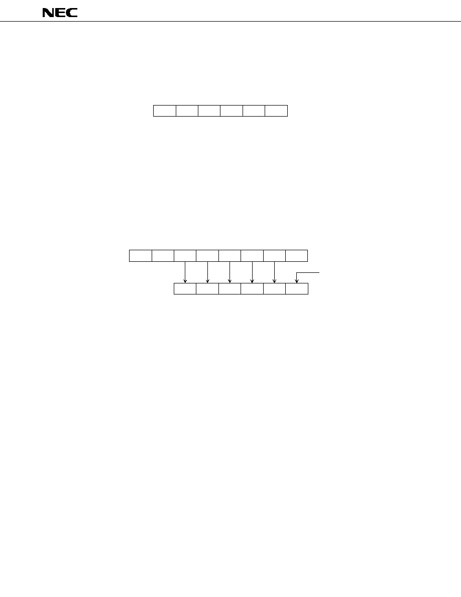
PD7564A, 7564A(A)
(3) Type O
V
DD
P≠ch
N≠ch
OUT
data
output
disable
Mask Option
(Middle-High Voltage,
High-Current)
(4) Type P
(5) Type R
Mask Option
V
DD
P≠ch
N≠ch
IN/OUT
data
output
disable
Mask Option
(Middle-High Voltage,
High-Current)
Middle-High Input Buffer

10
µ
PD7564A, 7564A(A)
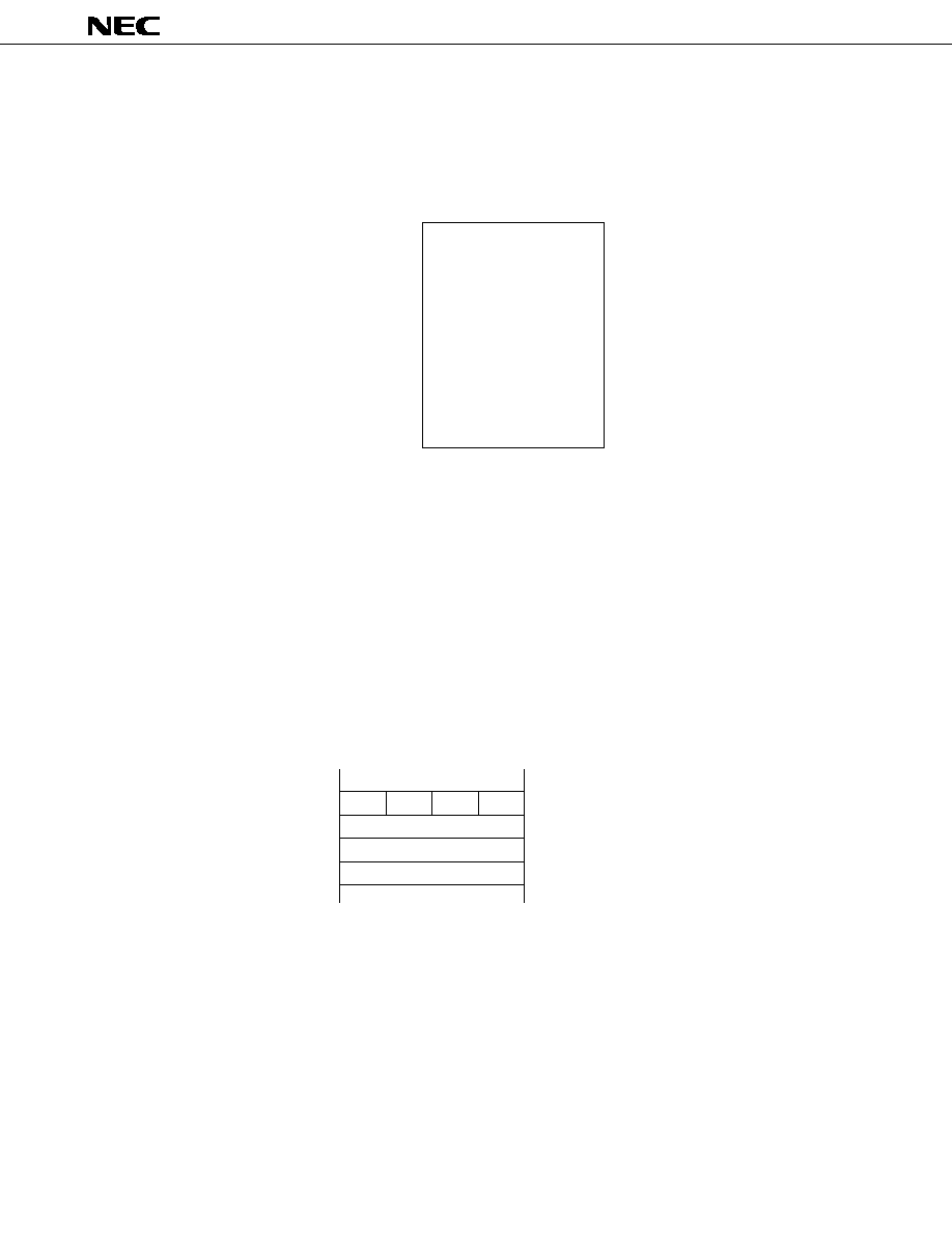
(6) Type S
IN
Mask Option
V
DD
(7) Type W
IN/OUT
V
DD
Type D
Type A
data
output
disable
Mask Option
(8) Type X
IN/OUT
V
DD
Type D
data
output
disable
Mask Option

11
µ
PD7564A, 7564A(A)
1.6
RECOMMENDED CONNECTION OF UNUSED
µ
PD7564A PINS
Pin
Recommended Connection
P00/INT0
Connect to V
SS
.
P01 to P03
Connect to V
SS
or V
DD
.
P80 to P82
Leave open.
P100 to P103
P110 to P113
1.7
OPERATION OF INPUT/OUTPUT PORTS
(1) P00 to P03 (Port 0)
The port 0 is a 4-bit input port consisting of 4-bit input pins P00 to P03. In addition to being used for port input,
P00 serves as a count clock input or testable input (INT0), each of P01 to P03 serves as a serial interface input/output.
To use P00 as a count clock input, set bits 2 (CM2) and 1 (CM1) of the clock mode register to 01. (See 2.10 "CLOCK
CONTROL CIRCUIT" for details.)
To use P00 as a INT0, set bit 3 (SM3) of the shift mode register to 1.
The serial interface function to use P01 to P03 as a serial interface I/O port is determined by bits 2 and 1 (SM2
and SM1) of the shift mode register. See 2.12 "SERIAL INTERFACE" for details.
Even though this port operates using any function other than the port function, execution of the port input
instruction (IPL) permits loading data on the P00 to P03 line to the accumulator (A0 to A3) at any time.
(2) P80 to P83 (Port 8)
The port 8 is a 4-bit output port with an output latch, which consists of 4-bit output pin.
The port output instruction (OPL) latches the content of the accumulator (A0 to A3) to the output latch and outputs
it to pins P80 to P83.
The SPBL and RPBL instructions allow bit-by-bit setting and resetting of pins P80 to P82.
For these ports, mask options for the output format are available to select CMOS (push-pull) output or N-ch open-
drain output.
The port specified as a N-ch open-drain output and provides an efficient interface to the circuit operating at a
different supply voltage because the output buffer has a dielectric strength of 9 V.
Input state : Connect to V
SS
or V
DD
.
Output state: Leave open.

12
µ
PD7564A, 7564A(A)
(3) P100 to P103 (Port 10) and P110 to P113 (Port 11): Quasi-bidirectional input/output
P100 to P103 are 4-bit I/O pins which form the port 10 (4-bit I/O port with an output latch). P110 to P113 are 4-
bit I/O pins which form the port 11 (4-bit I/O port with an output latch).
The port output instruction (OPL) latches the content of the accumulator to the output latch and outputs it to the
4-bit pins.
The data written once in the output latch and the output buffer state are retained until the output instruction to
operate the port 10 or 11 is executed or the RESET signal is input. Even though an input instruction is executed for
the port 10 or 11, the states of both the output latch and output buffer do not change.
The SPBL and RPBL instructions allow bit-by-bit setting and resetting of pins P100 to P103 and P110 to P113.
The input/output format of each of the ports 10 and 11 can be selected from among the N-ch open-drain input/
output, N-ch open-drain + pull-up resistor built-in input/output, and CMOS (push-pull) input/output by their
respective mask options.
When the CMOS (push-pull) input/output is selected, the port cannot return to the input mode once the output
instruction is executed. However, the states of the pins of the port can be checked by reading via the port input
instruction (IPL).
When one of the other two formats is selected, the port can enter the input mode to load the data on the 4-bit
line to the accumulator (as a quasi-bidirectional port) when the port receives high level output. Select each type of
the input/output format to meet the use of the port:
CMOS input/output
i)
Uses all 4 bits of the port as input ports.
ii) Uses pins of the port as output pins not requiring middle withstand voltage output.
N-ch open-drain input/output
i)
Uses pins of the port as I/O pins requiring a middle withstand voltage dielectric strength.
ii) Uses input pins of the port which also has output pins.
iii) Uses each pin of the port for both input and output by switching them over.
N-ch open-drain + pull-up resistor built-in input/output
i)
Uses input pins of the port which also has output pins, that require a pull-up resistor.
ii) Uses each pin of the port for both input and output by switching them over. This requires a pull-up resistor.
Caution
Before using input pins in the case of or , write 1 in the output latch to turn the N-ch transistor
off.

13
µ
PD7564A, 7564A(A)
2.
INTERNAL BLOCK FUNCTIONS
2.1
PROGRAM COUNTER (PC): 10 BITS
The program counter is a 10-bit binaryc ounter to retain program memory (ROM) address information.
Fig. 2-1 Program Counter Configuration
PC9
PC8
PC7
PC6
PC5
PC4
PC3
PC2
PC1
PC0
PC
When one instruction is executed, usually the program counter is incremented by the number of bytes of the
instruction.
When the call instruction is executed, the PC is loaded with a nkew call address after the stack memory saves
the current contents (return address) of the PC. When the return instruction is executed, the content (return address)
of the stack memory is loaded onto the PC. When the jump instruction is executed, the immediate data identifying
the destination of the jump is loaded to all or some of bits of the PC.
When a skip occurs, the PC is incremented by 2 or 3 during the machine cycle depending on the number of bytes
in the next instruction.
When the RESET signal is input, all the bits of the PC are cleared to zero.
14
µ
PD7564A, 7564A(A)
2.2
STACK POINTER (SP): 6 BITS
The stack pointer is a 6-bit register which retains head address information of the stack memory (LIFO type) which
is a part of the data memory.
Fig. 2-2 Stack Pointer Configuration
SP5
SP4
SP3
SP2
SP1
SP0
SP
The stack pointer is decremented when the call instruction is executed. It is incremented when the return
instruction is executed.
To determine the stack area, initialize the SP using the TAMSP instruction. Note that bit SP0 is loaded with 0
unconditionally when the TAMSP instruction is executed. Set the SP to the value of "the highest address of the stack
area + 1" because the stack operation starts with decrementation of the SP.
When the highest address of the stack area is 3FH which is the highest address of the data memory, the initial
value of SP5-0 must be 00H. For emulation using the
µ
PD7500H (EVAKIT-7500B), set the data to be used for AM
when executing the TAMSP instruction.
Fig. 2-3 In Execution of TAMSP Instruction
A3
A2
A1
A0
(HL)
3
(HL)
2
(HL)
1
(HL)
0
0
SP5
SP4
SP3
SP2
SP1
SP0
Note that the contents of the SP cannot be read.
Caution
Be sure to set the SP at the initial stage of the program execution because the SP becomes undefined
when the RESET signal is input.
Example
LHLI
00H
LAI
0
ST
LAI
4
TAMSP
;SP = 40H

15
µ
PD7564A, 7564A(A)
2.3
PROGRAM MEMORY (ROM): 1024 WORDS
◊
8 BITS
The program memory is a mask programmable ROM of 1024 word
◊
8 bits configuration. It is addressed by the
program counter.
The program memory stores programs.
Address 000H is the reset start address.
Fig. 2-4 Program Memory Map
(0) 000H
(1023) 3FFH
Reset Start
2.4
GENERAL REGISTER
General registers H (with two bits) and L (with four bits) operate individually. They also form a pair register HL
(H: high order and L: low order) to serve as a data pointer for addressing the data memory.
Fig. 2-5 General Register Configuration
1
0
H
L
3
0
The L register is also used to specify I/O ports and the mode register when an input/output instruction (IPL or
OPL) is executed. It also used to specify the bits of a port when the SPBL or RPBL instruction is executed.
16
µ
PD7564A, 7564A(A)
2.5
DATA MEMORY (RAM): 64
◊
4 BITS
The data memory is a static RAM of 64 word
◊
4 bits configuration. It is used as the area to store or stack processed
data. The data memory may be processed in 8-bit units when paired with the accumulator.
Fig. 2-6 Data Memory Map
( 0 ) 00H
(63) 3FH
64 Words
◊
4 Bits
The data memory is addressed in the following three ways:
∑ Direct: Direct addressing based on immediate data of an instruction
∑ Register indirect: Indirect addressing according to the contents of the pair register HL (including automatic
incrementation and decrementation)
∑ Stack: Indirect addressing according to the contents of the stack pointer (SP)
An arbitrary space of the data memory is available as stack memory. The boundary of the stack area is specified
when the TAMSP instruction initializes the SP. After that, the stack area is accessed automatically by the call or return
instruction.
After the call instruction is executed, the content of the PC and PSW is stored in the order shown in the following
diagram:
0
0
PC9
PC8
3
0
PSW*
PC3 ≠ PC0
PC7 ≠ PC4
SP ≠ 4
SP ≠ 3
SP ≠ 2
SP ≠ 1
Stack Area
* Bit 1 is fixed at 0.
When the return instruction is executed, the content of the PSW is not restored while those of the PC are restored.
Data in the data memory is retained at a low supply voltage in the STOP mode.

17
µ
PD7564A, 7564A(A)
2.6
ACCUMULATOR (A): 4 BITS
The accumulator is a 4-bit register which plays a major role in many types of arithmetic operations. The
accumulator may be processed in 8-bit units when paired with the data memory addressed by the pair register HL.
Fig. 2-7 Accumulator Configuration
A3
A2
A1
A0
A
2.7
ARITHMETIC LOGIC UNIT (ALU): 4 BITS
The arithmetic logic unit is a 4-bit arithmetic circuit to perform arithmetic and bit processing such as binary
addition, logical operation, incrementation, decrementation, and comparison.
2.8
PROGRAM STATUS WORD (PSW): 4 BITS
The program status word consists of skip flags (SK1 and SK0) and a carry flag (C). Bit 1 of the PSW is fixed at 0.
Fig. 2-8 Program Status Word Configuration
SK1
SK0
0
C
PSW
3
2
1
0
(1) Skip flags (SK1 and SK0)
Skip flags store the following skip status:
∑ Stacking by the LAI instruction
∑ Stacking by the LHLI instruction
∑ Skip condition establishment by any instruction other than stack instructions
The skip flags are set and reset automatically when respective instructions are executed.
(2) Carry flag (C)
The carry flag is set to 1 when a carry from bit 3 of the ALU occurs when the add instruction (ACSC) is executed.
The flag is reset to 0 when the carry does not occur. The SC and RC instructions respectively set and reset the carry
flag. The SKC instruction tests the contents of the flag.
The content of the PSW are automatically stored in the stack area when the call instruction is executed. It cannot
be restored by the return inhstruction.
When the RESET signal is input, SK1 and SK0 are both cleared to zero and C becomes undefined.
18
µ
PD7564A, 7564A(A)
2.9
SYSTEM CLOCK GENERATOR
The system clock generator contains an ceramic oscillator, 1/2 divider, and standby (STOP/HALT) mode control
circuit.
Fig. 2-9 System Clock Generator
HALT RELEASE
RESET ( )
(To CPU)
CL (System Clock)
RESET (High)
HALT*
STOP*
HALT F/F
Q
S
R
Q
S
R
STOP F/F
CL1
CL2
1/2
Ceramic
Oscillator
* Instruction execution
Oscillator
Stop
RESET ( )
The ceramic oscillator oscillates with a ceramic resonator R connected to pins CL1 and CL2.
The ceramic oscillator outputs the system clock (CL) which is 1/2 divided to the CPU clock (
).
The control circuit in the standby mode consists mainly of STOP F/F and HALT F/F.
The STOP F/F is set by the STOP instruction to stop ceramic oscillation, blocking every clock from being supplied
(STOP mode). The STOP F/F is reset by the RESET input (high level) to restart ceramic oscillation. When the RESET
input returns to the low level after that, the oscillator once more supplys each clock.
The HALT F/F is set by the HALT instruction to disable the input to the 1/2 divider which generates the CPU clock
, stopping only the CPU clock
(HALT mode).
The HALT F/F is reset at the fall of the HALT RELEASE signal (which goes active when even one test request flag
is set) or the RESET input signal, causing the oscillator to start supplying the CPU clock
.
The HALT F/F remains on for the same function of the HALT mode even while the RESET input is active (high).
When a power-on reset occurs, ceramic oscillation starts at rise of the RESET input signal. However, it takes a
certain time for the oscillation output level to be stabilized after the start of oscillation. To prevent the CPU from
malfunctioning by unstable clock pulses, the standby mode control circuit sets the HALT F/F while the RESET input
remains high to suppress the CPU clock
. Thus the high-level duration of the RESET input must be set so that it
exceeds the stabilizing time required for the ceramic resonator to be used.
19
µ
PD7564A, 7564A(A)
2.10 CLOCK CONTROL CIRCUIT
The clock control circuit consists of 2-bit clock mode registers (CM2 and CM1), prescalers 1, 2 and 3, and a
multiplexer. The circuit inputs the system clock generator output (CL) and the event pulse (P00). It also selects a
clock source and a prescaler according to the specifications of clock mode register and supplies a count pulse (CP)
to the timer/event counter.
Fig. 2-10 Clock Control Circuit
CP
CL
P00
PRESCALER 1
(1/4)
PRESCALER 2
(1/8)
PRESCALER 3
(1/8)
OPL*
CM2 CM1
Internal Bus
* Instruction execution
Use the OPL instruction to set codes in the clock mode registers.
Fig. 2-11 Clock Mode Register Format
Clock Mode Register
Caution
When setting codes in the clock mode registers using the OPL instruction, be sure to set bit 0 of the
accumulator to 0. (Bit 0 corresponds to CM0 of the
µ
PD7500 of EVAKIT-7500B in emulation.)
CM2
CM1
CM2
CM1
Count Pulse Frequency (CP)
0
0
CL
◊
1
256
0
1
P00
1
0
CL
◊
1
32
1
1
CL
◊
1
4
20
µ
PD7564A, 7564A(A)
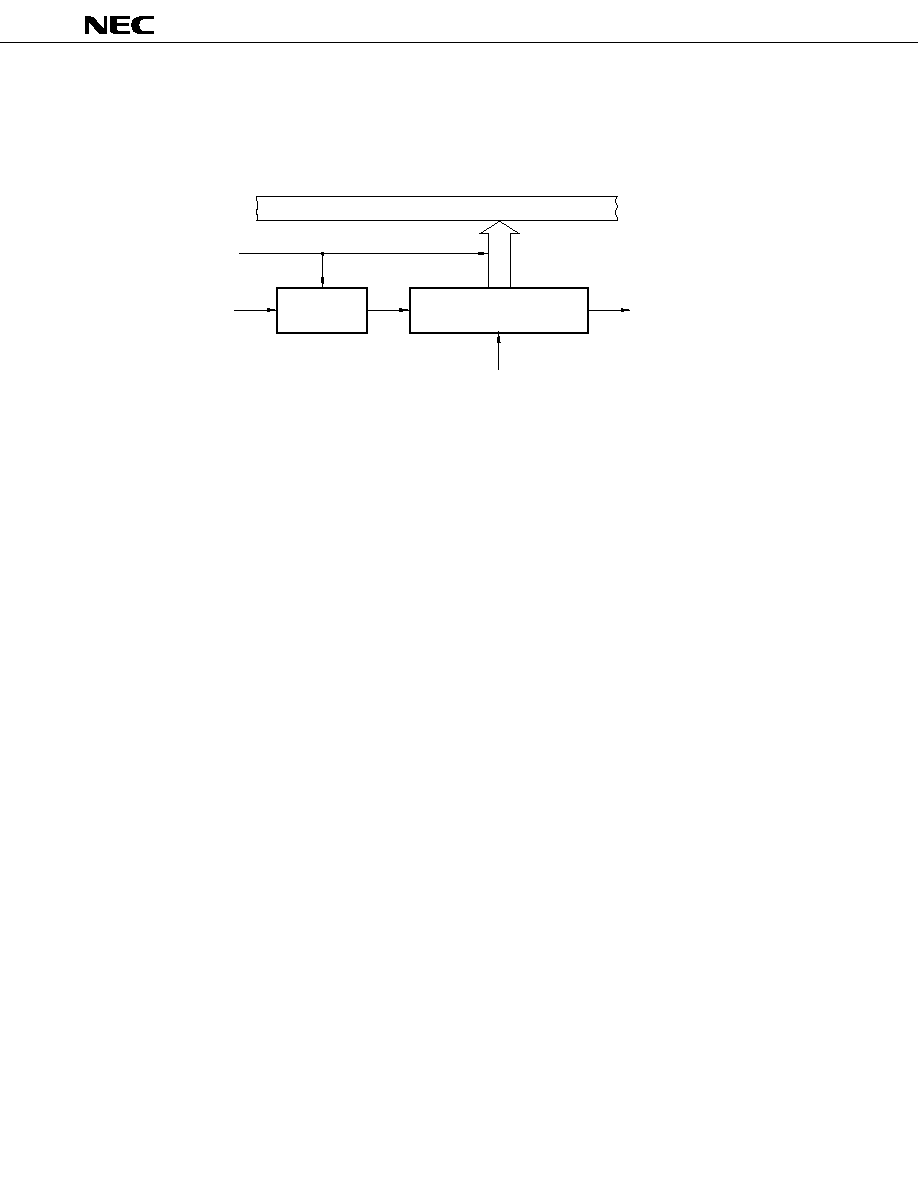
2.11 TIMER/EVENT COUNTER
The timer/event counter is based on an 8-bit count register as shown in Fig. 2-12.
Fig. 2-12 Timer/Event Counter
8-BIT COUNT REG
TIMER
RESET
CLR
CP
8
*TCNTAM
INTT
(To Test Control Circuit)
*
* Instruction execution
Internal Bus
Count
Holding
Circuit
The 8-bit count register is a binary 8-bit up-counter which is incremented whenever a count pulse (CP) is input.
The register is cleared to 00H when the TIMER instruction is executed, RESET signal is input, or an overflow occurs
(FFH to 00H).
As the count pulse, the clock mode register can select one of the following four. See 2.10 "CLOCK CONTROL
CIRCUIT".
1
1
1
CP : CL
◊
≠≠, CL
◊
≠≠≠, CL
◊
≠≠≠≠, P00
4
32
256
The count register continues to be incremented as long as count pulses are input. The TIMER instruction clears
the count register to 00H and triggers the timer operation.
The count register is incremented in synchronization with the CP (or the rise of the P00 input when an external
clock is used). On the count reaches 256, the register returns the count value to 00H from FFH, generates the overflow
signal INTT, and sets the INTT test flag INTT RQF.
In this way, the count register counts over from 00H.
To recognize the overflow, test the flag INTT RQF using the SKI instruction.
When the timer/event counter serves as a timer, the reference tiome is determined by the CP frequency. The
precision is determined by the system clock oscillator frequency when the system clock system is selected and by
the P00 input frequency when the P00 input is selected.
The content of the count register can be read at any time by the TCNTAM instruction. This function allows
checking the current time of the timer and counting event pulses input to the P00 input. This enables the number
of even pulses that have been generated so far (event counter function).
The count holding circuit ignores the change of the count pulse (CP) during execution of the TCNTAM instruction.
This is to prevent reading undefined data in the count register using the TCNTAM instruction while the counter is
being updated.
Since the timer/event counter operates the system clock system (CL) or the P00 input for count pulses, it is used
to cancel the HALT mode which stops the CPU clock
as well as the STOP mode which stops the system clock CL.
(See 3. "STANDBY FUNCTIONS".)

21
µ
PD7564A, 7564A(A)
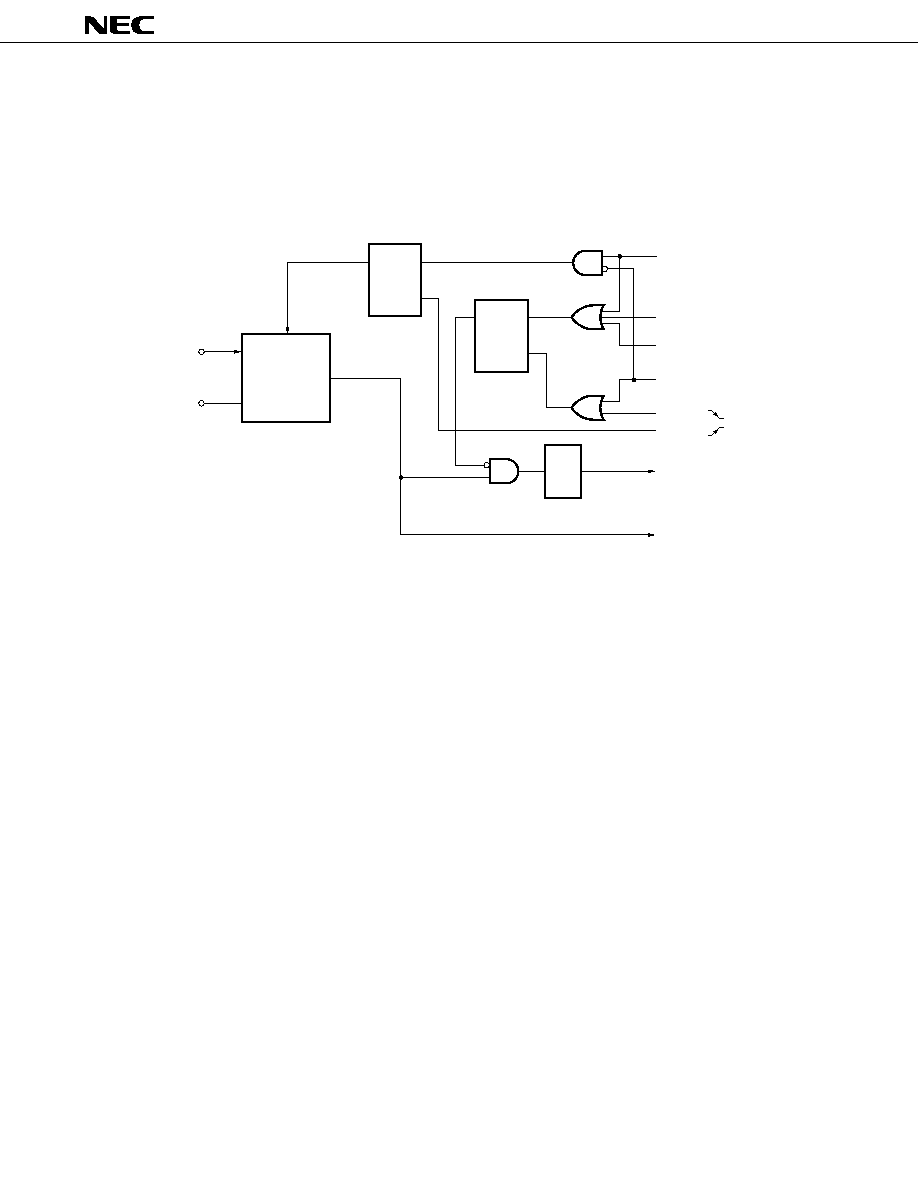
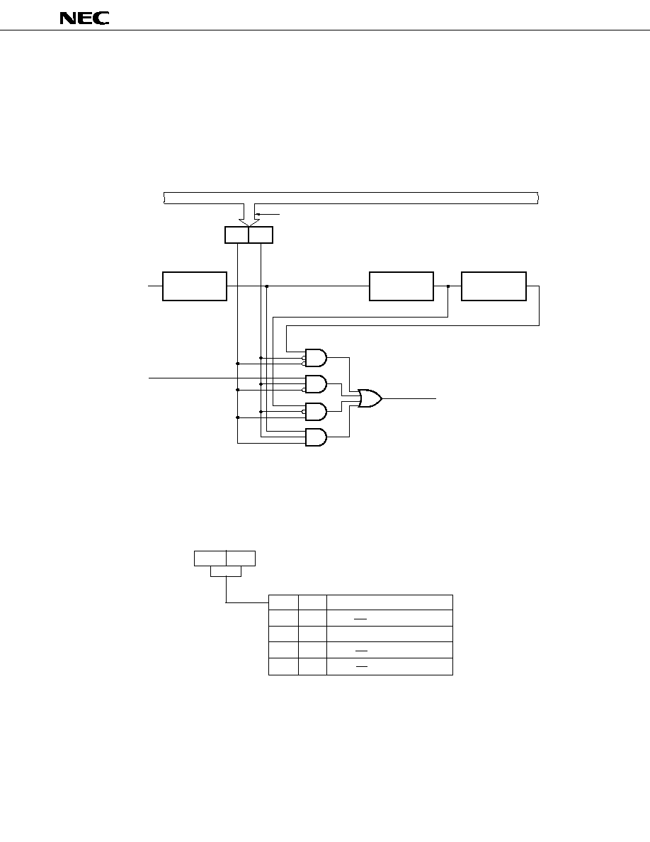
2.12 SERIAL INTERFACE
The serial interface consists of an 8-bit shift register, 3-bit shift mode register, and 3-bit counter. It is used for
input/output of serial data.
Fig. 2-13 Serial Interface Block Diagram
INT0
P00/INT0
P01/SCK
P02/SO
P03/SI
*IPL
*TSIOAM
TAMSIO*
LSB
8≠BIT SHIFT REG
MSB
3≠BIT CNT
RS F/F
R
S
Q
INTS
SIO*
SM3
SHIFT MODE REG
OPL*
4
8
8
Internal Bus
*
Instruction execution
Remarks
1.
indicates the internal clock signal (system clock).
2.
SM3 and INT0 go to the test control circuit.
Input/output of serial data is controlled by the serial clock. The highest bit (bit 7) of the shift register is output
from the SO line at rise of the serial clock (SCK pin signal). At its fall, the contents of the shift register is shifted by
one bit (bit n
bit n+1) and data on the SI line is loaded to the lowest bit (bit 0) of the shift register.
The 3-bit counter (octal counter) counts serial clock pulses. Wthenever it counts eight clock pulses (on completion
of 1-byte serial data transfer), the counter generates an internal test request signal INTS to set the test request flag
(INT0/S RQF).
Fig. 2-14 Shift Timing
INTS RQF
Setting Timing
SCK
SI
SO
DI
7
DO
7
MSB
DO
6
DO
5
DO
4
DO
3
DO
2
DO
1
DO
0
DI
6
DI
5
DI
4
DI
3
DI
2
DI
1
DI
0
LSB
Remarks
1.
DI: Serial data input
2.
DO: Serial data output
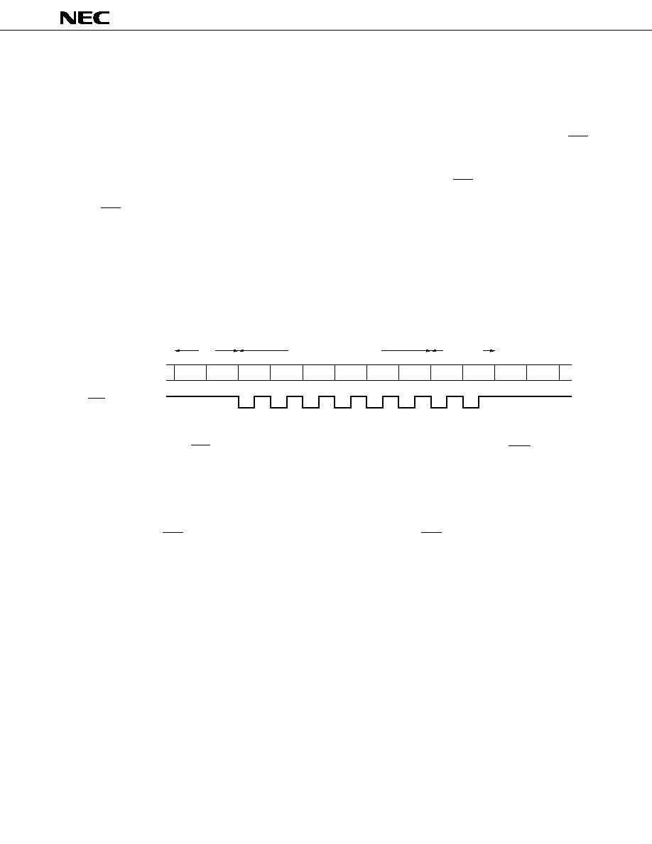
22
µ
PD7564A, 7564A(A)
The serial interface sets serial data for transmission in the shift register using the TAMSIO instruction and starts
the transfer using the SIO instruction. To recognize the termination of one-byte transfer, check the test request flag
INT0/S RQF using the corresponding instruction.
The serial interface starts serial data reception, using the SIO instruction, checks the termination of one-byte
transfer using the instruction, and then receives data from the shift register by executing the TSIOAM instruction.
Two types of serial clock sources are available: one is the system clock
and the other is the external clock (SCK
input). They are selected respectively by bits 2 and 1 (SM2 and SM1) of the shift mode register.
When the system clock
is selected and the SIO instruction is executed, the clock pulse is supplied to the serial
interface as a serial clock to control serial data input/output and is output from the SCK pin.
When the system clock
pulse is supplied eight times, the supply to the serial interface is automatically stopped
and the SCK output remains high. Since serial data input/output stops automatically after transfer of one byte. The
programmer does not need to control the serial clock. In this case, the transfer speed is determined by the system
clock frequency.
In this mode, it is possible to read receive data (by the TSIOAM instruction) and write data (by the TAMSIO
instruction) from and to the shift register only by waiting for 6 machine cycles after execution of the SIO instrucction
on the program without waiting until the INT0/S RQF is set.
Fig. 2-15 TAMSIO/TSIOAM Instruction Execution Timing
SCK
SIO
TAMSIO
TSIOAM
Wait (6 Machine Cycle)
Instruction Execution
Machine Cycle
When the external clock (SCK input) is selected, the interface inputs serial clock pulses from the SCK input. When
an external serial clock pulse is input eight times, the INT0/S RQF is set and the termination of one-byte transfer
can be recognized. However, the eight serial clocks to be input must be counted on the side of the external clock
source because serial clock disable control is not performed internally. The transfer speed is determined by the
external serial clock within the range from DC to the maximum value limited by the standard.
When the external clock is used, the SIO, TAMSIO, or TSIOAM instruction the execution must be executed while
the serial clock pulse SCK is high. If such an instruction is executed while the SCK is rising or falling or is low, the
function of the instruction is not guaranteed.
23
µ
PD7564A, 7564A(A)
Fig. 2-16 Shift Mode Register Format
Shift Mode Register
Settings for serial interface operation and the associated mode of the port 0
INT0/INTS selection
SM3
Test Sources
0
INTS
1
INT0
Caution
When setting a code in the shift mode register using the OPL instruction, be sure to set bit 0 of the
accumulator to 0 (Bit 0 corresponds to CM0 of the
µ
PD7500H of EVAKIT-7500B in emulation).
In the system which does not require serial interface, the 8-bit shift register can be used as a simple register and
data can be read or writtene by the TSIOAM or TAMSIO instruction when serial operation is off.
2.13 TEST CONTROL CIRCUIT
The
µ
PD7564A is provided with the following three types of test sources (one external source and two internal
sources):
The test control circuit checks consist mainly of test request flags (INTT RQF and INT0/S RQF) which are set by
three different test sources and the test request flag control circuit which checks the content of test request flags
using the SKI instruction and controls resetting the checked flags.
The INT0 and INTS are common in the request flag. Which one is selected is determined by bit 3 (SM3) of the
shift mode register.
SM3
SM2
SM1
SM2
SM1
P03/SI
P02/SO
P01/SCK
Serial Operation
0
0
Port input
Port input
Port input
Stop
0
1
continuous output
1
0
SI input
SO output
SCK input
Operation based on external clock
1
1
SCK output (
◊
8)
Operation based on
Test Sources
Internal/External
Request Flag
INTT (Overflow from timer/event counter)
Internal
INTT RQF
INT0 (Test request signal from P00 pin)
External
INT 0/S RQF
INTS (Transfer end signal from serial interface)
Internal
SM3
Test Sources
0
INTS
1
INT0
24
µ
PD7564A, 7564A(A)
The INTT RQF is set when a timer overflow occurs and is reset by the SKI or TIMER instruction.
The INT0/S request flag functions in the following two ways according to the setting of the SM3:
(1) SM3 = 0
The INTS is validated. The request flag INT0/S RQF is set when the INTS signal to indicate the termination of 8-
bit serial data transfer is issued. The flag is reset when the SKI or SIO instruction is executed.
(2) SM3 = 1
The IN0 is validated. The request flag INT0/S RQF is set when the leading edge signal enters the INT0/P00 pin.
The flag is reset when the SKI instruction is executed.
The OR output of each test request flag is used to cancel the HALT mode. If one or more request flags are set
in the HALT mode, the standby mode is cancelled.
The RESET signal cancels every request flag and the SM3. In the reset initial status, the INTS is selected and the
INT0 input is disabled.
Fig. 2-17 Test Control Circuit Block Diagram
INTS
TEST RQF
CONTROL
SKI*
TIMER*
S
R
INTT
RQF
Q
S
R
INT0/S
RQF
Q
NONSYNC
EDGE GATE
NONSYNC
EDGE GATE
SM3
OPL*
*SIO
INT0
INTT
HALT
RELEASE
Internal Bus
*
Instruction execution
Remarks
SM3 is bit 3 of the shift mode register.

25
µ
PD7564A, 7564A(A)
3.
STANDBY FUNCTIONS
The
µ
PD7564A provides two types of standby modes (STOP and HALT modes) to save power while the program
is on standby. The STOP and HALT modes are set by the STOP and HALT instructions, respectively. The STOP mode
stops every clock and the HALT mode stops only the CPU clock
. The HALT mode halts program execution, however,
it holds the contents of all the internal registers and data memory that have been stored.
The serial interface and timer/event counter can operate even in the HALT mode.
The STOP mode is cancelled only by RESET input. The HALT mode is cancelled when the test request flag (INTT
RQF or INT0/S RQF) is set or by RESET input. Note that if even one test request flag is set, the device cannot enter
either the STOP or HALT mode even though the STOP or HALT instruction is executed. Before setting the STOP
or HALT mode at a point where a test request flag may be set, execute the SKI instruction to reset the test request
flag.
3.1
STOP MODE
When the STOP instruction is executed, the device can enter the STOP mode at any time unless any request flag
is set.
In the STOP mode, the contents of the data memory are retained and the RESET input used to cancel the STOP
mode is valid. In the STOP mode, however, any other functions are turned off to minimize power consumption.
Caution
In the STOP mode, the CL1 input is internally connected to V
DD
(high level) to prevent a leak in the
ceramic oscillator.
3.2
CANCELLING THE HALT MODE
The HALT mode stops only the 1/2 divider in the system clock generator (allowing operation of the system clock
CL and stopping the CPU clock
). Therefore, the operations of the CPU requiring the
signal and the serial interface
using
as a serial clock are stopped in the HALT mode.
Since the HALT mode allows operation of the clock control circuit, the circuit inputs the CL signal from the clock
generator and the event pulse from the (P00) pin to supply the count pulses (CP) for both subsystems selectively
to the timer event counter. Thus, the timer event counter can operate depending on the both-system count pulses
and continue counting time.
The serial interface operates in this mode when the external clock (SCK input) is selected as a serial clock.
26
µ
PD7564A, 7564A(A)
3.3
CANCELLING STOP MODE BY RESET INPUT
When the RESET input goes high from low in the STOP mode, the standby mode returns to the HALT mode to
start ceramic oscillation.
When the RESET input returns to low, the HALT mode is cancelled and the CPU starts the program from address
0 after normal reset operation. The STOP mode is cancelled in this way.
Note that the content of the data memory is retained even during the cancelling operation, however, the content
of the other registers becomes undefined on cancellation.
Fig. 3-1 STOP Mode Cancel Timing
RESET Input
STOP
instruction
Starting Clock Oscillation
Cancellation
Normal Resetting Operation
(Starting from address 0)
HALT Mode
(Oscillation stabilizing time)
STOP Mode
Caution
The STOP mode does not result from setting the test request flag.
3.4
CANCELLING HALT MODE BY TEST REQUEST FLAG
When the test request flat (INTT RQF or INT0/S RQF) is set in the HALT mode, the mode is cancelled and the
program stars executing the instruction that follows the HALT instruction.
Cancellation of the HALT mode does not affect the content of any register or the data memory, that is retained
in the mode.
3.5
CANCELLING HALT MODE BY RESET INPUT
RESET input cancels the HALT mode unconditionally.
Fig. 3-2 shows the HALT mode unconditionally.
Fig. 3-2 HALT mode cancel timing by RESET input
RESET
HALT Mode
Cancellation
Normal Resetting Operation
(Starting from address 0)
The HALT mode is maintained while the RESET input is being active (high). When the RESET input goes low, the
HALT mode is cancelled and the CPU starts to execute the program from address 0 after a normal reset operation.
Note that RESET input does not affect the content of the data memory that is retained in the HALT mode, however,
the contents of the other registers become undefined on cancellation of the mode.

27
µ
PD7564A, 7564A(A)
4.
RESET FUNCTIONS
The
µ
PD7564A is reset and initialized when the RESET pin inputs a high or active RESET signal as follows:
4.1
DETAILS OF INITIALIZATION
(1) The program counter (PC9-PC0) is cleared to zero.
(2) The skip flags (SK1 and SK0) in the program status word are reset to zero.
(3) The count register in the timer-event counter is cleared to 00H.
(4) The clock control circuit becomes as follows:
∑ Clock mode registers (CM2 and CM1) = 0
1
© CP = CL
◊
≠≠≠≠≠
256
∑ Prescalers 1, 2, and 3 = 0
(5) The shift mode register (SM3 to SM1) is cleared to zero.
Shifting of the serial interface is stopped.
The port 0 enters the input mode (high impedance).
INT0/S, INTS is selected.
(6) The test request flag (INTT RQF or INT0/S RQF) is reset to zero.
(7) The contents of the data memory and the following registers become undefined:
Stack pointer (SP)
Accumulator (A)
Carry flag (C)
General registers (H and L)
Output latch of each port
(8) The output buffer of every port goes off and has high impedance. The I/O port enters the input mode.
Caution
When the STANDBY mode is cancelled by the RESET signal, the content of the data memory is retained
without becoming undefined.
When the RESET input is cancelled, the program is executed starting with address 000H. The content of each
register shall either be initialized in the process of the program or reinitialized depending on conditions.
28
µ
PD7564A, 7564A(A)
5.
µ
PD7564A INSTRUCTION SET
(1)
Operand representation and description
addr
10-bit immediate data or label
caddr
10-bit immediate data or label
caddr1
100H to 107H, 140H to 147H, 180H to 187H,
IC0H to IC7H immediate data or label
mem
6-bit immediate data or label
n5
5-bit immediate data or label
n4
4-bit immediate data or label
n2
2-bit immediate data or label
bit
2-bit immediate data or label
pr
HL-, HL+, HL
(2)
Mnemonics for operation descriptions
A
:
Accumulator
H
:
H register
L
:
L register
HL
:
Pair register HL
pr
:
Pair register HL-, HL+, or HL
SP
:
Stack pointer
PC
:
Program counter
C
:
Carry flag
PSW
:
Program status word
SIO
:
Shift register
CT
:
Count register
In
:
Immediate data to n5, n4 or n2
Pn
:
Immediate data to addr, caddr, or caddr1
Bn
:
Immediate data to bit
Dn
:
Immediate data to mem
Rn
:
Immediate data to pr
(
◊◊
)
:
Content addressed by
◊◊
◊
H
:
Hexadecimal data
29
µ
PD7564A, 7564A(A)
(3)
Port/mode register selection
IPL Instruction
L
Port
0
Port 0
AH
Port 10
BH
Port 11
OPL Instruction
L
Port/mode register
8
Port 8
AH
Port 10
BH
Port 11
CH
Clock mode register
FH
Shift mode register
RPBL/SPBL Instruction
L
FH
EH
DH
CH
BH
AH
9
8
2
1
0
Bit
3
2
1
0
3
2
1
0
2
1
0
Port
Port 11
Port 10
Port 8
(4)
Selection of pair register addressing
pr
R
1
R
0
HL≠
0
0
HL+
0
1
HL
1
0

30
µ
PD7564A, 7564A(A)
Accumulator &
carry flag
manipulation
instructions
Load/store instructions
Operation instructions
Mne-
Ope-
Operation Code
Operation
Skip
monic
rands
B1
B2
Condition
LAI
n4
0
0
0
1
I
3
I
2
I
1
I
0
A
n4
Loads n4 to the accumulator.
Stack LAI
LHI
n2
0
0
1
0
1
0
I
1
I
0
H
n2
Loads n2 to H register.
LAM
pr
0
1
0
1
0
0
R
1
R
0
A
(pr) pr = HL ≠, HL +, HL
Loads the contents of the memory
L = FH(HL ≠)
address by pr to the accumulator.
L = 0 (HL +)
LHLI
n5
1
1
0
I
4
I
3
I
2
I
1
I
0
H
0I
4
, L
I
3
≠
0
Loads n5 to the pair register HL.
Stack LHLI
ST
0
1
0
1
0
1
1
1
(HL)
A
Stores the contents of the accumulator
in the memory addressed by HL.
STII
n4
0
1
0
0
I
3
I
2
I
1
I
0
(HL)
n4, L
L+1
Stores n4 in the memory addressed by
HL and increments the L register.
XAL
0
1
1
1
1
0
1
1
A
L
Exchanges the contents of the accumu-
lator and the L register.
XAM
pr
0
1
0
1
0
1
R
1
R
0
A
(pr) pr = HL ≠ , HL + , HL
Exchanges the contents of the accumu-
L = FH(HL≠)
lator and the memory addressed by pr.
L = 0 (HL+)
AISC
n4
0
0
0
0
I
3
I
2
I
1
I
0
A
A + n4
Adds the accumulator to n4.
Carry
ASC
0
1
1
1
1
1
0
1
A
A + (HL)
Adds the contents of the accumulator
Carry
and the memory addressed by HL.
Adds the contents of the accumulator,
ACSC
0
1
1
1
1
1
0
0
A, C
A + (HL) + C
the memory addressed by HL, and of
Carry
the carry flag.
Calculate the exclusive OR of the
EXL
0
1
1
1
1
1
1
0
A
A
(HL)
contents of the accumulator and the
memory addressed by HL.
CMA
0
1
1
1
1
1
1
1
A
A
≠≠
Complements the accumulator.
RC
0
1
1
1
1
0
0
0
C
0
Resets the carry flag.
SC
0
1
1
1
1
0
0
1
C
1
Sets the carry flag.
ILS
0
1
0
1
1
0
0
1
L
L + 1
Increments the L register.
L = 0
IDRS
mem
0
0
1
1
1
1
0
1
0
0
D
5
D
4
D
3
D
2
D
1
D
0
(mem)
(mem) + 1
Increments the contents of the memory
(mem) = 0
addressed by mem.
DLS
0
1
0
1
1
0
0
0
L
L ≠ 1
Decrements the L register.
L = FH
DDRS
mem
0
0
1
1
1
1
0
0
0
0
D
5
D
4
D
3
D
2
D
1
D
0
(mem)
(mem) ≠ 1
Decrements the contents of the memory
(mem) = FH
addressed by mem.
RMB
bit
0
1
1
0
1
0
B
1
B
0
(HL)
bit
0
Resets the bits specified by B
1≠0
, of the
memory addressed by HL.
SMB
bit
0
1
1
0
1
1
B
1
B
0
(HL)
bit
1
Sets the bits specified by B
1≠0
, of the
memory addressed by HL.
Increment/decre-
ment instructions
Note
Instruction Group
Note
Memory bit
manipulation
Iistructions
31
µ
PD7564A, 7564A(A)
Mne-
Ope-
Operation Code
Operation
Skip
monic
rands
B1
B2
Condition
JMP
addr
0
0
1
0
0
0
P
9
P
8
P
7
P
6
P
5
P
4
P
3
P
2
P
1
P
0
PC
9≠0
P
9≠0
Jumps to the address specified by P
9≠0
.
JCP
addr
1
0
P
5
P
4
P
3
P
2
P
1
P
0
PC
5≠0
P
5≠0
Jumps to the address specified by
replacing PC
5≠0
with P
5≠0
.
(SP≠1)(SP≠2)(SP≠4)
PC
9≠0
Saves the contents of PC and PSW to the
CALL
caddr
0
0
1
1
0
0
P
9
P
8
P
7
P
6
P
5
P
4
P
3
P
2
P
1
P
0
(SP≠3)
PSW, SP
SP ≠ 4
stacxk memory, decrements SP by 4, and
PC
9≠0
P
9≠0
calls the address specified by caddr.
(SP≠1)(SP≠2)(SP≠4)
PC
9≠0
Saves the contents of PC and PSW to the
CAL
caddr1 1
1
1
P
4
P
3
P
2
P
1
P
0
(SP≠3)
PSW, SP
SP ≠ 4
stacxk memory, decrements SP by 4, and
PC
9≠0
0 1 P
4
P
3
0 0 0 P
2
P
1
P
0
calls the address specified by caddr1.
RT
0
1
0
1
0
0
1
1
PC
9≠0
(SP)(SP+2)(SP+3)
Restores the contents of the stack
SP
SP + 4
memory to PC, and increments SP by 4.
PC
9≠0
(SP)(SP+2)(SP+3)
Restores the contents of the stack
RTS
0
1
0
1
1
0
1
1
SP
SP + 4
memory to PC, increments SP by 4,
then skip unconditionally
and causes unconditional skipping.
Transfers the two low-order bits of the
TAMSP
0
0
1
1
1
1
1
1
0
0
1
1
0
0
0
1
PC
5≠4
A
1≠0
accumulator to SP
5≠4
and the three high-
SP
3≠1
(HL)
3≠1
, SP
0
0
order bits of the memory addressed by
HL to SP
3≠1
.
SKC
0
1
0
1
1
0
1
0
Skip if C = 1
Causes skipping if the carry flag is 1.
C = 1
SKABT
bit
0
1
1
1
0
1
B
1
B
0
Skip if A
bit
= 1
Causes skipping of the bit of the accumu-
A
bit
= 1
lator, which is specified by B
1-0
is 1.
Causes skipping of the bit of the memory
SKMBT
bit
0
1
1
0
0
1
B
1
B
0
Skip if (HL)
bit
= 1
addressed by HL, which is specified by
(HL)
bit
= 1
B
1≠0
is 1.
Causes skipping of the bit of the memory
SKMBF
bit
0
1
1
0
0
0
B
1
B
0
Skip if (HL)
bit
= 0
addressed by HL, which is specified by
(HL)
bit
= 0
B
1≠0
is 0.
Causes skipping if the contents are the
SKAEM
0
1
0
1
1
1
1
1
Skip if A = (HL)
same between the accumulator and the
A = (HL)
memory addressed by HL.
SKAEI
n4
0
0
1
1
1
1
1
1
0
1
1
0
I
3
I
2
I
1
I
0
Skip if A = n4
Skips if the accumulator is equal to n4.
A = n4
SKI
n2
0
0
1
1
1
1
1
1
0
1
0
0
0
0
I
1
I
0
Skip if INT RQF = 1
Skips if INT RQF is 1, and then sets
INT RQF = 1
Then reset INT RQF
INT RQF to 0.
Note
Jump
instructions
Subroutine/stack control instructions
Skip instructions
Note
Instruction Group
Uncondition-
ally
32
µ
PD7564A, 7564A(A)
Mne-
Ope-
Operation Code
Operation
Skip
monic
rands
B1
B2
Condition
Transfers the contents of the accumulator
SIO
7≠4
A
to the four high-order bits of the shift
TAMSIO
0
0
1
1
1
1
1
1
0
0
1
1
1
1
1
0
SIO
3≠0
(HL)
register and the contents of the memory
addressed by HL to the four low-order bits.
Transfers the four high-order bits of the
TSIOAM
0
0
1
1
1
1
1
1
0
0
1
1
1
0
1
0
A
SIO
7≠4
shift register to the accumulator and the
(HL)
SIO
3≠0
four low-order bits to the memory
addressed by HL.
SIO
0
0
1
1
1
1
1
1
0
0
1
1
0
0
1
1
Start SIO
Starts shifting.
TIMER
0
0
1
1
1
1
1
1
0
0
1
1
0
0
1
0
Start Timer
Starts timer operation.
Transfers the four high-order bits of
A
CT
7≠4
the count register to the accumulator
TCNTAM
0
0
1
1
1
1
1
1
0
0
1
1
1
0
1
1
(HL)
CT
3≠0
and the four low-order bits to the
memory addressed by HL.
IPL
0
1
1
1
0
0
0
0
A
Port (L)
Loads the contents of the port specified
by the L register to the accumulator.
Outputs the contents of the accumu-
OPL
0
1
1
1
0
0
1
0
Port/Mode reg. (L)
A
lator to the port specified by the L
register or the mode register.
RPBL*
0
1
0
1
1
1
0
0
Port bit (L)
0
Resets the bits of ports 8, 10, and 11,
that are specified by the L register.
SPBL*
0
1
0
1
1
1
0
1
Port bit (L)
1
Sets the bits of ports 8, 10, and 11,
that are specified by the L register.
HALT
0
0
1
1
1
1
1
1
0
0
1
1
0
1
1
0
Set Halt Mode
Sets the HALT mode.
STOP
0
0
1
1
1
1
1
1
0
0
1
1
0
1
1
1
Set Stop Mode
Sets the STOP mode.
NOP
0
0
0
0
0
0
0
0
No operation
Performs no operation for one
machine cycle.
Note
*
SPBL and RPBL are bit-wise set/reset instructions. They perform output to each 4-bit port including the specified bits as well as set and reset operation
(They output the contents of the output latch to bits other than the specified bits.). Before executing these instructions, intialize the contents of the output
latch using the OPL instruction.
Note
Instruction Group
SIO control instructions
Timer control
instructions
Input/output instructions
CPU control
instructions
33
µ
PD7564A, 7564A(A)
6.
ELECTRICAL SPECIFICATIONS
µ
PD7564A: ABSOLUTE MAXIMUM RATINGS (T
a
= 25
∞
C)
Parameter
Symbol
Test Conditions
Rating
Unit
Supply voltage
V
DD
≠0.3 to +7.0
V
Except ports 10 and 11
≠0.3 to V
DD
+ 0.3
V
Input voltage
V
I
Ports 10 and 11
*1
≠0.3 to V
DD
+ 0.3
V
*2
≠0.3 to +11
V
Except ports 8, 10, 11
≠0.3 to V
DD
+ 0.3
V
Output voltage
V
O
Ports 8, 10 and 11
*1
≠0.3 to V
DD
+ 0.3
V
*2
≠0.3 to +11
V
Output current high
I
OH
1 pin
≠5
mA
All pins in total
≠15
mA
P01, P02
5
mA
Output current low
I
OL
1 pin
Port 8
30
mA
Others
15
mA
All pins in total
100
mA
Operating temperature
T
opt
≠10 to +70
∞
C
Storage temperature
T
stg
≠65 to +150
∞
C
Power consumption
P
d
Ta = 70
∞
C
Shrink DIP
480
mW
Mini flat
250
*
1. CMOS input/output or N-ch open-drain output + pull-up resistor built-in input/output
2. N-ch open-drain input/output
Caution
Even if one of the parameters exceeds its absolute maximum rating even momentarily, the quality of
the product may be degraded. The absolute maximum rating therefore specifies the upper or lower
limit of the value at which the product can be used without physical damages. Be sure not to exceed
or fall below this value when using the product.
5
34
µ
PD7564A, 7564A(A)
µ
PD7564A(A): ABSOLUTE MAXIMUM RATINGS (T
a
= 25
∞
C)
Parameter
Symbol
Test Conditions
Rating
Unit
Supply voltage
V
DD
≠0.3 to +7.0
V
Except ports 10 and 11
≠0.3 to V
DD
+ 0.3
V
Input voltage
V
I
Ports 10 and 11
*1
≠0.3 to V
DD
+ 0.3
V
*2
≠0.3 to +11
V
Except ports 8, 10, 11
≠0.3 to V
DD
+ 0.3
V
Output voltage
V
O
Ports 8, 10 and 11
*1
≠0.3 to V
DD
+ 0.3
V
*2
≠0.3 to +11
V
Output current high
I
OH
1 pin
≠5
mA
All pins in total
≠15
mA
P01, P02
5
mA
Output current low
I
OL
1 pin
Port 8
30
mA
Others
15
mA
All pins in total
100
mA
Operating temperature
T
opt
≠40 to +85
∞
C
Storage temperature
T
stg
≠65 to +150
∞
C
Power consumption
P
d
T
a
= 85
∞
C
Shrink DIP
350
mW
Mini flat
195
*
1. CMOS input/output or N-ch open-drain output + pull-up resistor built-in input/output
2. N-ch open-drain input/output
Caution
Even if one of the parameters exceeds its absolute maximum rating even momentarily, the quality of
the product may be degraded. The absolute maximum rating therefore specifies the upper or lower
limit of the value at which the product can be used without physical damages. Be sure not to exceed
or fall below this value when using the product.
CAPACITY (T
a
= 25
∞
C, V
DD
= 0 V)
Parameter
Symbol
Test Conditions
MN.
TYP.
MAX.
Unit
Input capacity
C
IN
P00, P03
15
pF
Output capacity
C
OUT
Port 8
35
pF
I/O capacity
C
IO
P01, P02
15
pF
Ports 10 and 11
35
pF
5
f = 1 MHz
Unmeasured pins
returned to 0 V.
35
µ
PD7564A, 7564A(A)
RESONATOR CHARACTERISTICS
µ
PD7564A
: T
a
= ≠10 to +70
∞
C, V
DD
= 2.7 to 6.0 V
µ
PD7564A(A) : T
a
= ≠40 to +85
∞
C, V
DD
= 2.7 to 6.0 V
Resonator
External Circuit
Parameter
Test Conditions
MIN.
TYP.
MAX.
Unit
V
DD
= 4.5 to 6.0 V
290
700
710
kHz
V
DD
= 4.0 to 6.0 V
290
500
510
kHz
V
DD
= 3.5 to 6.0 V
290
400
410
kHz
V
DD
= 2.7 to 6.0 V
290
300
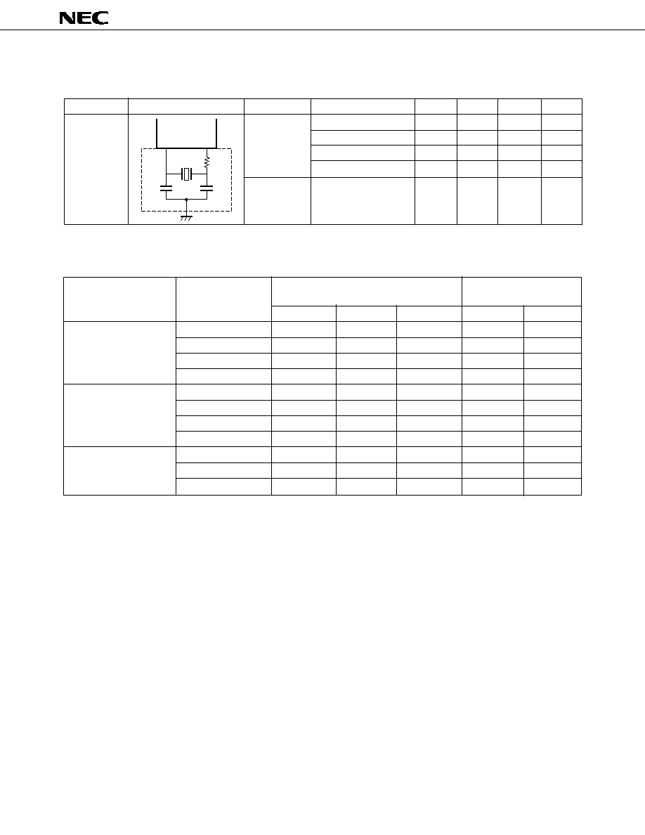
310
kHz
20
ms
*
The following ceramic resonators are recommended.
Recommended Constant
Operating Voltage
Manufacturer
Product Name
Range [V]
C1 [pF]
C2 [pF]
R2 [k
]
MIN.
MAX.
CSB300D
330
330
6.8
2.7
6.0
Murata Mfg.
CSB400P
220
220
6.8
3.5
6.0
CSB500E
100
100
6.8
4.0
6.0
CSB700A
100
100
6.8
4.5
6.0
KBR-300B
470
470
0
2.7
6.0
Kyocera
KBR-400B
330
330
0
3.5
6.0
KBR-500B
220
220
0
4.0
6.0
KBR-680B
220
220
0
4.5
6.0
CRK-400
120
120
12
3.5
6.0
Toko
CRK-500
100
100
12
4.0
6.0
CRK-680
82
82
12
4.5
6.0
Caution 1.
Install the oscillation circuit as close to CL1 and CL2 pins as possible.
2.
Do not allow other signal lines to pass through the area enclosed by dotted lines.
Oscillator
frequency
(f
CC
)
R2
CL1
CL2
C2
C1
After reaching MIN.
of operating voltage
range
Oscillation
stabilization
time (t
OS
)
Ceramic
resonator *
36
µ
PD7564A, 7564A(A)
DC CHARACTERISTICS
µ
PD7564A
: T
a
= ≠10 to +70
∞
C, V
DD
= 2.7 to 6.0 V
µ
PD7564A(A) : T
a
= ≠40 to +85
∞
C, V
DD
= 2.7 to 6.0 V
Parameter
Symbol
Test Conditions
MIN.
TYP.
MAX.
Unit
Input voltage high
V
IH1
Except ports 10 and 11
0.7V
DD
V
DD
V
V
IH2
Ports 10 and 11 *1
0.7V
DD
9
V
Input voltage low
V
IL
0
0.3V
DD
V
V
DD
= 4.5 to 6.0 V
V
DD
≠ 2.0
V
Output voltage high
V
OH
I
OH
= ≠1 mA
I
OH
= ≠100
µ
A
V
DD
≠ 1.0
V
V
DD
= 4.5 to 6.0 V
0.4
V
P01, P02
I
OL
= 1.6 mA
I
OL
= 400
µ
A
0.5
V
V
DD
= 4.5 to 6.0 V
0.4
V
I
OL
= 1.6 mA
Output voltage low
V
OL
Ports 10 and 11
V
DD
= 4.5 to 6.0 V
2.0
V
I
OL
= 10 mA
I
OL
= 400
µ
A
0.5
V
V
DD
= 4.5 to 6.0 V
2.0
V
Port 8
I
OL
= 15 mA
I
OL
= 600
µ
A
0.5
V
Input leak current high
I
LIH1
V
IN
= V
DD
3
µ
A
I
LIH2
V
IN
= 9 V, ports 10 and 11 *1
10
µ
A
Input leak current low
I
LIL
V
IN
= 0 V
≠3
µ
A
Output leak current high
I
LOH1
V
OUT
= V
DD
3
µ
A
I
LOH2
V
OUT
= 9 V, ports 8, 10, and 11 *1
10
µ
A
Output leak current low
I
LOL
V
OUT
= 0 V
≠3
µ
A
Input pin built-in resistor
Port 0, RESET
23.5
47
70.5
K
(pull-up/down resistor)
Output pin built-in resistor
Ports 10 and 11
7.5
15
22.5
K
(pull-up resistor)
V
DD
= 5 V
±
10 %
650
2200
µ
A
I
DD1
Operating mode
f
CC
= 700 kHz
V
DD
= 3 V
±
10 %
120
360
µ
A
f
CC
= 300 kHz
Supply current *2
V
DD
= 5 V
±
10 %
450
1500
µ
A
I
DD2
HALT mode
f
CC
= 700 kHz
V
DD
= 3 V
±
10 %
65
200
µ
A
f
CC
= 300 kHz
I
DD3
STOP mode
V
DD
= 5 V
±
10 %
0.1
10
µ
A
V
DD
= 3 V
±
10 %
0.1
5
µ
A
*
1. For N-ch open-drain input/output selection
2. The current flowing in built-in pull-up and pull-down resistors is excluded.
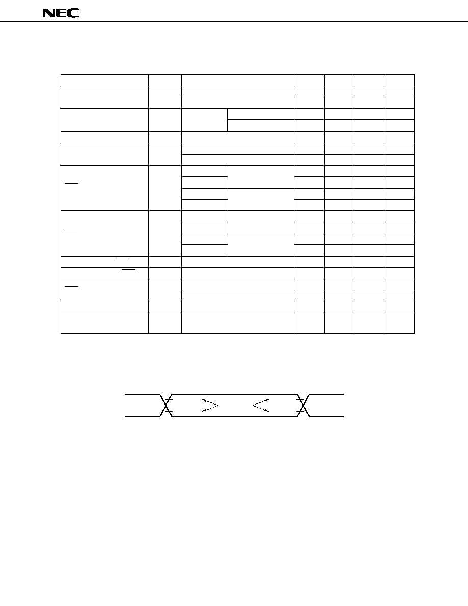
37
µ
PD7564A, 7564A(A)
AC CHARACTERISTICS
µ
PD7564A
: T
a
= ≠10 to +70
∞
C, V
DD
= 2.7 to 6.0 V
µ
PD7564A(A) : T
a
= ≠40 to +85
∞
C, V
DD
= 2.7 to 6.0 V
Parameter
Symbol
Test Conditions
MIN.
TYP.
MAX.
Unit
Internal clock cycle time
t
CY
*
V
DD
= 4.5 to 6.0 V
2.8
6.9
µ
s
6.4
6.9
µ
s
P00 event input frequency
f
PO
Duty = 50%
V
DD
= 4.5 to 6.0 V
0
710
kHz
0
350
kHz
P00 input rise/fall time
t
POR
, t
POF
0.2
µ
s
t
POH
, t
POL
V
DD
= 4.5 to 6.0 V
0.7
µ
s
1.45
µ
s
Input
V
DD
= 4.5 to 6.0 V
2.0
µ
s
SCK cycle time
t
KCY
Output
2.5
µ
s
Input
5.0
µ
s
Output
5.7
µ
s
Input
V
DD
= 4.5 to 6.0 V
1.0
µ
s
SCK high/low level width
t
KH
, t
KL
Output
1.25
µ
s
Input
2.5
µ
s
Output
2.85
µ
s
SI setup time (to SCK
)
t
SIK
100
ns
SI hold time (from SCK
)
t
KSI
100
ns
SCK
SO output delay time
t
KSO
V
DD
= 4.5 to 6.0 V
850
ns
1200
ns
INT0 high/low level width
t
IOH
, t
IOL
10
µ
s
RESET high/low level
t
RSH
, t
RSL
10
µ
s
width
*
t
CY
= 2/f
CC
(See the characteristics curves for the power supply conditions specified above.)
AC Timing Test Point (Except CL1 Input)
0.7 V
DD
0.3 V
DD
0.7 V
DD
0.3 V
DD
Test
Points
P00 input high/low level
width
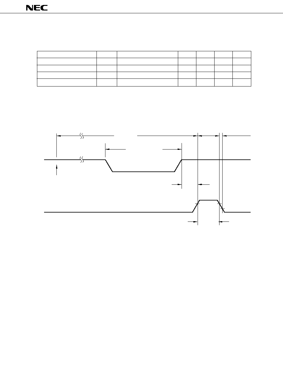
38
µ
PD7564A, 7564A(A)
CHARACTERISTICS OF DATA MEMORY DATA RETENTION AT LOW SUPPLY VOLTAGE IN STOP MODE
µ
PD7564A
: T
a
= ≠10 to +70
∞
C
µ
PD7564A(A) : T
a
= ≠40 to +85
∞
C
Parameter
Symbol
Test Conditions
MIN.
TYP.
MAX.
Unit
Data retention supply voltage
V
DDDR
2.0
6.0
V
Data retention supply current
I
DDDR
V
DDDR
= 2.0 V
0.1
5
µ
A
RESET setup time
t
SRS
0
µ
s
Oscillation stabilization time
t
OS
After V
DD
reaches 4.5 V
20
ms
Data Retention Timing
V
DD
RESET
STOP Instruction
Execution
STOP Mode
t
OS
Data Retention Mode
Operating Mode
HALT
mode
t
SRS
V
DDDR
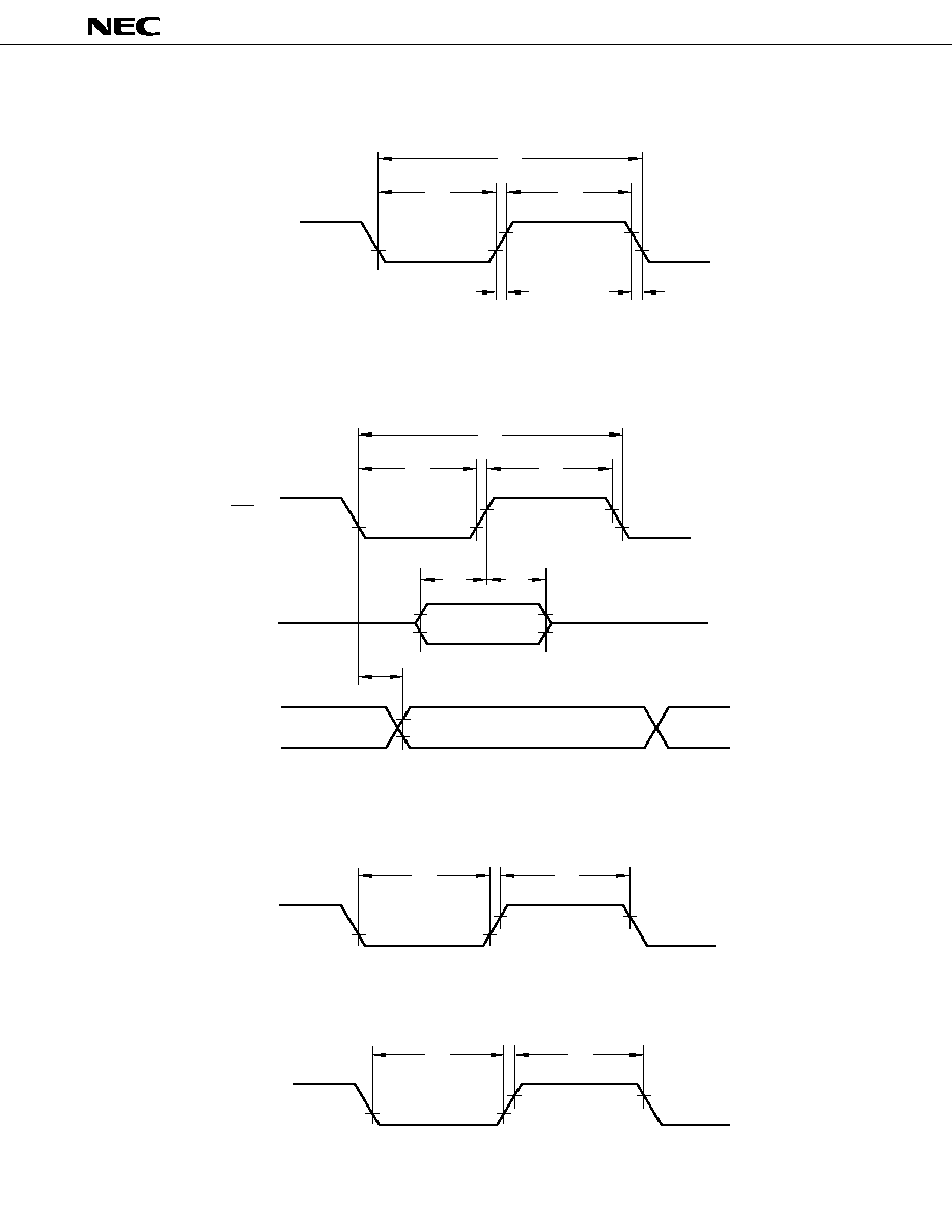
39
µ
PD7564A, 7564A(A)
P00 Input Timing
1/f
P0
t
POL
t
POH
P00 Input
t
POR
t
POF
Serial Transfer Timing
t
KCY
t
KL
t
KH
SCK
t
SIK
t
KSI
t
KSO
SI
SO
Output Data
Input Data
Test Input Timing
t
IOL
t
IOH
INT0
RESET Input Timing
t
RSL
t
RSH
RESET
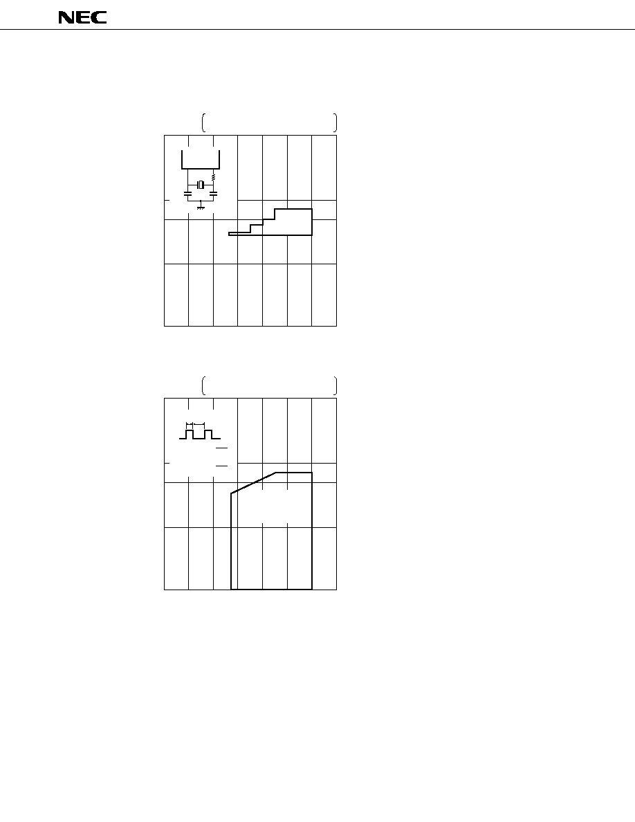
40
µ
PD7564A, 7564A(A)
7.
CHARACTERISTIC CURVES
1000
500
100
0
1
2
3
4
5
6
0
1
2
3
4
5
6
µ
f
CC
(Ceramic Oscillation) vs. V
DD
Operating
Guarantee
Range
System Clock Oscillator Frequency f
CC
[kHz]
P00 Event Input Frequency f
PO
[kHz]
Supply Voltage V
DD
[V]
f
PO
vs. V
DD
Operating Guarantee Range
Supply Voltage V
DD
[V]
t
1
t
2
CL1
t
1
>t
2
: f
X
=
1
2t
2
t
1
<t
2
: f
X
=
1
2t
1
1000
500
100
10
Operating
Guarantee
Range
R2
CL1 CL2
C2
C1
PD7564A
PD7564A(A)
: T
a
= ≠10 to +70∞C
: T
a
= ≠40 to +85∞C
µ
µ
PD7564A
PD7564A(A)
: T
a
= ≠10 to +70∞C
: T
a
= ≠40 to +85∞C
µ
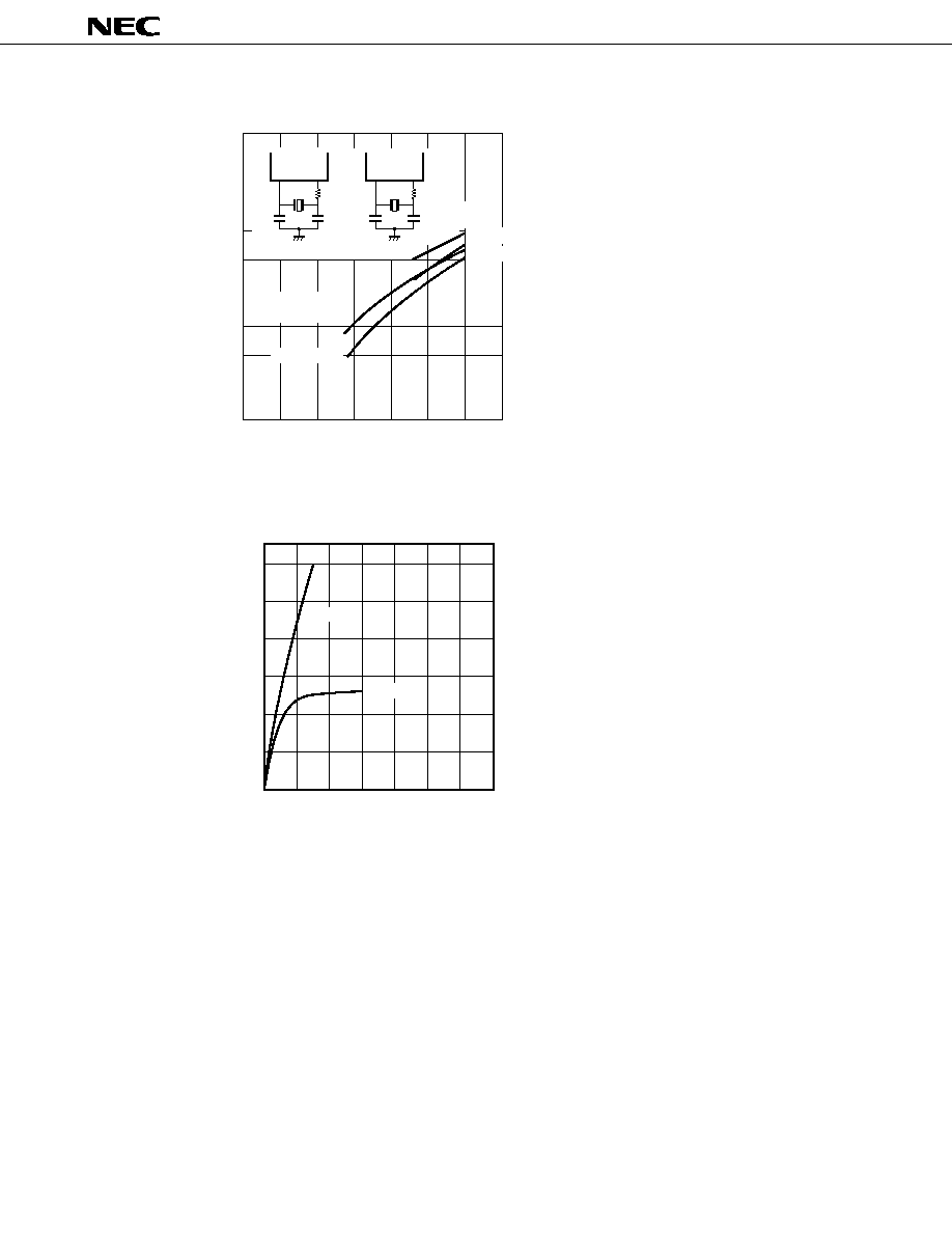
41
µ
PD7564A, 7564A(A)
Caution
The absolute maximum rating is 30
mA per pin.
1000
500
100
10
0
1
2
3
4
5
6
(T
a
= 25∞C)
Supply Current I
DD
[A
]
I
DD
vs. V
DD
Characteristic Example
(Reference Value)
Supply Voltage V
DD
[V]
50
µ
6.8 k
CL1 CL2
330
pF
CL1 CL2
6.8 k
100
pF
100
pF
330
pF
CSB300D
CSB700A
HALT mode
f
CC
=
700 kHz
f
CC
= 300 kHz
Operating mode
HALT mode
Operating mode
0
1
2
3
4
5
6
0
5
10
15
20
25
30
(T
a
= 25∞C)
V
DD
= 3 V
V
DD
= 5 V
I
OL
vs. V
OL
Characteristic Example (Port 8)
(Reference Value)
Output Current Low I
OL
[mA]
Output Voltage Low V
OL
[V]
42
µ
PD7564A, 7564A(A)
Caution
The absolute maximum rating is 15 mA per
pin.
Caution
The absolute maximum rating is -5 mA
per pin.
0
1
2
3
4
5
6
0
5
10
15
20
25
30
(T
a
= 25∞C)
0
1
2
3
4
5
6
0
≠1
≠2
≠3
≠4
≠5
(T
a
= 25∞C)
V
DD
= 3 V
V
DD
= 5 V
V
DD
= 5 V
V
DD
= 3 V
I
OL
vs. V
OL
Characteristic Example (Port 10, 11)
(Reference Value)
Output Current Low I
OL
[mA]
Output Voltage Low V
OL
[V]
I
OH
vs. V
OH
Characteristic Example
(Reference Value)
Output Current High I
OH
[mA]
V
DD
≠ V
OH
[V]
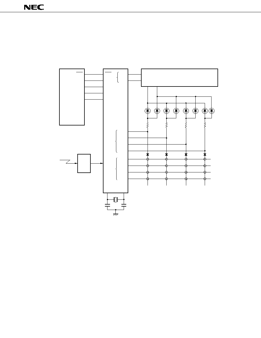
43
µ
PD7564A, 7564A(A)
8.
µ
PD7564A APPLIED CIRCUITS
(1)
Remote control reception + key entry + LED display
PD7564A
µ
SCK
SO
SI
PD75008
µ
PD75108
µ
SCK
SI
SO
P110
P111
CMOS Output
P113
RES
P80
P81
P82
P112
P100
P101
P102
P103
INT0
PC2800AHA(MS) etc.
µ
LED 8
PA80C
µ
Driver
(Chip
Selector
Transfer
Request)
Open-Drain Output
On-Chip Pull-Up
Resistor Input
Key Input 4
◊
4
Master
Microcomputer
etc.
Remote
Control
Signal
Amplifier
Circuit
CL1
CL2
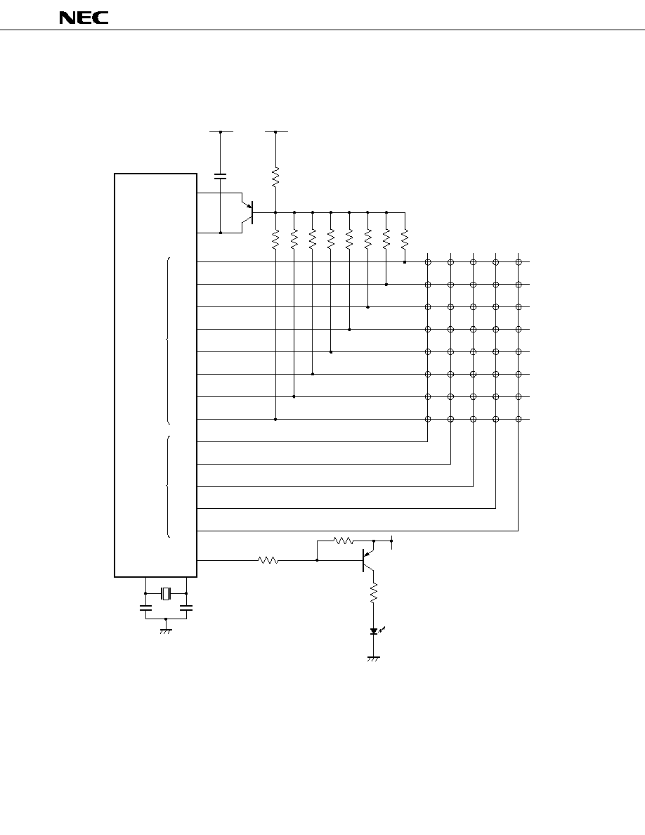
44
µ
PD7564A, 7564A(A)
(2)
Remote control transmission
PD7564A
µ
P113
N-ch
Open-Drain
Output
CL1
CL2
P112
P111
P110
P82
P103
P102
P101
P100
P03
P02
P01
P00
On-Chip
Pull-Up
Resistor
Input
P80
RESET
(CMOS Output)
P81
Ceramic Resonator
304 kHz
Infrared Light
Emitting Diode
SE307-C
2SA952
2SA733
MAX. 40 Keys
On-Chip Pull-Down
Resistor
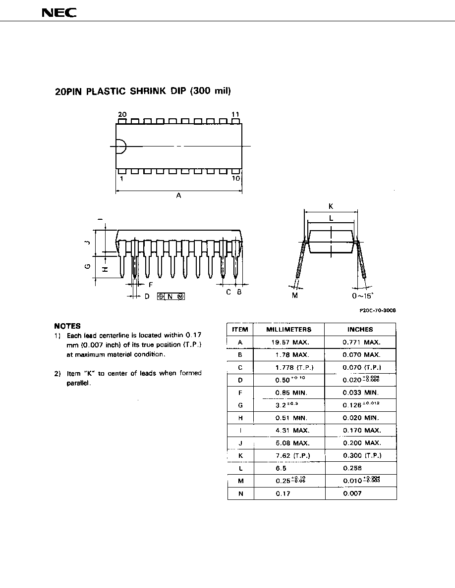
45
µ
PD7564A, 7564A(A)
9.
PACKAGE INFORMATION
DRAWINGS OF MASS-PRODUCTION PRODUCT PACKAGES
5
Caution
Dimensions of ES products are different from those of mass-production products. Refer to DRAWINGS
OF ES PRODUCT PACKAGES (1/2).
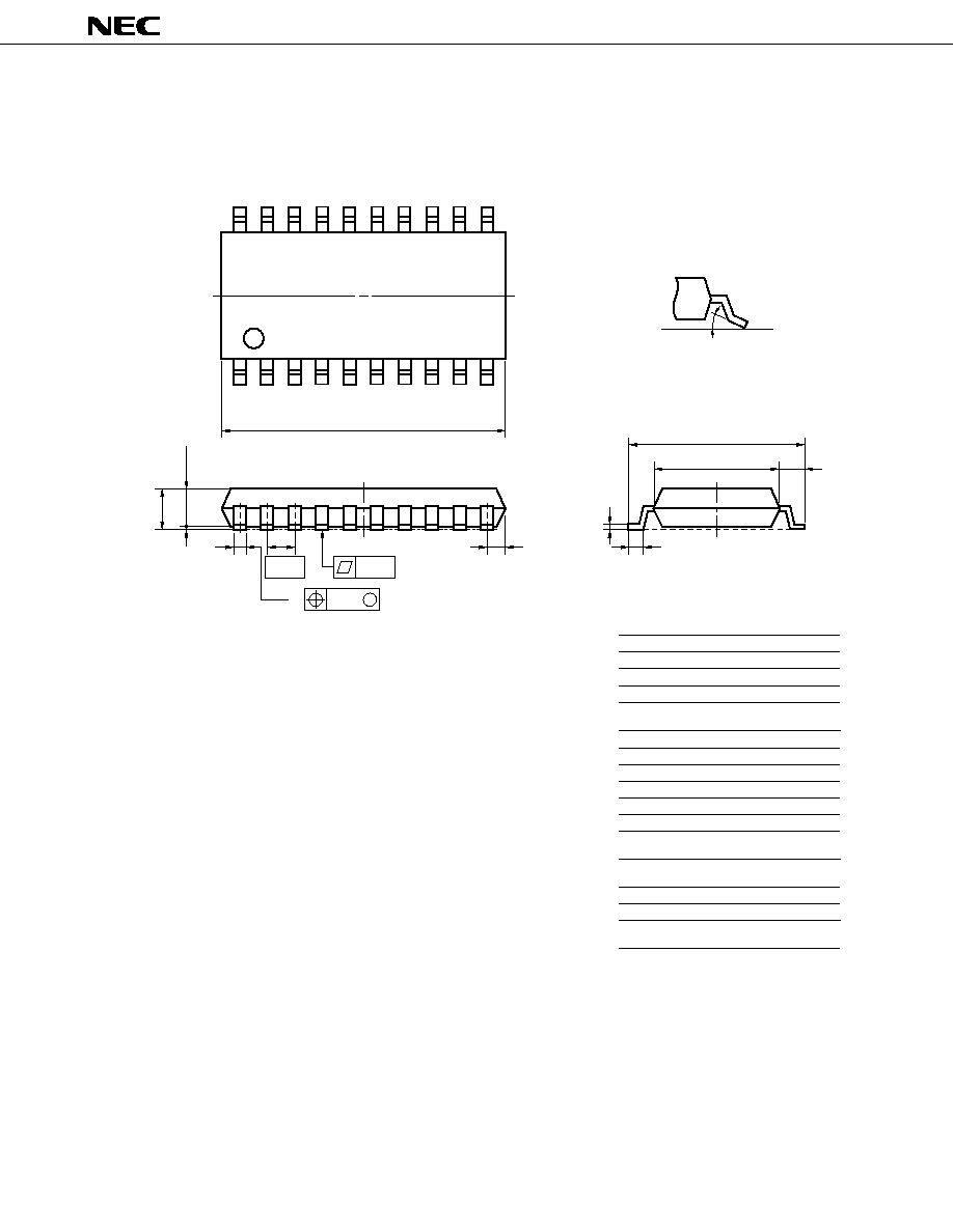
46
µ
PD7564A, 7564A(A)
DRAWINGS OF MASS-PRODUCTION PRODUCT PACKAGES (2/2)
20 PIN PLASTIC SOP (300 mil)
ITEM
MILLIMETERS
INCHES
A
B
C
E
F
G
H
I
J
13.00 MAX.
1.27 (T.P.)
1.8 MAX.
1.55
7.7±0.3
0.78 MAX.
0.12
1.1
5.6
M
0.1±0.1
N
0.512 MAX.
0.031 MAX.
0.004±0.004
0.071 MAX.
0.061
0.303±0.012
0.220
0.043
0.005
0.050 (T.P.)
P20GM-50-300B, C-4
P
3
∞
3
∞
+7
∞
NOTE
Each lead centerline is located within 0.12 mm (0.005 inch) of
its true position (T.P.) at maximum material condition.
D
0.40
0.016
+0.10
≠0.05
K
0.20
0.008
+0.10
≠0.05
L
0.6±0.2
0.024
0.10
≠3
∞
+7
∞
≠3
∞
0.004
+0.008
≠0.009
+0.004
≠0.002
+0.004
≠0.003
A
C
D
G
P
detail of lead end
F
E
B
H
I
L
K
M
J
N
M
1
10
11
20
Caution
Dimensions of ES products are different from those of mass-production products. Refer to DRAWINGS
OF ES PRODUCT PACKAGES (2/2).
5
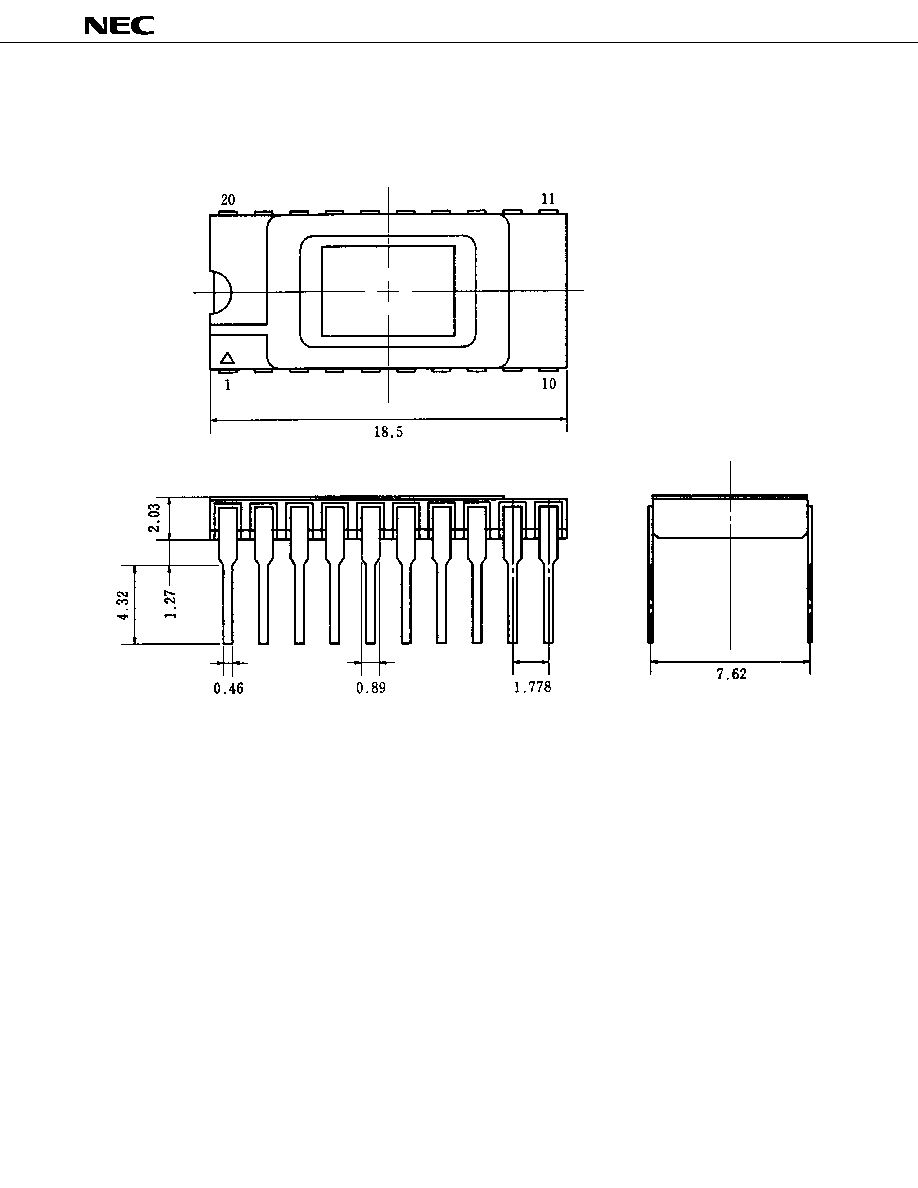
47
µ
PD7564A, 7564A(A)
DRAWINGS OF ES PRODUCT PACKAGES (1/2)
20-Pin Shrink DIP for ES (Reference) (Unit: mm)
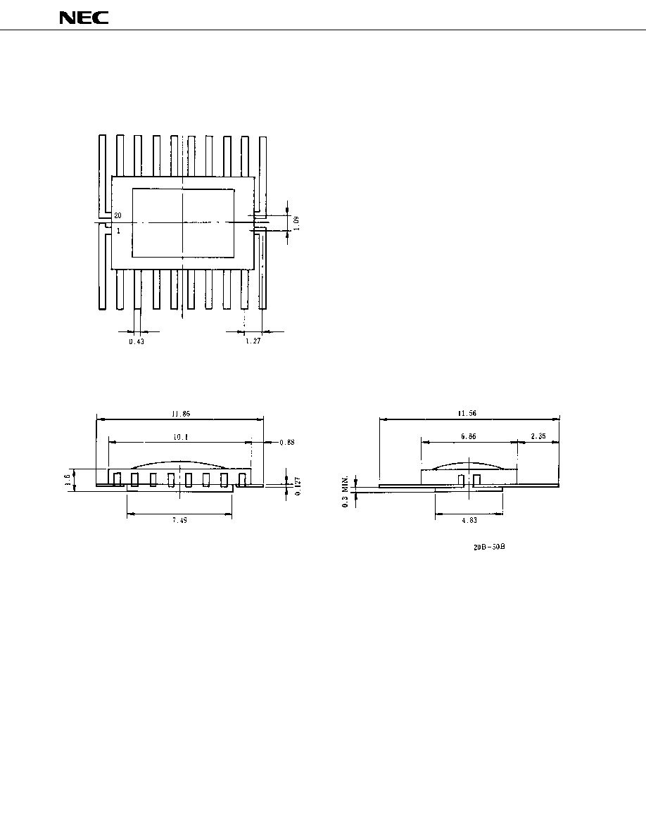
48
µ
PD7564A, 7564A(A)
DRAWINGS OF ES PRODUCT PACKAGES (2/2)
20-Pin Ceramic SOP for ES (Reference) (Unit: mm)
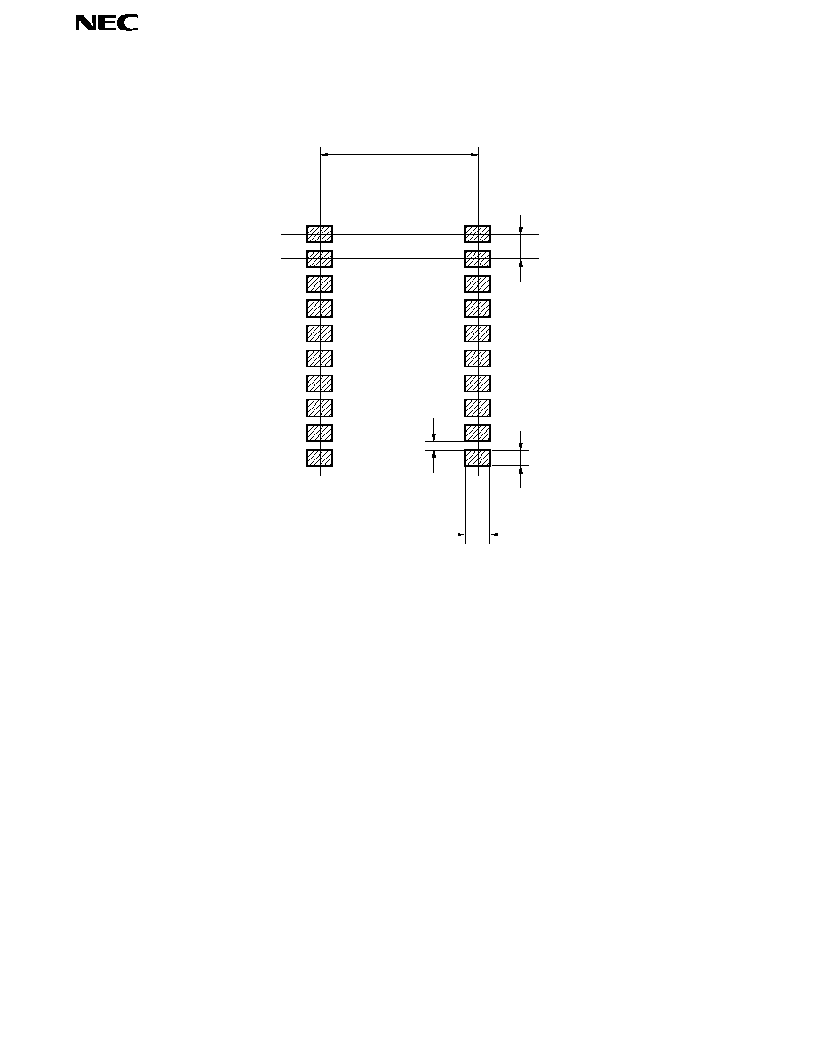
49
µ
PD7564A, 7564A(A)
10. RECOMMENDED PACKAGING PATTERN OF SOP (REFERENCE) (UNIT: mm)
7.62
1.27
0.76
0.51
1.27
∑
This recommended pattern conforms to the General Rules for Integrated Citrcuit Outer Shape (IC-74-2) specified
by the Electronic Industries Association of Japan (EIAJ).
∑
The above pattern dimensions are applicable to all the products designated as EIAJ flat DIP (mini flat) of "Form
A 300 mil type".
∑
If there is any possibility of causing a solder bridge, adjust the width (0.76) of each pad while maintaining the
same length (1.27).
50
µ
PD7564A, 7564A(A)
11. RECOMMENDED SOLDERING CONDITIONS
Solder
µ
PD7564A on the following recommended conditions.
For details of recommended soldering conditions, refer to the information document "Surface Mount Tech-
nology Manual" (IE-1207).
For details on the soldering method and soldering conditions other than the recommended conditions, call the
NEC salesman.
Table 11-1 Surface Mounting Type Conditions
µ
PD7564AG-
◊◊◊
: 20-pin plastic SOP (300 mil)
µ
PD7564AG(A)-
◊◊◊
: 20-pin plastic SOP (300 mil)
Soldering Method
Soldering Conditions
Recommended
Condition Symbol
Infrared reflow
IR30-00-1
VPS
VP15-00-1
Solder both temperature: 260∞C or below, Duration: 10 sec. max.,
Wave soldering
Number of times: Once, Preheat temperature: 120∞C max.
WS60-00-1
(Package surface temperature)
Pin part heating
Pin temperature: 300
∞
C or below, Duration: 3 sec. max. (per device side)
≠≠
Caution
Use of more than one soldering method should be avoided (except in the case of pin part heating).
Table 11-2 Insertion Type Soldering Conditions
µ
PD7564ACS-
◊◊◊
: 20-pin plastic shrink DIP (300 mil)
µ
PD7564ACS(A)-
◊◊◊
: 20-pin plastic shrink SOP (300 mil)
Soldering Method
Soldering Conditions
Wave soldering
Solder bath temperatures: 260
∞
C or below, Duration: 10 sec. max.
(Pin only)
Pin part heating
Pin temperature: 300
∞
C or below, Duration: 3 sec. max. (per pin)
Caution
Ensure that the application of wave soldering is limited to the pins and no solder touches the main unit
directly.
5
Package peak temperature: 230
∞
C, Duration: 30 sec. max. (at 210
∞
C or above),
Number of times: Once
Package peak temperature: 215
∞
C, Duration: 40 sec. max. (at 200
∞
C or above),
Number of times: Once
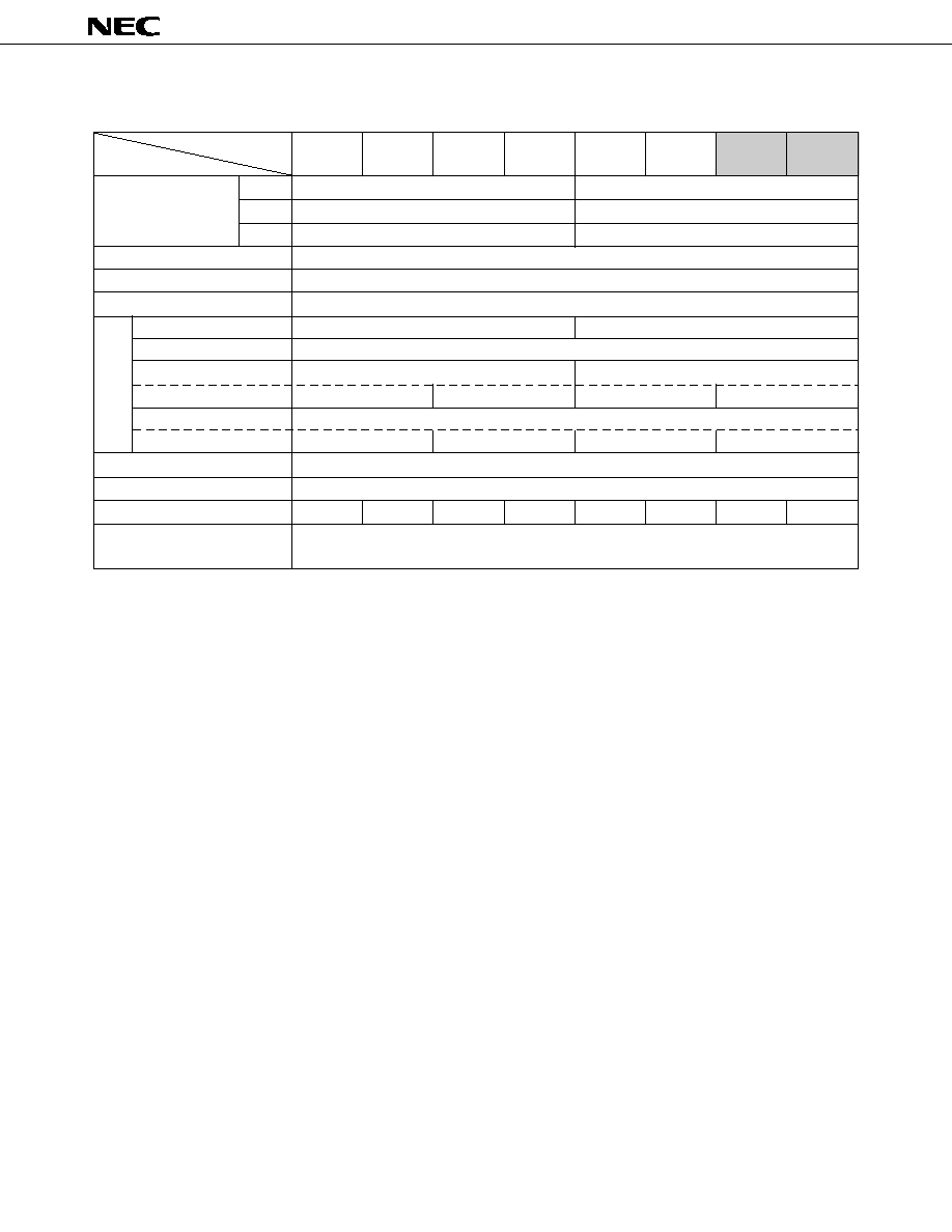
51
µ
PD7564A, 7564A(A)
Instruction cycle/system
clock (5 V)
5
APPENDIX A.
COMPARISON BETWEEN SUB-SERIES PRODUCT FUNCTIONS
Product Name
Item
µ
PD7554
µ
PD75P54
µ
PD7554A
µ
PD7554A(A)
µ
PD7564
µ
PD75P64
µ
PD7564A
µ
PD7564A(A)
RC
4
µ
s/500 kHz
≠≠≠≠
Outside
2.86
µ
s/700 kHz
≠≠≠≠
Ceramic
≠≠≠≠
2.86
µ
s/700 kHz
Instruction set
47 types (SET B)
ROM
1024
◊
8
RAM
64
◊
4
Total number
16
15
Port 0
P00 to P03
I/O
Port 8
P80 to P82, P83 (CL2)
P80 to P82
port
Withstand voltage
12 V
9 V
12 V
9 V
Ports 10 and 11
P100 to P103, P110 to P113
Withstand voltage
12 V
9 V
12 V
9 V
Timer/event counter
8 bits
Serial interface
8 bits
Power voltage range
2.5 to 6.0 V
4.5 to 6.0 V
2.0 to 6.0 V
2.7 to 6.0 V
2.7 to 6.0 V
4.5 to 6.0 V
2.7 to 6.0 V
2.7 to 6.0 V
Package
20-pin plastic shrink DIP
20-pin plastic SOP
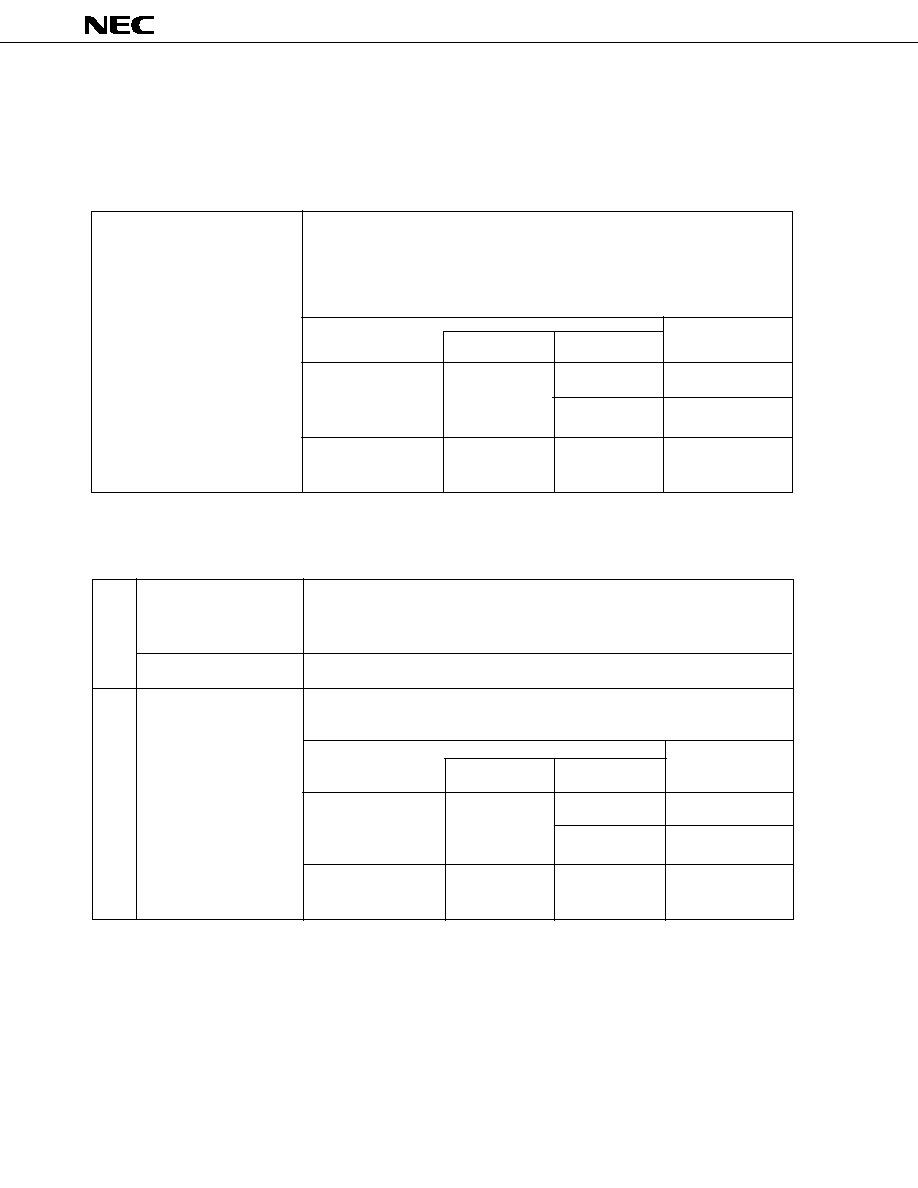
52
µ
PD7564A, 7564A(A)
APPENDIX B.
DEVELOPMENT TOOLS
The following development tools are available for developing systems that use
µ
PD7564A.
Language Processor
Host Machine
OS
Supply Medium
Ordering Code
(Product Name)
MS-DOSTM
3.5-inch 2HD
µ
S5A13AS7554
PC-9800 series
(Ver.3.10 to
Ver.5.00A*)
5-inch 2HD
µ
S5A10AS7554
IBM PC/ATTM
PC DOSTM
5-inch 2HC
µ
S7B10AS7554
(Ver. 3.1)
PROM Write Tools
*
A task swap function is provided in Ver. 5.00/5.00A, but the task swap function cannot be used with this
software.
Remarks
Operation of the assembler and PG-1500 controller is only guaranteed on the host machines and
OSs shown above.
PROM programmer which allows programming of single-chip microcomputer with
typical PROM of 256K to 4M bits by stand-alone or from a host machine by
connecting the accessory board and optional programmer adapter.
µ
PD75P54/75P64 PROM programmer adapter. Used by connecting it to the PG-1500.
Connects the PG-1500 and host machine by serial and parallel interface and controls
the PG-1500 on the host machine.
Hardware
PG-1500
PA-75P54CS
Ordering Code
Host Machine
OS
Supply Medium
(Product Name)
MS-DOS
3.5-inch 2HD
µ
S5A13PG1500
PC-9800 series
(Ver.3.10 to
Ver.5.00A*)
IBM PC/AT
PC DOS
5-inch 2HC
µ
S7B10PG1500
(Ver.3.1)
5-inch 2HD
µ
S5A10PG1500
Software
PG-1500 controller
This program is used to convert the program written with mnemonic codes to the
program written with object codes so that the program can be executed by the
microcomputer.
The function for automatic optimization of branch instruction and so on is also
provided.
µ
PD7550/7560 series
absolute assembler
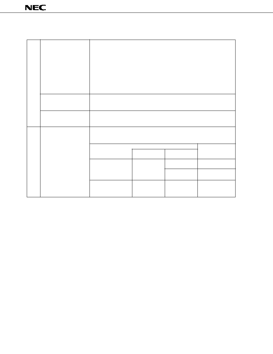
53
µ
PD7564A, 7564A(A)
Debugging Tools
*
A task swap function is provided in Ver. 5.00/5.00A, but the task swap function cannot be used with this
software.
Caution
It is not possible to internally mount a pull-up resistor in a port in the EVAKIT-7500B. When
evaluating, arrange to have a pull-up resistor mounted in the user system.
Remarks
Operation of the EVAKIT controller is only guaranteed on the host machines and OSs shown above.
EVAKIT-7500B is an evaluation board that can be used for
µ
PD7500 series models.
For
µ
PD7564A, EVAKIT-7500B and option board EV-7554A are combined and used
for system development.
EVAKIT-7500B can operate alone. EVAKIT-7500B has a built-in serial interface on
the board, so it enables debugging when it is connected to a RS-232-C interfaced
console.
EVAKIT-7500B works as is a real-time tracer and traces state of the program counter
and output port in real time. EVAKIT-7500B has a built-in PROM writer and improves
debugging efficiency considerably.
EV-7554A is an adapter board which is connected to EVAKIT-7500B and evaluates
µ
PD7564A.
SE-7554A is a simulation board that has the programs developed by EVAKIT-7500B.
SE-7554A evaluates a system in place of
µ
PD7564A.
EVAKIT-7500 Control Program connects EVAKIT-7500B and the host machine with
RC-232-C and controls EVAKIT-7500B on the host machine.
Hardware
EV-7554A
SE-7554A
EVAKIT-7500B
Software
Ordering Code
Host Machine
OS
Supply Medium
(Product Name)
PC-9800
MS-DOS
3.5-inch 2HD
µ
S5A13EV7500-P01
series
(Ver.3.10 to
Ver.5.00A*)
IBM PC
PC DOS
5-inch 2HC
µ
S7B11EV7500-P01
series
(Ver.3.1)
5-inch 2HD
µ
S5A10EV7500-P01
EVAKIT-7500
control program
(EVAKIT controller)
5

54
µ
PD7564A, 7564A(A)
APPENDIX C. RELATED DOCUMENTS
Document Related to Device
Document Name
Document No.
User's Manual
IEU-1111D
µ
PD7500 Series Selection Guide
IF-1027G
Document Related to Development Tool
Document Name
Document No.
Hardware
EVAKIT-7500B User's Manual
EEU-1017C
EV-7554A User's Manual
EEU-1034A
PG-1500 User's Manual
EEU-1335B
Software
µ
PD7550, 7560 Series Absolute Assembler User's Manual EEM-1006
EVAKIT-7500 Control Program User's Manual
MS-DOS base
EEM-1356
PC-DOS base
EEM-1049
PG-1500 Controller User's Manual
EEU-1291B
Other Related Document
Document Name
Document No.
Package Manual
IEI-1213
Semiconductor Device Mounting Technology Manual
IEI-1207
Quality Grade on NEC Semiconductor Devices
IEI-1209A
NEC Semiconductor Device Reliability/Quality Control System
IEI-1203A
Static Electricity Discharge (ESD) Test
IEI-1201
Semiconductor Device Quality Guarantee Guide
MEI-1202
Microcomputer Related Product Guide ≠ Third Party Product ≠
Note
Remarks These documents above are subject to change without notice. Be sure to use the latest document for
designing.
Note
To be published.
5

55
µ
PD7564A, 7564A(A)
NOTES FOR CMOS DEVICES
1
PRECAUTION AGAINST ESD FOR SEMICONDUCTORS
Note: Strong electric field, when exposed to a MOS device, can cause destruction of
the gate oxide and ultimately degrade the device operation. Steps must be
taken to stop generation of static electricity as much as possible, and quickly
dissipate it once, when it has occurred. Environmental control must be
adequate. When it is dry, humidifier should be used. It is recommended to
avoid using insulators that easily build static electricity. Semiconductor
devices must be stored and transported in an anti-static container, static
shielding bag or conductive material. All test and measurement tools including
work bench and floor should be grounded. The operator should be grounded
using wrist strap. Semiconductor devices must not be touched with bare
hands. Similar precautions need to be taken for PW boards with semiconductor
devices on it.
2
HANDLING OF UNUSED INPUT PINS FOR CMOS
Note: No connection for CMOS device inputs can be cause of malfunction. If no
connection is provided to the input pins, it is possible that an internal input
level may be generated due to noise, etc., hence causing malfunction. CMOS
devices behave differently than Bipolar or NMOS devices. Input levels of CMOS
devices must be fixed high or low by using a pull-up or pull-down circuitry. Each
unused pin should be connected to V
DD
or GND with a resistor, if it is considered
to have a possibility of being an output pin. All handling related to the unused
pins must be judged device by device and related specifications governing the
devices.
3
STATUS BEFORE INITIALIZATION OF MOS DEVICES
Note: Power-on does not necessarily define initial status of MOS device. Production
process of MOS does not define the initial operation status of the device.
Immediately after the power source is turned ON, the devices with reset
function have not yet been initialized. Hence, power-on does not guarantee
out-pin levels, I/O settings or contents of registers. Device is not initialized
until the reset signal is received. Reset operation must be executed immedi-
ately after power-on for devices having reset function.

µ
PD7564A, 7564A(A)
[MEMO]
MS-DOS is a trademark of MicroSoft Corporation.
PC DOS and PC/AT are trademarks of IBM Corporation.
No part of this document may be copied or reproduced in any form or by any means without the prior written
consent of NEC Corporation. NEC Corporation assumes no responsibility for any errors which may appear in this
document.
NEC Corporation does not assume any liability for infringement of patents, copyrights or other intellectual
property rights of third parties by or arising from use of a device described herein or any other liability arising
from use of such device. No license, either express, implied or otherwise, is granted under any patents,
copyrights or other intellectual property rights of NEC Corporation or others.
The devices listed in this document are not suitable for use in aerospace equipment, submarine cables, nuclear
reactor control systems and life support systems. If customers intend to use NEC devices for above applications
or they intend to use "Standard" quality grade NEC devices for applications not intended by NEC, please contact
our sales people in advance.
Application examples recommended by NEC Corporation
Standard: Computer, Office equipment, Communication equipment, Test and Measurement equipment,
Machine tools, Industrial robots, Audio and Visual equipment, Other consumer products, etc.
Special:
Automotive and Transportation equipment, Traffic control systems, Antidisaster systems, Anticrime
systems, etc.
M4 92.6
The application circuits and their parameters are for references only and are not intended for use in actual design-in's.