Document Outline
- COVER
- DESCRIPTION
- FEATURES
- ORDERING INFORMATION
- PIN CONFIGURATION (Top View)
- PIN IDENTIFICATION
- BLOCK DIAGRAM
- 1. PIN FUNCTIONS
- 1.1 PORT PINS
- 1.2 NON-PORT PINS
- 1.3 PIN INPUT/OUTPUT CIRCUITS
- 2. DIFFERENCES BETWEEN THE uPD75P048 AND THE uPD75048
- 3. PROM (PROGRAM MEMORY) WRITE AND VERIFY
- 3.1 PROM WRITE AND VERIFY OPERATION MODE
- 3.2 PROM WRITE PROCEDURE
- 3.3 PROM READ PROCEDURE
- 4. SCREENING OF ONE-TIME PROM MODEL
- 5. ELECTRICAL SPECIFICATIONS
- 6. PERFORMANCE CURVE (REFERENCE VALUE)
- 7. PACKAGE DRAWINGS
- 8. RECOMMENDED SOLDERING CONDITIONS
- APPENDIX A. DEVELOPMENT TOOLS
- APPENDIX B. RELATED DOCUMENTS
Printed in Japan
Document No. IC-3239
(O.D. No.
IC-8720)
Date Published August 1994 P
MOS INTEGRATED CIRCUIT
µ
PD75P048
4-BIT SINGLE-CHIP MICROCOMPUTER
DESCRIPTION
The
µ
PD75P048 is a One-Time PROM version of the
µ
PD75048. The
µ
PD75P048 is suitable for small-scale
production or experimental production in system development.
Detailed functions are described in the following user's manual. Read this manual when designing your
system.
µ
PD75048 User's Manual: IEU-1278
FEATURES
∑
The
µ
PD75048 compatible
∑
The
µ
PD75P048 for evaluation/pre-production, while the
µ
PD75048 for mass-production
∑
8064
◊
8 bits of one-time programmable ROM
∑
512
◊
4 bits of RAM
∑
1024
◊
4 bits of EEPROM (Data memory area)
∑
Ports 0 to 3 and 6 to 8 with software-selectable pull-up resistors
∑
Port 9 with software-selectable pull-down resistors
∑
12 N-channel open drain input/output ports (ports 4, 5, and 10)
∑
Low-voltage operation possible (V
DD
= 2.7 to 6.0 V)
ORDERING INFORMATION
Part number
Package
Quality grade
µ
PD75P048CW
64-pin plastic shrink DIP (750 mil)
Standard
µ
PD75P048GC-AB8
64-pin plastic QFP ( 14 mm)
Standard
Caution Pull-up/pull-down resistor mask options are not available.
Please refer to "Quality grade on NEC Semiconductor Devices" (Document number IEI-1209) published by
NEC Corporation to know the specification of quality grade on the devices and its recommended applications.
The information in this document is subject to change without notice.
The mark 5 shows major revised points.
©
1994
DATA SHEET
2
µ
PD75P048
PIN CONFIGURATION (Top View)
∑
64-pin plastic shrink DIP
∑
64-pin plastic QFP
SB1/SI/P03
SB0/SO/P02
SCK/P01
INT4/P00
BUZ/P23
PCL/P22
PPO/P21
PTO0/P20
MAT/P103
MAZ/P102
MAI/P101
MAR/P100
RESET
X1
X2
V
PP
XT1
XT2
V
DD
AV
DD
AV
REF+
AV
REF≠
AN7
AN6
AN5
AN4
AN3/P113
AN2/P112
AN1/P111
AN0/P110
AV
SS
TI0/P13
PD75P048CW
1
2
3
4
5
6
7
8
9
10
11
12
13
14
15
16
17
18
19
20
21
22
23
24
25
26
27
28
29
30
31
32
64
63
62
61
60
59
58
57
56
55
54
53
52
51
50
49
48
47
46
45
44
43
42
41
40
39
38
37
36
35
34
33
V
SS
P30/MD0
P31/MD1
P32/MD2
P33/MD3
P40
P41
P42
P43
P50
P51
P52
P53
P60/KR0
P61/KR1
P62/KR2
P63/KR3
P70/KR4
P71/KR5
P72/KR6
P73/KR7
P80
P81
P82
P83
P90
P91
P92
P93
P10/INT0
P11/INT1
P12/INT2
µ
P50
P51
P52
P53
P60/KR0
P61/KR1
P62/KR2
P63/KR3
P70/KR4
P71/KR5
P72/KR6
P73/KR7
P80
P81
P82
P83
48
47
46
45
44
43
42
41
40
39
38
37
36
35
34
33
P90
P91
P92
P93
P10/INT0
P11/INT1
P12/INT2
TI0/P13
AV
SS
AN0/P110
AN1/P111
AN2/P112
AN3/P113
AN4
AN5
AN6
P43
P42
P41
P40
MD3/P33
MD2/P32
MD1/P31
MD0/P30
V
SS
SB1/SI/P03
SB0/SO/P02
SCK/P01
INT4/P00
BUZ/P23
PCL/P22
PPO/P21
64 63 62 61 60 59 58 57 56 55 54 53 52 51 50 49
PTO0/P20
MAT/P103
MAZ/P102
MAI/P101
MAR/P100
RESET
X1
X2
V
PP
XT1
XT2
V
DD
AV
DD
AV
REF+
AV
REF≠
AN7
17 18 19 20 21 22 23 24 25 26 27 28 29 30 31 32
PD75P048GC-AB8
1
2
3
4
5
6
7
8
9
10
11
12
13
14
15
16
µ

3
µ
PD75P048
PIN IDENTIFICATION
P00-03
: Port0
P10-13
: Port1
P20-23
: Port2
P30-33
: Port3
P40-43
: Port4
P50-53
: Port5
P60-63
: Port6
P70-73
: Port7
P80-83
: Port8
P90-93
: Port9
P100-103
: Port10
P110-113
: Port11
KR0-7
: Key Return
SCK
: Serial Clock
SI
: Serial Input
SO
: Serial Output
SB0, 1
: Serial Bus 0, 1
RESET
: Reset Input
TI0
: Timer Input 0
PTO0
: Programmable Timer Output 0
BUZ
: Buzzer Clock
PCL
: Programmable Clock
INT0,1,4
: External Vectored Interrupt 0, 1, 4
INT2
: External Test Input 2
X1, 2
: Main System Clock Oscillation 1, 2
XT1, 2
: Subsystem Clock Oscillation 1, 2
MAR
: Reference Integration Control
MAI
: Integration Control
MAZ
: Autozero Control
MAT
: External Comparate Timing Input
PPO
: Programmable Pulse Output ... MFT timer mode
AN0-7
: Analog Input 0-7
AV
REF+
: Analog Reference (+)
AV
REF-
: Analog Reference (-)
AV
DD
: Analog V
DD
AV
SS
: Analog V
SS
V
DD
: Positive Power Supply
V
SS
: Ground
V
PP
: Programming Power Supply
MD0-MD3
: Mode Selection
Remarks MFT: Multi-function timer
MFT
A/D
mode
5

4
µ
PD75P048
BLOCK DIAGRAM
BASIC
INTERVAL
TIMER
INTBT
TIMER/
COUNTER
#0
INTT0
TI0/P13
PTO0/P20
SERIAL
INTERFACE
INTCSI
SI/SB1/P03
SO/SB0/P02
SCK/P01
INTERRUPT
CONTROL
INT0/P10
INT1/P11
INT2/P12
INT4/P00
KR0 - KR3/P60 - P63
KR4 - KR7/P70 - P73
A/D
CONVERTER
AV
DD
AV
REF+
AV
REF≠
AV
SS
AN0 - AN3/P110 - P113
AN4 - AN7
WATCH
TIMER
INTW
BUZ/P23
MULTI-
FUNCTION
TIMER
MAR/P100
MAI/P101
MAZ/P102
MAT/P103
PPO/P21
INTMFT
PROGRAM
COUNTER
PROM
PROGRAM
MEMORY
8064
◊
8 BITS
DECODE
AND
CONTROL
ALU
RAM
512
◊
4 BITS
GENERAL REG.
EEPROM
1024
◊
4 BITS
SP
CY
BANK
DATA
MEMORY
PORT 0
BIT SEQ.
BUFFER
P00 - P03
PORT 1
P10 - P13
PORT 2
P20 - P23
PORT 3
P30/MD0 - P33/MD3
PORT 4
P40 - P43
PORT 5
P50 - P53
PORT 6
P60 - P63
PORT 7
P70 - P73
PORT 8
P80 - P83
PORT 9
P90 - P93
PORT 10
P100 - P103
PORT 11
P110 - P113
f
x
/2
N
CPU CLOCK
CLOCK
OUTPUT
CONTROL
CLOCK
DIVIDER
PCL/P22
XT1 XT2
SUB
CLOCK GENERATOR
X1
X2
MAIN
STAND BY
CONTROL
RESET
V
SS
V
DD
V
PP

5
µ
PD75P048
CONTENTS
1.
PIN FUNCTIONS ∑∑∑∑∑∑∑∑∑∑∑∑∑∑∑∑∑∑∑∑∑∑∑∑∑∑∑∑∑∑∑∑∑∑∑∑∑∑∑∑∑∑∑∑∑∑∑∑∑∑∑∑∑∑∑∑∑∑∑∑∑∑∑∑∑∑∑∑∑∑∑∑∑∑∑∑∑∑∑∑∑∑∑∑∑∑∑∑∑∑∑∑∑∑∑∑∑∑∑∑∑∑∑∑∑∑∑∑∑∑∑∑∑∑∑∑∑∑∑∑∑
6
1.1
PORT PINS ∑∑∑∑∑∑∑∑∑∑∑∑∑∑∑∑∑∑∑∑∑∑∑∑∑∑∑∑∑∑∑∑∑∑∑∑∑∑∑∑∑∑∑∑∑∑∑∑∑∑∑∑∑∑∑∑∑∑∑∑∑∑∑∑∑∑∑∑∑∑∑∑∑∑∑∑∑∑∑∑∑∑∑∑∑∑∑∑∑∑∑∑∑∑∑∑∑∑∑∑∑∑∑∑∑∑∑∑∑∑∑∑∑∑∑∑∑∑∑∑∑∑∑∑∑∑∑∑∑∑∑∑∑∑∑∑∑∑
6
1.2
NON-PORT PINS ∑∑∑∑∑∑∑∑∑∑∑∑∑∑∑∑∑∑∑∑∑∑∑∑∑∑∑∑∑∑∑∑∑∑∑∑∑∑∑∑∑∑∑∑∑∑∑∑∑∑∑∑∑∑∑∑∑∑∑∑∑∑∑∑∑∑∑∑∑∑∑∑∑∑∑∑∑∑∑∑∑∑∑∑∑∑∑∑∑∑∑∑∑∑∑∑∑∑∑∑∑∑∑∑∑∑∑∑∑∑∑∑∑∑∑∑∑∑∑∑∑∑∑∑∑∑∑∑∑
8
1.3
PIN INPUT/OUTPUT CIRCUITS ∑∑∑∑∑∑∑∑∑∑∑∑∑∑∑∑∑∑∑∑∑∑∑∑∑∑∑∑∑∑∑∑∑∑∑∑∑∑∑∑∑∑∑∑∑∑∑∑∑∑∑∑∑∑∑∑∑∑∑∑∑∑∑∑∑∑∑∑∑∑∑∑∑∑∑∑∑∑∑∑∑∑∑∑∑∑∑∑∑∑∑∑∑∑∑∑∑∑∑∑∑∑∑∑
10
2.
DIFFERENCES BETWEEN THE
µ
PD75P048 AND THE
µ
PD75048 ∑∑∑∑∑∑∑∑∑∑∑∑∑∑∑∑∑∑∑∑∑∑∑∑∑∑∑∑∑∑∑∑∑∑∑∑∑∑∑ 13
3.
PROM (PROGRAM MEMORY) WRITE AND VERIFY ∑∑∑∑∑∑∑∑∑∑∑∑∑∑∑∑∑∑∑∑∑∑∑∑∑∑∑∑∑∑∑∑∑∑∑∑∑∑∑∑∑∑∑∑∑∑∑∑∑∑∑∑∑∑∑∑∑∑∑∑∑ 14
3.1
PROM WRITE AND VERIFY OPERATION MODE ∑∑∑∑∑∑∑∑∑∑∑∑∑∑∑∑∑∑∑∑∑∑∑∑∑∑∑∑∑∑∑∑∑∑∑∑∑∑∑∑∑∑∑∑∑∑∑∑∑∑∑∑∑∑∑∑∑∑∑∑∑∑∑∑∑∑∑∑∑∑∑∑∑∑
14
3.2
PROM WRITE PROCEDURE ∑∑∑∑∑∑∑∑∑∑∑∑∑∑∑∑∑∑∑∑∑∑∑∑∑∑∑∑∑∑∑∑∑∑∑∑∑∑∑∑∑∑∑∑∑∑∑∑∑∑∑∑∑∑∑∑∑∑∑∑∑∑∑∑∑∑∑∑∑∑∑∑∑∑∑∑∑∑∑∑∑∑∑∑∑∑∑∑∑∑∑∑∑∑∑∑∑∑∑∑∑∑∑∑∑∑∑∑∑∑
15
3.3
PROM READ PROCEDURE ∑∑∑∑∑∑∑∑∑∑∑∑∑∑∑∑∑∑∑∑∑∑∑∑∑∑∑∑∑∑∑∑∑∑∑∑∑∑∑∑∑∑∑∑∑∑∑∑∑∑∑∑∑∑∑∑∑∑∑∑∑∑∑∑∑∑∑∑∑∑∑∑∑∑∑∑∑∑∑∑∑∑∑∑∑∑∑∑∑∑∑∑∑∑∑∑∑∑∑∑∑∑∑∑∑∑∑∑∑∑∑∑
16
4.
SCREENING OF ONE-TIME PROM MODEL ∑∑∑∑∑∑∑∑∑∑∑∑∑∑∑∑∑∑∑∑∑∑∑∑∑∑∑∑∑∑∑∑∑∑∑∑∑∑∑∑∑∑∑∑∑∑∑∑∑∑∑∑∑∑∑∑∑∑∑∑∑∑∑∑∑∑∑∑∑∑∑∑∑∑∑ 17
5.
ELECTRICAL SPECIFICATIONS ∑∑∑∑∑∑∑∑∑∑∑∑∑∑∑∑∑∑∑∑∑∑∑∑∑∑∑∑∑∑∑∑∑∑∑∑∑∑∑∑∑∑∑∑∑∑∑∑∑∑∑∑∑∑∑∑∑∑∑∑∑∑∑∑∑∑∑∑∑∑∑∑∑∑∑∑∑∑∑∑∑∑∑∑∑∑∑∑∑∑∑∑∑∑∑∑∑∑ 18
6.
PERFORMANCE CURVE (REFERENCE VALUE) ∑∑∑∑∑∑∑∑∑∑∑∑∑∑∑∑∑∑∑∑∑∑∑∑∑∑∑∑∑∑∑∑∑∑∑∑∑∑∑∑∑∑∑∑∑∑∑∑∑∑∑∑∑∑∑∑∑∑∑∑∑∑∑∑∑∑∑∑∑ 32
7.
PACKAGE DRAWINGS ∑∑∑∑∑∑∑∑∑∑∑∑∑∑∑∑∑∑∑∑∑∑∑∑∑∑∑∑∑∑∑∑∑∑∑∑∑∑∑∑∑∑∑∑∑∑∑∑∑∑∑∑∑∑∑∑∑∑∑∑∑∑∑∑∑∑∑∑∑∑∑∑∑∑∑∑∑∑∑∑∑∑∑∑∑∑∑∑∑∑∑∑∑∑∑∑∑∑∑∑∑∑∑∑∑∑∑∑∑∑∑ 34
8.
RECOMMENDED SOLDERING CONDITIONS ∑∑∑∑∑∑∑∑∑∑∑∑∑∑∑∑∑∑∑∑∑∑∑∑∑∑∑∑∑∑∑∑∑∑∑∑∑∑∑∑∑∑∑∑∑∑∑∑∑∑∑∑∑∑∑∑∑∑∑∑∑∑∑∑∑∑∑∑∑∑∑∑∑ 36
APPENDIX A. DEVELOPMENT TOOLS ∑∑∑∑∑∑∑∑∑∑∑∑∑∑∑∑∑∑∑∑∑∑∑∑∑∑∑∑∑∑∑∑∑∑∑∑∑∑∑∑∑∑∑∑∑∑∑∑∑∑∑∑∑∑∑∑∑∑∑∑∑∑∑∑∑∑∑∑∑∑∑∑∑∑∑∑∑∑∑∑∑∑∑∑∑∑∑∑∑∑ 37
APPENDIX B. RELATED DOCUMENTS ∑∑∑∑∑∑∑∑∑∑∑∑∑∑∑∑∑∑∑∑∑∑∑∑∑∑∑∑∑∑∑∑∑∑∑∑∑∑∑∑∑∑∑∑∑∑∑∑∑∑∑∑∑∑∑∑∑∑∑∑∑∑∑∑∑∑∑∑∑∑∑∑∑∑∑∑∑∑∑∑∑∑∑∑∑∑∑∑∑∑ 38
5
5
5
5
5
5
6
µ
PD75P048
1. PIN FUNCTIONS
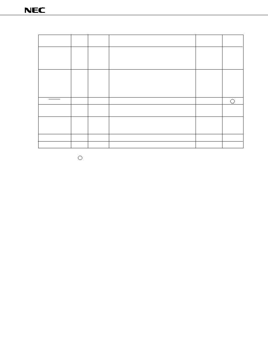
1.1 PORT PINS (1/2)
Pin Name
P00
P01
P02
P03
P10
P11
P12
P13
P20
P21
P22
P23
P30
Note 2
P31
Note 2
P32
Note 2
P33
Note 2
P40 - P43
Note 2
P50 - P53
Note 2
I/O Circuit
Type
Note 1
-A
-B
-C
-C
E-B
E-B
M-A
M-A
Input/
Output
Input
I/O
I/O
I/O
Input
I/O
I/O
I/O
I/O
Shared
Pin
INT4
SCK
SO/SB0
SI/SB1
INT0
INT1
INT2
TI0
PTO0
PPO
PCL
BUZ
MD0
MD1
MD2
MD3
≠
≠
When Reset
Input
Input
Input
Input
High
impedance
High
impedance
8-Bit
I/O
◊
◊
◊
◊
Function
4-bit input port (PORT0).
For P01 to P03, pull-up resistors can be
provided by software in units of 3 bits.
With noise elimination function
4-bit input port (PORT1).
Pull-up resistors can be provided by
software in units of 4 bits.
4-bit I/O port (PORT2).
Pull-up resistors can be provided by
software in units of 4 bits.
Programmable 4-bit I/O port (PORT3).
I/O can be specified bit by bit.
Pull-up resistors can be provided by
software in units of 4 bits.
N-ch open-drain 4-bit I/O port (PORT4).
Can withstand 10 V.
Data input/output pins for the PROM
write and verity (Four low-order bits).
N-ch open-drain 4-bit I/O port (PORT5).
Can withstand 10 V.
Data input/output pins for the PROM
write and verify (Four high-order bits).
B
F
M
B
F
Note 1. The circle (
) indicates the Schmitt trigger input.
2. Can directly drive LEDs.
7
µ
PD75P048
1.1 PORT PINS (2/2)
Pin Name
P60
P61
P62
P63
P70
P71
P72
P73
P80 - P83
P90 - P93
P100
P101
P102
P103
P110
P111
P112
P113
I/O Circuit
Type
Note
-A
-A
E-B
E-D
M-A
Y
Input/
Output
I/O
I/O
I/O
I/O
I/O
Input
Shared
Pin
KR0
KR1
KR2
KR3
KR4
KR5
KR6
KR7
≠
≠
MAR
MAI
MAZ
MAT
AN0
AN1
AN2
AN3
When Reset
Input
Input
Input
Input
High
impedance
Input
8-Bit
I/O
◊
◊
Function
Programmable 4-bit I/O port (PORT 6).
Pull-up resistors can be provided by
software in units of 4 bits.
4-bit I/O port (PORT 7).
A pull-up resistor can be provided by
software in units of 4 bits
4-bit I/O port (PORT 8).
A pull-up resistor can be provided by
software in units of 4 bits.
4-bit I/O port (PORT 9).
A pull-up resistor can be provided by
software in units of 4 bits.
N-ch open drain 4-bit I/O port (PORT 10).
Can withstand 10 V in open-drain
mode.
4-bit input port (PORT 11).
F
F
Note
The circle (
) indicates the Schmitt trigger input.
5

8
µ
PD75P048
Pin Name
TI0
PTO0
PCL
BUZ
SCK
SO/SB0
SI/SB1
INT4
INT0
INT1
INT2
KR0 - KR3
KR4 - KR7
MAR
MAI
MAZ
MAT
PPO
AN0 - AN3
AN4 - AN7
AV
REF+
AV
REF≠
AV
DD
AV
SS
I/O Circuit
Type
Note
-C
E-B
E-B
E-B
-A
-B
-C
-C
-C
-A
-A
M-A
M-A
M-A
M-A
E-B
Y-A
Y-A
Z-A
Z-A
≠
≠
Shared
Pin
P13
P20
P22
P23
P01
P02
P03
P00
P10
P11
P12
P60 - P63
P70 - P73
P100
P101
P102
P103
P21
P110 - P113
≠
≠
≠
≠
≠
When Reset
Input
Input
Input
Input
Input
Input
Input
Input
Input
Input
Input
Input
High
impedance
High
impedance
High
impedance
High
impedance
Input
≠
≠
≠
≠
≠
Input/
Output
Input
I/O
I/O
I/O
I/O
I/O
I/O
Input
Input
Input
I/O
I/O
I/O
I/O
I/O
I/O
I/O
Input
Input
Input
≠
≠
Function
Input for receiving external event pulse signal
for timer/event counter
Timer/event counter output
Clock output
Output for arbitrary frequency output (for
buzzer output or system clock trimming)
Serial clock I/O
Serial data output
Serial bus I/O
Serial data input
Serial bus I/O
Edge detection vectored interrupt input (either
rising edge or falling edge detection)
Edge detection vectored interrupt input
(detection edge selectable)
Edge detection testable input (rising edge
detection)
Parallel falling edge detection testable input
Parallel falling edge detection testable input
In MFT integrat-
ing A/D
converter mode
In MFT timer
mode
For A /D
converter only
B
F
F
M
B
B
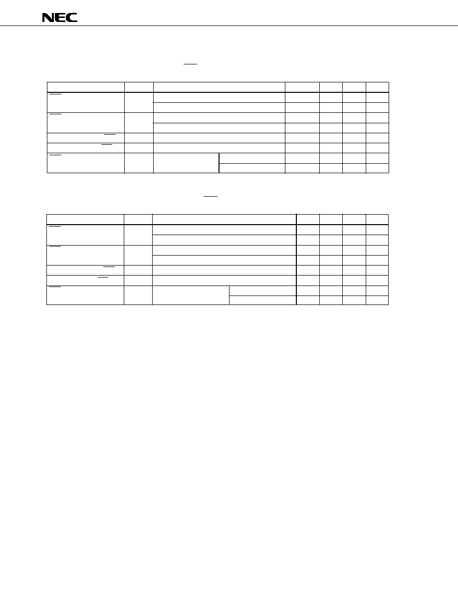
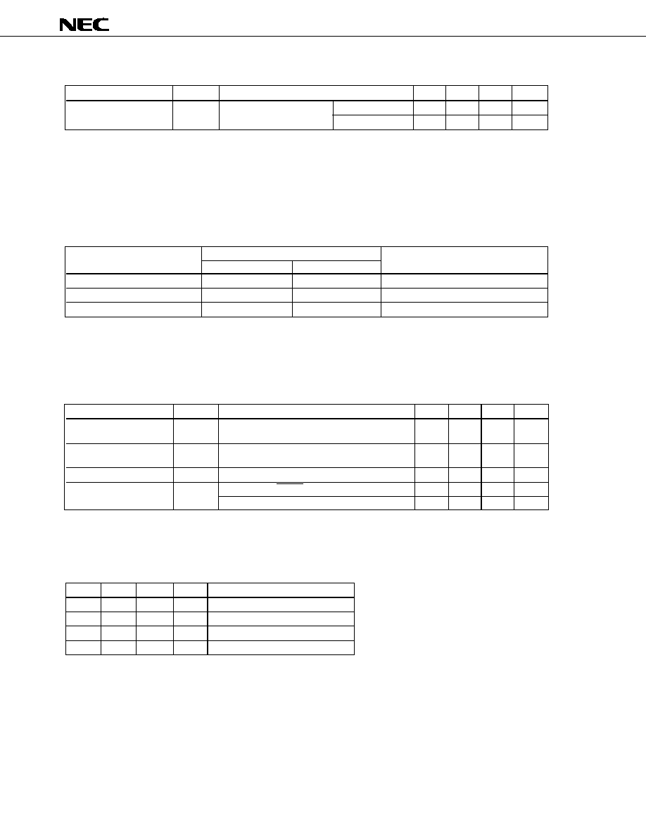
1.2 NON-PORT PINS (1/2)
B
F
F
Reverse integration signal
output
Integration signal output
Auto-zero signal output
Comparator input
Timer pulse output
8-bit analog input
Reference voltage input
(AV
DD
side)
Reference voltage input
(AV
SS
side)
Positive power supply
GND potential
Note The circle (
) indicates the Schmitt trigger input.
Remark MFT: Multi-Function Timer
9
µ
PD75P048
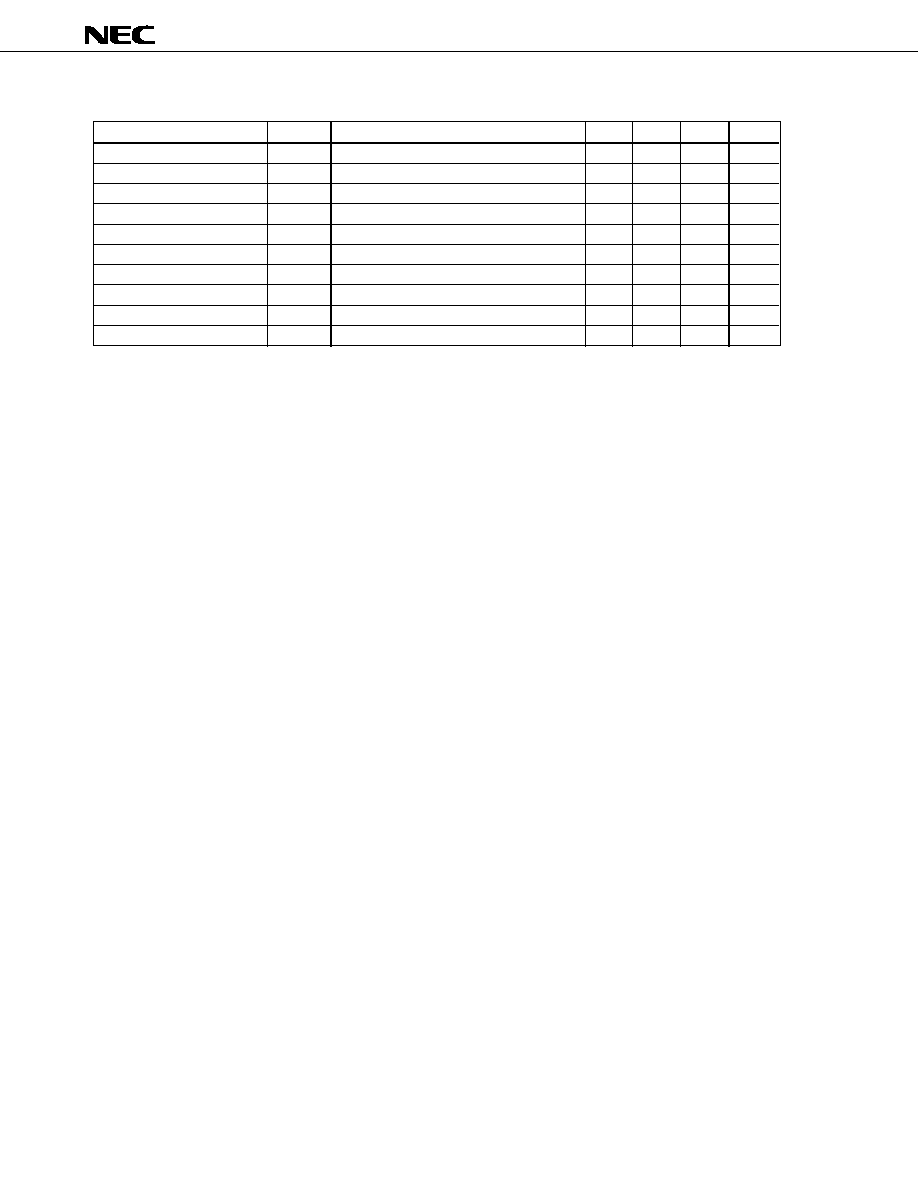
1.2 NON-PORT PINS (2/2)
Pin Name
X1, X2
XT1, XT2
RESET
MD0 - MD3
V
PP
Note 2
V
DD
V
SS
Shared
Pin
≠
≠
≠
P30 - P33
≠
≠
≠
When Reset
≠
≠
≠
Input
≠
≠
≠
Input/
Output
Input
Input
Input
I/O
≠
≠
≠
Function
Crystal/ceramic resonator connection for main
system clock generation. When external clock
signal is used, it is applied to X1, and its
reverse phase signal is applied to X2.
Crystal connection for subsystem clock
generation. When external clock signal is
used, it is applied to XT1, and its reverse
phase signal is applied to XT2. XT1 can be
used as a 1-bit input (test).
System reset input
Operation mode selection pins during the
PROM write/verify cycles.
Normally connected to V
DD
directly; +12.5 V is
applied as the programming voltage during the
PROM write/verify cycles.
Positive power supply
GND potential
I/O Circuit
Type
Note 1
≠
≠
E-B
≠
≠
≠
B
Note 1. The circle (
) indicates the Schmitt trigger input.
2. The V
PP
should be connected to V
DD
directly in normal operation mode. If V
PP
and V
DD
pins are not
connected, the
µ
PD75P048 does not operate correctly.
10
µ
PD75P048
1.3 PIN INPUT/OUTPUT CIRCUITS
The input/output circuit of each
µ
PD75P048 pin is shown below in a simplified manner.
P-ch
Type A (For Type E-B)
V
DD
N-ch
IN
Type D (For Type E-B, F-A)
P-ch
V
DD
N-ch
OUT
Data
Output
disable
CMOS input buffer
Push-pull output which can be set to high-impedance output
(off for both P-ch and N-ch)
Type B
Type E-B
IN
P-ch
V
DD
IN/OUT
Data
Output
disable
P.U.R.
enable
Type D
P.U.R.
Type A
Schmitt trigger input with hysteresis
P.U.R.: Pull-Up Resistor
Type B-C
Type E-D
P-ch
V
DD
IN
P.U.R.
P.U.R.
enable
N-ch
IN/OUT
P.D.R.
enable
P.D.R.
Data
Output
disable
Type D
Type A
P.U.R.: Pull-Up Resistor
P.D.R.: Pull-Down Resistor
(1/3)

11
µ
PD75P048
Type F-A
Type M-C
P-ch
V
DD
N-ch
IN/OUT
Data
Output
disable
P.U.R.: Pull-Up Resistor
Type F-B
Type Y
P-ch
V
DD
IN/OUT
Data
Output
disable
P.U.R.
enable
Type D
P.U.R.
Type B
P.U.R.: Pull-Up Resistor
Input
enable
Type M-A
Type Y-A
Middle-voltage input buffer
(Can withstand + 10 V)
(2/3)
P-ch
V
DD
IN/OUT
Data
Output
disable
P.U.R.
enable
P.U.R.
P.U.R.: Pull-Up Resistor
N-ch
AV
DD
AV
SS
+
≠
P-ch
IN
AV
SS
AV
DD
N-ch
Sampl-
ing C
Reference voltage
(from voltage tap of
series resistor string)
Output
disable
(N)
Output
disable
(P)
P-ch
V
DD
P.U.R.
enable
P.U.R.
N-ch
(Can with-
stand + 10 V)
Data
Output
disable
IN/OUT
AV
DD
AV
SS
+
≠
P-ch
IN
AV
SS
AV
DD
N-ch
Sampl-
ing C
Reference voltage
(from voltage tap of
series resistor string)
IN instruction
Input buffer
P.U.R.: Pull-Up Resistor
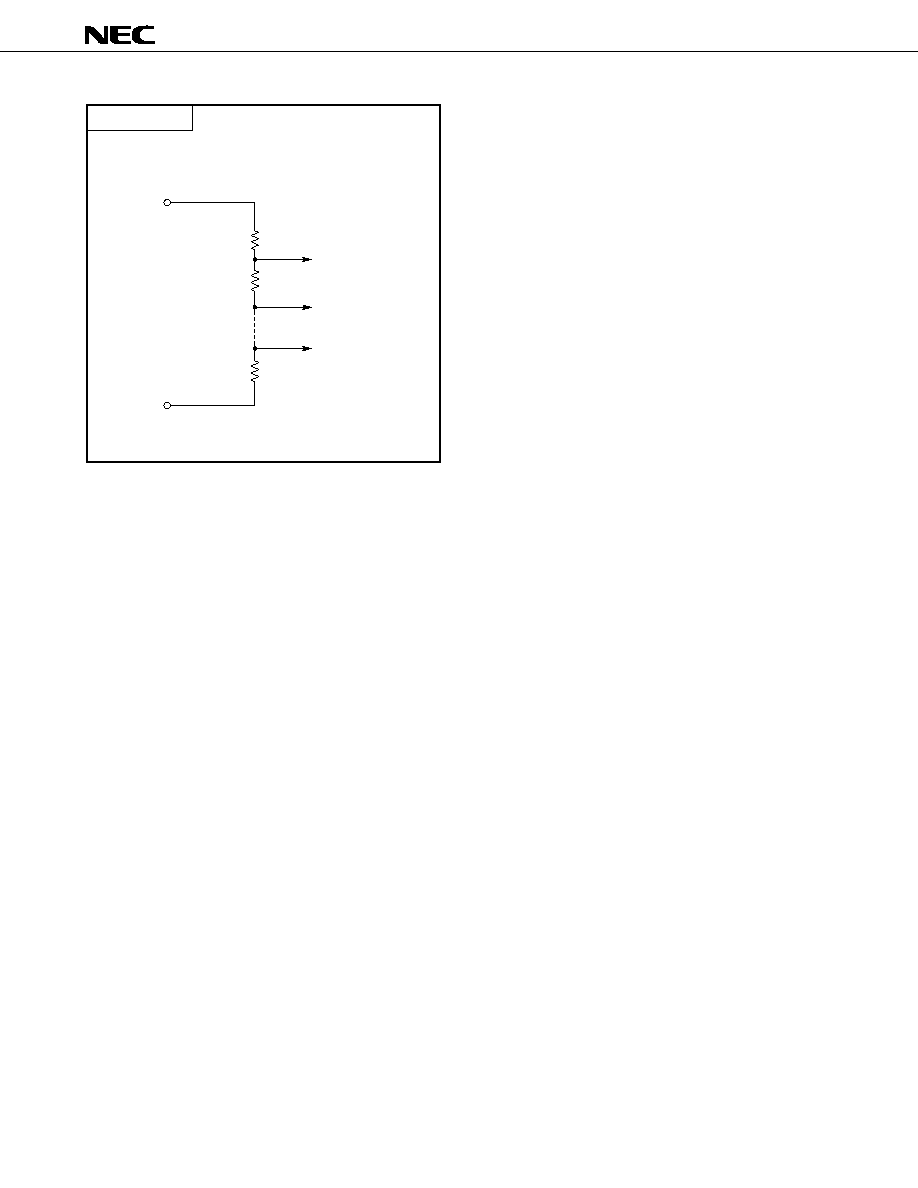
12
µ
PD75P048
AV
REF+
Reference voltage
AV
REF≠
Type Z-A
(3/3)

13
µ
PD75P048
2. DIFFERENCES BETWEEN THE
µ
PD75P048 AND THE
µ
PD75048
The
µ
PD75P048 is a One-Time PROM version of the
µ
PD75048. The
µ
PD75P048 has the same CPU and
internal hardwares. Table 2-1 shows the differences between the
µ
PD75P048 and the
µ
PD75048. Bear in mind
the differences between these two products when debugging or developing on an experimental basis your
application system by using the one-time PROM model, and then mass-producing the application system by
using the mask ROM model.
Details for the CPU functions and internal hardwares are available in
µ
PD75048 User's Manual (IEU-1278).
Table 2-1 Differences between the
µ
PD75P048 and the
µ
PD75048
Items
Program Memory
Pull-up Resistors
Pull-Down Resistors
XT1 Feedback Resistor
Pin Connection
Electrical Specification
Other
µ
PD75P048
µ
PD75048
One-time PROM
Mask ROM
∑ 0000H to 1F7FH
∑ 8064
◊
8 bits
Software-selectable
N/A
Mask-option
Software-selectable
On-chip
Mask-option
P33/MD3 - P30/MD0
P33 - P30
V
PP
IC
Current dissipation differs. For details,
refer to Data Sheet of each model.
Circuit scale and mask layout differ.
Consequently, noise immunity and noise
radiation differ.
Ports 0 to 3 and 6 to 8
Ports 4, 5 and 10
Port 9
60 - 63 (SDIP)
5 - 8 (QFP)
16 (SDIP)
25 (QFP)
Note The noise immunity and noise radiation of the PROM and mask ROM models differ. To replace the PROM
mode, which has been used for experimental production of your application system with the mask ROM
model for mass production of the application system, be sure to perform thorough evaluation by using
the CS model (not ES model) of the mask ROM model.
5
5
5
5

14
µ
PD75P048
3. PROM (PROGRAM MEMORY) WRITE AND VERIFY
The
µ
PD75P048 contains 8064 bytes of PROM. The following table shows the pin functions during the write
and verify cycles. Note that it is not necessary to enter an address, because the address is updated by pulsing
the X1 clock pins.
Pin Name
V
PP
X1, X2
MD0 - MD3 (P30 - P33)
P40 - P43 (lower 4 bits)
P50 - P53 (higher 4 bits)
V
DD
Function
Normally 2.7 to 6 V; 12.5 V is applied during write/verify
After a write/verify write, the X1 and X2 clock pins are
pulsed. The inverted signal of the X1 should be input to the
X2.
Note that these pins are also pulsed during a read.
Operation mode selection pins.
8-bit data input/output pins for write and verify
Supply voltage.
Normally 2.7 to 6 V; 6 V is applied during write/verify
Caution The
µ
PD75P048CW/GC do not have a UV erase window, thus the PROM contents cannot be erased
with ultra-violet ray.
3.1 PROM WRITE AND VERIFY OPERATION MODE
When 6 V and 12.5 V are applied to the V
DD
and V
PP
pins, respectively, the PROM is placed in the write/verify
mode. The operation is selected by the MD0 to MD3 pins, as shown in the table.
The other pins should be returned to V
SS
potential via pull-down resistors.
Operation Mode Specification
V
PP
+12.5 V
V
DD
+6 V
MD0
H
L
L
H
MD1
L
H
L
◊
MD2
H
H
H
H
MD3
L
H
H
H
Operation Mode
Clear program memory address to 0
Write mode
Verify mode
Program inhibit
◊
: Don't care.
15
µ
PD75P048
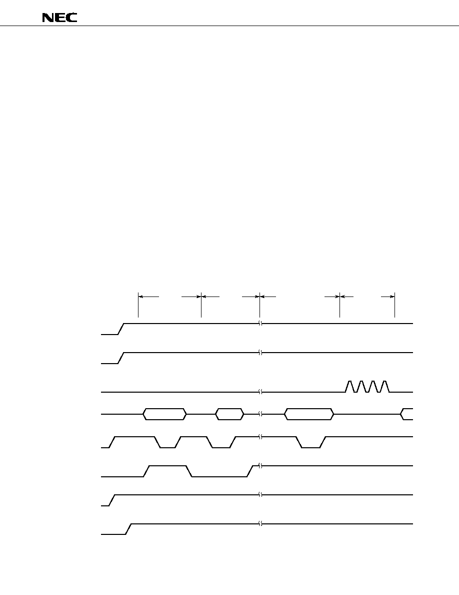
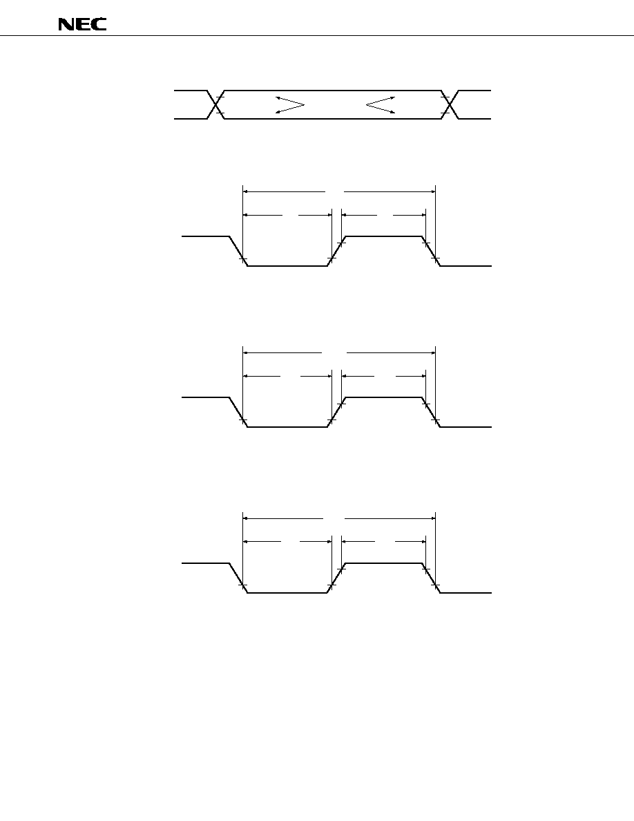
3.2 PROM WRITE PROCEDURE
PROMs can be written at high speed using the following procedure: (see the following figure)
(1) Pull unused pins to V
SS
through resistors. Set the X1 pin low.
(2) Supply 5 volts to the V
DD
and V
PP
pins.
(3) Wait for 10
µ
s.
(4) Select the zero clear program memory address mode.
(5) Supply 6 volts to the V
DD
and 12.5 volts to the V
PP
pins.
(6) Select the program inhibit mode.
(7) Write data in the 1 ms write mode.
(8) Select the program inhibit mode.
(9) Select the verify mode. If the data is correct, proceed to step (10). If not, repeat steps (7), (8) and (9).
(10) Perform one additional write (duration of 1 ms
◊
number of writes at (7) to (9)).
(11) Select the program inhibit mode.
(12) Apply four pulses to the X1 pin to increment the program memory address by one.
(13) Repeat steps (7) to (12) until the end address is reached.
(14) Select the zero clear program memory address mode.
(15) Return the V
DD
and V
PP
pins back to + 5 volts.
(16) Turn off the power.
The following figure shows steps (2) to (12).
MD0
(P30)
V
PP
V
PP
V
DD
V
DD
+1
V
DD
V
DD
X1
Input data
Output
data
Input data
P40-P43
P50-P53
MD1
(P31)
MD2
(P32)
MD3
(P33)
Write
Verify
Additional write
Address
increment
X repetition

16
µ
PD75P048
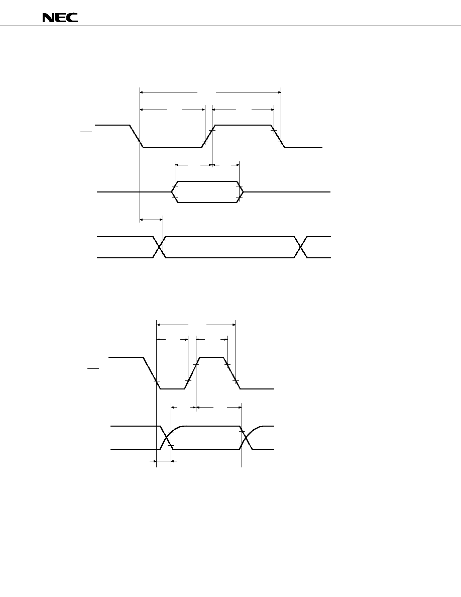
3.3 PROM READ PROCEDURE
The PROM contents can be read in the verify mode by using the following procedure: (see the following
figure)
(1) Pull unused pins to V
SS
through resistors. Set the X1 pin low.
(2) Supply 5 volts to the V
DD
and V
PP
pins.
(3) Wait for 10
µ
s.
(4) Select the clear program memory address mode.
(5) Supply 6 volts to the V
DD
and 12.5 volts to the V
PP
pins.
(6) Select the program inhibit mode.
(7) Select the verify mode. Apply four pulses to the X1 pin. Every four clock pulses will output the data stored
in one address.
(8) Select the program inhibit mode.
(9) Select the clear program memory address mode.
(10) Return the V
DD
and V
PP
pins back to + 5 volts.
(11) Turn off the power.
The following figure shows steps (2) to (9).
MD0
(P30)
V
PP
V
PP
V
DD
V
DD
+1
V
DD
V
DD
X1
Output data
P40-P43
P50-P53
MD1
(P31)
MD2
(P32)
MD3
(P33)
"L"
Output data

17
µ
PD75P048
4. SCREENING OF ONE-TIME PROM MODEL
Because of their structure, the one-time PROM models (
µ
PD75P48CW and
µ
PD75P48GC-AB8) cannot be
fully tested by NEC before shipment. It is therefore recommended that you implement screening to verify
the PROM after necessary data have been written to it, and after the PROM has been stored at high temperature
under the following conditions:
Storage Temperature
Storage Time
125 ∞C
24 hours
5

18
µ
PD75P048
5. ELECTRICAL SPECIFICATIONS
ABSOLUTE MAXIMUM RATINGS (T
a
= 25
∞
C)
Parameter
Symbol
Conditions
Ratings
Unit
Supply Voltage
V
DD
-0.3 to +7.0
V
Input Voltage
V
I1
Other than ports 4, 5, 10
-0.3 to V
DD
+0.3
V
V
I2
Ports 4, 5, 10
w/pull-up
-0.3 to V
DD
+0.3
V
resistor
Open drain
-0.3 to +11
V
Output Voltage
V
O
-0.3 to V
DD
+0.3
V
High-Level Output
I
OH
1 pin
-10
mA
Current
All pins
-30
mA
Low-Level Output
I
OL
Note
Ports 0, 3, 4, 5
Peak
30
mA
Current
1 pin
rms
15
mA
Other than ports 0, 3, 4, 5
Peak
20
mA
1 pin
rms
5
mA
Total of ports 0, 3 - 9, 11
Peak
170
mA
rms
120
mA
Total of ports 0, 2, 10
Peak
30
mA
rms
20
mA
Operating Temperature
T
opt
-10 to +70
∞
C
Storage Temperature
T
stg
-65 to +150
∞
C
Note rms = Peak value x
Duty
Caution Even if one of the parameters exceeds its absolute maximum rating even momentarily, the quality
of the product may be degraded. The absolute maximum rating therefore specifies the upper or
lower limit of the value at which the product can be used without physical damages. Be sure not
to exceed or fall below this value when using the product.
EEPROM RATINGS (T
a
= -10 to +70
∞
C, V
DD
= 2.7 to 6.0 V)
Parameter
Symbol
Conditions
Ratings
Unit
Write Times
--
100,000
times
Data Retention Time
--
10
years
CAPACITANCE (T
a
= 25
∞
C, V
DD
= 0 V)
Parameter
Symbol
Conditions
MIN.
TYP.
MAX.
Unit
Input Capacitance
C
I
f = 1 MHz
15
pF
Output Capacitance
C
O
Pins other than those measured are at 0 V
15
pF
Input/Output
C
IO
15
pF
5
19
µ
PD75P048
MAIN SYSTEM CLOCK OSCILLATOR CIRCUIT CHARACTERISTICS
(T
a
= -10 to +70
∞
C, V
DD
= 2.7 to 6.0 V)
Oscillator
Recommended
Item
Conditions
MIN.
TYP.
MAX.
Unit
Constants
Ceramic
Oscillation
V
DD
= oscillation
frequency(f
X
)
Note 1
voltage range
2.0
5.0
Note 3
MHz
Oscillation stabiliza-
After V
DD
come to
tion time
Note 2
MIN. value of
oscillation voltage
4
ms
range
Crystal
Oscillation
2.0
4.19
5.0
Note 3
MHz
frequency (f
X
)
Note 1
Oscillation stabiliza-
V
DD
= 4.5 to 6.0 V
10
ms
tion time
Note 2
30
ms
External Clock
X1 input frequency
(f
X
)
Note 1
2.0
5.0
Note 3
MHz
X1 input high-,
low-level widths
100
250
ns
(t
XH
, t
XL
)
Note 1. Only to express the characteristics of the oscillator circuit. For instruction execution time, refer to
AC Characteristics.
2. Time required for oscillation to stabilize after V
DD
has reached the minimum volue of the oscillation
voltage range or the STOP mode has been released.
3. When the oscillation frequency is 4.19 MHz < fx
5.0 MHz, do not select PCC = 0011 as the instruction
execution time: otherwise, one machine cycle is set to less than 0.95
µ
s, falling short of the rated
minimum value of 0.95
µ
s.
Caution When using the oscillation circuit of the main system clock, wire the portion enclosed in dotted
line in the figures as follows to avoid adverse influences on the wiring capacity:
∑
Keep the wiring length as short as possible.
∑
Do not cross the wiring over the other signal lines.
∑
Do not route the wiring in the vicinity of lines through which a high alternating current flows.
∑
Always keep the ground point of the capacitor of the oscillator circuit at the same potential as
V
DD
. Do not connect the ground pattern through which a high curent flows.
∑
Do not extract signals from the oscillation circuit.
X1
X2
C1
C2
V
DD
X1
X2
C1
C2
V
DD
X1
X2
PD74HCU04
µ
20
µ
PD75P048
SUBSYSTEM CLOCK OSCILLATOR CIRCUIT CHARACTERISTICS
(T
a
= -10 to +70
∞
C, V
DD
= 2.7 to 6.0 V)
Oscillator
Recommended
Item
Conditions
MIN.
TYP.
MAX.
Unit
Constants
Crystal
Oscillation
32
32.768
35
kHz
frequency (f
XT
)
Note 1
Oscillation stabiliza-
V
DD
= 4.5 to 6.0 V
1.0
2
s
tion time
Note 2
10
s
External Clock
XT1 input frequency
(f
XT
)
Note 1
32
100
kHz
XT1 input high-,
low-level widths
5
15
µ
s
(t
XTH
, t
XTL
)
Note 1. Indicates only the characteristics of the oscillator circuit. For instruction execution time, refer to AC
Characteristics.
2. Time required for oscillation to stabilize after V
DD
has reached the minimum value of the oscillation
voltage range.
Caution When using the oscillation circuit of the subsystem clock, wire the portion enclosed in dotted line
in the figures as follows to avoid adverse influences on the wiring capacity:
∑
Keep the wiring length as short as possible.
∑
Do not cross the wiring over the other signal lines.
∑
Do not route the wiring in the vicinity of lines through which a high alternating current flows.
∑
Always keep the ground point of the capacitor of the oscillator circuit at the same potential as
V
DD
. Do not connect the ground pattern through which a high current flows.
∑
Do not extract signals from the oscillation circuit.
The amplification factor of the subsystem clock oscillation circuit is designed to be low to reduce
the current dissipation and therefore, the subsystem clock oscillation circuit is influenced by noise
more easily than the main system clock oscillation circuit. When using the subsystem clock,
therefore, exercise utmost care in wiring the circuit.
XT1
XT2
XT1
XT2
R
C3
C4
V
DD
21
µ
PD75P048
DC CHARACTERISTICS (T
a
= -10 to +70
∞
C, V
DD
= 2.7 to 6.0 V)
Parameter
Symbol
Conditions
MIN.
TYP.
MAX.
Unit
High-Level Input
V
IH1
Ports 2,3,8,9,11
0.7V
DD
V
DD
V
Voltage
V
IH2
Ports 0,1,6,7, RESET
0.8V
DD
V
DD
V
V
IH3
Ports 4,5,10
w/pull-up resistor
0.7V
DD
V
DD
V
Open-drain
0.7V
DD
10
V
V
IH4
X1, X2, XT1, XT2
V
DD
-0.5
V
DD
V
Low-level Input
V
IL1
Ports 2-5, 8-11
0
0.3V
DD
V
Voltage
V
IL2
Ports 0, 1, 6, 7, RESET
0
0.2V
DD
V
V
IL3
X1, X2, XT1, XT2
0
0.4
V
High-Level Output
V
OH
V
DD
= 4.5 to 6.0V, I
OH
= -1 mA
V
DD
-1.0
V
Voltage
I
OH
= -100
µ
A
V
DD
-0.5
V
Low-Level Output
V
OL
Ports 3,4,5
V
DD
= 4.5 to 6.0V,
0.4
2.0
V
Voltage
I
OL
= 15mA
V
DD
= 4.5 to 6.0V, I
OL
= 1.6 mA
0.4
V
I
OL
= 400
µ
A
0.5
V
SB0, 1
Open-drain pull-up
0.2V
DD
V
resistor
1 k
High-Level Input
I
LIH1
V
I
= V
DD
Other than below
3
µ
A
Leakage Current
I
LIH2
X1,X2,XT1
20
µ
A
I
LIH3
V
I
= 9V
Ports 4,5,10
20
µ
A
(open-drain)
Low-Level Input
I
LIL1
V
I
= 0V
Other than below
-3
µ
A
Leakage Current
I
LIL2
X1,X2,XT1
-20
µ
A
High-Level Output
I
LOH1
V
O
= V
DD
Other than below
3
µ
A
Leakage Current
I
LOH2
V
O
= 9V
Ports 4,5,10
20
µ
A
(open-drain)
Low-Level Output
I
LOL
V
O
= 0V
-3
µ
A
Leakage Current
Internal Pull-Up Resistor
R
U1
Ports 0,1,2,3,6,7,8
V
DD
= 5.0V
±
10%
15
40
80
k
(except P00) V
I
= 0V
V
DD
= 3.0V
±
10%
30
300
k
R
U2
Ports 4,5,10
V
DD
= 5.0V
±
10%
15
40
70
k
V
O
= V
DD
-2.0 V
V
DD
= 3.0V
±
10%
10
60
k
Internal Pull-Down
R
D
Port 9 V
IN
= V
DD
V
DD
= 5.0V
±
10%
15
40
70
k
Resistor
V
DD
= 3.0V
±
10%
10
60
k
22
µ
PD75P048
Parameter
Symbol
Conditions
MIN.
TYP.
MAX.
Unit
Supply
I
DD1
4.19MHz crystal
V
DD
= 5V
±
10%
Note 2
5.5
17
mA
Current
Note 1
oscillator
V
DD
= 3V
±
10%
Note 3
1.7
5.1
mA
I
DD2
C1 = C2 = 22pF
HALT mode
V
DD
= 5V
±
10%
900
2700
µ
A
V
DD
= 3V
±
10%
450
1400
µ
A
I
DD3
32.768kHz
Note 4
Operation
V
DD
= 3V
±
10%
100
300
µ
A
crystal oscillator
mode
I
DD4
HALT mode
V
DD
= 3V
±
10%
35
110
µ
A
I
DD5
XT1 = 0V
V
DD
= 5V
±
10%
0.5
20
µ
A
STOP mode
V
DD
= 3V
±
10%
0.3
10
µ
A
T
a
= 25
∞
C
5
µ
A
I
DD6
32.768kHz oscillator
V
DD
= 3V
±
10%
Note 5
6
20
µ
A
STOP mode
Note 1. Current flowing through internal pull-up resistor. Current flowing when EEPROM is accessed is not
included.
2. When
µ
PD75048 operates in high-speed mode with processor clock control register (PCC) set to 0011.
3. When
µ
PD75048 operates in low-speed mode with PCC set to 0000.
4. When the system clock control register (SCC) is set to 1001, the oscillation of the main system clock
is stopped, and the subsystem clock is used.
5. When STOP instruction is executed with SCC set to 0000.
Note Supply current when EEPROM is accessed is shown in EEPROM Characteristics.

23
µ
PD75P048
AC CHARACTERISTICS (T
a
= -10 to +70
∞
C, V
DD
= 2.7 to 6.0 V)
Parameter
Symbol
Conditions
MIN.
TYP.
MAX.
Unit
CPU Clock Cycle Time
t
CY
w/main system clock
V
DD
= 4.5 to 6.0V
0.95
32
µ
s
(Minimum Instruction
3.8
32
µ
s
Execution Time
w/subsystem clock
114
122
125
µ
s
= 1 Machine Cycle)
Note 1
TI0 Input Frequency
f
TI
V
DD
= 4.5 to 6.0 V
0
1
MHz
0
275
kHz
TI0 Input High-, Low-
t
TIH
,
V
DD
= 4.5 to 6.0 V
0.48
µ
s
Level Widths
t
TIL
1.8
µ
s
Interrupt Input High-,
t
INTH
,
INT0
Note 2
µ
s
Low-Level Widths
t
INTL
INT1, 2, 4
10
µ
s
KR0-7
10
µ
s
RESET Low-Level Width
t
RSL
10
µ
s
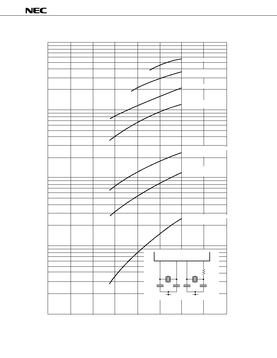
Note 1. The CPU clock (
) cycle time is de-
termined by the oscillation frequency
of the connected oscillator, system
clock control register (SCC), and
processor clock control register (PCC).
The figure on the right is cycle time t
CY
vs. supply voltage V
DD
characteristics
at the main system clock.
2. 2
tCY
or 128/f
X
depending on the set-
ting of the interrupt mode register
(IM0).
0
1
2
3
4
5
6
0.5
1
2
3
4
5
6
32
Supply voltage V
DD
[V]
Cycle time t
CY
[ s]
t
CY
vs V
DD
(with main system clock)
Operation
quaranteed
range
µ
24
µ
PD75P048
SERIAL TRANSFER OPERATION
Two-Line and Three-Line Serial I/O Modes (SCK: internal clock output)
Parameter
Symbol
Conditions
MIN.
TYP.
MAX.
Unit
SCK Cycle Time
t
KCY1
V
DD
= 4.5 to 6.0 V
1600
ns
3800
ns
SCK High-, Low-Level
t
KL1
V
DD
= 4.5 to 6.0 V
t
KCY1
/2-50
ns
Widths
t
KH1
t
KCY1
/2-150
ns
SI Set-Up Time (vs. SCK
) t
SIK1
150
ns
SI Hold Time (vs. SCK
)
t
KSI1
400
ns
SCK
SO Output
t
KSO1
R
L
= 1k
,
Note
V
DD
= 4.5 to 6.0V
250
ns
Delay Time
C
L
= 100pF
1000
ns
TWO-LINE AND THREE-LINE SERIAL I/O MODES (SCK: external clock input)
Parameter
Symbol
Conditions
MIN.
TYP.
MAX.
Unit
SCK Cycle Time
t
KCY2
V
DD
= 4.5 to 6.0V
800
ns
3200
ns
SCK High-, Low-Level
t
KL2
V
DD
= 4.5 to 6.0V
400
ns
Widths
t
KH2
1600
ns
SI Set-Up Time (vs. SCK
) t
SIK2
100
ns
SI Hold Time (vs. SCK
)
t
KSI2
400
ns
SCK
SO Output
t
KSO2
R
L
= 1k
, C
L
= 100 pF
Note
V
DD
= 4.5 to 6.0V
300
ns
Delay Time
1000
ns
Note R
L
and C
L
are load resistance and load capacitance of the SO output line.

25
µ
PD75P048
SBI MODE (SCK: internal clock output (master))
Parameter
Symbol
Conditions
MIN.
TYP.
MAX.
Unit
SCK Cycle Time
t
KCY3
V
DD
= 4.5 to 6.0 V
1600
ns
3800
ns
SCK High-, Low-Level
t
KL3
V
DD
= 4.5 to 6.0 V
t
KCY3
/2-50
ns
Widths
t
KH3
t
KCY3
/2-150
ns
SB0, 1 Set-Up Time
t
SIK3
150
ns
(vs. SCK
)
SB0, 1 Hold Time
t
KSI3
t
KCY3
/2
ns
(vs. SCK
)
SCK
SB0, 1 Output
t
KSO3
R
L
= 1k
,
Note
V
DD
= 4.5 to 6.0V
0
250
ns
Delay Time
C
L
= 100pF
0
1000
ns
SCK
SB0, 1
t
KSB
t
KCY3
ns
SB0,1
SCK
t
SBK
t
KCY3
ns
SB0, 1 Low-Level Width
t
SBL
t
KCY3
ns
SB0, 1 High-Level Width
t
SBH
t
KCY3
ns
SBI MODE (SCK: external clock input (slave))
Parameter
Symbol
Conditions
MIN.
TYP.
MAX.
Unit
SCK Cycle Time
t
KCY4
V
DD
= 4.5 to 6.0 V
800
ns
3200
ns
SCK Ligh-, Low-Level
t
KL4
V
DD
= 4.5 to 6.0 V
400
ns
Widths
t
KH4
1600
ns
SB0, 1 Set-Up Time
t
SIK4
100
ns
(vs. SCK
)
SB0, 1 Hold Time
t
KSI4
t
KCY4
/2
ns
(vs. SCK
)
SCK
SB0, 1 Output
t
KSO4
R
L
= 1k
,
Note
V
DD
= 4.5 to 6.0V
0
300
ns
Delay Time
C
L
= 100pF
0
1000
ns
SCK
SB0, 1
t
KSB
t
KCY4
ns
SB0,1
SCK
t
SBK
t
KCY4
ns
SB0, 1 Low-Level Width
t
SBL
t
KCY4
ns
SB0, 1 High-Level Width
t
SBH
t
KCY4
ns
Note R
L
and C
L
are load resistance and load capacitance of the SB0 and SB1 output lines.
26
µ
PD75P048
A/D CONVERTER (T
a
= -10 to +70
∞
C, V
DD
= 2.7 to 6.0V, AV
SS
= V
SS
= 0V)
Parameter
Symbol
Conditions
MIN.
TYP.
MAX.
Unit
Resolution
8
8
8
bit
Absolute Accuracy
Note 1
2.5V
AV
REF
V
DD
±
1.5
LSB
Conversion Time
Note 2
t
CONV
168/f
X
µ
s
Sampling Time
Note 3
t
SAMP
44/f
X
µ
s
Analog Input Voltage
V
IAN
AV
REF-
AV
REF+
V
Analog Supply Voltage
AV
DD
2.5
V
DD
V
Reference Input Voltage
AV
REF+
2.5V
(AV
ref+
) ≠ (AV
ref-
)
2.5
AV
DD
V
Reference Input Voltage
AV
REF-
2.5V
(AV
ref+
) ≠ (AV
ref-
)
0
1.0
V
Analog Input Impedance
R
AN
1000
M
AV
REF
Current
AI
REF
0.25
2.0
mA
Note 1. Absolute accuracy excluding quantization error (
±
1
≠
2
LSB)
2. Time since execution of conversion start instruction until end of conversion (EOC = 1) (40.1
µ
s: f
X
= 4.19
MHz)
3. Time since execution of conversion start instruction until end of sampling (10.5
µ
s: f
X
= 4.19 MHz)
27
µ
PD75P048
AC TIMING TEST POINT (excluding X1 and XT1 inputs)
Test points
0.8 V
DD
0.2 V
DD
0.8 V
DD
0.2 V
DD
CLOCK TIMING
X1 input
V
DD
≠0.5V
0.4 V
t
XL
t
XH
1/f
X
XT1 input
V
DD
≠0.5V
0.4 V
t
XTL
t
XTH
1/f
XT
TI0 TIMING
TI0
t
TIL
t
TIH
1/f
TI
28
µ
PD75P048
SERIAL TRANSFER TIMING
THREE-LINE SERIAL I/O MODE:
SCK
t
KL1
t
KH1
t
KCY1
Output data
t
SIK1
t
KSI1
t
KS01
Input data
SI
SO
TWO-LINE SERIAL I/O MODE:
SCK
t
KL2
t
KH2
t
KCY2
t
SIK2
t
KSI2
t
KSO2
SB0,1

29
µ
PD75P048
SERIAL TRANSFER TIMING
BUS RELEASE SIGNAL TRANSFER:
COMMAND SIGNAL TRANSFER:
SCK
t
KL3,4
t
KCY3,4
t
SIK3,4
t
KSI3,4
t
KS03,4
SB0,1
t
KH3,4
t
SBK
t
KSB
INTERRUPT INPUT TIMING
INT0, 1, 2, 4
KR0-7
t
INTL
t
INTH
RESET INPUT TIMING
RESET
t
RSL
SCK
t
KL3,4
t
KCY3,4
t
SIK3,4
t
KSI3,4
t
KS03,4
SB0,1
t
KH3,4
t
SBK
t
SBH
t
SBL
t
KSB
30
µ
PD75P048
EEPROM CHARACTERISTICS
Parameter
Symbol
Conditions
MIN.
TYP.
MAX.
Unit
Supply current for
I
DD7
4.19MHz crystal oscillator V
DD
= 5V+10%
Note 2
6.5
20
mA
EEPROM access
Note 1
C1 = C = 22pF
V
DD
= 3V+10%
Note 3
2
6
mA
Note 1. Current flowing through the internal pull-up resistor is not included.
2. When the processor clock control register (PCC) is set to 0011 and the high-speed mode is used.
3. When PCC is set to 0000 and the low-speed mode is used.
EEPROM WRITE TIME
Select the write time of the EEPROM in accordance with the oscillation frequency of the main system clock
as follows:
Oscillation Frequency of Main
Setting of EEPROM Control Register
Write time
System Clock (f
X
)
EWTC1
EWTC0
f
X
= 2.0 to 5.0 MHz
0
0
2
12
x 18/f
X
(17.6 ms)
f
X
= 2.0 to 4.2 MHz
0
1
2
11
x 18/f
X
(8.8 ms)
f
X
= 2.0 MHz
1
0
2
10
x 18/f
X
Remarks ( ): f
X
= 4.19 MHz
LOW-VOLTAGE DATA RETENTION CHARACTERISTICS OF DATA MEMORY IN STOP MODE
(T
a
= ≠10 to +70
∞
C)
Parameter
Symbol
Conditions
MIN.
TYP.
MAX.
Unit
Data Retention Supply
V
DDDR
2.0
6.0
V
Voltage
I
DDDR
V
DDDR
= 2.0 V
0.1
10
µ
A
Release Signal Set Time
t
SREL
0
µ
s
t
WAIT
Released by RESET
2
17
/f
X
ms
Released by interrupt request
ms
Note 1. Does not include current flowing through internal pull-up resistor
2. The oscillation stabilization wait time is the time during which the CPU is stopped to prevent unstable
operation when oscillation is started.
3. Depends on the setting of the basic interval timer mode register (BTM) as follows:
BTM3
BTM2
BTM1
BTM0
WAIT time ( ): f
X
= 4.19 MHz
≠
0
0
0
2
20
/f
X
(approx. 250 ms)
≠
0
1
1
2
17
/f
X
(approx. 31.3 ms)
≠
1
0
1
2
15
/f
X
(approx. 7.82 ms)
≠
1
1
1
2
13
/f
X
(approx. 1.95 ms)
Oscillation Stabilization
Wait Time
Note 2
Data Retention Supply
Current
Note 1
Note 3

31
µ
PD75P048
DATA RETENTION TIMING (releasing STOP mode by RESET)
STOP mode
Data retention mode
STOP instruction
execution
V
DD
RESET
V
DDDR
t
SREL
t
WAIT
Operation
mode
Internal reset operation
HALT mode
DATA RETENTION TIMING (standby release signal: releasing STOP mode by interrupt)
STOP mode
Data retention mode
STOP instruction execution
V
DD
V
DDDR
t
SREL
t
WAIT
Operation
mode
HALT mode
Standby release signal
(interrupt request)
32
µ
PD75P048
6. PERFORMANCE CURVE (REFERENCE VALUE)
Note
Does not include current flowing through EEPROM.
X1
X2
XT1
XT2
V
DD
V
DD
Crystal
oscillator
Crystal
oscillator
4.19 MHz
32.768 kHz
22 pF
22 pF
22 pF
22 pF
330 k
0
1
2
3
4
5
6
7
Supply voltage V
DD
[V]
I
DD
vs V
DD
(Crystal oscillation)
(T = 25
∞
C)
10
5.0
1.0
0.5
0.1
0.05
0.01
0.005
0.001
Supply current I
DD
[mA]
High-speed mode PCC = 0011
Main system clock
HALT mode
Subsystem clock HALT mode
Subsystem clock oscillation
Medium-speed mode
PCC = 0010
Low-speed mode PCC = 0000
Main system clock STOP mode
Main system clock stopped
a
Subsystem clock operation mode
Main system lock stopped
+
+
+
5
33
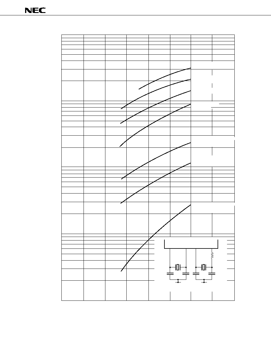
µ
PD75P048
Note Does not include current flowing through EEPROM.
X1
X2
XT1
XT2
V
DD
V
DD
Crystal
oscillator
Crystal
oscillator
2.0 MHz
32.768 kHz
22 pF
22 pF
22 pF
22 pF
330 k
0
1
2
3
4
5
6
7
Supply voltage V
DD
[V]
I
DD
vs V
DD
(Crystal oscillation)
(T = 25
∞
C)
10
5.0
1.0
0.5
0.1
0.05
0.01
0.005
0.001
Supply current I
DD
[mA]
High-speed mode PCC = 0011
Low-speed mode PCC = 0000
Main system clock
HALT mode
Main system clock stopped
Subsystem clock HALT mode
Subsystem clock oscillation
Medium-speed mode
PCC = 0010
Main system clock stopped
Main system clock STOP mode
a
+
+
+
Subsystem clock operation mode
34
µ
PD75P048
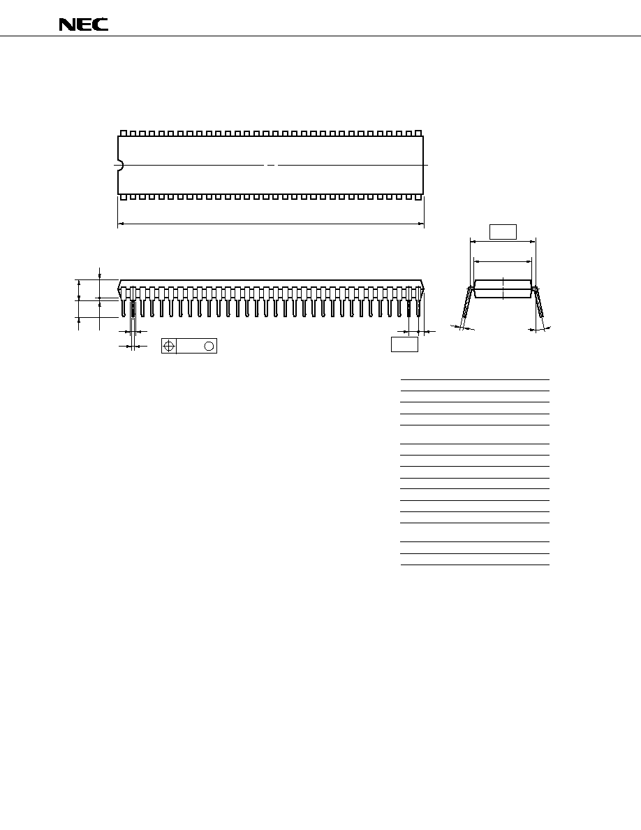
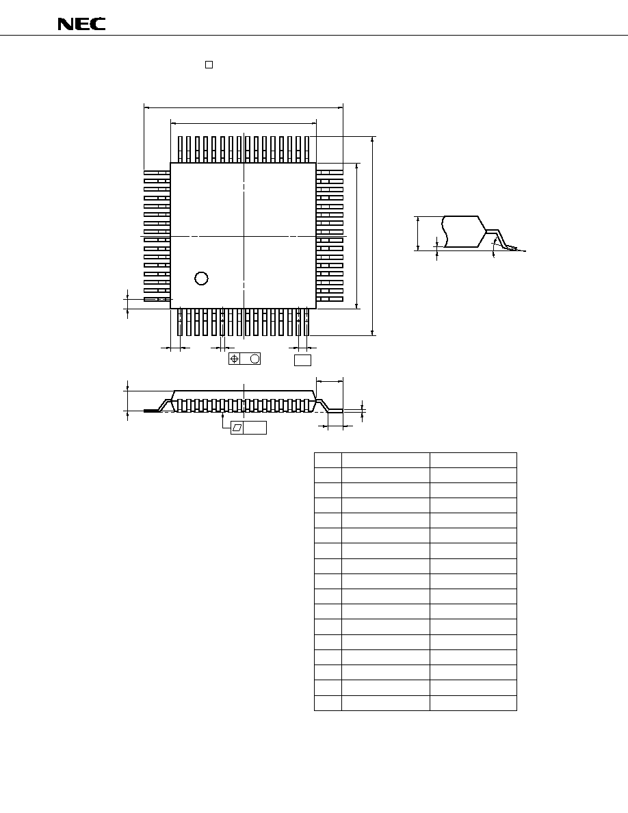
7. PACKAGE DRAWINGS
A
I
J
G
H
F
D
N
M
C
B
M
R
64
33
32
1
K
L
NOTE
Each lead centerline is located within 0.17 mm (0.007 inch) of
its true position (T.P.) at maximum material condition.
P64C-70-750A,C-1
ITEM
MILLIMETERS
INCHES
A
B
C
D
F
G
H
I
J
K
58.68 MAX.
1.778 (T.P.)
3.2±0.3
0.51 MIN.
4.31 MAX.
1.78 MAX.
L
M
0.17
0.25
19.05 (T.P.)
5.08 MAX.
17.0
N
0~15∞
0.50±0.10
0.9 MIN.
R
2.311 MAX.
0.070 MAX.
0.020
0.035 MIN.
0.126±0.012
0.020 MIN.
0.170 MAX.
0.200 MAX.
0.750 (T.P.)
0.669
0.010
0.007
0~15∞
+0.004
≠0.003
0.070 (T.P.)
1)
Item "K" to center of leads when formed parallel.
2)
+0.10
≠0.05
+0.004
≠0.005
64 PIN PLASTIC SHRINK DIP (750 mil)
35
µ
PD75P048
N
A
M
F
B
48
49
32
K
L
64 PIN PLASTIC QFP ( 14)
64
1
17
16
33
D
C
detail of lead end
S
Q
5∞±5∞
P
M
I
H
J
G
P64GC-80-AB8-2
ITEM
MILLIMETERS
INCHES
A
B
C
D
F
G
H
I
J
K
L
17.6±0.4
14.0±0.2
1.0
0.35±0.10
0.15
14.0±0.2
0.693±0.016
0.039
0.039
0.006
0.031 (T.P.)
0.551
NOTE
M
N
0.15
0.15
1.8±0.2
0.8 (T.P.)
0.006
0.006
+0.004
≠0.003
Each lead centerline is located within 0.15
mm (0.006 inch) of its true position (T.P.) at
maximum material condition.
0.071±0.008
0.014
0.551
0.8±0.2
0.031
P
2.55
0.100
0.693±0.016
17.6±0.4
1.0
+0.009
≠0.008
Q
0.1±0.1
0.004±0.004
S
2.85 MAX.
0.112 MAX.
+0.10
≠0.05
+0.009
≠0.008
+0.004
≠0.005
+0.009
≠0.008

36
µ
PD75P048
8. RECOMMENDED SOLDERING CONDITIONS
It is recommended that
µ
PD75P048 be soldered under the following conditions. For details on the recommended
soldering conditions, refer to Information Document "Semiconductor Devices Mounting Manual" (IEI-1207). For
other soldering methods and conditions, consult NEC.
Table 8-1 Soldering Conditions of Surface-Mount Type
µ
PD75P048GC-AB8: 64-pin plastic QFP (
14 mm)
Soldering Method
Soldering Conditions
Symbol for Recommended
Condition
Infrared Reflow
Package peak temperature: 235
∞
C,
IR35-00-2
time: 30 seconds max. (210
∞
C min.),
number of times: 2 max.
<Caution>
(1) Start second reflow after device temperature
(which has risen because of first reflow) has returned to
room temperature.
(2) Do not clean flux with water after first reflow.
VPS
Package peak temperature: 215
∞
C,
VP15-00-2
time: 40 seconds max. (200
∞
C min.),
number of times: 1 max.
<Caution>
(1) Start second reflow after device temperature
(which has risen because of first reflow) has returned to
room temperature.
(2) Do not clean flux with water after first reflow.
Pin Partial Heating
Pin temperature: 300
∞
C max.,
--
time: 3 seconds max. (per side)
Caution Do not use two or more soldering methods in combination (except the pin partial heating method).
Table 8-2 Soldering Conditions of Through-Hole Type
µ
PD75P048CW: 64-pin plastic shrink DIP (750 mil)
Soldering Method
Soldering Conditions
Wave soldering
Soldering bath temperature: 260
∞
C max.,
(lead parts only)
time: 10 seconds max.,
Pin Partial Heating
Pin temperature: 260
o
C max.,
time: 10 seconds max.
Caution The wave soldering must be performed at the lead part only. Note that the soldering must not be
directly contacted to the board.
5

37
µ
PD75P048
APPENDIX A. DEVELOPMENT TOOLS
The following development tools are readily available to support development of systems using
µ
PD75P048:
Hardware
IE-75000-R
Note 1
In-circuit emulator for 75X series
IE-75001-R
IE-75000-R-EM
Note 2
Emulation board for IE-75000-R and IE-75001-R
EP-75028CW-R
Common emulation probe commonly used with
µ
PD75028CW
EP-75028GC-R
Emulation probe commonly used with
µ
PD75028GC, provided with
EV-9200GC-64, 64-pin conversion socket
PG-1500
PROM programmer
PA-75P036CW
PROM programmer adapter commonly used with
µ
PD75P036. It is connected
to PG-1500.
PA-75P036GC
PROM programmer adapter commonly used with
µ
PD75P036GC. It is connected
to PG-1500.
Software
IE Control Program
Host machine
PG-1500 Controller
PC-9800 series (MS-DOS
TM
Ver. 3.30 to Ver. 5.00A
Note 3
)
RA75X Relocatable
IBM PC/AT
TM
(Refer to OS for IBM PC.)
Assembler
Note 1. Maintenance product
2. Not provided with IE-75001-R.
3. Ver. 5.00/5.00A has a task swap function, but this function cannot be used with this software.
Remarks For development tools from other companies, refer to 75X Series Selection Guide (IF-1027).
OS for IBM PC
As OS for IBM PC, the followings are supported.
OS
Version
PC DOS
TM
Ver. 5.02 to Ver. 6.1
MS-DOS
Ver. 3.30 to Ver. 5.00A
Note 1
5.0/V
Note 2
IBM DOS
TM
J5.02/V
Note 2
Note 1. Version later than 5.0 have a task swap function, but this function cannot be used with this software.
2. This supports English mode only.
5
EV-9200GC-64
38
µ
PD75P048
APPENDIX B. RELATED DOCUMENTS
Documents related to device
Document
Document No.
User's manual
IEU-1278
Instruction list
--
75X series selection guide
IF-1027
Documents related to development tools
Doument
Document No.
Hardware
IE-75000-R/IE-75001-R user's manual
EEU-1416
IE-75000-R-EM user's manual
EEU-1294
EP-750028CW-R user's manual
EEU-1314
EP-75028GC-R user's manual
EEU-1306
PG-1500 user's manual
EEU-1335
Software
RA75X assembler package user's manual
Operation
EEU-1346
Language
EEU-1343
PG-1500 controller user's manual
EEU1291
Other related documents
Document
Document No.
Package manual
IEI-1213
Semiconductor device - mounting maual
IEI-1207
NEC semiconductor device quality grade
IEI-1209
NEC semiconductor device reliabiliy quality control
--
Static electricity discharge (ESD) test
--
Semiconductor device quality guarantee guide
MEI-1202
Product guide related to microcomputer - other manufacturers
--
Note The documents listed above are subject to change without notice. Be sure to use the latest document
for designing.
5

39
µ
PD75P048
NOTES FOR CMOS DEVICES
1
PRECAUTION AGAINST ESD FOR SEMICONDUCTORS
Note: Strong electric field, when exposed to a MOS device, can cause destruction of
the gate oxide and ultimately degrade the device operation. Steps must be
taken to stop generation of static electricity as much as possible, and quickly
dissipate it once, when it has occurred. Environmental control must be
adequate. When it is dry, humidifier should be used. It is recommended to
avoid using insulators that easily build static electricity. Semiconductor
devices must be stored and transported in an anti-static container, static
shielding bag or conductive material. All test and measurement tools including
work bench and floor should be grounded. The operator should be grounded
using wrist strap. Semiconductor devices must not be touched with bare
hands. Similar precautions need to be taken for PW boards with semiconductor
devices on it.
2
HANDLING OF UNUSED INPUT PINS FOR CMOS
Note: No connection for CMOS device inputs can be cause of malfunction. If no
connection is provided to the input pins, it is possible that an internal input
level may be generated due to noise, etc., hence causing malfunction. CMOS
devices behave differently than Bipolar or NMOS devices. Input levels of CMOS
devices must be fixed high or low by using a pull-up or pull-down circuitry. Each
unused pin should be connected to V
DD
or GND with a resistor, if it is considered
to have a possibility of being an output pin. All handling related to the unused
pins must be judged device by device and related specifications governing the
devices.
3
STATUS BEFORE INITIALIZATION OF MOS DEVICES
Note: Power-on does not necessarily define initial status of MOS device. Production
process of MOS does not define the initial operation status of the device.
Immediately after the power source is turned ON, the devices with reset
function have not yet been initialized. Hence, power-on does not guarantee
out-pin levels, I/O settings or contents of registers. Device is not initialized
until the reset signal is received. Reset operation must be executed immedi-
ately after power-on for devices having reset function.
No part of this document may be copied or reproduced in any form or by any means without the prior written
consent of NEC Corporation. NEC Corporation assumes no responsibility for any errors which may appear in this
document.
NEC Corporation does not assume any liability for infringement of patents, copyrights or other intellectual
property rights of third parties by or arising from use of a device described herein or any other liability arising
from use of such device. No license, either express, implied or otherwise, is granted under any patents,
copyrights or other intellectual property rights of NEC Corporation or others.
The devices listed in this document are not suitable for use in aerospace equipment, submarine cables, nuclear
reactor control systems and life support systems. If customers intend to use NEC devices for above applications
or they intend to use "Standard" quality grade NEC devices for applications not intended by NEC, please contact
our sales people in advance.
Application examples recommended by NEC Corporation
Standard: Computer, Office equipment, Communication equipment, Test and Measurement equipment,
Machine tools, Industrial robots, Audio and Visual equipment, Other consumer products, etc.
Special:
Automotive and Transportation equipment, Traffic control systems, Antidisaster systems, Anticrime
systems, etc.
M4 92.6
NEC is manufacturing and selling the products under microcomputer (with
on-chip EEPROM) patent license with the BULL CP8.
This product should not be used for IC cards (SMART CARD).
[MEMO]
MS-DOS is a trademark of Microsoft Corporation.
IBM DOS, PC/AT and PC DOS are trademarks of IBM Corporation.
µ
PD75P048