
4-BIT SINGLE-CHIP MICROCOMPUTER
MOS INTEGRATED CIRCUIT
© NEC Corporation 1992
µ
PD75P316A
DATA SHEET
The information in this document is subject to change without notice.
The mark 5 shows major revised points.
Document No.
IC-2524A
(O. D. No.
IC-7950B)
Date Published October 1993 P
Printed in Japan
DESCRIPTION
The
µ
PD75P316A is a product of the
µ
PD75316 with on-chip ROM having been replaced with the one-time PROM
or EPROM.
It is most suitable for test production during system development and for production in small amounts since it
can operate under the same supply voltage as mask products.
The one-time PROM product is capable of writing only once and is effective for production of many kinds of sets
in small quantities and early startup. The EPROM product allows program writing and rewriting, and is therefore
suitable for system evaluation. The on-chip RAM has twice the capacity of the
µ
PD75316/75P316, enabling large
amounts of data to be processed.
Details of functions are described in the User's Manual shown below. Be sure to read in design.
µ
PD75308 User's Manual : IEM-5016
FEATURES
∑
Compatible (excluding mask option) with the mask products
∑
Memory capacity
∑ Program memory (PROM) : 16256
◊
8 bits
∑ Data memory (RAM)
: 1024
◊
4 bits
∑
Low-voltage operation capability: 2.7 to 6.0 V
ORDERING INFORMATION
Ordering Code
Package
On-Chip ROM
µ
PD75P316AGF-3B9
80-pin plastic QFP (14
◊
20 mm)
One-time PROM
µ
PD75P316AK
80-pin ceramic WQFN (LCC with window)
EPROM
QUALITY GRADE
Ordering Code
Package
Quality Grade
µ
PD75P316AGF-3B9
80-pin plastic QFP (14
◊
20 mm)
Standard
µ
PD75P316AK
80-pin ceramic WQFN (LCC with window)
Standard
Please refer to "Quality grade on NEC Semiconductor Devices" (Document number IEI-1209) published by
NEC Corporation to know the specification of quality grade on the devices and its recommended applications.
In descriptions common to one-time PROM products and EPROM products in this document, the term "PROM" is
used.
µ
PD75P316A
2
µ
PD75P316AGF
µ
PD75P316AK
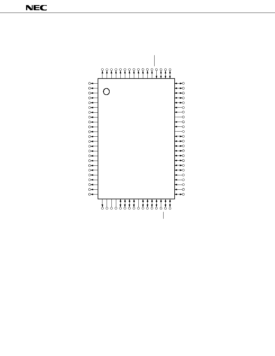
PIN CONFIGURATION (Top View)
S27/BP3
S28/BP4
S29/BP5
S30/BP6
S31/BP7
S12
S13
S14
S15
S16
S17
S18
S19
S20
S21
S22
S23
S24/BP0
S25/BP1
S26/BP2
COM0
COM1
COM2
COM3
P23/BUZ
P22/PCL
P21
P20/PTO0
P13/TI0
P70/KR4
P63/KR3
P62/KR2
P61/KR1
P60/KR0
X2
X1
V
PP
XT2
XT1
V
DD
P33 (MD3)
P32 (MD2)
P31/SYNC (MD1)
P30/LCDCL (MD0)
P12/INT2
P11/INT1
P10/INT0
P03/SI/SB1
S11
S10
S9
S8
S7
S6
S5
S4
S3
S2
S1
S0
RESET
P73/KR7
P72/KR6
P71/KR5
BIAS
V
LC0
V
LC1
V
LC2
P40
P41
P42
P43
V
SS
P50
P51
P52
P53
P00/INT4
P01/SCK
P02/SO/SB0
1
2
3
4
5
6
7
8
9
10
11
12
13
14
15
16
17
18
19
20
21
22
23
24
64
63
62
61
60
59
58
57
56
55
54
53
52
51
50
49
48
47
46
45
44
43
42
41
80797877767574737271706968676665
25262728293031323334353637383940
µ
PD75P316A
3
m
m
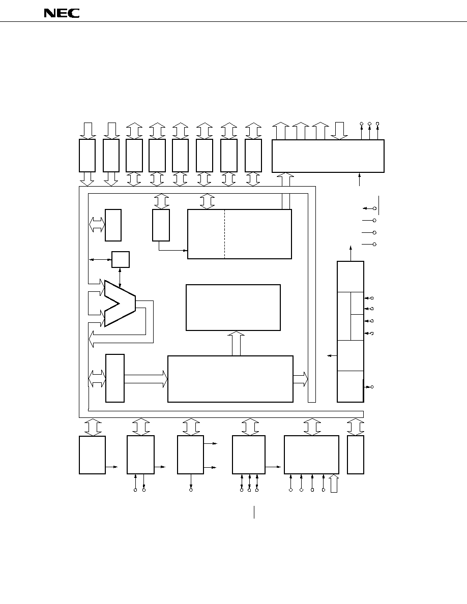
BLOCK DIAGRAM
PROGRAM
COUNTER (14)
PROGRAM
MEMORY
(PROM)
16256
◊
8 BITS
LCD
CONTROL-
LER
/DRIVER
S0-S23
S24/BP0
≠S31/BP7
COM0≠COM3
V
LC0
≠V
LC2
BIAS
LCDCL/P30
SYNC/P31
GENERAL REG.
DATA
MEMORY
(RAM)
1024
◊
4 BITS
BANK
SP(8)
ALU
CY
DECODE
AND
CONTROL
BIT SEQ.
BUFFER (16)
4
P00-P03
4
P10-P13
4
P20-P23
4
P30-P33
/MD0-MD3
PORT4
4
P40-P43
PORT5
4
P50-P53
PORT6
4
P60-P63
PORT7
4
P70-P73
PORT3
PORT2
PORT1
PORT0
24
8
4
3
f
LCD
RESET
V
SS
V
DD
CPU
CLOCK
V
PP
STAND BY
CONTROL
SYSTEM CLOCK
GENERATOR
SUB
MAIN
CLOCK
DIVIDER
CLOCK
OUTPUT
CONTROL
X2
X1
XT2
XT1
PCL/P22
f
X
/ 2
N
BASIC
INTERVAL
TIMER
INTBT
TIMER/EVENT
COUNTER
#0
INTT0
TI0/P13
PTO0/P20
WATCH
TIMER
INTW
f
LCD
BUZ/P23
SERIAL BUS
INTERFACE
INTCSI
SCK/P01
SO/SB0/P02
SI/SB1/P03
INTERRUPT
CONTROL
KR0/P60
≠KR7/P73
INT4/P00
INT2/P12
INT1/P11
INT0/P10

µ
PD75P316A
4
CONTENTS
1.
PIN FUNCTIONS ......................................................................................................................................... 5
1.1
PORT PINS ........................................................................................................................................................... 5
1.2
OTHER PINS ......................................................................................................................................................... 7
1.3
PIN INPUT/OUTPUT CIRCUITS ......................................................................................................................... 9
1.4
CAUTION ON USING P00/INT4 PIN AND RESET PIN .................................................................................. 11
2.
DIFFERENCES BETWEEN PRODUCTS IN SERIES ............................................................................... 11
3.
DATA MEMORY (RAM) ............................................................................................................................ 13
4.
PROGRAM MEMORY WRITE AND VERIFY ........................................................................................... 15
4.1
PROGRAM MEMORY WRITE/VERIFY OPERATING MODES ....................................................................... 15
4.2
PROGRAM MEMORY WRITING PROCEDURE ............................................................................................... 16
4.3
PROGRAM MEMORY READING PROCEDURE ............................................................................................... 17
4.4
ERASURE METHOD .......................................................................................................................................... 18
5.
ELECTRICAL SPECIFICATIONS ............................................................................................................... 19
6.
PACKAGE INFORMATION ....................................................................................................................... 35
7.
RECOMMENDED SOLDERING CONDITIONS ....................................................................................... 37
APPENDIX A. DEVELOPMENT TOOLS ......................................................................................................... 38
APPENDIX B. RELATED DOCUMENTS ........................................................................................................ 39
5
5
5
µ
PD75P316A
1.
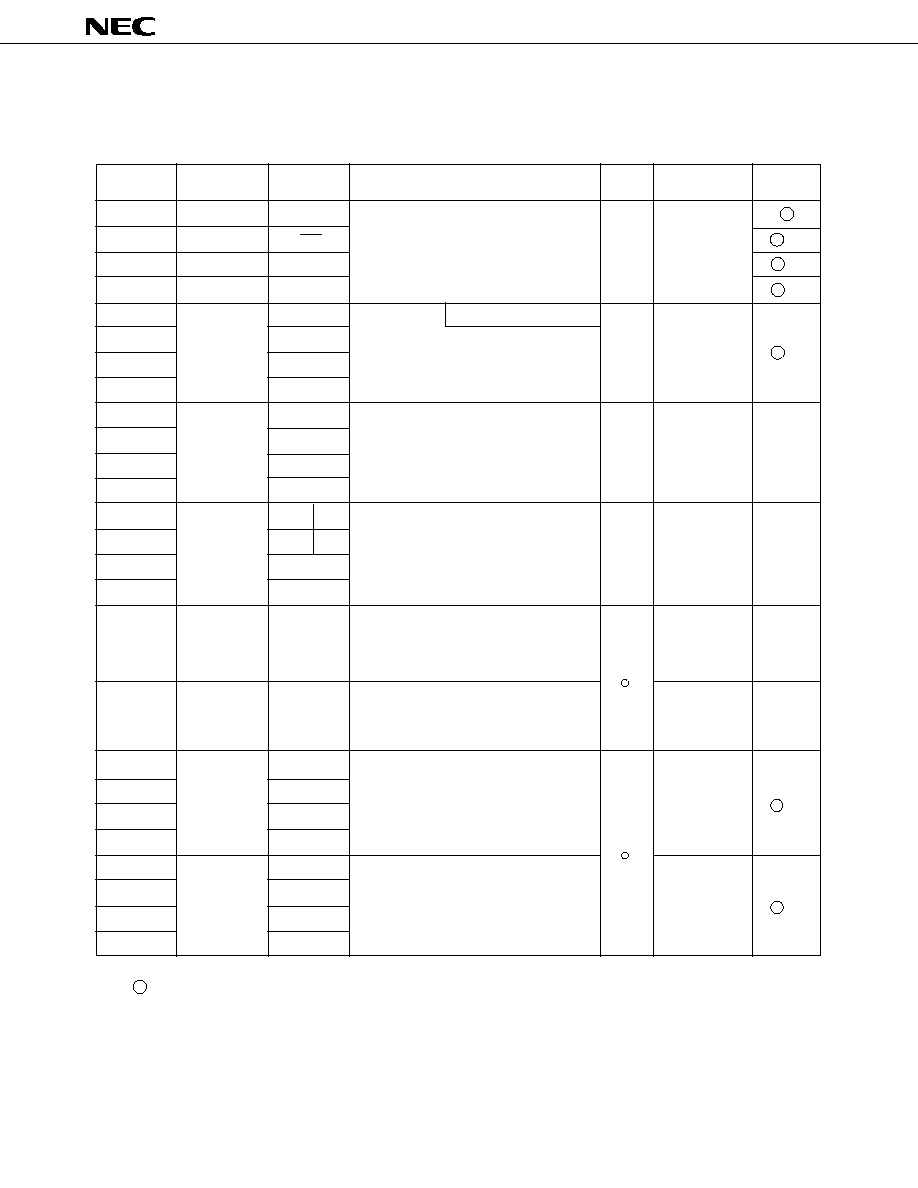
PIN FUNCTIONS
1.1
PORT PINS (1/2)
Input
Input/output
Input/output
Input/output
Input
Input/output
Input/output
Input/output
Input/output
P00
P01
P02
P03
P10
P11
P12
P13
P20
P21
P22
P23
P30 *2
P31 *2
P32 *2
P33 *2
P40 to P43*2
P50 to P53 *2
P60
P61
P62
P63
P70
P71
P72
P73
Dual-
Function Pin
INT4
SCK
SO/SB0
SI/SB1
INT0
INT1
INT2
TI0
PTO0
--
PCL
BUZ
LCDCL MD0
SYNC MD1
MD2
MD3
--
--
KR0
KR1
KR2
KR3
KR4
KR5
KR6
KR7
I/O Circuit
Type*1
B
F - A
F - B
M - C
B - C
E - B
E - B
M - A
M - A
F - A
F - A
Input
Input
Input
Input
High impedance
High impedance
Input
Input
◊
◊
◊
◊
With noise elimination circuit
Pin Name
Input/Output
8-Bit I/O
Afer Reset
Input/output
Input/output
*
1.
: Indicates a Schmitt-triggered input.
2 . Direct LED drive capability.
Function
4-bit input port (PORT0)
Internal pull-up resistor specification by soft-
ware is possible for P01 to P03 as a 3-bit unit.
4-bit input port (PORT1)
Internal pull-up resistor specification by soft-
ware is possible as a 4-bit unit.
4-bit input/output port (PORT2)
Internal pull-up resistor specification by soft-
ware is possible as a 4-bit unit.
Programmable 4-bit input/output port (PORT3)
Input/output settable bit-wise.
Internal pull-up resistor specification by soft-
ware is possible as a 4-bit unit.
N-ch open-drain 4-bit input/output port (PORT
4).
Data input/output pins for program memory
(PROM) write/verify (low-order 4 bits).
N-ch open-drain 4-bit input/output port (PORT 5)
Data input/output pins for program memory
(PROM) write/verify (high-order 4 bits).
Programmable 4-bit input/output port (PORT6).
Input/output settable bit-wise.
Internal pull-up resistor specification by soft-
ware is possible as a 4-bit unit.
4-bit input/output port (PORT7).
Internal pull-up resistor specification by soft-
ware is possible as a 4-bit unit.
6
µ
PD75P316A
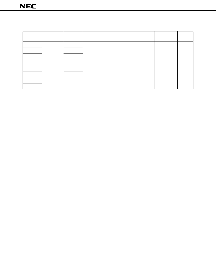
1.1
PORT PINS (2/2)
BP0
BP1
BP2
BP3
BP4
BP5
BP6
BP7
Dual-
Function Pin
S24
S25
S26
S27
S28
S29
S30
S31
I/O Circuit
TYPE
G - C
*
1-bit output port (BIT PORT)
Dual-function as segment output pins.
Output
Output
◊
Pin Name
Input/Output
Function
8-Bit I/O
After Reset
*
For BP0 to BP7, V
LC1
is selected as the input source. The output level depends on BP0 to BP7 and the V
LC1
external
circuit, however.
7
µ
PD75P316A
Input
output
Input/output
Input/output
Input/output
Input/output
Input/output
Input
Input
Input
Input/output
Input/output
Input
Input
Input
Input/output
--
--
--
TI0
PTO0
PCL
BUZ
SCK
SO/SB0
SI/SB1
INT4
INT0
INT1
INT2
KR0 to KR3
KR4 to KR7
X1, X2
XT1, XT2
RESET
MD0 to MD3
V
PP
V
DD
V
SS
1.2
OTHER PINS
--
Input
Input
Input
Input
Input
Input
--
--
--
Input
Input
--
--
--
Input
--
--
--
External event pulse input pin for timer/event counter.
Timer/event counter output pin
Clock output pin
Fixed frequency output pin (for buzzer or system clock
trimming)
Serial clock input/output pin
Serial data output pin
Serial bus input/output pin
Serial data input pin
Serial bus input/output pin
Edge-detected vectored interrupt input pin (rising or falling
edge detection).
Edge-detected vectored interrupt input pin (detection edge
selectable)
Edge-detected testable input pin (rising edge detection)
Testable Input/output pins (parallel falling edge detection)
Testable Input/output pins (parallel falling edge detection)
Main system clock oscillation crystal/ceramic connection
pins. When an external clock is used, the clock is input to
X1 and the inverted clock to X2.
Subsystem clock oscillation crystal connection pins
When an external clock is used, the clock is input to XT1 and
the inverted clock to XT2. XT1 can be used as a 1-bit input
(test) pin.
System reset input pin (low-level active).
Mode selection pin for program memory (PROM) write/
verify.
Program voltage application pin for program memory (PROM)
write/verify . Connected to V
DD
in normal operation. Applies
+12.5 V in program memory write/verify.
Positive power supply pin
GND potential pin
Dual-
Function Pin
P13
P20
P22
P23
P01
P02
P03
P00
P10
P11
P12
P60 to P63
P70 to P73
--
--
--
P30 to P33
--
--
--
Pin Name
Input/Output
Function
After Reset
I/O Circuit
Type
*1
B - C
E - B
E - B
E - B
F - A
F - B
M - C
B
B - C
B - C
F - A
F - A
--
--
B
E - B
--
--
--
S0 to S23
S24 to S31
COM0 to COM3
V
LC0
to V
LC2
BIAS
LCDCL*2
SYNC*2
Output
Output
Output
--
--
Input/output
Input/output
--
BP0 to 7
--
--
--
P30
P31
Segment signal output pins
Segment signal output pins
Common signal output pins
LCD drive power supply pins
External split cutting output pin
External extension driver drive clock output pin
External extension driver synchronization clock output pin
*3
*3
*3
--
High impedance
Input
Input
G - A
G - C
G - B
--
--
E - B
E - B

8
µ
PD75P316A
*
1.
: Indicates a Schmitt-triggered input.
2. Pins provided for future system expansion. Currently used only as pins 30 and 31.
3. V
LCX
shown below can be selected for display outputs.
S0 to S31: V
LC1
, COM0 to COM2: V
LC2
, COM3: V
LC0
However, display output levels depend on the display output and V
LCX
external circuit.
9
µ
PD75P316A
1.3
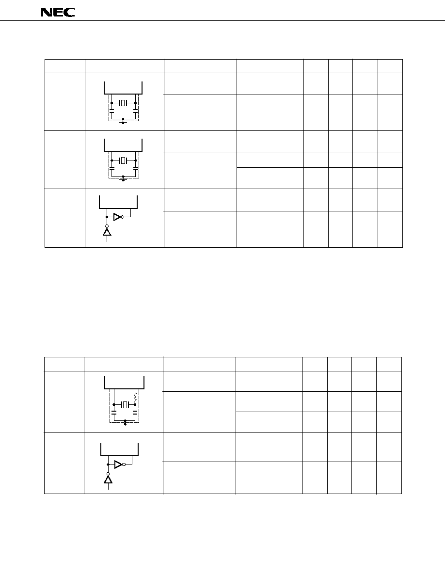
PIN INPUT/OUTPUT CIRCUITS
The input/output circuits of each pin of the
µ
PD75P316A are shown by in abbreviated form.
P-ch
V
DD
OUT
N-ch
data
output
disable
CMOS standard input buffer
Push-pull output that can be made high-impedance
output (P-ch and N-ch OFF)
TYPE A (For TYPE E-B)
TYPE D (For TYPE E-B, F-A)
TYPE B
TYPE E-B
TYPE B-C
TYPE F-A
Schmitt trigger input with hysteresis characteristic
IN
P-ch
V
DD
IN
N-ch
P.U.R.
P-ch
IN/OUT
P.U.R.
enable
data
output
disable
Type D
Type A
P.U.R.:Pull-Up Resistor
V
DD
P.U.R.
P-ch
IN/OUT
P.U.R.
enable
data
output
disable
Type D
Type B
P.U.R.:Pull-Up Resistor
V
DD
IN
P-ch
P.U.R.
P.U.R.
enable
V
DD
P.U.R. : Pull-Up Resistor
Schmitt trigger input with hysteresis characteristic

10
µ
PD75P316A
TYPE G-A
TYPE M-A
TYPE G-B
TYPE M-C
TYPE F-B
TYPE G-C
P.U.R.
IN/OUT
P.U.R.
enable
output
disable
(P)
output
disable
data
output
disable
(N)
V
DD
V
DD
P-ch
N-ch
P-ch
P.U.R.:Pull-Up Resistor
P-ch
V
LC0
V
LC1
V
LC2
P-ch
N-ch
OUT
SEG
data/Bit Port data
N-ch
V
DD
V
LC0
V
LC1
V
LC2
COM
data
N-ch
P-ch
P-ch
N-ch
OUT
N-ch
P-ch
IN/OUT
N-ch
data
output
disable
Middle-High Voltage Input Buffer
(+10 V Withstand Voltage)
(+10 V
Withstand
Voltage)
N-ch
P-ch
OUT
SEG
data
P-ch
V
LC0
V
LC1
V
LC2
N-ch
P.U.R.
enable
IN/OUT
P-ch
V
DD
N-ch
data
output
disable
P.U.R.:Pull-Up Resistor
P.U.R.
11
µ
PD75P316A
1.4
CAUTION ON USING P00/INT4 PIN AND RESET PIN
The P00/INT4 and RESET pins have a test mode setting function (IC test only) which tests internal operations of
the
µ
PD75P316A in addition to those functions given in 1.1 and 1.2.
The test mode is set when voltage greater than V
DD
is applied to either pin. Therefore, even during normal
operation, the test mode is engaged when noise greater than V
DD
is added, thus causing interference with normal
operation.
For example, this problem may occure if the P00/INT4 and RESET pins wiring is too long, causing line noise.
To avoid this, try to suppress line noise in wiring. If line noise is still high, try elimminating the noise using the
exterior add-on components shown in the Figures below.
∑ Connect a diode with low V
F
between the V
DD
and the pin.
∑ Connect a condenser between the V
DD
and the pin.
V
DD
V
DD
P00/INT4, RESET
Diode with
Small V
F
V
DD
V
DD
P00/INT4, RESET
5
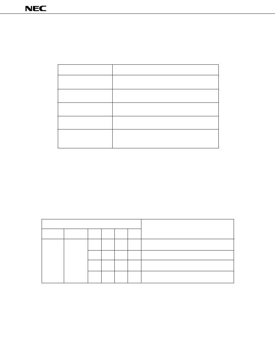
2. DIFFERENCES BETWEEN PRODUCTS IN SERIES
The
µ
PD75P316A is a product of the
µ
PD75316 with on-chip mask ROM having been replaced with the one-time
PROM or EPROM. If you use PROM for debugging the applied system or trial manufacturing, and proceed to use
masked ROM products for mass production, do so only with a full understanding of their differences beforehand.
Also,
µ
PD75P316A functions are an extension of those of the
µ
PD75P316. Table 2-1 shows the differences between
the series products. All products have the same functions except as indicated in this table.
For the details of the CPU functions and the built-in hardware, please refer to the
µ
PD75308 User's Manual (IEM-
5016).
12
µ
PD75P316
Table 2-1 Differences between Products in Series
ROM(
◊
8 bits)
RAM(
◊
4 bits)
Mask option
Pin
No. 50 to 53
connection
No. 57
Electrical specifications
Power supply voltage range
Operating temperature
range
Package
On-chip PROM product
Others
Mask ROM
Mask ROM
Mask ROM
Mask ROM
One-time PROM,EPROM
One-time PROM
One-time PROM,EPROM
One-time PROM
4K/6K/8K
12K/16K
4K/6K/8K
12K/16K
8K
16K
16K
16K
512
1024
512
1024
Port 4, 5 pull-up resistor incorporated
No
LCD driving power supplying split resistor
P30 to P33
P30/MD0 to P33/MD3
NC
IC
V
PP
Masked ROM products and PROM products have different current dissipation and operating temperature range *2. For details, refer to the electrical specifications of
respective data sheet.
2.7 to 6.0 V
2.0 to 6.0 V
2.0 to 5.5 V
5 V
±
5 %
2.7 to 6.0 V
2.0 to 5.5 V
≠40 to +85
∞
C
≠10 to +70
∞
C
≠40 to +85
∞
C
Under
investigation
∑ 80-pin plastic QFP (14
◊
20)
∑ 80-pin plastic QFP
∑ 80-pin plastic
∑ 80-pin plastic
∑ 80-pin plastic
∑ 80-pin plastic
∑ 80 pin plastic
QFP (
s
s
14)
QFP (
s
s
14)
QFP (14
◊
20)
QFP (14
◊
20)
QFP (14
◊
20)
QFP (
s
s
14)
∑ 80-pin plastic QFP
∑ 80-pin plastic
∑ 80-pin ceramic
∑ 80-pin ceramic
∑ 80 pin plastic
(14
◊
20)
TQFP (
s
s
12)
WQFN (LCC with
WQFN (LCC with
TQFP (
s
s
12)
∑ 80-pin plastic TQFP
window)
window)
(
s
s
12)
µ
PD75P308
µ
PD75P316
µ
PD75P316A
µ
PD75P316B
≠≠≠≠
µ
PD75P316A
µ
PD75P316B
Masked ROM products and PROM products have different noise endurance limits and noise radiation due to differing circuit scales and mask layouts.
Comparison Item
Product Name
µ
PD75304/75306/75308
µ
PD75312/75316
µ
PD75304B/75306B/75308B
µ
PD75312B/75316B
µ
PD75P308
µ
PD75P316
µ
PD75P316A
µ
PD75P316B*1
*
1. The
µ
PD75P316B is under development.
2. The
µ
PD75P316A is the same as the mask ROM products.
Note
PROM and masked ROM have different noise endurance limits and noise radiation. When considering replacement of masked ROM products after trial manufacturing
with PROM products, sufficient evaluation of CS products (not ES products) with masked ROM products should be performed.
5
5
5
5

13
µ
PD75P316A
3.
DATA MEMORY (RAM)
Fig. 3-1 shows the data memory configuration. It consists of a data area and a peripheral hardware area.
The data memory consists of memory banks 0 to 3 with each bank consisting of 256 words
◊
4 bits.
Peripheral hardware has been assigned to the area of memory bank 15.
(1)
Data area
The data area comprises a static RAM. It is used to store program data and as a subroutine, interrupt execution
stack memory. Even if the CPU operation is stopped in the standby mode, it is possible to hold the memory content
for a long time by battery backup, etc. The data area is operated by memory manipulation instructions.
The static RAM has been mapped to memory banks 0, 1, 2 and 3 by 256
◊
4 bits each. Bank 0 has been mapped
as a data area but is also available as a general register area (000H to 007H) and a stack area (000H to 0FFH) (banks
1, 2 and 3 are available only as a data area).
In the static RAM, 1 address consists of 4 bits. It can be operated in units of 8 bits by 8-bit memory manipulation
instructions or in bits by bit manipulation instructions, however. In an 8-bit manipulation instruction, an even
address should be specified.
(a)
General register area
The general register area can be operated either by general register operation instructions or by memory
manipulation instructions. Up to eight 4-bit registers are available. That part of the 8 general registers which
is not used in the program is available as a data area or a stack area.
(b) Stack area
The stack area is set by an instruction. It is available as a subroutine execution or interrupt service execution
save area.
(2)
Peripheral hardware area
The peripheral hardware area has been mapped to F80H to FFFH of memory bank 15.
It is operated by memory manipulation instructions just as the static RAM. In the peripheral hardware, however,
the operable bit unit differs from one address to another. An address to which peripheral hardware has not been
assigned is inaccessible since no data memory is built in.
µ
PD78012
14
µ
PD75P316A
Fig. 3-1 Data Memory Map
256
◊
4
128
◊
4
(8
◊
4)
Data Memory
Not On-Chip
Memory Bank
F80H
FFFH
Peripheral Hardware Area
General
Register Area
3FFH
300H
2FFH
200H
1FFH
100H
0FFH
008H
007H
000H
Data Area
Static RAM
(1024
◊
4)
Stack
Area
256
◊
4
256
◊
4
256
◊
4
0
1
2
3
15
15
µ
PD75P316A
4.
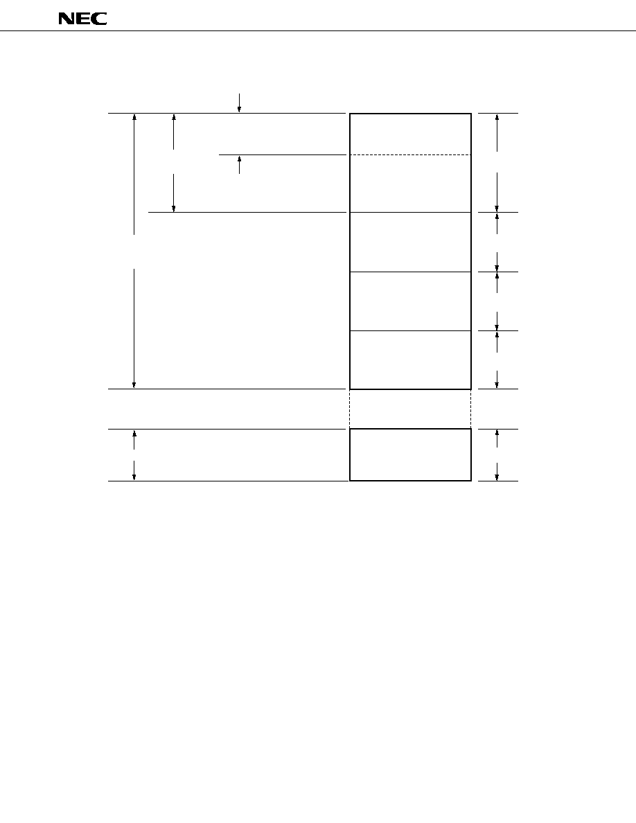
PROGRAM MEMORY WRITE AND VERIFY
The ROM built into the
µ
PD75P316A is a 16256
◊
8-bit electrically writable one-time PROM. The table below shows
the pins used to program this PROM. There is no address input; instead, a method to update the address by the
clock input via the X1 pin is adopted.
Function
Pin Name
Note
1. A lightshield cover film should be applied to the
µ
PD75P316AK provided
with an erasure window, except when erasing the EPROM.
2. The one-time PROM version of
µ
PD75P316AGF is not provided with an
erasure window, and therefore UV erasure is not possible.
4.1
PROGRAM MEMORY WRITE/VERIFY OPERATING MODES
The
µ
PD75P316A assumes the program memory write/verify mode when +6 V and +12.5 V are applied
respectively to the V
DD
and V
PP
pins. The table below shows the operating modes available by the MD0 to MD3 pin
setting in this mode. All the remaining pins are at the V
SS
potential by the pull-down resistor.
V
PP
+12.5 V
V
DD
+6 V
MD0
H
L
L
H
MD1
L
H
L
◊
MD2
H
H
H
H
MD3
L
H
H
H
Operating Mode
Program memory address zero-clear
Write mode
Verify mode
Program inhibit mode
Operating Mode Setting
◊
: L or H
V
PP
X1, X2
MD0 to MD3
P40 to P43 (low-order 4 bits)
P50 to P53 (high-order 4 bits)
V
DD
Voltage applecation pin for program memory write/verify
(normally V
DD
potential).
Address update clock inputs for program memory write/
verify. Inverse of X1 pin signal is input to X2 pin.
Operating mode selection pins for program memory write/
verify.
8-bit data input/output pins for progrm memory write/
verify.
Supply voltage application pin.
Applies 2.7 to 6.0 V in normal operation, and 6 V for
program memory write/verify.
µ
PD78012
16
µ
PD75P316A
4.2
PROGRAM MEMORY WRITING PROCEDURE
The program memory writing procedure is shown below. High-speed write is possible.
(1)
Pull down a pin which is not used to V
SS
via the resistor. The X1 pin is at the low level.
(2)
Supply 5 V to the V
DD
and V
PP
pins.
(3)
10
µ
s wait.
(4)
The program memory address 0 clear mode.
(5)
Supply 6 V and 12.5 V respectively to V
DD
and V
PP
.
(6)
The program inhibit mode.
(7)
Write data in the 1-ms write mode.
(8)
The program inhibit mode.
(9)
The verify mode. If written, proceed to (10); if not written, repeat (7) to (9).
(10) (Number of times written in (7) to (9): X)
◊
1-ms additional write.
(11) The program inhibit mode.
(12) Update (+1) the program memory address by inputting 4 pulses to the X1 pin.
(13) Repeat (7) to (12) up to the last address.
(14) The program memory address 0 clear mode.
(15) Change the V
DD
and V
PP
pins voltage to 5 V.
(16) Power off.
The diagram below shows the procedure of the above (2) to (12).
Data Input
Data Input
Write
Verify
Additional
Write
Address
Increment
Repeated X Times
Data Output
V
PP
V
PP
V
DD
V
DD
V
DD
+ 1
V
DD
X1
P40-P43
P50-P53
MD0
(P30)
MD1
(P31)
MD2
(P32)
MD3
(P33)
17
µ
PD75P316A
4.3
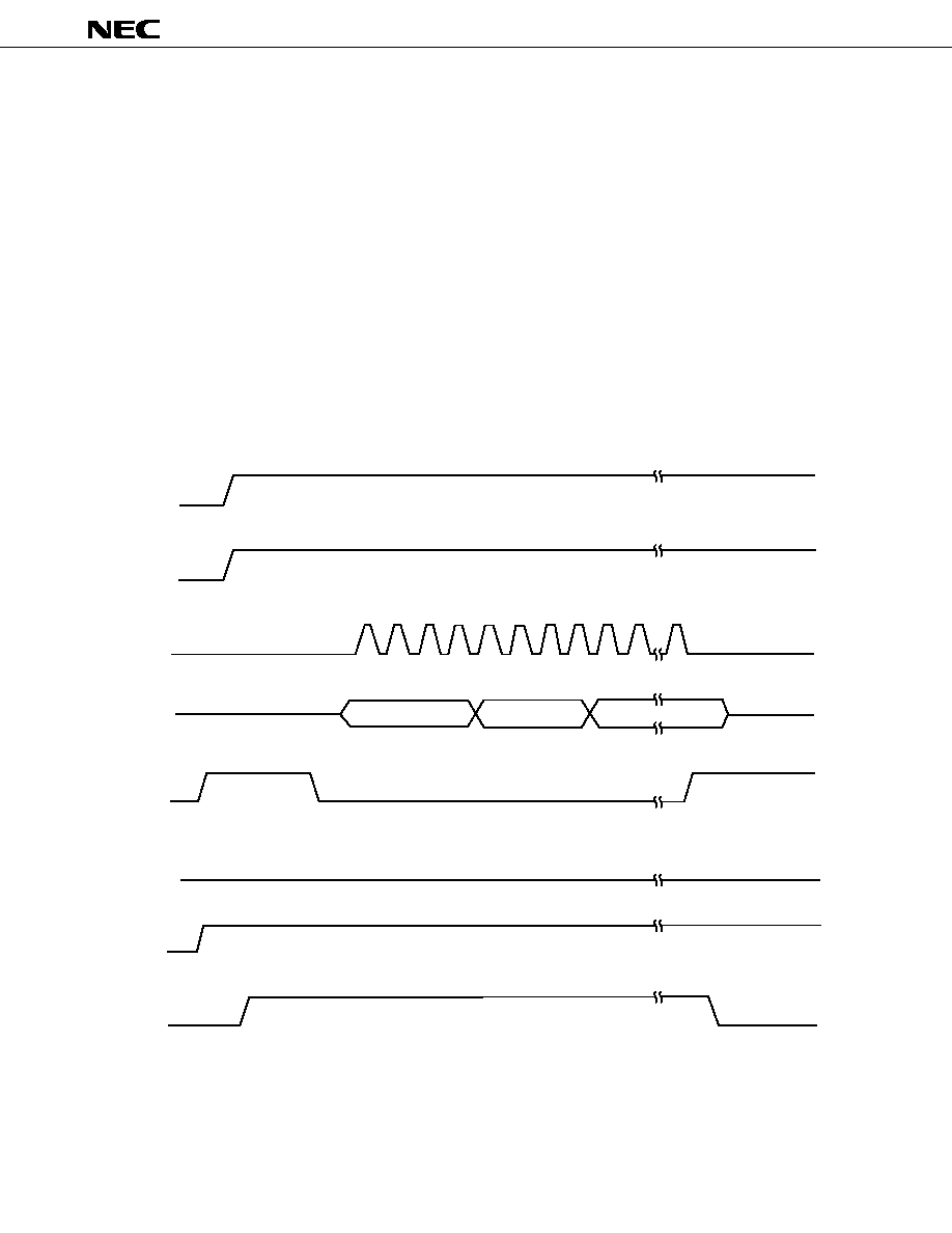
PROGRAM MEMORY READING PROCEDURE
The
µ
PD75P316A can read the content of the program memory in the following procedure. It reads in the verify
mode.
(1)
Pull down a pin which is not used to V
SS
via the resistor. The X1 pin is at the low level.
(2)
Supply 5 V to the V
DD
and V
PP
pins.
(3)
10
µ
s wait.
(4)
The program memory address 0 clear mode.
(5)
Supply 6 V and 12.5 V respectively to V
DD
and V
PP
.
(6)
The program inhibit mode.
(7)
The verify mode. If clock pulses are input to the X1 pin, data is output sequentially 1 address at a time at
the period of inputting 4 pulses.
(8)
The program inhibit mode.
(9)
The program memory address 0 clear mode.
(10) Change the V
DD
and V
PP
pins voltage to 5 V.
(11) Power off.
The diagram below shows the procedure of the above (2) to (9).
Data Output
Data Output
P40-P43
P50-P53
MD0
(P30)
MD1
(P31)
MD2
(P32)
MD3
(P33)
"L"
V
PP
V
PP
V
DD
V
DD
V
DD
+ 1
V
DD
X1

µ
PD78012
18
µ
PD75P316A
4.4
ERASING METHOD (
µ
PD75P316AK ONLY)
The content of the data programmed in the
µ
PD75P316A is erased as ultraviolet rays are irradiated to the window
in the upper part.
The erasable ultraviolet-ray wavelength is about 250 nm.
The dose required for complete erasure is 15 W∑s/cm
2
(ultraviolet-ray intensity
◊
erasure time). If a commercially
available ultraviolet-ray lamp (wavelength 254 nm, intensity 12 mW/cm
2
) is used, it takes about 15 to 20 minutes
to erase.
Note
1. The content may be erased if exposed to direct sunlight or fluorescent lamp light for a long time. To
protect the content, the window in the upper part should be masked with a lightshield cover film.
NEC attaches such a lightshield cover film to each UV EPROM product.
2. When erasing, the distance between the ultraviolet-ray lamp and the
µ
PD75P316A should be kept
normally within 2.5 cm.
Remarks
It may take longer to erase if the ultraviolet-ray lamp has deteriorated or if the package window is dirty
and so on.

19
µ
PD75P316A
5.
ELECTRICAL SPECIFICATIONS
ABSOLUTE MAXIMUM RATINGS (Ta = 25
∞
C)
Peak value
Effective value
Peak value
Effective value
Peak value
Effective value
1 pin
All pins
1 pin
Total of ports 0, 2, 3, 5
Total of ports 4, 6, 7
Output voltage
Output current high
V
O
I
OH
Ports 4, 5
Open-drain
V
I2
V
I1
Except ports 4, 5
Input voltage
Power supply voltage
V
DD
V
PP
≠15
≠30
30
15
100
60
100
60
≠40 to +85
≠65 to +150
≠0.3 to +11
≠0.3 to V
DD
+0.3
≠0.3 to +7.0
≠0.3 to +13.5
≠0.3 to V
DD
+0.3
PARAMETER
SYMBOL
TEST CONDITIONS
RATING
UNIT
V
V
mA
mA
mA
mA
mA
mA
mA
mA
∞
C
∞
C
V
V
V
I
OL
*
Output current low
Operating temperature
Storage temperature
T
opt
T
stg
*
Calculate the effective value with the formula [Effective value] = [Peak value]
◊
duty.
Input capacitance
Output capacitance
Input /output
capacitance
15
15
15
pF
pF
pF
C
IN
C
OUT
C
IO
CAPACITANCE (Ta = 25
∞
C, V
DD
= 0 V)
f = 1 MHz
Unmeasured pin returned to 0 V
SYMBOL
TEST CONDITIONS
PARAMETER
MIN.
TYP.
MAX.
UNIT
20
µ
PD75P316A
MAIN SYSTEM CLOCK OSCILLATOR CHARACTERISTICS (Ta = ≠40 to +85
∞
C, V
DD
= 2.7 to 6.0 V)
Oscillator frequency
(f
X
) *1
Oscillation stabilization
time *2
Oscillator frequency
(f
X
) *1
Oscillation stabilization
time *2
X1 input frequency
(f
X
) *1
X1 high and low level
widths (t
XH
, t
XL
)
1.0
1.0
1.0
100
Ceramic
resonator
Crystal
resonator
External
clock
4.19
MHz
ms
MHz
ms
ms
MHz
ns
5.0*3
4
5.0*3
10
30
5.0*3
500
µ
PD74HCU04
RESONATOR RECOMMENDED CIRCUIT
PARAMETER
TEST CONDITIONS
MIN.
TYP.
MAX.
UNIT
X1
X2
After V
DD
reaches the
minimum value in the
oscillation voltage
range
V
DD
= 4.5 to 6.0 V
Oscillation stabilization
time*
XT1 input frequency
(f
XT
)
XT1 high and low level
widths (t
XTH
, t
XTL
)
Crystal
resonator
External
clock
V
DD
= 4.5 to 6.0 V
32
32
5
32.768
1.0
35
2
10
100
15
kHz
s
s
kHz
µ
s
RESONATOR RECOMMENDED CIRCUIT
PARAMETER
TEST CONDITIONS
MIN.
TYP.
MAX.
UNIT
Oscillator frequency
(f
XT
)
SUBSYSTEM CLOCK OSCILLATOR CHARACTERISTICS (Ta = ≠40 to +85
∞
C, V
DD
= 2.7 to 6.0 V)
X1
X2
*
1. Oscillator characteristics only. Refer to the description of AC characteristics for details of instruction execution
time.
2. Time required for oscillation to become stabilized after V
DD
reaches MIN. of the oscillation voltage range or
after STOP mode release.
3. When the oscillator frequency is 4.19 MHz < f
X
5.0 MHz, do not select PPC = 0011 as instruction execution
time. If PCC = 0011 is selected, 1 machine cycle becomes less than 0.95
µ
s, with the result that specified MIN.
value 0.95
µ
s can not be observed.
X1
X2
C1
C2
V
DD
X1
X2
C1
C2
V
DD
XT1
XT2
C3
C4
R
V
DD

21
µ
PD75P316A
*
Time required for oscillation to become stabilized after V
DD
reaches MIN. of the oscillation voltage range or after
STOP made release.
Note
When the main system clock and subsystem clock oscillation circuit are used, the area enclosed by dotted
line in the figure should be wired as follows to prevent influence from the wiring capacitance, etc..
∑ Wiring should be as short as possible.
∑ Do not cross other signal lines.
Do not place the circuit closed to a line in which varying high current flows.
∑ The connecting point of oscillation circuit capacitor should always be the same potential as V
DD
. Do
not connect it to the power supply pattern in which high current flows.
∑ Do not pick up a signal from the oscillation circuit.
The subsystem clock oscillation circuit is designed to be low amplification circuit for low dissipation
current, thus misoperation due to noise occurs more often than with the main system clock oscillation
circuit. Therefore, when the subsystem clock is used, care is needed especially for the wiring procedure.
22
µ
PD75P316A
DC CHARACTERISTICS (Ta = ≠40 to +85
∞
C, V
DD
= 2.7 to 6.0 V) (1/2)
PARAMETER
SYMBOL
TEST CONDITIONS
MIN.
TYP.
MAX.
UNIT
V
IH1
Ports 2 and 3
0.7 V
DD
V
DD
V
V
IH2
Ports 0, 1, 6, 7, RESET
0.8 V
DD
V
DD
V
V
IH3
Ports 4 and 5
Open-drain
0.7 V
DD
10
V
VI
H4
X1, X2, XT1
V
DD
≠0.5
V
DD
V
V
IL1
Ports 2, 3, 4 and 5
0
0.3 V
DD
V
V
IL2
Ports 0, 1, 6, 7, RESET
0
0.2 V
DD
V
V
IL3
X1, X2, XT1
0
0.4
V
V
DD
= 4.5 to
6.0 V
I
OH
= ≠1 mA
I
OH
= -100
µ
A
V
DD
≠0.5
V
V
DD
= 4.5 to
6.0 V
I
OH
= ≠100
µ
A
I
OH
= ≠30
µ
A
V
DD
≠1.0
V
Ports 3, 4 and 5
V
DD
= 4.5 to
6.0 V
I
OL
= 15 mA
V
DD
= 4.5 to
6.0 V
I
OL
= 1.6 mA
I
OL
= 400
µ
A
0.5
V
Open-drain
pull-up
resistor
1 k
V
DD
= 4.5 to
6.0 V
I
OL
= 100
µ
A
I
OL
= 50
µ
A
1.0
V
Input voltage
high
Output voltage
high
Output voltage
low
V
0H2
V
OL1
V
OL2
Ports
0, 2, 3, 6, 7,
BIAS
V
OH1
BP0 to BP7
(with 2 I
OH
outputs)
Ports
0, 2, 3, 4, 5, 6
and 7
SB0, 1
BP0 to BP7 (with 2
I
OL
outputs)
0.4
2.0
0.4
0.2 V
DD
1.0
V
DD
≠1.0
V
DD
≠2.0
V
V
V
V
V
V
Input leakage
current high
3
I
LIH1
µ
A
Input voltage
low
Other than
below
I
LIL2
Input leakage
current low
V
IN
= 10 V
I
LIH3
µ
A
X1, X2, XT1
-20
µ
A
20
-3
µ
A
I
LIL1
Ports 4 and 5
(when open-
drain)
Other than
below
X1, X2, XT1
µ
A
20
V
IN
= V
DD
I
LIH2
V
IN
= 0 V

23
µ
PD75P316A
DC CHARACTERISTICS (Ta = ≠40 to +85
∞
C, V
DD
= 2.7 to 6.0 V) (1/2)
PARAMETER
SYMBOL
TEST CONDITIONS
MIN.
TYP.
MAX.
UNIT
Other than
below
Ports 4 and 5
(when open-
drain)
Output leakage
current low
V
DD
= 5.0 V
±
10%
LCD output
voltage
deviation*1
(common)
LCD output
voltage
deviation*1
(segment)
V
DD
= 5 V
±
10%*4
V
DD
= 3 V
±
10%*5
HALT
V
DD
=
mode
5 V
±
10%
V
DD
=
3 V
±
10%
HALT
V
DD
=
mode
3 V
±
10%
I
LOH1
V
OUT
= V
DD
V
OUT
= 10 V
I
LOH2
20
3
µ
A
µ
A
Output leakage
current high
I
LOL
V
OUT
= 0 V
µ
A
15
40
80
k
≠3
R
L1
Ports 0, 1, 2, 3, 6
and 7 (Except P00)
V
IN
= 0 V
30
300
k
On-chip pull-up
resistor
V
LCD
V
DD
V
2.5
V
ODC
I
O
=
±
5
µ
A
0
±
0.2
V
0
±
0.2
V
4.19 MHz*3 crystal
oscillation C1=C2
22 pF
I
DD2
700
2100
µ
A
300
900
µ
A
V
DD
=
3 V
±
10%
100
300
µ
A
20
60
µ
A
32 kHz*6
crystal oscillation
I
DD3
I
DD4
0.5
20
µ
A
0.1
10
µ
A
0.1
5
µ
A
XT1 =
0 V STOP mode
I
DD5
32 kHz
crystal oscillation
STOP mode
I
DD6
V
DD
= 3 V
±
10%*7
5
15
µ
A
Supply current*2
4.5
14
mA
T
a
= 25
∞
C
V
DD
=
3 V
±
10%
V
DD
= 5 V
±
10%
LCD drive voltage
V
ODC
I
DD1
I
O
=
±
5
µ
A
V
DD
= 3.0 V
±
10%
V
LCD0
= V
LCD
V
LCD1
=
V
LCD
◊
2/3
V
LCD2
= V
LCD
◊
1/3
2.7 V
V
LCD
V
DD
0.9
3
mA
Ope-
rating
mode

24
µ
PD75P316A
*
1. The voltage deviation is a difference between the segment and common output ideal value (V
LCDn
; n = 0, 1,
2) and output voltage.
2. Current flowing in the internal pull-up resistor and LCD split resistor are not included.
3. Includes when the subsystem clock is oscillated.
4. When the processor clock control register (PCC) is set to 0011 and operated in high-speed mode.
5. When the PCC is set to 0000 and operated in low-speed mode.
6. When operated by the subsystem clock with the system clock control register (SCC) set to 1011 and the main
system clock stops.
7. When the STOP instruction is executed during the main system clock operation and the subsystem clock is
oscillated.
25
µ
PD75P316A
AC CHARACTERISTICS (Ta = ≠40 to +85
∞
C , V
DD
= 2.7 to 6.0 V)
Operation with main
system clock
PARAMETER
SYMBOL
TEST CONDITIONS
MIN.
TYP.
MAX.
UNIT
Operation with
subsystem clock
t
CY
f
TI
TI0 input frequency
V
DD
= 4.5 to 6.0 V
TI0 input high and low-
level widths
t
TIH
,
t
TIL
t
INTH
,
t
INTL
Interrupt input high and
low-level widths
INT0
INT1, 2, 4
KR0≠7
RESET low-level width
t
RSL
V
DD
= 4.5 to 6.0 V
V
DD
= 4.5 to 6.0 V
0.95
64
µ
s
3.8
64
µ
s
114
122
125
µ
s
0
1
MHZ
0
275
kHz
0.48
µ
s
1.8
µ
s
*2
µ
s
10
µ
s
10
µ
s
10
µ
s
Cycle Time t
CY
[
µ
s]
* 1.
CPU clock (
) cycle time is determined by oscillator
frequency of the connected resonator, system clock
control register (SCC) and processor clock control
register (PCC). Characteristics for power supply
voltage V
DD
vs ∑ cycle time t
CY
in main system clock
operation is shown below.
2.
It becomes 2t
CY
or 128/f
X
by interrupt mode register
(IM0) setting.
70
64
30
6
5
4
3
2
1
0.5
0
1
2
3
4
5
6
t
CY
VS
V
DD
(Main System Clock in Operation)
Power Supply Voltage V
DD
[V]
CPU clock cycle time
(minimum instruction
execution time = 1
machine cycle )*1

26
µ
PD75P316A
SO output delay time
from SCK
1600
ns
3800
ns
V
DD
= 4.5 to 6.0 V
t
KCY1
/2≠50
ns
t
KCY1
/2≠150
ns
150
ns
400
ns
V
DD
= 4.5 to 6.0 V
250
ns
1000
ns
Serial Transfer Operation
2-wire and 3-wire serial I/O mode (SCK...Internal clock output)
SCK cycle time
t
KCY1
t
KSO1
SI setup time (to SCK
)
SI hold time (from SCK
)
t
KSI1
t
SIK1
t
KL1
t
KH1
SCK high and low level
widths
V
DD
= 4.5 to 6.0 V
*
R
L
and C
L
are SO output line load resistance and load capacitance, respectively.
2-wire and 3-wire serial I/O mode (SCK...External clock input)
V
DD
= 4.5 to 6.0 V
800
ns
3200
ns
V
DD
= 4.5 to 6.0 V
400
ns
1600
ns
100
ns
400
ns
V
DD
= 4.5 to 6.0 V
300
ns
1000
ns
SCK cycle time
t
KCY2
t
KL2
t
KH2
SI setup time (to SCK
)
t
SIK2
t
KSI2
SI hold time (from SCK
)
t
KSO2
SO output delay time
from SCK
*
R
L
and C
L
are SO output line load resistance and load capacitance, respectively.
SCK high and low level
widths
PARAMETER
SYMBOL
TEST CONDITIONS
MIN.
TYP.
MAX.
UNIT
PARAMETER
SYMBOL
TEST CONDITIONS
MIN.
TYP.
MAX.
UNIT
R
L
= 1 k
, C
L
= 100 pF*
R
L
= 1 k
, C
L
= 100 pF*
27
µ
PD75P316A
SBI mode (SCK...Internal clock output (master))
V
DD
= 4.5 to 6.0 V
1600
ns
3800
ns
V
DD
= 4.5 to 6.0 V
t
KCY3
/2≠50
ns
t
KCY3
/2≠150
ns
150
ns
t
KCY3
/2
ns
V
DD
= 4.5 to 6.0 V
0
250
ns
0
1000
ns
t
KCY3
ns
t
KCY3
ns
t
KCY3
ns
t
KCY3
ns
t
KCY3
t
KL3
t
KH3
t
SIK3
t
KSI3
t
KSO3
SCK cycle time
SB0 and SB1 setup time (to SCK
)
SB0 and SB1 hold time (from SCK
)
SB0 and SB1 output
delay time from SCK
SCK high and low level
widths
SB0, SB1
from SCK
SCK from SB0, SB1
SB0 and SB1 low-level widths
SB0 and SB1 high-level widths
t
KSB
t
SBK
t
SBL
t
SBH
*
R
L
and C
L
are SO output line load resistance and load capacitance, respectively.
SBI mode (SCK...External clock input (slave))
V
DD
= 4.5 to 6.0 V
800
ns
3200
ns
V
DD
= 4.5 to 6.0 V
400
ns
1600
ns
100
ns
t
KCY3
/2
ns
V
DD
= 4.5 to 6.0 V
0
300
ns
0
1000
ns
t
KCY4
ns
t
KCY4
ns
t
KCY4
ns
t
KCY4
ns
t
KCY4
t
KL4
t
KH4
t
SIK4
t
KSI4
t
KSO4
SCK cycle time
SB0 and SB1 setup time (to SCK
)
SB0 and SB1 hold time (from SCK
)
SB0 and SB1 output
delay time from SCK
SCK high and low level
widths
SB0, SB1
from SCK
SCK
from SB0, SB1
SB0 and SB1 low-level widths
SB0 and SB1 high-level widths
t
KSB
t
SBK
t
SBL
t
SBH
*
R
L
and C
L
are SO output line load resistance and load capacitance, respectively.
PARAMETER
SYMBOL
TEST CONDITIONS
MIN.
TYP.
MAX.
UNIT
PARAMETER
SYMBOL
TEST CONDITIONS
MIN.
TYP.
MAX.
UNIT
R
L
= 1 k
, C
L
= 100 pF*
R
L
= 1 k
, C
L
= 100 pF*

28
µ
PD75P316A
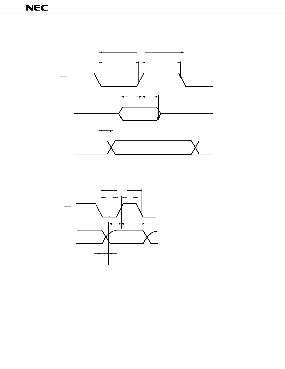
AC Timing Test Points (Except X1 and XT1 Inputs)
Clock Timing
TI0 Timing
0.8 V
DD
0.2 V
DD
0.8 V
DD
0.2 V
DD
Test Points
1/f
X
t
XL
t
XH
V
DD
- 0.5 V
0.4 V
X1 Input
1/f
XT
t
XTL
t
XTH
V
DD
- 0.5 V
0.4 V
XT1 Input
1/f
T1
t
TIL
t
TIH
TI0
29
µ
PD75P316A
Serial Transfer Timing
3-wire serial I/O mode:
2-wire serial I/O mode:
t
KSO1
SCK
SI
SO
Input Data
Output Data
t
KCY1
t
KH1
t
KL1
t
SIK1
t
KSI1
t
KCY2
t
KL2
t
KH2
t
SIK2
t
KS12
SCK
SB0,1
t
KSO2
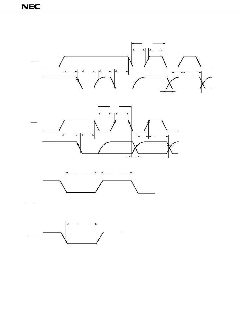
30
µ
PD75P316A
Serial Transfer Timing
Bus release signal transfer:
Command signal transfer:
Interrupt Input Timing
RESET Input Timing
t
KSB
SCK
SB0,1
t
SBL
t
SBH
t
SBK
t
KCY3,4
t
SIK3,4
t
KSI3,4
t
KSO3,4
t
KL3,4
t
KH3,4
SCK
t
KSB
SB0,1
t
SBK
t
KL3,4
t
KH3,4
t
KCY3,4
t
SIK3,4
t
KSI3,4
t
KSO3,4
INT0,1,2,4
KR0-7
t
INTL
t
INTH
RESET
t
RSL
31
µ
PD75P316A
DATA MEMORY STOP MODE LOW POWER SUPPLY VOLTAGE DATA RETENTION CHARACTERISTICS (Ta = ≠40
to +85
∞
C)
2.0
6.0
V
V
DDDR
= 2.0 V
0.1
10
µ
A
0
µ
s
Release by RESET
2
17
/f
X
ms
Release by interrupt request
*3
ms
* 1.
Current to the internal pull-up resistor is not included.
2.
Oscillation stabilization wait time is time to stop CPU operation to prevent unstable operation upon oscillation
start.
3.
According to the setting of the basic interval timer mode register (BTM) (see below).
--
0
0
0
2
20
/f
XX
(approx. 250 ms)
--
0
1
1
2
17
/f
XX
(approx. 31.3 ms)
--
1
0
1
2
15
/f
XX
(approx. 7.82 ms)
--
1
1
1
2
13
/f
XX
(approx. 1.95 ms)
BTM3
BTM2
BTM1
BTM0
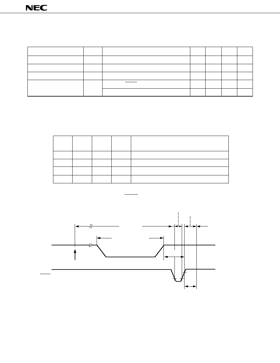
Data Retention Timing (STOP Mode Release by RESET)
PARAMETER
SYMBOL
TEST CONDITIONS
MIN.
TYP.
MAX.
UNIT
Release signal set time
Oscillation stabilization wait
time *2
t
WAIT
Data retention power supply voltage
Data retention power supply current *1
V
DDDR
I
DDDR
t
SREL
STOP Instruction Execution
V
DD
V
DDDR
Operating Mode
HALT Mode
STOP Mode
Data Retention Mode
t
WAIT
RESET
t
SREL
Internal Reset Operation
Wait Time
(Values at f
XX
= 4.19 MHz in parentheses)
32
µ
PD75P316A
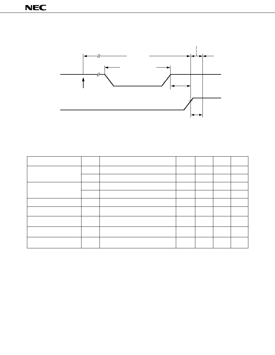
Data Retention Timing (Standby Release Signal: STOP Mode Release by Interrupt Signal)
STOP Instruction Execution
V
DD
V
DDDR
Standby Release Signal
(Interrupt Request)
Operating Mode
HALT Mode
STOP Mode
Data Retention Mode
t
WAIT
t
SREL
DC PROGRAMMING CHARACTERISTICS (Ta = ≠25 to
±
5
∞
C, V
DD
= 6.0
±
0.25 V, V
PP
= 12.5
±
0.3 V, V
SS
= 0 V)
TYP.
MAX.
UNIT
Input voltage high
Input voltage low
Input leakage current
Output voltage high
Output voltage low
V
DD
power supply current
V
PP
power supply current
V
IH1
V
IL1
V
IL2
V
IH2
I
LI
V
OH
V
OL
I
DD
I
PP
Except X1, X2
X1, X2
Except X1, X2
X1, X2
V
IN
= V
IL
or V
IH
I
OH
= ≠1mA
I
OL
= 1.6 mA
MD0 = V
IL
, MD1 = V
IH
0.7 V
DD
MIN.
V
DD
≠0.5
0
0
V
DD
≠1.0
V
DD
V
DD
0.3 V
DD
0.4
10
0.4
30
30
V
V
V
V
µ
A
V
V
mA
mA
Note
1. V
PP
including overshoot should not exceed +13.5 V.
2. V
DD
should be applied before V
PP
and should be cut after V
PP
.
SYMBOL
PARAMETER
TEST CONDITIONS

33
µ
PD75P316A
AC PROGRAMMING CHARACTERISTICS (Ta = 25 to
±
5
∞
C, V
DD
= 6.0
±
0.25 V, V
PP
= 12.5
±
0.3 V, V
SS
= 0 V)
*1
MIN.
TYP.
MAX.
MD1 setup time (to MD0
)
Data setup time (to MD0
)
Address hold time*2 (from MD0
)
Data hold time (to MD0
)
Data output float delay time from MD0
V
PP
setup time (to MD3
)
V
DD
setup time (to MD3
)
Initial program pulse width
Additional program pulse width
MD1 setup time (to MD1
)
Data output delay time from MD0
MD1 hold time (from MD0
)
MD1 recovery time (from MD0
)
Program counter reset time
X1 input high/low level width
X1 input frequency
Initial mode set time
MD3 setup time (to MD1
)
MD3 hold time (from MD1
)
MD3 setup time (to MD0
)
Data output delay time from address*2
Data output hold time from address*2
MD3 hold time (from MD0
)
Data output float delay time from MD3
Address setup time*2 (to MD0
)
t
AS
t
M1S
t
DS
t
AH
t
DH
t
DF
t
VPS
t
VDS
t
PW
t
OPW
t
MOS
t
DV
t
M1H
t
M1R
t
PCR
t
XH,
t
XL
f
X
t
I
t
M3S
t
M3H
t
M3SR
t
DAD
t
HAD
t
M3HR
t
DFR
t
AS
t
OES
t
DS
t
AH
t
DH
t
DF
t
VPS
t
VCS
t
PW
t
OPW
t
CES
t
DV
t
OEH
t
OR
≠
≠
≠
≠
≠
≠
≠
t
ACC
t
OH
≠
≠
When reading program memory
When reading program memory
When reading program memory
When reading program memory
When reading program memory
2
2
2
2
2
0
2
2
0.95
0.95
2
2
2
10
0.125
2
2
2
2
0
2
MD0 = MD1 = V
IL
t
M1H
+ t
M1R
50
µ
s
µ
s
µ
s
µ
s
µ
s
µ
s
ns
µ
s
µ
s
ms
ms
µ
s
µ
s
µ
s
µ
s
µ
s
µ
s
MHz
µ
s
µ
s
µ
s
µ
s
µ
s
ns
µ
s
µ
s
1.0
130
21.0
1.05
1
4.19
2
2
*
1. Symbol of the corresponding
µ
PD27C256A.
2. The internal address signal is incremented (+1) at the rising edge of the fourth X1 input. The signal is not
connected to pins.
PARAMETER
SYMBOL
UNIT
TEST CONDITIONS
130

34
µ
PD75P316A
Program Memory Write Timing
Program Memory Read Timing
V
PP
V
DD
V
DD
+ 1
V
DD
V
PP
V
DD
X1
P40 ≠ P43
P50 ≠P53
MD0
MD1
MD2
MD3
t
VPS
t
VDS
t
XH
t
XL
t
HAD
t
DAD
t
DV
Data Output
Data Output
t
I
t
PCR
t
M3SR
t
M3HR
t
DFR
V
PP
V
DD
V
DD
+ 1
V
DD
t
VPS
V
PP
V
DD
X1
P40 ≠ P43
P50 ≠P53
MD0
MD1
MD2
MD3
t
VDS
t
I
t
OH
t
DV
t
DF
t
DS
t
DH
t
AH
t
AS
t
XL
t
XH
t
OPW
t
MOS
t
M1R
t
PW
t
PCR
t
M1S
t
M1H
t
M3S
t
M3H
Data Input
Data Output
Data Input
Data Input
t
DS
35
µ
PD75P316A
6.
PACKAGE INFORMATION
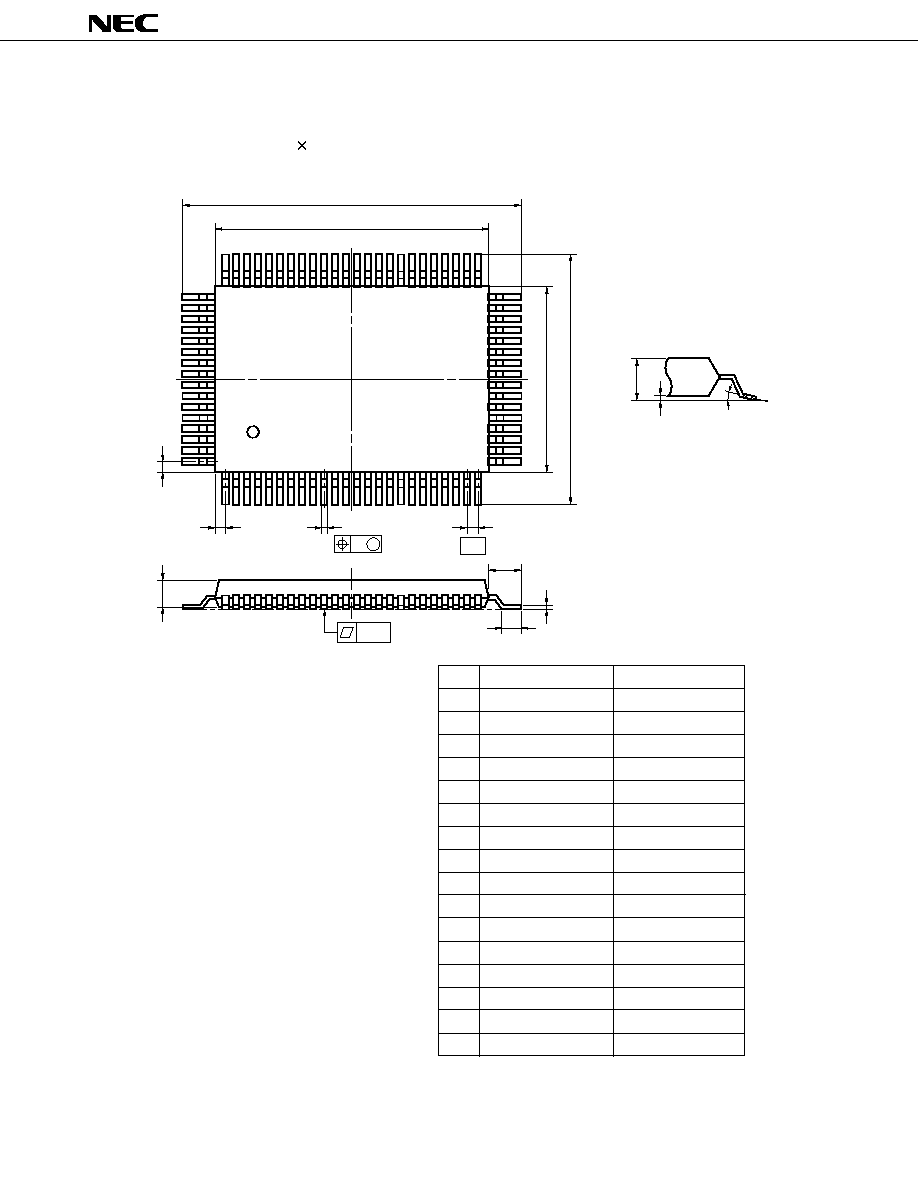
N
A
M
F
B
64
65
40
K
L
80 PIN PLASTIC QFP (14
◊
20)
80
1
25
24
41
G
D
C
P
detail of lead end
S
Q
5∞±5∞
M
I
H
J
P80GF-80-3B9-2
ITEM
MILLIMETERS
INCHES
A
B
C
D
F
G
H
I
J
K
L
23.6±0.4
14.0±0.2
0.8
0.35±0.10
0.15
20.0±0.2
0.929±0.016
0.039
0.031
0.006
0.031 (T.P.)
0.795
NOTE
M
N
0.15
0.15
1.8±0.2
0.8 (T.P.)
0.006
0.006
+0.004
≠0.003
Each lead centerline is located within 0.15
mm (0.006 inch) of its true position (T.P.) at
maximum material condition.
0.071
0.014
0.551
0.8±0.2
0.031
P
2.7
0.106
0.693±0.016
17.6±0.4
1.0
+0.009
≠0.008
Q
0.1±0.1
0.004±0.004
S
3.0 MAX.
0.119 MAX.
+0.10
≠0.05
+0.009
≠0.008
+0.004
≠0.005
+0.009
≠0.008
+0.008
≠0.009
36
µ
PD75P316A
X80KW-80A-1
ITEM
MILLIMETERS
INCHES
NOTE
Each lead centerline is located within 0.08
mm (0.003 inch) of its true position (T.P.) at
maximum material condition.
A
B
C
D
E
F
G
H
I
J
K
Q
R
S
T
U
W
20.0±0.4
19.0
13.2
14.2±0.4
1.64
2.14
4.064 MAX.
0.51±0.10
0.08
0.8 (T.P.)
1.0±0.2
C 0.5
0.8
1.1
R 3.0
12.0
0.75±0.2
0.787
0.748
0.520
0.559±0.016
0.065
0.084
0.160 MAX.
0.020±0.004
0.003
0.031 (T.P.)
0.039
C 0.020
0.031
0.043
R 0.118
0.472
0.030
+0.017
≠0.016
+0.009
≠0.008
+0.008
≠0.009
80 PIN CERAMIC WQFN
A
B
D
C
T
U
F
I
M
E
G
K
Q
J
80
R
1
H
S
W
37
µ
PD75P316A
7.
RECOMMENDED SOLDERING CONDITIONS
The
µ
PD75P316A should be soldered and mounted under the conditions recommended in the table below.
For detail of recommended soldering conditions, refer to the information document "Semiconductor Device
Mount Manual" (IEI-1207).
For soldering methods and conditions other than those recommended below, contact our salesman.
Table 7-1 Surface Mounting Type Soldering Conditions
µ
PD75P316AGF-3B9 : 80-pin plastic QFP (14
◊
20 mm)
Recommended
Condition Symbol
Solderring Method
Solderring Conditions
*
For the storage period after dry-pack decapsulation, storage conditions are max. 25
∞
C, 65 % RH.
Note
Use more than one soldering method should be avoided (except in the case of pin part heating).
Solder bath temperature: 260
∞
C or below. , Duration: 10 sec. max.
Number of times: Once, Time limit: 7 days*(thereafter 20 hours prebaking required
at 125
∞
C)
Package peak temperature: 230
∞
C, Duration: 30 sec. max. (at 210
∞
C or above),
Number of times: Once, Time limit: 7 days*(thereafter 20 hours prebaking required
at 125
∞
C)
Package peak temperature: 215
∞
C, Duration: 40 sec. max. (at 200
∞
C or above),
Number of times: Once, Time limit: 7 days* (thereafter 20 hours prebaking required
at 125
∞
C)
Pin part temperature: 300
∞
C or below , Duration: 3 sec. max. (per device side)
Infrared reflow
VPS
Pin part heating
WS60-207-1
IR30-207-1
VP15-207-1
≠≠≠
Wave soldering
For Your Information
Products to improve the recommended soldering conditions are available.
(Improvements : Extension of the infrared reflow peak temperature to 235
∞
C, doubled frequency, increased
life, etc.)
For further details, consult our sales personnel.

38
µ
PD75P316A
APPENDIX A. DEVELOPMENT TOOLS
The following development tools are available for system development using the
µ
PD75P316A.
Hardware
IE-75000-R*1
IE-75001-R
IE-75000-R-EM*2
EP-75308GF-R
EV-9200G-80
PG-1500
PA-75P308GF
PA-75P308K
IE-control program
PG-1500 controller
RA75X relocatable assembler
Soft
ware
*
1. Maintenance product
2. Not a built-in component in the IE-75001-R
3. Ver. 5.00/5.00A has a task swaping function, which cannot be used with this software.
Remarks
Refer to the 75X Series Selection Guide (IF-151) for third-party development tools.
In-circuit emulator for use with the 75X series
Emulation board for use with the IE-75000-R and the IE-75001-R
Emulation probe for use with the
µ
PD75P308GF 80-pin conversion socket EV-9200G-80
included
PROM programmer
Connect to PG-1500 with PROM programmer adapter for use with the
µ
PD75P308GF
Connect to PG-1500 with PROM programmer adapter for use wtih the
µ
PD75P308K
Host machine
∑ PC-9800 series (MS-DOS
TM
Ver. 3.30 to Ver.5.00A *3)
∑ IBM PC/AT
TM
(PC DOS
TM
Ver. 3.1)
39
µ
PD75P316A
APPENDIX B. RELATED DOCUMENTS
Device Related Documents
Document Name
Document Number
User's Manual
IEM-5016
Instruction Application Table
IEM-994
75X Series Selection Guide
IF-151
Development Tools Documents
Document Name
Document Number
IE-75000-R/IE-75001-R User's Manual
EEU-846
IE-75000-R-EM User's Manual
EEU-673
EP-75308GF-R User's Manual
EEU-689
PG-1500 User's Manual
EEU-651
RA75X Assembler Package User's Manual
Operation Volume
EEU-731
Language Volume
EEU-730
PG-1500 Controller User's Manual
EEU-704
Soft
ware
Hardware
Other Documents
Document Name
Document Number
Package Manual
IEI-635
Surface Mount Technology Manual
IEI-1207
Quality Grade on NEC Semiconductor Devices
IEI-1209
NEC Semiconductor Device Reliability & Quality Control
IEM-5068
Electrostatic Discharge (ESD) Test
MEM-539
Semiconductor Devices Quality Guide Guarantee Guide
MEI-603
Microcomputer Related Products Guide Other
MEI-604
Other Manufacturers Volume
Note
The information in these related documents is subject to change without notice. For design purpose, etc.,
check if your documents are the latest ones and be sure to use the latest ones.

40
µ
PD75P316A

41
µ
PD75P316A

[MEMO]
No part of this document may be copied or reproduced in any form or by any means without the prior written
consent of NEC Corporation. NEC Corporation assumes no responsibility for any errors which may appear in this
document.
NEC Corporation does not assume any liability for infringement of patents, copyrights or other intellectual
property rights of third parties by or arising from use of a device described herein or any other liability arising
from use of such device. No license, either express, implied or otherwise, is granted under any patents, copyrights
or other intellectual property rights of NEC Corporation or others.
The devices listed in this document are not suitable for use in aerospace equipment, submarine cables, nuclear
reactor control systems and life support systems. If customers intend to use NEC devices for above applications
or they intend to use "Standard" quality grade NEC devices for applications not intended by NEC, please contact
our sales people in advance.
Application examples recommended by NEC Corporation
Standard :
Computer, Office equipment, Communication equipment, Test and Measurement equipment,
Machine tools, Industrial robots, Audio and Visual equipment, Other consumer products, etc.
Special
:
Automotive and Transportation equipment, Traffic control systems, Antidisaster systems,
Anticrime systems, etc.
M4 92.6
µ
PD75P316A
MS-DOS is a trademark of MicroSoft Corporation.
PC DOS and PC/AT are trademarks of IBM Corporation.