
DATA S H E E T
NL10276AC24-05
TFT COLOR LCD MODULE
Document No. EN0208EJ2V0DS00
Date Published April 1997 M
Printed in Japan
1996
DESCRIPTION
NL10276AC24-05 is a TFT (thin film transistor) active matrix color liquid crystal display (LCD) comprising
amorphous silicon TFT attached to each signal electrode, a driving circuit and a backlight. NL10276AC24-05 has
a built-in backlight/inverter.
The 31cm diagonal display area contains 1024
◊
768 pixels and can display full-color (more than 16 million
colors) simultaneously by analog RGB signals of XGA, SVGA, VGA, VGA-TEXT, PC-9801, NTSC, and PAL.
NL10276AC24-05 is a succeeding model for NL10276AC24-02, and it has two additional operating modes of
NTSC and PAL.
FEATURES
TM Analog RGB interface
TM Vertical screen expansion (Multi-scan)~XGA, SVGA, VGA, VGA-TEXT, PC-9801, NTSC, PAL.
TM High luminous / Low reflection
TM Incorporated edge-light type backlight with inverter.
APPLICATIONS
TM Engineering workstation (EWS), Personal computer (PC), Word processor
TM Display terminals for control system
TM New media
TM Monitors for process controller
©
31cm (12.1 type), 1024
◊
768 pixels, Full color
Vertical screen expansion (Multi-scan), Incorporated backlight with inverter
The information in this document is subject to change without notice.

2
NL10276AC24-05
STRUCTURE AND FUNCTIONS
A TFT color LCD module comprises a TFT LCD panel, LSIs for driving liquid crystal, and a backlight. The TFT
LCD panel is composed of a TFT array glass substrate superimposed on a color filter glass substrate with liquid
crystal filled in the narrow gap between two substrates. The backlight apparatus is located on the backside of the
LCD panel.
RGB (Red, Green, Blue) data signals are sent to LCD panel drivers after modulation into suitable forms for
active matrix addressing through signal processor.
Each of the liquid crystal cells acts as an electro-optical switch that controls the light transmission from the
backlight by a signal applied to a signal electrode through the TFT switch.
BLOCK DIAGRAM
I/F
AIF
R
G
B
Vsync
Hsync
CLK
LCD timing
controller
DE
DESEL
CLAMP
CPSEL
FIELD
Analog
H-driver
CNTDAT
CNTCLK
CNTSTB
CNTSEL
TFT-LCD panel
H:1024
◊
3 (R, G, B)
V:768
Inverter
V
DDB
GNDB
BRTC
BRTH
BRTL
ACA
768
lines
Analog
H-driver
1536 lines
1536 lines
DC / DC
converter
ON
OFF
V
CC
V
DD
GND
POWC
LCD module
AMP
Backlight
V
-
driver
1 : GNDB is connected to the module frame ground.

3
NL10276AC24-05
OUTLINE OF CHARACTERISTICS (at room temperature)
Display area
245.76 (H)
◊
184.32 (V)mm
Drive system
a-Si TFT active matrix
Display colors
Full-color
Number of pixels
1024
◊
768
Pixel arrangement
RGB vertical stripe
Pixel pitch
0.24 (H)
◊
0.24 (V)mm
Module size
290 (H)
◊
225.0 (V)
◊
17.0 max. (D)mm
Weight
970 g (typ.)
Contrast ratio
150:1 (typ.)
Viewing angle (more than the contrast ratio of 10:1)
∑ Horizontal: 50∞ (typ. left side, right side)
∑ Vertical : 20∞ (typ. upper side), 20∞ (typ. lower side)
Designed viewing direction
∑ Wider viewing angle with contrast ratio
: Down side (6 o'clock)
∑ Wider viewing angle without image reversal : Up side (12 o'clock)
∑ Optimum grayscale (
= 2.2)
: Perpendicular
Color gamut
40% (min., At center, To NTSC)
Response time
40 ms (max.), "white" to "black"
Luminance
200 cd/m
2
(typ.)
Signal system
Analog RGB signals, Synchronous signals (Hsync, Vsync), Dot clock
Supply voltage
3.3 V, 12 V, 12 V
Backlight
Edge light type, Two cold cathode fluorescent lamps with inverter
Power consumption
14.4 W (typ.)

4
NL10276AC24-05
Item
Specifications
Unit
Module size
290.0
±
0.5(H)
◊
225.0
±
0.5(V)
◊
17.0 max. (D)
mm
Display area
245.76(H)
◊
184.32 (V)
mm
Number of pixels
1024(H)
◊
768 (V)
pixel
Dot pitch
0.08(H)
◊
0.24 (V)
mm
Pixel pitch
0.24(H)
◊
0.24 (V)
mm
Pixel arrangement
RGB(Red, Green, Blue) vertical stripe
≠
Display colors
Full-color
color
Weight
1000 (max.)
g
GENERAL SPECIFICATIONS
note : A variable resistor for the luminance control is extra.
ABSOLUTE MAXIMUM RATINGS
Parameter
Symbol
Ratings
Unit
Remarks
V
CC
≠0.3 to +4.6
V
Supply voltage
V
DD
≠0.3 to +14
V
V
DDB
≠0.3 to +14
V
Logic input voltage
VIN1
≠0.3 to +5.5
V
R, G, B input voltage
VIN2
≠4.0 to +4.0
V
CLK input voltage
VIN3
≠7.0 to +7.0
V
Storage temp.
Tst
≠20 to +60
∞ C
≠
Operating temp.
Top
0 to +50
∞ C
Module surface *
Humidity
95% relative humidity
Ta
=
40∞C
85% relative humidity
40∞C<Ta
50∞C
Absolute humidity shall not exceed
Ta > 50∞C
Ta = 50∞C, 85% relative humidity level.
Ta = 25∞C
no
condensa-
tion
* Measured at the display area
<
=
<
=
<
=
<
=

5
NL10276AC24-05
Parameter
Symbol
min.
typ.
max.
Unit
Remarks
V
CC
3.0
3.3
3.6
V
for logic
Supply voltage
V
DD
11.4
12.0
12.6
V
for LCD driving
V
DDB
11.4
12.0
12.6
V
for backlight
Logic input "L" voltage
V
IL
0
≠
0.8
V
Logic input "H" voltage
V
IH
2.2
≠
5.25
V
Logic input "L" current 1
I
IL1
≠1080
≠
≠
µ
A
Logic input "H" current 1
I
IH1
≠
≠
10
µ
A
Logic input "L" current 2
I
IL2
≠670
≠
≠
µ
A
Logic input "H" current 2
I
IH2
≠
≠
80
µ
A
Logic input "L" current 3
I
IL3
≠90
≠
≠
µ
A
Logic input "H" current 3
I
IH3
≠
≠
0
µ
A
Logic input "L" current 4
I
IL4
≠10
≠
≠
µ
A
Logic input "H" current 4
I
IH4
≠
≠
130
µ
A
CLK input voltage
V
ICLK
0.4
≠
1.0
Vp-p
CLK DC input level
V
Idc
-CLK
≠4.5
≠
+4.5
V
Supply current
I
DDB
≠
710
800
mA
V
DDB
= 12 V
I
DD
≠
480
700
mA
V
DD
= 12 V
I
CC
≠
120
200
mA
V
CC
= 3.3 V
ELECTRICAL CHARACTERISTICS
(1) Logic/LCD driving/Backlight
Ta = 25∞C
TTL level
Vcc=3.3 V
for CNTSEL, CPSEL and
POWC terminals
for BRTC terminal
for ACA terminal
except the above
logic input terminals
for CLK
1 000 pF
510
CLK
CLK input equivalent circuit
(2) Input video signals (R, G, B)
Ta = 25∞C
Parameter
Symbol
min.
typ.
max.
Unit
Remarks
Video input voltages
V
IRGB
0
≠
0.7
Vp-p
Video input limits
V
Idc
-RGB
≠2.5
≠
+2.5
V
for RGB
Zi = 75
1 : Ta = 0 to 50∞C : V
ICLK
= 0.6 V
p-p
(MIN.).
Ta = 25∞C : V
ICLK
= 0.4 V
p-p
(MIN.).
2 : dot-checkered pattern
1
2
2
2
(black)
(White)
6
NL10276AC24-05
SUPPLY VOLTAGE SEQUENCE
Voltage
V
DDB
POWC
V
DD
V
CC
Time
Logic signals
(Synchronous signals, Control signals)
0<
0<
0<
0<
CAUTION
Wrong power sequence may damage to the module.
(1) Logic signals (synchronous signals and control signals) should be "0" voltage (V), when V
CC
is not input. If
higher than 0.3 V is input to signal lines, the internal circuit will be damaged.
(2) LCD module will shut down the power supply of driving voltage to LCD panel internally, when one of CLK,
Hsync, Vsync, DE (at DE mode) is not input more than 90 ms typically. During this period, the display data are
unstable. But the backlight works correctly even this period, and the backlight can be controlled by BRTC
signal.
(3) The ON/OFF switching of backlight should operate while logic signals are supplied.
If the backlight power supply (V
DDB
) is turned ON / OFF without logic signals, unstable data will be displayed.
(4) Keep POWC signal "L" more than 200 ms after the power supply (V
CC
) is input, if POWC signal is controlled.
(refer to PIN FUNCTION)
(5) Analog RGB inputs are independent from this power supply sequence.
(6) It is better for the timing between logic signals and V
CC
as follows.
V
CC
Logic signals
0<t<30 ms
0<t<30 ms

7
NL10276AC24-05
INTERFACE PIN CONNECTION
(1) Connector 1
CN1
: MRF03-6R-SMT (coaxial type)
Adaptable socket : MRF03-2
◊
6P-1.27 (For cable type) or
MRF03-6PR-SMT (For board to board type)
Supplier
: HIROSE ELECTRIC CO., LTD.
Coaxial cable
: UL20537PF75VLAS
Supplier
: HITACHI CO., LTD.
note : A coaxial cable shield should be connected with GND.
(2) Connector 2
CN2
: IL-Z-12PL1-SMTY
Adaptable socket : IL-Z-12S-S125C3
Supplier
: Japan Aviation Electronics Industry Limited (JAE)
(3) Connector 3
CN3
: IL-Z-11PL1-SMTY
Adaptable socket : IL-Z-11S-S125C3
Supplier
: Japan Aviation Electronics Industry Limited (JAE)
Pin No.
Symbol
Pin No.
Symbol
1
CLK
4
R
2
Hsync
5
G
3
Vsync
6
B
Pin No.
Symbol
Pin No.
Symbol
1
V
DD
7
V
CC
2
V
DD
8
V
CC
3
GND
9
DESEL
4
GND
10
GND
5
POWC
11
GND
6
GND
12
DE
Pin No.
Symbol
Pin No.
Symbol
1
V
DDB
7
ACA
2
V
DDB
8
BRTC
3
V
DDB
9
BRTH
4
GNDB
10
BRTL
5
GNDB
11
N.C.
6
GNDB
<Figure from socket view>
6
5
4
3
2
1
<Figure from socket view>
12
11
∑ ∑ ∑
2
1
∑ ∑ ∑
<Figure from socket view>
11
10
2
1
note : N.C. (No Connection) should be open.

8
NL10276AC24-05
Pin No.
Symbol
Pin No.
Symbol
1
GND
8
CLAMP
2
CNTSEL
9
GND
3
CNTDAT
10
FIELD
4
CNTSTB
11
GND
5
GND
12
N.C.
6
CNTCLK
13
GND
7
CPSEL
note : N.C. (No Connection) should be open.
(4) Connector 4
CN4
: IL-Z-13PL1-SMTY
Adaptable socket : IL-Z-13S-S125C3
Supplier
: Japan Aviation Electronics Industry Limited (JAE)
∑ ∑ ∑
<Figure from socket view>
13
12
2
1
<Connector location: Rear view>
CN3
Connector
insert
direction
CN1
CN2
CN4
6
1
1
11
12
1
13
1

9
NL10276AC24-05
Symbol
Logic
Description
CLK
Positive
Dot clock input, timing signal for display data
Hsync
Negative
Horizontal synchronous signal input (TTL level)
Vsync
Negative
Vertical synchronous signal input (TTL level)
DE
Positive
Data enable signal input (TTL level)
Back-porch becomes free, when DESEL is "H".
Back-porch becomes fix, when DESEL is "L".
(DE should be fixed "H" or "L".)
R
≠
Red video signal input (0.7 Vp-p, 75
)
G
≠
Green video signal input (0.7 Vp-p, 75
)
B
≠
Blue video signal input (0.7 Vp-p, 75
)
CLAMP
≠
Clamp timing signal of black level (TTL level)
Valid for only CPSEL is "L".
CNTSEL
≠
Display control signal in case of serial communication. (TTL level)
H or open : Default
L
: External control
CNTDAT
Positive
Display control data (serial data)
(TTL level)
CNTCLK
Positive
CLK for display control data
(TTL level)
CNTSTB
Positive
Latch pulse for display control data
(TTL level)
DESEL
Positive
DE function select signal
(TTL level)
H
: DE mode
L or open : Fixed mode
CPSEL
≠
Clamp signal function select signal
(TTL level)
H or open : Default
L
: CLAMP signal is possible
FIELD
≠
Field select signal (valid for only NTSC/PAL-mode)
(TTL level)
1st field is "H".
2nd field is "L".
Field terminal is possible to use "OPEN" in case of except NTSC/ PAL-mode.
POWC
Positive
Power control signal
(TTL level)
H or open : Logic, LCD power is on
L
: Logic, LCD power is off
(*1)
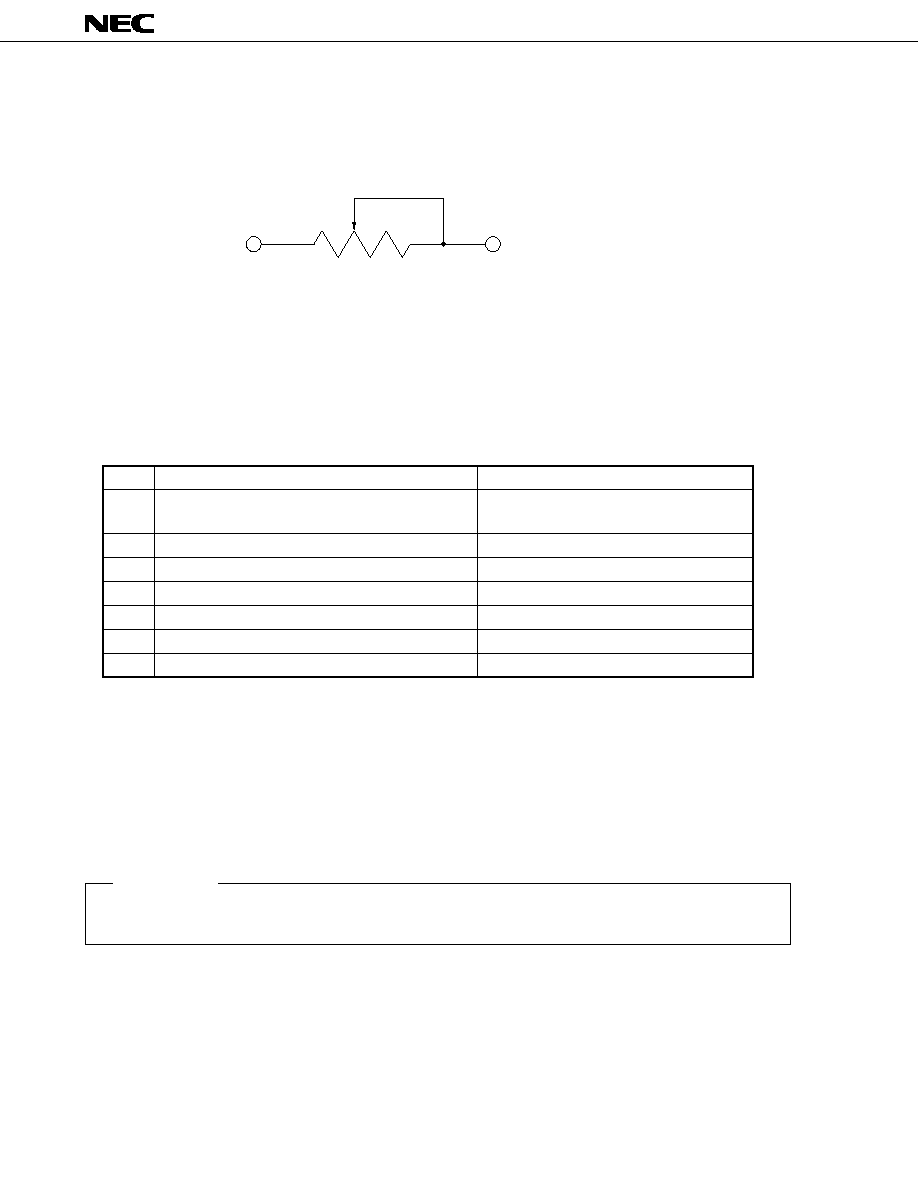
BRTH/BRTL
≠
Pins for backlight brightness control
Connect 10 kW variable resistor (*2) or voltage control (*3).
BRTC
Positive
Backlight ON/OFF control signal
H or open : Backlight on
L
: Backlight off
ACA
Positive
Luminance control signal
H or open : Normal luminance
L
: Low luminance (1/2 of normal luminance)
V
CC
≠
V
CC
(+3.3 V) power supply for logic
V
DD
≠
V
DD
(+12 V
±
5%) power supply for LCD
V
DDB
≠
V
DDB
(+12 V
±
5%) power supply for backlight
GNDB
Ground for backlight (V
DDB
)
GNDB is connected to the module frame ground.
GND
≠
Signal ground for logic / LCD driving (V
CC
, V
DD
)
(Connect to a system ground.)
PIN FUNCTION
10
NL10276AC24-05
*1 : When POWC is "L" logic input signal should be all "0 V". If input signals are more than "0.3 V", inside
circuits of the LCD module may be broken.
When POWC is "L", serial communication data is clear. Please set it again.
*2 : The variable resistor for brightness control should be 10 k
type, and zero point of the resistor corre-
sponds to the minimum of luminance.
*3 : In case of voltage control for brightness by BRTH/BRTL, at first, set BRTH to be "0 V". And BRTL input
voltage can control the brightness. When BRTL input voltage is "1 V" the luminance become maximum.
And when its voltage is "0 V", the luminance becomes minimum.
BRTH
BRTL (10 k
±
5% , B curve)
< connection of the variable resistor to pins >
FUNCTIONS
(1) Serial data
This LCD module has following functions by serial data input (Table 1).
No.
FUNCTIONS
DETAIL
1
Expansion mode
See Table 2
(Screen mode)
and EXPANSION FUNCTION
2
Display position control (HORIZONTAL)
See Table 6
3
Display position control (VERTICAL)
See Table 3
4
CLK delay control
See Table 4
5
Hsync period count number
See Table 7
6
CLK fall/rise synchronous change
See Table 5
7
Input frequency selection
See Table 8
HOW TO USE THE ABOVE FUNCTIONS
If CNTSEL is "L", the above functions are valid. (CNTSEL is "H" or open, default values are valid.) After serial
data are transferred, the data is latched by CNTSTB. Once, the data is latched, the above functions are
effective.
Please keep CNTSTB to be "L" during transferring data.
Input data can be changed during power on, but LCD display may be disturbed. When the serial data are
changed, we recommend that the backlight power is off using BRTC function.
ATTENTION
Input data can be changed during power on, but LCD display may be disturbed. When the serial data are
changed, we recommend that the backlight power is off using BRTC function.

11
NL10276AC24-05
CNTDAT
CNTSTB
CNTCLK
D0
D1
D3
D2
D41
D42
D43
D44
(2) Serial communication timing and waveform
Parameter
Symbol
min.
max.
Unit
Remarks
CLK pulse width
twck
50
≠
ns
CNTCLK
CLK frequency
fclk
≠
5
MHz
DATA setup-time
tdst
50
≠
ns
CNTDAT
DATA hold-time
tdhl
50
≠
ns
Latch-pulse width
twlp
50
≠
ns
CNTSTB
Latch setup-time
tlst
50
≠
ns
Rise / fall time
tr, tf
≠
50
ns
CNT
◊ ◊ ◊
V
CC
V
CC
CNTDATA
50%
GND
tdst
tdhl
twck
90%
CNTCLK
50%
50%
10%
GND
tr
tf
tlst
twlp
V
CC
CNTSTB
GND

12
NL10276AC24-05
Data
Data name
Function
D0
VEX3
Expansion mode
See table 2
D1
VEX2
Expansion mode
D2
VEX1
Expansion mode
D3
VEX0
Expansion mode
D4
VD10
Vertical display position (MSB)
See table 3
D5
VD9
Vertical display position
D6
VD8
Vertical display position
D7
VD7
Vertical display position
D8
VD6
Vertical display position
D9
VD5
Vertical display position
D10
VD4
Vertical display position
D11
VD3
Vertical display position
D12
VD2
Vertical display position
D13
VD1
Vertical display position
D14
VD0
Vertical display position (LSB)
D15
DELAY6
CLK delay (MSB)
See table 4
D16
DELAY5
CLK delay
D17
DELAY4
CLK delay
D18
DELAY3
CLK delay
D19
DELAY2
CLK delay
D20
DELAY1
CLK delay
D21
DELAY0
CLK delay (LSB)
D22
CKS
CLK reverse signal
See table 5
D23
HD8
Horizontal display position (MSB)
See table 6
D24
HD7
Horizontal display position
D25
HD6
Horizontal display position
D26
HD5
Horizontal display position
D27
HD4
Horizontal display position
D28
HD3
Horizontal display position
D29
HD2
Horizontal display position
D30
HD1
Horizontal display position
D31
HD0
Horizontal display position (LSB)
D32
HSE10
Horizontal count number (MSB)
See table 7
D33
HSE9
Horizontal count number
D34
HSE8
Horizontal count number
D35
HSE7
Horizontal count number
D36
HSE6
Horizontal count number
D37
HSE5
Horizontal count number
D38
HSE4
Horizontal count number
D39
HSE3
Horizontal count number
D40
HSE2
Horizontal count number
D41
HSE1
Horizontal count number
D42
HSE0
Horizontal count number (LSB)
D43
MOD1
CLK frequency select
See table 8
D44
MOD0
CLK frequency select
Table 1. CNTDAT COMPOSITION
MSB : Most Significant Bit
LSB : Least Significant Bit

13
NL10276AC24-05
Table 2. Display mode (VEX3 to VEX0 ; 4 bit)
VEX3
VEX2
VEX1
VEX0
Vertical magnification
Display mode
Display image
0
0
0
0
1
XGA
Standard
(note 1)
0
0
0
1
1.25
SVGA
0
0
1
0
1.6
PC98, VGA, TEXT
0
0
1
1
≠
Prohibit
See DISPLAY IMAGE
0
1
0
1
2.5
PAL
0
1
1
0
3.2
NTSC
0
1
1
1
≠
Prohibit
1
X
X
X
≠
Prohibit
note 1 : Display mode is XGA, when CNTSEL is "H" or "open".
VD10
VD9
VD8
VD7
VD6
VD5
VD4
VD3
VD2
VD1
VD0
Vertical position [H]
(note 2)
0
0
0
0
0
0
0
0
0
0
0
Prohibit
0
0
0
0
0
0
0
0
0
0
1
Prohibit
0
0
0
0
0
0
0
0
0
1
0
Prohibit
0
0
0
0
0
0
0
0
0
1
1
Prohibit
0
0
0
0
0
0
0
0
1
0
0
4
0
0
0
0
0
0
0
0
1
0
1
5
∑
∑
∑
∑
∑
∑
∑
∑
∑
∑
∑
∑
∑
∑
∑
∑
∑
∑
∑
∑
∑
∑
∑
∑
∑
∑
∑
∑
∑
∑
∑
∑
∑
∑
∑
∑
1
1
1
1
1
1
1
1
1
0
1
2045
1
1
1
1
1
1
1
1
1
1
0
2046
1
1
1
1
1
1
1
1
1
1
1
2047
(note 3)
Table 3. Vertical position (VD10 to VD0 ; 11 bit)
note 2 : This is horizontal line number for effecting VIDEO signal from Vsync-fall.
note 3 : The maximum vertical position is Vsync total.
note 4 : Vertical position is fixed at 35 H, when CNTSEL is "H" or "open".

14
NL10276AC24-05
Table 4. Clock (CLK) delay (DELAY6 to DELAY0 ; 7 bit)
DA (6 : 0)
Delay
(note 5)
value
00H
7.0 ns
01H
7.6 ns
02H
8.2 ns
03H
8.8 ns
04H
9.4 ns
05H
10.0 ns
06H
10.5 ns
07H
11.2 ns
08H
11.8 ns
09H
12.4 ns
0AH
13.0 ns
0BH
13.7 ns
0CH
14.2 ns
0DH
14.8 ns
0EH
15.3 ns
0FH
15.9 ns
10H
16.6 ns
11H
17.2 ns
12H
17.8 ns
13H
18.4 ns
14H
18.9 ns
15H
19.5 ns
16H
20.1 ns
17H
20.7 ns
18H
21.4 ns
19H
22.0 ns
1AH
22.6 ns
1BH
23.2 ns
1CH
23.8 ns
1DH
24.4 ns
1EH
24.9 ns
1FH
25.6 ns
20H
26.3 ns
21H
26.9 ns
22H
27.4 ns
23H
28.1 ns
24H
28.5 ns
25H
29.1 ns
26H
29.7 ns
27H
30.3 ns
28H
31.0 ns
29H
31.6 ns
2AH
32.2 ns
2BH
32.8 ns
DA (6 : 0)
Delay
(note 5)
value
2CH
33.3 ns
2DH
33.9 ns
2EH
34.4 ns
2FH
35.1 ns
30H
35.6 ns
31H
36.2 ns
32H
36.8 ns
33H
37.5 ns
34H
37.9 ns
35H
38.5 ns
36H
39.1 ns
37H
39.7 ns
38H
40.4 ns
39H
41.0 ns
3AH
41.5 ns
3BH
42.1 ns
3CH
42.6 ns
3DH
43.2 ns
3EH
43.8 ns
3FH
44.4 ns
40H
45.0 ns
41H
45.6 ns
42H
46.2 ns
43H
46.8 ns
44H
47.3 ns
45H
47.8 ns
46H
48.4 ns
47H
49.0 ns
48H
49.6 ns
49H
50.2 ns
4AH
50.8 ns
4BH
51.4 ns
4CH
51.9 ns
4DH
52.6 ns
4EH
53.1 ns
4FH
53.7 ns
50H
54.5 ns
51H
55.0 ns
52H
55.6 ns
53H
56.3 ns
54H
56.8 ns
55H
57.4 ns
56H
57.9 ns
57H
58.5 ns
DA (6:0)
Delay
(note 5)
value
58H
59.2 ns
59H
59.8 ns
5AH
60.4 ns
5BH
61.1 ns
5CH
61.6 ns
5DH
62.2 ns
5EH
62.7 ns
5FH
63.3 ns
60H
64.0 ns
61H
64.7 ns
62H
65.3 ns
63H
66.0 ns
64H
66.5 ns
65H
67.1 ns
66H
67.7 ns
67H
68.3 ns
68H
68.9 ns
69H
69.5 ns
6AH
70.1 ns
6BH
70.7 ns
6CH
71.2 ns
6DH
71.9 ns
6EH
72.4 ns
6FH
73.1 ns
70H
73.6 ns
71H
74.2 ns
72H
74.8 ns
73H
75.4 ns
74H
75.9 ns
75H
76.5 ns
76H
77.0 ns
77H
77.7 ns
78H
78.3 ns
79H
79.0 ns
7AH
79.6 ns
7BH
80.2 ns
7CH
80.8 ns
7DH
81.4 ns
7EH
81.9 ns
7FH
82.5 ns
note 5
: DA (6:0) means Delay
6 (D15) to 0 (D21)
<EXAMPLE>
DA (6:0)=00H
D15 16 17 18 19 20 21
0
0
0
0
0
0
0
DA (6 : 0) = 2AH
D15 16 17 18 19 20 21
0
1
0
1
0
1
0
note 6 : Delay value is approximate.
note 7 : DA (6:0) is fixed at 00H, when CNTSEL is "H" or "open". This value is the upper limit by setting MOD as
next page.

15
NL10276AC24-05
MOD1
MOD0
Upper limit of VD6 to VD0 CLK-delay setting (HEXADECIMAL)
0
0
Prohibit
0
1
59H
1
0
6BH
1
1
7FH
note 8 : This delay value is typical at Ta = 25∞C, V
CC
= 3.3 V. By changing ambient temperature and
power supply, the delay will be changed also.
See the following references.
q Variation of CLK delay by temperature drift. (as reference)
The temperature constant of CLK delay is 0.2 % / ∞C.
Calculated example:
In case that delay time is 20 ns at Ta = 25∞C;
(a) In case of Ta rising to 50 ∞C.
Increase of delay time
(50∞C-25∞C)
◊
0.002
◊
20 ns = +1 ns
So, the total delay time is 21 ns at Ta = 50∞C.
(b) In case of Ta falling to 0∞C.
Decrease of delay time
(0∞C-25∞C)
◊
0.002
◊
20ns = ≠1 ns
So, the total delay time is 19 ns at Ta = 0∞C.
w Variation of CLK delay time against V
CC
voltage change. (as reference)
Increase of 35 % / V in case of rising from V
CC
= 3.3 V.
Decrease of 48 % / V in case of falling from V
CC
= 3.3 V.
Calculated example:
In case that delay time is 20 ns at V
CC
= 3.3 V.
(a) In case of V
CC
rising to 3.6 V.
Decrease of delay time
(3.3 V-3.6 V)
◊
0.35
◊
20 ns = ≠2.1 ns
So, the total delay time is 17.9 ns at V
CC
= 3.6 V.
(b) In case of V
CC
falling to 3.0 V.
Increase of delay time
(3.3 V-3.0 V)
◊
0.48
◊
20 ns = +2.88 ns
So, the total delay time is 22.88 ns at V
CC
= 3.0 V.
Table 5. CLK reverse signal
CKS
FUNCTION
Data is sampled on rising edge of CLK.
Data is sampled on falling edge of CLK.
note 9 : CKS is "0", when CNTSEL is "H" or "open".
0
1

16
NL10276AC24-05
Table 6. Display horizontal position (HD8 to HD0; 9 bit)
HD8
HD7
HD6
HD5
HD4
HD3
HD2
HD1
HD0
Horizontal position [CLK] (note 10)
0
0
0
0
0
0
0
0
0
Prohibit
0
0
0
0
0
0
0
0
1
Prohibit
∑
∑
∑
∑
∑
∑
∑
∑
∑
∑
∑
∑
∑
∑
∑
∑
∑
∑
∑
∑
0
0
0
1
1
1
1
1
1
Prohibit
0
0
1
0
0
0
0
0
0
64
0
0
1
0
0
0
0
0
1
65
∑
∑
∑
∑
∑
∑
∑
∑
∑
∑
∑
∑
∑
∑
∑
∑
∑
∑
∑
∑
1
1
1
1
1
1
1
0
1
509
1
1
1
1
1
1
1
1
0
510
1
1
1
1
1
1
1
1
1
511
note 10 : This is CLK number from Hsync-fall to effecting VIDEO signal.
note 11 : Horizontal position is set at 296 CLK, when CNTSET is "H" or "open".
HSE10
HSE9
HSE8
HSE7
HSE6
HSE5
HSE4
HSE3
HSE2
HSE1
HSE0
CLK number (note 12)
0
0
0
0
0
0
0
0
0
0
0
0
0
0
0
0
0
0
0
0
0
0
1
1
0
0
0
0
0
0
0
0
0
1
0
2
0
0
0
0
0
0
0
0
0
1
1
3
0
0
0
0
0
0
0
0
1
0
0
4
∑
∑
∑
∑
∑
∑
∑
∑
∑
∑
∑
∑
∑
∑
∑
∑
∑
∑
∑
∑
∑
∑
∑
∑
∑
∑
∑
∑
∑
∑
∑
∑
∑
∑
∑
∑
1
1
1
1
1
1
1
1
1
0
1
2045
1
1
1
1
1
1
1
1
1
1
0
2046
1
1
1
1
1
1
1
1
1
1
1
2047
Table 7. Display horizontal CLK numbers (HSE10 to HSE0; 11 bit)
note 12 : This is from one falling edge of Hsync to the next Hsync.
note 13 : CLK number is set 1344 CLK, when CNTSEL is "H" or "open".
note 14 : Set HSE0 to 10 complying with CLK number of Hsync. If the setting value is different from actual
input signal, it cause a malfunction.
Table 8. Setting of CLK frequency (MOD1 to MOD0; 2 bit)
MOD1
MOD0
CLK frequency [MHz]
0
0
Prohibit
0
1
65 to 79
1
0
50 to 65
1
1
20 to 50
note 15 : Set MOD0 and MOD1 complying with input CLK frequency.
note 16 : CLK frequency is set 65 to 79 MHz, when CNTSEL is "H" or "open".

17
NL10276AC24-05
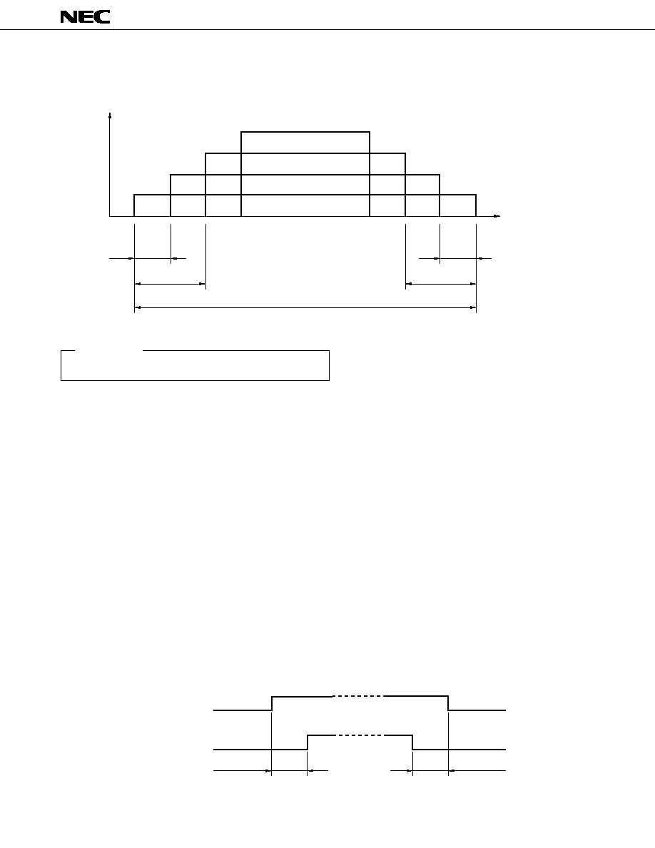
EXPANSION FUNCTION
HOW TO USE EXPANSION FUNCTION AND SCREEN IMAGE
Expansion mode is a function to expand screen. For example, VGA signal has 640
◊
480 pixels. But, if the
display data can expanded to 1.6 times vertically and horizontally, VGA screen image can be displayed fully
on the screen of XGA resolution.
This LCD module has the function of expanding vertical direction as shown in Table 1. And expanding
horizontal direction is possible by setting input CLK frequency which is equivalent to the magnification. It is
necessary to make this CLK outside of this LCD module.
DISPLAY IMAGE of after two pages is display example, when DE function is default and HD and VD are set
to most suitable frequency. And when DE function is used, HD and VD become default. Please adjust the
display to the best position by DE signal.
Please adopt these modes after evaluating display quality, because of becoming bad display in some cases.
Magnification
Vertical
Horizontal *
XGA
1024
◊
768
1
1
SVGA
800
◊
600
1.25
1.25
VGA
640
◊
480
1.6
1.6
VGA TEXT
720
◊
400
1.6
1.4
PC-9801
640
◊
400
1.6
1.6
NTSC
640
◊
(vertical 240
◊
2)
3.2
1.6
PAL
640
◊
(vertical 280
◊
2)
2.5
1.6
Input display
Resolution
The followings show display magnifications for each mode.
* The horizontal magnification multiples the input clock (CLK).
Input CLK = system CLK
◊
horizontal magnification
Example :
In case of XGA, VGA and PC-9801, CLK frequency can be decided as follows.
XGA
: (system CLK (65MHz))
◊
1.0=65MHz
VGA
: (system CLK (25.175MHz))
◊
1.6=40.28MHz
PC-9801 : (system CLK (21.053MHz))
◊
1.6=33.68MHz

18
NL10276AC24-05
SETTING SERIAL DATA FOR EXPANSION
Input signal
Mode
CLK
Hsync
Vsync
Horizontal
Vertical
Count
DSP
Count
DSP
HSE
HD
VD
number
(note 1) number (note 1)
[MHz]
[kHz]
[Hz]
[CLK]
[CLK]
[H]
[H]
(A)
(B)
≠
(C)
Calculation formula
(A)
◊
(B)
◊
= (C)
Vertical magnitude Horizontal magnitude
XGA
65.000
48.363
60.004
1344
296
806
35
(A)
◊
1
(B)
◊
1
= (C)
75.000
56.476
70.069
1328
280
806
35
79.000
58.088
72.980
1360
328
807
39
78.750
60.023
75.029
1312
272
800
31
SVGA
36.000
35.156
56.25
1024
200
625
24
(A)
◊
1.25
(B)
◊
1.25
40.000
37.879
60.317
1056
216
628
27
50.000
48.077
72.188
1040
184
666
29
49.500
46.875
75.000
1056
240
666
24
VGA
25.175
31.469
59.940
800
144
525
35
(A)
◊
1.6
(B)
◊
1.6
31.500
37.861
72.809
832
168
520
31
31.500
37.500
75.000
840
184
500
19
31.334
34.971
66.611
896
176
525
6
VGA
28.322
31.469
70.087
900
153
449
37
(A)
◊
1.4
(B)
◊
1.4
TEXT
31.500
37.927
85.040
936
180
446
45
PC-9801
21.053
24.827
56.424
848
144
440
33
(A)
◊
1.6
(B)
◊
1.6
433
25.175
31.469
70.086
800
144
449
37
NTSC
20.000
15.734
59.940
≠
205
262.5
9
1271
= (B)
= (C)
PAL
20.000
15.625
50.000
≠
205
312.5
9
1280
= (B)
= (C)
Module serial-data
setting
note 1 : DSP = Display Start Period. DSP is the total of "pulse-width" and "back-porch".
note 2 : HD and VD are approximate values. Set HD and VD in case of adjusting display to the screen center.
note 3 : The pulse-width of Hsync, Vsync and back-porch are the same as XGA-mode. (Standard-mode).
note 4 : Detail of HSE is mentioned in CLK number of Table 7.
note 5 : Detail of HD is mentioned in horizontal position of Table 6.
note 6 : Detail of VD is mentioned in vertical position of Table 3.

19
NL10276AC24-05
DISPLAY IMAGE
(1) SVGA MODE (800
◊
600)
(2) VGA MODE (640
◊
480)
(3) PC-9801 MODE (640
◊
400)
(4) VGA-TEXT MODE (720
◊
400)
(5) NTSC MODE (640
◊
240)
(6) PAL MODE (640
◊
280)
XGA (1024
◊
768 pixels)
Black display area
Valid area
Horizontal :
◊
1.25 (1000 pixels)
Vertical
:
◊
1.25 (750 pixels)
Horizontal :
◊
1.6 (1024 pixels)
Vertical
:
◊
1.6 (768 pixels)
Horizontal :
◊
1.6 (1024 pixels)
Vertical
:
◊
1.6 (640 pixels)
Horizontal :
◊
1.4 (1008 pixels)
Vertical
:
◊
1.6 (640 pixels)
Horizontal :
◊
1.6 (1024 pixels)
Vertical
:
◊
3.2 (768 pixels)
Horizontal :
◊
1.6 (1024 pixels)
Vertical
:
◊
2.5 (700 pixels)
20
NL10276AC24-05
INPUT SIGNAL TIMING
(1) XGA-MODE (Standard)
Without use serial communication (CNTSEL = "H" or OPEN)
Name
Symbol
min.
typ.
max.
Unit
Remarks
CLK
Frequency
1 / tc
52.0
65.0
79.0
MHz
XGA standard
≠
15.385
≠
ns
Rise / fall
tcrf
≠
≠
10.0
ns
≠
Duty
tch / tc
0.4
0.5
0.6
≠
≠
Hsync
Period
th
16.6
20.677
22.7
µ
s
48.363 kHz
≠
1344
≠
CLK
(typ.)
Display
thd
≠
15.754
≠
µ
s
≠
≠
1024
≠
CLK
Front-porch
thf
≠
0.369
-
µ
s
≠
10
24
-
CLK
Pulse-width
thp
≠
2.092
≠
µ
s
≠
16
136
≠
CLK
Back-porch
thb
1.0
2.462
≠
µ
s
≠
44
160
≠
CLK
Pulse-width
thpb
1.8
≠
≠
µ
s
≠
+ Back-porch
thch
4.0
≠
≠
ns
≠
thcs
2.0
≠
≠
ns
≠
thvh
4.0
≠
≠
ns
≠
thvs
1.0
≠
≠
CLK
≠
Rise / fall
thrf
≠
≠
10.0
ns
≠
Vsync
Period
tv
13.3
16.665
18.5
ms
60.004 Hz
≠
806
≠
H
(typ.)
Display
tvd
≠
15.880
≠
ms
≠
≠
768
≠
H
Front-porch
tvf
≠
62.031
≠
µ
s
≠
1
3
≠
H
Pulse-width
tvp
≠
124.06
≠
µ
s
≠
2
6
≠
H
Back-porch
tvb
≠
599.63
≠
µ
s
≠
5
29
≠
H
Rise / fall
tvrf
≠
≠
10.0
ns
NTSC/PAL MODE
Field timing
tfi
±
1
≠
≠
H
≠
DE
Setup time
tds
2.0
≠
≠
ns
≠
Hold time
tdh
4.0
≠
≠
ns
≠
Rise/fall
tdrf
≠
≠
10.0
ns
≠
Analog
RGB
CLK-Hsync timing
hold / setup time
V-Hsync timing
hold / setup time
tda
5.0
≠
≠
ns
≠

21
NL10276AC24-05
Without use serial communication (CNTSEL = "H" or OPEN)
*V
IH
= 2.2 V (min.) to 5.25 V (max.)
V
IL
= 0 V (min.) to 0.8 V (max.)
CLK
R
G
B
DE
Hsync
Vsync
Hsync
tc
tch
V
IdcCLK
V
I CLK
GND
V
IH
*
1.5 V
V
IL
*
V
IH
*
1.5 V
V
IL
*
V
IH
*
1.5 V
V
IL
*
V
IH
*
1.5 V
V
IL
*
V
IH
*
1.5 V
V
IL
*
tcrf
tds
tdh
tdrf
tda
thch
thcs
thrf
tvrf
thvh
thvs
22
NL10276AC24-05
<Horizontal>
<Vertical>
Hsync
Display period
Vsync
Display period
th
thp
thb
thf
thd
tv
tvp
tvb
tvf
tvd
(NTSC/PAL)
Vsync
Field
Vsync
Hsync
Field
First field
First field
1H(min.)
1H(min.)
1H(min.)
1H(min.)
Second field
Second field
First field
23
NL10276AC24-05
MOD1
MOD0
tA [CLK]
tB [CLK]
tC [ns]
0
0
Prohibit
0
1
44
32
1
0
34
22
200 min.
1
1
28
18
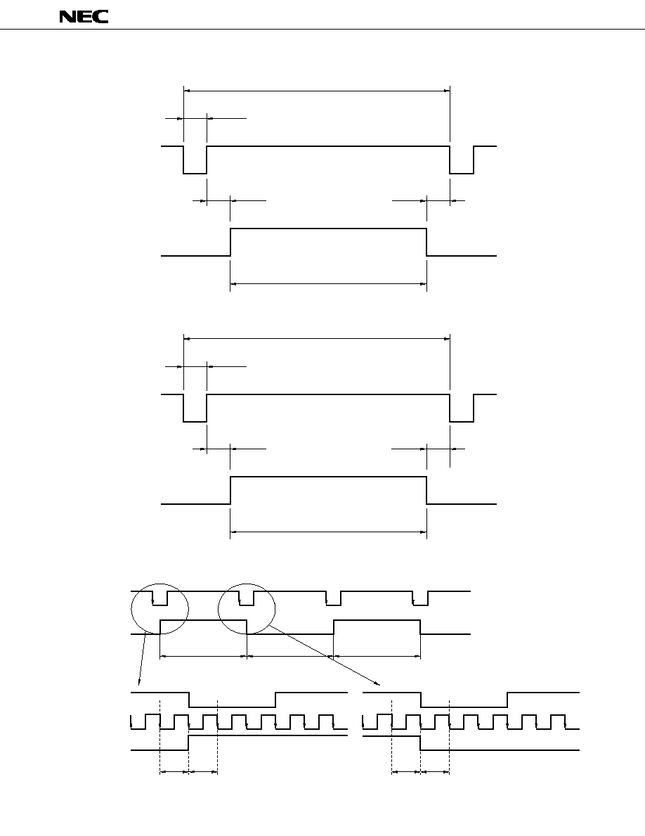
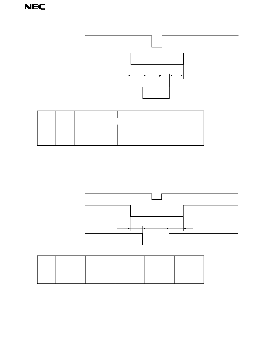
(2) Timing for generating CLAMP signal internally
Hsync
Display period
CLAMP
tA
tB
tC
(3) Timing for inputting CLAMP signal from outside
Hsync
Display period
CLAMP
tA
tB
tC
note : Exclude noises on analog RGB signal. Because during CLAMP = " L", the pedestal level of analog RGB
signals is sampled. If noises are on the analog signals, luminance level of display is changed and the
display becomes bad.
ITEMS
min.
typ.
max.
Unit
Remarks
tA
0.1
≠
≠
µ
s
≠
tB
0.3
≠
≠
µ
s
≠
tC
0.2
≠
≠
µ
s
≠
note : Exclude noises on analog RGB signal. Because during CLAMP = "L", the pedestal level of analog RGB
signals is sampled. If noises are on the analog signals, luminance level of display is changed and the
display becomes bad.
24
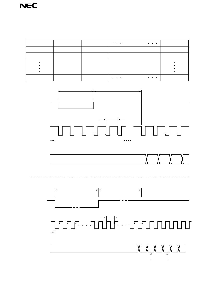
NL10276AC24-05
tvp
Vsync
Hsync
XGA mode
(CNTSEL="H" or "open")
R
G
B
R
G
B
Hsync
XGA mode
(CNTSEL="H" or "open")
CLK
INVALID
tvb
1 Line
INVALID
VALID
D (0, X) D (1, X) D (2, X)
thp
thb
1 CLK
D (X, 0)
D (X, 1)
D (X, 3)
D (X, 2)
D (X, 4)
0
1
2
296
297
0
1
2
3
4
5
35
36
INPUT SIGNAL AND DISPLAY POSITION (XGA STANDARD TIMING)
(1) DELSEL="L"
Pixels
D ( 0, 0 )
D ( 1, 0 )
D ( 2, 0 )
D ( 767, 0 )
D ( 0, 1 )
D ( 1, 1 )
D ( 767, 1 )
D ( 0, 2 )
D ( 767, 2 )
D ( 0, 1023 )
D ( 767, 1023 )
25
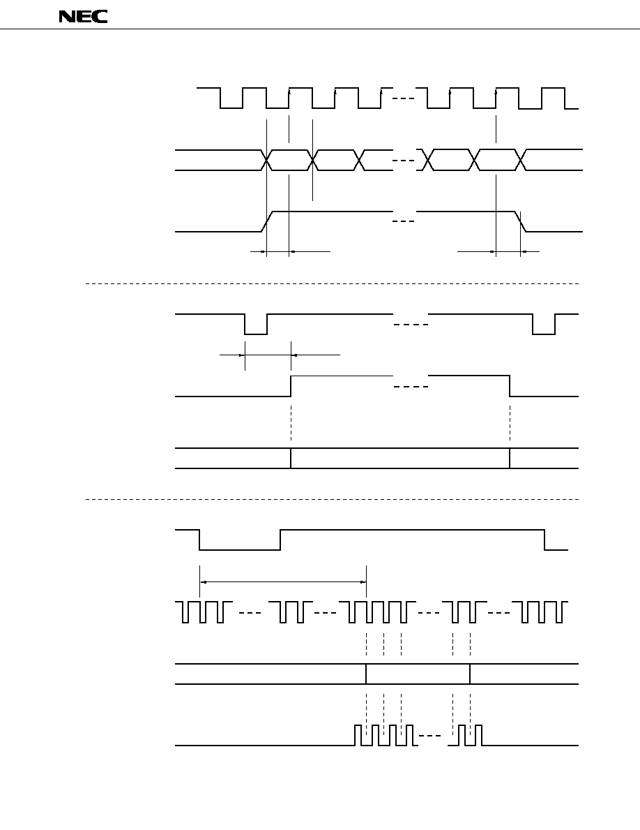
NL10276AC24-05
(2) DELSEL="H"
CLK
DATA
DE
Hsync
DE
DATA
Vsync
Hsync
DATA
DE
INVALID
INVALID
tds
tdh
thpd
INVALID
INVALID
VALID
INVALID
INVALID
VALID
tvp+tvb

26
NL10276AC24-05
GENERAL CAUTION
WARNING
Do not touch an inverter --on which is stuck a caution label-- while the LCD module is under the operation,
because of dangerous high voltage.
ATTENTION
Input data can be changed during power on, but LCD display may be disturbed. When the serial data are
changed, we recommend that the backlight power is off using BRTC function.
(1) Caution when taking out the module
q Pick the pouch only, when taking out module from a shipping package.
(2) Cautions for handling the module
q As the electrostatic discharges may break the LCD module, handle the LCD module with care. Peel a
protection sheet off from the LCD panel surface as slowly as possible.
w As the LCD panel and back-light element are made from fragile glass material, impulse and pressure
to the LCD module should be avoided.
e As the surface of polarizer is very soft and easily scratched, use a soft dry cloth without chemicals for
cleaning.
r Do not pull the interface connectors in or out while the LCD module is operating.
t Put the module display side down on a flat horizontal plane.
y Handle connectors and cables with care.
u The torque to mounting screws should be less than 0.392N
∑
m (4 kgf
∑
cm).
(3) Cautions for the operation
q When the module is operating, do not lose CLK, Hsync, or Vsync signals. If any one of these signals is
lost, the LCD panel would be damaged.
w Obey the supply voltage sequence. If wrong sequence is applied, the module would be damaged.
e Connect the variable resistor or fixed resistor (10 k
or less) to the pin of BRTH and BRTL. If the
resistors are not connected, the life of fluorescent lamp would be short.
r Please use a range of ELECTRICAL CHARACTERISTICS. If use over range of ABSOLUTE MAXIMUM
RATING, we can not guarantee the operation of LCD.
(4) Cautions for the atmosphere
q Dew drop atmosphere should be avoided.
w Do not store and / or operate the LCD module in a high temperature and/or humidity atmosphere.
Storage in an electro-conductive polymer packing pouch and under relatively low temperature atmos-
phere is recommended.
(5) Cautions for the module characteristics
q Do not apply fixed pattern data signal to the LCD module at product aging. Applying fixed pattern for
a long time may cause image sticking.
(6) Other cautions
q Do not disassemble and / or reassemble LCD module.
w Do not re-adjust variable resistor or switch etc.
e When returning the module for repair or etc., Please pack the module not to be broken.
We recommend to use the original shipping packages.

27
NL10276AC24-05
Liquid Crystal Display has following specific characteristics. These are not defects or malfunction.
The display condition of LCD module may be affected by the ambient temperature.
The LCD module uses cold cathode tube for backlight. The optical characteristics, like luminance or
uniformity, will change during life time.
Uneven brightness and/or small spots may be noticed depending on different display patterns.

28
NL10276AC24-05
OUTLINE DRAWING : Front View (Unit in mm)
C L
4- 3.5
(4)
(5)
215
±
0.3
290
±
0.5
252.8
±
0.3 (Bezel Opening)
(245.76) (Active Area)
280
±
0.3
(4)
(4)
(5)
280
±
0.3
(2.8)
(2.4)
max.17
(4)
(5)
(4)
(5)
(4)
(5)
(4)
(5)
225
±
0.5
188.8
±
0.3 (Bezel Opening)
(184.32) (Active Area)
215
±
0.3
(4)
note : The torque to mounting screws should be less than 0.392 N
∑
m (4 kgf
∑
cm).

29
NL10276AC24-05
OUTLINE DRAWING : Rear View (Unit in mm)
76
2
4
0
2
K2
0
0
0
A
THE TFT COLOR LCD
121BLM-3
N
L
10276AC24-05
A100100100100
ES2228421
MADE
IN
JAPAN
B/L
Lot.NO.
note : The torque to mounting screws should be less than 0.392 N
∑
m (4 kgf
∑
cm).
(55)
(29)
(73.5)
4-M3BR
(48.6)
(82.3)
(9.1)
(210)
(0.8)
(3.2)
(59.2)
(6)
(3)

30
NL10276AC24-05

31
NL10276AC24-05

No part of this document may be copied in any form or by any means without the prior written consent of
NEC Corporation.
NEC Corporation does not assume any liability for infringement of patents, copyrights or other intellectual
property rights of third parties by or arising from use of a device described herein or any other liability arising
from use of such device. No license, either express, implied or otherwise, is granted under any patents, copyrights
or other intellectual property rights of NEC Corporation or others.
NL10276AC24-05