NEC
NEC Electronics Inc.
uPD765A/uPD765B
Single/Double Density
Floppy-Disk Controller
Description
Features
The uPD765A/B is an LSI floppy disk controller (FDC)
chip which contains the circuitry and control functions
for interfacing a processor to 4 floppy disk drives. It is
capableof either
IBM
3740singledensity format (FM), or
IBM System 34 double density format (MFM) including
double-sided recording. The uPD765A/B provides con-
trol signals which simplify the design of an external
phase-locked loop and write precompensation circuitry.
The FDC simplifies and handles most of the burdens as-
sociated with implementing a floppy disk interface.
Hand-shaking signals are provided in the uPD765A/B
which make DMA operation easy to incorporate with the
aid of an external DMA controller chip, such as the
uPD8257. The
FDC will operate in eitherthe DMA or non-
DMA mode. In the non-DMA mode the FDC generates
interrupts to !he processor every time a data byte is to
be transferred. In the DMA mode, the processor need
only load the command into the FDC and all data
transfers occur under control of the FDC and DMA
controllers.
There are 16 commands which the uPD765A/uPD765B
will execute. Most of these commands require multiple
8-bit bytes to fully specify the operation which the
processor wishes the FDC to perform. The following
commands are available.
R e a d D a t a
R e a d D e l e t e d D a t a
R e a d I D
Write Data
Specify
Write ID (Format Write)
Read Diagnostic
Write Deleted Data
S c a n E q u a l
Seek
Scan High or Equal
Recalibrate
S c a n L o w o r E q u a l
Sense Interrupt Status
Version
Sense Drive Status.
Ordering Information
Address mark detection circuitry is internal to the FDC
which simplifies the phase-locked loop and read elec-
tronics. The track stepping rate, head load time, and
head unload time are user-programmable. The
uPD765A/uPD765B
offers additional features such as
multi-track and multi-side read and write commands
and single and double density capabilities.
FM, MFM Control
Variable recording length: 128,256, .8192 bytes/
sector
IBM-compatible format (single- and double-
sided, single- and double-density)
Multi-sector and multi-track transfer capability
Drive up to 4 floppy or micro floppydisk drives
Data scan capability-will scan a single sector or
an entire cylinder comparing byte-for-byte host
memory and disk data
Data transfers in DMA or non-DMA mode
Parallel seek operations on up to four drives
Compatible with uPD8080/85,
uPD8086/88,
V-series
and uPD780
(Z80@) microprocessors
Single-phase clock: 8 MHz maximum
3
+5V only
Z80 is a registered trademark of the Zilog
Corporation
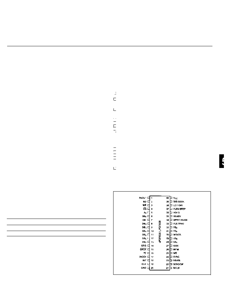
Pin Configuration
D e v i c e N u m b e r
uPD765AC2
uPD765B
Package Type
40-pin
plastic DIP
40-pin plastic DIP
Max
Freq. of Operation
8 MHz
8 MHz
N E C E L - 0 0 0 3 2 4
5-3
uPD765A/uPD765B
NEC
Pin Identification
No.
Symbol
1
R E S E T
2
RD
3
WR
4
C
S
5
A0
6-13
DB0-DB7
14
DRQ
15
DACK
16
T C
17
INDEX
Function
Reset input
Read control input
Write control input
Chip select input
Data or status select input
Bidirectional data bus
DMA request output
DMA acknowledge input
Terminal count input
I n d e x i n p u t
18
I N T
19
C L K
20
G N D
21
W C L K
2 2
W I N D O W
2 3
R D A T A
2 4
S Y N C
2 5
W E
26
M F M
2 7
SIDE
28 29
USn US1
Interrupt request output
Clock input
G r o u n d
Write clock input
Read data window input
Read data input
V C O s y n c o u t p u t
Write enable output
MFM output
Head select output
FDD unit select output
3 0
W D A T A
3 1 , 3 2
P S 0 PS1
3 3
FLT/TRK0
3 4
WPRT/2SIDE
3 5
R E A D Y
3 6
H D L D
3 7
FLTR/STEP
38
LCT/DIR
39
m / S E E K
4 0
k c
Write data output
Preshift output
Fault/track zero input
Write protect/two side
input
R e a d y input
Head load output
Fault reset/step output
Low current direction
output
Read/write/ seek output
DC power ( +5 V)
Pin Functions
RESET (Reset)
INT (Interrupt)
The RESET input places the FDC in the idle state. It re-
s e t s t h e o u t p u t l i n e s t o t h e F D D t o 0 ( l o w ) , e x c e p t P S O , 1
and WDATA (undefined), INT and DRQ also go low;
DBO-7 goes to an input state. It does not affect SRT,
H U T , o r H L T i n t h e S p e c i f y c o m m a n d . I f t h e R D Y i n p u t i s
held high during reset, the FDC will generate an inter-
rupt within 1.024ms.
To clear this interrupt, use the
Sense Interrupt Status command.
The INT output is FDC's interrupt request. In Non-DMA
mode, the signal is output for each byte. In DMA mode,
it is output at the termination of a command operation.
CLK (Clock)
CLK is the input for the FDC's single-phase, lTL-level
squarewave clock: 8 MHz or 4 MHz. (Requires a pull-up
resistor.)
RD (Read Strobe)
The RD input allows the transfer of data from the FDC
to the data bus when low and either C
S
or DACK is
asserted.
WR (Write Strobe)
The WR input allows the transfer of data to the FDC
from the data bus when low. Disabled when C
S is high.
A0 (Data/Status Select)
The A0 input selects the data register (A0 = 1) or status
register (A0=O) contents to be accessed through the
data bus.
C
S
(Chip Select)
The FDC is selected when C
S is low, enabling RD and
WR.
DBo-DB7 (Data Bus)
DBo-DB7 are a bidirectional 8-bit data bus. Disabled
when C
S is high.
DRQ (DMA Request)
The FDC asserts the DRQ output high to request a DMA
transfer.
DACK (DMA Acknowledge)
When the DACK input is low, a DMA cycle is active and
the controller is performing a DMA transfer.
TC (Terminal Count)
When t h e T C input is high, it indicates the termination of
a DMA transfer. It terminates data transfer during Read/
Write/Scan commands in DMA or interrupt mode.
INDEX (Index)
The INDEX input goes high at the beginning of a disk
track.
NEC
uPD765A/uPD765B
WCLK (Write Clock)
The WCLK input sets the data write rate to the FDD. It is
500 kHz for FM, 1 MHz for MFM drives, for 8 MHz opera-
tion of the FDC; 250kHz FM or 500 kHz MFM for 4 MHz
FDC operation.
This signal must be input for read and write
c y c l e s
WCLK's rising edge must be synchronized with CLK's
rising edge, except for the uPD765B.
WINDOW (Read Data Window)
The WINDOW input is generated by the phase-locked
loop (PLL). It is used to sample data from the FDD and in
distinguishing between clock and data bits in the FDC.
RDATA (Read Data)
The RDATA input is the read data from the FDD,
containing clock and data bits. To avoid a deadlock
situation, input RDATA and WINDOW together.
WDATA (Write Data)
WDATA is the serial clock and data output to the FDD.
WE (Write Enable)
The WE output enables write data into the FDD.
SYNC (VCO Sync)
The SYNC output inhibits the VCO in the PLL when low,
enables it when high.
MFM (MFM Mode)
The MFM output shows the
VCO's operation mode. It is
high for MFM, low for FM.
SIDE (Head Select)
Head 1 is selected when the SIDE output is 1 (high), head
0 is selected when SIDE is 0 (low).
U S 0 US1 (Unit Select 0,1)
The US0 and US1 outputs select up to 4 floppy disk drive
units using an external decoder.
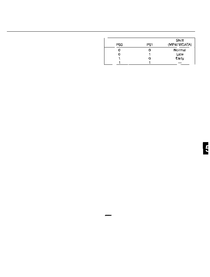
PS0, PS1 (Preshift 0,1)
The PS0 and PS1 outputs are the write precompensation
request signals for MFM mode. They determine early,
late, and normal times for WDATA shifting.
READY (Ready)
The READY input indicates that the FDD is ready to re-
ceive data.
HDLD (Head Load)
The HDLD output is the command which causes the
read/write head in the FDD to contact the diskette.
FLT/TRKO (Fault/Track 0)
In the read/write mode, the FLT input detects FDD fault
conditions. In the seek mode, TRKO indicates track 0
head position.
WPRT/2SlDE (Write Protect/Two Side)
In the read/write mode, the WPRT input senses write
protected status (at the drive or media.)
In
the seek
mode, 2SIDE senses two-sided media.
FLTR/STEP (Fault Reset/Step)
In the read/write mode, the FLTR output resets the fault
flip-flop in the FDD. In the seek mode, STEP outputs
step pulses to move the head to another cylinder. A fault
reset pulse is issued at the beginning or each Read or
Write command prior to the HDLD signal.
LCT/DlR (Low Current/Direction)
In the read/write mode, the LCT output indicates that
the R/W head is positioned at cylinder 42 or greater. In
the seek mode, the DIR output determines the direction
the head will move in when it receives a step pulse. If
DIR is 0, seeks are performed in the outward direction;
DIR is 1, seeks are performed in the inward direction.
RWlSEEK (Read/Write/Seek)
The RW/SEEK output specifies the read/write mode
when low, and the seek mode when high.
GND (Ground)
Ground.
Vcc(+5v)
+5 V power supply.
5-5
uPD765AIuPD765B
NEC
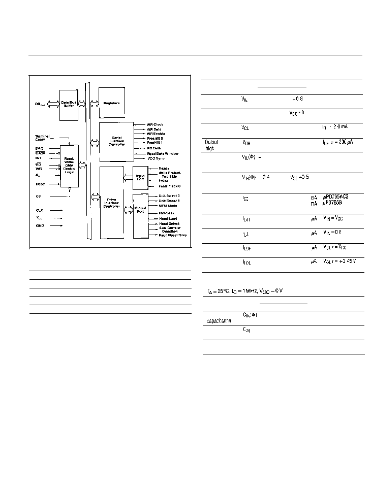
Block Diagram
Absolute Maximum Ratings
TA = 250C
Power supply voltage, VCC
- 0
5 to
+7v
Input
voltage, V1
-0.5
to +7v
Output voltage, VO
- 0 . 5 1 0
+7v
Operating temperature, TOpT
- 1OOC to +7ooc
Storage temperature, TSTG
-65�C to +150�C
Comment:
Exposing the device to stresses above those listed
in the Absolute Maximum Ratings could cause permanent
damage. The device should not be operated under conditions
outside the limits described in the operational sections of this
specification. Exposure to absolute maximum rating condi-
tions for extended periods
may
affect device reliability.
DC Characteristics
Th= -1O'C to
+70�C,Vcc =
+5V%lO%
__
Limits
Teal
Parameter
Symbol
Min
Typ
Max
Unit
C o n d i t i o n s
Input voltage
-0.5
v
IOW
Input voltage
V I H
2.0
5 v
high
Output voltage
0.45
V
l o w
V o l t a g e
2.4
Input voltage
0.5
low (CLK +
WCLK)
Input voltage
high
(CLK + WCLK)
Supply current
k c )
k c
V
0.65
V
v
1 5 0
140
Input load
1 0
c u r r e n t h i g h
Input load
- 1 0
c u r r e n t l o w
Output leakage
current high
Output leakage
c u r r e n t l o w
1 0
-10
Capacitance
Parameter
Input clock
Limits
Symbol Min
Typ
Max
Unit
20
pF
Test
C o n d i t i o n s
(Note 1)
Input
capacitance
10
pF
( N o t e 1 )
output
COUT
20
pF
c a p a c i t a n c e
Note:
(1) All
pinsexcept pin under test tied to
AC ground.
[ N o t e 1 )
5-6

NEC
uPD765A/uPD765B
DIFFERENCES BETWEEN ,uPD765A AND
uP D765B
The uPD765B is a functionally enhanced version of the
uPD765A.
Differences are explained below.
Overrun Bit [OR]
In uPD765A, when executing a read- or write-type
command (except READ ID and SCAN types), the
result status OR bit is not set if there is an overrun on
the final byte of a sector. An improvement in the
uPD765B allows it to set the OR bit in any situation.
DRQ Reset
When an overrun occurs, the uPD765A needs DACK
input to reset DRQ. If DACK is not available, an
external DMA controller continues to operate even after
the FDC enters the R-Phase (Result Phase), and stored
result status may be transferred accidentally as ordinary
data.
On the other hand, the uPD765B resets DRQ auto-
matically just before the R-Phaseentry and independent
of the DACK input. See AC Characteristics for DRQ
reset timing.
Clock Synchronization
The
uPD765B does not require synchronization
between the CLK and WCLK inputs.
Version Command
The Version command distinguishes the uPD765B
from other devices. The ST0 response to the Version
c o m m a n d i s :
Part No.
ST0 Value
uPD765A
8 0 H
uPD765B
90H
5-7