 | –≠–ª–µ–∫—Ç—Ä–æ–Ω–Ω—ã–π –∫–æ–º–ø–æ–Ω–µ–Ω—Ç: UPD77110 | –°–∫–∞—á–∞—Ç—å:  PDF PDF  ZIP ZIP |
Document Outline
- COVER
- DESCRIPTION
- FEATURES
- ORDERING INFORMATION
- BLOCK DIAGRAM
- PIN CONFIGURATION
- DSP FUNCTION LIST
- PIN CONFIGURATION
- PIN NAME
- 1. PIN FUNCTION
- 1.1 Pin Function Description
- 1.2 Connection of Unused Pins
- 2. FUNCTION OUTLINE
- 2.1 Program Control Unit
- 2.2 Arithmetic Unit
- 2.3 Data Memory Unit
- 2.4 Peripheral Units
- 3. CLOCK GENERATOR
- 4. RESET FUNCTION
- 4.1 Hardware Reset
- 4.2 Initializing PLL
- 5. FUNCTIONS OF BOOT-UP ROM
- 5.1 Boot at Reset
- 5.2 Reboot
- 5.3 Signature Operation
- 6. STANDBY MODES
- 6.1 HALT Mode
- 6.2 STOP Mode
- 7. MEMORY MAP
- 7.1 Instruction Memory
- 7.2 Data Memory
- 8. MASK OPTION
- 8.1 Clock Control Options
- 8.2 WAKEUP Function
- 8.3 Mask Option Equivalent Function of uPD77110
- 9. INSTRUCTIONS
- 9.1 Outline of Instructions
- 9.2 Instruction Set and Operation
- 10. ELECTRICAL SPECIFICATIONS
- 11. PACKAGE
- 12. RECOMMENDED SOLDERING CONDITIONS

The information in this document is subject to change without notice. Before using this document, please
confirm that this is the latest version.
Not all devices/types available in every country. Please check with local NEC representative for
availability and additional information.
MOS INTEGRATED CIRCUIT
µ
µ
µ
µ
PD77110, 77111, 77112
16-BIT FIXED-POINT DIGITAL SIGNAL PROCESSORS
Document No. U12801EJ4V0DS00 (4th edition)
Date Published November 1999 N CP(K)
Printed in Japan
DATA SHEET
The mark
shows major revised points.
1998, 1999
©
DESCRIPTION
The
µ
PD77110, 77111, and 77112 are 16-bit fixed-point digital signal processors (DSPs).
Compared with the
µ
PD77016 family, these DSPs have improved power consumption and are ideal for battery-
powered mobile terminals such as PDAs and cellular phones.
Both mask ROM and RAM models are available.
For details of the functions of these DSPs, refer to the following User's Manuals:
µ
PD77111 Family User's Manual
: To be available soon
µ
PD7701X Family User's Manual - Instructions: U13116E
FEATURES
z
Instruction cycle (operating clock)
µ
PD77110 : 15.3 ns MIN (65 MHz MAX)
13.3 ns MIN (75 MHz MAX) (Operating voltage and ambient temperature are limited.)
µ
PD77111 : 13.3 ns MIN (75 MHz MAX)
µ
PD77112 : 13.3 ns MIN (75 MHz MAX)
z
Memory
∑ Internal instruction memory
µ
PD77110 : RAM 35.5K words
◊
32 bits
µ
PD77111 : RAM 1K words
◊
32 bits
Mask ROM 31.75K words
◊
32 bits
µ
PD77112 : RAM 1K words
◊
32 bits
Mask ROM 31.75K words
◊
32 bits
∑ Data memory
µ
PD77110 : RAM 24K words
◊
16 bits
◊
2 banks
External memory space 32K words
◊
16 bits
◊
2 banks
µ
PD77111 : RAM 3K words
◊
16 bits
◊
2 banks
Mask ROM 16K words
◊
16 bits
◊
2 banks
µ
PD77112 : RAM 3K words
◊
16 bits
◊
2 banks
Mask ROM 16K words
◊
16 bits
◊
2 banks
External memory space 16K words
◊
16 bits
◊
2 banks

Data Sheet U12801EJ4V0DS00
2
µ
µ
µ
µ
PD77110, 77111, 77112
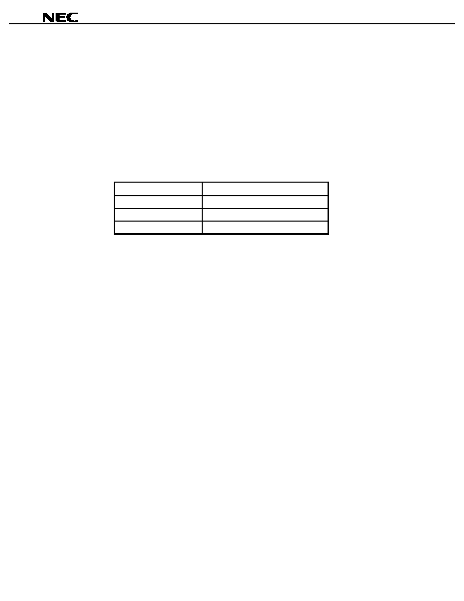
ORDERING INFORMATION
Part Number
Package
µ
PD77110GC-9EU
100-pin plastic TQFP (fine pitch) (14
◊
14 mm)
µ
PD77111GK-xxx-9EU
80-pin plastic TQFP (fine pitch) (12
◊
12 mm)
µ
PD77111F1-xxx-CN1
80-pin plastic fine-pitch BGA (9
◊
9 mm)
µ
PD77112GC-xxx-9EU
100-pin plastic TQFP (fine pitch) (14
◊
14 mm)
Remark xxx indicates ROM code suffix.

D
a
ta S
heet U
12801E
J4V
0
D
S
00
3
µ
µ
µ
µ
P
D
77110, 77111, 77112
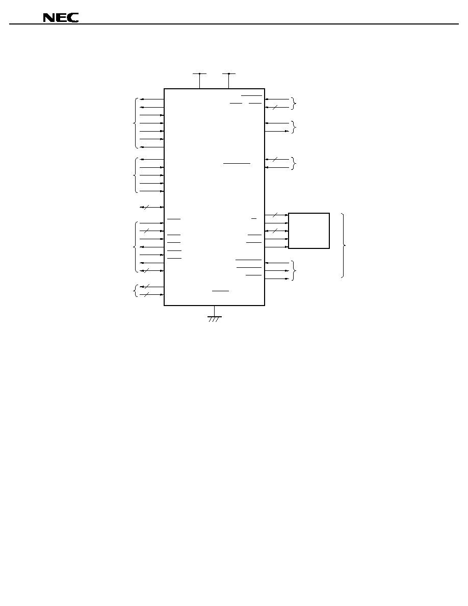
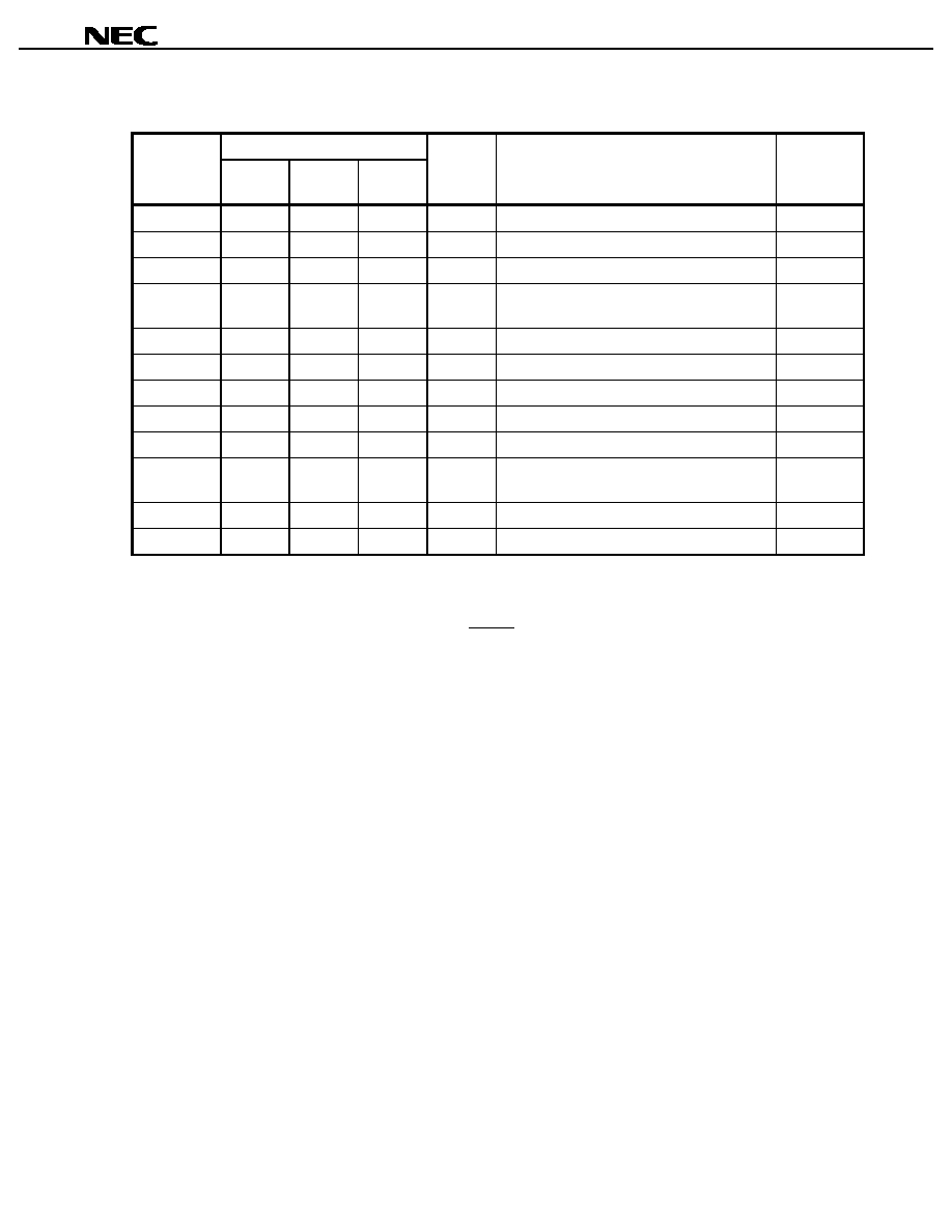
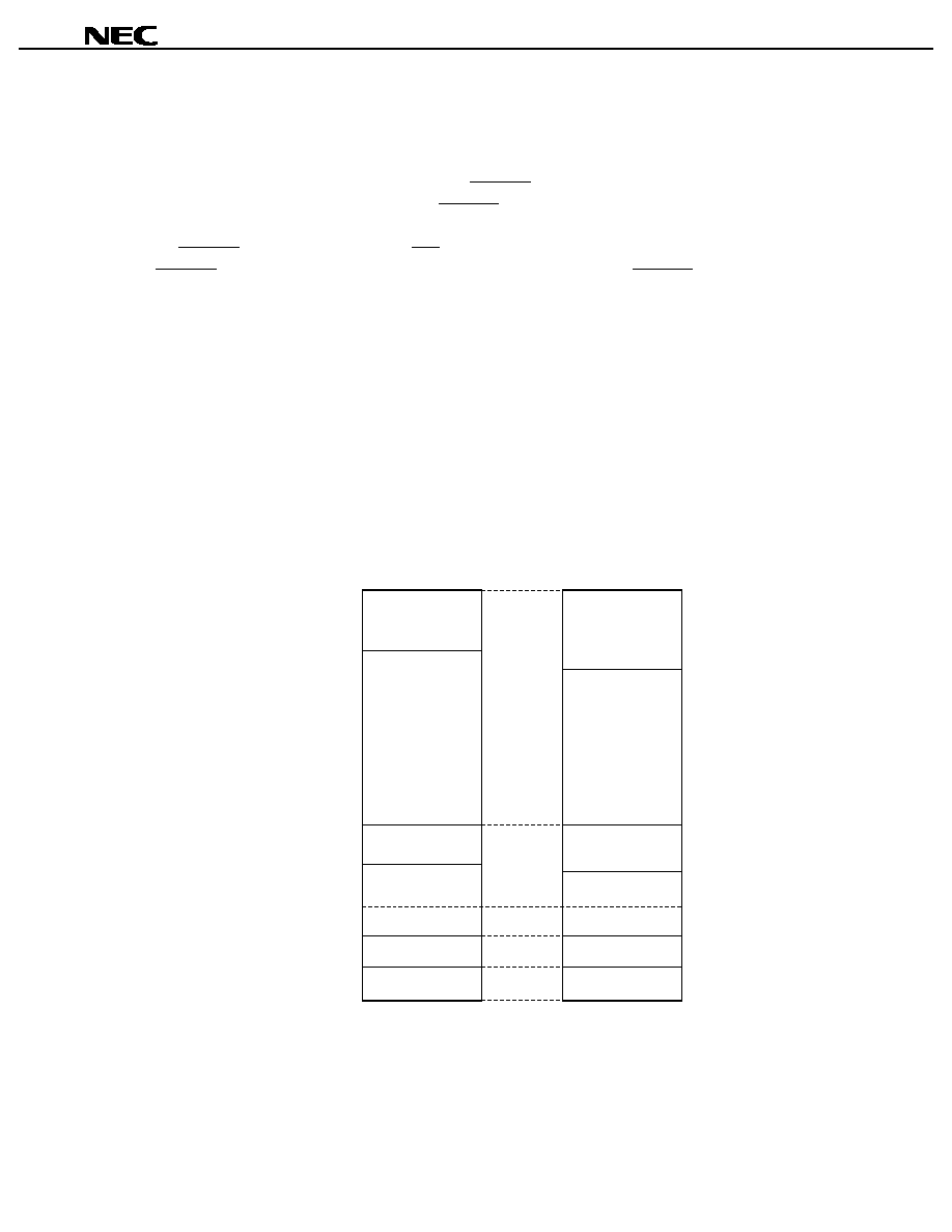
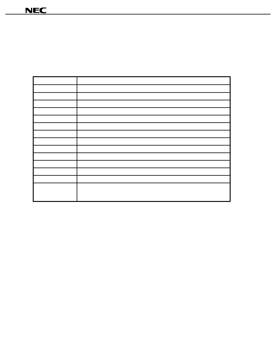
BLOCK DIAGRAM
Serial
I/O #1
Peripheral units
Data memory unit
Operation unit
Program
control unit
Serial
I/O #2
Port
Host I/O
X memory
data
addressing
unit
X memory
Y memory
Interrupt
control
Loop control
stack
PC stack
PLL
MPY
16
◊
16 + 40
40
ALU (40)
R0 - R7
X bus
Y bus
External memory
INT1 - INT4
Note 1
RESET
CLKOUT
CLKIN
WAKEUP
Note 1
PLL0 - PLL2
Note 2
Main bus
Wait
controller
IE
I/O
CPU control
Notes 1. The WAKEUP pin is multiplexed with the INT4 pin. With the PD77111 and 77112, the function of the WAKEUP pin can be
activated or deactivated by mask option. With the PD77110, this function is always valid.
2. These pins are provided only on the PD77110. The PLL0 and PLL1 pins are multiplexed with the P2 and P3 pins.
BSFT
Y memory
data
addressing
unit
Instruction
memory
µ
µ
µ
Data Sheet U12801EJ4V0DS00
4
µ
µ
µ
µ
PD77110, 77111, 77112
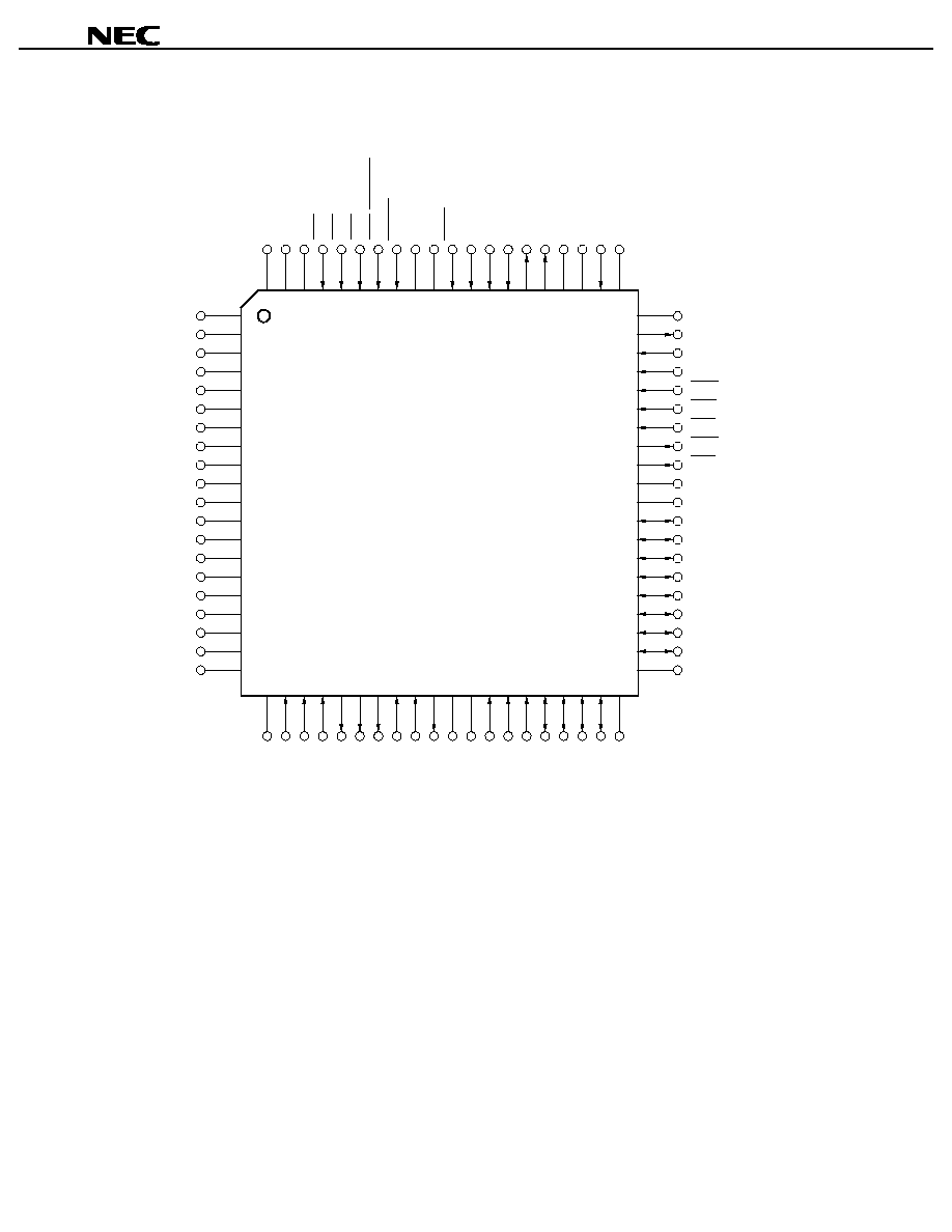
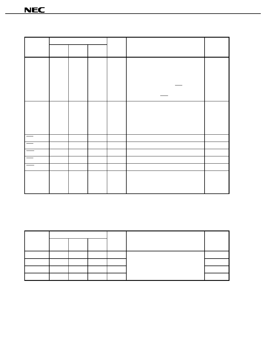
PIN CONFIGURATION
+2.5 V
+3 V
IV
DD
EV
DD
Reset, interrupt
System control
Data bus
control
Clock
External data
memory
Serial interface #1
Serial interface #2
Host interface
Port
For debugging
(4)
(4)
(3)
(15)
(16)
(2)
(4)
(2)
(8)
SO1
SORQ1
SOEN1
SCK1
SI1
SIEN1
SIAK1
RESET
INT1 - INT4
CLKIN
CLKOUT
PLL0 - PLL2
Note 1
WAKEUP
Note 2
DA0 - DA14
Note 3
X/Y
D0 - D15
MRD
MWR
HOLDRQ
HOLDAK
BSTB
SO2
SOEN2
SCK2
SI2
SIEN2
HCS
HA0, HA1
HRD
HRE
HWR
HWE
HD0 - HD7
TDO, TICE
TCK, TDI, TMS, TRST
P0 - P3
GND
Note 4
Notes 1. These pins are provided only on the
µ
PD77110.
2. With the
µ
PD77111 and 77112, the function of this pin can be activated or deactivated by mask option.
With the
µ
PD77110, this function is always valid.
3. DA14 is not provided on the
µ
PD77112.
4. An external data memory interface is not provided on the
µ
PD77111.
D
a
ta S
heet U
12801E
J4V
0
D
S
00
5
µ
µ
µ
µ
P
D
77110, 77111, 77112
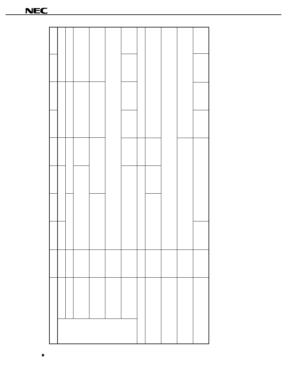
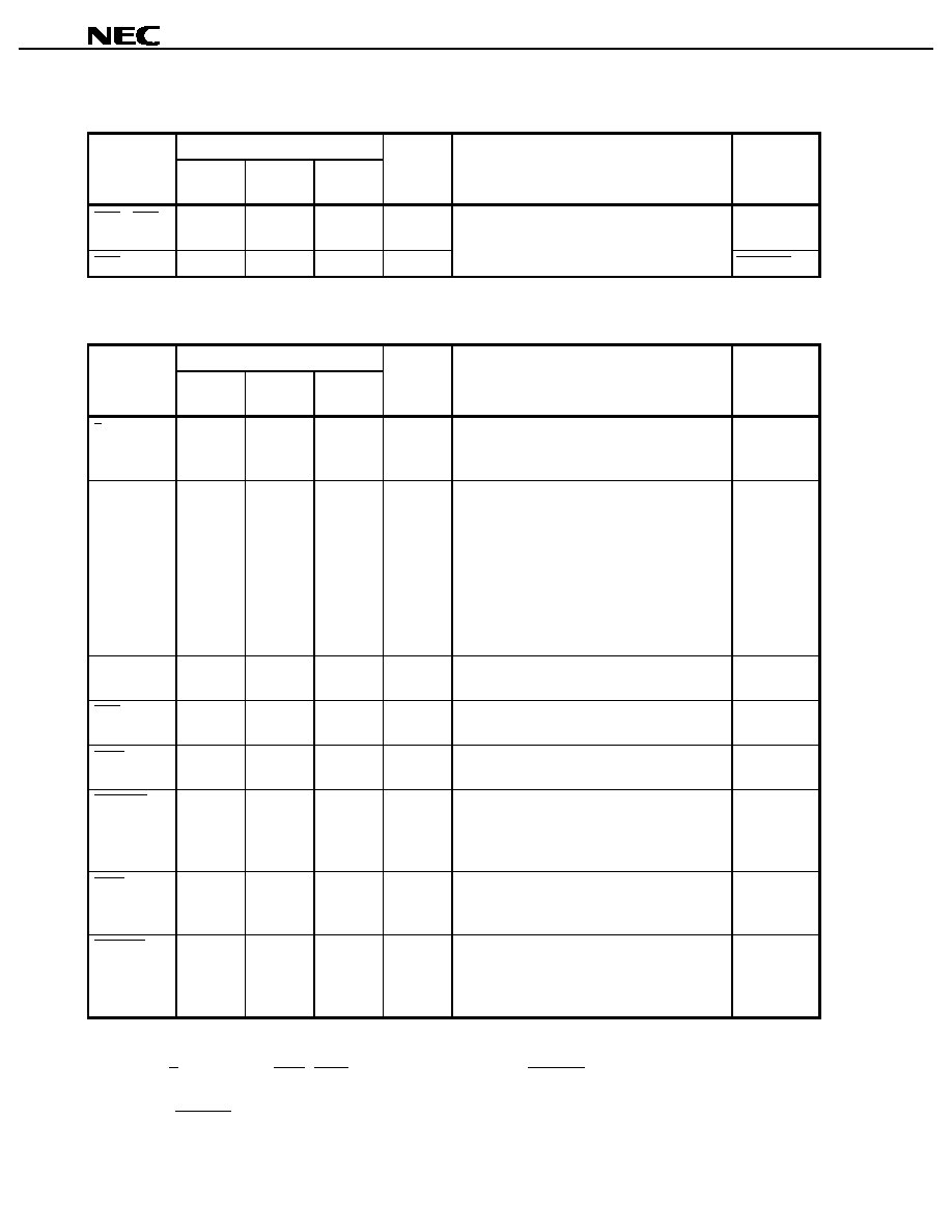
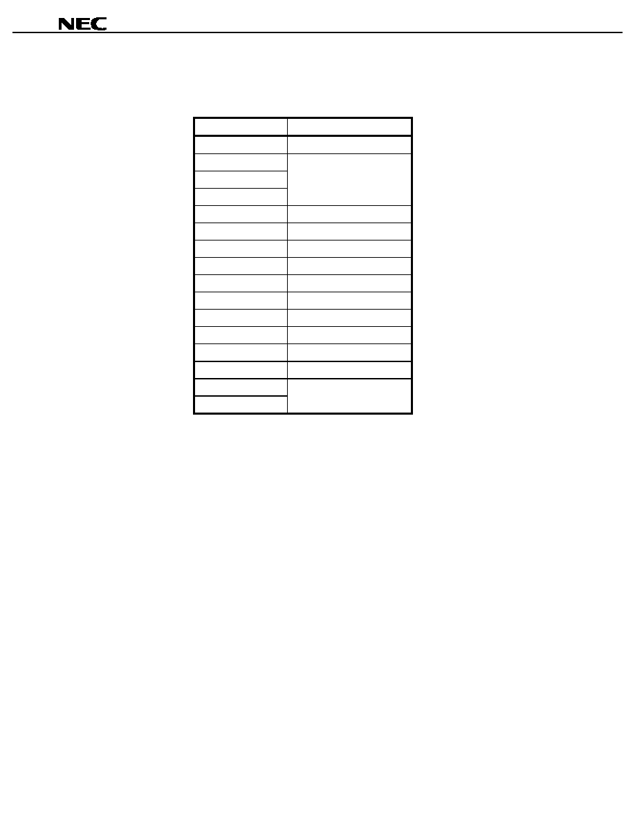
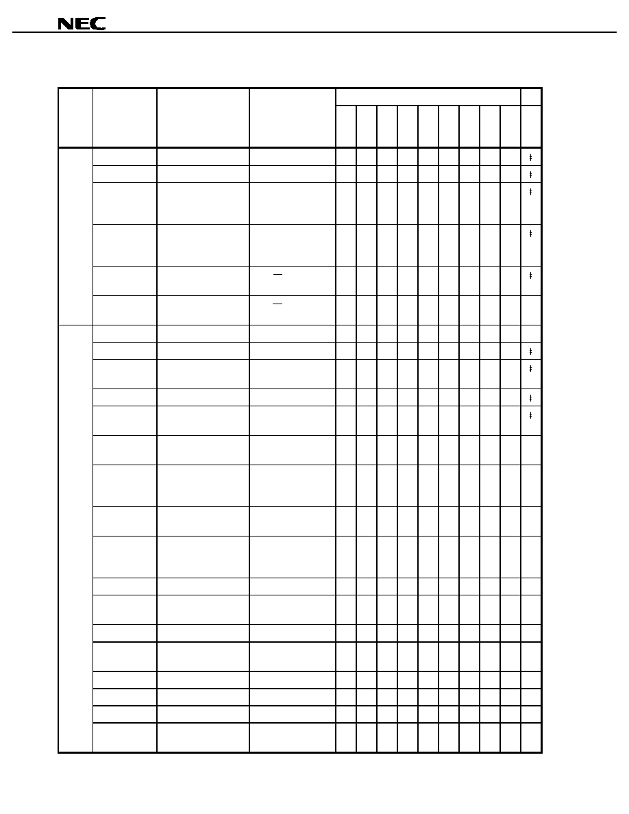
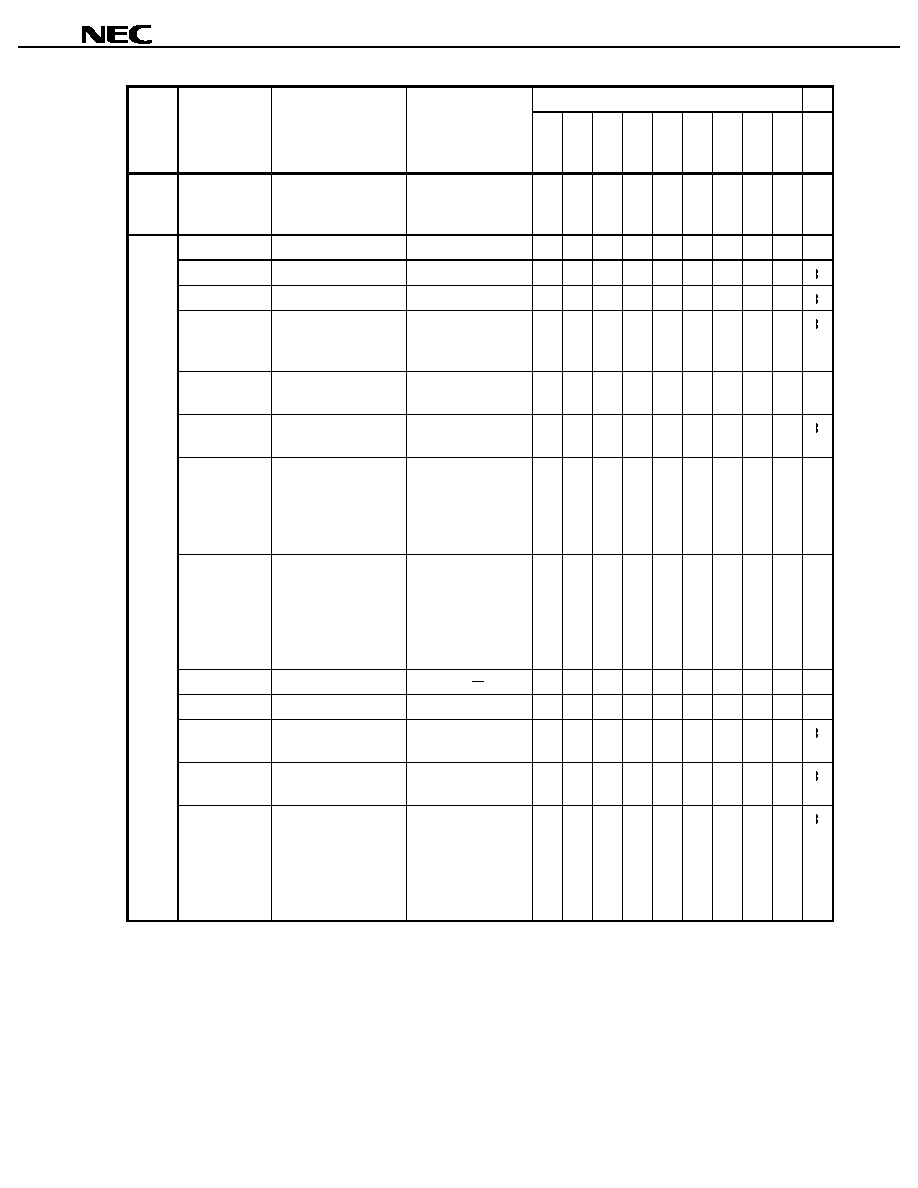
Item
PD77016
µ
µ
µ
µ
µ
µ
µ
PD77019
PD77018A
PD77019-013
PD77111
PD77112
µ
µ
PD77113
PD77114
Memory space
(words
◊
bits)
Instruction cycle (at maximum speed)
Multiple
Serial interface (two channels)
Supply voltage
Package
Internal instruction RAM
Internal instruction ROM
Data RAM
(X/Y memory)
Data ROM
(X/Y memory)
External data memory
(X/Y memory)
External instruction
memory
1.5K
◊
32
256
◊
32
4K
◊
32
1K
◊
32
24K
◊
32
None
None
31.75K
◊
32
2K
◊
16 each
3K
◊
16 each
3K
◊
16 each
None
12K
◊
16 each
16K
◊
16 each
48K
◊
32
5 V
3 V
DSP core: 2.5 V
I/O pins : 3 V
160-pin QFP
None
48K
◊
16 each
16K
◊
16 each
None
16K
◊
16 each
30 ns (33 MHz)
≠
100-pin TQFP
80-pin TQFP
80-pin FBGA
100-pin TQFP
100-pin TQFP
116-pin BGA
◊
1, 2, 3, 4, 8 (mask option)
Fixed to
◊
4
Integer of
◊
1 to 16 (mask option)
16.6 ns (60 MHz)
13.3 ns (75 MHz)
Channels 1 and 2
have same function.
Channel 1 has same function as PD77016. Channel 2 does not have SORQ2 and SIAK2 pins (for connection of codec).
µ
PD77110
35.5K
◊
32
24K
◊
16 each
32K
◊
16 each
15.3 ns (65 MHz)
Integer of
◊
1 to 8
(external pin)
None
3.5K
◊
32
48K
◊
32
16K
◊
16 each
32K
◊
16 each
None
8K
◊
16 each
80-pin FBGA
100-pin TQFP
DSP FUNCTION LIST
Data Sheet U12801EJ4V0DS00
6
µ
µ
µ
µ
PD77110, 77111, 77112
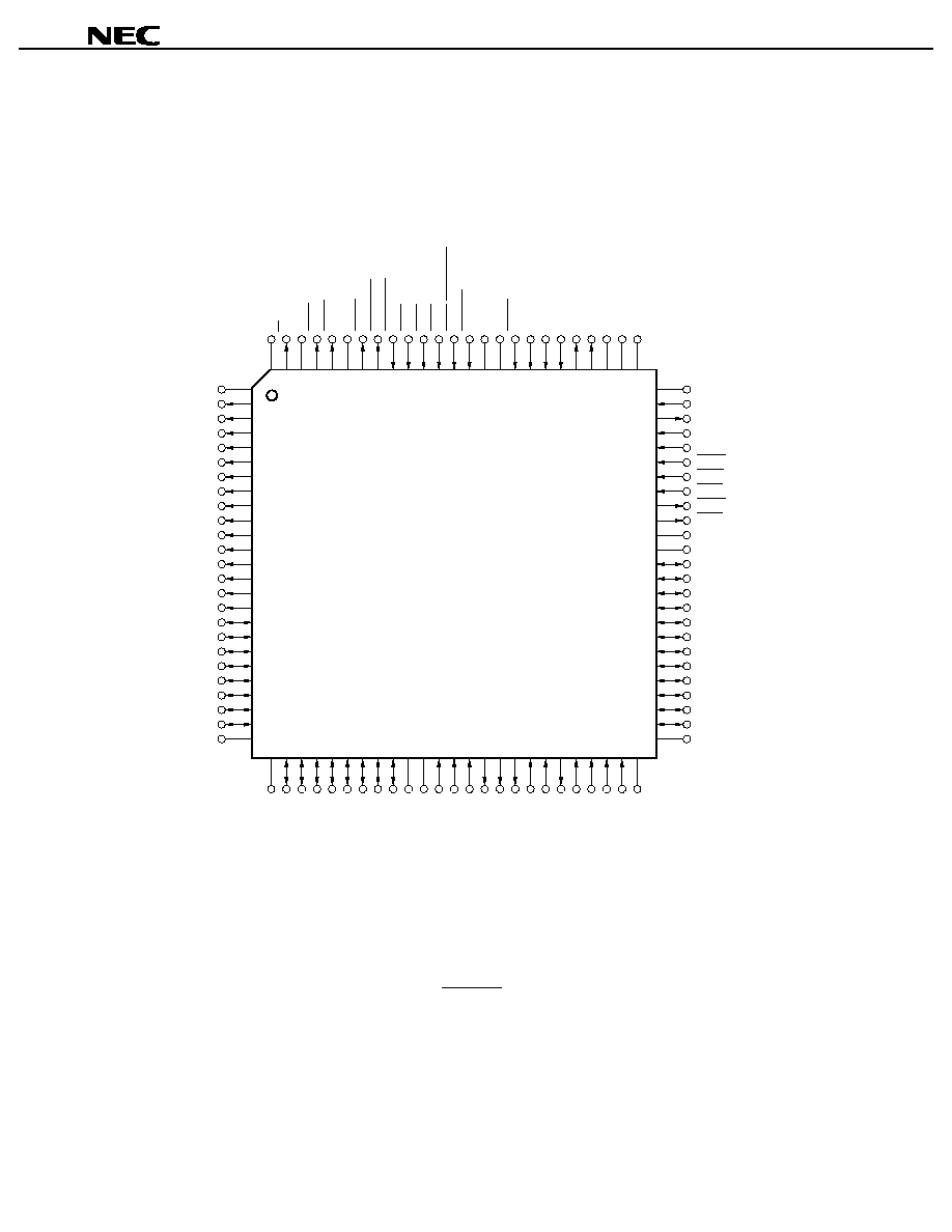
PIN CONFIGURATION
100-pin plastic TQFP (fine-pitch) (14
◊
◊
◊
◊
14 mm) (Top View)
µ
µ
µ
µ
PD77110GC-9EU
µ
µ
µ
µ
PD77112GC-xxx-9EU
1
2
3
4
5
6
7
8
9
10
11
12
13
14
15
16
17
18
19
20
21
22
23
24
25
75
74
73
72
71
70
69
68
67
66
65
64
63
62
61
60
59
58
57
56
55
54
53
52
51
GND
DA14/NC
Note 1
DA13
DA12
DA11
DA10
DA9
DA8
DA7
DA6
DA5
DA4
DA3
DA2
DA1
DA0
D15
D14
D13
D12
D11
D10
D9
D8
EV
DD
EV
DD
CLKIN
CLKOUT
HA1
HA0
HWR
HRD
HCS
HWE
HRE
GND
EV
DD
HD0
HD1
HD2
HD3
HD4
HD5
HD6
HD7
P0
P1
P2/PLL0
Note 4
P3/PLL1
Note 3
GND
EV
DD
X/Y
I.C.
MRD
MWR
NU
BSTB
HOLDAK
HOLDRQ
INT1
INT2
INT3
INT4/WAKEUP
Note 5
RESET
GND
IV
DD
TRST
TMS
TDI
TCK
TICE
TDO
GND
IV
DD
GND
GND
D7
D6
D5
D4
D3
D2
D1
D0
IV
DD
GND
SI1
SIEN1
SCK1
SIAK1
SO1
SORQ1
SOEN1
SOEN2
SO2
SCK2
SIEN2
SI2
PLL2/NC
Note 2
EV
DD
26 27 28 29 30 31 32 33 34 35 36 37 38 39 40 41 42 43 44 45 46 47 48 49 50
100 99 98 97 96 95 94 93 92 91 90 89 88 87 86 85 84 83 82 81 80 79 78 77 76
Notes 1. DA14 with
µ
PD77110, NC with
µ
PD77112
2. PLL2 with
µ
PD77110, NC with
µ
PD77112
3. P3 only for
µ
PD77112
4. P2 only for
µ
PD77112
5. With the
µ
PD77112, the function of the WAKEUP pin can be activated or deactivated by a mask
option.
Data Sheet U12801EJ4V0DS00
7
µ
µ
µ
µ
PD77110, 77111, 77112
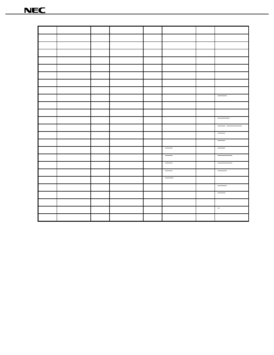
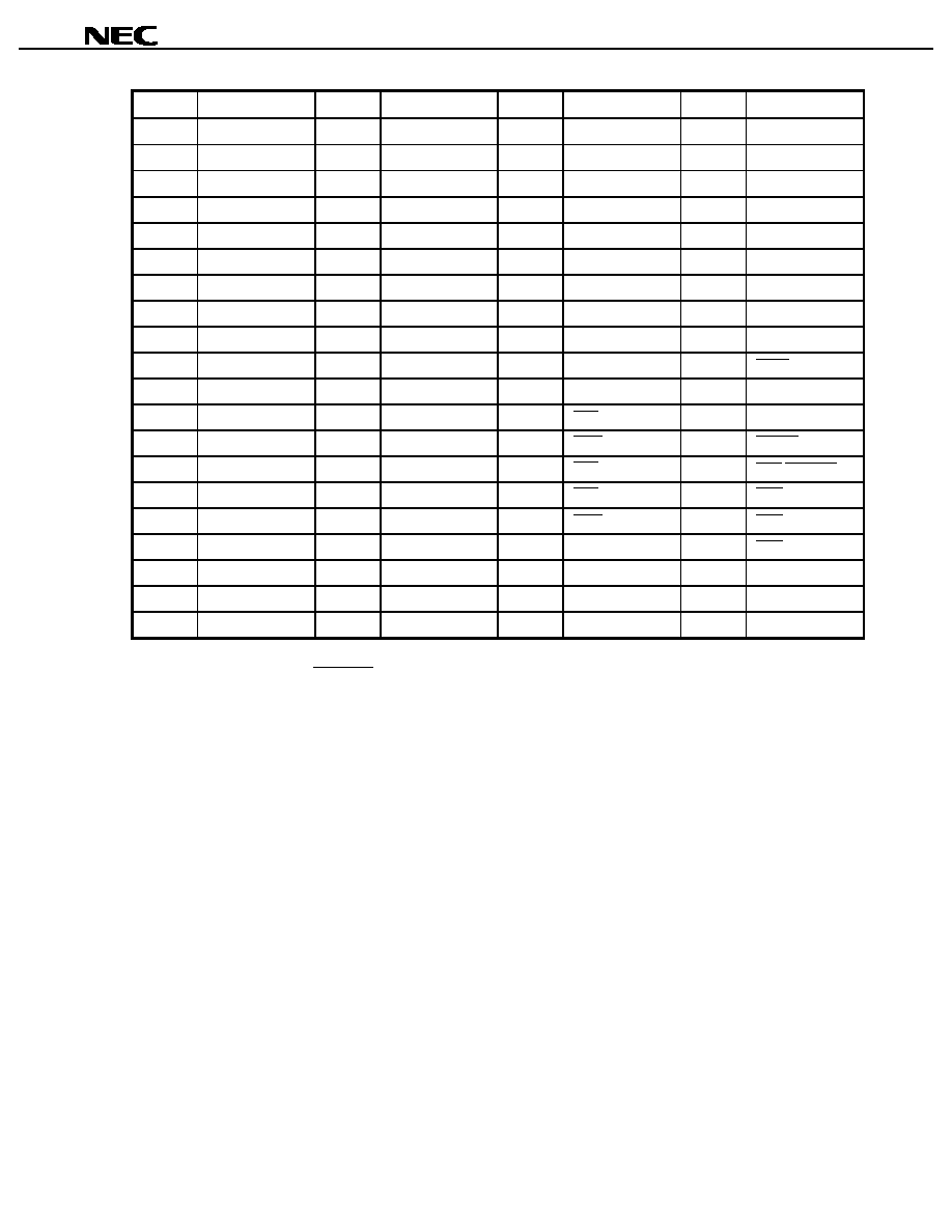
Pin No.
Pin Name
Pin No.
Pin Name
Pin No.
Pin Name
Pin No.
Pin Name
1
GND
26
GND
51
GND
76
GND
2
DA14/NC
27
D7
52
P3/PLL1
77
IV
DD
3
DA13
28
D6
53
P2/PLL0
78
GND
4
DA12
29
D5
54
P1
79
TDO
5
DA11
30
D4
55
P0
80
TICE
6
DA10
31
D3
56
HD7
81
TCK
7
DA9
32
D2
57
HD6
82
TD1
8
DA8
33
D1
58
HD5
83
TMS
9
DA7
34
D0
59
HD4
84
TRST
10
DA6
35
IV
DD
60
HD3
85
IV
DD
11
DA5
36
GND
61
HD2
86
GND
12
DA4
37
SI1
62
HD1
87
RESET
13
DA3
38
SIEN1
63
HD0
88
INT4/WAKEUP
14
DA2
39
SCK1
64
EV
DD
89
INT3
15
DA1
40
SIAK1
65
GND
90
INT2
16
DA0
41
SO1
66
HRE
91
INT1
17
D15
42
SORQ1
67
HWE
92
HOLDRQ
18
D14
43
SOEN1
68
HCS
93
HOLDAK
19
D13
44
SOEN2
69
HRD
94
BSTB
20
D12
45
SO2
70
HWR
95
NU
21
D11
46
SCK2
71
HA0
96
MWR
22
D10
47
SIEN2
72
HA1
97
MRD
23
D9
48
SI2
73
CLKOUT
98
I.C.
24
D8
49
PLL2/NC
74
CLKIN
99
X/Y
25
EV
DD
50
EV
DD
75
EV
DD
100
EV
DD
Data Sheet U12801EJ4V0DS00
8
µ
µ
µ
µ
PD77110, 77111, 77112
80-pin plastic TQFP (fine-pitch) (12
◊
◊
◊
◊
12 mm) (Top view)
µ
µ
µ
µ
PD77111GK-xxx-9EU
1
2
3
4
5
6
7
8
9
10
11
12
13
14
15
16
17
18
19
20
60
59
58
57
56
55
54
53
52
51
50
49
48
47
46
45
44
43
42
41
GND
NU
NU
NU
NU
NU
NU
NU
NU
EV
DD
GND
NU
NU
NU
NU
NU
NU
NU
NU
EV
DD
EV
DD
CLKOUT
HA1
HA0
HWR
HRD
HCS
HWE
HRE
GND
EV
DD
HD0
HD1
HD2
HD3
HD4
HD5
HD6
HD7
GND
21
22
23
24
25
26
27
28
29
30
31
32
33
34
35
36
37
38
39
40
80
79
78
77
76
75
74
73
72
71
70
69
68
67
66
65
64
63
62
61
GND
SI1
SIEN1
SCK1
SIAK1
SO1
SORQ1
SOEN1
SOEN2
SO2
IV
DD
GND
SCK2
SIEN2
SI2
P3
P2
P1
P0
EV
DD
EV
DD
NU
NU
INT1
INT2
INT3
INT4/WAKEUP
RESET
GND
IV
DD
TRST
TMS
TDI
TCK
TICE
TDO
GND
IV
DD
CLKIN
GND
Data Sheet U12801EJ4V0DS00
9
µ
µ
µ
µ
PD77110, 77111, 77112
Pin No.
Pin Name
Pin No.
Pin Name
Pin No.
Pin Name
Pin No.
Pin Name
1
GND
21
GND
41
GND
61
GND
2
NU
22
SI1
42
HD7
62
CLKIN
3
NU
23
SIEN1
43
HD6
63
IV
DD
4
NU
24
SCK1
44
HD5
64
GND
5
NU
25
SIAK1
45
HD4
65
TDO
6
NU
26
SO1
46
HD3
66
TICE
7
NU
27
SORQ1
47
HD2
67
TCK
8
NU
28
SOEN1
48
HD1
68
TDI
9
NU
29
SOEN2
49
HD0
69
TMS
10
EV
DD
30
SO2
50
EV
DD
70
TRST
11
GND
31
IV
DD
51
GND
71
IV
DD
12
NU
32
GND
52
HRE
72
GND
13
NU
33
SCK2
53
HWE
73
RESET
14
NU
34
SIEN2
54
HCS
74
INT4/WAKEUP
Note
15
NU
35
SI2
55
HRD
75
INT3
16
NU
36
P3
56
HWR
76
INT2
17
NU
37
P2
57
HA0
77
INT1
18
NU
38
P1
58
HA1
78
NU
19
NU
39
P0
59
CLKOUT
79
NU
20
EV
DD
40
EV
DD
60
EV
DD
80
EV
DD
Note The function of the WAKEUP pin can be activated or deactivated by a mask option.
Data Sheet U12801EJ4V0DS00
10
µ
µ
µ
µ
PD77110, 77111, 77112
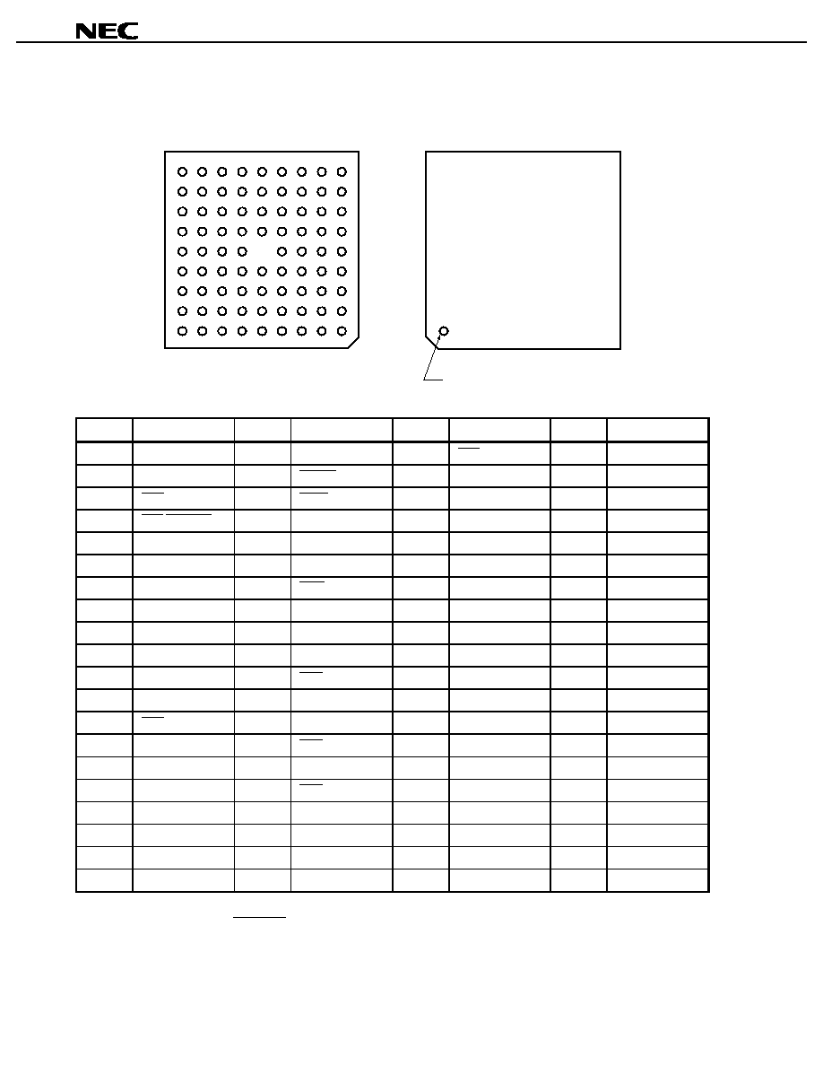
80-pin plastic fine-pitch BGA (9
◊
◊
◊
◊
9 mm)
µ
µ
µ
µ
PD77111F1-xxx-CN1
(Bottom View)
(Top View)
J
H
G
F
E
D
C
B
A
A
B
C
D
E
F
G
H
J
9
8
7
6
5
4
3
2
1
Index mark
Pin No.
Pin Name
Pin No.
Pin Name
Pin No.
Pin Name
Pin No.
Pin Name
A1
EV
DD
C3
NU
E6
HRE
G8
HD4
A2
NU
C4
RESET
E7
HD0
G9
HD5
A3
INT2
C5
TRST
E8
GND
H1
NU
A4
INT4/WAKEUP
Note
C6
TICE
E9
EV
DD
H2
NU
A5
IV
DD
C7
CLKIN
F1
NU
H3
SIEN1
A6
TCK
C8
HA0
F2
NU
H4
SOEN1
A7
IV
DD
C9
HWR
F3
NU
H5
GND
A8
GND
D1
NU
F4
SIAK1
H6
SI2
A9
EV
DD
D2
NU
F5
SOEN2
H7
P1
B1
NU
D3
NU
F6
P2
H8
GND
B2
GND
D4
INT1
F7
HD1
H9
HD7
B3
NU
D5
TMS
F8
HD3
J1
EV
DD
B4
INT3
D6
TDO
F9
HD2
J2
GND
B5
GND
D7
HCS
G1
NU
J3
SCK1
B6
TDI
D8
HRD
G2
NU
J4
SORQ1
B7
GND
D9
HWE
G3
SI1
J5
IV
DD
B8
CLKOUT
E1
EV
DD
G4
SO1
J6
SCK2
B9
HA1
E2
GND
G5
SO2
J7
P3
C1
NU
E3
NU
G6
SIEN2
J8
P0
C2
NU
E4
NU
G7
HD6
J9
EV
DD
Note The function of the WAKEUP pin can be activated or deactivated by a mask option.

Data Sheet U12801EJ4V0DS00
11
µ
µ
µ
µ
PD77110, 77111, 77112
PIN NAME
BSTB
: Bus Strobe
CLKIN
: Clock Input
CLKOUT
: Clock Output
D0 - D15
: 16-bit Data Bus
DA0 - DA14
: External Data Memory Address Bus
EV
DD
: Power Supply for I/O Pins
GND
: Ground
HA0, HA1
: Host Data Access
HCS
: Host Chip Select
HD0 - HD7
: Host Data Bus
HOLDAK
: Hold Acknowledge
HOLDRQ
: Hold Request
HRD
: Host Read
HRE
: Host Read Enable
HWE
: Host Write Enable
HWR
: Host Write
I.C.
: Internally Connected
INT1 - INT4
: Interrupt
IV
DD
: Power Supply for DSP Core
MRD
: Memory Read Output
MWR
: Memory Write Output
NC
: Non-Connection
NU
: Not Used
P0 - P3
: Port
PLL0 - PLL2
: PLL Multiple Rate Set
RESET
: Reset
SCK1, SCK2
: Serial Clock Input
SI1, SI2
: Serial Data Input
SIAK1
: Serial Input Acknowledge
SIEN1, SIEN2
: Serial Input Enable
SO1, SO2
: Serial Data Output
SOEN1, SOEN2 : Serial Output Enable
SORQ1
: Serial Output Request
TCK
: Test Clock Input
TDI
: Test Data Input
TDO
: Test Data Output
TICE
: Test In-Circuit Emulator
TMS
: Test Mode Select
TRST
: Test Reset
WAKEUP
: Wakeup from STOP Mode
X/Y
: X/Y Memory Select

Data Sheet U12801EJ4V0DS00
12
µ
µ
µ
µ
PD77110, 77111, 77112
CONTENTS
1. PIN FUNCTION .................................................................................................................................
13
1.1 Pin Function Description ..........................................................................................................
13
1.2 Connection of Unused Pins......................................................................................................
18
2. FUNCTION OUTLINE........................................................................................................................
20
2.1 Program Control Unit ................................................................................................................
20
2.2 Arithmetic Unit ...........................................................................................................................
21
2.3 Data Memory Unit ......................................................................................................................
22
2.4 Peripheral Units .........................................................................................................................
22
3. CLOCK GENERATOR ......................................................................................................................
23
4. RESET FUNCTION ...........................................................................................................................
23
4.1 Hardware Reset..........................................................................................................................
23
4.2 Initializing PLL ...........................................................................................................................
24
5. FUNCTIONS OF BOOT-UP ROM ...................................................................................................
24
5.1 Boot at Reset..............................................................................................................................
24
5.2 Reboot ........................................................................................................................................
25
5.3 Signature Operation ..................................................................................................................
26
6. STANDBY MODES ...........................................................................................................................
26
6.1 HALT Mode.................................................................................................................................
26
6.2 STOP Mode.................................................................................................................................
27
7. MEMORY MAP ..................................................................................................................................
27
7.1 Instruction Memory ...................................................................................................................
27
7.2 Data Memory ..............................................................................................................................
29
8. MASK OPTION..................................................................................................................................
30
8.1 Clock Control Options...............................................................................................................
30
8.2 WAKEUP Function.....................................................................................................................
31
8.3 Mask Option Equivalent Function of
µ
µ
µ
µ
PD77110 .....................................................................
31
9. INSTRUCTIONS .................................................................................................................................
33
9.1 Outline of Instructions ..............................................................................................................
33
9.2 Instruction Set and Operation ..................................................................................................
34
10. ELECTRICAL SPECIFICATIONS .....................................................................................................
40
11. PACKAGE ..........................................................................................................................................
72
12. RECOMMENDED SOLDERING CONDITIONS ...............................................................................
75
Data Sheet U12801EJ4V0DS00
13
µ
µ
µ
µ
PD77110, 77111, 77112
1. PIN FUNCTION
Because the pin numbers differ depending on the package, refer to the diagram of the package to be used.
1.1 Pin Function Description
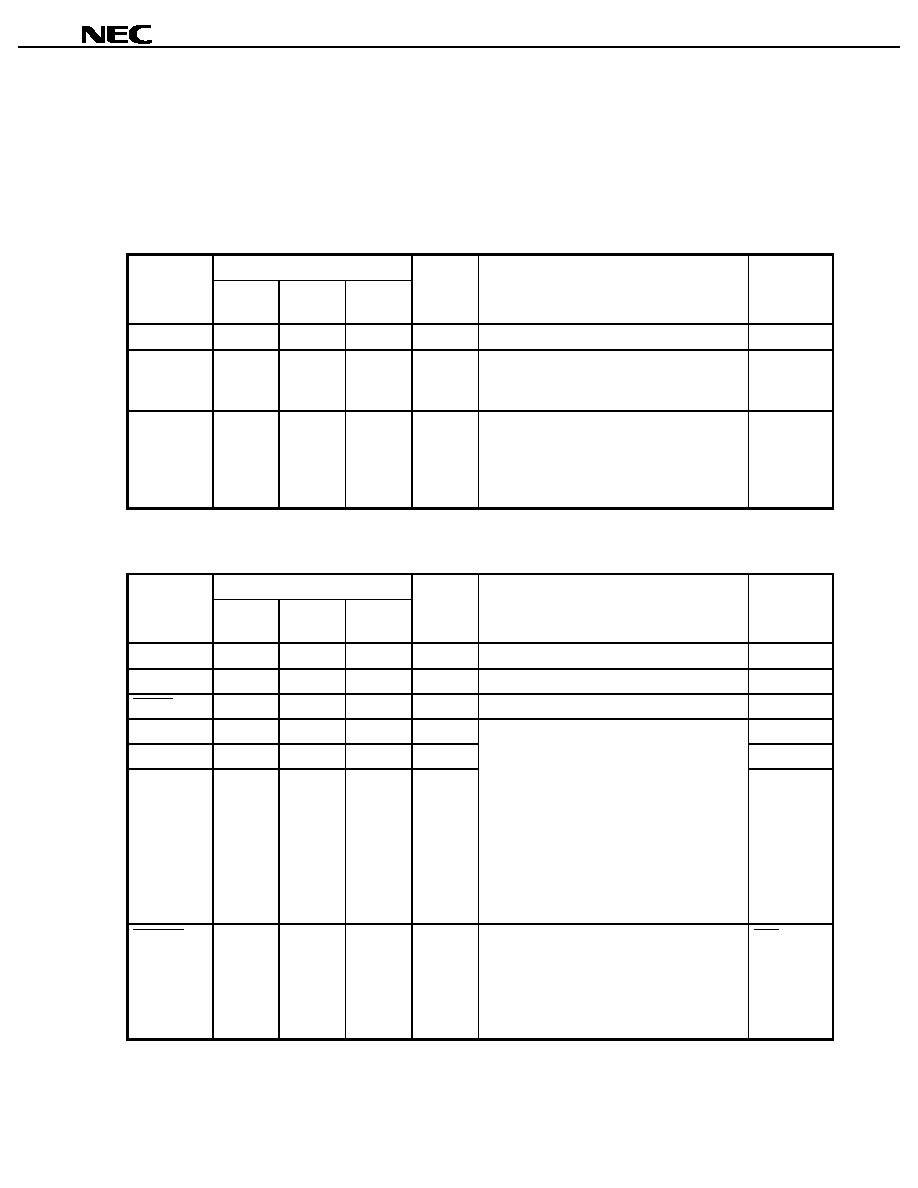
∑ Power supply
Pin No.
Pin Name
100-pin
TQFP
80-pin
TQFP
80-pin
FBGA
I/O
Function
Shared by:
IV
DD
35, 77, 85
31, 63, 71
A5, A7, J5
-
Power to DSP core (+2.5 V)
-
EV
DD
25, 50,
64, 75,
100
10, 20,
40, 50,
60, 80
A1, A9,
E1, E9,
J1, J9
-
Power to I/O pins (+3 V)
-
GND
1, 26, 36,
51, 65,
76, 78, 86
1, 11, 21,
32, 41,
51, 61,
64, 72
A8, B2,
B5, B7,
E2, E8,
H5, H8,
J2
-
Ground
-
∑ System control
Pin No.
Pin Name
100-pin
TQFP
80-pin
TQFP
80-pin
FBGA
I/O
Function
Shared by:
CLKIN
74
62
C7
Input
System clock input
-
CLKOUT
73
59
B8
Output
Internal system clock output
-
RESET
87
73
C4
Input
Internal system reset signal input
PLL0
53
-
-
Input
P2
PLL1
52
-
-
Input
P3
PLL2
49
-
-
Input
PLL multiple setting input (
µ
PD77110 only)
∑
Determines the PLL multiple at reset as
followings:
PLL2: PLL1: PLL0:
000 : Selects PLL multiple of
◊
1.
001 : Selects PLL multiple of
◊
2.
010 : Selects PLL multiple of
◊
3.
:
111 : Selects PLL multiple of
◊
8.
∑
These pins have no function on the
µ
PD77111 and 77112 .
-
WAKEUP
88
74
A4
Input
Stop mode release signal input.
∑
When this pin is asserted active, the stop
mode is released. The function of this pin
can be activated or deactivated by a mask
option.
∑
This pin is always valid on the
µ
PD77110 .
INT4
Data Sheet U12801EJ4V0DS00
14
µ
µ
µ
µ
PD77110, 77111, 77112
∑ Interrupt
Pin No.
Pin Name
100-pin
TQFP
80-pin
TQFP
80-pin
FBGA
I/O
Function
Shared by:
INT1 - INT3
91 - 89
77 - 75
D4, A3,
B4
Input
-
INT4
88
74
A4
Input
External maskable interrupt input.
∑
Detected at the falling edge.
WAKEUP
∑ External data memory interface
Pin No.
Pin Name
100-pin
TQFP
80-pin
TQFP
80-pin
FBGA
I/O
Function
Shared by:
X/Y
99
-
-
Output
(3S)
Memory select signal output.
0: Uses X memory.
1: Uses Y memory.
-
DA0 - DA14
16 - 2
-
-
Output
(3S)
Address bus of external data memory.
∑
Accesses the external memory.
∑
Continuously outputs the external memory
address accessed last when the external
memory is not being accessed. Kept low
(0x000) if the external memory is never
accessed after reset.
∑
DA14 is NC (no connection) and does not
function on the
µ
PD77112.
-
D0 - D15
34 - 27,
24 - 17
-
-
I/O
(3S)
16-bit data bus.
∑
Accesses the external memory.
-
MRD
97
-
-
Output
(3S)
Read output
∑
External memory read
-
MWR
96
-
-
Output
(3S)
Write output
∑
External memory write
-
HOLDRQ
92
-
-
Input
Hold request signal
∑
Input a low level to this pin when the external
device uses the external data memory bus of
the
µ
PD77110 and 77112.
-
BSTB
94
-
-
Output
Bus strobe signal
∑
This pin goes low when the
µ
PD77110 and
77112 use the external data memory bus.
-
HOLDAK
93
-
-
Output
Hold acknowledge signal
∑
This pin goes low when the external device
is enabled to use the external data memory
bus of the
µ
PD77110 and 77112.
-
Remark Pins marked "3S" under the heading "I/O" go into a high-impedance state in the following conditions:
X/Y, DA0-DA14, MRD, MWR: When the bus is released (HOLDAK = low level)
D0-D15: When the external data memory is not being accessed and when the bus is released
(HOLDAK = low level)
Data Sheet U12801EJ4V0DS00
15
µ
µ
µ
µ
PD77110, 77111, 77112
∑ Serial interface
Pin No.
Pin Name
100-pin
TQFP
80-pin
TQFP
80-pin
FBGA
I/O
Function
Shared by:
SCK1
39
24
J3
Input
Serial 1 clock input
-
SORQ1
42
27
J4
Output
Serial output 1 request
-
SOEN1
43
28
H4
Input
Serial output 1 enable
-
SO1
41
26
G4
Output
(3S)
Serial data output 1
-
SIEN1
38
23
H3
Input
Serial input 1 enable
-
SI1
37
22
G3
Input
Serial data input 1
-
SIAK1
40
25
F4
Output
Serial input 1 acknowledge
-
SCK2
46
33
J6
Input
Serial 2 clock input
-
SOEN2
44
29
F5
Input
Serial output 2 enable
-
SO2
45
30
G5
Output
(3S)
Serial data output 2
-
SIEN2
47
34
G6
Input
Serial input 2 enable
-
SI2
48
35
H6
Input
Serial data input 2
-
Remark The pins marked "3S" under the heading "I/O" go into a high-impedance state on completion of data
transfer and input of the hardware reset (RESET) signal.
Data Sheet U12801EJ4V0DS00
16
µ
µ
µ
µ
PD77110, 77111, 77112
∑ Host interface
Pin No.
Pin Name
100-pin
TQFP
80-pin
TQFP
80-pin
FBGA
I/O
Function
Shared by:
HA1
72
58
B9
Input
Specifies the register to be accessed by HD7
through HD0.
∑
1: Accesses the host interface status
register (HST).
∑
0: Accesses the host transmit data register
(HDT (out)) when read (HRD = 0), and
host receive data register (HDT (in))
when written (HWR = 0).
-
HA0
71
57
C8
Input
Specifies the register to be accessed by HD7
through HD0.
∑
1: Accesses bits 15 through 8 of HST, HDT
(in), and HDT (out).
∑
0: Accesses bits 7 through 0 of HST, HDT
(in), and HDT (out).
-
HCS
68
54
D7
Input
Chip select input
-
HRD
69
55
D8
Input
Host read input
-
HWR
70
56
C9
Input
Host write input
-
HRE
66
52
E6
Output
Host read enable output
-
HWE
67
53
D9
Output
Host write enable output
-
HD0 - HD7
63 - 56
49 - 42
E7, F7,
F9, F8,
G8, G9,
G7, H9
I/O
(3S)
8-bit host data bus
-
Remark The pins marked "3S" under the heading "I/O" go into a high-impedance state when the host interface is
not being accessed.
∑ I/O ports
Pin No.
Pin Name
100-pin
TQFP
80-pin
TQFP
80-pin
FBGA
I/O
Function
Shared by:
P0
55
39
J8
I/O
-
P1
54
38
H7
I/O
-
P2
53
37
F6
I/O
PLL0
Note
P3
52
36
J7
I/O
General-purpose I/O port
PLL1
Note
Note Only the
µ
PD77110. The
µ
PD77111 and 77112 have no multiplexed pins.
Data Sheet U12801EJ4V0DS00
17
µ
µ
µ
µ
PD77110, 77111, 77112
∑ Debugging interface
Pin No.
Pin Name
100-pin
TQFP
80-pin
TQFP
80-pin
FBGA
I/O
Function
Shared by:
TDO
79
65
D6
Output
-
TICE
80
66
C6
Output
-
TCK
81
67
A6
Input
-
TDI
82
68
B6
Input
-
TMS
83
69
D5
Input
-
TRST
84
70
C5
Input
For debugging
-
∑ Others
Pin No.
Pin Name
100-pin
TQFP
80-pin
TQFP
80-pin
FBGA
I/O
Function
Shared by:
I.C.
98
-
-
-
Internally connected. Leave this pin
unconnected.
-
NU
95
2, 3, 4, 5,
6, 7, 8, 9,
12, 13,
14, 15,
16, 17,
18, 19,
78, 79
A2, B1,
B3, C1,
C2, C3,
D1, D2,
D3, E3,
E4, F1,
F2, F3,
G1, G2,
H1, H2
-
No function pins. Connect these pins to EV
DD
.
-
NC
2, 49
-
-
-
No-connect pins (with
µ
PD77112). Leave these
pins unconnected.
-
Caution If any signal is input to these pins or if an attempt is made to read these pins, the normal
operation of the
µ
µ
µ
µ
PD77110, 77111, and 77112 is not guaranteed.
Data Sheet U12801EJ4V0DS00
18
µ
µ
µ
µ
PD77110, 77111, 77112
1.2 Connection of Unused Pins
1.2.1 Connection of Function Pins
When mounting, connect unused pins as follows:
Pin
I/O
Recommended Connection
INT1 - INT4
Input
Connect to EV
DD
.
X/Y
Output
DA0 - DA14
Output
Leave unconnected.
D0 - D15
Note 1
I/O
Connect to EV
DD
via pull-up resistor, or connect to GND via pull-down resistor.
MRD, MWR
Output
Leave unconnected.
HOLDRQ
Input
Connect to EV
DD
.
BSTB, HOLDAK
Output
Leave unconnected.
SCK1, SCK2
Input
SI1, SI2
Input
Connect to EV
DD
or GND.
SIEN1, SIEN2
Input
SOEN1, SOEN2
Input
Connect to GND.
SORQ1
Output
SO1, SO2
Output
SIAK1
Output
Leave unconnected.
HA0, HA1
Input
Connect to EV
DD
or GND.
HCS, HRD, HWR
Input
Connect to EV
DD
.
HRE, HWE
Output
Leave unconnected.
HD0 - HD7
Note 2
I/O
P0 - P3
I/O
Connect to EV
DD
via pull-up resistor, or connect to GND via pull-down resistor.
TCK
Input
Connect to GND via pull-down resistor.
TDO, TICE
Output
Leave unconnected.
TMS, TDI
Input
Leave unconnected. (internally pulled up).
TRST
Input
Leave unconnected. (internally pulled down).
CLKOUT
Output
Leave unconnected.
Notes 1. These pins may be left unconnected if the external data memory is not accessed in the program.
However, connect these pins as recommended in the halt and stop modes when the power
consumption must be lowered.
2. These pins may be left unconnected if HCS, HRD, and HWR are fixed to the high level.
However, connect these pins as recommended in the halt and stop modes when the power
consumption must be lowered.

Data Sheet U12801EJ4V0DS00
19
µ
µ
µ
µ
PD77110, 77111, 77112
1.2.2 Connection of no-function pins
Pin
I/O
Recommended Connection
I.C.
-
Leave unconnected.
NU
-
Connect to EV
DD
.
NC
-
Leave unconnected.

Data Sheet U12801EJ4V0DS00
20
µ
µ
µ
µ
PD77110, 77111, 77112
2. FUNCTION OUTLINE
2.1 Program Control Unit
This unit is used to execute instructions, and control branching, loops, interrupts, the clock, and the standby mode
of the DSP.
2.1.1 CPU control
A three-stage pipeline architecture is employed and almost all the instructions, except some instructions such as
branch instructions, are executed in one system clock.
2.1.2 Interrupt control
Interrupt requests input from external pins (INT1 through INT4) or generated by the internal peripherals (serial
interface and host interface) are serviced. The interrupt of each interrupt source can be enabled or disabled.
Multiple interrupts are also supported.
2.1.3 Loop control task
A loop function without any hardware overhead is provided. A loop stack with four levels is provided to support
multiple loops.
2.1.4 PC stack
A 15-level PC stack that stores the program counter supports multiple interrupts and subroutine calls.
2.1.5 PLL
A PLL is provided as a clock generator that can multiply or divide an external clock input to supply an operating
clock to the DSP. The multiplication and division ratio are set as follows:
∑
µ
PD77110: A multiple of
◊
1 to
◊
8 is specified by an external pin (division ratio is fixed).
∑
µ
PD77111 and 77112: A multiple of
◊
1 to
◊
16 or a division ratio of 1/1 to 1/16 can be set by a mask option.
Two standby modes are available for lowering the power consumption while the DSP is not in use.
∑
HALT mode : Set by execution of the HALT instruction. The current consumption drops to several mA. The
normal operation mode is recovered by an interrupt or hardware reset.
∑
STOP mode: Set by execution of the STOP instruction. The current consumption drops to several 10
µ
A. The
normal operation mode is recovered by hardware reset or WAKEUP pin
Note
.
Note If the WAKEUP function is activated by mask option
2.1.6 Instruction memory
The capacity and type of the memory differ depending on the model of the DSP.
64 words of the instruction RAM are allocated to interrupt vectors.
A boot-up ROM that boots up the instruction RAM is provided, and the instruction RAM can be initialized or
rewritten by self boot (boot from the internal data ROM or external data space) or host boot (boot via host interface).
∑
µ
PD77110: 35.5K-word RAM
∑
µ
PD77111, 77112: 1K-word RAM and 31.75K-word ROM

Data Sheet U12801EJ4V0DS00
21
µ
µ
µ
µ
PD77110, 77111, 77112
2.2 Arithmetic Unit
This unit performs multiplication, addition, logical operations, and shift, and consists of a 40-bit multiply
accumulator, 40-bit data ALU, 40-bit barrel shifter, and eight 40-bit general-purpose registers.
2.2.1 General-purpose registers (R0 through R7)
These eight 40-bit registers are used to input/output data for arithmetic operations, and load or store data from/to
data memory.
A general-purpose register (R0 to R7) is made up of three parts: R0L through R7L (bits 15 through 0), R0H
through R7H (bits 31 through 16), and R0E through R7E (bits 39 through 32). Depending on the type of operation,
RnL, RnH, and RnE are used as one register or in different combinations.
2.2.2 Multiply accumulator (MAC)
The MAC multiplies two 16-bit values, and adds or subtracts the multiplication result from one 40-bit value, and
outputs a 40-bit value.
The MAC is provided with a shifter (MSFT: MAC ShiFTer) at the stage preceding the input stage. This shifter can
arithmetically shift the 40-bit value to be added to or subtracted from the multiplication result 1 or 16 bits to the right .
2.2.3 Arithmetic logic unit (ALU)
This unit inputs one or two 40-bit values, executes an arithmetic or logical operation, and outputs a 40-bit value.
2.2.4 Barrel shifter (BSFT: Barrel ShiFTer)
The barrel shifter inputs a 40-bit value, shifts it to the left or right by any number of bits, and outputs a 40-bit value.
The data may be arithmetically shifted to the right shifted to the right, in which case the data is sign-extended, or
logically shifted to the right, in which case 0 is inserted from the MSB.

Data Sheet U12801EJ4V0DS00
22
µ
µ
µ
µ
PD77110, 77111, 77112
2.3 Data Memory Unit
The data memory unit consists of two banks of data memory and two data addressing units.
2.3.1 Data memory
The capacity and type of the memory differ depending on the model of the DSP. All DSPs have two banks of data
memory (X data memory and Y data memory). A 64-word peripheral area is assigned in the data memory space.
∑
µ
PD77110: RAM of 24K words
◊
2 banks
∑
µ
PD77111, 77112: RAM of 3K words
◊
2 banks and ROM of 16K words
◊
2 banks
In addition, some models have an external data memory interface so that the external memory can be expanded.
∑
µ
PD77110: External data memory of 32K words
◊
2 banks
∑
µ
PD77112: External data memory of 16K words
◊
2 banks
2.3.2 Data addressing unit
An independent data addressing unit is provided for each of the X data memory and Y data memory spaces.
Each data addressing unit has four data pointers (DPn), four index registers (DNn), one modulo register (DMX or
DMY), and an address ALU.
2.4 Peripheral Units
A serial interface, host interface, general-purpose I/O port, and wait cycle register are provided. All these internal
peripherals are mapped to the X data memory and Y data memory spaces, and are accessed from program as
memory-mapped I/Os.
2.4.1 Serial interface (SIO)
Two serial interfaces are provided. These serial interfaces have the following features:
∑
Serial clock : Supplied from external source to each interface. The same clock is used for input and output
on the interface.
∑
Frame length: 8 or 16 bits, and MSB or LSB first selectable for each interface and input or output
∑
Handshake : Handshaking with external devices is implemented with a dedicated status signal. With the
internal units, polling, wait, or interrupt are used.
2.4.2 Host interface (HIO)
This is an 8-bit parallel port that inputs data from or outputs data to an external host CPU or DMA controller. In
the DSP, a 16-bit register is mapped to memory for input data, output data, and status. Handshaking with an external
device is implemented by using a dedicated status signal. Handshaking with internal units is achieved by means of
polling, wait, or interrupts.
2.4.3 General-purpose I/O port (PIO)
This is a 4-bit I/O port that can be set in the input or output mode in 1-bit units.
Data Sheet U12801EJ4V0DS00
23
µ
µ
µ
µ
PD77110, 77111, 77112
2.4.4 Wait cycle register
The number of wait cycles to be inserted when the external data memory area is accessed can be specified in
advance by using a register (DWTR)
Note
. The number of wait cycles that can be set is 1, 3, or 7.
Note This function is not available on the
µ
PD77111 because this DSP does not have an external data area.
3. CLOCK GENERATOR
The clock generator generates an internal system clock based on the external clock input from the CLKIN pin and
supplies the generated clock to the internal units of the DSP.
For details of how to set the PLL multiple, refer to 4.2 Initializing PLL, 8.1 Clock Control Options, and 8.3.1
Settings related to clock control.
Stop mode
PLL control circuit
Output divider
Halt divider
Halt mode
Internal
system clock
◊
m
CLKOUT
CLKIN
˜
n
˜
l
4. RESET FUNCTION
When a low level of a specified width is input to the RESET pin, the device is initialized.
4.1 Hardware Reset
If the RESET pin is asserted active (low level) for a specified period, the internal circuitry of the DSP is initialized.
If the RESET pin is then deasserted inactive (high level), boot processing of the instruction RAM is performed
according to the status of the port pins (P0 and P1). After boot processing, processing is executed starting from the
instruction at address 0x200 of instruction memory (reset entry).
On power application, the RESET pin must be asserted active (low level) after 4 input clocks have been input with
the RESET pin in the inactive status (high level), after the supply voltage has reached the level of the operating
voltage. In other words, no power-ON reset function is available. On power application, the PLL must be initialized.
Data Sheet U12801EJ4V0DS00
24
µ
µ
µ
µ
PD77110, 77111, 77112
4.2 Initializing PLL
Initializing the PLL starts from the 1024th input clock after the RESET pin has been asserted active (low level).
Initialization takes 1024 clocks and it takes the PLL 100
µ
s to be locked.
After that, the DSP operates with the set value of the PLL specified by a mask option (
µ
PD77111 or 77112) or an
external pin (
µ
PD77110) when the RESET pin is deasserted inactive (high level).
After initializing the PLL, be sure to execute boot-up processing to re-initialize the internal RAM. To initialize the
PLL, the internal memory contents and register status of the DSP are not retained.
If the RESET pin is deasserted inactive before the PLL initialization mode is set, the DSP is normally reset (the
PLL is not initialized).
CLKIN
RESET
PLL initialization
mode
1024
1
2048
PLL lock time
Approx. 100 s
PLL initialization
(internal status)
µ
Caution Do not deassert the RESET signal inactive in the PLL initialization mode and during PLL lock
period.
5. FUNCTIONS OF BOOT-UP ROM
To rewrite the contents of the instruction memory on power application or from program, boot up the instruction
RAM by using the internal boot-up ROM.
The
µ
PD77110 has a function to verify the contents of the internal instruction RAM in the boot-up ROM.
5.1 Boot at Reset
After hardware reset has been cleared, the boot program first reads the general-purpose I/O ports P0 and P1 and,
depending on their bit pattern, determines the boot mode (self boot or host boot). After boot processing, processing
is executed starting from the instruction at address 0x200 (reset entry) of the instruction memory.
The pins (P0 and P1) that specify the boot mode must be kept stable for the duration of 3 clocks before and for
the duration of 12 clocks after reset has been cleared (the clock is input from CLKIN).
P1
P0
Boot Mode
0
0
Does not execute boot but branches to address 0x200
Note
.
0
1
Executes host boot and then branches to address 0x200.
1
1
Executes self boot and then branches to address 0x200.
1
0
Setting prohibited
Note This setting is used when the DSP must be reset to recover from the standby mode after reset boot has
been executed once.
Data Sheet U12801EJ4V0DS00
25
µ
µ
µ
µ
PD77110, 77111, 77112
5.1.1 Self boot
The boot-up ROM transfers the instruction code stored in the data memory space to the instruction RAM, based
on the boot parameter written to address 0x4000 of the Y data memory. Generally, with a mask ROM model
(
µ
PD77111 or 77112), this function is implemented by storing the instructions to be booted in the data ROM.
In addition, the instructions to be booted can be also stored in an external data area in the form of flash ROM, and
self boot can be executed from this external data area.
With the
µ
PD77110, the value of address 0x4000 of the Y data memory is undefined on power application,
because this address is in RAM. Therefore, with the
µ
PD77110, the self boot mode cannot be selected on power
application, and host boot must be executed. This also applies when the PLL is initialized. By writing a boot
parameter to address 0x4000 or those that follow of the Y data memory, self boot can be executed when the RESET
signal is subsequently input (except the reset that initializes the PLL). In this case, however, the instructions to be
booted are only those at address 0x0200 through 0x0FFF of the instruction RAM.
5.1.2 Host boot
In this boot mode, a boot parameter and instruction code are obtained via the host interface, and transferred to the
instruction RAM.
With the
µ
PD77110, the host boot mode is used on power application. The boot instruction area is the instruction
RAM from addresses 0x0200 through 0x0FFF. To boot up the instruction RAM from 0x4000 through 0xBFFF, host
reboot is used.
5.2 Reboot
By calling the next reboot entry from the program, the contents of the instruction RAM can be rewritten. In
particular, the
µ
PD77110 has a reboot function that boots up the instruction RAM from 0x4000 through 0xBFFF.
Reboot Mode
Entry Address
Word reboot
0x2
X memory
Byte reboot
0x4
Word reboot
0x1
Self boot
Y memory
Byte reboot
0x3
Host boot
Host reboot
0x6 (
µ
PD77110)
0x5 (
µ
PD77111, 77112)
5.2.1 Self reboot
The instruction codes stored in the data memory are transferred to the instruction RAM.
This boot mode cannot be used with the
µ
PD77110.
Set the following parameters and call the entry address of the corresponding reboot mode to execute self reboot.
∑
R7L : Number of instruction steps for rebooting
∑
DP3: First address of X memory in which instruction codes are stored (in the case of reboot from X memory),
or first address of the instruction memory to be loaded (in the case of reboot from Y memory)
∑
DP7: First address of instruction memory to be loaded (in the case of reboot from X memory), or first address
of X memory in which instruction codes are stored (in the case of reboot from Y memory)

Data Sheet U12801EJ4V0DS00
26
µ
µ
µ
µ
PD77110, 77111, 77112
5.2.2 Host reboot
An instruction code is obtained via the host interface and transferred to the instruction RAM.
With the
µ
PD77110, the host reboot mode is used to boot up the instruction RAM from addresses 0x4000 through
0xBFFF. Areas 0x0200 through 0x0FFF and 0x4000 through 0xBFFF cannot be rebooted all at once.
The entry address of the
µ
PD77110 is 0x6, and that of the
µ
PD77111 and 77112 is 0x5. Host reboot is executed
by calling this address after setting the following parameter:
∑
R7L : Number of instruction steps for rebooting
∑
DP3: First address of instruction memory to be loaded
5.3 Signature Operation
The
µ
PD77110 has a signature operation function so that the contents of the internal instruction RAM can be
verified. The signature operation performs a specific arithmetic operation on the data in the instruction RAM booted
up, and returns the result to a register. Perform the signature operation in advance on the device when it is operating
normally, and repeat the signature operation later to check whether the data in RAM is correct by comparing the
operation result with the previous result. If the results are identical, there is no problem.
The entry address is 0x9. Execute the operation by calling this address after setting the following parameter.
Note that the operation cannot be performed on the areas 0x0200 through 0x0FFF and 0x4000 through 0xBFFF at
the same time. The operation result is stored in register R7.
∑
R7L: Number of instruction steps for operation
∑
DP3: First address of instruction memory for operation
6. STANDBY MODES
Two standby modes are available. By executing the corresponding instruction, each mode is set and the power
consumption can be reduced.
6.1 HALT Mode
To set this mode, execute the HALT instruction. In this mode, functions other than clock circuit and PLL are
stopped to reduce the current consumption.
To release the HALT mode, use an interrupt or hardware reset. When releasing the HALT mode using an
interrupt, the contents of the internal registers and memory are retained. It takes several 10 system clocks to release
the HALT mode when the HALT mode is released using an interrupt.
In the HALT Mode, the clock circuit of the
µ
PD77111 family supplies the following clock as the internal system
clock. The clock output from the CLKOUT pin is as follows.
The clock output from the CLKOUT pin, however, has a high-level width that is equivalent to 1 cycle of the normal
operation (i.e., the duty factor is not 50%).
∑
µ
PD77110: 1/8 of internal system clock
∑
µ
PD77111, 77112: 1/l of internal system clock (l = integer from 1 to 16, specified by mask option)
Data Sheet U12801EJ4V0DS00
27
µ
µ
µ
µ
PD77110, 77111, 77112
6.2 STOP Mode
To set this mode, execute the STOP instruction. In this mode, all the functions, including the clock circuit and
PLL, are stopped and the power consumption is minimized with only leakage current flowing.
To release the STOP mode, use hardware reset or WAKEUP pin.
When releasing the STOP mode by using the WAKEUP pin, the contents of the internal registers and memory are
retained, but it takes several 100
µ
s to release the mode.
The WAKEUP pin is multiplexed with the INT4 pin. Usually, this pin functions as an interrupt pin, but functions as
the WAKEUP pin when it is asserted active in the STOP mode. Whether the WAKEUP pin is used to release the
STOP mode is selected by mask option. For details, refer to 8.2 WAKEUP Function and 8.3.2 WAKEUP function.
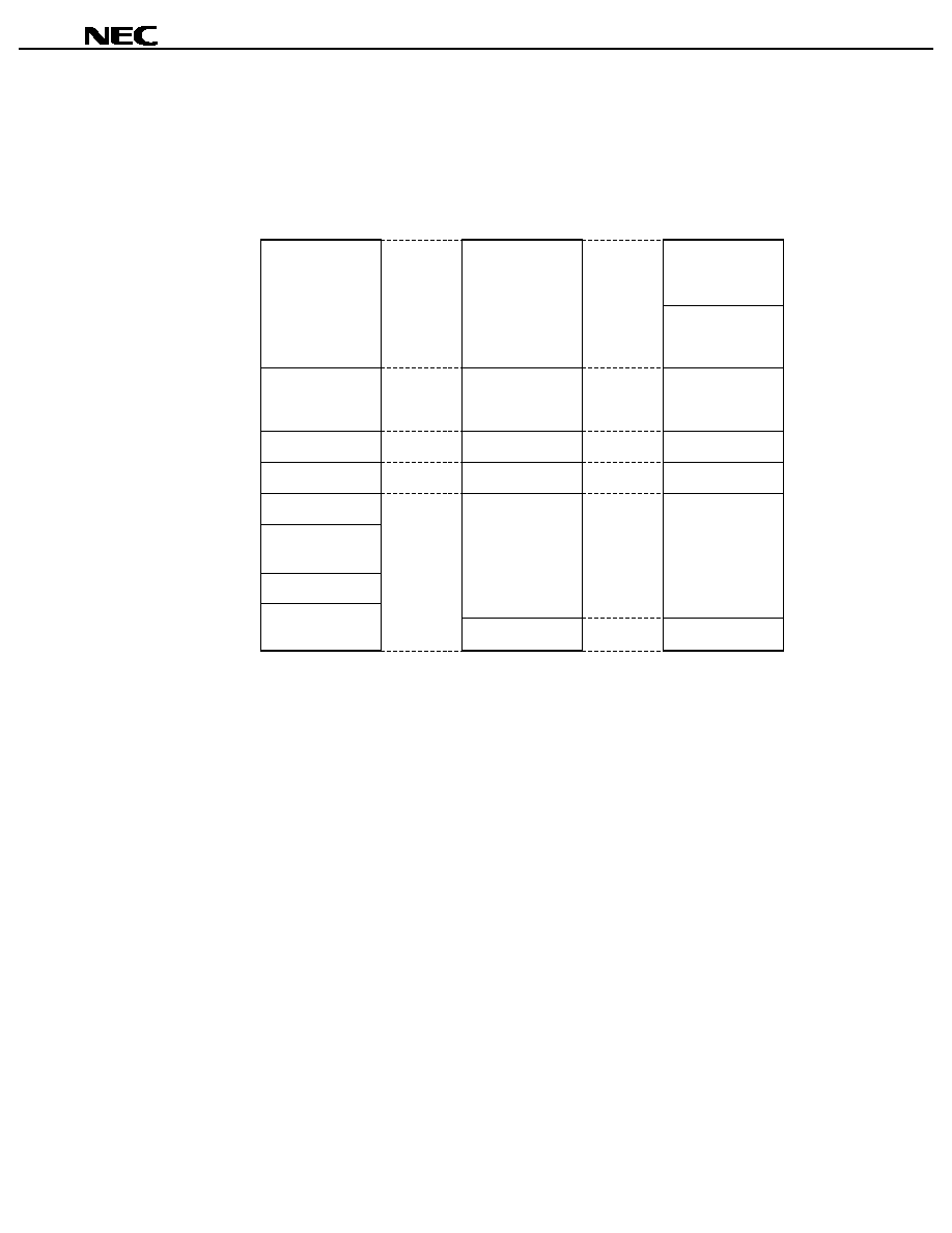
7. MEMORY MAP
A Harvard architecture, in which the instruction memory space and data memory space are separated is
employed.
7.1 Instruction Memory
7.1.1 Instruction memory map
The instruction memory space consists of 64K words
◊
32 bits, and the capacity and type of the memory differ
depending on the product.
System
PD77110
µ
µ
PD77111, 77112
Internal instruction
RAM
(32K words)
System
System
Internal instruction
ROM
(31.75K words)
System
Internal instruction RAM
(1K words)
Vector area (64 words)
System
Boot-up ROM
(256 words)
Internal instruction RAM
(3.5K words)
Vector area (64 words)
System
Boot-up ROM
(256 words)
0xFFFF
0xC000
0xBFFF
0xBF00
0xBEFF
0x0600
0x05FF
0x4000
0x3FFF
0x1000
0x0FFF
0x0240
0x023F
0x0200
0x01FF
0x0100
0x00FF
0x0000
Caution Programs and data cannot be placed at addresses reserved for the system, nor can these
addresses be accessed. If these addresses are accessed, the normal operation of the device
cannot be guaranteed.
Data Sheet U12801EJ4V0DS00
28
µ
µ
µ
µ
PD77110, 77111, 77112
7.1.2 Interrupt vector table
Addresses 0x200 through 0x23F of the instruction memory are entry points (vectors) of interrupts. Four
instruction addresses are assigned to each interrupt source.
Vector
Interrupt Source
0x200
Reset
0x204
0x208
0x20C
Reserved
0x210
INT1
0x214
INT2
0x218
INT3
0x21C
INT4
0x220
SI1 input
0x224
SO1 output
0x228
SI2 input
0x22C
SO2 output
0x230
HI input
0x234
HO output
0x238
0x23C
Reserved
Cautions
1. Although reset is not an interrupt, it is handled like an interrupt as an entry to a vector.
2. It is recommended that unused interrupt source vectors be used to branch an error
processing routine.
3. Because a vector area also exists in the internal RAM area of the mask ROM model, this
area must be booted up. In addition, because the entry address after reset is 0x200,
address 0x200 must be booted up even when the internal instruction RAM and interrupts are
not used.
Data Sheet U12801EJ4V0DS00
29
µ
µ
µ
µ
PD77110, 77111, 77112
7.2 Data Memory
7.2.1 Data memory map
The data memory space consists of an X memory space and a Y memory space of 64K words
◊
16 bits each, and
the memory capacity and memory type differ depending on the product.
External data
memory
(32K words)
Data RAM
(16K words)
System
Peripheral
(64 words)
System
Data RAM
(4K words)
System
Data RAM
(4K words)
System
Data ROM
(16K words)
System
Peripheral
(64 words)
Peripheral
(64 words)
System
Data RAM
(3K words)
System
Data ROM
(16K words)
External data
memory
(16K words)
System
PD77110
µ
µ
µ
PD77111
PD77112
System
Data RAM
(3K words)
0xFFFF
0x4000
0x3FFF
0x3840
0x383F
0x3800
0x37FF
0x3000
0x2FFF
0x2000
0x1FFF
0x1000
0x0FFF
0x0000
0x8000
0x7FFF
0x0C00
0x0BFF
0xC000
0xBFFF
Caution Programs and data cannot be placed at addresses reserved for the system, nor can these
addresses be accessed. If these addresses are accessed, the normal operation of the device
cannot be guaranteed.
Data Sheet U12801EJ4V0DS00
30
µ
µ
µ
µ
PD77110, 77111, 77112
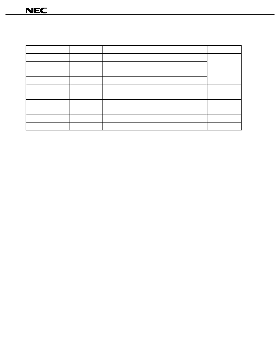
7.2.2 Internal peripherals
The internal peripherals are mapped to the internal data memory space.
X/Y Memory Address
Register Name
Function
Peripheral Name
0x3800
SDT1
First serial data register
0x3801
SST1
First serial status register
0x3802
SDT2
Second serial data register
0x3803
SST2
Second serial status register
SIO
0x3804
PDT
Port data register
0x3805
PCD
Port command register
IOP
0x3806
HDT
Host data register
0x3807
HST
Host status register
HIO
0x3808
DWTR
Data memory wait cycle register
WTR
0x3809 - 0x383F
Reserved area
Caution Do not access this area.
-
Cautions
1. The register names listed in this table are not reserved words of the assembler or the C
language. Therefore, when using these names in assembler or C, the user must define
them.
2. The same register is accessed, as long as the address is the same, regardless of whether
the X memory space or Y memory space is accessed.
3. Even different registers cannot be accessed at the same time from both the X and Y memory
spaces.
8. MASK OPTION
The
µ
PD77111 and 77112 have mask options that must be specified when an order for a ROM is placed. This
section explains these mask options. The mask options are specified in the Workbench (WB77016) development
tool. To order a mask ROM, output a mask ROM ordering file format (.msk file) using WB77016.
8.1 Clock Control Options
The following four clock related options must be specified.
∑
PLL multiple
∑
Output division ratio
∑
HALT division ratio
∑
Validity of CLKOUT pin

Data Sheet U12801EJ4V0DS00
31
µ
µ
µ
µ
PD77110, 77111, 77112
When the PLL multiple is m, output division ratio is n, and halt division ratio is l, the relationship between each
operation mode and operating clock is as follows:
Operation Mode
Clock Supplied Inside DSP
Normal operation mode
m/n times external input clock
HALT mode
m/n/l times external input clock
STOP mode
Stopped
The PLL control circuit multiplies the input clock by an integer from 1 to 16. Specify the mask option of the PLL
multiple so that the multiplied frequency falls within the specified PLL lock frequency range.
The output divider divides the clock multiplied by the PLL by an integer from 1 to 16. Specify the mask option of
the output division ratio so that the frequency m/n times the external input clock supplied to the DSP falls within the
specified operating frequency range of the DSP.
The HALT divider functions only in the HALT mode. It divides the clock of the output divider by an integer from 1
to 16 and supplies the divided clock to the internal circuitry. Specify the mask option of the HALT division ratio so
that necessary division can be performed.
Whether the clock supplied to the internal circuitry of the DSP (internal system clock) is "output" or "not output"
from the CLKOUT pin can be specified. Specify the mask option as necessary.
If an odd value (other than 1) is specified as the output division ratio, the high-level width of the clock output from
the CLKOUT pin is equal to one cycle during normal operation (i.e., the clock does not have a duty factor of 50%).
8.2 WAKEUP Function
The WAKEUP pin can be used to release the STOP mode as well as a hardware reset.
If the STOP mode is released by means of a hardware reset, the status before the STOP mode was set cannot be
restored after the STOP mode has been released. If the WAKEUP pin is used, however, the status before the STOP
mode is set can be retained and program execution can be resumed starting from the instruction after the STOP
instruction.
Whether the WAKEUP pin is used to release the STOP mode can be specified by a mask option.
When the WAKEUP function is specified valid, the WAKEUP pin is multiplexed with the INT4 pin and it usually
functions as an interrupt pin. The pin functions as the WAKEUP pin only in the STOP mode (if this pin is asserted
active in the STOP mode, it is used only to release the STOP mode, and execution does not branch to an interrupt
vector).
8.3 Mask Option Equivalent Function of
µ
µ
µ
µ
PD77110
Because the
µ
PD77110 does not have mask options, the multiple of the PLL cannot be specified in the same
manner as the
µ
PD77111 and 77112. However, an external pin on the
µ
PD77110 has a function equivalent to the
mask option. Care must be exercised when using the
µ
PD77110, including when it is used to emulate the
µ
PD77111
and 77112.
Data Sheet U12801EJ4V0DS00
32
µ
µ
µ
µ
PD77110, 77111, 77112
8.3.1 Settings related to clock control
External pins PLL0 through PLL2 are used to set the multiple of the PLL. PLL0 and PLL1 are multiplexed with
general-purpose I/O ports P2 and P3, and can be used as PLL setting pins only when it is so specified.
The multiple must be an integer from 1 to 8.
<PLL2: PLL1: PLL0> 000 m = 1
001 m = 2
:
111 m = 8
The output division ratio is fixed to 1/1 and the halt division ratio is fixed to 1/8.
Where the PLL multiple is m, the relationship between each operation mode and operating clock is as follows:
Operation Mode
Clock Supplied to DSP
Normal operation mode
m times external input clock
HALT mode
m/8 times external input clock
STOP mode
Stopped
For details on how to set the PLL multiple, refer to 4.2 Initializing PLL. Because the setting of PLL0 through
PLL2 becomes valid in the PLL initialization mode, the value of PLL0 through PLL2 must be fixed before the PLL
initialization mode is set.
The option that makes CLKOUT pin output valid or invalid is fixed to "valid".
8.3.2 WAKEUP function
The WAKEUP function of the
µ
PD77110 is fixed to "valid".

Data Sheet U12801EJ4V0DS00
33
µ
µ
µ
µ
PD77110, 77111, 77112
9. INSTRUCTIONS
9.1 Outline of Instructions
An instruction consists of 32 bits. Almost all the instructions, except some such as branch instructions, are
executed with one system clock. The maximum instruction cycle of the
µ
PD77110 is 15.3 ns. The maximum
instruction cycle of the
µ
PD77111 and 77112 is 13.3 ns. The following nine types of instructions are available:
(1) Trinomial operation instructions
These instructions specify an operation by the MAC. As the operands, three general-purpose registers can be
specified.
(2) Binomial operation instructions
These instructions specify an operation by the MAC, ALU, or BSFT. As the operands, two general-purpose
registers can be specified. An immediate value can be specified for some of these instructions, instead of a
general-purpose register, for one input.
(3) Uninominal operation instructions
These instructions specify an operation by the ALU. As the operands, one general-purpose register can be
specified.
(4) Load/store instructions
These instructions transfer 16-bit values between memory and a general-purpose register. Any general-purpose
register can be specified as the transfer source or destination.
(5) Register-to-register transfer instructions
These instructions transfer data from one general-purpose register to another.
(6) Immediate value setting instructions
These instructions write an immediate value to a general-purpose register and the registers of the address
operation unit.
(7) Branch instructions
These instruction specify branching of program execution.
(8) Hardware loop instructions
These instruction specify repetitive execution of an instruction.
(9) Control instructions
These instructions are used to control the program.
Data Sheet U12801EJ4V0DS00
34
µ
µ
µ
µ
PD77110, 77111, 77112
9.2 Instruction Set and Operation
An operation is written in the operation field for each instruction in accordance with the operation representation
format of that instruction. If two or more parameters can be written, select one of them.
(a) Representation formats and selectable registers
The following table shows the representation formats and selectable registers.
Representation Format
Selectable Register
r0, r0
, r0
R0 - R7
rI, rI
R0L - R7L
rh, rh
R0H - R7H
re
R0E - R7E
reh
R0EH - R7EH
dp
DP0 - DP7
dn
DN0 - DN7
dm
DMX, DMY
dpx
DP0 - DP3
dpy
DP4 - DP7
dpx_mod
DPn, DPn++, DPn
--
, DPn##, DPn%%, !DPn## (n = 0 - 3)
dpy_mod
DPn, DPn++, DPn
--
, DPn##, DPn%%, !DPn## (n = 4 - 7)
dp_imm
DPn##imm (n = 0 - 7)
*xxx
Contents of memory with address xxx
<Example> If the contents of the DP0 register are 1000, *DP0 indicates the contents of
address 1000 of the memory.

Data Sheet U12801EJ4V0DS00
35
µ
µ
µ
µ
PD77110, 77111, 77112
(b) Modifying data pointer
The data pointer is modified after the memory has been accessed. The result of modification becomes valid
starting from the instruction that immediately follows. The data pointer cannot be modified.
Example
Operation
DPn
Nothing is done (value of DPn is not changed.)
DPn++
DPn
DPn + 1
DPn
--
DPn
DPn
-
1
DPn##
DPn
DPn + DNn
(Adds value of corresponding DN0 to DN7 to DP0 to DP7.)
Example: DP0
DP0 + DN0
(n = 0 - 3) DPn = ((DP
L
+ DNn) mod (DMX + 1)) + DP
H
DPn%%
(n = 4 - 7) DPn = ((DP
L
+ DNn) mod (DMY + 1)) + DP
H
!DPn##
Reverses bits of DPn and then accesses memory.
After memory access, DPn
DPn + DNn
DPn##imm
DPn
DPn + imm
(c) Instructions that can be simultaneously written
Instructions that can be simultaneously written are indicated by O.
(d) Status of overflow flag (OV)
The status of the overflow flag is indicated by the following symbol:
z
: Not affected
: Set to 1 when overflow occurs
Caution If an overflow does not occur as a result of an operation, the overflow flag is not reset but
retains the status before the operation.
Data Sheet U12801EJ4V0DS00
36
µ
µ
µ
µ
PD77110, 77111, 77112
Instruction Set
Instructions Simultaneously Written
Flag
Instruc-
tion
Instruction
Name
Mnemonic
Operation
Trino-
mial
Bino-
mial
Unino-
minal
Load/
store
Trans-
fer
Imme-
diate-
value
Bran-
ch
Loop
Cont-
rol
OV
Multiply add
ro = ro + rh * rh
ro
ro + rh * rh
{
Multiply sub
ro = ro
-
rh * rh
ro
ro
-
rh * rh
{
Sign unsign
multiply add
ro = ro + rh * rl
(rl is in positive integer
format.)
ro
ro + rh * rl
{
Unsign unsign
multiply add
ro = ro + rl * rl
(rl and rl' are in positive
integer format.)
ro
ro + rl * rl
{
1-bit shift
multiply add
ro = (ro>>1) + rh * rh
ro
ro
2
+ rh * rh
{
Trinomial
operation
16-bit shift
multiply add
ro = (ro>>16) + rh * rh
ro
ro
2
16
+ rh * rh
{
z
Multiply
ro = rh * rh
ro
rh * rh
{
z
Add
ro
= ro + ro
ro
ro + ro
{
Immediate add
ro
= ro + imm
ro
ro + imm
(where imm
1)
Sub
ro
= ro
-
ro
ro
ro
-
ro
{
Immediate sub
ro
= ro
-
imm
ro
ro
-
imm
(where imm
1)
Arithmetic right
shift
ro
= ro SRA rl
ro
ro >> rl
{
z
Immediate
arithmetic right
shift
ro
= ro SRA imm
ro
ro >> imm
z
Logical right
shift
ro
= ro SRL rl
ro
ro >> rl
{
z
Immediate
logical right
shift
ro
= ro SRL imm
ro
ro >> imm
z
Logical left shift ro
= ro SLL rl
ro
ro << rl
{
z
Immediate
logical left shift
ro
= ro SLL imm
ro
ro << imm
z
AND
ro
= ro & ro
ro
ro & ro
{
z
Immediate
AND
ro
= ro & imm
ro
ro & imm
z
OR
ro
= ro
ro
ro
ro
ro
{
z
Immediate OR
ro
= ro
imm
ro
ro
imm
z
Exclusive OR
ro
= ro
ro
ro
ro
ro
{
z
Binomial
operation
Immediate
exclusive OR
ro
= ro
imm
ro
ro
imm
z
Data Sheet U12801EJ4V0DS00
37
µ
µ
µ
µ
PD77110, 77111, 77112
Instructions Simultaneously Written
Flag
Instruc-
tion
Instruction
Name
Mnemonic
Operation
Trino-
mial
Bino-
mial
Unino-
minal
Load/
store
Trans-
fer
Imme-
diate-
value
Bran-
ch
Loop
Cont-
rol
OV
Binomial
operation
Less than
ro
= LT (ro, ro
)
if (ro < ro
)
{ro
0x0000000001}
else {ro
0x0000000000}
{
z
Clear
CLR (ro)
ro
0x0000000000
{
{
z
Increment
ro
= ro + 1
ro
ro + 1
{
{
Decrement
ro
= ro
-
1
ro
ro
-
1
{
{
Absolute value
ro
= ABS (ro)
if (ro < 0)
{ro
-
ro}
else {ro
ro}
{
{
1's
complement
ro
= ~ro
ro
~ro
{
{
z
2's
complement
ro
=
-
ro
ro
-
ro
{
{
Clip
ro
= CLIP (ro)
if ( ro > 0x007FFFFFFF)
{ro
0x007FFFFFFF}
elseif {ro < 0xFF80000000}
{ro
0xFF80000000}
else {ro
ro}
{
{
z
Round
ro
= ROUND (ro)
if (ro > 0x007FFF0000)
{ro
0x007FFF0000}
elseif {ro < 0xFF80000000}
{ro
0xFF80000000}
else {ro
(ro + 0x8000)
& 0xFFFFFF0000}
{
{
z
Exponent
ro
= EXP (ro)
ro
log
2
(
1
ro
)
{
{
z
Substitution
ro
= ro
ro
ro
{
{
z
Accumulated
addition
ro
+ = ro
ro
ro
+ ro
{
{
Accumulated
subtraction
ro
-
= ro
ro
ro
-
ro
{
{
Uninom-
inal
operation
Division
ro
/ = ro
if (sign (ro
) == sign (ro))
{ro
(ro
-
ro) << 1}
else
{ro
(ro
+ ro)<<1}
if (sign (ro
)==0)
{ro
ro
+ 1}
{
{
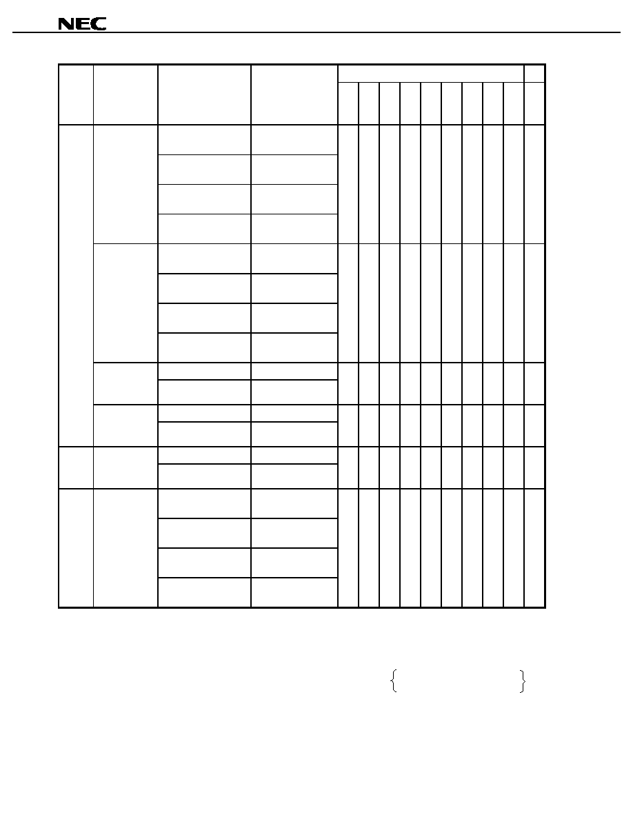
Data Sheet U12801EJ4V0DS00
38
µ
µ
µ
µ
PD77110, 77111, 77112
Instructions Simultaneously Written
Flag
Instruc-
tion
Instruction
Name
Mnemonic
Operation
Trino-
mial
Bino-
mial
Unino-
minal
Load/
store
Trans-
fer
Imme-
diate-
value
Bran-
ch
Loop
Cont-
rol
OV
ro = *dpx_mod ro
=
*dpy_mod
ro
*dpx, ro
*dpy
ro = *dpx_mod
*dpy_mod = rh
ro
*dpx, *dpy
rh
*dpx_mod = rh ro =
*dpy_mod
*dpx
rh, ro
*dpy
Parallel
load/store
Notes 1, 2
*dpx_mod = rh
*dpy_mod = rh
*dpx
rh, *dpy
rh
{
{
{
z
dest = *dpx_mod
dest
= *dpy_mod
dest
*dpx,
dest
*dpy
dest = *dpx_mod
*dpy_mod = source
dest
*dpx,
*dpy
source
*dpx_mod = source
dest = *dpy_mod
*dpx
source,
dest
*dpy
Partial load/
store
Notes 1, 2, 3
*dpx_mod = source
*dpy_mod = source
*dpx
source,
*dpy
source
z
dest = *addr
dest
*addr
Direct
addressing
load/store
Note 4
*addr = source
*addr
source
z
dest = *dp_imm
dest
*dp
Load/
store
Immediate
value index
load/store
Note 5
*dp_imm = source
*dp
source
z
dest = rl
dest
rl
Register-
to-register
transfer
Register-to-
register
transfer
Note 6
rl = source
rl
source
{
z
rl = imm
(where imm = 0 to 0xFFFF)
rl
imm
dp = imm
(where imm = 0 to 0xFFFF)
dp
imm
dn = imm
(where imm = 0 to 0xFFFF)
dn
imm
Immediate
value
setting
Immediate
value setting
dm = imm
(where imm = 1 to 0xFFFF)
dm
imm
z
Notes 1. Of the two mnemonics, either one of them or both can be written.
2. After transfer, modification specified by mod is performed.
3. Select any of dest, dest' = {ro, reh, re, rh, rl}, source, source' = {re, rh, rl}.
4. Select any of dest = {ro, reh, re, rh, rl}, source = {re, rh, rl},
0: X-0xFFF
0: Y-0xFFFF
: X (X memory)
: Y (Y memory)
addr =
.
5. Select any of dest = {ro, reh, re, rh, rl}, source = {re, rh, rl}.
6. Select any register other than general-purpose registers as dest and source.
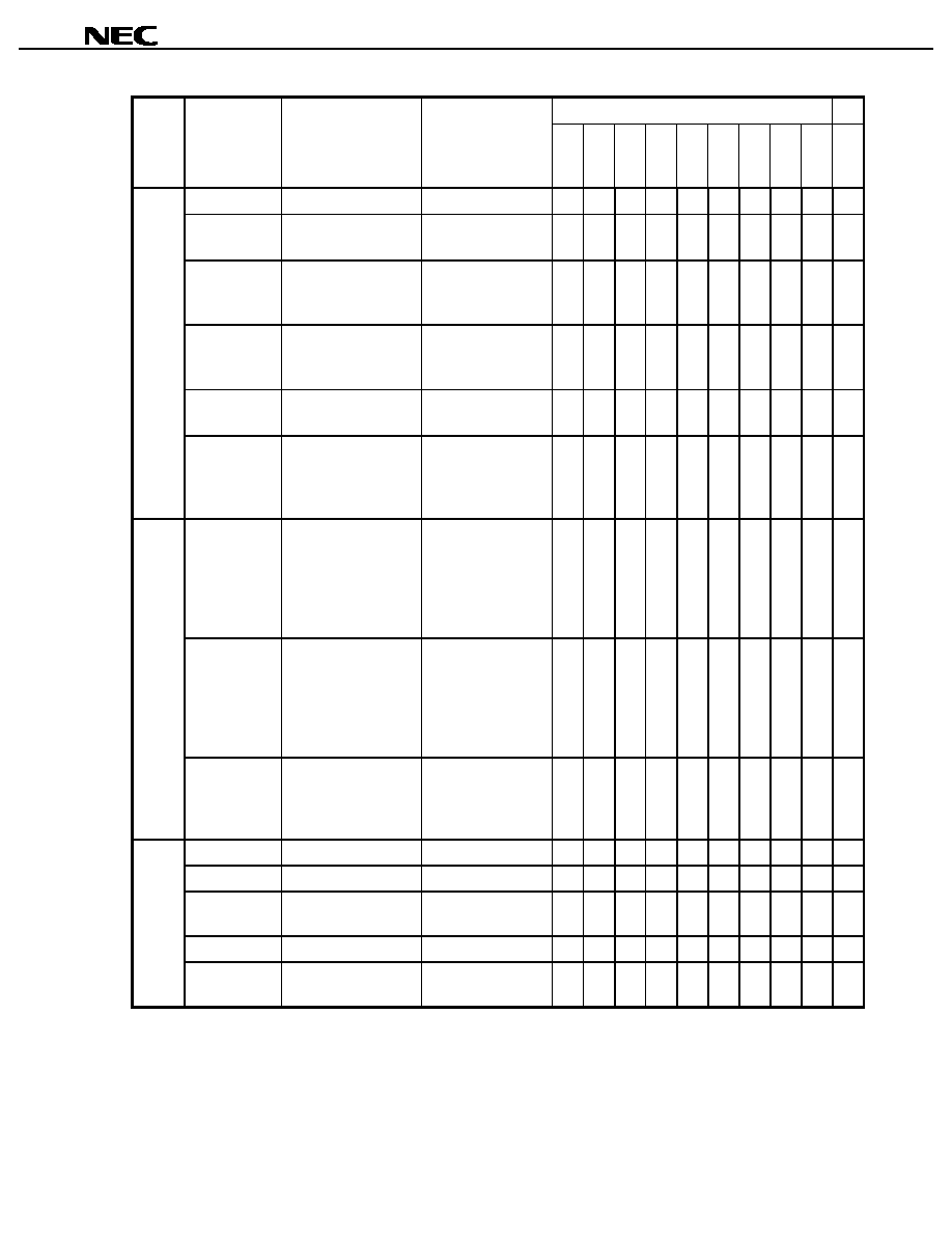
Data Sheet U12801EJ4V0DS00
39
µ
µ
µ
µ
PD77110, 77111, 77112
Instructions Simultaneously Written
Flag
Instruc-
tion
Instruction
Name
Mnemonic
Operation
Trino-
mial
Bino-
mial
Unino-
minal
Load/
store
Trans-
fer
Imme-
diate-
value
Bran-
ch
Loop
Cont-
rol
OV
Jump
JMP imm
PC
imm
{
z
Register
indirect jump
JMP dp
PC
dp
{
z
Subroutine call
CALL imm
SP
SP + 1
STK
PC + 1
PC
imm
{
z
Register
indirect
subroutine call
CALL dp
SP
SP + 1
STK
PC + 1
PC
dp
{
z
Return
RET
PC
STK
SP
SP
-
1
{
z
Branch
Interrupt return
RETI
PC
STK
STK
SP
-
1
Recovery of interrupt
enable flag
{
z
Repeat
REP count
Start
RC
count
RF
0
During repeat
PC
PC
RC
RC
-
1
End
PC
PC + 1
RF
1
z
Loop
LOOP count
(instruction of two or
more lines)
Start
RC
count
RF
0
During repeat
PC
PC
RC
RC
-
1
End
PC
PC + 1
RF
1
z
Hard-
ware
loop
Loop hop
LPOP
LC
LSR3
LE
LSR2
LS
LSR1
LSP
LSP
-
1
z
No operation
NOP
PC
PC + 1
z
Halt
HALT
CPU stops.
z
Stop
STOP
CPU, PLL, and
OSC stop.
z
Condition
IF (ro cond)
Condition test
{
{
{
z
Control
Forget interrupt
FINT
Discard interrupt
request
z
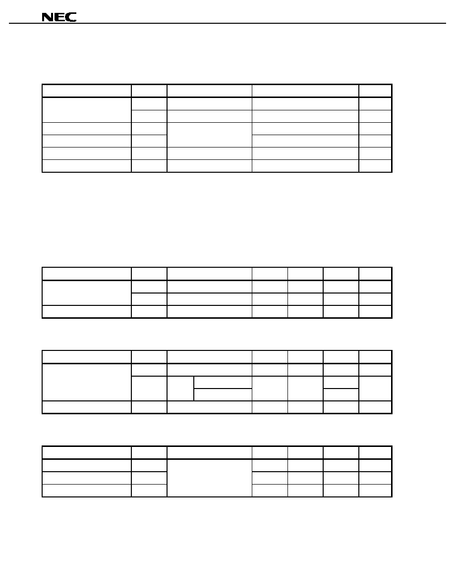
Data Sheet U12801EJ4V0DS00
40
µ
µ
µ
µ
PD77110, 77111, 77112
10. ELECTRICAL SPECIFICATIONS
Absolute Maximum Ratings (T
A
= +25
∞
∞
∞
∞
C)
Parameter
Symbol
Condition
Rating
Unit
IV
DD
For DSP core
-
0.5 to +3.6
V
Supply voltage
EV
DD
For I/O pins
-
0.5 to +4.6
V
Input voltage
V
I
-
0.5 to +4.1
V
Output voltage
V
O
V
I
< EV
DD
+ 0.5 V
-
0.5 to +4.1
V
Storage temperature
T
stg
-
65 to +150
∞
C
Operating temperature
T
A
-
40 to +85
∞
C
Caution If any of the parameters exceeds the absolute maximum ratings, even momentarily, the quality of
the product may be impaired. The absolute maximum ratings are values that may physically
damage the product(s). Be sure to use the product(s) within the ratings.
Recommended Operating Conditions
µ
PD77110
Parameter
Symbol
Condition
MIN.
TYP.
MAX.
Unit
IV
DD
For DSP core
2.3
2.7
V
Operating voltage
EV
DD
For I/O pins
2.7
3.6
V
Input voltage
V
I
0
EV
DD
V
µ
PD77111, 77112
Parameter
Symbol
Condition
MIN.
TYP.
MAX.
Unit
IV
DD
For DSP core
1.8
2.7
V
IV
DD
= 1.8 to 2.7 V
3.3
Operating voltage
EV
DD
For I/O
pins
IV
DD
= 2.3 to 2.7 V
2.7
3.6
V
Input voltage
V
I
0
EV
DD
V
Capacitance (T
A
= +25
∞
∞
∞
∞
C, IV
DD
= 0 V, EV
DD
= 0 V)
Parameter
Symbol
Condition
MIN.
TYP.
MAX.
Unit
Input capacitance
C
I
10
pF
Output capacitance
C
O
10
pF
I/O capacitance
C
IO
f = 1 MHz,
Pins other than those
tested: 0 V
10
pF
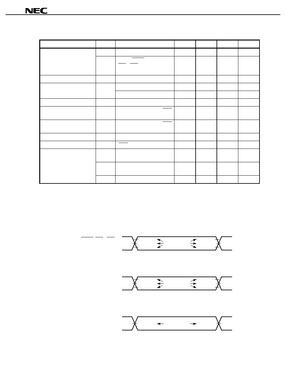
Data Sheet U12801EJ4V0DS00
41
µ
µ
µ
µ
PD77110, 77111, 77112
DC Characteristics (T
A
=
-
-
-
-
40 to +85
∞
∞
∞
∞
C, with IV
DD
and EV
DD
within recommended operating condition range)
Parameter
Symbol
Condition
MIN.
TYP.
MAX.
Unit
V
IHN
Pins other than below
0.7 EV
DD
EV
DD
V
High-level input voltage
V
IHS
CLKIN, RESET,
INT1 - INT4, SCK1, SIEN1,
SOEN1, SCK2, SIEN2, SOEN2
0.8 EV
DD
EV
DD
V
Low-level input voltage
V
IL
0
0.2 EV
DD
V
L
OH
=
-
2.0 mA
0.7 EV
DD
V
High-level output voltage
V
OH
I
OH
=
-
100
µ
A
0.8 EV
DD
V
Low-level output voltage
V
OL
I
OL
= 2.0 mA
0.2 EV
DD
V
High-level input leakage
current
I
LH
Other than TDI, TMS, and TRST
V
I
= EV
DD
0
10
µ
A
Low-level input leakage
current
I
LL
Other than TDI, TMS, and TRST
V
I
= 0 V
-
10
0
µ
A
Pull-up pin current
I
PUI
TDI, TMS, 0 V
V
I
EV
DD
-
250
0
µ
A
Pull-down pin current
I
PDI
TRST, 0 V
V
I
EV
DD
0
250
µ
A
I
DD
Note 1
During operating, 30 ns, IV
DD
=
2.7 V
TBD
75
mA
I
DDH
In halt mode, t
cC
= 30 ns,
divided by eight, IV
DD
= 2.7 V
TBD
10
mA
Internal supply current
[V
IHN
= V
IHS
= EV
DD
, V
IL
= 0 V,
no load]
I
DDS
In stop mode, 0
∞
C < T
A
< 60
∞
C
100
Note 2
µ
A
Notes 1. The TYP. values are when an ordinary program is executed.
The MAX. values are when a special program that brings about frequent switching inside the device is
executed.
2. Values of
µ
PD77111 and 77112. The parameters of the
µ
PD77110 are still under evaluation.
Common Test Criteria of Switching Characteristics
0.8 EV
DD
0.5 EV
DD
0.2 EV
DD
0.8 EV
DD
0.5 EV
DD
0.2 EV
DD
Test points
CLKIN, RESET, INT1 - INT4,
SCK1, SIEN1, SOEN1, SCK2,
SIEN2, SOEN2
0.7 EV
DD
0.5 EV
DD
0.2 EV
DD
0.7 EV
DD
0.5 EV
DD
0.2 EV
DD
Test points
Input
(other than above)
0.5 EV
DD
0.5 EV
DD
Test points
Output

Data Sheet U12801EJ4V0DS00
42
µ
µ
µ
µ
PD77110, 77111, 77112
µ
PD77110
(1)
µ
µ
µ
µ
PD77110 AC Characteristics (Unless otherwise specified, T
A
=
-
-
-
-
40 to +85
∞
∞
∞
∞
C, with IV
DD
and EV
DD
within
recommended operating condition range)
Clock
Timing requirements
Parameter
Symbol
Condition
MIN.
TYP.
MAX.
Unit
25
ns
CLKIN cycle time
Note 1
t
cCX
PLL lock range
Note 2
10
◊
m
50
◊
m
ns
CLKIN high-level width
t
wCXH
12.5
ns
CLKIN low-level width
t
wCXL
12.5
ns
CLKIN rise/fall time
t
rfCX
5
ns
Internal clock cycle time
requirements
Note 3
t
cC (R)
15.3
ns
Notes 1. m: Multiple
2. This is the range in which the PLL is locked (stably oscillates). Input t
cCX
within this range.
3. Input t
cCX
so that the value of (t
cCX
˜
m) satisfies this condition.
Timing requirements (T
A
=
-
-
-
-
40 to +60
∞
∞
∞
∞
C, IV
DD
= 2.5 to 2.7 V, EV
DD
= 2.7 to 3.6 V)
Parameter
Symbol
Condition
MIN.
TYP.
MAX.
Unit
25
ns
CLKIN cycle time
Note 1
t
cCX
PLL lock range
Note 2
10
◊
m
50
◊
m
ns
CLKIN high-level width
t
wCXH
12.5
ns
CLKIN low-level width
t
wCXL
12.5
ns
CLKIN rise/fall time
t
rfCX
5
ns
Internal clock cycle time
requirements
Note 2
t
cC (R)
13.3
ns
Notes 1. m: Multiple
2. This is the range in which the PLL is locked (stably oscillates). Input t
cCX
within this range.
3. Input t
cCX
so that the value of (t
cCX
˜
m) satisfies this condition.
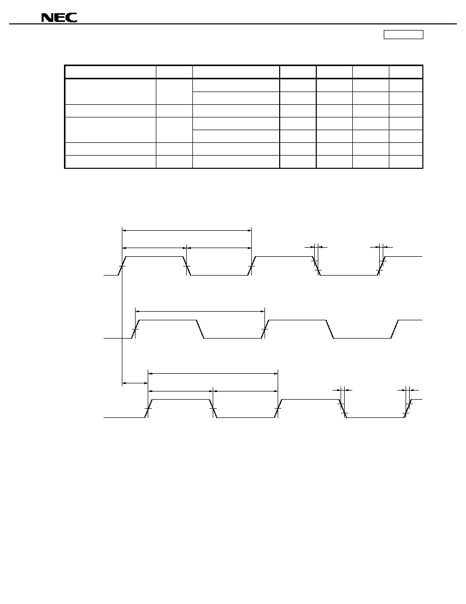
Data Sheet U12801EJ4V0DS00
43
µ
µ
µ
µ
PD77110, 77111, 77112
µ
PD77110
Switching characteristics
Parameter
Symbol
Condition
MIN.
TYP.
MAX.
Unit
During normal operation
t
cCX
˜
m
ns
Internal clock cycle
Note
t
cC
In HALT mode
t
cCX
˜
m
◊
l
ns
CLKOUT cycle time
t
cCO
t
cC
ns
During normal operation
t
cCX
˜
2
-
3
ns
CLKOUT width
t
wCO
In HALT mode
t
cCX
˜
m
-
3
ns
CLKOUT rise/fall time
t
rfCO
5
ns
CLKOUT delay time
t
dCO
15
ns
Note m: Multiple, l: HALT division ratio
Clock I/O timing
Internal clock
CLKIN
CLKOUT
t
cCX
t
cC,
t
cC (R)
t
wCXH
t
wCXL
t
rfCX
t
rfCX
t
cCO
t
dCO
t
wCO
t
wCO
t
rfCO
t
rfCO

Data Sheet U12801EJ4V0DS00
44
µ
µ
µ
µ
PD77110, 77111, 77112
µ
PD77110
Reset, Interrupt
Timing requirements
Parameter
Symbol
Condition
MIN.
TYP.
MAX.
Unit
On power application
Note 1
,
in STOP mode
100 +
2048t
cCX
µ
s
RESET low-level width
t
w (RL)
During normal operation,
in HALT mode
4t
cC
Note 2
Note 3
ns
On power application
Note 4
4t
cCX
ns
RESET recovery time
t
rec (R)
4t
cC
Note 2
ns
WAKEUP low-level width
t
w (WAKEUPL)
100
µ
s
INT1 - INT4 low-level width
t
w (INTL)
3t
cC
Note 2
ns
INT1 - INT4 recovery time
t
rec (INT)
3t
cC
ns
Notes 1. The value on power application is the time from when the supply voltages have reached IV
DD
= 1.8 V
and EV
DD
= 2.7 V. A stable clock input is also required.
2. Note that t
cC
is eight times this value during normal operation in the HALT mode.
3. If the low-level width of RESET is greater than 1024t
cC
, the PLL initialization mode is triggered. If there
is no need to use the PLL initialization mode, set the width to less than 1024t
cC
.
4. When the power is turned on, a recovery period of 4t
cCX
is necessary before inputting RESET.
Reset timing
RESET
t
w(RL)
t
rec(R)
WAKEUP timing
WAKEUP
t
w (WAKEUPL)
Interrupt timing
INT1 - INT4
t
w (INTL)
t
rec (INT)
Data Sheet U12801EJ4V0DS00
45
µ
µ
µ
µ
PD77110, 77111, 77112
µ
PD77110
External Data Memory Access
Timing requirements
Parameter
Symbol
Condition
MIN.
TYP.
MAX.
Unit
Read data setup time
t
suDDRD
18
ns
Read data hold time
t
hDDRD
0
ns
Switching characteristics
Parameter
Symbol
Condition
MIN.
TYP.
MAX.
Unit
Address cycle time
t
rcDA
t
cC
+ (t
cC
◊
t
cDW
)
Note
ns
Address output hold time
t
hDA
0
ns
MRD output delay time
t
dDR
5
ns
Write data output valid time
t
vDDWD
5
ns
Write data output hold time
t
hDDWD
0
ns
MWR output delay time
t
dDW
0
0.5 t
cC
ns
MWR output hold time
t
hDA
0
ns
MWR low-level width
t
wDWL
t
cC
◊
t
cDW
-
3
ns
MWR high-level width
t
wDWH
0.5 t
cC
-
3
ns
Note t
cDW
: Number of data wait cycles
Data Sheet U12801EJ4V0DS00
46
µ
µ
µ
µ
PD77110, 77111, 77112
µ
PD77110
External data memory access timing (read)
DA0 - DA14
MRD
X/Y
D0 - D15
t
rcDA
t
dDR
t
dDR
t
suDDRD
t
hDDRD
External data memory access timing (write)
DA0 - DA14
X/Y
MWR
D0 - D15
t
rcDA
t
dDW
t
vDDWD
Hi-Z
Hi-Z
t
vDDWD
t
hDDWD
t
wDWL
t
wDWH
t
hDA
t
dDW
Data Sheet U12801EJ4V0DS00
47
µ
µ
µ
µ
PD77110, 77111, 77112
µ
PD77110
Bus Arbitration
Timing requirements
Parameter
Symbol
Condition
MIN.
TYP.
MAX.
Unit
HOLDRQ setup time
t
suHRQ
0
ns
HOLDRQ hold time
t
hHRQ
0
ns
Switching characteristics
Parameter
Symbol
Condition
MIN.
TYP.
MAX.
Unit
BSTB hold time
t
hBS
0
ns
BSTB output delay time
t
dBS
20
ns
HOLDAK output delay time
t
dHAK
18
ns
Data hold time during bus
arbitration
t
h (BS-D)
25
ns
Data valid time during bus
arbitration
t
v (BS-D)
25
ns
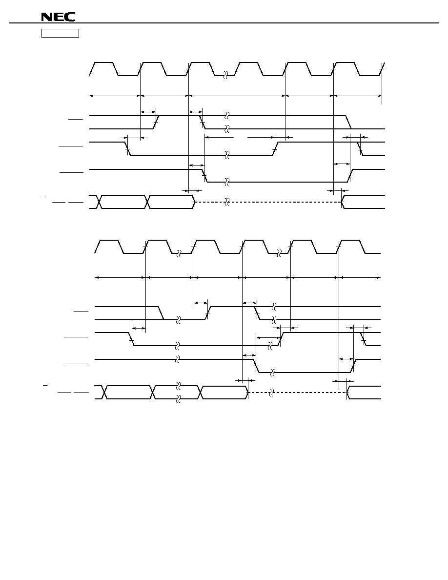
Data Sheet U12801EJ4V0DS00
48
µ
µ
µ
µ
PD77110, 77111, 77112
µ
PD77110
Bus arbitration timing (when bus is idle)
CLKIN
t
suHRQ
BSTB
HOLDRQ
HOLDAK
X/Y, DA0 - DA14,
MRD, MWR
t
hBS
(Bus busy)
Bus idle
t
dBS
t
dHAK
t
h (BS-D)
t
hHRQ
t
suHRQ
Bus release
Bus idle
(Bus busy)
t
hHRQ
t
v (BS-D)
t
dHAK
Hi-Z
Bus arbitration timing (when bus is busy)
CLKIN
t
suHRQ
BSTB
HOLDRQ
HOLDAK
X/Y, DA0 - DA14,
MRD, MWR
(Bus busy)
Bus busy
t
hBS
t
dHAK
t
suHRQ
Bus idle
Bus idle
(Bus busy)
t
hHRQ
t
v (BS-D)
t
dHAK
Bus release
t
hHRQ
t
dBS
t
h (BS-D)
Hi-Z
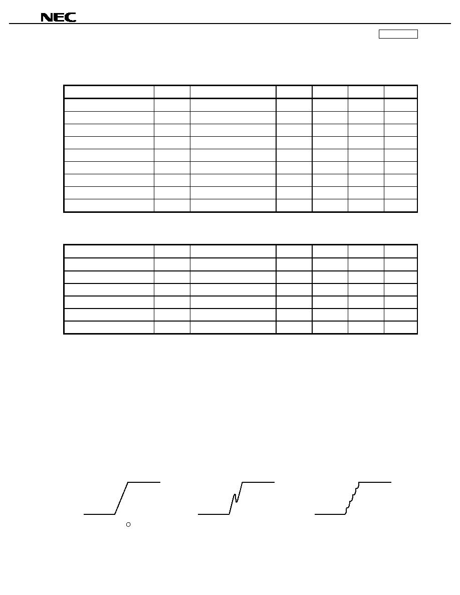
Data Sheet U12801EJ4V0DS00
49
µ
µ
µ
µ
PD77110, 77111, 77112
µ
PD77110
Serial Interface
Timing requirements
Parameter
Symbol
Condition
MIN.
TYP.
MAX.
Unit
SCK cycle time
t
cSC
60
ns
SCK high-/low-level width
t
wSC
25
ns
SCK rise/fall time
t
rtSC
20
ns
SOEN setup time
t
suSOE
5
ns
SOEN hold time
t
hSOE
10
ns
SIEN setup time
t
suSIE
5
ns
SIEN hold time
t
hSIE
10
ns
SI setup time
t
suSI
5
ns
SI hold time
t
hSI
10
ns
Switching characteristics
Parameter
Symbol
Condition
MIN.
TYP.
MAX.
Unit
SORQ output delay time
t
dSOR
25
ns
SORQ hold time
t
hSOR
0
ns
SO output delay time
t
dSO
25
ns
SO hold time
t
hSO
0
ns
SIAK output delay time
t
dSIA
25
ns
SIAK hold time
t
hSIA
0
ns
Caution If noise is superimposed on the serial clock, the serial interface may be deadlocked. Bear in
mind the following points when designing your system:
∑
Reinforce the wiring for power supply and ground (if noise is superimposed on the power and
ground lines, it has the same effect as if noise were superimposed on the serial clock).
∑
Shorten the wiring between the device's SCK1 and SCK2 pins, and clock supply source.
∑
Do not cross the signal lines of the serial clock with any other signal lines. Do not route the
serial clock line in the vicinity of a line through which a high alternating current flows.
∑
Supply the clock to the SCK1 and SCK2 pins of the device from the clock source on a one-to-
one basis. Do not supply clock to several devices from one clock source.
∑
Exercise care that the serial clock does not overshoot or undershoot. In particular, make sure
that the rising and falling of the serial clock waveform are clear.
◊
◊
Make sure that the serial clock
rises and falls linearly.
The serial clock must not bound. Noise
must not be superimposed on the serial clock.
The serial clock must not rise or
fall step-wise.
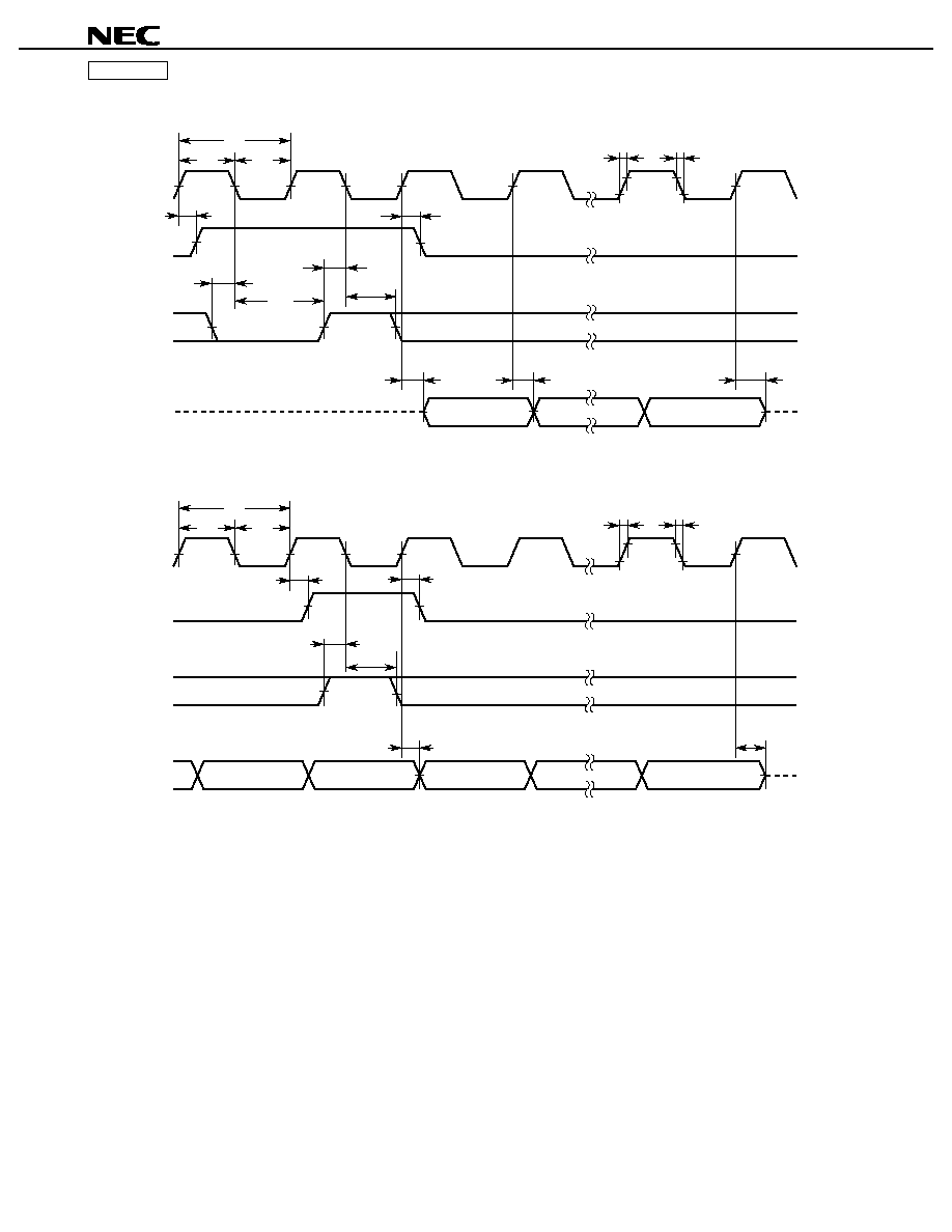
Data Sheet U12801EJ4V0DS00
50
µ
µ
µ
µ
PD77110, 77111, 77112
µ
PD77110
Serial output timing 1
SCK1,
SCK2
t
rfSC
SORQ1
SOEN1,
SOEN2
SO1,
SO2
1st
Last
t
hSO
t
dSO
t
dSO
t
hSOE
t
suSOE
t
suSOE
t
hSOE
t
dSOR
t
wSC
t
wSC
t
cSC
t
hSOR
t
rfSC
Hi-Z
Serial output timing 2 (during successive output)
SCK1,
SCK2
t
rfSC
SORQ1
SOEN1,
SOEN2
SO1,
SO2
1st
Last
t
dSO
t
hSOE
t
suSOE
t
dSOR
t
wSC
t
wSC
t
cSC
t
hSOR
t
rfSC
Last
t
hSO
Hi-Z
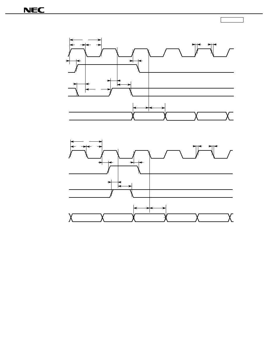
Data Sheet U12801EJ4V0DS00
51
µ
µ
µ
µ
PD77110, 77111, 77112
µ
PD77110
Serial input timing 1
SCK1,
SCK2
SIAK1
SIEN1,
SIEN2
SI1,
SI2
t
cSC
t
wSC
t
wSC
t
dSIA
t
suSIE
t
hSIE
t
suSIE
t
hSIE
t
hSIA
t
suSI
t
hSI
1st
2nd
t
rfSC
t
rfSC
3rd
Serial input timing 2 (during successive input)
SCK1,
SCK2
SIAK1
SIEN1,
SIEN2
SI1,
SI2
t
cSC
t
wSC
t
wSC
t
dSIA
t
suSIE
t
hSIE
t
hSIA
t
suSI
t
hSI
1st
3rd
t
rfSC
t
rfSC
Last
Last≠1
2nd
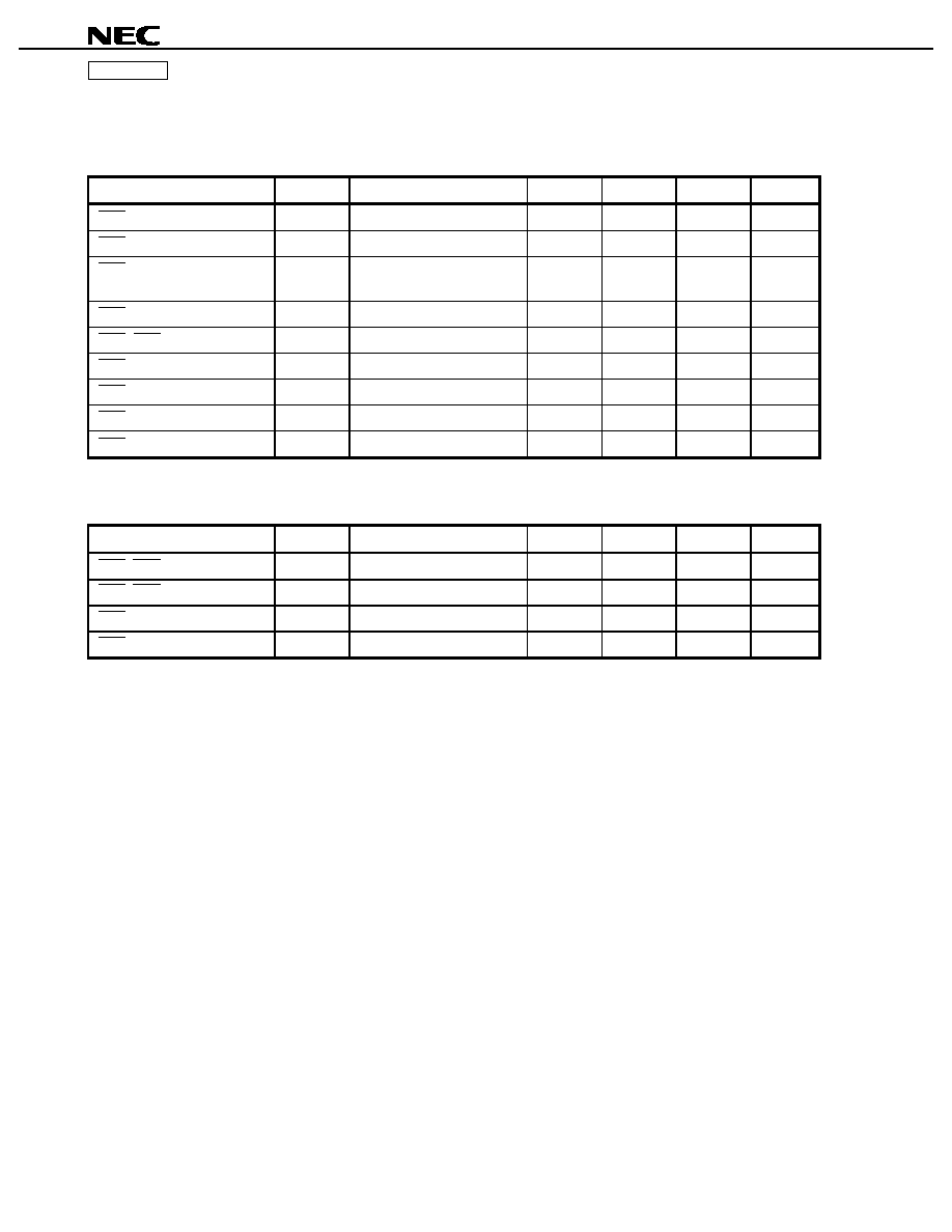
Data Sheet U12801EJ4V0DS00
52
µ
µ
µ
µ
PD77110, 77111, 77112
µ
PD77110
Host Interface
Timing requirements
Parameter
Symbol
Condition
MIN.
TYP.
MAX.
Unit
HRD delay time
t
dHR
10
ns
HRD width
t
wHR
60
ns
HCS, HA0, HA1, read hold
time
t
hHCAR
0
ns
HCS, HA0, HA1 line hold time
t
hHCAW
0
ns
HRD, HWR recovery time
t
recHS
60
ns
HWR delay time
t
dHW
10
ns
HWR width
t
wHW
60
ns
HWR hold time
t
hHDW
0
ns
HWR setup time
t
suHDW
10
ns
Switching characteristics
Parameter
Symbol
Condition
MIN.
TYP.
MAX.
Unit
HRE, HWE output delay time
t
dHE
25
ns
HRE, HWE hold time
t
hHE
25
ns
HRD valid time
t
vHDR
25
ns
HRD hold time
t
hHDR
0
ns
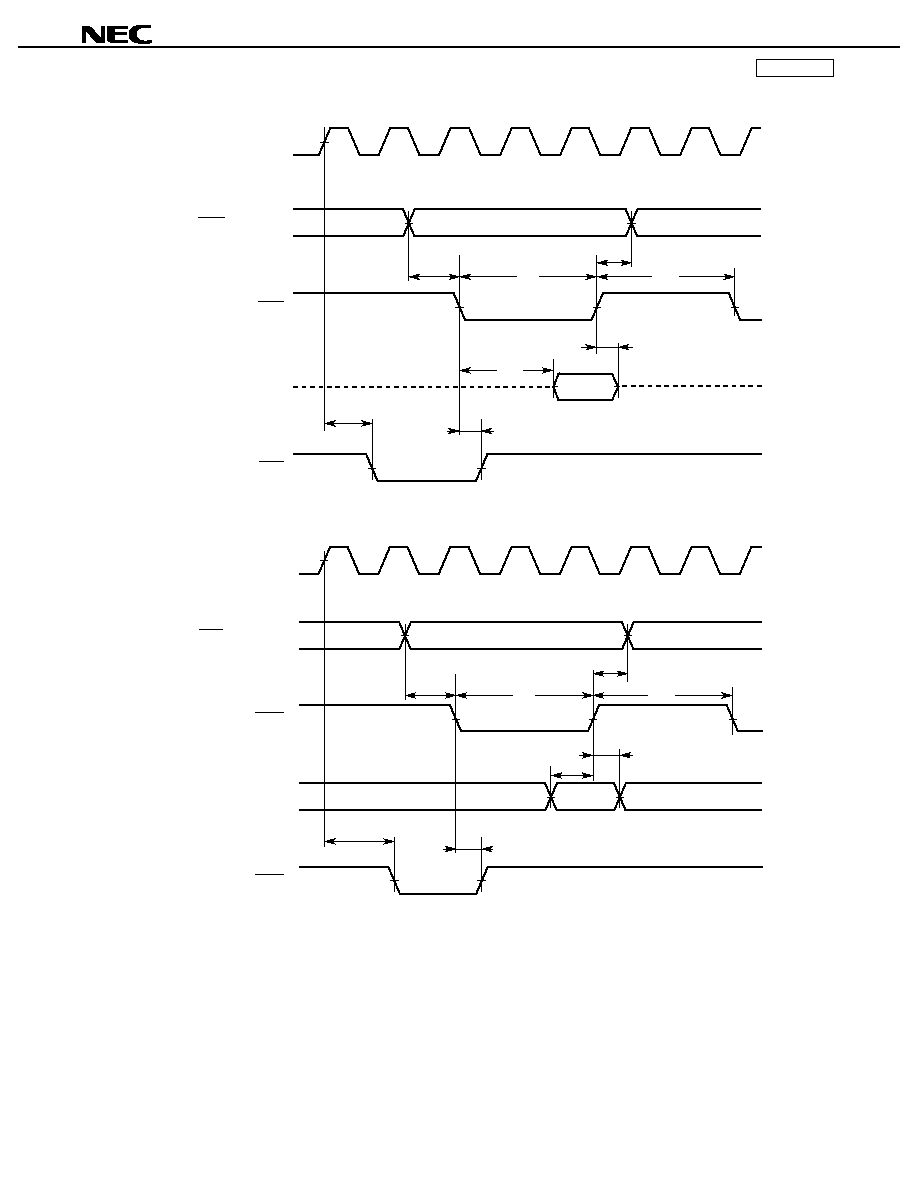
Data Sheet U12801EJ4V0DS00
53
µ
µ
µ
µ
PD77110, 77111, 77112
µ
PD77110
Host read interface timing
CLKIN
HRD
t
dHE
t
hHDR
t
hHCAR
t
recHS
t
vHDR
t
wHR
t
dHR
t
hHE
HCS, HA0, HA1
HD0 - HD7
HRE
Hi-Z
Hi-Z
Host write interface timing
CLKIN
HWR
t
dHE
t
hHDW
t
hHCAW
t
recHS
t
wHW
t
dHW
t
hHE
HCS, HA0, HA1
HD0 - HD7
HWE
t
suHDW
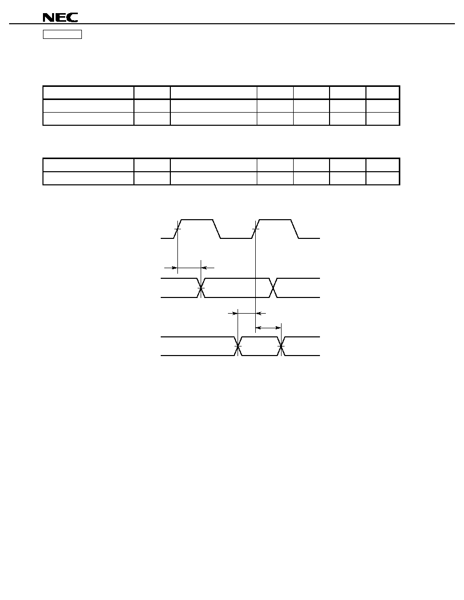
Data Sheet U12801EJ4V0DS00
54
µ
µ
µ
µ
PD77110, 77111, 77112
µ
PD77110
General-purpose I/O Port
Timing requirements
Parameter
Symbol
Condition
MIN.
TYP.
MAX.
Unit
Port input setup time
t
suPI
0
ns
Port input hold time
t
hPI
10
ns
Switching characteristics
Parameter
Symbol
Condition
MIN.
TYP.
MAX.
Unit
Port output delay time
t
dPO
25
ns
General-purpose I/O port timing
CLKIN
P0 - P3
(Output)
t
dPO
t
hPI
t
suPI
P0 - P3
(Input)
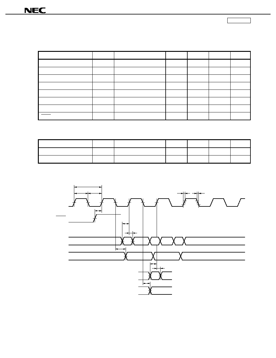
Data Sheet U12801EJ4V0DS00
55
µ
µ
µ
µ
PD77110, 77111, 77112
µ
PD77110
Debugging Interface (JTAG)
Timing requirements
Parameter
Symbol
Condition
MIN.
TYP.
MAX.
Unit
TCK cycle time
t
cTCK
120
ns
TCK high-/low-level width
t
wTCK
50
ns
TCK rise/fall time
t
rfTCK
20
ns
TMS, TDI setup time
t
suDI
20
ns
TMS, TDI hold time
t
hDI
20
ns
Input pin setup time
t
suJIN
20
ns
Input pin hold time
t
hJIN
20
ns
TRST setup time
t
suTRST
100
ns
Switching characteristics
Parameter
Symbol
Condition
MIN.
TYP.
MAX.
Unit
TDO output delay time
t
dDO
20
ns
Output pin output delay time
t
dJOUT
20
ns
Debugging interface timing
t
cTCK
t
suTRST
t
wTCK
t
wTCK
t
rfTCK
t
rfTCK
t
suDI
t
hDI
t
dDO
t
suJIN
t
hJIN
t
dJOUT
Valid
Valid
Valid
Valid
TCK
TRST
TMS, TDI
TDO
Capture state
Update state
Remark For details of JTAG, refer to IEEE1149.1.
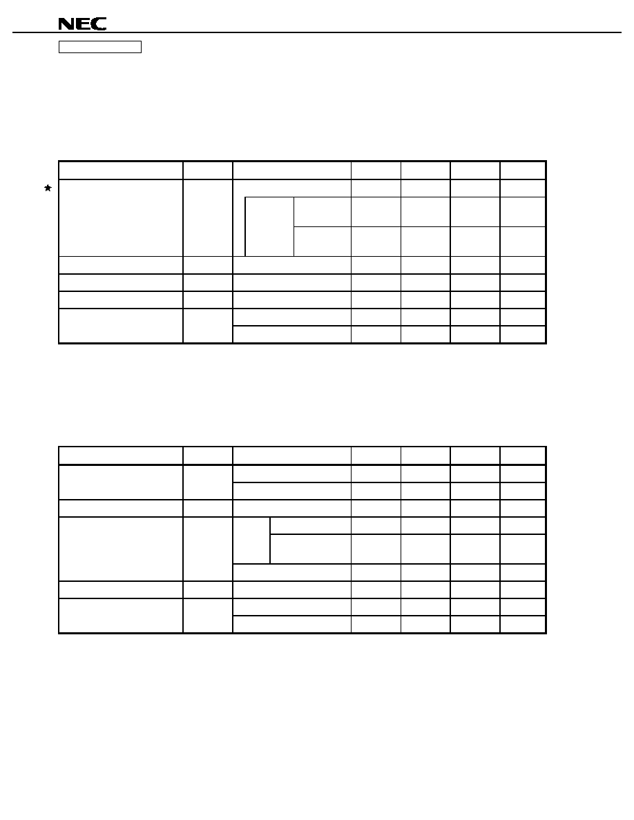
Data Sheet U12801EJ4V0DS00
56
µ
µ
µ
µ
PD77110, 77111, 77112
µ
PD77111, 77112
(2)
µ
µ
µ
µ
PD77111, 77112 AC Characteristics (T
A
=
-
-
-
-
40 to +85
∞
∞
∞
∞
C, with IV
DD
and EV
DD
within recommended
operating condition range)
Clock
Timing requirements
Parameter
Symbol
Condition
MIN.
TYP.
MAX.
Unit
25
ns
IV
DD
= 1.8
to 2.7 V
25
◊
m
50
◊
m
ns
CLKIN cycle time
Note 1
t
cCX
PLL lock
range
Note 2
IV
DD
= 2.3
to 2.7 V
10
◊
m
50
◊
m
ns
CLKIN high-level width
t
wCXH
12.5
ns
CLKIN low-level width
t
wCXL
12.5
ns
CLKIN rise/fall time
t
rfCX
5
ns
IV
DD
= 1.8 to 2.7 V
25
ns
Internal clock cycle time
requirements
Note 3
t
cC (R)
IV
DD
= 2.3 to 2.7 V
13.3
ns
Notes 1. m: Multiple, n: Division ratio
2. This is the range in which the PLL is locked (stably oscillates). Input t
cCX
within this range.
3. Input t
cCX
so that the value of (t
cCX
˜
m
◊
n) satisfies this condition.
Switching characteristics
Parameter
Symbol
Condition
MIN.
TYP.
MAX.
Unit
During normal operation
t
cCX
◊
n
˜
m
ns
Internal clock cycle
Note
t
cC
In HALT mode
t
cCX
◊
n
˜
m
◊
l
ns
CLKOUT cycle time
t
cCO
t
cC
ns
n = 1, or even number
t
cCX
˜
2
-
3
ns
During
normal
operation
n = odd number
(other than 1)
t
cCX
˜
m
-
3
ns
CLKOUT width
t
wCO
In HALT mode
t
cCX
˜
m
◊
n
-
3
ns
CLKOUT rise/fall time
t
rfCO
5
ns
IV
DD
= 1.8 to 2.7 V
20
ns
CLKOUT delay time
t
dCO
IV
DD
= 2.3 to 2.7 V
15
ns
Note m: Multiple, n: Division ratio, l: HALT division ratio
Data Sheet U12801EJ4V0DS00
57
µ
µ
µ
µ
PD77110, 77111, 77112
µ
PD77111, 77112
Clock I/O timing
Internal clock
CLKIN
CLKOUT
t
cCX
t
cC,
t
cC(R)
t
wCXH
t
wCXL
t
rfCX
t
rfCX
t
cCO
t
dCO
t
wCO
t
wCO
t
rfCO
t
rfCO
Data Sheet U12801EJ4V0DS00
58
µ
µ
µ
µ
PD77110, 77111, 77112
µ
PD77111, 77112
Reset, Interrupt
Timing requirements
Parameter
Symbol
Condition
MIN.
TYP.
MAX.
Unit
On power application
Note 1
,
in STOP mode
100 +
2048t
cCX
µ
s
RESET low-level width
t
w (RL)
During normal operation,
in HALT mode
4t
cC
Note 2
Note 3
ns
On power application
Note 4
4t
cCX
ns
RESET recovery time
t
rec (R)
4t
cC
Note 2
ns
WAKEUP low-level width
t
w (WAKEUPL)
100
µ
s
INT1 - INT4 low-level width
t
w (INTL)
3t
cC
Note 2
ns
INT1 - INT4 recovery time
t
rec (INT)
3t
cC
ns
Notes 1. The value on power application is the time from when the supply voltages have reached IV
DD
= 1.8 V
and EV
DD
= 2.7 V. A stable clock input is also required.
2. Note that t
cC
is I (I = integer of 1 to 16) times that during normal operation in the HALT mode.
3. If the low-level width of RESET is greater than 1024t
cC
, the PLL initialization mode is triggered. If there
is no need to use the PLL initialization mode, set the width to less than 1024t
cC
.
4. When the power is turned on, a recovery period of 4t
cCX
is necessary before inputting RESET.
Reset timing
RESET
t
w(RL)
t
rec(R)
WAKEUP timing
WAKEUP
t
w (WAKEUPL)
Interrupt timing
INT1 - INT4
t
w(INTL)
t
rec(INT)

Data Sheet U12801EJ4V0DS00
59
µ
µ
µ
µ
PD77110, 77111, 77112
µ
PD77111, 77112
External Data Memory Access (
µ
µ
µ
µ
PD77112 only)
Timing requirements
Parameter
Symbol
Condition
MIN.
TYP.
MAX.
Unit
Read data setup time
t
suDDRD
18
ns
Read data hold time
t
hDDRD
0
ns
Switching characteristics
Parameter
Symbol
Condition
MIN.
TYP.
MAX.
Unit
Address cycle time
t
rcDA
t
cC
+ (t
cC
◊
t
cDW
)
Note
ns
Address output hold time
t
hDA
0
ns
MRD output delay time
t
dDR
5
ns
Write data output valid time
t
vDDWD
5
ns
Write data output hold time
t
hDDWD
0
ns
MWR output delay time
t
dDW
0
0.5 t
cC
ns
MWR output hold time
t
hDA
0
ns
MWR low-level width
t
wDWL
t
cC
◊
t
cDW
-
3
ns
MWR high-level width
t
wDWH
0.5 t
cC
-
3
ns
Note t
cDW
: Number of data wait cycles
Data Sheet U12801EJ4V0DS00
60
µ
µ
µ
µ
PD77110, 77111, 77112
µ
PD77111, 77112
External data memory access timing (read)
DA0 - DA13
MRD
X/Y
D0 - D15
t
rcDA
t
dDR
t
dDR
t
suDDRD
t
hDDRD
External data memory access timing (write)
DA0 - DA13
X/Y
MWR
D0 - D15
t
rcDA
t
dDW
t
vDDWD
Hi-Z
Hi-Z
t
vDDWD
t
hDDWD
t
wDWL
t
wDWH
t
hDA
t
dDW

Data Sheet U12801EJ4V0DS00
61
µ
µ
µ
µ
PD77110, 77111, 77112
µ
PD77111, 77112
Bus Arbitration (
µ
µ
µ
µ
PD77112 only)
Timing requirements
Parameter
Symbol
Condition
MIN.
TYP.
MAX.
Unit
HOLDRQ setup time
t
suHRQ
0
ns
HOLDRQ hold time
t
hHRQ
0
ns
Switching characteristics
Parameter
Symbol
Condition
MIN.
TYP.
MAX.
Unit
BSTB hold time
t
hBS
0
ns
BSTB output delay time
t
dBS
20
ns
HOLDAK output delay time
t
dHAK
18
ns
Data hold time during bus
arbitration
t
h (BS-D)
25
ns
Data valid time during bus
arbitration
t
v (BS-D)
25
ns
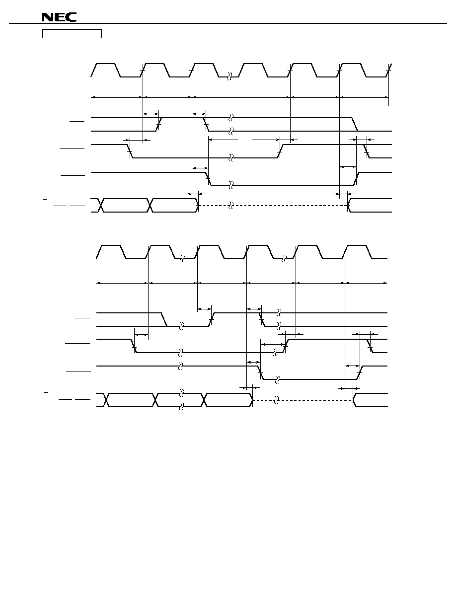
Data Sheet U12801EJ4V0DS00
62
µ
µ
µ
µ
PD77110, 77111, 77112
µ
PD77111, 77112
Bus arbitration timing (when bus is idle)
CLKIN
t
suHRQ
BSTB
HOLDRQ
HOLDAK
X/Y, DA0 - DA13,
MRD, MWR
t
hBS
(Bus busy)
Bus idle
t
dBS
t
dHAK
t
h (BS-D)
t
hHRQ
t
suHRQ
Bus release
Bus idle
(Bus busy)
t
hHRQ
t
v (BS-D)
t
dHAK
Hi-Z
Bus arbitration timing (when bus is busy)
CLKIN
t
suHRQ
BSTB
HOLDRQ
HOLDAK
X/Y, DA0 - DA13,
MRD, MWR
(Bus busy)
Bus busy
t
hBS
t
dHAK
t
suHRQ
Bus idle
Bus idle
(Bus busy)
t
hHRQ
t
v (BS-D)
t
dHAK
Bus release
t
hHRQ
t
dBS
t
h (BS-D)
Hi-Z
Data Sheet U12801EJ4V0DS00
63
µ
µ
µ
µ
PD77110, 77111, 77112
µ
PD77111, 77112
Serial Interface
Timing requirements
Parameter
Symbol
Condition
MIN.
TYP.
MAX.
Unit
SCK cycle time
t
cSC
60
ns
SCK high-/low-level width
t
wSC
25
ns
SCK rise/fall time
t
rfSC
20
ns
IV
DD
= 1.8 to 2.7 V
10
ns
SOEN setup time
t
suSOE
IV
DD
= 2.3 to 2.7 V
5
ns
IV
DD
= 1.8 to 2.7 V
15
ns
SOEN hold time
t
hSOE
IV
DD
= 2.3 to 2.7 V
10
ns
IV
DD
= 1.8 to 2.7 V
10
ns
SIEN setup time
t
suSIE
IV
DD
= 2.3 to 2.7 V
5
ns
IV
DD
= 1.8 to 2.7 V
15
ns
SIEN hold time
t
hSIE
IV
DD
= 2.3 to 2.7 V
10
ns
IV
DD
= 1.8 to 2.7 V
10
ns
SI setup time
t
suSI
IV
DD
= 2.3 to 2.7 V
5
ns
IV
DD
= 1.8 to 2.7 V
15
ns
SI hold time
t
hSI
IV
DD
= 2.3 to 2.7 V
10
ns
Switching characteristics
Parameter
Symbol
Condition
MIN.
TYP.
MAX.
Unit
IV
DD
= 1.8 to 2.7 V
30
ns
SORQ output delay time
t
dSOR
IV
DD
= 2.3 to 2.7 V
25
ns
SORQ hold time
t
hSOR
0
ns
IV
DD
= 1.8 to 2.7 V
30
ns
SO output delay time
t
dSO
IV
DD
= 2.3 to 2.7 V
25
ns
SO hold time
t
hSO
0
ns
IV
DD
= 1.8 to 2.7 V
30
ns
SIAK output delay time
t
dSIA
IV
DD
= 2.3 to 2.7 V
25
ns
SIAK hold time
t
hSIA
0
ns

Data Sheet U12801EJ4V0DS00
64
µ
µ
µ
µ
PD77110, 77111, 77112
µ
PD77111, 77112
Caution If noise is superimposed on the serial clock, the serial interface may be deadlocked. Bear in
mind the following points when designing your system:
∑
Reinforce the wiring for power supply and ground (if noise is superimposed on the power and
ground lines, it has the same effect as if noise were superimposed on the serial clock).
∑
Shorten the wiring between the device's SCK1 and SCK2 pins, and clock supply source.
∑
Do not cross the signal lines of the serial clock with any other signal lines. Do not route the
serial clock line in the vicinity of a line through which a high alternating current flows.
∑
Supply the clock to the SCK1 and SCK2 pins of the device from the clock source on a one-to-
one basis. Do not supply clock to several devices from one clock source.
∑
Exercise care that the serial clock does not overshoot or undershoot. In particular, make sure
that the rising and falling of the serial clock waveform are clear.
Make sure that the serial clock
rises and falls linearly.
The serial clock must not bound. Noise
must not be superimposed on the serial clock.
The serial clock must not rise or
fall step-wise.
◊
◊
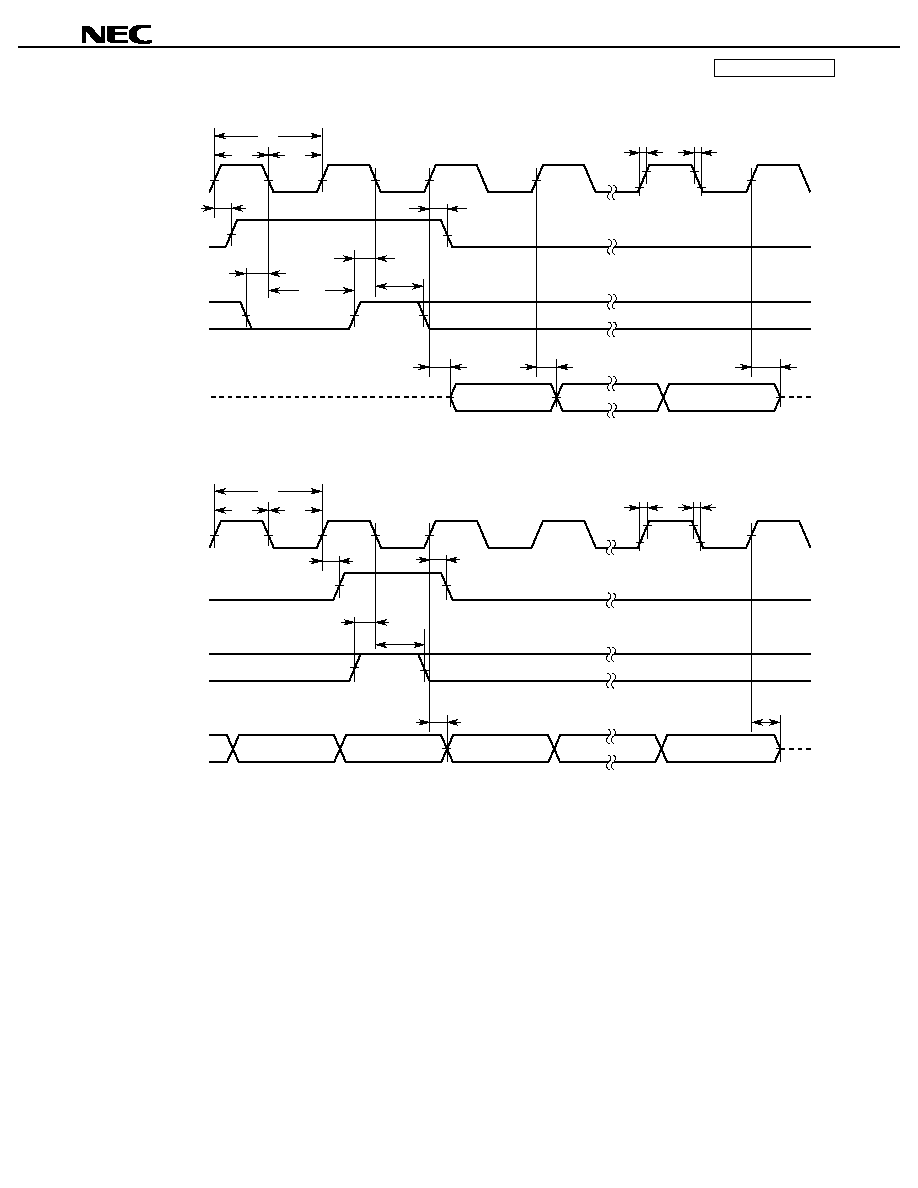
Data Sheet U12801EJ4V0DS00
65
µ
µ
µ
µ
PD77110, 77111, 77112
µ
PD77111, 77112
Serial output timing 1
SCK1,
SCK2
t
rfSC
SORQ1
SOEN1,
SOEN2
SO1,
SO2
1st
Last
t
hSO
t
dSO
t
dSO
t
hSOE
t
suSOE
t
suSOE
t
hSOE
t
dSOR
t
wSC
t
wSC
t
cSC
t
hSOR
t
rfSC
Hi-Z
Serial output timing 2 (during successive output)
SCK1,
SCK2
t
rfSC
SORQ1
SOEN1,
SOEN2
SO1,
SO2
1st
Last
t
dSO
t
hSOE
t
suSOE
t
dSOR
t
wSC
t
wSC
t
cSC
t
hSOR
t
rfSC
Last
t
hSO
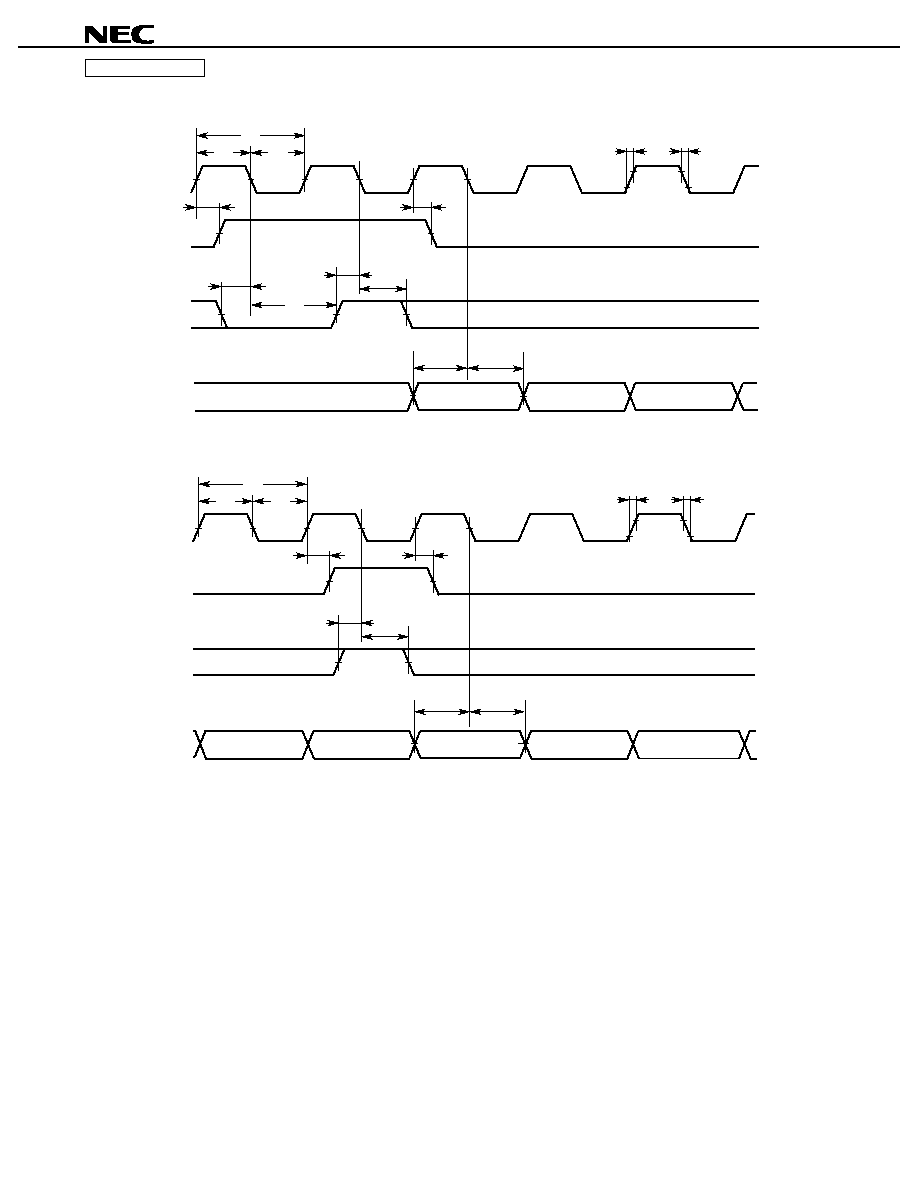
Data Sheet U12801EJ4V0DS00
66
µ
µ
µ
µ
PD77110, 77111, 77112
µ
PD77111, 77112
Serial input timing 1
SCK1,
SCK2
SIAK1
SIEN1,
SIEN2
SI1,
SI2
t
cSC
t
wSC
t
wSC
t
dSIA
t
suSIE
t
hSIE
t
suSIE
t
hSIE
t
hSIA
t
suSI
t
hSI
1st
2nd
t
rfSC
t
rfSC
3rd
Serial input timing 2 (during successive input)
SCK1,
SCK2
SIAK1
SIEN1,
SIEN2
SI1,
SI2
t
cSC
t
wSC
t
wSC
t
dSIA
t
suSIE
t
hSIE
t
hSIA
t
suSI
t
hSI
1st
3rd
t
rfSC
t
rfSC
Last
Last≠1
2nd
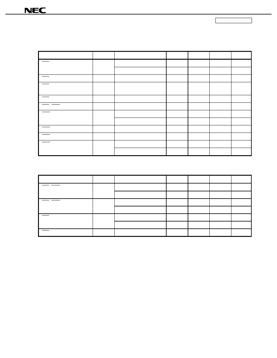
Data Sheet U12801EJ4V0DS00
67
µ
µ
µ
µ
PD77110, 77111, 77112
µ
PD77111, 77112
Host Interface
Timing requirements
Parameter
Symbol
Condition
MIN.
TYP.
MAX.
Unit
IV
DD
= 1.8 to 2.7 V
15
ns
HRD delay time
t
dHR
IV
DD
= 2.3 to 2.7 V
10
ns
HRD width
t
wHR
60
ns
HCS, HA0, HA1, read hold
time
t
hHCAR
0
ns
HCS, HA0, HA1 line hold time
t
hHCAW
0
ns
HRD, HWR recovery time
t
recHS
60
ns
IV
DD
= 1.8 to 2.7 V
15
ns
HWR delay time
t
dHW
IV
DD
= 2.3 to 2.7 V
10
ns
HWR width
t
wHW
60
ns
HWR hold time
t
hHDW
0
ns
IV
DD
= 1.8 to 2.7 V
15
ns
HWR setup time
t
suHDW
IV
DD
= 2.3 to 2.7 V
10
ns
Switching characteristics
Parameter
Symbol
Condition
MIN.
TYP.
MAX.
Unit
IV
DD
= 1.8 to 2.7 V
30
ns
HRE, HWE output delay time
t
dHE
IV
DD
= 2.3 to 2.7 V
25
ns
IV
DD
= 1.8 to 2.7 V
30
ns
HRE, HWE hold time
t
hHE
IV
DD
= 2.3 to 2.7 V
25
ns
IV
DD
= 1.8 to 2.7 V
30
ns
HRD valid time
t
vHDR
IV
DD
= 2.3 to 2.7 V
25
ns
HRD hold time
t
hHDR
0
ns
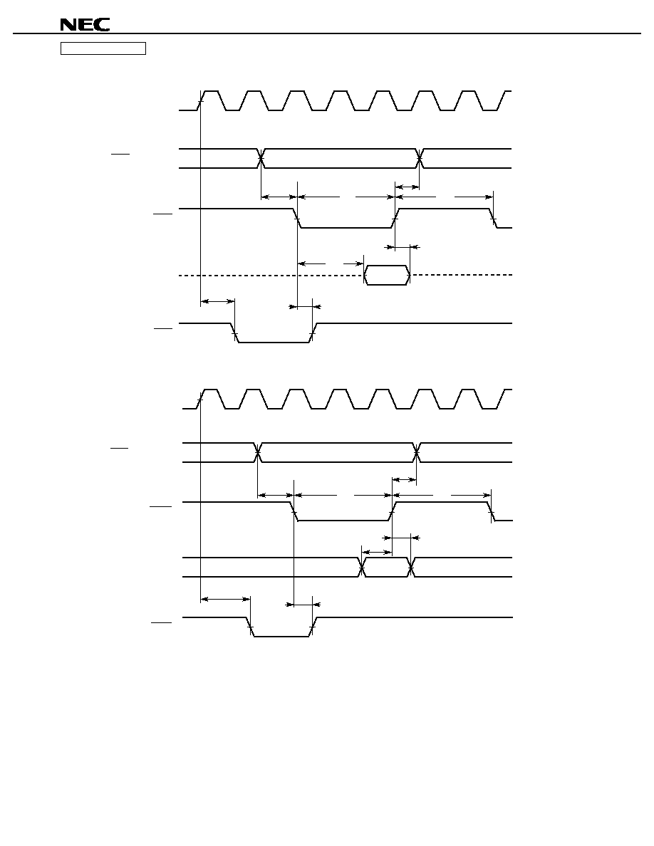
Data Sheet U12801EJ4V0DS00
68
µ
µ
µ
µ
PD77110, 77111, 77112
µ
PD77111, 77112
Host read interface timing
CLKIN
HRD
t
dHE
t
hHDR
t
hHCAR
t
recHS
t
vHDR
t
wHR
t
dHR
t
hHE
HCS, HA0, HA1
HD0 - HD7
HRE
Hi-Z
Hi-Z
Host write interface timing
CLKIN
HWR
t
dHE
t
hHDW
t
hHCAW
t
recHS
t
wHW
t
dHW
t
hHE
HCS, HA0, HA1
HD0 - HD7
HWE
t
suHDW
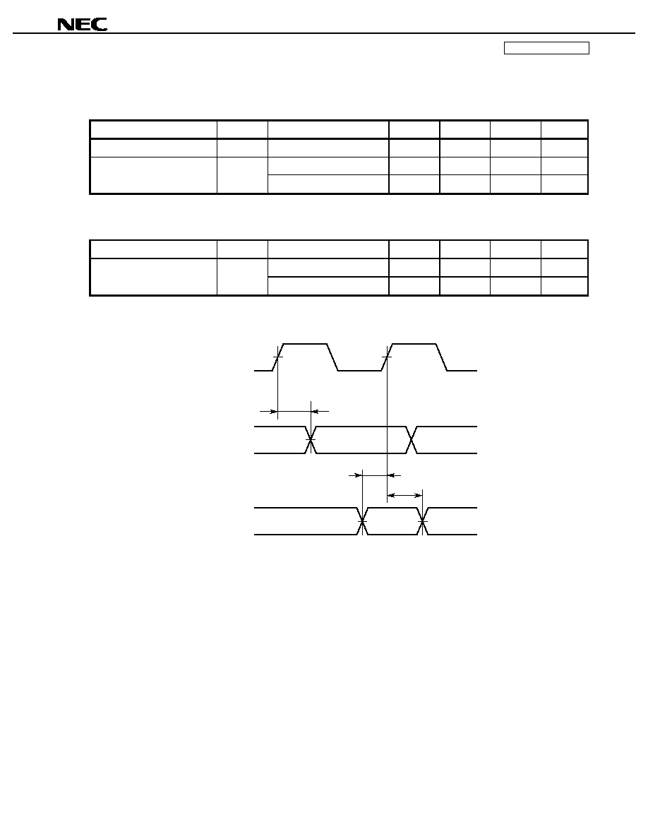
Data Sheet U12801EJ4V0DS00
69
µ
µ
µ
µ
PD77110, 77111, 77112
µ
PD77111, 77112
General-purpose I/O Port
Timing requirements
Parameter
Symbol
Condition
MIN.
TYP.
MAX.
Unit
Port input setup time
t
suPI
0
ns
IV
DD
= 1.8 to 2.7 V
15
ns
Port input hold time
t
hPI
IV
DD
= 2.3 to 2.7 V
10
ns
Switching characteristics
Parameter
Symbol
Condition
MIN.
TYP.
MAX.
Unit
IV
DD
= 1.8 to 2.7 V
30
ns
Port output delay time
t
dPO
IV
DD
= 2.3 to 2.7 V
25
ns
General-purpose I/O port timing
CLKIN
P0 - P3
(Output)
t
dPO
t
hPI
t
suPI
P0 - P3
(Input)
Data Sheet U12801EJ4V0DS00
70
µ
µ
µ
µ
PD77110, 77111, 77112
Debugging Interface (JTAG)
Timing requirements
Parameter
Symbol
Condition
MIN.
TYP.
MAX.
Unit
TCK cycle time
t
cTCK
120
ns
TCK high-/low-level width
t
wTCK
50
ns
TCK rise/fall time
t
rfTCK
20
ns
IV
DD
= 1.8 to 2.7 V
25
ns
TMS, TDI setup time
t
suDI
IV
DD
= 2.3 to 2.7 V
20
ns
IV
DD
= 1.8 to 2.7 V
25
ns
TMS, TDI hold time
t
hDI
IV
DD
= 2.3 to 2.7 V
20
ns
IV
DD
= 1.8 to 2.7 V
25
ns
Input pin setup time
t
suJIN
IV
DD
= 2.3 to 2.7 V
20
ns
IV
DD
= 1.8 to 2.7 V
25
ns
Input pin hold time
t
hJIN
IV
DD
= 2.3 to 2.7 V
20
ns
TRST setup time
t
suTRST
100
ns
Switching characteristics
Parameter
Symbol
Condition
MIN.
TYP.
MAX.
Unit
IV
DD
= 1.8 to 2.7 V
25
ns
TDO output delay time
t
dDO
IV
DD
= 2.3 to 2.7 V
20
ns
IV
DD
= 1.8 to 2.7 V
25
ns
Output pin output delay time
t
dJOUT
IV
DD
= 2.3 to 2.7 V
20
ns
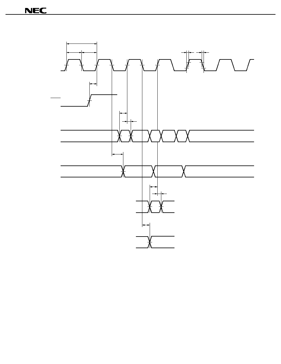
Data Sheet U12801EJ4V0DS00
71
µ
µ
µ
µ
PD77110, 77111, 77112
Debugging interface timing
t
cTCK
t
wTCK
t
suTRST
t
suDI
t
hDI
t
dDO
t
suJIN
t
hJIN
Valid
Valid
t
dJOUT
t
wTCK
t
rfTCK
t
rfTCK
Valid
Valid
TCK
TRST
TMS, TDI
TDO
Capture state
Update state
Remark For details of JTAG, refer to IEEE1149.1.
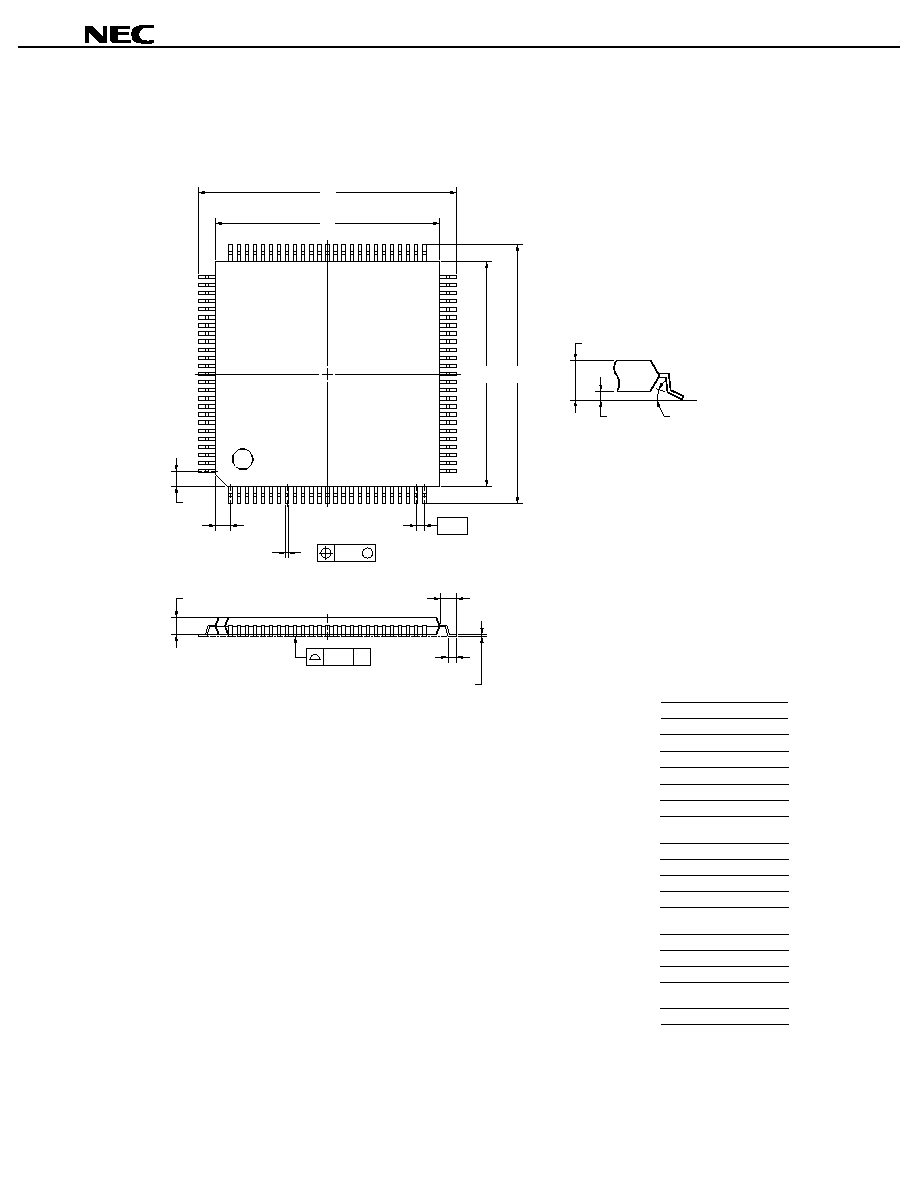
Data Sheet U12801EJ4V0DS00
72
µ
µ
µ
µ
PD77110, 77111, 77112
11. PACKAGE
100-PIN PLASTIC TQFP (FINE PITCH) (14x14)
NOTE
Each lead centerline is located within 0.10 mm of
its true position (T.P.) at maximum material condition.
ITEM
MILLIMETERS
A
B
D
G
16.0
±
0.2
14.0
±
0.2
0.5 (T.P.)
1.0
J
16.0
±
0.2
K
C
14.0
±
0.2
I
0.10
1.0
±
0.2
L
0.5
±
0.2
F
1.0
N
P
Q
0.10
1.0
±
0.1
0.1
±
0.05
S100GC-50-9EU-2
S
1.27 MAX.
H
0.22
+
0.05
-
0.04
M
0.145
+
0.055
-
0.045
R
3
∞+
7
∞
-
3
∞
75
76
50
100
1
26
25
51
S
N
J
detail of lead end
C
D
A
B
R
K
M
L
P
I
S
Q
G
F
M
H
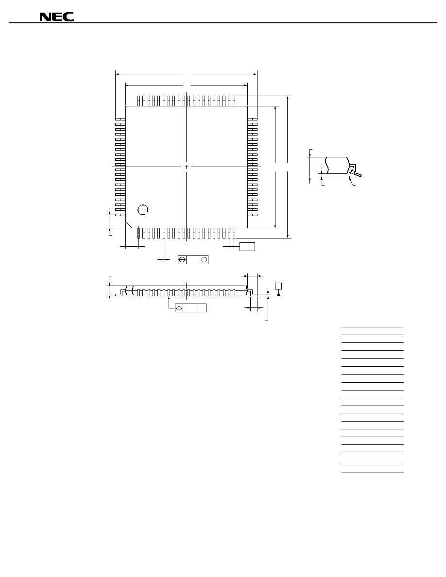
Data Sheet U12801EJ4V0DS00
73
µ
µ
µ
µ
PD77110, 77111, 77112
60
41
40
21
61
80
1
20
80-PIN PLASTIC TQFP (FINE PITCH) (12x12)
NOTE
Each lead centerline is located within 0.10 mm of
its true position (T.P.) at maximum material condition.
ITEM
MILLIMETERS
A
B
D
G
14.0
±
0.2
12.0
±
0.2
1.25
14.0
±
0.2
C
12.0
±
0.2
0.10
I
J
H
0.22
±
0.05
0.5 (T.P.)
K
1.0
±
0.2
F
1.25
M
0.145
±
0.05
1.0
±
0.05
P
Q
N
0.10
0.1
±
0.05
L
0.5
±
0.2
S80GK-50-9EU-1
S
1.2 MAX.
R
3
∞+
7
∞
-
3
∞
M
S
S
N
J
detail of lead end
C
D
A
B
R
K
M
L
P
I
S
Q
G
F
H
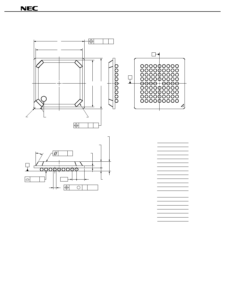
Data Sheet U12801EJ4V0DS00
74
µ
µ
µ
µ
PD77110, 77111, 77112
A
S
B
9
8
7
6
5
4
3
2
1
J
A
B
C
D
E
F
G
H
80-PIN PLASTIC FBGA (9x9)
ITEM
MILLIMETERS
B
C
8.40
8.40
D
9.00
±
0.10
A
9.00
±
0.10
S80F1-80-CN1-1
R
25
∞
W
Y1
0.20
0.20
E
F
0.8 (T.P.)
1.30
H
I
0.36
K
0.10
L
M
0.08
P
Q
R0.3
C1.0
0.96
G
0.35
±
0.1
J
1.31
±
0.15
0.50
+0.05
≠0.10
P
Index mark
R
J
F
E
G
H
I
W
S A
W
S B
K
S
Y1
S
M
S
M
L
D
C
A
B
Q
A B
Data Sheet U12801EJ4V0DS00
75
µ
µ
µ
µ
PD77110, 77111, 77112
12. RECOMMENDED SOLDERING CONDITIONS
It is recommended to solder this product under the following conditions.
For details of the recommended soldering conditions, refer to information document "SEMICONDUCTOR DEVICE
MOUNTING TECHNOLOGY MANUAL" (C10535E).
For soldering methods and conditions other than those recommended, consult NEC.
Surface mount type
µ
µ
µ
µ
PD77110GC-9EU: 100-pin plastic TQFP (fine pitch) (14
◊
◊
◊
◊
14 mm)
µ
µ
µ
µ
PD77111GK-xxx-9EU: 80-pin plastic TQFP (fine pitch) (12
◊
◊
◊
◊
12 mm)
Process
Conditions
Symbol
Infrared ray reflow
Package peak temperature: 235
∞
C, Time: 30 seconds MAX (210
∞
C MIN),
Number of times: 2 MAX, Number of days: 3
Note
(after that, prebaking is
necessary for 10 hours)
IR35-103-2
VPS
Package peak temperature: 215
∞
C, Time: 30 seconds MAX (210
∞
C MIN),
Number of times: 2 MAX, Number of days: 3
Note
(after that, prebaking is
necessary for 10 hours)
VP15-103-2
Partial heating method
Pin temperature: 300
∞
C MAX, Time: 3 seconds MAX (per side of device)
-
µ
µ
µ
µ
PD77112GC-xxx-9EU: 100-pin plastic TQFP (fine pitch) (14
◊
◊
◊
◊
14 mm)
Process
Conditions
Symbol
Infrared ray reflow
Package peak temperature: 235
∞
C, Time: 30 seconds MAX (210
∞
C MIN),
Number of times: 3 MAX, Number of days: 7
Note
(after that, prebaking is
necessary for 10 hours)
IR35-107-3
VPS
Package peak temperature: 215
∞
C, Time: 30 seconds MAX (210
∞
C MIN),
Number of times: 3 MAX, Number of days: 7
Note
(after that, prebaking is
necessary for 10 hours)
VP15-107-3
Partial heating method
Pin temperature: 300
∞
C MAX, Time: 3 seconds MAX (per side of device)
-
Note Number of days in storage after the dry pack has been opened. The storage conditions are at 25
∞
C, 65%
RH MAX.
Caution Do not use two or more soldering methods in combination (except partial heating method).
Data Sheet U12801EJ4V0DS00
76
µ
µ
µ
µ
PD77110, 77111, 77112
µ
µ
µ
µ
PD77111F1-xxx-CN1: 80-pin plastic fine-pitch BGA (9
◊
◊
◊
◊
9 mm)
Process
Conditions
Symbol
Infrared ray reflow
Package peak temperature: 230
∞
C, Time: 30 seconds MAX (210
∞
C MIN),
Number of times: 2 MAX, Number of days: 3
Note
(after that, prebaking is
necessary for 10 hours)
IR30-103-2
VPS
Package peak temperature: 215
∞
C, Time: 30 seconds MAX (210
∞
C MIN),
Number of times: 2 MAX, Number of days: 3
Note
(after that, prebaking is
necessary for 10 hours)
VP15-103-2
Note Number of days in storage after the dry pack has been opened. The storage conditions are at 25
∞
C, 65%
RH MAX.
Caution Do not use two or more soldering methods in combination (except partial heating method).

Data Sheet U12801EJ4V0DS00
77
µ
µ
µ
µ
PD77110, 77111, 77112
[MEMO]
Data Sheet U12801EJ4V0DS00
78
µ
µ
µ
µ
PD77110, 77111, 77112
NOTES FOR CMOS DEVICES
1
PRECAUTION AGAINST ESD FOR SEMICONDUCTORS
Note:
Strong electric field, when exposed to a MOS device, can cause destruction of the gate oxide and
ultimately degrade the device operation. Steps must be taken to stop generation of static electricity
as much as possible, and quickly dissipate it once, when it has occurred. Environmental control
must be adequate. When it is dry, humidifier should be used. It is recommended to avoid using
insulators that easily build static electricity. Semiconductor devices must be stored and transported
in an anti-static container, static shielding bag or conductive material. All test and measurement
tools including work bench and floor should be grounded. The operator should be grounded using
wrist strap. Semiconductor devices must not be touched with bare hands. Similar precautions need
to be taken for PW boards with semiconductor devices on it.
2
HANDLING OF UNUSED INPUT PINS FOR CMOS
Note:
No connection for CMOS device inputs can be cause of malfunction. If no connection is provided
to the input pins, it is possible that an internal input level may be generated due to noise, etc., hence
causing malfunction. CMOS devices behave differently than Bipolar or NMOS devices. Input levels
of CMOS devices must be fixed high or low by using a pull-up or pull-down circuitry. Each unused
pin should be connected to V
DD
or GND with a resistor, if it is considered to have a possibility of
being an output pin. All handling related to the unused pins must be judged device by device and
related specifications governing the devices.
3
STATUS BEFORE INITIALIZATION OF MOS DEVICES
Note:
Power-on does not necessarily define initial status of MOS device. Production process of MOS
does not define the initial operation status of the device. Immediately after the power source is
turned ON, the devices with reset function have not yet been initialized. Hence, power-on does
not guarantee out-pin levels, I/O settings or contents of registers. Device is not initialized until the
reset signal is received. Reset operation must be executed immediately after power-on for devices
having reset function.

Data Sheet U12801EJ4V0DS00
79
µ
µ
µ
µ
PD77110, 77111, 77112
Regional Information
Some information contained in this document may vary from country to country. Before using any NEC
product in your application, pIease contact the NEC office in your country to obtain a list of authorized
representatives and distributors. They will verify:
∑
Device availability
∑
Ordering information
∑
Product release schedule
∑
Availability of related technical literature
∑
Development environment specifications (for example, specifications for third-party tools and
components, host computers, power plugs, AC supply voltages, and so forth)
∑
Network requirements
In addition, trademarks, registered trademarks, export restrictions, and other legal issues may also vary
from country to country.
NEC Electronics Inc. (U.S.)
Santa Clara, California
Tel: 408-588-6000
800-366-9782
Fax: 408-588-6130
800-729-9288
NEC Electronics (Germany) GmbH
Duesseldorf, Germany
Tel: 0211-65 03 02
Fax: 0211-65 03 490
NEC Electronics (UK) Ltd.
Milton Keynes, UK
Tel: 01908-691-133
Fax: 01908-670-290
NEC Electronics Italiana s.r.l.
Milano, Italy
Tel: 02-66 75 41
Fax: 02-66 75 42 99
NEC Electronics (Germany) GmbH
Benelux Office
Eindhoven, The Netherlands
Tel: 040-2445845
Fax: 040-2444580
NEC Electronics (France) S.A.
Velizy-Villacoublay, France
Tel: 01-30-67 58 00
Fax: 01-30-67 58 99
NEC Electronics (France) S.A.
Spain Office
Madrid, Spain
Tel: 91-504-2787
Fax: 91-504-2860
NEC Electronics (Germany) GmbH
Scandinavia Office
Taeby, Sweden
Tel: 08-63 80 820
Fax: 08-63 80 388
NEC Electronics Hong Kong Ltd.
Hong Kong
Tel: 2886-9318
Fax: 2886-9022/9044
NEC Electronics Hong Kong Ltd.
Seoul Branch
Seoul, Korea
Tel: 02-528-0303
Fax: 02-528-4411
NEC Electronics Singapore Pte. Ltd.
United Square, Singapore 1130
Tel: 65-253-8311
Fax: 65-250-3583
NEC Electronics Taiwan Ltd.
Taipei, Taiwan
Tel: 02-2719-2377
Fax: 02-2719-5951
NEC do Brasil S.A.
Electron Devices Division
Rodovia Presidente Dutra, Km 214
07210-902-Guarulhos-SP Brasil
Tel: 55-11-6465-6810
Fax: 55-11-6465-6829
J99.1

µ
µ
µ
µ
PD77110, 77111, 77112
The export of these products from Japan is regulated by the Japanese government. The export of some or all of these
products may be prohibited without governmental license. To export or re-export some or all of these products from a
country other than Japan may also be prohibited without a license from that country. Please call an NEC sales
representative.
License not needed
:
µ
PD77110GC-9EU
The customer must judge the need for license:
µ
PD77111GK-xxx-9EU,
µ
PD77111F1-xxx-CN1,
µ
PD77112GC-xxx-9EU
∑
The information in this document is subject to change without notice. Before using this document, please
confirm that this is the latest version.
∑
No part of this document may be copied or reproduced in any form or by any means without the prior written
consent of NEC Corporation. NEC Corporation assumes no responsibility for any errors which may appear in
this document.
∑
NEC Corporation does not assume any liability for infringement of patents, copyrights or other intellectual property
rights of third parties by or arising from use of a device described herein or any other liability arising from use
of such device. No license, either express, implied or otherwise, is granted under any patents, copyrights or other
intellectual property rights of NEC Corporation or others.
∑
Descriptions of circuits, software, and other related information in this document are provided for illustrative
purposes in semiconductor product operation and application examples. The incorporation of these circuits,
software, and information in the design of the customer's equipment shall be done under the full responsibility
of the customer. NEC Corporation assumes no responsibility for any losses incurred by the customer or third
parties arising from the use of these circuits, software, and information.
∑
While NEC Corporation has been making continuous effort to enhance the reliability of its semiconductor devices,
the possibility of defects cannot be eliminated entirely. To minimize risks of damage or injury to persons or
property arising from a defect in an NEC semiconductor device, customers must incorporate sufficient safety
measures in its design, such as redundancy, fire-containment, and anti-failure features.
∑
NEC devices are classified into the following three quality grades:
"Standard", "Special", and "Specific". The Specific quality grade applies only to devices developed based on a
customer designated "quality assurance program" for a specific application. The recommended applications of
a device depend on its quality grade, as indicated below. Customers must check the quality grade of each device
before using it in a particular application.
Standard: Computers, office equipment, communications equipment, test and measurement equipment,
audio and visual equipment, home electronic appliances, machine tools, personal electronic
equipment and industrial robots
Special: Transportation equipment (automobiles, trains, ships, etc.), traffic control systems, anti-disaster
systems, anti-crime systems, safety equipment and medical equipment (not specifically designed
for life support)
Specific: Aircraft, aerospace equipment, submersible repeaters, nuclear reactor control systems, life
support systems or medical equipment for life support, etc.
The quality grade of NEC devices is "Standard" unless otherwise specified in NEC's Data Sheets or Data Books.
If customers intend to use NEC devices for applications other than those specified for Standard quality grade,
they should contact an NEC sales representative in advance.
M7 98. 8