Document Outline
- COVER
- DESCRIPTION
- FEATURES
- ORDERING INFORMATION
- BLOCK DIAGRAM
- FUNCTION PIN GROUPS
- DSP FUNCTION LIST
- PIN CONFIGURATIONS
- PIN NAME
- 1. PIN FUNCTION
- 1.1 Pin Function Description
- 1.2 Connection of Unused Pins
- 1.2.1 Connection of function pins
- 1.2.2 Connection of no-function pins
- 2. FUNCTION OUTLINE
- 2.1 Program Control Unit
- 2.1.1 CPU control
- 2.1.2 Interrupt control
- 2.1.3 Loop control task
- 2.1.4 PC stack
- 2.1.5 PLL
- 2.1.6 Instruction memory
- 2.2 Arithmetic Unit
- 2.2.1 General-purpose registers (R0 to R7)
- 2.2.2 Multiply accumulator (MAC)
- 2.2.3 Arithmetic logic unit (ALU)
- 2.2.4 Barrel shifter (BSFT: Barrel ShiFTer)
- 2.3 Data Memory Unit
- 2.3.1 Data memory
- 2.3.2 Data addressing unit
- 2.4 Peripheral Unit
- 2.4.1 Audio Serial interface (ASIO)
- 2.4.2 Host interface (HIO)
- 2.4.3 General-purpose I/O port (PIO)
- 2.4.4 SD card interface (SDCIF)
- 2.4.5 Timer
- 3. RESET FUNCTION
- 3.1 Hardware Reset
- 3.2 Initializing PLL
- 4. FUNCTIONS OF BOOT-UP ROM
- 4.1 Boot at Reset
- 4.2 Reboot
- 4.3 Signature Operation
- 5. STANDBY MODES
- 5.1 HALT Mode
- 5.2 STOP Mode
- 6. MEMORY MAP
- 6.1 Instruction Memory
- 6.1.1 Instruction memory map
- 6.1.2 Interrupt vector table
- 6.2 Data Memory
- 6.2.1 Data memory map
- 6.2.2 Internal peripherals
- 7. INSTRUCTIONS
- 7.1 Outline of Instructions
- 7.2 Instruction Set and Operation
- 8. ELECTRICAL SPECIFICATIONS
- 9. PACKAGES
- 10. RECOMMENDED SOLDERING CONDITIONS

The information in this document is subject to change without notice. Before using this document, please
confirm that this is the latest version.
Not all products and/or types are available in every country. Please check with an NEC Electronics
sales representative for availability and additional information.
MOS INTEGRATED CIRCUIT
µ
PD77115, 77115A
16-BIT FIXED-POINT DIGITAL SIGNAL PROCESSOR
Document No. U14867EJ5V0DS00 (5th edition)
Date Published August 2004 NS CP(K)
Printed in Japan
DATA SHEET
2000, 2004
The mark shows major revised points.
DESCRIPTION
The
µ
PD77115 and
µ
PD77115A are 16-bit fixed-point digital signal processors (DSP).
The
µ
PD77115 and
µ
PD77115A are RAM based DSP and have the specific circuit for audio application.
Unless otherwise specified, the
µ
PD77115 refers to
µ
PD77115 and 77115A.
For details of the functions of the
µ
PD77115, refer to the following User's Manuals:
µ
PD77111 Family User's Manual - Architecture
: U14623E
µ
PD77016 Family User's Manual - Instructions
: U13116E
FEATURES
∑
Instruction cycle (operating clock)
13.3 ns MIN. (75 MHz MAX.)
∑
Memory
∑ Internal instruction RAM
11.5K words
◊ 32 bits
∑ Internal data RAM
16K words
◊ 16 bits ◊ 2 banks
∑
Peripherals
∑ Audio serial interface
∑ Secure Digital (SD) card interface
∑ 16-bit
timer
∑ 16-bit host interface
∑ 8-bit
port
∑
Supply voltage
∑ DSP core voltage
2.0 to 2.7 V (MAX. operation speed 50 MHz)
2.3 to 2.7 V (MAX. operation speed 75 MHz)
∑ I/O pin voltage
2.7 to 3.6 V
∑
Power consumption
TYP. 50 mW (2.0 V, 50 MHz operation)
ORDERING INFORMATION
Part
Number
Package
µ
PD77115F1-CN6
80-pin plastic FBGA (9
◊ 9)
µ
PD77115GK-9EU
80-pin plastic TQFP (fine pitch) (12
◊ 12)
µ
PD77115AF1-xxx-CN6
80-pin plastic FBGA (9
◊ 9)
Remark xxx indicates ROM code suffix.
Data Sheet U14867EJ5V0DS
2
µ
PD77115, 77115A
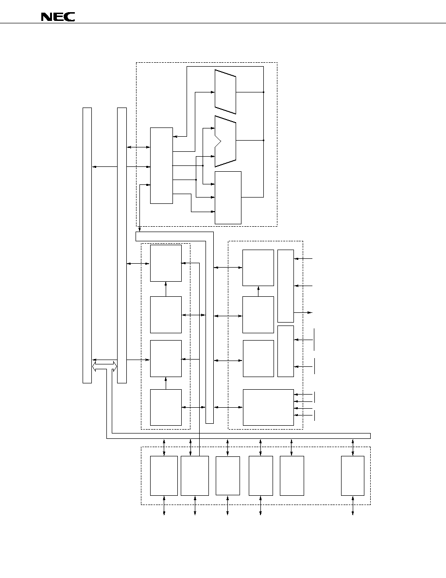
BLOCK DI
AGRAM
Audio serial
interface
Peripheral units
Data memory unit
Operation unit
Program
control unit
SD card
interface
Port
Host
interface
X memory
data
addressing
unit
X memory
Y memory
data
addressing
unit
Y memory
Interrupt
control
Loop control
stack
PC stack
PLL
MAC
16 x 16 + 40 -> 40
ALU(40)
R0 to R7
X bus
Y bus
INT1 to INT4
RESET
CLKOUT
CLKIN
WAKEUP
PLL0 to PLL3
Note
Main bus
Instruction
memory
Debug
interface
CPU control
Note The PLL0 to PLL3 pins are multiplexed with the P4 to P7 pins.
BSFT
Timer
DMA bus
Data Sheet U14867EJ5V0DS
3
µ
PD77115, 77115A
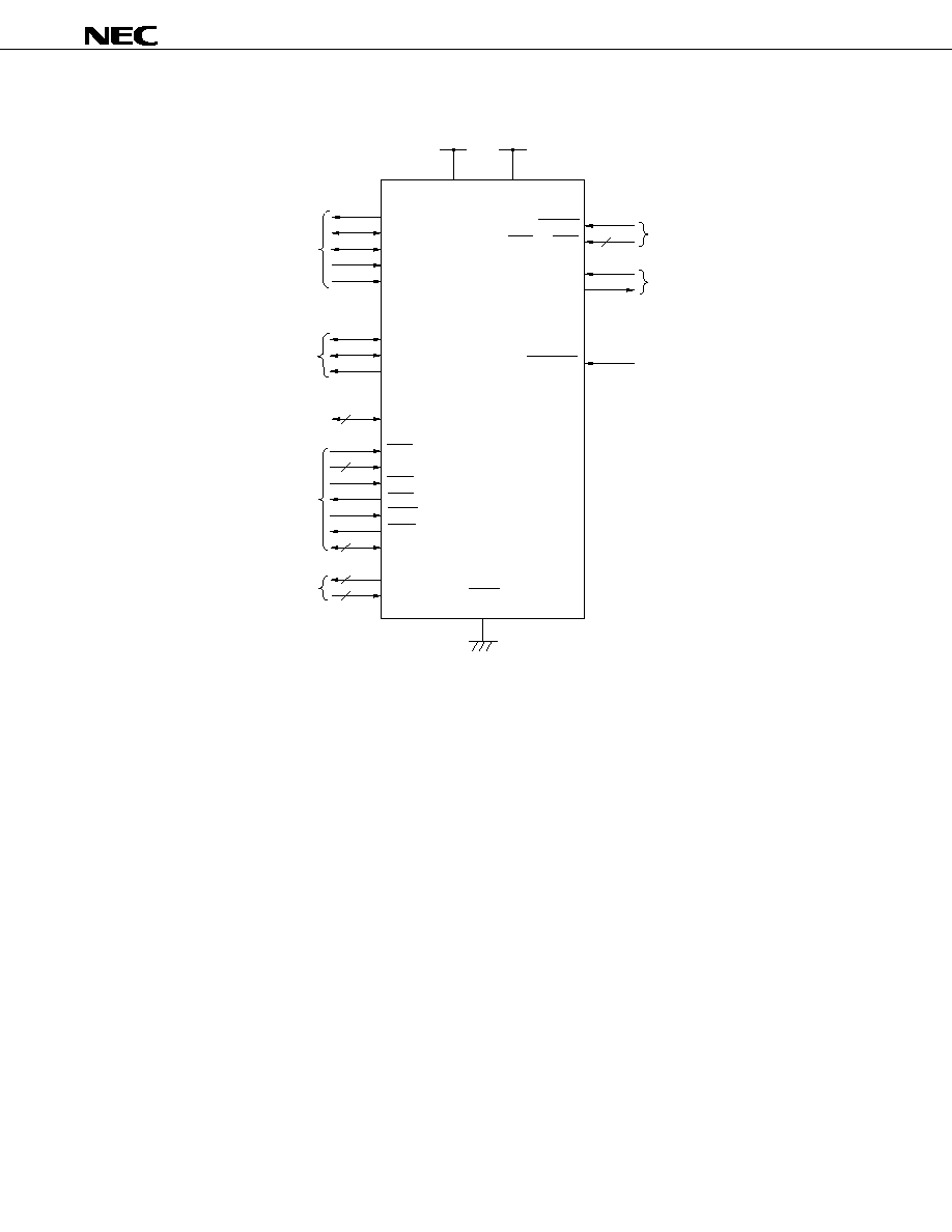
FUNCTION PIN GROUPS
RESET
INT1 to INT4
HCS
HA0,HA1
HRD
HRE
HWR
HWE
HD0 to HD15
+ 3 V
+ 2.5 V
IV
DD
EV
DD
Reset,
Interrupt
System Control
Clock
Audio
Serial
Interface
Host
Interface
Port
Debug
Interface
(8)
(4)
(2)
(4)
(2)
(16)
SO
SOEN/LRCLK
SCK/BCLK
SI
SIEN/MCLK
CLKIN
CLKOUT
WAKEUP
TDO,TICE
TCK,TDI,TMS,TRST
P0 to P3,P4/PLL0 to P7/PLL3
GND
SD Card
Interface
SDDAT
SDCR
SDCLK
Remark
The P4 to P7 pins are multiplexed with PLL0 to PLL3 pins.
Data Sheet U14867EJ5V0DS
4
µ
PD77115, 77115A
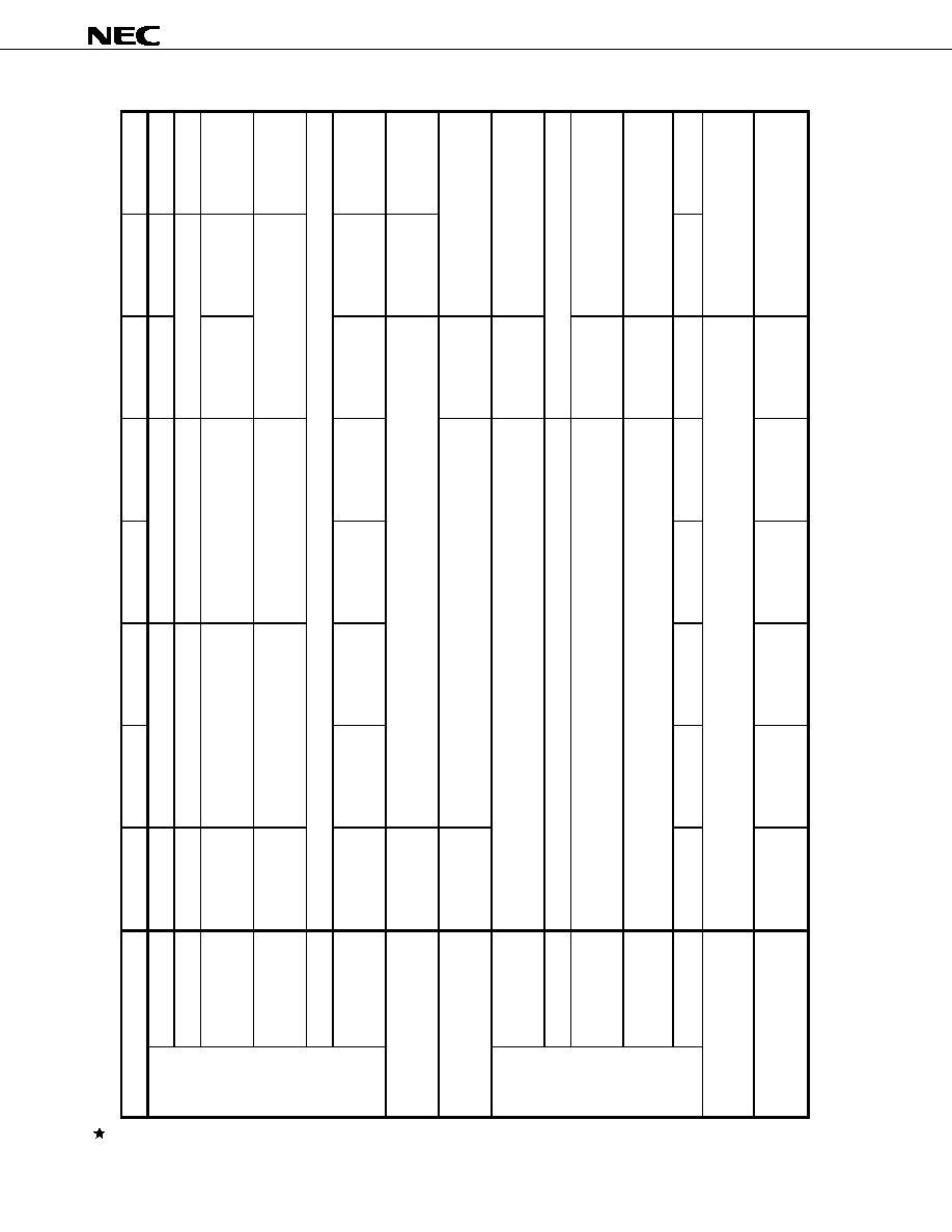
µ
PD77213
15.5 K
◊ 32
64K
◊ 32
18 K
◊ 16 each
32 K
◊ 16 each
1 M
◊ 16 (8 K ◊
16, using SD I/F)
8.33 ns
(120 MHz)
SD card I/F
µ
PD77210
31.5 K
◊ 32
30 K
◊ 16 each
1 M
◊ 16
6.25 ns
(160 MHz)
Integer multiple of
◊10 to 64
(external pin)
2 channels (time-division, audio)
16 bits (some are alternative with
host)
2 channels
(16-bit resolution)
-
DSP core: 1.5 V
I/O pins: 3 V
161-pin FBGA
144-pin LQFP
µ
PD77115,77115A
11.5 K
◊ 32
None
16 K
◊ 16 each
None
None
Integer multiple
of
◊1 to 16
(external pin)
1 channel
(audio CODEC)
16-bit bus
8 bits
1 channel
(16-bit resolution)
SD card I/F
80-pin TQFP
80-pin FBGA
µ
PD77114
8 K
◊ 16 each
-
100-pin TQFP
µ
PD77113A
3.5 K
◊ 32
48 K
◊ 32
16 K
◊ 16 each
32 K
◊ 16 each
None
-
80-pin FBGA
µ
PD77112
16 K
◊ 16 each
-
100-pin TQFP
µ
PD77111
1 K
◊ 32
31.75 K
◊ 32
3 K
◊ 16 each
16 K
◊ 16 each
None
13.3 ns
(75 MHz)
Integer multiple of
◊1 to 16
(mask option)
-
80-pin TQFP
80-pin FBGA
µ
PD77110
35.5 K
◊ 32
None
24 K
◊ 16 each
None
None
32 K
◊ 16 each
15.3 ns
(65 MHz)
Integer multiple
of
◊1 to 8
(external pin)
2 channels
(speech CODEC)
8-bit bus
4 bits
None
-
DSP core: 2.5 V
I/O pins: 3 V
100-pin TQFP
Int. instruction RAM
Int. instruction ROM
Data RAM
(X/Y memory)
Data ROM
(X/Y memory)
Ext. instruction
Ext. data memory (X/Y
memory)
Serial interface
Host interface
General-purpose
port (I/O
programmable)
Timer
Others
DSP FUNCTION LIST
Item
Memory
space
(words
◊
bits)
Instruction cycle (at maximum
operating speed)
Multiple
Peripheral
Supply voltage
Package
Data Sheet U14867EJ5V0DS
5
µ
PD77115, 77115A
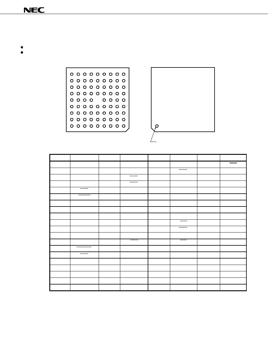
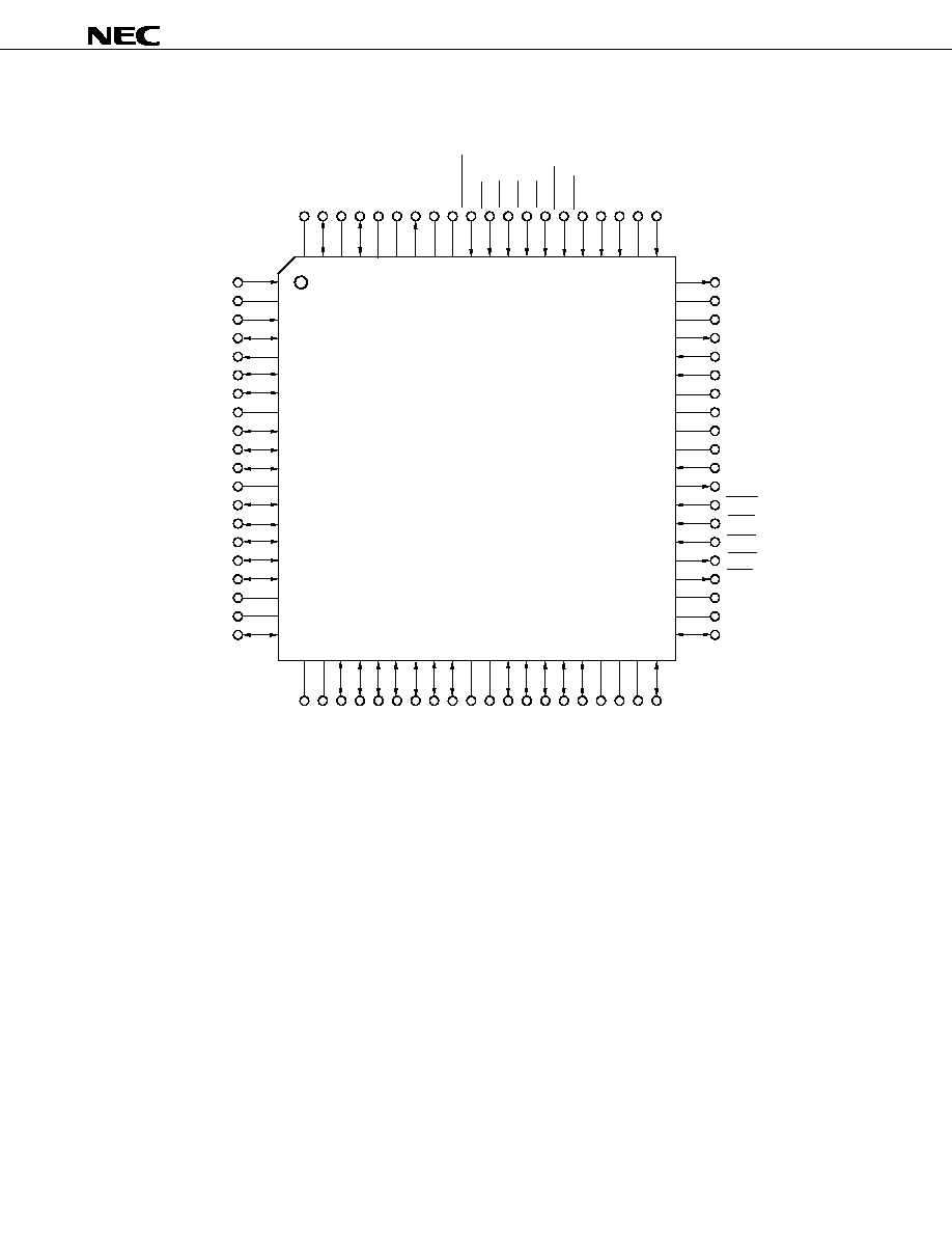
PIN CONFIGURATIONS
80-pin plastic fine pitch BGA (9
◊ 9)
µ
PD77115F1-CN6
µ
PD77115AF1-xxx-CN6
(Bottom View)
(Top View)
J
H
G
F
E
D
C
B
A
A
B
C
D
E
F
G
H
J
9
8
7
6
5
4
3
2
1
Index mark
Pin No.
Pin Name
Pin No.
Pin Name
Pin No.
Pin Name
Pin No.
Pin Name
A1 EV
DD
C3
SDDAT
E6 GND G8 HRE
A2 NC C4 GND E7
HWR G9
EV
DD
A3 EV
DD
C5 INT3 E8 EV
DD
H1 GND
A4 IV
DD
C6 TRST E9
CLKOUT
H2 EV
DD
A5 INT2 C7 TICE F1 EV
DD
H3 HD12
A6 RESET C8 TDO F2
P0
H4 EV
DD
A7 TDI C9 HA0 F3 P3 H5 GND
A8 I.C. D1
SOEN/LRCLK
F4 HD9 H6 HD2
A9 I.C. D2
P5/PLL1
F5 HD4 H7 IV
DD
B1 NC D3 SO F6 HRD H8 HD0
B2 SI D4
P7/PLL3
F7 HWE H9 GND
B3 SDCR D5 SDCLK F8 CLKIN J1 NC
B4 GND D6 INT4 F9 HCS J2 GND
B5 WAKEUP D7
IV
DD
G1 P1 J3 HD13
B6 INT1 D8 HA1 G2 HD15 J4 HD10
B7 TMS D9 GND G3 HD14 J5 HD7
B8 TCK E1
P6/PLL2
G4 HD11 J6 HD6
B9 I.C. E2
P4/PLL0
G5 HD8 J7 HD3
C1 SIEN/MCLK E3
GND
G6
HD5
J8
GND
C2 SCK/BCLK E4
P2
G7
HD1
J9
I.C.
Data Sheet U14867EJ5V0DS
6
µ
PD77115, 77115A
80-pin plastic TQFP (fine pitch) (12
◊ 12) (Top view)
µ
PD77115GK-9EU
1
2
3
4
5
6
7
8
9
10
11
12
13
14
15
16
17
18
19
20
60
59
58
57
56
55
54
53
52
51
50
49
48
47
46
45
44
43
42
41
SI
NC
SIEN/MCLK
SCK/BCLK
SO
SOEN/LRCLK
P7/PLL3
GND
P6/PLL2
P5/PLL1
P4/PLL0
EV
DD
P3
P2
P1
P0
HD15
GND
NC
HD14
TICE
I.C.
I.C.
TDO
HA1
HA0
GND
IV
DD
GND
EV
DD
CLKIN
CLKOUT
HWR
HRD
HCS
HWE
HRE
EV
DD
GND
HD0
21
22
23
24
25
26
27
28
29
30
31
32
33
34
35
36
37
38
39
40
80
79
78
77
76
75
74
73
72
71
70
69
68
67
66
65
64
63
62
61
EV
DD
GND
HD13
HD12
HD11
HD10
HD9
HD8
HD7
EV
DD
GND
HD6
HD5
HD4
HD3
HD2
IV
DD
GND
I.C.
HD1
EV
DD
SDDAT
NC
SDCR
GND
EV
DD
SDCLK
GND
IV
DD
WAKEUP
INT1
INT2
INT3
INT4
RESET
TRST
TMS
TDI
I.C.
TCK

Data Sheet U14867EJ5V0DS
7
µ
PD77115, 77115A
Pin No.
Pin Name
Pin No.
Pin Name
Pin No.
Pin Name
Pin No.
Pin Name
1 SI 21
EV
DD
41 HD0 61 TCK
2 NC 22 GND 42 GND 62 I.C.
3
SIEN/MCLK
23 HD13 43 EV
DD
63 TDI
4
SCK/BCLK
24 HD12 44 HRE 64 TMS
5 SO 25 HD11 45 HWE 65 TRST
6
SOEN/LRCLK
26 HD10 46 HCS 66 RESET
7
P7/PLL3
27 HD9 47 HRD 67 INT4
8 GND 28 HD8 48 HWR 68 INT3
9
P6/PLL2
29 HD7 49
CLKOUT
69 INT2
10 P5/PLL1 30 EV
DD
50 CLKIN 70 INT1
11 P4/PLL0 31 GND 51 EV
DD
71
WAKEUP
12 EV
DD
32 HD6 52 GND 72 IV
DD
13 P3 33 HD5 53 IV
DD
73 GND
14 P2 34 HD4 54 GND 74
SDCLK
15 P1 35 HD3 55 HA0 75 EV
DD
16 P0 36 HD2 56 HA1 76 GND
17 HD15 37 IV
DD
57 TDO 77 SDCR
18 GND 38 GND 58 I.C. 78 NC
19 NC 39 I.C. 59 I.C. 79
SDDAT
20 HD14 40 HD1 60 TICE 80 EV
DD

Data Sheet U14867EJ5V0DS
8
µ
PD77115, 77115A
PIN NAME
CLKIN :
Clock
Input
CLKOUT :
Clock
Output
EV
DD
: Power Supply for I/O Pins
GND :
Ground
HA0, HA1
: Host Data Access
HCS
: Host Chip Select
HD0 to HD15
: Host Data Bus
HRD :
Host
Read
HRE
: Host Read Enable
HWE
: Host Write Enable
HWR :
Host
Write
I.C. :
Internally
Connected
INT1 to INT4
: Interrupt
IV
DD
: Power Supply for DSP Core
NC :
Non-Connection
P0 to P3
: Port
P4/PLL0 to P7/PLL3 : Port/ PLL Setting Input
RESET :
Reset
SCK/BCLK
: Serial Clock Input/ Output
SDCLK
: SD Card Clock Output
SDCR
: SD Card Command Output/ Response Input
SDDAT
: SD Card Data Input/ Output
SI
: Serial Data Input
SIEN/MCLK :
Serial
Input
Enable/ Master Clock Input
SO
: Serial Data Output
SOEN/LRCLK : Serial Output Enable/ Left Right Clock Input/ Output
TCK
: Test Clock Input
TDI
: Test Data Input
TDO
: Test Data Output
TICE
: Test In-Circuit Emulator
TMS
: Test Mode Select
TRST :
Test
Reset
WAKEUP
: Wakeup from STOP Mode

Data Sheet U14867EJ5V0DS
9
µ
PD77115, 77115A
CONTENTS
1. PIN FUNCTION................................................................................................................................. 10
1.1 Pin Function Description ......................................................................................................... 10
1.2 Connection of Unused Pins ..................................................................................................... 14
2. FUNCTION OUTLINE....................................................................................................................... 15
2.1 Program Control Unit ............................................................................................................... 15
2.2 Arithmetic Unit .......................................................................................................................... 16
2.3 Data Memory Unit ..................................................................................................................... 17
2.4 Peripheral Unit .......................................................................................................................... 17
3. RESET FUNCTION........................................................................................................................... 18
3.1 Hardware Reset......................................................................................................................... 18
3.2 Initializing PLL........................................................................................................................... 18
4. FUNCTIONS OF BOOT-UP ROM .................................................................................................. 18
4.1 Boot at Reset............................................................................................................................. 18
4.2 Reboot........................................................................................................................................ 19
4.3 Signature Operation ................................................................................................................. 19
5. STANDBY
MODES........................................................................................................................... 20
5.1 HALT Mode ................................................................................................................................ 20
5.2 STOP Mode ................................................................................................................................ 20
6. MEMORY
MAP ................................................................................................................................. 21
6.1 Instruction Memory................................................................................................................... 21
6.2 Data Memory ............................................................................................................................. 23
7. INSTRUCTIONS ................................................................................................................................ 25
7.1 Outline of Instructions.............................................................................................................. 25
7.2 Instruction Set and Operation ................................................................................................. 26
8. ELECTRICAL
SPECIFICATIONS .................................................................................................... 32
9. PACKAGES ....................................................................................................................................... 51
10. RECOMMENDED SOLDERING CONDITIONS ................................................................................ 53
Data Sheet U14867EJ5V0DS
10
µ
PD77115, 77115A
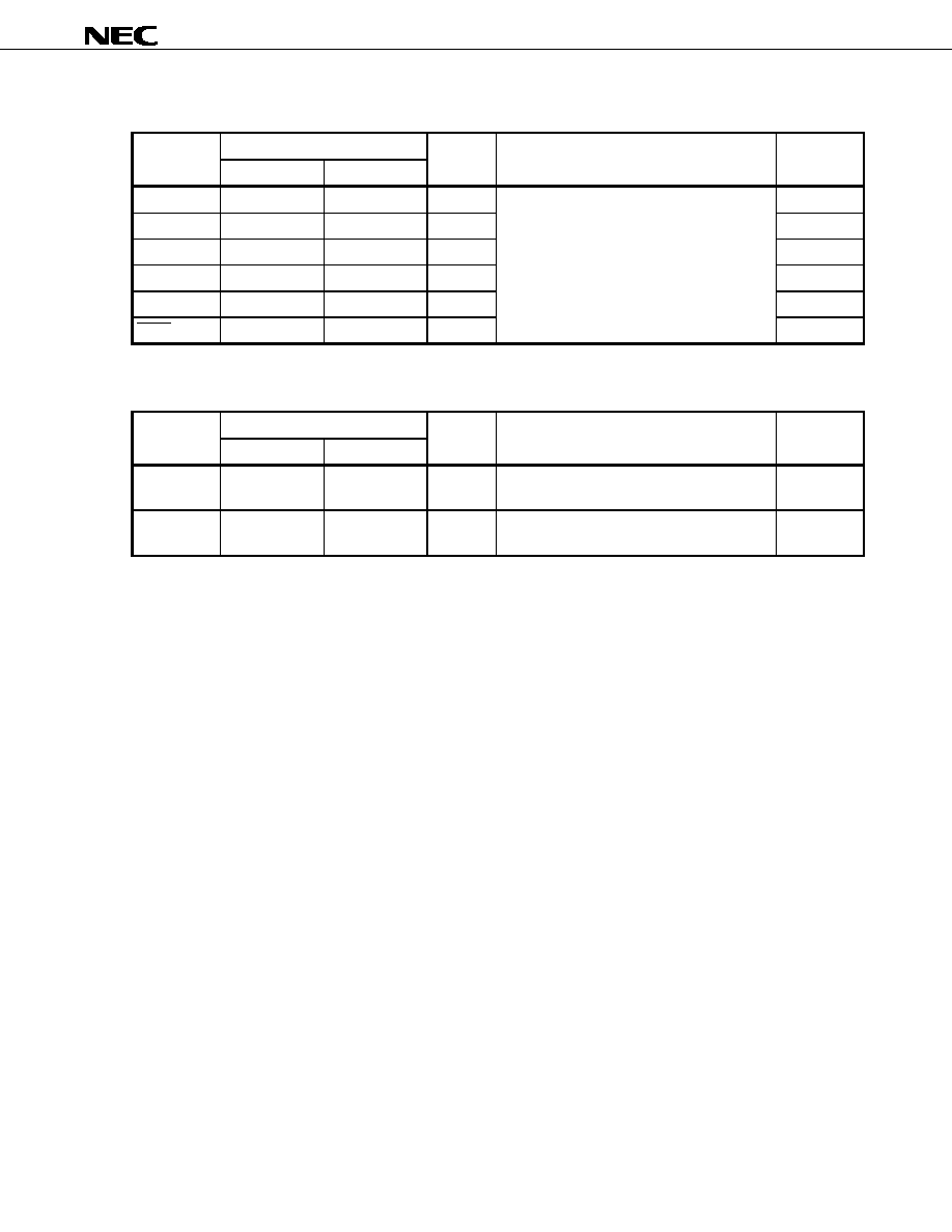
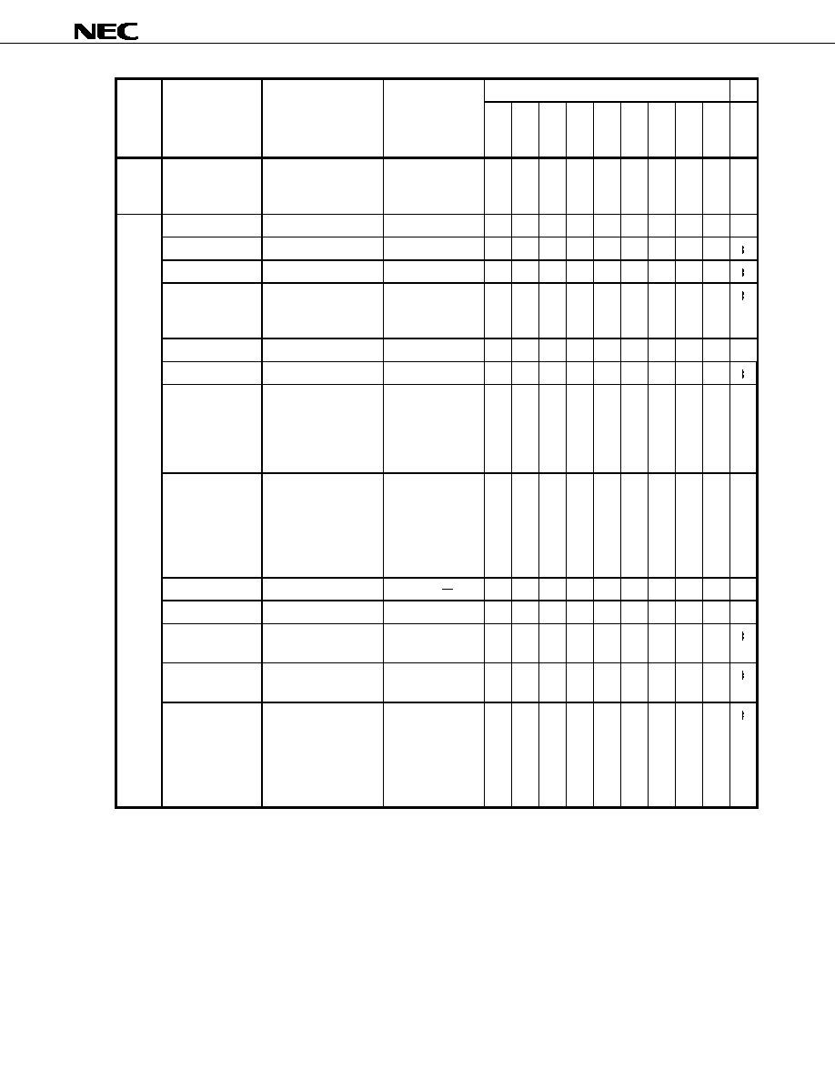
1. PIN FUNCTION
Because the pin numbers differ depending on the package, refer to the diagram of the package to be used.
1.1 Pin Function Description
∑ Power supply
Pin No.
Pin Name
80-pin FBGA
80-pin TQFP
I/O Function
Shared
by:
IV
DD
A4,D7,H7
37,53,72
-
Power to DSP core (+2.5 V)
-
EV
DD
A1,A3,E8,F1,
G9,H2,H4
12,21,30,43,51,
75,80
-
Power to I/O pins (+3 V)
-
GND B4,C4,D9,E3,
E6,H1,H5,H9,
J2,J8
8,18,22,31,
38,42,52,54,
73,76
-
Ground
-
∑ System control
Pin No.
Pin Name
80-pin FBGA
80-pin TQFP
I/O Function
Shared
by:
CLKIN
F8
50
Input
System clock input
-
CLKOUT
E9
49
Output
Internal system clock output
-
PLL0 to PLL3 E2,D2,E1,D4
11,10,9,7
Input
PLL multiple rate setting pin
PLL3 to PLL0:
0000 : x16, 0001 : x1, 0010 : x2, 0011 : x3,
0100 : x4, 0101 : x5, 0110 : x6, 0111 : x7,
1000 : x8, 1001 : x9, 1010 : x10, 1011 : x11,
1100 : x12, 1101 : x13, 1110 : x14,
1111 : x15
P4 to P7
RESET
A6
66
Input
Internal system reset signal input
-
WAKEUP
B5
71
Input
Stop mode release signal input.
∑ When this pin is asserted active, the stop
mode is released.
-
∑ Interrupt
Pin No.
Pin Name
80-pin FBGA
80-pin TQFP
I/O Function
Shared
by:
INT1 to INT4
B6,A5,C5,D6
70,69,68,67
Input
External maskable interrupt input.
∑ Detected at the falling edge.
-
Data Sheet U14867EJ5V0DS
11
µ
PD77115, 77115A
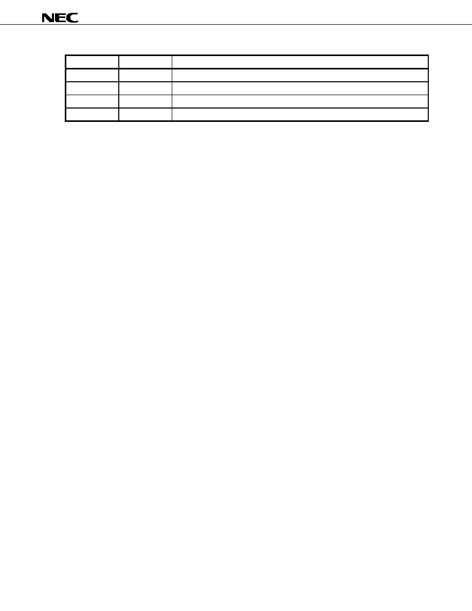
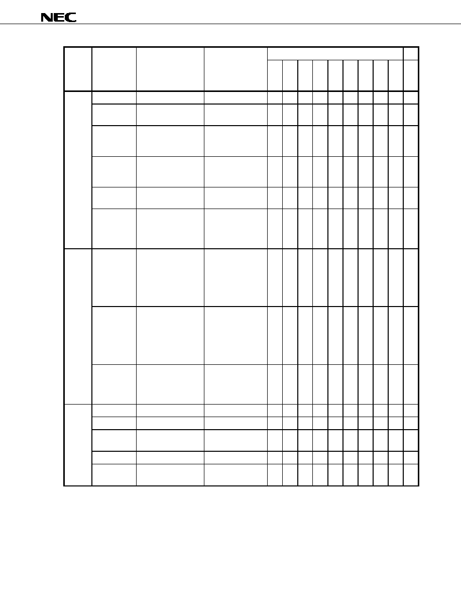
∑ Serial interface
Pin No.
Pin Name
80-pin FBGA
80-pin TQFP
I/O Function
Shared
by:
SCK/BCLK
C2
4
I/O
Serial clock input/output
SCK : Standard serial interface(input)
BCLK : Audio serial interface(I/O)
-
SOEN/LRCLK
D1
6
I/O
Serial output enable / Left Right clock
input/output
SOEN : Standard serial interface(input)
LRCLK : Audio serial interface(I/O)
-
SO D3 5
Output
(3S)
Serial data output
-
SIEN/MCLK C1
3
Input Serial
input enable / Master clock input
SIEN : Standard serial interface
MCLK : Audio serial interface (Master clock input
when master mode)
-
SI
B2
1
Input
Serial data input
-
Remark The pins marked "3S" under the heading "I/O" go into a high-impedance state on completion of data
transfer and input of the hardware reset (RESET) signal.
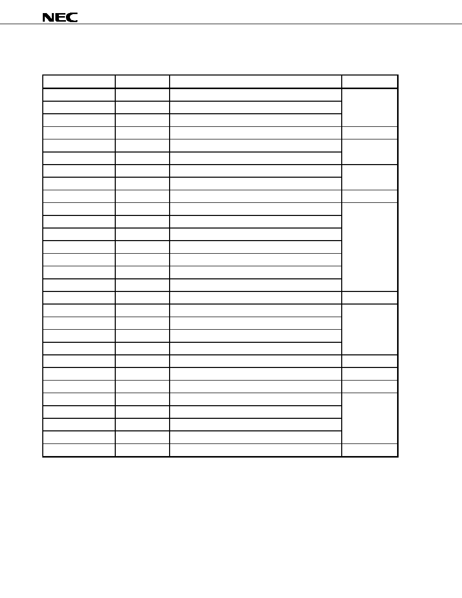
∑ SD card interface
Pin No.
Pin Name
80-pin FBGA
80-pin TQFP
I/O Function
Shared
by:
SDCLK
D5
74
Output
SD card clock output
-
SDCR B3
77
I/O
(3S)
SD card command/response
Input : Response
Output : Command
∑ Leave pulled up.
-
SDDAT C3
79
I/O
(3S)
SD card data input/output
Input : Read data
Output : Write data
∑Leave pulled up.
-
Remark The pins marked "3S" under the heading "I/O" go into a high-impedance state when the SD card
interface is not being accessed.
Data Sheet U14867EJ5V0DS
12
µ
PD77115, 77115A
∑ Host interface
Pin No.
Pin Name
80-pin FBGA
80-pin TQFP
I/O Function
Shared
by:
HA1
D8
56
Input
Specifies the register to be accessed by HD15 to
HD0.
∑ 1: Accesses the host interface status
register (HST).
∑ 0: Accesses the host transmit data register
(HDT (out)) when read (HRD = 0), and
host receive data register (HDT (in)) when
written (HWR = 0).
-
HA0
C9
55
Input
Specifies the register to be accessed by HD15 to
HD0.
∑ 1: Accesses bits 15 to 8 of HST, HDT (in),
and HDT (out).
∑ 0: Accesses bits 7 to 0 of HST, HDT (in),
and HDT (out).
When 8-bit mode, this signal becomes valid.
When 16-bit mode, this signal becomes invalid.
-
HCS
F9
46
Input
Chip select input
-
HRD
F6
47
Input
Host read input
-
HWR
E7
48
Input
Host write input
-
HRE
G8
44
Output
Host read enable output
-
HWE
F7
45
Output
Host write enable output
-
HD0 to HD15 H8,G7,H6,J7,
F5,G6,J6,J5,
G5,F4,J4,G4,
H3,J3,G3,G2
41,40,36,35,
34,33,32,29,
28,27,26,25,
24,23,20,17
I/O
(3S)
16-bit host data bus
-
Remark The pins marked "3S" under the heading "I/O" go into a high-impedance state when the host interface is
not being accessed.
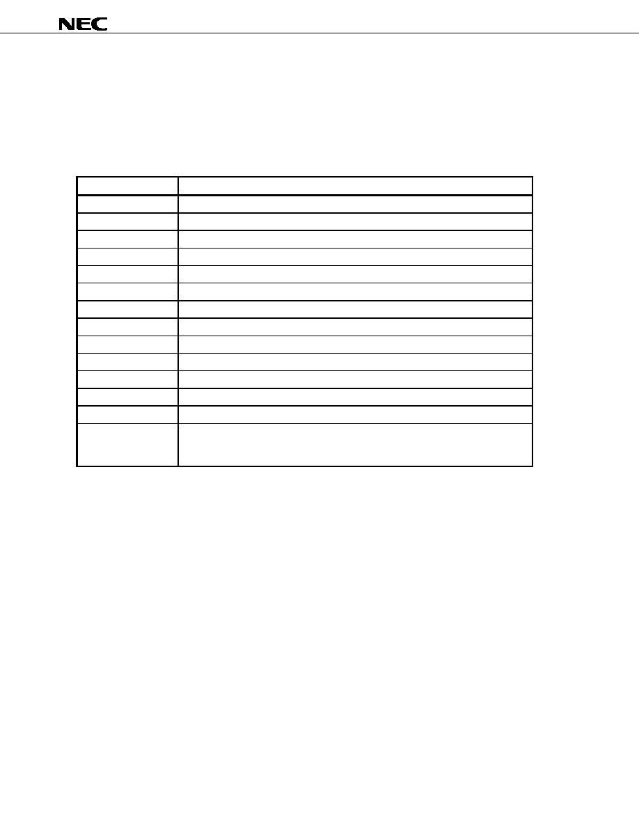
∑ I/O ports
Pin No.
Pin Name
80-pin FBGA
80-pin TQFP
I/O Function
Shared
by:
P0 F2
16
I/O
-
P1 G1
15
I/O
-
P2 E4
14
I/O
-
P3 F3
13
I/O
-
P4 E2
11
I/O
PLL0
P5 D2
10
I/O
PLL1
P6 E1
9
I/O
PLL2
P7 D4
7
I/O
General-purpose I/O port
PLL3
Data Sheet U14867EJ5V0DS
13
µ
PD77115, 77115A
∑ Debugging interface
Pin No.
Pin Name
80-pin FBGA
80-pin TQFP
I/O Function
Shared
by:
TDO C8
57
Output
-
TICE C7
60
Output
-
TCK B8
61
Input
-
TDI A7
63
Input
-
TMS B7
64
Input
-
TRST C6
65
Input
For debugging
-
∑ Others
Pin No.
Pin Name
80-pin FBGA
80-pin TQFP
I/O Function
Shared
by:
I.C. A8,A9,B9,J9
39,58,59,62
-
Internally connected. Leave this pin
unconnected.
-
NC A2,B1,J1
2,19,78
-
No-connect pins. Leave these pins
unconnected.
-
Caution If any signal is input to these pins or if an attempt is made to read these pins, the normal
operation of the
µ
PD77115 is not guaranteed.

Data Sheet U14867EJ5V0DS
14
µ
PD77115, 77115A
1.2 Connection of Unused Pins
1.2.1 Connection of function pins
When mounting, connect unused pins as follows:
Pin I/O
Recommended
Connection
INT1 to INT4
Input
Connect to EV
DD
.
SCK/BCLK I/O
SI Input
Connect to EV
DD
or GND.
SIEN/MCLK
Input
Connect to GND.
SOEN/LRCLK I/O
SO Output
Leave
unconnected
SDCLK Output
SDCR I/O
SDDAT I/O
Connect to EV
DD
via pull-up resistor, or connect to GND via pull-down resistor.
HA0, HA1
Input
Connect to EV
DD
or GND.
HCS, HRD, HWR
Input
Connect to EV
DD
.
HRE, HWE
Output
Leave unconnected.
HD0 to HD15
Note
I/O
P0 to P3
I/O
Connect to EV
DD
via pull-up resistor, or connect to GND via pull-down resistor.
TCK
Input
Connect to GND via pull-down resistor.
TDO, TICE
Output
Leave unconnected.
TMS, TDI
Input
Leave unconnected. (internally pulled up).
TRST Input
Leave
unconnected.
(internally pulled down).
CLKOUT Output
Leave
unconnected.
WAKEUP
Input
Connect to EV
DD
.
Note These pins may be left unconnected if HCS, HRD, and HWR are fixed to the high level.
However, connect these pins as recommended in the halt and stop modes when the power consumption
must be lowered.
1.2.2 Connection of no-function pins
Pin I/O
Recommended
Connection
I.C.
-
Leave unconnected.
NC
-
Leave unconnected.

Data Sheet U14867EJ5V0DS
15
µ
PD77115, 77115A
2. FUNCTION OUTLINE
2.1 Program Control Unit
This unit is used to execute instructions, and control branching, loops, interrupts, the clock, and the standby mode
of the DSP.
2.1.1 CPU control
A three-stage pipeline architecture is employed and almost all the instructions, except some instructions such as
branch instructions, are executed in one system clock.
2.1.2 Interrupt control
Interrupt requests input from external pins (INT1 to INT4) or generated by the internal peripherals (serial interface
and host interface) are serviced. The interrupt of each interrupt source can be enabled or disabled. Multiple interrupts
are also supported.
2.1.3 Loop control task
A loop function without any hardware overhead is provided. A loop stack with four levels is provided to support
multiple loops.
2.1.4 PC stack
A 15-level PC stack that stores the program counter supports multiple interrupts and subroutine calls.
2.1.5 PLL
A PLL is provided as a clock generator that can multiply an external clock input to supply an operating clock to the
DSP. A multiple of
◊1 to ◊16 can be set by pins(PLL0 to PLL3).
Two standby modes are available for lowering the power consumption while the DSP is not in use.
∑ HALT mode : Set by execution of the HALT instruction. The current consumption drops to several mA. The
normal operation mode is recovered by an interrupt or hardware reset.
∑ STOP mode : Set by execution of the STOP instruction. The current consumption drops to several 10
µ
A. The
normal operation mode is recovered by hardware reset or WAKEUP pin.
2.1.6 Instruction memory
64 words of the instruction RAM are allocated to interrupt vectors.
A boot-up ROM that boots up the instruction RAM is provided, and the instruction RAM can be initialized or
rewritten by host boot (boot via host interface).
The
µ
PD77115 has 11.5K-word instruction RAM.

Data Sheet U14867EJ5V0DS
16
µ
PD77115, 77115A
2.2 Arithmetic Unit
This unit performs multiplication, addition, logical operations, and shift, and consists of a 40-bit multiply accumulator,
40-bit data ALU, 40-bit barrel shifter, and eight 40-bit general-purpose registers.
2.2.1 General-purpose registers (R0 to R7)
These eight 40-bit registers are used to input/output data for arithmetic operations, and load or store data from/to
data memory.
A general-purpose register (R0 to R7) is made up of three parts: R0L to R7L (bits 15 to 0), R0H to R7H (bits 31 to
16), and R0E to R7E (bits 39 to 32). Depending on the type of operation, RnL, RnH, and RnE are used as one
register or in different combinations.
2.2.2 Multiply accumulator (MAC)
The MAC multiplies two 16-bit values, and adds or subtracts the multiplication result from one 40-bit value, and
outputs a 40-bit value.
The MAC is provided with a shifter (MSFT: MAC ShiFTer) at the stage preceding the input stage. This shifter can
arithmetically shift the 40-bit value to be added to or subtracted from the multiplication result 1 or 16 bits to the right .
2.2.3 Arithmetic logic unit (ALU)
This unit inputs one or two 40-bit values, executes an arithmetic or logical operation, and outputs a 40-bit value.
2.2.4 Barrel shifter (BSFT: Barrel ShiFTer)
The barrel shifter inputs a 40-bit value, shifts it to the left or right by any number of bits, and outputs a 40-bit value.
The data may be arithmetically shifted to the right shifted to the right, in which case the data is sign-extended, or
logically shifted to the right, in which case 0 is inserted from the MSB.

Data Sheet U14867EJ5V0DS
17
µ
PD77115, 77115A
2.3 Data Memory Unit
The data memory unit consists of two banks of data memory and two data addressing units.
2.3.1 Data memory
The DSP have two banks of data memory (X data memory and Y data memory). A 64-word peripheral area is
assigned in the data memory space.
The
µ
PD77115 has 16K words
◊ 2 banks data RAM.
2.3.2 Data addressing unit
An independent data addressing unit is provided for each of the X data memory and Y data memory spaces.
Each data addressing unit has four data pointers (DPn), four index registers (DNn), one modulo register (DMX or
DMY), and an address ALU.
2.4 Peripheral Unit
A serial interface, host interface, general-purpose I/O port, and wait cycle register are provided. All these internal
peripherals are mapped to the X data memory and Y data memory spaces, and are accessed from program as
memory-mapped I/Os.
2.4.1 Audio Serial interface (ASIO)
One serial interface is provided. This serial interface has two mode which are the audio serial and the standard
serial. The standard serial is compatible other
µ
PD77111 family DSP.
The audio serial interfaces have the following features:
∑ Mode : Master mode or Slave mode
Master mode : MCLK (input), BCLK (output), LRCLK (output), support 256 fs, 384 fs and 512 fs
Slave mode : MCLK (unused), BCLK (input), LRCLK (input)
∑ Frame
format
: 32 or 64 bits audio format (LRCLK format), MSB first input/output.
∑ Handshake :
Handshaking with the external devices is implemented with a dedicated frame signal (LRCLK).
Handshaking with the internal units, polling, wait, or interrupt are used.
The standard serial interfaces have the following features:
∑ Serial
clock :
Supplied from external source to each interface. The same clock is used for input and output
on the interface.
∑ Frame length : 8 or 16 bits, and MSB or LSB first selectable for each input or output
∑ Handshake :
Handshaking with external devices is implemented with a dedicated status signal. With the
internal units, polling, wait, or interrupt are used.
2.4.2 Host interface (HIO)
This is an 16-bit parallel port that inputs data from or outputs data to an external host CPU or DMA controller. In
the DSP, a 16-bit register is mapped to memory for input data, output data, and status. Handshaking with an external
device is implemented by using a dedicated status signal or a dedicated status register. Handshaking with internal
units is achieved by means of polling, wait, or interrupts.

Data Sheet U14867EJ5V0DS
18
µ
PD77115, 77115A
2.4.3 General-purpose I/O port (PIO)
This is a 8-bit I/O port that can be set in the input or output mode in 1-bit units.
2.4.4 SD card interface (SDCIF)
This interface is for access SD card. It supports the DMA transfer for input data to internal data RAM. The SD card
is accessed by using a dedicated routine of system ROM.
2.4.5 Timer
This is 16-bit timer unit. The count source can be selected from system clock, SD card clock, serial clock and INT4
input. Timer unit generates interrupt for interface internal units.
3. RESET FUNCTION
When a low level of a specified width is input to the RESET pin, the device is initialized.
3.1 Hardware Reset
If the RESET pin is asserted active (low level) for a specified period, the internal circuitry of the DSP is initialized. If
the RESET pin is then deasserted inactive (high level), boot processing of the instruction RAM is performed according
to the status of the port pins (P0 and P1). After boot processing, processing is executed starting from the instruction
at address 0x200 of instruction memory (reset entry).
No power-ON reset function is available.
3.2 Initializing PLL
Initializing the PLL starts during boot up program at reset. The pins (PLL0 to PLL3) that specify the PLL multiple
rate must be kept stable for the duration of 3 clocks before and for the duration of 50 clocks after reset has been
cleared (the clock is input from CLKIN). It takes the PLL 100
µ
s to be locked. Until the PLL is lacked, the DSP internal
is operated by the CLKIN clock.
To use the PLL clock as an internal operating clock, set the clock control register (internal peripheral) by user
program.
4. FUNCTIONS OF BOOT-UP ROM
To rewrite the contents of the instruction memory on power application or from program, boot up the instruction
RAM by using the internal boot-up ROM.
The
µ
PD77115 has a function to verify the contents of the internal instruction RAM.
4.1 Boot at Reset
After hardware reset has been cleared, the boot program first reads the general-purpose I/O ports P0 and P1 and,
depending on their bit pattern, determines the boot mode (host boot or non boot). After boot processing, processing is
executed starting from the instruction at address 0x200 (reset entry) of the instruction memory.
The pins (P0 and P1) that specify the boot mode must be kept stable for the duration of 3 clocks before and for the
duration of 12 clocks after reset has been cleared (the clock is input from CLKIN).
Data Sheet U14867EJ5V0DS
19
µ
PD77115, 77115A
P1 P0
Boot
Mode
0
0
Does not execute boot but branches to address 0x200
Note
.
0
1
Executes host byte boot and then branches to address 0x200.
1 0
Setting
prohibited
1
1
Executes host word boot and then branches to address 0x200.
Note This setting is used when the DSP must be reset to recover from the standby mode after reset boot has
been executed once.
A boot parameter and instruction code are obtained via the host interface, and transferred to the instruction RAM.
The data transfer support byte mode and word mode.
4.2 Reboot
By calling the reboot entry address from the program, the contents of the instruction RAM can be rewritten. An
instruction code is obtained via the host interface and transferred to the instruction RAM. The data transfer support
byte mode and word mode.
The entry address is 0x6. Host reboot is executed by calling this address after setting the following parameter:
∑ R7L : Number of instruction steps for rebooting
∑ DP3 : First address of instruction memory to be loaded
4.3 Signature Operation
The
µ
PD77115 has a signature operation function so that the contents of the internal instruction RAM can be
verified. The signature operation performs a specific arithmetic operation on the data in the instruction RAM booted
up, and returns the result to a register. Perform the signature operation in advance on the device when it is operating
normally, and repeat the signature operation later to check whether the data in RAM is correct by comparing the
operation result with the previous result. If the results are identical, there is no problem.
The entry address is 0x9. Execute the operation by calling this address after setting the following parameter. The
operation result is stored in register R7.
∑ R7L: Number of instruction steps for operation
∑ DP3: First address of instruction memory for operation

Data Sheet U14867EJ5V0DS
20
µ
PD77115, 77115A
5. STANDBY MODES
Two standby modes are available. By executing the corresponding instruction, each mode is set and the power
consumption can be reduced.
5.1 HALT Mode
To set this mode, execute the HALT instruction. In this mode, functions other than clock circuit and PLL are
stopped to reduce the current consumption.
To release the HALT mode, use an interrupt or hardware reset. When releasing the HALT mode using an interrupt,
the contents of the internal registers and memory are retained. It takes several 10 system clocks to release the HALT
mode when the HALT mode is released using an interrupt.
In the HALT Mode, the clock circuit of the
µ
PD77115 supplies the following clock as the internal system clock. The
clock output from the CLKOUT pin is also as follows.
The clock output from the CLKOUT pin, however, has a high-level width that is equivalent to 1 cycle of the normal
operation (i.e., the duty factor is not 50%).
∑
µ
PD77115: 1/l of internal system clock (l = integer from 1 to 16, specified by register)
5.2 STOP Mode
To set the STOP mode, execute the STOP instruction. In the STOP mode, all the functions, including the clock
circuit and PLL, can be stopped and the power consumption is minimized with only leakage current flowing.
To release the STOP mode, use hardware reset or WAKEUP pin.
When releasing the STOP mode by using the WAKEUP pin, the contents of the internal registers and memory are
retained, but it takes several 100
µ
s to release the mode.

Data Sheet U14867EJ5V0DS
21
µ
PD77115, 77115A
6. MEMORY MAP
A Harvard architecture, in which the instruction memory space and data memory space are separated is employed.
6.1 Instruction Memory
6.1.1 Instruction memory map
0xFFFF
0x0240
0x023F
0x0200
0x01FF
0x0000
System
Instruction RAM
(8K words)
Vector area (64 words)
Boot-up ROM
(512 words)
0x1000
0x0FFF
Instruction RAM
(3.5K words)
System
0x8000
0x7FFF
0xA000
0x9FFF
Caution Programs and data cannot be placed at addresses reserved for the system, nor can these
addresses be accessed. If these addresses are accessed, the normal operation of the device
cannot be guaranteed.

Data Sheet U14867EJ5V0DS
22
µ
PD77115, 77115A
6.1.2 Interrupt vector table
Addresses 0x200 to 0x23F of the instruction memory are entry points (vectors) of interrupts. Four instruction
addresses are assigned to each interrupt source.
Vector Interrupt
Source
0x200 Reset
0x204
0x208
0x20C
Reserved
0x210 INT1
0x214 INT2
0x218 INT3
0x21C INT4
0x220 SI
input
0x224
SO output
0x228
SDDAT input / PBU
0x22C SDDAT
output
0x230 HI
input
0x234 HO
output
0x238 SDCR
input
0x23C Timer
Cautions 1. Although reset is not an interrupt, it is handled like an interrupt as an entry to a vector.
2. It is recommended that unused interrupt source vectors be used to branch an error
processing routine.

Data Sheet U14867EJ5V0DS
23
µ
PD77115, 77115A
6.2 Data Memory
6.2.1 Data memory map
0xFFFF
0x0000
Data RAM
(8K words)
0x6000
0x5FFF
Peripheral (64 words)
System
Data RAM (4K words)
System
System
0x0FFF
0x3800
0x383F
0x3840
0x3FFF
0x4000
System
Data RAM (4K words)
0x2FFF
0x2000
0x1000
0x3000
0x37FF
0x1FFF
Caution Programs and data cannot be placed at addresses reserved for the system, nor can these
addresses be accessed. If these addresses are accessed, the normal operation of the device
cannot be guaranteed.
Data Sheet U14867EJ5V0DS
24
µ
PD77115, 77115A
6.2.2 Internal peripherals
The internal peripherals are mapped to the internal data memory space.
X/Y Memory Address
Register Name
Function
Peripheral Name
0x3800
SDT/ASDT
Serial data register
0x3801
SST
Serial status register
0x3802
ASST
Audio serial status register
ASIO
0x3803 Reserved
area
Caution Do not access this area.
-
0x3804
PDT
Port data register
0x3805
PCD
Port command register
PIO
0x3806
HDT
Host data register
0x3807
HST
Host status register
HIO
0x3808 to 0x380F
Reserved area
Caution Do not access this area.
-
0x3810
SDDR
SD card data register
0x3811
SDCMD_IDX
SD card command register index
0x3812
SDCMD_AGH
SD card command register argument high
0x3813
SDCMD_AGL
SD card command register argument low
0x3814
SDCTL
SD card control register
0x3815
SDRPR
SD card response register
0x3816
SDSBR
SD card CRC status busy register
SDCIF
0x3817 to 0x381F
Reserved area
Caution Do not access this area.
-
0x3820
TIR
Timer initialize value register
0x3821
TCR
Timer count register
0x3822
TCSR
Timer control / status register
0x3823
TENR
Timer count enable register
Timer
0x3824 to 0x382D
Reserved area
Caution Do not access this area.
-
0x382E
CLKCNTL
Clock control register
PLL
0x382F Reserved
area
Caution Do not access this area.
-
0x3830
PSAR
DMA start address register
0x3831
PSR
DMA size register
0x3832
PRR
DMA pointer register
0x3833
PCR
DMA control register
SDCIF
0x3834 to 0x383F
Reserved area
Caution Do not access this area.
-
Cautions 1. The register names listed in this table are not reserved words of the assembler or the C
language. Therefore, when using these names in assembler or C, the user must define them.
2. The same register is accessed, as long as the address is the same, regardless of whether
the X memory space or Y memory space is accessed.
3. Even different registers cannot be accessed at the same time from both the X and Y memory
spaces.

Data Sheet U14867EJ5V0DS
25
µ
PD77115, 77115A
7. INSTRUCTIONS
7.1 Outline of Instructions
An instruction consists of 32 bits. Almost all the instructions, except some such as branch instructions, are
executed with one system clock. The maximum instruction cycle of the
µ
PD77115 is 13.3 ns. The following nine
types of instructions are available:
(1) Trinomial operation instructions
These instructions specify an operation by the MAC. As the operands, three general-purpose registers can be
specified.
(2) Binomial operation instructions
These instructions specify an operation by the MAC, ALU, or BSFT. As the operands, two general-purpose
registers can be specified. An immediate value can be specified for some of these instructions, instead of a
general-purpose register, for one input.
(3) Uninominal operation instructions
These instructions specify an operation by the ALU. As the operands, one general-purpose register can be
specified.
(4) Load/store instructions
These instructions transfer 16-bit values between memory and a general-purpose register. Any general-purpose
register can be specified as the transfer source or destination.
(5) Register-to-register transfer instructions
These instructions transfer data from one general-purpose register to another.
(6) Immediate value setting instructions
These instructions write an immediate value to a general-purpose register and the registers of the address
operation unit.
(7) Branch instructions
These instruction specify branching of program execution.
(8) Hardware loop instructions
These instruction specify repetitive execution of an instruction.
(9) Control instructions
These instructions are used to control the program.
Data Sheet U14867EJ5V0DS
26
µ
PD77115, 77115A
7.2 Instruction Set and Operation
An operation is written in the operation field for each instruction in accordance with the operation representation
format of that instruction. If two or more parameters can be written, select one of them.
(a) Representation formats and selectable registers
The following table shows the representation formats and selectable registers.
Representation Format
Selectable Register
r0, r0', r0"
R0 to R7
rI, rI'
R0L to R7L
rh, rh'
R0H to R7H
re
R0E to R7E
reh
R0EH to R7EH
dp
DP0 to DP7
dn
DN0 to DN7
dm DMX,
DMY
dpx
DP0 to DP3
dpy
DP4 to DP7
dpx_mod
DPn, DPn++, DPn
- -, DPn##, DPn%%, !DPn## (n = 0 to 3)
dpy_mod
DPn, DPn++, DPn
- -, DPn##, DPn%%, !DPn## (n = 4 to 7)
dp_imm
DPn##imm (n = 0 to 7)
*xxx
Contents of memory with address xxx
<Example> If the contents of the DP0 register are 1000, *DP0 indicates the contents of
address 1000 of the memory.

Data Sheet U14867EJ5V0DS
27
µ
PD77115, 77115A
(b) Modifying data pointer
The data pointer is modified after the memory has been accessed. The result of modification becomes valid
starting from the instruction that immediately follows. The data pointer cannot be modified.
Example Operation
DPn
Nothing is done (value of DPn is not changed.)
DPn++
DPn
DPn + 1
DPn
- - DPn
DPn - 1
DPn##
DPn
DPn + DNn
(Adds value of corresponding DN0 to DN7 to DP0 to DP7.)
Example: DP0
DP0 + DN0
(n = 0 to 3) DPn = ((DP
L
+ DNn) mod (DMX + 1)) + DP
H
DPn%%
(n = 4 to 7) DPn = ((DP
L
+ DNn) mod (DMY + 1)) + DP
H
!DPn##
Reverses bits of DPn and then accesses memory.
After memory access, DPn
DPn + DNn
DPn##imm
DPn
DPn + imm
(c) Instructions that can be simultaneously written
Instructions that can be simultaneously written are indicated by O.
(d) Status of overflow flag (OV)
The status of the overflow flag is indicated by the following symbol:
∑ : Not affected
: Set to 1 when overflow occurs
Caution If an overflow does not occur as a result of an operation, the overflow flag is not reset but
retains the status before the operation.

Data Sheet U14867EJ5V0DS
28
µ
PD77115, 77115A
Instruction Set
Instructions Simultaneously Written
Flag
Instruc-
tion
Instruction
Name
Mnemonic Operation
Trino-
mial
Bino-
mial
Unino-
minal
Load/
store
Trans-
fer
Imme-
diate
value
Bran-
ch
Loop
Cont-
rol
OV
Multiply add
ro = ro + rh * rh'
ro
ro + rh * rh'
Multiply sub
ro = ro
- rh * rh'
ro
ro - rh * rh'
Sign unsign
multiply add
ro = ro + rh * rl
(rl is in positive integer
format.)
ro
ro + rh * rl
Unsign unsign
multiply add
ro = ro + rl * rl'
(rl and rl' are in
positive integer
format.)
ro
ro + rl * rl'
1-bit shift multiply
add
ro = (ro>>1) + rh * rh'
ro
ro
2
+ rh * rh'
Trinomial
operation
16-bit shift multiply
add
ro = (ro>>16) + rh * rh' ro
ro
2
16
+ rh * rh'
∑
Multiply
ro = rh * rh'
ro
rh * rh'
∑
Add
ro" = ro + ro'
ro"
ro + ro'
Immediate add
ro' = ro + imm
ro'
ro + imm
(where imm
1)
Sub
ro" = ro
- ro'
ro"
ro - ro'
Immediate sub
ro' = ro
- imm
ro'
ro - imm
(where imm
1)
Arithmetic right
shift
ro' = ro SRA rl
ro'
ro >> rl
∑
Immediate
arithmetic right
shift
ro' = ro SRA imm
ro'
ro >> imm
∑
Logical right shift
ro' = ro SRL rl
ro'
ro >> rl
∑
Immediate logical
right shift
ro' = ro SRL imm
ro'
ro >> imm
∑
Logical left shift
ro' = ro SLL rl
ro'
ro << rl
∑
Immediate logical
left shift
ro' = ro SLL imm
ro'
ro << imm
∑
AND
ro" = ro & ro'
ro"
ro & ro'
∑
Immediate AND
ro' = ro & imm
ro'
ro & imm
∑
OR
ro" = ro
ro'
ro"
ro ro'
∑
Immediate OR
ro' = ro
imm
ro'
ro imm
∑
Exclusive OR
ro" = ro
ro'
ro"
ro
ro'
∑
Binomial
operation
Immediate
exclusive OR
ro' = ro
imm
ro'
ro
imm
∑
Data Sheet U14867EJ5V0DS
29
µ
PD77115, 77115A
Instructions Simultaneously Written
Flag
Instruc-
tion
Instruction
Name
Mnemonic Operation
Trino-
mial
Bino-
mial
Unino-
minal
Load/
store
Trans-
fer
Imme-
diate
value
Bran-
ch
Loop
Cont-
rol
OV
Binomial
operation
Less than
ro" = LT (ro, ro')
if (ro < ro')
{ro"
0x0000000001}
else {ro"
0x0000000000}
∑
Clear CLR
(ro) ro
0x0000000000
∑
Increment
ro' = ro + 1
ro'
ro + 1
Decrement
ro' = ro
- 1
ro'
ro - 1
Absolute value
ro' = ABS (ro)
if (ro < 0)
{ro'
-ro}
else {ro'
ro}
1's complement
ro' = ~ro
ro'
~ro
∑
2's complement
ro' =
-ro ro'
-ro
Clip
ro' = CLIP (ro)
if ( ro > 0x007FFFFFFF)
{ro'
0x007FFFFFFF}
elseif {ro < 0xFF80000000}
{ro'
0xFF80000000}
else {ro'
ro}
∑
Round
ro' = ROUND (ro)
if (ro > 0x007FFF0000)
{ro'
0x007FFF0000}
elseif {ro < 0xFF80000000}
{ro'
0xFF80000000}
else {ro'
(ro + 0x8000)
& 0xFFFFFF0000}
∑
Exponent
ro' = EXP (ro)
ro'
log
2
(
1
ro
)
∑
Substitution
ro' = ro
ro'
ro
∑
Accumulated
addition
ro' + = ro
ro'
ro' + ro
Accumulated
subtraction
ro'
- = ro
ro'
ro' - ro
Uninom-
inal
operation
Division
ro' / = ro
if (sign (ro') == sign (ro))
{ro'
(ro' - ro) << 1}
else
{ro'
(ro' + ro)<<1}
if (sign (ro')==0)
{ro'
ro' + 1}

Data Sheet U14867EJ5V0DS
30
µ
PD77115, 77115A
Instructions Simultaneously Written
Flag
Instruc-
tion
Instruction
Name
Mnemonic Operation
Trino-
mial
Bino-
mial
Unino-
minal
Load/
store
Trans-
fer
Imme-
diate
value
Bran-
ch
Loop
Cont-
rol
OV
ro = *dpx_mod
ro' =*dpy_mod
ro
*dpx, ro' *dpy
ro = *dpx_mod
*dpy_mod = rh
ro
*dpx, *dpy rh
*dpx_mod = rh
ro = *dpy_mod
*dpx
rh, ro *dpy
Parallel
load/store
Notes 1, 2
*dpx_mod = rh
*dpy_mod = rh'
*dpx
rh, *dpy rh'
∑
dest = *dpx_mod
dest
= *dpy_mod
dest
*dpx,
dest
*dpy
dest = *dpx_mod
*dpy_mod = source
dest
*dpx,
*dpy
source
*dpx_mod = source
dest = *dpy_mod
*dpx
source,
dest
*dpy
Partial load/
store
Notes 1, 2, 3
*dpx_mod = source
*dpy_mod = source'
*dpx
source,
*dpy
source'
∑
dest = *addr
dest
*addr
Direct
addressing
load/store
Note 4
*addr = source
*addr
source
∑
dest = *dp_imm
dest
*dp
Load/
store
Immediate
value index
load/store
Note 5
*dp_imm = source
*dp
source
∑
dest = rl
dest
rl
Register-
to-register
transfer
Register-to-
register
transfer
Note 6
rl = source
rl
source
∑
rl = imm
(where imm = 0 to 0xFFFF)
rl
imm
dp = imm
(where imm = 0 to 0xFFFF)
dp
imm
dn = imm
(where imm = 0 to 0xFFFF)
dn
imm
Immediate
value
setting
Immediate
value setting
dm = imm
(where imm = 1 to 0xFFFF)
dm
imm
∑
Notes 1. Of the two mnemonics, either one of them or both can be written.
2. After transfer, modification specified by mod is performed.
3. Select any of dest, dest' = {ro, reh, re, rh, rl}, source, source' = {re, rh, rl}.
4. Select any of dest = {ro, reh, re, rh, rl}, source = {re, rh, rl},
0: X-0xFFF
0: Y-0xFFFF
: X (X memory)
: Y (Y memory)
addr =
.
5. Select any of dest = {ro, reh, re, rh, rl}, source = {re, rh, rl}.
6. Select any register other than general-purpose registers as dest and source.
Data Sheet U14867EJ5V0DS
31
µ
PD77115, 77115A
Instructions Simultaneously Written
Flag
Instruc-
tion
Instruction
Name
Mnemonic Operation
Trino-
mial
Bino-
mial
Unino-
minal
Load/
store
Trans-
fer
Imme-
diate
value
Bran-
ch
Loop
Cont-
rol
OV
Jump
JMP imm
PC
imm
∑
Register
indirect jump
JMP dp
PC
dp
∑
Subroutine
call
CALL imm
SP
SP + 1
STK
PC + 1
PC
imm
∑
Register
indirect
subroutine call
CALL dp
SP
SP + 1
STK
PC + 1
PC
dp
∑
Return RET
PC
STK
SP
SP - 1
∑
Branch
Interrupt
return
RETI
PC
STK
STK
SP - 1
Recovery of interrupt
enable flag
∑
Repeat REP
count
Start RC
count
RF
0
During repeat
PC
PC
RC
RC - 1
End PC
PC + 1
RF
1
∑
Loop LOOP
count
(instruction of two or
more lines)
Start RC
count
RF
0
During repeat
PC
PC
RC
RC - 1
End PC
PC + 1
RF
1
∑
Hard-
ware
loop
Loop pop
LPOP
LC
LSR3
LE
LSR2
LS
LSR1
LSP
LSP - 1
∑
No operation
NOP
PC
PC + 1
∑
Halt
HALT
CPU
stops.
∑
Stop
STOP
CPU, PLL, and
OSC stop
∑
Condition
IF (ro cond)
Condition test
∑
Control
Forget
interrupt
FINT Discard
interrupt
request
∑

Data Sheet U14867EJ5V0DS
32
µ
PD77115, 77115A
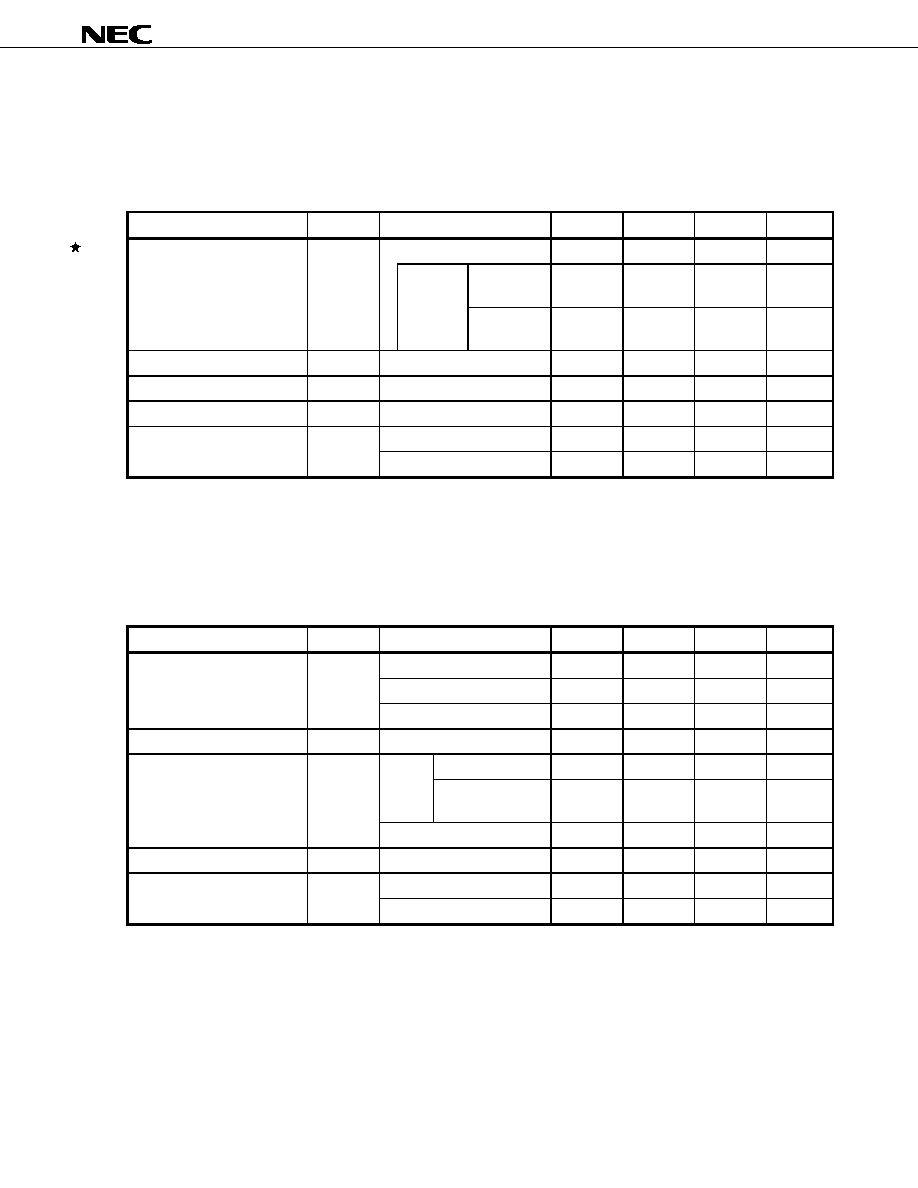
8. ELECTRICAL SPECIFICATIONS
Absolute Maximum Ratings (T
A
= +25
∞C)
Parameter Symbol Condition
Rating
Unit
IV
DD
For DSP core
-0.5 to +3.6
V
Supply voltage
EV
DD
For I/O pins
-0.5 to +4.6
V
Input voltage
V
I
-0.5 to +4.1
V
Output voltage
V
O
V
I
< EV
DD
+ 0.5 V
-0.5 to +4.1
V
Storage temperature
T
stg
-65 to +150
∞C
Operating ambient
temperature
T
A
-40 to +85
∞C
Caution Product quality may suffer if the absolute maximum rating is exceeded even momentarily for any
parameter. That is, the absolute maximum ratings are rated values at which the product is on the
verge of suffering physical damage, and therefore the product must be used under conditions
that ensure that the absolute maximum ratings are not exceeded.
Recommended Operating Conditions
Parameter Symbol Condition MIN.
TYP.
MAX.
Unit
IV
DD
For DSP core
2.0
2.7
V
Operating voltage
EV
DD
For I/O pins
2.7
3.6
V
Input voltage
V
I
0
EV
DD
V
Capacitance (T
A
= +25
∞C, IV
DD
= 0 V, EV
DD
= 0 V)
Parameter Symbol Condition MIN.
TYP.
MAX.
Unit
Input capacitance
C
I
10 pF
Output capacitance
C
O
10 pF
I/O capacitance
C
IO
f = 1 MHz,
Pins other than those
tested: 0 V
10 pF

Data Sheet U14867EJ5V0DS
33
µ
PD77115, 77115A
DC Characteristics (Unless otherwise specified, T
A
=
- 40 to + 85∞C, with IV
DD
and EV
DD
within recommended
operating condition range)
Parameter Symbol Condition
MIN.
TYP.
MAX.
Unit
V
IHN
Pins other than below
0.7 EV
DD
EV
DD
V
V
IHS
RESET, INT1 to INT4,
SCK, SIEN, SOEN
0.8 EV
DD
EV
DD
V
High-level input voltage
V
IHC
CLKIN
0.5
EV
DD
+0.25
EV
DD
V
V
IL
Pins other than below
0
0.2 EV
DD
V
Low-level input voltage
V
IC
CLKIN
0
0.5
EV
DD
≠0.25
V
I
OH
=
-2.0 mA
0.7 EV
DD
V
High-level output voltage
V
OH
I
OH
=
-100
µ
A
0.8 EV
DD
V
Low-level output voltage
V
OL
I
OL
= 2.0 mA
0.2 EV
DD
V
High-level input leakage
current
I
LH
Other than TDI, TMS, and TRST
V
I
= EV
DD
0 10
µ
A
Low-level input leakage
current
I
LL
Other than TDI, TMS, and TRST
V
I
= 0 V
-10
0
µ
A
Pull-up pin current
I
PUI
TDI, TMS, 0 V
V
I
EV
DD
-250
0
µ
A
Pull-down pin current
I
PDI
TRST, 0 V
V
I
EV
DD
0
250
µ
A
I
DD
Note
During operating, 30 ns, IV
DD
=
2.7 V
TBD
75 mA
I
DDH
In halt mode, t
cC
= 30 ns, divided
by eight, IV
DD
= 2.7 V
TBD
10 mA
Internal supply current
[V
IHN
= V
IHS
= EV
DD
, V
IL
= 0 V,
no load]
I
DDS
In stop mode, 0
∞C < T
A
< 60
∞C
100
µ
A
Note The TYP. values are when an ordinary program is executed.
The MAX. values are when a special program that brings about frequent switching inside the device is
executed.
Data Sheet U14867EJ5V0DS
34
µ
PD77115, 77115A
Common Test Criteria of Switching Characteristics
0.8 EV
DD
0.5 EV
DD
0.2 EV
DD
0.8 EV
DD
0.5 EV
DD
0.2 EV
DD
Test points
RESET, INT1 to INT4,
SCK, SIEN, SOEN
0.7 EV
DD
0.5 EV
DD
0.2 EV
DD
0.7 EV
DD
0.5 EV
DD
0.2 EV
DD
Test points
Input
(other than above)
0.5 EV
DD
+0.25
0.5 EV
DD
0.5 EV
DD
-0.25
0.5 EV
DD
+0.25
0.5 EV
DD
0.5 EV
DD
-0.25
Test points
CLKIN
0.5 EV
DD
0.5 EV
DD
Test points
Output
Data Sheet U14867EJ5V0DS
35
µ
PD77115, 77115A
AC Characteristics (T
A
=
- 40 to + 85∞C, with IV
DD
and EV
DD
within recommended operating condition range)
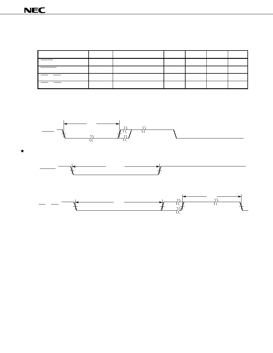
Clock
Timing requirements
Parameter Symbol Condition MIN.
TYP.
MAX.
Unit
25
ns
IV
DD
= 2.0
to 2.7 V
15
◊ m
50
◊ m
ns
CLKIN cycle time
Note 1
t
cCX
PLL lock
range
Note 2
IV
DD
= 2.3
to 2.7 V
10
◊ m
50
◊ m
ns
CLKIN high-level width
t
wCXH
12.5
ns
CLKIN low-level width
t
wCXL
12.5
ns
CLKIN rise/fall time
t
rfCX
5
ns
IV
DD
= 2.0 to 2.7 V
20
ns
Internal clock cycle time
requirements
Note 3
t
cC (R)
IV
DD
= 2.3 to 2.7 V
13.3
ns
Notes 1. m: Multiple
2. This is the range in which the PLL is locked (stably oscillates). Input t
cCX
within this range.
3. Input
t
cCX
so that the value of (t
cCX
˜ m ◊ n) satisfies this condition. m: Multiple, n: Division ratio
Switching characteristics
Parameter Symbol Condition MIN.
TYP.
MAX.
Unit
Internal clock cycle
Note
t
cC
External clock operation
t
cCX
ns
PLL clock operation
(t
cCX
˜ m) ◊ n
ns
In HALT mode
(t
cCX
˜ m) ◊ n ◊ l
ns
CLKOUT cycle time
t
cCO
t
cC
ns
n = 1, or even number
t
cC
˜ 2 - 3
ns
During
normal
operation
n = odd number
(other than 1)
t
cC
˜ n - 3
ns
CLKOUT width
t
wCO
In HALT mode
t
cC
˜ n - 3
ns
CLKOUT rise/fall time
t
rfCO
5
ns
IV
DD
= 2.0 to 2.7 V
20
ns
CLKOUT delay time
t
dCO
IV
DD
= 2.3 to 2.7 V
15
ns
Note m: Multiple, n: Division ratio, l: HALT division ratio
Data Sheet U14867EJ5V0DS
36
µ
PD77115, 77115A
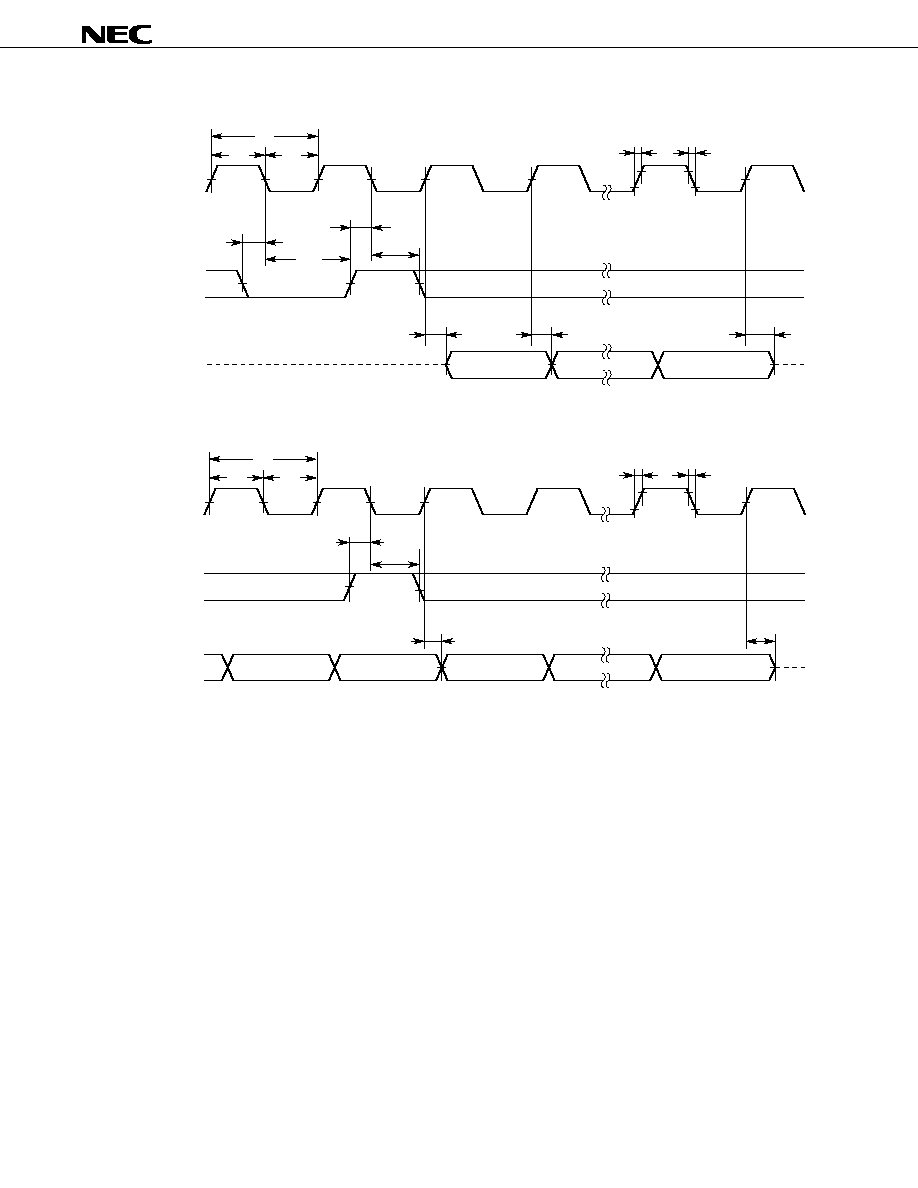
Clock I/O timing
Internal clock
CLKIN
CLKOUT
t
cCX
t
cC,
t
cC(R)
t
wCXH
t
wCXL
t
rfCX
t
rfCX
t
cCO
t
dCO
t
wCO
t
wCO
t
rfCO
t
rfCO
Data Sheet U14867EJ5V0DS
37
µ
PD77115, 77115A
Reset, Interrupt
Timing requirements
Parameter Symbol Condition MIN.
TYP.
MAX.
Unit
RESET low-level width
t
w (RL)
6
t
cC
Note
ns
WAKEUP low-level width
t
w (WAKEUPL)
6
t
cC
µ
s
INT1 to INT4 low-level width
t
w (INTL)
3
t
cC
Note
ns
INT1 to INT4 recovery time
t
rec (INT)
3
t
cC
ns
Note Note that t
cC
is I (I = integer of 1 to 16) times that during normal operation in the HALT mode.
Reset timing
RESET
t
w(RL)
WAKEUP timing
WAKEUP
t
w (WAKEUPL)
Interrupt timing
INT1 to INT4
t
w(INTL)
t
rec(INT)
Data Sheet U14867EJ5V0DS
38
µ
PD77115, 77115A
Serial Interface (Audio Serial mode)
Timing requirements
Parameter Symbol Condition MIN.
TYP.
MAX.
Unit
MCLK cycle time
t
cMC
Master
mode
40
ns
MCLK high-/low-level width
t
wMC
Master
mode
0.4
◊ t
cMC
ns
MCLK rise/fall time
t
rfMC
Master
mode
Note ns
BCLK cycle time
t
cBC
Slave
mode
300
ns
BCLK high-/low-level width
t
wBC
Slave
mode
120
ns
BCLK rise/fall time
t
rfBC
Slave
mode
20
ns
LRCLK setup time
t
su(BC-LR)
Slave
mode
50
ns
SI setup time
t
suSI
50
ns
SI hold time
t
hSI
50
ns
Note 5 or maximum value of 0.1
◊ t
cMC
Switching characteristics
Parameter Symbol Condition MIN.
TYP.
MAX.
Unit
BCLK cycle time
t
cBC
Master mode, 64-bit mode
1/64 fs
ns
Master mode, 32-bit mode
1/32 fs
ns
BCLK high-/low-level width
t
wBC
Master mode
0.4 t
cBC
ns
BCLK rise/fall time
t
rfBC
Master
mode
20
ns
LRCLK delay time
t
d(BC-LR)
Master
mode
-40
+40
ns
SO output delay time
t
dSO
-40
+40
ns

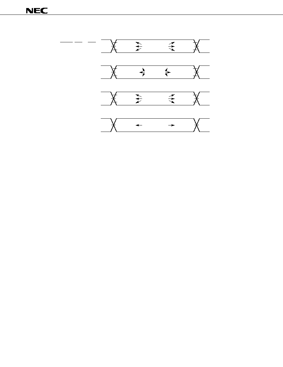
Data Sheet U14867EJ5V0DS
39
µ
PD77115, 77115A
Audio Serial clock timing
MCLK
t
cMC
t
wMC
t
wMC
t
rfMC
t
rfMC
Audio Serial Master mode timing
BCLK
(OUTPUT)
t
rfBC
LRCLK
(OUTPUT)
t
d(BC-LR)
t
wBC
t
wBC
t
cBC
t
d(BC-LR)
t
rfBC
SO
t
dSO
SI
t
hSI
t
suSI
Audio Serial Slave mode timing
BCLK
(INPUT)
t
rfBC
LRCLK
(INPUT)
t
su(BC-LR)
t
wBC
t
wBC
t
cBC
t
rfBC
SO
t
dSO
SI
t
hSI
t
suSI
t
su(BC-LR)
Data Sheet U14867EJ5V0DS
40
µ
PD77115, 77115A
Serial Interface (Standard Serial mode)
Timing requirements
Parameter Symbol
Condition MIN.
TYP.
MAX.
Unit
SCK cycle time
t
cSC
60 and 2t
cC
ns
SCK high-/low-level width
t
wSC
25
ns
SCK rise/fall time
t
rfSC
20
ns
IV
DD
= 2.0 to 2.7 V
10
ns
SOEN setup time
t
suSOE
IV
DD
= 2.3 to 2.7 V
5
ns
IV
DD
= 2.0 to 2.7 V
15
ns
SOEN hold time
t
hSOE
IV
DD
= 2.3 to 2.7 V
10
ns
IV
DD
= 2.0 to 2.7 V
10
ns
SIEN setup time
t
suSIE
IV
DD
= 2.3 to 2.7 V
5
ns
IV
DD
= 2.0 to 2.7 V
15
ns
SIEN hold time
t
hSIE
IV
DD
= 2.3 to 2.7 V
10
ns
IV
DD
= 2.0 to 2.7 V
10
ns
SI setup time
t
suSI
IV
DD
= 2.3 to 2.7 V
5
ns
IV
DD
= 2.0 to 2.7 V
15
ns
SI hold time
t
hSI
IV
DD
= 2.3 to 2.7 V
10
ns
Switching characteristics
Parameter Symbol Condition MIN.
TYP.
MAX.
Unit
IV
DD
= 2.0 to 2.7 V
30
ns
SO output delay time
t
dSO
IV
DD
= 2.3 to 2.7 V
25
ns
SO hold time
t
hSO
0
ns
Data Sheet U14867EJ5V0DS
41
µ
PD77115, 77115A
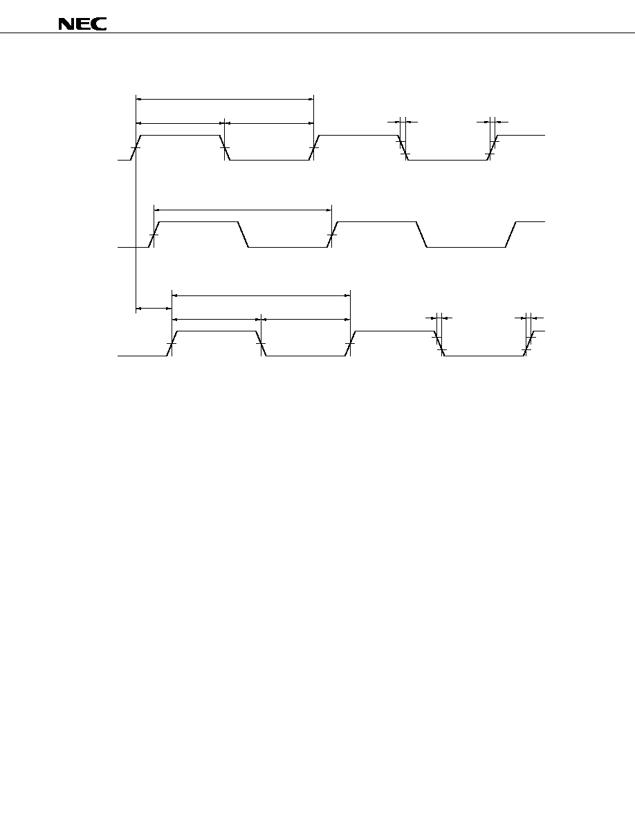
Serial output timing 1
SCK
t
rfSC
SOEN
SO
1st
Last
t
hSO
t
dSO
t
dSO
t
hSOE
t
suSOE
t
suSOE
t
hSOE
t
wSC
t
wSC
t
cSC
t
rfSC
Hi-Z
Serial output timing 2 (during successive output)
SCK
t
rfSC
SOEN
SO
1st
Last
t
dSO
t
hSOE
t
suSOE
t
wSC
t
wSC
t
cSC
t
rfSC
Last
t
hSO

Data Sheet U14867EJ5V0DS
42
µ
PD77115, 77115A
Serial input timing 1
SCK
SIEN
SI
t
cSC
t
wSC
t
wSC
t
suSIE
t
hSIE
t
suSIE
t
hSIE
t
suSI
t
hSI
1st
2nd
t
rfSC
t
rfSC
3rd
Serial input timing 2 (during successive input)
SCK
SIEN
SI
t
cSC
t
wSC
t
wSC
t
suSIE
t
hSIE
t
suSI
t
hSI
1st
3rd
t
rfSC
t
rfSC
Last
Last≠1
2nd

Data Sheet U14867EJ5V0DS
43
µ
PD77115, 77115A
Caution If noise is superimposed on the serial clock, the serial interface may be deadlocked. Bear in
mind the following points when designing your system:
∑ Reinforce the wiring for power supply and ground (if noise is superimposed on the power and
ground lines, it has the same effect as if noise were superimposed on the serial clock).
∑ Shorten the wiring between the device's SCK pin, and clock supply source.
∑ Do not cross the signal lines of the serial clock with any other signal lines. Do not route the
serial clock line in the vicinity of a line through which a high alternating current flows.
∑ Supply the clock to the SCK pin of the device from the clock source on a one-to-one basis. Do
not supply clock to several devices from one clock source.
∑ Exercise care that the serial clock does not overshoot or undershoot. In particular, make sure
that the rising and falling of the serial clock waveform are clear.
Make sure that the serial clock
rises and falls linearly.
The serial clock must not bound. Noise
must not be superimposed on the serial clock.
The serial clock must not rise or
fall step-wise.
◊
◊

Data Sheet U14867EJ5V0DS
44
µ
PD77115, 77115A
Host Interface
Timing requirements
Parameter Symbol Condition MIN.
TYP.
MAX.
Unit
IV
DD
= 2.0 to 2.7 V
15
ns
HRD delay time
t
dHR
IV
DD
= 2.3 to 2.7 V
5
ns
HRD width
t
wHR
40
ns
HCS, HA0, HA1, read hold
time
t
hHCAR
0
ns
HCS, HA0, HA1 write hold
time
t
hHCAW
0
ns
HRD, HWR recovery time
t
recHS
3t
cC
ns
IV
DD
= 2.0 to 2.7 V
15
ns
HWR delay time
t
dHW
IV
DD
= 2.3 to 2.7 V
10
ns
HWR width
t
wHW
40
ns
HWR hold time
t
hHDW
0
ns
IV
DD
= 2.0 to 2.7 V
15
ns
HWR setup time
t
suHDW
IV
DD
= 2.3 to 2.7 V
10
ns
Switching characteristics
Parameter Symbol Condition MIN.
TYP.
MAX.
Unit
IV
DD
= 2.0 to 2.7 V
30
ns
HRE, HWE output delay time
t
dHE
IV
DD
= 2.3 to 2.7 V
25
ns
IV
DD
= 2.0 to 2.7 V
30
ns
HRE, HWE hold time
t
hHE
IV
DD
= 2.3 to 2.7 V
25
ns
IV
DD
= 2.0 to 2.7 V
30
ns
HRD valid time
t
vHDR
IV
DD
= 2.3 to 2.7 V
25
ns
HRD hold time
t
hHDR
0
ns

Data Sheet U14867EJ5V0DS
45
µ
PD77115, 77115A
Host read interface timing
CLKIN
HRD
t
dHE
t
hHDR
t
hHCAR
t
recHS
t
vHDR
t
wHR
t
dHR
t
hHE
HCS, HA0, HA1
HD0 to HD15
HRE
Hi-Z
Hi-Z
Host write interface timing
CLKIN
HWR
t
dHE
t
hHDW
t
hHCAW
t
recHS
t
wHW
t
dHW
t
hHE
HCS, HA0, HA1
HD0 to HD15
HWE
t
suHDW

Data Sheet U14867EJ5V0DS
46
µ
PD77115, 77115A
General-purpose I/O Port
Timing requirements
Parameter Symbol Condition MIN.
TYP.
MAX.
Unit
Port input setup time
t
suPI
0
ns
IV
DD
= 2.0 to 2.7 V
15
ns
Port input hold time
t
hPI
IV
DD
= 2.3 to 2.7 V
10
ns
Switching characteristics
Parameter Symbol Condition MIN.
TYP.
MAX.
Unit
IV
DD
= 2.0 to 2.7 V
30
ns
Port output delay time
t
dPO
IV
DD
= 2.3 to 2.7 V
25
ns
General-purpose I/O port timing
CLKIN
P0 to P7
(Output)
t
dPO
t
hPI
t
suPI
P0 to P7
(Input)

Data Sheet U14867EJ5V0DS
47
µ
PD77115, 77115A
SD card Interface
Timing requirements
Parameter Symbol Condition MIN.
TYP.
MAX.
Unit
SDCR input setup time
t
suSDCR
Input
Response
5
ns
SDCR input hold time
t
hSDCR
Input
Response
0
ns
SDDAT input setup time
t
suSDD
Input
data
5
ns
SDDAT input hold time
t
hSDD
Input
data
0
ns
Switching characteristics
Parameter Symbol Condition MIN.
TYP.
MAX.
Unit
SDCLK cycle time
t
cSDC
40
ns
SDCLK high- level width
t
wSDCH
10
ns
SDCLK low-level width
t
wSDCL
10
ns
SDCLK rise/fall time
t
rfSDC
10
ns
SDCR output delay time
t
dSDCR
Output
Command
10
ns
SDCR output valid time
t
vSDCR
Output
Command
0
ns
SDDAT output delay time
t
dSDD
Output
data
10
ns
SDDAT output valid time
t
vSDD
Output
data
0
ns

Data Sheet U14867EJ5V0DS
48
µ
PD77115, 77115A
SDCR timing
SDCLK
SDCR
(Output)
t
dSDCR
t
hSDCR
t
suSDCR
SDCR
(Input)
t
vSDCR
t
cSDC
t
wSDCL
t
wSDCH
t
rfSDC
t
rfSDC
SDDAT timing
SDCLK
SDDAT
(Output)
t
dSDD
t
hSDD
t
suSDD
SDDAT
(Input)
t
vSDD
t
cSDC
t
wSDCL
t
wSDCH
t
rfSDC
t
rfSDC

Data Sheet U14867EJ5V0DS
49
µ
PD77115, 77115A
Debugging Interface (JTAG)
Timing requirements
Parameter Symbol Condition MIN.
TYP.
MAX.
Unit
TCK cycle time
t
cTCK
120
ns
TCK high-/low-level width
t
wTCK
50
ns
TCK rise/fall time
t
rfTCK
20
ns
IV
DD
= 2.0 to 2.7 V
25
ns
TMS, TDI setup time
t
suDI
IV
DD
= 2.3 to 2.7 V
20
ns
IV
DD
= 2.0 to 2.7 V
25
ns
TMS, TDI hold time
t
hDI
IV
DD
= 2.3 to 2.7 V
20
ns
IV
DD
= 2.0 to 2.7 V
25
ns
Input pin setup time
t
suJIN
IV
DD
= 2.3 to 2.7 V
20
ns
IV
DD
= 2.0 to 2.7 V
25
ns
Input pin hold time
t
hJIN
IV
DD
= 2.3 to 2.7 V
20
ns
TRST setup time
t
suTRST
100
ns
Switching characteristics
Parameter Symbol Condition MIN.
TYP.
MAX.
Unit
IV
DD
= 2.0 to 2.7 V
25
ns
TDO output delay time
t
dDO
IV
DD
= 2.3 to 2.7 V
20
ns
IV
DD
= 2.0 to 2.7 V
25
ns
Output pin output delay time
t
dJOUT
IV
DD
= 2.3 to 2.7 V
20
ns

Data Sheet U14867EJ5V0DS
50
µ
PD77115, 77115A
Debugging interface timing
t
cTCK
t
wTCK
t
suTRST
t
suDI
t
hDI
t
dDO
t
suJIN
t
hJIN
Valid
Valid
t
dJOUT
t
wTCK
t
rfTCK
t
rfTCK
Valid
Valid
TCK
TRST
TMS, TDI
TDO
Capture state
Update state
Remark For details of JTAG, refer to IEEE1149.1.
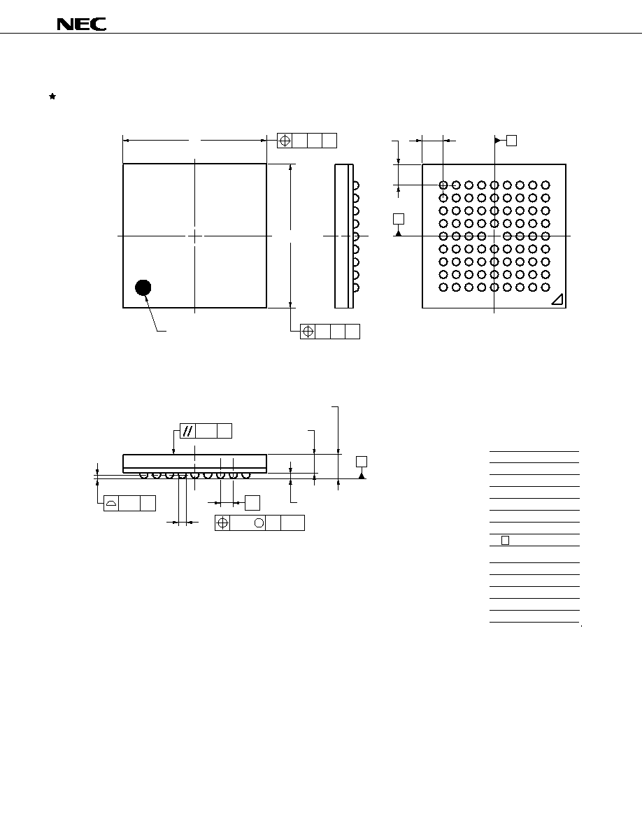
Data Sheet U14867EJ5V0DS
51
µ
PD77115, 77115A
9. PACKAGES
ITEM
DIMENSIONS
D
E
w
A
A1
A2
e
9.00
±0.10
9.00
±0.10
0.80
0.20
0.35
±0.06
1.28
±0.10
0.93
(UNIT:mm)
0.08
0.10
0.20
1.30
1.30
P80F1-80-CN6
0.50+0.05
≠0.10
x
y
y1
ZD
ZE
b
S
w
B
S
w
A
ZD
ZE
INDEX MARK
B
A
1
A
B
C
D
E
F
G
H
J
2
3
4
5
6
7
8
9
D
E
S
e
x
b
A B
M
S
A
A2
A1
y1
S
S
y
80-PIN PLASTIC FBGA (9x9)
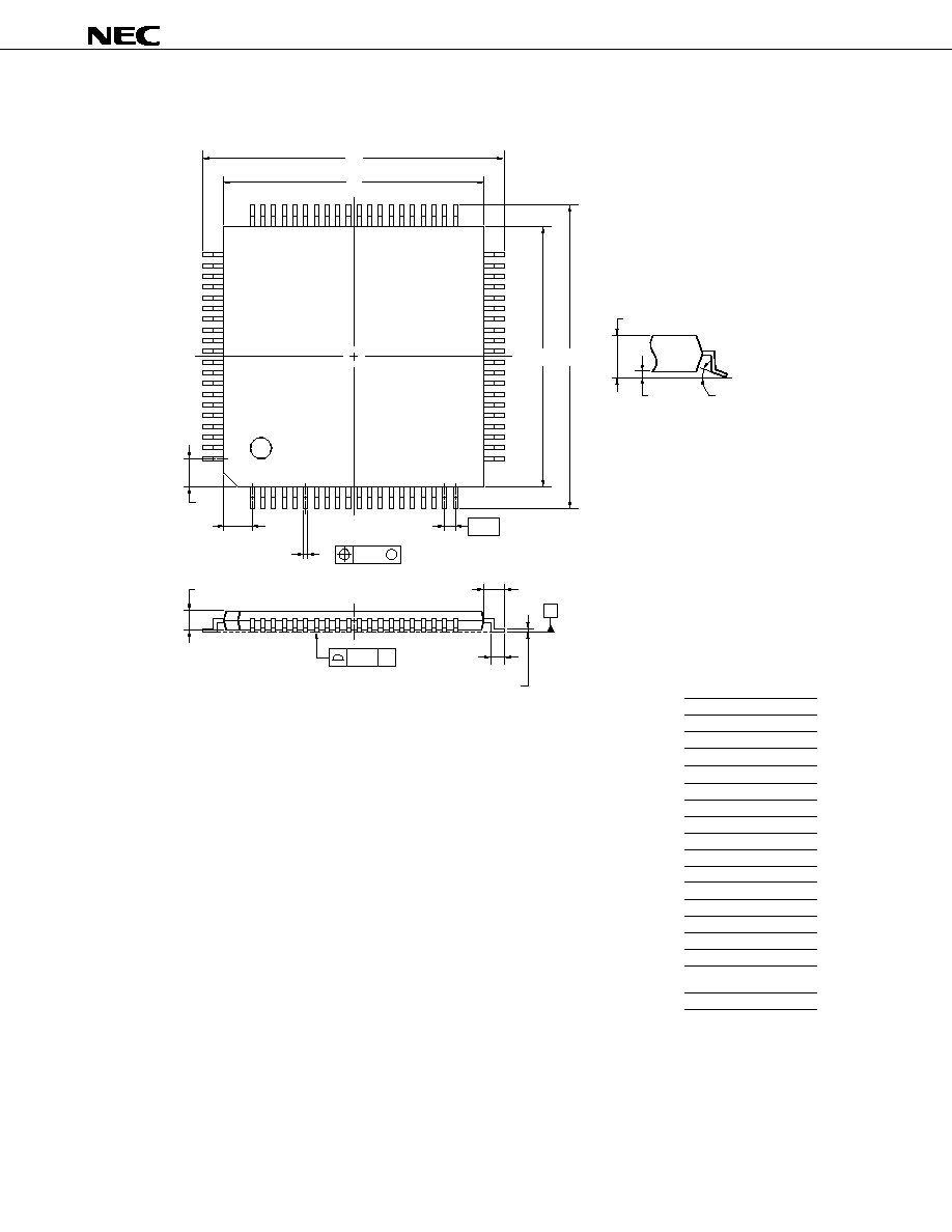
Data Sheet U14867EJ5V0DS
52
µ
PD77115, 77115A
60
41
40
21
61
80
1
20
80-PIN PLASTIC TQFP (FINE PITCH) (12x12)
NOTE
Each lead centerline is located within 0.10 mm of
its true position (T.P.) at maximum material condition.
ITEM
MILLIMETERS
A
B
D
G
14.0
±0.2
12.0
±0.2
1.25
14.0
±0.2
C
12.0
±0.2
0.10
I
J
H
0.22
±0.05
0.5 (T.P.)
K
1.0
±0.2
F
1.25
M
0.145
±0.05
1.0
±0.05
P
Q
N
0.10
0.1
±0.05
L
0.5
±0.2
S80GK-50-9EU-1
S
1.2 MAX.
R
3
∞+7∞
-3∞
M
S
S
N
J
detail of lead end
C
D
A
B
R
K
M
L
P
I
S
Q
G
F
H

Data Sheet U14867EJ5V0DS
53
µ
PD77115, 77115A
10. RECOMMENDED SOLDERING CONDITIONS
It is recommended to solder this product under the following conditions.
For soldering methods and conditions other than those recommended below, contact an NEC Electronics sales
representative.
For technical information, see the following website.
Semiconductor Device Mount Manual (http://www.necel.com/pkg/en/mount/index.html)
Surface-Mount Type
∑
µ
PD77115GK-9EU: 80-pin plastic TQFP (fine-pitch) (12
◊ 12)
Soldering Process
Soldering Conditions
Symbol
Infrared ray reflow
Package peak temperature: 235∞C, Time: 30 seconds MAX (210∞C MIN),
Number of times: 2 MAX, Number of days: 3
Note
(after that, prebaking is necessary
for 10 to 72 hours at 125∞C))
IR35-103-2
VPS
Package peak temperature: 215∞C, Time: 40 seconds MAX (200∞C MIN),
Number of times: 2 MAX, Number of days: 3
Note
(after that, prebaking isnecessary
for 10 to 72 hours at 125∞C)
VP15-103-2
Partial heating method
Pin temperature: 300∞C MAX, Time: 3 seconds MAX (per side of device)
-
∑
µ
PD77115F1-CN6: 80-pin plastic FBGA (9
◊ 9)
∑
µ
PD77115AF1-xxx-CN6: 80-pin plastic FBGA (9
◊ 9)
Soldering Process
Soldering Conditions
Symbol
Infrared ray reflow
Package peak temperature: 235∞C, Time: 30 seconds MAX (210∞C MIN),
Number of times: 2 MAX, Number of days: 3
Note
(after that, prebaking is necessary
for 10 to 72 hours at 125∞C))
IR35-103-2
VPS
Package peak temperature: 215∞C, Time: 40 seconds MAX (200∞C MIN),
Number of times: 2 MAX, Number of days: 3
Note
(after that, prebaking isnecessary
for 10 to 72 hours at 125∞C)
VP15-103-2
Note Number of days in storage after the dry pack has been opened. The storage conditions are at 25∞C, 65%
RH MAX.
Caution Apply wave soldering only to the pins and be careful not to bring solder into direct contact with
the package.

Data Sheet U14867EJ5V0DS
54
µ
PD77115, 77115A
Regional Information
∑
Device availability
∑
Ordering information
∑
Product release schedule
∑
Availability of related technical literature
∑
Development environment specifications (for example, specifications for third-party tools and
components, host computers, power plugs, AC supply voltages, and so forth)
∑
Network requirements
In addition, trademarks, registered trademarks, export restrictions, and other legal issues may also vary
from country to country.
[GLOBAL SUPPORT]
http://www.necel.com/en/support/support.html
NEC Electronics America, Inc. (U.S.)
Santa Clara, California
Tel: 408-588-6000
800-366-9782
NEC Electronics Hong Kong Ltd.
Hong Kong
Tel: 2886-9318
NEC Electronics Hong Kong Ltd.
Seoul Branch
Seoul, Korea
Tel: 02-558-3737
NEC Electronics Shanghai Ltd.
Shanghai, P.R. China
Tel: 021-5888-5400
NEC Electronics Taiwan Ltd.
Taipei, Taiwan
Tel: 02-2719-2377
NEC Electronics Singapore Pte. Ltd.
Novena Square, Singapore
Tel: 6253-8311
J04.1
NEC Electronics (Europe) GmbH
Duesseldorf, Germany
Tel: 0211-65030
∑
Sucursal en EspaÒa
Madrid, Spain
Tel: 091-504 27 87
VÈlizy-Villacoublay, France
Tel: 01-30-67 58 00
∑
Succursale FranÁaise
∑
Filiale Italiana
Milano, Italy
Tel: 02-66 75 41
∑
Branch The Netherlands
Eindhoven, The Netherlands
Tel: 040-244 58 45
∑
Tyskland Filial
Taeby, Sweden
Tel: 08-63 80 820
∑
United Kingdom Branch
Milton Keynes, UK
Tel: 01908-691-133
Some information contained in this document may vary from country to country. Before using any NEC
Electronics product in your application, pIease contact the NEC Electronics office in your country to
obtain a list of authorized representatives and distributors. They will verify:

Data Sheet U14867EJ5V0DS
55
µ
PD77115, 77115A
1
2
3
4
VOLTAGE APPLICATION WAVEFORM AT INPUT PIN
Waveform distortion due to input noise or a reflected wave may cause malfunction. If the input of the
CMOS device stays in the area between V
IL
(MAX) and V
IH
(MIN) due to noise, etc., the device may
malfunction. Take care to prevent chattering noise from entering the device when the input level is fixed,
and also in the transition period when the input level passes through the area between V
IL
(MAX) and
V
IH
(MIN).
HANDLING OF UNUSED INPUT PINS
Unconnected CMOS device inputs can be cause of malfunction. If an input pin is unconnected, it is
possible that an internal input level may be generated due to noise, etc., causing malfunction. CMOS
devices behave differently than Bipolar or NMOS devices. Input levels of CMOS devices must be fixed
high or low by using pull-up or pull-down circuitry. Each unused pin should be connected to V
DD
or GND
via a resistor if there is a possibility that it will be an output pin. All handling related to unused pins must
be judged separately for each device and according to related specifications governing the device.
PRECAUTION AGAINST ESD
A strong electric field, when exposed to a MOS device, can cause destruction of the gate oxide and
ultimately degrade the device operation. Steps must be taken to stop generation of static electricity as
much as possible, and quickly dissipate it when it has occurred. Environmental control must be
adequate. When it is dry, a humidifier should be used. It is recommended to avoid using insulators that
easily build up static electricity. Semiconductor devices must be stored and transported in an anti-static
container, static shielding bag or conductive material. All test and measurement tools including work
benches and floors should be grounded. The operator should be grounded using a wrist strap.
Semiconductor devices must not be touched with bare hands. Similar precautions need to be taken for
PW boards with mounted semiconductor devices.
STATUS BEFORE INITIALIZATION
Power-on does not necessarily define the initial status of a MOS device. Immediately after the power
source is turned ON, devices with reset functions have not yet been initialized. Hence, power-on does
not guarantee output pin levels, I/O settings or contents of registers. A device is not initialized until the
reset signal is received. A reset operation must be executed immediately after power-on for devices
with reset functions.
POWER ON/OFF SEQUENCE
In the case of a device that uses different power supplies for the internal operation and external
interface, as a rule, switch on the external power supply after switching on the internal power supply.
When switching the power supply off, as a rule, switch off the external power supply and then the
internal power supply. Use of the reverse power on/off sequences may result in the application of an
overvoltage to the internal elements of the device, causing malfunction and degradation of internal
elements due to the passage of an abnormal current.
The correct power on/off sequence must be judged separately for each device and according to related
specifications governing the device.
INPUT OF SIGNAL DURING POWER OFF STATE
Do not input signals or an I/O pull-up power supply while the device is not powered. The current
injection that results from input of such a signal or I/O pull-up power supply may cause malfunction and
the abnormal current that passes in the device at this time may cause degradation of internal elements.
Input of signals during the power off state must be judged separately for each device and according to
related specifications governing the device.
NOTES FOR CMOS DEVICES
5
6

µ
PD77115, 77115A
These commodities, technology or software, must be exported in accordance
with the export administration regulations of the exporting country.
Diversion contrary to the law of that country is prohibited.
The information in this document is current as of August, 2004. The information is subject to
change without notice. For actual design-in, refer to the latest publications of NEC Electronics data
sheets or data books, etc., for the most up-to-date specifications of NEC Electronics products. Not
all products and/or types are available in every country. Please check with an NEC Electronics sales
representative for availability and additional information.
No part of this document may be copied or reproduced in any form or by any means without the prior
written consent of NEC Electronics. NEC Electronics assumes no responsibility for any errors that may
appear in this document.
NEC Electronics does not assume any liability for infringement of patents, copyrights or other intellectual
property rights of third parties by or arising from the use of NEC Electronics products listed in this document
or any other liability arising from the use of such products. No license, express, implied or otherwise, is
granted under any patents, copyrights or other intellectual property rights of NEC Electronics or others.
Descriptions of circuits, software and other related information in this document are provided for illustrative
purposes in semiconductor product operation and application examples. The incorporation of these
circuits, software and information in the design of a customer's equipment shall be done under the full
responsibility of the customer. NEC Electronics assumes no responsibility for any losses incurred by
customers or third parties arising from the use of these circuits, software and information.
While NEC Electronics endeavors to enhance the quality, reliability and safety of NEC Electronics products,
customers agree and acknowledge that the possibility of defects thereof cannot be eliminated entirely. To
minimize risks of damage to property or injury (including death) to persons arising from defects in NEC
Electronics products, customers must incorporate sufficient safety measures in their design, such as
redundancy, fire-containment and anti-failure features.
NEC Electronics products are classified into the following three quality grades: "Standard", "Special" and
"Specific".
The "Specific" quality grade applies only to NEC Electronics products developed based on a customer-
designated "quality assurance program" for a specific application. The recommended applications of an NEC
Electronics product depend on its quality grade, as indicated below. Customers must check the quality grade of
each NEC Electronics product before using it in a particular application.
The quality grade of NEC Electronics products is "Standard" unless otherwise expressly specified in NEC
Electronics data sheets or data books, etc. If customers wish to use NEC Electronics products in applications
not intended by NEC Electronics, they must contact an NEC Electronics sales representative in advance to
determine NEC Electronics' willingness to support a given application.
(Note)
∑
∑
∑
∑
∑
∑
M8E 02. 11-1
(1)
(2)
"NEC Electronics" as used in this statement means NEC Electronics Corporation and also includes its
majority-owned subsidiaries.
"NEC Electronics products" means any product developed or manufactured by or for NEC Electronics (as
defined above).
Computers, office equipment, communications equipment, test and measurement equipment, audio
and visual equipment, home electronic appliances, machine tools, personal electronic equipment
and industrial robots.
Transportation equipment (automobiles, trains, ships, etc.), traffic control systems, anti-disaster
systems, anti-crime systems, safety equipment and medical equipment (not specifically designed
for life support).
Aircraft, aerospace equipment, submersible repeaters, nuclear reactor control systems, life
support systems and medical equipment for life support, etc.
"Standard":
"Special":
"Specific":