 | –≠–ª–µ–∫—Ç—Ä–æ–Ω–Ω—ã–π –∫–æ–º–ø–æ–Ω–µ–Ω—Ç: UPD7759 | –°–∫–∞—á–∞—Ç—å:  PDF PDF  ZIP ZIP |
µ
PD7759
MOS INTEGRATED CIRCUIT
ADPCM SPEECH SYNTHESIZER LSIs
Please refer to "Quality grade on NEC Semiconductor Devices" (Document number IEI-1209) published by
NEC Corporation to know the specification of quality grade on the devices and its recommended applications.
The
µ
PD7759 is an external ROM type speech synthesis LSI employing the waveform coding
method. In addition to the ROM capability of up to 1 Mbit, the
µ
PD7759 realizes the synthesis of
speech sounds of any length by using the ADPCM data transferred from an external ROM.
As the synthesizing method, it adopts the ADPCM method and the PCM + waveform element method.
The ADPCM method is suitable for synthesizing clear and natural speech sounds, and the PCM + waveform
element method is for the synthesis of sound effects and melodies. And by using them together, the
µ
PD7759 realizes the long-time synthesis of high-quality sounds.
Because of the short turn-around time of speech analysis, the
µ
PD7759 can perform the quick system
development using a PROM, or the evaluation of an on-chip ROM type of the
µ
PD7755 family.
FEATURES
q Synthesizing method
: ADPCM, PCM + waveform element methods used together
q Sampling frequency
: 5, 6 or 8 kHz
q Bit rate (speech)
: 20 to 32 K bps
q Number of Messages
: 256 (MAX.)
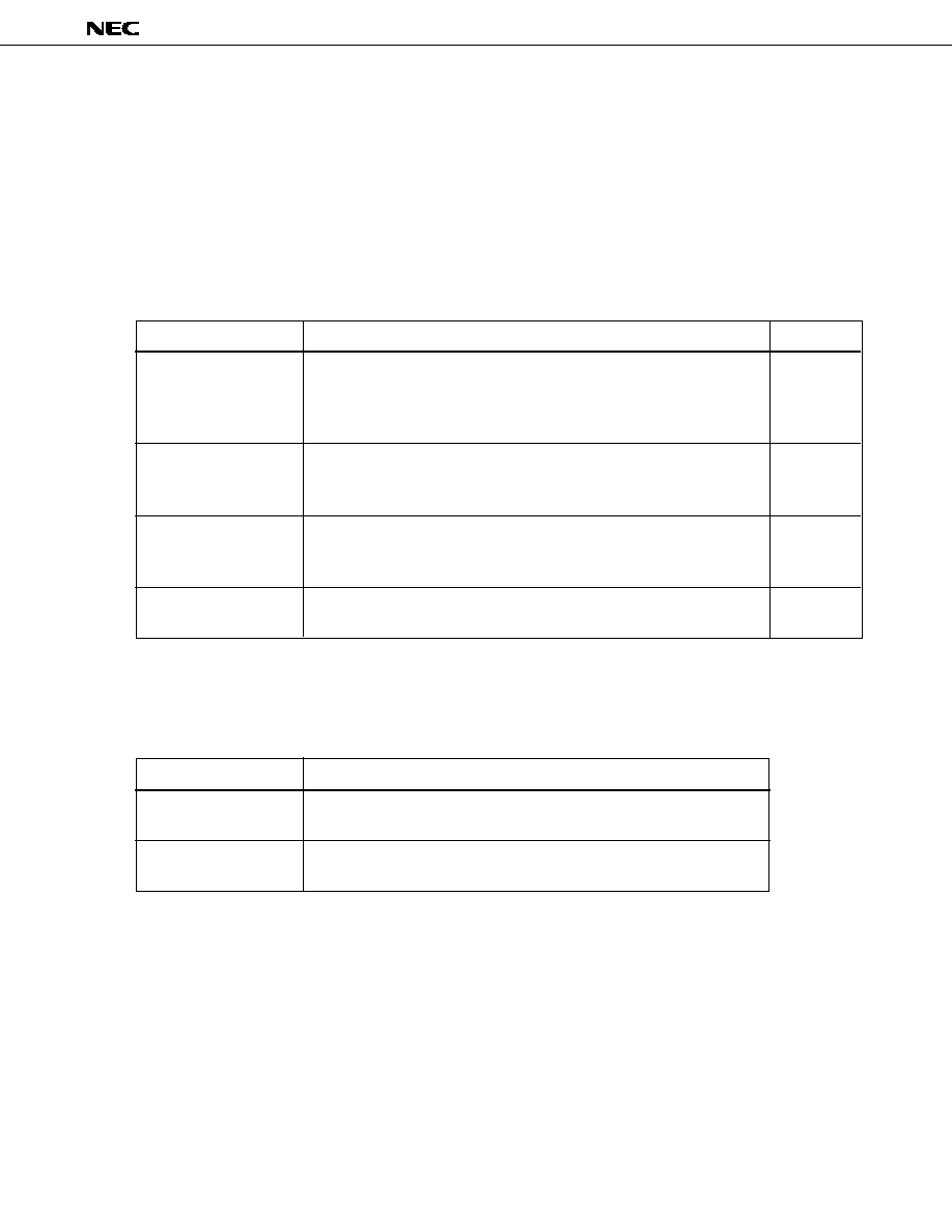
q External speech data ROM
Parameters
Synthesizing time
Melodies & sound effects
Note2
Products
(PCM + waveform element)
µ
PD7759
1 Mbits
50 sec. (TYP.)
340 sec. (TYP.)
Note 1.
The synthesizing time for the speech is the value for a 6 kHz sampling.
2.
The synthesizing time for the melodies & sound effects is variable according to their tone.
q Speech output
: Current sink type analog output, 9-bit D/A converter
q Host CPU interface
: Compatible with a 4/8-bit CPU
q Standby mode
: Pop-noise preventive circuit incorporated
q Supply voltage
: 2.7 to 5.5 V
q CMOS technology
ORDERING INFORMATION
Part Number
Package
Quality grade
µ
PD7759C
40-pin plastic DIP (600 mil)
Standard
µ
PD7759GC-3BH
52-pin plastic QFP (
s
s
14 mm)
Standard
Speech data ROM
(External)
Speech (ADPCM)
Note1
5
5
DATA SHEET
1988, 1993
©
The mark 5 shows revised points.
Document No.
IC-2323A
(O.D.No.
IC-6960D)
Date Published
January 1993
Printed in Japan
The information in this document is subject to change without notice.

µ
PD7759
2
PIN CONFIGURATION (Top View)
BLOCK DIAGRAM
1
2
3
4
5
6
7
8
9
10
11
12
13
14
15
16
17
18
19
20
40
39
38
37
36
35
34
33
32
31
30
29
28
27
26
25
24
23
22
21
ASD5
ASD6
ASD7
I0
I1
I2
I3
I4
I5
I6
I7
AEN/ WR
SAA
DRQ
ALE
REF
AVO
BUSY
RESET
GND
V
DD
ASD4
ASD3
ASD2
ASD1
ASD0
A8
A7
A6
A5
A4
A3
A2
A1
A0
CS
X2
X1
ST
MD
PD7759C
µ
∑
40-pin plastic DIP
40
41
42
43
44
45
46
47
48
49
50
51
52
26
25
24
23
22
21
20
19
18
17
16
15
14
1 2 3 4 5 6 7 8 9 10 11 12 13
39 38 37 36 35 34 33 32 31 30 29 28 27
NC
A0
A1
A2
A3
A4
NC
A5
A6
A7
A8
ASD0
NC
NC
ALE
DRQ
SAA
AEN / W R
I7
NC
I6
I5
I4
I3
I2
NC
NC
CS
X2
X1
ST
MD
NC
GND
RESET
BUSY
AVO
REF
NC
NC
ASD1
ASD2
ASD3
ASD4
V
DD
NC
ASD5
ASD6
ASD7
I0
I1
NC
PD7759GC-3BH
µ
SAA
ALE
AEN/ WR
DRQ
MD
BUSY
CS
ST
RESET
∑
52-pin plastic QFP
ADPCM
Decoder
ROM Address & Speech Data Interface
ASD0 to ASD7
A0 to A8
X1
X2
D/A
Converter
Message Select Interface
OSC
REF
AVO
GND
V
DD
I0 to I7
System
Controller

µ
PD7759
3
1. PIN FUNCTIONS
1.1 COMMON FUNCTION TO ALL MODES
Pin
52-pin
40-pin
(Abbre-
QFP
DIP
I/O
Function
viation)
Pin No.
Pin No.
V
DD
6
40
--
Power supply (2.7 to 5.5 V)
DRQ
24
14
Output
Speech synthesis data request.
D/A converter reference current input.
The sink-load current input causes the output current of the
D/A converter to change.
The D/A converter reference current is passed to V
DD
via
a resistor.
In standby mode, REF is set to high impedance.
Analog speech signal output.
AVO outputs a unipolar sink-load current.
The output current is reduced to 0 when the
µ
PD7759 is in the
standby mode.
The output current of the D/A converter from AVO is changed
according to the input current from REF.
Maximum output current of the D/A converter is approx. the
34 times the REF input current.
Active-low BUSY signal output. When inputting ST signal,
it outputs a low level signal.
MD, ST and WR are invalid while BUSY is low.
In standby mode, BUSY is set to high impedance.
Reset input.
In standby mode, RESET must be at low level more than 12
RESET
31
19
Input
clock cycles after clock oscillation becomes stable.
In operation mode, RESET must be at low level for 12 clock
cycles (oscillation clock).
GND
32
20
--
Ground.
Ceramic resonator connection for generating a clock signal.
The 640 kHz ceramic resonator can be connected.
In standby mode, the
µ
PD7759 outputs a low-level to X1 and
a high-level to X2.
1, 7, 13,
14, 20, 26,
27, 33, 39,
40, 46, 52
X1
36
23
--
X2
37
24
--
REF
28
16
Input
AVO
29
17
Output
BUSY
30
18
Output
NC
--
--
No Connection
5
µ
PD7759
4
1.2 PIN FUNCTION FOR STAND ALONE MODE
Pin
52-pin
40-pin
(Abbre-
QFP
DIP
I/O
Function
viation)
Pin No.
Pin No.
I0
11
4
Message selection code input.
I1
12
5
The message selection code signals are positive logics.
I2
15
6
Ground the pins not used.
I3
16
7
These pins are connected to the internal latch circuit which
I4
17
8
latches I0 to I7 data at the rising edge of the ST input.
I5
18
9
In standby mode, these pins should be set high or low level.
I6
19
10
If they are biased at or near the typical CMOS threshold,
I7
21
11
the excess supply current is caused.
This signal is at low level while address signal is valid.
AEN/WR
22
12
Controls the latch circuit for the higher 8 bits of the external
ROM address.
Outputs high level when the start address of a message stored
in the directory area of data memory, is being read out.
Determines the timing that higher 8 bits of the external ROM
ALE
25
15
Output
address are externally latched. They must be latched at the
falling edge of the signal.
MD
34
21
Input
set at high-level.
Start signal input.
When ST goes low while CS is at low level, the
µ
PD7759 starts
ST
35
22
Input
synthesizing the message specified by I0 to I7. In standby
mode, this signal resets the standby mode and starts speech
synthesis.
Chip select signal input.
ST becomes valid when CS goes low.
A0
41
26
A1
42
27
A2
43
28
A3
44
29
A4
45
30
Output
Outputs the lower 9 bits of the external ROM address.
A5
47
31
A6
48
32
A7
49
33
A8
50
34
ASD0
51
35
ASD1
2
36
ASD2
3
37
(1) Outputs the higher 8 bits of external ROM address.
ASD3
4
38
Input/
(2) Inputs 8-bit speech synthesis data from the external ROM.
ASD4
5
39
Output
These functions are executed from (1) to (2) on a time-
ASD5
8
1
shared basis.
ASD6
9
2
ASD7
10
3
SAA
23
13
Output
CS
38
25
Input
Input
Output/
Input
µ
PD7759
5
1.3 PIN FUNCTION FOR SLAVE MODE
Pin
52-pin
40-pin
(Abbre-
QFP
DIP
I/O
Function
viation)
Pin No.
Pin No.
I0
11
4
I1
12
5
I2
15
6
I3
16
7
Invalid.
I4
17
8
Set at high or low level.
I5
18
9
I6
19
10
I7
21
11
Output/
Input
Invalid.
Leave this pin open.
Invalid.
Leave this pin open.
Slave mode selection input.
MD
34
21
Input
Transition between two operation mode is not accepted
during synthesis or in the standby mode.
Invalid.
Set at high level.
Chip select signal input.
WR becomes valid when CS goes low.
A0
41
26
A1
42
27
A2
43
28
A3
44
29
A4
45
30
Output
A5
47
31
A6
48
32
A7
49
33
A8
50
34
ASD0
51
35
ASD1
2
36
ASD2
3
37
ASD3
4
38
ASD4
5
39
ASD5
8
1
ASD6
9
2
ASD7
10
3
Input
Input speech synthesis data from an external source.
Invalid.
Leave these pins open.
SAA
23
13
Output
ALE
25
15
Output
ST
35
22
Input
CS
38
25
Input
AEN/WR
22
12
Inputs write strobe signal for a speech synthesis data.
Input

µ
PD7759
6
V
IH1
0.7 V
DD
V
DD
V
V
IH2
2.2
V
DD
V
V
IL1
0
0.3 V
DD
V
V
IL2
0
0.8
V
2. ELECTRICAL SPECIFICATIONS
ABSOLUTE MAXIMUM RATINGS (Ta = 25
∞
C)
Parameters
Symbol
Conditions
Ratings
Unit
Power supply voltage
V
DD
≠0.3 to + 7.0
V
Input voltage
V
I
≠0.3 to V
DD
+ 0.3
V
Output voltage
V
o
≠0.3 to V
DD
+ 0.3
V
Storage temperature
T
stg
≠40 to +125
∞
C
Operating temperature
T
opt
≠10 to +70
∞
C
RECOMMENDED OPERATING CONDITIONS
Parameters
Symbol
Conditions
MIN.
TYP.
MAX.
Unit
Supply voltage
V
DD
2.7
5.5
V
Applied to I0 to I7, ST, CS,
RESET, MD, WR
High-level input voltage
Applied to ASD0 to ASD7,
V
DD
= 5 V
±
10 %
Applied to I0 to I7, ST, CS,
RESET, MD, WR
Low-level input voltage
Applied to ASD0 to ASD7,
V
DD
= 5 V
±
10 %
Clock frequency
f
OSC
630
640
650
kHz
Remark
AC timing test voltage
V
IL
= V
OL
= 0.3 V
DD
V
IH
= V
OH
= 0.7 V
DD
µ
PD7759
7
Input leak current
| I
LI
|
3
µ
A
10
mA
20
µ
A
1
mA
10
µ
A
DC CHARACTERISTICS (Ta = ≠10 to +70
∞
C, V
DD
= 2.7 to 5.5 V, f
OSC
= 640 kHz)
Parameters
Symbol
Conditions
MIN.
TYP.
MAX.
Unit
High-level output voltage
V
OH
I
OH
= ≠100
µ
A
V
DD
≠0.5
V
Low-level output voltage
V
OL
V
DD
= 5 V
±
10 %, I
OL
= 1.6 mA
0.4
V
I
0
to I
7
, ST, CS, WR, ASD0
to ASD7, MD
Output leak current
| I
LO
|
BUSY, A0 to A8
3
µ
A
(Stand alone, slave mode)
V
DD
= 5 V
(Standby mode)
V
DD
= 5 V
Supply current
I
DD
(Stand alone, slave mode)
2.7 V V
DD
3.5 V
(Standby mode)
2.7 V V
DD
3.5 V
V
DD
= 2.7 V, R
REF
= 0
140
250
440
µ
A
V
DD
= 5.5 V, R
REF
= 0
500
760
1200
µ
A
Reference input current
Note
I
REF
V
DD
= 2.7 V, R
REF
= 50 k
21
30
39
µ
A
V
DD
= 5.5 V, R
REF
= 50 k
68
78
88
µ
A
2.7 V V
DD
5.5 V
V
AVO
= 2.0 V, D/A input: 1 FFH
0 V V
AVO
V
DD
in the standby mode
Note Measuring circuit
D/A converter output current
I
AVO
32 I
REF
34 I
REF
36 I
REF
µ
A
D/A converter output leak current
| I
LD
|
5
µ
A
<
=
<
=
<
=
<
=
<
=
<
=
<
=
<
=
V
DD
REF
AVO
I
AVO
I
REF
R
REF
µ
PD7759
8
AC CHARACTERISTICS (Ta = ≠10 to +70
∞
C, V
DD
= 2.7 to 5.5 V, f
OSC
= 640 kHz)
TIMING REQUIREMENTS (common to all modes)
Parameters
Symbol
Conditions
MIN.
TYP.
MAX.
Unit
t
r1
C
L
= 150 pF, V
DD
= 5 V
±
10 %
800
ns
BUSY rise time
t
r2
C
L
= 150 pF, V
DD
= 2.7 to 5.5 V
2
µ
s
t
f1
C
L
= 150 pF, V
DD
= 5 V
±
10 %
800
ns
BUSY fall time
t
f2
C
L
= 150 pF, V
DD
= 2.7 to 5.5 V
2
µ
s
BUSY output stop time
t
RB
from RESET
9.5
µ
s
2.1 STAND ALONE MODE
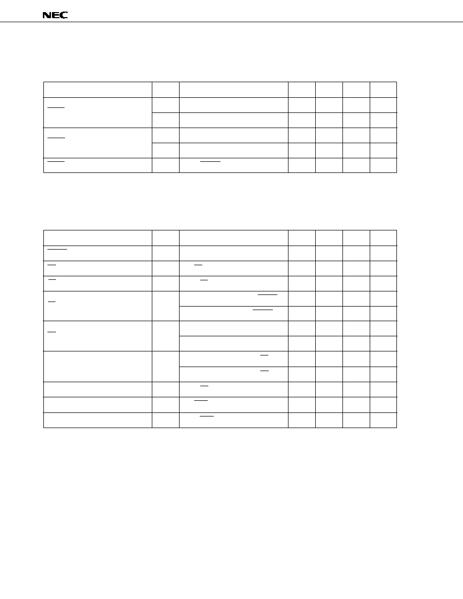
(1)
TIMING REQUIREMENTS
Parameters
Symbol
Conditions
MIN.
TYP.
MAX.
Unit
RESET pulse width
t
RST
18.5
µ
s
CS set up time
t
CS
for ST
0
ns
CS hold time
t
SC
from ST
0
ns
In operation mode, from RESET
200
µ
s
ST set up time
t
RS
In standby mode, from RESET
1.6
ms
2.7 V V
DD
5.5 V
2
µ
s
ST pulse width
t
CC
4.5 V V
DD
5.5 V
350
ns
2.7 V V
DD
5.5 V, from ST
5
µ
s
Message select code set up time
t
DW
4.5 V V
DD
5.5 V, from ST
350
ns
Message select code hold time
t
WD
from ST
0
ns
Speech data set up time
t
DR
for DRQ
2
7.5
µ
s
Speech data hold time
t
RDH
from DRQ
1.25
µ
s
<
=
<
=
<
=
<
=
<
=
<
=
<
=
<
=
5
5

µ
PD7759
9
(2)
SWITCHING CHARACTERISTICS
Parameters
Symbol
Conditions
MIN.
TYP.
MAX.
Unit
BUSY output delay
t
SBO
In operation mode, from ST
6.25
10
µ
s
Speech output delay
t
SSO
In operation mode, from BUSY
2.1
2.2
ms
BUSY hold time
t
BD
from synthesis
15
µ
s
ALE pulse width
t
LL
3.13
µ
s
t
AL
for ALE
3.13
µ
s
Higher address set up time
t
AE
for AEN
0
µ
s
t
LA
from ALE
3.13
µ
s
Higher address hold time
t
EA
from AEN
0
µ
s
AEN pulse width
t
AEN
14.1
µ
s
DRQ output delay
t
LC
from ALE
3.13
µ
s
Higher address pulse width
t
AC
6.25
µ
s
DRQ pulse width
t
DCC
7.81
µ
s
ROM read cycle time
t
MRO
37.5
µ
s
TIMING CHART (at reset)
(1)
(2)
RESET
ST
t
RST
t
RS
BUSY
t
RB
RESET
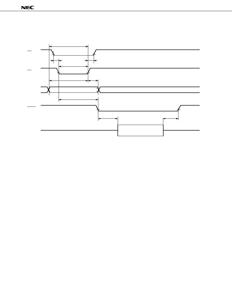
µ
PD7759
10
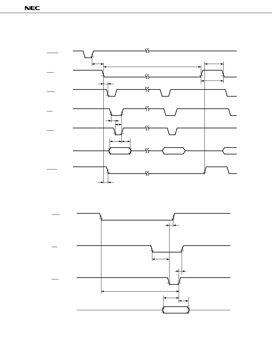
TIMING CHART (Stand alone mode)
(1) CONTROL
CS
ST
I0 to I7
t
BD
1FFH-
t
SSO
Synthesized
sound output
t
SBO
VALID
t
DW
t
WD
t
CS
t
DW
t
CC
BUSY
100H-
000H-
(D/A converter input value)
t
SC
I
AVO
µ
PD7759
11
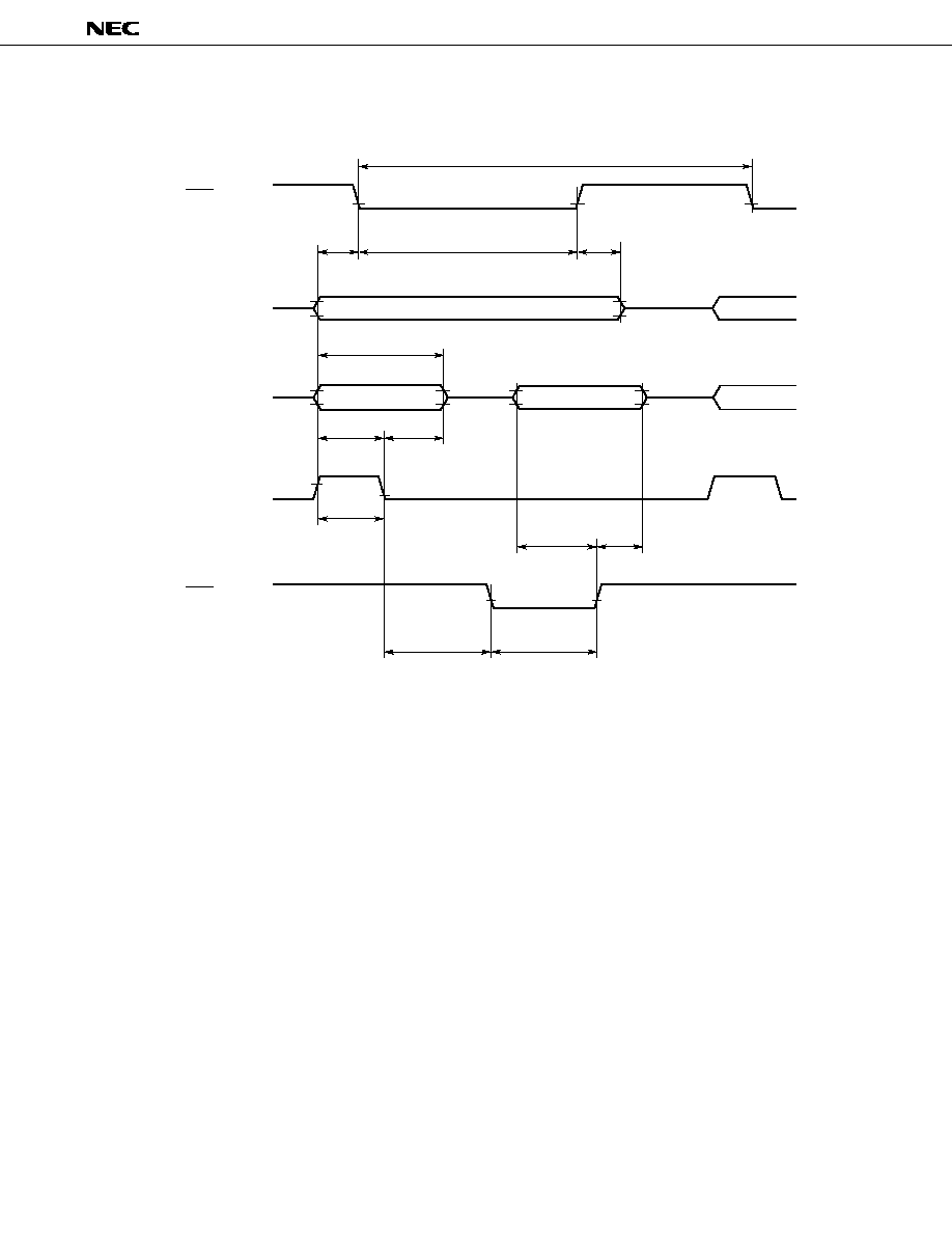
(2) MEMORY ACCESS
AEN
A0 to A8
t
AE
ASD
0
to ASD
7
ALE
t
MRO
t
AC
t
AL
t
LA
DRQ
t
AEN
t
EA
t
LL
t
DR
t
RDH
t
DCC
t
LC
µ
PD7759
12
DRQ output delay
t
MDR
µ
s
50
50000
2.2 SLAVE MODE
(1) TIMING REQUIREMENTS
Parameters
Symbol
Conditions
MIN.
TYP.
MAX.
Unit
t
RM
from RESET
200
µ
s
MD set up time
t
BM
from BUSY
0
ns
t
MD
from MD
6.2
µ
s
MD pulse width
t
MD2
6.2
µ
s
Speech data set up time
t
DW
for WR
, 5 V
±
10 %
350
ns
Speech data hold time
t
WD
from WR
, 5 V
±
10 %
0
ns
WR input stop time
t
WR
from DRQ
31.7
µ
s
WR pulse width
t
CC
5 V
±
10 %
350
ns
CS set up time
t
CW
for WR
0
ns
CS hold time
t
WC
from WR
0
ns
(2) SWITCHING CHARACTERISTICS
Parameters
Symbol
Conditions
MIN.
TYP.
MAX.
Unit
BUSY output delay
t
SBO
from MD
9.5
µ
s
In operation mode, from MD
50
70
In standby mode,
after RESET input, from MD
DRQ output stop time
t
WRQ
from WR
3
µ
s
5
5
µ
PD7759
13
TIMING CHART (Slave mode)
(1) CONTROL
RESET
ASD
0
to ASD
7
t
MD2
t
BM
t
RM
t
MD
t
SBO
t
DW
t
WD
t
CC
t
CW
MD
DRQ
CS
WR
BUSY
t
MDR
(2) DATA TRANSFER
DRQ
t
WC
t
WR
t
WRQ
CS
WR
ASD
0
to ASD
7
t
CW
t
DW
t
WD
µ
PD7759
14
t
DA
46.5
47
ms
BUSY output delay
t
SBS
4
80
ms
t
AW
V
DD
= 5 V
±
10 %
350
ns
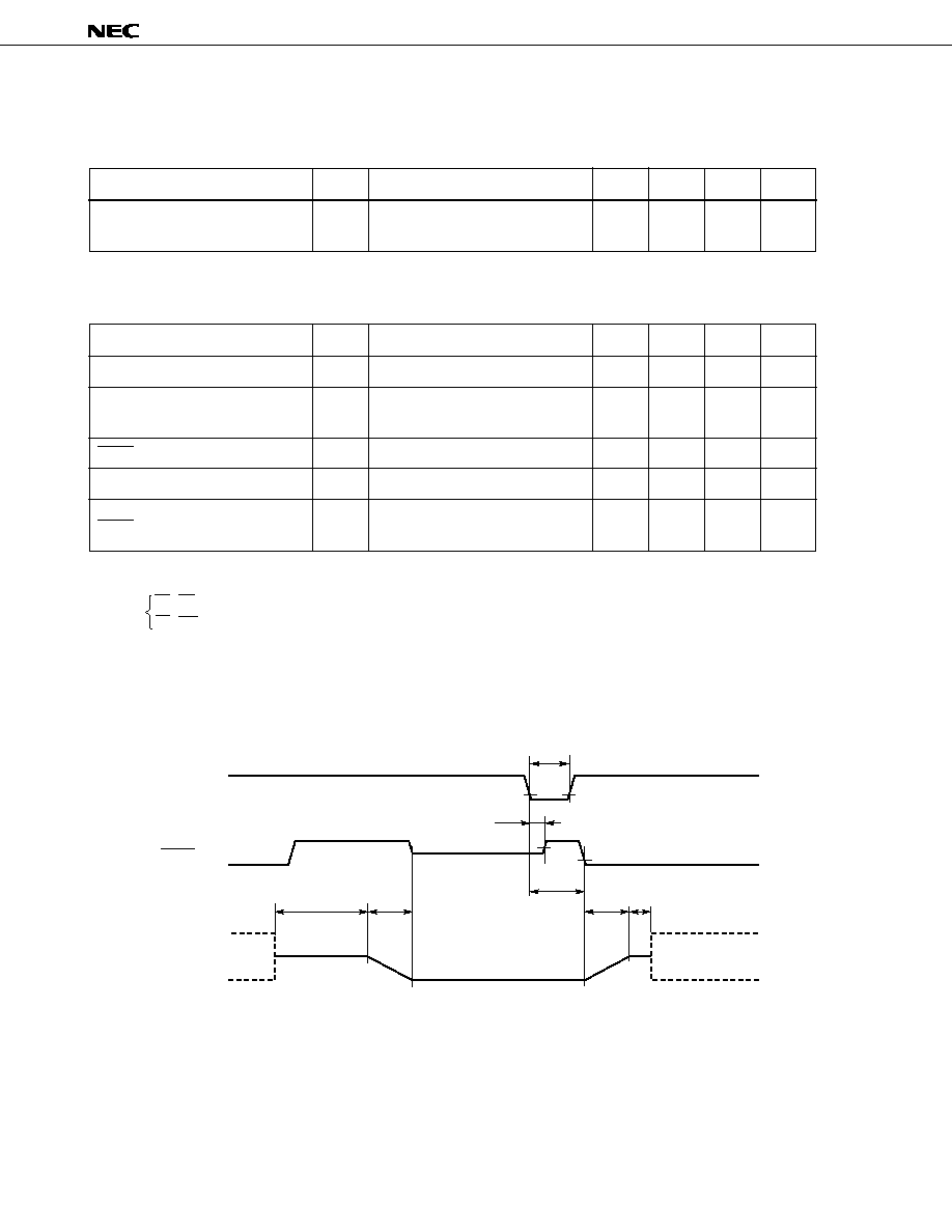
2.3 STANDBY MODE
(1) TIMING REQUIREMENTS
Parameters
Symbol
Conditions
MIN.
TYP.
MAX.
Unit
Standby escape signal
L*
Note
pulse width
(2) SWITCHING CHARACTERISTICS
Parameters
Symbol
Conditions
MIN.
TYP.
MAX.
Unit
Operation mode hold time
t
STB
after synthesis
2.9
3
s
D/A converter activate
/inactivate time
BUSY set up time
t
SB
from L*
6.25
10
µ
s
Synthesis start time
t
SSS
after D/A converter activation
2.1
2.2
ms
In standby mode, oscillation
start time is included.
Note L*: Signal to release standby mode.
CS ST : When operation mode is stand alone mode.
=
CS WR : When operation mode is slave mode
TIMING CHART (Standby mode)
t
AW
BUSY
L*
t
SB
t
STB
t
DA
t
SBS
t
DA
t
SSS
Synthesis
max
mid
0
I
AVO
< <
µ
PD7759
15
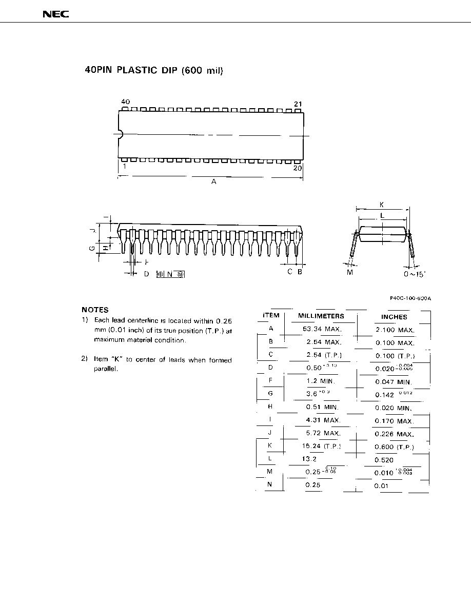
3. PACKAGE DRAWINGS
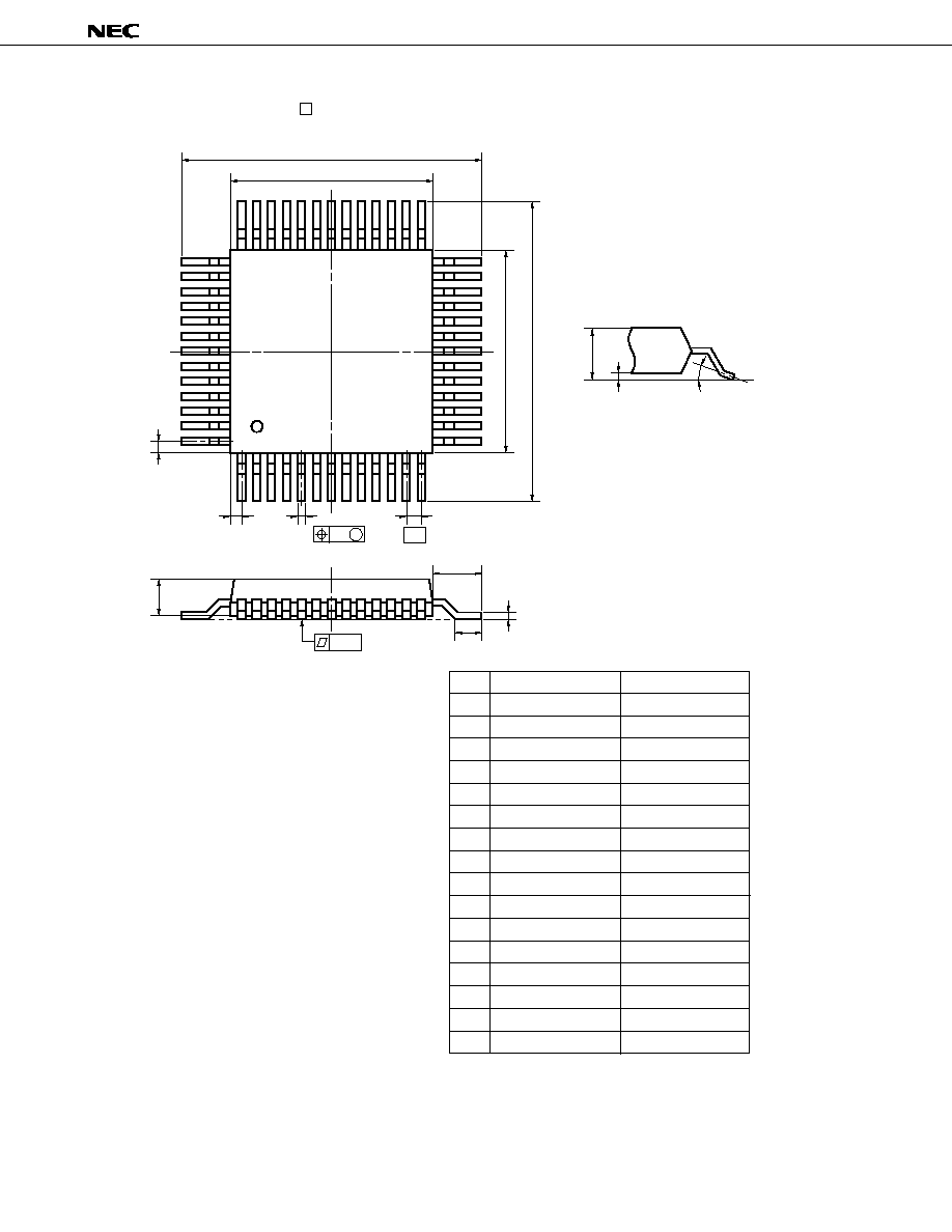
µ
PD7759
16
M
K
L
P
H
G
C
D
B
A
F
39
40
52
1
26
27
14
13
52 PIN PLASTIC QFP ( 14)
detail of lead end
M
I
J
Q
5∞±5∞
S
N
P52GC-100-3B6,3BH-1
ITEM
MILLIMETERS
INCHES
A
B
C
D
F
G
H
I
J
K
L
17.6±0.4
14.0±0.2
1.0
0.40±0.10
0.20
14.0±0.2
0.693±0.016
0.039
0.039
0.008
0.039 (T.P.)
0.551
NOTE
M
N
0.12
0.15
1.8±0.2
1.0 (T.P.)
0.005
0.006
+0.004
≠0.003
Each lead centerline is located within 0.20
mm (0.008 inch) of its true position (T.P.) at
maximum material condition.
0.071
0.016
0.551
0.8±0.2
0.031
P
2.7
0.106
0.693±0.016
17.6±0.4
1.0
+0.009
≠0.008
Q
0.1±0.1
0.004±0.004
S
3.0 MAX.
0.119 MAX.
+0.10
≠0.05
+0.009
≠0.008
+0.009
≠0.008
+0.004
≠0.005
+0.008
≠0.009
5
µ
PD7759
17
4. RECOMMENDED SOLDERING CONDITIONS
The following conditions (see tables below) must be met when soldering the
µ
PD7759. Please consult
with our sales offices in case other soldering process is used, or in case soldering is done under
different conditions.
For more details, refer to our document "SEMICONDUCTOR DEVICE MOUNTING TECHNOLOGY
MANUAL" (IEI-1207).
q
q
TYPE OF SURFACE MOUNT DEVICE
µ
PD7759GC-3BH:52-pin plastic QFP (
s
s
14 mm)
Soldering Process
Soldering Conditions
Symbol
Solder temperature: 260
∞
C or below,
Flow time: 10 seconds or below,
Temperature of pre-heat: 120
∞
C or below (Plastic surface temperature),
Number of flow process: 1
Peak package's surface temperature: 230
∞
C or below,
Infrared Ray Reflow
Reflow time: 30 seconds or below (210
∞
C or higher),
IR30-00-1
Number of reflow process: 1
Peak package's temperature: 215
∞
C or below,
VPS
Reflow time: 40 seconds or below (200
∞
C or higher),
VP15-00-1
Number of reflow process: 1
Terminal temperature: 300
∞
C or below,
Time: 3 seconds or below (Per one side of the device)
Caution Do not apply more than one soldering method at any one time, except for "Partial heating method".
q
q
TYPE OF THROUGH HOLE DEVICE
µ
PD7759C:40-pin plastic DIP (600mil)
Soldering Process
Soldering Conditions
Wave Soldering
Solder Temperature: 260
∞
C or below
(only lead part)
Flow time: 10 seconds or below
Terminal temperature: 260
∞
C or below
Time: 10 seconds or below
Caution Do not jet molten solder on the surface of package.
5
Partial Heating Method
--
Wave Soldering
WS60-00-1
Partial Heating Method

µ
PD7759
No part of this document may be copied or reproduced in any form or by any means without the prior written
consent of NEC Corporation. NEC Corporation assumes no responsibility for any errors which may appear in this
document.
NEC Corporation does not assume any liability for infringement of patents, copyrights or other intellectual
property rights of third parties by or arising from use of a device described herein or any other liability arising
from use of such device. No license, either express, implied or otherwise, is granted under any patents,
copyrights or other intellectual property rights of NEC Corporation or others.
The devices listed in this document are not suitable for use in aerospace equipment, submarine cables, nuclear
reactor control systems and life support systems. If customers intend to use NEC devices for above applications
or they intend to use "Standard" quality grade NEC devices for applications not intended by NEC, please contact
our sales people in advance.
Application examples recommended by NEC Corporation
Standard: Computer, Office equipment, Communication equipment, Test and Measurement equipment,
Machine tools, Industrial robots, Audio and Visual equipment, Other consumer products, etc.
Special:
Automotive and Transportation equipment, Traffic control systems, Antidisaster systems, Anticrime
systems, etc.
M4 92.6
The
µ
PD7759 has the following user's manual as a separate volume.
Please use it for reference.
q
µ
PD7755 family User's Manual: IEU-1218