Document Outline
- COVER
- DESCRIPTION
- FEATURES
- APPLICATION
- ORDERING INFORMATION
- 78K/0 SERIES PRODUCT DEVELOPMENT
- OVERVIEW OF FUNCTION
- 1. PIN CONFIGURATION (TOP VIEW)
- 2. BLOCK DIAGRAM
- 3. PIN FUNCTIONS
- 3.1 PORT PINS
- 3.2 OTHER PINS
- 3.3 PIN I/O CIRCUIT AND RECOMMENDED CONNECTION OF UNUSED PINS
- 4. MEMORY SPACE
- 5 PERIPHERAL HARDWARE FUNCTION FEATURES
- 5.1 PORTS
- 5.2 CLOCK GENERATOR
- 5.3 TIMER/EVENT COUNTER
- 5.4 CLOCK OUTPUT CONTROL CIRCUIT
- 5.5 BUZZER OUTPUT CONTROL CIRCUIT
- 5.6 SERIAL INTERFACES
- 6. INTERRUPT FUNCTIONS AND DEST FUNCTIONS
- 6.1 INTERRUPT FUNCTIONS
- 6.2 TEST FUNCTIONS
- 7. EXTERNAL DEVICE EXPANSION FUNCTIONS
- 8. STANDBY FUNCTIONS
- 9. RESET FUNCTION
- 10. INSTRUCTION SET
- 11. ELECTRICAL SPECIFICATIONS
- 12. CHARACTERISTIC CURVE (REFERENCE VALUES)
- 13. PACKAGE DRAWINGS
- 14. RECOMMENDED SOLDERING CONDITIONS
- APPENDIX A. DEVEROPMENT TOOLS
- APPENDIX B. RELATED DOCUMENTS

DESCRIPTION
The
µ
PD78001B(A)/78002B(A) are products in the
µ
PD78002 subseries within the 78K/0 series.
The
µ
PD78001B(A)/78002B(A) have various peripheral hardware such as timer, serial interface and interrupt
function.
A one-time PROM or EPROM product, the
µ
PD78P014, capable of operating in the same power supply voltage
range as that of the mask ROM product and other development tools is provided.
Functions are described in detail in the following User's Manual, which should be read when carrying out design
work.
µ
PD78002, 78002Y Series User's Manual: IEU-1334
FEATURES
∑
The
µ
PD78001B, in comparison with the 78002B, is a higher reliability device, as a result of a more comprehensive
quality assurance program (Refer to Quality Grade on NEC Semiconductor Devices (IEI-1209))
∑
Large on-chip ROM & RAM
MOS INTEGRATED CIRCUIT
µ
PD78001B(A), 78002B(A)
8-BIT SINGLE-CHIP MICROCOMPUTER
The information in this document is subject to change without notice.
©
1995
DATA SHEET
Item
Program Memory
Data Memory
Product Name
(ROM)
(Internal High-Speed RAM)
µ
PD78001B(A)
8K bytes
256 bytes
∑
64-pin plastic shrink DIP (750 mil)
µ
PD78002B(A)
16K byte
384 bytes
∑
64-pin plastic QFP (
14 mm)
Package
∑
External memory expansion space: 64K bytes
∑
Instruction execution time can be varied from high-speed (0.4
µ
s) to ultra-low-speed (122
µ
s)
∑
I/O ports: 53 (N-ch open-drain : 4)
∑
Serial interface : 1 channel
∑
Timer: 4 channels
∑
Operating voltage range : 2.7 to 6.0 V
APPLICATION
Transmission equipment control device, gas detector circuit breaker, safety devices, etc.
Document No. IC-3599
(O.D. No. IC-9078)
Date Published February 1995 P
Printed in Japan
2
µ
PD78001B(A), 78002B(A)
ORDERING INFORMATION
Part Number
Package
Quality Grade
µ
PD78001BCW (A)-
◊◊◊
64-pin plastic shrink DIP (750 mil)
Special
µ
PD78001BGC (A)-
◊◊◊
-AB8
64-pin plastic QFP (
s
s
14 mm)
Special
µ
PD78002BCW (A)-
◊◊◊
64-pin plastic shrink DIP (750 mil)
Special
µ
PD78002BGC (A)-
◊◊◊
-AB8
64-pin plastic QFP (
s
s
14 mm)
Special
Remark
◊◊◊
indicates ROM code No.
Please refer to "Quality grade on NEC Semiconductor Devices" (Document number IEI-1209) published by
NEC Corporation to know the specification of quality grade on the devices and its recommended applications.
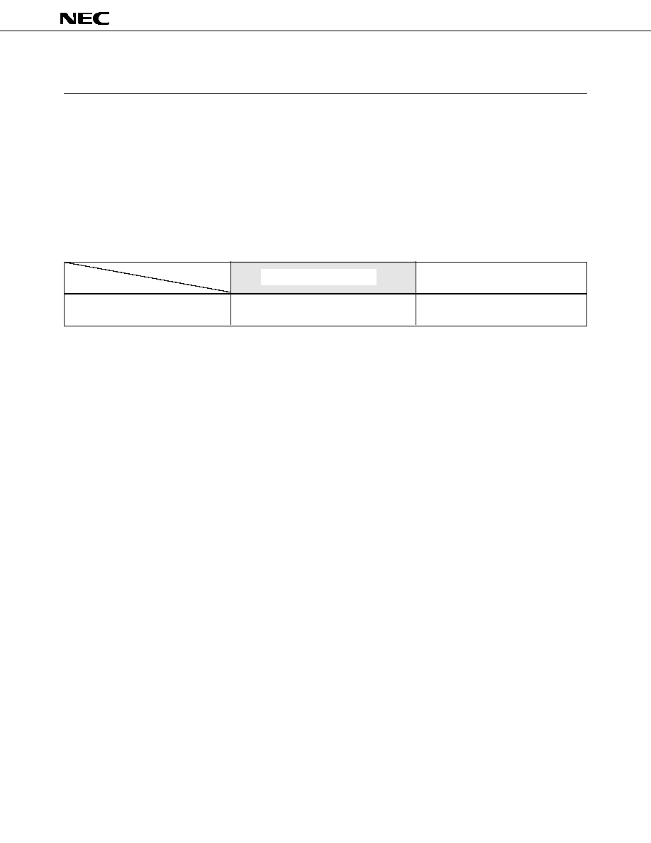
Difference between the
µ
PD78001B(A), 78002B(A) and the
µ
PD78001B, 78002B.
Product Name
µ
PD78001B(A), 78002B(A)
µ
PD78001B, 78002B
Item
Quality Grade
Special
Standard
µ
PD78001B(A), 78002B(A)
3
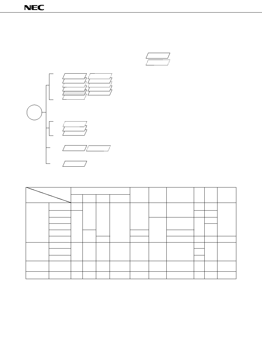
78K/0 SERIES PRODUCT DEVELOPMENT
These products are a further development in the 78K/0 Series. The designations appearing inside the boxes
are subseries names.
Products in Volume Production
Products under Development
Y series products are compatible with I
2
C bus.
100-pin
For control
Timer added to the PD78054, external interface functions
80-pin
64-pin
Low-voltage (1.8 V) operation version of the PD78014, with enhanced ROM and RAM variations
A/D and 16-bit timer added to the PD78002
Basic subseries for control
42/44-pin
Internal UART, low-voltage (1.8 V) operation possible
For FIP
Æ
driving
I/O, FIP C/D of the PD78044A enhanced, display output total: 53
6-bit U/D counter added to the PD78024, display output total: 34
Basic subseries for FIP driving, display output total: 26
For LCD driving
Subseries for LCD driving, internal UART
For IEBus
TM
IEBus controller added to the PD78054
PD78078
PD78054
PD78018F
PD78014
PD78002
PD78083
PD78078Y
PD78054Y
PD78018FY
PD78014Y
PD78002Y
PD780208
PD78044A
PD78024
PD78064
PD78064Y
PD78098
64-pin
64-pin
100-pin
80-pin
64-pin
100-pin
78K/0
Series
80-pin
UART and D/A added to the PD78014, I/O enhanced
µ
µ
µ
µ
µ
µ
µ
µ
µ
µ
µ
µ
µ
µ
µ
µ
µ
µ
µ
µ
µ
µ
µ
µ
The major functional differences among the subseries are shown below.
Function
Timer
Serial
V
DD
External
A/D
D/A
Interface
I/O
MIN.
Expansion
Name
8-bit
16-bit
Watch
Watchdog
Value
µ
PD78078
4ch
1ch
1ch
1ch
8-bit
◊
8ch
8-bit
◊
2ch 3ch (UART: 1ch)
88
1.8 V
C
µ
PD78054
2ch
69
2.0 V
µ
PD78018F
--
2ch
53
1.8 V
µ
PD78014
2.7 V
µ
PD78002
--
--
1ch
µ
PD78083
--
8-bit
◊
8ch
1ch (UART: 1ch)
33
1.8 V
--
µ
PD780208
2ch
1ch
1ch
1ch
8-bit
◊
8ch
--
2ch
74
2.7 V
--
µ
PD78044A
68
µ
PD78024
54
µ
PD78064
2ch
1ch
1ch
1ch
8-bit
◊
8ch
--
2ch (UART: 1ch)
57
2.0 V
--
µ
PD78098
2ch
1ch
1ch
1ch
8-bit
◊
8ch
8-bit
◊
2ch 3ch (UART: 1ch)
69
2.7 V
C
For Control
For LCD
driving
For IEBus
TM
For FIP
Æ
driving
4
µ
PD78001B(A), 78002B(A)
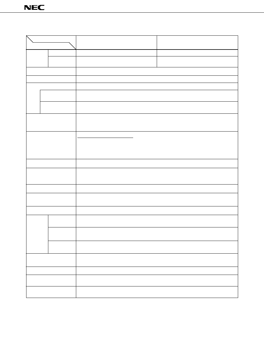
OVERVIEW OF FUNCTION
Item
ROM
Internal high-
speed RAM
8K bytes
16K bytes
64K bytes
8 bits
◊
32 registers (8 bits
◊
8 registers
◊
4 banks)
On-chip instruction execution time cycle modification function
0.4
µ
s/0.8
µ
s/1.6
µ
s/3.2
µ
s/6.4
µ
s (at 10.0 MHz operation)
122
µ
s (at 32.768 kHz operation)
∑ 16-bit operation
∑ Bit manipulation (set, reset, test, boolean operation)
∑ BCD correction, etc.
Total
: 53
∑ CMOS input
:
0
2
∑ CMOS I/O
: 47
∑ N-channel open-drain I/O
(15 V withstand voltage)
:
0
4
∑ 3-wire/SBI/2-wire mode selectable
∑ 8-bit timer/event counter
: 2 channels
∑ Watch timer
: 1 channel
∑ Watchdog timer
: 1 channel
2
39.1 kHz, 78.1 kHz, 156 kHz, 313 kHz, 625 kHz, 1.25 MHz (at main system clock 10.0 MHz operation),
32.768 kHz (at subsystem clock 32.768 kHz operation)
2.4 kHz, 4.9 kHz, 9.8 kHz (at main system clock 10.0 MHz operation)
Internal : 5
External : 4
Internal : 1
Internal : 1
Internal : 1
External : 1
V
DD
= 2.7 to 6.0 V
≠40 to +85
∞
C
∑ 64-pin plastic shrink DIP (750 mil)
∑ 64-pin plastic QFP (
s
s
14 mm)
256 bytes
384 bytes
When main system
clock selected
When subsystem
clock selected
Maskable
interrupts
Non-maskable
interrupt
Software
interrupt
Product Name
µ
PD78001B(A)
µ
PD78002B(A)
Internal
memory
Memory space
General registers
Instruction cycle
Instruction set
I/O ports
Serial interface
Timer
Timer output
Clock output
Buzzer output
Vectored
interrupts
Test input
Operating voltage range
Operating ambient
temperature range
Package

µ
PD78001B(A), 78002B(A)
5
1.
PIN CONFIGURATION (TOP VIEW) .....................................................................................................
6
2.
BLOCK DIAGRAM ...................................................................................................................................
9
3.
PIN FUNCTIONS ..................................................................................................................................... 10
3.1
PORT PINS ...................................................................................................................................................... 10
3.2
OTHER PINS ................................................................................................................................................... 12
3.3
PIN I/O CIRCUIT AND RECOMMENDED CONNECTION OF UNUSED PINS ...................................... 13
4.
MEMORY SPACE .................................................................................................................................... 15
5.
PERIPHERAL HARDWARE FUNCTION FEATURES ............................................................................ 16
5.1
PORTS .............................................................................................................................................................. 16
5.2
CLOCK GENERATOR ...................................................................................................................................... 17
5.3
TIMER/EVENT COUNTER .............................................................................................................................. 18
5.4
CLOCK OUTPUT CONTROL CIRCUIT ......................................................................................................... 20
5.5
BUZZER OUTPUT CONTROL CIRCUIT ....................................................................................................... 20
5.6
SERIAL INTERFACES ..................................................................................................................................... 21
6.
INTERRUPT FUNCTIONS AND TEST FUNCTIONS .......................................................................... 22
6.1
INTERRUPT FUNCTIONS ............................................................................................................................... 22
6.2
TEST FUNCTIONS .......................................................................................................................................... 25
7.
EXTERNAL DEVICE EXPANSION FUNCTIONS ................................................................................. 26
8.
STANDBY FUNCTIONS ......................................................................................................................... 26
9.
RESET FUNCTION .................................................................................................................................. 26
10. INSTRUCTION SET ................................................................................................................................ 27
11. ELECTRICAL SPECIFICATIONS ............................................................................................................. 30
12. CHARACTERISTIC CURVE (REFERENCE VALUES) ........................................................................... 48
13. PACKAGE DRAWINGS ........................................................................................................................... 52
14. RECOMMENDED SOLDERING CONDITIONS ..................................................................................... 56
APPENDIX A. DEVELOPMENT TOOLS ...................................................................................................... 57
APPENDIX B. RELATED DOCUMENTS ...................................................................................................... 59
CONTENTS