Document Outline
- COVER
- DESCRIPTION
- FEATURES
- ORDERING INFORMATION
- QUALITY GRADE
- CORRESPONDENCE BETWEEN MASK ROM PRODUCTS AND FLASH MEMORY PRODUCTS
- 78K/0 SERIES LINEUP
- OVERVIEW OF FUNCTIONS
- 1. PIN CONFIGURATION (TOP VIEW)
- 2. BLOCK DIAGRAM
- 3. PIN FUNCTIONS
- 3.1 Port Pins
- 3.2 Non-Port Pins
- 3.3 Pin I/O Circuits and Recommended Connection of Unused Pins
- 4. DIFFERENCES BETWEEN uPD78F0034B, 78F0034BY, AND MASK ROM VERSIONS
- 5. DIFFERENCES BETWEEN uPD78F0034B, 78F0034BY AND uPD78F0034A, 78F0034AY
- 6. DIFFERENCES BETWEEN uPD78F0034B, 78F0034BY AND uPD78F0034B(A), 78F0034BY(A)
- 7. MEMORY SIZE SWITCHING REGISTER (IMS)
- 8. FLASH MEMORY PROGRAMMING
- 8.1 Selection of Communication Mode
- 8.2 Flash Memory Programming Functions
- 8.3 Connection of Flashpro III/Flashpro IV
- 9. ELECTRICAL SPECIFICATIONS
- 9.1 µPD78F0034B, 78F0034B(A)
- 9.2 µPD78F0034BY, 78F0034BY(A)
- 9.3 Timing Chart
- 10. PACKAGE DRAWINGS
- 11. RECOMMENDED SOLDERING CONDITIONS
- APPENDIX A. DEVELOPMENT TOOLS
- APPENDIX B. RELATED DOCUMENTS

DATA SHEET
©
MOS INTEGRATED CIRCUIT
8-BIT SINGLE-CHIP MICROCONTROLLERS
µ
PD78F0034B, 78F0034BY, 78F0034B(A), 78F0034BY(A)
DESCRIPTION
The
µ
PD78F0034B is a member of the
µ
PD780034A Subseries in the 78K/0 Series, and is equivalent to the
µ
PD780034A (expanded-specification product) but with flash memory in place of internal ROM.
The
µ
PD78F0034BY is a member of the
µ
PD780034AY Subseries, featuring flash memory in place of the internal
ROM of the
µ
PD780034AY.
The
µ
PD78F0034B(A) and 78F0034BY(A) are products to which a quality assurance program more stringent than
that used for the
µ
PD78F0034B and 78F0034BY (standard models) is applied (NEC Electronics classifies these
products as "special" quality grade models).
The
µ
PD78F0034B, 78F0034BY, 78F0034B(A), and 78F0034BY(A) incorporate flash memory, which can be
programmed and erased while mounted on the board.
Detailed function descriptions are provided in the following user's manuals. Be sure to read them before
designing.
µ
PD780024A, 780034A, 780024AY, 780034AY Subseries User's Manual: U14046E
78K/0 Series Instruction User's Manual: U12326E
FEATURES
∑
Pin-compatible with mask ROM versions (except V
PP
pin)
∑
Flash memory:
32 KB
Note
∑
Internal high-speed RAM: 1,024 bytes
Note
∑
Supply voltage:
V
DD
= 1.8 to 5.5 V
Note
The flash memory and internal high-speed RAM capacities can be changed with the memory size switching
register (IMS).
Remark
For the differences between the flash memory and the mask ROM versions, refer to 4. DIFFERENCES
BETWEEN
µ
PD78F0034B, 78F0034BY, AND MASK ROM VERSIONS.
Document No. U16369EJ1V0DS00 (1st edition)
Date Published January 2003 N CP(K)
Printed in Japan
The information in this document is subject to change without notice. Before using this document, please
confirm that this is the latest version.
Not all products and/or types are available in every country. Please check with an NEC Electronics
sales representative for availability and additional information.

µ
PD78F0034B, 78F0034BY, 78F0034B(A), 78F0034BY(A)
2
Data Sheet U16369EJ1V0DS
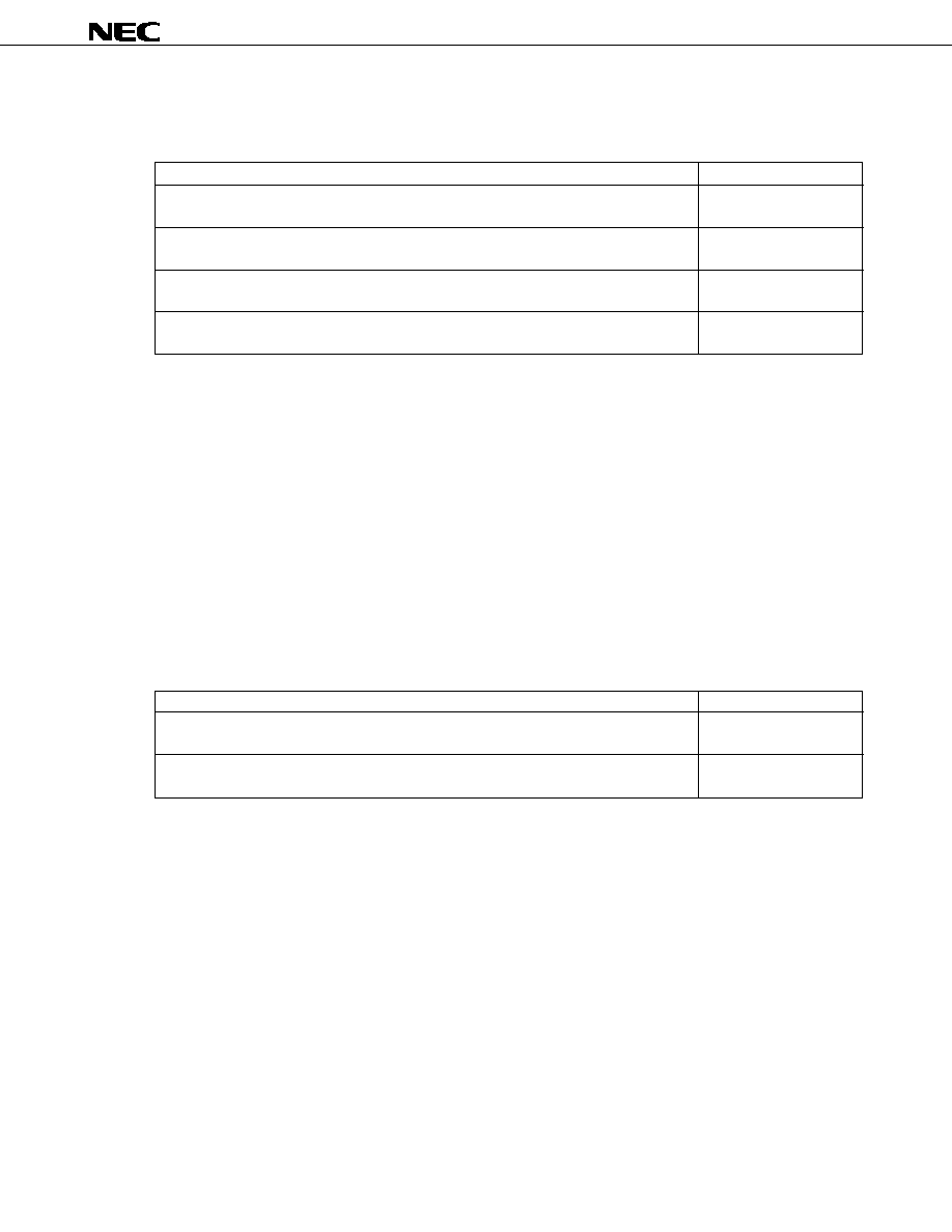
ORDERING INFORMATION
Part Number
Package
Internal ROM
µ
PD78F0034BGB-8EU
64-pin plastic LQFP (10 x 10)
Flash memory
µ
PD78F0034BGC-8BS
64-pin plastic LQFP (14 x 14)
Flash memory
µ
PD78F0034BGK-9ET
64-pin plastic TQFP (12 x 12)
Flash memory
µ
PD78F0034BF1-CN3
73-pin plastic FBGA (9 x 9)
Flash memory
µ
PD78F0034BGB(A)-8EU
64-pin plastic LQFP (10 x 10)
Flash memory
µ
PD78F0034BGC(A)-8BS
64-pin plastic LQFP (14 x 14)
Flash memory
µ
PD78F0034BGK(A)-9ET
64-pin plastic TQFP (12 x 12)
Flash memory
µ
PD78F0034BYGB-8EU
64-pin plastic LQFP (10 x 10)
Flash memory
µ
PD78F0034BYGC-8BS
64-pin plastic LQFP (14 x 14)
Flash memory
µ
PD78F0034BYGK-9ET
64-pin plastic TQFP (12 x 12)
Flash memory
µ
PD78F0034BYF1-CN3
73-pin plastic FBGA (9 x 9)
Flash memory
µ
PD78F0034BYGB(A)-8EU
64-pin plastic LQFP (10 x 10)
Flash memory
µ
PD78F0034BYGC(A)-8BS
64-pin plastic LQFP (14 x 14)
Flash memory
µ
PD78F0034BYGK(A)-9ET
64-pin plastic TQFP (12 x 12)
Flash memory
QUALITY GRADE
Part Number
Package
Quality Grade
µ
PD78F0034BGB-8EU
64-pin plastic LQFP (10 x 10)
Standard
µ
PD78F0034BGC-8BS
64-pin plastic LQFP (14 x 14)
Standard
µ
PD78F0034BGK-9ET
64-pin plastic TQFP (12 x 12)
Standard
µ
PD78F0034BF1-CN3
73-pin plastic FBGA (9 x 9)
Standard
µ
PD78F0034BGB(A)-8EU
64-pin plastic LQFP (10 x 10)
Special
µ
PD78F0034BGC(A)-8BS
64-pin plastic LQFP (14 x 14)
Special
µ
PD78F0034BGK(A)-9ET
64-pin plastic TQFP (12 x 12)
Special
µ
PD78F0034BYGB-8EU
64-pin plastic LQFP (10 x 10)
Standard
µ
PD78F0034BYGC-8BS
64-pin plastic LQFP (14 x 14)
Standard
µ
PD78F0034BYGK-9ET
64-pin plastic TQFP (12 x 12)
Standard
µ
PD78F0034BYF1-CN3
73-pin plastic FBGA (9 x 9)
Standard
µ
PD78F0034BYGB(A)-8EU
64-pin plastic LQFP (10 x 10)
Special
µ
PD78F0034BYGC(A)-8BS
64-pin plastic LQFP (14 x 14)
Special
µ
PD78F0034BYGK(A)-9ET
64-pin plastic TQFP (12 x 12)
Special
P l e a s e r e f e r t o " Q u a l i t y G r a d e s o n N E C S e m i c o n d u c t o r D e v i c e s " ( D o c u m e n t N o . C 1 1 5 3 1 E ) p u b l i s h e d b y
NEC Corporation to know the specification of quality grade on the devices and its recommended applications.
µ
PD78F0034B, 78F0034BY, 78F0034B(A), 78F0034BY(A)
3
Data Sheet U16369EJ1V0DS
CORRESPONDENCE BETWEEN MASK ROM PRODUCTS AND FLASH MEMORY PRODUCTS
∑
µ
PD780024A, 780034A Subseries
Mask ROM Products
Flash Memory Products
Expanded-specification products of
µ
PD780021A, 780022A, 780023A, 780024A
µ
PD78F0034B
Expanded-specification products of
µ
PD780031A, 780032A, 780033A, 780034A
Conventional products of
µ
PD780021A, 780022A, 780023A, 780024A
µ
PD78F0034A
Conventional products of
µ
PD780031A, 780032A, 780033A, 780034A
Expanded-specification products of
µ
PD780021A(A), 780022A(A), 780023A(A), 780024A(A)
µ
PD78F0034B(A)
Expanded-specification products of
µ
PD780031A(A), 780032A(A), 780033A(A), 780034A(A)
Conventional products of
µ
PD780021A(A), 780022A(A), 780023A(A), 780024A(A)
µ
PD78F0034B(A)
Conventional products of
µ
PD780031A(A), 780032A(A), 780033A(A), 780034A(A)
Caution The
µµ
µµ
µ
PD78F0034B(A) and conventional products of the
µµ
µµ
µ
PD780021A(A), 780022A(A), 780023A(A),
780024A(A) and
µµ
µµ
µ
PD780031A(A), 780032A(A), 780033A(A), and 780034A(A) differ in the operating
frequency ratings. When using the mask ROM versions in place of the flash memory versions,
take note of the power supply voltage and operating frequency used.
Remarks 1. The
µ
PD78F0034B, 78F0034B(A) and 78F0034A differ in the operating frequency ratings and
communication mode of the flash memory programming. Refer to 5. DIFFERENCES BETWEEN
µµ
µµ
µ
PD78F0034B, 78F0034BY AND
µµ
µµ
µ
PD78F0034A, 78F0034AY.
2. The expanded-specification products and conventional products of the mask ROM versions differ
in the operating frequency ratings. Refer to the data sheets of the products.
3. The special grade version of the
µ
PD78F0034A is not provided (only the standard grade version
is provided).
∑
µ
PD780024AY, 780034AY Subseries
Mask ROM Products
Flash Memory Products
µ
PD780021AY, 780022AY, 780023AY, 780024AY
µ
PD78F0034AY
µ
PD780031AY, 780032AY, 780033AY, 780034AY
µ
PD78F0034BY
µ
PD780021AY(A), 780022AY(A), 780023AY(A), 780024AY(A)
µ
PD78F0034BY(A)
µ
PD780031AY(A), 780032AY(A), 780033AY(A), 780034AY(A)
Remarks 1. The
µ
PD78F0034BY, 78F0034BY(A) and 78F0034AY differ in the communication mode of the flash
memory programming. Refer to 5. DIFFERENCES BETWEEN
µµ
µµ
µ
PD78F0034B, 78F0034BY AND
µµ
µµ
µ
PD78F0034A, 78F0034AY.
2. The expanded-specification products of the
µ
PD780024AY, 780034AY Subseries are not provided
(only the conventional products are provided).
3. The special grade version of the
µ
PD78F0034A is not provided (only the standard grade version
is provided).

µ
PD78F0034B, 78F0034BY, 78F0034B(A), 78F0034BY(A)
4
Data Sheet U16369EJ1V0DS
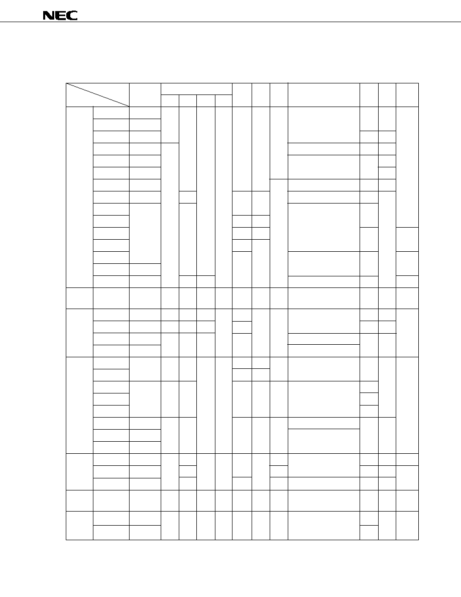
78K/0 SERIES LINEUP
The products in the 78K/0 Series are listed below. The names enclosed in boxes are subseries names.
Remark
VFD (Vacuum Fluorescent Display) is referred to as FIP
TM
(Fluorescent Indicator Panel) in some
documents, but the functions of the two are same.
PD78083
PD78018F
PD78018FY
PD78014H
EMI-noise reduced version of the PD78018F
Basic subseries for control
On-chip UART, capable of operating at low voltage (1.8 V)
µ
µ
µ
µ
42/44-pin
64-pin
64-pin
52-pin
52-pin version of the PD780024A
µ
µ
PD780024AS
µ
52-pin
52-pin version of the PD780034A
PD780034AS
PD78054 with IEBus
TM
controller
PD78054 with enhanced serial I/O
PD78078Y with enhanced serial I/O and limited function
PD78054 with timer and enhanced external interface
64-pin
64-pin
80-pin
80-pin
80-pin
EMI-noise reduced version of the PD78054
PD78018F with UART and D/A converter, and enhanced I/O
PD780034A
PD780988
PD780034AY
µ
µ
µ
64-pin
PD780024A with expanded RAM
PD780024A with enhanced A/D converter
µ
µ
µ
µ
On-chip inverter control circuit and UART. EMI-noise reduced.
PD78064
PD78064B
PD780308
100-pin
100-pin
100-pin
PD780308Y
PD78064Y
80-pin
78K/0
Series
LCD drive
PD78064 with enhanced SIO, and expanded ROM and RAM
EMI-noise reduced version of the PD78064
Basic subseries for driving LCDs, on-chip UART
Bus interface supported
µ
µ
µ
µ
µ
µ
µ
µ
µ
PD78018F with enhanced serial I/O
µ
µ
80-pin
100-pin
100-pin
Products in mass production
Products under development
Y subseries products are compatible with I
2
C bus.
ROMless version of the PD78078
µ
100-pin
µ
µ
100-pin
EMI-noise reduced version of the PD78078
µ
Inverter control
PD780208
100-pin
VFD drive
PD78044F with enhanced I/O and VFD C/D. Display output total: 53
µ
µ
PD78098B
µ
100-pin
PD780024A
PD780024AY
µ
µ
µ
80-pin
80-pin
PD780852
PD780828B
µ
µ
For automobile meter driver. On-chip CAN controller
100-pin
PD780958
µ
For industrial meter control
On-chip automobile meter controller/driver
Meter control
80-pin
On-chip IEBus controller
80-pin
On-chip controller compliant with J1850 (Class 2)
PD780833Y
µ
PD780948
On-chip CAN controller
µ
64-pin
PD780078
PD780078Y
µ
µ
PD780034A with timer and enhanced serial I/O
PD78054
PD78054Y
PD78058F
PD78058FY
µ
µ
µ
µ
PD780058
PD780058Y
µ
µ
PD78070A
PD78070AY
PD78078
PD78078Y
PD780018AY
µ
µ
µ
µ
µ
Control
PD78075B
µ
PD780065
µ
µ
PD78044H
PD780232
80-pin
80-pin
For panel control. On-chip VFD C/D. Display output total: 53
PD78044F with N-ch open-drain I/O. Display output total: 34
µ
µ
PD78044F
80-pin
Basic subseries for driving VFD. Display output total: 34
µ
µ
120-pin
PD780308 with enhanced display function and timer. Segment signal output: 40 pins max.
PD780318
PD780328
120-pin
120-pin
PD780308 with enhanced display function and timer. Segment signal output: 32 pins max.
PD780308 with enhanced display function and timer. Segment signal output: 24 pins max.
µ
µ
PD780338
µ
µ
PD780308 with enhanced display function and timer. Segment signal output: 40 pins max.
µ
µ
µ
On-chip CAN controller
Specialized for CAN controller function
80-pin
PD780703Y
µ
PD780702Y
µ
64-pin
PD780816
µ
PD780344 with enhanced A/D converter
100-pin
100-pin
µ
PD780344
PD780344Y
PD780354
PD780354Y
µ
µ
µ
µ
µ
PD78F0034B, 78F0034BY, 78F0034B(A), 78F0034BY(A)
5
Data Sheet U16369EJ1V0DS
The major functional differences among the subseries are listed below.
∑
Non-Y subseries
Function
ROM
Timer
8-Bit 10-Bit 8-Bit
Serial Interface
I/O
External
Subseries Name
8-Bit 16-Bit Watch WDT
A/D
A/D
D/A
Expansion
Control
µ
PD78075B 32 K to 40 K 4 ch
1 ch
1 ch
1 ch
8 ch
≠
2 ch 3 ch (UART: 1 ch)
88
1.8 V
µ
PD78078
48 K to 60 K
µ
PD78070A
≠
61
2.7 V
µ
PD780058 24 K to 60 K 2 ch
3 ch (time-division UART: 1 ch)
68
1.8 V
µ
PD78058F 48 K to 60 K
3 ch (UART: 1 ch)
69
2.7 V
µ
PD78054
16 K to 60 K
2.0 V
µ
PD780065 40 K to 48 K
≠
4 ch (UART: 1 ch)
60
2.7 V
µ
PD780078 48 K to 60 K
2 ch
≠
8 ch
3 ch (UART: 2 ch)
52
1.8 V
µ
PD780034A 8 K to 32 K
1 ch
3 ch (UART: 1 ch)
51
µ
PD780024A
8 ch
≠
µ
PD780034AS
≠
4 ch
39
≠
µ
PD780024AS
4 ch
≠
µ
PD78014H
8 ch
2 ch
53
µ
PD78018F 8 K to 60 K
µ
PD78083
8 K to 16 K
≠
≠
1 ch (UART: 1 ch)
33
≠
Inverter
µ
PD780988 16 K to 60 K 3 ch Note
≠
1 ch
≠
8 ch
≠
3 ch (UART: 2 ch)
47
4.0 V
control
VFD
µ
PD780208 32 K to 60 K 2 ch
1 ch
1 ch
1 ch
8 ch
≠
≠
2 ch
74
2.7 V
≠
drive
µ
PD780232 16 K to 24 K 3 ch
≠
≠
4 ch
40
4.5 V
µ
PD78044H 32 K to 48 K 2 ch
1 ch
1 ch
8 ch
1 ch
68
2.7 V
µ
PD78044F 16 K to 40 K
2 ch
LCD
µ
PD780354 24 K to 32 K 4 ch
1 ch
1 ch
1 ch
≠
8 ch
≠
3 ch (UART: 1 ch)
66
1.8 V
≠
drive
µ
PD780344
8 ch
≠
µ
PD780338 48 K to 60 K 3 ch
2 ch
≠
10 ch 1 ch 2 ch (UART: 1 ch)
54
µ
PD780328
62
µ
PD780318
70
µ
PD780308 48 K to 60 K 2 ch
1 ch
8 ch
≠
≠
3 ch (time-division UART: 1 ch)
57
2.0 V
µ
PD78064B 32 K
2 ch (UART: 1 ch)
µ
PD78064
16 K to 32 K
Bus
µ
PD780948 60 K
2 ch
2 ch
1 ch
1 ch
8 ch
≠
≠
3 ch (UART: 1 ch)
79
4.0 V
interface
µ
PD78098B 40 K to 60 K
1 ch
2 ch
69
2.7 V
≠
supported
µ
PD780816 32 K to 60 K
2 ch
12 ch
≠
2 ch (UART: 1 ch)
46
4.0 V
Meter
µ
PD780958 48 K to 60 K 4 ch
2 ch
≠
1 ch
≠
≠
≠
2 ch (UART: 1 ch)
69
2.2 V
≠
control
Dash-
µ
PD780852 32 K to 40 K 3 ch
1 ch
1 ch
1 ch
5 ch
≠
≠
3 ch (UART: 1 ch)
56
4.0 V
≠
board
control
µ
PD780828B 32 K to 60 K
59
Note 16-bit timer: 2 channels
10-bit timer: 1 channel
V
DD
MIN.
Value
Capacity
(Bytes)
µ
PD78F0034B, 78F0034BY, 78F0034B(A), 78F0034BY(A)
6
Data Sheet U16369EJ1V0DS
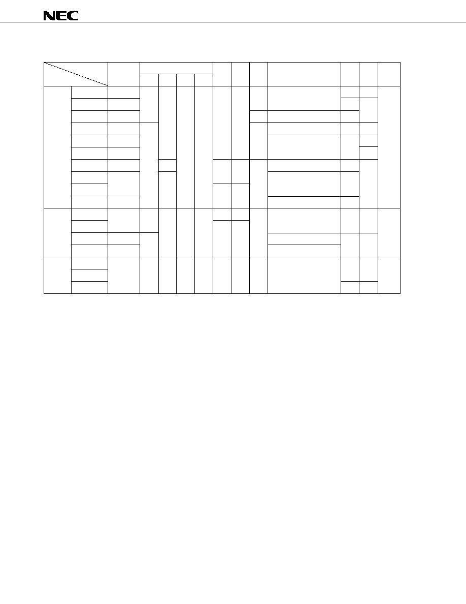
∑
Y subseries
Function
Timer
8-Bit 10-Bit 8-Bit
Serial Interface
I/O
External
Subseries Name
8-Bit 16-Bit Watch WDT
A/D
A/D
D/A
Expansion
Control
µ
PD78078Y 48 K to 60 K 4 ch
1 ch
1 ch
1 ch
8 ch
≠
2 ch 3 ch (UART: 1 ch, I
2
C: 1 ch)
88
1.8 V
µ
PD78070AY
≠
61
2.7 V
µ
PD780018AY 48 K to 60 K
≠
3 ch (I
2
C: 1 ch)
88
µ
PD780058Y 24 K to 60 K 2 ch
2 ch 3 ch (time-division UART: 1 ch, I
2
C: 1 ch)
68
1.8 V
µ
PD78058FY 48 K to 60 K
3 ch (UART: 1 ch, I
2
C: 1 ch)
69
2.7 V
µ
PD78054Y 16 K to 60 K
2.0 V
µ
PD780078Y 48 K to 60 K
2 ch
≠
8 ch
≠
4 ch (UART: 2 ch, I
2
C: 1 ch)
52
1.8 V
µ
PD780034AY 8 K to 32 K
1 ch
3 ch (UART: 1 ch, I
2
C: 1 ch)
51
µ
PD780024AY
8 ch
≠
µ
PD78018FY 8 K to 60 K
2 ch (I
2
C: 1 ch)
53
LCD
µ
PD780354Y 24 K to 32 K 4 ch
1 ch
1 ch
1 ch
≠
8 ch
≠
4 ch (UART: 1 ch,
66
1.8 V
≠
drive
µ
PD780344Y
8 ch
≠
I
2
C: 1 ch)
µ
PD780308Y 48 K to 60 K 2 ch
3 ch (time-division UART: 1 ch, I
2
C: 1 ch)
57
2.0 V
µ
PD78064Y 16 K to 32 K
2 ch (UART: 1 ch, I
2
C: 1 ch)
Bus
µ
PD780701Y 60 K
3 ch
2 ch
1 ch
1 ch 16 ch
≠
≠
4 ch (UART: 1 ch, I
2
C: 1 ch)
67
3.5 V
≠
interface
µ
PD780703Y
supported
µ
PD780833Y
65
4.5 V
Remark
Functions other than the serial interface are common to both the Y and non-Y subseries.
V
DD
MIN.
Value
ROM
Capacity
(Bytes)
µ
PD78F0034B, 78F0034BY, 78F0034B(A), 78F0034BY(A)
7
Data Sheet U16369EJ1V0DS
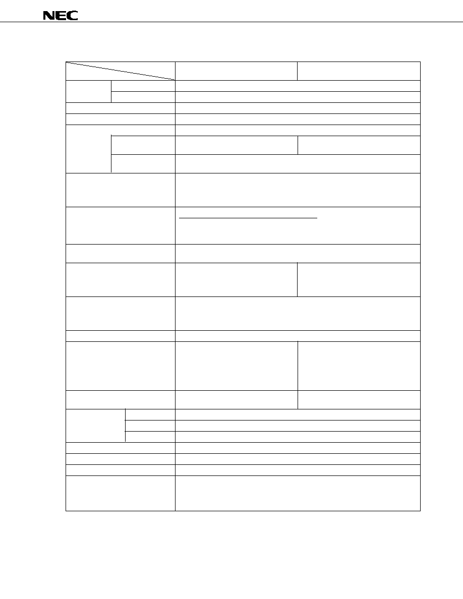
OVERVIEW OF FUNCTIONS
Part Number
µ
PD78F0034B
µ
PD78F0034BY
Item
µ
PD78F0034B(A)
µ
PD78F0034BY(A)
Internal
Flash memory
32 KB
Note 1
memory
High-speed RAM
1,024 bytes
Note 1
Memory space
64 KB
General-purpose registers
8 bits
◊
32 registers (8 bits
◊
8 registers
◊
4 banks)
Minimum instruction execution time
On-chip minimum instruction execution time cycle variable function
When main system
0.166
µ
s/0.333
µ
s/0.666
µ
s/1.33
µ
s/2.66
µ
s
0.238
µ
s/0.48
µ
s/0.95
µ
s/1.91
µ
s/3.81
µ
s
(@ 12 MHz operation, V
DD
= 4.5 to 5.5 V)
(@ 8.38 MHz operation, V
DD
= 4.0 to 5.5 V)
When subsystem
122
µ
s (@ 32.768 kHz operation)
clock selected
Instruction set
∑ 16-bit operation
∑ Multiply/divide (8 bits
◊
8 bits, 16 bits
˜
8 bits)
∑ Bit manipulation (set, reset, test, Boolean operation)
∑ BCD adjust, etc.
I/O ports
Total:
51
∑ CMOS input:
8
∑ CMOS I/O:
39
∑ N-ch open-drain I/O (5 V withstand voltage): 4
A/D converter
∑ 10-bit resolution
◊
8 channels
∑ Operable over a wide power supply voltage range: AV
DD
= 1.8 to 5.5 V
Serial interface
∑ UART mode:
1 channel
∑ UART mode:
1 channel
∑ 3-wire serial I/O mode: 2 channels
∑ 3-wire serial I/O mode:
1 channel
∑ I
2
C bus mode
(multimaster supporting): 1 channel
Timers
∑ 16-bit timer/event counter: 1 channel
∑ 8-bit timer/event counter:
2 channels
∑ Watch timer:
1 channel
∑ Watchdog timer:
1 channel
Timer outputs
3 (8-bit PWM output capable: 2)
Clock output
∑ 93.75 kHz, 187.5 kHz, 375 kHz, 750 kHz,
∑ 65.5 kHz, 131 kHz, 262 kHz, 524 kHz, 1.05
1.25 MHz, 3 MHz, 6 MHz, 12 MHz
MHz, 2.10 MHz, 4.19 MHz, 8.38 MHz
(@ 12 MHz operation with main system
(@ 8.38 MHz operation with main system
clock)
clock)
∑ 32.768 kHz (@ 32.768 kHz operation with
∑ 32.768 kHz (@ 32.768 kHz operation with
subsystem clock)
subsystem clock)
Buzzer output
1.46 kHz, 2.93 kHz, 5.86 kHz, 11.7 kHz
1.02 kHz, 2.05 kHz, 4.10 kHz, 8.19 kHz
(@ 12 MHz operation with main system clock)
(@ 8.38 MHz operation with main system clock)
Vectored interrupt
Maskable
Internal: 13, external: 5
sources
Non-maskable
Internal: 1
Software
1
Test inputs
Internal: 1, external: 1
Supply voltage
V
DD
= 1.8 to 5.5 V
Operating ambient temperature
T
A
= ≠40 to +85
∞
C
Package
∑ 64-pin plastic LQFP (10 x 10)
∑ 64-pin plastic LQFP (14 x 14)
∑ 64-pin plastic TQFP (12 x 12)
∑ 73-pin plastic FBGA (9 x 9)
Note 2
Notes 1.
The capacities of the flash memory and the internal high-speed RAM can be changed with the memory
size switching register (IMS).
2.
The special grade version of the 73-pin plastic FBGA (9 x 9) is not provided.

µ
PD78F0034B, 78F0034BY, 78F0034B(A), 78F0034BY(A)
8
Data Sheet U16369EJ1V0DS
CONTENTS
1.
PIN CONFIGURATION (TOP VIEW) ..............................................................................................
9
2.
BLOCK DIAGRAM .......................................................................................................................... 12
3.
PIN FUNCTIONS .............................................................................................................................
13
3.1
Port Pins .................................................................................................................................................
13
3.2
Non-Port Pins .........................................................................................................................................
14
3.3
Pin I/O Circuits and Recommended Connection of Unused Pins ..................................................
16
4.
DIFFERENCES BETWEEN
µµ
µµ
µ
PD78F0034B, 78F0034BY, AND MASK ROM VERSIONS .........
19
5.
DIFFERENCES BETWEEN
µµ
µµ
µ
PD78F0034B, 78F0034BY AND
µµ
µµ
µ
PD78F0034A, 78F0034AY .....
21
6.
DIFFERENCES BETWEEN
µµ
µµ
µ
PD78F0034B, 78F0034BY AND
µµ
µµ
µ
PD78F0034B(A), 78F0034BY(A) .....
22
7.
MEMORY SIZE SWITCHING REGISTER (IMS) ............................................................................
23
8.
FLASH MEMORY PROGRAMMING ..............................................................................................
24
8.1
Selection of Communication Mode .....................................................................................................
24
8.2
Flash Memory Programming Functions .............................................................................................
26
8.3
Connection of Flashpro III/Flashpro IV ..............................................................................................
26
9.
ELECTRICAL SPECIFICATIONS ...................................................................................................
28
9.1
µµ
µµ
µ
PD78F0034B, 78F0034B(A) ................................................................................................................
28
9.2
µµ
µµ
µ
PD78F0034BY, 78F0034BY(A) ............................................................................................................
46
9.3
Timing Chart ...........................................................................................................................................
64
10. PACKAGE DRAWINGS ..................................................................................................................
71
11. RECOMMENDED SOLDERING CONDITIONS .............................................................................
75
APPENDIX A. DEVELOPMENT TOOLS ............................................................................................. 77
APPENDIX B. RELATED DOCUMENTS ............................................................................................ 85
µ
PD78F0034B, 78F0034BY, 78F0034B(A), 78F0034BY(A)
9
Data Sheet U16369EJ1V0DS
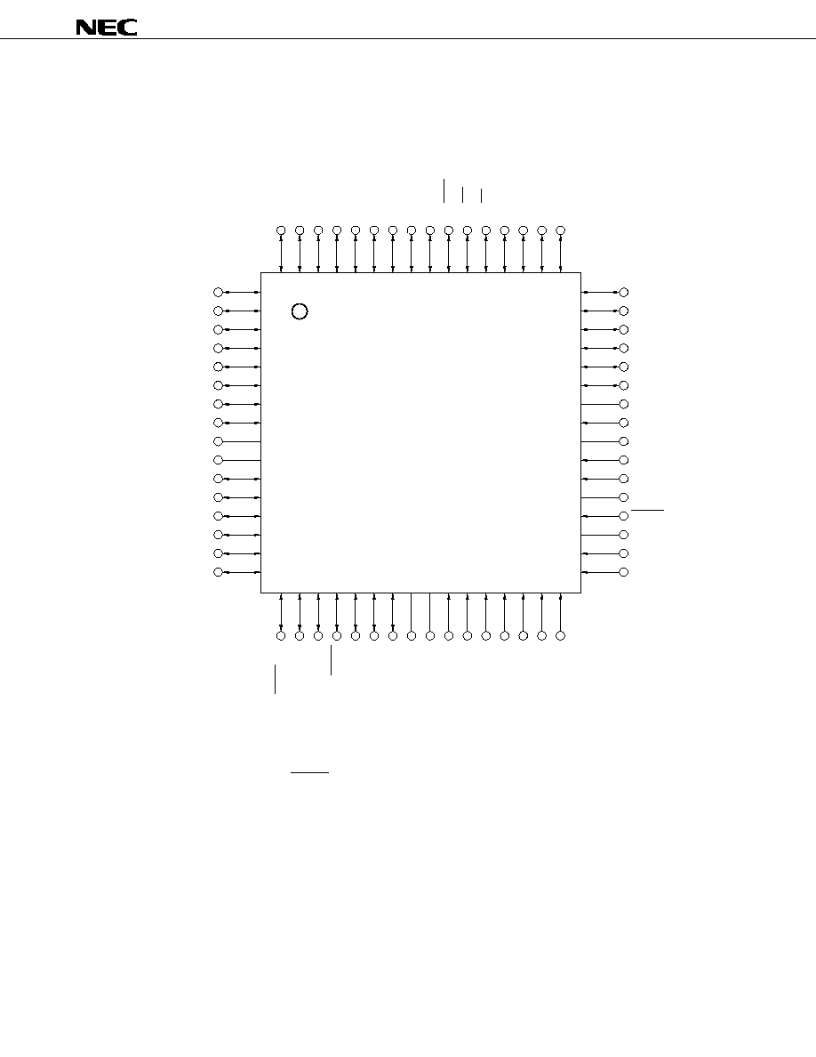
1. PIN CONFIGURATION (TOP VIEW)
∑
64-pin plastic LQFP (10 x 10)
∑ 64-pin plastic TQFP (12 x 12)
∑
64-pin plastic LQFP (14 x 14)
1
2
3
4
5
6
7
8
9
10
11
12
13
14
15
16
P50/A8
P51/A9
P52/A10
P53/A11
P54/A12
P55/A13
P56/A14
P57/A15
V
SS0
V
DD0
P30
P31
P32/SDA0
Note 1
P33/SCL0
Note 1
P34/SI31
Note 2
P35/SO31
Note 2
P36/SCK31
Note 2
P20/SI30
P21/SO30
P22/SCK30
P23/RxD0
P24/TxD0
P25/ASCK0
V
DD1
AV
SS
P17/ANI7
P16/ANI6
P15/ANI5
P14/ANI4
P13/ANI3
P12/ANI2
P11/ANI1
48
47
46
45
44
43
42
41
40
39
38
37
36
35
34
33
P71/TI01
P70/TI00/TO0
P03/INTP3/ADTRG
P02/INTP2
P01/INTP1
P00/INTP0
V
SS1
X1
X2
V
PP
XT1
XT2
RESET
AV
DD
AV
REF
P10/ANI0
17 18 19 20 21 22
23
24 25
26 27 28 29 30
31 32
64 63 62 61 60 59
58
57 56
55 54 53 52 51
50 49
P47/AD7
P46/AD6
P45/AD5
P44/AD4
P43/AD3
P42/AD2
P41/AD1
P40/AD0
P67/ASTB
P66/WAIT
P65/WR
P64/RD
P75/BUZ
P74/PCL
P73/TI51/TO51
P72/TI50/TO50
Notes 1.
SDA0 and SCL0 are incorporated only in the
µ
PD78F0034BY, 78F0034BY(A) Subseries.
2.
SI31, SO31, and SCK31 are incorporated only in the
µ
PD78F0034B, 78F0034B(A) Subseries.
Cautions 1. Connect the V
PP
pin directly to V
SS0
or V
SS1
in normal operation mode.
2. Connect the AV
SS
pin to V
SS0
.
Remark
When the
µ
PD78F0034B, 78F0034BY, 78F0034B(A), and 78F0034BY(A) are used in application fields
that require reduction of the noise generated from inside the microcontroller, the implementation of noise
reduction measures, such as supplying voltage to V
DD0
and V
DD1
individually and connecting V
SS0
and
V
SS1
to different ground lines, is recommended.
µ
PD78F0034B, 78F0034BY, 78F0034B(A), 78F0034BY(A)
10
Data Sheet U16369EJ1V0DS
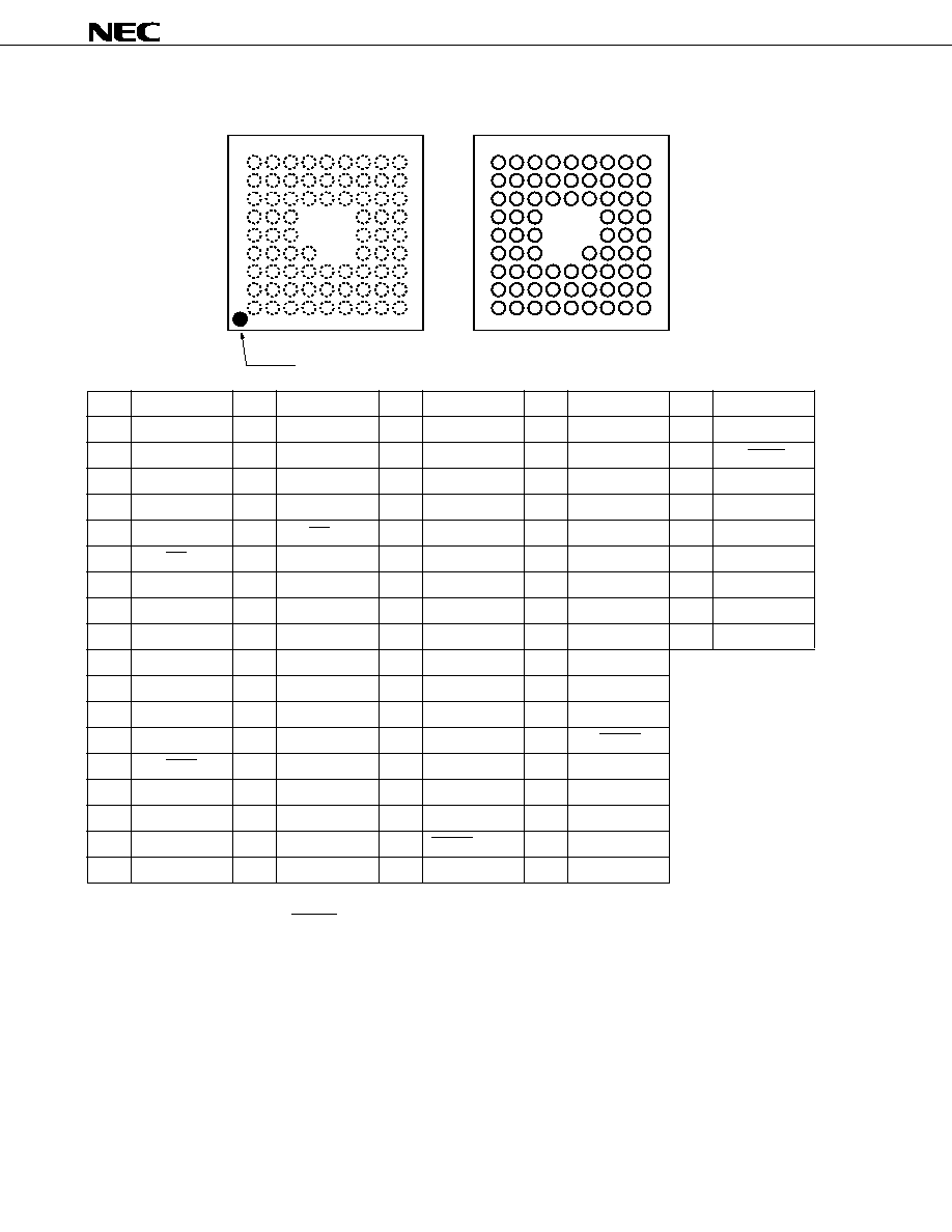
Pin No.
Pin Name
Pin No. Pin Name
Pin No.
Pin Name
Pin No. Pin Name
Pin No. Pin Name
A1
NC
C1
P52/A10
E1
P57/A15
G1
P33/SCL0
Note 1
J1
NC
A2
P46/AD6
C2
P53/A11
E2
V
DD0
G2
P32/SDA0
Note 1
J2
P36/SCK31
Note 2
A3
P44/AD4
C3
P45/AD5
E3
P54/A12
G3
P20/SI30
J3
NC
A4
P41/AD1
C4
P42/AD2
E4
-
G4
P21/SO30
J4
P25/ASCK0
A5
P67/ASTB
C5
P64/RD
E5
-
G5
P24/TxD0
J5
NC
A6
P65/WR
C6
P73/TI51/TO51
E6
-
G6
V
DD1
J6
P17/ANI7
A7
P74/PCL
C7
P03/INTP3/ADTRG
E7
P00/INTP0
G7
P16/ANI6
J7
P12/ANI2
A8
NC
C8
P01/INTP1
E8
XT1
G8
AV
DD
J8
P13/ANI3
A9
NC
C9
V
SS1
E9
X2
G9
NC
J9
NC
B1
P51/A9
D1
P55/A13
F1
P30
H1
P34/SI31
Note 2
B2
P47/AD7
D2
P56/A14
F2
P31
H2
P35/SO31
Note 2
B3
P43/AD3
D3
P50/A8
F3
V
SS0
H3
P23/RxD0
B4
P40/AD0
D4
NC
F4
-
H4
P22/SCK30
B5
P66/WAIT
D5
-
F5
-
H5
AV
SS
B6
P75/BUZ
D6
-
F6
-
H6
P15/ANI5
B7
P72/TI50/TO51
D7
P02/INTP2
F7
P14/ANI4
H7
P11/ANI1
B8
P71/TI01
D8
V
PP
F8
RESET
H8
P10/ANI0
B9
P70/TI00/TO0
D9
X1
F9
XT2
H9
AV
REF
Notes 1. SDA0 and SCL0 are incorporated only in the
µ
PD78F0034BY Subseries.
2. SI31, SO31, and SCK31 are incorporated only in the
µ
PD78F0034B Subseries.
Cautions 1. Connect the V
PP
pin directly to V
SS0
or V
SS1
in normal operation mode.
2. Connect the AV
SS
pin to V
SS0
.
Remarks 1. When the
µ
PD78F0034B, 78F0034BY, 78F0034B(A), and 78F0034BY(A) are used in application
fields that require reduction of the noise generated from inside the microcontroller, the implementation
of noise reduction measures, such as supplying voltage to V
DD0
and V
DD1
individually and connecting
V
SS0
and V
SS1
to different ground lines, is recommended.
2. The special grade version of the 73-pin plastic FBGA (9 x 9) is not provided.
∑ 73-pin plastic FBGA (9 x 9)
Top View
Bottom View
J H G F E D C B A
A B C D E F G H J
9
8
7
6
5
4
3
2
1
Index mark

µ
PD78F0034B, 78F0034BY, 78F0034B(A), 78F0034BY(A)
11
Data Sheet U16369EJ1V0DS
A8 to A15:
Address bus
P70 to P75:
Port 7
AD0 to AD7:
Address/data bus
PCL:
Programmable clock
ADTRG:
AD trigger input
RD:
Read strobe
ANI0 to ANI7:
Analog input
RESET:
Reset
ASCK0:
Asynchronous serial clock
RxD0:
Receive data
ASTB:
Address strobe
SCK30, SCK31, SCL0: Serial clock
AV
DD
:
Analog power supply
SDA0:
Serial data
AV
REF
:
Analog reference voltage
SI30, SI31:
Serial input
AV
SS
:
Analog ground
SO30, SO31:
Serial output
BUZ:
Buzzer clock
TI00, TI01, TI50, TI51:
Timer input
INTP0 to INTP3:
External interrupt input
TO0, TO50, TO51:
Timer output
NC:
No connection
TxD0:
Transmit data
P00 to P03:
Port 0
V
DD0
, V
DD1
:
Power supply
P10 to P17:
Port 1
V
PP
:
Programming power supply
P20 to P25:
Port 2
V
SS0
, V
SS1
:
Ground
P30 to P36:
Port 3
WAIT:
Wait
P40 to P47:
Port 4
WR:
Write strobe
P50 to P57:
Port 5
X1, X2:
Crystal (main system clock)
P64 to P67:
Port 6
XT1, XT2:
Crystal (subsystem clock)

µ
PD78F0034B, 78F0034BY, 78F0034B(A), 78F0034BY(A)
12
Data Sheet U16369EJ1V0DS
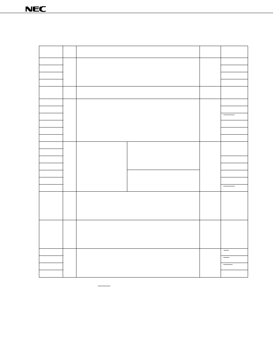
2. BLOCK DIAGRAM
Notes 1.
Incorporated only in the
µ
PD78F0034B and 78F0034B(A)
2.
Incorporated only in the
µ
PD78F0034BY and 78F0034BY(A)
16-bit timer/
event counter
8-bit timer/
event counter 50
8-bit timer/
event counter 51
Watchdog timer
Watch timer
Serial
interface 30
Serial
interface 31
Note 1
UART0
A/D converter
Interrupt control
Buzzer output
Clock output
control
TI00/TO0/P70
TI01/P71
I
2
C bus
Note 2
SDA0/P32
SCL0/P33
TI50/TO50/P72
TI51/TO51/P73
SI30/P20
SO30/P21
SCK30/P22
SI31/P34
SO31/P35
SCK31/P36
RxD0/P23
TxD0/P24
ASCK0/P25
AV
DD
AV
SS
AV
REF
BUZ/P75
PCL/P74
ANI0/P10 to
ANI7/P17
INTP0/P00 to
INTP3/P03
V
DD0
V
DD1
V
SS0
V
SS1
V
PP
78K/0
CPU core
Flash
memory
(32 KB)
RAM
(1,024
bytes)
Port 0
P00 to P03
Port 1
P10 to P17
Port 2
P20 to P25
Port 3
P30 to P36
Port 4
P40 to P47
Port 5
P50 to P57
Port 6
P64 to P67
Port 7
P70 to P75
External access
System control
AD0/P40 to
AD7/P47
A8/P50 to
A15/P57
RD/P64
WR/P65
WAIT/P66
ASTB/P67
RESET
X1
X2
XT1
XT2
µ
PD78F0034B, 78F0034BY, 78F0034B(A), 78F0034BY(A)
13
Data Sheet U16369EJ1V0DS
3. PIN FUNCTIONS
3.1 Port Pins (1/2)
Pin Name
I/O
Function
After Reset
Alternate
Function
P00
I/O
Port 0
Input
INTP0
P01
4-bit I/O port.
INTP1
P02
Input/output can be specified in 1-bit units.
INTP2
P03
An on-chip pull-up resistor can be specified by software.
INTP3/ADTRG
P10 to P17
Input
Port 1
Input
ANI0 to ANI7
8-bit input-only port.
P20
I/O
Port 2
Input
SI30
P21
6-bit I/O port.
SO30
P22
Input/output can be specified in 1-bit units.
SCK30
P23
An on-chip pull-up resistor can be specified by software.
RxD0
P24
TxD0
P25
ASCK0
P30
I/O
Port 3
N-ch open-drain I/O port.
Input
≠
P31
7-bit I/O port.
LEDs can be driven directly.
P32
Input/output can be specified
SDA0
Note 1
P33
in 1-bit units.
SCL0
Note 1
P34
An on-chip pull-up resistor can be
SI31
Note 2
P35
specified by software.
SO31
Note 2
P36
SCK31
Note 2
P40 to P47
I/O
Port 4
Input
AD0 to AD7
8-bit I/O port.
Input/output can be specified in 1-bit units.
An on-chip pull-up resistor can be specified by software.
Interrupt request flag KRIF is set to 1 by falling edge detection.
P50 to P57
I/O
Port 5
Input
A8 to A15
8-bit I/O port.
LEDs can be driven directly.
Input/output can be specified in 1-bit units.
An on-chip pull-up resistor can be specified by software.
P64
I/O
Port 6
Input
RD
P65
4-bit I/O port.
WR
P66
Input/output can be specified in 1-bit units.
WAIT
P67
An on-chip pull-up resistor can be specified by software.
ASTB
Notes 1.
SDA0 and SCL0 are incorporated only in the
µ
PD78F0034BY and 78F0034BY(A).
2.
SI31, SO31, and SCK31 are incorporated only in the
µ
PD78F0034B and 78F0034B(A).
µ
PD78F0034B, 78F0034BY, 78F0034B(A), 78F0034BY(A)
14
Data Sheet U16369EJ1V0DS
3.1 Port Pins (2/2)
Pin Name
I/O
Function
After Reset
Alternate
Function
P70
I/O
Port 7
Input
TI00/TO0
P71
6-bit I/O port.
TI01
P72
Input/output can be specified in 1-bit units.
TI50/TO50
P73
An on-chip pull-up resistor can be specified by software.
TI51/TO51
P74
PCL
P75
BUZ
3.2 Non-Port Pins (1/2)
Pin Name
I/O
Function
After Reset
Alternate
Function
INTP0
Input
External interrupt request input by which the valid edge (rising edge,
Input
P00
INTP1
falling edge, or both rising and falling edges) can be specified.
P01
INTP2
P02
INTP3
P03/ADTRG
SI30
Input
Serial interface serial data input.
Input
P20
SI31
Note 1
P34
SDA0
Note 2
I/O
Serial interface serial data input/output
Input
P32
SO30
Output
Serial interface serial data output.
Input
P21
SO31
Note 1
P35
SCK30
I/O
Serial interface serial clock input/output.
Input
P22
SCK31
Note 1
P36
SCL0
Note 2
P33
RxD0
Input
Serial data input for asynchronous serial interface.
Input
P23
TxD0
Output
Serial data output for asynchronous serial interface.
Input
P24
ASCK0
Input
Serial clock input for asynchronous serial interface.
Input
P25
TI00
Input
External count clock input to 16-bit timer/event counter 0.
Input
P70/TO0
Capture trigger signal input to capture register 01 (CR01) of 16-bit timer/
event counter 0.
TI01
Capture trigger signal input to capture register 00 (CR00) of 16-bit timer/
P71
event counter 0.
TI50
External count clock input to 8-bit timer/event counter 50.
P72/TO50
TI51
External count clock input to 8-bit timer/event counter 51.
P73/TO51
TO0
Output
16-bit timer/event counter 0 output.
Input
P70/TI00
TO50
8-bit timer/event counter 50 output (shared with 8-bit PWM output).
Input
P72/TI50
TO51
8-bit timer/event counter 51 output (shared with 8-bit PWM output).
P73/TI51
PCL
Output
Clock output (for trimming of main system clock and subsystem clock).
Input
P74
BUZ
Output
Buzzer output.
Input
P75
AD0 to AD7
I/O
Lower address/data bus for extending memory externally.
Input
P40 to P47
Notes 1.
SI31, SO31, and SCK31 are incorporated only in the
µ
PD78F0034B and 78F0034B(A).
2.
SDA0 and SCL0 are incorporated only in the
µ
PD78F0034BY and 78F0034BY(A).
µ
PD78F0034B, 78F0034BY, 78F0034B(A), 78F0034BY(A)
15
Data Sheet U16369EJ1V0DS
3.2 Non-Port Pins (2/2)
Pin Name
I/O
Function
After Reset
Alternate
Function
A8 to A15
Output
Higher address bus for extending memory externally.
Input
P50 to P57
RD
Output
Strobe signal output for read operation of external memory.
Input
P64
WR
Strobe signal output for write operation of external memory.
P65
WAIT
Input
Inserting wait for accessing external memory.
Input
P66
ASTB
Output
Strobe output which externally latches address information output to
Input
P67
ports 4 and 5 to access external memory.
ANI0 to ANI7
Input
A/D converter analog input.
Input
P10 to P17
ADTRG
Input
A/D converter trigger signal input.
Input
P03/INTP3
AV
REF
Input
A/D converter reference voltage input.
≠
≠
AV
DD
≠
A/D converter analog power supply.
≠
≠
Set the voltage equal to V
DD0
or V
DD1
.
AV
SS
≠
A/D converter ground potential.
≠
≠
Set the voltage equal to V
SS0
or V
SS1
.
RESET
Input
System reset input.
≠
≠
X1
Input
Connecting crystal resonator for main system clock oscillation.
≠
≠
X2
≠
≠
≠
XT1
Input
Connecting crystal resonator for subsystem clock oscillation.
≠
≠
XT2
≠
≠
≠
V
DD0
≠
Positive power supply voltage for ports.
≠
≠
V
SS0
≠
Ground potential of ports.
≠
≠
V
DD1
≠
Positive power supply (except ports).
≠
≠
V
SS1
≠
Ground potential (except ports).
≠
≠
V
PP
≠
Applying high-voltage for program write/verify. Connect to V
SS0
or V
SS1
≠
≠
in normal operation mode.
NC
Note
≠
Not internally connected. Leave open.
≠
≠
Note
NC is incorporated only in the 73-pin plastic FBGA.
µ
PD78F0034B, 78F0034BY, 78F0034B(A), 78F0034BY(A)
16
Data Sheet U16369EJ1V0DS
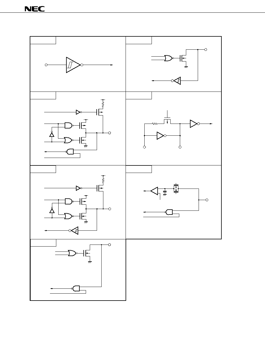
3.3 Pin I/O Circuits and Recommended Connection of Unused Pins
The input/output circuit type of each pin and recommended connection of unused pins are shown in Table 3-1.
For the input/output configuration of each type, refer to Figure 3-1 .
Table 3-1. Types of Pin I/O Circuits (1/2)
Pin Name
I/O Circuit Type
I/O
Recommended Connection of Unused Pins
P00/INTP0
8-C
I/O
Input: Independently connect to V
SS0
or V
SS1
via a
P01/INTP1
via a resistor.
P02/INTP2
Output: Leave open.
P03/INTP3/ADTRG
P10/ANI0 to P17/ANI7
25
Input
Directly connect to V
DD0
, V
DD1
, V
SS0
, or V
SS1
.
P20/SI30
8-C
I/O
Input: Independently connect to V
DD0
, V
DD1
, V
SS0
, or
P21/SO30
5-H
V
SS1
via a resistor.
P22/SCK30
8-C
Output: Leave open.
P23/RxD0
P24/TxD0
5-H
P25/ASCK0
8-C
P30, P31
13-P
Input: Directly connect to V
SS0
or V
SS1
.
P32/SDA0
Note 1
13-R
Output: Leave open at low-level output.
P33/SCL0
Note 1
P34/SI31
Note 2
8-C
Input: Independently connect to V
DD0
, V
DD1
, V
SS0
or
P35/SO31
Note 2
5-H
V
SS1
via a resistor.
P36/SCK31
Note 2
8-C
Output: Leave open.
P40/AD0 to P47/AD7
5-H
Input: Independently connect to V
DD0
or V
DD1
via a
resistor.
Output: Leave open.
P50/A8 to P57/A15
5-H
Input: Independently connect to V
DD0
, V
DD1
, V
SS0
, or
P64/RD
V
SS1
via a resistor.
P65/WR
Output: Leave open.
P66/WAIT
P67/ASTB
P70/TI00/TO0
8-C
P71/TI01
P72/TI50/TO50
P73/TI51/TO51
P74/PCL
5-H
P75/BUZ
Notes 1.
SDA0 and SCL0 are incorporated only in the
µ
PD78F0034BY and 78F0034BY(A).
2.
SI31, SO31, and SCK31 are incorporated only in the
µ
PD78F0034B and 78F0034B(A).
µ
PD78F0034B, 78F0034BY, 78F0034B(A), 78F0034BY(A)
17
Data Sheet U16369EJ1V0DS
Table 3-1. Types of Pin I/O Circuits (2/2)
Pin Name
I/O Circuit Type
I/O
Recommended Connection of Unused Pins
RESET
2
Input
≠
XT1
16
Directly connect to V
DD0
or V
DD1
.
XT2
≠
Leave open.
AV
DD
≠
Directly connect to V
DD0
or V
DD1
.
AV
REF
Directly connect to V
SS0
or V
SS1
.
AV
SS
V
PP
Connect to V
SS0
or V
SS1
.
µ
PD78F0034B, 78F0034BY, 78F0034B(A), 78F0034BY(A)
18
Data Sheet U16369EJ1V0DS
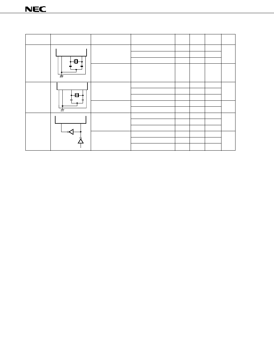
Figure 3-1. Pin I/O Circuits
TYPE 2
Schmitt-triggered input with hysteresis characteristics
IN
TYPE 8-C
Data
Output
disable
P-ch
IN/OUT
V
DD0
N-ch
P-ch
V
DD0
Pullup
enable
TYPE 5-H
Data
Output
disable
P-ch
IN/OUT
V
DD0
N-ch
Input
enable
P-ch
V
DD0
Pullup
enable
TYPE 16
Data
Output disable
IN/OUT
N-ch
Data
Output disable
IN/OUT
N-ch
TYPE 13-R
Input
enable
V
SS0
TYPE 25
V
SS0
V
SS0
V
SS0
P-ch
Feedback
cut-off
XT1
XT2
TYPE 13-P
Input
enable
Comparator
+
≠
P-ch
N-ch
V
REF
(threshold voltage)
V
SS0
IN

µ
PD78F0034B, 78F0034BY, 78F0034B(A), 78F0034BY(A)
19
Data Sheet U16369EJ1V0DS
4. DIFFERENCES BETWEEN
µ
PD78F0034B, 78F0034BY, AND MASK ROM VERSIONS
The
µ
PD78F0034B and 78F0034BY are products provided with a flash memory which enables writing, erasing,
and rewriting of programs with device mounted on the target system.
The functions of the
µ
PD78F0034B and 78F0034BY (except the functions specified for flash memory) can be made
the same as those of the mask ROM versions by setting the memory size switching register (IMS).
Tables 4-1 and 4-2 show the differences between the
µ
PD78F0034B, 78F0034BY and the mask ROM versions.
Table 4-1. Differences Between
µµ
µµ
µ
PD78F0034B and Mask ROM Versions
Item
µ
PD78F0034B
Mask ROM Versions
µ
PD780034A Subseries
µ
PD780024A Subseries
Note
Internal ROM structure
Flash memory
Mask ROM
Internal ROM capacity
32 KB
µ
PD780031A: 8 KB
µ
PD780021A: 8 KB
µ
PD780032A: 16 KB
µ
PD780022A: 16 KB
µ
PD780033A: 24 KB
µ
PD780023A: 24 KB
µ
PD780034A: 32 KB
µ
PD780024A: 32 KB
Internal high-speed RAM capacity
1,024 bytes
µ
PD780031A: 512 bytes
µ
PD780021A: 512 bytes
µ
PD780032A: 512 bytes
µ
PD780022A: 512 bytes
µ
PD780033A: 1,024 bytes
µ
PD780023A: 1,024 bytes
µ
PD780034A: 1,024 bytes
µ
PD780024A: 1,024 bytes
Minimum instruction execution time
Minimum instruction execution time variable function incorporated
When main system clock is selected
<
µ
PD78F0034B and expanded-specification products of the mask ROM versions>
0.166
µ
s/0.333
µ
s/0.666
µ
s/1.33
µ
s/2.66
µ
s (@ 12 MHz operation, V
DD
= 4.5 to 5.5 V)
<Conventional products of the mask ROM versions>
0.238
µ
s/0.48
µ
s/0.95
µ
s/1.91
µ
s/3.81
µ
s (@ 8.38 MHz operation, V
DD
= 4.0 to 5.5 V)
When subsystem clock is selected
122
µ
s (32.768 kHz)
Clock output
<
µ
PD78F0034B and expanded-specification products of the mask ROM versions>
∑ 93.75 kHz, 187.5 kHz, 375 kHz, 750 kHz, 1.25 MHz, 3 MHz, 6 MHz, 12 MHz
(@ 12 MHz operation with main system clock)
∑ 32.768 kHz (@ 32.768 kHz operation with subsystem clock)
<Conventional products of the mask ROM versions>
∑ 65.5 kHz, 131 kHz, 262 kHz, 524 kHz, 1.05 MHz, 2.10 MHz, 4.19 MHz, 8.38 MHz
(@ 8.38 MHz operation with main system clock)
∑ 32.768 kHz (@ 32.768 kHz operation with subsystem clock)
Buzzer output
<
µ
PD78F0034B and expanded-specification products of the mask ROM versions>
1.46 kHz, 2.93 kHz, 5.86 kHz, 11.7 kHz (@ 12 MHz operation with main system clock)
<Conventional products of the mask ROM versions>
∑ 1.02 kHz, 2.05 kHz, 4.10 kHz, 8.19 kHz (@ 8.38 MHz operation with main system clock)
A/D converter resolution
10 bits
8 bits
Mask option specification of on-chip
Not available
Available
pull-up resistor for pins P30 to P33
IC pin
Not provided
Provided
V
PP
pin
Provided
Not provided
Electrical specifications,
Refer to the data sheet of individual products.
recommended soldering conditions
Note
The
µ
PD78F0034B can be used as the flash memory version of the
µ
PD780024A Subseries.
Caution There are differences in noise immunity and noise radiation between the flash memory and mask
ROM versions. When pre-producing an application set with the flash memory version and then mass
producing it with the mask ROM version, be sure to conduct sufficient evaluations on the
commercial samples (CS) (not engineering samples (ES)) of the mask ROM versions.
µ
PD78F0034B, 78F0034BY, 78F0034B(A), 78F0034BY(A)
20
Data Sheet U16369EJ1V0DS
Table 4-2. Differences Between
µµ
µµ
µ
PD78F0034BY and Mask ROM Versions
Item
µ
PD78F0034BY
Mask ROM Versions
µ
PD780034AY Subseries
µ
PD780024AY Subseries
Note
Internal ROM structure
Flash memory
Mask ROM
Internal ROM capacity
32 KB
µ
PD780031AY: 8 KB
µ
PD780021AY: 8 KB
µ
PD780032AY: 16 KB
µ
PD780022AY: 16 KB
µ
PD780033AY: 24 KB
µ
PD780023AY: 24 KB
µ
PD780034AY: 32 KB
µ
PD780024AY: 32 KB
Internal high-speed RAM capacity
1,024 bytes
µ
PD780031AY: 512 bytes
µ
PD780021AY: 512 bytes
µ
PD780032AY: 512 bytes
µ
PD780022AY: 512 bytes
µ
PD780033AY: 1,024 bytes
µ
PD780023AY: 1,024 bytes
µ
PD780034AY: 1,024 bytes
µ
PD780024AY: 1,024 bytes
Minimum instruction execution time
Minimum instruction execution time variable function incorporated
When main system clock is selected
0.238
µ
s/0.48
µ
s/0.95
µ
s/1.91
µ
s/3.81
µ
s
(operation at 8.38 MHz, V
DD
= 4.0 to 5.5 V)
When subsystem clock is selected
122
µ
s (32.768 kHz)
Clock output
∑ 65.5 kHz, 131 kHz, 262 kHz, 524 kHz, 1.05 MHz, 2.10 MHz, 4.19 MHz, 8.38 MHz
(@ 8.38 MHz operation with main system clock)
∑ 32.768 kHz
(@ 32.768 kHz operation with subsystem clock)
Buzzer output
1.02 kHz, 2.05 kHz, 4.10 kHz, 8.19 kHz
(@ 8.38 MHz operation with main system clock)
A/D converter resolution
10 bits
8 bits
Mask option specification of on-chip
Not available
Available
pull-up resistor for pins P30 and P31
IC pin
Not provided
Provided
V
PP
pin
Provided
Not provided
Electrical specifications,
Refer to the data sheet of individual products.
recommended soldering conditions
Note
The
µ
PD78F0034BY can be used as the flash memory version of the
µ
PD780024AY Subseries.
Caution There are differences in noise immunity and noise radiation between the flash memory and mask
ROM versions. When pre-producing an application set with the flash memory version and then mass
producing it with the mask ROM version, be sure to conduct sufficient evaluations on the
commercial samples (CS) (not engineering samples (ES)) of the mask ROM versions.

µ
PD78F0034B, 78F0034BY, 78F0034B(A), 78F0034BY(A)
21
Data Sheet U16369EJ1V0DS
5. DIFFERENCES BETWEEN
µµ
µµ
µ
PD78F0034B, 78F0034BY AND
µµ
µµ
µ
PD78F0034A, 78F0034AY
Table 5-1 shows the differences between the
µ
PD78F0034B and
µ
PD78F0034A, and Table 5-2 shows differences
between the
µ
PD78F0034BY and 78F0034AY.
Table 5-1. Differences Between
µµ
µµ
µ
PD78F0034B and
µµ
µµ
µ
PD78F0034A
Item
µ
PD78F0034B
µ
PD78F0034A
Guaranteed operating speed
4.5 to 5.5 V
12 MHz (0.166
µ
s)
8.38 MHz (0.238
µ
s)
(operating frequency)
4.0 to 5.5 V
8.38 MHz (0.238
µ
s)
8.38 MHz (0.238
µ
s)
3.0 to 5.5 V
8.38 MHz (0.238
µ
s)
5 MHz (0.4
µ
s)
2.7 to 5.5 V
5 MHz (0.4
µ
s)
5 MHz (0.4
µ
s)
1.8 to 5.5 V
1.25 MHz (1.6
µ
s)
1.25 MHz (1.6
µ
s)
Maximum instruction execution time
Minimum instruction execution time variable function incorporated
When main system clock is selected
0.166
µ
s/0.333
µ
s/0.666
µ
s/1.33
µ
s/2.66
µ
s
0.238
µ
s/0.48
µ
s/0.95
µ
s/1.91
µ
s/3.81
µ
s
(@ 12 MHz operation, V
DD
= 4.5 to 5.5 V)
(@ 8.38 MHz operation, V
DD
= 4.0 to 5.5 V)
When subsystem clock is selected
122
µ
s (32.768 kHz)
Clock output
∑ 93.75 kHz, 187.5 kHz, 375 kHz, 750 kHz,
∑ 65.5 kHz, 131 kHz, 262 kHz, 524 kHz,
1.25 MHz, 3 MHz, 6 MHz, 12 MHz (@ 12
1.05 MHz, 2.10 MHz, 4.19 MHz, 8.38
MHz operation with main system clock)
MHz (@ 8.38 MHz operation with main
∑ 32.768 kHz (@ 32.768 kHz operation
system clock)
with subsystem clock)
∑ 32.768 kHz (@ 32.768 kHz operation
with subsystem clock)
Buzzer output
1.46 kHz, 2.93 kHz, 5.86 kHz, 11.7 kHz
1.02 kHz, 2.05 kHz, 4.10 kHz, 8.19 kHz
(@ 12 MHz operation with main system
(@ 8.38 MHz operation with main system
clock)
clock)
Communication mode of flash memory
∑ 3-wire serial I/O:
2 channels
Note
∑ 3-wire serial I/O:
2 channels
Note
programming
∑ UART:
1 channel
∑ UART:
1 channel
∑ Pseudo 3-wire serial I/O: 1 channel
∑ Pseudo 3-wire serial I/O: 1 channel
Electrical specifications, recommended
Refer to the data sheet of individual products.
soldering conditions
Note
The
µ
PD78F0034B can use one channel (serial interface SIO30) as a handshake mode.
The
µ
PD78F0034A cannot use a handshake mode.
Remark
The operating frequency ratings of the
µ
PD78F0034B and the expanded-specification products of the
mask ROM versions of the
µ
PD780024A, 780034A Subseries are the same. The operating frequency
ratings of the
µ
PD78F0034A and the conventional products of the mask ROM versions of the
µ
PD780024A, 780034A Subseries are the same.
µ
PD78F0034B, 78F0034BY, 78F0034B(A), 78F0034BY(A)
22
Data Sheet U16369EJ1V0DS
Table 5-2. Differences Between
µµ
µµ
µ
PD78F0034BY and
µµ
µµ
µ
PD78F0034AY
Item
µ
PD78F0034BY
µ
PD78F0034AY
Guaranteed operating speed
4.5 to 5.5 V
8.38 MHz (0.238
µ
s)
(operating frequency)
4.0 to 5.5 V
8.38 MHz (0.238
µ
s)
3.0 to 5.5 V
5 MHz (0.4
µ
s)
2.7 to 5.5 V
5 MHz (0.4
µ
s)
1.8 to 5.5 V
1.25 MHz (1.6
µ
s)
Maximum instruction execution time
Minimum instruction execution time variable function incorporated
When main system clock is selected
0.238
µ
s/0.48
µ
s/0.95
µ
s/1.91
µ
s/3.81
µ
s (@ 8.38 MHz operation, V
DD
=
4.0 to 5.5 V)
When subsystem clock is selected
122
µ
s (32.768 kHz)
Clock output
∑ 65.5 kHz, 131 kHz, 262 kHz, 524 kHz, 1.05 MHz, 2.10 MHz, 4.19 MHz,
8.38 MHz (@ 8.38 MHz operation with main system clock)
∑ 32.768 kHz (@ 32.768 kHz operation with subsystem clock)
Buzzer output
1.02 kHz, 2.05 kHz, 4.10 kHz, 8.19 kHz (@ 8.38 MHz operation with main
system clock)
Communication mode of flash memory
∑ 3-wire serial I/O:
2 channels
Note
∑ 3-wire serial I/O:
2 channels
Note
programming
∑ UART:
1 channel
∑ UART:
1 channel
∑ Pseudo 3-wire serial I/O: 1 channel
∑ Pseudo 3-wire serial I/O: 1 channel
Electrical specifications, recommended
Refer to the data sheet of individual products.
soldering conditions
Note
The
µ
PD78F0034BY can use one channel (serial interface SIO30) as a handshake mode.
The
µ
PD78F0034AY cannot use a handshake mode.
Remark
The operating frequency ratings of the
µ
PD78F0034BY, 78F0034AY and the mask ROM versions of the
µ
PD780024AY, 780034AY Subseries are the same.
6. DIFFERENCES BETWEEN
µµ
µµ
µ
PD78F0034B, 78F0034BY AND
µµ
µµ
µ
PD78F0034B(A), 78F0034BY(A)
The
µ
PD78F0034(A) and 78F0034BY(A) are products to which a quality assurance program more stringent than
that used for the
µ
PD780034B and 780034BY (standard models) is applied (NEC Electronics classifies these products
as "special" quality grade models).
The
µ
PD78F0034B, 78F0034BY and
µ
PD78F0034B(A), 78F0034BY(A) only differ in the quality grade; there are
no differences in functions and electrical specifications.
Table 6-1. Differences Between
µµ
µµ
µ
PD78F0034B, 78F0034BY and
µµ
µµ
µ
PD78F0034B(A), 78F0034BY(A)
Item
µ
PD78F0034B, 78F0034BY
µ
PD78F0034B(A), 78F0034BY(A)
Quality grade
Standard
Special
Functions and electrical specifications
No differences.
µ
PD78F0034B, 78F0034BY, 78F0034B(A), 78F0034BY(A)
23
Data Sheet U16369EJ1V0DS
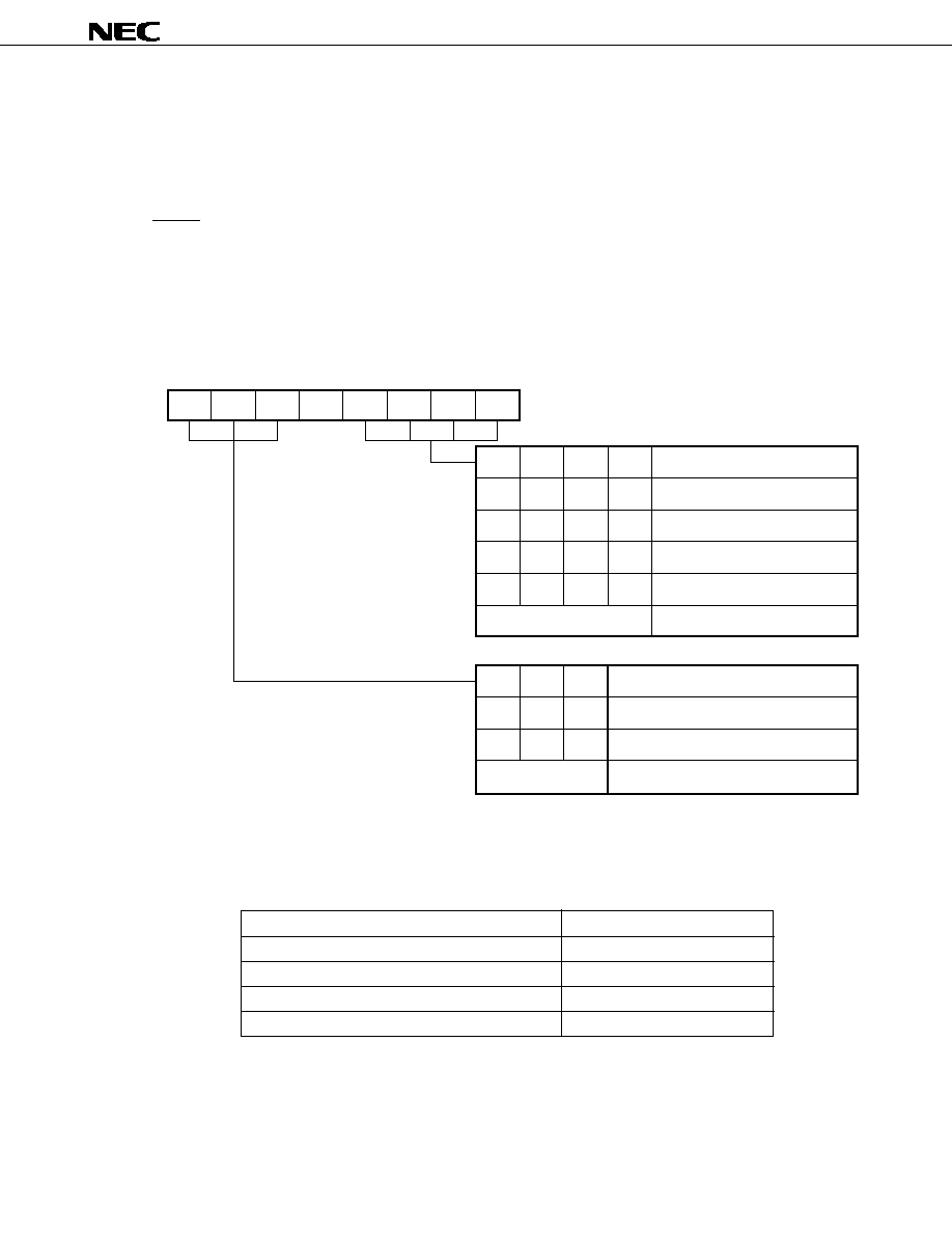
7. MEMORY SIZE SWITCHING REGISTER (IMS)
IMS is a register that is set by software and is used to specify a part of the internal memory that is not to be used.
By setting memory size switching register (IMS), the internal memory of the
µ
PD78F0034B, 78F0034BY, 78F0034B(A),
and 78F0034BY(A) can be mapped identically to that of a mask ROM version.
IMS is set with an 8-bit memory manipulation instruction.
RESET input sets IMS to CFH.
Caution The initial value of IMS is setting disabled (CFH). Be sure to set C8H or the value of the target
mask ROM version at the moment of initial setting.
Figure 7-1. Format of Memory Size Switching Register
Table 7-1 shows the IMS set value to make the memory mapping the same as those of mask ROM versions.
Table 7-1. Set Value of Memory Size Switching Register
Target Mask ROM Versions
IMS Set Value
µ
PD780021A, 780021AY, 780031A, 780031AY
42H
µ
PD780022A, 780022AY, 780032A, 780032AY
44H
µ
PD780023A, 780023AY, 780033A, 780033AY
C6H
µ
PD780024A, 780024AY, 780034A, 780034AY
C8H
IMS
RAM2 RAM1 RAM0
0
ROM3 ROM2 ROM1 ROM0
ROM3
0
0
0
1
ROM2
0
1
1
0
ROM1
1
0
1
0
ROM0
0
0
0
0
Selection of Internal ROM Capacity
8 KB
16 KB
24 KB
32 KB
Other than above
Setting prohibited
7
6
5
4
3
2
1
0
FFF0H
CFH
R/W
Address
After reset
R/W
RAM2
0
1
RAM1
1
1
RAM0
0
0
Selection of Internal High-Speed RAM Capacity
512 bytes
1,024 bytes
Other than above
Setting prohibited
µ
PD78F0034B, 78F0034BY, 78F0034B(A), 78F0034BY(A)
24
Data Sheet U16369EJ1V0DS
8. FLASH MEMORY PROGRAMMING
Writing to flash memory can be performed without removing the memory from the target system (on board
programming). Writing is performed with the dedicated flash programmer (Flashpro III (part No.: FL-PR3 and PG-
FP3)/(Flashpro IV (part No.: FL-PR4 and PG-FP4)) connected to the host machine and the target system.
Writing to flash memory can also be performed using flash memory writing adapter connected to Flashpro III/
Flashpro IV.
Remark
FL-PR3 and FL-PR4 are products of Naito Densei Machida Mfg. Co., Ltd.
8.1 Selection of Communication Mode
Writing to a flash memory is performed using Flashpro III/Flashpro IV in a serial communication. Select one of
the communication modes in Tables 8-1 and 8-2. The selection of the communication mode is made by using the
format shown in Figure 8-1. Each communication mode is selected by the number of V
PP
pulses shown in Tables
8-1 and 8-2.
Table 8-1. List of Communication Mode (
µµ
µµ
µ
PD78F0034B)
Communication Mode
Channels
Pin Used
V
PP
Pulses
3-wire serial I/O
2
SI30/P20
0
SO30/P21
SCK30/P22
SI31/P34
1
SO31/P35
SCK31/P36
SI30/P20
3
SO30/P21
SCK30/P22
HS/P25
UART
1
RxD0/P23
8
TxD0/P24
Pseudo 3-wire serial I/O
1
P72/TI50/TO50
12
(serial clock input)
P71/TI01
(serial data output)
P70/TI00/TO0
(serial data input)
Caution Be sure to select a communication mode using the number of V
PP
pulses shown in Table 8-1.
µ
PD78F0034B, 78F0034BY, 78F0034B(A), 78F0034BY(A)
25
Data Sheet U16369EJ1V0DS
Table 8-2. List of Communication Mode (
µµ
µµ
µ
PD78F0034BY)
Communication Mode
Channels
Pin Used
V
PP
Pulses
3-wire serial I/O
1
SI30/P20
0
SO30/P21
SCK30/P22
SI30/P20
3
SO30/P21
SCK30/P22
HS/P25
I
2
C bus
1
SDA0/P32
4
SCL0/P33
UART
1
RxD0/P23
8
TxD0/P24
Pseudo 3-wire serial I/O
1
P72/TI50/TO50
12
(serial clock input)
P71/TI01
(serial data output)
P70/TI00/TO0
(serial data input)
Caution Be sure to select a communication mode using the number of V
PP
pulses shown in Table 8-2.
Figure 8-1. Format of Communication Mode Selection
10 V
V
PP
pulses
Flash write mode
V
PP
RESET
V
DD
V
SS
V
DD
V
SS
1
2
n
µ
PD78F0034B, 78F0034BY, 78F0034B(A), 78F0034BY(A)
26
Data Sheet U16369EJ1V0DS
8.2 Flash Memory Programming Functions
Operations such as writing to flash memory are performed by various command/data transmission and reception
operations according to the selected communication mode. Table 8-3 shows major functions of flash memory
programming.
Table 8-3. Major Functions of Flash Memory Programming
Function
Description
Reset
Used to stop write operation and detect transmission cycle.
Batch verify
Compares the entire memory contents with the input data.
Batch erase
Erases the entire memory contents.
Batch blank check
Checks the deletion status of the entire memory.
High-speed write
Performs write to the flash memory based on the write start address and the number of data
to be written (number of bytes).
Continuous write
Performs continuous write based on the information input with high-speed write operation.
Status
Used to confirm the current operating mode and operation end.
Oscillation frequency setting
Sets the frequency of the resonator.
Erase time setting
Sets the memory erase time.
Baud rate setting
Sets the communication rate for UART mode
I
2
C mode setting
Sets standard/high-speed mode for I
2
C bus mode
Silicon signature read
Outputs the device name and memory capacity, and device block information.
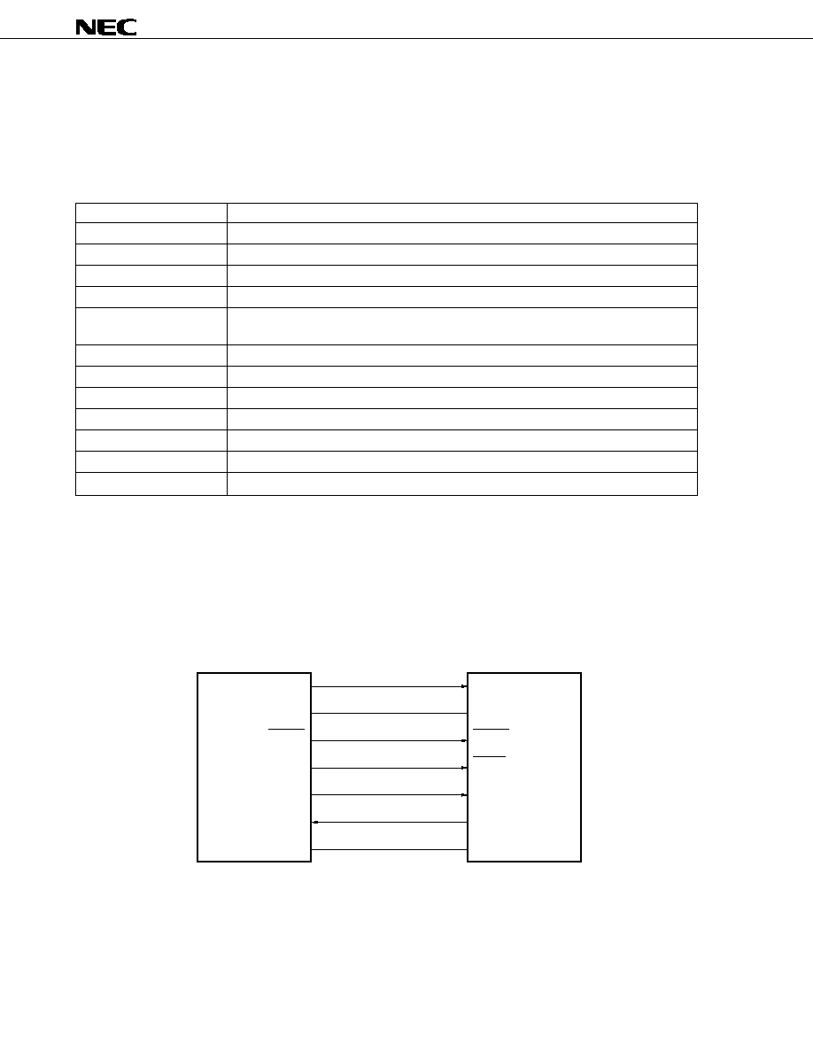
8.3 Connection of Flashpro III/Flashpro IV
The connection of Flashpro III/Flashpro IV and the
µ
PD78F0034B or 78F0034BY differs according to the
communication mode (3-wire serial I/O, UART, pseudo 3-wire serial I/O, and I
2
C bus). The connection for each
communication mode is shown in Figures 8-2 to 8-6, respectively.
Figure 6-2. Connection of Flashpro III/Flashpro IV in 3-Wire Serial I/O Mode
Remark
µ
PD78F0034B:
n = 0, 1
µ
PD78F0034BY: n = 0
Flashpro III/Flashpro IV
V
PP
VPP
VDD
V
SS0
/V
SS1
/AV
SS
/AV
REF
V
DD0
/V
DD1
/AV
DD
RESET
SCK3n
SI3n
SO3n
RESET
SCK
SO
SI
GND
PD78F0034B,
PD78F0034BY
µ
µ
µ
PD78F0034B, 78F0034BY, 78F0034B(A), 78F0034BY(A)
27
Data Sheet U16369EJ1V0DS
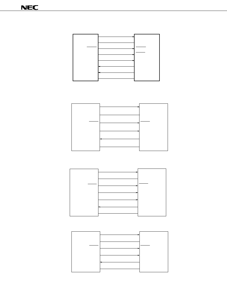
Figure 8-4. Connection of Flashpro III/Flashpro IV for UART Mode
Figure 8-5. Connection of Flashpro III/Flashpro IV for Pseudo 3-Wire Serial I/O Mode
Figure 8-6. Connection of Flashpro III/Flashpro IV for I
2
C Bus Mode (
µµ
µµ
µ
PD78F0034BY only)
Figure 8-3. Connection of Flashpro III in 3-Wire Serial I/O Mode (Using Handshake)
Flashpro III/Flashpro IV
V
PP
VPP
VDD
V
SS0
/V
SS1
/AV
SS
/AV
REF
V
DD0
/V
DD1
/AV
DD
RESET
RxD0
TxD0
RESET
SO
SI
GND
PD78F0034B,
PD78F0034BY
µ
µ
VPP
VDD
RESET
SCK
SO
SI
GND
Flashpro III/Flashpro IV
V
PP
V
DD0
/V
DD1
/AV
DD
RESET
P72
(serial clock input)
P70
(serial data input)
P71
(
serial data output)
V
SS0
/V
SS1
/AV
SS
/AV
REF
PD78F0034B,
PD78F0034BY
µ
µ
Flashpro III/Flashpro IV
V
PP
VPP
VDD
V
SS0
/V
SS1
/AV
SS
/AV
REF
V
DD0
/V
DD1
/AV
DD
RESET
SCL0
SDA0
PD78F0034BY
RESET
SO
SI
GND
µ
Flashpro III/Flashpro IV
PD78F0034B,
PD78F0034BY
GND
SI
SO
SCK
RESET
VDD
VPP
V
SS0
/V
SS1
/AV
SS
/AV
REF
SO30
HS
HS (P25)
SI30
SCK30
RESET
V
DD0
/V
DD1
/AV
DD
V
PP
µ
µ
µ
PD78F0034B, 78F0034BY, 78F0034B(A), 78F0034BY(A)
28
Data Sheet U16369EJ1V0DS
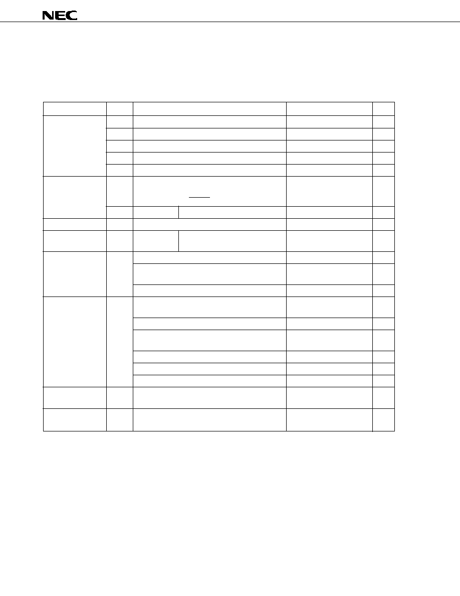
9. ELECTRICAL SPECIFICATIONS
9.1
µµ
µµ
µ
PD78F0034B, 78F0034B(A)
Absolute Maximum Ratings (T
A
= 25
∞
C)
Parameter
Symbol
Conditions
Ratings
Unit
Supply voltage
V
DD
≠0.3 to +6.5
V
V
PP
Note 2
≠0.3 to +10.5
V
AV
DD
≠0.3 to V
DD
+ 0.3
Note 1
V
AV
REF
≠0.3 to V
DD
+ 0.3
Note 1
V
AV
SS
≠0.3 to +0.3
V
Input voltage
V
I1
P00 to P03, P10 to P17, P20 to P25, P34 to P36,
≠0.3 to V
DD
+ 0.3
Note 1
V
P40 to P47, P50 to P57, P64 to P67, P70 to P75,
X1, X2, XT1, XT2,
RESET
V
I2
P30 to P33
N-ch open drain
≠0.3 to +6.5
V
Output voltage
V
O
≠0.3 to V
DD
+ 0.3
Note 1
V
Analog input voltage
V
AN
P10 to P17
Analog input pin
AV
SS
≠0.3 to AV
REF
+ 0.3
Note 1
V
and ≠0.3 to V
DD
+ 0.3
Note 1
Output current, high
I
OH
Per pin
≠10
mA
Total for P00 to P03, P40 to P47, P50 to P57,
≠15
mA
P64 to P67, P70 to P75
Total for P20 to P25, P30 to P36
≠15
mA
Output current, low
I
OL
Per pin for P00 to P03, P20 to P25, P34 to P36,
20
mA
P40 to P47, P64 to P67, P70 to P75
Per pin for P30 to P33, P50 to P57
30
mA
Total for P00 to P03, P40 to P47, P64 to P67,
50
mA
P70 to P75
Total for P20 to P25
20
mA
Total for P30 to P36
100
mA
Total for P50 to P57
100
mA
Operating ambient
T
A
During normal operation
≠40 to +85
∞
C
temperature
Storage
T
stg
≠40 to +125
∞
C
temperature
Notes 1.
6.5 V or below
(Note 2 is explained on the following page.)
Caution Product quality may suffer if the absolute maximum rating is exceeded even momentarily for any
parameter. That is, the absolute maximum ratings are rated values at which the product is on the
verge of suffering physical damage, and therefore the product must be used under conditions
that ensure that the absolute maximum ratings are not exceeded.
µ
PD78F0034B, 78F0034BY, 78F0034B(A), 78F0034BY(A)
29
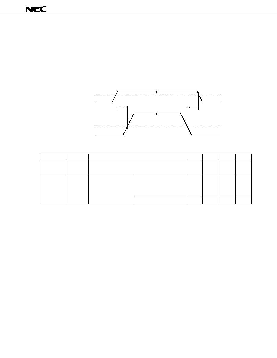
Data Sheet U16369EJ1V0DS
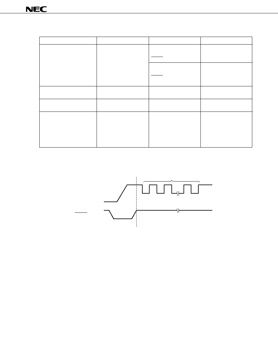
Notes 2. Make sure that the following conditions of the V
PP
voltage application timing are satisfied when the flash
memory is written.
∑ When supply voltage rises
V
PP
must exceed V
DD
10
µ
s or more after V
DD
has reached the lower-limit value (1.8 V) of the
operating voltage range (see a in the figure below).
∑ When supply voltage drops
V
DD
must be lowered 10
µ
s or more after V
PP
falls below the lower-limit value (1.8 V) of the
operating voltage range of V
DD
(see b in the figure below).
Capacitance (T
A
= 25
∞
C, V
DD
= V
SS
= 0 V)
Parameter
Symbol
Conditions
MIN.
TYP.
MAX.
Unit
Input
C
IN
f = 1 MHz
15
pF
capacitance
Unmeasured pins returned to 0 V.
I/O
C
IO
f = 1 MHz
P00 to P03, P20 to P25,
15
pF
capacitance
Unmeasured pins
P34 to P36, P40 to P47,
returned to 0 V.
P50 to P57, P64 to P67,
P70 to P75,
P30 to P33
20
pF
Remark
Unless otherwise specified, the characteristics of alternate-function pins are the same as those of port
pins.
1.8 V
V
DD
0 V
0 V
V
PP
1.8 V
a
b
µ
PD78F0034B, 78F0034BY, 78F0034B(A), 78F0034BY(A)
30
Data Sheet U16369EJ1V0DS
Main System Clock Oscillator Characteristics (T
A
= ≠40 to +85
∞
C, V
DD
= 1.8 to 5.5 V)
Resonator
Recommended
Parameter
Conditions
MIN.
TYP.
MAX.
Unit
Circuit
Ceramic
Oscillation
4.5 V
V
DD
5.5 V
1.0
12.0
MHz
resonator
frequency (f
X
)
Note 1
3.0 V
V
DD
<
4.5 V
1.0
8.38
1.8 V
V
DD
<
3.0 V
1.0
5.0
Oscillation
After V
DD
reaches
4
ms
stabilization time
Note 2
oscillation voltage range
MIN.
Crystal
Oscillation
4.5 V
V
DD
5.5 V
1.0
12.0
MHz
resonator
frequency (f
X
)
Note 1
3.0 V
V
DD
<
4.5 V
1.0
8.38
1.8 V
V
DD
<
3.0 V
1.0
5.0
Oscillation
4.0 V
V
DD
5.5 V
10
ms
stabilization time
Note 2
1.8 V
V
DD
<
4.0 V
30
External
X1 input
4.5 V
V
DD
5.5 V
1.0
12.0
MHz
clock
frequency (f
X
)
Note 1
3.0 V
V
DD
<
4.5 V
1.0
8.38
1.8 V
V
DD
<
3.0 V
1.0
5.0
X1 input
4.5 V
V
DD
5.5 V
38
500
ns
high-/low-level width
3.0 V
V
DD
<
4.5 V
50
500
(t
XH
, t
XL
)
1.8 V
V
DD
<
3.0 V
85
500
Notes 1. Indicates only oscillator characteristics. Refer to AC Characteristics for instruction execution time.
2. Time required to stabilize oscillation after reset or STOP mode release.
Cautions
1. When using the main system clock oscillator, wire as follows in the area enclosed by the broken
lines in the above figures to avoid an adverse effect from wiring capacitance.
∑ Keep the wiring length as short as possible.
∑ Do not cross the wiring with the other signal lines.
∑ Do not route the wiring near a signal line through which a high fluctuating current flows.
∑ Always make the ground point of the oscillator capacitor the same potential as V
SS1
.
∑ Do not ground the capacitor to a ground pattern through which a high current flows.
∑ Do not fetch signals from the oscillator.
2. When the main system clock is stopped and the system is operating on the subsystem clock,
wait until the oscillation stabilization time has been secured by the program before switching
back to the main system clock.
Remark
For the resonator selection and oscillator constant, customers are required to either evaluate the
oscillation themselves or apply to the resonator manufacturer for evaluation.
X2
X1
C2
C1
X1
X2
V
PP
C2
C1
X1
X2
V
PP
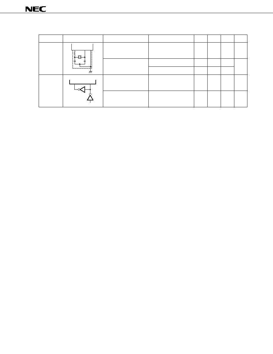
µ
PD78F0034B, 78F0034BY, 78F0034B(A), 78F0034BY(A)
31
Data Sheet U16369EJ1V0DS
Subsystem Clock Oscillator Characteristics (T
A
= ≠40 to +85
∞
C, V
DD
= 1.8 to 5.5 V)
Resonator
Recommended Circuit
Parameter
Conditions
MIN.
TYP.
MAX.
Unit
Crystal
Oscillation
32
32.768
35
kHz
resonator
frequency (f
XT
)
Note 1
Oscillation
4.0 V
V
DD
5.5 V
1.2
2
s
stabilization time
Note 2
1.8 V
V
DD
<
4.0 V
10
External
X1 input
32
38.5
kHz
clock
frequency (f
XT
)
Note 1
X1 input high-/low-level
12
15
µ
s
width (t
XTH
, t
XTL
)
Notes 1. Indicates only oscillator characteristics. Refer to AC Characteristics for instruction execution time.
2. Time required to stabilize oscillation after V
DD
reaches oscillator voltage MIN.
Cautions 1. When using the subsystem clock oscillator, wire as follows in the area enclosed by the
broken lines in the above figures to avoid an adverse effect from wiring capacitance.
∑ Keep the wiring length as short as possible.
∑ Do not cross the wiring with the other signal lines.
∑ Do not route the wiring near a signal line through which a high fluctuating current flows.
∑ Always make the ground point of the oscillator capacitor to the same potential as V
SS1
.
∑ Do not ground the capacitor to a ground pattern through which a high current flows.
∑ Do not fetch signals from the oscillator.
2. The subsystem clock oscillator is designed as a low-amplitude circuit for reducing power
consumption, and is more prone to malfunction due to noise than the main system clock
oscillator. Particular care is therefore required with the wiring method when the subsystem
clock is used.
Remark
For the resonator selection and oscillator constant, customers are required to either evaluate the
oscillation themselves or apply to the resonator manufacturer for evaluation.
C3
XT2
XT1V
PP
R2
C4
XT1
XT2
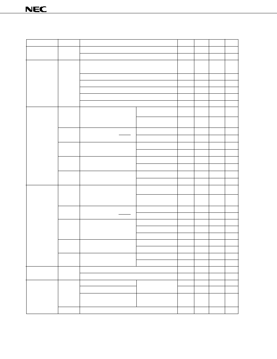
µ
PD78F0034B, 78F0034BY, 78F0034B(A), 78F0034BY(A)
32
Data Sheet U16369EJ1V0DS
DC Characteristics (T
A
= ≠40 to +85
∞
C, V
DD
= 1.8 to 5.5 V)
Parameter
Symbol
Conditions
MIN.
TYP.
MAX.
Unit
Output current,
I
OH
Per pin
≠1
mA
high
All pins
≠15
mA
Output current,
I
OL
Per pin for P00 to P03, P20 to P25, P34 to P36,
10
mA
low
P40 to P47, P64 to P67, P70 to P75
Per pin for P30 to P33, P50 to P57
15
mA
Total for P00 to P03, P40 to P47, P64 to P67, P70 to P75
20
mA
Total for P20 to P25
10
mA
Total for P30 to P36
70
mA
Total for P50 to P57
70
mA
Input voltage,
V
IH1
P10 to P17, P21, P24, P35,
2.7 V
V
DD
5.5 V
0.7V
DD
V
DD
V
high
P40 to P47, P50 to P57,
1.8 V
V
DD
<
2.7 V
0.8V
DD
V
DD
V
P64 to P67, P74, P75
V
IH2
P00 to P03, P20, P22, P23, P25,
2.7 V
V
DD
5.5 V
0.8V
DD
V
DD
V
P34, P36, P70 to P73, RESET
1.8 V
V
DD
<
2.7 V
0.85V
DD
V
DD
V
V
IH3
P30 to P33
2.7 V
V
DD
5.5 V
0.7V
DD
5.5
V
(N-ch open-drain)
1.8 V
V
DD
<
2.7 V
0.8V
DD
5.5
V
V
IH4
X1, X2
2.7 V
V
DD
5.5 V
V
DD
≠
0.5
V
DD
V
1.8 V
V
DD
<
2.7 V
V
DD
≠
0.2
V
DD
V
V
IH5
XT1, XT2
4.0 V
V
DD
5.5 V
0.8V
DD
V
DD
V
1.8 V
V
DD
<
4.0 V
0.9V
DD
V
DD
V
Input voltage,
V
IL1
P10 to P17, P21, P24, P35,
2.7 V
V
DD
5.5 V
0
0.3V
DD
V
low
P40 to P47, P50 to P57,
1.8 V
V
DD
<
2.7 V
0
0.2V
DD
V
P64 to P67, P74, P75
V
IL2
P00 to P03, P20, P22, P23, P25,
2.7 V
V
DD
5.5 V
0
0.2V
DD
V
P34, P36, P70 to P73, RESET
1.8 V
V
DD
<
2.7 V
0
0.15V
DD
V
V
IL3
P30 to P33
4.0 V
V
DD
5.5 V
0
0.3V
DD
V
2.7 V
V
DD
<
4.0 V
0
0.2V
DD
V
1.8 V
V
DD
<
2.7 V
0
0.1V
DD
V
V
IL4
X1, X2
2.7 V
V
DD
5.5 V
0
0.4
V
1.8 V
V
DD
<
2.7 V
0
0.2
V
V
IL5
XT1, XT2
4.0 V
V
DD
5.5 V
0
0.2V
DD
V
1.8 V
V
DD
<
4.0 V
0
0.1V
DD
V
Output voltage,
V
OH1
4.0 V
V
DD
5.5 V, I
OH
= ≠1 mA
V
DD
≠
1.0
V
DD
V
high
1.8 V
V
DD
<
4.0 V, I
OH
= ≠100
µ
A
V
DD
≠
0.5
V
DD
V
Output voltage,
V
OL1
P30 to P33
4.0 V
V
DD
5.5 V,
2.0
V
low
P50 to P57
I
OL
= 15 mA
0.4
2.0
V
P00 to P03, P20 to P25, P34 to P36, 4.0 V
V
DD
5.5 V,
0.4
V
P40 to P47, P64 to P67, P70 to P75
I
OL
= 1.6 mA
V
OL2
I
OL
= 400
µ
A
0.5
V
Remark
Unless otherwise specified, the characteristics of alternate-function pins are the same as those of port pins.

µ
PD78F0034B, 78F0034BY, 78F0034B(A), 78F0034BY(A)
33
Data Sheet U16369EJ1V0DS
DC Characteristics (T
A
= ≠40 to +85
∞
C, V
DD
= 1.8 to 5.5 V)
Parameter
Symbol
Conditions
MIN.
TYP.
MAX.
Unit
Input leakage
I
LIH1
V
IN
= V
DD
P00 to P03, P10 to P17, P20 to P25,
3
µ
A
current, high
P34 to P36, P40 to P47, P50 to P57,
P64 to P67, P70 to P75,
RESET
I
LIH2
X1, X2, XT1, XT2
20
µ
A
I
LIH3
V
IN
= 5.5 V
P30 to P33
3
µ
A
Input leakage
I
LIL1
V
IN
= 0 V
P00 to P03, P10 to P17, P20 to P25,
≠3
µ
A
current, low
P34 to P36, P40 to P47, P50 to P57,
P64 to P67, P70 to P75,
RESET
I
LIL2
X1, X2, XT1, XT2
≠20
µ
A
I
LIL3
P30 to P33
≠3
µ
A
Output leakage
I
LOH
V
OUT
= V
DD
3
µ
A
current, high
Output leakage
I
LOL
V
OUT
= 0 V
≠3
µ
A
current, low
Software pull-
R
V
IN
= 0 V,
15
30
90
k
up resistor
P00 to P03, P20 to P25, P34 to P36, P40 to P47,
P50 to P57, P64 to P67, P70 to P75
Remark
Unless otherwise specified, the characteristics of alternate-function pins are the same as those of port
pins.

µ
PD78F0034B, 78F0034BY, 78F0034B(A), 78F0034BY(A)
34
Data Sheet U16369EJ1V0DS
DC Characteristics (T
A
= ≠40 to +85
∞
C, V
DD
= 1.8 to 5.5 V)
Parameter
Symbol
Conditions
MIN.
TYP.
MAX.
Unit
Power supply
I
DD1
Note 2
12.0 MHz
V
DD
= 5.0 V
±
10%
Note 3
When A/D converter is
16
32
mA
current
Note 1
crystal oscillation
stopped
operating mode
When A/D converter is
17
34
mA
operating
Note 7
8.38 MHz
V
DD
= 5.0 V
±
10%
Note 3
When A/D converter is
10.5
21
mA
crystal oscillation
stopped
operating mode
When A/D converter is
11.5
23
mA
operating
Note 7
V
DD
= 3.0 V + 10%
Notes 3, 6
When A/D converter is
7
14
mA
stopped
When A/D converter is
8
16
mA
operating
Note 7
5.00 MHz
V
DD
= 3.0 V
±
10%
Note 3
When A/D converter is
4.5
9
mA
crystal oscillation
stopped
operating mode
When A/D converter is
5.5
11
mA
operating
Note 7
V
DD
= 2.0 V
±
10%
Note 4
When A/D converter is
1
2
mA
stopped
When A/D converter is
2
6
mA
operating
Note 7
I
DD2
12.0 MHz
V
DD
= 5.0 V
±
10%
Note 3
When peripheral functions
2
4
mA
crystal oscillation
are stopped
HALT mode
When peripheral functions
8
mA
are operating
8.38 MHz
V
DD
= 5.0 V
±
10%
Note 3
When peripheral functions
1.2
2.4
mA
crystal oscillation
are stopped
HALT mode
When peripheral functions
5
mA
are operating
V
DD
= 3.0 V + 10%
Notes 3, 6
When peripheral functions
0.6
1.2
mA
are stopped
When peripheral functions
2.4
mA
are operating
5.00 MHz
V
DD
= 3.0 V
±
10%
Note 3
When peripheral functions
0.4
0.8
mA
crystal oscillation
are stopped
HALT mode
When peripheral functions
1.7
mA
are operating
V
DD
= 2.0 V
±
10%
Note 4
When peripheral functions
0.2
0.4
mA
are stopped
When peripheral functions
1.1
mA
are operating
I
DD3
32.768 kHz crystal oscillation
V
DD
= 5.0 V
±
10%
115
230
µ
A
operating mode
Note 5
V
DD
= 3.0 V
±
10%
95
190
µ
A
V
DD
= 2.0 V
±
10%
75
150
µ
A
I
DD4
32.768 kHz crystal oscillation
V
DD
= 5.0 V
±
10%
30
60
µ
A
HALT mode
Note 5
V
DD
= 3.0 V
±
10%
6
18
µ
A
V
DD
= 2.0 V
±
10%
2
10
µ
A
I
DD5
XT1 = V
DD
STOP mode
V
DD
= 5.0 V
±
10%
0.1
30
µ
A
When feedback resistor is not used
V
DD
= 3.0 V
±
10%
0.05
10
µ
A
V
DD
= 2.0 V
±
10%
0.05
10
µ
A

µ
PD78F0034B, 78F0034BY, 78F0034B(A), 78F0034BY(A)
35
Data Sheet U16369EJ1V0DS
Notes 1. Total current through the internal power supply (V
DD0
, V
DD1
) (except the current through pull-up resistors
of ports).
2. I
DD1
includes the peripheral operation current.
3. When the processor clock control register (PCC) is set to 00H.
4. When PCC is set to 02H.
5. When main system clock operation is stopped.
6. The values show the specifications when V
DD
= 3.0 to 3.3 V. The value in the TYP. column show the
specifications when V
DD
= 3.0 V.
7. Includes the current through the AV
DD
pin.
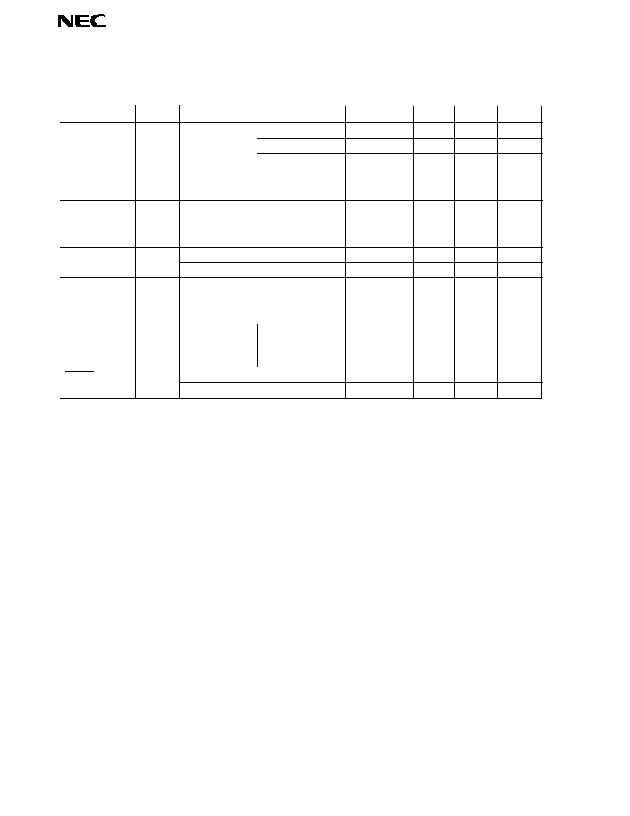
µ
PD78F0034B, 78F0034BY, 78F0034B(A), 78F0034BY(A)
36
Data Sheet U16369EJ1V0DS
AC Characteristics
(1) Basic Operation
(T
A
= ≠40 to +85
∞
C, V
DD
= 1.8 to 5.5 V)
Parameter
Symbol
Conditions
MIN.
TYP.
MAX.
Unit
Cycle time
T
CY
Operating with
4.5 V
V
DD
5.5 V
0.166
16
µ
s
(Min. instruction
main system clock
3.0 V
V
DD
4.5 V
0.238
16
µ
s
execution time)
2.7 V
V
DD
3.0 V
0.4
16
µ
s
1.8 V
V
DD
2.7 V
1.6
16
µ
s
Operating with subsystem clock
103.9
Note 1
122
125
µ
s
TI00, TI01 input
t
TIH0
, t
TIL0
3.0 V
V
DD
5.5 V
2/f
sam
+0.1
Note 2
µ
s
high-/low-level
2.7 V
V
DD
<
3.0 V
2/f
sam
+0.2
Note 2
µ
s
width
1.8 V
V
DD
<
2.7 V
2/f
sam
+0.5
Note 2
µ
s
TI50, TI51 input
f
TI5
2.7 V
V
DD
5.5 V
0
4
MHz
frequency
1.8 V
V
DD
<
2.7 V
0
275
kHz
TI50, TI51 input
t
TIH5
, t
TIL5
2.7 V
V
DD
5.5 V
100
ns
high-/low-level
1.8 V
V
DD
<
2.7 V
1.8
ns
width
Interrupt request
t
INTH
, t
INTL
INTP0 to INTP3,
2.7 V
V
DD
5.5 V
1
µ
s
input high-/low-
P40 to P47
1.8 V
V
DD
<
2.7 V
2
µ
s
level width
RESET
t
RSL
2.7 V
V
DD
5.5 V
10
µ
s
low-level width
1.8 V
V
DD
<
2.7 V
20
µ
s
Notes 1. Value when the external clock is used. When a crystal resonator is used, it is 114
µ
s (MIN.).
2. Selection of fsam = f
X
, f
X
/4, f
X
/64 is possible using bits 0 and 1 (PRM00, PRM01) of prescaler mode
register 0 (PRM0). However, if the TI00 valid edge is selected as the count clock, the value becomes
fsam = f
X
/8.

µ
PD78F0034B, 78F0034BY, 78F0034B(A), 78F0034BY(A)
37
Data Sheet U16369EJ1V0DS
T
CY
vs. V
DD
(main system clock operation)
5.0
1.0
2.0
1.6
0.4
0.238
0.166
0.1
Supply voltage V
DD
[V]
Cycle time T
CY
[ S]
0
10.0
1.0
2.0
3.0
4.0
5.0
6.0
1.8
5.5
2.7
4.5
Operation
guaranteed
range
16.0
µ

µ
PD78F0034B, 78F0034BY, 78F0034B(A), 78F0034BY(A)
38
Data Sheet U16369EJ1V0DS
(2) Read/write operation (T
A
= ≠40 to +85
∞
C, V
DD
= 4.0 to 5.5 V)
(1/3)
Parameter
Symbol
Conditions
MIN.
MAX.
Unit
ASTB high-level width
t
ASTH
0.3t
CY
ns
Address setup time
t
ADS
20
ns
Address hold time
t
ADH
6
ns
Input time from address to data
t
ADD1
(2 + 2n)t
CY
≠ 54
ns
t
ADD2
(3 + 2n)t
CY
≠ 60
ns
Output time from RD
to address
t
RDAD
0
100
ns
Input time from RD
to data
t
RDD1
(2 + 2n)t
CY
≠ 87
ns
t
RDD2
(3 + 2n)t
CY
≠ 93
ns
Read data hold time
t
RDH
0
ns
RD low-level width
t
RDL1
(1.5 + 2n)t
CY
≠ 33
ns
t
RDL2
(2.5 + 2n)t
CY
≠ 33
ns
Input time from RD
to WAIT
t
RDWT1
t
CY
≠ 43
ns
t
RDWT2
t
CY
≠ 43
ns
Input time from WR
to WAIT
t
WRWT
t
CY
≠ 25
ns
WAIT low-level width
t
WTL
(0.5 + n)t
CY
+ 10
(2 + 2n)t
CY
ns
Write data setup time
t
WDS
60
ns
Write data hold time
t
WDH
6
ns
WR low-level width
t
WRL1
(1.5 + 2n)t
CY
≠ 15
ns
Delay time from ASTB
to RD
t
ASTRD
6
ns
Delay time from ASTB
to WR
t
ASTWR
2t
CY
≠ 15
ns
Delay time from RD
to ASTB
in
t
RDAST
0.8t
CY
≠ 15
1.2t
CY
ns
external fetch
Hold time from RD
to address in
t
RDADH
0.8t
CY
≠ 15
1.2t
CY
+ 30
ns
external fetch
Write data output time from RD
t
RDWD
40
ns
Write data output time from WR
t
WRWD
10
60
ns
Hold time from WR
to address
t
WRADH
0.8t
CY
≠ 15
1.2t
CY
+ 30
ns
Delay time from WAIT
to RD
t
WTRD
0.8t
CY
2.5t
CY
+ 25
ns
Delay time from WAIT
to WR
t
WTWR
0.8t
CY
2.5t
CY
+ 25
ns
Caution T
CY
can only be used when the MIN. value is 0.238
µµ
µµ
µ
s.
Remarks 1. t
CY
= T
CY
/4
2. n indicates the number of waits.
3. C
L
= 100 pF (C
L
is the load capacitance of the AD0 to AD7, A8 to A15, RD, WR, WAIT, and ASTB
pins.)
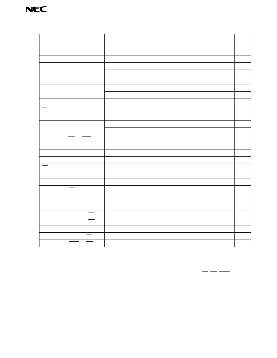
µ
PD78F0034B, 78F0034BY, 78F0034B(A), 78F0034BY(A)
39
Data Sheet U16369EJ1V0DS
(2) Read/write operation (T
A
= ≠40 to +85
∞
C, V
DD
= 2.7 to 4.0 V)
(2/3)
Parameter
Symbol
Conditions
MIN.
MAX.
Unit
ASTB high-level width
t
ASTH
0.3t
CY
ns
Address setup time
t
ADS
30
ns
Address hold time
t
ADH
10
ns
Input time from address to data
t
ADD1
(2 + 2n)t
CY
≠ 108
ns
t
ADD2
(3 + 2n)t
CY
≠ 120
ns
Output time from RD
to address
t
RDAD
0
200
ns
Input time from RD
to data
t
RDD1
(2 + 2n)t
CY
≠ 148
ns
t
RDD2
(3 + 2n)t
CY
≠ 162
ns
Read data hold time
t
RDH
0
ns
RD low-level width
t
RDL1
(1.5 + 2n)t
CY
≠ 40
ns
t
RDL2
(2.5 + 2n)t
CY
≠ 40
ns
Input time from RD
to WAIT
t
RDWT1
t
CY
≠ 75
ns
t
RDWT2
t
CY
≠ 60
ns
Input time from WR
to WAIT
t
WRWT
t
CY
≠ 50
ns
WAIT low-level width
t
WTL
(0.5 + 2n)t
CY
+ 10
(2 + 2n)t
CY
ns
Write data setup time
t
WDS
60
ns
Write data hold time
t
WDH
10
ns
WR low-level width
t
WRL1
(1.5 + 2n)t
CY
≠ 30
ns
Delay time from ASTB
to RD
t
ASTRD
10
ns
Delay time from ASTB
to WR
t
ASTWR
2t
CY
≠ 30
ns
Delay time from RD
to ASTB
in
t
RDAST
0.8t
CY
≠ 30
1.2t
CY
ns
external fetch
Hold time from RD
to address in
t
RDADH
0.8t
CY
≠ 30
1.2t
CY
+ 60
ns
external fetch
Write data output time from RD
t
RDWD
40
ns
Write data output time from WR
t
WRWD
20
120
ns
Hold time from WR
to address
t
WRADH
0.8t
CY
≠ 30
1.2t
CY
+ 60
ns
Delay time from WAIT
to RD
t
WTRD
0.5t
CY
2.5t
CY
+ 50
ns
Delay time from WAIT
to WR
t
WTWR
0.5t
CY
2.5t
CY
+ 50
ns
Caution T
CY
can only be used when the MIN. value is 0.4
µµ
µµ
µ
s.
Remarks 1. t
CY
= T
CY
/4
2. n indicates the number of waits.
3. C
L
= 100 pF (C
L
is the load capacitance of the AD0 to AD7, A8 to A15, RD, WR, WAIT, and ASTB
pins.)
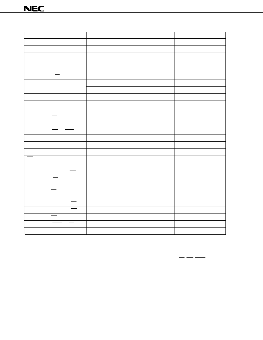
µ
PD78F0034B, 78F0034BY, 78F0034B(A), 78F0034BY(A)
40
Data Sheet U16369EJ1V0DS
(2) Read/write operation (T
A
= ≠40 to +85
∞
C, V
DD
= 1.8 to 2.7 V)
(3/3)
Parameter
Symbol
Conditions
MIN.
MAX.
Unit
ASTB high-level width
t
ASTH
0.3t
CY
ns
Address setup time
t
ADS
120
ns
Address hold time
t
ADH
20
ns
Input time from address to data
t
ADD1
(2 + 2n)t
CY
≠ 233
ns
t
ADD2
(3 + 2n)t
CY
≠ 240
ns
Output time from RD
to address
t
RDAD
0
400
ns
Input time from RD
to data
t
RDD1
(2 + 2n)t
CY
≠ 325
ns
t
RDD2
(3 + 2n)t
CY
≠ 332
ns
Read data hold time
t
RDH
0
ns
RD low-level width
t
RDL1
(1.5 + 2n)t
CY
≠ 92
ns
t
RDL2
(2.5 + 2n)t
CY
≠ 92
ns
Input time from RD
to WAIT
t
RDWT1
t
CY
≠ 350
ns
t
RDWT2
t
CY
≠ 132
ns
Input time from WR
to WAIT
t
WRWT
t
CY
≠ 100
ns
WAIT low-level width
t
WTL
(0.5 + 2n)t
CY
+ 10
(2 + 2n)t
CY
ns
Write data setup time
t
WDS
60
ns
Write data hold time
t
WDH
20
ns
WR low-level width
t
WRL1
(1.5 + 2n)t
CY
≠ 60
ns
Delay time from ASTB
to RD
t
ASTRD
20
ns
Delay time from ASTB
to WR
t
ASTWR
2t
CY
≠ 60
ns
Delay time from RD
to ASTB
in
t
RDAST
0.8t
CY
≠ 60
1.2t
CY
ns
external fetch
Hold time from RD
to address in
t
RDADH
0.8t
CY
≠ 60
1.2t
CY
+ 120
ns
external fetch
Write data output time from RD
t
RDWD
40
ns
Write data output time from WR
t
WRWD
40
240
ns
Hold time from WR
to address
t
WRADH
0.8t
CY
≠ 60
1.2t
CY
+ 120
ns
Delay time from WAIT
to RD
t
WTRD
0.5t
CY
2.5t
CY
+ 100
ns
Delay time from WAIT
to WR
t
WTWR
0.5t
CY
2.5t
CY
+ 100
ns
Caution T
CY
can only be used when the MIN. value is 1.6
µµ
µµ
µ
s.
Remarks 1. t
CY
= T
CY
/4
2. n indicates the number of waits.
3. C
L
= 100 pF (C
L
is the load capacitance of the AD0 to AD7, A8 to A15, RD, WR, WAIT, and ASTB
pins.)
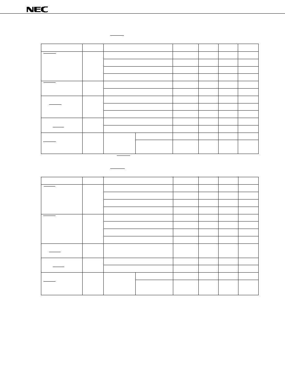
µ
PD78F0034B, 78F0034BY, 78F0034B(A), 78F0034BY(A)
41
Data Sheet U16369EJ1V0DS
(3) Serial Interface (T
A
= ≠40 to +85
∞
C, V
DD
= 1.8 to 5.5 V)
(a) 3-wire serial I/O mode (SCK3n... Internal clock output)
Parameter
Symbol
Conditions
MIN.
TYP.
MAX.
Unit
SCK3n
t
KCY1
4.5 V
V
DD
5.5 V
666
ns
cycle time
3.0 V
V
DD
<
4.5 V
954
ns
2.7 V
V
DD
<
3.0 V
1600
ns
1.8 V
V
DD
<
2.7 V
3200
ns
SCK3n high-/
t
KH1
, t
KL1
3.0 V
V
DD
5.5 V
t
KCY1
/2 ≠ 50
ns
low-level width
1.8 V
V
DD
<
3.0 V
t
KCY1
/2 ≠ 100
ns
SI3n setup time
t
SIK1
3.0 V
V
DD
5.5 V
100
ns
(to SCK3n
)
2.7 V
V
DD
< 3.0 V
150
ns
1.8 V
V
DD
<
2.7 V
300
ns
SI3n hold time
t
KSI1
4.5 V
V
DD
5.5 V
300
ns
(from SCK3n
)
1.8 V
V
DD
<
4.5 V
400
ns
Delay time from
t
KSO1
C = 100 pF
Note
4.5 V
V
DD
5.5 V
200
ns
SCK3n
to SO3n
1.8 V
V
DD
<
4.5 V
300
ns
output
Note C is the load capacitance of the SCK3n and SO3n output lines.
(b) 3-wire serial I/O mode (SCK3n... External clock input)
Parameter
Symbol
Conditions
MIN.
TYP.
MAX.
Unit
SCK3n
t
KCY2
4.5 V
V
DD
5.5 V
666
ns
cycle time
3.0 V
V
DD
<
4.5 V
800
ns
2.7 V
V
DD
<
3.0 V
1600
ns
1.8 V
V
DD
<
2.7 V
3200
ns
SCK3n high-/
t
KH2
, t
KL2
4.5 V
V
DD
5.5 V
333
ns
low-level width
3.0 V
V
DD
<
4.5 V
400
ns
2.7 V
V
DD
<
3.0 V
800
ns
1.8 V
V
DD
<
2.7 V
1600
ns
SI3n setup time
t
SIK2
100
ns
(to SCK3n
)
SI3n hold time
t
KSI2
4.5 V
V
DD
5.5 V
300
ns
(from SCK3n
)
1.8 V
V
DD
<
4.5 V
400
ns
Delay time from
t
KSO2
C = 100 pF
Note
4.5 V
V
DD
5.5 V
200
ns
SCK3n
to SO3n
1.8 V
V
DD
<
4.5 V
300
ns
output
Note C is the load capacitance of the SO3n output line.
Remark
n = 0, 1
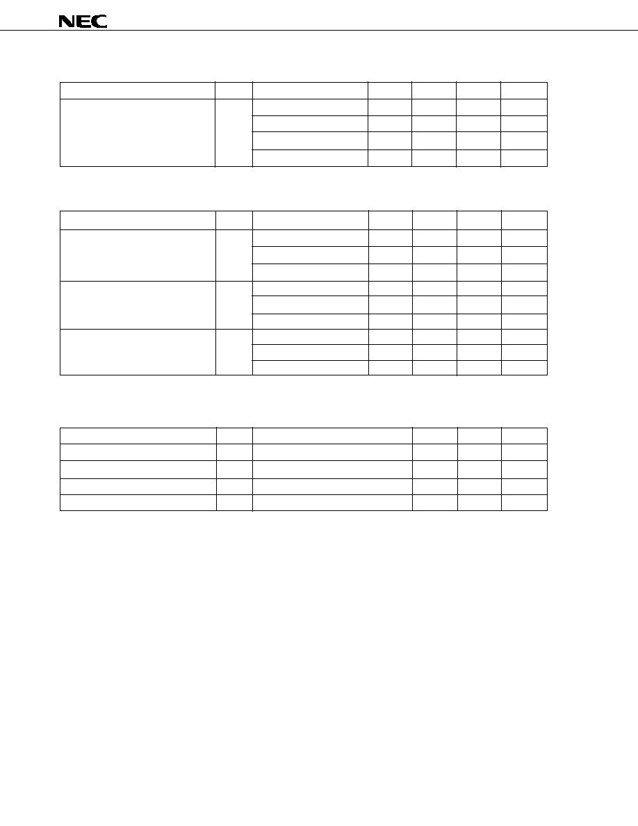
µ
PD78F0034B, 78F0034BY, 78F0034B(A), 78F0034BY(A)
42
Data Sheet U16369EJ1V0DS
(c) UART mode (dedicated baud-rate generator output)
Parameter
Symbol
Conditions
MIN.
TYP.
MAX.
Unit
Transfer rate
4.5 V
V
DD
5.5 V
187500
bps
3.0 V
V
DD
< 4.5 V
131031
bps
2.7 V
V
DD
< 3.0 V
78125
bps
1.8 V
V
DD
< 2.7 V
39063
bps
(d) UART mode (external clock input)
Parameter
Symbol
Conditions
MIN.
TYP.
MAX.
Unit
ASCK0 cycle time
t
KCY3
4.0 V
V
DD
5.5 V
800
ns
2.7 V
V
DD
< 4.0 V
1600
ns
1.8 V
V
DD
< 2.7 V
3200
ns
ASCK0 high-/low-level width
t
KH3
,
4.0 V
V
DD
5.5 V
400
ns
t
KL3
2.7 V
V
DD
< 4.0 V
800
ns
1.8 V
V
DD
< 2.7 V
1600
ns
Transfer rate
4.0 V
V
DD
5.5 V
39063
bps
2.7 V
V
DD
< 4.0 V
19531
bps
1.8 V
V
DD
< 2.7 V
9766
bps
(e) UART mode (infrared data transfer mode)
Parameter
Symbol
Conditions
MIN.
MAX.
Unit
Transfer rate
4.0 V
V
DD
5.5 V
131031
bps
Allowable bit rate error
4.0 V
V
DD
5.5 V
±
0.87
%
Output pulse width
4.0 V
V
DD
5.5 V
1.2
0.24/fbr
Note
µ
s
Input pulse width
4.0 V
V
DD
5.5 V
4/f
X
µ
s
Note fbr: Specified baud rate
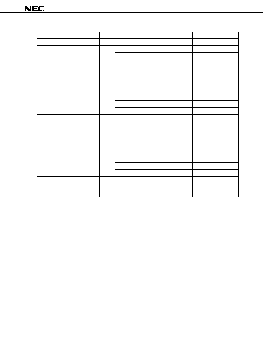
µ
PD78F0034B, 78F0034BY, 78F0034B(A), 78F0034BY(A)
43
Data Sheet U16369EJ1V0DS
A/D Converter Characteristics (T
A
= ≠40 to +85
∞
C, V
DD
= AV
DD
= 1.8 to 5.5 V, AV
SS
= V
SS
= 0 V)
Parameter
Symbol
Conditions
MIN.
TYP.
MAX.
Unit
Resolution
10
10
10
bit
Overall error
Note
4.0 V
AV
REF
5.5 V
±
0.2
±
0.4
%FSR
2.7 V
AV
REF
< 4.0 V
±
0.3
±
0.6
%FSR
1.8 V
AV
REF
< 2.7 V
±
0.6
±
1.2
%FSR
Conversion time
t
CONV
4.5 V
AV
DD
5.5 V
12
96
µ
s
4.0 V
AV
DD
< 4.5 V
14
96
µ
s
2.7 V
AV
DD
< 4.0 V
17
96
µ
s
1.8 V
AV
DD
< 2.7 V
28
96
µ
s
Zero-scale error
Notes 1, 2
4.0 V
AV
REF
5.5 V
±
0.4
%FSR
2.7 V
AV
REF
< 4.0 V
±
0.6
%FSR
1.8 V
AV
REF
< 2.7 V
±
1.2
%FSR
Full-scale error
Notes 1, 2
4.0 V
AV
REF
5.5 V
±
0.4
%FSR
2.7 V
AV
REF
< 4.0 V
±
0.6
%FSR
1.8 V
AV
REF
< 2.7 V
±
1.2
%FSR
Integral linearity error
Note 1
4.0 V
AV
REF
5.5 V
±
2.5
LSB
2.7 V
AV
REF
< 4.0 V
±
4.5
LSB
1.8 V
AV
REF
< 2.7 V
±
8.5
LSB
Differential linearity error
4.0 V
AV
REF
5.5 V
±
1.5
LSB
2.7 V
AV
REF
4.0 V
±
2.0
LSB
1.8 V
AV
REF
< 2.7 V
±
3.5
LSB
Analog input voltage
V
IAN
0
AV
REF
V
Reference voltage
AV
REF
1.8
AV
DD
V
Resistance between AV
REF
and AV
SS
R
REF
During A/D conversion operation
20
40
k
Notes 1. Excluding quantization error (
±
1/2 LSB).
2. Indicated as a ratio to the full-scale value (%FSR).
Remark
When the
µ
PD78F0034B is used as an 8-bit resolution A/D converter, the specifications are the same
as for the
µ
PD780024A Subseries A/D converter.

µ
PD78F0034B, 78F0034BY, 78F0034B(A), 78F0034BY(A)
44
Data Sheet U16369EJ1V0DS
Data Memory STOP Mode Low Supply Voltage Data Retention Characteristics (T
A
= ≠40 to +85
∞
C)
Parameter
Symbol
Conditions
MIN.
TYP.
MAX.
Unit
Data retention supply voltage
V
DDDR
1.6
5.5
V
Data retention supply current
I
DDDR
Subsystem clock stop (XT1 = V
DD
)
0.1
30
µ
A
and feed-back resistor disconnected
Release signal set time
t
SREL
0
µ
s
Oscillation stabilization wait time
t
WAIT
Release by RESET
2
17
/f
X
s
Release by interrupt request
Note
s
Note
Selection of 2
12
/f
X
and 2
14
/f
X
to 2
17
/f
X
is possible using bits 0 to 2 (OSTS0 to OSTS2) of the oscillation
stabilization time select register (OSTS).
Remark The impedance of the analog input pins is shown below.
[Equivalent circuit]
[Parameter value]
(TYP.)
AV
DD
R1
R2
C1
C2
C3
2.7 V
12 k
8.0 k
3.0 pF
3.0 pF
2.0 pF
4.5 V
4 k
2.7 k
3.0 pF
1.4 pF
2.0 pF
C3
C2
R2
R1
C1
ANIn
(n = 0 to 3)
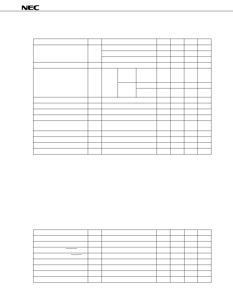
µ
PD78F0034B, 78F0034BY, 78F0034B(A), 78F0034BY(A)
45
Data Sheet U16369EJ1V0DS
Flash Memory Programming Characteristics (T
A
= +10 to +40
∞
C, V
DD
= 1.8 to 5.5 V, V
SS
= AV
SS
= 0 V)
(1) Write erase characteristics
Parameter
Symbol
Conditions
MIN.
TYP.
MAX.
Unit
Operating frequency
f
X
4.5 V
V
DD
5.5 V
1.0
10.0
MHz
3.0 V
V
DD
< 4.5 V
1.0
8.38
MHz
1.8 V
V
DD
< 3.0 V
1.0
1.25
MHz
V
PP
supply voltage
V
PP2
During flash memory programming
9.7
10.0
10.3
V
V
DD
supply current
I
DD
When
10 MHz crystal
V
DD
= 5.0 V
±
10%
30
mA
V
PP
= V
PP2
oscillation
operating mode
8.38 MHz crystal V
DD
= 5.0 V
±
10%
24
mA
oscillation
V
DD
= 3.0 V
±
10%
17
mA
operating mode
V
PP
supply current
I
PP
When V
PP
= V
PP2
100
mA
Step erase time
Note 1
T
er
0.199
0.2
0.201
s
Overall erase time
Note 2
T
era
When step erase time = 0.2 s
20
s/chip
Writeback time
Note 3
T
wb
49.4
50
50.6
ms
Number of writebacks per
C
wb
When writeback time = 50 ms
60
Times
writeback command
Note 4
Number of erases/writebacks
C
erwb
16
Times
Step write time
Note 5
T
wr
48
50
52
µ
s
Overall write time per word
Note 6
T
wrw
When step write time = 50
µ
s (1 word = 1 byte)
48
520
µ
s
Number of rewrites per chip
Note 7
C
erwb
1 erase + 1 write after erase = 1 rewrite
20
Times
Notes 1. The recommended setting value of the step erase time is 0.2 s.
2. The prewrite time before erasure and the erase verify time (writeback time) are not included.
3. The recommended setting value of the writeback time is 50 ms.
4. Writeback is executed once by the issuance of the writeback command. Therefore, the number of retries
must be the maximum value minus the number of commands issued.
5. The recommended setting value of the step write time is 50
µ
s.
6. The actual write time per word is 100
µ
s longer. The internal verify time during or after a write is not
included.
7. When a product is first written after shipment, "erase
write" and "write only" are both taken as one
rewrite.
Example:
P: Write, E: Erase
Shipped product
P
E
P
E
P: 3 rewrites
Shipped product
E
P
E
P
E
P: 3 rewrites
(2) Serial write operation characteristics
Parameter
Symbol
Conditions
MIN.
TYP.
MAX.
Unit
V
PP
set time
t
PSRON
V
PP
high voltage
1.0
µ
s
Set time from V
DD
to V
PP
t
DRPSR
V
PP
high voltage
10
µ
s
Set time from V
PP
to RESET
t
PSRRF
V
PP
high voltage
1.0
µ
s
V
PP
count start time from RESET
t
RFCF
1.0
µ
s
Count execution time
t
COUNT
2.0
ms
V
PP
counter high-level width
t
CH
8.0
µ
s
V
PP
counter low-level width
t
CL
8.0
µ
s
V
PP
counter noise elimination width
t
NFW
40
ns
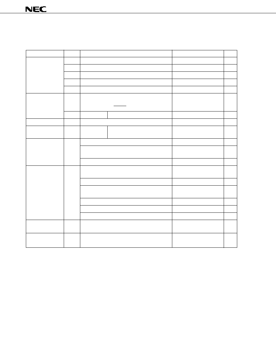
µ
PD78F0034B, 78F0034BY, 78F0034B(A), 78F0034BY(A)
46
Data Sheet U16369EJ1V0DS
9.2
µµ
µµ
µ
PD78F0034BY, 78F0034BY(A)
Absolute Maximum Ratings (T
A
= 25
∞
C)
Parameter
Symbol
Conditions
Ratings
Unit
Supply voltage
V
DD
≠0.3 to +6.5
V
V
PP
Note 2
≠0.3 to +10.5
V
AV
DD
≠0.3 to V
DD
+ 0.3
Note 1
V
AV
REF
≠0.3 to V
DD
+ 0.3
Note 1
V
AV
SS
≠0.3 to +0.3
V
Input voltage
V
I1
P00 to P03, P10 to P17, P20 to P25, P34 to P36,
≠0.3 to V
DD
+ 0.3
Note 1
V
P40 to P47, P50 to P57, P64 to P67, P70 to P75,
X1, X2, XT1, XT2,
RESET
V
I2
P30 to P33
N-ch open drain
≠0.3 to +6.5
V
Output voltage
V
O
≠0.3 to V
DD
+ 0.3
Note 1
V
Analog input voltage
V
AN
P10 to P17
Analog input pin
AV
SS
≠0.3 to AV
REF
+ 0.3
Note 1
V
and ≠0.3 to V
DD
+ 0.3
Note 1
Output current, high
I
OH
Per pin
≠10
mA
Total for P00 to P03, P40 to P47, P50 to P57,
≠15
mA
P64 to P67, P70 to P75
Total for P20 to P25, P30 to P36
≠15
mA
Output current, low
I
OL
Per pin for P00 to P03, P20 to P25, P34 to P36,
20
mA
P40 to P47, P64 to P67, P70 to P75
Per pin for P30 to P33, P50 to P57
30
mA
Total for P00 to P03, P40 to P47, P64 to P67,
50
mA
P70 to P75
Total for P20 to P25
20
mA
Total for P30 to P36
100
mA
Total for P50 to P57
100
mA
Operating ambient
T
A
During normal operation
≠40 to +85
∞
C
temperature
Storage
T
stg
≠40 to +125
∞
C
temperature
Notes 1.
6.5 V or below
(Note 2 is explained on the following page.)
Caution Product quality may suffer if the absolute maximum rating is exceeded even momentarily for any
parameter. That is, the absolute maximum ratings are rated values at which the product is on the
verge of suffering physical damage, and therefore the product must be used under conditions
that ensure that the absolute maximum ratings are not exceeded.
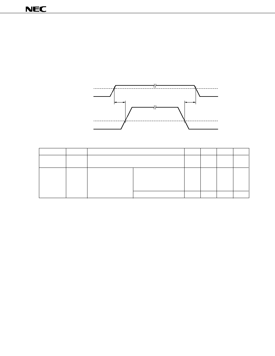
µ
PD78F0034B, 78F0034BY, 78F0034B(A), 78F0034BY(A)
47
Data Sheet U16369EJ1V0DS
Notes 2. Make sure that the following conditions of the V
PP
voltage application timing are satisfied when the flash
memory is written.
∑ When supply voltage rises
V
PP
must exceed V
DD
10
µ
s or more after V
DD
has reached the lower-limit value (1.8 V) of the
operating voltage range (see a in the figure below).
∑ When supply voltage drops
V
DD
must be lowered 10
µ
s or more after V
PP
falls below the lower-limit value (1.8 V) of the
operating voltage range of V
DD
(see b in the figure below).
Capacitance (T
A
= 25
∞
C, V
DD
= V
SS
= 0 V)
Parameter
Symbol
Conditions
MIN.
TYP.
MAX.
Unit
Input
C
IN
f = 1 MHz
15
pF
capacitance
Unmeasured pins returned to 0 V.
I/O
C
IO
f = 1 MHz
P00 to P03, P20 to P25,
15
pF
capacitance
Unmeasured pins
P34 to P36, P40 to P47,
returned to 0 V.
P50 to P57, P64 to P67,
P70 to P75,
P30 to P33
20
pF
Remark
Unless otherwise specified, the characteristics of alternate-function pins are the same as those of port
pins.
1.8 V
V
DD
0 V
0 V
V
PP
1.8 V
a
b
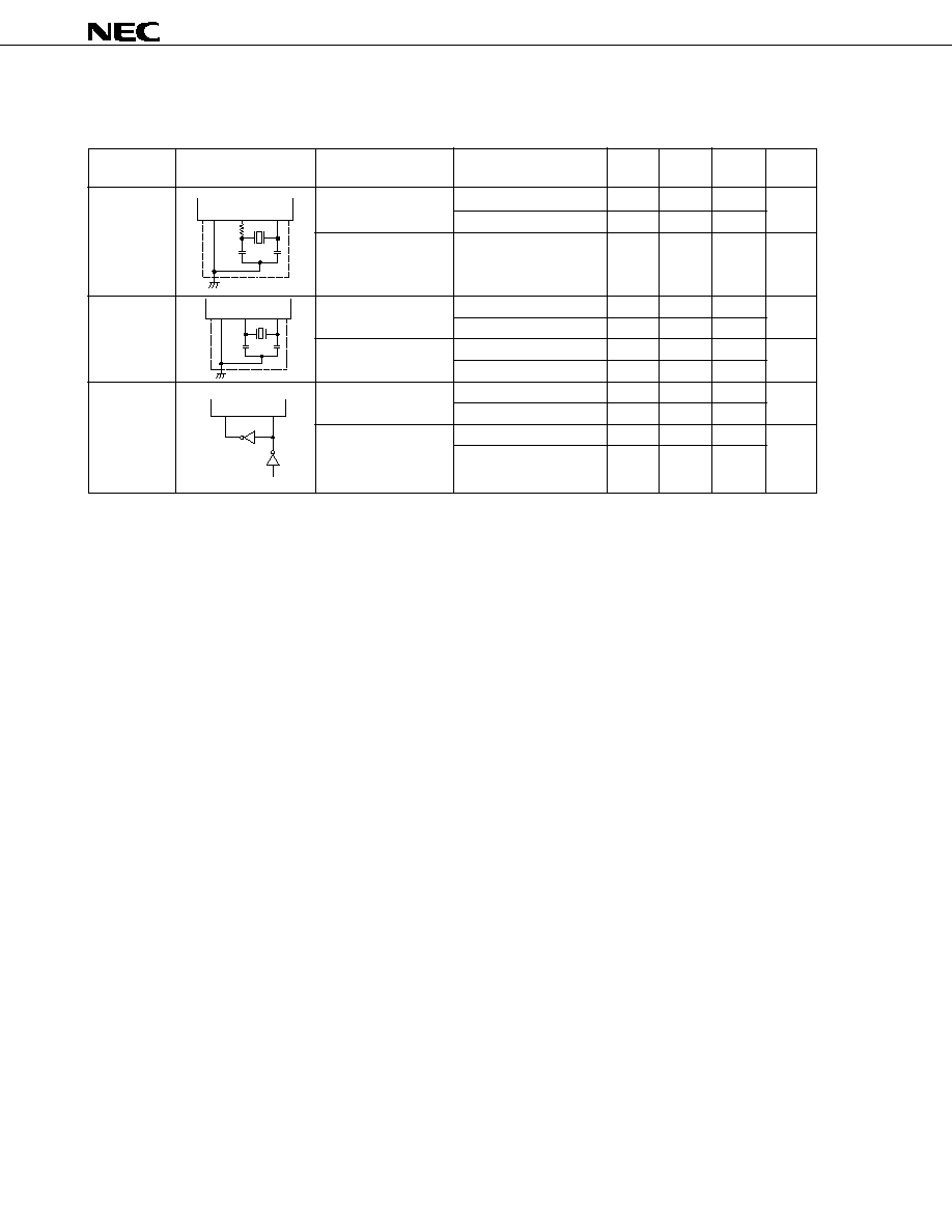
µ
PD78F0034B, 78F0034BY, 78F0034B(A), 78F0034BY(A)
48
Data Sheet U16369EJ1V0DS
Resonator
Recommended
Parameter
Conditions
MIN.
TYP.
MAX.
Unit
Circuit
Ceramic
Oscillation
4.0 V
V
DD
5.5 V
1.0
8.38
MHz
resonator
frequency (f
X
)
Note 1
1.8 V
V
DD
<
4.0 V
1.0
5.0
Oscillation
After V
DD
reaches
4
ms
stabilization time
Note 2
oscillation voltage range
MIN.
Crystal
Oscillation
4.0 V
V
DD
5.5 V
1.0
8.38
MHz
resonator
frequency (f
X
)
Note 1
1.8 V
V
DD
<
4.0 V
1.0
5.0
Oscillation
4.0 V
V
DD
5.5 V
10
ms
stabilization time
Note 2
1.8 V
V
DD
<
4.0 V
30
External
X1 input
4.0 V
V
DD
5.5 V
1.0
8.38
MHz
clock
frequency (f
X
)
Note 1
1.8 V
V
DD
<
4.0 V
1.0
5.0
X1 input
4.0 V
V
DD
5.5 V
50
500
ns
high-/low-level width
1.8 V
V
DD
<
4.0 V
85
500
(t
XH
, t
XL
)
Main System Clock Oscillator Characteristics (T
A
= ≠40 to +85
∞
C, V
DD
= 1.8 to 5.5 V)
Notes 1. Indicates only oscillator characteristics. Refer to AC Characteristics for instruction execution time.
2. Time required to stabilize oscillation after reset or STOP mode release.
Cautions
1. When using the main system clock oscillator, wire as follows in the area enclosed by the broken
lines in the above figures to avoid an adverse effect from wiring capacitance.
∑ Keep the wiring length as short as possible.
∑ Do not cross the wiring with the other signal lines.
∑ Do not route the wiring near a signal line through which a high fluctuating current flows.
∑ Always make the ground point of the oscillator capacitor the same potential as V
SS1
.
∑ Do not ground the capacitor to a ground pattern through which a high current flows.
∑ Do not fetch signals from the oscillator.
2. When the main system clock is stopped and the system is operating on the subsystem clock,
wait until the oscillation stabilization time has been secured by the program before switching
back to the main system clock.
Remark
For the resonator selection and oscillator constant, customers are required to either evaluate the
oscillation themselves or apply to the resonator manufacture for evaluation.
X2
X1
C2
C1
X1
X2
V
PP
C2
C1
X1
X2
V
PP
R1
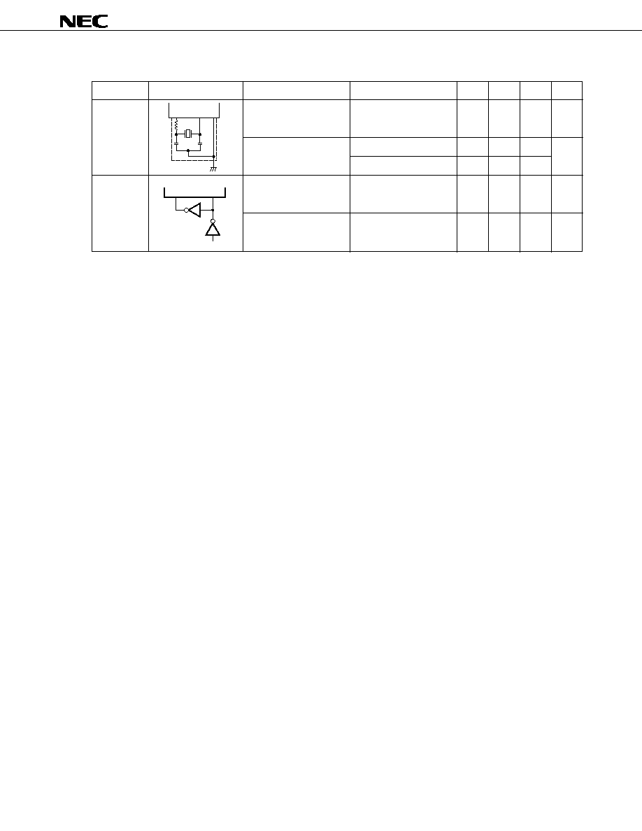
µ
PD78F0034B, 78F0034BY, 78F0034B(A), 78F0034BY(A)
49
Data Sheet U16369EJ1V0DS
Subsystem Clock Oscillator Characteristics (T
A
= ≠40 to +85
∞
C, V
DD
= 1.8 to 5.5 V)
Resonator
Recommended Circuit
Parameter
Conditions
MIN.
TYP.
MAX.
Unit
Crystal
Oscillation
32
32.768
35
kHz
resonator
frequency (f
XT
)
Note 1
Oscillation
4.0 V
V
DD
5.5 V
1.2
2
s
stabilization time
Note 2
1.8 V
V
DD
<
4.0 V
10
External
X1 input
32
38.5
kHz
clock
frequency (f
XT
)
Note 1
X1 input high-/low-level
12
15
µ
s
width (t
XTH
, t
XTL
)
Notes 1. Indicates only oscillator characteristics. Refer to AC Characteristics for instruction execution time.
2. Time required to stabilize oscillation after V
DD
reaches oscillator voltage MIN.
Cautions 1. When using the subsystem clock oscillator, wire as follows in the area enclosed by the
broken lines in the above figures to avoid an adverse effect from wiring capacitance.
∑ Keep the wiring length as short as possible.
∑ Do not cross the wiring with the other signal lines.
∑ Do not route the wiring near a signal line through which a high fluctuating current flows.
∑ Always make the ground point of the oscillator capacitor to the same potential as V
SS1
.
∑ Do not ground the capacitor to a ground pattern through which a high current flows.
∑ Do not fetch signals from the oscillator.
2. The subsystem clock oscillator is designed as a low-amplitude circuit for reducing power
consumption, and is more prone to malfunction due to noise than the main system clock
oscillator. Particular care is therefore required with the wiring method when the subsystem
clock is used.
Remark
For the resonator selection and oscillator constant, customers are required to either evaluate the
oscillation themselves or apply to the resonator manufacturer for evaluation.
C3
XT2
XT1V
PP
R2
C4
XT1
XT2
µ
PD78F0034B, 78F0034BY, 78F0034B(A), 78F0034BY(A)
50
Data Sheet U16369EJ1V0DS
DC Characteristics (T
A
= ≠40 to +85
∞
C, V
DD
= 1.8 to 5.5 V)
Parameter
Symbol
Conditions
MIN.
TYP.
MAX.
Unit
Output current,
I
OH
Per pin
≠1
mA
high
All pins
≠15
mA
Output current,
I
OL
Per pin for P00 to P03, P20 to P25, P34 to P36,
10
mA
low
P40 to P47, P64 to P67, P70 to P75
Per pin for P30 to P33, P50 to P57
15
mA
Total for P00 to P03, P40 to P47, P64 to P67, P70 to P75
20
mA
Total for P20 to P25
10
mA
Total for P30 to P36
70
mA
Total for P50 to P57
70
mA
Input voltage,
V
IH1
P10 to P17, P21, P24, P35,
2.7 V
V
DD
5.5 V
0.7V
DD
V
DD
V
high
P40 to P47, P50 to P57,
1.8 V
V
DD
<
2.7 V
0.8V
DD
V
DD
V
P64 to P67, P74, P75
V
IH2
P00 to P03, P20, P22, P23, P25,
2.7 V
V
DD
5.5 V
0.8V
DD
V
DD
V
P34, P36, P70 to P73, RESET
1.8 V
V
DD
<
2.7 V
0.85V
DD
V
DD
V
V
IH3
P30 to P33
2.7 V
V
DD
5.5 V
0.7V
DD
5.5
V
(N-ch open-drain)
1.8 V
V
DD
<
2.7 V
0.8V
DD
5.5
V
V
IH4
X1, X2
2.7 V
V
DD
5.5 V
V
DD
≠
0.5
V
DD
V
1.8 V
V
DD
<
2.7 V
V
DD
≠
0.2
V
DD
V
V
IH5
XT1, XT2
4.0 V
V
DD
5.5 V
0.8V
DD
V
DD
V
1.8 V
V
DD
<
4.0 V
0.9V
DD
V
DD
V
Input voltage,
V
IL1
P10 to P17, P21, P24, P35,
2.7 V
V
DD
5.5 V
0
0.3V
DD
V
low
P40 to P47, P50 to P57,
1.8 V
V
DD
<
2.7 V
0
0.2V
DD
V
P64 to P67, P74, P75
V
IL2
P00 to P03, P20, P22, P23, P25,
2.7 V
V
DD
5.5 V
0
0.2V
DD
V
P34, P36, P70 to P73, RESET
1.8 V
V
DD
<
2.7 V
0
0.15V
DD
V
V
IL3
P30 to P33
4.0 V
V
DD
5.5 V
0
0.3V
DD
V
2.7 V
V
DD
<
4.0 V
0
0.2V
DD
V
1.8 V
V
DD
<
2.7 V
0
0.1V
DD
V
V
IL4
X1, X2
2.7 V
V
DD
5.5 V
0
0.4
V
1.8 V
V
DD
<
2.7 V
0
0.2
V
V
IL5
XT1, XT2
4.0 V
V
DD
5.5 V
0
0.2V
DD
V
1.8 V
V
DD
<
4.0 V
0
0.1V
DD
V
Output voltage,
V
OH1
4.0 V
V
DD
5.5 V, I
OH
= ≠1 mA
V
DD
≠
1.0
V
DD
V
high
1.8 V
V
DD
<
4.0 V, I
OH
= ≠100
µ
A
V
DD
≠
0.5
V
DD
V
Output voltage,
V
OL1
P30 to P33
4.0 V
V
DD
5.5 V,
2.0
V
low
P50 to P57
I
OL
= 15 mA
0.4
2.0
V
P00 to P03, P20 to P25, P34 to P36, 4.0 V
V
DD
5.5 V,
0.4
V
P40 to P47, P64 to P67, P70 to P75
I
OL
= 1.6 mA
V
OL2
I
OL
= 400
µ
A
0.5
V
Remark
Unless otherwise specified, the characteristics of alternate-function pins are the same as those of port pins.
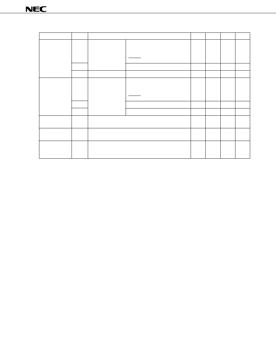
µ
PD78F0034B, 78F0034BY, 78F0034B(A), 78F0034BY(A)
51
Data Sheet U16369EJ1V0DS
DC Characteristics (T
A
= ≠40 to +85
∞
C, V
DD
= 1.8 to 5.5 V)
Parameter
Symbol
Conditions
MIN.
TYP.
MAX.
Unit
Input leakage
I
LIH1
V
IN
= V
DD
P00 to P03, P10 to P17, P20 to P25,
3
µ
A
current, high
P34 to P36, P40 to P47, P50 to P57,
P64 to P67, P70 to P75,
RESET
I
LIH2
X1, X2, XT1, XT2
20
µ
A
I
LIH3
V
IN
= 5.5 V
P30 to P33
3
µ
A
Input leakage
I
LIL1
V
IN
= 0 V
P00 to P03, P10 to P17, P20 to P25,
≠3
µ
A
current, low
P34 to P36, P40 to P47, P50 to P57,
P64 to P67, P70 to P75,
RESET
I
LIL2
X1, X2, XT1, XT2
≠20
µ
A
I
LIL3
P30 to P33
≠3
µ
A
Output leakage
I
LOH
V
OUT
= V
DD
3
µ
A
current, high
Output leakage
I
LOL
V
OUT
= 0 V
≠3
µ
A
current, low
Software pull-
R
V
IN
= 0 V,
15
30
90
k
up resistor
P00 to P03, P20 to P25, P34 to P36, P40 to P47,
P50 to P57, P64 to P67, P70 to P75
Remark
Unless otherwise specified, the characteristics of alternate-function pins are the same as those of port
pins.
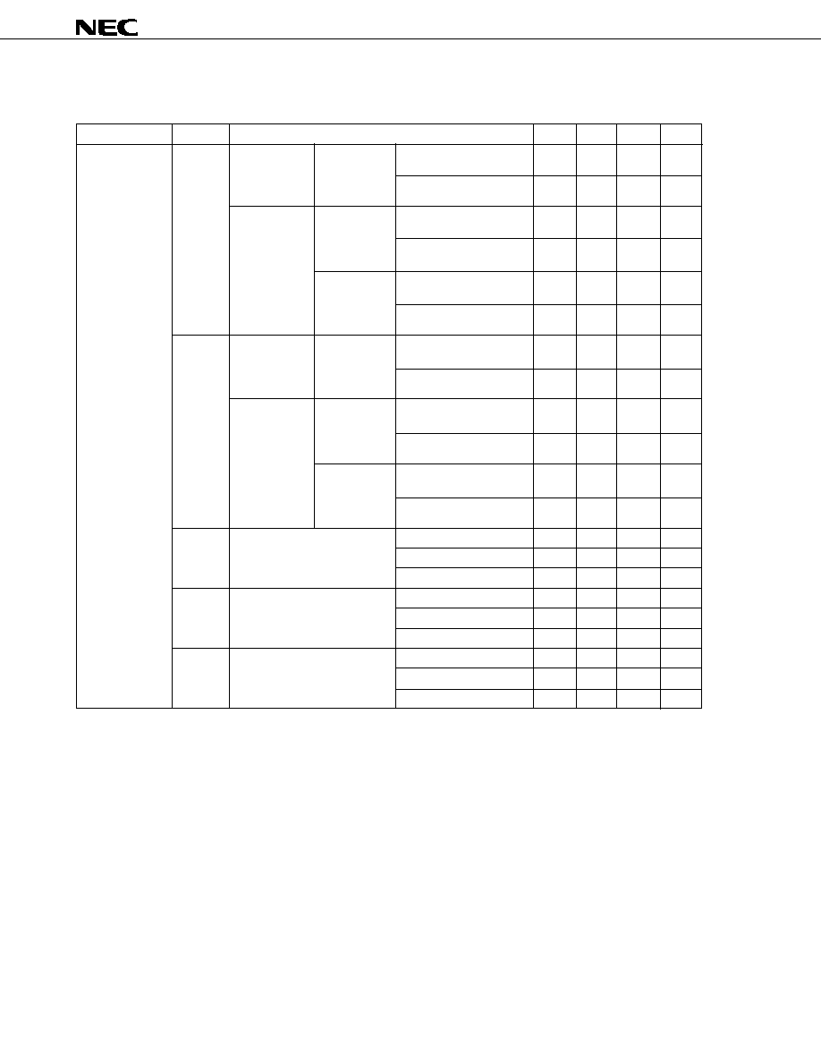
µ
PD78F0034B, 78F0034BY, 78F0034B(A), 78F0034BY(A)
52
Data Sheet U16369EJ1V0DS
DC Characteristics (T
A
= ≠40 to +85
∞
C, V
DD
= 1.8 to 5.5 V)
Parameter
Symbol
Conditions
MIN.
TYP.
MAX.
Unit
Power supply
I
DD1
Note 2
8.38 MHz
V
DD
= 5.0 V
±
10%
Note 3
When A/D converter is
10.5
21
mA
current
Note 1
crystal oscillation
stopped
operating mode
When A/D converter is
11.5
23
mA
operating
Note 6
5.00 MHz
V
DD
= 3.0 V
±
10%
Note 3
When A/D converter is
4.5
9
mA
crystal oscillation
stopped
operating mode
When A/D converter is
5.5
11
mA
operating
Note 6
V
DD
= 2.0 V
±
10%
Note 4
When A/D converter is
1
2
mA
stopped
When A/D converter is
2
6
mA
operating
Note 6
I
DD2
8.38 MHz
V
DD
= 5.0 V
±
10%
Note 3
When peripheral functions
1.2
2.4
mA
crystal oscillation
are stopped
HALT mode
When peripheral functions
5
mA
are operating
5.00 MHz
V
DD
= 3.0 V
±
10%
Note 3
When peripheral functions
0.4
0.8
mA
crystal oscillation
are stopped
HALT mode
When peripheral functions
1.7
mA
are operating
V
DD
= 2.0 V
±
10%
Note 4
When peripheral functions
0.2
0.4
mA
are stopped
When peripheral functions
1.1
mA
are operating
I
DD3
32.768 kHz crystal oscillation
V
DD
= 5.0 V
±
10%
Note 2
115
230
µ
A
operating mode
Note 5
V
DD
= 3.0 V
±
10%
Note 2
95
190
µ
A
V
DD
= 2.0 V
±
10%
Note 3
75
150
µ
A
I
DD4
32.768 kHz crystal oscillation
V
DD
= 5.0 V
±
10%
Note 2
30
60
µ
A
HALT mode
Note 5
V
DD
= 3.0 V
±
10%
Note 2
6
18
µ
A
V
DD
= 2.0 V
±
10%
Note 3
2
10
µ
A
I
DD5
XT1 = V
DD
STOP mode
V
DD
= 5.0 V
±
10%
Note 2
0.1
30
µ
A
When feedback resistor is not used
V
DD
= 3.0 V
±
10%
Note 2
0.05
10
µ
A
V
DD
= 2.0 V
±
10%
Note 3
0.05
10
µ
A
Notes 1. Total current through the internal power supply (V
DD0
, V
DD1
) (except the current through pull-up resistors
of ports).
2. I
DD1
includes the peripheral operation current.
3. When the processor clock control register (PCC) is set to 00H.
4. When PCC is set to 02H.
5. When main system clock operation is stopped.
6. Includes the current through the AV
DD
pin.
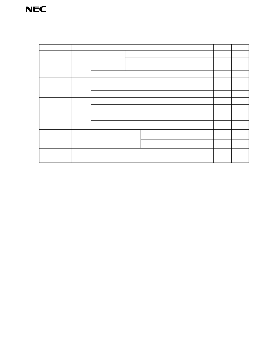
µ
PD78F0034B, 78F0034BY, 78F0034B(A), 78F0034BY(A)
53
Data Sheet U16369EJ1V0DS
AC Characteristics
(1) Basic Operation
(T
A
= ≠40 to +85
∞
C, V
DD
= 1.8 to 5.5 V)
4.0 V
V
DD
5.5 V
2.7 V
V
DD
<
4.0 V
Parameter
Symbol
Conditions
MIN.
TYP.
MAX.
Unit
Cycle time
T
CY
Operating with
0.238
16
µ
s
(Min. instruction
main system clock
0.4
16
µ
s
execution time)
1.6
16
µ
s
Operating with subsystem clock
103.9
Note 1
122
125
µ
s
TI00, TI01 input
t
TIH0
, t
TIL0
4.0 V
V
DD
5.5 V
2/f
sam
+0.1
Note 2
µ
s
high-/low-level
2.7 V
V
DD
<
4.0 V
2/f
sam
+0.2
Note 2
µ
s
width
1.8 V
V
DD
<
2.7 V
2/f
sam
+0.5
Note 2
µ
s
TI50, TI51 input
f
TI5
2.7 V
V
DD
5.5 V
0
4
MHz
frequency
1.8 V
V
DD
<
2.7 V
0
275
kHz
TI50, TI51 input
t
TIH5
, t
TIL5
2.7 V
V
DD
5.5 V
100
ns
high-/low-level
1.8 V
V
DD
<
2.7 V
1.8
ns
width
Interrupt request
t
INTH
, t
INTL
INTP0 to INTP3,
2.7 V
V
DD
5.5 V
1
µ
s
input high-/low-
P40 to P47
1.8 V
V
DD
<
2.7 V
2
µ
s
level width
RESET
t
RSL
2.7 V
V
DD
5.5 V
10
µ
s
low-level width
1.8 V
V
DD
<
2.7 V
20
µ
s
Notes 1. Value when the external clock is used. When a crystal resonator is used, it is 114
µ
s (MIN.).
2. Selection of f
sam
= f
X
, f
X
/4, f
X
/64 is possible using bits 0 and 1 (PRM00, PRM01) of prescaler mode register
0 (PRM0). However, if the TI00 valid edge is selected as the count clock, the value becomes f
sam
= f
X
/8.
1.8 V
V
DD
<
2.7 V

µ
PD78F0034B, 78F0034BY, 78F0034B(A), 78F0034BY(A)
54
Data Sheet U16369EJ1V0DS
T
CY
vs. V
DD
(main system clock operation)
5.0
1.0
2.0
1.6
0.4
0.238
0.1
0
10.0
1.0
2.0
3.0
4.0
5.0
6.0
1.8
5.5
2.7
Operation
guaranteed
range
16.0
Cycle time T
CY
[ S]
µ
Supply voltage V
DD
[V]

µ
PD78F0034B, 78F0034BY, 78F0034B(A), 78F0034BY(A)
55
Data Sheet U16369EJ1V0DS
(2) Read/write operation (T
A
= ≠40 to +85
∞
C, V
DD
= 4.0 to 5.5 V)
(1/3)
Parameter
Symbol
Conditions
MIN.
MAX.
Unit
ASTB high-level width
t
ASTH
0.3t
CY
ns
Address setup time
t
ADS
20
ns
Address hold time
t
ADH
6
ns
Input time from address to data
t
ADD1
(2 + 2n)t
CY
≠ 54
ns
t
ADD2
(3 + 2n)t
CY
≠ 60
ns
Output time from RD
to address
t
RDAD
0
100
ns
Input time from RD
to data
t
RDD1
(2 + 2n)t
CY
≠ 87
ns
t
RDD2
(3 + 2n)t
CY
≠ 93
ns
Read data hold time
t
RDH
0
ns
RD low-level width
t
RDL1
(1.5 + 2n)t
CY
≠ 33
ns
t
RDL2
(2.5 + 2n)t
CY
≠ 33
ns
Input time from RD
to WAIT
t
RDWT1
t
CY
≠ 43
ns
t
RDWT2
t
CY
≠ 43
ns
Input time from WR
to WAIT
t
WRWT
t
CY
≠ 25
ns
WAIT low-level width
t
WTL
(0.5 + n)t
CY
+ 10
(2 + 2n)t
CY
ns
Write data setup time
t
WDS
60
ns
Write data hold time
t
WDH
6
ns
WR low-level width
t
WRL1
(1.5 + 2n)t
CY
≠ 15
ns
Delay time from ASTB
to RD
t
ASTRD
6
ns
Delay time from ASTB
to WR
t
ASTWR
2t
CY
≠ 15
ns
Delay time from RD
to ASTB
in
t
RDAST
0.8t
CY
≠ 15
1.2t
CY
ns
external fetch
Hold time from RD
to address in
t
RDADH
0.8t
CY
≠ 15
1.2t
CY
+ 30
ns
external fetch
Write data output time from RD
t
RDWD
40
ns
Write data output time from WR
t
WRWD
10
60
ns
Hold time from WR
to address
t
WRADH
0.8t
CY
≠ 15
1.2t
CY
+ 30
ns
Delay time from WAIT
to RD
t
WTRD
0.8t
CY
2.5t
CY
+ 25
ns
Delay time from WAIT
to WR
t
WTWR
0.8t
CY
2.5t
CY
+ 25
ns
Caution T
CY
can only be used when the MIN. value is 0.238
µµ
µµ
µ
s.
Remarks 1. t
CY
= T
CY
/4
2. n indicates the number of waits.
3. C
L
= 100 pF (C
L
is the load capacitance of the AD0 to AD7, A8 to A15, RD, WR, WAIT, and ASTB
pins.)
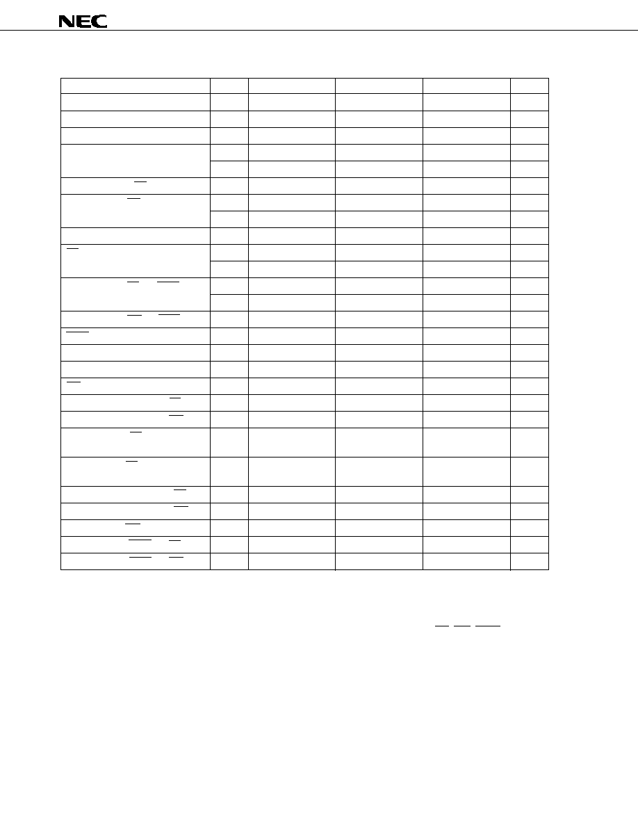
µ
PD78F0034B, 78F0034BY, 78F0034B(A), 78F0034BY(A)
56
Data Sheet U16369EJ1V0DS
(2) Read/write operation (T
A
= ≠40 to +85
∞
C, V
DD
= 2.7 to 4.0 V)
(2/3)
Parameter
Symbol
Conditions
MIN.
MAX.
Unit
ASTB high-level width
t
ASTH
0.3t
CY
ns
Address setup time
t
ADS
30
ns
Address hold time
t
ADH
10
ns
Input time from address to data
t
ADD1
(2 + 2n)t
CY
≠ 108
ns
t
ADD2
(3 + 2n)t
CY
≠ 120
ns
Output time from RD
to address
t
RDAD
0
200
ns
Input time from RD
to data
t
RDD1
(2 + 2n)t
CY
≠ 148
ns
t
RDD2
(3 + 2n)t
CY
≠ 162
ns
Read data hold time
t
RDH
0
ns
RD low-level width
t
RDL1
(1.5 + 2n)t
CY
≠ 40
ns
t
RDL2
(2.5 + 2n)t
CY
≠ 40
ns
Input time from RD
to WAIT
t
RDWT1
t
CY
≠ 75
ns
t
RDWT2
t
CY
≠ 60
ns
Input time from WR
to WAIT
t
WRWT
t
CY
≠ 50
ns
WAIT low-level width
t
WTL
(0.5 + 2n)t
CY
+ 10
(2 + 2n)t
CY
ns
Write data setup time
t
WDS
60
ns
Write data hold time
t
WDH
10
ns
WR low-level width
t
WRL1
(1.5 + 2n)t
CY
≠ 30
ns
Delay time from ASTB
to RD
t
ASTRD
10
ns
Delay time from ASTB
to WR
t
ASTWR
2t
CY
≠ 30
ns
Delay time from RD
to ASTB
in
t
RDAST
0.8t
CY
≠ 30
1.2t
CY
ns
external fetch
Hold time from RD
to address in
t
RDADH
0.8t
CY
≠ 30
1.2t
CY
+ 60
ns
external fetch
Write data output time from RD
t
RDWD
40
ns
Write data output time from WR
t
WRWD
20
120
ns
Hold time from WR
to address
t
WRADH
0.8t
CY
≠ 30
1.2t
CY
+ 60
ns
Delay time from WAIT
to RD
t
WTRD
0.5t
CY
2.5t
CY
+ 50
ns
Delay time from WAIT
to WR
t
WTWR
0.5t
CY
2.5t
CY
+ 50
ns
Caution T
CY
can only be used when the MIN. value is 0.4
µµ
µµ
µ
s.
Remarks 1. t
CY
= T
CY
/4
2. n indicates the number of waits.
3. C
L
= 100 pF (C
L
is the load capacitance of the AD0 to AD7, A8 to A15, RD, WR, WAIT, and ASTB
pins.)

µ
PD78F0034B, 78F0034BY, 78F0034B(A), 78F0034BY(A)
57
Data Sheet U16369EJ1V0DS
(2) Read/write operation (T
A
= ≠40 to +85
∞
C, V
DD
= 1.8 to 2.7 V)
(3/3)
Parameter
Symbol
Conditions
MIN.
MAX.
Unit
ASTB high-level width
t
ASTH
0.3t
CY
ns
Address setup time
t
ADS
120
ns
Address hold time
t
ADH
20
ns
Input time from address to data
t
ADD1
(2 + 2n)t
CY
≠ 233
ns
t
ADD2
(3 + 2n)t
CY
≠ 240
ns
Output time from RD
to address
t
RDAD
0
400
ns
Input time from RD
to data
t
RDD1
(2 + 2n)t
CY
≠ 325
ns
t
RDD2
(3 + 2n)t
CY
≠ 332
ns
Read data hold time
t
RDH
0
ns
RD low-level width
t
RDL1
(1.5 + 2n)t
CY
≠ 92
ns
t
RDL2
(2.5 + 2n)t
CY
≠ 92
ns
Input time from RD
to WAIT
t
RDWT1
t
CY
≠ 350
ns
t
RDWT2
t
CY
≠ 132
ns
Input time from WR
to WAIT
t
WRWT
t
CY
≠ 100
ns
WAIT low-level width
t
WTL
(0.5 + 2n)t
CY
+ 10
(2 + 2n)t
CY
ns
Write data setup time
t
WDS
60
ns
Write data hold time
t
WDH
20
ns
WR low-level width
t
WRL1
(1.5 + 2n)t
CY
≠ 60
ns
Delay time from ASTB
to RD
t
ASTRD
20
ns
Delay time from ASTB
to WR
t
ASTWR
2t
CY
≠ 60
ns
Delay time from RD
to ASTB
in
t
RDAST
0.8t
CY
≠ 60
1.2t
CY
ns
external fetch
Hold time from RD
to address in
t
RDADH
0.8t
CY
≠ 60
1.2t
CY
+ 120
ns
external fetch
Write data output time from RD
t
RDWD
40
ns
Write data output time from WR
t
WRWD
40
240
ns
Hold time from WR
to address
t
WRADH
0.8t
CY
≠ 60
1.2t
CY
+ 120
ns
Delay time from WAIT
to RD
t
WTRD
0.5t
CY
2.5t
CY
+ 100
ns
Delay time from WAIT
to WR
t
WTWR
0.5t
CY
2.5t
CY
+ 100
ns
Caution T
CY
can only be used when the MIN. value is 1.6
µµ
µµ
µ
s.
Remarks 1. t
CY
= T
CY
/4
2. n indicates the number of waits.
3. C
L
= 100 pF (C
L
is the load capacitance of the AD0 to AD7, A8 to A15, RD, WR, WAIT, and ASTB
pins.)
µ
PD78F0034B, 78F0034BY, 78F0034B(A), 78F0034BY(A)
58
Data Sheet U16369EJ1V0DS
(3) Serial Interface (T
A
= ≠40 to +85
∞
C, V
DD
= 1.8 to 5.5 V)
(a) 3-wire serial I/O mode (SCK30... Internal clock output)
Parameter
Symbol
Conditions
MIN.
TYP.
MAX.
Unit
SCK30
t
KCY1
4.0 V
V
DD
5.5 V
954
ns
cycle time
2.7 V
V
DD
<
4.0 V
1600
ns
1.8 V
V
DD
<
2.7 V
3200
ns
SCK30 high-/
t
KH1
, t
KL1
4.0 V
V
DD
5.5 V
t
KCY1
/2 ≠ 50
ns
low-level width
1.8 V
V
DD
<
4.0 V
t
KCY1
/2 ≠ 100
ns
SI30 setup time
t
SIK1
4.0 V
V
DD
5.5 V
100
ns
(to SCK30
)
2.7 V
V
DD
< 4.0 V
150
ns
1.8 V
V
DD
<
2.7 V
300
ns
SI3n hold time
t
KSI1
400
ns
(from SCK30
)
Delay time from
t
KSO1
C = 100 pF
Note
300
ns
SCK30
to SO30
output
Note C is the load capacitance of the SCK30 and SO30 output lines.
(b) 3-wire serial I/O mode (SCK30... External clock input)
Parameter
Symbol
Conditions
MIN.
TYP.
MAX.
Unit
SCK30
4.0 V
V
DD
5.5 V
800
ns
cycle time
2.7 V
V
DD
< 4.0 V
1600
ns
1.8 V
V
DD
<
2.7 V
3200
ns
SCK30 high-/
t
KH2
, t
KL2
4.0 V
V
DD
5.5 V
400
ns
low-level width
2.7 V
V
DD
< 4.0 V
800
ns
1.8 V
V
DD
<
2.7 V
1600
ns
SI30 setup time
t
SIK2
100
ns
(to SCK30
)
SI30 hold time
t
KSI2
400
ns
(from SCK30
)
Delay time from
t
KSO2
C = 100 pF
Note
300
ns
SCK30
to SO30
output
Note C is the load capacitance of the SO30 output line.
t
KCY2

µ
PD78F0034B, 78F0034BY, 78F0034B(A), 78F0034BY(A)
59
Data Sheet U16369EJ1V0DS
(c) UART mode (dedicated baud-rate generator output)
Parameter
Symbol
Conditions
MIN.
TYP.
MAX.
Unit
Transfer rate
4.0 V
V
DD
5.5 V
131031
bps
2.7 V
V
DD
< 4.0 V
78125
bps
1.8 V
V
DD
< 2.7 V
39063
bps
(d) UART mode (external clock input)
Parameter
Symbol
Conditions
MIN.
TYP.
MAX.
Unit
ASCK0 cycle time
t
KCY3
4.0 V
V
DD
5.5 V
800
ns
2.7 V
V
DD
< 4.0 V
1600
ns
1.8 V
V
DD
< 2.7 V
3200
ns
ASCK0 high-/low-level width
t
KH3
,
4.0 V
V
DD
5.5 V
400
ns
t
KL3
2.7 V
V
DD
< 4.0 V
800
ns
1.8 V
V
DD
< 2.7 V
1600
ns
Transfer rate
4.0 V
V
DD
5.5 V
39063
bps
2.7 V
V
DD
< 4.0 V
19531
bps
1.8 V
V
DD
< 2.7 V
9766
bps
(e) UART mode (infrared data transfer mode)
Parameter
Symbol
Conditions
MIN.
MAX.
Unit
Transfer rate
4.0 V
V
DD
5.5 V
131031
bps
Allowable bit rate error
4.0 V
V
DD
5.5 V
±
0.87
%
Output pulse width
4.0 V
V
DD
5.5 V
1.2
0.24/fbr
Note
µ
s
Input pulse width
4.0 V
V
DD
5.5 V
4/f
X
µ
s
Note
fbr: Specified baud rate
µ
PD78F0034B, 78F0034BY, 78F0034B(A), 78F0034BY(A)
60
Data Sheet U16369EJ1V0DS
(f)
I
2
C bus mode
Parameter
Symbol
Standard Mode
High-Speed Mode
Unit
MIN.
MAX.
MIN.
MAX.
SCL0 clock frequency
f
CLK
0
100
0
400
kHz
Bus free time
t
BUF
4.7
≠
1.3
≠
µ
s
(between stop and start condition)
Hold time
Note 1
t
HD:STA
4.0
≠
0.6
≠
µ
s
SCL0 clock low-level width
t
LOW
4.7
≠
1.3
≠
µ
s
SCL0 clock high-level width
t
HIGH
4.0
≠
0.6
≠
µ
s
Start/restart condition setup time
t
SU:STA
4.7
≠
0.6
≠
µ
s
Data hold time
CBUS compatible master
t
HD:DAT
5.0
≠
≠
≠
µ
s
I
2
C bus
0
Note 2
≠
0
Note 2
0.9
Note 3
µ
s
Data setup time
t
SU:DAT
250
≠
100
Note 4
≠
ns
SDA0 and SCL0 signal rise time
t
R
≠
1,000
20 + 0.1Cb
Note 5
300
ns
SDA0 and SCL0 signal fall time
t
F
≠
300
20 + 0.1Cb
Note 5
300
ns
Stop condition setup time
t
SU:STO
4.0
≠
0.6
≠
µ
s
Spike pulse width controlled by input filter
t
SP
≠
≠
0
50
ns
Capacitive load per each bus line
Cb
≠
400
≠
400
pF
Notes 1. In the start condition, the first clock pulse is generated after this hold time.
2. To fill in the undefined area of the SCL0 falling edge, it is necessary for the device to internally provide
at least 300 ns of hold time for the SDA0 signal (which is V
IHmin.
of the SCL0 signal).
3. If the device does not extend the SCL0 signal low hold time (t
LOW
), only maximum data hold time t
HD:DAT
needs to be fulfilled.
4. The high-speed mode I
2
C bus is available in a standard mode I
2
C bus system. At this time, the
conditions described below must be satisfied.
∑ If the device does not extend the SCL0 signal low state hold time
t
SU:DAT
250 ns
∑ If the device extends the SCL0 signal low state hold time
Be sure to transmit the next data bit to the SDA0 line before the SCL0 line is released (t
Rmax.
+ t
SU:DAT
= 1,000 + 250 = 1,250 ns by standard mode I
2
C bus specification).
5. Cb: Total capacitance per one bus line (unit: pF)

µ
PD78F0034B, 78F0034BY, 78F0034B(A), 78F0034BY(A)
61
Data Sheet U16369EJ1V0DS
A/D Converter Characteristics (T
A
= ≠40 to +85
∞
C, V
DD
= AV
DD
= 1.8 to 5.5 V, AV
SS
= V
SS
= 0 V)
Parameter
Symbol
Conditions
MIN.
TYP.
MAX.
Unit
Resolution
10
10
10
bit
Overall error
Note
4.0 V
AV
REF
5.5 V
±
0.2
±
0.4
%FSR
2.7 V
AV
REF
< 4.0 V
±
0.3
±
0.6
%FSR
1.8 V
AV
REF
< 2.7 V
±
0.6
±
1.2
%FSR
Conversion time
t
CONV
4.5 V
AV
DD
5.5 V
12
96
µ
s
4.0 V
AV
DD
< 4.5 V
14
96
µ
s
2.7 V
AV
DD
< 4.0 V
17
96
µ
s
1.8 V
AV
DD
< 2.7 V
28
96
µ
s
Zero-scale error
Notes 1, 2
4.0 V
AV
REF
5.5 V
±
0.4
%FSR
2.7 V
AV
REF
< 4.0 V
±
0.6
%FSR
1.8 V
AV
REF
< 2.7 V
±
1.2
%FSR
Full-scale error
Notes 1, 2
4.0 V
AV
REF
5.5 V
±
0.4
%FSR
2.7 V
AV
REF
< 4.0 V
±
0.6
%FSR
1.8 V
AV
REF
< 2.7 V
±
1.2
%FSR
Integral linearity error
Note 1
4.0 V
AV
REF
5.5 V
±
2.5
LSB
2.7 V
AV
REF
< 4.0 V
±
4.5
LSB
1.8 V
AV
REF
< 2.7 V
±
8.5
LSB
Differential linearity error
4.0 V
AV
REF
5.5 V
±
1.5
LSB
2.7 V
AV
REF
4.0 V
±
2.0
LSB
1.8 V
AV
REF
< 2.7 V
±
3.5
LSB
Analog input voltage
V
IAN
0
AV
REF
V
Reference voltage
AV
REF
1.8
AV
DD
V
Resistance between AV
REF
and AV
SS
R
REF
During A/D conversion operation
20
40
k
Notes 1. Excluding quantization error (
±
1/2 LSB).
2. Indicated as a ratio to the full-scale value (%FSR).
Remark
When the
µ
PD78F0034BY is used as an 8-bit resolution A/D converter, the specifications are the same
as for the
µ
PD780024AY Subseries A/D converter.
µ
PD78F0034B, 78F0034BY, 78F0034B(A), 78F0034BY(A)
62
Data Sheet U16369EJ1V0DS
Data Memory STOP Mode Low Supply Voltage Data Retention Characteristics (T
A
= ≠40 to +85
∞
C)
Parameter
Symbol
Conditions
MIN.
TYP.
MAX.
Unit
Data retention supply voltage
V
DDDR
1.6
5.5
V
Data retention supply current
I
DDDR
Subsystem clock stop (XT1 = V
DD
)
0.1
30
µ
A
and feed-back resistor disconnected
Release signal set time
t
SREL
0
µ
s
Oscillation stabilization wait time
t
WAIT
Release by RESET
2
17
/f
X
s
Release by interrupt request
Note
s
Note
Selection of 2
12
/f
X
and 2
14
/f
X
to 2
17
/f
X
is possible using bits 0 to 2 (OSTS0 to OSTS2) of the oscillation
stabilization time select register (OSTS).
Remark The impedance of the analog input pins is shown below.
[Equivalent circuit]
[Parameter value]
(TYP.)
AV
DD
R1
R2
C1
C2
C3
2.7 V
12 k
8.0 k
3.0 pF
3.0 pF
2.0 pF
4.5 V
4 k
2.7 k
3.0 pF
1.4 pF
2.0 pF
C3
C2
R2
R1
C1
ANIn
(n = 0 to 3)

µ
PD78F0034B, 78F0034BY, 78F0034B(A), 78F0034BY(A)
63
Data Sheet U16369EJ1V0DS
Flash Memory Programming Characteristics (T
A
= +10 to +40
∞
C, V
DD
= 1.8 to 5.5 V, V
SS
= AV
SS
= 0 V)
(1) Write erase characteristics
Parameter
Symbol
Conditions
MIN.
TYP.
MAX.
Unit
Operating frequency
f
X
4.5 V
V
DD
5.5 V
1.0
10.0
MHz
3.0 V
V
DD
< 4.5 V
1.0
8.38
MHz
1.8 V
V
DD
< 3.0 V
1.0
1.25
MHz
V
PP
supply voltage
V
PP2
During flash memory programming
9.7
10.0
10.3
V
V
DD
supply current
I
DD
When
10 MHz crystal
V
DD
= 5.0 V
±
10%
30
mA
V
PP
= V
PP2
oscillation
operating mode
8.38 MHz crystal V
DD
= 5.0 V
±
10%
24
mA
oscillation
V
DD
= 3.0 V
±
10%
17
mA
operating mode
V
PP
supply current
I
PP
When V
PP
= V
PP2
100
mA
Step erase time
Note 1
T
er
0.199
0.2
0.201
s
Overall erase time
Note 2
T
era
When step erase time = 0.2 s
20
s/chip
Writeback time
Note 3
T
wb
49.4
50
50.6
ms
Number of writebacks per
C
wb
When writeback time = 50 ms
60
Times
writeback command
Note 4
Number of erases/writebacks
C
erwb
16
Times
Step write time
Note 5
T
wr
48
50
52
µ
s
Overall write time per word
Note 6
T
wrw
When step write time = 50
µ
s (1 word = 1 byte)
48
520
µ
s
Number of rewrites per chip
Note 7
C
erwb
1 erase + 1 write after erase = 1 rewrite
20
Times
Notes 1. The recommended setting value of the step erase time is 0.2 s.
2. The prewrite time before erasure and the erase verify time (writeback time) are not included.
3. The recommended setting value of the writeback time is 50 ms.
4. Writeback is executed once by the issuance of the writeback command. Therefore, the number of retries
must be the maximum value minus the number of commands issued.
5. The recommended setting value of the step write time is 50
µ
s.
6. The actual write time per word is 100
µ
s longer. The internal verify time during or after a write is not
included.
7. When a product is first written after shipment, "erase
write" and "write only" are both taken as one
rewrite.
Example:
P: Write, E: Erase
Shipped product
P
E
P
E
P: 3 rewrites
Shipped product
E
P
E
P
E
P: 3 rewrites
(2) Serial write operation characteristics
Parameter
Symbol
Conditions
MIN.
TYP.
MAX.
Unit
V
PP
set time
t
PSRON
V
PP
high voltage
1.0
µ
s
Set time from V
DD
to V
PP
t
DRPSR
V
PP
high voltage
10
µ
s
Set time from V
PP
to RESET
t
PSRRF
V
PP
high voltage
1.0
µ
s
V
PP
count start time from RESET
t
RFCF
1.0
µ
s
Count execution time
t
COUNT
2.0
ms
V
PP
counter high-level width
t
CH
8.0
µ
s
V
PP
counter low-level width
t
CL
8.0
µ
s
V
PP
counter noise elimination width
t
NFW
40
ns
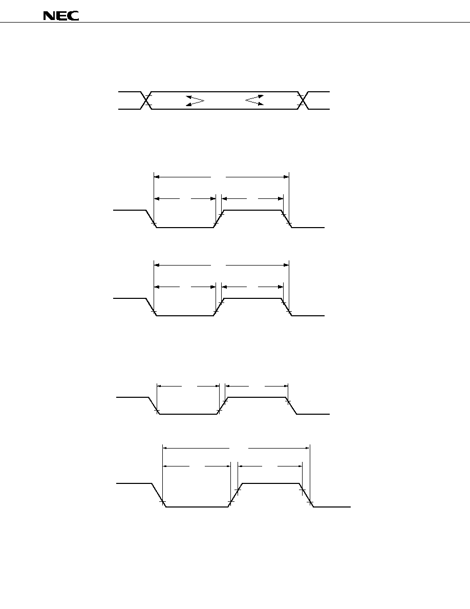
µ
PD78F0034B, 78F0034BY, 78F0034B(A), 78F0034BY(A)
64
Data Sheet U16369EJ1V0DS
AC Timing Test Point (Excluding X1, XT1 Input)
Clock Timing
t
XL
t
XH
1/f
X
V
IH4
(MIN.)
V
IL4
(MAX.)
t
XTL
t
XTH
1/f
XT
V
IH5
(MIN.)
V
IL5
(MAX.)
X1 input
XT1 input
TI Timing
9.3 Timing Chart
0.8V
DD
0.2V
DD
0.8V
DD
0.2V
DD
Point of test
t
TIL0
t
TIH0
TI00, TI01
1/f
TI5
t
TIH5
t
TIL5
TI50, TI51

µ
PD78F0034B, 78F0034BY, 78F0034B(A), 78F0034BY(A)
65
Data Sheet U16369EJ1V0DS
Interrupt Request Input Timing
RESET Input Timing
t
RSL
RESET
INTP0 to INTP3
t
INTL
t
INTH
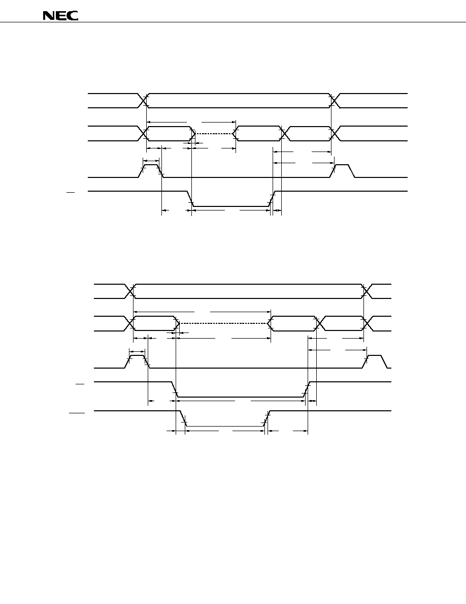
µ
PD78F0034B, 78F0034BY, 78F0034B(A), 78F0034BY(A)
66
Data Sheet U16369EJ1V0DS
Read/Write Operation
External fetch (no wait):
External fetch (wait insertion):
A8 to A15
AD0 to AD7
ASTB
RD
Higher 8-bit address
Lower 8-bit
address
t
ADD1
Hi-Z
t
ADS
t
ASTH
t
ADH
t
RDD1
t
RDAD
Instruction code
t
RDADH
t
RDAST
t
ASTRD
t
RDL1
t
RDH
A8 to A15
AD0 to AD7
ASTB
RD
Higher 8-bit address
Lower 8-bit
address
t
ADD1
Hi-Z
t
ADS
t
ASTH
t
ADH
t
RDAD
t
RDD1
Instruction code
t
RDADH
t
RDAST
t
ASTRD
t
RDL1
t
RDH
WAIT
t
RDWT1
t
WTL
t
WTRD
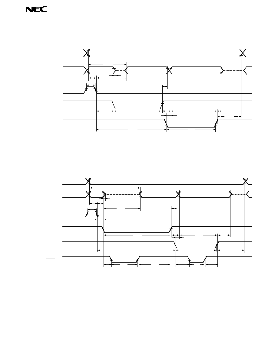
µ
PD78F0034B, 78F0034BY, 78F0034B(A), 78F0034BY(A)
67
Data Sheet U16369EJ1V0DS
External data access (no wait):
External data access (wait insertion):
A8 to A15
AD0 to AD7
ASTB
RD
Higher 8-bit address
Lower 8-bit
address
t
ADD2
Hi-Z
t
ADS
t
ASTH
t
ADH
t
RDD2
t
RDAD
Read data
t
ASTRD
t
RDWD
WR
t
ASTWR
Write data
Hi-Z
t
WDH
t
WRADH
t
WDS
t
WRWD
t
WRL1
t
RDH
t
RDL2
A8 to A15
AD0 to AD7
ASTB
RD
Higher 8-bit address
Lower 8-bit
address
t
ADD2
t
ADS
t
ASTH
t
ADH
t
RDAD
t
RDD2
Read data
t
ASTRD
WR
t
ASTWR
Write data
Hi-Z
t
WDH
t
WRADH
t
WDS
t
WRWD
t
WRL1
t
RDH
t
RDL2
t
RDWT2
t
WTL
t
WRWT
t
WTL
t
WTWR
t
WTRD
WAIT
t
RDWD
Hi-Z
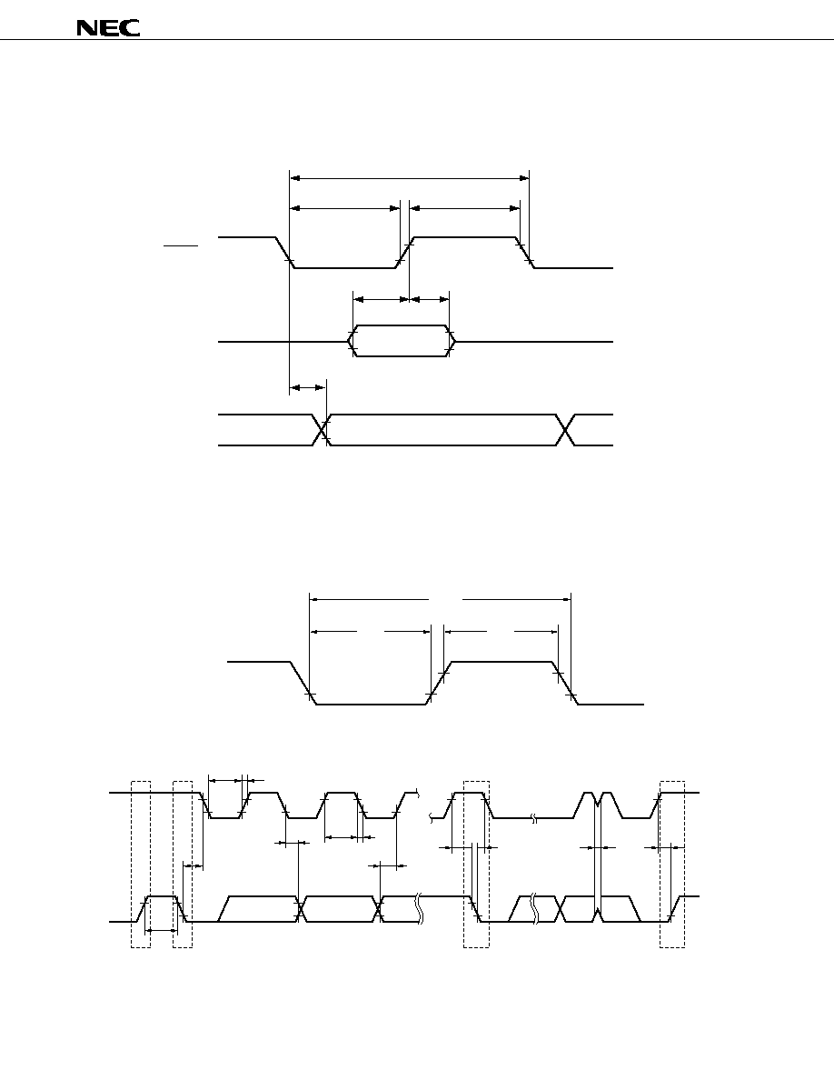
µ
PD78F0034B, 78F0034BY, 78F0034B(A), 78F0034BY(A)
68
Data Sheet U16369EJ1V0DS
Serial Transfer Timing
3-wire serial I/O mode:
t
KCY3
t
KH3
t
KL3
ASCK0
I
2
C bus mode (
µµ
µµ
µ
PD78F0034BY only):
t
KCYm
t
KLm
t
KHm
SCK3n
SI3n
SO3n
t
SIKm
t
KSIm
t
KSOm
Input data
Output data
t
R
t
LOW
t
F
t
HIGH
t
HD:STA
Stop
condition
Start
condition
Restart
condition
Stop
condition
t
BUF
t
SU:DAT
t
SU:STA
t
HD:STA
t
SP
t
SU:STO
t
HD:DAT
SCL0
SDA0
Remarks 1. m = 1, 2
2.
µ
PD78F0034B and 78F0034B(A):
n = 0, 1
3.
µ
PD78F0034BY and 78F0034BY(A): n = 0
UART mode (external clock input):
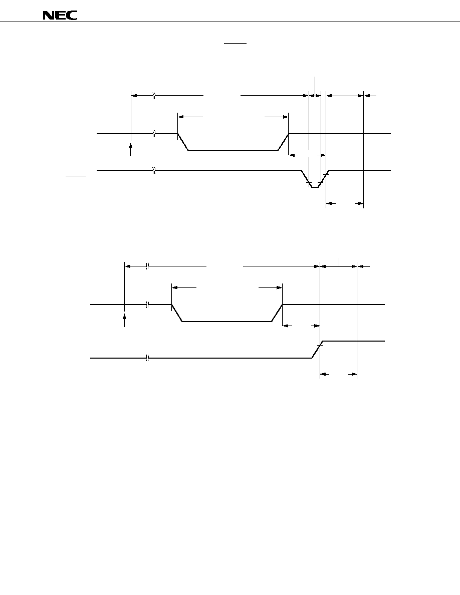
µ
PD78F0034B, 78F0034BY, 78F0034B(A), 78F0034BY(A)
69
Data Sheet U16369EJ1V0DS
Data Retention Timing (STOP Mode Release by RESET)
Data Retention Timing (Standby Release Signal: STOP Mode Release by Interrupt Request Signal)
t
SREL
t
WAIT
V
DD
RESET
STOP instruction execution
STOP mode
Data retention mode
Internal reset operation
HALT mode
Operating mode
V
DDDR
t
SREL
t
WAIT
V
DD
STOP instruction execution
STOP mode
Data retention mode
HALT mode
Operating mode
Standby release signal
(Interrupt request)
V
DDDR
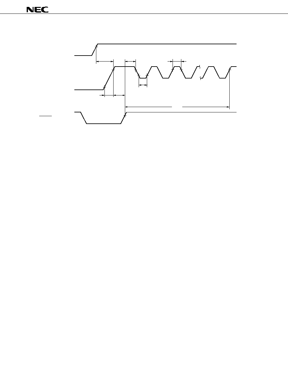
µ
PD78F0034B, 78F0034BY, 78F0034B(A), 78F0034BY(A)
70
Data Sheet U16369EJ1V0DS
Flash Memory Write Mode Set Timing
V
DD
V
DD
0 V
0 V
V
DD
RESET (input)
0 V
V
PPH
V
PP
V
PPL
t
RFCF
t
PSRON
t
PSRRF
t
DRPSR
t
CH
t
CL
t
COUNT
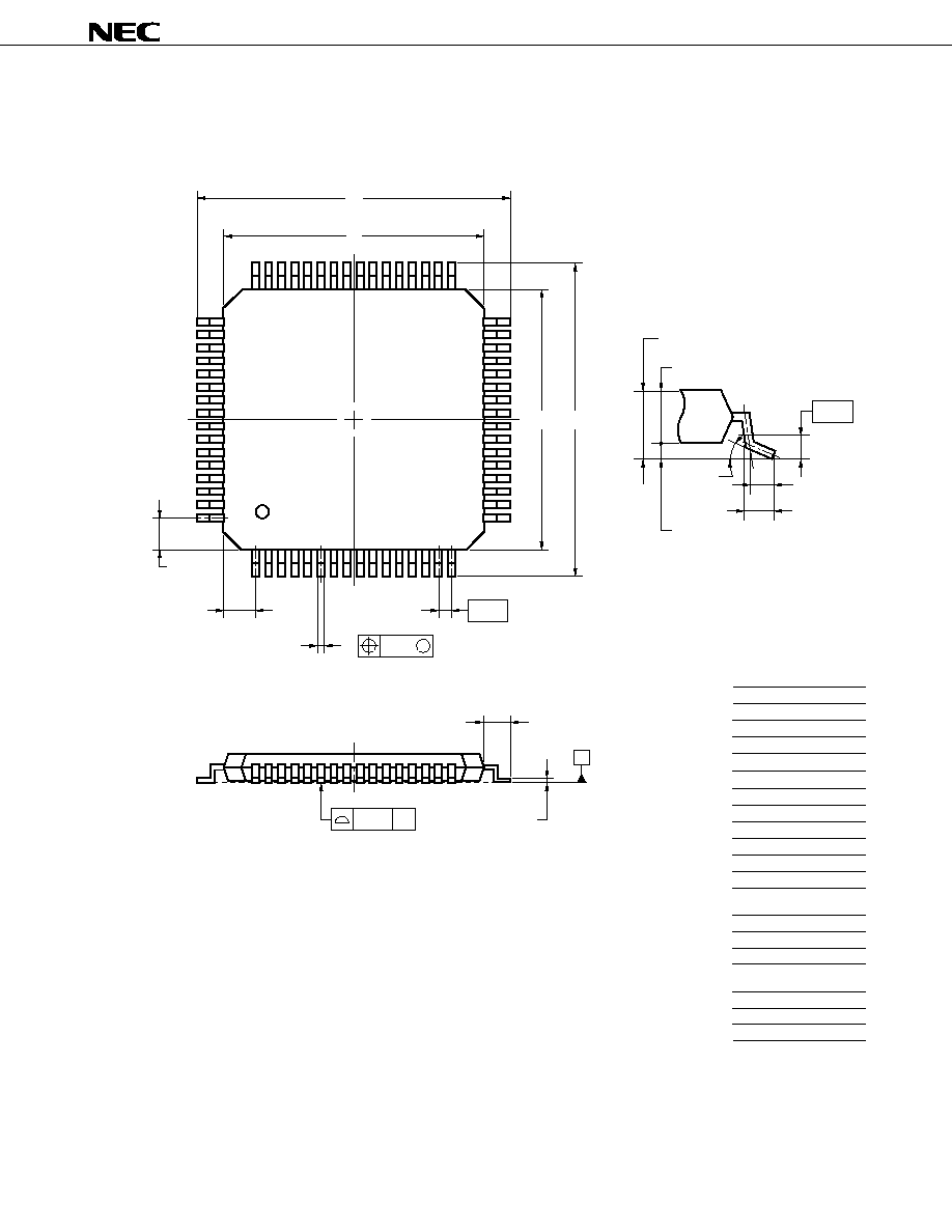
µ
PD78F0034B, 78F0034BY, 78F0034B(A), 78F0034BY(A)
71
Data Sheet U16369EJ1V0DS
M
48
32
33
64
1
17
16
49
S
N
S
J
detail of lead end
R
K
M
I
S
L
T
P
Q
G
F
H
64-PIN PLASTIC LQFP (10x10)
ITEM
MILLIMETERS
A
B
D
G
12.0
±
0.2
10.0
±
0.2
1.25
12.0
±
0.2
H
0.22
±
0.05
C
10.0
±
0.2
F
1.25
I
J
K
0.08
0.5 (T.P.)
1.0
±
0.2
L
0.5
P
1.4
Q
0.1
±
0.05
T
0.25
S
1.5
±
0.10
U
0.6
±
0.15
S64GB-50-8EU-2
R
3
∞+
4
∞
-
3
∞
N
0.08
M
0.17
+
0.03
-
0.07
A
B
C
D
U
NOTE
Each lead centerline is located within 0.08 mm of
its true position (T.P.) at maximum material condition.
Remark
The package and material of ES products are the same as mass produced products.
10. PACKAGE DRAWINGS
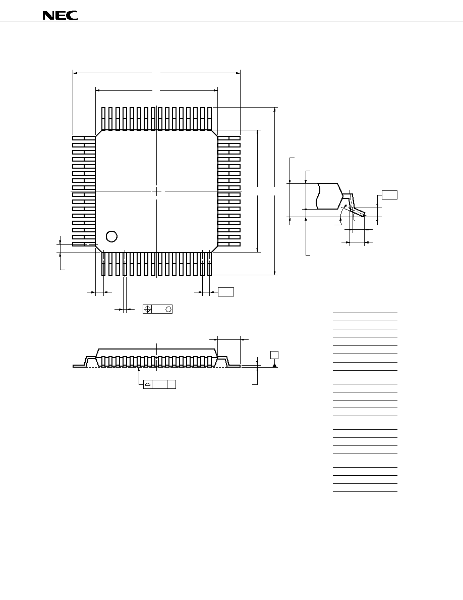
µ
PD78F0034B, 78F0034BY, 78F0034B(A), 78F0034BY(A)
72
Data Sheet U16369EJ1V0DS
Remark
The package and material of ES products are the same as mass produced products.
64-PIN PLASTIC LQFP (14x14)
NOTE
Each lead centerline is located within 0.20 mm of
its true position (T.P.) at maximum material condition.
ITEM
MILLIMETERS
A
B
D
G
17.2
±
0.2
14.0
±
0.2
0.8 (T.P.)
1.0
J
17.2
±
0.2
K
C
14.0
±
0.2
I
0.20
1.6
±
0.2
L
0.8
F
1.0
N
P
Q
0.10
1.4
±
0.1
0.127
±
0.075
U
0.886
±
0.15
R
S
3
∞
1.7 MAX.
T
0.25
P64GC-80-8BS
H
0.37
+
0.08
-
0.07
M
0.17
+
0.03
-
0.06
S
N
J
T
detail of lead end
C
D
A
B
K
M
I
S
P
R
L
U
Q
G
F
M
H
+
4
∞
-
3
∞
1
64
49
17
32
16
48
33
S
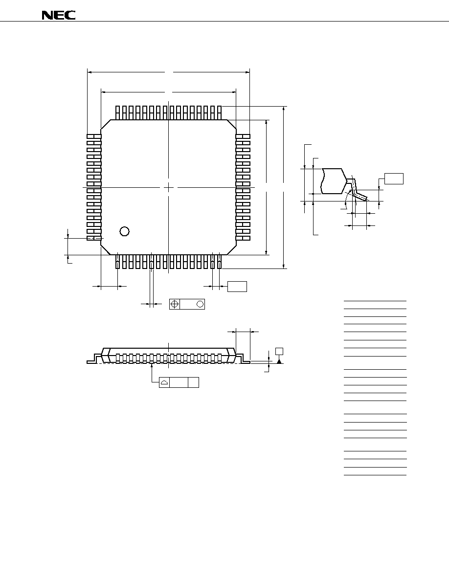
µ
PD78F0034B, 78F0034BY, 78F0034B(A), 78F0034BY(A)
73
Data Sheet U16369EJ1V0DS
Remark
The package and material of ES products are the same as mass produced products.
48
32
33
64
1
17
16
49
S
S
64-PIN PLASTIC TQFP (12x12)
ITEM
MILLIMETERS
G
1.125
A
14.0
±
0.2
C
12.0
±
0.2
D
F
1.125
14.0
±
0.2
B
12.0
±
0.2
N
0.10
P
Q
0.1
±
0.05
1.0
S
R
3
∞+
4
∞
-
3
∞
R
H
K
J
Q
G
I
S
P
detail of lead end
NOTE
Each lead centerline is located within 0.13 mm of
its true position (T.P.) at maximum material condition.
M
H
0.32
+
0.06
-
0.10
I
0.13
J
K
1.0
±
0.2
0.65 (T.P.)
L
0.5
M
0.17
+
0.03
-
0.07
P64GK-65-9ET-3
T
U
0.6
±
0.15
0.25
F
M
A
B
C
D
N
T
L
U
1.1
±
0.1
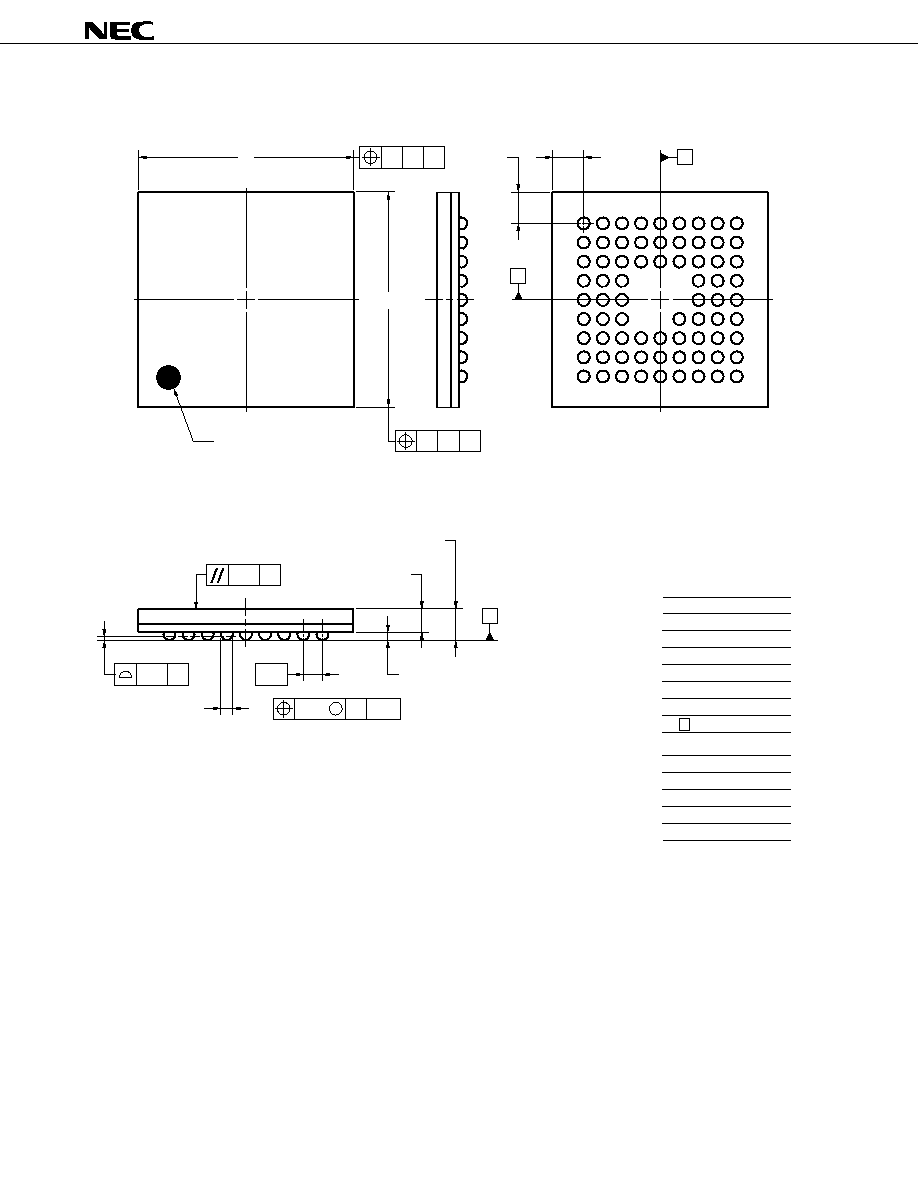
µ
PD78F0034B, 78F0034BY, 78F0034B(A), 78F0034BY(A)
74
Data Sheet U16369EJ1V0DS
B
S
A
A
B
C
D
E
F
G
H
J
S
w
B
y1
S
S
w
A
S
y
S
e
x
b
A
A1
A2
A
B
M
E
ZE
ZD
9
8
7
6
5
4
3
2
1
INDEX MARK
D
ITEM
DIMENSIONS
D
E
w
A
A1
A2
e
9.00
±
0.10
9.00
±
0.10
0.80
0.08
0.10
0.20
1.30
1.30
0.20
0.35
±
0.06
1.28
±
0.10
0.93
P73F1-80-CN3
0.50+0.05
≠0.10
(UNIT:mm)
x
y
y1
ZD
ZE
b
73-PIN PLASTIC FBGA (9x9)
Remark
The external dimensions and materials of the ES version are the same as those of the mass-produced
version.

µ
PD78F0034B, 78F0034BY, 78F0034B(A), 78F0034BY(A)
75
Data Sheet U16369EJ1V0DS
11. RECOMMENDED SOLDERING CONDITIONS
The
µ
PD78F0034B, 78F0034BY, 78F0034B(A), and 78F0034BY(A) should be soldered and mounted under
the following recommended conditions.
For details of the recommended soldering conditions, refer to the document Semiconductor Device Mounting
Technology Manual (C10535E).
For soldering methods and conditions other than those recommended below, contact an NEC Electronics sales
representative.
Table 11-1. Surface Mounting Type Soldering Conditions (1/2)
(1)
µµ
µµ
µ
PD78F0034BGB-8EU:
64-pin plastic LQFP (10 x 10)
µµ
µµ
µ
PD78F0034BGB(A)-8EU:
64-pin plastic LQFP (10 x 10)
µµ
µµ
µ
PD78F0034BYGB-8EU:
64-pin plastic LQFP (10 x 10)
µµ
µµ
µ
PD78F0034BYGB(A)-8EU: 64-pin plastic LQFP (10 x 10)
Soldering Method
Soldering Conditions
Recommended
Condition Symbol
Infrared reflow
Package peak temperature: 235
∞
C, Time: 30 seconds max. (at 210
∞
C or higher),
IR35-107-2
Count: Two times or less,
Exposure limit: 7 days
Note
(after 7 days, prebake at 125
∞
C for 10 hours)
VPS
Package peak temperature: 215
∞
C, Time: 40 seconds max. (at 200
∞
C or higher),
VP15-107-2
Count: Two times or less,
Exposure limit: 7 days
Note
(after 7 days, prebake at 125
∞
C for 10 hours)
Partial heating
Pin temperature: 300
∞
C max., Time: 3 seconds max. (per pin row)
≠
Note
After opening the dry pack, store it at 25
∞
C or less and 65% RH or less for the allowable storage period.
Caution Do not use different soldering methods together (except for partial heating).
(2)
µµ
µµ
µ
PD78F0034BGC-8BS:
64-pin plastic LQFP (14 x 14)
µµ
µµ
µ
PD78F0034BGC(A)-8BS:
64-pin plastic LQFP (14 x 14)
µµ
µµ
µ
PD78F0034BYGC-8BS:
64-pin plastic LQFP (14 x 14)
µµ
µµ
µ
PD78F0034BYGC(A)-8BS: 64-pin plastic LQFP (14 x 14)
Soldering Method
Soldering Conditions
Recommended
Condition Symbol
Infrared reflow
Package peak temperature: 235
∞
C, Time: 30 seconds max. (at 210
∞
C or higher),
IR35-00-2
Count: Two times or less
VPS
Package peak temperature: 215
∞
C, Time: 40 seconds max. (at 200
∞
C or higher),
VP15-00-2
Count: Two times or less
Wave soldering
Solder bath temperature: 260
∞
C max., Time: 10 seconds max., Count: Once,
WS60-00-1
Preheating temperature: 120
∞
C max. (package surface temperature)
Partial heating
Pin temperature: 300
∞
C max., Time: 3 seconds max. (per pin row)
≠
Caution Do not use different soldering methods together (except for partial heating).
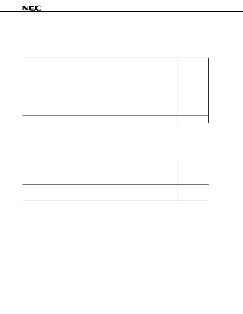
µ
PD78F0034B, 78F0034BY, 78F0034B(A), 78F0034BY(A)
76
Data Sheet U16369EJ1V0DS
Table 11-1. Surface Mounting Type Soldering Conditions (2/2)
(3)
µµ
µµ
µ
PD78F0034BGK-9ET:
64-pin plastic TQFP (12 x 12)
µµ
µµ
µ
PD78F0034BGK(A)-9ET:
64-pin plastic TQFP (12 x 12)
µµ
µµ
µ
PD78F0034BYGK-9ET:
64-pin plastic TQFP (12 x 12)
µµ
µµ
µ
PD78F0034BYGK(A)-9ET: 64-pin plastic TQFP (12 x 12)
Soldering Method
Soldering Conditions
Recommended
Condition Symbol
Infrared reflow
Package peak temperature: 235
∞
C, Time: 30 seconds max. (at 210
∞
C or higher),
IR35-107-2
Count: Two times or less,
Exposure limit: 7 days
Note
(after 7 days, prebake at 125
∞
C for 10 hours)
VPS
Package peak temperature: 215
∞
C, Time: 40 seconds max. (at 200
∞
C or higher),
VP15-107-2
Count: Two times or less,
Exposure limit: 7 days
Note
(after 7 days, prebake at 125
∞
C for 10 hours)
Wave soldering
Solder bath temperature: 260
∞
C max., Time: 10 seconds max.,
WS60-107-1
Count: Once, Preheating temperature: 120
∞
C max. (package surface temperature),
Exposure limit: 7 days
Note
(after 7 days, prebake at 125
∞
C for 10 hours)
Partial heating
Pin temperature: 300
∞
C max., Time: 3 seconds max. (per pin row)
≠
Note
After opening the dry pack, store it at 25
∞
C or less and 65% RH or less for the allowable storage period.
Caution Do not use different soldering methods together (except for partial heating).
(4)
µµ
µµ
µ
PD78F0034BF1-CN3:
73-pin plastic FBGA (9 x 9)
µµ
µµ
µ
PD78F0034BYF1-CN3: 73-pin plastic FBGA (9 x 9)
Soldering Method
Soldering Conditions
Recommended
ConditionSymbol
Infrared reflow
Package peak temperature: 260
∞
C, Time: 60 seconds max. (at 220
∞
C or higher),
IR60-203-3
Count: Three times or less,
Exposure limit: 3 days
Note
(after that, prebake at 125
∞
C for 20 hours)
VPS
Package peak temperature: 215
∞
C, Time: 40 seconds max. (at 200
∞
C or higher),
VP15-203-3
Count: Three times or less,
Exposure limit: 3 days
Note
(after that, prebake at 125
∞
C for 20 hours)
Note
After opening the dry pack, store it at 25
∞
C or less and 65%RH or less for the allowable storage period.
Caution Do not use different soldering methods together.

µ
PD78F0034B, 78F0034BY, 78F0034B(A), 78F0034BY(A)
77
Data Sheet U16369EJ1V0DS
APPENDIX A. DEVELOPMENT TOOLS
The following development tools are available for system development using the
µ
PD780034B, 780034BY.
Also refer to (6) Cautions on Using Development Tools.
(1) Software Package
SP78K0
CD-ROM in which various software tools for 78K/0 development are integrated in one
package
(2) Language Processing Software
RA78K0
Assembler package common to 78K/0 Series
CC78K0
C compiler package common to 78K/0 Series
DF780034
Device file for
µ
PD780034A, 780034AY Subseries
CC78K0-L
C compiler library source file common to 78K/0 Series
(3) Flash Memory Writing Tools
Flashpro III (FL-PR3, PG-FP3)
Flash programmer dedicated to microcontrollers with on-chip flash memory
Flashpro IV (FL-PR4, PG-FP4)
FA-64GB-8EU
Adapter for flash memory writing used connected to the Flashpro III/Flashpro IV.
FA-64GC-8BS-A
∑ FA-64GB-8EU:
64-pin plastic LQFP (GB-8EU type)
FA-64GK-9ET
∑ FA-64GC-8BS-A: 64-pin plastic LQFP (GC-8BS type)
FA-73F1-CN3-A
∑ FA-64GK-9ET:
64-pin plastic TQFP (GK-9ET type)
∑ FA-73F1-CN3-A: 73-pin plastic FBGA (F1-CN3 type)
µ
PD78F0034B, 78F0034BY, 78F0034B(A), 78F0034BY(A)
78
Data Sheet U16369EJ1V0DS
(4) Debugging Tools
∑ When using in-circuit emulator IE-78K0-NS
IE-78K0-NS
In-circuit emulator common to 78K/0 Series
IE-70000-MC-PS-B
Power supply unit for IE-78K0-NS
IE-78K0-NS-PA
Performance board to enhance and expand the functions of IE-78K0-NS
IE-70000-98-IF-C
Adapter required when using PC-9800 series as host machine (excluding notebook PCs) (C bus supported)
IE-70000-CD-IF-A
PC card and interface cable when using notebook PC as host machine (PCMCIA socket supported)
IE-70000-PC-IF-C
Adapter required when using IBM PC/AT
TM
or compatible as host machine (ISA bus supported)
IE-70000-PCI-IF-A
Adapter required when using PC in which PCI bus is incorporated as host machine
IE-780034-NS-EM1
Emulation board to emulate
µ
PD780034A, 780034AY Subseries
NP-64GC
Emulation probe for 64-pin plastic LQFP (GC-8BS type)
NP-64GC-TQ
NP-H64GC-TQ
NP-64GK
Emulation probe for 64-pin plastic TQFP (GK-9ET type)
NP-H64GK-TQ
NP-H64GB-TQ
Emulation probe for 64-pin plastic LQFP (GB-8EU type)
NP-73F1-CN3
Note
Emulation probe for 73-pin plastic FBGA (F1-CN3 type)
EV-9200GC-64
Conversion socket to connect the NP64GC and a target system board on which a 64-pin plastic LQFP
(GC-8BS type) can be mounted.
TGC-064SAP
Conversion adapter to connect the NP-64GC-TQ or NP-H64GC-TQ and a target system board on
which a 64-pin plastic LQFP (GC-8BS type) can be mounted
TGK-064SBW
Conversion adapter to connect the NP-64GK or NP-H64GK-TQ and a target system on which a 64-
pin plastic TQFP (GK-9ET type) can be mounted
TGB-064SDP
Conversion socket to connect the NP-H64GB-TQ and a target system board on which a 64-pin
plastic LQFP (GB-8EU type) can be mounted
CSICE73A0909N01,
Conversion socket to connect the NP-73F1-CN3 and a target system board on which a 73-pin plastic
LSPACK73A0909N01,
FBGA (F1-CN3 type) can be mounted
CSSOCKET73A0909N01
ID78K0-NS
Integrated debugger for IE-78K0-NS
SM78K0
System simulator common to 78K/0 Series
DF780034
Device file for
µ
PD780034A, 780034AY Subseries
Note
The conversion socket (CSICE73A0909N01, LSPACK73A0909N01, or CSSOCKET73A0909N01) is supplied
with the emulation probe (NP-73F1-CN3).
µ
PD78F0034B, 78F0034BY, 78F0034B(A), 78F0034BY(A)
79
Data Sheet U16369EJ1V0DS
∑ When using in-circuit emulator IE-78001-R-A
IE-78001-R-A
In-circuit emulator common to 78K/0 Series
IE-70000-98-IF-C
Adapter required when using PC-9800 series as host machine (excluding notebook PCs) (C bus supported)
IE-70000-PC-IF-C
Interface adapter when using IBM PC/AT or compatible as host machine (ISA bus supported)
IE-70000-PCI-IF-A
Adapter required when using PC in which PCI bus is incorporated as host machine
IE-780034-NS-EM1
Emulation board to emulate
µ
PD780034A, 780034AY Subseries
IE-78K0-R-EX1
Emulation probe conversion board necessary when using IE-780034-NS-EM1 on IE-78001-R-A
EP-78240GC-R
Emulation probe for 64-pin plastic LQFP (GC-8BS type)
EP-78012GK-R
Emulation probe for 64-pin plastic TQFP (GK-9ET type)
EV-9200GC-64
Conversion socket to connect the EP-78240GC-R and a target system board on which a 64-pin
plastic LQFP (GC-8BS type) can be mounted
TGK-064SBW
Conversion adapter to connect the EP-78012GK-R and a target system board on which a 64-pin plastic
TQFP (GK-9ET type) can be mounted
ID78K0
Integrated debugger for IE-78001-R-A
SM78K0
System simulator common to 78K/0 Series
DF780034
Device file for
µ
PD780034A, 780034AY Subseries
(5) Real-Time OS
RX78K0
Real-time OS for 78K/0 Series
Caution The 64-pin plastic LQFP (GB-8EU type) and 73-pin plastic FBGA (F1-CN3 type) do not support
the IE-78001-R-A.
µ
PD78F0034B, 78F0034BY, 78F0034B(A), 78F0034BY(A)
80
Data Sheet U16369EJ1V0DS
(6) Cautions on Using Development Tools
∑ The ID78K0-NS, ID78K0, and SM78K0 are used in combination with the DF780034.
∑ The CC78K0 and RX78K0 are used in combination with the RA78K0 and the DF780034.
∑ FL-PR3, FL-PR4, FA-64GC-8BS-A, FA-64GB-8EU, FA-64GK-9ET, FA-73F1-CN3-A, NP-64GC, NP-64GC-
TQ, NP-H64GC-TQ, NP-64GK, NP-H64GK-TQ, NP-H64GB-TQ, and NP-73F1-CN3 are products made by
Naito Densei Machida Mfg. Co., Ltd. (+81-45-475-4191).
∑ TGC-064SAP, TGK-064SBW, TGB-064SDP, CSICE73A0909N01, LSPACK73A0909N01, and
CSSOCKET73A0909N01 are products made by TOKYO ELETECH CORPORATION.
Contact: Daimaru Kogyo, Ltd.
Tokyo Electronic Division (+81-3-3820-7112)
Osaka Electronic Division (+81-6-6244-6672)
∑ For third-party development tools, see the Single-chip Microcontroller Development Tool Selection Guide
(U11069E).
∑ The host machines and OSs supporting each software are as follows.
Host Machine
PC
EWS
[OS]
PC-9800 series [Japanese Windows
TM
]
HP9000 series 700
TM
[HP-UX
TM
]
IBM PC/AT and compatibles
SPARCstation
TM
[SunOS
TM
, Solaris
TM
]
Software
[Japanese/English Windows]
RA78K0
Note
CC78K0
Note
ID78K0-NS
≠
ID78K0
≠
SM78K0
≠
RX78K0
Note
Note
DOS-based software

µ
PD78F0034B, 78F0034BY, 78F0034B(A), 78F0034BY(A)
81
Data Sheet U16369EJ1V0DS
Conversion Socket Drawing (EV-9200GC-64) and Footprints
Figure A-1. EV-9200GC-64 Drawing (For Reference Only)
A
F
1
E
EV-9200GC-64
B
D
C
M
N
L
K
R
Q
I
H
P
O
S
T
J
G
No.1 pin index
EV-9200GC-64-G0
ITEM
MILLIMETERS
INCHES
A
B
C
D
E
F
G
H
I
J
K
L
M
N
O
P
Q
R
S
T
18.8
14.1
14.1
18.8
4-C 3.0
0.8
6.0
15.8
18.5
6.0
15.8
18.5
8.0
7.8
2.5
2.0
1.35
0.35
±
0.1
2.3
1.5
0.74
0.555
0.555
0.74
4-C 0.118
0.031
0.236
0.622
0.728
0.236
0.622
0.728
0.315
0.307
0.098
0.079
0.053
0.014
0.091
0.059
+0.004
≠0.005
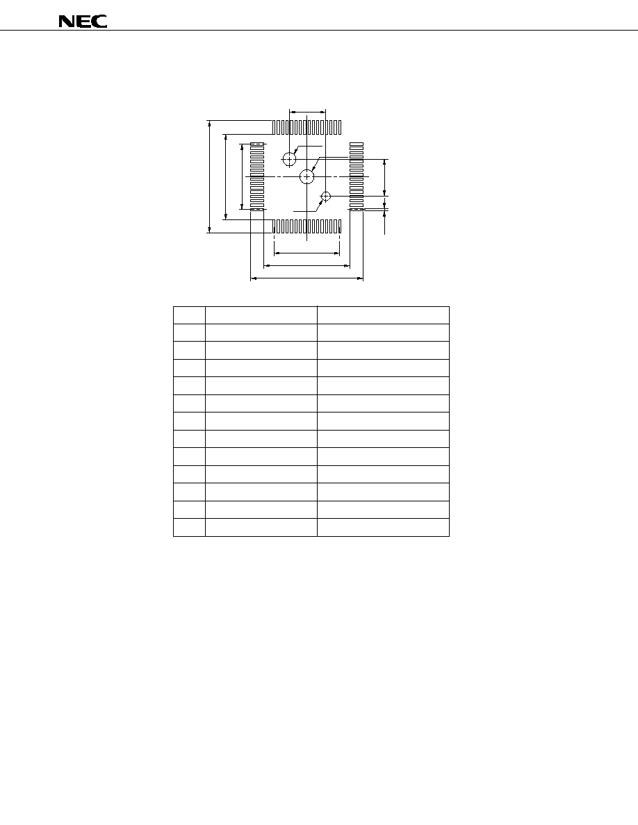
µ
PD78F0034B, 78F0034BY, 78F0034B(A), 78F0034BY(A)
82
Data Sheet U16369EJ1V0DS
Figure A-2. EV-9200GC-64 Footprints (For Reference Only)
F
E
D
G
H
I
J
K
L
C
B
A
0.031
◊
0.591=0.472
0.031
◊
0.591=0.472
EV-9200GC-64-P1E
ITEM
MILLIMETERS
INCHES
A
B
C
D
E
F
G
H
I
J
K
L
19.5
14.8
14.8
19.5
6.00
±
0.08
6.00
±
0.08
0.5
±
0.02
2.36
±
0.03
2.2
±
0.1
1.57
±
0.03
0.768
0.583
0.583
0.768
0.236
0.236
0.197
0.093
0.087
0.062
0.8
±
0.02
◊
15=12.0
±
0.05
0.8
±
0.02
◊
15=12.0
±
0.05
+0.002
≠0.001
+0.003
≠0.002
+0.002
≠0.001
+0.003
≠0.002
+0.004
≠0.003
+0.004
≠0.003
+0.001
≠0.002
+0.001
≠0.002
+0.004
≠0.005
+0.001
≠0.002
Dimensions of mount pad for EV-9200 and that for target device
(QFP) may be different in some parts. For the recommended
mount pad dimensions for QFP, refer to "SEMICONDUCTOR
DEVICE MOUNTING TECHNOLOGY MANUAL"
(C10535E).
Caution
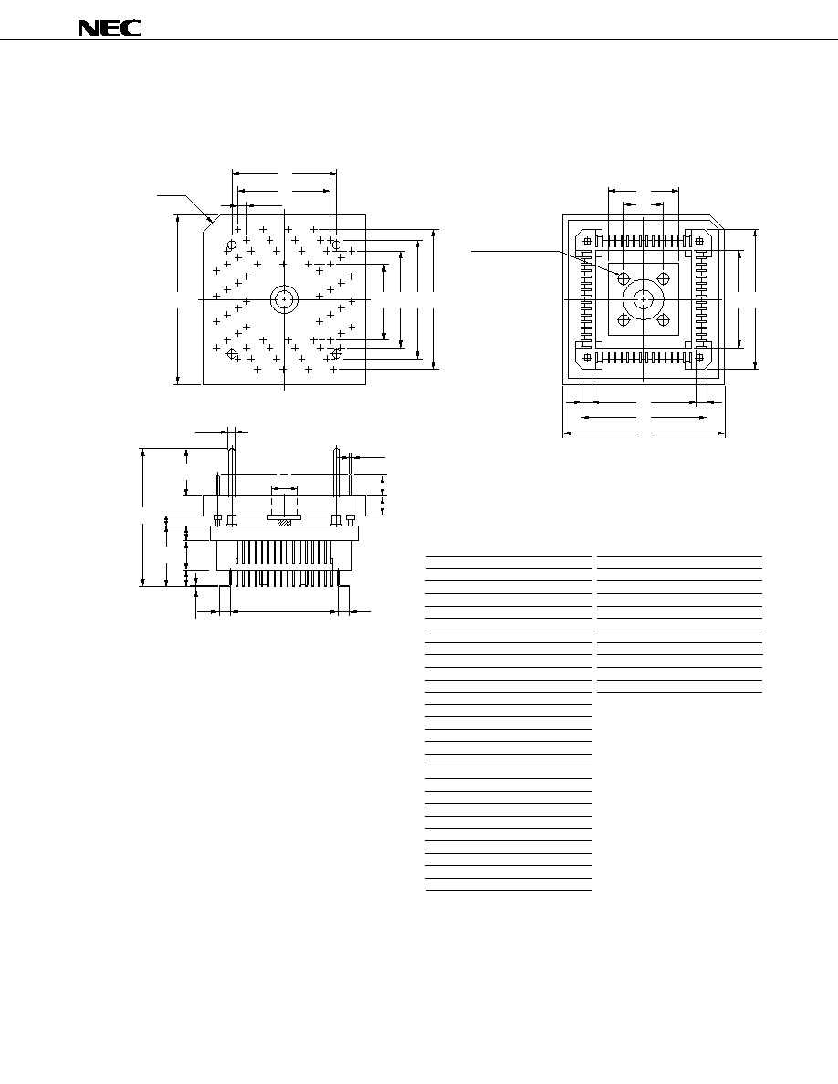
µ
PD78F0034B, 78F0034BY, 78F0034B(A), 78F0034BY(A)
83
Data Sheet U16369EJ1V0DS
Conversion Adapter Drawing (TGC-064SAP)
Figure A-3. TGC-064SAP Drawing (For Reference Only)
ITEM
MILLIMETERS
INCHES
b
3.5
0.138
c
2.0
0.079
a
1.85
0.073
d
6.0
0.236
e
0.25
0.010
f
13.6
g
1.2
0.047
0.535
ITEM
MILLIMETERS
INCHES
B
0.8x15=12.0
0.031x0.591=0.472
C
0.8
0.031
A
14.12
0.556
D
H
17.2
0.677
I
C 2.0
C 0.079
J
9.05
0.356
E
10.0
0.394
F
12.4
0.488
K
5.0
0.197
L
13.35
0.526
M
Q
12.5
0.492
R
17.5
0.689
S
N
1.325
0.052
O
16.0
P
20.65
0.813
4- 1.3
4- 0.051
0.630
W
X
(19.65)
(0.667)
Y
7.35
0.289
T
U
V
Z
1.2
0.047
20.65
1.325
0.813
0.052
G
14.8
0.583
V
C
I
j
i
a
e g
h
f
b
c
W
note: Product by TOKYO ELETECH CORPORATION.
Z
M
N
1.8
0.071
3.55
0.140
0.9
0.035
0.3
0.012
h
1.2
0.047
i
2.4
j
2.7
0.106
0.094
TGC-064SAP-G0E
Protrusion height
A
B
U
G H
Q R
F
E
D
L
O
K
T
S
J
P
X
Y
d
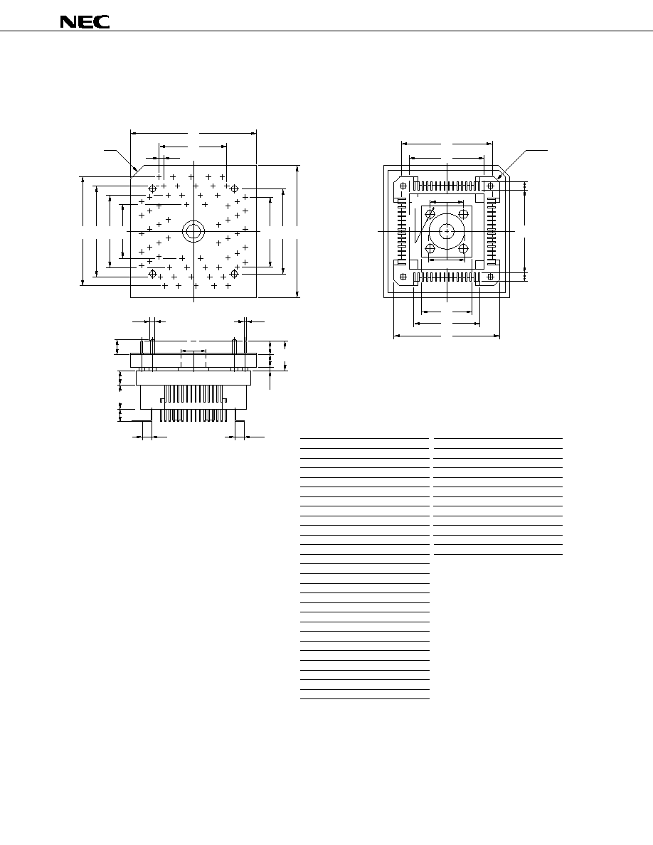
µ
PD78F0034B, 78F0034BY, 78F0034B(A), 78F0034BY(A)
84
Data Sheet U16369EJ1V0DS
Conversion Adapter Drawing (TGK-064SBW)
Figure A-4. TGK-064SBW Drawing (For Reference Only) (Unit: mm)
ITEM
MILLIMETERS
INCHES
b
1.85
0.073
c
3.5
0.138
a
0.3
0.012
d
2.0
0.079
h
5.9
0.232
i
0.8
0.031
j
2.4
0.094
e
3.9
0.154
f
1.325
g
1.325
0.052
0.052
ITEM
MILLIMETERS
INCHES
B
0.65x15=9.75
0.026x0.591=0.384
C
0.65
0.026
A
18.4
0.724
D
H
0.65x15=9.75
0.026x0.591=0.384
I
11.85
0.467
J
18.4
0.724
E
10.15
0.400
F
12.55
0.494
K
C 2.0
C 0.079
L
12.45
0.490
M
Q
11.1
0.437
R
1.45
0.057
S
1.45
0.057
N
7.7
0.303
O
10.02
P
14.92
0.587
0.394
W
5.3
0.209
X
4-C 1.0
4-C 0.039
Y
3.55
0.140
T
4- 1.3
4- 0.051
U
1.8
V
5.0
0.197
0.071
Z
0.9
0.035
7.75
10.25
0.305
0.404
G
14.95
0.589
k
2.7
0.106
TGK-064SBW-G1E
H
A
h
a
g
Z
c
L
Q
N
B
C
I
J
K
G F E D
M
X
R
S
W
O
P
Protrusion height
U
T
V
k
j
i
Y
e
d
b
f
note: Product by TOKYO ELETECH CORPORATION.
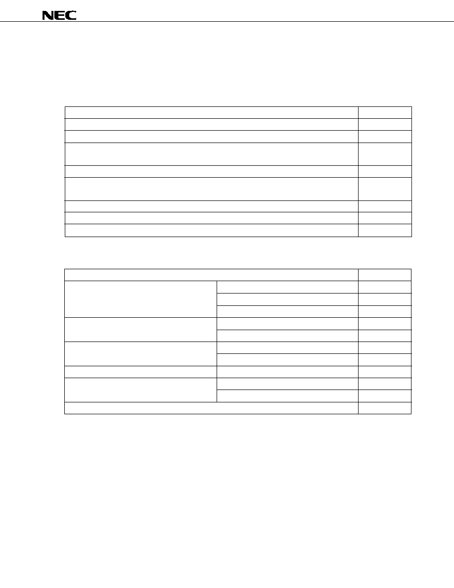
µ
PD78F0034B, 78F0034BY, 78F0034B(A), 78F0034BY(A)
85
Data Sheet U16369EJ1V0DS
APPENDIX B. RELATED DOCUMENTS
The related documents indicated in this publication may include preliminary versions. However, preliminary
versions are not marked as such.
Documents Related to Devices
Document Name
Document No.
µ
PD780024A, 780034A, 780024AY, 780034AY Subseries User's Manual
U14046E
µ
PD780021A, 780022A, 780023A, 780024A, 780021AY, 780022AY, 780023AY, 780024AY Data Sheet
U14042E
µ
PD780021A(A), 780022A(A), 780023A(A), 780024A(A), 780021AY(A), 780022AY(A), 780023AY(A),
U15131E
780024AY(A) Data Sheet
µ
PD780031A, 780032A, 780033A, 780034A, 780031AY, 780032AY, 780033AY, 780034AY Data Sheet
U14044E
µ
PD780031A(A), 780032A(A), 780033A(A), 780034A(A), 780031AY(A), 780032AY(A), 780033AY(A),
U15132E
780034AY(A) Data Sheet
µ
PD78F0034A, 78F0034AY Data Sheet
U14040E
µ
PD78F0034B, 78F0034BY, 78F0034B(A), 78F0034BY(A) Data Sheet
This document
78K/0 Series User's Manual Instruction
U12326E
Documents Related to Development Software Tools (User's Manuals)
Document Name
Document No.
RA78K0 Assembler Package
Operation
U14445E
Language
U14446E
Structured Assembly Language
U11789E
CC78K0 C Compiler
Operation
U14297E
Language
U14298E
SM78K Series System Simulator Ver. 2.30 or Later
Operation (Windows
Based)
U15373E
External Part User Open Interface Specifications
U15802E
ID78K Series Integrated Debugger Ver. 2.30 or Later
Operation (Windows Based)
U15185E
RX78K0 Real-time OS
Fundamentals
U11537E
Installation
U11536E
Project Manager Ver. 3.12 or Later (Windows Based)
U14610E
Caution
The related documents listed above are subject to change without notice. Be sure to use the latest
version of each document for designing.
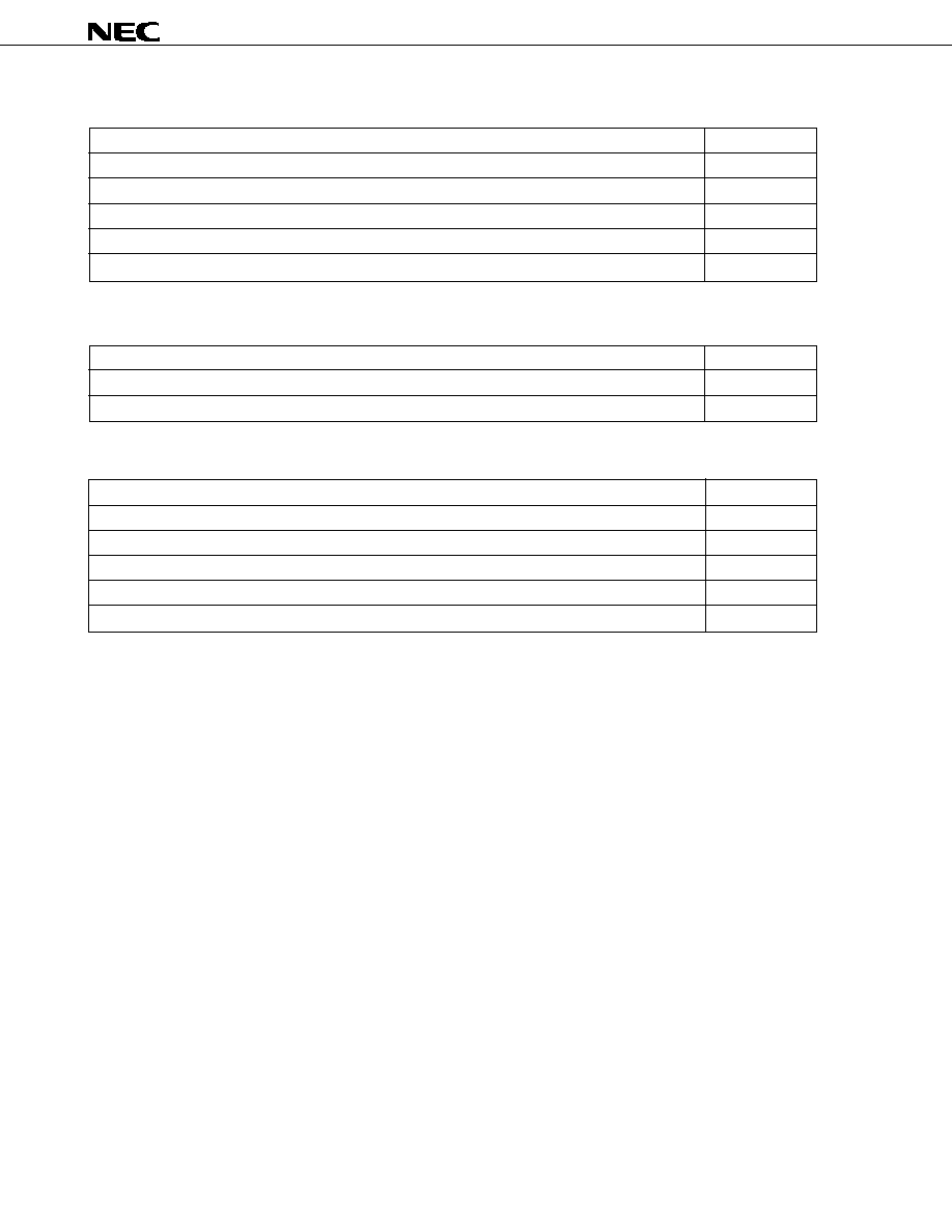
µ
PD78F0034B, 78F0034BY, 78F0034B(A), 78F0034BY(A)
86
Data Sheet U16369EJ1V0DS
Documents Related to Development Hardware Tools (User's Manuals)
Document Name
Document No.
IE-78K0-NS In-Circuit Emulator
U13731E
IE-78K0-NS-A In-Circuit Emulator
U14889E
IE-780034-NS-EM1 Emulation Board
U14642E
IE-78001-R-A In-Circuit Emulator
U14142E
IE-78K0-R-EX1 In-Circuit Emulator
To be prepared
Documents Related to Flash Memory Writing
Document Name
Document No.
PG-FP3 Flash Memory Programmer User's Manual
U13502E
PG-FP4 Flash Memory Programmer User's Manual
U15260E
Other Related Documents
Document Name
Document No.
SEMICONDUCTORS SELECTION GUIDE - Products & Packages -
X13769E
Semiconductor Device Mounting Technology Manual
C10535E
Quality Grades on NEC Semiconductor Devices
C11531E
NEC Semiconductor Device Reliability/Quality Control System
C10983E
Guide to Prevent Damage for Semiconductor Devices by Electrostatic Discharge (ESD)
C11892E
Caution
The related documents listed above are subject to change without notice. Be sure to use the latest
version of each document for designing.

µ
PD78F0034B, 78F0034BY, 78F0034B(A), 78F0034BY(A)
87
Data Sheet U16369EJ1V0DS
[MEMO]
µ
PD78F0034B, 78F0034BY, 78F0034B(A), 78F0034BY(A)
88
Data Sheet U16369EJ1V0DS
NOTES FOR CMOS DEVICES
1
PRECAUTION AGAINST ESD FOR SEMICONDUCTORS
Note:
Strong electric field, when exposed to a MOS device, can cause destruction of the gate oxide and
ultimately degrade the device operation. Steps must be taken to stop generation of static electricity
as much as possible, and quickly dissipate it once, when it has occurred. Environmental control
must be adequate. When it is dry, humidifier should be used. It is recommended to avoid using
insulators that easily build static electricity. Semiconductor devices must be stored and transported
in an anti-static container, static shielding bag or conductive material. All test and measurement
tools including work bench and floor should be grounded. The operator should be grounded using
wrist strap. Semiconductor devices must not be touched with bare hands. Similar precautions need
to be taken for PW boards with semiconductor devices on it.
2
HANDLING OF UNUSED INPUT PINS FOR CMOS
Note:
No connection for CMOS device inputs can be cause of malfunction. If no connection is provided
to the input pins, it is possible that an internal input level may be generated due to noise, etc., hence
causing malfunction. CMOS devices behave differently than Bipolar or NMOS devices. Input levels
of CMOS devices must be fixed high or low by using a pull-up or pull-down circuitry. Each unused
pin should be connected to V
DD
or GND with a resistor, if it is considered to have a possibility of
being an output pin. All handling related to the unused pins must be judged device by device and
related specifications governing the devices.
3
STATUS BEFORE INITIALIZATION OF MOS DEVICES
Note:
Power-on does not necessarily define initial status of MOS device. Production process of MOS
does not define the initial operation status of the device. Immediately after the power source is
turned ON, the devices with reset function have not yet been initialized. Hence, power-on does
not guarantee out-pin levels, I/O settings or contents of registers. Device is not initialized until the
reset signal is received. Reset operation must be executed immediately after power-on for devices
having reset function.
Note: Purchase of NEC Electronics I
2
C components conveys a license under the Philips I
2
C Patent Rights to
use these components in an I
2
C system, provided that the system conforms to the I
2
C Standard
Specification as defined by Philips.
FIP and IEBus are trademarks of NEC Electronics Corporation.
Windows is either a registered trademark or trademark of Microsoft Corporation in the United States and/or
other countries.
PC/AT is a trademark of International Business Machines Corporation.
HP9000 series 700 and HP-UX are trademarks of Hewlett-Packard Company.
SPARCstation is a trademark of SPARC International, Inc.
Solaris and SunOS are trademarks of Sun Microsystems, Inc.

µ
PD78F0034B, 78F0034BY, 78F0034B(A), 78F0034BY(A)
89
Data Sheet U16369EJ1V0DS
Regional Information
∑
Device availability
∑
Ordering information
∑
Product release schedule
∑
Availability of related technical literature
∑
Development environment specifications (for example, specifications for third-party tools and
components, host computers, power plugs, AC supply voltages, and so forth)
∑
Network requirements
In addition, trademarks, registered trademarks, export restrictions, and other legal issues may also vary
from country to country.
NEC Electronics America, Inc. (U.S.)
Santa Clara, California
Tel: 408-588-6000
800-366-9782
Fax: 408-588-6130
800-729-9288
NEC Electronics Hong Kong Ltd.
Hong Kong
Tel: 2886-9318
Fax: 2886-9022/9044
NEC Electronics Hong Kong Ltd.
Seoul Branch
Seoul, Korea
Tel: 02-528-0303
Fax: 02-528-4411
NEC Electronics Shanghai, Ltd.
Shanghai, P.R. China
Tel: 021-6841-1138
Fax: 021-6841-1137
NEC Electronics Taiwan Ltd.
Taipei, Taiwan
Tel: 02-2719-2377
Fax: 02-2719-5951
NEC Electronics Singapore Pte. Ltd.
Novena Square, Singapore
Tel: 6253-8311
Fax: 6250-3583
J02.11
NEC Electronics (Europe) GmbH
Duesseldorf, Germany
Tel: 0211-65 03 01
Fax: 0211-65 03 327
∑ Sucursal en EspaÒa
Madrid, Spain
Tel: 091-504 27 87
Fax: 091-504 28 60
VÈlizy-Villacoublay, France
Tel: 01-30-67 58 00
Fax: 01-30-67 58 99
∑ Succursale FranÁaise
∑ Filiale Italiana
Milano, Italy
Tel: 02-66 75 41
Fax: 02-66 75 42 99
∑ Branch The Netherlands
Eindhoven, The Netherlands
Tel: 040-244 58 45
Fax: 040-244 45 80
∑ Tyskland Filial
Taeby, Sweden
Tel: 08-63 80 820
Fax: 08-63 80 388
∑ United Kingdom Branch
Milton Keynes, UK
Tel: 01908-691-133
Fax: 01908-670-290
Some information contained in this document may vary from country to country. Before using any NEC
Electronics product in your application, pIease contact the NEC Electronics office in your country to
obtain a list of authorized representatives and distributors. They will verify:

µ
PD78F0034B, 78F0034BY, 78F0034B(A), 78F0034BY(A)
The information in this document is current as of September, 2002. The information is subject to
change without notice. For actual design-in, refer to the latest publications of NEC Electronics data
sheets or data books, etc., for the most up-to-date specifications of NEC Electronics products. Not
all products and/or types are available in every country. Please check with an NEC Electronics sales
representative for availability and additional information.
No part of this document may be copied or reproduced in any form or by any means without the prior
written consent of NEC Electronics. NEC Electronics assumes no responsibility for any errors that may
appear in this document.
NEC Electronics does not assume any liability for infringement of patents, copyrights or other intellectual
property rights of third parties by or arising from the use of NEC Electronics products listed in this document
or any other liability arising from the use of such products. No license, express, implied or otherwise, is
granted under any patents, copyrights or other intellectual property rights of NEC Electronics or others.
Descriptions of circuits, software and other related information in this document are provided for illustrative
purposes in semiconductor product operation and application examples. The incorporation of these
circuits, software and information in the design of a customer's equipment shall be done under the full
responsibility of the customer. NEC Electronics assumes no responsibility for any losses incurred by
customers or third parties arising from the use of these circuits, software and information.
While NEC Electronics endeavors to enhance the quality, reliability and safety of NEC Electronics products,
customers agree and acknowledge that the possibility of defects thereof cannot be eliminated entirely. To
minimize risks of damage to property or injury (including death) to persons arising from defects in NEC
Electronics products, customers must incorporate sufficient safety measures in their design, such as
redundancy, fire-containment and anti-failure features.
NEC Electronics products are classified into the following three quality grades: "Standard", "Special" and
"Specific".
The "Specific" quality grade applies only to NEC Electronics products developed based on a customer-
designated "quality assurance program" for a specific application. The recommended applications of an NEC
Electronics product depend on its quality grade, as indicated below. Customers must check the quality grade of
each NEC Electronics product before using it in a particular application.
The quality grade of NEC Electronics products is "Standard" unless otherwise expressly specified in NEC
Electronics data sheets or data books, etc. If customers wish to use NEC Electronics products in applications
not intended by NEC Electronics, they must contact an NEC Electronics sales representative in advance to
determine NEC Electronics' willingness to support a given application.
(Note)
∑
∑
∑
∑
∑
∑
M8E 02. 11-1
(1)
(2)
"NEC Electronics" as used in this statement means NEC Electronics Corporation and also includes its
majority-owned subsidiaries.
"NEC Electronics products" means any product developed or manufactured by or for NEC Electronics (as
defined above).
Computers, office equipment, communications equipment, test and measurement equipment, audio
and visual equipment, home electronic appliances, machine tools, personal electronic equipment
and industrial robots.
Transportation equipment (automobiles, trains, ships, etc.), traffic control systems, anti-disaster
systems, anti-crime systems, safety equipment and medical equipment (not specifically designed
for life support).
Aircraft, aerospace equipment, submersible repeaters, nuclear reactor control systems, life
support systems and medical equipment for life support, etc.
"Standard":
"Special":
"Specific":