Document Outline
- COVER
- DESCRIPTION
- FEATURES
- APPLICATIONS
- ORDERING INFORMATION
- 78K/0 SERIES LINEUP
- OVERVIEW OF FUNCTIONS
- 1. PIN CONFIGURATION (Top View)
- 2. BLOCK DIAGRAM
- 3. PIN FUNCTIONS
- 3.1 Port Pins
- 3.2 Non-Port Pins
- 3.3 Pin I/O Circuits and Recommended Connection of Unused Pins
- 4. MEMORY SPACE
- 5. PERIPHERAL HARDWARE FUNCTION FEATURES
- 5.1 Ports
- 5.2 Clock Generator
- 5.3 Timer/Counter
- 5.4 Clock Output/Buzzer Output Control Circuit
- 5.5 A/D Converter
- 5.6 Serial Interface
- 6. INTERRUPT FUNCTION
- 7. EXTERNAL DEVICE EXPANSION FUNCTION
- 9. RESET FUNCTION
- 10. MASK OPTION
- 11. INSTRUCTION SET
- 12. ELECTRICAL SPECIFICATIONS
- 13. PACKAGE DRAWINGS
- 14. RECOMMENDED SOLDERING CONDITIONS
- APPENDIX A. DEVELOPMENT TOOLS
- APPENDIX B. RELATED DOCUMENTS
©
1999
DATA SHEET
DESCRIPTION
The
µ
PD780031AY, 780032AY, 780033AY, and 780034AY are members of the
µ
PD780034AY Subseries of the
78K/0 Series. This is a
µ
PD780034A Subseries product with an added multimaster-supporting I
2
C bus interface, and
is suitable for AV equipment applications.
A flash memory version, the
µ
PD78F0034AY, that can operate in the same power supply voltage range as the mask
ROM version, and various development tools, are available.
Detailed function descriptions are provided in the following user's manuals. Be sure to read them before
designing.
µ
PD780024A, 780034A, 780024AY, 780034AY
Subseries User's Manual:
U14046E
78K/0 Series User's Manual Instructions:
U12326E
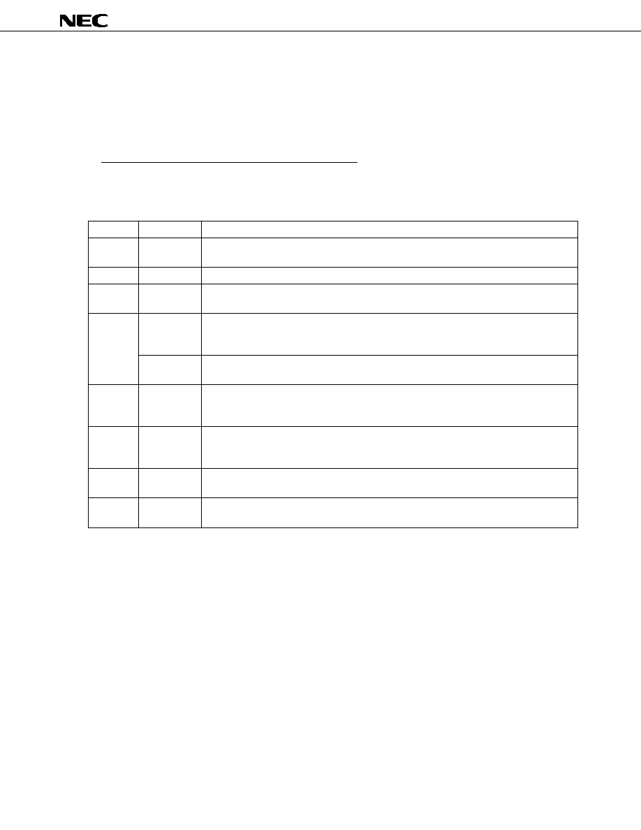
FEATURES
∑
Internal ROM and RAM
Item
Program Memory
Data Memory
Package
Part Number
(Internal ROM)
(Internal High-Speed RAM)
µ
PD780031AY
8 Kbytes
512 bytes
∑ 64-pin plastic shrink DIP (750 mils)
µ
PD780032AY
16 Kbytes
∑ 64-pin plastic QFP (14
◊
14 mm)
µ
PD780033AY
24 Kbytes
1024 bytes
∑ 64-pin plastic LQFP (12
◊
12 mm)
µ
PD780034AY
32 Kbytes
∑
External memory expansion space: 64 Kbytes
∑
Minimum instruction execution time: 0.24
µ
s (@ f
X
= 8.38-MHz operation)
∑
I/O ports: 51 (5-V-tolerant N-ch open-drain: 4)
∑
10-bit resolution A/D converter: 8 channels (AV
DD
= 1.8 to 5.5 V)
∑
Serial interface: 3 channels (multimaster-supporting I
2
C bus mode, UART mode, 3-wire serial I/O mode)
∑
Timer: 5 channels
∑
Power supply voltage: V
DD
= 1.8 to 5.5 V
APPLICATIONS
Telephones, home electric appliances, pagers, AV equipment, car audios, office automation equipment, etc.
8-BIT SINGLE-CHIP MICROCONTROLLERS
Document No. U14045EJ1V0DS00 (1st edition)
Date Published August 1999 N CP(K)
Printed in Japan
MOS INTEGRATED CIRCUIT
µ
PD780031AY, 780032AY, 780033AY, 780034AY
The information in this document is subject to change without notice. Before using this document, please
confirm that this is the latest version.
Not all devices/types available in every country. Please check with local NEC representative for
availability and additional information.

2
µ
PD780031AY, 780032AY, 780033AY, 780034AY
Data Sheet U14045EJ1V0DS00
ORDERING INFORMATION
Part Number
Package
µ
PD780031AYCW-
◊◊◊
64-pin plastic shrink DIP (750 mils)
µ
PD780031AYGC-
◊◊◊
-AB8
64-pin plastic QFP (14
◊
14 mm)
µ
PD780031AYGK-
◊◊◊
-8A8
64-pin plastic LQFP (12
◊
12 mm)
µ
PD780032AYCW-
◊◊◊
64-pin plastic shrink DIP (750 mils)
µ
PD780032AYGC-
◊◊◊
-AB8
64-pin plastic QFP (14
◊
14 mm)
µ
PD780032AYGK-
◊◊◊
-8A8
64-pin plastic LQFP (12
◊
12 mm)
µ
PD780033AYCW-
◊◊◊
64-pin plastic shrink DIP (750 mils)
µ
PD780033AYGC-
◊◊◊
-AB8
64-pin plastic QFP (14
◊
14 mm)
µ
PD780033AYGK-
◊◊◊
-8A8
64-pin plastic LQFP (12
◊
12 mm)
µ
PD780034AYCW-
◊◊◊
64-pin plastic shrink DIP (750 mils)
µ
PD780034AYGC-
◊◊◊
-AB8
64-pin plastic QFP (14
◊
14 mm)
µ
PD780034AYGK-
◊◊◊
-8A8
64-pin plastic LQFP (12
◊
12 mm)
Remark
◊◊◊
indicates ROM code suffix.

3
µ
PD780031AY, 780032AY, 780033AY, 780034AY
Data Sheet U14045EJ1V0DS00
78K/0 SERIES LINEUP
The products in the 78K/0 Series are listed below. The names enclosed in boxes are subseries names.
64-pin
64-pin
80-pin
80-pin
80-pin
PD780034A
PD780988
PD780034AY
µ
µ
µ
64-pin
64-pin
PD780078
PD780078Y
µ
µ
EMI-noise reduced version of the PD78054
µ
PD78018F with added UART and D/A converter and enhanced I/O
µ
PD780024A with increased RAM capacity
µ
PD780024A with enhanced A/D converter
µ
On-chip inverter control circuit and UART. EMI-noise reduced.
PD78044H
PD780232
80-pin
80-pin
PD78064
PD780841
PD78064B
PD780308
100-pin
100-pin
100-pin
PD780308Y
PD78064Y
80-pin
78K/0
Series
For panel control. On-chip FIP C/D. Display output total: 53
LCD drive
Basic subseries for driving LCDs, on-chip UART
Bus interface supported
Call ID supported
µ
µ
µ
µ
µ
µ
µ
80-pin
On-chip Call ID and simple DTMF. EMI-noise reduced.
µ
PD78064 with enhanced SIO, and increased ROM, RAM capacity.
µ
EMI-noise reduced version of the PD78064
µ
PD78083
PD78018F
PD78018FY
PD78014H
µ
EMI-noise reduced version of the PD78018F
Basic subseries for control
On-chip UART, capable of operating at low voltage (1.8 V)
µ
µ
µ
µ
42/44-pin
64-pin
64-pin
µ
A PD780034A with added timer and enhanced serial I/O
PD78018F with enhanced serial I/O
µ
80-pin
µ
PD78054 with enhanced serial I/O
100-pin
100-pin
Products in mass production
Products under development
Y subseries products are compatible with I
2
C bus.
100-pin
µ
PD78078Y with enhanced serial I/O and limited functions
PD78054 with added timer and enhanced external interface
µ
ROM-less version of the PD78078
µ
100-pin
EMI-noise reduced version of the PD78078
µ
Inverter control
PD780228
100-pin
µ
µ
PD780208
100-pin
FIP
TM
drive
µ
PD78044F with enhanced I/O and FIP C/D. Display output total: 53
µ
PD78044H with enhanced I/O and FIP C/D. Display output total: 48
µ
PD780208
µ
PD78098B
µ
PD78054 with IEBus
TM
controller added. EMI-noise reduced.
µ
100-pin
PD780024A
PD780024AY
µ
µ
80-pin
100-pin
PD780958
PD780955
µ
µ
Ultra low-power consumption. On-chip UART.
80-pin
PD780973
µ
On-chip automobile meter controller/driver
80-pin
PD780824
µ
For automobile meter. On-chip D-CAN controller.
For industrial meter control
Meter control
PD78044F
80-pin
Basic subseries for driving FIP. Display output total: 34
µ
PD78044F with added N-ch open drain I/O. Display output total: 34
µ
80-pin
PD780701Y
On-chip D-CAN/IEBus controller
µ
80-pin
PD780833Y
On-chip controller compliant with J1850 (Class 2)
µ
PD780948
On-chip D-CAN controller
µ
PD780065
µ
PD78054
PD78058F
µ
µ
PD780058
µ
PD78070A
PD78078
µ
µ
Control
PD78075B
µ
PD78054Y
PD78058FY
µ
µ
PD780058Y
µ
PD78070AY
PD78078Y
PD780018AY
µ
µ
µ

4
µ
PD780031AY, 780032AY, 780033AY, 780034AY
Data Sheet U14045EJ1V0DS00
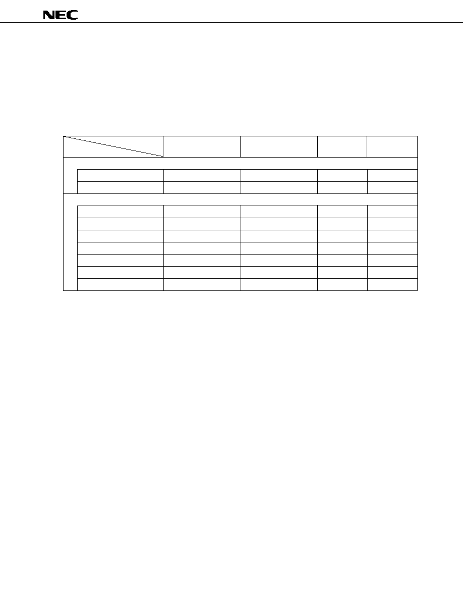
The major functional differences among the Y subseries are shown below.
Function ROM Capacity
Configuration of Serial Interface
I/O V
DD
MIN.
Subseries Name
Value
Control
µ
PD78078Y
48 K to 60 K
3-wire/2-wire/I
2
C:
1 ch
88
1.8 V
3-wire with automatic transmit/receive function: 1 ch
µ
PD78070AY
--
3-wire/UART:
1 ch
61
2.7 V
µ
PD780018AY
48 K to 60 K
3-wire with automatic transmit/receive function: 1 ch
88
Time-division 3-wire:
1 ch
I
2
C bus (multimaster supported):
1 ch
µ
PD780058Y
24 K to 60 K
3-wire/2-wire/I
2
C:
1 ch
68
1.8 V
3-wire with automatic transmit/receive function: 1 ch
3-wire/time-division UART:
1 ch
µ
PD78058FY
48 K to 60 K
3-wire/2-wire/I
2
C:
1 ch
69
2.7 V
3-wire with automatic transmit/receive function: 1 ch
µ
PD78054Y
16 K to 60 K
3-wire/UART:
1 ch
2.0 V
µ
PD780078Y
48 K to 60 K
3-wire:
1 ch
52
1.8 V
UART:
1 ch
3-wire/UART:
1 ch
I
2
C bus (multimaster supported):
1 ch
µ
PD780034AY
8 K to 32 K
UART:
1 ch
51
1.8 V
3-wire:
1 ch
µ
PD780024AY
I
2
C bus (multimaster supported):
1 ch
µ
PD78018FY
8 K to 60 K
3-wire/2-wire/I
2
C:
1 ch
53
3-wire with automatic transmit/receive function: 1 ch
LCD
µ
PD780308Y
48 K to 60 K
3-wire/2-wire/I
2
C:
1 ch
57
2.0 V
drive
3-wire/time-division UART:
1 ch
3-wire:
1 ch
µ
PD78064Y
16 K to 32 K
3-wire/2-wire/I
2
C:
1 ch
3-wire/UART:
1 ch
Remark
Functions other than the serial interface are common to the non-Y subseries.
5
µ
PD780031AY, 780032AY, 780033AY, 780034AY
Data Sheet U14045EJ1V0DS00
OVERVIEW OF FUNCTIONS
Part Number
µ
PD780031AY
µ
PD780032AY
µ
PD780033AY
µ
PD780034AY
Item
Internal
ROM
8 Kbytes
16 Kbytes
24 Kbytes
32 Kbytes
memory
High-speed RAM
512 bytes
1024 bytes
Memory space
64 Kbytes
General-purpose registers
8 bits
◊
32 registers (8 bits
◊
8 registers
◊
4 banks)
Minimum instruction execution
On-chip minimum instruction execution time cycle variable function
When main system
0.24
µ
s/0.48
µ
s/0.95
µ
s/1.91
µ
s/3.81
µ
s (@ 8.38-MHz operation)
clock selected
When subsystem
122
µ
s (@ 32.768-kHz operation)
clock selected
Instruction set
∑ 16-bit operation
∑ Multiply/divide (8 bits
◊
8 bits,16 bits
˜
8 bits)
∑ Bit manipulation (set, reset, test, Boolean operation)
∑ BCD adjust, etc.
I/O ports
Total:
51
∑ CMOS input:
8
∑ CMOS I/O:
39
∑ 5-V-tolerant N-ch open-drain I/O:
4
A/D converter
∑ 10-bit resolution x 8 channels
∑ Low-voltage operation available: AV
DD
= 1.8 to 5.5 V
Serial interface
∑ 3-wire serial I/O mode:
1 channel
∑ UART mode:
1 channel
∑ I
2
C bus mode (multimaster supported):
1 channel
Timer
∑ 16-bit timer/event counter:
1 channel
∑ 8-bit timer/event counter:
2 channels
∑ Watch timer:
1 channel
∑ Watchdog timer:
1 channel
Timer output
3 (8-bit PWM output capable: 2)
Clock output
∑ 65.5 kHz, 131 kHz, 262 kHz, 524 kHz, 1.05 MHz, 2.10 MHz, 4.19 MHz, 8.38 MHz
(@ 8.38-MHz operation with main system clock )
∑ 32.768 kHz (@ 32.768-kHz operation with subsystem clock)
Buzzer output
1.02 kHz, 2.05 kHz, 4.10 kHz, 8.19 kHz (@ 8.38-MHz operation with main system clock)
Vectored
Maskable
Internal: 13, external: 5
interrupt
Non-maskable
Internal: 1
sources
Software
1
Power supply voltage
V
DD
= 1.8 to 5.5 V
Operating ambient temperature
T
A
= ≠40 to +85
∞
C
Package
∑ 64-pin plastic shrink DIP (750 mils)
∑ 64-pin plastic QFP (14
◊
14 mm)
∑ 64-pin plastic LQFP (12
◊
12 mm)
time

6
µ
PD780031AY, 780032AY, 780033AY, 780034AY
Data Sheet U14045EJ1V0DS00
CONTENTS
1.
PIN CONFIGURATION (Top View) ..................................................................................................... 7
2.
BLOCK DIAGRAM .............................................................................................................................10
3.
PIN FUNCTIONS ................................................................................................................................ 11
3.1
Port Pins .................................................................................................................................................... 11
3.2
Non-Port Pins ............................................................................................................................................ 12
3.3
Pin I/O Circuits and Recommended Connection of Unused Pins ..................................................... 14
4.
MEMORY SPACE ...............................................................................................................................16
5. PERIPHERAL HARDWARE FUNCTION FEATURES ....................................................................... 17
5.1
Ports ........................................................................................................................................................... 17
5.2
Clock Generator ........................................................................................................................................ 18
5.3
Timer/Counter ........................................................................................................................................... 19
5.4
Clock Output/Buzzer Output Control Circuit ....................................................................................... 23
5.5
A/D Converter ........................................................................................................................................... 24
5.6
Serial Interface .......................................................................................................................................... 25
6.
INTERRUPT FUNCTION .................................................................................................................... 28
7.
EXTERNAL DEVICE EXPANSION FUNCTION ............................................................................... 31
8.
STANDBY FUNCTION .......................................................................................................................31
9.
RESET FUNCTION ............................................................................................................................31
10. MASK OPTION ...................................................................................................................................31
11. INSTRUCTION SET ...........................................................................................................................32
12. ELECTRICAL SPECIFICATIONS ...................................................................................................... 34
13. PACKAGE DRAWINGS .....................................................................................................................57
14. RECOMMENDED SOLDERING CONDITIONS ................................................................................ 60
APPENDIX A. DEVELOPMENT TOOLS ................................................................................................ 62
APPENDIX B. RELATED DOCUMENTS ............................................................................................... 65

7
µ
PD780031AY, 780032AY, 780033AY, 780034AY
Data Sheet U14045EJ1V0DS00
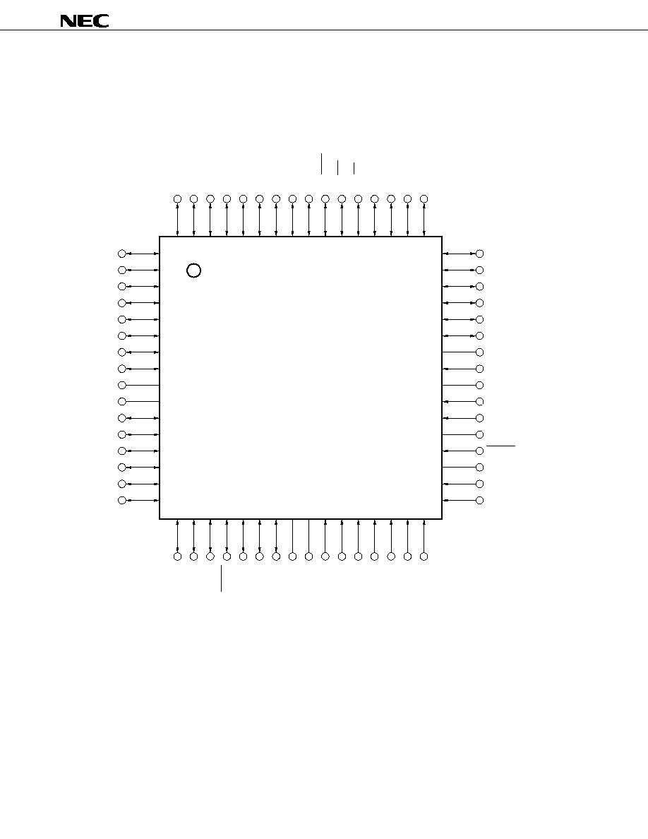
1. PIN CONFIGURATION (Top View)
∑
64-pin plastic shrink DIP (750 mils)
µ
PD780031AYCW-
◊◊◊
, 780032AYCW-
◊◊◊
, 780033AYCW-
◊◊◊
, 780034AYCW-
◊◊◊
Cautions 1. Connect the IC (Internally Connected) pin directly to V
SS0
or V
SS1
.
2. Connect the AV
SS
pin to V
SS0
.
Remark
When the
µ
PD780031AY, 780032AY, 780033AY, and 780034AY are used in applications where the
noise generated inside the microcontroller needs to be reduced, the implementation of noise reduction
measures, such as supplying voltage to V
DD0
and V
DD1
individually and connecting V
SS0
and V
SS1
to
different ground lines, is recommended.
1
2
3
4
5
6
7
8
9
10
11
12
13
14
15
16
17
18
19
20
21
22
23
24
25
26
27
28
29
30
31
32
P67/ASTB
P66/WAIT
P65/WR
P64/RD
P75/BUZ
P74/PCL
P73/TI51/TO51
P72/TI50/TO50
P71/TI01
P70/TI00/TO0
P03/INTP3/ADTRG
P02/INTP2
P01/INTP1
P00/INTP0
V
SS1
X1
X2
IC
XT1
XT2
RESET
AV
DD
AV
REF
P10/ANI0
P11/ANI1
P12/ANI2
P13/ANI3
P14/ANI4
P15/ANI5
P16/ANI6
P17/ANI7
AV
SS
64
63
62
61
60
59
58
57
56
55
54
53
52
51
50
49
48
47
46
45
44
43
42
41
40
39
38
37
36
35
34
33
P40/AD0
P41/AD1
P42/AD2
P43/AD3
P44/AD4
P45/AD5
P46/AD6
P47/AD7
P50/A8
P51/A9
P52/A10
P53/A11
P54/A12
P55/A13
P56/A14
P57/A15
V
SS0
V
DD0
P30
P31
P32/SDA0
P33/SCL0
P34
P35
P36
P20/SI30
P21/SO30
P22/SCK30
P23/RxD0
P24/TxD0
P25/ASCK0
V
DD1
8
µ
PD780031AY, 780032AY, 780033AY, 780034AY
Data Sheet U14045EJ1V0DS00
∑
64-pin plastic QFP (14
◊
14 mm)
µ
PD780031AYGC-
◊◊◊
-AB8, 780032AYGC-
◊◊◊
-AB8, 780033AYGC-
◊◊◊
-AB8, 780034AYGC-
◊◊◊
-AB8
∑
64-pin plastic LQFP (12
◊
12 mm)
µ
PD780031AYGK-
◊◊◊
-8A8, 780032AYGK-
◊◊◊
-8A8, 780033AYGK-
◊◊◊
-8A8, 780034AYGK-
◊◊◊
-8A8
Cautions 1. Connect the IC (Internally Connected) pin directly to V
SS0
or V
SS1
.
2. Connect the AV
SS
pin to V
SS0
.
Remark
When the
µ
PD780031AY, 780032AY, 780033AY, and 780034AY are used in applications where the
noise generated inside the microcontroller needs to be reduced, the implementation of noise reduction
measures, such as supplying voltage to V
DD0
and V
DD1
individually and connecting V
SS0
and V
SS1
to
different ground lines, is recommended.
1
2
3
4
5
6
7
8
9
10
11
12
13
14
15
16
P50/A8
P51/A9
P52/A10
P53/A11
P54/A12
P55/A13
P56/A14
P57/A15
V
SS0
V
DD0
P30
P31
P32/SDA0
P33/SCL0
P34
P35
P36
P20/SI30
P21/SO30
P22/SCK30
P23/RxD0
P24/TxD0
P25/ASCK0
V
DD1
AV
SS
P17/ANI7
P16/ANI6
P15/ANI5
P14/ANI4
P13/ANI3
P12/ANI2
P11/ANI1
48
47
46
45
44
43
42
41
40
39
38
37
36
35
34
33
P71/TI01
P70/TI00/TO0
P03/INTP3/ADTRG
P02/INTP2
P01/INTP1
P00/INTP0
V
SS1
X1
X2
IC
XT1
XT2
RESET
AV
DD
AV
REF
P10/ANI0
17 18 19 20 21 22
23
24 25
26 27 28 29 30
31 32
64 63 62 61 60 59
58
57 56
55 54 53 52 51
50 49
P47/AD7
P46/AD6
P45/AD5
P44/AD4
P43/AD3
P42/AD2
P41/AD1
P40/AD0
P67/ASTB
P66/WAIT
P65/WR
P64/RD
P75/BUZ
P74/PCL
P73/TI51/TO51
P72/TI50/TO50

9
µ
PD780031AY, 780032AY, 780033AY, 780034AY
Data Sheet U14045EJ1V0DS00
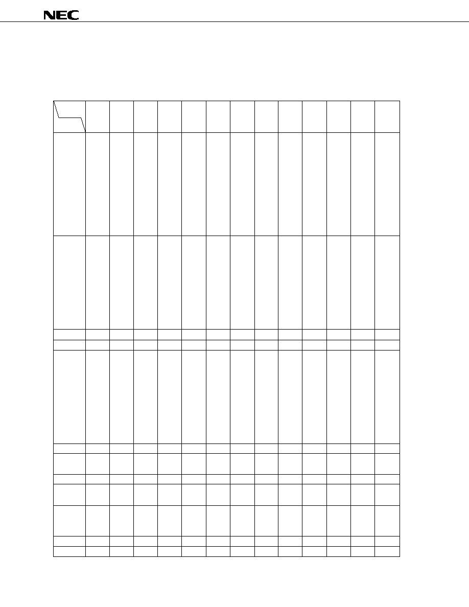
P70 to P75:
Port 7
PCL:
Programmable Clock
RD:
Read Strobe
RESET:
Reset
RxD0:
Receive Data
SCK30, SCL0:
Serial Clock
SDA0:
Serial Data
SI30:
Serial Input
SO30:
Serial Output
TI00, TI01, TI50, TI51: Timer Input
TO0, TO50, TO51:
Timer Output
TxD0:
Transmit Data
V
DD0
, V
DD1
:
Power Supply
V
SS0
, V
SS1
:
Ground
WAIT:
Wait
WR:
Write Strobe
X1, X2:
Crystal (Main System Clock)
XT1, XT2:
Crystal (Subsystem Clock)
A8 to A15:
Address Bus
AD0 to AD7:
Address/Data Bus
ADTRG:
AD Trigger Input
ANI0 to ANI7:
Analog Input
ASCK0:
Asynchronous Serial Clock
ASTB:
Address Strobe
AV
DD
:
Analog Power Supply
AV
REF
:
Analog Reference Voltage
AV
SS
:
Analog Ground
BUZ:
Buzzer Clock
IC:
Internally Connected
INTP0 to INTP3:
External Interrupt Input
P00 to P03:
Port 0
P10 to P17:
Port 1
P20 to P25:
Port 2
P30 to P36:
Port 3
P40 to P47:
Port 4
P50 to P57:
Port 5
P64 to P67:
Port 6
10
µ
PD780031AY, 780032AY, 780033AY, 780034AY
Data Sheet U14045EJ1V0DS00
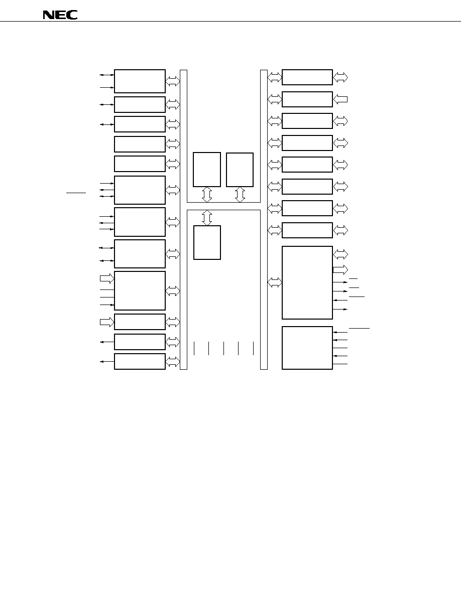
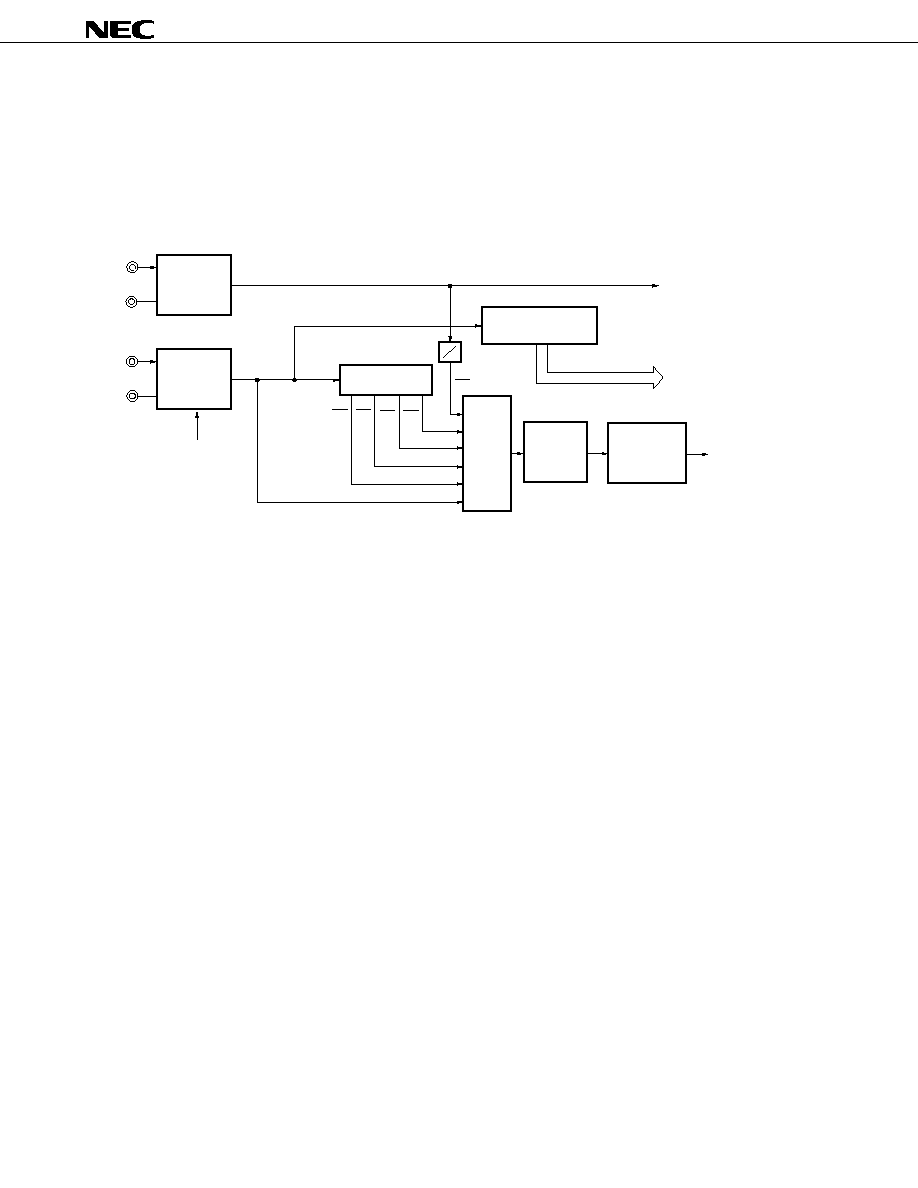
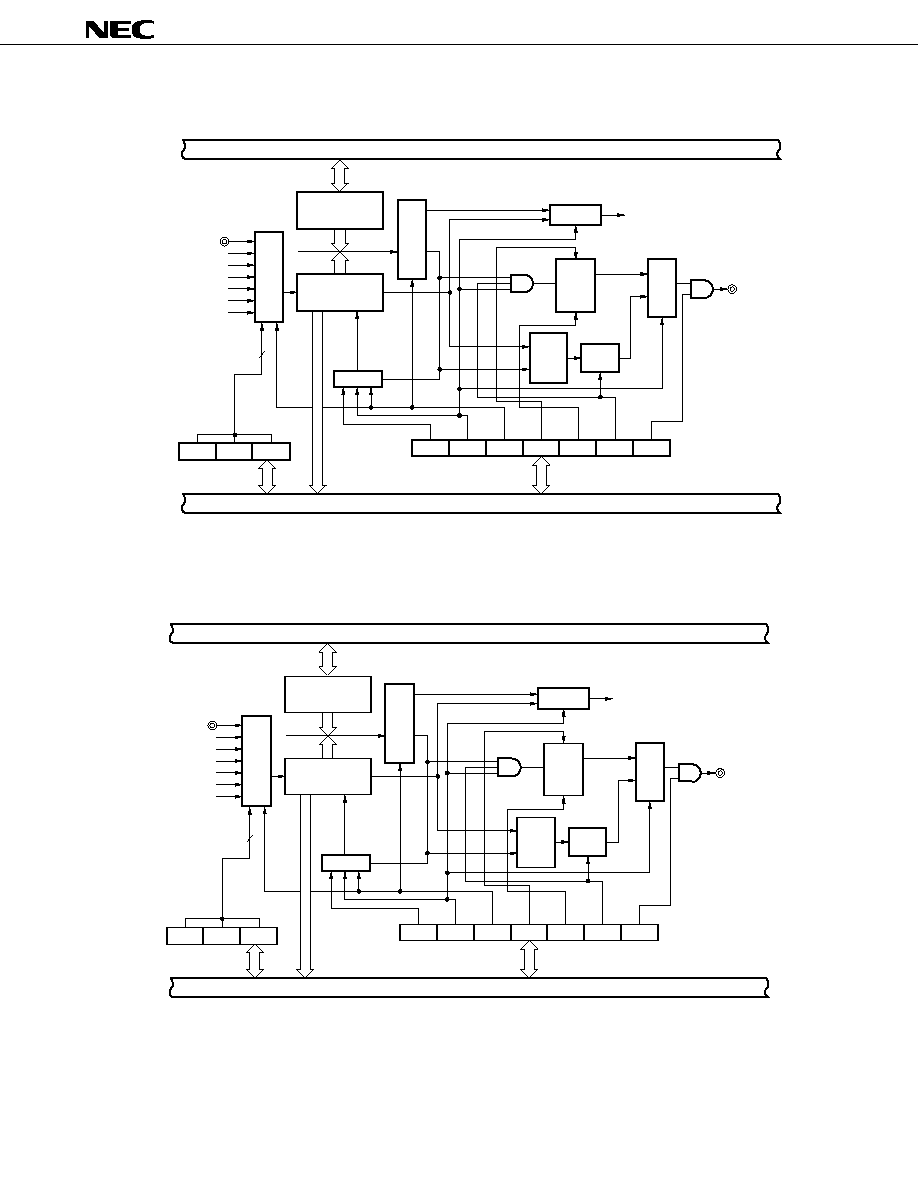
2. BLOCK DIAGRAM
Remark
The internal ROM and RAM capacities differ depending on the product.
TI00/TO0/P70
16-BIT TIMER/
EVENT COUNTER
SERIAL
INTERFACE 30
INTERRUPT
CONTROL
BUZZER OUTPUT
CLOCK OUTPUT
CONTROL
78K/0
CPU CORE
PORT 0
PORT 1
PORT 2
PORT 3
PORT 4
PORT 5
PORT 6
PORT 7
P70 to P75
P64 to P67
P50 to P57
P40 to P47
P30 to P36
P20 to P25
P10 to P17
P00 to P03
EXTERNAL
ACCESS
SYSTEM
CONTROL
RESET
X1
X2
XT1
XT2
RD/P64
WR/P65
WAIT/P66
ASTB/P67
AD0/P40 to
AD7/P47
A8/P50 to
A15/P57
ROM
RAM
A/D CONVERTER
V
DD0
V
DD1
V
SS0
V
SS1
IC
WATCHDOG TIMER
WATCH TIMER
8-BIT TIMER/
EVENT COUNTER 50
8-BIT TIMER/
EVENT COUNTER 51
TI50/TO50/P72
TI51/TO51/P73
SI30/P20
SO30/P21
SCK30/P22
AV
DD
AV
SS
AV
REF
BUZ/P75
PCL/P74
ANI0/P10 to
ANI7/P17
INTP0/P00 to
INTP3/P03
TI01/P71
I
2
C BUS
SDA0/P32
SCL0/P33
UART0
RxD0/P23
TxD0/P24
ASCK0/P25
11
µ
PD780031AY, 780032AY, 780033AY, 780034AY
Data Sheet U14045EJ1V0DS00
3. PIN FUNCTIONS
3.1 Port Pins (1/2)
Pin Name
I/O
Function
After
Alternate
Reset
Function
P00
I/O
Port 0
Input
INTP0
P01
4-bit input/output port
INTP1
P02
Input/output can be specified in 1-bit units.
INTP2
P03
An on-chip pull-up resistor can be connected by means of software.
INTP3/ADTRG
P10 to P17
Input
Port 1
Input
ANI0 to ANI7
8-bit input-only port
P20
I/O
Port 2
Input
SI30
P21
6-bit input/output port
SO30
P22
Input/output can be specified in 1-bit units.
SCK30
P23
An on-chip pull-up resistor can be connected by means of software.
RxD0
P24
TxD0
P25
ASCK0
P30
I/O
Port 3
N-ch open-drain input/output port
Input
--
P31
7-bit input/output port
The mask option can be used to specify the
P32
Input/output can be
connection of an on-chip pull-up resistor to P30, P31.
SDA0
P33
specified in 1-bit units.
LEDs can be driven directly.
SCL0
P34
An on-chip pull-up resistor can be
--
P35
connected by means of software.
P36
P40 to P47
I/O
Port 4
Input
AD0 to AD7
8-bit input/output port
Input/output can be specified in 1-bit units.
An on-chip pull-up resistor can be connected by means of software.
The interrupt request flag (KRIF) is set to 1 by falling edge detection.
P50 to P57
I/O
Port 5
Input
A8 to A15
8-bit input/output port
LEDs can be driven directly.
Input/output can be specified in 1-bit units.
An on-chip pull-up resistor can be connected by means of software.
P64
I/O
Port 6
Input
RD
P65
4-bit input/output port
WR
P66
Input/output can be specified in 1-bit units.
WAIT
P67
An on-chip pull-up resistor can be connected by means of software.
ASTB

12
µ
PD780031AY, 780032AY, 780033AY, 780034AY
Data Sheet U14045EJ1V0DS00
3.1 Port Pins (2/2)
Pin Name
I/O
Function
After
Alternate
Reset
Function
P70
I/O
Port 7
Input
TI00/TO0
P71
6-bit input/output port
TI01
P72
Input/output can be specified in 1-bit units.
TI50/TO50
P73
An on-chip pull-up resistor can be connected by means of software.
TI51/TO51
P74
PCL
P75
BUZ
3.2 Non-Port Pins (1/2)
Pin Name
I/O
Function
After
Alternate
Reset
Function
INTP0
Input
External interrupt request input for which the valid edge (rising edge,
Input
P00
INTP1
falling edge, or both rising and falling edges) can be specified
P01
INTP2
P02
INTP3
P03/ADTRG
SI30
Input
Serial interface serial data input
Input
P20
SO30
Output
Serial interface serial data output
Input
P21
SDA0
I/O
Serial interface serial data input/output
Input
P32
SCK30
I/O
Serial interface serial clock input/output
Input
P22
SCL0
P33
RxD0
Input
Serial data input for asynchronous serial interface
Input
P23
TxD0
Output
Serial data output for asynchronous serial interface
Input
P24
ASCK0
Input
Serial clock input for asynchronous serial interface
Input
P25
TI00
Input
External count clock input to 16-bit timer (TM0)
Input
P70/TO0
Capture trigger input to capture register (CR01) of 16-bit timer (TM0)
TI01
Capture trigger input to capture register (CR00) of 16-bit timer (TM0)
P71
TI50
External count clock input to 8-bit timer (TM50)
P72/TO50
TI51
External count clock input to 8-bit timer (TM51)
P73/TO51
TO0
Output
16-bit timer (TM0) output
Input
P70/TI00
TO50
8-bit timer (TM50) output (also used for 8-bit PWM output)
Input
P72/TI50
TO51
8-bit timer (TM51) output (also used for 8-bit PWM output)
P73/TI51
PCL
Output
Clock output (for trimming of main system clock and subsystem clock)
Input
P74
BUZ
Output
Buzzer output
Input
P75
AD0 to AD7
I/O
Lower address/data bus for expanding memory externally
Input
P40 to P47
A8 to A15
Output
Higher address bus for expanding memory externally
Input
P50 to P57
RD
Output
Strobe signal output for reading from external memory
Input
P64
WR
Strobe signal output for writing to external memory
P65
WAIT
Input
Wait insertion at external memory access
Input
P66
ASTB
Output
Strobe output that externally latches address information output to
Input
P67
ports 4 and 5 to access external memory
13
µ
PD780031AY, 780032AY, 780033AY, 780034AY
Data Sheet U14045EJ1V0DS00
3.2 Non-Port Pins (2/2)
Pin Name
I/O
Function
After
Alternate
Reset
Function
ANI0 to ANI7
Input
A/D converter analog input
Input
P10 to P17
ADTRG
Input
A/D converter trigger signal input
Input
P03/INTP3
AV
REF
Input
A/D converter reference voltage input
--
--
AV
DD
--
A/D converter analog power supply. Set potential to that of V
DD0
or V
DD1
.
--
--
AV
SS
--
A/D converter ground potential. Set potential to that of V
SS0
or V
SS1
.
--
--
RESET
Input
System reset input
--
--
X1
Input
Connecting crystal resonator for main system clock oscillation
--
--
X2
--
--
--
XT1
Input
Connecting crystal resonator for subsystem clock oscillation
--
--
XT2
--
--
--
V
DD0
--
Positive power supply for ports
--
--
V
SS0
--
Ground potential of ports
--
--
V
DD1
--
Positive power supply (except ports)
--
--
V
SS1
--
Ground potential (except ports)
--
--
IC
--
Internally connected. Connect directly to V
SS0
or V
SS1
.
--
--
14
µ
PD780031AY, 780032AY, 780033AY, 780034AY
Data Sheet U14045EJ1V0DS00
3.3 Pin I/O Circuits and Recommended Connection of Unused Pins
The input/output circuit type of each pin and recommended connection of unused pins are shown in Table 3-1.
For the input/output circuit configuration of each type, see Figure 3-1.
Table 3-1. Types of Pin Input/Output Circuits
Pin Name
Input/Output
I/O
Recommended Connection of Unused Pins
Circuit Type
P00/INTP0 to P02/INTP2
8-C
Input
Independently connect to V
SS0
via a resistor.
P03/INTP3/ADTRG
P10/ANI0 to P17/ANI7
25
Input
Independently connect to V
DD0
or V
SS0
via a resistor.
P20/SI30
8-C
I/O
P21/SO30
5-H
P22/SCK30
8-C
P23/RxD0
P24/TxD0
5-H
P25/ASCK0
8-C
P30, P31
13-Q
I/O
Independently connect to V
DD0
via a resistor.
P32/SDA0
13-R
P33/SCL0
P34
8-C
Independently connect to V
DD0
or V
SS0
via a resistor.
P35
5-H
P36
8-C
P40/AD0 to P47/AD7
5-H
I/O
Independently connect to V
DD0
via a resistor.
P50/A8 to P57/A15
I/O
Independently connect to V
DD0
or V
SS0
via a resistor.
P64/RD
I/O
P65/WR
P66/WAIT
P67/ASTB
P70/TI00/TO0
8-C
P71/TI01
P72/TI50/TO50
P73/TI51/TO51
P74/PCL
5-H
P75/BUZ
RESET
2
Input
--
XT1
16
Connect to V
DD0
.
XT2
--
Leave open.
AV
DD
--
Connect to V
DD0
.
AV
REF
Connect to V
SS0
.
AV
SS
IC
Connect directly to V
SS0
or V
SS1
.
15
µ
PD780031AY, 780032AY, 780033AY, 780034AY
Data Sheet U14045EJ1V0DS00
Figure 3-1. Pin Input/Output Circuits
TYPE 2
Schmitt-triggered input with hysteresis characteristics
IN
TYPE 8-C
Data
Output
disable
P-ch
IN/OUT
V
DD0
N-ch
P-ch
V
DD0
Pullup
enable
TYPE 5-H
Data
Output
disable
P-ch
IN/OUT
V
DD0
N-ch
Input
enable
P-ch
V
DD0
Pullup
enable
TYPE 13-Q
Data
Output disable
IN/OUT
N-ch
V
DD0
Mask
option
TYPE 13-R
Input
enable
V
SS0
TYPE 25
V
SS0
V
SS0
Data
Output disable
IN/OUT
N-ch
V
SS0
P-ch
Feedback
cut-off
XT1
XT2
TYPE 16
Input
enable
Comparator
+
≠
P-ch
N-ch
V
REF
(threshold voltage)
V
SS0
IN

16
µ
PD780031AY, 780032AY, 780033AY, 780034AY
Data Sheet U14045EJ1V0DS00
4. MEMORY SPACE
Figure 4-1 shows the memory map of the
µ
PD780031AY, 780032AY, 780033AY, and 780034AY.
Figure 4-1. Memory Map
Note
The internal ROM and internal high-speed RAM capacities differ depending on the product (see the
following table).
Part Number
Last Address of Internal ROM
Start Address of Internal High-Speed RAM
nnnnH
mmmmH
µ
PD780031AY
1FFFH
FD00H
µ
PD780032AY
3FFFH
µ
PD780033AY
5FFFH
FB00H
µ
PD780034AY
7FFFH
Special function registers
(SFRs) 256
◊
8 bits
General-purpose
registers
32
◊
8 bits
Internal high-speed
RAM
Note
Reserved
External memory
Internal ROM
Note
Data memory
space
Program memory
space
FFFFH
FF00H
FEFFH
FEE0H
FEDFH
mmmmH
mmmmH ≠ 1
F7FFH
nnnnH + 1
nnnnH
0000H
Program area
CALLF entry area
Program area
CALLT table area
Vector table area
nnnnH
1000H
0FFFH
0800H
07FFH
0080H
007FH
0040H
003FH
0000H
F800H
17
µ
PD780031AY, 780032AY, 780033AY, 780034AY
Data Sheet U14045EJ1V0DS00
5. PERIPHERAL HARDWARE FUNCTION FEATURES
5.1 Ports
The following 3 types of I/O ports are available.
∑
CMOS input (Port 1):
8
∑
CMOS input/output (Ports 0, 2 to 7, P34 to P36):
39
∑
N-ch open-drain input/output (P30 to P33):
4
Total:
51
Table 5-1. Port Functions
Name
Pin Name
Function
Port 0
P00 to P03
I/O port pins. Input/output can be specified in 1-bit units.
An on-chip pull-up resistor can be connected by means of software.
Port 1
P10 to P17
Dedicated input port pins.
Port 2
P20 to P25
I/O port pins. Input/output can be specified in 1-bit units.
An on-chip pull-up resistor can be connected by means of software.
Port 3
P30 to P33
N-ch open-drain I/O port pins. Input/output can be specified in 1-bit units.
The mask option can be used to specify the connection of an on-chip pull-up resistor to P30, P31.
LEDs can be driven directly.
P34 to P36
I/O port pins. Input/output can be specified in 1-bit units.
An on-chip pull-up resistor can be connected by means of software.
Port 4
P40 to P47
I/O port pins. Input/output can be specified in 1-bit units.
An on-chip pull-up resistor can be connected by means of software.
The interrupt request flag (KRIF) is set to 1 by falling edge detection.
Port 5
P50 to P57
I/O port pins. Input/output can be specified in 1-bit units.
An on-chip pull-up resistor can be connected by means of software.
LEDs can be driven directly.
Port 6
P64 to P67
I/O port pins. Input/output can be specified in 1-bit units.
An on-chip pull-up resistor can be connected by means of software.
Port 7
P70 to P75
I/O port pins. Input/output can be specified in 1-bit units.
An on-chip pull-up resistor can be connected by means of software.
18
µ
PD780031AY, 780032AY, 780033AY, 780034AY
Data Sheet U14045EJ1V0DS00
5.2 Clock Generator
A system clock generator is incorporated.
The minimum instruction execution time can be changed.
∑
0.24
µ
s/0.48
µ
s/0.95
µ
s/1.91
µ
s/3.81
µ
s (@ 8.38-MHz operation with main system clock)
∑
122
µ
s
(@ 32.768-kHz operation with subsystem clock)
Figure 5-1. Clock Generator Block Diagram
XT1
XT2
X1
X2
f
XT
f
X
Subsystem
clock
oscillator
Watch timer, clock
output function
Prescaler
Main system
clock
oscillator
Clock to peripheral
hardware
CPU clock
(f
CPU
)
Standby
control
circuit
Wait control
circuit
2
f
X
2
2
f
X
2
3
f
X
2
4
f
X
f
XT
2
Prescaler
Selector
STOP
2
1
19
µ
PD780031AY, 780032AY, 780033AY, 780034AY
Data Sheet U14045EJ1V0DS00
5.3 Timer/Counter
Five timer/counter channels are incorporated.
∑
16-bit timer/event counter: 1 channel
∑
8-bit timer/event counter:
2 channels
∑
Watch timer:
1 channel
∑
Watchdog timer:
1 channel
Table 5-2. Operations of Timer/Event Counters
16-Bit Timer/
8-Bit Timer/
Watch Timer
Watchdog Timer
Event Counter TM0
Event Counters TM50, TM51
Operation mode
Interval timer
1 channel
2 channels
1 channel
Note 1
1 channel
Note 2
External event counter
1 channel
2 channels
--
--
Function
Timer output
1 output
2 outputs
--
--
PPG output
1 output
--
--
--
PWM output
--
2 outputs
--
--
Pulse width measurement
2 inputs
--
--
--
Square wave output
1 output
2 outputs
--
--
One-shot pulse output
1 output
--
--
--
Interrupt source
2
2
2
1
Notes 1. The watch timer can perform both watch timer and interval timer functions at the same time.
2. The watchdog timer has watchdog timer and interval timer functions. However, use the watchdog timer
by selecting either the watchdog timer function or the interval timer function.
20
µ
PD780031AY, 780032AY, 780033AY, 780034AY
Data Sheet U14045EJ1V0DS00
Figure 5-2. Block Diagram of 16-Bit Timer/Event Counter TM0
Internal bus
TI01/P71
f
X
f
X
/2
2
f
X
/2
6
f
X
/2
3
TI00/TO0/P70
16-bit capture/compare
register 01 (CR01)
Match
Match
16-bit timer counter 0
(TM0)
Clear
Noise
elimi-
nation
circuit
INTTM00
TO0/TI00/P70
INTTM01
Internal bus
Selector
16-bit capture/compare
register 00 (CR00)
Selector
Selector
Selector
Noise
elimi-
nation
circuit
Noise
elimi-
nation
circuit
Output
control
circuit
21
µ
PD780031AY, 780032AY, 780033AY, 780034AY
Data Sheet U14045EJ1V0DS00
Figure 5-3. Block Diagram of 8-Bit Timer/Event Counter TM50
Figure 5-4. Block Diagram of 8-Bit Timer/Event Counter TM51
Internal bus
8-bit compare
register 50 (CR50)
TI50/TO50/P72
f
X
/2
4
f
X
/2
6
f
X
/2
8
f
X
/2
10
f
X
f
X
/2
2
Match
Mask circuit
OVF
Clear
3
Selector
TCL502 TCL501 TCL500
Timer clock select
register 50 (TCL50)
Internal bus
TCE50 TMC506 TMC504 LVS50 LVR50 TMC501 TOE50
Invert
level
8-bit timer mode control
register 50 (TMC50)
S
R
S
Q
R
INV
Selector
INTTM50
TO50/TI50/P72
Selector
8-bit timer counter
50 (TM50)
Selector
Internal bus
TI51/TO51/P73
f
X
/2
3
f
X
/2
5
f
X
/2
7
f
X
/2
9
f
X
/2
11
f
X
/2
Match
Mask circuit
OVF
Clear
3
TCL512 TCL511 TCL510
Timer clock select
register 51 (TCL51)
Internal bus
TCE51 TMC516 TMC514 LVS51 LVR51 TMC511 TOE51
Invert
level
8-bit timer mode control
register 51 (TMC51)
S
R
Q
R
INV
Selector
INTTM51
TO51/TI51/P73
Selector
Selector
Selector
8-bit compare
register 51
(CR51)
8-bit timer
counter 51
(TM51)
S

22
µ
PD780031AY, 780032AY, 780033AY, 780034AY
Data Sheet U14045EJ1V0DS00
Figure 5-5. Watch Timer Block Diagram
Figure 5-6. Watchdog Timer Block Diagram
f
X
/2
7
f
XT
f
W
f
W
2
4
f
W
2
5
f
W
2
6
f
W
2
7
f
W
2
8
f
W
2
9
Clear
9-bit prescaler
Clear
5-bit counter
INTWT
INTWTI
WTM7 WTM6 WTM5 WTM4 WTM1 WTM0
Watch timer operation
mode register (WTM)
Internal bus
Selector
Selector
Oscillation
stabilization time
select register
(OSTS)
Clock
input
control
circuit
INTWDT
RESET
WDT mode signal
3
OSTS2 OSTS1 OSTS0
WDCS2 WDCS1 WDCS0
Internal bus
Division
circuit
Divided
clock
selection
circuit
Output
control
circuit
Division mode
selection circuit
RUN WDTM4 WDTM3
Watchdog timer
clock select
register (WDCS)
Watchdog timer
mode register
(WDTM)
RUN
f
X
/2
8

23
µ
PD780031AY, 780032AY, 780033AY, 780034AY
Data Sheet U14045EJ1V0DS00
5.4 Clock Output/Buzzer Output Control Circuit
A clock output/buzzer output control circuit (CKU) is incorporated.
Clocks with the following frequencies can be output as clock output.
∑
65.5 kHz/131 kHz/262 kHz/524 kHz/1.05 MHz/2.10 MHz/4.19 MHz/8.38 MHz (@ 8.38-MHz operation with main
system clock)
∑
32.768 kHz (@ 32.768-kHz operation with subsystem clock)
Clocks with the following frequencies can be output as buzzer output.
∑
1.02 kHz/2.05 kHz/4.10 kHz/8.19 kHz (@ 8.38-MHz operation with main system clock)
Figure 5-7. Block Diagram of Clock Output/Buzzer Output Control Circuit CKU
Prescaler
f
X
f
XT
8
Clock
control
circuit
PCL/P74
BUZ/P75
4
f
X
to f
X
/2
7
f
X
/2
10
to f
X
/2
13
Selector
BCS0, BCS1
BZOE
CLOE
BZOE
BCS1
BCS0
CLOE
CCS3
CCS2
CCS1
CCS0
Internal bus
Clock output select register (CKS)
Selector
24
µ
PD780031AY, 780032AY, 780033AY, 780034AY
Data Sheet U14045EJ1V0DS00
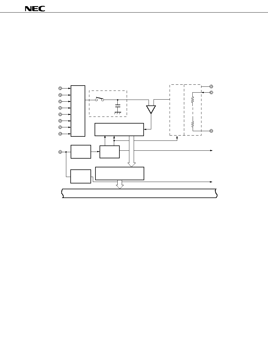
5.5 A/D Converter
An A/D converter consisting of eight 10-bit resolution channels is incorporated.
The following two A/D conversion operation start-up methods are available.
∑
Hardware start
∑
Software start
Figure 5-8. A/D Converter Block Diagram
Tap
selector
INTAD
AV
DD
INTP3
Internal bus
AV
REF
A/D conversion
result register 0 (ADCR0)
Control
circuit
Succesive approximation
register (SAR)
Edge
detection
circuit
ANI0/P10
ANI1/P11
ANI2/P12
ANI3/P13
ANI4/P14
ANI5/P15
ANI6/P16
ANI7/P17
ADTRG/INTP3/P03
Selector
Sample & hold circuit
Voltage comparator
Series resistor string
Edge
detection
circuit
AV
SS
25
µ
PD780031AY, 780032AY, 780033AY, 780034AY
Data Sheet U14045EJ1V0DS00
5.6 Serial Interface
Three serial interface channels are incorporated.
∑
Serial interface UART0:
1 channel
∑
Serial interface SIO30:
1 channel
∑
Serial interface IIC0:
1 channel
(1) Serial interface UART0
The serial interface UART0 has two modes: asynchronous serial interface (UART) mode and infrared data
transfer mode.
∑
Asynchronous serial interface (UART) mode
This mode enables full-duplex operation wherein one byte of data starting from the start bit is transmitted
and received.
The on-chip UART-dedicated baud-rate generator enables communication using a wide range of selectable
baud rates. In addition, a baud rate can be also defined by dividing the clock input to the ASCK0 pin.
The UART-dedicated baud-rate generator can also be used to generate a MIDI-standard baud rate (31.25
kbps).
∑
Infrared data transfer mode
This mode enables pulse output and pulse reception in data format.
This mode can be used for office equipment applications such as personal computers.
Figure 5-9. Block Diagram of Serial Interface UART0
Internal bus
Asynchronous serial
interface mode register 0
(ASIM0)
Asynchronous serial
interface status
register 0 (ASIS0)
Receive
buffer
register 0
RXB0
RxD0/P23
TxD0/P24
Receive
shift
register 0
PE0 FE0 OVE0
TXS0
INTSER0
INTST0
Baud rate
generator
f
X
/2 to f
X
/2
7
TXE0 RXE0 PS01 PS00 CL0
SL0 ISRM0 IRDAM0
INTSR0
Receive
control
circuit
(parity
check)
Transmit
shift
register 0
Transmit
control
circuit
(parity
addition)
RX0
ASCK0/P25
26
µ
PD780031AY, 780032AY, 780033AY, 780034AY
Data Sheet U14045EJ1V0DS00
(2) Serial interface SIO30
The serial interface SIO30 has one mode: 3-wire serial I/O mode.
∑
3-wire serial I/O mode (fixed as MSB first)
This is an 8-bit data transfer mode using three lines: a serial clock line (SCK30), serial output line (SO30),
and serial input line (SI30).
Since simultaneous transmit and receive operations are enabled in the 3-wire serial I/O mode, the
processing time for data transfer is reduced.
The first bit in 8-bit data in the serial transfer is fixed as MSB.
The 3-wire serial I/O mode is useful for connection to peripheral I/O devices, display controllers, etc. that
include a clocked serial interface.
Figure 5-10. Block Diagram of Serial Interface SIO30
Internal bus
8
Serial clock
control circuit
Serial clock
counter
Interrupt request
signal generator
Selector
Serial I/O shift register
30 (SIO30)
SI30/P20
SO30/P21
SCK30/P22
INTCSI30
f
X
/2
3
f
X
/2
4
f
X
/2
5

27
µ
PD780031AY, 780032AY, 780033AY, 780034AY
Data Sheet U14045EJ1V0DS00
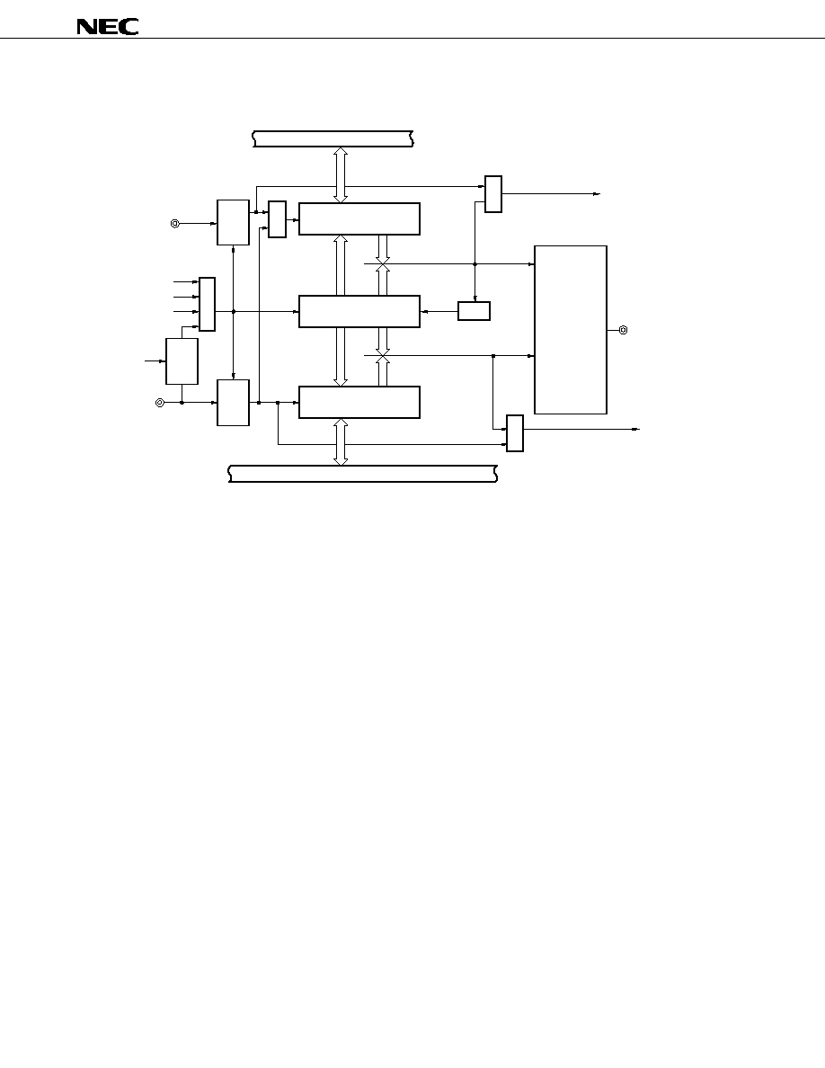
(3) Serial interface IIC0
The serial interface IIC0 has the I
2
C (Inter IC) bus mode (multimaster supported).
∑
I
2
C bus mode (multimaster supported)
This is an 8-bit data transfer mode using two lines: a serial clock line (SCL0) and serial data bus line (SDA0).
This mode complies with the I
2
C bus format, and can output "start condition", "data", and "stop condition"
during transmission via the serial data bus. This data is automatically detected by hardware during
reception.
Since the SCL0 and SDA0 are open-drain outputs in IIC0, pull-up resistors for the serial clock line and the
serial data bus line are required.
Figure 5-11. Block Diagram of Serial Interface IIC0
Internal bus
IIC status register 0
(IICS0)
IIC control register 0
(IICC0)
Slave address
register 0 (SVA0)
Noise elimination
circuit
Noise elimination
circuit
Matched
signal
IIC shift register 0
(IIC0)
SO0 latch
IICE0
D
SET
CLEAR
CL00
SDA0/P32
SCL0/P33
N-ch open-
drain output
Data hold
time correction
circuit
Acknowledge
detection
circuit
Wake-up control
circuit
Acknowledge
detection circuit
Stop condition
detection circuit
Serial clock counter
Interrupt request
signal generator
Serial clock control circuit
N-ch open-drain
output
Serial clock wait
control circuit
Prescaler
INTIIC0
f
X
CLD0
IIC transfer clock select
register 0 (IICCL0)
Internal bus
LREL0 WREL0 SPIE0 WTIM0 ACKE0
STT0
SPT0
MSTS0 ALD0 EXC0
COI0
TRC0 ACKD0 STD0 SPD0
Start condition
detection circuit
DAD0 SMC0 DFC0 CL00
28
µ
PD780031AY, 780032AY, 780033AY, 780034AY
Data Sheet U14045EJ1V0DS00
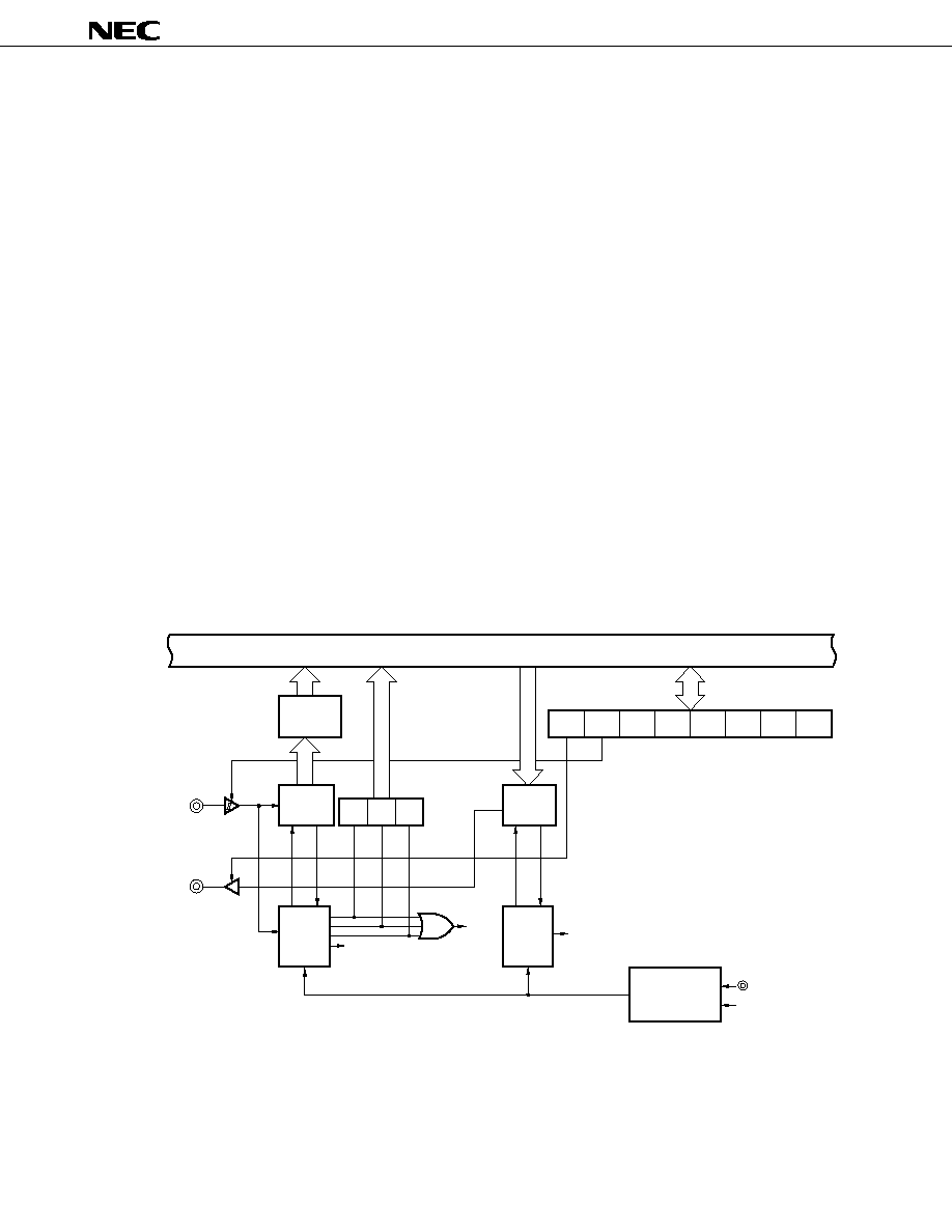
6. INTERRUPT FUNCTION
A total of 20 interrupt sources are provided, divided into the following three types.
∑
Non-maskable: 1
∑
Maskable:
18
∑
Software:
1
Table 6-1. Interrupt Source List
Interrupt
Default
Interrupt Source
Internal/
Vector Table
Type
Priority
Note 1
Name
Trigger
External
Address
Non-
--
INTWDT
Watchdog timer overflow (with watchdog timer
Internal
0004H
(A)
maskable
mode 1 selected)
Maskable
0
INTWDT
Watchdog timer overflow (with interval timer
(B)
mode selected)
1
INTP0
Pin input edge detection
External
0006H
(C)
2
INTP1
0008H
3
INTP2
000AH
4
INTP3
000CH
5
INTSER0
Generation of serial interface UART0
Internal
000EH
(B)
reception error
6
INTSR0
End of serial interface UART0 reception
0010H
7
INTST0
End of serial interface UART0 transmission
0012H
8
INTCSI30
End of serial interface SIO30 transfer
0014H
9
INTIIC0
End of serial interface IIC0 transfer
0016H
10
INTWTI
Reference time interval signal from watch timer
001AH
11
INTTM00
Matching of TM0 and CR00 (when CR00 is
001CH
specified as a compare register)
Detection of TI01 pin valid edge (when CR00
is specified as a capture register)
12
INTTM01
Matching of TM0 and CR01 (when CR01 is
001EH
specified as a compare register)
Detection of TI00 pin valid edge (when CR00
is specified as a capture register)
13
INTTM50
Matching of TM50 and CR50
0020H
14
INTTM51
Matching of TM51 and CR51
0022H
15
INTAD0
End of conversion by A/D converter
0024H
16
INTWT
Watch timer overflow
0026H
17
INTKR
Detection of port 4 falling edge
External
0028H
(D)
Software
--
BRK
Execution of BRK instruction
--
003EH
(E)
Notes 1. Default priority is the priority order when several maskable interrupt requests are generated at the same
time. 0 is the highest and 17 is the lowest.
2. Basic configuration types (A) to (E) correspond to (A) to (E) in Figure 6-1.
Basic
Configuration
Type
Note 2
29
µ
PD780031AY, 780032AY, 780033AY, 780034AY
Data Sheet U14045EJ1V0DS00
Figure 6-1. Basic Configuration of Interrupt Function (1/2)
(A) Internal non-maskable interrupt
(B) Internal maskable interrupt
(C) External maskable interrupt (INTP0 to INTP3)
Internal bus
Priority control
circuit
Vector table
address
generator
Standby release
signal
Interrupt
request
MK
Internal bus
IE
PR
ISP
IF
Priority control
circuit
Vector table
address
generator
Standby release
signal
Interrupt
request
MK
IE
PR
ISP
IF
Priority control
circuit
Vector table
address
generator
External interrupt
edge enable register
(EGP, EGN)
Edge
detection
circuit
Internal bus
Standby release
signal
Interrupt
request
30
µ
PD780031AY, 780032AY, 780033AY, 780034AY
Data Sheet U14045EJ1V0DS00
Figure 6-1. Basic Configuration of Interrupt Function (2/2)
(D) External maskable interrupt (INTKR)
(E) Software interrupt
IF:
Interrupt request flag
IE:
Interrupt enable flag
ISP:
In-service priority flag
MK:
Interrupt mask flag
PR:
Priority specification flag
MEM: Memory expansion mode register
MK
IE
PR
ISP
IF
Priority control
circuit
Vector table
address
generator
Falling edge
detection circuit
Internal bus
Standby release
signal
Interrupt
request
1 when MEM = 01H
Priority control
circuit
Vector table
address
generator
Internal bus
Interrupt
request
31
µ
PD780031AY, 780032AY, 780033AY, 780034AY
Data Sheet U14045EJ1V0DS00
7. EXTERNAL DEVICE EXPANSION FUNCTION
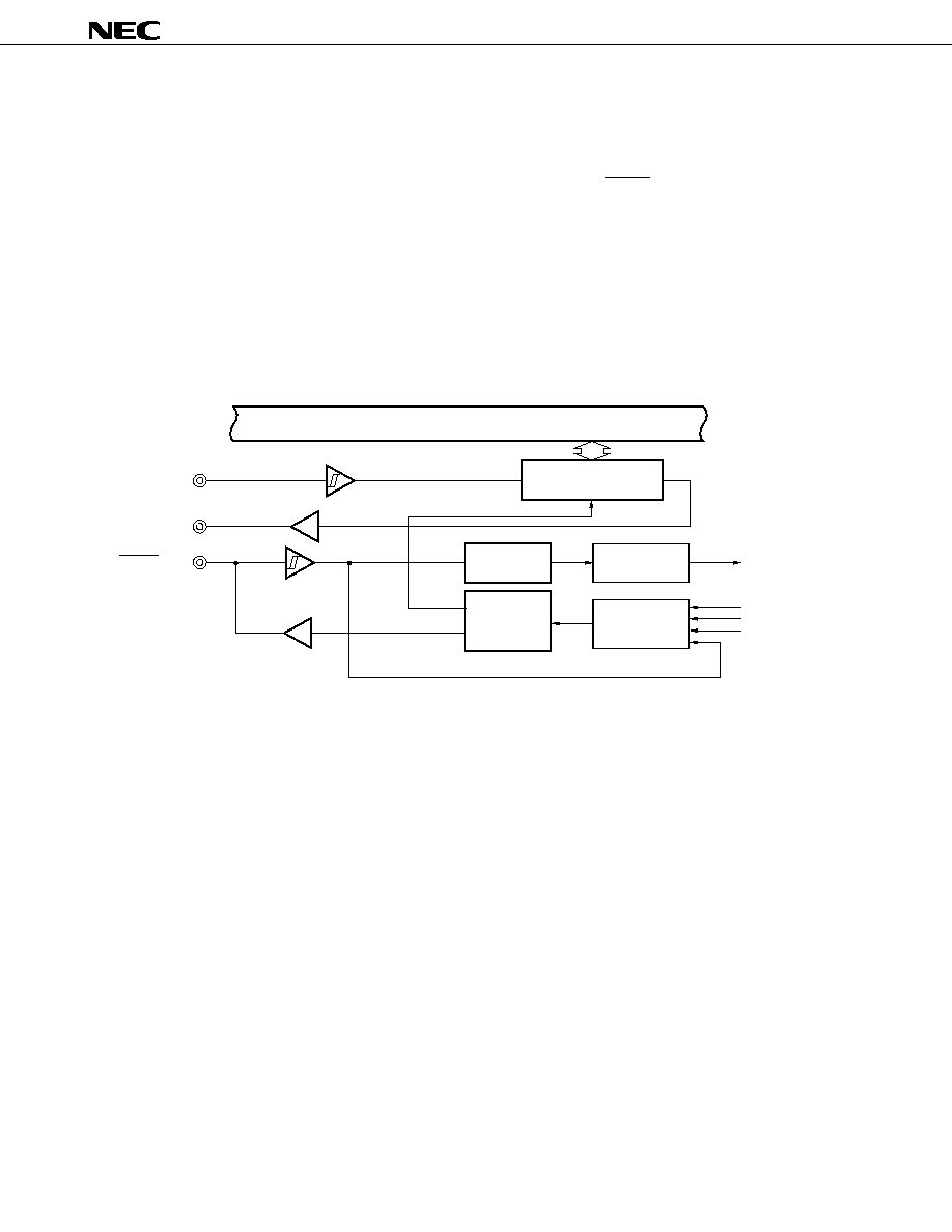
The external device expansion function is for connecting external devices to areas other than the internal ROM,
RAM, and SFR. Ports 4 to 6 are used for external device connection.
8. STANDBY FUNCTION
The following two standby modes are available for further reduction of system current consumption.
∑ HALT mode: In this mode, the CPU operation clock is stopped. The average current consumption can be
reduced by intermittent operation by combining this mode with the normal operation mode.
∑ STOP mode: In this mode, oscillation of the main system clock is stopped. All the operations performed on
the main system clock are suspended, and only the subsystem clock is used, resulting in
extremely small power consumption. This can be used only when the main system clock is
operating (the subsystem clock oscillation cannot be stopped).
Figure 8-1. Standby Function
9. RESET FUNCTION
The following two reset methods are available.
∑
External reset by RESET signal input
∑
Internal reset by watchdog timer runaway time detection
10. MASK OPTION
Table 10.1 Pin Mask Option Selection
Pins
Mask Option
P30, P31
An on-chip pull-up resistor can be specified in 1-bit units.
The mask option can be used to specify the connection of an on-chip pull-up resistor to P30, P31, in 1-bit units.
Main system clock
operation
STOP mode
Main system clock
operation is stopped
Interrupt
request
Interrupt
request
HALT
instruction
HALT
instruction
Interrupt
request
STOP
instruction
CSS = 1
CSS = 0
Subsystem clock
operation
HALT mode
HALT mode
Clock supply for CPU is stopped,
oscillation is maintained
Clock supply for CPU is stopped,
oscillation is maintained
32
µ
PD780031AY, 780032AY, 780033AY, 780034AY
Data Sheet U14045EJ1V0DS00
11. INSTRUCTION SET
(1) 8-bit instructions
MOV, XCH, ADD, ADDC, SUB, SUBC, AND, OR, XOR, CMP, MULU, DIVUW, INC, DEC, ROR,
ROL, RORC, ROLC, ROR4, ROL4, PUSH, POP, DBNZ
2nd
Operand
1st
Operand
#byte
A
r
Note
sfr
saddr
!addr16
PSW
[DE]
[HL]
[HL + byte]
[HL + B]
[HL + C]
$addr16
1
None
A
r
ADD
ADDC
SUB
SUBC
AND
OR
XOR
CMP
MOV
MOV
MOV
MOV
MOV
MOV
MOV
MOV
ROR
XCH
XCH
XCH
XCH
XCH
XCH
XCH
ROL
ADD
ADD
ADD
ADD
ADD
RORC
ADDC
ADDC
ADDC
ADDC
ADDC
ROLC
SUB
SUB
SUB
SUB
SUB
SUBC
SUBC
SUBC
SUBC
SUBC
AND
AND
AND
AND
AND
OR
OR
OR
OR
OR
XOR
XOR
XOR
XOR
XOR
CMP
CMP
CMP
CMP
CMP
MOV
MOV
ADD
ADDC
SUB
SUBC
AND
OR
XOR
CMP
INC
DEC
B, C
sfr
MOV
MOV
DBNZ
MOV
ADD
ADDC
SUB
SUBC
AND
OR
XOR
CMP
saddr
MOV
DBNZ
INC
DEC
!addr16
MOV
PSW
MOV
MOV
PUSH
POP
[DE]
ROR4
MOV
[HL]
MOV
ROL4
[HL + byte]
[HL + B]
[HL + C]
MOV
X
C
MULU
DIVUW
Note
Except r = A
33
µ
PD780031AY, 780032AY, 780033AY, 780034AY
Data Sheet U14045EJ1V0DS00
(2) 16-bit instructions
MOVW, XCHW, ADDW, SUBW, CMPW, PUSH, POP, INCW, DECW
2nd Operand
1st Operand
AX
rp
sfrp
saddrp
!addr16
SP
#word
ADDW
SUBW
CMPW
MOVW
MOVW
MOVW
MOVW
AX
MOVW
Note
MOVW
MOVW
MOVW
MOVW
MOVW
rp
Note
XCHW
sfrp
MOVW
saddrp
MOVW
!addr16
MOVW
SP
MOVW
None
INCW, DECW
PUSH, POP
2nd Operand
1st Operand
A.bit
sfr.bit
saddr.bit
PSW.bit
[HL].bit
CY
$addr16
None
A.bit
sfr.bit
saddr.bit
PSW.bit
[HL].bit
CY
MOV1
MOV1
MOV1
MOV1
MOV1
BT
BF
BTCLR
BT
BF
BTCLR
BT
BF
BTCLR
BT
BF
BTCLR
BT
BF
BTCLR
SET1
CLR1
SET1
CLR1
SET1
CLR1
SET1
CLR1
SET1
CLR1
SET1
CLR1
NOT1
MOV1
AND1
OR1
XOR1
MOV1
AND1
OR1
XOR1
MOV1
AND1
OR1
XOR1
MOV1
AND1
OR1
XOR1
MOV1
AND1
OR1
XOR1
2nd Operand
1st Operand
AX
!addr16
!addr11
[addr5]
$addr16
Basic instruction
Compound
instruction
BR
CALL
BR
CALLF
CALLT
BR, BC, BNC
BZ, BNZ
BT, BF
BTCLR
DBNZ
Note
Only when rp = BC, DE or HL
(3) Bit manipulation instructions
MOV1, AND1, OR1, XOR1, SET1, CLR1, NOT1, BT, BF, BTCLR
(4) Call instructions/branch instructions
CALL, CALLF, CALLT, BR, BC, BNC, BZ, BNZ, BT, BF, BTCLR, DBNZ
(5) Other instructions
ADJBA, ADJBS, BRK, RET, RETI, RETB, SEL, NOP, EI, DI, HALT, STOP
34
µ
PD780031AY, 780032AY, 780033AY, 780034AY
Data Sheet U14045EJ1V0DS00
12. ELECTRICAL SPECIFICATIONS
Absolute Maximum Ratings (T
A
= 25
∞
C)
Parameter
Symbol
Test Conditions
Ratings
Unit
Supply voltage
V
DD
≠0.3 to +6.5
V
AV
DD
≠0.3 to V
DD
+ 0.3
Note
V
AV
REF
≠0.3 to V
DD
+ 0.3
Note
V
AV
SS
≠0.3 to +0.3
V
Input voltage
V
I1
P00 to P03, P10 to P17, P20 to P25, P34 to P36, P40 to P47,
≠0.3 to V
DD
+ 0.3
Note
V
P50 to P57, P64 to P67, P70 to P75, X1, X2, XT1, XT2,
RESET
V
I2
P30 to P33
N-ch open-drain
Without pull-up resistor
≠0.3 to +6.5
V
With pull-up resistor
≠0.3 to V
DD
+ 0.3
Note
V
Output voltage
V
O
≠0.3 to V
DD
+ 0.3
Note
V
Analog input voltage
V
AN
P10 to P17
Analog input pin
AV
SS
≠ 0.3 to AV
REF
+ 0.3
Note
V
and ≠0.3 to V
DD
+ 0.3
Note
Output current,
I
OH
Per pin
≠10
mA
high
Total for P00 to P03, P40 to P47, P50 to P57, P64 to P67, P70 to P75
≠15
mA
Total for P20 to P25, P30 to P36
≠15
mA
Output current,
I
OL
Per pin for P00 to P03, P20 to P25, P34 to
20
mA
low
P36, P40 to P47, P64 to P67, P70 to P75
Per pin for P30 to P33, P50 to P57
30
mA
Total for P00 to P03, P40 to P47,
50
mA
P64 to P67, P70 to P75
Total for P20 to P25
20
mA
Total for P30 to P36
100
mA
Total for P50 to P57
100
mA
Operating ambient
T
A
≠40 to +85
∞
C
temperature
Storage
T
stg
≠65 to +150
∞
C
temperature
Note 6.5 V or below
Caution
Product quality may suffer if the absolute maximum rating is exceeded even momentarily for any
parameter. That is, the absolute maximum ratings are rated values at which the product is on the
verge of suffering physical damage, and therefore the product must be used under conditions that
ensure that the absolute maximum ratings are not exceeded.
35
µ
PD780031AY, 780032AY, 780033AY, 780034AY
Data Sheet U14045EJ1V0DS00
Resonator
Recommended
Parameter
Test Conditions
MIN.
TYP.
MAX.
Unit
Circuit
Ceramic
Oscillation
V
DD
= 4.0 to 5.5 V
1.0
8.38
MHz
resonator
frequency (f
X
)
Note 1
1.0
5.0
Oscillation
After V
DD
reaches
4
ms
stabilization time
Note 2
oscillation voltage range
MIN.
Crystal
Oscillation
V
DD
= 4.0 to 5.5 V
1.0
8.38
MHz
resonator
frequency (f
X
)
Note 1
1.0
5.0
Oscillation
V
DD
= 4.0 to 5.5 V
10
ms
stabilization time
Note 2
30
External
X1 input
V
DD
= 4.0 to 5.5 V
1.0
8.38
MHz
clock
frequency (f
X
)
Note 1
1.0
5.0
X1 input
V
DD
= 4.0 to 5.5 V
50
500
ns
high-/low-level width
85
500
(t
XH
, t
XL
)
Capacitance
(T
A
= 25
∞
C
,
V
DD
= V
SS
= 0 V)
Parameter
Symbol
Test Conditions
MIN.
TYP.
MAX.
Unit
Input
C
IN
f = 1 MHz
15
pF
capacitance
Unmeasured pins returned to 0 V.
I/O
C
IO
f = 1 MHz
P00 to P03, P20 to P25,
15
pF
capacitance
Unmeasured pins
P34 to P36, P40 to P47,
returned to 0 V.
P50 to P57, P64 to P67,
P70 to P75
P30 to P33
20
pF
Remark
Unless otherwise specified, the characteristics of alternate-function pins are the same as those of port pins.
Main System Clock Oscillator Characteristics (T
A
= ≠40 to 85
∞
C, V
DD
= 1.8 to 5.5 V)
Notes 1. Indicates only oscillator characteristics. Refer to AC Characteristics for instruction execution time.
2. Time required to stabilize oscillation after reset or STOP mode release.
Cautions
1. When using the main system clock oscillator, wire as follows in the area enclosed by the broken
lines in the above figures to avoid an adverse effect from wiring capacitance.
∑ Keep the wiring length as short as possible.
∑ Do not cross the wiring with the other signal lines.
∑ Do not route the wiring near a signal line through which a high fluctuating current flows.
∑ Always make the ground point of the oscillator capacitor the same potential as V
SS1
.
∑ Do not ground the capacitor to a ground pattern through which a high current flows.
∑ Do not fetch signals from the oscillator.
2. When the main system clock is stopped and the system is operating on the subsystem clock,
wait until the oscillation stabilization time has been secured by the program before switching
back to the main system clock.
C2
X1
X2 IC
C1
C2
X1
X2 IC
C1
X2
X1
PD74HCU04
µ

36
µ
PD780031AY, 780032AY, 780033AY, 780034AY
Data Sheet U14045EJ1V0DS00
Subsystem Clock Oscillator Characteristics
(T
A
= ≠40 to +85
∞
C, V
DD
= 1.8 to 5.5 V)
Notes 1. Indicates only oscillator characteristics. Refer to AC Characteristics for instruction execution time.
2. Time required to stabilize oscillation after V
DD
reaches oscillation voltage range MIN.
Cautions
1. When using the subsystem clock oscillator, wire as follows in the area enclosed by the broken
lines in the above figures to avoid an adverse effect from wiring capacitance.
∑ Keep the wiring length as short as possible.
∑ Do not cross the wiring with the other signal lines.
∑ Do not route the wiring near a signal line through which a high fluctuating current flows.
∑ Always make the ground point of the oscillator capacitor the same potential as V
SS1
.
∑ Do not ground the capacitor to a ground pattern through which a high current flows.
∑ Do not fetch signals from the oscillator.
2. The subsystem clock oscillator is designed as a low-amplitude circuit for reducing current
consumption, and is more prone to malfunction due to noise than the main system clock
oscillator. Particular care is therefore required with the wiring method when the subsystem
clock is used.
MIN.
32
32
Resonator
Crystal
resonator
External
clock
Parameter
Oscillation
frequency (f
XT
)
Note 1
Oscillation
stabilization time
Note 2
XT1 input
frequency (f
XT
)
Note 1
XT1 input
high-/low-level width
(t
XTH
, t
XTL
)
Test Conditions
TYP.
32.768
1.2
MAX.
35
2
10
38.5
Unit
kHz
s
kHz
V
DD
= 4.0 to 5.5 V
Recommended Circuit
5
15
C3
XT2
XT1 IC
R
C4
XT1
XT2
µ
PD74HCU04
µ
s

37
µ
PD780031AY, 780032AY, 780033AY, 780034AY
Data Sheet U14045EJ1V0DS00
Recommended Oscillator Constant
Main system clock: Ceramic resonator (T
A
= ≠40 to +85
∞
C)
Manufacturer
Part Number
Frequency
Recommended Circuit Constant
Oscillation Voltage Range
(MHz)
C1 (pF)
C2 (pF)
MIN. (V)
MAX. (V)
Murata Mfg.
CSB1000J
1.00
100
100
1.8
5.5
Co., Ltd.
CSA2.00MG040
2.00
100
100
1.8
5.5
CST2.00MG040
2.00
On-chip
On-chip
1.8
5.5
CSA3.58MG
3.58
30
30
1.8
5.5
CST3.58MGW
3.58
On-chip
On-chip
1.8
5.5
CSA4.19MG
4.19
30
30
1.8
5.5
CST4.19MGW
4.19
On-chip
On-chip
1.8
5.5
CSA5.00MG
5.00
30
30
1.8
5.5
CST5.00MGW
5.00
On-chip
On-chip
1.8
5.5
CSA8.00MTZ
8.00
30
30
4.0
5.5
CST8.00MTW
8.00
On-chip
On-chip
4.0
5.5
CSA8.00MTZ093
8.00
30
30
4.0
5.5
CST8.00MTW093
8.00
On-chip
On-chip
4.0
5.5
CSA8.38MTZ
8.38
30
30
4.0
5.5
CST8.38MTW
8.38
On-chip
On-chip
4.0
5.5
CSA8.38MTZ093
8.38
30
30
4.0
5.5
CST8.38MTW093
8.38
On-chip
On-chip
4.0
5.5
TDK
CCR3.58MC3
3.58
On-chip
On-chip
1.8
5.5
CCR4.19MC3
4.19
On-chip
On-chip
1.8
5.5
CCR5.0MC3
5.00
On-chip
On-chip
1.8
5.5
CCR8.0MC5
8.00
On-chip
On-chip
4.0
5.5
CCR8.38MC5
8.38
On-chip
On-chip
4.0
5.5
Caution The oscillator constant and oscillation voltage range indicate conditions of stable oscillation.
Oscillation frequency precision is not guaranteed. For applications requiring oscillation
frequency precision, the oscillation frequency must be adjusted on the implementation circuit.
For details, please contact directly the manufacturer of the resonator you will use.
38
µ
PD780031AY, 780032AY, 780033AY, 780034AY
Data Sheet U14045EJ1V0DS00
DC Characteristics (T
A
= ≠40 to +85
∞
C, V
DD
= 1.8 to 5.5 V)
Parameter
Symbol
Test Conditions
MIN.
TYP.
MAX.
Unit
Output current,
I
OH
Per pin
≠1
mA
high
All pins
≠15
mA
Output current,
I
OL
Per pin for P00 to P03, P20 to P25, P34 to P36,
10
mA
low
P40 to P47, P64 to P67, P70 to P75
Per pin for P30 to P33, P50 to P57
15
mA
Total for P00 to P03, P40 to P47, P64 to P67, P70 to P75
20
mA
Total for P20 to P25
10
mA
Total for P30 to P36
70
mA
Total for P50 to P57
70
mA
Input voltage,
V
IH1
P10 to P17, P21, P24, P35,
V
DD
= 2.7 to 5.5 V
0.7V
DD
V
DD
V
high
P40 to P47, P50 to P57,
P64 to P67, P74, P75
0.8V
DD
V
DD
V
V
IH2
P00 to P03, P20, P22, P23, P25,
V
DD
= 2.7 to 5.5 V
0.8V
DD
V
DD
V
P34, P36, P70 to P73, RESET
0.85V
DD
V
DD
V
V
IH3
P30 to P33
V
DD
= 2.7 to 5.5 V
0.7V
DD
5.5
V
(N-ch open-drain)
0.8V
DD
5.5
V
V
IH4
X1, X2
V
DD
= 2.7 to 5.5 V
V
DD
≠
0.5
V
DD
V
V
DD
≠
0.2
V
DD
V
V
IH5
XT1, XT2
V
DD
= 4.0 to 5.5 V
0.8V
DD
V
DD
V
0.9V
DD
V
DD
V
Input voltage,
V
IL1
P10 to P17, P21, P24, P35,
V
DD
= 2.7 to 5.5 V
0
0.3V
DD
V
low
P40 to P47, P50 to P57,
P64 to P67, P74, P75
0
0.2V
DD
V
V
IL2
P00 to P03, P20, P22, P23, P25,
V
DD
= 2.7 to 5.5 V
0
0.2V
DD
V
P34, P36, P70 to P73, RESET
0
0.15V
DD
V
V
IL3
P30 to P33
4.0 V
V
DD
5.5 V
0
0.3V
DD
V
2.7 V
V
DD
< 4.0 V
0
0.2V
DD
V
1.8 V
V
DD
< 2.7 V
0
0.1V
DD
V
V
IL4
X1, X2
V
DD
= 2.7 to 5.5 V
0
0.4
V
0
0.2
V
V
IL5
XT1, XT2
V
DD
= 4.0 to 5.5 V
0
0.2V
DD
V
0
0.1V
DD
V
Output voltage,
V
OH1
V
DD
= 4.0 to 5.5 V, I
OH
= ≠1 mA
V
DD
≠
1.0
V
DD
V
high
I
OH
= ≠100
µ
A
V
DD
≠
0.5
V
DD
V
Output voltage,
V
OL1
P30 to P33
V
DD
= 4.0 to 5.5 V,
2.0
V
low
P50 to P57
I
OL
= 15 mA
0.4
2.0
V
P00 to P03, P20 to P25, P34 to P36, V
DD
= 4.0 to 5.5 V,
0.4
V
P40 to P47, P64 to P67, P70 to P75
I
OL
= 1.6 mA
V
OL2
I
OL
= 400
µ
A
0.5
V
Remark
Unless otherwise specified, the characteristics of alternate-function pins are the same as those of port pins.

39
µ
PD780031AY, 780032AY, 780033AY, 780034AY
Data Sheet U14045EJ1V0DS00
DC Characteristics (T
A
= ≠40 to +85
∞
C, V
DD
= 1.8 to 5.5 V)
Parameter
Symbol
Test Conditions
MIN.
TYP.
MAX.
Unit
Input leakage
I
LIH1
V
IN
= V
DD
P00 to P03, P10 to P17, P20 to P25,
3
µ
A
current, high
P34 to P36, P40 to P47, P50 to P57,
P64 to P67, P70 to P75,
RESET
I
LIH2
X1, X2, XT1, XT2
20
µ
A
I
LIH3
V
IN
= 5.5 V
P30 to P33
Note
3
µ
A
Input leakage
I
LIL1
V
IN
= 0 V
P00 to P03, P10 to P17, P20 to P25,
≠3
µ
A
current, low
P34 to P36, P40 to P47, P50 to P57,
P64 to P67, P70 to P75,
RESET
I
LIL2
X1, X2, XT1, XT2
≠20
µ
A
I
LIL3
P30 to P33
Note
≠3
µ
A
Output leakage
I
LOH
V
OUT
= V
DD
3
µ
A
current, high
Output leakage
I
LOL
V
OUT
= 0 V
≠3
µ
A
current, low
Mask option
R
1
V
IN
= 0 V,
15
30
90
k
pull-up resistance
P30, P31
Software pull-
R
2
V
IN
= 0 V,
15
30
90
k
up resistance
P00 to P03, P20 to P25, P34 to P36, P40 to P47,
P50 to P57, P64 to P67, P70 to P75
Note
When pull-up resistors are not connected to P30, P31 (specified by the mask option).
Remark
Unless otherwise specified, the characteristics of alternate-function pins are the same as those of port pins.
40
µ
PD780031AY, 780032AY, 780033AY, 780034AY
Data Sheet U14045EJ1V0DS00
DC Characteristics (T
A
= ≠40 to +85
∞
C, V
DD
= 1.8 to 5.5 V)
Parameter
Symbol
Test Conditions
MIN.
TYP.
MAX.
Unit
Power supply
I
DD1
8.38-MHz
V
DD
= 5.0V
±
10%
Note 2
When A/D converter is
5.5
11
mA
current
Note 1
crystal oscillation
stopped
operating mode
When A/D converter is
6.5
13
mA
operating
5.00-MHz
V
DD
= 3.0V
±
10%
Note 2
When A/D converter is
2
4
mA
crystal oscillation
stopped
operating mode
When A/D converter is
3
6
mA
operating
V
DD
= 2.0V
±
10%
Note 3
When A/D converter is
0.4
1.5
mA
stopped
When A/D converter is
1.4
4.2
mA
operating
I
DD2
8.38-MHz
V
DD
= 5.0V
±
10%
Note 2
When peripheral functions
1.1
2.2
mA
crystal oscillation
are stopped
HALT mode
When peripheral functions
4.7
mA
are operating
5.00-MHz
V
DD
= 3.0V
±
10%
Note 2
When peripheral functions
0.35
0.7
mA
crystal oscillation
are stopped
HALT mode
When peripheral functions
1.7
mA
are operating
V
DD
= 2.0V
±
10%
Note 3
When peripheral functions
0.15
0.4
mA
are stopped
When peripheral functions
1.1
mA
are operating
I
DD3
32.768-kHz crystal oscillation
V
DD
= 5.0 V
±
10%
40
80
µ
A
operating mode
Note 4
V
DD
= 3.0 V
±
10%
20
40
µ
A
V
DD
= 2.0 V
±
10%
10
20
µ
A
I
DD4
32.768-kHz crystal oscillation
V
DD
= 5.0 V
±
10%
30
60
µ
A
HALT mode
Note 4
V
DD
= 3.0 V
±
10%
6
18
µ
A
V
DD
= 2.0 V
±
10%
2
10
µ
A
I
DD5
XT1 = 0V STOP mode
V
DD
= 5.0 V
±
10%
0.1
30
µ
A
When feedback resistor is not used
V
DD
= 3.0 V
±
10%
0.05
10
µ
A
V
DD
= 2.0 V
±
10%
0.05
10
µ
A
Notes 1. Total current through the internal power supply (V
DD0
, V
DD1
), including the peripheral operation current
(except the current through pull-up resistors of ports and the AV
REF
pin).
2. When the processor clock control register (PCC) is set to 00H.
3. When PCC is set to 02H.
4. When main system clock operation is stopped.
41
µ
PD780031AY, 780032AY, 780033AY, 780034AY
Data Sheet U14045EJ1V0DS00
AC Characteristics
(1) Basic Operation
(T
A
= ≠40 to +85
∞
C, V
DD
= 1.8 to 5.5 V)
Parameter
Symbol
Test Conditions
MIN.
TYP.
MAX.
Unit
Cycle time
T
CY
Operating with
4.0 V
V
DD
5.5 V
0.24
16
µ
s
(Min. instruction
main system clock
2.7 V
V
DD
< 4.0 V
0.4
16
µ
s
execution time)
1.6
16
µ
s
Operating with subsystem clock
103.9
Note 1
122
125
µ
s
TI00, TI01 input
t
TIH0
, t
TIL0
4.0 V
V
DD
5.5 V
2/f
sam
+ 0.1
Note2
µ
s
high-/low-level
2.7 V
V
DD
< 4.0 V
2/f
sam
+ 0.2
Note2
µ
s
width
2/f
sam
+ 0.5
Note2
µ
s
TI50, TI51 input
f
TI5
V
DD
= 2.7 to 5.5 V
0
4
MHz
frequency
0
275
kHz
TI50, TI51 input
t
TIH5
, t
TIL5
V
DD
= 2.7 to 5.5 V
100
ns
high-/low-level
width
1.8
ns
Interrupt request
t
INTH
, t
INTL
INTP0 to INTP3,
V
DD
= 2.7 to 5.5 V
1
µ
s
input high-/low
P40 to P47
-level width
2
µ
s
RESET
t
RSL
V
DD
= 2.7 to 5.5 V
10
µ
s
low-level width
20
µ
s
Notes 1. Value when an external clock is used. When a crystal resonator is used, it is 114
µ
s (MIN.).
2. Selection of f
sam
= f
X
, f
X
/4, f
X
/64 is possible using bits 0 and 1 (PRM00, PRM01) of prescaler mode register
0 (PRM0). However, if the TI00 valid edge is selected as the count clock, the value becomes f
sam
= f
X
/8.
42
µ
PD780031AY, 780032AY, 780033AY, 780034AY
Data Sheet U14045EJ1V0DS00
T
CY
vs. V
DD
(main system clock operation)
16.0
5.0
1.0
2.0
1.6
0.4
0.24
0.1
Supply voltage V
DD
[V]
Cycle time T
CY
[ s]
0
10.0
1.0
2.0
3.0
4.0
5.0
6.0
1.8
5.5
2.7
Operation
guaranteed
range
µ
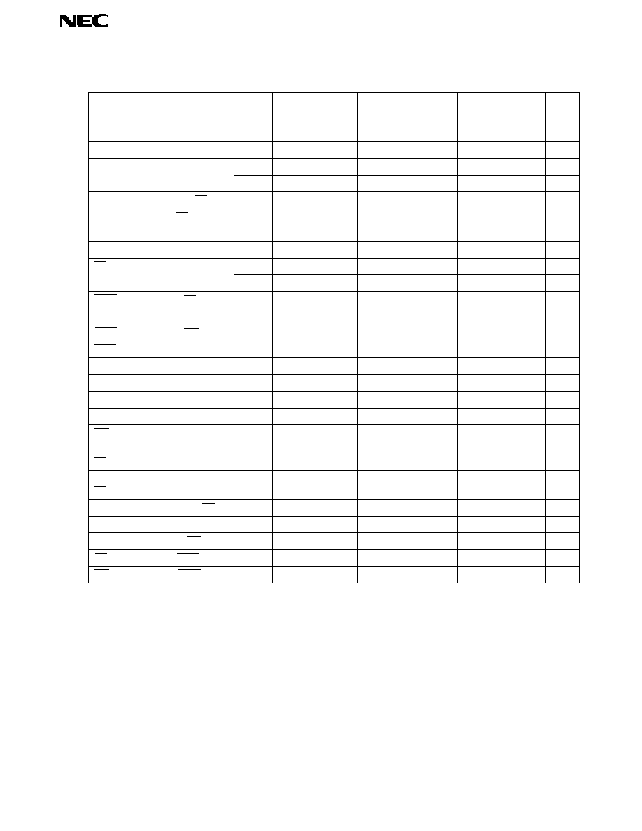
43
µ
PD780031AY, 780032AY, 780033AY, 780034AY
Data Sheet U14045EJ1V0DS00
(2) Read/Write Operation (T
A
= ≠40 to + 85
∞
C, V
DD
= 4.0 to 5.5 V)
(1/3)
Parameter
Symbol
Test Conditions
MIN.
MAX.
Unit
ASTB high-level width
t
ASTH
0.3t
CY
ns
Address setup time
t
ADS
20
ns
Address hold time
t
ADH
6
ns
Data input time from address
t
ADD1
(2 + 2n)t
CY
≠ 54
ns
t
ADD2
(3 + 2n)t
CY
≠ 60
ns
Address output time from RD
t
RDAD
0
100
ns
Data input time from RD
t
RDD1
(2 + 2n)t
CY
≠ 87
ns
t
RDD2
(3 + 2n)t
CY
≠ 93
ns
Read data hold time
t
RDH
0
ns
RD low-level width
t
RDL1
(1.5 + 2n)t
CY
≠ 33
ns
t
RDL2
(2.5 + 2n)t
CY
≠ 33
ns
WAIT
input time from RD
t
RDWT1
t
CY
≠ 43
ns
t
RDWT2
t
CY
≠ 43
ns
WAIT
input time from WR
t
WRWT
t
CY
≠ 25
ns
WAIT low-level width
t
WTL
(0.5 + n)t
CY
+ 10
(2 + 2n)t
CY
ns
Write data setup time
t
WDS
60
ns
Write data hold time
t
WDH
6
ns
WR low-level width
t
WRL1
(1.5 + 2n)t
CY
≠ 15
ns
RD
delay time from ASTB
t
ASTRD
6
ns
WR
delay time from ASTB
t
ASTWR
2t
CY
≠ 15
ns
ASTB
delay time from
t
RDAST
0.8t
CY
≠ 15
1.2t
CY
ns
RD
at external fetch
Address hold time from
t
RDADH
0.8t
CY
≠ 15
1.2t
CY
+ 30
ns
RD
at external fetch
Write data output time from RD
t
RDWD
40
ns
Write data output time from WR
t
WRWD
10
60
ns
Address hold time from WR
t
WRADH
0.8t
CY
≠ 15
1.2t
CY
+ 30
ns
RD
delay time from WAIT
t
WTRD
0.8t
CY
2.5t
CY
+ 25
ns
WR
delay time from WAIT
t
WTWR
0.8t
CY
2.5t
CY
+ 25
ns
Remarks
1.
t
CY
= T
CY
/4
2.
n indicates the number of waits.
3.
C
L
= 100 pF (C
L
indicates the load capacitance of the AD0 to AD7, A8 to A15, RD, WR, WAIT, and
ASTB pins.)
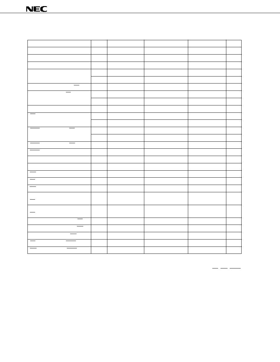
44
µ
PD780031AY, 780032AY, 780033AY, 780034AY
Data Sheet U14045EJ1V0DS00
(2) Read/Write Operation (T
A
= ≠40 to + 85
∞
C, V
DD
= 2.7 to 4.0 V)
(2/3)
Parameter
Symbol
Test Conditions
MIN.
MAX.
Unit
ASTB high-level width
t
ASTH
0.3t
CY
ns
Address setup time
t
ADS
30
ns
Address hold time
t
ADH
10
ns
Data input time from address
t
ADD1
(2 + 2n)t
CY
≠ 108
ns
t
ADD2
(3 + 2n)t
CY
≠ 120
ns
Address output time from RD
t
RDAD
0
200
ns
Data input time from RD
t
RDD1
(2 + 2n)t
CY
≠ 148
ns
t
RDD2
(3 + 2n)t
CY
≠ 162
ns
Read data hold time
t
RDH
0
ns
RD low-level width
t
RDL1
(1.5 + 2n)t
CY
≠ 40
ns
t
RDL2
(2.5 + 2n)t
CY
≠ 40
ns
WAIT
input time from RD
t
RDWT1
t
CY
≠ 75
ns
t
RDWT2
t
CY
≠ 60
ns
WAIT
input time from WR
t
WRWT
t
CY
≠ 50
ns
WAIT low-level width
t
WTL
(0.5 + 2n)t
CY
+ 10
(2 + 2n)t
CY
ns
Write data setup time
t
WDS
60
ns
Write data hold time
t
WDH
10
ns
WR low-level width
t
WRL1
(1.5 + 2n)t
CY
≠ 30
ns
RD
delay time from ASTB
t
ASTRD
10
ns
WR
delay time from ASTB
t
ASTWR
2t
CY
≠ 30
ns
ASTB
delay time from
t
RDAST
0.8t
CY
≠ 30
1.2t
CY
ns
RD
at external fetch
Address hold time from
t
RDADH
0.8t
CY
≠ 30
1.2t
CY
+ 60
ns
RD
at external fetch
Write data output time from RD
t
RDWD
40
ns
Write data output time from WR
t
WRWD
20
120
ns
Address hold time from WR
t
WRADH
0.8t
CY
≠ 30
1.2t
CY
+ 60
ns
RD
delay time from WAIT
t
WTRD
0.5t
CY
2.5t
CY
+ 50
ns
WR
delay time from WAIT
t
WTWR
0.5t
CY
2.5t
CY
+ 50
ns
Remarks
1.
t
CY
= T
CY
/4
2.
n indicates the number of waits.
3.
C
L
= 100 pF (C
L
indicates the load capacitance of the AD0 to AD7, AD8 to AD15, RD, WR, WAIT,
and ASTB pins.)

45
µ
PD780031AY, 780032AY, 780033AY, 780034AY
Data Sheet U14045EJ1V0DS00
(2) Read/Write Operation (T
A
= ≠40 to + 85
∞
C, V
DD
= 1.8 to 2.7 V)
(3/3)
Parameter
Symbol
Test Conditions
MIN.
MAX.
Unit
ASTB high-level width
t
ASTH
0.3t
CY
ns
Address setup time
t
ADS
120
ns
Address hold time
t
ADH
20
ns
Data input time from address
t
ADD1
(2 + 2n)t
CY
≠ 233
ns
t
ADD2
(3 + 2n)t
CY
≠ 240
ns
Address output time from RD
t
RDAD
0
400
ns
Data input time from RD
t
RDD1
(2 + 2n)t
CY
≠ 325
ns
t
RDD2
(3 + 2n)t
CY
≠ 332
ns
Read data hold time
t
RDH
0
ns
RD low-level width
t
RDL1
(1.5 + 2n)t
CY
≠ 92
ns
t
RDL2
(2.5 + 2n)t
CY
≠ 92
ns
WAIT
input time from RD
t
RDWT1
t
CY
≠ 350
ns
t
RDWT2
t
CY
≠ 132
ns
WAIT
input time from WR
t
WRWT
t
CY
≠ 100
ns
WAIT low-level width
t
WTL
(0.5 + 2n)t
CY
+ 10
(2 + 2n)t
CY
ns
Write data setup time
t
WDS
60
ns
Write data hold time
t
WDH
20
ns
WR low-level width
t
WRL1
(1.5 + 2n)t
CY
≠ 60
ns
RD
delay time from ASTB
t
ASTRD
20
ns
WR
delay time from ASTB
t
ASTWR
2t
CY
≠ 60
ns
ASTB
delay time from
t
RDAST
0.8t
CY
≠ 60
1.2t
CY
ns
RD
at external fetch
Address hold time from
t
RDADH
0.8t
CY
≠ 60
1.2t
CY
+ 120
ns
RD
at external fetch
Write data output time from RD
t
RDWD
40
ns
Write data output time from WR
t
WRWD
40
240
ns
Address hold time from WR
t
WRADH
0.8t
CY
≠ 60
1.2t
CY
+ 120
ns
RD
delay time from WAIT
t
WTRD
0.5t
CY
2.5t
CY
+ 100
ns
WR
delay time from WAIT
t
WTWR
0.5t
CY
2.5t
CY
+ 100
ns
Remarks
1.
t
CY
= T
CY
/4
2.
n indicates the number of waits.
3.
C
L
= 100pF (C
L
indicates the load capacitance of the AD0 to AD7, AD8 to AD15, RD, WR, WAIT, and
ASTB pins.)

46
µ
PD780031AY, 780032AY, 780033AY, 780034AY
Data Sheet U14045EJ1V0DS00
(3) Serial Interface (T
A
= ≠40 to + 85
∞
C, V
DD
= 1.8 to 5.5 V)
(a) 3-wire serial I/O mode (SCK30 ... Internal clock output)
Parameter
Symbol
Test Conditions
MIN.
TYP.
MAX.
Unit
SCK30 cycle time
t
KCY1
4.0 V
V
DD
5.5 V
954
ns
2.7 V
V
DD
<
4.0 V
1600
ns
3200
ns
SCK30 high-/low-level
t
KH1
, t
KL1
V
DD
= 4.0 to 5.5 V
t
KCY1
/2 ≠ 50
ns
width
t
KCY1
/2 ≠ 100
ns
SI30 setup time
t
SIK1
4.0 V
V
DD
5.5V
100
ns
(to SCK30
)
2.7 V
V
DD
< 4.0V
150
ns
300
ns
SI30 hold time
t
KSI1
400
ns
(from SCK30
)
SO30 output
t
KSO1
C = 100 pF
Note
300
ns
delay time from
SCK30
Note C is the load capacitance of the SCK30 and SO30 output lines.
(b) 3-wire serial I/O mode (SCK30 ... External clock input)
Parameter
Symbol
Test Conditions
MIN.
TYP.
MAX.
Unit
SCK30 cycle time
t
KCY2
4.0 V
V
DD
5.5 V
800
ns
2.7 V
V
DD
< 4.0 V
1600
ns
3200
ns
SCK30 high-/low-level
t
KH2
, t
KL2
4.0 V
V
DD
5.5 V
400
ns
width
2.7 V
V
DD
< 4.0 V
800
ns
1600
ns
SI30 setup time
t
SIK2
100
ns
(to SCK30
)
SI30 hold time
t
KSI2
400
ns
(from SCK30
)
SO30 output
t
KSO2
C = 100 pF
Note
300
ns
delay time from
SCK30
Note C is the load capacitance of the SO30 output line.

47
µ
PD780031AY, 780032AY, 780033AY, 780034AY
Data Sheet U14045EJ1V0DS00
(c) UART mode (Dedicated baud-rate generator output)
Parameter
Symbol
Test Conditions
MIN.
TYP.
MAX.
Unit
Transfer rate
4.0 V
V
DD
5.5 V
131031
bps
2.7 V
V
DD
< 4.0 V
78125
bps
39063
bps
(d) UART mode (External clock input)
Parameter
Symbol
Test Conditions
MIN.
TYP.
MAX.
Unit
ASCK0 cycle time
t
KCY3
4.0 V
V
DD
5.5 V
800
ns
2.7 V
V
DD
< 4.0 V
1600
ns
3200
ns
ASCK0 high-/low-level width
t
KH3
,
4.0 V
V
DD
5.5 V
400
ns
t
KL3
2.7 V
V
DD
< 4.0 V
800
ns
1600
ns
Transfer rate
4.0 V
V
DD
5.5 V
39063
bps
2.7 V
V
DD
< 4.0 V
19531
bps
9766
bps
(e) UART mode (Infrared ray data transfer mode)
Parameter
Symbol
Test Conditions
MIN.
MAX.
Unit
Transfer rate
V
DD
= 4.0 to 5.5 V
131031
bps
Bit rate allowable error
V
DD
= 4.0 to 5.5 V
±
0.87
%
Output pulse width
V
DD
= 4.0 to 5.5 V
1.2
0.24/fbr
Note
µ
s
Input pulse width
V
DD
= 4.0 to 5.5 V
4/f
X
µ
s
Note
fbr: Specified baud rate
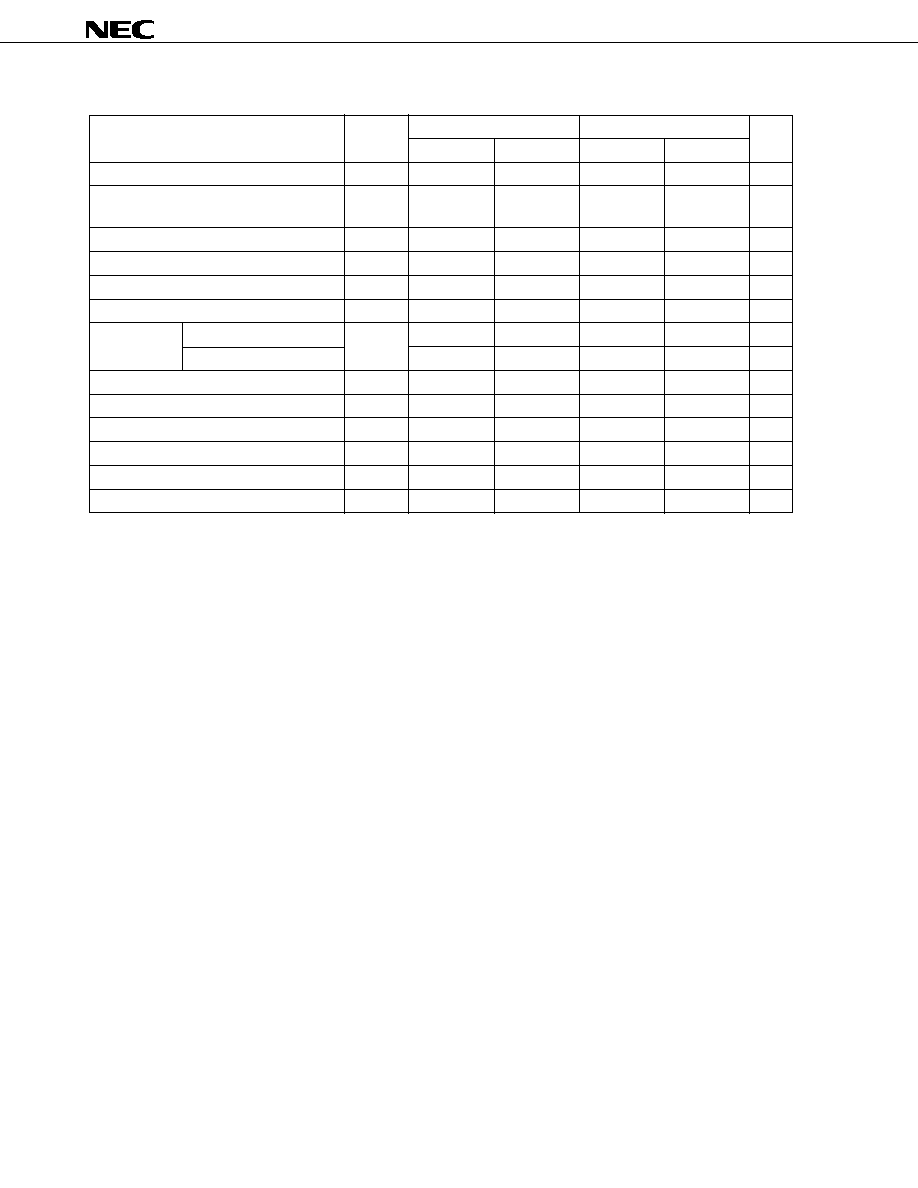
48
µ
PD780031AY, 780032AY, 780033AY, 780034AY
Data Sheet U14045EJ1V0DS00
(f) I
2
C bus Mode
Parameter
Symbol
Standard Mode
High-Speed Mode
Unit
MIN.
MAX.
MIN.
MAX.
SCL0 clock frequency
f
CLK
0
100
0
400
kHz
Bus-free time
t
BUF
4.7
--
1.3
--
µ
s
(between stop and start condition)
Hold time
Note 1
t
HD:STA
4.0
--
0.6
--
µ
s
SCL0 clock low-level width
t
LOW
4.7
--
1.3
--
µ
s
SCL0 clock high-level width
t
HIGH
4.0
--
0.6
--
µ
s
Start/restart condition setup time
t
SU:STA
4.7
--
0.6
--
µ
s
Data hold time
CBUS compatible master
t
HD:DAT
5.0
--
--
--
µ
s
I
2
C bus
0
Note 2
--
0
Note 2
0.9
Note 3
µ
s
Data setup time
t
SU:DAT
250
--
100
Note 4
--
ns
SDA0 and SCL0 signal rise time
t
R
--
1000
20 + 0.1Cb
Note 5
300
ns
SDA0 and SCL0 signal fall time
t
F
--
300
20 + 0.1Cb
Note 5
300
ns
Stop condition setup time
t
SU:STO
4.0
--
0.6
--
µ
s
Spike pulse width controlled by input filter
t
SP
--
--
0
50
ns
Capacitive load per bus line
Cb
--
400
--
400
pF
Notes 1. In the start condition, the first clock pulse is generated after this hold time.
2. To fill in the undefined area of the SCL0 falling edge, it is necessary for the device to internally provide
at least 300 ns of hold time for the SDA0 signal (which is V
IHmin.
of the SCL0 signal).
3. If the device does not extend the SCL0 signal low hold time (t
LOW
), only maximum data hold time t
HD:DAT
needs to be fulfilled.
4. The high-speed mode I
2
C bus is available in a standard mode I
2
C bus system. At this time, the conditions
described below must be satisfied.
∑ If the device does not extend the SCL0 signal low state hold time
t
SU:DAT
250 ns
∑ If the device extends the SCL0 signal low state hold time
Be sure to transmit the next data bit to the SDA0 line before the SCL0 line is released (t
Rmax.
+ t
SU:DAT
= 1000 + 250 = 1250 ns by standard mode I
2
C bus specification).
5. Cb: Total capacitance per bus line (unit: pF)
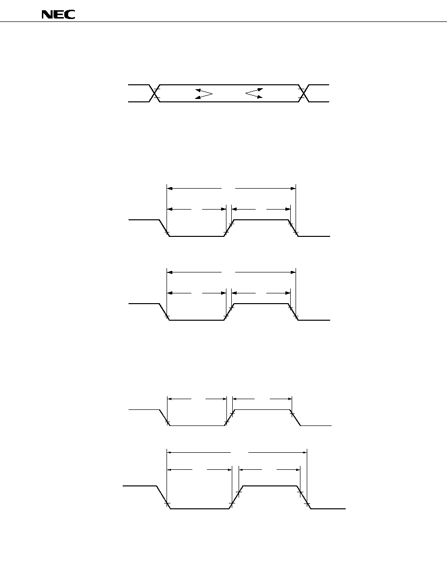
49
µ
PD780031AY, 780032AY, 780033AY, 780034AY
Data Sheet U14045EJ1V0DS00
AC Timing Test Points (Excluding X1, XT1 Inputs)
Clock Timing
TI Timing
t
XL
t
XH
1/f
X
V
IH4
(MIN.)
V
IL4
(MAX.)
t
XTL
t
XTH
1/f
XT
V
IH5
(MIN.)
V
IL5
(MAX.)
X1 Input
XT1 Input
t
TIL0
t
TIH0
TI00, TI01
0.8V
DD
0.2V
DD
Test points
0.8V
DD
0.2V
DD
1/f
TI5
t
TIH5
t
TIL5
TI50, TI51

50
µ
PD780031AY, 780032AY, 780033AY, 780034AY
Data Sheet U14045EJ1V0DS00
Read/Write Operation
External fetch (no wait):
External fetch (wait insertion):
A8 to A15
AD0 to AD7
ASTB
RD
Higher 8-bit address
Lower-8-bit address
t
ADD1
Hi-Z
t
ADS
t
ASTH
t
ADH
t
RDD1
t
RDAD
Instruction code
t
RDADH
t
RDAST
t
ASTRD
t
RDL1
t
RDH
A8 to A15
AD0 to AD7
ASTB
RD
Higher 8-bit address
Lower 8-bit address
t
ADD1
Hi-Z
t
ADS
t
ASTH
t
ADH
t
RDAD
t
RDD1
Instruction code
t
RDADH
t
RDAST
t
ASTRD
t
RDL1
t
RDH
WAIT
t
RDWT1
t
WTL
t
WTRD
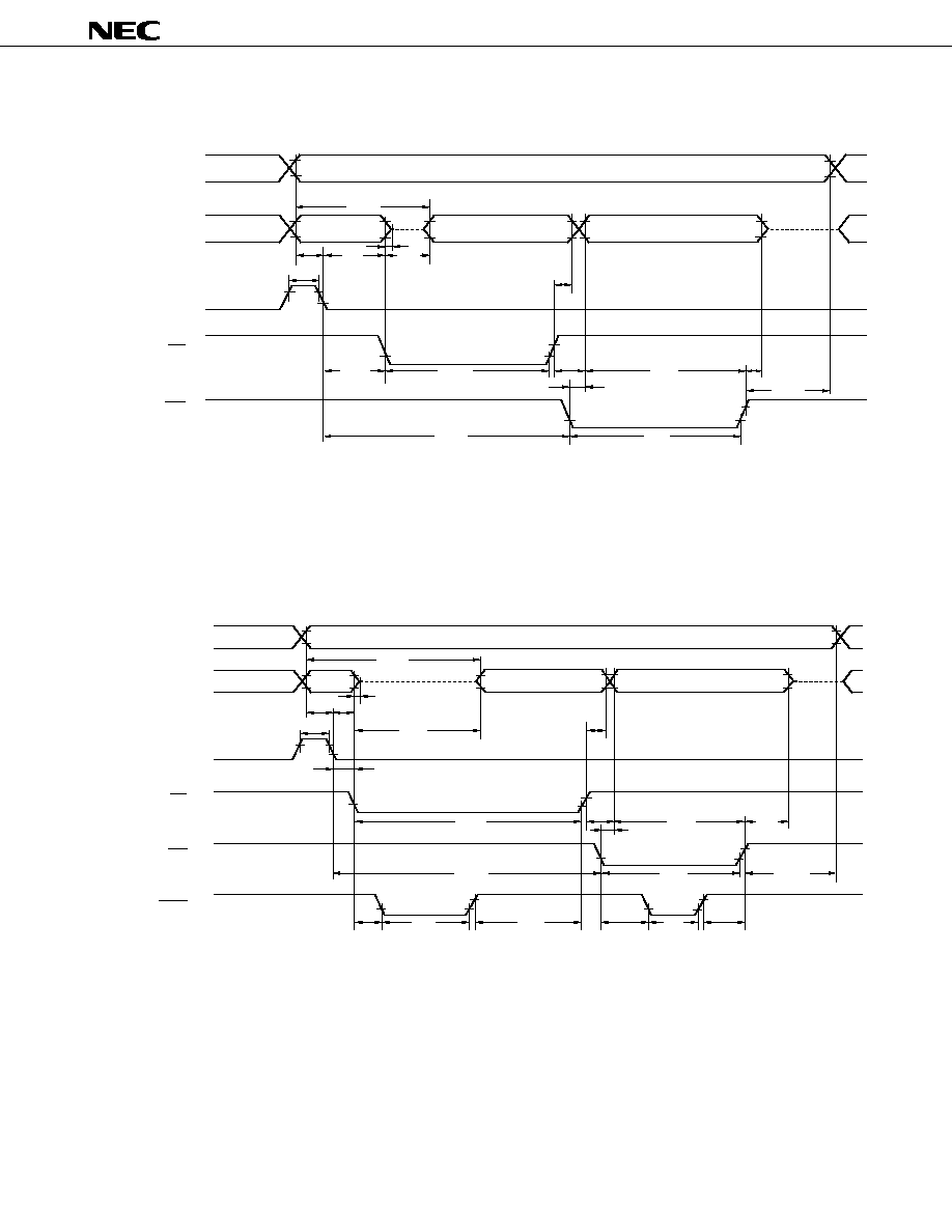
51
µ
PD780031AY, 780032AY, 780033AY, 780034AY
Data Sheet U14045EJ1V0DS00
External data access (no wait):
External data access (wait insertion):
A8 to A15
AD0 to AD7
ASTB
RD
Higher 8-bit address
Lower 8-bit address
t
ADD2
Hi-Z
t
ADS
t
ASTH
t
ADH
t
RDD2
t
RDAD
Read data
t
ASTRD
t
RDWD
WR
t
ASTWR
Write data
Hi-Z
t
WDH
t
WRADH
t
WDS
t
WRWD
t
WRL1
t
RDH
t
RDL2
A8 to A15
AD0 to AD7
ASTB
RD
Higher 8-bit address
Lower 8-bit
address
t
ADD2
t
ADS
t
ASTH
t
ADH
t
RDAD
t
RDD2
Read data
t
ASTRD
WR
t
ASTWR
Write data
Hi-Z
t
WDH
t
WRADH
t
WDS
t
WRWD
t
WRL1
t
RDH
t
RDL2
t
RDWT2
t
WTL
t
WRWT
t
WTL
t
WTWR
t
WTRD
WAIT
t
RDWD
Hi-Z

52
µ
PD780031AY, 780032AY, 780033AY, 780034AY
Data Sheet U14045EJ1V0DS00
Serial Transfer Timing
3-wire serial I/O mode:
UART mode (external clock input):
t
KCYm
t
KLm
t
KHm
SCK30
SI30
SO30
t
SIKm
t
KSIm
t
KSOm
Input data
Output data
m = 1, 2
t
KCY3
t
KH3
t
KL3
ASCK0
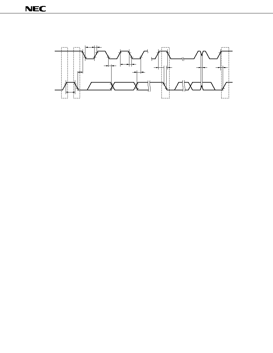
53
µ
PD780031AY, 780032AY, 780033AY, 780034AY
Data Sheet U14045EJ1V0DS00
I
2
C Bus Mode:
SCL0
SDA0
t
HD:STA
t
BUF
t
HD:DAT
t
HIGH
t
F
t
SU:DAT
t
SU:STA
t
HD:STA
t
SP
t
SU:STO
t
R
t
LOW
Stop
condition
Start
condition
Stop
condition
Restart
condition
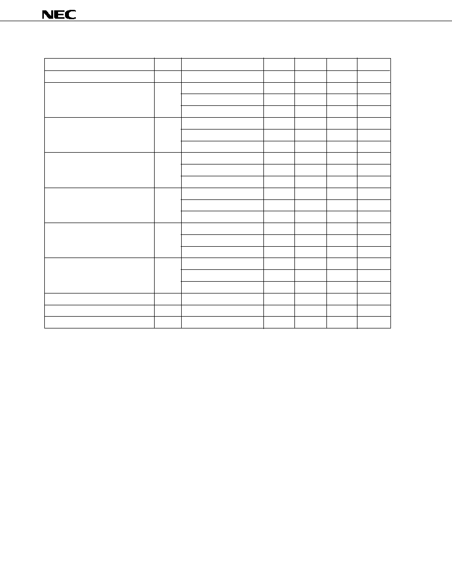
54
µ
PD780031AY, 780032AY, 780033AY, 780034AY
Data Sheet U14045EJ1V0DS00
A/D Converter Characteristics (T
A
= ≠40 to +85
∞
C, V
DD
= AV
DD
= AV
REF
= 1.8 to 5.5 V, AV
SS
= V
SS
= 0 V)
Parameter
Symbol
Conditions
MIN.
TYP.
MAX.
Unit
Resolution
10
10
10
bit
Overall error
Notes 1, 2
4.0 V
AV
REF
5.5 V
±
0.2
±
0.4
%FSR
2.7 V
AV
REF
<
4.0 V
±
0.3
±
0.6
%FSR
1.8 V
AV
REF
<
2.7 V
±
0.6
±
1.2
%FSR
Conversion time
t
CONV
4.0 V
AV
REF
5.5 V
14
96
µ
s
2.7 V
AV
REF
<
4.0 V
19
96
µ
s
1.8 V
AV
REF
<
2.7 V
28
96
µ
s
Zero-scale offset
Notes 1, 2
4.0 V
AV
REF
5.5 V
±
0.4
%FSR
2.7 V
AV
REF
<
4.0 V
±
0.6
%FSR
1.8 V
AV
REF
<
2.7 V
±
1.2
%FSR
Full-scale offset
Notes 1, 2
4.0 V
AV
REF
5.5 V
±
0.4
%FSR
2.7 V
AV
REF
<
4.0 V
±
0.6
%FSR
1.8 V
AV
REF
<
2.7 V
±
1.2
%FSR
Integral linearity error
Note 1
4.0 V
AV
REF
5.5 V
±
2.5
LSB
2.7 V
AV
REF
<
4.0 V
±
4.5
LSB
1.8 V
AV
REF
<
2.7 V
±
8.5
LSB
Differential linearity error
Note 1
4.0 V
AV
REF
5.5 V
±
1.5
LSB
2.7 V
AV
REF
<
4.0 V
±
2.0
LSB
1.8 V
AV
REF
<
2.7 V
±
3.5
LSB
Analog input voltage
V
IAN
0
AV
REF
V
Reference voltage
AV
REF
1.8
AV
DD
V
Resistance between AV
REF
and AV
SS
R
REF
When A/D conversion is not performed
20
40
k
Notes 1. Excludes quantization error (
±
1/2 LSB).
2. Shown as a percentage of the full scale value.
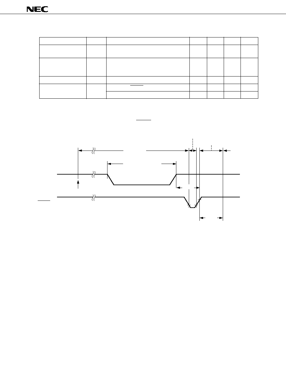
55
µ
PD780031AY, 780032AY, 780033AY, 780034AY
Data Sheet U14045EJ1V0DS00
Data Memory STOP Mode Low Supply Voltage Data Retention Characteristics (T
A
= ≠40 to +85
∞
C)
Parameter
Symbol
Test Conditions
MIN.
TYP.
MAX.
Unit
Data retention power
V
DDDR
1.6
5.5
V
supply voltage
Data retention
I
DDDR
V
DDDR
= 1.6 V
0.1
30
µ
A
power supply
Subsystem clock stop (XT1 = V
DD
) and
current
feed-back resistor disconnected
Release signal set time
t
SREL
0
µ
s
Oscillation stabilization
t
WAIT
Release by RESET
2
17
/fx
ms
time
Release by interrupt request
Note
ms
Note Selection of 2
12
/f
X
and 2
14
/f
X
to 2
17
/f
X
is possible using bits 0 to 2 (OSTS0 to OSTS2) of the oscillation
stabilization time select register (OSTS).
Data Retention Timing (STOP mode release by RESET)
t
SREL
t
WAIT
V
DD
RESET
STOP instruction execution
STOP mode
Data retention mode
Internal reset operation
HALT mode
Operating mode
V
DDDR
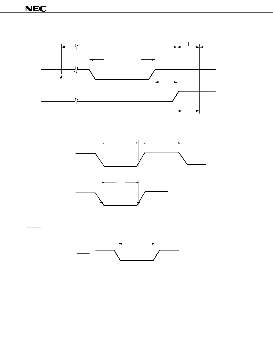
56
µ
PD780031AY, 780032AY, 780033AY, 780034AY
Data Sheet U14045EJ1V0DS00
Data Retention Timing (Standby release signal: STOP mode release by interrupt request signal)
Interrupt Request Input Timing
RESET Input Timing
t
SREL
t
WAIT
V
DD
STOP Instruction execution
STOP mode
Data retention mode
HALT mode
Operating mode
Standby release signal
(interrupt request)
V
DDDR
INTP0 to INTP2
INTP3
t
INTL
t
INTH
t
INTL
t
RSL
RESET
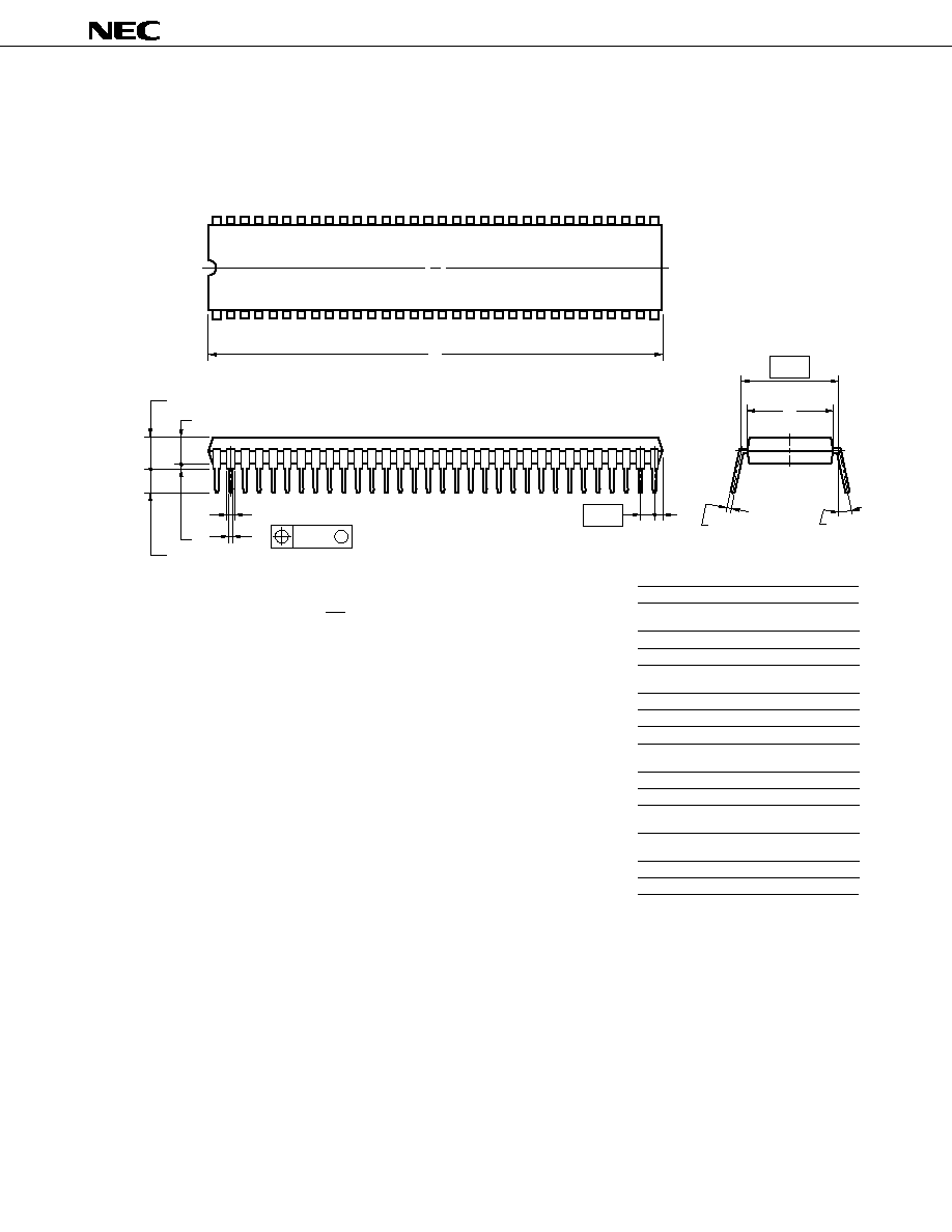
57
µ
PD780031AY, 780032AY, 780033AY, 780034AY
Data Sheet U14045EJ1V0DS00
13. PACKAGE DRAWINGS
Remark
The external dimensions and materials of the ES version are the same as those of the mass-produced
version.
I
J
G
H
F
D
N
M
C
B
M
R
64
33
32
1
K
L
NOTES
1. Controlling dimension millimeter.
P64C-70-750A,C-3
ITEM
MILLIMETERS
INCHES
B
C
D
F
G
H
J
K
1.778 (T.P.)
3.2
±
0.3
0.51 MIN.
1.78 MAX.
L
M
0.17
0.25
19.05 (T.P.)
5.08 MAX.
17.0
±
0.2
N
0 to 15
∞
0.50
±
0.10
0.9 MIN.
R
0.070 MAX.
0.020
0.035 MIN.
0.126
±
0.012
0.020 MIN.
0.200 MAX.
0.750 (T.P.)
0.669
0.010
0.007
0 to 15
∞
+0.004
≠0.003
0.070 (T.P.)
+0.10
≠0.05
+0.004
≠0.005
64 PIN PLASTIC SHRINK DIP (750 mil)
2. Each lead centerline is located within 0.17 mm (0.007 inch) of
its true position (T.P.) at maximum material condition.
3. Item "K" to center of leads when formed parallel.
A
58.0
2.283
+0.028
≠0.008
+0.68
≠0.20
I
4.05
0.159
+0.011
≠0.008
+0.26
≠0.20
A
+0.009
≠0.008
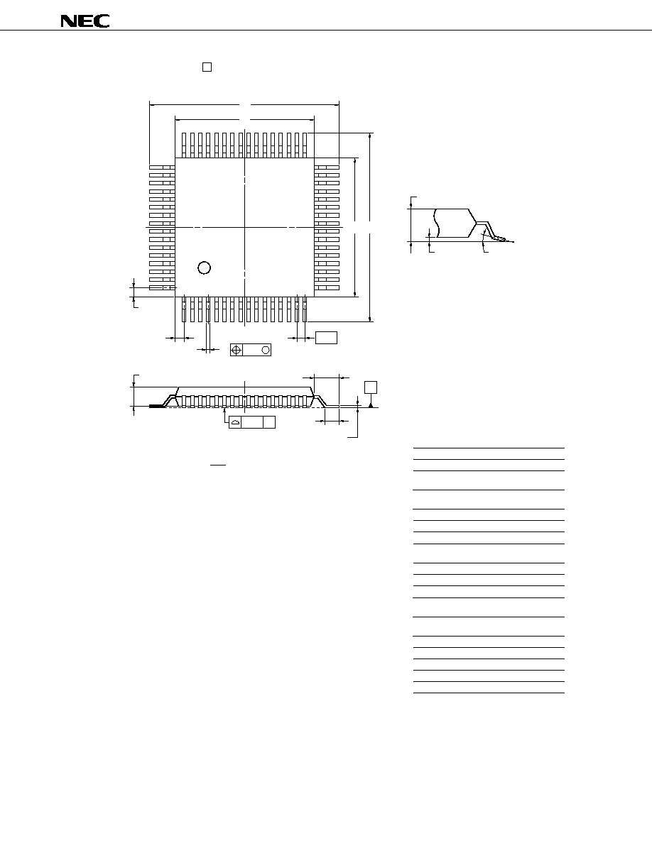
58
µ
PD780031AY, 780032AY, 780033AY, 780034AY
Data Sheet U14045EJ1V0DS00
Remark
The external dimensions and materials of the ES version are the same as those of the mass-produced
version.
64 PIN PLASTIC QFP ( 14)
ITEM
MILLIMETERS
INCHES
I
J
0.8 (T.P.)
0.15
0.006
0.031 (T.P.)
A
17.6
±
0.4
0.693
±
0.016
B
14.0
±
0.2
0.551+0.009
≠0.008
C
14.0
±
0.2
0.551+0.009
≠0.008
D
17.6
±
0.4
0.693
±
0.016
F
G
1.0
1.0
0.039
0.039
H
0.37
0.015
P64GC-80-AB8-4
L
0.8
±
0.2
0.031+0.009
≠0.008
M
0.17
0.007
N
0.10
0.004
+0.08
≠0.07
+0.08
≠0.07
Q
0.1
±
0.1
0.004
±
0.004
R
S
2.85 MAX.
5
∞±
5
∞
5
∞±
5
∞
0.113 MAX.
+0.003
≠0.004
NOTE
1. Controlling dimension millimeter.
2. Each lead centerline is located within 0.15 mm (0.006 inch) of
its true position (T.P.) at maximum material condition.
M
Q
R
K
M
L
P
G
F
H
I
S
detail of lead end
K
1.8
±
0.2
0.071
±
0.008
P
2.55
±
0.1
0.100
±
0.004
+0.003
≠0.004
48
49
32
64
1
17
16
33
S
A
B
C D
J
N
S

59
µ
PD780031AY, 780032AY, 780033AY, 780034AY
Data Sheet U14045EJ1V0DS00
Remark
The external dimensions and materials of the ES version are the same as those of the mass-produced
version.
64 PIN PLASTIC LQFP (12x12)
ITEM
MILLIMETERS
INCHES
0.65 (T.P.)
J
0.026
K
1.4
±
0.2
0.055
±
0.008
F
1.125
1.125
G
0.044
0.044
14.8
±
0.4
D
0.583
±
0.016
NOTES
1. Controlling dimension millimeter.
2. Each lead centerline is located within 0.13 mm of
its true position (T.P.) at maximum material condition.
A
14.8
±
0.4
0.583
±
0.016
B
12.0
±
0.2
0.472
C
12.0
±
0.2
0.472
0.13
I
0.005
H
0.32
±
0.08
0.013
Q
R
P
G
L
M
K
H
I
J
F
S
detail of lead end
0.10
N
0.004
M
0.17
0.007
P
1.4
±
0.1
0.055
5
∞±
5
∞
R
5
∞±
5
∞
S
1.7 MAX.
0.067 MAX.
0.125
±
0.075
Q
0.005
±
0.003
L
0.6
±
0.2
0.024
P64GK-65-8A8-2
A
B
C
D
M
48
49
32
64
1
17
16
33
S
N
S
+
0.08
-
0.07
+
0.009
-
0.008
+
0.009
-
0.008
+
0.003
-
0.004
+
0.008
-
0.009
+
0.003
-
0.004
+
0.004
-
0.005

60
µ
PD780031AY, 780032AY, 780033AY, 780034AY
Data Sheet U14045EJ1V0DS00
14. RECOMMENDED SOLDERING CONDITIONS
This product should be soldered and mounted under the following recommended conditions.
For the details of the recommended soldering conditions, refer to the document Semiconductor Device
Mounting Technology Manual (C10535E).
For soldering methods and conditions other than those recommended below, contact your NEC sales represen-
tative.
Table 14-1. Surface Mounting Type Soldering Conditions
(1)
µ
PD780031AYGC-
◊◊◊
-AB8: 64-pin plastic QFP (14
◊
14 mm)
µ
PD780032AYGC-
◊◊◊
-AB8: 64-pin plastic QFP (14
◊
14 mm)
µ
PD780033AYGC-
◊◊◊
-AB8: 64-pin plastic QFP (14
◊
14 mm)
µ
PD780034AYGC-
◊◊◊
-AB8: 64-pin plastic QFP (14
◊
14 mm)
Soldering Method
Soldering Conditions
Recommended
Condition Symbol
Infrared reflow
Package peak temperature: 235
∞
C, Time: 30 seconds max.
IR35-00-3
(at 210
∞
C or higher), Count: three times or less
VPS
Package peak temperature: 215
∞
C, Time: 40 seconds max.
VP15-00-3
(at 200
∞
C or higher), Count: three times or less
Wave soldering
Solder bath temperature: 260
∞
C max., Time: 10 seconds max.,
WS60-00-1
Count: once, Preheating temperature: 120
∞
C max. (package surface
temperature)
Partial heating
Pin temperature: 300
∞
C max., Time: 3 seconds max. (per pin row)
≠≠
Caution Do not use different soldering methods together (except for partial heating).

61
µ
PD780031AY, 780032AY, 780033AY, 780034AY
Data Sheet U14045EJ1V0DS00
(2)
µ
PD780031AYGK-
◊◊◊
-8A8: 64-pin plastic LQFP (12
◊
12 mm)
µ
PD780032AYGK-
◊◊◊
-8A8: 64-pin plastic LQFP (12
◊
12 mm)
µ
PD780033AYGK-
◊◊◊
-8A8: 64-pin plastic LQFP (12
◊
12 mm)
µ
PD780034AYGK-
◊◊◊
-8A8: 64-pin plastic LQFP (12
◊
12 mm)
Soldering Method
Soldering Conditions
Recommended
Condition Symbol
Infrared reflow
Package peak temperature: 235
∞
C, Time: 30 seconds max.
IR35-107-2
(at 210
∞
C or higher),
Count: two times or less, Exposure limit: 7 days
Note
(after that,
prebake at 125
∞
C for 10 hours)
VPS
Package peak temperature: 215
∞
C, Time: 40 seconds max.
VP15-107-2
(at 200
∞
C or higher),
Count: two times or less, Exposure limit: 7 days
Note
(after that,
prebake at 125
∞
C for 10 hours)
Wave soldering
Solder bath temperature: 260
∞
C max., Time: 10 seconds max.,
WS60-107-1
Count: once, Preheating temperature: 120
∞
C max. (package
surface temperature), Exposure limit: 7 days
Note
(after that, prebake
at 125
∞
C for 10 hours)
Partial heating
Pin temperature: 300
∞
C max., Time: 3 seconds max. (per pin row)
≠≠
Note After opening the dry pack, store it at 25
∞
C or less and 65%RH or less for the allowable storage
period.
Caution Do not use different soldering methods together (except for partial heating).
Table 14-2. Insertion Type Soldering Conditions
µ
PD780031AYCW-
◊◊◊
: 64-pin plastic shrink DIP (750mils)
µ
PD780032AYCW-
◊◊◊
: 64-pin plastic shrink DIP (750mils)
µ
PD780033AYCW-
◊◊◊
: 64-pin plastic shrink DIP (750mils)
µ
PD780034AYCW-
◊◊◊
: 64-pin plastic shrink DIP (750mils)
Soldering Method
Soldering Conditions
Wave soldering
Solder bath temperature: 260
∞
C max., Time: 10 seconds max.
(only for pins)
Partial heating
Pin temperature: 300
∞
C max., Time: 3 seconds max. (per pin row)
Caution Apply wave soldering only to the pins and be careful not to bring solder into direct contact with
the package.
62
µ
PD780031AY, 780032AY, 780033AY, 780034AY
Data Sheet U14045EJ1V0DS00
APPENDIX A. DEVELOPMENT TOOLS
The following development tools are available for system development using the
µ
PD780034AY Subseries.
Also refer to (5) Cautions on Using Development Tools.
(1) Language Processing Software
RA78K/0
Assembler package common to 78K/0 Series
CC78K/0
C compiler package common to 78K/0 Series
DF780034
Device file common to
µ
PD780034A Subseries
CC78K/0-L
C compiler library source file common to 78K/0 Series
(2) Flash Memory Writing Tools
Flashpro II (FL-PR2)
Flash programmer dedicated to microcontrollers with on-chip flash memory
Flashpro III (FL-PR3, PG-FP3)
FA-64CW
Adapter for flash memory writing
FA-64GC
FA-64GK
(3) Debugging Tools
∑ When using in-circuit emulator IE-78K0-NS
IE-78K0-NS
In-circuit emulator common to 78K/0 Series
IE-70000-MC-PS-B
Power supply unit for IE-78K0-NS
IE-78K0-NS-PA
Note
Performance board to enhance and expand the functions of IE-78K0-NS
IE-70000-98-IF-C
Interface adapter when using PC-9800 series as host machine (excluding notebook PCs) (C bus supported)
IE-70000-CD-IF-A
PC card and interface cable when using notebook PC as host machine (PCMCIA socket supported)
IE-70000-PC-IF-C
Interface adapter when using IBM PC/AT
TM
or compatible as host machine (ISA bus supported)
IE-70000-PCI-IF
Adapter required when using PC in which PCI bus is embedded as host machine
IE-780034-NS-EM1
Emulation board to emulate
µ
PD780034AY Subseries
NP-64CW
Emulation probe for 64-pin plastic shrink DIP (CW type)
NP-64GC
Emulation probe for 64-pin plastic QFP (GC-AB8 type)
NP-64GC-TQ
NP-64GK
Emulation probe for 64-pin plastic LQFP (GK-8A8 type)
TGK-064SBW
Conversion adapter to connect NP-64GK and target system board on which a 64-pin plastic LQFP
(GK-8A8 type) can be mounted.
EV-9200GC-64
Socket to be mounted on target system board made for 64-pin plastic QFP (GC-AB8 type)
ID78K0-NS
Integrated debugger for IE-78K0-NS
SM78K0
System simulator common to 78K/0 Series
DF780034
Device file common to
µ
PD780034A Subseries
Note
Under development
63
µ
PD780031AY, 780032AY, 780033AY, 780034AY
Data Sheet U14045EJ1V0DS00
∑ When using in-circuit emulator IE-78001-R-A
IE-78001-R-A
In-circuit emulator common to 78K/0 Series
IE-70000-98-IF-C
Interface adapter when using PC-9800 series as host machine (excluding notebook PCs) (C bus supported)
IE-70000-PC-IF-C
Interface adapter when using IBM PC/AT or compatible as host machine (ISA bus supported)
IE-70000-PCI-IF
Adapter required when using PC in which PCI bus is embedded as host machine
IE-78000-R-SV3
Interface adapter and cable when using EWS as host machine
IE-780034-NS-EM1
Emulation board to emulate
µ
PD780034AY Subseries
IE-78K0-R-EX1
Emulation probe conversion board necessary when using IE-780034-NS-EM1 on IE-78001-R-A
EP-78240CW-R
Emulation probe for 64-pin plastic shrink DIP (CW type)
EP-78240GC-R
Emulation probe for 64-pin plastic QFP (GC-AB8 type)
EP-78012GK-R
Emulation probe for 64-pin plastic LQFP (GK-8A8 type)
TGK-064SBW
Conversion adapter to connect EP-78012GK-R and target system board on which a 64-pin plastic
LQFP (GK-8A8 type) can be mounted.
EV-9200GC-64
Socket to be mounted on target system board made for 64-pin plastic QFP (GC-AB8 type)
ID78K0
Integrated debugger for IE-78001-R-A
SM78K0
System simulator common to 78K/0 Series
DF780034
Device file common to
µ
PD780034A Subseries
(4) Real-time OS
RX78K/0
Real-time OS for 78K/0 Series
MX78K0
OS for 78K/0 Series

64
µ
PD780031AY, 780032AY, 780033AY, 780034AY
Data Sheet U14045EJ1V0DS00
(5) Cautions on Using Development Tools
∑ The ID78K0-NS, ID78K0, and SM78K0 are used in combination with the DF780034.
∑ The CC78K/0 and RX78K/0 are used in combination with the RA78K/0 and the DF780034.
∑ FL-PR2, FL-PR3, FA-64CW, FA-64GC, FA-64GK, NP-64CW, NP-64GC, NP-64GC-TQ, and NP-64GK are
products made by Naito Densei Machida Mfg. Co., Ltd. (+81-44-822-3813).
Contact an NEC distributor regarding the purchase of these products.
∑ The TGK-064SBW is a product made by TOKYO ELETECH CORPORATION.
Refer to: Daimaru Kogyo, Ltd.
Tokyo Electronic Division (+81-3-3820-7112)
Osaka Electronic Division (+81-6-6244-6672)
∑ For third-party development tools, see the 78K/0 Series Selection Guide (U11126E).
∑ The host machines and OSs supporting each software are as follows.
Host Machine
PC
EWS
[OS]
PC-9800 series [Windows
TM
]
HP9000 series 700
TM
[HP-UX
TM
]
IBM PC/AT and compatibles
SPARCstation
TM
[SunOS
TM
, Solaris
TM
]
Software
[Japanese/English Windows]
NEWS
TM
(RISC) [NEWS-OS
TM
]
RA78K/0
Note
CC78K/0
Note
ID78K0-NS
≠
ID78K0
SM78K0
≠
RX78K/0
Note
MX78K0
Note
Note
DOS-based software

65
µ
PD780031AY, 780032AY, 780033AY, 780034AY
Data Sheet U14045EJ1V0DS00
APPENDIX B. RELATED DOCUMENTS
Documents Related to Devices
Document Name
Document No.
Document No.
(English)
(Japanese)
µ
PD780024A, 780034A, 780024AY, 780034AY Subseries User's Manual
U14046E
U14046J
µ
PD780031AY, 780032AY, 780033AY, 780034AY Data Sheet
This document
U14045J
µ
PD78F0034AY Data Sheet
U14041E
U14041J
78K/0 Series User's Manual Instructions
U12326E
U12326J
78K/0 Series Instruction Table
--
U10903J
78K/0 Series Instruction Set
--
U10904J
Documents Related to Development Tools (User's Manuals)
Document Name
Document No.
Document No.
(English)
(Japanese)
RA78K0 Assembler Package
Operation
U11802E
U11802J
Assembly Language
U11801E
U11801J
Structured Assembly Language
U11789E
U11789J
RA78K Series Structured Assembler Preprocessor
EEU-1402
U12323J
CC78K0 C Compiler
Operation
U11517E
U11517J
Language
U11518E
U11518J
CC78K0 C Compiler Application Note
Programming Know-how
U13034E
U13034J
IE-78K0-NS
To be prepared
To be prepared
IE-78001-R-A
To be prepared
To be prepared
IE-780034-NS-EM1
To be prepared
To be prepared
EP-78240
U10332E
EEU-986
EP-78012GK-R
EEU-1538
EEU-5012
SM78K0 System Simulator Windows based
Reference
U10181E
U10181J
SM78K Series System Simulator
External Part User Open
U10092E
U10092J
Interface Specifications
ID78K0-NS Integrated Debugger Windows based Reference
U12900E
U12900J
ID78K0 Integrated Debugger EWS based
Reference
--
U11151J
ID78K0 Integrated Debugger PC based
Reference
U11539E
U11539J
ID78K0 Integrated Debugger Windows based
Guide
U11649E
U11649J
Caution The related documents listed above are subject to change without notice. Be sure to use the latest
version of each document for designing.

66
µ
PD780031AY, 780032AY, 780033AY, 780034AY
Data Sheet U14045EJ1V0DS00
Documents Related to Embedded Software (User's Manuals)
Document Name
Document No.
Document No.
(English)
(Japanese)
78K/0 Series Real-time OS
Basics
U11537E
U11537J
Installation
U11536E
U11536J
78K/0 Series OS MX78K0
Basics
U12257E
U12257J
Other Related Documents
Document Name
Document No.
Document No.
(English)
(Japanese)
SEMICONDUCTORS SELECTION GUIDE Products & Packages (CD-ROM)
X13769X
Semiconductor Device Mounting Technology Manual
C10535E
C10535J
Quality Grades on NEC Semiconductor Devices
C11531E
C11531J
NEC Semiconductor Device Reliability/Quality Control System
C10983E
C10983J
Guide to Prevent Damage for Semiconductor Devices by Electrostatic Discharge (ESD)
C11892E
C11892J
Guide to Microcomputer-Related Products by Third Party
--
U11416J
Caution The related documents listed above are subject to change without notice. Be sure to use the latest
version of each document for designing.

67
µ
PD780031AY, 780032AY, 780033AY, 780034AY
Data Sheet U14045EJ1V0DS00
[MEMO]
68
µ
PD780031AY, 780032AY, 780033AY, 780034AY
Data Sheet U14045EJ1V0DS00
NOTES FOR CMOS DEVICES
1
PRECAUTION AGAINST ESD FOR SEMICONDUCTORS
Note:
Strong electric field, when exposed to a MOS device, can cause destruction of the gate oxide and
ultimately degrade the device operation. Steps must be taken to stop generation of static electricity
as much as possible, and quickly dissipate it once, when it has occurred. Environmental control
must be adequate. When it is dry, humidifier should be used. It is recommended to avoid using
insulators that easily build static electricity. Semiconductor devices must be stored and transported
in an anti-static container, static shielding bag or conductive material. All test and measurement
tools including work bench and floor should be grounded. The operator should be grounded using
wrist strap. Semiconductor devices must not be touched with bare hands. Similar precautions need
to be taken for PW boards with semiconductor devices on it.
2
HANDLING OF UNUSED INPUT PINS FOR CMOS
Note:
No connection for CMOS device inputs can be cause of malfunction. If no connection is provided
to the input pins, it is possible that an internal input level may be generated due to noise, etc., hence
causing malfunction. CMOS devices behave differently than Bipolar or NMOS devices. Input levels
of CMOS devices must be fixed high or low by using a pull-up or pull-down circuitry. Each unused
pin should be connected to V
DD
or GND with a resistor, if it is considered to have a possibility of
being an output pin. All handling related to the unused pins must be judged device by device and
related specifications governing the devices.
3
STATUS BEFORE INITIALIZATION OF MOS DEVICES
Note:
Power-on does not necessarily define initial status of MOS device. Production process of MOS
does not define the initial operation status of the device. Immediately after the power source is
turned ON, the devices with reset function have not yet been initialized. Hence, power-on does
not guarantee out-pin levels, I/O settings or contents of registers. Device is not initialized until the
reset signal is received. Reset operation must be executed immediately after power-on for devices
having reset function.
Caution Purchase of NEC I
2
C components conveys a license under the Philips I
2
C Patent Rights to use
these components in an I
2
C system, provided that the system conforms to the I
2
C Standard
Specification as defined by Philips.

69
µ
PD780031AY, 780032AY, 780033AY, 780034AY
Data Sheet U14045EJ1V0DS00
Regional Information
Some information contained in this document may vary from country to country. Before using any NEC
product in your application, pIease contact the NEC office in your country to obtain a list of authorized
representatives and distributors. They will verify:
∑
Device availability
∑
Ordering information
∑
Product release schedule
∑
Availability of related technical literature
∑
Development environment specifications (for example, specifications for third-party tools and
components, host computers, power plugs, AC supply voltages, and so forth)
∑
Network requirements
In addition, trademarks, registered trademarks, export restrictions, and other legal issues may also vary
from country to country.
NEC Electronics Inc. (U.S.)
Santa Clara, California
Tel: 408-588-6000
800-366-9782
Fax: 408-588-6130
800-729-9288
NEC Electronics (Germany) GmbH
Duesseldorf, Germany
Tel: 0211-65 03 02
Fax: 0211-65 03 490
NEC Electronics (UK) Ltd.
Milton Keynes, UK
Tel: 01908-691-133
Fax: 01908-670-290
NEC Electronics Italiana s.r.l.
Milano, Italy
Tel: 02-66 75 41
Fax: 02-66 75 42 99
NEC Electronics (Germany) GmbH
Benelux Office
Eindhoven, The Netherlands
Tel: 040-2445845
Fax: 040-2444580
NEC Electronics (France) S.A.
Velizy-Villacoublay, France
Tel: 01-30-67 58 00
Fax: 01-30-67 58 99
NEC Electronics (France) S.A.
Spain Office
Madrid, Spain
Tel: 91-504-2787
Fax: 91-504-2860
NEC Electronics (Germany) GmbH
Scandinavia Office
Taeby, Sweden
Tel: 08-63 80 820
Fax: 08-63 80 388
NEC Electronics Hong Kong Ltd.
Hong Kong
Tel: 2886-9318
Fax: 2886-9022/9044
NEC Electronics Hong Kong Ltd.
Seoul Branch
Seoul, Korea
Tel: 02-528-0303
Fax: 02-528-4411
NEC Electronics Singapore Pte. Ltd.
United Square, Singapore 1130
Tel: 65-253-8311
Fax: 65-250-3583
NEC Electronics Taiwan Ltd.
Taipei, Taiwan
Tel: 02-2719-2377
Fax: 02-2719-5951
NEC do Brasil S.A.
Electron Devices Division
Rodovia Presidente Dutra, Km 214
07210-902-Guarulhos-SP Brasil
Tel: 55-11-6465-6810
Fax: 55-11-6465-6829
J99.1

µ
PD780031AY, 780032AY, 780033AY, 780034AY
The export of this product from Japan is regulated by the Japanese government. To export this product may be prohibited
without governmental license, the need for which must be judged by the customer. The export or re-export of this product
from a country other than Japan may also be prohibited without a license from that country. Please call an NEC sales
representative.
The related documents indicated in this publication may include preliminary versions. However, preliminary
versions are not marked as such.
FIP and IEBus are trademarks of NEC Corporation.
Windows is either a registered trademark or a trademark of Microsoft Corporation in the United States and/
or other countries.
PC/AT is a trademark of International Business Machines Corporation.
HP9000 series 700 and HP-UX are trademarks of Hewlett-Packard Company.
SPARCstation is a trademark of SPARC International, Inc.
Solaris and SunOS are trademarks of Sun Microsystems, Inc.
NEWS and NEWS-OS are trademarks of Sony Corporation.
∑
The information in this document is subject to change without notice. Before using this document, please
confirm that this is the latest version.
∑
No part of this document may be copied or reproduced in any form or by any means without the prior written
consent of NEC Corporation. NEC Corporation assumes no responsibility for any errors which may appear in
this document.
∑
NEC Corporation does not assume any liability for infringement of patents, copyrights or other intellectual property
rights of third parties by or arising from use of a device described herein or any other liability arising from use
of such device. No license, either express, implied or otherwise, is granted under any patents, copyrights or other
intellectual property rights of NEC Corporation or others.
∑
Descriptions of circuits, software, and other related information in this document are provided for illustrative
purposes in semiconductor product operation and application examples. The incorporation of these circuits,
software, and information in the design of the customer's equipment shall be done under the full responsibility
of the customer. NEC Corporation assumes no responsibility for any losses incurred by the customer or third
parties arising from the use of these circuits, software, and information.
∑
While NEC Corporation has been making continuous effort to enhance the reliability of its semiconductor devices,
the possibility of defects cannot be eliminated entirely. To minimize risks of damage or injury to persons or
property arising from a defect in an NEC semiconductor device, customers must incorporate sufficient safety
measures in its design, such as redundancy, fire-containment, and anti-failure features.
∑
NEC devices are classified into the following three quality grades:
"Standard", "Special", and "Specific". The Specific quality grade applies only to devices developed based on a
customer designated "quality assurance program" for a specific application. The recommended applications of
a device depend on its quality grade, as indicated below. Customers must check the quality grade of each device
before using it in a particular application.
Standard: Computers, office equipment, communications equipment, test and measurement equipment,
audio and visual equipment, home electronic appliances, machine tools, personal electronic
equipment and industrial robots
Special: Transportation equipment (automobiles, trains, ships, etc.), traffic control systems, anti-disaster
systems, anti-crime systems, safety equipment and medical equipment (not specifically designed
for life support)
Specific: Aircraft, aerospace equipment, submersible repeaters, nuclear reactor control systems, life
support systems or medical equipment for life support, etc.
The quality grade of NEC devices is "Standard" unless otherwise specified in NEC's Data Sheets or Data Books.
If customers intend to use NEC devices for applications other than those specified for Standard quality grade,
they should contact an NEC sales representative in advance.
M7 98. 8