 | –≠–ª–µ–∫—Ç—Ä–æ–Ω–Ω—ã–π –∫–æ–º–ø–æ–Ω–µ–Ω—Ç: UPD780058 | –°–∫–∞—á–∞—Ç—å:  PDF PDF  ZIP ZIP |
Document Outline
- COVER
- DESCRIPTION
- FEATURES
- APPLICATIONS
- ORDERING INFORMATION
- 78K/0 SERIES LINEUP
- FUNCTION OVERVIEW
- 1. PIN CONFIGURATION (TOP VIEW)
- 2. BLOCK DIAGRAM
- 3. PIN FUNCTIONS
- 3.1 Port Pins
- 3.2 Non-Port Pins
- 3.3 Pin I/O Circuits and Recommended Connection of Unused Pins
- 4. MEMORY SPACE
- 5. PERIPHERAL HARDWARE FUNCTION FEATURES
- 5.1 Port
- 5.2 Clock Generator
- 5.3 Timer/Event Counter
- 5.4 A/D Converter
- 5.5 Serial Interface
- 5.6 VFD Controller/Driver
- 6. INTERRUPT FUNCTIONS
- 7. STANDBY FUNCTION
- 8. RESET FUNCTION
- 9. MASK OPTION
- 10. INSTRUCTION SET
- 11. ELECTRICAL SPECIFICATIONS
- 12. PACKAGE DRAWING
- 13. RECOMMENDED SOLDERING CONDITIONS
- APPENDIX A. DEVELOPMENT TOOLS
- APPENDIX B. RELATED DOCUMENTS
©
2000
DATA SHEET
1998
Document No. U13415EJ2V0DS00 (2nd edition)
Date Published May 2001 N CP(K)
Printed in Japan
DESCRIPTION
The
µ
PD780232 is a member of the
µ
PD780232 Subseries in the 78K/0 Series.
The
µ
PD780232 Subseries consists of products that incorporate a VFD controller/driver for panel control.
A flash memory version, the
µ
PD78F0233, that can operate within the same power supply voltage range as the
mask ROM version, and various development tools are also under development.
Detailed function descriptions are provided in the following user's manuals. Be sure to read them before
designing.
µ
PD780232 Subseries User's Manual:
U13364E
78K/0 Series User's Manual Instructions:
U12326E
FEATURES
∑ I/O ports: 40
∑ Internal ROM and RAM
∑ Internal ROM:
16 KB
∑ Internal high-speed RAM:
768 bytes
∑ Internal buffer RAM:
32 bytes
∑ VFD display RAM:
112 bytes
∑ Minimum instruction execution time can be changed
from high speed (0.4
µ
s) to low speed (6.4
µ
s)
∑ VFD controller/driver: 53 display outputs
(Universal grid supported)
∑ 8-bit resolution A/D converter: 4 channels
∑ Serial interface: 2 channels
∑ Timer: 4 channels
∑ Power supply voltage: V
DD
= 4.5 to 5.5 V
MOS INTEGRATED CIRCUIT
µ
PD780232
8-BIT SINGLE-CHIP MICROCONTROLLER
APPLICATIONS
Monolithic mini components, separated mini components, tuners, cassette tape decks, CD/MD players, audio
amplifiers, etc.
ORDERING INFORMATION
Part Number
Package
µ
PD780232GC-
◊◊◊
-8BT
80-pin plastic QFP (14
◊
14)
Remark
◊◊◊
indicates ROM code suffix.
The mark shows major revised points.
The information in this document is subject to change without notice. Before using this document, please
confirm that this is the latest version.
Not all devices/types available in every country. Please check with local NEC representative for
availability and additional information.
2
µPD780232
Data Sheet U13415EJ2V0DS
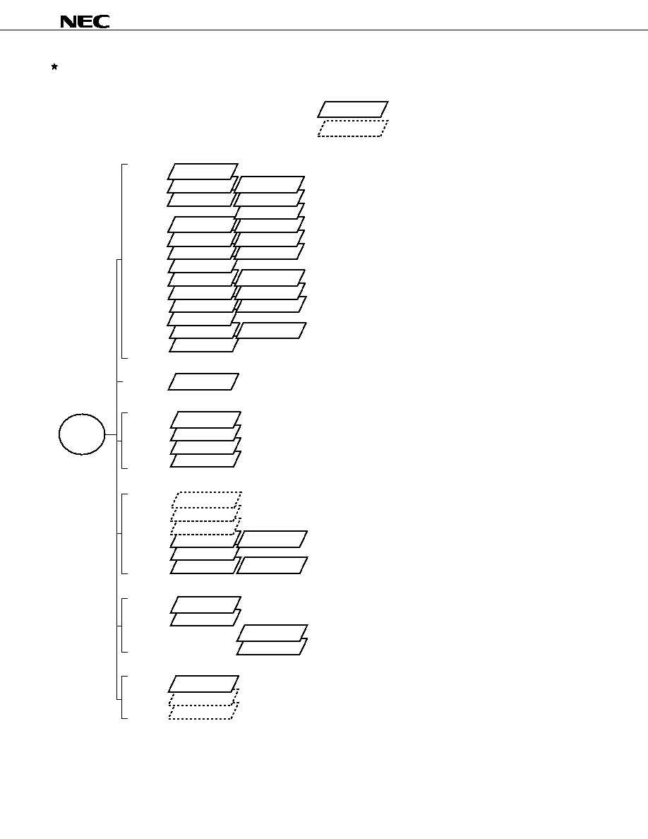
78K/0 SERIES LINEUP
The products in the 78K/0 Series are listed below. The names enclosed in boxes are subseries names.
Remark
VFD (Vacuum Fluorescent Display) is referred to as FIPTM (Fluorescent Indicator Panel) in some
documents, but the functions of the two are the same.
PD78054 with added IEBus
TM
controller. EMI-noise reduced.
64-pin
64-pin
80-pin
80-pin
80-pin
EMI-noise reduced version of the PD78054
PD78018F with added UART and D/A converter and enhanced I/O
PD780034A
PD780988
PD780034AY
µ
µ
µ
64-pin
PD780024A with expanded RAM capacity
PD780024A with enhanced A/D converter
µ
µ
µ
µ
On-chip inverter controller and UART. EMI-noise reduced.
PD78064
PD78064B
PD780308
100-pin
100-pin
100-pin
PD780308Y
PD78064Y
80-pin
78K/0
Series
LCD drive
PD78064 with enhanced SIO, and expanded ROM, RAM capacity
EMI-noise reduced version of the PD78064
Basic subseries for LCD drive, on-chip UART
Bus interface supported
µ
µ
µ
µ
µ
µ
µ
µ
PD78083
PD78018F
PD78018FY
PD78014H
EMI-noise reduced version of the PD78018F
Basic subseries for control
On-chip UART, capable of operating at low voltage (1.8 V)
µ
µ
µ
µ
42-/44-pin
64-pin
64-pin
PD78018F with enhanced serial I/O
µ
µ
80-pin
PD78054 with enhanced serial I/O
100-pin
100-pin
Products in mass production
Products under development
Y subseries products are compatible with I
2
C bus.
PD78054 with added timer and enhanced external interface
ROMless version of the PD78078
µ
100-pin
PD78078Y with enhanced serial I/O and limited function
µ
100-pin
EMI-noise reduced version of the PD78078
µ
µ
Inverter control
PD780208
100-pin
VFD drive
PD78044F with enhanced I/O and VFD C/D. Display output total: 53
µ
µ
PD780208
µ
PD78098B
µ
100-pin
PD780024A
PD780024AY
µ
µ
80-pin
80-pin
PD780852
PD780824
µ
µ
For automobile meter driver. On-chip DCAN controller
100-pin
PD780958
µ
For industrial meter control
On-chip automobile meter controller/driver
Meter control
80-pin
PD780701Y
On-chip DCAN/IEBus controller
µ
80-pin
PD780833Y
On-chip controller compliant with J1850 (Class 2)
µ
PD780948
On-chip DCAN controller
µ
64-pin
PD780078
PD780078Y
µ
µ
PD780034A with added timer and enhanced serial I/O
PD78054
PD78054Y
PD78058F
PD78058FY
µ
µ
µ
µ
PD780058
PD780058Y
µ
µ
PD78070A
PD78070AY
PD78078
PD78078Y
PD780018AY
µ
µ
µ
µ
µ
Control
PD78075B
µ
PD780065
µ
µ
PD78044H
PD780232
80-pin
80-pin
For panel control. On-chip VFD C/D. Display output total: 53
PD78044F with added N-ch open-drain I/O. Display output total: 34
µ
µ
PD78044F
80-pin
Basic subseries for VFD drive. Display output total: 34
µ
µ
120-pin
PD780308 with enhanced display capacity and timer. Segment signal output: 40 pins max.
PD780318
PD780328
120-pin
120-pin
PD780308 with enhanced display capacity and timer. Segment signal output: 32 pins max.
PD780308 with enhanced display capacity and timer. Segment signal output: 24 pins max.
µ
µ
PD780338
µ
µ
µ
µ
µ
3
µPD780232
Data Sheet U13415EJ2V0DS
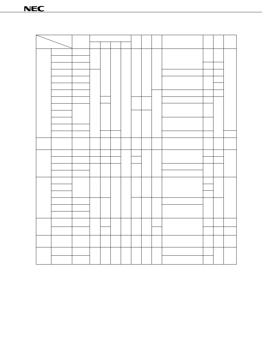
The major functional differences among the subseries are shown below.
Function
Timer
8-Bit 10-Bit 8-Bit
Serial Interface
I/O
External
Subseries Name
8-Bit 16-Bit Watch WDT
A/D
A/D
D/A
Expansion
Control
µ
PD78075B 32 K to 40 K 4 ch
1 ch
1 ch
1 ch
8 ch
≠
2 ch 3 ch (UART: 1 ch)
88
1.8 V
µ
PD78078
48 K to 60 K
µ
PD78070A
≠
61
2.7 V
µ
PD780058 24 K to 60 K 2 ch
3 ch (time-division UART: 1 ch)
68
1.8 V
µ
PD78058F 48 K to 60 K
3 ch (UART: 1 ch)
69
2.7 V
µ
PD78054
16 K to 60 K
2.0 V
µ
PD780065 40 K to 48 K
≠
4 ch (UART: 1 ch)
60
2.7 V
µ
PD780078 48 K to 60 K
2 ch
≠
8 ch
3 ch (UART: 2 ch)
52
1.8 V
µ
PD780034A 8 K to 32 K
1 ch
3 ch (UART: 1 ch)
51
µ
PD780024A
8 ch
≠
µ
PD78014H
2 ch
53
µ
PD78018F 8 K to 60 K
µ
PD78083
8 K to 16 K
≠
≠
1 ch (UART: 1 ch)
33
≠
Inverter
µ
PD780988 16 K to 60 K 3 ch
Note
≠
1 ch
≠
8 ch
≠
3 ch (UART: 2 ch)
47
4.0 V
control
VFD
µ
PD780208 32 K to 60 K 2 ch
1 ch
1 ch
1 ch
8 ch
≠
≠
2 ch
74
2.7 V
≠
drive
µ
PD780232 16 K to 24 K 3 ch
≠
≠
4 ch
40
4.5 V
µ
PD78044H 32 K to 48 K 2 ch
1 ch
1 ch
8 ch
1 ch
68
2.7 V
µ
PD78044F 16 K to 40 K
2 ch
LCD
µ
PD780338 48 K to 60 K 3 ch
2 ch
1 ch
1 ch
≠
10 ch 1 ch 2 ch (UART: 1 ch)
54
1.8 V
≠
drive
µ
PD780328
62
µ
PD780318
70
µ
PD780308 48 K to 60 K 2 ch
1 ch
8 ch
≠
≠
3 ch (time-division UART: 1 ch)
57
2.0 V
µ
PD78064B 32 K
2 ch (UART: 1 ch)
µ
PD78064
16 K to 32 K
Bus
µ
PD780948 60 K
2 ch
2 ch
1 ch
1 ch
8 ch
≠
≠
3 ch (UART: 1 ch)
79
4.0 V
interface
supported
µ
PD78098B 40 K to 60 K
1 ch
2 ch
69
2.7 V
≠
Meter
µ
PD780958 48 K to 60 K 4 ch
2 ch
≠
1 ch
≠
≠
≠
2 ch (UART: 1 ch)
69
2.2 V
≠
control
Dash-
µ
PD780852 32 K to 40 K 3 ch
1 ch
1 ch
1 ch
5 ch
≠
≠
3 ch (UART: 1 ch)
56
4.0 V
≠
board
control
µ
PD780824 32 K to 60 K
2 ch (UART: 1 ch)
59
Note
16-bit timer: 2 channels
10-bit timer: 1 channel
V
DD
MIN.
Value
ROM
Capacity
4
µPD780232
Data Sheet U13415EJ2V0DS
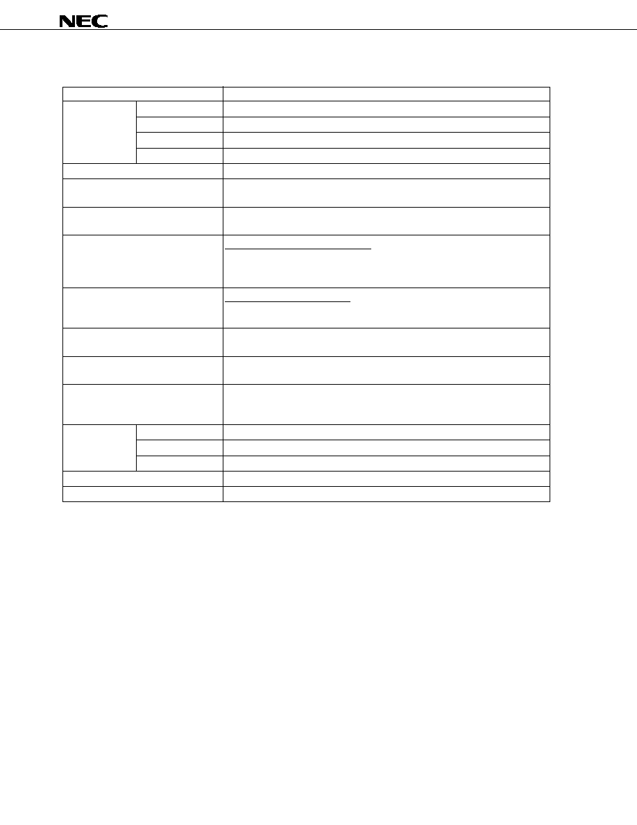
FUNCTION OVERVIEW
Item
Function
Internal memory
ROM
16 KB
High-speed RAM
768 bytes
Buffer RAM
32 bytes
VFD display RAM
112 bytes
General-purpose register
8 bits
◊
32 registers (8 bits
◊
8 registers
◊
4 banks)
Minimum instruction execution time
∑ On-chip minimum instruction execution time variable function
∑ 0.4
µ
s/0.8
µ
s/1.6
µ
s/3.2
µ
s/6.4
µ
s (@ 5.0 MHz operation with system clock)
Instruction set
∑ Multiply/divide (8 bits
◊
8 bits, 16 bits
˜
8 bits)
∑ Bit manipulation (set, reset, test, Boolean operation)
I/O ports
Total:
40
(including alternate-function pins for VFD) ∑ CMOS I/Os:
11
∑ P-ch open-drain I/Os:
13
∑ P-ch open-drain outputs: 16
VFD controller/driver
Total of display outputs: 53
∑ 15 mA display current: 20
∑ 5 mA display current:
33
A/D converter
∑ 8-bit resolution
◊
4 channels
∑ Power supply voltage: AV
DD
= 4.5 to 5.5 V
Serial interface
∑ 3-wire serial mode (automatic transmit/receive function): 1 channel
∑ 2-wire serial mode (transmit only):
1 channel
Timer
∑ 8-bit remote control timer: 1 channel
∑ 8-bit timer:
2 channels
∑ Watchdog timer:
1 channel
Vectored interrupt
Maskable
Internal: 10, external: 2
sources
Non-maskable
Internal: 1
Software
1
Power supply voltage
V
DD
= 4.5 to 5.5 V
Package
80-pin plastic QFP (14
◊
14)

5
µPD780232
Data Sheet U13415EJ2V0DS
CONTENTS
1.
PIN CONFIGURATION (TOP VIEW) ................................................................................................. 6
2.
BLOCK DIAGRAM ............................................................................................................................. 8
3.
PIN FUNCTIONS ................................................................................................................................ 9
3.1
Port Pins ..................................................................................................................................................... 9
3.2
Non-Port Pins .......................................................................................................................................... 10
3.3
Pin I/O Circuits and Recommended Connection of Unused Pins ................................................... 11
4.
MEMORY SPACE ............................................................................................................................. 13
5.
PERIPHERAL HARDWARE FUNCTION FEATURES ................................................................... 14
5.1
Port ............................................................................................................................................................ 14
5.2
Clock Generator ...................................................................................................................................... 15
5.3
Timer/Event Counter ............................................................................................................................... 15
5.4
A/D Converter .......................................................................................................................................... 18
5.5
Serial Interface ........................................................................................................................................ 18
5.6
VFD Controller/Driver ............................................................................................................................. 19
6.
INTERRUPT FUNCTIONS ............................................................................................................... 21
7.
STANDBY FUNCTION ..................................................................................................................... 24
8.
RESET FUNCTION ........................................................................................................................... 24
9.
MASK OPTION ................................................................................................................................. 24
10. INSTRUCTION SET .......................................................................................................................... 25
11. ELECTRICAL SPECIFICATIONS .................................................................................................... 28
12. PACKAGE DRAWING ...................................................................................................................... 42
13. RECOMMENDED SOLDERING CONDITIONS .............................................................................. 43
APPENDIX A. DEVELOPMENT TOOLS ............................................................................................... 44
APPENDIX B. RELATED DOCUMENTS .............................................................................................. 47