Document Outline
- Cover
- Ordering Information
- Overview of Functions
- Table of Contents
- 1.Pin Configuration (Top View)
- 2.Block Diagram
- 3.Pin Functions
- 3.1 Normal Operating Mode Pins
- 3.2 Non-port Pins
- 3.3 Pin I/ O Circuits and Recommended Connection of Unused Pins
- 4.Memory Space
- 5.Peripheral Hardware Functions
- 5.1 Ports
- 5.2 Clock Generator
- 5.3 Main System Clock Oscillator
- 5.4 Subsystem Clock Oscillator
- 5.5 Timer/ Event Counter
- 5.6 Clock Output Control Circuit
- 5.7 Sound Generator
- 5.8 A/ D Converter
- 5.9 Power Fail Detector
- 5.10 Serial Interfaces
- 5.11 CAN-Bus Interface
- 5.12 LCD Controller/ Driver
- 6.Interrupt Functions and Test Functions
- 6.1 Interrupt Functions
- 6.2 Interrupts
- 7.External Device Expansion Functions
- 8.EEPROM Function
- 9.Standby Function
- 10.Reset Function
- 11.Instruction Set
- 12.Electrical Specifications
- 13.Package Drawings
- 14.Recommended Soldering Conditions
- Appendix A. Development Tools
- Appendix B. Related Documents

©
19
DATA SHEET
Document No. U12237EE1V2PM00 (2 nd edition)
Date : April 1998
The information in this document is subject to change without notice.
8-BIT SINGLE-CHIP MICROCONTROLLER
©
NEC Corporation 1998
MOS INTEGRATED CIRCUIT
PRELIMINARY PRODUCT INFORMATION
Description
The
µ
PD780948/780949 is a member of the 78K/0 series microcontrollers. Besides a high speed, high
performance CPU, these microcontrollers have on-chip ROM, RAM, I/O ports, 8-bit resolution A/D converter,
timer, CAN-interface, serial interface, interrupt control, LCD-controller/driver and various other peripheral
hardware.
The
µ
PD78F0948/780949 device includes a FLASH EEPROM version which can operate in the same
power supply voltage range as the mask ROM version, and various development tools are available.
The details of the functions are described in the following user manuals. Be sure to read it before
starting design.
µ
PD780949, Subseries User's Manual : U12670EE1V0UM00
78K/0 Series User's Manual - Instructions : U12336EJ3V0UM00
Features
∑ Internal high capacity ROM and RAM
∑ External memory expansions space : 1K bytes
∑ CAN-Interface
∑ Instruction execution time can be changed from
∑ Serial interface : 3 channels
high speed (0.25 µs) to ultra low speed
∑ 2-wire mode : 1 channel
∑ I/O ports: 79 (N-ch open drain : 5)
∑ 3-wire mode : 1 channel
∑ 8-bit resolution A/D converter : 8 channels
∑ UART mode : 1 channel
∑ Sound generator
∑ Timer
: 6 channels
∑ LCD-controller / driver
∑ Supply voltage : V
DD
= 4.0 to 5.5 V
Application
Dashboard, climate controller, security unit etc.
µPD780948(A), µPD780949(A)
Item
Program
Data Memory
Part
Number
Memory
(ROM)
Internal
High-Speed
RAM
LCD Display
RAM
Internal
Expansion RAM
EEPROM
Package
µPD780948(A)
60K bytes
1024 bytes
40 bytes
992 bytes
-
100-pin plastic QFP (fine pitch)
µPD780949(A)
60K bytes
1024 bytes
40 bytes
992 bytes
256 bytes
100-pin plastic QFP (fine pitch)

2
µPD780948(A), µPD780949(A)
78K/0 Series Development
These products are a further development in the 78K/0 Series. The designations appearing inside the
boxes are subseries names.
Function
Timer
V
DD
I/O
MIN.
Subseries Name
8-bit
16-bit Watch WDT
Value
For Control
µPD78078
32 K-60 K
4ch
1ch
1ch
1ch
8ch
2ch
3ch (UART: 1ch)
88
1.8 V
µPD78070A
61
2.7 V
µPD78054 16 K-60 K
2ch
69
2.0 V
µPD78018F 8 K-60 K
2ch
53
1.8 V
µPD78014
8 K-32 K
2.7 V
µPD780001 8 K
1ch
39
µPD78002
8 K-16 K
1ch
53
µPD78083
8ch
1ch (UART: 1ch)
33
1.8 V
For FIP
µPD780208 32 K-60 K
2ch
1ch
1ch
1ch
8ch
2ch
74
2.7 V
driving
µPD78044A 16 K-40 K
68
µPD78024
24 K-32 K
54
For LCD
µPD78064
16 K-32 K
2ch
1ch
1ch
1ch
8ch
2ch (UART: 1ch)
57
2.0 V
driving
For IEBus
µPD78098
32 K-60 K
2ch
1ch
1ch
1ch
8ch
2ch
3ch (UART: 1ch)
69
2.7 V
For CANBus
µPD780949 60 K
2ch
2ch
1ch
1ch
8ch
--
3ch (UART: 1ch)
79
4.0 V
8-bit
A/D
8-bit
D/A
Serial
Interface
External
Expansion
--
--
--
--
O
O
O
--
--
--
--
--
--
--
--
ROM
Capacity
O
Major functional differences among the subseries
Ordering Information
Part Number
Package
µPD780948GF(A)-3BA
100-pin plastic QFP (14 x 20 mm, resin thickness 2.7 mm)
µPD780949GF(A)-3BA
100-pin plastic QFP (14 x 20 mm, resin thickness 2.7 mm)
PD78002
µ
PD78083
µ
Products in mass production
Products under development
Y subseries products are compatible with I
2
C bus.
Timer added to the PD78054, external interface functions enhanced
ROM-less product for the PD78078
UART and D/A added to the PD78014, I/O enhanced
Low-voltage (1.8 V) operation version of the PD78014, ROM and RAM variations enhanced
A/D and 16-bit timer added to the PD78002
Basic subseries for control
µ
µ
µ
µ
100-pin
100-pin
80-pin
64-pin
64-pin
64-pin
100-pin
80-pin
64-pin
100-pin
80-pin
For control
PD78078
µ
µ
µ
PD78070A
µ
PD78054
µ
PD78018F
µ
PD78014
µ
PD780001
µ
64-pin
42/44-pin
PD78078Y
µ
PD78070AY
µ
PD78054Y
µ
PD78018FY
µ
PD78014Y
µ
PD78002Y
µ
For FIP driving
PD780208
µ
PD78044A
µ
PD78024
µ
For LCD driving
PD78064
µ
PD78064Y
µ
For IEBus
TM
PD78098
µ
I/O, FIP C/D of the PD78044A enhanecd, display output total: 53
6-bit U/D counter added to the PD78024, display output total: 34
Basic subseries for FIP driving, display output total: 26
Subseries for LCD driving, internal UART
IEBus controller added to the PD78054
µ
µ
µ
78K/0
Series
Internal UART, low-voltage (1.8 V) operation possible
A/D added to the PD78002
PD780949
µ
For CANBus
CANBus controller
100-pin

3
µPD780948(A), µPD780949(A)
Overview of Functions
Major Changes
Page
Description
18
The internal high-speed RAM is 1024 x 8 bits
Note:
The mark
5
shows major revised points.
Part Number
Item
µPD780948
µPD780949
ROM
60 Kbytes
Internal high-speed RAM
1024 bytes
LCD Display RAM
40 bytes
Internal Expansion RAM
992 bytes
Internal
memory
EEPROM
-
256 bytes
Memory space
64 Kbytes
General registers
8 bits x 32 registers ( 8 bits x 8 registers x 4 banks)
Instruction cycle
On-chip instruction execution time selective function
When main system clock
selected
0,25 µs/0,5 µs/1 µs/2 µs/4 µs (at 8 MHz)
When subsystem clock
selected
122 µs (at 32.768 kHz)
Instruction set
∑
16-bit operation
∑
Multiplication/division ( 8 bits x 8 bits, 16 bits ≠ 8 bits )
∑
Bit manipulation ( set, reset, test, boolean operation )
∑
BCD adjustment, etc.
Total : 79
I/O ports
∑
CMOS input : 8
∑
CMOS I/O : 71
A/D converter
∑
8 bit resolution x 8 channels
Serial Interface
∑
3-wire mode : 1 channel
∑
2-wire mode : 1 channel
∑
UART mode : 1 channel
Timer
∑
16 bit timer / event counter : 2 channels
∑
8 bit timer / event counter : 2 channels
∑
Watch timer : 1 channel
∑
Watchdog timer : 1 channel
Timer output
3 ( 16-bit RWM output x 1, 8-bit RWM output x 2 )
Clock output
62,5 kHz, 125 kHz, 250 kHz, 500 kHz, 1 MHz, 2 MHz,
4 MHz, 8 MHz (at main system clock of 8.0 MHz)
CAN
1 channel
Maskable interrupts
Internal : 22
External : 5
Non-maskable interrupts
Internal : 1
Vectored
interrupts
Software interrupts
Internal : 1
Supply voltage
V
DD
= 4,0 V to 5,5 V
Package
100-pin plastic QFP ( 14 mm x 20 mm )

4
µPD780948(A), µPD780949(A)
Contents
1.
Pin Configuration (Top View) ........................................................................................................ 5
2.
Block Diagram ................................................................................................................................ 7
3.
Pin Functions ................................................................................................................................. 8
3.1 Normal Operating Mode Pins ........................................................................................................ 8
3.2 Non-port Pins ............................................................................................................................... 10
3.3 Pin I/O Circuits and Recommended Connection of Unused Pins ............................................ 12
4.
Memory Space .............................................................................................................................. 18
5.
Peripheral Hardware Functions .................................................................................................. 19
5.1 Ports .............................................................................................................................................. 19
5.2 Clock Generator ........................................................................................................................... 20
5.3 Main System Clock Oscillator ..................................................................................................... 20
5.4 Subsystem Clock Oscillator ........................................................................................................ 21
5.5 Timer/Event Counter .................................................................................................................... 21
5.6 Clock Output Control Circuit ....................................................................................................... 27
5.7 Sound Generator .......................................................................................................................... 29
5.8 A/D Converter ............................................................................................................................... 30
5.9 Power Fail Detector ...................................................................................................................... 31
5.10 Serial Interfaces ............................................................................................................................ 32
5.11 CAN-Bus Interface ........................................................................................................................ 34
5.12 LCD Controller/Driver ................................................................................................................... 34
6.
Interrupt Functions and Test Functions ..................................................................................... 36
6.1 Interrupt Functions ...................................................................................................................... 36
6.2 Interrupts ...................................................................................................................................... 37
7.
External Device Expansion Functions ........................................................................................ 39
8.
EEPROM Function ........................................................................................................................
39
9.
Standby Function ......................................................................................................................... 39
10. Reset Function ............................................................................................................................. 39
11. Instruction Set .............................................................................................................................. 40
12. Electrical Specifications .............................................................................................................. 43
13. Package Drawings ........................................................................................................................ 60
14. Recommended Soldering Conditions ......................................................................................... 61
Appendix A. Development Tools .................................................................................................... 62
Appendix B. Related Documents .................................................................................................... 64

5
µPD780948(A), µPD780949(A)
1. Pin Configuration (Top View)
ð
100-pin plastic QFP (14 x 20 mm)
µPD780948GF(A)-XXX-3BA
Cautions:
1. Connect IC (internally connected) pin directly to V
SS
.
2. AV
SS
pin should be connected to V
SS
.
3. AV
DD
pin should be connected to V
DD
.
Figure 1-1: Pin Configuration
µPD780949GF(A)-XXX-3BA
CTxD
P00/INTP0
P01/INTP1
P02/INTP2
P03/INTP3/T2PO
P04/INTP4/TI01
P05/TI00/TO0
P06/TI50/TO50
P07/TI51/TO51
P20/SI0
P21/SO0
P22/SCK0
P23/SI1/SO1
P24/SCK1
P25/RxD
P26/TxD
RESET
X1
X2
VPP(/IC)
CL1/CCLK
CL2
V
SS
2
V
DD
2
AV
DD
P10/ANI0
P11/ANI1
P12/ANI2
P13/ANI3
P14/ANI4
P15/ANI5
P16/ANI6
P17/ANI7
AV
SS
P30/TI20
P31/TI21
P32/TI22
P33/PCL/SGOA
P34/SGO/SGOF
V
SS
1
V
DD
1
VLC0
VLC1
VLC2
COM0
COM1
COM2
COM3
P147/S0
P146/S1
P70/S31
P71/S30
P72/S29
P73/S28
P74/S27
P75/S26
P76/S25
P77/S24
P120/S23
P121/S22
P122/S21
P123/S20
P124/S19
P125/S18
P126/S17
P127/S16
P130/S15
P131/S14
P132/S13
P133/S12
P134/S11
P135/S10
P136/S9
P137/S8
P140/S7
P141/S6
P142/S5
P143/S4
P144/S3
P145/S2
CRxD
P64/RD
P65/WR
P67/ASTB
P40/AD0
P41/AD1
P42/AD2
P43/AD3
P44/AD4
P45/AD5
P46/AD6
P47/AD7
P50/A8/S39
P51/A9/S38
P52/A10/S37
P53/A11/S36
P54/A12/S35
P55/A13/S34
P56/A14/S33
P57/A15/S32
1
2
3
4
5
6
7
8
9
10
11
12
13
14
15
16
17
18
19
20
21
22
23
24
25
26
27
28
29
30
31 32 33 34 35 36 37 38 39 40 41 42 43 44 45 46 47 48 49 50
80
79
78
77
76
75
74
73
72
71
70
69
68
67
66
65
64
63
62
61
60
59
58
57
56
55
54
53
52
51
100 99 98 97 96 95 94 93 92 91 90 89 88 87 86 85 84 83 82 81

6
µPD780948(A), µPD780949(A)
Pin Identifications
P00 to P07
: Port0
P10 to P17
: Port1
P20 to P26
: Port2
P30 to P34
: Port3
P40 to P47
: Port4
P50 to P57
: Port5
P64, P65, P67
: Port6
P70 to P77
: Port7
P120 to P127
: Port12
P130 to P137
: Port13
P140 to P147
: Port14
INTP0 to INTP4
: Interrupt from Peripherals
TI00, TI01, TI50, TI51 : Timer Input
TI20 to TI22
: Timer Input
TO0 , TO51, TO52
: Timer Output
T2PO
: Timer Output
CRxD
: CAN Receive Data
CTxD
: CAN Transmit Data
CCLK
: CAN Clock
SI0
: Serial Input
SO0
: Serial Output
SIO1
: Serial Input / Output
SCK0, SCK1
: Serial Clock
RxD
: Receive Data
TxD
: Transmit Data
SGO
: Sound Generator Output
SGOA
: Sound Generator Amplitude
SGOF
: Sound Generator Frequency
PCL
: Programmable Clock Output
AD0 to AD7
: Address / Data Bus
A8 to A15
: Address Bus
RD
: Read Strobe
WR
: Write Strobe
ASTB
: Address Strobe
S0 to S39
: Segment Output
COM0 to COM3 : Common Output
X1, X2
: Crystal (Main System Clock)
CL1, CL2
: RC (Subsystem Clock)
RESET
: Reset
ANI0 to ANI7
: Analog Input
AV
SS
: Analog Ground
AV
DD
: Analog Reference Voltage
V
DD
: Power Supply
V
PP
: Programming Power supply
V
SS
: Ground
IC
: Internally Connected

7
µPD780948(A), µPD780949(A)
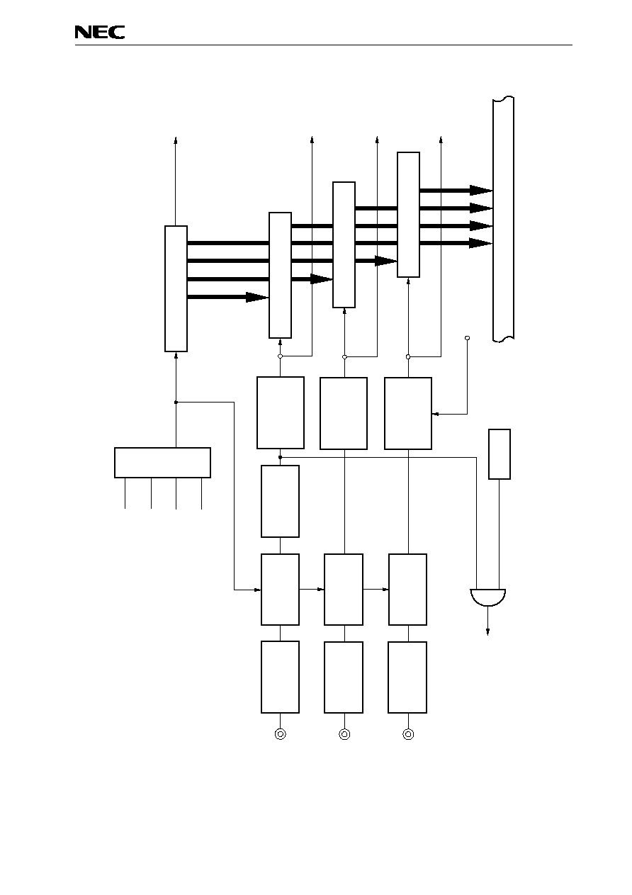
2. Block Diagram
Remark:
The EEPROM capacity depends on the product.
Figure 2-1: Block Diagram
µPD780948 - no EEPROM
µPD780949 - with EEPROM
S16-S23
S24-S31
S32-S39
COM0-COM3
VLC0-VLC2
Port 0
LCD
Controller
driver
16 bit Timer 0
16 bit Timer 2
TI00/TO0
78K/0
CPU
Core
Port 1
Port 2
Port 3
Port 4
Port 5
Port 6
Port 7
TI01
TI20
TI21
TI50/TO50
SI0
SO0
SCK0
Port 12
Port 13
Port 14
S0-S7
S8-S15
TI22
T2PO
8 bit Timer 50
TI51/TO51
8 bit Timer 51
Watch Timer
Watchdog Timer
Serial Interface
Channel 0
SIO1
SCK1
Serial Interface
Channel 1
RxD
TxD
UART
A/D Converter
ANI0-
ANI7
AV
SS
AV
DD
External
Access
AD0-
AD7
A8-
A15
/RD
/WR
ASTB
Interrupt
Control
INTP0-
INTP4
8
8
6
5
8
8
3
8
8
8
8
Sound Generator
Clock Output
Control
Standby
Control
SGO/SGOF
SGOA
PCL
RAM
1K
Byte
EEPROM
256 Byte
60 K ROM
DCAN
Interface
RAM
992 Byte
Interface
System
Control
8MHz / SV
RC Oscillator
RESET
X1
X2
CL1
CL2
V
DD
V
DD
V
SS
V
SS
IC/V
PP
CCLK
CRxD
CTxD

8
µPD780948(A), µPD780949(A)
3.
Pin Functions
3.1 Normal Operating Mode Pins / Pin Input/Output Types
Table 3-1: Pin Input/Output Types (1/2)
Input /
Output
Pin
Name
Function
Alternate
Function
After
Reset
P00
INTP0
Input
P01
INTP1
Input
P02
INTP2
Input
P03
INTP3/T2P0
Input
P04
INTP4/TI01
Input
P05
TI00/TO0
Input
P06
TI50/TO50
Input
Input /
Output
P07
Port 0
8 bit input / output port
Input / output mode can be specified bit-wise
If used as an input port, a pull-up resistor can be
connected by software bit-wise
TI51/TO51
Input
Input
P10-P17
Port 1
8 bit input port
Input mode can be specified bit-wise
ANI0-ANI7
Input
P20
SI0
Input
P21
SO0
Input
P22
/SCK0
Input
P23
SI/SO1
Input
P24
/SCK1
Input
P25
RxD
Input
Input /
Output
P26
Port 2
7 bit input/output port
Input / output mode can be specified bit-wise
TxD
Input
Input/
Output
P40-P47
Port 4
8 bit input / output port
Input / output mode can be specified bit-wise
If used as an input port, a pull-up resistor can be
connected by software
AD0-AD7
Input
Input/
Output
P50-P57
Port 5
8 bit input / output port
Input / output mode can be specified bit-wise
This port can be used in External Memory
Expansion Mode with the 4, 6 or 8 bit address by
setting the
Memory Expansion Mode Register
Not for external memory expansion used ports can
be used either for LCD or port function
A8/S39-A15/S32
Input
P64
/RD
Input
P65
/WR
Input
Input /
Output
P67
Port 6
3 bit input / output port
input / output mode can be specified bit-wise
ASTB
Input

9
µPD780948(A), µPD780949(A)
Table 3-1
:
Pin Input/Output Types (2/2)
Input /
Output
Pin Name
Function
Alternate
Function
After
Reset
Input/
Output
P70-P77
Port 7
8 bit input / output port
Input / output mode can be specified bit-wise
If used as an input port, a pull-up resistor can be
connected by software
This port can be used as a segment signal output port
or an I/O port in 1 bit units by setting port function
S31-S24
Input
Input/
Output
P120-P127
Port 12
8 bit input / output port
Input / output mode can be specified bit-wise
This port can be used as a segment signal output port
or an I/O port in 8 bit units by setting LCD control
register
S23-S16
Input
Input/
Output
P130-P137
Port 13
8 bit input / output port
Input / output mode can be specified bit-wise
If used as an input port, a pull-up resistor can be
connected by software
This port can be used as a segment signal output port
or an I/O port in 8 bit units by setting LCD control
register
S15-S8
Input
Input/
Output
P140-P147
Port 14
8 bit input / output port
Input / output mode can be specified bit-wise
This port can be used as a segment signal output port
or an I/O port in 8 bit units by setting LCD control
register
S7-S0
Input

10
µPD780948(A), µPD780949(A)
3.2 Non-Port Pins
Table 3-2: Non-Port Pins (1/2)
Pin Name
I/O
Function
After
Reset
Alternate
Function Pin
INTP0
P00
INTP1
P01
INTP2
P02
INTP3
P03/T2P0
INTP4
Input
External interrupts with specifiable valid edges (rising
edge, falling edge, both rising and falling edges)
Input
P04/TI01
SI0
P20
SI1
Input
Serial interface serial data input
Input
P23/SO1
SO0
P21
SO1
Output
Serial interface serial data output
Input
P23/SI1
SCK0
P22
SCK1
Input/
Output
Serial interface serial clock input / output
Input
P24
RxD
Input
Asynchronous serial interface data input
Input
P25
TxD
Output
Asynchronous serial interface data output
Input
P26
CRxD
Input
CAN
serial data input
Input
-
CTxD
Output
CAN
serial data output
Output
-
CCLK
Input
CAN
serial clock input
-
CL1
TI00
P05/TO0
Ti01
External count clock input to 16-bit timer (TM0)
P04/INTP4
TI20
Capture trigger input
P30
TI21
Capture trigger input
P31
TI22
Capture trigger input
P32
TI50
External count clock input to 8-bit timer (TM50)
P06/TO50
TI51
Input
External count clock input to 8-bit timer (TM51)
Input
P07/TO51
TO0
16-bit timer output
P05/TI00
T2P0
16-bit timer output
P03/INTP3
TO50
8-bit timer output (also used for PWM output)
P06/TI50
TO51
Output
8-bit timer output (also used for PWM output)
Input
P07/TI51
PCL
Output
Clock output (for main system clock trimming)
Input
P33/SGOA
AD0 to AD7
Input/
Output
Low-order address/data bus at external memory
expansion
Input
P40 to P47
A8 to A15
Output
High-order address/data bus at external memory
expansion
Input
P50 to P57
S39 to S32
RD
Strobe signal output for read operation from external
memory
P64
WR
Output
Strobe signal output for read operation from external
memory
Input
P65
ASTB
-
Strobe output externally latching address information
output to ports 4, 5 to access external memory
Input
P67
S0 to S7
P147 to P140
S8 to S15
P137 to P130
S16 to S23
P127 to P120
S24 to S31
P77 to P70
S32 to S39
Output
Segment signal output of LCD controller / driver
Input
P57 to P50
A15 to A8

11
µPD780948(A), µPD780949(A)
Table 3-2: Non-Port Pins (2/2)
Pin Name
I/O
Function
After
Reset
Alternate
Function Pin
COM0-COM3
Output
Common signal output of LCD controller/driver
Output
-
V
LC
0 to V
LC
2
-
LCD drive voltage
-
-
SGO
Output
Sound generator output
Input
P34/SGOF
SGOA
Output
Sound generator amplitude output
Input
P33/PCL
SGOF
Output
Sound generator frequency output
Input
P34/SGO
ANI0 to ANI7
Input
A/D Converter analog input
Input
P10 ≠ P17
AV
DD
-
A/D Converter reference voltage input and power
supply
-
-
AV
SS
-
A/D Converter ground potential. Connect to V
SS.
-
-
RESET
Input
System reset input
-
-
X1
-
Crystal connection for main system clock
-
-
X2
-
-
-
CL1
Input
RC connection for subsystem clock
-
CCLK
CL2
-
-
-
V
DD
1, V
DD
2
-
Positive power supply
-
-
V
SS
1, V
SS
2
-
Ground potential
-
-
V
PP
-
High voltage supply for flash programming (only
flash version)
-
IC
IC
-
Internal connection. Connect directly to V
SS
(only
MaskROM version)
-
V
PP

12
µPD780948(A), µPD780949(A)
3.3 Pin I/O Circuits and Recommended Connection of Unused Pins
The input/output circuit type of each pin and recommended connection of unused pins are shown in the
following table.
For the input/output circuit configuration of each type, see table.
Table 3-3: Types of Pin Input/Output Circuits (1/3)
Pin Name
Input/Output
Circuit Type
I/O
Recommended Connection for Unused Pins
P00/INTP0
P01/INTP1
P02/INTP2
P03/INPT3/T2P0
P04/INTP4/TI01
P05/TI00/TO0
P06/TI50/TO50
P07/TI51/TO51
8-A
I/O
Connect to Vdd or Vss via a resistor individually
P10/ANI0
P11/ANI1
P12/ANI2
P13/ANI3
P14/ANI4
P15/ANI5
P16/ANI6
P17/ANI7
11-B
I
Connect to Vdd or Vss via a resistor individually
P20/SI0
P21/SO0
P22/SCK0
P23/SI1/SOA
P24/SCK1
10
P25/RxD
8
P26/TxD
5
I/O
Connect to Vdd or Vss via a resistor individually
P30/TI20
P31/TI21
P32/TI22
8
P33/PCL/SGOA
P34/SGO/SGOF
5
I/O
Connect to Vdd or Vss via a resistor individually
P40/AD0
P41/AD1
P42/AD2
P43/AD3
P44/AD4
P45/AD5
P46/AD6
P47/AD7
5-A
I/O
Connect to Vdd or Vss via a resistor individually

13
µPD780948(A), µPD780949(A)
Table 3-3: Types of Pin Input/Output Circuits (2/3)
Pin Name
Input/Output
Circuit Type
I/O
Recommended Connection for Unused Pins
P50/A8/S39
P51/A9/S38
P52/A10/S37
P53/A11/S36
P54/A12/S35
P55/A13/S34
P56/A14/S33
P57/A15/S32
17
I/O
Connect to Vdd or Vss via a resistor individually
P64/RD
P65/WR
P67/ASTB
5-A
I/O
Connect to Vdd or Vss via a resistor individually
P70/S31
P71/S30
P72/S29
P73/S28
P74/S27
P75/S26
P76/S25
P77/S24
17-B
I/O
Connect to Vdd or Vss via a resistor individually
P120/S23
P121/S22
P122/S21
P123/S20
P124/S19
P125/S18
P126/S17
P127/S16
17-C
I/O
Connect to Vdd or Vss via a resistor individually
P130/S15
P131/S14
P132/S13
P133/S12
P134/S11
P135/S10
P136/S9
P137/S8
17-A
I/O
Connect to Vdd or Vss via a resistor individually
P140/S7
P141/S6
P142/S5
P143/S4
P144/S3
P145/S2
P146/S1
P147/S0
17-A
I/O
Connect to Vdd or Vss via a resistor individually

14
µPD780948(A), µPD780949(A)
Table 3-3: Types of Pin Input/Output Circuits (3/3)
Pin Name
Input/Output
Circuit Type
I/O
Recommended Connection for Unused Pins
COM0 ≠ COM3
18
O
V
LC
0 ≠ V
LC
2
-
-
Leave open
CRxD
1
I
Connect to Vdd or Vss via a resistor individually
CTxD
2
O
Leave open
CL1/CCLK
-
-
Connect to Vdd or Vss via a resistor individually
C2
-
-
Leave open
RESET
1
I
-
AV
REF
-
-
Connect to V
DD
AV
SS
-
-
Connect to V
SS
IC
V
PP
-
-
Connect directly to V
SS

15
µPD780948(A), µPD780949(A)
Figure 3-1: Pin Input/Output Circuits (1/3)
Type 1
IN
Pullup
enable
Data
Output
disable
V
P-ch
N-ch
P-ch
IN/OUT
DD
V
DD
Type 5-A
Input
enable
Type 5
Data
Output
disable
V
P-ch
N-ch
IN/OUT
DD
Input
disable
Type 2
Data
V
P-ch
N-ch
OUT
DD
Type 8-A
Pullup
enable
Data
Output
disable
V
P-ch
N-ch
P-ch
IN/OUT
DD
V
DD
Type 8
Data
Output
disable
V
P-ch
N-ch
IN/OUT
DD

16
µPD780948(A), µPD780949(A)
Figure 3-1: Pin Input/Output Circuits (2/3)
Type 10
Data
Open drain
output disable
N-ch
P-ch
V
DD
IN/OUT
Type 11-B
P-ch
N-ch
Input
enable
+
-
V
REF
(Threshold Voltage)
IN
Comparator
Type 17
Data
Output
disable
V
P-ch
N-ch
IN/OUT
DD
Input
enable
P-ch
P-ch
N-ch
P-ch
N-ch
N-ch
V
LC0
V
LC1
V
LC2
SEG
Data
Type 17-A
Pullup
enable
Data
Output
disable
V
P-ch
N-ch
P-ch
IN/OUT
DD
V
DD
Input
enable
P-ch
P-ch
N-ch
P-ch
N-ch
N-ch
V
LC0
V
LC1
V
LC2
SEG
Data

17
µPD780948(A), µPD780949(A)
Figure 3-1: Pin Input/Output Circuits (3/3)
Type 17-C
Data
Output
disable
V
P-ch
N-ch
IN/OUT
DD
P-ch
P-ch
N-ch
P-ch
N-ch
N-ch
V
LC0
V
LC1
V
LC2
SEG
Data
Type 17-B
Pullup
enable
Data
Output
disable
V
P-ch
N-ch
P-ch
IN/OUT
DD
V
DD
P-ch
P-ch
N-ch
P-ch
N-ch
N-ch
V
LC0
V
LC1
V
LC2
SEG
Data
Type 18
P-ch
N-ch
V
LC0
V
LC1
V
LC2
COM
OUT

18
µPD780948(A), µPD780949(A)
4. Memory Space
The memory map of the µPD780949 is shown in Figure 4-1.
Figure 4-1: Memory Map
Remark:
The EEPROM is only available in the µPD780949 und not in the µPD780948.
FFFFH
FF00H
FEFFH
FA80H
FA7FH
FEE0H
FEDFH
F900H
F8FFH
FA00H
F9FFH
F000H
EFFFH
0000H
nnnnH
1000H
0FFFH
0800H
07FFH
0080H
007FH
0040H
003FH
0000H
LCD Display RAM
40 x 4 bits
Internal Expansion RAM
992 x 8 bits
External Memory
Program Area
CALLF Entry Area
Program Area
CALLT Table Area
Vector Table Area
Special Function Registers
(SFRs) 256 x 8 bits
General Registers
32 x 8 bits
Internal High-speed RAM
1024 x 8 bits
Internal ROM
61440 x 8 bits
EEPROM
256 x 8 bits
Not usable
Not usable
Not usable
Not usable
FF20H
FF1FH
FE20H
FB00H
FA58H
FA57H
FAFFH
F800H
F7DFH
F400H
F3FFH

19
µPD780948(A), µPD780949(A)
Port Name
Pin Name
Function
Port 0
P00 to P07
Port 1
P10 to P17
Port 2
P20 to P26
Port 3
P30 to P34
Port 4
P40 to P47
Port 5
P50 to P57
Port 6
P64, P65, P67
Port 7
P70 to P77
Port 12
P120 to P127
Port 13
P130 to P137
5. Peripheral Hardware Function
5.1 Ports
Input/output ports are classified into three types.
∑ CMOS input/output (Port 0, Port 2 to 5, P64, P65, P67, Port 7,
Port 8, Port 12, Port 13, Port 14)
: 71
∑ Input (P10 to P17)
: 8
Total
: 79
Input/output port. Input/output can be specified bit-wise.
When used as an input port, on-chip pull-up resistor can be used bit-wise by software.
Input port.
Port 14
P140 to P147
Input/output port. Input/output can be specified bit-wise.
When used as an output port, on-chip output buffer can be used by software.
Input/output port. Input/output can be specified bit-wise.
Input/output port. Input/output can be specified bit-wise.
When used as an input port, on-chip pull-up resistor can be used bit-wise by software.
Input/output port. Input/output can be specified bit-wise.
Input/output port. Input/output can be specified bit-wise.
When used as an input port, on-chip pull-up resistor can be used bit-wise by software.
When used as an output port, port function can be specified by software.
Input/output port. Input/output can be specified bit-wise.
When used as an output port, port function can be specified by software.
Input/output port. Input/output can be specified bit-wise.
When used as an output port, port function can be specified by software.
Input/output port. Input/output can be specified bit-wise.
When used as an input port, on-chip pull-up resistor can be used bit-wise by software.
When used as an output port, port function can be specified by software.
Input/output port. Input/output can be specified bit-wise.
Table 5-1: Functions of Ports

20
µPD780948(A), µPD780949(A)
5.2 Clock Generator
There are two kinds of clock generators: main system and subsystem clock generators.
It is possible to change the instruction execution time.
∑ 0.25 µs/0.5 µs/1 µs/2 µs/4 µs (at main system clock frequency of 8.0 MHz)
∑ 122 µs (at subsystem clock frequency of 32.768 kHz)
5.3 Main system clock oscillator
The main system clock oscillator oscillates with a crystal or a ceramic resonator connected to the X1 and
X2 pins.
Figure 5-2: Oscillator Circuit
Figure 5-1: Clock Generator Block Diagram
(a) Crystal and ceramic oscillation
(b) External clock
f
X
f
X
f
X
2
f
X
3
2
f
X
4
2
f
XT
2
CPU Clock (f
CPU
)
Prescaler
Selector
2
2
Standby
Control
Circuit
2
1
Prescaler
Clock to peripheral
hardware
Watch Timer
Main System
Clock
Oscillator
Subsystem
Clock
Oscillator
f
X
f
XT
STOP
CL1
CL2
X1
X2
Crystal
resonator
or ceramic
resonator
External
Clock
IC
X2
X1
X1
X2
21
µPD780948(A), µPD780949(A)
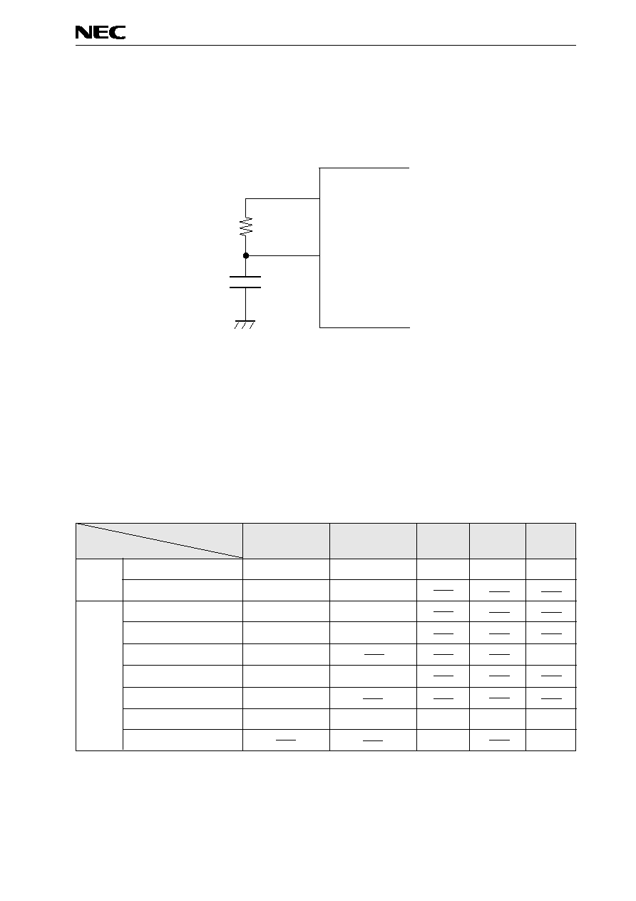
5.4 Subsystem Clock Oscillator
Subsystem clock oscillator is for RC oscillation with very low frequency.
5.5 Timer/Event Counter
There are the following seven timer/event counter channels:
∑ 16-bit timer/event counter
: 1 channel
∑ 8-bit timer/event counter
: 4 channels
∑ Watch timer
: 1 channel
∑ Watchdog timer
: 1 channel
16-bit Timer/Event 8-bit Timer/Event
Watch
Watchdog
16-bit
Counter
Counter
Timer
Timer
Timer
Type
Interval timer
2 channels
2 channels
1 channel
1 channel 1 channel
External event counter
1 channel
2 channels
Timer output
1 output
2 outputs
PWM output
1 output
2 outputs
Pulse with measurement
2 inputs
3 inputs
Function Square wave output
1 output
2 outputs
One-shot pulse output
1 output
Interrupt request
2
2
2
1
4
Test input
1
3
Figure 5-3: Oscillator Circuit
Table 5-2: T ypes and Functions of Timer/Event Counters
CL1
CL2
R
C

22
µPD780948(A), µPD780949(A)
Figure 5-4: 16 bit Timer TM0
Match
Match
Clear
Circuit
16-bit Capture/
Compare Control
Register (CR00)
Internal Bus
Output
Control
INTP4
TI01/P04/
INTP4
Selector
Selector
Internal Bus
16-bit Capture/
Compare Control
Register (CR01)
16-bit Timer
Register (TM0)
Noise
Rejection
Circuit
Noise
Rejection
Circuit
Selector
Noise
Rejection
Circuit
Selector
fx / 2
fx / 16
fx / 128
fx / 2
TI00/P05/
TO0
INTTM00
TO0/P05/
TI00
INTTM01
23
µPD780948(A), µPD780949(A)
Figure 5-5: 16 Bit Timer TM2
Internal Bus
16-Bit Timer Register (TM2)
16-Bit Capture Register (CR22)
16-Bit Capture Register (CR21)
16-Bit Capture Register (CR20)
Edge Detection
Circuit 1)
Edge Detection
Circuit 1)
Edge Detection
Circuit 1)
Prescaler
1, 1/2, 1/4, 1/8
Digital
Filter
Schmitt Trigger
Input Buffer
Schmitt Trigger
Input Buffer
Schmitt Trigger
Input Buffer
Digital
Filter
Digital
Filter
Selector
TPOE
Overflow INT
INTTM22
INTTM21
INTTM20
fx / 4
fx / 8
fx / 32
fx / 128
T2PO Terminal to
related output port
DCAN
TI22
TI21
TI20
1) Valid edge (rising edge, falling edge or both edges) is selectable via software

24
µPD780948(A), µPD780949(A)
Figure 5-6: Digital Capture Input Filter
1/1 1/2 1/4 1/8
Selector
D
Q
C
D
Q
C
S
Q
R
D
Q
C
3 bit
Counter
Edge
Detection
To
Internal
TI22
CLK
D
Q
C
D
Q
C
S
Q
R
D
Q
C
Edge
Detection
To
Internal
TI20,
TI21
CLK
25
µPD780948(A), µPD780949(A)
Figure 5-7: 8-Bit Timer/Event Counter 51 Block Diagram
Figure 5-8: 8-Bit Timer/Event Counter 50 Block Diagram
Match
Internal Bus
8-bit Timer Register n
(TM51)
8-bit Compare Register
(CR51)
Output Control
Circuit
Selector
fx / 2
1
fx / 2
5
fx / 2
12
fx
fx / 2
3
fx / 2
7
TI51 / P07 / TO51
OVF
Clear
INTTM 51
TO51 / P07 / TI51
Internal Bus
Match
Internal Bus
8-bit Timer Register n
(TM50)
8-bit Compare Register
(CR50)
Output Control
Circuit
Selector
fx / 2
1
fx / 2
5
fx / 2
9
fx
fx / 2
3
fx / 2
7
TI50 / P06 / TO50
OVF
Clear
INTTM 50
TO50 / P06 / TI50
Internal Bus
26
µPD780948(A), µPD780949(A)
Figure 5-9: Watch Timer Block Diagram
Figure 5-10: Watchdog Timer Block Diagram
fw
fw
6
fw
7
2
fw
8
2
fw
2
INTWTI
Prescaler
Selector
2
2
Selector
5-bit Counter
INTWT
Selector
fw
5
9
fw
2
4
fw
2
14
fw
2
5
fx/2
8
fx
T
INTWDT
Maskable
interrupt request
Prescaler
Selector
fx/2
13
fx/2
12
Control
Circuit
fx/2
14
fx/2
15
fx/2
16
fx/2
17
fx/2
18
fx/2
20
RESET
INTWDT
Non-maskable
interrupt request

27
µPD780948(A), µPD780949(A)
5.6 Clock Output Control Circuit
This circuit can output clocks of the following frequencies:
∑ 62.5 kHz/125 kHz/250 kHz/500 kHz/1 MHz/2 MHz/4 MHz/8 MHz (at main system clock frequency of
8.0 MHz)
Figure 5-11: Clock Output Control Circuit Block Diagram
PCL / P33 / SGOA
f
X
/2
2
f
X
/2
3
f
X
/2
4
f
X
/2
5
f
X
/2
6
f
X
/2
7
Synchronization
Circuit
f
X
/2
f
X
Selector
Output Control
Circuit

28
µPD780948(A), µPD780949(A)
Figure 5-12: Block Diagram of the Sound Generator
5.7 Sound Generator
The sound generator will produce sounds composed of a rectangular frequency signal and a PWM signal
for volume control.
Internal Bus
SGO/SGOF/P34
Selector 2
Selector 1
Selector 3
Comparator
Comparator
1/2
1/2
S
R
Internal Bus
Internal Bus
SGOA/PCL/P33
CLK (F
SYS
)
To counter
Clear
f
SG2
f
SG1
SGBR=1
PWM @ Amplitude
SGCR
SGBR
SGAM
TCE
SGOB
SGCL2 SGCL1 SGCL0
SGBR3 SGBR2 SGBR1 SGBR0
SGAM6 SGAM5 SGAM4 SGAM3 SGAM2 SGAM1 SGAM0

29
µPD780948(A), µPD780949(A)
The sound generator output is selectable as separate frequency-/volume-output SGOF/SGOA or as
composed signal SGO.
The output signal at the composed output has the following principle shape:
Figure 5-13: Composed Sound Generator Output SGO
SGOF Output
SGOA Output
(Amplitude)
SGO Output

30
µPD780948(A), µPD780949(A)
5.8 A/D Converter
The A/D converter consists of eight 8-bit resolution channels.
A/D conversion can be started by software.
Figure 5-14: A/D Converter Block Diagram
Tap Selector
ANI0/P10
ANI2/P12
ANI3/P13
ANI4/P14
ANI5/P15
ANI6/P16
ANI7/P17
ANI1/P11
AV
DD
AV
SS
INTAD
Series Resistor String
Selector
Sample & Hold Circuit
Voltage Comparator
Successive Approximation
Register (SAR)
Control
Circuit
A/D Conversion Result
Register (ADCR1)
Internal Bus

31
µPD780948(A), µPD780949(A)
5.9 Power Fail Detector
The block diagram of the power fail detector is shown in figure 5-15.
Figure 5-15: Block Diagram Power Fail Detector
Internal Bus
Compare
Register (PFT)
A/D
INTAD
(A/D Conversion termination interrupt)
(Power fail / Power on detection interrupt)
A/D Conversion
Result Register (ADCR1)
Comparator
Selector
ANI7/P17
ANI6/P16
ANI5/P15
ANI4/P14
ANI3/P13
ANI2/P12
ANI1/P11
ANI0/P10
Selector

32
µPD780948(A), µPD780949(A)
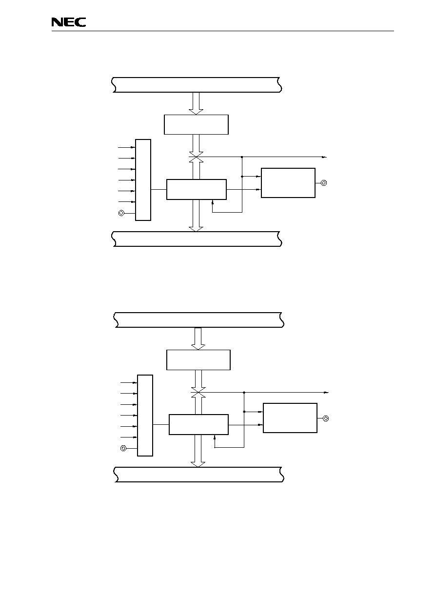
5.10 Serial Interfaces
There are the following three on-chip serial interface channels synchronous with the clock:
∑ Serial interface channel 0
∑ Serial interface channel 1
∑ Serial interface channel 2
Figure 5-16: Serial Interface Channel 0 Block Diagram
Table 5-3: Types and Functions of Serial Interfaces
Internal Bus
Serial I/O Shift
Register 1 (SIO13O)
Selector
Serial Clock Counter
SI0/P20
SO0/P21
SCK0/P22
INTCSI0
f
X
/2
3
TO50
Serial Clock
Control Circuit
f
X
/2
7
Function
Serial Interface
Channel 0
Serial Interface
Channel 1
Serial Interface
Channel 2
3-wire serial I/O mode
(MSB first)
2-wire serial I/O mode
(MSB first)
Asynchronous serial
interface (UART) mode
(On-chip
dedicated baud
rate generator)

33
µPD780948(A), µPD780949(A)
Figure 5-17: Serial Interface Channel 1 Block Diagram
Figure 5-18: Serial Interface UART Block Diagram
Internal Bus
Serial I/O Shift
Register 1 (SIO3O)
Selector
Serial Clock Counter
SI1/SO1/P23
SCK1/P24
INTCSI1
f
X
/2
6
TO50
Serial Clock
Control Circuit
f
X
/2
7
Receive Buffer
Register (RXB0)
Internal Bus
Direction Control
Circuit
Direction Control
Circuit
Transmit Shift
Register (TXS0)
Receive Shift
Register (RXS0)
Receive Control
Circuit
Transmit Control
Circuit
Baud Rate
Generator
INTSER
INTST
INTSR
f
X
/2
1
- f
X
/2
8
T
X
D/P26
R
X
D/P25
Selector
f
SCK

34
µPD780948(A), µPD780949(A)
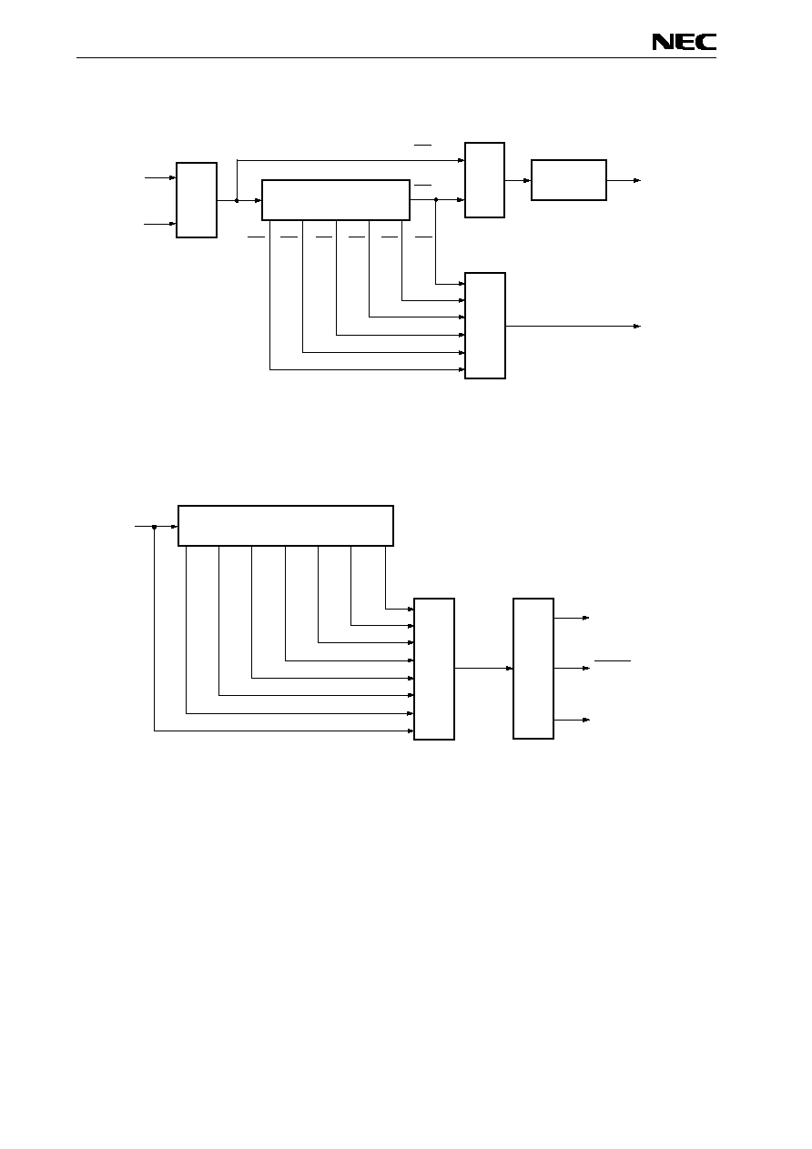
5.11 CAN-Bus Interface
The CAN-Bus Interface has the following functions:
∑ CAN 2.0 B protocol with active extended frame.
∑ The maximum Baud rate is 500 kB (@ 8 MHz clock).
∑ Receice messages will be stored in RAM area depending on message identifier, at which unused
bytes can be used by CPU.
∑ Unique identifier for all 16 messages usable.
∑ Up to 2 transmit channels with masks.
Figure 5-19: CAN-Bus Interface
5.12 LCD Controller/Driver
Table 5-4: Display Mode Types and Maximum Number of Display Pixels
CTxD
High Speed
RAM
DCAN-Interface
Extended
RAM
CPU
DMA Control
CRxD
Bias Method
Time Multiplexing
Common Signal used
Maximum Number of Display Pixels
1/3
4
COM0 to COM3
160 (40 segments x 4 commons)

35
µPD780948(A), µPD780949(A)
Figure 5-20: LCD Controller/Driver Block Diagram
Internal Bus
Segment
Data Selector
Segment Driver
Timing Controller
S0/P147..........S39/P50
Display
Data Memory
LCD Drive Voltage
Generator
Common Driver
Prescaler
Selector
COM0 COM1 COM2 COM3
V
LC2
V
LC1
V
LC0
f
LCD
fx
2
17
fx
2
16
fx
2
15
fx
2
14

36
µPD780948(A), µPD780949(A)
6.
Interrupt Functions and Test Functions
6.1 Interrupt Functions
A total of 29 interrupt functions are provided, divided into the following three types.
∑ Non-maskable interrupt : 1
∑ Maskable interrupt
: 27
∑ Software interrupt
: 1
Table 6-1: Interrupt Vector Table
Interrupt Source
Maska-
bility
Note 1
Interrupt
Priority
Name
Trigger
Internal/
Vector
External
Address
Note 2
Basic
Structure
Type
Non-
maskable
_
INTWDT
Overflow of watchdog timer (When the
watchdog timer NMI is selected)
(A)
0
INTWDT
Overflow of watchdog timer (When the
interval timer mode is selected)
0004H
1
INTAD
End of A/D converter conversion
0006H
2
INTOVF
Overflow of 16-bit timer 2
0008H
3
INTTM20
Generation of 16-bit timer 2 capture register
(CR20) match signal
000AH
4
INTTM21
Generation of 16-bit timer 2 capture register
(CR21) match signal
000CH
5
INTTM22
Generation of 16-bit timer 2 capture register
(CR22) match signal
Internal
000EH
(B)
6
INTP0
0010H
7
INTP1
0012H
8
INTP2
0014H
9
INTP3
0016H
10
INTP4
Pin input edge detection
External
0018H
(C)
11
INTCE
CAN Error
001AH
12
INTCR
CAN Receive
001CH
13
INTCT0
CAN Transmitbuffer 0
001EH
14
INTCT1
CAN Transmitbuffer 1
0020H
15
INTCSI0
End of serial interface channel 0 transfer
0022H
16
INTCSI1
End of serial interface channel 1 transfer
0024H
17
INTSER
Serial interface channel 1 UART reception
error generation
0026H
18
INTSR
End of serial interface channel 1 UART
reception
0028H
19
INTST
End of serial interface channel 1 UART
transfer
002AH
20
INTTM00
Generation of 16-bit timer 0 capture/compare
register (CR00) match signal
002CH
21
INTTM01
Generation of 16-bit timer 0 capture/compare
register (CR01) match signal
002EH
22
INTTM50
Generation of 8-bit timer/event counter 50
match signal
0030H
23
INTTM51
Generation of 8-bit timer/event counter 51
match signal
0032H
24
INTWE
EEPROM write completion interrupt
0034H
25
INTWTI
Reference time interval signal from watch
timer
Maskable
26
INTWT
Reference time interval signal from watch
timer
Internal
0036H
(B)
Software
_
BRK
BRK instruction execution
Internal
003EH
(D)

37
µPD780948(A), µPD780949(A)
Notes:
1. Default priority is the priority order when several maskable interruptions are generated at
the same time. 0 is the highest order and 20 is the lowest order.
2. Basic structure types (A) to (D) correspond to (A) to (D) in Figure 6-1.
Figure 6-1: Interrupt Function Basic Configuration (1/2)
6.2 Interrupts
(A) Internal non-maskable interrupt
(B) Internal maskable interrupt
(C) External maskable interrupt
Interrupt
request
Standby release
signal
Internal Bus
Vector Table
Address
Generator
Priority
Control
Circuit
MK
IE
PR
ISP
IF
Interrupt
request
Internal Bus
Priority
Control
Circuit
Vector Table
Address
Generator
Standby release
signal
IF
IE
PR
ISP
External Interrupt
Mode Register
(EGP, EGN)
Edge
Detector
Interrupt
request
Internal bus
MK
Priority
Control
Circuit
Vector Table
Address
Generator
Standby
release
signal

38
µPD780948(A), µPD780949(A)
(D) Software interrupt
Figure 6-1: Interrupt Function Basic Configuration (1/2)
Internal Bus
Interrupt
request
Vector Table
Address
Generator
Priority Control
Circuit

39
µPD780948(A), µPD780949(A)
7.
External Device Expansion Functions
The external device expansion functions connect external devices to areas other than the internal ROM,
RAM and SFR. External devices connection uses ports 4 to 6.
The external device expansion function has the following mode:
∑ Multiplexed bus mode:
External devices are connected by using a time-division multiplexed
address /data bus. This mode is useful for reducing the number of ports
used when external devices are connected.
Note:
Current consumption is reduced by shutting off the main system clock.
If the CPU is operating on subsystemclock, shut off the main system clock by setting MCC.
Caution:
When switching on the main system clock again after the subsystem clock has been used
with the main system clock stopped, be sure to provide enough time for the generation
to be stable with the program first.
Figure 9-1: Standby Function
9.
Standby Function
The standby function intends to reduce current consumption. It has the following two modes:
∑ HALT mode:
In this mode, the CPU operation clock is stopped. The average current consump-
tion can be reduced by intermittent operation by combining this mode with the
normal operation mode.
∑ STOP mode:
In this mode, oscillation of the main system clock is stopped. All the operations
performed on the main system clock are suspended, and only the subsystem
clock is used for extremely small power consumption.
8.
EEPROM Function
The µPD780948 incorporates not only a 2016 byte x 8-bit RAM but also 256 byte x 8-bit EEPROM
(Electrically Erasable PROM) as data memory.
EEPROM, unlike static RAM, can retain its contents when the power is turned off. Unlike EPROM, it`s
contents can electrically be erased without using ultraviolet rays. EEPROM is manipulated by 8-bit memory
manipulation instructions.
10. Reset Function
There are the following two reset methods.
∑ External reset input by RESET pin
∑ Internal reset by watchdog timer runaway time detection
Note:
The EEPROM is only avaiable in the µPD780949.
Main System Clock Operation
Subsystem Clock Operation
Note
Interrupt
request
STOP
instruction
STOP Mode
(Oscillation of the main system
clock is stopped.)
Interrupt
request
Interrupt
request
HALT instruction
HALT Mode
(Supply of clock to CPU is
stopped although clock
is generated.)
HALT instruction
HALT Mode
Note
(Supply of clock to CPU is
stopped although clock
is generated.)
CSS = 1
CSS = 0

40
µPD780948(A), µPD780949(A)
11. Instruction Set
(1) 8-Bit Instructions
MOV, XCH, ADD, ADDC, SUB, SUBC, AND, OR, XOR, CMP, MULU, DIVUW, INC, DEC, ROR, ROL,
RORC, ROLC, ROR4, ROL4, PUSH, POP, DBNZ.
Note:
Except r = A
Note
Table 11-1: 8-Bit Instructions
2nd Operand
#byte
A
r
sfr
saddr
!addr16
PSW
[DE]
[HL]
[HL+byte]
[HL + B]
[HL + C]
$addr16
1
None
1st Operand
A
ADD
ADDC
SUB
SUBC
AND
OR
XOR
CMP
MOV
XCH
ADD
ADDC
SUB
SUBC
AND
OR
XOR
CMP
MOV
XCH
MOV
XCH
ADD
ADDC
SUB
SUBC
AND
OR
XOR
CMP
MOV
XCH
ADD
ADDC
SUB
SUBC
AND
OR
XOR
CMP
MOV
MOV
XCH
MOV
XCH
ADD
ADDC
SUB
SUBC
AND
OR
XOR
CMP
MOV
XCH
ADD
ADDC
SUB
SUBC
AND
OR
XOR
CMP
MOVU
ROR
ROL
RORC
ROLC
r
MOV
MOV
ADD
ADDC
SUB
SUBC
AND
OR
XOR
CMP
INC
DEC
r1
DBNZ
sfr
MOV
MOV
saddrMOV
MOV
ADD
ADDC
SUB
SUBC
AND
OR
XOR
CMP
DBNZ
INC
DEC
!addr16
MOV
PSW
MOV
MOV
PUSH
POP
[DE]
MOV
[HL]
MOV
ROR4
ROL4
[HL+byte]
[HL + B]
[HL + C]
MOV
X
MULU
C
DIVUW

41
µPD780948(A), µPD780949(A)
2nd Operand
A.bit
sfr.bit
saddr.bit
PSW.bit
[HL].bit
CY
$addr16
None
1st Operand
A.bit
MOV1
BT
BF
BTCLR
SET1
CLR1
sfr.bit
MOV1
BT
BF
BTCLR
SET1
CLR1
saddr.bit
MOV1
BT
BF
BTCLR
SET1
CLR1
PSW.bit
MOV1
BT
BF
BTCLR
SET1
CLR1
[HL].bit
MOV1
BT
BF
BTCLR
SET1
CLR1
CY
MOV1
AND1
OR1
XOR1
MOV1
AND1
OR1
XOR1
MOV1
AND1
OR1
XOR1
MOV1
AND1
OR1
XOR1
MOV1
AND1
OR1
XOR1
SET1
CLR1
NOT1
2nd Operand
#word
AX
rp
sfrp
saddrp
!addr16
SP
None
1st Operand
AX
ADDW
SUBW
CMPW
MOVW
XCHW
MOVW
MOVW
MOVW
MOVW
rp
MOVW
MOVW
INCW, DECW
PUSH, POP
sfrp
MOVW
MOVW
saddrp
MOVW
MOVW
!addr16
MOVW
SP
MOVW
MOVW
(2) 16-Bit Instructions
MOVW, XCHW, ADDW, SUBW, CMPW, PUSH, POP, INCW, DECW.
(3) Bit Manipulation Instructions
MOV1, AND1, OR1, XOR1, SET1, CLR1, NOT1, BT, BF, BTCLR.
Note:
Only when rp = BC, DE, HL
Note
Table 11-2: 16-Bit Instructions
Table 11-3: Bit Manipulation Instructions

42
µPD780948(A), µPD780949(A)
(4) Call instructions/Branch instructions
CALL, CALLF, CALLT, BR, BC, BNC, BZ, BNZ, BT, BF, BTCLR, DBNZ.
(5) Other instructions
ADJBA, ADJBS, BRK, RET, RETI, RETB, SEL, NOP, EI, DI, HALT, STOP.
2nd Operand
AX
!addr16
!addr11
[addr5]
$addr16
1st Operand
Basic instruction
BR
CALL
BR
CALLF
CALLT
BR, BC
BNC
BZ, BNZ
Compound instruction
BT, BF
BTCLR
DBNZ
Table 11-4: Call Instructions/Branch Instructions

43
µPD780948(A), µPD780949(A)
12. Electrical Specifications
Absolute Maximum Ratings (T
A
= 25∞ C)
Note:
Effective value should be calculated as follows: [Effective value] = [Peak value] x
÷
duty
Caution:
Product quality may suffer if the absolute maximum ratings are exceeded for even a single
parameter or even momentarily. That is, the absolute maximum ratings are rated values
at which the product is on the verge of suffering physical damage, and therefore the
product must be used under conditions which ensure that the absolute maximum ratings
are not exceeded.
Remark:
The characteristics of the dual-function pins are the same as those of the port pins unless
otherwise specified.
Table 12-1: Absolute Maximum Ratings
Parameter
Symbol
Conditions
Rating
Unit
V
DD
-0.3 to +5.5
V
PP
-0.3 to +11.0
AV
DD
-0.3 to V
DD
+0.3
Supply voltage
AV
SS
-0.3 to +0.3
Input voltage
V
1
P00 to P07, P10 to P17, P20 to P26, P30 to
P34, P40 to P47, P50 to P57, P64, P65, P67,
P70 to P77, P120 to P127, P130 to P137,
P140 to P147, X1, X2, CL1, RESET
-0.3 to V
DD
+0.3
Output voltage
V
0
-0.3 to V
DD
+0.3
Analog input
voltage
V
AN
P10 to P17
Analog input pin
AV
SS
-0.3 to AV
DD
+0.3
V
1 pin (except P34)
-10
P34
-30
High level output
current
I
OH
P00 to P07, P20 to P26, P30 to P33, P40 to
P47, P50 to P57, P64, P65, P67, P70 to P77,
P120 to P127, P130 to P137, P140 to P147,
CTxD total
-30
Peak value
20
1 pin (except P34)
Effective
value
10
Peak value
30
P34
Effective
value
20
P00 to P07, P20 to P26, P30 to P33,
P40 to P47, P64, P65, P67, CTxD total
Peak value
50
P40 to P47, P64, P65, P67, CTxD total
Effective
value
20
P50 to P57, P70 to P77, P120 to P127,
P130 to P137, P140 to P147 total
Peak value
50
High level output
Current
I
OL
Note
P130 to P137, P140 to P147 total
Effective
value
20
mA
Operating
ambient
temperature
T
A
-40 to +85
Storage
temperature
T
STG
-65 to +150
o
C

44
µPD780948(A), µPD780949(A)
Remark:
The characteristics of the dual-function pins are the same as those of the port pins unless
otherwise specified.
Capacitance (T
A
= 25∞ C, V
DD
= V
SS
= 0 V)
Table 12-2: Capacitance
Parameter
Symbol
Function
Min.
Typ
Max.
Unit
Input
capacitance
C
IN
F = 1 MHz
Other than measured pins: 0 V
15
pF
P00 to P07, P10 to P17, P20 to
P26, P30 to P33, P40 to P47, P50
to P57, P64, P65, P67, P70 to P77,
P100 to P103, P120 to P127,
P130 to P137, P140 to P147
15
PF
Input/output
capacitance
C
IO
F = 1 MHz
Other than
measured pins: 0 V
P34
20
pF

45
µPD780948(A), µPD780949(A)
Notes:
1. Indicates only oscillation circuit characteristics. Refer to "AC Characteristics" for instruction
execution time.
2. Time required to stabilize oscillation after reset or STOP mode release.
Cautions:
1. When using the main system clock oscillation circuit, wiring in the area enclosed with
the broken line should be carried out as follows to avoid an adverse effect from wiring
capacitance.
∑ Wiring should be as short as possible.
∑ Wiring should not cross other signal lines.
∑ Wiring should not be placed close to a varying high current.
∑ The potential of the oscillation circuit capacitor ground should always be the same
as that of VSS.
∑ Do not ground wiring to a ground pattern in which a high current flows.
∑ Do not fetch a signal from the oscillation circuit.
2. When the main system clock is stopped and the system is operated by the subsystem
clock, the subsystem clock should be switched again to the main system clock after
the oscillation stabilization time is secured by the program.
Main System Clock Oscillation Circuit Characteristics (T
A
= -40 to +85∞ C, V
DD
= 1.8 to 5.5 V)
Table 12-3: Main System Clock Oscillation Circuit Characteristics
Resonator
Recommended Circuit
Parameter
Conditions
MIN.
TYP.
MAX.
Unit
Oscillator
frequency (fx)
Note 1
V
DD
= 4.0 to 5.5 V
4.0
8.0
8.5
MHz
Ceramic
resonator
Oscillation
stabilization time
Note2
After V
DD
reaches
oscillator voltage
range MIN. 4.0 V
10
ms
Oscillator
frequency (fx)
Note 1
V
DD
= 4.0 to 5.5 V
4.0
8.0
8.5
MHz
Crystal
resonator
Oscillation
stabilization time
Note2
After V
DD
reaches
oscillator voltage
range MIN. 4.0 V
10
ms
X1 input
frequency (fx)
Note 1
V
DD
= 4.0 to 5.5 V
4.0
8.0
8.5
MHz
External
clock
X1 input
high/low-level width
(t
XH
, t
XL
)
V
DD
= 4.0 to 5.5 V
55
125
ns
IC X2
X1
C2
C1
IC X2
X1
C2
C1
X2
X1
PD74HCU04
µ

46
µPD780948(A), µPD780949(A)
Subystem Clock Oscillation Circuit Characteristics (T
A
= -40 to +85∞ C, V
DD
= 1.8 to 5.5 V)
Cautions:
1. When using the subsystem clock oscillation circuit, wiring in the area enclosed with
the broken line should be carried out as follows to avoid an adverse effect from wiring
capacitance.
∑ Wiring should be as short as possible.
∑ Wiring should not cross other signal lines.
∑ Wiring should not be placed close to a varying high current.
∑ The potential of the oscillation circuit capacitor ground should always be the same
as that of VSS.
∑ Do not ground wiring to a ground pattern in which a high current flows.
∑ Do not fetch a signal from the oscillation circuit.
2. The subsystem clock oscillation circuit is designed to be a circuit with a low amplifi-
cation level, for low power consumption more prone to misoperation due to noise than
that of the main system clock. Therefore, when using the subsystem clock, take special
cautions for wiring methods.
Table 12-4: Subsystem Clock Oscillation Circuit Characteristics
Resonator
Recommended
circuit
Parameter
Test Conditions
MIN.
TYP.
MAX.
Unit
RC osc.
Oscillator
frequency (fxt)
4.0 V
V
DD
5.5 V
R = 518 k
C = 33 pF
32
40
tbd
kHz
CL1 Input
Note
frequency (fxt)
4.0 V
V
DD
5.5 V
tbd
8.0
8.5
MHz
External
clock
CL1 Input
high/low level
width
t
XTH
, t
XTL
)
4.0 V
V
DD
5.5 V
55
tbd
ns
Note:
Only oscillator circuit characteristics are shown. Regarding instruction execute time, please
refer to AC characteristics.
R
CL1
CL2
C
CL1
CL2

47
µPD780948(A), µPD780949(A)
DC Characteristics (T
A
= -40 to +85∞ C, V
DD
= 4.0 to 5.5 V)
Remark:
The characteristics of the dual-function pins are the same as those of the port pins unless
otherwise specified.
Table 12-5: DC Characteristics
Parameter
Symbol
Conditions
MIN.
TYP
MAX
Unit
V
IH1
P00 to P07, P10 to P17, P20 to
P26, P30 to P34, P40 to P47,
P50 to P57, P64, P65, P67, P70
to P77, P120 to P127, P130 to
P137, P140 to P147
0.7 V
DD
High-level
input
voltage
V
IH4
X1, X2, CL1, CL2
V
DD
- 0.5
V
DD
V
IL1
P00 to P07, P10 to P17, P20 to
P26, P30 to P34, P40 to P47,
P50 to P57, P64, P65, P67, P70
to P77, P120 to P127, P130 to
P137, P140 to P147
0
0.3
V
DD
Low-level
input
voltage
V
IL4
X1, X2, CL1, CL2
0
0.4
V
OH1
P00 to P07, P10 to P17, P20 to
P26, P30 to P34, P40 to P47,
P50 to P57, P64, P65, P67, P70
to P77, P120 to P127, P130 to
P137, P140 to P147
V
DD
= 4.0 to 5.5 V
I
OH
= -1 mA
V
DD
- 1.0
V
DD
= 4.0 to 5.5 V
I
OH
= -20 mA
High-level
output
voltage
V
OH3
SGO
V
DD
= 4.0 to 5.5 V
I
ON
= -20 mA
tbd
Low-level
output
voltage
V
OL1
P00 to P07, P10 to P17, P20 to
P26, P30 to P34, P40 to P47,
P50 to P57, P64, P65, P67, P70
to P77, P120 to P127, P130 to
P137, P140 to P147
V
DD
= 4.0 to 5.5 V
I
OL
= 1.6 mA
0.07
0.5
V
DD
=
4.0 to 5.5 V
I
OL
= 20 mA
0.5
V
OL3
SGO
V
DD
= 4.0 to 5.5 V
I
ON
= 20 mA
tbd
V
I
LIH1
P00 to P07, P10 to P17, P20 to
P26, P30 to P34, P40 to P47,
P50 to P57, P64, P65, P67, P70
to P77, P120 to P127, P130 to
P137, P140 to P147
V
IN
= V
DD
3
High-level
input
leakage
current
I
LIH2
X1, X2, CL1, CL2
20
I
LIL1
P00 to P07, P10 to P17, P20 to
P26, P30 to P34, P40 to P47,
P50 to P57, P64, P65, P67, P70
to P77, P120 to P127, P130 to
P137, P140 to P147
V
IN
= 0 V
-3
Low-level
input
leakage
current
I
LIL2
X1, X2, CL1, CL2
-20
High-level
output
leakage
current
I
LOH
V
OUT
= V
DD
3
Low-level
output
leakage
current
I
LOL
V
OUT
= 0 V
-3
µA
Software
pull-up
resistor
R2
V
IN
= 0 V
4.5 V
V
DD
5.5 V
10
30
100
k

48
µPD780948(A), µPD780949(A)
DC Characteristics (T
A
= -40 to +85∞ C, V
DD
= 4.0 to 5.5 V)
Mask ROM Version
Note:
The AV
REF
current, port current (including a current flowing in the on-chip pull-up resistor), the
LCD split resistors and the EEPROM access are not included.
Remarks:
1. f
X
: Main system clock oscillator frequency.
2. f
XT
: Subsystem clock oscillator frequency.
Table 12-6: DC Characteristics Mask ROM Version
DC Characteristics (T
A
= -10 to +85∞ C, V
DD
= 4.0. to 5.5 V)
LCD C/D 1/3 Bias Method
Note:
The voltage deviation is the difference from the output voltage corresponding to the ideal value
of the segment and common outputs (V
LCDN
; n = 0, 1, 2).
Table 12-7: DC Characteristics 1/3 Bias Method
Parameter
Symbol
Conditions
MIN
TYP
MAX
Unit
I
DD1
8.0 MHz crystal oscillation
operating mode (P
CC
= 00H)
9.5
tbd
mA
I
DD2
8.0 MHz crystal oscillation
HALT mode
1.2
tbd
mA
I
DD3
RC oscillation operating mode
(fx
T
= 40 kHz)
180
tbd
µA
I
DD4
RC oscillation HALT mode
(fx
T
= 40 kHz)
60
tbd
µA
Power supply
Note
current
I
DD5
CL1 = V
DD
STOP mode
1
30
µA
Parameter
Symbol
Test Conditions
MIN
TYP
MAX.
Unit
LCD drive voltage
V
LCD
3.0
V
DD
V
LCD split resistor
R
LCD
tbd
15
tbd
k
LCD output voltage
deviation
Note
(common)
V
ODC
I
O
= ± 5 µA
0
0.2
LCD output voltage
deviation
Note
(segment)
V
ODS
I
O
= ± 1 µA
3.0 V
V
LCD
V
DD
V
LCD
0 = V
LCD
V
LCD
1 = V
LCD
x 2/3
V
LCD
2 = V
LCD
x 1/3
0
0.2
V

49
µPD780948(A), µPD780949(A)
AC Characteristics
(1) Basic Operation (T
A
= -40 to +85∞ C, V
DD
= 4.0. to 5.5 V)
Notes:
1. f
SMP
2
(sampling clock) = fx/4, fx/8, fx/32, fx/128
2. f
SMP
0
(sampling clock) = fx/2, fx/16, fx/128
Table 12-8: AC Characteristics Basic Operation
Figure 12-1: T
CY
vs V
DD
(At fx = fx/2 main system clock operation)
Parameter
Symbol
Test Conditions
MIN.
TYP.
MAX.
Unit
Cycle time (min. instruction
T
CY
4.5 V
V
DD
5.5 V
0.25
100
µs
execution time)
4.0 V
V
DD
5.5 V
0.5
100
TI50, TI51 input frequency
f
TI5
0
4
MHz
TI50, TI51 input high/low level
t
TIH5,
100
ns
width
t
TIL5
TI20, TI21, TI22 input high/low
t
TIH2,
3/ f
SMP2
µs
level width
t
TIL2
Note1
TI00, TI01 input high/low level
T
CAPH
,
3/ f
SMP0
µs
width
T
CAPL
Note2
Interrupt input high/low level
T
INTH
,
INTP0-4
1
µs
width
T
INTL
RESET low level width
t
RSL
10
µs
60
Cycle time T
CY
[ s]
10
2.0
1.0
0.5
0.4
0
1
2
3
4
5
6
Supply voltage V
DD
[V]
Operation guaranteed
range
µ

50
µPD780948(A), µPD780949(A)
(2) Read/Write Operation (T
A
= -40 to +85∞ C, V
DD
= 4.0. to 5.5 V)
Remarks:
1. t
CY
= T
CY
/4
2. n indicates the number of waits
3. C
L
= 100 pF (C
L
are capacitances of AD0 to AD7, A8 to A15, RD, WR, ASTB pin)
Table 12-9: Read/Write Operation
Parameter
Symbol
Conditions
MIN.
MAX.
Unit
ASTB high-level width
t
ASTH
0.5
t
CY
Address setup time
t
ADS
0.5
t
CY
- 54
Address hold time
t
ADH
10
t
ADD1
(2.2 + 2n)
t
CY
- 108
Data input time from address
t
ADD2
(3 + 2n)
t
CY
- 120
t
RDD1
(2 + 2n)
t
CY
- 148
Data input time from RD
t
RDD2
(3 + 2n)
t
CY
- 162
Address output time from RD
t
RDAD
0
200
Read data hold time
t
RDH
0
t
RDL1
(1.5 + 2n)
t
CY
- 40
RD low-level width
t
RDL2
(2.5 + 2n)
t
CY
- 40
Write data setup time
t
WDS
60
Write data hold time
t
WDH
10
WR low-level width
t
WRL
(1.5 + 2n)
t
CY
- 30
RD
delay time from ASTB
t
ASTRD
10
WR
delay time from ASTB
t
ASTWR
2
t
CY
- 30
ASTB
delay time from RD
at external fetch
t
RDAST
0.8
t
CY
- 30
1.2
t
CY
Address hold time from RD
at external fetch
t
RDADH
0.8
t
CY
- 30
1.2
t
CY
+ 60
Write data output time from
RD
t
RDWD
40
Write data output time from
WR
t
WRDWD
20
120
Address hold time from WR
t
WRADH
0.8
t
CY
- 30
1.2
t
CY
+ 60
ns

51
µPD780948(A), µPD780949(A)
(3) Serial Interface (T
A
= -40 to +85∞ C, V
DD
= 4.0. to 5.5 V)
(a) Serial Interface Channel 30
Note:
C is the load capacitance of SO0, SCK0 output line
Note:
C is the load capacitance of SO0, SCK0 output line.
Table 12-10: 3-wire serial I/O mode (SCK0... Internal clock output)
Table 12-11: 3-wire serial I/O mode (SCK0... External clock output)
Parameter
Symbol
Conditions
MIN.
MAX.
Unit
SCK0 cycle time
T
KCY1
1000
SCK0 high/low-level width
t
KH1,
t
KL1
t
KCY1
/2 - 50
SI0 setup time ( to SCK0)
t
SIK1
100
SI0 hold time (from SCK0)
t
KSI1
400
SO0 output delay time (from SCK0)
t
KSO1
C = 100 pF
Note
300
ns
Parameter
Symbol
Conditions
MIN.
MAX.
Unit
SCK0 cycle time
t
KSO1
800
SCK0 high/low-level width
t
KH1,
t
KL1
400
SI0 setup time ( to SCK0)
t
SIK1
100
SI0 hold time (from SCK0)
t
KSI1
400
SO0 output delay time (from SCK0)
t
KSO1
C = 100 pF
Note
300
ns
52
µPD780948(A), µPD780949(A)
Note:
R and C are the load resistance and load capacitance of the SI1/SO1 and SCK1 output line.
Note:
R and C are the load resistance and load capacitance of the SI1/SO1 and SCK1 output line.
Table 12-12: 2-wire serial I/O mode (SCK0... Internal clock output)
Table 12-13: 2-wire serial I/O mode (SCK0... External clock output)
Table 12-14: UART Mode (Dedicated baud rate generator output)
Parameter
Symbol
Conditions
MIN.
TYP
MAX.
Unit
Transfer rate
125
bps
Parameter
Symbol
Conditions
MIN.
TYP
MAX
Unit
SCK1 cycle time
t
KCY5
2000
SCK1 high -level width
t
KH
5
t
KCY5
/2 - 160
SCK1 low-level width
t
KL5
t
KCY5
/2 - 160
SI1 setup time ( to SCK1)
t
SIK5
300
SI1 hold time (from SCK1)
t
KSI5
600
SO1 output delay time (from SCK1)
t
KSO5
R = 1k
C = 100 pF
Note
300
ns
Parameter
Symbol
Conditions
MIN.
TYP
MAX
Unit
SCK1 cycle time
t
KCY5
2000
SCK1 high -level width
t
KH
5
840
SCK1 low-level width
t
KL5
840
SI1, SO1 setup time ( to SCK1)
t
SIK5
300
SI1, SO1 hold time (from SCK1)
t
KSI5
600
SI1, SO1 output delay time (from SCK1)
t
KSO5
R = 1k
C = 100 pF
Note
300
ns

53
µPD780948(A), µPD780949(A)
Figure 12-2: AC Timing Test Points (excluding X1, CL1 inputs)
Figure 12-3: Clock Timing
Figure 12-4: TI Timing
0.8 V
DD
0.2 V
DD
0.8 V
DD
0.2 V
DD
Test points
t
XL
t
XH
1/f
X
V
DD
≠ 0.5 V
0.4 V
t
XTL
t
XTH
1/f
XT
V
DD
≠ 0.5 V
0.4 V
X1 Input
CL1 Input
t
CAPL
t
CAPH
TI00, TI01
TI20, TI21, TI22
t
TIH2
t
TIL2

54
µPD780948(A), µPD780949(A)
Read/Write Operation
Figure 12-5: External fetch (no wait)
Figure 12-6: External fetch (wait insertion)
t
ASTH
t
ADH
t
ADD1
Hi-Z
t
ADS
t
RDD1
t
RDADH
t
RDAST
t
ASTRD
t
RDL1
t
RDH
A8 - A15
AD0 - AD7
ASTB
RD
Upper (lower) 8-bit address
Operation
code
Lower 8-bit
address
t
ASTH
t
ADH
t
ADD1
Hi-Z
t
ADS
t
RDADH
t
RDAST
t
ASTRD
t
RDL1
t
RDH
A8 - A15
AD0 - AD7
ASTB
RD
t
RDD1
Upper (lower) 8-bit address
Operation
code
Lower 8-bit
address

55
µPD780948(A), µPD780949(A)
Figure 12-7: External data access (no wait)
Figure 12-8: External data access (wait insertion)
t
ASTRD
t
ASTH
t
ADH
t
ADD2
Hi-Z
t
ADS
t
RDL2
A8 - A15
AD0 - AD7
ASTB
RD
t
WDS
t
WRL
WR
t
RDH
Hi-Z
Hi-Z
t
WRWD
t
ASTWR
t
WRADH
Upper (lower) 8-bit address
Write data
Read data
Lower
8-bit
address
t
RDD2
t
WDH
t
RDWD
t
ASTRD
t
ASTH
t
ADH
t
ADD2
Hi-Z
t
ADS
t
RDL2
A8 - A15
AD0 - AD7
ASTB
RD
t
WDS
t
WRL
WR
t
RDH
Hi-Z
Hi-Z
t
WRWD
t
ASTWR
t
WRADH
Upper (lower) 8-bit address
Write data
Read data
Lower
8-bit
address
t
RDD2
t
WDH
t
RDWD

56
µPD780948(A), µPD780949(A)
Serial Transfer Timing
Remark:
m=1
Figure 12-9: 3-wire serial I/O mode
Figure 12-10: 2-wire serial I/O mode
t
KCYm
t
KLm
t
KHm
SCK0
SI0
SO0
t
SIKm
t
KSIm
t
KSO m
Input data
Output data
t
KSO5
t
SIK5
t
KCY5
t
KL5
t
KH5
SCK1
t
KSI5
SI1, SO1

57
µPD780948(A), µPD780949(A)
A/D Converter Characteristics (T
A
= -40 to +85∞ C, V
DD
= 4.0 to 5.5 V, AV
SS
= V
SS
=0 V, fx = 8 MHz)
Note:
Overall error excluding quantization error (± 1/2 LSB). It is indicated as a ratio to the full-scale value.
Remark:
fx: Main system clock oscillation frequency
EEPROM Characteristics (T
A
= -40 to +85∞ C, fx = 8.0 MHz)
Table 12-16: A/D Converter Characteristics
Table 12-17: EEPROM Characteristics
Note:
The EEPROM is only available in the µPD780949 and not in the µPD780948.
Parameter
Symbol
Conditions
MIN.
TYP.
MAX.
Unit
Resolution
8
8
8
bit
Overall error
± 0.6
%
Conversion time
t
CONV
18
µs
Analog input voltage
V
IAN
AV
SS
AV
DD
Reference voltage
AV
REF
4.0
V
DD
V
Resistor string
R
AIREF
CS-bit = 1
21
k
Parameter
Symbol
Test Conditions
MIN.
TYP.
MAX.
Unit
Voltage range for R/W
V
EERW
4.0
5.5
V
Write time
t
EEW
3
6
ms
Erase/Write cycles
N
EEWT
100000
cycle
Additional current when EEPROM is
erased/written
I
EE
-
W
V
DD
= 5.0 V
1
tbd
mA

58
µPD780948(A), µPD780949(A)
Data Memory Stop Mode Low Supply Voltage Data Retention Characteristics (T
A
= -40 to +85∞ C)
Note:
In combination with bits 0 to 2 (OSTS0 to OSTS2) of oscillation stabilization time select register,
selection of 2
12
/fx and 2
14
/fx to 2
17
/fx is possible
Remark:
fx: Main system clock oscillation frequency
Table 12-18: Data Memory Stop Mode Low Supply Voltage Data Retention Characteristics
Figure 12-11: Data Retention Timing (STOP mode release by RESET)
Figure 12-12: Data Retention Timing (Standby release signal: STOP mode release by interrupt signal)
Parameter
Symbol
Test Conditions
MIN.
TYP.
MAX.
Unit
Data retention power supply voltage
V
DDDR
4.0
5.5
V
Data retention power supply current
I
DDDR
V
DDDR
= 4.0 V
1
30
µA
Release signal set time
t
SREL
0
µS
Release by RESET
2
17
/fx
Oscillation stabilization wait time
t
WAIT
Release by interrupt
Note
ms
t
SREL
t
WAIT
V
DD
RESET
STOP instruction execution
STOP mode
Data retension mode
Internal reset operation
HALT mode
Operating mode
V
DDDR
t
SREL
t
WAIT
V
DD
STOP instruction execution
STOP mode
Data retension mode
HALT mode
Operating mode
Standby release signal
(interrupt request)
V
DDDR
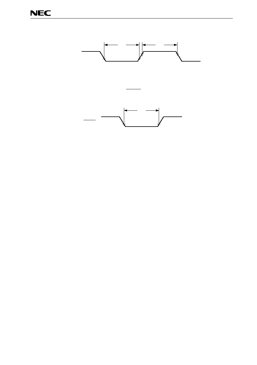
59
µPD780948(A), µPD780949(A)
Figure 12-13: Interrupt Input Timing
Figure 12-14: RESET Input Timing
t
INTL
t
INTH
INTP0 - INTP4
t
RSL
RESET

60
µPD780948(A), µPD780949(A)
13. Package Drawing
Remark:
The shape and material of the ES product is the same as the mass produced product.
Figure 13-1: Package Drawing
J
N
M
P
80
81
50
100
1
31
30
51
G
Detail of lead end
S
5°
±
5°
C
D
A
B
H
Q
K
L
F
M
I
P100GF-65-3BA1-2
Item
Millimeters
Inches
A
B
C
D
F
G
H
I
J
K
L
23.6±0.4
14.0±0.2
0.6
0.30±0.10
0.15
20.0±0.2
0.929±0.016
0.031
0.024
0.006
0.026 (T.P.)
0.795
Note:
M
N
0.10
0.15
1.8±0.2
0.65 (T.P.)
0.006
0.031
+0.009
≠0.008
Each lead centerline is located within 0.15
mm (0.006 inch) of its true position (T.P.) at
maximum material condition.
0.012
0.551
0.8±0.2
0.071
P
2.7
0.106
0.693±0.016
17.6±0.4
0.8
+0.008
≠0.009
Q
0.1±0.1
0.004±0.004
S
3.0 MAX.
0.119 MAX.
+0.10
≠0.05
+0.009
≠0.008
+0.004
≠0.005
+0.009
≠0.008
+0.004
≠0.003
0.004

61
µPD780948(A), µPD780949(A)
14. Recommended Soldering Conditions
The µPD780948 should be soldered and mounted under the conditions in the table below. For detail
of recommended soldering conditions, refer to the information document Semiconductor Device
Mounting Technology Manual (IEI-1207).
For soldering methods and conditions other than those recommended below, consult our sales personnel.
µPD780948GF-XXX-3BA : 100-pin plastic QFP (14 x
20 mm)
Caution:
Use of more than one soldering method should be avoided (exept in the case of pin part
heating).
Table 14-1: Surface Mounting Type Soldering Conditions
µPD780949GF-XXX-3BA : 100-pin plastic QFP (14 x
20 mm)
Soldering Method
Soldering Conditions
Recommended
Condition Symbol
Infrared reflow
Package peak temperature: 235
∞
C, Duration: 30 sec. max.
(at 210
∞
C or above).
Number of times: twice max.
<Precautions>
(1) The second reflow schold be started after the first reflow
device temperature has retumed to the ordinary state.
(2) Flux washing must not be performed by the use of water
after the first reflow.
IR35-00-2
VPS
Package peak temperature: 215
∞
C, Duration: 40 sec. max.
(at 210
∞
C or above).
Number of times: twice max.
<Precautions>
(3) The second reflow schold be started after the first reflow
device temperature has retumed to the ordinary state.
(4) Flux washing must not be performed by the use of water
after the first reflow.
VP15-00-2
Wave soldering
Soldering bath temperature: 260
∞
C max.
Duration: 10 sec. max.
Number of times: once, Preheating temperature: 120
∞
C
max. (package surface temperature)
WS60-00-1
Pin part heating
Pin temperature: 300
∞
C max.
Duration: 3 sec. max. (per device side).
-

62
µPD780948(A), µPD780949(A)
Appendix A. Development Tools
The following tools are available for system development using the µPD780948.
Language Processing Software
PROM Writing Tools
Debugging Tools
RA78K/0
Notes 1, 2, 3
Assembler package used in common for the 78K/0 series
CC78K/0
Notes 1, 2, 3
C compiler package used in common for the 78K/0 series
DF780948, DF780949
Device file used for the
µ
PD780949 subseries
CC78K/0-L
Notes 1, 2, 3
C compiler library source file used in common for the 78K/0 series
Flashpro
Dedicated flash writer for micro controllers with on-chip flash memory
FA-100GF
Programmer adapter connected to the Flash-Pro
IE-78001-R-A
In-circuit emulator used in common for the 78K/0 series
IE-78001-R-BK
Break board used in common for the 78K/0 series
IE-70000-PC-IF-B
This adapter is required when using an IBM PC/AT or compatible as host
IE-780948-SL-EM1
Emulation board and probe board for the
µ
PD780949 subseries
IE-780948-SL-EM4
EP-100GF-SL
Emulation probe used in common for the
µ
PD780949 subseries
SM78K0
System simulator used in common for the 78K/0 series
ID78K/0
Integrated debugger for the IE-78001-R-A
DF780948, DF780949
Device file used for the
µ
PD780949 subseries
RX78K/0
Notes 1, 2, 3
Real-time OS used for the 78K/0 series
MX78K0
Notes 1, 2, 3
OS used for the 78K/0 series
Real-Time OS
FE9000
Note 1
/FE9200
Note 5
Fuzzy knowledge data creating tool
FT9080
Note 1
/FT9085
Note 2
Translator
FI78K0
Note 1, 2
Fuzzy interference module
FD78K0
Note 1, 2
Fuzzy interference debugger
Fuzzy Interference Development Support System
Notes:
1. Based on PC-9800 series (MS-DOS
TM
)
2. Based on IBM PC/AT
TM
(PC DOS
TM
)
3. Based on HP9000 series 300
TM
, HP9000 series 700
TM
(HP-UX
TM
), SPARCstation
TM
(SunOS
TM
),
and EWS-4800 series (EWS-UX/V)
4. Based on PC-9800 series (MS-DOS + Windows
TM
)
5. Based on IBM PC/AT (PC DOS + Windows)
Remarks:
1. For development tools supplied by third-party manufacturers, refer to 78K/0 series Selection
Guide (IF-1185).
2. Use the RA78K/0, CC78K/0, SM78K0 and D78K/0 in combination with the DF780945/F0948.
63
µPD780948(A), µPD780949(A)
Appendix B. Related Documents
Documents Related to Devices
Documents on Development Tools (User's Manuals)
Caution:
The above documents are subject to change without notice. Be sure to use the latest
documents for design or for any other similar purpose.
Document No.
Document
Japanese
English
78K0 Series User's Manual-Instruction
IEU-849
IEU-1372
78K0 Series Instruction Table
IEM-5522
--
78K0 Series Instruction Set
IEM-5521
--
78K0 Series Application Note-Fundamental (III)
IEA-767
To be prepared
Document No.
Document
Japanese
English
Operation
EEU-809
EEU-1399
RA78K Series Assembler Package
Language
EEU-815
EEU-1404
RA78K Series Structured Assembler Reprocessor
EEU-817
EEU-1402
Operation
EEU-656
EEU-1280
CC78K Series C Compiler
Language
EEU-655
EEU-1284
CC78K0 C Compiler Application Note
Programming Know-how
EEU-618
To be prepared
CC78K Series Library Source File
EEU-777
--
IE78001-R-A
EEU-810
U10057
IE-78001-R-BK
EEU-867
To be prepared
IE-780948-SL-EM1
EEU-978
U12412
IE-780948-SL-EM4
--
U12412
EP-100GF-SL
EEU-934
EEU-1522
SM78K0 System Simulator
Reference
--
U10181
IBM PC/AT (PC DOS) Base
External Port Specification
--
U10092
ID78K0 Integrated Debugger
Reference
--
U11539
IBM PC/AT (PC DOS) Base
Guide
--
U11649

64
µPD780948(A), µPD780949(A)
Documents on Embeded Software (User's Manuals)
Other Documents
Caution:
The above documents are subject to change without notice. Be sure to use the latest
documents for design or for any other similar purpose.
Document No.
Document
Japanese
English
78K0 Series Real-time OS
Basic
EEU-912
--
Installation
EEU-911
--
Technical
EEU-913
--
78K0 Series OS MX78K0
Fundamental
EEU-5010
--
Fuzzy Knowledge Data Creation Tool
EEU-829
EEU-1438
78K0, 78K/II, 87AD Series
Fuzzy Inference Development Support System Translator
EEA-862
EEU-1444
78K0 Fuzzy Inference Development Support System Fuzzy Inference Module
EEU-858
EEU-1441
78K0 Fuzzy Inference Development Support System Fuzzy Inference
Debugger
EEU-921
EEU-1458
Document No.
Document
Japanese
English
Package Manual
IEI-635
IEI-1213
Semiconductor Device Mounting Technology Manual
IEI-616
IEI-1207
Quality Grade on NEC Semiconductor Devices
IEI-620
IEI-1209
NEC Semiconductor Device Reliability/Quality Control System
IEM-5068
--
Electrostatic Discharge (ESD) Test
MEM-539
--
Semiconductor Device Quality Assurance Guide
MEI-603
MEI-1202
Microcontroller-Related Product Guide - Third Party Products -
MEI-604
--
65
µPD780948(A), µPD780949(A)
Notes for CMOS Devices
1
Precaution against ESD for Semiconductors
Note: Strong electric field, when exposed to a MOS device, can cause destruction of the gate
oxide and ultimately degrade the device operation. Steps must be taken to stop
generation of static electricity as much as possible, and quickly dissipate it once, when
it has occurred. Environmental control must be adequate. When it is dry, humidifier
should be used. It is recommended to avoid using insulators that easily build static
electricity. Semiconductor devices must be stored and transported in an anti-static
container, static shielding bag or conductive material. All test and measurement tools
including work bench and floor should be grounded. The operator should be grounded
using wrist strap. Semiconductor devices must not be touched with bare hands. Similar
precautions need to be taken for PW boards with semiconductor devices on it.
2
Handling of unused input pins for CMOS
Note: No connection for CMOS device inputs can be cause of malfunction. If no connection
is provided to the input pins, it is possible that an internal input level may be generated
due to noise, etc., hence causing malfunction. CMOS device behave differently than
Bipolar or NMOS devices. Input levels of CMOS devices must be fixed high or low by
using a pull-up or pull-down circuitry. Each unused pin should be connected to V
DD
or GND with a resistor, if it is considered to have a possibility of being an output pin.
All handling related to the unused pins must be judged device by device and related
specifications governing the devices.
3
Status before initialization of MOS devices
Note: Power-on does not necessarily define initial status of MOS device. Production process
of MOS does not define the initial operation status of the device. Immediately after the
power source is turned ON, the devices with reset function have not yet been initialized.
Hence, power-on does not guarantee out-pin levels, I/O settings or contents of
registers. Device is not initialized until the reset signal is received. Reset operation
must be executed immediately after power-on for devices having reset function.

66
µPD780948(A), µPD780949(A)
NEC Electronics Inc. (U.S.)
Santa Clara, California
Tel: 800-366-9782
Fax: 800-729-9288
NEC Electronics (Germany) GmbH
Duesseldorf, Germany
Tel: 0211-65 03 02
Fax: 0211-65 03 490
NEC Electronics (UK) Ltd.
Milton Keynes, UK
Tel: 01908-691-133
Fax: 01908-670-290
NEC Electronics Italiana s.r.l.
Milano, Italy
Tel: 02-66 75 41
Fax: 02-66 75 42 99
NEC Electronics Hong Kong Ltd.
Hong Kong
Tel: 2886-9318
Fax: 2886-9022/9044
NEC Electronics Hong Kong Ltd.
Seoul Branch
Seoul, Korea
Tel: 02-528-0303
Fax: 02-528-4411
NEC Electronics Singapore Pte. Ltd.
United Square, Singapore 1130
Tel: 253-8311
Fax: 250-3583
NEC Electronics Taiwan Ltd.
Taipei, Taiwan
Tel: 02-719-2377
Fax: 02-719-5951
NEC do Brasil S.A.
Sao Paulo-SP, Brasil
Tel: 011-889-1680
Fax: 011-889-1689
NEC Electronics (Germany) GmbH
Benelux Office
Eindhoven, The Netherlands
Tel: 040-2445845
Fax: 040-2444580
NEC Electronics (France) S.A.
Velizy-Villacoublay, France
Tel: 01-30-67 58 00
Fax: 01-30-67 58 99
NEC Electronics (France) S.A.
Spain Office
Madrid, Spain
Tel: 01-504-2787
Fax: 01-504-2860
NEC Electronics (Germany) GmbH
Scandinavia Office
Taeby, Sweden
Tel: 08-63 80 820
Fax: 08-63 80 388
Regional Information
Some information contained in this document may vary from country to country. Before using any NEC
product in your application, please contact the NEC office in your country to obtain a list of authorized
representatives and distributors. They will verify:
∑ Device availability
∑ Ordering information
∑ Product release schedule
∑ Availability of related technical literature
∑ Development environment specifications (for example, specifications for third-party tools and components,
host computers, power plugs, AC supply voltages, and so forth)
∑ Network requirements
In addition, trademarks, registered trademarks, export restrictions, and other legal issues may also vary
from country to country.

67
µPD780948(A), µPD780949(A)
FIP is a registered trademark of NEC Corporation.
IEBus is a trademark of NEC Corporation.
MS-DOS and MS-Windows are either registered trademarks or trademarks of Microsoft
Corporation in the United States and/or other countries.
PC/AT and PC DOS are trademarks of IBM Corp.
HP9000 series 300, HP9000 series 700, and HP-UX are trademarks of Hewlett Packard Co.
SPARCstation is a trademark of SPARC International, Inc.
SunOS is a trademark of SUN Microsystems, Inc.
The related documents in this publication may include preliminary versions. However, prelimi-
nary versions are not marked as such.
The export of this product from Japan is regulated by the Japanese government. To export this
product may be prohibited without governmental license, the need for which must be judged by the
customer. The export or re-export of this product from a country other than Japan may also be
prohibited without a license from that country. Please call an NEC sales representative.
M4 94.11
No part of this document may be copied or reproduced in any form or by any means without the prior written
consent of NEC Corporation. NEC Corporation assumes no responsibility for any errors which may appear
in this document.
NEC Corporation does not assume any liability for infringement of patents, copyrights or other intellectual
property rights of third parties by or arising from use of a device described herein or any other liability arising
from use of such device. No license, either express, implied or otherwise, is granted under any patents,
copyrights or other intellectual property rights of NEC Corporation or others.
While NEC Corporation has been making continuous effort to enhance the reliability of its semiconductor
devices, the possibility of defects cannot be eliminated entirely. To minimize risks of damage or injury to
persons or property arising from a defect in an NEC semiconductor device, customer must incorporate
sufficient safety measures in its design, such as redundancy, fire-containment, and anti-failure features.
NEC devices are classified into the following three quality grades:
"Standard", "Special", and "Specific". The Specific quality grade applies only to devices developed based
on a customer designated "quality assurance program" for a specific application. The recommended
applications of a device depend on its quality grade, as indicated below. Customers must check the quality
grade of each device before using it in a particular application.
Standard:Computers, office equipment, communications equipment, test and measurement equipment,
audio and visual equipment, home electronic appliances, machine tools, personal electronic
equipment and industrial robots
Special: Transportation equipment (automobiles, trains, ships, etc.), traffic control systems, anti-disaster
systems, anti-crime systems, safety equipment and medical equipment (not specifically designed
for life support)
Specific: Aircrafts, aerospace equipment, submersible repeaters, nuclear reactor control systems, life
support systems or medical equipment for life support, etc.
The quality grade of NEC devices is "Standard" unless otherwise specified in NEC's Data Sheets or Data
Books.
If customers intend to use NEC devices for applications other than those specified for Standard quality
grade, they should contact NEC Sales Representative in advance.
Anti-radioactive design is not implemented in this product.