 | –≠–ª–µ–∫—Ç—Ä–æ–Ω–Ω—ã–π –∫–æ–º–ø–æ–Ω–µ–Ω—Ç: UPD78045H | –°–∫–∞—á–∞—Ç—å:  PDF PDF  ZIP ZIP |
Document Outline
- COVER
- FEATURES
- APPLICATIONS
- ORDERING INFORMATION
- 78K/0 SERIES PRODUCT DEVELOPMENT
- FUNCTIONAL OUTLINE
- 1. PIN CONFIGURATION (TOP VIEW)
- 2. BLOCK DIAGRAM
- 3. PIN FUNCTIONS
- 3.1 PORT PINS
- 3.2 PINS OTHER THAN PORT PINS
- 3.3 PIN I/O CIRCUITS AND PROCESSING OF UNUSED PINS
- 4. MEMORY SPACE
- 5. PERIPHERAL HARDWARE FUNCTIONS
- 5.1 PORTS
- 5.2 CLOCK GENERATOR CIRCUIT
- 5.3 TIMER/EVENT COUNTER
- 5.4 CLOCK OUTPUT CONTROL CIRCUIT
- 5.5 BUZZER OUTPUT CONTROL CIRCUIT
- 5.6 A/D CONVERTER
- 5.7 SERIAL INTERFACE
- 5.8 FIP CONTROLLER/DRIVER
- 6. INTERRUPT FUNCTION AND TEST FUNCTION
- 6.1 INTERRUPT FUNCTION
- 6.2 TEST FUNCTION
- 7. STANDBY FUNCTION
- 8. RESET FUNCTION
- 9. INSTRUCTION SET
- 10. ELECTRICAL SPECIFICATIONS
- 11. PACKAGE DRAWING
- 12. RECOMMENDED SOLDERING CONDITIONS
- APPENDIX A DEVELOPMENT TOOLS
- APPENDIX B RELATED DOCUMENTS
8-BIT SINGLE-CHIP MICROCOMPUTER
MOS INTEGRATED CIRCUIT
DATA SHEET
µ
PD78044H,
78045H,
78046H
Document No. U10865EJ1V0DS00 (1st edition)
Date Published August 1996 P
Printed in Japan
The
µ
PD78044H,
µ
PD78045H, and
µ
PD78046H are
µ
PD78044H sub-series products in the 78K/0 series.
These microcomputers are advanced models of the
µ
PD78044A sub-series, featuring the added N-ch open-drain
I/O ports.
In addition, the
µ
PD78P048B (one-time PROM or EPROM model) that can operate in the same voltage range as
that of the mask ROM models, and various development tools are provided.
The functions of these microcomputers are described in detail in the following User's Manual. Be sure
to read this manual when you design a system using any of these microcomputers.
µ
PD78044H Sub-Series User's Manual : To be created
78K/0 Series User's Manual, Instruction: IEU-1372
FEATURES
∑ I/O ports: 68 (N-ch open-drain I/O: 13)
∑ High-capacity ROM and RAM
Data memory
FIP display RAM
48 bytes
∑ Serial interface: 1 channel
∑ Timer: 5 channels
∑ Power supply voltage: V
DD
= 2.7 to 5.5 V
APPLICATIONS
VCRs, audio systems, etc.
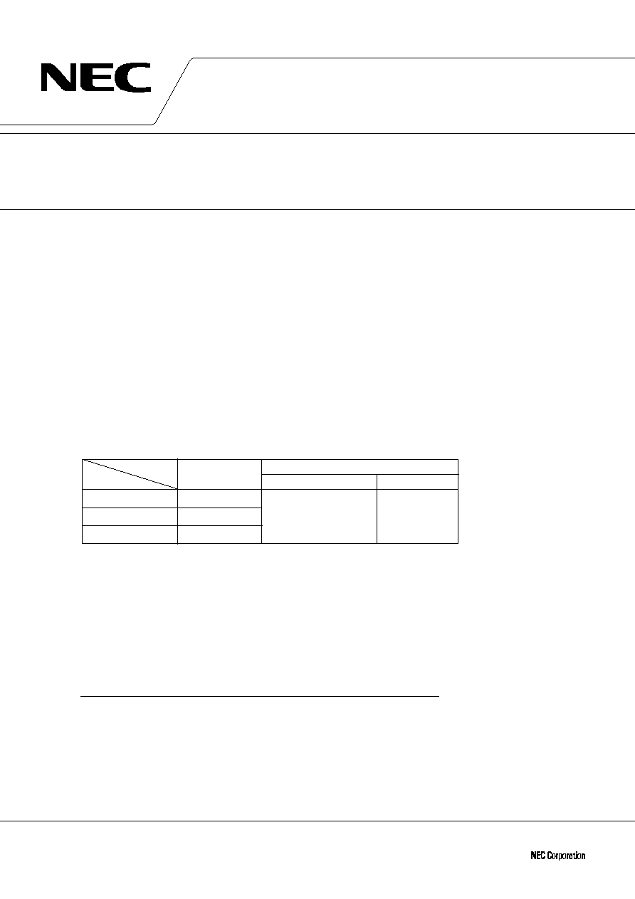
ORDERING INFORMATION
Part number Package
µ
PD78044HGF-
◊◊◊
-3B9 80-pin plastic QFP (14
◊
20 mm)
µ
PD78045HGF-
◊◊◊
-3B9 80-pin plastic QFP (14
◊
20 mm)
µ
PD78046HGF-
◊◊◊
-3B9 80-pin plastic QFP (14
◊
20 mm)
Remark
◊◊◊
indicates ROM code number.
∑ Wide range of instruction execution time:
From high-speed (0.4
µ
s) to ultra low-speed (122
µ
s)
∑ FIP controller/driver: total display outputs: 34
∑ 8-bit resolution A/D converter: 8 channels
µ
PD78044H
µ
PD78045H
µ
PD78046H
32K bytes
40K bytes
48K bytes
1024 bytes
Internal high-speed RAM
Program memory
(ROM)
Product name
Item
The information in this document is subject to change without notice.
The mark
5
shows major revised points.
©
1990
1996

2
µ
PD78044H, 78045H, 78046H
78K/0 SERIES PRODUCT DEVELOPMENT
The 78K/0 series products were developed as shown below. The sub-series names are indicated in frames.
100-pin
80-pin
80-pin
64-pin
64-pin
64-pin
42-/44-pin
PD78078
PD78078Y
PD78070A
PD78070AY
PD78054
PD78054Y
PD78018F
PD78018FY
PD78014
PD78014Y
PD780001
PD780208
PD78044F
PD78024
100-pin
80-pin
80-pin
64-pin
100-pin
100-pin
100-pin
A timer has been added to the PD78054 to enhance external interface functions.
The I/O and FIP C/D of the PD78044F have been enhanced.
Total indication output pins: 53
N-ch open-drain I/O ports have been added to the PD78044F.
Total indication output pins: 34
The SIO of the PD78064 has been enhanced. ROM and RAM
have been expanded.
Basic sub-series for FIP driving. Total indication output pins: 26
Sub-series for LCD driving. These products include an UART.
EMI noise-reduced version of the PD78064
PD780308
PD78098
PD780308Y
Products being mass-produced
Products under development
Y sub-series products are compatible with the I
2
C bus.
Used for control
78K/0
series
For FIP driving
For LCD driving
Compatible with IEBus
TM
PD78002
PD78083
100-pin
100-pin
64-pin
80-pin
ROM-less versions of the PD78078
The serial I/O of the PD78078 has been enhanced. The functions have been
limited.
EMI noise-reduced version of the PD78054
An UART and D/A converter have been added to the PD78014 to enhance I/O.
Low-voltage (1.8 V) versions of the PD78014. ROM and RAM variations have
been enhanced.
An A/D converter and 16-bit timer have been added to the PD78002.
An A/D converter has been added to the PD78002.
Basic sub-series for control
These products include an UART and can operate at a low voltage (1.8 V).
A 6-bit U/D counter has been added to the PD78024.
Total indication output pins: 34
PD78002Y
µ
µ
PD780018Y
µ
µ
µ
µ
µ
µ
µ
PD780018
µ
PD78058F
PD78058FY
µ
µ
µ
µ
µ
µ
µ
µ
µ
PD78044H
µ
µ
µ
µ
PD78064B
µ
µ
PD78064
PD78064Y
µ
µ
µ
An IEBus controller has been added to the PD78054.
A PWM output, LV digital code decoder, and Hsync counter are
incorporated.
PD78P0914
For LV
64-pin
µ
µ
µ
µ
µ
µ
µ
µ
µ
µ
µ
µ
µ
µ
µ
3
µ
PD78044H, 78045H, 78046H
The table below shows the main differences between sub-series.
Sub-series name
Function
For control
µ
PD78078
µ
PD78070A
µ
PD780018
µ
PD78058F
µ
PD78054
µ
PD78018F
µ
PD78014
µ
PD780001
µ
PD78002
µ
PD78083
µ
PD780208
µ
PD78044F
µ
PD78044H
µ
PD78024
µ
PD780308
µ
PD78064B
µ
PD78064
µ
PD78098
µ
PD78P0914
--
--
--
--
Timer
3ch (UART:1ch)
2ch
3ch (UART:1ch)
2ch
1ch
1ch (UART:1ch)
2ch
1ch
2ch
3ch (UART:1ch)
2ch (UART:1ch)
3ch (UART:1ch)
2ch
External
expan-
sion
Watch
8-bit
WDT
ROM
capacity
32K-60K
--
48K-60K
48K-60K
16K-60K
8K-60K
8K-32K
8K
8K-16K
32K-60K
16K-40K
32K-48K
24K-32K
48K-60K
32K
16K-32K
32K-60K
32K
4ch
2ch
2ch
2ch
2ch
6ch
16-bit
1ch
1ch
1ch
1ch
1ch
8ch
--
8ch
8ch
8ch
8ch
8ch
2ch
--
2ch
--
--
--
2ch
--
8-bit
A/D
8-bit
D/A
Serial
interface
Minimum
V
DD
I/O
For LV
Compatible
with IEBus
For LCD
driving
For FIP
driving
1ch
--
1ch
--
1ch
1ch
1ch
--
88 pins
61 pins
88 pins
69 pins
53 pins
39 pins
53 pins
33 pins
74 pins
68 pins
54 pins
57 pins
69 pins
54 pins
1ch
--
1ch
1ch
1ch
--
1.8 V
2.7 V
2.0 V
1.8 V
2.7 V
1.8 V
2.7 V
1.8 V
2.0 V
2.7 V
4.5 V
4
µ
PD78044H, 78045H, 78046H
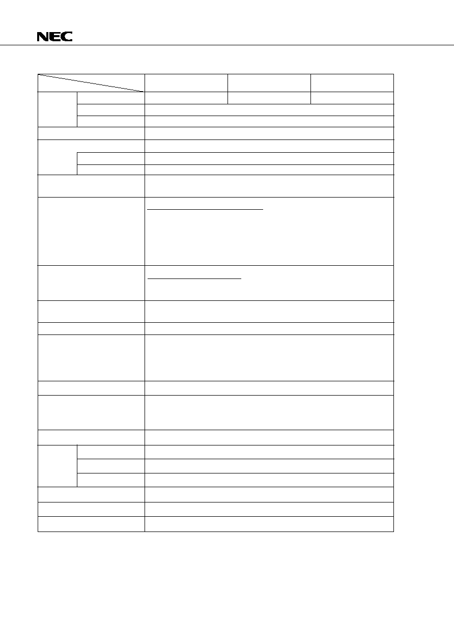
FUNCTIONAL OUTLINE
Internal
memory
Item
Product name
Instruction
cycle
ROM
Internal high-speed RAM
FIP display RAM
General registers
8 bits
◊
32 registers (8 bits
◊
8 registers
◊
4 banks)
Variable instruction execution time
For main system clock
0.4
µ
s/0.8
µ
s/1.6
µ
s/3.2
µ
s/6.4
µ
s (at 5.0 MHz)
For subsystem clock
122
µ
s (at 32.768 kHz)
Instruction set
∑ Multiplication/division (8 bits
◊
8 bits, 16 bits
˜
8 bits)
∑ Bit (set, reset, test, Boolean algebra)
I/O ports (including those
Total
: 68 lines
multiplexed with FIP pins)
∑ CMOS input
:
2 lines
∑ CMOS I/O
: 19 lines
∑ N-ch open-drain
: 13 lines
∑ P-ch open-drain I/O
: 16 lines
∑ P-ch open-drain output
: 18 lines
FIP controller/driver
Total
: 34 lines
∑ Segments
: 9 to 24 lines
∑ Digits
: 2 to 16 lines
A/D converter
∑ 8-bit resolution
◊
8 channels
∑ Power supply voltage: AV
DD
= 4.0 to 5.5 V
Serial interface
∑ 3-wire serial I/O mode
: 1 channel
Timer
∑ 16-bit timer/event counter : 1 channel
∑ 8-bit timer/event counter : 2 channels
∑ Watch timer
: 1 channel
∑ Watchdog timer
: 1 channel
Timer output
3 lines (one for 14-bit PWM output)
Clock output
19.5 kHz, 39.1 kHz, 78.1 kHz, 156 kHz, 313 kHz, 625 kHz
(main system clock: when operating at 5.0 MHz)
32.768 kHz (subsystem clock: when operating at 32.768 kHz)
Buzzer output
1.2 kHz, 2.4 kHz, 4.9 kHz (main system clock: when operating at 5.0 MHz)
Maskable interrupt
Internal 8 lines, external 4 lines
Non-maskable interrupt
Internal 1 line
Software interrupt
1 line
Text input
Internal 1 line
Power supply voltage
V
DD
= 2.7 to 5.5 V
Package
80-pin plastic QFP (14
◊
20 mm)
Vectored
interrupt
µ
PD78044H
µ
PD78045H
µ
PD78046H
32K bytes
1024 bytes
48 bytes
40K bytes
48K bytes

5
µ
PD78044H, 78045H, 78046H
CONTENTS
1.
PIN CONFIGURATION (TOP VIEW) .........................................................................................
6
2.
BLOCK DIAGRAM ......................................................................................................................
8
3.
PIN FUNCTIONS .........................................................................................................................
9
3.1 PORT PINS ..........................................................................................................................................
9
3.2 PINS OTHER THAN PORT PINS .......................................................................................................
11
3.3 PIN I/O CIRCUITS AND PROCESSING OF UNUSED PINS ...........................................................
12
4.
MEMORY SPACE .......................................................................................................................
15
5.
PERIPHERAL HARDWARE FUNCTIONS ................................................................................
16
5.1
PORTS .............................................................................................................................................
16
5.2
CLOCK GENERATOR CIRCUIT ....................................................................................................
17
5.3
TIMER/EVENT COUNTER ..............................................................................................................
17
5.4
CLOCK OUTPUT CONTROL CIRCUIT .........................................................................................
20
5.5
BUZZER OUTPUT CONTROL CIRCUIT .......................................................................................
20
5.6
A/D CONVERTER ...........................................................................................................................
21
5.7
SERIAL INTERFACE ......................................................................................................................
22
5.8
FIP CONTROLLER/DRIVER ..........................................................................................................
23
6.
INTERRUPT FUNCTION AND TEST FUNCTION .....................................................................
25
6.1
INTERRUPT FUNCTION .................................................................................................................
25
6.2
TEST FUNCTION ............................................................................................................................
28
7.
STANDBY FUNCTION ................................................................................................................
29
8.
RESET FUNCTION .....................................................................................................................
29
9.
INSTRUCTION SET ....................................................................................................................
30
10. ELECTRICAL SPECIFICATIONS ..............................................................................................
33
11. PACKAGE DRAWING ................................................................................................................
50
12. RECOMMENDED SOLDERING CONDITIONS .........................................................................
51
APPENDIX A DEVELOPMENT TOOLS .........................................................................................
52
APPENDIX B RELATED DOCUMENTS .........................................................................................
54