 | –≠–ª–µ–∫—Ç—Ä–æ–Ω–Ω—ã–π –∫–æ–º–ø–æ–Ω–µ–Ω—Ç: UPD78053A | –°–∫–∞—á–∞—Ç—å:  PDF PDF  ZIP ZIP |
Document Outline
- COVER
- DESCRIPTION
- FEATURES
- ORDERING INFORMATION
- SYSTEM CONFIGURATION
- BLOCK DIAGRAM
- PIN CONFIGURATION
- PIN CONFIGURATION (Top View)
- PIN NAMES
- 1. PIN FUNCTION
- 1.1 PHY Device Interface Pin
- 1.2 Bus Interface Pins
- 1.3 Bus Monitor Pins
- 1.4 Control Memory Interface Pins
- 1.5 JTAG Boundary Scan Pins
- 1.6 Test Pin
- 1.7 Power Supply and Ground Pins
- 1.8 Pin Status During and After Reset
- 2. DIFFERENCES FROM uPD98401
- 2.1 Additional Functions
- 2.2 Differences from uPD98401 (NEASCOT-S10)
- 3. ELECTRICAL SPECIFICATIONS
- 4. PACKAGE DRAWINGS
- 5. RECOMMENDED SOLDERING CONDITIONS

The information in this document is subject to change without notice.
MOS INTEGRATED CIRCUIT
µ
µ
µ
µ
PD98401A
ATM SAR CHIP
1997
©
Document No. S12100EJ3V0DS00 (3rd edition)
Date Published February 1999 N CP(K)
Printed in Japan
DATA SHEET
The mark
shows major revised points.
DESCRIPTION
The
µ
PD98401A (NEASCOT-S15
TM
) is a high-performance SAR chip that segments and reassembles ATM cells.
This chip can interface with an ATM network when it is included in a workstation, computer, front-end processor,
network hub, or router. The
µ
PD98401A conforms to the ATM Forum Recommendation, and provides the functions
of the AAL-5 SAR sublayer and ATM layer.
The
µ
PD98401A is compatible with its predecessor,
µ
PD98401, in terms of hardware and software.
Functions are explained in detail in the following User's Manual. Be sure to read this manual when designing your
system.
µ
µ
µ
µ
PD98401A User's Manual: S12054E
FEATURES
∑ Conforms to ATM Forum
∑ AAL-5 SAR sublayer and ATM layer functions
∑ Hardware support of AAL-5 processing
∑ Processing of non-AAL-5 traffic (AAL-3/4 cell, OAM cell, RM cell) by software with raw cell processing function
∑ Hardware support of comparison/generation of CRC-10 for non-AAL-5 traffic
∑ Supports up to 32K virtual channels (VC)
∑ Provided with 16 traffic shapers that carry out transmission scheduling (control of average rate/peak rate) so as to
set different transmission rate for each VC
∑ Interface and commands for controlling PHY device
∑ Employs "UTOPIA interface" as cell data interface with PHY device
- Octet-level handshake
- Cell-level handshake
∑ 32-bit general-purpose bus interface
∑ High-speed DMAC (supports 1-, 2-, 4-, 8-, 12-, and 16-word burst)
∑ JTAG boundary scan test function (IEEE1149.1)
∑ CMOS technology
∑ +5 V single power source
Remark
In this document, an active low pin is indicated by
◊◊◊
_B (_B after a pin name).

Data Sheet S12100EJ3V0DS00
2
µ
µ
µ
µ
PD98401A
ORDERING INFORMATION
Part Number
Package
µ
PD98401AGD-MML
208-pin plastic QFP (fine pitch) (28
◊
28 mm)
SYSTEM CONFIGURATION
µ
PD98401A
µ
PD98402A
PMD
ATM interface card
Control
memory
Bus
interface
Reception
Transmission
ATM network
I/O bus
BLOCK DIAGRAM
System
port
DMA controller
and host
interface
Receive data
FIFO
Reception controller
Transmission controller
Sequencer
Transmit data FIFO
(10 cells)
PHY interface
reception block
Control
memory
interface
PHY interface
transmission
block
PHY device
transmission block
Control memory
PHY device
reception block

Data Sheet S12100EJ3V0DS00
3
µ
µ
µ
µ
PD98401A
PIN CONFIGURATION
Rx7-Rx0
RCLK
RENBL_B
RSOC
EMPTY_B/RxCLAV
Tx7-Tx0
TCLK
TENBL_B
TSOC
FULL_B/TxCLAV
PHRW_B
PHOE_B
PHCE_B
PHINT_B
AD31-AD0
PAR3-PAR0
OE_B
SIZE2-SIZE0
DR/W_B
ATTN_B
GNT_B
RDY_B
ABRT_B
ERR_B
SR/W_B
V
DD
SEL_B
ASEL_B
CLK
RST_B
INTR_B
CD31-CD0
CPAR3-CPAR0
CA17-CAD
CWE_B
COE_B
CBE_B3-CBE_B0
INITD
DBMD
DBVC
DBML
DBMF
DBMR
JDO
JDI
JCK
JMS
JRST_B
TRF_B
V
DD
GND
PHY
interface
Bus
interface
Master
Slave Power
supply
Test pin
(fixed to low level)
JTAG boundary
scan interface
Bus monitoring
Control memory
interface

Data Sheet S12100EJ3V0DS00
4
µ
µ
µ
µ
PD98401A
PIN CONFIGURATION (Top View)
208-pin plastic QFP (fine pitch) (28
◊
◊
◊
◊
28 mm)
V
DD
DBVC
DBMR
GND
V
DD
JRST_B
JMS
JDI
JDO
GND
V
DD
JCK
GND
V
DD
DBMF
DBML
DBMD
GND
V
DD
TRF_B
INTID
COE_B
CWE_B
CBE_B0
CBE_B1
V
DD
GND
CBE_B2
CBE_B3
CA0
CA1
CA2
CA3
GND
V
DD
CA4
CA5
CA6
CA7
CA8
CA9
CA10
GND
V
DD
CA11
CA12
CA13
CA14
CA15
CA16
CA17
V
DD
208
207
206
205
204
203
202
201
200
199
198
197
196
195
194
193
192
191
190
189
188
187
186
185
184
183
182
181
180
179
178
177
176
175
174
173
172
171
170
169
168
167
166
165
164
163
162
161
160
159
158
157
GND
GND
CPAR0
CPAR1
CPAR2
CPAR3
GND
CD0
CD1
CD2
CD3
CD4
CD5
CD6
V
DD
GND
CD7
CD8
CD9
CD10
CD11
CD12
CD13
CD14
CD15
GND
V
DD
CD16
CD17
CD18
CD19
CD20
V
DD
GND
CD21
CD22
CD23
CD24
CD25
CD26
CD27
GND
V
DD
CD28
CD29
CD30
CD31
PHRW_B
PHOE_B
PHINT_B
GND
GND
156
155
154
153
152
151
150
149
148
147
146
145
144
143
142
141
140
139
138
137
136
135
134
133
132
131
130
129
128
127
126
125
124
123
122
121
120
119
118
117
116
115
114
113
112
111
110
109
108
107
106
105
GND
GND
AD31
AD30
AD29
AD28
AD27
GND
AD26
AD25
AD24
AD23
AD22
GND
V
DD
AD21
AD20
AD19
AD18
AD17
GND
AD16
AD15
AD14
AD13
GND
V
DD
AD12
RST_B
V
DD
GND
CLK
GND
V
DD
AD11
AD10
AD9
AD8
AD7
GND
V
DD
AD6
AD5
AD4
AD3
AD2
AD1
AD0
PAR3
PAR2
GND
GND
1
2
3
4
5
6
7
8
9
10
11
12
13
14
15
16
17
18
19
20
21
22
23
24
25
26
27
28
29
30
31
32
33
34
35
36
37
38
39
40
41
42
43
44
45
46
47
48
49
50
51
52
V
DD
PAR1
PAR0
OE_B
SIZE2
V
DD
GND
SIZE1
SIZE0
DR/W_B
ATTN_B
GND_B
RDY_B
ABRT_B
ERR_B
SR/W_B
SEL_B
ASEL_B
INTR_B
V
DD
GND
Rx7
Rx6
Rx5
Rx4
V
DD
GND
Rx3
Rx2
Rx1
Rx0
RCLK
RENBL_B
RSOC
EMPTY_B/RxCLAV
FULL_B/TxCLAV
TSOC
TENBL_B
GND
TCLK
GND
V
DD
Tx7
Tx6
Tx5
Tx4
Tx3
Tx2
Tx1
Tx0
PHCE_B
V
DD
53
54
55
56
57
58
59
60
61
62
63
64
65
66
67
68
69
70
71
72
73
74
75
76
77
78
79
80
81
82
83
84
85
86
87
88
89
90
91
92
93
94
95
96
97
98
99
100
101
102
103
104
PD98401AGD-MML
µ

Data Sheet S12100EJ3V0DS00
5
µ
µ
µ
µ
PD98401A
PIN NAMES
ABRT_B
: Abort
PHCE_B
: PHY Chip Enable
AD31_AD0
: Address/Data
PHINT_B
: PHY Interrupt
ASEL_B
: Slave Address Select
PHOE_B
: PHY Output Enable
ATTN_B
: Attention/Burst Frame
PHRW_B
: PHY Read/Write
CA17-CA0
: Control Memory Address
RCLK
: Receive Clock
CBE_B3_CBE_B0 : Local Port Byte Enable
RDY_B
: Target Ready
CD31-CD0
: Control Memory Data
RENBL_B
: Receive Enable
CLK
: Clock
RSOC
: Receive Start Cell
COE_B
: Control Memory Output Enable
RST_B
: Reset
CPAR3-CPAR0
: Control Memory Parity
Rx7-Rx0
: Receive Data Bus
CWE_B
: Control Memory Write Enable
SLE_B
: Slave Select
DBMD
: DMA Bus Monitor Data
SIZE2-SIZE0
: Burst Size
DBMF
: DMA Bus Monitor First
SR/W_B
: Slave Read/Write
DBML
: DMA Bus Monitor Last
TCLK
: Transmit Clock
DBVC
: DMA Bus Monitor VC
TENBL_B
: Transmit Enable
DBMR
: DMA Bus Monitor Remaining
TSOC
: Transmit Start of Cell
DR/W_B
: DMA Read/Write
TRF_B
: Delay Select
EMPTY_B/RxCLAV : PHY Output Buffer Empty
Tx7-Tx0
: Transmit Data Bus
ERR_B
: Error
V
DD
: Power Supply
FULL_B/TxCLAV
: PHY Buffer Ful
GND
: Ground
GNT_B
: Grant
INITD
: Initialization Disable
INTR_B
: Interrupt
JCK
: JTAG Test Pin
JDI
: JTAG Test Pin
JDO
: JTAG Test Pin
JMS
: JTAG Test Pin
JRST_B
: JTAG Test Pin
OE_B
: Output Enable
PAR3-PAR0
: Bus Parity

Data Sheet S12100EJ3V0DS00
6
µ
µ
µ
µ
PD98401A
CONTENTS
1. PIN FUNCTION ..................................................................................................................................... 7
1.1 PHY Device Interface Pin ............................................................................................................. 7
1.2 Bus Interface Pins ........................................................................................................................ 9
1.3 Bus Monitor Pins ........................................................................................................................ 12
1.4 Control Memory Interface Pins.................................................................................................. 13
1.5 JTAG Boundary Scan Pins ........................................................................................................ 14
1.6 Test Pin........................................................................................................................................ 14
1.7 Power Supply and Ground Pins ................................................................................................ 14
1.8 Pin Status During and After Reset ............................................................................................ 15
2. DIFFERENCES FROM
µ
µ
µ
µ
PD98401.................................................................................................... 16
2.1 Additional Functions .................................................................................................................. 16
2.2 Differences from
µ
µ
µ
µ
PD98401 (NEASCOT-S10
TM
)........................................................................ 16
3. ELECTRICAL SPECIFICATIONS ...................................................................................................... 17
4. PACKAGE DRAWINGS ...................................................................................................................... 33
5. RECOMMENDED SOLDERING CONDITIONS.................................................................................. 34

Data Sheet S12100EJ3V0DS00
7
µ
µ
µ
µ
PD98401A
1. PIN
FUNCTION
The
µ
PD98401A is housed in a package having 208 pins, of which 152 pins are function pins and 56 pins are V
DD
and GND pins.
1.1 PHY Device Interface Pin
PHY device interfaces include a UTOPIA interface through which the
µ
PD98401A transfers ATM cells with a PHY
device, and a PHY control interface by which the
µ
PD98401A controls the PHY device.
(1)
UTOPIA interface
(1/2)
Pin Name
Pin No.
I/O
I/O Level
Function
Rx7-Rx4
Rx3-Rx0
74 - 77
80 - 83
I
TTL
Receive Data Bus.
Rx7 through Rx0 constitute an 8-bit input bus which inputs data
received from a network in byte format from a PHY device. The
µ
PD98401A loads data in at the rising edge of RCLK.
RSOC
86
I
TTL
Receive Start Cell.
The RSOC signal is input in synchronization with the first byte of the
cell data from a PHY device. This signal remains high while the first
byte of the header is input to Rx7 through Rx0.
RENBL_B
85
O
CMOS
Receive Enable.
The RENBL_B signal indicates to a PHY device that the
µ
PD98401A
is ready to receive data in the next clock cycle. This signal goes high
during and after reset.
EMPTY_B/
RxCLAV
87
I
TTL
PHY Output Buffer Empty/Rx Cell Available.
This signal notifies the
µ
PD98401A that there is no cell data to be
transferred in the receive FIFO and that no receive data can be
supplied to the PHY device. When the UTOPIA interface is in the
octet-level handshake mode, this signal serves as EMPTY_B,
indicating that the data on Rx7 through Rx0 are invalid in the current
clock cycle. In the cell-level handshake mode, it serves as RxCLAV,
indicating that there is no cell to be supplied next after the transfer of
the current cell is completed.
RCLK
84
O
CMOS
Receive Clock.
This is a synchronization clock used to transfer cell data with the PHY
cell device at the recieve side. The system clock input to the CLK pin
is output from this pin as is, immediately after reset.
Tx7-Tx0
95 - 102
O
CMOS
Transmit Data Bus.
Tx7 through Tx0 constitute an 8-bit output bus which outputs transmit
data in byte format to a PHY device. The
µ
PD98401A outputs data at
the rising edge of TCLK.
TSOC
89
O
CMOS
Transmit Start of Cell.
The TSOC signal is output in synchronization with the first byte of
transmit cell data.
Data Sheet S12100EJ3V0DS00
8
µ
µ
µ
µ
PD98401A
(2/2)
Pin Name
Pin No.
I/O
I/O Level
Function
TENBL_B
90
O
CMOS
Transmit Enable.
The TENBL_B signal indicates to a PHY device that data has been
output to Tx7 through Tx0 in the current clock cycle. This signal
remains high during reset and after reset.
FULL_B/
TxCLAV
88
I
TTL
PHY Buffer Full/Tx Cell Available.
The FULL_B signal notifies the
µ
PD98401A that the input buffer of the
PHY device is full and that the device can receive no more data.
When the UTOPIA interface is in the octet-level handshake mode, the
PHY device inputs an inactive level to receive cell of data. In the cell-
level handshake mode, this signal indicates that the PHY device can
receive all the next one cell of data after the current cell has been
completely transferred
TCLK
92
O
CMOS
Transmit Clock.
This is a synchronization clock used to transfer cell data with the PHY
device at the transmission side. The system clock input to the CLK
pin is output from this pin as is.
(2)
PHY device control interface
Pin Name
Pin No.
I/O
I/O Level
Function
PHRW_B
109
O
CMOS
PHY Read/Write.
The
µ
PD98401A indicates the direction in which the PHY device is
controlled, by using PHRW_B. This signal goes low after reset.
1: Read
0: Write
PHOE_B
108
O
CMOS
PHY Output Enable.
The
µ
PD98401A enables output from the PHY device by making
PHOE_B low
PHCE_B
103
O
CMOS
PHY Chip Enable.
The
µ
PD98401A makes PHCE_B low to access a PHY device. This
signal goes high after reset.
PHINT_B
107
I
TTL
PHY Interrupt.
This is an interrupt input signal from a PHY device. The PHY device
indicates to the
µ
PD98401A that it has an interrupt source, by
inputting a low level to PHINT_B. This signal goes high after reset.

Data Sheet S12100EJ3V0DS00
9
µ
µ
µ
µ
PD98401A
1.2 Bus Interface Pins
The bus interface is a general-purpose bus interface compatible with most generally used I/O buses (such as PCI,
S bus, GIO, and AP bus).
(1/3)
Pin Name
Pin No.
I/O
I/O Level
Function
AD31-AD27
AD26-AD22
AD21-AD17
AD16-AD13
AD12
AD11-AD7
AD6-AD0
3 - 7
9 - 13
16 - 20
22 - 25
28
35 - 39
42 - 48
I/O
3-state
TTL in
CMOS out
Address/Data.
AD31 through AD0 constitute a 32-bit address/data bus. These pins
are I/O pins multiplexing an address bus and a data bus. At the first
clock of input/output, AD31 through AD0 transfer an address. They
transfer data at the second clock and onward. The AD bus goes into
a high-impedance state when the
µ
PD98401A does not access the
bus.
PAR3
PAR2
PAR1
PAR0
49
50
54
55
I/O
3-state
TTL in
CMOS out
Bus Parity.
PAR pins indicate the parity of AD31 through AD0. A parity check
mode is set by GMR. Enabling or disabling parity, odd or even parity,
and word or byte parity can be specified. If byte parity is specified,
PAR3 indicates the parity of AD31 through AD24, and PAR0 indicates
the parity of AD7 through AD0. If word parity is specified, PAR3
serves as an input/output pin. It serves as an output pin when an
address is output and when data is written, and as an input pin when
data is read.
When the
µ
PD98401A does not access the bus, PAR3 through PAR0
go into a high-impedance state. Pull up these pins when they are not
used.
OE_B
56
I
TTL
Output Enable.
When this pin is low, the
µ
PD98401A uses AD31 through AD0 and
PAR3 through PAR0 as 3-state I/O pins. These pins go into a high-
impedance state while a high level is being input to OE_B. This pin is
an option pin. Fix this pin to low level in a system where it is not
necessary to forcibly set the bus of the
µ
PD98401A in a high-
impedance state by controlling this pin.
SIZE2
SIZE1
SIZE0
57
60
61
O
CMOS
Burst Size.
SIZE2 through SIZE0 indicate the size of the current DMA transfer.
These pins are used to interface a bus (such as S bus) requiring clear
burst size.
SIZE2
SIZE1
SIZE0
Function
0
0
0
1-word transfer
0
0
1
2-word burst
0
1
0
4-word burst
0
1
1
8-word burst
1
0
0
16-word burst
1
0
1
12-word burst
1
1
0
Undefined
1
1
1
Reception side byte alignment

Data Sheet S12100EJ3V0DS00
10
µ
µ
µ
µ
PD98401A
(2/3)
Pin Name
Pin No.
I/O
I/O Level
Function
DR/W_B
62
O
CMOS
DMA Read/Write.
DR/W_B indicates the direction of DMA access.
1: Read access
0: Write access
This pin is set to 1 after reset.
ATTN_B
63
O
CMOS
Attention/Burst Frame (DMA request).
The
µ
PD98401A makes the ATTN_B signal low when it performs a
DMA operation. The ATTN_B signal becomes inactive at the rising
edge of CLK when the data to be transferred by means of DMA has
decreased to 1 word.
GNT_B
64
I
TTL
Grant.
The GNT_B signal inputs a low level when the bus arbiter grants the
µ
PD98401A use of the bus in response to a DMA request from the
µ
PD98401A. The
µ
PD98401A recognizes that it has been granted
use of the bus and starts DMA operation when the GNT_B signal goes
low (active). Make sure that the GNT_B signal falls at least one
system clock cycle after the rising of the ATTN_B signal. The GNT_B
signal must be returned to the high (inactive) level before the
µ
PD98401A makes the ATTN_B signal low (active) to issue the next
DMA cycle request.
RDY_B
65
I
TTL
Target Ready.
RDY_B indicates to the
µ
PD98401A in the DMA cycle that the target
device is ready for input/output. During the DMA read operation of the
µ
PD98401A, the RDY_B signal is made low if valid data is on AD31
through AD0.
During the DMA write operation of the
µ
PD98401A, the RDY_B signal
is made low if the target device is ready for receiving data.
The sampling timing of the RDY_B and ABRT_B signals of the
µ
PD98401A can be advanced by one clock (early mode) by using an
internal register (GMR register).
ABRT_B
66
I
TTL
Abort.
ABRT_B is used to abort the DMA transfer cycle. If this signal goes
low while data is being transferred in the DMA cycle, DMA transfer is
aborted in that cycle, and the ATTN_B signal is briefly deasserted
inactive. After that, the
µ
PD98401A asserts the ATTN_B signal active
again, and resumes burst transfer from the data at which the DMA
transfer was aborted. While a low level is input to ABRT_B, the
RDY_B signal is ignored. The user can advance the sampling timing
of the RDY_B and ABRT_B signals of the
µ
PD98401A by one clock
(early mode) by using an internal register (GMR register). Pull up this
pin when it is not used.
ERR_B
67
I
TTL
Error.
This pin is used by a device that manages the bus to stop the
operation of the
µ
PD98401A when occurrence of an error is detected
on the system bus.
When a low level is input to this pin, the
µ
PD98401A stops all bus
operations, sets the system bus error bit (bit 25) of the GSR register
(when not masked), and generates an interrupt. Pull up this pin when
it is not used.
Data Sheet S12100EJ3V0DS00
11
µ
µ
µ
µ
PD98401A
(3/3)
Pin Name
Pin No.
I/O
I/O Level
Function
SR/W_B
68
I
TTL
Slave Read/Write.
The SR/W_B signal determines the direction in which the slave is
accessed.
1: Read access
2: Write access
SEL_B
69
I
TTL
Slave Select.
This signal goes low (active) when the
µ
PD98401A is accessed as a
slave. The SEL_B signal must goes low as soon as or after the
ASEL_B signal has gone low. An inactive period of at least 2 system
clock cycles must be inserted between when the SEL_B signal has
become inactive and when it becomes active again.
ASEL_B
70
I
TTL
Slave Address Select.
The ASEL_B signal is used to select the direct address register of the
µ
PD98401A.
When a low level is input to ASEL_B, the
µ
PD98401A samples the AD
bus at the first rising edge of CLK.
CLK
32
I
TTL
Clock.
This pin inputs the system clock. Input a clock in a range of 8 to 33
MHz.
RST_B
29
I
TTL
Reset.
The RST_B signal initializes the
µ
PD98401A (on starting, etc.). After
reset, the
µ
PD98401A can start normal operation. When a low level is
input to RST_B, the internal state machine and registers of the
µ
PD98401A are reset, and all 3-state signals go into a high-
impedance state. The reset input is asynchronous. When this signal
is input during operation, the operating status at that time is lost. Hold
RST_B low at least for the duration of one clock. After reset, do not
access the
µ
PD98401A for at least 20 clock cycles.
INTR_B
71
O
Nch open-
drain output
Interrupt.
This is an open-drain signal and must be pulled up.
INTR_B informs the CPU that the interrupt bit (unmasked) of the GSR
register is set.
Data Sheet S12100EJ3V0DS00
12
µ
µ
µ
µ
PD98401A
1.3 Bus Monitor Pins
The bus monitor pins indicate the type of data under DMA transfer. These five pins are enabled when the BME bit
of the GMR register is set to 1; they go into a high-impedance state when the BME bit is 0.
Pin Name
Pin No.
I/O
I/O Level
Function
DBMD
192
O
3-state
CMOS
DMA Bus Monitor Data.
This pin indicates that the payload of an AAL-5 cell is under DMA
transfer. This pin is enabled when the BME bit of the GMR register is
set to 1, and goes into a high-impedance state when the BME bit is 0.
The DBMD signal changes in synchronization with the falling of the
ATTN_B signal. The high level of this signal indicates that the
payload of an ALL-5 packet transmit/receive cell is under DMA
transfer, and low level indicates that the other data is being
transferred.
DBML
193
O
3-state
CMOS
DMA Bus Monitor Last.
If one-word data currently under DMA transfer satisfies any of the
following conditions, this pin goes high in synchronization with output
of the data.
∑
Last 1 word of last cell of AAL-5 packet
∑
1-word data to be written to last word of receive buffer
∑
Last 1-word data of last cell of receive packet in which MAX.
NUMBER OF SEGMENTS error has occurred
When this pin is low, it indicates that the data is other than above.
This pin is enabled when the BME bit of the GMR register is set to 1; it
goes into a high-impedance state when the bit is 0.
DBMF
194
O
3-state
CMOS
DMA Bus Monitor First.
This pin indicates that the data under DMA transfer is the start cell of
a receive AAL-5 packet. This pin is enabled when the BME bit of the
GMR register is set to 1; it goes into a high-impedance state when the
bit is 0. This pin goes high in synchronization with the last word data
of the first cell of an AAL-5 packet.
DBMR
206
O
3-state
CMOS
DMA Bus Monitor Remaining.
This pin indicates that the number of cells remaining in the transmit
buffer is equal to, or has dropped below the value assigned to the RCS
register. This pin is enabled when the BME bit of the GMR register is set
to 1; it goes into a high-impedance state when the bit is 0.
DBVC
206
O
3-state
CMOS
DMA Bus Monitor VC.
This pin indicates that the data currently being transferred by DMA is
that of the VC for which the VCP bit in the receive VC table is set to 1.
This pin is asserted active in synchronization with the falling of
ATTN_B. It is enabled when the BME bit of the GMR register is set to
1, and goes into a high-impedance state when the bit is 0.

Data Sheet S12100EJ3V0DS00
13
µ
µ
µ
µ
PD98401A
1.4 Control Memory Interface Pins
These pins constitute an interface through which the
µ
PD98401A accesses an external control memory and a
PHY device. A 18-bit address bus and a 32-bit data bus are used. The control memory of the host is accessed only
via this interface.
Pin Name
Pin No.
I/O
I/O Level
Function
CD31-CD28
CD27-CD21
CD20-CD16
CD15-CD7
CD6-CD0
110-113
116-122
125-129
132-140
143-149
I/O
3-state
TTL in,
CMOS out
Control Memory Data.
CD31 through CD0 are 3-state I/O pins and constitute a 32-bit data
bus which is used to transfer data with the control memory or a PHY
device.
CPAR3-
CPAR0
151-154
I/O
TTL in,
CMOS out
Control Memory Parity.
CPAR3 through CPAR0 indicate the parity of CD31 through CD0 in 8-
bit units. In the read cycle, the
µ
PD98401A checks the parity (when
enabled). In the write cycle, CPAR3 through CPAR0 output the parity.
Pull up these pins when they are not used.
CA17-C11
CA10-CA4
CA3-CA0
158-164
167-173
176-179
O
CMOS
Control Memory Address.
CA17 through CA0 constitute an 18-bit address bus. They output an
address to the control memory or a PHY device during read/write
operation.
CWE_B
186
O
CMOS
Control Memory Write Enable.
CWE_B signal indicates the direction in which the control memory is
accessed.
1: Read access
2: Write access
COE_B
187
O
CMOS
Control Memory Output Enable
COE_B enables or disables data output of the control memory.
CBE_B3
CBE_B2
CBE_B1
CBE_B0
180
181
184
185
O
CMOS
Local Port Byte Enable.
CBE_B3 through CBE_B0 indicate the byte on the control port to be
read or written.
INITD
188
I
TTL
Initialization Disable.
The INITD signal is used to disable automatic initialization of the
control memory during chip test. During normal operation other than
test, directly connect INITD to GND.
Data Sheet S12100EJ3V0DS00
14
µ
µ
µ
µ
PD98401A
1.5 JTAG Boundary Scan Pins
Pin Name
Pin No.
I/O
I/O Level
Function
JDI
201
I
TTL
JTAG Test Data Input.
The JDI pin is used to input data to the JTAG boundary scan circuit
register.
Normally, fix this pin to high or low level.
JDO
200
O
3-state
CMOS
JTAG Test Data Output.
The JDO pin is used to output data from the JTAG boundary scan
circuit register. It changes output at the falling edge of the clock input
to the JCK pin.
Normally, leave this pin open.
JCK
197
I
TTL
JTAG Test Clock.
This pin is used to supply a clock to the JTAG boundary scan circuit
register.
Normally, fix this pin to a high or low level.
JMS
202
I
TTL
JTAG Test Mode Select.
Normally, fix this pin to a high or low level.
JRST_B
203
I
TTL
JTAG Test Reset.
This pin initializes the JTAG boundary scan circuit register. Normally,
fix this pin to a low level.
1.6 Test Pin
Pin Name
Pin No.
I/O
I/O Level
Function
TRF_B
189
I
TTL
This pin is used to test the internal circuitry of the chip.
0: Normal operation
1: Test
Normally, directly connect this pin to ground and fix it to a low level.
1.7 Power Supply and Ground Pins
Pin Name
Pin No.
I/O
Function
V
DD
15, 27, 30, 34, 41, 53, 58,
72, 78, 94, 104, 114, 124,
130, 142, 157, 165, 174,
183, 190, 195, 198, 204,
208
Power supply (24 pins)
These 24 V
DD
pins supply a voltage of +5 V
±
5% to the chip.
GND
1, 2, 8, 14, 21, 26, 31, 33,
40, 51, 52, 59, 73, 79, 91,
93, 105 ,106, 115, 123,
131, 141, 150, 155, 156,
166, 175, 182, 191, 196,
199, 205
Ground (32 pins)
Connect these pins to ground.

Data Sheet S12100EJ3V0DS00
15
µ
µ
µ
µ
PD98401A
1.8 Pin Status During and After Reset
Pin
During Reset
After Reset
AD0-AD31
Hi-Z (input mode)
Hi-Z (input mode)
PAR0-PAR3
Hi-Z (input mode)
Hi-Z (input mode)
SIZE0-SIZE2
0
0
DR/W_B
1
1
ATTN_B
1
1
INTR_B
1 (however, pulled up)
1 (however, pulled up)
CA17-CA0
0
0
CD0-CD31
All 0 (output mode)
All 0 (output mode)
CWE_B
1
1
COE_B
1
1 (repetition of high/low)
CBE_B3-CBE_B0
All 1
All 1
PHRW_B
0
0
PHOE_B
1
1
PHCE_B
1
1
RCLK
CLK output
CLK output
RENBL_B
1
0
Tx0-Tx7
All 0
All 0
TCLK
CLK output
CLK output
TENBL_B
1
1
TSOC
0
0
JDO
Hi-Z (3-state)
Hi-Z (3-state)
DBMD
Hi-Z
Hi-Z
DBML
Hi-Z
Hi-Z
DBMF
Hi-Z
Hi-Z
DBMR
Hi-Z
Hi-Z
DBVC
Hi-Z
Hi-Z

Data Sheet S12100EJ3V0DS00
16
µ
µ
µ
µ
PD98401A
2.
DIFFERENCES FROM
µ
µ
µ
µ
PD98401
2.1 Additional Functions
The
µ
PD98401A is compatible with the
µ
PD98401 in terms of hardware and software.
However, the
µ
PD98401A has the following additional functions as compared with the
µ
PD98401. All the
additional functions are enabled by the setting of the GMR register.
(1) DMA 12-word burst cycle
(2) Byte alignment transfer function of receive data buffer
(3) Bus monitor pin
(4) Mode to insert idle cell for transmission rate adjustment
(5) New scheduling function
Aggregate mode
(6) Receive packet size indication (cell units/Length mode added)
(7) Cell-level support of UTOPIA interface
(8) AAL-3/4 traffic assist function
(9) JTAG boundary scan support
2.2 Differences from
µ
µ
µ
µ
PD98401 (NEASCOT-S10
TM
)
(1) Increased receive FIFO size
µ
PD98401
: 10 cells
µ
PD98401A : 23 cells
(2) Cell processing of PTI field (1
XX
)
µ
PD98401
: Receives cells other than those of OAM F5 pattern (101, 100) as user data cells.
µ
PD98401A : Processes as raw cell of 1
XX
pattern. Stores in pool 0.
(3) Changing transmission mode of unassigned cell
The
µ
PD98401 starts transmitting unassigned cells immediately after power application and continues
transmitting the unassigned cells while there is no active transmission VC. It also has a function to stop
transmitting unassigned cells while there is not an active VC, by using the UCE bit of the GMR register.
The
µ
PD98401A deletes this UCE bit function, makes the TENBL_B signal inactive on power application and
when there is no active VC, and does not transmit unassigned cells. The
µ
PD98401A transmits unassigned cells
only when there is an active VC and when the unassigned cell generator function is enabled.

Data Sheet S12100EJ3V0DS00
17
µ
µ
µ
µ
PD98401A
3.
ELECTRICAL SPECIFICATIONS
An asterisk (*) mark indicates portion which have been revised from
µ
PD98401.
Absolute Maximum Ratings
Parameter
Symbol
Condition
Ratings
Unit
Supply voltage
V
DD
-
0.5 to +6.5
V
Input voltage
V
I
-
0.5 to V
DD
+0.5
V
Output current
I
O1
Note 1
24
mA
I
O2
Note 2
36
mA
Operating ambient temperature
T
A
0 to +80
∞
C
Storage temperature
T
stg
-
65 to +150
∞
C
Caution
If any of the parameters exceeds the absolute maximum ratings, even momentarily, the quality
of the product may be impaired. The absolute maximum ratings are values that may physically
damage the product(s). Be sure to use the product(s) within the ratings.
DC Characteristics (T
A
= 0 to +80
∞
∞
∞
∞
C, V
DD
= 5 V
±
±
±
±
5 %)
Parameter
Symbol
Condition
MIN.
TYP.
MAX.
Unit
Low level input voltage
V
IL
-
0.5
+0.8
V
High level input voltage
V
IH1
Except pins RST_B or CLK
+2.2
V
DD
+ 0.5
V
V
IH2
Pins RST_B or CLK
+3.3
V
DD
+ 0.5
V
High level output voltage
V
OH1
Note 1
I
OH
=
-
4.0 mA
V
DD
◊
0.7
V
V
OH2
Note 2
I
OH
=
-
6.0 mA
V
DD
◊
0.7
V
Low level output voltage
V
OL1
Note 1
I
OL
= 8.0 mA
0.4
V
V
OL2
Note 2
I
OL
= 12.0 mA
0.4
V
Supply current
I
DD
Normal operation
350
500
mA
Input leakage current
I
LI
V
I
= V
DD
or GND
-
10
+10
µ
A
Output leakage current
I
OZ
Vo = V
DD
or GND
-
10
+10
µ
A
Notes 1. I
O1
, V
OH1
and V
OL1
apply to the following pins:
CD31 - CD0, CPAR3 - CPAR0, CA17 - CA0, CBE_B3 - CBE_B0, CWE_B, COE_B,
RCLK, RENBL_B, TSOC, TENBL_B, TCLK, Tx7 - Tx0, PHCE_B, PHOE_B, PHRW_B, JDO
2. I
O2
, V
OH2
and V
OL2
apply to the following pins:
AD31 - AD0, PAR3 - PAR0, SIZE2 - SIZE0, DR/W, ATTN_B, INTR_B, DBMD, DBML, DBMF, DBMR,
DBVC
Data Sheet S12100EJ3V0DS00
18
µ
µ
µ
µ
PD98401A
Capacitance (T
A
= 25
∞
∞
∞
∞
C, V
DD
= 0 V, f = 1 MHz)
Parameter
Symbol
Condition
MIN.
TYP.
MAX.
Unit
Output capacitance
C
O
f = 1 MHz
7
10
pF
Input capacitance
C
I
f = 1 MHz
7
10
pF
I/O capacitance
C
IO
f = 1 MHz
7
10
pF
AC Characteristics (T
A
= 0 to +80 ∞C, V
DD
= 5 V
±
±
±
±
5 %)
AC Test Condition
Test point
V
DD
0 V
2.5 V
2.5 V
Load Condition
D.U.T
(Device to be tested)
C
L
= 50 pF
CLK Input
Parameter
Symbol
Condition
MIN.
TYP.
MAX.
Unit
CLK cycle time
t
CYCLK
30
125
ns
CLK high level width
t
CLKH
11
ns
CLK low level width
t
CLKL
11
ns
CLK rise time
t
R
4
ns
CLK fall time
t
F
4
ns
t
CYCLK
CLK
t
CLKH
t
F
t
R
t
CLKL
Data Sheet S12100EJ3V0DS00
19
µ
µ
µ
µ
PD98401A
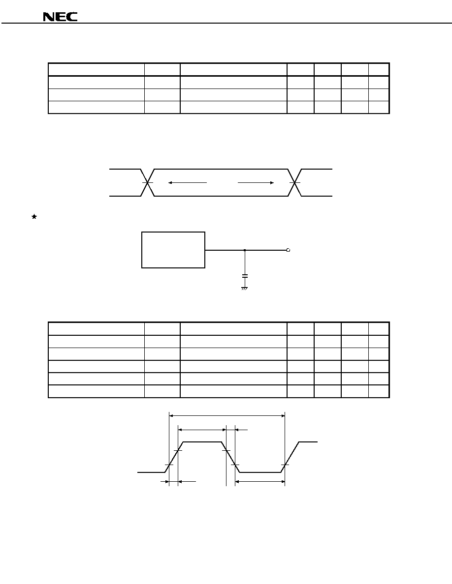
PHY Interface (1/2)
(1) Transmission operation
Parameter
Symbol
Condition
MIN.
TYP.
MAX.
Unit
TCLK
T
X
delay time
t
DTX
3
18
ns
TCLK
TSOC delay time
t
DTSOC
3
18
ns
TCLK
TEMBL_B delay time
t
DTEN
3
18
ns
FULL_B setup time
t
SFULL
8
ns
FULL_B hold time
t
HFULL
1
ns
H1
H2
H3
H4
P1
P2
P3
P4
P5
P6
P7
P8
P9
t
DTX
t
DTSOC
t
DTSOC
t
DTEN
t
HFULL
t
SFULL
t
DTEN
TCLK
H4-H1
P9-P1
: ATM Header
: Payload Data
Tx7-Tx0
TSOC
TENBL_B
FULL_B
`00H'
INVALID

Data Sheet S12100EJ3V0DS00
20
µ
µ
µ
µ
PD98401A
PHY Interface (2/2)
(2) Reception operation
Parameter
Symbol
Condition
MIN.
TYP.
MAX.
Unit
R
X
setup time
t
SRX
8
ns
R
X
hold time
t
HRX
1
ns
RSOC setup time
t
SRSOC
8
ns
RSOC hold time
t
HRSOC
1
ns
RCLK
RENBL_B delay time
t
DREN
3
18
ns
EMPTY_B setup time
t
SEMPT
8
ns
EMPTY_B hold time
t
HEMPT
1
ns
H1
H2
H3
H4
H5
P1
P2
P3
P4
P5
P6
P7
t
SRX
t
HRX
t
SRSOC
t
HRSOC
t
DREN
t
DREN
t
SEMPT
t
HEMPT
RCLK
H4-H1
P7-P1
: ATM Header
: Payload Data
Rx7-Rx0
RSOC
RENBL_B
EMPTY_B
INVALID
INVALID

Data Sheet S12100EJ3V0DS00
21
µ
µ
µ
µ
PD98401A
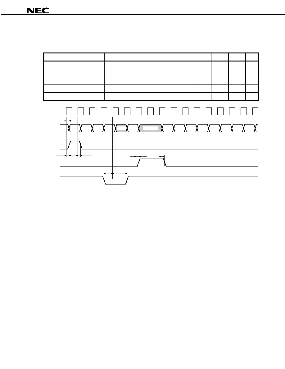
Host Slave Access (1/2)
(1) Write
Parameter
Symbol
Condition
MIN.
TYP.
MAX.
Unit
ASEL_B setup time
t
SASEL
8
ns
ASEL_B hold time
t
HASEL
3
ns
SEL_B setup time
t
SSEL
8
ns
SEL_B hold time
t
HSEL
1t
CYCLK
+3
ns
Address setup time
t
SDADD
8
ns
Address hold time
t
HDADD
3
ns
Data setup time
t
SDDAT
8
ns
Data hold time
t
HDDAT
3
ns
PAR setup time
t
SPAR1
8
ns
PAR hold time
t
HPAR1
3
ns
SR/W_B setup time
t
SSRW
8
ns
SR/W_B hold time
t
HSRW
3
ns
Write timing
ADDRESS
DATA
(input)
(input)
t
SASEL
t
SSEL
t
SDADD
t
SSRW
t
SPAR1
t
HPAR1
t
HPAR1
t
SPAR1
t
HSRW
t
SDDAT
t
HDADD
t
HDDAT
t
HSEL
t
HASEL
CLK
ASEL_B
SEL_B
AD31-AD0
SR/W_B
PAR3-PAR0

Data Sheet S12100EJ3V0DS00
22
µ
µ
µ
µ
PD98401A
Host Slave Access (2/2)
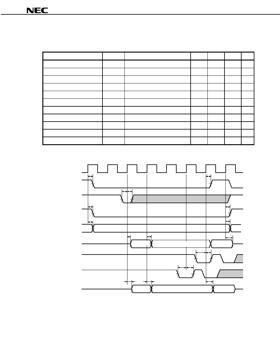
(2) Read
Parameter
Symbol
Condition
MIN.
TYP.
MAX.
Unit
ASEL_B setup time
t
SASEL
8
ns
ASEL_B hold time
t
HASEL
3
ns
SEL_B setup time
t
SSEL
8
ns
SEL_B hold time
t
HSEL
1t
CYCLK
+3
ns
Address setup time
t
SDADD
8
ns
Address hold time
t
HDADD
3
ns
CLK
data delay time
t
DDDAT
20
ns
CLK
data floating time
t
FDDAT
3
18
ns
PAR setup time
t
SPAR1
8
ns
PAR hold time
t
HPAR1
3
ns
CLK
PAR delay time
t
DPAR1
20
ns
CLK
PAR floating time
t
FPAR1
3
18
ns
SR/W_B setup time
t
SSRW
8
ns
SR/W_B hold time
t
HSRW
3
ns
Read timing
ADDRESS (input)
(input)
(output)
t
SASEL
t
SSEL
t
SDADD
t
HDADD
t
FDDAT
t
DDDAT
t
DPAR1
t
HSEL
t
HASEL
t
SSRW
t
SPAR1
t
HSRW
t
HPAR1
t
FPAR1
CLK
ASEL_B
SEL_B
AD31-AD0
SR/W_B
PAR3-PAR0
DATA (output)
Data Sheet S12100EJ3V0DS00
23
µ
µ
µ
µ
PD98401A
DMA Access (1/2)
(1) Write
Parameter
Symbol
Condition
MIN.
TYP.
MAX.
Unit
CLK
ATTN_B delay time
t
DATTN
18
ns
GNT_B setup time
t
SGNT
8
ns
GNT_B hold time
t
HGNT
3
ns
CLK
DR/W_B delay time
t
DDRW
3
18
ns
CLK
SIZE delay time
t
DSIZE
3
18
ns
CLK
address delay time
t
DSADD
20
ns
CLK
address/data floating time
t
FSADD
3
18
ns
CLK
PAR delay time
t
DPAR2
20
ns
CLK
PAR floating time
t
FPAR2
3
18
ns
RDY_B setup time
t
SRDY
8
ns
RDY_B hold time
t
HRDY
3
ns
Write timing ( Example: 2 word burst)
DATA 1
(output)
(output)
Hi-Z
t
DATTN
t
DDRW
t
DSIZE
t
HRDY
t
DPAR2
t
FPAR2
t
DPAR2
t
SRDY
t
HRDY
t
SRDY
t
DATTN
t
DDRW
t
DSIZE
t
DSADD
t
FSADD
t
FSADD
t
HGNT
t
SGNT
DATA 0 (output)
CLK
ATTN_B
GNT_B
DR/W_B
SIZE2-SIZE0
PAR3-PAR0
AD31-AD0
RDY_B
(Normal mode)
RDY_B
(Early mode)
(output)
(output)
ADDRESS
(output)
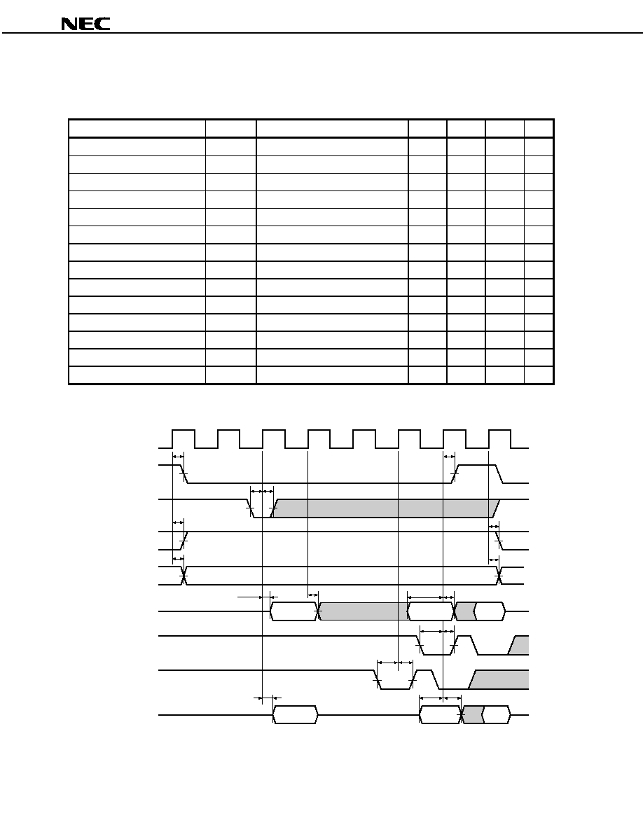
Data Sheet S12100EJ3V0DS00
24
µ
µ
µ
µ
PD98401A
DMA Access (2/2)
(2) Read
Parameter
Symbol
Condition
MIN.
TYP.
MAX.
Unit
CLK
ATTN B_delay time
t
DATTN
18
ns
GNT_B setup time
t
SGNT
8
ns
GNT_B hold time
t
HGNT
3
ns
CLK
DR/W_B delay time
t
DDRW
3
18
ns
CLK
SIZE delay time
t
DSIZE
3
18
ns
CLK
address delay time
t
DSADD
20
ns
CLK
address/data floating time
t
FSADD
3
18
ns
CLK
PAR delay time
t
DPAR2
20
ns
RDY_B setup time
t
SRDY
8
ns
RDY_B hold time
t
HRDY
3
ns
Data setup time
t
SSDAT
8
ns
Data hold time
t
HSDAT
3
ns
PAR setup time
t
SPAR2
8
ns
PAR hold time
t
HPAR2
3
ns
Read timing (Example: 2 word burst)
ADDRESS
(output)
Hi-Z
t
DATTN
t
DDRW
t
DSIZE
t
HRDY
t
HPAR2
t
SPAR2
t
DPAR2
t
SRDY
t
HRDY
t
SRDY
t
DATTN
t
DDRW
t
DSIZE
t
DSADD
t
FSADD
t
SSDAT
t
HSDAT
t
HGNT
t
SGNT
CLK
ATTN_B
GNT_B
DR/W_B
SIZE2-SIZE0
PAR3-PAR0
AD31-AD0
RDY_B
(Normal mode)
RDY_B
(Early mode)
DATA 1
(input)
(input)
(input)
(output)
DATA 0
(input)

Data Sheet S12100EJ3V0DS00
25
µ
µ
µ
µ
PD98401A
Signals ABRT B, ERR B, and OE_B
Parameter
Symbol
Condition
MIN.
TYP.
MAX.
Unit
ABRT_B setup time
t
SABRT
8
ns
ABRT_B hold time
t
HABRT
3
ns
ERR_B setup time
t
SERR
8
ns
ERR_B hold time
t
HERR
3
ns
OE_B
AD, PAR output
definition time
t
DADOE
18
ns
OE_B
AD, PAR Hi-Z definition
time
t
FADOE
18
ns
DMA abort/ERR B timing
t
HABRT
t
SABRT
t
HERR
t
SERR
CLK
ATTN_B
GNT_B
ABRT_B
ERR_B
OE_B timing
DATA 0
(Output)
DATA 0
(Output)
t
FADOE
Hi-Z
t
DADOE
OE_B
AD31-AD0
PAR3-PAR0

Data Sheet S12100EJ3V0DS00
26
µ
µ
µ
µ
PD98401A
Bus Monitoring Signal
Parameter
Symbol
Condition
MIN.
TYP.
MAX.
Unit
CLK
DBMD delay time
t
DDBMD
18
ns
CLK
DBML delay time
t
DDBML
19
ns
CLK
DBMF delay time
t
DDBMF
19
ns
CLK
DBMR delay time
t
DDBMR
18
ns
Bus monitoring signal timing
t
DDBMD
t
DDBMR
t
DDBML
t
DDBML
t
DDBMF
t
DDBMF
CLK
ATTN_B
DBMD
DBML
DBMF
DBMR

Data Sheet S12100EJ3V0DS00
27
µ
µ
µ
µ
PD98401A
Control Memory Access (1/2)
(1) Write
Parameter
Symbol
Condition
MIN.
TYP.
MAX.
Unit
CA
CWE_B
setup time
t
SCWE
0
ns
CBE_B
CWE_B
setup time
t
SCWE2
0
ns
CWE_B low level width
t
CWEL
1t
CLKH
-
2
ns
CWE_B
CD floating time
t
FCD
0
1t
CLKL
+10
ns
CWE_B
COE_B delay time
t
DCOE
0
ns
CA hold time (vs. CWE_B
)
t
HCA
0
ns
CBE_B hold time (vs. CWE_B
)
t
HCBE
0
ns
CD output time (vs. CWE_B
)
t
SCD
8
ns
CWE_B
CPAR floating time
t
FCPAR
0
1t
CLKL
+10
ns
CPAR output time (vs. CWE_B
)
t
SCPAR
8
ns
Write timing
t
SCWE2
t
HCBE
t
HCA
t
SCWE
t
DCOE
t
CWEL
t
SCD
t
FCD
t
SCPAR
t
FCPAR
CLK
CBE_B3-CBE_B0
CA17-CA0
CWE_B
COE_B
CD31-CD0
CPAR3-CPAR0
(output)
(output)
Data Sheet S12100EJ3V0DS00
28
µ
µ
µ
µ
PD98401A
Control Memory Access (2/2)
(2) Read
Parameter
Symbol
Condition
MIN.
TYP.
MAX.
Unit
CD delay enable time (vs. CBE_B
)
t
DCDCB
1t
CYCLK
-
15
ns
CD delay enable time (vs. CA)
t
DCDCA
1t
CYCLK
-
15
ns
CD delay enable time (vs. COE_B
)
t
DCDCO
1t
CYCLK
-
15
ns
CD hold time (vs. CBE_B
)
t
HCDCB
0
ns
CD hold time (vs. CA)
t
HCDCA
0
ns
CD hold time (vs. COE_B
)
t
HCDCO
0
ns
CPAR hold enable time (vs. CBE_B
)
t
DCPCB
1t
CYCLK
-
15
ns
CPAR hold enable time (vs. CA)
t
DCPCA
1t
CYCLK
-
15
ns
CPAR hold enable time (vs. COE_B
)
t
DCPCO
1t
CYCLK
-
15
ns
CPAR hold time (vs. CBE_B
)
t
HCPCB
0
ns
CPAR hold time (vs. CA)
t
HCPCA
0
ns
CPAR hold time (vs. COE_B
)
t
HCPCO
0
ns
Read timing
t
DCDCB
t
DCDCA
t
DCDCO
t
HCDCB
t
HCDCA
t
HCDCO
t
HCPCO
t
HCPCA
t
HCPCB
t
DCPCO
t
DCPCA
t
DCPCB
`H'
CLK
CBE_B3-CBE_B0
CA17-CA0
(input)
(input)
CWE_B
COE_B
CD31-CD0
CPAR3-CPAR0

Data Sheet S12100EJ3V0DS00
29
µ
µ
µ
µ
PD98401A
PHY Status Access (1/2)
(1) Write
Parameter
Symbol
Condition
MIN.
TYP.
MAX.
Unit
CLK
CA delay time
t
DPCA
20
ns
CLK
PHRW_B delay time
t
DPHRW
20
ns
CLK
PHCE_B delay time
t
DPHCE
20
ns
CLK
CD delay time
t
DPCD
20
ns
PHCE_B
CD floating time
t
FPCD
1t
CYCLK
-
10
1t
CYCLK
+10
ns
Write timing
t
DPCA
t
DPCA
1 clock
1 clock
4 clocks
t
DPHCE
`H'
(output)
t
DPCD
t
FPCD
t
DPHCE
t
DPHRW
CLK
CA17-CA0
PHRW_B
PHCE_B
PHOE_B
CD31-CD0
t
DPHRW

Data Sheet S12100EJ3V0DS00
30
µ
µ
µ
µ
PD98401A
PHY Status Access (2/2)
(2) Read
Parameter
Symbol
Condition
MIN.
TYP.
MAX.
Unit
CD setup time
t
SPCD
0
ns
CD hold time
t
HPOECD
0
ns
CLK
CA delay time
t
DPCA
20
ns
CLK
PHRW_B delay time
t
DPHRW
20
ns
CLK
PHCE_B delay time
t
DPHCE
20
ns
CLK
PHOE_B delay time
t
DPHOE
20
ns
Read timing
t
DPCA
t
DPHCE
t
DPHCE
t
DPHOE
t
SPCD
t
DPHOE
t
HPOECD
t
DPCA
t
DPHRW
(input)
1 clock
6 clocks
4 clocks
5 clocks
CLK
CA17-CA0
PHRW_B
PHCE_B
PHOE_B
CD31-CD0
Data Sheet S12100EJ3V0DS00
31
µ
µ
µ
µ
PD98401A
JTAG Boundary Scan
Parameter
Symbol
Condition
MIN.
TYP.
MAX.
Unit
JCK cycle time
t
CYJCK
100
ns
JCK high-level width
t
JCKH
40
ns
JCK low-level width
t
JCKL
40
ns
JMS setup time
t
SJMS
10
ns
JMS hold time
t
HJMS
10
ns
JDI setup time
t
SJDI
10
ns
JDI hold time
t
HJDI
10
ns
Capture_DR data input setup time
t
SJIN
15
ns
Capture_DR data input hold time
t
HJIN
15
ns
JCK
Up Date_DR output delay time
t
DJOUT
25
ns
JCK
JDO delay time
t
DJDO
20
ns
JRST_B low-level width
t
JRSTL
1t
CYJCK
ns
JTAG boundary scan timing
t
CYJCK
t
SJMS
t
HJMS
t
SJDI
t
DJDO
t
HJDI
t
SJIN
t
DJOUT
t
HJIN
t
JCKL
t
JRSTL
t
JCKH
JCK
JRST_B
JMS
JDI
JDO
All input
All output
Data Sheet S12100EJ3V0DS00
32
µ
µ
µ
µ
PD98401A
Others
Parameter
Symbol
Condition
MIN.
TYP.
MAX.
Unit
SEL_B recovery time
t
RVSEL
2
t
CYCLK
SEL_B
GNT_B
recovery time
t
RVSM
1
t
CYCLK
RDY_B
SEL_B
recovery time
t
RVMS
RDY_B mode in normal operation
1
t
CYCLK
PHINT_B setup time
t
SPHI
8
ns
PHINT_B hold time
t
HPHI
1
ns
RST_B input pulse width
t
RSTL
1
t
CYCLK
RST_B
SEL_B
recovery time
t
RSTSL
20
t
CYCLK
Other timing
t
RVMS
t
RVSEL
t
RSTL
t
RSTSL
t
RVSM
t
HPHI
t
SPHI
CLK
SEL_B
GNT_B
RST_B
RDY_B
SEL_B
PHINT_B

Data Sheet S12100EJ3V0DS00
33
µ
µ
µ
µ
PD98401A
4.
PACKAGE DRAWINGS
208-PIN PLASTIC QFP (FINE PITCH) (28x28)
ITEM
MILLIMETERS
F
G
1.25
1.25
B
C
28.0
±
0.2
28.0
±
0.2
H
0.22
I
0.10
S
3.8 MAX.
K
1.3
±
0.2
L
0.5
±
0.2
M
0.17
N
0.10
P
3.2
±
0.1
+
0.05
-
0.04
J
0.5 (T.P.)
P208GD-50-LML, MML, SML-6
+
0.03
-
0.07
R
5
∞±
5
∞
J
I
N
S
S
detail of lead end
Q
0.4
±
0.1
M
NOTE
Each lead centerline is located within 0.10 mm of
its true position (T.P.) at maximum material condition.
1
208
52
53
156
157
105
104
C
A
B
Q
R
H
K
M
L
D
P
G
F
S
A
30.6
±
0.2
D
30.6
±
0.2

Data Sheet S12100EJ3V0DS00
34
µ
µ
µ
µ
PD98401A
5.
RECOMMENDED SOLDERING CONDITIONS
Solder the product under the following recommended conditions.
For details of the recommended soldering conditions, refer to Information Document Semiconductor Device
Mounting Technology Manual (C10535E).
For soldering methods and soldering conditions other than those recommended, consult NEC.
Surface Mount Type
µ
µ
µ
µ
PD98401AGD-MML: 208-pin plastic QFP (Fine pitch) (28 x 28 mm)
Soldering Method
Soldering Conditions
Symbol of Recommended Condition
Infrared reflow
Package peak temperature: 235
∞
C, Time: 30 seconds max. (210
∞
C
min.), Number of times: 2 max., Number of days: 7
Note
(Afterwards,
prebaking is necessary at 125
∞
C for 36 hours.)
IR35-367-2
Partial heating
Pin temperature: 300
∞
C max., Time: 3 seconds max. (per side of device)
-
Note The number of days during which the product can be stored at 25
∞
C, 65 % RH max. after the dry pack has
been opened.
Data Sheet S12100EJ3V0DS00
35
µ
µ
µ
µ
PD98401A
NOTES FOR CMOS DEVICES
1
PRECAUTION AGAINST ESD FOR SEMICONDUCTORS
Note: Strong electric field, when exposed to a MOS device, can cause destruction
of the gate oxide and ultimately degrade the device operation. Steps must
be taken to stop generation of static electricity as much as possible, and
quickly dissipate it once, when it has occurred. Environmental control must
be adequate. When it is dry, humidifier should be used. It is recommended
to avoid using insulators that easily build static electricity. Semiconductor
devices must be stored and transported in an anti-static container, static
shielding bag or conductive material. All test and measurement tools
including work bench and floor should be grounded. The operator should
be grounded using wrist strap. Semiconductor devices must not be touched
with bare hands. Similar precautions need to be taken for PW boards with
semiconductor devices on it.
2
HANDLING OF UNUSED INPUT PINS FOR CMOS
Note: No connection for CMOS device inputs can be cause of malfunction. If no
connection is provided to the input pins, it is possible that an internal input
level may be generated due to noise, etc., hence causing malfunction. CMOS
device behave differently than Bipolar or NMOS devices. Input levels of
CMOS devices must be fixed high or low by using a pull-up or pull-down
circuitry. Each unused pin should be connected to V
DD
or GND with a
resistor, if it is considered to have a possibility of being an output pin. All
handling related to the unused pins must be judged device by device and
related specifications governing the devices.
3
STATUS BEFORE INITIALIZATION OF MOS DEVICES
Note: Power-on does not necessarily define initial status of MOS device. Produc-
tion process of MOS does not define the initial operation status of the device.
Immediately after the power source is turned ON, the devices with reset
function have not yet been initialized. Hence, power-on does not guarantee
out-pin levels, I/O settings or contents of registers. Device is not initialized
until the reset signal is received. Reset operation must be executed imme-
diately after power-on for devices having reset function.

µ
µ
µ
µ
PD98401A
NEASCOT-S10 and NEASCOT-S15 are trademarks of NEC Corporation.
The export of this product from Japan is prohibited without governmental license. To export or re-export this product from
a country other than Japan may also be prohibited without a license from that country. Please call an NEC sales
representative.
No part of this document may be copied or reproduced in any form or by any means without the prior written
consent of NEC Corporation. NEC Corporation assumes no responsibility for any errors which may appear in this
document.
NEC Corporation does not assume any liability for infringement of patents, copyrights or other intellectual
property rights of third parties by or arising from use of a device described herein or any other liability arising
from use of such device. No license, either express, implied or otherwise, is granted under any patents,
copyrights or other intellectual property rights of NEC Corporation or others.
While NEC Corporation has been making continuous effort to enhance the reliability of its semiconductor devices,
the possibility of defects cannot be eliminated entirely. To minimize risks of damage or injury to persons or
property arising from a defect in an NEC semiconductor device, customers must incorporate sufficient safety
measures in its design, such as redundancy, fire-containment, and anti-failure features.
NEC devices are classified into the following three quality grades:
"Standard", "Special", and "Specific". The Specific quality grade applies only to devices developed based on
a customer designated "quality assurance program" for a specific application. The recommended applications
of a device depend on its quality grade, as indicated below. Customers must check the quality grade of each
device before using it in a particular application.
Standard: Computers, office equipment, communications equipment, test and measurement equipment,
audio and visual equipment, home electronic appliances, machine tools, personal electronic
equipment and industrial robots
Special: Transportation equipment (automobiles, trains, ships, etc.), traffic control systems, anti-disaster
systems, anti-crime systems, safety equipment and medical equipment (not specifically designed
for life support)
Specific: Aircrafts, aerospace equipment, submersible repeaters, nuclear reactor control systems, life
support systems or medical equipment for life support, etc.
The quality grade of NEC devices is "Standard" unless otherwise specified in NEC's Data Sheets or Data Books.
If customers intend to use NEC devices for applications other than those specified for Standard quality grade,
they should contact an NEC sales representative in advance.
Anti-radioactive design is not implemented in this product.
M4 96. 5