 | –≠–ª–µ–∫—Ç—Ä–æ–Ω–Ω—ã–π –∫–æ–º–ø–æ–Ω–µ–Ω—Ç: UPD78062A | –°–∫–∞—á–∞—Ç—å:  PDF PDF  ZIP ZIP |
Document Outline
- COVER
- DESCRIPTION
- FEATURES
- APPLICATIONS
- ORDERING INFORMATION
- QUALITY GRADE
- DIFFERENCES BETWEEN uPD78062(A), 78063(A) and 78064(A), and uPD78062, 78063 and 78064
- 78K/0 SERIES DEVELOPMENT
- FUNCTIONAL OUTLINE
- 1. PIN CONFIGURATION (TOP VIEW)
- 2. BLOCK DIAGRAM
- 3. PIN FUNCTIONS
- 3.1 Port Pins
- 3.2 Other Pins
- 3.3 Pin I/O Circuits and Recommended Connection of Unused Pins
- 4. MEMORY SPACE
- 5. PERIPHERAL HARDWARE FUNCTION FEATURE
- 5.1 Port
- 5.2 Clock Generator
- 5.3 Timer/Event Counter
- 5.4 Clock Output Control Circuit
- 5.5 Buzzer Output Control Circuit
- 5.6 A/D Converter
- 5.7 Serial Interface
- 5.8 LCD Controller/Driver
- 6. INTERRUPT FUNCTIONS AND TEST FUNCTIONS
- 6.1 Interrupt Functions
- 6.2 Test Functions
- 7. STANDBY FUNCTION
- 8. RESET FUNCTION
- 9. INSTRUCTION SET
- 10. ELECTRICAL SPECIFICATIONS
- 11. CHARACTERISTIC CURVES (REFERENCE VALUES)
- 12. PACKAGE DRAWINGS
- 13. RECOMMENDED SOLDERING CONDITIONS
- APPENDIX A. DEVELOPMENT TOOLS
- APPENDIX B. RELATED DOCUMENTS
MOS INTEGRATED CIRCUIT
µ
PD78062(A), 78063(A), 78064(A)
8-BIT SINGLE-CHIP MICROCONTROLLER
The mark
shows major revised points.
The information in this document is subject to change without notice.
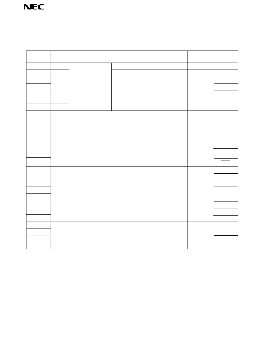
DESCRIPTION
The
µ
PD78062(A), 78063(A), and 78064(A) are products to which a quality assurance program more stringent than that
used for the
µ
PD78062, 78063, and 78064 (standard models) is applied (NEC classifies these products as "special" quality
grade models).
µ
PD78062(A), 78063(A), and 78064(A) are products in the
µ
PD78064 subseries within the 78K/0 series, which
incorporate LCD controller/driver, 8-bit resolution A/D converter, timer, serial interface, interrupt functions and many other
peripheral hardwares.
Various development tools are also provided.
For the details of functional description, refer to the following user's manual.Be sure to read this manual
before designing your system.
µ
PD78064 78064Y Subseries User's Manual : U10105E
78K/0 Series User's Manual (Instruction
: IEU-1372
FEATURES
∑
Large on-chip ROM & RAM
Note
Under planning
∑
Minimum instruction execution time can be varied from high speed (0.4
µ
s) to ultra-low speed (122
µ
s)
∑
I/O ports: 57 (including segment signal output dual-function pins)
∑
LCD controller/driver
Supply voltage
V
DD
= 2.0 to 6.0 V (Static display mode)
V
DD
= 2.5 to 6.0 V (1/3 bias)
V
DD
= 2.7 to 6.0 V (1/2 bias)
∑
8-bit resolution A /D converter : 8 channels
∑
Serial interface : 2 channels
∑
Timer: 5 channels
∑
Supply voltage : V
DD
= 2.0 to 6.0 V
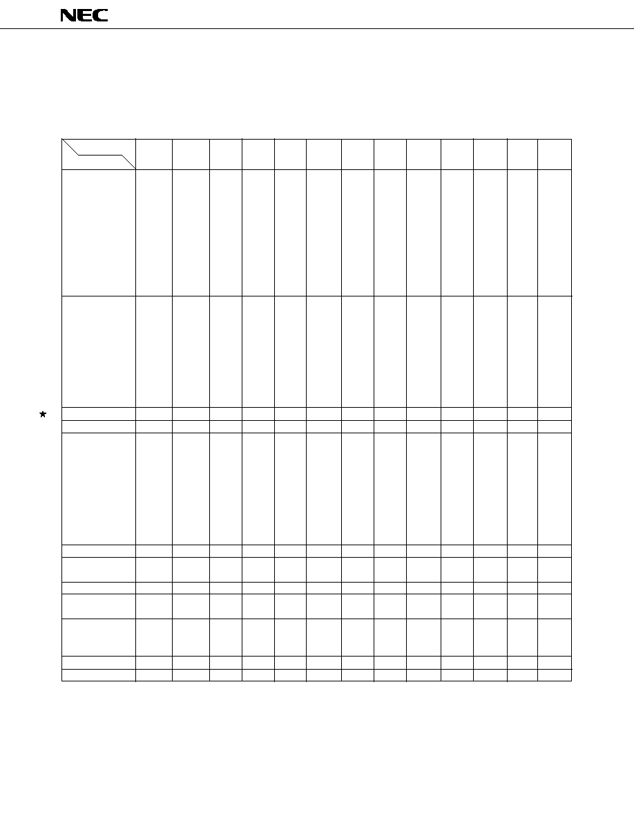
Item
Program Memory
Data Memory
Product Name
(ROM)
Internal High-Speed RAM
LCD Display RAM
µ
PD78062(A)
16K bytes
512 bytes
µ
PD78063(A)
24K bytes
40
◊
4 bits
µ
PD78064(A)
32K bytes
Package
1024 bytes
100-pin plastic QFP (fine pitch)
(14
◊
14mm, 0.5 mm pitch)
100-pin plastic QFP
(14
◊
20 mm, 0.65 mm pitch)
100-pin plastic LQFP
Note
(fine pitch)
(14
◊
14 mm, 0.5 mm pitch)
Document No. U10335EJ2V0DS00 (2nd edition)
Date Published August 1997 N
Printed in Japan
©
1997
DATA SHEET
2
µ
PD78062(A), 78063(A), 78064(A)
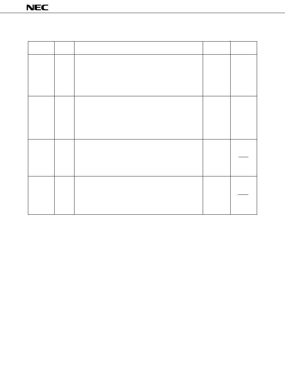
APPLICATIONS
Control units of automobile electronic systems, gas detectors and circuit breakers, various safety systems, hemadynamometers,
etc.
ORDERING INFORMATION
Part Number
Package
µ
PD78062GC(A)-
◊◊◊
-7EA
100-pin plastic QFP (fine pitch) (14
◊
14 mm, resin thickness: 1.45 mm)
µ
PD78062GC(A)-
◊◊◊
-8EU
Note
100-pin plastic LQFP (fine pitch) (14
◊
14 mm, resin thickness: 1.40 mm)
µ
PD78062GF(A)-
◊◊◊
-3BA
100-pin plastic QFP (14
◊
20mm)
µ
PD78063GC(A)-
◊◊◊
-7EA
100-pin plastic QFP (fine pitch) (14
◊
14 mm, resin thickness: 1.45 mm)
µ
PD78063GC(A)-
◊◊◊
-8EU
Note
100-pin plastic LQFP (fine pitch) (14
◊
14 mm, resin thickness: 1.40 mm)
µ
PD78063GF(A)-
◊◊◊
-3BA
100-pin plastic QFP (14
◊
20mm)
µ
PD78064GC(A)-
◊◊◊
-7EA
100-pin plastic QFP (fine pitch) (14
◊
14 mm, resin thickness: 1.45 mm)
µ
PD78064GC(A)-
◊◊◊
-8EU
Note
100-pin plastic LQFP (fine pitch) (14
◊
14 mm, resin thickness: 1.40 mm)
µ
PD78064GF(A)-
◊◊◊
-3BA
100-pin plastic QFP (14
◊
20mm)
Note
Under planning
Caution The
µ
PD78062GC(A), 78063GC(A), and 78064GC(A) are available in two types of packages (refer to 12.
PACKAGE DRAWINGS). For the available packages, consult NEC.
Remark
◊◊◊
indicates a ROM code suffix.
QUALITY GRADE
Special
DIFFERENCES BETWEEN
µ
PD78062(A), 78063(A) and 78064(A), and
µ
PD78062, 78063 and 78064
Product name
µ
PD78062(A), 78063(A), 78064(A)
µ
PD78062, 78063, 78064
Item
Quality grade
Special
Standard
Please refer to "Quality Grades on NEC Semiconductor Devices" (Document No. C11531E) published by
NEC Corporation to know the specification of quality grade on the devices and its recommended applications.
3
µ
PD78062(A), 78063(A), 78064(A)
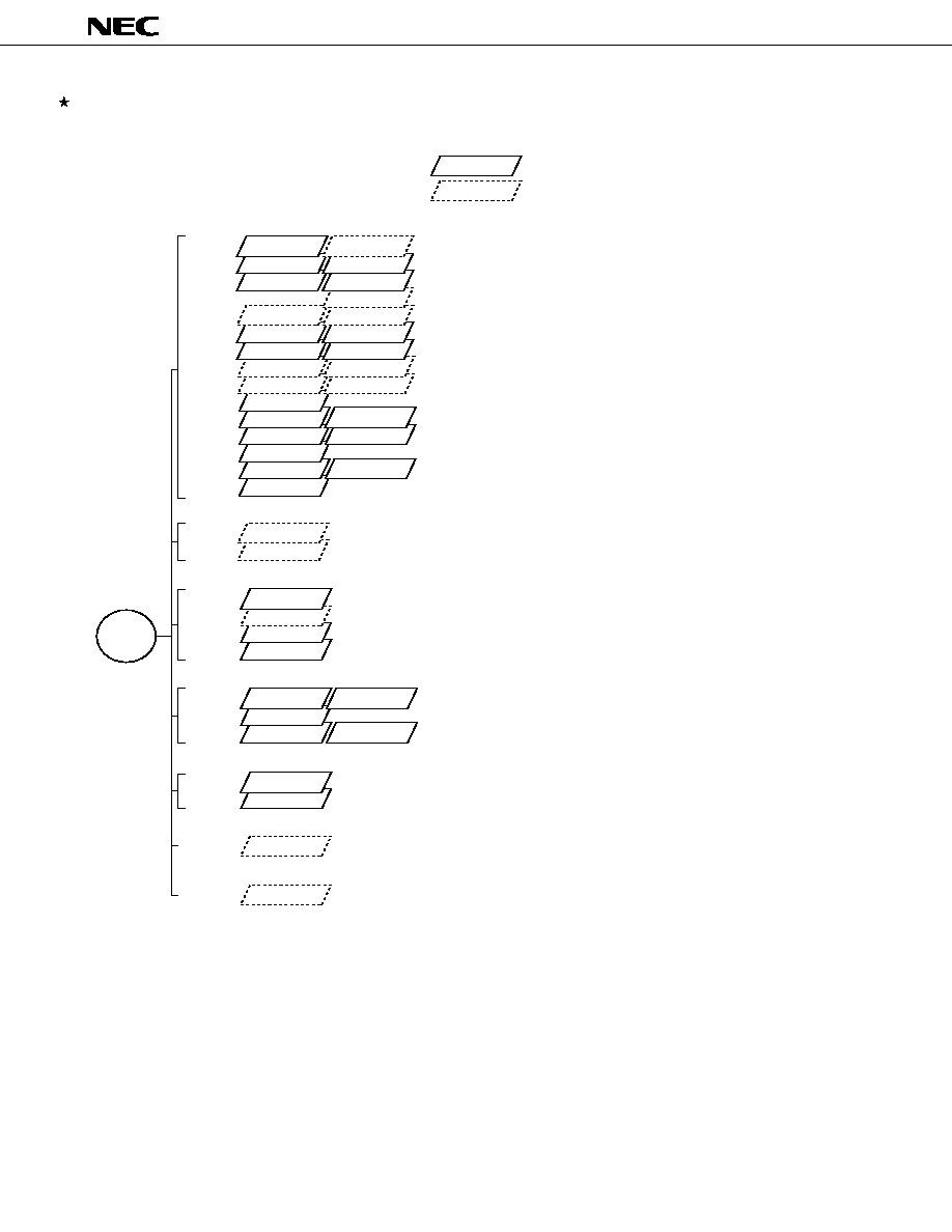
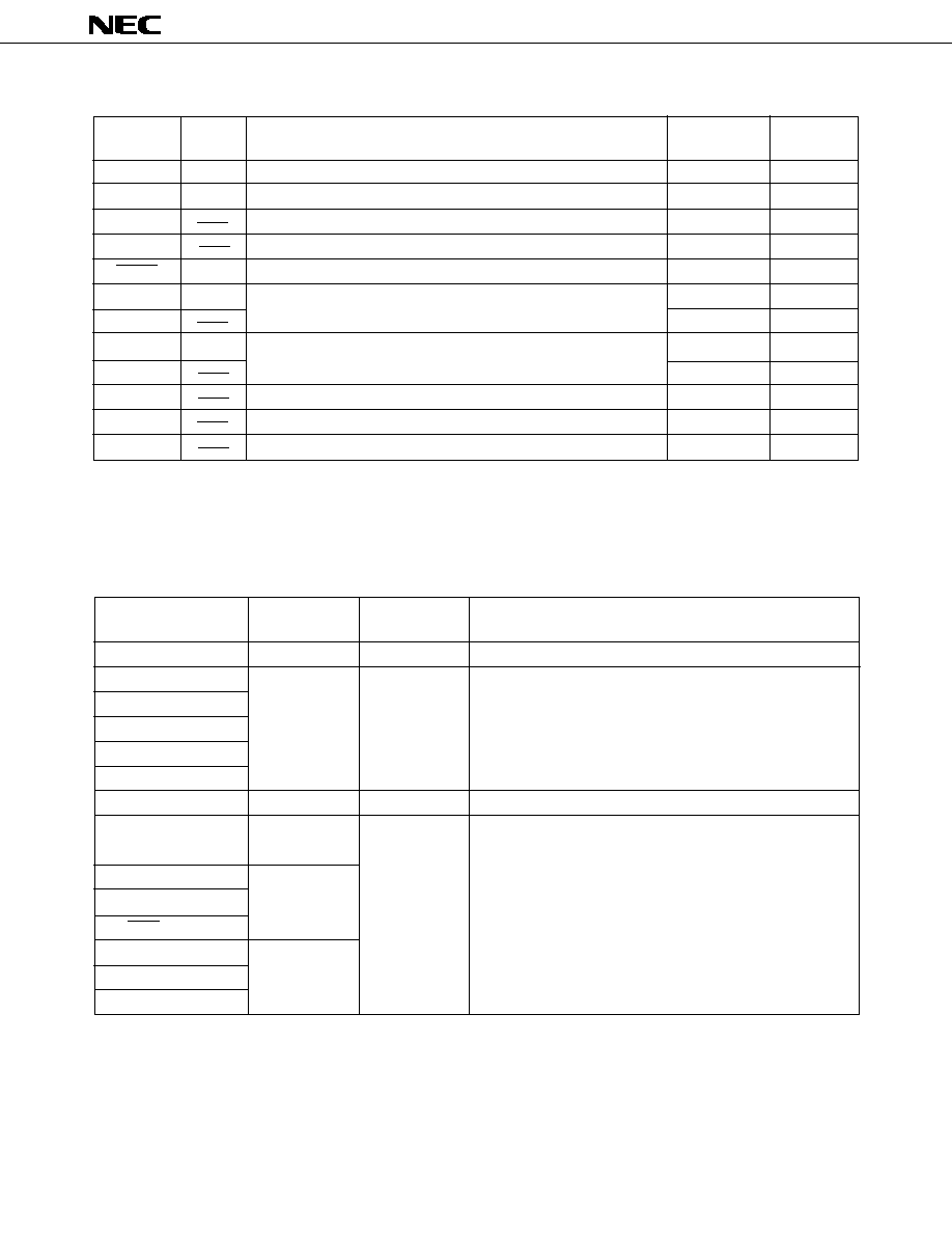
78K/0 SERIES DEVELOPMENT
The following shows the 78 K/0 Series products development. Subseries names are shown inside frames.
Note
Under planning
64-pin
64-pin
64-pin
64-pin
80-pin
80-pin
EMI noise reduction version of the PD78054.
UART and D/A converter were added to the PD78014, and I/O was enhanced.
PD78054
PD78054Y
PD78058F
PD78058FY
PD780034
PD780024
PD780964
PD780924
PD780034Y
PD780024Y
µ
µ
µ
µ
µ
µ
µ
µ
µ
µ
64-pin
An A/D converter of the PD780024 was enhanced.
Serial I/O of the PD78018F was enhanced, EMI noise reduction version.
On-chip inverter control circuit and UART, EMI noise reduction version.
µ
µ
µ
µ
An A/D converter of the PD780924 was enhanced.
µ
PD78044F
PD78044H
80-pin
80-pin
PD78064
PD78064B
PD780308
100-pin
100-pin
100-pin
PD780308Y
PD78064Y
PD78098
80-pin
PD78P0914
64-pin
78K/0
Series
N-ch open drain input/output was added to the PD78044F, Display output total: 34
Basic subseries for driving FIP, Display output total: 34
LCD drive
SIO of the PD78064 was enhanced, and ROM and RAM were expanded.
EMI noise reduced version of the PD78064.
Basic subseries for driving LCDs, On-chip UART.
IEBus
TM
supported
An IEBus controller was added to the PD78054.
LV
On-chip PWM output, LV digital code decoder, and Hsync counter.
µ
µ
µ
µ
µ
µ
µ
µ
µ
µ
µ
µ
µ
µ
µ
µ
PD78083
PD78002
PD78002Y
PD780001
PD78014
PD78014Y
PD78018F
PD78018FY
Low-voltage (1.8 V) operation versions of the PD78014 with several ROM and RAM capacities available.
An A/D converter and 16-bit timer were added to the PD78002.
An A/D converter was added to the PD78002.
Basic subseries for control.
On-chip UART, capable of operating at a low voltage (1.8 V).
µ
µ
µ
µ
µ
µ
µ
µ
42/44-pin
64-pin
64-pin
64-pin
64-pin
PD78014H
µ
EMI noise reduction version of PD78018F.
µ
µ
PD780058
PD780058Y
Note
µ
µ
80-pin
Serial I/O of the PD78054 was enhanced, EMI noise reduction version.
100-pin
100-pin
Products in mass production
Products under development
Y subseries products are compatible with I
2
C bus.
A timer was added to the PD78054, and the external interface function was enhanced.
ROM-less versions of the PD78078.
PD78070A
PD78070AY
µ
PD78078
PD78078Y
PD780018AY
µ
µ
µ
µ
µ
100-pin
Serial I/O of the PD78078Y was enhanced, and only selected functions are provided.
µ
µ
100-pin
Control
PD78075B
PD78075BY
µ
µ
EMI noise reduction version of the PD78078.
µ
Inverter control
PD780228
100-pin
The I/O and FIP C/D of the PD78044H were enhanced, Display output total: 48
µ
µ
µ
PD780208
100-pin
FIP
TM
drive
The I/O and FIP C/D of the PD78044F were enhanced, Display output total: 53
µ
µ
PD780208
µ
PD78098B
EMI noise reduction version of the PD78098.
µ
80-pin
µ
Meter control
PD780973
On-chip automobile meter driving controller/driver.
µ
80-pin
4
µ
PD78062(A), 78063(A), 78064(A)
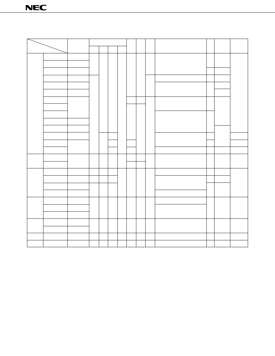
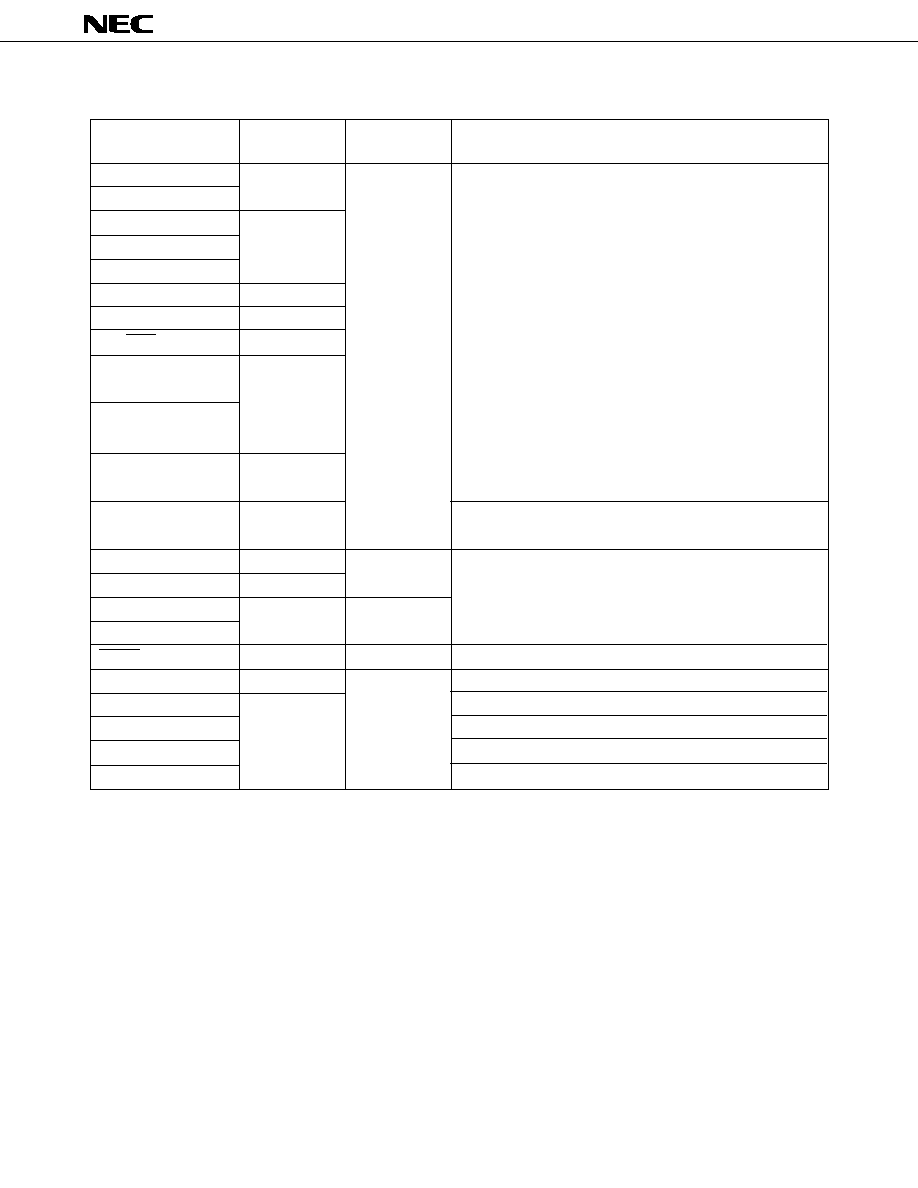
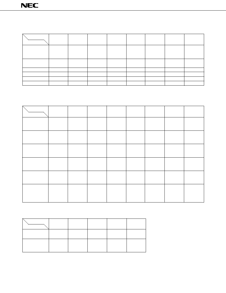
The following table shows the differences among subseries functions.
Function
ROM
Timer
8-bit 10-bit 8-bit
Serial Interface
I/O
V
DD
MIN.
External
Subseries Name
Capacity
8-bit 16-bit Watch WDT A/D A/D
D/A
Value
Expansion
Control
µ
PD78075B
32 K to 40 K 4ch
1ch
1ch 1ch
8ch
≠
2ch 3ch (UART: 1ch)
88
1.8 V
Available
µ
PD78078
48 K to 60 K
µ
PD78070A
≠
61
2.7 V
µ
PD780058
24 K to 60 K 2ch
2ch 3ch (time division UART: 1ch)
68
1.8 V
µ
PD78058F
48 K to 60 K
3ch (UART: 1ch)
69
2.7 V
µ
PD78054
16 K to 60 K
2.0 V
µ
PD780034
8 K to 32 K
≠
8ch
≠
3ch (UART: 1ch,
51
1.8 V
µ
PD780024
8ch
≠
time division 3-wire: 1ch)
µ
PD78014H
2ch
53
µ
PD78018F
8 K to 60 K
µ
PD78014
8 K to 32 K
2.7 V
µ
PD780001
8 K
≠
≠
1ch
39
≠
µ
PD78002
8 K to 16 K
1ch
≠
53
Available
µ
PD78083
≠
8ch
1ch (UART: 1ch)
33
1.8 V
≠
Inverter
µ
PD780964
8 K to 32 K 3ch Note
≠
1ch
≠
8ch
≠
2ch (UART: 2ch)
47
2.7 V
Available
control
µ
PD780924
8ch
≠
FIP
µ
PD780208
32 K to 60 K 2ch
1ch
1ch 1ch
8ch
≠
≠
2ch
74
2.7 V
≠
drive
µ
PD780228
48 K to 60 K 3ch
≠
≠
1ch
72
4.5 V
µ
PD78044H
32 K to 48 K 2ch
1ch
1ch
68
2.7 V
µ
PD78044F
16 K to 40 K
2ch
LCD
µ
PD780308
48 K to 60 K 2ch
1ch
1ch 1ch
8ch
≠
≠
3ch (time division UART: 1ch)
57
2.0 V
≠
drive
µ
PD78064B
32 K
2ch (UART: 1ch)
µ
PD78064
16 K to 32 K
IEBus
µ
PD78098B
40 K to 60 K 2ch
1ch
1ch 1ch
8ch
≠
2ch 3ch (UART: 1ch)
69
2.7 V
Available
supported
µ
PD78098
32 K to 60 K
Meter control
µ
PD780973
24 K to 32 K 3ch
1ch
1ch 1ch
5ch
≠
≠
2ch (UART: 1ch)
56
4.5 V
≠
LV
µ
PD78P0914 32 K
6ch
≠
≠
1ch
8ch
≠
≠
2ch
54
4.5 V
Available
Note
10-bit timer: 1 channel
5
µ
PD78062(A), 78063(A), 78064(A)
FUNCTIONAL OUTLINE
16K bytes
24K bytes
32K bytes
512 bytes
1024 bytes
40
◊
4 bits
8 bits
◊
32 registers (8 bits
◊
8 registers
◊
4 banks)
On-chip minimum instruction execution time cycle modification function
0.4
µ
s/0.8
µ
s/1.6
µ
s/3.2
µ
s/6.4
µ
s/12.8
µ
s (at 5.0 MHz operation)
122
µ
s (at 32.768 kHz operation)
∑ 16-bit operation
∑ Multiplication/division (8 bits
◊
8 bits,16 bits
˜
8 bits)
∑ Bit manipulation (set, reset, test, boolean operation)
∑ BCD correction, etc.
Total
: 57
∑ CMOS input
:
0
2
∑ CMOS I/O
: 55
∑ 8-bit resolution
◊
8 channels
∑ Segment signal output : Maximum 40
∑ Common signal output : Maximum 4
∑ Bias : 1/2 or 1/3 switchable
∑ 3-wire serial I/O/SBI/2-wire serial I/O mode selectable
: 1 channel
∑ 3-wire serial I/O/UART mode selectable
: 1 channel
∑ 16-bit timer/event counter
:
1 channel
∑ 8-bit timer/event counter
:
2 channels
∑ Watch timer
:
1 channel
∑ Watchdog timer
:
1 channel
3 (14-bit PWM output capability : 1)
19.5 kHz, 39.1 kHz, 78.1 kHz, 156 kHz, 313 kHz, 625 kHz, 1.25 MHz, 2.5 MHz,
5.0 MHz (at main system clock 5.0 MHz operation)
32.768 kHz (at subsystem clock 32.768 kHz operation)
1.2 kHz, 2.4 kHz, 4.9 kHz, 9.8 kHz (at main system clock 5.0 MHz operation)
Internal : 12, external :
6
Internal : 1
1
Internal:
1, external: 1
V
DD
= 2.0 to 6.0 V
∑ 100-pin plastic QFP (Fine pitch) (14
◊
14 mm, resin thickness: 1.45 mm)
∑ 100-pin plastic QFP (14
◊
20 mm)
∑ 100-pin plastic LQFP (Fine pitch) (14
◊
14 mm, resin thickness: 1.40 mm, under planning)
ROM
High-speed RAM
LCD display RAM
µ
PD78064(A)
µ
PD78063(A)
µ
PD78062(A)
Instruction set
LCD controller/driver
Serial interface
Timer
Internal
memory
When main system clock
selected
When subsystem clock
selected
I/O ports
(including segment signal output pins)
A/D converter
Vectored
interrupt
sources
Package
Maskable
Non-maskable
Softwar
Item
Product Name
General registers
Minimum instruction execution time
Timer output
Clock output
Buzzer output
Test input
Supply voltage

6
µ
PD78062(A), 78063(A), 78064(A)
CONTENTS
1.
PIN CONFIGURATION (TOP VIEW) ........................................................................................................
7
2.
BLOCK DIAGRAM ................................................................................................................................... 10
3.
PIN FUNCTIONS ...................................................................................................................................... 11
3.1
Port Pins ..........................................................................................................................................................
11
3.2
Other Pins ........................................................................................................................................................
13
3.3
Pin I/O Circuits and Recommended Connection of Unused Pins .............................................................
14
4.
MEMORY SPACE ..................................................................................................................................... 18
5.
PERIPHERAL HARDWARE FUNCTION FEATURE ............................................................................... 19
5.1
Port ...................................................................................................................................................................
19
5.2
Clock Generator ..............................................................................................................................................
20
5.3
Timer/Event Counter .......................................................................................................................................
20
5.4
Clock Output Control Circuit .........................................................................................................................
23
5.5
Buzzer Output Control Circuit .......................................................................................................................
23
5.6
A/D Converter ..................................................................................................................................................
24
5.7
Serial Interface ...............................................................................................................................................
24
5.8
LCD Controller/Driver .....................................................................................................................................
26
6.
INTERRUPT FUNCTIONS AND TEST FUNCTIONS ............................................................................... 27
6.1
Interrupt Functions .........................................................................................................................................
27
6.2
Test Functions .................................................................................................................................................
31
7.
STANDBY FUNCTION ............................................................................................................................. 32
8.
RESET FUNCTION .................................................................................................................................. 32
9.
INSTRUCTION SET ................................................................................................................................. 33
10. ELECTRICAL SPECIFICATIONS ............................................................................................................ 35
11. CHARACTERISTIC CURVES (REFERENCE VALUES) ......................................................................... 56
12. PACKAGE DRAWINGS ........................................................................................................................... 58
13. RECOMMENDED SOLDERING CONDITIONS ....................................................................................... 61
APPENDIX A. DEVELOPMENT TOOLS ....................................................................................................... 62
APPENDIX B. RELATED DOCUMENTS ....................................................................................................... 64
7
µ
PD78062(A), 78063(A), 78064(A)
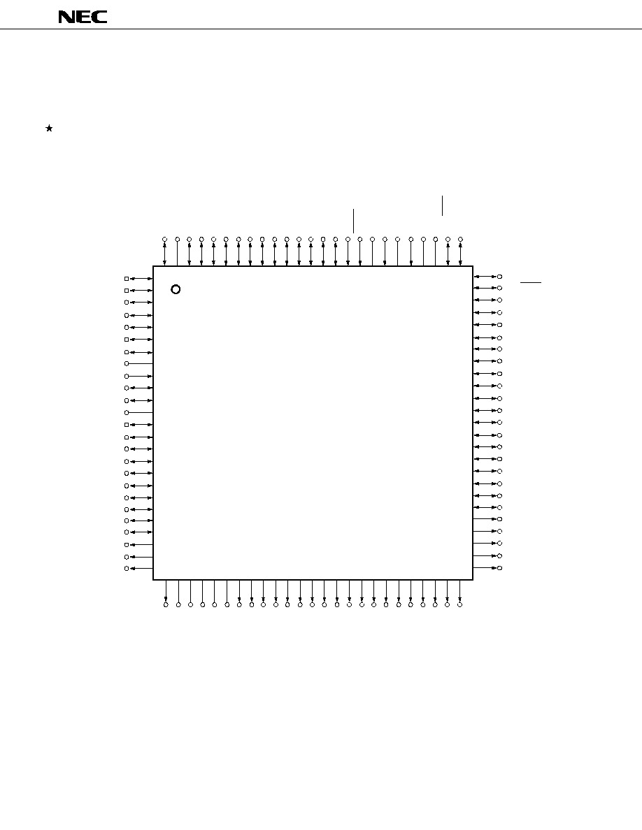
1.
PIN CONFIGURATION (TOP VIEW)
∑ 100-pin plastic QFP (fine pitch)(14
◊
14 mm, resin thickness: 1.45 mm)
µ
PD78062GC(A)-
◊◊◊
-7EA, 78063GC(A)-
◊◊◊
-7EA, 78064GC(A)-
◊◊◊
-7EA
∑ 100-pin plastic LQFP (fine pitch)(14
◊
14 mm, resin thickness: 1.40 mm)
µ
PD78062GC(A)-
◊◊◊
-8EU
Note
, 78063GC(A)-
◊◊◊
-8EU
Note
, 78064GC(A)-
◊◊◊
-8EU
Note
P11/ANI1
P10/ANI0
98
99
100
97 96 95 94 93 92 91 90 89 88 87
AV
SS
P117
P116
P115
P114
P113
P112
P111
P110
P05/INTP5
P04/INTP4
P03/INTP3
P02/INTP2
86 85 84 83 82
P01/INTP1/TI01
P00/INTP0/TI00
RESET
XT2
XT1/P07
V
DD
1
P12/ANI2
P13/ANI3
2
3
P14/ANI4
4
P15/ANI5
5
P16/ANI6
6
P17/ANI7
7
AV
DD
8
AV
REF
9
P100
10
P101
11
V
SS
12
P102
13
P103
14
P30/TO0
15
P31/TO1
16
P32/TO2
17
P33/TI1
18
19
20
P34/TI2
P35/PCL
40
39
38
37
36
35
34
33
32
31
30
29
28
27
26
45
S13
44
43
42
41
S12
S11
S10
S9
S8
S7
S6
S5
S4
S3
S2
S1
S0
V
SS
V
LC2
V
LC1
V
LC0
BIAS
COM3
P36/BUZ
21
P37
22
COM0
23
24
25
COM1
COM2
50
S18
49
48
47
46
S17
S16
S15
S14
P27/SCK0
72
73
74
75
70
71
69
68
67
66
65
64
63
62
61
60
59
58
57
56
P70/SI2/R
X
D
P26/SO0/SB1
P25/SI0/SB0
P80/S39
P81/S38
P82/S37
P83/S36
P84/S35
P85/S34
P86/S33
P87/S32
P90/S31
P91/S30
P92/S29
P93/S28
P94/S27
P95/S26
P96/S25
P97/S24
55
54
53
52
51
S23
S22
S21
S20
S19
80 79 78 77 76
X1
X2
IC
P72/SCK2/ASCK
P71/SO2/T
X
D
81
Note Under planning
Cautions 1. Connect directly the IC (Internally Connected) pin to V
SS
.
2. Connect the AV
DD
pin to V
DD
.
3. Connect the AV
SS
pin to V
SS
.
8
µ
PD78062(A), 78063(A), 78064(A)
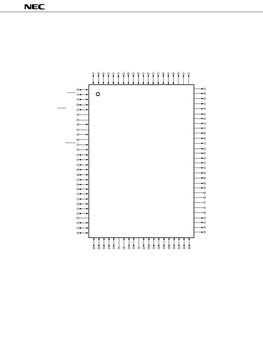
∑ 100-pin plastic QFP (14
◊
20 mm)
µ
PD78062GF(A)-
◊◊◊
-3BA, 78063GF(A)-
◊◊◊
-3BA
µ
PD78064G(A)-
◊◊◊
-3BA
Cautions 1. Connect directly the IC (Internally Connected) pin to V
SS
.
2. Connect the AV
DD
pin to V
DD
.
3. Connect the AV
SS
pin to V
SS
.
P26/SO0/SB1
P25/SI0/SB0
98
99
100
97 96 95 94 93 92 91 90 89 88 87
P80/S39
P81/S38
P82/S37
P83/S36
P84/S35
P85/S34
P86/S33
P87/S32
P90/S31
P91/S30
P92/S29
P93/S28
P94/S27
86 85 84 83 82
P95/S26
P96/S25
P97/S24
S23
S22
S21
1
P27/SCK0
P70/SI2/R
X
D
2
3
P71/SO2/T
X
D
4
P72/SCK2/ASCK
5
IC
6
X2
7
X1
8
V
DD
9
XT1/P07
10
XT2
11
RESET
12
P00/INTP0/TI00
13
P01/INTP1/TI01
14
P02/INTP2
15
P03/INTP3
16
P04/INTP4
17
P05/INTP5
18
19
P110
20
P111
P112
21
P113
22
P114
23
24
25
P115
P116
81
26
P117
AV
SS
27
P10/ANI0
28
P11/ANI1
29
30
P12/ANI2
45
44
43
42
41
40
39
38
37
36
35
34
33
32
31 50
49
48
47
46
P37
P36/BUZ
P35/PCL
P34/TI2
P33/TI1
P32/TO2
P31/TO1
P30/TO0
P103
P102
V
SS
P101
P100
AV
REF
AV
DD
P17/ANI7
P16/ANI6
P15/ANI5
P14/ANI4
P13/ANI3
77
78
79
80
75
76
74
73
72
71
70
69
68
67
66
65
64
63
62
61
60
59
58
57
56
55
54
53
52
51
S20
S19
S18
S17
S16
S15
S14
S13
S12
S11
S10
S9
S8
S7
S6
S5
P4
S3
S2
S1
S0
V
SS
V
LC2
V
LC1
V
LC0
BIAS
COM3
COM2
COM1
COM0

9
µ
PD78062(A), 78063(A), 78064(A)
ANI0-ANI7
: Analog Input
P110-P117
: Port11
ASCK
: Asynchronous Serial Clock
PCL
: Programmable Clock
AV
DD
: Analog Power Supply
RESET
: Reset
AV
REF
: Analog Reference Voltage
R
X
D
: Receive Data
AVss
: Analog Ground
S0-S39
: Segment Output
BIAS
: LCD Power Supply Bias Control
SB0-SB1
: Serial Bus
BUZ
: Buzzer Clock
SI0, SI2
: Serial Input
COM0-COM3 : Common Output
SO0, SO2
: Serial Output
IC
: Internally Connected
SCK0, SCK2 : Serial Clock
INTP0-INTP5 : Interrupt from Peripherals
TI00, TI01
: Timer Input
P00-P05, P07 : port0
TI1, TI2
: Timer Input
P10-P17
: Port1
TO0-TO2
: Timer Output
P25-P27
: Port2
T
X
D
: Transmit Data
P30-P37
: Port3
V
DD
: Power Supply
P70-P72
: Port7
V
LC0
-V
LC2
: LCD Power Supply
P80-P87
: Port8
V
SS
: Ground
P90-P97
: Port9
X1, X2
: Crystal (Main System Clock)
P100-P103
: Port10
XT1, XT2
: Crystal (Subsystem Clock)
10
µ
PD78062(A), 78063(A), 78064(A)
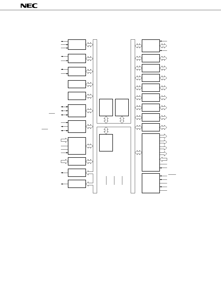
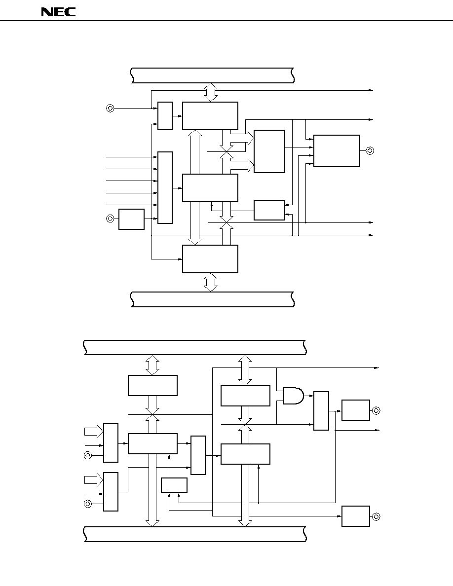
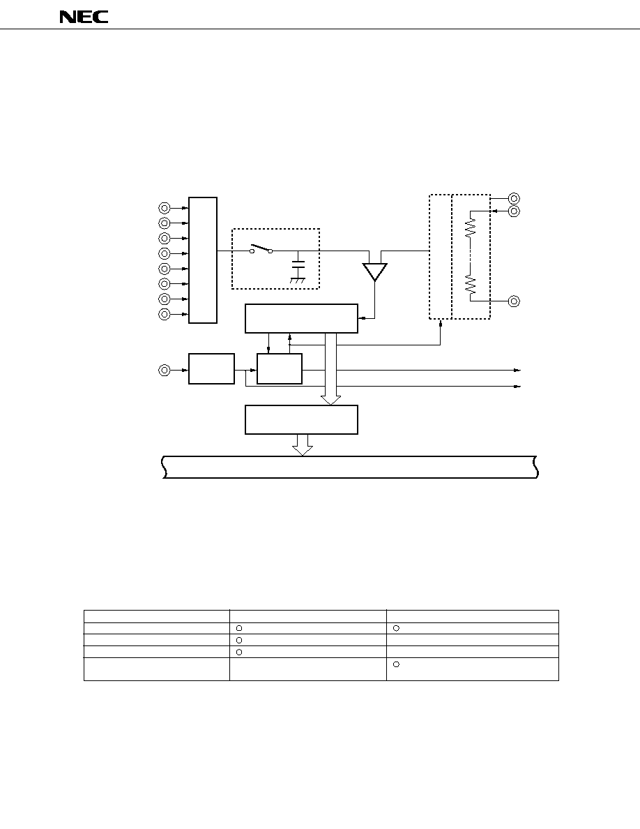
2.
BLOCK DIAGRAM
TO0/P30
16-bit TIMER/
EVENT COUNTER
TI00/INTP0/P00
TI01/INTP1/P01
TO1/P31
8-bit TIMER/
EVENT COUNTER 1
TI1/P33
TO2/P32
8-bit TIMER/
EVENT COUNTER 2
TI2/P34
WATCHDOG TIMER
WATCH TIMER
SI0/SB0/P25
SERIAL
INTERFACE 0
SO0/SB1/P26
SCK0/P27
SI2/RxD/P70
SERIAL
INTERFACE 2
SO2/TxD/P71
SCK2/ASCK/P72
AV
DD
A/D CONVERTER
AV
SS
AV
REF
ANI0/P10-
ANI7/P17
INTERRUPT
CONTROL
INTP0/P00-
INTP5/P05
BUZZER OUTPUT
BUZ/P36
CLOCK OUTPUT
CONTROL
PCL/P35
P00
PORT0
P01-P05
P07
PORT1
P10-P17
PORT11
P110-P117
PORT2
P25-P27
PORT3
P30-P37
PORT7
P70-P72
PORT8
P80-P87
PORT9
P90-P97
PORT10
P100-P103
LCD
CONTROLLER/
DRIVER
S0-S23
BIAS
f
LCD
RESET
X1
X2
XT1/P07
XT2
78K/0
CPU CORE
ROM
RAM
SYSTEM
CONTROL
V
DD
V
SS
IC
S24/P97-
S31/P90
S32/P87-
S39/P80
COM0-COM3
V
LC0
-V
LC2
Remark
The internal ROM and RAM capacities differ depending on the product.
11
µ
PD78062(A), 78063(A), 78064(A)
3.
PIN FUNCTIONS
3.1
Port Pins (1/2)
Dual-
Function Pin
Pin Name
I/O
Input only
Port 1
8-bit input/output port.
Input/output can be specified bit-wise.
When used as an input port, on-chip pull-up resistor can be used in
software.
Note2
Input
TO0
TO1
TO2
TI1
TI2
PCL
BUZ
----
SI2/RxD
SO2/TxD
SCK2/
ASCK
P25
P26
P27
P30
P31
P32
P33
P34
P35
P36
P37
Port 7
3-bit input/output port.
Input/output can be specified bit-wise.
When used as an input port, on-chip pull-up resistor can be used in
software.
P00
P01
P02
P03
P04
P05
P07
Note1
P10 to P17
Input
Input only
Input
INTP0/TI00
INTP1/TI01
INTP2
INTP3
INTP4
INTP5
XT1
ANI0 to
ANI7
Input
P70
P71
P72
Function
After Reset
Input
Input
Input
Input
Input
Port 3
8-bit input/output port.
Input/output can be specified bit-wise.
When used as an input port, on-chip pull-up resistor can be used in
software.
Input/
output
Input/
output
Port 2
3-bit input/output port.
Input/output can be specified bit-wise.
When used as an input port, on-chip pull-up resistor can be used in
software.
Input/
output
Input/
output
Input/output can be specified bit-wise.
When used as an input port, on-chip pull-up
resistor can be used in software.
Port 0
7-bit I/O port.
Input/
output
Notes 1.
When using the P07/XT1 pins as an input port, set (1) bit 6 (FRC) of the processor clock control register (PCC)
(the on-chip feedback resistor of the subsystem clock oscillator should not be used).
2.
When using the P10/ANI0 to P17/ANI7 pins as the A/D converter analog input, port 1 is set to input mode.
However, on-chip pull-up resistor is not automatically used.
SO0/SB1
SI0/SB0
SCK0
12
µ
PD78062(A), 78063(A), 78064(A)
3.1
Port Pins (2/2)
Dual-
Function Pin
Pin Name
I/O
Port 8
8-bit input/output port
Input/output can be specified bit-wise.
When used as an input port , on-chip pull-up resistor can be used in
software.
Input/output port/segment signal output function can be specified in 2-bit
unit by the LCD control register (LCDC).
After Reset
Port 10
4-bit input/output port
Input/output can be specified bit-wise.
When used as an input port, on-chip pull-up resistor can be used in
software.
LED direct drive capability.
Port 11
8-bit input/output port
Input/output can be specified bit-wise.
When used as an input port, on-chip pull-up resistor can be used in
software.
Falling edge detection capability.
Port 9
8-bit input/output port
Input/output can be specified bit-wise.
When used as an input port, on-chip pull-up resistor can be used in
software.
Input/output port/segment signal output function can be specified in 2-bit
unit by the LCD control register (LCDC).
Function
P80 to P87
Input/
output
Input
S39 to S32
S31 to S24
Input
Input/
output
P90 to P97
Input/
output
P100 to
P103
Input
Input/
output
P110 to
P117
Input

13
µ
PD78062(A), 78063(A), 78064(A)
3.2
Other Pins (1/2)
INTP0
INTP1
INTP2
INTP3
INTP4
INTP5
SI0
SI2
SO0
SO2
SB0
SB1
SCK0
SCK2
RxD
TxD
ASCK
TI00
TI01
TI1
TI2
TO0
TO1
TO2
PCL
BUZ
S0 to S23
S24 to S31
S32 to S39
COM0 to COM3
V
LC0
to V
LC2
BIAS
P00/TI00
P01/TI01
P02
P03
P04
P05
P25/SB0
P70/RxD
P26/SB1
P71/TxD
P25/SI0
P26/SO0
P27
P72/ASCK
P70/SI2
P71/SO2
P72/SCK2
P00/INTP0
P01/INTP1
P33
P34
P30
P31
P32
P35
P36
P97 to P90
P87 to P80
Dual-
Function Pin
Pin Name
I/O
Function
After Reset
Input
Output
Serial interface serial data output.
Input
Serial interface serial data input.
External interrupt request input by which the effective edge (rising
edge, falling edge, or both rising edge and falling edge) can be
specified.
Serial interface serial data input/output.
Input
/output
Input
Output
Input
Input
Input
/output
Serial interface serial clock input/output.
Output
Output
Output
Output
Output
Asynchronous serial interface serial data input.
Asynchronous serial interface serial data output.
Asynchronous serial interface serial clock input.
External count clock input to 16-bit timer (TM0).
Capture trigger signal input to capture register (CR00).
External count clock input to 8-bit timer (TM1).
External count clock input to 8-bit timer (TM2).
16-bit timer (TM0) output (shared with 14-bit PWM output).
Input
Input
Input
Input
Input
Input
Input
Input
Input
Input
Input
Input
Output
Input
Output
Clock output (for main system clock, subsystem clock trimming).
Buzzer output.
LCD controller/driver segment signal output.
LCD controller/driver common signal output.
LCD drive voltage. Split resistors can be incorporated by mask option.
LCD drive power supply.
8-bit timer (TM1) output.
8-bit timer (TM2) output.
14
µ
PD78062(A), 78063(A), 78064(A)
3.2
Other Pins (2/2)
A/D converter analog input.
A/D converter reference voltage input.
A/D converter analog power supply. Connect to V
DD
.
A/D converter ground potential. Connect to V
SS
.
System reset input.
Main system clock oscillation crystal connection.
Subsystem clock oscillation crystal connection.
Positive power supply.
Ground potential.
Internal connection. Connect directly to V
SS
pin.
Pin Name
I/O
ANI0 to ANI7
AV
REF
AV
DD
AV
SS
RESET
X1
X2
XT1
XT2
V
DD
V
SS
IC
Input
Function
After Reset
Dual-
Function Pin
----
----
----
----
----
----
P10 to P17
----
----
----
----
----
----
P07
----
----
----
----
----
----
----
----
Input
3.3
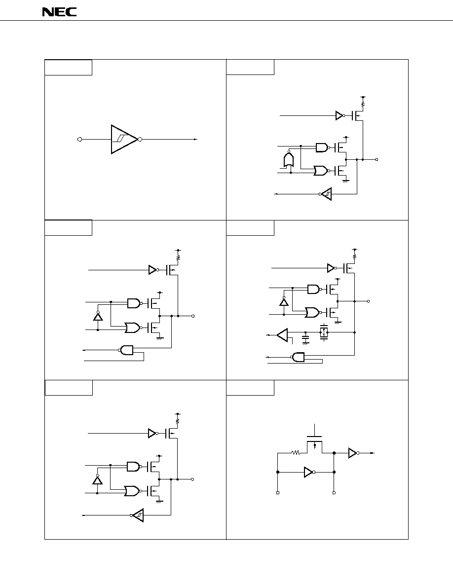
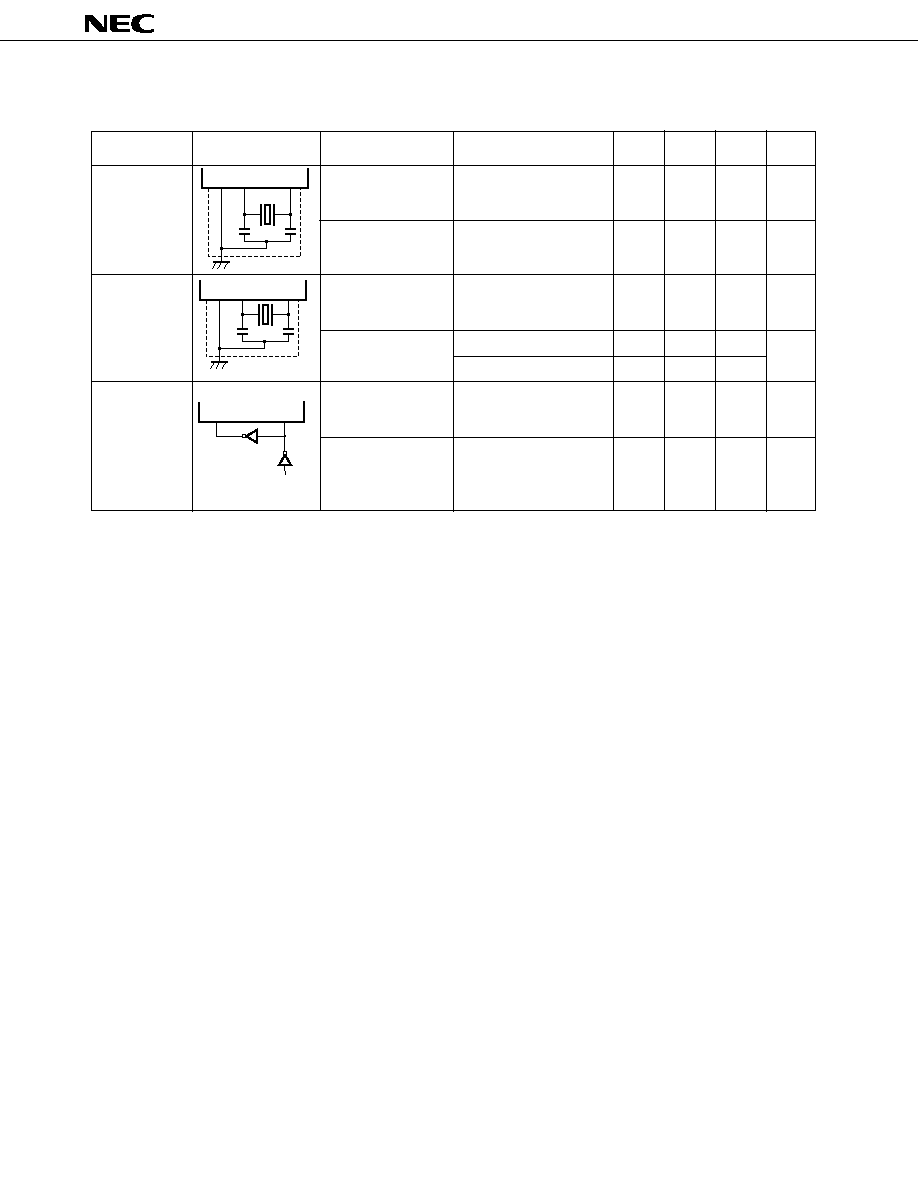
Pin I/O Circuits and Recommended Connection of Unused Pins
The input/output circuit type of each pin and recommended connection of unused pins are shown in Table 3-1.
For the input/output circuit configuration of each type, refer to Figure 3-1.
Table 3-1. Input/Output Circuit Type of Each Pin (1/2)
P00/INTP0/TI00
P01/INTP1/TI01
P02/INTP2
P03/INTP3
P04/INTP4
P05/INTP5
P07/XT1
P10/ANI0 to P17/ANI7
P25/SI0/SB0
P26/SO0/SB1
P27/SCK0
P30/TO0
P31/TO1
P32/TO2
Connected to V
SS
.
Connected to V
DD
.
Input
Input/output
Input
Input/output
2
8-A
16
11
10-A
5-A
Pin Name
I/O
Recommended Connection when not Used
Input/output
Circuit Type
Input
Input
Input
Input
Input
Independently connected to V
DD
or V
SS
through resistor.
Independently connected to V
SS
through resistor.
15
µ
PD78062(A), 78063(A), 78064(A)
I/O
Recommended Connection when not Used
Pin Name
Input/output
Circuit Type
8-A
5-A
8-A
5-A
8-A
17-A
5-A
8-A
17
18
----
2
16
----
Table 3-1. Input/Output Circuit Type of Each Pin (2/2)
P33/TI1
P34/TI2
P35/PCL
P36/BUZ
P37
P70/SI2/RxD
P71/SO2/TxD
P72/SCK2/ASCK
P80/S39 to P87/S32
P90/S31 to P97/S24
P100 to P103
P110 to P117
S0 to S23
COM0 to COM3
V
LC0
to V
LC2
BIAS
RESET
XT2
AV
REF
AV
DD
AV
SS
IC
Leave open.
----
Leave open.
Connected to V
SS
.
Connected to V
DD
.
Connected to V
SS
.
Connected directly to V
SS
.
Output
----
Input
----
Independently connected to V
DD
or V
SS
through resistor.
Input/output
Independently connected to V
DD
through resistor.
16
µ
PD78062(A), 78063(A), 78064(A)
IN
Type 2
Type 5-A
Type 8-A
Type 11
Type 16
Type 10-A
Schmitt-Triggered Input with Hysteresis Characteristic
pull-up
enable
data
output
disable
P-ch
IN/OUT
V
DD
V
DD
P-ch
N-ch
pull-up
enable
data
output
disable
input
enable
P-ch
IN/OUT
V
DD
V
DD
P-ch
N-ch
Figure 3-1. Pin Input/Output Circuits (1/2)
pull-up
enable
data
output disable
P-ch
IN/OUT
V
DD
V
DD
P-ch
N-ch
open drain
pull-up
enable
data
output
disable
input
enable
P-ch
IN/OUT
V
DD
V
DD
P-ch
N-ch
N-ch
V
REF
+
≠
P-ch
(Threshold Voltage)
Comparator
feedback cut-off
P-ch
XT1
XT2
17
µ
PD78062(A), 78063(A), 78064(A)
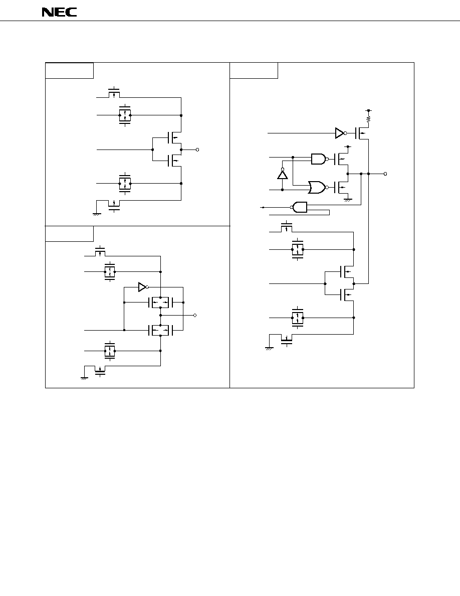
Figure 3-1. Pin Input/Output Circuits (2/2)
Type 17
Type 18
Type 17-A
OUT
P-ch
N-ch
P-ch
N-ch
P-ch
N-ch
V
LC0
V
LC1
V
LC2
SEG
data
P-ch
N-ch
P-ch
N-ch
P-ch
N-ch
V
LC0
V
LC1
V
LC2
COM
data
N-ch
P-ch
OUT
pull-up
enable
data
output
disable
input
enable
P-ch
IN/OUT
V
DD
V
DD
P-ch
N-ch
P-ch
N-ch
P-ch
N-ch
P-ch
N-ch
V
LC0
V
LC1
V
LC2
SEG
data
18
µ
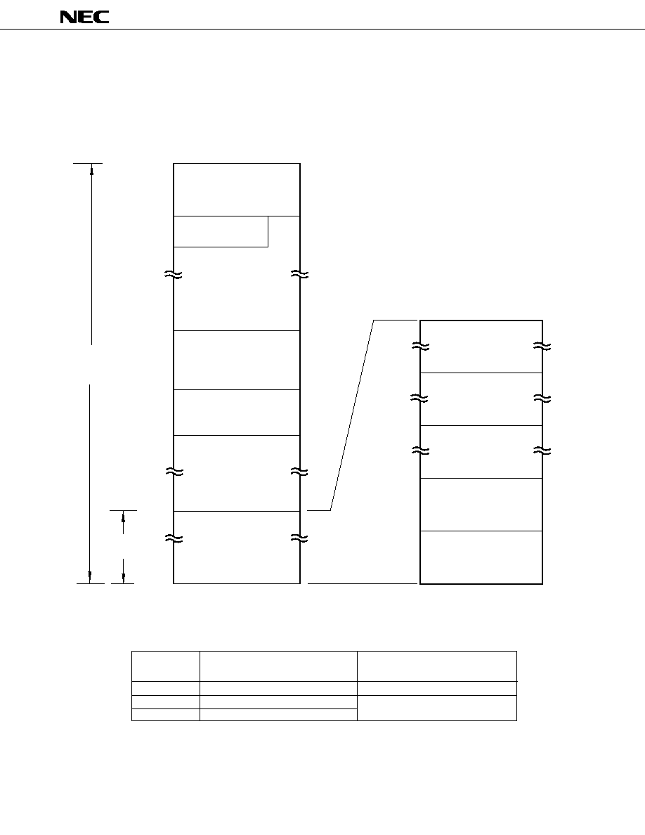
PD78062(A), 78063(A), 78064(A)
µ
PD78062(A)
3FFFH
FD00H
µ
PD78063(A)
5FFFH
µ
PD78064(A)
7FFFH
4.
MEMORY SPACE
The memory map of
µ
PD78062(A)/78063(A)/78064(A) is shown in Figure 4-1.
Figure 4-1. Memory Map
Note
The Internal ROM and Internal High-Speed RAM capacities differ depending on the product. (refer to the following
table.)
FB00H
Last Address of Internal ROM
Start Address of Internal High-Speed RAM
nnnnH
mmmmH
Product Name
FFFFH
FF00H
FEFFH
mmmmH
mmmmH-1
FEE0H
FA80H
FA7FH
FA58H
FA57H
nnnnH+1
nnnnH
0000H
nnnnH
0FFFH
0800H
07FFH
0080H
007FH
0040H
003FH
0000H
Use Prohibited
Use Prohibited
Program Area
CALLF Entry Area
Program Area
CALLT Table Area
Vector Table Area
General Registers
32
◊
8 Bits
Internal High-Speed RAM
Note
LCD Display RAM
40
◊
4 Bits
Program
Memory
Space
Data Memory
Space
Special Function Register (SFR)
256
◊
8 Bits
1000H
Internal ROM
Note
19
4
µ
PD78062(A), 78063(A), 78064(A)
5.
PERIPHERAL HARDWARE FUNCTION FEATURE
5.1
Port
There are two kinds of I/O port.
∑
CMOS input (P00, P07)
: 2
∑
CMOS input/output (P01 to P05, Port 1 to 3, 7 to 11)
: 55
Total
: 57
Table 5-1. Functions of Ports
Function
Name
Pin Name
Dedicated input port
Input/output port. Input/output specifiable bit-wise.
When used as input port, on-chip pull-up resistor can be used in software .
Input/output port. Input/output specifialbe bit-wise.
When used as input port, on-chip pull-up resistor can be used in software .
Input/output port. Input/output specifiable bit-wise.
When used as input port, on-chip pull-up resistor can be used in software .
Input/output port. Input/output specifiable bit-wise.
When used as input port, on-chip pull-up resistor can be used in software.
Input/output port. Input/output specifiable bit-wise.
When used as input port, on-chip pull-up resistor can be used in software.
Input/output port. Input/output specifiable bit-wise.
When used as input port, on-chip pull-up resistor can be used in software.
Input/output port/segment signal output function specifiable in 2-bit units by LCD control
register (LCDC).
Input/output port. Input/output specifiable bit-wise.
When used as input port, on-chip pull-up resistor can be used in software.
Input/output port/segment signal output function specifiable in 2-bit units by LCD control
register (LCDC).
Input/output port. Input/output specifiable bit-wise.
When used as input port, on-chip pull-up resistor can be used in software.
Direct LED drive capability.
Input/output port. Input/output specifiable bit-wise.
When used as input port, on-chip pull-up resistor can be used in software.
Test flag (KRIF) is set to 1 by falling edge detection.
Port 0
Port 1
Port 2
Port 3
Port 7
Port 8
Port 9
Port 10
Port 11
P00, P07
P01 to P05
P10 to P17
P25 to P27
P30 to P37
P70 to P72
P80 to P87
P90 to P97
P100 to P103
P110 to P117
20
µ
PD78062(A), 78063(A), 78064(A)
Interval timer
1 channel
2 channels
1 channel
1 channel
External event counter
1 channel
2 channels
≠
≠
Timer output
1 output
2 outputs
≠
≠
PWM output
1 output
≠
≠
≠
Pulse width measurement
2 inputs
≠
≠
≠
Square wave output
1 output
2 outputs
≠
≠
One-shot pulse output
1 output
≠
≠
≠
Interrupt request
2
2
2
1
Test input
≠
≠
1 input
≠
5.2
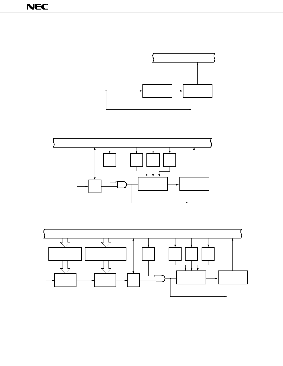
Clock Generator
There are two kinds of clocks, main system clock and subsystem clock.
The minimum instruction execution time can also be changed.
∑
0.4
µ
s/0.8
µ
s/1.6
µ
s/3.2
µ
s/6.4
µ
s/12.8
µ
s (main system clock: in 5.0 MHz operation)
∑
122
µ
s (subsystem clock: in 32.768 kHz operation)
Figure 5-1. Clock Generator Block Diagram
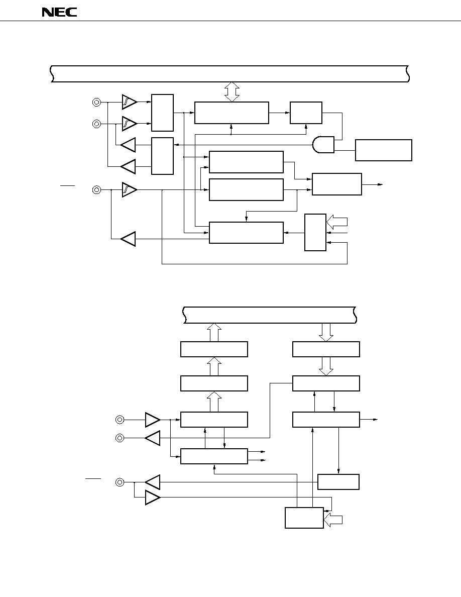
5.3
Timer/Event Counter
Five timer/event counter channels are incorporated.
∑
16-bit timer/event counter
: 1 channel
∑
8-bit timer/event counter
: 2 channels
∑
Watch timer
: 1 channel
∑
Watchdog timer
: 1 channel
Table 5-2. Timer/Event Counter Types and Functions
16-bit Timer/
Event Counter
8-bit Timer/
Event Counter
Watch Timer
Watchdog Timer
Type
Function
X1
X2
XT1/P07
XT2
f
XT
f
XX
2
f
XX
2
2
f
XX
2
3
f
XX
2
4
f
XT
2
f
X
2
STOP
f
X
CPU
Clock
(f
CPU
)
Subsystem
Clock
Oscillator
Main
System
Clock
Oscillator
Scaler
Selec-
tor
Prescaler
Prescaler
Standby
Control
Circuit
Selec-
tor
Watch Timer
Clock Output Function
Clock to
Peripheral
Hardware
To INTP0
Sampling Clock
f
XX
1/2
21
4
µ
PD78062(A), 78063(A), 78064(A)
Figure 5-2. 16-Bit Timer/Event Counter Block Diagram
Figure 5-3. 8-Bit Timer/Event Counter Block Diagram
TI01/P01/INTP1
Watch Timer Output
TI00/P00/INTP0
2f
XX
f
XX
f
XX
/2
f
XX
/2
2
INTP0
INTTM01
INTP1
INTTM00
TO0/P30
Internal Bus
Selec-
tor
16-Bit
Capture/Compare
Register (CR00)
Match
Match
PWM
Pulse
Output
Control
Circuit
Output
Control Circuit
Edge
Detector
16-Bit
Timer Register
(TM0)
Clear
16-Bit
Capture/Compare
Register
(CR01)
Internal Bus
Selec-
tor
Selector
INTTM1
TO2/P32
INTTM2
TO1/P31
f
XX
/2-f
XX
/2
9
f
XX
/2
11
TI1/P33
TI2/P34
f
XX
/2-f
XX
/2
9
f
XX
/2
11
Internal Bus
8-Bit
Compare
Register (CR10)
Match
Match
Selec-
tor
8-Bit
Timer Register 1
(TM1)
Clear
Selec-
tor
Selector
8-Bit
Compare Register
(CR20)
8-Bit
Timer Register 2
(TM2)
Clear
Selec-
tor
Output
Control
Circuit
Output
Control
Circuit
Internal Bus
Selec-
tor
22
µ
PD78062(A), 78063(A), 78064(A)
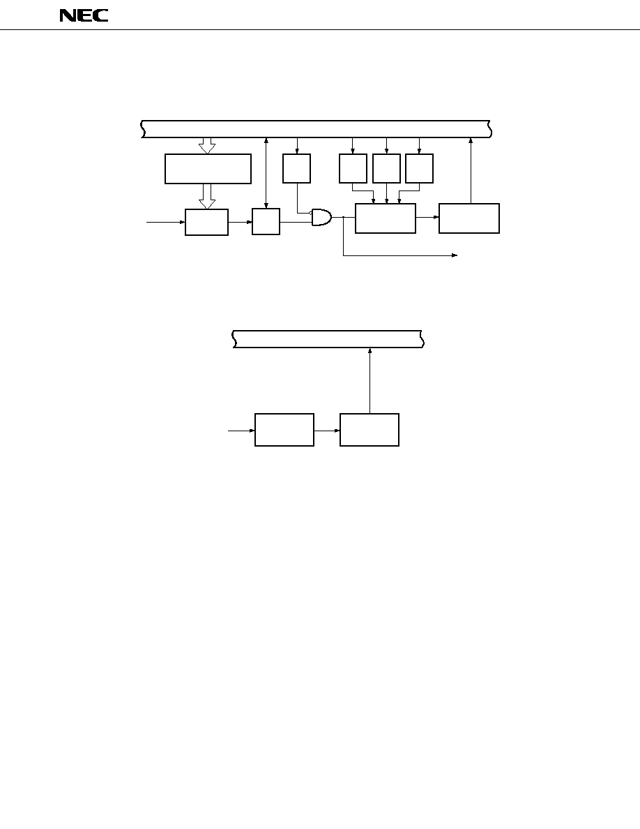
Figure 5-4. Watch Timer Block Diagram
Figure 5-5. Watchdog Timer Block Diagram
f
W
2
4
f
W
2
5
f
W
2
6
f
W
2
7
f
W
2
8
f
W
2
9
f
XX
/2
7
f
XT
f
W
f
W
2
14
f
W
2
13
INTWT
INTTM3
Selec-
tor
Prescaler
5-Bit Counter
Selector
Selector
Selector
To 16-Bit
Timer/Event Counter
To LCD
Controller/Driver
f
XX
2
6
f
XX
2
7
f
XX
2
8
f
XX
2
9
f
XX
2
11
f
XX
2
5
f
XX
2
4
f
XX
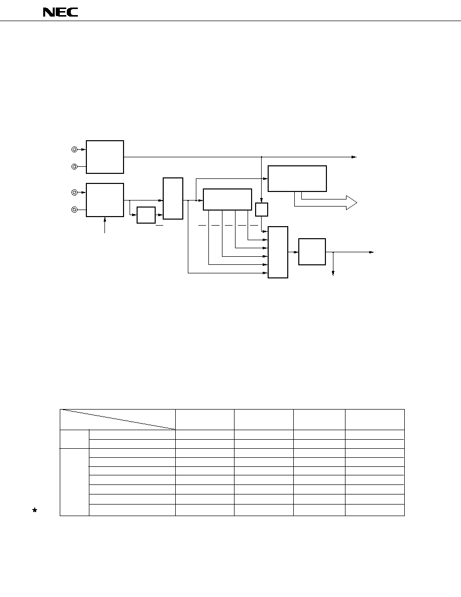
2
3
RESET
INTWDT
Non-Maskable
Interrupt
Request
INTWDT
Maskable
Interrupt
Request
Prescaler
Selector
8-Bit Counter
Control
Circuit
23
4
µ
PD78062(A), 78063(A), 78064(A)
5.4
Clock Output Control Circuit
Clocks of the following frequency can be output as clock outputs.
∑
19.5 kHz/39.1kHz/78.1 kHz/156 kHz/313 kHz/625 kHz/1.25 MHz/2.5 MHz/5.0 MHz (main system clock: in 5.0
kHz operation)
∑
32.768 kHz (subsystem clock: in 32.768 kHz operation)
Figure 5-6. Clock Output Circuit Block Diagram
5.5
Buzzer Output Control Circuit
Clocks of the following frequency can be output as buzzer outputs.
∑
1.2 kHz/2.4 kHz/4.9 kHz/9.8 kHz (main system clock : in 5.0 MHz operation)
Figure 5-7. Buzzer Output Control Circuit Block Diagram
PCL/P35
f
XX
/2
2
f
XX
/2
3
f
XX
/2
4
f
XX
/2
5
f
XX
/2
6
f
XX
/2
7
f
XT
Selector
Synchronization
Circuit
f
XX
/2
f
XX
Output Control Circuit
BUZ/P36
Selector
f
XX
/2
9
f
XX
/2
10
f
XX
/2
11
Output Control Circuit
24
µ
PD78062(A), 78063(A), 78064(A)
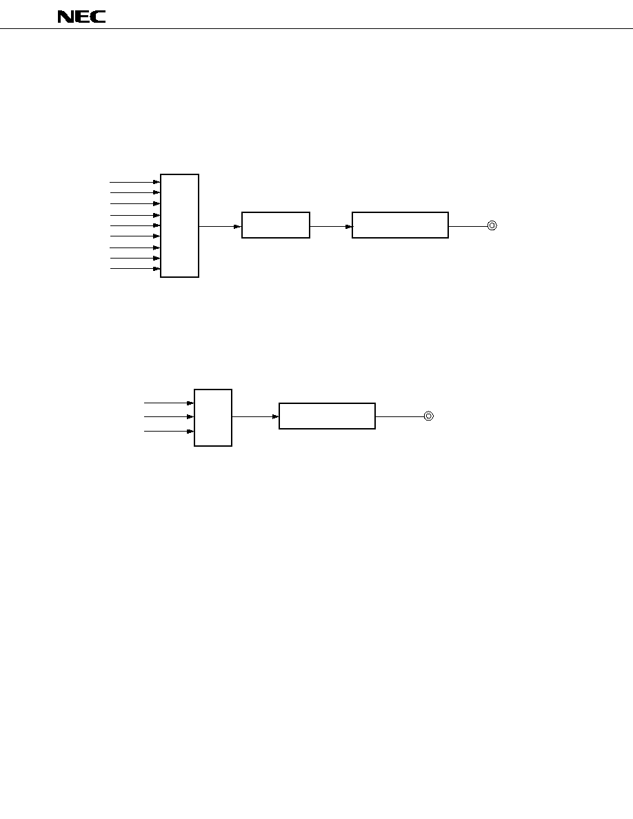
5.6
A/D Converter
Eight 8-bit resolution A/D converter channels are incorporated.
The following two types of start-up method are available.
∑
Hardware start
∑
Software start
Figure 5-8. A/D Converter Block Diagram
5.7
Serial Interface
Two clocked serial interface channels are incorporated.
∑
Serial interface channel 0
∑
Serial interface channel 2
Table 5-3. Serial Interface Channel Block Diagram
3-wire serial I/O mode
(MSB/LSB-first switchable)
(MSB/LSB-first switchable)
SBI (serial bus interface) mode
(MSB-first)
----
2-wire serial I/O mode
(MSB-first)
----
Asynchronous serial interface
(Dedicated baud rate generator
(UART) mode
incorpoorated)
Function
Serial Interface Channel 0
Serial Interface Channel 2
----
ANI0/P10
ANI1/P11
ANI2/P12
ANI3/P13
ANI4/P14
ANI5/P15
ANI6/P16
ANI7/P17
AV
DD
AV
REF
AV
SS
INTAD
INTP3
Selec-
tor
Sample & Hold Circuit
INTP3/P03
Voltage Comparator
Series Resistor String
Tap
Selec-
tor
Successive Approximation
Register (SAR)
Control
Circuit
Edge
Detector
A/D Conversion Result
Register (ADCR)
Internal Bus
25
4
µ
PD78062(A), 78063(A), 78064(A)
Figure 5-9. Serial Interface Channel 0 Block Diagram
Figure 5-10. Serial Interface Channel 2 Block Diagram
R
X
D/SI2/P70
T
X
D/SO2/P71
ASCK/SCK2/P72
INTSER
INTSR/INTCSI2
f
XX
-f
XX
/2
10
INTST
Receive Buffer
Register (RXB/SIO2)
Direction
Control Circuit
Receive Shift
Register (RXS)
Direction
Control Circuit
Transmit Shift
Register (TXS/SIO2)
Transmit
Control Circuit
Receive
Control Circuit
SCK Output
Control Circuit
Baud Rate
Generator
Internal bus
SI0/SB0/P25
SO0/SB1/P26
SCK0/P27
INTCSI0
TO2
f
XX
/2-f
XX
/2
8
Internal Bus
Selector
Selector
Serial I/O
Shift Register 0 (SIO0)
Output
Latch
Busy/Acknowledge
Output Circuit
Bus Release/Command/
Acknowledge Detector
Serial Clock Counter
Interrupt Request
Signal Generator
Serial Clock Control Circuit
Selector
26
µ
PD78062(A), 78063(A), 78064(A)
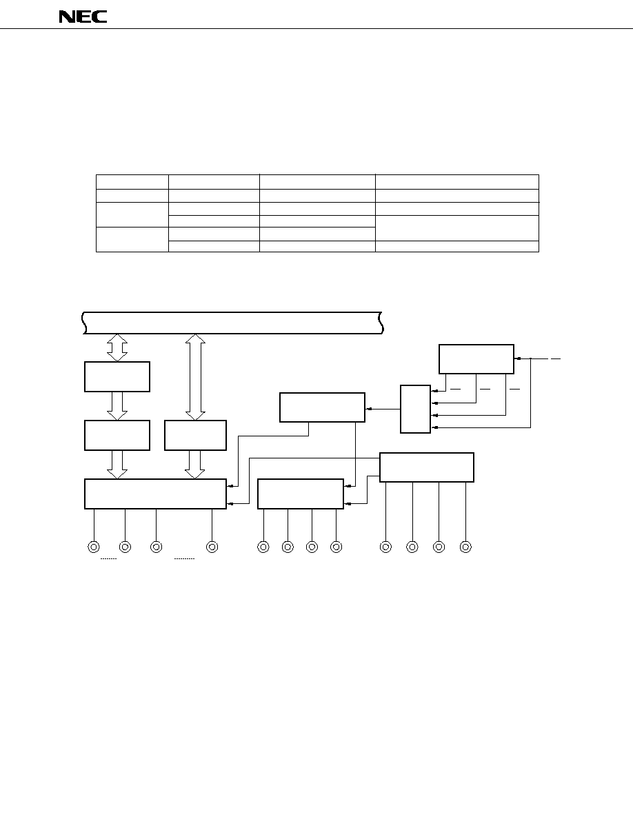
5.8
LCD Controller/Driver
An LCD controller/driver with the following functions is incorporated.
∑
Selection of 5 types of display mode
∑
16 of the segment signal of outputs can be switched to input/output ports in units of 2.
(P80/S39 to P87/S32, P90/S31 to P97/S24)
Table 5-4. Display Mode Types and Maximum Number of Display Pixels
Bias Method
Time Multiplexing
Common Signal Used
Maximum Number of Display Pixels
----
Static
COM0 (COM1 to COM3)
40 (40 segments
◊
1 common)
2
COM0, COM1
80 (40 segments
◊
2 commons)
3
COM0 to COM2
3
COM0 to COM2
4
COM0 to COM3
160 (40 segments
◊
4 commons)
1/2
1/3
120 (40 segments
◊
3 commons)
Figure 5-11. LCD Controller/Driver Block Diagram
V
LC2
V
LC1
V
LC0
BIAS
COM3
COM2
COM1
COM0
S39/P80
S0
S23
S24/P97
LCDCL
f
W
2
9
f
W
2
8
f
W
2
7
f
W
2
6
Internal Bus
Display
Data Memory
Segment
Data Selector
Port
Output Data
Segment Driver
Prescaler
Selector
Timing Controller
LCD Drive Voltage
Generator
Common Driver

27
µ
PD78062(A), 78063(A), 78064(A)
6.
INTERRUPT FUNCTIONS AND TEST FUNCTIONS
6.1
Interrupt Functions
The following three types, 20 sources of interrupt functions are available:
∑
Non-maskable : 1
∑
Maskable
: 18
∑
Software
: 1
28
µ
PD78062(A), 78063(A), 78064(A)
Table 6-1. Interrupt Source List
Interrupt Source
Name
Interrupt
Type
Default
Priority
Note1
Internal/
External
Vector
Table
Address
Basic Con-
figuration
Type
Note2
Watchdog timer overflow (with watchdog timer
mode 1 selected)
Watchdog timer overflow (with interval timer
mode selected)
Pin input edge detection
Serial interface channel 0 transfer termination
Serial interface channel 2 UART reception
error generation
Serial interface channel 2 UART reception
termination
Serial interface channel 2 3-wire transfer
termination
Serial interface channel 2 UART transmission
termination
Reference time interval signal from watch
timer
16-bit timer register and capture/compare
register (CR00) match signal generation
16-bit timer register and capture/compare
register (CR01) match signal generation
8-bit timer/event counter 1 match signal
generation
8-bit timer/event counter 2 match signal
generation
A/D converter conversion termination
BRK instruction execution
INTWDT
INTWDT
INTP0
INTP1
INTP2
INTP3
INTP4
INTP5
INTCSI0
INTSER
INTSR
INTCSI2
INTST
INTTM3
INTTM00
INTTM01
INTTM1
INTTM2
INTAD
BRK
Trigger
(A)
(B)
Internal
0004H
0006H
0008H
000AH
000CH
000EH
0010H
0014H
0018H
001AH
001CH
001EH
0020H
0022H
0024H
0026H
0028H
003EH
(C)
(D)
External
Internal
(B)
----
(E)
1
2
3
4
5
6
7
8
9
10
11
12
13
14
15
16
----
----
0
Maskable
Software
Notes 1.
Default priority is a priority order when more than one maskable interrupt request is generated simultaneously.
0 is the highest and 16 the lowest.
2.
Basic configuration types (A) to (E) correspond to those shown in Figure 6-1.
Non-
maskable
29
µ
PD78062(A), 78063(A), 78064(A)
Figure 6-1. Basic Configuration of Interrupt Functions (1/2)
(A) Internal non-maskable interrupt
Interrupt
Request
Standby Release
Signal
Internal Bus
Vector Table
Address
Generator
Priority
Control
Circuit
(B) Intrnal maskable interrupt
MK
IE
PR
ISP
IF
Interrupt
Request
Internal Bus
Priority
Control
Circuit
Vector Table
Address
Generator
Standby Release
Signal
(C) External maskable interrupt (INTP0)
Sampling Clock
Select Register
(SCS)
IF
IE
PR
ISP
External Interrupt
Mode Register
(INTM0)
Sampling
Clock
Edge
Detector
Interrupt
Request
Internal Bus
MK
Priority
Control
Circuit
Vector Table
Address
Generator
Standby
Release
Signal
30
µ
PD78062(A), 78063(A), 78064(A)
Figure 6-1. Basic Configuration of Interrupt Functions (2/2)
(D) External maskable interrupt (except INTP0)
IF
Internal Bus
Interrupt
Request
Edge
Detector
Vector Table
Address
Generator
Standby
Release
Signal
External Interrupt
Mode Register
(INTM0, INTM1)
MK
IE
PR
ISP
Priority Control
Circuit
(E) Software interrupt
Internal Bus
Interrupt
Request
Vector Table
Address
Generator
Priority
Control
Circuit
IF
: Interrupt request flag
IE
: Interrupt enable flag
ISP : In-service priority flag
MK : Interrupt mask flag
PR : Priority specification flag
31
µ
PD78062(A), 78063(A), 78064(A)
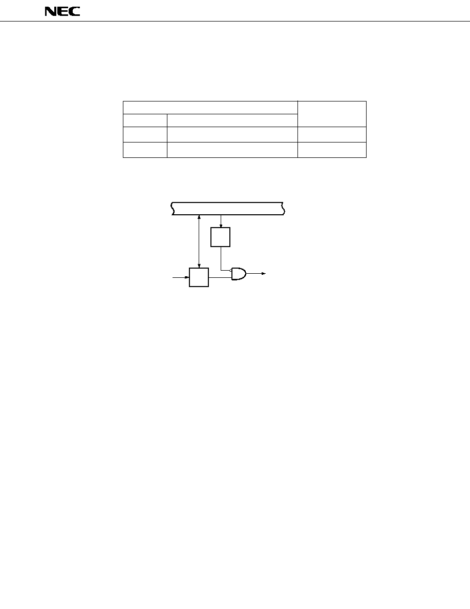
6.2
Test Functions
There are two sources of test functions as shown in Table 6-2.
Table 6-2. Test Input Source List
Figure 6-2. Basic Configuration of Test Function
IF
: Test input flag
MK : Test mask flag
Test Input Source
Name
Trigger
Internal/External
INTWT
Watch timer overflow
Internal
INTPT11
Port 11 falling edge detection
External
MK
IF
Internal Bus
Standby Release
Signal
Test Input
Signal
32
µ
PD78062(A), 78063(A), 78064(A)
7.
STANDBY FUNCTION
The standby function is a function to reduce the consumption current and there are the following two kinds of standby
functions.
q
HALT mode : Halts CPU operating clock and can reduce average consumption current by the intermittent operation
along with the normal operation.
q
STOP mode : Halts main system clock oscillation. Halts all operations with the main system clock and sets ultra-low
consumption current state with subsystem clock only.
Figure 7-1. Standby Function
Note
Halting the main system clock enables the consumption current to be reduced.
When the CPU is operated by the subsystem clock, the main system clock should be halted by setting the bit 7 (MCC)
of the processor clock control register (PCC).
The STOP instruction is not available.
Caution When the main system clock is stopped and the system is operated by the subsystem clock, the main
system clock should be returned to after securing the oscillation stabilization time in software.
8.
RESET FUNCTION
There are the following two kinds of resetting methods.
∑
External reset by RESET pin.
∑
Internal reset by watchdog timer hung-up time detection.
CSS=1
CSS=0
Main System Clock Operation
Interrupt
Request
STOP Mode
Main System Clock
Oscillation Halted
STOP
Instruction
(
)
Interrupt
Request
HALT Instruction
HALT Mode
Clock Supply to CPU Halted,
Oscillation Maintained
(
)
Subsystem Clock Operation
Note
HALT Instruction
Interrupt
Request
HALT Mode
Note
Clock Supply to CPU Halted,
Oscillation Maintained
(
)
33
µ
PD78062(A), 78063(A), 78064(A)
9.
INSTRUCTION SET
(1) 8-bit instruction
MOV, XCH, ADD, ADDC, SUB, SUBS, AND, OR, XOR, CMP, MULU, DIVUW, INC, DEC, ROR, ROL, RORC, ROLC,
ROR4, ROL4, PUSH, POP, DBNZ
#byte
A
r
Note
sfr
saddr
!addr16
PSW
[DE]
[HL]
$addr16
1
None
2nd operand
1st operand
ADD
ADDC
SUB
SUBC
AND
OR
XOR
CMP
MOV
MOV
MOV
ADD
ADDC
SUB
SUBC
AND
OR
XOR
CMP
MOV
MOV
ADD
ADDC
SUB
SUBC
AND
OR
XOR
CMP
MOV
MOV
MOV
MOV
MOV
MOV
MOV
MOV
XCH
MOV
XCH
ADD
ADDC
SUB
SUBC
AND
OR
XOR
CMP
MOV
XCH
ADD
ADDC
SUB
SUBC
AND
OR
XOR
CMP
MOV
XCH
ADD
ADDC
SUB
SUBC
AND
OR
XOR
CMP
MOV
MOV
XCH
MOV
XCH
ADD
ADDC
SUB
SUBC
AND
OR
XOR
CMP
MOV
XCH
ADD
ADDC
SUB
SUBC
AND
OR
XOR
CMP
[HL+byte]
[HL+B]
[HL+C]
ROR
ROL
RORC
ROLC
INC
DEC
INC
DEC
PUSH
POP
ROR4
ROL4
MULU
DIVUW
DBNZ
DBNZ
A
r
B, C
sfr
saddr
!addr16
PSW
[DE]
[HL]
[HL+byte]
[HL+B]
[HL+C]
X
C
Note Except r = A
34
µ
PD78062(A), 78063(A), 78064(A)
2nd operand
1st operand
#word
AX
rp
Note
sfrp
saddrp
!addr16
SP
None
A
rp
sfrp
saddrp
!addr16
SP
ADDW
SUBW
CMPW
MOVW
MOVW
MOVW
MOVW
MOVW
Note
MOVW
MOVW
MOVW
MOVW
MOVW
MOVW
MOVW
MOVW
INCW, DECW
PUSH, POP
MOVW
XCHW
Note Only when rp=BC, DE, HL
(3) Bit manipulation instruction
MOV1, AND1, OR1, XOR1, SET1, CLR1, NOT1, BT, BF, BTCLR
2nd operand
1st operand
A.bit
sfr.bit
saddr.bit
PSW.bits
[HL].bit
CY
$addr16
None
A.bit
sfr.bit
saddr.bit
PSW.bit
[HL].bit
CY
MOV1
AND1
OR1
XOR1
MOV1
AND1
OR1
XOR1
MOV1
AND1
OR1
XOR1
MOV1
AND1
OR1
XOR1
BT, BF,
BTCLR
DBNZ
CALLT
CALLF
CALL
BR
BR
Basic instruction
Compound
Instruction
(5) Other instructions
ADJBA, ADJBS, BRK, RET, RETI, RETB, SEL, NOP, EI, DI, HALT, STOP
(2) 16-bit instruction
MOVW, XCHW, ADDW, SUBW, CMPW, PUSH, POP, INCW, DECW
(4) Call instruction/branch instruction
CALL, CALLF, CALLT, BR, BC, BNC, BZ, BNZ, BT, BF, BTCLR, DNZB
BR, BC, BNC,
BZ, BNZ
2nd Operand
1st Operand
AX
!addr16
!addr11
[addr5]
$addr16
MOV1
MOV1
MOV1
MOV1
MOV1
SET1
CLR1
SET1
CLR1
SET1
CLR1
SET1
CLR1
SET1
CLR1
SET1
CLR1
NOT1
BT
BF
BTCLR
BT
BF
BTCLR
BT
BF
BTCLR
BT
BF
BTCLR
BT
BF
BTCLR
MOV1
AND1
OR1
XOR1
35
µ
PD78062(A), 78063(A), 78064(A)
10. ELECTRICAL SPECIFICATIONS
Absolute Maximum Ratings (T
A
= 25
∞
C)
V
DD
AV
DD
AV
REF
AV
SS
V
I
V
O
V
AN
I
OH
I
OL
Note
Parameter
Symbol
Test Conditions
Rating
Unit
P10 to P17
Analog input pin
1 pin
Total for P00 to P05, P07, P10 to P17, P100,
P101 & P110 to P117
Total for P25 to P27, P30 to P37, P70 to P72, P80
to P87, P90 to P97, P102 & P103
≠0.3 to +7.0
≠0.3 to V
DD
+ 0.3
≠0.3 to V
DD
+ 0.3
≠0.3 to +0.3
≠0.3 to V
DD
+ 0.3
≠0.3 to V
DD
+ 0.3
AV
SS
≠ 0.3 to AV
REF
+ 0.3
≠10
≠15
≠15
30
15
100
70
100
70
50
20
≠40 to +85
≠65 to +150
V
V
V
V
V
V
V
mA
mA
mA
mA
mA
mA
mA
mA
mA
mA
mA
∞
C
∞
C
Peak value
rms value
Peak value
rms value
Peak value
rms value
Peak value
rms value
1 pin
Total for P00 to P05, P10 to
P17, P100, P101 & P110 to
P117
Total for P30 to P37, P102 &
P103
Total for P25 to P27, P70 to
P72, P80 to P87 & P90 to P97
Supply voltage
Input voltage
Output voltage
Analog input voltage
Output current high
Output current low
T
A
T
stg
Operating ambient
temperature
Storage temperature
Note The rms value should be calculated as follows: [rms value] = [Peak value]
◊
Duty
Caution The product quality may be damaged even if a value of only one of the above parameters exceeds the
absolute maximum rating or any value exceeds the absolute maximum rating for an instant. That is, the
absolute maximum rating is a rating value which may cause a product to be damaged physically. The
absolute maximum rating values must therefore be observed in using the product.
Remark Unless otherwise specified, the characteristics of dual-function pins are the same as those of port pins.
36
µ
µ
PD78062(A), 78063(A), 78064(A)
Permissible Inrush Current Characteristics of Pins on Application of Overvoltage (T
A
= ≠40 to +85
∞
C, V
DD
= 2.0
to 6.0 V)
Parameter
Symbol
Conditions
MIN.
TYP.
MAX.
Unit
Positive inrush current
I
IJH1
1 pin
Input ports other than
Peak value
5.00
mA
(V
IN
> V
DD
)
ANIn (n = 0 to 7)
Mean value
0.50
mA
I
IJH2
ANIn (n = 0 to 7)
Note 1
Peak value
1.50
mA
Mean value
0.15
mA
I
IJH3
Total of
Input ports other than
Peak value
40.0
mA
all input ANIn (n = 0 to 7)
Mean value
4.00
mA
I
IJH4
pins
ANIn (n = 0 to 7)
Note 2
Peak value
1.50
mA
Mean value
0.15
mA
Negative inrush current
I
IJL1
1 pin
Input ports other than
Peak value
≠0.50
mA
(V
IN
< V
SS
)
ANIn (n = 0 to 7)
Mean value
≠0.05
mA
I
IJL2
ANIn (n = 0 to 7)
Note 1
Peak value
≠0.50
mA
Mean value
≠0.05
mA
I
IJL3
Total of
Input ports other than
Peak value
≠4.00
mA
all input ANIn (n = 0 to 7)
Mean value
≠0.40
mA
I
IJL4
pins
ANIn (n = 0 to 7)
Note 2
Peak value
≠1.50
mA
Mean value
≠0.15
mA
Notes 1. If an inrush current flows to one analog input pin (ANIn: n = 0 to 7), the A/D conversion result of the analog
input pin is the value when the inrush current does not flow
±
2 LSB.
2. If an inrush current flows to two or more analog input pins (ANIn: n = 0 to 7), the A/D conversion result of
the analog input pin is the value when the inrush current does not flow
±
4 LSB.
Remarks 1. The mean value (absolute value) of the inrush current of a pin can be calculated by the following
expression:
Mean value = ((1/T)
T
0
| i (t) |
3/2
dt)
2/3
where i (t) is a pin inrush current, and the maximum value of |i (t)| is the peak value.
2. V
IN
is the input voltage applied to the pin.
Capacitance (T
A
= 25
∞
C, V
DD
= V
SS
= 0 V)
Input capacitance
Output capacitance
I/O capacitance
pF
pF
pF
15
15
15
C
IN
C
OUT
C
IO
f = 1 MHz
unmeasured pins
returned to 0 V.
Parameter
Symbol
Test Conditions
MIN.
TYP.
MAX.
Unit
37
µ
PD78062(A), 78063(A), 78064(A)
Main System Clock Oscillator Characteristics (T
A
= ≠40 to +85
∞
C, V
DD
= 2.0 to 6.0 V)
Unit
MHz
ms
MHz
ms
MHz
ns
MAX.
5
4
5
10
30
5.0
500
Recommended
circuit
Parameter
Oscillator
frequency (f
X
)
Note1
Oscillation
stabilization time
Note2
Oscillator
frequency (f
X
)
Note1
Oscillation
stabilization time
Note2
X1 input
frequency (f
X
)
Note1
X1 input
high/low level width
(t
XH
, t
XL
)
MIN.
1
1
1.0
85
Oscillator
Ceramic
oscillator
Crystal
resonator
External clock
Notes 1. Indicates only oscillator characteristics. Refer to AC Characteristics for instruction execution time.
2. Time required to stabilize oscillation after reset or STOP mode release.
Cautions 1.
When using the main system clock oscillator, wiring in the area enclosed with the dotted line should
be carried out as follows to avoid an adverse effect from wiring capacitance.
∑ Wiring should be as short as possible.
∑ Wiring should not cross other signal lines.
∑ Wiring should not be placed close to a varying high current.
∑ The potential of the oscillator capacitor ground should be the same as V
SS
.
∑ Do not ground it to the ground pattern in which a high current flows.
∑ Do not fetch a signal from the oscillator.
2.
If the main system clock oscillator is operated by the subsystem clock when the main system clock
is stopped, reswitching to the main system clock should be performed after the stable oscillation time
has been obtained by the program.
TYP.
X1
X2
µ
PD74HCU04
Test conditions
V
DD
= Oscillator
voltage range
After V
DD
reaches oscil-
lator voltage range MIN.
V
DD
= 4.5 to 6.0 V
X1
X2
IC
C1
C2
X1
X2
IC
C1
C2
38
µ
µ
PD78062(A), 78063(A), 78064(A)
Subsystem Clock Oscillator Characteristics (T
A
= ≠40 to +85
∞
C, V
DD
= 2.0 to 6.0 V)
V
DD
= 4.5 to 6.0 V
Crystal resonator
External clock
Oscillator frequency
(f
XT
)
Note1
Oscillation stabilization time
Note2
XT1 input frequency
(f
XT
)
Note1
XT1 input high-/low-level
width (t
XTH
/t
XTL
)
35
2
10
100
15
32.768
1.2
32
32
5
XT1
XT2
Resonator
Recommended Circuit
Parameter
Test Conditions
MIN.
TYP.
MAX.
Unit
R2
XT2
XT1
IC
C4
C3
kHz
s
kHz
µ
s
Notes 1.
Indicates only oscillator characteristics. Refer to AC Characteristics for instruction execution time.
2.
Time required to stabilize oscillation after V
DD
has reached the minimum oscillation voltage range.
Cautions 1.
When using the subsystem clock oscillator, wiring in the area enclosed with the dotted line should
be carried out as follows to avoid an adverse effect from wiring capacitance.
∑ Wiring should be as short as possible.
∑ Wiring should not cross other signal lines.
∑ Wiring should not be placed close to a varying high current.
∑ The potential of the oscillator capacitor ground should be the same as V
SS
.
∑ Do not ground it to the ground pattern in which a high current flows.
∑ Do not fetch a signal from the oscillator.
2.
The subsystem clock oscillator is designed as a low amplification circuit to provide low consumption
current, causing misoperation by noise more frequently than the main system clock oscillation
circuit. Special care should therefore be taken to wiring method when the subsystem clock is used.
39
µ
PD78062(A), 78063(A), 78064(A)
C3 (pF)
C4 (pF)
R2 (k
)
MIN. (V)
MAX. (V)
32.768
15
22
220
2.0
6.0
C1 (pF)
C2 (pF)
MIN. (V)
MAX. (V)
CSA5.00MG
5.00
30
30
2.2
6.0
CST5.00MGW
5.00
Built-in
Built-in
2.7
6.0
EF0GC5004A4
5.00
Built-in
Built-in
2.7
6.0
Lead type
EF0EC5004A4
5.00
Built-in
Built-in
2.0
6.0
Round lead type
EF0EN5004A4
5.00
33
33
2.7
6.0
Lead type
EF0S5004B5
5.00
Built-in
Built-in
2.7
6.0
Chip type
KBR-5.0MSA
5.00
33
33
2.7
6.0
Lead type
PBRC5.00A
5.00
33
33
2.7
6.0
Chip type
KBR-5.0MKS
5.00
Built-in
Built-in
2.7
6.0
Lead type
KBR-5.0MWS
5.00
Built-in
Built-in
2.7
6.0
Chip type
Main system clock: ceramic oscillator (T
A
= ≠40 to +85
∞
C)
Murata Mfg.
Co., Ltd.
Recommended Oscillator Constant
Product Name
Matsushita
Electronics
Components
Co., Ltd.
Kyocera
Corporation
Oscillator
Voltage Range
Recommended
Circuit Constant
Manufacturer
Remarks
Subsystem clock: crystal resonator (T
A
= ≠40 to +60
∞
C)
Product Name
Manufacturer
Oscillator
Voltage Range
Recommended
Circuit Constant
Kyocera
Corporation
KF-38G-12P0200
Note
(Load capacitance 12 pF)
Frequency (MHz)
Frequency (kHz)
Note KF-38G-12P0200 is a maintenance product.
Caution The oscillation circuit constants and oscillation voltage range indicate conditions for stable oscillation.
However, they do not guarantee accuracy of the oscillation frequency. If the application circuit requires
accuracy of the oscillation frequency, it is necessary to set the oscillation frequency in the application
circuit. For this, it is necessary to directly contact the manufacturer of the resonator being used.
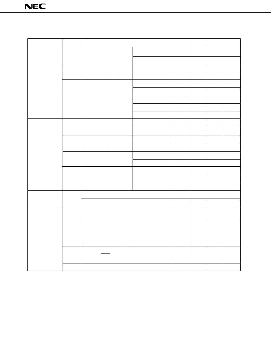
40
µ
µ
PD78062(A), 78063(A), 78064(A)
DC Characteristics (T
A
= ≠40 to +85
∞
C, V
DD
= 2.0 to 6.0 V)
0.7 V
DD
V
DD
V
0.8 V
DD
V
DD
V
0.8 V
DD
V
DD
V
0.85 V
DD
V
DD
V
V
DD
≠0.5
V
DD
V
V
DD
≠0.2
V
DD
V
0.8 V
DD
V
DD
V
0.9 V
DD
V
DD
V
0.9 V
DD
V
DD
V
0
0.3 V
DD
V
0
0.2 V
DD
V
0
0.2 V
DD
V
0
0.15 V
DD
V
0
0.4
V
0
0.2
V
0
0.2 V
DD
V
0
0.1 V
DD
V
0
0.1 V
DD
V
V
DD
≠1.0
V
DD
V
V
DD
≠0.5
V
DD
V
0.4
2.0
V
0.4
V
0.2 V
DD
V
0.5
V
P10 to P17, P30 to P32,
P35 to P37, P80 to P87,
P90 to P97, P100 to P103
P00 to P05, P25 to P27,
P33, P34, P70 to P72,
P110 to P117, RESET
X1, X2
XT1/P07, XT2
P10 to P17, P30 to P32,
P35 to P37, P80 to P87,
P90 to P97, P100 to P103
P00 to P05, P25 to P27,
P33, P34, P70 to P72,
P110 to P117, RESET
X1, X2
XT1/P07, XT2
V
DD
= 4.5 to 6.0 V, I
OH
= ≠1 mA
I
OH
= ≠100
µ
A
P100 to P103
P00 to P05, P10 to P17,
P25 to P27, P30 to P37,
P70 to P72, P80 to P87,
P90 to P97, P110 to P117
SB0, SB1, SCK0
I
OL
= 400
µ
A
Output voltage
high
V
DD
= 4.5 to 6.0 V,
I
OL
= 15 mA
V
DD
= 4.5 to 6.0 V,
I
OL
= 1.6 mA
4.5 V
V
DD
6.0 V,
open-drain,
pulled high (R = 1 k
)
Output voltage
low
Note When P07/XT1 is used as P07, the inverse phase of P07 should be input to XT2.
Remark Unless otherwise specified, the characteristics of dual-function pins are the same as those of port pins.
V
IH1
V
IH2
V
IH3
V
IH4
V
IL1
V
IL2
V
IL3
V
IL4
V
OH
V
OL1
V
OL2
V
OL3
Input voltage
high
Input voltage
low
V
DD
= 2.7 to 6.0 V
V
DD
= 2.7 to 6.0 V
V
DD
= 2.7 to 6.0 V
4.5 V
V
DD
6.0 V
2.7 V
V
DD
< 4.5 V
2.0 V
V
DD
< 2.7 V
Note
V
DD
= 2.7 to 6.0 V
V
DD
= 2.7 to 6.0 V
V
DD
= 2.7 to 6.0 V
4.5 V
V
DD
6.0 V
2.7 V
V
DD
< 4.5 V
2.0 V
V
DD
< 2.7 V
Note
Parameter
Symbol
Test Conditions
MIN.
TYP.
MAX.
Unit
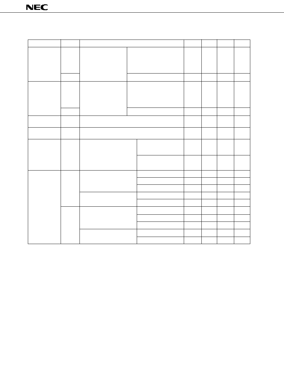
41
µ
PD78062(A), 78063(A), 78064(A)
Symbol
Test Conditions
MIN.
TYP.
MAX.
Unit
P00 to P05, P10 to P17,
P25 to P27, P30 to P37,
P70 to P72, P80 to P87,
3
µ
A
P90 to P97, P100 to P103,
P110 to P117
I
LIH2
X1, X2, XT1/P07, XT2
20
µ
A
P00 to P05, P10 to P17,
P25 to P27, P30 to P37,
P70 to P72, P80 to P87,
≠3
µ
A
P90 to P97, P100 to P103,
P110 to P117
I
LIL2
X1, X2, XT1/P07, XT2
≠20
µ
A
I
LOH
V
O
= V
DD
3
µ
A
I
LOL
V
O
= 0 V
≠3
µ
A
V
I
= 0 V, P01 to P05,
P10 to P17, P25 to P27,
R
P30 to P37, P70 to P72,
P80 to P87, P90 to P97,
P100 to P103, P110 to P117
V
DD
= 5.0 V
±
10 %
Note4
4
12
mA
V
DD
= 3.0 V
±
10 %
Note5
0.6
1.8
mA
V
DD
= 2.2 V
±
10 %
Note5
0.35
1.05
mA
V
DD
= 5.0 V
±
10 %
Note4
6.5
19.5
mA
V
DD
= 3.0 V
±
10 %
Note5
0.8
2.4
mA
V
DD
= 5.0 V
±
10 %
1.4
4.2
mA
V
DD
= 3.0 V
±
10 %
500
1500
µ
A
V
DD
= 2.2 V
±
10 %
280
840
µ
A
V
DD
= 5.0 V
±
10 %
1.6
4.8
mA
V
DD
= 3.0 V
±
10 %
650
1950
µ
A
DC Characteristics (T
A
= ≠40 to +85
∞
C, V
DD
= 2.0 to 6.0 V)
Parameter
V
I
= V
DD
I
LIH1
V
I
= 0 V
I
LIL1
I
DD2
2.7 V
V
DD
< 4.5 V
20
500 k
Input leakage
current high
Input leakage
current low
Output leakage
current high
Output leakage
current low
Software
pull-up resistor
Supply
current
Note1
4.5 V
V
DD
6.0 V
15
40
90
k
Remark Unless otherwise specified, the characteristics of dual-function pins are the same as those of port pins.
Notes 1. Not including currents flowing in on-chip pull-up resistors or LCD split resistors.
2. Main system clock f
XX
= f
X
/2 operation (when oscillation mode selection register (OSMS) is set to 00H)
3. Main system clock f
XX
= f
X
operation (when OSMS is set to 01H)
4. High-speed mode operation (when processor clock control register (PCC) is set to 00H)
5. Low-speed mode operation (when PCC is set to 04H)
5.00 MHz, Crystal oscillation (f
XX
= 2.5 MHz)
Note2
operating mode
I
DD1
5.00 MHz, Crystal oscillation
(f
XX
= 5.0 MHz)
Note3
HALT mode
5.00 MHz, Crystal oscillation
(f
XX
= 2.5 MHz)
Note2
HALT mode
5.00 MHz, Crystal oscillation
(f
XX
= 5.0 MHz)
Note3
operating mode
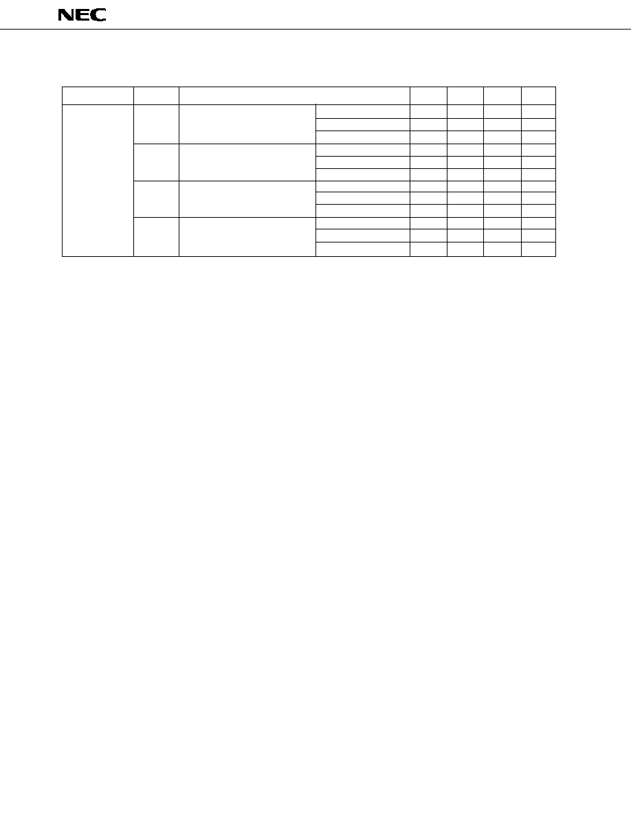
42
µ
µ
PD78062(A), 78063(A), 78064(A)
Parameter
DC Characteristics (T
A
= ≠40 to +85
∞
C, V
DD
= 2.0 to 6.0 V)
Symbol
Test Conditions
MIN.
TYP.
MAX.
Unit
V
DD
= 5.0 V
±
10 %
60
120
µ
A
V
DD
= 3.0 V
±
10 %
32
64
µ
A
V
DD
= 2.2 V
±
10 %
24
48
µ
A
V
DD
= 5.0 V
±
10 %
25
55
µ
A
V
DD
= 3.0 V
±
10 %
5
15
µ
A
V
DD
= 2.2 V
±
10 %
2.5
12.5
µ
A
V
DD
= 5.0 V
±
10 %
1
30
µ
A
V
DD
= 3.0 V
±
10 %
0.5
10
µ
A
V
DD
= 2.2 V
±
10 %
0.3
10
µ
A
V
DD
= 5.0 V
±
10 %
0.1
30
µ
A
V
DD
= 3.0 V
±
10 %
0.05
10
µ
A
V
DD
= 2.2 V
±
10 %
0.05
10
µ
A
Notes 1. Not including currents flowing in on-chip pull-up resistors or LCD split resistors.
2. When the main system clock is stopped.
XT1 = V
DD
STOP mode
When feedback resistor is connected
32,768 kHz, Crystal oscillation
operating mode
Note2
I
DD3
32,768 kHz, Crystal oscillation
HALT mode
Note2
XT1 = V
DD
STOP mode
When feedback resistor is disconnected
I
DD6
I
DD5
Supply
current
Note1
I
DD4
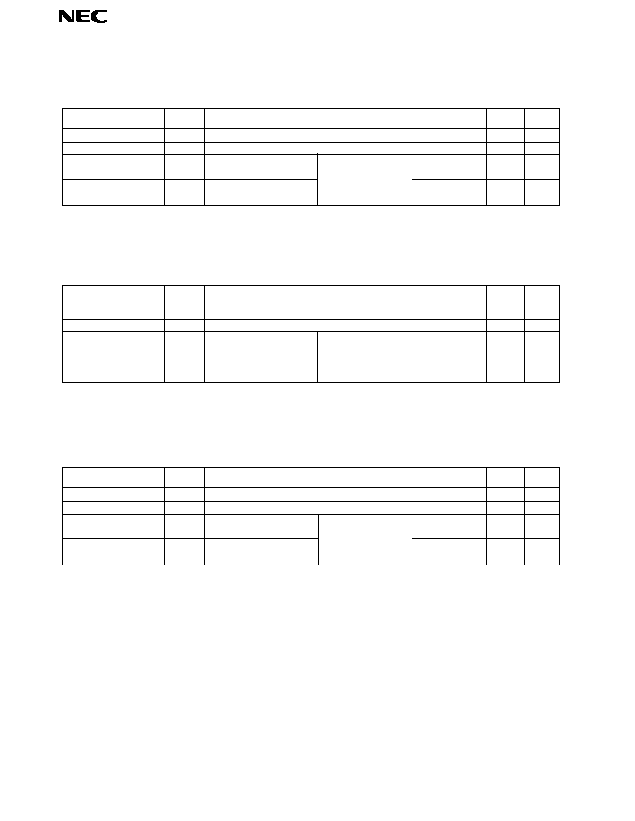
43
µ
PD78062(A), 78063(A), 78064(A)
Symbol
Test Conditions
MIN.
TYP.
MAX.
Unit
LCD drive voltage
V
LCD
2.5
V
DD
V
LCD split resistor
R
LCD
60
100
150
k
LCD output voltage
deviation
Note
(common)
LCD output voltage
deviation
Note
(segment)
DC Characteristics (T
A
= ≠10 to +85
∞
C)
Symbol
Test Conditions
MIN.
TYP.
MAX.
Unit
LCD drive voltage
V
LCD
2.0
V
DD
V
LCD split resistor
R
LCD
60
100
150
k
LCD output voltage
deviation
Note
(common)
LCD output voltage
deviation
Note
(segment)
Parameter
(1)
Static display mode (V
DD
= 2.0 to 6.0 V)
V
ODC
I
O
=
±
5
µ
A
0
±
0.2
V
V
ODS
I
O
=
±
1
µ
A
0
±
0.2
V
2.0 V
V
LCD
V
DD
V
LCD0
= V
LCD
Note
The voltage deviation is the difference from the output voltage corresponding to the ideal value of the segment and
common outputs (V
LCDn
; n = 0, 1, 2).
Parameter
(2)
1/3 bias method (V
DD
= 2.5 to 6.0 V)
Note
The voltage deviation is the difference from the output voltage corresponding to the ideal value of the segment and
common outputs (V
LCDn
; n = 0, 1, 2).
Symbol
Test Conditions
MIN.
TYP.
MAX.
Unit
LCD drive voltage
V
LCD
2.7
V
DD
V
LCD split resistor
R
LCD
60
100
150
k
LCD output voltage
deviation
Note
(common)
LCD output voltage
deviation
Note
(segment)
(3)
1/2 bias method (V
DD
= 2.7 to 6.0 V)
Note
The voltage deviation is the difference from the output voltage corresponding to the ideal value of the segment and
common outputs (V
LCDn
; n = 0, 1, 2).
V
ODC
I
O
=
±
5
µ
A
0
±
0.2
V
V
ODS
I
O
=
±
1
µ
A
0
±
0.2
V
2.7 V
V
LCD
V
DD
V
LCD0
= V
LCD
V
LCD1
= V
LCD
◊
1/2
V
LCD2
= V
LCD1
V
ODC
I
O
=
±
5
µ
A
0
±
0.2
V
V
ODS
I
O
=
±
1
µ
A
0
±
0.2
V
2.5 V
V
LCD
V
DD
V
LCD0
= V
LCD
V
LCD1
= V
LCD
◊
2/3
V
LCD2
= V
LCD
◊
1/3
Parameter
44
µ
µ
PD78062(A), 78063(A), 78064(A)
AC Characteristics
(1)
Basic operation (T
A
= ≠40 to +85
∞
C, V
DD
= 2.0 to 6.0 V)
Parameter
T
CY
f
TI1
t
TIH1,
t
TIL1
t
INTH
,
t
INTL
t
RSL
Notes 1.
Main system clock f
XX
= f
X
/2 operation (when oscillation mode selection register (OSMS) is set to 00H)
2.
Main system clock f
XX
= f
X
operation (when OSMS is set to 01H)
3.
This is the value when the external clock is used. The value is 114
µ
s (min.) when the crystal resonator is used.
4.
In combination with bits 0 (SCS0) and 1 (SCS1) of sampling clock select register (SCS), selection of f
sam
is
possible between f
XX
/2
N
, f
XX
/32, f
XX
/64 and f
XX
/128 (when N = 0 to 4).
Cycle time
(Minimum
instruction
execution time)
TI00 input
frequency
TI00 input high/
low-level width
TI01 input high/
low-level width
TI1, TI2 input high/
low-level width
TI1, TI2 input high/
low-level width
Interrupt input
high/low-level
width
RESET low level
width
Symbol
Test Conditions
MIN.
TYP.
MAX.
Unit
Operating on main system clock
V
DD
= 2.7 to 6.0 V
0.8
64
µ
s
(f
XX
= 2.5 MHz)
Note1
2.2
64
µ
s
Operating on main system clock
4.5
V
DD
6.0 V
0.4
32
µ
s
(f
XX
= 5.0 MHz)
Note2
2.7
V
DD
< 4.5 V
0.8
32
µ
s
Operating on subsystem clock
40
Note3
122
125
µ
s
t
TI00
= t
TIH00
+ t
TIL00
0
1/t
TI00
MHz
4.5 V
V
DD
6.0 V
2/f
sam
+0.1
Note 4
µ
s
2.7 V
V
DD
< 4.5 V
2/f
sam
+0.2
Note 4
µ
s
2.0 V
V
DD
< 2.7 V
2/f
sam
+0.5
Note 4
µ
s
2.7 V
V
DD
6.0 V
10
µ
s
20
µ
s
V
DD
= 4.5 to 6.0 V
0
4
MHz
0
275
kHz
V
DD
= 4.5 to 6.0 V
100
ns
1.8
µ
s
INTP0
8/f
sam
Note4
µ
s
INTP1 to INTP5,
V
DD
= 2.7 to 6.0 V
10
µ
s
P110 to P117
20
µ
s
V
DD
= 2.7 to 6.0 V
10
µ
s
20
µ
s
f
TI00
f
TIH00,
t
TIL00
f
TIH01,
t
TIL01
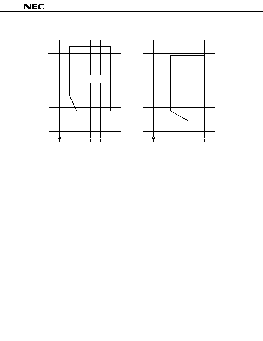
45
µ
PD78062(A), 78063(A), 78064(A)
T
CY
vs V
DD
(At main system clock f
XX
= f
X
/2 operation)
T
CY
vs V
DD
(At main system clock f
XX
= f
X
operation)
60
10
2.0
1.0
1
0
2
3
4
5
6
0.8
0.4
60
10
2.0
1.0
1
0
2
3
4
5
6
0.8
0.4
Supply Voltage V
DD
[V]
Cycle Time T
CY
[ s]
µ
Guaranteed Operation
Range
Supply Voltage V
DD
[V]
Cycle Time T
CY
[ s]
µ
Guaranteed Operation
Range
32
46
µ
µ
PD78062(A), 78063(A), 78064(A)
(2)
Serial Interface (T
A
= ≠40 to +85
∞
C, V
DD
= 2.0 to 6.0 V)
(a) Serial interface channel 0
(i) 3-wire serial I/O mode (SCK0... Internal clock output)
SCK0 cycle time
SCK0 high/low-level width
SI0 setup time (to SCK0
)
SI0 hold time (from SCK0
)
SO0 output delay time
from SCK0
Note C is the load capacitance of SCK0, SO0 output line.
(ii) 3-wire serial I/O mode (SCK0...External clock input)
SCK0 cycle time
SCK0 high/low-level width
SI0 setup time (to SCK0
)
SI0 hold time (from SCK0
)
SO0 output delay time
from SCK0
SCK0 rise, fall time
t
KH2
,
t
KL2
Note C is the load capacitance of SO0 output line.
Parameter
Symbol
Test Conditions
MIN.
TYP.
MAX.
Unit
4.5 V
V
DD
6.0 V
800
ns
t
KCY2
2.7 V
V
DD
< 4.5 V
1600
ns
3200
ns
4.5 V
V
DD
6.0 V
400
ns
2.7 V
V
DD
< 4.5 V
800
ns
1600
ns
t
SIK2
100
ns
t
KSI2
400
ns
t
KSO2
C = 100 pF
Note
300
ns
1000
ns
Parameter
Symbol
Test Conditions
MIN.
TYP.
MAX.
Unit
4.5 V
V
DD
6.0 V
800
ns
t
KCY1
2.7 V
V
DD
< 4.5 V
1600
ns
3200
ns
t
KH1
,
V
DD
= 4.5 to 6.0 V
t
KCY1
/2≠50
ns
t
KL1
t
KCY1
/2≠100
ns
4.5 V
V
DD
6.0 V
100
ns
t
SIK1
2.7 V
V
DD
< 4.5 V
150
ns
300
ns
t
KSI1
400
ns
t
KSO1
C = 100 pF
Note
300
ns
t
R2
,
t
F2
47
µ
PD78062(A), 78063(A), 78064(A)
(iii) SBI mode (SCK0...Internal clock output)
Parameter
Symbol
Test Conditions
MIN.
TYP.
MAX.
Unit
V
DD
= 4.5 to 6.0 V
800
ns
3200
ns
V
DD
= 4.5 to 6.0 V
t
KCY3
/2≠50
ns
t
KCY3
/2≠150
ns
V
DD
= 4.5 to 6.0 V
100
ns
300
ns
R = 1 k
,
V
DD
= 4.5 to 6.0 V
0
250
ns
C = 100 pF
Note
0
1000
ns
t
KCY3
ns
t
KCY3
ns
t
KCY3
ns
t
KCY3
ns
SCK0 cycle time
SCK0 high/low-level
width
SB0, SB1 setup time (to
SCK0
)
SB0, SB1 hold time
(from SCK0
)
SB0, SB1 output delay
time from SCK0
SB0, SB1
from SCK0
SCK0
from SB0, SB1
SB0, SB1 high-level
width
SB0, SB1 low-level
width
t
KCY3
t
KH3
,
t
KL3
t
SIK3
t
KSI3
t
KSO3
t
KSB
t
SBK
t
SBH
t
SBL
t
KCY3
/2
ns
Note R and C are the load resistance and load capacitance of the SCK0, SB0 and SB1 output line.
(iv) SBI mode (SCK0...External clock input)
Parameter
Symbol
Test Conditions
MIN.
TYP.
MAX.
Unit
V
DD
= 4.5 to 6.0 V
800
ns
3200
ns
V
DD
= 4.5 to 6.0 V
400
ns
1600
ns
V
DD
= 4.5 to 6.0 V
100
ns
300
ns
R = 1 k
,
V
DD
= 4.5 to 6.0 V
0
300
ns
C = 100 pF
Note
0
1000
ns
t
KCY4
ns
t
KCY4
ns
t
KCY4
ns
t
KCY4
ns
1000
ns
t
KCY4
/2
ns
Note R and C are the load resistance and load capacitance of the SB0 and SB1 output line.
t
KCY4
t
KH4
,
t
KL4
t
SIK4
t
KSI4
t
KSO4
t
KSB
t
SBK
t
SBH
t
SBL
t
R4
,
t
F4
SCK0 cycle time
SCK0 high/low-level
width
SB0, SB1 setup time (to
SCK0
)
SB0, SB1 hold time
(from SCK0
)
SB0, SB1 output delay
time from SCK0
SB0, SB1
from SCK0
SCK0
from SB0, SB1
SB0, SB1 high-level
width
SB0, SB1 low-level
width
SCK0 rise, fall time
48
µ
µ
PD78062(A), 78063(A), 78064(A)
(v) 2-wire serial I/O mode (SCK0... Internal clock output)
Parameter
Symbol
Test Conditions
MIN.
TYP.
MAX.
Unit
V
DD
= 2.7 to 6.0 V
1600
ns
3200
ns
V
DD
= 2.7 to 6.0 V
t
KCY5
/2≠160
ns
t
KCY5
/2≠190
ns
V
DD
= 4.5 to 6.0 V
t
KCY5
/2≠50
ns
t
KCY5
/2≠100
ns
4.5 V
V
DD
6.0 V
300
ns
2.7 V
V
DD
< 4.5 V
350
ns
400
ns
600
ns
300
ns
t
KCY5
t
KSI5
t
KSO5
t
SIK5
t
KH5
t
KL5
R = 1 k
,
C = 100 pF
Note
t
KCY6
t
KH6
t
KL6
t
SIK6
t
KSI6
t
KSO6
(vi) 2-wire serial I/O mode (SCK0... External clock input)
SCK0 cycle time
SCK0 high-level width
SCK0 low-level width
SB0, SB1 setup time
(to SCK0
)
SB0, SB1 hold time
(from SCK0
)
SB0, SB1 output delay
time from SCK0
Note R and C are the load resistance and load capacitance of the SCK0, SB0 and SB1 output line.
Note R and C are the load resistance and load capacitance of the SB0 and SB1 output line.
Parameter
Symbol
Test Conditions
MIN.
TYP.
MAX.
Unit
V
DD
= 2.7 to 6.0 V
1600
ns
3200
ns
V
DD
= 2.7 to 6.0 V
650
ns
1300
ns
V
DD
= 2.7 to 6.0 V
800
ns
1600
ns
100
ns
t
KCY6
/2
ns
R = 1 k
,
V
DD
= 4.5 to 6.0 V
0
300
ns
C = 100 pF
Note
0
500
ns
1000
ns
SCK0 cycle time
SCK0 high-level width
SCK0 low-level width
SB0, SB1 setup time
(to SCK0
)
SB0, SB1 hold time
(from SCK0
)
SB0, SB1 output delay
time from SCK0
SCK0 rise, fall time
t
R6
,
t
F6
49
µ
PD78062(A), 78063(A), 78064(A)
(b) Serial interface channel 2
(i) 3-wire serial I/O mode (SCK2... Internal clock output)
SCK2 cycle time
SCK2 high/low-level width
SI2 setup time (to SCK2
)
SI2 hold time (from SCK2
)
SO2 output delay time
from SCK2
Note C is the load capacitance of SCK2, SO2 output line.
(ii) 3-wire serial I/O mode (SCK2...External clock input)
SCK2 cycle time
SCK2 high/low-level width
SI2 setup time (to SCK2
)
SI2 hold time (from SCK2
)
SO2 output delay time
from SCK2
SCK2 rise, fall time
Note C is the load capacitance of SO2 output line.
Parameter
Symbol
Test Conditions
MIN.
TYP.
MAX.
Unit
4.5 V
V
DD
6.0 V
800
ns
t
KCY8
2.7 V
V
DD
< 4.5 V
1600
ns
3200
ns
4.5 V
V
DD
6.0 V
400
ns
2.7 V
V
DD
< 4.5 V
800
ns
1600
ns
t
SIK8
100
ns
t
KSI8
400
ns
t
KSO8
C = 100 pF
Note
300
ns
1000
ns
Parameter
Symbol
Test Conditions
MIN.
TYP.
MAX.
Unit
4.5 V
V
DD
6.0 V
800
ns
t
KCY7
2.7 V
V
DD
< 4.5 V
1600
ns
3200
ns
t
KH7
,
V
DD
= 4.5 to 6.0 V
t
KCY1
/2≠50
ns
t
KL7
t
KCY1
/2≠100
ns
4.5 V
V
DD
6.0 V
100
ns
t
SIK7
2.7 V
V
DD
< 4.5 V
150
ns
300
ns
t
KSI7
400
ns
t
KSO7
C = 100 pF
Note
300
ns
t
R8
,
t
F8
t
KH8
,
t
KL8
50
µ
µ
PD78062(A), 78063(A), 78064(A)
Parameter
Symbol
Test Conditions
MIN.
TYP.
MAX.
Unit
4.5 V
V
DD
6.0 V
800
ns
t
KCY9
2.7 V
V
DD
< 4.5 V
1600
ns
3200
ns
4.5 V
V
DD
6.0 V
400
ns
2.7 V
V
DD
< 4.5 V
800
ns
1600
ns
4.5 V
V
DD
6.0 V
39063
bps
2.7 V
V
DD
< 4.5 V
19531
bps
9766
bps
1000
ns
Parameter
Symbol
Test Conditions
MIN.
TYP.
MAX.
Unit
4.5 V
V
DD
6.0 V
78125
bps
2.7 V
V
DD
< 4.5 V
39063
bps
19531
bps
Transfer rate
(iii) UART mode (Dedicated baud rate generator output)
t
KH9
,
t
KL9
ASCK cycle time
ASCK high/low-level
width
Transfer rate
ASCK rise, fall time
(iv) UART mode (External clock input)
t
R9
,
t
F9
51
µ
PD78062(A), 78063(A), 78064(A)
AC Timing Test Point (Excluding X1, XT1 Input)
Clock Timing
TI Timing
0.8 V
DD
0.2 V
DD
0.8 V
DD
0.2 V
DD
Test Points
t
XL
t
XH
1/f
X
V
IH3
(MIN.)
V
IL3
(MAX.)
t
XTL
t
XTH
1/f
XT
V
IH4
(MIN.)
V
IL4
(MAX.)
X1 Input
XT1 Input
t
TIL1
t
TIH1
1/f
TI1
TI0≠TI2
t
TIL00,
t
TIL01
t
TIH00,
t
TIH01
TI00, TI01
52
µ
µ
PD78062(A), 78063(A), 78064(A)
Serial Transfer Timing
3-wire serial I/O mode:
SBI mode (bus release signal transfer):
SBI mode (command signal transfer):
t
KCY 1, 2, 7, 8
t
KL1, 2, 7, 8
t
KH1, 2, 7, 8
SCK0, SCK2
SI0, SI2
SO0, SO2
t
SIK1, 2, 7, 8
t
KSI1, 2, 7, 8
t
KSO1, 2, 7, 8
Input Data
Output Data
t
R2, 8
t
F2, 8
t
SIK3, 4
t
KCY3, 4
t
KL3, 4
t
KH3, 4
SCK0
t
SBL
t
SBH
t
KSB
t
SBK
t
KSI3, 4
t
KSO3, 4
SB0, SB1
t
R4
t
F4
t
SIK3, 4
t
KCY3, 4
t
KL3, 4
t
KH3, 4
SCK0
t
KSB
t
SBK
t
KSI3.4
t
KSO3, 4
SB0, SB1
t
R4
t
F4
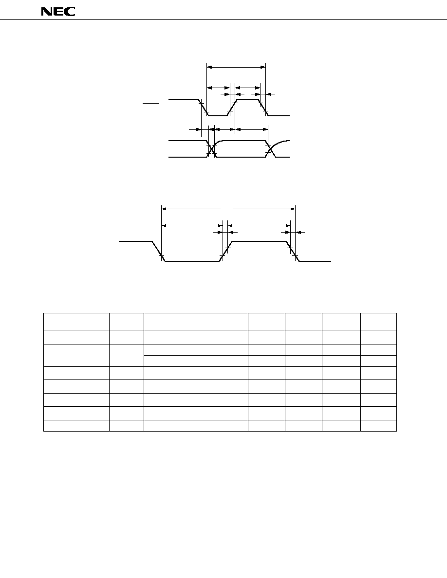
53
µ
PD78062(A), 78063(A), 78064(A)
2-wire serial I/O mode:
UART mode:
A/D Converter (T
A
= ≠40 to +85
∞
C, AV
DD
= V
DD
= 2.0 to 6.0 V, AV
SS
= V
SS
= 0 V)
Parameter
Symbol
Test Conditions
MIN.
TYP.
MAX.
Unit
8
8
8
bit
2.7 V
AV
REF
6.0 V
±
0.6
%
±
1.4
%
t
CONV
19.1
200
µ
s
t
SAMP
12/f
XX
µ
s
V
IAN
AV
SS
AV
REF
V
AV
REF
2.0
AV
DD
V
R
AIREF
4
14
k
Resolution
Overall error
Note
Conversion time
Sampling time
Analog input voltage
Reference voltage
AV
REF
-AV
SS
resistance
Note Quantization error (
±
1/2 LSB) is not included. This is expressed in proportion to the full-scale value.
t
KSO5, 6
t
SIK5, 6
t
KCY5.6
t
KL5, 6
t
KH5, 6
SCK0
t
KSI5, 6
SB0, SB1
t
R6
t
F6
ASCK
t
KCY9
t
KL9
t
KH9
t
R9
t
F9
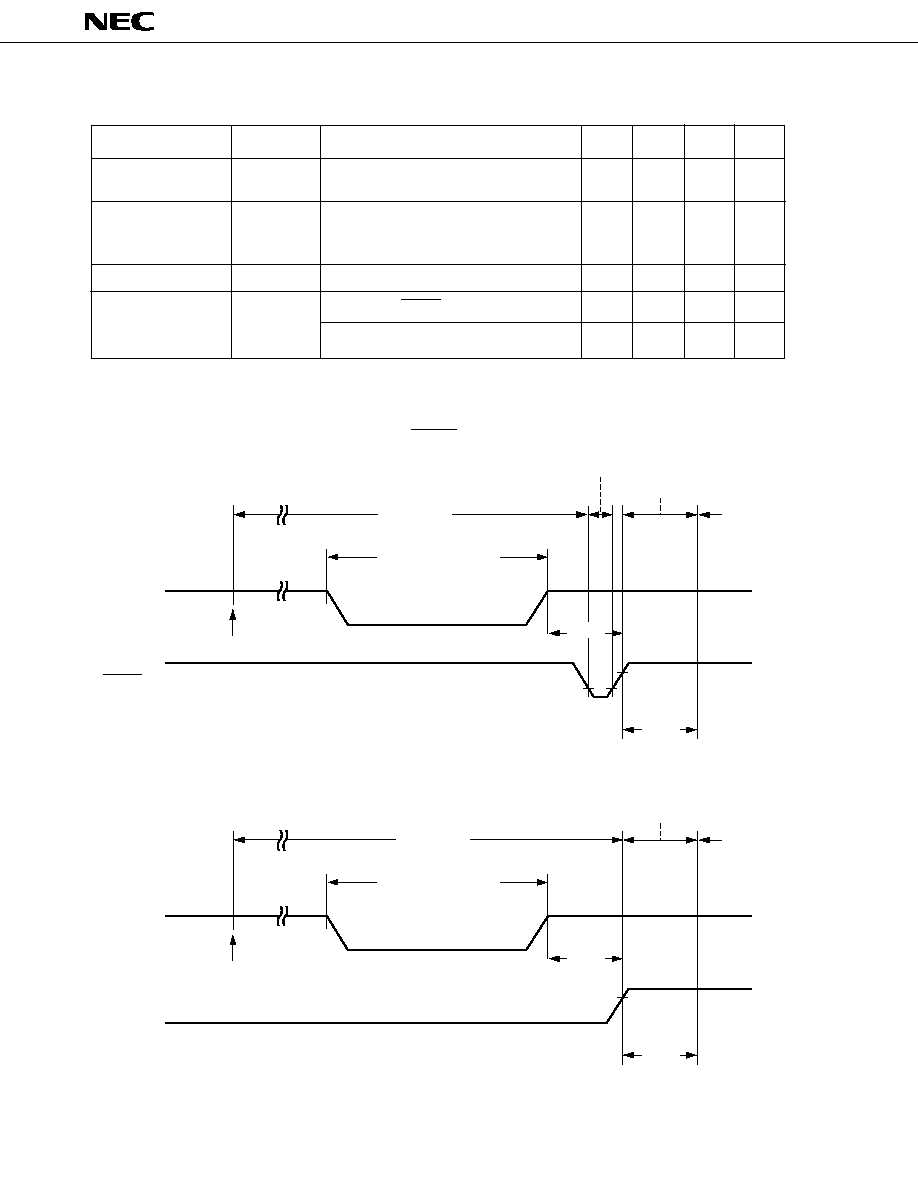
54
µ
µ
PD78062(A), 78063(A), 78064(A)
Data retention
supply voltage
V
DDDR
= 1.8 V
I
DDDR
Subsystem clock stopped and
0.1
10
µ
A
feed-back resistor disconnected
Release signal set time
t
SREL
0
µ
s
Oscillation
Release by RESET
2
17
/f
x
ms
stabilization
t
WAIT
wait time
Release by interrupt
Note
ms
Data Memory STOP Mode Low Supply Voltage Data Retention Characteristics (T
A
= ≠40 to +85
∞
C)
Parameter
Symbol
Test Conditions
MIN.
TYP.
MAX.
Unit
V
DDDR
1.8 6.0 V
Note In combination with bits 0 to 2 (OSTS0 to OSTS2) of oscillation stabilization time select register (OSTS), selection
of 2
12
/f
XX
and 2
14
/f
XX
to 2
17
/f
XX
is possible.
Data retention timing (STOP mode release by RESET)
Data retention timing (STOP mode release by standby release signal: Interrupt signal)
Data retention
supply current
t
SREL
t
WAIT
V
DD
STOP Instruction Execution
STOP Mode
Data Retention Mode
HALT Mode
Operating Mode
Standby Release Signal
(Interrupt Request)
V
DDDR
t
SREL
t
WAIT
V
DD
RESET
STOP Instruction Execution
STOP Mode
Data Retention Mode
Internal Reset Operation
HALT Mode
Operating Mode
V
DDDR
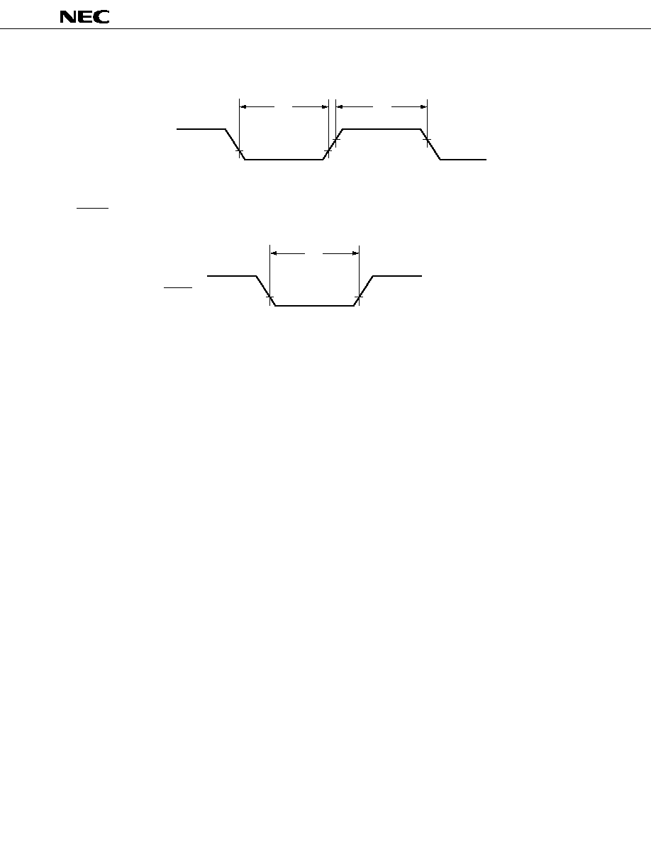
55
µ
PD78062(A), 78063(A), 78064(A)
Interrupt input timing
t
INTL
t
INTH
INTP0≠INTP5
RESET input timing
t
RSL
RESET
56
µ
PD78062(A), 78063(A), 78064(A)
11. CHARACTERISTIC CURVES (REFERENCE VALUES)
I
DD
vs V
DD
(Main System Clock: 5.0 MHz)
0
2
1
3
4
5
6
7
8
PCC=B0H
PCC=02H
PCC=03H
PCC=04H
(T
A
= 25
∞
C)
10.0
5.0
1.0
0.5
0.1
0.05
0.01
0.005
Supply Voltage V
DD
(V)
Supply Current I
DD
(mA)
0.001
HALT (X1 Oscillation,
XT1 Oscillation)
PCC=00H
PCC=01H
PCC=30H
f
XT
= 32.768 kHz
f
XX
= 5.0 MHz
HALT
STOP
(X1 Stop, XT1 Oscillation)
(X1 Stop, XT1 Oscillation)
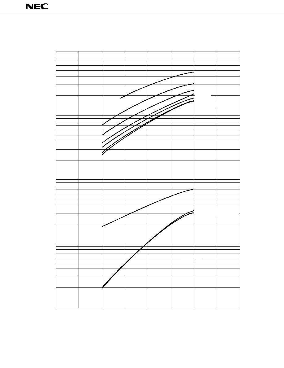
57
µ
PD78062(A), 78063(A), 78064(A)
I
DD
vs V
DD
(Main System Clock: 2.5 MHz)
0
2
1
3
4
5
6
7
8
PCC=B0H
PCC=02H
PCC=03H
PCC=04H
(T
A
= 25
∞
C)
10.0
5.0
1.0
0.5
0.1
0.05
0.01
0.005
Supply Voltage V
DD
(V)
Supply Current I
DD
(mA)
0.001
HALT (X1 Oscillation,
XT1 Oscillation)
PCC=00H
PCC=01H
PCC=30H
f
XT
= 32.768 kHz
f
XX
= 2.5 MHz
HALT
STOP
(X1 Stop, XT1 Oscillation)
(X1 Stop, XT1 Oscillation)
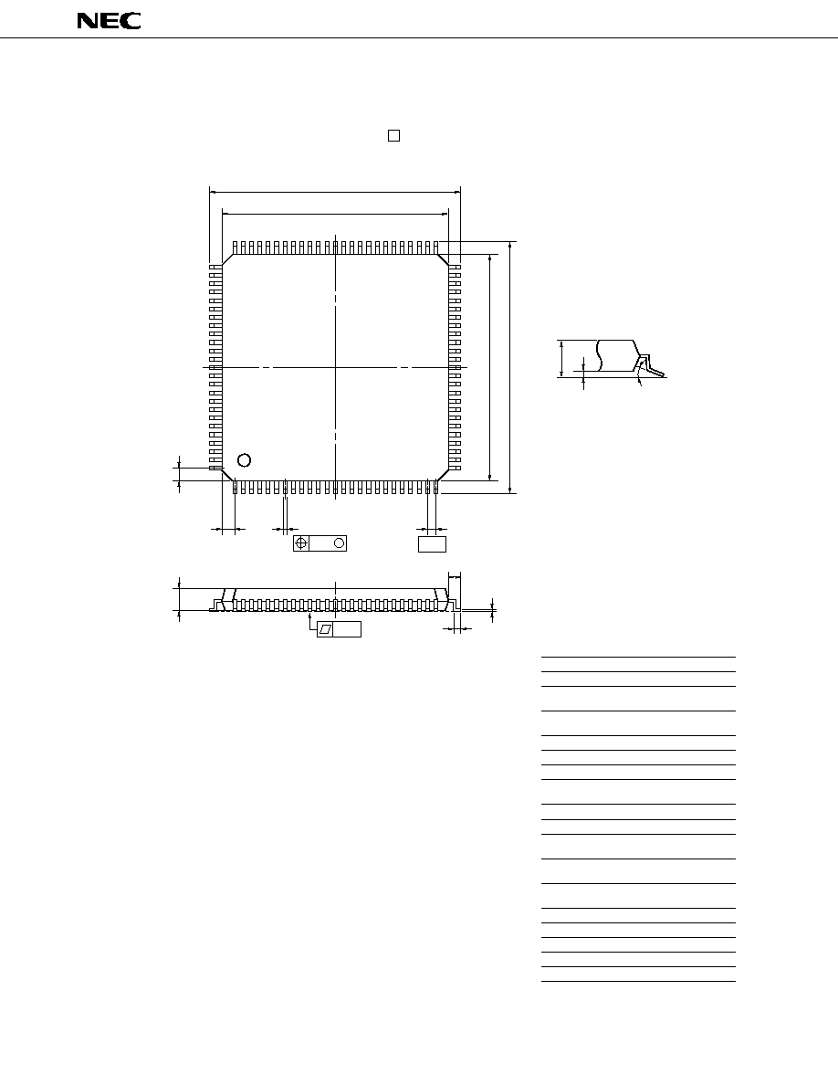
58
µ
PD78062(A), 78063(A), 78064(A)
12. PACKAGE DRAWINGS
100 PIN PLASTIC QFP (FINE PITCH) ( 14)
ITEM MILLIMETERS
INCHES
I
J
0.5 (T.P.)
0.10
0.004
0.020 (T.P.)
A
NOTE
Each lead centerline is located within 0.10 mm (0.004 inch) of
its true position (T.P.) at maximum material condition.
S
A
16.0±0.2
0.630±0.008
B
14.0±0.2
0.551 +0.009
≠0.008
C
14.0±0.2
0.551 +0.009
≠0.008
D
16.0±0.2
0.630±0.008
F
G
1.0
1.0
0.039
0.039
H
0.22
0.009±0.002
P100GC-50-7EA-2
K
1.0±0.2
0.039 +0.009
≠0.008
L
0.5±0.2
0.020 +0.008
≠0.009
M
0.17
0.007
N
0.10
0.004
P
1.45
0.057
+0.05
≠0.04
+0.03
≠0.07
B
C
D
J
H
I
G
F
P
N
L
K
M
Q
R
detail of lead end
Q
0.125±0.075
0.005±0.003
R
S
1.7 MAX.
5∞±5∞
5∞±5∞
0.067 MAX.
+0.001
≠0.003
M
1
25
26
50
100
76
75
51
Remark
Dimensions and materials of ES products are same as those
of mass production product.
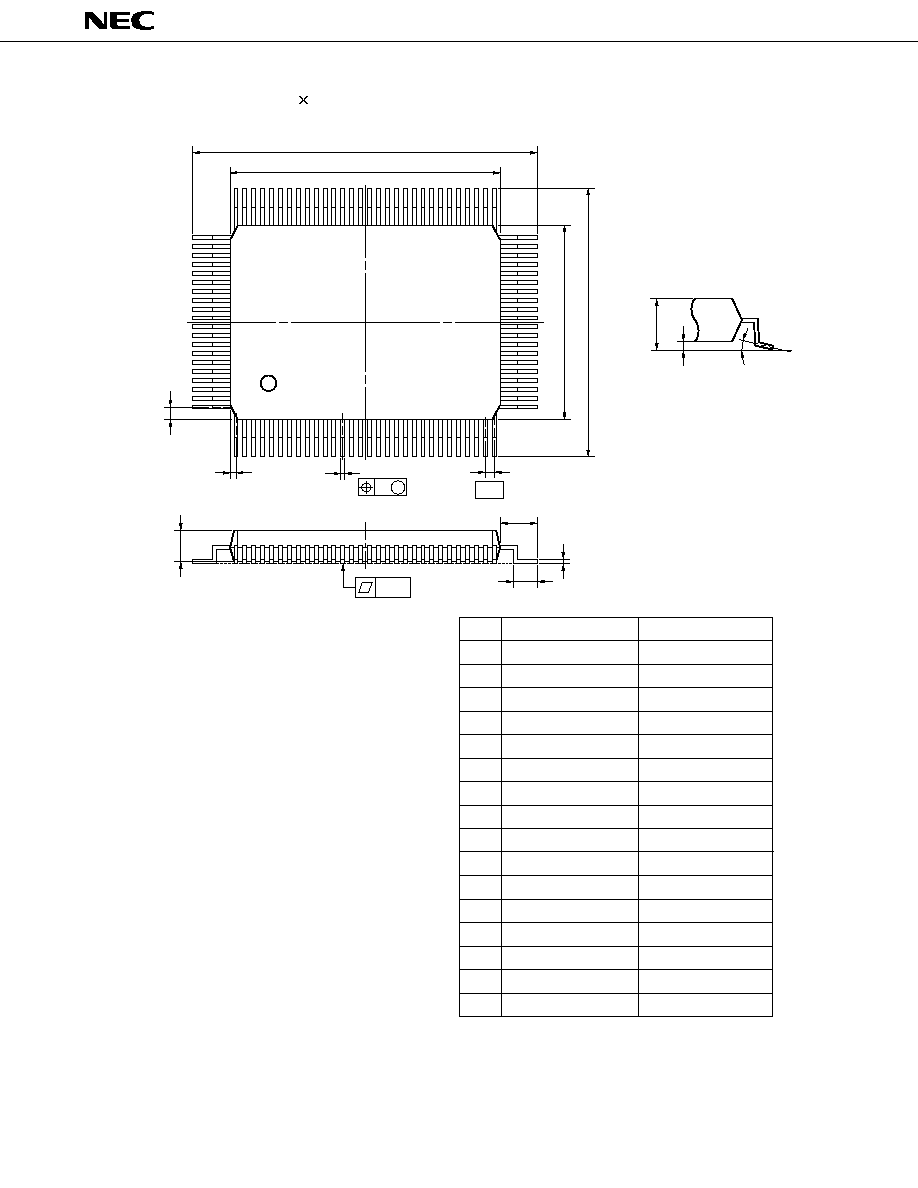
59
µ
PD78062(A), 78063(A), 78064(A)
J
N
M
P
80
81
50
100 PIN PLASTIC QFP (14
◊
20)
100
1
31
30
51
G
detail of lead end
S
5∞
±
5∞
C
D
A
B
H
Q
K
L
F
M
I
P100GF-65-3BA1-2
ITEM
MILLIMETERS
INCHES
A
B
C
D
F
G
H
I
J
K
L
23.6±0.4
14.0±0.2
0.6
0.30±0.10
0.15
20.0±0.2
0.929±0.016
0.031
0.024
0.006
0.026 (T.P.)
0.795
NOTE
M
N
0.10
0.15
1.8±0.2
0.65 (T.P.)
0.006
0.031
+0.009
≠0.008
Each lead centerline is located within 0.15
mm (0.006 inch) of its true position (T.P.) at
maximum material condition.
0.012
0.551
0.8±0.2
0.071
P
2.7
0.106
0.693±0.016
17.6±0.4
0.8
+0.008
≠0.009
Q
0.1±0.1
0.004±0.004
S
3.0 MAX.
0.119 MAX.
+0.10
≠0.05
+0.009
≠0.008
+0.004
≠0.005
+0.009
≠0.008
+0.004
≠0.003
0.004
Remark
Dimensions and materials of ES products are
same as mass production product.
60
µ
PD78062(A), 78063(A), 78064(A)
100 PIN PLASTIC LQFP (FINE PITCH) (14
◊
14)
ITEM
MILLIMETERS
INCHES
NOTE
Each lead centerline is located within 0.08 mm (0.003 inch) of
its true position (T.P.) at maximum material condition.
S100GC-50-8EU
F
1.00
0.039
B
14.00±0.20
0.551+0.009
≠0.008
S
1.60 MAX.
0.063 MAX.
L
0.50±0.20
0.020+0.008
≠0.009
+0.009
≠0.008
C
14.00±0.20
0.551+0.009
≠0.008
A
16.00±0.20
0.630±0.008
G
1.00
0.039
H
0.22
0.009±0.002
I
0.08
0.003
J
0.50 (T.P.)
0.020 (T.P.)
K
1.00±0.20
0.039+0.009
≠0.008
N
0.08
0.003
P
1.40±0.05
0.055±0.002
R
3
∞
3
∞
+7
∞
≠3
∞
+7
∞
≠3
∞
D
16.00±0.20
0.630±0.008
M
Q
R
K
M
L
J
H
I
F
G
P
N
detail of lead end
M
0.17
0.007+0.001
≠0.003
+0.03
≠0.07
Q
0.10±0.05
0.004±0.002
+0.05
≠0.04
1
25
26
50
100
76
75
51
C
D
S
A
B
Remark
Dimensions and materials of ES products are
same as mass production product.
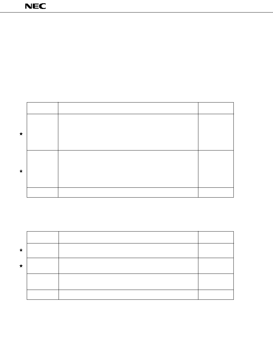
61
µ
PD78062(A), 78063(A), 78064(A)
13. RECOMMENDED SOLDERING CONDITIONS
The
µ
PD78062(A)/78063(A)/78064(A) should be soldered and mounted under the conditions recommended in the table
below.
For detail of recommended soldering conditions, refer to the information document Semiconductor Device Mounting
Technology Manual (C10535E).
For soldering methods and conditions other than those recommended below, contact our sales personnel.
Table 13-1. Surface Mounting Type Soldering Conditions (1/2)
(1)
µ
PD78062GC(A)-
◊◊◊
-7EA : 100-pin plastic QFP (Fine pitch)
(14
◊
14mm, resin thickness: 1.45 mm)
µ
PD78063GC(A)-
◊◊◊
-7EA : 100-pin plastic QFP (Fine pitch)
(14
◊
14mm, resin thickness: 1.45 mm)
µ
PD78064GC(A)-
◊◊◊
-7EA : 100-pin plastic QFP (Fine pitch)
(14
◊
14mm, resin thickness: 1.45 mm)
Package peak temperature: 235
∞
C, Duration: 30 sec. max. (at 210
∞
C or above),
Number of times: Twice max., Time limit: 7 days
Note
(thereafter 10 hours prebaking
required at 125
∞
C)
<precaution>
Baking cannot be applied to other than heat-resistant trays (magazine, taping, non-
heat-resistant trays) when the product is wrapped.
Package peak temperature: 215
∞
C, Duration: 40 sec. (at 200
∞
C or above),
Number of times: Twice max., Time limit: 7 days
Note
(thereafter 10 hours prebaking
required at 125
∞
C)
<precaution>
Baking cannot be applied to other than heat-resistant trays (magazine, taping, non-
heat-resistant trays) when the product is wrapped.
Pin temperature: 300
∞
C max. Duration: 3 sec. max. (per device side)
Recommended
Condition Symbol
Soldering
Method
Soldering Conditions
Infrared reflow
VPS
Partial heating
IR35-107-2
VP15-107-2
--
Note For the storage period after dry-pack decapsulation, storage conditions are max. 25
∞
C, 65% RH.
(2)
µ
PD78062GF(A)-
◊◊◊
-3BA : 100-pin plastic QFP (14
◊
20 mm)
µ
PD78063GF(A)-
◊◊◊
-3BA : 100-pin plastic QFP (14
◊
20 mm)
µ
PD78064GF(A)-
◊◊◊
-3BA : 100-pin plastic QFP (14
◊
20 mm)
Package peak temperature: 235
∞
C, Duration: 30 sec. max. (at 210
∞
C or above),
Number of times: Thrice max.
Package peak temperature: 215
∞
C, Duration: 40 sec. (at 200
∞
C or above),
Number of times: Thrice max.
Solder bath temperature: 260
∞
C max., Duration: 10 sec. max., Number of times: Once,
Preliminary heat temperature: 120
∞
C max. (Package surface temperature)
Pin temperature: 300
∞
C max. Duration: 3 sec. max. (per device side)
Recommended
Condition Symbol
Soldering
Method
Soldering Conditions
IR35-00-3
VP15-00-3
WS60-00-1
--
Infrared reflow
VPS
Wave soldering
Partial heating
Cautions 1. Use of more than one soldering method should be avoided (except in the case of partial heating).
2. The
µ
PD78062GC(A)-
◊◊◊
-8EU, 78063GC(A)-
◊◊◊
-8EU, and 78064GC(A)-
◊◊◊
-8EU are under planning.
Therefore, soldering conditions for these products have not been specified.
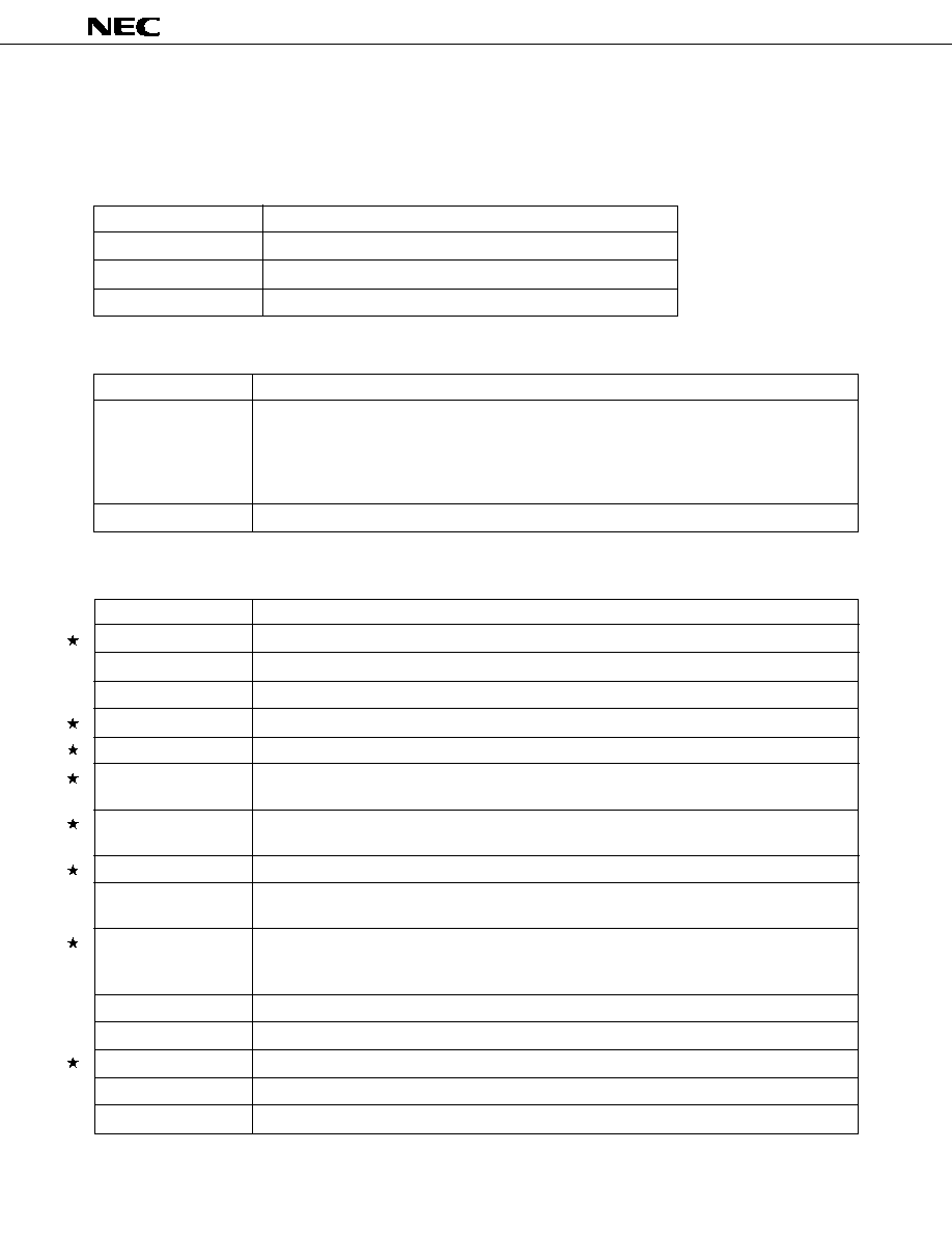
62
µ
PD78062(A), 78063(A), 78064(A)
APPENDIX A. DEVELOPMENT TOOLS
The following development tools are available for system development using
µ
PD78062(A)/78063(A)/78064(A).
Language Processing Software
RA78K/0
Note 1, 2, 3, 4
CC78K/0
Note 1, 2, 3, 4
DF78064
Note 1, 2, 3, 4
CC78K/0-L
Note 1, 2, 3 ,4
78K/0 series common assembler package
78K/0 series common C compiler package
µ
PD78064 subseries device file
78K/0 series common C compiler library source file
PROM Writing Tools
IE-78000-R
IE-78000-R-A
IE-78000-R-BK
IE-78064-R-EM
Note 8
IE-780308-R-EM
IE-78000-R-SV3
IE-70000-98-IF-B
IE-70000-98N-IF
IE70000-PC-IF-B
EP-78064GC-R
EP-78064GF-R
TGC-100SDW
EV-9200GF-100
SM78K0
Note 5, 6, 7
ID78K0
Note 4, 5, 6, 7
SD78K/0
Note 1, 2
DF78064
Note 1, 2, 4, 5, 6, 7
78K/0 series common in-circuit emulator
78K/0 series common in-circuit emulator (for integrated debugger)
78K/0 series common break board
µ
PD78064 subseries evaluation emulation board
µ
PD780308 subseries common emulation board
Interface adapter and cable when EWS is used as host machine (for IE-78000-R-A)
Interface adapter when PC-9800 series (except notebook type) is used as host machine (for IE-
78000-R-A)
Interface adapter and cable when notebook type PC-9800 series is used as host machine (for IE-
78000-R-A)
Interface adapter when IBM PC/AT
TM
is used as host machine (IE-78000-R-A)
µ
PD78064 subseries common emulation probes
Adapter to be mounted on a target system board made for 100-pin plastic QFP (GC-7EA, GC-8EU type)
TGC-100SDW is a product from Tokyo Eletech Corp. (TEL (03) 5295-1661)
When purchasing this product, please consult with our sales offices.
Socket to be mounted on a target system board made for 100-pin plastic QFP (GF-3BA type)
78K/0 series common system simulator
IE-78000-R-A integrated dubugger
IE-78000-R screen debugger
µ
PD78064 subseries device file
PG-1500
PA-78P0308GC
(or PA-78P064GC)
PA-78P0308GF
(or PA-78P064GF)
PA-78P0308KL-T
PG-1500 controller
Notes 1, 2
PROM programmer
Programmer adapters connected to PG-1500
PG-1500 control program
Debugging Tools
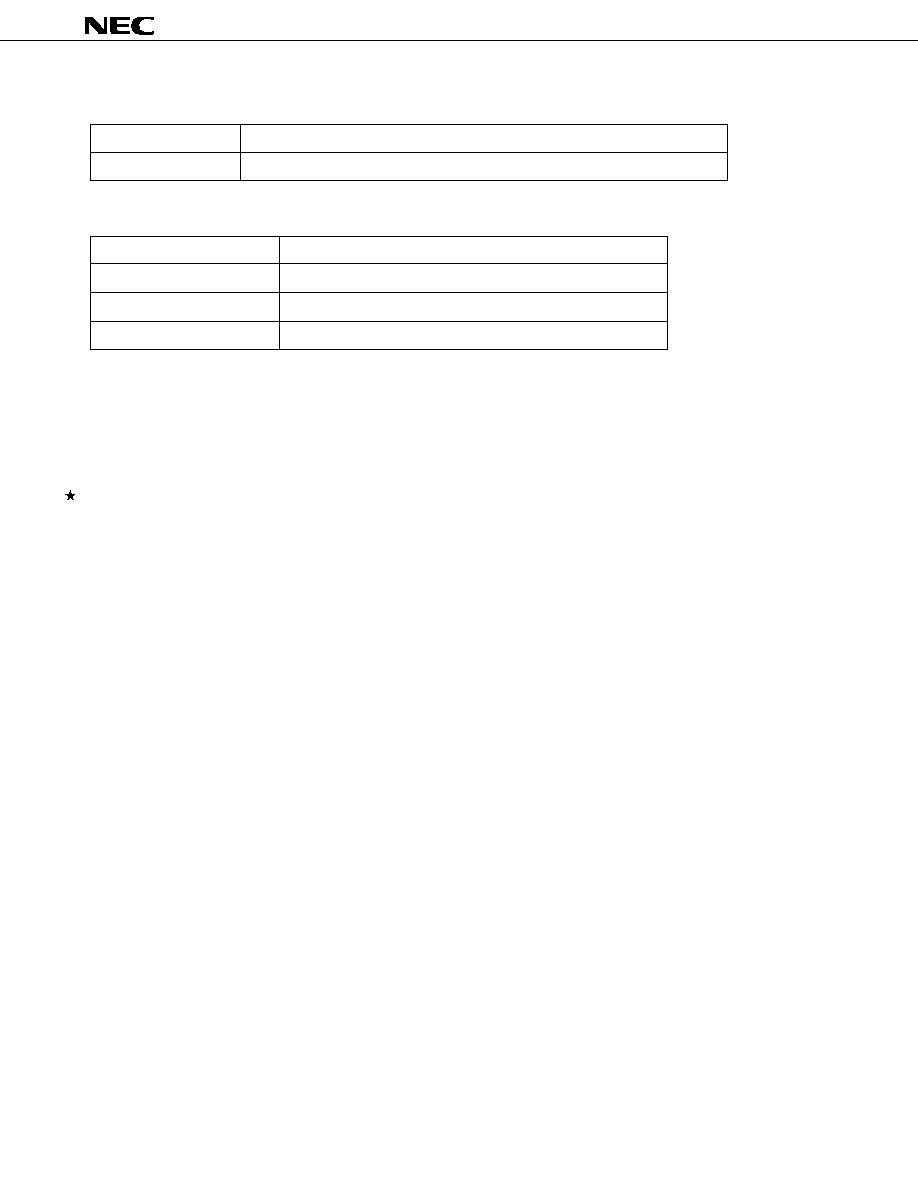
63
µ
PD78062(A), 78063(A), 78064(A)
Fuzzy Inference Development Support System
Notes 1.
PC-9800 series (MS-DOS
TM
) based
2.
IBM PC/AT and compatible (PC DOS
TM
/IBM DOS
TM
/MS-DOS) based
3.
HP9000 series 300
TM
(HP-UX
TM
) based
4.
HP9000 series 700
TM
(HP-UX) based, SPARCstation
TM
(SunOS
TM
) based, EWS-4800 series (EWS-UX/V) based
5.
PC-9800 series (MS-DOS + Windows
TM
) based.
6.
IBM PC/AT and compatible (PC DOS/IBM DOS/MS-DOS + Windows) based
7.
NEWS
TM
(NEWS-OS
TM
) based
8.
IE-78064-R-EM is a maintenance product.
FE9000
Note 1
, FE9200
Note 6
FT9080
Note 1
, FT9085
Note 2
FI78K/0
Note 1, 2
FD78K/0
Note 1, 2
Fuzzy knowledge data creation tool
Translator
Fuzzy inference module
Fussy inference debugger
Remarks 1.
For third party development tools, refer to the 78K/0 Series Selection Guide (U11126E).
2.
RA78K/0, CC78K/0, SM78K0, ID78K0, SD78K/0, and RX78K/0 are used in combination with DF78064.
Real-Time OS
RX78K/0
Note 1, 2, 3, 4
MX78K0
Note 1, 2, 3, 4
78K/0 series real-time OS
78K/0 series OS
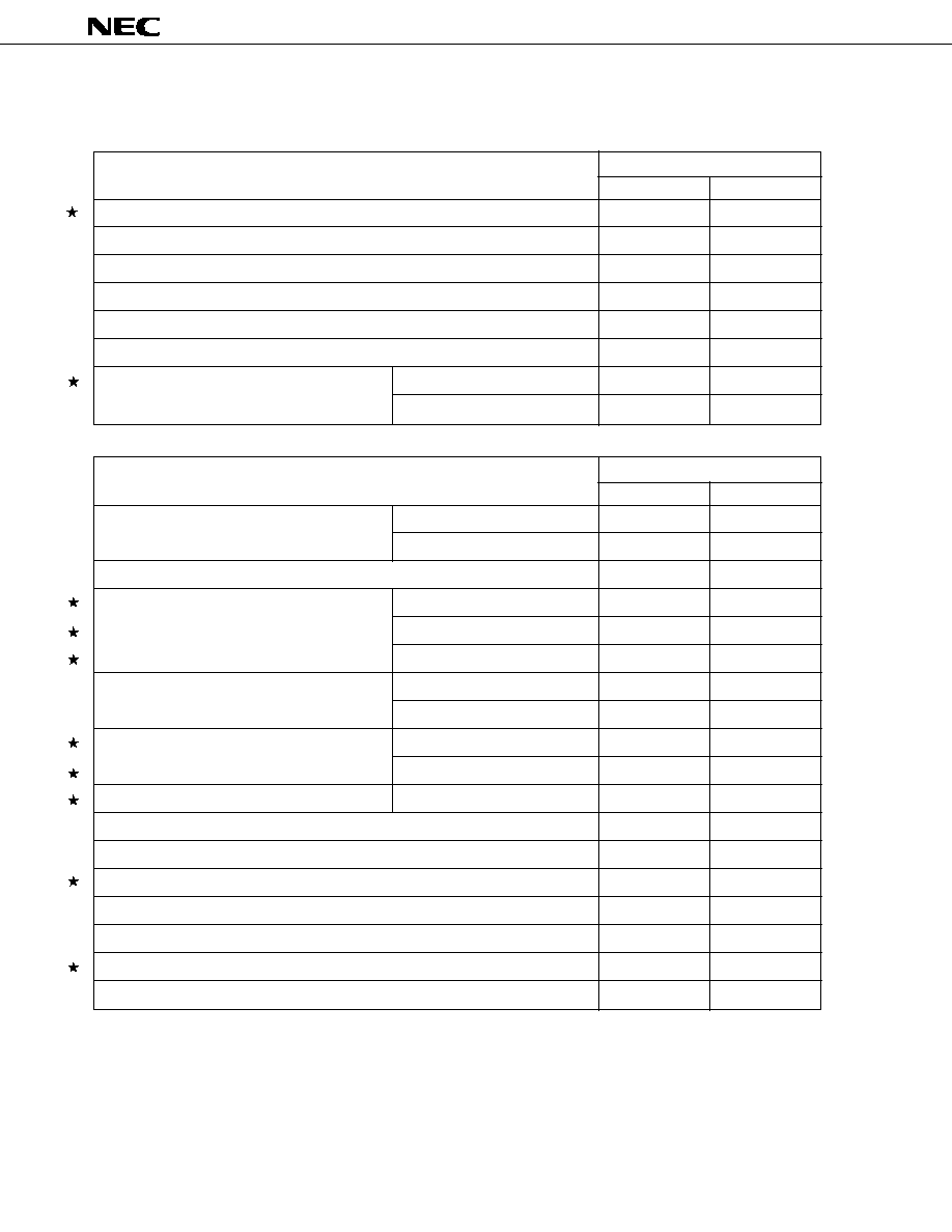
64
µ
PD78062(A), 78063(A), 78064(A)
APPENDIX B. RELATED DOCUMENTS
Device Related Documents
Document Name
Document No.
Japanese
English
µ
PD78062(A), 78063(A) 78064(A) Data Sheet
U10335J
This document
µ
PD78064, 78064Y Subseries User's Manual
U10105J
U10105E
78K/0 Series User's Manual - Instruction
U12326J
IEU-1372
78K/0 Series Instruction Table
U10903J
--
78K/0 Series Instruction Set
U10904J
--
µ
PD78018F Subseries Special Function Register Table
IEM-5568
--
78K/0 Series Application Note
Fundamental (III)
IEA-767
U10182E
Floating-Point Arithmetic Program
IEA-718
IEA-1289
Development Tools Related Documents (User's Manual) (1/2)
Document Name
Document No.
Japanese
English
RA78K Series Assembler Package
Operation
EEU-809
EEU-1399
Language
EEU-815
EEU-1404
RA78K Series Structured Assembler Preprocessor
EEU-817
EEU-1402
RA78K0 Assembler Package
Operation
U11802J
U11802E
Assembly Language
U11801J
U11801E
Structured Assembly Language
U11789J
U11789E
CC78K Series C Compiler
Operation
EEU-656
EEU-1280
Language
EEU-655
EEU-1284
CC78K/0 C Compiler
Operation
U11517J
U11517E
Language
U11518J
U11518E
CC78K/0 C Compiler Application Note
Programming Know-how
EEA-618
EEA-1208
CC78K Series Library Source File
U12322J
--
IE-78000-R
EEU-810
U11376E
IE-78000-R-A
U10057J
U10057E
IE-78000-R-BK
EEU-867
EEU-1427
IE-78064-R-EM
EEU-905
EEU-1443
IE-780308-R-EM
U11362J
U11362E
EP-78064
EEU-934
EEU-1469
Caution The contents of the above related documents are subject to change without notice. The latest
documents should be used for design, etc.
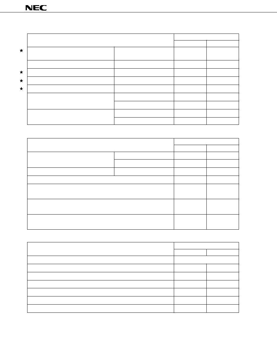
65
µ
PD78062(A), 78063(A), 78064(A)
Development Tools Documents (User's Manual) (2/2)
Document Name
Document No.
Japanese
English
SM78K Series System Simulator
External Components User Open
U10092J
U10092E
Interface
SM78K0 System Simulator Windows Based
Reference
U10181J
U10181E
ID78K0 Integrated Debugger EWS Based
Reference
U11515J
--
ID78K0 Integrated Debugger PC Based
Reference
U11539J
U11539E
ID78K0 Integrated Debugger Windows Based
Guide
U11649J
U11649E
SD78K/0 Screen Debugger
Introduction
EEU-852
U10539E
PC-9800 Series (MS-DOS) Based
Reference
U10952J
--
SD78K/0 Screen Debugger
Introduction
EEU-5024
EEU-1414
IBM PC/AT (PC DOS) Based
Reference
U11279J
U11279E
Embedded Software Documents (User's Manual)
Document Name
Document No.
Japanese
English
78K/0 Series Real-Time OS
Fundamental
U11537J
--
Installation
U11536J
--
78K/0 Series OS MX78K0
Fundamental
U12257J
--
Fuzzy Knowledge Data Creation Tool
EEU-829
EEU-1438
78K/0, 78K/II, 87AD Series Fuzzy Inference Development Support System
EEU-862
EEU-1444
- Translator
78K/0 Series Fuzzy Inference Development Suport System
EEU-858
EEU-1441
- Fuzzy Inference Module
78K/0 Series Fuzzy Inference Development Support System
EEU-921
EEU-1458
- Fuzzy Inference Debugger
Other Documents
Document Name
Document No.
Japanese
English
IC Package Manual
C10943X
Semiconductor Device Mounting Technology Manual
C10535J
C10535E
Quality Grades on NEC Semiconductor Device
C11531J
C11531E
NEC Semiconductor Device Reliability/Quality Control System
C10983J
C10983E
Electrostatic Discharge (ESD) Test
MEM-539
--
Guide to Quality Assurance for Semiconductor Device
C11893J
C11893E
Guide for Products Related to MicroComputer: Other Companies
U11416J
--
Caution
The contents of the above related documents are subject to change without notice. The latest
documents should be used for design, etc.
66
µ
PD78062(A), 78063(A), 78064(A)
NOTES FOR CMOS DEVICES
1
PRECAUTION AGAINST ESD FOR SEMICONDUCTORS
Note: Strong electric field, when exposed to a MOS device, can cause destruction
of the gate oxide and ultimately degrade the device operation. Steps must
be taken to stop generation of static electricity as much as possible, and
quickly dissipate it once, when it has occurred. Environmental control must
be adequate. When it is dry, humidifier should be used. It is recommended
to avoid using insulators that easily build static electricity. Semiconductor
devices must be stored and transported in an anti-static container, static
shielding bag or conductive material. All test and measurement tools
including work bench and floor should be grounded. The operator should
be grounded using wrist strap. Semiconductor devices must not be touched
with bare hands. Similar precautions need to be taken for PW boards with
semiconductor devices on it.
2
HANDLING OF UNUSED INPUT PINS FOR CMOS
Note: No connection for CMOS device inputs can be cause of malfunction. If no
connection is provided to the input pins, it is possible that an internal input
level may be generated due to noise, etc., hence causing malfunction. CMOS
device behave differently than Bipolar or NMOS devices. Input levels of
CMOS devices must be fixed high or low by using a pull-up or pull-down
circuitry. Each unused pin should be connected to V
DD
or GND with a
resistor, if it is considered to have a possibility of being an output pin. All
handling related to the unused pins must be judged device by device and
related specifications governing the devices.
3
STATUS BEFORE INITIALIZATION OF MOS DEVICES
Note: Power-on does not necessarily define initial status of MOS device. Produc-
tion process of MOS does not define the initial operation status of the device.
Immediately after the power source is turned ON, the devices with reset
function have not yet been initialized. Hence, power-on does not guarantee
out-pin levels, I/O settings or contents of registers. Device is not initialized
until the reset signal is received. Reset operation must be executed imme-
diately after power-on for devices having reset function.

67
µ
PD78062(A), 78063(A), 78064(A)
NEC Electronics Inc. (U.S.)
Santa Clara, California
Tel: 800-366-9782
Fax: 800-729-9288
NEC Electronics (Germany) GmbH
Duesseldorf, Germany
Tel: 0211-65 03 02
Fax: 0211-65 03 490
NEC Electronics (UK) Ltd.
Milton Keynes, UK
Tel: 01908-691-133
Fax: 01908-670-290
NEC Electronics Italiana s.r.1.
Milano, Italy
Tel: 02-66 75 41
Fax: 02-66 75 42 99
NEC Electronics Hong Kong Ltd.
Hong Kong
Tel: 2886-9318
Fax: 2886-9022/9044
NEC Electronics Hong Kong Ltd.
Seoul Branch
Seoul, Korea
Tel: 02-528-0303
Fax: 02-528-4411
NEC Electronics Singapore Pte. Ltd.
United Square, Singapore 1130
Tel: 253-8311
Fax: 250-3583
NEC Electronics Taiwan Ltd.
Taipei, Taiwan
Tel: 02-719-2377
Fax: 02-719-5951
NEC do Brasil S.A.
Sao Paulo-SP, Brasil
Tel: 011-889-1680
Fax: 011-889-1689
NEC Electronics (Germany) GmbH
Benelux Office
Eindhoven, The Netherlands
Tel: 040-2445845
Fax: 040-2444580
NEC Electronics (France) S.A.
Velizy-Villacoublay, France
Tel: 01-30-67 58 00
Fax: 01-30-67 58 99
NEC Electronics (France) S.A.
Spain Office
Madrid, Spain
Tel: 01-504-2787
Fax: 01-504-2860
NEC Electronics (Germany) GmbH
Scandinavia Office
Taeby, Sweden
Tel: 08-63 80 820
Fax: 08-63 80 388
Regional Information
Some information contained in this document may vary from country to country. Before using any NEC
product in your application, please contact the NEC office in your country to obtain a list of authorized
representatives and distributors. They will verify:
∑ Device availability
∑ Ordering information
∑ Product release schedule
∑ Availability of related technical literature
∑ Development environment specifications (for example, specifications for third-party tools and
components, host computers, power plugs, AC supply voltages, and so forth)
∑ Network requirements
In addition, trademarks, registered trademarks, export restrictions, and other legal issues may also vary
from country to country.
J96. 8

µ
PD78062(A), 78063(A), 78064(A)
FIP is a registered trademark of NEC Corporation.
IEBus is a trademark of NEC Corporation.
MS-DOS and Windows are either registered trademarks or trademarks of Microsoft Corporation in the United
States and/or other countries.
IBM-DOS, PC/AT, and PC DOS are trademarks of IBM Corporation.
HP9000 series 300, HP9000 series 700, and HP-UX are trademarks of Hewlett-Packard Company.
SPARCstation is a trademark of SPARC International, Inc.
SunOS is a trademark of Sun Microsystems, Inc.
NEWS and NEWS-OS are trademarks of Sony Corporation.
Some of related document may be preliminary, but is not marked as such.
Please keep this in mind as you refer to this information.
No part of this document may be copied or reproduced in any form or by any means without the prior written
consent of NEC Corporation. NEC Corporation assumes no responsibility for any errors which may appear in
this document.
NEC Corporation does not assume any liability for infringement of patents, copyrights or other intellectual property
rights of third parties by or arising from use of a device described herein or any other liability arising from use
of such device. No license, either express, implied or otherwise, is granted under any patents, copyrights or other
intellectual property rights of NEC Corporation or others.
While NEC Corporation has been making continuous effort to enhance the reliability of its semiconductor devices,
the possibility of defects cannot be eliminated entirely. To minimize risks of damage or injury to persons or
property arising from a defect in an NEC semiconductor device, customers must incorporate sufficient safety
measures in its design, such as redundancy, fire-containment, and anti-failure features.
NEC devices are classified into the following three quality grades:
"Standard", "Special", and "Specific". The Specific quality grade applies only to devices developed based on a
customer designated "quality assurance program" for a specific application. The recommended applications of
a device depend on its quality grade, as indicated below. Customers must check the quality grade of each device
before using it in a particular application.
Standard: Computers, office equipment, communications equipment, test and measurement equipment,
audio and visual equipment, home electronic appliances, machine tools, personal electronic
equipment and industrial robots
Special:
Transportation equipment (automobiles, trains, ships, etc.), traffic control systems, anti-disaster
systems, anti-crime systems, safety equipment and medical equipment (not specifically designed
for life support)
Specific:
Aircrafts, aerospace equipment, submersible repeaters, nuclear reactor control systems, life
support systems or medical equipment for life support, etc.
The quality grade of NEC devices is "Standard" unless otherwise specified in NEC's Data Sheets or Data Books.
If customers intend to use NEC devices for applications other than those specified for Standard quality grade,
they should contact an NEC sales representative in advance.
Anti-radioactive design is not implemented in this product.
M4 96.5
The export of this product from Japan is regulated by the Japanese government. To export this product may be prohibited
without governmental license, the need for which must be judged by the customer. The export or re-export of this product
from a country other than Japan may also be prohibited without a license from that country. Please call an NEC sales
representative.