 | –≠–ª–µ–∫—Ç—Ä–æ–Ω–Ω—ã–π –∫–æ–º–ø–æ–Ω–µ–Ω—Ç: uPD78082 | –°–∫–∞—á–∞—Ç—å:  PDF PDF  ZIP ZIP |
Document Outline
- COVER
- FEATURES
- ORDERING INFORMATION
- FUNCTION OUTLINE
- 1. PIN CONFIGURATION (Top View)
- 2. BLOCK DIAGRAM
- 3. PIN FUNCTIONS
- 3.1 Port Pins
- 3.2 Non-port Pins
- 3.3 Equivalent Circuits for Pins
- 3.4 Recommended Connection of Unused Pins
- 4. Mk I AND Mk II MODE SELECTION FUNCTION
- 4.1 Differences between Mk I Mode and Mk II Mode
- 4.2 Setting of Stack Bank Selection (SBS) Register
- 5. DIFFERENCES BETWEEN uPD75P3116 AND uPD753104, 753106, 753108
- 6. MEMORY CONFIGURATION
- 7. INSTRUCTION SET
- 8. ONE-TIME PROM (PROGRAM MEMORY) WRITE AND VERIFY
- 8.1 Operation Modes for Program Memory Write/Verify
- 8.2 Program Memory Write Procedure
- 8.3 Program Memory Read Procedure
- 8.4 One-time PROM Screening
- 9. ELECTRICAL SPECIFICATIONS
- 10. CHARACTERISTIC CURVES (REFERENCE VALUES)
- 11. PACKAGE DRAWINGS
- 12. RECOMMENDED SOLDERING CONDITIONS
- APPENDIX A. FUNCTION LIST OF uPD75308B, 753108 AND 75P3116
- APPENDIX B. DEVELOPMENT TOOLS
- APPENDIX C. RELATED DOCUMENTS
The
µ
PD75P3116 replaces the
µ
PD753108's internal mask ROM with a one-time PROM, and features expanded ROM
capacity.
Because the
µ
PD75P3116 supports programming by users, it is suitable for use in evaluation of systems in the
development stage using the
µ
PD753104, 753106, or 753108, and for use in small-scale production.
Detailed information about functions is provided in the following User's Manual. Be sure to read it before
designing:
µ
PD753108 User's Manual : U10890E
FEATURES
Compatible with
µ
PD753108
Memory capacity:
∑ PROM : 16384 x 8 bits
∑ RAM
: 512 x 4 bits
Can be operated in same power supply voltage range as the mask version
µ
PD753108
∑ V
DD
= 1.8 to 5.5 V
On-chip LCD controller/driver
QTOP
TM
microcontroller
Remark QTOP microcontrollers are microcontrollers with on-chip one-time PROM that are totally supported by NEC.
The support include writing application programs, marking, screening, and verification.
ORDERING INFORMATION
Part Number
Package
µ
PD75P3116GC-AB8
64-pin plastic QFP (14 x 14 mm, 0.8-mm pitch)
µ
PD75P3116GK-8A8
64-pin plastic QFP (12 x 12 mm, 0.65-mm pitch)
Caution This device does not provide an internal pull-up resistor connection function by means of mask
option.
µ
PD75P3116
MOS INTEGRATED CIRCUIT
4-BIT SINGLE-CHIP MICROCONTROLLER
The mark
shows major revised points.
Document No.
U11369EJ2V0DS00 (2nd edition)
Date Published March 1997 N
Printed in Japan
©
1994
DATA SHEET
The information in this document is subject to change without notice.

µ
PD75P3116
2
FUNCTION OUTLINE
Item
Function
Instruction execution time
∑ 0.95, 1.91, 3.81, or 15.3
µ
s (main system clock: @ 4.19 MHz)
∑ 0.67, 1.33, 2.67, or 10.7
µ
s (main system clock: @ 6.0 MHz)
∑ 122
µ
s (subsystem clock: @ 32.768 kHz)
Internal memory
PROM
16384 x 8 bits
RAM
512 x 4 bits
General-purpose register
∑ 4-bit manipulation: 8 x 4 banks
∑ 8-bit manipulation: 4 x 4 banks
I/O ports
CMOS input
8
Internal pull-up resistor connection can be specified by software: 7
CMOS I/O
20
Internal pull-up resistor connection can be specified by software: 12
Shared by segment pin: 8
N-ch open-drain I/O
4
13-V withstand voltage
Total
32
LCD controller/driver
∑ Segment number selection : 16/20/24 segments (Switchable to CMOS I/O
ports in a batch of 4 pins, max. 8 pins)
∑ Display mode selection
: static, 1/2 duty (1/2 bias), 1/3 duty (1/2 bias),
1/3 duty (1/3 bias), 1/4 duty (1/3 bias)
Timers
5 channels: ∑ 8-bit timer/event counter : 3 channels
(Can be used as 16-bit timer/event counter, carrier generator,
and timer with gate)
∑ Basic interval timer/watchdog timer : 1 channel
∑ Watch timer : 1 channel
Serial interface
∑ 3-wire serial I/O mode ∑∑∑ MSB/LSB first switchable
∑ 2-wire serial I/O mode
∑ SBI mode
Bit sequential buffer (BSB)
16 bits
Clock output (PCL)
, 524, 262, and 65.5 kHz (main system clock: @ 4.19 MHz)
, 750, 375, and 93.8 kHz (main system clock: @ 6.0 MHz)
Buzzer output (BUZ)
∑ 2, 4, and 32 kHz (main system clock: @ 4.19 MHz or subsystem clock: @ 32.768 kHz)
∑ 2.93, 5.86, 46.9 kHz (main system clock: @ 6.0 MHz)
Vectored interrupts
∑ External : 3
∑ Internal : 5
Test inputs
∑ External : 1
∑ Internal : 1
System clock oscillation circuit
∑ Ceramic/crystal oscillation circuit for main system clock
∑ Crystal oscillation circuit for subsystem clock
Standby function
STOP/HALT mode
Power supply voltage
V
DD
= 1.8 to 5.5 V
Package
∑ 64-pin plastic QFP (14 x 14 mm, 0.8-mm pitch)
∑ 64-pin plastic QFP (12 x 12 mm, 0.65-mm pitch)

µ
PD75P3116
3
CONTENTS
1. PIN CONFIGURATION (Top View) ..................................................................................................
4
2. BLOCK DIAGRAM ............................................................................................................................
5
3. PIN FUNCTIONS ...............................................................................................................................
6
3.1
Port Pins ...................................................................................................................................................
6
3.2
Non-port Pins ...........................................................................................................................................
8
3.3
Equivalent Circuits for Pins .................................................................................................................... 10
3.4
Recommended Connection of Unused Pins ......................................................................................... 12
4. Mk I AND Mk II MODE SELECTION FUNCTION ............................................................................. 13
4.1
Differences between Mk I Mode and Mk II Mode ................................................................................... 13
4.2
Setting of Stack Bank Selection (SBS) Register ................................................................................... 14
5. DIFFERENCES BETWEEN
µ
PD75P3116 AND
µ
PD753104, 753106, AND 753108 ...................... 15
6. MEMORY CONFIGURATION ........................................................................................................... 16
7. INSTRUCTION SET .......................................................................................................................... 18
8. ONE-TIME PROM (PROGRAM MEMORY) WRITE AND VERIFY ................................................... 27
8.1
Operation Modes for Program Memory Write/Verify ............................................................................ 27
8.2
Program Memory Write Procedure ......................................................................................................... 28
8.3
Program Memory Read Procedure ......................................................................................................... 29
8.4
One-time PROM Screening ..................................................................................................................... 30
9. ELECTRICAL SPECIFICATIONS ..................................................................................................... 31
10. CHARACTERISTIC CURVES (REFERENCE VALUES) .................................................................. 46
11. PACKAGE DRAWINGS ................................................................................................................... 48
12. RECOMMENDED SOLDERING CONDITIONS ................................................................................ 50
APPENDIX A. FUNCTION LIST OF
µ
PD75308B, 753108, AND 75P3116 ........................................... 51
APPENDIX B. DEVELOPMENT TOOLS ................................................................................................ 53
APPENDIX C. RELATED DOCUMENTS ............................................................................................... 57
µ
PD75P3116
4
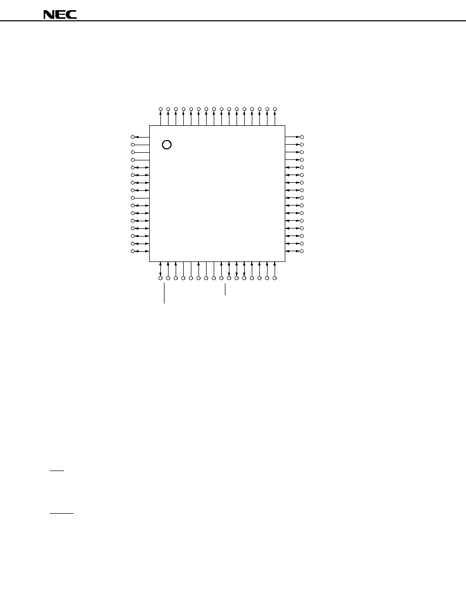
1. PIN CONFIGURATION (Top View)
∑ 64-pin plastic QFP (14 x 14 mm, 0.8-mm pitch) :
µ
PD75P3116GC-AB8
∑ 64-pin plastic QFP (12 x 12 mm, 0.65-mm pitch) :
µ
PD75P3116GK-8A8
Note
Always connect the V
PP
pin directly to V
DD
during normal operation.
PIN IDENTIFICATIONS
P00-P03
: Port0
COM0 to COM3 : Common Output 0 to 3
P10-P13
: Port1
V
LC0
to
V
LC2
: LCD Power Supply 0 to 2
P20-P23
: Port2
BIAS
: LCD Power Supply Bias Control
P30-P33
: Port3
LCDCL
: LCD Clock
P50-P53
: Port5
SYNC
: LCD Synchronization
P60-P63
: Port6
TI0 to TI2
: Timer Input 0 to 2
P80-P83
: Port8
PTO0 to PTO2
: Programmable Timer Output 0 to 2
P90-P93
: Port9
BUZ
: Buzzer Clock
KR0-KR3
: Key Return 0 to 3
PCL
: Programmable Clock
SCK
: Serial Clock
INT0, 1, 4
: External Vectored Interrupt 0, 1, 4
SI
: Serial Input
INT2
: External Test Input 2
SO
: Serial Output
X1, X2
: Main System Clock Oscillation 1, 2
SB0, SB1
: Serial Data Bus 0, 1
XT1, XT2
: Subsystem Clock Oscillation 1, 2
RESET
: Reset
V
PP
: Programming Power Supply
MD0 to MD3
: Mode Selection 0 to 3
V
DD
: Positive Power Supply
D0 to D7
: Data Bus 0 to 7
Vss
: Ground
S0 to S23
: Segment Output 0 to 23
48
S12
47
S13
46
S14
45
S15
44
P93/S16
43
P92/S17
42
P91/S18
41
P90/S19
40
P83/S20
39
P82/S21
38
P81/S22
37
P80/S23
36
P23/BUZ
35
P22/PCL/PTO2
34
P21/PTO1
33
P20/PTO0
64
COM3
63
COM2
62
COM1
61
COM0
60
S0
59
S1
58
S2
57
S3
56
S4
55
S5
54
S6
53
S7
52
S8
51
S9
50
S10
49
S11
1
BIAS
2
V
LC0
3
V
LC1
4
V
LC2
5
P30/LCDCL/MD0
6
P31/SYNC/MD1
7
P32/MD2
8
P33/MD3
9
Vss
10
P50/D4
11
P51/D5
12
P52/D6
13
P53/D7
14
P60/KR0/D0
15
P61/KR1/D1
16
P62/KR2/D2
17
P63/KR3/D3
18
RESET
19
XT1
20
XT2
21
V
PP
22
X1
23
X2
24
V
DD
25
P00/INT4
26
P01/SCK
27
P02/SO/SB0
28
P03/SI/SB1
29
P10/INT0
30
P11/INT1
31
P12/INT2/TI1/TI2
32
P13/TI0
Note
µ
PD75P3116
5
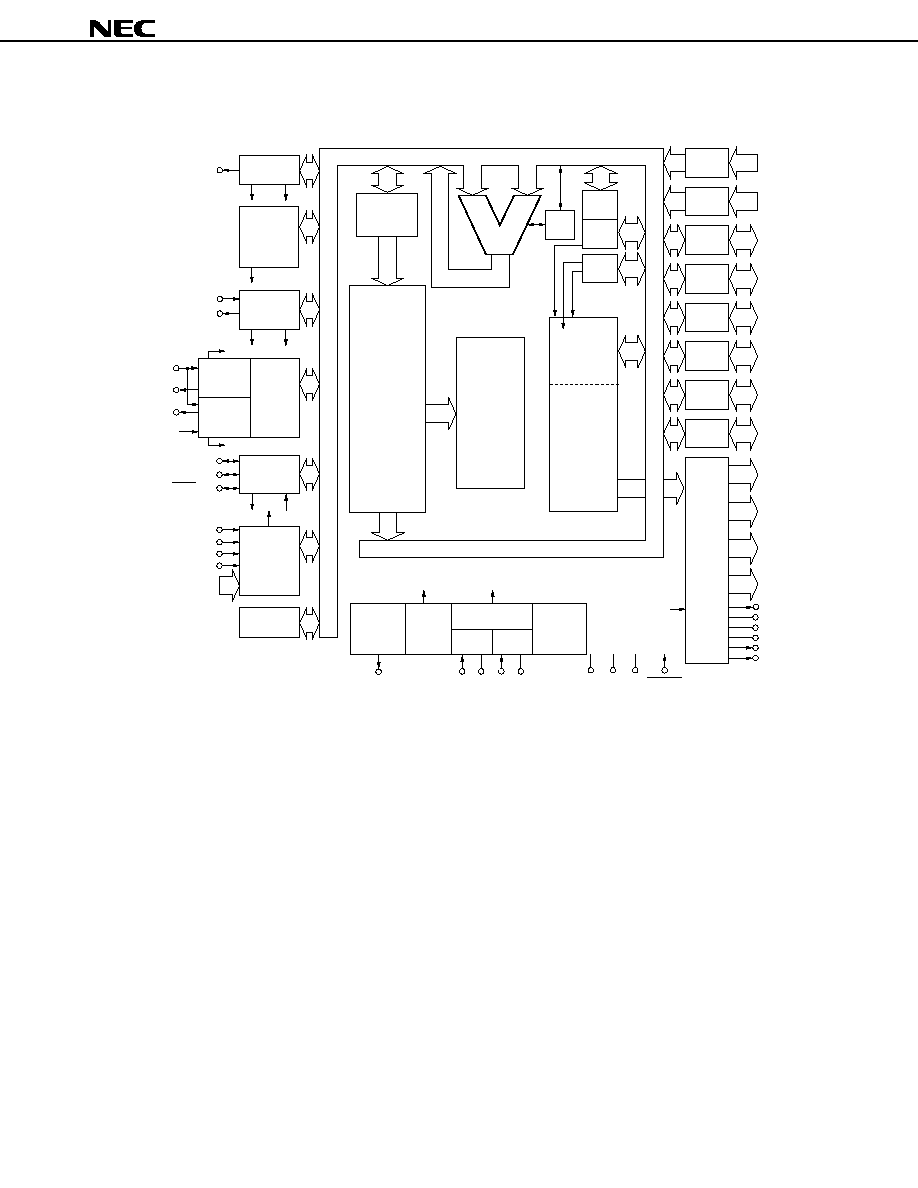
2. BLOCK DIAGRAM
P20 to P23
PORT0
P00 to P03
S0 to S15
16
4
4
4
4
4
4
4
4
COM0 to COM3
4
BIAS
f
LCD
V
PP
V
DD
RESET
Vss
CPU CLOCK
STAND BY
CONTROL
X2
X1
XT2
XT1
SYSTEM CLOCK
GENERATOR
MAIN
SUB
CLOCK
DIVIDER
CLOCK
OUTPUT
CONTROL
fx/2
N
PCL/PTO2/P22
GENERAL
REG.
DATA
MEMORY
(RAM)
512 x 4 BITS
BANK
SBS
SP (8)
CY
ALU
PROGRAM
COUNTER (14)
PROGRAM
MEMORY
(PROM)
16384 x 8 BITS
DECODE
AND
CONTROL
PORT1
P10 to P13
PORT2
PORT3
P30/MD0 to
P33/MD3
PORT5
P50/D4 to
P53/D7
PORT6
P60/D0 to
P63/D3
PORT8
P80 to P83
PORT9
P90 to P93
LCD
CONTROLLER/
DRIVER
4
S16/P93 to
S19/P90
4
S20/P83 to
S23/P80
V
LC0
V
LC1
V
LC2
SYNC/P31
LCDCL/P30
CLOCKED
SERIAL
INTERFACE
SI/SB1/P03
INTCSI
INTERRUPT
CONTROL
INT0/P10
SO/SB0/P02
SCK/P01
TOUT0
INT1/P11
INT4/P00
INT2/P12/TI1/TI2
P60/KR0 to
P63/KR3
BIT SEQ.
BUFFER (16)
4
INT1
8-BIT
TIMER/EVENT
COUNTER #1
8-BIT
TIMER/EVENT
COUNTER #2
CASCADED
16-BIT
TIMER/
EVENT
COUNTER
INTT2
INTT1
TI1/TI2/
P12/INT2
PTO1/P21
TOUT0
PTO2/
PCL/P22
INTT0
TOUT0
8-BIT
TIMER/EVENT
COUNTER #0
TI0/P13
PTO0/P20
BASIC
INTERVAL
TIMER/
WATCHDOG
TIMER
INTBT
BUZ/P23
WATCH
TIMER
INTW f
LCD