 | –≠–ª–µ–∫—Ç—Ä–æ–Ω–Ω—ã–π –∫–æ–º–ø–æ–Ω–µ–Ω—Ç: UPD780924 | –°–∫–∞—á–∞—Ç—å:  PDF PDF  ZIP ZIP |
Document Outline
- COVER
- DESCRIPTION
- FEATURES
- APPLICATION FIELD
- ORDERING INFORMATION
- 78K/0 SERIES DEVELOPMENT
- OVERVIEW OF FUNCTION
- 1. PIN CONFIGURATION (TOP VIEW)
- 2. BLOCK DIAGRAM
- 3. PIN FUNCTIONS
- 3.1 Port Pins
- 3.2 Non-port Pins
- 3.3 Pin I/O Circuits and Recommended Connection of Unused Pins
- 4. MEMORY SPACE
- 5. PERIPHERAL HARDWARE FUNCTIONS
- 5.1 Ports
- 5.2 Clock Generator
- 5.3 Timer/Event Counter
- 5.4 Clock Output Control Circuit
- 5.5 Buzzer Output Control Circuit
- 5.6 A/D Converter
- 5.7 Serial Interfaces
- 6. INTERRUPT FUNCTIONS AND TEST FUNCTIONS
- 6.1 Interrupt Functions
- 6.2 Test Functions
- 7. EXTERNAL DEVICE EXPANSION FUNCTIONS
- 8. STANDBY FUNCTION
- 9. RESET FUNCTION
- 10. INSTRUCTION SET
- 11. PACKAGE DRAWINGS
- APPENDIX A. DEVELOPMENT TOOLS
- APPENDIX B. RELATED DOCUMENTS
DESCRIPTION
The
µ
PD780016Y and 780018Y are members of the
µ
PD780018Y subseries of the 78K/0 series microcontrollers.
Besides a high-speed, high-performance CPU, these microcontrollers have on-chip ROM, RAM, I/O ports, timer,
serial interface, real-time output port, interrupt control, and various other peripheral hardware.
The
µ
PD78P0018Y devices including a one-time PROM version and an EPROM version, both of which can operate
in the same power supply voltage range as a mask ROM version, and various development tools are available.
The details of the functions are described in the following user's manuals. Be sure to read it before starting design.
µ
PD780018,780018Y Subseries User's Manual: U11754E
78K/0 Series User's Manual ≠ Instructions
: IEU-1372
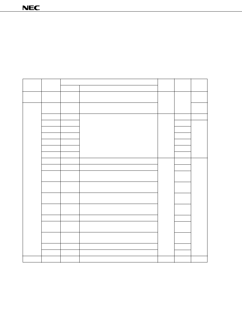
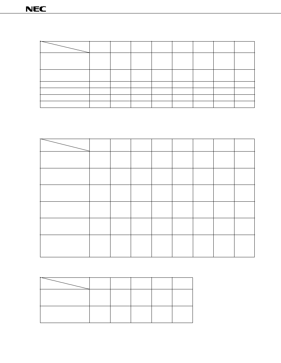
FEATURES
∑
Internal high capacity ROM and RAM
Item
Program
Data Memory
Part
Memory
Internal High-Speed
Buffer RAM
Internal Extended
Package
Number
(ROM)
RAM
RAM
µ
PD780016Y
48K bytes
1024 bytes
32 bytes
1024 bytes
100-pin plastic QFP
µ
PD780018Y
60K bytes
(14
◊
20 mm)
MOS INTEGRATED CIRCUIT
µ
PD780016Y, 780018Y
8-BIT SINGLE-CHIP MICROCONTROLLER
∑
External memory expansion space: 64K bytes
∑
Instruction execution time can be changed from
high-speed (0.4
µ
s) to ultra-low-speed (122
µ
s)
∑
I/O ports: 88
∑
8-bit resolution A/D converter: 8 channels
∑
Timer: 7 channels
∑
Serial interface: 3 channels
∑
3-wire serial I/O mode
(with automatic data transmit/receive function): 1 channel
∑
3-wire serial I/O mode
(with time division transfer function): 1 channel
∑
I
2
C bus mode (supporting multi-task): 1 channel
∑
Supply voltage : V
DD
= 2.7 to 5.5 V
APPLICATION FIELD
Cellular phones, cordless phones, AV equipment, etc.
Document No. U11810EJ1V0PM00 (1st edition)
Date Published December 1996 N
Printed in Japan
The information contained in this document is being issued in advance of the production cycle for the
device. The parameters for the device may change before final production or NEC Corporation, at its own
discretion, may withdraw the device prior to its production.
©
1996
PRELIMINARY PRODUCT INFORMATION

2
µ
PD780016Y, 780018Y
ORDERING INFORMATION
Part Number
Package
µ
PD780016YGF-XXX-3BA
100-pin plastic QFP (14
◊
20 mm)
µ
PD780018YGF-XXX-3BA
100-pin plastic QFP (14
◊
20 mm)
Remark
XXX indicates ROM code suffix.
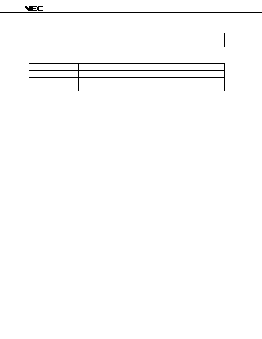
78K/0 SERIES DEVELOPMENT
These products are a further development in the 78K/0 Series. The designations appearing inside the boxes are
subseries names.
PD78014Y
PD78018F
PD78014
PD780001
PD780208
PD78044F
PD78024
PD78098
For LV
Low-voltage (1.8 V) operation product of the PD78014, ROM, RAM variations enhanced
A/D, 16-bit timer added to the PD78002
A/D added to the PD78002
I/O, FIP C/D of the PD78044F enhanced, display output total: 53
6-bit U/D counter added to the PD78024, display output total: 34
Basic subseries for FIP driving, display output total: 26
64-pin
64-pin
64-pin
100-pin
80-pin
64-pin
PD78P0914
64-pin
80-pin
78K/0
series
PD780308
PD78064B
PD78064
100-pin
100-pin
100-pin
PD78002
PD78083
PD78018FY
PD78002Y
64-pin
42/44-pin
Basic subseries for control
Internal UART, low-voltage (1.8 V) operation possible
Enhanced SIO of the PD78064, ROM, RAM extended
Reduced EMI noise product of the PD78064
Basic subseries for LCD driving, internal UART
IEBus controller added to the PD78054
PWM output, internal LV digital code decoder, Hsync counter
PD780308Y
PD78064Y
µ
µ
µ
µ
µ
µ
µ
µ
µ
µ
µ
µ
µ
µ
µ
µ
µ
µ
µ
µ
µ
µ
µ
µ
µ
µ
Supporting IEBus
TM
For driving LCD
For driving FIP
TM
PD780024Y
PD780034
PD780024
PD780964
Enhanced A/D of the PD780024
Enhanced serial I/O of the PD78018F. Reduced EMI noise product.
Enhanced A/D of the PD780924
64-pin
64-pin
64-pin
PD780924
PD78014H
PD780034Y
64-pin
64-pin
Internal inverter control circuit and UART. Reduced EMI noise product.
Reduced EMI noise of the PD78018F.
µ
µ
µ
µ
µ
µ
µ
µ
µ
PD78078
PD78070A
PD780018
Note
PD78058F
PD78054
PD78078Y
PD78070AY
PD780018Y
Note
PD78058FY
PD78054Y
For control
Timer added to the PD78054, external interface functions enhanced
ROM-less product for the PD78078
Enhanced serial I/O of the PD78078, functions limited
Reduced EMI noise product of the PD78054
UART and D/A added to the PD78014, enhanced I/O
100-pin
100-pin
100-pin
80-pin
80-pin
µ
µ
µ
µ
µ
µ
µ
µ
µ
µ
µ
µ
µ
µ
µ
Y subseries supports I
2
C bus.
Under mass production
Under development
µ
Note Under planning
µ
µ
PD780016Y, 780018Y
3
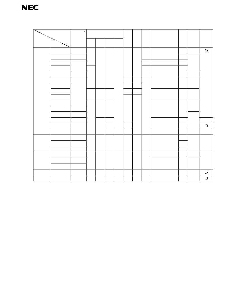
The major functional differences among the subseries are shown below.
Function
Timer
V
DD
I/O
MIN.
Subseries Name
8-bit 16-bit Watch WDT
Value
For Control
µ
PD78078
32 K-60 K
4ch
1ch
1ch
1ch
8ch
--
2ch
3ch (UART: 1ch)
88
1.8 V
µ
PD78070A --
61
2.7 V
µ
PD780018
48 K-60 K
--
2ch
88
µ
PD78058F
2ch
2ch
3ch (UART: 1ch)
69
µ
PD78054 16 K-60 K
2.0 V
µ
PD780034
8 K-32 K
--
8ch
--
51
1.8 V
µ
PD780024
8ch
--
µ
PD780964
3ch
Note
--
--
8ch
2ch (UART: 2ch)
47
2.7 V
µ
PD780924
8ch
--
µ
PD78014H
2ch
1ch
1ch
2ch
53
1.8 V
µ
PD78018F 8 K-60 K
µ
PD78014
8 K-32 K
2.7 V
µ
PD780001
8 K
--
--
1ch
39
--
µ
PD78002
8 K-16 K
1ch
--
53
µ
PD78083
--
8ch
1ch (UART: 1ch)
33
1.8 V
--
For FIP
µ
PD780208
32 K-60 K
2ch
1ch
1ch
1ch
8ch
--
--
2ch
74
2.7 V
--
driving
µ
PD78044F 16 K-40 K
68
µ
PD78024
24 K-32 K
54
For LCD
µ
PD780308
48 K-60 K
2ch
1ch
1ch
1ch
8ch
--
--
3ch (UART: 1ch)
57
1.8 V
--
driving
µ
PD78064B 32 K
2ch (UART: 1ch)
2.0 V
µ
PD78064
16 K-32 K
For IEBus
µ
PD78098
32 K-60 K
2ch
1ch
1ch
1ch
8ch
--
2ch
3ch (UART: 1ch)
69
2.7 V
For LV
µ
PD78P0914 32 K
6ch
--
--
1ch
8ch
--
--
2ch
54
4.5 V
Note
10-bit timer: 1 channel
External
Eexpansion
8-bit
A/D
8-bit
D/A
Serial
Interface
ROM
Capacity
10-bit
A/D
4
µ
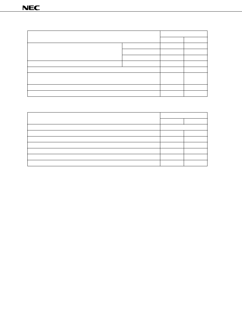
PD780016Y, 780018Y
Internal
ROM
48K bytes
60K bytes
memory
Internal high-speed RAM
1024 bytes
Buffer RAM
32 butes
Internal expansion RAM
1024 bytes
Memory space
64K bytes
General registers
8 bits
◊
32 registers (8 bits
◊
8 registers
◊
4 banks)
Instruction cycle
On-chip instruction execution time selective function
When main system clock selected
0.4
µ
s/0.8
µ
s/1.6
µ
s/3.2
µ
s/6.4
µ
s (at 5.0 MHz)
When subsystem clock selected
122
µ
s (at 32.768 kHz)
Instruction set
∑ 16-bit operation
∑ Multiplcation/division (8 bits
◊
8 bits,16 bits
˜
8 bits)
∑ Bit manipulation (set, reset, test, boolean operation)
∑ BCD adjustment, etc.
I/O ports
Total
: 88
∑ CMOS input
:
9
∑ CMOS I/O
: 79
A/D converter
∑ 8-bit resolution
◊
8 channels
Serial interface
∑ 3-wire serial I/O mode (with automatic data transmit/receive function): 1 channel
∑ 3-wire serial I/O mode (with time division transfer function)
: 1 channel
∑ I
2
C bus mode (supporting multi-task)
: 1 channel
Timer
∑ 16-bit timer/event counter : 1 channel
∑ 8-bit timer/event counter : 4 channels
∑ Watch timer
: 1 channel
∑ Watchdog timer
: 1 channel
Timer output
5 (14-bit PWM output
◊
1, 8-bit PWM output
◊
2)
Clock output
39.1 kHz, 78.1 kHz, 156 kHz, 313 kHz, 625 kHz, 1.25 MHz, 2.5 MHz, 5.0 MHz
(at main system clock of 5.0 MHz)
32.768 kHz (at subsystem clock of 32.768 kHz)
Buzzer output
2.4 kHz, 4.9 kHz, 9.8 kHz (at main system clock: at 5.0 MHz)
Vectored
Maskable
Internal : 12
interrupt
External : 7
sources
Non-maskable
Internal : 1
Software
1
Test input
Internal : 1
External : 1
Supply voltage
V
DD
= 2.7 to 5.5 V
Package
∑ 100-pin plastic QFP (14
◊
20 mm)
OVERVIEW OF FUNCTION
Part Number
Item
µ
PD780016Y
µ
PD780018Y

µ
PD780016Y, 780018Y
5
CONTENTS
1.
PIN CONFIGURATION (TOP VIEW) ................................................................................................... 6
2.
BLOCK DIAGRAM .............................................................................................................................. 8
3.
PIN FUNCTIONS ................................................................................................................................. 9
3.1
Port Pins ...................................................................................................................................................... 9
3.2
Non-port Pins ............................................................................................................................................ 11
3.3
Pin I/O Circuits and Recommended Connection of Unused Pins ..................................................... 13
4.
MEMORY SPACE .............................................................................................................................. 16
5.
PERIPHERAL HARDWARE FUNCTIONS ....................................................................................... 17
5.1
Ports ........................................................................................................................................................... 17
5.2
Clock Generator ........................................................................................................................................ 18
5.3
Timer/Event Counter ................................................................................................................................ 18
5.4
Clock Output Control Circuit .................................................................................................................. 22
5.5
Buzzer Output Control Circuit ................................................................................................................ 22
5.6
A/D Converter ........................................................................................................................................... 23
5.7
Serial Interfaces ........................................................................................................................................ 24
6.
INTERRUPT FUNCTIONS AND TEST FUNCTIONS ....................................................................... 26
6.1
Interrupt Functions .................................................................................................................................. 26
6.2
Test Functions .......................................................................................................................................... 29
7.
EXTERNAL DEVICE EXPANSION FUNCTIONS ............................................................................. 30
8.
STANDBY FUNCTION ...................................................................................................................... 30
9.
RESET FUNCTION ............................................................................................................................ 31
10. INSTRUCTION SET ........................................................................................................................... 32
11. PACKAGE DRAWINGS ..................................................................................................................... 34
APPENDIX A. DEVELOPMENT TOOLS ................................................................................................ 35
APPENDIX B. RELATED DOCUMENTS ............................................................................................... 37
6
µ
PD780016Y, 780018Y
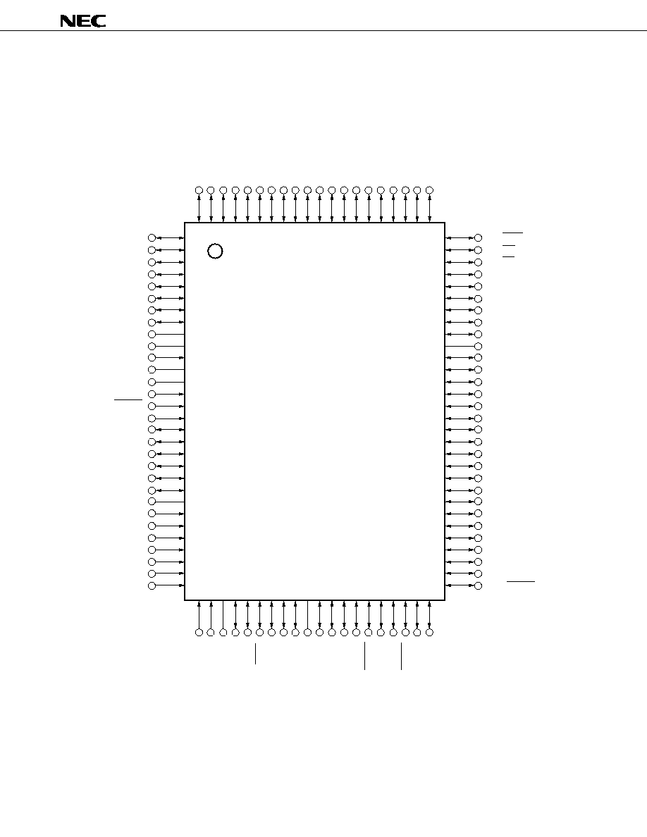
1. PIN CONFIGURATION (TOP VIEW)
∑
100-pin plastic QFP (14
◊
20 mm)
µ
PD780016YGF-XXX-3BA, 780018YGF-XXX-3BA
Cautions 1. Connect IC (internally connected) pin directly to V
SS0
.
2. AV
SS
pin should be connected to V
SS0
.
Remark
When the circuit is used in an application where the noise generated from the inside of the microcontroller
needs to be reduced, take countermeasures against noise such as supplying power to V
DD0
and V
DD1
separately and connecting V
SS0
and V
SS1
to the ground line separately.
P80/A0
P81/A1
P82/A2
P83/A3
P84/A4
P85/A5
P86/A6
P87/A7
IC
X2
X1
V
DD1
XT2
XT1
RESET
P00/INTP0/TI00
P01/INTP1/TI01
P02/INTP2
P03/INTP3
P04/INTP4
P05/INTP5
P06/INTP6
V
DD0
AV
REF
P10/ANI0
P11/ANI1
P12/ANI2
P13/ANI3
P14/ANI4
P15/ANI5
P16/ANI6
P17/ANI7
AV
SS
P20/SI1
P21/SO1
P22/SCK1
P23/STB
P24/BUSY
P25
V
SS1
P26
P27
P90/SI4A
P91/SO4A
P92/SCK4A
P93/SI4B
P94/SO4B
P95/SCK4B
P110/SI4C
P111/SO4C
P66/WAIT
P65/WR
P64/RD
P63
P62
P61
P60
P57/A15
P56/A14
V
SS0
P55/A13
P54/A12
P53/A11
P52/A10
P51/A9
P50/A8
P47/AD7
P46/AD6
P45/AD5
P44/AD4
P43/AD3
P42/AD2
P41/AD1
P40/AD0
P117/SCL
P116/SDA
P115
P114
P113
P112/SCK4C
P156
P155
P154
P153
P152
P151
P150
P37
P36/BUZ
P35/PCL
P34/TI2
P33/TI1
P32/TO2
P31/TO1
P30/TO0
P103
P102
P101/TI6/TO6
P100/TI5/TO5
P67/ASTB
1
2
3
4
5
6
7
8
9
10
11
12
13
14
15
16
17
18
19
20
21
22
23
24
25
26
27
28
29
30
31 32 33 34 35 36 37 38 39 40 41 42 43 44 45 46 47 48 49 50
80
79
78
77
76
75
74
73
72
71
70
69
68
67
66
65
64
63
62
61
60
59
58
57
56
55
54
53
52
51
100 99 98 97 96 95 94 93 92 91 90 89 88 87 86 85 84 83 82 81

µ
PD780016Y, 780018Y
7
A0-A15
: Address Bus
AD0-AD7
: Address/Data Bus
ANI0-ANI7
: Analog Input
ASTB
: Address Strobe
AV
REF
: Analog Reference Voltage
AV
SS
: Analog Ground
BUSY
: Busy
BUZ
: Buzzer Clock
IC
: Internally Connected
INTP0-INTP6
: Interrupt from Peripherals
P00-P06
: Port0
P10-P17
: Port1
P20-P27
: Port2
P30-P37
: Port3
P40-P47
: Port4
P50-P57
: Port5
P60-P67
: Port6
P80-P87
: Port8
P90-P96
: Port9
P100-P103
: Port10
P110-P117
: Port11
P150-P156
: Port15
PCL
: Programmable Clock
RD
: Read Strobe
RESET
: Reset
SCK1
: Serial Clock
SCK4A, SCK4B, SCK4C : Serial Clock
SCL
: Serial Clock
SDA
: Serial Data
SI1
: Serial Input
SI4A, SI4B, SI4C
: Serial Input
SO1
: Serial Output
SO4A, SO4B, SO4C
: Serial Output
STB
: Strobe
TI00, TI01
: Timer Input
TI1, TI2, TI5, TI6
: Timer Input
TO0-TO2, TO5, TO6
: Timer Output
V
DD0
, V
DD1
: Power Supply
V
SS0
, V
SS1
: Ground
WAIT
: Wait
WR
: Write Strobe
X1, X2
: Crystal (Main System Clock)
XT, XT2
: Crystal (Subsystem Clock)
8
µ
PD780016Y, 780018Y
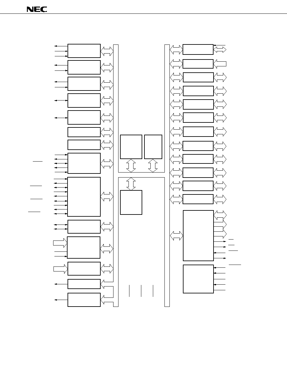
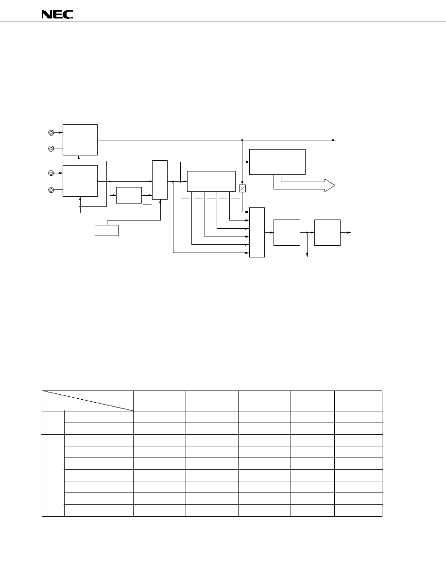
2. BLOCK DIAGRAM
Remark
The internal ROM capacity depends on the product.
A8/P50_
A15/P57
RD/P64
WR/P65
WAIT/P66
ASTB/P67
Port 0
External
access
RAM
16-bit timer/
event counter
8-bit timer/
event
counter 1
8-bit timer/
event
counter 2
Watch timer
TO0/P30
Clock output
control
System
control
78K/0
CPU Core
A/D
converter
Interrupt
control
Serial
interface 1
Port 1
Port 2
Port 3
Port 4
Port 5
Port 6
Port 11
Port 15
8-bit timer/
event
counter 5
8-bit timer/
event
counter 6
TI00/INTP0/P00
TI01/INTP1/P01
TO1/P31
TI1/P33
TO2/P32
TI2/P34
TI5/TO5/P100
TI6/TO6/P101
SI1/P20
SO1/P21
SCK1/P22
STB/P23
BUSY/P24
ANI0/P10_
ANI7/P17
AV
SS
AV
REF
INTP0/P00_
INTP6/P06
BUZ/P36
PCL/P35
Buzzer output
Port 8
Port 9
Port 10
P01_P06
P10_P17
P20_P27
P30_P37
P40_P47
P50_P57
P60_P67
P80_P87
P90_P95
P100_P103
P110_P117
P150_P156
AD0/P40_
AD7/P47
A0/P80_
A7/P87
RESET
X1
X2
XT1
XT2
ROM
V
DD0
,
V
DD1
V
SS0
,
V
SS1
IC
P00
Serial
interface 4
SI4A/P90
SO4A/P91
SCK4A/P92
SI4B/P93
SO4B/P94
SCK4B/P95
SI4C/P110
SO4C/P111
SCK4C/P112
Watchdog timer
Serial
interface 5
SDA/P116
SCL/P117
µ
PD780016Y, 780018Y
9
3. PIN FUNCTIONS
3.1 Port Pins (1/2)
Function
Pin Name
I/O
Port 0
7-bit I/O port
Input
Input/
output
P00
P01
P02
P03
P04
P05
P06
P10 to P17
P20
P21
P22
P23
P24
P25-P27
P30
P31
P32
P33
P34
P35
P36
P37
P40 to P47
Port 1
8-bit input port
On-chip pull-up resistor can be used by software.
Note
Input
Input
Input/
output
Port 2
8-bit input/output port
Input/output can be specified bit-wise.
When used as an input port, on-chip pull-up resistor can be used by software.
Port 3
8-bit input/output port
Input/output can be specified bit-wise.
When used as an input port, on-chip pull-up resistor can be used by software.
Input/
output
Input/
output
Port 4
8-bit input/output port
Input/output can be specified in 8-bit units.
When used as an input port, on-chip pull-up resistor can be used by software.
Test input flag (KRIF) is set to 1 by falling edge detection.
Input
Input
Input only
Input/output can be specified bit-wise.
When used as an input port, on-chip pull-up resistor
can be used by software.
Alternate
Function Pin
After
Reset
Input
Input
INTP0/TI00
INTP1/TI01
INTP2
INTP3
INTP4
INTP5
INTP6
ANI0 to
ANI7
SI1
SO1
SCK1
STB
BUSY
--
TO0
TO1
TO2
TI1
TI2
PCL
BUZ
--
AD0 to AD7
Input
Note
When using the P10/ANI0 to P17/ANI7 pins as the A/D converter analog input, on-chip pull-up resistor is
automatically disconnected.

10
µ
PD780016Y, 780018Y
3.1 Port Pins (2/2)
P50 to P57
P60
P61
P62
P63
P64
P65
P66
P67
P80 to P87
P90
P91
P92
P93
P94
P95
P100
P101
P102, P103
P110
P111
P112
P113-P115
P116
P117
P150-P156
Function
Pin Name
I/O
Input/
output
Port 5
8-bit input/output port
LED can be driven directly.
Input/output can be specified bit-wise.
When used as an input port, on-chip pull-up resistor can be used by software.
Input
A8 to A15
--
RD
WR
WAIT
ASTB
A0 to A7
SI4A
SO4A
SCK4A
SI4B
SO4B
SCK4B
TI5/TO5
TI6/TO6
--
SI4C
SO4C
SCK4C
--
SDA
SCL
--
Input/
output
Port 11
8-bit input/output port
Input/output can be specified bit-wise.
When used as an input port, on-chip pull-up resistor can be used by software.
Input
Input/
output
Port 8
8-bit input/output port
Input/output can be specified bit-wise.
When used as an input port, on-chip pull-up resistor can be used by software.
Input
Input/
output
Port 6
8-bit input/ output port
Input/output can be specified bit-wise.
When used as an input port, on-chip pull-up resistor can be used by software.
Input
Alternate
Function Pin
After
Reset
Port 9
6-bit input/output port
Input/output can be specified bit-wise.
When used as an input port, on-chip pull-up resistor can be used by software.
Input
Input/
output
Input/
output
Port 10
4-bit input/output port
Input/output can be specified bit-wise.
When used as an input port, on-chip pull-up resistor can be used by software.
Input
Port 15
7-bit input/output port
Input/output can be specified bit-wise.
When used as an input port, on-chip pull-up resistor can be used by software.
Input/
output
Input
µ
PD780016Y, 780018Y
11
3.2 Non-port Pins (1/2)
P00/TI00
P01/TI01
P02
P03
P04
P05
P06
P20
P90
P93
P110
P21
P91
P94
P111
P116
P22
P92
P95
P112
P117
P23
P24
P00/INTP0
P01/INTP1
P33
P34
P100/TO5
P100/TO6
P30
P31
P32
P100/TI5
P101/TI6
P35
P36
P40 to P47
INTP0
INTP1
INTP2
INTP3
INTP4
INTP5
INTP6
SI1
SI4A
SI4B
SI4C
SO1
SO4A
SO4B
SO4C
SDA
SCK1
SCK4A
SCK4B
SCK4C
SCL
STB
BUSY
TI00
TI01
TI1
TI2
TI5
TI6
TO0
TO1
TO2
TO5
TO6
PCL
BUZ
AD0 to AD7
Function
Pin Name
I/O
Input
External interrupt request input by which the active edge (rising edge, falling
edge, or both rising and falling edges) can be specified.
Input
After
Reset
Alternate
Function Pin
Input
Input
Serial interface serial data input.
Output
Serial interface serial data output.
Input
Input/output
Input/output of serial data of serial interface.
Input
Input
/output
Serial interface serial clock input/output.
Input
Output
External count clock input to 8-bit timer (TM6).
16-bit timer (TM0) output (also used for 14-bit PWM output).
8-bit timer (TM1) output.
8-bit timer (TM2) output.
8-bit timer (TM5) output (also used for 8-bit PWM output).
8-bit timer (TM6) output (also used for 8-bit PWM output).
Clock output (for main system clock, subsystem clock trimming).
Buzzer output.
Low-order address/data bus at external memory expansion.
Input
Input
External count clock input to 8-bit timer (TM5).
External count clock input to 16-bit timer (TM0).
Capture trigger signal input to capture register (CR00).
External count clock input to 8-bit timer (TM1).
External count clock input to 8-bit timer (TM2).
Input
Serial interface automatic transmit/receive busy input.
Input
Input
Input
Output
Input
Output
Input
Output
Input
/output
Input
Serial interface automatic transmit/receive strobe output.

12
µ
PD780016Y, 780018Y
3.2 Non-port Pins (2/2)
Low-order address bus at external memory expansion.
High-order address bus at external memory expansion.
External memory read operation strobe signal output.
External memory write operation strobe signal output.
Wait insertion at external memory access.
Strobe output which externally latches the address information output to
ports 4, 5 and 8 to access external memory.
A/D converter analog input.
A/D converter reference voltage input (shared with analog power supply).
A/D converter ground potential. Same potential as V
SS0
.
System reset input.
Main system clock oscillation crystal connection.
Subsystem clock oscillation crystal connection.
Port block positive power supply.
Port block ground potential.
Positive power supply (except for port and analog blocks)
Ground potential (except for port and analog blocks)
Internal connection. Connect directly to V
SS0
.
Function
Pin Name
I/O
A0 to A7
A8 to A15
RD
WR
WAIT
ASTB
ANI0 to ANI7
AV
REF
AV
SS
RESET
X1
X2
XT1
XT2
V
DD0
V
SS0
V
DD1
V
SS1
IC
Alternate
Function Pin
Output
P80 to P87
P50 to P57
P64
P65
P66
P67
P10 to P17
--
--
--
--
--
--
--
--
--
--
--
--
Output
Output
Input
Output
Input
Input
--
Input
Input
--
Input
--
--
--
--
--
--
After
Reset
Input
Input
Input
Input
Input
Input
--
--
--
--
--
Input
--
--
--
--
--
--
µ
PD780016Y, 780018Y
13
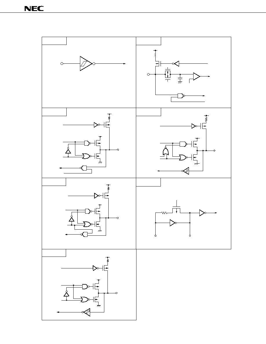
3.3 Pin I/O Circuits and Recommended Connection of Unused Pins
The input/output circuit type of each pin and recommended connection of unused pins are shown in Table 3-1.
For the input/output circuit configuration of each type, see Figure 3-1.
Table 3-1. Types of Pin Input/Output Circuits (1/2)
P00/INTP0/TI00
2
Input
Connect to V
SS0
.
P01/INTP1/TI01
8-C
Input/output
Connect to V
SS0
via a resistor individually.
P02/INTP2
P03/INTP3
P04/INTP4
P05/INTP5
P06/INTP6
P10/ANI0-P17/ANI7
9-B
Input
Connect to V
DD0
or V
SS0
via a resistor individually.
P20/SI1
8-C
Input/output
P21/SO1
5-H
P22/SCK1
8-C
P23/STB
5-H
P24/BUSY
8-C
P25-P27
5-H
P30/TO0-P32/TO2
P33/TI1
8-C
P34/TI2
P35/PCL
5-H
P36/BUZ
P37
P40/AD0-P47/AD7
5-N
Input/output
Connect to V
DD0
via a resistor individually.
P50/A8-P57/A15
5-H
Input/output
Connect to V
DD0
or V
SS0
via a resistor individually.
P60-P63
P64/RD
P65/WR
P66/WAIT
P67/ASTB
P80/A0-P87/A7
P90/SI4A
8-C
P91/SO4A
5-H
P92/SCK4A
8-C
P93/SI4B
P94/SO4B
5-H
P95/SCK4B
8-C
Input/Output
Circuit Type
Pin Name
I/O
Recommended Connection for Unused Pins

14
µ
PD780016Y, 780018Y
Table 3-1. Types of Pin Input/Output Circuits (2/2)
Input/Output
Circuit Type
Pin Name
I/O
Recommended Connection for Unused Pins
P100/TI5/TO5
8-C
Input/output
Connect to V
DD0
or V
SS0
via a resistor individually.
P101/TI6/TO6
P102, P103
5-H
P110/SI4C
8-C
P111/SO4C
5-H
P112/SCK4C
8-C
P113-P115
5-H
P116/SDA
10-B
P117/SCL
P150-P156
5-H
RESET
2
Input
--
XT1
16
--
Connect to V
DD0
.
XT2
Leave open.
AV
REF
--
Connect to V
SS0
.
AV
SS
IC
Connect to V
SS0
.
µ
PD780016Y, 780018Y
15
Figure 3-1. Pin Input/Output Circuits
Type 2
IN
Type 9-B
pullup
enable
data
output
disable
V
DD0
P-ch
N-ch
P-ch
IN/OUT
V
DD0
Type 10-B
Type 16
pullup
enable
data
output
disable
V
DD0
P-ch
N-ch
P-ch
IN/OUT
V
DD0
Type 5-H
input
enable
Type 5-N
pullup
enable
data
output
disable
V
DD0
P-ch
N-ch
P-ch
IN/OUT
V
DD0
Schmitt-triggered input with hysteresis characteristic
pullup
enable
data
open drain
output disable
N-ch
P-ch
V
DD0
V
DD0
P-ch
IN/OUT
XT1
XT2
P-ch
feedback
cut-off
V
SS0
V
SS0
Type 8-C
V
SS0
V
SS0
pullup
enable
P-ch
N-ch
V
SS0
V
REF
input
enable
IN
P-ch
V
DD0
+
_
threshold voltage
comparator
16
µ
PD780016Y, 780018Y
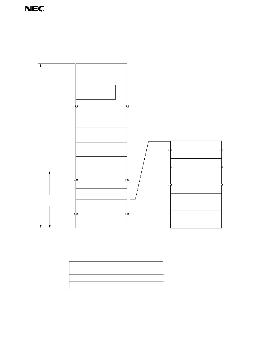
4. MEMORY SPACE
The memory map of the
µ
PD780016Y and 780018Y is shown in Figure 4-1.
Figure 4-1. Memory Map
Notes 1. If external device expansion functions are to be employed for the
µ
PD780018Y, set the size of the
internal ROM to below 56K bytes using the memory size switching register (IMS).
2. The internal ROM capacity depends on the product. (See the following table.)
Part Number
Internal ROM Last Address
nnnnH
µ
PD780016Y
BFFFH
µ
PD780018Y
EFFFH
FFFFH
FF00H
FEFFH
FB00H
FAFFH
FEE0H
FEDFH
FAE0H
FADFH
FAC0H
FABFH
F800H
F7FFH
nnnnH+1
nnnnH
0000H
nnnnH
1000H
0FFFH
0800H
07FFH
0080H
007FH
0040H
003FH
0000H
Use prohibited
Use prohibited
Internal extended RAM
1024
◊
8 bits
Program area
CALLF entry area
Program area
CALLT table area
Vector table area
Special function registers
(SFR) 256
◊
8 bits
General-purpose registers
32
◊
8 bits
Internal high-speed RAM
1024
◊
8 bits
Internal ROM
Note 2
Buffer RAM
32
◊
8 bits
Program
memory
space
Data
memory
space
F400H
F3FFH
Use prohibited
Note 1
µ
PD780016Y, 780018Y
17
5. PERIPHERAL HARDWARE FUNCTIONS
5.1 Ports
Input/output ports are classified into two types.
∑ CMOS input (P00, Port 1)
: 9
∑ CMOS input/output (P01 to P06, Port 2 to 6, Port 8 to 11, Port 15)
: 79
Total
: 88
Table 5-1. Functions of Ports
Port Name
Pin Name
Function
Port 0
P00
Input only.
P01 to P06
Input/output port. Input/output can be specified bit-wise.
When used as an input port, on-chip pull-up resistor can be used by software.
Port 1
P10 to P17
Input only.
On-chip pull-up resistor can be used by software.
Port 2
P20 to P27
Input/output port. Input/output can be specified bit-wise.
When used as an input port, on-chip pull-up resistor can be used by software.
Port 3
P30 to P37
Input/output port. Input/output can be specified bit-wise.
When used as an input port, on-chip pull-up resistor can be used by software.
Port 4
P40 to P47
Input/output port. Input/output can be specified in 8-bit units.
When used as an input port, on-chip pull-up resistor can be used by software.
The test input flag (KRIF) is set to 1 by falling edge detection.
Port 5
P50 to P57
Input/output port. Input/output can be specified bit-wise.
When used as an input port, on-chip pull-up resistor can be used by software.
LED can be driven directly.
Port 6
P60 to P67
Input/output port. Input/output can be specified bit-wise.
When used as an input port, on-chip pull-up resistor can be used by software.
Port 8
P80 to P87
Input/output port. Input/output can be specified bit-wise.
When used as an input port, on-chip pull-up resistor can be used by software.
Port 9
P90 to P95
Input/output port. Input/output can be specified bit-wise.
When used as an input port, on-chip pull-up resistor can be used by software.
Port 10
P100 to P103
Input/output port. Input/output can be specified bit-wise.
When used as an input port, on-chip pull-up resistor can be used by software.
Port 11
P110 to P117
Input/output port. Input/output can be specified bit-wise.
When used as an input port, on-chip pull-up resistor can be used by software.
Port 15
P150 to P156
Input/output port. Input/output can be specified bit-wise.
When used as an input port, on-chip pull-up resistor can be used by software.
18
µ
PD780016Y, 780018Y
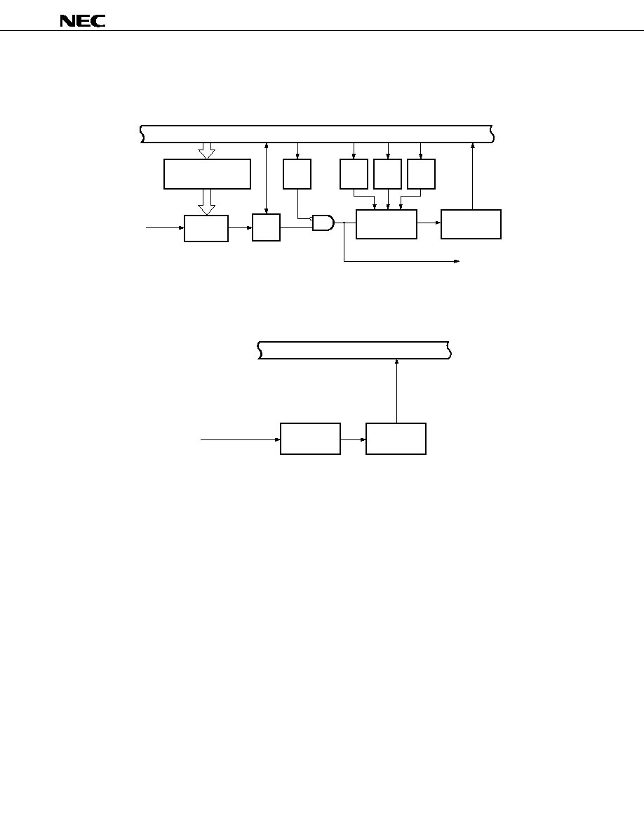
5.2 Clock Generator
There are two kinds of clock generators: main system and subsystem clock generators.
It is possible to change the instruction execution time.
∑ 0.4
µ
s/0.8
µ
s/1.6
µ
s/3.2
µ
s/6.4
µ
s (at main system clock frequency of 5.0 MHz)
∑ 122
µ
s (at subsystem clock frequency of 32.768 kHz)
Figure 5-1. Clock Generator Block Diagram
XT1
XT2
X1
X2
STOP
f
XT
f
XX
Watch timer, Clock
output function
Clock to peripheral
hardware
CPU clock
(f
CPU
)
To INTP0
sampling clock
2
f
XX
2
3
f
XX
2
2
f
XX
f
X
f
X
2
Subsystem
clock
oscillator
Main system
clock
oscillator
Division
circuit
Prescaler
Standby
control
circuit
Wait
control
circuit
Prescaler
Selector
Selector
f
XT
2
4
f
XX
2
2
1
MCS
Note
Oscillation mode
select register
Type
Function
Note
Be sure to set 1 to MCS.
5.3 Timer/Event Counter
There are the following seven timer/event counter channels:
∑ 16-bit timer/event counter
: 1 channel
∑ 8-bit timer/event counter
: 4 channels
∑ Watch timer
: 1 channel
∑ Watchdog timer
: 1 channel
Table 5-2. Types and Functions of Timer/Event Counters
16-bit Timer/Event 8-bit Timer/Event
8-bit Timer/Event
Watch Timer
Watchdog Timer
Counter
Counters 1, 2
Counters 5, 6
Interval timer
1 channel
2 channels
2 channels
1 channel
1 channel
External event counter
1 channel
2 channels
2 channels
--
--
Timer output
1 output
2 outputs
2 outputs
--
--
PWM output
1 output
--
2 outputs
--
--
Pulse width measurement
2 inputs
--
--
--
--
Square wave output
1 output
2 outputs
2 outputs
--
--
One-shot pulse output
1 output
--
--
--
--
Interrupt request
2
2
2
1
1
Test input
--
--
--
1 input
--

µ
PD780016Y, 780018Y
19
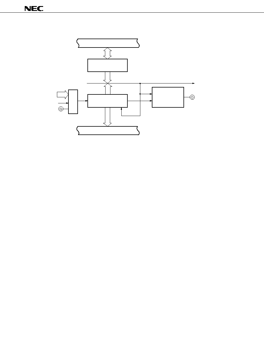
Figure 5-2. 16-Bit Timer/Event Counter Block Diagram
Match
Match
Clear
Selector
16-bit capture/
compare register
(CR00)
Internal bus
Output
control circuit
INTP1
INTTM00
TO0/P30
INTTM01
INTP0
TI01/P01/
INTP1
Watch timer
output
f
XX
f
XX
/2
f
XX
/2
2
TI00/P00/
INTP0
Selector
Edge
detector
Selector
Internal bus
16-bit capture/
compare register
(CR01)
PWM pulse
output
control
circuit
16-bit timer
register (TM0)
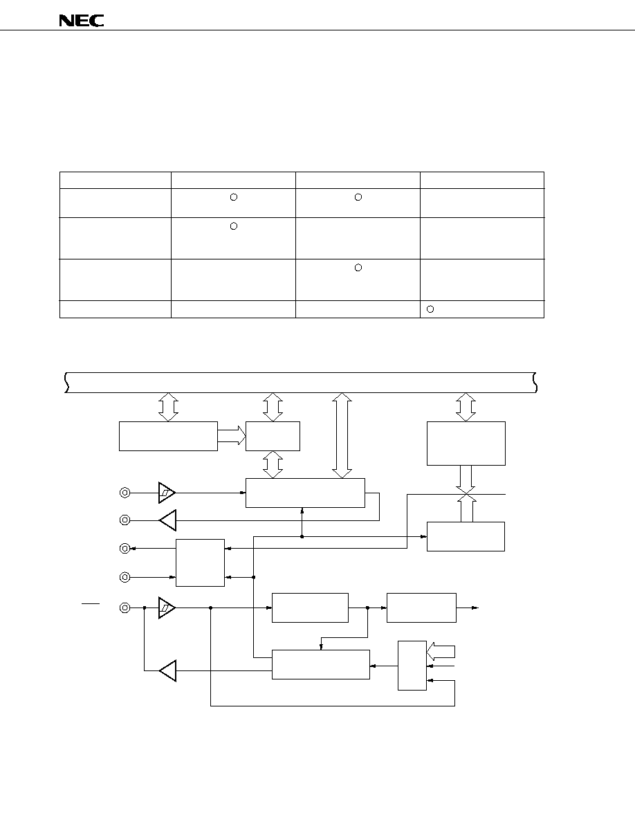
Figure 5-3. 8-Bit Timer/Event Counter 1, 2 Block Diagram
Clear
Clear
f
XX
/2
9
f
XX
/2
11
TI2/P34
TI1/P33
INTTM2
TO2/P32
TO1/P31
Match
Match
INTTM1
f
XX
/2-
f
XX
/2
11
f
XX
/2
9
f
XX
/2-
Internal bus
Selector
Selector
Selector
8-bit timer
register 1 (TM1)
8-bit compare
register (CR20)
8-bit compare
register (CR10)
Output
control
circuit
8-bit timer
register 2 (TM2)
Output
control
circuit
Internal bus
Selector
Selector
20
µ
PD780016Y, 780018Y
Figure 5-4. 8-Bit Timer/Event Counter 5, 6 Block Diagram
n = 5, 6
Internal bus
8-bit compare register
(CR
n
0)
8-bit timer register n
(TMn)
Internal bus
Output control
circuit
Selector
f
XX
- f
XX
/2
9
f
XX
/2
11
TI5/P100/TO5,
TI6/P101/TO6 Clear
OVF
INTTMn
TO5/P100/TI5,
TO6/P101/TI6
Match

µ
PD780016Y, 780018Y
21
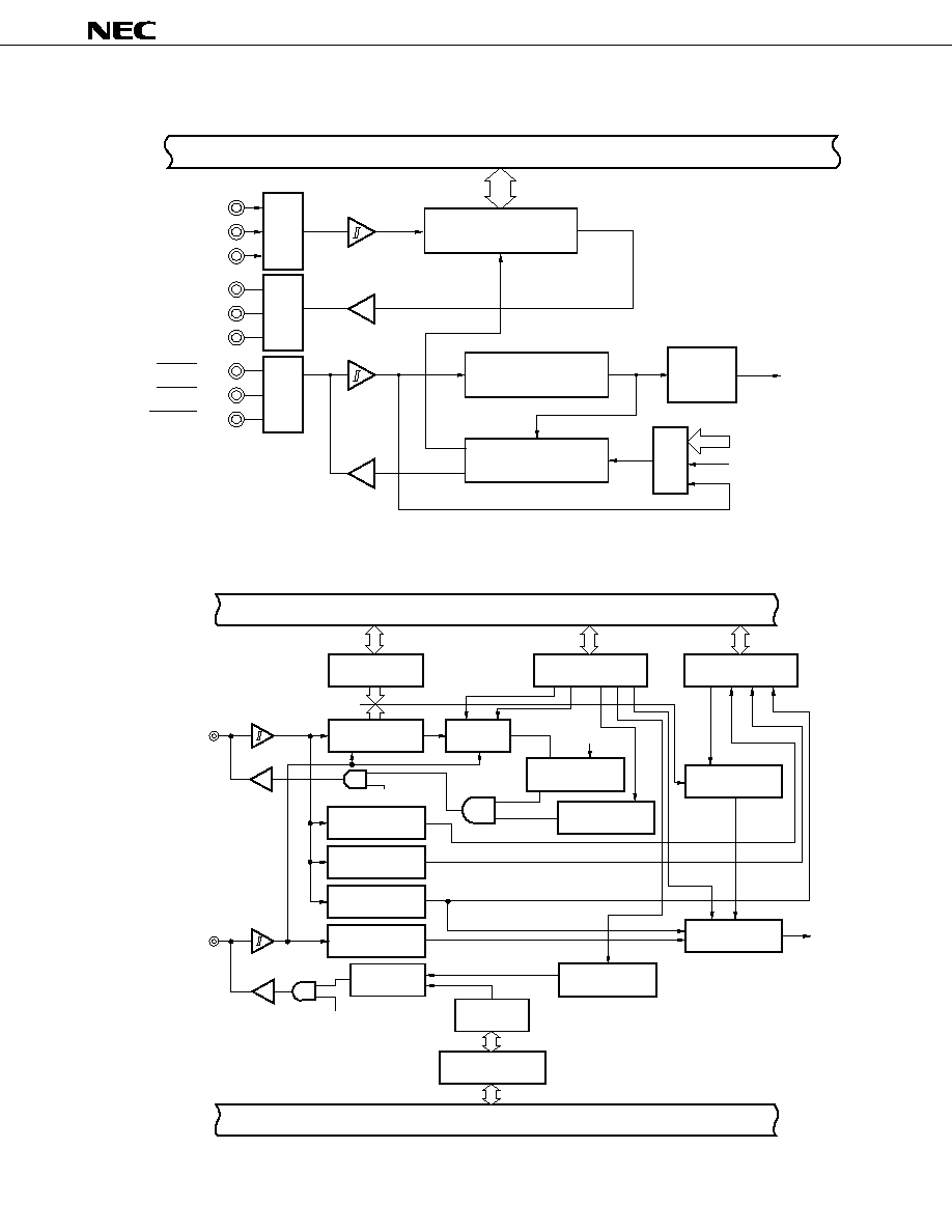
Figure 5-5. Watch Timer Block Diagram
f
W
2
4
f
W
2
5
f
W
2
6
f
W
2
7
f
W
2
8
f
W
2
9
f
W
2
13
f
W
2
14
f
XT
Selector
5-bit counter
Selector
Prescaler
Selector
INTWT
INTTM3
Selector
f
W
To 16-bit timer/
event counter
f
XX
/2
7
Figure 5-6. Watchdog Timer Block Diagram
f
XX
f
XX
f
XX
f
XX
2
7
f
XX
2
8
f
XX
2
9
f
XX
2
11
INTWDT
maskable
interrupt request
RESET
INTWDT
non-maskable
interrupt request
Prescaler
Selector
Control
circuit
2
4
2
5
2
6
8-bit counter
f
XX
2
3
22
µ
PD780016Y, 780018Y
5.4 Clock Output Control Circuit
This circuit can output clocks of the following frequencies:
∑
39.1 kHz/78.1 kHz/156 kHz/313 kHz/625 kHz/1.25 MHz/2.5 MHz/5.0 MHz (at main system clock frequency
of 5.0 MHz)
∑
32.768 kHz (at subsystem clock frequency of 32.768 kHz)
Figure 5-7. Clock Output Control Circuit Block Diagram
5.5 Buzzer Output Control Circuit
This circuit can output clocks of the following frequencies that can be used for driving buzzers:
∑ 2.4 kHz/4.9 kHz/9.8 kHz (at main system clock frequency of 5.0 MHz)
Figure 5-8. Buzzer Output Control Circuit Block Diagram
PCL/P35
f
XX
/2
2
f
XX
/2
3
f
XX
/2
4
f
XX
/2
5
f
XX
/2
6
f
XX
/2
7
f
XT
Synchronization
circuit
f
XX
/2
f
XX
Selector
Output control
circuit
Selector
Output control
circuit
BUZ/P36
f
XX
/2
9
f
XX
/2
10
f
XX
/2
11

µ
PD780016Y, 780018Y
23
5.6 A/D Converter
The A/D converter consists of eight 8-bit resolution channels.
A/D conversion can be started by the following two methods:
∑ Hardware starting
∑ Software starting
Figure 5-9. A/D Converter Block Diagram
INTP3/P03
Tap selector
ANI0/P10
ANI2/P12
ANI3/P13
ANI4/P14
ANI5/P15
ANI6/P16
ANI7/P17
ANI1/P11
AV
REF
AV
SS
INTAD
INTP3
Series resistor string
Selector
Sample & hold circuit
Voltage comparator
Successive approximation
register (SAR)
Edge
detector
Control
circuit
A/D conversion result
register (ADCR)
Internal bus
AV
SS
24
µ
PD780016Y, 780018Y
5.7 Serial Interfaces
There are the following three on-chip serial interface channels synchronous with the clock:
∑ Serial interface channel 1
∑ Serial interface channel 4
∑ Serial interface channel 5
Table 5-3. Types and Functions of Serial Interfaces
Function
Serial Interface Channel 1
Serial Interface Channel 4
Serial Interface Channel 5
3-wire serial I/O mode
--
(Starting bit MSB/LSB switching possible)
(Starting bit MSB/LSB switching possible)
3-wire serial I/O mode with
--
--
automatic data transmit/
(Starting bit MSB/LSB switching possible)
/receive function
3-wire serial I/O mode with
--
--
automatic data transmit/
(Starting bit MSB/LSB switching possible)
receive function
I
2
C bus mode
--
--
(MSB first)
Figure 5-10. Serial Interface Channel 1 Block Diagram
Internal bus
Buffer RAM
Automatic data transmit/
receive address
pointer (ADTP)
Serial I/O shift
register 1 (SIO1)
Automatic data
transmit/receive
interval specification
register (ADTI)
Match
5-bit counter
Selector
Handshake
control
circuit
Serial clock counter
SI1/P20
SO1/P21
STB/P23
BUSY/P24
SCK1/P22
INTCSI1
f
XX
/2
2
--f
XX
/2
8
TO2
Interrupt request
signal generator
Serial clock
control circuit
µ
PD780016Y, 780018Y
25
Figure 5-11. Serial Interface Channel 4 Block Diagram
Internal bus
Serial I/O
shift register 4
(SIO4)
Serial clock
counter
Serial clock
control circuit
Interrupt
request
signal
generator
INTCSI4
f
XX
/2
2
-f
XX
/2
8
SI4B/P93
SI4A/P90
SI4C/P110
SO4B/P94
SO4A/P91
SO4C/P111
SCK4A/P92
SCK4B/P95
SCK4C/P112
TO2
Selector
Selector
Selector
Selector
Figure 5-12. Serial Interface Channel 5 Block Diagram
Internal bus
Serial I/O shift
register 5 (SIO5)
Serial clock
counter
Interrupt request signal
generation circuit
INTIIC
Wake-up
control circuit
Acknowledge
output circuit
Data retention time
correction circuit
Acknowledge
detection circuit
Start condition
detection circuit
Stop condition
detection circuit
Serial clock
control circuit
Serial clock wait
control circuit
Prescaler
I
2
C bus interface control
register (IICC)
I
2
C bus interface status
register (IICS)
Slave address
register 5 (SVA5)
Internal bus
I
2
C bus interface clock
select register (IICCL)
Match signal
Clear
Set
CL0
P117 output latch
P116 output latch
P117/SCL
N-ch open-drain output
P116/SDA
N-ch open-drain output
Output latch
26
µ
PD780016Y, 780018Y
6. INTERRUPT FUNCTIONS AND TEST FUNCTIONS
6.1 Interrupt Functions
A total of 21 interrupt functions are provided, divided into the following three types.
∑ Non-maskable : 1
∑ Maskable
: 19
∑ Software
: 1
Table 6-1. List of Interrupt Factors
Interrupt
Default
Note 1
Interrupt Factor
Internal/
Vector Table Basic
Note 2
Type
Priority
Name
Trigger
External
Address
Structure Type
Non-
--
INTWDT
Overflow of watchdog timer (When the watchdog
Internal
0004H
(A)
maskable
timer mode 1 is selected)
Maskable
0
INTWDT
Overflow of watchdog timer (When the interval
(B)
timer mode is selected)
1
INTP0
Pin input edge detection
External
0006H
(C)
2
INTP1
0008H
(D)
3
INTP2
000AH
4
INTP3
000CH
5
INTP4
000EH
6
INTP5
0010H
7
INTP6
0012H
8
INTCSI1
Completion of serial interface channel 1 transfer
Internal
0016H
(B)
9
INTTM3
Reference interval signal from watch timer
001EH
10
INTTM00
Generation of matching signal of 16-bit timer
0020H
register and capture/compare register (CR00)
11
INTTM01
Generation of matching signal of 16-bit timer
0022H
register and capture/compare register (CR01)
12
INTTM1
Generation of matching signal of 8-bit timer/event
0024H
counter 1
13
INTTM2
Generation of matching signal of 8-bit timer/event
0026H
counter 2
14
INTAD
Completion of A/D conversion
0028H
15
INTTM5
Generation of matching signal of 8-bit timer/event
002AH
counter 5
16
INTTM6
Generation of matching signal of 8-bit timer/event
002CH
counter 6
17
INTCSI4
Completion of serial interface channel 4 transfer
002EH
18
INTIIC
Completion of serial interface channel 5 transfer
0030H
Software
--
BRK
Execution of BRK instruction
--
003EH
(E)
Notes 1. Default priority is the priority order when several maskable interruptions are generated at the same time.
0 is the highest order and 18 is the lowest order.
2. Basic structure types (A) to (E) correspond to (A) to (E) in Figure 6-1.

µ
PD780016Y, 780018Y
27
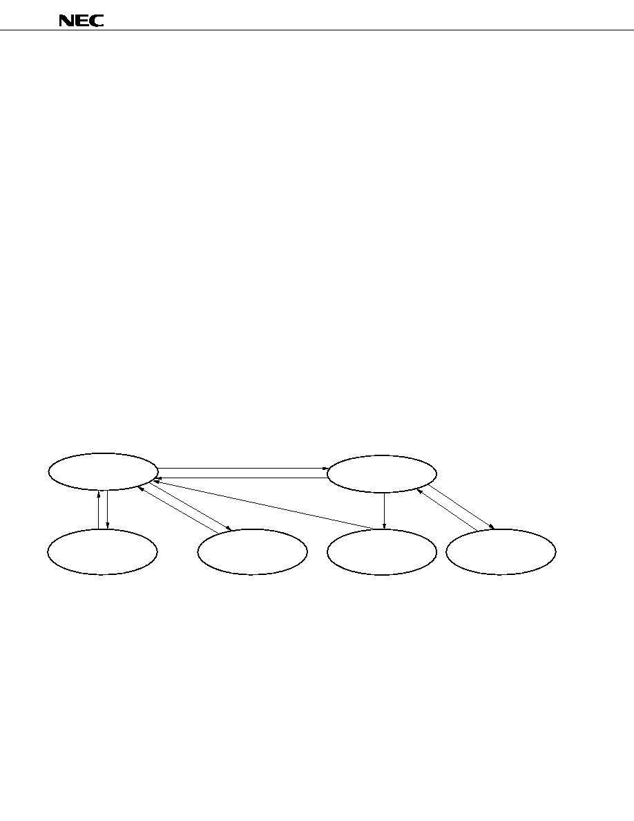
Figure 6-1. Interrupt Function Basic Configuration (1/2)
(A) Internal non-maskable interrupt
Interrupt
request
Standby release
signal
Internal bus
Vector table
address
generator
Priority
control
circuit
(B) Internal maskable interrupt
(C) External maskable interrupt (INTP0)
MK
IE
PR
ISP
IF
Interrupt
request
Internal bus
Priority
control
circuit
Vector table
address
generator
Standby release
signal
Sampling clock
select register
(SCS)
IF
IE
PR
ISP
External interrupt
mode register
(INTM0)
Sampling
clock
Edge
detector
Interrupt
request
Internal bus
MK
Priority
control
circuit
Vector table
address
generator
Standby
release
signal
28
µ
PD780016Y, 780018Y
IF
:
Interrupt request flag
E
:
Interrupt enable flag
ISP :
In-service priority flag
MK :
Interrupt mask flag
PR :
Priority specification flag
Figure 6-1. Interrupt Function Basic Configuration (2/2)
(D) External maskable interrupt (except INTP0)
IF
Internal bus
Interrupt
request
Edge
detector
Vector table
address
generator
Standby
release
signal
External interrupt
mode register
(INTM0, INTM1)
MK
IE
PR
ISP
Priority control
circuit
(E) Software interrupt
Internal bus
Interrupt
request
Vector table
address
generator
Priority
control
circuit

µ
PD780016Y, 780018Y
29
6.2 Test Functions
Table 6-2 shows the two test functions available.
Table 6-2. Test Input Factors
Test Input Factor
Internal/
Name
Trigger
External
INTWT
Overflow of watch timer
Internal
INTPT4
Detection of falling edge of port 4
External
Figure 6-2. Basic Configuration of Test Function
IF
:
Test input flag
MK
:
Test mask flag
MK
IF
Internal bus
Standby release
signal
Test input
signal
30
µ
PD780016Y, 780018Y
7. EXTERNAL DEVICE EXPANSION FUNCTIONS
The external device expansion functions connect external devices to areas other than the internal ROM, RAM and
SFR.
External devices connection uses ports 4 to 6 and port 8.
The external device expansion function has the following two modes:
∑
Separate bus mode
: External devices are connected by using an independent address bus and data
bus. Because an external latch circuit is not necessary, this mode is effective for
reducing the number of components and the mounting area on a printed wiring
board.
∑
Multiplexed bus mode
: External devices are connected by using a time-division multiplexed address/data
bus. This mode is useful for reducing the number of ports used when external
devices are connected.
8. STANDBY FUNCTION
The standby function intends to reduce current consumption. It has the following three modes:
∑
HALT mode
: In this mode, the CPU operation clock is stopped. The average current consumption
can be reduced by intermittent operation by combining this mode with the normal
operation mode.
∑
Main STOP mode : In this mode, oscillation of the main system clock is stopped. The power consumption
can be reduced because the whole internal circuit is stopped.
∑
Sub-STOP mode : In this mode, oscillation of the subsystem clock is stopped. The whole operation is
stopped and the power is consumed very little.
Figure 8-1. Standby Function
Note
Current consumption is reduced by shutting off the main system clock.
If the CPU is operating on subsystemclock, shut off the main system clock by setting MCC. You cannot
use a STOP instruction in HALT mode.
Cautions 1. The main stop mode can be used only when the main system clock is being operated. (The
oscillation of the subsystem clock cannot be stopped.)
2. When switching on the main system clock again after the subsystem clock has been used
with the main system clock stopped, be sure to provide enough time for the generation
to be stable with the program first.
Main system clock operation
Subsystem clock operation
Note
Interrupt
request
STOP
instruction
STOP mode
(Oscillation of the main system
clock is stopped.)
Interrupt
request
Interrupt
request
HALT
instruction
HALT mode
(Supply of clock to CPU is
stopped although clock
is generated.)
HALT instruction
HALT mode
Note
(Supply of clock to CPU is
stopped although clock
is generated.)
CSS = 1
CSS = 0
Reset
STOP
instructon
Sub-STOP mode
(Oscillation of the main
system clock and subsystem
clock is stopped.)

µ
PD780016Y, 780018Y
31
9. RESET FUNCTION
There are the following two reset methods.
∑ External reset input by RESET pin
∑ Internal reset by watchdog timer inadvertent program loop time detection
32
µ
PD780016Y, 780018Y
10. INSTRUCTION SET
(1) 8-bit instructions
MOV, XCH, ADD, ADDC, SUB, SUBC, AND, OR, XOR, CMP, MULU, DIVUW, INC, DEC, ROR, ROL, RORC,
ROLC, ROR4, ROL4, PUSH, POP, DBNZ
2nd Operand
[HL + byte]
#byte
A
r
Note
sfr
saddr
!addr16
PSW
[DE]
[HL]
[HL + B] $addr16
1
None
1st Operand
[HL + C]
A
ADD
MOV
MOV
MOV
MOV
MOV
MOV
MOV
MOV
ROR
ADDC
XCH
XCH
XCH
XCH
XCH
XCH
XCH
ROL
SUB
ADD
ADD
ADD
ADD
ADD
RORC
SUBC
ADDC
ADDC
ADDC
ADDC
ADDC
ROLC
AND
SUB
SUB
SUB
SUB
SUB
OR
SUBC
SUBC
SUBC
SUBC
SUBC
XOR
AND
AND
AND
AND
AND
CMP
OR
OR
OR
OR
OR
XOR
XOR
XOR
XOR
XOR
CMP
CMP
CMP
CMP
CMP
r
MOV
MOV
INC
ADD
DEC
ADDC
SUB
SUBC
AND
OR
XOR
CMP
B, C
DBNZ
sfr
MOV
MOV
saddr
MOV
MOV
DBNZ
INC
ADD
DEC
ADDC
SUB
SUBC
AND
OR
XOR
CMP
!addr16
MOV
PSW
MOV
MOV
PUSH
POP
[DE]
MOV
[HL]
MOV
ROR4
ROL4
[HL + byte]
MOV
[HL + B]
[HL + C]
X
MULU
C
DIVUW
Note
Except r = A
µ
PD780016Y, 780018Y
33
(2) 16-bit instructions
MOVW, XCHW, ADDW, SUBW, CMPW, PUSH, POP, INCW, DECW
2nd Operand
#word
AX
rp
Note
sfrp
saddrp
!addr16
SP
None
1st Operand
AX
ADDW
MOVW
MOVW
MOVW
MOVW
MOVW
SUBW
XCHW
CMPW
rp
MOVW
MOVW
Note
INCW, DECW
PUSH, POP
sfrp
MOVW
MOVW
saddrp
MOVW
MOVW
!addr16
MOVW
SP
MOVW
MOVW
Note
Only when rp = BC, DE, HL
(3) Bit manipulation instructions
MOV1, AND1, OR1, XOR1, SET1, CLR1, NOT1, BT, BF, BTCLR
2nd Operand
A.bit
sfr.bit
saddr.bit
PSW.bit
[HL].bit
CY
$addr16
None
1st Operand
A.bit
MOV1
BT
SET1
BF
CLR1
BTCLR
sfr.bit
MOV1
BT
SET1
BF
CLR1
BTCLR
saddr.bit
MOV1
BT
SET1
BF
CLR1
BTCLR
PSW.bit
MOV1
BT
SET1
BF
CLR1
BTCLR
[HL].bit
MOV1
BT
SET1
BF
CLR1
BTCLR
CY
MOV1
MOV1
MOV1
MOV1
MOV1
SET1
AND1
AND1
AND1
AND1
AND1
CLR1
OR1
OR1
OR1
OR1
OR1
NOT1
XOR1
XOR1
XOR1
XOR1
XOR1
(4) Call instructions/Branch instructions
CALL, CALLF, CALLT, BR, BC, BNC, BZ, BNZ, BT, BF, BTCLR, DBNZ
2nd Operand
AX
!addr16
!addr11
[addr5]
$addr16
1st Operand
Basic instruction
BR
CALL
CALLF
CALLT
BR, BC
BNC
BR
BZ, BNZ
Compound instruction
BT, BF
BTCLR
DBNZ
(5) Other instructions
ADJBA, ADJBS, BRK, RET, RETI, RETB, SEL, NOP, EI, DI, HALT, STOP

34
µ
PD780016Y, 780018Y
11. PACKAGE DRAWINGS
J
N
M
P
80
81
50
100 PIN PLASTIC QFP (14
◊
20)
100
1
31
30
51
G
detail of lead end
S
5∞
±
5∞
C
D
A
B
H
Q
K
L
F
M
I
P100GF-65-3BA1-2
ITEM
MILLIMETERS
INCHES
A
B
C
D
F
G
H
I
J
K
L
23.6±0.4
14.0±0.2
0.6
0.30±0.10
0.15
20.0±0.2
0.929±0.016
0.031
0.024
0.006
0.026 (T.P.)
0.795
NOTE
M
N
0.10
0.15
1.8±0.2
0.65 (T.P.)
0.006
0.031
+0.009
≠0.008
Each lead centerline is located within 0.15
mm (0.006 inch) of its true position (T.P.) at
maximum material condition.
0.012
0.551
0.8±0.2
0.071
P
2.7
0.106
0.693±0.016
17.6±0.4
0.8
+0.008
≠0.009
Q
0.1±0.1
0.004±0.004
S
3.0 MAX.
0.119 MAX.
+0.10
≠0.05
+0.009
≠0.008
+0.004
≠0.005
+0.009
≠0.008
+0.004
≠0.003
0.004

µ
PD780016Y, 780018Y
35
APPENDIX A. DEVELOPMENT TOOLS
The following tools are available for system development using the
µ
PD780016Y and 780018Y.
Language Processing Software
RA78K/0
Notes 1, 2, 3, 4
Assembler package used in common for the 78K/0 series
CC78K/0
Notes 1, 2, 3, 4
C compiler package used in common for the 78K/0 series
DF780018
Notes 1, 2, 3, 4, 8
Device file used in common for the
µ
PD780018 subseries
CC78K/0≠L
Notes 1, 2, 3, 4
C compiler library source file used in common for the 78K/0 series
PROM Writing Tools
PG-1500
PROM programmer
PA-78P0018GF
Note 8
Programmer adapter connected to the PG-1500
PA-78P0018KL-T
Note 8
PG-1500 controller
Notes 1, 2
Control program for the PG-1500
Debugging Tools
IE-78000-R
In-circuit emulator used in common for the 78K/0 series
IE-78000-R-A
Note 8
In-circuit emulator used in common for the 78K/0 series (for integrated debugger)
IE-78000-R-BK
Break board used in common for the 78K/0 series
IE-780018-R-EM
Note 8
Emulation board used in common for the
µ
PD780018 subseries
EP-78064GF-R
Emulation probe used in common for the
µ
PD78064 subseries
EV-9200GF-100
Socket mounted on the target system board prepared for 100-pin plastic QFP
(GF-3BA type)
EV-9900
Tool used for removing the
µ
PD78P0018YKL-T from the EV-9200GF-100.
SM78K0
Notes 5, 6, 7
System simulator used in common for the 78K/0 series
ID78K0
Notes 4, 5, 6, 7, 8
Integrated debugger for IE-78000-R-A
SD78K/0
Notes 1, 2
Screen debugger for the IE-78000-R
DF780018
Notes 1, 2, 4, 5, 6, 7, 8
Device file used in common for the
µ
PD780018 subseries
36
µ
PD780016Y, 780018Y
Real-Time OS
RX78K/0
Notes 1, 2, 3, 4
Real-time OS used for the 78K/0 series
MX78K0
Notes 1, 2, 3, 4
OS used for the 78K/0 series
Fuzzy Inference Development Support System
FE9000
Note 1
/FE9200
Note 6
Fuzzy knowledge data creating tool
FT9080
Note 1
/FT9085
Note 2
Translator
FI78K0
Notes 1, 2
Fuzzy inference module
FD78K0
Notes 1, 2
Fuzzy inference debugger
Notes 1. Based on PC-9800 series (MS-DOS
TM
)
2. Based on IBM PC/AT
TM
and compatible machines (PC DOS
TM
/IBM DOS
TM
/MS-DOS)
3. Based on HP9000 series 300
TM
(HP-UX
TM
)
4. Based on HP9000 series 700
TM
(HP-UX), SPARCstation
TM
(SunOS
TM
), and EWS-4800 series (EWS-UX/
V)
5. Based on PC-9800 series (MS-DOS + Windows
TM
)
6. Based on IBM PC/AT and compatible machines (PC DOS/IBM DOS/MS DOS + Windows)
7. Based on NEW
TM
(NEWS-OS
TM
)
8. Under development
Remarks 1. For development tools supplied by third-party manufacturers, refer to 78K/0 Series Selection Guide
(U11126E).
2. Use the RA78K/0, CC78K/0, SM78K0, ID78K0, SD78K/0, and RX78K/0 in combination with the
DF780018.

µ
PD780016Y, 780018Y
37
APPENDIX B. RELATED DOCUMENTS
Documents Related to Devices
Document
Document No.
Japanese
English
µ
PD780018Y, 780018Y Subseries User's Manual
U11754J
To be prepared
µ
PD780016Y, 780018Y Preliminary Product Information
U11810J
This document
µ
PD78P0018Y Preliminary Product Information
U11603J
To be prepared
78K/0 Series User's Manual-Instruction
IEU-849
IEU-1372
78K/0 Series Instruction Table
U10903J
--
78K/0 Series Instruction Set
U10904J
--
µ
PD780018Y Subseries Special-Function Register Table
To be prepared
--
Documents on Development Tools (User's Manuals)
Document
Document No.
Japanese
English
RA78K Series Assembler Package
Operation
EEU-809
EEU-1399
Language
EEU-815
EEU-1404
RA78K Series Structured Assembler Preprocessor
EEU-817
EEU-1402
CC78K Series C Compiler
Operation
EEU-656
EEU-1280
Language
EEU-655
EEU-1284
CC78K0 C Compiler
Operation
U11517J
--
Language
U11518J
--
CC78K/0 C Compiler Application Note
Programing Know-how
EEA-618
EEA-1208
CC78K Series Library Source File
EEU-777
--
PG-1500 PROM Programmer
EEU-651
EEU-1335
PG-1500 Controller PC-9800 Series (MS-DOS) Base
EEU-704
EEU-1291
PG-1500 Controller IBM PC Series (PC-DOS) Base
EEU-5008
U10540E
IE-78000-R
EEU-810
U11376E
IE-78000-R-A
U10057J
U10057E
IE-78000-R-BK
EEU-867
EEU-1427
IE-780018-R-EM
U11838J
To be prepared
EP-78064
EEU-934
EEU-1469
SM78K0 System Simulator Windows Base
Reference
U10181J
U10181E
SM78K Series System Simulator
External component user
U10092J
U10092E
open interface specification
ID78K0 Integrated Debugger EWS Base
Reference
U11151J
--
ID78K0 Integrated Debugger PC Base
Reference
U11539J
--
ID78K0 Integrated Debugger Windows Base
Guide
U11649J
--
SD78K/0 Screen Debugger
Introduction
EEU-852
--
PC-9800 Series (MS-DOS) Base
Reference
U10952J
--
SD78K/0 Screen Debugger
Introduction
EEU-5024
EEU-1414
IBM PC/AT (PC DOS) Base
Reference
U11279J
EEU-1413
Caution The above documents are subject to change without notice. Be sure to use the latest documents
for design or for any other similar purpose.
38
µ
PD780016Y, 780018Y
Documents on Embeded Software (User's Manuals)
Document
Document No.
Japanese
English
Basic
U11537J
--
78K/0 Series Real-time OS
Installation
U11536J
--
Technical
U11538J
--
78K/0 Series OS MX78K0
Fundamental
EEU-5010
--
Fuzzy Knowledge Data Creation Tool
EEU-829
EEU-1438
78K/0, 78K/II, 87AD Series
Fuzzy Inference Development Support System Translator
EEU-862
EEU-1444
78K/0 Series Fuzzy Inference Development Support System Fuzzy Inference Module
EEU-858
EEU-1441
78K/0 Series Fuzzy Inference Development Support System Fuzzy Inference Debugger
EEU-921
EEU-1458
Other Documents
Document
Document No.
Japanese
English
IC Package Manual
C10943X
Semiconductor Device Mounting Technology Manual
C10535J
C10535E
Quality Grade on NEC Semiconductor Devices
C11531J
C11531E
NEC Semiconductor Device Reliability/Quality Control System
U10983J
U10983E
Electrostatic Discharge (ESD) Test
MEM-539
--
Semiconductor Device Quality Assurance Guide
MEI-603
MEI-1202
Microcontroller-Related Product Guide ≠ Third Party Products ≠
U11416J
--
Caution The above documents are subject to change without notice. Be sure to use the latest documents
for design or for any other similar purpose.

µ
PD780016Y, 780018Y
39
[MEMO]
40
µ
PD780016Y, 780018Y
NOTES FOR CMOS DEVICES
1
PRECAUTION AGAINST ESD FOR SEMICONDUCTORS
Note: Strong electric field, when exposed to a MOS device, can cause destruction
of the gate oxide and ultimately degrade the device operation. Steps must
be taken to stop generation of static electricity as much as possible, and
quickly dissipate it once, when it has occurred. Environmental control must
be adequate. When it is dry, humidifier should be used. It is recommended
to avoid using insulators that easily build static electricity. Semiconductor
devices must be stored and transported in an anti-static container, static
shielding bag or conductive material. All test and measurement tools
including work bench and floor should be grounded. The operator should
be grounded using wrist strap. Semiconductor devices must not be touched
with bare hands. Similar precautions need to be taken for PW boards with
semiconductor devices on it.
2
HANDLING OF UNUSED INPUT PINS FOR CMOS
Note: No connection for CMOS device inputs can be cause of malfunction. If no
connection is provided to the input pins, it is possible that an internal input
level may be generated due to noise, etc., hence causing malfunction. CMOS
device behave differently than Bipolar or NMOS devices. Input levels of
CMOS devices must be fixed high or low by using a pull-up or pull-down
circuitry. Each unused pin should be connected to V
DD
or GND with a
resistor, if it is considered to have a possibility of being an output pin. All
handling related to the unused pins must be judged device by device and
related specifications governing the devices.
3
STATUS BEFORE INITIALIZATION OF MOS DEVICES
Note: Power-on does not necessarily define initial status of MOS device. Produc-
tion process of MOS does not define the initial operation status of the device.
Immediately after the power source is turned ON, the devices with reset
function have not yet been initialized. Hence, power-on does not guarantee
out-pin levels, I/O settings or contents of registers. Device is not initialized
until the reset signal is received. Reset operation must be executed imme-
diately after power-on for devices having reset function.

µ
PD780016Y, 780018Y
41
NEC Electronics Inc. (U.S.)
Santa Clara, California
Tel: 800-366-9782
Fax: 800-729-9288
NEC Electronics (Germany) GmbH
Duesseldorf, Germany
Tel: 0211-65 03 02
Fax: 0211-65 03 490
NEC Electronics (UK) Ltd.
Milton Keynes, UK
Tel: 01908-691-133
Fax: 01908-670-290
NEC Electronics Italiana s.r.1.
Milano, Italy
Tel: 02-66 75 41
Fax: 02-66 75 42 99
NEC Electronics Hong Kong Ltd.
Hong Kong
Tel: 2886-9318
Fax: 2886-9022/9044
NEC Electronics Hong Kong Ltd.
Seoul Branch
Seoul, Korea
Tel: 02-528-0303
Fax: 02-528-4411
NEC Electronics Singapore Pte. Ltd.
United Square, Singapore 1130
Tel: 253-8311
Fax: 250-3583
NEC Electronics Taiwan Ltd.
Taipei, Taiwan
Tel: 02-719-2377
Fax: 02-719-5951
NEC do Brasil S.A.
Sao Paulo-SP, Brasil
Tel: 011-889-1680
Fax: 011-889-1689
NEC Electronics (Germany) GmbH
Benelux Office
Eindhoven, The Netherlands
Tel: 040-2445845
Fax: 040-2444580
NEC Electronics (France) S.A.
Velizy-Villacoublay, France
Tel: 01-30-67 58 00
Fax: 01-30-67 58 99
NEC Electronics (France) S.A.
Spain Office
Madrid, Spain
Tel: 01-504-2787
Fax: 01-504-2860
NEC Electronics (Germany) GmbH
Scandinavia Office
Taeby, Sweden
Tel: 08-63 80 820
Fax: 08-63 80 388
Regional Information
Some information contained in this document may vary from country to country. Before using any NEC
product in your application, please contact the NEC office in your country to obtain a list of authorized
representatives and distributors. They will verify:
∑ Device availability
∑ Ordering information
∑ Product release schedule
∑ Availability of related technical literature
∑ Development environment specifications (for example, specifications for third-party tools and
components, host computers, power plugs, AC supply voltages, and so forth)
∑ Network requirements
In addition, trademarks, registered trademarks, export restrictions, and other legal issues may also vary
from country to country.
J96. 8

µ
PD780016Y, 780018Y
Purchase of NEC I
2
C components conveys a license under the Philips I
2
C Patent Rights to use these
components in an I
2
C system, provided that the system conforms to the I
2
C Standard Specification as
defined by Philips.
No part of this document may be copied or reproduced in any form or by any means without the prior written
consent of NEC Corporation. NEC Corporation assumes no responsibility for any errors which may appear in
this document.
NEC Corporation does not assume any liability for infringement of patents, copyrights or other intellectual property
rights of third parties by or arising from use of a device described herein or any other liability arising from use
of such device. No license, either express, implied or otherwise, is granted under any patents, copyrights or other
intellectual property rights of NEC Corporation or others.
While NEC Corporation has been making continuous effort to enhance the reliability of its semiconductor devices,
the possibility of defects cannot be eliminated entirely. To minimize risks of damage or injury to persons or
property arising from a defect in an NEC semiconductor device, customers must incorporate sufficient safety
measures in its design, such as redundancy, fire-containment, and anti-failure features.
NEC devices are classified into the following three quality grades:
"Standard", "Special", and "Specific". The Specific quality grade applies only to devices developed based on a
customer designated "quality assurance program" for a specific application. The recommended applications of
a device depend on its quality grade, as indicated below. Customers must check the quality grade of each device
before using it in a particular application.
Standard: Computers, office equipment, communications equipment, test and measurement equipment,
audio and visual equipment, home electronic appliances, machine tools, personal electronic
equipment and industrial robots
Special:
Transportation equipment (automobiles, trains, ships, etc.), traffic control systems, anti-disaster
systems, anti-crime systems, safety equipment and medical equipment (not specifically designed
for life support)
Specific:
Aircrafts, aerospace equipment, submersible repeaters, nuclear reactor control systems, life
support systems or medical equipment for life support, etc.
The quality grade of NEC devices is "Standard" unless otherwise specified in NEC's Data Sheets or Data Books.
If customers intend to use NEC devices for applications other than those specified for Standard quality grade,
they should contact an NEC sales representative in advance.
Anti-radioactive design is not implemented in this product.
M4 96.5
The export of this product from Japan is regulated by the Japanese government. To export this product may be prohibited
without governmental license, the need for which must be judged by the customer. The export or re-export of this product
from a country other than Japan may also be prohibited without a license from that country. Please call an NEC sales
representative.
The related documents in this publication may include preliminary versions, but may not be marked as such.
FIP is a trademark of NEC Corp.
IEBus is a trademark of NEC Corp.
MS-DOS and Windows are trademarks of Microsoft Corp.
IBM DOS, PC/AT, and PC DOS are trademarks of IBM Corp.
HP9000 series 300, HP9000 series 700, and HP-UX are trademarks of Hewlett Packard Co.
SPARCstation is a trademark of SPARC International, Inc.
SunOS is a trademark of Sun Microsystems, Inc.
NEWS and NEWS-OS are trademarks of Sony Corp.