
User's Manual
µ
µ
µ
µPD780957(A)
µ
µ
µ
µPD780958(A)
µ
µ
µ
µ
PD780958 Subseries
8-Bit Single-Chip Microcontrollers
Printed in Japan
Document No. U13655EJ2V1UD00 (2nd edition)
Date Published May 2003 N CP(K)
c

2
User's Manual U13655EJ2V1UD
[MEMO]

User's Manual U13655EJ2V1UD
3
FIP and IEBus are trademarks of NEC Electronics Corporation.
Windows and Windows NT are either registered trademarks or trademarks of Microsoft Corporation in the
United States and/or other countries.
PC/AT is a trademark of International Business Machines Corporation.
HP9000 Series 700 and HP-UX are trademarks of Hewlett-Packard Company.
SPARCstation is a trademark of SPARC International, Inc.
SunOS and Solaris are trademarks of Sun Microsystems, Inc.
TRON is an acronym of The Realtime Operating system Nucleus.
ITRON is an abbreviation of Industrial TRON.
NOTES FOR CMOS DEVICES
1
PRECAUTION AGAINST ESD FOR SEMICONDUCTORS
Note:
Strong electric field, when exposed to a MOS device, can cause destruction of the gate oxide and
ultimately degrade the device operation. Steps must be taken to stop generation of static electricity
as much as possible, and quickly dissipate it once, when it has occurred. Environmental control
must be adequate. When it is dry, humidifier should be used. It is recommended to avoid using
insulators that easily build static electricity. Semiconductor devices must be stored and transported
in an anti-static container, static shielding bag or conductive material. All test and measurement
tools including work bench and floor should be grounded. The operator should be grounded using
wrist strap. Semiconductor devices must not be touched with bare hands. Similar precautions need
to be taken for PW boards with semiconductor devices on it.
2
HANDLING OF UNUSED INPUT PINS FOR CMOS
Note:
No connection for CMOS device inputs can be cause of malfunction. If no connection is provided
to the input pins, it is possible that an internal input level may be generated due to noise, etc., hence
causing malfunction. CMOS devices behave differently than Bipolar or NMOS devices. Input levels
of CMOS devices must be fixed high or low by using a pull-up or pull-down circuitry. Each unused
pin should be connected to V
DD
or GND with a resistor, if it is considered to have a possibility of
being an output pin. All handling related to the unused pins must be judged device by device and
related specifications governing the devices.
3
STATUS BEFORE INITIALIZATION OF MOS DEVICES
Note:
Power-on does not necessarily define initial status of MOS device. Production process of MOS
does not define the initial operation status of the device. Immediately after the power source is
turned ON, the devices with reset function have not yet been initialized. Hence, power-on does
not guarantee out-pin levels, I/O settings or contents of registers. Device is not initialized until the
reset signal is received. Reset operation must be executed immediately after power-on for devices
having reset function.

4
User's Manual U13655EJ2V1UD
These commodities, technology or software, must be exported in accordance
with the export administration regulations of the exporting country.
Diversion contrary to the law of that country is prohibited.
The information in this document is current as of December, 2002. The information is subject to
change without notice. For actual design-in, refer to the latest publications of NEC Electronics data
sheets or data books, etc., for the most up-to-date specifications of NEC Electronics products. Not
all products and/or types are available in every country. Please check with an NEC Electronics sales
representative for availability and additional information.
No part of this document may be copied or reproduced in any form or by any means without the prior
written consent of NEC Electronics. NEC Electronics assumes no responsibility for any errors that may
appear in this document.
NEC Electronics does not assume any liability for infringement of patents, copyrights or other intellectual
property rights of third parties by or arising from the use of NEC Electronics products listed in this document
or any other liability arising from the use of such products. No license, express, implied or otherwise, is
granted under any patents, copyrights or other intellectual property rights of NEC Electronics or others.
Descriptions of circuits, software and other related information in this document are provided for illustrative
purposes in semiconductor product operation and application examples. The incorporation of these
circuits, software and information in the design of a customer's equipment shall be done under the full
responsibility of the customer. NEC Electronics assumes no responsibility for any losses incurred by
customers or third parties arising from the use of these circuits, software and information.
While NEC Electronics endeavors to enhance the quality, reliability and safety of NEC Electronics products,
customers agree and acknowledge that the possibility of defects thereof cannot be eliminated entirely. To
minimize risks of damage to property or injury (including death) to persons arising from defects in NEC
Electronics products, customers must incorporate sufficient safety measures in their design, such as
redundancy, fire-containment and anti-failure features.
NEC Electronics products are classified into the following three quality grades: "Standard", "Special" and
"Specific".
The "Specific" quality grade applies only to NEC Electronics products developed based on a customer-
designated "quality assurance program" for a specific application. The recommended applications of an NEC
Electronics product depend on its quality grade, as indicated below. Customers must check the quality grade of
each NEC Electronics product before using it in a particular application.
"Standard": Computers, office equipment, communications equipment, test and measurement equipment, audio
and visual equipment, home electronic appliances, machine tools, personal electronic equipment
and industrial robots.
"Special":
Transportation equipment (automobiles, trains, ships, etc.), traffic control systems, anti-disaster
systems, anti-crime systems, safety equipment and medical equipment (not specifically designed
for life support).
"Specific": Aircraft, aerospace equipment, submersible repeaters, nuclear reactor control systems, life
support systems and medical equipment for life support, etc.
The quality grade of NEC Electronics products is "Standard" unless otherwise expressly specified in NEC
Electronics data sheets or data books, etc. If customers wish to use NEC Electronics products in applications
not intended by NEC Electronics, they must contact an NEC Electronics sales representative in advance to
determine NEC Electronics' willingness to support a given application.
(Note)
(1) "NEC Electronics" as used in this statement means NEC Electronics Corporation and also includes its
majority-owned subsidiaries.
(2) "NEC Electronics products" means any product developed or manufactured by or for NEC Electronics (as
defined above).
∑
∑
∑
∑
∑
∑
M8E 02. 11-1

User's Manual U13655EJ2V1UD
5
Regional Information
∑
Device availability
∑
Ordering information
∑
Product release schedule
∑
Availability of related technical literature
∑
Development environment specifications (for example, specifications for third-party tools and
components, host computers, power plugs, AC supply voltages, and so forth)
∑
Network requirements
In addition, trademarks, registered trademarks, export restrictions, and other legal issues may also vary
from country to country.
[GLOBAL SUPPORT]
http://www.necel.com/en/support/support.html
NEC Electronics America, Inc. (U.S.)
Santa Clara, California
Tel: 408-588-6000
800-366-9782
NEC Electronics Hong Kong Ltd.
Hong Kong
Tel: 2886-9318
NEC Electronics Hong Kong Ltd.
Seoul Branch
Seoul, Korea
Tel: 02-558-3737
NEC Electronics Shanghai, Ltd.
Shanghai, P.R. China
Tel: 021-6841-1138
NEC Electronics Taiwan Ltd.
Taipei, Taiwan
Tel: 02-2719-2377
NEC Electronics Singapore Pte. Ltd.
Novena Square, Singapore
Tel: 6253-8311
J03.4
NEC Electronics (Europe) GmbH
Duesseldorf, Germany
Tel: 0211-65 03 01
∑ Sucursal en EspaÒa
Madrid, Spain
Tel: 091-504 27 87
VÈlizy-Villacoublay, France
Tel: 01-30-67 58 00
∑ Succursale FranÁaise
∑ Filiale Italiana
Milano, Italy
Tel: 02-66 75 41
∑ Branch The Netherlands
Eindhoven, The Netherlands
Tel: 040-244 58 45
∑ Tyskland Filial
Taeby, Sweden
Tel: 08-63 80 820
∑ United Kingdom Branch
Milton Keynes, UK
Tel: 01908-691-133
Some information contained in this document may vary from country to country. Before using any NEC
Electronics product in your application, pIease contact the NEC Electronics office in your country to
obtain a list of authorized representatives and distributors. They will verify:

6
User's Manual U13655EJ2V1UD
Major Revisions in This Edition (1/3)
Page
Description
Throughout
∑ Change of following register name
∑ 8-bit counter 8-bit MR counter 0
∑ Serial mode register 3 Serial operation mode register 3
∑ LCD0 mode register LCD display mode register 0
∑ LCD0 clock select register LCD clock control register 0
∑ Change of main system clock symbol as shown below.
f
X
f
CC
∑ Change of example of main system clock oscillation frequency as shown below.
1.0 MHz
1.2 MHz
∑ Modification of description of minimum instruction execution time
p. 34
Timer overview table moved from CHAPTER 7 16-BIT TIMER/EVENT COUNTER 0 to 1.8 Overview of
Functions.
p. 44
Modification of Figure 2-3. Connection Example of VR
OUT0
, VR
OUT1
p. 45
Modification of Table 2-1. Types of Pin I/O Circuits
p. 52
3.1.2 Internal data memory space
Addition of descriptions to (1) Internal high-speed RAM and (2) Internal expansion RAM
p. 80
Modification of Figure 4-2. Block Diagram of P00 to P06
p. 82
Addition of Figure 4-4. Block Diagram of P22 to P27
p. 83
Addition of Figure 4-5. Block Diagram of P30, P32, and P35
p. 84
Addition of Figure 4-6. Block Diagram of P31 and P37
p. 87
Addition of Figure 4-9. Block Diagram of P50 to P55
p. 100
Addition of RESET pin to Table 4-4. Mask Option of Mask-ROM Version
p. 102
Modification of Figure 5-1. Block Diagram of Clock Generator
p. 103
Addition of Table 5-2. System Clock Supplied to Each Peripheral Hardware
p. 105
Modification of Table 5-3. Relationship Between CPU Clock and Minimum Instruction Execution Time
p. 106
Modification of Figure 5-4. External Circuit of Main System Clock Oscillator
p. 115
Modification of 5.5.1 Main system clock operations
p. 117
Total revision of 5.6.2 System clock and CPU clock switching procedure
∑ Modification of Figure 5-11. System Clock and CPU Clock Switching
∑ Modification of descriptions in <1> to <4>
∑ Modification of description in Note
∑ Addition of Caution 1, modification of descriptions in Cautions 2 and 3
p. 124
Deletion of one-shot pulse output function from CHAPTER 7 16-BIT TIMER/EVENT COUNTER 0
p. 125
Modification of Figure 7-1. Block Diagram of 16-Bit Timer/Event Counter 0
p. 127
Modification of Table 7-2. TI00/TO0/P31 Pin Valid Edge and Capture/Compare Register Capture Trigger
p. 130
Modification of Figure 7-2. Format of 16-Bit Timer Mode Control Register 0 (TMC0)
p. 131
Addition of Caution 4 to Figure 7-3. Format of Capture/Compare Control Register 0 (CRC0)
p. 132
Modification of Figure 7-4. Format of 16-Bit Timer Output Control Register 0 (TOC0)
p. 133
Addition of Note to Figure 7-5. Format of Prescaler Mode Register 0 (PRM0)

User's Manual U13655EJ2V1UD
7
Major Revisions in This Edition (2/3)
Page
Description
p. 138
Addition of Figure 7-11. Configuration Diagram for PPG Output
p. 138
Addition of Figure 7-12. PPG Output Operation Timing
p. 140
Modification of Figure 7-15. Timing of Pulse-Width Measurement Operation with Free-Running Counter
and One Capture Register (with Both Edges Specified)
p. 142
Modification of Figure 7-17. CR01 Capture Operation with Rising Edge Specified
p. 142
Modification of Figure 7-18. Timing of Two-Pulse-Width Measurement Operation with Free-Running
Counter (with Both Edges Specified)
p. 144
Modification of Figure 7-20. Timing of Pulse-Width Measurement Operation with Free-Running Counter
and Two Capture Registers (with Rising Edge Specified)
p. 145
Modification of Figure 7-22. Timing of Pulse-Width Measurement Operation by Means of Restart (with
Rising Edge Specified)
p. 150
p. 150
p. 151
p. 151
p. 152
7.6 Operating Cautions for 16-Bit Timer/Event Counter 0
∑ Modification of Figure 7-30. Capture Register Data Retention Timing
∑ Modification of Figure 7-31. Operation Timing of OVF0 Flag
∑ Addition of <2> to <4> to (9) Capture operation
∑ Modification of <1> in (10) Compare operation
∑ Addition of <2> to (11) Edge detection
p. 157
Addition of Caution 2 to 8.5.1 Interval timer operation
pp. 158, 159
Modification of Figure 8-4. Timing of Interval Timer Operation (When Using Internal Clock)
p. 160
Addition of Caution 2 to 8.5.2 External event counter operation
p. 161
Modification of Figure 8-7. Timing of External Event Counter Operation
p. 162
Modification of Figure 8-8. Start Timing of 16-Bit Timer Counter 2 (TM2)
pp. 171, 172
Modification of Figure 9-6. Timing of Interval Timer Operation
p. 173
Modification of Figure 9-7. Start Timing of 8-Bit Timer Counter 8n (TM8n)
p. 175
Modification of Figure 10-1. Block Diagram of Watchdog Timer
p. 181
p. 181
Modification of the following contents in 11.3 Sampling Output Timer/Detector Configuration
∑ Modification of Note
∑ Addition of Caution
p. 186
p. 187
11.4 Sampling Output Timer/Detector Control Registers
∑ Addition of Cautions 15 and 16 to Figure 11-4. Format of SMTD Control Register 0 (TSM0)
∑ Addition of Caution to (8) SMDT sampling level setting register 0 (SMS0)
p. 190
Modification of Figure 12-1. Block Diagram of MR Sampling
p. 191
Addition of Caution to (2) MRTD compare register 0 (CRM0) in 12.3 MR Sampling Configuration
p. 192
Addition of Note to Figure 12-2. Format of MRTD Control Register 0 (TCM0)
p. 194
Modification of Figure 12-4. Format of MR Sampling Control Register 0 (MRM0)
p. 196
Modification of 12.6 Phase Detector Operation
p. 199
Modification of Figure 13-1. Block Diagram of Clock Output Controller

8
User's Manual U13655EJ2V1UD
Major Revisions in This Edition (3/3)
Page
Description
p. 214
p. 214
p. 215
p. 215
p. 216
p. 217
(2) Communication operation in 14.3 Control Registers of Serial Interface UART2
∑ Modification of Figure 14-7. Generation Timing of Asynchronous Serial Interface Transmission
Completion Interrupt Request
∑ Addition of Caution 3 to Figure 14-7. Generation Timing of Asynchronous Serial Interface
Transmission Completion Interrupt Request
∑ Addition of Note to (d) Reception
∑ Modification of Figure 14-8. Generation Timing of Asynchronous Serial Interface Reception
Completion Interrupt Request
∑ Modification of Figure 14-9. Receive Error Timing
∑ Addition of (f) Clearing of RXE2 during UART2 reception
p. 228
Addition of Note 1 and Caution 3 to Figure 16-3. Format of LCD Display Mode Register 0 (LCDM0)
p. 229
Addition of Caution to Figure 16-4. Format of LCD Clock Control Register 0 (LCDC0)
pp. 235 to 240
Total revision of 16.8 Display Mode
p. 247
Addition of Caution 3 to Figure 17-2. Format of Interrupt Flag Registers
p. 262
Addition of Figure 18-1. Standby Function
p. 264
Addition of (2) Release by non-maskable interrupt request in 18.2.2 Releasing HALT mode
p. 265
Modification of Caution 1 in CHAPTER 19 RESET FUNCTION
p. 266
Modification of Figure 19-2. Reset Timing by RESET Input
p. 266
Modification of Figure 19-3. Reset Timing by Watchdog Timer Overflow
p. 266
Addition of Figure 19-4. Reset Timing After Power Application
p. 267
Modification of Caution 5 in Table 19-1. Hardware Status After Reset
p. 269
Addition of CHAPTER 20
µ
µ
µ
µPD78F0958 (REFERENCE)
p. 291
Addition of CHAPTER 22 SUB-HALT TEST PROGRAM
p. 294
Addition of CHAPTER 23 ELECTRICAL SPECIFICATIONS
p. 303
Addition of CHAPTER 24 PACKAGE DRAWING
p. 304
Addition of CHAPTER 25 RECOMMENDED SOLDERING CONDITIONS
pp. 305 to 314
Modification of APPENDIX A DEVELOPMENT TOOLS
p. 315
Addition of APPENDIX B NOTES ON TARGET SYSTEM DESIGN
p. 323
Addition of APPENDIX D REVISION HISTORY
The mark shows major revised points.

User's Manual U13655EJ2V1UD
9
INTRODUCTION
Readers
This manual is intended for users who wish to understand the functions of the
µPD780958 Subseries and to design and develop its application systems and
programs.
The target devices are products in the following subseries.
µPD780958 Subseries: µPD780957(A), 780958(A)
Purpose
This manual is intended to give users an understanding of the functions described in
the Organization below.
Organization
Two manuals are available for the
µPD780958 Subseries:
This manual and the Instruction Manual (common to the 78K/0 Series).
µPD780958 Subseries
User's Manual
(This Manual)
78K/0 Series
User's Manual
Instructions
∑ Pin functions
∑ Internal block functions
∑ Interrupts
∑ Other internal peripheral functions
∑ Electrical specifications
∑ CPU function
∑ Instruction set
∑ Instruction description
How to Read This Manual
It is assumed that the reader of this manual has general knowledge in the fields of
electrical engineering, logic circuits, and microcontrollers.
∑ To understand the overall functions of the
µPD780958 Subseries:
Read this manual in the order of the CONTENTS.
∑ How to interpret the register format:
The name of a bit whose number is in a square is defined as a reserved word in
the RA78K0, and already defined in the header file named sfrbit.h. in the
CC78K0.
∑ When you know a register name and want to confirm its details:
Refer to APPENDIX C REGISTER INDEX.
Conventions
Data significance:
Higher digits on the left and lower digits on the right
Active low representation:
xxx (overscore over pin or signal name)
Note:
Footnote for item marked with Note in the text
Caution:
Information requiring particular attention
Remark:
Supplementary information
Numerical representation:
Binary ... xxxx or xxxxB
Decimal ... xxxx
Hexadecimal ... xxxxH

User's Manual U13655EJ2V1UD
10
RELATED DOCUMENTS
The related documents indicated in this publication may include preliminary versions. However, preliminary
versions are not marked as such.
Documents Related to Devices
Document Name
Document No.
µPD780958 Subseries User's Manual
This manual
78K/0 Series Instructions User's Manual
U12326E
Documents Related to Development Software Tools (User's Manuals)
Document Name
Document No.
Operation
U14445E
Language
U14446E
RA78K0 Assembler Package
Structured Assembly Language
U11789E
Operation
U14297E
CC78K0 C Compiler
Language
U14298E
Operation (Windows
TM
Based)
U15373E
SM78K Series System Simulator Ver. 2.30 or Later
External Part User Open Interface Specification
U15802E
ID78K Series Integrated Debugger Ver. 2.30 or Later
Operation (Windows Based)
U15185E
Fundamentals
U11537E
RX78K0 Real-time OS
Installation
U11536E
Project Manager Ver. 3.12 or Later (Windows Based)
U14610E
Documents Related to Development Hardware Tools (User's Manuals)
Document Name
Document No.
IE-78K0-NS In-Circuit Emulator
U13731E
IE-78K0-NS-A In-Circuit Emulator
U14889E
IE-78K0-NS-PA Performance Board
To be prepared
IE-780958-NS-EM4
To be prepared
IE-78001-R-A In-Circuit Emulator
U14142E
IE-78K0-R-EX1 In-Circuit Emulator
To be prepared
Caution
The related documents listed above are subject to change without notice. Be sure to use the
latest version of each document for designing.

User's Manual U13655EJ2V1UD
11
Documents Related to Flash Memory Writing
Document Name
Document No.
PG-FP3 Flash Memory Programmer User's Manual
U13502E
PG-FP4 Flash Memory Programmer User's Manual
U15260E
Other Related Documents
Document Name
Document No.
SEMICONDUCTOR SELECTION GUIDE - Products and Packages -
X13769X
Semiconductor Device Mounting Technology Manual
Note
Quality Grades on NEC Semiconductor Devices
C11531E
NEC Semiconductor Device Reliability/Quality Control System
C10983E
Guide to Prevent Damage for Semiconductor Devices by Electrostatic Discharge (ESD)
C11892E
Note See the "Semiconductor Device Mount Manual" webpage (http://www.necel.com/pkg/en/mount/index.html)
Caution
The related documents listed above are subject to change without notice. Be sure to use the
latest version of each document for designing.

12
User's Manual U13655EJ2V1UD
CONTENTS
CHAPTER 1 GENERAL........................................................................................................................... 25
1.1
Features ......................................................................................................................................... 25
1.2
Application Fields ......................................................................................................................... 26
1.3
Ordering Information .................................................................................................................... 26
1.4
Quality Grade ................................................................................................................................ 26
1.5
Pin Configuration (Top View) ...................................................................................................... 27
1.6
78K/0 Series Lineup...................................................................................................................... 29
1.7
Block Diagram............................................................................................................................... 32
1.8
Overview of Functions ................................................................................................................. 33
CHAPTER 2 PIN FUNCTIONS ............................................................................................................... 35
2.1
Pin Function List........................................................................................................................... 35
2.2
Description of Pin Functions ....................................................................................................... 39
2.3
Pin I/O Circuits and Recommended Connection of Unused Pins ........................................... 46
CHAPTER 3 CPU ARCHITECTURE ...................................................................................................... 49
3.1
Memory Space............................................................................................................................... 49
3.1.1
Internal program memory space ...................................................................................................... 51
3.1.2
Internal data memory space............................................................................................................. 52
3.1.3
Special-function register (SFR) area ................................................................................................ 52
3.1.4
Data memory addressing ................................................................................................................. 53
3.2
Processor Registers ..................................................................................................................... 55
3.2.1
Control registers............................................................................................................................... 55
3.2.2
General-purpose registers ............................................................................................................... 58
3.2.3
Special-function registers (SFRs) .................................................................................................... 59
3.3
Addressing Instruction Address ................................................................................................. 64
3.3.1
Relative addressing ......................................................................................................................... 64
3.3.2
Immediate addressing...................................................................................................................... 65
3.3.3
Table indirect addressing ................................................................................................................. 66
3.3.4
Register addressing ......................................................................................................................... 67
3.4
Addressing of Operand Address ................................................................................................ 68
3.4.1
Implied addressing ........................................................................................................................... 68
3.4.2
Register addressing ......................................................................................................................... 69
3.4.3
Direct addressing ............................................................................................................................. 70
3.4.4
Short direct addressing .................................................................................................................... 71
3.4.5
Special-function register (SFR) addressing...................................................................................... 72
3.4.6
Register indirect addressing............................................................................................................. 73
3.4.7
Based addressing ............................................................................................................................ 74
3.4.8
Based indexed addressing............................................................................................................... 75
3.4.9
Stack addressing ............................................................................................................................. 75
CHAPTER 4 PORT FUNCTIONS ........................................................................................................... 76
4.1
Port Functions............................................................................................................................... 76

User's Manual U13655EJ2V1UD
13
4.2
Port Configuration .........................................................................................................................79
4.2.1
Port 0 ................................................................................................................................................79
4.2.2
Port 2 ................................................................................................................................................81
4.2.3
Port 3 ................................................................................................................................................83
4.2.4
Port 4 ................................................................................................................................................86
4.2.5
Port 5 ................................................................................................................................................87
4.2.6
Port 6 ................................................................................................................................................89
4.2.7
Port 7 ................................................................................................................................................91
4.2.8
Port 8 ................................................................................................................................................92
4.2.9
Port 9 ................................................................................................................................................93
4.3
Port Function Control Registers ..................................................................................................94
4.4
Port Function Operations .............................................................................................................99
4.4.1
Writing to I/O ports............................................................................................................................99
4.4.2
Reading from I/O ports .....................................................................................................................99
4.4.3
Arithmetic operations on I/O ports ....................................................................................................99
4.5
Mask Option Selection ................................................................................................................100
CHAPTER 5 CLOCK GENERATOR ......................................................................................................101
5.1
Clock Generator Functions ........................................................................................................101
5.2
Clock Generator Configuration ..................................................................................................101
5.3
Clock Generator Control Registers ...........................................................................................104
5.4
Main System Clock Oscillator ....................................................................................................106
5.4.1
Main system clock oscillator ...........................................................................................................106
5.4.2
Subsystem clock 1 oscillator...........................................................................................................109
5.4.3
Divider ............................................................................................................................................111
5.4.4
Subsystem clock 2 oscillator...........................................................................................................111
5.5
Clock Generator Operations.......................................................................................................114
5.5.1
Main system clock operations.........................................................................................................115
5.5.2
Subsystem clock 1 operations ........................................................................................................115
5.6
Changing System Clock and CPU Clock Settings ...................................................................116
5.6.1
Time required for switchover between system clock and CPU clock ..............................................116
5.6.2
System clock and CPU clock switching procedure .........................................................................117
CHAPTER 6 REAL-TIME OUTPUT FUNCTION....................................................................................118
6.1
Real-Time Output Functions ......................................................................................................118
6.2
Real-Time Output Configuration ................................................................................................118
6.3
Real-Time Output Port Control Registers .................................................................................120
6.4
Real-Time Output Operation.......................................................................................................121
6.5
Real-Time Output Function Operating Cautions......................................................................123
CHAPTER 7 16-BIT TIMER/EVENT COUNTER 0...............................................................................124
7.1
Outline of 16-Bit Timer/Event Counter 0 ...................................................................................124
7.2
Functions of 16-Bit Timer/Event Counter 0 ..............................................................................124
7.3
Configuration of 16-Bit Timer/Event Counter 0 ........................................................................126
7.4
Control Registers of 16-Bit Timer/Event Counter 0 .................................................................129
7.5
Operations of 16-Bit Timer/Event Counter 0.............................................................................135
7.5.1
Interval timer operation ...................................................................................................................135

14
User's Manual U13655EJ2V1UD
7.5.2
PPG output operation..................................................................................................................... 137
7.5.3
Pulse-width measurement operations ............................................................................................ 139
7.5.4
External event counter operation ................................................................................................... 146
7.5.5
Square-wave output operation ....................................................................................................... 148
7.6
Operating Cautions for 16-Bit Timer/Event Counter 0 ............................................................ 149
CHAPTER 8 16-BIT TIMER/EVENT COUNTER 2 .............................................................................. 153
8.1
Outline of 16-Bit Timer/Event Counter 2................................................................................... 153
8.2
Functions of 16-Bit Timer/Event Counter 2.............................................................................. 153
8.3
Configuration of 16-Bit Timer/Event Counter 2 ....................................................................... 153
8.4
Control Registers of 16-Bit Timer/Event Counter 2................................................................. 155
8.5
Operations of 16-Bit Timer/Event Counter 2 ............................................................................ 157
8.5.1
Interval timer operation .................................................................................................................. 157
8.5.2
External event counter operation ................................................................................................... 160
8.5.3
External event counter input control operation............................................................................... 161
8.6
Operating Cautions for 16-Bit Timer/Event Counter 2 ............................................................ 162
CHAPTER 9 8-BIT TIMERS 80 TO 83............................................................................................... 164
9.1
Outline of 8-Bit Timers 80 to 83 ................................................................................................. 164
9.2
Functions of 8-Bit Timers 80 to 83 ............................................................................................ 164
9.3
Configuration of 8-Bit Timers 80 to 83...................................................................................... 164
9.4
Control Register of 8-Bit Timers 80 to 83 ................................................................................. 166
9.5
Operations of 8-Bit Timers 80 to 83 .......................................................................................... 170
9.6
Operating Cautions for 8-Bit Timers 80 to 83 .......................................................................... 173
CHAPTER 10 WATCHDOG TIMER ..................................................................................................... 174
10.1 Outline of Watchdog Timer ........................................................................................................ 174
10.2 Watchdog Timer Functions........................................................................................................ 174
10.3 Watchdog Timer Configuration ................................................................................................. 175
10.4 Watchdog Timer Control Registers .......................................................................................... 176
10.5 Watchdog Timer Operations...................................................................................................... 178
10.5.1
Watchdog timer operation .............................................................................................................. 178
10.5.2
Interval timer operation .................................................................................................................. 179
CHAPTER 11 SAMPLING OUTPUT TIMER/DETECTOR .................................................................. 180
11.1 Outline of Sampling Output Timer/Detector............................................................................. 180
11.2 Sampling Output Timer/Detector Function .............................................................................. 180
11.3 Sampling Output Timer/Detector Configuration...................................................................... 180
11.4 Sampling Output Timer/Detector Control Registers ............................................................... 183
CHAPTER 12 MR SAMPLING FUNCTION ......................................................................................... 190
12.1 Outline of MR Sampling Function ............................................................................................. 190
12.2 MR Sampling Function ............................................................................................................... 190
12.3 MR Sampling Configuration ...................................................................................................... 191
12.4 MR Sampling Control Registers ................................................................................................ 192
12.5 MR Sampling Output Circuit Operations.................................................................................. 195
12.6 Phase Detector Operation.......................................................................................................... 196

User's Manual U13655EJ2V1UD
15
12.7 MR Sampling Function Operating Cautions .............................................................................197
CHAPTER 13 CLOCK OUTPUT CONTROLLER ................................................................................198
13.1 Clock Output Controller Functions............................................................................................198
13.2 Clock Output Controller Configuration .....................................................................................199
13.3 Clock Output Function Control Registers ................................................................................200
CHAPTER 14 SERIAL INTERFACE UART2 .......................................................................................202
14.1 Functions of Serial Interface UART2 .........................................................................................202
14.2 Configuration of Serial Interface UART2...................................................................................204
14.3 Control Registers of Serial Interface UART2 ............................................................................206
CHAPTER 15 SERIAL INTERFACE SIO3 ...........................................................................................218
15.1 Functions of Serial Interface SIO3 .............................................................................................218
15.2 Configuration of Serial Interface SIO3 ......................................................................................219
15.3 Control Registers of Serial Interface SIO3................................................................................220
15.4 Operations of Serial Interface SIO3 ...........................................................................................222
15.4.1
Operation stop mode ......................................................................................................................222
15.4.2
3-wire serial I/O mode.....................................................................................................................222
CHAPTER 16 LCD CONTROLLER/DRIVER........................................................................................225
16.1 LCD Controller/Driver Functions ...............................................................................................225
16.2 LCD Controller/Driver Configuration .........................................................................................227
16.3 LCD Controller/Driver Control Registers ..................................................................................228
16.4 LCD Controller/Driver Settings ..................................................................................................230
16.5 LCD Display Data Memory..........................................................................................................230
16.6 Common Signals and Segment Signals....................................................................................231
16.7 Supply of LCD Drive Voltages V
LC1
and V
LC2
............................................................................234
16.8 Display Mode................................................................................................................................235
16.8.1
Static display example ....................................................................................................................235
16.8.2
3-time-division display example ......................................................................................................238
CHAPTER 17 INTERRUPT FUNCTIONS .............................................................................................241
17.1 Types of Interrupt Functions......................................................................................................241
17.2 Interrupt Sources and Configuration ........................................................................................241
17.3 Interrupt Function Control Registers ........................................................................................245
17.4 Interrupt Servicing Operation.....................................................................................................252
17.4.1
Non-maskable interrupt request acknowledgement operation ........................................................252
17.4.2
Maskable interrupt request acknowledgement operation................................................................255
17.4.3
Software interrupt request acknowledgment operation...................................................................257
17.4.4
Multiple interrupt processing ...........................................................................................................258
17.4.5
Pending interrupt requests..............................................................................................................261
CHAPTER 18 STANDBY FUNCTION ...................................................................................................262
18.1 Standby Function and Configuration ........................................................................................262
18.2 Operation of Standby Function..................................................................................................263

16
User's Manual U13655EJ2V1UD
18.2.1
Setting and operation status of HALT mode .................................................................................. 263
18.2.2
Releasing HALT mode ................................................................................................................... 263
CHAPTER 19 RESET FUNCTION........................................................................................................ 265
CHAPTER 20
µ
µ
µ
µ
PD78F0958 (REFERENCE) ......................................................................................... 269
20.1 Memory Size Switching Register .............................................................................................. 270
20.2 Internal Expansion RAM Size Switching Register (IXS) ......................................................... 271
20.3 Flash Memory Programming ..................................................................................................... 272
20.3.1
Selection of communication mode ................................................................................................. 272
20.3.2
Flash memory programming function............................................................................................. 273
20.3.3
Connection of Flashpro III and Flashpro IV.................................................................................... 274
CHAPTER 21 INSTRUCTION SET....................................................................................................... 275
21.1 Conventions ................................................................................................................................ 276
21.1.1
Operand representation and description formats ........................................................................... 276
21.1.2
Description of operation column..................................................................................................... 277
21.1.3
Description of flag operation column .............................................................................................. 277
21.2 Operation List.............................................................................................................................. 278
21.3 Instruction List by Addressing .................................................................................................. 287
CHAPTER 22 SUB-HALT TEST PROGRAM........................................................................................ 291
22.1 Sub-HALT Test Program Overview ........................................................................................... 291
22.2 Sub-HALT Test Program Flowchart .......................................................................................... 291
22.3 Verification Form ........................................................................................................................ 292
CHAPTER 23 ELECTRICAL SPECIFICATIONS .................................................................................. 294
CHAPTER 24 PACKAGE DRAWING.................................................................................................... 303
CHAPTER 25 RECOMMENDED SOLDERING CONDITIONS ............................................................. 304
APPENDIX A DEVELOPMENT TOOLS............................................................................................... 305
A.1
Software Package ....................................................................................................................... 307
A.2
Language Processing Software ................................................................................................ 307
A.3
Control Software ......................................................................................................................... 308
A.4
Flash Memory Writing Tools...................................................................................................... 308
A.5
Debugging Tools (Hardware)..................................................................................................... 309
A.5.1
When using in-circuit emulator IE-78K0-NS or IE-78K0-NS-A ....................................................... 309
A.5.2
When using in-circuit emulator IE-78001-R-A ................................................................................ 310
A.6
Debugging Tools (Software) ...................................................................................................... 311
A.7
Embedded Software .................................................................................................................. 312
A.8
System Upgrade from Former In-Circuit Emulator for 78K/0 Series to IE-78001-R-A ......... 313
A.9
Conversion Adapter (TGC-100SDW) Package Drawing.......................................................... 314
APPENDIX B NOTES ON TARGET SYSTEM DESIGN ................................................................... 315

User's Manual U13655EJ2V1UD
17
APPENDIX C REGISTER INDEX ..........................................................................................................317
C.1
Register Index (Register Name) .................................................................................................317
C.2
Register Index (Register Symbol) ..............................................................................................320
APPENDIX D REVISION HISTORY ......................................................................................................323

18
User's Manual U13655EJ2V1UD
LIST OF FIGURES (1/5)
Figure No.
Title
Page
2-1
Recommended Connection Example of CAPH and CAPL (3-Time Division Bias Mode)..............................43
2-2
Recommended Connection Example of V
LC1
and V
LC2
(3-Time Division Bias Mode) ...................................44
2-3
Connection Example of VR
OUT0
and VR
OUT1
.................................................................................................44
2-4
Pin I/O Circuits .............................................................................................................................................47
3-1
Memory Map (for
µPD780957(A)).................................................................................................................49
3-2
Memory Map (for
µPD780958(A))................................................................................................................50
3-3
Data Memory Addressing (
µPD780957(A))...................................................................................................53
3-4
Data Memory Addressing (
µPD780958(A))...................................................................................................54
3-5
Format of Program Counter ..........................................................................................................................55
3-6
Format of Program Status Word ...................................................................................................................55
3-7
Format of Stack Pointer ................................................................................................................................57
3-8
Data Saved to Stack Memory .......................................................................................................................57
3-9
Data Restored from Stack Memory...............................................................................................................57
3-10
Format of General-Purpose Registers ..........................................................................................................58
4-1
Port Configuration .........................................................................................................................................76
4-2
Block Diagram of P00 to P06 ........................................................................................................................80
4-3
Block Diagram of P20 and P21 .....................................................................................................................81
4-4
Block Diagram of P22 to P27 ........................................................................................................................82
4-5
Block Diagram of P30, P32, and P35............................................................................................................83
4-6
Block Diagram of P31 and P37 .....................................................................................................................84
4-7
Block Diagram of P33, P34, and P36............................................................................................................85
4-8
Block Diagram of P40 to P47 ........................................................................................................................86
4-9
Block Diagram of P50 to P55 ........................................................................................................................87
4-10
Block Diagram of P56 and P57 .....................................................................................................................88
4-11
Block Diagram of P60 to P62 ........................................................................................................................89
4-12
Block Diagram of P63 to P67 ........................................................................................................................90
4-13
Block Diagram of P70 to P77 ........................................................................................................................91
4-14
Block Diagram of P80 to P87 ........................................................................................................................92
4-15
Block Diagram of P90 to P95 ........................................................................................................................93
4-16
Format of Port Mode Registers (PM0 and PM2 to PM9)...............................................................................95
4-17
Format of Pull-up Resistor Option Registers (PU0 and PU2 to PU9)............................................................97
4-18
Format of Port Function Control Registers (PF7 to PF9) ..............................................................................98
5-1
Block Diagram of Clock Generator..............................................................................................................102
5-2
Format of Processor Clock Control Register (PCC) ....................................................................................104
5-3
Format of SUB2 Clock Control Register (CKC)...........................................................................................105
5-4
External Circuit of Main System Clock Oscillator ........................................................................................106
5-5
Examples of Incorrect Resonator Connection.............................................................................................107
5-6
External Circuit of Subsystem Clock 1 Oscillator ........................................................................................109
5-7
Examples of Incorrect Resonator Connection.............................................................................................109

User's Manual U13655EJ2V1UD
19
LIST OF FIGURES (2/5)
Figure No.
Title
Page
5-8
External Circuit of Subsystem Clock 2 Oscillator ........................................................................................ 111
5-9
Examples of Incorrect Resonator Connection ............................................................................................ 112
5-10
Main System Clock Stop Function (Operation when MCC is set to 1 after setting CSS to 1 during main
system clock operation) .............................................................................................................................. 115
5-11
System Clock and CPU Clock Switching .................................................................................................... 117
6-1
Block Diagram of Real-Time Output Port 1 (RTO1).................................................................................... 119
6-2
Configuration of RTO Data Registers 10 and 11 (RTO10 and RTO11) ...................................................... 119
6-3
Format of RTO Operation Mode Register 1 (RTM1)................................................................................... 120
6-4
Example of Real-Time Output Timing......................................................................................................... 122
7-1
Block Diagram of 16-Bit Timer/Event Counter 0 ......................................................................................... 125
7-2
Format of 16-Bit Timer Mode Control Register 0 (TMC0) ........................................................................... 130
7-3
Format of Capture/Compare Control Register 0 (CRC0) ............................................................................ 131
7-4
Format of 16-Bit Timer Output Control Register 0 (TOC0) ......................................................................... 132
7-5
Format of Prescaler Mode Register 0 (PRM0)............................................................................................ 133
7-6
Format of Port Mode Register 3 (PM3)....................................................................................................... 134
7-7
Control Register Settings for Interval Timer Operation ............................................................................... 135
7-8
Configuration Diagram for Interval Timer.................................................................................................... 136
7-9
Interval Timer Operation Timing ................................................................................................................. 136
7-10
Control Register Settings for PPG Output Operation.................................................................................. 137
7-11
Configuration Diagram for PPG Output ...................................................................................................... 138
7-12
PPG Output Operation Timing .................................................................................................................... 138
7-13
Control Register Settings for Pulse-Width Measurement with Free-Running Counter and One Capture
Register ...................................................................................................................................................... 139
7-14
Configuration Diagram for Pulse-Width Measurement by Free-Running Counter ...................................... 140
7-15
Timing of Pulse-Width Measurement Operation with Free-Running Counter and One Capture Register
(with Both Edges Specified)........................................................................................................................ 140
7-16
Control Register Settings for Two-Pulse-Width Measurement with Free-Running Counter........................ 141
7-17
CR01 Capture Operation with Rising Edge Specified................................................................................. 142
7-18
Timing of Two-Pulse-Width Measurement Operation with Free-Running Counter (with Both Edges
Specified).................................................................................................................................................... 142
7-19
Control Register Settings for Pulse-Width Measurement with Free-Running Counter and Two Capture
Registers .................................................................................................................................................... 143
7-20
Timing of Pulse-Width Measurement Operation with Free-Running Counter and Two Capture Registers
(with Rising Edge Specified) ....................................................................................................................... 144
7-21
Control Register Settings for Pulse-Width Measurement by Means of Restart........................................... 145
7-22
Timing of Pulse-Width Measurement Operation by Means of Restart (with Rising Edge Specified) .......... 145
7-23
Control Register Settings in External Event Counter Mode ........................................................................ 146
7-24
Configuration Diagram for External Event Counter..................................................................................... 147
7-25
External Event Counter Operation Timing (with Rising Edge Specified)..................................................... 147
7-26
Control Register Settings in Square-Wave Output Mode............................................................................ 148

20
User's Manual U13655EJ2V1UD
LIST OF FIGURES (3/5)
Figure No.
Title
Page
7-27
Timing of Square-Wave Output Operation ..................................................................................................148
7-28
Start Timing of 16-Bit Timer Counter 0 .......................................................................................................149
7-29
Timing After Change of Compare Register During Timer Count Operation ................................................149
7-30
Capture Register Data Retention Timing ....................................................................................................150
7-31
Operation Timing of OVF0 Flag ..................................................................................................................150
8-1
Block Diagram of 16-Bit Timer/Event Counter 2 .........................................................................................154
8-2
Format of Timer Mode Control Register 2 (TMC2)......................................................................................155
8-3
Format of Timer Input Control Register 2 (TICT2) ......................................................................................156
8-4
Timing of Interval Timer Operation (When Using Internal Clock) ................................................................158
8-5
Control Register Settings in External Event Counter Mode ........................................................................160
8-6
Configuration Diagram for External Event Counter .....................................................................................160
8-7
Timing of External Event Counter Operation...............................................................................................161
8-8
Start Timing of 16-Bit Timer Counter 2 (TM2) .............................................................................................162
9-1
Block Diagram of 8-Bit Timers 80 to 83 ......................................................................................................164
9-2
Format of 8-Bit Timer Control Register 80 (TMC80) ...................................................................................166
9-3
Format of 8-Bit Timer Control Register 81 (TMC81) ...................................................................................167
9-4
Format of 8-Bit Timer Control Register 82 (TMC82) ...................................................................................168
9-5
Format of 8-Bit Timer Control Register 83 (TMC83) ...................................................................................169
9-6
Timing of Interval Timer Operation..............................................................................................................171
9-7
Start Timing of 8-Bit Timer Counter 8n (TM8n) ...........................................................................................173
10-1
Block Diagram of Watchdog Timer .............................................................................................................175
10-2
Format of Watchdog Timer Clock Select Register (WDCS) ........................................................................176
10-3
Format of Watchdog Timer Mode Register (WDTM)...................................................................................177
11-1
Block Diagram of Sampling Output Timer/Detector ....................................................................................182
11-2
Format of SMTD Clock Select Register A0 (TCSA0) ..................................................................................184
11-3
Format of SMTD Clock Select Register B0 (TCSB0) ..................................................................................184
11-4
Format of SMTD Control Register 0 (TSM0)...............................................................................................185
11-5
Format of SMTD Sampling Level Setting Register 0 (SMS0)......................................................................187
11-6
Format of SMTD Sampling Pin Status Register 0 (SMD0)..........................................................................187
11-7
Timing Chart of SMO0 Output.....................................................................................................................188
11-8
Timing Chart of Sampling Detection ...........................................................................................................189
12-1
Block Diagram of MR Sampling ..................................................................................................................190
12-2
Format of MRTD Control Register 0 (TCM0) ..............................................................................................192
12-3
Format of MRTD Output Control Register 0 (TMM0) ..................................................................................193
12-4
Format of MR Sampling Control Register 0 (MRM0) ..................................................................................194
12-5
Timing Charts of MRO0/MRO1 Outputs .....................................................................................................195
12-6
Timing Example of Phase Detector.............................................................................................................196

User's Manual U13655EJ2V1UD
21
LIST OF FIGURES (4/5)
Figure No.
Title
Page
13-1
Block Diagram of Clock Output Controller .................................................................................................. 199
13-2
Format of Clock Output Select Register (CKS)........................................................................................... 200
13-3
Format of Port Mode Register 3 (PM3)....................................................................................................... 201
14-1
Block Diagram of Serial Interface UART2................................................................................................... 203
14-2
Format of Asynchronous Serial Interface Mode Register 2 (ASIM2) .......................................................... 207
14-3
Format of Asynchronous Serial Interface Status Register 2 (ASIS2)..........................................................208
14-4
Format of Asynchronous Serial Interface Function Register 2 (ASIF2) ...................................................... 209
14-5
Format of UART Pin Switching Register (UTCH0)...................................................................................... 210
14-6
Format of Asynchronous Serial Interface Transmit/Receive Data (Positive Logic) ..................................... 212
14-7
Generation Timing of Asynchronous Serial Interface Transmission Completion Interrupt Request............ 214
14-8
Generation Timing of Asynchronous Serial Interface Reception Completion Interrupt Request................. 215
14-9
Receive Error Timing .................................................................................................................................. 216
14-10
Timing for Clearing RXE2 (to 0) (During UART2 Reception) ...................................................................... 217
15-1
Block Diagram of Serial Interface SIO3 ...................................................................................................... 218
15-2
Format of Serial Operation Mode Register 3 (CSIM3) ................................................................................ 221
15-3
Format of Serial Operation Mode Register 3 (CSIM3) (Operation Stop Mode)........................................... 222
15-4
Format of Serial Operation Mode Register 3 (CSIM3) (3-Wire Serial I/O Mode) ........................................ 223
15-5
Timing of 3-Wire Serial I/O Mode................................................................................................................ 224
16-1
Block Diagram of LCD Controller/Driver ..................................................................................................... 226
16-2
Block Diagram of LCD Clock Selector ........................................................................................................ 227
16-3
Format of LCD Display Mode Register 0 (LCDM0)..................................................................................... 228
16-4
Format of LCD Clock Control Register 0 (LCDC0) ..................................................................................... 229
16-5
Format of Port Function Control Registers 7 to 9 (PF7 to PF9) .................................................................. 229
16-6
Relationship Between LCD Display Data Memory Contents and Segment/Common Outputs ................... 230
16-7
Common Signal Waveform......................................................................................................................... 232
16-8
Voltages and Phases of Common Signal and Segment Signal .................................................................. 233
16-9
Connection Example of LCD Drive Voltage ................................................................................................ 234
16-10
Static LCD Display Pattern and Electrode Connections ............................................................................. 235
16-11
Connection Example of Static LCD Panel .................................................................................................. 236
16-12
Static LCD Driving Waveform Example ...................................................................................................... 237
16-13
3-Time-Division LCD Display Pattern and Electrode Connections.............................................................. 238
16-14
Connection Example of 3-Time-Division LCD Panel................................................................................... 239
16-15
Example of 3-Time-Division LCD Drive Waveform (1/3 Bias) ..................................................................... 240
17-1
Basic Configuration of Interrupt Function.................................................................................................... 243
17-2
Format of Interrupt Request Flag Registers................................................................................................ 247
17-3
Format of Interrupt Mask Flag Registers .................................................................................................... 248
17-4
Format of Priority Specification Flag Registers ........................................................................................... 249

22
User's Manual U13655EJ2V1UD
LIST OF FIGURES (5/5)
Figure No.
Title
Page
17-5
Format of External Interrupt Rising Edge Enable Register (EGP) and External Interrupt Falling Edge
Enable Register (EGN) ...............................................................................................................................250
17-6
Configuration of Program Status Word (PSW)............................................................................................251
17-7
Flowchart from Non-Maskable Interrupt Request Generation to Acknowledgement...................................253
17-8
Timing of Non-Maskable Interrupt Request Acknowledgement ..................................................................253
17-9
Non-Maskable Interrupt Request Acknowledgement Operation .................................................................254
17-10
Interrupt Request Acknowledgement Program Algorithm ...........................................................................256
17-11
Interrupt Request Acknowledgment Timing (Minimum Time)......................................................................257
17-12
Interrupt Request Acknowledgement Timing (Maximum Time)...................................................................257
17-13
Example of Multiple Interrupt Processing....................................................................................................259
17-14
Pending Interrupt Requests ........................................................................................................................261
18-1
Standy Function ..........................................................................................................................................262
18-2
Release of HALT Mode by Interrupt Request .............................................................................................263
18-3
Release of HALT Mode by RESET Input ....................................................................................................264
19-1
Block Diagram of Reset Function................................................................................................................265
19-2
Reset Timing by RESET Input ....................................................................................................................266
19-3
Reset Timing by Watchdog Timer Overflow................................................................................................266
19-4
Reset Timing After Power Application.........................................................................................................266
20-1
Format of Memory Size Switching Register (IMS) ......................................................................................270
20-2
Format of Internal Expansion RAM Size Switching Register (IXS) .............................................................271
20-3
Communication Mode Selection Format .....................................................................................................273
20-4
Connection of Flashpro III and Flashpro IV Using 3-Wire Serial I/O (SIO3) Mode......................................274
20-5
Connection of Flashpro III and Flashpro IV Using UART (UART2) Mode ...................................................274
A-1
Development Tool Configuration.................................................................................................................306
A-2
TGC-100SDW Package Drawing (For Reference Only) (Unit: mm)............................................................314
B-1
Distance Between In-Circuit Emulator and Conversion Adapter (1)............................................................315
B-2
Distance Between In-Circuit Emulator and Conversion Adapter (2)............................................................316
B-3
Connection Condition of Target System......................................................................................................316

User's Manual U13655EJ2V1UD
23
LIST OF TABLES (1/2)
Table No.
Title
Page
2-1
Types of Pin I/O Circuits ............................................................................................................................... 46
3-1
Internal Memory Capacity ............................................................................................................................. 51
3-2
Vector Table ................................................................................................................................................. 51
3-3
List of Special-Function Registers ................................................................................................................ 60
4-1
Port Functions .............................................................................................................................................. 77
4-2
Port Configuration......................................................................................................................................... 79
4-3
Pull-up Resistor Connection of Port 6........................................................................................................... 89
4-4
Mask Option of Mask-ROM Version ........................................................................................................... 100
5-1
Configuration of Clock Generator ............................................................................................................... 101
5-2
System Clock Supplied to Each Peripheral Hardware ................................................................................ 103
5-3
Relationship Between CPU Clock and Minimum Instruction Execution Time ............................................. 105
5-4
Maximum Time Required for CPU Clock Switchover.................................................................................. 116
6-1
Configuration of Real-Time Output Port...................................................................................................... 118
7-1
Configuration of 16-Bit Timer/Event Counter 0 ........................................................................................... 126
7-2
TI00/TO0/P31 Pin Valid Edge and Capture/Compare Register Capture Trigger ........................................ 127
7-3
TI01/P30 Pin Valid Edge and Capture/Compare Register Capture Trigger ................................................ 127
8-1
Configuration of 16-Bit Timer/Event Counter 2 ........................................................................................... 153
9-1
Configuration of 8-Bit Timers 80 to 83 ........................................................................................................ 164
9-2
Count Clock Values of TM80 to TM83 ........................................................................................................ 165
10-1
Loop Detection Time of Watchdog Timer ................................................................................................... 174
10-2
Interval Time ............................................................................................................................................... 174
10-3
Watchdog Timer Configuration ................................................................................................................... 175
10-4
Loop Detection Time of Watchdog Timer ................................................................................................... 178
10-5
Interval Time of Interval Timer .................................................................................................................... 179
12-1
Configuration of MR Sampling .................................................................................................................... 191
13-1
Configuration of Clock Output Controller .................................................................................................... 199
14-1
Configuration of Serial Interface UART2..................................................................................................... 204
14-2
Example of Relationship Between Baud Rate Generator/Counter Input Selection Clock and Baud Rate .. 211
14-3
Receive Error Causes................................................................................................................................. 216
15-1
Configuration of Serial Interface SIO3 ........................................................................................................ 219

24
User's Manual U13655EJ2V1UD
LIST OF TABLES (2/2)
Table No.
Title
Page
16-1
Maximum Number of Display Pixels ...........................................................................................................225
16-2
Configuration of LCD Controller/Driver .......................................................................................................227
16-3
COM Signals...............................................................................................................................................231
16-4
Selection and Non-Selection Voltages (COM0) ..........................................................................................235
16-5
Selection and Non-Selection Voltages (COM0 to COM2) ...........................................................................238
17-1
Interrupt Source List....................................................................................................................................242
17-2
Flags Corresponding to Interrupt Request Sources ....................................................................................246
17-3
Time from Generation of Maskable Interrupt Request to Interrupt Servicing ..............................................255
17-4
Interrupt Requests Enabled for Multiple Interrupt Processing During Interrupt Servicing ...........................258
18-1
Operation Status in HALT Mode .................................................................................................................263
18-2
Operation After Release of HALT Mode .....................................................................................................264
19-1
Hardware Status After Reset ......................................................................................................................267
20-1
Differences Between
µPD78F0958 and Mask ROM Versions ....................................................................269
20-2
Memory Size Switching Register Settings...................................................................................................270
20-3
Communication Mode List...........................................................................................................................272
20-4
Main Functions of Flash Memory Programming..........................................................................................273
21-1
Operand Representation and Description Formats.....................................................................................276
25-1
Surface Mounting Type Soldering Conditions .............................................................................................304
A-1
System Upgrade Method from Former In-Circuit Emulator for 78K/0 Series to IE-78001-R-A....................313
B-1
Distance Between In-Circuit Emulator and Conversion Adapter .................................................................315

User's Manual U13655EJ2V1UD
25
CHAPTER 1 GENERAL
1.1 Features
78K/0 Series (8-bit CPU core)
Main system clock: RC oscillation
Minimum instruction execution time: 1.7
µs (@ 1.2 MHz operation with main system clock)
61
µs (@ 32.768 kHz operation with subsystem clock 1)
Instruction set suited to system control
Interrupt controller
∑ Vectored interrupt servicing
Standby function
∑ HALT mode
Internal memory: Mask ROM
48 KB (
µPD780957(A))
60 KB (
µPD780958(A))
RAM
2,048 bytes (
µPD780957(A), 780958(A))
I/O ports (including pins that have an alternate function as segment signal outputs): 69
∑ Software programmable pull-up ports: 66
∑ Mask option pull-up ports:
3
LCD controller/driver
Real-time output function: 4-bit resolution
◊ 4 channels
MR sampling function: 1 channel (can be used as an 8-bit timer when MR sampling function is not used)
Timer: 7 channels
∑ 16-bit timer/event counter: 2 channels
∑ 8-bit timer:
4 channels
∑ Watchdog timer:
1 channel
Serial interface: 2 channels
∑ UART mode (with pin switching function): 1 channel (communication is possible with subsystem clock 1 or 2)
∑ 3-wire serial I/O mode:
1 channel
Sampling output timer/detector: 1 channel
(can be used as a 2-channel 8-bit timer when sampling output timer/detector is not used)
Power supply voltage: V
DD
= 2.2 to 3.5 V

CHAPTER 1 GENERAL
User's Manual U13655EJ2V1UD
26
1.2 Application Fields
Industrial meter control, etc.
1.3 Ordering Information
Part Number
Package
Internal ROM
µPD780957GC(A)-◊◊◊-8EU
100-pin plastic LQFP (fine-pitch) (14
◊ 14)
Mask ROM
µPD780958GC(A)-◊◊◊-8EU
100-pin plastic LQFP (fine-pitch) (14
◊ 14)
Mask ROM
Remark
◊◊◊ indicates ROM code suffix.
1.4 Quality Grade
Special (for high-reliability electronic equipment)
Please refer to "Quality Grades on NEC Semiconductor Devices" (Document No. C11531E) published by NEC
Corporation to know the specification of the quality grade on the devices and its recommended applications.

CHAPTER 1 GENERAL
User's Manual U13655EJ2V1UD
27
1.5 Pin Configuration (Top View)
∑ 100-pin plastic LQFP (fine-pitch) (14
◊
◊
◊
◊ 14)
µPD780957GC(A)-◊◊◊-8EU, 780958GC(A)-◊◊◊-8EU
1
2
3
4
5
6
7
8
9
10
11
12
13
14
15
16
17
18
19
20
21
22
23
24
25
S5
S4
S3
S2
S1
S0
COM2
COM1
COM0
V
LC1
V
LC2
CAPH
CAPL
VR
OUT0
VR
OUT1
V
DD1
V
SS1
XT1
XT2
IC1
CL1
CL2
IC0
XT3
XT4
WDTOUT
P95/S29
P94/S28
P93/S27
P92/S26
P91/S25
P90/S24
P87/S23
P86/S22
P85/S21
P84/S20
P83/S19
P82/S18
P81/S17
P80/S16
P77/S15
P76/S14
P75/S13
P74/S12
P73/S11
P72/S10
P71/S9
P70/S8
S7
S6
P42
P43
P44
P45
P46
P47
P50
P51
P52
P53
P54
P55
P56/MRO0
P57/MRO1
V
DD0
V
SS0
P60
P61
P62
P63/ENA
P64/RTO0
P65/RTO1
P66/RTO2
P67/RTO3
RESET
P00/INTP0
P01/INTP1
P02/INTP2
P03/INTP3
P04/INTP4
P05/INTP5/SMP0/RxD20
P06/INTP6/RxD21
P20/TxD20
P21/TxD21
P22/SMP1
P23/SMP2
P24/SMP3
P25/SMP4
P26/MRI0
P27/MRI1
P30/TI01
P31/TI00/TO0
P32/TI2
P33/SMO0
P34/PCL
P35/SI3
P36/SO3
P37/SCK3
P40
P41
75
74
73
72
71
70
69
68
67
66
65
64
63
62
61
60
59
58
57
56
55
54
53
52
51
26 27 28 29 30 31 32 33 34 35 36 37 38 39 40 41 42 43 44 45 46 47 48 49 50
10099 98 97 96 95 94 93 92 91 90 89 88 87 86 85 84 83 82 81 80 79 78 77 76
Caution
Be sure to connect the IC0 and IC1 pins to the V
SS0
or V
SS1
pin directly.
Remark
When the
µPD780958 Subseries is used in applications where the noise generated inside the
microcontroller needs to be reduced, the implementation of noise reduction measures, such as
supplying separate power to V
DD0
and V
DD1
individually, and connecting V
SS0
and V
SS1
to separate
ground lines, is recommended.

CHAPTER 1 GENERAL
User's Manual U13655EJ2V1UD
28
CAPH and CAPL:
Capacitor (for LCD)
RESET:
Reset
CL1 and CL2:
RC oscillator
RTO0 to RTO3:
Real-time output port
COM0 to COM2:
Common output
RxD20 and RxD21:
Receive data
ENA:
Enable
SCK3:
Serial clock
IC0 and IC1:
Internally connected
SI3:
Serial input
INTP0 to INTP6:
External interrupt input
SMP0 to SMP4:
Sampling input
MRI0 and MRI1:
MR sampling input
SMO0:
Sampling output
MRO0 and MRO1:
MR sampling output
SO3:
Serial output
P00 to P06:
Port 0
S0 to S29:
Segment output
P20 to P27:
Port 2
TI00, TI01, and TI2: Timer input
P30 to P37:
Port 3
TO0:
Timer output
P40 to P47:
Port 4
TxD20 and TxD21:
Transmit data
P50 to P57:
Port 5
V
DD0
and V
DD1
:
Power supply
P60 to P67:
Port 6
V
LC1
and V
LC2
:
Power supply (for LCD)
P70 to P77:
Port 7
VR
OUT0
and VR
OUT1
: Capacitor (for regulator)
P80 to P87:
Port 8
V
SS0
and V
SS1
:
Ground
P90 to P95:
Port 9
WDTOUT:
Watchdog timer output
PCL:
Programmable clock
XT1 and XT2:
Crystal (subsystem clock 1)
XT3 and XT4:
Crystal (subsystem clock 2)

CHAPTER 1 GENERAL
User's Manual U13655EJ2V1UD
29
1.6 78K/0 Series Lineup
The products in the 78K/0 Series are listed below. The names enclosed in boxes are subseries names.
PD78083
PD78018F
PD78018FY
PD78014H
EMI-noise reduced version of the PD78018F
Basic subseries for control
On-chip UART, capable of operating at low voltage (1.8 V)
µ
µ
µ
µ
42/44-pin
64-pin
64-pin
52-pin
52-pin version of the PD780024A
µ
µ
PD780024AS
µ
52-pin
52-pin version of the PD780034A
PD780034AS
PD78054 with IEBus
TM
controller
PD78054 with enhanced serial I/O
PD78078Y with enhanced serial I/O and limited function
PD78054 with timer and enhanced external interface
64-pin
64-pin
80-pin
80-pin
80-pin
EMI-noise reduced version of the PD78054
PD78018F with UART and D/A converter, and enhanced I/O
PD780034A
PD780988
PD780034AY
µ
µ
µ
64-pin
PD780024A with expanded RAM
PD780024A with enhanced A/D converter
µ
µ
µ
µ
On-chip inverter control circuit and UART. EMI-noise reduced.
PD78064
PD78064B
PD780308
100-pin
100-pin
100-pin
PD780308Y
PD78064Y
80-pin
78K/0
Series
LCD drive
PD78064 with enhanced SIO, and expanded ROM and RAM
EMI-noise reduced version of the PD78064
Basic subseries for driving LCDs, on-chip UART
Bus interface supported
µ
µ
µ
µ
µ
µ
µ
µ
µ
PD78018F with enhanced serial I/O
µ
µ
80-pin
100-pin
100-pin
Products in mass production
Products under development
Y subseries products are compatible with I
2
C bus.
ROMless version of the PD78078
µ
100-pin
µ
µ
100-pin
EMI-noise reduced version of the PD78078
µ
Inverter control
PD780208
100-pin
VFD drive
PD78044F with enhanced I/O and VFD C/D. Display output total: 53
µ
µ
PD78098B
µ
100-pin
PD780024A
PD780024AY
µ
µ
µ
80-pin
80-pin
PD780852
PD780828B
µ
µ
For automobile meter driver. On-chip CAN controller
100-pin
PD780958
µ
For industrial meter control
On-chip automobile meter controller/driver
Meter control
80-pin
On-chip IEBus controller
80-pin
On-chip controller compliant with J1850 (Class 2)
PD780833Y
µ
PD780948
On-chip CAN controller
µ
64-pin
PD780078
PD780078Y
µ
µ
PD780034A with timer and enhanced serial I/O
PD78054
PD78054Y
PD78058F
PD78058FY
µ
µ
µ
µ
PD780058
PD780058Y
µ
µ
PD78070A
PD78070AY
PD78078
PD78078Y
PD780018AY
µ
µ
µ
µ
µ
Control
PD78075B
µ
PD780065
µ
µ
PD78044H
PD780232
80-pin
80-pin
For panel control. On-chip VFD C/D. Display output total: 53
PD78044F with N-ch open-drain I/O. Display output total: 34
µ
µ
PD78044F
80-pin
Basic subseries for driving VFD. Display output total: 34
µ
µ
120-pin
PD780308 with enhanced display function and timer. Segment signal output: 40 pins max.
PD780318
PD780328
120-pin
120-pin
PD780308 with enhanced display function and timer. Segment signal output: 32 pins max.
PD780308 with enhanced display function and timer. Segment signal output: 24 pins max.
µ
µ
PD780338
µ
µ
PD780308 with enhanced display function and timer. Segment signal output: 40 pins max.
µ
µ
µ
On-chip CAN controller
Specialized for CAN controller function
80-pin
PD780703Y
µ
PD780702Y
µ
64-pin
PD780816
µ
PD780344 with enhanced A/D converter
100-pin
100-pin
µ
PD780344
PD780344Y
PD780354
PD780354Y
µ
µ
µ
µ
Remark
VFD (Vacuum Fluorescent Display) is referred to as FIP
TM
(Fluorescent Indicator Panel) in some
documents, but the functions of the two are the same.

CHAPTER 1 GENERAL
User's Manual U13655EJ2V1UD
30
The major functional differences between the subseries are listed below.
∑ Non-Y subseries
Timer
Function
Subseries Name
ROM
Capacity
(Bytes)
8-Bit
16-Bit Watch WDT
8-Bit
A/D
10-Bit
A/D
8-Bit
D/A
Serial Interface
I/O
V
DD
MIN.
Value
External
Expansion
µPD78075B
32 K to 40 K
µPD78078
48 K to 60 K
88
1.8 V
µPD78070A
-
4ch
3ch (UART: 1ch)
61
2.7 V
µPD780058
24 K to 60 K
3ch (time-division
UART: 1ch)
68
1.8 V
µPD78058F
48 K to 60 K
2.7 V
µPD78054
16 K to 60 K
2ch
3ch (UART: 1ch)
69
2.0 V
µPD780065
40 K to 48 K
1ch
8ch
-
4ch (UART: 1ch)
60
2.7 V
µPD780078
48 K to 60 K
2ch
3ch (UART: 2ch)
52
µPD780034A
-
8ch
µPD780024A
8ch
-
51
µPD780034AS
-
4ch
µPD780024AS
4ch
3ch (UART: 1ch)
39
-
µPD78014H
8 K to 32 K
µPD78018F
8 K to 60 K
1ch
1ch
2ch
53
Control
µPD78083
8 K to 16 K
2ch
-
-
1ch
8ch
-
-
1ch (UART: 1ch)
33
1.8 V
-
Inverter
control
µPD780988
16 K to 60 K
3ch
Note
-
1ch
-
8ch
-
3ch (UART: 2ch)
47
4.0 V
µPD780208
32 K to 60 K
2ch
1ch
1ch
8ch
74
2.7 V
µPD780232
16 K to 24 K
3ch
-
-
4ch
2ch
40
4.5 V
µPD78044H
32 K to 48 K
1ch
VFD
drive
µPD78044F
16 K to 40 K
2ch
1ch
1ch
1ch
8ch
-
-
2ch
68
2.7 V
-
µPD780354
-
8ch
µPD780344
24 K to 32 K
4ch
1ch
8ch
-
-
3ch (UART: 1ch)
66
µPD780338
54
µPD780328
62
µPD780318
48 K to 60 K
3ch
2ch
-
10ch
1ch
2ch (UART: 1ch)
70
1.8 V
µPD780308
48 K to 60 K
3ch (time-division
UART: 1ch)
µPD78064B
32 K
LCD
drive
µPD78064
16 K to 32 K
2ch
1ch
1ch
1ch
8ch
-
-
2ch (UART: 1ch)
57
2.0 V
-
µPD780948
60 K
2ch
-
79
4.0 V
µPD78098B
40 K to 60 K
1ch
8ch
2ch
3ch (UART :1ch)
69
2.7 V
Bus
interface
supported
µPD780816
32 K to 60 K
2ch
2ch
1ch
1ch
12ch
-
-
2ch (UART: 1ch)
46
4.0 V
-
Meter
control
µPD780958
48 K to 60 K
4ch
2ch
-
1ch
-
-
-
2ch (UART: 1ch)
69
2.2 V
-
µPD780852
32 K to 40 K
56
Dash-
board
control
µPD780828B 32 K to 60K
3ch
1ch
1ch
1ch
5ch
-
-
3ch (UART: 1ch)
59
4.0 V
-
Note 16-bit timer: 2 channels
10-bit timer: 1 channel

CHAPTER 1 GENERAL
User's Manual U13655EJ2V1UD
31
∑ Y subseries
Timer
Function
Subseries Name
ROM
Capacity
(Bytes)
8-Bit 16-Bit Watch WDT
8-Bit
A/D
10-Bit
A/D
8-Bit
D/A
Serial Interface
I/O
V
DD
MIN.
Value
External
Expansion
µPD78078Y
48 K to 60 K
88
1.8 V
µPD78070AY
-
2ch
3ch (UART: 1ch,
I
2
C: 1ch)
61
µPD780018AY
48 K to 60 K
4ch
-
3ch (I
2
C: 1ch)
88
2.7 V
µPD780058Y
24 K to 60 K
3ch (time-division
UART: 1ch, I
2
C:
1ch)
68
1.8 V
µPD78058FY
48 K to 60 K
2.7 V
µPD78054Y
16 K to 60 K
1ch
8ch
-
2ch
3ch (UART: 1ch,
I
2
C: 1ch)
69
2.0 V
µPD780078Y
48 K to 60 K
2ch
4ch (UART: 2ch,
I
2
C: 1ch)
52
µPD780034AY
-
8ch
µPD780024AY
8 K to 32 K
3ch (UART: 1ch,
I
2
C: 1ch)
51
Control
µPD78018FY
8 K to 60 K
2ch
1ch
1ch
1ch
8ch
-
-
2ch (I
2
C: 1ch)
53
1.8 V
µPD780354Y
-
8ch
µPD780344Y
24 K to 32 K
4ch
4ch (UART: 1ch,
I
2
C: 1ch)
66
1.8 V
µPD780308Y
48 K to 60 K
3ch (time-division
UART: 1ch, I
2
C:
1ch)
LCD
drive
µPD78064Y
16 K to 32 K
2ch
1ch
1ch
1ch
8ch
-
-
2ch (UART: 1ch,
I
2
C: 1ch)
57
2.0 V
-
µPD780701Y
µPD780703Y
67
3.5 V
Bus
interface
supported µPD780833Y
60 K
3ch
2ch
1ch
1ch
16ch
-
-
4ch (UART: 1ch,
I
2
C: 1ch)
65
4.5 V
-
Remark
Functions other than the serial interface are common to both the Y and non-Y subseries.

CHAPTER 1 GENERAL
User's Manual U13655EJ2V1UD
32
1.7 Block Diagram
16-bit timer/
event counter 0
16-bit timer/
event counter 2
8-bit timer 80
8-bit timer 81
8-bit timer 82
8-bit timer 83
& for RTO1
8-bit timer
8-bit timer
8-bit timer
(MRTD0)
UART2
Serial
interface
SIO3
Interrupt
control
Clock output
control
Watchdog timer
(SMTD0)
Port0
P00 to P06
Port2
Port3
Port4
Port5
Port6
Port7
Port8
Port9
P20 to P27
P30 to P37
P40 to P47
P50 to P57
P60 to P67
P70 to P77
P80 to P87
P90 to P95
RTO0/P64 to
RTO3/P67
S8/P70 to
S15/P77
S16/P80 to
S23/P87
S24/P90 to
S29/P95
S0 to S7
COM0 to COM2
V
LC1
V
LC2
CAPH
CAPL
RESET
VR
OUT0
VR
OUT1
CL1
CL2
XT1
XT2
XT3
XT4
ENA/P63
Real-time
output port (RTO1)
78K/0
CPU core
ROM
RAM
(2 KB)
LCD
controller/driver
System
control
Main
Sub1
Sub2
TI00/TO0/P31
TI01/P30
TI02/P32
SMO0/P33
WDTOUT
MRO0/P56
MRO1/P57
MRI0/P26
MRI1/P27
RxD20/P05
RxD21/P06
TxD20/P20
TxD21/P21
SI3/P35
SO3/P36
SCK3/P37
INTP0/P00 to
INTP6/P06
PCL/P34
SMP0/P05,
SMP1/P22 to
SMP4/P25
V
DD0
,
V
DD1
V
SS0
,
V
SS1
IC0,
IC1
Remark
The internal ROM and RAM capacities differ depending on the product.

CHAPTER 1 GENERAL
User's Manual U13655EJ2V1UD
33
1.8 Overview of Functions
Part Number
Item
µPD780957(A)
µPD780958(A)
ROM
48 KB
60 KB
High-speed RAM
1,024 bytes
Internal memory
Expansion RAM
1,024 bytes
General-purpose registers
8 bits
◊ 32 registers (8 bits ◊ 8 registers ◊ 4 banks)
Minimum instruction execution time
Minimum instruction execution time variable function
1.7
µs/3.4 µs/6.7 µs (@ 1.2 MHz (RC oscillation) operation with main system clock)
61
µs (@ 32.768 kHz operation with subsystem clock 1)
Instruction set
∑ 16-bit operation
∑ Multiply/divide (8 bits
◊ 8 bits, 16 bits ˜ 8 bits)
∑ Bit manipulation (set, reset, test, Boolean operation)
∑ BCD adjust, etc.
I/O ports
Total:
69
∑ CMOS I/O:
66
∑ N-ch open-drain I/O: 3 (3.6 V breakdown)
MR sampling function
MR sampling output/phase detection
◊ 1 channel
(can also be used as one interval timer with 8-bit compare register)
Sampling function
Sampling output timer/detector
◊ 1 channel
(can also be used as two interval timers with 8-bit compare register)
Serial interface
∑ UART mode (with pin switch function): 1 channel
∑ 3-wire serial I/O mode:
1 channel
Timer
∑ 16-bit timer/event counter:
2 channels
∑ 8-bit timer:
4 channels
∑ Watchdog timer:
1 channel
Timer output
1 output (or 3 outputs when the sampling output function and MR sampling function
are not used)
Clock output
256 Hz, 512 Hz, 1.024 kHz, 2.048 kHz, 4.096 kHz, 8.192 kHz, 16.384 kHz, 32.768 kHz
(@ 32.768 kHz operation with subsystem clock 1)
Real-time output
4 channels (4-bit
◊ 4 buffers)
LCD controller/driver
30 segment signals
◊ 3 common signals (static, 1/3 bias)
Maskable
Internal: 17, external: 12
Non-maskable
Internal: 1
Vectored interrupt
sources
Software
1
Power supply voltage
V
DD
= 2.2 to 3.5 V
Operating ambient temperature
T
A
=
-40 to +80∞C
Package
100-pin plastic LQFP (fine-pitch) (14
◊ 14)

CHAPTER 1 GENERAL
User's Manual U13655EJ2V1UD
34
The outline of the timer is as follows (for details, refer to CHAPTER 7 16-BIT TIMER/EVENT COUNTER 0,
CHAPTER 8 16-BIT TIMER/EVENT COUNTER 2, CHAPTER 9 8-BIT TIMERS 80 TO 83, CHAPTER 10
WATCHDOG TIMER, CHAPTER 11 SAMPLING OUTPUT TIMER/DETECTOR, and CHAPTER 12 MR SAMPLING
FUNCTION).
16-Bit Timer/Event
Counter 0
16-Bit Timer/Event
Counter 2
8-Bit Timers 80 to 83
Interval timer
1 channel
1 channel
4 channels
Operation
mode
External event counter
1 channel
1 channel
-
Timer output
1 output
-
-
PPG output
1 output
-
-
Pulse-width
measurement
2 inputs
-
-
Square-wave output
1 output
-
-
Event input control
function
-
1 input
Note 1
-
Function
Interrupt sources
2
1
4
Watchdog Timer
Sampling Output
Timer/Detector
MR Sampling
Function
Interval timer
1 channel
Note 2
2 channels
Note 3
1 channel
Note 4
Operation
mode
External event counter
-
-
-
Timer output
-
1 output
1 output
PPG output
-
-
-
Pulse-width
measurement
-
-
-
Square-wave output
-
-
-
Event input control
function
-
-
-
Function
Interrupt source
1
2
1
Notes 1.
The event input control function is used together with 8-bit timer 82.
2.
Even though the watchdog timer can function as a watchdog timer and as an interval timer, be sure to
select one or the other function.
3.
SMTD0 cannot function as an interval timer while it is being used for sampling output.
4.
MRTD0 cannot function as an interval timer while the MR sampling function is being used.

User's Manual U13655EJ2V1UD
35
CHAPTER 2 PIN FUNCTIONS
2.1 Pin Function List
(1) Port pins (1/2)
Pin Name
I/O
Function
After Reset
Alternate Function
P00 to P04
INTP0 to INTP4
P05
INTP5/SMP0/R
X
D20
P06
I/O
Port 0.
7-bit input/output port.
Input/output can be specified in 1-bit units.
On-chip pull-up resistors can be used by software settings.
Input
INTP6/R
X
D21
P20
T
X
D20
P21
T
X
D21
P22 to P25
SMP1 to SMP4
P26
MRI0
P27
I/O
Port 2.
8-bit input/output port.
Input/output can be specified in 1-bit units.
On-chip pull-up resistors can be used by software settings.
Input
MRI1
P30
TI01
P31
TI00/TO0
P32
TI2
P33
SMO0
P34
PCL
P35
SI3
P36
SO3
P37
I/O
Port 3.
8-bit input/output port.
Input/output can be specified in 1-bit units.
On-chip pull-up resistors can be used by software settings.
Input
SCK3
P40 to P47
I/O
Port 4.
8-bit input/output port.
Input/output can be specified in 1-bit units.
On-chip pull-up resistors can be used by software settings.
Input
-
P50
P51 to P55
-
P56
MRO0
P57
I/O
Port 5.
8-bit input/output port.
Input/output can be specified in 1-bit units.
On-chip pull-up resistors can be used by software settings.
Input
MRO1
P60 to P62
N-ch open-drain I/O port (3.6
V breakdown).
On-chip pull-up resistor
connection can be specified
by means of mask option.
-
P63
ENA
P64 to P67
I/O
Port 6.
8-bit input/output port.
Input/output can be specified
in 1-bit units.
On-chip pull-up resistors can
be used by software settings.
Input
RTO0 to RTO3
Note Refer to CHAPTER 22 SUB-HALT TEST PROGRAM.
Sub-HALT test program pin
Note
.

CHAPTER 2 PIN FUNCTIONS
User's Manual U13655EJ2V1UD
36
(1) Port pins (2/2)
Pin Name
I/O
Function
After Reset
Alternate Function
P70 to P77
I/O
Port 7.
8-bit input/output port.
Input/output can be specified in 1-bit units.
On-chip pull-up resistors can be used by software settings.
Input
S8 to S15
P80 to P87
I/O
Port 8.
8-bit input/output port.
Input/output can be specified in 1-bit units.
On-chip pull-up resistors can be used by software settings.
Input
S16 to S23
P90 to P95
I/O
Port 9.
6-bit input/output port.
Input/output can be specified in 1-bit units.
On-chip pull-up resistors can be used by software settings.
Input
S24 to S29

CHAPTER 2 PIN FUNCTIONS
User's Manual U13655EJ2V1UD
37
(2) Non-port pins (1/2)
Pin Name
I/O
Function
After Reset
Alternate Function
INTP0 to INTP4
P00 to P04
INTP5
P05/SMP0/R
X
D20
INTP6
Input
External interrupt request input for which the valid edge
(rising edge, falling edge, or both rising and falling edges)
can be specified.
Input
P06/R
X
D21
RxD20
Serial data input for asynchronous serial interface UART2.
P05/INTP5/SMP0
RxD21
Input
Serial data input (pin for switching) for asynchronous serial
interface UART2.
Input
P06/INTP6
TxD20
Serial data output for asynchronous serial interface UART2.
P20
TxD21
Output
Serial data output (pin for switching) for asynchronous serial
interface UART2.
Input
P21
SMP0
P05/INTP5/R
X
D20
SMP1 to SMP4
Input
Sampling input.
Input
P22 to P25
SMO0
Output
Sampling output.
Input
P33
MRI0
P26
MRI1
Input
Phase detection input.
Input
P27
MRO0
P56
MRO1
Output
MR sampling output.
Input
P57
TI00
External clock count input to 16-bit timer/event counter 0.
Capture trigger input to 16-bit timer/event counter 0 capture
register (CR00/CR01).
P31/TO0
TI01
Capture trigger input to 16-bit timer/event counter 0 capture
register (CR00).
P30
TI2
Input
External count clock input to 16-bit timer/event counter 2.
Input
P32
TO0
Output
16-bit timer output.
Input
P31/TI00
SI3
Input
Serial interface SIO3 serial data input.
Input
P35
SO3
Output
Serial interface SIO3 serial data output.
Input
P36
SCK3
I/O
Serial interface SIO3 serial clock input/output.
Input
P37
PCL
Output
Clock output (for subsystem clock 1 trimming).
Input
P34
S0 to S7
Output
-
S8 to S15
P70 to P77
S16 to S23
P80 to P87
S24 to S29
Output
LCD controller segment signal output.
Input
P90 to P95
COM0 to COM2
Output
LCD controller common signal output.
Output
-
ENA
Output
Real-time output enable signal output.
Input
P63
RTO0 to RTO3
Output
Real-time output port that outputs data in synchronization
with a trigger.
Input
P64 to P67
WDTOUT
Output
Watchdog timer overflow output.
Output
-
RESET
Input
System reset input. On-chip pull-up resistor connection can
be specified by means of mask option.
-
-

CHAPTER 2 PIN FUNCTIONS
User's Manual U13655EJ2V1UD
38
(2) Non-port pins (2/2)
Pin Name
I/O
Function
After Reset
Alternate Function
CL1
Input
-
-
CL2
-
Connection of resonator (R) and capacitor (C) for main
system clock oscillation.
-
-
XT1
Input
-
-
XT2
-
Connection of crystal resonator for subsystem clock 1
oscillation.
-
-
XT3
Input
-
-
XT4
-
Connection of crystal resonator for subsystem clock 2
oscillation.
-
-
V
DD0
-
Positive power supply for ports.
-
-
V
DD1
-
Positive power supply (except for ports).
-
-
V
SS0
-
Ground potential for ports.
-
-
V
SS1
-
Ground potential (except for ports).
-
-
V
LC1
, V
LC2
-
Positive power supply for LCD controller.
-
-
VR
OUT0
, VR
OUT1
-
Connection of capacitor for internal regulator.
-
-
CAPH, CAPL
-
Connection of capacitor for LCD controller.
-
-
IC0, IC1
-
Connected internally. Connect directly to V
SS0
or V
SS1
.
-
-

CHAPTER 2 PIN FUNCTIONS
User's Manual U13655EJ2V1UD
39
2.2 Description of Pin Functions
(1) P00 to P06 (Port 0)
P00 to P06 function as a 7-bit I/O port. Besides serving as input/output port pins, P00 to P06 have alternate
functions as the external interrupt input pins, data input pins for serial interface UART2, and sampling clock input
pin.
P00 to P06 can be set to the following operation modes in 1-bit units.
(a) Port mode
In this mode, P00 to P06 function as a 7-bit I/O port. Input/output can be specified for P00 to P06 in 1-bit
units by setting port mode register 0 (PM0).
An on-chip pull-up resistor can be connected to each pin by setting pull-up resistor option register 0 (PU0).
(b) Control mode
In this mode, P00 to P06 function as the external interrupt request inputs (INTP0 to INTP6), UART2 data
inputs (R
X
D20 and R
X
D21), and sampling clock input (SMP0).
<1> INTP0 to INTP6
INTP0 to INTP6 are external interrupt request input pins for which the valid edge (rising edge, falling
edge, or both rising and falling edges) can be specified.
<2> R
X
D20 and R
X
D21
UART2 data input pins.
<3> SMP0
Sampling clock input pin.
(2) P20 to P27 (Port 2)
P20 to P27 function as an 8-bit I/O port. Besides serving as input/output port pins, P20 to P27 have has alternate
functions as the serial interface UART2 data outputs, sampling clock inputs, and MR sampling inputs.
P20 to P27 can be set to the following operation modes in 1-bit units.
(a) Port mode
In this mode, P20 to P27 function as an 8-bit I/O port. Input/output can be specified for P20 to P27 in 1-bit
units by setting port mode register 2 (PM2).
An on-chip pull-up resistor can be connected to each pin by setting pull-up resistor option register 2 (PU2).
(b) Control mode
In this mode, P20 to P27 function as UART2 data outputs (T
X
D20 and T
X
D21), sampling clock inputs (SMP1
to SMP4), and MR sampling inputs (MRI0 and MRI1).
<1> T
X
D20 and T
X
D21
UART2 data output pins.
<2> SMP1 to SMP4
Sampling clock input pins.

CHAPTER 2 PIN FUNCTIONS
User's Manual U13655EJ2V1UD
40
<3> MRI0 and MRI1
MR sampling input pins.
(3) P30 to P37 (Port 3)
P30 to P37 function as an 8-bit I/O port. Besides serving as input/output port pins, P30 to P37 have alternate
functions as the external count clock inputs, capture trigger inputs, timer output, serial interface SIO3 data I/O,
serial clock I/O, and sampling clock output.
P30 to P37 can be set to the following operation modes in 1-bit units.
(a) Port mode
In this mode, P30 to P37 function as an 8-bit I/O port. Input/output can be specified for P30 to P37 in 1-bit
units by setting port mode register 3 (PM3).
An on-chip pull-up resistor can be connected to each pin by setting pull-up resistor option register 3 (PU3).
P30 and P31 function as the 16-bit timer/event counter's capture trigger signal input pins (TI00 and TI01) by
inputting the valid edge.
(b) Control mode
In this mode, P30 to P37 function as the external count clock inputs, capture trigger inputs, timer output,
serial interface data I/O, serial clock I/O, and sampling clock output.
<1> TI00
This is an input pin for the external count clock that is supplied to 16-bit timer/event counter 0 (TM0). It
also functions as a capture trigger signal input pin for TM0's capture registers (CR00, CR01).
<2> TI01
This is a capture trigger signal input pin for the TM0 capture register (CR00).
<3> TI2
This is an external count clock input pin for 16-bit timer/event counter 2 (TM2).
<4> TO0
Timer output pin.
<5> PCL
Clock output pin.
<6> SI3 and SO3
Serial interface SIO3 serial data input and output pins.
<7> SCK3
Serial interface SIO3 serial clock input/output pin.
<8> SMO0
Sampling clock data output pin.

CHAPTER 2 PIN FUNCTIONS
User's Manual U13655EJ2V1UD
41
(4) P40 to P47 (Port 4)
P40 to P47 function as an 8-bit I/O port. Input/output can be specified for P40 to P47 in 1-bit units by setting port
mode register 4 (PM4).
An on-chip pull-up resistor can be connected to each pin by setting pull-up resistor option register 4 (PU4).
(5) P50 to P57 (Port 5)
P50 to P57 function as an 8-bit I/O port. Besides serving as input/output port pins, P50 to P57 have an alternate
function as the MR sampling data outputs.
This port can be set to the following operation modes in 1-bit units.
(a) Port mode
In this mode, P50 to P57 function as an 8-bit I/O port. Input/output can be specified for P50 to P57 in 1-bit
units by setting port mode register 5 (PM5).
An on-chip pull-up resistor can be connected to each pin by setting pull-up resistor option register 5 (PU5).
P56 and P57 function as MR sampling data output pins (MRO0 and MRO1) by inputting the valid edge.
(b) Control mode
In this mode, P56 and P57 function as the MR sampling data output pins.
∑
∑
∑
∑ MRO0 and MRO1
MR sampling data output pins.
Remark
P50 uses the sub-HALT test program prior to execution (refer to CHAPTER 22 SUB-HALT TEST
PROGRAM for details).
(6) P60 to P67 (Port 6)
P60 to P67 function as an 8-bit I/O port. Besides serving as input/output port pins, P60 to P67 have alternate
functions as the real-time output ports and real-time output enable signal output.
P60 to P67 can be set to the following operation modes in 1-bit units.
(a) Port mode
In this mode, P60 to P67 function as an 8-bit I/O port. Input/output can be specified for P60 to P67 in 1-bit
units by setting port mode register 6 (PM6). P60 to P62 are N-ch open-drain I/O pins. For mask-ROM
versions, an on-chip pull-up resistor can be connected to each pin by a mask option.
For P63 to P67, connection of an on-chip pull-up resistor can also be specified by setting pull-up resistor
option register 6 (PU6).
(b) Control mode
In this mode, P60 to P67 function as the real-time outputs and real-time output enable signal output.
<1> RTO0 to RTO3
These are real-time output ports, which output data in synchronization with a trigger.
<2> ENA
This is an enable signal output pin for real-time output.

CHAPTER 2 PIN FUNCTIONS
User's Manual U13655EJ2V1UD
42
(7) P70 to P77 (Port 7)
P70 to P77 function as an 8-bit I/O port. Besides serving as input/output port pins, P70 to P77 have an alternate
function as the LCD controller's segment signal outputs.
P70 to P77 can be set to the following operation modes in 1-bit units.
(a) Port mode
In this mode, P70 to P77 function as an 8-bit I/O port. Input/output can be specified for P70 to P77 in 1-bit
units by setting port mode register 7 (PM7).
An on-chip pull-up resistor can be connected to each pin by setting pull-up resistor option register 7 (PU7).
(b) Control mode
In this mode, P70 to P77 function as the LCD controller's segment signal outputs.
Whether each P70 to P77 function as an I/O port pin or a segment signal output can be specified by setting
port function control register 7 (PF7).
∑
∑
∑
∑ S8 to S15
LCD controller's segment signal output pins.
(8) P80 to P87 (Port 8)
P80 to P87 function as an 8-bit I/O port. Besides serving as input/output port pins, P80 to P87 have an alternate
function as the LCD controller's segment signal outputs.
P80 to P87 can be set to the following operation modes in 1-bit units.
(a) Port mode
In this mode, P80 to P87 function as an 8-bit I/O port. Input/output can be specified for P80 to P87 in 1-bit
units by setting port mode register 8 (PM8).
An on-chip pull-up resistor can be connected to each pin by setting pull-up resistor option register 8 (PU8).
(b) Control mode
In this mode, P80 to P87 function as the LCD controller's segment signal outputs.
Whether P80 to P87 function as an I/O port pin or a segment signal output can be specified by setting port
function control register 8 (PF8).
∑
∑
∑
∑ S16 to S23
LCD controller's segment signal output pins.
(9) P90 to P95 (Port 9)
P90 to P95 function as a 6-bit I/O port. Besides serving as input/output port pins, P90 to P95 have an alternate
function as the LCD controller's segment signal outputs.
This port can be set to the following operation modes in 1-bit units.
(a) Port mode
In this mode, P90 to P95 function as a 6-bit I/O port. Input/output can be specified for P90 to P95 in 1-bit
units by setting port mode register 9 (PM9).
An on-chip pull-up resistor can be connected to each pin by setting pull-up resistor option register 9 (PU9).

CHAPTER 2 PIN FUNCTIONS
User's Manual U13655EJ2V1UD
43
(b) Control mode
In this mode, P90 to P95 function as the LCD controller's segment signal outputs.
Whether P90 to P95 function as an I/O port pin or a segment signal output can be specified by setting port
function control register 9 (PF9).
∑
∑
∑
∑ S24 to S29
LCD controller's segment signal output pins.
(10) RESET
This is the low-level active system reset input pin. Connection of an internal pull-up resistor can be specified by a
mask option.
(11) CL1 and CL2
These are the resistor (R) and capacitor (C) connection pins for main system clock oscillation.
(12) XT1 and XT2
These are the crystal resonator connection pins for subsystem clock 1 oscillation.
(13) XT3 and XT4
These are the crystal resonator connection pins for subsystem clock 2 oscillation.
When inputting an external clock, input it to XT3 and input its inverted signal to XT4.
(14) V
DD0
and V
DD1
V
DD0
is the positive power supply pin for ports.
V
DD1
is the positive power supply pin for other than ports.
(15) V
SS0
and V
SS1
V
SS0
is the ground potential pin for ports.
V
SS1
is the ground potential pin for other than ports.
(16) WDTOUT
This is the watchdog timer overflow output pin.
(17) CAPH
This is a capacitor connection pin for the LCD controller's power supply.
(18) CAPL
This is a capacitor connection pin for the LCD controller's power supply.
Figure 2-1. Recommended Connection Example of CAPH and CAPL (3-Time Division Bias Mode)
PD780958(A)
CAPH
CAPL
µ
0.47 F
µ

CHAPTER 2 PIN FUNCTIONS
User's Manual U13655EJ2V1UD
44
(19) V
LC1
This is LCD controller power supply connection pin 1.
(20) V
LC2
This is LCD controller power supply connection pin 2.
Figure 2-2. Recommended Connection Example of V
LC1
and V
LC2
(3-Time Division Bias Mode)
PD780958(A)
V
LC1
V
LC2
0.47 F
0.47 F
µ
µ
µ
(21) VR
OUT0
This is a capacitor connection pin for the on-chip regulator.
(22) VR
OUT1
This is a capacitor connection pin for the on-chip regulator.
Figure 2-3. Connection Example of VR
OUT0
and VR
OUT1
PD780958(A)
VR
OUT0
VR
OUT1
10 F
10 F
µ
µ
µ

CHAPTER 2 PIN FUNCTIONS
User's Manual U13655EJ2V1UD
45
(23) IC0 and IC1
The IC (Internally Connected) pin is provided to set the test mode to check the
µPD780958 Subseries products at
shipment. Connect these pins directly to V
SS0
or V
SS1
with the shortest possible wire when in the normal
operation mode.
When a voltage difference occurs between the IC pin and V
SS0
or V
SS1
because the wiring between those two
pins is too long or external noise is input to the IC pin, the user program may not run normally.
Caution
Connect the IC0 and IC1 pins to V
SS0
or V
SS1
directly.
V
SS0
(V
SS1
)
IC0 (IC1)
As short as possible
(24) COM0 to COM2
These are the LCD controller's common signal output pins.
(25) S0 to S29
These are the LCD controller's segment signal output pins.
S8 to S15 are the alternate functions of P70 to P77 (port 7). Similarly, S16 to S23 are the alternate functions of
P80 to P87 (port 8) and S24 to S29 are those of P90 to P95 (port 9).

CHAPTER 2 PIN FUNCTIONS
User's Manual U13655EJ2V1UD
46
2.3 Pin I/O Circuits and Recommended Connection of Unused Pins
Table 2-1 shows the pin I/O circuit types and the recommended connection of unused pins.
Refer to Figure 2-4 for the configuration of the I/O circuit of each type.
Table 2-1. Types of Pin I/O Circuits
Pin Name
I/O Circuit Type
I/O
Recommended Connection of Unused Pins
P00/INTP0 to P04/INTP4
P05/INTP5/SMP0/R
X
D20
P06/INTP6/R
X
D21
8-C
Input:
Independently connect to V
SS0
or V
SS1
via a resistor.
Output: Leave open.
P20/T
X
D20
P21/T
X
D21
5-H
P22/SMP1 to P25/SMP4
P26/MRI0
P27/MRI1
P30/TI01
P31/TI00/TO0
P32/TI2
8-C
P33/SMO0
P34/PCL
5-H
P35/SI3
8-C
P36/SO3
5-H
P37/SCK3
8-C
P40 to P47
P50 to P55
5-H
P56/MRO0
P57/MRO1
5-S
Input:
Independently connect to V
DD0
, V
DD1
, V
SS0
, or V
SS1
via a
resistor.
Output: Leave open.
P60 to P62
13-Q
Input:
Connect directly to V
SS0
or V
SS1
.
Output: Leave open for low-level output.
P63/ENA
P64/RTO0 to P67/RTO3
5-H
P70/S8 to P77/S15
P80/S16 to P87/S23
P90/S24 to P95/S29
17-C
I/O
Input:
Independently connect to V
DD0
, V
DD1
, V
SS0
, or V
SS1
via a
resistor.
Output: Leave open.
S0 to S7
17-B
COM0 to COM2
18-A
WDTOUT
13-AC
Output
Leave open.
RESET
2-D
Input
-
CAPL, V
LC1
, V
LC2
-
-
Independently connect to GND via a resistor.
CAPH
-
-
Independently connect to V
DD0
or V
DD1
via a resistor.
IC0 and IC1
-
-
Connect directly to V
SS0
or V
SS1
via a resistor.
Remark
I/O circuit type numbers in the table above are not in series because these numbers are common to
the 78K Series (i.e., some I/O circuits may not be employed depending on products).

CHAPTER 2 PIN FUNCTIONS
User's Manual U13655EJ2V1UD
47
Figure 2-4. Pin I/O Circuits (1/2)
Type 2-D
Type 5-H
Type 8-C
P-ch
IN/OUT
IN
P-ch
N-ch
V
DD0
Pullup
enable
Data
Output
disable
Input
enable
Input
enable
Type 5-S
Type 13-Q
Type 13-AC
V
SS0
V
DD0
V
DD0
P-ch
IN/OUT
IN/OUT
P-ch
N-ch
N-ch
N-ch
3.6 V breakdown
OUT
Pullup
enable
Data
Output
disable
Data
Data
Output disable
V
SS0
V
SS0
V
SS0
V
SS0
V
DD0
V
DD0
V
DD0
P-ch
IN/OUT
N-ch
Data
Output
disable
Input
enable
V
SS0
V
DD0
Mask
option
Mask
option
Schmitt-triggered input with hysteresis characteristics.
V
DD0

CHAPTER 2 PIN FUNCTIONS
User's Manual U13655EJ2V1UD
48
Figure 2-4. Pin I/O Circuits (2/2)
Type 17-B
Type 18-A
Type 17-C
V
LC0
V
LC1
SEG
data
V
LC2
P-ch
N-ch
P-ch
N-ch
P-ch
N-ch
OUT
V
LC0
V
LC1
COM
data
V
LC2
P-ch
N-ch
P-ch
N-ch
P-ch
N-ch
OUT
N-ch
P-ch
V
LC0
V
LC1
SEG
data
V
LC2
P-ch
N-ch
P-ch
N-ch
P-ch
N-ch
P-ch
N-ch
Input
enable
Output
disable
Data
Pullup
enable
V
DD0
P-ch
IN/OUT
V
DD0
V
SS0
V
SS1
V
SS1
V
SS1

User's Manual U13655EJ2V1UD
49
CHAPTER 3 CPU ARCHITECTURE
3.1 Memory Space
The
µPD780958 Subseries can access a 64 KB memory space (special-function registers and internal RAM).
Figures 3-1 and 3-2 show the memory maps.
Caution
As the program initial setting, be sure to set the values shown in the table below to the memory
size switching register (IMS) and internal expansion RAM size switching register (IXS).
IMS Setting Value
IXS Setting Value
µPD780957(A)
CCH
µPD780958(A)
CFH
Note
0AH
Note This value is the initial value of IMS. Therefore, it is not necessary to set IMS again
for the
µPD780958(A).
Figure 3-1. Memory Map (for
µ
µ
µ
µPD780957(A))
Special-function registers
(SFR) 256
◊ 8 bits
Internal high-speed RAM
1,024
◊ 8 bits
LCD display RAM
30
◊ 3 bits
Internal expansion RAM
1,024
◊ 8 bits
Internal ROM
49,152
◊ 8 bits
Reserved
Reserved
Program area
CALLF entry area
Program area
CALLT table area
Vector table area
Reserved
General-purpose
registers 32
◊ 8 bits
F F F F H
F F 0 0 H
F E F F H
F E E 0 H
F E D F H
F B 0 0 H
F A F F H
F A 1 E H
F A 1 D H
F A 0 0 H
F 9 F F H
F 8 0 0 H
F 7 F F H
F 4 0 0 H
F 3 F F H
B F F F H
C 0 0 0 H
B F F F H
1 0 0 0 H
0 F F F H
0 8 0 0 H
0 7 F F H
0 0 8 0 H
0 0 7 F H
0 0 0 0 H
0 0 4 0 H
0 0 3 F H
0 0 0 0 H
Data memory
space
Program memory
space

CHAPTER 3 CPU ARCHITECTURE
User's Manual U13655EJ2V1UD
50
Figure 3-2. Memory Map (for
µ
µ
µ
µPD780958(A))
Special-function registers
(SFR) 256
◊ 8 bits
Internal high-speed RAM
1,024
◊ 8 bits
LCD display RAM
30
◊ 3 bits
Internal expansion RAM
1,024
◊ 8 bits
Internal ROM
61,440
◊ 8 bits
Reserved
Reserved
Program area
CALLF entry area
Program area
CALLT table area
Vector table area
Reserved
General-purpose
registers 32
◊ 8 bits
F F F F H
F F 0 0 H
F E F F H
F E E 0 H
F E D F H
F B 0 0 H
F A F F H
F A 1 E H
F A 1 D H
F A 0 0 H
F 9 F F H
F 8 0 0 H
F 7 F F H
F 4 0 0 H
F 3 F F H
E F F F H
F 0 0 0 H
E F F F H
1 0 0 0 H
0 F F F H
0 8 0 0 H
0 7 F F H
0 0 8 0 H
0 0 7 F H
0 0 0 0 H
0 0 4 0 H
0 0 3 F H
0 0 0 0 H
Data memory
space
Program memory
space

CHAPTER 3 CPU ARCHITECTURE
User's Manual U13655EJ2V1UD
51
3.1.1 Internal program memory space
The internal program memory space stores program data and table data. This space is generally accessed using
the program counter (PC).
The
µPD780958 Subseries has internal ROM (or flash memory) whose capacity differs depending on the product.
Table 3-1. Internal Memory Capacity
Product Name
Capacity
µPD780957(A)
49,152
◊ 8 bits (0000H to BFFFH)
µPD780958(A)
61,440
◊ 8 bits (0000H to EFFFH)
The following areas are allocated to the internal program memory space.
(1) Vector table area
The 64-byte area of addresses 0000H to 003FH is reserved as a vector table area. This area stores the
program start addresses to which an executing program branches when the RESET signal is input or when
an interrupt request is generated.
Of the 16-bit program start address, the lower 8 bits are stored in even addresses and the higher 8 bits are
stored in odd addresses.
Table 3-2. Vector Table
Vector Table Address
Interrupt Source
Vector Table Address
Interrupt Source
0000H
RESET input
0022H
INTMRT0
0004H
INTWDT
0024H
INTTM80
0006H
INTP0
0026H
INTTM81
0008H
INTMRO0
0028H
INTTM82
000AH
INTP1
002AH
INTTM83
000CH
INTP2
002CH
INTTM2
000EH
INTP3
002EH
INTSA0
0010H
INTP4
0030H
INTSB0
0012H
INTP5
0032H
INTRTO1
0014H
INTP6
0034H
INTSMP0
0016H
INTTM00
0036H
INTSMP1
0018H
INTTM01
0038H
INTSMP2
001AH
INTSER2
003AH
INTSMP3
001CH
INTSR2
003CH
INTSMP4
001EH
INTST2
003EH
BRK instruction
0020H
INTCSI3

CHAPTER 3 CPU ARCHITECTURE
User's Manual U13655EJ2V1UD
52
(2) CALLT instruction table area
The 64-byte area of addresses 0040H to 007FH can store the subroutine entry address of a 1-byte call
instruction (CALLT).
(3) CALLF instruction table area
From the 2 KB area of addresses 0800H to 0FFFH, a subroutine can be directly called using a 2-byte call
instruction (CALLF).
3.1.2 Internal data memory space
The
µPD780958 Subseries has the following internal RAMs.
(1) Internal high-speed RAM
The internal high-sped RAM is allocated to the 1024-byte area of FB00H to FEFFH. In this area, four banks
of general-purpose registers, each bank consisting of eight 8-bit registers, are allocated to the 32-byte area of
FEE0H to FEFFH.
Instructions cannot be written and executed using this RAM as a program area.
The internal high-speed RAM can also be used as a stack memory.
(2) Internal expansion RAM
The internal expansion RAM is allocated to the 1024-byte area of F400H to F7FFH.
The internal expansion RAM can be used as a normal data area in the same way as the internal high-speed
RAM.
This RAM can also be used for writing and execution as a program area.
(3) LCD display RAM
The LCD display RAM is allocated to the 30
◊ 3-bit area of FA00H to FA10H. The LCD display RAM can be
used as normal RAM.
3.1.3 Special-function register (SFR) area
The special-function registers (SFRs) of the on-chip peripheral hardware are allocated to the 256-byte area of
addresses FF00H to FFFFH (refer to Table 3-3 List of Special-Function Registers in 3.2.3 Special-function
registers (SFRs)).
Caution
Do not access an address where an SFR is not allocated.

CHAPTER 3 CPU ARCHITECTURE
User's Manual U13655EJ2V1UD
53
3.1.4 Data memory addressing
Addressing is used to specify the address of the instruction to be executed next or the address of a register or
memory to be manipulated when an instruction is executed.
The address of the instruction to be executed next is specified by the program counter (PC) (for details, refer to 3.3
Addressing Instruction Address).
To specify the address in the memory to be manipulated when an instruction is executed, the
µPD780958
Subseries is provided with many addressing modes to improve operability. In the area that incorporates data memory
especially (FB00H to FFFFH), specific addressing modes that correspond to the particular functions of an area, such
as the special-function registers (SFR) or general-purpose registers, are available. Figures 3-3 and 3-4 show the data
memory addressing modes. For details of each kind of addressing, refer to 3.4 Addressing of Operand Address.
Figure 3-3. Data Memory Addressing (
µ
µ
µ
µPD780957(A))
Special-function registers (SFR)
256
◊ 8 bits
Internal high-speed RAM
1,024
◊ 8 bits
LCD display RAM
30
◊ 3 bits
Internal expansion RAM
1,024
◊ 8 bits
Internal ROM
49,152
◊ 8 bits
Reserved
Reserved
Reserved
General-purpose registers
32
◊ 8 bits
F F F F H
F F 2 0 H
F E 1 F H
F E 0 0 H
F E F F H
F E E 0 H
F E D F H
F E 2 0 H
F E 1 F H
F B 0 0 H
F A F F H
F A 1 E H
F A 1 D H
F A 0 0 H
F 9 F F H
F 7 F F H
F 8 0 0 H
F 3 F F H
F 4 0 0 H
B F F F H
C 0 0 0 H
0 0 0 0 H
SFR addressing
Register addressing
Short direct addressing
Direct addressing
Register indirect addressing
Based addressing
Based indexed addressing

CHAPTER 3 CPU ARCHITECTURE
User's Manual U13655EJ2V1UD
54
Figure 3-4. Data Memory Addressing (
µ
µ
µ
µPD780958(A))
Special-function registers (SFR)
256
◊ 8 bits
Internal high-speed RAM
1,024
◊ 8 bits
LCD display RAM
30
◊ 3 bits
Internal expansion RAM
1,024
◊ 8 bits
Internal ROM
61,440
◊ 8 bits
Reserved
Reserved
Reserved
General-purpose registers
32
◊ 8 bits
F F F F H
F F 2 0 H
F F 1 F H
F E 0 0 H
F E F F H
F E E 0 H
F E D F H
F E 2 0 H
F E 1 F H
F B 0 0 H
F A F F H
F A 1 E H
F A 1 D H
F A 0 0 H
F 9 F F H
F 7 F F H
F 8 0 0 H
F 3 F F H
F 4 0 0 H
E F F F H
F 0 0 0 H
0 0 0 0 H
SFR addressing
Register addressing
Short direct addressing
Direct addressing
Register indirect addressing
Based addressing
Based indexed addressing

CHAPTER 3 CPU ARCHITECTURE
User's Manual U13655EJ2V1UD
55
3.2 Processor Registers
The
µPD780958 Subseries is provided with the following processor registers.
3.2.1 Control registers
Each of these registers has a dedicated function such as controlling the program sequence, status, and stack
memory. The control registers consist of the program counter (PC), program status word (PSW), and stack pointer
(SP).
(1) Program counter (PC)
The program counter is a 16-bit register that holds the address information of the next program to be
executed.
In normal operation, the contents of the PC are automatically incremented according to the number of bytes
of the instruction to be fetched. When a branch instruction is executed, immediate data or register contents
are set to the PC.
When the RESET signal is input, the value of the reset vector table at addresses 0000H and 0001H is set to
the PC.
Figure 3-5. Format of Program Counter
15
0
PC15 PC14 PC13 PC12 PC11 PC10 PC9
PC8
PC7
PC6
PC5
PC4
PC3
PC2
PC1
PC0
PC
(2) Program status word (PSW)
The program status word is an 8-bit register consisting of flags that are set or reset as a result of instruction
execution.
The contents of the program status word are automatically pushed to the stack when an interrupt request
generated or when the PUSH PSW instruction is executed, and are automatically popped from the stack
when the RETB, RETI, or POP PSW instruction is executed.
When the RESET signal is input, the contents of the PSW are set to 02H.
Figure 3-6. Format of Program Status Word
7
0
IE
Z
RBS1
AC
RBS0
0
ISP
CY
PSW

CHAPTER 3 CPU ARCHITECTURE
User's Manual U13655EJ2V1UD
56
(a) Interrupt enable flag (IE)
This flag controls the acknowledgement of an interrupt request by the CPU.
When IE = 0, all interrupt requests except non-maskable interrupts are disabled (DI status).
When IE = 1, interrupts are enabled (EI status). At this time, acknowledgement of interrupt requests is
controlled with an in-service priority flag (ISP), an interrupt mask flag for various interrupt sources, and a
priority specification flag.
The interrupt enable flag is reset to 0 when the DI instruction is executed or when an interrupt is
acknowledged, and set to 1 when the EI instruction is executed.
(b) Zero flag (Z)
This flag is set to 1 when the result of an operation performed is 0; otherwise it is reset to 0.
(c) Register bank select flags (RBS0 and RBS1)
These 2-bit flags select one of the four register banks.
Information of 2 bits that indicates the register bank selected by execution of the "SEL RBn" instruction is
stored in these flags.
(d) Auxiliary carry flag (AC)
This flag is set to 1 when a carry occurs from bit 3 or a borrow to bit 3 occurs as a result of an operation
performed; otherwise it is reset to 0.
(e) In-service priority flag (ISP)
This flag controls the priority of maskable vectored interrupts that can be acknowledged. When ISP = 0,
the vectored interrupt request whose priority is specified by the priority specification flag registers (PR0L,
PR0H, PR1L, PR1H) (refer to 17.3 (3) Priority specification flag registers (PR0L, PR0H, PR1L,
PR1H)) as low is disabled. Whether the interrupt request is actually acknowledged is controlled by the
status of the interrupt enable flag (IE).
(f) Carry flag (CY)
This flag records an overflow or underflow that occurs as the result of executing an add or subtract
instruction. It also records the value shifted out when a rotate instruction is executed. In addition, it also
functions as a bit accumulator when a bit operation instruction is executed.

CHAPTER 3 CPU ARCHITECTURE
User's Manual U13655EJ2V1UD
57
(3) Stack pointer (SP)
This is a 16-bit register that holds the first address of the stack area in the memory. Only the internal high-
speed RAM area (FB00H to FEFFH) can be specified as the stack area.
Figure 3-7. Format of Stack Pointer
15
0
SP15 SP14 SP13 SP12 SP11 SP10 SP9
SP8
SP7
SP6
SP5
SP4
SP3
SP2
SP1
SP0
SP
The contents of the stack pointer are decremented when data is written (saved) to the stack memory, and
incremented when data is read (restored) from the stack memory.
The data saved/restored as a result of each stack operation is as shown in Figures 3-8 and 3-9.
Caution
The contents of the SP become undefined when the RESET signal is input. Be sure to initialize
the SP before executing an instruction.
Figure 3-8. Data Saved to Stack Memory
Interrupt, BRK instructions
PSW
PC15 to PC8
PC15 to PC8
PC7 to PC0
Register pair, lower
SP SP _ 2
SP _ 2
Register pair, higher
CALL, CALLF, CALLT instructions
PUSH rp instruction
SP _ 1
SP
SP SP _ 2
SP _ 2
SP _ 1
SP
PC7 to PC0
SP _ 3
SP _ 2
SP _ 1
SP
SP SP _ 3
Figure 3-9. Data Restored from Stack Memory
RETI, RETB instructions
PSW
PC15 to PC8
PC15 to PC8
PC7 to PC0
Register pair, lower
SP SP + 2
SP
Register pair, higher
RET instruction
POP rp instruction
SP + 1
PC7 to PC0
SP SP + 2
SP
SP + 1
SP + 2
SP
SP + 1
SP SP + 3

CHAPTER 3 CPU ARCHITECTURE
User's Manual U13655EJ2V1UD
58
3.2.2 General-purpose registers
General-purpose registers are mapped to specific addresses of the data memory (FEE0H to FEFFH). Four banks
of general-purpose registers, each consisting of eight 8-bit registers (X, A, C, B, E, D, L, and H) are available.
Each register can be used as an 8-bit register. Moreover, two 8-bit registers can be used as a register pair to
make a 16-bit register (AX, BC, DE, and HL).
Each register can be described not only by a function name (X, A, C, B, E, D, L, H, AX, BC, DE, or HL) but also by
an absolute name (R0 to R7, RP0 to RP3).
The register bank used for instruction execution is set by the CPU control instruction (SEL RBn). Because four
register banks are provided, an efficient program can be developed by using one register bank for ordinary processing
and another bank for interrupt servicing.
Figure 3-10. Format of General-Purpose Registers
(a) Absolute name
BANK0
BANK1
BANK2
BANK3
FEFFH
FEF8H
FEE0H
RP3
RP2
RP1
RP0
R7
15
0
7
0
R6
R5
R4
R3
R2
R1
R0
16-bit processing
8-bit processing
FEF0H
FEE8H
(b) Function name
BANK0
BANK1
BANK2
BANK3
FEFFH
FEF8H
FEE0H
HL
DE
BC
AX
H
15
0
7
0
L
D
E
B
C
A
X
16-bit processing
8-bit processing
FEF0H
FEE8H

CHAPTER 3 CPU ARCHITECTURE
User's Manual U13655EJ2V1UD
59
3.2.3 Special-function registers (SFRs)
Unlike the general-purpose registers, special-function registers have their own functions, and are allocated to the
area of addresses FF00H to FFFFH.
The special-function registers can also be manipulated in the same manner as the general-purpose registers by
using operation, transfer, and bit manipulation instructions. The bit units for manipulation (1, 8, or 16) vary depending
on the special-function register type.
The bit unit for manipulation is specified as follows.
∑ 1-bit manipulation
A symbol reserved by the assembler is described as the operand (sfr.bit) of a 1-bit manipulation instruction.
An address can also be specified.
∑ 8-bit manipulation
A symbol reserved by the assembler is described as the operand (sfr) of an 8-bit manipulation instruction. An
address can also be specified.
∑ 16-bit manipulation
A symbol reserved by the assembler is described as the operand (sfrp) of a 16-bit manipulation instruction.
When specifying an address, describe an even address.
Table 3-3 lists the special-function registers. The meanings of the symbols in this table are as follows.
∑ Symbol
These symbols indicate the addresses of the special-function registers. They are reserved words in the
RA78K0 and defined by the header file sfrbit.h in the CC78K0. These symbols can be described as the
operands of instructions when the RA78K0, ID78K0-NS, or SM78K0 is used.
∑ R/W
Indicates whether the corresponding special-function register can be read or written.
R/W: Read/write enable
R:
Read only
W:
Write only
∑ Bit Units for Manipulation
indicates the bit unit for manipulation (1, 8, or 16). - indicates the bit unit for which manipulation is not
possible.
∑ After Reset
Indicates the status of the special-function register when the RESET signal is input.

CHAPTER 3 CPU ARCHITECTURE
User's Manual U13655EJ2V1UD
60
Table 3-3. List of Special-Function Registers (1/3)
Bit Units for Manipulation
Address
Special-Function Register (SFR) Name
Symbol
R/W
1 Bit
8 Bits
16 Bits
After
Reset
FF00H
Port 0
P0
-
FF02H
Port 2
P2
-
FF03H
Port 3
P3
-
FF04H
Port 4
P4
-
FF05H
Port 5
P5
-
FF06H
Port 6
P6
-
FF07H
Port 7
P7
-
FF08H
Port 8
P8
-
FF09H
Port 9
P9
-
00H
FF0AH
FF0BH
16-bit timer capture/compare register 00
CR00
-
-
FF0CH
FF0DH
16-bit timer capture/compare register 01
CR01
R/W
-
-
Undefined
FF0EH
FF0FH
16-bit timer counter 0
TM0
R
-
-
FF10H
FF11H
16-bit timer compare register 2
CR2
-
-
0000H
FF12H
8-bit compare register 80
CR80
-
-
FF13H
8-bit compare register 81
CR81
-
-
FF14H
8-bit compare register 82
CR82
-
-
FF15H
8-bit compare register 83
CR83
-
-
FF16H
SMTD compare register A0
CRSA0
-
-
FF17H
SMTD compare register B0
CRSB0
R/W
-
-
FF18H
SMTD timer counter A0
TMSA0
R
-
-
FF19H
MRTD compare register 0
CRM0
R/W
-
-
00H
Transmit shift register 2
TXS2
W
-
-
FF1BH
Receive buffer register 2
RXB2
R
-
-
FFH
FF1FH
Serial I/O shift register 3
SIO3
-
-
Undefined
FF20H
Port mode register 0
PM0
-
FF22H
Port mode register 2
PM2
-
FF23H
Port mode register 3
PM3
-
FF24H
Port mode register 4
PM4
-
FF25H
Port mode register 5
PM5
-
FF26H
Port mode register 6
PM6
-
FF27H
Port mode register 7
PM7
-
FF28H
Port mode register 8
PM8
-
FF29H
Port mode register 9
PM9
R/W
-
FFH

CHAPTER 3 CPU ARCHITECTURE
User's Manual U13655EJ2V1UD
61
Table 3-3. List of Special-Function Registers (2/3)
Bit Units for Manipulation
Address
Special Function Register (SFR) Name
Symbol
R/W
1 Bit
8 Bits
16 Bits
After
Reset
FF30H
Pull-up resistor option register 0
PU0
-
FF32H
Pull-up resistor option register 2
PU2
-
FF33H
Pull-up resistor option register 3
PU3
-
FF34H
Pull-up resistor option register 4
PU4
-
FF35H
Pull-up resistor option register 5
PU5
-
FF36H
Pull-up resistor option register 6
PU6
-
FF37H
Pull-up resistor option register 7
PU7
-
FF38H
Pull-up resistor option register 8
PU8
-
FF39H
Pull-up resistor option register 9
PU9
-
FF40H
Clock output select register
CKS
-
FF42H
Watchdog timer clock select register
WDCS
-
-
FF48H
External interrupt rising edge enable register
EGP
-
FF49H
External interrupt falling edge enable register
EGN
-
FF57H
Port function control register 7
PF7
-
FF58H
Port function control register 8
PF8
-
FF59H
Port function control register 9
PF9
-
FF60H
16-bit timer mode control register 0
TMC0
-
FF61H
Prescaler mode register 0
PRM0
-
-
FF62H
Capture/compare control register 0
CRC0
-
FF63H
16-bit timer output control register 0
TOC0
R/W
-
00H
FF64H
FF65H
16-bit timer counter 2
TM2
R
-
-
Undefined
FF66H
Timer mode control register 2
TMC2
-
FF67H
Timer input control register 2
TICT2
-
FF69H
SUB2 clock control register
CKC
-
FF70H
8-bit timer control register 80
TMC80
-
FF71H
8-bit timer control register 81
TMC81
-
FF72H
8-bit timer control register 82
TMC82
-
FF73H
8-bit timer control register 83
TMC83
-
FF74H
SMTD clock select register A0
TCSA0
-
FF75H
SMTD clock select register B0
TCSB0
-
FF76H
SMTD control register 0
TSM0
-
FF77H
SMTD sampling level setting register 0
SMS0
R/W
-
FF78H
SMTD sampling pin status register 0
SMD0
R
-
00H

CHAPTER 3 CPU ARCHITECTURE
User's Manual U13655EJ2V1UD
62
Table 3-3. List of Special-Function Registers (3/3)
Bit Units for Manipulation
Address
Special Function Register (SFR) Name
Symbol
R/W
1 Bit
8 Bits
16 Bits
After
Reset
FF79H
MRTD control register 0
TCM0
R/W
-
FF7AH
MRTD output control register 0
TMM0
W
-
FF7BH
MR sampling control register 0
MRM0
-
FF90H
LCD display mode register 0
LCDM0
-
FF91H
LCD clock control register 0
LCDC0
R/W
-
-
FF97H
RTO data register 10
RTO10
-
-
FF98H
RTO data register 11
RTO11
W
-
-
FF99H
RTO reload interrupt compare register 1
RTC1
-
-
FF9AH
RTO operation mode register 1
RTM1
-
FFA0H
Asynchronous serial interface mode register 2 ASIM2
-
FFA1H
Asynchronous serial interface function register 2
ASIF2
R/W
-
FFA2H
Asynchronous serial interface status register 2
ASIS2
R
-
FFA3H
Compare register 2 for baud rate generation
BRCR2
-
-
FFA4H
UART pin switch register
UTCH0
-
FFB0H
Serial operation mode register 3
CSIM3
-
FFE0H
Interrupt request flag register 0L
IF0L
FFE1H
Interrupt request flag register 0H
IF0H
IF0
FFE2H
Interrupt request flag register 1L
IF1L
FFE3H
Interrupt request flag register 1H
IF1H
IF1
00H
FFE4H
Interrupt mask flag register 0L
MK0L
FFE5H
Interrupt mask flag register 0H
MK0H
MK0
FFE6H
Interrupt mask flag register 1L
MK1L
FFE7H
Interrupt mask flag register 1H
MK1H
MK1
FFE8H
Priority specification flag register 0L
PR0L
FFE9H
Priority specification flag register 0H
PR0H
PR0
FFEAH
Priority specification flag register 1L
PR1L
FFEBH
Priority specification flag register 1H
PR1H
PR1
FFH
FFF0H
Memory size switching register
IMS
-
-
CFH
FFF4H
Internal expansion RAM size switching register
IXS
R/W
-
-
0CH
FFF9H
Watchdog timer mode register
WDTM
W
-
00H
FFFBH
Processor clock control register
PCC
R/W
-
04H

CHAPTER 3 CPU ARCHITECTURE
User's Manual U13655EJ2V1UD
63
Cautions 1. As the program initial setting, be sure to set the values shown in the table below to the
memory size switching register (IMS) and internal expansion RAM size switching register
(IXS).
IMS Setting Value
IXS Setting Value
µPD780957(A)
CCH
µPD780958(A)
CFH
Note
0AH
Note This value is the default value of IMS. Therefore, it is not necessary to set
IMS again for the
µPD780958(A).
2. The initial value of the processor clock control register (PCC) is 04H, but be sure to set this
value to either 00H, 01H, or 02H before subsystem clock 1 operation begins (otherwise
correct clock switching will not be possible).

CHAPTER 3 CPU ARCHITECTURE
User's Manual U13655EJ2V1UD
64
3.3 Addressing Instruction Address
An instruction address is determined by the contents of the program counter (PC). The contents of the PC are
usually automatically incremented by the number of bytes of an instruction to be fetched (by 1 per byte) every time an
instruction is executed. When an instruction that causes program execution to branch is performed, the address
information of the branch destination is set to the PC by means of the following addressing (for details of each
instruction, refer to 78K/0 Series Instructions User's Manual (U12326E)).
3.3.1 Relative addressing
[Function]
The 8-bit immediate data (displacement value: jdisp8) of the instruction code is added to the first address of the
next instruction, the resultant sum is transferred to the program counter (PC), and the program branches. The
displacement value is treated as signed 2's complement data (
-128 to +127), and bit 7 serves as a sign bit. In other
words, relative addressing consists of relative branching from the first address of the following instruction to the
-128
to +127 range.
This addressing is used when the BR $addr16 instruction or conditional branch instruction is executed.
[Operation]
15
0
PC
+
15
0
8
7
6
S
15
0
PC
jdisp8
When S = 0, all bits of
are 0.
When S = 1, all bits of
are 1.
The PC holds first address of instruction
next to BR instruction.
...

CHAPTER 3 CPU ARCHITECTURE
User's Manual U13655EJ2V1UD
65
3.3.2 Immediate addressing
[Function]
The immediate data in an instruction word is transferred to the program counter (PC), and the program branches.
This addressing is used when the CALL !addr16, BR !addr16, or CALLF !addr11 instruction is executed.
The entire memory space can be used as the destination when the program is branched by executing the CALL
!addr16 or BR !addr16 instruction. However, when the CALLF !addr11 instruction is executed, only the area of 0800H
to 0FFFH can be used as the program branch destination.
[Operation]
When CALL !addr16 or BR !addr16 instruction is executed
15
0
PC
8 7
7
0
CALL or BR
Lower addr.
Higher addr.
When CALLF !addr11 instruction is executed
15
0
PC
8 7
7
0
fa
10 to 8
11 10
0
0
0
0
1
6
4
3
CALLF
fa
7 to 0

CHAPTER 3 CPU ARCHITECTURE
User's Manual U13655EJ2V1UD
66
3.3.3 Table indirect addressing
[Function]
The contents of a specific location table (branch destination address) addressed by the immediate data of bits 1 to
5 of an instruction code are transferred to the program counter (PC), and the program branches.
This addressing is used when the CALLT [addr5] instruction is executed. This instruction references an address
stored in the memory table from 40H to 7FH, and allows branching to the entire memory space.
[Operation]
15
1
15
0
PC
7
0
Lower addr.
Higher addr.
Memory (table)
Effective address + 1
Effective address
0
1
0
0
0
0
0
0
0
0
8
7
8
7
6
5
0
0
1
1
1
7
6
5
1
0
ta
4 to 0
Instruction code

CHAPTER 3 CPU ARCHITECTURE
User's Manual U13655EJ2V1UD
67
3.3.4 Register addressing
[Function]
The contents of the register pair (AX) specified by an instruction word are transferred to the program counter (PC),
and the program branches.
This addressing is used when the BR AX instruction is executed.
[Operation]
7
0
rp
0
7
A
X
15
0
PC
8
7

CHAPTER 3 CPU ARCHITECTURE
User's Manual U13655EJ2V1UD
68
3.4 Addressing of Operand Address
The following methods are available to specify the register and memory (addressing) that undergo manipulation
during instruction execution.
3.4.1 Implied addressing
[Function]
This addressing automatically (implicitly) addresses a register that functions as an accumulator (A or AX) in the
general register area.
Of the instruction words of the
µPD780958 Subseries, those that use implied addressing are as follows.
Instruction
Register Specified by Implied Addressing
MULU
Register A to store multiplicand and register AX to store product
DIVUW
Register AX to store dividend and quotient
ADJBA/ADJBS
Register A to store numeric value subject to decimal adjustment
ROR4/ROL4
Register A to store digit data subject to digit rotation
[Operand Format]
Since implied addressing is automatically employed with an instruction, no particular operand format is necessary.
[Description Example]
MULU X
The product of registers A and X is stored in register AX as a result of executing a multiply instruction of 8 bits
◊ 8
bits. In this operation, registers A and AX are specified by implied addressing.

CHAPTER 3 CPU ARCHITECTURE
User's Manual U13655EJ2V1UD
69
3.4.2 Register addressing
[Function]
This addressing accesses a general-purpose register as an operand. The general-purpose register to be accessed
is specified by the register bank select flags (RBS0 and RBS1) or by the register specification code (Rn and RPn) in
an instruction code.
Register addressing is used when an instruction that has the following operand format is executed. When an 8-bit
register is specified, one of the eight registers is specified with 3 bits in the instruction code.
[Operand Format]
Operand
Operand Description
r
X, A, C, B, E, D, L, H
rp
AX, BC, DE, HL
`r' and `rp' can be described with absolute names (R0 to R7 and RP0 to RP3), as well as function names (X, A, C,
B, E, D, L, H, AX, BC, DE, HL).
[Description Example]
MOV A, C: When selecting C register for r
Instruction code
Register specification
code
0
0
1
0
0
1
1
0
INCW DE: When selecting DE register pair for rp
Instruction code
Register specification
code
1
0
0
1
0
0
0
0

CHAPTER 3 CPU ARCHITECTURE
User's Manual U13655EJ2V1UD
70
3.4.3 Direct addressing
[Function]
This addressing directly addresses the memory indicated by the immediate data in the instruction word.
[Operand Format]
Operand
Operand Description
addr16
Label or 16-bit immediate data
[Description Example]
MOV A, !0FE00H: When setting FE00H for !addr16
Instruction code
OP code
1
0
1
1
1
0
0
0
00H
0
0
0
0
0
0
0
0
FEH
1
0
1
1
1
1
1
1
[Operation]
Memory
0
7
addr16 (lower)
addr16 (higher)
OP code

CHAPTER 3 CPU ARCHITECTURE
User's Manual U13655EJ2V1UD
71
3.4.4 Short direct addressing
[Function]
This addressing directly addresses a memory area to be manipulated from a fixed space by using the 8-bit data in
an instruction word.
This addressing is applicable to the fixed 256-byte space of FE20H to FF1FH. The internal high-speed RAM is
mapped to addresses FE20H to FEFFH, and special-function registers (SFRs) are mapped to addresses FF00H to
FF1FH.
The SFR area (FF00H to FF1FH) to which short direct addressing is applied is a part of the entire SFR area. Ports
and compare and capture registers of timer/event counters, which are frequently accessed on the program, are
mapped to the SFR area. These SFRs can be manipulated with few bytes and clocks.
Bit 8 of the effective address is 0 if the 8-bit immediate data is in the range of 20H to FFH, and is 1 if the data is in
the range of 00H to 1FH. Refer to [Operation] below.
[Operand Format]
Operand
Operand Description
saddr
Label or immediate data of FE20H to FF1FH
saddrp
Label or immediate data of FE20H to FF1FH (even address only)
[Description Example]
MOV 0FE30H, #50H: When setting FE30H for saddr and 50H for immediate data
Instruction code
OP code
0
1
0
0
0
0
0
1
30H (saddr-offset)
0
0
0
0
0
0
1
1
50H (immediate data)
0
0
0
0
0
1
0
1
[Operation]
15
0
Effective address
8 7
7
0
1
OP code
saddr-offset
1
1
1
1
1
1
Short direct memory
When 8-bit immediate data is 20H to FFH,
= 0
When 8-bit immediate data is 00H to 1FH,
= 1

CHAPTER 3 CPU ARCHITECTURE
User's Manual U13655EJ2V1UD
72
3.4.5 Special-function register (SFR) addressing
[Function]
This addressing addresses special-function registers (SFRs) mapped to the memory by using an 8-bit immediate
data in an instruction word.
This addressing is applied to the 240-byte space of FF00H to FFCFH and FFE0H to FFFFH. However, the SFRs
mapped to the area of FF00H to FF1FH can also be accessed by means of short direct addressing.
[Operand Format]
Operand
Operand Description
sfr
Special-function register name
sfrp
Name of special-function register that can be manipulated in 16-bit units (even address only).
[Description Example]
MOV PM0, A: When selecting PM0 (FF20H) for sfr
Instruction code
OP code
1
0
1
1
0
1
1
1
20H (sfr-offset)
0
0
0
0
0
0
1
0
[Operation]
15
0
Effective address
8
7
7
0
1
OP code
sfr-offset
1
1
1
1
1
1
SFR
1

CHAPTER 3 CPU ARCHITECTURE
User's Manual U13655EJ2V1UD
73
3.4.6 Register indirect addressing
[Function]
This addressing addresses memory by using the contents of a specified register pair, which is specified as an
operand. The register pair to be accessed is specified by the register bank select flags (RBS0 and RBS1) and the
register pair specification code in an instruction code. This addressing can address the entire memory space.
[Operand Format]
Operand
Operand Description
-
[DE], [HL]
[Description Format]
MOV A, [DE]: When selecting [DE] for register pair
Instruction code
1
1
0
1
0
0
0
0
[Operation]
15
0
DE
8 7
D
E
7
0
0
7
A
Memory
The contents of the
memory addressed
are transferred
The memory address
specified by the
register pair DE

CHAPTER 3 CPU ARCHITECTURE
User's Manual U13655EJ2V1UD
74
3.4.7 Based addressing
[Function]
This addressing addresses memory by using the result of adding 8-bit immediate data to the contents of the HL
register pair, which is used as a base register. The HL register pair to be accessed is in the register bank specified by
the register bank select flags (RBS0 and RBS1). The addition is executed by extending the offset data to 16 bits as a
positive number. A carry from the 16th bit is ignored. This addressing can address the entire memory space.
[Operand Format]
Operand
Operand Description
-
[HL + byte]
[Description Example]
MOV A, [HL + 10H]: When setting 10H for byte
Instruction code
1
0
1
1
1
0
1
0
0
0
0
0
0
0
0
1

CHAPTER 3 CPU ARCHITECTURE
User's Manual U13655EJ2V1UD
75
3.4.8 Based indexed addressing
[Function]
This addressing addresses memory by using the result of adding the contents of the B or C register specified in the
instruction word to the contents of the HL register, which is used as a base register. The HL, B, and C registers
accessed are in the register bank specified by the register bank select flags (RBS0 and RBS1). The addition is
executed with the contents of the B or C register extended to 16 bits as a positive number. A carry from the 16th bit is
ignored. This addressing can address the entire memory space.
[Operand Format]
Operand
Operand Description
-
[HL + B], [HL + C]
[Description Example]
MOV A, [HL + B]
Instruction code
1
1
1
0
1
0
1
0
3.4.9 Stack addressing
[Function]
This addressing indirectly addresses the stack area by using the contents of the stack pointer (SP).
This addressing is automatically used to save/restore register contents when the PUSH, POP, subroutine call, or
return instruction is executed, or when an interrupt request is generated.
Stack addressing can access the internal high-speed RAM area only.
[Description Example]
PUSH DE
Instruction code
1
1
0
1
0
0
1
1

User's Manual U13655EJ2V1UD
76
CHAPTER 4 PORT FUNCTIONS
4.1 Port Functions
The
µPD780958 Subseries incorporates sixty-nine I/O port pins. Each port can be manipulated in 1-bit or 8-bit
units, enabling considerably varied control. Figure 4-1 shows the port configuration.
Besides port functions, the port pins can also serve as on-chip hardware I/O pins.
For ports 0 and 2 to 9
Note
, on-chip pull-up resistor connection can be specified by software, regardless of input or
output mode.
Table 4-1 shows each port function.
Note Even though an on-chip pull-up resistor is not provided for pins P60 to P62, it is possible to specify on-chip
pull-up resistor connection in 1-bit units for these pins using a mask option.
Figure 4-1. Port Configuration
Port 7
Port 0
Port 2
Port 8
Port 9
P00
P06
P70
P77
P80
P87
P90
P95
P20
P27
P30
P37
P40
P47
P50
P57
P60
P67
Port 3
Port 4
Port 5
Port 6

CHAPTER 4 PORT FUNCTIONS
User's Manual U13655EJ2V1UD
77
Table 4-1. Port Functions (1/2)
Pin Name
I/O
Function
After Reset
Alternate Function
P00 to P04
INTP0 to INTP4
P05
INTP5/SMP0/R
X
D20
P06
I/O
Port 0.
7-bit input/output port.
Input/output can be specified in 1-bit units.
On-chip pull-up resistors can be used by software settings.
Input
INTP6/R
X
D21
P20
T
X
D20
P21
T
X
D21
P22 to P25
SMP1 to SMP4
P26
MRI0
P27
I/O
Port 2.
8-bit input/output port.
Input/output can be specified in 1-bit units.
On-chip pull-up resistors can be used by software settings.
Input
MRI1
P30
TI01
P31
TI00/TO0
P32
TI2
P33
SMO0
P34
PCL
P35
SI3
P36
SO3
P37
I/O
Port 3.
8-bit input/output port.
Input/output can be specified in 1-bit units.
On-chip pull-up resistors can be used by software settings.
Input
SCK3
P40 to P47
I/O
Port 4.
8-bit input/output port.
Input/output can be specified in 1-bit units.
On-chip pull-up resistors can be used by software settings.
Input
-
P50
Port 5.
Sub-HALT test program pin
Note
.
P51 to P55
-
P56
MRO0
P57
I/O
8-bit input/output port.
Input/output can be specified in 1-bit units.
On-chip pull-up resistors can be used by software settings.
Input
MRO1
P60 to P62
N-ch open-drain I/O port (3.6
V breakdown).
On-chip pull-up resistor
connection can be specified
by means of mask option.
-
P63
ENA
P64 to P67
I/O
Port 6.
8-bit input/output port.
Input/output can be specified
in 1-bit units.
On-chip pull-up resistors can
be used by software settings.
Input
RTO0 to RTO3
Note Refer to CHAPTER 22 SUB-HALT TEST PROGRAM.

CHAPTER 4 PORT FUNCTIONS
User's Manual U13655EJ2V1UD
78
Table 4-1. Port Functions (2/2)
Pin Name
I/O
Function
After Reset
Alternate Function
P70 to P77
I/O
Port 7.
8-bit input/output port.
Input/output can be specified in 1-bit units.
On-chip pull-up resistors can be used by software settings.
Input
S8 to S15
P80 to P87
I/O
Port 8.
8-bit input/output port.
Input/output can be specified in 1-bit units.
On-chip pull-up resistors can be used by software settings.
Input
S16 to S23
P90 to P95
I/O
Port 9.
6-bit input/output port.
Input/output can be specified in 1-bit units.
On-chip pull-up resistors can be used by software settings.
Input
S24 to S29

CHAPTER 4 PORT FUNCTIONS
User's Manual U13655EJ2V1UD
79
4.2 Port Configuration
A port consists of the following hardware.
Table 4-2. Port Configuration
Item
Configuration
Control registers
Port mode register (PM0, PM2 to PM9)
Pull-up resistor option register (PU0, PU2 to PU9)
Port function control register (PF7 to PF9)
Ports
Total: 69
Pull-up resistors
Total: 69
(software control: 66, mask option control: 3)
4.2.1 Port 0
This is a 7-bit I/O port with an output latch. Input/output can be specified for P00 to P06 in 1-bit units by setting
port mode register 0 (PM0). On-chip pull-up resistor connection can be specified in 1-bit units using pull-up resistor
option register 0 (PU0).
This port also functions as the external interrupt request inputs (INTP0 to INTP6), serial interface (UART2) data
inputs (R
X
D20 and R
X
D21), and sampling clock input (SMP0).
RESET input sets this port to input mode.
Figure 4-2 shows the block diagram of port 0.
Cautions 1. Since port 0 also functions as the external interrupt request inputs, an interrupt request flag
is set when a port pin is specified in output mode and its output level is changed.
Therefore, be sure to set the interrupt mask flag to 1 when using a port 0 pin in the output
mode.
2. When using a port 0 pin in the output mode, be sure to set the corresponding bit of pull-up
resistor option register 0 (PU0) to 0.

CHAPTER 4 PORT FUNCTIONS
User's Manual U13655EJ2V1UD
80
Figure 4-2. Block Diagram of P00 to P06
RD
Internal bus
P00/INTP0 to
P04/INTP4,
P05/INTP5/SMP0/RxD20,
P06/INTP6/RxD21
P-ch
WR
PU
WR
PORT
WR
PM
PU00 to PU06
Output latch
(P00 to P06)
PM00 to PM06
Selector
Alternate
function
V
DD
PU:
PM:
RD:
WR:
Port mode register
Pull-up resistor option register
Port 0 read signal
Port 0 write signal

CHAPTER 4 PORT FUNCTIONS
User's Manual U13655EJ2V1UD
81
4.2.2 Port 2
This is an 8-bit I/O port with an output latch. Input/output can be specified for P20 to P27 in 1-bit units by setting
port mode register 2 (PM2). On-chip pull-up resistor connection can be specified in 1-bit units using pull-up resistor
option register 2 (PU2).
This port also functions as the serial interface (UART2) data outputs (T
X
D20 and T
X
D21), sampling clock inputs
(SMP1 to SMP4), and MR sampling inputs (MRI0 and MRI1).
RESET input sets this port to input mode.
Figures 4-3 and 4-4 show the block diagrams of port 2.
Cautions 1. When a transmit operation is performed via the serial interface, set the pins to be used to
the output mode and set the output latch to 0. When this port functions as the sampling
clock input or MR sampling data input, set the pin to be used to the input mode.
2. When using a port 2 pin in the output mode, be sure to set the corresponding bit of pull-up
resistor option register 2 (PU2) to 0.
Figure 4-3. Block Diagram of P20 and P21
Internal bus
P20/TxD20,
P21/TxD21
WR
PORT
WR
PM
Output latch
(P20, P21)
Selector
PM20, PM21
Alternate
function
RD
P-ch
WR
PU
PU20, PU21
V
DD0
PM:
RD:
WR:
PU:
Port 2 write signal
Pull-up resistor option register
Port mode register
Port 2 read signal

CHAPTER 4 PORT FUNCTIONS
User's Manual U13655EJ2V1UD
82
Figure 4-4. Block Diagram of P22 to P27
RD
Internal bus
P-ch
WR
PU
WR
PORT
WR
PM
PU22 to PU27
Output latch
(P22 to P27)
PM22 to PM27
Selector
Alternate
function
V
DD
PU:
PM:
RD:
WR:
Port mode register
Pull-up resistor option register
Port 2 read signal
Port 2 write signal
P22/SMP1 to
P25/SMP4,
P26/MRI0,
P27/MRI1

CHAPTER 4 PORT FUNCTIONS
User's Manual U13655EJ2V1UD
83
4.2.3 Port 3
This is an 8-bit I/O port with an output latch. Input/output can be specified for P30 to P37 in 1-bit units by setting
port mode register 3 (PM3). On-chip pull-up resistor connection can be specified in 1-bit units using pull-up resistor
option register 3 (PU3).
This port also functions as the capture trigger signal inputs (TI00 and TI01), timer output (TO0), external event
count clock input (TI2), sampling clock output (SMO0), PCL output (PCL), serial interface serial data I/O (SI3 and
SO3), and serial interface serial clock I/O (SCK3).
RESET input sets this port to input mode.
Figures 4-5 to 4-7 show the block diagrams of port 3.
Cautions 1. When a transmit operation is performed by serial interface, or when this port functions as
the timer output, sampling clock output, or PCL output, set the pins to be used to the output
mode and set the output latch to 0. On the other hand, when a receive operation is
performed by serial interface, or when this port functions as the capture trigger input,
external event count clock input, or MR sampling input, set the pins to be used to the input
mode.
2. When using a port 3 pin in the output mode, be sure to set the corresponding bit of pull-up
resistor option register 3 (PU3) to 0.
Figure 4-5. Block Diagram of P30, P32, and P35
RD
Internal bus
P30/TI01,
P32/TI2,
P35/SI3
P-ch
WR
PU
WR
PORT
WR
PM
PU30, PU32, PU35
Output latch
(P30, P32, P35)
PM30, PM32, PM35
Selector
Alternate
function
V
DD
PU:
PM:
RD:
WR:
Port mode register
Pull-up resistor option register
Port 3 read signal
Port 3 write signal

CHAPTER 4 PORT FUNCTIONS
User's Manual U13655EJ2V1UD
84
Figure 4-6. Block Diagram of P31 and P37
Internal bus
WR
PORT
WR
PM
Output latch
(P31, P37)
Selector
PM31, PM37
Alternate
function
RD
P-ch
WR
PU
PU31, PU37
V
DD0
PM:
RD:
WR:
PU:
Port 3 write signal
Pull-up resistor option register
Port mode register
Port 3 read signal
P31/TI00/TO0,
P37/SCK3
Alternate
function

CHAPTER 4 PORT FUNCTIONS
User's Manual U13655EJ2V1UD
85
Figure 4-7. Block Diagram of P33, P34, and P36
Internal bus
WR
PORT
WR
PM
Output latch
(P33, P34, P36)
Selector
Alternate
function
RD
P-ch
WR
PU
PU33, PU34, PU36
V
DD0
PM:
RD:
WR:
PU:
Port 3 write signal
Pull-up resistor option register
Port mode register
Port 3 read signal
P33/SMO0,
P34/PCL,
P36/SO3
PM33, PM34, PM36

CHAPTER 4 PORT FUNCTIONS
User's Manual U13655EJ2V1UD
86
4.2.4 Port 4
This is an 8-bit I/O port with an output latch. Input/output can be specified for P40 to P47 in 1-bit units by setting
port mode register 4 (PM4). On-chip pull-up resistor connection can be specified in 1-bit units using pull-up resistor
option register 4 (PU4).
RESET input sets this port to input mode.
Figure 4-8 shows the block diagram of port 4.
Caution
When using a port 4 pin in the output mode, be sure to set the corresponding bit of pull-up
resistor option register 4 (PU4) to 0.
Figure 4-8. Block Diagram of P40 to P47
RD
Internal bus
P40
to
P47
P-ch
WR
PU
WR
PORT
WR
PM
PU40 to PU47
Output latch
(P40 to P47)
PM40 to PM47
Selector
V
DD0
PU:
PM:
RD:
WR:
Port mode register
Pull-up resistor option register
Port 4 read signal
Port 4 write signal

CHAPTER 4 PORT FUNCTIONS
User's Manual U13655EJ2V1UD
87
4.2.5 Port 5
This is an 8-bit I/O port with an output latch. Input/output can be specified for P50 to P57 in 1-bit units by setting
port mode register 5 (PM5). On-chip pull-up resistor connection can be specified in 1-bit units using pull-up resistor
option register 5 (PU5).
This port also functions as the MR sampling outputs (MRO0 and MRO1).
RESET input sets this port to input mode.
Figures 4-9 and 4-10 show the block diagrams of port 5.
Cautions 1. When this port functions as the MR sampling data output, set the pin to be used to the
output mode and set the output latch to 0.
2. When using a port 5 pin in the output mode, be sure to set the corresponding bit of pull-up
resistor option register 5 (PU5) to 0.
Figure 4-9. Block Diagram of P50 to P55
RD
Internal bus
P50
to
P55
P-ch
WR
PU
WR
PORT
WR
PM
PU50 to PU55
Output latch
(P50 to P55)
PM50 to PM55
Selector
V
DD0
PU:
PM:
RD:
WR:
Port mode register
Pull-up resistor option register
Port 5 read signal
Port 5 write signal

CHAPTER 4 PORT FUNCTIONS
User's Manual U13655EJ2V1UD
88
Figure 4-10. Block Diagram of P56 and P57
PM:
RD:
WR:
PU:
Port 5 write signal
Pull-up resistor option register
Port mode register
Port 5 read signal
Internal bus
P56/MRO0,
P57/MRO1
WR
PORT
WR
PM
Output latch
(P56, P57)
Selector
PM56, PM57
Alternate
function
RD
P-ch
WR
PU
PU56, PU57
V
DD0

CHAPTER 4 PORT FUNCTIONS
User's Manual U13655EJ2V1UD
89
4.2.6 Port 6
This is an 8-bit I/O port with an output latch. Input/output can be specified for P60 to P67 in 1-bit units by setting
port mode register 6 (PM6).
An on-chip pull-up resistor can be connected to each pin of this port, but the connection method differs depending
on the bit, as shown in the following table.
Table 4-3. Pull-up Resistor Connection of Port 6
Higher 5 Bits
Lower 3 Bits
On-chip pull-up resistors can be connected in 1-bit
units using PU6.
On-chip pull-up resistors can be connected in 1-bit
units using a mask option.
PU6: Pull-up resistor option register 6
Pins P60 to P62 are an N-ch open-drain I/O port (3.6 V breakdown).
This port also functions as the real-time output enable signal output (ENA) and real-time outputs (RTO0 to RTO3).
RESET input sets this port to input mode.
Figures 4-11 and 4-12 show the block diagrams of port 6.
Cautions 1. When this port functions as the real-time output enable signal output or real-time output, set
the pin to be used to the output mode and set the output latch to 0.
2. When using a port 6 pin in the output mode, be sure to set the corresponding bit of pull-up
resistor option register 6 (PU6) to 0.
Figure 4-11. Block Diagram of P60 to P62
RD
Internal bus
P60 to P62
WR
PORT
WR
PM
Output latch
(P60 to P62)
PM60 to PM62
Selector
V
DD0
PM:
RD:
WR:
Port mode register
Port 6 read signal
Port 6 write signal
Mask option resistor

CHAPTER 4 PORT FUNCTIONS
User's Manual U13655EJ2V1UD
90
Figure 4-12. Block Diagram of P63 to P67
Internal bus
P63/ENA,
P64/RTO0 to
P67/RTO3
WR
PORT
WR
PM
Output latch
(P63 to P67)
Selector
PM63 to PM67
Alternate
function
RD
P-ch
WR
PU
PU63 to PU67
V
DD0
PM:
RD:
WR: Port 6 write signal
Port mode register
PU: Pull-up resistor option register
Port 6 read signal

CHAPTER 4 PORT FUNCTIONS
User's Manual U13655EJ2V1UD
91
4.2.7 Port 7
This is an 8-bit I/O port with an output latch. Input/output can be specified for P70 to P77 in 1-bit units by setting
port mode register 7 (PM7). On-chip pull-up resistor connection can be specified in 1-bit units using pull-up resistor
option register 7 (PU7).
Port 7 also functions as the segment pins (S8 to S15). Whether this port functions as an I/O port or segment pins
can be selected using port function control register 7 (PF7).
RESET input sets this port to input mode.
Figure 4-13 shows the block diagram of port 7.
Cautions 1. When this port functions as the LCD controller's segment signal outputs, set PF7 to 1.
When the segment output function is selected by setting PF7 to 1, the values of PM7 and
port latch become invalid. At this time, be sure to set PU7 to 0.
2. When using a port 7 pin in the output mode, be sure to set the corresponding bit of pull-up
resistor option register 7 (PU7) to 0.
Figure 4-13. Block Diagram of P70 to P77
RD
Internal bus
P70/S8 to
P77/S15
P-ch
WR
PU
WR
PORT
WR
PM
PU70 to PU77
Output latch
(P70 to P77)
PM70 to PM77
Selector
V
DD0
PU:
PM:
RD:
WR:
Port mode register
Pull-up resistor option register
Port 7 read signal
Port 7 write signal
Caution
For the control of the LCD controller's segment signal output block, refer to CHAPTER 16 LCD
CONTROLLER/DRIVER.

CHAPTER 4 PORT FUNCTIONS
User's Manual U13655EJ2V1UD
92
4.2.8 Port 8
This is an 8-bit I/O port with an output latch. Input/output can be specified for P80 to P87 in 1-bit units by setting
port mode register 8 (PM8). On-chip pull-up resistor connection can be specified in 1-bit units using pull-up resistor
option register 8 (PU8).
Port 8 also functions as the segment pins (S16 to S23). Whether this port functions as an I/O port or segment pins
can be selected using port function control register 8 (PF8).
RESET input sets this port to input mode.
Figure 4-14 shows the block diagram of port 8.
Cautions 1. When this port functions as the LCD controller's segment signal outputs, set PF8 to 1.
When the segment output function is selected by setting PF8 to 1, the values of PM8 and
port latch become invalid. At this time, be sure to set PU8 to 0.
2. When using a port 8 pin in the output mode, be sure to set the corresponding bit of pull-up
resistor option register 8 (PU8) to 0.
Figure 4-14. Block Diagram of P80 to P87
RD
Internal bus
P80/S16 to
P87/S23
P-ch
WR
PU
WR
PORT
WR
PM
PU80 to PU87
Output latch
(P80 to P87)
PM80 to PM87
Selector
V
DD0
PU:
PM:
RD:
WR:
Port mode register
Pull-up resistor option register
Port 8 read signal
Port 8 write signal
Caution
For the control of the LCD controller's segment signal output block, refer to CHAPTER 16 LCD
CONTROLLER/DRIVER.

CHAPTER 4 PORT FUNCTIONS
User's Manual U13655EJ2V1UD
93
4.2.9 Port 9
This is a 6-bit I/O port with an output latch. Input/output can be specified for P90 to P95 in 1-bit units by setting
port mode register 9 (PM9). On-chip pull-up resistor connection can be specified in 1-bit units using pull-up resistor
option register 9 (PU9).
Port 9 also functions as the segment pins (S24 to S29). Whether this port functions as an I/O port or segment pins
can be selected using port function control register 9 (PF9).
RESET input sets this port to input mode.
Figure 4-15 shows the block diagram of port 9.
Cautions 1. When this port functions as the LCD controller's segment signal outputs, set PF9 to 1.
When the segment output function is selected by setting PF9 to 1, the values of PM9 and
port latch become invalid. At this time, be sure to set PU9 to 0.
2. When using a port 9 pin in the output mode, be sure to set the corresponding bit of pull-up
resistor option register 9 (PU9) to 0.
Figure 4-15. Block Diagram of P90 to P95
RD
Internal bus
P90/S24 to
P95/S29
P-ch
WR
PU
WR
PORT
WR
PM
PU90 to PU95
Output latch
(P90 to P95)
PM90 to PM95
Selector
V
DD0
PU:
PM:
RD:
WR:
Port mode register
Pull-up resistor option register
Port 9 read signal
Port 9 write signal
Caution
For the control of the LCD controller's segment signal output block, refer to CHAPTER 16 LCD
CONTROLLER/DRIVER.

CHAPTER 4 PORT FUNCTIONS
User's Manual U13655EJ2V1UD
94
4.3 Port Function Control Registers
The following three types of registers control the ports.
∑ Port mode registers (PM0, PM2 to PM9)
∑ Pull-up resistor option registers (PU0, PU2 to PU9)
∑ Port function control registers (PF7 to PF9)
(1) Port mode registers (PM0, PM2 to PM9)
These registers set the corresponding ports to input or output mode in 1-bit units.
PM0 and PM2 to PM9 are manipulated with a 1-bit or 8-bit memory manipulation instruction.
RESET input sets these registers to FFH.
Cautions 1. Since port 0 also functions as the external interrupt request inputs, an interrupt request
flag is set when a port pin is specified in output mode and its output level is changed.
Therefore, be sure to set the interrupt mask flag to 1 when using a port 0 pin in the
output mode.
2. Even if a pin in port 0 or port 2 to port 9 is set to the output mode, a pull-up resistor that
has been connected will not be disconnected. Therefore, be sure to set the bit of the
corresponding pull-up resistor option register to 0 when using a pin in the output mode.

CHAPTER 4 PORT FUNCTIONS
User's Manual U13655EJ2V1UD
95
Figure 4-16. Format of Port Mode Registers (PM0 and PM2 to PM9)
Address: FF20H
After reset: FFH
R/W
Symbol
7
6
5
4
3
2
1
0
PM0
1
PM06
PM05
PM04
PM03
PM02
PM01
PM00
Address: FF22H
After reset: FFH
R/W
Symbol
7
6
5
4
3
2
1
0
PM2
PM27
PM26
PM25
PM24
PM23
PM22
PM21
PM20
Address: FF23H
After reset: FFH
R/W
Symbol
7
6
5
4
3
2
1
0
PM3
PM37
PM36
PM35
PM34
PM33
PM32
PM31
PM30
Address: FF24H
After reset: FFH
R/W
Symbol
7
6
5
4
3
2
1
0
PM4
PM47
PM46
PM45
PM44
PM43
PM42
PM41
PM40
Address: FF25H
After reset: FFH
R/W
Symbol
7
6
5
4
3
2
1
0
PM5
PM57
PM56
PM55
PM54
PM53
PM52
PM51
PM50
Address: FF26H
After reset: FFH
R/W
Symbol
7
6
5
4
3
2
1
0
PM6
PM67
PM66
PM65
PM64
PM63
PM62
PM61
PM60
Address: FF27H
After reset: FFH
R/W
Symbol
7
6
5
4
3
2
1
0
PM7
PM77
PM76
PM75
PM74
PM73
PM72
PM71
PM70
Address: FF28H
After reset: FFH
R/W
Symbol
7
6
5
4
3
2
1
0
PM8
PM87
PM86
PM85
PM84
PM83
PM82
PM81
PM80
Address: FF29H
After reset: FFH
R/W
Symbol
7
6
5
4
3
2
1
0
PM9
1
1
PM95
PM94
PM93
PM92
PM91
PM90
PMmn
Pmn pin input/output mode selection (m = 0, 2 to 9: n = 0 to 7)
0
Output mode (output buffer on)
1
Input mode (output buffer off)

CHAPTER 4 PORT FUNCTIONS
User's Manual U13655EJ2V1UD
96
(2) Pull-up resistor option registers (PU0, PU2 to PU9)
These registers set whether to use an on-chip pull-up resistor at each port pin. When a bit of PU0 or PU2 to
PU9 is set to 1, an on-chip pull-up resistor is connected to the corresponding pin irrespective of the port mode
setting. Therefore, when a port pin is set to the output mode, it is necessary to set the corresponding bit of
PU0 or PU2 to PU9 to 0.
PU0 and PU2 to PU9 are manipulated with a 1-bit or 8-bit memory manipulation instruction.
RESET input sets these registers to 00H.

CHAPTER 4 PORT FUNCTIONS
User's Manual U13655EJ2V1UD
97
Figure 4-17. Format of Pull-up Resistor Option Registers (PU0 and PU2 to PU9)
Address: FF30H
After reset: 00H
R/W
Symbol
7
6
5
4
3
2
1
0
PU0
0
PU06
PU05
PU04
PU03
PU02
PU01
PU00
Address: FF32H
After reset: 00H
R/W
Symbol
7
6
5
4
3
2
1
0
PU2
PU27
PU26
PU25
PU24
PU23
PU22
PU21
PU20
Address: FF33H
After reset: 00H
R/W
Symbol
7
6
5
4
3
2
1
0
PU3
PU37
PU36
PU35
PU34
PU33
PU32
PU31
PU30
Address: FF34H
After reset: 00H
R/W
Symbol
7
6
5
4
3
2
1
0
PU4
PU47
PU46
PU45
PU44
PU43
PU42
PU41
PU40
Address: FF35H
After reset: 00H
R/W
Symbol
7
6
5
4
3
2
1
0
PU5
PU57
PU56
PU55
PU54
PU53
PU52
PU51
PU50
Address: FF36H
After reset: 00H
R/W
Symbol
7
6
5
4
3
2
1
0
PU6
PU67
PU66
PU65
PU64
PU63
PU62
PU61
PU60
Address: FF37H
After reset: 00H
R/W
Symbol
7
6
5
4
3
2
1
0
PU7
PU77
PU76
PU75
PU74
PU73
PU72
PU71
PU70
Address: FF38H
After reset: 00H
R/W
Symbol
7
6
5
4
3
2
1
0
PU8
PU87
PU86
PU85
PU84
PU83
PU82
PU81
PU80
Address: FF39H
After reset: 00H
R/W
Symbol
7
6
5
4
3
2
1
0
PU9
0
0
PU95
PU94
PU93
PU92
PU91
PU90
PUmn
Pmn pin on-chip pull-up resistor connection selection
(m = 0, 2 to 9: n = 0 to 7)
0
On-chip pull-up resistor not used.
1
On-chip pull-up resistor used.

CHAPTER 4 PORT FUNCTIONS
User's Manual U13655EJ2V1UD
98
(3) Port function control registers (PF7 to PF9)
These registers set whether to use pins in ports 7 to 9 as I/O port pins or as segment output pins.
When a pin in ports 7 to 9 are used as a segment output pin by setting the corresponding bit of PF7 to PU9 to
1, the values of port mode registers 7 to 9 (PM7 to PM9) and the output latch become invalid.
If a bit of PF7 to PF9 is set to 1, be sure to set the corresponding bit of pull-up resistor option registers 7 to 9
(PU7 to PU9) to 0.
PF7 to PF9 are manipulated with a 1-bit or 8-bit memory manipulation instruction.
RESET input sets these registers to 00H.
Figure 4-18. Format of Port Function Control Registers (PF7 to PF9)
Address: FF57H
After reset: 00H
R/W
Symbol
7
6
5
4
3
2
1
0
PF7
PF77
PF76
PF75
PF74
PF73
PF72
PF71
PF70
Address: FF58H
After reset: 00H
R/W
Symbol
7
6
5
4
3
2
1
0
PF8
PF87
PF86
PF85
PF84
PF83
PF82
PF81
PF80
Address: FF59H
After reset: 00H
R/W
Symbol
7
6
5
4
3
2
1
0
PF9
0
0
PF95
PF94
PF93
PF92
PF91
PF90
PF7m,
PF8m,
PF9n
P7m, P8m, P9n pin function selection (m = 0 to 7, n = 0 to 5)
0
Functions as an I/O port pin.
1
Functions as a segment output pin.

CHAPTER 4 PORT FUNCTIONS
User's Manual U13655EJ2V1UD
99
4.4 Port Function Operations
Port function operations differ depending on whether the port is set to input or output mode, as described below.
4.4.1 Writing to I/O ports
(1) In output mode
A value can be written to the output latch of a port by using a transfer instruction. The contents of the output
latch can be output from the pins.
Data once written to the output latch is retained until new data is written to the output latch.
(2) In input mode
A value can be written to the output latch by using a transfer instruction. However, the status of the port pin
does not change because the output buffer is off.
Data once written to the output latch is retained until new data is written to the output latch.
Caution
A 1-bit memory manipulation instruction is executed to manipulate 1 bit of a port. At this
time, however, this instruction accesses the port in 8-bit units. When the instruction is
executed to a port in which both input-mode pins and output-mode pins exist, therefore, the
contents of the output latch of the pin, which is set in the input mode and not subject to
manipulation, become undefined.
4.4.2 Reading from I/O ports
(1) In output mode
The contents of the output latch can be read by using a transfer instruction. The contents of the output latch
do not change.
(2) In input mode
The status of a pin can be read by using a transfer instruction. The contents of the output latch do not
change.
4.4.3 Arithmetic operations on I/O ports
(1) In output mode
An arithmetic operation can be performed on the contents of the output latch. The result of the operation is
written to the output latch. The contents of the output latch are output from the port pins.
Data once written to the output latch is retained until new data is written to the output latch.
(2) In input mode
The contents of the output latch become undefined. However, the status of the pin does not change because
the output buffer is off.
Caution
A 1-bit memory manipulation instruction is executed to manipulate 1 bit of a port. At this
time, however, this instruction accesses the port in 8-bit units. When the instruction is
executed to a port in which both input-mode pins and output-mode pins exist, therefore, the
contents of the output latch of the pin, which is set in the input mode and not subject to
manipulation, become undefined.

CHAPTER 4 PORT FUNCTIONS
User's Manual U13655EJ2V1UD
100
4.5 Mask Option Selection
The following mask option is provided in the mask-ROM versions (
µPD780957(A) and 780958(A)).
Table 4-4. Mask Option of Mask-ROM Version
Pin Name
Mask Option
P60 to P62, RESET
Pull-up resistors can be incorporated in 1-bit units.

User's Manual U13655EJ2V1UD
101
CHAPTER 5 CLOCK GENERATOR
5.1 Clock Generator Functions
The clock generator generates the clock to be supplied to the CPU and peripheral hardware. The following three
types of system clock oscillators are available.
(1) Main system clock (RC) oscillator
This circuit oscillates at frequency of 1.2 MHz. Oscillation can be stopped by setting the processor clock
control register (PCC).
(2) Subsystem clock 1 oscillator
This circuit oscillates at frequency of 32.768 kHz. Oscillation cannot be stopped.
(3) Subsystem clock 2 oscillator
This circuit oscillates at frequency of 4.91 MHz. Start and stop of subsystem clock 2 oscillation can be set
using the SUB2 clock control register (CKC).
5.2 Clock Generator Configuration
The clock generator consists of the following hardware.
Table 5-1. Configuration of Clock Generator
Item
Configuration
Control registers
Processor clock control register (PCC)
SUB2 clock control register (CKC)
Oscillators
Main system clock oscillator
Subsystem clock 1 and 2 oscillators
Figure 5-1 shows the block diagram of the clock generator.

CHAPTER 5 CLOCK GENERATOR
User's Manual U13655EJ2V1UD
102
Figure 5-1. Block Diagram of Clock Generator
XT1
XT2
Subsystem
clock 1
oscillator
Main system
clock
oscillator
f
XT1
f
CC
Prescaler
f
CC
2
f
CC
2
2
f
XT1
Prescaler
Clocks to
peripheral hardware
XT3
XT4
Subsystem
clock 2
oscillator
SCC
f
XT2
Prescaler
Clocks to 16-bit timer/
event counter 0, serial
interface SIO3, UART2,
and MR sampling function
CPU clock (f
CPU
)
Standby
controller
3
Selector
0
CLS
CSS PCC2 PCC1 PCC0
Processor clock control register (PCC)
Internal bus
CL1
CL2
MCC
SUB2 clock control register (CKC)
Clocks to
8-bit timers 80 and 81

CHAPTER 5 CLOCK GENERATOR
User's Manual U13655EJ2V1UD
103
Table 5-2. System Clock Supplied to Each Peripheral Hardware
Peripheral Hardware
System Clock
Serial interface SIO3
Serial interface UART2
16-bit timer/event counter 0
Operates with subsystem clock 1 or 2
16-bit timer/event counter 2
Operates with subsystem clock 1
8-bit timer 80
8-bit timer 81
Operates with main system clock or subsystem clock 1
8-bit timer 82
8-bit timer 83
Watchdog timer
Operates with subsystem clock 1
MR sampling function
Operates with subsystem clock 1 or 2
Sampling output timer/detector
LCD controller/driver
Clock output controller
Operates with subsystem clock 1
Remark
Main system clock:
1.2 MHz (RC oscillation)
Subsystem clock 1: 32.768 kHz
Subsystem clock 2: 4.91 MHz

CHAPTER 5 CLOCK GENERATOR
User's Manual U13655EJ2V1UD
104
5.3 Clock Generator Control Registers
The following two registers are used to control the clock generator.
∑ Processor clock control register (PCC)
∑ SUB2 clock control register (CKC)
(1) Processor clock control register (PCC)
PCC is a register that selects the CPU clock, sets the division ratio, and specifies whether to operate or stop
the main system clock oscillator.
PCC is set with a 1-bit or 8-bit memory manipulation instruction.
RESET input sets PCC to 04H.
Figure 5-2. Format of Processor Clock Control Register (PCC)
Address: FFFBH
After reset: 04H
R/W
Note 1
Symbol
7
6
5
4
3
2
1
0
PCC
MCC
0
CLS
CSS
0
PCC2
PCC1
PCC0
MCC
Main system clock oscillation control
Note 2
0
Oscillation possible
1
Oscillation stopped
CLS
CPU clock status
0
Main system clock
1
Subsystem clock 1
CSS
PCC2
PCC1
PCC0
CPU clock (f
CPU
) selection
0
0
0
f
CC
0
0
1
f
CC
/2
0
0
1
0
f
CC
/2
2
0
0
0
0
0
1
1
0
1
0
f
XT1
Other than above
Setting prohibited
Notes 1.
Bit 5 is a read-only bit.
2.
When the CPU is operating with subsystem clock 1, use the MCC bit to stop the main system clock
oscillation.

CHAPTER 5 CLOCK GENERATOR
User's Manual U13655EJ2V1UD
105
Cautions 1. Bits 3 and 6 must be set to 0.
2. PCC = 04H (f
CC
/2
4
) only during reset. After reset, be sure to set PCC to either 00H, 01H, or
02H before subsystem clock 1 operation begins (otherwise correct clock switching will not
be possible).
3. When changing the CPU clock from the main system clock to subsystem clock 1 and
stopping the main system clock oscillation (bit 7 (MCC) set to 1), be sure to confirm that the
CPU clock is completely switched to subsystem clock 1 (CLS is set to 1) before stopping
the oscillation.
4. Do not change the value of bits 4 (CSS) and 7 (MCC) at the same time; otherwise
malfunction may occur.
Remarks 1. f
CC
: Main system clock oscillation frequency
2. f
XT1
: Subsystem clock 1 oscillation frequency
(2) SUB2 clock control register (CKC)
CKC is a register that specifies whether to operate or stop the subsystem clock 2 oscillator.
CKC is set with a 1-bit memory manipulation instruction.
RESET input sets CKC to 00H.
Figure 5-3. Format of SUB2 Clock Control Register (CKC)
Address: FF69H
After reset: 00H
R/W
Symbol
7
6
5
4
3
2
1
0
CKC
0
0
0
0
0
0
0
SCC
SCC
SUB2 clock oscillation control
0
Oscillation stopped
1
Oscillation possible
Caution
When SUB2 clock oscillation is stopped by setting SCC to 0 and then started again, the
oscillation stabilization time wait function will not be performed. Therefore, when using the
SUB2 clock as a clock for peripherals, use it after the oscillation stabilization time has elapsed.
The fastest instruction of the
µPD780958 Subseries is executed in two CPU clocks. Therefore, the relationship
between the CPU clock (f
CPU
) and the minimum instruction execution time is as shown in Table 5-3.
Table 5-3. Relationship Between CPU Clock and Minimum Instruction Execution Time
CPU Clock (f
CPU
)
Minimum Instruction Execution Time: 2/f
CPU
f
CC
1.7
µs
f
CC
/2
3.4
µs
f
CC
/2
2
6.7
µs
f
XT1
61
µs
Remarks 1. When operating at f
CC
= 1.2 MHz (f
CC
: Main system clock oscillation frequency)
2. When operating at f
XT1
= 32.768 kHz (f
XT1
: Subsystem clock 1 oscillation frequency)

CHAPTER 5 CLOCK GENERATOR
User's Manual U13655EJ2V1UD
106
5.4 Main System Clock Oscillator
5.4.1 Main system clock oscillator
The main system clock oscillator is oscillated using the resistor (R) and capacitor (C) (1.2 MHz TYP.) connected to
the CL1 and CL2 pins.
Figure 5-4 shows the external circuit of the main system clock oscillator.
Figure 5-4. External Circuit of Main System Clock Oscillator
V
SS1
CL1
R
C
CL2
RC oscillation
Reference: R = 18 k
Note
C = 22 pF
Note The oscillation frequency is influenced by the electrical characteristics (wiring capacitance, wiring
resistance, etc.) and temperature of the set. Moreover, as there are also variations in characteristics
among devices, determine the optimum CR value based on evaluations performed on the set.
Caution
When using the main system clock oscillator, wire as follows in the area enclosed by the
broken lines in Figure 5-4 to avoid an adverse effect from wiring capacitance.
∑ Keep the wiring length as short as possible.
∑ Do not cross the wiring with the other signal lines. Do not route the wiring near a signal line
through which a high fluctuating current flows.
∑ Always make the ground point of the oscillator capacitor the same potential as V
SS1
. Do not
ground the capacitor to a ground pattern through which a high current flows.
∑ Do not fetch signals from the oscillator.
Figure 5-5 shows examples of incorrect resonator connection.

CHAPTER 5 CLOCK GENERATOR
User's Manual U13655EJ2V1UD
107
Figure 5-5. Examples of Incorrect Resonator Connection (1/2)
(a) Wiring of connection circuits is too long
(b) Signal conductors are intersecting
V
SS1
CL2
CL1
V
SS1
CL2
PORTn
(n = 0, 2 to 9
Note
)
CL1
Note For port 6, only applies to pins P63 to P67.

CHAPTER 5 CLOCK GENERATOR
User's Manual U13655EJ2V1UD
108
Figure 5-5. Examples of Incorrect Resonator Connection (2/2)
(c) Changing high current is too near
(d) Current flows through the grounding line of the
a signal conductor
oscillator (potential at points A and B fluctuates)
V
SS1
CL2
CL1
High
current
V
SS1
V
DD
CL2
CL1
PORTn
(n = 0, 2 to 9
Note
)
A
B
High current
(e) Signals are fetched
V
SS1
CL2
CL1
Note For port 6, only applies to pins P63 to P67.

CHAPTER 5 CLOCK GENERATOR
User's Manual U13655EJ2V1UD
109
5.4.2 Subsystem clock 1 oscillator
The subsystem clock 1 oscillator is oscillated by the crystal resonator (32.768 kHz TYP.) connected to the XT1 and
XT2 pins.
Figure 5-6 shows the external circuit of the subsystem clock 1 oscillator.
Figure 5-6. External Circuit of Subsystem Clock 1 Oscillator
XT1
V
SS1
XT2
32.768
kHz
Crystal oscillation
Caution
When using the subsystem clock 1 oscillator, wire as follows in the area enclosed by the
broken lines in Figure 5-6 to avoid an adverse effect from wiring capacitance.
∑ Keep the wiring length as short as possible.
∑ Do not cross the wiring with the other signal lines. Do not route the wiring near a signal line
through which a high fluctuating current flows.
∑ Always make the ground point of the oscillator capacitor the same potential as V
SS1
. Do not
ground the capacitor to a ground pattern through which a high current flows.
∑ Do not fetch signals from the oscillator.
Since the subsystem clock 1 oscillator is designed as a low-amplitude circuit for reducing
current consumption, particular care is required with the wiring method when subsystem clock
1 is used.
Figure 5-7 shows examples of incorrect resonator connection.
Figure 5-7. Examples of Incorrect Resonator Connection (1/2)
(a) Wiring of connection circuits is too long
(b) Signal conductors are intersecting
V
SS1
XT2
XT1
XT1
XT2
V
SS1
PORTn
(n = 0, 2 to 9
Note
)
Note For port 6, only applies to pins P63 to P67.

CHAPTER 5 CLOCK GENERATOR
User's Manual U13655EJ2V1UD
110
Figure 5-7. Examples of Incorrect Resonator Connection (2/2)
(c) Changing high current is too near
(d) Current flows through the grounding line of the
a signal conductor
oscillator (potential at points A, B, and C fluctuates)
XT2
XT1
V
SS1
XT2
XT1
V
SS1
High
current
V
DD
High current
A
B
C
Pnm
(e) Signals are fetched
XT2
XT1
V
SS1

CHAPTER 5 CLOCK GENERATOR
User's Manual U13655EJ2V1UD
111
5.4.3 Divider
The divider divides the output of the subsystem clock 1 oscillator output (f
XT1
) to generate various clocks.
5.4.4 Subsystem clock 2 oscillator
The subsystem clock 2 oscillator is oscillated by the crystal resonator (4.91 MHz TYP.) connected to the XT3 and
XT4 pins.
An external clock can also be input to the circuit. In this case, input the clock signal to the X3 pin, and input the
reversed signal to the X4 pin.
Figure 5-8 shows the external circuit of the subsystem clock 2 oscillator.
Figure 5-8. External Circuit of Subsystem Clock 2 Oscillator
(a) Crystal oscillation
XT4
XT3
V
SS1
4.91
MHz
(b) External clock
XT4
XT3
External
clock
Cautions 1. Subsystem clock 2 cannot be used as the CPU clock.
2. When using the main system clock and the subsystem clock 2 oscillator, wire as follows in
the area enclosed by the broken lines in Figure 5-8 to avoid an adverse effect from wiring
capacitance.
∑ Keep the wiring length as short as possible.
∑ Do not cross the wiring with the other signal lines. Do not route the wiring near a signal
line through which a high fluctuating current flows.
∑ Always make the ground point of the oscillator capacitor the same potential as V
SS1
. Do
not ground the capacitor to a ground pattern through which a high current flows.
∑ Do not fetch signals from the oscillator.
Since the subsystem clock 2 oscillator is designed as a low-amplitude circuit for reducing
current consumption, particular care is required with the wiring method when subsystem
clock 2 is used.
Figure 5-9 shows examples of incorrect resonator connection.

CHAPTER 5 CLOCK GENERATOR
User's Manual U13655EJ2V1UD
112
Figure 5-9. Examples of Incorrect Resonator Connection (1/2)
(a) Wiring of connection circuits is too long
(b) Signal conductors are intersecting
V
SS1
XT4
XT3
XT3
XT4
V
SS1
PORTn
(n = 0, 2 to 9
Note
)
Note For port 6, only applies to pins P63 to P67.

CHAPTER 5 CLOCK GENERATOR
User's Manual U13655EJ2V1UD
113
Figure 5-9. Examples of Incorrect Resonator Connection (2/2)
(c) Changing high current is too near
(d) Current flows through the grounding line of the
a signal conductor
oscillator (potential at points A, B, and C fluctuates)
XT4
XT3
V
SS1
XT4
XT3
V
SS1
High
current
V
DD
High current
A
B
C
Pnm
(e) Signals are fetched
XT4
XT3
V
SS1

CHAPTER 5 CLOCK GENERATOR
User's Manual U13655EJ2V1UD
114
5.5 Clock Generator Operations
The clock generator generates the following clocks and controls the operation modes of the CPU, such as the
standby mode.
∑ Main system clock f
CC
∑ Subsystem clock 1 f
XT1
∑ Subsystem clock 2 f
XT2
∑ CPU clock f
CPU
∑ Clock to peripheral hardware
The following clock generator functions and operations are determined with the processor clock control register
(PCC).
(a) The RESET signal sets the processor clock control register (PCC) to 04H
Note
. Note that while a low-level
signal is being input to the RESET pin, oscillation of the main system clock is stopped.
Note
Be sure to set PCC to either 00H, 01H, or 02H before subsystem clock 1 operation begins
(otherwise correct clock switching will not be possible).
(b) While the main system clock is selected, three types of minimum instruction execution time (1.7
µs, 3.4
µs, and 6.7 µs: @ 1.2 MHz operation) can be selected by setting PCC.
(c) HALT mode is available while the main system clock is selected.
(d) Low-current consumption operation (61
µs: @ 32.768 kHz operation) is available with subsystem clock 1,
which is selected by setting PCC.
(e) While subsystem clock 1 is selected, the main system clock oscillation can be stopped by setting PCC.
At this time the HALT mode can be used.
(f)
The peripheral functions that are connected to subsystem clocks 1 and 2 can be used even if HALT
mode is entered.
(g) The SUB2 clock control register (CKC) is used to control subsystem clock 2. Subsystem clock 2 can be
used as the clock for TM0, MRTD0, SIO3, and UART2.
Caution
Subsystem clock 2 cannot be used as the CPU clock.

CHAPTER 5 CLOCK GENERATOR
User's Manual U13655EJ2V1UD
115
5.5.1 Main system clock operations
When the device operates with the main system clock (with bit 5 (CLS) of the processor clock control register
(PCC) set to 0), the minimum instruction execution time can be changed by setting bits 0 to 2 (PCC0 to PCC2) of
PCC.
Figure 5-10. Main System Clock Stop Function
(Operation when MCC is set to 1 after setting CSS to 1 during main system clock operation)
MCC
CSS
CLS
Main system clock oscillation
Subsystem clock 1 oscillation
CPU clock
5.5.2 Subsystem clock 1 operations
When the device operates with subsystem clock 1 (with bit 5 (CLS) of the processor clock control register (PCC)
set to 1), the operation is carried out as below.
∑ The minimum instruction execution time remains constant (61
µs: @ 32.768 kHz operation) irrespective of the
setting of bits 0 to 2 (PCC0 to PCC2) of PCC.

CHAPTER 5 CLOCK GENERATOR
User's Manual U13655EJ2V1UD
116
5.6 Changing System Clock and CPU Clock Settings
5.6.1 Time required for switchover between system clock and CPU clock
The system clock and CPU clock can be switched over by setting bits 0 to 2 (PCC0 to PCC2) and bit 4 (CSS) of
PCC.
The actual switchover operation is not performed immediately after writing to PCC. Operation continues on the
pre-switchover clock for several instructions (refer to Table 5-4).
Whether the system is operated on the main system clock or the subsystem clock 1 can be checked using bit 5
(CLS) of PCC.
Table 5-4. Maximum Time Required for CPU Clock Switchover
Set Value Before
Switchover
Set Value After Switchover
CSS PCC2 PCC1 PCC0 CSS PCC2 PCC1 PCC0 CSS PCC2 PCC1 PCC0 CSS PCC2 PCC1 PCC0
CSS PCC2 PCC1 PCC0
0
0
0
0
0
0
0
1
0
0
1
0
1
◊
◊
◊
0
0
0
16 instructions
16 instructions
f
CC
/2f
XT
instruction
(31 instructions)
0
0
1
8 instructions
8 instructions
f
CC
/4f
XT
instruction
(16 instructions)
0
0
1
0
4 instructions
4 instructions
f
CC
/8f
XT
instruction
(8 instructions)
1
◊
◊
◊
1 instruction
1 instruction
1 instruction
Remarks 1. The execution time of one instruction is the minimum instruction execution time with the pre-
switchover CPU clock.
2. Figures in parentheses apply to operation with f
CC
= 1.2 MHz or f
XT1
= 32.768 kHz.
Caution
Do not set the CPU clock selection (by setting PCC0 to PCC2) and switchover from the main
system clock to subsystem clock 1 (changing CSS from 0 to 1) simultaneously.
Simultaneous setting is possible, however, for the CPU clock division selection (by setting bits
PCC0 to PCC2) and switchover from the subsystem clock 1 to the main system clock (changing
CSS from 1 to 0).

CHAPTER 5 CLOCK GENERATOR
User's Manual U13655EJ2V1UD
117
5.6.2 System clock and CPU clock switching procedure
This section describes the procedure for switching between the system clock and CPU clock.
Figure 5-11. System Clock and CPU Clock Switching
System clock
CPU clock
RESET
f
CC
f
CC
f
XT1
f
CC
Time to stabilize oscillation
of subsystem clock 1
Maximum
speed
operation
Subsystem clock 1
operation
Wait (0.25 s: @ f
XT1
= 32.768 kHz operation)
Internal reset operation
<1> The CPU is reset by setting the RESET signal to low after power-on. After that, reset is released if the
RESET signal is set to high, and the main system clock starts oscillating. At this time, the oscillation
stabilization time (0.25 s: f
XT1
= 32.768 kHz operation) is secured automatically.
The CPU then starts executing instructions at the minimum speed of the main system clock f
CC
/2
4
(PCC =
04H
Note
).
<2> Overwrite the processor clock control register (PCC) to 00H to switch the CPU clock to the highest speed.
<3> Set bit 4 (CSS) of the PCC register to 1 to switch the operation to subsystem clock 1 operation.
If main system clock oscillation is stopped, also set bit 7 (MCC) of the PCC register to 1.
<4> If main system clock oscillation is stopped, set bit 7 (MCC) of the PCC register to 0 to start main system
clock oscillation, and then set bit 4 (CSS) of the PCC register to 0 to switch to main system clock operation.
Note
Be sure to set PCC to either 00H, 01H, or 02H before subsystem clock 1 operation begins
(otherwise correct clock switching will not be possible).
Cautions 1. To achieve low power consumption for this device, the drive voltage of the subsystem clock 1
oscillator is lower than the V
DD
voltage. However, taking into consideration the characteristics at
oscillation start, the drive voltage of the subsystem clock 1 oscillator becomes the V
DD
voltage
during the reset interval.
Therefore, at reset following power application, input a low level for the time required for the
subsystem clock 1 oscillation to stabilize.
2. The oscillation of the main system clock stabilizes in 1 clock of subsystem clock 1. Therefore,
when the main system clock is stopped and operation is performed using subsystem clock 1, it
is not necessary to secure oscillation stabilization time in order to switch back to the main
system clock.
3. Input a low level to the RESET pin while the subsystem clock 1 oscillation is stabilizing only
immediately after power application.

118
User's Manual U13655EJ2V1UD
CHAPTER 6 REAL-TIME OUTPUT FUNCTION
6.1 Real-Time Output Functions
Data set previously in the RTO data register can be transferred to the output latch by hardware concurrently with
generation of 8-bit timer 83's interrupt request signal (INTTM83), then output externally. This is called the real-time
output function, and the pin outputting data at this time is called the real-time output port.
By using a real-time output port, a signal that has no jitter can be output. This port is therefore suitable for control
of stepper motors, etc.
While pins P64 to P67 are being used as real-time output ports, they cannot be used as normal I/O ports.
6.2 Real-Time Output Configuration
The real-time output port consists of the following hardware.
Table 6-1. Configuration of Real-Time Output Port
Item
Configuration
Output buffer register
RTO data registers 10 and 11 (RTO10 and RTO11)
Control registers
RTO reload interrupt compare register 1 (RTC1)
RTO operation mode register 1 (RTM1)
Figure 6-1 shows the block diagram of the real-time output port.

CHAPTER 6 REAL-TIME OUTPUT FUNCTION
User's Manual U13655EJ2V1UD
119
Figure 6-1. Block Diagram of Real-Time Output Port 1 (RTO1)
RTO11 (H)
RTO reload interrupt
compare register 1 (RTC1)
Internal bus
Internal Bus
RTO data register
(8-bit
◊ 2 channels)
(RTO10 and RTO11)
RTO11 (L)
RTO10 (H)
Match
RTO10 (L)
INTRTO1
RTO0/P64 to
RTO3/P67
ENA/P63
Reload counter
RTO1 output latch
RCE1
FENA1
RTO operation mode register 1 (RTM1)
4
4
INTTM83
∑
∑
∑
∑ RTO data registers 10 and 11 (RTO10 and RTO11)
These are write-only 8-bit registers that hold data to be output.
RTO10 and RTO11 are mapped to separate addresses in the special-function register (SFR) area as shown in the
figure below.
Figure 6-2. Configuration of RTO Data Registers 10 and 11 (RTO10 and RTO11)
Higher 4 bits
Lower 4 bits
FF97H
RTO10 (H, L)
FF98H
RTO11 (H, L)

CHAPTER 6 REAL-TIME OUTPUT FUNCTION
120
User's Manual U13655EJ2V1UD
6.3 Real-Time Output Port Control Registers
The following two registers are used to control the real-time output port.
∑ RTO reload interrupt compare register 1 (RTC1)
∑ RTO operation mode register 1 (RTM1)
(1) RTO reload interrupt compare register 1 (RTC1)
RTC1 is an 8-bit register that sets the number of reloads for generating an interrupt.
The reload counter counts the number of reloads, and if it matches the value of RTC1, INTRTO1 is output.
RTC1 is set with an 8-bit memory manipulation instruction.
RESET input sets RTC1 to 00H.
(2) RTO operation mode register 1 (RTM1)
RTM1 is a register that selects the operation mode of the real-time output port (real-time output port mode or
port mode) and controls RTO1 output.
RTM1 is set with a 1-bit or 8-bit memory manipulation instruction.
RESET input sets RTC1 to 00H.
Figure 6-3. Format of RTO Operation Mode Register 1 (RTM1)
Address: FF9AH
After reset: 00H
R/W
Symbol
7
6
5
4
3
2
1
0
RTM1
RCE1
0
0
0
0
0
0
FENA1
RCE1
Real-time output operation mode selection
0
Operates in port mode
1
Operates in real-time output port mode
FENA1
RTO1 output control
0
Disables output to real-time output port, and outputs 0 to ENA
pin
1
Enables output to real-time output port, and outputs 1 to ENA
pin
Cautions 1. For the real-time output function, be sure to set the port that executes real-time output
(including the ENA pin) to the output mode. Use port mode register 6 (PM6) to set the
output mode, and set the port latch (P63 to P67) to 0.
2. P63 to P67 cannot be used as an I/O port when they are set to be used as a real-time output
port.
3. Be sure to stop 8-bit timer 83 operation before making each pin operate as a real-time
output pin (set RCE1 to 1).

CHAPTER 6 REAL-TIME OUTPUT FUNCTION
User's Manual U13655EJ2V1UD
121
6.4 Real-Time Output Operation
(1) Initial setting
∑ Set bit 7 (RCE1) of RTO operation mode register 1 (RTM1) to 0.
∑ Set RTO reload interrupt compare register 1 (RTC1) to optional values (between 00H and FFH).
∑ Set pins P64 to P67, which also function as real-time output port pins, to output mode using port mode
register 6 (PM6), and set the corresponding port latch to 0.
∑ Stop the operation of 8-bit timer 83.
∑ Set the interval time for 8-bit timer 83.
∑ Set RTO data registers 10 and 11 (RTO10 and RTO11) to optional values.
(2) Enabling real-time output operation
∑ Set bit 1 (RCE1) of RTM1 to 1, and then set bit 0 (FENA1) of RTM1 to 1. Immediately after RCE1 is set to
1, the lower 4-bit data of RTO10 is automatically transferred to the RTO1 output latch, and immediately
after FENA1 is set to 1, the data of the RTO1 output latch is output to RTO0 to RTO3.
∑ Enable the operation of 8-bit timer 83.
∑ The data of RTO10 and RTO11 are transferred to the RTO1 output latch in this order and then output to
RTO0 to RTO3 in order for every 8-bit timer 83 interval time.
(3) Stopping real-time output operation
∑ Set bit 0 (FENA1) of RTM1 to 0 to disable data output to RTO0 to RTO3.
∑ Stop the operation of 8-bit timer 83, and then set bit 7 (RCE1) of RTM1 to 0.
Figure 6-4 shows an example of the real-time output timing.

CHAPTER 6 REAL-TIME OUTPUT FUNCTION
122
User's Manual U13655EJ2V1UD
Figure 6-4. Example of Real-Time Output Timing
69H
03H
5AH
AH
5H
9H
AH
6H
0H
0H
AH
6H
9H
5H
AH
00H
01H
02H
03H
00H
0H
RTO
output latch
RTO3 to RTO0
Reload counter
RTO10
RTO11
RTC1
RCE1 flag
FENA1 flag
INTTM83
INTRTO1
0H

CHAPTER 6 REAL-TIME OUTPUT FUNCTION
User's Manual U13655EJ2V1UD
123
6.5 Real-Time Output Function Operating Cautions
(1) Before enabling a real-time output operation again after it was disabled (by changing RCE1 = 0 to RCE1 = 1),
it is necessary to preset the same value as the initial value of the RTO1 output latch to the lower 4 bits of
RTO10.
(2) Set bit 7 (RCE1) of RTO operation mode register 1 (RTM1) to 0 before writing to RTO data registers 10 and
11 (RTO10 and RTO11).
(3) Set bit 7 (RCE1) of RTM1 to 0 before accessing RTO reload interrupt compare register 1 (RTC1).
(4) Set the port mode of P64 to P67 to the output mode and set the output latches to 0 before enabling a real-
time output operation.
(5) Setting bit 7 (RCE1) of RTM1 to 0 initializes the RTO1 output latches of RTO10 and RTO11 to 00H.

124
User's Manual U13655EJ2V1UD
CHAPTER 7 16-BIT TIMER/EVENT COUNTER 0
7.1 Outline of 16-Bit Timer/Event Counter 0
16-bit timer/event counter 0 can be used for various functions including as an interval timer and external event
counter, for pulse-width measurement, PPG output, and square-wave output at an optional frequency.
7.2 Functions of 16-Bit Timer/Event Counter 0
16-bit timer/event counter 0 has the following functions.
∑ Interval timer
∑ PPG output
∑ Pulse-width measurement
∑ External event counter
∑ Square-wave output
(1) Interval timer
16-bit timer/event counter 0 generates an interrupt request at a preset interval.
(2) PPG output
16-bit timer/event counter 0 can output a rectangular wave whose frequency and output-pulse width can be
set freely.
(3) Pulse-width measurement
16-bit timer/event counter 0 can measure the pulse width of an externally input signal.
(4) External event counter
16-bit timer/event counter 0 can measure the number of pulses of an externally input signal.
(5) Square-wave output
16-bit timer/event counter 0 can output a square-wave whose frequency can be set freely.

CHAPTER 7 16-BIT TIMER/EVENT COUNTER 0
User's Manual U13655EJ2V1UD
125
Figure 7-1. Block Diagram of 16-Bit Timer/Event Counter 0
Internal bus
Capture/compare
control register 0
(CRC0)
TI01/P30
f
XT1
f
XT1
/2
f
XT2
/2
4
f
XT2
/2
2
TI00/TO0/P31
Prescaler mode
register 0 (PRM0)
2
Selector
Noise
eliminator
Noise
eliminator
PRM01PRM00
CRC02
16-bit timer capture/compare
register 01 (CR01)
Match
Match
16-bit timer counter 0
(TM0)
Clear
Selector
Noise
eliminator
CRC02 CRC01 CRC00
16-bit timer capture/compare
register 00 (CR00)
Selector
INTTM00
TO0/TI00/
P31
INTTM01
Output controller
16-bit timer output
control register 0
(TOC0)
16-bit timer mode
control register 0
(TMC0)
Internal bus
Selector
TMC03 TMC02 OVF0
TOC04 LVS0 LVR0 TOC01 TOE0

CHAPTER 7 16-BIT TIMER/EVENT COUNTER 0
User's Manual U13655EJ2V1UD
126
7.3 Configuration of 16-Bit Timer/Event Counter 0
16-bit timer/event counter 0 consists of the following hardware.
Table 7-1. Configuration of 16-Bit Timer/Event Counter 0
Item
Configuration
Timer counter
16 bits
◊ 1 (TM0)
Register
16-bit timer capture/compare register: 16 bits
◊ 2 (CR00 and CR01)
Timer output
1 output (TO0)
Control registers
16-bit timer mode control register 0 (TMC0)
Capture/compare control register 0 (CRC0)
16-bit timer output control register 0 (TOC0)
Prescaler mode register 0 (PRM0)
Port mode register 3 (PM3)
Note
Note Refer to Figure 4-5 Block Diagram of P30, P32, and P35 and Figure 4-6 Block Diagram of P31 and P37.
(1) 16-bit timer counter 0 (TM0)
TM0 is a 16-bit read-only register that counts the count pulses.
The counter is incremented in synchronization with the rising edge of the input clock. If the count value is
read during operation, input of the count clock is temporarily stopped, and the count value at that point is
read.
For this reason, errors may occur during counting.
The count value is reset to 0000H in the following cases.
<1> At RESET input
<2> If TMC03 and TMC02 are cleared
<3> If the valid edge of TI0n is input in the clear & start mode by inputting the valid edge of TI0n
<4> If TM0 and CR0n match in the clear & start mode entered on a match between TM0 and CR0n
Remark n = 0 or 1
(2) 16-bit timer capture/compare register 00 (CR00)
CR00 is a 16-bit register that has the functions of both a capture register and a compare register. Whether it
is used as a capture register or as a compare register is set by bit 0 (CRC00) of capture/compare control
register 0 (CRC0).

CHAPTER 7 16-BIT TIMER/EVENT COUNTER 0
User's Manual U13655EJ2V1UD
127
∑ When CR00 is used as a compare register
The value set in CR00 is constantly compared with the 16-bit timer counter 0 (TM0) count value, and an
interrupt request (INTTM00) is generated if they match. It can also be used as the register that holds the
interval time when TM0 is set to interval timer operation.
∑ When CR00 is used as a capture register
It is possible to use the valid edge of the TI00/TO0/P31 pin or the TI01/P30 pin as the capture trigger. The
valid edges of TI00 and TI01 are specified by setting prescaler mode register 0 (PRM0).
When CR00 is specified as a capture register and the valid edge of the TI00/TO0/P31 pin is specified as
the capture trigger, the situation is as shown in Table 7-2 and if the valid edge of the TI01/P30 pin is
specified as the capture trigger, the situation is as shown in Table 7-3.
Table 7-2. TI00/TO0/P31 Pin Valid Edge and Capture/Compare Register Capture Trigger
ES01
ES00
TI00/TO0/P31 Pin Valid Edge
CR00 Capture Trigger
CR01 Capture Trigger
0
0
Falling edge
Rising edge
Falling edge
0
1
Rising edge
Falling edge
Rising edge
1
0
Setting prohibited
Setting prohibited
Setting prohibited
1
1
Both rising and falling edges
No capture operation
Both rising and falling edges
Table 7-3. TI01/P30 Pin Valid Edge and Capture/Compare Register Capture Trigger
ES11
ES10
TI01/P30 Pin Valid Edge
CR00 Capture Trigger
0
0
Falling edge
Falling edge
0
1
Rising edge
Rising edge
1
0
Setting prohibited
Setting prohibited
1
1
Both rising and falling edges
Both rising and falling edges
CR00 is set by a 16-bit memory manipulation instruction.
RESET input makes CR00 undefined.
Cautions 1. Set CR00 to a value other than 0000H in the clear & start mode entered on match
between TM0 and CR00. However, in the free-running mode or in the clear & start mode
on a TI00 valid edge, if CR00 is set to 0000H, an interrupt request (INTTM00) is
generated after the overflow (FFFFH).
2. If the value after CR00 is changed is smaller than that of 16-bit timer counter 0 (TM0),
TM0 continues counting and overflows, then starts counting again from 0. Therefore, if
the value of CR00 after changing is smaller than the value before changing, it is
necessary to reset and restart the timer after changing the value of CR00.
3. When the valid edge of TI00 is selected as a capture trigger, the TI00/TO0/P31 pin
cannot be used as TO0. Similarly, when this pin is used as TO0, the valid edge of TI00
cannot be used as a capture trigger.

CHAPTER 7 16-BIT TIMER/EVENT COUNTER 0
User's Manual U13655EJ2V1UD
128
(3) 16-bit timer capture/compare register 01 (CR01)
CR01 is a 16-bit register that has the functions of both a capture register and a compare register. Whether it
is used as a capture register or as a compare register is set by bit 2 (CRC02) of 16-bit capture/compare
control register 0 (CRC0).
∑ When CR01 is used as a compare register
The value set in CR01 is constantly compared with the 16-bit timer counter 0 (TM0) count value, and an
interrupt request (INTTM01) is generated if they match.
∑ When CR01 is used as a capture register
It is possible to use the valid edge of the TI00/TO0/P31 pin as the capture trigger. The valid edge of
TI00/TO0/P31 is specified by setting prescaler mode register 0 (PRM0). Table 7-2 shows the various
settings that result when the valid edge of pin TI00/TO0/P31 is specified as the capture trigger.
CR01 is set with a 16-bit memory manipulation instruction.
RESET input makes CR01 undefined.
Cautions 1. Set CR01 to a value other than 0000H in the clear & start mode entered on match
between TM0 and CR01. However, in the free-running mode or in the clear & start mode
on a TI01 valid edge, if CR01 is set to 0000H, an interrupt request (INTTM01) is
generated after the overflow (FFFFH).
2. If the value after CR01 is changed is smaller than that of 16-bit timer counter 0 (TM0),
TM0 continues counting and overflows, then starts counting again from 0. Therefore, if
the value of CR01 after changing is smaller than the value before changing, it is
necessary to reset and restart the timer after changing the value of CR01.

CHAPTER 7 16-BIT TIMER/EVENT COUNTER 0
User's Manual U13655EJ2V1UD
129
7.4 Control Registers of 16-Bit Timer/Event Counter 0
The following five registers are used to control 16-bit timer/event counter 0.
∑ 16-bit timer mode control register 0 (TMC0)
∑ Capture/compare control register 0 (CRC0)
∑ 16-bit timer output control register 0 (TOC0)
∑ Prescaler mode register 0 (PRM0)
∑ Port mode register 3 (PM3)
(1) 16-bit timer mode control register 0 (TMC0)
This register sets the 16-bit timer operating mode, 16-bit timer counter 0 (TM0) clear mode, and output timing,
and detects an overflow.
TMC0 is set with a 1-bit or 8-bit memory manipulation instruction.
RESET input sets TMC0 to 00H.
Caution
16-bit timer counter 0 (TM0) starts operation at the moment TMC02 and TMC03 are set to
values other than 0, 0 (operation stop mode) respectively. To stop operation, be sure to set
TMC02 and TMC03 to 0, 0.

CHAPTER 7 16-BIT TIMER/EVENT COUNTER 0
User's Manual U13655EJ2V1UD
130
Figure 7-2. Format of 16-Bit Timer Mode Control Register 0 (TMC0)
Address: FF60H
After reset: 00H
R/W
Symbol
7
6
5
4
3
2
1
0
TMC0
0
0
0
0
TMC03
TMC02
0
OVF0
TMC03
TMC02
Operation mode and
clear mode selection
TO0 output timing
selection
Interrupt request
generation
0
0
Operation stop
(TM0 cleared to 0)
No change
Not generated
0
1
Free-running mode
On match between
TM0 and CR00 or
TM0 and CR01
1
0
Clear & start on
TI00 valid edge
-
1
1
Clear & start on
match between
TM0 and CR00
On match between
TM0 and CR00 or
TM0 and CR01
Generated on
match between
TM0 and CR00 or
between TM0 and
CR01
OVF0
16-bit timer counter 0 (TM0) overflow detection
0
Overflow not detected
1
Overflow detected
Cautions 1. For bits other than the OVF0 flag, writing should be performed after timer operation has
stopped.
2. The valid edge of the TI00/TO0/P31 pin is specified by setting prescaler mode register 0
(PRM0).
3. When clear & start mode entered on a match between TM0 and CR00 is selected, if the TM0
value changes from FFFFH to 0000H while the set value of CR00 is FFFFH, the OVF0 flag is
set to 1.
Remark
TO0:
16-bit timer/event counter 0 output pin
TI00:
16-bit timer/event counter 0 input pin
TM0:
16-bit timer counter 0
CR00: 16-bit capture/compare register 00
CR01: 16-bit capture/compare register 01

CHAPTER 7 16-BIT TIMER/EVENT COUNTER 0
User's Manual U13655EJ2V1UD
131
(2) Capture/compare control register 0 (CRC0)
This register is used to control the operation of 16-bit timer capture/compare registers 00 and 01 (CR00 and
CR01).
CRC0 is set with a 1-bit or 8-bit memory manipulation instruction.
RESET input sets CRC0 to 00H.
Figure 7-3. Format of Capture/Compare Control Register 0 (CRC0)
Address: FF62H
After reset: 00H
R/W
Symbol
7
6
5
4
3
2
1
0
CRC0
0
0
0
0
0
CRC02
CRC01
CRC00
CRC02
CR01 operation mode selection
0
Operates as compare register
1
Operates as capture register
CRC01
CR00 capture trigger selection
0
Captures on valid edge of TI01
1
Captures on inverse phase of valid edge of TI00
CRC00
CR00 operation mode selection
0
Operates as compare register
1
Operates as capture register
Cautions 1. Timer operation must be stopped before setting CRC0.
2. CR00 must not be specified as a capture register when the clear & stop mode entered on a
match between TM0 and CR00 is selected by 16-bit timer mode control register 0 (TMC0).
3.
Capture is not performed when both the rising and falling edges are selected as the valid
edges of TI00.
4.
To ensure the reliability of the capture operation, the capture trigger requires a pulse two
times longer than the count clock selected by prescaler mode register 0 (PRM0).

CHAPTER 7 16-BIT TIMER/EVENT COUNTER 0
User's Manual U13655EJ2V1UD
132
(3) 16-bit timer output control register 0 (TOC0)
This register is used to control the operation of the 16-bit timer/event counter 0 output controller. TOC0
sets/resets R-S type flip-flops (LV0), enables/disables inverting the output, and enables/disables 16-bit
timer/event counter 0 timer output.
TOC0 is set with a 1-bit or 8-bit memory manipulation instruction.
RESET input sets TOC0 to 00H.
Figure 7-4 shows the format of TOC0.
Figure 7-4. Format of 16-Bit Timer Output Control Register 0 (TOC0)
Address: FF63H
After reset: 00H
R/W
Symbol
7
6
5
4
3
2
1
0
TOC0
0
0
0
TOC04
LVS0
LVR0
TOC01
TOE0
TOC04
Control of timer output F/F on match between CR01 and TM0
0
Disables inverse operation
1
Enables inverse operation
LVS0
LVR0
Setting of 16-bit timer/event counter 0 timer output F/F state
0
0
No change
0
1
Resets timer output F/F to 0
1
0
Sets timer output F/F to 1
1
1
Setting prohibited
TOC01
Control of timer output F/F on match between CR00 and TM0
0
Disables inverse operation
1
Enables inverse operation
TOE0
Control of 16-bit timer/event counter 0 output
0
Disables output (output is fixed to 0)
1
Enables output
Cautions 1. Timer operation must be stopped before setting TOC0.
2. If LVS0 or LVR0 is read after data setting, 0 is read.

CHAPTER 7 16-BIT TIMER/EVENT COUNTER 0
User's Manual U13655EJ2V1UD
133
(4) Prescaler mode register 0 (PRM0)
This register is used to set the count clock of 16-bit timer counter 0 (TM0) and the valid edge of the TI00 and
TI01 inputs.
PRM0 is set with an 8-bit memory manipulation instruction.
RESET input sets PRM0 to 00H.
Figure 7-5. Format of Prescaler Mode Register 0 (PRM0)
Address: FF61H
After reset: 00H
R/W
Symbol
7
6
5
4
3
2
1
0
PRM0
ES11
ES10
ES01
ES00
0
0
PRM01
PRM00
ES11
ES10
TI01 valid edge selection
0
0
Falling edge
0
1
Rising edge
1
0
Setting prohibited
1
1
Both rising and falling edges
ES01
ES00
TI00 valid edge selection
0
0
Falling edge
0
1
Rising edge
1
0
Setting prohibited
1
1
Both rising and falling edges
PRM01
PRM00
Count clock selection
0
0
f
XT1
(30.5
µs)
0
1
f
XT1
/2 (61
µs)
1
0
f
XT2
/2
4
(3.26
µs)
1
1
TI00 valid edge
Note
Note The external clock requires a pulse two times longer than internal clock (f
XT2
/2
2
).
Cautions 1. Timer operation must be stopped before setting PRM0.
2. When the valid edge of TI00 is specified for the count clock, it must not be set as a capture
trigger or a trigger of the clear & start operation mode. In this case, the P31/TI00/TO0 pin
cannot be used as a timer output (TO0).
3. When the TI00 or TI01 pin is high immediately after system reset, if the valid edge of TI00 or
TI01 is specified as the rising edge or both rising and falling edges and the operation of 16-bit
timer/event counter 0 is enabled, the rising edge will be detected immediately after these
settings. Therefore, be careful in cases when the TI00 or TI01 pin is pulled up. No rising edge
will be detected, however, when the operation of TM0 is enabled again after being stopped.
Remarks 1. f
XT1
: Subsystem clock 1 oscillation frequency, f
XT2
: Subsystem clock 2 oscillation frequency.
2. TI00 and TI01: 16-bit timer/event counter 0 input pins
3.
Figures in parentheses apply to operation with f
XT1
= 32.768 kHz, f
XT2
= 4.91 MHz.

CHAPTER 7 16-BIT TIMER/EVENT COUNTER 0
User's Manual U13655EJ2V1UD
134
(5) Port mode register 3 (PM3)
This register is used to set the input/output mode of port 3 in 1-bit units.
When using the P31/TO0/TI00 pin as a timer output, set PM31 to the output mode and set the output latch of
P31 to 0. When using the P31/TO0/TI00 pin as a timer input, set PM31 to the input mode.
PM3 is set with a 1-bit or 8-bit memory manipulation instruction.
RESET input sets PM3 to FFH.
Figure 7-6. Format of Port Mode Register 3 (PM3)
Address: FF23H
After reset: FFH
R/W
Symbol
7
6
5
4
3
2
1
0
PM3
PM37
PM36
PM35
PM34
PM33
PM32
PM31
PM30
PM3n
P3n pin input/output mode selection (n = 0 to 7)
0
Output mode (output buffer on)
1
Input mode (output buffer off)

CHAPTER 7 16-BIT TIMER/EVENT COUNTER 0
User's Manual U13655EJ2V1UD
135
7.5 Operations of 16-Bit Timer/Event Counter 0
7.5.1 Interval timer operation
Setting 16-bit timer mode control register 0 (TMC0) and capture/compare control register 0 (CRC0) as shown in
Figure 7-7 allows operation as an interval timer. Interrupt requests are generated repeatedly using the count value set
in advance to 16-bit capture/compare register 00 (CR00) as the interval.
When the count value of 16-bit timer counter 0 (TM0) matches the value set to CR00, counting continues, with the
TM0 value cleared to 0, and an interrupt request signal (INTTM00) is generated.
The count clock of TM0 can be selected with bits 0 and 1 (PRM00 and PRM01) of prescaler mode register 0
(PRM0).
For the operation to be performed when the value of the compare register is changed during timer count operation,
refer to 7.6 (3) Operation after compare register change during timer count operation.
Figure 7-7. Control Register Settings for Interval Timer Operation
(a) 16-bit timer mode control register 0 (TMC0)
0
0
0
0
0
TMC03
1
TMC02
1
OVF0
0
TMC0
Clear & start mode entered on match
between TM0 and CR00
(b) Capture/compare control register 0 (CRC0)
0
0
0
0
0
CRC02
0/1
CRC01
0/1
CRC00
0
CRC0
CR00 used as compare register
Remark 0/1: Setting 0 or 1 allows another function to be used simultaneously with the interval timer. See
Figures 7-2 and 7-3 for details.

CHAPTER 7 16-BIT TIMER/EVENT COUNTER 0
User's Manual U13655EJ2V1UD
136
Figure 7-8. Configuration Diagram for Interval Timer
16-bit timer capture/
compare register 00 (CR00)
16-bit timer counter 0 (TM0)
OVF0
Clear
circuit
INTTM00
Selector
f
XT1
f
XT1
/2
f
XT2
/2
4
TI00/P31
Figure 7-9. Interval Timer Operation Timing
Count clock
t
TM0 count value
CR00
INTTM00
TO0
0000H
0001H
N
0000H 0001H
N
0000H 0001H
N
N
N
N
N
Count start
Clear
Clear
Interrupt request
acknowledged
Interrupt request
acknowledged
Interval time
Interval time
Interval time
Remark
Interval time = (N + 1)
◊ t
N = 0001H to FFFFH

CHAPTER 7 16-BIT TIMER/EVENT COUNTER 0
User's Manual U13655EJ2V1UD
137
7.5.2 PPG output operation
Setting 16-bit timer mode control register 0 (TMC0) and capture/compare control register 0 (CRC0) as shown in
Figure 7-10 allows operation as a programmable pulse generator (PPG) output.
A PPG output pulse is output from the TO0/TI00/P31 pin in a rectangular waveform, using the count value preset in
16-bit timer capture/compare register 00 (CR00) as the cycle and using the count value preset in 16-bit timer
capture/compare register 01 (CR01) as the pulse width.
Figure 7-10. Control Register Settings for PPG Output Operation
(a) 16-bit timer mode control register 0 (TMC0)
Clear & start mode entered on
match between TM0 and CR00
0
0
0
0
TMC03
1
TMC02
1
0
OVF0
0
TMC0
(b) Capture/compare control register 0 (CRC0)
0
0
0
0
0
CRC02
0
CRC01 CRC00
0
CRC0
CR00 used as compare register
CR01 used as compare register
◊
(c) 16-bit timer output control register 0 (TOC0)
0
0
0
TOC04
1
LVS0
0/1
LVR0
0/1
TOC01
1
TOE0
1
TOC0
TO0 output enable
Invert output on match between TM0 and CR00
Specify the initial value of TO0 output F/F
Invert output on match between TM0 and CR01
Cautions 1. When setting CR00 and CR01, be sure to satisfy the following expression.
0000H < CR01 < CR00
FFFFH
2. The cycle of the pulse generated by PPG output is "CR00 set value + 1", and the duty is
(CR01 set value + 1)/(CR00 set value + 1).
Remark
◊: don't care

CHAPTER 7 16-BIT TIMER/EVENT COUNTER 0
User's Manual U13655EJ2V1UD
138
Figure 7-11. Configuration Diagram for PPG Output
f
X
f
X
/2
2
f
X
/2
6
TO0
16-bit timer capture/compare
register 00 (CR00)
16-bit timer capture/compare
register 01 (CR01)
Selector
16-bit timer counter 0 (TM0)
Clear circuit
Output controller
Figure 7-12. PPG Output Operation Timing
t
0000H
0000H 0001H
0001H
M-1
TO00
N
M
M
N-1
N
Count clock
Count value
Value loaded to CR00
Value loaded to CR01
Count start
Clear
Pulse width: (M+1)
◊ t
1 cycle: (N+1)
◊ t
Remark
0000H < M < N
FFFFH

CHAPTER 7 16-BIT TIMER/EVENT COUNTER 0
User's Manual U13655EJ2V1UD
139
7.5.3 Pulse-width measurement operations
It is possible to measure the pulse width of the signal input to the TI00/TO0/P31 pin and TI01/P30 pin using 16-bit
timer counter 0 (TM0).
There are two measurement methods: measuring with TM0 used in free-running mode, and measuring by
restarting the timer in synchronization with the edge of the signal input to the TI00/TO0/P31 pin.
(1) Pulse width measurement with free-running counter and one capture register
When 16-bit timer counter 0 (TM0) is operated in free-running mode (see Figure 7-13) and the edge
specified by prescaler mode register 0 (PRM0) is input to the TI00/TO0/P31 pin, the value of TM0 is taken
into 16-bit timer capture/compare register 01 (CR01) and an external interrupt request signal (INTTM01) is
set.
The valid edge of the TI00/TO0/P31 pin is set with bits 6 and 7 (ES10 and ES11) of PRM0. The rising edge,
falling edge, or both edges can be selected as the valid edge.
Sampling is performed at the count clock interval selected using PRM0, and a capture operation is only
performed when the valid level of the TI00/TO0/P31 pin is detected twice, thus eliminating noise with a short
pulse width.
Figure 7-13. Control Register Settings for Pulse-Width Measurement with Free-Running Counter
and One Capture Register
(a) 16-bit timer mode control register 0 (TMC0)
0
0
0
0
TMC03
0
TMC02
1
0
OVF0
0
TMC0
Free-running mode
(b) Capture/compare control register 0 (CRC0)
0
0
0
0
0
CRC02
1
CRC01
0/1
CRC00
1
CRC0
CR00 used as compare register
CR01 used as capture register
Remark 0/1: Setting 0 or 1 allows another function to be used simultaneously with pulse-width measurement.
See Figures 7-2 and 7-3 for details.

CHAPTER 7 16-BIT TIMER/EVENT COUNTER 0
User's Manual U13655EJ2V1UD
140
Figure 7-14. Configuration Diagram for Pulse-Width Measurement by Free-Running Counter
f
XT1
f
XT1
/2
f
XT2
/2
4
Selector
TI00/TO0/P31
16-bit timer counter 0 (TM0)
OVF0
16-bit timer capture/
compare register 01 (CR01)
Internal bus
INTTM01
Figure 7-15. Timing of Pulse-Width Measurement Operation with Free-Running Counter
and One Capture Register (with Both Edges Specified)
t
0000H
0000H
FFFFH
0001H
D0
D0
Count clock
TM0 count value
TI00 pin input
Value loaded to CR01
INTTM01
OVF0
(D1 D0)
◊ t
(D3 D2)
◊ t
(10000H D1 + D2)
◊ t
D1
D2
D3
D2
D3
D0 + 1
D1
D1 + 1

CHAPTER 7 16-BIT TIMER/EVENT COUNTER 0
User's Manual U13655EJ2V1UD
141
(2) Measurement of two pulse widths with free-running counter
When 16-bit timer counter 0 (TM0) is operated in free-running mode (refer to Figure 7-16), it is possible to
simultaneously measure the pulse widths of the two signals input to the TI00/TO0/P31 and the TI01/P30 pins.
When the edge specified by bits 4 and 5 (ES00 and ES001) of prescaler mode register 0 (PRM0) is input to
the TI00/TO0/P31 pin, the value of TM0 is taken into 16-bit timer capture/compare register 01 (CR01) and an
external interrupt request signal (INTTM01) is set.
Also, when the edge specified by bits 6 and 7 (ES10 and ES11) of PRM0 is input to the TI01/P30 pin, the
value of TM0 is taken into 16-bit timer capture/compare register 00 (CR00) and an external interrupt request
signal (INTTM00) is set.
The valid edges of the TI00/TO0/P31 and TI01/P30 pins are specified by bits 4 and 5 (ES00 and ES01) and
bits 6 and 7 (ES10 and ES11) of PRM0, respectively. It is possible to select the rising edge, falling edge, or
both edges as the valid edge.
Sampling is performed at the count clock interval selected using PRM0, and a capture operation is only
performed when the valid level of the TI00/TO0/P31 pin or TI01/P30 pin is detected twice, thus eliminating
noise with a short pulse width.
Figure 7-16. Control Register Settings for Two-Pulse-Width Measurement with Free-Running Counter
(a) 16-bit timer mode control register 0 (TMC0)
0
0
0
0
TMC03
0
TMC02
1
0
OVF0
0
TMC0
Free-running mode
(b) Capture/compare control register 0 (CRC0)
0
0
0
0
0
CRC02
1
CRC01
0
CRC00
1
CRC0
CR00 used as capture register
CR01 used as capture register
Captures data to CR00 at the
TI01/P30 pin valid edge
Remark 0/1: Setting 0 or 1 allows another function to be used simultaneously with pulse-width measurement.
See Figures 7-2 and 7-3 for details.

CHAPTER 7 16-BIT TIMER/EVENT COUNTER 0
User's Manual U13655EJ2V1UD
142
∑ Capture operation mode (free-running mode)
The capture register operation when a capture trigger is input is shown below.
Figure 7-17. CR01 Capture Operation with Rising Edge Specified
Count clock
TM0
TI00
Rising edge detection
CR01
INTTM01
n 3
n 2
n 1
n
n + 1
n
Figure 7-18. Timing of Two-Pulse-Width Measurement Operation with Free-Running Counter
(with Both Edges Specified)
t
0000H
0000H
FFFFH
0001H
D0
D0
Count clock
TM0 count value
TI00 pin input
Value loaded to CR01
TI01 pin input
Value loaded to CR00
INTTM01
INTTM00
OVF0
D1
D2 + 1
D1
D2
D2
D3
D0 + 1
D1
D1 + 1
D2 + 1 D2 + 2
(D1 D0)
◊ t
(D3 D2)
◊ t
(10000H D1 + D2)
◊ t
(10000H D1 + (D2 + 1))
◊ t

CHAPTER 7 16-BIT TIMER/EVENT COUNTER 0
User's Manual U13655EJ2V1UD
143
(3) Pulse width measurement with free-running counter and two capture registers
When 16-bit timer counter 0 (TM0) is operated in free-running mode (refer to Figure 7-19), it is possible to
measure the pulse width of the signal input to TI00/TO0/P31 pin.
When the edge specified by bits 4 and 5 (ES00 and ES01) of prescaler mode register 0 (PRM0) is input to
the TI00/TO0/P31 pin, the value of TM0 is taken into 16-bit timer capture/compare register 01 (CR01) and an
external interrupt request signal (INTTM01) is set.
Also, on input of the inverse edge to that of the capture operation into CR01, the value of TM0 is taken into
16-bit timer capture/compare register 00 (CR00).
The valid edge of the TI00/TO0/P31 pin is specified by bits 4 and 5 (ES00 and ES01) of PRM0, and it is
possible to select the rising edge or falling edge.
Sampling is performed at the count clock interval selected using PRM0, and a capture operation is only
performed when the valid level of the TI00/TO0/P31 pin is detected twice, thus eliminating noise with a short
pulse width.
Caution
When both the rising and falling edges are selected as the valid edges of the TI00/TO0/P31
pin, capture/compare register 00 (CR00) cannot perform the capture operation.
Figure 7-19. Control Register Settings for Pulse-Width Measurement with Free-Running Counter and
Two Capture Registers
(a) 16-bit timer mode control register 0 (TMC0)
0
0
0
0
TMC03
0
TMC02
1
0
OVF0
0
TMC0
Free-running mode
(b) Capture/compare control register 0 (CRC0)
0
0
0
0
0
CRC02
1
CRC01
1
CRC00
1
CRC0
CR00 used as capture register
Captures data to CR00 at the reverse
edge of the TI00/TO0/P31 valid edge
Uses CR01 used as capture register
Remark 0/1: Setting 0 or 1 allows another function to be used simultaneously with pulse-width measurement.
See the descriptions of the respective control registers for details.

CHAPTER 7 16-BIT TIMER/EVENT COUNTER 0
User's Manual U13655EJ2V1UD
144
Figure 7-20. Timing of Pulse-Width Measurement Operation with Free-Running Counter and
Two Capture Registers (with Rising Edge Specified)
t
0000H
0000H
FFFFH
0001H
D0
D0
Count clock
TM0 count value
TI00 pin input
Value loaded to CR01
Value loaded to CR00
INTTM01
OVF0
D2
D1
D3
D2
D3
D0 + 1
D2 + 1
D1
D1 + 1
(D1 D0)
◊ t
(D3 D2)
◊ t
(10000H D1 + D2)
◊ t
(4) Pulse width measurement by means of restart
When input of a valid edge to the TI00/TO0/P31 pin is detected, the count value of 16-bit timer counter 0
(TM0) is taken into 16-bit timer capture/compare register 01 (CR01), and then the pulse width of the signal
input to the TI00/TO0/P31 pin is measured by clearing TM0 and restarting the count (refer to Figure 7-21).
The valid edge of the TI00/TO0/P31 pin is specified by bits 4 and 5 (ES00 and ES01) of PRM0, and it is
possible to select the rising edge or falling edge.
Sampling is performed at the count clock interval selected using PRM0, and a capture operation is only
performed when the valid level of the TI00/TO0/P31 pin is detected twice, thus eliminating noise with a short
pulse width.
Caution
When both the rising and falling edges are selected as the valid edges of the TI00/TO0/P31
pin, 16-bit timer capture/compare register 00 (CR00) cannot perform the capture operation.

CHAPTER 7 16-BIT TIMER/EVENT COUNTER 0
User's Manual U13655EJ2V1UD
145
Figure 7-21. Control Register Settings for Pulse-Width Measurement by Means of Restart
(a) 16-bit timer mode control register 0 (TMC0)
0
0
0
0
TMC03
1
TMC02
0
0
OVF0
0
TMC0
Clear & start mode at the
TI00/TO0/P31 valid edge
(b) Capture/compare control register 0 (CRC0)
0
0
0
0
0
CRC02
1
CRC01
1
CRC00
1
CRC0
CR00 used as capture register
CR01 used as capture register
Captures data to CR00 at the reverse edge
of the TI00/TO0/P31 valid edge
Remark 0/1: Setting 0 or 1 allows another function to be used simultaneously with pulse-width measurement.
See Figures 7-2 and 7-3 for details.
Figure 7-22. Timing of Pulse-Width Measurement Operation by Means of Restart (with Rising Edge Specified)
t
0000H
0001H
0000H
0001H
0000H 0001H
D0
D0
Count clock
TM0 count value
TI00 pin input
Value loaded to CR01
Value loaded to CR00
INTTM01
D1
◊ t
D2
◊ t
D2
D1
D2
D1

CHAPTER 7 16-BIT TIMER/EVENT COUNTER 0
User's Manual U13655EJ2V1UD
146
7.5.4 External event counter operation
The external event counter counts the number of external clock pulses to be input to the TI00/TO0/P31 pin by 16-
bit timer counter 0 (TM0).
TM0 is incremented each time the valid edge specified by prescaler mode register 0 (PRM0) is input.
When the TM0 counted value matches the 16-bit timer capture/compare register 00 (CR00) value, TM0 is cleared
to 0 and an interrupt request signal (INTTM00) is generated.
CR00 should be set to a value other than 0000H (one-pulse count operation is not possible).
The valid edge of the TI00/TO0/P31 pin is specified by bits 4 and 5 (ES00 and ES01) of PRM0, and the rising
edge, falling edge, or both edges can be selected.
Sampling is performed at the internal clock (f
XT2
/2
2
), and a capture operation is only performed when the valid level
of the TI00/TO0/P31 pin is detected twice, thus eliminating noise with a short pulse width.
Caution
When TM0 is used as an external event counter, the P31/TI00/TO0 pin cannot be used as a timer
output (TO0).
Figure 7-23. Control Register Settings in External Event Counter Mode
(a) 16-bit timer mode control register 0 (TMC0)
0
0
0
0
TMC03
1
TMC02
1
0
OVF0
0
TMC0
Clear & start mode entered on match
between TM0 and CR00
(b) Capture/compare control register 0 (CRC0)
0
0
0
0
0
CRC02
0/1
CRC01
0/1
CRC00
0
CRC0
CR00 used as compare register
Remark 0/1: Setting 0 or 1 allows another function to be used simultaneously with the external event counter.
See Figures 7-2 and 7-3 for details.

CHAPTER 7 16-BIT TIMER/EVENT COUNTER 0
User's Manual U13655EJ2V1UD
147
Figure 7-24. Configuration Diagram for External Event Counter
16-bit timer capture/compare
register 00 (CR00)
16-bit timer counter 0 (TM0)
16-bit timer capture/compare
register 01 (CR01)
Internal bus
Selector
Match
Clear
OVF0
INTTM00
f
XT1
/2
f
XT2
/2
4
f
XT1
Noise eliminator
Valid edge
of TI00
f
XT2
/2
2
Figure 7-25. External Event Counter Operation Timing (with Rising Edge Specified)
TI00 pin input
TM0 count value
CR00
INTTM00
0000H 0001H 0002H 0003H 0004H 0005H
N 1
N
0000H 0001H 0002H 0003H
N
Caution
When reading the external event counter count value, TM0 should be read.

CHAPTER 7 16-BIT TIMER/EVENT COUNTER 0
User's Manual U13655EJ2V1UD
148
7.5.5 Square-wave output operation
TM0 can output a square wave with any selected frequency. This square wave is output using the count value
preset in 16-bit timer capture/compare register 00 (CR00) as an interval.
The TO0/P31 pin output status is reversed at the intervals of the count value preset in CR00 by setting bits 0
(TOE0) and 1 (TOC01) of 16-bit timer output control register 0 (TOC0) to 1. This enables a square wave with any
selected frequency to be output.
Figure 7-26. Control Register Settings in Square-Wave Output Mode
(a) 16-bit timer mode control register 0 (TMC0)
Clear & start mode entered on match
between TM0 and CR00
0
0
0
0
TMC03
1
TMC02
1
0
OVF0
0
TMC0
(b) Capture/compare control register 0 (CRC0)
0
0
0
0
0
CRC02
0/1
CRC01
0/1
CRC00
0
CRC0
CR00 used as compare register
(c) 16-bit timer output control register 0 (TOC0)
0
0
0
TOC04
0
LVS0
0/1
LVR0
0/1
TOC01
1
TOE0
1
TOC0
TO0 output enable
Invert output on match between TM0 and CR00
Specify the initial value of TO0 output F/F
Do not invert output on match between TM0 and CR01
Remark 0/1: Setting 0 or 1 allows another function to be used simultaneously with square-wave output. See
Figures 7-2, 7-3, and 7-4 for details.
Figure 7-27. Timing of Square-Wave Output Operation
Count clock
TM0 count value
CR00
INTTM00
TO0 pin output
0000H 0001H 0002H
N 1
N
0000H 0001H 0002H
N 1
N
0000H
N

CHAPTER 7 16-BIT TIMER/EVENT COUNTER 0
User's Manual U13655EJ2V1UD
149
7.6 Operating Cautions for 16-Bit Timer/Event Counter 0
(1) Timer start errors
An error of up to one clock may occur in the time required for a match signal to be generated after timer start.
This is because 16-bit timer counter 0 (TM0) starts operation asynchronously to the count pulse.
Figure 7-28. Start Timing of 16-Bit Timer Counter 0
TM0 count value
0000H
0001H
0002H
0004H
Count pulse
Timer start
0003H
(2) 16-bit compare register setting (in the clear & start mode entered on match between TM0 and CR00)
Set 16-bit timer capture/compare registers 00 and 01 (CR00 and CR01) to a value other than 0000H.
(3) Operation after compare register change during timer count operation
If the value after the change of 16-bit timer capture/compare register 00 (CR00) is smaller than that of 16-bit
timer counter 0 (TM0), TM0 continues counting, overflows, and then restarts counting from 0. Thus, if the
value (M) after the CR00 change is smaller than that (N) before change, it is necessary to reset and restart
the timer after changing CR00.
Figure 7-29. Timing After Change of Compare Register During Timer Count Operation
CR00
N
M
Count pulse
TM0 count value
X 1
X
FFFFH
0000H
0001H
0002H
Remark
N > X > M

CHAPTER 7 16-BIT TIMER/EVENT COUNTER 0
User's Manual U13655EJ2V1UD
150
(4) Capture register data retention timing
If the valid edge of the TI00/TO0/P31 pin is input during 16-bit timer capture/compare register 01 (CR01)
read, CR01 performs a capture operation, but the capture value at this time is not guaranteed. The interrupt
request signal (TMIF01) is, however, set upon detection of the valid edge.
Figure 7-30. Capture Register Data Retention Timing
Count pulse
TM0 count value
Edge input
Interrupt request flag
Capture read signal
CR01 interrupt value
N
N + 1
N + 2
M
M + 1
M + 2
X
N + 1
Captured but not
guaranteed
Capture operation
(5) Valid edge setting
Set the valid edge of the TI00/TO0/P31 pin after the timer operation is stopped by setting bits 2 and 3
(TMC02 and TMC03) of 16-bit timer mode control register 0 (TMC0) to 0, 0, respectively. The valid edge of
the TI00/TO0/P31 pin is specified by setting bits 4 and 5 (ES00 and ES01) of PRM0.
(6) Operation of OVF0 flag
<1> The OVF0 (bit 0 of TMC0) flag is set to 1 in the following case.
Either the clear & start mode entered on a match between TM0 and CR00, the clear & start mode
triggered by the valid edge of TI00, or the free-running mode is selected.
CR00 is set to FFFFH.
When TM0 has counted up from FFFFH to 0000H.
Figure 7-31. Operation Timing of OVF0 Flag
Count pulse
CR00
TM0
OVF0
INTTM00
FFFFH
FFFEH
FFFFH
0000H
0001H

CHAPTER 7 16-BIT TIMER/EVENT COUNTER 0
User's Manual U13655EJ2V1UD
151
<2> After TM0 overflows, it is reset and the clear instruction becomes invalid even if the OVF0 flag is
cleared before the next count clock (before TM0 becomes 0001H).
(7) Conflicting operations
<1> Conflict between the read period of a 16-bit timer capture/compare register (CR00 or CR01) and
capture trigger input (CR00 or CR01 used as a capture register)
The capture trigger input has priority. The data read from CR00 and CR01 is not defined.
<2> Conflict between the write period of a 16-bit timer capture/compare register (CR00 or CR01) and the
match timing of CR00 or CR01 and 16-bit timer counter 0 (TM0) (CR00 or CR01 used as a compare
register)
The match judgement is not performed normally. Do not write any data to CR00 and CR01 near the
match timing.
(8) Timer operation
<1> Even if 16-bit timer counter 0 (TM0) is read, the value is not captured in 16-bit timer capture/compare
register 01 (CR01).
<2> Regardless of the operation mode of the CPU, the noise of the external interrupt request input is not
eliminated while the timer is stopped.
(9) Capture operation
<1> When the valid edge of TI00 is specified for the count clock, the capture register that specified
TI00 as the trigger cannot perform the capture operation normally.
<2> A capture operation is not performed when both the rising and falling edges are specified for the TI00
valid edge.
<3> In order to ensure the capture operation, a pulse longer than two clocks of the count clock specified by
prescaler mode register 0 (PRM0) is required for a capture trigger.
<4> Capture operations start at the falling edge of the count clock. However, interrupt request input
(INTTM0n) starts at the rising edge of the count clock.
Remark n = 0, 1
(10) Compare operation
<1> If values are written to 16-bit capture/compare registers 00 and 01 (CR00, CR01) at the timing when
the set values of CR00 and CR01 and the count value of 16-bit timer counter 0 (TM0) match
generating INTTM0n, INTTM0n may not be generated. Therefore, do not write values to CR00 and
CR01 repeatedly even if the values are the same.
Remark n = 0, 1

CHAPTER 7 16-BIT TIMER/EVENT COUNTER 0
User's Manual U13655EJ2V1UD
152
<2> CR00/CR01 set in the compare mode cannot perform a capture operation even if the capture trigger is
input.
(11) Edge detection
<1> When the TI00 pin or the TI01 pin is high level immediately after system reset, and if the rising edge or
both edges are specified as the valid edge of the TI00 pin or the TI01 pin, then the rising edge is
detected immediately after operation of 16-bit timer counter 0 (TM0) is enabled. Be careful when the
TI00 pin or the TI01 pin is pulled up. When operation is enabled again after being stopped, the rising
edge cannot be detected.
<2> A different sampling clock for noise elimination is used when the TI00 pin valid edge is used for the
count clock and when it is used for capture trigger. In the former case, a count clock of f
XT2
/2
2
is used,
and in the latter case the count clock specified by prescaler mode register 0 (PRM0) is used for
sampling. A capture operation is only performed when sampling is performed using the above
described sampling clock and when a valid level is detected twice, thus eliminating noise with a short
pulse width.
Remark n = 0, 1

User's Manual U13655EJ2V1UD
153
CHAPTER 8 16-BIT TIMER/EVENT COUNTER 2
8.1 Outline of 16-Bit Timer/Event Counter 2
16-bit timer/event counter 2 can be used as an interval timer and external event counter.
8.2 Functions of 16-Bit Timer/Event Counter 2
16-bit timer/event counter 2 has the following functions.
∑ Interval timer
∑ External event counter
(1) Interval timer
16-bit timer/event counter 2 generates an interrupt request at a preset optional interval.
(2) External event counter
16-bit timer/event counter 2 can measure the number of pulses of an externally input signal. The number of
pulses of any time can be measured by using the 8-bit timer 82 interrupt request signal (INTTM82).
8.3 Configuration of 16-Bit Timer/Event Counter 2
16-bit timer/event counter 2 consists of the following hardware.
Table 8-1. Configuration of 16-Bit Timer/Event Counter 2
Item
Configuration
Timer counter
16 bits
◊ 1 (TM2)
Register
Compare register: 16 bits
◊ 1 (CR2)
Control registers
Timer mode control register 2 (TMC2)
Timer input control register 2 (TICT2)
Figure 8-1 shows the block diagram of 16-bit timer/event counter 2.

CHAPTER 8 16-BIT TIMER/EVENT COUNTER 2
User's Manual U13655EJ2V1UD
154
Figure 8-1. Block Diagram of 16-Bit Timer/Event Counter 2
Internal bus
Clear
TCL20
TCL21
TCE2
TIEN2
2
16-bit timer counter 2
(TM2)
Clear control
Internal bus
Match
INTTM2
16-bit timer compare register 2
(CR2)
TISL2
Timer input control
register 2 (TICT2)
TI2/P32
Q
f
XT1
f
XT1
/2
3
f
XT1
/2
6
Selector
E
D
R
TM82
match signal
Timer mode control
register 2 (TMC2)
(1) 16-bit timer compare register 2 (CR2)
CR2 is a 16-bit register. The value set in CR2 is constantly compared with the 16-bit timer counter 2 (TM2)
count value, and an interrupt request is generated if they match.
The value of CR2 can be set between 0000H and FFFFH.
Caution
Do not rewrite the CR2 value during a timer count operation.
(2) 16-bit timer counter 2 (TM2)
TM2 is a 16-bit register that counts count pulses.
RESET input makes TM2 undefined.

CHAPTER 8 16-BIT TIMER/EVENT COUNTER 2
User's Manual U13655EJ2V1UD
155
8.4 Control Registers of 16-Bit Timer/Event Counter 2
The following two registers are used to control 16-bit timer/event counter 2.
∑ Timer mode control register 2 (TMC2)
∑ Timer input control register 2 (TICT2)
(1) Timer mode control register 2 (TMC2)
This register is used to enable/disable 16-bit timer counter 2 (TM2) operation and to set the count clock.
TMC2 is set with a 1-bit or 8-bit memory manipulation instruction.
RESET input sets TMC2 to 00H.
Caution
Do not rewrite the CR2 value during a timer count operation.
Figure 8-2. Format of Timer Mode Control Register 2 (TMC2)
Address: FF66H
After reset: 00H
R/W
Symbol
7
6
5
4
3
2
1
0
TMC2
TCE2
0
0
0
0
0
TCL21
TCL20
TCE2
TM2 count operation control
0
Stops operation (TM2 is cleared to 0)
1
Enables operation
TCL21
TCL20
TM2 count clock selection
0
0
TI2 rising edge
0
1
f
XT1
(30.5
µs)
1
0
f
XT1
/2
3
(244
µs)
1
1
f
XT1
/2
6
(1.95 ms)
Cautions 1. Do not rewrite CR2, TCL21, and TCL20 during a timer count operation.
2. Bits 2 to 6 must be set to 0.
Remark
Figures in parentheses apply to operation with f
XT1
= 32.768 kHz (f
XT1
: Subsystem clock 1 oscillation
frequency).

CHAPTER 8 16-BIT TIMER/EVENT COUNTER 2
User's Manual U13655EJ2V1UD
156
(2) Timer input control register 2 (TICT2)
This register is used to enable/disable input of an external input clock during an external event counter
operation.
TICT2 is set with a 1-bit or 8-bit memory manipulation instruction.
RESET input sets TICT2 to 00H.
Figure 8-3. Format of Timer Input Control Register 2 (TICT2)
Address: FF67H
After reset: 00H
R/W
Symbol
7
6
5
4
3
2
1
0
TICT2
0
0
0
0
0
0
TISL2
TIEN2
TISL2
External input event clock input control enable flag
0
Disables input control (external event input is always possible)
1
Enables input control (TIEN2 flag can be used for input control)
TIEN2
External input event clock input control flag (valid when TISL2 = 1)
0
Disables input of external input event clock
1
Enables input of external input event clock
Cautions 1. Do not set/reset TISL2 while TIEN2 is set to 1.
2. Setting TIEN2 to 1 must be performed after TISL2 is set to 1.
Remark
Setting INTTM82 to 1 clears TIEN2 to 0.

CHAPTER 8 16-BIT TIMER/EVENT COUNTER 2
User's Manual U13655EJ2V1UD
157
8.5 Operations of 16-Bit Timer/Event Counter 2
8.5.1 Interval timer operation
16-bit timer/event counter 2 can operate as an interval timer that generates interrupt requests repeatedly using the
count value set in advance to 16-bit timer compare register 2 (CR2) as the interval.
When the count value of 16-bit timer counter 2 (TM2) matches the value set to CR2, counting continues, with the
TM2 value cleared to 0, and an interrupt request signal (INTTM2) is generated.
The count clock of TM2 can be selected with bits 0 and 1 (TCL20 and TCL21) of timer mode control register 2
(TMC2).
The setting method is described below.
<1> Setting of each register is performed after the timer count operation is stopped (TCE2 = 0).
∑ CR2: Compare value
∑ TMC2: Count clock selection
<2> Setting TCE2 to 1 enables the timer count operation.
<3> When the values of TM2 and CR2 match, INTTM2 is generated (TM2 is cleared to 0000H).
<4> Hereafter, INTTM2 is generated repeatedly at the same interval. To stop the timer count operation, set TCE2
= 0.
Cautions 1. Do not rewrite CR2 during a timer count operation. Rewriting is possible, however, if the
value to be written is the same as the one before rewrite.
2. When the internal clock is used as the count clock, the count value of 16-bit timer counter 2
(TM2) changes as follows.
Count Value of 16-Bit Timer Counter 2 (TM2)
From when TCE2 = 1 to clearing of 1st count value
Actually input clock count ≠ 1
Following clearing of 1st count value
Actually input clock count

CHAPTER 8 16-BIT TIMER/EVENT COUNTER 2
User's Manual U13655EJ2V1UD
158
Figure 8-4. Timing of Interval Timer Operation (When Using Internal Clock) (1/2)
(a) Basic operation
N
t
1
N-1
N
N-1
N-1
N
N-1
N
0
0
0
0
Count clock
TCE2
Internal TCE2 signal
TM2 count value
CR2
INTTM2
Count start
Match
Clear
Match
Clear
Match
Clear
Interrupt
request
acknowledged
Interrupt
request
acknowledged
Interrupt
request
acknowledged
Interval time
Interval time
(b) When CR2 = 0000H
TCE2
Count clock
Internal TCE2 signal
TM2 count value
INTTM2
CR2
0000H
0
t
Caution
When CR2 is set to 0000H, INTTM2 is fixed to high level, with the result that only the first valid
edge is output.

CHAPTER 8 16-BIT TIMER/EVENT COUNTER 2
User's Manual U13655EJ2V1UD
159
Figure 8-4. Timing of Interval Timer Operation (When Using Internal Clock) (2/2)
(c) When CR2 = FFFFH
FFFFH
t
FFFEH
0
0
0
0
FFFFH
FFFEH FFFFH
FFFEH FFFFH
FFFEH
0001H
Count clock
TCE2
Internal TCE2 signal
TM2 count value
CR2
INTTM2
Count start
Match
Clear
Match
Clear
Match
Clear
Interrupt
request
acknowledged
Interrupt
request
acknowledged
Interrupt
request
acknowledged
Interval time
Interval time

CHAPTER 8 16-BIT TIMER/EVENT COUNTER 2
User's Manual U13655EJ2V1UD
160
8.5.2 External event counter operation
The external event counter counts the number of external clock pulses to be input to the TI2/P32 pin by 16-bit timer
counter 2 (TM2).
TM2 is incremented each time a rising edge is input.
When the TM2 count value matches the 16-bit timer compare register 2 (CR2) value, TM2 is cleared to 0 and an
interrupt request signal (INTTM2) is generated.
Cautions 1. When TM2 is used as an external event counter, be sure to set CR2 to a value other than
0000H (1-pulse count operation is impossible).
2. When the external clock is used as the count clock, the count value of 16-bit timer counter 2
(TM2) changes as follows.
Count Value of 16-Bit Timer Counter 2 (TM2)
From when TCE2 = 1 to clearing of 1st count value
Actually input clock count ≠ 2
Following clearing of 1st count value
Actually input clock count
Figure 8-5. Control Register Settings in External Event Counter Mode
Timer Mode Control Register 2 (TMC2)
0
0
0
0
TCE2
1
0
TCL21 TCL20
TMC2
Clear & start mode entered on match
between TM2 and CR2
Figure 8-6. Configuration Diagram for External Event Counter
16-bit timer counter 2
(TM2)
Clear control
Internal bus
Match
INTTM2
16-bit timer compare register 2
(CR2)
f
XT1
f
XT1
/2
3
f
XT1
/2
6
Selector
TI2/P32

CHAPTER 8 16-BIT TIMER/EVENT COUNTER 2
User's Manual U13655EJ2V1UD
161
8.5.3 External event counter input control operation
16-bit timer/event counter 2 can be used as an external event counter.
The number of external clock pulses to be input to the TI2/P32 pin is counted by 16-bit timer counter 2 (TM2). The
count measurement time is controlled by 8-bit timer 82.
16-bit timer counter 2 (TM2) is incremented each time a rising edge is input.
To stop the count operation, clear the TCE2 flag (bit 7 of timer mode control register 2 (TMC2)) to 0. The TIEN2
flag is automatically cleared to 0 upon generation of 8-bit timer 82's interrupt request signal (INTTM82).
Figure 8-7. Timing of External Event Counter Operation
0001H
0002H
FFFFH
0000H
0001H
0002H
INTTM82
INTTM2
TM2 count value
CR2
N
TIEN2
Internal TIEN2 signal
External input
TI2
pulse
0000H
Cautions 1. An external input pulse (TI2/P32) must start from low level. If it starts from high level, one
extra pulse may be counted unnecessarily.
2. The 16-bit timer compare register 2 (CR2) value and TM2 count value are constantly
compared. If they match, an interrupt request signal (INTTM2) is generated.

CHAPTER 8 16-BIT TIMER/EVENT COUNTER 2
User's Manual U13655EJ2V1UD
162
8.6 Operating Cautions for 16-Bit Timer/Event Counter 2
(1) Timer start errors
An error of up to 1 clock occurs in the time from timer start until match signal occurrence when using the
internal clock and an error of up to 2 clocks occurs in the same time when using an external clock. This is
because 16-bit timer counter 2 (TM2) starts operation asynchronously with the count pulse.
Figure 8-8. Start Timing of 16-Bit Timer Counter 2 (TM2)
(1) When using internal clock
02H
01H
03H
04H
TCE2
Timer start
Count clock
Internal TCE2 signal
TM2 count value
(2) When using external clock
02H
01H
03H
04H
TCE2
Timer start
Count clock
Internal TCE2 signal
TM2 count value
(2) Cautions during timer count operation
(a) 16-bit timer compare register 2 (CR2)
Do not rewrite CR2 during a timer count operation. Rewriting is possible, however, if the value to be
written is the same as the one before rewrite.
Timer count operation must be stopped (by setting TCE2 to 0) before rewriting a CR2 value.
(b) Bits 0 and 1 (TCL20 and TCL21) of timer mode control register 2 (TMC2)
Do not write a value to bits 0 and 1 (TCL20 and TCL21) of timer mode control register 2 (TMC2) during a
timer count operation.
Timer count operation must be stopped (by setting TCE2 to 0) before setting TCL20 and TCL21.

CHAPTER 8 16-BIT TIMER/EVENT COUNTER 2
User's Manual U13655EJ2V1UD
163
(3) Cautions while TM2 is operating as an external event counter
∑ Be sure to set 16-bit timer compare register 2 (CR2) to a value other than 0000H (1-pulse count operation
is impossible).
∑ The CR2 value and TM2 count value are constantly compared. If they match, an interrupt request signal
(INTTM2) is generated.

164
User's Manual U13655EJ2V1UD
CHAPTER 9 8-BIT TIMERS 80 TO 83
9.1 Outline of 8-Bit Timers 80 to 83
These 8-bit timers can be used as interval timers.
9.2 Functions of 8-Bit Timers 80 to 83
8-bit timers 80 to 83 have an interval timer function. The interval timer generates an interrupt request repeatedly,
using the preset count value as interval.
8-bit timer 82 is used to control the external event clock input operation of 16-bit timer/event counter 2.
8-bit timer 83 is used for the real-time output function reload timing.
9.3 Configuration of 8-Bit Timers 80 to 83
8-bit timers 80 to 83 consist of the following hardware.
Table 9-1. Configuration of 8-Bit Timers 80 to 83
Item
Configuration
Timer register
8-bit timer counter 8n (TM80, TM81, TM82, TM83)
Register
8-bit compare register 8n (CR80, CR81, CR82, CR83)
Control register
8-bit timer control register 8n (TMC80, TMC81, TMC82, TMC83)
Remark
n = 0 to 3
Figure 9-1 shows the block diagram of 8-bit timers 80 to 83.
Figure 9-1. Block Diagram of 8-Bit Timers 80 to 83
f
XT1
f
XT1
/2
f
XT1
/2
2
f
CC
TCE8n
TCL8n1
8-bit timer counter 8n
(TM8n)
8-bit compare register 8n
(CR8n)
Internal bus
Match
INTTM8n
TCL8n0
3
8-bit timer control register 8n
(TMC8n)
Selector
Caution
The count clocks in the figure above are those of TM80 and TM81. For the count clocks of
TM82 and TM83, refer to Table 9-2.
Remark
n = 0 to 3

CHAPTER 9 8-BIT TIMERS 80 TO 83
User's Manual U13655EJ2V1UD
165
Table 9-2. Count Clock Values of TM80 to TM83
TM80
TM81
TM82
TM83
f
XT1
(30.5
µs)
f
XT1
/2
7
(3.9 ms)
f
XT1
(30.5
µs)
f
XT1
/2 (61
µs)
f
XT1
/2
9
(15.6 ms)
f
XT1
/2
3
(244
µs)
f
XT1
/2
2
(122
µs)
f
XT1
/2
11
(62.5 ms)
f
XT1
/2
6
(1.95 ms)
f
CC
(0.83
µs)
f
XT1
/2
13
(0.25 s)
f
XT1
/2
9
(15.6 ms)
Remarks 1. Figures in parentheses apply to operation with f
CC
= 1.2 MHz and f
XT1
= 32.768 kHz.
2. f
CC
: Main system clock oscillation frequency
f
XT1
: Subsystem clock 1 oscillation frequency
(1) 8-bit compare register 8n (CR8n: n = 0 to 3)
The value set in CR8n is constantly compared with the 8-bit timer counter 8n (TM8n) count value, and an
interrupt request signal (INTTM8n) is generated if they match.
The value of CR8n can be set within the range of 00H to FFH.
Caution
Do not rewrite the CR8n value during a timer count operation. Rewriting is possible,
however, if the value to be written is the same as the one before rewrite.
Remark
n = 0 to 3
(2) 8-bit timer counter 8n (TM8n: n = 0 to 3)
This is an 8-bit register that counts the count pulses.
RESET input sets TM8n to 00H.

CHAPTER 9 8-BIT TIMERS 80 TO 83
166
User's Manual U13655EJ2V1UD
9.4 Control Register of 8-Bit Timers 80 to 83
8-bit timer control register 8n (TMC8n: n = 0 to 3) is used to control the 8-bit timers 80 to 83.
(1) 8-bit timer control register 8n (TMC8n: n = 0 to 3)
This register is used to enable/disable operation of 8-bit timers 80 to 83 and to set the count clock.
TMC8n is set with a 1-bit or 8-bit memory manipulation instruction.
RESET input sets TMC8n to 00H.
Remark
n = 0 to 3
Figure 9-2. Format of 8-Bit Timer Control Register 80 (TMC80)
Address: FF70H
After reset: 00H
R/W
Symbol
7
6
5
4
3
2
1
0
TMC80
TCE80
0
0
0
0
0
TCL801
TCL800
TCE80
TM80 count operation control
0
Stops count operation (TM80 is cleared to 00H)
1
Enables count operation
TCL801
TCL800
TM80 count clock selection
0
0
f
XT1
(30.5
µs)
0
1
f
XT1
/2 (61
µs)
1
0
f
XT1
/2
2
(122
µs)
1
1
f
CC
(0.83
µs)
Cautions 1. Timer operation must be stopped before rewriting TCL800 and TCL801.
2. Be sure to set bits 2 to 6 to 0.
Remarks 1. Figures in parentheses apply to operation with f
CC
= 1.2 MHz, f
XT1
= 32.768 kHz
2. f
CC
: Main system clock oscillation frequency
f
XT1
: Subsystem clock 1 oscillation frequency

CHAPTER 9 8-BIT TIMERS 80 TO 83
User's Manual U13655EJ2V1UD
167
Figure 9-3. Format of 8-Bit Timer Control Register 81 (TMC81)
Address: FF71H
After reset: 00H
R/W
Symbol
7
6
5
4
3
2
1
0
TMC81
TCE81
0
0
0
0
0
TCL811
TCL810
TCE81
TM81 count operation control
0
Stops count operation (TM81 is cleared to 00H)
1
Enables count operation
TCL811
TCL810
TM81 count clock selection
0
0
f
XT1
(30.5
µs)
0
1
f
XT1
/2 (61
µs)
1
0
f
XT1
/2
2
(122
µs)
1
1
f
CC
(0.83
µs)
Cautions 1. Timer operation must be stopped before rewriting TCL810 and TCL811.
2. Be sure to set bits 2 to 6 to 0.
Remarks 1. Figures in parentheses apply to operation with f
CC
= 1.2 MHz, f
XT1
= 32.768 kHz
2. f
CC
: Main system clock oscillation frequency
f
XT1
: Subsystem clock 1 oscillation frequency

CHAPTER 9 8-BIT TIMERS 80 TO 83
168
User's Manual U13655EJ2V1UD
Figure 9-4. Format of 8-Bit Timer Control Register 82 (TMC82)
Address: FF72H
After reset: 00H
R/W
Symbol
7
6
5
4
3
2
1
0
TMC82
TCE82
0
0
0
0
0
TCL821
TCL820
TCE82
TM82 count operation control
0
Stops count operation (TM82 is cleared to 00H)
1
Enables count operation
TCL821
TCL820
TM82 count clock selection
0
0
f
XT1
/2
7
(3.9 ms)
0
1
f
XT1
/2
9
(15.6 ms)
1
0
f
XT1
/2
11
(62.5 ms)
1
1
f
XT1
/2
13
(0.25 s)
Cautions 1. Timer operation must be stopped before rewriting TCL820 and TCL821.
2. Be sure to set bits 2 to 6 to 0.
Remarks 1. Figures in parentheses apply to operation with f
XT1
= 32.768 kHz
2. f
XT1
: Subsystem clock 1 oscillation frequency

CHAPTER 9 8-BIT TIMERS 80 TO 83
User's Manual U13655EJ2V1UD
169
Figure 9-5. Format of 8-Bit Timer Control Register 83 (TMC83)
Address: FF73H
After reset: 00H
R/W
Symbol
7
6
5
4
3
2
1
0
TMC83
TCE83
0
0
0
0
0
TCL831
TCL830
TCE83
TM83 count operation control
0
Stops count operation (TM83 is cleared to 00H)
1
Enables count operation
TCL831
TCL830
TM83 count clock selection
0
0
f
XT1
(30.5
µs)
0
1
f
XT1
/2
3
(244
µs)
1
0
f
XT1
/2
6
(1.95 ms)
1
1
f
XT1
/2
9
(15.6 ms)
Cautions 1. Timer operation must be stopped before rewriting TCL830 and TCL831.
2. Be sure to set bits 2 to 6 to 0.
Remarks 1. Figures in parentheses apply to operation with f
XT1
= 32.768 kHz
2. f
XT1
: Subsystem clock 1 oscillation frequency

CHAPTER 9 8-BIT TIMERS 80 TO 83
170
User's Manual U13655EJ2V1UD
9.5 Operations of 8-Bit Timers 80 to 83
8-bit timers 80 to 83 operate as interval timers that generate interrupt requests repeatedly using the count value set
in advance to 8-bit compare register 8n (CR8n) as the interval.
When the count value of 8-bit timer counter 8n (TM8n) matches the value set to CR8n, counting continues, with the
TM8n value cleared to 0, and an interrupt request signal (INTTM8n) is generated.
The count clock of TM8n can be selected with bits 0 and 1 (TCL8n0 and TMC8n1) of 8-bit timer control register 8n
(TMC8n).
The setting method is described below.
<1> Setting of each register is performed after the timer count operation is stopped (TCE8n = 0).
∑ CR8n: Compare value
∑ TMC8n: Count clock selection
<2> Setting TCE8n to 1 starts the timer count operation.
<3> When the values of TM8n and CR8n match, INTTM8n is generated (TM8n is cleared to 00H).
<4> Hereafter, INTTM8n is generated repeatedly at the same interval. To stop the timer count operation, set
TCE8n = 0.
Caution
Do not rewrite CR8n during a timer count operation. Rewriting is possible, however, if the value
to be written is the same as the one before rewrite.
Remark
n = 0 to 3

CHAPTER 9 8-BIT TIMERS 80 TO 83
User's Manual U13655EJ2V1UD
171
Figure 9-6. Timing of Interval Timer Operation (1/2)
(a) Basic operation
TCE8n
CR8n
N
INTTM8n
t
1
N-1
N-1
N-1
N-1
N
N
N
0
0
0
0
Count clock
Internal TCE8n signal
TM8n count value
Count start
Match
Clear
Match
Clear
Match
Clear
Interrupt
request
acknowledged
Interrupt
request
acknowledged
Interrupt
request
acknowledged
Interval time
Interval time
Remark
n = 0 to 3
(b) When CR8n = 00H
Count clock
TCE8n
Internal TCE8n signal
TM8n count value
INTTM8n
CR8n
00H
0
t
Caution
When CR8n is set to 00H, INTTM8n is fixed to high level, with the result that only the first valid
edge is output.
Remark
n = 0 to 3

CHAPTER 9 8-BIT TIMERS 80 TO 83
172
User's Manual U13655EJ2V1UD
Figure 9-6. Timing of Interval Timer Operation (2/2)
(c) When CR8n = FFH
TCE8n
CR8n
FFH
INTTM8n
t
FEH
0
0
0
0
FFH
FEH
FFH
FEH
FFH
FEH
01H
Count start
Match
Clear
Match
Clear
Match
Clear
Interrupt
request
acknowledged
Interrupt
request
acknowledged
Interrupt
request
acknowledged
Interval time
Interval time
Count clock
Internal TCE8n signal
TM8n count value
Remark
n = 0 to 3

CHAPTER 9 8-BIT TIMERS 80 TO 83
User's Manual U13655EJ2V1UD
173
9.6 Operating Cautions for 8-Bit Timers 80 to 83
(1) Timer start errors
An error of up to one clock may occur in the time required for a match signal to be generated after timer start.
This is because 8-bit timer counter 8n (TM8n: n = 0 to 3) starts operation asynchronously to the count pulse.
Figure 9-7. Start Timing of 8-Bit Timer Counter 8n (TM8n)
Count clock
TM8n count value
01H
00H
02H
03H
04H
Count start
n = 0 to 3
(2) Cautions during timer count operation
(a) 8-bit compare register 8n (CR8n)
Do not rewrite CR8n during a timer count operation. Rewriting is possible, however, if the value to be
written is the same as the one before rewrite.
Timer count operation must be stopped (by setting TCE8n to 0) before rewriting a CR8n value.
(b) Bits 0 and 1 (TCL8n0 and TCL8n1) of 8-bit timer control register 8n (TMC8n)
Do not write a value to bits 0 and 1 (TCL8n0 and TCL8n1) of 8-bit timer control register 8n (TMC8n)
during a timer count operation.
Timer count operation must be stopped (by setting TCE8n to 0) before setting TCL8n0 and TCL8n1.
Remark
n = 0 to 3

User's Manual U13655EJ2V1UD
174
CHAPTER 10 WATCHDOG TIMER
10.1
Outline of Watchdog Timer
In addition to a watchdog timer function, the watchdog timer can generate non-maskable interrupt requests,
maskable interrupt requests, and the RESET signal (this signal can also be output from the WDTOUT pin) at a preset
optional interval.
10.2 Watchdog Timer Functions
The watchdog timer has the following functions.
∑ Watchdog timer
∑ Interval timer
Caution
Select the watchdog timer mode or interval timer mode by using the watchdog timer mode
register (WDTM) (the watchdog timer and interval timer cannot be used simultaneously).
(1) Watchdog timer mode
The watchdog timer is used to detect an inadvertent program loop. When a program loop is detected, a non-
maskable interrupt request or the RESET signal can be generated.
The watchdog timer overflow signal can be output from the WDTOUT pin (the pulse width of WDTOUT is 20
µs (TYP.))
Table 10-1. Loop Detection Time of Watchdog Timer
Loop Detection Time
f
XT1
= 32.768 kHz
Loop Detection Time
f
XT1
= 32.768 kHz
f
XT1
/2
13
0.25 s
f
XT1
/2
17
4 s
f
XT1
/2
14
0.5 s
f
XT1
/2
18
8 s
f
XT1
/2
15
1 s
f
XT1
/2
19
16 s
f
XT1
/2
16
2 s
f
XT1
/2
21
64 s
f
XT1
: Subsystem clock 1 oscillation frequency
(2) Interval timer mode
When the watchdog timer is used as an interval timer, it generates an interrupt request at time intervals set in
advance.
Table 10-2. Interval Time
Interval Time
f
XT1
= 32.768 kHz
Interval Time
f
XT1
= 32.768 kHz
f
XT1
/2
13
0.25 s
f
XT1
/2
17
4 s
f
XT1
/2
14
0.5 s
f
XT1
/2
18
8 s
f
XT1
/2
15
1 s
f
XT1
/2
19
16 s
f
XT1
/2
16
2 s
f
XT1
/2
21
64 s
f
XT1
: Subsystem clock 1 oscillation frequency
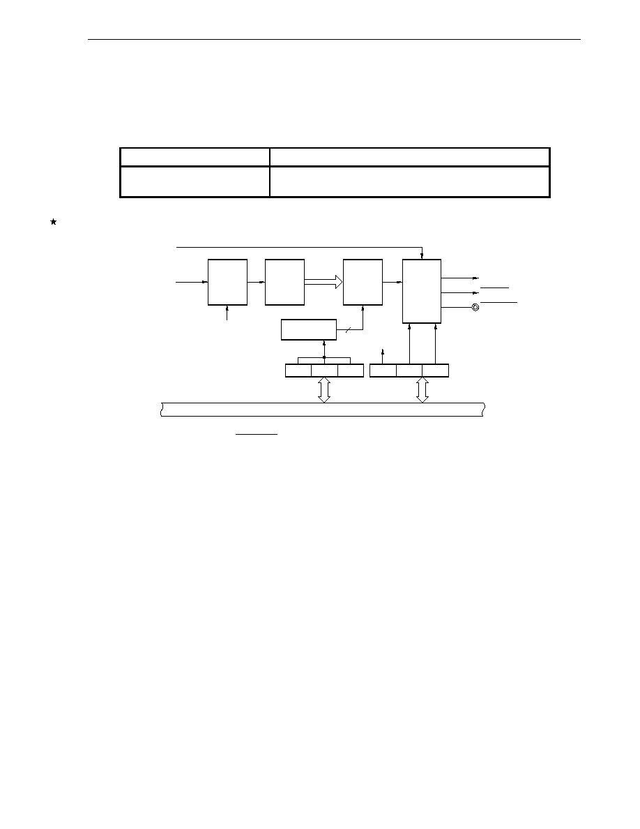
CHAPTER 10 WATCHDOG TIMER
User's Manual U13655EJ2V1UD
175
10.3 Watchdog Timer Configuration
The watchdog timer consists of the following hardware.
Table 10-3. Watchdog Timer Configuration
Item
Configuration
Control registers
Watchdog timer clock select register (WDCS)
Watchdog timer mode register (WDTM)
Figure 10-1. Block Diagram of Watchdog Timer
f
XT1
/2
9
f
XT1
RUN
Clock
input
controller
Divider
Division
clock
selector
Output
controller
INTWDT
WDTOUT
RESET
3
Division mode
selector
Internal bus
Watchdog timer clock select
register (WDCS)
Watchdog timer mode
register (WDTM)
WDCS2 WDCS1 WDCS0
WDTM4 WDTM3
RUN
f
XT1
/2
13
to
f
XT1
/2
19
,
f
XT1
/2
21
Caution
The pulse width of WDTOUT is 20
µ
µ
µ
µs (TYP.).

CHAPTER 10 WATCHDOG TIMER
User's Manual U13655EJ2V1UD
176
10.4 Watchdog Timer Control Registers
The following two registers are used to control the watchdog timer.
∑ Watchdog timer clock select register (WDCS)
∑ Watchdog timer mode register (WDTM)
(1) Watchdog timer clock select register (WDCS)
This register is used to set the overflow time of the watchdog timer and interval timer.
WDCS is set with an 8-bit memory manipulation instruction.
RESET input sets WDCS to 00H.
Figure 10-2. Format of Watchdog Timer Clock Select Register (WDCS)
Address: FF42H
After reset: 00H
R/W
Symbol
7
6
5
4
3
2
1
0
WDCS
0
0
0
0
0
WDCS2
WDCS1
WDCS0
WDCS2
WDCS1
WDCS0
Watchdog timer/interval timer overflow time
0
0
0
f
XT1
/2
13
(0.25 s)
0
0
1
f
XT1
/2
14
(0.5 s)
0
1
0
f
XT1
/2
15
(1 s)
0
1
1
f
XT1
/2
16
(2 s)
1
0
0
f
XT1
/2
17
(4 s)
1
0
1
f
XT1
/2
18
(8 s)
1
1
0
f
XT1
/2
19
(16 s)
1
1
1
f
XT1
/2
21
(64 s)
Remarks 1. f
XT1
: Subsystem clock 1 oscillation frequency
2. Figures in parentheses apply to operation with f
XT1
= 32.768 kHz

CHAPTER 10 WATCHDOG TIMER
User's Manual U13655EJ2V1UD
177
(2) Watchdog timer mode register (WDTM)
This register is used to set the watchdog timer operation mode, and enables/disables the counting operation
of the watchdog timer.
WDTM is written with a 1-bit or 8-bit memory manipulation instruction.
WDTM is a write-only register.
RESET input sets WDTM to 00H.
Figure 10-3. Format of Watchdog Timer Mode Register (WDTM)
Address: FFF9H
After reset: 00H
W
Symbol
7
6
5
4
3
2
1
0
WDTM
RUN
0
0
WDTM4
WDTM3
0
0
0
RUN
Watchdog timer operation mode selection
Note 1
0
Counting stopped
1
Counter cleared and counting restarted
WDTM4
WDTM3
Watchdog timer operation mode selection
Note 2
0
◊
Interval timer mode
Note 3
(Maskable interrupt request is generated when overflow
occurs)
1
0
Watchdog timer mode 1
(Non-maskable interrupt request is generated when overflow
occurs)
1
1
Watchdog timer mode 2
(Reset operation is activated when overflow occurs, and a low-
level signal is output to WDTOUT pin)
Notes 1.
Once RUN is set to 1, it cannot be cleared to 0 by software. Therefore, once the counting operation is
started, it cannot be stopped by any means other than RESET input.
2.
Once WDTM3 and WDTM4 are set to 1, they cannot be cleared to 0 by software.
3.
The watchdog timer starts operation as an interval timer as soon as RUN is set to 1.
Caution
When the watchdog timer is cleared by setting RUN to 1, the actual overflow time is up to 2
9
/f
XT1
seconds shorter than the time set by the watchdog timer clock select register (WDCS).
Remark
◊: don't care

CHAPTER 10 WATCHDOG TIMER
User's Manual U13655EJ2V1UD
178
10.5 Watchdog Timer Operations
10.5.1 Watchdog timer operation
Setting bit 4 (WDTM4) of the watchdog timer mode register (WDTM) to 1 specifies operation as a watchdog timer,
which is used to detect an inadvertent program loop.
The count clock (loop detection time interval) of the watchdog timer can be selected by setting bits 0 to 2 (WDCS0
to WDCS2) of the watchdog timer clock select register (WDCS). The watchdog timer starts the count operation by
setting bit 7 (RUN) of WDTM to 1. After the watchdog timer starts the count operation, if RUN is set to 1 again within
the loop detection time interval set in advance, the watchdog timer is cleared and the count operation restarts.
If the loop detection time had elapsed without RUN having been set to 1, the system is reset or a non-maskable
interrupt request is generated according to the value of WDTM bit 3 (WDTM3). When the system is reset, a low-level
signal of 20
µs (TYP.) is output from WDTOUT pin at the same time.
The watchdog timer continues operation in the HALT mode.
Caution
The actual loop detection time may be up to 2
9
/f
XT1
seconds shorter than the set time.
Table 10-4. Loop Detection Time of Watchdog Timer
WDCS2
WDCS1
WDCS0
Watchdog Timer Loop Detection Time
0
0
0
f
XT1
/2
13
(0.25 s)
0
0
1
f
XT1
/2
14
(0.5 s)
0
1
0
f
XT1
/2
15
(1 s)
0
1
1
f
XT1
/2
16
(2 s)
1
0
0
f
XT1
/2
17
(4 s)
1
0
1
f
XT1
/2
18
(8 s)
1
1
0
f
XT1
/2
19
(16 s)
1
1
1
f
XT1
/2
21
(64 s)
Remarks 1. f
XT1
: Subsystem clock oscillation 1 frequency
2. Figures in parentheses apply to operation with f
XT1
= 32.768 kHz

CHAPTER 10 WATCHDOG TIMER
User's Manual U13655EJ2V1UD
179
10.5.2 Interval timer operation
Setting bit 4 (WDTM4) of the watchdog timer mode register to 0 specifies operation as an interval timer, which is
used to generate an interrupt request repeatedly using the preset count clock as the interval.
The count clock (interval time) can be selected by setting bits 0 to 2 (WDCS0 to WDCS2) of the watchdog timer
clock select register (WDCS). The watchdog timer starts operation as an interval timer when bit 7 (RUN) of WDTM is
set to 1.
The interval timer continues operation in the HALT mode.
Cautions 1. Once bit 4 (WDTM4) of WDTM has been set to 1 (this setting selects the watchdog timer
mode), the interval timer mode is disabled, unless the RESET signal is input.
2. The interval time immediately after it has been set by WDTM may be up to 2
9
/f
XT1
seconds
shorter than the set time.
Table 10-5. Interval Time of Interval Timer
WDCS2
WDCS1
WDCS0
Interval Time
0
0
0
f
XT1
/2
13
(0.25 s)
0
0
1
f
XT1
/2
14
(0.5 s)
0
1
0
f
XT1
/2
15
(1 s)
0
1
1
f
XT1
/2
16
(2 s)
1
0
0
f
XT1
/2
17
(4 s)
1
0
1
f
XT1
/2
18
(8 s)
1
1
0
f
XT1
/2
19
(16 s)
1
1
1
f
XT1
/2
21
(64 s)
Remarks 1. f
XT1
: Subsystem 1 clock oscillation frequency
2. Figures in parentheses apply to operation with f
XT1
= 32.768 kHz

User's Manual U13655EJ2V1UD
180
CHAPTER 11 SAMPLING OUTPUT TIMER/DETECTOR
11.1 Outline of Sampling Output Timer/Detector
This is a function that outputs and detects a sampling pulse periodically. After RESET, the sampling output
timer/detector functions as a normal timer.
11.2 Sampling Output Timer/Detector Function
The sampling output timer/detector employs pins from which a sampling pulse signal is output periodically. By
supplying this pulse signal to a switch in the target, input-closed circuits for the SMP1 to SMP4 pins are realized, and
the state of the switch is checked.
The sampling output timer/detector can generate an interrupt request when a switch in the target is set to a
specified state, removing the necessity of releasing the HALT mode frequently.
Moreover, by making a setting whereby an interrupt is generated only when a switch is set to a specified state, the
sampling output timer/detector can control interrupt generation, removing the necessity of releasing the HALT mode at
an unnecessary timing.
Caution
After RESET, the sampling output timer/detector functions as a normal timer.
11.3 Sampling Output Timer/Detector Configuration
The sampling output timer/detector consists of a 2-channel 8-bit timer. Sampling output mode and 8-bit timer
mode can be selected.
∑
∑
∑
∑ Sampling output mode
Note
<1> For the panel output cycle count of the SMO0 pin, a match signal between TMSA0 and TMSB0 or a
match signal between Prin output and TMSB0 can be selected.
<2> When a match signal between Prin output and TMSB0 is selected for the panel output cycle count,
TMSA0 can operate separately as an interval timer.
<3> Sampling of the SMP0 to SMP4 pins is performed at the falling edge of SMO0. The level of the sampling
interrupt can be set using SMTD sampling level setting register 0 (SMS0).
<4> The levels of the SMP0 to SMP4 pins, which are latched at the sampling timing, can be identified using
SMTD sampling pin status register 0 (SMD0).
∑
∑
∑
∑ 8-bit timer mode
<1> TMSA0 and TMSB0 can operate as separate 8-bit timers.
<2> For the pulse output of the SMO0 pin, TMSA0 or Prin output (0.5 s interval clock (when f
XT1
= 32.768 kHz
operation (f
XT1
: Subsystem clock 1 oscillation frequency))) can be selected.

CHAPTER 11 SAMPLING OUTPUT TIMER/DETECTOR
User's Manual U13655EJ2V1UD
181
Note
∑ Setting when match signal between TMSB0 and TMSA0 is selected:
TMSB0 interval time
half of TMSA0 interval time
∑ Setting when match signal between TMSB0 and Prin output is selected:
TMSB0 interval time
half of Prin cycle
(Sampling output is equal to or less than 1/2 duty.)
∑ Selected clock cycle setting: TMSB0 selected clock cycle
TMSA0 selected clock cycle
∑ Formula of SMO0 cycle of sampling clock and high-level width:
Cycle: (CRSA0 + 1)
◊ TMSA0 clock width
High-level width:
<1> When TMSA0 clock width = TMSB0 clock width, or TMSB0 clock = f
XT1
:
(CRSB0 + 1)
◊ TMSB0 clock width
<2> When TMSA0 clock width > TMSB0 clock width:
(CRSB0 + 0.5)
◊ TMSB0 clock width
<3> When TMSA0 clock width < TMSB0 clock width:
(CRSB0 + 0.5)
◊ TMSB0 clock width ± Gap width (Gap width: TMSB0 clock width/2 max.)
Caution In the 8-bit timer mode, sampling of the SMPn bit (n:0 to 4) is not performed.

CHAPTER 11 SAMPLING OUTPUT TIMER/DETECTOR
User's Manual U13655EJ2V1UD
182
Figure 11-1 shows the block diagram of the sampling output timer/detector.
Figure 11-1. Block Diagram of Sampling Output Timer/Detector
SMTD compare register
B0 (CRSB0)
SMTD timer counter
B0 (TMSB0)
SMTD compare register
A0 (CRSA0)
SMTD timer counter A0
(TMSA0)
Input
controller
SLSMD0
SLPE0
TCEP0
SLSMD0,
SMOE0,
LVSS0,
LVRS0
Clear
Clear
Output
controller
Selector
Enable control
Selector
Selector
f
XT1
f
XT1
/2
2
f
XT1
/2
4
f
XT1
/2
6
f
XT1
f
XT1
/2
3
f
XT1
/2
10
f
XT1
/2
14
Prin
Internal bus
Internal bus
SMD04
SMS04
SMTD sampling level setting register 0
(SMS0)
SMS03
SMS02
SMS01
SMS00
SMD03
SMD02
SMD01
SMD00
SMP4/P25
SMP3/P24
SMP2/P23
SMP1/P22
SMP0/P05/INTP5/RxD20
INTSMP4
INTSMP3
INTSMP2
INTSMP1
INTSMP0
INTSA0
SMO0/P33
INTSB0

CHAPTER 11 SAMPLING OUTPUT TIMER/DETECTOR
User's Manual U13655EJ2V1UD
183
11.4 Sampling Output Timer/Detector Control Registers
The following nine registers are used to control the sampling output timer/detector.
∑ SMTD timer counter A0 (TMSA0)
∑ SMTD timer counter B0 (TMSB0)
∑ SMTD compare register A0 (CRSA0)
∑ SMTD compare register B0 (CRSB0)
∑ SMTD clock select register A0 (TCSA0)
∑ SMTD clock select register B0 (TCSB0)
∑ SMTD control register 0 (TSM0)
∑ SMTD sampling level setting register 0 (SMS0)
∑ SMTD sampling pin status register 0 (SMD0)
(1) SMTD timer counter A0 (TMSA0)
TMSA0 is an 8-bit read-only register that counts the count pulse.
The counter is incremented in synchronization with the rising edge of the count clock.
Even if the count value is read out during a count operation, the count operation will not stop. Therefore, the
read value may differ from the actual count value.
The count value becomes 00H in the following cases.
<1> RESET input
<2> TCESA0 cleared
<3> Match between TMSA0 and CRSA0
(2) SMTD timer counter B0 (TMSB0)
TMSB0 is an 8-bit counter that counts the count pulse.
This counter cannot be operated directly by a program (read/write disabled).
The counter is incremented in synchronization with the rising edge of the count clock.
The count value becomes 00H in the following cases.
<1> RESET input
<2> TCESB0 cleared
<3> Match between TMSB0 and CRSB0
<4> In the sampling output mode, when SMO0 = low level
(3) SMTD compare register A0 (CRSA0)
The value set in CRSA0 is constantly compared with the count value of SMTD timer counter A0 (TMSA0). If
they match, an interrupt request (INTSA0) is generated.
The value of CRSA0 can be set within the range of 00H to FFH.
Rewriting during a count operation is prohibited.
(4) SMTD compare register B0 (CRSB0)
The value set in CRSB0 is constantly compared with the count value of SMTD timer counter B0 (TMSB0). If
they match, an interrupt request (INTSB0) is generated.
The value of CRSB0 can be set within the range of 00H to FFH.
Rewriting during a count operation is prohibited.

CHAPTER 11 SAMPLING OUTPUT TIMER/DETECTOR
User's Manual U13655EJ2V1UD
184
(5) SMTD clock select register A0 (TCSA0)
TCSA0 is a register that sets the count clock for SMTD timer counter A0 (TMSA0).
TCSA0 is set with a 1-bit or 8-bit memory manipulation instruction.
RESET input sets TCSA0 to 00H.
Figure 11-2. Format of SMTD Clock Select Register A0 (TCSA0)
Address: FF74H
After reset: 00H
R/W
Symbol
7
6
5
4
3
2
1
0
TCSA0
0
0
0
0
0
0
TCA01
TCA00
TCA01
TCA00
Clock selection
0
0
f
XT1
(30.5
µs)
0
1
f
XT1
/2
3
(244
µs)
1
0
f
XT1
/2
10
(31.3 ms)
1
1
f
XT1
/2
14
(0.5 s)
Caution The TMSA0 count operation must be stopped before setting TCSA0.
Remark Figures in parentheses apply to operation with f
XT1
= 32.768 kHz (f
XT1
: Subsystem clock 1
oscillation frequency).
(6) SMTD clock select register B0 (TCSB0)
TCSB0 is a register that sets the count clock for SMTD timer counter B0 (TMSB0).
TCSB0 is set with a 1-bit or 8-bit memory manipulation instruction.
RESET input sets TCSB0 to 00H.
Figure 11-3. Format of SMTD Clock Select Register B0 (TCSB0)
Address: FF75H
After reset: 00H
R/W
Symbol
7
6
5
4
3
2
1
0
TCSB0
0
0
0
0
0
0
TCB01
TCB00
TCB01
TCB00
Clock selection
0
0
f
XT1
(30.5
µs)
0
1
f
XT1
/2
2
(122
µs)
1
0
f
XT1
/2
4
(488
µs)
1
1
f
XT1
/2
6
(1.95 ms)
Caution The TMSB0 count operation must be stopped before setting TCSB0.
Remark Figures in parentheses apply to operation with f
XT1
= 32.768 kHz (f
XT1
: Subsystem clock 1
oscillation frequency).

CHAPTER 11 SAMPLING OUTPUT TIMER/DETECTOR
User's Manual U13655EJ2V1UD
185
(7) SMTD control register 0 (TSM0)
TSM0 is a register that controls the count operation of SMTD timer counters A0 and B0 (TMSA0 and TMSB0)
and Prin, selects the SMO0 output mode, controls the SMO0 output signal selection and the timer output, and
sets the initial setting of the SMO0 output level.
TSM0 is set with a 1-bit or 8-bit memory manipulation instruction.
RESET input sets TSM0 to 00H.
Figure 11-4. Format of SMTD Control Register 0 (TSM0)
Address: FF76H
After reset: 00H
R/W
Symbol
7
6
5
4
3
2
1
0
TSM0
TCESA0
TCESB0
TCEP0
SLSMD0
SLPE0
SMOE0
LVSS0
LVRS0
TCESA0
TMSA0 count enable flag
0
Stops TMSA0 count operation (TMSA0 = 00H)
1
Enables TMSA0 count operation
TCESB0
TMSB0 count enable flag
0
Stops TMSB0 count operation (TMSB0 = 00H)
1
Enables TMSB0 count operation
TCEP0
Prin (prescaler input) count enable flag
0
Stops Prin count operation
1
Enables Prin count operation
SLSMD0
SMO0 output mode selection flag
0
Timer mode
1
Sampling output mode
SLPE0
SMO0 output signal control selection flag
Note
0
Selects Prin (0.5 s: with f
XT1
= 32.768 kHz operation)
1
Selects a match signal (INTSA0) between TMSA0 and CRSA0
SMOE0
Output control flag
0
Disables output (port mode)
1
Enables output
LVSS0
LVRS0
Timer output F/F initial state setting flag
0
0
No change
0
1
Resets timer output F/F to 0
1
0
Sets timer output F/F to 1
1
1
Setting prohibited

CHAPTER 11 SAMPLING OUTPUT TIMER/DETECTOR
User's Manual U13655EJ2V1UD
186
Note This is a flag that selects a signal that is to be input to the output controller and output from the SMO0
output pin. This flag is used for frequency selection in the sampling output mode, and for output-pulse
width selection in the timer mode.
Cautions 1. Timer operation must be stopped before setting bits 0 to 5 (LVRS0, LVSS0, SMOE0,
SLPE0, SLSMD0, TCEP0).
2. Setting of TCESA0, TCESB0, TCEP0, and SMOE0 should be performed after SLSMD0,
SLPE0, LVSS0, and LVRS0 are set.
3. SLSMD0, SLPE0, LVSS0, and LVRS0 cannot be written while SMOE0 is 1.
4. Write to TCESA0, TCESB0, and SMOE0 ("0"
"1" or "1"
"0") at the same time that
SLSMD0 = 1, SLPE0 = 1 are set (in the sampling mode, when INTSA0 is selected).
5. Write to TCESB0, TCEP0, and SMOE0 ("0"
"1" or "1"
"0") at the same time that
SLSMD0 = 1, SLPE0 = 0 are set (in the sampling mode, when Prin (0.5 s) is selected).
6. Write to TCESA0, TCESB0, and SMOE0 ("0"
"1" or "1"
"0") at the same time that
SLSMD0 = 0, SLPE0 = 1 are set (in the timer mode, when INTSA0 is selected).
7. Write to TCESB0, TCEP0, and SMOE0 write ("0"
"1" or "1"
"0") at the same time
that SLSMD0 = 0, SLPE0 = 0 are set (in the timer mode, when Prin (0.5 s) is selected).
8. When using the SMO0/P33 pin as a general-purpose port pin, be sure to set SMOE0 to 0
in the timer mode (SLSMD0 = 0) (In the sampling mode, the SMO0/P33 pins may be high-
level output when SMOE0 = 0. Also, in the timer mode, the SMO0/P33 pins may be high-
level output when SMOE0 = 1).
9. The sampling signal detect register (SMD0) and INTSMP0 to INTSMP4 can operate only
when SLSMD0 is 1 (sampling mode).
10. In the sampling mode, the state of the SMO0/P33 pin (sampling clock) output is
maintained when the value of SMOE0 is changed from "1" to "0".
11. In the sampling mode, after the value of SMOE0 has been changed from "1" to "0" to
hold the value of the SMO0/P33 pin output at high level and then changed again from
"0" to "1", the level of the SMO0/P33 pin output changes from high to low at the falling
edge of subsystem clock 1 (32.768 kHz) and sampling clock output starts. Moreover,
sampling of the SMP0 to SMP4 pins is performed at the falling edge of the SMO0/P33
pin.
12. In the sampling mode, if the value of SMOE0 is changed from "0" to "1" to hold the
value of the SMO0/P33 pin output at low level, an interrupt signal is output according to
the data (bits 0 to 4 (SMD00 to SMD04) of SMTD sampling pin status register 0 (SMD0))
sampled when SMOE0 was written ("0"
"1") immediately before the held value.
13. In the timer mode, the level of the SMO0/P33 pin output is held when the value of
SMOE0 is changed from "1" to "0". Therefore, next time the value of SMOE0 is changed
from "0" to "1", the held value is output.
14. If, during operation in the sampling mode, the sampling signal active level setting flag
(SMS0) is rewritten, the contents of INTSMP0 to INTSMP4 and SMD00 to SMD04 may
differ.
15. The SMD0 data may be destroyed after the SMD0 data is read, but the status of the
SMP0 to SMP4 pins is sampled after one cycle of subsystem clock 1 (32.768 kHz).
16. After the count value of SMTD timer counter A0 (TMSA0) has been read, that data may
be destroyed, but the count value is read again after the lapse of 1 cycle of the TMSA0
selection clock.

CHAPTER 11 SAMPLING OUTPUT TIMER/DETECTOR
User's Manual U13655EJ2V1UD
187
(8) SMTD sampling level setting register 0 (SMS0)
If the sampling input level of the SMP0 to SMP4 pins matches the level that is set as an active level by SMS0,
a sampling interrupt (INTSMP0 to INTSMP4) can be generated.
Sampling of the SMP0 to SMP4 pins is performed at the falling edge of the sampling clock.
SMS0 is set with a 1-bit or 8-bit memory manipulation instruction.
RESET input sets SMS0 to 00H.
Figure 11-5. Format of SMTD Sampling Level Setting Register 0 (SMS0)
Address: FF77H
After reset: 00H
R/W
Symbol
7
6
5
4
3
2
1
0
SMS0
0
0
0
SMS04
SMS03
SMS02
SMS01
SMS00
SMS0n
Sampling signal active level setting flag (n = 0 to 4)
0
An interrupt request is generated if a low-level signal is
detected at the falling edge of the sampling clock
1
An interrupt request is generated if a high-level signal is
detected at the falling edge of the sampling clock
Caution
When SLSMD0 = 1 and SMOE0 = 1 (in the sampling output mode), do not write to SMS0.
(9) SMTD sampling pin status register 0 (SMD0)
SMD0 is a register that detects the status of the SMP0 to SMP4 pins, which are latched at the falling edge of
the sampling clock (SMO0).
SMD0 operates only in the sampling output mode (bit 4 (SLSMD0) of SMTD control register 0 (TSM0) is 1).
SMD0 is read with a 1-bit or 8-bit memory manipulation instruction.
RESET input sets SMD0 to 00H.
Figure 11-6. Format of SMTD Sampling Pin Status Register 0 (SMD0)
Address: FF78H
After reset: 00H
R
Symbol
7
6
5
4
3
2
1
0
SMD0
0
0
0
SMD04
SMD03
SMD02
SMD01
SMD00
SMD0n
SMPn pin status (n = 0 to 4)
0
Low level
1
High level
Caution When sampling output is stopped (the timer enable flag used is cleared to 0), SMD0
becomes undefined. Therefore, the interrupt mask flags of INTSMP0 to INTSMP4 must be
set to 1 (disabling interrupt servicing) before stopping the sampling output.

CHAPTER 11 SAMPLING OUTPUT TIMER/DETECTOR
User's Manual U13655EJ2V1UD
188
Figure 11-7 shows the SMO0 output timings in the sampling output mode and in the timer mode.
Figure 11-7. Timing Chart of SMO0 Output
(1) SMO0 output in the sampling output mode
INTSA0
TMSB0 interval time
∑ When a match signal between TMSA0 and TMSB0 is selected
∑ When a match signal between Prin output and TMSB0 is selected
INTSB0
P33/SMO0
Prin output
INTSB0
P33/SMO0
TMSA0 interval time
(f
XT1
= 32.768 kHz)
0.5 s
(2) SMO0 output in the timer mode
∑ When a match signal between TMSA0 and TMSB0 is selected
∑ When a match signal between Prin output and TMSB0 is selected
INTSA0
SMO0
Prin output
P33/SMO0
(f
XT1
= 32.768 kHz)
0.5 s

CHAPTER 11 SAMPLING OUTPUT TIMER/DETECTOR
User's Manual U13655EJ2V1UD
189
Figure 11-8 shows the sampling detection timing.
Figure 11-8. Timing Chart of Sampling Detection
P33/SMO0
SMP0 to SMP4
Status latching
Interrupt generation timing
P33/SMO0
<When the active level of sampling input is high for interrupt generation>
<When the active level of sampling input is low for interrupt generation>
<When the active level of sampling input is high for interrupt generation>
[Sampling detection 1]
[Sampling detection 2]
<When the active level of sampling input is low for interrupt generation>
SMP0 to SMP4
Status latching
Interrupt generation timing
P33/SMO0
SMP0 to SMP4
Status latching
Interrupt generation timing
P33/SMO0
SMP0 to SMP4
Status latching
Interrupt generation timing

User's Manual U13655EJ2V1UD
190
CHAPTER 12 MR SAMPLING FUNCTION
12.1
Outline of MR Sampling Function
This is a function that drives an MR sensor (magnetic sensor). After RESET, this functions as a normal timer.
12.2 MR Sampling Function
The MR sampling function is a function used to drive an MR sensor (magnetic sensor).
The MR sampling function consists of two blocks, an MR sampling output circuit and a phase detector. It can be
used as an 8-bit interval timer when the MR sampling function is not used.
Figure 12-1 shows the block diagram of the MR sampling function.
Figure 12-1. Block Diagram of MR Sampling
f
XT1
f
XT1
/2
3
f
XT1
/2
7
f
XT2
/2
4
INTMRT0
MRO0/P56
MRO1/P57
MROE00
MROE01
Selector
Internal bus
MRTD compare
register 0 (CRM0)
8-bit MR counter 0
(TMMR0)
MR sampling control
register 0 (MRM0)
Sampling
generator
Edge
detector
Internal bus
MR sampling control
register 0 (MRM0)
Sampling
circuit
Sampling
circuit
MRI0/P26
MRI1/P27
MRD01
MRD00
PRTY0
INTMRO0
Phase discriminator
D Q
D Q
D Q
Clear

CHAPTER 12 MR SAMPLING FUNCTION
User's Manual U13655EJ2V1UD
191
12.3 MR Sampling Configuration
The MR sampling function consists of the following hardware.
Table 12-1. Configuration of MR Sampling
Item
Configuration
Registers
8-bit MR counter 0 (TMMR0)
MRTD compare register 0 (CRM0)
Control registers
MRTD control register 0 (TCM0)
MRTD output control register 0 (TMM0)
MR sampling control register 0 (MRM0)
(1) 8-bit MR counter 0 (TMMR0)
TMMR0 is an 8-bit counter that counts the count pulse.
The counter is incremented in synchronization with the rising edge of the count clock.
TMMR0 cannot be written or read, and the count value is cleared to 00H in the following cases.
<1> RESET input
<2> Bit 7 (TCEM0) of the MRTD control register 0 (TCM0) is reset to 0
<3> Match between TMMR0 and CRM0
(2) MRTD compare register 0 (CRM0)
The value set in CRM0 is constantly compared with the count value of 8-bit MR counter 0 (TMMR0). If they
match, an interrupt request (INTMRT0) is generated.
CRM0 can be written and read in 8-bit units.
The value of CRM0 can be set within the range of 01H to FFH. Rewriting during a count operation is
prohibited.
Caution
Setting 00H is prohibited.

CHAPTER 12 MR SAMPLING FUNCTION
User's Manual U13655EJ2V1UD
192
12.4 MR Sampling Control Registers
The following three registers are used to control the MR sampling function.
∑ MRTD control register 0 (TCM0)
∑ MRTD output control register 0 (TMM0)
∑ MR sampling control register 0 (MRM0)
(1) MRTD control register 0 (TCM0)
TCM0 is a register that controls the TMMR0 count operation, selects whether the 8-bit timer mode or the MR
sampling output mode is used, and is also used to select the count clock of TMMR0.
TCM0 is set with a 1-bit or 8-bit memory manipulation instruction.
RESET input sets TCM0 to 00H.
Figure 12-2. Format of MRTD Control Register 0 (TCM0)
Address: FF79H
After reset: 00H
R/W
Symbol
7
6
5
4
3
2
1
0
TCM0
TCEM0
SLMR0
0
0
0
0
TCM01
TCM00
TCEM0
TMMR0 count operation control
0
Clears the TMMR0 counter to 0 and then stops the count
operation (TMMR0 = 00H)
1
Enables TMMR0 count operation
SLMR0
8-bit timer/MR sampling output mode selection
0
8-bit timer mode
1
MR sampling output mode
TCM01
TCM00
TMMR0 count clock selection
0
0
f
XT1
(30.5
µs)
0
1
f
XT1
/2
3
(244
µs)
1
0
f
XT1
/2
7
(3.9 ms)
1
1
f
XT2
/2
4
(3.25
µs)
Note
Note
Can only be selected in the 8-bit timer mode.
Remarks 1. Figures in parentheses apply to operation with f
XT1
= 32.768 kHz, f
XT2
= 4.91 MHz.
2. f
XT1
: Subsystem clock 1 oscillation frequency
f
XT2
: Subsystem clock 2 oscillation frequency

CHAPTER 12 MR SAMPLING FUNCTION
User's Manual U13655EJ2V1UD
193
(2) MRTD output control register 0 (TMM0)
TMM0 is a register that sets the status of the timer output flip-flop (F/F) in the 8-bit timer mode.
TMM0 is set with a 1-bit or 8-bit memory manipulation instruction.
RESET input sets TMM0 to 00H.
Figure 12-3. Format of MRTD Output Control Register 0 (TMM0)
Address: FF7AH
After reset: 00H
W
Symbol
7
6
5
4
3
2
1
0
TMM0
0
0
0
0
0
0
LVSM0
LVRM0
LVSM0
LVRM0
Timer output F/F status setting
0
0
No change
0
1
Resets timer output F/F to 0
1
0
Sets timer output F/F to 1
1
1
Setting prohibited
Remark TMM0 cannot be written during a TMMR0 count operation.

CHAPTER 12 MR SAMPLING FUNCTION
User's Manual U13655EJ2V1UD
194
(3) MR sampling control register 0 (MRM0)
MRM0 is a register used to display the sampling state of signals input from the MR sensor and control the
operation of MRO0/MRI0 and MRO1/MRI1. Bits 5 to 7 of MRM0 are read-only bits.
MRM0 is sets with a 1-bit or 8-bit memory manipulation instruction.
RESET input sets MRM0 to 00H.
Figure 12-4. Format of MR Sampling Control Register 0 (MRM0)
Address: FF7BH
After reset: 00H
R/W
Symbol
7
6
5
4
3
2
1
0
MRM0
MRD01
MRD00
PRTY0
0
CK01
CK00
MROE01 MROE00
MRD01
MRI1 internal shaped waveform level status flag
0
Low level
1
High level
MRD00
MRI0 internal shaped waveform level status flag at rising edge of
MRI1 internal shaped waveform
0
MRI0 internal shaped waveform = Low level
1
MRI0 internal shaped waveform = High level
PRTY0
MRI0 internal shaped waveform level status flag at rising/falling
edge of MRI1 internal shaped waveform
0
The MRI0 internal shaped waveform is high at the rising edge
of the MRI1 internal shaped waveform or low at the falling edge
of the MRI1 internal shaped waveform
1
The MRI0 internal shaped waveform is low at the rising edge of
the MRI1 internal shaped waveform or high at the falling edge
of the MRI1 internal shaped waveform
CK01
CK00
MRO1, MRO0 pins output clock pulse width setting
0
0
2
◊ f
XT1
(15
µs)
0
1
f
XT1
(30.5
µs)
1
0
f
XT1
/2 (61
µs)
1
1
f
XT1
/2
5
(977
µs)
MROE01
MRO1 pin output control flag
0
Disables output
1
Enables output
MROE00
MRO0 pin output control flag
0
Disables output
1
Enables output

CHAPTER 12 MR SAMPLING FUNCTION
User's Manual U13655EJ2V1UD
195
Remarks 1. MRD01, MRD00, and PRTY0 are cleared in the 8-bit timer mode (bit 6 of MRTD control
register 0 (TCM0) is 0).
2. Figures in parentheses apply to operation with f
XT1
= 32.768 kHz (f
XT1
: Subsystem clock 1
oscillation frequency).
12.5 MR Sampling Output Circuit Operations
(1) In 8-bit timer mode
∑ 8-bit MR counter 0 (TMMR0) operates as an 8-bit timer by setting bit 6 (SLMR0) of MRTD control register 0
(TCM0) to 0.
∑ The outputs of MRO0/MRO1 are inverted and output by an interrupt request (INTMRT0) that is generated
on a match between MRTD compare register 0 (CRM0) and TMMR 0.
(2) MR sampling output mode
∑ 8-bit MR counter 0 (TMMR0) operates as an 8-bit interval timer, which is cleared if the value of this interval
timer matches the MRTD compare register 0 (CRM0) value.
∑ The output cycle of the MRO0/MRO1 pins is determined by an interrupt request (INTMRT0) that is
generated on a match between MRTD compare register 0 (CRM0) and TMMR0. The duty is set using bits
2 and 3 (CK00 and CK01) of MR sampling control register 0 (MRM0).
Figure 12-5 shows the timing charts of the MRO0/MRO1 outputs.
Figure 12-5. Timing Charts of MRO0/MRO1 Outputs
INTMRT0
MRO0/MRO1
<In 8-bit timer mode>
<In MR sampling output mode>
∑ When both CK01 and CK00 are 0
15 s
(f
XT1
= 32.768 kHz)
15 s
INTMRT0
MRO0/MRO1
µ
µ
Remarks 1. The pulse width of MRO0/MRO1 is set using bits 2 and 3 (CK00 and CK01) of MRM0.
2. f
XT1
: Subsystem clock 1 oscillation frequency

CHAPTER 12 MR SAMPLING FUNCTION
User's Manual U13655EJ2V1UD
196
12.6 Phase Detector Operation
∑ The MRI0/MRI1 input is latched to the sampling circuit at the falling edge of the MRO0/MRO1 clock and
waveform shaping of the input signal is performed.
∑ An MRTD edge detection interrupt (INTMRO0) occurs at both the rising and falling edges of the MRI1 signal
that has undergone waveform shaping internally.
Occurrence of the INTMRO0 interrupt is delayed 15
µs in relation to the waveform-shaped MRI1 signal.
∑ Bit 7 (MRD01) of MR sampling control register 0 (MRM0) latches the level of the internally waveform-shaped
MRI1 signal upon occurrence of the INTMRO0 interrupt, and this value is transferred to MRD01. MRD01 is set
(to 1) when MRI1 is high level, and cleared (to 0) when MRI1 is low level.
∑ Bit 6 (MRD00) of MRM0 latches the level of the internally waveform-shaped MRI0 at both the falling and the
rising edges of the internally waveform-shaped MRI1 signal, and this value is transferred to MRD00 upon
occurrence of the INTMRO0 interrupt. MRD00 is set (to 1) when MRI0 is high level, and cleared (to 0) when
MRI0 is low level.
∑ Bit 5 (PRTY0) of MRM0 is used to verify MRI0/MRI1 phase detection (normal/inverted). PRTY0 is cleared (to
0) (normal) when the waveform-shaped MRI0 signal is high level at the rising edge of the waveform-shaped
MRI1 signal, or when MRI0 is low level at the falling edge of the MRI1 signal.
On the other hand, PRTY0 is set (to 1) (inverted) when MRI0 is low level at the rising edge of MRI1, or when
MRI0 is high level at the falling edge of MRI1.
∑ In the 8-bit timer mode, the phase detector does not operate.
Caution
The INTMRO0 occurrence timing and the MRD00/MRD01, PRTY0 set/clear timing are always
delayed 15
µ
µ
µ
µs in relation to the MRI1 internal shaped waveform.
Figure 12-6 shows a timing example of the phase detector.
Figure 12-6. Timing Example of Phase Detector
MRO0/P56
MRO1/P57
MRI0/P26
MRI1/P27
MRI0 internal
shaped waveform
MRD01 flag
MRD00 flag
MRI1 internal
shaped waveform
PRTY0 flag
INTMRO0
MRD00/01 and INTMRO0 and PRTY0
are always delayed 15 s in relation to
the MRI1 internal shaped waveform.
µ

CHAPTER 12 MR SAMPLING FUNCTION
User's Manual U13655EJ2V1UD
197
12.7 MR Sampling Function Operating Cautions
(1) MRI0 and MRI1 input waveforms
∑ When MRI0 and MRI1 change at the same time
When the edges of MRI0 and MRI1 overlap, the value of the MRI0 internal shaped waveform level status
flag is undefined.
∑ Change timing of INTMRO0 and each status flag
INTMRO0 and the status flags (MRD00, MRD01, and PRTY0) change at the same timing.
(2) Register setting
∑ All flags must be set after the TMMR0 count operation control flag (TCEM0) is cleared to 0.
(After all settings such as the timer mode/MR mode setting and MRO0/MRO1 pin output enable/disable
setting are completed, the timer starts operation. To change the status flags, the timer must be stopped
beforehand by clearing TCEM0 to 0.)
(3) Switching of MR sampling output mode and 8-bit timer mode
∑ Be sure to stop the timer operation (TCEM0 = 0) before switching the mode between MR sampling output
mode and 8-bit timer mode.
(4) Waveform in MR sampling output mode
∑ MR sampling output should be set so that it is equal to or less than 1/2 the duty.

User's Manual U13655EJ2V1UD
198
CHAPTER 13 CLOCK OUTPUT CONTROLLER
13.1 Clock Output Controller Functions
This circuit is used to output the clock to be supplied to the carrier output and to peripheral LSIs during a remote-
control transmission. The clock is selected by the clock output selection register (CKS), and then output via the
PCL/P34 pin.
Clock-pulse output is performed using the following procedure.
<1> Select the clock pulse output frequency using bits 0 to 3 (CCS0 to CCS3) of CKS (clock-pulse output
disabled state).
<2> Set the output latch of P34 to 0.
<3> Set bit 4 (PM34) of port mode register 3 (PM3) to 0 (this sets the output mode).
<4> Set bit 4 (CLOE) of CKS to 1.
Caution Setting the output latch of P34 to 1 disables clock output.
Remark The clock output controller is designed so as not to output a narrow-width pulse when the clock output
is switched between enabled and disabled.

CHAPTER 13 CLOCK OUTPUT CONTROLLER
User's Manual U13655EJ2V1UD
199
13.2 Clock Output Controller Configuration
The clock output controller consists of the following hardware.
Table 13-1. Configuration of Clock Output Controller
Item
Configuration
Control registers
Clock output selection register (CKS)
Port mode register 3 (PM3)
Figure 13-1. Block Diagram of Clock Output Controller
f
XT1
8
PCL/P34
f
XT1
-f
XT1
/2
7
CLOE
CLOE
CCS3
CCS2
CCS1
CCS0
Internal bus
Prescaler
Selector
Clock
controller
Clock output selection register (CKS)

CHAPTER 13 CLOCK OUTPUT CONTROLLER
User's Manual U13655EJ2V1UD
200
13.3 Clock Output Function Control Registers
The following two registers are used to control the clock output function.
∑ Clock output select register (CKS)
∑ Port mode register 3 (PM3)
(1) Clock output select register (CKS)
CKS is a register that specifies the PCL output clock.
CKS is set with a 1-bit or 8-bit memory manipulation instruction.
RESET input sets CKS to 00H.
Figure 13-2. Format of Clock Output Select Register (CKS)
Address: FF40H
After reset: 00H
R/W
Symbol
7
6
5
4
3
2
1
0
CKS
0
0
0
CLOE
CCS3
CCS2
CCS1
CCS0
CLOE
PCL output enable/disable specification
0
Stops clock division circuit operation, PCL is fixed to low.
1
Enables clock division circuit operation and PCL output
CCS3
CCS2
CCS1
CCS0
PCL output clock selection
0
0
0
0
f
XT1
(32.768 kHz)
0
0
0
1
f
XT1
/2 (16.384 kHz)
0
0
1
0
f
XT1
/2
2
(8.192 kHz)
0
0
1
1
f
XT1
/2
3
(4.096 kHz)
0
1
0
0
f
XT1
/2
4
(2.048 kHz)
0
1
0
1
f
XT1
/2
5
(1.024 kHz)
0
1
1
0
f
XT1
/2
6
(512 Hz)
0
1
1
1
f
XT1
/2
7
(256 Hz)
Other than above
Setting prohibited
Remark Figures in parentheses apply to operation with f
XT1
= 32.768 kHz (f
XT1
: Subsystem clock 1
oscillation frequency)

CHAPTER 13 CLOCK OUTPUT CONTROLLER
User's Manual U13655EJ2V1UD
201
(2) Port mode register 3 (PM3)
This is a register that specifies input/output for port 3 in 1-bit units.
When the P34/PCL pin is used for the clock output function, the output latches of PM34 and P34 must be set
to 0.
PM3 is set with a 1-bit or 8-bit memory manipulation instruction.
RESET input sets PM3 to FFH.
Figure 13-3. Format of Port Mode Register 3 (PM3)
Address: FF23H
After reset: FFH
R/W
Symbol
7
6
5
4
3
2
1
0
PM3
PM37
PM36
PM35
PM34
PM33
PM32
PM31
PM30
PM3n
P3n input/output mode selection (n = 0 to 7)
0
Output mode (output buffer is on)
1
Input mode (output buffer is off)

202
User's Manual U13655EJ2V1UD
CHAPTER 14 SERIAL INTERFACE UART2
14.1 Functions of Serial Interface UART2
Serial interface UART2 has the following two modes.
(1) Operation stop mode
This mode is used when serial transfer is not performed. Power consumption can therefore be reduced in
this mode.
(2) Asynchronous serial interface (UART) mode (with pin switching function)
In this mode, one byte of data starting with the start bit is transmitted/received, and full-duplex operation is
possible.
A dedicated UART baud rate generator is incorporated, allowing communication over a wide range of baud
rates.
The transfer data length can be selected from 5 bits, 7 bits, and 8 bits.
Positive logic/negative logic can be selected for both transmission and reception.
By using subsystem clock 1, transmission/reception is possible at a transfer rate of 200 bps and 300 bps. By
using subsystem clock 2, transmission/reception is possible at a transfer rate of 1,200 bps and 2,400 bps.
Dual-system data I/O pins (RxD and TxD) are provided, and the pin to be used can be selected by software
(time-division transfer function). For actual usage, however, only one system can be used at once.
Caution
Pins not being used for pin switching can be used as port pins.
Figure 14-1 shows the block diagram of serial interface UART2.

CHAPTER 14 SERIAL INTERFACE UART2
User's Manual U13655EJ2V1UD
203
Figure 14-1. Block Diagram of Serial Interface UART2
Internal bus
Internal bus
RxD20/P05/
INTP5/SMP0
RxD21/P06/
INTP6
UART pin
switching
register
(UTCH0)
PE2 FE2 OVE2
Asynchronous serial
interface status
register 2 (ASIS2)
Asynchronous serial
interface mode register 2
(ASIM2)
Asynchronous serial
interface function register 2
(ASIF2)
Receive
controller
(parity check)
Transmit shift
register 2
(TXS2)
Transmit
controller
(parity add)
Prescaler
(2-division)
INTSER2
INTST2
8-bit baud rate
generator/counter
Compare register 2
for baud rate
generator (BRCR2)
f
XT2
/2
6
f
XT1
/2
8
TXE2 RXE2 PS21 PS20 SL2 ISRM2
TPS21TPS20 REV2 CL21 CL20
INTSR2
Selector
TxD20/P20
TxD21/P21
Selector
Selector
f
XT1
TSL2
Receive buffer
register 2
(RXB2)
Receive shift
register 2
(RX2)

CHAPTER 14 SERIAL INTERFACE UART2
User's Manual U13655EJ2V1UD
204
14.2 Configuration of Serial Interface UART2
Serial interface UART2 consists of the following hardware.
Table 14-1. Configuration of Serial Interface UART2
Item
Configuration
Registers
Transmit shift register 2 (TXS2)
Receive shift register 2 (RX2)
Receive buffer register 2 (RXB2)
Control registers
Asynchronous serial interface mode register 2 (ASIM2)
Asynchronous serial interface status register 2 (ASIS2)
Asynchronous serial interface function register 2 (ASIF2)
Compare register 2 for baud rate generation (BRCR2)
UART pin switching register (UTCH0)
(1) Transmit shift register 2 (TXS2)
This register is used to set the transmit data. The data written in TXS2 is transmitted as serial data.
If the data length is specified as 7 bits, bits 0 to 6 of the data written in TXS2 are transmitted as transmit data.
Writing data to TXS2 starts the transmit operation.
TXS2 is written with an 8-bit memory manipulation instruction. It cannot be read.
RESET input sets TXS2 to FFH.
Caution
TSX2 must not be written to during a transmit operation.
TXS2 and receive buffer register 2 (RXB2) are allocated to the same address, and when a
read is performed, the value of RXB2 is read.
(2) Receive shift register 2 (RX2)
This register is used to convert serial data input to the RxD20 and RxD21 pins into parallel data. When one
byte of data is received, the receive data is transferred to receive buffer register 2 (RXB2).
RX2 cannot be directly manipulated by a program.
(3) Receive buffer register 2 (RXB2)
This register holds receive data. Each time one byte of data is received, new receive data is transferred from
receive shift register 2 (RX2).
If the data length is specified as 7 bits, the receive data is transferred to bits 0 to 6 of RXB2, and the MSB (bit
7) of RXB2 is always set to 0.
RXB2 is read with an 8-bit memory manipulation instruction. It cannot be written to.
RESET input sets RXB2 to FFH.
Caution
Be sure to read receive buffer register 2 (RXB2) even if a receive error occurs. Otherwise,
an overrun error occurs when the next data is received, resulting in a receive-error state.

CHAPTER 14 SERIAL INTERFACE UART2
User's Manual U13655EJ2V1UD
205
(4) Transmission controller
This circuit controls transmit operations such as the addition of a start bit, parity bit, and stop bit to data
written in transmit shift register 2 (TXS2) in accordance with the contents set in asynchronous serial interface
mode register 2 (ASIM2).
(5) Reception controller
This circuit controls receive operations in accordance with the contents set in asynchronous serial interface
mode register 2 (ASIM2). It also performs error checks for parity errors, etc., during receive operations, and if
an error is detected, sets a value in asynchronous serial interface status register 2 (ASIS2).

CHAPTER 14 SERIAL INTERFACE UART2
User's Manual U13655EJ2V1UD
206
14.3 Control Registers of Serial Interface UART2
The following five registers are used to control serial interface UART2.
∑ Asynchronous serial interface mode register 2 (ASIM2)
∑ Asynchronous serial interface status register 2 (ASIS2)
∑ Asynchronous serial interface function register 2 (ASIF2)
∑ Compare register 2 for baud rate generation (BRCR2)
∑ UART pin switching register (UTCH0)
(1) Register setting
(a) Asynchronous serial interface mode register 2 (ASIM2)
This is an 8-bit register that controls the serial transfer operation of serial interface UART2.
ASIM2 is set with a 1-bit or 8-bit memory manipulation instruction.
RESET input sets ASIM2 to 00H.
Figure 14-2 shows the format of this register.
Caution
Set the port mode register (PM
◊◊
◊◊
◊◊
◊◊) in the UART mode as shown below. Set each output
latch of the port that is set to the output mode to 0.
∑ For receive
(when TSL2 = 0)
Set P05 (RxD20) to input mode (PM05 = 1).
(when TSL2 = 1)
Set P06 (RxD21) to input mode (PM06 = 1).
∑ For transmit
(when TSL2 = 0)
Set P20 (TxD20) to output mode (PM20 = 0).
(when TSL2 = 1)
Set P21 (TxD21) to output mode (PM21 = 0).
∑ For transmit and receive
(when TSL2 = 0)
Set P05 (RxD20) to input mode (PM05 = 1).
Set P20 (TxD20) to output mode (PM20 = 0).
(when TSL2 = 1)
Set P06 (RxD21) to input mode (PM06 = 1).
Set P21 (TxD21) to output mode (PM21 = 0).
Remark
TSL2: Bit 0 of the UART pin switching register (UTCH0)

CHAPTER 14 SERIAL INTERFACE UART2
User's Manual U13655EJ2V1UD
207
Figure 14-2. Format of Asynchronous Serial Interface Mode Register 2 (ASIM2)
Address: FFA0H
After reset: 00H
R/W
Symbol
7
6
5
4
3
2
1
0
ASIM2
TXE2
RXE2
PS21
PS20
SL2
ISRM2
0
0
n = 0 or 1
TXE2
RXE2
Operation mode
Function of RxD2n/P
◊◊ pin
Function of TxD2n/P
◊◊ pin
0
0
Operation stops
Port function
0
1
UART mode (receive only)
Serial function
Port function
1
0
UART mode (transmit only)
Port function
1
1
UART mode
(transmit/receive)
Serial function
Serial function
PS21
PS20
Parity bit operation
0
0
No parity
0
1
Transmission: 0 parity
Reception: Parity error not generated
1
0
Odd parity
1
1
Even parity
SL2
Transmit data stop bit length specification
0
1 bit
1
2 bits
ISRM2
Reception end interrupt request control upon occurrence of error
0
Generates reception end interrupt request on occurrence of error.
1
Does not generate reception end interrupt request on occurrence of error.
Caution
Be sure to stop serial transmission/reception before changing the operation mode.

CHAPTER 14 SERIAL INTERFACE UART2
User's Manual U13655EJ2V1UD
208
(b) Asynchronous serial interface status register 2 (ASIS2)
This register indicates the error contents when a receive error occurs in the UART mode.
ASIS2 can be read with a 1-bit or 8-bit memory manipulation instruction.
RESET input sets ASIS2 to 00H.
Figure 14-3. Format of Asynchronous Serial Interface Status Register 2 (ASIS2)
Address: FFA2H
After reset: 00H
R
Symbol
7
6
5
4
3
2
1
0
ASIS2
0
0
0
0
0
PE2
Note 1
FE2
Note 2
OVE2
Note 3
PE2
Parity error flag
0
Parity error did not occur.
1
Parity error occurred (specified parity of transmit data does not match receive
data parity).
FE2
Framing error flag
0
Framing error did not occur.
1
Framing error occurred (when stop bit is not detected).
OVE2
Overrun error flag
0
Overrun error did not occur.
1
Overrun error occurred (when next receive is completed before data is read
from receive buffer register).
Notes 1.
The parity error flag is cleared to 0 when the next parity bit is received completely.
2.
Even if the stop bit length is set to 2 bits by using bit 3 (SL2) of asynchronous serial interface
mode register 2 (ASIM2), only 1 stop bit is detected during reception.
3.
The contents of the receive shift register 2 (RX2) are transferred to receive buffer register 2
(RXB2) every time one-character reception is completed. Therefore, since the next data is over-
written to RXB2 when an overrun error occurs, the next received data will be read out if reading
RXB2. If an overrun error occurs, be sure to read RXB2. Until RXB2 is read, an overrun error
persistently occurs each time data is received.

CHAPTER 14 SERIAL INTERFACE UART2
User's Manual U13655EJ2V1UD
209
(c) Asynchronous serial interface function register 2 (ASIF2)
In the UART mode, this register selects the input clock for baud rate generator/counter, changes the
transfer data length, and specifies positive logic and negative logic for both the transmit and receive
signals.
ASIF2 is set with a 1-bit or 8-bit memory manipulation instruction.
RESET input sets ASIF2 to 00H.
Figure 14-4. Format of Asynchronous Serial Interface Function Register 2 (ASIF2)
Address: FFA1H
After reset: 00H
R/W
Symbol
7
6
5
4
3
2
1
0
ASIF2
0
0
TPS21
TPS20
0
REV2
CL21
CL20
TPS21
TPS20
Baud rate generator/counter input clock selection
0
0
f
XT1
(30.5
µs)
0
1
f
XT1
/2
8
(7.8 ms)
1
0
f
XT2
/2
6
(13.0
µs)
1
1
Setting prohibited
REV2
Positive logic/negative logic specification for transmit/receive signals
0
Positive logic
1
Negative logic
CL21
CL20
Data character length specification
0
0
7 bits
0
1
8 bits
1
0
1
1
5 bits
Cautions 1. Be sure to stop serial transmission/reception before changing the operation mode.
2. Be sure to stop serial transmission/reception before changing the count clock of the baud
rate generator/counter. (If the count clock is changed during serial transmission/reception,
the baud rate to be generated will be disturbed and communication will be abnormal.)
3. When negative logic is specified for a transmit/receive signal (by setting bit 2 (REV2) of
asynchronous serial interface function register 2 (ASIF2) to 1), the start bit, stop bit, and
data are transferred after being inverted. The parity should be set as "No parity".
Remarks 1. Figures in parentheses apply to operation with f
XT1
= 32.768 kHz, f
XT2
= 4.91 MHz.
2. f
XT1
: Subsystem clock 1 oscillation frequency
f
XT2
: Subsystem clock 2 oscillation frequency

CHAPTER 14 SERIAL INTERFACE UART2
User's Manual U13655EJ2V1UD
210
(d) Compare register 2 for baud rate generation (BRCR2)
This register is an 8-bit compare register that generates the baud rate in the UART mode.
BRCR2 is set with an 8-bit memory manipulation instruction.
RESET input sets BRCR2 to 00H.
Cautions 1. Be sure to stop serial transmission/reception before writing to BRCR2. (If BRCR2 is
written to during serial transmission/reception, the baud rate to be generated will be
disturbed and communication will be abnormal.)
2. Be sure to set BRCR2 to a value other than between 00H to 07H or other than FFH.
(e) UART pin switching register (UTCH0)
UTCH0 has a function that switches the operation of the UART data input/output pin according to a
division of time (time-division switching function).
UTCH0 is set with a 1-bit or 8-bit memory manipulation instruction.
RESET input sets UTCH0 to 00H.
Figure 14-5. Format of UART Pin Switching Register (UTCH0)
Address: FFA4H
After reset: 00H
R/W
Symbol
7
6
5
4
3
2
1
0
UTCH0
0
0
0
0
0
0
0
TSL2
TSL2
Pin switching function
0
Selects T
X
D20 and R
X
D20
1
Selects T
X
D21 and R
X
D21
Cautions 1. The combination of RxD20 and TxD21 or RxD21 and TxD20 cannot be selected.
2. Be sure to stop serial transmission/reception before switching the pin operation.
Remark
Pins that are switched so that they do not function as UART data input/output pins can be used as
I/O port pins.

CHAPTER 14 SERIAL INTERFACE UART2
User's Manual U13655EJ2V1UD
211
The transfer baud rate to be generated is determined by the input clock supplied to the baud rate
generator/counter and the value set in compare register 2 for baud rate generation (BRCR2).
The transmit/receive clock is generated by dividing subsystem clock 1 or 2.
The baud rate generated from subsystem clock 1 or 2 is obtained using the expression below.
f
SCLK
: Input selection clock frequency of the baud rate generator/counter. This is selected using bits 4 and 5
(TPS20 and TPS21) of asynchronous serial interface function register 2 (ASIF2).
k:
BRCR2 set value (7 < k
254)
Table 14-2 shows an example of the relationship between the input selection clock of the baud rate
generator/counter and the baud rate.
Table 14-2. Example of Relationship Between Baud Rate Generator/Counter Input Selection Clock
and Baud Rate
When f
SCLK
= f
XT1
Is Selected
When f
SCLK
= f
XT2
/2
6
Is Selected
Baud Rate
[bps]
BRCR2 Set Value
Error (%)
BRCR2 Set Value
Error (%)
200
52H
-0.098
C0H
-0.106
300
37H
-0.703
80H
-0.106
600
1BH
1.136
40H
-0.106
1,200
0EH
-2.476
20H
-0.106
2,400
-
-
10H
-0.106
4,800
-
-
08H
-0.106
Remark
f
XT1
:
Subsystem clock 1 (@ 32.768 kHz operation)
f
XT2
:
Subsystem clock 2 (@ 4.91 MHz operation)
BRCR2: Compare register 2 for baud rate generation
[Baud rate] =
2
◊ k
f
SCLK
[Error (%)] =
Expected transfer baud rate
Actual baud rate (including an error with respect to the theoretic value)
◊ 100 - 100

CHAPTER 14 SERIAL INTERFACE UART2
User's Manual U13655EJ2V1UD
212
(2) Communication operation
(a) Data format
Figure 14-6 shows the transmit/receive data format.
Figure 14-6. Format of Asynchronous Serial Interface Transmit/Receive Data (Positive Logic)
Caution
When negative logic is specified for a transmit/receive signal (by setting bit 2 (REV2) of
asynchronous serial interface function register 2 (ASIF2) to 1), the start bit, stop bit, and data
are transferred after being inverted. The parity should be set as "No parity".
One data frame consists of the following bits:
∑ Start bit∑∑∑∑∑∑∑∑∑∑∑∑∑∑∑ 1 bit
∑ Character bits ∑∑∑∑ 5/7/8 bits
∑ Parity bits∑∑∑∑∑∑∑∑∑∑∑ Even parity/odd parity/0 parity/no parity
∑ Stop bit(s)∑∑∑∑∑∑∑∑∑∑∑ 1 bit/2 bits
The character bit length of one-data frame and whether positive logic or negative logic is selected are specified by
ASIF2.
The selection of the parity bit and length of the stop bit for each data frame is specified by asynchronous serial
interface mode register 2 (ASIM2).
When 7 bits are selected as the number of character bits, only the lower 7 bits (bits 0 to 6) are valid. In
transmission, the most significant bit (bit 7) is ignored, and in reception, it is always "1".
When 5 bits are selected as the number of character bits, only the lower 5 bits (bits 0 to 4) are valid. In
transmission, the higher 3 bits (bits 5 to 7) are ignored, and in reception, they are always "1".
The serial transfer rate is selected by ASIF2 and compare register 2 for baud rate generation (BRCR2).
If a serial data receive error occurs, the receive-error contents can be determined by reading the status of
asynchronous serial interface status register 2 (ASIS2).
1 data frame
Start
bit
D0
D1
D2
D3
D4
D5
D6
D7
Parity
bit
Stop bit
Character bits

CHAPTER 14 SERIAL INTERFACE UART2
User's Manual U13655EJ2V1UD
213
(b) Parity types and operation
The parity bit is used to detect a bit error in the communication data. Normally, the same kind of parity bit
is used on the transmitting side and the receiving side. With even parity and odd parity, a "1" bit (odd
number) error can be detected. With 0 parity and no parity, an error cannot be detected.
Caution
When negative logic is selected for a transmit/receive signal, this bit must be set as "No
parity".
(i)
Even parity
∑ Transmission
The number of bits with a value of 1, including the parity bit, in the transmit data is controlled to be
even. The value of the parity bit is as follows:
Number of bits with a value of 1 in transmit data is odd:
1
Number of bits with a value of 1 in transmit data is even:
0
∑ Reception
The number of bits with a value of "1", including the parity bit, in the receive data is counted. If it is
odd, a parity error occurs.
(ii) Odd parity
∑ Transmission
Conversely to the situation with even parity, the number of bits with a value of 1, including the
parity bit, in the transmit data is controlled to be odd. The value of the parity bit is as follows:
Number of bits with a value of 1 in transmit data is odd:
0
Number of bits with a value of 1 in transmit data is even:
1
∑ Reception
The number of bits with a value of 1, including the parity bit, in the receive data is counted. If it is
even, a parity error occurs.
(iii) 0 parity
When transmitting, the parity bit is set to 0 irrespective of the transmit data.
At reception, no parity bit check is performed. Therefore, no parity error occurs, irrespective of
whether the parity bit is set to 0 or 1.
(iv) No parity
No parity bit is added to the transmit data.
At reception, data is received assuming that there is no parity bit. Since there is no parity bit, no
parity error occurs.

CHAPTER 14 SERIAL INTERFACE UART2
User's Manual U13655EJ2V1UD
214
(c) Transmission
A transmit operation is started by writing transmit data to the transmit shift register (TXS2). The start bit,
parity bit, and stop bit(s) are added automatically.
When the transmit operation starts, the data in TXS2 is shifted out, and when TXS2 becomes empty, a
transmission completion interrupt request (INTST2) is generated.
Figure 14-7 shows the generation timing of the transmission completion interrupt request.
Figure 14-7. Generation Timing of Asynchronous Serial Interface Transmission Completion Interrupt Request
(i)
Stop bit length: 1
(ii) Stop bit length: 2
Cautions 1. Writing to asynchronous serial interface mode register 2 (ASIM2), asynchronous serial
interface function register 2 (ASIF2), and compare register 2 for baud rate generation
(BRCR2) should not be performed during a transmit operation. If these registers are
written to during transmission, subsequent transmit operations may not be performed
normally (the normal state is restored by RESET input).
It is possible to determine whether transmission is in progress by means of software
using a transmission completion interrupt request (INTST2) or the interrupt request flag
(STIF2) set by INTST2.
2.
To select TxD21 and RxD21, set bit 0 (TSL2) of the UART pin switching register (UTCH0)
to 1 (TxD20 and RxD20 are selected by default).
3.
Following RESET input, TXS2 becomes empty, but a transmission completion interrupt
(INTST2) is not output. At this time, transmission is started by writing transmit data to
TXS2. Do not write data to the TXS2 register during transmission.
Remark
n = 0, 1
Positive logic
T
X
D2n (output)
INTST2
D0
START
D1
D2
D6
D7
Parity STOP
Negative logic
T
X
D2n (output)
D0
START
D1
D2
D5
D6
D7
STOP
Positive logic
T
X
D2n (output)
INTST2
D0
START
D1
D2
D6
D7
Parity
STOP
Negative logic
T
X
D2n (output)
D0
START
D1
D2
D5
D6
D7
STOP

CHAPTER 14 SERIAL INTERFACE UART2
User's Manual U13655EJ2V1UD
215
(d) Reception
When bit 6 (RXE2) of asynchronous serial interface mode register 2 (ASIM2) is set to 1, a receive
operation is enabled and sampling of the RxD2n pin input is performed.
RxD2n pin input sampling is performed using the serial clock specified by asynchronous serial interface
function register 2 (ASIF2).
When the RxD2n pin input becomes low
Note
, the 5-bit counter of the baud rate generator starts counting,
and when half the time determined by the specified baud rate has passed, the data sampling start timing
signal is output. If the RxD2n pin input is sampled again by this start timing signal and the result is
low
Note
, it is identified as a start bit, the 8-bit counter is initialized and starts counting, and data sampling is
performed. When character data, a parity bit, and one stop bit are detected after the start bit, reception
of one frame of data ends.
When one frame of data has been received, the receive data in the shift register is transferred to receive
buffer register 2 (RXB2), and a reception completion interrupt request (INTSR2) is generated.
Even if an error occurs, the receive data in which the error occurred is still transferred to RXB2. INTSR2
is generated if bit 2 (ISRM2) of ASIM2 is cleared to 0 upon occurrence of the error (see Figure 14-9). If
the ISRM2 bit is set to 1, INTSR2 is not generated.
If the RXE2 bit is reset to 0 during the receive operation, the receive operation is stopped immediately. In
this case, the contents of RXB2 and ASIS2 are not changed, and INTSR2 is not generated.
Figure 14-8 shows the asynchronous serial interface reception completion interrupt request generation
timing.
Note
Positive logic: Low level; Negative logic: High level
Figure 14-8. Generation Timing of Asynchronous Serial Interface Reception Completion Interrupt Request
Cautions 1. Receive buffer register 2 (RXB2) must be read even if a receive error occurs. If RXB2 is
not read, an overrun error will occur when the next data is received, and the receive-
error state will continue indefinitely.
2.
To select TxD21 and RxD21, set bit 0 (TSL2) of the UART pin switching register (UTCH0)
to 1 (TxD20 and RxD20 are selected by default).
Remark
n = 0, 1
Positive logic
R
X
D2n (input)
INTSR2
D0
START
D1
D2
D6
D7
Parity
STOP
Negative logic
R
X
D2n (input)
D0
START
D1
D2
D5
D6
D7
STOP

CHAPTER 14 SERIAL INTERFACE UART2
User's Manual U13655EJ2V1UD
216
(e) Receive errors
Three types of errors can be generated during a receive operation: a parity error, a framing error, and an
overrun error. If, as the result of data reception, an error flag is set in asynchronous serial interface
status register 2 (ASIS2), a receive-error interrupt request (INTSER2) is generated. Tables 14-3 shows
the receive-error causes. The receive-error interrupt request (INTSER2) is generated before the receive-
complete interrupt request (INTSR2).
Reading the contents of ASIS2 during receive-error interrupt servicing (INTSER2) allows detection of
what error has been generated during reception (see Table 14-3 and Figure 14-9).
The contents of ASIS2 are reset to 0 by reading receive buffer register 2 (RXB2) or receiving the next
data (if there is an error in the next data, the corresponding error flag is set).
Table 14-3. Receive Error Causes
Receive Error
Cause
ASIS2 Value
Parity error
The parity specified at transmission and the parity of the receive data do not
match.
04H
Framing error
No stop bit detected
02H
Overrun error
Reception of next data is completed before data is read from receive buffer
register 2 (RXB2).
01H
Figure 14-9. Receive Error Timing
Positive logic
RxD2n (input)
INTSR2
Note
D1
D0
START
D2
D6
D7
Parity
STOP
INTSER2 (on occurrence
of framing/overrun error)
INTSER2
(on occurrence of parity error)
Negative logic
RxD2n (input)
D0
START
D1
D2
D5
D6
D7
STOP
Note
INTSR2 is not generated if a receive error occurs when bit 2 (ISRM2) of asynchronous serial interface
mode register 2 (ASIM2) is set to 1.

CHAPTER 14 SERIAL INTERFACE UART2
User's Manual U13655EJ2V1UD
217
Cautions 1. The contents of ASIS2 are reset to 0 by reading RXB2 or receiving the next data. To
ascertain the error contents, ASIS2 must be read before reading RXB2.
2. RXB2 must be read even if a receive error occurs. If RXB2 is not read, an overrun error
occurs when the next data is received, and the receive-error state will continue
indefinitely.
3. To select TxD21 and RxD21, set bit 0 (TSL2) of the UART pin switching register (UTCH0)
to 1 (TxD20 and RxD20 are selected by default).
Remark n = 0, 1
(f) Clearing of RXE2 during UART2 reception
There are three timings at which RXE2 is cleared to 0 during UART2 reception (before occurrence of
receive interrupt INTSR2), as shown in <1> to <3> in Figure 14-10.
Figure 14-10. Timing for Clearing RXE2 (to 0) (During UART2 Reception)
Remark n = 0, 1
Clear Timing (RXE2 = 0)
INTSER2
Note
INTSR2
RXB2
<1>
Not generated
Not generated
Old data
<2>
Not generated
(Generated in case of parity error)
Not generated
Old data
(New data in case of parity error)
<3>
Generated
Not generated
New data
<4>
Generated
Generated
New data
Note
The receive data interrupt (INTSER2) is generated only when a receive error has occurred. Therefore, INTSER2
may not be generated even if the RXB2 value is updated at the clear timing (<2> above).
D6
STOP
D5
Negative logic
RxD2n (input)
D6
D7
STOP
Positive logic
RxD2n (input)
Parity
D7
INTSER2
Note
INTSER2
(in case of parity error)
INTSR2
RXB2
Old data
New data
<1>
<2>
<3>
<4>
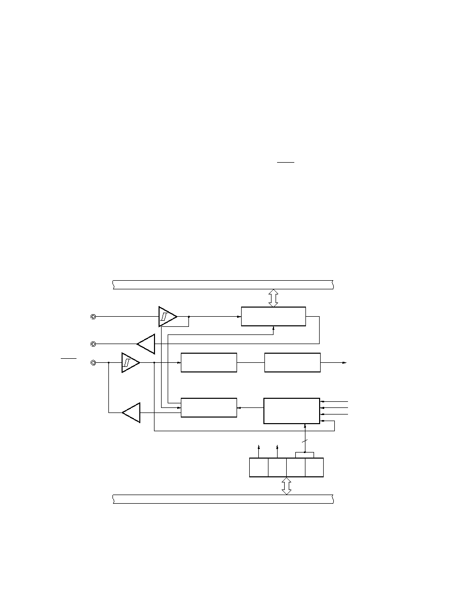
User's Manual U13655EJ2V1UD
218
CHAPTER 15 SERIAL INTERFACE SIO3
15.1 Functions of Serial Interface SIO3
Serial interface SIO3 has the following two modes.
(1) Operation stop mode
This mode is used when serial transfer is not performed. For details, see 15.4.1 Operation stop mode.
(2) 3-wire serial I/O mode (fixed to MSB first)
This is an 8-bit data transfer mode using three lines: serial clock 3 (SCK3), a serial output line (SO3), and a
serial input line (SI3).
Since transmit and receive operations can be performed simultaneously in the 3-wire serial I/O mode, the
processing time for data transfers is reduced.
The first bit of 8-bit serial transfer data is fixed as the MSB.
The 3-wire serial I/O mode is useful when connecting to devices such as peripheral I/Os and display
controllers, which incorporate a clocked serial interface. For details, see 15.4.2 3-wire serial I/O mode.
Figure 15-1 shows the block diagram of serial interface SIO3.
Figure 15-1. Block Diagram of Serial Interface SIO3
Internal bus
Internal bus
Selector
Serial I/O shift
register 3 (SIO3)
Serial clock counter
Interrupt request
signal generator
Serial clock
controller
INTCSI3
Serial operation mode register 3 (CSIM3)
2
SI3/P35
SO3/P36
SCK3/P37
CSIE3 MODE SCL31 SCL30
f
XT2
/2
10
f
XT2
/2
11
f
XT1

CHAPTER 15 SERIAL INTERFACE SIO3
User's Manual U13655EJ2V1UD
219
15.2 Configuration of Serial Interface SIO3
Serial interface SIO3 consists of the following hardware.
Table 15-1. Configuration of Serial Interface SIO3
Item
Configuration
Register
Serial I/O shift register 3 (SIO3)
Control register
Serial operation mode register 3 (CSIM3)
(1) Serial I/O shift register 3 (SIO3)
This is an 8-bit register that performs parallel-serial conversion and serial transmit-receive operations (shift
operations) in synchronization with the serial clock.
SIO3 is set by an 8-bit memory manipulation instruction.
When bit 7 (CSIE3) of serial operation mode register 3 (CSIM3) is set to 1, a serial operation can be started
by writing data to or reading data from SIO3.
When transmitting, data written to SIO3 is output to the serial output (SO3).
When receiving, data is read from the serial input (SI3) and written to SIO3.
RESET input makes SIO3 undefined.
Caution
Do not access SIO3 during a transfer operation unless the access is a transfer-start trigger
(read operations are disabled when MODE = 0 and write operations are disabled when
MODE = 1).

CHAPTER 15 SERIAL INTERFACE SIO3
User's Manual U13655EJ2V1UD
220
15.3 Control Registers of Serial Interface SIO3
Serial interface SIO3 is controlled by serial operation mode register 3 (CSIM3).
(1) Serial operation mode register 3 (CSIM3)
This register is used to set the SIO3 interface's serial clock, operation mode, and operation enable/disable.
CSIM3 can be set with a 1-bit or 8-bit memory manipulation instruction.
RESET input sets CSIM3 to 00H.
Caution
When using the 3-wire serial I/O mode, set port mode register 3 (PM3x) as shown below.
Also, set the output latches of the ports set to output mode to 0.
∑ For serial clock output (master transmit/receive)
Set P37 (SCK3) to the output mode (PM37 = 0).
∑ For serial clock input (slave transmit/receive)
Set P37 to the input mode (PM37 = 1).
∑ For transmit/transmit and receive mode
Set P36 (SO3) to the output mode (PM36 = 0).
(Set P35 (SI3) to the input mode (PM35 = 1) (in transmit/receive mode).
∑ For receive mode
Set P35 (SI3) to the input mode (PM35 = 1).

CHAPTER 15 SERIAL INTERFACE SIO3
User's Manual U13655EJ2V1UD
221
Figure 15-2. Format of Serial Operation Mode Register 3 (CSIM3)
Address: FFB0H
After reset: 00H
R/W
Symbol
7
6
5
4
3
2
1
0
CSIM3
CSIE3
0
0
0
0
MODE
SCL31
SCL30
SIO3 operation enable/disable specification
CSIE3
Shift register operation
0
Disables operation
1
Enables operation
Transfer operation mode flag
MODE
Operation mode
0
Transmit/transmit and receive mode
1
Receive-only mode
SCL31
SCL30
Clock selection
0
0
Input clock from external
0
1
f
XT2
/2
10
(209
µs)
1
0
f
XT2
/2
11
(417
µs)
1
1
f
XT1
(30.5
µs)
Caution
Be sure to set bits 3 to 6 to 0.
Remarks 1. Figures in parentheses apply to operation with f
XT1
= 32.768 kHz, f
XT2
= 4.91 MHz
2. f
XT1
: Subsystem clock 1 oscillation frequency
f
XT2
: Subsystem clock 2 oscillation frequency
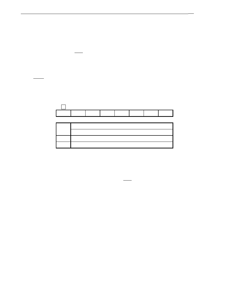
CHAPTER 15 SERIAL INTERFACE SIO3
User's Manual U13655EJ2V1UD
222
15.4 Operations of Serial Interface SIO3
This section explains the two modes of serial interface SIO3.
15.4.1 Operation stop mode
Since serial transfer is not performed in this mode, the power consumption can be reduced.
In addition, in this mode, the P37/SCK3, P36/SO3, and P35/SI3 pins can be used as ordinary I/O port pins.
(1) Register settings
The operation stop mode is set by serial operation mode register 3 (CSIM3).
CSIM3 is set with a 1-bit or 8-bit memory manipulation instruction.
RESET input sets CSIM3 to 00H.
Figure 15-3. Format of Serial Operation Mode Register 3 (CSIM3) (Operation Stop Mode)
Address: FFB0H
After reset: 00H
R/W
Symbol
7
6
5
4
3
2
1
0
CSIM3
CSIE3
0
0
0
0
MODE
SCL31
SCL30
SIO3 operation enable/disable specification
CSIE3
Shift register operation
0
Disables operation
1
Enables operation
Caution
Be sure to set bits 3 to 6 to 0.
15.4.2 3-wire serial I/O mode
The 3-wire serial I/O mode is useful when connecting to devices such as peripheral I/Os and display controllers,
which incorporate a clocked serial interface.
This mode executes data transfer via three lines: serial clock 3 (SCK3), a serial output line (SO3), and a serial
input line (SI3).
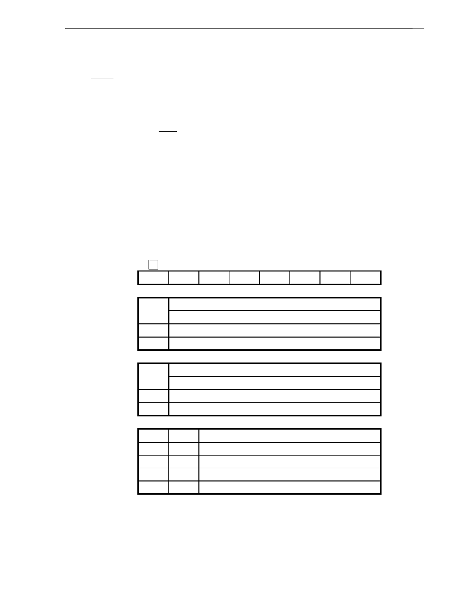
CHAPTER 15 SERIAL INTERFACE SIO3
User's Manual U13655EJ2V1UD
223
(1) Register settings
The 3-wire serial I/O mode is set by serial operation mode register 3 (CSIM3).
CSIM3 can be set by a 1-bit or 8-bit memory manipulation instruction.
RESET input sets CSIM3 to 00H.
Caution
When using the 3-wire serial I/O mode, set port mode register 3 (PM3x) as shown below.
Also, set the output latches of the ports set to output mode to 0.
∑ For serial clock output (master transmit/receive)
Set P37 (SCK3) to the output mode (PM37 = 0).
∑ For serial clock input (slave transmit/receive)
Set P37 to the input mode (PM37 = 1).
∑ For transmit/transmit and receive mode
Set P36 (SO3) to the output mode (PM36 = 0).
(Set P35 (SI3) to the input mode (PM35 = 1) (in transmit/receive mode).
∑ For receive mode
Set P35 (SI3) to the input mode (PM35 = 1).
Figure 15-4. Format of Serial Operation Mode Register 3 (CSIM3) (3-Wire Serial I/O Mode)
Address: FFB0H
After reset: 00H
R/W
Symbol
7
6
5
4
3
2
1
0
CSIM3
CSIE3
0
0
0
0
MODE
SCL31
SCL30
SIO3 operation enable/disable specification
CSIE3
Shift register operation
0
Disables operation
1
Enables operation
Transfer operation mode flag
MODE
Operation mode
0
Transmit/transmit and receive mode
1
Receive-only mode
SCL31
SCL30
Clock selection
0
0
Input clock from external
0
1
f
XT2
/2
10
(209
µs)
1
0
f
XT2
/2
11
(417
µs)
1
1
f
XT1
(30.5
µs)
Caution
Be sure to set bits 3 to 6 to 0.
Remarks 1. Figures in parentheses apply to operation with f
XT1
= 32.768 kHz, f
XT2
= 4.91 MHz
2. f
XT1
: Subsystem clock 1 oscillation frequency
f
XT2
: Subsystem clock 2 oscillation frequency

CHAPTER 15 SERIAL INTERFACE SIO3
User's Manual U13655EJ2V1UD
224
(2) Communication operations
In the 3-wire serial I/O mode, data is transmitted and received in 8-bit units. Each bit of data is transmitted or
received in synchronization with the serial clock.
Serial I/O shift register 3 (SIO3) is shifted in synchronization with the falling edge of the serial clock.
Transmission data is held in the SO3 latch and is output from the SO3 pin. Data that is received via the SI3
pin is latched to SIO3 in synchronization with the rising edge of the serial clock.
Completion of an 8-bit transfer automatically stops operation of SIO3 and sets the serial transfer end flag.
Figure 15-5. Timing of 3-Wire Serial I/O Mode
(3) Transfer start
Serial transfer starts when the following two conditions have been satisfied and transfer data has been set to
(or read from) serial I/O shift register 3 (SIO3).
∑ The SIO3 operation control bit (CSIE3) = 1
∑ After an 8-bit serial transfer, either the internal serial clock is stopped or the serial clock is set to high level.
Transmit/transmit and receive mode
When CSIE3 = 1 and MODE = 0, transfer starts when writing to SIO3.
Receive-only mode
When CSIE3 = 1 and MODE = 1, transfer starts when reading from SIO3.
Caution
After data has been written to SIO3, transfer will not start even if the CSIE3 bit value is set
to 1.
Completion of an 8-bit transfer automatically stops the serial transfer operation and sets the serial transfer end flag.
Serial clock
SI3
SO3
Serial transfer end flag
Transfer starts in synchronization with the falling edge of serial clock
Transfer completion
1
2
3
4
5
6
7
8
DI7
DI6
DI5
DO7
DO6
DO5
DI4
DI3
DI2
DO4
DO3
DO2
DI1
DI0
DO1
DO0

User's Manual U13655EJ2V1UD
225
CHAPTER 16 LCD CONTROLLER/DRIVER
16.1 LCD Controller/Driver Functions
The functions of the LCD controller/driver incorporated in the
µPD780958 Subseries are described below.
(1) Automatic output of segment signals and common signals is possible by automatic reading of the display data
memory.
(2) Display mode
∑ 1/3 duty (1/3 bias), static mode
(3) Any of four frame frequencies can be selected in each display mode.
(4) Maximum of 30 segment signal outputs (S0 to S29); 3 common signal outputs (COM0 to COM2).
Twenty two of the segment signal outputs can be individually switched to input/output ports (P70/S8 to
P77/S15, P80/S16 to P87/S23, and P90/S24 to P95/S29).
The maximum number of displayable pixels in each display mode is shown in Table 16-1.
Table 16-1. Maximum Number of Display Pixels
Bias Method
Time Division
Common Signals Used
Maximum Number of Pixels
1/3
3
COM0 to COM2
90 (30 segments
◊ 3 commons)
Note
Note 10 digits on type LCD panel with 3 segments/digit.

CHAPTER 16 LCD CONTROLLER/DRIVER
User's Manual U13655EJ2V1UD
226
Figure 16-1. Block Diagram of LCD Controller/Driver
Notes 1. PFn: Port function control register n (n = 7 to 9)
2. Segment
driver
Remark In the same way as port mode register n (PMn), each flag of PFn corresponds to each bit of a port (8
bits for ports 7 and 8, and 6 bits for port 9). This register can therefore be controlled in 1-bit units.
...
...
...
...
...
...
Internal bus
LCD clock control register 0
(LCDC0)
Display data memory
LCD display mode
register 0 (LCDM0)
PFn
Note 1
LCDON0
LCD drive voltage
controller
LCDC01
FA07H
FA00H
Selector
Selector
P70 output
buffer
P95 output
buffer
LIPS0
LCDC00
LCD clock selector
Timing controller
Note 2
Note 2
Common driver
V
LC1
V
LC2
COM2
COM1
COM0
S7
FA08H
Selector
Note 2
S8/P70
FA1DH
Selector
Note 2
S29/P95
S0
...
...
76543210
76543210 76543210 76543210
210
210
210
210
2
f
LCD

CHAPTER 16 LCD CONTROLLER/DRIVER
User's Manual U13655EJ2V1UD
227
16.2 LCD Controller/Driver Configuration
The LCD controller/driver consists of the following hardware.
Table 16-2. Configuration of LCD Controller/Driver
Item
Configuration
Display outputs
Segment signals: 30 Outputs dedicated to segment signals: 8
Outputs with alternate function as I/O ports: 22
Common signals: 3 (COM0 to COM2)
Control registers
LCD display mode register 0 (LCDM0)
LCD clock control register 0 (LCDC0)
Port function control registers 7 to 9 (PF7 to PF9)
Figure 16-2. Block Diagram of LCD Clock Selector
Remark LCDCL: LCD clock
Prescaler
LCDC00
Selector
LCDC01
f
XT1
/2
6
f
XT1
/2
7
f
XT1
/2
8
LCDCL
2
LCD clock control register 0 (LCDC0)
f
XT1
/2
9
Internal bus
f
XT1
CHAPTER 16 LCD CONTROLLER/DRIVER
User's Manual U13655EJ2V1UD
228
16.3 LCD Controller/Driver Control Registers
The following three types of registers are used to control the LCD controller/driver.
∑ LCD display mode register 0 (LCDM0)
∑ LCD clock control register 0 (LCDC0)
∑ Port function control registers 7 to 9 (PF7 to PF9)
(1) LCD display mode register 0 (LCDM0)
This is a register that enables/disables LCD operation, controls the power supply for LCD driving, and sets
the display mode.
LCDM0 is set with a 1-bit or 8-bit memory manipulation instruction.
RESET input sets LCDM0 to 00H.
Figure 16-3. Format of LCD Display Mode Register 0 (LCDM0)
Address: FF90H
After reset: 00H
R/W
Symbol
7
6
5
4
3
2
1
0
LCDM0
LCDON0
0
0
LIPS0
0
LCDM02
LCDM01
LCDM00
LCDON0
Note 1
LCD display enable/disable
0
Display OFF
1
Display ON
LIPS0
Note 2
Power supply for LCD drive
0
Does not supply LCD drive power
1
Supplies LCD drive power
Display mode selection
LCDM02
LCDM01 LCDM00
Time division
Bias method
0
0
0
No selection
0
0
1
3
1/3
1
0
0
Static
Other than above
Setting prohibited
Notes 1. When bit 7 (LCDON0) is 0, the S0 to S7, S8/P70 to S2/P95, and COM0 to COM2 pins become
low-level outputs.
2. The V
LC1
and V
LC2
pins become high-impedance when bit 4 (LIPS0) is 0.
Cautions 1. To enable the LCD display, set LCDON0 to 1 after 0.5 seconds have elapsed following
supply of the power for LCD driving (LIPS0 is set to 1). 0.5 seconds is the time during
which the LCD drive power supply stabilizes.
2.
The initial value for display mode selection is "No selection". Therefore, it is necessary
to select either "1/3 bias" or "Static" for the display mode when the LCD is used.
3.
When the static mode is selected (LCDM02 = 1, LCDM01 and LCDM00 = 0), set LIPS0 to
0.

CHAPTER 16 LCD CONTROLLER/DRIVER
User's Manual U13655EJ2V1UD
229
(2) LCD clock control register 0 (LCDC0)
This is a register that sets the frame frequencies.
LCDC0 is set with an 8-bit memory manipulation instruction.
RESET input sets LCDC0 to 00H.
Figure 16-4. Format of LCD Clock Control Register 0 (LCDC0)
Address: FF91H
After reset: 00H
R/W
Symbol
7
6
5
4
3
2
1
0
LCDC0
0
0
0
0
0
0
LCDC01
LCDC00
LCDC01
LCDC00
LCD frame frequency
0
0
f
XT1
/2
6
(512 Hz)
0
1
f
XT1
/2
7
(256 Hz)
1
0
f
XT1
/2
8
(128 Hz)
1
1
f
XT1
/2
9
(64 Hz)
Caution
Do not overwrite LCDC0 while the display is ON (bit 7 (LCDON0) of LCD display mode
register 0 (LCDM0) = 1).
Remarks 1. Figures in parentheses apply to operation with f
XT1
= 32.768 kHz.
2. f
XT1
: Subsystem clock 1 oscillation frequency
(3) Port function control registers 7 to 9 (PF7 to PF9)
This is a register that sets whether the pins of ports 7 to 9 are used as ports or as LCD drive power supply
segment outputs.
PF7 to PF9 are set with a 1-bit or 8-bit memory manipulation instruction.
RESET input sets PF7 to PF9 to 00H.
Figure 16-5. Format of Port Function Control Registers 7 to 9 (PF7 to PF9)
Address: FF57H, FF58H, FF59H
After reset: 00H
R/W
Symbol
7
6
5
4
3
2
1
0
PF7
PF77
PF76
PF75
PF74
PF73
PF72
PF71
PF70
7
6
5
4
3
2
1
0
PF8
PF87
PF86
PF85
PF84
PF83
PF82
PF81
PF80
7
6
5
4
3
2
1
0
PF9
0
0
PF95
PF94
PF93
PF92
PF91
PF90
PF7m, PF8m, PF9n
P7m, P8m, P9n pin function control (m = 0 to 7, n = 0 to 5)
0
Functions as port pin
1
Functions as segment output pin

CHAPTER 16 LCD CONTROLLER/DRIVER
User's Manual U13655EJ2V1UD
230
Caution When a pin is selected to function as a segment output pin using the port function control
register, the port mode and port latch values of the corresponding bit become invalid.
However, a software pull-up resistor specified by pull-up resistor option registers 7 to 9
(PU7 to PU9) will not be disconnected. When a pin is used as a segment pin, therefore, be
sure to set the corresponding bit of PU7 to PU9 to 0.
16.4 LCD Controller/Driver Settings
LCD controller/driver settings should be performed as shown below.
<1> Set the display data to the display data memory (FA00H to FA1DH).
<2> Set the corresponding bit of the port function control register (PF) for the pins that are set to be used as
segment outputs.
<3> Set bit 4 (LIPS0) of LCD display mode register 0 (LCDM0) to 1 and select the display mode.
<4> Set the LCD frame frequency using LCD clock control register 0 (LCDC0).
<5> After LCD drive power supply is stabilized (0.5 seconds min.), set bit 7 (LCDON0) of LCD display mode
register 0 (LCDM0) to 1.
Next, set data in the display data memory according to the display contents.
16.5 LCD Display Data Memory
The LCD display data memory is mapped to addresses FA00H to FA1DH. The data stored in the LCD display data
memory can be displayed on an LCD panel by the LCD controller/driver.
Figure 16-6 shows the relationship between the LCD display data memory contents and the segment/common
outputs.
Any area not used for display can be used as normal RAM.
Figure 16-6. Relationship Between LCD Display Data Memory Contents and Segment/Common Outputs
S0
F A 0 0 H
S1
F A 0 1 H
S2
F A 0 2 H
S3
F A 0 3 H
S27/P93
F A 1 B H
S28/P94
F A 1 C H
S29/P95
F A 1 D H
COM2
COM1
COM0
b
7
b
6
b
5
b
4
b
3
b
2
b
1
b
0
Address
Caution
The higher 5 bits of the LCD display data memory do not incorporate memory. Be sure to set
them to 0.

CHAPTER 16 LCD CONTROLLER/DRIVER
User's Manual U13655EJ2V1UD
231
16.6 Common Signals and Segment Signals
An individual pixel on an LCD panel lights when the potential difference of the corresponding common signal and
segment signal reaches or exceeds a given voltage (the LCD drive voltage V
LCD
). The pixel turns off when the
potential difference becomes less than V
LCD
.
As an LCD panel deteriorates if a DC voltage is applied to the common signals and segment signals, it is driven by
AC voltage.
(1) Common signals
For common signals, the selection timing order is as shown in Table 16-3 in accordance with the number of
time divisions set, and operations are repeated with these as the cycle. In the static display mode, the same
signal is output to COM0 to COM2.
Table 16-3. COM Signals
(2) Segment signals
Segment signals correspond to a 30-byte LCD display data memory (FA00H to FA1DH). Bits 0, 1, and 2 of
each data memory are read in synchronization with the COM0, COM1, and COM2 timings respectively, and if
the value of the bit is 1, it is converted to the selection voltage. If the value of the bit is 0, it is converted to the
non-selection voltage and output to a segment pin (S0 to S29) (S8 to S29 have alternate functions as I/O
ports).
Consequently, it is necessary to check what combination of front surface electrodes (corresponding to the
segment signals) and rear surface electrodes (corresponding to the common signals) of the LCD display to
be used form the display pattern, and then write bit data corresponding on a one-to-one basis with the pattern
to be displayed.
In addition, because LCD display data memory bits 1 and 2 are not used for LCD display in the static display
mode, they can be used for other than display purposes.
Bits 3 to 7 are fixed to 0.
COM Signal
Time Division
Static
3-time division
COM0
COM1
COM2

CHAPTER 16 LCD CONTROLLER/DRIVER
User's Manual U13655EJ2V1UD
232
(3) Common signal and segment signal output waveforms
The voltages shown in Figures 16-7 and 16-8 are output to the common signals and segment signals.
The
±V
LCD
ON voltage is only produced when the common signal and segment signal are both at the
selection voltage; other combinations turn the voltage OFF.
Figure 16-7. Common Signal Waveform
(a) Static display mode
T: One LCDCL cycle T
F
: Frame frequency
(b) 1/3 bias method
T: One LCDCL cycle T
F
: Frame frequency
Remark LCDCL: LCD clock
COMn
(static)
T
F
= T
V
DD
V
SS1
V
LCD
COMn
(divided by 3)
T
F
= 3
◊ T
V
DD
V
SS1
V
LCD
V
LC1
V
LC2

CHAPTER 16 LCD CONTROLLER/DRIVER
User's Manual U13655EJ2V1UD
233
Figure 16-8. Voltages and Phases of Common Signal and Segment Signal
(a) Static display mode
T: One LCDCL cycle
(b) 1/3 bias method
T: One LCDCL cycle
Remark LCDCL: LCD clock
Selected
Not selected
Common signal
Segment signal
V
DD
V
SS1
V
LCD
V
DD
V
SS1
V
LCD
T
T
Selected
Not selected
Common signal
Segment signal
V
DD
V
SS1
V
LCD
V
DD
V
SS1
V
LCD
T
T
V
LC2
V
LC2
V
LC1
V
LC1

CHAPTER 16 LCD CONTROLLER/DRIVER
User's Manual U13655EJ2V1UD
234
16.7 Supply of LCD Drive Voltages V
LC1
and V
LC2
In mask ROM versions, an external capacitor can be connected to the V
LC1
and V
LC2
pins to produce the LCD drive
voltage. By employing the split-capacitor method instead of conventional split-resistor method it is possible to reduce
the LCD drive current.
Figure 16-9 shows an example of LCD drive voltage supply.
Figure 16-9. Connection Example of LCD Drive Voltage
Caution The level of the LCD drive voltage (V
LC1
, V
LC2
) differs between devices and emulation boards.
∑
∑
∑
∑ In devices (
µ
µ
µ
µPD780957(A), 780958(A))... V
LC2
> V
LC1
∑
∑
∑
∑ In emulation boards (IE-780958-NS-EM4)... V
LC1
> V
LC2
The pin connection is the same for both devices and emulation boards, as shown Figure 16-9
above.
Remark LIPS0: Bit 4 of LCD display mode register 0 (LCDM0)
LCD drive
voltage
controller
V
DD
LIPS0
<Static mode>
Open
Open
V
DD
CAPH
CAPL
V
LCD
V
LC2
V
LC1
V
SS
LCD drive
voltage
controller
V
DD
LIPS0
<3-time-division bias mode>
V
DD
CAPH
CAPL
V
LCD
V
LC2
V
LC1
V
SS
0.47 F
0.47 F
0.47 F
µ
µ
µ

CHAPTER 16 LCD CONTROLLER/DRIVER
User's Manual U13655EJ2V1UD
235
16.8 Display Mode
16.8.1 Static display example
Figure 16-11 shows the connection between a static-type 3-digit LCD panel with the display pattern shown in
Figure 16-10 and the
µPD780958 Subseries segment (S0 to S23) and common (COM0) signals. The display
example is "1.23", and the display data memory contents (addresses FA00H to FA17H) correspond to this.
An explanation is given here taking the example of the first digit from the right "3."( .). In accordance with the
display pattern in Figure 16-10, selection and non-selection voltages must be output to pins S0 to S7 as shown in
Table 16-4 at the COM0 common signal timing.
Table 16-4. Selection and Non-Selection Voltages (COM0)
Segment
Common
S0
S1
S2
S3
S4
S5
S6
S7
COM0
NS
S
S
S
NS
S
NS
S
Remark S = Selection, NS = Non-selection
From this, it can be seen that 01110101 must be prepared for bit 0 of the display data memory (addresses FA00H
to FA07H) corresponding to S0 to S7.
The LCD drive waveforms for S0, S1, and COM0 are shown in Figure 16-12. When S1 is the selection voltage at
the COM0 selection timing, it can be seen that the +V
LCD
/
-V
LCD
AC square wave, which is the LCD illumination (ON)
level, is generated.
Shorting the COM0 to COM2 lines increases the current drive capability because the same waveform as COM0 is
output to COM1 and COM2.
Figure 16-10. Static LCD Display Pattern and Electrode Connections
S
8n + 3
S
8n + 2
S
8n + 5
S
8n + 1
S
8n
S
8n + 4
S
8n + 6
S
8n + 7
COM0
n = 0 to 2

CHAPTER 16 LCD CONTROLLER/DRIVER
User's Manual U13655EJ2V1UD
236
Figure 16-11. Connection Example of Static LCD Panel
◊: Any data can always be stored in this bit because this is a static display.
Timing strobe
COM2
COM1
COM0
BIT0
BIT1
BIT2
S0
S1
S2
S3
◊
FA00H
◊
1
◊
2
◊
3
S4
S5
S6
S7
◊
4
◊
5
◊
6
◊
7
S8
S9
S10
S11
◊
8
◊
9
◊
A
◊
B
S12
S13
S14
S15
◊
C
◊
D
◊
E
◊
F
S16
S17
S18
S19
◊
FA10H
◊
1
◊
2
◊
3
S20
S21
S22
S23
◊
4
◊
5
◊
6
0
1
1
1
0
1
0
1
0
0
1
1
0
1
1
1
1
1
1
0
0
0
0
0
◊
◊
◊
◊
◊
◊
◊
◊
◊
◊
◊
◊
◊
◊
◊
◊
◊
◊
◊
◊
◊
◊
◊
◊
◊
FA17H
Can be shorted.
Data memory address
LCD panel

CHAPTER 16 LCD CONTROLLER/DRIVER
User's Manual U13655EJ2V1UD
237
Figure 16-12. Static LCD Driving Waveform Example
T
F
V
LC0
V
SS1
COM0
V
LC0
V
SS1
S1
V
LC0
V
SS1
S0
+V
LCD
0
COM0-S0
Non-display waveform
Display waveform
-V
LCD
+V
LCD
0
COM0-S1
-V
LCD

CHAPTER 16 LCD CONTROLLER/DRIVER
User's Manual U13655EJ2V1UD
238
16.8.2 3-time-division display example
Figure 16-14 shows the connection between a 3-time-division type 10-digit LCD panel with the display pattern
shown in Figure 16-13 and the
µPD780958 Subseries segment signals (S0 to S29) and common signals (COM0 to
COM2). The display example is "123456.7890", and the display data memory contents (addresses FA00H to FA1DH)
correspond to this.
An explanation is given here taking the example of the fifth digit from the right "6." ( .). In accordance with the
display pattern in Figure 16-13, selection and non-selection voltages must be output to pins S12 to S14 as shown in
Table 16-5 at the COM0 to COM2 common signal timings.
Table 16-5. Selection and Non-Selection Voltages (COM0 to COM2)
Segment
Common
S12
S13
S14
COM0
NS
S
S
COM1
S
S
S
COM2
S
S
-
Remark S = Selection, NS = Non-selection
From this, it can be seen that 00000110 must be prepared in the display data memory (address FA0CH)
corresponding to S12.
Examples of the LCD drive waveforms between S12 and the common signals are shown in Figure 16-15 (1/3 bias
method). When S12 is the selection voltage at the COM1 selection timing or S12 is the selection voltage at the COM2
selection timing, it can be seen that the +V
LCD
/
-V
LCD
AC square wave, which is the LCD illumination (ON) level, is
generated.
Figure 16-13. 3-Time-Division LCD Display Pattern and Electrode Connections
;
;
;
;
;
;;;
;;;
;;
;;
;;
;
;
;
;
S
3n + 2
S
3n
COM0
COM2
S
3n + 1
COM1
n = 0 to 9

CHAPTER 16 LCD CONTROLLER/DRIVER
User's Manual U13655EJ2V1UD
239
Figure 16-14. Connection Example of 3-Time-Division LCD Panel
◊': Any data can be stored in this bit because it has no corresponding segment in the LCD panel.
Timing strobe
COM2
COM1
COM0
BIT1
S0
S1
S2
S3
FA00H
1
2
3
S4
S5
S6
S7
4
5
6
7
S8
S9
S10
S11
8
9
A
B
S12
S13
S14
S15
C
D
E
F
S16
S17
S18
S19
FA10H
1
2
3
S20
S21
S22
S23
4
5
6
7
S24
S25
S26
S27
8
9
A
B
S28
S29
C
BIT0
1
1
0
1
1
1
1
1
1
1
1
1
0
1
1
0
1
1
1
0
1
1
1
0
1
1
0
1
0
0
BIT2
0
1
◊
'
0
0
◊
'
0
1
◊
'
0
0
◊
'
1
1
◊
'
0
1
◊
'
0
0
◊
'
0
1
◊
'
0
1
◊
'
0
0
◊
'
D
Data memory address
LCD panel
1
0
0
1
1
0
1
1
1
1
0
0
1
1
1
1
1
0
1
1
0
1
1
0
0
1
1
1
0
0

CHAPTER 16 LCD CONTROLLER/DRIVER
User's Manual U13655EJ2V1UD
240
Figure 16-15. Example of 3-Time-Division LCD Drive Waveform (1/3 Bias)
V
DD
V
LC2
COM0
+V
LCD
0
COM0 - S12
V
LC1
+1/3V
LCD
V
SS1
V
DD
V
LC2
COM1
V
LC1
V
SS1
V
DD
V
LC2
COM2
V
LC1
V
SS1
V
DD
V
LC2
S12
V
LC1
V
SS1
+V
LCD
0
COM1 - S12
+1/3V
LCD
+V
LCD
0
COM2 - S12
+1/3V
LCD
T
F
1/3V
LCD
V
LCD
1/3V
LCD
V
LCD
1/3V
LCD
V
LCD

User's Manual U13655EJ2V1UD
241
CHAPTER 17 INTERRUPT FUNCTIONS
17.1 Types of Interrupt Functions
The following three types of interrupt functions are available.
(1) Non-maskable interrupt
This interrupt is unconditionally acknowledged even in the interrupt disabled status. It is not subject to
interrupt priority control and therefore takes precedence over all interrupt requests.
This interrupt generates a standby release signal.
One interrupt request from the watchdog timer is incorporated as a non-maskable interrupt.
(2) Maskable interrupts
These interrupts are subject to mask control, and can be divided into two groups according to the setting of
the priority specification flag registers (PR0L, PR0H, PR1L): one with higher priority and one with lower
priority. Higher-priority interrupts can nest lower-priority interrupts (multiple interrupt function). The priority
when two or more interrupt requests with the same priority occur at the same time is predetermined (see
Table 17-1).
The interrupt generates a standby release signal.
Twelve external interrupt requests and seventeen internal interrupt requests are incorporated as maskable
interrupts.
(3) Software interrupt
This is a vectored interrupt generated when the BRK instruction is executed and can be acknowledged even
in the interrupt disabled status. This interrupt is not subject to interrupt priority control.
17.2 Interrupt Sources and Configuration
A total of 31 interrupt sources including non-maskable, maskable, and software interrupt sources are available (see
Table 17-1).

CHAPTER 17 INTERRUPT FUNCTIONS
User's Manual U13655EJ2V1UD
242
Table 17-1. Interrupt Source List
Interrupt Source
Interrupt
Type
Default
Priority
Note 1
Name
Trigger
Internal/
External
Vector Table
Address
Basic Con-
figuration
Note 2
Non-
maskable
≠
INTWDT
Watchdog timer overflow (when non-maskable
interrupt is selected)
(A)
0
(highest)
INTWDT
Watchdog timer overflow (when maskable
interrupt is selected)
Internal
0004H
(B)
1
INTP0
INTP0 pin input edge detection
External
0006H
(C)
2
INTMRO0 MRTD edge detection
Internal
0008H
(B)
3
INTP1
INTP1 pin input edge detection
000AH
4
INTP2
INTP2 pin input edge detection
000CH
5
INTP3
INTP3 pin input edge detection
000EH
6
INTP4
INTP4 pin input edge detection
0010H
7
INTP5
INTP5 pin input edge detection
0012H
8
INTP6
INTP6 pin input edge detection
External
0014H
(C)
9
INTTM00
∑ When CR00 is specified for compare register:
TM0 & CR00 match signal generation
∑ When CR00 is specified for capture register:
TI01 pin valid edge detection
0016H
10
INTTM01
∑ When CR01 is specified for compare register:
TM0 & CR01 match signal generation
∑ When CR01 is specified for capture register:
TI00 pin valid edge detection
0018H
11
INTSER2
Serial interface UART2 reception error occurrence
001AH
12
INTSR2
Serial interface UART2 reception completion
001CH
13
INTST2
Serial interface UART2 transmission completion
001EH
14
INTCSI3
Serial interface SIO3 transfer completion
0020H
15
INTMRT0
TMMR0 & CRM0 match signal generation
0022H
16
INTTM80
TM80 & CR80 match signal generation
0024H
17
INTTM81
TM81 & CR81 match signal generation
0026H
18
INTTM82
TM82 & CR82 match signal generation
0028H
19
INTTM83
TM83 & CR83 match signal generation
002AH
20
INTTM2
TM2 & CR2 match signal generation
002CH
21
INTSA0
Sampling timer (TMSA0) & compare register
(CRSA0) match signal generation
002EH
22
INTSB0
Sampling timer (TMSB0) & compare register
(CRSB0) match signal generation
0030H
23
INTRTO1
Real-time output specified number of reloads
achieve register
Internal
0032H
(B)
24
INTSMP0
Sampling interrupt input 0
0034H
25
INTSMP1
Sampling interrupt input 1
0036H
26
INTSMP2
Sampling interrupt input 2
0038H
27
INTSMP3
Sampling interrupt input 3
003AH
Maskable
28
INTSMP4
Sampling interrupt input 4
External
003CH
(C)
Software
≠
BRK
Execution of BRK instruction
≠
003EH
(D)
Notes 1.
The default priority is the highest priority when more than one maskable interrupt is generated. 0 is
the highest priority and 28 is the lowest.
2.
Basic configuration types (A) to (D) correspond to (A) to (D) in Table 17-1.
Remark
There are two types of watchdog timer interrupt sources (INTWDT), a non-maskable interrupt and a
maskable interrupt (internal). Select one of these types.

CHAPTER 17 INTERRUPT FUNCTIONS
User's Manual U13655EJ2V1UD
243
Figure 17-1. Basic Configuration of Interrupt Function (1/2)
(A)
Internal non-maskable interrupt
(B)
Internal maskable interrupt
(C)
External maskable interrupt (INTP0 to INTP6)
Internal bus
Interrupt
request
Priority controller
Vector table
address generator
Standby release signal
Internal bus
Interrupt
request
IF
MK
IE
PR
ISP
Priority controller
Vector table
address generator
Standby release
signal
Internal bus
Interrupt
request
IF
MK
IE
PR
ISP
Standby release
signal
Edge detector
Priority controller
Vector table
address generator
External interrupt rising and
falling edge enable register
(EGP, EGN)

CHAPTER 17 INTERRUPT FUNCTIONS
User's Manual U13655EJ2V1UD
244
Figure 17-1. Basic Configuration of Interrupt Function (2/2)
(D)
Software interrupt
IF:
Interrupt request flag
IE:
Interrupt enable flag
ISP: In-service priority flag
MK: Interrupt mask flag
PR: Priority specification flag
Interrupt
request
Internal bus
Vector table
address generator

CHAPTER 17 INTERRUPT FUNCTIONS
User's Manual U13655EJ2V1UD
245
17.3 Interrupt Function Control Registers
The following 6 types of registers are used to control the interrupt function.
∑ Interrupt request flag registers (IF0L, IF0H, IF1L, IF1H)
∑ Interrupt mask flag registers (MK0L, MK0H, MK1L, MK1H)
∑ Priority specification flag registers (PR0L, PR0H, PR1L, PR1H)
∑ External interrupt rising edge enable register (EGP)
∑ External interrupt falling edge enable register (EGN)
∑ Program status word (PSW)
Table 17-2 shows the names of the interrupt request flags, interrupt mask flags, and priority specification flags
corresponding to the respective interrupt request sources.

CHAPTER 17 INTERRUPT FUNCTIONS
User's Manual U13655EJ2V1UD
246
Table 17-2. Flags Corresponding to Interrupt Request Sources
Interrupt Request Flag
Interrupt Mask Flag
Priority Specification Flag
Interrupt Source
Register
Register
Register
INTWDT
WDTIF
Note
WDTMK
Note
WDTPR
Note
INTP0
PIF0
PMK0
PPR0
INTMRO0
MROIF0
MROMK0
MROPR0
INTP1
PIF1
PMK1
PPR1
INTP2
PIF2
PMK2
PPR2
INTP3
PIF3
PMK3
PPR3
INTP4
PIF4
PMK4
PPR4
INTP5
PIF5
IF0L
PMK5
MK0L
PPR5
PR0L
INTP6
PIF6
PMK6
PPR6
INTTM00
TMIF00
TMMK00
TMPR00
INTTM01
TMIF01
TMMK01
TMPR01
INTSER2
SERIF2
SERMK2
SERPR2
INTSR2
SRIF2
SRMK2
SRPR2
INTST2
STIF2
STMK2
STPR2
INTCSI3
CSIIF3
CSIMK3
CSIPR3
INTMRT0
MRTIF0
IF0H
MRTMK0
MK0H
MRTPR0
PR0H
INTTM80
TMIF80
TMMK80
TMPR80
INTTM81
TMIF81
TMMK81
TMPR81
INTTM82
TMIF82
TMMK82
TMPR82
INTTM83
TMIF83
TMMK83
TMPR83
INTTM2
TMIF2
TMMK2
TMPR2
INTSA0
SAIF0
SAMK0
SAPR0
INTSB0
SBIF0
SBMK0
SBPR0
INTRTO1
RTOIF1
IF1L
RTOMK1
MK1L
RTOPR1
PR1L
INTSMP0
SMPIF0
SMPMK0
SMPPR0
INTSMP1
SMPIF1
SMPMK1
SMPPR1
INTSMP2
SMPIF2
SMPMK2
SMPPR2
INTSMP3
SMPIF3
SMPMK3
SMPPR3
INTSMP4
SMPIF4
IF1H
SMPMK4
MK1H
SMPPR4
PR1H
Note This is an interrupt control flag for when the watchdog timer is used as an interval timer.

CHAPTER 17 INTERRUPT FUNCTIONS
User's Manual U13655EJ2V1UD
247
(1) Interrupt request flag registers (IF0L, IF0H, IF1L, IF1H)
An interrupt request flag is set to 1 when the corresponding interrupt request is generated or when an
instruction is executed, and is cleared to 0 when the interrupt request is acknowledged, when the RESET
signal is input, or when an instruction is executed.
IF0L, IF0H, IF1L, and IF1H are set with a 1-bit or 8-bit memory manipulation instruction. When combining
IF0L and IF0H to be used as 16-bit register IF0 or when combining IF1L and IF1H to be used as 16-bit
register IF1, they are set with a 16-bit memory manipulation instruction.
RESET input sets these registers to 00H.
Figure 17-2. Format of Interrupt Request Flag Registers
Address: FFE0H
After reset: 00H
R/W
Symbol
7
6
5
4
3
2
1
0
IF0L
PIF5
PIF4
PIF3
PIF2
PIF1
MROIF0
PIF0
WDTIF
Address: FFE1H
After reset: 00H
R/W
Symbol
7
6
5
4
3
2
1
0
IF0H
MRTIF0
CSIIF3
STIF2
SRIF2
SERIF2
TMIF01
TMIF00
PIF6
Address: FFE2H
After reset: 00H
R/W
Symbol
7
6
5
4
3
2
1
0
IF1L
RTOIF1
SBIF0
SAIF0
TMIF2
TMIF83
TMIF82
TMIF81
TMIF80
Address: FFE3H
After reset: 00H
R/W
Symbol
7
6
5
4
3
2
1
0
IF1H
0
0
0
SMPIF4
SMPIF3
SMPIF2
SMPIF1
SMPIF0
◊◊IF◊
Interrupt request flag
0
Interrupt request signal is not generated
1
Interrupt request signal is generated and interrupt is requested
Cautions 1. The WDTIF flag can be read/written only when the watchdog timer is used as an interval
timer. Clear the WDTIF flag to 0 when watchdog timer mode 1 is used.
2.
Before restarting the timer or serial interface after the standby mode is released, be
sure to clear the interrupt request flag; otherwise noise, etc., may cause the interrupt
request flag to be set.
3.
When an interrupt is acknowledged, the interrupt request flag is automatically cleared,
and then servicing of the interrupt routine is started.
CHAPTER 17 INTERRUPT FUNCTIONS
User's Manual U13655EJ2V1UD
248
(2) Interrupt mask flag registers (MK0L, MK0H, MK1L, MK1H)
The interrupt mask flag enables or disables the corresponding maskable interrupt servicing.
MK0L, MK0H, MK1L, and MK1H are set with a 1-bit or 8-bit memory manipulation instruction. When
combining MK0L and MK0H to be used as 16-bit register MK0 or when combining MK1L and MK1H to be
used as 16-bit register MK1, they are set with a 16-bit memory manipulation instruction.
RESET input sets these registers to FFH.
Figure 17-3. Format of Interrupt Mask Flag Registers
Address: FFE4H
After reset: FFH
R/W
Symbol
7
6
5
4
3
2
1
0
MK0L
PMK5
PMK4
PMK3
PMK2
PMK1
MROMK0
PMK0
WDTMK
Address: FFE5H
After reset: FFH
R/W
Symbol
7
6
5
4
3
2
1
0
MK0H
MRTMK0
CSIMK3
STMK2
SRMK2
SERMK2 TMMK01 TMMK00
PMK6
Address: FFE6H
After reset: FFH
R/W
Symbol
7
6
5
4
3
2
1
0
MK1L
RTOMK1
SBMK0
SAMK0
TMMK2
TMMK83 TMMK82 TMMK81 TMMK80
Address: FFE7H
After reset: FFH
R/W
Symbol
7
6
5
4
3
2
1
0
MK1H
1
1
1
SMPMK4 SMPMK3 SMPMK2 SMPMK1 SMPMK0
◊◊MK◊
Interrupt servicing control
0
Enables interrupt servicing
1
Disables interrupt servicing
Caution
Because port 0 has an alternate function as external interrupt request inputs, the
corresponding interrupt request flag is set when the output mode is specified and the
output level of a port pin is changed. Therefore, to use the port in the output mode, set the
corresponding interrupt mask flag to 1 in advance.

CHAPTER 17 INTERRUPT FUNCTIONS
User's Manual U13655EJ2V1UD
249
(3) Priority specification flag registers (PR0L, PR0H, PR1L, PR1H)
A priority specification flag sets the priority of the corresponding maskable interrupt.
PR0L, PR0H, PR1L, and PR1H are set with a 1-bit or 8-bit memory manipulation instruction. When combining
PR0L and PR0H to be used as 16-bit register PR0 or when combining PR1L and PR1H to be used as 16-bit
register PR1, they are set with a 16-bit memory manipulation instruction.
RESET input sets these registers to FFH.
Figure 17-4. Format of Priority Specification Flag Registers
Address: FFE8H
After reset: FFH
R/W
Symbol
7
6
5
4
3
2
1
0
PR0L
PPR5
PPR4
PPR3
PPR2
PPR1
MROPR0
PPR0
WDTPR
Address: FFE9H
After reset: FFH
R/W
Symbol
7
6
5
4
3
2
1
0
PR0H
MRTPR0
CSIPR3
STPR2
SRPR2
SERPR2
TMPR01
TMPR00
PPR6
Address: FFEAH
After reset: FFH
R/W
Symbol
7
6
5
4
3
2
1
0
PR1L
RTOPR1
SBPR0
SAPR0
TMPR2
TMPR83
TMPR82
TMPR81
TMPR80
Address: FFEBH
After reset: FFH
R/W
Symbol
7
6
5
4
3
2
1
0
PR1H
1
1
1
SMPPR4 SMPPR3 SMPPR2 SMPPR1 SMPPR0
◊◊PR◊
Priority level selection
0
High priority level
1
Low priority level

CHAPTER 17 INTERRUPT FUNCTIONS
User's Manual U13655EJ2V1UD
250
(4) External interrupt rising edge enable register (EGP), external interrupt falling edge enable register
(EGN)
These registers are used to specify the valid edge detected at the P00 to P06 pins.
EGP and EGN can be read/written with a 1-bit or 8-bit memory manipulation instruction.
RESET input sets these registers to 00H.
Figure 17-5. Format of External Interrupt Rising Edge Enable Register (EGP)
and External Interrupt Falling Edge Enable Register (EGN)
Address: FF48H
After reset: 00H
R/W
Symbol
7
6
5
4
3
2
1
0
EGP
0
EGP6
EGP5
EGP4
EGP3
EGP2
EGP1
EGP0
Address: FF49H
After reset: 00H
R/W
Symbol
7
6
5
4
3
2
1
0
EGN
0
EGN6
EGN5
EGN4
EGN3
EGN2
EGN1
EGN0
EGPn
EGNn
Selection of valid edge of INTPn pin (n = 0 to 6)
0
0
Interrupts disabled
0
1
Falling edge
1
0
Rising edge
1
1
Both rising and falling edges

CHAPTER 17 INTERRUPT FUNCTIONS
User's Manual U13655EJ2V1UD
251
(5) Program status word (PSW)
The program status word is a register that holds the current status resulting from instruction execution or
interrupt request. An IE flag that enables/disables maskable interrupts and an ISP flag that controls multiple
interrupt processing are mapped to this register.
This register can be read or written in 8-bit units. It can also be manipulated by using a bit manipulation
instruction or dedicated instruction (EI, DI). When a vectored interrupt request is acknowledged, or the BRK
instruction is executed, the contents of the PSW are automatically saved to the stack and the IE flag is reset
to 0. If a maskable interrupt request has been acknowledged, the contents of the priority flag of that interrupt
are transferred to the ISP flag. The contents of the PSW can also be saved to the stack with the PUSH PSW
instruction, and restored from the stack by the RETI, RETB, or POP PSW instruction.
RESET input sets PSW to 02H.
Figure 17-6. Configuration of Program Status Word (PSW)
7
IE
Symbol
6
Z
5
RBS1
4
AC
3
RBS0
2
0
1
ISP
0
CY
PSW
After reset
02H
ISP
Interrupt with higher priority is being serviced
(interrupt with lower priority is disabled)
IE
Priority of interrupt currently being serviced
Interrupt request acknowledge enable/disable
Used when a normal instruction is executed
Interrupt is not acknowledged, or interrupt with
lower priority is being serviced (all maskable
interrupts are enabled)
0
1
0
1
Disable
Enable

CHAPTER 17 INTERRUPT FUNCTIONS
User's Manual U13655EJ2V1UD
252
17.4 Interrupt Servicing Operation
17.4.1 Non-maskable interrupt request acknowledgement operation
Non-maskable interrupt requests are unconditionally acknowledged even when interrupt requests are disabled.
They are not subject to interrupt priority control and take precedence over all other interrupts.
When a non-maskable interrupt is acknowledged, the contents of the PSW and PC are saved into the stacks in the
order of PSW then PC. The IE flag and ISP flag are reset to 0, the contents of the vector table are loaded to the PC,
and then the program execution branches.
If a new non-maskable interrupt request is generated while the non-maskable interrupt service program is being
executed, that interrupt request is acknowledged when the current execution of the non-maskable interrupt service
program has been completed (after the RETI instruction has been executed), and one instruction in the main routine
has been executed. If two or more non-maskable interrupt requests are generated while the non-maskable interrupt
service program is being executed, only one non-maskable interrupt request is acknowledged after execution of the
non-maskable interrupt service program has been completed.
Figure 17-7 shows the flowchart from non-maskable interrupt request generation to acknowledgement, Figure 17-8
shows the acknowledgement timing of a non-maskable interrupt request, and Figure 17-9 shows the
acknowledgement operation when multiple non-maskable interrupt requests are generated.

CHAPTER 17 INTERRUPT FUNCTIONS
User's Manual U13655EJ2V1UD
253
Figure 17-7. Flowchart from Non-Maskable Interrupt Request Generation to Acknowledgement
WDTM: Watchdog timer mode register
WDT:
Watchdog timer
Figure 17-8. Timing of Non-Maskable Interrupt Request Acknowledgement
WDTIF: Watchdog timer interrupt request flag
Start
WDTM4 = 1
(watchdog timer mode
is selected)
WDT overflows
WDTM3 = 0
(non-maskable interrupt
request is selected)
WDT interrupt is
not serviced
Interrupt control register
is not accessed
Interval timer
No
Reset processing
No
Interrupt request is generated
Interrupt servicing is started
Interrupt request pending
No
No
No
Yes
Yes
Yes
Yes
Yes
Instruction
Instruction
Save PSW and PC, and
jump to interrupt service
Interrupt servicing
program
CPU processing
WDTIF
An interrupt request generated during this interval
is acknowledged at the timing indicated by .

CHAPTER 17 INTERRUPT FUNCTIONS
User's Manual U13655EJ2V1UD
254
Figure 17-9. Non-Maskable Interrupt Request Acknowledgement Operation
(a) When new non-maskable interrupt request is generated while non-maskable interrupt service
program is being executed
(b) If two new non-maskable interrupt requests are generated while non-maskable interrupt service
program is being executed
Main routine
NMI request <1>
NMI request <1> is executed,
NMI request <2> is pending.
Pending NMI request <2>
is serviced.
NMI request <2>
Execution of
one Instruction
Main routine
NMI request <1>
NMI request <1> is executed,
NMI requests <2> and <3>
are pending.
Pending NMI request <2>
is serviced.
NMI request <2>
NMI request <3>
Execution of
one Instruction
NMI request <3> is not acknowledged
(NMI request is acknowledged only once
even if it occurs twice or more.)

CHAPTER 17 INTERRUPT FUNCTIONS
User's Manual U13655EJ2V1UD
255
17.4.2 Maskable interrupt request acknowledgement operation
A maskable interrupt request can be acknowledged when the interrupt request flag is set to 1 and the
corresponding interrupt request mask (MK) flag is cleared to 0. A vectored interrupt request is acknowledged in the
interrupt enabled state (when the IE flag is set to 1). However, an interrupt request with a lower priority cannot be
acknowledged while an interrupt with a higher priority is being serviced (when the ISP flag is reset to 0).
Table 17-3 shows the time required to start the interrupt service after a maskable interrupt request has been
generated.
For the timing of the interrupt request acknowledgement, see Figures 17-11 and 17-12.
Table 17-3. Time from Generation of Maskable Interrupt Request to Interrupt Servicing
Minimum Time
Maximum Time
Note
When
◊◊PR◊ = 0
7 clocks
32 clocks
When
◊◊PR◊ = 1
8 clocks
33 clocks
Note The wait time reaches maximum when an interrupt request is generated
immediately before a divide instruction.
Remark
1 clock: 1/f
CPU
(f
CPU
: CPU clock)
When two or more maskable interrupt requests are generated at the same time, they are acknowledged starting
from the one assigned the highest priority by the priority specification flag. If the same priorities are specified by the
priority specification flag, the interrupt with the highest default priority is acknowledged first.
A pending interrupt request is acknowledged when the status in which it can be acknowledged is set.
Figure 17-10 shows the interrupt request acknowledgement algorithm.
When a maskable interrupt request is acknowledged, the contents of the program status word (PSW) and program
counter (PC) are saved into the stacks in the order of PSW then PC. Then the IE flag is reset to 0, and the contents
of the interrupt priority specification flag of the acknowledged interrupt request are transferred to the ISP flag. In
addition, the data in the vector table determined for each interrupt request is loaded on the PC, and program
execution branches.
To return from interrupt servicing, use the RETI instruction.

CHAPTER 17 INTERRUPT FUNCTIONS
User's Manual U13655EJ2V1UD
256
Figure 17-10. Interrupt Request Acknowledgement Program Algorithm
◊◊IF◊: Interrupt request flag
◊◊MK◊: Interrupt mask flag
◊◊PR◊: Priority specification flag
IE:
Flag that controls acknowledgement of maskable interrupt request (1 = Enable, 0 = Disable).
ISP:
Flag that indicates the priority level of the interrupt currently being serviced (0 = Higher-priority
interrupt servicing, 1 = No interrupt request acknowledged, or lower-priority interrupt servicing)
Start
◊◊IF◊ = 1?
IE = 1?
ISP = 1?
Yes
Yes
No
No
Yes
No
No
Yes
Yes
No
Interrupt request pending
IE = 1?
No
Was this interrupt
generated at the same time as an
interrupt that is a
◊◊PR
◊
= 0 interrupt and
has a higher priority ?
Yes (high priority)
No
Yes
Yes
No
Interrupt request pending
Interrupt request pending
Vectored interrupt servicing
◊◊MK◊ = 0?
◊◊PR◊ = 0?
No (low priority)
Yes (interrupt request generated)
Was this interrupt
generated at the same time as
a
◊◊PR◊ = 0 interrupt?
Interrupt request pending
Interrupt request pending
Interrupt request pending
Interrupt request pending
Vectored interrupt servicing
Was this interrupt
generated at the same time as
an interrupt that has a
higher priority?

CHAPTER 17 INTERRUPT FUNCTIONS
User's Manual U13655EJ2V1UD
257
Figure 17-11. Interrupt Request Acknowledgment Timing (Minimum Time)
Remark
1 clock: 1/f
CPU
(f
CPU
: CPU clock)
Figure 17-12. Interrupt Request Acknowledgement Timing (Maximum Time)
Remark
1 clock: 1/f
CPU
(f
CPU
: CPU clock)
17.4.3 Software interrupt request acknowledgment operation
Software interrupt requests can be acknowledged when the BRK instruction is executed. This type of interrupt
cannot be disabled.
When a software interrupt is acknowledged, the contents of the program status word (PSW) and program counter
(PC) are saved into the stacks in the order of PSW then PC. The IE flag is reset to 0, the contents of the vector tables
(003EH, 003FH) are loaded to the PC, and the program execution branches.
To return from the software interrupt servicing, use the RETB instruction.
Caution
Do not use the RETI instruction to return from a software interrupt.
Instruction
Instruction
Save PSW and PC, and
jump to interrupt service
Interrupt servicing
program
CPU processing
◊◊IF◊
(
◊◊PR◊ = 1)
◊◊IF◊
(
◊◊PR◊ = 0)
6 clocks
8 clocks
7 clocks
33 clocks
32 clocks
6 clocks
25 clocks
Instruction
Divide instruction
Save PSW and PC, and
jump to interrupt service
Interrupt servicing
program
CPU processing
◊◊IF◊
(
◊◊PR◊ = 1)
◊◊IF◊
(
◊◊PR◊ = 0)

CHAPTER 17 INTERRUPT FUNCTIONS
User's Manual U13655EJ2V1UD
258
17.4.4 Multiple interrupt processing
Acknowledging another interrupt request while an interrupt is being serviced is called multiple interrupt processing.
Multiple interrupt processing cannot be done unless the interrupt request acknowledgement enable state (IE = 1) is
set (except for non-maskable interrupts). When an interrupt request is acknowledged, the interrupt request
acknowledgement disable state (IE = 0) is automatically set. Therefore, to enable multiple interrupt processing, the IE
flag must be set to 1 by executing the EI instruction during interrupt servicing in order to set the interrupt request
acknowledgement enable state.
Even if the interrupt enable state is set, multiple interrupt processing may not be enabled, due to priority control
factors. Interrupts have two types of priorities: default priority and programmable priority. Multiple interrupt
processing control is done by programmable priority.
In the EI status, if a interrupt request having the same as or a higher priority than that of the interrupt currently
being serviced is generated, the interrupt is acknowledged for multiple interrupt processing. If an interrupt request
with a priority lower than that of the interrupt currently serviced is generated, the interrupt is not acknowledged for
multiple interrupt processing.
In the interrupt disable state, or if an interrupt is not acknowledged for multiple interrupt processing because it has
a low priority, the interrupt is held pending. After the servicing of the current interrupt has been completed and one
instruction of the main processing has been executed, the pending interrupt request is acknowledged.
Interrupts are not acknowledged for multiple interrupt processing while a non-maskable interrupt is being serviced.
Table 17-4 shows interrupt requests enabled for multiple interrupt processing, and Figure 17-13 shows examples
of multiple interrupt processing.
Table 17-4. Interrupt Requests Enabled for Multiple Interrupt Processing During Interrupt Servicing
Maskable Interrupt Request
◊◊PR◊ = 0
◊◊PR◊ = 1
Multiple Interrupt Request
Currently Serviced Interrupt
Non-Maskable
Interrupt Request
IE = 1 IE = 0 IE = 1 IE = 0
Non-maskable interrupt
-
-
-
-
-
ISP = 0
-
-
-
Maskable interrupt
ISP = 1
-
-
Software interrupt
-
-
Remarks 1.
: Multiple interrupt processing enable
-: Multiple interrupt processing disable
2. ISP and IE are flags included in the PSW.
ISP = 0: An interrupt with higher priority is currently being serviced.
ISP = 1: The interrupt request was not acknowledged or an interrupt with a lower
priority is currently being serviced.
IE = 0:
Interrupt request acknowledgement is disabled.
IE = 1:
Interrupt request acknowledgement is enabled.
3.
◊◊PR◊ is a flag included in PR0L, PR0H, PR1L, and PR1H.
◊◊PR◊ = 0: Higher priority level
◊◊PR◊ = 1: Lower priority level

CHAPTER 17 INTERRUPT FUNCTIONS
User's Manual U13655EJ2V1UD
259
Figure 17-13. Example of Multiple Interrupt Processing (1/2)
Example 1. Multiple interrupts are acknowledged twice
Two multiple interrupt requests INTyy and INTzz are acknowledged while interrupt INTxx is being
serviced. Before each interrupt request is acknowledged, the EI instruction is always issued and the
interrupt request is enabled.
Example 2. A multiple interrupt is not acknowledged because of its priority
Interrupt request INTyy, which was generated while INTxx was being serviced, is not acknowledged for
multiple interrupt processing because the priority of INTyy is lower than that of INTxx. INTyy is held
pending and is acknowledged after one instruction of the main processing has been executed.
xxPRx = 0: Higher priority level
xxPRx = 1: Lower priority level
IE = 0: Interrupt request acknowledgement is disabled.
Main processing
INTxx servicing
INTyy servicing
INTzz servicing
EI
EI
EI
RETI
RETI
RETI
INTxx
(xxPRx = 1)
INTyy
(xxPRx = 0)
INTzz
(xxPRx = 0)
IE = 0
IE = 0
IE = 0
Main processing
INTxx servicing
INTyy servicing
INTxx
(xxPRx = 0)
INTyy
(xxPRx = 1)
EI
RETI
IE = 0
IE = 0
EI
RETI
1 instruction
execution

CHAPTER 17 INTERRUPT FUNCTIONS
User's Manual U13655EJ2V1UD
260
Figure 17-13. Example of Multiple Interrupt Processing (2/2)
Example 3. A multiple interrupt is not acknowledged because of interrupt disabled state
During the servicing of INTxx, other interrupts are not enabled (the EI instruction is not executed).
Therefore, INTyy is not acknowledged for multiple interrupt processing. INTyy is held pending and is
acknowledged after one instruction of the main processing has been executed.
xxPRx = 0: Higher priority level
IE = 0:
Interrupt request acknowledgement is disabled.
Main processing
INTxx servicing
INTyy servicing
EI
RETI
RETI
INTyy
(xxPRx = 0)
IE = 0
IE = 0
INTxx
(xxPRx = 0)
1 instruction
execution

CHAPTER 17 INTERRUPT FUNCTIONS
User's Manual U13655EJ2V1UD
261
17.4.5 Pending interrupt requests
There are some instructions that, even if an interrupt request is issued for them while another instruction is being
executed, cause a request acknowledgement to be held pending until the end of execution of the next instruction.
These instructions (instructions for which instruction requests are held pending) are listed below.
∑ MOV PSW,
#byte
∑ MOV A,
PSW
∑ MOV PSW,
A
∑ MOV1 PSW.bit,
CY
∑ MOV1 CY, PSW. bit
∑ AND1 CY, PSW. bit
∑ OR1
CY, PSW. bit
∑ XOR1 CY, PSW. bit
∑ SET1 PSW.
bit
∑ CLR1 PSW.
bit
∑ RETB
∑ RETI
∑ PUSH PSW
∑ POP PSW
∑ BT
PSW. bit, $addr16
∑ BF
PSW. bit, $addr16
∑ BTCLR PSW. bit, $addr16
∑ IE
∑ DI
∑ Manipulation instructions for IF0L, IF0H, IF1L, IF1H, MK0L, MK0H, MK1L, MK1H, PR0L, PR0H, PR1L, PR1H,
EGP, and EGN registers.
Caution
The BRK instruction is not one of the above-listed instructions. However, a software interrupt
activated by executing the BRK instruction causes the IE flag to be cleared to 0. Therefore,
even if a maskable interrupt request is generated during execution of the BRK instruction, the
interrupt request is not acknowledged. However, non-maskable interrupts are acknowledged.
The timing at which interrupt requests are held pending is shown in Figure 17-14.
Figure 17-14. Pending Interrupt Requests
Remarks 1. Instruction N: Instruction for which interrupt request is held pending
2. Instruction M: Instruction other than instruction for which interrupt request is held pending
3.
◊◊IF◊ (interrupt request) operation is not affected by the value of ◊◊PR◊ (priority level).
Instruction N
Instruction M
Save PSW and PC, and
jump to interrupt service
Interrupt servicing
program
CPU processing
◊◊IF◊

User's Manual U13655EJ2V1UD
262
CHAPTER 18 STANDBY FUNCTION
18.1 Standby Function and Configuration
The standby function is a function for reducing the power consumption of the system. The
µPD780958 Subseries
supports only the HALT mode.
The HALT mode is set when the HALT instruction is executed. In HALT mode, the CPU operating clock is
stopped, while the system clock oscillator continues oscillating. Therefore, this mode is useful for resuming
processing immediately when an interrupt request is generated or for an intermittent operation, such as a watch
operation.
All the contents of registers, flags, and data memory immediately before entering the HALT mode are retained.
The states of I/O port output latches and output buffers are also retained.
Caution Do not execute a STOP instruction since the
µ
µ
µ
µPD780958 Subseries does not support STOP
mode.
Figure 18-1. Standby Function
Remark
CSS: Bit 4 of the processor clock control register (PCC)
CSS = 1
CSS = 0
Main system
clock operation
HALT mode
HALT mode
Clock supply to CPU halted,
oscillation maintained
Clock supply to CPU halted,
oscillation maintained
HALT instruction
HALT instruction
Interrupt request
Interrupt request
Subsystem
clock 1 operation

CHAPTER 18 STANDBY FUNCTION
User's Manual U13655EJ2V1UD
263
18.2 Operation of Standby Function
18.2.1 Setting and operation status of HALT mode
The HALT mode is set by executing the HALT instruction.
The operation status in the HALT mode is shown in the table below.
Table 18-1. Operation Status in HALT Mode
Item
Operation Status in HALT Mode
Clock generator
Oscillation is enabled but clock supply to the
CPU is stopped.
CPU
Operation stopped
Port (output latch)
Retains status prior to when HALT mode
was set.
16-bit timer/event counter
8-bit timer
Watchdog timer
Sampling output timer/detector
MR sampling function
Serial interface
LCD controller
External interrupt request
Operable
18.2.2 Releasing HALT mode
The HALT mode can be released by the following two sources.
(1) Release by unmasked interrupt request
The HALT mode is released upon generation of an unmasked interrupt request. If interrupt requests are
enabled at this time, vectored interrupt servicing is performed. If interrupt requests are disabled, the
instruction at the next address is executed.
Figure 18-2. Release of HALT Mode by Interrupt Request
Remarks 1. The broken lines indicate the case where the interrupt request that has released the standby
mode is acknowledged.
2. The wait time is as follows:
∑ When vectored interrupt servicing is performed: 8 to 9 clocks
∑ When vectored interrupt servicing is not performed: 2 to 3 clocks
HALT instruction
Interrupt request
Wait
Wait
Operation mode
HALT mode
Operation mode
Oscillation
Clock
Standby release
signal

CHAPTER 18 STANDBY FUNCTION
User's Manual U13655EJ2V1UD
264
(2) Release by non-maskable interrupt request
When a non-maskable interrupt request is generated, the HALT mode is released and vectored interrupt
servicing is carried out, regardless of whether interrupt acknowledgement is enabled or disabled.
(3) Release by RESET input
RESET signal input releases the HALT mode. Execution branches to the reset vector address in the same
manner as an ordinary reset operation, and program execution is started.
Figure 18-3. Release of HALT Mode by RESET Input
Caution
Since the processor clock control register (PCC) is set to 04H after RESET signal
generation, it is necessary to set PCC to 00H, 01H, or 02H at the beginning of the program.
In this case, the time of one-instruction execution is required to switch the value of PCC.
Remark
Figures in parentheses apply to operation with f
CC
= 1.2 MHz, f
XT1
= 32.768 kHz
Table 18-2. Operation After Release of HALT Mode
Releasing Source
◊◊MK◊
◊◊PR◊
IE
ISP
Operation
0
0
0
◊
Executes next address instruction.
0
0
1
◊
Executes interrupt servicing.
0
1
0
1
0
1
◊
0
Executes next address instruction.
0
1
1
1
Executes interrupt servicing.
Maskable interrupt
request
1
◊
◊
◊
Maintains HALT mode.
RESET input
≠
≠
◊
◊
Reset processing
◊ : don't care
HALT instruction
Oscillation stabilization
wait status
Operation mode
HALT mode
Operation
mode
Clock
RESET signal
Oscillation
stop
Reset
period
Wait (0.25 s)
(Main system
clock selection)
Oscillation
Oscillation

User's Manual U13655EJ2V1UD
265
CHAPTER 19 RESET FUNCTION
The reset signal can be effected by the following two methods.
(1)
External reset input from RESET pin
(2)
Internal reset by inadvertent program loop detection by watchdog timer
Execution of the program is started from the addresses written to 0000H and 0001H when the RESET signal is
input.
The reset function is effected when a low-level signal is input to the RESET pin or when an overflow occurs in the
watchdog timer. As a result, each hardware enters the status shown in Table 19-1. Each pin goes into a high-
impedance state while the RESET signal is input, and during the oscillation stabilization time immediately after the
reset function has been released.
When a high-level signal is input to the RESET pin, the reset function is released and program execution is started
after the oscillation stabilization time (0.25 s: with f
XT1
= 32.768 kHz operation) has elapsed (see Figures 19-2, 19-3,
and 19-4).
Regarding reset caused by watchdog timer overflow, after reset, reset is automatically released, and program
execution starts following the lapse of the oscillation stabilization time (0.25 s: with f
XT1
= 32.768 kHz operation). The
watchdog timer overflow signal is output from the WDTOUT pin.
Cautions 1. Input a low-level signal to the RESET pin for 10
µ
µ
µ
µs or longer to execute an external reset.
However, after reset following power application, input a low level to the RESET pin during
the time required for the subsystem clock 1 oscillation to stabilize.
2. Oscillation of the main system clock and subsystem clock 2 is stopped while the RESET
signal is being input, but subsystem clock 1 oscillation is not.
3. Since the processor clock control register (PCC) is set to 04H after RESET signal
generation, it is necessary to set PCC to 00H, 01H, or 02H at the beginning of the program.
In this case, the time of one-instruction execution is required to switch the value of PCC.
Figure 19-1. Block Diagram of Reset Function
Reset
controller
Watchdog timer
RESET
Count clock
Stop
Overflow
Reset
signal
Interrupt
function
WDTOUT

CHAPTER 19 RESET FUNCTION
User's Manual U13655EJ2V1UD
266
Figure 19-2. Reset Timing by RESET Input
Figure 19-3. Reset Timing by Watchdog Timer Overflow
Figure 19-4. Reset Timing After Power Application
RESET
Internal
reset signal
Port pin
CL1
Hi-Z
XT2
V
DD
Delay
Delay
Reset period
Oscillation stabilization time
(0.25s@32.768kHz
counting with
subsystem clock 1)
Normal operation
Operation with CL1
CL1
XT2
RESET
Internal
reset signal
Port pin
Hi-Z
V
DD
Delay
Delay
Reset period
Oscillation stabilization time
(0.25s@32.768kHz
counting with
subsystem clock 1)
Normal operation
Operation with CL1
Internal
reset signal
Port pin
CL1
Hi-Z
XT2
V
DD
Reset period
Oscillation stabilization time
(0.25s@32.768kHz
counting with
subsystem clock 1)
Normal operation
Operation with CL1
Overflow in
watchdog timer

CHAPTER 19 RESET FUNCTION
User's Manual U13655EJ2V1UD
267
Table 19-1. Hardware Status After Reset (1/2)
Hardware
Status After Reset
Program counter (PC)
Note 1
Contents of reset vector table
(0000H, 0001H) are set.
Stack pointer (SP)
Undefined
Program status word (PSW)
02H
Data memory
Undefined
Note 2
RAM
General-purpose registers
Undefined
Note 2
Ports (output latches)
00H
Port mode registers (PM0, PM2 to PM9)
FFH
Pull-up resistor option registers (PU0, PU2 to PU9)
00H
Processor clock control register (PCC)
04H
Note 3
Clock output select register (CKS)
00H
SUB2 clock control register (CKC)
00H
Memory size switching register (IMS)
CFH
Note 4
Internal expansion RAM size switching register (IXS)
0CH
Note 5
Timer counter 0 (TM0)
0000H
Timer capture/compare registers 00, 01 (CR00, CR01)
Undefined
Timer mode control register 0 (TMC0)
00H
Prescaler mode register 0 (PRM0)
00H
Capture/compare control register 0 (CRC0)
00H
16-bit timer/event counter 0
Timer output control register 0 (TOC0)
00H
Timer counter 2 (TM2)
Undefined
Timer compare register 2 (CR2)
0000H
Timer mode control register 2 (TMC2)
00H
16-bit timer/event counter 2
Timer input control register 2 (TICT2)
00H
Timer counters 80 to 83 (TM80 to TM83)
00H
Compare registers 80 to 83 (CR80 to CR83)
00H
8-bit timers 80 to 83
Timer control registers 80 to 83 (TMC80 to TMC83)
00H
Notes 1.
Only the contents of the PC among the hardware elements become undefined during reset input and
oscillation stabilization wait. The other statuses do not differ from the status after reset above.
2.
If the reset signal is input in the standby mode, the status before reset is retained.
3.
Be sure to set PCC to 00H, 01H, or 02H at the beginning of the program.
4.
Even though the initial value is CFH, it should be set to the following values for each microcontroller.
µPD780957(A): CCH
µPD780958(A): CFH (This is the initial value of IMS. IMS does not need to be set in the µPD780958(A).)
5.
Even though the initial value is 0CH, use this register with a setting of 0AH.

CHAPTER 19 RESET FUNCTION
User's Manual U13655EJ2V1UD
268
Table 19-1. Hardware Status After Reset (2/2)
Hardware
Status After Reset
Mode register (WDTM)
00H
Watchdog timer
Clock select register (WDCS)
00H
SMTD timer counters A0, B0 (TMSA0, TMSB0)
00H
SMTD compare registers A0, B0 (CRSA0, CRSB0)
00H
SMTD clock select registers A0, B0 (TCSA0, TCSB0)
00H
SMTD control register 0 (TSM0)
00H
SMTD sampling level setting register 0 (SMS0)
00H
Sampling output
timer/detector
SMTD sampling pin status register 0 (SMD0)
00H
8-bit MR counter 0 (TMMR0)
00H
MRTD compare register 0 (CRM0)
00H
MRTD control register 0 (TCM0)
00H
MRTD output control register 0 (TMM0)
00H
MR sampling
MR sampling control register 0 (MRM0)
00H
Asynchronous serial interface mode register 2 (ASIM2)
00H
Asynchronous serial interface function register 2 (ASIF2)
00H
Asynchronous serial interface status register 2 (ASIS2)
00H
Compare register 2 for baud rate generation (BRCR2)
00H
UART pin switching register (UTCH0)
00H
Transmit shift register 2 (TXS2)
Serial interface UART2
Receive buffer register 2 (RXB2)
FFH
Serial I/O shift register 3 (SIO3)
Undefined
Serial interface SIO3
Serial operation mode register 3 (CSIM3)
00H
RTO data registers 10, 11 (RTO10, RTO11)
00H
RTO reload interrupt compare register 1 (RTC1)
00H
Real-time output function
RTO operation mode register 1 (RTM1)
00H
LCD display mode register 0 (LCDM0)
00H
LCD clock control register 0 (LCDC0)
00H
LCD controller/driver
Port function control registers 7 to 9 (PF7 to PF9)
00H
Request flag registers 0L, 0H, 1L, 1H (IF0L, IF0H, IF1L, IF1H)
00H
Mask flag registers 0L, 0H, 1L, 1H (MK0L, MK0H, MK1L, MK1H)
FFH
Priority specification flag registers 0L, 0H, 1L, 1H (PR0L, PR0H, PR1L,
PR1H)
FFH
External interrupt rising edge enable register (EGP)
00H
Interrupt
External interrupt falling edge enable register (EGN)
00H

User's Manual U13655EJ2V1UD
269
CHAPTER 20
µ
µ
µ
µ
PD78F0958 (REFERENCE)
The
µPD78F0958 is provided as the flash memory version of the µPD780958 Subseries.
The
µPD78F0958 replaces the internal mask ROM of the µPD780958 with flash memory to which a program can
be written, erased and overwritten while mounted on the substrate. Table 20-1 lists the differences between the
µPD78F0958 and the mask ROM versions.
Table 20-1. Differences Between
µ
µ
µ
µPD78F0958 and Mask ROM Versions
Item
µPD78F0958
µPD780957(A)
µPD780958(A)
Internal ROM configuration
Flash memory
Mask ROM
Internal ROM capacity
60 KB
Note
48 KB
60 KB
Mask option to specify the
on-chip pull-up resistors of
P60 to P62 and RESET pins
Not possible
Possible
Operation of overflow signal
of watchdog timer
After reset by the watchdog
timer, a high level is output
for 20
µs (TYP.).
After reset by the watchdog timer, a low level is output for
20
µs (TYP.).
IC pin
None
Available
V
PP
pin
Available
None
Electrical specifications
For details, contact an NEC Electronics sales representative.
Note
The same capacity as the mask ROM versions can be specified by means of the memory size switching register
(IMS).
Cautions 1. The
µ
µ
µ
µPD78F0958 is available only as an engineering sample. For details, contact an NEC
Electronics sales representative.
2. Flash memory versions and mask ROM versions differ in their noise immunity and noise
radiation. If replacing a flash memory version with a mask ROM version when changing from trial
production to mass production, be sure to perform sufficient evaluation with the CS version (not
ES version) of the mask ROM version.

CHAPTER 20
µ
µ
µ
µPD78F0958 (REFERENCE)
User's Manual U13655EJ2V1UD
270
20.1
Memory Size Switching Register
The
µPD78F0958 allows users to select the internal memory capacity using the memory size switching register
(IMS) so that the same memory map as that of the
µPD780957(A) and 780958(A) with a different size internal
memory capacity can be achieved.
IMS is set by an 8-bit memory manipulation instruction.
RESET input sets the value of IMS to CFH.
Caution
Always set IMS to CCH or CFH as the program's initial value.
Figure 20-1. Format of Memory Size Switching Register (IMS)
Address: FFF0H After reset: CFH R/W
Symbol
7
6
5
4
3
2
1
0
IMS
RAM2
RAM1
RAM0
0
ROM3
ROM2
ROM1
ROM0
RAM2
RAM1
RAM0
Internal high-speed RAM capacity selection
1
1
0
1024 bytes
Other than above
Setting prohibited
ROM3
ROM2
ROM1
ROM0
Internal ROM capacity selection
1
1
0
0
48 KB
1
1
1
1
60 KB
Other than above
Setting prohibited
The IMS settings to obtain the same memory map as mask ROM versions are shown in Table 20-2.
Table 20-2. Memory Size Switching Register Settings
Target Mask ROM Versions
IMS Setting
µPD780957(A)
CCH
µPD780958(A)
CFH
Caution
When using a mask ROM version, be sure to set IMS to the value indicated in Table 20-2.

CHAPTER 20
µ
µ
µ
µPD78F0958 (REFERENCE)
User's Manual U13655EJ2V1UD
271
20.2 Internal Expansion RAM Size Switching Register (IXS)
This register is used to set the internal expansion RAM capacity via software.
This register is set by using an 8-bit memory manipulation instruction.
RESET input sets the value of IXS to 0CH.
Caution
Setting the default value of IXS (0CH) is prohibited. Be sure to initialize the value of this
register to 0AH.
Figure 20-2. Format of Internal Expansion RAM Size Switching Register (IXS)
Address: FFF4H After reset: 0CH R/W
Symbol
7
6
5
4
3
2
1
0
IXS
0
0
0
IXRAM4
IXRAM3
IXRAM2
IXRAM1
IXRAM0
IXRAM4
IXRAM3
IXRAM2
IXRAM1
IXRAM0
Selects internal expansion RAM capacity
0
1
0
1
0
1024 bytes
Other than above
Setting prohibited

CHAPTER 20
µ
µ
µ
µPD78F0958 (REFERENCE)
User's Manual U13655EJ2V1UD
272
20.3 Flash Memory Programming
On-board writing of flash memory (with device mounted on target system) is supported.
On-board writing is performed after connecting a dedicated flash programmer (Flashpro III (part number: FL-PR3,
PG-FP3), Flashpro IV (FL-PR4, PG-FP4)) to the host machine and target system.
Moreover, writing to flash memory can also be performed using a flash memory writing adapter connected to
Flashpro III or Flashpro IV.
Remarks 1. FL-PR3 and FL-PR4 are products of Naito Densei Machida Mfg. Co., Ltd.
2. USB is supported only by Flashpro IV.
20.3.1 Selection of communication mode
Writing to flash memory is performed using Flashpro III or Flashpro IV and serial communication. Select the
communication mode for writing from Table 20-3. For the selection of the communication mode, a format like the one
shown in Figure 20-2 is used. The communication mode is selected with the V
PP
pulse numbers shown in Table 20-3.
Table 20-3. Communication Mode List
Communication Mode
Number of Channels
Pins Used
Note
Number of V
PP
Pulses
3-wire serial I/O (SIO3)
1
P35/SI3
P36/SO3
P37/SCK3
0
UART (UART2)
2
P05/INTP5/SMP0/RxD20
P20/TxD20
8
P06/INTP6/RxD21
P21/TxD21
9
Note When the flash memory programming mode is entered, all pins that are not used for flash memory
programming become the same status as the status immediately after reset. Therefore, when the external
device connected to each port does not acknowledge the port status immediately after reset, pin handling
such as connecting to V
DD
via a resistor or connecting to V
SS
via a resistor are required.
Cautions 1. Be sure to select the number of VPP pulses shown in Table 20-3 for the communication
mode.
2. If performing write operations to flash memory with the UART communication mode,
connect a 4.91 MHz resonator to the XT3 and XT4 pins, or input a 4.91 MHz external clock to
the XT3 pin.

CHAPTER 20
µ
µ
µ
µPD78F0958 (REFERENCE)
User's Manual U13655EJ2V1UD
273
Figure 20-3. Communication Mode Selection Format
20.3.2
Flash memory programming function
Flash memory writing is performed via command and data transmit/receive operations using the selected
communication mode. The main functions are listed in Table 20-4.
Table 20-4. Main Functions of Flash Memory Programming
Function
Description
Reset
Used to detect write stop and transmission synchronization.
Batch verify
Compares entire memory contents and input data.
Batch delete
Deletes the entire memory contents.
Batch blank check
Checks the deletion status of the entire memory.
High-speed write
Performs writing to flash memory according to write start address and number of write data
(bytes).
Continuous write
Performs successive write operations using the data input by high-speed write operation.
Status
Checks the current operation mode and operation end.
Oscillation frequency setting
Inputs the resonator oscillation frequency information.
Erase time setting
Inputs the memory erase time.
Baud rate setting
Sets the transmission rate when the UART mode is used.
Silicon signature read
Outputs the device name, memory capacity, and device block information.
10 V
V
PP
RESET
V
DD
V
SS
V
DD
V
SS
V
PP
pulses
Flash memory write mode

CHAPTER 20
µ
µ
µ
µPD78F0958 (REFERENCE)
User's Manual U13655EJ2V1UD
274
20.3.3 Connection of Flashpro III and Flashpro IV
Connection of the Flashpro III, Flashpro IV and the
µPD78F0958 differs depending on the communication mode (3-
wire serial I/O (SIO3) and UART (UART2). Each type of connection is shown in Figures 20-4 and 20-5.
Figure 20-4. Connection of Flashpro III and Flashpro IV Using 3-Wire Serial I/O (SIO3) Mode
Note CLK = 1.0 to 5.0 MHz
Figure 20-5. Connection of Flashpro III and Flashpro IV Using UART (UART2) Mode
V
PP
V
DD
RESET
CLK
SO
SI
GND
V
PP
V
DD0
/V
DD1
RESET
XT2
P03
RxD0
TxD0
V
SS0
/V
SS1
Flashpro III, Flashpro IV
PD78F0958
XT3
XT4
4.91 MHz
µ
V
PP
V
DD
RESET
CLK
Note
SCK
SO
SI
GND
IC0
V
DD0
/V
DD1
RESET
XT2
P03
SCK3
SI3
SO3
V
SS0
/V
SS1
Flashpro III, Flashpro IV
PD78F0958
µ

User's Manual U13655EJ2V1UD
275
CHAPTER 21 INSTRUCTION SET
This chapter lists the instruction set for the
µPD780958 Subseries. For details of the operation and machine
language (instruction code) of each instruction, see the 78K/0 Series Instructions User's Manual (U12326E).

CHAPTER 21 INSTRUCTION SET
User's Manual U13655EJ2V1UD
276
21.1 Conventions
21.1.1 Operand representation and description formats
In the operand field for each instruction, an operand is described according to the description format for operand
representation of that instruction (for details, see the assembler specifications). Some operands may be described in
two or more description formats. In this case, select one of them. Uppercase characters, #, !, $, and [ ] are keywords
and must be described as is. The meanings of the symbols are as follows.
∑ #:
Immediate data
∑ !:
Absolute address
∑ $:
Relative address
∑ [ ]: Indirect address
To describe immediate data, also describe an appropriate numeric value or label. To describe a label, be sure to
use #, !, $, or [ ].
Register description formats r and rp for an operand can be described as a function name (such as X, A, or C) or
absolute name (the name in parentheses in the table below, such as R0, R1, or R2).
Table 21-1. Operand Representation and Description Formats
Representation
Description Format
r
rp
sfr
sfrp
X (R0), A (R1), C (R2), B (R3), E (R4), D (R5), L (R6), H (R7)
AX (RP0), BC (RP1), DE (RP2), HL (RP3)
Special-function register symbol
Note
Special-function register symbol (only even address of register
that can be manipulated in 16-bit units)
Note
saddr
saddrp
FE20H to FF1FH Immediate data or label
FE20H to FF1FH Immediate data or label (even address only)
addr16
addr11
addr5
0000H to FFFFH Immediate data or label
(only even address for 16-bit transfer instruction)
0800H to 0FFFH Immediate data or label
0040H to 007FH Immediate data or label (even address only)
word
byte
bit
16-bit immediate data or label
8-bit immediate data or label
3-bit immediate data or label
RBn
RB0 to RB3
Note FFD0H to FFDFH cannot be addressed.
Remark
For the symbols of the special-function registers, see Table 3-3 List of Special-
Function Registers.

CHAPTER 21 INSTRUCTION SET
User's Manual U13655EJ2V1UD
277
21.1.2 Description of operation column
A:
A register; 8-bit accumulator
X:
X register
B:
B register
C:
C register
D:
D register
E:
E register
H:
H register
L:
L register
AX:
AX register pair; 16-bit accumulator
BC:
BC register pair
DE:
DE register pair
HL:
HL register pair
PC:
Program counter
SP:
Stack pointer
PSW:
Program status word
CY:
Carry flag
AC:
Auxiliary carry flag
Z:
Zero flag
RBS:
Register bank select flag
IE:
Interrupt request enable flag
NMIS:
Non-maskable interrupt servicing flag
( ):
Memory contents indicated by contents of address or register in ( )
◊
H
,
◊
L
:
Higher 8 bits and lower 8 bits of 16-bit register
:
Logical product (AND)
:
Logical sum (OR)
:
Exclusive logical sum (exclusive OR)
:
Inverted data
addr16: 16-bit immediate data or label
jdisp8:
Signed 8-bit data (displacement value)
21.1.3 Description of flag operation column
(Blank): Not affected
0:
Cleared to 0
1:
Set to 1
◊:
Set/cleared according to result
R:
Value saved before is restored

CHAPTER 21 INSTRUCTION SET
User's Manual U13655EJ2V1UD
278
21.2 Operation List
Clocks
Flag
Instruction
Group
Mnemonic
Operand
Bytes
Note 1
Note 2
Operation
Z AC CY
r, #byte
2
4
≠
r
byte
saddr, #byte
3
6
7
(saddr)
byte
sfr, #byte
3
≠
7
sfr
byte
A, r
Note 3
1
2
≠
A
r
r, A
Note 3
1
2
≠
r
A
A, saddr
2
4
5
A
(saddr)
saddr, A
2
4
5
(saddr)
A
A, sfr
2
≠
5
A
sfr
sfr, A
2
≠
5
sfr
A
A, !addr16
3
8
9
A
(addr16)
!addr16, A
3
8
9
(addr16)
A
PSW, #byte
3
≠
7
PSW
byte
◊ ◊ ◊
A, PSW
2
≠
5
A
PSW
PSW, A
2
≠
5
PSW
A
◊ ◊ ◊
A, [DE]
1
4
5
A
(DE)
[DE], A
1
4
5
(DE)
A
A, [HL]
1
4
5
A
(HL)
[HL], A
1
4
5
(HL)
A
A, [HL+byte]
2
8
9
A
(HL+byte)
[HL+byte], A
2
8
9
(HL+byte)
A
A, [HL+B]
1
6
7
A
(HL+B)
[HL+B], A
1
6
7
(HL+B)
A
A, [HL+C]
1
6
7
A
(HL+C)
8-bit data
transfer
MOV
[HL+C], A
1
6
7
(HL+C)
A
Notes 1.
When the internal high-speed RAM area is accessed or when an instruction that does not access data
is executed.
2.
When an area other than the internal high-speed RAM area is accessed.
3.
Except for r = A
Remark
One clock of an instruction is equal to one CPU clock (f
CPU
) selected by the processor clock control
register (PCC).

CHAPTER 21 INSTRUCTION SET
User's Manual U13655EJ2V1UD
279
Clocks
Flag
Instruction
Group
Mnemonic
Operand
Bytes
Note 1
Note 2
Operation
Z AC CY
A, r
Note 3
1
2
≠
A
r
A, saddr
2
4
6
A
(saddr)
A, sfr
2
≠
6
A
sfr
A, !addr16
3
8
10
A
(addr16)
A, [DE]
1
4
6
A
(DE)
A, [HL]
1
4
6
A
(HL)
A, [HL+byte]
2
8
10
A
(HL+byte)
A, [HL+B]
2
8
10
A
(HL+B)
8-bit data
transfer
XCH
A, [HL+C]
2
8
10
A
(HL+C)
rp, #word
3
6
≠
rp
word
saddrp, #word
4
8
10
(saddrp)
word
sfrp, #word
4
≠
10
sfrp
word
AX, saddrp
2
6
8
AX
(saddrp)
saddrp, AX
2
6
8
(saddrp)
AX
AX, sfrp
2
≠
8
AX
sfrp
sfrp, AX
2
≠
8
sfrp
AX
AX, rp
Note 4
1
4
≠
AX
rp
rp, AX
Note 4
1
4
≠
rp
AX
AX, !addr16
3
10
12
AX
(addr16)
MOVW
!addr16, AX
3
10
12
(addr16)
AX
16-bit
data
transfer
XCHW
AX, rp
Note 4
1
4
≠
AX
rp
A, #byte
2
4
≠
A, CY
A+byte
◊ ◊ ◊
saddr, #byte
3
6
8
(saddr), CY
(saddr)+byte
◊ ◊ ◊
A, r
Note 3
2
4
≠
A, CY
A+r
◊ ◊ ◊
r, A
2
4
≠
r, CY
r+A
◊ ◊ ◊
A, saddr
2
4
5
A, CY
A+(saddr)
◊ ◊ ◊
A, !addr16
3
8
9
A, CY
A+(addr16)
◊ ◊ ◊
A, [HL]
1
4
5
A, CY
A+(HL)
◊ ◊ ◊
A, [HL+byte]
2
8
9
A, CY
A+(HL+byte)
◊ ◊ ◊
A, [HL+B]
2
8
9
A, CY
A+(HL+B)
◊ ◊ ◊
8-bit
operation
ADD
A, [HL+C]
2
8
9
A, CY
A+(HL+C)
◊ ◊ ◊
Notes 1.
When the internal high-speed RAM area is accessed or when an instruction that does not access data
is executed.
2.
When an area other than the internal high-speed RAM area is accessed.
3.
Except for r = A
4.
Only when rp = BC, DE, HL.
Remark
One clock of an instruction is equal to one CPU clock (f
CPU
) selected by the processor clock control
register (PCC).

CHAPTER 21 INSTRUCTION SET
User's Manual U13655EJ2V1UD
280
Clocks
Flag
Instruction
Group
Mnemonic
Operand
Bytes
Note 1
Note 2
Operation
Z AC CY
A, #byte
2
4
≠
A, CY
A+byte+CY
◊ ◊ ◊
saddr, #byte
3
6
8
(saddr), CY
(saddr)+byte+CY
◊ ◊ ◊
A, r
Note 3
2
4
≠
A, CY
A+r+CY
◊ ◊ ◊
r, A
2
4
≠
r, CY
r+A+CY
◊ ◊ ◊
A, saddr
2
4
5
A, CY
A+(saddr)+CY
◊ ◊ ◊
A, !addr16
3
8
9
A, CY
A+(addr16)+CY
◊ ◊ ◊
A, [HL]
1
4
5
A, CY
A+(HL)+CY
◊ ◊ ◊
A, [HL+byte]
2
8
9
A, CY
A+(HL+byte)+CY
◊ ◊ ◊
A, [HL+B]
2
8
9
A, CY
A+(HL+B)+CY
◊ ◊ ◊
ADDC
A, [HL+C]
2
8
9
A, CY
A+(HL+C)+CY
◊ ◊ ◊
A, #byte
2
4
≠
A, CY
A≠byte
◊ ◊ ◊
saddr, #byte
3
6
8
(saddr), CY
(saddr)≠byte
◊ ◊ ◊
A, r
Note 3
2
4
≠
A, CY
A≠r
◊ ◊ ◊
r, A
2
4
≠
r, CY
r≠A
◊ ◊ ◊
A, saddr
2
4
5
A, CY
A≠(saddr)
◊ ◊ ◊
A, !addr16
3
8
9
A, CY
A≠(addr16)
◊ ◊ ◊
A, [HL]
1
4
5
A, CY
A≠(HL)
◊ ◊ ◊
A, [HL+byte]
2
8
9
A, CY
A≠(HL+byte)
◊ ◊ ◊
A, [HL+B]
2
8
9
A, CY
A≠(HL+B)
◊ ◊ ◊
SUB
A, [HL+C]
2
8
9
A, CY
A≠(HL+C)
◊ ◊ ◊
A, #byte
2
4
≠
A, CY
A≠byte≠CY
◊ ◊ ◊
saddr, #byte
3
6
8
(saddr), CY
(saddr)≠byte≠CY
◊ ◊ ◊
A, r
Note 3
2
4
≠
A, CY
A≠r≠CY
◊ ◊ ◊
r, A
2
4
≠
r, CY
r≠A≠CY
◊ ◊ ◊
A, saddr
2
4
5
A, CY
A≠(saddr)≠CY
◊ ◊ ◊
A, !addr16
3
8
9
A, CY
A≠(addr16)≠CY
◊ ◊ ◊
A, [HL]
1
4
5
A, CY
A≠(HL)≠CY
◊ ◊ ◊
A, [HL+byte]
2
8
9
A, CY
A≠(HL+byte)≠CY
◊ ◊ ◊
A, [HL+B]
2
8
9
A, CY
A≠(HL+B)≠CY
◊ ◊ ◊
8-bit data
operation
SUBC
A, [HL+C]
2
8
9
A, CY
A≠(HL+C)≠CY
◊ ◊ ◊
Notes 1.
When the internal high-speed RAM area is accessed or when an instruction that does not access data
is executed.
2.
When an area other than the internal high-speed RAM area is accessed.
3.
Except for r = A
Remark
One clock of an instruction is equal to one CPU clock (f
CPU
) selected by the processor clock control
register (PCC).

CHAPTER 21 INSTRUCTION SET
User's Manual U13655EJ2V1UD
281
Clocks
Flag
Instruction
Group
Mnemonic
Operand
Bytes
Note 1
Note 2
Operation
Z AC CY
A, #byte
2
4
≠
A
A byte
◊
saddr, #byte
3
6
8
(saddr)
(saddr) byte
◊
A, r
Note 3
2
4
≠
A
A r
◊
r, A
2
4
≠
r
r A
◊
A, saddr
2
4
5
A
A (saddr)
◊
A, !addr16
3
8
9
A
A (addr16)
◊
A, [HL]
1
4
5
A
A (HL)
◊
A, [HL+byte]
2
8
9
A
A (HL+byte)
◊
A, [HL+B]
2
8
9
A
A (HL+B)
◊
AND
A, [HL+C]
2
8
9
A
A (HL+C)
◊
A, #byte
2
4
≠
A
A byte
◊
saddr, #byte
3
6
8
(saddr)
(saddr) byte
◊
A, r
Note 3
2
4
≠
A
A r
◊
r, A
2
4
≠
r
r A
◊
A, saddr
2
4
5
A
A (saddr)
◊
A, !addr16
3
8
9
A
A (addr16)
◊
A, [HL]
1
4
5
A
A (HL)
◊
A, [HL+byte]
2
8
9
A
A (HL+byte)
◊
A, [HL+B]
2
8
9
A
A (HL+B)
◊
OR
A, [HL+C]
2
8
9
A
A (HL+C)
◊
A, #byte
2
4
≠
A
A byte
◊
saddr, #byte
3
6
8
(saddr)
(saddr) byte
◊
A, r
Note 3
2
4
≠
A
A r
◊
r, A
2
4
≠
r
r A
◊
A, saddr
2
4
5
A
A (saddr)
◊
A, !addr16
3
8
9
A
A (addr16)
◊
A, [HL]
1
4
5
A
A (HL)
◊
A, [HL+byte]
2
8
9
A
A (HL+byte)
◊
A, [HL+B]
2
8
9
A
A (HL+B)
◊
8-bit
operation
XOR
A, [HL+C]
2
8
9
A
A (HL+C)
◊
Notes 1.
When the internal high-speed RAM area is accessed or when an instruction that does not access data
is executed.
2.
When an area other than the internal high-speed RAM area is accessed.
3.
Except for r = A
Remark
One clock of an instruction is equal to one CPU clock (f
CPU
) selected by the processor clock control
register (PCC).
CHAPTER 21 INSTRUCTION SET
User's Manual U13655EJ2V1UD
282
Clocks
Flag
Instruction
Group
Mnemonic
Operand
Bytes
Note 1
Note 2
Operation
Z AC CY
A, #byte
2
4
≠
A≠byte
◊ ◊ ◊
saddr, #byte
3
6
8
(saddr)≠byte
◊ ◊ ◊
A, r
Note 3
2
4
≠
A≠r
◊ ◊ ◊
r, A
2
4
≠
r≠A
◊ ◊ ◊
A, saddr
2
4
5
A≠(saddr)
◊ ◊ ◊
A, !addr16
3
8
9
A≠(addr16)
◊ ◊ ◊
A, [HL]
1
4
5
A≠(HL)
◊ ◊ ◊
A, [HL+byte]
2
8
9
A≠(HL+byte)
◊ ◊ ◊
A, [HL+B]
2
8
9
A≠(HL+B)
◊ ◊ ◊
8-bit
operation
CMP
A, [HL+C]
2
8
9
A≠(HL+C)
◊ ◊ ◊
ADDW
AX, #word
3
6
≠
AX, CY
AX+word
◊ ◊ ◊
SUBW
AX, #word
3
6
≠
AX, CY
AX≠word
◊ ◊ ◊
16-bit
operation
CMPW
AX, #word
3
6
≠
AX≠word
◊ ◊ ◊
MULU
X
2
16
≠
AXA
◊X
Multiply/
divide
DIVUW
C
2
25
≠
AX (quotient), C (remainder)
AX˜C
r
1
2
≠
rr+1
◊ ◊
INC
saddr
2
4
6
(saddr)
(saddr)+1
◊ ◊
r
1
2
≠
r
r≠1
◊ ◊
DEC
saddr
2
4
6
(saddr)
(saddr)≠1
◊ ◊
INCW
rp
1
4
≠
rp
rp+1
Increment/
decrement
DECW
rp
1
4
≠
rp
rp≠1
ROR
A, 1
1
2
≠
(CY, A
7
A
0
, A
m≠1
A
m
)
◊ 1
◊
ROL
A, 1
1
2
≠
(CY, A
0
A
7
, A
m+1
A
m
)
◊ 1
◊
RORC
A, 1
1
2
≠
(CY, A
0
, A
7
CY, A
m≠1
A
m
)
◊ 1
◊
ROLC
A, 1
1
2
≠
(CY, A
7
, A
0
CY, A
m+1
A
m
)
◊ 1
◊
ROR4
[HL]
2
10
12
A
3-0
(HL)
3-0
, (HL)
7-4
A
3-0
, (HL)
3-0
(HL)
7-4
Rotate
ROL4
[HL]
2
10
12
A
3-0
(HL)
7-4
, (HL)
3-0
A
3-0
, (HL)
7-4
(HL)
3-0
ADJBA
2
4
≠
Decimal Adjust Accumulator after Addition
◊ ◊ ◊
BCD
adjustment
ADJBS
2
4
≠
Decimal Adjust Accumulator after Subtract
◊ ◊ ◊
Notes 1.
When the internal high-speed RAM area is accessed or when an instruction that does not access data
is executed.
2.
When an area other than the internal high-speed RAM area is accessed.
3.
Except for r = A
Remark
One clock of an instruction is equal to one CPU clock (f
CPU
) selected by the processor clock control
register (PCC).

CHAPTER 21 INSTRUCTION SET
User's Manual U13655EJ2V1UD
283
Clocks
Flag
Instruction
Group
Mnemonic
Operand
Bytes
Note 1
Note 2
Operation
Z AC CY
CY, saddr.bit
3
6
7
CY
(saddr.bit)
◊
CY, sfr.bit
3
≠
7
CY
sfr.bit
◊
CY, A.bit
2
4
≠
CY
A.bit
◊
CY, PSW.bit
3
≠
7
CY
PSW.bit
◊
CY, [HL].bit
2
6
7
CY
(HL).bit
◊
saddr.bit, CY
3
6
8
(saddr.bit)
CY
sfr.bit, CY
3
≠
8
sfr.bit
CY
A.bit, CY
2
4
≠
A.bit
CY
PSW.bit, CY
3
≠
8
PSW.bit
CY
◊ ◊
MOV1
[HL].bit, CY
2
6
8
(HL).bit
CY
CY, saddr.bit
3
6
7
CY
CY (saddr.bit)
◊
CY, sfr.bit
3
≠
7
CY
CY sfr.bit
◊
CY, A.bit
2
4
≠
CY
CY A.bit
◊
CY, PSW.bit
3
≠
7
CY
CY PSW.bit
◊
AND1
CY, [HL].bit
2
6
7
CY
CY (HL).bit
◊
CY, saddr.bit
3
6
7
CY
CY (saddr.bit)
◊
CY, sfr.bit
3
≠
7
CY
CY sfr.bit
◊
CY, A.bit
2
4
≠
CY
CY A.bit
◊
CY, PSW.bit
3
≠
7
CY
CY PSW.bit
◊
OR1
CY, [HL].bit
2
6
7
CY
CY (HL).bit
◊
CY, saddr.bit
3
6
7
CY
CY (saddr.bit)
◊
CY, sfr.bit
3
≠
7
CY
CY sfr.bit
◊
CY, A.bit
2
4
≠
CY
CY A.bit
◊
CY, PSW.bit
3
≠
7
CY
CY PSW.bit
◊
XOR1
CY, [HL].bit
2
6
7
CY
CY (HL).bit
◊
saddr.bit
2
4
6
(saddr.bit)
1
sfr.bit
3
≠
8
sfr.bit
1
A.bit
2
4
≠
A.bit
1
PSW.bit
2
≠
6
PSW.bit
1
◊ ◊ ◊
Bit
manipula-
tion
SET1
[HL].bit
2
6
8
(HL).bit
1
Notes 1.
When the internal high-speed RAM area is accessed or when an instruction that does not access data
is executed.
2.
When an area other than the internal high-speed RAM area is accessed.
Remark
One clock of an instruction is equal to one CPU clock (f
CPU
) selected by the processor clock control
register (PCC).

CHAPTER 21 INSTRUCTION SET
User's Manual U13655EJ2V1UD
284
Clocks
Flag
Instruction
Group
Mnemonic
Operand
Bytes
Note 1
Note 2
Operation
Z AC CY
saddr.bit
2
4
6
(saddr.bit)
0
sfr.bit
3
≠
8
sfr.bit
0
A.bit
2
4
≠
A.bit
0
PSW.bit
2
≠
6
PSW.bit
0
◊ ◊ ◊
CLR1
[HL].bit
2
6
8
(HL).bit
0
SET1
CY
1
2
≠
CY
1
1
CLR1
CY
1
2
≠
CY
0
0
Bit
manipula-
tion
NOT1
CY
1
2
≠
CY
CY
◊
CALL
!addr16
3
7
≠
(SP≠1)
(PC+3)
H
, (SP≠2)
(PC+3)
L
,
PC
addr16, SPSP≠2
CALLF
!addr11
2
5
≠
(SP≠1)
(PC+2)
H
, (SP≠2)
(PC+2)
L
,
PC
15-11
00001, PC
10-0
addr11,
SP
SP≠2
CALLT
[addr5]
1
6
≠
(SP≠1)
(PC+1)
H
, (SP≠2)
(PC+1)
L
,
PC
H
(00000000, addr5+1),
PC
L
(00000000, addr5+1), SPSP≠2
BRK
1
6
≠
(SP≠1)
PSW, (SP≠2)(PC+1)
H
,
(SP≠3)
(PC+1)
L
, PC
H
(003FH),
PC
L
(003EH), SPSP≠3, IE0
RET
1
6
≠
PC
H
(SP+1), PC
L
(SP), SPSP+2
RETI
1
6
≠
PC
H
(SP+1), PC
L
(SP),
PSW
(SP+2), SPSP+3, NMIS0
R R R
Call/
return
RETB
1
6
≠
PC
H
(SP+1), PC
L
(SP),
PSW
(SP+2), SPSP+3
R R R
PSW
1
2
≠
(SP≠1)
PSW, SPSP≠1
PUSH
rp
1
4
≠
(SP≠1)
rp
H
, (SP≠2)
rp
L
, SP
SP≠2
PSW
1
2
≠
PSW
(SP), SPSP+1
R R R
POP
rp
1
4
≠
rp
H
(SP+1), rp
L
(SP), SPSP+2
SP, #word
4
≠
10
SP
word
SP, AX
2
≠
8
SP
AX
Stack
manipula-
tion
MOVW
AX, SP
2
≠
8
AX
SP
Notes 1.
When the internal high-speed RAM area is accessed or when an instruction that does not access data
is executed.
2.
When an area other than the internal high-speed RAM area is accessed.
Remark
One clock of an instruction is equal to one CPU clock (f
CPU
) selected by the processor clock control
register (PCC).

CHAPTER 21 INSTRUCTION SET
User's Manual U13655EJ2V1UD
285
Clocks
Flag
Instruction
Group
Mnemonic
Operand
Bytes
Note 1
Note 2
Operation
Z AC CY
!addr16
3
6
≠
PC
addr16
$addr16
2
6
≠
PC
PC+2+jdisp8
Uncondi-
tional
branch
BR
AX
2
8
≠
PC
H
A, PC
L
X
BC
$addr16
2
6
≠
PC
PC+2+jdisp8 if CY = 1
BNC
$addr16
2
6
≠
PC
PC+2+jdisp8 if CY = 0
BZ
$addr16
2
6
≠
PC
PC+2+jdisp8 if Z = 1
BNZ
$addr16
2
6
≠
PC
PC+2+jdisp8 if Z = 0
saddr.bit, $addr16
3
8
9
PC
PC+3+jdisp8 if (saddr.bit) = 1
sfr.bit, $addr16
4
≠
11
PC
PC+4+jdisp8 if sfr.bit = 1
A.bit, $addr16
3
8
≠
PC
PC+3+jdisp8 if A.bit = 1
PSW.bit, $addr16
3
≠
9
PC
PC+3+jdisp8 if PSW.bit = 1
BT
[HL].bit, $addr16
3
10
11
PC
PC+3+jdisp8 if (HL).bit = 1
saddr.bit, $addr16
4
10
11
PC
PC+4+jdisp8 if (saddr.bit) = 0
sfr.bit, $addr16
4
≠
11
PC
PC+4+jdisp8 if sfr.bit = 0
A.bit, $addr16
3
8
≠
PC
PC+3+jdisp8 if A.bit = 0
PSW.bit, $addr16
4
≠
11
PC
PC+4+jdisp8 if PSW.bit = 0
BF
[HL].bit, $addr16
3
10
11
PC
PC+3+jdisp8 if (HL).bit = 0
saddr.bit, $addr16
4
10
12
PC
PC+4+jdisp8 if (saddr.bit) = 1
then reset (saddr.bit)
sfr.bit, $addr16
4
≠
12
PC
PC+4+jdisp8 if sfr.bit = 1
then reset sfr.bit
A.bit, $addr16
3
8
≠
PC
PC+3+jdisp8 if A.bit = 1
then reset A.bit
PSW.bit, $addr16
4
≠
12
PC
PC+4+jdisp8 if PSW.bit = 1
then reset PSW.bit
◊ ◊ ◊
Condi-
tional
branch
BTCLR
[HL].bit, $addr16
3
10
12
PC
PC+3+jdisp8 if (HL).bit = 1
then reset (HL).bit
Notes 1.
When the internal high-speed RAM area is accessed or when an instruction that does not access data
is executed.
2.
When an area other than the internal high-speed RAM area is accessed.
Remark
One clock of an instruction is equal to one CPU clock (f
CPU
) selected by the processor clock control
register (PCC).

CHAPTER 21 INSTRUCTION SET
User's Manual U13655EJ2V1UD
286
Clocks
Flag
Instruction
Group
Mnemonic
Operand
Bytes
Note 1
Note 2
Operation
Z AC CY
B, $addr16
2
6
≠
B
B≠1, then
PC
PC+2+jdisp8 if B 0
C, $addr16
2
6
≠
C
C≠1, then
PC
PC+2+jdisp8 if C 0
Condi-
tional
branch
DBNZ
saddr, $addr16
3
8
10
(saddr)
(saddr)≠1, then
PC
PC+3+jdisp8 if (saddr) 0
SEL
RBn
2
4
≠
RBS1, 0
n
NOP
1
2
≠
No Operation
EI
2
≠
6
IE
1 (Enable Interrupt)
DI
2
≠
6
IE
1 (Disable Interrupt)
CPU
control
HALT
2
6
≠
Set HALT Mode
Notes 1.
When the internal high-speed RAM area is accessed or when an instruction that does not access data
is executed.
2.
When an area other than the internal high-speed RAM area is accessed.
Remark
One clock of an instruction is equal to one CPU clock (f
CPU
) selected by the processor clock control
register (PCC).

CHAPTER 21 INSTRUCTION SET
User's Manual U13655EJ2V1UD
287
21.3 Instruction List by Addressing
(1) 8-bit instructions
MOV, XCH, ADD, ADDC, SUB, SUBC, AND, OR, XOR, CMP, MULU, DIVUW, INC, DEC, ROR, ROL,
RORC, ROLC, ROR4, ROL4, PUSH, POP, DBNZ

CHAPTER 21 INSTRUCTION SET
User's Manual U13655EJ2V1UD
288
2nd Operand
1st Operand
#byte
A
r
Note
sfr
saddr
!addr16
PSW
[DE]
[HL]
[HL+byte]
[HL+B]
[HL+C]
$addr16
1
None
A
ADD
ADDC
SUB
SUBC
AND
OR
XOR
CMP
MOV
XCH
ADD
ADDC
SUB
SUBC
AND
OR
XOR
CMP
MOV
XCH
MOV
XCH
ADD
ADDC
SUB
SUBC
AND
OR
XOR
CMP
MOV
XCH
ADD
ADDC
SUB
SUBC
AND
OR
XOR
CMP
MOV
MOV
XCH
MOV
XCH
ADD
ADDC
SUB
SUBC
AND
OR
XOR
CMP
MOV
XCH
ADD
ADDC
SUB
SUBC
AND
OR
XOR
CMP
ROR
ROL
RORC
ROLC
r
MOV
MOV
ADD
ADDC
SUB
SUBC
AND
OR
XOR
CMP
INC
DEC
B, C
DBNZ
sfr
MOV
MOV
saddr
MOV
ADD
ADDC
SUB
SUBC
AND
OR
XOR
CMP
MOV
DBNZ
INC
DEC
!addr16
MOV
PSW
MOV
MOV
PUSH
POP
[DE]
MOV
[HL]
MOV
ROR4
ROL4
[HL+byte]
[HL+B]
[HL+C]
MOV
X
MULU
C
DIVUW
Note Except for r = A

CHAPTER 21 INSTRUCTION SET
User's Manual U13655EJ2V1UD
289
(2) 16-bit instructions
MOVW, XCHW, ADDW, SUBW, CMPW, PUSH, POP, INCW, DECW
2nd Operand
1st Operand
#word
AX
rp
Note
sfrp
saddrp
!addr16
SP
None
AX
ADDW
SUBW
CMPW
MOVW
XCHW
MOVW
MOVW
MOVW
MOVW
rp
MOVW
MOVW
Note
INCW
DECW
PUSH
POP
sfrp
MOVW
MOVW
saddrp
MOVW
MOVW
!addr16
MOVW
SP
MOVW
MOVW
Note Only when rp = BC, DE, HL
(3) Bit manipulation instructions
MOV1, AND1, OR1, XOR1, SET1, CLR1, NOT1, BT, BF, BTCLR
2nd Operand
1st Operand
A.bit
sfr.bit
saddr.bit
PSW.bit
[HL].bit
CY
$addr16
None
A.bit
MOV1
BT
BF
BTCLR
SET1
CLR1
sfr.bit
MOV1
BT
BF
BTCLR
SET1
CLR1
saddr.bit
MOV1
BT
BF
BTCLR
SET1
CLR1
PSW.bit
MOV1
BT
BF
BTCLR
SET1
CLR1
[HL].bit
MOV1
BT
BF
BTCLR
SET1
CLR1
CY
MOV1
AND1
OR1
XOR1
MOV1
AND1
OR1
XOR1
MOV1
AND1
OR1
XOR1
MOV1
AND1
OR1
XOR1
MOV1
AND1
OR1
XOR1
SET1
CLR1
NOT1
CHAPTER 21 INSTRUCTION SET
User's Manual U13655EJ2V1UD
290
(4) Call/branch instructions
CALL, CALLF, CALLT, BR, BC, BNC, BZ, BNZ, BT, BF, BTCLR, DBNZ
2nd Operand
1st Operand
AX
!addr16
!addr11
[addr5]
$addr16
Basic instructions
BR
CALL
BR
CALLF
CALLT
BR
BC
BNC
BZ
BNZ
Compound instruction
BT
BF
BTCLR
DBNZ
(5) Other instructions
ADJBA, ADJBS, BRK, RET, RETI, RETB, SEL, NOP, EI, DI, HALT

User's Manual U13655EJ2V1UD
291
CHAPTER 22 SUB-HALT TEST PROGRAM
22.1 Sub-HALT Test Program Overview
The
µPD780957(A) and 780958(A) feature a considerably lower current consumption compared with existing
products. In the HALT mode during subsystem clock 1 operation, the current consumption is 4.0
µA (MAX.) (T
A
= -40
to +60∞C), which is approximately one fourth the level of existing products, so that there is the risk that defective
samples may get mixed in when conventional shipment screening methods are used. Shipment screening in the
same environment as the actual operation environment is made possible through the incorporation of the sub-HALT
current test program (program that reflects the check items listed in the Verification Form in section 22.3) in the user
program, thereby enabling a stable supply of acceptable samples.
During user program tape out, be sure to verify the check items (check off each item in the Judgment column) on
the Verification Form shown in section 22.3, and after inputting any other required items, submit the Verification Form
to an NEC Electronics sales representative or authorized NEC Electronics distributor (copies of the Verification Form
can be made).
22.2 Sub-HALT Test Program Flowchart
Program start
(initial setting)
P50 input level judgment
Does operation time (t)
from program start satisfy:
0 ms < t
10 ms?
Sub-HALT mode
Correct the program.
Yes
No
∑ Power application
∑ Low level input to P50 pin
∑ Release reset (low level
Note
high level)
Note Low-level input during the time required
for the subsystem clock 1 oscillation to
stabilize
∑ Securing of automatic wait of 250 ms
∑ Perform same setting as normally set for SFR
register in sub-HALT mode.
∑ Main system clock/subsystem clock 2 must
be stopped.
∑ HALT mode cannot be released other than
through reset input.
∑ Do not make pins to which a pull-up resistor
has been connected via mask option low level.
∑ Execute the settings listed in the Verification
Form shown in section 22.3.
(Software)
(Hardware)
Main program
Low level
High level

CHAPTER 22 SUB-HALT TEST PROGRAM
User's Manual U13655EJ2V1UD
292
22.3 Verification Form
The following check items were reflected in the Verification and ROM Tape Out Program on ________ (MMDDYY).
Your Company Name:
Section Name:
Your Name:
Code No.:
<Sub-HALT Current Test Program Check Items>
Check the following items when preparing a program.
Check Items
Judgment
1
Sub-HALT current test program is inserted.
2
After P50 pin reset has been released by a low level, sub-HALT mode is entered following the lapse
of time <T> such that 250 ms (oscillation stabilization time) < T
260 ms.
At this time, the main system clock and subsystem clock 2 (XT3/XT4) must be stopped.
3
The setting values of the SFR registers during sub-HALT execution of the sub-HALT current test
program and the normal setting values of the SFR registers during sub-HALT must be the same.
(Except status flags)
4
Once the sub-HALT mode has been entered, it is not possible to release the sub-HALT mode other
than through reset input (possible only for the RESET pin).
When using a watchdog timer during normal operation, start the sub-HALT current test program prior
to setting the watchdog timer.
5
The status of pins to which a pull-up resistor has been connected via mask option or software pull-up
instruction must not be low-level output.
6
Do not use read instructions for high-impedance (refer to description below) pins.
Reason: Because the sub-HALT current cannot be stably measured.
7
The status of the pins (P00 to P06, P22 to P27, P30 to P32, P35, P37, P50) for high-/low-level input
in the sub-HALT current test program must be the input status.
8
Verify the operation of the sub-HALT current test program using an in-circuit emulator.
<Status of pins during sub-HALT current testing during shipment inspection>
Pin Name
Pin Level
During Testing
Pin Status
Pin Name
Pin Level
During Testing
Pin Status
P00 to P06
High-level input
Input mode
P50
Low-level input
Input mode
P20, P21
Hi-Z
Don't care
P51 to P57
Hi-Z
Don't care
P22 to P27
Low-level input
Input mode
P60 to P67
Hi-Z
Don't care
P30 to P32
P35, P37
Low-level input
Input mode
P70 to P77
Hi-Z
Don't care
P33, P34, P36
Hi-Z
Don't care
P80 to P87
Hi-Z
Don't care
P40 to P47
Hi-Z
Don't care
P90 to P95
Hi-Z
Don't care

CHAPTER 22 SUB-HALT TEST PROGRAM
User's Manual U13655EJ2V1UD
293
Cautions 1. Do not set P00 to P06, P22 to P27, P30 to P32, P35, P37, and P50 to the output mode.
All other pins can be set to either the input mode or the output mode.
2. Do not set pins to which a pull-up resistor has been connected via a mask option or
software pull-up to the output mode.
Remark
Verification form flow
Customer
NEC Electronics sales
representative or
authorized NEC
Electronics distributor
NEC Electronics
applied engineering
department
(internal verification)
NEC Electronics design
department

User's Manual U13655EJ2V1UD
294
CHAPTER 23 ELECTRICAL SPECIFICATIONS
Absolute Maximum Ratings (T
A
= 25
∞
∞
∞
∞C)
Parameter
Symbol
Conditions
Ratings
Unit
Power supply voltage
V
DD
-0.3 to +3.6
V
V
I1
P00 to P06, P20 to P27, P30 to P37, P40 to P47,
P50 to P57, P63 to P67, P70 to P77, P80 to P87,
P90 to P95, X1, X2, XT1, XT2, RESET
-0.3 to V
DD
+ 0.3
Note
V
P60 to P62
N-ch open drain
-0.3 to +3.6
V
Input voltage
V
I2
With pull-up resistor
-0.3 to V
DD
+ 0.3
Note
V
Output voltage
V
O
-0.3 to V
DD
+ 0.3
V
Per pin
-10
mA
Output current, high
I
OH
Total for all pins
-30
mA
Per pin
30
mA
Output current, low
I
OL
Total for all pins
160
mA
Operating ambient
temperature
T
A
-40 to +80
∞C
Storage temperature
T
stg
-60 to +150
∞C
Note 3.6 V or below
Caution
Product quality may suffer if the absolute maximum rating is exceeded even momentarily for any
parameter. That is, the absolute maximum ratings are rated values at which the product is on the
verge of suffering physical damage, and therefore the product must be used under conditions that
ensure that the absolute maximum ratings are not exceeded.
Remark
Unless specified otherwise, the characteristics of alternate-function pins are the same as those of port pins.

CHAPTER 23 ELECTRICAL SPECIFICATIONS
User's Manual U13655EJ2V1UD
295
Main System Clock Oscillator Characteristics (T
A
=
-
-
-
-40 to +80∞∞∞∞C, V
DD
= 2.2 to 3.5 V)
Resonator
Parameter
Conditions
MIN.
TYP.
MAX.
Unit
RC resonator
Oscillation frequency (f
CC
)
Note 1
Reference: C = 22 pF, R = 18 k
Note 2
1.0
1.2
1.5
MHz
Notes 1. Indicates only oscillator characteristics. For instruction execution time, refer to AC Characteristics.
2. The oscillation frequency is influenced by the electrical characteristics (wiring capacitance, wiring
resistance, etc.) and temperature of the set. Moreover, as there are also variations in characteristics among
devices, determine the optimum CR value based on evaluations performed on the set.
Subsystem Clock 1 Oscillator Characteristics (T
A
=
-
-
-
-40 to +80∞∞∞∞C, V
DD
= 2.2 to 3.5 V)
Resonator
Parameter
Conditions
MIN.
TYP.
MAX.
Unit
Oscillation frequency (f
XT1
)
Note 1
32
32.768
35
kHz
Crystal
resonator
Oscillation stabilization time
Note 2
3
10
s
Notes 1. Indicates only oscillator characteristics. For instruction execution time, refer to AC Characteristics.
2. Time required to stabilize oscillation after reset. Make sure the RESET pin holds a low level during this
period.
Subsystem Clock 2 Oscillator Characteristics (T
A
=
-
-
-
-40 to +80∞∞∞∞C, V
DD
= 2.2 to 3.5 V)
Resonator
Parameter
MIN.
TYP.
MAX.
Unit
Oscillation frequency (f
XT2
)
Note 1
4
4.2
5
MHz
Crystal
resonator
Oscillation stabilization time
Note 2
20
ms
XT3 input frequency (f
XT2
)
4
5
MHz
External clock
XT3 input high-/low-level width (t
XT2H
, t
XT2L
)
85
100
ns
Notes 1. Indicates only oscillator characteristics. For instruction execution time, refer to AC Characteristics.
2. Time required to stabilize oscillation after reset.
Recommended Oscillator Constant
Subsystem Clock 1: Ceramic resonator (T
A
=
-
-
-
-40 to +85∞∞∞∞C)
Recommended
Circuit Constant
Oscillation Voltage
Range
Manufacturer
Part Number
Frequency
(kHz)
C1
C2
MIN.(V)
MAX.(V)
Remark
C-002RX
MC-206
Seiko Epson Inc.
MC-306
32.768
22
22
2.0
3.6
Rd = 330 k
Caution
The oscillator constant is a reference value based on evaluation in specific environments by the
resonator manufacturer.
If the oscillator characteristics need to be optimized in the actual application, request the resonator
manufacturer for evaluation on the implementation circuit.
Note that the oscillation voltage and oscillation frequency merely indicate the characteristics of the
oscillator. Use the internal operation conditions of the
µ
µ
µ
µPD780958 Subseries within the
specifications of the DC and AC characteristics.

CHAPTER 23 ELECTRICAL SPECIFICATIONS
User's Manual U13655EJ2V1UD
296
DC Characteristics (T
A
=
-
-
-
-40 to +80∞∞∞∞C, V
DD
= 2.2 to 3.5 V)
Parameter
Symbol
Conditions
MIN.
TYP.
MAX.
Unit
Per pin
-1
Output current,
high
I
OH
All pins
-15
mA
Per pin
15
Output current,
low
I
OL
All pins
80
mA
V
IH1
P20, P21, P33, P34, P36, P40 to P47, P50 to P57, P60
to P67, P70 to P77, P80 to P87, P90 to P95
0.7V
DD
V
DD
V
V
IH2
P00 to P06, P22 to P27, P30 to P32, P35, P37, RESET
0.8V
DD
V
DD
V
Input voltage,
high
V
IH3
XT3, XT4
V
DD
- 0.1
V
DD
V
V
IL1
P20, P21, P33, P34, P36, P40 to P47, P50 to P57, P60
to P67, P70 to P77, P80 to P87, P90 to P95
0
0.3V
DD
V
V
IL2
P00 to P06, P22 to P27, P30 to P32, P35, P37, RESET
0
0.2V
DD
V
Input voltage,
low
V
IL3
XT3, XT4
0
0.1
V
I
OH
=
-10 mA
V
DD
- 0.5
V
DD
V
I
OH
=
-2 mA
P56/MRO0, P57/MRO1
V
DD
- 0.1
V
DD
V
I
OH
=
-5 mA
P55
V
DD
- 0.5
V
DD
V
Output voltage,
high
V
OH1
I
OH
=
-400
µA
P00 to P06, P20 to P27, P30 to P37,
P40 to P47, P50 to P54, P63 to P67,
P70 to P77, P80 to P87, P90 to P95
V
DD
- 0.5
V
DD
V
I
OL
= 5 mA
P60 to P62 (N-ch open drain)
0
0.5
V
Output voltage,
low
V
OL1
I
OL
= 400
µA
P00 to P06, P20 to P27, P30 to P37,
P40 to P47, P50 to P57, P63 to P67,
P70 to P77, P80 to P87, P90 to P95,
WDTOUT
0
0.5
V
T
A
=
-40 to +60∞C
Note 4
230
400
µA
I
DD1
1.0 MHz RC oscillation
operation mode
Note 2
T
A
= +60 to +80
∞C
Note 5
400
µA
T
A
=
-40 to +60∞C
Note 4
6.0
12.0
µA
I
DD2
32.768 kHz crystal oscillation
operation mode
Note 3
T
A
= +60 to +80
∞C
Note 5
18.0
µA
T
A
=
-40 to +60∞C
Note 6
2.0
4.0
µA
Power supply
current
Note 1
I
DD3
32.768 kHz crystal oscillation
HALT mode
Note 3
T
A
= +60 to +80
∞C
Note 7
8.0
µA
Subsystem
clock 2
oscillation
current
I
SUB2
CKC = 01H (When subsystem clock 2 oscillation
enabled)
200
600
µA
Notes 1. Refers to the current flowing through the V
DD0
and V
DD1
pins. The current flowing through the LCD
controller and ports is not included.
2. When PCC = 00H.
3. When the main system clock is stopped.
4. Only RAM during access (when subsystem clock 2 oscillation and all peripheral functions are stopped).
5. During RAM access and when all peripheral functions are operating (but when LCD operation and
subsystem clock 2 oscillation are stopped).
6. When only the sampling output timer/detector and 8-bit timers 80 and 81 are operating (but when
subsystem clock 2 oscillation is stopped).
7. When all peripheral functions are operating (but when LCD operation and subsystem clock 2 oscillation are
stopped).
Remark
Unless specified otherwise, the characteristics of alternate-function pins are the same as those of port pins.

CHAPTER 23 ELECTRICAL SPECIFICATIONS
User's Manual U13655EJ2V1UD
297
DC Characteristics (T
A
=
-
-
-
-40 to +80∞∞∞∞C, V
DD
= 2.2 to 3.5 V)
Parameter
Symbol
Conditions
MIN.
TYP.
MAX.
Unit
I
LIH1
XT1, XT2, XT3, XT4
0.7
10
µA
Input leakage
current, high
I
LIH2
V
IN
= V
DD
P00 to P06, P20 to P27, P30 to P37, P40
to P47, P50 to P57, P60 to P67, P70 to
P77, P80 to P87, P90 to P95, RESET
0.03
3
µA
I
LIL1
XT1, XT2, XT3, XT4,
P60 to P62 (Other than when reading)
-0.7
-10
µA
Input leakage
current, low
I
LIL2
V
IN
= 0 V
P00 to P06, P20 to P27, P30 to P37, P40
to P47, P50 to P57, P63 to P67, P70 to
P77, P80 to P87, P90 to P95, RESET
-0.03
-3
µA
Output leakage
current, high
I
LOH
V
OUT
= V
DD
0.03
3
µA
Output leakage
current, low
I
LOL
V
OUT
= 0 V
-0.03
-3
µA
R
1
RESET
10
20
40
k
Mask option
pull-up resistor
R
2
V
IN
= 0 V
P60 to P62
100
200
400
k
Software pull-up
resistor
R
3
V
IN
= 0 V
P00 to P06, P20 to P27, P30 to P37, P40
to P47, P50 to P57, P63 to P67, P70 to
P77, P80 to P87, P90 to P95
100
200
400
k
Remark
Unless specified otherwise, the characteristics of alternate-function pins are the same as those of port pins.
LCD Controller/Driver Characteristics (T
A
=
-
-
-
-40 to +80∞∞∞∞C, V
DD
= 2.2 to 3.5 V)
Parameter
Symbol
Conditions
MIN.
TYP.
MAX.
Unit
LCD drive
voltage
V
LCD
V
DD
= V
LCD
2.2
3.5
V
Power boosting
time for capacitor
drive
Note 1
t
VCLD
C = 0.47
µF
Note 2
500
ms
LCD output
voltage deviation
(common)
Note 3, 4
V
ODC
I
O
=
±5
µA
Static 1/3 bias method
0
±0.2
V
LCD output
voltage deviation
(segment)
Note 3, 4
V
ODS
I
O
=
±1
µA
Static 1/3 bias method
0
±0.2
V
Notes 1. Means the time required for the capacitor to boost after bit 4 (LIP0) of LCD display mode register 0
(LCDM0) is set to 1 (power supply for LCD drive).
2. "C" is the capacitor connected to V
LC1
and V
LC2
between CAPH and CAPL.
3. The power deviation is the difference between the ideal segment and common output values (V
LCD1
, V
LCD2
)
and the output voltage.
4. Voltage when there is no load.

CHAPTER 23 ELECTRICAL SPECIFICATIONS
User's Manual U13655EJ2V1UD
298
AC Characteristics
(1)
Basic operation (T
A
=
-
-
-
-40 to +80∞∞∞∞C, V
DD
= 2.2 to 3.5 V)
Parameter
Symbol
Conditions
MIN.
TYP.
MAX.
Unit
Main system clock operation
1.33
8
µs
Cycle time (Minimum
instruction execution
time)
T
CY
Subsystem clock 1 operation
57.1
61
62.5
µs
TI00, TI01, input high-
/low-level width
t
TIH0
,
t
TIL0
2/f
sam
+
0.5
Note
µs
TI2 input frequency
f
TI2
500
kHz
TI2 input high-/low-
level width
t
TIH2
,
t
TIL2
0.8
µs
2.7 V
V
DD
3.5 V
10
µs
Interrupt input high-
/low-level width
t
INTH
,
t
INTL
INTP0 to INTP6
2.2 V
V
DD
< 2.7 V
20
µs
2.7 V
V
DD
3.5 V
10
µs
RESET input low-level
width
t
RSL
2.2 V
V
DD
< 2.7 V
20
µs
WDTOUT output low-
level width
t
WDTL
20
µs
Note At each capture trigger, sampling is performed using the count clock selected by bits 0 and 1 (PRM00, PRM01)
of prescaler mode register 0 (PRM0) (f
sam
= f
XT1
, f
XT1
/2, f
XT2
/2
4
). However, if the TI00 valid edge is selected as
the count clock, the value becomes f
sam
= f
XT1
/4.
AC timing test points (excluding X1, XT1 inputs)
0.8 V
DD
0.2 V
DD
Test points
0.8 V
DD
0.2 V
DD
Clock timing
1/f
CC
t
XL
t
XH
1/f
XT1, 2
t
XTL1, 2
CL1 input
XT1, XT3 inputs
t
XTH1, 2

CHAPTER 23 ELECTRICAL SPECIFICATIONS
User's Manual U13655EJ2V1UD
299
TI timing
TI00, TI01
t
TIL0
t
TIH0
TI2
1/f
TI2
t
TIL2
t
TIH2
Interrupt request input timing
INTP0 to INTP6
t
INTL
t
INTH
RESET input timing
RESET
t
RSL
WDTOUT output timing
WDTOUT
t
WDTL

CHAPTER 23 ELECTRICAL SPECIFICATIONS
User's Manual U13655EJ2V1UD
300
(2)
Sampling output timer/detector
Parameter
Symbol
Conditions
MIN.
TYP.
MAX.
Unit
Sampling input setup
time
t
SMPS
500
ns
Sampling input hold
time
t
SMPH
500
ns
Sampling output timer/detector input timing
(3)
MR sampling function
Parameter
Symbol
Conditions
MIN.
TYP.
MAX.
Unit
Phase detection input
setup time
t
MRIS
500
ns
Phase detection input
hold time
t
MRIH
500
ns
MR sampling function input timing
MROn
MRIn
n = 0, 1
t
MRIS
t
MRIH
SMO0
SMPn
n = 1 to 4
t
SMPS
t
SMPH

CHAPTER 23 ELECTRICAL SPECIFICATIONS
User's Manual U13655EJ2V1UD
301
(4)
Serial interface
(a)
UART mode (dedicated baud rate generator output)
Parameter
Symbol
Conditions
MIN.
TYP.
MAX.
Unit
Select subsystem clock 1 for the input clock of the
baud rate generator (ASIF2 TPS21 = 0, TPS20 = 0)
1200
Transfer rate
Select subsystem clock 2 for the input clock of the
baud rate generator (ASIF2 TPS21 = 1, TPS20 = 0)
4800
bps
Remark
ASIF2: Asynchronous serial interface function register 2
(b)
3-wire serial I/O mode (internal clock output)
Parameter
Symbol
Conditions
MIN.
TYP.
MAX.
Unit
SCK3 cycle time
t
KCY1
30.5
µs
SCK3 high-/low-level
width
t
KH1
,
t
KL1
t
KCY1
/2
-
50
ns
SI3 setup time (to
SCK3
)
t
SIK1
300
ns
SI3 hold time (from
SCK3
)
t
KSI1
400
ns
Delay time from
SCK3
to SO3 output
t
KSO1
C = 100 pF
Note
300
ns
Note C is the load capacitance of the SCK3 and SO3 output lines.
(c)
3-wire serial I/O mode (external clock input)
Parameter
Symbol
Conditions
MIN.
TYP.
MAX.
Unit
SCK3 cycle time
t
KCY2
3.2
µs
SCK3 high-/low-level
width
t
KH2
,
t
KL2
1600
ns
SI3 setup time (to
SCK3
)
t
SIK2
100
ns
SI3 hold time (from
SCK3
)
t
KSI2
400
ns
Delay time from
SCK3
to SO3 output
t
KSO2
C = 100 pF
Note
300
ns
Note C is the load capacitance of the SO3 output line.

CHAPTER 23 ELECTRICAL SPECIFICATIONS
User's Manual U13655EJ2V1UD
302
Serial Transfer Timing
3-wire serial I/O mode:
SI3
SO3
t
KCYm
Input data
Output data
t
KLm
t
KHm
t
SIKm
t
KSIm
t
KSOm
SCK3
Remark
m = 1, 2

User's Manual U13655EJ2V1UD
303
CHAPTER 24 PACKAGE DRAWING
100-PIN PLASTIC LQFP (FINE PITCH) (14x14)
NOTE
Each lead centerline is located within 0.08 mm of
its true position (T.P.) at maximum material condition.
ITEM
MILLIMETERS
A
B
D
G
16.00
±0.20
14.00
±0.20
0.50 (T.P.)
1.00
J
16.00
±0.20
K
C
14.00
±0.20
I
0.08
1.00
±0.20
L
0.50
±0.20
F
1.00
N
P
Q
0.08
1.40
±0.05
0.10
±0.05
S100GC-50-8EU, 8EA-2
S
1.60 MAX.
H
0.22+0.05
-0.04
M
0.17+0.03
-0.07
R
3
∞+7∞
-3∞
1
25
26
50
100
76
75
51
S
S
N
J
detail of lead end
C
D
A
B
R
K
M
L
P
I
S
Q
G
F
M
H
Remark The dimensions and materials of the ES version are the same as those of the mass-produced version.

User's Manual U13655EJ2V1UD
304
CHAPTER 25 RECOMMENDED SOLDERING CONDITIONS
The
µPD780957(A) and 780958(A) should be soldered and mounted under the following recommended conditions.
For soldering methods and conditions other than those recommended below, contact an NEC Electronics sales
representative.
For technical information, see the following website.
Semiconductor Device Mount Manual (http://www.necel.com/pkg/en/mount/index.html)
Table 25-1. Surface Mounting Type Soldering Conditions
µ
µ
µ
µPD780957GC(A)-◊◊◊
◊◊◊
◊◊◊
◊◊◊-8EU: 100-pin plastic LQFP (fine pitch) (14 ◊◊◊◊ 14)
µ
µ
µ
µPD780958GC(A)-◊◊◊
◊◊◊
◊◊◊
◊◊◊-8EU: 100-pin plastic LQFP (fine pitch) (14 ◊◊◊◊ 14)
Soldering Method
Soldering Conditions
Recommended
Condition Symbol
Infrared reflow
Package peak temperature: 235∞C, Time: 30 sec. max. (at 210∞C or
higher), Count: two times or less
IR35-00-2
VPS
Package peak temperature: 215∞C, Time: 40 sec. max. (at 200∞C or
higher), Count: two times or less
VP15-00-2
Partial heating
Pin temperature: 300∞C max., Time: 3 sec. max. (per pin row)
--
Caution
Do not use different soldering methods together (except for partial heating).

User's Manual U13655EJ2V1UD
305
APPENDIX A DEVELOPMENT TOOLS
The following development tools are available for the development of systems that employ the
µPD780958
Subseries.
∑ Support of the PC98-NX Series
Unless otherwise specified, the
µPD780958 Subseries products supported by IBM PC/AT
TM
and compatibles
can be used for the PC98-NX Series. When using the PC98-NX Series, see the descriptions of the IBM PC/AT
and compatibles.
∑ Windows
Unless otherwise specified,
"Windows" indicates the following OSs.
∑ Windows 3.1
∑ Windows 95
∑ Windows 98
∑ Windows 2000
∑ Windows NT
TM
Ver. 4.0

APPENDIX A DEVELOPMENT TOOLS
User's Manual U13655EJ2V1UD
306
Figure A-1. Development Tool Configuration
Notes 1.
The C library source file is not included in the software package.
2.
The project manager is included in the assembler package.
The project manager is only used for Windows.
Language processing software
∑ Assembler package
∑ C compiler package
∑ Device file
∑ C library source file
Note 1
Debugging software
∑ Integrated debugger
∑ System simulator
Host machine (PC or EWS)
Interface adapter,
PC card interface, etc.
In-circuit emulator
Emulation board
Emulation probe
Conversion socket or
conversion adapter
Target system
Flash programmer
Flash memory
write adapter
Flash memory
∑ Software package
∑ Project manager
(Windows only)
Note 2
Software package
Flash memory
write environment
Control software
Embedded software
∑ Real-time OS
I/O board
Performance board
Power supply unit

APPENDIX A DEVELOPMENT TOOLS
User's Manual U13655EJ2V1UD
307
A.1 Software Package
This package contains various software tools for 78K/0 Series development.
The following tools are included.
RA78K0, CC78K0, ID78K0-NS, SM78K0, and various device files
SP78K0
Software Package
Part Number:
µS◊◊◊◊SP78K0
Remark
◊◊◊◊in the part number differs depending on the OS used.
µS◊◊◊◊SP78K0
◊◊◊◊
Host Machine
OS
Supply Medium
AB17
Windows (Japanese version)
BB17
PC-9800 series,
IBM PC/AT compatibles
Windows (English version)
CD-ROM
A.2 Language Processing Software
This assembler converts programs written in mnemonics into object code executable with a
microcontroller.
Further, this assembler is provided with functions capable of automatically creating symbol
tables and branch instruction optimization.
This assembler should be used in combination with the DF780958 device file (sold
separately).
<Caution when using RA78K0 in PC environment>
This assembler package is a DOS-based application. However, it can also be used in
Windows by using the project manager (included in the assembler package) in Windows.
RA78K0
Assembler Package
Part number:
µS◊◊◊◊RA78K0
This compiler converts programs written in C language into object codes executable with a
microcontroller.
This compiler should be used with an assembler package and device file (sold separately).
<Caution when using CC78K0 in PC environment>
This C compiler is a DOS-based application. However, it can also be used in Windows by
using the project manager (included in the assembler package) in Windows.
CC78K0
C Compiler Package
Part number:
µS◊◊◊◊CC78K0
This file contains information peculiar to the device.
The device file should be used in combination with one of the separately-sold tools (RA78K0,
CC78K0, SM78K0, ID78K0-NS, ID78K0, or RX78K0).
The corresponding OS and host machine differ depending on the tool used.
DF780958
Note 1
Device File
Part number:
µS◊◊◊◊DF780958
This is a source file of functions configuring the object library included in the C compiler
package.
This file is required to match the object library included in the C compiler package to the
customer
's specifications.
The operating environment does not depend on the OS because this is a source file.
CC78K0-L
Note 2
C Library Source File
Part number:
µS◊◊◊◊CC78K0-L
Notes 1.
The DF780958 can be used in common with the RA78K0, CC78K0, SM78K0, ID78K0-NS, ID78K0,
and RX78K0.
2. CC78K0-L is not included in the software package (SP78K0).

APPENDIX A DEVELOPMENT TOOLS
User's Manual U13655EJ2V1UD
308
Remark
◊◊◊◊ in the part number differs depending on the host machine and OS used.
µS◊◊◊◊RA78K0
µS◊◊◊◊CC78K0
◊◊◊◊
Host Machine
OS
Supply Medium
AB13
Windows (Japanese version)
BB13
Windows (English version)
3.5-inch 2HD FD
AB17
Windows (Japanese version)
BB17
PC-9800 series,
IBM PC/AT compatibles
Windows (English version)
3P17
HP9000 series 700
TM
HP-UX
TM
(Rel. 10.10)
3K17
SPARCstation
TM
SunOS
TM
(Rel. 4.1.4),
Solaris
TM
(Rel. 2.5.1)
CD-ROM
µS◊◊◊◊DF780958
µS◊◊◊◊CC78K0-L
◊◊◊◊
Host Machine
OS
Supply Medium
AB13
Windows (Japanese version)
BB13
PC-9800 series,
IBM PC/AT compatibles
Windows (English version)
3.5-inch 2HD FD
3P16
HP9000 series 700
HP-UX (Rel. 10.10)
DAT
3K13
3.5-inch 2HD FD
3K15
SPARCstation
SunOS (Rel. 4.1.4),
Solaris (Rel. 2.5.1)
1/4-inch CGMT
A.3 Control Software
Project manager
This is control software designed to enable efficient user program development in the
Windows environment. All operations used in development of a user program, such
as starting the editor, building, and starting the debugger, can be performed from the
project manager.
<Caution>
The project manager is included in the assembler package (RA78K0).
It can only be used in Windows.
A.4 Flash Memory Writing Tools
Flashpro III
(Part number: FL-PR3, PG-FP3)
Flashpro IV
(Part number: FL-PR4, PG-FP4)
Flash programmer
Flash programmer dedicated to microcontrollers with on-chip flash memory.
FA-100GC-8EU
Flash memory writing adapter
Flash memory writing adapter used connected to the Flashpro III/Flashpro IV.
∑ FA-100GC-8EU: 100-pin plastic LQFP (GC-8EU type)
Remark FL-PR3, FL-PR4, and FA-100GC-8EU are products of Naito Densei Machida Mfg. Co., Ltd.
Contact: +81-45-475-4191 Naito Densei Machida Mfg. Co., Ltd.

APPENDIX A DEVELOPMENT TOOLS
User's Manual U13655EJ2V1UD
309
A.5 Debugging Tools (Hardware)
A.5.1 When using in-circuit emulator IE-78K0-NS or IE-78K0-NS-A
IE-78K0-NS
In-Circuit Emulator
This in-circuit emulator serves to debug hardware and software when developing
application systems using a 78K/0 Series product. It corresponds to the ID78K0-NS
integrated debugger. This emulator should be used in combination with a power
supply unit, emulation probe, and interface adapter connecting this emulator to the
host machine.
IE-78K0-NS-PA
Performance Board
This board is used for extending the IE-78K0-NS functions, and is used connected to
the IE-78K0-NS. With the addition of this board, the addition of a coverage function,
enhancement of tracer and timer functions, and other such debugging function
enhancement are possible.
IE-78K0-NS-A
In-Circuit Emulator
In-circuit emulator that combines IE-78K0-NS and IE-78KS-PA
IE-70000-MC-PS-B
Power Supply Unit
This adapter is used to supply power from a power outlet of 100 VAC to 240 VAC.
IE-70000-98-IF-C
Interface Adapter
This adapter is required when using a PC-9800 Series computer (except notebook
type) as the host machine (C bus supported).
IE-70000-CD-IF-A
PC Card Interface
This PC card and interface cable are required when using a notebook PC as the host
machine (PCMCIA socket supported).
IE-70000-PC-IF-C
Interface Adapter
This adapter is required when using an IBM PC/AT or compatible computer as the
host machine (ISA bus supported).
IE-70000-PCI-IF-A
Interface Adapter
This adapter is required when using a computer that includes a PCI bus as the host
machine.
IE-780958-NS-EM4
Emulation Board
This board emulates the operations of the peripheral hardware peculiar to a device.
It should be used in combination with an in-circuit emulator.
IE-78K0-NS-P02
I/O Board
This I/O board is needed to use the IE-780958-NS-EM4.
NP-100GC
NP-H100GC-TQ
Emulation Probe
This probe is used to connect the in-circuit emulator to the target system, and is
designed for a 100-pin plastic LQFP (GC-8EU type).
TGK-100SDW Conversion
Adapter (see Figure A-2)
This conversion adapter connects the NP-100GC or NP-H100GC-TQ to the target
system board designed to mount a 100-pin plastic LQFP (GC-8EU type).
Remarks 1. The NP-100GC and NP-H100GC-TQ are products made by Naito Densei Machida Mfg. Co., Ltd.
Contact: +81-45-475-4191 Naito Densei Machida Mfg. Co., Ltd.
2. The TGC-100SDW is a product made by TOKYO ELETECH CORPORATION.
For further information, contact: Daimaru Kougyou, Ltd.
Tokyo Electronics Department (Tel +81-3-3820-7112)
Osaka Electronics Department (Tel +81-6-6244-6672)
3. The TGC-100SDW is sold in one units.
APPENDIX A DEVELOPMENT TOOLS
User's Manual U13655EJ2V1UD
310
A.5.2 When using in-circuit emulator IE-78001-R-A
IE-78001-R-A
In-Circuit Emulator
The in-circuit emulator serves to debug hardware and software when developing
application systems using a 78K/0 Series product. It corresponds to the integrated
debugger (ID78K0). This emulator should be used in combination with an emulation
probe and interface adapter, which is required to connect this emulator to the host
machine.
IE-70000-98-IF-C
Interface Adapter
This adapter is required when using a PC-9800 series computer (except notebook
type) as the IE-78001-R-A host machine (C bus supported).
IE-70000-PC-IF-C
Interface Adapter
This adapter is required when using an IBM PC/AT or compatible computer as the
IE-78001-R-A host machine (ISA bus supported).
IE-70000-PCI-IF-A
Interface Adapter
This adapter is required when using a computer with a PCI bus as the IE-78001-R-A
host machine.
IE-780958-NS-EM4
Emulation Board
This board emulates the operations of the peripheral hardware peculiar to a device. It
should be used in combination with an in-circuit emulator and emulation probe
conversion board.
IE-78K0-NS-P02
I/O Board
This I/O board is needed to use the IE-780958-NS-EM4.
IE-78K0-R-EX1
Emulation Probe
Conversion Board
This board is required when using the IE-780958-NS-EM4+IE-78K0-NS-P02 on the
IE-78001-R-A.
EP-78064GC-R
Emulation Probe
This probe is used to connect the in-circuit emulator to a target system and is
designed for use with a 100-pin plastic LQFP (GC-8EU type).
TGC-100SDW
Conversion Adapter
(See Figure A-2)
This conversion adapter connects the EP-78064GC-R to a target system board
designed for a 100-pin plastic LQFP (GC-8EU type).
Remarks 1. TGC-100SDW is a product of TOKYO ELETECH CORPORATION.
Inquiry: Daimaru Kogyo, Ltd. Phone: Tokyo +81-3-3820-7112 Electronics Dept.
Osaka
+81-6-6244-6672 Electronics 2nd Dept.
2. TGC-100SDW is sold in one units.

APPENDIX A DEVELOPMENT TOOLS
User's Manual U13655EJ2V1UD
311
A.6 Debugging Tools (Software)
This is a system simulator for the 78K/0 Series. The SM78K0 is Windows-
based software.
It is used to perform debugging at the C source level or assembler level while
simulating the operation of the target system on a host machine.
Use of the SM78K0 allows the execution of application logical testing and
performance testing on an independent basis from hardware development,
thereby providing higher development efficiency and software quality.
The SM78K0 should be used in combination with a device file (DF780958)
(sold separately).
SM78K0
System Simulator
Part Number:
µS◊◊◊◊SM78K0
This debugger supports the in-circuit emulators for the 78K/0 Series. The
ID78K0-NS and ID78K0 are Windows-based software.
It has improved C-compatible debugging functions and can display the results
of tracing with the source program using an integrating window function that
the source program, disassemble display, and memory display with the trace
result.
It should be used in combination with a device file (sold separately).
ID78K0-NS
Integrated Debugger
(Supporting In-Circuit Emulators
IE-78K0-NS and IE-78K0-NS-A)
ID78K0
Integrated Debugger
(Supporting In-Circuit Emulator IE-78001-R-A)
Part Number:
µS◊◊◊◊ID78K0-NS, µS◊◊◊◊ID78K0
Remark
◊◊◊◊ in the part number differs depending on the host machine and OS used.
µS◊◊◊◊SM78K0
µS◊◊◊◊ID78K0-NS
µS◊◊◊◊ID78K0
◊◊◊◊
Host Machine
OS
Supply Medium
AB13
Windows (Japanese version)
BB13
Windows (English version)
3.5-inch 2HD FD
AB17
Windows (Japanese version)
BB17
PC-9800 series,
IBM PC/AT compatibles
Windows (English version)
CD-ROM

APPENDIX A DEVELOPMENT TOOLS
User's Manual U13655EJ2V1UD
312
A.7 Embedded Software
RX78K0 is a real-time OS conforming to the
µITRON specification.
A tool (configurator) for generating the nucleus of the RX78K0 and multiple information
tables is supplied.
Use in combination with an assembler package (RA78K0) and device file (DF780958) (both
sold separately).
<Caution when using RX78K/0 in PC environment>
The real-time OS is a DOS-based application. It should be used with the DOS prompt in
Windows.
RX78K0
Real-Time OS
Part number:
µS◊◊◊◊RX78013-
Caution
When purchasing the RX78K0, fill in the purchase application form in advance and sign the
User Agreement.
Remark
◊◊◊◊ and in the part number differ depending on the host machine and OS used.
µS◊◊◊◊RX78013-
Product Outline
Maximum Number for Use in Mass Production
001
Evaluation object
Do not use for mass-produced product.
100K
0.1 million units
001M
1 million units
010M
Mass-production
object
10 million units
S01
Source program
Source program for mass-produced program
◊◊◊◊
Host Machine
OS
Supply Medium
AA13
PC-9800 Series
Windows (Japanese version)
AB13
Windows (Japanese version)
BB13
IBM PC/AT and compatibles
Windows (English version)
3.5-inch 2HD FD

APPENDIX A DEVELOPMENT TOOLS
User's Manual U13655EJ2V1UD
313
A.8 System Upgrade from Former In-Circuit Emulator for 78K/0 Series to IE-78001-R-A
If you already have a former in-circuit emulator for 78K/0 Series microcontrollers (IE-78000-R or IE-78000-R-A),
that in-circuit emulator can operate as an equivalent to the IE-78001-R-A by replacing its internal break board with the
IE-78001-R-BK.
Table A-1. System Upgrade Method from Former In-Circuit Emulator for 78K/0 Series to IE-78001-R-A
In-Circuit Emulator Owned
In-Circuit Emulator Casing Upgrade
Note
Board To Be Purchased
IE-78000-R
Required
IE-78000-R-A
Not required
IE-78001-R-BK
Note For upgrading of the casing, send your in-circuit emulator to NEC Electronics.

APPENDIX A DEVELOPMENT TOOLS
User's Manual U13655EJ2V1UD
314
A.9 Conversion Adapter (TGC-100SDW) Package Drawing
Figure A-2. TGC-100SDW Package Drawing (For Reference Only) (Unit: mm)
ITEM
MILLIMETERS
INCHES
b
1.85±0.25
0.073±0.010
c
3.5
0.138
a
14.45
0.569
d
2.0
0.079
h
16.0
0.630
i
1.125±0.3
0.044±0.012
j
0~5
∞
0.000~0.197
∞
e
3.9
0.154
f
0.25
g
4.5
0.177
TGC-100SDW-G1E
0.010
k
5.9
0.232
l
0.8
0.031
m
2.4
0.094
n
2.7
0.106
ITEM
MILLIMETERS
INCHES
B
0.5x24=12
0.020x0.945=0.472
C
0.5
0.020
A
21.55
0.848
D
0.5x24=12
0.020x0.945=0.472
H
10.9
0.429
I
13.3
0.524
J
15.7
0.618
E
15.0
0.591
F
21.55
G
3.55
0.140
0.848
K
18.1
0.713
L
13.75
0.541
M
0.5x24=12.0
0.020x0.945=0.472
Q
10.0
0.394
R
11.3
0.445
S
18.1
0.713
N
1.125±0.3
0.044±0.012
O
1.125±0.2
P
7.5
0.295
0.044±0.008
W
1.8
0.071
X
C 2.0
C 0.079
Y
0.9
0.035
T
5.0
0.197
U
5.0
V
4- 1.3
4- 0.051
0.197
Z
0.3
0.012
TGC-100SDW (TQPACK100SD + TQSOCKET100SDW)
Package dimension (unit: mm)
H
A
B
C
I J K
G
F E D
N
O
L
M
X
P Q R S
U
Protrusion height
W
V
k
I
m
n
Z
j
g
i
h
a
e
d
c
b
Y
f
X
T
note: Product by TOKYO ELETECH CORPORATION.

User's Manual U13655EJ2V1UD
315
APPENDIX B NOTES ON TARGET SYSTEM DESIGN
A diagram outlining the connection conditions for the emulation probe and adapter is shown below. Perform system
design based on this configuration, taking into consideration the shape of the parts to be mounted on the target
system as well as other relevant factors.
Table B-1. Distance Between In-Circuit Emulator and Conversion Adapter
Emulation Probe
Conversion Adapter
Distance Between In-Circuit Emulator
and Conversion Adapter
NP-100GC
170 mm
NP-H100GC-TQ
TGC-100SDW
370 mm
Remarks 1. Use NP-100GC and NP-H100GC-TQ when using in-circuit emulators IE-78K0-NS and IE-78K0-
NS-A.
2. The NP-100GC and NP-H100GC-TQ are products made by Naito Densei Machida Mfg. Co., Ltd.
The TGC-100SDW is a product made by TOKYO ELETECH CORPORATION.
Figure B-1. Distance Between In-Circuit Emulator and Conversion Adapter (1)
In-circuit emulator:
IE-78K0-NS or IE-78K0-NS-A
Emulation probe:
NP-100GC
Conversion adapter: TGC-100SDW
Emulation board:
IE-780958-NS-EM4
CN6
170 mm
Target system

APPENDIX B NOTES ON TARGET SYSTEM DESIGN
User's Manual U13655EJ2V1UD
316
Figure B-2. Distance Between In-Circuit Emulator and Conversion Adapter (2)
Figure B-3. Connection Condition of Target System
In-circuit emulator:
IE-78K0-NS or IE-78K0-NS-A
Emulation probe:
NP-H100GC-TQ
Conversion adapter: TGC-100SDW
Emulation board:
IE-780958-NS-EM4
CN6
370 mm
Target system
45 mm
21.55 mm
1 Pin
Emulation probe:
NP-100GC, NP-H100GC-TQ
Emulation board:
IE-780958-NS-EM4
25 mm
34 mm
40 mm
23 mm
65 mm
Target system
11 mm
Conversion adapter: TGC-100SDW
21.55 mm

User's Manual U13655EJ2V1UD
317
APPENDIX C REGISTER INDEX
C.1 Register Index (Register Name)
[Numeric]
16-bit timer capture/compare register 00 (CR00)
.........................................................................................
126
16-bit timer capture/compare register 01 (CR01)
.........................................................................................
128
16-bit timer compare register 2 (CR2)
.........................................................................................................
154
16-bit timer mode control register 0 (TMC0)
................................................................................................
129
16-bit timer output control register 0 (TOC0)
...............................................................................................
132
16-bit timer counter 0 (TM0)
......................................................................................................................
126
16-bit timer counter 2 (TM2)
......................................................................................................................
154
8-bit compare register 80 (CR80)
...............................................................................................................
165
8-bit compare register 81 (CR81)
...............................................................................................................
165
8-bit compare register 82 (CR82)
...............................................................................................................
165
8-bit compare register 83 (CR83)
...............................................................................................................
165
8-bit MR counter 0 (TMMR0)
.....................................................................................................................
191
8-bit timer control register 80 (TMC80)
.......................................................................................................
166
8-bit timer control register 81 (TMC81)
.......................................................................................................
166
8-bit timer control register 82 (TMC82)
.......................................................................................................
166
8-bit timer control register 83 (TMC83)
.......................................................................................................
166
8-bit timer counter 80 (TM80)
....................................................................................................................
165
8-bit timer counter 81 (TM81)
....................................................................................................................
165
8-bit timer counter 82 (TM82)
....................................................................................................................
165
8-bit timer counter 83 (TM83)
....................................................................................................................
165
[A]
Asynchronous serial interface function register 2 (ASIF2)
.............................................................................
209
Asynchronous serial interface mode register 2 (ASIM2)
...............................................................................
206
Asynchronous serial interface status register 2 (ASIS2)
...............................................................................
208
[C]
Capture/compare control register 0 (CRC0)
................................................................................................
131
Clock output select register (CKS)
.............................................................................................................
200
Compare register 2 for baud rate generation (BRCR2)
.................................................................................
210
[E]
External interrupt falling edge enable register (EGN)
....................................................................................
250
External interrupt rising edge enable register (EGP)
....................................................................................
250
[I]
Internal expansion RAM size switching register (IXS)
..............................................................................
49, 271
Interrupt mask flag register 0H (MK0H)
.......................................................................................................
248
Interrupt mask flag register 0L (MK0L)
........................................................................................................
248
Interrupt mask flag register 1H (MK1H)
.......................................................................................................
248
Interrupt mask flag register 1L (MK1L)
........................................................................................................
248
Interrupt request flag register 0H (IF0H)
.....................................................................................................
247
Interrupt request flag register 0L (IF0L)................................................................................................................. 247

APPENDIX C REGISTER INDEX
User's Manual U13655EJ2V1UD
318
Interrupt request flag register 1H (IF1H) ................................................................................................................247
Interrupt request flag register 1L (IF1L) .................................................................................................................247
[L]
LCD clock control register 0 (LCDC0) ...................................................................................................................229
LCD display mode register 0 (LCDM0) ..................................................................................................................228
[M]
Memory size switching register (IMS)
....................................................................................................
49, 270
MR sampling control register 0 (MRM0) ................................................................................................................194
MRTD compare register 0 (CRM0)........................................................................................................................191
MRTD control register 0 (TCM0) ...........................................................................................................................192
MRTD output control register 0 (TMM0) ................................................................................................................193
[P]
Port 0 (P0) ...............................................................................................................................................................79
Port 2 (P2) ...............................................................................................................................................................82
Port 3 (P3) ...............................................................................................................................................................83
Port 4 (P4) ...............................................................................................................................................................86
Port 5 (P5) ...............................................................................................................................................................87
Port 6 (P6) ...............................................................................................................................................................89
Port 7 (P7) ...............................................................................................................................................................91
Port 8 (P8) ...............................................................................................................................................................92
Port 9 (P9) ...............................................................................................................................................................93
Port function control register 7 (PF7)...............................................................................................................98, 229
Port function control register 8 (PF8)...............................................................................................................98, 229
Port function control register 9 (PF9)...............................................................................................................98, 229
Port mode register 0 (PM0) .....................................................................................................................................94
Port mode register 2 (PM2) .....................................................................................................................................94
Port mode register 3 (PM3) ..................................................................................................................... 94, 134, 201
Port mode register 4 (PM4) .....................................................................................................................................94
Port mode register 5 (PM5) .....................................................................................................................................94
Port mode register 6 (PM6) .....................................................................................................................................94
Port mode register 7 (PM7) .....................................................................................................................................94
Port mode register 8 (PM8) .....................................................................................................................................94
Port mode register 9 (PM9) .....................................................................................................................................94
Prescaler mode register 0 (PRM0) ........................................................................................................................133
Priority specification flag register 0H (PR0H).........................................................................................................249
Priority specification flag register 0L (PR0L)..........................................................................................................249
Priority specification flag register 1H (PR1H).........................................................................................................249
Priority specification flag register 1L (PR1L)..........................................................................................................249
Processor clock control register (PCC)..................................................................................................................104
Program status word (PSW) ............................................................................................................................55, 251
Pull-up resistor option register 0 (PU0)....................................................................................................................96
Pull-up resistor option register 2 (PU2)....................................................................................................................96
Pull-up resistor option register 3 (PU3)....................................................................................................................96
Pull-up resistor option register 4 (PU4)....................................................................................................................96
Pull-up resistor option register 5 (PU5)....................................................................................................................96

APPENDIX C REGISTER INDEX
User's Manual U13655EJ2V1UD
319
Pull-up resistor option register 6 (PU6) ................................................................................................................... 96
Pull-up resistor option register 7 (PU7) ................................................................................................................... 96
Pull-up resistor option register 8 (PU8) ................................................................................................................... 96
Pull-up resistor option register 9 (PU9) ................................................................................................................... 96
[R]
Receive buffer register 2 (RXB2) .......................................................................................................................... 204
RTO data register 10 (RTO10) .............................................................................................................................. 119
RTO data register 11 (RTO11) .............................................................................................................................. 119
RTO operation mode register 1 (RTM1)................................................................................................................ 120
RTO reload interrupt compare register 1 (RTC1) .................................................................................................. 120
[S]
Serial I/O shift register 3 (SIO3) ............................................................................................................................ 219
Serial operation mode register 3 (CSIM3) ............................................................................................................. 220
SMTD clock select register A0 (TCSA0) ............................................................................................................... 184
SMTD clock select register B0 (TCSB0) ............................................................................................................... 184
SMTD compare register A0 (CRSA0).................................................................................................................... 183
SMTD compare register B0 (CRSB0).................................................................................................................... 183
SMTD control register 0 (TSM0) ........................................................................................................................... 185
SMTD sampling level setting register 0 (SMS0) .................................................................................................... 187
SMTD sampling pin status register 0 (SMD0) ....................................................................................................... 187
SUB2 clock control register (CKC) ........................................................................................................................ 105
[T]
Timer input control register 2 (TICT2) ................................................................................................................... 156
Timer mode control register 2 (TMC2) .................................................................................................................. 155
Transmit shift register 2 (TXS2) ............................................................................................................................ 204
[U]
UART pin switching register (UTCH0)................................................................................................................... 210
[W]
Watchdog timer clock select register (WDCS) ...................................................................................................... 176
Watchdog timer mode register (WDTM)................................................................................................................ 177

APPENDIX C REGISTER INDEX
User's Manual U13655EJ2V1UD
320
C.2 Register Index (Register Symbol)
[A]
ASIF2:
Asynchronous serial interface function register 2.........................................................................209
ASIM2:
Asynchronous serial interface mode register 2 ............................................................................206
ASIS2:
Asynchronous serial interface status register 2............................................................................208
[B]
BRCR2:
Compare register 2 for baud rate generation ...............................................................................210
[C]
CKC:
SUB2 clock control register ..........................................................................................................105
CKS:
Clock output select register ..........................................................................................................200
CR00:
16-bit timer capture/compare register 00......................................................................................126
CR01:
16-bit timer capture/compare register 01......................................................................................128
CR2:
16-bit timer compare register 2 ....................................................................................................154
CR80:
8-bit compare register 80 .............................................................................................................165
CR81:
8-bit compare register 81 .............................................................................................................165
CR82:
8-bit compare register 82 .............................................................................................................165
CR83:
8-bit compare register 83 .............................................................................................................165
CRC0:
Capture/compare control register 0 ..............................................................................................131
CRM0:
MRTD compare register 0 ............................................................................................................191
CRSA0:
SMTD compare register A0..........................................................................................................183
CRSB0:
SMTD compare register B0..........................................................................................................183
CSIM3:
Serial operation mode register 3 ..................................................................................................220
[E]
EGN:
External interrupt falling edge enable register ..............................................................................250
EGP:
External interrupt rising edge enable register...............................................................................250
[I]
IF0H:
Interrupt request flag register 0H..................................................................................................247
IF0L:
Interrupt request flag register 0L ..................................................................................................247
IF1H:
Interrupt request flag register 1H..................................................................................................247
IF1L:
Interrupt request flag register 1L ..................................................................................................247
IMS:
Memory size switching register ..............................................................................................49, 270
IXS:
Internal expansion RAM size switching register .....................................................................49, 271
[L]
LCDC0:
LCD clock control register 0 .........................................................................................................229
LCDM0:
LCD display mode register 0 ........................................................................................................228
[M]
MK0H:
Interrupt mask flag register 0H .....................................................................................................248
MK0L:
Interrupt mask flag register 0L......................................................................................................248
MK1H:
Interrupt mask flag register 1H .....................................................................................................248
MK1L:
Interrupt mask flag register 1L......................................................................................................248
MRM0:
MR sampling control register 0.....................................................................................................194

APPENDIX C REGISTER INDEX
User's Manual U13655EJ2V1UD
321
[P]
P0:
Port 0 ............................................................................................................................................. 79
P2:
Port 2 ............................................................................................................................................. 82
P3:
Port 3 ............................................................................................................................................. 83
P4:
Port 4 ............................................................................................................................................. 86
P5:
Port 5 ............................................................................................................................................. 87
P6:
Port 6 ............................................................................................................................................. 89
P7:
Port 7 ............................................................................................................................................. 91
P8:
Port 8 ............................................................................................................................................. 92
P9:
Port 9 ............................................................................................................................................. 93
PCC:
Processor clock control register ................................................................................................... 104
PF7:
Port function control register 7 ............................................................................................... 98, 229
PF8:
Port function control register 8 ............................................................................................... 98, 229
PF9:
Port function control register 9 ............................................................................................... 98, 229
PM0:
Port mode register 0 ...................................................................................................................... 94
PM2:
Port mode register 2 ...................................................................................................................... 94
PM3:
Port mode register 3 ...................................................................................................... 94, 134, 201
PM4:
Port mode register 4 ...................................................................................................................... 94
PM5:
Port mode register 5 ...................................................................................................................... 94
PM6:
Port mode register 6 ...................................................................................................................... 94
PM7:
Port mode register 7 ...................................................................................................................... 94
PM8:
Port mode register 8 ...................................................................................................................... 94
PM9:
Port mode register 9 ...................................................................................................................... 94
PR0H:
Priority specification flag register 0H............................................................................................ 249
PR0L:
Priority specification flag register 0L ............................................................................................ 249
PR1H:
Priority specification flag register 1H............................................................................................ 249
PR1L:
Priority specification flag register 1L ............................................................................................ 249
PRM0:
Prescaler mode register 0 ............................................................................................................ 133
PSW:
Program status word.............................................................................................................. 55, 251
PU0:
Pull-up resistor option register 0 .................................................................................................... 96
PU2:
Pull-up resistor option register 2 .................................................................................................... 96
PU3:
Pull-up resistor option register 3 .................................................................................................... 96
PU4:
Pull-up resistor option register 4 .................................................................................................... 96
PU5:
Pull-up resistor option register 5 .................................................................................................... 96
PU6:
Pull-up resistor option register 6 .................................................................................................... 96
PU7:
Pull-up resistor option register 7 .................................................................................................... 96
PU8:
Pull-up resistor option register 8 .................................................................................................... 96
PU9:
Pull-up resistor option register 9 .................................................................................................... 96
[R]
RTC1:
RTO reload interrupt compare register 1 ..................................................................................... 120
RTM1:
RTO operation mode register 1.................................................................................................... 120
RTO10:
RTO data register 10 ................................................................................................................... 119
RTO11:
RTO data register 11 ................................................................................................................... 119
RXB2:
Receive buffer register 2 .............................................................................................................. 204

APPENDIX C REGISTER INDEX
User's Manual U13655EJ2V1UD
322
[S]
SIO3:
Serial I/O shift register 3...............................................................................................................219
SMD0:
SMTD sampling pin status register 0 ...........................................................................................187
SMS0:
SMTD sampling level setting register 0 ........................................................................................187
[T]
TCM0:
MRTD control register 0 ...............................................................................................................192
TCSA0:
SMTD clock select register A0 .....................................................................................................184
TCSB0:
SMTD clock select register B0 .....................................................................................................184
TICT2:
Timer input control register 2........................................................................................................156
TM0:
16-bit timer counter 0 ...................................................................................................................126
TM2:
16-bit timer counter 2 ...................................................................................................................154
TM80:
8-bit timer counter 80 ...................................................................................................................165
TM81:
8-bit timer counter 81 ...................................................................................................................165
TM82:
8-bit timer counter 82 ...................................................................................................................165
TM83:
8-bit timer counter 83 ...................................................................................................................165
TMC0:
16-bit timer mode control register 0..............................................................................................129
TMC2:
Timer mode control register 2 ......................................................................................................155
TMC80:
8-bit timer control register 80........................................................................................................166
TMC81:
8-bit timer control register 81........................................................................................................166
TMC82:
8-bit timer control register 82........................................................................................................166
TMC83:
8-bit timer control register 83........................................................................................................166
TMM0:
MRTD output control register 0 ....................................................................................................193
TMMR0:
8-bit MR counter 0........................................................................................................................191
TOC0:
16-bit timer output control register 0.............................................................................................132
TSM0:
SMTD control register 0 ...............................................................................................................185
TXS2:
Transmit shift register 2................................................................................................................204
[U]
UTCH0:
UART pin switching register .........................................................................................................210
[W]
WDCS:
Watchdog timer clock select register............................................................................................176
WDTM:
Watchdog timer mode register .....................................................................................................177

User's Manual U13655EJ2V1UD
323
APPENDIX D REVISION HISTORY
A history of the revisions up to this edition is shown below. "Applied to:" indicates the chapter to which the revision
was applied.
(1/4)
Edition
Description
Applied to:
∑ Change of following register name
∑ 8-bit counter 8-bit MR counter 0
∑ Serial mode register 3 Serial operation mode register 3
∑ LCD0 mode register LCD display mode register 0
∑ LCD0 clock select register LCD clock control register 0
∑ Change of main system clock symbol as shown below.
f
X
f
CC
∑ Change of example of main system clock oscillation frequency as shown below.
1.0 MHz
1.2 MHz
∑ Modification of description of minimum instruction execution time
Throughout
Timer overview table moved from CHAPTER 7 16-BIT TIMER/EVENT COUNTER 0 to
1.8 Overview of Functions.
CHAPTER 1 GENERAL
Modification of Figure 2-3. Connection Example of VR
OUT0
, VR
OUT1
Modification of Table 2-1. Types of Pin I/O Circuits
CHAPTER 2
PIN FUNCTIONS
3.1.2 Internal data memory space
Addition of descriptions to (1) Internal high-speed RAM and (2) Internal expansion
RAM
CHAPTER 3
CPU ARCHITECTURE
Modification of Figure 4-2. Block Diagram of P00 to P06
Addition of Figure 4-4. Block Diagram of P22 to P27
Addition of Figure 4-5. Block Diagram of P30, P32, and P35
Addition of Figure 4-6. Block Diagram of P31 and P37
Addition of Figure 4-9. Block Diagram of P50 to P55
Addition of RESET pin to Table 4-4. Mask Option of Mask-ROM Version
CHAPTER 4
PORT FUNCTION
Modification of Figure 5-1. Block Diagram of Clock Generator
Addition of Table 5-2. System Clock Supplied to Each Peripheral Hardware
Modification of Table 5-3. Relationship Between CPU Clock and Minimum
Instruction Execution Time
Modification of Figure 5-4. External Circuit of Main System Clock Oscillator
Modification of 5.5.1 Main system clock operations
2nd
Total revision of 5.6.2 System clock and CPU clock switching procedure
∑ Modification of Figure 5-11. System Clock and CPU Clock Switching
∑ Modification of descriptions in <1> to <4>
∑ Modification of description in Note
∑ Addition of Caution 1, modification of descriptions in Cautions 2 and 3
CHAPTER 5
CLOCK GENERATOR

APPENDIX D REVISION HISTORY
User's Manual U13655EJ2V1UD
324
(2/4)
Edition
Description
Applied to:
Deletion of one-shot pulse output function from CHAPTER 7 16-BIT TIMER/EVENT
COUNTER 0
Modification of Figure 7-1. Block Diagram of 16-Bit Timer/Event Counter 0
Modification of Table 7-2. TI00/TO0/P31 Pin Valid Edge and Capture/Compare
Register Capture Trigger
Modification of Figure. 7-2. Format of 16-Bit Timer Mode Control Register 0 (TMC0)
Addition of Caution 4 to Figure 7-3. Format of Capture/Compare Control Register 0
(CRC0)
Modification of Figure 7-4. Format of 16-Bit Timer Output Control Register 0 (TOC0)
Addition of Note to Figure 7-5. Format of Prescaler Mode Register 0 (PRM0)
Addition of Figure 7-11. Configuration Diagram for PPG Output
Addition of Figure 7-12. PPG Output Operation Timing
Modification of Figure 7-15. Timing of Pulse-Width Measurement Operation with
Free-Running Counter and One Capture Register (with Both Edges Specified)
Modification of Figure 7-17. CR01 Capture Operation with Rising Edge Specified
Modification of Figure 7-18. Timing of Two-Pulse-Width Measurement Operation
with Free-Running Counter (with Both Edges Specified)
Modification of Figure 7-20. Timing of Pulse-Width Measurement Operation with
Free-Running Counter and Two Capture Registers (with Rising Edge Specified)
Modification of Figure 7-22. Timing of Pulse-Width Measurement Operation by
Means of Restart (with Rising Edge Specified)
7.6 Operating Cautions for 16-Bit Timer/Event Counter 0
∑ Modification of Figure 7-30. Capture Register Data Retention Timing
∑ Modification of Figure 7-31. Operation Timing of OVF0 Flag
∑ Addition of <2> to <4> to (9) Capture operation
∑ Modification of <1> in (10) Compare operation
∑ Addition of <2> to (11) Edge detection
CHAPTER 7
16-BIT TIMER/EVENT
COUNTER 0
Addition of Caution 2 to 8.5.1 Interval timer operation
Modification of Figure 8-4. Timing of Interval Timer Operation (When Using Internal
Clock)
Addition of Caution 2 to 8.5.2 External event counter operation
Modification of Figure 8-7. Timing of External Event Counter Operation
Modification of Figure 8-8. Start Timing of 16-Bit Timer Counter 2 (TM2)
CHAPTER 8
16-BIT TIMER/EVENT
COUNTER 2
Modification of Figure 9-6. Timing of Interval Timer Operation
Modification of Figure 9-7. Start Timing of 8-Bit Timer Counter 8n (TM8n)
CHAPTER 9
8-BIT TIMERS 80 TO 83
2nd
Modification of Figure 10-1. Block Diagram of Watchdog Timer
CHAPTER 10
WATCHDOG TIMER

APPENDIX D REVISION HISTORY
User's Manual U13655EJ2V1UD
325
(3/4)
Edition
Description
Applied to:
Modification of the following contents in 11.3 Sampling Output Timer/Detector
Configuration
∑ Modification of Note
∑ Addition of Caution
11.4 Sampling Output Timer/Detector Control Registers
∑ Addition of Cautions 15 and 16 to Figure 11-4. Format of SMTD Control Register 0
(TSM0)
∑ Addition of Caution to (8) SMDT sampling level setting register 0 (SMS0)
CHAPTER 11
SAMPLING OUTPUT
TIMER/DETECTOR
Modification of Figure 12-1. Block Diagram of MR Sampling
Addition of Caution to (2) MRTD compare register 0 (CRM0) in 12.3 MR Sampling
Configuration
Addition of Note to Figure 12-2. Format of MRTD Control Register 0 (TCM0)
Modification of Figure 12-4. Format of MR Sampling Control Register 0 (MRM0)
Modification of 12.6 Phase Detector Operation
CHAPTER 12
MR SAMPLING
FUNCTION
Modification of Figure 13-1. Block Diagram of Clock Output Controller
CHAPTER 13 CLOCK
OUTPUT
CONTROLLER
(2) Communication operation in 14.3 Control Registers of Serial Interface UART2
∑ Modification of Figure 14-7. Generation Timing of Asynchronous Serial Interface
Transmission Completion Interrupt Request
∑ Addition of Caution 3 to Figure 14-7. Generation Timing of Asynchronous Serial
Interface Transmission Completion Interrupt Request
∑ Addition of Note to (d) Reception
∑ Modification of Figure 14-8. Generation Timing of Asynchronous Serial Interface
Reception Completion Interrupt Request
∑ Modification of Figure 14-9. Receive Error Timing
∑ Addition of (f) Clearing of RXE2 during UART2 reception
CHAPTER 14 SERIAL
INTERFACE UART2
Addition of Note 1 and Caution 3 to Figure 16-3. Format of LCD Display Mode
Register 0 (LCDM0)
Addition of Caution to Figure 16-4. Format of LCD Clock Control Register 0
(LCDC0)
Total revision of 16.8 Display Mode
CHAPTER 16 LCD
CONTROLLER/DRIVER
Addition of Caution 3 to Figure 17-2. Format of Interrupt Request Flag Registers
CHAPTER 17
INTERRUPT
FUNCTIONS
Addition of Figure 18-1. Standby Function
2nd
Addition of (2) Release by non-maskable interrupt request in 18.2.2 Releasing
HALT mode
CHAPTER 18
STANDBY FUNCTION

APPENDIX D REVISION HISTORY
User's Manual U13655EJ2V1UD
326
(4/4)
Edition
Description
Applied to:
Modification of Caution 1 in CHAPTER 19 RESET FUNCTION
Modification of Figure 19-2. Reset Timing by RESET Input
Modification of Figure 19-3. Reset Timing by Watchdog Timer Overflow
Addition of Figure 19-4. Reset Timing After Power Application
Modification of Caution 5 in Table 19-1. Hardware Status After Reset
CHAPTER 19
RESET FUNCTION
Addition of CHAPTER 20
µ
µ
µ
µPD78F0958 (REFERENCE)
CHAPTER 20
µPD78F0958
(REFERENCE)
Addition of CHAPTER 22 SUB-HALT TEST PROGRAM
CHAPTER 22 SUB-
HALT TEST PROGRAM
Addition of CHAPTER 23 ELECTRICAL SPECIFICATIONS
CHAPTER 23
ELECTRICAL
SPECIFICATIONS
Addition of CHAPTER 24 PACKAGE DRAWING
CHAPTER 24
PACKAGE DRAWING
Addition of CHAPTER 25 RECOMMENDED SOLDERING CONDITIONS
CHAPTER 25
RECOMMENDED
SOLDERING
CONDITIONS
Modification of APPENDIX A DEVELOPMENT TOOLS
APPENDIX A
DEVELOPMENT
TOOLS
Addition of APPENDIX B NOTES ON TARGET SYSTEM DESIGN
APPENDIX B
NOTES ON TARGET
SYSTEM DESIGN
2nd
Addition of APPENDIX D REVISION HISTORY
APPENDIX D
REVISION HISTORY