
�
PD780973 Subseries
8-Bit Single-Chip Microcontrollers
�
PD780973(A)
�
PD78F0974
Document No. U12406EJ2V0UM00 (2nd edition)
Date Published May 1998 N CP(K)
1997
Preliminary User's Manual
Printed in Japan
�

2
[MEMO]

3
EEPROM, FIP, and IEBus are trademarks of NEC Corporation.
Windows and WindowsNT are either registered trademarks or trademarks of Microsoft Corporation in the
United States and/or other countries.
PC/AT is a trademark of International Business Machines Corporation.
HP9000 series 700 and HP-UX are trademarks of Hewlett-Packard Company.
SPARCstation is a trademark of SPARC International, Inc.
SunOS is a trademark of Sun Microsystems, Inc.
Ethernet is a trademark of Xerox Corporation.
NEWS and NEWS-OS are trademarks of Sony Corporation.
OSF/Motif is a trademark of OpenSoftware Foundation, Inc.
TRON is an abbreviation of The Realtime Operating system Nucleus.
ITRON is an abbreviation of Industrial TRON.
NOTES FOR CMOS DEVICES
1
PRECAUTION AGAINST ESD FOR SEMICONDUCTORS
Note:
Strong electric field, when exposed to a MOS device, can cause destruction of the gate oxide and
ultimately degrade the device operation. Steps must be taken to stop generation of static electricity
as much as possible, and quickly dissipate it once, when it has occurred. Environmental control
must be adequate. When it is dry, humidifier should be used. It is recommended to avoid using
insulators that easily build static electricity. Semiconductor devices must be stored and transported
in an anti-static container, static shielding bag or conductive material. All test and measurement
tools including work bench and floor should be grounded. The operator should be grounded using
wrist strap. Semiconductor devices must not be touched with bare hands. Similar precautions need
to be taken for PW boards with semiconductor devices on it.
2
HANDLING OF UNUSED INPUT PINS FOR CMOS
Note:
No connection for CMOS device inputs can be cause of malfunction. If no connection is provided
to the input pins, it is possible that an internal input level may be generated due to noise, etc., hence
causing malfunction. CMOS devices behave differently than Bipolar or NMOS devices. Input levels
of CMOS devices must be fixed high or low by using a pull-up or pull-down circuitry. Each unused
pin should be connected to V
DD
or GND with a resistor, if it is considered to have a possibility of
being an output pin. All handling related to the unused pins must be judged device by device and
related specifications governing the devices.
3
STATUS BEFORE INITIALIZATION OF MOS DEVICES
Note:
Power-on does not necessarily define initial status of MOS device. Production process of MOS
does not define the initial operation status of the device. Immediately after the power source is
turned ON, the devices with reset function have not yet been initialized. Hence, power-on does
not guarantee out-pin levels, I/O settings or contents of registers. Device is not initialized until the
reset signal is received. Reset operation must be executed immediately after power-on for devices
having reset function.

4
The information in this document is subject to change without notice.
No part of this document may be copied or reproduced in any form or by any means without the prior written
consent of NEC Corporation. NEC Corporation assumes no responsibility for any errors which may appear in
this document.
NEC Corporation does not assume any liability for infringement of patents, copyrights or other intellectual
property rights of third parties by or arising from use of a device described herein or any other liability arising
from use of such device. No license, either express, implied or otherwise, is granted under any patents, copyrights
or other intellectual property rights of NEC Corporation or others.
While NEC Corporation has been making continuous effort to enhance the reliability of its semiconductor devices,
the possibility of defects cannot be eliminated entirely. To minimize risks of damage or injury to persons or
property arising from a defect in an NEC semiconductor device, customers must incorporate sufficient safety
measures in its design, such as redundancy, fire-containment, and anti-failure features.
NEC devices are classified into the following three quality grades:
"Standard", "Special", and "Specific". The Specific quality grade applies only to devices developed based on a
customer designated "quality assurance program" for a specific application. The recommended applications of
a device depend on its quality grade, as indicated below. Customers must check the quality grade of each device
before using it in a particular application.
Standard: Computers, office equipment, communications equipment, test and measurement equipment,
audio and visual equipment, home electronic appliances, machine tools, personal electronic
equipment and industrial robots
Special:
Transportation equipment (automobiles, trains, ships, etc.), traffic control systems, anti-disaster
systems, anti-crime systems, safety equipment and medical equipment (not specifically designed
for life support)
Specific:
Aircrafts, aerospace equipment, submersible repeaters, nuclear reactor control systems, life
support systems or medical equipment for life support, etc.
The quality grade of NEC devices is "Standard" unless otherwise specified in NEC's Data Sheets or Data Books.
If customers intend to use NEC devices for applications other than those specified for Standard quality grade,
they should contact an NEC sales representative in advance.
Anti-radioactive design is not implemented in this product.
M7 96.5
This product is produced and sold based on the licensed agreement with CP8 Transac concerning EEPROM-
contained microcontroller.
This product cannot be used for an IC card (SMART CARD).
The application circuits and their parameters are for reference only and are not intended for use in actual design-ins.
License not needed
:
�
PD78F0974GF-3B9
The customer must judge the need for license :
�
PD780973GF(A)-
���
-3B9
The export of these products from Japan is regulated by the Japanese government. The export of some or all of these products
may be prohibited without governmental license. To export or re-export some or all of these products from a country other than
Japan may also be prohibited without a license from that country. Please call an NEC sales representative.

5
NEC Electronics Inc. (U.S.)
Santa Clara, California
Tel: 408-588-6000
800-366-9782
Fax: 408-588-6130
800-729-9288
NEC Electronics (Germany) GmbH
Duesseldorf, Germany
Tel: 0211-65 03 02
Fax: 0211-65 03 490
NEC Electronics (UK) Ltd.
Milton Keynes, UK
Tel: 01908-691-133
Fax: 01908-670-290
NEC Electronics Italiana s.r.1.
Milano, Italy
Tel: 02-66 75 41
Fax: 02-66 75 42 99
NEC Electronics Hong Kong Ltd.
Hong Kong
Tel: 2886-9318
Fax: 2886-9022/9044
NEC Electronics Hong Kong Ltd.
Seoul Branch
Seoul, Korea
Tel: 02-528-0303
Fax: 02-528-4411
NEC Electronics Singapore Pte. Ltd.
United Square, Singapore 1130
Tel: 65-253-8311
Fax: 65-250-3583
NEC Electronics Taiwan Ltd.
Taipei, Taiwan
Tel: 02-719-2377
Fax: 02-719-5951
NEC do Brasil S.A.
Cumbica-Guarulhos-SP, Brasil
Tel: 011-6465-6810
Fax: 011-6465-6829
NEC Electronics (Germany) GmbH
Benelux Office
Eindhoven, The Netherlands
Tel: 040-2445845
Fax: 040-2444580
NEC Electronics (France) S.A.
Velizy-Villacoublay, France
Tel: 01-30-67 58 00
Fax: 01-30-67 58 99
NEC Electronics (France) S.A.
Spain Office
Madrid, Spain
Tel: 01-504-2787
Fax: 01-504-2860
NEC Electronics (Germany) GmbH
Scandinavia Office
Taeby, Sweden
Tel: 08-63 80 820
Fax: 08-63 80 388
Regional Information
Some information contained in this document may vary from country to country. Before using any NEC
product in your application, please contact the NEC office in your country to obtain a list of authorized
representatives and distributors. They will verify:
� Device availability
� Ordering information
� Product release schedule
� Availability of related technical literature
� Development environment specifications (for example, specifications for third-party tools and
components, host computers, power plugs, AC supply voltages, and so forth)
� Network requirements
In addition, trademarks, registered trademarks, export restrictions, and other legal issues may also vary
from country to country.
J98. 2

6
MAJOR REVISIONS IN THIS EDITION (1/2)
Page
Description
p.38
Table 2-1. Pin Input/Output Circuit Types
Correction of ports 8 and 9 input/output circuit types
p.40
Figure 2-1. I/O Circuits of Pins
Change of type 17-A to type 17-G
p.54
Addition of oscillator mode register to Table 3-5. Special Function Register List
p.67
4.1 EEPROM Functions
Change of the number of rewrite frequency per 1 byte as follows:
10,000 times
100,000 times
p.77
5.2.3 Port 2
� Correction of description
� Correction of Figure 5-4. P20 to P27 Block Diagram
p.78
5.2.4 Port 3
� Correction of description
� Correction of Figure 5-5. P30 to P37 Block Diagram
p.82
5.2.8 Port 8
� Correction of description
� Addition of Figure 5-9. P81 Block Diagram
� Correction of Figure 5-10. P82 to P87 Block Diagram
p.83
5.2.9 Port 9
� Correction of description
� Correction of Figure 5-11. P90 to P97 Block Diagram
p.85
Table 5-3. Port Mode Register and Output Latch Settings when Using Alternate Functions
� Change of P
��
setting values of P20 to P27 and P30 to P37 from 0 to
�
� Change of Note 2
p.86
Addition of Note in Figure 5-13. Port Mode Register (PM2, PM3) Format
p.89
CHAPTER 6 CLOCK GENERATOR
� Addition of oscillator mode register to Table 6-1. Clock Generator Configuration
� Change of Figure 6-1. Clock Generator Block Diagram
� Addition of (2) Oscillator mode register (OSCM) to 6.3 Clock Generator Control Register
� Addition of explanation of oscillator mode register to 6.5 Operation of Clock Generator
p.163
13.6 Cautions on Emulation
Change of in-circuit emulator of (1) D/A converter mode register (DAM1) as follows:
IE-78001-R-A
IE78K0-NS
Addition of (2) A/D converter of IE-780974-NS-EM1
p.203
16.9 Cautions on Emulation
Change of in-circuit emulator of (1) LCD timer control register (LCDTM) as follows:
IE-78001-R-A
IE78K0-NS
p.205
17.1 Sound Generator Function
Correction of description on (1) Basic cycle output signal (with/without amplitude)
p.214
18.2 Meter Controller/Driver Configuration
Addition of Cautions to (1) Free running up counter (MCNT)
p.247
Table 20-1. HALT Mode Operating Status
Correction of HALT mode operating status of A/D converter
Operable
Operation stops
The mark shows major revised points.

7
MAJOR REVISIONS IN THIS EDITION (2/2)
Page
Description
p.255
Addition of oscillator mode register to Table 21-1. Hardware Status after Reset
p.257
Change of Note in Table 22-1. Differences between
�
PD78F0974 and
�
PD780973(A)
p.279
APPENDIX A DEVELOPMENT TOOLS
� Support of in-circuit emulator IE-78K0-NS
� Change in supported OS
� Addition of A.4 Upgrading Former In-circuit Emulator for 78K/0 Series to IE-78001-R-A
� Deletion of OS for IBM PC from previous edition
� Deletion of Development Environment when Using IE-78000-R-A from previous edition
p.291
APPENDIX B EMBEDDED SOFTWARE
� Change in supported OS
� Deletion of Fuzzy Inference Development Support System from previous edition
The mark shows major revised points.

8
INTRODUCTION
Readers
This manual has been prepared for user engineers who want to understand the functions
of the
�
PD780973 Subseries and design and develop its application systems and
programs.
Purpose
This manual is designed to help users understand the following functions using the
organization below.
Organization
The
�
PD780973 Subseries manual is separated into two parts: this manual and the
instruction edition (common to the 78K/0 Series).
�
PD780973 Subseries
78K/0 Series
User's Manual
User's Manual
(This Manual)
Instructions
� Pin functions
� CPU functions
� Internal block functions
� Instruction set
� Interrupt
� Explanation of each instruction
� Other on-chip peripheral functions
How to Read This Manual This manual assumes general knowledge of electric engineering, logic circuits, and
microcontrollers.
� To understand the functions of the
�
PD780973(A) and 78F0974 in general:
Read this manual in the order of the CONTENTS.
� How to read register formats:
The name of a bit whose number is enclosed in square is reserved for the RA78K/
0 and is defined for the CC78K/0 by the header file sfrbit.h.
� To learn the detailed functions of a register whose register name is known:
Refer to APPENDIX C REGISTER INDEX.
The application examples in this manual are for the "standard" model for general-
purpose electronic systems. If the examples in this manual are to be used for
applications where a quality higher than that of the "special" model is required, study
the quality grade of the respective components and circuits actually used.
Conventions
Data significance
:
Higher digits on the left and lower digits on the right
Active low representation
:
���
(overscore over pin or signal name)
Note
:
Footnote for item marked with Note in the text
Caution
:
Information requiring particular attention
Remark
:
Supplementary information
Numerical representation
:
Binary
���
����
or
����
B
Decimal
���
����
Hexadecimal ���
����
H
9
Related Documents
The related documents indicated in this publication may include preliminary versions.
However, preliminary versions are not marked as such.
� Related documents for
�
PD780973 Subseries
Document Name
Document No.
Japanese
English
�
PD780973(A) Preliminary Product Information
U12759J
U12759E
�
PD78F0974 Preliminary Product Information
U12646J
U12646E
�
PD780973 Subseries User's Manual
U12406J
This manual
78K/0 Series User's Manual Instructions
U12326J
U12326E
78K/0 Series Instruction Table
U10903J
--
78K/0 Series Instruction Set
U10904J
--
�
PD780973 Subseries Special Function Register Table
U12748J
--
� Related documents for development tool (User's Manual)
Document Name
Document No.
Japanese
English
RA78K0 Assembler Package
Operation
U11802J
U11802E
Assembly Language
U11801J
U11801E
Structured Assembly Language
U11789J
U11789E
RA78K Series Structured Assembler Preprocessor
EEU-817
EEU-1402
CC78K0 C Compiler
Operation
U11517J
U11517E
Language
U11518J
U11518E
CC78K/0 C Compiler Application Note
Programming Know-how
U13034J
EEA-1208
CC78K Series Library Source File
U12322J
--
IE-78K0-NS
To be prepared
To be prepared
IE-78001-R-A
To be prepared
To be prepared
SM78K0 System Simulator Windows
TM
Base
Reference
U10181J
U10181E
SM78K Series System Simulator
External Part User Open
U10092J
U10092E
Interface Specifications
ID78K0-NS Integrated Debugger PC Base
Reference
U12900J
To be prepared
ID78K0 Integrated Debugger EWS Base
Reference
U11151J
--
ID78K0 Integrated Debugger PC Base
Reference
U11539J
U11539E
ID78K0 Integrated Debugger Windows Base
Guide
U11649J
U11649E
Caution
The above documents are subject to change without prior notice. Be sure to use the latest
version of a document when starting design.

10
� Related documents for embedded software (User's Manual)
Document Name
Document No.
Japanese
English
78K/0 Series Real-Time OS
Basics
U11537J
U11537E
Installation
U11536J
U11536E
78K/0 Series OS MX78K0
Basics
U12257J
U12257E
� Other related documents
Document Name
Document No.
Japanese
English
IC Package Manual
C10943X
Semiconductor Device Mounting Technology Manual
C10535J
C10535E
Quality Grades on NEC Semiconductor Devices
C11531J
C11531E
NEC Semiconductor Device Reliability/Quality Control System
C10983J
C10983E
Guide to Prevent Damage for Semiconductor Devices by Electro Static Discharge (ESD)
C11892J
C11892E
Guide to Quality Assurance for Semiconductor Devices
--
MEI-1202
Microcomputer Product Series Guide
U11416J
--
Caution
The above documents are subject to change without prior notice. Be sure to use the latest
version of a document when starting design.

11
CONTENTS
CHAPTER 1
OUTLINE ....................................................................................................................
23
1.1
Features ................................................................................................................................
23
1.2
Applications .........................................................................................................................
23
1.3
Ordering Information ...........................................................................................................
24
1.4
Quality Grade .......................................................................................................................
24
1.5
Pin Configuration (Top View) .............................................................................................
25
1.6
78K/0 Series Product Development ...................................................................................
27
1.7
Block Diagram ......................................................................................................................
29
1.8
Outline of Function ..............................................................................................................
30
CHAPTER 2
PIN FUNCTION ..........................................................................................................
31
2.1
Pin Function List ..................................................................................................................
31
2.2
Description of Pin Functions ..............................................................................................
33
2.2.1 P00 to P07 (Port 0) .....................................................................................................................
33
2.2.2 P10 to P14 (Port 1) .....................................................................................................................
33
2.2.3 P20 to P27 (Port 2) .....................................................................................................................
33
2.2.4 P30 to P37 (Port 3) .....................................................................................................................
34
2.2.5
P40 to P44 (Port 4) .....................................................................................................................
34
2.2.6
P50 to P54 (Port 5) .....................................................................................................................
34
2.2.7
P60, P61 (Port 6) ........................................................................................................................
35
2.2.8
P81 to P87 (Port 8) .....................................................................................................................
35
2.2.9
P90 to P97 (Port 9) .....................................................................................................................
36
2.2.10 COM0 to COM3 ..........................................................................................................................
36
2.2.11 V
LCD
.............................................................................................................................................
36
2.2.12 AV
REF
..........................................................................................................................................
36
2.2.13 AV
SS
............................................................................................................................................
36
2.2.14 RESET ........................................................................................................................................
36
2.2.15 X1 and X2 ...................................................................................................................................
36
2.2.16 SMV
DD
.........................................................................................................................................
36
2.2.17 SMV
SS
.........................................................................................................................................
36
2.2.18 V
DD
..............................................................................................................................................
36
2.2.19 V
SS
..............................................................................................................................................
36
2.2.20 V
PP
(
�
PD78F0974) ......................................................................................................................
37
2.2.21 IC (
�
PD780973(A)) .....................................................................................................................
37
2.3
Input/output Circuits and Recommended Connection of Unused Pins .........................
38
CHAPTER 3
CPU ARCHITECTURE ..............................................................................................
41
3.1
Memory Spaces ...................................................................................................................
41
3.1.1
Internal program memory space .................................................................................................
43
3.1.2
Internal data memory space .......................................................................................................
44
3.1.3
Special function register (SFR) area ...........................................................................................
44
3.1.4
Data memory addressing ............................................................................................................
45
3.2
Processor Registers ............................................................................................................
47
3.2.1
Control registers .........................................................................................................................
47
3.2.2
General registers ........................................................................................................................
50

12
3.2.3 Special function registers (SFRs) ...............................................................................................
51
3.3
Instruction Address Addressing ........................................................................................
55
3.3.1 Relative addressing ....................................................................................................................
55
3.3.2 Immediate addressing ................................................................................................................
56
3.3.3 Table indirect addressing ............................................................................................................
57
3.3.4 Register addressing ....................................................................................................................
57
3.4
Operand Address Addressing ............................................................................................
58
3.4.1 Implied addressing ......................................................................................................................
58
3.4.2 Register addressing ....................................................................................................................
59
3.4.3 Direct addressing ........................................................................................................................
60
3.4.4 Short direct addressing ...............................................................................................................
61
3.4.5 Special-function register (SFR) addressing ................................................................................
62
3.4.6 Register indirect addressing .......................................................................................................
63
3.4.7 Based addressing .......................................................................................................................
64
3.4.8 Based indexed addressing .........................................................................................................
64
3.4.9 Stack addressing ........................................................................................................................
65
CHAPTER 4
EEPROM .....................................................................................................................
67
4.1
EEPROM Functions .............................................................................................................
67
4.2
EEPROM Configuration .......................................................................................................
68
4.3
EEPROM Control Register ..................................................................................................
69
4.4
EEPROM Reading ................................................................................................................
70
4.5
EEPROM Writing ..................................................................................................................
71
4.6
EEPROM Control-Related Interrupt ...................................................................................
71
4.7
Cautions regarding EEPROM Writing ................................................................................
72
CHAPTER 5
PORT FUNCTIONS ...................................................................................................
73
5.1
Port Functions .....................................................................................................................
73
5.2
Port Configuration ...............................................................................................................
75
5.2.1
Port 0 ..........................................................................................................................................
75
5.2.2
Port 1 ..........................................................................................................................................
76
5.2.3
Port 2 ..........................................................................................................................................
77
5.2.4
Port 3 ..........................................................................................................................................
78
5.2.5
Port 4 ..........................................................................................................................................
79
5.2.6
Port 5 ..........................................................................................................................................
80
5.2.7
Port 6 ..........................................................................................................................................
81
5.2.8
Port 8 ..........................................................................................................................................
82
5.2.9
Port 9 ..........................................................................................................................................
83
5.3
Port Function Control Registers ........................................................................................
84
5.4
Port Function Operations ...................................................................................................
88
5.4.1
Writing to input/output port ..........................................................................................................
88
5.4.2
Reading from input/output port ...................................................................................................
88
5.4.3
Operations on input/output port ..................................................................................................
88
CHAPTER 6
CLOCK GENERATOR ..............................................................................................
89
6.1
Clock Generator Functions .................................................................................................
89
6.2
Clock Generator Configuration ..........................................................................................
89
6.3
Clock Generator Control Register ......................................................................................
90

13
6.4
System Clock Oscillator ......................................................................................................
92
6.4.1 Main system clock oscillator .......................................................................................................
92
6.4.2 Divider circuit ..............................................................................................................................
94
6.5
Operation of Clock Generator ............................................................................................
95
6.6
Changing Setting of CPU Clock .........................................................................................
96
6.6.1 Time required for switching CPU clock .......................................................................................
96
6.6.2 Switching CPU clock ...................................................................................................................
97
CHAPTER 7
16-BIT TIMER 0 TM0 ...............................................................................................
99
7.1
Outline of Internal Timer of
�
PD780973 Subseries ...........................................................
99
7.2
16-Bit Timer 0 Functions .....................................................................................................
100
7.3
16-Bit Timer 0 Configuration ..............................................................................................
102
7.4
16-Bit Timer 0 Control Registers ........................................................................................
103
7.5
16-Bit Timer 0 Operations ...................................................................................................
106
7.5.1 Pulse width measurement operations .........................................................................................
106
7.6
16-Bit Timer 0 Cautions .......................................................................................................
109
CHAPTER 8
8-BIT TIMER 1 TM1 .................................................................................................
111
8.1
8-Bit Timer 1 Functions .......................................................................................................
111
8.2
8-Bit Timer 1 Configuration ................................................................................................
112
8.3
8-Bit Timer 1 Control Registers ..........................................................................................
113
8.4
8-Bit Timer 1 Operations .....................................................................................................
115
8.4.1
8-bit interval timer operation .......................................................................................................
115
8.5
8-Bit Timer 1 Cautions .........................................................................................................
118
CHAPTER 9
8-BIT TIMER/EVENT COUNTERS 2, 3 TM2, TM3 ..............................................
119
9.1
8-Bit Timer/Event Counters 2 and 3 Functions .................................................................
119
9.2
8-Bit Timer/Event Counters 2 and 3 Configurations ........................................................
121
9.3
8-Bit Timer/Event Counters 2 and 3 Control Registers ....................................................
122
9.4
8-Bit Timer/Event Counters 2 and 3 Operations ...............................................................
125
9.4.1
8-bit interval timer operation .......................................................................................................
125
9.4.2
External event counter operation ................................................................................................
127
9.4.3
Square-wave output operation (8-bit resolution) .........................................................................
128
9.4.4
8-bit PWM output operation ........................................................................................................
129
9.5
8-Bit Timer/Event Counters 2 and 3 Cautions ...................................................................
132
CHAPTER 10 WATCH TIMER ..........................................................................................................
133
10.1 Watch Timer Functions .......................................................................................................
133
10.2 Watch Timer Configuration .................................................................................................
134
10.3 Watch Timer Control Register ............................................................................................
135
10.4 Watch Timer Operations .....................................................................................................
136
10.4.1 Watch timer operation .................................................................................................................
136
10.4.2 Interval timer operation ...............................................................................................................
136
CHAPTER 11 WATCHDOG TIMER .................................................................................................
139
11.1 Watchdog Timer Functions ................................................................................................
139
11.2 Watchdog Timer Configuration ..........................................................................................
141
11.3 Watchdog Timer Control Registers ...................................................................................
141

14
11.4 Watchdog Timer Operations ...............................................................................................
143
11.4.1 Watchdog timer operation ...........................................................................................................
143
11.4.2 Interval timer operation ...............................................................................................................
144
CHAPTER 12 CLOCK OUTPUT CONTROL CIRCUIT ..................................................................
145
12.1 Clock Output Control Circuit Functions ............................................................................
145
12.2 Clock Output Control Circuit Configuration .....................................................................
145
12.3 Clock Output Control Circuit Control Registers ...............................................................
146
12.4 Clock Output Control Circuit Operation ............................................................................
148
12.4.1 Clock output operation ................................................................................................................
148
CHAPTER 13 A/D CONVERTER .....................................................................................................
149
13.1 A/D Converter Functions ....................................................................................................
149
13.2 A/D Converter Configuration ..............................................................................................
150
13.3 A/D Converter Control Registers .......................................................................................
152
13.4 A/D Converter Operations ...................................................................................................
155
13.4.1 Basic operations of A/D converter ..............................................................................................
155
13.4.2 Input voltage and conversion results ..........................................................................................
157
13.4.3 A/D converter operation mode ....................................................................................................
158
13.5 A/D Converter Cautions ......................................................................................................
160
13.6 Cautions on Emulation ........................................................................................................
163
CHAPTER 14 SERIAL INTERFACE UART ....................................................................................
165
14.1 UART Functions ...................................................................................................................
165
14.2 UART Configuration ............................................................................................................
166
14.3 UART Control Registers ......................................................................................................
167
14.4 UART Operations .................................................................................................................
171
14.4.1 Operation stop mode ..................................................................................................................
171
14.4.2 Asynchronous serial interface (UART) mode .............................................................................
171
CHAPTER 15 SERIAL INTERFACE SIO3 ......................................................................................
183
15.1 SIO3 Functions ....................................................................................................................
183
15.2 SIO3 Configuration ..............................................................................................................
184
15.3 SIO3 Control Register .........................................................................................................
185
15.4 SIO3 Operations ...................................................................................................................
186
15.4.1 Operation stop mode ..................................................................................................................
186
15.4.2 Three-wire serial I/O mode .........................................................................................................
187
CHAPTER 16 LCD CONTROLLER/DRIVER ...................................................................................
189
16.1 LCD Controller/Driver Functions ........................................................................................
189
16.2 LCD Controller/Driver Configuration .................................................................................
190
16.3 LCD Controller/Driver Control Registers ...........................................................................
192
16.4 LCD Controller/Driver Settings ...........................................................................................
194
16.5 LCD Display Data Memory ..................................................................................................
195
16.6 Common Signals and Segment Signals ............................................................................
196
16.7 Supplying LCD Drive Voltage V
LC0
, V
LC1
, and V
LC2
...........................................................
198
16.8 Display Mode ........................................................................................................................
200
16.8.1 4-time-division display example ..................................................................................................
200

15
16.9 Cautions on Emulation ........................................................................................................
203
CHAPTER 17 SOUND GENERATOR ..............................................................................................
205
17.1 Sound Generator Function .................................................................................................
205
17.2 Sound Generator Configuration .........................................................................................
206
17.3 Sound Generator Control Registers ..................................................................................
207
17.4 Sound Generator Operations .............................................................................................
212
17.4.1 To output basic cycle signal SGOF (without amplitude) .............................................................
212
17.4.2 To output basic cycle signal SGO (with amplitude) .....................................................................
212
CHAPTER 18 METER CONTROLLER/DRIVER ..............................................................................
213
18.1 Meter Controller/Driver Functions .....................................................................................
213
18.2 Meter Controller/Driver Configuration ...............................................................................
214
18.3 Meter Controller/Driver Control Registers ........................................................................
216
18.4 Meter Controller/Driver Operations ....................................................................................
220
18.4.1 Basic operation of free-running up counter (MCNT) ...................................................................
220
18.4.2 To update PWM data ..................................................................................................................
220
18.4.3 Operation of 1-bit addition circuit ................................................................................................
221
18.4.4 PWM output operation (output with 1 clock shifted) ...................................................................
222
CHAPTER 19 INTERRUPT FUNCTIONS .........................................................................................
223
19.1 Interrupt Function Types ....................................................................................................
223
19.2 Interrupt Sources and Configuration .................................................................................
223
19.3 Interrupt Function Control Registers .................................................................................
227
19.4 Interrupt Servicing Operations ...........................................................................................
234
19.4.1 Non-maskable interrupt request acknowledge operation ...........................................................
234
19.4.2 Maskable interrupt request acknowledge operation ...................................................................
237
19.4.3 Software interrupt request acknowledge operation ....................................................................
239
19.4.4 Multiple interrupt servicing ..........................................................................................................
240
19.4.5 Interrupt request hold ..................................................................................................................
243
CHAPTER 20 STANDBY FUNCTION ..............................................................................................
245
20.1 Standby Function and Configuration ................................................................................
245
20.1.1 Standby function .........................................................................................................................
245
20.1.2 Standby function control register ................................................................................................
246
20.2 Standby Function Operations ............................................................................................
247
20.2.1 HALT mode .................................................................................................................................
247
20.2.2 STOP mode ................................................................................................................................
250
CHAPTER 21 RESET FUNCTION ....................................................................................................
253
21.1 Reset Function .....................................................................................................................
253
CHAPTER 22
�
PD78F0974 ...............................................................................................................
257
22.1 Memory Size Switching Register .......................................................................................
258
22.2 Flash Memory Programming ..............................................................................................
259
22.2.1 Selection of transmission method ...............................................................................................
259
22.2.2 Flash memory programming function .........................................................................................
260
22.2.3 Flashpro II connection ................................................................................................................
260

16
CHAPTER 23 INSTRUCTION SET ...................................................................................................
263
23.1 Legend for Operation List ...................................................................................................
264
23.1.1 Operand identifiers and description formats ...............................................................................
264
23.1.2 Description of "operation" column ...............................................................................................
265
23.1.3 Description of "flag operation" column ........................................................................................
265
23.2 Operation List ......................................................................................................................
266
23.3 Instructions Listed by Addressing Type ...........................................................................
274
APPENDIX A DEVELOPMENT TOOLS ..........................................................................................
279
A.1 Language Processing Software .........................................................................................
282
A.2 Flash Memory Writing Tools ...............................................................................................
283
A.3 Debugging Tools .................................................................................................................
284
A.3.1 Hardware ....................................................................................................................................
284
A.3.2 Software ......................................................................................................................................
286
A.4 Upgrading Former In-circuit Emulator for 78K/0 Series to IE-78001-R-A .......................
288
APPENDIX B EMBEDDED SOFTWARE .........................................................................................
291
APPENDIX C REGISTER INDEX .....................................................................................................
293
C.1 Register Index (In Alphabetical Order with Respect to Register Name) ........................
293
C.2 Register Index (In Alphabetical Order with Respect to Register Symbol) .....................
296
APPENDIX D REVISION HISTORY ..................................................................................................
299

17
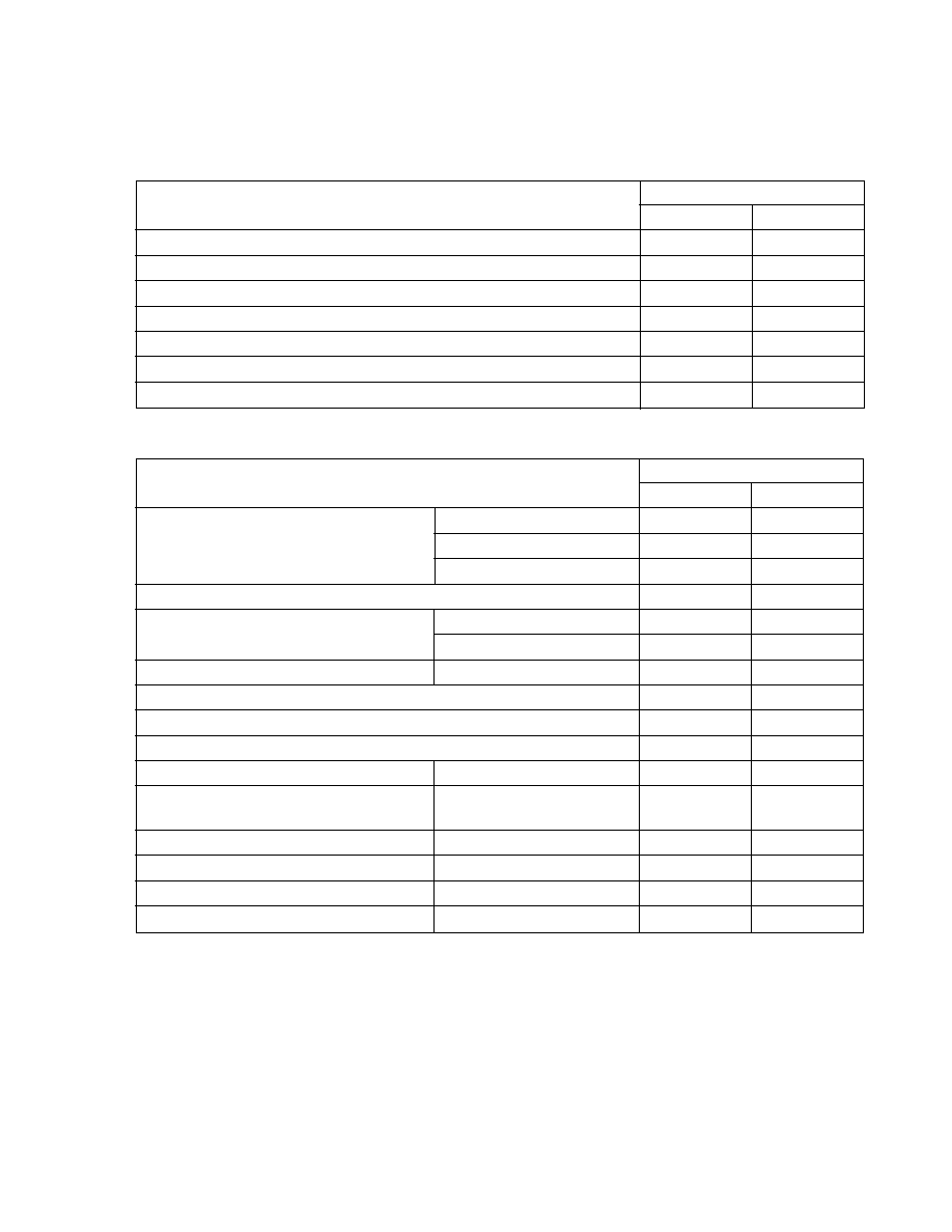
LIST OF FIGURES (1/4)
Figure No.
Title
Page
2-1.
I/O Circuits of Pins ............................................................................................................................
39
3-1.
Memory Map (
�
PD780973(A)) ..........................................................................................................
41
3-2.
Memory Map (
�
PD78F0974) ............................................................................................................
42
3-3.
Data Memory Addressing (
�
PD780973(A)) ......................................................................................
45
3-4.
Data Memory Addressing (
�
PD78F0974) .........................................................................................
46
3-5.
Program Counter Configuration ........................................................................................................
47
3-6.
Program Status Word Configuration .................................................................................................
47
3-7.
Stack Pointer Configuration ..............................................................................................................
49
3-8.
Data to be Saved to Stack Memory ..................................................................................................
49
3-9.
Data to be Reset from Stack Memory ...............................................................................................
49
3-10.
General Register Configuration ........................................................................................................
50
4-1.
EEPROM Block Diagram ..................................................................................................................
68
4-2.
EEPROM Write Control Register (EEWC) Format ...........................................................................
69
5-1.
Port Types .........................................................................................................................................
73
5-2.
P00 to P07 Block Diagram ................................................................................................................
76
5-3.
P10 to P14 Block Diagram ................................................................................................................
76
5-4.
P20 to P27 Block Diagram ................................................................................................................
77
5-5.
P30 to P37 Block Diagram ................................................................................................................
78
5-6.
P40 to P44 Block Diagram ................................................................................................................
79
5-7.
P50 to P54 Block Diagram ................................................................................................................
80
5-8.
P60 and P61 Block Diagram .............................................................................................................
81
5-9.
P81 Block Diagram ...........................................................................................................................
82
5-10.
P82 to P87 Block Diagram ................................................................................................................
82
5-11.
P90 to P97 Block Diagram ................................................................................................................
83
5-12.
Port Mode Register (PM0, PM4 to PM6, PM8, PM9) Format ...........................................................
86
5-13.
Port Mode Register (PM2, PM3) Format ..........................................................................................
86
5-14.
Pull-Up Resistor Option Register (PU0) Format ...............................................................................
87
6-1.
Clock Generator Block Diagram .......................................................................................................
89
6-2.
Processor Clock Control Register (PCC) Format .............................................................................
90
6-3.
Oscillator Mode Register (OSCM) Format ........................................................................................
91
6-4.
External Circuit of Main System Clock Oscillator ..............................................................................
92
6-5.
Incorrect Examples of Resonator Connection ..................................................................................
93
6-6.
Switching CPU Clock ........................................................................................................................
97
7-1.
Timer 0 (TM0) Block Diagram ...........................................................................................................
101
7-2.
16-Bit Timer Mode Control Register (TMC0) Format ........................................................................
103
7-3.
Capture Pulse Control Register (CRC0) Format ..............................................................................
104
7-4.
Prescaler Mode Register (PRM0) Format ........................................................................................
105
7-5.
Configuration Diagram for Pulse Width Measurement by Free-Running Counter ............................
106
7-6.
Timing of Pulse Width Measurement Operation by Free-Running Counter
and One Capture Register (with Both Edges Specified) ...................................................................
106

18
LIST OF FIGURES (2/4)
Figure No.
Title
Page
7-7.
CR0m Capture Operation with Rising Edge Specified .....................................................................
107
7-8.
Timing of Pulse Width Measurement Operation by Free-Running Counter
(with Both Edges Specified) ..............................................................................................................
108
7-9.
16-Bit Timer Register Start Timing ....................................................................................................
109
7-10.
Capture Register Data Retention Timing ..........................................................................................
109
8-1.
Timer 1 (TM1) Block Diagram ...........................................................................................................
111
8-2.
Timer Clock Select Register 1 (TCL1) Format ..................................................................................
113
8-3.
8-Bit Timer Mode Control Register 1 (TMC1) Format .......................................................................
114
8-4.
Interval Timer Operation Timings ......................................................................................................
115
8-5.
Timer 1 Start Timing ..........................................................................................................................
118
8-6.
Timing after Compare Register Change during Timer Count Operation ...........................................
118
9-1.
Timer 2 (TM2) Block Diagram ...........................................................................................................
119
9-2.
Timer 3 (TM3) Block Diagram ...........................................................................................................
120
9-3.
Timer Clock Select Register 2 (TCL2) Format ..................................................................................
122
9-4.
Timer Clock Select Register 3 (TCL3) Format ..................................................................................
123
9-5.
8-Bit Timer Mode Control Register n (TMCn) Format .......................................................................
124
9-6.
Interval Timer Operation Timings ......................................................................................................
125
9-7.
External Event Counter Operation Timings (with Rising Edge Specified) ........................................
128
9-8.
PWM Output Operation Timing .........................................................................................................
130
9-9.
Timing of Operation by Change of CRn ............................................................................................
131
9-10.
Timer n Start Timing ..........................................................................................................................
132
9-11.
Timing after Compare Register Change during Timer Count Operation ...........................................
132
10-1.
Watch Timer Block Diagram .............................................................................................................
133
10-2.
Watch Timer Mode Control Register (WTM) Format ........................................................................
135
10-3.
Operation Timing of Watch Timer/Interval Timer ...............................................................................
137
11-1.
Watchdog Timer Block Diagram .......................................................................................................
139
11-2.
Watchdog Timer Clock Select Register (WDCS) Format ..................................................................
141
11-3.
Watchdog Timer Mode Register (WDTM) Format ............................................................................
142
12-1.
Clock Output Control Circuit Block Diagram .....................................................................................
145
12-2.
Clock Output Selection Register (CKS) Format ................................................................................
146
12-3.
Port Mode Register 6 (PM6) Format .................................................................................................
147
12-4.
Remote Control Output Application Example ...................................................................................
148
13-1.
A/D Converter Block Diagram ...........................................................................................................
149
13-2.
Power-Fail Detection Function Block Diagram .................................................................................
150
13-3.
A/D Converter Mode Register (ADM1) Format .................................................................................
152
13-4.
Analog Input Channel Specification Register (ADS1) Format ..........................................................
153
13-5.
Power-Fail Compare Mode Register (PFM) Format .........................................................................
154
13-6.
Basic Operation of 8-Bit A/D Converter ............................................................................................
156
13-7.
Relation between Analog Input Voltage and A/D Conversion Result ................................................
157

19
LIST OF FIGURES (3/4)
Figure No.
Title
Page
13-8.
A/D Conversion .................................................................................................................................
159
13-9.
Example of Method of Reducing Current Consumption in Standby Mode .......................................
160
13-10.
Analog Input Pin Connection ............................................................................................................
161
13-11.
A/D Conversion End Interrupt Request Generation Timing ..............................................................
162
13-12.
D/A Converter Mode Register (DAM1) Format .................................................................................
163
14-1.
UART Block Diagram ........................................................................................................................
165
14-2.
Asynchronous Serial Interface Mode Register (ASIM) Format .........................................................
168
14-3.
Asynchronous Serial Interface Status Register (ASIS) Format ........................................................
169
14-4.
Baud Rate Generator Control Register (BRGC) Format ..................................................................
170
14-5.
Error Tolerance (when k = 0) including Sampling Errors ..................................................................
176
14-6.
Format of Transmit/Receive Data in Asynchronous Serial Interface ................................................
177
14-7.
Timing of Asynchronous Serial Interface Transmit Completion Interrupt ..........................................
179
14-8.
Timing of Asynchronous Serial Interface Receive Completion Interrupt ...........................................
180
14-9.
Receive Error Timing ........................................................................................................................
181
15-1.
SIO3 Block Diagram .........................................................................................................................
183
15-2.
Serial Operation Mode Register (CSIM) Format ...............................................................................
185
15-3.
Serial Operation Mode Register (CSIM) Format ...............................................................................
186
15-4.
Serial Operation Mode Register (CSIM) Format ...............................................................................
187
15-5.
Three-Wire Serial I/O Mode Timing ..................................................................................................
188
16-1.
LCD Controller/Driver Block Diagram ...............................................................................................
190
16-2.
LCD Clock Select Circuit Block Diagram ..........................................................................................
191
16-3.
LCD Display Mode Register (LCDM) Format ...................................................................................
192
16-4.
LCD Display Control Register (LCDC) Format .................................................................................
193
16-5.
Relationship between LCD Display Data Memory Contents and Segment/Common Outputs .........
195
16-6.
Common Signal Waveform ...............................................................................................................
197
16-7.
Common Signal and Segment Signal Voltages and Phases ............................................................
197
16-8.
Example of Connection of LCD Drive Power Supply ........................................................................
199
16-9.
4-Time-Division LCD Display Pattern and Electrode Connections ...................................................
200
16-10.
4-Time-Division LCD Panel Connection Example ............................................................................
201
16-11.
4-Time-Division LCD Drive Waveform Examples (1/3 Bias Method) ...............................................
202
16-12.
LCD Timer Control Register (LCDTM) Format .................................................................................
203
17-1.
Sound Generator Block Diagram ......................................................................................................
205
17-2.
Concept of Each Signal ....................................................................................................................
206
17-3.
Sound Generator Control Register (SGCR) Format .........................................................................
208
17-4.
Sound Generator Buzzer Control Register (SGBR) Format .............................................................
210
17-5.
Sound Generator Amplitude Register (SGAM) Format .....................................................................
211
17-6.
Sound Generator Output Operation Timing ......................................................................................
212
17-7.
Sound Generator Output Operation Timing ......................................................................................
212

20
LIST OF FIGURES (4/4)
Figure No.
Title
Page
18-1.
Meter Controller/Driver Block Diagram .............................................................................................
213
18-2.
1-Bit Addition Circuit Block Diagram .................................................................................................
214
18-3.
Timer Mode Control Register (MCNTC) Format ...............................................................................
216
18-4.
Compare Control Register n (MCMPCn) Format ..............................................................................
217
18-5.
Port Mode Control Register (PMC) Format ......................................................................................
218
18-6.
Restart Timing after Count Stop (Count Start
Count Stop
Count Start) ......................................
220
18-7.
Timing in 1-Bit Addition Circuit Operation .........................................................................................
221
18-8.
Timing of Output with 1 Clock Shifted ...............................................................................................
222
19-1.
Basic Configuration of Interrupt Function .........................................................................................
225
19-2.
Interrupt Request Flag Register (IF0L, IF0H, IF1L) Format ..............................................................
228
19-3.
Interrupt Mask Flag Register (MK0L, MK0H, MK1L) Format ............................................................
229
19-4.
Priority Specify Flag Register (PR0L, PR0H, PR1L) Format ............................................................
230
19-5.
External Interrupt Rising Edge Enable Register (EGP),
External Interrupt Falling Edge Enable Register (EGN) Format .......................................................
231
19-6.
Prescaler Mode Register (PRM0) Format ........................................................................................
232
19-7.
Program Status Word Format ...........................................................................................................
233
19-8.
Non-Maskable Interrupt Request Generation to Acknowledge Flowchart ........................................
235
19-9.
Non-Maskable Interrupt Request Acknowledge Timing ....................................................................
235
19-10.
Non-Maskable Interrupt Request Acknowledge Operation ...............................................................
236
19-11.
Interrupt Request Acknowledge Processing Algorithm .....................................................................
238
19-12.
Interrupt Request Acknowledge Timing (Minimum Time) .................................................................
239
19-13.
Interrupt Request Acknowledge Timing (Maximum Time) ................................................................
239
19-14.
Multiple Interrupt Examples ..............................................................................................................
241
19-15.
Interrupt Request Hold ......................................................................................................................
243
20-1.
Oscillation Stabilization Time Select Register (OSTS) Format .........................................................
246
20-2.
HALT Mode Clear upon Interrupt Generation ...................................................................................
248
20-3.
HALT Mode Clear upon RESET Input ..............................................................................................
249
20-4.
STOP Mode Clear upon Interrupt Generation ..................................................................................
251
20-5.
STOP Mode Clear upon RESET Input ..............................................................................................
252
21-1.
Reset Function Block Diagram .........................................................................................................
253
21-2.
Timing of Reset by RESET Input ......................................................................................................
254
21-3.
Timing of Reset due to Watchdog Timer Overflow ...........................................................................
254
21-4.
Timing of Reset in STOP Mode by RESET Input ..............................................................................
254
22-1.
Memory Size Switching Register (IMS) Format ................................................................................
258
22-2.
Transmission Method Selection Format ...........................................................................................
259
22-3.
Flashpro II Connection Using 3-Wire Serial I/O Method ...................................................................
260
22-4.
Flashpro II Connection Using UART Method ....................................................................................
261
22-5.
Flashpro II Connection Using Pseudo 3-Wire Serial I/O Method ......................................................
261
A-1.
Development Tool Configuration .......................................................................................................
280
A-2.
Dimensions of TGF-080RAP (Reference) ........................................................................................
289

21
LIST OF TABLES (1/2)
Table No.
Title
Page
2-1.
Pin Input/Output Circuit Types ..........................................................................................................
38
3-1.
Internal Memory Capacity .................................................................................................................
43
3-2.
Vector Table ......................................................................................................................................
43
3-3.
Internal High-Speed RAM Capacity ..................................................................................................
44
3-4.
Internal High-Speed RAM Area ........................................................................................................
48
3-5.
Special Function Register List ..........................................................................................................
52
5-1.
Port Functions ...................................................................................................................................
74
5-2.
Port Configuration .............................................................................................................................
75
5-3.
Port Mode Register and Output Latch Settings when Using Alternate Functions .............................
85
6-1.
Clock Generator Configuration .........................................................................................................
89
6-2.
Relation between CPU Clock and Minimum Instruction Execution Time ..........................................
90
6-3.
Maximum Time Required for Switching CPU Clock ..........................................................................
96
7-1.
Timer/Event Counter Operations ......................................................................................................
100
7-2.
Timer 0 Configuration .......................................................................................................................
102
8-1.
Timer 1 Configuration .......................................................................................................................
112
9-1.
Timers 2 and 3 Configurations ..........................................................................................................
121
10-1.
Interval Timer Interval Time ..............................................................................................................
134
10-2.
Watch Timer Configuration ...............................................................................................................
134
10-3.
Interval Timer Interval Time ..............................................................................................................
136
11-1.
Watchdog Timer Runaway Detection Time .......................................................................................
140
11-2.
Interval Time .....................................................................................................................................
140
11-3.
Watchdog Timer Configuration .........................................................................................................
141
11-4.
Watchdog Timer Runaway Detection Time .......................................................................................
143
11-5.
Interval Timer Interval Time ..............................................................................................................
144
12-1.
Clock Output Control Circuit Configuration .......................................................................................
145
13-1.
A/D Converter Configuration .............................................................................................................
150
14-1.
UART Configuration ..........................................................................................................................
166
14-2.
Relation between 5-bit Counter's Source Clock and "n" Value .........................................................
175
14-3.
Relation between Main System Clock and Baud Rate .....................................................................
176
14-4.
Causes of Receive Errors .................................................................................................................
181
15-1.
SIO3 Configuration ...........................................................................................................................
184

22
LIST OF TABLES (2/2)
Table No.
Title
Page
16-1.
Maximum Number of Display Pixels .................................................................................................
189
16-2.
LCD Controller/Driver Configuration .................................................................................................
190
16-3.
COM Signals .....................................................................................................................................
196
16-4.
LCD Drive Voltage ............................................................................................................................
196
16-5.
LCD Drive Voltage ............................................................................................................................
198
16-6.
Selection and Non-Selection Voltages (COM0 to COM3) ................................................................
200
17-1.
Sound Generator Configuration ........................................................................................................
206
18-1.
Meter Controller/Driver Configuration ...............................................................................................
214
19-1.
Interrupt Source List .........................................................................................................................
224
19-2.
Flags Corresponding to Interrupt Request Sources .........................................................................
227
19-3.
Times from Generation of Maskable Interrupt Request until Servicing .............................................
237
19-4.
Interrupt Request Enabled for Multiple Interrupt during Interrupt Servicing ......................................
240
20-1.
HALT Mode Operating Status ...........................................................................................................
247
20-2.
Operation after HALT Mode Clear ....................................................................................................
249
20-3.
STOP Mode Operating Status ..........................................................................................................
250
20-4.
Operation after STOP Mode Clear ....................................................................................................
252
21-1.
Hardware Status after Reset ............................................................................................................
255
22-1.
Differences between
�
PD78F0974 and
�
PD780973(A) ...................................................................
257
22-2.
Memory Size Switching Register Settings ........................................................................................
258
22-3.
Transmission Method List .................................................................................................................
259
22-4.
Main Functions of Flash Memory Programming ...............................................................................
260
23-1.
Operand Identifiers and Description Formats ...................................................................................
264
A-1.
Upgrading Former In-circuit Emulator for 78K/0 Series to IE-78001-R-A .........................................
288

23
CHAPTER 1 OUTLINE
1.1 Features
�
Internal memory
Item
Program Memory
Data Memory
Part Number
(ROM/Flash Memory)
Internal High-Speed RAM
LCD Display RAM
EEPROM
TM
�
PD780973(A)
24 Kbytes
768 bytes
20
�
4 bits
256 bytes
�
PD78F0974
32 Kbytes
1024 bytes
�
High-speed instruction execution time (0.24
�
s: @ 8.38-MHz operation with main system clock)
�
Instruction set suited to system control
� Bit manipulation possible in all address spaces
� Multiply and divide instructions
�
Fifty-six I/O ports : (including pins that have an alternate function as segment signal output)
�
LCD controller/driver
� Segment signal output :
20 max.
� Common signal output :
4 max.
� Bias
:
1/3 bias
� Power supply voltage
:
V
LCD
= 3.0 V to V
DD
�
8-bit resolution A/D converter : 5 channels
�
Serial interface
:
2 channels
� 3-wire serial I/O mode :
1 channel
� UART mode
:
1 channel
�
Timer : Six channels
� 16-bit timer
:
1 channel
� 8-bit timer
:
1 channel
� 8-bit timer/event counter :
2 channels
� Watch timer
:
1 channel
� Watchdog timer
:
1 channel
�
Meter controller/driver : PWM output (8-bit resolution) : 16
: Can set pulse width with a precision of 8 + 1 bits with 1-bit addition function
�
Sound generator : 1 channel
�
Vectored interrupt sources : 21
�
Power supply voltage : V
DD
= 5 V
�
10%
1.2 Applications
Automobile meter (dash board) control

24
CHAPTER 1 OUTLINE
1.3 Ordering Information
Part Number
Package
Internal ROM
�
PD780973GF(A)-
���
-3B9
80-pin plastic QFP (14
�
20 mm)
Mask ROM
�
PD78F0974GF-3B9
80-pin plastic QFP (14
�
20 mm)
Flash memory
1.4 Quality Grade
Part Number
Package
Quality Grade
�
PD78F0974GF-3B9
80-pin plastic QFP (14
�
20 mm)
Standard
�
PD780973GF(A)-
���
-3B9
80-pin plastic QFP (14
�
20 mm)
Special
Remark
���
indicates ROM code suffix.
Please refer to "Quality Grades on NEC Semiconductor Devices" (Document No. C11531E) published by
NEC Corporation to know the specification of quality grade on the devices and its recommended applications.
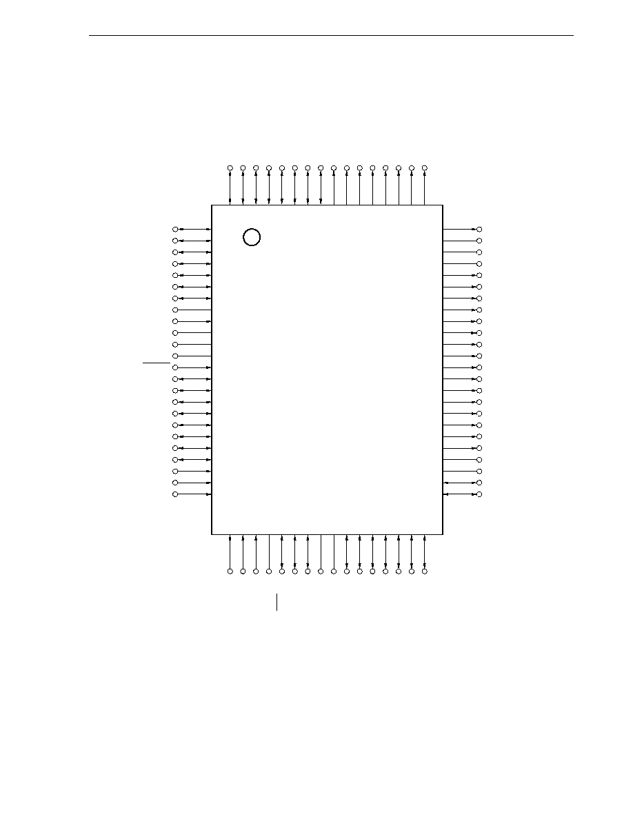
25
CHAPTER 1 OUTLINE
1.5 Pin Configuration (Top View)
� 80-pin plastic QFP (14
�
20 mm)
�
PD780973GF(A)-
���
, 78F0974GF
64
63
62
61
60
59
58
57
56
55
54
53
52
51
50
49
48
47
46
45
44
43
42
41
1
2
3
4
5
6
7
8
9
10
11
12
13
14
15
16
17
18
19
20
21
22
23
24
25 26 27 28 29 30 31 32 33 34 35 36 37 38 39 40
80 79 78 77 76 75 74 73 72 71 70 69 68 67 66 65
COM0
V
LCD
SMV
SS
SMV
DD
SM11/P20
SM12/P21
SM13/P22
SM14/P23
SM21/P24
SM22/P25
SM23/P26
SM24/P27
SM31/P30
SM32/P31
SM33/P32
SM34/P33
SM41/P34
SM42/P35
SM43/P36
SM44/P37
SMV
DD
SMV
SS
SGO/SGOF/P61
SGOA/PCL/P60
P87/S13
P86/S14
P85/S15
P84/S16
P83/S17
P82/S18
TPO/P81/S19
IC (V
PP
)
X1
X2
V
SS
V
DD
RESET
P07
P06
P05
P04
P03
INTP2/P02
INTP1/P01
INTP0/P00
AV
REF
P14/ANI4
P13/ANI3
ANI2/P12
ANI1/P11
ANI0/P10
AV
SS
SCK/P50
SO/P51
SI/P52
V
DD
V
SS
RxD/P53
TxD/P54
TI00/P40
TI01/P41
TI02/P42
TIO2/P43
TIO3/P44
S12/P90
S11/P91
S10/P92
S9/P93
S8/P94
S7/P95
S6/P96
S5/P97
S4
S3
S2
S1
S0
COM3
COM2
COM1
Cautions 1. Connect IC (Internally Connected) pin to V
SS
directly.
2. Connect AV
SS
pin to V
SS
.
Remarks 1. When these devices are used in applications that require reduction of the noise generated from inside
the microcontroller, the implementation of noise reduction measures, such as supplying voltage to
the two V
DD
individually, and connecting the two V
SS
to different ground lines, is recommended.
2. Pin connection in parentheses is intended for the
�
PD78F0974.

26
CHAPTER 1 OUTLINE
ANI0 to ANI4
: Analog Input
SCK
:
Serial Clock
AV
REF
: Analog Reference Voltage
SGO
:
Sound Generator Output
AV
SS
: Analog Ground
SGOA
:
Sound Generator Amplitude Output
COM0 to COM3 : Common Output
SGOF
:
Sound Generator Frequency Output
IC
: Internally Connected
SI
:
Serial Input
INTP0 to INTP2
: Interrupt from Peripherals
SM11 to SM14, SM21 to SM24, SM31 to SM34, SM41 to SM44
P00 to P07
: Port0
:
Meter Output
P10 to P14
: Port1
SMV
DD
:
Meter Controller Power Supply
P20 to P27
: Port2
SMV
SS
:
Meter Controller Ground
P30 to P37
: Port3
SO
:
Serial Output
P40 to P44
: Port4
TI00 to TI02
:
Timer Input
P50 to P54
: Port5
TIO2, TIO3
:
Timer Output/Event Counter Input
P60, P61
: Port6
TPO
:
Prescaler Output
P81 to P87
: Port8
TxD
:
Transmit Data
P90 to P97
: Port9
V
DD
:
Power Supply
PCL
: Clock Output
V
LCD
:
LCD Power Supply
RESET
: Reset
V
PP
:
Programming Power Supply
RxD
: Receive Data
V
SS
:
Ground
S0 to S19
: Segment Output
X1, X2
:
Crystal (Main System Clock)
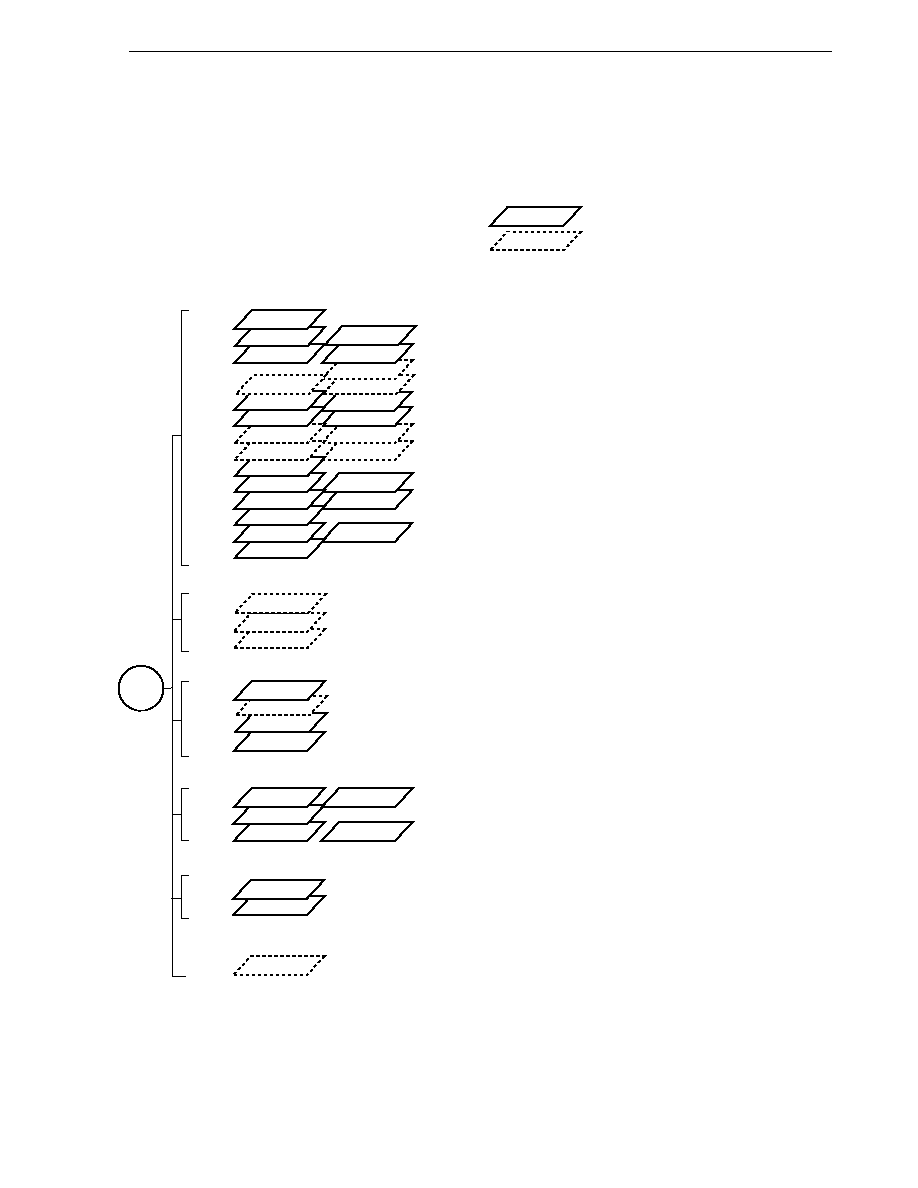
27
CHAPTER 1 OUTLINE
1.6 78K/0 Series Product Development
These products are a further development in the 78K/0 Series. The designations appearing inside the boxes are
subseries names.
Note Under planning
PD78014
PD78002
PD78083
PD78002Y
100-pin
100-pin
100-pin
64-pin
64-pin
64-pin
42/44-pin
Control
Y subseries products are compatible with I
2
C bus.
Timer was added to the PD78054, and the external interface function was enhanced.
EMI-noise reduced version of the PD78078.
ROM-less versions of the PD78078.
A/D converter and 16-bit timer were added to the PD78002.
A/D converter was added to the PD78002.
Basic subseries for control.
On-chip UART, capable of operating at a low voltage (1.8 V).
PD780018AY
100-pin
Serial I/O of the PD78078Y was enhanced, and only selected functions are provided.
PD78078
PD78070A
PD78075B
PD78070AY
�
�
�
�
�
�
�
�
�
�
�
�
�
�
�
�
Inverter control
PD780964
64-pin
�
A/D converter of the PD780924 was enhanced.
PD78078Y
�
PD78018F
PD780001
PD78018FY
PD78014Y
80-pin
80-pin
64-pin
78K/0
Series
Products in mass production
Products under development
EMI-noise reduced version of the PD78054.
UART and D/A converter were added to the PD78014, and I/O was enhanced.
Low-voltage (1.8 V) operation versions of the PD78014 with several ROM and RAM capacities available.
A/D converter of the PD780024 was enhanced.
EMI-noise reduced version of the PD78018F.
On-chip inverter control circuit and UART, EMI-noise reduced version.
Serial I/O of the PD78018F was enhanced.
Serial I/O of the PD78054 was enhanced, EMI-noise reduced version.
PD780058
80-pin
�
�
�
PD780034
PD780024
PD78014H
PD780034Y
PD780024Y
64-pin
64-pin
64-pin
�
�
�
�
�
�
�
�
�
�
�
�
�
FIP
TM
drive
PD78044F
100-pin
80-pin
80-pin
�
�
I/O and FIP C/D of the PD78044F were enhanced, Display output total: 53
I/O and FIP C/D of the PD78044H were enhanced, Display output total: 48
N-ch open-drain input/output was added to the PD78044F, Display output total: 34
Basic subseries for driving FIP, Display output total: 34
�
�
100-pin
PD780924
64-pin
�
PD780308
PD78064B
PD78064
100-pin
100-pin
100-pin
�
�
SIO of the PD78064 was enhanced, and ROM and RAM were expanded.
EMI-noise reduced version of the PD78064.
Basic subseries for driving LCDs, On-chip UART.
�
PD780308Y
�
PD78064Y
�
LCD drive
�
�
PD78054
�
PD78054Y
�
PD78058FY
�
PD780058Y
Note
�
PD78058F
�
PD78044H
�
�
PD780228
PD780208
�
�
�
IEBus
TM
supported
PD78098B
80-pin
�
EMI-noise reduced version of the PD78098.
IEBus controller was added to the PD78054.
PD78098
80-pin
�
�
Meter control
PD780973
80-pin
�
On-chip automobile meter driving controller/driver.
PD780988
64-pin
�
�
Inverter control, timer, and SIO of the
PD780964 were enhanced, with ROM and RAM expansion.

28
CHAPTER 1 OUTLINE
The major functional differences among the subseries are shown below.
Function
ROM
Timer
8-bit 10-bit 8-bit
V
DD
External
Serial Interface
I/O
MIN.
Subseries Name
Capacity
8-bit
16-bit
Watch
WDT
A/D
A/D
D/A
Value
Expansion
Control
�
PD78075B 32 K to 40 K
4 ch
1 ch
1 ch
1 ch
8 ch
�
2 ch
3 ch (UART: 1 ch)
88
1.8 V Available
�
PD78078
48 K to 60 K
�
PD78070A
�
61
2.7 V
�
PD780058
24 K to 60 K
2 ch
3 ch (time-division
68
1.8 V
UART: 1ch)
�
PD78058F 48 K to 60 K
3 ch (UART: 1 ch)
69
2.7 V
�
PD78054
16 K to 60 K
2.0 V
�
PD780034
8 K to 32 K
�
8 ch
�
3 ch (UART: 1 ch, time- 51
1.8 V
�
PD780024
8 ch
�
division 3-wire: 1 ch)
�
PD78014H
2 ch
53
�
PD78018F 8 K to 60 K
�
PD78014
8 K to 32 K
2.7 V
�
PD780001
8 K
�
�
1 ch
39
�
�
PD78002
8 K to 16 K
1 ch
�
53
Available
�
PD78083
�
8 ch
1 ch (UART: 1 ch)
33
1.8 V
�
Inverter
�
PD780988
32 K to 60 K
3 ch
Note 1
�
1 ch
�
8 ch
�
3 ch (UART: 2 ch)
47
4.0 V Available
control
�
PD780964
8 K to 32 K
Note 2
2 ch (UART: 2 ch)
2.7 V
�
PD780924
8 ch
�
FIP
�
PD780208
32 K to 60 K
2 ch
1 ch
1 ch
1 ch
8 ch
�
�
2 ch
74
2.7 V
�
drive
�
PD780228
48 K to 60 K
3 ch
�
�
1 ch
72
4.5 V
�
PD78044H 32 K to 48 K
2 ch
1 ch
1 ch
68
2.7 V
�
PD78044F 16 K to 40 K
2 ch
LCD
�
PD780308
48 K to 60 K
2 ch
1 ch
1 ch
1 ch
8 ch
�
�
3 ch (time-division
57
2.0 V
�
drive
UART: 1 ch)
�
PD78064B 32 K
2 ch (UART: 1 ch)
�
PD78064
16 K to 32 K
IEBus
�
PD78098B 40 K to 60 K
2 ch
1 ch
1 ch
1 ch
8 ch
�
2 ch
3 ch (UART: 1 ch)
69
2.7 V Available
supported
�
PD78098
32 K to 60 K
Meter
�
PD780973
24 K to 32 K
3 ch
1 ch
1 ch
1 ch
5 ch
�
�
2 ch (UART: 1 ch)
56
4.5 V
�
control
Notes 1. 16-bit timer: 2 channels
10-bit timer: 1 channel
2. 10-bit timer: 1 channel

29
CHAPTER 1 OUTLINE
1.7 Block Diagram
Remarks 1. The internal ROM and RAM capacities depend on the product.
2. Memory type in parentheses is for the
�
PD78F0974.
TI00/P40 to TI02/P42
16-bit TIMER0
PORT0
P00 to P07
P10 to P14
P20 to P27
P30 to P37
P40 to P44
P50 to P54
P60, P61
P81 to P87
P90 to P97
S0 to S4
S5/P97 to S12/P90
PORT1
PORT2
PORT3
PORT4
PORT5
PORT6
PORT8
PORT9
LCD
CONTROLLER/
DRIVER
METER
CONTROLLER/
DRIVER
SYSTEM
CONTROL
8-bit TIMER1
8-bit TIMER/
EVENT
COUNTER2
8-bit TIMER/
EVENT
COUNTER3
WATCHDOG
TIMER
SERIAL
INTERFACE
A/D
CONVERTER
INTERRUPT
CONTROL
STANDBY
CONTROL
SOUND
GENERATOR
OUTPUT
V
DD
V
SS
IC
(V
PP
)
CLOCK OUTPUT
CONTROL
POWER FAIL
DETECTOR
UART
RAM
78K/0
CPU CORE
ROM
FLASH
MEMORY
EEPROM
WATCH TIMER
TIO2/P43
TIO3/P44
SCK/P50
SO/P51
SI/P52
ANI0/P10 to ANI4/P14
AV
SS
AV
REF
RxD/P53
TxD/P54
INTP0/P00 to
INTP2/P02
PCL/SGOA/P60
SGO/SGOF/P61
S13/P87 to S18/P82
SM11/P20 to SM14/P23
SM21/P24 to SM24/P27
SM31/P30 to SM34/P33
SM41/P34 to SM44/P37
S19/P81/TPO
COM0 to COM3
V
LCD
SMV
DD
SMV
SS
X1
X2
RESET
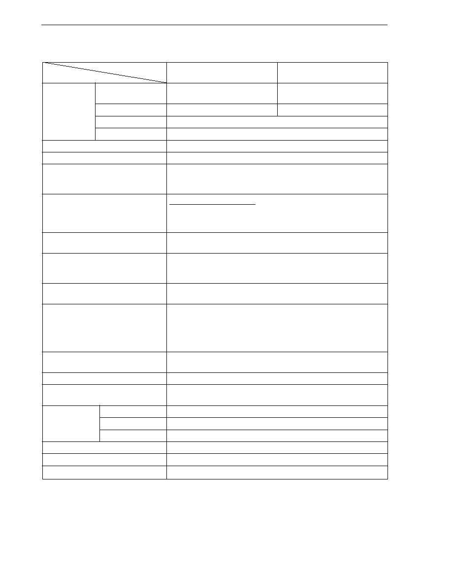
30
CHAPTER 1 OUTLINE
1.8 Outline of Function
Part Number
Item
�
PD780973(A)
�
PD78F0974
Internal memory
ROM
24 Kbytes
32 Kbytes
(Mask ROM)
(Flash memory)
Internal high-speed RAM
768 bytes
1024 bytes
EEPROM
256 bytes
LCD display RAM
20
�
4 bits
General register
8 bits
�
32 registers (8 bits
�
8 registers
�
4 banks)
Minimum instruction execution time
0.24
�
s/0.48
�
s/0.95
�
s/1.91
�
s/3.81
�
s (in operation at 8.38 MHz)
Instruction set
� 16-bit operation
� Multiply/divide (8 bits
�
8 bits, 16 bits
�
8 bits)
� Bit manipulation (set, reset, test, and Boolean operation)
I/O port
Total
: 56
(including pins shared with segment
� CMOS input
: 5
signal output)
� CMOS output
: 16
� CMOS input/output
: 35
A/D converter
� 8-bit resolution
�
5 channels
� Power-fail detection function
LCD controller/driver
� Segment signal outputs
: 20 max.
� Common signal outputs
: 4 max.
� Bias
: 1/3 bias only
Serial interface
� 3-wire serial I/O mode
: 1 channel
� UART mode
: 1 channel
Timer
� 16-bit timer
: 1 channel
� 8-bit timer
: 1 channel
� 8-bit timer/event counter : 2 channels
� Watch timer
: 1 channel
� Watchdog timer
: 1 channel
Meter control
PWM output (8-bit resolution) : 16
Can set pulse width with a precision of 8 + 1 bits with 1-bit addition function
Sound generator
1 channel
Clock output
65.5 kHz, 131 kHz, 262 kHz, 524 kHz, 1.04 MHz, 2.09 MHz, 4.19 MHz,
8.38 MHz (@ 8.38-MHz operation with main system clock)
Vectored interrupt
Maskable
Internal: 16, External: 3
source
Non-maskable
Internal: 1
Software
1
Power supply voltage
V
DD
(SMV
DD
) = 5 V
�
10%
Operating ambient temperature
T
A
= �40 to +85�C
Package
80-pin plastic QFP (14
�
20 mm)
31
CHAPTER 2 PIN FUNCTION
2.1 Pin Function List
(1) Port Pins
Pin Name
Input/Output
Function
After Reset
Alternate
Function
P00 to P02
Input/Output
Input
INTP0 to INTP2
P03 to P07
--
P10 to P14
Input
Port 1
Input
ANI0 to ANI4
5-bit input only port.
P20 to P23
Output
Port 2
Hi-Z
SM11 to SM14
P24 to P27
8-bit output only port.
SM21 to SM24
P30 to P33
Output
Port 3
Hi-Z
SM31 to SM34
P34 to P37
8-bit output only port.
SM41 to SM44
P40 to P42
Input/Output
Input
TI00 to TI02
P43, P44
TIO2, TIO3
P50
Input/Output
Port 5
Input
SCK
P51
5-bit input/output port.
SO
P52
Input/output mode can be specified bit-wise.
SI
P53
RxD
P54
TxD
P60
Input/Output
Input
PCL/SGOA
P61
SGO/SGOF
P81
Input/Output
Input
S19/TPO
P82 to P87
S18 to S13
P90 to P97
Input/Output
Port 9
Input
S12 to S5
8-bit input/output port.
Input/output mode can be specified bit-wise.
Can be set in I/O port mode or segment output mode in 2-
bit units by using LCD display control register (LCDC).
Port 0
8-bit input/output port.
Input/output mode can be specified bit-wise.
If used as an input port, an on-chip pull-up resistor can be
used by software.
Port 4
5-bit input/output port.
Input/output mode can be specified bit-wise.
Port 6
2-bit input/output port.
Input/output mode can be specified bit-wise.
Port 8
7-bit input/output port.
Input/output mode can be specified bit-wise.
Can be set in I/O port mode or segment output mode in 2-
bit units by using LCD display control register (LCDC).

32
CHAPTER 2 PIN FUNCTION
(2) Non-port pins
Pin Name
Input/Output
Function
After Reset
Alternate
Function
INTP0 to INTP2
Input
External interrupt request input with specifiable valid edges
Input
P00 to P02
(rising edge, falling edge, both rising and falling edges).
SI
Input
Serial interface serial data input.
Input
P52
SO
Output
Serial interface serial data output.
Input
P51
SCK
Input/Output
Serial interface serial data input/output.
Input
P50
RxD
Input
Asynchronous serial interface serial data input.
Input
P53
TxD
Output
Asynchronous serial interface serial data output.
Input
P54
TI00
Input
Capture trigger signal input to capture register (CR00).
Input
P40
TI01
Capture trigger signal input to capture register (CR01).
P41
TI02
Capture trigger signal input to capture register (CR02).
P42
TIO2
Input/Output
8-bit timer (TM2) input/output.
Input
P43
TIO3
8-bit timer (TM3) input/output.
P44
PCL
Output
Clock output (for main system clock trimming).
Input
SGOA/P60
SGOA
Output
Sound generator signal output.
Input
PCL/P60
SGOF
SGO/P61
SGO
SGOF/P61
TPO
Output
Prescaler output of 16-bit timer (TM0).
Input
P81/S19
S0 to S4
Output
Segment signal output of LCD controller/driver.
Output
--
S5 to S12
Input
P97 to P90
S13 to S18
P87 to P82
S19
P81/TPO
COM0 to COM3
Output
Common signal output of LCD controller/driver.
Output
--
V
LCD
--
LCD driving power supply.
--
--
SM11 to SM14
Output
Meter control signal output.
Hi-Z
P20 to P23
SM21 to SM24
P24 to P27
SM31 to SM34
P30 to P33
SM41 to SM44
P34 to P37
ANI0 to ANI4
Input
A/D converter analog input.
Input
P10 to P14
AV
REF
Input
A/D converter reference voltage input (shared with analog
--
--
power supply).
AV
SS
--
A/D converter ground potential. Same potential as V
SS
.
--
--
RESET
Input
System reset input.
--
--
X1
Input
Crystal connection for main system clock oscillation.
--
--
X2
--
--
--
SMV
DD
--
Power supply for meter controller/driver.
--
--
SMV
SS
--
Ground potential for meter controller/driver.
--
--
V
DD
--
Positive power supply.
--
--
V
SS
--
Ground potential.
--
--
V
PP
--
High-voltage application for program write/verify.
--
--
Connect directly to V
SS
in normal operating mode.
IC
--
Internally connected. Connect directly to V
SS
.
--
--

33
CHAPTER 2 PIN FUNCTION
2.2 Description of Pin Functions
2.2.1 P00 to P07 (Port 0)
These pins constitute an 8-bit input/output port. In addition, they are also used to input external interrupt request
signals.
The following operating modes can be specified bit-wise.
(1) Port mode
In this mode, P00 to P07 function as an 8-bit input/output port.
P00 to P07 can be specified as an input or output port bit-wise with port mode register 0 (PM0). When these
pins are used as an input port, an on-chip pull-up resistor can be used if so specified by the pull-up resistor option
register (PU0).
(2) Control mode
In this mode, P00 to P07 function as external interrupt input pins (INTP0 to INTP2) and external interrupt request
input pins with specifiable valid edges (rising edge, falling edge, both rising and falling edges).
2.2.2 P10 to P14 (Port 1)
These pins constitute a 5-bit input only port. In addition, they are also used to input A/D converter analog signals.
The following operating modes can be specified bit-wise.
(1) Port mode
In this mode, P10 to P14 function as a 5-bit input only port.
(2) Control mode
In this mode, P10 to P14 function as A/D converter analog input pins (ANI0 to ANI4).
2.2.3 P20 to P27 (Port 2)
These pins constitute an 8-bit output only port. In addition, they are also used as PWM output pins to control meters.
The following operating modes can be specified bit-wise.
(1) Port mode
In this mode, P20 to P27 function as an 8-bit output only port. They go into a high-impedance state when 1 is
set to port mode register 2 (PM2).
(2) Control mode
In this mode, P20 to P27 function as PWM output pins (SM11 to SM14 and SM21 to SM24) for meter control.

34
CHAPTER 2 PIN FUNCTION
2.2.4 P30 to P37 (Port 3)
These pins constitute an 8-bit output only port. In addition, they also function as PWM output pins to control meters.
The following operating modes can be specified bit-wise.
(1) Port mode
In this mode, P30 to P37 function as an 8-bit output only port. They go into a high-impedance state when 1 is
set to port mode register 3 (PM3).
(2) Control mode
In this mode, P30 to P37 function as PWM output pins (SM31 to SM34 and SM41 to SM44) for meter control.
2.2.5 P40 to P44 (Port 4)
These pins constitute a 5-bit input/output port. In addition, they also function as timer input/output pins.
The following operating modes can be specified bit-wise.
(1) Port mode
In this mode, P40 to P44 function as a 5-bit input/output port. They can be set bit-wise in the input or output
mode by using port mode register 4 (PM4).
(2) Control mode
In this mode, P40 to P44 function as timer input/output pins.
(a) TIO2, TIO3
Timer output pins.
(b) TI00 to TI02
These pins input a capture trigger signal to the 16-bit timer capture registers (CR00 to CR02).
2.2.6 P50 to P54 (Port 5)
These pins constitute a 5-bit input/output port. In addition, they also function as serial interface data input/output
and clock input/output pins.
The following operating modes can be specified bit-wise.
(1) Port mode
In this mode, P50 to P54 function as a 5-bit input/output port. They can be set bit-wise in the input or output
mode by using port mode register 5 (PM5).
(2) Control mode
In this mode, P50 to P54 function as serial interface data input/output and clock input/output.
(a) SI
Serial interface serial data input pin.
(b) SO
Serial interface serial data output pin.

35
CHAPTER 2 PIN FUNCTION
(c) SCK
Serial interface serial clock input/output pin.
(d) RxD, TxD
Asynchronous serial interface serial data input/output pins.
2.2.7 P60, P61 (Port 6)
These pins constitute a 2-bit input/output port. In addition, they also function as clock output and sound generator
output pins.
The following operating modes can be specified bit-wise.
(1) Port mode
In this mode, P60 and P61 function as a 2-bit input/output port. They can be set bit-wise in the input or output
mode by using port mode register 6 (PM6).
(2) Control mode
In this mode, P60 and P61 function as clock output and sound generator output pins.
(a) PCL
Clock output pin.
(b) SGOF
Sound generator (without amplitude) signal output pin.
(c) SGO
Sound generator (with amplitude) signal output pin.
(d) SGOA
Sound generator amplitude signal output pin.
2.2.8 P81 to P87 (Port 8)
These pins constitute a 7-bit input/output port. In addition, they also function as output pins for segment signals
from the internal LCD controller/driver, and one of them as a prescaler signal output pin.
The following operating modes can be specified bit-wise.
(1) Port mode
In this mode, P81 to P87 function as a 7-bit input/output port. They can be set bit-wise in the input or output
mode by using port mode register 8 (PM8).
(2) Control mode
In this mode, P81 to P87 function as segment signal output pins of the LCD controller/driver, and one of them
as a prescaler signal output pins.
(a) S13 to S19
Segment signal output pins of the LCD controller/driver.
(b) TPO
Prescaler signal output pin of the 16-bit timer.

36
CHAPTER 2 PIN FUNCTION
2.2.9 P90 to P97 (Port 9)
These pins constitute an 8-bit input/output port. In addition, they also function to output segment signals from the
internal LCD controller/driver.
The following operating modes can be specified bit-wise.
(1) Port mode
In this mode, P90 to P97 function as an 8-bit input/output port. They can be set bit-wise in the input or output
mode by using port mode register 9 (PM9).
(2) Control mode
In this mode, P90 to P97 function as segment signal output pins (S5 to S12) of the LCD controller/driver.
2.2.10 COM0 to COM3
These pins output common signals from the internal LCD controller/driver during 4-time division drive in 1/3 bias
mode (COM0 to COM3 outputs).
2.2.11 V
LCD
This pin supplies a voltage to drive an LCD.
2.2.12 AV
REF
This is an A/D converter reference voltage input pin. This pin also functions as an analog power supply pin. Supply
power to this pin when the A/D converter is used.
When A/D converter is not used, connect this pin to V
SS
.
2.2.13 AV
SS
This is a ground voltage pin of A/D converter. Always use the same voltage as that of the V
SS
pin even when an
A/D converter is not used.
2.2.14 RESET
This is a low-level active system reset input pin.
2.2.15 X1 and X2
Crystal resonator connect pins for main system clock oscillation. When using an external clock supply, input it
to X1 and its inverted signal to X2.
2.2.16 SMV
DD
This pin supplies a positive power to the meter controller/driver.
2.2.17 SMV
SS
This is the ground pin of the meter controller/driver.
2.2.18 V
DD
Positive power supply port pin.
2.2.19 V
SS
Ground potential port pin.
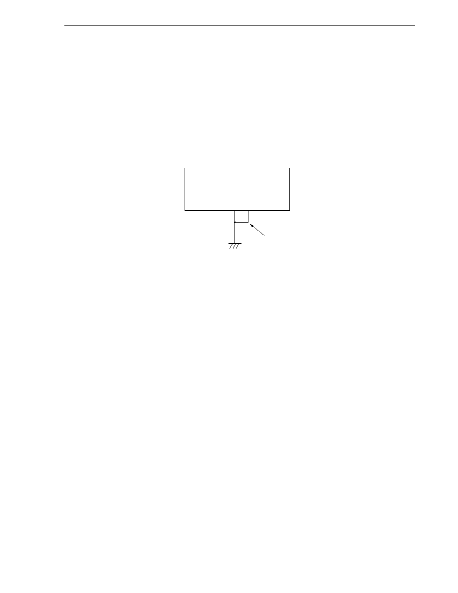
37
CHAPTER 2 PIN FUNCTION
2.2.20 V
PP
(
�
PD78F0974)
A high voltage should be applied to this pin when the flash memory programming mode is set and when the program
is written or verified. Directly connect this pin to V
SS
in the normal operating mode.
2.2.21 IC (
�
PD780973(A))
The IC (Internally Connected) pin is provided to set the test mode to check the
�
PD780973(A) before shipment.
In the normal operating mode, directly connect this pin to the V
SS
pin with as short a wiring length as possible.
When a potential difference is generated between the IC pin and V
SS
pin because the wiring between those two
pins is too long or external noise is input to the IC pin, the user's program may not run normally.
� Directly connect the IC pin to the V
SS
pin.
Keep short
IC
V
SS

38
CHAPTER 2 PIN FUNCTION
2.3 Input/output Circuits and Recommended Connection of Unused Pins
Table 2-1 shows the input/output circuit types of pins and the recommended connection for unused pins.
Refer to Figure 2-1 for the configuration of the input/output circuit of each type.
Table 2-1. Pin Input/Output Circuit Types
Pin Name
Input/Output Circuit Type
Input/Output
Recommended Connection of Unused Pins
P00/INTP0
8-A
Input/output
Independently connect to V
SS
via a resistor.
P01/INTP1
P02/INTP2
P03 to P07
P10/ANI0 to P14/ANI4
9
Input
Independently connect to V
DD
or V
SS
via a resistor.
P20/SM11 to P23/SM14
4
Output
Leave open.
P24/SM21 to P27/SM24
P30/SM31 to P33/SM34
P34/SM41 to P37/SM44
P40/TI00 to P42/TI02
8
Input/output
Independently connect to V
DD
or V
SS
via a resistor.
P43/TIO2
P44/TIO3
P50/SCK
P51/SO
5
P52/SI
8
P53/RxD
P54/TxD
5
P60/SGOA/PCL
P61/SGO/SGOF
P81/S19/TPO
17-G
P82/S18 to P87/S13
P90/S12 to P97/S5
S0 to S4
17
Output
Leave open.
COM0 to COM3
18
V
LCD
--
--
RESET
2
Input
--
SMV
DD
--
--
Connect to V
DD
.
SMV
SS
Connect to V
SS
.
AV
REF
AV
SS
V
PP
(
�
PD78F0974)
IC (
�
PD780973(A))
Connect directly to V
SS
.

39
CHAPTER 2 PIN FUNCTION
Figure 2-1. I/O Circuits of Pins (1/2)
Type 2
Schmitt-triggered input with hysteresis characteristics
IN
Type 5
data
output
disable
P-ch
IN/OUT
V
DD
N-ch
P-ch
V
DD
pullup
enable
Type 4
data
output
disable
P-ch
OUT
V
DD
N-ch
Type 8-A
Type 8
Type 9
data
output
disable
P-ch
IN/OUT
V
DD
N-ch
data
output
disable
input
enable
P-ch
IN/OUT
V
DD
N-ch
+
�
input
enable
Comparator
P-ch
N-ch
V
REF
(Threshold voltage)
IN
Push-pull output whose output can go into a high-
impedance state (both P-ch and N-ch are off).
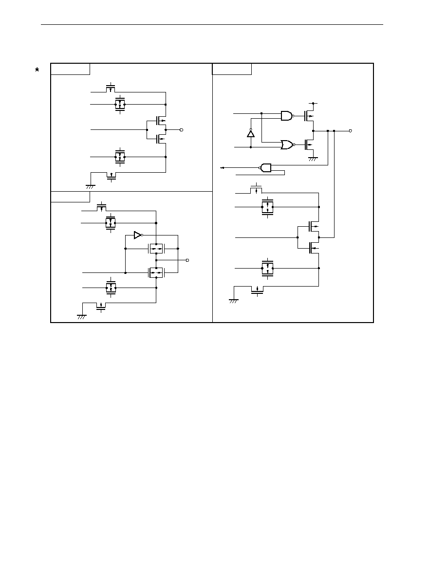
40
CHAPTER 2 PIN FUNCTION
Figure 2-1. I/O Circuits of Pins (2/2)
Type 17
Type 18
Type 17-G
V
LC0
V
LC1
SEG
data
V
LC2
P-ch
N-ch
P-ch
N-ch
P-ch
N-ch
OUT
V
LC0
V
LC1
COM
data
V
LC2
P-ch
N-ch
P-ch
N-ch
P-ch
N-ch
OUT
N-ch
P-ch
V
LC0
V
LC1
SEG
data
V
LC2
P-ch
N-ch
P-ch
N-ch
P-ch
N-ch
P-ch
N-ch
input
enable
output
disable
data
IN/OUT
V
DD
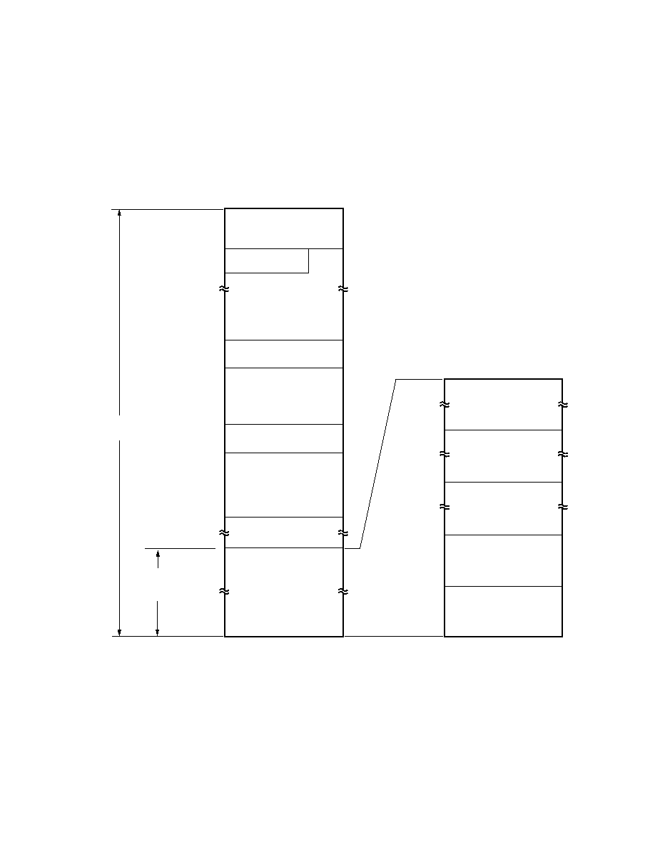
41
CHAPTER 3 CPU ARCHITECTURE
3.1 Memory Spaces
The
�
PD780973 Subseries can access a 64-Kbyte memory space. Figures 3-1 and 3-2 show memory maps of
the respective devices.
Figure 3-1. Memory Map (
�
PD780973(A))
0000H
Data memory
space
General Registers
32
�
8 bits
Internal ROM
24576
�
8 bits
5FFFH
1000H
0FFFH
0800H
07FFH
0080H
007FH
0040H
003FH
0000H
CALLF Entry Area
CALLT Table Area
Vector Table Area
Program Area
Program Area
LCD Display RAM
20
�
4 bits
Reserved
Program
memory
space
6000H
5FFFH
FA59H
FA58H
FA6DH
FA6CH
FEE0H
FEDFH
FF00H
FEFFH
FFFFH
Internal High-speed RAM
768
�
8 bits
Special Function
Registers (SFRs)
256
�
8 bits
Reserved
FC00H
FBFFH
Reserved
EEPROM
256
�
8 bits
FA00H
F9FFH
F900H
F8FFH
42
CHAPTER 3 CPU ARCHITECTURE
Figure 3-2. Memory Map (
�
PD78F0974)
0000H
Data memory
space
General Registers
32
�
8 bits
Flash Memory
32768
�
8 bits
7FFFH
1000H
0FFFH
0800H
07FFH
0080H
007FH
0040H
003FH
0000H
CALLF Entry Area
CALLT Table Area
Vector Table Area
Program Area
Program Area
LCD Display RAM
20
�
4 bits
Reserved
Program
memory
space
8000H
7FFFH
FA59H
FA58H
FA6DH
FA6CH
FEE0H
FEDFH
FF00H
FEFFH
FFFFH
Internal High-speed RAM
1024
�
8 bits
Special Function
Registers (SFRs)
256
�
8 bits
Reserved
FB00H
FAFFH
Reserved
EEPROM
256
�
8 bits
FA00H
F9FFH
F900H
F8FFH

43
CHAPTER 3 CPU ARCHITECTURE
3.1.1 Internal program memory space
The internal program memory space contains the program and table data. Normally, it is addressed with the
program counter (PC).
The
�
PD780973 Subseries incorporate internal ROM (or flash memory), as listed below.
Table 3-1. Internal Memory Capacity
Part Number
Type
Capacity
�
PD780973(A)
Mask ROM
24576
�
8 bits (0000H to 5FFFH)
�
PD78F0974
Flash Memory
32768
�
8 bits (0000H to 7FFFH)
The following three areas are allocated to the program memory space.
(1) Vector table area
The 64-byte area 0000H to 003FH is reserved as a vector table area. This area stores program start addresses
to which execution branches when the RESET signal is input or when an interrupt request is generated. Of a
16-bit address, the lower 8 bits are stored at an even address and the higher 8 bits are stored at an odd address.
Table 3-2. Vector Table
Vector Table Address
Interrupt Source
0000H
RESET input
0004H
INTWDT
0006H
INTAD
0008H
INTOVF
000AH
INTTM00
000CH
INTTM01
000EH
INTTM02
0010H
INTP0
0012H
INTP1
0014H
INTP2
0016H
INTCS10
0018H
INTSER
001AH
INTSR
001CH
INTST
001EH
INTTM1
0020H
INTTM2
0022H
INTTM3
0024H
INTWE
0026H
INTWI
0028H
INTWT
003EH
BRK
44
CHAPTER 3 CPU ARCHITECTURE
(2) CALLT instruction table area
The 64-byte area 0040H to 007FH can store the subroutine entry address of a 1-byte call instruction (CALLT).
(3) CALLF instruction entry area
The area 0800H to 0FFFH can perform a direct subroutine call with a 2-byte call instruction (CALLF).
3.1.2 Internal data memory space
The
�
PD780973 Subseries have the following RAM.
(1) Internal high-speed RAM
Table 3-3. Internal High-Speed RAM Capacity
Product
Internal High-Speed RAM
�
PD780973(A)
768
�
8 bits (FC00H to FEFFH)
�
PD78F0974
1024
�
8 bits (FB00H to FEFFH)
The 32-byte area FEE0H to FEFFH is allocated with four general-purpose register banks composed of eight 8-
bit registers.
The internal high-speed RAM can be used as stack memory.
(2) LCD display RAM
An LCD display RAM is allocated to a 20
�
4 bits area consisting of FA59H to FA6CH. The LCD display RAM
can also be used as a normal RAM.
3.1.3 Special function register (SFR) area
An on-chip peripheral hardware special-function register (SFR) is allocated in the area FF00H to FFFFH (Refer
to 3.2.3 Special function registers (SFRs) Table 3-5 Special Function Register List).
Caution Do not access addresses where the SFR is not assigned.

45
CHAPTER 3 CPU ARCHITECTURE
3.1.4 Data memory addressing
Addressing refers to the method of specifying the address of the instruction to be executed next or the address
of the register or memory relevant to the execution of instructions.
The address of an instruction to be executed next is addressed by the program counter (PC) (for details, see 3.3
Instruction Address Addressing).
Several addressing modes are provided for addressing the memory relevant to the execution of instructions for
the
�
PD780973 Subseries, based on operability and other considerations. For areas containing data memory in
particular, special addressing methods designed for the functions of special function registers (SFR) and general-
purpose registers are available for use. Data memory addressing is illustrated in Figures 3-3 and 3-4. For the details
of each addressing mode, see 3.4 Operand Address Addressing.
Figure 3-3. Data Memory Addressing (
�
PD780973(A))
0000H
General Registers
32
�
8 bits
Internal ROM
24576
�
8 bits
LCD Display RAM
20
�
4 bits
EEPROM
256
�
8 bits
6000H
5FFFH
FA59H
FA58H
FA6DH
FA6CH
FEE0H
FEDFH
FF00H
FEFFH
FFFFH
Internal High-speed RAM
768
�
8 bits
Reserved
FC00H
FBFFH
FF20H
FF1FH
FE20H
FE1FH
Special Function
Registers (SFRs)
256
�
8 bits
SFR Addressing
Register Addressing
Short Direct
Addressing
Direct Addressing
Register Indirect
Addressing
Based Addressing
Based Indexed
Addressing
FA00H
F9FFH
Reserved
F900H
F8FFH
Reserved
46
CHAPTER 3 CPU ARCHITECTURE
Figure 3-4. Data Memory Addressing (
�
PD78F0974)
0000H
General Registers
32
�
8 bits
Flash Memory
32768
�
8 bits
LCD Display RAM
20
�
4 bits
8000H
7FFFH
FA59H
FA58H
FA6DH
FA6CH
FEE0H
FEDFH
FF00H
FEFFH
FFFFH
Internal High-speed RAM
1024
�
8 bits
Reserved
FB00H
FAFFH
FF20H
FF1FH
FE20H
FE1FH
Special Function
Registers (SFRs)
256
�
8 bits
SFR Addressing
Register Addressing
Short Direct
Addressing
Direct Addressing
Register Indirect
Addressing
Based Addressing
Based Indexed
Addressing
FA00H
F9FFH
Reserved
F900H
F8FFH
Reserved
EEPROM
256
�
8 bits

47
CHAPTER 3 CPU ARCHITECTURE
3.2 Processor Registers
The
�
PD780973 Subseries incorporate the following processor registers.
3.2.1 Control registers
The control registers control the program sequence, status, and stack memory. The control registers consist of
a program counter, a program status word, and a stack pointer.
(1) Program counter (PC)
The program counter is a 16-bit register which holds the address information of the next program to be executed.
In normal operation, the PC is automatically incremented according to the number of bytes of the instruction to
be fetched. When a branch instruction is executed, immediate data and register contents are set.
RESET input sets the reset vector table values at addresses 0000H and 0001H to the program counter.
Figure 3-5. Program Counter Configuration
PC
15
0
PC15 PC14 PC13 PC12 PC11 PC10 PC9 PC8 PC7 PC6 PC5 PC4 PC3 PC2 PC1 PC0
(2) Program status word (PSW)
The program status word is an 8-bit register consisting of various flags to be set/reset by instruction execution.
Program status word contents are automatically stacked upon interrupt request generation or PUSH PSW
instruction execution and are automatically reset upon execution of the RETB, RETI and POP PSW instructions.
RESET input sets the PSW to 02H.
Figure 3-6. Program Status Word Configuration
7
0
IE
Z
RBS1
AC
RBS0
0
ISP
CY
PSW

48
CHAPTER 3 CPU ARCHITECTURE
(a) Interrupt enable flag (IE)
This flag controls the interrupt request acknowledge operations of the CPU.
When 0, the IE is set to DI, and only non-maskable interrupt request becomes acknowledgeable. Other
interrupt requests are all disabled. When 1, the IE is set to EI and interrupt request acknowledge enable
is controlled with an in-service priority flag (ISP), an interrupt mask flag for various interrupt sources and
a priority specify flag.
The IE is reset (to 0) upon DI instruction execution or interrupt acknowledgement and is set (to 1) upon EI
instruction execution.
(b) Zero flag (Z)
When the operation result is zero, this flag is set (to 1). It is reset (to 0) in all other cases.
(c) Register bank select flags (RBS0 and RBS1)
These are 2-bit flags to select one of the four register banks.
In these flags, the 2-bit information which indicates the register bank selected by SEL RBn instruction
execution is stored.
(d) Auxiliary carry flag (AC)
If the operation result has a carry from bit 3 or a borrow at bit 3, this flag is set (to 1). It is reset (to 0) in
all other cases.
(e) In-service priority flag (ISP)
This flag manages the priority of acknowledgeable maskable vectored interrupts. When this flag is 0, low-
level vectored interrupts specified with a priority specify flag register (PR0L, PR0H, PR1L) (refer to 19.3 (3)
Priority specify flag registers (PR0L, PR0H, PR1L)) are disabled for acknowledgement. Actual
acknowledgement is controlled with the interrupt enable flag (IE).
(f)
Carry flag (CY)
This flag stores overflow and underflow upon add/subtract instruction execution. It stores the shift-out value
upon rotate instruction execution and functions as a bit accumulator during bit manipulation instruction
execution.
(3) Stack pointer (SP)
This is a 16-bit register to hold the start address of the memory stack area. Only the internal high-speed RAM
area can be set as the stack area. The internal high-speed RAM areas of each product are as follows.
Table 3-4. Internal High-Speed RAM Area
Product
Internal High-Speed RAM Area
�
PD780973(A)
FC00H to FEFFH
�
PD78F0974
FB00H to FEFFH
49
CHAPTER 3 CPU ARCHITECTURE
Figure 3-7. Stack Pointer Configuration
Figure 3-9. Data to be Reset from Stack Memory
The SP is decremented prior to write (save) to the stack memory and is incremented after read (restore) from
the stack memory.
Each stack operation saves/restores data as shown in Figures 3-8 and 3-9.
Caution
Since RESET input makes SP contents undefined, be sure to initialize the SP before
instruction execution.
Figure 3-8. Data to be Saved to Stack Memory
SP
15
0
SP15 SP14 SP13 SP12 SP11 SP10 SP9 SP8 SP7 SP6 SP5 SP4 SP3 SP2 SP1 SP0
Interrupt and
BRK Instruction
PSW
PC15 to PC8
PC15 to PC8
PC7 to PC0
Register Pair, Low
SP SP _ 2
SP _ 2
Register Pair, High
CALL, CALLF, and
CALLT Instructions
PUSH rp Instruction
SP _ 1
SP
SP SP _ 2
SP _ 2
SP _ 1
SP
PC7 to PC0
SP _ 3
SP _ 2
SP _ 1
SP
SP SP _ 3
RETI and RETB
Instructions
PSW
PC15 to PC8
PC15 to PC8
PC7 to PC0
Register Pair, Low
SP SP + 2
SP
Register Pair, High
RET Instruction
POP rp Instruction
SP + 1
PC7 to PC0
SP SP + 2
SP
SP + 1
SP + 2
SP
SP + 1
SP SP + 3

50
CHAPTER 3 CPU ARCHITECTURE
3.2.2 General registers
General registers are mapped at particular addresses (FEE0H to FEFFH) of the data memory. Four banks of
general registers, each consisting of eight 8-bit registers (X, A, C, B, E, D, L and H) are available.
Each register can also be used as an 8-bit register. Two 8-bit registers can be used in pairs as a 16-bit register
(AX, BC, DE and HL).
They can be described in terms of function names (X, A, C, B, E, D, L, H, AX, BC, DE and HL) and absolute names
(R0 to R7 and RP0 to RP3).
Register banks to be used for instruction execution are set with the CPU control instruction (SEL RBn). Because
of the 4-register bank configuration, an efficient program can be created by switching between a register for normal
processing and a register for interrupt processing for each bank.
Figure 3-10. General Register Configuration
(a) Absolute Name
BANK0
BANK1
BANK2
BANK3
FEFFH
FEF8H
FEE0H
RP3
RP2
RP1
RP0
R7
15
0
7
0
R6
R5
R4
R3
R2
R1
R0
16-Bit Processing
8-Bit Processing
FEF0H
FEE8H
(b) Function Name
BANK0
BANK1
BANK2
BANK3
FEFFH
FEF8H
FEE0H
HL
DE
BC
AX
H
15
0
7
0
L
D
E
B
C
A
X
16-Bit Processing
8-Bit Processing
FEF0H
FEE8H

51
CHAPTER 3 CPU ARCHITECTURE
3.2.3 Special function registers (SFRs)
Unlike the general registers, these registers have special functions.
They are allocated in the FF00H to FFFFH area.
The special-function registers can be manipulated like the general registers, with the operation, transfer and bit
manipulation instructions. The bit units (1, 8, or 16 bits) for the manipulation vary for each register.
Each manipulation bit unit can be specified as follows.
� 1-bit manipulation
Describe the symbol reserved with assembler for the 1-bit manipulation instruction operand (sfr.bit).
This manipulation can also be specified with an address.
� 8-bit manipulation
Describe the symbol reserved with assembler for the 8-bit manipulation instruction operand (sfr).
This manipulation can also be specified with an address.
� 16-bit manipulation
Describe the symbol reserved with assembler for the 16-bit manipulation instruction operand (sfrp).
When addressing an address, describe an even address.
Table 3-5 gives a list of special-function registers. The meaning of items in the table is as follows.
� Symbol
Symbol indicating the address of a special function register. It is a reserved word in the RA78K/0, and is defined
via the header file "sfrbit.h" in the CC78K/0. It can be described as an instruction operand when the RA78K/
0 and ID78K0 are used.
� R/W
Indicates whether the corresponding special-function register can be read or written.
R/W : Read/write enable
R
: Read only
W
: Write only
� Manipulatable bit units
Indicates the manipulatable bit unit (1, 8, or 16). "--" indicates a bit unit for which manipulation is not possible.
� After reset
Indicates each register status upon RESET input.
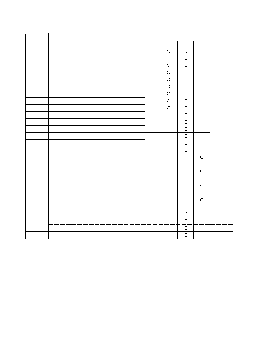
52
CHAPTER 3 CPU ARCHITECTURE
Address
Special-Function Register (SFR) Name
Symbol
R/W
Manipulatable Bit Unit
After Reset
1 bit
8 bits
16 bits
FF00H
Port 0
P0
R/W
--
00H
FF01H
Port 1
P1
R
--
--
FF02H
Port 2
P2
R/W
Note
--
FF03H
Port 3
P3
--
FF04H
Port 4
P4
R/W
--
FF05H
Port 5
P5
--
FF06H
Port 6
P6
--
FF08H
Port 8
P8
--
FF09H
Port 9
P9
--
FF0AH
8-bit compare register 1
CR1
--
--
FF0BH
8-bit compare register 2
CR2
--
--
FF0CH
8-bit compare register 3
CR3
--
--
FF0DH
8-bit counter 1
TM1
R
--
--
FF0EH
8-bit counter 2
TM2
--
--
FF0FH
8-bit counter 3
TM3
--
--
FF10H
Capture register 00
CR00
--
--
0000H
FF11H
FF12H
Capture register 01
CR01
--
--
FF13H
FF14H
Capture register 02
CR02
--
--
FF15H
FF16H
16-bit timer register
TM0
--
--
FF17H
FF18H
Serial I/O shift register
SIO
R/W
--
--
00H
FF19H
Transmit shift register
TXS
W
--
--
FFH
Receive buffer register
RXB
R
--
--
FFH
FF1BH
A/D conversion result register
ADCR1
R
--
--
00H
Note When PM2 and PM3 are set to 00H, read operation is enabled. Moreover, when PM2 and PM3 are set to
FFH, these ports go into a high-impedance state.
Table 3-5. Special Function Register List (1/3)

53
CHAPTER 3 CPU ARCHITECTURE
Address
Special-Function Register (SFR) Name
Symbol
R/W
Manipulatable Bit Unit
After Reset
1 bit
8 bits
16 bits
FF20H
Port mode register 0
PM0
R/W
--
FFH
FF22H
Port mode register 2
PM2
--
FF23H
Port mode register 3
PM3
--
FF24H
Port mode register 4
PM4
--
FF25H
Port mode register 5
PM5
--
FF26H
Port mode register 6
PM6
--
FF28H
Port mode register 8
PM8
--
FF29H
Port mode register 9
PM9
--
FF30H
Pull-up resistor option register
PU0
--
00H
FF40H
Clock output selection register
CKS
--
FF41H
Watch timer mode control register
WTM
--
FF42H
Watchdog timer clock select register
WDCS
--
FF48H
External interrupt rising edge enable register
EGP
--
FF49H
External interrupt falling edge enable register
EGN
--
FF4AH
LCD timer control register
LCDTM
W
--
FF61H
Compare register (sin side)
MCMP10
R/W
--
FF62H
Compare register (cos side)
MCMP11
--
FF63H
Compare register (sin side)
MCMP20
--
FF64H
Compare register (cos side)
MCMP21
--
FF65H
Compare register (sin side)
MCMP30
--
FF66H
Compare register (cos side)
MCMP31
--
FF67H
Compare register (sin side)
MCMP40
--
FF68H
Compare register (cos side)
MCMP41
--
FF69H
Timer mode control register
MCNTC
--
FF6AH
Port mode control register
PMC
--
FF6BH
Compare control register 1
MCMPC1
--
FF6CH
Compare control register 2
MCMPC2
--
FF6DH
Compare control register 3
MCMPC3
--
FF6EH
Compare control register 4
MCMPC4
--
FF70H
Prescaler mode register
PRM0
--
FF71H
Capture pulse control register
CRC0
--
FF72H
16-bit timer mode control register
TMC0
--
FF73H
Timer clock select register 1
TCL1
--
--
FF74H
Timer clock select register 2
TCL2
--
--
FF75H
Timer clock select register 3
TCL3
--
--
Table 3-5. Special Function Register List (2/3)

54
CHAPTER 3 CPU ARCHITECTURE
Address
Special-Function Register (SFR) Name
Symbol
R/W
Manipulatable Bit Unit
After Reset
1 bit
8 bits
16 bits
FF76H
8-bit timer mode control register 1
TMC1
R/W
--
04H
FF77H
8-bit timer mode control register 2
TMC2
--
FF78H
8-bit timer mode control register 3
TMC3
--
FF80H
A/D converter mode register
ADM1
--
00H
FF81H
Analog input channel specification register
ADS1
--
FF82H
Power-fail compare mode register
PFM
--
FF83H
Power-fail compare threshold value register
PFT
--
FF84H
Serial operation mode register
CSIM
--
FF85H
Asynchronous serial interface mode register
ASIM
--
FF86H
Asynchronous serial interface status register
ASIS
R
--
--
FF87H
Baud rate generator control register
BRGC
R/W
--
--
FF89H
D/A converter mode register
DAM1
W
--
FF90H
EEPROM write control register
EEWC
R/W
--
FF94H
Sound generator control register
SGCR
--
FF95H
Sound generator buzzer control register
SGBR
--
FF96H
Sound generator amplitude register
SGAM
--
FFA0H
Oscillator mode register
Note 1
OSCM
--
FFB0H
LCD display mode register
LCDM
--
FFB2H
LCD display control register
LCDC
--
FFE0H
Interrupt request flag register 0L
IF0
IF0L
FFE1H
Interrupt request flag register 0H
IF0H
FFE2H
Interrupt request flag register 1L
IF1L
--
FFE4H
Interrupt mask flag register 0L
MK0 MK0L
FFH
FFE5H
Interrupt mask flag register 0H
MK0H
FFE6H
Interrupt mask flag register 1L
MK1L
--
FFE8H
Priority specify flag register 0L
PR0
PR0L
FFE9H
Priority specify flag register 0H
PR0H
FFEAH
Priority specify flag register 1L
PR1L
--
FFF0H
Memory size switching register
IMS
--
--
CFH
Note 2
FFF9H
Watchdog timer mode register
WDTM
--
00H
FFFAH
Oscillation stabilization time select register
OSTS
--
--
04H
FFFBH
Processor clock control register
PCC
--
Notes 1.
�
PD780973(A) only
2. The initial value of this register is CFH. Set the following value to this register of each model.
�
PD780973(A): 06H
�
PD78F0974 (to set the same memory map as
�
PD780973(A)): 06H
Table 3-5. Special Function Register List (3/3)
55
CHAPTER 3 CPU ARCHITECTURE
3.3 Instruction Address Addressing
An instruction address is determined by program counter (PC) contents and is normally incremented (+1 for each
byte) automatically according to the number of bytes of an instruction to be fetched each time another instruction is
executed. When a branch instruction is executed, the branch destination information is set to the PC and branched
by the following addressing (For details of instructions, refer to 78K/0 SERIES USER'S MANUAL Instructions
(U12326E)).
3.3.1 Relative addressing
[Function]
The value obtained by adding 8-bit immediate data (displacement value: jdisp8) of an instruction code to the
start address of the following instruction is transferred to the program counter (PC) and branched. The
displacement value is treated as signed two's complement data (�128 to +127) and bit 7 becomes a sign bit.
In other words, relative addressing consists in relative branching from the start address of the following instruction
to the �128 to +127 range.
This function is carried out when the BR $addr16 instruction or a conditional branch instruction is executed.
[Operation]
15
0
PC
+
15
0
8
7
6
S
15
0
PC
jdisp8
When S = 0, all bits of
are 0.
When S = 1, all bits of
are 1.
PC indicates the start address
of the instruction
after the BR instruction.
...
56
CHAPTER 3 CPU ARCHITECTURE
3.3.2 Immediate addressing
[Function]
Immediate data in the instruction word is transferred to the program counter (PC) and branched.
This function is carried out when the CALL !addr16 or BR !addr16 or CALLF !addr11 instruction is executed.
CALL !addr16 and BR !addr16 instructions can be branched to the entire memory space. The CALLF !addr11
instruction is branched to the 0800H to 0FFFH area.
[Operation]
In the case of CALL !addr16 and BR !addr16 instructions
In the case of CALLF !addr11 instruction
15
0
PC
8 7
7
0
CALL or BR
Low Addr.
High Addr.
15
0
PC
8 7
7
0
fa
10�8
11 10
0
0
0
0
1
6
4
3
CALLF
fa
7�0
57
CHAPTER 3 CPU ARCHITECTURE
3.3.3 Table indirect addressing
[Function]
Table contents (branch destination address) of the particular location to be addressed by bits 1 to 5 of the
immediate data of an operation code are transferred to the program counter (PC) and branched.
This function is carried out when the CALLT [addr5] instruction is executed.
This instruction references the address stored in the memory table from 40H to 7FH, and allows branching to
the entire memory space.
[Operation]
3.3.4 Register addressing
[Function]
Register pair (AX) contents to be specified with an instruction word are transferred to the program counter (PC)
and branched.
This function is carried out when the BR AX instruction is executed.
[Operation]
15
1
15
0
PC
7
0
Low Addr.
High Addr.
Memory (Table)
Effective Address+1
Effective Address
0
1
0
0
0
0
0
0
0
0
8
7
8
7
6
5
0
0
1
1
1
7
6
5
1
0
ta
4�0
Operation Code
7
0
rp
0
7
A
X
15
0
PC
8
7

58
CHAPTER 3 CPU ARCHITECTURE
3.4 Operand Address Addressing
The following methods are available to specify the register and memory (addressing) which undergo manipulation
during instruction execution.
3.4.1 Implied addressing
[Function]
The register which functions as an accumulator (A and AX) in the general register is automatically (implicitly)
addressed.
Of the
�
PD780973 Subseries instruction words, the following instructions employ implied addressing.
Instruction
Register to be Specified by Implied Addressing
MULU
Register A for multiplicand and register AX for product storage
DIVUW
Register AX for dividend and quotient storage
ADJBA/ADJBS
Register A for storage of numeric values subject to decimal adjustment
ROR4/ROL4
Register A for storage of digit data subject to digit rotation
[Operand format]
Because implied addressing can be automatically employed with an instruction, no particular operand format is
necessary.
[Description example]
In the case of MULU X
With an 8-bit
�
8-bit multiply instruction, the product of A register and X register is stored in AX. In this example,
the A and AX registers are specified by implied addressing.

59
CHAPTER 3 CPU ARCHITECTURE
3.4.2 Register addressing
[Function]
The general register to be specified is accessed as an operand with the register specify code (Rn and RPn) in
an operation code and with the register bank select flags (RBS0 and RBS1).
Register addressing is carried out when an instruction with the following operand format is executed. When an
8-bit register is specified, one of the eight registers is specified with 3 bits in the operation code.
[Operand format]
Identifier
Description
r
X, A, C, B, E, D, L, H
rp
AX, BC, DE, HL
`r' and `rp' can be described with function names (X, A, C, B, E, D, L, H, AX, BC, DE and HL) as well as absolute
names (R0 to R7 and RP0 to RP3).
[Description example]
MOV A, C; when selecting C register as r
Operation code
0 1 1 0 0 0 1 0
Register specify code
INCW DE; when selecting DE register pair as rp
Operation code
1 0 0 0 0 1 0 0
Register specify code

60
CHAPTER 3 CPU ARCHITECTURE
3.4.3 Direct addressing
[Function]
The memory to be manipulated is addressed with immediate data in an instruction word becoming an operand
address.
[Operand format]
Identifier
Description
addr16
Label or 16-bit immediate data
[Description example]
MOV A, !0FE00H; when setting !addr16 to FE00H
Operation code
1 0 0 0 1 1 1 0
OP code
0 0 0 0 0 0 0 0
00H
1 1 1 1 1 1 1 0
FEH
[Operation]
Memory
0
7
addr16 (lower)
addr16 (upper)
OP code
61
CHAPTER 3 CPU ARCHITECTURE
3.4.4 Short direct addressing
[Function]
The memory to be manipulated in the fixed space is directly addressed with 8-bit data in an instruction word.
This addressing is applied to the 256-byte space FE20H to FF1FH. An internal high-speed RAM and a special-
function register (SFR) are mapped at FE20H to FEFFH and FF00H to FF1FH, respectively.
If the SFR area (FF00H to FF1FH) where short direct addressing is applied, ports which are frequently accessed
in a program and a compare register of the timer/event counter and a capture register of the timer/event counter
are mapped and these SFRs can be manipulated with a small number of bytes and clocks.
When 8-bit immediate data is at 20H to FFH, bit 8 of an effective address is set to 0. When it is at 00H to 1FH,
bit 8 is set to 1. Refer to [Operation] below.
[Operand format]
Identifier
Description
saddr
Label or FE20H to FF1FH immediate data
saddrp
Label or FE20H to FF1FH immediate data (even address only)
[Description example]
MOV 0FE30H, #50H; when setting saddr to FE30H and immediate data to 50H
Operation code
0 0 0 1 0 0 0 1
OP code
0 0 1 1 0 0 0 0
30H (saddr-offset)
0 1 0 1 0 0 0 0
50H (immediate data)
[Operation]
When 8-bit immediate data is 20H to FFH,
= 0
When 8-bit immediate data is 00H to 1FH,
= 1
15
0
Short Direct Memory
Effective Address
1
1
1
1
1
1
1
8 7
0
7
OP code
saddr-offset
62
CHAPTER 3 CPU ARCHITECTURE
3.4.5 Special-function register (SFR) addressing
[Function]
The memory-mapped special-function register (SFR) is addressed with 8-bit immediate data in an instruction
word.
This addressing is applied to the 240-byte spaces FF00H to FFCFH and FFE0H to FFFFH. However, the SFR
mapped at FF00H to FF1FH can be accessed with short direct addressing.
[Operand format]
Identifier
Description
sfr
Special-function register name
sfrp
16-bit manipulatable special-function register name (even address only)
[Description example]
MOV PM0, A; when selecting PM0 (FF20H) as sfr
Operation code
1 1 1 1 0 1 1 0
OP code
0 0 1 0 0 0 0 0
20H (sfr-offset)
[Operation]
15
0
SFR
Effective Address
1
1
1
1
1
1
1
8 7
0
7
OP code
sfr-offset
1
63
CHAPTER 3 CPU ARCHITECTURE
3.4.6 Register indirect addressing
[Function]
This addressing is to address a memory area to be manipulated by using as an operand address the contents
of a register pair specified by the register bank select flags (RBS0 and RBS1) and the register pair specification
code in the operation code. This addressing can be carried out for all the memory spaces.
[Operand format]
Identifier
Description
--
[DE], [HL]
[Description example]
MOV A, [DE]; when selecting [DE] as register pair
Operation code
1 0 0 0 0 1 0 1
[Operation]
16
0
8
D
7
E
0
7
7 0
A
DE
The contents of the memory
addressed are transferred.
Memory
The memory address
specified with the
register pair DE

64
CHAPTER 3 CPU ARCHITECTURE
3.4.7 Based addressing
[Function]
8-bit immediate data is added as offset data to the contents of the base register, that is, the HL register pair in
an instruction word of the register bank specified with the register bank select flags (RBS0 and RBS1) and the
sum is used to address the memory. Addition is performed by expanding the offset data as a positive number
to 16 bits. A carry from the 16th bit is ignored. This addressing can be carried out for all the memory spaces.
[Operand format]
Identifier
Description
--
[HL + byte]
[Description example]
MOV A, [HL + 10H]; when setting byte to 10H
Operation code
1 0 1 0 1 1 1 0
0 0 0 1 0 0 0 0
3.4.8 Based indexed addressing
[Function]
The B or C register contents specified in an instruction word are added to the contents of the base register, that
is, the HL register pair in an instruction word of the register bank specified with the register bank select flags
(RBS0 and RBS1) and the sum is used to address the memory.
Addition is performed by expanding the B or C register contents as a positive number to 16 bits. A carry from
the 16th bit is ignored. This addressing can be carried out for all the memory spaces.
[Operand format]
Identifier
Description
--
[HL + B], [HL + C]
[Description example]
In the case of MOV A, [HL + B]
Operation code
1 0 1 0 1 0 1 1

65
CHAPTER 3 CPU ARCHITECTURE
3.4.9 Stack addressing
[Function]
The stack area is indirectly addressed with the stack pointer (SP) contents.
This addressing method is automatically employed when the PUSH, POP, subroutine call and RETURN
instructions are executed or the register is saved/reset upon generation of an interrupt request.
Stack addressing enables to address the internal high-speed RAM area only.
[Description example]
In the case of PUSH DE
Operation code
1 0 1 1 0 1 0 1

66
[MEMO]

67
CHAPTER 4 EEPROM
4.1 EEPROM Functions
The
�
PD780973 Subseries products contain on-chip 256
�
8-bit EEPROM (Electrically Erasable PROM) in addition
to internal high-speed RAM, as data memory.
EEPROM differs from ordinary RAM in that its contents are saved even after power is cut off. Moreover, unlike
EPROM, its contents can be erased electrically without using UV light. For this reason, it is suitable for applications
where the setting values of the odometer and trip meter on the dash board are saved, etc.
EEPROM can be manipulated with 8-bit memory manipulation instructions.
The EEPROM contained on-chip in the
�
PD780973 Subseries has the following features.
(1) Written contents are saved even when the power is cut off.
(2) Can be manipulated with 8-bit memory manipulation instructions in the same way as ordinary RAM.
(3) Erasure and writing is performed in the time set with EWCS0 and EWCS1 (EEPROM write control register (EEWC)
bits 4 and 5) (see Figure 4-2). Therefore, the write time control software load is reduced. Moreover, during writing,
instructions other than instructions related to EEPROM writing and reading can also be executed.
� Rewrite frequency for all chips : 1,000,000 times
� Rewrite frequency per 1 byte : 100,000 times
Caution The values shown above are target values. These values are subject to change without notice,
so please contact your NEC sales representative for the latest value before designing.
(4) When write is completed, interrupt request signal (INTWE) is issued.
(5) The write enabled/disabled status can be checked with EWST (EEPROM write control register (EEWC) bit 1).

68
CHAPTER 4 EEPROM
4.2 EEPROM Configuration
EEPROM is composed of EEPROM itself and a control area.
The control area consists of the EEPROM write control register (EEWC) that controls EEPROM writing, and
an area that generates an interrupt request signal (INTWE) upon detecting write termination.
Figure 4-1. EEPROM Block Diagram
INTWE
EWCS1 EWCS0 EWCC
EWE
EWST
EEPROM
(256
�
8 bits)
Prescaler
Read/write
controller
EEPROM timer
Data latch
f
X
Internal bus
EEPROM write control register (EEWC)
Address
latch
Write termination
69
CHAPTER 4 EEPROM
4.3 EEPROM Control Register
EEPROM is controlled with the EEPROM write control register (EEWC).
EEWC is set with either a 1-bit or 8-bit memory manipulation instruction.
RESET input sets EEWC to 00H.
Figure 4-2. EEPROM Write Control Register (EEWC) Format
Address: FF90H After Reset : 00H R/W
Symbol
7
6
5
4
3
2
1
0
EEWC
0
0
EWCS1
EWCS0
0
EWCC
EWST
EWE
EWCS1
EWCS0
EEPROM Write Time
0
0
(2
14
+ 2
10
)/f
X
Note 1
0
1
(2
15
+ 2
11
)/f
X
Note 2
Other than above
Setting prohibited
EWCC
EEPROM Operation Control
0
Operating mode
1
EEPROM stop
EWST
EEPROM Write Status
0
Not currently writing to EEPROM (EEPROM write/read is enabled. However, when
EWE = 0, write is disabled)
1
Currently writing to EEPROM (EEPROM write/read is disabled)
EWE
EEPROM Write Operation Control
0
EEPROM write disabled
1
EEPROM write enabled
Notes 1. Set the main system clock frequency (f
X
) in the range of 4 to 5.120 MHz.
2. Set the main system clock frequency (f
X
) in the range of 5.364 to 8.38 MHz.
Cautions 1. If the main system clock frequency is set in the range of 5.120 < f
X
< 5.364 MHz, the EEPROM
cannot be used.
2. When EWE is cleared (to 0) during EEPROM writing, writing is immediately interrupted.
Data that was being written becomes undefined. Be sure to clear EWE before stopping the
main system clock during the write period.
3. After EWCC is cleared (to 0), set a wait time of 20
�
s or more by software to read EEPROM
contents.
4. Be sure to check that EWST is 0 before performing EEPROM access.
5. Bits 3, 6, and 7 must be set to 0.

70
CHAPTER 4 EEPROM
4.4 EEPROM Reading
Reading of EEPROM data is performed with the following procedure.
<1> Check that EWST (EEPROM write control register (EEWC) bit 1) is 0 (EEPROM writing is not in
progress).
<2> Execute read instruction.
Cautions 1. Before reading, be sure to check that EWST is 0. If an EEPROM read instruction is executed
during EEPROM write, read values are undefined.
2. If reading EEPROM contents immediately after changing EWCC (EEPROM write control
register (EEWC) bit 2) from 1 to 0, set a wait time of at least 20
�
s by software.
If no wait time is set, the correct values cannot be read.
Example: Insertion of NOP instructions to set wait time of 20
�
s or more.
CLR1 EWCC
NOP
Insert NOP instructions to secure a wait time of 20
�
s or more.
NOP
MOV A,!0F800H

71
CHAPTER 4 EEPROM
4.5 EEPROM Writing
Data writing to EEPROM is performed with the following procedure.
<1> Check that EWST (EEPROM write control register (EEWC) bit 1) is 0 (EEPROM writing is not in
progress).
<2> Set the write time with EWCS0 and EWCS1 (EEWC bits 4 and 5).
<3> Set EWE (EEWC bit 0) to 1 (EEPROM writing enabled).
<4> Execute write instruction.
If performing several write operations in succession, perform the next write operation after the current write
operation has been completed. The following methods can be used for write termination and time control.
(1) Method using write termination interrupt request (INTWE)
After writing 1 data, wait for generation of write termination interrupt request while processing other than write
is performed. When write termination interrupt request is generated, start next write operation.
(2) Method using write status flag (EWST)
Poll EWST (EEPROM write control register (EEWC) bit 1), and wait for EWST to become 0. When EWST becomes
0, start the next write operation.
4.6 EEPROM Control-Related Interrupt
EEPROM write termination interrupt request (INTWE) is generated from EEPROM.
INTWE is an interrupt request generated upon termination of EEPROM writing.
This interrupt request is generated when the time set with EWCS0 and EWCS1 (EEPROM write control register
(EEWC) bits 4 and 5) has elapsed.
When this interrupt request is generated, data writing to EEPROM is terminated, indicating that writing of the
next data is enabled.

72
CHAPTER 4 EEPROM
4.7 Cautions regarding EEPROM Writing
The following shows cautions of EEPROM write.
Before performing EEPROM write, be sure to read the following cautions.
(1) Before writing, be sure to check that EWST (EEPROM write control register (EEWC) bit 1) is 0. If executing
another write instructions during EEPROM writing, the instruction executed last will be ignored.
(2) For write time, see Figure 4-2.
(3) If performing several write operations in succession, be sure to wait until the current write operation is completed
before starting the next one.
(4) Even if the mode changes to HALT mode during EEPROM writing, writing is continued.
(5) If the mode changes to STOP mode during EEPROM writing, the data being written becomes undefined. If this
STOP mode is cancelled by interrupt request, a write termination interrupt request (INTWE) is generated after
the STOP mode has been cancelled. If you want to set the STOP mode after normally terminating write
processing, check that write processing has ended using any of the available methods (refer to 4.5 EEPROM
Writing), then set the STOP mode.
(6) If you want to read the EEPROM contents immediately after changing EWCC (EEPROM write control register
(EEWC) bit 2) from 1 to 0, set a wait time of 20
�
s or more by software. If no wait time is set, the data read will
not be correct.
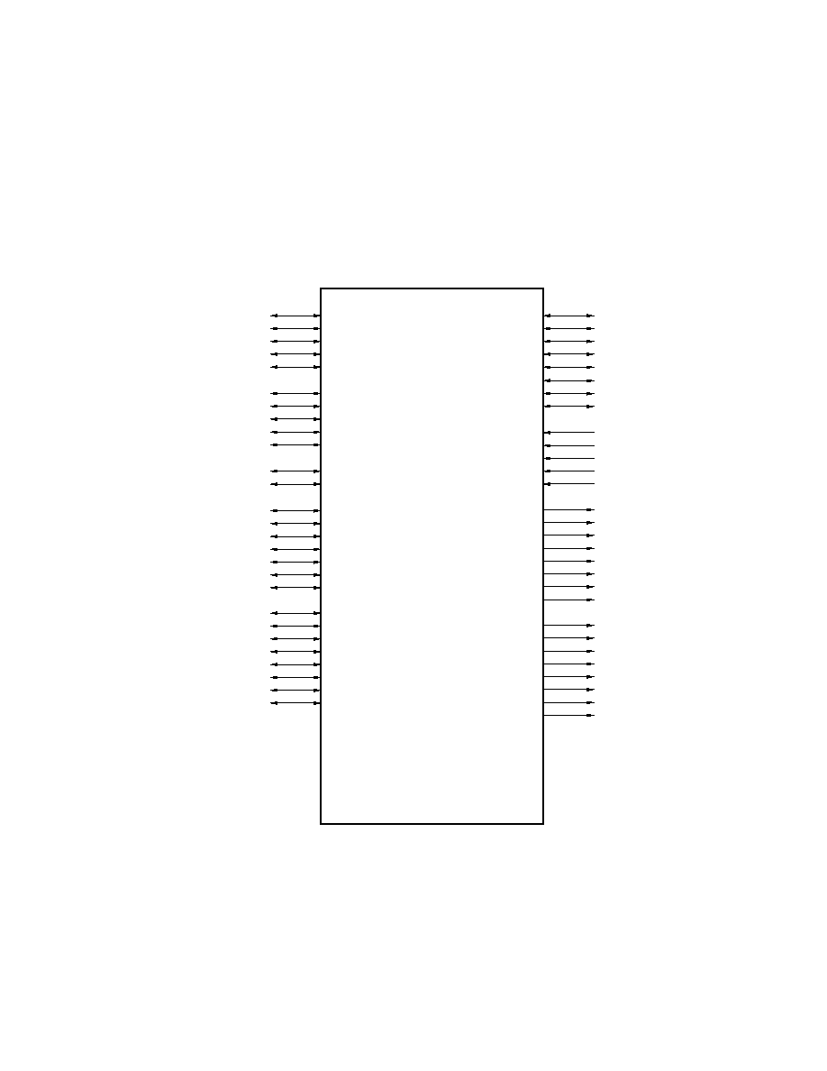
73
CHAPTER 5 PORT FUNCTIONS
5.1 Port Functions
The
�
PD780973 Subseries are provided with five input port pins, sixteen output port pins, and thirty-five input/output
port pins. Figure 5-1 shows the port configuration. Every port can be manipulated in 1-bit or 8-bit units controlled
in various ways. Moreover, the port pins can also serve as I/O pins of the internal hardware.
Figure 5-1. Port Types
P00
Port 0
P10
Port 1
P14
P20
Port 2
P27
P30
Port 4
Port 5
Port 6
Port 9
P40
P44
P50
P54
P60
P61
Port 8
P81
P87
P90
P97
Port 3
P37
P07
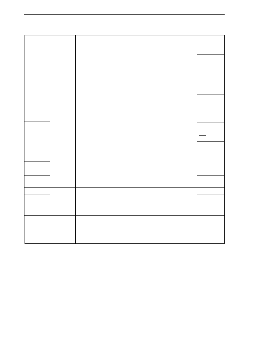
74
CHAPTER 5 PORT FUNCTIONS
Table 5-1. Port Functions
Pin Name
Input/Output
Function
Alternate
Function
P00 to P02
Input/Output
INTP0 to INTP2
P03 to P07
--
P10 to P14
Input
Port 1
ANI0 to ANI4
5-bit input only port.
P20 to P23
Output
Port 2
SM11 to SM14
P24 to P27
8-bit output only port.
SM21 to SM24
P30 to P33
Output
Port 3
SM31 to SM34
P34 to P37
8-bit output only port.
SM41 to SM44
P40 to P42
Input/Output
TI00 to TI02
P43, P44
TIO2, TIO3
P50
Input/Output
Port 5
SCK
P51
5-bit input/output port.
SO
P52
Input/output mode can be specified bit-wise.
SI
P53
RxD
P54
TxD
P60
Input/Output
PCL/SGOA
P61
SGO/SGOF
P81
Input/Output
S19/TPO
P82 to P87
S18 to S13
P90 to P97
Input/Output
Port 9
S12 to S5
8-bit input/output port.
Input/output mode can be specified bit-wise.
Can be set in input/output port or segment output mode in 2-bit units by
using LCD display control register (LCDC).
Port 0
8-bit input/output port.
Input/output mode can be specified bit-wise.
If used as an input port, an on-chip pull-up resistor can be used by
software.
Port 4
5-bit input/output port.
Input/output mode can be specified bit-wise.
Port 6
2-bit input/output port.
Input/output mode can be specified bit-wise.
Port 8
7-bit input/output port.
Input/output mode can be specified bit-wise.
Can be set in input/output port or segment output mode in 2-bit units by
using LCD display control register (LCDC).
75
CHAPTER 5 PORT FUNCTIONS
5.2 Port Configuration
A port consists of the following hardware:
Table 5-2. Port Configuration
Item
Configuration
Control register
Port mode register (PMm: m = 0, 2 to 6, 8, 9)
Pull-up resistor option register (PU0)
Port
Total: 56 lines (5 inputs, 16 outputs, 35 inputs/outputs)
Pull-up resistor
Total: 8 (software specifiable: 8)
5.2.1 Port 0
Port 0 is an 8-bit input/output port with output latch. P00 to P07 pins can specify the input mode/output mode in
1-bit units with the port mode register 0 (PM0). When P00 to P07 pins are used as input ports, an on-chip pull-up
resistor can be used to them in 1-bit units with a pull-up resistor option register (PU0).
Alternate functions include external interrupt request input.
RESET input sets port 0 to input mode.
Figure 5-2 shows a block diagram of port 0.
Caution
Because port 0 also serves for external interrupt request input, when the port function output
mode is specified and the output level is changed, the interrupt request flag is set. Thus, when
the output mode is used, set the interrupt mask flag to 1.
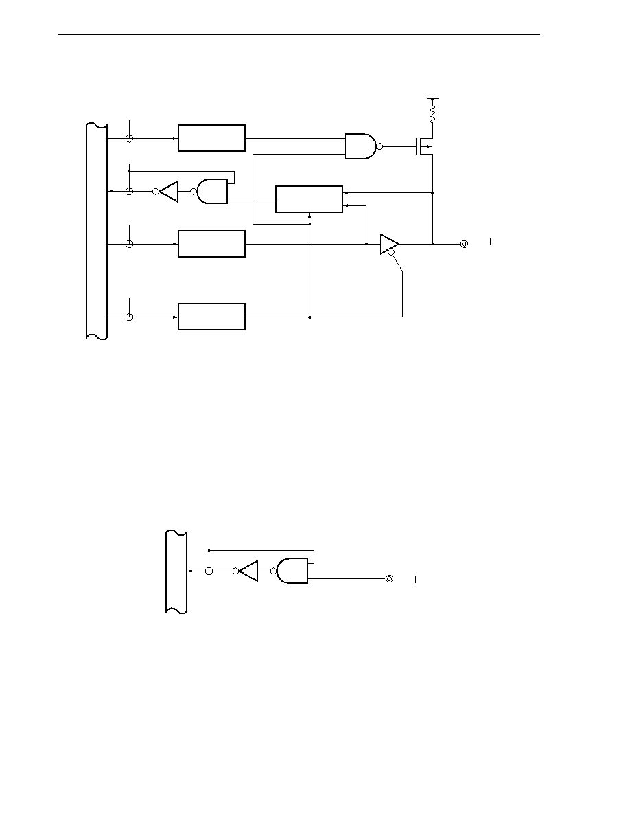
76
CHAPTER 5 PORT FUNCTIONS
Figure 5-2. P00 to P07 Block Diagram
RD
P00/INTP0
P02/INTP2
P03 to P07
P-ch
WR
PUO
WR
PORT
WR
PM
PU00 to PU07
Output latch
(P00 to P07)
PM00 to PM07
Selector
V
DD
Internal bus
PU : Pull-up resistor option register
PM : Port mode register
RD : Port 0 read signal
WR : Port 0 write signal
5.2.2 Port 1
Port 1 is a 5-bit input only port.
Alternate functions include an A/D converter analog input.
Figure 5-3 shows a block diagram of port 1.
Figure 5-3. P10 to P14 Block Diagram
RD
P10/ANI0
P14/ANI4
Internal bus
RD : Port 1 read signal

77
CHAPTER 5 PORT FUNCTIONS
5.2.3 Port 2
Port 2 is an 8-bit output only port with output latch. P20 to P27 pins go into a high-impedance state when the ENn
of port mode control register (PMC) is set to 0 and the port mode register 2 (PM2) is set to 1.
Alternate functions include meter control PWM output.
RESET input sets port 2 to high-impedance state.
Figure 5-4 shows a block diagram of port 2.
Figure 5-4. P20 to P27 Block Diagram
PM : Port mode register
RD : Port 2 read signal
WR : Port 2 write signal
Caution
When PM2 is set to 0, read operation is enabled. When PM2 is set to 1, read operation is disabled.
Remark
n = 1, 2
P20/SM11 to P23/SM14
P24/SM21 to P27/SM24
WR
PORT
WR
PM
Output latch
(P20 to P27)
Selector
Decoder
PM20 to PM27
2
Alternate
functions
Internal bus
RD
DIRn1 DIRn0
MODn ENn
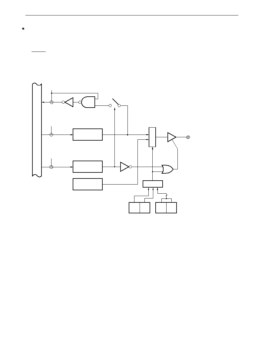
78
CHAPTER 5 PORT FUNCTIONS
5.2.4 Port 3
Port 3 is an 8-bit output only port with output latch. P30 to P37 pins go into a high-impedance state when the ENn
of port mode control register (PMC) is set to 0 and the port mode register 3 (PM3) is set to 1.
Alternate functions include meter control PWM output.
RESET input sets port 3 to high-impedance state.
Figure 5-5 shows a block diagram of port 3.
Figure 5-5. P30 to P37 Block Diagram
PM : Port mode register
RD
: Port 3 read signal
WR : Port 3 write signal
Caution
When PM3 is set to 0, read operation is enabled. When PM3 is set to 1, read operation is disabled.
Remark
n = 3, 4
P30/SM31 to P33/SM34
P34/SM41 to P37/SM44
WR
PORT
WR
PM
Output latch
(P30 to P37)
PM30 to PM37
Alternate
functions
Internal bus
RD
Selector
Decoder
2
DIRn1 DIRn0
MODn ENn
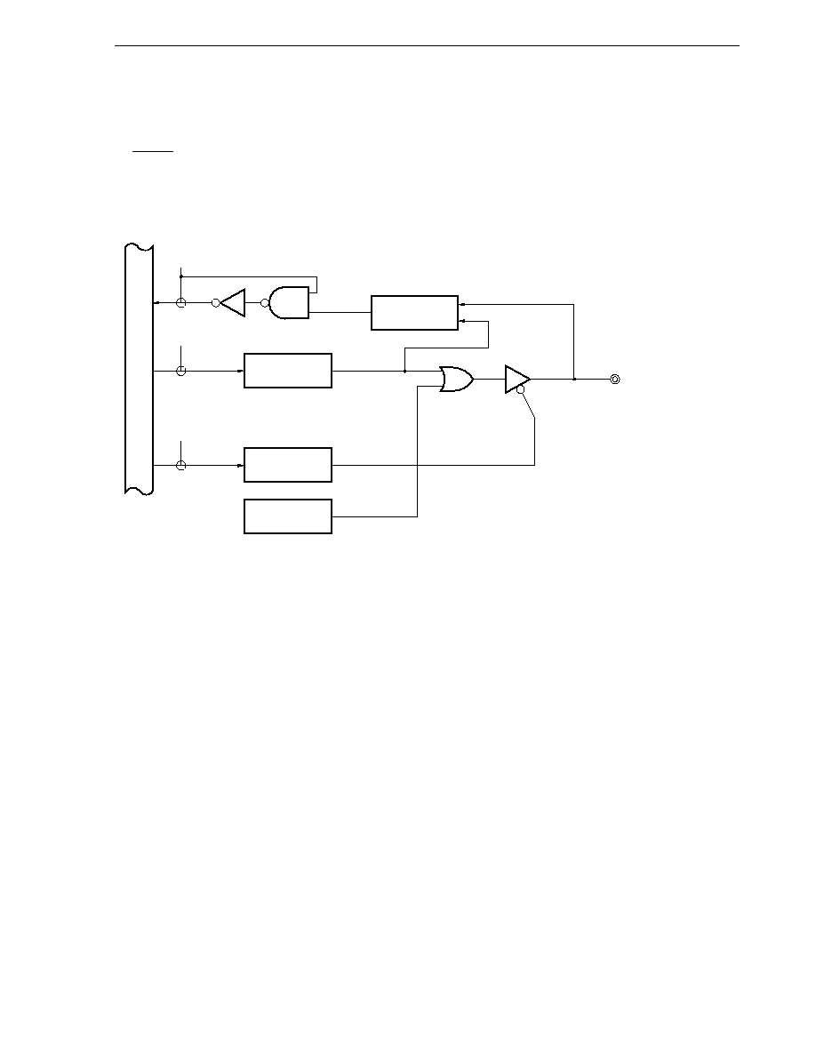
79
CHAPTER 5 PORT FUNCTIONS
5.2.5 Port 4
Port 4 is a 5-bit input/output port with output latch. P40 to P44 pins can specify the input mode/output mode in
1-bit units with the port mode register 4 (PM4).
Alternate functions also include timer input/output.
RESET input sets port 4 to input mode.
Figure 5-6 shows a block diagram of port 4.
Figure 5-6. P40 to P44 Block Diagram
PM
: Port mode register
RD
: Port 4 read signal
WR
: Port 4 write signal
RD
P40/TI00 to P42/TI02
P43/TIO2
P44/TIO3
WR
PORT
WR
PM
Output latch
(P40 to P44)
PM40 to PM44
Alternate
functions
Selector
Internal bus
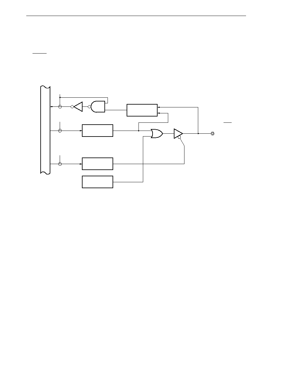
80
CHAPTER 5 PORT FUNCTIONS
5.2.6 Port 5
Port 5 is a 5-bit input/output port with output latch. P50 to P54 pins can specify the input mode/output mode in
1-bit units with the port mode register 5 (PM5).
Alternate functions include serial interface data input/output and clock input/output.
RESET input sets port 5 to input mode.
Figure 5-7 shows a block diagram of port 5.
Figure 5-7. P50 to P54 Block Diagram
PM : Port mode register
RD : Port 5 read signal
WR : Port 5 write signal
RD
P50/SCK
P51/SO
P52/SI
P53/RxD
P54/TxD
WR
PORT
WR
PM
Output latch
(P50 to P54)
PM50 to PM54
Alternate
functions
Selector
Internal bus
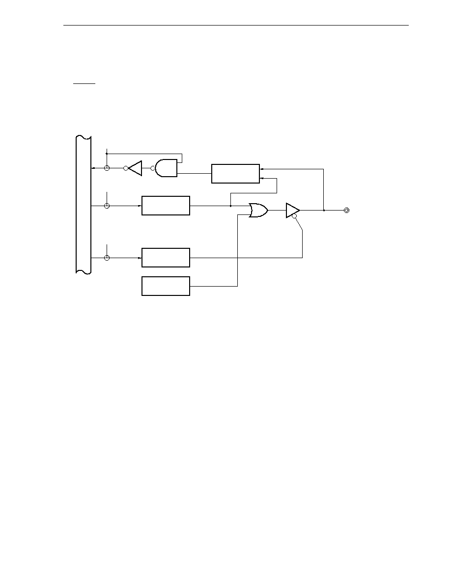
81
CHAPTER 5 PORT FUNCTIONS
5.2.7 Port 6
Port 6 is a 2-bit input/output port with output latch. P60 and P61 pins can specify the input mode/output mode
in 1-bit units with the port mode register 6 (PM6).
Alternate functions include clock output and sound generator output.
RESET input sets port 6 to input mode.
Figure 5-8 shows a block diagram of port 6.
Figure 5-8. P60 and P61 Block Diagram
PM : Port mode register
RD : Port 6 read signal
WR : Port 6 write signal
RD
P60/PCL/SGOA
P61/SGO/SGOF
WR
PORT
WR
PM
Output latch
(P60, P61)
PM60, PM61
Alternate
functions
Selector
Internal bus
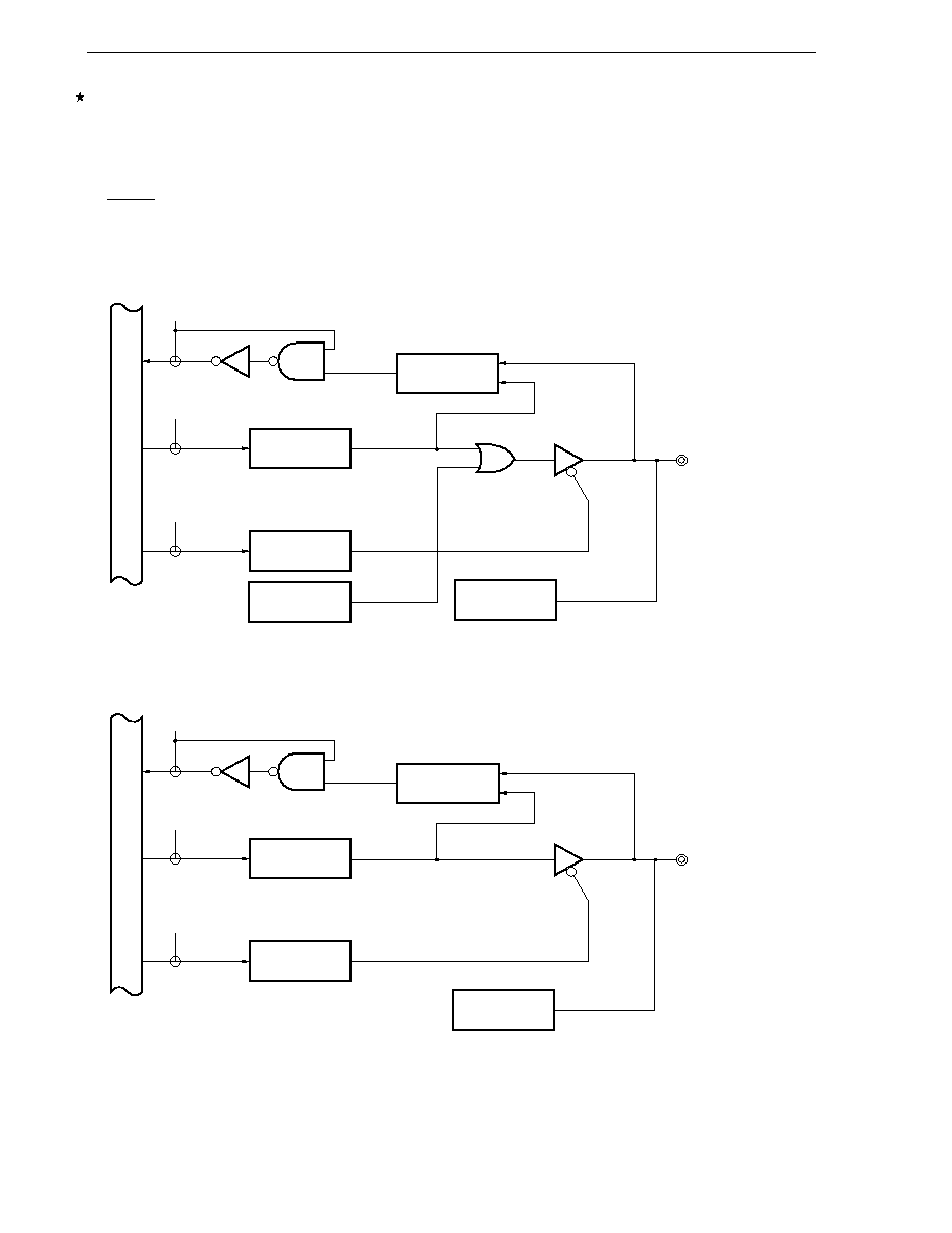
82
CHAPTER 5 PORT FUNCTIONS
5.2.8 Port 8
Port 8 is a 7-bit input/output port with output latch. P81 to P87 pins can specify the input mode/output mode in
1-bit units with the port mode register 8 (PM8).
Alternate functions also include segment signal output of the LCD controller/driver and prescaler signal output.
Segment output and input/output port can be switched by setting the LCD display control register (LCDC).
RESET input sets port 8 to input mode.
Figures 5-9 and 5-10 show block diagrams of port 8.
Figure 5-9. P81 Block Diagram
Figure 5-10. P82 to P87 Block Diagram
PM : Port mode register
RD : Port 8 read signal
WR : Port 8 write signal
RD
P81/S19/TPO
WR
PORT
WR
PM
PM81
Selector
Output latch
(P81)
Internal bus
Segment output
function
Alternate
functions
RD
P82/S18 to P87/S13
WR
PORT
WR
PM
PM82 to PM87
Selector
Output latch
(P82 to P87)
Internal bus
Segment output
function
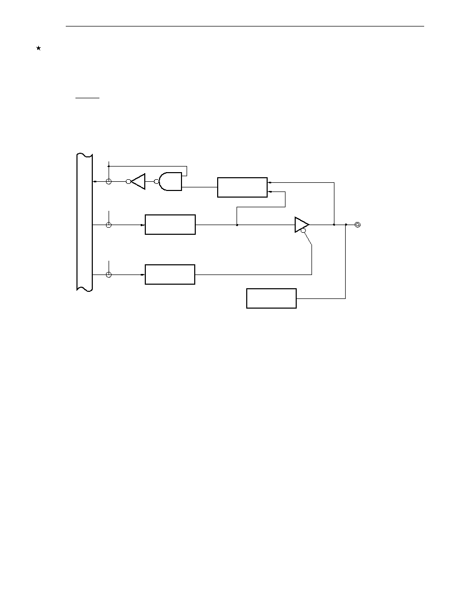
83
CHAPTER 5 PORT FUNCTIONS
5.2.9 Port 9
Port 9 is an 8-bit input/output port with output latch. P90 to P97 pins can specify the input mode/output mode in
1-bit units with the port mode register 9 (PM9).
Alternate functions also include segment signal output of the LCD controller/driver.
Segment output and input/output port can be switched by setting the LCD display control register (LCDC).
RESET input sets port 9 to input mode.
Figure 5-11 shows a block diagram of port 9.
Figure 5-11. P90 to P97 Block Diagram
PM : Port mode register
RD : Port 9 read signal
WR : Port 9 write signal
RD
P90/S12 to P97/S5
WR
PORT
WR
PM
PM90 to PM97
Selector
Output latch
(P90 to P97)
Internal bus
Segment output
function

84
CHAPTER 5 PORT FUNCTIONS
5.3 Port Function Control Registers
The following two types of registers control the ports.
� Port mode registers (PM0, PM2 to PM6, PM8, PM9)
� Pull-up resistor option register (PU0)
(1) Port mode registers (PM0, PM2 to PM6, PM8, PM9)
These registers are used to set port input/output in 1-bit units.
PM0, PM2 to PM6, PM8, and PM9 are independently set with a 1-bit or 8-bit memory manipulation instruction.
RESET input sets registers to FFH.
Cautions 1. Pins P10 and P14 are input-only pins, and pins P20 to P27 and P30 to P37 are output-
only pins.
2. Port 0 has an alternate function as external interrupt request input, when the port function
output mode is specified and the output level is changed, the interrupt request flag is
set. When the output mode is used, therefore, the interrupt mask flag should be set to
1 beforehand.
3. Ports 2 and 3 that can be also used as meter driving PWM signal output pins go into a
high-impedance state when 1 is set to PM2
�
and PM3
�
, respectively.
85
CHAPTER 5 PORT FUNCTIONS
Table 5-3. Port Mode Register and Output Latch Settings when Using Alternate Functions
Notes 1. If these ports are read out when these pins are used in the alternate function mode, undefined
values are read.
2. The P20 to P27 and P30 to P37 pins have an alternate function as meter driving PWM signal output.
When 0 is set to ENn (n = 1 to 4) of port mode control register (PMC) and 1 is set to PM
��
, these
pins go into the high-impedance state. Refer to the port mode register format.
3. When the P81 to P87 and P90 to P97 pins are used for alternate functions, set the function with
the LCD display control register (LCDC).
Caution
When port 5 is used for serial interface, the I/O latch or output latch must be set according
to their function. For the setting methods, see Figure 14-2 Asynchronous Serial Interface
Mode Register (ASIM) Format and Figure 15-2 Serial Operation Mode Register (CSIM)
Format.
Remark
�
: don't care
PM
��
: port mode register
P
��
: port output latch
P00
INTP0
Input
1
�
P01
INTP1
Input
1
�
P02
INTP2
Input
1
�
P10 to P14
Note 1
ANI0 to ANI4
Input
1
�
P20 to P27
SM11 to SM24
Output
0
Note 2
�
P30 to P37
SM31 to SM44
Output
0
Note 2
�
P40 to P42
TI00 to TI02
Input
1
�
P43, P44
TIO2, TIO3
Output
0
0
P60
SGOA/PCL
Output
0
0
P61
SGO/SGOF
Output
0
0
P81, P82 to P87
S19/TPO, S18 to S13 Output
�
Note 3
P90 to P97
S12 to S5
Output
�
Note 3
Alternate Functions
Name
P
��
PM
��
Input/Output
Pin Name
86
CHAPTER 5 PORT FUNCTIONS
Figure 5-12. Port Mode Register (PM0, PM4 to PM6, PM8, PM9) Format
Address: FF20H After Reset : FFH R/W
Symbol
7
6
5
4
3
2
1
0
PM0
PM07
PM06
PM05
PM04
PM03
PM02
PM01
PM00
Address: FF24H After Reset : FFH R/W
Symbol
7
6
5
4
3
2
1
0
PM4
1
1
1
PM44
PM43
PM42
PM41
PM40
Address: FF25H After Reset : FFH R/W
Symbol
7
6
5
4
3
2
1
0
PM5
1
1
1
PM54
PM53
PM52
PM51
PM50
Address: FF26H After Reset : FFH R/W
Symbol
7
6
5
4
3
2
1
0
PM6
1
1
1
1
1
1
PM61
PM60
Address: FF28H After Reset : FFH R/W
Symbol
7
6
5
4
3
2
1
0
PM8
PM87
PM86
PM85
PM84
PM83
PM82
PM81
1
Address: FF29H After Reset : FFH R/W
Symbol
7
6
5
4
3
2
1
0
PM9
PM97
PM96
PM95
PM94
PM93
PM92
PM91
PM90
PMmn
Pmn Pin Input/Output Mode Select (m = 0, 4 to 6, 8, 9 ; n = 0 to 7)
0
Output Mode (Output buffer on)
1
Input Mode (Output buffer off)
Figure 5-13. Port Mode Register (PM2, PM3) Format
Address: FF22H After Reset : FFH R/W
Symbol
7
6
5
4
3
2
1
0
PM2
PM27
PM26
PM25
PM24
PM23
PM22
PM21
PM20
Address: FF23H After Reset : FFH R/W
Symbol
7
6
5
4
3
2
1
0
PM3
PM37
PM36
PM35
PM34
PM33
PM32
PM31
PM30
PMmn
Pmn Pin Input/Output Mode Select (m = 2, 3 ; n = 0 to 7)
0
Output Mode (Output buffer on)
1
High-impedance state (Output buffer off)
Note
Note When 0 is set to ENn of port mode control register (PMC)

87
CHAPTER 5 PORT FUNCTIONS
(2) Pull-up resistor option register (PU0)
This register is used to set whether to use an internal pull-up resistor at port 0 or not. A pull-up resistor is internally
used at bits which are set to the input mode at a port where pull-up resistor use has been specified with PU0.
No pull-up resistors can be used to the bits set to the output mode irrespective of PU0 setting.
PU0 is set with a 1-bit or 8-bit memory manipulation instruction.
RESET input sets this register to 00H.
Figure 5-14. Pull-Up Resistor Option Register (PU0) Format
Address: FF30H After Reset : 00H R/W
Symbol
7
6
5
4
3
2
1
0
PU0
PU07
PU06
PU05
PU04
PU03
PU02
PU01
PU00
PU0m
P0m Pin Internal Pull-Up Resistor Select (m = 0 to 7)
0
On-chip pull-up resistor not used
1
On-chip pull-up resistor used

88
CHAPTER 5 PORT FUNCTIONS
5.4 Port Function Operations
Port operations differ depending on whether the input or output mode is set, as shown below.
5.4.1 Writing to input/output port
(1) Output mode
A value is written to the output latch by a transfer instruction, and the output latch contents are output from the
pin.
Once data is written to the output latch, it is retained until data is written to the output latch again.
(2) Input mode
A value is written to the output latch by a transfer instruction, but since the output buffer is OFF, the pin status
does not change.
Once data is written to the output latch, it is retained until data is written to the output latch again.
Caution
In the case of 1-bit memory manipulation instruction, although a single bit is manipulated,
the port is accessed as an 8-bit unit. Therefore, on a port with a mixture of input and output
pins, the output latch contents for pins specified as input are undefined, even for bits other
than the manipulated bit.
5.4.2 Reading from input/output port
(1) Output mode
The output latch contents are read by a transfer instruction. The output latch contents do not change.
(2) Input mode
The pin status is read by a transfer instruction. The output latch contents do not change.
5.4.3 Operations on input/output port
(1) Output mode
An operation is performed on the output latch contents, and the result is written to the output latch. The output
latch contents are output from the pins.
Once data is written to the output latch, it is retained until data is written to the output latch again.
(2) Input mode
The output latch contents are undefined, but since the output buffer is OFF, the pin status does not change.
Caution
In the case of 1-bit memory manipulation instruction, although a single bit is manipulated,
the port is accessed as an 8-bit unit. Therefore, on a port with a mixture of input and output
pins, the output latch contents for pins specified as input are undefined, even for bits other
than the manipulated bit.
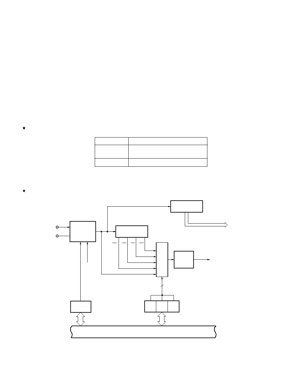
89
CHAPTER 6 CLOCK GENERATOR
6.1 Clock Generator Functions
The clock generator generates the clock to be supplied to the CPU and peripheral hardware.
� Main system clock oscillator
This circuit oscillates at frequencies of 4.19 to 8.38 MHz. Oscillation can be stopped by executing the STOP
instruction or setting the processor clock control register (PCC).
6.2 Clock Generator Configuration
The clock generator consists of the following hardware.
Table 6-1. Clock Generator Configuration
Item
Configuration
Control register
Processor clock control register (PCC)
Oscillator mode register (OSCM)
Note
Oscillator
Main system clock oscillator
Note
�
PD780973(A) only
Figure 6-1. Clock Generator Block Diagram
X1
X2
Main system
clock oscillator
HALFOSC
f
X
Prescaler
f
X
2
f
X
2
2
f
X
2
3
f
X
2
4
Prescaler
Clock to
peripheral
hardware
CPU clock
(f
CPU
)
Standby
control
circuit
Selector
STOP
PCC2 PCC1
3
PCC0
Processor clock control register
Oscillator mode register
Internal bus
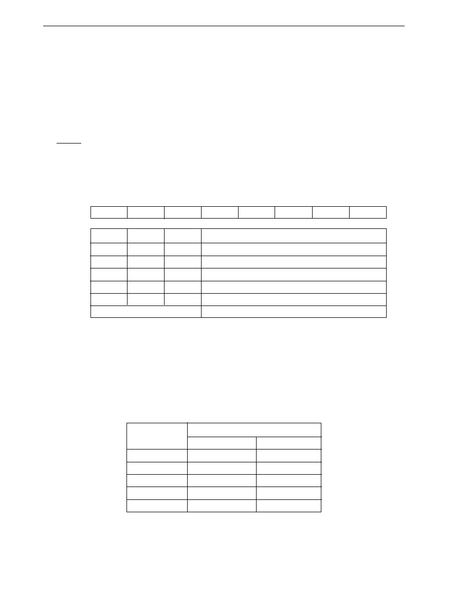
90
CHAPTER 6 CLOCK GENERATOR
6.3 Clock Generator Control Register
The following two types of registers are used to control the clock generator.
� Processor clock control register (PCC)
� Oscillator mode register (OSCM)
(1) Processor clock control register (PCC)
The PCC sets the division ratio of the CPU clock.
The PCC is set with a 1-bit or 8-bit memory manipulation instruction.
RESET input sets the PCC to 04H.
Figure 6-2. Processor Clock Control Register (PCC) Format
Address: FFFBH After Reset: 04H R/W
Symbol
7
6
5
4
3
2
1
0
PCC
0
0
0
0
0
PCC2
PCC1
PCC0
PCC2
PCC1
PCC0
CPU Clock (f
CPU
) Select
0
0
0
f
X
0
0
1
f
X
/2
0
1
0
f
X
/2
2
0
1
1
f
X
/2
3
1
0
0
f
X
/2
4
Other than above
Setting prohibited
Caution
Bits 3 to 7 must be set to 0.
Remark
f
X
: Main system clock oscillation frequency
The fastest instructions of the
�
PD780973 Subseries are executed in two CPU clocks. Therefore, the relation
between the CPU clock (f
CPU
) and the minimum instruction execution time is as shown in Table 6-2.
Table 6-2. Relation between CPU Clock and Minimum Instruction Execution Time
CPU Clock (f
CPU
)
Minimum Instruction Execution Time: 2/f
CPU
f
X
= 8 MHz
f
X
= 8.38 MHz
f
X
0.25
�
s
0.24
�
s
f
X
/2
0.5
�
s
0.48
�
s
f
X
/2
2
1.0
�
s
0.95
�
s
f
X
/2
3
2.0
�
s
1.91
�
s
f
X
/2
4
4.0
�
s
3.81
�
s
Remark
f
X
: Main system clock oscillation frequency
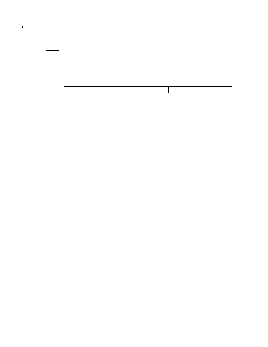
91
CHAPTER 6 CLOCK GENERATOR
(2) Oscillator mode register (OSCM)
The
�
PD780973(A) can be set to the reduced current consumption mode by setting OSCM (only when operated
at f
X
= 4 to 4.19 MHz).
OSCM is set with a 1-bit or 8-bit memory manipulation instruction.
RESET input sets OSCM to 00H.
Figure 6-3. Oscillator Mode Register (OSCM) Format
Address: FFA0H After Reset: 00H R/W
Symbol
7
6
5
4
3
2
1
0
OSCM
HALFOSC
0
0
0
0
0
0
0
HALFOSC
Oscillator Mode Selection
0
Normal operation mode
1
Reduced current consumption mode (only when operated at f
X
= 4 to 4.19 MHz)
Cautions 1. This function is available only when the device is operated at f
X
= 4 to 4.19 MHz. In other cases,
be sure not to set 1 to bit 7.
2. When using in normal operation mode, setting OSCM is not necessary.
3. Only the first setting of OSCM is effective.
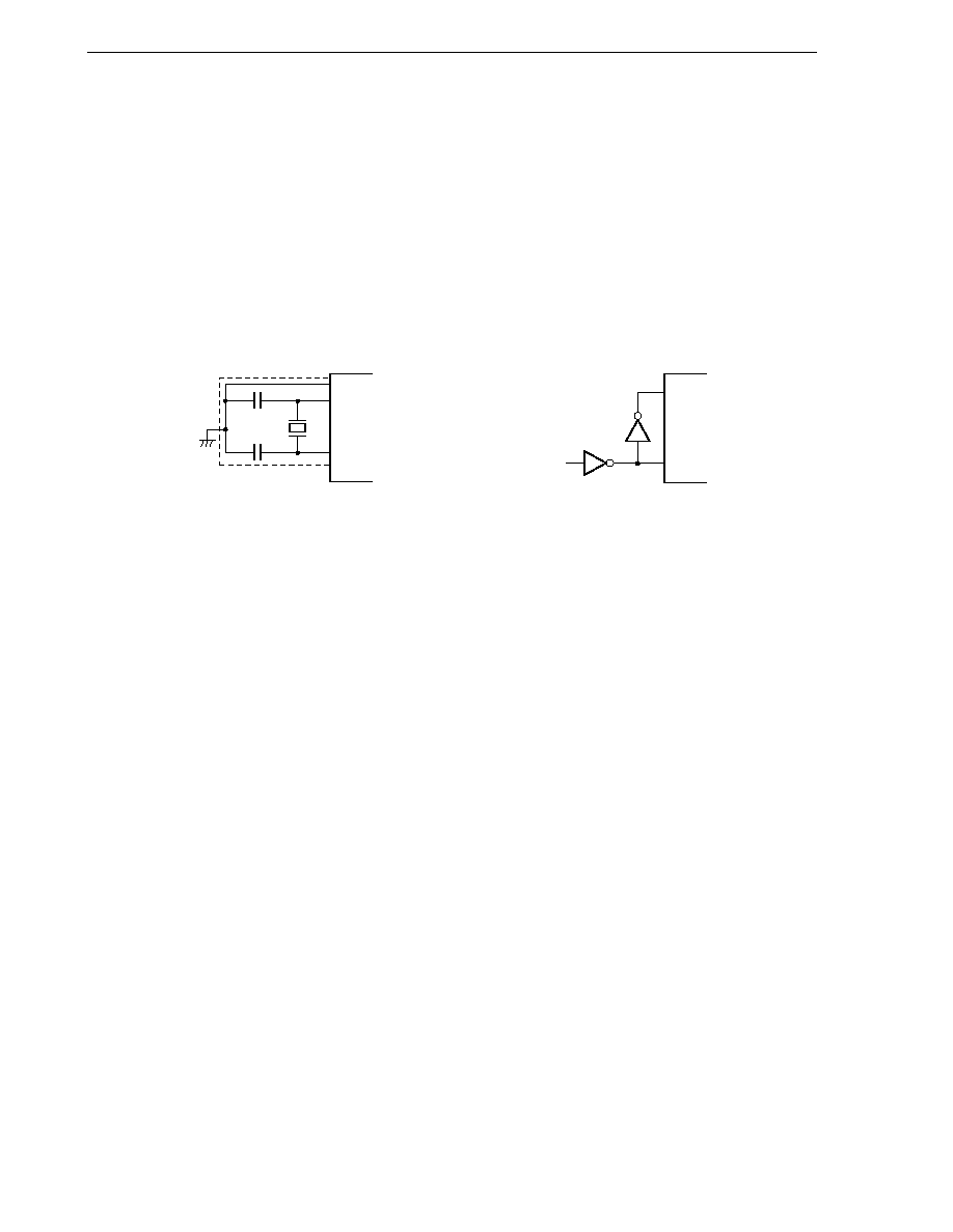
92
CHAPTER 6 CLOCK GENERATOR
6.4 System Clock Oscillator
6.4.1 Main system clock oscillator
The main system clock oscillator oscillates with a crystal resonator or a ceramic resonator (standard: 8.38 MHz)
connected to the X1 and X2 pins.
External clocks can be input to the main system clock oscillator. In this case, input a clock signal to the X1 pin
and an inverted clock signal to the X2 pin.
Figure 6-4 shows an external circuit of the main system clock oscillator.
Figure 6-4. External Circuit of Main System Clock Oscillator
(a) Crystal and ceramic oscillation
(b) External clock
Crystal resonator or
ceramic resonator
X2
X1
PD74HCU04
External
clock
X2
X1
IC
�
Caution
Do not execute the STOP instruction while an external clock is input. This is because if the STOP
instruction is executed, the main system clock operation is stopped, and the X2 pin is connected
to V
DD
, via a pull-up resistor.
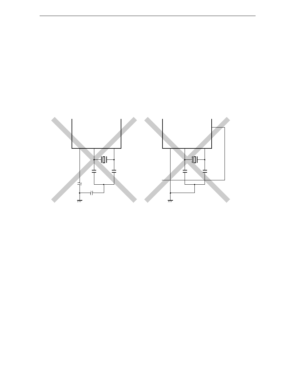
93
CHAPTER 6 CLOCK GENERATOR
Caution
When using a main system clock oscillator, carry out wiring in the broken line area in Figure
6-4 as follows to avoid influence of wiring capacity.
� Keep the wiring length as short as possible.
� Do not cross the wiring with any other signal lines. Do not route the wiring in the vicinity
of a line through which a high alternating current flows.
� Always keep the ground of the capacitor of the oscillator at the same potential as V
SS
. Do
not ground the capacitor to a ground pattern through which a high current flows.
� Do not fetch signals from the oscillator.
Figure 6-5 shows examples of resonator having bad connection.
Figure 6-5. Incorrect Examples of Resonator Connection (1/2)
(a) Too long wiring
(b) Crossed signal line
X1
IC
X2
X2
IC
X1
PORTn
(n = 0 to 6, 8 and 9)
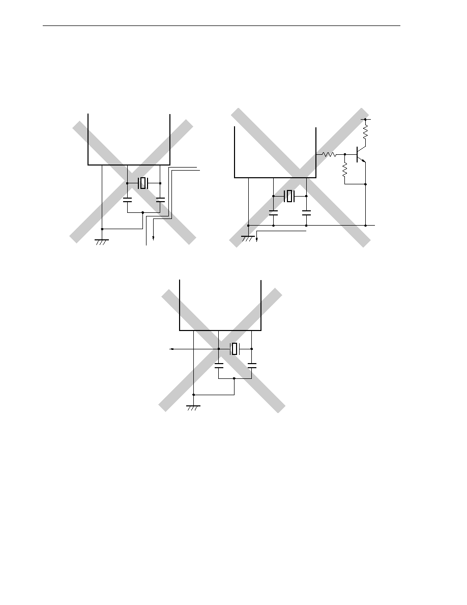
94
CHAPTER 6 CLOCK GENERATOR
Figure 6-5. Incorrect Examples of Resonator Connection (2/2)
(c) Wiring near high alternating current
(d) Current flowing through ground line of
oscillator (potential at points A, B, and C
fluctuates)
IC
X2
X1
IC
X2
X1
A
B
C
Pmn
V
DD
High current
High current
(e) Signals are fetched
IC
X2
X1
6.4.2 Divider circuit
The divider circuit divides the output of the main system clock oscillation circuit (f
X
) to generate various clocks.

95
CHAPTER 6 CLOCK GENERATOR
6.5 Operation of Clock Generator
The clock generator generates the following clocks and controls the operation modes of the CPU, such as the
standby mode:
� Main system clock f
X
� CPU clock f
CPU
� Clock to peripheral hardware
The operation of the clock generator is determined by the processor clock control register (PCC) and oscillator
mode register (OSCM) as follows:
(a) The slowest mode (3.81
�
s: at 8.38-MHz operation) of the main system clock is selected when the RESET
signal is generated (PCC = 04H). While a low level is input to the RESET pin, oscillation of the main system
clock is stopped.
(b) Five types of CPU clocks (0.24
�
s, 0.48
�
s, 0.95
�
s, 1.91
�
s, and 3.81
�
s: at 8.38-MHz operation) can be
selected by the PCC setting.
(c) Two standby modes, STOP and HALT, can be used.
(d) The clock to the peripheral hardware is supplied by dividing the main system clock. The other peripheral
hardware is stopped when the main system clock is stopped (except, however, the external clock input
operation).
(e) The
�
PD780973(A) can be set to the reduced current consumption mode by setting OSCM (only when operated
at f
X
= 4 to 4.19 MHz). Setting 1 to bit 7 (HALFOSC) of OSCM will reduce the power consumption.
Cautions 1. This function is available only when the device is operated at f
X
= 4 to 4.19 MHz. In other cases,
be sure not to set 1 to bit 7.
2. When using in normal operation mode, setting OSCM is not necessary.
3. Only the first setting of OSCM is effective.
96
CHAPTER 6 CLOCK GENERATOR
6.6 Changing Setting of CPU Clock
6.6.1 Time required for switching CPU clock
The CPU clock can be selected by using bits 0 to 2 (PCC0 to PCC2) of the processor clock control register (PCC).
Actually, the specified clock is not selected immediately after the setting of PCC has been changed, and the old
clock is used for the duration of several instructions after that (refer to Table 6-3).
Table 6-3. Maximum Time Required for Switching CPU Clock
Set Value after Switching
PCC2 PCC1 PCC0 PCC2 PCC1 PCC0 PCC2 PCC1 PCC0 PCC2 PCC1 PCC0 PCC2 PCC1 PCC0
PCC2 PCC1 PCC0
0
0
0
0
0
1
0
1
0
0
1
1
1
0
0
0
0
0
16 instructions
16 instructions
16 instructions
16 instructions
0
0
1
8 instructions
8 instructions
8 instructions
8 instructions
0
1
0
4 instructions
4 instructions
4 instructions
4 instructions
0
1
1
2 instructions
2 instructions
2 instructions
2 instructions
1
0
0
1 instruction
1 instruction
1 instruction
1 instruction
Remark
One instruction is the minimum instruction execution time of the CPU clock before switching.
Set Value
before Switching
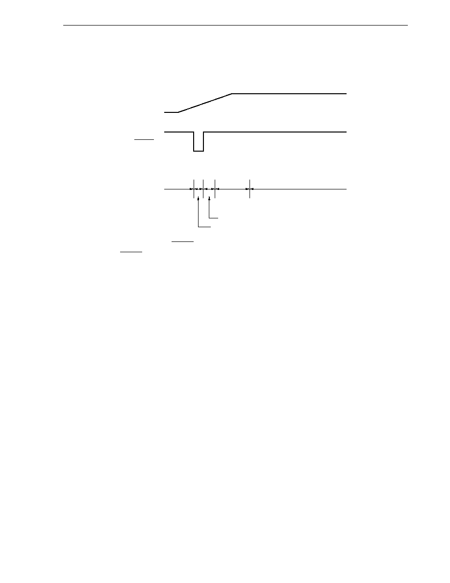
97
CHAPTER 6 CLOCK GENERATOR
6.6.2 Switching CPU clock
The following figure illustrates how the CPU clock switches.
Figure 6-6. Switching CPU Clock
V
DD
RESET
CPU clock
Slowest
operation
Fastest
operation
Wait (15.6 ms: at 8.38-MHz operation)
Internal reset operation
<1> The CPU is reset when the RESET pin is made low on power application. The effect of resetting is released
when the RESET pin is later made high, and the main system clock starts oscillating. At this time, the time
during which oscillation stabilizes (2
17
/f
X
) is automatically secured.
After that, the CPU starts instruction execution at the slowest speed of the main system clock (3.81
�
s: at
8.38-MHz operation).
<2> After the time during which the V
DD
voltage rises to the level at which the CPU can operate at the highest
speed has elapsed, PCC is rewritten so that the highest speed can be selected.

98
[MEMO]

99
CHAPTER 7 16-BIT TIMER 0 TM0
7.1 Outline of Internal Timer of
�
PD780973 Subseries
This chapter explains the 16-bit timer 0. Before that, the internal timers of the
�
PD780973 Subseries, and the
related functions are briefly explained below.
(1) 16-bit timer 0 TM0
The TM0 can be used for pulse widths measurement, divided output of input pulse.
(2) 8-bit timer 1 TM1
The TM1 can be used for an interval timer (See CHAPTER 8 8-BIT TIMER 1 TM1).
(3) 8-bit timer/event counters 2, 3 TM2, TM3
TM2 and TM3 can be used to serve as an interval timer and an external event counter and to output square waves
with any selected frequency, PWM output (See CHAPTER 9 8-BIT TIMER/EVENT COUNTERS 2, 3 TM2, TM3).
(4) Watch timer
This timer can set a flag every 0.5 sec. and simultaneously generates interrupt request at the preset time intervals
(See CHAPTER 10 WATCH TIMER).
(5) Watchdog timer
This timer can perform the watchdog timer function or generate non-maskable interrupt request, maskable
interrupt request and RESET at the preset time intervals (See CHAPTER 11 WATCHDOG TIMER).
(6) Clock output control circuit
Clock output supplies other devices with the divided main system clock (See CHAPTER 12 CLOCK OUTPUT
CONTROL CIRCUIT).
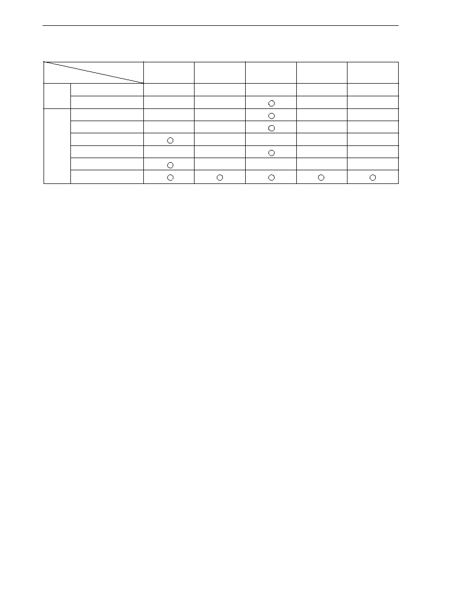
100
CHAPTER 7 16-BIT TIMER 0 TM0
Table 7-1. Timer/Event Counter Operations
16-bit Timer TM0 8-bit Timer TM1
8-bit Timer/Event
Watch Timer
Watchdog Timer
Counter TM2, TM3
Operating
Interval timer
�
1 channel
2 channels
1 channel
Note 1
1 channel
Note 2
mode
External event counter
�
�
�
�
Function
Timer output
�
�
�
�
PWM output
�
�
�
�
Pulse width measurement
�
�
�
�
Square-wave output
�
�
�
�
Divided output
�
�
�
�
Interrupt request
Notes 1. Watch timer can perform both watch timer and interval timer functions at the same time.
2. Watchdog timer can perform either the watchdog timer function or the interval timer function, as
selected.
7.2 16-Bit Timer 0 Functions
The 16-bit timer 0 (TM0) has the following functions.
� Pulse width measurement
� Divided output of input pulse
Figure 7-1 shows 16-bit timer 0 block diagram.
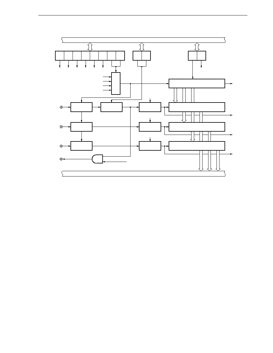
101
CHAPTER 7 16-BIT TIMER 0 TM0
Figure 7-1. Timer 0 (TM0) Block Diagram
(1) Pulse width measurement
TM0 can measure the pulse width of an externally input signal.
(2) Divided output of input pulse
The frequency of an input signal can be divided and the divided signal can be output.
Internal bus
Internal bus
16-bit timer register (TM0)
16-bit capture register (CR02)
Edge detection
circuit
Edge detection
circuit
Edge detection
circuit
ES01, ES00
TPOE
ES11, ES10
ES21, ES20
16-bit capture register (CR01)
16-bit capture register (CR00)
INTOVF
INTTM02
INTTM01
INTTM00
ES21 ES20 ES11
f
X
/8
f
X
/16
f
X
/32
f
X
/64
ES10 ES01
CRC01
TMC02 TPOE
CRC00
ES00 PRM01 PRM00
Prescaler mode
register (PRM0)
Capture pulse control
register (CRC0)
16-bit timer mode control
register (TMC0)
Selector
TI02/P42
TI01/P41
TI00/P40
TPO/P81/S19
Prescaler
1, 1/2, 1/4, 1/8
Noise rejection
circuit
Noise rejection
circuit
Noise rejection
circuit
102
CHAPTER 7 16-BIT TIMER 0 TM0
7.3 16-Bit Timer 0 Configuration
Timer 0 consists of the following hardware.
Table 7-2. Timer 0 Configuration
Item
Configuration
Timer register
16 bits
�
1 (TM0)
Register
Capture register: 16 bits
�
3 (CR00 to CR02)
Control register
16-bit timer mode control register (TMC0)
Capture pulse control register (CRC0)
Prescaler mode register (PRM0)
(1) 16-bit timer register (TM0)
TM0 is a 16-bit read-only register that counts count pulses.
The counter is incremented in synchronization with the rising edge of an input clock. If the count value is read
during operation, input of the count clock is temporarily stopped, and the count value at that point is read. The
count value is reset to 0000H in the following cases:
<1> At RESET input
<2> If TMC02 is cleared
(2) Capture register 00 (CR00)
The valid edge of the TI00 pin can be selected as the capture trigger. Setting of the TI00 valid edge is performed
by setting of the prescaler mode register (PRM0). When the valid edge of the TI00 is detected, an interrupt request
(INTTM00) is generated.
CR00 is read by a 16-bit memory manipulation instruction.
After RESET input, the value of CR00 is undefined.
(3) Capture register 01 (CR01)
The valid edge of the TI01 pin can be selected as the capture trigger. Setting of the TI01 valid edge is performed
by setting of the prescaler mode register (PRM0). When the valid edge of the TI01 is detected, an interrupt request
(INTTM01) is generated.
CR01 is read by a 16-bit memory manipulation instruction.
After RESET input, the value of CR01 is undefined.
(4) Capture register 02 (CR02)
The valid edge of the TI02 pin can be selected as the capture trigger. Setting of the TI02 valid edge is performed
by setting of the prescaler mode register (PRM0). When the valid edge of the TI02 is detected, an interrupt request
(INTTM02) is generated.
CR02 is read by a 16-bit memory manipulation instruction.
After RESET input, the value of CR02 is undefined.
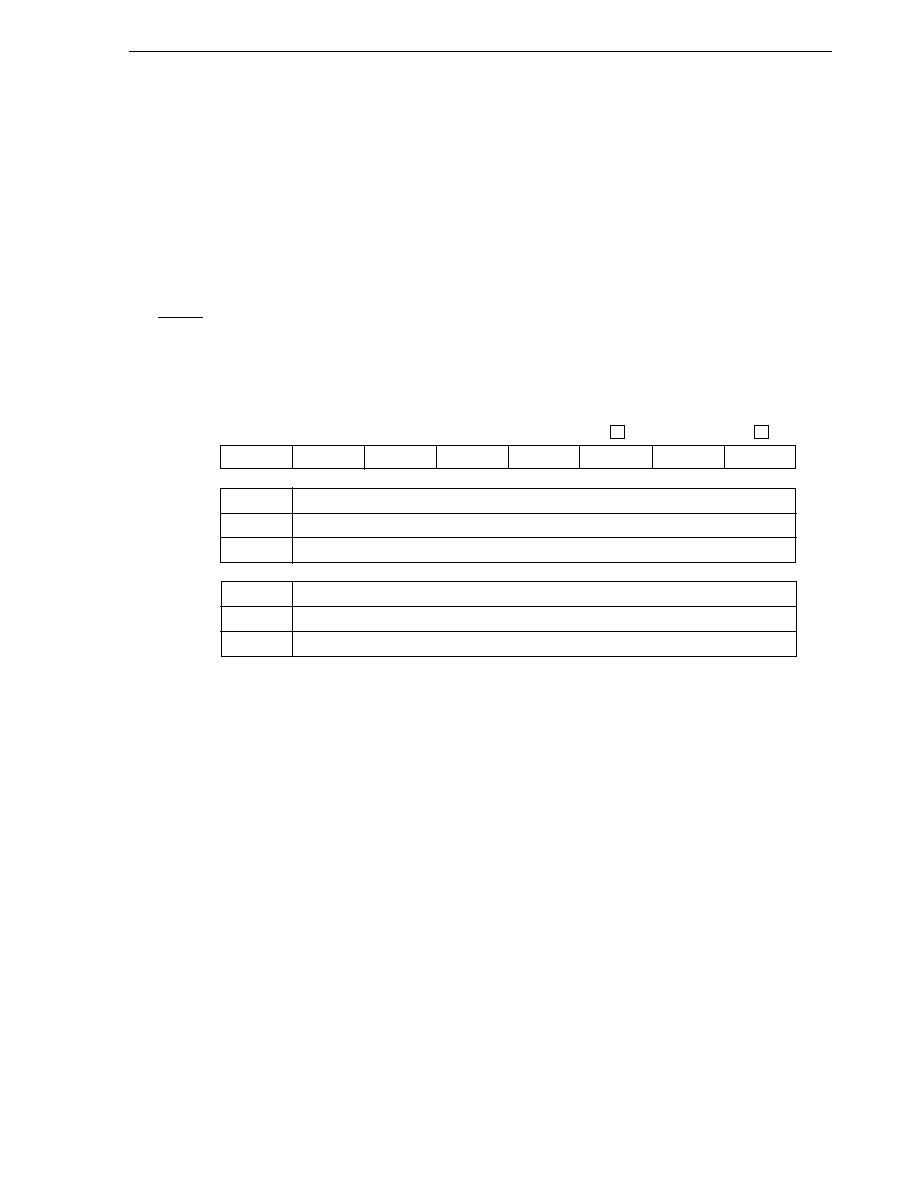
103
CHAPTER 7 16-BIT TIMER 0 TM0
7.4 16-Bit Timer 0 Control Registers
The following three types of registers are used to control timer 0.
� 16-bit timer mode control register (TMC0)
� Capture pulse control register (CRC0)
� Prescaler mode register (PRM0)
(1) 16-bit timer mode control register (TMC0)
This register sets the 16-bit timer operating mode and controls the prescaler output signals.
TMC0 is set with a 1-bit or 8-bit memory manipulation instruction.
RESET input clears TMC0 value to 00H.
Figure 7-2. 16-Bit Timer Mode Control Register (TMC0) Format
Address: FF72H After Reset: 00H R/W
Symbol
7
6
5
4
3
2
1
0
TMC0
0
0
0
0
0
TMC02
0
TPOE
TMC02
Timer 0 Operating Mode Selection
0
Operation stop (TM0 cleared to 0)
1
Operation enabled
TPOE
Timer 0 Prescaler Output Control
0
Prescaler signal output disabled
1
Prescaler signal output enabled
Cautions 1. Before changing the operation mode, stop the timer operation (by setting 0 to TMC02).
2. Bit 1 and bits 3 to 7 must be set to 0.
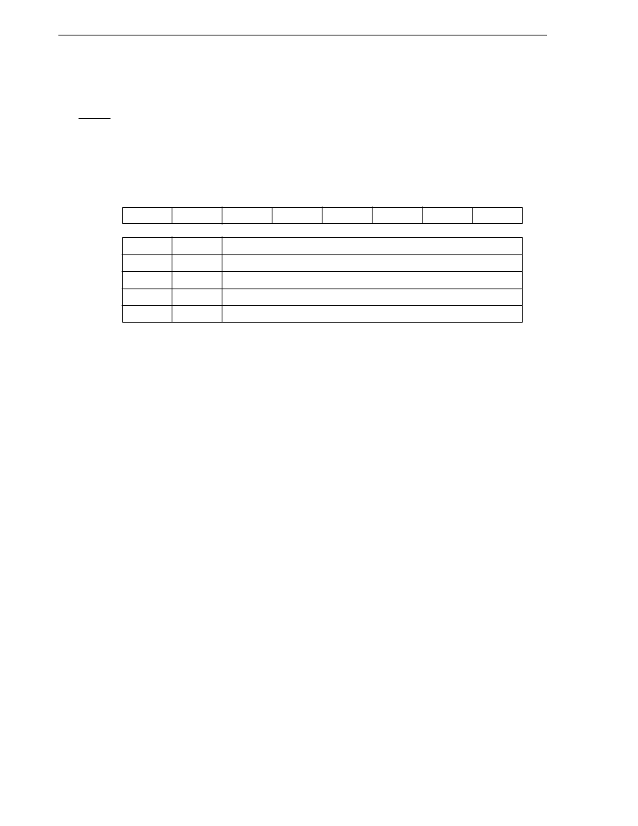
104
CHAPTER 7 16-BIT TIMER 0 TM0
(2) Capture pulse control register (CRC0)
This register specifies the division ratio of the capture pulse input to the 16-bit capture register (CR02) from an
external source.
CRC0 is set with a 1-bit or 8-bit memory manipulation instruction.
RESET input sets CRC0 value to 04H.
Figure 7-3. Capture Pulse Control Register (CRC0) Format
Address: FF71H After Reset: 00H R/W
Symbol
7
6
5
4
3
2
1
0
CRC0
0
0
0
0
0
0
CRC01
CRC00
CRC01
CRC00
Capture Pulse Selection
0
0
Does not divide capture pulse
0
1
Divides capture pulse by 2
1
0
Divides capture pulse by 4
1
1
Divides capture pulse by 8
Cautions 1. Timer operation must be stopped before setting CRC0.
2. Bits 2 to 7 must be set to 0.

105
CHAPTER 7 16-BIT TIMER 0 TM0
(3) Prescaler mode register (PRM0)
This register is used to set 16-bit timer (TM0) count clock and valid edge of TI0n (n = 0 to 2) input.
PRM0 is set with an 8-bit memory manipulation instruction.
RESET input sets PRM0 value to 00H.
Figure 7-4. Prescaler Mode Register (PRM0) Format
Address: FF70H After Reset: 00H R/W
Symbol
7
6
5
4
3
2
1
0
PRM0
ES21
ES20
ES11
ES10
ES01
ES00
PRM01
PRM00
ES21
ES20
TI02 Valid Edge Selection
0
0
Falling edge
0
1
Rising edge
1
0
Setting prohibited
1
1
Both falling and rising edges
ES11
ES10
TI01 Valid Edge Selection
0
0
Falling edge
0
1
Rising edge
1
0
Setting prohibited
1
1
Both falling and rising edges
ES01
ES00
TI00 Valid Edge Selection
0
0
Falling edge
0
1
Rising edge
1
0
Setting prohibited
1
1
Both falling and rising edges
PRM01
PRM00
Count Clock Selection
0
0
f
X
/2
3
0
1
f
X
/2
4
1
0
f
X
/2
5
1
1
f
X
/2
6
Caution
Timer operation must be stopped before setting PRM0.
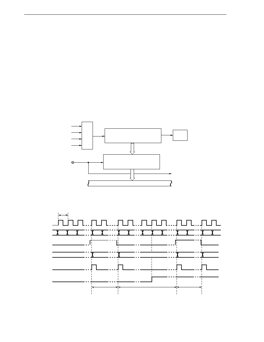
106
CHAPTER 7 16-BIT TIMER 0 TM0
7.5 16-Bit Timer 0 Operations
7.5.1 Pulse width measurement operations
It is possible to measure the pulse width of the signals input to the TI00/P40 to TI02/P42 pins using the
16-bit timer register (TM0). TM0 is used in free-running mode.
(1) Pulse width measurement with free-running counter and one capture register (TI00)
When the edge specified by prescaler mode register (PRM0) is input to the TI00/P40 pin, the value of TM0 is
taken into 16-bit capture register 00 (CR00) and an external interrupt request signal (INTTM00) is set.
Any of three edge specifications can be selected--rising, falling, or both edges--by means of bits 2 and 3 (ES00
and ES01) of PRM0.
For valid edge detection, sampling is performed at the count clock selected by PRM0, and a capture operation
is only performed when a valid level is detected twice, thus eliminating noise with a short pulse width.
Figure 7-5. Configuration Diagram for Pulse Width Measurement by Free-Running Counter
f
X
/2
3
f
X
/2
4
f
X
/2
5
f
X
/2
6
TI00
16-bit timer register (TM0)
INTOVF
16-bit capture register 00 (CR00)
Internal bus
INTTM00
Selector
Figure 7-6.
Timing of Pulse Width Measurement Operation by Free-Running Counter
and One Capture Register (with Both Edges Specified)
t
Count clock
TM0 count
value
Value loaded
to CR00
INTOVF
0000H 0001H
D0
D1
FFFFH 0000H
D2
D3
D3
D2
D1
D0
(D1 � D0)
�
t
(10000H � D1 + D2)
�
t
(D3 � D2)
�
t
TI00 pin
input
INTTM00
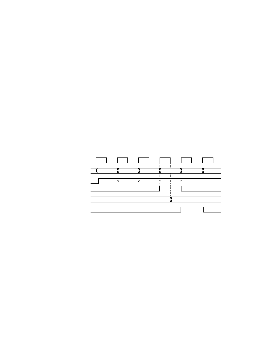
107
CHAPTER 7 16-BIT TIMER 0 TM0
(2) Measurement of three pulse widths with free-running counter
The 16-bit timer register (TM0) allows simultaneous measurement of the pulse widths of the three signals input
to the TI00/P40 to TI02/P42 pins.
When the edge specified by bits 2 and 3 (ES00 and ES01) of prescaler mode register (PRM0) is input to the
TI00/P40 pin, the value of TM0 is taken into 16-bit capture register 00 (CR00) and an external interrupt request
signal (INTTM00) is set.
Also, when the edge specified by bits 4 and 5 (ES10 and ES11) of PRM0 is input to the TI01/P41 pin, the value
of TM0 is taken into 16-bit capture register 01 (CR01) and an external interrupt request signal (INTTM01) is set.
When the edge specified by bits 6 and 7 (ES20 and ES21) of PRM0 is input to the TI02/P42 pin, the value of
TM0 is taken into 16-bit capture register 02 (CR02) and external interrupt request signal (INTTM02) is set.
Any of three edge specifications can be selected--rising, falling, or both edges--as the valid edges for the TI00/
P40 to TI02/P42 pins by means of bits 2 and 3 (ES00 and ES01), bits 4 and 5 (ES10 and ES11), and bits 6 and
7 (ES06 and ES07) of PRM0, respectively.
For TI00/P40 pin valid edge detection, sampling is performed at the interval selected by means of the prescaler
mode register (PRM0), and a capture operation is only performed when a valid level is detected twice, thus
eliminating noise with a short pulse width.
� Capture operation
Capture register operation in capture trigger input is shown.
Figure 7-7. CR0m Capture Operation with Rising Edge Specified
Count clock
TM0
TI0m
Rising edge detection
CR0m
INTTM0m
n�3
n�2
n�1
n
n+1
n
Remark
m = 0 to 2
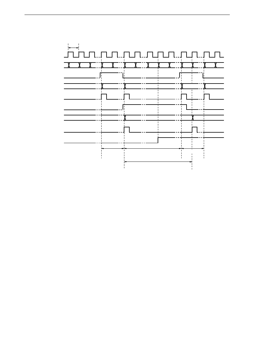
108
CHAPTER 7 16-BIT TIMER 0 TM0
Figure 7-8.
Timing of Pulse Width Measurement Operation by Free-Running Counter
(with Both Edges Specified)
Count clock
TM0 count value
TI0m pin input
Value loaded to CR0m
INTTM0m
TI0n pin input
Value loaded to CR0n
INTTM0n
INTOVF
(D1 � D0)
�
t
(10000H � D0 + D2)
�
t
(10000H � D1 + (D2 + 1)
�
t
(D3 � D2)
�
t
t
0000H 0001H
D0
D1
FFFFH 0000H
D2
D3
D3
D1
D0
D1
D2
Remark
m = 0 to 2, n = 1, 2
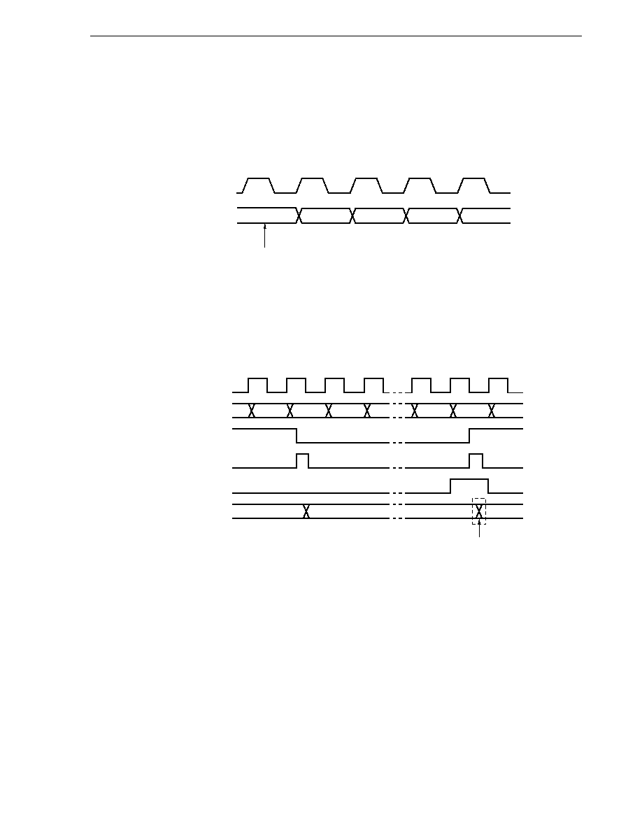
109
CHAPTER 7 16-BIT TIMER 0 TM0
7.6 16-Bit Timer 0 Cautions
(1) Timer start errors
An error with a maximum of one clock may occur until counting is started after timer start. This is because the
16-bit timer register (TM0) is started asynchronously with the count pulse.
Figure 7-9. 16-Bit Timer Register Start Timing
TM0 count value
0000H
0001H
0002H
0004H
Count pulse
Timer start
0003H
(2) Capture register data retention timings
If the valid edge of the TI0m/P4m pin is input during 16-bit capture register 0m (CR0m) read, CR0m performs
capture operation, but the capture value is not guaranteed. However, the interrupt request flag (INTTM0m) is
set upon detection of the valid edge.
Figure 7-10. Capture Register Data Retention Timing
Count pulse
TM0 count value
Edge input
Interrupt request flag
Capture read signal
CR0m interrupt value
N
N+1
N+2
M
M+1
M+2
X
N+1
Capture operation
Remark
m = 0 to 2
(3) Valid edge setting
Set the valid edge of the TI0m/P4m pin after setting bit 2 (TMC02) of the 16-bit timer mode control register to
0, and then stopping timer operation. Valid edge setting is carried out with bits 2 to 7 (ESm0 and ESm1) of the
prescaler mode register (PRM0).
Remark
m = 0 to 2

110
CHAPTER 7 16-BIT TIMER 0 TM0
(4) Occurrence of INTTM0n
INTTM0n occurs even if no capture pulse exists, immediately after the timer operation has been started (TMC02
of TMC0 has been set to 1) with a high level applied to input pins TI00 to TI02 of 16-bit timer 0, and with the
rising edge (with ESn1 and ESn0 of PRM0 set to 0, 1), or both the rising and falling edges (with ESn1 and ESn0
of PRM0 set to 1, 1) selected. However, INTTM0n does not occur if a low level is applied to TI00 to TI02.
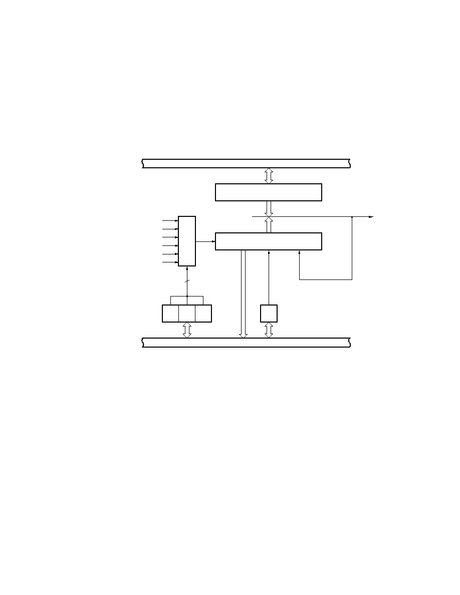
111
CHAPTER 8 8-BIT TIMER 1 TM1
8.1 8-Bit Timer 1 Functions
The 8-bit timer 1 operates as an 8-bit interval timer.
Figure 8-1 shows timer 1 block diagram.
Figure 8-1. Timer 1 (TM1) Block Diagram
Internal bus
Internal bus
8-bit compare register 1 (CR1)
8-bit counter (TM1)
Clear
Coincidence
INTTM1
3
Timer mode control register (TMC1)
Timer clock select register 1 (TCL1)
TCE1
TCL12 TCL11 TCL10
f
X
/2
3
f
X
/2
4
f
X
/2
5
f
X
/2
7
f
X
/2
9
f
X
/2
11
Selector

112
CHAPTER 8 8-BIT TIMER 1 TM1
8.2 8-Bit Timer 1 Configuration
Timer 1 consists of the following hardware.
Table 8-1. Timer 1 Configuration
Item
Configuration
Timer register
8-bit counter 1 (TM1)
Register
8-bit compare register 1 (CR1)
Control register
Timer clock select register 1 (TCL1)
8-bit timer mode control register 1 (TMC1)
Remark
n = 0, 1
(1) 8-bit counter 1 (TM1)
TM1 is an 8-bit read-only register which counts the count pulses.
The counter is incremented in synchronization with the rising edge of the count clock. When count value is read
during operation, count clock input is temporary stopped, and then the count value is read. In the following
situations, the count value is set to 00H.
<1>
RESET input
<2>
Clear TCE1
<3>
Match between TM1 and CR1
(2) 8-bit compare register 1 (CR1)
The value set in the CR1 is constantly compared with the 8-bit counter 1 (TM1) count value, and an interrupt
request (INTTM1) is generated if they match.
It is possible to rewrite the value of CR1 within 00H to FFH during count operation.
113
CHAPTER 8 8-BIT TIMER 1 TM1
8.3 8-Bit Timer 1 Control Registers
The following two types of registers are used to control timer 1.
� Timer clock select register 1 (TCL1)
� 8-bit timer mode control register 1 (TMC1)
(1) Timer clock select register 1 (TCL1)
This register sets count clocks of timer 1.
TCL1 is set with an 8-bit memory manipulation instruction.
RESET input clears to 00H.
Figure 8-2. Timer Clock Select Register 1 (TCL1) Format
Address: FF73H After Reset: 00H R/W
Symbol
7
6
5
4
3
2
1
0
TCL1
0
0
0
0
0
TCL12
TCL11
TCL10
TCL12
TCL11
TCL10
Count Clock Selection
0
0
0
Setting prohibited
0
0
1
Setting prohibited
0
1
0
f
X
/2
3
(1.04 MHz)
0
1
1
f
X
/2
4
(523 kHz)
1
0
0
f
X
/2
5
(261 kHz)
1
0
1
f
X
/2
7
(65.4 kHz)
1
1
0
f
X
/2
9
(16.3 kHz)
1
1
1
f
X
/2
11
(4.09 kHz)
Cautions 1. When rewriting TCL1 to other data, stop the timer operation beforehand.
2. Set bits 3 to 7 to 0.
Remarks 1. f
X
: Main system clock oscillation frequency
2. Figures in parentheses apply to operation with f
X
= 8.38 MHz
114
CHAPTER 8 8-BIT TIMER 1 TM1
(2) 8-bit timer mode control register 1 (TMC1)
TMC1 is a register that controls the counting operation of the 8-bit counter 1 (TM1).
TMC1 is set with a 1-bit or 8-bit memory manipulation instruction.
RESET input sets to 04H.
Figure 8-3 shows TMC1 format.
Figure 8-3. 8-Bit Timer Mode Control Register 1 (TMC1) Format
Address: FF76H After Reset: 04H R/W
Symbol
7
6
5
4
3
2
1
0
TMC1
TCE1
0
0
0
0
1
0
0
TCE1
Timer 1 Count Operation Control
0
After clearing counter to 0, count operation disabled
1
Count operation start
Caution Be sure to set 0 to bit 0, bit 1, and bits 3 to 6, and set 1 to bit 2.
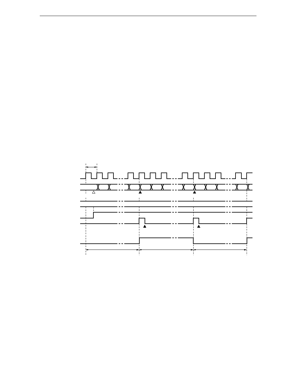
115
CHAPTER 8 8-BIT TIMER 1 TM1
8.4 8-Bit Timer 1 Operations
8.4.1 8-bit interval timer operation
The 8-bit timer 1 operates as an interval timer which generates interrupt requests repeatedly at intervals of the
count value preset to 8-bit compare register 1 (CR1).
When the count values of the 8-bit counter 1 (TM1) match the values set to CR1, counting continues with the TM1
values cleared to 0 and the interrupt request signal (INTTM1) is generated.
Count clock of the TM1 can be selected with bits 0 to 2 (TCL10 to TCL12) of the timer clock select register 1 (TCL1).
[Setting]
<1>
Set the registers.
� TCL1 : Select count clock.
� CR1 : Compare value
<2>
After TCE1 = 1 is set, count operation starts.
<3>
If the values of TM1 and CR1 match, the INTTM1 is generated and TM1 is cleared to 00H.
<4>
INTTM1 generates repeatedly at the same interval. Set TCE1 to 0 to stop count operation.
Figure 8-4. Interval Timer Operation Timings (1/3)
(a) Basic operation
t
Count clock
TM1 count value
CR1
TCE1
INTTM1
TM1 interval time
Note
Start count
Clear
Clear
00H
01H
N
00H
01H
N
00H
01H
N
N
N
N
N
Interrupt received
Interrupt received
Interval time
Interval time
Interval time
Remark
Interval time = (N + 1)
�
t: N = 00H to FFH
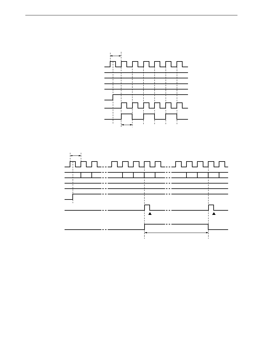
116
CHAPTER 8 8-BIT TIMER 1 TM1
Figure 8-4. Interval Timer Operation Timings (2/3)
(b) When CR1 = 00H
t
Count clock
TM1
CR1
TCE1
INTTM1
TM1 interval time
Interval time
00H
00H
00H
00H
00H
(c) When CR1 = FFH
t
Count clock
TM1
CR1
TCE1
INTTM1
TM1 interval time
01
FE
FF
00
FE
FF
00
FF
FF
FF
Interval time
Interrupt
received
Interrupt received
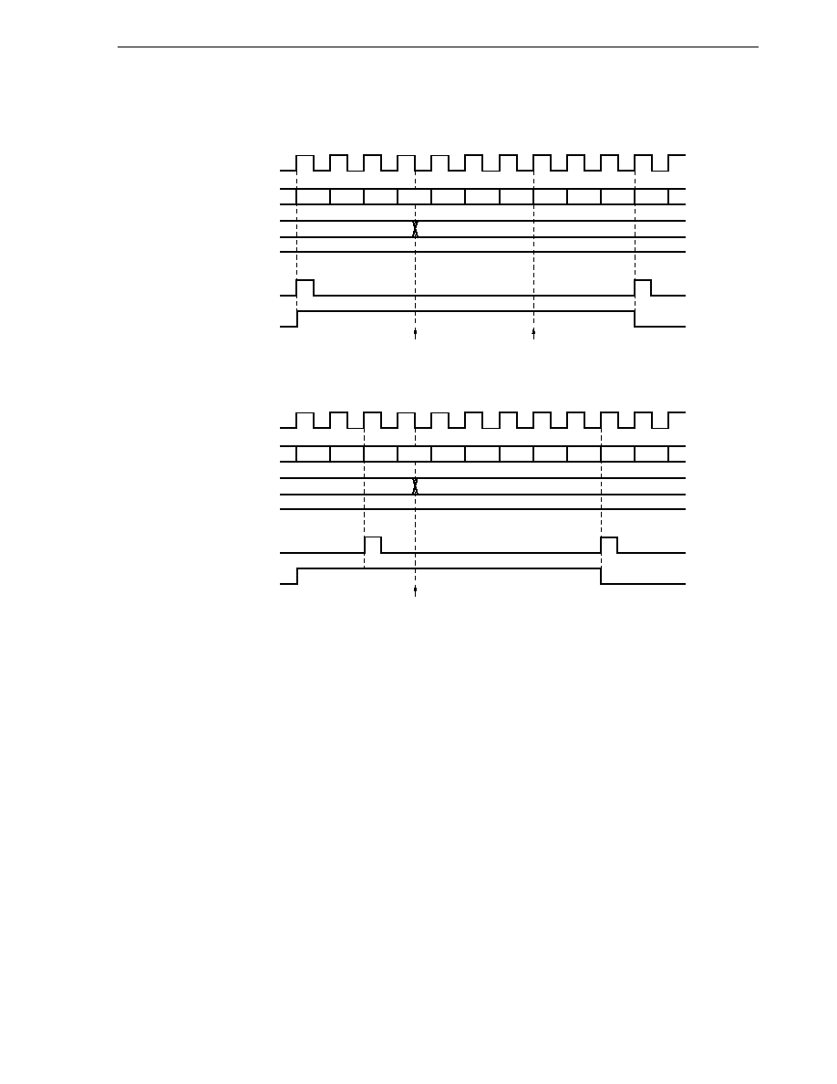
117
CHAPTER 8 8-BIT TIMER 1 TM1
Figure 8-4. Interval Timer Operation Timings (3/3)
(d) Operated by CR1 transition (M < N)
Count clock
TM1
CR1
TCE1
INTTM1
TM1 interval time
00H
N
N
M
N
FFH
00H
M
00H
M
CR1 transition
TM1 overflows since M < N
(e) Operated by CR1 transition (M > N)
Count clock
TM1
CR1
TCE1
INTTM1
TM1 interval time
N�1
N
N
00H
01H
N
M�1
M
00H
01H
M
CR1 transition

118
CHAPTER 8 8-BIT TIMER 1 TM1
8.5 8-Bit Timer 1 Cautions
(1) Timer start errors
An error with a maximum of one clock may occur concerning the time required for a match signal to be generated
after timer start. This is because 8-bit counter 1 (TM1) is started asynchronously with the count pulse.
Figure 8-5. Timer 1 Start Timing
Count pulse
TM1 count value
00H
01H
02H
03H
04H
Timer start
(2) Operation after compare register change during timer count operation
If the values after the 8-bit compare register 1 (CR1) is changed are smaller than the value of 8-bit timer register
1 (TM1), TM1 continues counting, overflows and then restarts counting from 0. Thus, if the value (M) after CR1
change is smaller than value (N) before the change, it is necessary to restart the timer after changing CR1.
Figure 8-6. Timing after Compare Register Change during Timer Count Operation
Count pulse
CR1
TM1 count value
N
M
X�1
X
FFH
00H
01H
02H
Remark
N > X > M
Caution Always set TCE1 = 0 before setting the STOP state.
(3) TM1 reading during timer operation
When TM1 is read during operation, choose a count clock which has a longer high/low level wave because 8-
bit counter (TM1) is stopped temporary.

119
CHAPTER 9 8-BIT TIMER/EVENT COUNTERS 2, 3 TM2, TM3
9.1 8-Bit Timer/Event Counters 2 and 3 Functions
The 8-bit timer/event counters 2 and 3 operate as an 8-bit timer/event counter.
TM2 and TM3 can have the following functions.
� Interval timer
� External event counter
� Square wave output
� PWM output
Figure 9-1 shows timer 2 block diagram, and Figure 9-2 shows timer 3 block diagram.
Figure 9-1. Timer 2 (TM2) Block Diagram
Note Bit 3 of port mode register (PM4)
Internal bus
8-bit compare
register 2 (CR2)
8-bit counter 2
(TM2)
TIO2/P43
f
X
/2
11
f
X
/2
5
Selector
Selector
Coincidence
Mask circuit
OVF
Clear
3
Selector
TCL22 TCL21 TCL20
Timer clock select
register 2 (TCL2)
Internal bus
TCE2 TMC26 LVS2 LVR2 TMC21 TOE2
Invert
level
Timer mode control
register 2 (TMC2)
S
R
S
Q
R
INV
Selector
INTTM2
TIO2/P43
f
X
/2
3
f
X
/2
7
f
X
/2
8
f
X
/2
9
P43 output latch PM43
Note
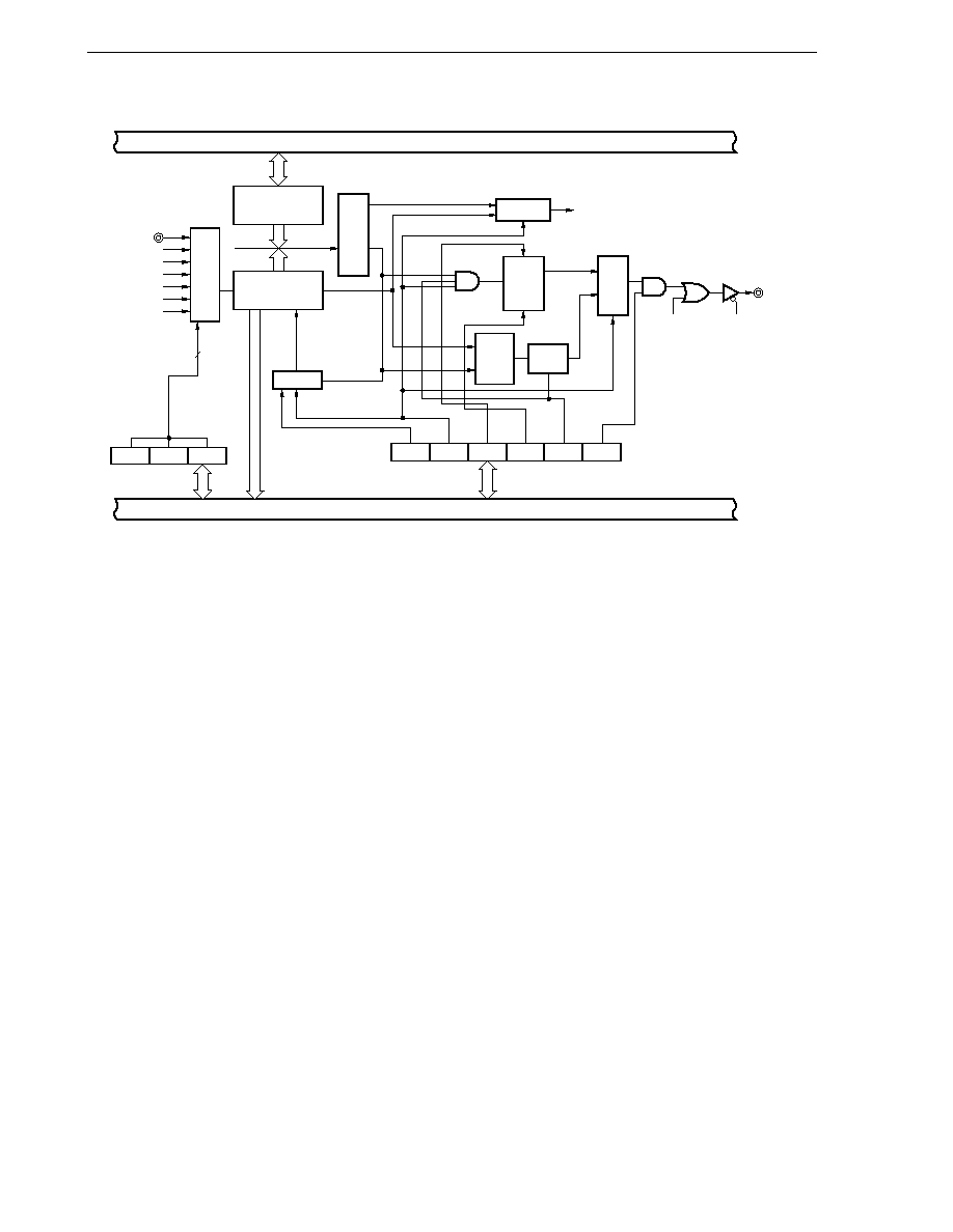
120
CHAPTER 9 8-BIT TIMER/EVENT COUNTERS 2, 3 TM2, TM3
Figure 9-2. Timer 3 (TM3) Block Diagram
Note Bit 4 of port mode register 4 (PM4)
Internal bus
8-bit compare
register 3 (CR3)
8-bit counter 3
(TM3)
TIO3/P44
f
X
/2
12
f
X
/2
4
f
X
/2
6
Selector
Coincidence
Mask circuit
OVF
Clear
3
Selector
TCL32 TCL31 TCL30
Timer clock select
register 3 (TCL3)
Internal bus
TCE3 TMC36 LVS3 LVR3 TMC31 TOE3
Invert
level
Timer mode control
register 3 (TMC3)
S
R
Q
R
INV
Selector
INTTM3
S
TIO3/P44
P44 output latch PM44
Note
f
X
/2
7
f
X
/2
8
f
X
/2
10
Selector
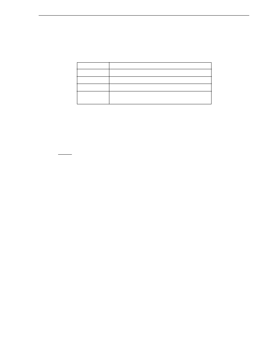
121
CHAPTER 9 8-BIT TIMER/EVENT COUNTERS 2, 3 TM2, TM3
9.2 8-Bit Timer/Event Counters 2 and 3 Configurations
Timers 2 and 3 consist of the following hardware.
Table 9-1. Timers 2 and 3 Configurations
Item
Configuration
Timer register
8-bit counter n (TMn)
Register
8-bit compare register n (CRn)
Timer output
2 (TIOn)
Control register
Timer clock select register n (TCLn)
8-bit timer mode control register n (TMCn)
Remark
n = 2, 3
(1) 8-bit counter n (TMn: n = 2, 3)
TMn is an 8-bit read-only register which counts the count pulses.
The counter is incremented in synchronization with the rising edge of the count clock. When count value is read
during operation, count clock input is temporary stopped, and then the count value is read. In the following
situations, the count value is set to 00H.
<1>
RESET input
<2>
Clear TCEn
<3>
Match between TMn and CRn in clear and start made with match between TMn and CRn
Remark n = 2, 3
(2) 8-bit compare register n (CRn: n = 2, 3)
The value set in the CRn is constantly compared with the 8-bit counter n (TMn) count value, and an interrupt
request (INTTMn) is generated if they match (except PWM mode).
It is possible to rewrite the value of CRn within 00H to FFH during count operation.
Remark
n = 2, 3
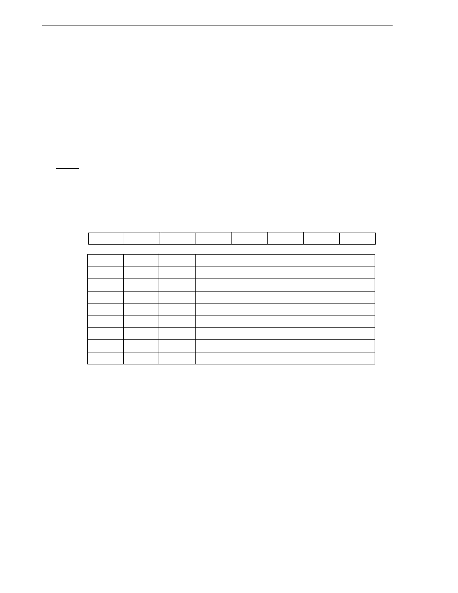
122
CHAPTER 9 8-BIT TIMER/EVENT COUNTERS 2, 3 TM2, TM3
9.3 8-Bit Timer/Event Counters 2 and 3 Control Registers
The following two types of registers are used to control timers 2 and 3.
� Timer clock select register n (TCLn)
� 8-bit timer mode control register n (TMCn)
n = 2, 3
(1) Timer clock select register n (TCLn: n = 2, 3)
This register sets count clocks of timers 2 and 3.
TCLn is set with an 8-bit memory manipulation instruction.
RESET input sets to 00H.
Figure 9-3. Timer Clock Select Register 2 (TCL2) Format
Address: FF74H After Reset: 00H R/W
Symbol
7
6
5
4
3
2
1
0
TCL2
0
0
0
0
0
TCL22
TCL21
TCL20
TCL22
TCL21
TCL20
Count Clock Selection
0
0
0
TIO2 Falling edge
0
0
1
TIO2 Rising edge
0
1
0
f
X
/2
3
(1.04 MHz)
0
1
1
f
X
/2
5
(261 kHz)
1
0
0
f
X
/2
7
(65.4 kHz)
1
0
1
f
X
/2
8
(32.7 kHz)
1
1
0
f
X
/2
9
(16.3 kHz)
1
1
1
f
X
/2
11
(4.09 kHz)
Cautions 1. When rewriting TCL2 to other data, stop the timer operation beforehand.
2. Set bits 3 to 7 to 0.
Remarks
1. f
X
: Main system clock oscillation frequency
2. Figures in parentheses apply to operation with f
X
= 8.38 MHz
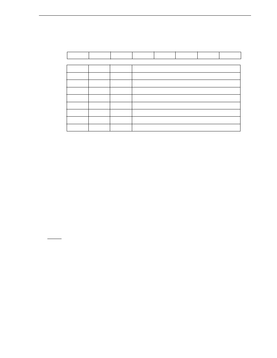
123
CHAPTER 9 8-BIT TIMER/EVENT COUNTERS 2, 3 TM2, TM3
Figure 9-4. Timer Clock Select Register 3 (TCL3) Format
Address: FF75H After Reset: 00H R/W
Symbol
7
6
5
4
3
2
1
0
TCL3
0
0
0
0
0
TCL32
TCL31
TCL30
TCL32
TCL31
TCL30
Count Clock Selection
0
0
0
TIO3 Falling edge
0
0
1
TIO3 Rising edge
0
1
0
f
X
/2
4
(523 kHz)
0
1
1
f
X
/2
6
(130 kHz)
1
0
0
f
X
/2
7
(65.4 kHz)
1
0
1
f
X
/2
8
(32.7 kHz)
1
1
0
f
X
/2
10
(8.18 kHz)
1
1
1
f
X
/2
12
(2.04 kHz)
Cautions 1. When rewriting TCL3 to other data, stop the timer operation beforehand.
2. Set bits 3 to 7 to 0.
Remarks
1. f
X
: Main system clock oscillation frequency
2. Figures in parentheses apply to operation with f
X
= 8.38 MHz
(2) 8-bit timer mode control register n (TMCn: n = 2, 3)
TMCn is a register which sets up the following five types.
<1>
8-bit counter n (TMn) count operation control
<2>
8-bit counter n (TMn) operating mode selection
<3>
Timer output F/F (flip flop) status setting
<4>
Active level selection in timer F/F control or PWM (free-running) mode.
<5>
Timer output control
TMCn is set with a 1-bit or 8-bit memory manipulation instruction.
RESET input sets to 04H.
Figure 9-5 shows TMCn format.

124
CHAPTER 9 8-BIT TIMER/EVENT COUNTERS 2, 3 TM2, TM3
Figure 9-5. 8-Bit Timer Mode Control Register n (TMCn) Format
Address: FF77H (TMC2) FF78H (TMC3) After Reset: 04H R/W
Symbol
7
6
5
4
3
2
1
0
TMCn
TCEn
TMCn6
0
0
LVSn
LVRn
TMCn1
TOEn
TCEn
TM2, TM3 Count Operation Control
0
After clearing counter to 0, count operation disabled (prescaler disabled)
1
Count operation start
TMCn6
TM2, TM3 Operating Mode Selection
0
Clear and start mode by matching between TMn and CRn
1
PWM (Free-running) mode
LVSn
LVRn
Timer Output F/F Status Setting
0
0
No change
0
1
Timer output F/F reset (to 0)
1
0
Timer output F/F set (to 1)
1
1
Setting prohibited
TMCn1
In Other Modes (TMCn6 = 0)
In PWM Mode (TMCn6 = 1)
Timer F/F Control
Active Level Selection
0
Inversion operation disabled
Active high
1
Inversion operation enabled
Active low
TOEn
Timer Output Control
0
Output disabled (Port mode)
1
Output enabled
Cautions 1. Set bit 4 and bit 5 to 0.
2. Bit 2 and bit 3 are write-only.
Remarks
1. In PWM mode, PWM output will be inactive because of TCEn = 0.
2. If LVSn and LVRn are read after data is set, they will be 0.
3. n = 2, 3
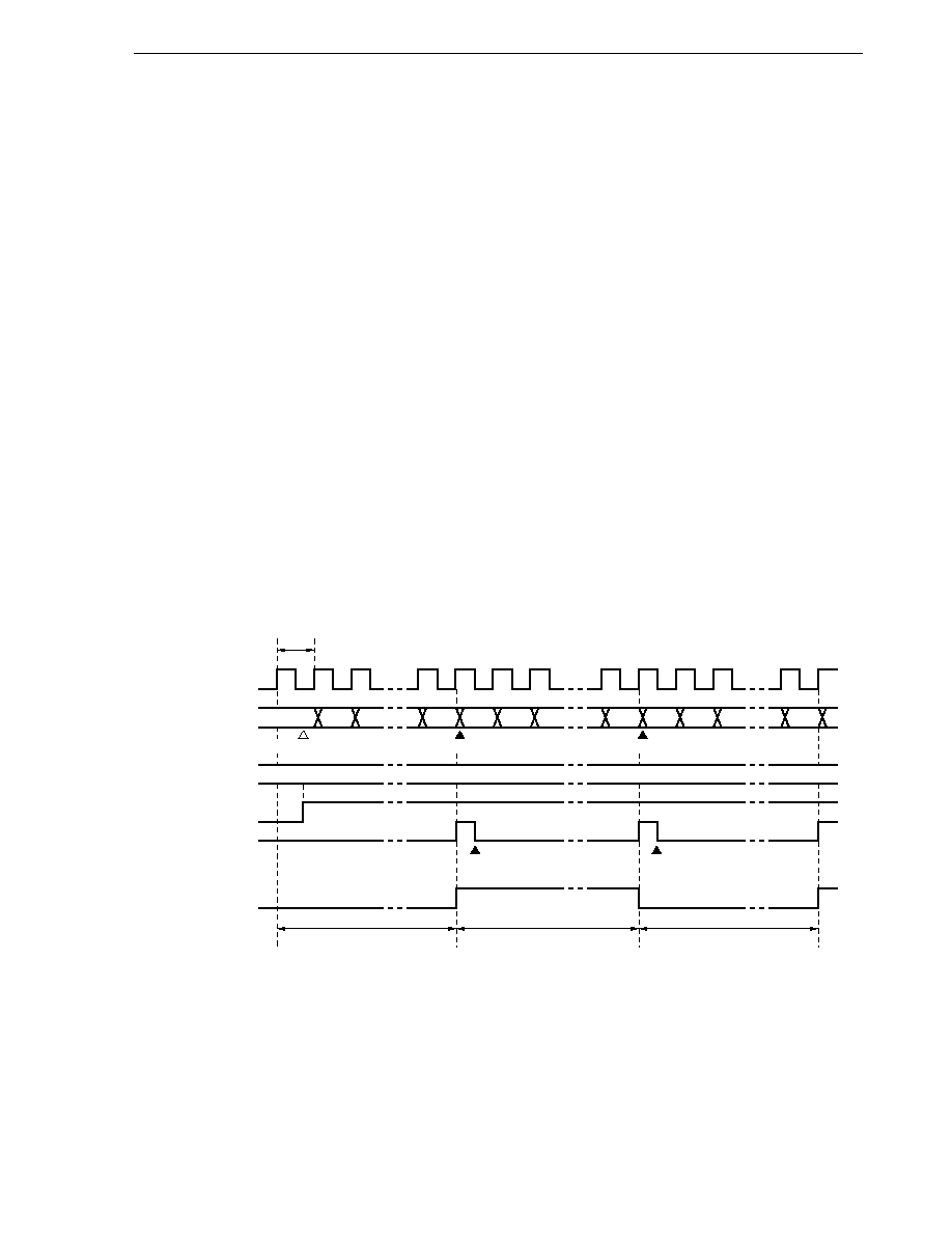
125
CHAPTER 9 8-BIT TIMER/EVENT COUNTERS 2, 3 TM2, TM3
9.4 8-Bit Timer/Event Counters 2 and 3 Operations
9.4.1 8-bit interval timer operation
The 8-bit timer/event counters operate as interval timers which generate interrupt requests repeatedly at intervals
of the count value preset to 8-bit compare register n (CRn).
When the count values of the 8-bit counter n (TMn) match the values set to CRn, counting continues with the TMn
values cleared to 0 and the interrupt request signal (INTTMn) is generated.
Count clock of the TMn can be selected with bits 0 to 2 (TCLn0 to TCLn2) of the timer clock select register n (TCLn).
[Setting]
<1> Set the registers.
� TCLn : Select count clock.
� CRn
: Compare value
� TMCn : Select clear and start mode by match of TMn and CRn.
(TMCn = 0000
���
0B
�
= don't care)
<2> After TCEn = 1 is set, count operation starts.
<3> If the values of TMn and CRn match, the INTTMn is generated and TMn is cleared to 00H.
<4> INTTMn generates repeatedly at the same interval. Set TCEn to 0 to stop count operation.
Remark n = 2, 3
Figure 9-6. Interval Timer Operation Timings (1/3)
(a) Basic operation
t
Count clock
TMn count value
CRn
TCEn
INTTMn
TIOn
Start count
Clear
Clear
00H
01H
N
00H
01H
N
00H
01H
N
N
N
N
N
Interrupt received
Interrupt received
Interval time
Interval time
Interval time
Remarks 1. Interval time = (N + 1)
�
t: N = 00H to FFH
2. n = 2, 3
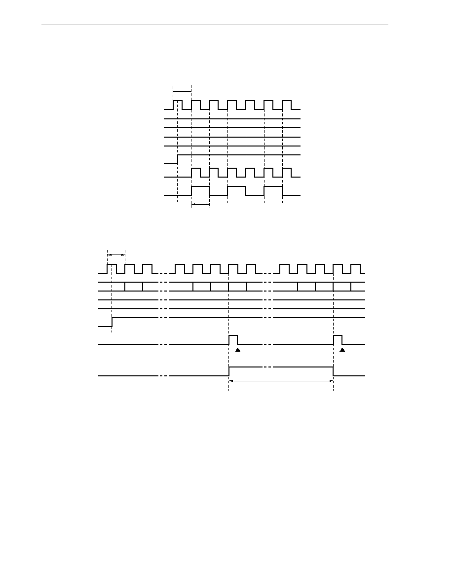
126
CHAPTER 9 8-BIT TIMER/EVENT COUNTERS 2, 3 TM2, TM3
Figure 9-6. Interval Timer Operation Timings (2/3)
(b) When CRn = 00H
t
Count clock
TMn
CRn
TCEn
INTTMn
TIOn
Interval time
00H
00H
00H
00H
00H
(c) When CRn = FFH
t
Count clock
TMn
CRn
TCEn
INTTMn
TIOn
01
FE
FF
00
FE
FF
00
FF
FF
FF
Interval time
Interrupt
received
Interrupt received
n = 2 , 3
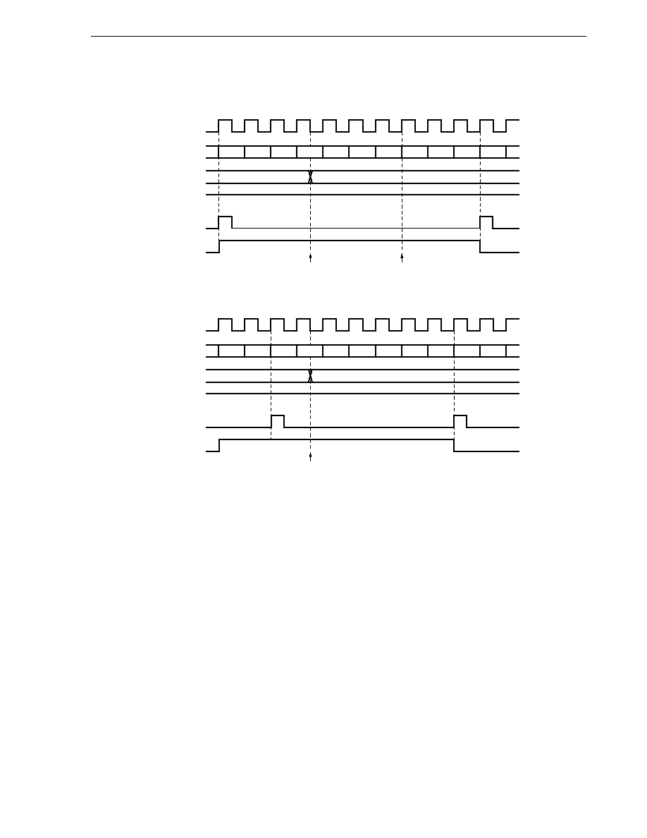
127
CHAPTER 9 8-BIT TIMER/EVENT COUNTERS 2, 3 TM2, TM3
Figure 9-6. Interval Timer Operation Timings (3/3)
(d) Operated by CRn transition (M < N)
Count clock
TMn
CRn
TCEn
INTTMn
TIOn
00H
N
N
M
N
FFH
00H
M
00H
M
CRn transition
TMn overflows since M < N
(e) Operated by CRn transition (M > N)
Count clock
TMn
CRn
TCEn
INTTMn
TIOn
N�1
N
N
00H
01H
N
M�1
M
00H
01H
M
CRn transition
n = 2, 3
9.4.2 External event counter operation
The external event counter counts the number of external clock pulses to be input to the TIOn.
TMn is incremented each time the valid edge specified with the timer clock select register n (TCLn) is input. Either
the rising or falling edge can be selected.
When the TMn counted values match the values of 8-bit compare register n (CRn), TMn is cleared to 0 and the
interrupt request signal (INTTMn) is generated.
Whenever the TMn value matches the value of CRn, INTTMn is generated.
Remark
n = 2, 3

128
CHAPTER 9 8-BIT TIMER/EVENT COUNTERS 2, 3 TM2, TM3
Figure 9-7. External Event Counter Operation Timings (with Rising Edge Specified)
TIOn
TMn count value
CRn
INTTMn
0000 0001 0002 0003 0004 0005
N�1
N
0000 0001 0002 0003
N
n = 2, 3
9.4.3 Square-wave output operation (8-bit resolution)
A square wave with any selected frequency is output at intervals of the value preset to 8-bit compare register n
(CRn).
TIOn pin output status is inverted at intervals of the count value preset to CRn by setting bit 0 (TOEn) of 8-bit timer
mode control register n (TMCn) to 1. This enables a square wave with any selected frequency to be output (duty
= 50%).
[Setting]
<1> Set each register.
� Set port latch and port mode register to 0.
� TCLn: Select count clock
� CRn: compare value
� TMCn: Clear and start mode by match of TMn and CRn
LVSn
LVRn
Timer Output F/F Status Setting
1
0
High-level output
0
1
Low-level output
Timer output F/F inversion enabled
Timer output enabled
TOEn = 1
<2> After TCEn = 1 is set, count operation starts.
<3> Timer output F/F is inverted by match of TMn and CRn. After INTTMn is generated, TMn is cleared to 00H.
<4> Timer output F/F is inverted at the same interval and square wave is output from TIOn.
Remark n = 2, 3

129
CHAPTER 9 8-BIT TIMER/EVENT COUNTERS 2, 3 TM2, TM3
9.4.4 8-bit PWM output operation
8-bit timer/event counters operate as PWM output when bit 6 (TMCn6) of 8-bit timer mode control register n (TMCn)
is set to 1.
The duty rate pulse determined by the value set to 8-bit compare register n (CRn) is output from TIOn.
Set the active level width of PWM pulse to CRn, and the active level can be selected with bit 1 (TMCn1) of TMCn.
Count clock can be selected with bit 0 to bit 2 (TCLn0 to TCLn2) of timer clock select register n (TCLn).
PWM output enable/disable can be selected with bit 0 (TOEn) of TMCn.
Caution
Rewrite of CRn in PWM mode is allowed only once in a cycle.
Remark
n = 2, 3
(1) PWM output basic operation
[Setting]
<1>
Set port latch (P43, P44) and port mode register 4 (PM43, PM44) to 0.
<2>
Set active level width with 8-bit compare register (CRn).
<3>
Select count clock with timer clock select register n (TCLn).
<4>
Set active level with bit 1 (TMCn1) of TMCn.
<5>
Count operation starts when bit 7 (TCEn) of TMCn is set to 1.
Set TCEn to 0 to stop count operation.
[PWM output operation]
<1>
PWM output (output from TIOn) outputs inactive level after count operation starts until overflow is
generated.
<2>
When overflow is generated, the active level set in <1> of setting is output.
The active level is output until CRn matches the count value of 8-bit counter n (TMn).
<3>
After the CRn matches the count value, PWM output outputs the inactive level again until overflow is
generated.
<4>
PWM output operation <2> and <3> are repeated until the count operation stops.
<5>
When the count operation is stopped with TCEn = 0, PWM output changes to inactive level.
Remark n = 2, 3
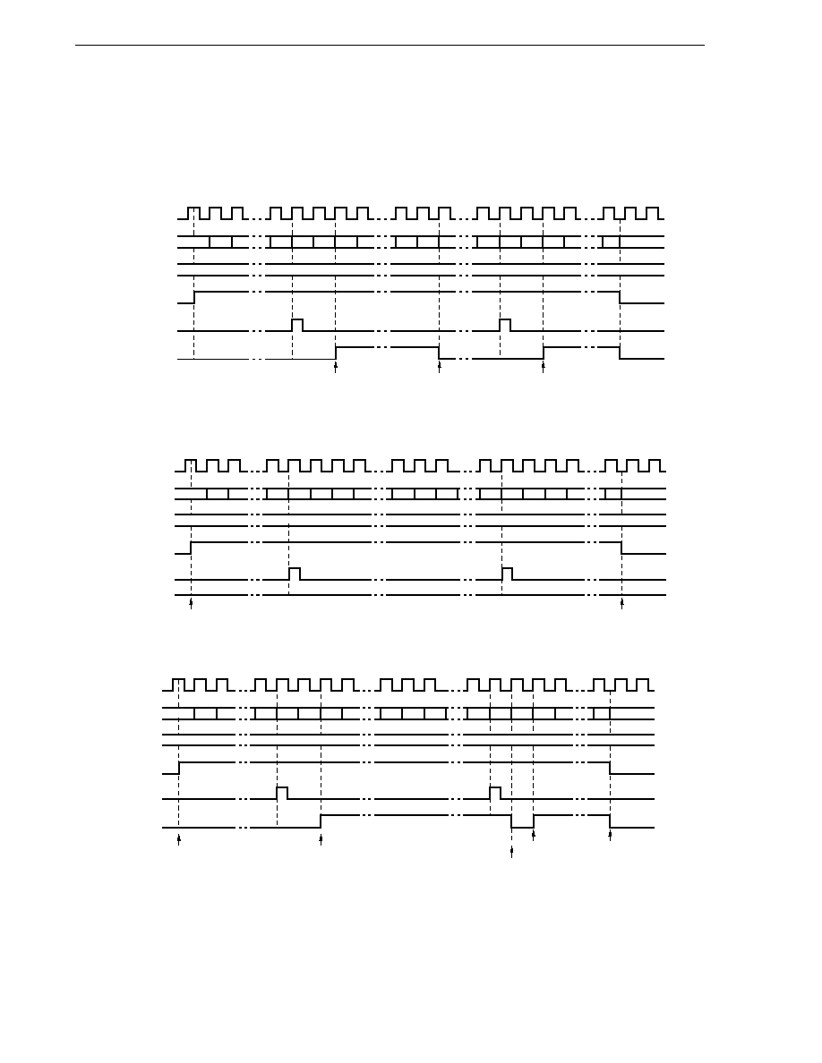
130
CHAPTER 9 8-BIT TIMER/EVENT COUNTERS 2, 3 TM2, TM3
(a) PWM output basic operation
Figure 9-8. PWM Output Operation Timing
(i)
Basic operation (active level = H)
Count clock
TMn
CRn
TCEn
INTTMn
TIOn
00H 01H
FFH 00H 01H 02H
N N+1
FFH 00H 01H 02H
M
00H
N
Active level
Active level
Inactive level
(ii) CRn = 0
Count clock
TMn
CRn
TCEn
INTTMn
TIOn
Inactive level
Inactive level
01H
00H
FFH 00H 01H 02H
N N+1
FFH 00H 01H 02H
M 00H
00H
N+2
(iii) CRn = FFH
TMn
CRn
TCEn
INTTMn
TIOn
01H
00H
FFH 00H 01H 02H
N N+1
FFH 00H 01H 02H
M 00H
FFH
N+2
Inactive level
Active level
Inactive level
Active level
Inactive level
n = 2, 3
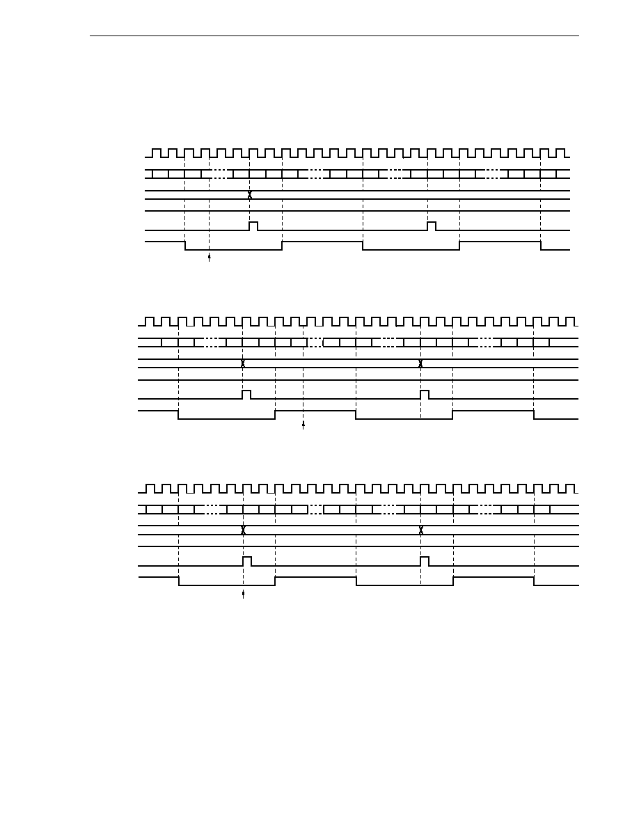
131
CHAPTER 9 8-BIT TIMER/EVENT COUNTERS 2, 3 TM2, TM3
(b) Operation by change of CRn
Figure 9-9. Timing of Operation by Change of CRn
(i)
Change of CRn value to N to M before overflow of TMn
Count clock
TMn
CRn
TCEn
INTTMn
TIOn
CRn transition (N
M)
N N+1 N+2
FFH 00H 01H
M M+1 M+2
FFH 00H 01H 02H
M M+1 M+2
N
02H
M
H
(ii) Change of CRn value to N to M after overflow of TMn
Count clock
TMn
CRn
TCEn
INTTMn
TIOn
N
N+1 N+2
FFH 00H 01H
N
N+1 N+2
FFH 00H 01H 02H
N
02H
N
H
03H
M
M M+1 M+2
CRn transition (N
M)
(iii) Change of CRn value to N to M between two clocks (00H and 01H) after overflow of TMn
Count clock
TMn
CRn
TCEn
INTTMn
TIOn
N
N+1 N+2
FFH 00H 01H
N
N+1 N+2
FFH 00H 01H 02H
N
02H
N
H
M
M M+1 M+2
CRn transition (N
M)
n = 2, 3
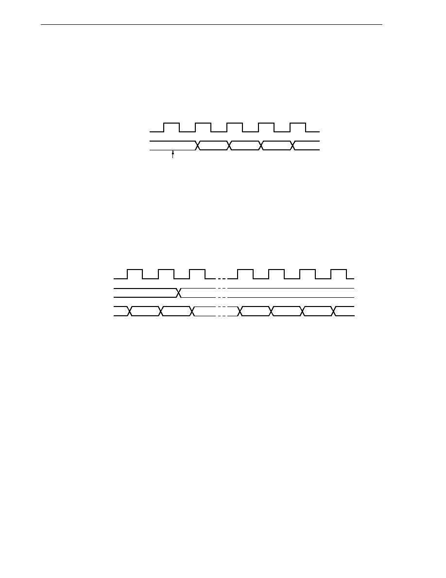
132
CHAPTER 9 8-BIT TIMER/EVENT COUNTERS 2, 3 TM2, TM3
9.5 8-Bit Timer/Event Counters 2 and 3 Cautions
(1) Timer start errors
An error with a maximum of one clock may occur concerning the time required for a match signal to be generated
after timer start. This is because 8-bit counter n (TMn) is started asynchronously with the count pulse.
Figure 9-10. Timer n Start Timing
Count pulse
TMn count value
00H
01H
02H
03H
04H
Timer start
n = 2, 3
(2) Operation after compare register change during timer count operation
If the values after the 8-bit compare register n (CRn) is changed are smaller than the value of 8-bit timer register
n (TMn), TMn continues counting, overflows and then restarts counting from 0. Thus, if the value (M) after CRn
change is smaller than value (N) before the change, it is necessary to restart the timer after changing CRn.
Figure 9-11. Timing after Compare Register Change during Timer Count Operation
Count pulse
CRn
TMn count value
N
M
X�1
X
FFH
00H
01H
02H
Remarks 1.
N > X > M
2.
n = 2, 3
Caution Except when the TIOn input is selected, always set TCEn = 0 before setting the STOP state.
Remark
n = 2, 3
(3) TMn (n = 2, 3) reading during timer operation
When TMn is read during operation, choose a select clock which has a longer high/low level wave because the
select clock is stopped temporarily.

133
CHAPTER 10 WATCH TIMER
10.1 Watch Timer Functions
The watch timer has the following functions.
� Watch timer
� Interval timer
The watch timer and the interval timer can be used simultaneously.
Figure 10-1 shows watch timer block diagram.
Figure 10-1. Watch Timer Block Diagram
9-bit prescaler
5-bit counter
Selector
Selector
Selector
WTM7
f
X
/2
7
f
X
/2
11
WTM6 WTM5 WTM4
Internal bus
WTM3 WTM1 WTM0
Watch timer mode
control register (WTM)
Clear
Clear
INTWT
INTWTI
f
W
2
4
f
W
2
5
f
W
2
6
f
W
2
7
f
W
2
8
f
W
2
9
f
W
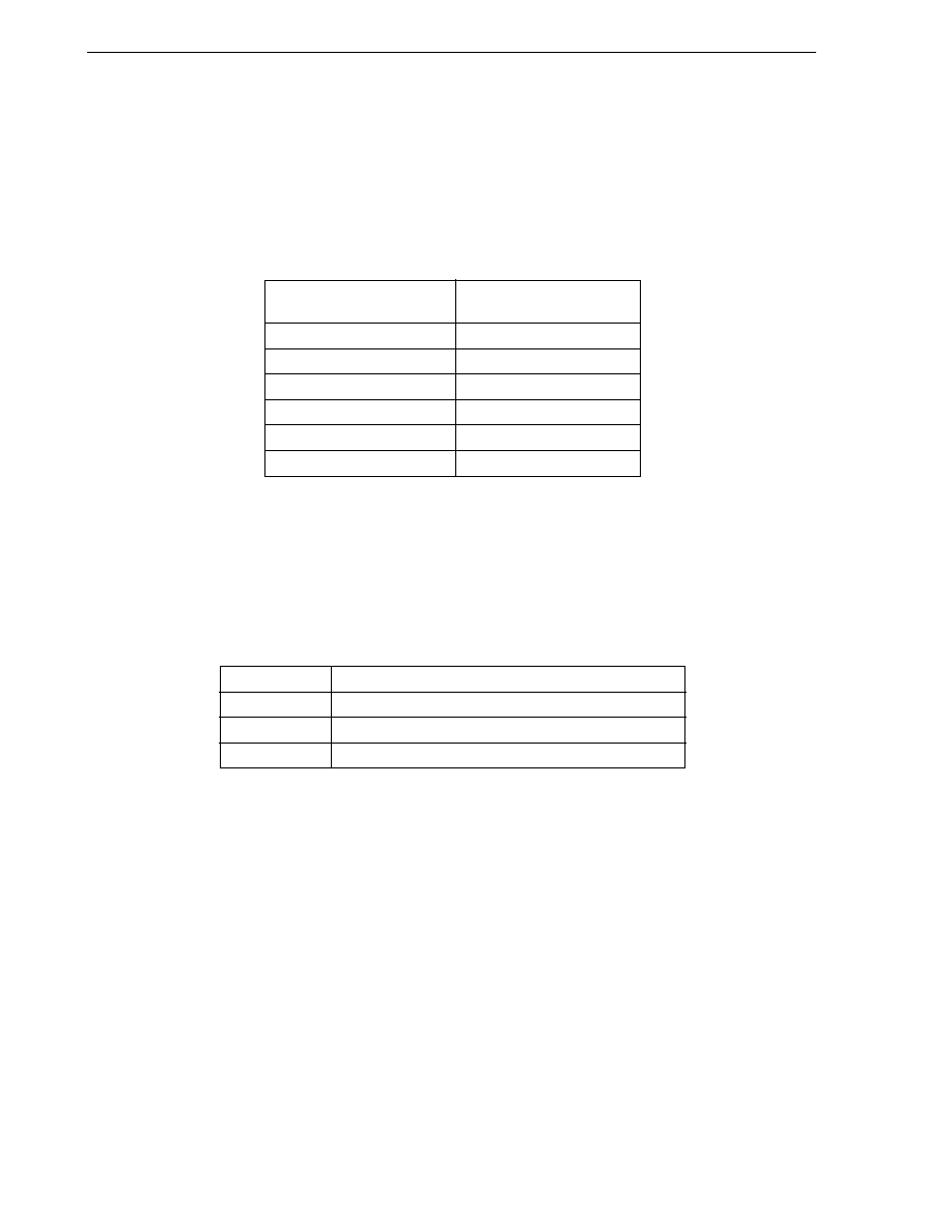
134
CHAPTER 10 WATCH TIMER
(1) Watch timer
When the main system clock is used, interrupt requests (INTWT) are generated at 0.25 second (at f
X
= 8.38-
MHz operation) intervals.
(2) Interval timer
Interrupt requests (INTWT) are generated at the preset time interval.
Table 10-1. Interval Timer Interval Time
Interval Time
When Operated at
f
X
= 8.38 MHz
2
12
�
1/f
X
489
�
s
2
13
�
1/f
X
978
�
s
2
14
�
1/f
X
1.96 ms
2
15
�
1/f
X
3.91 ms
2
16
�
1/f
X
7.82 ms
2
17
�
1/f
X
15.65 ms
Remark
f
X
: Main system clock oscillation frequency
10.2 Watch Timer Configuration
The watch timer consists of the following hardware.
Table 10-2. Watch Timer Configuration
Item
Configuration
Counter
5 bits
�
1
Prescaler
9 bits
�
1
Control register
Watch timer mode control register (WTM)
135
CHAPTER 10 WATCH TIMER
10.3 Watch Timer Control Register
The watch timer mode control register (WTM) is used to control the watch timer.
� Watch timer mode control register (WTM)
This register sets the watch timer count clock, operation enable/disable, prescaler interval time and 5-bit counter
operation control.
WTM is set with an 8-bit memory manipulation instruction.
RESET input clears WTM to 00H.
Figure 10-2. Watch Timer Mode Control Register (WTM) Format
Address: FF41H After Reset: 00H R/W
Symbol
7
6
5
4
3
2
1
0
WTM
WTM7
WTM6
WTM5
WTM4
WTM3
0
WTM1
WTM0
WTM7
Watch Timer Count Clock Selection
0
f
X
/2
7
(65.4 kHz)
1
f
X
/2
11
(4.09 kHz)
WTM6
WTM5
WTM4
Prescaler Interval Time Selection
0
0
0
2
4
/f
W
(3.91 ms)
0
0
1
2
5
/f
W
(7.82 ms)
0
1
0
2
6
/f
W
(15.6 ms)
0
1
1
2
7
/f
W
(31.2 ms)
1
0
0
2
8
/f
W
(62.5 ms)
1
0
1
2
9
/f
W
(125 ms)
Other than above
Setting prohibited
WTM3
Watch Flag Set Time Selection
0
Normal operating mode (flag set at f
W
/2
14
)
1
Fast feed operating mode (flag set at f
W
/2
5
)
WTM1
5-bit Counter Operation Control
0
Clear after operation stop
1
Start
WTM0
Watch Timer Operation Control
0
Operation stop (clear both prescaler and timer)
1
Operation enable
Remarks 1. f
W
: Watch timer clock frequency (f
X
/2
7
or f
X
/2
11
)
2. f
X
: Main system clock oscillation frequency
3. Figures in parentheses apply to operation with f
X
= 8.38 MHz, f
W
= 4.09 kHz.

136
CHAPTER 10 WATCH TIMER
10.4 Watch Timer Operations
10.4.1 Watch timer operation
When the 8.38-MHz main system clock is used, the timer operates as a watch timer with a 0.25-second interval.
The watch timer generates interrupt requests at a constant time interval.
When bit 0 (WTM0) and bit 1 (WTM1) of the watch timer mode control register are set to 1, the count operation
starts. When set to 0, the 5-bit counter is cleared and the count operation stops.
For simultaneous operation of the interval timer, zero-second start can be set only for the watch timer by setting
WTM1 to 0. However, since the 9-bit prescaler is not cleared the first overflow of the watch timer (INTWT) after zero-
second start may include an error of up to 2
9
�
1/f
W
.
10.4.2 Interval timer operation
The watch timer operates as interval timer which generates interrupt request repeatedly at an interval of the preset
count value.
The interval time can be selected with bits 4 to 6 (WTM4 to WTM6) of the watch timer mode control register (WTM).
Table 10-3. Interval Timer Interval Time
WTM6
WTM5
WTM4
Interval Time
When Operated at
When Operated at
f
W
= 65.4 kHz
f
W
= 4.09 kHz
0
0
0
2
4
�
1/f
W
244
�
s
3.91 ms
0
0
1
2
5
�
1/f
W
489
�
s
7.81 ms
0
1
0
2
6
�
1/f
W
978
�
s
15.6 ms
0
1
1
2
7
�
1/f
W
1.96 ms
31.3 ms
1
0
0
2
8
�
1/f
W
3.91 ms
62.5 ms
1
0
1
2
9
�
1/f
W
7.82 ms
125 ms
Other than above
Setting prohibited
Remark
f
W
: Watch timer clock frequency
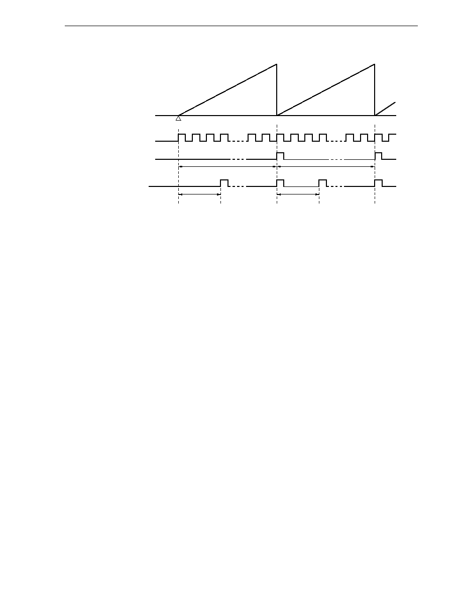
137
CHAPTER 10 WATCH TIMER
Figure 10-3. Operation Timing of Watch Timer/Interval Timer
0H
Start
Overflow
Overflow
5-bit counter
Count clock
f
W
or f
W
/2
9
Watch timer
interrupt INTWT
Interval timer
interrupt INTWTI
Interrupt time of watch timer (0.25 s)
Interval timer
(T)
T
Interrupt time of watch timer (0.25 s)
Remark
f
W
: Watch timer clock frequency
( ) : f
W
= 4.09 kHz (f
X
= 8.38 MHz)

138
[MEMO]

139
CHAPTER 11 WATCHDOG TIMER
11.1 Watchdog Timer Functions
The watchdog timer has the following functions.
� Watchdog timer
� Interval timer
Caution
Select the watchdog timer mode or the interval timer mode with the watchdog timer mode
register (WDTM).
Figure 11-1 shows the watchdog timer block diagram.
Figure 11-1. Watchdog Timer Block Diagram
Prescaler
INTWDT
Maskable
interrupt request
INTWDT
Non-maskable
interrupt request
RESET
WDTIF
WDTMK
RUN
Selector
Control circuit
f
X
/2
7
f
X
/2
12
f
X
/2
13
f
X
/2
14
f
X
/2
15
f
X
/2
16
f
X
/2
17
f
X
/2
18
f
X
/2
20
3
Internal bus
Internal bus
WDCS2 WDCS1 WDCS0
RUN WDTM4 WDTM3
Watchdog timer mode register (WDTM)
Watchdog timer clock
select register (WDCS)

140
CHAPTER 11 WATCHDOG TIMER
(1) Watchdog timer mode
A runaway is detected. Upon detection of the runaway, a non-maskable interrupt request or RESET can be
generated.
Table 11-1. Watchdog Timer Runaway Detection Time
Runaway Detection Time
2
12
�
1/f
X
(489
�
s)
2
13
�
1/f
X
(978
�
s)
2
14
�
1/f
X
(1.96 ms)
2
15
�
1/f
X
(3.91 ms)
2
16
�
1/f
X
(7.82 ms)
2
17
�
1/f
X
(15.6 ms)
2
18
�
1/f
X
(31.3 ms)
2
20
�
1/f
X
(125 ms)
Remarks 1. f
X
: Main system clock oscillation frequency
2. Figures in parentheses apply to operation with f
X
= 8.38 MHz.
(2) Interval timer mode
Interrupt requests are generated at preset time intervals.
Table 11-2. Interval Time
Interval Time
2
12
�
1/f
X
(489
�
s)
2
13
�
1/f
X
(978
�
s)
2
14
�
1/f
X
(1.96 ms)
2
15
�
1/f
X
(3.91 ms)
2
16
�
1/f
X
(7.82 ms)
2
17
�
1/f
X
(15.6 ms)
2
18
�
1/f
X
(31.3 ms)
2
20
�
1/f
X
(125 ms)
Remarks 1. f
X
: Main system clock oscillation frequency
2. Figures in parentheses apply to operation with f
X
= 8.38 MHz.
141
CHAPTER 11 WATCHDOG TIMER
11.2 Watchdog Timer Configuration
The watchdog timer consists of the following hardware.
Table 11-3. Watchdog Timer Configuration
Item
Configuration
Control register
Watchdog timer clock select register (WDCS)
Watchdog timer mode register (WDTM)
11.3 Watchdog Timer Control Registers
The following two types of registers are used to control the watchdog timer.
� Watchdog timer clock select register (WDCS)
� Watchdog timer mode register (WDTM)
(1) Watchdog timer clock select register (WDCS)
This register sets overflow time of the watchdog timer and the interval timer.
WDCS is set with an 8-bit memory manipulation instruction.
RESET input clears WDCS to 00H.
Figure 11-2. Watchdog Timer Clock Select Register (WDCS) Format
Address: FF42H After Reset: 00H R/W
Symbol
7
6
5
4
3
2
1
0
WDCS
0
0
0
0
0
WDCS2
WDCS1
WDCS0
WDCS2
WDCS1
WDCS0
Overflow Time of Watchdog Timer/Interval Timer
0
0
0
2
12
/f
X
(489
�
s)
0
0
1
2
13
/f
X
(978
�
s)
0
1
0
2
14
/f
X
(1.96 ms)
0
1
1
2
15
/f
X
(3.91 ms)
1
0
0
2
16
/f
X
(7.82 ms)
1
0
1
2
17
/f
X
(15.6 ms)
1
1
0
2
18
/f
X
(31.3 ms)
1
1
1
2
20
/f
X
(125 ms)
Cautions 1. When rewriting WDCS to other data, stop the timer operation beforehand.
2. Bits 3 to 7 must be set to 0.
Remarks 1. f
X
: Main system clock oscillation frequency
2. Figures in parentheses apply to operation with f
X
= 8.38 MHz
142
CHAPTER 11 WATCHDOG TIMER
(2) Watchdog timer mode register (WDTM)
This register sets the watchdog timer operating mode and enables/disables counting.
WDTM is set with a 1-bit or 8-bit memory manipulation instruction.
RESET input clears WDTM to 00H.
Figure 11-3. Watchdog Timer Mode Register (WDTM) Format
Address: FFF9H After Reset: 00H R/W
Symbol
7
6
5
4
3
2
1
0
WDTM
RUN
0
0
WDTM4
WDTM3
0
0
0
RUN
Watchdog Timer Operation Mode Selection
Note 1
0
Count stop
1
Counter is cleared and counting starts
WDTM4
WDTM3
Watchdog Timer Operation Mode Selection
Note 2
0
�
Interval timer mode
(Maskable interrupt request occurs upon generation of an overflow)
1
0
Watchdog timer mode 1
(Non-maskable interrupt request occurs upon generation of an overflow)
1
1
Watchdog timer mode 2
(Reset operation is activated upon generation of an overflow)
Notes 1. Once set to 1, RUN cannot be cleared to 0 by software.
Thus, once counting starts, it can only be stopped by RESET input.
2. Once set to 1, WDTM3 and WDTM4 cannot be cleared to 0 by software.
Cautions 1. When 1 is set in RUN so that the watchdog timer is cleared, the actual overflow time is
up to 0.5% shorter than the time set by the watchdog timer clock select register.
2. To use watchdog timer modes 1 and 2, make sure that the interrupt request flag (WDTIF)
is 0, and then set WDTM4 to 1.
If WDTM4 is set to 1 when WDTIF is 1, the non-maskable interrupt request occurs,
regardless of the contents of WDTM3.
Remark
�
: don't care

143
CHAPTER 11 WATCHDOG TIMER
11.4 Watchdog Timer Operations
11.4.1 Watchdog timer operation
When bit 4 (WDTM4) of the watchdog timer mode register (WDTM) is set to 1, the watchdog timer is operated to
detect any runaways.
Watchdog timer starts by setting bit 7 (RUN) of WDTM to 1. After the watchdog timer is started, set RUN to 1 within
the set runaway time interval. The watchdog timer can be cleared and counting is started.
If RUN is not set to 1 and the runaway detection time is past, system reset or a non-maskable interrupt request
is generated according to the WDTM bit 3 (WDTM3) value.
The watchdog timer continues operating in the HALT mode but it stops in the STOP mode. Thus, set RUN to 1
before the STOP mode is set, clear the watchdog timer and then execute the STOP instruction.
Caution
The actual runaway detection time may be shorter than the set time by a maximum of 0.5%.
Table 11-4. Watchdog Timer Runaway Detection Time
Runaway Detection Time
2
12
�
1/f
X
(489
�
s)
2
13
�
1/f
X
(978
�
s)
2
14
�
1/f
X
(1.96 ms)
2
15
�
1/f
X
(3.91 ms)
2
16
�
1/f
X
(7.82 ms)
2
17
�
1/f
X
(15.6 ms)
2
18
�
1/f
X
(31.3 ms)
2
20
�
1/f
X
(125 ms)
Remarks 1. f
X
: Main system clock oscillation frequency
2. Figures in parentheses apply to operation with f
X
= 8.38 MHz.

144
CHAPTER 11 WATCHDOG TIMER
11.4.2 Interval timer operation
The watchdog timer operates as an interval timer which generates interrupt request repeatedly at an interval of
the preset count value when bit 3 (WDTM3) and bit 4 (WDTM4) of the watchdog timer mode register (WDTM) are
set to 1 and 0, respectively.
When the watchdog timer operates as interval timer, the interrupt mask flag (WDTMK) and priority specify flag
(WDTPR) are validated and the maskable interrupt request (INTWDT) can be generated. Among maskable interrupts,
the INTWDT default has the highest priority.
The interval timer continues operating in the HALT mode but it stops in STOP mode. Thus, set RUN to 1 before
the STOP mode is set, clear the interval timer and then execute the STOP instruction.
Cautions 1. Once bit 4 (WDTM4) of WDTM is set to 1 (with the watchdog timer mode selected), the interval
timer mode is not set unless RESET input is applied.
2. The interval time just after setting with WDTM may be shorter than the set time by a maximum
of 0.5%.
Table 11-5. Interval Timer Interval Time
Interval Time
2
12
�
1/f
X
(489
�
s)
2
13
�
1/f
X
(978
�
s)
2
14
�
1/f
X
(1.96 ms)
2
15
�
1/f
X
(3.91 ms)
2
16
�
1/f
X
(7.82 ms)
2
17
�
1/f
X
(15.6 ms)
2
18
�
1/f
X
(31.3 ms)
2
20
�
1/f
X
(125 ms)
Remarks 1. f
X
: Main system clock oscillation frequency
2. Figures in parentheses apply to operation with f
X
= 8.38 MHz.

145
CHAPTER 12 CLOCK OUTPUT CONTROL CIRCUIT
12.1 Clock Output Control Circuit Functions
The clock output control circuit is intended for carrier output during remote controlled transmission and clock output
for supply to peripheral LSIs. The clock selected with the clock output selection register (CKS) is output from the
PCL/SGOA/P60 pin.
Figure 12-1 shows the clock output control circuit (CKU) block diagram.
Figure 12-1. Clock Output Control Circuit Block Diagram
f
X
f
X
/2
f
X
/2
2
f
X
/2
3
f
X
/2
4
f
X
/2
5
f
X
/2
6
f
X
/2
7
Selector
Clock control
circuit
CLOE CCS2 CCS1 CCS0
PM60
PCL/SGOA/P60
Clock output selection register (CKS)
Port mode register 6 (PM6)
P60
output latch
3
Internal bus
SGOA
Note
Note SGOA: Sound generator amplitude signal
12.2 Clock Output Control Circuit Configuration
The clock output control circuit (CKU) consists of the following hardware.
Table 12-1. Clock Output Control Circuit Configuration
Item
Configuration
Control register
Clock output selection register (CKS)
Port mode register 6 (PM6)

146
CHAPTER 12 CLOCK OUTPUT CONTROL CIRCUIT
12.3 Clock Output Control Circuit Control Registers
The following two types of registers are used to control the CKU.
� Clock output selection register (CKS)
� Port mode register 6 (PM6)
(1) Clock output selection register (CKS)
This register sets output clock.
CKS is set with a 1-bit or 8-bit memory manipulation instruction.
RESET input clears CKS to 00H.
Figure 12-2. Clock Output Selection Register (CKS) Format
Address: FF40H After Reset: 00H R/W
Symbol
7
6
5
4
3
2
1
0
CKS
0
0
0
CLOE
0
CCS2
CCS1
CCS0
CLOE
PCL Output Enable/Disable Specification
0
Stop clock division circuit operation.
1
Enable clock division circuit operation.
CCS2
CCS1
CCS0
PCL Output Clock Selection
0
0
0
f
X
(8.38 MHz)
0
0
1
f
X
/2 (4.19 MHz)
0
1
0
f
X
/2
2
(2.09 MHz)
0
1
1
f
X
/2
3
(1.04 MHz)
1
0
0
f
X
/2
4
(524 kHz)
1
0
1
f
X
/2
5
(262 kHz)
1
1
0
f
X
/2
6
(131 kHz)
1
1
1
f
X
/2
7
(65.5 kHz)
Cautions 1. When rewriting CKS to other data, stop the timer operation beforehand.
2. Bit 3 and bits 5 to 7 must be set to 0.
Remarks 1. f
X
= main system clock oscillation frequency
2. Figures in parentheses apply to operation with f
X
= 8.38 MHz.

147
CHAPTER 12 CLOCK OUTPUT CONTROL CIRCUIT
(2) Port mode register 6 (PM6)
This register sets port 6 input/output in 1-bit units.
When using the P60/PCL/SGOA pin for clock output, set PM60 and the output latch of P60 to 0.
PM6 is set with a 1-bit or 8-bit memory manipulation instruction.
RESET input sets PM6 to FFH.
Figure 12-3. Port Mode Register 6 (PM6) Format
Address: FF26H After Reset: FFH R/W
Symbol
7
6
5
4
3
2
1
0
PM6
1
1
1
1
1
1
PM61 PM60
PM6n
P6n Pin Input/Output Mode Selection (n = 0 , 1)
0
Output mode (output buffer ON)
1
Input mode (output buffer OFF)

148
CHAPTER 12 CLOCK OUTPUT CONTROL CIRCUIT
12.4 Clock Output Control Circuit Operation
12.4.1 Clock output operation
To output the clock pulse, follow the procedure described below.
<1>
Select the clock pulse output frequency with bits 0 to 3 (CCS0 to CCS3) of the clock output selection register
(CKS) (clock pulse output in disabled status).
<2>
Set bit 3 (SGOB) of the sound generator control register (SGCR) to 1 (SGOF output in disabled status).
<3>
Set the P60 output latch to 0.
<4>
Set bit 0 (PM60) of port mode register 6 to 0 (set to output mode).
<5>
Set bit 4 (CLOE) of CKS to 1, and enable clock output.
Remark
The clock output control circuit is designed not to output pulses with a small width during output enable/
disable switching of the clock output. As shown in Figure 12-4, be sure to start output from the low period
of the clock (marked with * in the figure below). When stopping output, do so after securing high level
of the clock.
Figure 12-4. Remote Control Output Application Example
CLOE
Clock output
*
*

149
CHAPTER 13 A/D CONVERTER
13.1 A/D Converter Functions
The A/D converter is an 8-bit resolution converter that converts analog inputs into digital values. It can control
up to 5 analog input channels (ANI0 to ANI4).
This A/D converter has the following functions:
(1) A/D conversion with 8-bit resolution
One channel of analog input is selected from ANI0 to ANI4, and A/D conversion is repeatedly executed with a
resolution of 8 bits. Each time the conversion has been completed, interrupt request (INTAD) is generated.
(2) Power-fail detection function
This function is to detect a voltage drop in the battery of an automobile. The result of A/D conversion (value of
the ADCR1 register) and the value of PFT register (PFT: power-fail compare threshold value register) are
compared. If the condition for comparison is satisfied, INTAD is generated.
Figure 13-1. A/D Converter Block Diagram
ANI0/P10
ANI1/P11
ANI2/P12
ANI3/P13
ANI4/P14
Selector
Sample & hold circuit
Voltage comparator
Successive
approximation
register (SAR)
Control
circuit
3
A/D conversion result
register (ADCR1)
Tap selector
AV
REF
AV
SS
INTAD
A/D converter mode register
Analog input channel
specification register
Internal bus
ADS12 ADS11 ADS10
ADCS1 FR12 FR11 FR10
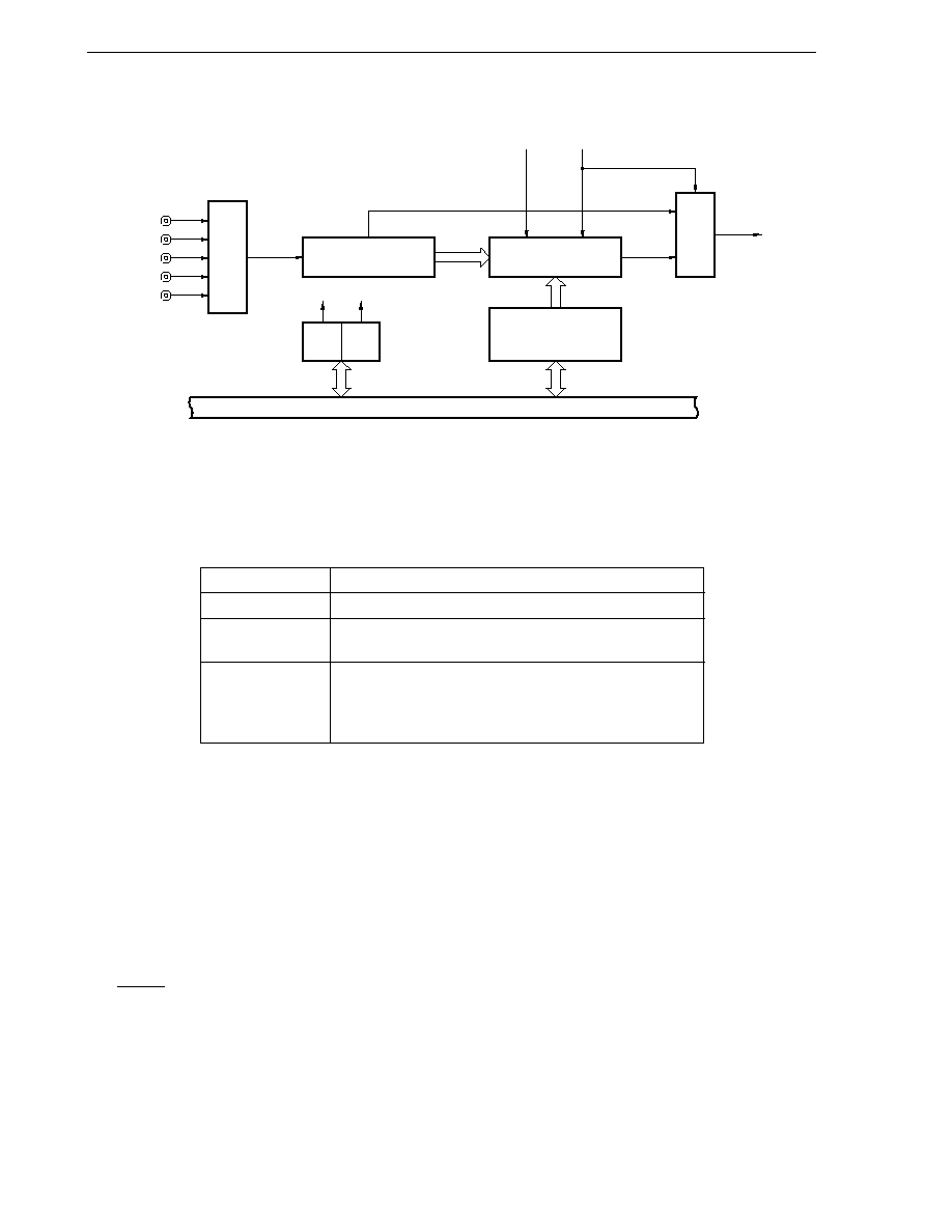
150
CHAPTER 13 A/D CONVERTER
Figure 13-2. Power-Fail Detection Function Block Diagram
ANI0/P10
ANI1/P11
ANI2/P12
ANI3/P13
ANI4/P14
Multiplexer
Selector
A/D converter
Internal bus
Power-fail compare
mode register (PFM)
Comparator
PFEN PFCM
Power-fail compare
threshold value
register (PFT)
INTAD
PFEN
PFCM
13.2 A/D Converter Configuration
A/D converter consists of the following hardware.
Table 13-1. A/D Converter Configuration
Item
Configuration
Analog input
5 channels (ANI0 to ANI4)
Register
Successive approximation register (SAR)
A/D conversion result register (ADCR1)
Control register
A/D converter mode register (ADM1)
Analog input channel specification register (ADS1)
Power-fail compare mode register (PFM)
Power-fail compare threshold value register (PFT)
(1) Successive approximation register (SAR)
This register compares the analog input voltage value to the voltage tap (compare voltage) value applied from
the series resistor string, and holds the result from the most significant bit (MSB).
When up to the least significant bit (LSB) is set (end of A/D conversion), the SAR contents are transferred to
the A/D conversion result register.
(2) A/D conversion result register (ADCR1)
This register holds the A/D conversion result. Each time A/D conversion ends, the conversion result is loaded
from the successive approximation register.
ADCR1 is read with an 8-bit memory manipulation instruction.
RESET input clears ADCR1 to 00H.
Caution
When write operation is executed to A/D converter mode register (ADM1) and analog input
channel specification register (ADS1), the contents of ADCR1 are undefined. Read the
conversion result before write operation is executed to ADM1, ADS1. If a timing other than
the above is used, the correct conversion result may not be read.

151
CHAPTER 13 A/D CONVERTER
(3) Sample & hold circuit
The sample & hold circuit samples each analog input sequentially applied from the input circuit, and sends it to
the voltage comparator. This circuit holds the sampled analog input voltage value during A/D conversion.
(4) Voltage comparator
The voltage comparator compares the analog input to the series resistor string output voltage.
(5) Series resistor string
The series resistor string is in AV
REF
to AV
SS
, and generates a voltage to be compared to the analog input.
(6) ANI0 to ANI4 pins
These are five analog input pins to input analog signals to undergo A/D conversion to the A/D converter. ANI0
to ANI4 are alternate-function pins that can also be used for digital input.
Caution
Use ANI0 to ANI4 input voltages within the specification range. If a voltage higher than
AV
REF
or lower than AV
SS
is applied (even if within the absolute maximum rating range), the
conversion value of that channel will be undefined and the conversion values of other
channels may also be affected.
(7) AV
REF
pin (Shared with AV
DD
pin)
This pin inputs the A/D converter reference voltage.
This pin also functions as an analog power supply pin. Supply power to this pin when the A/D converter is used.
It converts signals input to ANI0 to ANI4 into digital signals according to the voltage applied between AV
REF
and
AV
SS
.
The current flowing in the series resistor string can be reduced by setting the voltage to be input to the AV
REF
pin to AV
SS
level in the standby mode.
(8) AV
SS
pin
This is the GND potential pin of the A/D converter. Always keep it at the same potential as the V
SS
pin even
when not using the A/D converter.
152
CHAPTER 13 A/D CONVERTER
13.3 A/D Converter Control Registers
The following 4 types of registers are used to control A/D converter.
� A/D converter mode register (ADM1)
� Analog input channel specification register (ADS1)
� Power-fail compare mode register (PFM)
� Power-fail compare threshold value register (PFT)
(1) A/D converter mode register (ADM1)
This register sets the conversion time for analog input to be A/D converted, conversion start/stop and external
trigger. ADM1 is set with an 8-bit memory manipulation instruction.
RESET input clears ADM1 to 00H.
Figure 13-3. A/D Converter Mode Register (ADM1) Format
Address: FF80H After Reset: 00H R/W
Symbol
7
6
5
4
3
2
1
0
ADM1
ADCS1
0
FR12
FR11
FR10
0
0
0
ADCS1
A/D Conversion Operation Control
0
Stop conversion operation.
1
Enable conversion operation.
FR12
FR11
FR10
Conversion Time Selection
Note
0
0
0
144/f
X
0
0
1
120/f
X
0
1
0
96/f
X
1
0
0
288/f
X
1
0
1
240/f
X
1
1
0
192/f
X
Other than above
Setting prohibited
Note Set so that the A/D conversion time is 19.1
�
s or more.
Caution
Bits 0 to 2 and bit 6 must be set to 0.
Remark
f
X
: Main system clock oscillation frequency
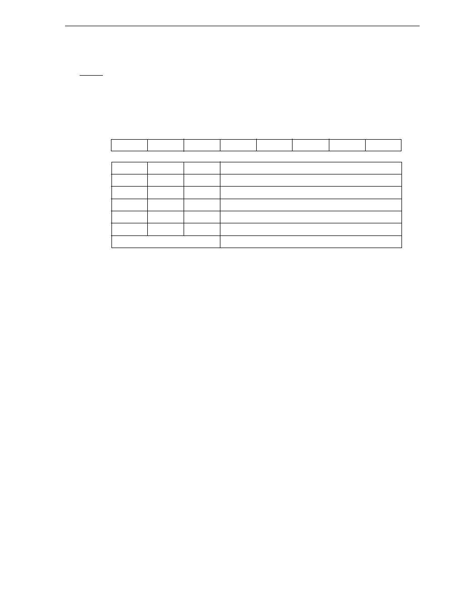
153
CHAPTER 13 A/D CONVERTER
(2) Analog input channel specification register (ADS1)
This register specifies the analog voltage input port for A/D conversion.
ADS1 is set with an 8-bit memory manipulation instruction.
RESET input clears ADS1 to 00H.
Figure 13-4. Analog Input Channel Specification Register (ADS1) Format
Address: FF81H After Reset: 00H R/W
Symbol
7
6
5
4
3
2
1
0
ADS1
0
0
0
0
0
ADS12
ADS11
ADS10
ADS12
ADS11
ADS10
Analog Input Channel Specification
0
0
0
ANI0
0
0
1
ANI1
0
1
0
ANI2
0
1
1
ANI3
1
0
0
ANI4
Other than above
Setting prohibited
Caution
Bits 3 to 7 must be set to 0.
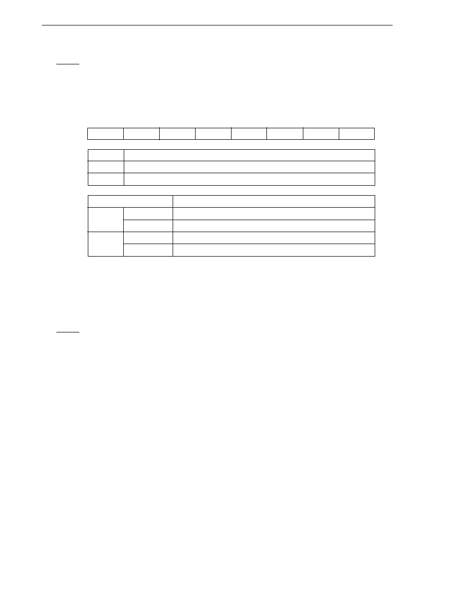
154
CHAPTER 13 A/D CONVERTER
(3) Power-fail compare mode register (PFM)
The power-fail compare mode register (PFM) controls a comparison operation.
RESET input clears PFM to 00H.
Figure 13-5. Power-Fail Compare Mode Register (PFM) Format
Address: FF82H After Reset: 00H R/W
Symbol
7
6
5
4
3
2
1
0
PFM
PFEN
PFCM
0
0
0
0
0
0
PFEN
Enables Power-Fail Comparison
0
Disables power-fail comparison (used as normal A/D converter)
1
Enables power-fail comparison (used to detect power failure)
PFCM
Power-Fail Compare Mode Selection
0
ADCR1
PFT
Generates interrupt request signal INTAD
ADCR1 < PFT
Does not generate interrupt request signal INTAD
1
ADCR1
PFT
Does not generate interrupt request signal INTAD
ADCR1 < PFT
Generates interrupt request signal INTAD
Caution
Bits 0 to 5 must be set to 0.
(4) Power-fail compare threshold value register (PFT)
The power-fail compare threshold value register (PFT) sets a threshold value against which the result of A/D
conversion is to be compared.
PFT is set with an 8-bit memory manipulation instruction.
RESET input clears PFT to 00H.

155
CHAPTER 13 A/D CONVERTER
13.4 A/D Converter Operations
13.4.1 Basic operations of A/D converter
<1> Select one channel for A/D conversion with the analog input channel specification register (ADS1).
<2> The voltage input to the selected analog input channel is sampled by the sample & hold circuit.
<3> When sampling has been done for a certain time, the sample & hold circuit is placed in the hold state and the
input analog voltage is held until the A/D conversion operation is ended.
<4> Set bit 7 of the successive approximation register (SAR) so that the tap selector sets the series resistor string
voltage tap to (1/2) AV
REF
.
<5> The voltage difference between the series resistor string voltage tap and analog input is compared with the
voltage comparator. If the analog input is greater than (1/2) AV
REF
, the MSB of SAR remains set. If the analog
input is smaller than (1/2) AV
REF
, the MSB is reset.
<6> Next, bit 6 of SAR is automatically set, and the operation proceeds to the next comparison. The series resistor
string voltage tap is selected according to the preset value of bit 7, as described below.
�
Bit 7 = 1: (3/4) AV
REF
�
Bit 7 = 0: (1/4) AV
REF
The voltage tap and analog input voltage are compared and bit 6 of SAR is manipulated as follows.
�
Analog input voltage
Voltage tap: Bit 6 = 1
�
Analog input voltage < Voltage tap: Bit 6 = 0
<7> Comparison is continued in this way up to bit 0 of SAR.
<8> Upon completion of the comparison of 8 bits, an effective digital result value remains in SAR, and the result
value is transferred to and latched in the A/D conversion result register (ADCR1).
At the same time, the A/D conversion end interrupt request (INTAD) can also be generated.

156
CHAPTER 13 A/D CONVERTER
Figure 13-6. Basic Operation of 8-Bit A/D Converter
Conversion time
Sampling time
Sampling
A/D conversion
Undefined
80H
C0H
or
40H
Conversion
result
A/D converter
operation
SAR
ADCR1
INTAD
Conversion
result
A/D conversion operations are performed continuously until bit 7 (ADCS1) of the A/D converter mode register
(ADM1) is reset (to 0) by software.
If a write operation to the ADM1 and analog input channel specification register (ADS1) is performed during an
A/D conversion operation, the conversion operation is initialized, and if the ADCS1 bit is set (to 1), conversion starts
again from the beginning.
RESET input sets the A/D conversion result register (ADCR1) to 00H.
157
CHAPTER 13 A/D CONVERTER
13.4.2 Input voltage and conversion results
The relation between the analog input voltage input to the analog input pins (ANI0 to ANI4) and the A/D conversion
result (stored in the A/D conversion result register (ADCR1)) is shown by the following expression.
ADCR1 = INT (
V
IN
�
256 + 0.5)
AV
REF
or
(ADCR1 � 0.5)
�
AV
REF
V
IN
< (ADCR1 + 0.5)
�
AV
REF
256 256
where,
INT( )
: Function which returns integer part of value in parentheses
V
IN
: Analog input voltage
AV
REF
: AV
REF
pin voltage
ADCR1 : A/D conversion result register (ADCR1) value
Figure 13-7 shows the relation between the analog input voltage and the A/D conversion result.
Figure 13-7. Relation between Analog Input Voltage and A/D Conversion Result
255
254
253
3
2
1
0
A/D conversion result
(ADCR1)
1
512
1
256
3
512
2
256
5
512
3
256
507
512
254
256
509
512
255
256
511
512
1
Input voltage/AV
REF

158
CHAPTER 13 A/D CONVERTER
13.4.3 A/D converter operation mode
The operation mode of the A/D converter is the select mode. One analog input channel is selected from among
ANI0 to ANI4 with the analog input channel specification register (ADS1) and A/D conversion is performed.
The following two types of functions can be selected by setting the PFEN flag of the PFM register.
(1) Normal 8-bit A/D converter (PFEN = 0)
(2) Power-fail detection function (PFEN = 1)
(1) A/D conversion (when PFEN = 0)
When bit 7 (ADCS1) of the A/D converter mode register (ADM1) is set to 1 and bit 7 of the power-fail compare
mode register (PFM) is set to 0, A/D conversion of the voltage applied to the analog input pin specified with the
analog input channel specification register (ADS1) starts.
Upon the end of the A/D conversion, the conversion result is stored in the A/D conversion result register (ADCR1),
and the interrupt request signal (INTAD) is generated. After one A/D conversion operation is started and ended,
the next conversion operation is immediately started. A/D conversion operations are repeated until new data
is written to ADS1.
If ADS1 is rewritten during A/D conversion operation, the A/D conversion operation under execution is stopped,
and A/D conversion of a newly selected analog input channel is started.
If data with ADCS1 set to 0 is written to ADM1 during A/D conversion operation, the A/D conversion operation
stops immediately.
(2) Power-fail detection function (when PFEN = 1)
When bit 7 (ADCS1) of the A/D converter mode register (ADM1) and bit 7 (PFEN) of the power-fail compare mode
register (PFM) are set to 1, A/D conversion of the voltage applied to the analog input pin specified with the analog
input channel specification register (ADS1) starts.
Upon the end of the A/D conversion, the conversion result is stored in the A/D conversion result register (ADCR1),
compared with the value of the power-fail compare threshold value register (PFT), and INTAD is generated under
the condition specified by the PFCM flag of the PFM register.
Caution
When executing power-fail comparison, the interrupt request signal (INTAD) is not gener-
ated on completion of the first conversion after ADCS1 has been set to 1. INTAD is valid
from completion of the second conversion.
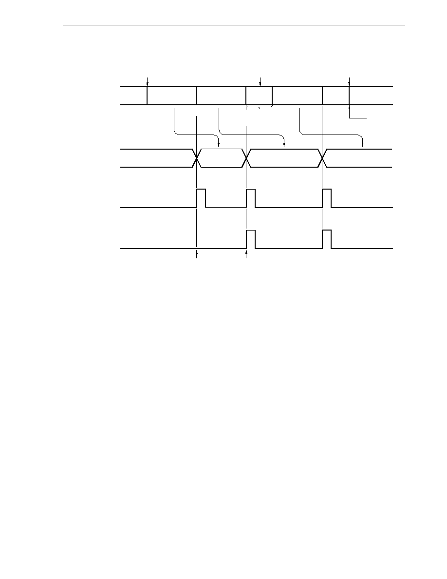
159
CHAPTER 13 A/D CONVERTER
Figure 13-8. A/D Conversion
ADM1 rewrite
ADCS1 = 1
ADS1 rewrite
ADCS1 = 0
A/D conversion
ADCR1
INTAD
(PFEN = 0)
INTAD
(PFEN = 1)
ANIn
ANIn
ANIn
ANIm
ANIm
Stop
ANIn
ANIn
ANIm
Conversion suspended;
Conversion results are not stored
First conversion Condition satisfied
Remarks 1. n = 0, 1, ..., 4
2. m = 0, 1, ..., 4

160
CHAPTER 13 A/D CONVERTER
13.5 A/D Converter Cautions
(1) Current consumption in standby mode
A/D converter stops operating in the standby mode. At this time, current consumption can be reduced by setting
bit 7 (ADCS1) of the A/D converter mode register (ADM1) to 0 to stop conversion.
Figure 13-9 shows how to reduce the current consumption in the standby mode.
Figure 13-9. Example of Method of Reducing Current Consumption in Standby Mode
AV
REF
AV
SS
P-ch
Series resistor string
ADCS1
(2) Input range of ANI0 to ANI4
The input voltages of ANI0 to ANI4 should be within the specification range. In particular, if a voltage higher
than AV
REF
or lower than AV
SS
is input (even if within the absolute maximum rating range), the conversion value
of that channel will be undefined and the conversion values of other channels may also be affected.
(3) Contending operations
<1>
Contention between A/D conversion result register (ADCR1) write and ADCR1 read by instruction
upon the end of conversion
ADCR1 read is given priority. After the read operation, the new conversion result is written to ADCR1.
<2>
Contention between ADCR1 write and A/D converter mode register (ADM1) write or analog input
channel specification register (ADS1) write upon the end of conversion
ADM1 or ADS1 write is given priority. ADCR1 write is not performed, nor is the conversion end interrupt
request signal (INTAD) generated.
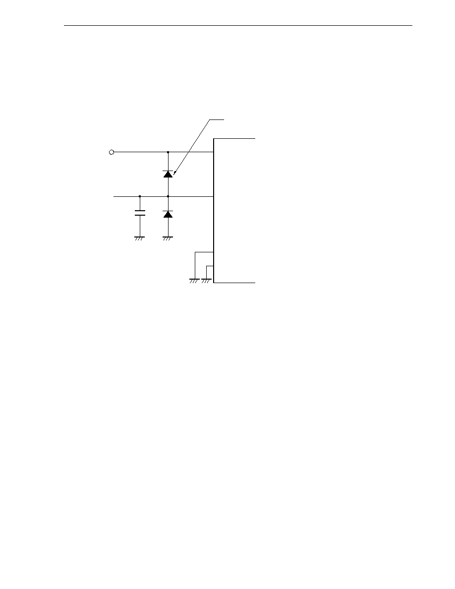
161
CHAPTER 13 A/D CONVERTER
(4) Noise countermeasures
To maintain 8-bit resolution, attention must be paid to noise input to pin AV
REF
and pins ANI0 to ANI4. Because
the effect increases in proportion to the output impedance of the analog input source, it is recommended that
a capacitor be connected externally as shown in Figure 13-10 to reduce noise.
Figure 13-10. Analog Input Pin Connection
Reference
voltage
input
C = 100 to 1000 pF
If there is a possibility that noise equal to or higher than AV
REF
or
equal to or lower than AV
SS
may enter, clamp with a diode with a
small V
F
value (0.3 V or lower).
AV
REF
AV
SS
V
SS
ANI0 to ANI4
(5) ANI0 to ANI4
The analog input pins (ANI0 to ANI4) also function as input port pins (P10 to P14).
When A/D conversion is performed with any of pins ANI0 to ANI4 selected, do not execute a port input instruction
while conversion is in progress, as this may reduce the conversion resolution.
Also, if digital pulses are applied to a pin adjacent to the pin in the process of A/D conversion, the expected A/D
conversion value may not be obtainable due to coupling noise. Therefore, avoid applying pulses to pins adjacent
to the pin undergoing A/D conversion.
(6) AV
REF
pin input impedance
A series resistor string of approximately 21 k
is connected between the AV
REF
pin and the AV
SS
pin.
Therefore, if the output impedance of the reference voltage is high, this will result in parallel connection to the
series resistor string between the AV
REF
pin and the AV
SS
pin, and there will be a large reference voltage error.
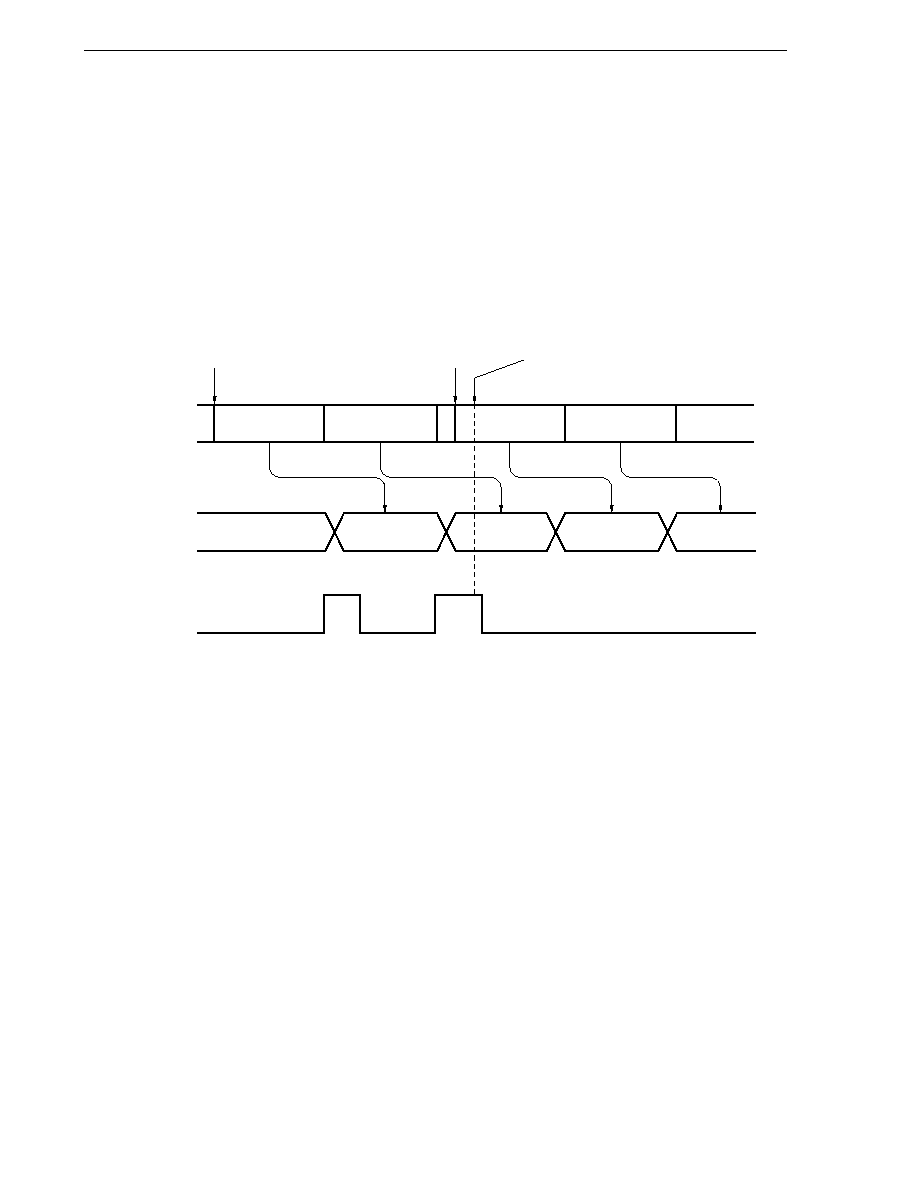
162
CHAPTER 13 A/D CONVERTER
(7) Interrupt request flag (ADIF)
The interrupt request flag (ADIF) is not cleared even if the analog input channel specification register (ADS1)
is changed.
Caution is therefore required since, if a change of analog input pin is performed during A/D conversion, the
A/D conversion result and conversion end interrupt request flag for the pre-change analog input may be set just
before the ADS1 rewrite, and when ADIF is read immediately after the ADS1 rewrite, ADIF may be set despite
the fact that the A/D conversion for the post-change analog input has not ended.
When the A/D conversion is stopped and then resumed, clear ADIF before the A/D conversion operation is
resumed.
Figure 13-11. A/D Conversion End Interrupt Request Generation Timing
ADS1 rewrite
(start of ANIn conversion)
A/D conversion
ADCR1
INTAD
ANIn
ANIn
ANIm
ANIm
ANIn
ANIn
ANIm
ANIm
ADS1 rewrite
(start of ANIm conversion)
ADIF is set but ANIm conversion
has not ended.
Remarks 1. n = 0, 1, ..., 4
2. m = 0, 1, ..., 4
(8) Read of A/D conversion result register (ADCR1)
When write operation is executed to A/D converter mode register (ADM1) and analog input channel specification
register (ADS1), the contents of ADCR1 are undefined. Read the conversion result before write operation is
executed to ADM1, ADS1. If a timing other than the above is used, the correct conversion result may not be read.
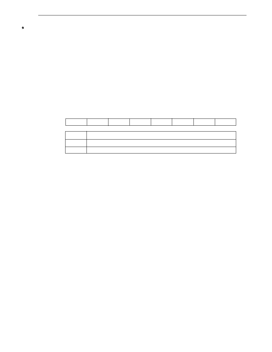
163
CHAPTER 13 A/D CONVERTER
13.6 Cautions on Emulation
(1) D/A converter mode register (DAM1)
To perform debugging with an in-circuit emulator (IE-78K0-NS), the D/A converter mode register (DAM1) must
be set. DAM1 is a register used to set a probe board (IE-780974-NS-EM1).
DAM1 is used when the power-fail detection function is used. Unless DAM1 is set, the power-fail detection function
cannot be used. DAM1 is a write-only register.
Because the IE-780974-NS-EM1 uses an external analog comparator and a D/A converter to implement part of
the power-fail detection function, the reference voltage must be controlled. Therefore, set bit 0 (DACE) of DAM1
to 1 when using the power-fail detection function.
Figure 13-12. D/A Converter Mode Register (DAM1) Format
Address: FF89H After Reset: 00H W
Symbol
7
6
5
4
3
2
1
0
DAM1
0
0
0
0
0
0
0
DACE
DACE
Reference Voltage Control
0
Disabled
1
Enabled (when power-fail detection function is used)
Cautions 1. DAM1 is a special register that must be set when debugging is performed with an in-circuit
emulator. Even if this register is used, the operation of the
�
PD780973 Subseries is not
affected. However, delete the instruction that manipulates this register from the program at
the final stage of debugging.
2. Bits 7 to 1 must be set to 0.
(2) A/D converter of IE-780974-NS-EM1
The A/D converter of the IE-780974-NS-EM1 may not satisfy the rating of the first A/D conversion value right after
A/D conversion has been started.
The above applies only to the IE-780974-NS-EM1 and does not affect the operation of the
�
PD780973 Subseries.

164
[MEMO]
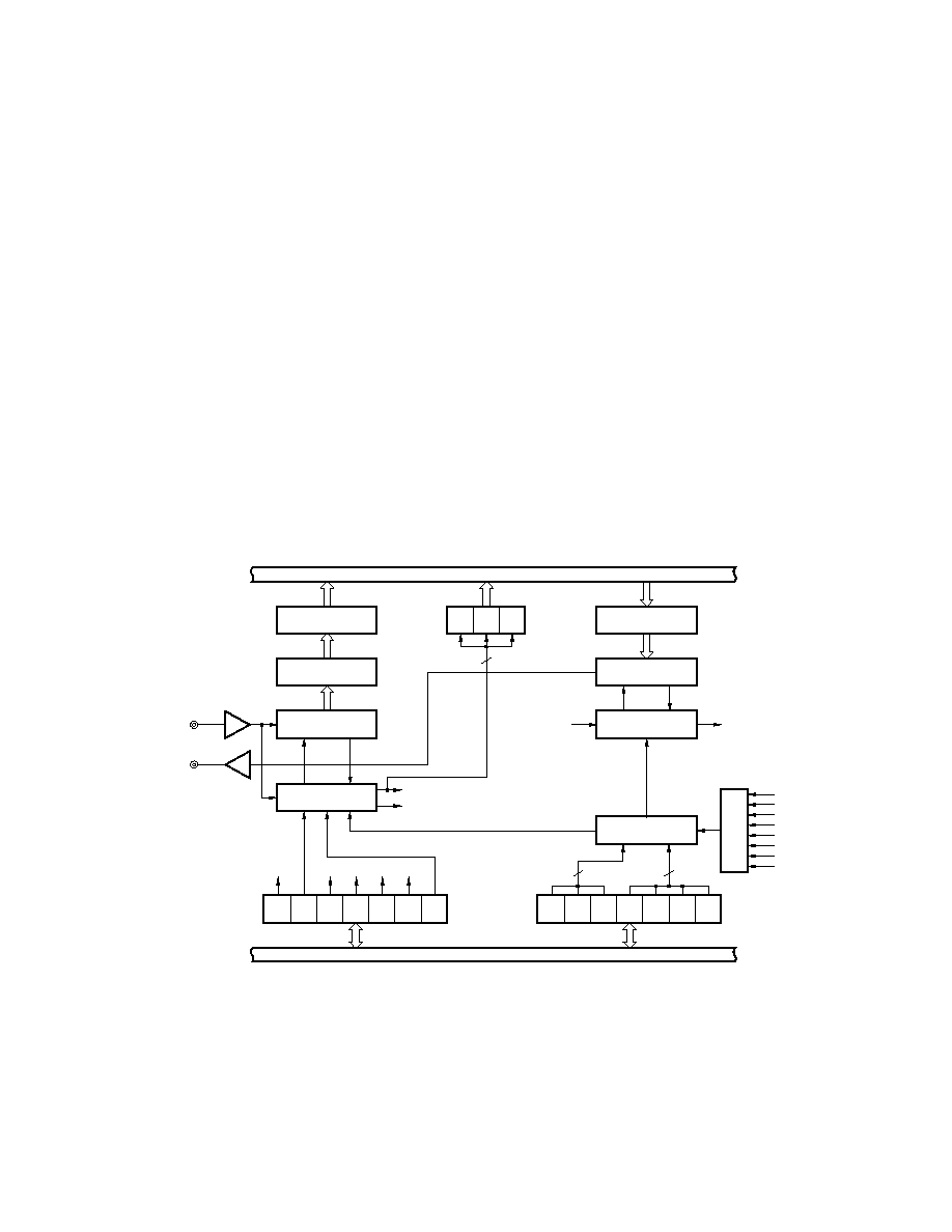
165
CHAPTER 14 SERIAL INTERFACE UART
14.1 UART Functions
The serial interface UART has the following two modes.
(1) Operation stop mode
This mode is used when serial transfers are not performed to reduce power consumption.
For details, see 14.4.1 Operation stop mode.
(2) Asynchronous serial interface (UART) mode
This mode enables full-duplex operation wherein one byte of data is transmitted and received after the start bit.
The on-chip dedicated UART baud rate generator enables communications using a wide range of selectable baud
rates.
The UART baud rate generator can also be used to generate a MIDI-standard baud rate (31.25 kbps).
For details, see 14.4.2 Asynchronous serial interface (UART) mode.
Figure 14-1 shows the UART block diagram.
Figure 14-1. UART Block Diagram
Internal bus
Internal bus
Receive buffer
register (RXB)
Receive shift
register (RXS)
Direction control
circuit
Direction control circuit
Transmit control circuit
Baud rate generator
Transmit shift
register (TXS)
Receive control
circuit
3
3
4
Asynchronous serial interface
status register (ASIS)
Asynchronous serial interface mode register (ASIM)
Baud rate generator control register (BRGC)
RxD/P53
TxD/P54
INTSER
INTSR
TXE
INTST
TXE RXE PS1 PS0 CL
SL ISRM
TPS2 TPS1 TPS0 MDL3 MDL2 MDL1 MDL0
FE
PE
OVE
f
X
/2
f
X
/2
2
f
X
/2
3
f
X
/2
4
f
X
/2
5
f
X
/2
6
f
X
/2
7
f
X
/2
8
Selector
f
SCK

166
CHAPTER 14 SERIAL INTERFACE UART
14.2 UART Configuration
The UART consists of the following hardware.
Table 14-1. UART Configuration
Item
Configuration
Registers
Transmit shift register (TXS)
Receive shift register (RXS)
Receive buffer register (RXB)
Control registers
Asynchronous serial interface mode register (ASIM)
Asynchronous serial interface status register (ASIS)
Baud rate generator control register (BRGC)
(1) Transmit shift register (TXS)
This is the register for setting transmit data. Data written to TXS is transmitted as serial data.
When the data length is set as 7 bits, bits 0 to 6 of the data written to TXS are transmitted as transmit data. Writing
data to TXS starts the transmit operation.
TXS is written with an 8-bit memory manipulation instruction. It cannot be read.
When RESET is input, its value is FFH.
Caution
Do not write to TXS during a transmit operation.
The same address is assigned to TXS and the receive buffer register (RXB). A read
operation reads values from RXB.
(2) Receive shift register (RXS)
This register converts serial data input via the RxD pin to parallel data. When one byte of data is received at
this register, the receive data is transferred to the receive buffer register (RXB).
RXS cannot be manipulated directly by a program.
(3) Receive buffer register (RXB)
This register is used to hold receive data. When one byte of data is received, one byte of new receive data is
transferred from the receive shift register (RXS).
When the data length is set as 7 bits, receive data is transferred to bits 0 to 6 of RXB. In RXB, the MSB must
be set to 0.
RXB is read with an 8-bit memory manipulation instruction. It cannot be written to.
When RESET is input, its value is FFH.
Caution
The same address is assigned to RXB and the transmit shift register (TXS). During a write
operation, values are written to TXS.
(4) Transmit control circuit
The transmit control circuit controls transmit operations, such as adding a start bit, parity bit, and stop bit to data
that is written to the transmit shift register (TXS), based on the values set to the asynchronous serial interface
mode register (ASIM).

167
CHAPTER 14 SERIAL INTERFACE UART
(5) Receive control circuit
The receive control circuit controls receive operations based on the values set to the asynchronous serial interface
mode register (ASIM). During a receive operation, it performs error checking, such as for parity errors, and sets
various values to the asynchronous serial interface status register (ASIS) according to the type of error that is
detected.
14.3 UART Control Registers
The UART uses the following three types of registers for control functions.
� Asynchronous serial interface mode register (ASIM)
� Asynchronous serial interface status register (ASIS)
� Baud rate generator control register (BRGC)
(1) Asynchronous serial interface mode register (ASIM)
This is an 8-bit register that controls UART's serial transfer operations.
ASIM is set with a 1-bit or 8-bit memory manipulation instruction.
RESET input clears the value to 00H.
Figure 14-2 shows the format of ASIM.
Caution
In UART mode, set the port mode register (PM5X) as follows. Besides that, set all output
latches to 0.
� When receiving
Set P53 (R
X
D) to the input mode (PM53 = 1)
� When transmitting
Set P54 (T
X
D) to the output mode (PM54 = 0)
� When transceiving
Set P53 to the input mode and P54 to the output mode
168
CHAPTER 14 SERIAL INTERFACE UART
Figure 14-2. Asynchronous Serial Interface Mode Register (ASIM) Format
Address: FF85H After Reset: 00H R/W
Symbol
7
6
5
4
3
2
1
0
ASIM
TXE
RXE
PS1
PS0
CL
SL
ISRM
0
TXE
RXE
Operation Mode
0
0
Operation stop
0
1
UART mode (receive only)
1
0
UART mode (transmit only)
1
1
UART mode (transmit and receive)
PS1
PS0
Parity Bit Specification
0
0
No parity
0
1
Zero parity always added during transmission
No parity detection during reception (parity errors do not occur)
1
0
Odd parity
1
1
Even parity
CL
Character Length Specification
0
7 bits
1
8 bits
SL
Stop Bit Length Specification for Transmit Data
0
1 bit
1
2 bits
ISRM
Receive Completion Interrupt Control when Error Occurs
0
Receive completion interrupt is issued when an error occurs
1
Receive completion interrupt is not issued when an error occurs
Cautions 1. Do not switch the operation mode until after the current serial transmit/receive operation
has stopped.
2. Bit 0 must be set to 0.
169
CHAPTER 14 SERIAL INTERFACE UART
(2) Asynchronous serial interface status register (ASIS)
When a receive error occurs during UART mode, this register indicates the type of error.
ASIS is read with an 8-bit memory manipulation instruction.
When RESET is input, its value is 00H.
Figure 14-3. Asynchronous Serial Interface Status Register (ASIS) Format
Address: FF86H After Reset: 00H R
Symbol
7
6
5
4
3
2
1
0
ASIS
0
0
0
0
0
PE
FE
OVE
PE
Parity Error Flag
0
No parity error
1
Parity error
(Transmit data parity does not match)
FE
Framing Error Flag
0
No framing error
1
Framing error
Note 1
(Stop bit not detected)
OVE
Overrun Error Flag
0
No overrun error
1
Overrun error
Note 2
(Next receive operation was completed before data was read from receive buffer register)
Notes 1. Even if a stop bit length of two bits has been set to bit 2 (SL) in the asynchronous serial interface
mode register (ASIM), stop bit detection during a receive operation only applies to a stop bit length
of 1 bit.
2. Be sure to read the contents of the receive buffer register (RXB) when an overrun error has
occurred.
Until the contents of RXB are read, further overrun errors will occur when receiving data.
(3) Baud rate generator control register (BRGC)
This register sets the serial clock for UART.
BRGC is set with an 8-bit memory manipulation instruction.
When RESET is input, its value is 00H.
Figure 14-4 shows the format of BRGC.

170
CHAPTER 14 SERIAL INTERFACE UART
Figure 14-4. Baud Rate Generator Control Register (BRGC) Format
Address: FF87H After Reset: 00H R/W
Symbol
7
6
5
4
3
2
1
0
BRGC
0
TPS2
TPS1
TPS0
MDL3
MDL2
MDL1
MDL0
(f
X
= 8.38 MHz)
TPS2
TPS1
TPS0
Source Clock Selection for 5-bit Counter
n
0
0
0
f
X
/2
1
0
0
1
f
X
/2
2
2
0
1
0
f
X
/2
3
3
0
1
1
f
X
/2
4
4
1
0
0
f
X
/2
5
5
1
0
1
f
X
/2
6
6
1
1
0
f
X
/2
7
7
1
1
1
f
X
/2
8
8
MDL3
MDL2
MDL1
MDL0
Input Clock Selection for Baud Rate Generator
k
0
0
0
0
f
SCK
/16
0
0
0
0
1
f
SCK
/17
1
0
0
1
0
f
SCK
/18
2
0
0
1
1
f
SCK
/19
3
0
1
0
0
f
SCK
/20
4
0
1
0
1
f
SCK
/21
5
0
1
1
0
f
SCK
/22
6
0
1
1
1
f
SCK
/23
7
1
0
0
0
f
SCK
/24
8
1
0
0
1
f
SCK
/25
9
1
0
1
0
f
SCK
/26
10
1
0
1
1
f
SCK
/27
11
1
1
0
0
f
SCK
/28
12
1
1
0
1
f
SCK
/29
13
1
1
1
0
f
SCK
/30
14
1
1
1
1
Setting prohibited
--
Cautions 1. Writing to BRGC during a communication operation may cause abnormal output from
the baud rate generator and disable further communication operations. Therefore, do
not write to BRGC during a communication operation.
2. Bit 7 must be set to 0.
Remarks 1. f
SCK
: Source clock for 5-bit counter
2. n
: Value set via TPS0 to TPS2 (1
n
8)
3. k
: Value set via MDL0 to MDL3 (0
k
14)
171
CHAPTER 14 SERIAL INTERFACE UART
14.4 UART Operations
This section explains the two modes of the UART.
14.4.1 Operation stop mode
This mode is used when serial transfers are not performed to reduce power consumption.
In the operation stop mode, P53/RxD and P54/TxD pins can be used as ordinary ports.
(1) Register settings
Operation stop mode settings are made via the asynchronous serial interface mode register (ASIM).
ASIM is set with a 1-bit or 8-bit memory manipulation instruction.
When RESET is input, its value is 00H.
Address: FF85H After Reset: 00H R/W
Symbol
7
6
5
4
3
2
1
0
ASIM
TXE
RXE
PS1
PS0
CL
SL
ISRM
0
TXE
RXE
Operation Mode
RxD/P53 Pin Function
TxD/P54 Pin Function
0
0
Operation stop
Port function
Port function
0
1
UART mode
Serial function
Port function
(receive only)
1
0
UART mode
Port function
Serial function
(transmit only)
1
1
UART mode
Serial function
Serial function
(transmit and receive)
Cautions 1. Do not switch the operation mode until after the current serial transmit/receive operation
has stopped.
2. Bit 0 must be set to 0.
14.4.2 Asynchronous serial interface (UART) mode
This mode enables full-duplex operation wherein one byte of data is transmitted or received after the start bit.
The on-chip dedicated UART baud rate generator enables communications using a wide range of selectable baud
rates.
The UART baud rate generator can also be used to generate a MIDI-standard baud rate (31.25 kbps).
(1) Register settings
UART mode settings are made via the asynchronous serial interface mode register (ASIM), asynchronous serial
interface status register (ASIS), and the baud rate generator control register (BRGC).
172
CHAPTER 14 SERIAL INTERFACE UART
(a) Asynchronous serial interface mode register (ASIM)
ASIM is set with a 1-bit or 8-bit memory manipulation instruction.
When RESET is input, its value is 00H.
Caution
In UART mode, set the port mode register (PM5X) as follows. Besides that, set all output
latches to 0.
� When receiving
Set P53 (R
X
D) to the input mode (PM53 = 1)
� When transmitting
Set P54 (T
X
D) to the output mode (PM54 = 0)
� When transceiving
Set P53 to the input mode and P54 to the output mode
Address: FF85H After Reset: 00H R/W
Symbol
7
6
5
4
3
2
1
0
ASIM
TXE
RXE
PS1
PS0
CL
SL
ISRM
0
TXE
RXE
Operation Mode
RxD/P53 Pin Function
TxD/P54 Pin Function
0
0
Operation stop
Port function
Port function
0
1
UART mode
Serial function
Port function
(receive only)
1
0
UART mode
Port function
Serial function
(transmit only)
1
1
UART mode
Serial function
Serial function
(transmit and receive)
PS1
PS0
Parity Bit Specification
0
0
No parity
0
1
Zero parity always added during transmission
No parity detection during reception (parity errors do not occur)
1
0
Odd parity
1
1
Even parity
CL
Character Length Specification
0
7 bits
1
8 bits
SL
Stop Bit Length Specification for Transmit Data
0
1 bit
1
2 bits
ISRM
Receive Completion Interrupt Control when Error Occurs
0
Receive completion interrupt is issued when an error occurs
1
Receive completion interrupt is not issued when an error occurs
Cautions 1. Do not switch the operation mode until after the current serial transmit/receive
operation has stopped.
2. Bit 0 must be set to 0.
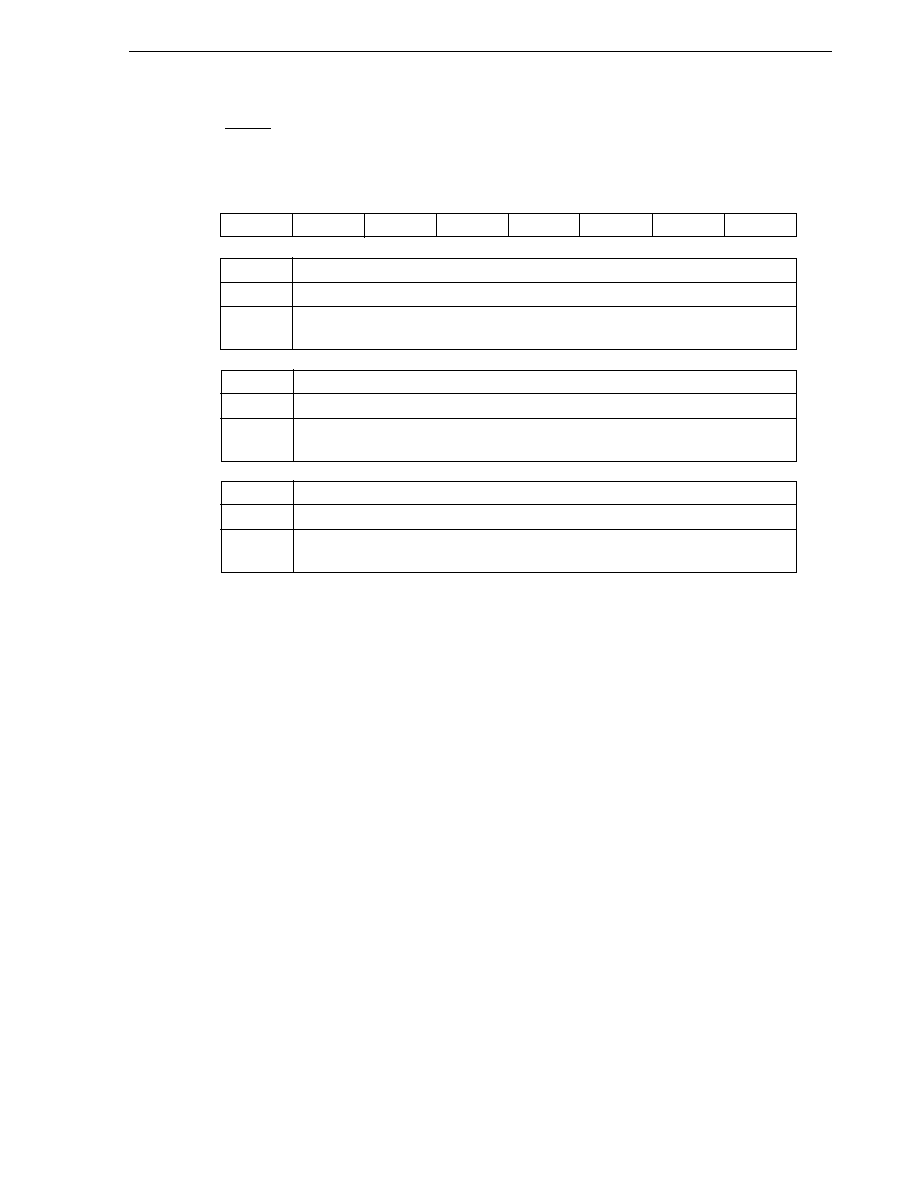
173
CHAPTER 14 SERIAL INTERFACE UART
(b) Asynchronous serial interface status register (ASIS)
ASIS is read with an 8-bit memory manipulation instruction.
When RESET is input, its value is 00H.
Address: FF86H After Reset: 00H R
Symbol
7
6
5
4
3
2
1
0
ASIS
0
0
0
0
0
PE
FE
OVE
PE
Parity Error Flag
0
No parity error
1
Parity error
(Transmit data parity does not match)
FE
Framing Error Flag
0
No framing error
1
Framing error
Note 1
(Stop bit not detected)
OVE
Overrun Error Flag
0
No overrun error
1
Overrun error
Note 2
(Next receive operation was completed before data was read from receive buffer register)
Notes 1. Even if a stop bit length of two bits has been set to bit 2 (SL) in the asynchronous serial interface
mode register (ASIM), stop bit detection during a receive operation only applies to a stop bit
length of 1 bit.
2. Be sure to read the contents of the receive buffer register (RXB) when an overrun error has
occurred.
Until the contents of RXB are read, further overrun errors will occur when receiving data.

174
CHAPTER 14 SERIAL INTERFACE UART
(c) Baud rate generator control register (BRGC)
BRGC is set with an 8-bit memory manipulation instruction.
When RESET is input, its value is 00H.
Address: FF87H After Reset: 00H R/W
Symbol
7
6
5
4
3
2
1
0
BRGC
0
TPS2
TPS1
TPS0
MDL3
MDL2
MDL1
MDL0
(f
X
= 8.38 MHz)
TPS2
TPS1
TPS0
Source Clock Selection for 5-bit Counter
n
0
0
0
f
X
/2
1
0
0
1
f
X
/2
2
2
0
1
0
f
X
/2
3
3
0
1
1
f
X
/2
4
4
1
0
0
f
X
/2
5
5
1
0
1
f
X
/2
6
6
1
1
0
f
X
/2
7
7
1
1
1
f
X
/2
8
8
MDL3
MDL2
MDL1
MDL0
Input Clock Selection for Baud Rate Generator
k
0
0
0
0
f
SCK
/16
0
0
0
0
1
f
SCK
/17
1
0
0
1
0
f
SCK
/18
2
0
0
1
1
f
SCK
/19
3
0
1
0
0
f
SCK
/20
4
0
1
0
1
f
SCK
/21
5
0
1
1
0
f
SCK
/22
6
0
1
1
1
f
SCK
/23
7
1
0
0
0
f
SCK
/24
8
1
0
0
1
f
SCK
/25
9
1
0
1
0
f
SCK
/26
10
1
0
1
1
f
SCK
/27
11
1
1
0
0
f
SCK
/28
12
1
1
0
1
f
SCK
/29
13
1
1
1
0
f
SCK
/30
14
1
1
1
1
Setting prohibited
--
Cautions 1. Writing to BRGC during a communication operation may cause abnormal output
from the baud rate generator and disable further communication operations. There-
fore, do not write to BRGC during a communication operation.
2. Bit 7 must be set to 0.
Remarks 1. f
SCK
: Source clock for 5-bit counter
2. n
: Value set via TPS0 to TPS2 (1
n
8)
3. k
: Value set via MDL0 to MDL3 (0
k
14)

175
CHAPTER 14 SERIAL INTERFACE UART
The transmit/receive clock that is used to generate the baud rate is obtained by dividing the main system
clock.
� Use of main system clock to generate a transmit/receive clock for baud rate
The main system clock is divided to generate the transmit/receive clock. The baud rate generated by
the main system clock is determined according to the following formula.
[Baud rate] =
f
X
[Hz]
2
n+1
(k + 16)
f
X
: Main system clock oscillation frequency
n : Value set via TPS0 to TPS2 (1
n
8)
For details, see Table 14-2.
k : Value set via MDL0 to MDL3 (0
k
14)
Table 14-2 shows the relation between the 5-bit counter's source clock assigned to bits 4 to 6 (TPS0 to TPS2)
of BRGC and the "n" value in the above formula.
Table 14-2. Relation between 5-bit Counter's Source Clock and "n" Value
TPS2
TPS1
TPS0
5-bit Counter's Source Clock Selection
n
0
0
0
f
X
/2
1
0
0
1
f
X
/2
2
2
0
1
0
f
X
/2
3
3
0
1
1
f
X
/2
4
4
1
0
0
f
X
/2
5
5
1
0
1
f
X
/2
6
6
1
1
0
f
X
/2
7
7
1
1
1
f
X
/2
8
8
Remark
f
X
: Main system clock oscillation frequency (f
X
= 8.38 MHz)

176
CHAPTER 14 SERIAL INTERFACE UART
� Error tolerance range for baud rates
The tolerance range for baud rates depends on the number of bits per frame and the counter's division
rate [1/(16 + k)].
Table 14-3 describes the relation between the main system clock and the baud rate and Figure 14-5 shows
an example of a baud rate error tolerance range.
Table 14-3. Relation between Main System Clock and Baud Rate
Baud rate
f
X
= 8.386 MHz
(bps)
BRGC Set Value
Error (%)
600
7BH
1.10
1200
6BH
1.10
2400
5BH
1.10
4800
4BH
1.10
9600
3BH
1.10
19200
2BH
�1.3
31250
21H
1.10
38400
1BH
1.10
76800
0BH
1.10
115200
01H
1.03
Remark
f
X
: Main system clock oscillation frequency
Figure 14-5. Error Tolerance (when k = 0) including Sampling Errors
Basic timing
(clock cycle T)
START
D0
D7
P
STOP
High-speed clock
(clock cycle T')
enabling normal
reception
START
D0
D7
P
STOP
Low-speed clock
(clock cycle T")
enabling normal
reception
START
D0
D7
P
STOP
32T
64T
256T
288T
320T
352T
Ideal
sampling
point
304T
336T
30.45T
60.9T
304.5T
15.5T
15.5T
0.5T
Sampling error
33.55T
67.1T
301.95T
335.5T
Remark
T : 5-bit counter's source clock cycle
Baud rate error tolerance (when k = 0) =
�
15.5
�
100 = 4.8438 (%)
320

177
CHAPTER 14 SERIAL INTERFACE UART
(2) Communication operations
(a) Data format
As shown in Figure 14-6, the format of the transmit/receive data consists of a start bit, character bits, a parity
bit, and one or more stop bits.
The asynchronous serial interface mode register (ASIM) is used to set the character bit length, parity
selection, and stop bit length within each data frame.
Figure 14-6. Format of Transmit/Receive Data in Asynchronous Serial Interface
D0
D1
D2
D3
D4
D5
D6
D7
Start
bit
Parity
bit
Stop bit
1 data frame
� Start bit ............. 1 bit
� Character bits ... 7 bits or 8 bits
� Parity bit ........... Even parity, odd parity, zero parity, or no parity
� Stop bit(s) ........ 1 bit or 2 bits
When "7 bits" is selected as the number of character bits, only the low-order 7 bits (bits 0 to 6) are valid,
so that during a transmission the highest bit (bit 7) is ignored and during reception the highest bit (bit 7) must
be set to "0".
The asynchronous serial interface mode register (ASIM) and the baud rate generator control register (BRGC)
are used to set the serial transfer rate.
If a receive error occurs, information about the receive error can be recognized by reading the asynchronous
serial interface status register (ASIS).

178
CHAPTER 14 SERIAL INTERFACE UART
(b) Parity types and operations
The parity bit is used to detect bit errors in transfer data. Usually, the same type of parity bit is used by the
transmitting and receiving sides. When odd parity or even parity is set, errors in the parity bit (the odd-number
bit) can be detected. When zero parity or no parity is set, errors are not detected.
(i)
Even parity
� During transmission
The number of bits in transmit data that includes a parity bit is controlled so that there are an even
number of "1" bits. The value of the parity bit is as follows.
If the transmit data contains an odd number of "1" bits : the parity bit value is "1"
If the transmit data contains an even number of "1" bits: the parity bit value is "0"
� During reception
The number of "1" bits is counted among the receive data that include a parity bit, and a parity error
occurs when the result is an odd number.
(ii) Odd parity
� During transmission
The number of bits in transmit data that includes a parity bit is controlled so that there is an odd number
of "1" bits. The value of the parity bit is as follows.
If the transmit data contains an odd number of "1" bits : the parity bit value is "0"
If the transmit data contains an even number of "1" bits: the parity bit value is "1"
� During reception
The number of "1" bits is counted among the receive data that include a parity bit, and a parity error
occurs when the result is an even number.
(iii) Zero parity
During transmission, the parity bit is set to "0" regardless of the transmit data.
During reception, the parity bit is not checked. Therefore, no parity errors will occur regardless of
whether the parity bit is a "0" or a "1".
(iv) No parity
No parity bit is added to the transmit data.
During reception, receive data is regarded as having no parity bit. Since there is no parity bit, no parity
errors will occur.
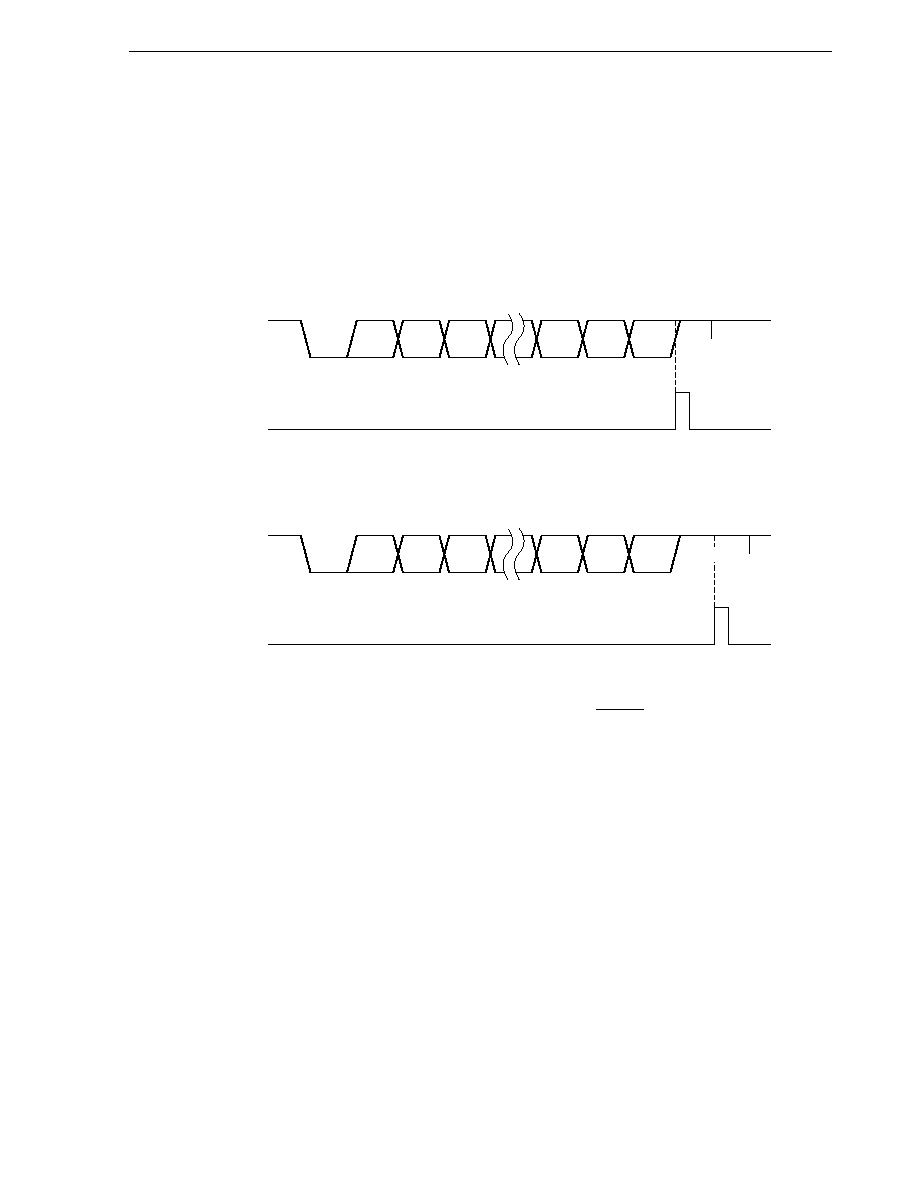
179
CHAPTER 14 SERIAL INTERFACE UART
(c) Transmission
The transmit operation is started when transmit data is written to the transmit shift register (TXS). A start
bit, parity bit, and stop bit(s) are automatically added to the data.
Starting the transmit operation shifts out the data in TXS, thereby emptying TXS, after which a transmit
completion interrupt (INTST) is issued.
The timing of the transmit completion interrupt is shown in Figure 14-7.
Figure 14-7. Timing of Asynchronous Serial Interface Transmit Completion Interrupt
TxD (output)
D0
D1
D2
D6
D7
Parity
STOP
START
INTST
(i) Stop bit length: 1 bit
TxD (output)
D0
D1
D2
D6
D7
Parity
START
INTST
(ii) Stop bit length: 2 bits
STOP
Caution
Do not rewrite the asynchronous serial interface mode register (ASIM) during a transmit
operation. Rewriting to the ASIM register during a transmit operation may disable
further transmit operations (in such case, enter a RESET to restore normal operation).
Whether or not a transmit operation is in progress can be determined by software using
the transmit completion interrupt (INTST) or the interrupt request flag (STIF) that is set
by INTST.
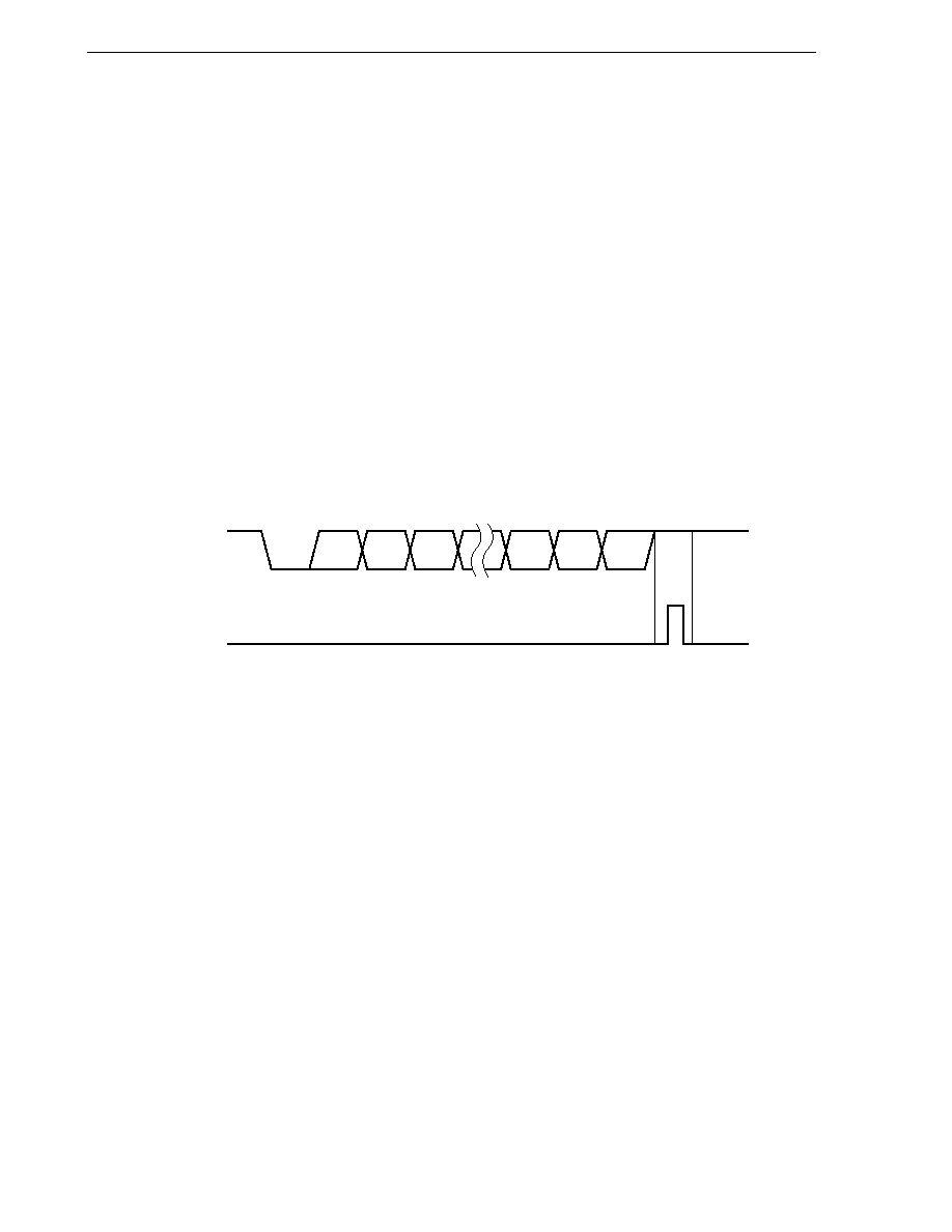
180
CHAPTER 14 SERIAL INTERFACE UART
(d) Reception
The receive operation is enabled when "1" is set to bit 6 (RXE) of the asynchronous serial interface mode
register (ASIM), and input via the RxD pin is sampled.
The serial clock specified by ASIM is used when sampling the RxD pin.
When the RxD pin goes low, the 5-bit counter begins counting and the start timing signal for data sampling
is output when half of the specified baud rate time has elapsed. If sampling the RxD pin input with this start
timing signal yields a low-level result, a start bit is recognized, after which the 5-bit counter is initialized and
starts counting and data sampling begins. After the start bit is recognized, the character data, parity bit,
and one-bit stop bit are detected, at which point reception of one data frame is completed.
Once reception of one data frame is completed, the receive data in the shift register is transferred to the
receive buffer register (RXB) and a receive completion interrupt (INTSR) occurs.
Even if an error has occurred, the receive data in which the error occurred is still transferred to RXB. INTSR
occurs if bit 1 (ISRM) of ASIM is cleared to 0 on occurrence of an error. If the ISRM bit is set to 1, INTSR
does not occur (see Figure 14-9).
If the RXE bit is reset (to "0") during a receive operation, the receive operation is stopped immediately. At
this time, the contents of RXB and ASIS do not change, nor does INTSR or INTSER occur.
Figure 14-8 shows the timing of the asynchronous serial interface receive completion interrupt.
Figure 14-8. Timing of Asynchronous Serial Interface Receive Completion Interrupt
RxD (input)
D0
D1
D2
D6
D7
Parity
STOP
START
INTSR
Caution
Be sure to read the contents of the receive buffer register (RXB) even when a receive
error has occurred. Overrun errors will occur during the next data receive operations
and the receive error status will remain until the contents of RXB are read.

181
CHAPTER 14 SERIAL INTERFACE UART
(e) Receive errors
Three types of errors can occur during a receive operation: parity error, framing error, or overrun error. If,
as the result of data reception, an error flag is set to the asynchronous serial interface status register (ASIS),
a receive error interrupt (INTSER) will occur. Receive error interrupts are generated before receive interrupts
(INTSR). Table 14-4 lists the causes behind receive errors.
As part of receive error interrupt (INTSER) servicing, the contents of ASIS can be read to determine which
type of error occurred during the receive operation (see Table 14-4 and Figure 14-9).
The contents of ASIS are reset (to "0") when the receive buffer register (RXB) is read or when the next data
is received (if the next data contains an error, another error flag will be set).
Table 14-4. Causes of Receive Errors
Receive Error
Cause
ASIS Value
Parity error
Parity specified during transmission does not match parity of receive data
04H
Framing error
Stop bit was not detected
02H
Overrun error
Reception of the next data was completed before data was read from the
01H
receive buffer register
Figure 14-9. Receive Error Timing
RxD (input)
D0
D1
D2
D6
D7
Parity
STOP
START
INTSR
Note
INTSER
(when framing/overrun
error occurs)
INTSER
(when parity error occurs)
Note If a reception error occurs when bit 1 (ISRM) of the asynchronous serial interface mode register
(ASIM) is set to 1, INTSR does not occur.
Cautions 1. The contents of asynchronous serial interface status register (ASIS) are reset (to
"0") when the receive buffer register (RXB) is read or when the next data is received.
To obtain information about the error, be sure to read the contents of ASIS before
reading RXB.
2. Be sure to read the contents of the receive buffer register (RXB) even when a receive
error has occurred. Overrun errors will occur during the next data receive operations
and the receive error status will remain until the contents of RXB are read.

182
[MEMO]
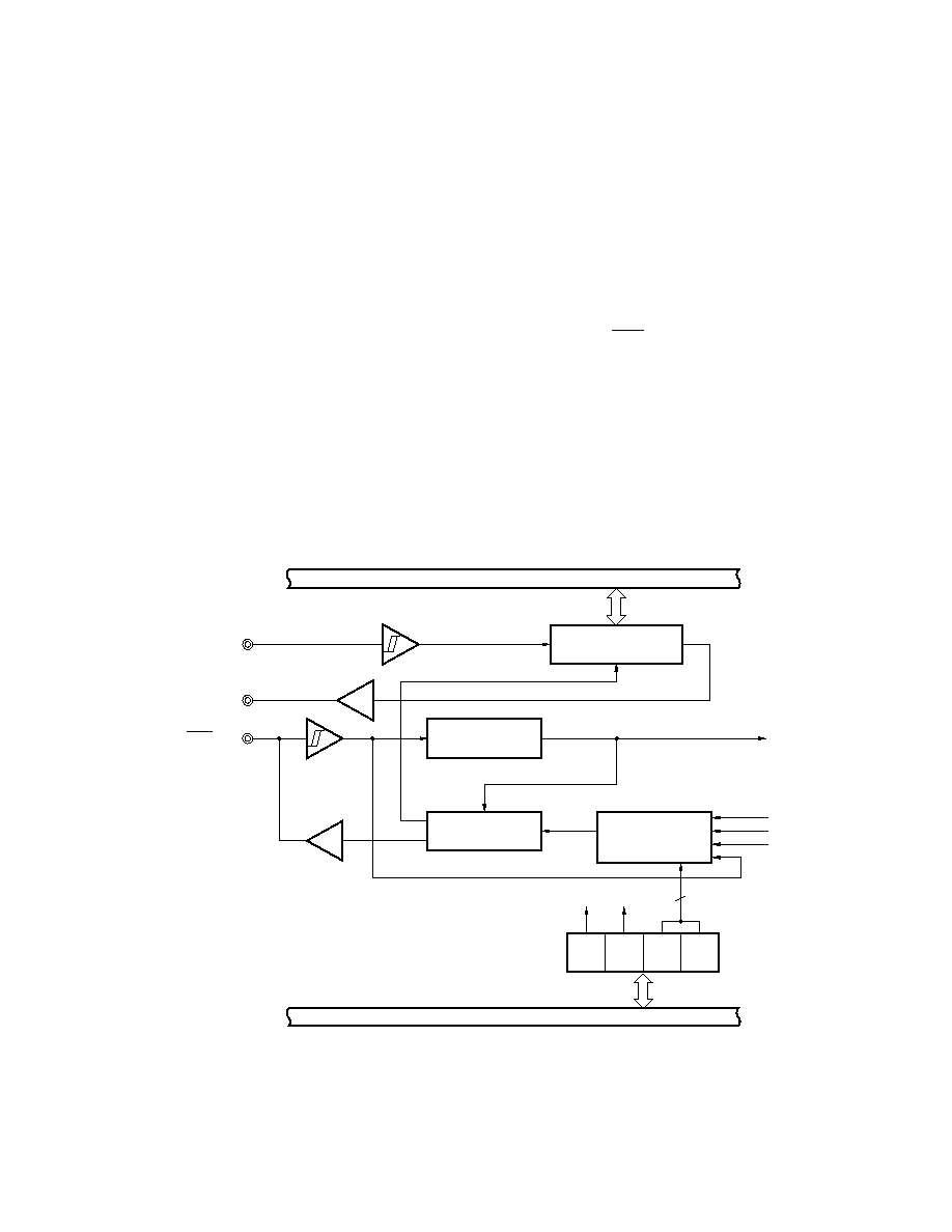
183
CHAPTER 15 SERIAL INTERFACE SIO3
15.1 SIO3 Functions
The serial interface SIO3 has the following two modes.
(1) Operation stop mode
This mode is used when serial transfers are not performed. For details, see 15.4.1 Operation stop mode.
(2) 3-wire serial I/O mode (fixed as MSB first)
This is an 8-bit data transfer mode using three lines: a serial clock line (SCK), serial output line (SO), and serial
input line (SI).
Since simultaneous transmit and receive operations are enabled in 3-wire serial I/O mode, the processing time
for data transfers is reduced.
The first bit in the 8-bit data in serial transfers is fixed as the MSB.
3-wire serial I/O mode is useful for connection to a peripheral I/O device that includes a clock-synchronous serial
interface, a display controller, etc. For details, see 15.4.2 Three-wire serial I/O mode.
Figure 15-1 shows the SIO3 block diagram.
Figure 15-1. SIO3 Block Diagram
Internal bus
Internal bus
Selector
Serial I/O shift
register (SIO)
Serial clock
counter
Serial clock control
circuit
INTCSI
Serial operation mode register (CSIM)
2
SI/P52
SO/P51
SCK/P50
CSIE MODE SCL1 SCL0
f
X
/2
2
f
X
/2
3
f
X
/2
4

184
CHAPTER 15 SERIAL INTERFACE SIO3
15.2 SIO3 Configuration
The SIO3 consists of the following hardware.
Table 15-1. SIO3 Configuration
Item
Configuration
Register
Serial I/O shift register (SIO)
Control register
Serial operation mode register (CSIM)
(1) Serial I/O shift register (SIO)
This is an 8-bit register that performs parallel-serial conversion and serial transmit/receive (shift operations)
synchronized with the serial clock.
SIO is set with an 8-bit memory manipulation instruction.
When "1" is set to bit 7 (CSIE) of the serial operation mode register (CSIM), a serial operation can be started
by writing data to or reading data from SIO.
When transmitting, data written to SIO is output via the serial output (SO).
When receiving, data is read from the serial input (SI) and written to SIO.
The RESET signal resets the register value to 00H.
Caution
Do not access SIO during a transfer operation unless the access is triggered by a transfer
start (Read is disabled when MODE = 0 and write is disabled when MODE = 1).
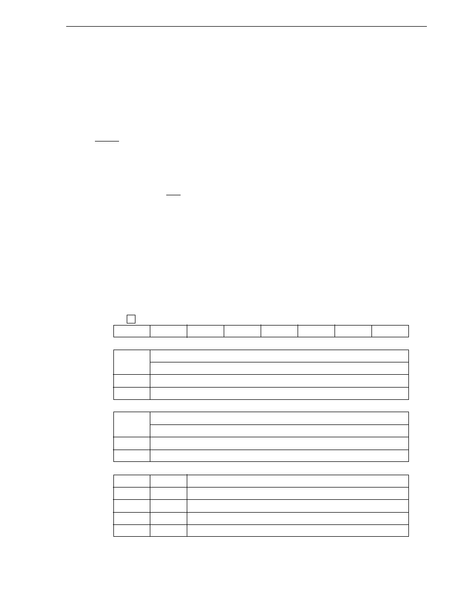
185
CHAPTER 15 SERIAL INTERFACE SIO3
15.3 SIO3 Control Register
The SIO3 uses the following type of register for control functions.
� Serial operation mode register (CSIM)
(1) Serial operation mode register (CSIM)
This register is used to enable or disable SIO3's serial clock, operation modes, and specific operations.
CSIM is set with a 1-bit or 8-bit memory manipulation instruction.
The RESET input resets the value to 00H.
Caution
In the 3-wire serial I/O mode, set the port mode register (PM5X) as follows. Besides that,
set all output latches to 0.
� When serial clock output (Master transmit or Master receive)
Set P50 (SCK) to the output mode (PM50 = 0)
� When serial clock input (Slave transmit or Slave receive)
Set P50 to the input mode (PM50 = 1)
� When transmit/transceive mode
Set P51 (SO) to the output mode (PM51 = 0)
� When receive mode
Set P52 (SI) to the input mode (PM52 = 1)
Figure 15-2. Serial Operation Mode Register (CSIM) Format
Address: FF84H After Reset: 00H R/W
Symbol
7
6
5
4
3
2
1
0
CSIM
CSIE
0
0
0
0
MODE
SCL1
SCL0
CSIE
SIO3 Operation Enable/Disable Specification
Shift Register Operation
0
Operation disable
1
Operation enable
MODE
Transfer Operation Mode Flag
Operation Mode
0
Transmit or transmit/receive mode
1
Receive-only mode
SCL1
SCL0
Clock Selection (f
X
= 8.38 MHz)
0
0
External clock input
0
1
f
X
/2
2
1
0
f
X
/2
3
1
1
f
X
/2
4
Caution
Bits 3 to 6 must be set to 0.
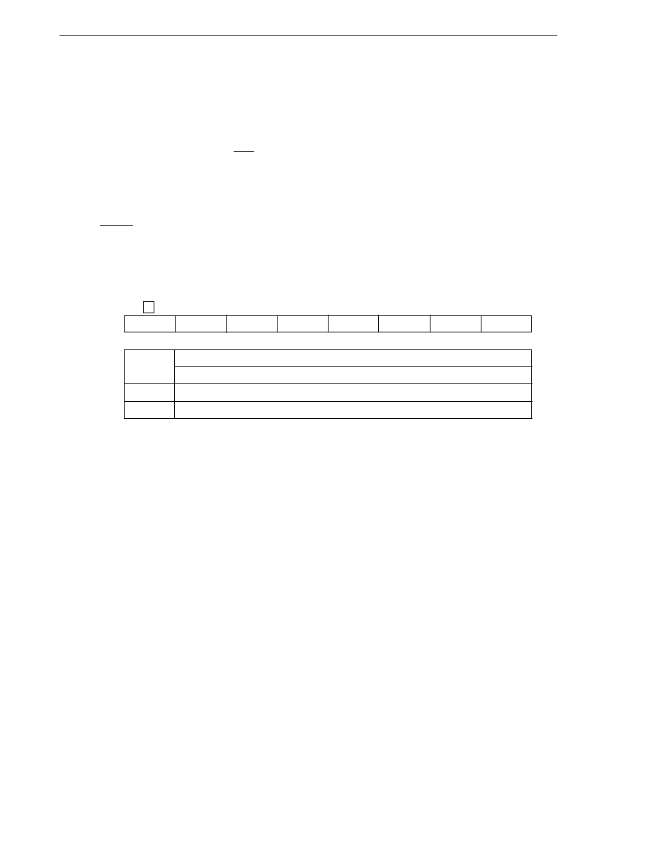
186
CHAPTER 15 SERIAL INTERFACE SIO3
15.4 SIO3 Operations
This section explains the two modes of the SIO3.
15.4.1 Operation stop mode
This mode is used when serial transfers are not performed to reduce power consumption.
In the operation stop mode, the P50/SCK, P51/SO, and P52/SI pins can be used as normal I/O ports as well.
(1) Register settings
Operation stop mode are set via serial operation mode register (CSIM).
CSIM is set with a 1-bit or 8-bit memory manipulation instruction.
The RESET input resets the value to 00H.
Figure 15-3. Serial Operation Mode Register (CSIM) Format
Address: FF84H After Reset: 00H R/W
Symbol
7
6
5
4
3
2
1
0
CSIM
CSIE
0
0
0
0
MODE
SCL1
SCL0
CSIE
SIO3 Operation Enable/Disable Specification
Shift Register Operation
0
Operation disable
1
Operation enable
Caution
Bits 3 to 6 must be set to 0.

187
CHAPTER 15 SERIAL INTERFACE SIO3
15.4.2 Three-wire serial I/O mode
The three-wire serial I/O mode is useful when connecting a peripheral I/O device that includes a clock-synchronous
serial interface, a display controller, etc.
This mode executes data transfers via three lines: a serial clock line (SCK), serial output line (SO), and serial input
line (SI).
(1) Register settings
3-wire serial I/O mode is set via serial operation mode register (CSIM).
CSIM is set with a 1-bit or 8-bit memory manipulation instruction.
The RESET input resets the value to 00H.
Caution
In the 3-wire serial I/O mode, set the port mode register (PM5X) as follows. Besides that,
set all output latches to 0.
� When serial clock output (Master transmit or Master receive)
Set P50 (SCK) to the output mode (PM50 = 0)
� When serial clock input (Slave transmit or Slave receive)
Set P50 to the input mode (PM50 = 1)
� When transmit/transceive mode
Set P51 (SO) to the output mode (PM51 = 0)
� When receive mode
Set P52 (SI) to the input mode (PM52 = 1)
Figure 15-4. Serial Operation Mode Register (CSIM) Format
Address: FF84H After Reset: 00H R/W
Symbol
7
6
5
4
3
2
1
0
CSIM
CSIE
0
0
0
0
MODE
SCL1
SCL0
CSIE
SIO3 Operation Enable/Disable Specification
Shift Register Operation
0
Operation disable
1
Operation enable
MODE
Transfer Operation Mode Flag
Operation Mode
0
Transmit or transmit/receive mode
1
Receive-only mode
SCL1
SCL0
Clock Selection (f
X
= 8.38 MHz)
0
0
External clock input
0
1
f
X
/2
2
1
0
f
X
/2
3
1
1
f
X
/2
4
Caution
Bits 3 to 6 must be set to 0.
188
CHAPTER 15 SERIAL INTERFACE SIO3
(2) Communication operations
In the three-wire serial I/O mode, data is transmitted and received in 8-bit units. Each bit of data is transmitted
or received in synchronized with the serial clock.
The serial I/O shift register (SIO) is shifted in synchronized with the falling edge of the serial clock. Transmission
data is held in the SO latch and is output from the SO pin. Data that is received via the SI pin in synchronized
with the rising edge of the serial clock is latched to SIO.
Completion of an 8-bit transfer automatically stops operation of SIO3 and sets a serial transfer completion flag.
Figure 15-5. Three-Wire Serial I/O Mode Timing
SI
DI7
DI6
DI5
DI4
DI3
DI2
DI1
DI0
Serial transfer
completion flag
Serial clock
1
SO
DO7
DO6
DO5
DO4
DO3
DO2
DO1
DO0
2
3
4
5
6
7
8
Transfer completion
Transfer starts in synchronized with the serial clock's falling edge
(3) Transfer start
A serial transfer starts when the following two conditions have been satisfied and transfer data has been set to
serial I/O shift register (SIO).
� SIO3 operation control bit (CSIE) = 1
� After an 8-bit serial transfer, the internal serial clock is either stopped or is set to high level.
� Transmit or transmit/receive mode
When CSIE = 1 and MODE = 0, transfer starts when writing to SIO.
� Receive-only mode
When CSIE = 1 and MODE = 1, transfer starts when reading from SIO.
Caution
After data has been written to SIO, transfer will not start even if the CSIE bit value is set
to "1".
Completion of an 8-bit transfer automatically stops the serial transfer operation and sets a serial transfer
completion flag.

189
CHAPTER 16 LCD CONTROLLER/DRIVER
16.1 LCD Controller/Driver Functions
The functions of the LCD controller/driver incorporated in the
�
PD780973 Subseries are shown below.
(1) Automatic output of segment signals and common signals is possible by automatic reading of the display data
memory.
(2) Display mode
� 1/4 duty (1/3 bias)
(3) Any of four frame frequencies can be selected in each display mode.
(4) Maximum of 20 segment signal outputs (S0 to S19); 4 common signal outputs (COM0 to COM3).
Fifteen of the segment signal outputs can be switched to input/output ports in units of 2 (P81/S19 to P87/S13,
P90/S12 to P97/S5).
The maximum number of displayable pixels is shown in Table 16-1.
Table 16-1. Maximum Number of Display Pixels
Bias Method
Time Division
Common Signals Used
Maximum Number of Display Pixels
1/3
4
COM0 to COM3
80 (20 segments
�
4 commons)
Note
Note 10 digits on
type LCD panel with 2 segments/digit.
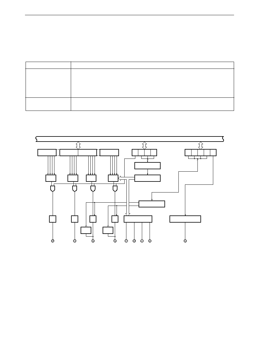
190
CHAPTER 16 LCD CONTROLLER/DRIVER
16.2 LCD Controller/Driver Configuration
The LCD controller/driver consists of the following hardware.
Table 16-2. LCD Controller/Driver Configuration
Item
Configuration
Display outputs
Segment signals : 20
Dedicated segment signals: 5
Segment signal/input/output port alternate function: 14
Segment signal/input/output port/16-bit timer prescaler output alternate
function: 1
Common signals : 4 (COM0 to COM3)
Control registers
LCD display mode register (LCDM)
LCD display control register (LCDC)
Figure 16-1. LCD Controller/Driver Block Diagram
Internal bus
FA59H
7 6 5 4 3 2 1 0
FA67H
7 6 5 4 3 2 1 0
FA68H
7 6 5 4 3 2 1 0
FA6CH
7 6 5 4 3 2 1 0
Display data memory
3 2 1 0
selector
3 2 1 0
selector
3 2 1 0
selector
3 2 1 0
selector
.........
.........
Note
Note
Note
Note
P97 output
buffer
S4
S0
.........
.........
...............
.........
S5/P97
P81 output
buffer
S19/P81
Segment selector
Common driver
COM0
COM3
COM1 COM2
LCD driver voltage controller
V
LCD
LCDON LCDM6 LCDM5 LCDM4
LCD clock selector
f
LCD
3
LCD display mode register (LCDM)
LCDC6 LCDC5 LCDC4 LIPS
LCD display control register (LCDC)
4
..................
.........
Timing controller
LCDC7
Note Segment driver
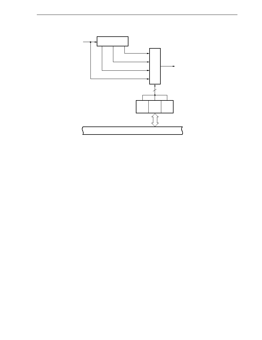
191
CHAPTER 16 LCD CONTROLLER/DRIVER
Figure 16-2. LCD Clock Select Circuit Block Diagram
Prescaler
f
LCD
/2
3
f
X
/2
14
f
LCD
/2
2
f
LCD
/2
f
LCD
Selector
LCDM6 LCDM5 LCDM4
3
LCDCL
LCD display mode register
Internal bus
Remarks 1. LCDCL : LCD clock
2. f
LCD
: LCD clock frequency
192
CHAPTER 16 LCD CONTROLLER/DRIVER
16.3 LCD Controller/Driver Control Registers
The LCD controller/driver is controlled by the following two registers.
� LCD display mode register (LCDM)
� LCD display control register (LCDC)
(1) LCD display mode register (LCDM)
This register sets display operation enabling/disabling, the LCD clock, frame frequency.
LCDM is set with a 1-bit or 8-bit memory manipulation instruction.
RESET input clears LCDM to 00H.
Figure 16-3. LCD Display Mode Register (LCDM) Format
Address: FFB0H After Reset: 00H R/W
Symbol
7
6
5
4
3
2
1
0
LCDM
LCDON
LCDM6
LCDM5
LCDM4
0
0
0
0
LCDON
LCD Display Enable/Disable
0
Display off (all segment outputs are non-select signal outputs)
1
Display on
LCDM6
LCDM5
LCDM4
LCD Clock Selection (f
X
= 8.38 MHz)
0
0
0
f
X
/2
17
(64 Hz)
0
0
1
f
X
/2
16
(128 Hz)
0
1
0
f
X
/2
15
(256 Hz)
0
1
1
f
X
/2
14
(512 Hz)
Other than above
Setting prohibited
Remark f
X
= Main system clock oscillation frequency
193
CHAPTER 16 LCD CONTROLLER/DRIVER
(2) LCD display control register (LCDC)
This register sets cutoff of the current flowing to split resistors for LCD drive voltage generation and switchover
between segment output and input/output port functions.
LCDC is set with a 1-bit or 8-bit memory manipulation instruction.
RESET input clears LCDC to 00H.
Figure 16-4. LCD Display Control Register (LCDC) Format
Address: FFB2H After Reset: 00H R/W
Symbol
7
6
5
4
3
2
1
0
LCDC
LCDC7
LCDC6
LCDC5
LCDC4
0
0
0
LIPS
LCDC7
LCDC6
LCDC5
LCDC4
P81/S19 to P97/S5 Pin Functions
Port Pins
Segment Pins
0
0
0
0
P81 to P97
None
0
0
0
1
P81 to P95
S5 to S6
0
0
1
0
P81 to P93
S5 to S8
0
0
1
1
P81 to P91
S5 to S10
0
1
0
0
P81 to P87
S5 to S12
0
1
0
1
P81 to P85
S5 to S14
0
1
1
0
P81 to P83
S5 to S16
0
1
1
1
P81
S5 to S18
1
0
0
0
None
S5 to S19
Other than above
Setting prohibited
LIPS
LCD Driving Power Supply Selection
0
Does not supply power to LCD.
1
Supplies power to LCD from V
DD
pin.
Cautions 1. Pins which perform segment output cannot be used as output port pins even if 0 is
set in the port mode register.
2. If a pin which performs segment output is read as a port, its value will be 0.

194
CHAPTER 16 LCD CONTROLLER/DRIVER
16.4 LCD Controller/Driver Settings
LCD controller/driver settings should be performed as shown below.
<1> Set the initial value in the display data memory (FA59H to FA6CH).
<2> Set the pins to be used as segment outputs in the LCD display control register (LCDC).
<3> Set the LCD clock in the LCD display mode register (LCDM).
Next, set data in the display data memory according to the display contents.
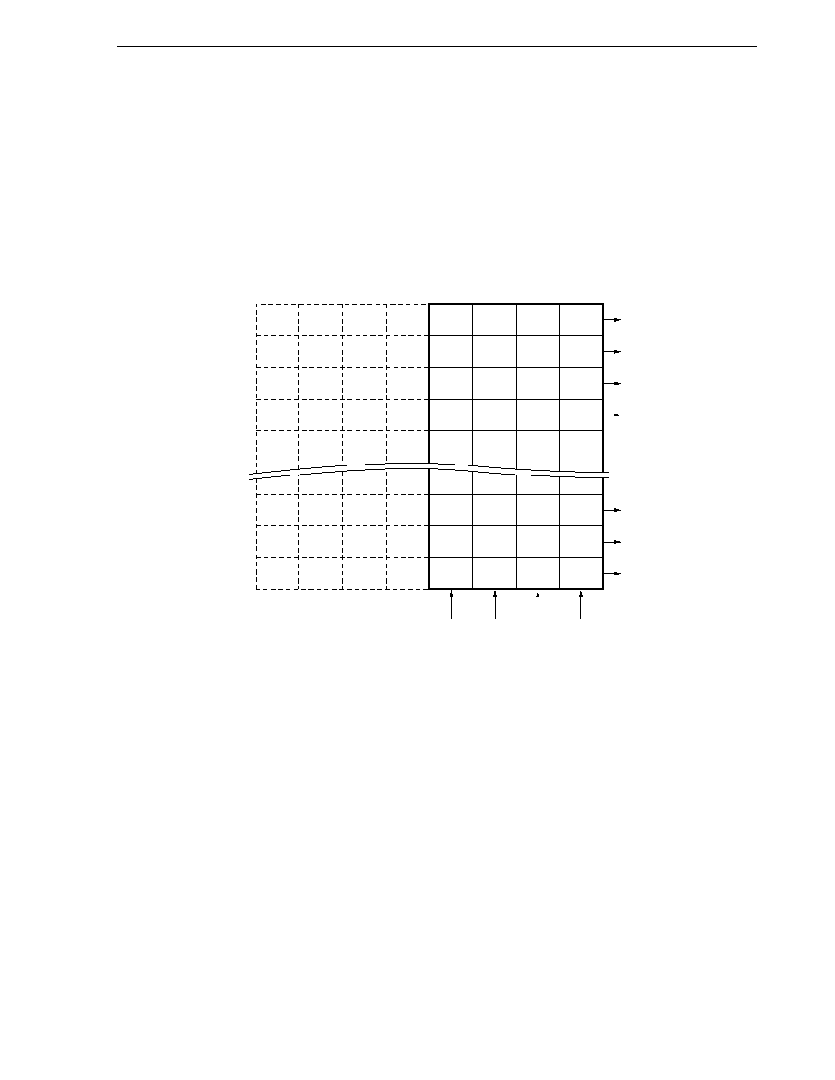
195
CHAPTER 16 LCD CONTROLLER/DRIVER
16.5 LCD Display Data Memory
The LCD display data memory is mapped onto addresses FA59H to FA6CH. The data stored in the LCD display
data memory can be displayed on an LCD panel by the LCD controller/driver.
Figure 16-5 shows the relationship between the LCD display data memory contents and the segment outputs/
common outputs.
Any area not used for display can be used as normal RAM.
Figure 16-5. Relationship between LCD Display Data Memory Contents
and Segment/Common Outputs
S0
FA6CH
S1
FA6BH
S2
FA6AH
S3
FA69H
S17/P83
FA5BH
S18/P82
FA5AH
S19/P81
FA59H
COM3
COM2
COM1
COM0
b
7
b
6
b
5
b
4
b
3
b
2
b
1
b
0
Address
Caution
The higher 4 bits of the LCD display data memory do not incorporate memory. Be sure to set
them to 0.
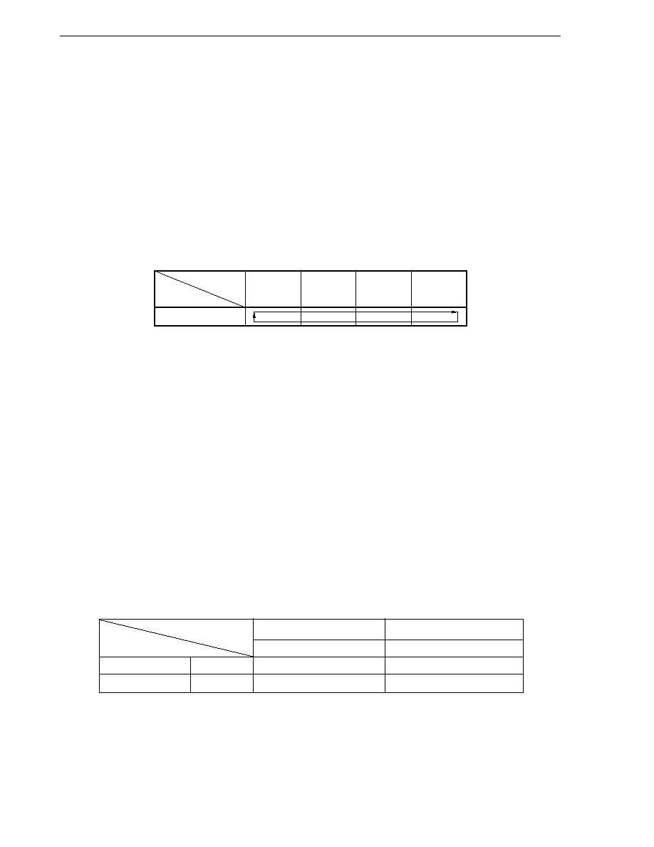
196
CHAPTER 16 LCD CONTROLLER/DRIVER
16.6 Common Signals and Segment Signals
An individual pixel on an LCD panel lights when the potential difference of the corresponding common signal
and segment signal reaches or exceeds a given voltage (the LCD drive voltage V
LCD
). The light goes off when the
potential difference becomes V
LCD
or lower.
As an LCD panel deteriorates if a DC voltage is applied in the common signals and segment signals, it is driven
by AC voltage.
(1) Common signals
For common signals, the selection timing order is as shown in Table 16-3, and operations are repeated with these
as the cycle.
Table 16-3. COM Signals
COM signal
Time division
4-time division
COM0
COM1
COM2
COM3
(2) Segment signals
Segment signals correspond to a 20-byte LCD display data memory (FA59H to FA6CH). Each display data
memory bit 0, bit 1, bit 2, and bit 3 is read in synchronization with the COM0, COM1, COM2 and COM3 timings
respectively, and if the value of the bit is 1, it is converted to the selection voltage. If the value of the bit is 0,
it is converted to the non-selection voltage and output to a segment pin (S0 to S19) (S18 to S5 have an alternate
function as input/output port pins).
Consequently, it is necessary to check what combination of front surface electrodes (corresponding to the
segment signals) and rear surface electrodes (corresponding to the common signals) of the LCD panel to be
used form the display pattern, and then write bit data corresponding on a one-to-one basis with the pattern to
be displayed.
Bits 4 to 7 are fixed at 0.
(3) Common signal and segment signal output waveforms
The voltages shown in Table 16-4 are output in the common signals and segment signals.
The
�
V
LCD
ON voltage is only produced when the common signal and segment signal are both at the selection
voltage; other combinations produce the OFF voltage.
Table 16-4. LCD Drive Voltage
Segment
Select Level
Non-Select Level
Common
V
SS1
, V
LC0
V
LC1
, V
LC2
Select level
V
LC0
, V
SS1
�V
LCD
, +V
LCD
�1/3V
LCD
, +1/3V
LCD
Non-select level
V
LC2
, V
LC1
�1/3V
LCD
, +1/3V
LCD
�1/3V
LCD
, +1/3V
LCD
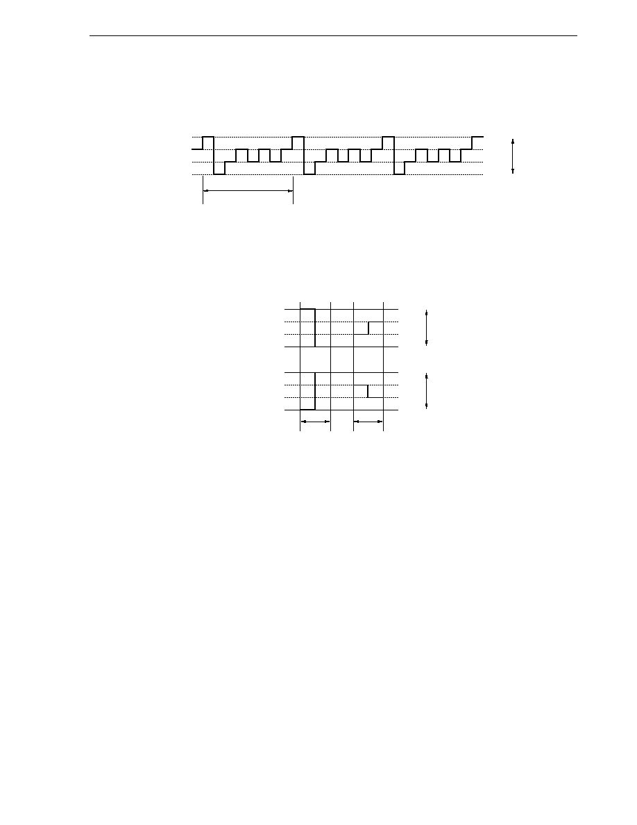
197
CHAPTER 16 LCD CONTROLLER/DRIVER
Figure 16-6 shows the common signal waveform, and Figure 16-7 shows the common signal and segment signal
voltages and phases.
Figure 16-6. Common Signal Waveform
T
F
= 4 x T
COMn
(Divided by 4)
V
LC0
V
SS
V
LCD
V
LC1
V
LC2
T: One LCDCL cycle
T
F
: Frame frequency
Figure 16-7. Common Signal and Segment Signal Voltages and Phases
Selected
Not selected
Common signal
Segment signal
V
LC0
V
SS
V
LCD
V
LC0
V
SS
V
LCD
T
T
V
LC2
V
LC2
V
LC1
V
LC1
T : One LCDCL cycle
198
CHAPTER 16 LCD CONTROLLER/DRIVER
16.7 Supplying LCD Drive Voltage V
LC0
, V
LC1
, and V
LC2
The
�
PD780973 Subseries have a split resistor to create an LCD drive voltage, and the drive voltage is fixed
to 1/3 bias.
To supply various LCD drive voltages, internal V
DD
or external V
LCD
supply voltage can be selected.
Table 16-5. LCD Drive Voltage
Bias Method
1/3 Bias Method
LCD Drive Voltage
V
LC0
V
LCD
V
LC1
2/3 V
LCD
V
LC2
1/3 V
LCD
Figure 16-8 shows an example of supplying an LCD drive voltage from an internal source according to Table
16-5. By using variable resistors r
1
and r
2
, a non-stepwise LCD drive voltage can be supplied.
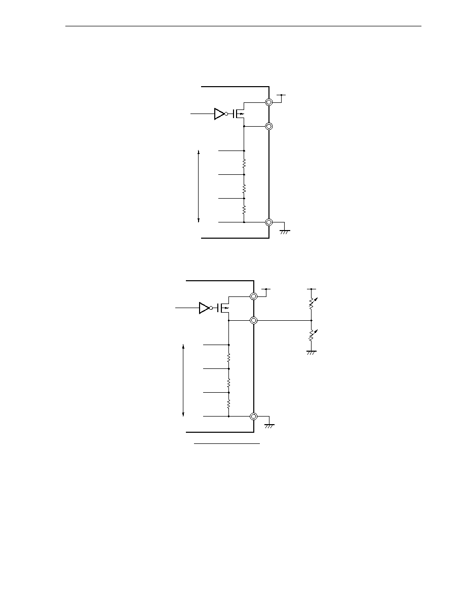
199
CHAPTER 16 LCD CONTROLLER/DRIVER
Figure 16-8. Example of Connection of LCD Drive Power Supply
(a) To supply LCD drive voltage from V
DD
V
DD
V
SS
V
LCD
= V
DD
P-ch
LIPS
(= 1)
R
R
R
V
SS
V
LC2
V
LC1
V
LC0
V
LCD
Open V
LCD
pin
(b) To supply LCD drive voltage from external source
V
DD
V
LCD
V
DD
r
1
r
2
V
SS
V
SS
V
LCD
=
�
V
DD
P-ch
LIPS
(= 0)
R
R
R
V
SS
V
LC2
V
LC1
V
LC0
V
LCD
3R
�
r
2
3R
�
r
2
+ 3R
�
r
1
+ r
1
�
r
2

200
CHAPTER 16 LCD CONTROLLER/DRIVER
16.8 Display Mode
16.8.1 4-time-division display example
Figure 16-10 shows the connection of a 4-time-division type 10-digit LCD panel with the display pattern shown
in Figure 16-9 with the
�
PD780973 Subseries segment signals (S0 to S19) and common signals (COM0 to COM3).
The display example is "1234567890," and the display data memory contents (addresses FA59H to FA6CH)
correspond to this.
An explanation is given here taking the example of the 5th digit "6" (
). In accordance with the display pattern
in Figure 16-9, selection and non-selection voltages must be output to pins S8 and S9 as shown in Table 16-6 at
the COM0 to COM3 common signal timings.
Table 16-6. Selection and Non-Selection Voltages (COM0 to COM3)
Segment
S8
S9
Common
COM0
S
S
COM1
NS
S
COM2
S
S
COM3
NS
S
S: Selection, NS: Non-selection
From this, it can be seen that 0101 must be prepared in the display data memory (address FA64H) corresponding
to S8.
Examples of the LCD drive waveforms between S8 and the COM0 and COM1 signals are shown in Figure 16-
11 (for the sake of simplicity, waveforms for COM2 and COM3 have been omitted). When S8 is at the selection
voltage at the COM0 selection timing, it can be seen that the +V
LCD
/�V
LCD
AC square wave, which is the LCD
illumination (ON) level, is generated.
Figure 16-9. 4-Time-Division LCD Display Pattern and Electrode Connections
,,
,,
,,
,,
,,
,,
,
,
,
,
,
,
COM0
S
2n
COM1
S
2n + 1
COM2
COM3
n = 0 to 9
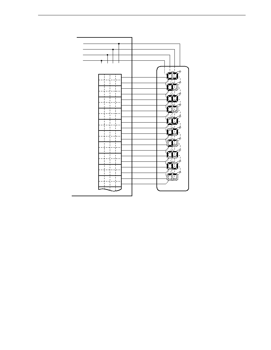
201
CHAPTER 16 LCD CONTROLLER/DRIVER
Figure 16-10. 4-Time-Division LCD Panel Connection Example
Timing strobes
COM3
COM2
COM1
COM0
BIT0
BIT1
BIT2
BIT3
S0
S1
S2
S3
1
1
0
FA6CH
1
1
1
B
1
1
0
A
1
0
0
9
S4
S5
S6
S7
1
1
0
8
1
1
1
7
1
1
0
6
1
0
0
5
S8
S9
S10
S11
1
1
0
4
1
1
1
3
1
1
0
2
1
0
1
1
S12
S13
S14
S15
0
1
0
0
1
0
0
FA5FH
1
1
0
E
0
0
1
D
S16
S17
S18
S19
1
0
0
C
0
1
1
B
0
1
0
A
0
0
0
FA59H
Data memory address
LCD panel
1
0
1
1
1
1
1
0
0
1
0
1
1
1
1
1
1
1
1
0

202
CHAPTER 16 LCD CONTROLLER/DRIVER
Figure 16-11. 4-Time-Division LCD Drive Waveform Examples (1/3 Bias Method)
,
,
,
,
T
F
V
LC0
V
LC2
COM0
+V
LCD
0
COM0 to S8
�V
LCD
V
LC1
+1/3V
LCD
�1/3V
LCD
V
SS
V
LC0
V
LC2
COM1
V
LC1
V
SS
V
LC0
V
LC2
COM2
V
LC1
V
SS
V
LC0
V
LC2
COM3
V
LC1
V
SS
+V
LCD
0
COM1 to S8
�V
LCD
+1/3V
LCD
�1/3V
LCD
V
LC0
V
LC2
S8
V
LC1
V
SS
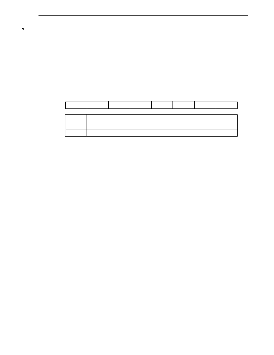
203
CHAPTER 16 LCD CONTROLLER/DRIVER
16.9 Cautions on Emulation
(1) LCD timer control register (LCDTM)
To perform debugging with an in-circuit emulator (IE-78K0-NS), the LCD timer control register (LCDTM) must
be set. LCDTM is a register used to set a probe board (IE-780974-NS-EM1).
LCDTM is a write-only register that controls supply of the LCD clock. Unless LCDTM is set, the LCD controller/
driver does not operate. Therefore, set bit 1 (TMC21) of LCDTM to 1 when using the LCD controller/driver.
Figure 16-12. LCD Timer Control Register (LCDTM) Format
Address: FF4AH After Reset: 00H W
Symbol
7
6
5
4
3
2
1
0
LCDTM
0
0
0
0
0
0
TMC21
0
TMC21
LCD Clock Supply Control
0
LCD controller/driver stop mode (supply of LCD clock is stopped)
1
LCD controller/driver operating mode (supply of LCD clock is enabled)
Cautions 1. LCDTM is a special register that must be set when debugging is performed with an in-circuit
emulator. Even if this register is used, the operation of the
�
PD780973 Subseries is not
affected. However, delete the instruction that manipulates this register from the program at
the final stage of debugging.
2. Bits 7 to 2, and bit 0 must be set to 0.

204
[MEMO]
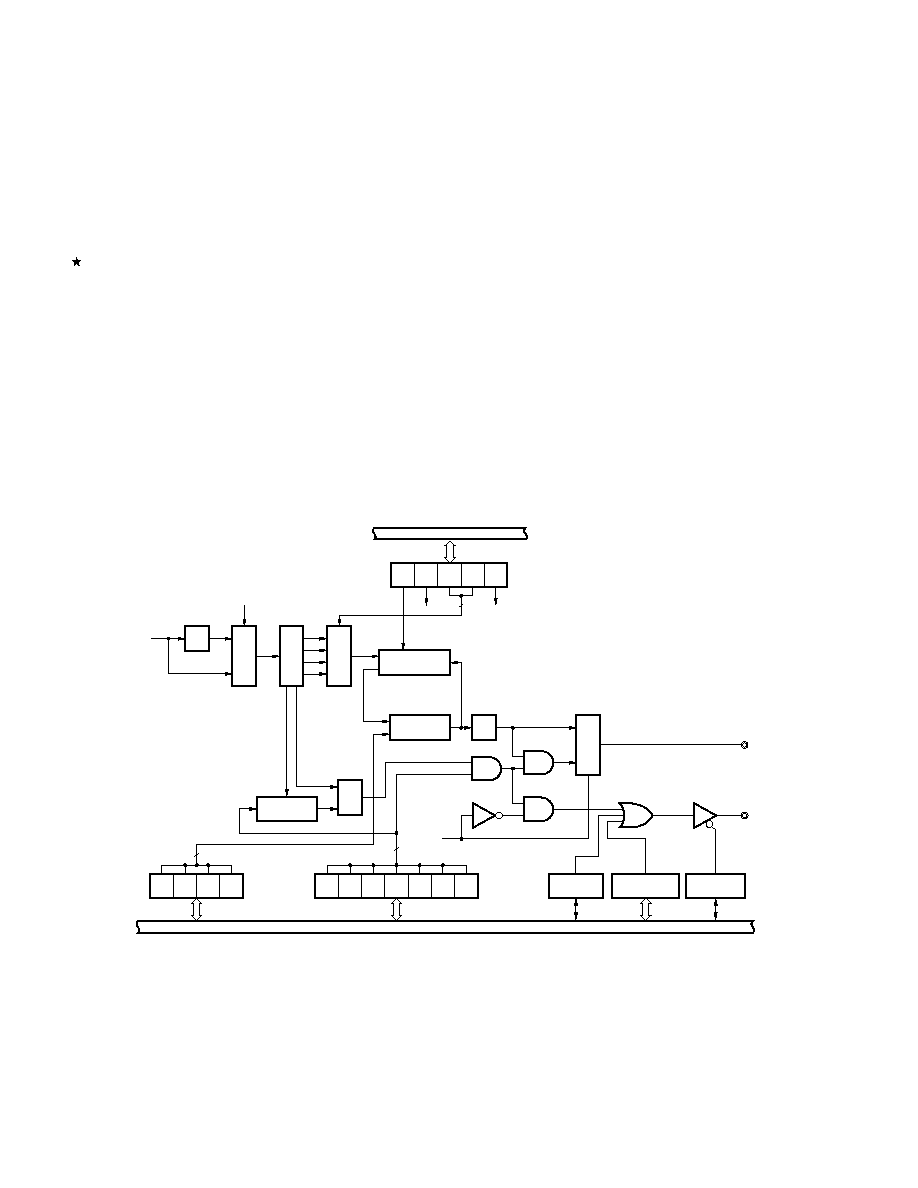
205
CHAPTER 17 SOUND GENERATOR
17.1 Sound Generator Function
The sound generator has the function to sound the buzzer from an external speaker, and the following two signals
are output.
(1) Basic cycle output signal (with/without amplitude)
The signal is a buzzer signal with a variable frequency. By setting bits 0 to 2 (SGCL0 to SGCL2) of the sound
generator control register (SGCR), the signal in a range of 0.25 to 7.7 kHz can be output (when f
X
= 8.38 MHz).
The amplitude of the basic cycle output signal can be varied by ANDing the basic cycle output signal with the
7-bit-resolution PWM signal, to enable control of the buzzer sound volume.
(2) Amplitude output signal
A PWM signal with a 7-bit resolution for variable amplitude can be independently output.
Figure 17-1 shows the sound generator block diagram and Figure 17-2 shows the concept of each signal.
Figure 17-1. Sound Generator Block Diagram
Internal bus
Internal bus
Sound generator control register (SGCR)
TCE SGOB SGCL2 SGCL1 SGCL0
2
4
7
Q
f
X
f
SG1
f
SG2
1/2
1/2
Selector
Prescaler
Selector
Selector
5-bit counter
Comparator
Comparator
SGO/SGOF/P61
PCL/SGOA/P60
Clear
PWM amplitude
S
R
SGOB
SGCL0
SGBR3 SGBR2 SGBR1 SGBR0
SGAM6 SGAM5 SGAM4 SGAM3 SGAM2 SGAM1 SGAM0
P60 output
latch
Clock output
control circuit (PCL)
PM60
Sound generator buzzer
control register (SGBR)
Sound generator amplitude
register (SGAM)
Port mode
register 6 (PM6)
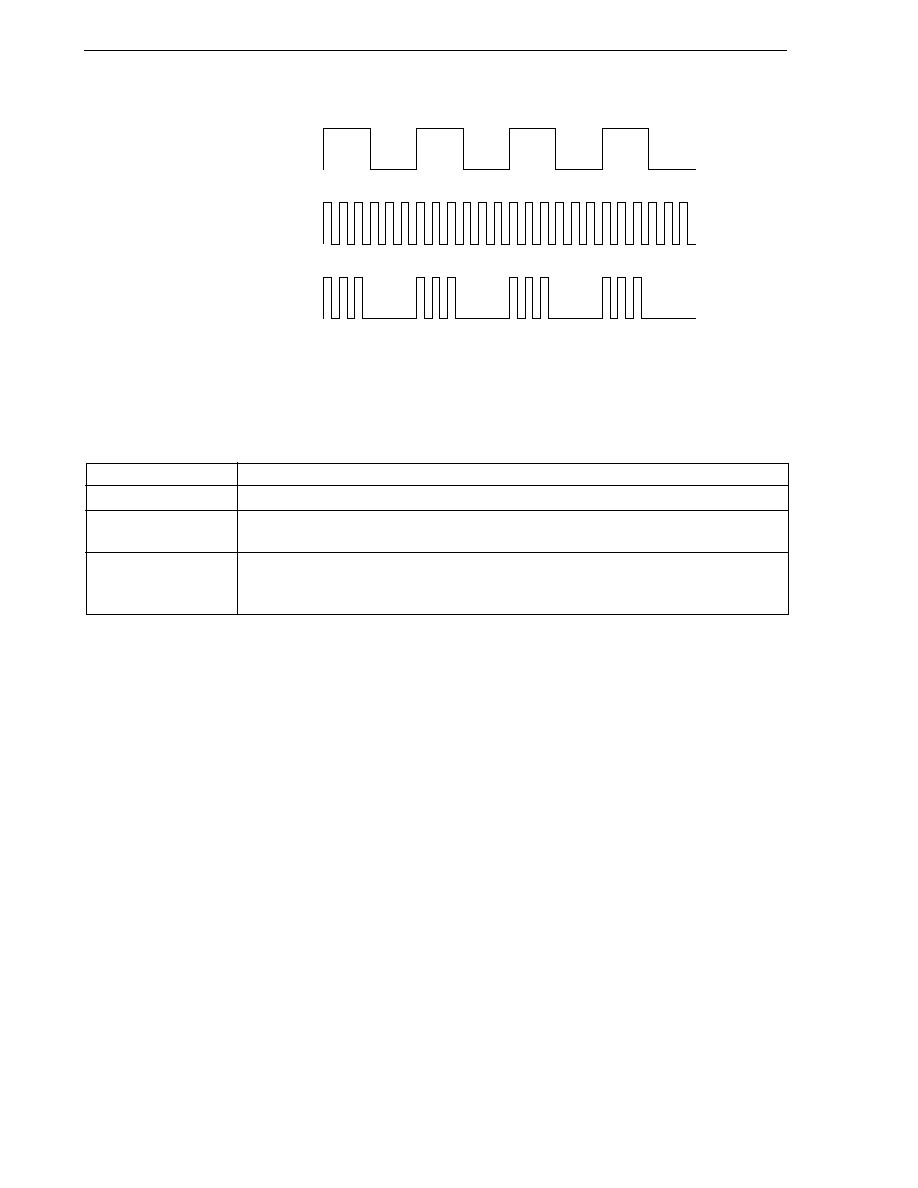
206
CHAPTER 17 SOUND GENERATOR
Figure 17-2. Concept of Each Signal
Basic cycle output SGOF
(without amplitude)
Amplitude output SGOA
Basic cycle output SGO
(with amplitude)
17.2 Sound Generator Configuration
The sound generator consists of the following hardware.
Table 17-1. Sound Generator Configuration
Item
Configuration
Counter
8 bits
�
1, 5 bits
�
1
SG output
SGO/SGOF (with/without append bit of basic cycle output)
SGOA (amplitude output)
Control register
Sound generator control register (SGCR)
Sound generator buzzer control register (SGBR)
Sound generator amplitude register (SGAM)

207
CHAPTER 17 SOUND GENERATOR
17.3 Sound Generator Control Registers
The following three types of registers are used to control the sound generator.
� Sound generator control register (SGCR)
� Sound generator buzzer control register (SGBR)
� Sound generator amplitude register (SGAM)
(1) Sound generator control register (SGCR)
SGCR is a register which sets up the following four types.
� Controls sound generator output
� Selects output of sound generator
� Selects sound generator input frequency f
SG1
� Selects 5-bit counter input frequency f
SG2
SGCR is set with a 1-bit or 8-bit memory manipulation instruction.
RESET input clears SGCR to 00H.
Figure 17-3 shows the SGCR format.
208
CHAPTER 17 SOUND GENERATOR
Figure 17-3. Sound Generator Control Register (SGCR) Format
Address: FF94H After Reset: 00H R/W
Symbol
7
6
5
4
3
2
1
0
SGCR
TCE
0
0
0
SGOB
SGCL2
SGCL1
SGCL0
TCE
Sound Generator Operation Selection
0
Timer operation stopped
SGOF/SGO and SGOA for low-level output
1
Sound generator operation
SGOF/SGO and SGOA for output
Caution
Before setting the TCE bit, set all the other bits.
Remark SGOF: Basic cycle signal (without amplitude)
SGO:
Basic cycle signal (with amplitude)
SGOA: Amplitude signal
SGOB
Sound Generator Output Selection
0
Selects SGOF and SGOA outputs
1
Selects SGO and PCL outputs
SGCL2
SGCL1
5-Bit Counter Input Frequency f
SG2
Selection
0
0
f
SG2
= f
SG1
/2
5
0
1
f
SG2
= f
SG1
/2
6
1
0
f
SG2
= f
SG1
/2
7
1
1
f
SG2
= f
SG1
/2
8
SGCL0
Sound Generator Input Frequency Selection
0
f
SG1
= f
X
/2
1
f
SG1
= f
X
Cautions 1. When rewriting SGCR to other data, stop the timer operation (TCE = 0) beforehand.
2. Bits 4 to 6 must be set to 0.
209
CHAPTER 17 SOUND GENERATOR
The maximum and minimum values of the buzzer output frequency are as follows.
SGCL2
SGCL1
SGCL0
Maximum and Minimum Values of Buzzer Output
f
SG2
f
X
= 8 MHz
f
X
= 8.38 MHz
Max. (kHz)
Min. (kHz)
Max. (kHz)
Min. (kHz)
0
0
0
f
SG1
/2
6
3.677
1.953
3.851
2.046
0
0
1
f
SG1
/2
5
7.354
3.906
7.702
4.092
0
1
0
f
SG1
/2
7
1.838
0.976
1.926
1.024
0
1
1
f
SG1
/2
6
3.677
1.953
0.481
2.046
1
0
0
f
SG1
/2
8
0.919
0.488
0.963
0.512
1
0
1
f
SG1
/2
7
1.838
0.976
1.926
1.024
1
1
0
f
SG1
/2
9
0.460
0.244
0.481
0.256
1
1
1
f
SG1
/2
8
0.919
0.488
0.963
0.512
The sound generator output frequency f
SG
can be calculated by the following expression.
f
SG
= 2
(SGCL0 � SGCL1 � 2
�
SGCL2 � 7)
�
{f
X
/(SGBR + 17)}
Substitute set 0 or 1 to SGCL0 to SGCL2 in the above expression. Substitute a decimal value to SGBR.
Where f
X
= 8 MHz, SGCL0 to SGCL2 is (1, 0, 0), and SGBR0 to SGBR3 is (1, 1, 1, 1), SGBR = 15.
Therefore,
f
SG
= 2
(1 � 0 � 2
�
0 � 7)
�
{f
X
/(15 + 17)}
= 3.906 kHz
(2) Sound generator buzzer control register (SGBR)
SGBR is a register that sets the basic frequency of the sound generator output signal.
SGBR is set with a 1-bit or 8-bit memory manipulation instruction.
RESET input clears SGBR to 00H.
Figure 17-4 shows the SGBR format.

210
CHAPTER 17 SOUND GENERATOR
Figure 17-4. Sound Generator Buzzer Control Register (SGBR) Format
Address: FF95H After Reset: 00H R/W
Symbol
7
6
5
4
3
2
1
0
SGBR
0
0
0
0
SGBR3
SGBR2
SGBR1
SGBR0
SGBR3
SGBR2
SGBR1
SGBR0
Buzzer Output Frequency (kHz)
Note
f
X
= 8 MHz
f
X
= 8.38 MHz
0
0
0
0
3.677
3.851
0
0
0
1
3.472
3.637
0
0
1
0
3.290
3.446
0
0
1
1
3.125
3.273
0
1
0
0
2.976
3.117
0
1
0
1
2.841
2.976
0
1
1
0
2.717
2.847
0
1
1
1
2.604
2.728
1
0
0
0
2.500
2.619
1
0
0
1
2.404
2.518
1
0
1
0
2.315
2.425
1
0
1
1
2.232
2.339
1
1
0
0
2.155
2.258
1
1
0
1
2.083
2.182
1
1
1
0
2.016
2.112
1
1
1
1
1.953
2.046
Note Output frequency where SGCL0, SGCL1, and SGCL2 are 0, 0, and 0.
Cautions 1. When rewriting SGBR to other data, stop the timer operation (TCE = 0) beforehand.
2. Bits 4 to 7 must be set to 0.
(3) Sound generator amplitude register (SGAM)
SGAM is a register that sets the amplitude of the sound generator output signal.
SGAM is set with a 1-bit or 8-bit memory manipulation instruction.
RESET input clears SGAM to 00H.
Figure 17-5 shows the SGAM format.

211
CHAPTER 17 SOUND GENERATOR
Figure 17-5. Sound Generator Amplitude Register (SGAM) Format
Address: FF96H After Reset: 00H R/W
Symbol
7
6
5
4
3
2
1
0
SGAM
0
SGAM6
SGAM5
SGAM4
SGAM3
SGAM2
SGAM1
SGAM0
SGAM6
SGAM5
SGAM4
SGAM3
SGAM2
SGAM1
SGAM0
Amplitude
0
0
0
0
0
0
0
0/128
0
0
0
0
0
0
1
2/128
0
0
0
0
0
1
0
3/128
0
0
0
0
0
1
1
4/128
0
0
0
0
1
0
0
5/128
0
0
0
0
1
0
1
6/128
0
0
0
0
1
1
0
7/128
0
0
0
0
1
1
1
8/128
0
0
0
1
0
0
0
9/128
0
0
0
1
0
0
1
10/128
0
0
0
1
0
1
0
11/128
0
0
0
1
0
1
1
12/128
0
0
0
1
1
0
0
13/128
0
0
0
1
1
0
1
14/128
0
0
0
1
1
1
0
15/128
0
0
0
1
1
1
1
16/128
0
0
1
0
0
0
0
17/128
0
0
1
0
0
0
1
18/128
0
0
1
0
0
1
0
19/128
0
0
1
0
0
1
1
20/128
0
0
1
0
1
0
0
21/128
0
0
1
0
1
0
1
22/128
0
0
1
0
1
1
0
23/128
0
0
1
0
1
1
1
24/128
0
0
1
1
0
0
0
25/128
0
0
1
1
0
0
1
26/128
0
0
1
1
0
1
0
27/128
0
0
1
1
0
1
1
28/128
0
0
1
1
1
0
0
29/128
0
0
1
1
1
0
1
30/128
0
0
1
1
1
1
0
31/128
1
1
1
1
1
1
1
128/128
Cautions 1. When rewriting the contents of SGAM, the timer operation does not need to be
stopped. However, note that a high level may be output for one period due to rewrite
timing.
2. Bit 7 must be set to 0.
...
...
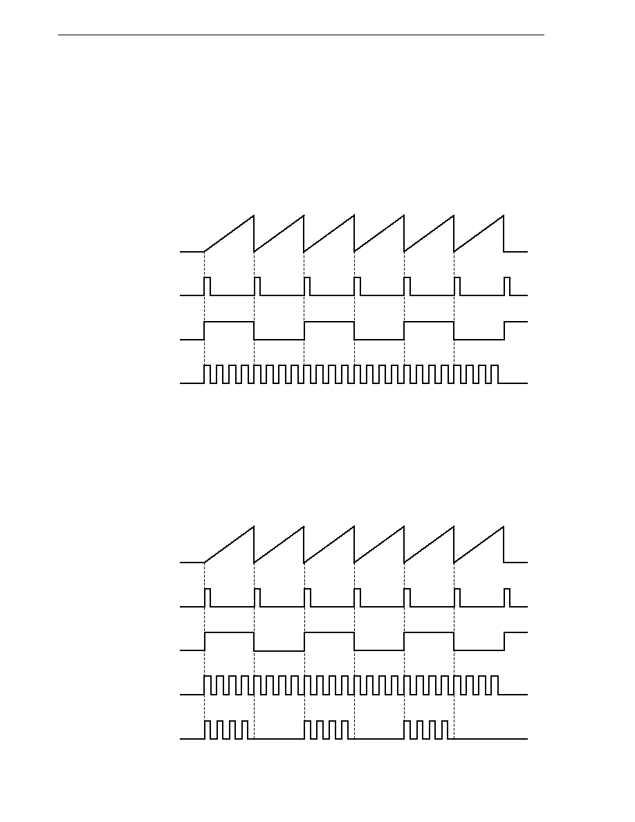
212
CHAPTER 17 SOUND GENERATOR
17.4 Sound Generator Operations
17.4.1 To output basic cycle signal SGOF (without amplitude)
Select SGOF output by setting bit 3 (SGOB) of the sound generator control register (SGCR) to "0".
The basic cycle signal with a frequency specified by the SGCL0 to SGCL2 and SGBR0 to SGBR3 is output.
At the same time, the amplitude signal with an amplitude specified by the SGAM0 to SGAM6 is output from the
SGOA pin.
Figure 17-6. Sound Generator Output Operation Timing
Timer
Comparator 1 coincidence
SGOF
SGOA
n
n
n
n
n
n
17.4.2 To output basic cycle signal SGO (with amplitude)
Select SGO output by setting bit 3 (SGOB) of the sound generator control register (SGCR) to "1".
The basic cycle signal with a frequency specified by the SGCL0 to SGCL2 and SGBR0 to SGBR3 is output.
When SGO output is selected, the SGOA pin can be used as a PCL output (clock output) or I/O port pin.
Figure 17-7. Sound Generator Output Operation Timing
Timer
Comparator 1 coincidence
SGOF
SGOA
SGO
n
n
n
n
n
n
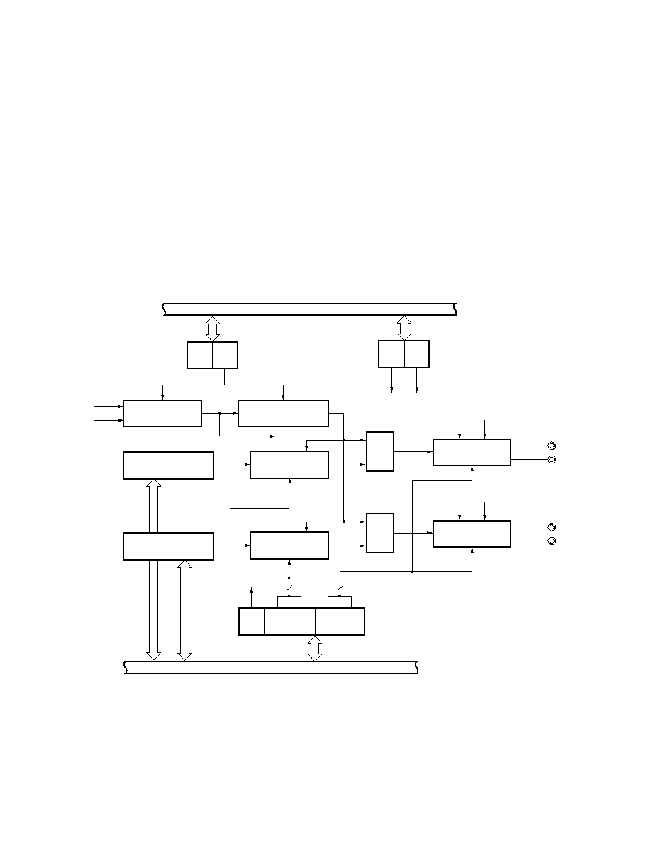
213
CHAPTER 18 METER CONTROLLER/DRIVER
18.1 Meter Controller/Driver Functions
The meter controller/driver is a function to drive a stepping motor for external meter control or cross coil.
� Can set pulse width with a precision of 8 bits
� Can set pulse width with a precision of 8 + 1 bits with 1-bit addition function
� Can drive up to four 360� type meters
Figure 18-1 shows the block diagram of the meter controller/driver, Figure 18-2 shows 1-bit addition circuit block
diagram.
Figure 18-1. Meter Controller/Driver Block Diagram
Remark
n = 1 to 4
Internal bus
Compare register
(MCMPn0)
8-bit timer register
f
CC
Selector
1-bit addition circuit
f
X
f
X
/2
PCS PCE
Compare register
(MCMPn1)
1-bit addition circuit
Internal bus
MODn ENn
Port mode control register (PMC)
Timer mode control register (MCNTC)
DIRn1 DIRn0
ADBn1
TENn
ADBn0
Compare control register n (MCMPCn)
Output control circuit
SMn1 (sin+)
SMn2 (sin�)
MODn
OVF
ENn
2
2
Q
S
R
Output control circuit
SMn3 (cos+)
SMn4 (cos�)
MODn ENn
Q
S
R
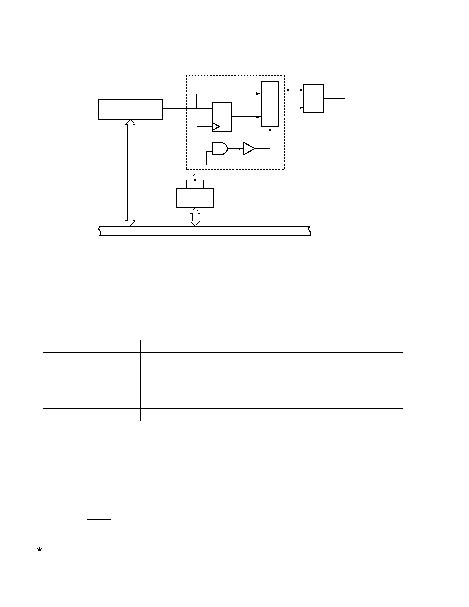
214
CHAPTER 18 METER CONTROLLER/DRIVER
Figure 18-2. 1-Bit Addition Circuit Block Diagram
Remark
n = 1 to 4, m = 0, 1
18.2 Meter Controller/Driver Configuration
The meter controller/driver consists of the following hardware.
Table 18-1. Meter Controller/Driver Configuration
Item
Configuration
Timer
Free-running up counter (MCNT): 1 channel
Register
Compare register (MCMPn1, MCMPn0): 8 channels
Control registers
Timer mode control register (MCNTC)
Compare control register n (MCMPCn)
Port mode control register (PMC)
Pulse control circuit
1-bit addition circuit/output control circuit
Remark
n = 1 to 4
(1) Free running up counter (MCNT)
MCNT is an 8-bit free running up counter, and is a register that executes increment at the rising edge of input
clock.
A PWM pulse with a resolution of 8 bits can be output. The duty factor can be set in a range of 0 to 100%.
The count value is cleared in the following cases.
� When RESET signal input
� When counter stops (PCE = 0)
Cautions 1. MCNT executes counting operation from 01H to FFH repeatedly. However, it counts from
00H upon operation start.
2. The PWM output is not output until the first overflow of MCNT.
Internal bus
f
CC
OVF
Compare register
(MCMPnm)
Q
S
R
Q
S
Selector
ADBn1 ADBn0
Compare control register (MCMPCn)
2

215
CHAPTER 18 METER CONTROLLER/DRIVER
(2) Compare register n0 (MCMPn0)
MCMPn0 is an 8-bit register that can rewrite compare values through specification of bit 4 (TENn) of the compare
control register n (MCMPCn).
RESET input sets this register to 00H and clears hardware to 0.
MCMPn0 is a register that supports read/write only for 8-bit access instructions. MCMPn0 continuously compares
its value with the MCNT value. When the above two values match, a match signal of the sin side of meter n is
generated.
(3) Compare register n1 (MCMPn1)
MCMPn1 is an 8-bit register that can rewrite compare values through specification of bit 4 (TENn) of the compare
control register n (MCMPCn).
RESET input sets this register to 00H and clears hardware to 0.
MCMPn1 is a register that supports read/write only for 8-bit access instructions. MCMPn1 continuously compares
its value with the MCNT value. When the above two values match, a match signal of the cos side of meter n is
generated.
(4) 1-bit addition circuit
The 1-bit addition circuit repeats 1-bit addition/non-addition to PWM output alternately upon MCNT overflow
output, and enables the state of PWM output between current compare value and the next compare value. This
circuit is controlled by bits 2 and 3 (ADBn0, ADBn1) of the MCMPCn register.
(5) Output control circuit
This circuit consists of a Pch and Nch drivers and can drive a meter in H bridge configuration by connecting a
coil. When a meter is driven in half bridge configuration, the unused pins can be used as normal output port
pins.
The relation of the duty factor of the PWM signal output from the SMnm pin is indicated by the following expression
(n = 1 to 4, m = 0, 1).
PWM (duty) =
Set value of MCMPnm
�
cycle of MCNT count clock
�
100%
255
�
cycle of MCNT count clock
=
Set value of MCMPnm
�
100%
255
Cautions 1. MCMPn0 and MCMPn1 cannot be read or written by a 16-bit access instruction.
2. MCMPn0 and MCMPn1 are in master-slave configuration, and MCNT is compared
with a slave register. The PWM pulse is not output until the first overflow occurs
after the counting operation has been started because the compare data is not
transferred to the slave.

216
CHAPTER 18 METER CONTROLLER/DRIVER
18.3 Meter Controller/Driver Control Registers
The meter controller/driver is controlled by the following three registers.
� Timer mode control register (MCNTC)
� Compare control register n (MCMPCn)
� Port mode control register (PMC)
Remark
n = 1 to 4
(1) Timer mode control register (MCNTC)
MCNTC is an 8-bit register that controls the operation of the free-running up counter (MCNT).
MCNTC is set with an 8-bit memory manipulation instruction.
RESET input clears MCNTC to 00H.
Figure 18-3 shows the MCNTC format.
Figure 18-3. Timer Mode Control Register (MCNTC) Format
Address: FF69H After Reset: 00H R/W
Symbol
7
6
5
4
3
2
1
0
MCNTC
0
0
PCS
PCE
0
0
0
0
PCS
Timer Counter Clock Selection
0
f
X
1
f
X
/2
PCE
Timer Operation Control
0
Operation stopped (timer value is cleared)
1
Operation enabled
Cautions 1. When rewriting MCNTC to other data, stop the timer operation (PCE = 0) beforehand.
2. Bits 0 to 3, 6, and 7 must be set to 0.
217
CHAPTER 18 METER CONTROLLER/DRIVER
(2) Compare control register (MCMPCn)
MCMPCn is an 8-bit register that controls the operation of the compare register and output direction of the PWM
pin.
MCMPCn is set with an 8-bit memory manipulation instruction.
RESET input clears MCMPCn to 00H.
Figure 18-4 shows the MCMPCn format.
Figure 18-4. Compare Control Register n (MCMPCn) Format
Address: FF6BH to FF6EH After Reset: 00H R/W
Symbol
7
6
5
4
3
2
1
0
MCMPCn (n = 1 to 4)
0
0
0
TENn
ADBn1
ADBn0
DIRn1
DIRn0
TENn
Note
Enables Transfer by Register from Master to Slave
0
Disables data transfer from master to slave.
New data can be written.
1
Transfer data from master to slave when MCNT overflows.
New data cannot be written.
ADBn1
Control of 1-bit addition circuit (cos side of meter n)
0
No 1-bit addition to PWM output
1
1-bit addition to PWM output
ADBn0
Control of 1-bit addition circuit (sin side of meter n)
0
No 1-bit addition to PWM output
1
1-bit addition to PWM output
Note TENn functions as a control bit and status flag.
As soon as the timer overflows and PWM data is output, TENn is cleared to "0" by hardware.
The relation among the DIRn1 and DIRn0 bits of the MCMPCn register and output pin is shown below.
DIRn1
DIRn0
Direction Control Bit
SMn1
SMn2
SMn3
SMn4
0
0
PWM
0
PWM
0
0
1
PWM
0
0
PWM
1
0
0
PWM
0
PWM
1
1
0
PWM
PWM
0
Caution
Bits 5 to 7 must be set to 0.
(3) Port mode control register (PMC)
PMC is an 8-bit register that specifies PWM/PORT output.
PMC is set with an 8-bit memory manipulation instruction.
RESET input clears PMC to 00H.
Figure 18-5 shows the PMC format.

218
CHAPTER 18 METER CONTROLLER/DRIVER
Figure 18-5. Port Mode Control Register (PMC) Format
Address: FF6AH After Reset: 00H R/W
Symbol
7
6
5
4
3
2
1
0
PMC
MOD4
MOD3
MOD2
MOD1
EN4
EN3
EN2
EN1
MOD4
Meter 4 Full/Half Bridge Selection
0
Meter 4 output is full bridge.
1
Meter 4 output is half bridge.
MOD3
Meter 3 Full/Half Bridge Selection
0
Meter 3 output is full bridge.
1
Meter 3 output is half bridge.
MOD2
Meter 2 Full/Half Bridge Selection
0
Meter 2 output is full bridge.
1
Meter 2 output is half bridge.
MOD1
Meter 1 Full/Half Bridge Selection
0
Meter 1 output is full bridge.
1
Meter 1 output is half bridge.
EN4
Meter 4 Port/PWM Mode Selection
0
Meter 4 output is in port mode.
1
Meter 4 output is in PWM mode.
EN3
Meter 3 Port/PWM Mode Selection
0
Meter 3 output is in port mode.
1
Meter 3 output is in PWM mode.
EN2
Meter 2 Port/PWM Mode Selection
0
Meter 2 output is in port mode.
1
Meter 2 output is in PWM mode.
EN1
Meter 1 Port/PWM Mode Selection
0
Meter 1 output is in port mode.
1
Meter 1 output is in PWM mode.

219
CHAPTER 18 METER CONTROLLER/DRIVER
The relation among the ENn and MODn bits of the PMC register, DIRn1 and DIRn0 bits of the MCMPCn register,
and output pins is shown below.
ENn
MODn
DIRn1
DIRn0
SMn1
SMn2
SMn3
SMn4
Mode
(sin+)
(sin�)
(cos+)
(cos�)
0
�
�
�
PORT
PORT
PORT
PORT
Port mode
1
0
0
0
PWM
0
PWM
0
PWM mode full bridge
1
0
0
1
PWM
0
0
PWM
1
0
1
0
0
PWM
0
PWM
1
0
1
1
0
PWM
PWM
0
1
1
0
0
PWM
PORT
PWM
PORT
PWM mode half bridge
1
1
0
1
PWM
PORT
PORT
PWM
1
1
1
0
PORT
PWM
PORT
PWM
1
1
1
1
PORT
PWM
PWM
PORT
DIRn1 and DIRn0 mean the quadrant of sin and cos, and DIRn1, DIRn0 = 00 through 11 correspond to quadrants
1 through 4, respectively. The PWM signal is output to the specific pin of the + and � polarities of sin and cos
of each quadrant.
When ENn = 0, all the output pins are used as port pins regardless of MODn, DIRn1, and DIRn0.
When ENn = 1 and MODn = 0, the full bridge mode is set, and 0 is output to a pin that does not output a PWM
signal.
When ENn = 1 and MODn = 1, the half bridge mode is set, and the pin that does not output a PWM signal is
used as a port pin.
Caution
The output polarity of the PWM output changes when MCNT overflows.
220
CHAPTER 18 METER CONTROLLER/DRIVER
18.4 Meter Controller/Driver Operations
18.4.1 Basic operation of free-running up counter (MCNT)
The free-running up counter is counted up by the count clock selected by the PCS bit of the timer mode control
register.
The value of MCNT is cleared by RESET input.
The counting operation is enabled or disabled by the PCE bit of the timer mode control register (MCNTC).
Figure 18-6 shows the timing from count start to restart.
Figure 18-6. Restart Timing after Count Stop (Count Start
Count Stop
Count Start)
Remark
N = 00H to FFH
18.4.2 To update PWM data
Confirm that bit 4 (TENn) of MCMPCn is 0, and then set 8-bit PWM data to MCMPn1 and MCMPn0, and bits
2 and 3 (ADBn1 and ADBn0) of MCMPCn, and at the same time, set TENn to 1.
The data will be automatically transferred to the slave latch when the timer overflows, and the PWM data becomes
valid. At the same time, TENn is automatically cleared to 0.
CLK
MCNT
PCE
0H
1H
2H
1H
2H
3H
4H
N
N + 1
00H
� � �
Count Start
Count Stop
Count Start

221
CHAPTER 18 METER CONTROLLER/DRIVER
18.4.3 Operation of 1-bit addition circuit
Figure 18-7. Timing in 1-Bit Addition Circuit Operation
The 1-bit addition mode repeats 1-bit addition/non-addition to PWM output alternately upon MCNT overflow output,
and enables the state of PWM output between current compare value N and the next compare value N+1. In this mode,
1-bit addition to the PWM output is set by setting ADBn of the MCMPCn register to 1, and 1-bit non-addition (normal
output) is set by setting ADBn to 0.
Remark
n = 1 to 4
MCNT Value
OVF (Overflow)
Match signal of
expected value N
PWM output of
expected value N
(1-bit non-addition)
PWM output of
expected value N
(1-bit addition)
PWM output of
expected value N+1
(1-bit non-addition)
FFH
00H
01H
N

222
CHAPTER 18 METER CONTROLLER/DRIVER
18.4.4 PWM output operation (output with 1 clock shifted)
Figure 18-8. Timing of Output with 1 Clock Shifted
Count clock
Meter 1 sin
(SM11, SM12)
Meter 1 cos
(SM13, SM14)
Meter 2 sin
(SM21, SM22)
Meter 2 cos
(SM23, SM24)
Meter 3 sin
(SM31, SM32)
Meter 3 cos
(SM33, SM34)
Meter 4 sin
(SM41, SM42)
Meter 4 cos
(SM43, SM44)
If the wave of sin and cos of meters 1 to 4 rises and falls internally as indicated by the broken line, the SM11
to SM44 pins always shift the count clock by 1 clock and output signals, in order to prevent V
DD
/GND from fluctuating.

223
CHAPTER 19 INTERRUPT FUNCTIONS
19.1 Interrupt Function Types
The following three types of interrupt functions are used.
(1) Non-maskable interrupt
This interrupt is acknowledged unconditionally even in the interrupt disabled state. It does not undergo priority
control and is given top priority over all other interrupt requests.
A standby release signal is generated.
One interrupt request from the watchdog timer is incorporated as a non-maskable interrupt.
(2) Maskable interrupts
These interrupts undergo mask control. Maskable interrupts can be divided into a high interrupt priority group
and a low interrupt priority group by setting the priority specify flag registers (PR0L, PR0H, PR1L).
Multiple high priority interrupts can be applied to low priority interrupts. If two or more interrupts with the same
priority are simultaneously generated, each interrupt has a predetermined priority (see Table 19-1).
A standby release signal is generated.
Three external interrupt requests and sixteen internal interrupt requests are incorporated as maskable interrupts.
(3) Software interrupt
This is a vectored interrupt to be generated by executing the BRK instruction. It is acknowledged even in the
interrupt disabled state. The software interrupt does not undergo interrupt priority control.
19.2 Interrupt Sources and Configuration
A total of 21 interrupt sources exist among non-maskable, maskable, and software interrupts (see Table 19-1).
224
CHAPTER 19 INTERRUPT FUNCTIONS
Table 19-1. Interrupt Source List
Note 1
Interrupt Source
Internal/
Vector
Basic
Interrupt Type
Default
External
Table
Configuration
Priority
Name
Trigger
Address
Type
Note 2
Non-maskable
--
INTWDT
Watchdog timer overflow
Internal
0004H
(A)
(with non-maskable interrupt selected)
Maskable
0
INTWDT
Watchdog timer overflow
(B)
(with interval timer selected)
1
INTAD
End of A/D conversion
0006H
2
INTOVF
16-bit timer overflow
0008H
3
INTTM00
TI00 valid edge detection
000AH
(C)
4
INTTM01
TI01 valid edge detection
000CH
5
INTTM02
TI02 valid edge detection
000EH
6
INTP0
Pin input edge detection
External
0010H
(D)
7
INTP1
0012H
8
INTP2
0014H
9
INTCSI
End of serial interface SIO3 transfer
Internal
0016H
(B)
10
INTSER
Generation of serial interface UART receive error
0018H
11
INTSR
End of serial interface UART reception
001AH
12
INTST
End of serial interface UART transmission
001CH
13
INTTM1
Generation of 8-bit timer register and capture
001EH
register (CR1) match signal
14
INTTM2
Generation of 8-bit timer register and capture
0020H
register (CR2) match signal
15
INTTM3
Generation of 8-bit timer register and capture
0022H
register (CR3) match signal
16
INTWE
End of EEPROM write
0024H
17
INTWTI
Watch timer overflow
0026H
18
INTWT
Reference time interval signal from watch timer
0028H
Software
--
BRK
BRK instruction execution
--
003EH
(E)
Notes 1. The default priority is the priority applicable when two or more maskable interrupt requests are
generated simultaneously. 0 is the highest priority, and 18 is the lowest.
2. Basic configuration types (A) to (E) correspond to (A) to (E) in Figure 19-1.
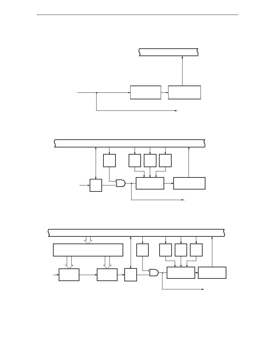
225
CHAPTER 19 INTERRUPT FUNCTIONS
Figure 19-1. Basic Configuration of Interrupt Function (1/2)
(A) Internal non-maskable interrupt
(B) Internal maskable interrupt
(C) External maskable interrupt (16-bit timer capture input)
Internal bus
Interrupt
request
Priority control
circuit
Vector table
address generator
Standby release signal
Internal bus
Interrupt
request
IF
MK
IE
PR
ISP
Priority control
circuit
Vector table
address generator
Standby release signal
Internal bus
Interrupt
request
IF
MK
IE
PR
ISP
Priority control
circuit
Vector table
address generator
Standby release signal
Sampling
clock
Edge
detector
Prescaler mode register (PRM0)

226
CHAPTER 19 INTERRUPT FUNCTIONS
Figure 19-1. Basic Configuration of Interrupt Function (2/2)
(D) External maskable interrupt (except 16-bit timer capture input)
IF
MK
IE
PR
ISP
Internal bus
Interrupt
request
Priority control
circuit
Vector table
address generator
Standby release signal
External interrupt edge
enable register
(EGP, EGN)
Edge
detector
(E) Software interrupt
Internal bus
Interrupt
request
Priority control
circuit
Vector table
address generator
IF
: Interrupt request flag
IE
: Interrupt enable flag
ISP : In-service priority flag
MK : Interrupt mask flag
PR : Priority specify flag

227
CHAPTER 19 INTERRUPT FUNCTIONS
19.3 Interrupt Function Control Registers
The following 7 types of registers are used to control the interrupt functions.
� Interrupt request flag register (IF0L, IF0H, IF1L)
� Interrupt mask flag register (MK0L, MK0H, MK1L)
� Priority specify flag register (PR0L, PR0H, PR1L)
� External interrupt rising edge enable register (EGP)
� External interrupt falling edge enable register (EGN)
� Prescaler mode register (PRM0)
� Program status word (PSW)
Table 19-2 gives a list of interrupt request flags, interrupt mask flags, and priority specify flags corresponding to
interrupt request sources.
Table 19-2. Flags Corresponding to Interrupt Request Sources
Interrupt Source
Interrupt Request Flag
Interrupt Mask Flag
Priority Specify Flag
Register
Register
Register
INTWDT
WDTIF
IF0L
WDTMK
MK0L
WDTPR
PR0L
INTAD
ADIF
ADMK
ADPR
INTOVF
OVFIF
OVFMK
OVFPR
INTTM00
TMIF00
TMMK00
TMPR00
INTTM01
TMIF01
TMMK01
TMPR01
INTTM02
TMIF02
TMMK02
TMPR02
INTP0
PIF0
PMK0
PPR0
INTP1
PIF1
PMK1
PPR1
INTP2
PIF2
IF0H
PMK2
MK0H
PPR2
PR0H
INTCSI
CSIIF
CSIMK
CSIPR
INTSER
SERIF
SERMK
SERPR
INTSR
SRIF
SRMK
SRPR
INTST
STIF
STMK
STPR
INTTM1
TMIF1
TMMK1
TMPR1
INTTM2
TMIF2
TMMK2
TMPR2
INTTM3
TMIF3
TMMK3
TMPR3
INTWE
WEIF
IF1L
WEMK
MK1L
WEPR
PR1L
INTWTI
WTIIF
WTIMK
WTIPR
INTWT
WTIF
WTMK
WTPR
Remark
The WDTIF, WDTMK, and WDTPR flags are interrupt control flags when the watchdog timer is used
as an interval timer.

228
CHAPTER 19 INTERRUPT FUNCTIONS
(1) Interrupt request flag registers (IF0L, IF0H, IF1L)
The interrupt request flags are set to 1 when the corresponding interrupt request is generated or an instruction
is executed. They are cleared to 0 when an instruction is executed upon acknowledgment of an interrupt request
or upon application of RESET input.
IF0L, IF0H, and IF1L are set with a 1-bit or 8-bit memory manipulation instruction. When IF0L and IF0H are
combined to form 16-bit register IF0, they are set with a 16-bit memory manipulation instruction.
RESET input sets these registers to 00H.
Figure 19-2. Interrupt Request Flag Register (IF0L, IF0H, IF1L) Format
Address: FFE0H After Reset: 00H R/W
Symbol
7
6
5
4
3
2
1
0
IF0L
PIF1
PIF0
TMIF02
TMIF01
TMIF00
OVFIF
ADIF
WDTIF
Address: FFE1H After Reset: 00H R/W
Symbol
7
6
5
4
3
2
1
0
IF0H
TMIF3
TMIF2
TMIF1
STIF
SRIF
SERIF
CSIIF
PIF2
Address: FFE2H After Reset: 00H R/W
Symbol
7
6
5
4
3
2
1
0
IF1L
0
0
0
0
0
WTIF
WTIIF
WEIF
XXIFX
Interrupt Request Flag
0
No interrupt request signal is generated
1
Interrupt request signal is generated, interrupt request status
Cautions 1. The WDTIF flag is R/W enabled only when the watchdog timer is used as the interval timer.
If watchdog timer mode 1 is used, set the WDTIF flag to 0.
2. Be sure to set 0 to IF1L bits 3 to 7.
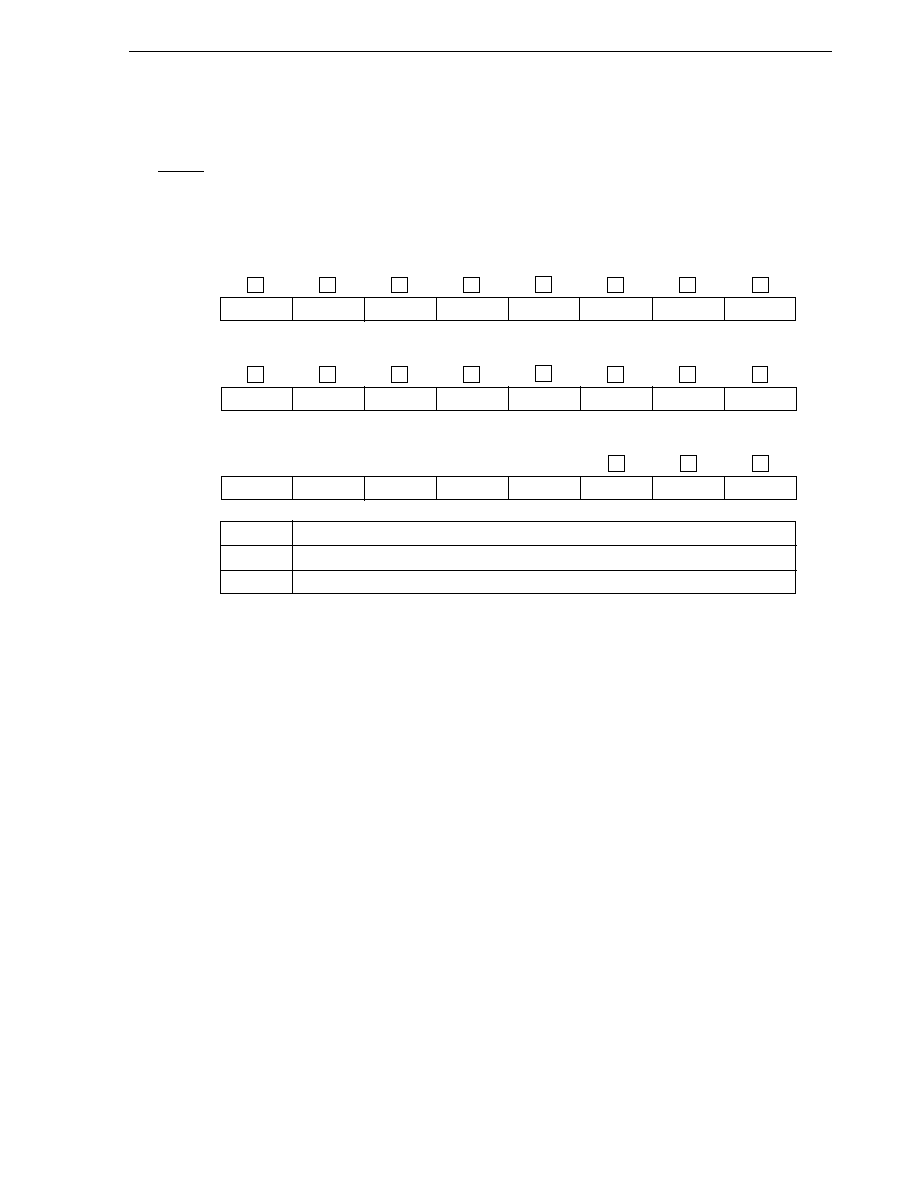
229
CHAPTER 19 INTERRUPT FUNCTIONS
(2) Interrupt mask flag registers (MK0L, MK0H, MK1L)
The interrupt mask flags are used to enable/disable the corresponding maskable interrupt service.
MK0L, MK0H, and MK1L are set with a 1-bit or 8-bit memory manipulation instruction. When MK0L and MK0H
are combined to form a 16-bit register MK0, they are set with a 16-bit memory manipulation instruction.
RESET input sets these registers to FFH.
Figure 19-3. Interrupt Mask Flag Register (MK0L, MK0H, MK1L) Format
Address: FFE4H After Reset: FFH R/W
Symbol
7
6
5
4
3
2
1
0
MK0L
PMK1
PMK0
TMMK02
TMMK01
TMMK00
OVFMK
ADMK
WDTMK
Address: FFE5H After Reset: FFH R/W
Symbol
7
6
5
4
3
2
1
0
MK0H
TMMK3
TMMK2
TMMK1
STMK
SRMK
SERMK
CSIMK
PMK2
Address: FFE6H After Reset: FFH R/W
Symbol
7
6
5
4
3
2
1
0
MK1L
1
1
1
1
1
WTMK
WTIMK
WEMK
XXMKX
Interrupt Servicing Control
0
Interrupt servicing enabled
1
Interrupt servicing disabled
Cautions 1. If the watchdog timer is used in watchdog timer mode 1, the contents of the WDTMK flag
become undefined when read.
2. Because port 0 pins have an alternate function as external interrupt request input, when
the output level is changed by specifying the output mode of the port function, an
interrupt request flag is set. Therefore, 1 should be set in the interrupt mask flag before
using the output mode.
3. Be sure to set 1 to MK1L bits 3 to 7.

230
CHAPTER 19 INTERRUPT FUNCTIONS
(3) Priority specify flag registers (PR0L, PR0H, PR1L)
The priority specify flag registers are used to set the corresponding maskable interrupt priority orders.
PR0L, PR0H, and PR1L are set with a 1-bit or 8-bit memory manipulation instruction. If PR0L and PR0H are
combined to form 16-bit register PR0, they are set with a 16-bit memory manipulation instruction.
RESET input sets these registers to FFH.
Figure 19-4. Priority Specify Flag Register (PR0L, PR0H, PR1L) Format
Address: FFE8H After Reset: FFH R/W
Symbol
7
6
5
4
3
2
1
0
PR0L
PPR1
PPR0
TMPR02
TMPR01
TMPR00
OVFPR
ADPR
WDTPR
Address: FFE9H After Reset: FFH R/W
Symbol
7
6
5
4
3
2
1
0
PR0H
TMPR3
TMPR2
TMPR1
STPR
SRPR
SERPR
CSIPR
PPR2
Address: FFEAH After Reset: FFH R/W
Symbol
7
6
5
4
3
2
1
0
PR1L
1
1
1
1
1
WTPR
WTIPR
WEPR
XXPRX
Priority Level Selection
0
High priority level
1
Low priority level
Cautions 1. When the watchdog timer is used in the watchdog timer mode 1, set 1 in the WDTPR flag.
2. Be sure to set 1 to PR1L bits 3 to 7.
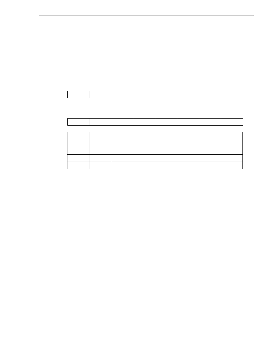
231
CHAPTER 19 INTERRUPT FUNCTIONS
(4) External interrupt rising edge enable register (EGP), external interrupt falling edge enable register (EGN)
These registers specify the valid edge for INTP0 to INTP2.
EGP and EGN are set with a 1-bit or 8-bit memory manipulation instruction.
RESET input sets these registers to 00H.
Figure 19-5. External Interrupt Rising Edge Enable Register (EGP),
External Interrupt Falling Edge Enable Register (EGN) Format
Address: FF48H After Reset: 00H R/W
Symbol
7
6
5
4
3
2
1
0
EGP
0
0
0
0
0
EGP2
EGP1
EGP0
Address: FF49H After Reset: 00H R/W
Symbol
7
6
5
4
3
2
1
0
EGN
0
0
0
0
0
EGN2
EGN1
EGN0
EGPn
EGNn
INTPn Pin Valid Edge Selection (n = 0 to 2)
0
0
Interrupt disable
0
1
Falling edge
1
0
Rising edge
1
1
Both rising and falling edges

232
CHAPTER 19 INTERRUPT FUNCTIONS
(5) Prescaler mode register (PRM0)
This register specifies the valid edge for TI00/P40 to TI02/P42 pins input.
PRM0 is set with an 8-bit memory manipulation instruction.
RESET input sets this register to 00H.
Figure 19-6. Prescaler Mode Register (PRM0) Format
Address: FF70H After Reset: 00H R/W
Symbol
7
6
5
4
3
2
1
0
PRM0
ES21
ES20
ES11
ES10
ES01
ES00
PRM01
PRM00
ES21
ES20
TI02 Valid Edge Selection
0
0
Falling edge
0
1
Rising edge
1
0
Setting prohibited
1
1
Both rising and falling edges
ES11
ES10
TI01 Valid Edge Selection
0
0
Falling edge
0
1
Rising edge
1
0
Setting prohibited
1
1
Both rising and falling edges
ES01
ES00
TI00 Valid Edge Selection
0
0
Falling edge
0
1
Rising edge
1
0
Setting prohibited
1
1
Both rising and falling edges
Caution
Set the valid edge of the TI00/P40 to TI02/P42 pins after setting bit 2 of 16-bit timer mode
control register 0 (TMC0) to 0 to stop the timer operation.
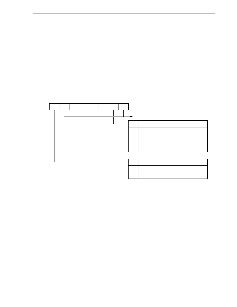
233
CHAPTER 19 INTERRUPT FUNCTIONS
(6) Program status word (PSW)
The program status word is a register to hold the instruction execution result and the current status for an interrupt
request. The IE flag to set maskable interrupt enable/disable and the ISP flag to control multiple processing are
mapped.
Besides 8-bit read/write, this register can carry out operations with a bit manipulation instruction and dedicated
instructions (EI and DI). When a vectored interrupt request is acknowledged, if the BRK instruction is executed,
the contents of PSW are automatically saved into a stack and the IE flag is reset to 0. If a maskable interrupt
request is acknowledged, the contents of the priority specify flag of the acknowledged interrupt are transferred
to the ISP flag. The PSW contents are also saved into the stack with the PUSH PSW instruction. They are reset
from the stack with the RETI, RETB, and POP PSW instructions.
RESET input sets PSW to 02H.
Figure 19-7. Program Status Word Format
7
IE
6
Z
5
RBS1
4
AC
3
RBS0
2
0
1
ISP
0
CY
PSW
After Reset
02H
ISP
High-priority interrupt servicing (Low-priority
interrupt disable)
IE
0
1
Disable
Priority of Interrupt Currently Being Serviced
Interrupt Request Acknowledge Enable/Disable
Used when normal instruction is executed
Enable
Interrupt request not acknowledged, or low-
priority interrupt servicing. (all maskable
interrupts enable)
0
1

234
CHAPTER 19 INTERRUPT FUNCTIONS
19.4 Interrupt Servicing Operations
19.4.1 Non-maskable interrupt request acknowledge operation
A non-maskable interrupt request is unconditionally acknowledged even if in an interrupt acknowledge disable
state. It does not undergo interrupt priority control and has highest priority over all other interrupts.
If a non-maskable interrupt request is acknowledged, the contents are saved into the stacks in the order of PSW,
then PC, the IE flag and ISP flag are reset (to 0), and the contents of the vector table are loaded into PC and branched.
A new non-maskable interrupt request generated during execution of a non-maskable interrupt servicing program
is acknowledged after the current execution of the non-maskable interrupt servicing program is terminated (following
RETI instruction execution) and one main routine instruction is executed. However, if a new non-maskable interrupt
request is generated twice or more during non-maskable interrupt servicing program execution, only one non-
maskable interrupt request is acknowledged after termination of the non-maskable interrupt servicing program
execution. Figures 19-8, 19-9, and 19-10 show the flowchart of the non-maskable interrupt request generation through
acknowledge, acknowledge timing of non-maskable interrupt request, and acknowledge operation at multiple non-
maskable interrupt request generation, respectively.
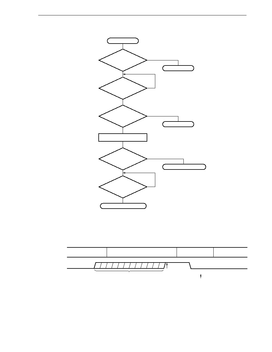
235
CHAPTER 19 INTERRUPT FUNCTIONS
Figure 19-8. Non-Maskable Interrupt Request Generation to Acknowledge Flowchart
Start
WDTM4 = 1
(with watchdog timer
mode selected)?
Overflow in WDT?
WDT interrupt
servicing?
Interrupt
control register not
accessed?
Interval timer
No
Reset processing
No
Interrupt request generation
Start of interrupt servicing
Interrupt request held pending
No
No
No
Yes
Yes
Yes
Yes
Yes
WDTM: Watchdog timer mode register
WDT : Watchdog timer
WDTM3 = 0
(with non-maskable
interrupt selected)?
Figure 19-9. Non-Maskable Interrupt Request Acknowledge Timing
Instruction
Instruction
PSW and PC save, jump
to interrupt servicing
Interrupt servicing
program
CPU processing
WDTIF
Interrupt request generated during this interval is acknowledged at .
WDTIF: Watchdog timer interrupt request flag
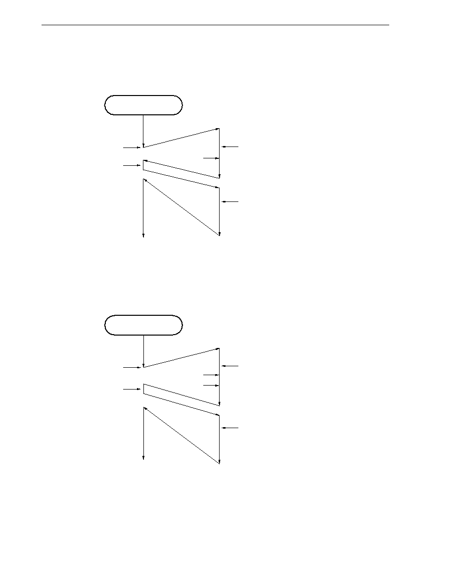
236
CHAPTER 19 INTERRUPT FUNCTIONS
Figure 19-10. Non-Maskable Interrupt Request Acknowledge Operation
(a) If a non-maskable interrupt request is generated during non-maskable interrupt servicing program
execution
Main routine
NMI request <1>
Execution of 1 instruction
NMI request <2>
Execution of NMI request <1>
NMI request <2> held pending
Servicing of NMI request <2> that was pended
(b) If two non-maskable interrupt requests are generated during non-maskable interrupt servicing program
execution
Main routine
NMI request <1>
Execution of 1 instruction
Execution of NMI request <1>
NMI request <2> held pending
NMI request <3> held pending
Servicing of NMI request <2> that was pended
NMI request <3> not acknowledged
(Although two or more NMI requests have been generated,
only one request is acknowledged.)
NMI request <2>
NMI request <3>

237
CHAPTER 19 INTERRUPT FUNCTIONS
19.4.2 Maskable interrupt request acknowledge operation
A maskable interrupt request becomes acknowledgeable when an interrupt request flag is set to 1 and the mask
(MK) flag corresponding to that interrupt is cleared to 0. A vectored interrupt request is acknowledged if in the interrupt
enable state (when IE flag is set to 1). However, a low-priority interrupt request is not acknowledged during servicing
of a higher priority interrupt request (when the ISP flag is reset to 0).
The times from generation of a maskable interrupt request until interrupt servicing is performed are listed in Table
19-3 below.
For the interrupt request acknowledge timing, see the Figures 19-12 and 19-13.
Table 19-3. Times from Generation of Maskable Interrupt Request until Servicing
Minimum Time
Maximum Time
Note
When
��
PR = 0
7 clocks
32 clocks
When
��
PR = 1
8 clocks
33 clocks
Note If an interrupt request is generated just before a divide instruction, the wait time becomes longer.
Remark
1 clock: 1/f
CPU
(f
CPU
: CPU clock)
If two or more maskable interrupt requests are generated simultaneously, the request with a higher priority level
specified in the priority specify flag is acknowledged first. If two or more interrupts requests have the same priority
level, the request with the highest default priority is acknowledged first.
An interrupt request that is held pending is acknowledged when it becomes acknowledgeable.
Figure 19-11 shows the interrupt request acknowledge algorithm.
If a maskable interrupt request is acknowledged, the contents are saved into the stacks in the order of program
status word (PSW), then program counter (PC), the IE flag is reset (to 0), and the contents of the priority specify flag
corresponding to the acknowledged interrupt are transferred to the ISP flag. Further, the vector table data determined
for each interrupt request is loaded into PC and branched.
Return from an interrupt is possible with the RETI instruction.
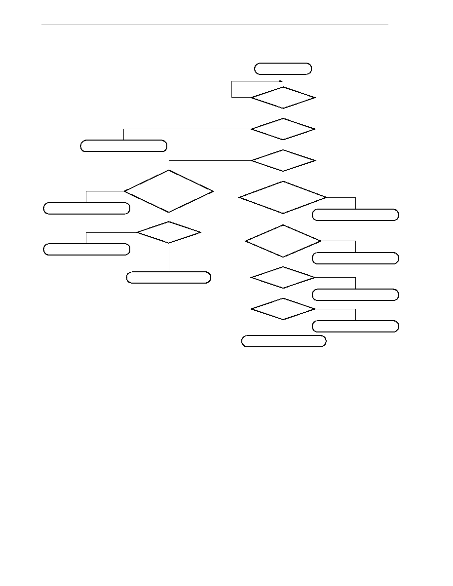
238
CHAPTER 19 INTERRUPT FUNCTIONS
Figure 19-11. Interrupt Request Acknowledge Processing Algorithm
Start
��
IF = 1?
��
MK = 0?
��
PR = 0?
IE = 1?
ISP = 1?
Interrupt request held pending
Yes
Yes
No
No
Yes (Interrupt request generation)
Yes
No (Low priority)
No
No
Yes
Yes
No
IE = 1?
No
Any high-priority
interrupt request among those
simultaneously generated
with
��
PR = 0?
Yes (High priority)
No
Yes
Yes
No
Vectored interrupt servicing
Interrupt request held pending
Interrupt request held pending
Interrupt request held pending
Interrupt request held pending
Interrupt request held pending
Interrupt request held pending
Vectored interrupt servicing
Any interrupt
request among
those simultaneously
generated?
Any interrupt
request among those
simultaneously generated
with
��
PR = 0?
��
IF
: Interrupt request flag
��
MK : Interrupt mask flag
��
PR : Priority specify flag
IE
: Flag that controls acknowledge of maskable interrupt request (1 = Enable, 0 = Disable)
ISP
: Flag that indicates the priority level of the interrupt currently being serviced (0 = High-priority interrupt
servicing, 1 = No interrupt request acknowledged, or low-priority interrupt servicing)
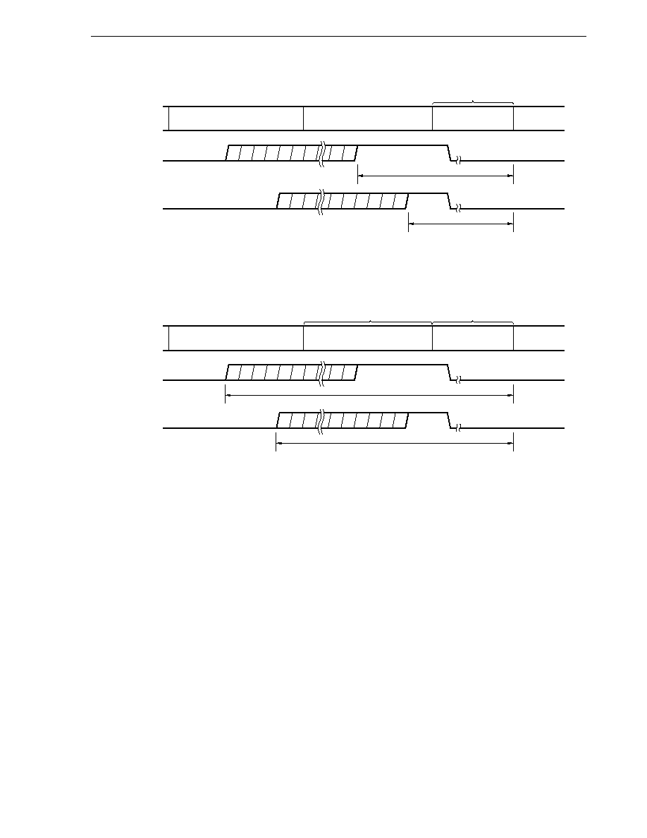
239
CHAPTER 19 INTERRUPT FUNCTIONS
Figure 19-12. Interrupt Request Acknowledge Timing (Minimum Time)
8 clocks
7 clocks
Instruction
Instruction
PSW and PC Save,
Jump to interrupt
servicing
Interrupt servicing
program
CPU processing
��
IF
(
��
PR = 1)
��
IF
(
��
PR = 0)
6 clocks
Remark
1 clock: 1/f
CPU
(f
CPU
: CPU clock)
Figure 19-13. Interrupt Request Acknowledge Timing (Maximum Time)
33 clocks
32 clocks
Instruction
Divide instruction
PSW and PC Save,
Jump to interrupt
servicing
Interrupt servicing
program
CPU processing
��
IF
(
��
PR = 1)
��
IF
(
��
PR = 0)
6 clocks
25 clocks
Remark
1 clock: 1/f
CPU
(f
CPU
: CPU clock)
19.4.3 Software interrupt request acknowledge operation
A software interrupt acknowledge is acknowledged by BRK instruction execution. Software interrupts cannot be
disabled.
If a software interrupt request is acknowledged, the contents are saved into the stacks in the order of the program
status word (PSW), then program counter (PC), the IE flag is reset (to 0), and the contents of the vector table (003EH,
003FH) are loaded into PC and branched.
Return from a software interrupt is possible with the RETB instruction.
Caution
Do not use the RETI instruction for returning from the software interrupt.

240
CHAPTER 19 INTERRUPT FUNCTIONS
19.4.4 Multiple interrupt servicing
Multiple interrupts occur when another interrupt request is acknowledged during execution of an interrupt.
Multiple interrupts do not occur unless the interrupt request acknowledge enable state is selected (IE = 1) (except
non-maskable interrupts). Also, when an interrupt request is received, interrupt requests acknowledge becomes
disabled (IE = 0). Therefore, to enable multiple interrupts, it is necessary to set (to 1) the IE flag with the EI instruction
during interrupt servicing to enable interrupt acknowledge.
Moreover, even if interrupts are enabled, multiple interrupts may not be enabled, this being subject to interrupt
priority control. Two types of priority control are available: default priority control and programmable priority control.
Programmable priority control is used for multiple interrupts.
In the interrupt enable state, if an interrupt request with a priority equal to or higher than that of the interrupt currently
being serviced is generated, it is acknowledged for multiple interrupt servicing. If an interrupt with a priority lower
than that of the interrupt currently being serviced is generated during interrupt servicing, it is not acknowledged for
multiple interrupt servicing. Interrupt requests that are not enabled because of the interrupt disable state or they have
a lower priority are held pending. When servicing of the current interrupt ends, the pended interrupt request is
acknowledged following execution of one main processing instruction execution.
Multiple interrupt servicing is not possible during non-maskable interrupt servicing.
Table 19-4 shows interrupt requests enabled for multiple interrupt servicing, and Figure 19-14 shows multiple
interrupt examples.
Table 19-4. Interrupt Request Enabled for Multiple Interrupt during Interrupt Servicing
Multiple Interrupt Request
Maskable Interrupt Request
Non-Maskable Interrupt Request
PR = 0
PR = 1
Interrupt being Serviced
IE = 1
IE = 0
IE = 1
IE = 0
Non-maskable interrupt
�
�
�
�
�
Maskable interrupt
ISP = 0
�
�
�
ISP = 1
�
�
Software interrupt
�
�
Remarks 1.
: Multiple interrupt enable
2.
�
: Multiple interrupt disable
3. ISP and IE are flags contained in PSW.
ISP = 0 : An interrupt with higher priority is being serviced.
ISP = 1 : No interrupt request has been acknowledged, or an interrupt with a lower priority is being
serviced.
IE = 0 : Interrupt request acknowledge is disabled.
IE = 1 : Interrupt request acknowledge is enabled.
4. PR is a flag contained in PR0L, PR0H, and PR1L.
PR = 0 : Higher priority level
PR = 1 : Lower priority level
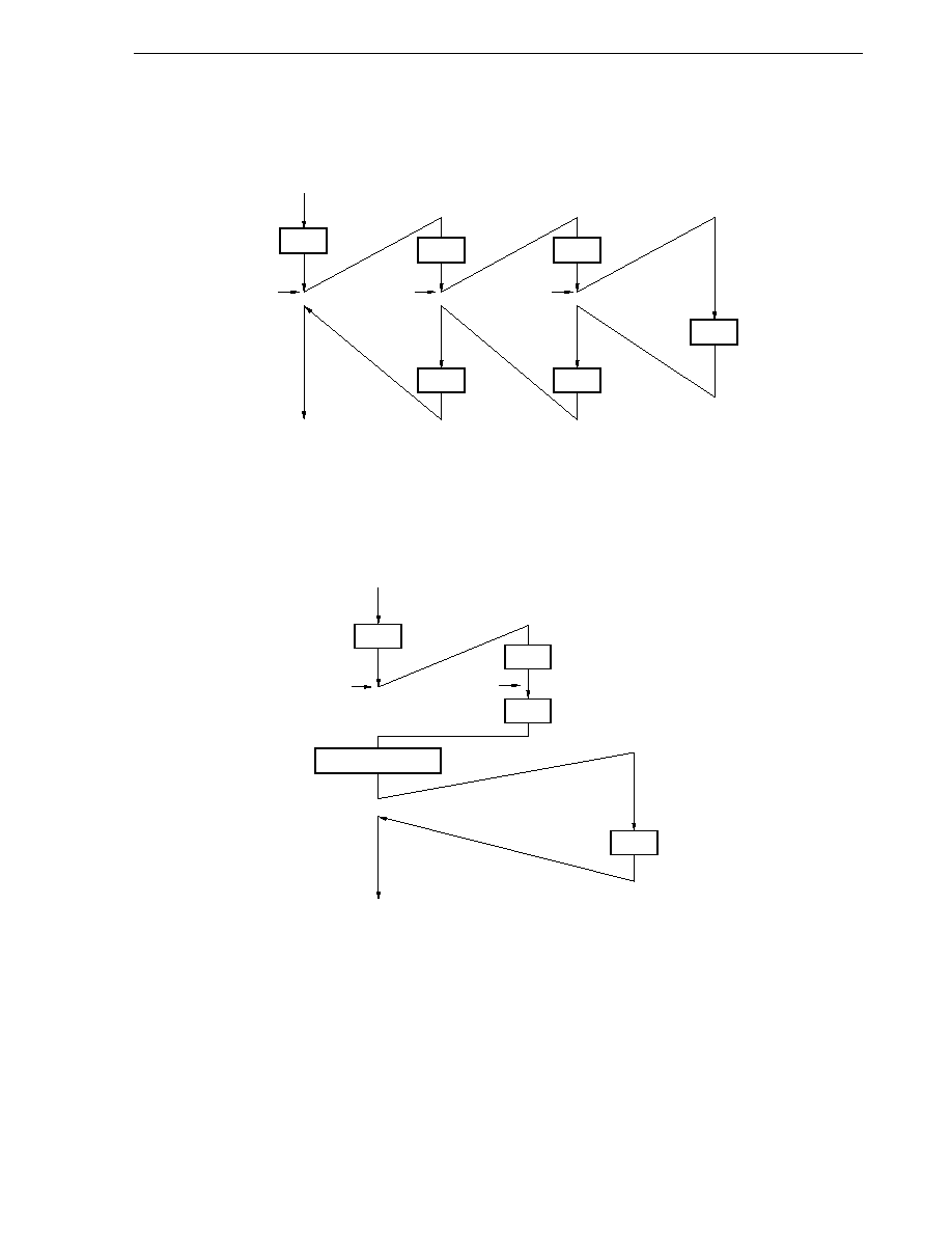
241
CHAPTER 19 INTERRUPT FUNCTIONS
Figure 19-14. Multiple Interrupt Examples (1/2)
Example 1. Multiple interrupts occur twice
Main processing
INTxx servicing
INTyy servicing
INTzz servicing
EI
EI
EI
RETI
RETI
RETI
INTxx
(PR = 1)
INTyy
(PR = 0)
INTzz
(PR = 0)
IE = 0
IE = 0
IE = 0
During servicing of interrupt INTxx, two interrupt requests, INTyy and INTzz, are acknowledged, and multiple
interrupt servicing takes place. Before each interrupt request is acknowledged, the EI instruction must always be
issued to enable interrupt request acknowledge.
Example 2. Multiple interrupt servicing does not occur due to priority control
Main processing
INTxx servicing
INTyy servicing
INTxx
(PR = 0)
INTyy
(PR = 1)
EI
RETI
IE = 0
IE = 0
EI
1 instruction execution
RETI
Interrupt request INTyy issued during servicing of interrupt INTxx is not acknowledged because its priority is lower
than that of INTxx, and multiple interrupt servicing does not take place. The INTyy interrupt request is held pending,
and is acknowledged following execution of one main processing instruction.
PR = 0 : Higher priority level
PR = 1 : Lower priority level
IE = 0
: Interrupt request acknowledge disable
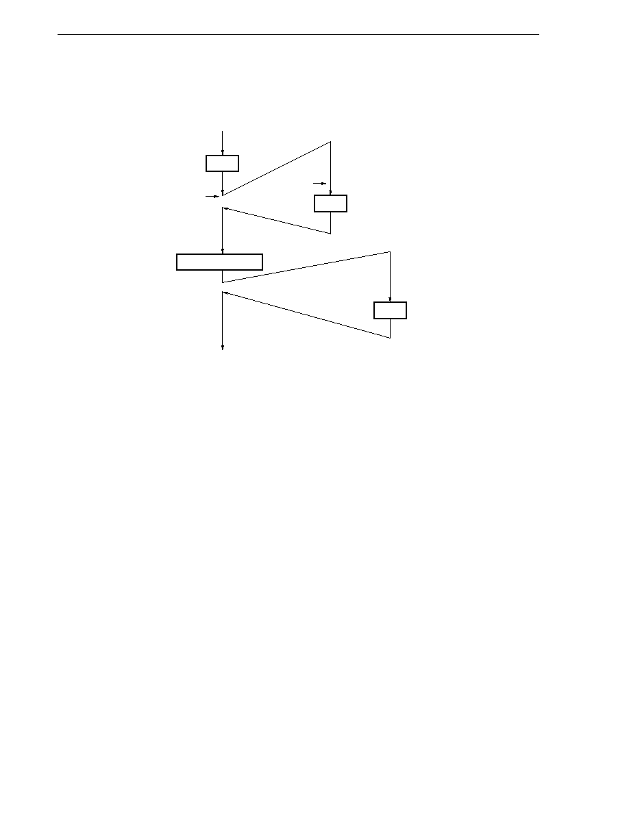
242
CHAPTER 19 INTERRUPT FUNCTIONS
Figure 19-14. Multiple Interrupt Examples (2/2)
Example 3. Multiple interrupt servicing does not occur because interrupt is not enabled
Main processing
INTxx servicing INTyy servicing
EI
1 instruction execution
RETI
RETI
INTxx
(PR = 0)
INTyy
(PR = 0)
IE = 0
IE = 0
Interrupt is not enabled during servicing of interrupt INTxx (EI instruction is not issued), therefore, interrupt request
INTyy is not acknowledged and multiple interrupt servicing does not take place. The INTyy interrupt request is held
pending, and is acknowledged following execution of one main processing instruction.
PR = 0 : Higher priority level
IE = 0
: Interrupt request acknowledge disable

243
CHAPTER 19 INTERRUPT FUNCTIONS
19.4.5 Interrupt request hold
There are instructions where, even if an interrupt request is issued for them while another instruction is executed,
request acknowledge is held pending until the end of execution of the next instruction. These instructions (interrupt
request hold instructions) are listed below.
� MOV PSW, #byte
� MOV A, PSW
� MOV PSW, A
� MOV1 PSW.bit, CY
� MOV1 CY, PSW.bit
� AND1 CY, PSW.bit
� OR1 CY, PSW.bit
� XOR1 CY, PSW.bit
� SET1 PSW.bit
� CLR1 PSW.bit
� RETB
� RETI
� PUSH PSW
� POP PSW
� BT PSW.bit, $addr16
� BF PSW.bit, $addr16
� BTCLR PSW.bit, $addr16
� EI
� DI
� Manipulate instructions for the IF0L, IF0H, IF1L, MK0L, MK0H, MK1L, PR0L, PR0H, PR1L, EGP, and EGN
registers
Caution
The BRK instruction is not one of the above-listed interrupt request hold instruction. However,
the software interrupt activated by executing the BRK instruction causes the IE flag to be
cleared. Therefore, even if a maskable interrupt request is generated during execution of the
BRK instruction, the interrupt request is not acknowledged. However, a non-maskable interrupt
request is acknowledged.
The timing with which interrupt requests are held pending is shown in Figure 19-15.
Figure 19-15. Interrupt Request Hold
Instruction N
Instruction M
Save PSW and PC, Jump
to interrupt servicing
Interrupt servicing
program
CPU processing
��
IF
Remarks 1. Instruction N: Interrupt request hold instruction
2. Instruction M: Instruction other than interrupt request hold instruction
3. The
��
PR (priority level) values do not affect the operation of
��
IF (interrupt request).

244
[MEMO]

245
CHAPTER 20 STANDBY FUNCTION
20.1 Standby Function and Configuration
20.1.1 Standby function
The standby function is designed to decrease power consumption of the system. The following two modes are
available.
(1) HALT mode
Halt instruction execution sets the HALT mode. The HALT mode is intended to stop the CPU operation clock.
The system clock oscillator continues oscillating. In this mode, current consumption is not decreased as much
as in the STOP mode. However, the HALT mode is effective to restart operation immediately upon interrupt
request and to carry out intermittent operations such as watch operation.
(2) STOP mode
Stop instruction execution sets the STOP mode. In the STOP mode, the main system clock oscillator stops,
stopping the whole system, thereby considerably reducing the CPU current consumption.
Data memory low-voltage hold (down to V
DD
= 2.0 V) is possible. Thus, the STOP mode is effective to hold data
memory contents with ultra-low current consumption.
Because this mode can be cleared upon interrupt request, it enables intermittent operations to be carried out.
However, because a wait time is required to secure an oscillation stabilization time after the STOP mode is
cleared, select the HALT mode if it is necessary to start processing immediately upon interrupt request.
In either of these two modes, all the contents of registers, flags and data memory just before the standby mode
is set are held. The input/output port output latch and output buffer status are also held.
Cautions 1. When operation is transferred to the STOP mode, be sure to stop the peripheral hardware
operation and execute the STOP instruction.
2. The following sequence is recommended for power consumption reduction of the A/D
converter when the standby function is used: First clear bit 7 (ADCS1) of the A/D converter
mode register (ADM1) to 0 to stop the A/D conversion operation, and then execute the HALT
or STOP instruction.
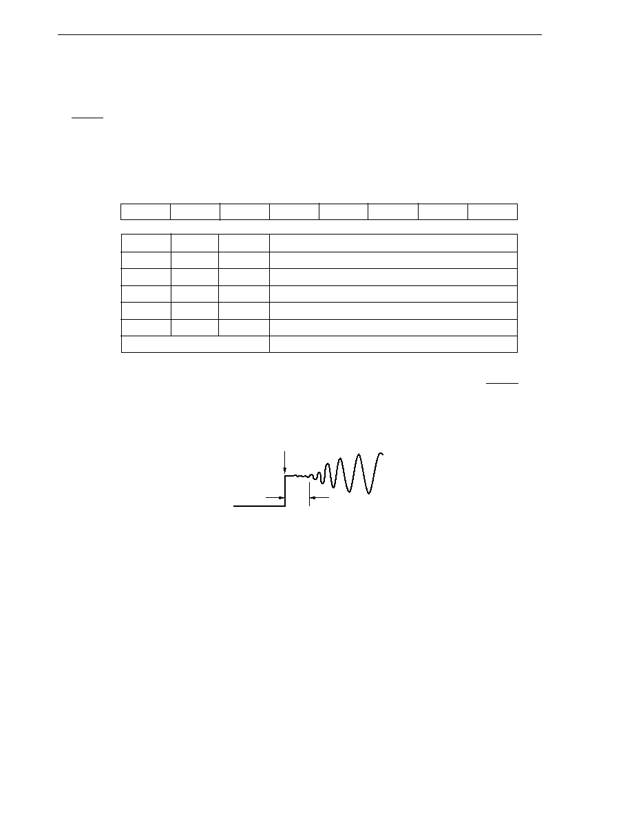
246
CHAPTER 20 STANDBY FUNCTION
20.1.2 Standby function control register
The wait time after the STOP mode is cleared upon interrupt request is controlled with the oscillation stabilization
time select register (OSTS).
OSTS is set with an 8-bit memory manipulation instruction.
RESET input sets OSTS to 04H.
Figure 20-1. Oscillation Stabilization Time Select Register (OSTS) Format
Address: FFFAH After Reset: 04H R/W
Symbol
7
6
5
4
3
2
1
0
OSTS
0
0
0
0
0
OSTS2
OSTS1
OSTS0
OSTS2
OSTS1
OSTS0
Selection of Oscillation Stabilization Time
0
0
0
2
12
/f
X
(488
�
s)
0
0
1
2
14
/f
X
(1.95 ms)
0
1
0
2
15
/f
X
(3.91 ms)
0
1
1
2
16
/f
X
(7.81 ms)
1
0
0
2
17
/f
X
(15.6 ms)
Other than above
Setting prohibited
Caution
The wait time after the STOP mode is cleared does not include the time (see "a" in the illustration
below) from STOP mode clear to clock oscillation start, regardless of clearance by RESET input
or by interrupt request generation.
STOP mode clear
X1 pin voltage
waveform
V
SS
a
Remarks 1. f
X
: Main system clock oscillation frequency
2. Values in parentheses apply to operation with f
X
= 8.38 MHz.
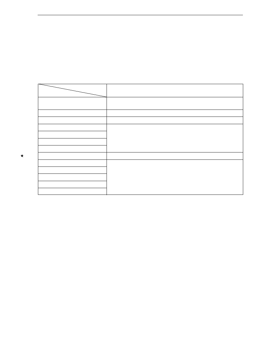
247
CHAPTER 20 STANDBY FUNCTION
20.2 Standby Function Operations
20.2.1 HALT mode
(1) HALT mode setting and operating status
The HALT mode is set by executing the HALT instruction.
The operating status in the HALT mode is described below.
Table 20-1. HALT Mode Operating Status
HALT Mode Setting
During HALT Instruction Execution Using Main System Clock
Item
Clock generator
Main system clock can be oscillated.
Clock supply to CPU stops.
CPU
Operation stops.
Port (Output latch)
Status before HALT mode setting is held.
16-bit timer
Operable
8-bit timer
Watch timer
Watchdog timer
A/D converter
Operation stops.
Serial interface
Operable
LCD controller/driver
External interrupt
Sound generator
Meter controller/driver
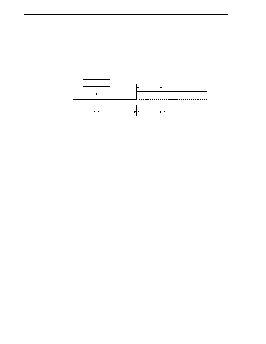
248
CHAPTER 20 STANDBY FUNCTION
(2) HALT mode clear
The HALT mode can be cleared with the following three types of sources.
(a) Clear upon unmasked interrupt request
An unmasked interrupt request is used to clear the HALT mode. If interrupt acknowledge is enabled, vectored
interrupt service is carried out. If interrupt acknowledge is disabled, the next address instruction is executed.
Figure 20-2. HALT Mode Clear upon Interrupt Generation
HALT instruction
Wait
Wait
Operating mode
HALT mode
Operating mode
Oscillation
Clock
Standby release
signal
Remarks 1. The broken line indicates the case when the interrupt request which has cleared the standby
mode is acknowledged.
2. Wait times are as follows:
� When vectored interrupt service is carried out
: 8 to 9 clocks
� When vectored interrupt service is not carried out : 2 to 3 clocks
(b) Clear upon non-maskable interrupt request
The HALT mode is cleared and vectored interrupt service is carried out whether interrupt acknowledge is
enabled or disabled.
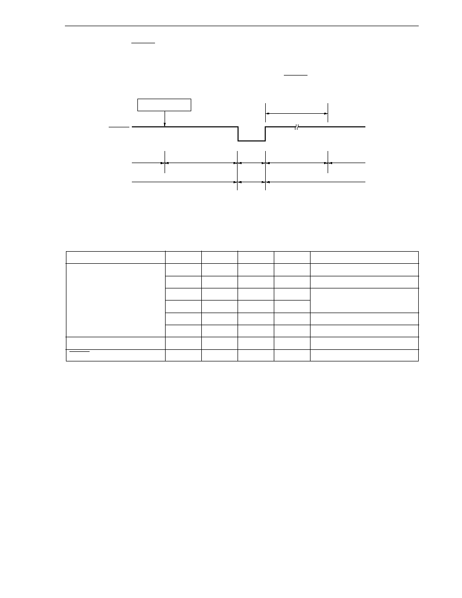
249
CHAPTER 20 STANDBY FUNCTION
(c) Clear upon RESET input
As in the case with normal reset operation, a program is executed after branch to the reset vector address.
Figure 20-3. HALT Mode Clear upon RESET Input
HALT instruction
Wait
(2
17
/f
X
: 15.6 ms)
Oscillation stabilization
wait status
Operating mode
HALT mode
Operating mode
Oscillation
stop
Clock
RESET
signal
Oscillation
Oscillation
Reset
period
Remarks 1. f
X
: Main system clock oscillation frequency
2. Values in parentheses apply to operation with f
X
= 8.38 MHz.
Table 20-2. Operation after HALT Mode Clear
Clear Source
MK
��
PR
��
IE
ISP
Operation
Maskable interrupt request
0
0
0
�
Next address instruction execution
0
0
1
�
Interrupt service execution
0
1
0
1
Next address instruction execution
0
1
�
0
0
1
1
1
Interrupt service execution
1
�
�
�
HALT mode hold
Non-maskable interrupt request
--
--
�
�
Interrupt service execution
RESET input
--
--
�
�
Reset processing
�
: don't care

250
CHAPTER 20 STANDBY FUNCTION
20.2.2 STOP mode
(1) STOP mode setting and operating status
The STOP mode is set by executing the STOP instruction.
Cautions 1. When the STOP mode is set, the X2 pin is internally connected to V
DD
via a pull-up resistor
to minimize the leakage current at the crystal oscillator. Thus, do not use the STOP mode
in a system where an external clock is used for the main system clock.
2. Because the interrupt request signal is used to clear the standby mode, if there is an
interrupt source with the interrupt request flag set and the interrupt mask flag reset, the
standby mode is immediately cleared if set. Thus, the STOP mode is reset to the HALT
mode immediately after execution of the STOP instruction. After the wait set using the
oscillation stabilization time select register (OSTS), the operating mode is set.
The operating status in the STOP mode is described below.
Table 20-3. STOP Mode Operating Status
STOP Mode Setting
During STOP Instruction Execution Using Main System Clock
Item
Clock generator
Only main system clock oscillation is stopped.
CPU
Operation stops.
Port (Output latch)
Status before STOP mode setting is held.
16-bit timer
Operation stops.
8-bit timer
Operable only when TIO2 and TIO3 are selected as count clock.
Watch timer
Operation stops.
Watchdog timer
Operation stops.
A/D converter
Operation stops.
Serial interface
Other than UART
Operable only when externally supplied input clock is specified as the serial clock.
UART
Operation stops.
LCD controller/driver
Operation stops.
External interrupt
Operable
Sound generator
Operation stops.
Meter controller/driver
Operation stops.
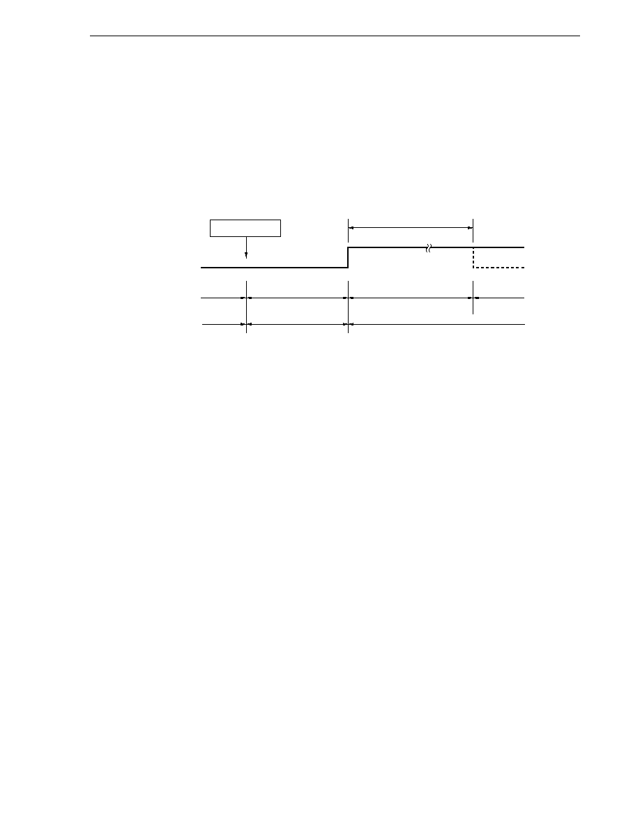
251
CHAPTER 20 STANDBY FUNCTION
(2) STOP mode clear
The STOP mode can be cleared with the following two types of sources.
(a) Clear upon unmasked interrupt request
An unmasked interrupt request is used to clear the STOP mode. If interrupt acknowledge is enabled after
the lapse of oscillation stabilization time, vectored interrupt service is carried out. If interrupt acknowledge
is disabled, the next address instruction is executed.
Figure 20-4. STOP Mode Clear upon Interrupt Generation
STOP instruction
Wait
(Time set by OSTS)
Oscillation stabilization
wait status
Operating mode
STOP mode
Operating mode
Oscillation
Clock
Standby release
signal
Oscillation stop
Oscillation
Remark
The broken line indicates the case when the interrupt request which has cleared the standby
mode is acknowledged.

252
CHAPTER 20 STANDBY FUNCTION
(b) Clear upon RESET input
The STOP mode is cleared and after the lapse of oscillation stabilization time, reset operation is carried out.
Figure 20-5. STOP Mode Clear upon RESET Input
STOP instruction
Wait
(2
17
/f
X
: 15.6 ms)
Oscillation stabilization
wait status
Operating mode
STOP mode
Operating mode
Oscillation stop
Clock
RESET
signal
Oscillation
Oscillation
Reset
period
Remarks 1. f
X
: Main system clock oscillation frequency
2. Values in parentheses apply to operation with f
X
= 8.38 MHz.
Table 20-4. Operation after STOP Mode Clear
Clear Source
MK
��
PR
��
IE
ISP
Operation
Maskable interrupt request
0
0
0
�
Next address instruction execution
0
0
1
�
Interrupt service execution
0
1
0
1
Next address instruction execution
0
1
�
0
0
1
1
1
Interrupt service execution
1
�
�
�
STOP mode hold
RESET input
--
--
�
�
Reset processing
�
: don't care
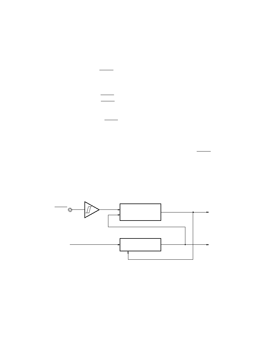
253
CHAPTER 21 RESET FUNCTION
21.1 Reset Function
The following two operations are available to generate the reset signal.
(1) External reset input with RESET pin
(2) Internal reset by watchdog timer overrun time detection
External reset and internal reset have no functional differences. In both cases, program execution starts at the
address at 0000H and 0001H by RESET input.
When a low level is input to the RESET pin or the watchdog timer overflows, a reset is applied and each hardware
is set to the status shown in Table 21-1. Each pin has high impedance during reset input or during oscillation
stabilization time just after reset clear.
When a high level is input to the RESET pin, the reset is cleared and program execution starts after the lapse of
oscillation stabilization time (2
17
/f
X
). The reset applied by watchdog timer overflow is automatically cleared after a
reset and program execution starts after the lapse of oscillation stabilization time (2
17
/f
X
) (see Figures 21-2 to 21-
4).
Cautions 1. For an external reset, input a low level for 10
�
s or more to the RESET pin.
2. During reset input, main system clock oscillation remains stopped but subsystem clock
oscillation continues.
3. When the STOP mode is cleared by reset, the STOP mode contents are held during reset input.
However, the port pin becomes high-impedance.
Figure 21-1. Reset Function Block Diagram
RESET
Count clock
Reset control circuit
Watchdog timer
Stop
Overflow
Reset signal
Interrupt function

254
CHAPTER 21 RESET FUNCTION
Figure 21-2. Timing of Reset by RESET Input
Delay
Delay
Hi-Z
Normal operation
Reset period
(Oscillation stop)
Oscillation
stabilization
time wait
Normal operation
(Reset processing)
X1
RESET
Internal
reset signal
Port pin
Figure 21-3. Timing of Reset due to Watchdog Timer Overflow
Hi-Z
Normal operation
Reset period
(Oscillation stop)
Oscillation
stabilization
time wait
Normal operation
(Reset processing)
X1
Watchdog
timer
overflow
Internal
reset signal
Port pin
Figure 21-4. Timing of Reset in STOP Mode by RESET Input
Delay
Delay
Hi-Z
Normal operation
Oscillation
stabilization
time wait
Normal operation
(Reset processing)
X1
RESET
Internal
reset signal
Port pin
Stop status
(Oscillation stop)
STOP instruction execution
Reset period
(Oscillation stop)
255
CHAPTER 21 RESET FUNCTION
Table 21-1. Hardware Status after Reset (1/2)
Hardware
Status After Reset
Program counter (PC)
Note 1
Contents of reset vector table
(0000H, 0001H) are set.
Stack pointer (SP)
Undefined
Program status word (PSW)
02H
RAM
Data memory
Undefined
Note 2
General register
Undefined
Note 2
Port (Output latch)
00H
Port mode registers (PM0 to PM6, PM8, PM9)
FFH
Pull-up resistor option register (PU0)
00H
Processor clock control register (PCC)
04H
Memory size switching register (IMS)
CFH
Oscillation stabilization time select register (OSTS)
04H
Oscillator mode register (OSCM)
Note 3
00H
16-bit timer TM0
Timer register (TM0)
00H
Capture registers (CR00 to CR02)
00H
Prescaler mode register (PRM0)
00H
Mode control register (TMC0)
00H
Capture pulse control register (CRC0)
00H
Notes 1. During reset input or oscillation stabilization time wait, only the PC contents among the hardware status
become undefined. All other hardware statuses remain unchanged after reset.
2. The post-reset status is held in the standby mode.
3. For
�
PD780973(A) only.
256
CHAPTER 21 RESET FUNCTION
Table 21-1. Hardware Status after Reset (2/2)
Hardware
Status After Reset
8-bit timer TM1 to TM3
Timer counters (TM1 to TM3)
00H
Compare registers (CR1 to CR3)
00H
Clock select registers (TCL1 to TCL3)
00H
Mode control registers (TMC1 to TMC3)
04H
Watch timer
Mode control register (WTM)
00H
Watchdog timer
Clock select register (WDCS)
00H
Mode register (WDTM)
00H
A/D converter
Conversion result register (ADCR1)
00H
Mode register (ADM1)
00H
Analog input channel specification register (ADS1)
00H
Power-fail compare mode register (PFM)
00H
Power-fail compare threshold value register (PFT)
00H
Serial interface UART
Asynchronous serial interface mode register (ASIM)
00H
Asynchronous serial interface status register (ASIS)
00H
Baud rate generator control register (BRGC)
00H
Transmit shift register (TXS)
FFH
Receive buffer register (RXB)
Serial interface SIO3
Shift register (SIO)
00H
Mode register (CSIM)
00H
LCD controller/driver
Display mode register (LCDM)
00H
Display control register (LCDC)
00H
EEPROM
Write control register (EEWC)
00H
Sound generator
Control register (SGCR)
00H
Buzzer control register (SGBR)
00H
Amplitude register (SGAM)
00H
Meter controller/driver
Compare registers (MCMP10, MCMP11, MCMP20,
00H
MCMP21, MCMP30, MCMP31, MCMP40, MCMP41)
Timer mode control register (MCNTC)
00H
Port mode control register (PMC)
00H
Compare control registers (MCMPC1 to MCMPC3)
00H
Interrupt
Request flag registers (IF0L, IF0H, IF1L)
00H
Mask flag registers (MK0L, MK0H, MK1L)
FFH
Priority specify flag registers (PR0L, PR0H, PR1L)
FFH
External interrupt rising edge enable register (EGP)
00H
External interrupt falling edge enable register (EGN)
00H

257
CHAPTER 22
�
PD78F0974
The
�
PD78F0974 replace the internal ROM of the
�
PD780973(A) with flash memory to which a program can be
written, deleted and overwritten while mounted on a board. Table 22-1 lists the differences between the
�
PD78F0974
and the
�
PD780973(A).
Table 22-1. Differences between
�
PD78F0974 and
�
PD780973(A)
Item
�
PD78F0974
�
PD780973(A)
ROM type
Flash memory
Mask ROM
Internal ROM capacity
32 Kbytes
24 Kbytes
Internal high-speed RAM capacity
1024 bytes
768 bytes
Change of internal ROM and internal
Possible
Note
Not provided
high-speed RAM capacity using
memory size switching register
IC pin
None
Available
V
PP
pin
Available
None
Electrical specifications
See data sheet of each product.
Quality grade
Standard
Special
Note Although the initial value is CFH, set the following values.
IMS Setting Value
Flash Memory
Internal
Remarks
High-speed RAM
06H
24 Kbytes
768 bytes
When using the same memory map as that of
�
PD780973(A)
C8H
32 Kbytes
1024 bytes
When using the maximum value
Caution
There are differences in noise immunity and noise radiation between the flash memory and
mask ROM versions. When pre-producing an application set with the flash memory version and
then mass-producing it with the mask ROM version, be sure to conduct sufficient evaluations
for the commercial samples (not engineering samples) of the mask ROM version.
258
CHAPTER 22
�
PD78F0974
22.1 Memory Size Switching Register
The
�
PD78F0974 allow users to select the internal memory capacity using the memory size switching register (IMS)
so that the same memory map as that of the
�
PD780973(A) with a different size of internal memory capacity can be
achieved.
IMS is set by using an 8-bit memory manipulation instruction.
RESET input sets IMS to CFH.
Figure 22-1. Memory Size Switching Register (IMS) Format
Address: FFF0H After Reset: CFH R/W
Symbol
7
6
5
4
3
2
1
0
IMS
RAM2
RAM1
RAM0
0
ROM3
ROM2
ROM1
ROM0
RAM2
RAM1
RAM0
Internal High-Speed RAM Capacity Selection
0
0
0
768 bytes
1
1
0
1024 bytes
Other than above
Setting prohibited
ROM3
ROM2
ROM1
ROM0
Internal ROM Capacity Selection
0
1
1
0
24 Kbytes
1
0
0
0
32 Kbytes
Other than above
Setting prohibited
The IMS settings to obtain the same memory map as the
�
PD780973(A) are shown in Table 22-2.
Table 22-2. Memory Size Switching Register Settings
Product
IMS Setting
�
PD780973(A)
06H
Caution
With the
�
PD780973(A), IMS must be set to 06H.

259
CHAPTER 22
�
PD78F0974
22.2 Flash Memory Programming
On-board writing of flash memory (with device mounted on target system) is supported.
On-board writing is done after connecting a dedicated flash writer (Flashpro II) to the host machine and target
system.
Moreover, writing to flash memory can also be performed using a flash memory writing adapter connected to
Flashpro II.
Remark
Flashpro II is a product of Naitou Densei Machidaseisakusho Co., Ltd.
22.2.1 Selection of transmission method
Writing to flash memory is performed using Flashpro II and serial communication. Select the transmission method
for writing from Table 22-3. For the selection of the transmission method, a format like the one shown in Figure
22-2 is used. The transmission methods are selected with the V
PP
pulse numbers shown in Table 22-3.
Table 22-3. Transmission Method List
Transmission Method
Number of Channels
Pin Used
Number of V
PP
Pulses
3-wire serial I/O
1
SI/P52
0
SO/P51
SCK/P50
UART
1
RxD/P53
8
TxD/P54
Pseudo 3-wire serial I/O
2
P05 (serial clock input)
12
P06 (serial data output)
P07 (serial data input)
P95/S7 (serial clock input)
13
P96/S6 (serial data output)
P97/S5 (serial data input)
Cautions 1. Be sure to select the number of V
PP
pulses shown in Table 22-3 for the transmission method.
2. If performing write operations to flash memory with the UART transmission method, set the
main system clock oscillation frequency to 4.19 MHz or higher.
Figure 22-2. Transmission Method Selection Format
10 V
V
PP
RESET
V
DD
V
SS
V
DD
V
SS
V
PP
pulses
Flash write mode

260
CHAPTER 22
�
PD78F0974
22.2.2 Flash memory programming function
Flash memory writing is performed through command and data transmit/receive operations using the selected
transmission method. The main functions are listed in Table 22-4.
Table 22-4. Main Functions of Flash Memory Programming
Function
Description
Reset
Detects write stop and transmission synchronization.
Batch verify
Compares entire memory contents and input data.
Batch delete
Deletes the entire memory contents.
Batch blank check
Checks the deletion status of the entire memory.
High-speed write
Performs writing to flash memory according to write start address and number of write data
(bytes).
Continuous write
Performs successive write operations using the data input with high-speed write operation.
Status
Checks the current operation mode and operation end.
Oscillation frequency setting
Inputs the resonator oscillation frequency information.
Delete time setting
Inputs the memory delete time.
Baud rate setting
Sets the transmission rate when the UART method is used.
Silicon signature read
Outputs the device name, memory capacity, and device block information.
22.2.3 Flashpro II connection
Connection of Flashpro II and the
�
PD78F0974 differs depending on transmission method (3-wire serial I/O, UART,
and pseudo 3-wire serial I/O). Each case of connection shows in Figures 22-3, 22-4, and 22-5.
Figure 22-3. Flashpro II Connection Using 3-Wire Serial I/O Method
V
PP
V
DD
RESET
SCK
SO
SI
GND
V
PP
V
DD
RESET
SCK
SI
SO
V
SS
Flashpro II
PD78F0974
�
261
CHAPTER 22
�
PD78F0974
Figure 22-4. Flashpro II Connection Using UART Method
Figure 22-5. Flashpro II Connection Using Pseudo 3-Wire Serial I/O Method
V
PP
V
DD
RESET
SCK
SO
SI
GND
V
PP
V
DD
RESET
P05, P95 (Serial clock input)
P07, P97 (Serial data input)
P06, P96 (Serial data output)
V
SS
Flashpro II
PD78F0974
�
V
PP
V
DD
RESET
SO
SI
GND
V
PP
V
DD
RESET
RxD
TxD
V
SS
Flashpro II
PD78F0974
�

262
[MEMO]

263
CHAPTER 23 INSTRUCTION SET
This chapter lists the instruction set of the
�
PD780973 Subseries. For details of the operation and machine
language (instruction code), refer to the separate document "78K/0 Series User's Manual--Instructions (U12326E)."

264
CHAPTER 23 INSTRUCTION SET
23.1 Legend for Operation List
23.1.1 Operand identifiers and description formats
Operands are described in "Operand" column of each instruction in accordance with the description format of the
instruction operand identifier (refer to the assembler specifications for detail). When there are two or more description
formats, select one of them. Alphabetic letters in capitals and symbols, #, !, $ and [ ] are key words and must be
described as they are. The meaning of the symbols are as follows.
�
# : Immediate data
�
!
: Absolute address
�
$ : Relative address
�
[ ] : Indirect address
In the case of immediate data, describe an appropriate numeric value or a label. When using a label, be sure to
describe the #, !, $, and [ ] symbols.
For operand register identifiers, r and rp, either function names (X, A, C, etc.) or absolute names (names in
parentheses in the table below, R0, R1, R2, etc.) can be used for description.
Table 23-1. Operand Identifiers and Description Formats
Identifier
Description Format
r
X (R0), A (R1), C (R2), B (R3), E (R4), D (R5), L (R6), H (R7)
rp
AX (RP0), BC (RP1), DE (RP2), HL (RP3)
sfr
Special-function register symbol
Note
sfrp
Special-function register symbol (16-bit manipulatable register even addresses only)
Note
saddr
FE20H to FF1FH Immediate data or labels
saddrp
FE20H to FF1FH Immediate data or labels (even addresses only)
addr16
0000H to FFFFH Immediate data or labels
(Only even addresses for 16-bit data transfer instructions)
addr11
0800H to 0FFFH Immediate data or labels
addr5
0040H to 007FH Immediate data or labels (even addresses only)
word
16-bit immediate data or label
byte
8-bit immediate data or label
bit
3-bit immediate data or label
RBn
RB0 to RB3
Note Addresses from FFD0H to FFDFH cannot be accessed with these operands.
Remark
For special-function register symbols, refer to Table 3-5 Special Function Register List.

265
CHAPTER 23 INSTRUCTION SET
23.1.2 Description of "operation" column
A
: A register; 8-bit accumulator
X
: X register
B
: B register
C
: C register
D
: D register
E
: E register
H
: H register
L
: L register
AX
: AX register pair; 16-bit accumulator
BC
: BC register pair
DE
: DE register pair
HL
: HL register pair
PC
: Program counter
SP
: Stack pointer
PSW
: Program status word
CY
: Carry flag
AC
: Auxiliary carry flag
Z
: Zero flag
RBS
: Register bank select flag
IE
: Interrupt request enable flag
NMIS : Non-maskable interrupt servicing flag
( )
: Memory contents indicated by address or register contents in parentheses
�
H
,
�
L
: Higher 8 bits and lower 8 bits of 16-bit register
: Logical product (AND)
: Logical sum (OR)
: Exclusive logical sum (exclusive OR)
----
: Inverted data
addr16 : 16-bit immediate data or label
jdisp8 : Signed 8-bit data (displacement value)
23.1.3 Description of "flag operation" column
(Blank) : Not affected
0
: Cleared to 0
1
: Set to 1
�
: Set/cleared according to the result
R
: Previously saved value is restored
266
CHAPTER 23 INSTRUCTION SET
23.2 Operation List
Clock
Flag
Note 1
Note 2
Z AC CY
r, #byte
2
4
�
r
byte
saddr, #byte
3
6
7
(saddr)
byte
sfr, #byte
3
�
7
sfr
byte
A, r
Note 3
1
2
�
A
r
r, A
Note 3
1
2
�
r
A
A, saddr
2
4
5
A
(saddr)
saddr, A
2
4
5
(saddr)
A
A, sfr
2
�
5
A
sfr
sfr, A
2
�
5
sfr
A
A, !addr16
3
8
9
A
(addr16)
!addr16, A
3
8
9
(addr16)
A
PSW, #byte
3
�
7
PSW
byte
� � �
A, PSW
2
�
5
A
PSW
PSW, A
2
�
5
PSW
A
� � �
A, [DE]
1
4
5
A
(DE)
[DE], A
1
4
5
(DE)
A
A, [HL]
1
4
5
A
(HL)
[HL], A
1
4
5
(HL)
A
A, [HL + byte]
2
8
9
A
(HL + byte)
[HL + byte], A
2
8
9
(HL + byte)
A
A, [HL + B]
1
6
7
A
(HL + B)
[HL + B], A
1
6
7
(HL + B)
A
A, [HL + C]
1
6
7
A
(HL + C)
[HL + C], A
1
6
7
(HL + C)
A
A, r
Note 3
1
2
�
A
r
A, saddr
2
4
6
A
(saddr)
A, sfr
2
�
6
A
sfr
A, !addr16
3
8
10
A
(addr16)
XCH
A, [DE]
1
4
6
A
(DE)
A, [HL]
1
4
6
A
(HL)
A, [HL + byte]
2
8
10
A
(HL + byte)
A, [HL + B]
2
8
10
A
(HL + B)
A, [HL + C]
2
8
10
A
(HL + C)
Notes 1. When the internal high-speed RAM area is accessed or instruction with no data access
2. When an area except the internal high-speed RAM area is accessed.
3. Except "r = A"
Remark
One instruction clock cycle is one cycle of the CPU clock (f
CPU
) selected by the processor clock control
register (PCC).
Mnemonic
Operands
Byte
Operation
Instruction
Group
8-bit data
transfer
MOV

267
CHAPTER 23 INSTRUCTION SET
Clock
Flag
Note 1
Note 2
Z AC CY
rp, #word
3
6
�
rp
word
saddrp, #word
4
8
10
(saddrp)
word
sfrp, #word
4
�
10
sfrp
word
AX, saddrp
2
6
8
AX
(saddrp)
saddrp, AX
2
6
8
(saddrp)
AX
MOVW
AX, sfrp
2
�
8
AX
sfrp
sfrp, AX
2
�
8
sfrp
AX
AX, rp
Note 3
1
4
�
AX
rp
rp, AX
Note 3
1
4
�
rp
AX
AX, !addr16
3
10
12
AX
(addr16)
!addr16, AX
3
10
12
(addr16)
AX
XCHW
AX, rp
Note 3
1
4
�
AX
rp
A, #byte
2
4
�
A, CY
A + byte
� � �
saddr, #byte
3
6
8
(saddr), CY
(saddr) + byte
� � �
A, r
Note 4
2
4
�
A, CY
A + r
� � �
r, A
2
4
�
r, CY
r + A
� � �
A, saddr
2
4
5
A, CY
A + (saddr)
� � �
A, !addr16
3
8
9
A, CY
A + (addr16)
� � �
A, [HL]
1
4
5
A, CY
A + (HL)
� � �
A, [HL + byte]
2
8
9
A, CY
A + (HL + byte)
� � �
A, [HL + B]
2
8
9
A, CY
A + (HL + B)
� � �
A, [HL + C]
2
8
9
A, CY
A + (HL + C)
� � �
A, #byte
2
4
�
A, CY
A + byte + CY
� � �
saddr, #byte
3
6
8
(saddr), CY
(saddr) + byte + CY
� � �
A, r
Note 4
2
4
�
A, CY
A + r + CY
� � �
r, A
2
4
�
r, CY
r + A + CY
� � �
A, saddr
2
4
5
A, CY
A + (saddr) + CY
� � �
A, !addr16
3
8
9
A, CY
A + (addr16) + CY
� � �
A, [HL]
1
4
5
A, CY
A + (HL) + CY
� � �
A, [HL + byte]
2
8
9
A, CY
A + (HL + byte) + CY
� � �
A, [HL + B]
2
8
9
A, CY
A + (HL + B) + CY
� � �
A, [HL + C]
2
8
9
A, CY
A + (HL + C) + CY
� � �
Notes 1. When the internal high-speed RAM area is accessed or instruction with no data access
2. When an area except the internal high-speed RAM area is accessed
3. Only when rp = BC, DE or HL
4. Except "r = A"
Remark
One instruction clock cycle is one cycle of the CPU clock (f
CPU
) selected by the processor clock control
register (PCC).
Mnemonic
Operands
Byte
Operation
Instruction
Group
16-bit
data
transfer
ADD
ADDC
8-bit
operation
268
CHAPTER 23 INSTRUCTION SET
Clock
Flag
Note 1
Note 2
Z AC CY
A, #byte
2
4
�
A, CY
A � byte
� � �
saddr, #byte
3
6
8
(saddr), CY
(saddr) � byte
� � �
A, r
Note 3
2
4
�
A, CY
A � r
� � �
r, A
2
4
�
r, CY
r � A
� � �
A, saddr
2
4
5
A, CY
A � (saddr)
� � �
A, !addr16
3
8
9
A, CY
A � (addr16)
� � �
A, [HL]
1
4
5
A, CY
A � (HL)
� � �
A, [HL + byte]
2
8
9
A, CY
A � (HL + byte)
� � �
A, [HL + B]
2
8
9
A, CY
A � (HL + B)
� � �
A, [HL + C]
2
8
9
A, CY
A � (HL + C)
� � �
A, #byte
2
4
�
A, CY
A � byte � CY
� � �
saddr, #byte
3
6
8
(saddr), CY
(saddr) � byte � CY
� � �
A, r
Note 3
2
4
�
A, CY
A � r � CY
� � �
r, A
2
4
�
r, CY
r � A � CY
� � �
A, saddr
2
4
5
A, CY
A � (saddr) � CY
� � �
A, !addr16
3
8
9
A, CY
A � (addr16) � CY
� � �
A, [HL]
1
4
5
A, CY
A � (HL) � CY
� � �
A, [HL + byte]
2
8
9
A, CY
A � (HL + byte) � CY
� � �
A, [HL + B]
2
8
9
A, CY
A � (HL + B) � CY
� � �
A, [HL + C]
2
8
9
A, CY
A � (HL + C) � CY
� � �
A, #byte
2
4
�
A
A
byte
�
saddr, #byte
3
6
8
(saddr)
(saddr)
byte
�
A, r
Note 3
2
4
�
A
A
r
�
r, A
2
4
�
r
r
A
�
A, saddr
2
4
5
A
A
(saddr)
�
A, !addr16
3
8
9
A
A
(addr16)
�
A, [HL]
1
4
5
A
A
(HL)
�
A, [HL + byte]
2
8
9
A
A
(HL + byte)
�
A, [HL + B]
2
8
9
A
A
(HL + B)
�
A, [HL + C]
2
8
9
A
A
(HL + C)
�
Notes 1. When the internal high-speed RAM area is accessed or instruction with no data access
2. When an area except the internal high-speed RAM area is accessed
3. Except "r = A"
Remark
One instruction clock cycle is one cycle of the CPU clock (f
CPU
) selected by the processor clock control
register (PCC).
Mnemonic
Operands
Byte
Operation
Instruction
Group
SUB
SUBC
AND
8-bit
operation

269
CHAPTER 23 INSTRUCTION SET
Clock
Flag
Note 1
Note 2
Z AC CY
A, #byte
2
4
�
A
A byte
�
saddr, #byte
3
6
8
(saddr)
(saddr) byte
�
A, r
Note 3
2
4
�
A
A r
�
r, A
2
4
�
r
r A
�
A, saddr
2
4
5
A
A (saddr)
�
A, !addr16
3
8
9
A
A (addr16)
�
A, [HL]
1
4
5
A
A (HL)
�
A, [HL + byte]
2
8
9
A
A (HL + byte)
�
A, [HL + B]
2
8
9
A
A (HL + B)
�
A, [HL + C]
2
8
9
A
A (HL + C)
�
A, #byte
2
4
�
A
A
byte
�
saddr, #byte
3
6
8
(saddr)
(saddr)
byte
�
A, r
Note 3
2
4
�
A
A
r
�
r, A
2
4
�
r
r
A
�
A, saddr
2
4
5
A
A
(saddr)
�
A, !addr16
3
8
9
A
A
(addr16)
�
A, [HL]
1
4
5
A
A
(HL)
�
A, [HL + byte]
2
8
9
A
A
(HL + byte)
�
A, [HL + B]
2
8
9
A
A
(HL + B)
�
A, [HL + C]
2
8
9
A
A
(HL + C)
�
A, #byte
2
4
�
A � byte
� � �
saddr, #byte
3
6
8
(saddr) � byte
� � �
A, r
Note 3
2
4
�
A � r
� � �
r, A
2
4
�
r � A
� � �
A, saddr
2
4
5
A � (saddr)
� � �
A, !addr16
3
8
9
A � (addr16)
� � �
A, [HL]
1
4
5
A � (HL)
� � �
A, [HL + byte]
2
8
9
A � (HL + byte)
� � �
A, [HL + B]
2
8
9
A � (HL + B)
� � �
A, [HL + C]
2
8
9
A � (HL + C)
� � �
Notes 1. When the internal high-speed RAM area is accessed or instruction with no data access
2. When an area except the internal high-speed RAM area is accessed
3. Except "r = A"
Remark
One instruction clock cycle is one cycle of the CPU clock (f
CPU
) selected by the processor clock control
register (PCC).
Mnemonic
Operands
Byte
Operation
Instruction
Group
OR
XOR
CMP
8-bit
operation

270
CHAPTER 23 INSTRUCTION SET
Clock
Flag
Note 1
Note 2
Z AC CY
ADDW
AX, #word
3
6
�
AX, CY
AX + word
� � �
SUBW
AX, #word
3
6
�
AX, CY
AX � word
� � �
CMPW
AX, #word
3
6
�
AX � word
� � �
MULU
X
2
16
�
AX
A
�
X
DIVUW
C
2
25
�
AX (Quotient), C (Remainder)
AX
�
C
r
1
2
�
r
r + 1
� �
saddr
2
4
6
(saddr)
(saddr) + 1
� �
r
1
2
�
r
r � 1
� �
saddr
2
4
6
(saddr)
(saddr) � 1
� �
INCW
rp
1
4
�
rp
rp + 1
DECW
rp
1
4
�
rp
rp � 1
ROR
A, 1
1
2
�
(CY, A
7
A
0
, A
m � 1
A
m
)
�
1 time
�
ROL
A, 1
1
2
�
(CY, A
0
A
7
, A
m + 1
A
m
)
�
1 time
�
RORC
A, 1
1
2
�
(CY
A
0
, A
7
CY, A
m � 1
A
m
)
�
1 time
�
ROLC
A, 1
1
2
�
(CY
A
7
, A
0
CY, A
m + 1
A
m
)
�
1 time
�
A
3 � 0
(HL)
3 � 0
, (HL)
7 � 4
A
3 � 0
,
(HL)
3 � 0
(HL)
7 � 4
A
3 � 0
(HL)
7 � 4
, (HL)
3 � 0
A
3 � 0
,
(HL)
7 � 4
(HL)
3 � 0
Decimal Adjust Accumulator after
Addition
Decimal Adjust Accumulator after
Subtract
CY, saddr.bit
3
6
7
CY
(saddr.bit)
�
CY, sfr.bit
3
�
7
CY
sfr.bit
�
CY, A.bit
2
4
�
CY
A.bit
�
CY, PSW.bit
3
�
7
CY
PSW.bit
�
CY, [HL].bit
2
6
7
CY
(HL).bit
�
saddr.bit, CY
3
6
8
(saddr.bit)
CY
sfr.bit, CY
3
�
8
sfr.bit
CY
A.bit, CY
2
4
�
A.bit
CY
PSW.bit, CY
3
�
8
PSW.bit
CY
� �
[HL].bit, CY
2
6
8
(HL).bit
CY
Notes 1. When the internal high-speed RAM area is accessed or instruction with no data access
2. When an area except the internal high-speed RAM area is accessed
Remark
One instruction clock cycle is one cycle of the CPU clock (f
CPU
) selected by the processor clock control
register (PCC).
Mnemonic
Operands
Byte
Operation
Instruction
Group
INC
16-bit
operation
Increment/
decrement
DEC
Rotate
ROR4
[HL]
2
10
12
ROL4
[HL]
2
10
12
ADJBA
2
4
�
� � �
ADJBS
2
4
�
� � �
BCD
adjust
MOV1
Bit
manipu-
late
Multiply/
divide
271
CHAPTER 23 INSTRUCTION SET
Clock
Flag
Note 1
Note 2
Z AC CY
CY, saddr.bit
3
6
7
CY
CY
(saddr.bit)
�
CY, sfr.bit
3
�
7
CY
CY
sfr.bit
�
AND1
CY, A.bit
2
4
�
CY
CY
A.bit
�
CY, PSW.bit
3
�
7
CY
CY
PSW.bit
�
CY, [HL].bit
2
6
7
CY
CY
(HL).bit
�
CY, saddr.bit
3
6
7
CY
CY (saddr.bit)
�
CY, sfr.bit
3
�
7
CY
CY sfr.bit
�
OR1
CY, A.bit
2
4
�
CY
CY A.bit
�
CY, PSW.bit
3
�
7
CY
CY PSW.bit
�
CY, [HL].bit
2
6
7
CY
CY (HL).bit
�
CY, saddr.bit
3
6
7
CY
CY
(saddr.bit)
�
CY, sfr.bit
3
�
7
CY
CY
sfr.bit
�
XOR1
CY, A.bit
2
4
�
CY
CY
A.bit
�
CY, PSW.bit
3
�
7
CY
CY
PSW.bit
�
CY, [HL].bit
2
6
7
CY
CY
(HL).bit
�
saddr.bit
2
4
6
(saddr.bit)
1
sfr.bit
3
�
8
sfr.bit
1
SET1
A.bit
2
4
�
A.bit
1
PSW.bit
2
�
6
PSW.bit
1
� � �
[HL].bit
2
6
8
(HL).bit
1
saddr.bit
2
4
6
(saddr.bit)
0
sfr.bit
3
�
8
sfr.bit
0
CLR1
A.bit
2
4
�
A.bit
0
PSW.bit
2
�
6
PSW.bit
0
� � �
[HL].bit
2
6
8
(HL).bit
0
SET1
CY
1
2
�
CY
1
1
CLR1
CY
1
2
�
CY
0
0
NOT1
CY
1
2
�
CY
CY
�
Notes 1. When the internal high-speed RAM area is accessed or instruction with no data access
2. When an area except the internal high-speed RAM area is accessed
Remark
One instruction clock cycle is one cycle of the CPU clock (f
CPU
) selected by the processor clock control
register (PCC).
Mnemonic
Operands
Byte
Operation
Instruction
Group
Bit
manipu-
late
272
CHAPTER 23 INSTRUCTION SET
Mnemonic
Operands
Byte
Operation
Instruction
Group
CALL
!addr16
3
7
�
CALLT
[addr5]
1
6
�
RETB
1
6
�
R
R
R
RET
1
6
�
rp
1
4
�
rp
1
4
�
PUSH
POP
Uncondi-
tional
branch
Stack
manipu-
late
Conditional
branch
Call/return
Clock
Flag
Note 1
Note 2
Z AC CY
(SP � 1)
(PC + 3)
H
, (SP � 2)
(PC + 3)
L
,
PC
addr16, SP
SP � 2
(SP � 1)
(PC + 2)
H
, (SP � 2)
(PC + 2)
L
,
CALLF
!addr11
2
5
�
PC
15 � 11
00001, PC
10 � 0
addr11,
SP
SP � 2
(SP � 1)
(PC + 1)
H
, (SP � 2)
(PC + 1)
L
,
PC
H
(00000000, addr5 + 1),
PC
L
(00000000, addr5),
SP
SP � 2
(SP � 1)
PSW, (SP � 2)
(PC + 1)
H
,
BRK
1
6
�
(SP � 3)
(PC + 1)
L
, PC
H
(003FH),
PC
L
(003EH), SP
SP � 3, IE
0
PC
H
(SP + 1), PC
L
(SP),
SP
SP + 2
PC
H
(SP + 1), PC
L
(SP),
RETI
1
6
�
PSW
(SP + 2), SP
SP + 3,
R
R
R
NMIS
0
PC
H
(SP + 1), PC
L
(SP),
PSW
(SP + 2), SP
SP + 3
PSW
1
2
�
(SP � 1)
PSW, SP
SP � 1
(SP � 1)
rp
H
, (SP � 2)
rp
L
,
SP
SP � 2
PSW
1
2
�
PSW
(SP), SP
SP + 1
R
R
R
rp
H
(SP + 1), rp
L
(SP),
SP
SP + 2
SP, #word
4
�
10
SP
word
MOVW
SP, AX
2
�
8
SP
AX
AX, SP
2
�
8
AX
SP
!addr16
3
6
�
PC
addr16
BR
$addr16
2
6
�
PC
PC + 2 + jdisp8
AX
2
8
�
PC
H
A, PC
L
X
BC
$addr16
2
6
�
PC
PC + 2 + jdisp8 if CY = 1
BNC
$addr16
2
6
�
PC
PC + 2 + jdisp8 if CY = 0
BZ
$addr16
2
6
�
PC
PC + 2 + jdisp8 if Z = 1
BNZ
$addr16
2
6
�
PC
PC + 2 + jdisp8 if Z = 0
Notes 1. When the internal high-speed RAM area is accessed or instruction with no data access
2. When an area except the internal high-speed RAM area is accessed
Remark
One instruction clock cycle is one cycle of the CPU clock (f
CPU
) selected by the processor clock control
register (PCC).
273
CHAPTER 23 INSTRUCTION SET
Clock
Flag
Note 1
Note 2
Z AC CY
saddr.bit, $addr16
3
8
9
PC
PC + 3 + jdisp8 if (saddr.bit) = 1
sfr.bit, $addr16
4
�
11
PC
PC + 4 + jdisp8 if sfr.bit = 1
BT
A.bit, $addr16
3
8
�
PC
PC + 3 + jdisp8 if A.bit = 1
PSW.bit, $addr16
3
�
9
PC
PC + 3 + jdisp8 if PSW.bit = 1
[HL].bit, $addr16
3
10
11
PC
PC + 3 + jdisp8 if (HL).bit = 1
saddr.bit, $addr16
4
10
11
PC
PC + 4 + jdisp8 if (saddr.bit) = 0
sfr.bit, $addr16
4
�
11
PC
PC + 4 + jdisp8 if sfr.bit = 0
BF
A.bit, $addr16
3
8
�
PC
PC + 3 + jdisp8 if A.bit = 0
PSW.bit, $addr16
4
�
11
PC
PC + 4 + jdisp8 if PSW.bit = 0
[HL].bit, $addr16
3
10
11
PC
PC + 3 + jdisp8 if (HL).bit = 0
saddr.bit, $addr16
4
10
12
PC
PC + 4 + jdisp8 if (saddr.bit) = 1
then reset (saddr.bit)
PC
PC + 4 + jdisp8 if sfr.bit = 1
then reset sfr.bit
BTCLR
PC
PC + 3 + jdisp8 if A.bit = 1
then reset A.bit
PC
PC + 4 + jdisp8 if PSW.bit = 1
then reset PSW.bit
PC
PC + 3 + jdisp8 if (HL).bit = 1
then reset (HL).bit
B
B � 1, then
PC
PC + 2 + jdisp8 if B
0
C
C � 1, then
PC
PC + 2 + jdisp8 if C
0
(saddr)
(saddr) � 1, then
PC
PC + 3 + jdisp8 if (saddr)
0
SEL
RBn
2
4
�
RBS1, 0
n
NOP
1
2
�
No Operation
EI
2
�
6
IE
1 (Enable Interrupt)
DI
2
�
6
IE
0 (Disable Interrupt)
HALT
2
6
�
Set HALT Mode
STOP
2
6
�
Set STOP Mode
Notes 1. When the internal high-speed RAM area is accessed or instruction with no data access
2. When an area except the internal high-speed RAM area is accessed
Remark
One instruction clock cycle is one cycle of the CPU clock (f
CPU
) selected by the processor clock control
register (PCC).
sfr.bit, $addr16
4
�
12
A.bit, $addr16
3
8
�
PSW.bit, $addr16
4
�
12
� � �
[HL].bit, $addr16
3
10
12
B, $addr16
2
6
�
DBNZ
C, $addr16
2
6
�
saddr, $addr16
3
8
10
Mnemonic
Operands
Byte
Operation
Instruction
Group
CPU
control
Condi-
tional
branch

274
CHAPTER 23 INSTRUCTION SET
23.3 Instructions Listed by Addressing Type
(1) 8-bit instructions
MOV, XCH, ADD, ADDC, SUB, SUBC, AND, OR, XOR, CMP, MULU, DIVUW, INC, DEC, ROR, ROL, RORC,
ROLC, ROR4, ROL4, PUSH, POP, DBNZ

275
CHAPTER 23 INSTRUCTION SET
Second Operand
[HL + byte]
#byte
A
r
Note
sfr
saddr !addr16 PSW
[DE]
[HL]
[HL + B]
$addr16
1
None
First Operand
[HL + C]
A
ADD
MOV
MOV
MOV
MOV
MOV
MOV
MOV
MOV
ROR
ADDC
XCH
XCH
XCH
XCH
XCH
XCH
XCH
ROL
SUB
ADD
ADD
ADD
ADD
ADD
RORC
SUBC
ADDC
ADDC ADDC
ADDC ADDC
ROLC
AND
SUB
SUB
SUB
SUB
SUB
OR
SUBC
SUBC SUBC
SUBC SUBC
XOR
AND
AND
AND
AND
AND
CMP
OR
OR
OR
OR
OR
XOR
XOR
XOR
XOR
XOR
CMP
CMP
CMP
CMP
CMP
r
MOV
MOV
INC
ADD
DEC
ADDC
SUB
SUBC
AND
OR
XOR
CMP
B, C
DBNZ
sfr
MOV
MOV
saddr
MOV
MOV
DBNZ
INC
ADD
DEC
ADDC
SUB
SUBC
AND
OR
XOR
CMP
!addr16
MOV
PSW
MOV
MOV
PUSH
POP
[DE]
MOV
[HL]
MOV
ROR4
ROL4
[HL + byte]
MOV
[HL + B]
[HL + C]
X
MULU
C
DIVUW
Note Except r = A

276
CHAPTER 23 INSTRUCTION SET
(2) 16-bit instructions
MOVW, XCHW, ADDW, SUBW, CMPW, PUSH, POP, INCW, DECW
Second Operand
1st Operand
AX
ADDW
MOVW
MOVW
MOVW
MOVW
MOVW
SUBW
XCHW
CMPW
rp
MOVW
MOVW
Note
INCW
DECW
PUSH
POP
sfrp
MOVW
MOVW
saddrp
MOVW
MOVW
!addr16
MOVW
SP
MOVW
MOVW
Note Only when rp = BC, DE, HL
(3) Bit manipulation instructions
MOV1, AND1, OR1, XOR1, SET1, CLR1, NOT1, BT, BF, BTCLR
Second Operand
First Operand
A.bit
MOV1
BT
SET1
BF
CLR1
BTCLR
sfr.bit
MOV1
BT
SET1
BF
CLR1
BTCLR
saddr.bit
MOV1
BT
SET1
BF
CLR1
BTCLR
PSW.bit
MOV1
BT
SET1
BF
CLR1
BTCLR
[HL].bit
MOV1
BT
SET1
BF
CLR1
BTCLR
CY
MOV1
MOV1
MOV1
MOV1
MOV1
SET1
AND1
AND1
AND1
AND1
AND1
CLR1
OR1
OR1
OR1
OR1
OR1
NOT1
XOR1
XOR1
XOR1
XOR1
XOR1
#word
AX
rp
Note
sfrp
saddrp
!addr16
SP
None
A.bit
sfr.bit
saddr.bit
PSW.bit
[HL].bit
CY
$addr16
None

277
CHAPTER 23 INSTRUCTION SET
AX
!addr16
!addr11
[addr5]
$addr16
(4) Call/branch instructions
CALL, CALLF, CALLT, BR, BC, BNC, BZ, BNZ, BT, BF, BTCLR, DBNZ
Second Operand
First Operand
Basic instruction
BR
CALL
CALLF
CALLT
BR
BR
BC
BNC
BZ
BNZ
Compound
BT
instruction
BF
BTCLR
DBNZ
(5) Other instructions
ADJBA, ADJBS, BRK, RET, RETI, RETB, SEL, NOP, EI, DI, HALT, STOP

278
[MEMO]

279
APPENDIX A DEVELOPMENT TOOLS
The following development tools are available for the development of systems that employ the
�
PD780973
Subseries.
Figure A-1 shows the development tool configuration.
280
APPENDIX A DEVELOPMENT TOOLS
Figure A-1. Development Tool Configuration (1/2)
(1) When using in-circuit emulator IE-78K0-NS
� System simulator
� Integrated debugger
� Device file
Embedded Software
� Real-time OS
� OS
Debugging Tools
� Assembler package
� C compiler package
� C library source file
� Device file
Language Processing Software
On-chip flash
memory version
In-circuit emulator
Power unit
Emulation probe
Conversion socket or
conversion adapter
Target system
Host Machine (PC)
Interface adapter,
PC card interface, etc.
Emulation board
Flash programmer
Flash memory
writing environment

281
APPENDIX A DEVELOPMENT TOOLS
Figure A-1. Development Tool Configuration (2/2)
(2) When using in-circuit emulator IE-78001-R-A
Remark The tool enclosed in a broken line depends on the development environment. Refer to A.3.1 Hard-
ware.
� System simulator
� Integrated debugger
� Device file
Embedded Software
� Real-time OS
� OS
Debugging Tools
� Assembler package
� C compiler package
� C library source file
� Device file
Language Processing Software
In-circuit emulator
Emulation probe
Conversion socket or
conversion adapter
Target system
Host Machine (PC or EWS)
Interface board
Interface adapter
CPU core board
I/O board
Probe board
On-chip flash
memory version
Flash memory
writing environment
Flash programmer

282
APPENDIX A DEVELOPMENT TOOLS
A.1 Language Processing Software
Notes 1. The DF780974 is used in common with the RA78K/0, CC78K/0, SM78K0, ID78K0-NS, and ID78K0.
2. Under development
Remark
����
in the part number differs depending on the host machine and OS used.
RA78K/0
This assembler converts programs written in mnemonics into an object code
Assembler Package
executable with a microcontroller.
Further, this assembler is provided with functions capable of automatically creating
symbol tables and branch instruction optimization.
This assembler is used in combination with an optional device file (DF780974).
<Caution when using in PC environment>
This assembler package is a DOS-based application, however using Project Manager,
which is included in the assembler package, enables use of this assembler in a
Windows environment.
Part Number:
�
S
����
RA78K0
CC78K/0
This compiler converts programs written in C language into an object code executable
C Compiler Package
with a microcontroller.
This compiler is used in combination with an optional assembler package (RA78K/0)
and device file (DF780974).
<Caution when using in PC environment>
This C compiler package is a DOS-based application, however using Project Manager,
which is included in the assembler package, enables use of this compiler in a Windows
environment.
Part Number:
�
S
����
CC78K0
DF780974
Notes 1, 2
This file contains information peculiar to the device.
Device File
This file is used in combination with each optional tools RA78K/0, CC78K/0, SM78K0,
ID78K0-NS, and ID78K0. Supported OS and host machine depend on each tool.
Part Number:
�
S
����
DF780974
CC78K/0-L
This is a source of functions configuring the object library included in the C compiler
C Library Source File
package.
It is required for matching the object library included in the C compiler package with to
the customer's specifications.
Operation environment does not depend on OS because the source file is used.
Part Number:
�
S
����
CC78K0-L
283
APPENDIX A DEVELOPMENT TOOLS
�
S
����
RA78K0
�
S
����
CC78K0
�
S
����
DF780974
�
S
����
CC78K0-L
����
Host Machine
OS
Supply Medium
AA13
PC-9800 Series
Windows
3.5-inch 2HD FD
Japanese version
Notes 1, 2
AB13
IBM PC/ATTM and compatibles
Windows
3.5-inch 2HC FD
Japanese version
Notes 1, 2
BB13
Windows
English version
Notes 1, 2
3P16
HP9000 Series 700TM
HP-UXTM (Rel. 9.05)
DAT (DDS)
3K13
SPARCstationTM
SunOSTM (Rel. 4.1.4)
3.5-inch 2HC FD
3K15
1/4-inch CGMT
3R13
NEWSTM (RISC)
NEWS-OSTM (Rel. 6.1)
3.5-inch 2HC FD
Notes
1. DOS is also supported.
2. WindowsNTTM is not supported.
A.2 Flash Memory Writing Tools
Flashpro II (FL-PR2)
Flash Writer
Remark Flashpro II is a product of Naitou Densei Machidaseisakusho Co., Ltd.
Naitou Densei Machidaseisakusho Co., Ltd. (TEL +81-44-822-3813)
Dedicated flash writer for microcontrollers with on-chip flash memory.

284
APPENDIX A DEVELOPMENT TOOLS
A.3 Debugging Tools
A.3.1 Hardware (1/2)
(1) When using in-circuit emulator IE-78K0-NS
IE-78K0-NS
Note
This in-circuit emulator is used to debug hardware and software when developing application
In-circuit Emulator
systems using the 78K/0 Series. It supports the integrated debugger (ID78K0-NS). This
emulator is used in combination with a power unit, an emulation probe, and an interface
adapter for connection to a host machine.
IE-70000-MC-PS-B
This is an adapter for power supply from a receptacle of 100-V to 240-V AC.
Power Unit
IE-70000-98-IF-C
Note
This adapter is required when using the PC-9800 Series computer (except notebook type) as
Interface Adapter
the IE-78K0-NS host machine.
IE-70000-CD-IF
Note
These PC card and interface cable are required when using a PC-9800 Series notebook as the
PC Card Interface
IE-78K0-NS host machine.
IE-70000-PC-IF-C
Note
This adapter is required when using an IBM PC/AT or compatible as the IE-78K0-NS host
Interface Adapter
machine.
IE-780974-NS-EM1
Note
This board is used to emulate the peripheral hardware that is peculiar to the device. This
Emulation Board
board is used in combination with an in-circuit emulator.
EP-80GF-NS
This probe is used to connect an in-circuit emulator and target system. It is for 80-pin plastic
Emulation Probe
QFPs (GF-3B9 type).
TGF-080RAP
This conversion adapter is used to connect a target system board designed to allow
Conversion Adapter
mounting of an 80-pin plastic QFP (GF-3B9 type) and the EP80GF-NS.
(Refer to Figure A-2)
Note Under development
Remarks 1. TGF-080RAP is a product of TOKYO ELETECH Corporation.
For inquiry: DAIMARU KOUGYOU Corporation
Phone: +81-3-3820-7112 Tokyo Electronic Components Division
+81-6-244-6672 Osaka Electronic Components Division
2. The TGF-080RAP is sold in single units.

285
APPENDIX A DEVELOPMENT TOOLS
A.3.1 Hardware (2/2)
(2) When using in-circuit emulator IE-78001-R-A
IE-78001-R-A
Note
In-circuit Emulator
IE-70000-98-IF-B or IE-70000-98-IF-C
Note
Interface Adapter
IE-70000-PC-IF-B or IE-70000-PC-IF-C
Note
Interface Adapter
IE-78000-R-SV3
Interface Adapter
IE-78K0-SL-EM
Note
CPU Core Board
IE-780974-SL-EM1
Probe Board
EP-80GF-SL
Emulation Probe
TGF-080RAP
Conversion Adapter
(See Figure A-2)
Note Under development
Remarks 1. TGF-080RAP is a product of TOKYO ELETECH Corporation.
For inquiry: DAIMARU KOUGYOU Corporation
Phone: +81-3-3820-7112 Tokyo Electronic Components Division
+81-6-244-6672 Osaka Electronic Components Division
2. The TGF-080RAP is sold in single units.
This in-circuit emulator is used to debug hardware and software when developing
application systems using the 78K/0 Series. It supports the integrated debugger
(ID78K0). This emulator is used in combination with an emulation probe and an
interface adapter for connection to a host machine.
This adapter is required when using the PC-9800 Series computer (except notebook
type) as the IE-78001-R-A host machine.
This adapter is required when using an IBM PC/AT or compatible as the IE-78001-R-A
host machine.
This is an adapter and cable when an EWS is used as the host machine for the IE-
78001-R-A and is connected to the board in the IE-78001-R-A.
10Base-5 is supported as Ethernet
TM
. For the other methods, a commercially
available conversion adapter is necessary.
This board is used to emulate a 78K/0 Series CPU.
This board is used in combination with an in-circuit emulator and probe board.
This board is used to perform mask option settings and pin connection changes.
This probe is used to connect an in-circuit emulator and target system.
It is for 80-pin plastic QFPs (GF-3B9 type).
An 80-pin conversion socket (TGF-080RAP) is included to facilitate target system
development.
This conversion adapter is used to connect a target system board designed to allow
mounting of an 80-pin plastic QFP (GF-3B9 type) and the EP-80GF-SL.

286
APPENDIX A DEVELOPMENT TOOLS
A.3.2 Software (1/2)
SM78K0
This system simulator is used to perform debugging at C source level or assembler
System Simulator
level while simulating the operation of the target system on a host machine.
The SM78K0 operates on Windows.
Use of the SM78K0 allows the execution of application logical testing and
performance testing on an independent basis from hardware development without
having to use an in-circuit emulator, thereby providing higher development efficiency
and software quality.
The SM78K0 is used in combination with the optional device file (DF780974).
Part Number:
�
S
����
SM78K0
Remark
����
in the part number differs depending on the host machine and OS used.
�
S
����
SM78K0
����
Host Machine
OS
Supply Medium
AA13
PC-9800 Series
Windows Japanese version
Note
3.5-inch 2HD FD
AB13
IBM PC/AT and compatibles
Windows Japanese version
Note
3.5-inch 2HC FD
BB13
Windows English version
Note
Note WindowsNT is not supported.
287
APPENDIX A DEVELOPMENT TOOLS
A.3.2 Software (2/2)
ID78K0-NS
Note
Integrated Debugger
(Supports in-circuit emulator
IE-78K0-NS)
ID78K0
Integrated Debugger
(Supports in-circuit emulator
IE-78001-R-A)
Note Under development
Remark
����
in the part number differs depending on the host machine and OS used.
�
S
����
ID78K0-NS
����
Host Machine
OS
Supply Medium
AA13
PC-9800 Series
Windows Japanese version
Note
3.5-inch 2HD FD
AB13
IBM PC/AT and compatibles
Windows Japanese version
Note
3.5-inch 2HC FD
BB13
Windows English version
Note
Note WindowsNT is not supported.
�
S
����
ID78K0
����
Host Machine
OS
Supply Medium
AA13
PC-9800 Series
Windows Japanese version
Note
3.5-inch 2HD FD
AB13
IBM PC/AT and compatibles
Windows Japanese version
Note
3.5-inch 2HC FD
BB13
Windows English version
Note
3P16
HP9000 Series 700
HP-UX (Rel. 9.05)
DAT (DDS)
3K13
SPARCstation
SunOS (Rel. 4.1.4)
3.5-inch 2HC FD
3K15
1/4-inch CGMT
3R13
NEWS (RISC)
NEWS-OS (Rel. 6.1)
3.5-inch 2HC FD
Note WindowsNT is not supported.
This is a control program used to debug the 78K/0 Series.
The graphical user interfaces employed are Windows for personal computers and OSF/
Motif
TM
for EWSs, offering the standard appearance and operability typical of these
interfaces. Further, debugging functions supporting C language are reinforced, and the
trace result can be displayed in C language level by using a window integrating function
that associates the source program, disassemble display, and memory display with the
trace result. In addition, it can enhance the debugging efficiency of a program using a
real-time OS by incorporating function expansion modules such as a task debugger and
system performance analyzer.
This debugger is used in combination with an optional device file (DF780974).
Part Number:
�
S
����
ID78K0-NS,
�
S
����
ID78K0

288
APPENDIX A DEVELOPMENT TOOLS
A.4 Upgrading Former In-circuit Emulator for 78K/0 Series to IE-78001-R-A
If you have a former in-circuit emulator for the 78K/0 Series (IE-78000-R or IE-78000-R-A), your in-circuit emulator
can be upgraded to be equivalent to the IE-78001-R-A in-circuit emulator by simply replacing the break board with
the IE-78001-R-BK (under development).
Table A-1. Upgrading Former In-circuit Emulator for 78K/0 Series to IE-78001-R-A
In-circuit Emulator
Cabinet Upgrading
Note
Board to be Purchased
IE-78000-R
Required
IE-78001-R-BK
IE-78000-R-A
Not required
Note To upgrade your cabinet, bring it to NEC.

289
APPENDIX A DEVELOPMENT TOOLS
Dimensions of Conversion Adapter (TGF-080RAP)
Figure A-2. Dimensions of TGF-080RAP (Reference)
ITEM
MILLIMETERS
INCHES
b
c
a
d
e
f
g
ITEM
MILLIMETERS
INCHES
B
14.1
0.555
C
0.8x15=12
0.031x0.591=0.472
A
20.65
0.813
D
H
I
10.0
0.394
23.6
0.929
J
12.4
0.488
E
16.4
0.646
F
18.8
0.740
K
14.8
0.583
L
17.2
0.677
M
Q
C 2.0
C 0.079
R
18.65
0.734
13.35
0.526
S
N
20.5
0.807
O
27.05
P
0.8
0.031
1.065
W
X
Y
T
U
V
Z
0.8
0.8x23=18.4
0.031
0.031x0.906=0.724
G
21.2
0.835
Note: Product of TOKYO ELETECH CORPORATION.
1.325
0.052
19.75
0.778
23.55
0.927
27.05
1.065
10.6
0.417
17.1
0.673
1.125
0.044
14.40
0.567
18.8
0.740
20.65
0.813
9.5
0.374
1.8
0.071
3.55
0.140
5.3
0.209
5.0
0.197
0.9
0.035
0.3
0.012
q
3.5
0.138
r
2.0
0.079
0.25
0.010
s
n
7.35
0.289
o
1.2
p
1.85
0.073
0.047
w
t
u
v
7.7
(16.95)
0.303
(0.667)
4- 1.3
4- 0.051
13.6
0.535
1.2
0.047
2.7
0.106
2.4
0.094
h
i
j
k
l
m
g
TGF-080RAP-G0
D
P
Q
A
B
C
R
S
T
T
Y
i
d
e
f
Z
a
I
J
K
L
k
w
v
l
u
u
s
r
q
n
p
m
o
H G F E
M N O
X W U
b c
V
V
j
t
Protrusion height
h

290
[MEMO]

291
APPENDIX B EMBEDDED SOFTWARE
For efficient development and maintenance of the
�
PD780973 Subseries, the following embedded software
products are available.
Real-Time OS (1/2)
RX78K/0
RX78K/0 is a real-time OS conforming with the
�
ITRON specifications.
Real-time OS
Tool (configurator) for generating nucleus of RX78K/0 and plural information tables
is supplied.
Used in combination with an optional assembler package (RA78K/0) and device file
(DF780974).
<Caution when using in PC environment>
Real-time OS is a DOS-based application.
Use DOS prompt in Windows.
Part number:
�
S
����
RX78013-
Caution
When purchasing the RX78K/0, fill in the purchase application form in advance and sign the User
Agreement.
Remark
����
and
in the part number differ depending on the host machine and OS used.
�
S
����
RX78013-
Product Outline
Upper Limit of Mass-Production Quantity
001
Evaluation object
Do not use for mass-produced products.
100K
Object for mass-produced product
0.1 million units
001M
1 million units
010M
10 million units
S01
Source program
Source program for mass-produced object
����
Host Machine
OS
Supply Medium
AA13
PC-9800 Series
Windows Japanese version
Notes 1, 2
3.5-inch 2HD FD
AB13
IBM PC/AT and compatibles
Windows Japanese version
Notes 1, 2
3.5-inch 2HC FD
BB13
Windows English version
Notes 1, 2
3P16
HP9000 Series 700
HP-UX (Rel. 9.05)
DAT (DDS)
3K13
SPARCstation
SunOS (Rel. 4.1.4)
3.5-inch 2HC FD
3K15
1/4-inch CGMT
3R13
NEWS (RISC)
NEWS-OS (Rel. 6.1)
3.5-inch 2HC FD
Notes 1. DOS is also supported.
2. WindowsNT is not supported.

292
APPENDIX B EMBEDDED SOFTWARE
Real-Time OS (2/2)
MX78K0
�
lTRON specification subset OS. Nucleus of MX78K0 is supplied.
OS
This OS performs task management, event management, and time management.
It controls the task execution sequence for task management and selects the task
to be executed next.
<Caution when using in PC environment>
MX78K0 is a DOS-based application.
Use DOS prompt in Windows.
Part number:
�
S
����
MX78K0-
Remark
����
and
in the part number differ depending on the host machine and OS used.
�
S
����
MX78K0-
Product Outline
Note
001
Evaluation object
Use for trial product.
��
Object for mass-produced product
Use for mass-produced product.
S01
Source program
Can be purchased only when object for
mass-produced product is purchased.
����
Host Machine
OS
Supply Medium
AA13
PC-9800 Series
Windows Japanese version
Notes 1, 2
3.5-inch 2HD FD
AB13
IBM PC/AT and compatibles
Windows Japanese version
Notes 1, 2
3.5-inch 2HC FD
BB13
Windows English version
Notes 1, 2
3P16
HP9000 Series 700
HP-UX (Rel. 9.05)
DAT (DDS)
3K13
SPARCstation
SunOS (Rel. 4.1.4)
3.5-inch 2HC FD
3K15
1/4-inch CGMT
3R13
NEWS (RISC)
NEWS-OS (Rel. 6.1)
3.5-inch 2HC FD
Notes 1. DOS is also supported.
2. WindowsNT is not supported.

293
APPENDIX C REGISTER INDEX
C.1 Register Index (In Alphabetical Order with Respect to Register Name)
[A]
A/D conversion result register (ADCR1) ... 150
A/D converter mode register (ADM1) ... 152
Analog input channel specification register (ADS1) ... 153
Asynchronous serial interface mode register (ASIM) ... 167, 171, 172
Asynchronous serial interface status register (ASIS) ... 169, 173
[B]
Baud rate generator control register (BRGC) ... 169, 174
[C]
Capture pulse control register (CRC0) ... 104
Capture register 00 (CR00) ... 102
Capture register 01 (CR01) ... 102
Capture register 02 (CR02) ... 102
Clock output selection register (CKS) ... 146
Compare control register 1 (MCMPC1) ... 217
Compare control register 2 (MCMPC2) ... 217
Compare control register 3 (MCMPC3) ... 217
Compare control register 4 (MCMPC4) ... 217
Compare register 10 (MCMP10) ... 215
Compare register 11 (MCMP11) ... 215
Compare register 20 (MCMP20) ... 215
Compare register 21 (MCMP21) ... 215
Compare register 30 (MCMP30) ... 215
Compare register 31 (MCMP31) ... 215
Compare register 40 (MCMP40) ... 215
Compare register 41 (MCMP41) ... 215
[D]
D/A converter mode register (DAM1) ... 163
[E]
EEPROM write control register (EEWC) ... 69
8-bit compare register 1 (CR1) ... 112
8-bit compare register 2 (CR2) ... 121
8-bit compare register 3 (CR3) ... 121
8-bit counter 1 (TM1) ... 112
8-bit counter 2 (TM2) ... 121
8-bit counter 3 (TM3) ... 121
8-bit timer mode control register 1 (TMC1) ... 114
8-bit timer mode control register 2 (TMC2) ... 123
8-bit timer mode control register 3 (TMC3) ... 123

294
APPENDIX C REGISTER INDEX
External interrupt falling edge enable register (EGN) ... 231
External interrupt rising edge enable register (EGP) ... 231
[I]
Interrupt mask flag register 0H (MK0H) ... 229
Interrupt mask flag register 0L (MK0L) ... 229
Interrupt mask flag register 1L (MK1L) ... 229
Interrupt request flag register 0H (IF0H) ... 228
Interrupt request flag register 0L (IF0L) ... 228
Interrupt request flag register 1L (IF1L) ... 228
[L]
LCD display control register (LCDC) ... 193
LCD display mode register (LCDM) ... 192
LCD timer control register (LCDTM) ... 203
[M]
Memory size switching register (IMS) ... 258
[O]
Oscillation stabilization time select register (OSTS) ... 246
Oscillator mode register (OSCM) ... 91
[P]
Port 0 (P0) ... 75
Port 1 (P1) ... 76
Port 2 (P2) ... 77
Port 3 (P3) ... 78
Port 4 (P4) ... 79
Port 5 (P5) ... 80
Port 6 (P6) ... 81
Port 8 (P8) ... 82
Port 9 (P9) ... 83
Port mode control register (PMC) ... 217
Port mode register 0 (PM0) ... 84
Port mode register 2 (PM2) ... 84
Port mode register 3 (PM3) ... 84
Port mode register 4 (PM4) ... 84
Port mode register 5 (PM5) ... 84
Port mode register 6 (PM6) ... 84, 147
Port mode register 8 (PM8) ... 84
Port mode register 9 (PM9) ... 84
Power-fail compare mode register (PFM) ... 154
Power-fail compare threshold value register (PFT) ... 154
Prescaler mode register (PRM0) ... 105, 232
Priority specify flag register 0H (PR0H) ... 230
Priority specify flag register 0L (PR0L) ... 230
Priority specify flag register 1L (PR1L) ... 230
Processor clock control register (PCC) ... 90
Pull-up resistor option register (PU0) ... 87

295
APPENDIX C REGISTER INDEX
[R]
Receive buffer register (RXB) ... 166
[S]
Serial I/O shift register (SIO) ... 184
Serial operation mode register (CSIM) ... 185, 186
16-bit timer mode control register (TMC0) ... 103
16-bit timer register (TM0) ... 102
Sound generator amplitude register (SGAM) ... 210
Sound generator buzzer control register (SGBR) ... 209
Sound generator control register (SGCR) ... 207
[T]
Timer clock select register 1 (TCL1) ... 113
Timer clock select register 2 (TCL2) ... 122
Timer clock select register 3 (TCL3) ... 122
Timer mode control register (MCNTC) ... 216
Transmit shift register (TXS) ... 166
[W]
Watch timer mode control register (WTM) ... 135
Watchdog timer clock select register (WDCS) ... 141
Watchdog timer mode register (WDTM) ... 142

296
APPENDIX C REGISTER INDEX
C.2 Register Index (In Alphabetical Order with Respect to Register Symbol)
[A]
ADCR1
:
A/D conversion result register ... 150
ADM1
:
A/D converter mode register ... 152
ADS1
:
Analog input channel specification register ... 153
ASIM
:
Asynchronous serial interface mode register ... 167, 171, 172
ASIS
:
Asynchronous serial interface status register ... 169, 173
[B]
BRGC
:
Baud rate generator control register ... 169, 174
[C]
CKS
:
Clock output selection register ... 146
CR00
:
Capture register 00 ... 102
CR01
:
Capture register 01 ... 102
CR02
:
Capture register 02 ... 102
CR1
:
8-bit compare register 1 ... 112
CR2
:
8-bit compare register 2 ... 121
CR3
:
8-bit compare register 3 ... 121
CRC0
:
Capture pulse control register ... 104
CSIM
:
Serial operation mode register ... 185, 186
[D]
DAM1
:
D/A converter mode register ... 163
[E]
EEWC
:
EEPROM write control register ... 69
EGN
:
External interrupt falling edge enable register ... 231
EGP
:
External interrupt rising edge enable register ... 231
[I]
IF0H
:
Interrupt request flag register 0H ... 228
IF0L
:
Interrupt request flag register 0L ... 228
IF1L
:
Interrupt request flag register 1L ... 228
IMS
:
Memory size switching register ... 258
[L]
LCDC
:
LCD display control register ... 193
LCDM
:
LCD display mode register ... 192
LCDTM
:
LCD timer control register ... 203
[M]
MCMP10 :
Compare register 10 ... 215
MCMP11 :
Compare register 11 ... 215
MCMP20 :
Compare register 20 ... 215
MCMP21 :
Compare register 21 ... 215
MCMP30 :
Compare register 30 ... 215
MCMP31 :
Compare register 31 ... 215

297
APPENDIX C REGISTER INDEX
MCMP40 :
Compare register 40 ... 215
MCMP41 :
Compare register 41 ... 215
MCMPC1 :
Compare control register 1 ... 217
MCMPC2 :
Compare control register 2 ... 217
MCMPC3 :
Compare control register 3 ... 217
MCMPC4 :
Compare control register 4 ... 217
MCNTC
:
Timer mode control register ... 216
MK0H
:
Interrupt mask flag register 0H ... 229
MK0L
:
Interrupt mask flag register 0L ... 229
MK1L
:
Interrupt mask flag register 1L ... 229
[O]
OSCM
:
Oscillator mode register ... 91
OSTS
:
Oscillation stabilization time select register ... 246
[P]
P0
:
Port 0 ... 75
P1
:
Port 1 ... 76
P2
:
Port 2 ... 77
P3
:
Port 3 ... 78
P4
:
Port 4 ... 79
P5
:
Port 5 ... 80
P6
:
Port 6 ... 81
P8
:
Port 8 ... 82
P9
:
Port 9 ... 83
PCC
:
Processor clock control register ... 90
PFM
:
Power-fail compare mode register ... 154
PFT
:
Power-fail compare threshold value register ... 154
PM0
:
Port mode register 0 ... 84
PM2
:
Port mode register 2 ... 84
PM3
:
Port mode register 3 ... 84
PM4
:
Port mode register 4 ... 84
PM5
:
Port mode register 5 ... 84
PM6
:
Port mode register 6 ... 84, 147
PM8
:
Port mode register 8 ... 84
PM9
:
Port mode register 9 ... 84
PMC
:
Port mode control register ... 217
PR0H
:
Priority specify flag register 0H ... 230
PR0L
:
Priority specify flag register 0L ... 230
PR1L
:
Priority specify flag register 1L ... 230
PRM0
:
Prescaler mode register ... 105, 232
PU0
:
Pull-up resistor option register ... 87
[R]
RXB
:
Receive buffer register ... 166
[S]
SGAM
:
Sound generator amplitude register ... 210
SGBR
:
Sound generator buzzer control register ... 209

298
APPENDIX C REGISTER INDEX
SGCR
:
Sound generator control register ... 207
SIO
:
Serial I/O shift register ... 184
[T]
TCL1
:
Timer clock select register 1 ... 113
TCL2
:
Timer clock select register 2 ... 122
TCL3
:
Timer clock select register 3 ... 122
TM0
:
16-bit timer register ... 102
TM1
:
8-bit counter 1 ... 112
TM2
:
8-bit counter 2 ... 121
TM3
:
8-bit counter 3 ... 121
TMC0
:
16-bit timer mode control register ... 103
TMC1
:
8-bit timer mode control register 1 ... 114
TMC2
:
8-bit timer mode control register 2 ... 123
TMC3
:
8-bit timer mode control register 3 ... 123
TXS
:
Transmit shift register ... 166
[W]
WDCS
:
Watchdog timer clock select register ... 141
WDTM
:
Watchdog timer mode register ... 142
WTM
:
Watch timer mode control register ... 135
299
APPENDIX D REVISION HISTORY
The revision history of this edition is listed below. "Chapter" indicates the chapter of the previous edition where
the revision was made.
(1/2)
Edition
Revisions
Chapter
Second
Table 2-1. Pin Input/Output Circuit Types
CHAPTER 2 PIN FUNCTION
Correction of ports 8 and 9 input/output circuit types
Figure 2-1. I/O Circuits of Pins
Change of type 17-A to type 17-G
Addition of oscillator mode register to Table 3-5. Special Function
CHAPTER 3 CPU ARCHITECTURE
Register List
4.1 EEPROM Functions
CHAPTER 4 EEPROM
Change of the number of rewrite frequency per 1 byte as follows:
10,000 times
100,000 times
5.2.3 Port 2
CHAPTER 5 PORT FUNCTIONS
� Correction of description
� Correction of Figure 5-4. P20 to P27 Block Diagram
5.2.4 Port 3
� Correction of description
� Correction of Figure 5-5. P30 to P37 Block Diagram
5.2.8 Port 8
� Correction of description
� Addition of Figure 5-9. P81 Block Diagram
� Correction of Figure 5-10. P82 to P87 Block Diagram
5.2.9 Port 9
� Correction of description
� Correction of Figure 5-11. P90 to P97 Block Diagram
Table 5-3. Port Mode Register and Output Latch Settings when
Using Alternate Functions
� Change of P
��
setting values of P20 to P27 and P30 to P37 from 0 to
�
� Change of Note 2
Addition of Note in Figure 5-13. Port Mode Register (PM2, PM3) Format
� Addition of oscillator mode register to Table 6-1. Clock Generator
CHAPTER 6 CLOCK GENERATOR
Configuration
� Change of Figure 6-1. Clock Generator Block Diagram
� Addition of (2) Oscillator mode register (OSCM) to 6.3 Clock
Generator Control Register
� Addition of explanation of oscillator mode register to 6.5 Operation of
Clock Generator
13.6 Cautions on Emulation
CHAPTER 13 A/D CONVERTER
Change of in-circuit emulator of (1) D/A converter mode register (DAM1)
as follows:
IE-78001-R-A
IE78K0-NS
Addition of (2) A/D converter of IE-780974-NS-EM1
16.9 Cautions on Emulation
CHAPTER 16
Change of in-circuit emulator of (1) LCD timer control register (LCDTM) LCD CONTROLLER/DRIVER
as follows:
IE-78001-R-A
IE78K0-NS

300
APPENDIX D REVISION HISTORY
(2/2)
Edition
Revisions
Chapter
Second
17.1 Sound Generator Function
CHAPTER 17
Correction of description on (1) Basic cycle output signal
SOUND GENERATOR
(with/without amplitude)
18.2 Meter Controller/Driver Configuration
CHAPTER 18
Addition of Cautions to (1) Free running up counter (MCNT)
METER CONTROLLER/DRIVER
Table 20-1. HALT Mode Operating Status
CHAPTER 20
Correction of HALT mode operating status of A/D converter
STANDBY FUNCTION
Operable
Operation stops
Addition of oscillator mode register to Table 21-1. Hardware Status
CHAPTER 21 RESET FUNCTION
after Reset
Change of Note in Table 22-1. Differences between
�
PD78F0974 and
CHAPTER 22
�
PD78F0974
�
PD780973(A)
� Support of in-circuit emulator IE-78K0-NS
APPENDIX A DEVELOPMENT
� Change in supported OS
TOOLS
� Addition of A.4 Upgrading Former In-circuit Emulator for 78K/0
Series to IE-78001-R-A
� Deletion of OS for IBM PC from previous edition
� Deletion of Development Environment when Using IE-78000-R-A
from previous edition
� Change in supported OS
APPENDIX B
� Deletion of Fuzzy Inference Development Support System from
EMBEDDED SOFTWARE
previous edition
Although NEC has taken all possible steps
to ensure that the documentation supplied
to our customers is complete, bug free
and up-to-date, we readily accept that
errors may occur. Despite all the care and
precautions we've taken, you may
encounter problems in the documentation.
Please complete this form whenever
you'd like to report errors or suggest
improvements to us.
Hong Kong, Philippines, Oceania
NEC Electronics Hong Kong Ltd.
Fax: +852-2886-9022/9044
Korea
NEC Electronics Hong Kong Ltd.
Seoul Branch
Fax: 02-528-4411
Taiwan
NEC Electronics Taiwan Ltd.
Fax: 02-719-5951
Address
North America
NEC Electronics Inc.
Corporate Communications Dept.
Fax: 1-800-729-9288
1-408-588-6130
Europe
NEC Electronics (Europe) GmbH
Technical Documentation Dept.
Fax: +49-211-6503-274
South America
NEC do Brasil S.A.
Fax: +55-11-6465-6829
Asian Nations except Philippines
NEC Electronics Singapore Pte. Ltd.
Fax: +65-250-3583
Japan
NEC Semiconductor Technical Hotline
Fax: 044-548-7900
I would like to report the following error/make the following suggestion:
Document title:
Document number:
Page number:
Thank you for your kind support.
If possible, please fax the referenced page or drawing.
Excellent
Good
Acceptable
Poor
Document Rating
Clarity
Technical Accuracy
Organization
CS 98.2
Name
Company
From:
Tel.
FAX
Facsimile
Message