Document Outline
- COVER
- DESCRIPTION
- FEATURES
- APPLICATION FIELDS
- ORDERING INFORMATION
- 78K/II Product Development
- FUNCTION LIST
- PIN CONFIGURATION (TOP VIEW)
- PIN IDENTIFICATION
- EXAMPLE OF SYSTEM CONFIGURATION (INVERTER AIR-CONDITIONER IN-DOOR UNIT)
- INTERNAL BLOCK DIAGRAM
- 1. DIFFERENCES BETWEEN uPD78218A AND uPD78214 SUBSERIES
- 2. PIN FUNCTIONS
- 2.1 PORTS
- 2.2 NON-PORT PINS
- 2.3 PIN I/O CIRCUITS AND UNUSED PIN CONNECTION
- 3. INTERNAL BLOCK FUNCTIONS
- 3.1 MEMORY SPACE
- 3.2 PORTS
- 3.3 REAL-TIME OUTPUT PORT
- 3.4 TIMER/COUNTER UNIT
- 3.5 A/D CONVERTER
- 3.6 SERIAL INTERFACE
- 3.6.1 Asynchronous Serial Interface
- 3.6.2 Clock Synchronous Serial Interface
- 4. INTERNAL/EXTERNAL CONTROL FUNCTION
- 4.1 INTERRUPTS
- 4.1.1 Interrupt Sources
- 4.1.2 Vectored Interrupt
- 4.1.3 Macro Service
- 4.1.4 Macro Service Application Examples
- 4.2 LOCAL BUS INTERFACE
- 4.2.1 Memory Expansion
- 4.2.2 Programmable Wait
- 4.2.3 Pseudo-Static RAM Refresh Function
- 4.3 STANDBY
- 4.4 RESET
- 5. INSTRUCTION SET
- 6. ELECTRICAL SPECIFICATIONS
- 7. PACKAGE DRAWINGS
- 8. RECOMMENDED SOLDERING CONDITIONS
- APPENDIX A. DEVELOPMENT TOOLS
- APPENDIX B. RELATED DOCUMENTS

The mark 5 shows revised points.
The information in this document is subject to change without notice.
Document No. IC-2748E
(O. D. No. IC-8131E)
Date Published April 1995 P
Printed in Japan
DESCRIPTION
The
µ
PD78217A and 78218A are members of the 78K/II series of microcontrollers featuring a high-speed high-
performance CPU. The
µ
PD78217A and 78218A are based on the
µ
PD78213 and 78214, and feature increased memory
capacity and added functions, such as a timer/counter and macro servicing.
Functions are described in detail in the following User's Manuals, which should be read when carrying out design
work.
µ
PD78218A Subseries User's Manual: Hardware (IEU-1313)
78K/II Series User's Manual: Instruction (IEU-1311)
FEATURES
∑
Upper compatibility with
µ
PD78214 subseries (pin-compatible)
∑
High-speed instruction execution (at 12 MHz): 333 ns (
µ
PD78218A), 500 ns (
µ
PD78217A)
∑
On-chip high-performance interrupt controller
∑
On-chip A/D converter: 8 bits
◊
8 channels
∑
Number of I/O pins: 54 (
µ
PD78218A), 36 (
µ
PD78217A)
∑
Real-time output ports: 8 bits
◊
1 channel or 4 bits
◊
2 channels
∑
Serial interface: 2 channels
∑
Timer/counter: 16 bits
◊
1 channel and 8 bits
◊
3 channels
APPLICATION FIELDS
Printers, typewriters, OA equipment such as plain paper copiers (PPCs) and faxes, electronic music instruments,
inverters, cameras, etc.
ORDERING INFORMATION
Part Number
Package
On-Chip ROM
On-Chip RAM
µ
PD78217ACW
64-pin plastic shrink DIP (750 mil)
None
1024
µ
PD78217AGC-AB8
64-pin plastic QFP (14 x 14 mm)
None
1024
µ
PD78218ACW-
◊◊◊
64-pin plastic shrink DIP (750 mil)
32K
1024
µ
PD78218AGC-
◊◊◊
-AB8
64-pin plastic QFP (14 x 14 mm)
32K
1024
Remark
◊◊◊
is the ROM code suffix.
8-BIT SINGLE-CHIP MICROCONTROLLER
DATA SHEET
MOS INTEGRATED CIRCUIT
µ
PD78217A,78218A
©
1992
1991
2
µ
PD78217A, 78218A
78K/II Product Development
On-Chip A/D Converter
Improved Timer/Counter and
Baud Rate Generator Function
Comparator Deletion
On-Chip A/D and D/A Converters
Additional PWM Output Function
Improved Macro Service and
Timer/Counter
Comparator Deletion
On-Chip D/A Converter
Additional PWM
Output Function
Improved Macro
Service and
Timer/Counter
Additional EEPROM
Improved Macro Service
and Timer/Counter
Expanded On-Chip Memory
Capacity
Improved Macro Service
and Timer/Counter
µ
PD78234 Subseries
µ
PD78224 Subseries
µ
PD78214 Subseries
µ
PD78218A(A)
µ
PD78P218A
µ
PD78218A
µ
PD78217A
µ
PD78218A Subseries
µ
PD78244 Subseries
3
µ
PD78217A, 78218A
65
333 ns (at 12-MHz)
16-bit operation
Multiply and divide (8 bits
◊
8 bits, 16 bits
˜
8 bits)
Bit manipulate
BCD adjust, etc.
None
32 Kbytes
1024 bytes
Program memory: 64 Kbytes, data memory: 1 Mbytes
14
12
10
28
36
54
16
34
--
16
8
ROM-less version
EA pin = low level
8 bits
◊
8
◊
4 banks (memory mapping)
16-bit timer/counter
Timer register
◊
1
Pulse output capability
Capture register
◊
1
Toggle output, PWM/PPG
◊
2
Compare register
◊
2
One-shot pulse output
8-bit timer/counter 1
Timer register
◊
1
Pulse output capability
Capture/compare register
◊
1
(Real-time outputs, 4 bits
◊
2)
Compare register
◊
1
8-bit timer/counter 2
Timer register
◊
1
Pulse output capability
Capture register
◊
1
Toggle output
Compare register
◊
2
PWM/PPG
◊
2
8-bit timer/counter 3
Timer register
◊
1
Compare register
◊
1
Output port linked 8-bit timer/counter 1
4 bits
◊
2 channels
UART
: 1 channel (on-chip dedicated baud rate generator)
CSI (3-wire serial I/O, SBI) : 1 channel
8-bit resolution
◊
8 channels
19 sources (external 7, internal 12) + BRK instruction
2-level priority order (programmable)
2 servicing modes (vectored interrupt, macro service)
64-pin plastic shrink DIP (750 mil)
64-pin plastic QFP (14 x 14 mm)
Additional
function pins
FUNCTION LIST
Basic instructions
(mnemonic)
Minimum instruction
execution time
Instruction set
On-chip memory
capacity
Address space
I/O
pins
ROM-less mode setting
General registers
Timer/counter
Real-time output port
Serial interface
A/D converter
Interrupt
Package
µ
PD78218A
Item
µ
PD78217A
ROM
RAM
Input
Output
Input/Output
Total
Pins with pull-up resistor
LED direct drive outputs
Transistor direct drive
outputs
Note Additional function pins are included in I/O pins.
Note
4
µ
PD78217A, 78218A
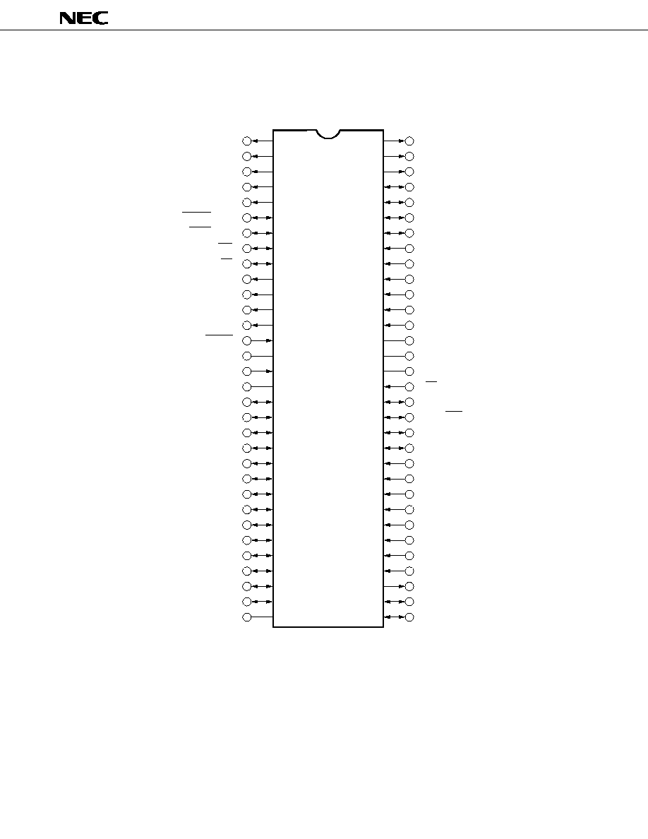
PIN CONFIGURATION (TOP VIEW)
64-pin plastic shrink DIP
m
m
µ
PD78217ACW
µ
PD78218ACW≠
◊ ◊ ◊
1
P03
2
P04
3
P05
4
P06
5
P07
6
P67/REFRQ/AN7
7
P66/WAIT/AN6
8
P65/WR
9
P64/RD
10
P63/A19
11
P62/A18
12
P61/A17
13
P60/A16
14
RESET
15
X2
16
X1
17
V
SS
18
P57/A15
19
P56/A14
20
P55/A13
21
P54/A12
22
P53/A11
23
P52/A10
24
P51/A9
25
P50/A8
26
P47/AD7
27
P46/AD6
28
P45/AD5
29
P44/AD4
30
P43/AD3
31
P42/AD2
32
V
SS
64
63
62
61
60
59
58
57
56
55
54
53
52
51
50
49
48
47
46
45
44
43
42
41
40
39
38
37
36
35
34
33
P02
P01
P00
P37/TO3
P36/TO2
P35/TO1
P34/TO0
P70/AN0
P71/AN1
P72/AN2
P73/AN3
P74/AN4
P75/AN5
AV
REF
AV
SS
V
DD
EA
P33/SO/SB0
P32/SCK
P31/T
X
D
P30/R
X
D
P27/SI
P26/INTP5
P25/INTP4/ASCK
P24/INTP3
P23/INTP2/CI
P22/INTP1
P21/INTP0
P20/NMI
ASTB
P40/AD0
P41/AD1
5
µ
PD78217A, 78218A
1
2
3
4
5
6
7
8
9
10
11
12
13
14
15
16
P71/AN1
P72/AN2
P73/AN3
P74/AN4
P75/AN5
AV
REF
AV
SS
V
DD
EA
P33/SO/SB0
P32/SCK
P31/T
X
D
P30/R
X
D
P27/SI
P26/INTP5
P25/INTP4/ASCK
X1
V
SS
P64/RD
P63/A19
P62/A18
P61/A17
P60/A16
RESET
X2
P57/A15
P56/A14
P55/A13
P54/A12
P53/A11
P52/A10
P51/A9
17
18
19
20
21
22
23
24
25
26
27
28
29
30
31
32
64
63
62
61
60
59
58
57
56
55
54
53
52
51
50
49
48
47
46
45
44
43
42
41
40
39
38
37
36
35
34
33
P65/WR
P66/WAIT/AN6
P67/REFRQ/AN7
P07
P06
P05
P04
P03
P02
P01
P00
P37/TO3
P36/TO2
P35/TO1
P34/TO0
P70/AN0
P50/A8
P47/AD7
P46/AD6
P45/AD5
P44/AD4
P43/AD3
P42/AD2
V
SS
P41/AD1
P40/AD0
ASTB
P20/NMI
P21/INTP0
P22/INTP1
P23/INTP2/CI
P24/INTP3
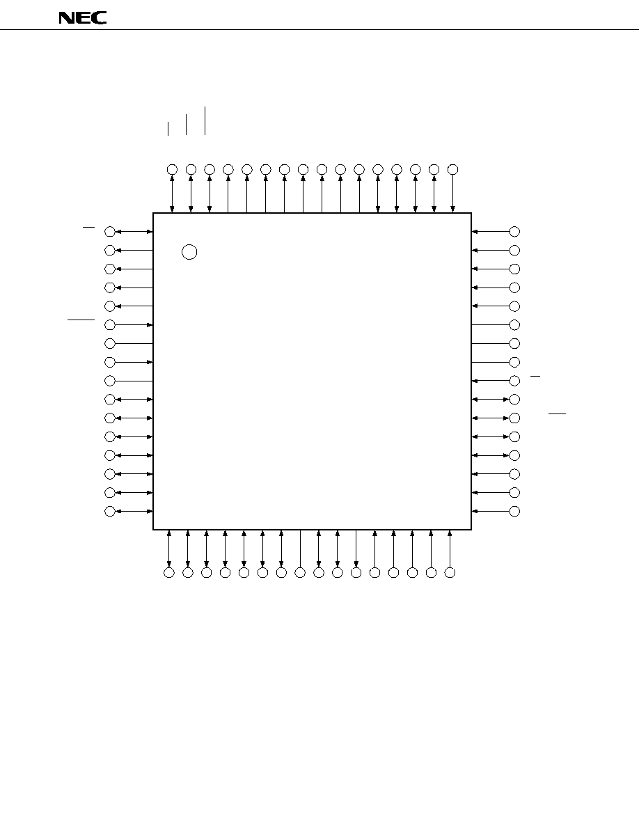
64-pin plastic QFP
µ
PD78217AGC≠AB8
µ
PD78218AGC≠
◊ ◊ ◊
≠AB8

6
µ
PD78217A, 78218A
PIN IDENTIFICATION
P00 to P07
: Port 0
P20 to P27
: Port 2
P30 to P37
: Port 3
P40 to P47
: Port 4
P50 to P57
: Port 5
P60 to P67
: Port 6
P70 to P75
: Port 7
TO0 to TO3
: Timer Output
CI
: Clock Input
R
X
D
: Receive Data
T
X
D
: Transmit Data
SCK
: Serial Clock
ASCK
: Asynchronous Serial Clock
SB0
: Serial Bus
SI
: Serial Input
SO
: Serial Output
NMI
: Non-maskable Interrupt
INTP0 to INTP5 : Interrupt From Peripherals
AD0 to AD7
: Address/Data Bus
A8 to A19
: Address Bus
RD
: Read Strobe
WR
: Write Strobe
WAIT
: Wait
ASTB
: Address Strobe
REFRQ
: Refresh Request
RESET
: Reset
X1, X2
: Crystal
EA
: External Access
AN0 to AN7
: Analog Input
AV
REF
: Reference Voltage
AV
SS
: Analog Ground
V
DD
: Power Supply
V
SS
: Ground
7
µ
PD78217A, 78218A
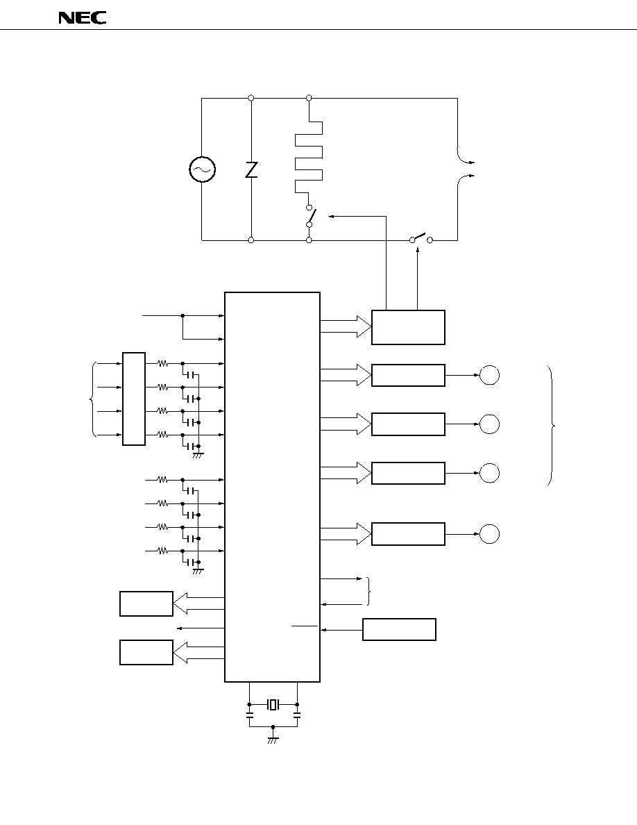
EXAMPLE OF SYSTEM CONFIGURATION (INVERTER AIR-CONDITIONER IN-DOOR UNIT)
µ
PD78218A
Relay Driver
Stepping Motors
2
P55,P56
Driver
M
Right/
Left Wind
Direction
4
P00-P03
Driver
M
Up-Down
Wind
Direction
4
P60-P63
Driver
M
Right/
Left Wind
Direction
4
P04-P07
Driver
M
Indoor
Fan Motor
5
P50-P54
RESET
Serial Communication
T
X
D
R
X
D
RESET
X2
X1
HA Control
2
Display
8
Buzzer
P35,P36
P34
P40-P47
Wind Direction Setting
Remote Control
Receive
Wired Remote Control
INTP0
P32
AN0
AN1
AN2
AN3
AN4
AN5
AN6
AN7
Room Temperature
Special Sensor
Humidity
Heat Exchanger
Temperature
Varistor
AC
100 V
Quick Heater
Outdoor Unit
8
µ
PD78217A, 78218A
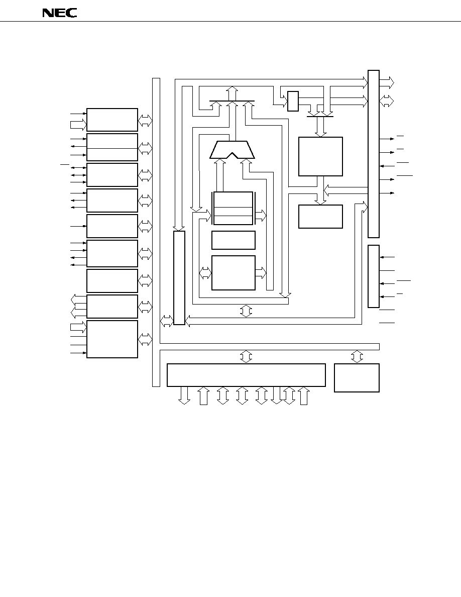
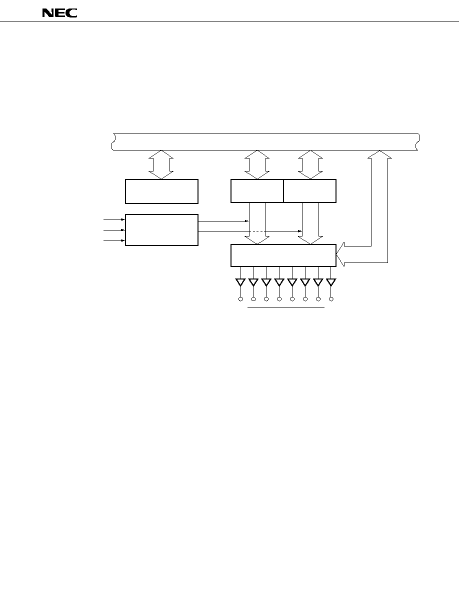
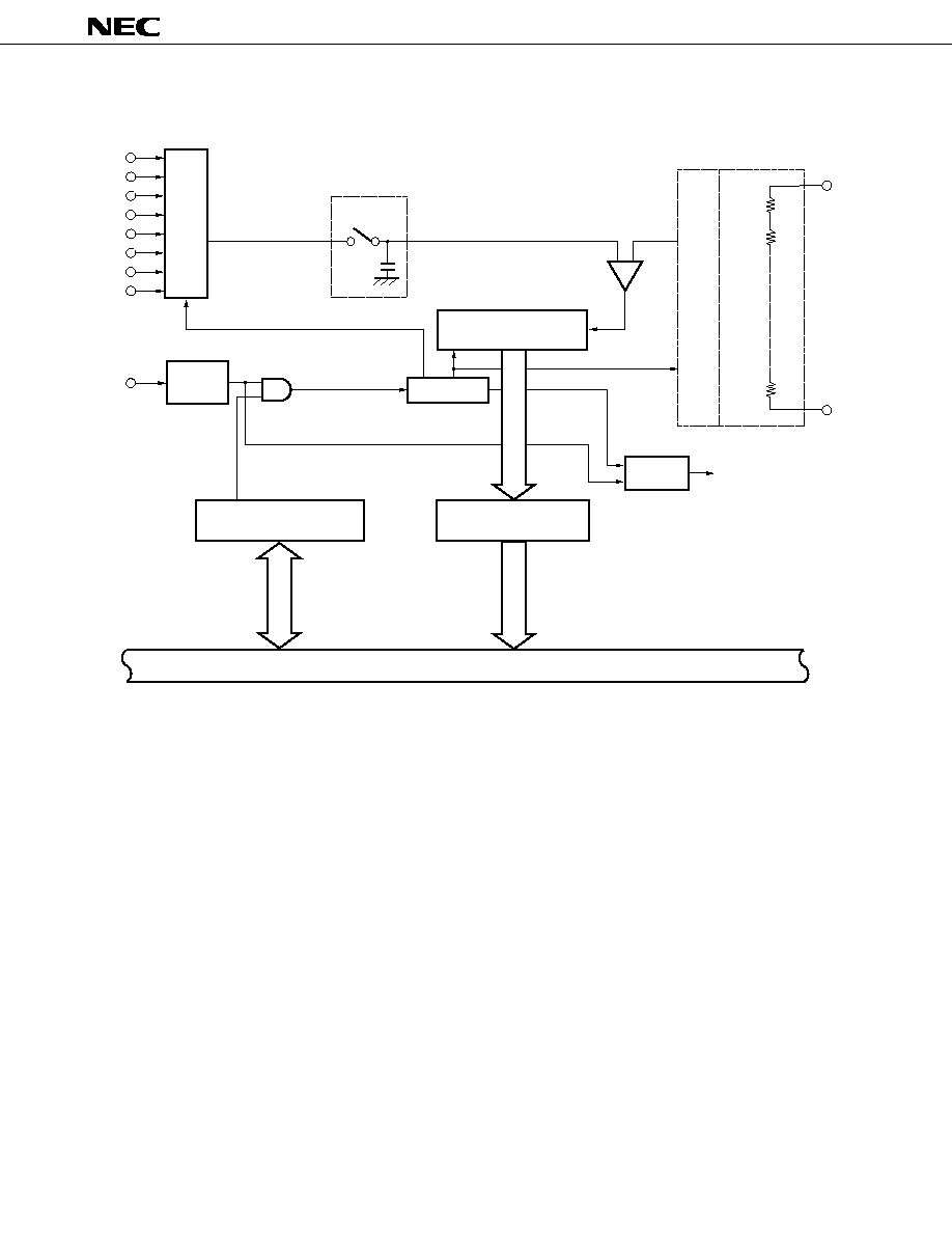
INTERNAL BLOCK DIAGRAM
Caution
Inernal ROM/RAM capacity varies depending on the product.
Note
In case of the
µ
PD78217A, P40 to P47, P50 to P57, P64 and P65 cannot be used as ports.
P70
-P75
INTP5
PROGRAMMABLE
INTERRUPT
CONTROLLER
BAUD RATE
GENERATOR
UART
CLOCKED
SERIAL
INTERFACE
TIMER/COUNTER
(16 BITS)
REAL-TIME
OUTPUT PORT
(4 BITS
◊
2)
TIMER/COUNTER
CHANNEL-1
(PS + 8 BITS)
TIMER/COUNTER
CHANNEL-2
(PS + 8 BITS)
TIMER/COUNTER
CHANNEL-3
(PS + 8 BITS)
A/D CONVERTER
SFR ADDRESS/DATA BUS
AV
SS
AV
REF
AN0-AN7
P04-P07
P00-P03
TO3
TO2
INTP2
INTP1
INTP0
TO1
TO0
INTP3
SI
SO/SB0
SCK
ASCK
T
X
D
R
X
D
NMI
INTP0-INTP5
BUS CONTROL
ADDRESS BUS
PC
ALU
ROM
TEMPORARY
REGISTERS
SP
PSW
BOOLEAN
PROCESSOR
∑ RAM (256 Bytes)
∑ GR
∑ MACRO
SERVICE
CHANNEL
DATA BUS (8)
∑ MICRO ROM
∑ MICRO≠
SEQUENCER
BUS I/F
SYSTEM CONTROL
DATA BUS
PORT
RAM
A16-A19
(Expansion)
A8-A15
AD0-AD7
RD
WR
WAIT
REFRQ
ASTB
X1
X2
RESET
EA
V
DD
V
SS
P7
P2
P6
P6
P5
P64
-P67
P60
-P63
P4
P3
P0
P50
-P57
P40
-P47
P30
-P37
P20
-P27
P00
-P07
Note
Note
Note

9
µ
PD78217A, 78218A
CONTENTS
1.
DIFFERENCES BETWEEN
µ
PD78218A AND
µ
PD78214 SUBSERIES .................................................. 10
2.
PIN FUNCTIONS ........................................................................................................................................11
2.1
PORTS .................................................................................................................................................................11
2.2
NON-PORT PINS ................................................................................................................................................12
2.3
PIN I/O CIRCUITS AND UNUSED PIN CONNECTION ................................................................................... 13
3.
INTERNAL BLOCK FUNCTIONS ..............................................................................................................15
3.1
MEMORY SPACE ...............................................................................................................................................15
3.2
PORTS .................................................................................................................................................................17
3.3
REAL-TIME OUTPUT PORT .............................................................................................................................. 19
3.4
TIMER/COUNTER UNIT ....................................................................................................................................20
3.5
A/D CONVERTER ...............................................................................................................................................22
3.6
SERIAL INTERFACE ...........................................................................................................................................24
3.6.1
Asynchronous Serial Interface ........................................................................................................ 25
3.6.2
Clock Synchronous Serial Interface ................................................................................................26
4.
INTERNAL/EXTERNAL CONTROL FUNCTION ...................................................................................... 27
4.1
INTERRUPTS ..................................................................................................................................................... 27
4.1.1
Interrupt Sources .............................................................................................................................. 28
4.1.2
Vectored Interrupt .............................................................................................................................30
4.1.3
Macro Service ....................................................................................................................................30
4.1.4
Macro Service Application Examples ............................................................................................. 31
4.2
LOCAL BUS INTERFACE ...................................................................................................................................33
4.2.1
Memory Expansion ...........................................................................................................................33
4.2.2
Programmable Wait ..........................................................................................................................33
4.2.3
Pseudo-Static RAM Refresh Function ............................................................................................ 33
4.3
STANDBY ...........................................................................................................................................................34
4.4
RESET ..................................................................................................................................................................35
5.
INSTRUCTION SET ...................................................................................................................................36
6.
ELECTRICAL SPECIFICATIONS ................................................................................................................40
7.
PACKAGE DRAWINGS .............................................................................................................................57
8.
RECOMMENDED SOLDERING CONDITIONS ........................................................................................59
APPENDIX A. DEVELOPMENT TOOLS ......................................................................................................... 60
APPENDIX B. RELATED DOCUMENTS ......................................................................................................... 62
10
µ
PD78217A, 78218A
Part Number
Minimum instruction execution
time (at 12-MHz)
PUSH PSW instruction execution
time (number of clocks)
Power voltage range
On-chip memory
I/O pins
16-bit timer/counter one-shot
pulse output
Macro service counter bit width
Macro service type C MPD, MPT
increments
Macro service execution time
Restrictions when data is
transferred from macro service
type A memory to SFR
A/D converter
Stabilization time for oscillation
in STOP mode release
Package
µ
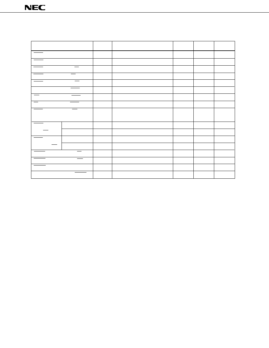
PD78214 Subseries
µ
PD78212
µ
PD78213
µ
PD78214
µ
PD78P214
333 ns
500 ns
333 ns
When stack area is an internal dual port RAM
: 5 or 7
Other than above
: 7 or 9
V
DD
=+5V
±
10%
8 Kbytes
ROM-less
16 Kbytes
16 Kbytes
(mask ROM)
(mask ROM)
(PROM)
384 bytes
512 bytes
54
36
54
Not available
NMI active pulse width + dedicated counter 16 bits
∑ 64-pin plastic shrink DIP (750 mil)
∑ 64-pin plastic QUIP: Except
µ
PD78212
∑ 68-pin plastic QFJ: Except
µ
PD78212
∑ 64-pin plastic QFP (14 x 14 mm)
∑ 74-pin plastic QFP (20 x 20 mm)
∑ 64-pin ceramic shrink DIP
(CERDIP, with window, 750 mil):
µ
PD78P214 only
8/16 bits select capability (except type A)
16-bit increment
Input voltage
restrictions
AV
REF
voltage
restrictions
1.
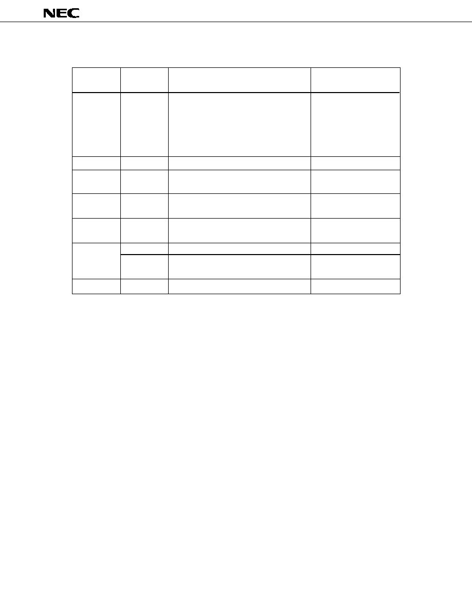
DIFFERENCES BETWEEN
µ
PD78218A AND
µ
PD78214 SUBSERIES
Macro service depends on mode. Compare with user's manual of products.
Generated when transfer source buffer (memory) address is
0FED0H to 0FEDFH.
Only pins involved in A/D conversion
3.6 V to V
DD
Dedicated counter 15 bits or NMI active pulse width + dedi-
cated counter 16 bits
∑ 64-pin plastic shrink DIP (750 mil)
∑ 64-pin plastic QFP (14 x 14 mm)
∑ 64-pin ceramic shrink DIP
(CERDIP, with window, 750 mil):
µ
PD78P218A only
Only 8 bits
Only low-order 8 bits increment
(high-order 8 bits are unchanged)
Generated when transfer data is in D0H to DFH.
Pins involved in A/D conversion and pins selected by ADM
register bits ANI0 to ANI2 only: 0V to AV
REF
pin voltage
3.4 V to V
DD
Series Name
Available
µ
PD78218A Subseries
µ
PD78217A
µ
PD78218A
µ
PD78P218A
500 ns
333 ns
When stack area is an internal dual port RAM
: 6
Other than above
: 8
V
DD
=+5V
±
10%
V
DD
=+5V
±
0.3V
ROM-less
32 Kbytes
32 Kbytes
(mask ROM)
(PROM)
1024 bytes
36
54
ROM
RAM
11
µ
PD78217A, 78218A
NMI
INTP0
INTP1
INTP2/CI
INTP3
INTP4/ASCK
INTP5
SI
RxD
TxD
SCK
SO/SB0
TO0 to TO3
AD0 to AD7
A8 to A15
A16 to A19
RD
WR
WAIT/AN6
REFRQ/AN7
AN0 to AN5
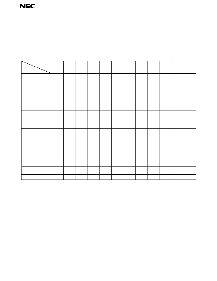
2.
PIN FUNCTIONS
2.1
PORTS
Pin Name
I/O
Function
Alternate
Function
Port 0 (P0):
Established as a real-time output port (4 bits
◊
2)
Direct drive of transistors capability
Port 2 (P2):
P20 cannot be used as a general-purpose port. (Non-maskable interrupt)
However, the input level can be confirmed in the interrupt routine.
The connection of the on-chip pull-up resistor can be specified as a 6-bit unit for P22
to P27 by software.
Port 3 (P3):
The input/output specifiable bit-wise.
Input mode pins specifiable for on-chip pull-up resistor connection as a batch by
software.
Port 4 (P4):
The input/output specifiable as an 8-bit batch.
The connection of the on-chip pull-up resistor specifiable as an 8-bit batch by
software.
LED direct drive capability.
Port 5 (P5):
The input/output specifiable bit-wise.
Input mode pins specifiable for on-chip pull-up resistor connection as a batch by
software.
LED direct drive capability.
Port 6 (P6):
P64 to P67 enables to specify the input/output bit-wise.
The connection of the on-chip pull-up resistor to input mode pins can be specified
as a batch for P64 to P67 by software.
Port 7 (P7)
Output
Input
Input/
output
Input/
output
Input/
output
Output
Input/
output
Input
P00 to P07
P20
P21
P22
P23
P24
P25
P26
P27
P30
P31
P32
P33
P34 to P37
P40 to
P47
Note
P50 to
P57
Note
P60 to P63
P64
Note
P65
Note
P66
P67
P70 to P75
Note
In case of the
µ
PD78217A, these cannot be used as ports.
12
µ
PD78217A, 78218A
P34 to P37
P23 /INTP2
P30
P31
P25/INTP4
P33/SO
P27
P33/SB0
P32
P20
P21
P22
P23/CI
P24
P25/ASCK
P26
P40 to P47
Note
P50 to P57
Note
P60 to P63
P64
Note
P65
Note
P66/AN6
P67/AN7
P70 to P75
TO0 to TO3
CI
R
X
D
T
X
D
ASCK
SB0
SI
SO
SCK
NMI
INTP0
INTP1
INTP2
INTP3
INTP4
INTP5
AD0 to AD7
A8 to A15
A16 to A19
RD
WR
WAIT
ASTB
REFRQ
RESET
X1
X2
EA
AN0 to AN5
AN6, AN7
AV
REF
AV
SS
V
DD
V
SS
Pin Name
I/O
Output
Input
Input
Output
Input
Input
Output
Input/output
Input/output
Input
Input/output
Output
Output
Output
Output
Input
Output
Input
Output
Input
Input
Input
Note
In case of the
µ
PD78217A, these cannot be used as ports.
P66/WAIT,
P67/REFRQ
Alternate
Function
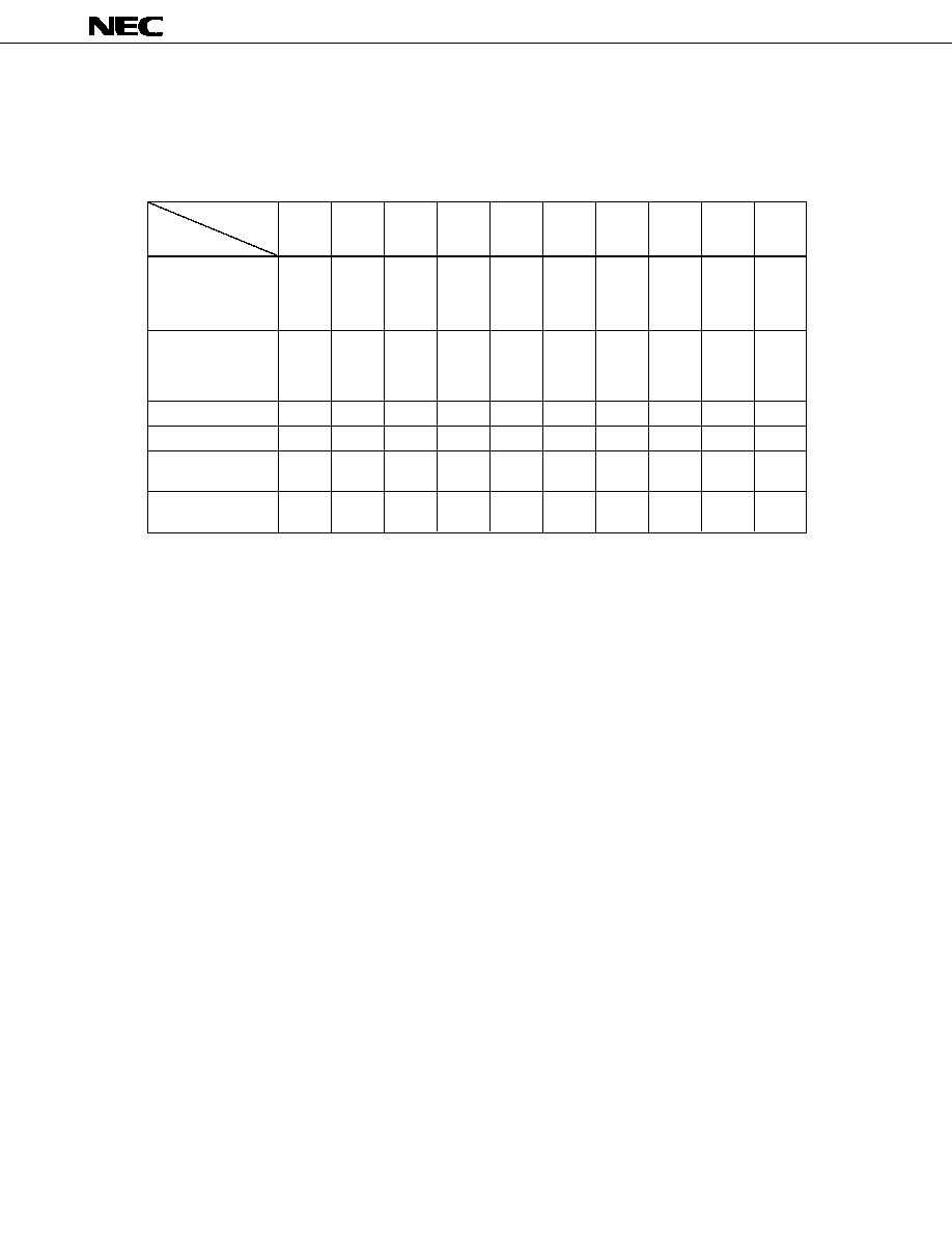
2.2
NON-PORT PINS
Function
Timer output
Count clock input to 8-bit timer/counter 2
Serial data input (UART)
Serial data output (UART)
Baud rate clock input (UART)
Serial data input/output (SBI)
Serial data input (3-wire serial I/O)
Serial data output (3-wire serial I/O)
Serial clock input/output (SBI, 3-wire serial I/O)
External interrupt request
Time multiplexing address/data bus (external memory connection)
Upper address bus (external memory connection)
Upper address when extending address (external memory connection)
Read strobe into external memory
Write strobe into external memory
Wait insertion
Address (A0 to A7) latch timing output (during external memory access)
Refresh pulse output into external pseudo-static memory
Chip reset
Crystal connection for system clock oscillation (external clock input to X1
enabled)
ROM-less operating specification (external access of the same space as internal
ROM). Used high for the
µ
PD78218A and used low for the
µ
PD78217A.
Analog voltage input for A/D converter
Reference voltage apply for A/D converter
GND for A/D converter
Positive power supply
GND
13
µ
PD78217A, 78218A
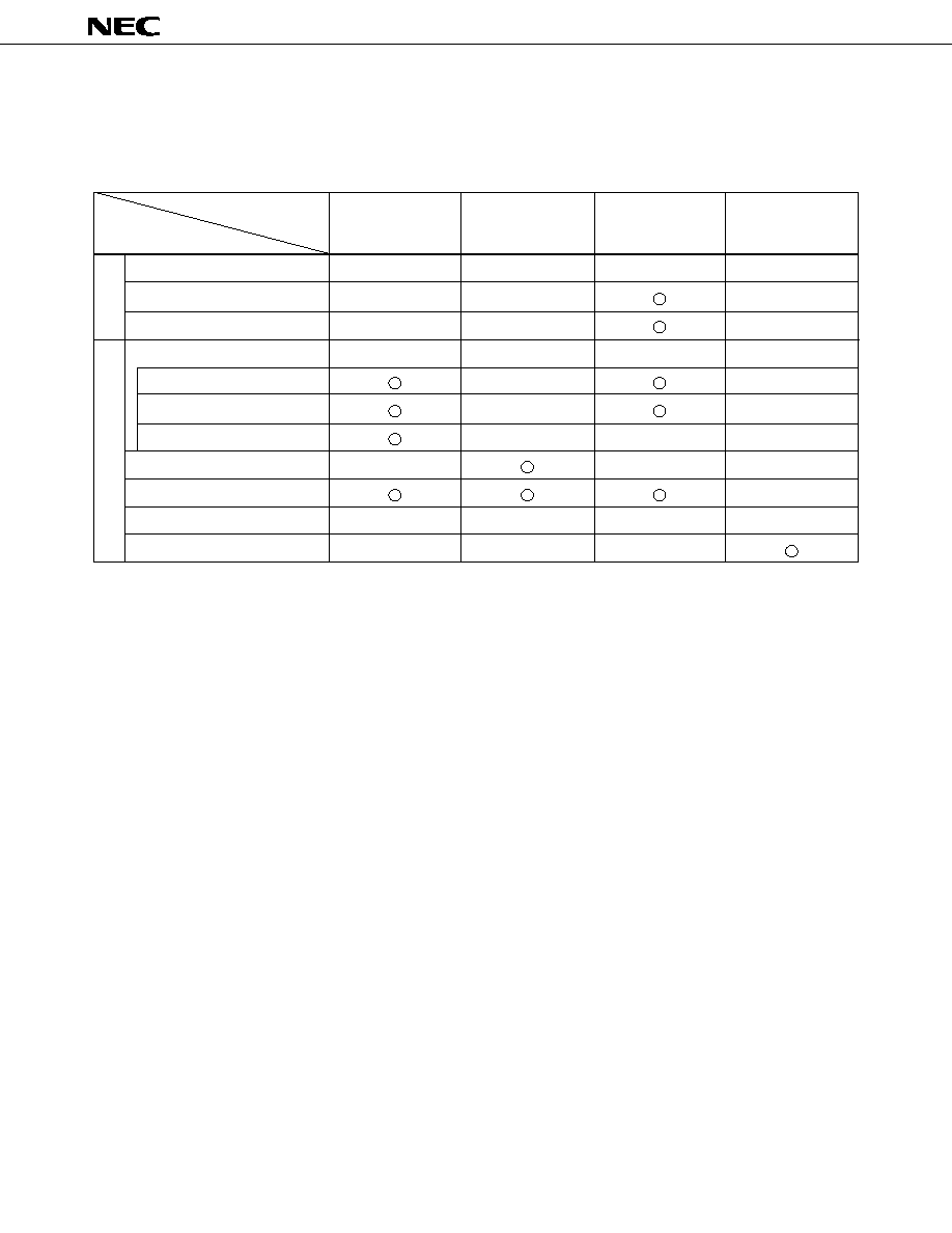
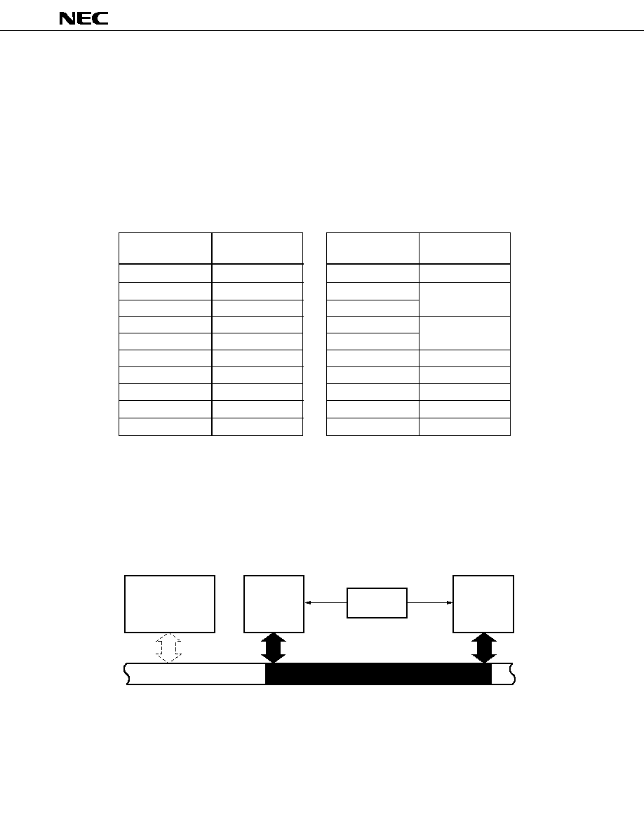
2.3
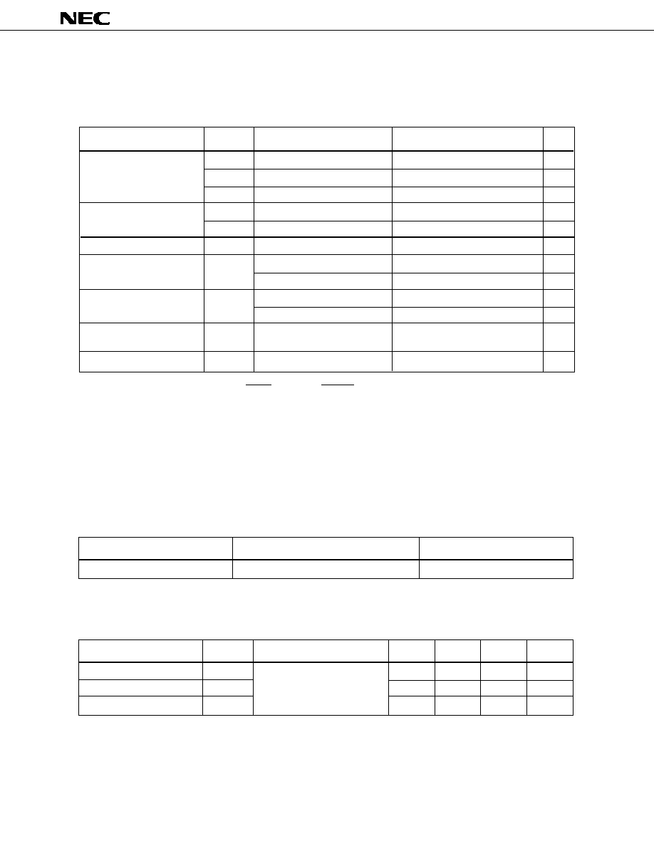
PIN I/O CIRCUITS AND UNUSED PIN CONNECTION
The input/output circuit type of each pin and recommended connection of unused pins are shown in Table 2-1.
For the input/output circuit configuration of each type, see Fig. 2-1.
Table 2-1 Input/Output Circuit Type of Each Pin
4
2
2-A
5-A
8-A
10-A
5-A
4
5-A
11
9
4
2
1
Leave open.
Connected to V
DD
or V
SS
.
Connected to V
DD
.
Input
: Connected to V
DD
.
Output
: Leave open.
Leave open.
Input
: Connected to V
DD
.
Output
: Leave open.
Input
: Connected to V
DD
.
Note
Output
: Leave open.
Connected to V
SS
.
Leave open.
Connected to V
SS
or V
DD
.
Note
Connected to V
SS
.
Input/Output
Circuit Type
Output
Input
Input/output
Output
Input/output
Input
Output
Input
P00 to P07
P20/NMI
P21/INTP0
P22/INTP1
P23/INTP2/CI
P24/INTP3
P25/INTP4/ASCK
P26/INTP5
P27/SI
P30/R
X
D
P31/T
X
D
P32/SCK
P33/SB0/SO
P34/TO0 to P37/TO3
P40/AD0 to P47/AD7
P50/A8 to P57/A15
P60/A16 to P63/A19
P64/RD
P65/WR
P66/WAIT/AN6
P67/REFRQ/AN7
P70/AN0 to P75/AN5
ASTB
RESET
EA
AV
REF
AV
SS
Unused Pin Connection
Pin Name
I/O
Caution
If the input/output mode is undefined for the input/output dual-function pins, connect these pins to
V
DD
via a resistor of several ten k
.
(Especially if the reset input pin exceeds the low-level input voltage at power-on or in case of input/
output switching by software.)
Remark
The type numbers are standardized for 78K series, therefore they are not always consecutive numbers
for each product (some circuits are not incorporated).
Note
A voltage outside the range AV
SS
to AV
REF
should not be applied, as this may damage the
µ
PD78217A/78218A.
14
µ
PD78217A, 78218A
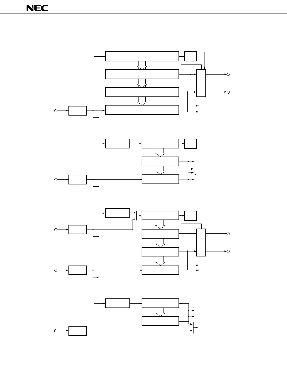
Fig. 2-1 Pin Input/Output Circuits
Type 1
IN
Type 2-A
pullup
enable
P
V
DD
V
DD
P
IN
N
Type 2
Schmitt-Triggered Input with Hysteresis Characteristic
Type 8-A
pullup
enable
data
output
disable
V
DD
P
N
P
IN / OUT
V
DD
Type 10-A
pullup
enable
P
V
DD
data
output
disable
N
IN / OUT
V
DD
P
open
drain
data
output
disable
N
OUT
V
DD
P
Type 4
Push-pull output which enables output to be high-impedance
(both P-ch and N-ch off).
IN
Schmitt-Triggered Input with Hysteresis Characteristic
Type 5-A
pullup
enable
data
output
disable
V
DD
P
N
P
IN / OUT
V
DD
input
enable
Type 9
N
P
IN
+
-
V
ref
V
ref
input
enable
(Threshold Voltage)
Comparator
Type 11
enable
V
DD
pullup
enable
data
output
disable
IN / OUT
input
(Threshold Voltage)
V
DD
P
N
P
+
-
Comparator
N
P

15
µ
PD78217A, 78218A
3.
INTERNAL BLOCK FUNCTIONS
3.1
MEMORY SPACE
A memory space of 1 Mbytes can be accessed. Fig. 3-1 shows that memory space. The program memory mapping
differs depending on the EA pin status.
(1)
µ
PD78217A (EA = L)
The program memory is mapped onto external memory (64256 bytes: 00000H to 0FAFFH). This area can also
be used as data memory.
The data memory is mapped onto internal RAM (1024 bytes: 0FB00H to 0FEFFH). In the 1-Mbyte expansion
mode, external memory (960 Kbytes: 10000H to FFFFFH) is mapped as expanded data memory.
(2)
µ
PD78218A (EA = H)
The program memory is mapped onto internal ROM (32 Kbytes: 00000H to 07FFFH) and external memory (31488
bytes: 08000H to 0FAFFH). The external memory is accessed in the external memory expansion mode. The area
mapped onto the external memory can also be used as data memory.
The data memory is mapped onto internal RAM (1024 bytes: 0FB00H to 0FEFFH). In the 1-Mbyte expansion
mode, external memory (960 Kbytes: 10000H to FFFFFH) is mapped as expanded data memory.
16
µ
PD78217A, 78218A
Fig. 3-1 Memory Map
Notes 1. Accessed by 1-Mbyte expansion mode. Shaded areas denote internal memory.
2. Accessed by external memory expansion mode.
3. The
µ
PD78217A applies only when EA = L.
FFFFFH
0FFFFH
0FFDFH
0FFD0H
0FF00H
0FEFFH
0FB00H
0FAFFH
00000H
External Memory
(960 Kbytes)
Internal ROM
(32 Kbytes)
10000H
External Memory
(31488 bytes)
Internal RAM
(1024 bytes)
08000H
07FFFH
External Memory
(64256 bytes)
0FEFFH
0FEE0H
0FEDFH
0FB00H
General Register
(32 bytes)
07FFFH
01000H
00FFFH
00800H
007FFH
00080H
0007FH
00040H
0003FH
00000H
Program Area
(28 Kbytes)
CALLF Entry Area
(2 Kbytes)
Program Area
(1920 bytes)
CALLT Table Area
(64 bytes)
Vector Table Area
(64 bytes)
Data Area
(1024 bytes)
Macro Service Control
Word (30 bytes)
0FEC2H
Extended Address
Data Memory
Program Memory/
Data Memory
Program
Memory/
Data
Memory
EA = H
EA = L (ROM-Less Mode)
Normal Address (64 Kbytes)
Data
Memory
Memory Space (1 Mbytes)
Note2
(256 bytes)
00FFFH
Program Memory / Data Memory
Note2
Note1
Note1
Special Function Register (SFR)
Note3

17
µ
PD78217A, 78218A
3.2
PORTS
The
µ
PD78217A/78218A has the ports shown in Fig. 3-2 which allow various kinds of control. The functions of
each port are shown in Table 3-1. For ports 2 to 6, on-chip pull-up resistor can be specified by software at input.
Fig. 3-2 Port Configuration
Note
In case of the
µ
PD78217A, P40 to P47, P50 to P57, P64, and P65 cannot be used as ports.
8
Port 0
Port 2
Port 3
8
8
Port 5
Port 4
4
6
Port 7
Port 6
P00-P07
P20-P27
P30
P37
P40-P47
P50
P57
P60-63
P64
P67
P70-P75
Note
Note
Note
18
µ
PD78217A, 78218A
Table 3-1 Port Function
Output or high-impedance specifiable as
an 8-bit batch.
Can also operate as 4 bits real-time output
(P00 to P03, P04 to P07).
Transistor direct drive capability.
Input port
Input or output specifiable bit-wise.
Input or output specifiable as an 8-bit batch.
LED direct drive capability.
Input or output specifiable bit-wise.
LED direct drive capability.
Output port
Input or output specifiable bit-wise.
Input port
Designation of Software
Pull-Up
Name
Pin Name
Function
P00 to P07
P20 to P27
P30 to P37
P40 to P47
P50 to P57
P60 to P63
P64 to P67
P70 to P75
Port 0
Port 2
Port 3
Port 4
Note
Port 5
Note
Port 6
Note
Port 7
≠≠≠≠≠
6-bit batch (P22 to P27)
Input mode pins specifiable
as a batch
8-bit batch
Input mode pins specifiable
as a batch
≠≠≠≠≠
Input mode pins specifiable
as a batch
≠≠≠≠≠
Note
In case of the
µ
PD78217A, P40 to P47, P50 to P57, P64, and P65 cannot be used as ports.
19
µ
PD78217A, 78218A
3.3
REAL-TIME OUTPUT PORT
The real-time output port outputs the data stored in the buffer in synchronization with timer match interrupts
or external interrupts. A jitterless pulse output is obtained by means of this.
Therefore, it is most suitable for applications which output any pattern at any interval time. (Stepping motor open
loop control, etc.)
Port 0 and the buffer register are the core elements of the configuration, as shown in Fig. 3-3.
Fig. 3-3 Real-Time Output Port Block Diagram
4
4
4
4
8
Buffer
Register
INTP0 (From Outside)
INTC10 (From Timer)
INTC11 (From Timer)
Real-Time Output Port
Control Register
Output Trigger
Control Circuit
Internal Bus
P0H
P0L
Output Latch (P0)
P07
P00
8
20
µ
PD78217A, 78218A
3.4
TIMER/COUNTER UNIT
The
µ
PD78217A/78218A has a 16-bit timer/counter unit for 1 channel and 8-bit timer/counter units for 3 channels.
Table 3-2 Type and Function of Timer/Counter
2 chs
2 chs
2 chs
1 ch
≠≠≠
≠≠≠
≠≠≠
≠≠≠
≠≠≠
≠≠≠
2 chs
≠≠≠
2 chs
≠≠≠
≠≠≠
≠≠≠
≠≠≠
≠≠≠
≠≠≠
≠≠≠
≠≠≠
≠≠≠
≠≠≠
≠≠≠
≠≠≠
2
2
2
1
≠≠≠
≠≠≠
≠≠≠
Interval timer
External event counter
One-shot timer
Timer output
Toggle output
PWM/PPG output
One-shot pulse output
Real-time output
Pulse amplitude measurement
Number of interrupt requests
Clock source of serial interface
Unit
Type & Function
Type
8-Bit Timer/
Counter 3
8-Bit Timer/
Counter 2
8-Bit Timer/
Counter 1
16-Bit Timer/
Counter
Since 7 interrupt requests are supported in total, it can also function as timer for 7 channels.
Remark
The one-shot pulse output function activates the pulse output level by software, and inactivates it by
hardware (interrupt request signal).
This function is different from the one-shot timer function of 8-bit timer/counter 2.
Function
21
µ
PD78217A, 78218A
Fig. 3-4 Timer/Counter Unit Block Diagram
8-bit timer/counter unit 2
8-bit timer/counter unit 3
8-bit timer/counter unit 1
16-bit timer/counter unit
Compare Register CR00
Compare Register CR01
Capture Register CR02
f
CLK/8
INTP3
Edge
Detection
INTP3
Software Trigger
OVF
Pulse Output
Control
Match
Match
INTC00
INTC01
TO0
TO1
Capture/Compare
Register CR11
Prescaler
f
CLK/16
Compare Register
CR10
OVF
Match
Match
INTC10
To Real-Time
Output Port
INTC11
INTP0
Edge
Detection
INTP0
Compare Register
CR20
Prescaler
f
CLK/16
INTP2/CI
Edge
Detection
INTP2
Event Input
Compare Register
CR21
Capture Register
CR22
OVF
Pulse Output
Control
Match
Match
INTC20
INTC21
TO2
TO3
INTP1
Edge
Detection
INTP1
Prescaler
f
CLK/8
Compare Register
CR30
Clear
Match
UART
INTP4/
INTC30
INTP4/
ASCK
Edge
Detection
CSI
OVF: Overflow Flag
Timer Register TM0
Timer Register TM1
Timer Register TM2
Timer Register TM3
22
µ
PD78217A, 78218A
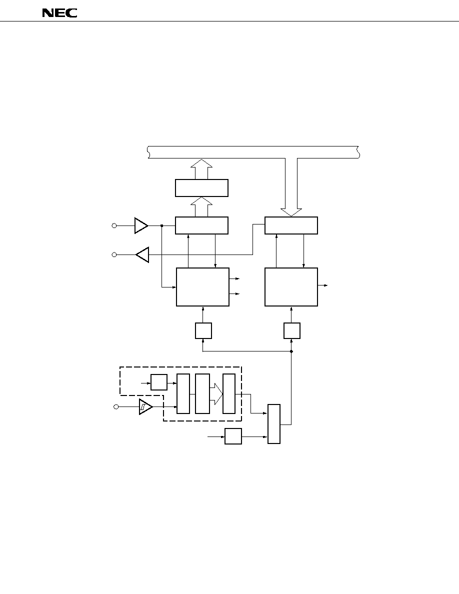
3.5
A/D CONVERTER
The
µ
PD78217A/78218A incorporate the analog/digital (A/D) converter with 8-channel multiplexed analog input
(AN0 to AN7).
The conversion method used is successive approximation. After the A/D conversion results are generated, they
are held in the 8-bit A/D conversion result register (ADCR), which may allow high-speed and high-precision
conversion (conversion time: Approx. 30
µ
s; at 12-MHz operation).
The following two modes are available for starting A/D conversion:
∑
Hardware start : Starts conversion by trigger input (INTP5)
∑
Software start
: Starts conversion by the A/D converter mode register (ADM) bit setting
The following two modes of operation after starting are available:
∑
Scan mode
: Multiple analog input are selected sequentially and conversion data is obtained from all pins.
∑
Select mode : The analog input is fixed at one pin and a continuous conversion value is obtained.
The above modes and the conversion operation are all stopped by ADM.
If the conversion result is transferred to the ADCR, an interrupt request INTAD is generated, (except in software
start select mode). Therefore, the conversion value can be transferred to memory continuously using macro service
(See section 4.1.3 "Macro Service").
Table 3-3 INTAD Generation Mode
Scan Mode
Select Mode
Hardware start
Software start
≠≠≠
23
µ
PD78217A, 78218A
Fig. 3-5 A/D Converter Block Diagram
INTP5
Interrupt Request
Series Resistor String
Input Selector
Sample & Hold Circuit
Voltage Comparator
Tap Selector
Successive Approximation
Register (SAR)
Edge
Detector
Controller
Trigger Enable
A/D Conversion Result
Register (ADCR)
A/D Converter Mode
Register (ADM)
AN0
AN1
AN2
AN3
AN4
AN5
AN6
AN7
INTP5
Conversion
Trigger
8
8
INTAD
Selector
AV
REF
AV
SS
R/2
R
R/2
Internal Bus
8
8

24
µ
PD78217A, 78218A
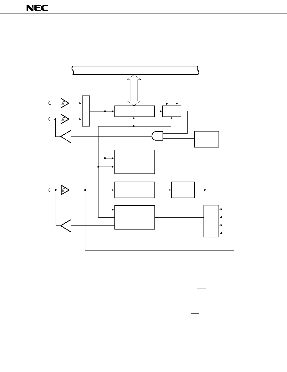
3.6
SERIAL INTERFACE
The
µ
PD78217A/78218A has two independent serial interfaces.
∑
Asynchronous serial interface (UART)
∑
Clock synchronous serial interface (CSI)
∑ 3-wire serial I/O
∑ Serial bus interface (SBI)
Therefore, communication with external devices and local communication inside the system can be performed
simultaneously (See Fig. 3-6).
Fig. 3-6 Serial Interface Example
(a) UART + SBI
(b) UART + 3-wire serial I/O
µ
PD78218A (Master)
Note Handshake Line
µ
PD78218A (Master)
V
DD
[UART]
RS-232-C
Driver
PD4711A
R
X
D
T
X
D
Port
SB0
SCK
[SBI]
SB0
SCK
PD75402A (Slave)
SB0
SCK
PD75328 (Slave)
LCD
µ
µ
µ
[UART]
RS-232-C
Driver
PD4711A
R
X
D
T
X
D
Port
SI
SCK
SO
INTPm
Port
PD78C11A (Slave)
[3-Wire Serial I/O]
SO
SCK
SI
Port
INT
PD78C14 (Slave)
SI
SCK
SO
Port
INT
INTPn
Port
µ
µ
µ
Note
Note
25
µ
PD78217A, 78218A
3.6.1
Asynchronous Serial Interface
The
µ
PD78217A/78218A incorporates UART (Universal Asynchronous Receiver Transmitter) as the asynchronous
serial interface. UART is used to send/receive one byte of data following a start bit.
The UART incorporates a dedicated baud rate generator which can generate a wide range of desired baud rates
and also determine baud rates by scaling the ASCK pin input clocks or 8-bit timer/counter 3 output (TM3 output),
allowing transmission/reception with a variety of baud rates.
If the UART dedicated baud rate generator is used, the MIDI standard baud rate (31.25 kbps) can also be obtained.
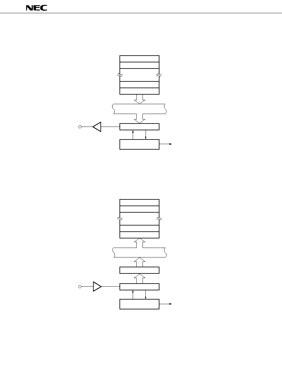
Fig. 3-7 Asynchronous Serial Interface (UART) Block Diagram
f
CLK
: Internal system clock frequency (System Clock Frequency/2)
ASCK
R
X
D
T
X
D
Receive Buffer
Receive Shift
Register
Receive Control
Parity Check
1/16
Internal Bus
Transmit Shift
Register
Transmit Control
Parity Addition
1/16
INTSR
INTSER
INTST
TXS
RXB
Selector
Selector
Selector
1/N
2
1/N
1
f
CLK
1/2
TM3 Output
UART Dedicated Baud Rate Generator
26
µ
PD78217A, 78218A
3.6.2
Clock Synchronous Serial Interface
The master device starts transmission by activating the serial clock and transfers one-byte data in synchronization
with this clock.
Fig. 3-8 Clock Synchronous Serial Interface Block Diagram
f
CLK
: Internal System Clock Frequency (System Clock Frequency/2)
(1)
3-wire serial I/O
This is an interface for communicating with devices incorporating a conventional clock synchronous serial
interface.
Basically, communication is performed with three lines, one serial clock line (SCK) and two serial data lines
(SI, SO). When connecting to multiple devices, a handshake line is necessary.
(2)
SBI
Communication with multiple devices is performed with one serial clock line (SCK) and one serial bus line (SB0).
This is NEC's standard serial interface.
The master device selects the slave device to be communicated with by outputting its "address" from the SB0
pin. Therefore, "commands" and "data" perform transfer and receive between the master and slave.
SCK
Shift Register
Internal Bus
INTCSI
SIO
Selector
SI
SO/SB0
Output
Latch
Set Clear
Busy/
Acknowledge
Generator
Selector
Interrupt
Generator
TM3 Output/2
f
CLK
/8
f
CLK
/32
Bus Release
Command/
Acknowledge
Detector
Serial Clock
Controller
Serial Clock
Counter
N-ch Open-drain output
also possible (SB0: SBI)

27
µ
PD78217A, 78218A
Service Mode
Servicing Subject
Service
PC, PSW Contents
Vectored interrupt
Software
With save and return
Macro service
Firmware
Hold
4.
INTERNAL/EXTERNAL CONTROL FUNCTION
4.1
INTERRUPTS
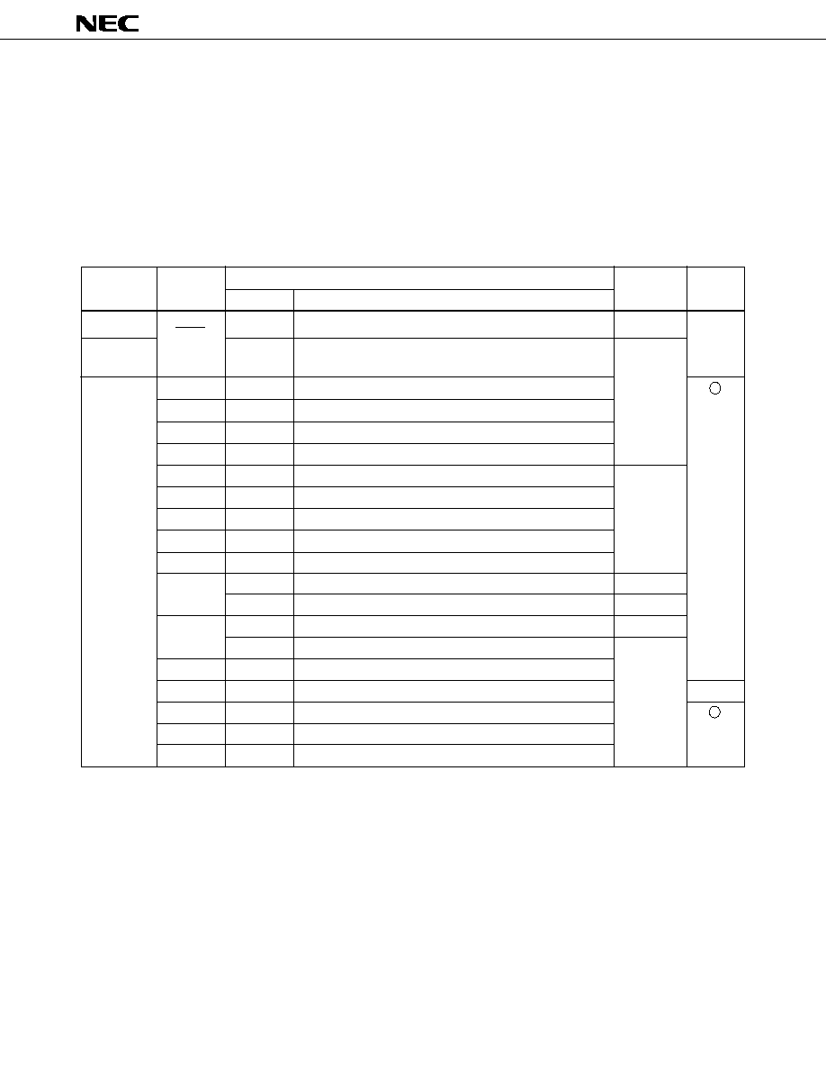
Two interrupt request servicing methods can be selected, as shown in the following table.
Table 4-1 Interrupt Request Servicing
Branches to service routine, and executes
(any process contents)
Data transfer, etc., between memory and I/O
(fixed process contents)
28
µ
PD78217A, 78218A
4.1.1
Interrupt Sources
There are 19 types of interrupt sources and a BRK instruction execution, as shown in Table 4-2.
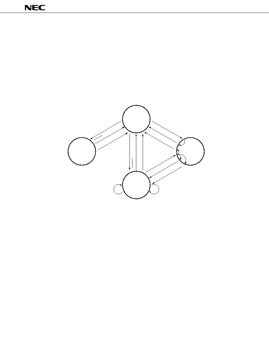
The priority of the interrupt servicing can be set to 2 levels (high and low priority levels). Therefore, the levels
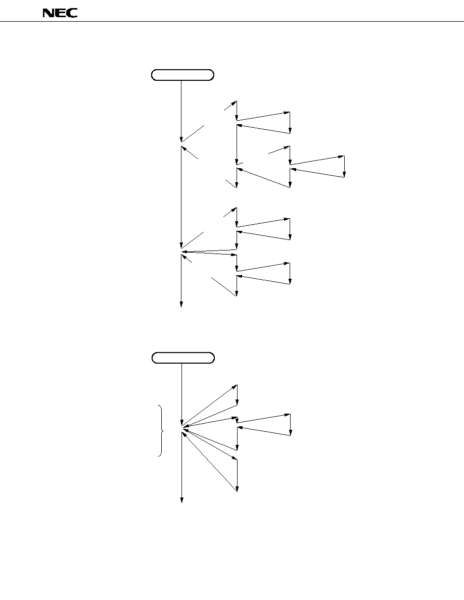
of nest control when the interrupt is in progress and when interrupt requests occur simultaneously (see Fig. 4-1,
Fig. 4-2) can be separated. Nesting will always take place in the macro service (It won't be put on hold).
The default priority is the priority level (fixed) to service the interrupt requests which occur at the same level
simultaneously (see Fig. 4-2).
Table 4-2 Interrupt Sources
Trigger
Type
Default
Priority
Source
0 (highest)
1
2
3
4
5
6
7
8
9
10
11
12
13
14
15 (lowest)
Name
Instruction execution
Pin input edge detection
Pin input edge detection (TM1 capture trigger)
Pin input edge detection (TM2 capture trigger)
Pin input edge detection (TM2 event counter input)
Pin input edge detection (TM0 capture trigger)
TM0 to CR00 match signal generation
TM0 to CR01 match signal generation
TM1 to CR10 match signal generation
TM1 to CR11 match signal generation
TM2 to CR21 match signal generation
Pin input edge detection
TM3 to CR30 match signal generation
Pin input edge detection
A/D converter conversion termination (transfer to ADCR)
TM2 to CR20 match signal generation
ASI receive error generation
ASI receive termination
ASI transmit termination
CSI transfer termination
BRK
NMI
INTP0
INTP1
INTP2
INTP3
INTC00
INTC01
INTC10
INTC11
INTC21
INTP4
INTC30
INTP5
INTAD
INTC20
INTSER
INTSR
INTST
INTCSI
Software
External
Internal
External
Non-
maskable
Maskable
External
Internal
Internal
≠≠≠≠≠
≠≠≠
≠≠≠
TM0
:
16-bit timer
TM1 to TM3 :
8-bit timer
ASI
:
Asynchronous serial interface
CSI
:
Clock synchronous serial interface
Macro
Service
Internal/
External
29
µ
PD78217A, 78218A
Fig. 4-1 Servicing Example when an Interrupt Request Occurrence is Issued while an Interrupt is Serviced
Fig. 4-2 Servicing Example of Simultaneous Interrupt Requests
Main Routine
Vectored Interrupt Request a
(Low-Priority Level)
Vectored Interrupt Request e
(High-Priority Level)
Servicing of b
Servicing of c
Servicing of d
Servicing of a
Macro Service
Request b
Vectored
Interrupt
Request c
(High-Priority
Level)
Macro Service
Request d
Servicing of e
Macro Service
Request f
Servicing of f
Macro Service
Request h
Vectored Interrupt Request g (Low-Priority
Level: Pending)
Servicing
of g
Servicing of h
[Nesting 1]
[Nesting 2]
[Nesting 3]
Main Routine
[Nesting 1]
[Nesting 2]
Servicing of b
Servicing of d
Servicing of c
Servicing of a
∑ Vectored Interrupt Request a
(Low-Priority Level)
∑ Macro Service Request b
(High-Priority Level)
∑ Macro Service Request c
(Low-Priority Level)
∑ Vectored Interrupt Request d
(High-Priority Level)
Default Priority: a > b > c > d
30
µ
PD78217A, 78218A
4.1.2
Vectored Interrupt
The memory contents of the vector table address, which corresponds to the interrupt source, is branched into
the service routine as a destination address.
As the CPU executes the interrupt servicing, the following operations occur.
∑
When branch :
Saving the CPU status (PC, PSW contents) to the stack.
∑
When return
:
Returning the CPU status (PC, PSW contents) from the stack.
The RETI instruction executes returning to the main routine from the service routine.
Table 4-3 Vector Table Address
Interrupt Source
INTC21
INTP4
INTC30
INTP5
INTAD
INTC20
INTSER
INTSR
INTST
INTCSI
BRK
NMI
INTP0
INTP1
INTP2
INTP3
INTC00
INTC01
INTC10
INTC11
4.1.3
Macro Service
This is a function to transfer data between the memory and special function registers (SFR) without going through
the CPU. The macro service controller accesses the memory and SFR, and transfers data directly without fetching
it.
High-speed data transfer is enabled because no data is saved, restored or fetched.
Fig. 4-3 Macro Service
003EH
0002H
0006H
0008H
000AH
000CH
0014H
0016H
0018H
001AH
Vector Table
Address
Interrupt Source
Vector Table
Address
001CH
000EH
0010H
0012H
0020H
0022H
0024H
0026H
CPU
Memory
SFR
Macro Service
Controller
Internal Bus
Read
Write
Read
Write
31
µ
PD78217A, 78218A
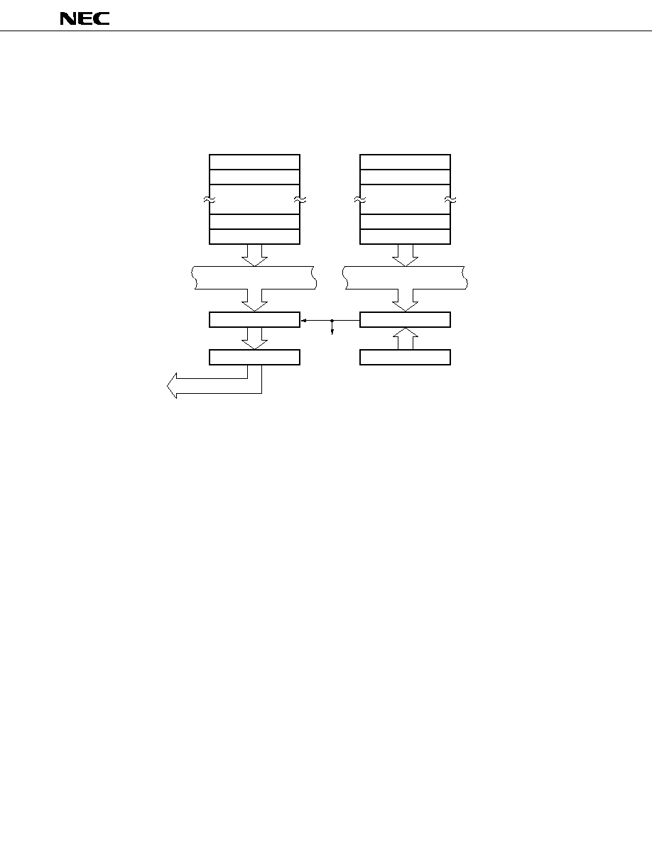
4.1.4
Macro Service Application Examples
(1)
Transmit operation of serial interface
Whenever the macro service request INTSR is generated, the receive data is transferred to the memory
from RXB. When the data n (last byte) is transferred to the memory (the receive data storage buffer becomes
empty), the vectored interrupt request INTSR is generated.
Whenever the macro service request INTST is generated, the next transmit data is transferred to TXS from
the memory. When the data n (last byte) is transferred to TXS (the transmit data storage buffer becomes
empty), a vectored interrupt request INTST is generated.
(2)
Receive operation of serial interface
Data n
Data n≠1
Data 2
Data 1
Transmit Shift Register
Transmission Control
T
X
D
INTST
TXS (SFR)
Internal Bus
Transmit Data Storage Buffer (Memory)
Data n
Data n≠1
Data 2
Data 1
Internal Bus
Receive Shift Register
Receive Control
R
X
D
INTSR
RXB (SFR)
Receive Buffer
Receive Data Storage Buffer (Memory)
32
µ
PD78217A, 78218A
(3)
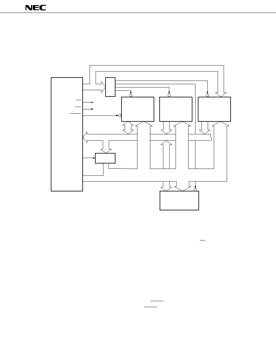
Real-time output port
The INTC10 and INTC11 become output triggers of the real-time output port. In the macro service for them, the
next output pattern and interval can be set simultaneously. Therefore, the INTC10 and INTC11 can control 2
system stepping motor independently. Also, they can be applied to control a PWM or DC motor, etc.
Whenever the macro service request INTC10 is generated, the pattern and timing are transferred to P0L and
CR10, respectively. When the contents of the TM1 match with the contents of the CR10, the next INTC10 is
generated and the contents of the P0L are sent to the output latch. If T
n
(last byte) is sent to CR10, a vectored
interrupt request INTC10 is generated.
The same operation is available for INTC11 (differences: CR10
CR11, P0L
P0H, P00-P03
P04-P07).
(SFR)
INTC10
Match
P
n
P
n-1
P
2
P
1
P0L
Internal Bus
Output Latch
Output Pattern Profile (Memory)
T
n
T
n-1
T
2
T
1
CR10
Internal Bus
TM1
Output Timing Profile (Memory)
(SFR)
P00-P03
33
µ
PD78217A, 78218A
4.2.1
Memory Expansion
The following modes have been prepared as a memory expansion function.
∑
External memory expansion mode
: Expands the program memory and data memory to 31488 bytes (64256
bytes for the
µ
PD78217A) externally. However, this area can be used
unconditionally under the ROM-less mode (EA = L).
∑
1-Mbyte expansion mode
: Expands the data memory by 960 Kbytes and become a 1-Mbyte
memory space.
4.2.2
Programmable Wait
A wait can be independently inserted to the memory mapped on both a normal address (00000H to 0FFFFH) and
an expanded address (10000H to FFFFFH). Therefore, the efficiency of the entire system is not decreased.
4.2.3
Pseudo-Static RAM Refresh Function
The refresh operations are as follows.
∑
Pulse refresh
:
Outputs the refresh pulse to REFRQ pin in synchronization with a bus cycle.
∑
Power-down self refresh :
Outputs a low-level to the REFRQ pin in the standby mode and holds the contents
of the pseudo-static RAM.
4.2
LOCAL BUS INTERFACE
The
µ
PD78217A/78218A can be connected to an external memory and I/O (memory mapped I/O), and supports
the 1M-byte memory space (see Fig.3-1).
Fig. 4-4 Local Bus Interface Example
µ
PD78218A
Latch
A16-A19
RD
WR
REFRQ
AD0-AD7
ASTB
A8-A15
Decoder
Pseudo SRAM
PROM
PD27C256A
PD24C1000
Data Bus
Address Bus
Gate Array
I/O Expansion
Centronics I/F, etc.
Kanji-Character
Generator
µ
µ
34
µ
PD78217A, 78218A
4.3
STANDBY
This is a function to reduce the power consumption of the chip. The following modes are available.
∑
HALT mode : Stops the operation clock of the CPU. The average power consumption is reduced by switching
from normal mode to HALT mode and vice-versa.
∑
STOP mode : Stops the oscillator. This stops all operation in the chip and enables minute power consumption
consisting only of leakage current.
These modes are programmable.
The macro service is started from the HALT mode.
Fig. 4-5 Standby Status Flow
Notes 1. In case a vectored interrupt request is a low-priority level (status to disable interrupt of a low-priority
sequence under the HALT setting).
2. In case a vectored interrupt request is a high-priority level or in case of the status to enable interrupt of
a low-priority sequence under the HALT setting.
3. In case a macro service is a high-priority level (status to disable interrupt of a low-priority sequence under
the HALT setting).
4. In case a macro service is a high-priority level or in case of the status to enable interrupt of a low-priority
sequence under the HALT setting.
HALT Set
RESET Input NMI Input
Vectored Interrupt Request
Program
Operation
HALT
(Standby)
STOP
(Standby)
Macro
Service
STOP Set
RESET Input
NMI Input
Macro Service Request
1-Byte Transfer
Termination
Data Transfer
Interrupt Request
at Interrupt Disable
Macro Service Request
1-Byte Transfer
Termination
Data Transfer
Vectored Interrupt Request
Note 2
Note 3
Note 4
Note 1
35
µ
PD78217A, 78218A
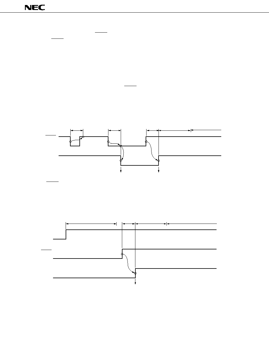
Set the RESET signal active in the reset operation at power-on until the oscillation stabilization time (approx. 40
ms) elapses.
Fig. 4-7 Reset Operation at Power-On
4.4
RESET
When a low level is input to the RESET pin, the internal hardware is initialized (reset state).
When the RESET input changes from low level to high level, the following data is set in the program counter (PC).
∑
Lower 8 bits of PC :
Contents of 0000H address
∑
Upper 8 bits of PC :
Contents of 0001H address
The contents of the PC set the destination address and the program starts to be executed from the address.
Therefore, it can start from any address by reset start.
Please set the program for the contents of each register as required.
A noise eliminator has been incorporated in the RESET input circuit to prevent any error from noise. This noise
eliminator is a sampling circuit based on analog delay.
Fig. 4-6 Reset Acknowledge
Delay
Delay
Reset Start
Delay
Reset End
PC Initialization
Instruction Execution
of Reset Start Address
RESET
(Input)
Internal
Reset Signal
RESET
(Input)
Internal
Reset Signal
V
DD
Oscillation Stabilization Time
Delay
PC Initialization
Instruction Execution of Reset Start Address
Reset End
36
µ
PD78217A, 78218A
MOV
MOV
MOV
MOV
A
ADD
Note1
XCH
XCH
XCH
XCH
MOV
MOV
MOV
ADD
Note1
ADD
Note1
ADD
Note1
ADD
Note1
ROL
MOV
ROLC
MULU
r
MOV
XCH
ROR
DIVUW
ADD
Note1
RORC
INC
SHR
DEC
SHL
r1
DBNZ
MOV
INC
saddr
MOV
XCH
DBNZ
ADD
Note1
DEC
MOV
PUSH
ADD
Note1
POP
mem
& mem
mem1
ROR4
&mem1
ROL4
!addr16
&!addr16
PUSH
POP
STBC
MOV
5.
INSTRUCTION SET
(1)
8-bit instructions
MOV, XCH, ADD, ADDC, SUB, SUBC, AND, OR, XOR, CMP, MULU, DIVUW, INC, DEC, ROR, ROL, RORC,
ROLC, SHR, SHL, ROR4, ROL4, DBNZ, PUSH, POP
Table 5-1 Instructions Classified by 8-Bit Addressing Mode
r
saddr
#byte
A
sfr
mem
&mem
!addr16 &!addr16
PSW
n
None
Note2
r'
saddr'
1st Operand
2nd Operand
MOV
XCH
MOV
Notes
1.
ADDC, SUB, SUBC, AND, OR, XOR and CMP are the same as ADD.
2.
There is no 2nd operand, or the 2nd operand is not an operand address.
sfr
MOV
ADD
Note1
MOV
MOV
PSW
MOV
MOV
MOV
37
µ
PD78217A, 78218A
(2)
16-bit instructions
MOVW, ADDW, SUBW, CMPW, INCW, DECW, SHRW, SHLW, PUSH, POP
Table 5-2 Instructions Classified by 16-Bit Addressing Mode
MOVW
MOVW
ADDW
ADDW
SUBW
SUBW
CMPW
CMPW
INCW
SHLW
DECW
SHRW
PUSH
POP
saddrp
MOVW
MOVW
sfrp
MOVW
MOVW
mem1
&mem1
INCW
DECW
1st Operand
2nd Operand
rp
#word
AX
saddrp
sfrp
mem1 &mem1
SP
n
None
rp'
MOVW
MOVW
MOVW
rp
MOVW
MOVW
SP
MOVW
MOVW
ADDW
ADDW
AX
SUBW
SUBW
CMPW
CMPW
MOVW

38
µ
PD78217A, 78218A
saddr.
/saddr.
/PSW.
CY
A.bit
/A.bit
X.bit
/X.bit
sfr.bit
/sfr.bit
PSW.bit
None
Note
bit
bit
bit
(3)
Bit manipulation instructions
MOV1, AND1, OR1, XOR1, SET1, CLR1, NOT1, BT, BF, BTCLR
Table 5-3 Instructions Classified by Bit Manipulation Instruction Addressing Mode
MOV1
MOV1
MOV1
MOV1
MOV1
SET1
AND1
AND1
AND1
AND1
AND1
AND1
AND1
AND1
AND1
AND1
CLR1
OR1
OR1
OR1
OR1
OR1
OR1
OR1
OR1
OR1
OR1
NOT1
XOR1
XOR1
XOR1
XOR1
XOR1
SET1
CLR1
NOT1
BT
BF
BTCLR
SET1
CLR1
NOT1
BT
BF
BTCLR
SET1
CLR1
NOT1
BT
BF
BTCLR
SET1
CLR1
NOT1
BT
BF
BTCLR
SET1
CLR1
NOT1
BT
BF
BTCLR
1st Operand
2nd Operand
Note There is no 2nd operand, or the 2nd operand is not an operand address.
A.bit
MOV1
CY
PSW.bit
MOV1
sfr.bit
MOV1
saddr.bit
MOV1
X.bit
MOV1
39
µ
PD78217A, 78218A
(4)
Call/branch instructions
CALL, CALLF, CALLT, BR, BC, BT, BF, BTCLR, DBNZ, BL, BNC, BNL, BZ, BE, BNZ, BNE
Table 5-4 Instructions Classified by Call/Branch Instruction Addressing Mode
Operands of
Instruction
$addr16
!addr16
rp
!addr11
[addr5]
Address
Basic
BR
CALL
CALL
CALLF
CALLT
instructions
BC
Note
BR
BR
BT
Compound
BF
instructions
BTCLR
DBNZ
Note
BL, BNC, BNL, BZ, BE, BNZ and BNE are the same as BC.
(5)
Other instructions
ADJBA, ADJBS, BRK, RET, RETI, RETB, NOP, EI, DI, SEL
40
µ
PD78217A, 78218A
PARAMETER
SYMBOL
TEST CONDITIONS
RATING
UNIT
V
DD
≠0.5 to +7.0
V
AV
REF
≠0.5 to V
DD
+0.5
V
AV
SS
≠0.5 to +0.5
V
V
I1
≠0.5 to V
DD
+0.5
V
V
I2
Note
≠0.5 to AV
REF
+0.5
V
V
O
≠0.5 to V
DD
+0.5
V
Per pin
15
mA
All output pins
100
mA
Per pin
≠10
mA
All output pins
≠50
mA
≠40 to +85
∞
C
T
stg
≠65 to +150
∞
C
Supply voltage
Input voltage
Output voltage
Output current, low
Output current, high
Operating ambient
temperature
Storage temperature
6.
ELECTRICAL SPECIFICATIONS
ABSOLUTE MAXIMUM RATINGS (T
A
= 25
∞
C)
I
OH
I
OL
T
A
5
Note
P70/AN0 to P75/AN5, P66/WAIT/AN6, P67/REFRQ/AN7 pins are used as A/D converter input pins.
However, V
I1
absolute maximum ratings should also be satisfied.
Caution
Product quality may suffer if the absolute maximum rating is exceeded for even a single parameter
even momentarily. That is, the absolute maximum ratings are rated values at which the product is
on the verge of suffering physical damage, and therefore the product must be used under conditions
which ensure that the absolute maximum ratings are not exceeded.
CAPACITANCE (T
A
= 25
∞
C, V
DD
= V
SS
= 0 V)
OPERATING CONDITIONS
Input capacitance
Output capacitance
I/O capacitance
pF
pF
pF
PARAMETER
SYMBOL
TEST CONDITIONS
MIN.
TYP.
MAX.
UNIT
20
20
20
C
I
C
O
C
IO
CLOCK FREQUENCY
OPERATING AMBIENT TEMPERATURE (T
A
)
SUPPLY VOLTAGE (V
DD
)
4 MHz
f
XX
12 MHz
≠40 to +85
∞
C
+5 V
±
10 %
f = 1 MHz
unmeasured pins
returned to 0 V.
5
41
µ
PD78217A, 78218A
OSCILLATOR CHARACTERISTICS (T
A
= ≠40 to +85
∞
C, V
DD
= +5 V
±
10 %, V
SS
= 0 V)
RESONATOR
Ceramic
resonator
or
crystal
resonator
External
clock
RECOMMENDED
CIRCUIT
PARAMETER
Oscillator frequency (f
XX
)
X1 input frequency (f
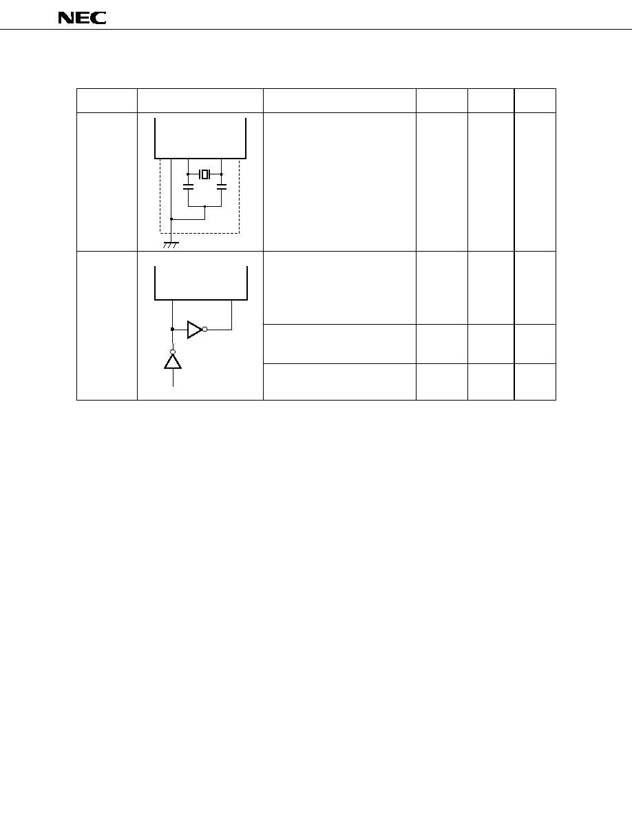
X
)
X1 input rising/falling time
(t
XR
, t
XF
)
X1 input high/low level width
(t
WXH
, t
WXL
)
UNIT
MHz
MHz
ns
ns
MIN.
4
4
0
30
MAX.
12
12
30
130
X1
X2
V
SS
C1
C2
Caution
When using the clock oscillator, wiring in the area enclosed with the dotted line should be carried
out as follows to avoid an adverse effect from wiring capacitance.
∑
Wiring should be as short as possible.
∑
Wiring should not cross other signal lines.
∑
Wiring should not be placed close to a varying high current.
∑
The potential of the oscillator capacitor ground should be the same as V
SS
. Do not ground it to
a ground pattern in which a high current flows.
∑
Do not fetch a signal from the oscillator.
X1
X2
HCMOS
Inverter
42
µ
PD78217A, 78218A
CSA12.0MTZ
30
30
CST12.0MTW
Capacitor on-chip type
EFOGC1205C4
Note
EFOEC1205C4
EFOEN1205C4
33
33
FCR12.0M2S
33
33
FCR12.0MC
Capacitor on-chip type
RECOMMENDED OSCILLATOR CONSTANTS
CERAMIC RESONATOR
RECOMMENDED CONSTANTS
C1 [pF]
C2 [pF]
PART NUMBER
MANUFACTURER
FREQUENCY
[MHz]
Capacitor on-chip type
Murata Mfg.
12
12
12
TDK Co.
Matsushita
Electronics Parts
Note
Production discontinued.
5
5
43
µ
PD78217A, 78218A
Input voltage, low
Input voltage, high
Output voltage, high
X1 input current, low
X1 input current, high
Input leakage current
Output leakage current
AV
REF
current
Data retention voltage
Pull-up resistor
V
IL
0
0.8
V
V
IH1
Pins except for Note 1 and Note 2
2.2
V
DD
V
V
IH2
Pin of Note 1
2.2
AV
REF
V
V
IH3
Pin of Note 2
0.8 V
DD
V
DD
V
V
OL1
I
OL
= 2.0 mA
0.45
V
V
OL2
I
OL
= 8.0 mA
Note3
1.0
V
V
OH1
I
OH
= ≠1.0 mA
V
DD
≠1.0
V
V
OH2
I
OH
= ≠100
µ
A
V
DD
≠0.5
V
V
OH3
I
OH
= ≠5.0 mA
Note4
2.0
V
I
IL
0 V
V
I
V
IL
≠100
µ
A
I
IH
V
IH3
V
I
V
DD
100
µ
A
I
LI
0 V
V
I
V
DD
±
10
µ
A
I
LO
0 V
V
O
V
DD
±
10
µ
A
AI
REF
Operating mode f
XX
= 12 MHz
1.5
5.0
mA
I
DD1
Operating mode f
XX
= 12 MHz
20
40
mA
I
DD2
HALT mode f
XX
= 12 MHz
7
20
mA
V
DDDR
STOP mode
2.5
5.5
V
V
DDDR
= 2.5 V
2
20
µ
A
V
DDDR
= 5 V
±
10 %
5
50
µ
A
R
L
V
I
= 0 V
15
40
80
k
DC CHARACTERISTICS (T
A
= ≠40 to +85
∞
C, V
DD
= +5 V
±
10 %, V
SS
= 0 V)
I
DDDR
STOP
mode
Output voltage, low
V
DD
supply current
Data retention current
PARAMETER
SYMBOL
TEST CONDITIONS
MIN.
TYP.
MAX.
UNIT
Notes 1. P70/AN0 to P75/AN5, P66/WAIT/AN6, P67/REFRQ/AN7 pins are used as A/D converter input pins.
2. X1, X2, RESET, P20/NMI, P21/INTP0, P22/INTP1, P23/INTP2/CI, P24/INTP3, P25/INTP4/ASCK, P26/
INTP5, P27/SI, P32/SCK, P33/SO/SB0, EA pins
3. P40/AD0 to P47/AD7, P50/A8 to P57/A15 pins
4. P00 to P07 pins
44
µ
PD78217A, 78218A
X1 input clock cycle time
t
CYX
82
250
ns
Address setup time (to ASTB
)
t
SAST
∑
52
ns
Address hold time (from ASTB
)
Note
t
HSTA
25
ns
Address hold time (from RD
)
t
HRA
30
ns
Address hold time (from WR
)
t
HWA
30
ns
RD
delay time from address
t
DAR
∑
129
ns
Address float time (from RD
)
t
FAR
∑
11
ns
Data input time from address
t
DAID
∑
No. of waits = 0
228
ns
Data input time from ASTB
t
DSTID
∑
No. of waits = 0
181
ns
Data input time from RD
t
DRID
∑
No. of waits = 0
100
ns
RD
delay time from ASTB
t
DSTR
∑
52
ns
Data hold time (from RD
)
t
HRID
0
ns
Address active time from RD
t
DRA
∑
124
ns
ASTB
delay time from RD
t
DRST
∑
124
ns
RD low-level width
t
WRL
∑
No. of waits = 0
124
ns
ASTB high-level width
t
WSTH
∑
52
ns
WR
delay time from address
t
DAW
∑
129
ns
Data output time from ASTB
t
DSTOD
∑
142
ns
Data output time from WR
t
DWOD
60
ns
t
DSTW1
∑
Refreshing disabled
52
ns
t
DSTW2
∑
Refreshing enabled
129
ns
Data setup time (to WR
)
t
SODWR
∑
No. of waits = 0
146
ns
Data setup time (to WR
)
t
SODWF
∑
Refreshing enabled
22
ns
Data hold time (from WR
)
Note
t
HWOD
20
ns
ASTB
delay time from WR
t
DWST
∑
42
ns
Refreshing disabled
No. of waits = 0
Refreshing enabled
No. of waits = 0
WAIT
input time from address
t
DAWT
∑
146
ns
WAIT
input time from ASTB
t
DSTWT
∑
84
ns
AC CHARACTERISTICS (T
A
= ≠40 to +85
∞
C, V
DD
= +5 V
±
10 %, V
SS
= 0 V)
READ/WRITE OPERATION (1/2)
WR
delay time from ASTB
PARAMETER
SYMBOL
TEST CONDITIONS
MIN.
MAX.
UNIT
WR low-level width
t
WWL1
∑
t
WWL2
∑
114
ns
Note
The hold time includes the time to hold the V
OH
and V
OL
under the load conditions of C
L
= 100 pF and
R
L
= 2 k
.
Remarks 1.
The values in the above table are based on "f
XX
= 12 MHz and C
L
= 100 pF".
2.
For a parameter with a dot (∑) in the SYMBOL column, refer to "t
CYX
DEPENDENT BUS TIMING
DEFINITION" as well.
196
ns
45
µ
PD78217A, 78218A
WAIT hold time from ASTB
t
HSTWT
∑
No. of external waits = 1
174
ns
WAIT
delay time from ASTB
t
DSTWTH
∑
No. of external waits = 1
273
ns
WAIT
input time from RD
t
DRWTL
∑
22
ns
WAIT hold time from RD
t
HRWT
∑
No. of external waits = 1
87
ns
WAIT
delay time from RD
t
DRWTH
∑
No. of external waits = 1
186
ns
Data input time from WAIT
t
DWTID
∑
62
ns
WR
delay time from WAIT
t
DWTW
∑
154
ns
RD
delay time from WAIT
t
DWTR
∑
72
ns
WAIT input time from WR
WAIT hold time
t
HWWT1
∑
No. of external waits = 1
87
ns
from WR
t
HWWT2
∑
No. of external waits = 1
5
ns
WAIT
delay
t
DWWTH1
∑
No. of external waits = 1
186
ns
time from WR
t
DWWTH2
∑
No. of external waits = 1
104
ns
REFRQ
delay time from RD
t
DRRFQ
∑
154
ns
REFRQ
delay time from WR
t
DWRFQ
∑
72
ns
REFRQ low-level width
t
WRFQL
∑
120
ns
ASTB
delay time from REFRQ
t
DRFQST
∑
280
ns
READ/WRITE OPERATION (2/2)
(At refresh disabled)
Refresh disabled
Refresh enabled
Refresh disabled
Refresh enabled
PARAMETER
SYMBOL
TEST CONDITIONS
MIN.
MAX.
UNIT
t
DWWTL
∑
22 ns
Remarks 1.
The values in the above table are based on "f
XX
= 12 MHz and C
L
= 100 pF".
2.
For a parameter with a dot (∑) in the SYMBOL column, refer to "t
CYX
DEPENDENT BUS TIMING
DEFINITION" as well.
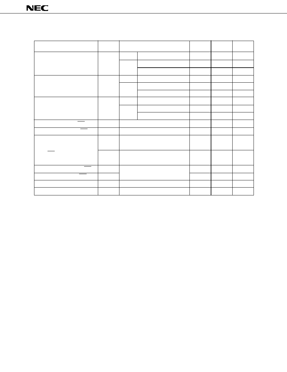
46
µ
PD78217A, 78218A
Input
External clock
1.0
µ
s
Serial clock cycle time
t
CYSK
Internal divided by 16
1.3
µ
s
Internal divided by 64
5.3
µ
s
Input
External clock
420
ns
Serial clock low-level width
t
WSKL
Internal divided by 16
556
ns
Internal divided by 64
2.5
µ
s
Input
External clock
420
ns
Serial clock high-level width
t
WSKH
Internal divided by 16
556
ns
Internal divided by 64
2.5
µ
s
SI, SB0 setup time (to SCK
)
t
SSSK
150
ns
SI, SB0 hold time (from SCK
)
t
HSSK
400
ns
CMOS push-pull output
SO/SB0 output delay time
(3-wire serial I/O mode)
(from SCK
)
Open-drain output (SBI mode),
R
L
= 1 k
SB0 high hold time (from SCK
)
t
HSBSK
4
t
CYX
SB0 low setup time (to SCK
)
t
SSBSK
4
t
CYX
SB0 low-level width
t
WSBL
4
t
CYX
SB0 high-level width
t
WSBH
4
t
CYX
SERIAL OPERATION
PARAMETER
SYMBOL
TEST CONDITIONS
MIN.
MAX.
UNIT
Output
Output
Output
SBI mode
t
DSBSK1
0
300
ns
t
DSBSK2
0
800
ns
Remark
The values in the above table are based on "f
XX
= 12 MHz and C
L
= 100 pF".

47
µ
PD78217A, 78218A
PARAMETER
SYMBOL
TEST CONDITIONS
MIN.
TYP.
MAX.
UNIT
8
bit
0.4
%
0.8
%
0.8
%
±
1/2
LSB
t
CONV
t
SAMP
AV
REF
+0.3
Resolution
Overall error
Note1
Quantization error
Conversion time
Sampling time
Analog input voltage
Analog input
impedance
Reference voltage
AV
REF
current
AV
REF
3.6
V
DD
V
f
XX
= 12 MHz
1.5
5.0
mA
Note 2
0.2
1.5
mA
OTHER OPERATIONS
NMI low-level width
t
WNIL
10
µ
s
NMI high-level width
t
WNIH
10
µ
s
INTP0 to INTP5 low-level width
t
WITL
24
t
CYX
INTP0 to INTP5 high-level width
t
WITH
24
t
CYX
RESET low-level width
t
WRSL
10
µ
s
RESET high-level width
t
WRSH
10
µ
s
EXTERNAL CLOCK TIMING
X1 input low-level width
t
WXL
30
130
ns
X1 input high-level width
t
WXH
30
130
ns
X1 input rise time
t
XR
0
30
ns
X1 input fall time
t
XF
0
30
ns
X1 input clock cycle time
t
CYX
82
250
ns
A/D CONVERTER CHRACTERISTICS (T
A
= ≠40 to +85
∞
C, V
DD
= +5 V
±
10 %, V
SS
= AV
SS
= 0 V)
82 ns
t
CYX
< 125 ns
(The FR bit of ADM is to be "0")
125 ns
t
CYX
< 250 ns
(The FR bit of ADM is to be "1")
82 ns
t
CYX
< 125 ns
(The FR bit of ADM is to be "0")
125 ns
t
CYX
< 250 ns
(The FR bit of ADM is to be "1")
R
AN
1000
M
V
IAN
≠0.3 V
AI
REF
Notes 1.
Quantization error is not included. Represented by the ratio to full-scale value.
2.
When ADM register's CS bit = 0, in STOP mode.
PARAMETER
SYMBOL
TEST CONDITIONS
MIN.
MAX.
UNIT
PARAMETER
SYMBOL
TEST CONDITIONS
MIN.
MAX.
UNIT
4.0 V
AV
REF
V
DD
T
A
= ≠10 to +70
∞
C
3.6 V
AV
REF
V
DD
T
A
= ≠10 to +70
∞
C
4.0 V
AV
REF
V
DD
360
t
CYX
240
t
CYX
72
t
CYX
48
t
CYX
5
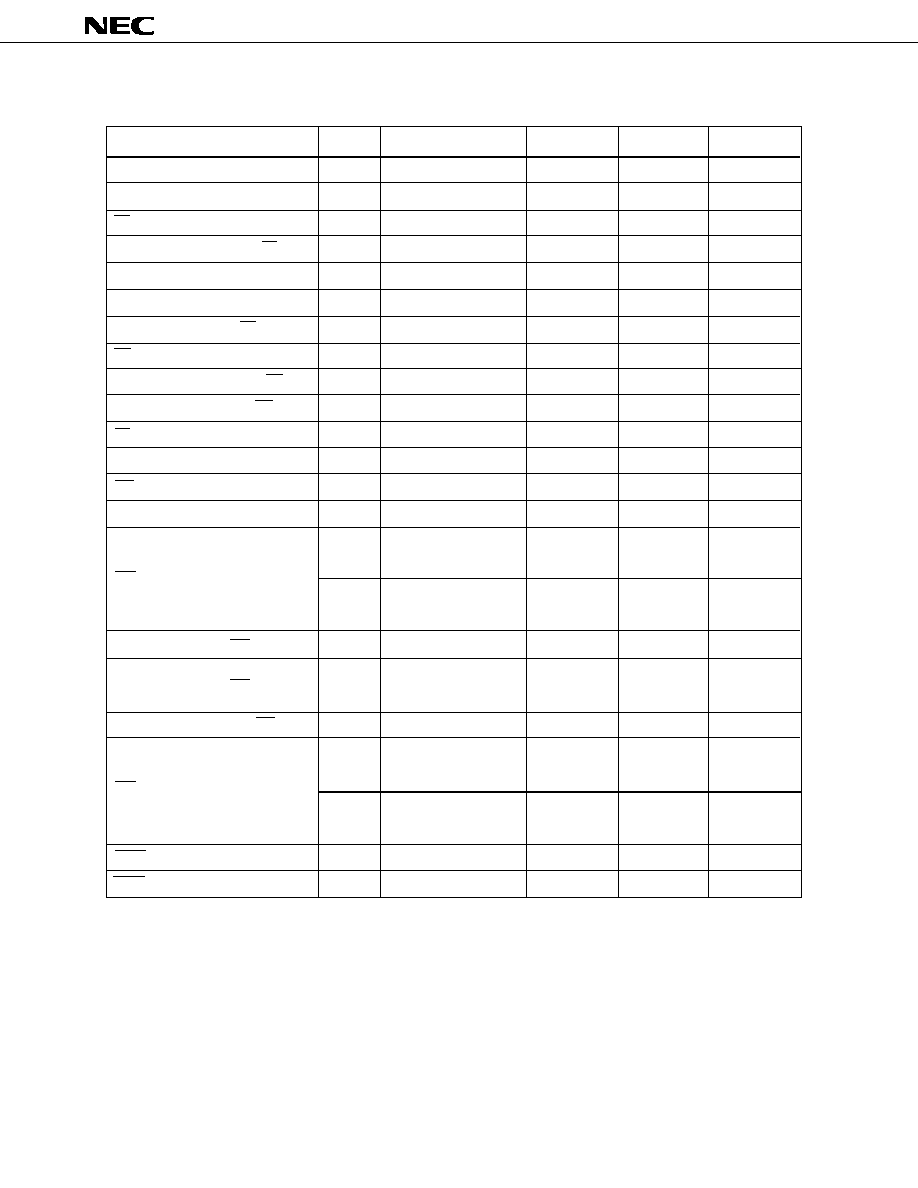
48
µ
PD78217A, 78218A
PARAMETER
SYMBOL
FORMULA
MIN./MAX.
12 MHz
UNIT
X1 input clock cycle time
t
CYX
MIN.
82
ns
Address setup time (to ASTB
)
t
SAST
t
CYX
≠ 30
MIN.
52
ns
RD
delay time from address
t
DAR
2t
CYX
≠ 35
MIN.
129
ns
Address float time (from RD
)
t
FAR
t
CYX
/2 ≠ 30
MIN.
11
ns
Data input time from address
t
DAID
(4 + 2n) t
CYX
≠ 100
MAX.
228
Note
ns
Data input time from ASTB
t
DSTID
(3 + 2n) t
CYX
≠ 65
MAX.
181
Note
ns
Data input time from RD
t
DRID
(2 + 2n) t
CYX
≠ 64
MAX.
100
Note
ns
RD
delay time from ASTB
t
DSTR
t
CYX
≠ 30
MIN.
52
ns
Address active time from RD
t
DRA
2t
CYX
≠ 40
MIN.
124
ns
ASTB
delay time from RD
t
DRST
2t
CYX
≠ 40
MIN.
124
ns
RD low-level width
t
WRL
(2 + 2n) t
CYX
≠ 40
MIN.
124
Note
ns
ASTB high-level width
t
WSTH
t
CYX
≠ 30
MIN.
52
ns
WR
delay time from address
t
DAW
2t
CYX
≠ 35
MIN.
129
ns
Data output time from ASTB
t
DSTOD
t
CYX
+ 60
MAX.
142
ns
t
CYX
≠ 30
(Refreshing disabled)
2t
CYX
≠ 35
(Refreshing enabled)
Data setup time (to WR
)
t
SODWR
(3 + 2n) t
CYX
≠ 100
MIN.
146
Note
ns
t
CYX
≠ 60
(Refreshing enabled)
ASTB
delay time from WR
t
DWST
t
CYX
≠ 40
MIN.
42
ns
(3 + 2n) t
CYX
≠ 50
(Refreshing disabled)
(2 + 2n) t
CYX
≠ 50
(Refreshing enabled)
WAIT
input time from address
t
DAWT
3t
CYX
≠ 100
MAX.
146
ns
WAIT
input time from ASTB
t
DSTWT
2t
CYX
≠ 80
MAX.
84
ns
t
WWL1
MIN.
196
Note
ns
t
WWL2
MIN.
114
Note
ns
WR low-level width
t
CYX
DEPENDENT BUS TIMING DEFINITION (1/2)
Data setup time (to WR
)
t
SODWF
MIN.
22
ns
WR
delay time from ASTB
t
DSTW1
MIN.
52
ns
t
DSTW2
MIN.
129
ns
Remark
"n" indicates the number of waits.
Note
When n = 0
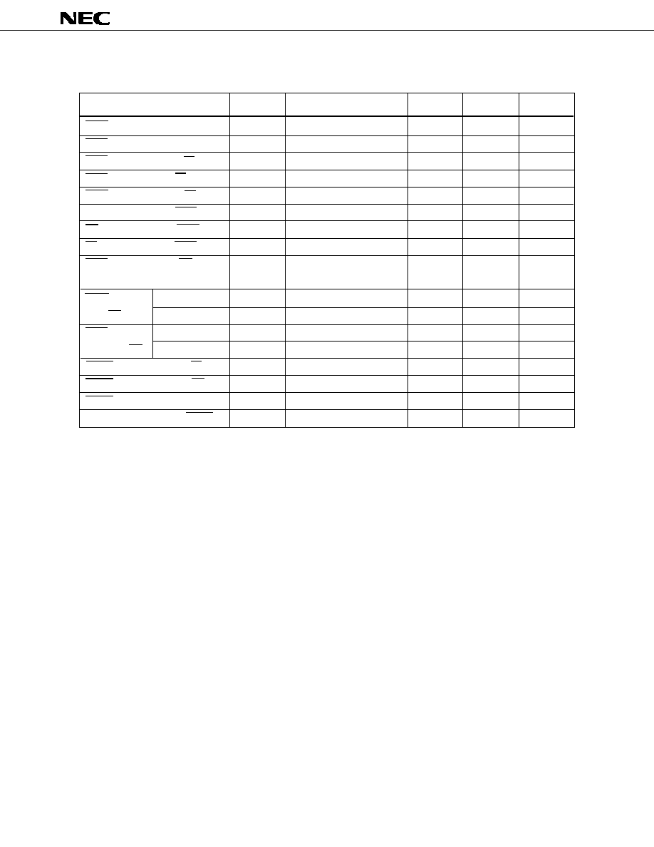
49
µ
PD78217A, 78218A
PARAMETER
SYMBOL
FORMULA
MIN./MAX.
12 MHz
UNIT
WAIT hold time from ASTB
t
HSTWT
2Xt
CYX
+ 10
MIN.
174
Note
ns
WAIT
delay time from ASTB
t
DSTWTH
2(1 + X)t
CYX
≠ 55
MAX.
273
Note
ns
WAIT
input time from RD
t
DRWTL
t
CYX
≠ 60
MAX.
22
ns
WAIT hold time from RD
t
HRWT
(2X ≠ 1)t
CYX
+ 5
MIN.
87
Note
ns
WAIT
delay time from RD
t
DRWTH
(2X + 1)t
CYX
≠ 60
MAX.
186
Note
ns
Data input time from WAIT
t
DWTID
t
CYX
≠ 20
MAX.
62
ns
WR
delay time from WAIT
t
DWTW
2t
CYX
≠ 10
MIN.
154
ns
RD
delay time from WAIT
t
DWTR
t
CYX
≠ 10
MIN.
72
ns
WAIT input time from WR
WAIT hold time
t
HWWT1
(2X ≠ 1)t
CYX
+ 5
MIN.
87
Note
ns
from WR
t
HWWT2
2(X ≠ 1)t
CYX
+ 5
MIN.
5
Note
ns
WAIT
delay
t
DWWTH1
(2X + 1)t
CYX
≠ 60
MAX.
186
Note
ns
time from WR
t
DWWTH2
2Xt
CYX
≠ 60
MAX.
104
Note
ns
REFRQ
delay time from RD
t
DRRFQ
2t
CYX
≠ 10
MIN.
154
ns
REFRQ
delay time from WR
t
DWRFQ
t
CYX
≠ 10
MIN.
72
ns
REFRQ low-level width
t
WRFQL
2t
CYX
≠ 44
MIN.
120
ns
ASTB
delay time from REFRQ
t
DRFQST
4t
CYX
≠ 48
MIN.
280
ns
t
CYX
DEPENDENT BUS TIMING DEFINITION (2/2)
(At refresh disabled)
Refresh disabled
Refresh enabled
Refresh disabled
Refresh enabled
t
DWWTL
t
CYX
≠ 60
MAX.
22
ns
Remarks 1.
X: The number of the external waits (1, 2, ...)
2.
t
CYX
82 ns (f
XX
= 12 MHz)
3.
"n" indicates the number of waits.
Note
When X = 1
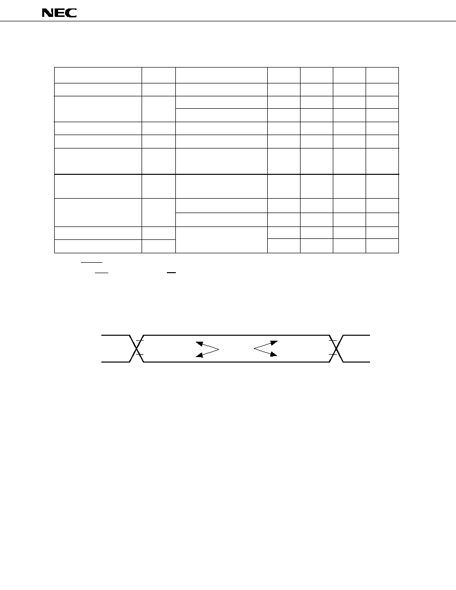
50
µ
PD78217A, 78218A
Note
RESET, P20/NMI, P21/INTP0, P22/INTP1, P23/INTP2/CI, P24/INTP3, P25/INTP4/ASCK, P26/INTP5, P27/SI,
P32/SCK, P33/SO/SB0 and EA pins.
PARAMETER
SYMBOL
TEST CONDITIONS
MIN.
TYP.
MAX.
UNIT
STOP mode
2.5
5.5
V
V
DDDR
= 2.5 V
2
20
µ
A
V
DDDR
= 5 V
±
10 %
5
50
µ
A
200
µ
s
200
µ
s
Crystal resonator
30
ms
Ceramic resonator
5
ms
0
0.1 V
DDDR
V
0.9 V
DDDR
V
DDDR
V
DATA RETENTION CHARACTERISTICS (T
A
= ≠40 to +85
∞
C)
Data retention voltage
Data retention current
V
DD
rise time
V
DD
fall time
V
DD
hold time (from
STOP mode setting)
STOP release signal
input time
Oscillation stabilization
wait time
Low-level input voltage
High-level input voltage
Specified pin
Note
AC Timing Test Point
V
DDDR
I
DDDR
t
RVD
t
FVD
t
HVD
t
DREL
t
WAIT
V
IL
V
IH
0
ms
0
ms
0.8 V or 2.2 V
DD
Test Points
0.8 V
0.8 V or 2.2 V
DD
0.8 V
V -1 V
DD
0.45 V
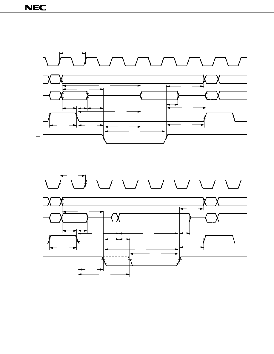
51
µ
PD78217A, 78218A
Timing Waveform
Read operation
Write operation
X1
t
CYX
A8-A15
P60-P63
AD0-AD7
t
DAR
t
DAID
t
HRA
t
DRA
t
DRST
t
SAST
t
HSTA
t
FAR
t
DSTID
t
WSTH
t
DSTR
ASTB
RD
t
WRL
t
DRID
t
HRID
X1
t
CYX
A8-A15
P60-P63
AD0-AD7
t
DAW
t
HWA
t
DWST
t
SAST
t
HSTA
t
SODWR
t
WSTH
ASTB
WR
t
WWL2
t
WWL1
t
DSTW1
t
DSTW2
t
HWOD
t
DSTOD
t
SODWF
t
DWOD
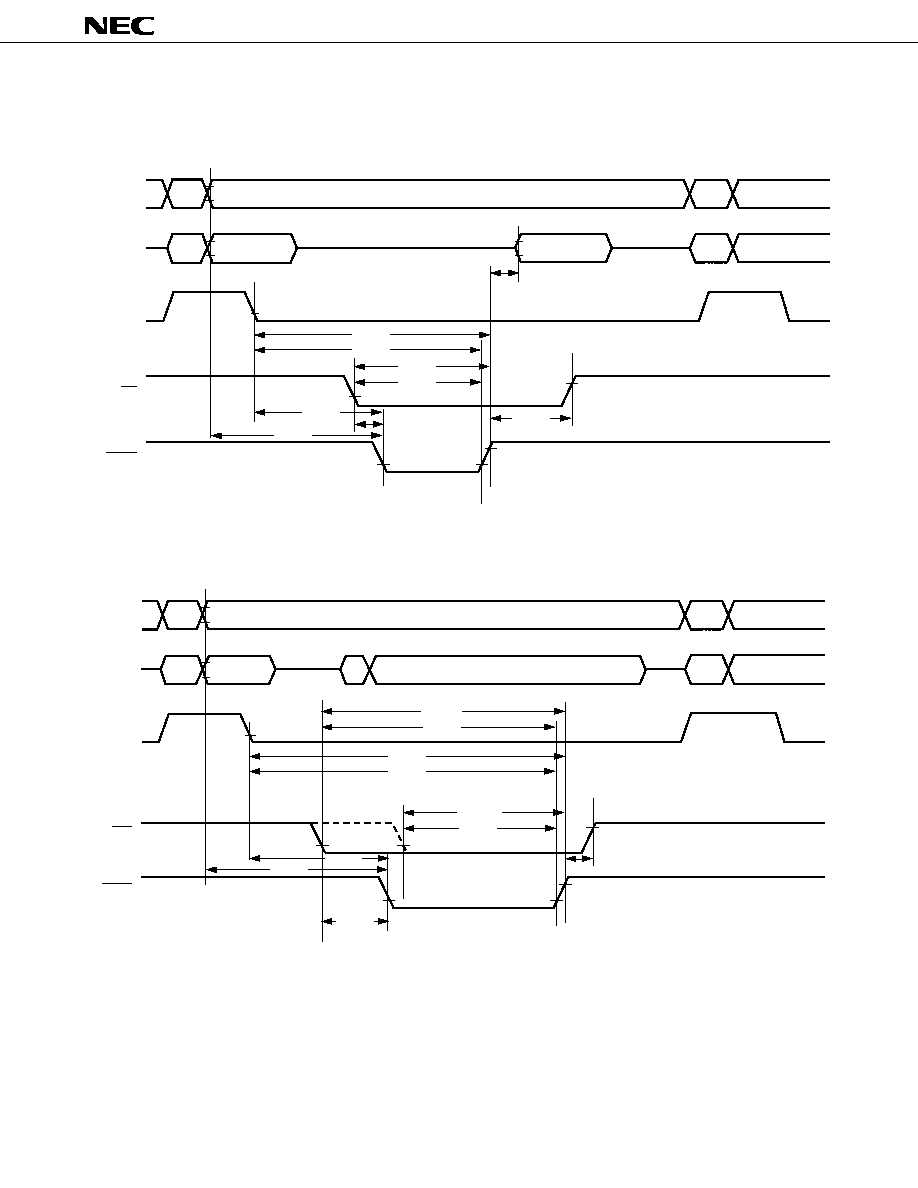
52
µ
PD78217A, 78218A
External WAIT Signal Input Timing
Read operation
Write operation
A8-A15
P60-P63
AD0-AD7
t
DSTWTH
ASTB
RD
t
HRWT
t
HSTWT
t
DRWTH
t
DSTWT
t
DAWT
t
DRWTL
t
DWTR
t
DWTID
WAIT
A8-A15
P60-P63
AD0-AD7
t
DSTWTH
ASTB
WR
t
HSTWT
t
DWWTL
WAIT
t
HWWT1
t
DAWT
t
DWTW
t
HWWT2
t
DWWTH1
t
DWWTH2
t
DSTWT
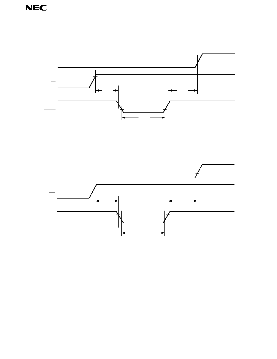
53
µ
PD78217A, 78218A
Refresh Timing Waveform
Refresh after read
Refresh after write
ASTB
WR
REFRQ
t
WRFQL
t
DWRFQ
t
DRFQST
ASTB
RD
REFRQ
t
WRFQL
t
DRRFQ
t
DRFQST
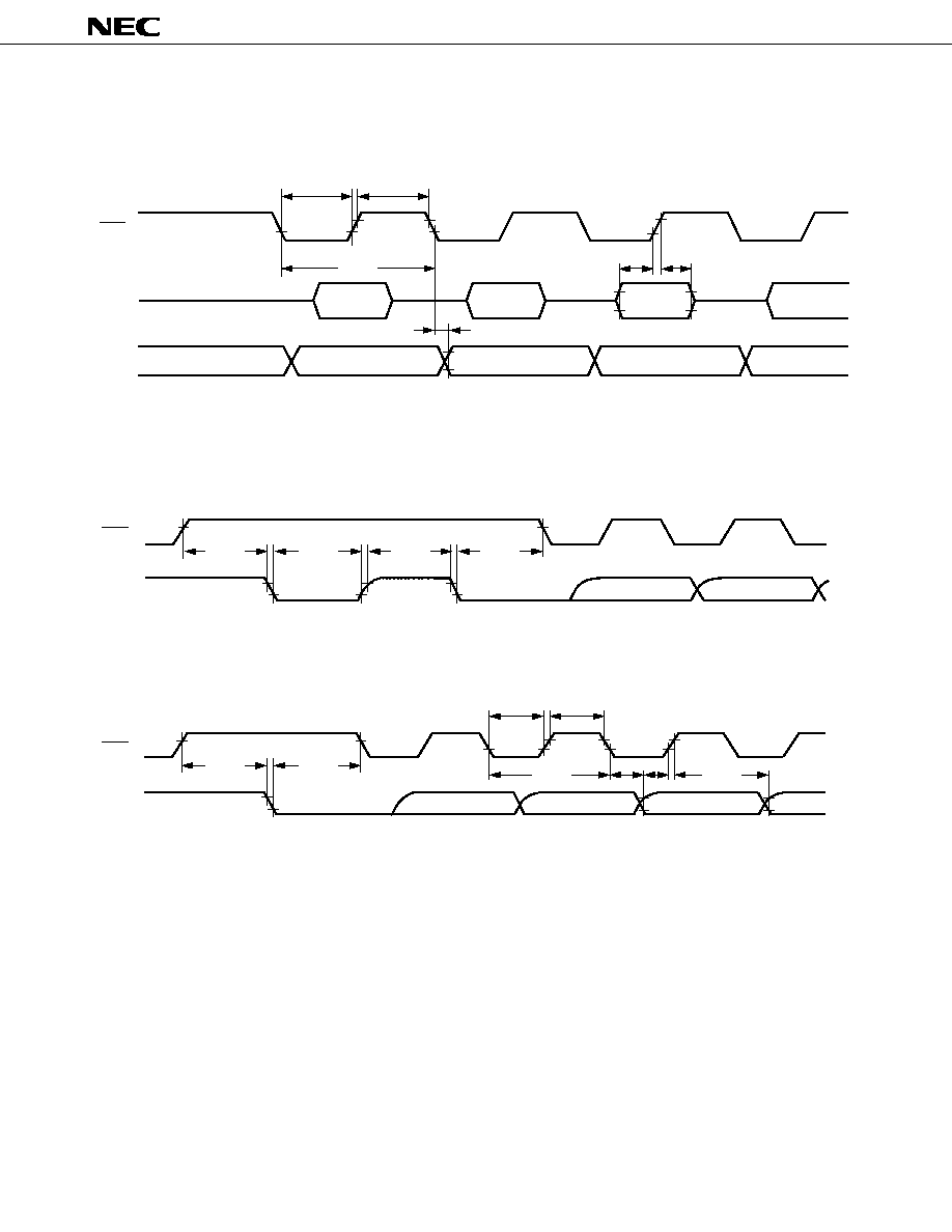
54
µ
PD78217A, 78218A
Serial Operation
3-wire serial I/O mode
Command signal transfer
SBI Mode
Bus release signal transfer
SCK
SB0
t
HSBSK
t
WSBL
t
WSBH
t
SSBSK
t
WSKL
SCK
SI
SO
Output Data
t
WSKH
t
CYSK
t
DSBSK1
t
SSSK
t
HSSK
Input Data
I/O Data
SCK
SB0
t
HSBSK
t
SSBSK
t
CYSK
t
WSKL
t
WSKH
t
HSSK
t
SSSK
t
DSBSK2
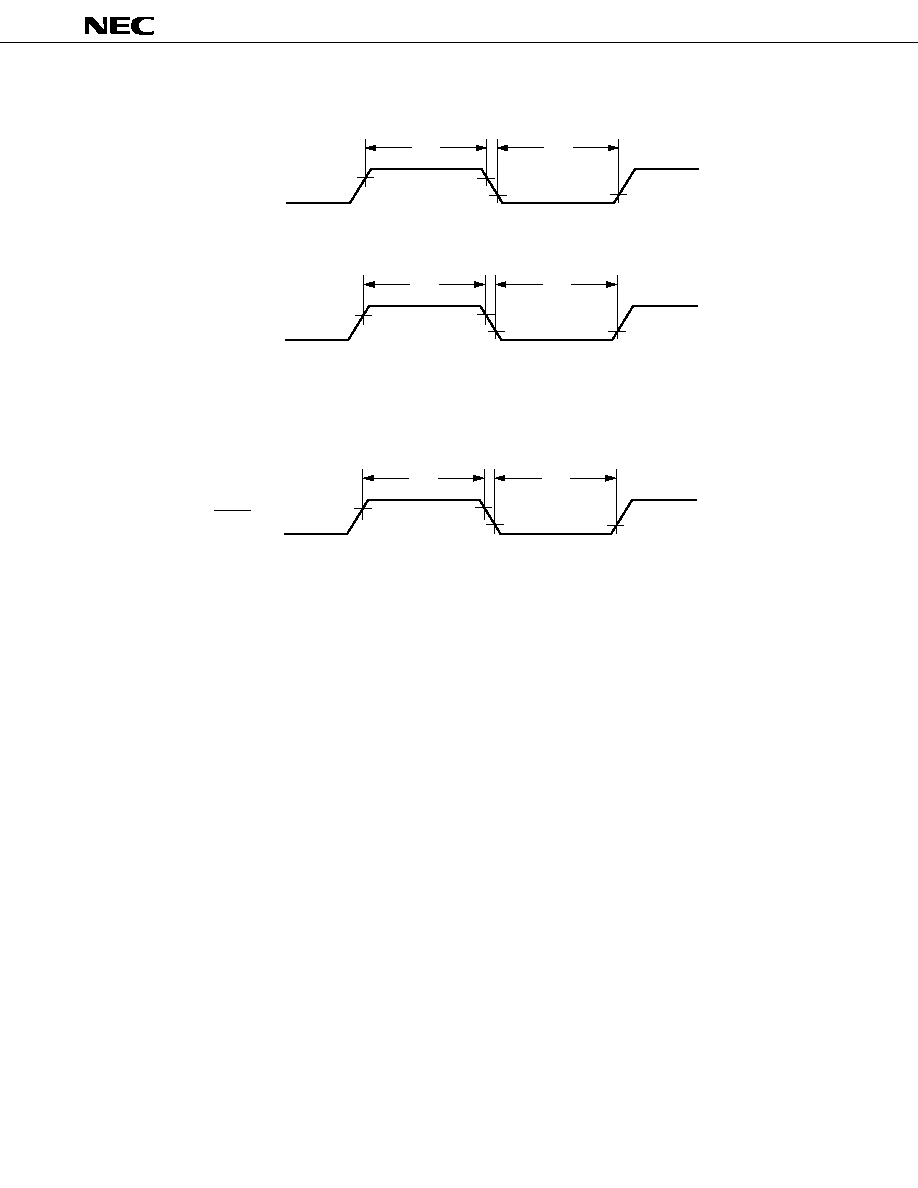
55
µ
PD78217A, 78218A
Interrupt Input Timing
Reset Input Timing
NMI
t
WNIH
t
WNIL
0.8 V
DD
0.8 V
INTP0-INTP5
t
WITH
t
WITL
0.8 V
DD
0.8 V
RESET
t
WRSH
t
WRSL
0.8 V
DD
0.8 V
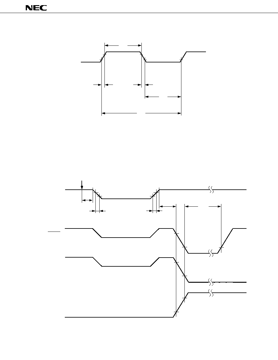
56
µ
PD78217A, 78218A
Data Retention Characteristics
External Clock Timing
X1
t
WXH
0.8 V
DD
0.8 V
t
XR
t
XF
t
WXL
t
CYX
STOP Mode Setting
V
DD
t
HVD
V
DDDR
t
FVD
t
RVD
t
DREL
RESET
0.8 V
DD
0.8 V
0.8 V
NMI
(Release by Falling Edge)
0.8 V
DD
NMI
(Release by Rising Edge)
0.8 V
DD
0.8 V
t
WAIT
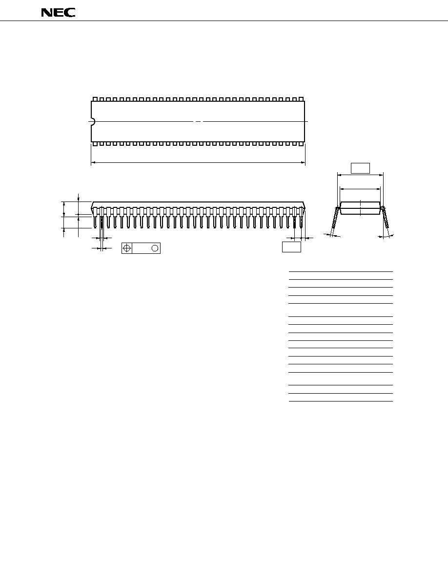
57
µ
PD78217A, 78218A
7.
PACKAGE DRAWINGS
A
I
J
G
H
F
D
N
M
C
B
M
R
64
33
32
1
K
L
NOTE
Each lead centerline is located within 0.17 mm (0.007 inch) of
its true position (T.P.) at maximum material condition.
P64C-70-750A,C-1
ITEM
MILLIMETERS
INCHES
A
B
C
D
F
G
H
I
J
K
58.68 MAX.
1.778 (T.P.)
3.2±0.3
0.51 MIN.
4.31 MAX.
1.78 MAX.
L
M
0.17
0.25
19.05 (T.P.)
5.08 MAX.
17.0
N
0~15∞
0.50±0.10
0.9 MIN.
R
2.311 MAX.
0.070 MAX.
0.020
0.035 MIN.
0.126±0.012
0.020 MIN.
0.170 MAX.
0.200 MAX.
0.750 (T.P.)
0.669
0.010
0.007
0~15∞
+0.004
≠0.003
0.070 (T.P.)
1)
Item "K" to center of leads when formed parallel.
2)
+0.10
≠0.05
+0.004
≠0.005
64 PIN PLASTIC SHRINK DIP (750 mil)
Remark
ES versions have the same package drawings and use the same materials as mass-produced versions.
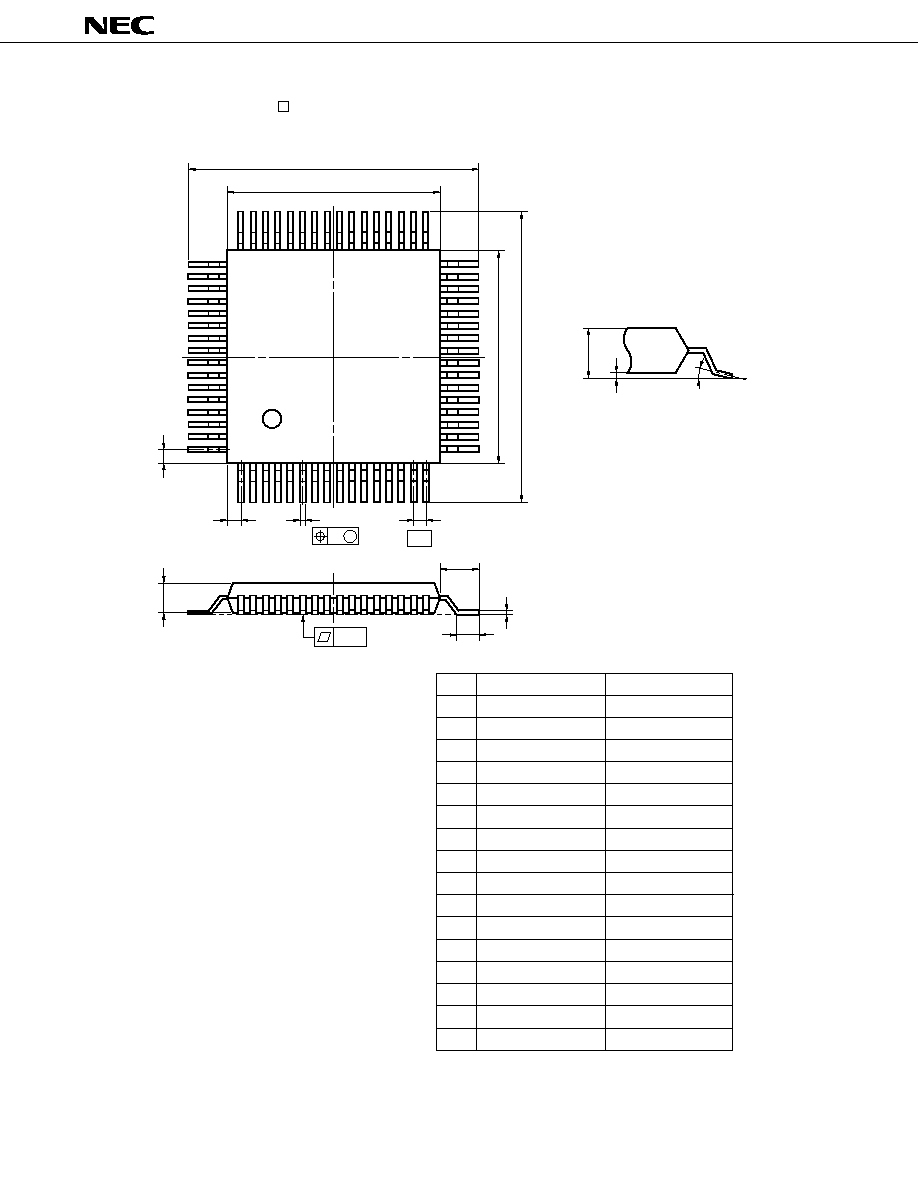
58
µ
PD78217A, 78218A
N
A
M
F
B
48
49
32
K
L
64 PIN PLASTIC QFP ( 14)
64
1
17
16
33
D
C
detail of lead end
S
Q
5∞±5∞
P
M
I
H
J
G
P64GC-80-AB8-3
ITEM
MILLIMETERS
INCHES
A
B
C
D
F
G
H
I
J
K
L
17.6±0.4
14.0±0.2
1.0
0.35±0.10
0.15
14.0±0.2
0.693±0.016
0.039
0.039
0.006
0.031 (T.P.)
0.551
NOTE
M
N
0.10
0.15
1.8±0.2
0.8 (T.P.)
0.004
0.006
+0.004
≠0.003
Each lead centerline is located within 0.15
mm (0.006 inch) of its true position (T.P.) at
maximum material condition.
0.071±0.008
0.014
0.551
0.8±0.2
0.031
P
2.55
0.100
0.693±0.016
17.6±0.4
1.0
+0.009
≠0.008
Q
0.1±0.1
0.004±0.004
S
2.85 MAX.
0.112 MAX.
+0.10
≠0.05
+0.009
≠0.008
+0.004
≠0.005
+0.009
≠0.008
Remark
ES versions have the same package drawings and use the same materials as mass-produced versions.
59
µ
PD78217A, 78218A
8.
RECOMMENDED SOLDERING CONDITIONS
The
µ
PD78217A/78218A should be soldered and mounted under the conditions recommended in the table below.
For detail of recommended soldering conditions, refer to the information document "Semiconductor Device Mounting
Technology Manual" (IEI-1207).
For soldering methods and conditions other than those recommended below, contact an NEC sales represen-
tative.
Table 8-1 Surface Mounting Type Soldering Conditions
5
Soldering Method
Soldering Conditions
Infrared ray reflow
IR35-00-2
Package peak temperature: 235
∞
C, Reflow time: 30 seconds or less (at 210
∞
C or
higher), Maximum number of reflow processes: 2 times
<Cautions>
(1) After the first reflow process, cool the package down to room temperature , then
start the second reflow process.
(2) After the first reflow process, do not use water to remove residual flux.
Package peak temperature: 215
∞
C, Reflow time: 40 seconds or less (at 200
∞
C or
higher), Maximum number of reflow processes: 2 times
<Cautions>
(1) After the first reflow process, cool the package down to room temperature , then
start the second reflow process.
(2) After the first reflow process, do not use water to remove residual flux.
Pin temperature: 300
∞
C or below, Heat time: 3 seconds or less (per each side of
the device)
VPS
Partial heating
VP15-00-2
≠≠≠
Caution
Apply only one kind of soldering method to a device, except for partial heating method.
µ
PD78217AGC-AB8/78218AGC-
◊◊◊
-AB8 : 64-pin plastic QFP (14 x 14 mm)
Symbol
Table 8-2 Insertion Type Soldering Conditions
Solder temperature: 260
∞
C or below, Flow time: 10 seconds or less
Pin temperature: 300
∞
C or below, Heat time: 3 seconds or less (per pin)
Partial heating
Caution
The wave soldering process must be applied only to pins, and make sure that the package body does
not get jet soldered.
Soldering Method
Soldering Conditions
Wave soldering
(pin only)
µ
PD78217ACW/78218ACW-
◊◊◊
: 64-pin plastic shrink DIP (750 mil)
60
µ
PD78217A, 78218A
APPENDIX A. DEVELOPMENT TOOLS
The following development tools are available for system development using the
µ
PD78217A/78218A.
Language Processing Software
RA78K/II
Notes1, 2, 3
CC78K/II
Notes1, 2, 3
CC78K/II-L
Notes1, 2, 3
PROM Writing Tools
PG-1500
PA-78P214CW
PA-78P214GC
PG-1500 controller
Notes
1, 2
Debugging Tools
IE-78240-R-A
IE-78240-R
Note
4
IE-78200-R-BK
IE-78240-R-EM
IE-78200-R-EM
Note
4
EP-78210CW
Note
4
EP-78240CW-R
EP-78210GC
Note
4
EP-78240GC-R
EV-9200GC-64
SD78K/II
Notes
1, 2
DF78210
Notes
1, 2
Fuzzy Inference Development Support System
FE9000
Note
1
, FE9200
Note
5
FT9080
Note
1
, FT9085
Note
2
FI78K/II
Notes
1, 2
FD78K/II
Notes
1, 2
78K/II series common assembler package
78K/II series common C compiler package
78K/II series common C compiler library source file
µ
PD78218A subseries common in-circuit emulators
78K/II series common break board
µ
PD78218A subseries evaluation emulation boards
µ
PD78218A subseries common emulation probes
Socket to be mounted on a user system board made for 64-pin plastic QFP
IE-78240-R-A screen debugger
µ
PD78218A subseries device file
Fuzzy knowledge data creation tool
Translator
Fuzzy inference module
Fuzzy inference debugger
PROM programmer
Programmer adapters connected to PG-1500
PG-1500 control program

61
µ
PD78217A, 78218A
Remark
For third-party development tools, see the 78K/II Series Development Tool Selection Guide (EF-231).
Notes 1. PC-9800 series (MS-DOS
TM
) based
2. IBM PC/AT
TM
(PC DOS
TM
) based
3. HP9000 series 300
TM
(HP-UX
TM
) based, SPARCstation
TM
(Sun OS
TM
) based, EWS-4800 series (EWS-UX/
V) based
4. No longer manufactured and not available for purchase
5. IBM PC/AT (PC DOS
+
Windows
TM
) based
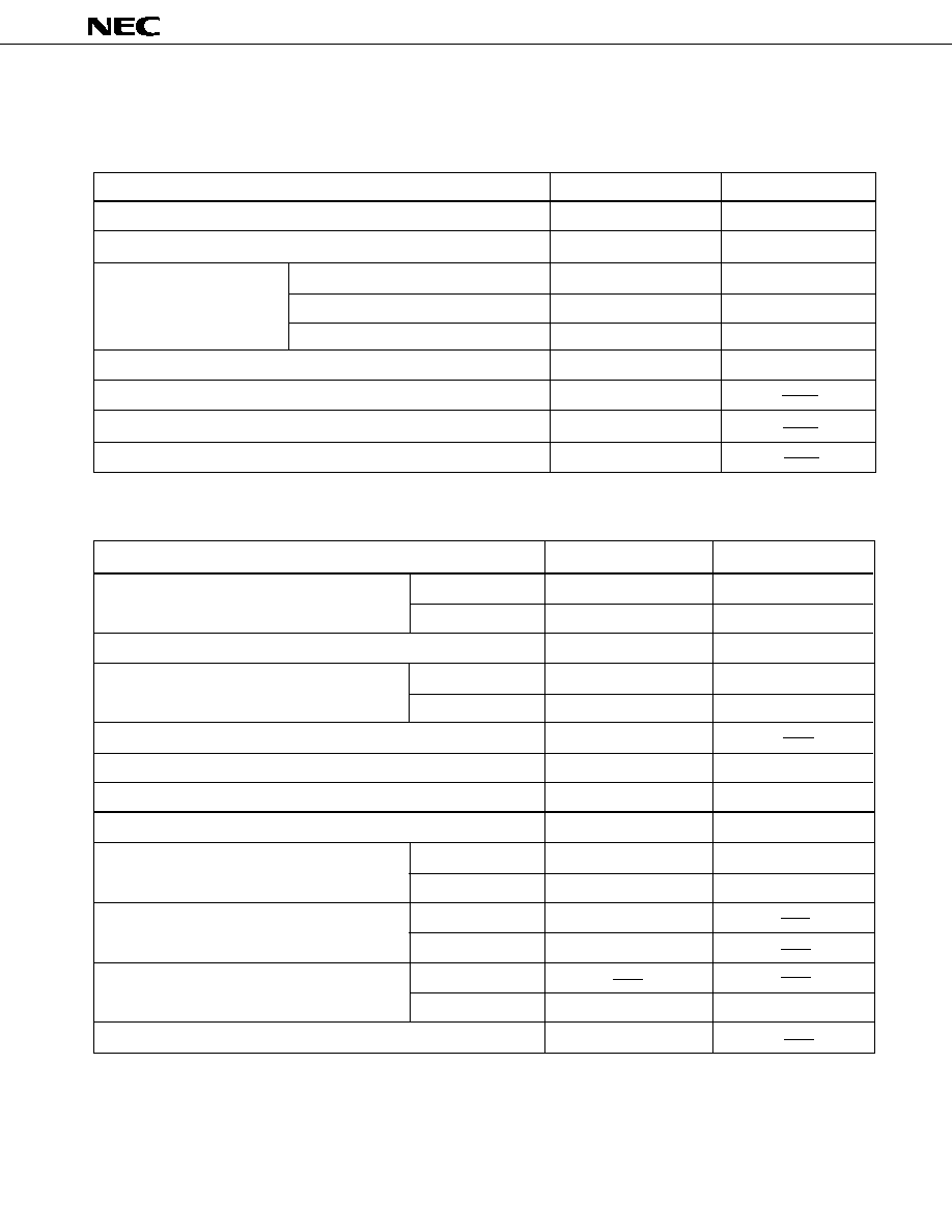
62
µ
PD78217A, 78218A
APPENDIX B. RELATED DOCUMENTS
Device Related Documents
Document Name
RA78K Series Assembler Package
RA78K Series Structured Assembler Preprocessor
CC78K Series C Compiler
CC78K Series Library Source File
PG-1500 PROM Programmer
PG-1500 Controller
IE-78240-R-A In-Circuit Emulator
IE-78240-R In-Circuit Emulator
SD78K/II Screen Debugger
MS-DOS Based
SD78K/II Screen Debugger
PC DOS Based
78K/II Series Development Tool Selection Guide
Development Tool Related Documents (User`s Manuals)
Operation
Language
Operation
Language
Document No. (Japanese)
EEU-809
EEU-815
EEU-817
EEU-656
EEU-655
EEU-777
EEU-651
EEU-704
EEU-796
EEU-705
EEU-706
EEU-841
EEU-813
EEU-956
EF-231
Document No. (English)
EEU-1399
EEU-1404
EEU-1402
EEU-1280
EEU-1284
EEU-1335
EEU-1291
EEU-1395
EEU-1322
EEU-1331
EEU-1447
Document Name
µ
PD78218A Subseries User's Manual: Hardware
78K/II Series User's Manual: Instruction
78K/II Series Application Note
78K/II Series Selection Guide
78K/II Series Instruction Table
78K/II Series Instruction Set
µ
PD78218A Series Special Function Register Table
Document No. (English)
IEU-1313
IEU-1311
IEA-1220
IEA-1282
IEA-1273
IF-1160
Document No. (Japanese)
IEU-755
IEU-754
IEA-607
IEA-700
IEA-686
IF-304
IEM-5101
IEM-5102
IEM-5532
Fundamentals
Application
Floating Point Operation Program
Hardware
Software
Introduction
Reference
Introduction
Reference
Caution
The contents of the above related documents are subject to change without notice. The latest documents
should be used for design, etc.
63
µ
PD78217A, 78218A
Document No. (English)
EEU-1438
EEU-1444
EEU-1440
EEU-1459
Document Name
RX78K/II Real-Time OS
Fuzzy Knowledge Data Creation Tool
78K/0, 78K/II, 87AD Series
Fuzzy Inference Development Support System
78K/II Series
Fuzzy Inference Development Support System
78K/II Series Fuzzy Inference Debugger
Document No. (Japanese)
EEU-910
EEU-884
EEU-895
EEU-885
EEU-829
EEU-862
EEU-860
EEU-917
Basic
Installation
Debugger
Technical
Translator
Fuzzy Inference
Module
Document Name
QTOP Microcomputer Pamphlet
Semiconductor Device Package Manual
Semiconductor Device Mounting Technology Manual
Quality Grades on NEC Semiconductor Devices
NEC Semiconductor Device Reliability & Quality Control System
Electrostatic Discharge (ESD) Test
Guide to Quality Assurance for Semiconductor Devices
Microcomputer-Related Products Guide ≠ Third Party Products
Embedded Software Related Documents (User's Manuals)
Other Related Documents
Document No. (English)
IEI-1213
IEI-1207
IEI-1209
MEI-1202
Document No. (Japanese)
IB-5040
IEI-635
IEI-616
IEI-620
IEM-5068
MEM-539
MEI-603
MEI-604
Caution
The contents of the above related documents are subject to change without notice. The latest documents
should be used for design, etc.

64
µ
PD78217A, 78218A
[MEMO]

65
µ
PD78217A, 78218A
NOTES FOR CMOS DEVICES
1
PRECAUTION AGAINST ESD FOR SEMICONDUCTORS
Note: Strong electric field, when exposed to a MOS device, can cause destruction of
the gate oxide and ultimately degrade the device operation. Steps must be
taken to stop generation of static electricity as much as possible, and quickly
dissipate it once, when it has occurred. Environmental control must be
adequate. When it is dry, humidifier should be used. It is recommended to
avoid using insulators that easily build static electricity. Semiconductor
devices must be stored and transported in an anti-static container, static
shielding bag or conductive material. All test and measurement tools including
work bench and floor should be grounded. The operator should be grounded
using wrist strap. Semiconductor devices must not be touched with bare
hands. Similar precautions need to be taken for PW boards with semiconductor
devices on it.
2
HANDLING OF UNUSED INPUT PINS FOR CMOS
Note: No connection for CMOS device inputs can be cause of malfunction. If no
connection is provided to the input pins, it is possible that an internal input
level may be generated due to noise, etc., hence causing malfunction. CMOS
device behave differently than Bipolar or NMOS devices. Input levels of CMOS
devices must be fixed high or low by using a pull-up or pull-down circuitry. Each
unused pin should be connected to V
DD
or GND with a resistor, if it is considered
to have a possibility of being an output pin. All handling related to the unused
pins must be judged device by device and related specifications governing the
devices.
3
STATUS BEFORE INITIALIZATION OF MOS DEVICES
Note: Power-on does not necessarily define initial status of MOS device. Production
process of MOS does not define the initial operation status of the device.
Immediately after the power source is turned ON, the devices with reset
function have not yet been initialized. Hence, power-on does not guarantee
out-pin levels, I/O settings or contents of registers. Device is not initialized
until the reset signal is received. Reset operation must be executed immedi-
ately after power-on for devices having reset function.

µ
PD78217A, 78218A
MS-DOS and Windows are trademarks of Microsoft Corporation.
PC/AT and PC DOS
are trademarks of IBM Corporation.
SPARCstation is a trademark of SPARC International, Inc.
Sun OS
is a trademark of Sun Microsystems, Inc.
HP9000 series 300 and HP-UX are
trademarks of Hewlett-Packard Company.
No part of this document may be copied or reproduced in any form or by any means without the prior written
consent of NEC Corporation. NEC Corporation assumes no responsibility for any errors which may appear in this
document.
NEC Corporation does not assume any liability for infringement of patents, copyrights or other intellectual
property rights of third parties by or arising from use of a device described herein or any other liability arising
from use of such device. No license, either express, implied or otherwise, is granted under any patents,
copyrights or other intellectual property rights of NEC Corporation or others.
While NEC Corporation has been making continuous effort to enhance the reliability of its semiconductor devices,
the possibility of defects cannot be eliminated entirely. To minimize risks of damage or injury to persons or
property arising from a defect in an NEC semiconductor device, customer must incorporate sufficient safety
measures in its design, such as redundancy, fire-containment, and anti-failure features.
NEC devices are classified into the following three quality grades:
"Standard", "Special", and "Specific". The Specific quality grade applies only to devices developed based on
a customer designated "quality assurance program" for a specific application. The recommended applications
of a device depend on its quality grade, as indicated below. Customers must check the quality grade of each
device before using it in a particular application.
Standard: Computers, office equipment, communications equipment, test and measurement equipment,
audio and visual equipment, home electronic appliances, machine tools, personal electronic
equipment and industrial robots
Special:
Transportation equipment (automobiles, trains, ships, etc.), traffic control systems, anti-disaster
systems, anti-crime systems, safety equipment and medical equipment (not specifically designed
for life support)
Specific: Aircrafts, aerospace equipment, submersible repeaters, nuclear reactor control systems, life
support systems or medical equipment for life support, etc.
The quality grade of NEC devices in "Standard" unless otherwise specified in NEC's Data Sheets or Data Books.
If customers intend to use NEC devices for applications other than those specified for Standard quality grade,
they should contact NEC Sales Representative in advance.
Anti-radioactive design is not implemented in this product.
M4 94.11
The export of these products from Japan is regulated by the Japanese government. The export of some or all of
these products may be prohibited without governmental license. To export or re-export some or all of these
products from a country other than Japan may also be prohibited without a license from that country. Please call
an NEC sales representative.
License not needed:
µ
PD78217ACW, 78217AGC-AB8
The customer must
judge the need for license:
µ
PD78218ACW-xxx, 78218AGC-xxx-AB8