Document Outline
- COVER
- DESCRIPTION
- FEATURES
- APPLICATIONS
- ORDERING INFORMATION
- PIN CONFIGURATION
- GENERAL DESCRIPTION OF FUNCTIONS
- DIFFERENCES BETWEEN uPD78324 AND 78323
- BLOCK DIAGRAM
- 1. LIST OF PIN FUNCTIONS
- 1.1 PORT PINS
- 1.2 PINS OTHER THAN PORTS
- 1.3 PIN INPUT/OUTPUT CIRCUITS AND RECOMMENDED CONNECTION OF UNUSED PINS
- 2. CPU ARCHITECTURE
- 2.1 MEMORY SPACE
- 2.2 PROCESSOR REGISTERS
- 2.2.1 Control Register
- 2.2.2 General Registers
- 2.2.3 Special Function Registers (SFR)
- 2.3 DATA MEMORY ADDRESSING
- 2.3.1 General Register Addressing
- 2.3.2 Short Direct Addressing
- 2.3.3 Special Function Register (SFR) Addressing
- 3. BLOCK FUNCTIONS
- 3.1 BUS CONTROL UNIT (BCU)
- 3.2 EXECUTION UNIT (EXU)
- 3.3 ROM/RAM
- 3.4 INTERRUPT CONTROLLER
- 3.5 PORT FUNCTIONS
- 3.6 CLOCK GENERATOR
- 3.7 REALTIME PULSE UNIT (RPU)
- 3.7.1 Configuration
- 3.7.2 Realtime Output Function
- 3.8 A/D CONVERTER
- 3.9 SERIAL INTERFACE
- 3.10 WATCHDOG TIMER
- 4. INTERRUPT FUNCTIONS
- 4.1 OVERVIEW
- 4.2 MACRO SERVICE
- 4.3 CONTEXT SWITCHING FUNCTION
- 4.3.1 Context Switching Function at Interrupt Request
- 4.3.2 Context Switching Function by BRKCS Instruction
- 5. STANDBY FUNCTIONS
- 6. EXTERNAL DEVICE EXPANSION FUNCTION
- 7. OPERATION AFTER RESET
- 8. INSTRUCTION SET
- 9. ELECTRICAL SPECIFICATIONS
- 10. PACKAGE DRAWINGS
- 11. RECOMMENDED SOLDERING CONDITIONS
- APPENDIX A. LIST OF 78K/ III SERIES PRODUCTS
- APPENDIX B. TOOLS
- B.1 DEVELOPMENT TOOLS
- B.2 EVALUATION TOOLS
- B.3 EMBEDDED SOFTWARE

The information in this document is subject to change without notice.
DESCRIPTION
The
µ
PD78324 is a 16/8-bit single-chip microcontroller that incorporates a high-performance 16-bit CPU. The
µ
PD78324
is one of 78K/III series. The internal capacity is significantly increased compared with the conventional
µ
PD78322.
A realtime pulse unit for realtime pulse control required in motor control, an A/D converter, a ROM, and a RAM have been
integrated into one chip.
The
µ
PD78324 incorporates 32K-byte mask ROM and 1024-byte RAM.
The
µ
PD78323 is a ROM-less version of the
µ
PD78324. Also, It is provided the
µ
PD78P324 as an on-chip PROM
product.
Detailed information about product features and specifications can be found in the following document.
µ
PD78322 User's Manual : IEU-1248
FEATURES
∑
Internal 16-bit architecture and external 8-bit data bus
∑
High-speed processing by pipeline control and instruction prefetch
∑ Minimum instruction execution time: 250 ns (with 16 MHz external clock in operation)
∑
Instruction set suitable for control operations (
µ
PD78312 upward compatible)
∑ Multiply/divide instructions (16 bits
◊
16 bits, 32 bits
˜
16 bits)
∑ Bit manipulation instruction
∑ String instruction, etc.
∑
On-chip high-function interrupt controller
∑ 3-level priority specifiable
∑ 3-type interrupt processing mode selectable
(Vectored interrupt function, context switching function, and macro service function)
∑
Variety of peripheral hardware
∑ Realtime pulse unit
∑ 8-channel, 10-bit A/D converter
∑ Watchdog timer
∑
Powerful serial interface (with an on-chip dedicated baud rate generator)
∑ UART
∑∑∑∑∑ 1 channel
∑ SBI (NEC Standard Serial Bus Interface)
∑ 3-wire serial I/O
APPLICATIONS
∑
Motor control devices
Unless there are any particular diferences, the
µ
PD78324 is described as the representative model in this document.
©
1991
DATA SHEET
µ
PD78323,78324
MOS INTEGRATED CIRCUIT
16/8-BIT SINGLE-CHIP MICROCONTROLLER
∑∑∑∑∑ 1 channel
The mark shows major revised points.
Document No. U10456EJ4V0DS00 (4th edition)
(Previous No. IC-2870)
Date Published November 1995 P
Printed in Japan

µ
PD78323, 78324
2
ORDERING INFORMATION
Part Number
Package
On-chip ROM
µ
PD78323GJ-5BJ
74-pin plastic QFP (20
◊
20 mm)
None
µ
PD78323LP
68-pin plastic QFJ (
950 mil)
None
µ
PD78324GJ-
◊ ◊ ◊
-5BJ
74-pin plastic QFP (20
◊
20 mm)
Mask ROM
µ
PD78324LP-
◊ ◊ ◊
68-pin plastic QFJ (
950 mil)
Mask ROM
Remark
◊ ◊ ◊
Indicates ROM code number.
3
µ
PD78323, 78324
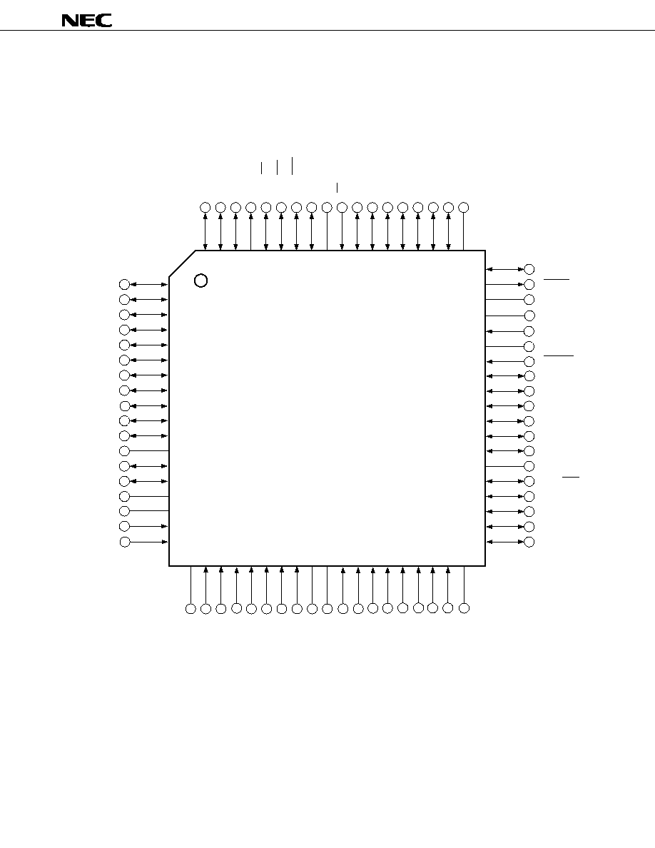
PIN CONFIGURATION
∑
74-pin plastic QFP (20
◊
20 mm)
µ
PD78323GJ-5BJ
µ
PD78324GJ-
◊◊◊
-5BJ
74
P42/AD2
73
P41/AD1
72
P40/AD0
71
ASTB
70
P90/RD
69
P91/WR
68
P92/TAS
67
P93/TMD
66
V
SS
65
EA
64
P07/RTP7
63
P06/RTP6
62
P05/RTP5
61
P04/RTP4
60
P03/RTP3
59
P02/RTP2
58
P01/RTP1
57
NC
19 20 21 22 23 24 25 26 27 28 29 30 31 32 33 34 35 36 37
P00/RTP0
WDTO
V
SS
NC
X1
X2
RESET
P85/TO11
P84/TO10
P83/TO03
P82/TO02
P81/TO01
P80/TO00
NC
P34/SCK
P33/SI/SB1
P32/SO/SB0
P31/R
X
D
P30/T
X
D
P43/AD3
P44/AD4
P45/AD5
P46/AD6
P47/AD7
P50/A8
P51/A9
P52/A10
P53/A11
P54/A12
P55/A13
NC
P56/A14
P57/A15
V
DD
AV
SS
P70/AN0
P71/AN1
1
2
3
4
5
6
7
8
9
10
11
12
13
14
15
16
17
18
56
55
54
53
52
51
50
49
48
47
46
45
44
43
42
41
40
39
38
P72/AN2
P73/AN3
P74/AN4
P75/AN5
P76/AN6
P77/AN7
AV
REF
AV
DD
V
DD
P20/NMI
P21/INTP0
P22/INTP1
P23/INTP2
P24/INTP3
P25/INTP4
P26/INTP5
P27/INTP6/TI
NC
NC
Caution The NC pin should be connected to VSS for noise control (can also be left open).

µ
PD78323, 78324
4
∑
68-pin plastic QFJ (
950 mil)
µ
PD78323LP
µ
PD78324LP-
◊◊◊
9
P27/INTP6/TI
8
P26/INTP5
7
P25/INTP4
6
P24/INTP3
5
P23/INTP2
4
P22/INTP1
3
P21/INTP0
2
P20/NMI
1
V
SS
68
AV
DD
67
AV
REF
66
P77/AN7
65
P76/AN6
64
P75/AN5
63
P74/AN4
62
P73/AN3
61
P72/AN2
27 28 29 30 31 32 33 34 35 36 37 38 39 40 41 42 43
P30/T
X
D
P31/R
X
D
P32/SO/SB0
P33/SI/SB1
P34/SCK
P80/TO00
P81/TO01
P82/TO02
P83/TO03
P84/TO10
P85/TO11
RESET
X2
X1
V
SS
WDTO
RTP0/P00
10
11
12
13
14
15
16
17
18
19
20
21
22
23
24
25
26
RTP1/P01
RTP2/P02
RTP3/P03
RTP4/P04
RTP5/P05
RTP6/P06
RTP7/P07
EA
V
SS
P93/TMD
P92/TAS
P91/WR
P90/RD
ASTB
P40/AD0
P41/AD1
P42/AD2
P71/AN1
P70/AN0
AV
SS
V
DD
P57/A15
P56/A14
P55/A13
P54/A12
P53/A11
P52/A10
P51/A9
P50/A8
P47/AD7
P46/AD6
P45/AD5
P44/AD4
P43/AD3
60
59
58
57
56
55
54
53
52
51
50
49
48
47
46
45
44

5
µ
PD78323, 78324
P00 to P07
: Port0
RESET
: Reset
P20 to P27
: Port2
X1, X2
: Crystal
P30 to P34
: Port3
WDTO
: Watchdog Timer Output
P40 to P47
: Port4
EA
: External Access
P50 to P57
: Port5
TMD
: Turbo Mode
P70 to P77
: Port7
TAS
: Turbo Access Strobe
P80 to P85
: Port8
WR
: Write Strobe
P90 to P93
: Port9
RD
: Read Strobe
NMI
: Nonmaskable Interrupt
ASTB
: Address Strobe
INTP0 to INTP6 : Interrupt From Peripherals
AD0 to AD7
: Address/Data Bus
RTP0 to RTP7
: Realtime Port
A8 to A15
: Address Bus
TI
: Timer Input
AN0 to AN7
: Analog Input
T
X
D
: Transmit Data
AV
REF
: Analog Reference Voltage
R
X
D
: Receive Data
AV
SS
: Analog V
SS
SB0/SO
: Serial Bus/Serial Output
AV
DD
: Analog V
DD
SB1/SI
: Serial Bus/Serial Input
V
DD
: Power Supply
SCK
: Serial Clock
V
SS
: Ground
TO00 to TO03
:
NC
: Non-connection
TO10 to TO11
:
Timer Output

µ
PD78323, 78324
6
GENERAL DESCRIPTION OF FUNCTIONS
∑ ROM : 32K bytes (
µ
PD78324)
None (
µ
PD78323)
∑ RAM : 1K bytes
64K bytes
8 bits
◊
16
◊
8 banks (memory mapping)
∑ Input port
: 16 (dual-function as analog input: 8)
∑ Input/output port : 39 (
µ
PD78324)
21 (
µ
PD78323)
∑ 18/16-bit free running timer
◊
1
∑ 16-bit timer/event counter
◊
1
∑ 16-bit compare register
◊
6
∑ 18-bit capture register
◊
4
∑ 18-bit capture/compare register
◊
2
∑ Realtime output port
◊
8
Serial interface with a dedicated baud rate generator
∑ UART
: 1 channel
∑ SBI (NEC Serial Bus Interface) : 1 channel
10-bit resolution (8 analog inputs)
∑ External : 8, internal : 14 (dual-function as external : 2)
∑ 3 processing modes
(vectored interrupt function, context switching function, and macro service function)
Internal : 1
STOP mode/HALT mode
16-bit transfer/operation instruction, multiplication/division instruction (16
◊
16, 32
˜
16), bit manipu-
lation instruction, string instruction, etc.
On-chip watchdog timer
∑ 68-pin plastic QFJ (
950 mil)
∑ 74-pin plastic QFP (20
◊
20 mm)
Basic instructions
Minimum instruction
execution time
Memory space
General registers
A/D converter
Interrupt
Test factor
Standby
Instruction set
Others
Package
250 ns (with 16 MHz external clock in operation)
Internal memory
I/O line
Real-time pulse unit
Serial communication
interface
111

7
µ
PD78323, 78324
DIFFERENCES BETWEEN
µ
PD78324 AND 78323
Internal ROM
Input
Input
/output
Port 4
(P40 to P47)
Port 5
(P50 to P57)
Port 9
(P90 to P93)
Memory expansion
mode register (MM)
Port 5 mode register
(PM5)
Item
I/O line
Product Name
Always P90 and P91 function as RD strobe and
WR strobe signal output, respectively.
Port 4 I/O mode is set as an 8-bit unit .
Port 5 I/O mode is set bit-wise.
Note Maintenance product
µ
PD78324
µ
PD78323
32K bytes
None
16 (dual-function as analog input: 8)
39
21
Specifiable as I/O as an 8-bit unit.
Functions as multiplexed address/data buses
Functions always as multiplexed address/data
(AD0 to AD7) in the external memory expansion
buses.
mode.
Specifiable as I/O bit-wise.
Functions as address bus (A8 to A15) in the
Functions always as address bus.
external memory expansion mode.
Specifiable as I/O bit-wise.
In the external memory expansion mode, P90
and P91 function as RD strobe signal output
and WR strobe signal output, respectively. In
the external memory high-speed fetch mode,
P92 P93 function as TAS output and TMD out-
put respectively.
In the
µ
PD78324 emulation mode, turbo acces
acces manager (
µ
PD71P301)
Note
PA and PB pins
are controlled as port 4 and port 5 emulation
pins.

µ
PD78323, 78324
8
BCU
ROM/RAM
SYSTEM
CONTROL
&
BUS
CONTROL
&
PREFETCH
CONTROL
ROM
Note
32K
bytes
Peripheral
RAM
768
bytes
EXU
ALU
GENERAL
REGISTERS
128 bytes
&
DATA
MEMORY
128 bytes
MICRO SEQUENCE
CONTROL
MICRO ROM.
Main RAM
PROGRAMMABLE
INTERRUPT
CONTROLLER
TIMER/COUNTER UNIT
(REALTIME PULSE UNIT)
SERIAL INTERFACE
(SBI)
(UART)
(P20) NMI
INTP0≠INTP5
(P21≠P26)
(P80) TO00
(P81) TO01
(P82) TO02
(P83) TO03
(P84) TO10
(P85) TO11
(P27) TI/INTP6
(P34) SCK
(P32) SO/SB0
(P33) SI/SB1
(P30) T
X
D
(P31) R
X
D
AN0≠AN7
(P70≠P77)
AV
DD
AV
SS
AV
REF
WDTO
WDT
A/D CONVERTER
(10 BIT)
PORT
P90≠P93
P80≠P85
P70≠P77
P50≠P57
P40≠P47
P30≠P34
P20≠P27
P00≠P07 (REALTIME PORT)
V
DD
V
SS
AD0≠AD7 (P40≠P47)
A8≠A15 (P50≠P57)
EA
TMD (P93)
TAS (P92)
WR (P91)
RD (P90)
ASTB
RESET
X2
X1
BLOCK DIAGRAM
Note The
µ
PD78323 does not incorporate ROM.

9
µ
PD78323, 78324
CONTENTS
1.
LIST OF PIN FUNCTIONS ..................................................................................................................... 11
1.1
PORT PINS ...................................................................................................................................................... 11
1.2
PINS OTHER THAN PORTS .......................................................................................................................... 12
1.3
PIN INPUT/OUTPUT CIRCUITS AND RECOMMENDED CONNECTION OF UNUSED PINS ................... 14
2.
CPU ARCHITECTURE ............................................................................................................................ 16
2.1
MEMORY SPACE ............................................................................................................................................ 16
2.2
PROCESSOR REGISTERS ............................................................................................................................ 19
2.2.1
Control Registers ........................................................................................................................... 20
2.2.2
General Registers ........................................................................................................................... 22
2.2.3
Special Function Registers (SFR) ................................................................................................ 24
2.3
DATA MEMORY ADDRESSING ..................................................................................................................... 29
2.3.1
General Register Addressing ....................................................................................................... 29
2.3.2
Short Direct Addressing ................................................................................................................ 29
2.3.3
Special Function Register (SFR) Addressing ............................................................................ 29
3.
BLOCK FUNCTIONS .............................................................................................................................. 30
3.1
BUS CONTROL UNIT (BCU) .......................................................................................................................... 30
3.2
EXECUTION UNIT (EXU) ................................................................................................................................ 30
3.3
ROM/RAM ........................................................................................................................................................ 30
3.4
INTERRUPT CONTROLLER .......................................................................................................................... 30
3.5
PORT FUNCTIONS ......................................................................................................................................... 31
3.6
CLOCK GENERATOR .................................................................................................................................... 32
3.7
REALTIME PULSE UNIT (RPU) ..................................................................................................................... 34
3.7.1
Configuration .................................................................................................................................. 34
3.7.2
Realtime Output Function ............................................................................................................. 36
3.8
A/D CONVERTER ........................................................................................................................................... 37
3.9
SERIAL INTERFACE ...................................................................................................................................... 37
3.10 WATCHDOG TIMER ....................................................................................................................................... 40
4.
INTERRUPT FUNCTIONS ...................................................................................................................... 41
4.1
OVERVIEW ...................................................................................................................................................... 41
4.2
MACRO SERVICE ........................................................................................................................................... 42
4.3
CONTEXT SWITCHING FUNCTION .............................................................................................................. 44
4.3.1
Context Switching Function at Interrupt Request ..................................................................... 44
4.3.2
Context Switching Function by BRKCS Instruction ................................................................. 45
5.
STANDBY FUNCTIONS ......................................................................................................................... 46
6.
EXTERNAL DEVICE EXPANSION FUNCTION .................................................................................... 47
7.
OPERATION AFTER RESET ................................................................................................................. 48
8.
INSTRUCTION SET ................................................................................................................................ 49
9.
ELECTRICAL SPECIFICATIONS .......................................................................................................... 63

µ
PD78323, 78324
10
10. PACKAGE DRAWINGS .......................................................................................................................... 74
11. RECOMMENDED SOLDERING CONDITIONS ..................................................................................... 76
APPENDIX A. LIST OF 78K/III SERIES PRODUCTS ................................................................................ 77
APPENDIX B. TOOLS .................................................................................................................................... 79
B.1
DEVELOPMENT TOOLS ................................................................................................................................ 79
B.2
EVALUATION TOOLS .................................................................................................................................... 83
B.3 EMBEDDED SOFTWARE ................................................................................................................................ 83

11
µ
PD78323, 78324
1.
LIST OF PIN FUNCTIONS
1.1
PORT PINS
Dual-
Function Pin
RTP0 to
RTP7
NMI
INTP0
INTP1
INTP2
INTP3
INTP4
INTP5
INTP6/TI
T
X
D
R
X
D
SO/SB0
SI/SB1
SCK
AD0 to AD7
A8 to A15
AN0 to AN7
TO00
TO01
TO02
TO03
TO10
TO11
RD
WR
TAS
TMD
P00 to P07
P20
P21
P22
P23
P24
P25
P26
P27
P30
P31
P32
P33
P34
P40 to P47
P50 to P57
P70 to P77
Function
Pin Name
I/O
Port 0
8-bit input/output port
Input/output can be specified bit-wise
Also serves as a realtime output port.
Input
Input/
output
Port 4
8-bit input/output port
Input/output can be specified in 8-bit unit.
Port 5
8-bit input/output port
Input/output can be specified bit-wise
Port 7
Dedicated port for 8-bit input
Port 8
6-bit input/output port
Input/output can be specified bit-wise
Input/
output
Input/
output
Input/
output
Input
P80
P81
P82
P83
P84
P85
P90
P91
P92
P93
Input/
output
Port 2
Dedicated port for 8-bit input
Port 3
5-bit input/output port
Input/output can be specified bit-wise
Port 9
4-bit input/output port
Input/output can be specified bit-wise
Input/
output

12
µ
PD78323, 78324
RTP0 to RTP7
NMI
INTP0
INTP1
INTP2
INTP3
INTP4
INTP5
INTP6
TI
T
X
D
R
X
D
SO
SI
SB0
SB1
SCK
AD0 to AD7
1.2
PINS OTHER THAN PORTS (1/2)
A8 to A15
TO00
TO01
TO02
TO03
TO10
TO11
RD
WR
TAS
TMD
WDTO
ASTB
Serial data output of asynchronous serial interface (UART)
Serial data input of asynchronous serial interface (UART)
Serial data output of clock synchronous serial interface in 3-wire mode
Serial data input of clock synchronous serial interface in 3-wire mode
Serial data output of clock synchronous serial interface in SBI mode
Dual-
Function Pin
Function
Pin Name
I/O
Realtime output port which generates pulses in synchronization with the trigger signal
transmitted from the realtime pulse unit (RPU).
Nonmaskable interrupot request input capable of specifying the effective at the rising or
falling edge by a mode register.
Input
Output
P00 to P07
P20
P21
P22
P23
P24
P25
P26
P27/TI
P27/INTP6
P30
P31
P32/SB0
P33/SB1
P32/SO
P33/SI
P34
P40 to P47
P50 to P57
P80
P81
P82
P83
P84
P85
P90
P91
P92
P93
≠≠
≠≠
Input
Input
External count clock input to timer 1 (TM1)
Output
Input
Output
Input
/output
Input
/output
Input
/output
Output
Output
Output
Strobe signal output generated for external memory read operation
Strobe signal output generated for external memory write operation
Control signal output generated for access to turbo access manager
µ
PD71P301
Note
Signal output indicating that the watchdog timer has generated a nonmascable
interrupt.
Timing signal output generated for externally latching the address information output from
pins AD0 to AD7 in order to access the external memory.
Output
Output
External interrupt request input capable of specifying the effective edgy by a mode
register.
Input
Serial clock input/output of clock synchronous serial interface
Multiplexed address/data bus for external memory expansion
Address bus for external memory expansion
Pulse output from the realtime pulse unit
Note Maintenance product
13
µ
PD78323, 78324
1.2
PINS OTHER THAN PORTS (2/2)
Dual-
Function Pin
Function
Pin Name
--
I/O
AN0 to AN7
AV
REF
AV
DD
AV
SS
RESET
X1
X2
V
DD
V
SS
NC
--
--
--
--
--
--
--
--
--
--
Input
Input
--
--
Input
Input
--
≠≠
--
--
A/D converter analog input.
A/D converter reference voltage input.
A/D converter analog power supply
A/D converter GND
System reset input
Crystal connect pin for sysem clock oscillation. When an external clock is supplied,
the clock is input to X1 and the inverted clock is input to X2. (X2 can also be left
open.)
Positive power supply
GND pin
Not internally connected. Connected to V
SS
(GND) (can also be left open).
EA
Input
In the
µ
PD78324, EA pin is normally connected to V
DD
. Connecting EA pin to V
SS
sets
the ROM-less mode and accesses the external memory. In the
µ
PD78323, this pin should
be fixed to "0" (low level). The EA pin level cannot be changed during operation.

14
µ
PD78323, 78324
1.3
PIN INPUT/OUTPUT CIRCUITS AND RECOMMENDED CONNECTION OF UNUSED PINS
The pin input/output circuits, partly simplified, are shown in Table 1-1 and Figure 1-1.
Table 1-1. I/O Circuit Types of Pins and Their Recommended
Connection Methods when Unused
Recommended Connection Method
Input/Output
Circuit Type
Pin
P00/RTP0 to P07/RTP7
P20/NMI
P21/INTP0 to P26/INTP5
P27/INTP6/TI
P30/T
X
D
P31/R
X
D
P32/SO/SB0
P33/SI/SB1
P34/SCK
P40/AD0 to P47/AD7
P50/A8 to P57/A15
P70/AN0 to P77/AN7
P80/TO00 to P83/TO03
P84/TO10, P85/TO11
P90/RD
P91/WR
P92/TAS
P93/TMD
WDTO
ASTB
EA
RESET
AV
REF
, AV
SS
AV
DD
NC
Input mode : Individually connected to V
DD
or V
SS
via resistor
Output mode: Leave open
Connected to V
SS
5
2
5
8
5
9
5
5
3
4
1
2
≠≠
≠≠
≠≠
Input mode : Individually connected to V
DD
or V
SS
via resistor
Output mode: Leave open
Connected to V
SS
Input mode : Individually connected to V
DD
or V
SS
via resistor
Output mode: Leave open
Leav open
≠≠
≠≠
Connected to V
SS
Connected to V
DD
Connected to V
SS
(can also be left open)
15
µ
PD78323, 78324
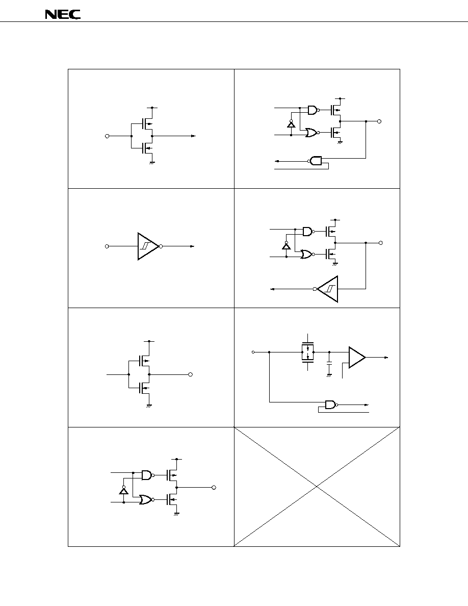
Figure 1-1. Pin Input/Output Circuits
Type 1
Type 2
Type 5
Type 8
Type 3
Type 4
Type 9
P-ch
N-ch
IN
V
DD
IN
Schmitt-trigger input having hysteresis characteristics.
Push-pull output which can become high-impedance
output (with both P-ch and N-ch set to off)
V
DD
OUT
P-ch
N-ch
V
DD
OUT
P-ch
N-ch
data
output
disable
data
output
disable
input
enable
IN/OUT
P-ch
N-ch
V
DD
V
REF
P-ch
N-ch
IN
Comparator
+
≠
(Threshold Voltage)
input
enable
IN/OUT
P-ch
N-ch
V
DD
data
output
disable

16
µ
PD78323, 78324
2.
CPU ARCHITECTURE
2.1
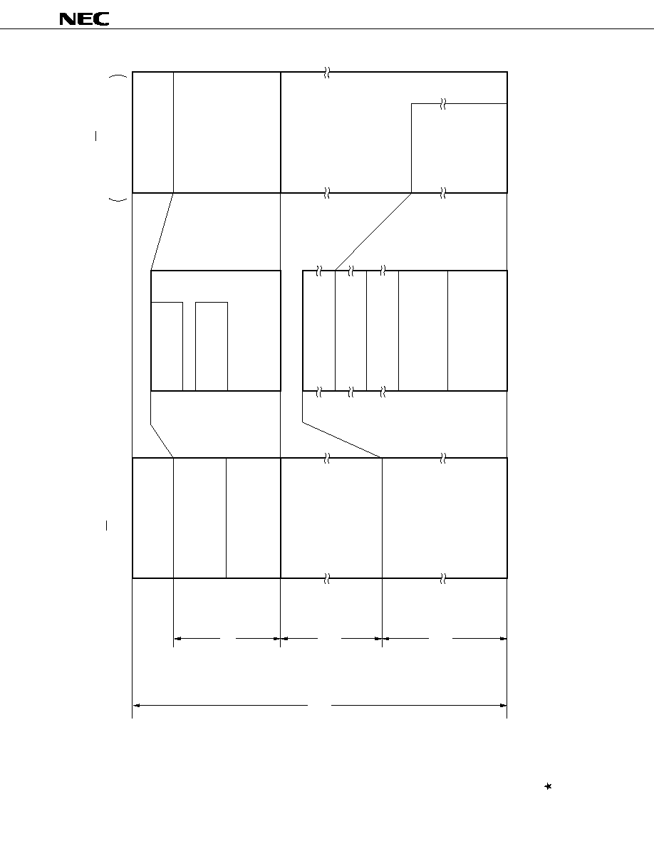
MEMORY SPACE
In the
µ
PD78324 a maximum of 64K bytes of memory can be addressed (see Figure 2-1).
Program fetches can be performed within the area from 0000H to FDFFH. However, when external memory expansion
is implemented in the area from FE00H to FFFFH (main RAM and special function register area), program fetches can also
be performed on this area. In this case, a program fetch is performed on the external memory, not on the main RAM or special
function registers.
(1)
Vector table area
Interrupt request from the peripheral hardware, reset input, external interrupt request and interrupt branch address by
break instruction are stored in the 0000H to 003FH 64-byte area. Generation of an interrupt request sets the even address
content of each table in the lower 8 bits of the program counter (PC) and the odd address content in the higher 8 bits.
Interrupt Source
Vector Table Address
RESET
(RESET pin input) ...........................................
0000H
NMI
(NMI pin input) ................................................
0002H
WDT
(Watchdog timer) ............................................
0004H
TMF0
(Realtime pulse unit) .......................................
0006H
EXF0
(INTP0 pin input) .............................................
0008H
EXF1
(INTP1 pin input) .............................................
000AH
EXF2
(INTP2 pin input) .............................................
000CH
EXF3
(INTP3 pin input) .............................................
000EH
EXF4/CCFX0
(INTP4 pin input/realtime pulse unit) .............
0010H
EXF5/CCFX1
(INTP5 pin input/realtime pulse unit) .............
0012H
EXF6/TI
(INTP6/TI pin input) ........................................
0014H
CMF00
(Realtime pulse unit) .......................................
0016H
CMF01
(Realtime pulse unit) .......................................
0018H
CMF02
(Realtime pulse unit) .......................................
001AH
CMF03
(Realtime pulse unit) .......................................
001CH
CMF10
(Realtime pulse unit) .......................................
001EH
CMF11
(Realtime pulse unit) .......................................
0020H
SRF
(Serial receive complete) ................................
0024H
STF
(Serial send complete) ....................................
0026H
CSIIF
(Clock synchronous serial interface) ..............
0028H
ADF
(A/D converter) ................................................
002AH
Operation code trap ...................................................................
003CH
BRK
(Break instruction) ...........................................
003EH
If bit 1 (TPF) of CPU control word (CCW) is set to 1, the 8002H to 803FH external memory area is used as an interrupt
vector table in place of 0002H to 003FH.

17
µ
PD78323, 78324
Note Maintenance product
(2)
CALLT table area
32 tables of call addresses of 1-byte call instruction (CALLT) can be stored in the 0040H to 007FH 64-byte area.
If bit 1 (TPF) of CPU control word (CCW) is set to 1, the 8040H to 807FH external memory area is used as a CALLT
instruction table in place of 0040H to 007FH.
(3)
CALLF entry area
The 0800H to 0FFFH area can be directly subroutine-called by 2-byte call instruction (CALLF).
(4)
On-chip RAM area
A 1024-byte RAM is built in FB00H to FEFFH. This area is composed of the following 2 RAMs.
∑ Peripheral RAM : FB00H to FDFFH (768 bytes)
∑ Main RAM
: FE00H to FEFFH (256 bytes)
The main RAM can be accessed at high speed.
In the main RAM area, the macro service control word and general register group composed of 8 register banks are
mapped onto the 36 bytes from FE06H to FE2BH and the 128 bytes from FE80H to FEFFH, respectively.
(5)
Special function register (SFR) area
Registers having specially assigned functions, such as on-chip peripheral hardware mode registers and control registers,
are mapped in the FF00H to FFFFH area. Addresses without mapped registers cannot be accessed.
(6)
External memory area
The
µ
PD78324 can add external memories (ROM, RAM) to the 32K-byte (8000H to FFFFH) area.
The
µ
PD78323 can connect external memories (ROM, RAM) to the 64K-byte (0000H to FFFFH) area.
Each external memory can be accessed using P40/AD0 to P47/AD7 (multiplexed address/data bus), P50/A8 to P57/A15
(address bus) and RD, WR and ASTB signals.
The external access area is mapped in the FFD0H to FFDFH 16-byte area of the special function register (SFR). In this
way, the external memory can be accessed by SFR addressing.
Dedicated pins (TAS and TMD pins) are provided to connect turbo access manager (
µ
PD71P301)
Note
. If the
µ
PD71P301
is used, the program processing speed equal to that of the on-chip ROM can be obtained.
18
µ
PD78323, 78324
CALLF Instruction Entry Area
(2048
◊
8)
Special Function Register
(SFR)
(256
◊
8)
Main RAM
(256
◊
8)
External Memory
Note
(31488
◊
8)
Internal ROM
(32768
◊
8)
FFFFH
FF00H
FEFFH
FB00H
FAFFH
8000H
7FFFH
0000H
Program Memory
Data Memory
Program Memory
Data Memory
Data Memory
Memory Space
(64K
◊
8)
General Register
(128
◊
8)
Macro Service Control
(36
◊
8)
Data Area
(1024
◊
8)
Program Area
CALLF Instruction Table Area
(64
◊
8)
Program Area
Vector Table Area
(64
◊
8)
FEFFH
FE80H
FE06H
FB00H
0040H
003FH
0000H
0080H
007FH
0800H
07FFH
1000H
0FFFH
7FFFH
FE2BH
External Memory
(64256
◊
8)
EA = H
( PD78324)
EA = L
∑ PD78323
∑ PD78324 ROM-Less Mode
0FFFH
0000H
µ
µ
µ
Peripheral RAM
(768
◊
8)
FE00H
FDFFH
Figure 2-1. Memory Map
Note Accessed in external memory expansion mode.
Caution For word access (including stack operations) to the main RAM area (FE00H-FEFFH), the address that
specifies the operand must be an even value.

19
µ
PD78323, 78324
2.2
PROCESSOR REGISTERS
The processor registers consist mainly of three groups. They are general registers consisting of 8 banks of sixteen 8-
bit registers, control registers consisting of one 8-bit register and three 16-bit registers, and special function registers such
as peripheral hardware I/O mode registers.
Figure 2-2. Register Configuration
Remark The CCWs of the control registers are mapped in the special function register (SFR) area.
PSW
S P
P C
CCW
R 1
R 3
R 5
R 7
R 9
R 11
R 13
R 15
R 0
R 2
R 4
R 6
R 8
R 10
R 12
R 14
SFR 255
7
SFR 253
SFR 251
SFR 249
SFR 1
SFR 254
SFR 252
SFR 250
SFR 248
SFR 0
0 7
0
7
0
7
0
7
0
15
0
Control Registers
General Registers
Special Function Registers

20
µ
PD78323, 78324
2.2.1
Control Register
The control registers carry out dedicated functions such as control of the program sequence, status and stack memory,
and modification of operand addressing. They consist of three 16-bit registers and one 8-bit register.
(1)
Program counter (PC)
This is a 16-bit register which holds the address information of the next program to be executed. It is normally incremented
according to the number of bytes of the instruction to be fetched. If an instruction with data branch is executed, immediate
data and the register content are set. RESET input sets and branches the data of 0000H and 0001H reset vector tables
in the PC.
(2)
Program status word (PSW)
This is a 16-bit register consisting of various flags which are set or reset by the result of instruction execution. Read/
write access is carried out in units of the higher 8 bits (PSWH) or lower 8 bits (PSWL). Each flag can be operated using
the bit operation instruction. If an interrupt request is made or BRK instruction is executed, data is automatically saved in
the stack and is recovered by RETI or RETB instruction.
All bits are reset to 0 by RESET input.
Figure 2-3. PSW Format
(a)
Interrupt priority level transition flag (LT)
7
6
5
4
3
2
1
0
UF
RBS2 RBS1 RBS0
0
0
0
0
7
6
5
4
3
2
1
0
S
Z
RSS
AC
IE
P/V
LT
CY
This flag is used to control the interrupt priority. For normal operation of the interrupt control circuit, this bit must
not be operated by a program.
(b) Carry flag (CY)
If a carry is generated out of bit 7 or 15 as a result of the execution of an operation instruction or a borrow is generated
into bit 7 or 15, this flag is set to 1. In all other cases, this flag is reset to 0. This flag can be tested by the conditional
branch instruction.
When a bit control instruction is executed, this flag functions as a bit accumulator.
(c) Zero flag (Z)
When the operation result is zero, this flag is set to 1. In all other cases, this flag is reset to 0. This flag can be tested
by the conditional branch instruction.
(d) Sign flag (S)
When MSB of the operation result is "1", this flag is set to 1. When the MSB is "0", this flag is reset to 0. This flag
can be tested by the conditional branch instruction.
(e)
Parity/overflow flag (P/V)
Only when an overflow or underflow occurs as two's complement during execution of an arithmetic operation
instruction, this flag is set to 1. In all other cases, it is reset to 0 (overflow flag operation).
If the bit number of the operation result set to 1 is even during execution of an logic operation instruction, this flag
is set to 1. If the bit number is odd, this flag is reset to 0 (parity flag operation).
This flag can be tested by the conditional branch instruction.
PSWH
PSWL

21
µ
PD78323, 78324
(f)
Auxiliary carry flag (AC)
If a carry is generated out of bit 3 as a result of operation or a borrow is generated into bit 3, this flag is set to 1.
In all other cases, this flag is reset to 0. This flag can be tested by the conditional branch instruction.
(g) Register set select flag (RSS)
This flag is used to specify general registers X, A, C and B. As shown in Table 2-1, the RSS value determines the
relationship between the functional register and the absolute register.
Thus, another register set (X, A, C, B) can be used by switching the RSS flag.
(h) Interrupt request enable flag (IE)
This flag is used to indicate interrupt request enable/disable. This flag is set to 1 by execution of EI instruction and
is reset to 0 byexecution of DI instruction or acceptance of an interrupt.
(i)
Register bank select flag (RBS0 to RBS2)
This is a 3-bit flag to select one of eight register banks (RBANK0 to RBANK7).
(j)
User flag (UF)
This flag is set or reset in the user program and can be used for program control.
(3)
Stack pointer (SP)
This is a 16-bit register which holds the first address of the stack area (LIFO format) of the memory.
It is operated by a dedicated instruction.
SP is decremented before write (save) operation into the stack memory and is incremented after read (return) operation
from the stack memory.
Since SP becomes indeterminate by RESET input, it must be set before subroutine call.
22
µ
PD78323, 78324
(4)
CPU control word (CCW)
This is an 8-bit register consisting of CPU control related flags. It is mapped in the special function register area and can
be controlled by the software.
All bits are reset to 0 by RESET input.
Figure 2-4. CCW Format
∑ Table position flag (TPF)
This flag is used to specify the interrupt vector table area and the memory area used as CALLT instruction table area.
As TPF has been reset to 0 after application of RESET input, the 0000H to 007FH address is used as each table area.
The 8002H to 807FH address of the external memory area in place of 0002H to 007FH address can be used as each table
area by setting TPF to 1 using the software. The vector tables of the BRK instruction, operation code trap interrupt and reset
input are fixed to 003EH, 003CH and 0000H, respectively, and they are not affected by TPF.
2.2.2
General Registers
These are 128-byte registers mapped in the special area (FE80H to FEFFH) of the internal RAM space. They consist
of eight register banks. The general register in the bank consists of sixteen 8-bit registers.
Figure 2-5. General Register Memory Location
7
6
5
4
3
2
1
0
0
0
0
0
0
0
TPF
0
CCW
(FH)
RP7
(EH)
(DH)
RP6
(CH)
(BH)
RP5
(AH)
(9H)
RP4
(8H)
(7H)
RP3
(6H)
(5H)
RP2
(4H)
(3H)
RP1
(2H)
(1H)
RP0
(0H)
R15
R14
R13
R12
R11
R10
R9
R8
R7
R6
R5
R4
R3
R2
R1
R0
7
0 7
0
15
0
RBNK0
RBNK1
RBNK2
RBNK3
RBNK4
RBNK5
RBNK6
RBNK7
FEFFH
FE80H
8-Bit Processing
16-Bit Processing
23
µ
PD78323, 78324
The sixteen 8-bit registers can function as eight 16-bit register pairs (RP0 to RP7) as well.
As shown in Table 2-1, the sixteen 8-bit registers are characterized by functional names. The X register functions as
the lower half of the 16-bit accumulator, the A register functions as the upper half of the 8-bit or 16-bit accumulator, the B
and C registers function as a counter, and DE, HL, VP and UP function as address register pairs. In particular the VP register
is function as a base register and the UP register is as a user stack pointer.
The unique function register charges as shown in Table 2-1 according to the value of the register set select flag (RSS)
in the PSW. Thus, if the program is described by the functional name, another register set of X, A, C and B can be used
by means of the RSS flag.
The
µ
PD78324 can carry out processed data addressing operations, implied addressing by functional names with
importance attached to the unique function of each register and register addressing by absolute names with a view to fast
processing with a small number of data transfers or creating highly descriptive programs.
Table 2-1. General Register Configuration
R5
A
R6
C
R7
B
R8
VP
L
VP
L
R9
VP
H
VP
H
R10
UP
L
UP
L
R11
UP
H
UP
H
R12
E
E
R13
D
D
R14
L
L
R15
H
H
Absolute
Functional Name
Name
RSS = 0
RSS = 1
R0
X
R1
A
R2
C
R3
B
R4
X
RP5
UP
UP
RP6
DE
DE
RP7
HL
HL
Absolute
Functional Name
Name
RSS = 0
RSS = 1
RP0
AX
RP1
BC
RP2
AX
RP3
BC
RP4
VP
VP

24
µ
PD78323, 78324
2.2.3
Special Function Registers (SFR)
These registers are provided with special functions. They include various peripheral hardware mode registers and control
registers (CCW).
The special function registers are assigned in the FF00H to FFFFH 256-byte space. Short direct memory addressing
is applied to the FF00H to FF1FH 32-byte area for processing with a short word length.
The bit manipulation, arithmetic and transfer instructions can be executed in all areas. The FFD0H to FFDFH 16-byte
area is externally accessible by SFR addressing. Thus, the external memory can be accessed and the external device bit
manipulation can be carried out by an instruction having a short word length.
Table 2-2 lists the special function registers (SFR). The items in the table have the following meanings.
∑ Symbol................. Indicates the address of the built-in special function register.
Can be described in the instruction operand column.
∑ R/W.......................Indicates if the corresponding special function register can read or write.
R/W : Read/write enable
R
: Read only enable (register bit test enable)
W
: Write only enable
∑ Manipulable bit unit
....................... Indicates the applicable operation bit unit for the corresponding special function
register.
16-bit manipulable SFR can be described in operand sfrp. When specified by an
address, an even address is described.
1-bit manipulable SFR can be described by the bit operation instruction.
∑ On reset ............... Indicates the state of each register when RESET is input.
Cautions 1. Addresses for which no special function registers have been assigned cannot be accessed in the
FF00H to FFFFH area.
2. Do not write to the read only register. If data is written, the internal circuit may malfunction.
25
µ
PD78323, 78324
Table 2-2. List of Special Function Registers (1/4)
FF00H
FF02H
FF03H
FF04H
FF05H
FF07H
FF08H
FF09H
FF0AH
FF0BH
FF10H
FF11H
FF12H
FF13H
FF14H
FF15H
FF16H
FF17H
FF18H
FF19H
FF1AH
FF1BH
FF20H
FF23H
FF25H
FF28H
FF29H
FF2AH
FF2BH
FF2CH
FF2DH
FF30H
FF31H
FF32H
FF33H
FF34H
FF35H
q
q
q
q
≠≠
q
q
q
q
q
q
q
q
q
q
q
q
q
q
≠≠
q
q
q
q
q
q
q
q
q
q
≠≠
≠≠
≠≠
≠≠
≠≠
≠≠
≠≠
≠≠
≠≠
≠≠
≠≠
≠≠
≠≠
≠≠
≠≠
≠≠
≠≠
≠≠
≠≠
≠≠
≠≠
≠≠
≠≠
≠≠
≠≠
≠≠
≠≠
q
q
≠≠
q
q
≠≠
q
q
≠≠
q
q
≠≠
q
q
≠≠
≠≠
≠≠
≠≠
≠≠
≠≠
≠≠
≠≠
≠≠
≠≠
≠≠
≠≠
≠≠
≠≠
≠≠
≠≠
≠≠
≠≠
≠≠
≠≠
Port 0
Port 2
Port 3
Port 4
Port 5
Port 7
Port 8
Port 9
Free running counter
(lower 16 bits)
Note
Capture register X0
(lower 16 bits)
Note
Capture register 01
(lower 16 bits)
Note
Capture register 02
(lower 16 bits)
Note
Capture register 03
(lower 16 bits)
Note
Capture/compoare register X0
(lower 16 bits)
Note
Capture/compoare register 01
(lower 16 bits)
Note
Port 0 mode register
Port 3 mode register
Port 5 mode register
Port 8 mode register
Port 9 mode register
Free runnting counter
(higher 16 bits)
Note
Timer register 1
Capture register X0
(higher 16 bits)
Note
Capture register 01
(higher 16 bits)
Note
Capture register 02
(higher 16 bits)
Note
1 bit
8 bits
16 bits
Address
Special Function Register (SFR) Name
R/W
On Reset
Symbol
P0
P2
P3
P4
P5
P7
P8
P9
R/W
R
R/W
R
R/W
R
R/W
W
R
TM0LW
CTX0LW
CT01LW
CT02LW
CT03LW
CCX0LW
CC01LW
PM0
PM3
PM5
PM8
PM9
TM0UW
TM1
CTX0UW
CT01UW
CT02UW
Undefined
0000H
Undefined
FFH
◊ ◊ ◊
1 1111B
FFH
◊ ◊
11 1111B
◊ ◊ ◊ ◊
1111B
0000H
Undefined
Manipulable Bit Unit
≠≠
≠≠
≠≠
≠≠
≠≠
q
q
q
q
q
q
q
q
q
q
q
q
q
q
≠≠
≠≠
≠≠
≠≠
≠≠
q
q
q
q
q
q
q
q
q
q
Note Upper or lower half of 18-bit register.

26
µ
PD78323, 78324
Capture register 03
(higher 16 bits)
Note
Capture/compoare register X0
(higher 16 bits)
Note
Capture/compoare register 01
(higher 16 bits)
Note
Port 0 mode control register
Realtime output port reset register
Port 3 mode control register
Port 8 mode control register
Baud rate generator
Realtime output port register
Realtime output port reset register
Port read control register
A/D converter mode register
A/D conversion result register
(for 16-bit access)
A/D conversion result register
(for upper 8-bit access)
Compare register 00
Compare register 01
Compare register 02
Compare register 03
Compare register 10
Compare register 11
Clock synchronous serial
interface mode register
Serial bus interface control register
Serial I/O shift register
≠≠
≠≠
≠≠
≠≠
≠≠
≠≠
≠≠
≠≠
≠≠
≠≠
≠≠
≠≠
≠≠
≠≠
≠≠
≠≠
≠≠
≠≠
≠≠
≠≠
≠≠
≠≠
≠≠
≠≠
q
q
q
q
q
q
q
q
q
q
q
q
Undefined
00H
◊ ◊ ◊
0 0000B
◊ ◊
00 0000B
Undefined
00H
Undefined
00H
Undefined
q
q
q
q
q
q
≠≠
≠≠
≠≠
≠≠
q
q
≠≠
≠≠
≠≠
≠≠
q
q
≠≠
q
q
q
q
q
q
q
q
q
q
q
q
≠≠
≠≠
≠≠
≠≠
≠≠
≠≠
≠≠
≠≠
≠≠
≠≠
≠≠
≠≠
≠≠
≠≠
≠≠
≠≠
q
q
q
q
q
q
≠≠
q
q
≠≠
q
q
≠≠
≠≠
≠≠
≠≠
q
q
q
q
q
q
q
q
q
q
q
q
q
q
q
q
≠≠
≠≠
≠≠
q
q
Table 2-2. List of Special Function Registers (2/4)
FF36H
FF37H
FF38H
FF39H
FF3AH
FF3BH
FF40H
FF41H
FF43H
FF48H
FF4CH
FF4DH
FF60H
FF61H
FF62H
FF68H
1 bit
8 bits
16 bits
Address
Special Function Register (SFR) Name
R/W
On Reset
Symbol
Manipulable Bit Unit
FF6AH
FF6BH
FF70H
FF71H
FF72H
FF73H
FF74H
FF75H
FF76H
FF77H
FF7CH
FF7DH
FF7EH
FF7FH
FF80H
CT03UW
CCX0UW
CC01UW
PMC0
RTPS
PMC3
PMC8
BRG
RTP
RTPR
PRDC
ADM
ADCR
ADCRH
CM00
CM01
CM02
CM03
CM10
CM11
CSIM
SBIC
SIO
R
R/W
W
R/W
W
R/W
R
R/W
R/W
FF82H
FF86H
Note Upper or lower half of 18-bit register.

27
µ
PD78323, 78324
≠≠
q
q
≠≠
q
q
q
q
q
q
q
q
q
q
q
q
q
q
q
q
q
q
q
q
q
q
q
q
q
q
q
q
q
q
q
q
q
q
q
q
q
q
q
q
q
q
q
q
q
q
q
q
q
q
q
q
q
q
q
q
q
q
q
q
q
q
q
q
q
q
≠≠
≠≠
q
q
q
q
q
q
q
q
q
q
q
q
≠≠
≠≠
q
q
q
q
q
q
q
q
q
q
q
q
≠≠
≠≠
q
q
q
q
q
q
q
q
q
q
q
q
≠≠
≠≠
RXB
TXS
TMC
BRGM
PRM
TOC0
TOC1
RPUM
STBC
CCW
WDM
MM
PWC
FCC
Asynchronous serial interface
mode register
Asynchronous serial interface
status register
Serial receive buffer
:UART
Serial send shift register
:UART
Timer control register
Baud rate generator mode register
Prescalar mode register
Timer output control register 0
Timer output control register 1
RPU mode register
Standby control register
CPU control word
Watchdog timer mode register
Memory expansion mode register
Programmable weight control register
Fetch cycle control register
External acces area
Interrupt request flag rgister 0L
Interrupt request flag rgister 0H
Interrupt request flag rgister 1L
≠≠
Interrupt mask flag rgister 0L
Interrupt mask flag rgister 0H
Interrupt mask flag rgister 1L
≠≠
Priority specify bufer register 0L
Priority specify bufer register 0H
Priority specify bufer register 1L
≠≠
Interrupt processing mode specify register 0L
Interrupt processing mode specify register 0H
Interrupt processing mode specify register 1L
≠≠
Table 2-2. List of Special Function Registers (3/4)
1 bit
8 bits
16 bits
Address
Special Function Register (SFR) Name
R/W
On Reset
Symbol
Manipulable Bit Unit
ASIM
ASIS
R/W
R
W
R/W
R/W
Note
R/W
R/W
Note
R/W
Note Write enable in case of special instructions.
FF8CH
FF8EH
FFB0H
FFB1H
FFB2H
FFB8H
FFB9H
FFBFH
FFC0H
FFC1H
FFC2H
FFC4H
FFC6H
FF88H
FF8AH
FFC9H
FFD0H to
FFDFH
FFE0H
FFE1H
FFE2H
FFE3H
FFE4H
FFE5H
FFE6H
FFE7H
FFE8H
FFE9H
FFEAH
FFEBH
FFECH
FFEDH
FFEEH
FFEFH
IF0
IF1
MK0
MK1
PB0
PB1
ISM0
ISM1
IF0L
IF0H
IF1L
≠≠
MK0L
MK0H
MK1L
≠≠
PB0L
PB0H
PB1L
≠≠
ISM0L
ISM0H
ISM1L
≠≠
q
q
q
q
q
q
q
q
≠≠
≠≠
≠≠
≠≠
≠≠
≠≠
≠≠
≠≠
≠≠
≠≠
≠≠
≠≠
≠≠
≠≠
≠≠
≠≠
≠≠
q
q
q
q
q
q
q
q
q
q
q
q
q
q
q
q
80H
00H
Undefined
00H
0000
◊
000B
00H
22H
00H
Undefined
00H
≠≠
FFH
◊ ◊
◊ ◊
◊
111B
≠≠
00H
≠≠
00H
≠≠

28
µ
PD78323, 78324
Table 2-2. List of Special Function Registers (4/4)
FFF0H
FFF1H
FFF2H
FFF3H
FFF4H
FFF5H
FFF8H
FFF9H
q
q
q
q
q
q
q
q
q
q
q
q
≠≠
≠≠
q
q
q
q
q
q
q
q
≠≠
q
q
q
q
q
q
Context switching enable register 0L
Context switching enable register 0H
Context switching enable register 1L
≠≠
External interupt mode register 0
External interupt mode register 1
In-service priority register
Priority specify register
1 bit
8 bits
16 bits
Address
Special Function Register (SFR) Name
R/W
On Reset
Symbol
Manipulable Bit Unit
INTM0
INTM1
ISPR
PRSL
CSE0L
CSE0H
CSE1L
≠≠
CSE0
CSE1
q
q
q
q
≠≠
≠≠
≠≠
≠≠
00H
≠≠
00H
R/W
R
R/W
2.3
DATA MEMORY ADDRESSING
In the
µ
PD78324, the internal RAM space (FB00H to FEFFH) and the special function register area (FF00H to FFFFH)
are mapped in the FB00H to FFFFH area. In the FE20H to FF1FH space of the data memory, short direct addressing enables
direct addressing by 1-byte data in an instruction word.
Figure 2-6. Data Memory Addressing Space
Note When EA = L, and with the
µ
PD78323, this is external memory.
Caution For word access (including stack operations) to the main RAM area (FE00H-FEFFH), the address that
specifies the operand must be an even value.
FFFFH
FF1FH
FF00H
FEFFH
FE80H
FE00H
FB00H
7FFFH
0000H
Special Function Register
(SFR)
Main RAM
External Memory
General Register
Internal ROM
Note
SFR Addressing
Register Addressing
Short Direct Addressing
Direct Addressing
Register Indirect Addressing
Based Addressing
Paste Indexed Addressing
Paste Indexed Addressing
(Provided with Displacement)
FE20H
Peripheral RAM
FDFFH

29
µ
PD78323, 78324
2.3.1
General Register Addressing
The general registers consist of eight register banks, each consisting of sixteen 8-bit registers or eight 16-bit registers.
General register addressing is carried out using the register specify field of 3 or 4 bits supplied from an instruction word,
the register bank select flag (RBS0 to RBS2) and the register set select flag (RSS) in the PSW.
2.3.2
Short Direct Addressing
Short direct addressing which enables direct address specification by 1-byte data in an instruction work is applied to the
FE20H to FF1FH space. The short direct memory is accessed as 8-bit or 16-bit data. When accessing the memory as 16-
bit data, specification of even data for 1-byte address specify data will cause 2-byte data specified by continuous addresses
of even and odd addresses to be accessed. (Do not specify odd number for address specify data.)
2.3.3
Special Function Register (SFR) Addressing
This addressing is applied to operations for the special function register (SFR) mapped in the SFR area of FF00H to
FFFFH. Addressing is performed by 1-byte data in the instruction word corresponding to the lower 8 bits of the special
function register address. For 16-bit access of 16-bit operational SFR, 2-byte data specified by continuous even and odd
addresses is accessed as is the case with short direct addressing.

30
µ
PD78323, 78324
3.
BLOCK FUNCTIONS
3.1
BUS CONTROL UNIT (BCU)
In the BCU, the necessary bus cycle is started according to the physical address obtained by the execution unit (EXU).
If no bus cycle startup request is made from the EXU, a prefetch address is generated and instruction prefetch is carried
out. The prefetched instruction code is fetched into the instruction queue.
3.2
EXECUTION UNIT (EXU)
In the EXU, address calculation, arithmetic logical operation and data transfer are controlled by microprograms. A 256-
byte RAM is built in the EXU.
The 256-byte RAM in the EXU is accessible by the relevant instruction faster than peripheral RAM (768 bytes).
3.3
ROM/RAM
This block consists of a 32K-byte ROM and a 768-byte RAM. However, the
µ
PD78323 does not incorporate ROM.
ROM access can be disabled by EA pin.
3.4
INTERRUPT CONTROLLER
Various interrupt requests (NMI, INTP0 to INTP6) generated either externally or from the peripheral hardware are
processed by the context switch, vectored interrupt or macro service function.
The 3-level interrupt priority is also specified.

31
µ
PD78323, 78324
3.5
PORT FUNCTIONS
Table 3-1 lists the digital input/output ports.
Each port can carry out many control operations including 8 and other bit data input/output operations.
Table 3-1. Port Functions and Features
Port Name
Function
Feature
Remarks
Specifiable bit-wise for input/output.
Serves as RTP0 to RTP7
Also specifiable for realtime output port.
and pins.
Serves as NMI, INTP0 to
INTP5, INTP6/TI and pins.
Serves as T
X
D, R
X
D,
Port 3
5-bit input/output
Specifiable bit-wise for port pins or control pins.
SO/SB0, SI/SB1, SCK and
pins.
Specifiable in 8-bit units for input or output.
Port 4
8-bit input/output
Functions as the multiplexed address/data bus (AD0 to
≠≠≠≠≠≠≠≠
AD7) in the external memory expansion mode.
Specifiable bit-wise for input or output.
Functions as the address bus (A8 to A15) in the external
Port 5
8-bit input/output
memory expansion mode.
≠≠≠≠≠≠≠≠
Pins which are not used as the address bus can be used
as a port.
Input port pin. Also functions as analog input to the
Serves as AN0 to AN7
A/D converter.
and pins.
Functions as TO00 to
Port 8
6-bit input/output
Specifiable bit-wise for the port pin or control pin.
TO03, TO10 to TO11 and
pins.
Specifiable bit-wise for input/output.
P90 and P91 function as RD output and WR output,
Port 9
4-bit input/output
respectively, in the external memory expansion mode.
≠≠≠≠≠≠≠≠
P92 and P93 function as TAS output and TMD output,
respectively, in the high-speed fetch mode.
Port 2
8-bit input
Input port pin. Functions as an external interrupt input.
Port 7
8-bit input
Port 0
8-bit input/outpput
32
µ
PD78323, 78324
3.6
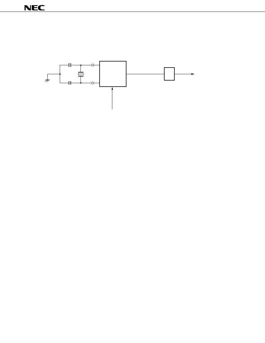
CLOCK GENERATOR
The clock generator generates and controls internal system clocks (CLK) supplied to the CPU. It is configured as shown
in Figure 3-1.
Figure 3-1. Block Diagram of Clock Generator
X1
X2
STOP Mode
f
XX
or f
X
1/2
f
CLK
Internal System
Clock (CLK)
Divider
System
Clock
Generator
Remarks
1.
f
XX
: Crystal oscillator frequency
2.
f
X
: External clock frequency
3.
f
CLK
: Internal system clock frequency
The system clock oscillator oscillates by a crystal resonator connected to X1 and X2 pins. It stops oscillating when set
to the standby mode (STOP).
External clocks can be input to the system clock oscillator. In such cases, input a clock signal to the X1 pin and input
the reverse phase of the clock signal to the X2 pin. The X2 pin can also be left open.
Caution When using external clocks, do not set the STBC STP bit.
The divider generates internal system clocks (f
CLK
) by dividing a system clock oscillator output (fxx for crystal oscillation
and fx for external clocks) into two parts.

33
µ
PD78323, 78324
Figure 3-2. Externally-Mounted System Clock Generator
(a) Crystal oscillator
Cautions 1. When the system clock oscillator is used, the following points should be noted concerning wiring
within broken lines shown in Figure 3-2, in order to prevent the effects of wiring capacitance, etc.
∑
Keep the wiring as short as possible.
∑
Do not cross any other signal lines, and keep clear of lines in which a high fluctuating current
flows.
∑
Ensure that oscillator capacitor connection points are always at the same potential as V
SS
. Do not
ground in a ground pattern in which a high current flows.
∑
Do not take a signal from the oscillator.
2. When an external clock is input to the X1 pin and the X2 pin is left open, ensure that no loads such
as wiring capacitance are connected to the X2 pin.
(b) External clock
(i) When the inverted phase of an
external clock to be input to the
X1 pin is input to the X2 pin
(ii) When X2 pin is left open
X2
X1
V
SS
PD78324
µ
X1
X2
External
Clock
PD78324
µ
X1
X2
Open
External
Clock
PD78324
µ

34
µ
PD78323, 78324
3.7
REALTIME PULSE UNIT (RPU)
This unit can measure pulse intervals and frequencies, and generate programmable pulse outputs.
It consists mainly of two timers. To flexibly cope with many applications, the configuration of registers connected to the
timers can be changed using programs. To meet various applications, toggle output (6 max.) or set/ reset output (4 max.)
can be selected as timer output.
3.7.1
Configuration
The realtime pulse unit is configured mainly of timer 0 (TM0) which functions as a 16-bit or 18-bit free running timer and
timer 1 (TM1) which functions as a 16-bit timer/event counter shown in Figure 3-3.

35
µ
PD78323, 78324
Figure 3-3. Realtime Pulse Unit Configuration
16-BIT TIMER/EVENT COUNTER
TM1
(CLEAR CONTROL)
INTP0
(OPPOSITE EDGE)
OVF
Match
INTCM10
INTCM11
Match
T
R
S
T
TO11
TO10
COMPARE REG. CM10
COMPARE REG. CM11
INTP6/TI
f
CLK
/16
INTOV
OVF
INTCM00
INTCM01
INTCM02
INTCM03
INTCC01
CAPTURE REG. CTX0
INTP0
INTP4
CAPTURE/COMPARE REG. CCX0
Match
Match
MODE1
MODE0
INTP0
INTCCX0
CAPTURE/COMPARE REG. CC01
CAPTURE REG. CT03
CAPTURE REG. CT02
CAPTURE REG. CT01
INTP5
INTCCX0
INTP3
INTP2
INTP1
INTP0
f
CLK
/4
COMPARE REG. CM03
COMPARE REG. CM02
COMPARE REG. CM01
COMPARE REG. CM00
2
0
f
CLK
/8
16/18-BIT FREE RUNNING TIMER
10 11
15
17
TM0
T
R
S
T
R
S
T
R
S
T
TO03
TO02
TO01
TO00
36
µ
PD78323, 78324
3.7.2
Realtime Output Function
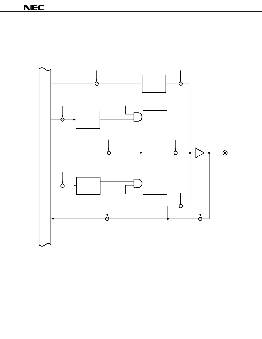
The realtime output port can set/reset port outputs bit-wise in synchronization with the trigger signal transmitted from
the RPU (Realtime Pulse Unit). It enables to generate multi-channel synchronous pulses easily.
Figure 3-4. Realtime Output Port
WR
PORT
WR
RTPR
RTPR
n
INTCM03
R
D
S
Q
P0
n
Output Latch
PMC0
n
= 0
PMC0
n
= 1
P0
n
PM0
n
= 1
PM0
n
= 0
RD
INTCCX0
RTPS
n
WR
RTPS
WR
PTP
Internal Bus
RTP
n

37
µ
PD78323, 78324
3.8
A/D CONVERTER
The
µ
PD78324 incorporates a high-speed, high-resolution 10-bit analog/digital (A/D) converter. This A/D converter is
equipped with eight analog inputs (AN0 to AN7) and A/D conversion result register (ADCR) which holds the conversion
results. Upon termination of conversion, the interrupt which can start the macro service is generated.
Figure 3-5. A/D Converter Block Diagram
3.9
SERIAL INTERFACE
The
µ
PD78324 is equipped with the following two independent channels for the serial interface function.
Asynchronous serial interface
Clock synchronous serial interface
∑
3-wire serial I/O mode
∑
Serial bus interface mode (SBI mode)
Since the
µ
PD78324 incorporates a baud rate generator, it can set any serial transfer rate irrespective of the operating
frequency. The baud rate generator functions for the 2-channel serial interface.
The serial transfer rate can be selected from 75 bps to 19.2 Kbps by setting the mode register.
AN0
AN1
AN2
AN3
AN4
AN5
AN6
AN7
Input Circuit
ADM (8)
Internal Bus
8
Sample & Hold Circuit
Comparator
SAR (10)
D/A Converter
ADCR (10)
10
Internal Bus
AV
REF
AV
SS
10
10

38
µ
PD78323, 78324
Figure 3-6. Asynchronous Serial Interface Block Diagram
BRGM
BRG
SCK
SL
CL
PS0
PS1
REX
ASIM
2
1
Match
Clear
f
CLK
/8
f
CLK
/4
Send/Receive Baud Rate Generator Output
Baud Rate Generator
Selector
16
1
16
1
INTSR
Receive
Control
Parity
Check
Shift Register
Receive Buffer
R
X
D
T
X
D
RXB
Shift Register
OVE
FE
PE
ASIS
TXS
Send Control
Parity
Addition
Internal Bus
INTST
INTSER

39
µ
PD78323, 78324
BSYE
ACKD
ACKE
ACKT
CMDD
RELD
CMDT
RELT
8
SBIC
SET
CLEAR
D
SO Latch
Q
Busy/
Acknowledge
Detector
Shift Register SIO
Internal Bus
MOD0
CLS0
CLS1
MOD1
WUP
CRXE
CTXE
MOD2
CSIM
8
SI/SB1
SO/SB0
N-ch Open Drain
Output Enable
SCK
Bus Release/
Command/Acknowledge
Detector
Serial Clock
Counter
Serial Clock
Controller
Interrupt
Signal
Generation
Controller
INTCSI
MPX
CLS1 CLS0
Baud Rate Generator
Output
f
CLK
/8
f
CLK
/32
Figure 3-7. Block Diagram of Clock Synchronous Serial Interface

40
µ
PD78323, 78324
3.10 WATCHDOG TIMER
The watchdog timer is used to prevent program overrun and deadlock. Normal operation of the program or system can
be confirmed by checking that no watchdog timer interrupt has been generated. Thus, an instruction to clear the watchdog
timer (timer start) is set into each program module.
If the watchdog timer clear instruction is not cleared within the time period set into the watchdog timer and the watchdog
timer overflows, a watchdog timer interrupt is generated, and a low level is generated to WDTO pin, thereby notifying of
an error in the program.
The watchdog timer can also be used to maintain the oscillation stabilizing time of the oscillator after the stop mode has
been released.
Figure 3-8 shows the watchdog timer configuration.
Figure 3-8. Watchdog Timer Configuration
f
CLK
/2
8
f
CLK
/2
10
f
CLK
/2
12
Watchdog Timer (8 Bits)
Clear
Timer (5 Bits)
Oscillation Stabilizing
Time Controller
INTWDT
WDTO
WDT CLR
WDT STOP
Overflow

41
µ
PD78323, 78324
4.
INTERRUPT FUNCTIONS
4.1
OVERVIEW
In the
µ
PD78324, various interrupt requests generated externally or from the on-chip peripheral hardware are handled
in the following three processing modes.
Interrupt requests are classified into the following three groups.
∑ Nonmaskable interrupt requests
∑ Maskable interrupt requests
∑ Interrupt requests by software
Figure 4-1 shows the maskable interrupt request processing modes. Table 4-1 gives a listing of interrupt factors which
can be processed.
Figure 4-1. Interrupt Request Processing Modes
Handled by Vectored Interrupt Processing
Interrupt Request
Handled by Context Switching
Handled by Macro Service
◊ ◊
MK = 1 (Interrupt Masked)
Vectored Interrupt and Macro Service Reserved
◊ ◊
MK = 0 (Interrupt Unmasked)
◊ ◊
ISM = 0 (Vectored Interrupt Processing Mode)
DI
Vectored Interrupt Processing Reserved
EI
◊ ◊
CSE = 0
Vectored Interrupt Processing Executed
◊ ◊
CSE = 1
Context Switching Executed
◊ ◊
ISM = 1 (Macro Service Processing Mode)
Macro Service Processing Executed
42
µ
PD78323, 78324
Table 4-1. List of Interrupt Factors
Available
Interrupt
Default
Interrupt Factor
Generator
Macro
Vector Table
Request Type
Priority
Request Signal
Function
Unit
Service
Address
≠≠≠
≠≠≠
BRK instruction
≠≠≠
≠≠≠
003EH
≠≠≠
≠≠≠
Operation code trap
≠≠≠
≠≠≠
003CH
(External
interrupt)
≠≠≠
INTWDT
Watchdog timer
(WDT)
≠≠≠
0004H
0
INTOV
Timer 0 overflow
(RPU)
0006H
1
INTP0
INTP0 pin input
(External)
0008H
2
INTP1
INTP1 pin input
(External)
000AH
3
INTP2
INTP2 pin input
(External)
000CH
4
INTP3
INTP3 pin input
(RPU/exteranl)
000EH
5
INTP4/INTCCX0
INTP4 pin input/CCX0 match signal
(RPU/exteranl)
0010H
6
INTP5/INTCC01
INTP5 pin input/CC01 match signal
(RPU/exteranl)
0012H
7
INTP6/TI
INTP6 pin input/TI input
(Exteranl)
0014H
8
INTCM00
CM00 match signal
(RPU)
0016H
9
INTCM01
CM01 match signal
(RPU)
0018H
10
INTCM02
CM02 match signal
(RPU)
001AH
11
INTCM03
CM03 match signal
(RPU)
001CH
12
INTCM10
CM10 match signal
(RPU)
001EH
13
INTCM11
CM11 match signal
(RPU)
0020H
14
INTSR
Serial receive terminate interrupt
(UART)
0024H
15
INTST
Serial send terminate interrupt
(UART)
0026H
16
INTCSI
Serial send/receive interrupt
(CSI)
0028H
17
INTAD
A/D conversion terminate interrupt
(A/D)
002AH
≠≠≠
≠≠≠
INTSER
Note
Serial receive error signal
(UART)
≠≠≠
≠≠≠
Note
Reset
≠≠≠
RESET
Reset input
≠≠≠
≠≠≠
0000H
Note This is a test factor. A vectored interrupt is not generated.
Software
Non-
maskable
Maskable
NMI
NMI pin input
≠≠≠
0002H
≠≠≠
43
µ
PD78323, 78324
4.2
MACRO SERVICE
The macro service function is executed at the interrupt request to carry out data operation and data transfer in hardware
terms between the special function register area and the memory space.
Upon startup of the macro service, the CPU stops program execution temporarily. 1-byte/2-byte data operation and
transfer are automatically carried out between the special function register (SFR) and the memory. Upon termination of the
macro service, the interrupt request flag is reset to 0 and the CPU restarts program execution. When the CPU carries out
the macro service operations as many as set into the macro service counter (MSC), a vectored interrupt request is generated.
Figure 4-2. Macro Service Processing Sequence Example
; Data Transfer, and Realtime
Output Port Control
Macro Service Processing
Interrupt Request Generated
Macro service execution
MSC
MSC≠1
MSC = 0?
Yes
No
ISM
◊◊
0
Next Instruction Executed
Interrupt request flag
0
; Macro Service Counter (MSC)
Decrement (by 1)
Vectored Interrupt Request Occurred

44
µ
PD78323, 78324
4.3
CONTEXT SWITCHING FUNCTION
This is the function to first select the specified register bank in hardware terms by generating an interrupt request or
executing BRKCS instruction, to branch the selected register bank to the vector address prestored in the register bank, and
also to stack the current PC and PSW contents into the register bank.
4.3.1
Context Switching Function at Interrupt Request
The context switching function start is enabled by setting the
◊ ◊
CSE bit preset at each interrupt request to 1.
If an unmasked interrupt request for which the context switching function has been enabled is generated in the EI state,
the register bank which is specified by the lower 3 bits of the lower address (even address) of the corresponding interrupt
vector table address is selected. The vector address prestored in the selected register bank is transferred to the PC, the
PC and PSW contents are saved into the register bank, and the operation is branched to the interrupt processing routine.
Return is by means of executing the RETCS instruction.
Figure 4-3. Context Switching at Interrupt Request
Register
Banks
(0 to 7)
RBANK n
PC
PSW
Exchange
Save
A
B
R5
R7
D
H
X
C
R4
R6
E
L
VP
UP
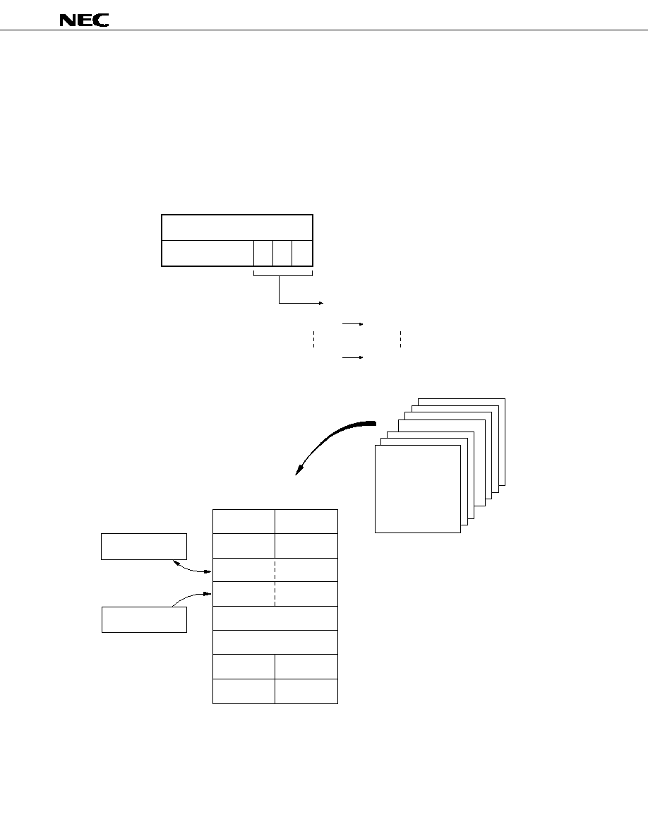
45
µ
PD78323, 78324
4.3.2
Context Switching Function by BRKCS Instruction
The context switching function can be started by executing BRKCS instruction.
The context switched register bank is specified by the lower 3-bit immediate data of the 2nd operation code of BRKCS
instruction. When BRKCS instruction is executed, the register bank specified by the 3-bit immediate data is selected, the
vector address prestored in the register bank is set and branched to the PC, and the PC and PSW contents are saved into
the register bank.
Return is by means of executing the RETCSB instruction.
Figure 4-4. Context Switching by Execution of BRKCS Instruction
OP CODE
OP CODE
N
2
N
1
N
0
000
111
RBANK0
RBANK7
Register Bank Specification
(BRKCS)
Register
Banks
(0 to 7)
RBANK n (n = 0 ≠ 7)
PC
PSW
Exchange
Save
A
B
R5
R7
D
H
X
C
R4
R6
E
L
VP
UP

46
µ
PD78323, 78324
5.
STANDBY FUNCTIONS
The
µ
PD78324 has the standby function to decrease the power consumption of the system. The following two modes
are available for execution of the standby function.
∑ HALT mode........ Mode for halting the CPU operation clock. The total power consumption of the
system can be decreased by intermittent operation in combination with the normal
operating mode.
∑ STOP mode....... Mode for stopping the whole system by stopping the oscillator. Considerably low
power consumption with leak current only can be set.
Each mode is set by the software. Figure 5-1 shows standby mode (STOP/HALT mode) transition.
Figure 5-1. Standby Status Transition
Normal
Status
STOP
HALT
RESET Release
HALT set
Unmasked
Interrupt
Generated
NMI
STOP Set
RESET Release

47
µ
PD78323, 78324
6.
EXTERNAL DEVICE EXPANSION FUNCTION
The
µ
PD78324 can expand external devices (data memory, program memory peripheral device) for areas (8000H to
FAFFH) except the internal ROM and RAM areas. Table 6-1 and 6-2 show the pin used for external device access and the
pin function setting procedure.
Table 6-1. Pin Function Setting (
µ
PD78324)
Memory Expansion
Mode Register
MM0 to MM2
MM7
Fetch Cycle
Control
Register
00H
00H
Except 00H
EA Pin
1
Remarks
0
1
0
1
Port mode
Expansion
mode
General port
Setting prohibited
AD0 to AD7
RD
WR
External device
connection mode
µ
PD71P301
connection mode
Set to A8 to
A15 in steps
General port
TAS
TMD
Pin Function
P40 to P47
P50 to P57
P90
P91
P92
P93
P50 to P57 pins according to the externally expanded memory size. The memory can be expanded in steps from 256
bytes to about 32K bytes. The pins which are not used as the address bus can be used as the general-purpose input/output
port.
Table 6-2. Port and Address Setting for Port 5 (
µ
PD78324)
P57
P56
P55
P54
P53
P52
P51
P50
External Address Space
Port
Port
Port
Port
Port
Port
Port
Port
256 bytes or less
Port
Port
Port
Port
A11
A10
A9
A8
4K bytes or less
Port
Port
A13
A12
A11
A10
A9
A8
16K bytes or less
A15
A14
A13
A12
A11
A10
A9
A8
About 32K bytes or less
Table 6-3. Pin Function Setting (
µ
PD78323)
AD0 to AD7
A8 to A15
RD
WR
Memory Expansion
Mode Register
MM7
Fetch Cycle
Control
Register
00H
Except 00H
EA Pin
ASTB
1
Remarks
≠≠
0
1
External device
connection mode
µ
PD71P301
connection mode
General port
TAS
TMD
Pin Function
AD0 to AD7
A8 to A15
RD
WR
P92
P93
µ
PD78324
emulation mode
TAS
TMD

48
µ
PD78323, 78324
7.
OPERATION AFTER RESET
If the RESET input pin is set to the low level, the system reset is applied and each hardware becomes as initialized status
(reset status). If RESET input becomes high level, program execution is started. Initialize the contents of various registers
in the program as required.
Change the number of cycles for the programmable wait register and the fetch cycle control register in particular.
The RESET input pin is equipped with an analog delay noise suppressor to prevent malfunctioning due to noise.
Cautions 1. While RESET is active(low level), all pins remain high impedance (except WDTO, AV
REF
, AV
DD
, AV
SS
,
V
DD
, V
SS
, X1 and X2).
2. If RAM has been expanded externally, mount a pull-up resistor to the P90/RD and P91/WR pins. It is
possible that the P90/RD and P91/WR pins become high impedance resulting in an external RAM
contents corruption or input unit damage. In addition, signals may collide on the address/data bus,
resulting in the destruction of the input/output circuit.
Figure 7-1. Reset Signal Acknowledge
For reset operation upon power-up, secure the oscillation stabilizing time of about 40 msec from power-up to reset
acknowledge as shown in Figure 7-2.
Figure 7-2. Reset Upon Power-Up
RESET Input
Analog
Delay
Removed
as Noise
Analog
Delay
Reset
Acknowl-
edged
Analog
Delay
Reset
Release
Oscillation
Stabilizing
Time
Analog
Delay
Reset
Release
V
DD
RESET
49
µ
PD78323, 78324
8.
INSTRUCTION SET
This chapter covers instruction operations.
For the operation codes and the number of instruction execution clock cycles, see
µ
PD78322 User's Manual (IEU-1248).
(1) Operand representation format and description method
In each instruction operand column, enter the operand using the description method for the instruction operand
representation format (refer to the assembler specification for details). If two or more factors are included in the description
method column, select one factor. The capital alphabetic letters and +, -, #, $, ! and [ ] symbols are keywords and should
be described as they are.
In case of immediate data, describe appropriate numeric values or labels. When describing labels, make sure to describe
#, $, ! and [ ] symbols.
Table 8-1. Operand Representation and Description Method
r
R0, R1, R2, R3, R4, R5, R6, R7, R8, R9, R10, R11, R12, R13, R14, R15
r1
R0, R1, R2, R3, R4, R5, R6, R7
r2
C, B
rp
RP0, RP1, RP2, RP3, RP4, RP5, RP6, RP7
rp1
RP0, RP1, RP2, RP3, RP4, RP5, RP6, RP7
rp2
DE, HL, VP, UP
sfr
Special function register code (see Table 2-2)
sfrp
Special function register code (16-bit operation enable register; see Table 2-2)
RP0, RP1, RP2, RP3, RP4, RP5/PSW, RP6, RP7
post
(Two or more instructions can be described. Only PUSH and POP instructions can be
described for RP5 and only PUSHU and POPU instructions can be described for PSW.)
[DE], [HL], [DE+], [HL+], [DE-], [HL-], [VP], [UP]
; Register indirect mode
[DE+A], [HL+A], [DE+B], [HL+B], [VP+DE], [VP+HL]
; Based indexed mode
[DE+byte], [HL+byte], [VP+byte], [UP+byte], [SP+byte] ; Based mode
word[A], word[B], word[DE], word[HL]
; Index mode
saddr
FE20H to FF1FH Immediate data or label
saddrp
FE20H to FF1EH Immediate data (bit0 = 0) or label (for 16-bit operation)
$addr16
0000H to FDFFH Immediate data or label; relative addressing
!addr16
0000H to FDFFH Immediate data or label; immediate addressing
(Up to FFFFH describable by MOV instruction)
addr11
800H to FFFH Immediate data or label
addr5
40H to 7EH Immediate data (bit0 = 0)
Note
or label
word
16-bit immediate data or label
byte
8-bit immediate data or label
bit
3-bit immediate data or label
n
3-bit immediate data (0 to 7)
Note Do not make work access to bit0 = 1 (odd address).
Remarks
1.
Although rp and rp1 have the same describable register names, they generate different codes.
2.
r, r1, rp, rp1 and post can be described with absolute names (R0 to R15, RP0 to RP7) as well as functional
names (X, A, C, B, E, D, L, H, AX, BC, DE, HL, VP, UP (refer to Table 2-1 for details of the relationships
between the absolute and functional names).
3.
Immediate addressing is enabled for all spaces. Relative addressing is only enabled from the first address
of the subsequent instruction to the range of ≠128 to +127.
mem
Representation
Format
Description Method
50
µ
PD78323, 78324
r1
byte
(saddr)
byte
sfr
byte
r
r1
A
r1
A
(saddr)
(saddr)
A
(saddr)
(saddr)
A
sfr
sfr
A
A
(mem)
(mem)
A
A
((saddrp))
((saddrp))
A
A
(addr16)
(addr16)
A
PSW
L
byte
PSW
H
byte
PSW
L
A
PSW
H
A
A
PSW
L
A
PSW
H
A
r1
r
r1
A
(mem)
A
(saddr)
A
sfr
A
((saddrp))
(saddr)
(saddr)
Mnemonic
r1, #byte
saddr, #byte
sfr
Note
, #byte
r, r1
A, r1
A, saddr
saddr, A
saddr, saddr
A, sfr
sfr, A
A, mem
mem, A
A, [saddrp]
[saddrp], A
A, !addr16
!addr16, A
PSWL, #byte
PSWH, #byte
PSWL, A
PSWH, A
A, PSWL
A, PSWH
A, r1
r, r1
A, mem
A, saddr
A, sfr
A, [saddrp]
saddr, saddr
2
3
3
2
1
2
2
3
2
2
1-4
1-4
2
2
4
4
3
3
2
2
2
2
1
2
2-4
2
3
2
3
Bytes
Operand
Operation
Flags
S
Z
AC P/V CY
MOV
XCH
◊
◊
◊
◊
◊
◊
◊
◊
◊
◊
Note
If STBC and WDM are described for sft, a different dedicated instruction having a different number of bytes
is used.
Remark For the symbols in the Flags column, refer to the table below.
Instruction
Group
8-bit data transfer
Symbol
Description
(Blank)
No change
0
Clear to 0.
1
Set to 1.
◊
Set/clear according to the result.
P
P/V flag operates as a parity flag
V
P/V flag operates as an overflow flag.
R
The previously stored value is restored.
51
µ
PD78323, 78324
AX, sfrp
sfrp, AX
rp1, !addr16
!addr16, rp1
AX, mem
mem, AX
AX, saddrp
AX, sfrp
saddrp, saddrp
rp,rp1
AX, mem
A, #byte
saddr, #byte
sfr, #byte
r, r1
A, saddr
A, sfr
saddr, saddr
A, mem
mem, A
A, #byte
saddr, #byte
sfr, #byte
r, r1
A, saddr
A, sfr
saddr, saddr
A, mem
mem, A
MOVW
XCHW
ADD
ADDC
Mnemonic
rp1, #word
saddrp, #word
sfrp, #word
rp, rp1
AX, saddrp
saddrp, AX
saddrp, saddrp
3
4
4
2
2
2
3
2
2
4
4
2-4
2-4
2
3
3
2
2-4
2
3
4
2
2
3
3
2-4
2-4
2
3
4
2
2
3
3
2-4
2-4
Bytes
Operation
Flags
S
Z
AC P/V CY
Operand
rp1
word
(saddrp)
word
sfrp
word
rp
rp1
AX
(saddrp)
(saddrp)
AX
(saddrp)
(saddrp)
AX
sfrp
sfrp
AX
rp1
(addr16)
(addr16)
rp1
AX
(mem)
(mem)
AX
AX
(saddrp)
AX
sfrp
(saddrp)
(saddrp)
rp
rp1
AX
(mem)
A, CY
A + byte
(saddr), CY
(saddr) + byte
sfr, CY
sfr + byte
r, CY
r + r1
A, CY
A + (saddr)
A, CY
A + sfr
(saddr), CY
(saddr) + (saddr)
A, CY
A + (mem)
(mem), CY
(mem) + A
A, CY
A + byte + CY
(saddr), CY
(saddr) + byte + CY
sfr, CY
sfr + byte + CY
r, CY
r + r1 + CY
A, CY
A + (saddr) + CY
A, CY
A + sfr + CY
(saddr), CY
(saddr) + (saddr) + CY
A, CY
A + (mem) + CY
(mem), CY
(mem) + A + CY
◊
◊
◊
V
◊
◊
◊
◊
V
◊
◊
◊
◊
V
◊
◊
◊
◊
V
◊
◊
◊
◊
V
◊
◊
◊
◊
V
◊
◊
◊
◊
V
◊
◊
◊
◊
V
◊
◊
◊
◊
V
◊
◊
◊
◊
V
◊
◊
◊
◊
V
◊
◊
◊
◊
V
◊
◊
◊
◊
V
◊
◊
◊
◊
V
◊
◊
◊
◊
V
◊
◊
◊
◊
V
◊
◊
◊
◊
V
◊
◊
◊
◊
V
◊
Instruction
Group
16-bit data transfer
8-bit opration

52
µ
PD78323, 78324
A, mem
mem, A
A, #byte
saddr, #byte
sfr, #byte
r, r1
A, saddr
A, sfr
saddr, saddr
A, mem
mem, A
A, #byte
saddr, #byte
sfr, #byte
r, r1
A, saddr
A, sfr
saddr, saddr
A, mem
mem, A
Mnemonic
A, #byte
saddr, #byte
sfr, #byte
r, r1
A, saddr
A, sfr
saddr, saddr
2
3
4
2
2
3
3
2-4
2-4
2
3
4
2
2
3
3
2-4
2-4
2
3
4
2
2
3
3
2-4
2-4
Bytes
Operation
Flags
S
Z
AC P/V CY
Operand
A, CY
A ≠ byte
(saddr), CY
(saddr) ≠ byte
sfr, CY
sfr ≠ byte
r, CY
r ≠ r1
A, CY
A ≠ (saddr)
A, CY
A ≠ sfr
(saddr), CY
(saddr) ≠ (saddr)
A, CY
A ≠ (mem)
(mem), CY
(mem) ≠ A
A, CY
A ≠ byte ≠ CY
(saddr), CY
(saddr) ≠ byte ≠ CY
sfr, CY
sfr ≠ byte ≠ CY
r, CY
r ≠ r1 ≠ CY
A, CY
A ≠ (saddr) ≠ CY
A, CY
A ≠ sfr ≠ CY
(saddr), CY
(saddr) ≠ (saddr) ≠ CY
A, CY
A ≠ (mem) ≠ CY
(mem), CY
(mem) ≠ A ≠ CY
A
A
byte
(saddr)
(saddr)
byte
sfr
sfr
byte
r
r
r1
A
A
(saddr)
A
A
sfr
(saddr)
(saddr)
(saddr)
A
A
(mem)
(mem)
(mem)
A
SUB
SUBC
AND
◊
◊
◊
V
◊
◊
◊
◊
V
◊
◊
◊
◊
V
◊
◊
◊
◊
V
◊
◊
◊
◊
V
◊
◊
◊
◊
V
◊
◊
◊
◊
V
◊
◊
◊
◊
V
◊
◊
◊
◊
V
◊
◊
◊
◊
V
◊
◊
◊
◊
V
◊
◊
◊
◊
V
◊
◊
◊
◊
V
◊
◊
◊
◊
V
◊
◊
◊
◊
V
◊
◊
◊
◊
V
◊
◊
◊
◊
V
◊
◊
◊
◊
V
◊
◊
◊
P
◊
◊
P
◊
◊
P
◊
◊
P
◊
◊
P
◊
◊
P
◊
◊
P
◊
◊
P
◊
◊
P
Instruction
Group
8-bit opration

53
µ
PD78323, 78324
Flags
A, mem
mem, A
A, #byte
saddr, #byte
sfr, #byte
r, r1
A, saddr
A, sfr
saddr, saddr
A, mem
mem, A
A, #byte
saddr, #byte
sfr, #byte
r, r1
A, saddr
A, sfr
saddr, saddr
A, mem
mem, A
Mnemonic
A, #byte
saddr, #byte
sfr, #byte
r, r1
A, saddr
A, sfr
saddr, saddr
2
3
4
2
2
3
3
2-4
2-4
2
3
4
2
2
3
3
2-4
2-4
2
3
4
2
2
3
3
2-4
2-4
Bytes
Operation
S
Z
AC P/V CY
Operand
A
A
byte
(saddr)
(saddr)
byte
sfr
sfr
byte
r
r
r1
A
A
(saddr)
A
A
sfr
(saddr)
(saddr)
(saddr)
A
A
(mem)
(mem)
(mem)
A
A
A
byte
(saddr)
(saddr)
byte
sfr
sfr
byte
r
r
r1
A
A
(saddr)
A
A
sfr
(saddr)
(saddr)
(saddr)
A
A
(mem)
(mem)
(mem)
A
A ≠ byte
(saddr) ≠ byte
sfr ≠ byte
r ≠ r1
A ≠ (saddr)
A ≠ sfr
(saddr) ≠ (saddr)
A ≠ (mem)
(mem) ≠ A
OR
XOR
CMP
◊
◊
P
◊
◊
P
◊
◊
P
◊
◊
P
◊
◊
P
◊
◊
P
◊
◊
P
◊
◊
P
◊
◊
P
◊
◊
P
◊
◊
P
◊
◊
P
◊
◊
P
◊
◊
P
◊
◊
P
◊
◊
P
◊
◊
P
◊
◊
P
◊
◊
◊
V
◊
◊
◊
◊
V
◊
◊
◊
◊
V
◊
◊
◊
◊
V
◊
◊
◊
◊
V
◊
◊
◊
◊
V
◊
◊
◊
◊
V
◊
◊
◊
◊
V
◊
◊
◊
◊
V
◊
Instruction
Group
8-bit opration

54
µ
PD78323, 78324
AX, #word
saddrp, #word
sfrp, #word
rp, rp1
AX, saddrp
AX, sfrp
saddrp, saddrp
AX, #word
saddrp, #word
sfrp, #word
rp, rp1
AX, saddrp
AX, sfrp
saddrp, saddrp
r1
r1
rp1
rp1
rp1
Mnemonic
AX, #word
saddrp, #word
sfrp, #word
rp, rp1
AX, saddrp
AX, sfrp
saddrp, saddrp
3
4
5
2
2
3
3
3
4
5
2
2
3
3
3
4
5
2
2
3
3
2
2
2
2
2
Bytes
Operation
Flags
S
Z
AC P/V CY
Operand
AX, CY
AX + word
(saddrp), CY
(saddrp) + word
sfrp, CY
sfrp + word
rp, CY
rp + rp1
AX, CY
AX + (saddrp)
AX, CY
AX + sfrp
(saddrp), CY
(saddrp) + (saddrp)
AX, CY
AX ≠ word
(saddrp), CY
(saddrp) ≠ word
sfrp, CY
sfrp ≠ word
rp, CY
rp ≠ rp1
AX, CY
AX ≠ (saddrp)
AX, CY
AX ≠ sfrp
(saddrp), CY
(saddrp) ≠ (saddrp)
AX ≠ word
(saddrp) ≠ word
sfrp ≠ word
rp ≠ rp1
AX ≠ (saddrp)
AX ≠ sfrp
(saddrp) ≠ (saddrp)
AX
A
◊
r1
AX(quotient), r1(remainder)
AX
˜
r1
AX(higher 16 bits), rp1(lower 16 bits)
AX
◊
rp1
AXDE(quotient), rp1(remainder)
AXDE
˜
rp1
AX(higher 16 bits), rp1(lower 16 bits)
AX
◊
rp1
◊
◊
◊
V
◊
◊
◊
◊
V
◊
◊
◊
◊
V
◊
◊
◊
◊
V
◊
◊
◊
◊
V
◊
◊
◊
◊
V
◊
◊
◊
◊
V
◊
◊
◊
◊
V
◊
◊
◊
◊
V
◊
◊
◊
◊
V
◊
◊
◊
◊
V
◊
◊
◊
◊
V
◊
◊
◊
◊
V
◊
◊
◊
◊
V
◊
◊
◊
◊
V
◊
◊
◊
◊
V
◊
◊
◊
◊
V
◊
◊
◊
◊
V
◊
◊
◊
◊
V
◊
◊
◊
◊
V
◊
◊
◊
◊
V
◊
16-bit opration
Instruction
Group
Signed
multiplication
Multiplication/division
ADDW
SUBW
CMPW
MULU
DIVUM
MULUW
DIVUX
MULW

55
µ
PD78323, 78324
r1
r1 + 1
(saddr)
(saddr) + 1
r1
r1 ≠ 1
(saddr)
(saddr) ≠ 1
rp2
rp2 + 1
(saddrp)
(saddrp) + 1
rp2
rp2 ≠ 1
(saddrp)
(saddrp) ≠ 1
(CY, r1
7
r1
0
, r1
m≠1
r
1m
)
◊
n times
(CY, r1
0
r1
7
, r1
m+1
r1
m
)
◊
n times
(CY
r1
0
, r1
7
CY, r1
m≠1
r1
m
)
◊
n times
(CY
r1
7
, r1
0
CY, r1
m+1
r1
m
)
◊
n times
(CY
r1
0
, r1
7
0, r1
m≠1
r1
m
)
◊
n times
(CY
r1
7
, r1
0
0, r1
m+1
r1
m
)
◊
n times
(CY
rp1
0
, rp1
15
0, rp1
m≠1
rp1
m
)
◊
n times
(CY
rp1
15
, rp1
0
0, rp1
m+1
rp1
m
)
◊
n times
A
3≠0
(rp1)
3≠0
,
(rp1)
7≠4
A
3≠0
,
(rp1)
3≠0
(rp1)
7≠4
A
3≠0
(rp1)
7≠4
,
(rp1)
3≠0
A
3≠0
,
(rp1)
7≠4
(rp1)
3≠0
Decimal Adjust Accumulator
When A
7
= 0, X
A, A
00H
When A
7
= 1, X
A, A
FFH
Flags
saddrp
r1, n
r1, n
r1, n
r1, n
r1, n
r1, n
rp1, n
rp1, n
[rp1]
[rp1]
Mnemonic
r1
saddr
r1
saddr
rp2
saddrp
rp2
1
2
1
2
1
3
1
3
2
2
2
2
2
2
2
2
2
2
2
1
Bytes
Operation
S
Z
AC P/V CY
Operand
◊
◊
◊
V
◊
◊
◊
V
◊
◊
◊
V
◊
◊
◊
V
P
◊
P
◊
P
◊
P
◊
◊
◊
0
P
◊
◊
◊
0
P
◊
◊
◊
0
P
◊
◊
◊
0
P
◊
◊
◊
◊
P
◊
INC
DEC
INCW
DECW
ROR
ROL
RORC
ROLC
SHR
SHL
SHRW
SHLW
ROR4
ROL4
ADJBA
ADJBS
CVTBW
Instruction
Group
Increase/decrease
Shift-rotate
BCD
calibration
Data
conversion

56
µ
PD78323, 78324
sfr. bit, CY
A. bit, CY
X. bit, CY
PSWH. bit, CY
PSWL. bit, CY
CY, saddr. bit
CY, /saddr. bit
CY, sfr. bit
CY, /sfr. bit
CY, A. bit
CY, /A. bit
CY, X. bit
CY, /X. bit
CY, PSWH. bit
CY, /PSWH. bit
CY, PSWL. bit
CY, /PSWL. bit
CY, saddr. bit
CY, /saddr. bit
CY, sfr. bit
CY, /sfr. bit
CY, A. bit
CY, /A. bit
CY, X. bit
CY, /X. bit
CY, PSWH. bit
CY, /PSWH. bit
CY, PSWL. bit
CY, /PSWL. bit
Mnemonic
CY, saddr. bit
CY, sfr. bit
CY, A. bit
CY, X. bit
CY, PSWH. bit
CY, PSWL. bit
saddr. bit, CY
3
3
2
2
2
2
3
3
2
2
2
2
3
3
3
3
2
2
2
2
2
2
2
2
3
3
3
3
2
2
2
2
2
2
2
2
Bytes
Operation
Flags
S
Z
AC P/V CY
Operand
CY
(saddr.bit)
CY
sfr.bit
CY
A.bit
CY
X.bit
CY
PSW
H
.bit
CY
PSW
L
.bit
(saddr.bit)
CY
sfr.bit
CY
A.bit
CY
X.bit
CY
PSW
H
.bit
CY
PSW
L
.bit
CY
CY
CY
(saddr.bit)
CY
CY
(saddr.bit)
CY
CY
sfr.bit
CY
CY
sfr.bit
CY
CY
A.bit
CY
CY
A.bit
CY
CY
X.bit
CY
CY
X.bit
CY
CY
PSW
H
.bit
CY
CY
PSW
H
.bit
CY
CY
PSW
L
.bit
CY
CY
PSW
L
.bit
CY
CY
(saddr.bit)
CY
CY
(saddr.bit)
CY
CY
sfr.bit
CY
CY
sfr.bit
CY
CY
A.bit
CY
CY
A.bit
CY
CY
X.bit
CY
CY
X.bit
CY
CY
PSW
H
.bit
CY
CY
PSW
H
.bit
CY
CY
PSW
L
.bit
CY
CY
PSW
L
.bit
◊
◊
◊
◊
◊
◊
◊
◊
◊
◊
◊
◊
◊
◊
◊
◊
◊
◊
◊
◊
◊
◊
◊
◊
◊
◊
◊
◊
◊
◊
MOV1
AND1
OR1
Instruction
Group
Bit manipulation

57
µ
PD78323, 78324
sfr. bit
A. bit
X. bit
PSWH. bit
PSWL. bit
saddr. bit
sfr. bit
A. bit
X. bit
PSWH. bit
PSWL. bit
saddr. bit
sfr. bit
A. bit
X. bit
PSWH. bit
PSWL. bit
CY
CY
CY
Mnemonic
CY, saddr. bit
CY, sfr. bit
CY, A. bit
CY, X. bit
CY, PSWH. bit
CY, PSWL. bit
saddr. bit
3
3
2
2
2
2
2
3
2
2
2
2
2
3
2
2
2
2
3
3
2
2
2
2
1
1
1
Bytes
Operation
Flags
S
Z
AC P/V CY
Operand
CY
CY
(saddr.bit)
CY
CY
sfr.bit
CY
CY
A.bit
CY
CY
X.bit
CY
CY
PSW
H
.bit
CY
CY
PSW
L
.bit
(saddr.bit)
1
sfr.bit
1
A.bit
1
X.bit
1
PSW
H
.bit
1
PSW
L
.bit
1
(saddr.bit)
0
sfr.bit
0
A.bit
0
X.bit
0
PSW
H
.bit
0
PSW
L
.bit
0
(saddr.bit)
(saddr.bit)
sfr.bit
sfr.bit
A.bit
A.bit
X.bit
X.bit
PSW
H
.bit
PSW
H
.bit
PSW
L
.bit
PSW
L
.bit
CY
1
CY
0
CY
CY
◊
◊
◊
◊
◊
◊
◊
◊
◊
◊
◊
◊
◊
◊
◊
◊
◊
◊
◊
◊
◊
1
0
◊
XOR1
SET1
CLR1
NOT1
SET1
CLR1
NOT1
Instruction
Group
Bit manipulation

58
µ
PD78323, 78324
Flags
Mnemonic
Bytes
Operation
S
Z
AC P/V CY
Operand
CALL
CALLF
CALLT
CALL
BRK
RET
RETB
RETI
PUSH
PUSHU
POP
POPU
MOVW
INCW
DECW
CHKL
CHKLA
(SP≠1)
(PC+3)
H
, (SP≠2)
(PC+3)
L
,
PC
addr16, SP
SP≠2
(SP≠1)
(PC+2)
H
, (SP≠2)
(PC+2)
L
,
PC
15≠11
00001, PC
10≠0
addr11,SP
SP≠2
(SP≠1)
(PC+1)
H
, (SP≠2)
(PC+1)
L
,
PC
H
(TPF, 00000000, addr5+1),
PC
L
(TPF, 00000000, addr5), SP
SP≠2
(SP≠1)
(PC+2)
H
, (SP≠2)
(PC+2)
L
,
PC
H
rp1
H
, PC
L
rp1
L
, SP
SP≠2
(SP≠1)
(PC+2)
H
, (SP≠2)
(PC+2)
L
,
PC
H
(rp1+1), PC
L
(rp1), SP
SP≠2
(SP≠1)
PSW
H
, (SP≠2)
PSW
L
(SP≠3)
(PC+1)
H
, (SP≠4)
(PC+1)
L
,
PC
L
(003EH), PC
H
(003FH), SP
SP≠4
IE
0
PC
L
(SP), PC
H
(SP+1), SP
SP+2
PC
L
(SP), PC
H
(SP+1)
PSW
L
(SP+2),
PSW
H
(SP+3)
SP
SP+4
PC
L
(SP), PC
H
(SP+1)
PSW
L
(SP+2),
PSW
H
(SP+3)
SP
SP+4
(SP≠1)
sfr
H
(SP≠2)
sfr
L
SP
SP≠2
{(SP≠1)
post
H
, (SP≠2)
post
L
,SP
SP≠2}
◊
n times
Note
(SP≠1)
PSW
H
, (SP≠2)
PSW
L
, SP
SP≠2
{(UP≠1)
post
H
, (UP≠2)
post
L
, UP
UP≠2}
◊
n times
Note
sfr
L
(SP)
sfr
H
(SP+1)
SP
SP+2
{post
L
(SP), post
H
(SP+1), SP
SP+2}
◊
n times
Note
PSW
L
(SP), PSW
H
(SP+1), SP
SP+2
{post
L
(UP), post
H
(UP+1), UP
UP+2}
◊
n times
Note
SP
word
SP
AX
AX
SP
SP
SP+1
SP
SP≠1
(pin level)
(signal level before output
buffer)
A
(pin level)
(signal level before output
buffer)
!addr16
!addr11
[addr5]
rp1
[rp1]
sfrp
post
PSW
post
sfrp
post
PSW
post
SP, #word
SP, AX
AX, SP
SP
SP
sfr
sfr
Note n indicates the number of registers described as post.
3
2
1
2
2
1
1
1
1
3
2
1
2
3
2
1
2
4
2
2
2
2
3
3
R
R
R
R
R
R
R
R
R
R
R
R
R
R
R
◊
◊
P
◊
◊
P
Instruction
Group
Stack manipulation
Call-return
Special

59
µ
PD78323, 78324
Mnemonic
!addr16
rp1
[rp1]
$ addr16
$ addr16
3
2
2
2
2
2
2
2
2
2
2
2
3
3
3
3
3
3
3
4
3
3
3
3
4
4
3
3
3
3
Bytes
Operation
Flags
S
Z
AC P/V CY
Operand
PC
addr16
PC
H
rp1
H
, PC
L
rp1
L
PC
H
(rp1+1), PC
L
(rp1)
PC
PC+2+jdisp8
PC
PC+2+jdisp8 if CY=1
PC
PC+2+jdisp8 if CY=0
PC
PC+2+jdisp8 if Z=1
PC
PC+2+jdisp8 if Z=0
PC
PC+2+jdisp8 if P/V=1
PC
PC+2+jdisp8 if P/V=0
PC
PC+2+jdisp8 if S=1
PC
PC+2+jdisp8 if S=0
PC
PC+3+jdisp8 if (P/V
S)
Z=0
PC
PC+3+jdisp8 if P/V
S=0
PC
PC+3+jdisp8 if P/V
S=1
PC
PC+3+jdisp8 if (P/V
S)
Z=1
PC
PC+3+jdisp8 if Z
CY=0
PC
PC+3+jdisp8 if Z
CY=1
PC
PC+3+jdisp8 if (saddr.bit)=1
PC
PC+4+jdisp8 if sfr.bit=1
PC
PC+3+jdisp8 if A.bit=1
PC
PC+3+jdisp8 if X.bit=1
PC
PC+3+jdisp8 if PSW
H
.bit=1
PC
PC+3+jdisp8 if PSW
L
.bit=1
PC
PC+4+jdisp8 if (saddr.bit)=0
PC
PC+4+jdisp8 if sfr.bit=0
PC
PC+3+jdisp8 if A.bit=0
PC
PC+3+jdisp8 if X.bit=0
PC
PC+3+jdisp8 if PSW
H
.bit=0
PC
PC+3+jdisp8 if PSW
L
.bit=0
BR
BC
BL
BNC
BNL
BZ
BE
BNZ
BNE
BV
BPE
BNV
BPO
BN
BP
BGT
BGE
BLT
BLE
BH
BNH
BT
BF
$ addr16
$ addr16
$ addr16
$ addr16
$ addr16
$ addr16
$ addr16
$ addr16
$ addr16
$ addr16
$ addr16
$ addr16
$ addr16
saddr. bit, $ addr16
sfr. bit, $ addr16
A. bit, $ addr16
X. bit, $ addr16
PSWH. bit, $ addr16
PSWL. bit, $ addr16
saddr. bit, $ addr16
sfr. bit, $ addr16
A. bit, $ addr16
X. bit, $ addr16
PSWH. bit, $ addr16
PSWL. bit, $ addr16
Instruction
Group
Unconditional
branch
Conditional branch
60
µ
PD78323, 78324
Mnemonic
Bytes
Operation
Flags
S
Z
AC P/V CY
Operand
PC
PC+4+jdisp8 if (saddr.bit)=1
then reset (saddr.bit)
PC
PC+4+jdisp8 if sfr.bit=1
then reset sfr.bit
PC
PC+3+jdisp8 if A.bit=1
then reset A.bit
PC
PC+3+jdisp8 if X.bit=1
then reset X.bit
PC
PC+3+jdisp8 if PSW
H
.bit=1
then reset PSW
H
.bit
PC
PC+3+jdisp8 if PSW
L
.bit=1
then reset PSW
L
.bit
PC
PC+4+jdisp8 if (saddr.bit)=0
then set (saddr.bit)
PC
PC+4+jdisp8 if sfr.bit=0
then set sfr.bit
PC
PC+3+jdisp8 if A.bit=0
then set A.bit
PC
PC+3+jdisp8 if X.bit=0
then set X.bit
PC
PC+3+jdisp8 if PSW
H
.bit=0
then set PSW
H
.bit
PC
PC+3+jdisp8 if PSW
L
.bit=0
then set PSW
L
.bit
r2
r2≠1,
then PC
PC+2+jdisp8 if r2
0
(saddr)
(saddr)≠1,
then PC
PC+3+jdisp8 if (saddr)
0
PC
H
R5, PC
L
R4, R7
PSW
H
,
R6
PSW
L
, RBS2≠0
n, RSS
0, IE
0
PC
H
R5, PC
L
R4, R5, R4
addr16,
PSW
H
R7, PSW
L
R6
PC
H
R5, PC
L
R4, R5, R4
addr16,
PSW
H
R7, PSW
L
R6
X.bit, $ addr16
PSWH.bit, $ addr16
PSWL.bit, $ addr16
saddr.bit, $ addr16
sfr.bit, $ addr16
A.bit, $ addr16
X.bit, $ addr16
PSWH.bit, $ addr16
PSWL.bit, $ addr16
r2, $ addr16
saddr, $ addr16
RBn
!addr16
!addr16
saddr.bit, $ addr16
sfr.bit, $ addr16
A.bit, $ addr16
BTCLR
BFSET
DBNZ
BRKCS
RETCS
RETCSB
4
4
3
3
3
3
4
4
3
3
3
3
2
3
2
3
4
R
R
R
R
R
R
R
R
R
R
◊
◊
◊
◊
◊
◊
◊
◊
◊
◊
Instruction
Group
Conditional branch
Context switching
61
µ
PD78323, 78324
Mnemonic
Bytes
Operation
Flags
S
Z
AC P/V CY
Operand
(DE + )
A, C
C≠1
End if C=0
(DE ≠ )
A, C
C≠1
End if C=0
(DE + )
(HL + ), C
C≠1
End if C=0
(DE ≠ )
(HL ≠ ), C
C≠1
End if C=0
(DE + )
A, C
C≠1
End if C=0
(DE ≠ )
A, C
C≠1
End if C=0
(DE + )
(HL + ), C
C≠1
End if C=0
(DE ≠ )
(HL ≠ ), C
C≠1
End if C=0
(DE + ) ≠ A, C
C≠1
End if C=0 or Z=0
(DE ≠ ) ≠ A, C
C≠1
End if C=0 or Z=0
(DE + ) ≠ (HL + ), C
C≠1
End if C=0 or Z=0
(DE ≠ ) ≠ (HL ≠ ), C
C≠1
End if C=0 or Z=0
(DE + ) ≠ A, C
C≠1
End if C=0 or Z=1
(DE ≠ ) ≠ A, C
C≠1
End if C=0 or Z=1
(DE + ) ≠ (HL + ), C
C≠1
End if C=0 or Z=1
(DE ≠ ) ≠ (HL ≠ ), C
C≠1
End if C=0 or Z=1
(DE + ) ≠ A, C
C≠1
End if C=0 or CY=0
(DE ≠ ) ≠ A, C
C≠1
End if C=0 or CY=0
[DE ≠ ], [HL ≠ ]
[DE + ], A
[DE ≠ ], A
[DE + ], [HL + ]
[DE ≠ ], [HL ≠ ]
[DE + ], A
[DE ≠ ], A
[DE + ], [HL + ]
[DE ≠ ], [HL ≠ ]
[DE + ], A
[DE ≠ ], A
[DE + ], [HL + ]
[DE ≠ ], [HL ≠ ]
[DE + ], A
[DE ≠ ], A
[DE + ], A
[DE ≠ ], A
[DE + ], [HL + ]
2
2
2
2
2
2
2
2
2
2
2
2
2
2
2
2
2
2
MOVM
MOVBK
XCHM
XCHBK
CMPME
CMPBKE
CMPMNE
CMPBKNE
CMPMC
◊
◊
◊
V
◊
◊
◊
◊
V
◊
◊
◊
◊
V
◊
◊
◊
◊
V
◊
◊
◊
◊
V
◊
◊
◊
◊
V
◊
◊
◊
◊
V
◊
◊
◊
◊
V
◊
◊
◊
◊
V
◊
◊
◊
◊
V
◊
Instruction
Group
String
62
µ
PD78323, 78324
Mnemonic
Bytes
Operation
Flags
S
Z
AC P/V CY
Operand
(DE + ) ≠ (HL + ), C
C≠1
End if C=0 or CY=0
(DE ≠ ) ≠ (HL ≠ ), C
C≠1
End if C=0 or CY=0
(DE + ) ≠ A, C
C≠1
End if C=0 or CY=1
(DE ≠ ) ≠ A, C
C≠1
End if C=0 or CY=1
(DE + ) ≠ (HL + ), C
C≠1
End if C=0 or CY=1
(DE ≠ ) ≠ (HL ≠ ), C
C≠1
End if C=0 or CY=1
STBC
byte
Note
WDM
byte
Note
RSS
RSS
RBS2 ≠ 0
n, RSS
0
RBS2 ≠ 0
n, RSS
1
No Operation
IE
1 (Enable Interrupt)
IE
0 (Disable Interrupt)
[DE ≠ ], A
[DE + ], [HL + ]
[DE ≠ ], [HL ≠ ]
STBC, #byte
WDM, #byte
RBn
RBn, ALT
[DE + ], [HL + ]
[DE ≠ ], [HL ≠ ]
[DE + ], A
2
2
2
2
2
2
4
4
1
2
2
1
1
1
CMPBKC
CMPMNC
CMPBKNC
MOV
SWRS
SEL
NOP
EI
DI
◊
◊
◊
V
◊
◊
◊
◊
V
◊
◊
◊
◊
V
◊
◊
◊
◊
V
◊
◊
◊
◊
V
◊
◊
◊
◊
V
◊
Note
If the operation code of STBC register and WDM register operation instructions is abnormal, an operation code
trap interrupt is generated.
Operation in the eent of trap:
(SP≠1)
PSW
H
, (SP≠2)
PSW
L
,
(SP≠3)
(PC≠4)
H
, (SP≠4)
(PC≠4)
L
,
PC
L
(003CH), PC
H
(003DH),
SP
SP≠4, IE
0
Instruction
Group
String
CPU control
63
µ
PD78323, 78324
9.
ELECTRICAL SPECIFICATIONS
ABSOLUTE MAXIMUM RATINGS (T
A
= 25
∞
C)
I
OL
I
OH
V
IAN
V
V
AV
REF
AV
DD
>
V
DD
V
DD
AV
DD
AV
DD
>
V
DD
V
DD
AV
DD
Notes 1. Except the pin described in Note 2.
2. P70/ANI0 to P77/ANI7 pins
Caution If the absoute maximum rating of any one of the parameters is exceeded even momentarily, the quality
of the product may be degraded. In other words, the product may be physically damaged if any of the
absolute maximum raings is exceeded. Be sure to use the product without exceeding these rarings.
RECOMMENDED OPERATING CONDITION
Oscillation frequency
T
A
V
DD
8 MHz
f
XX
16 MHz
≠10 to +70
∞
C
+5.0 V
±
10 %
CAPACITANCE (T
A
= 25
∞
C, V
SS
= V
DD
= 0 V)
Parameter
Symbol
Test Conditions
Rating
Unit
V
DD
≠0.5 to + 7.0
V
AV
DD
≠0.5 to V
DD
+ 0.5
V
AV
SS
≠0.5 to + 0.5
V
V
I
Note 1
≠0.5 to V
DD
+ 0.5
V
V
O
≠0.5 to V
DD
+ 0.5
V
All output pins
4.0
mA
All output pins total
90
mA
All output pins
≠1.0
mA
All output pins total
≠20
mA
≠0.5 to V
DD
+ 0.5
≠0.5 to AV
DD
+ 0.5
≠0.5 to V
DD
+ 0.3
≠0.5 to AV
DD
+ 0.3
T
A
≠10 to + 70
∞
C
T
stg
≠65 to + 150
∞
C
Note 2
Supply voltage voltage
Input voltage
Output voltage
Output current low
Output current high
Analog input voltage
A/D converter reference
input voltage
Operating ambient temperature
Storage temperature
TYP.
MAX.
10
20
20
Unit
pF
pF
pF
MIN.
Parameter
Input capacitance
Output capacitance
I/O capacitance
Test Conditions
Symbol
C
I
C
O
C
IO
f=1 MHz
Unmeasured pins returned to 0 V.

64
µ
PD78323, 78324
OSCILLATOR CHARACTERISTICS (T
A
= ≠10 to +70
∞
C, V
DD
= +5 V
±
10 %, V
SS
= 0 V)
Parameter
Oscillation frequency (f
XX
)
X1 input frequency (f
X
)
X1 input rise/fall time (t
XR
, t
XF
)
X1 input high/low level width
(t
WXH
, t
WXL
)
MIN.
8
8
0
25
Unit
MHz
MHz
ns
ns
MAX.
16
16
20
80
Recommended Circuit
or
X1
X2
HCMOS
Invertor
Resonator
Ceramic resonator
or
crystal resonator
External clock
X1
X2
HCMOS
Invertor
Open
X1
X2
C1
C2
V
SS
Caution
When using the system clock oscillation circuit, wire the part encircled in the dotted line in the following
manner to avoid the influence of the wiring capacity, etc.
∑ Make the wiring as short as possible.
∑ Avoid intersecting other signal conductors. Avoid approaching lines in which very high fluctuating
currents run.
∑ Make sure that the grounding point of the oscillation circuit capacitor always has the same electrical
potential as V
SS
. Avoid grounding with a grand pattern in which very high currents run.
∑ Do not fetch signals from the oscillation circuit.
65
µ
PD78323, 78324
RECOMMENDED OSCILLATOR CONSTANT
CERAMIC RESONATOR
Manufacturer
Product Name
Frequency
[MHz]
C1 [pF]
C2 [pF]
CSA8.00MT
CSA12.0MT
CSA14.74MXZ040
CSA16.00MXZ040
8.0
12.0
14.74
16.0
30
30
15
15
CST8.00MTW
CST12.0MTW
CST14.74MXW0C3
CST16.00MXW0C3
8.0
12.0
17.74
16.0
On-chip
On-chip
Murata Mfg.
Co., Ltd.
CRYSTAL RESONATOR
Manufacturer
Product Name
Frequency
[MHz]
C1 [pF]
C2 [pF]
HC49/U-S
HC49/U
10
10
Kinseki Co., Ltd.
8 to 16
Recommended Constant
Recommended Constant
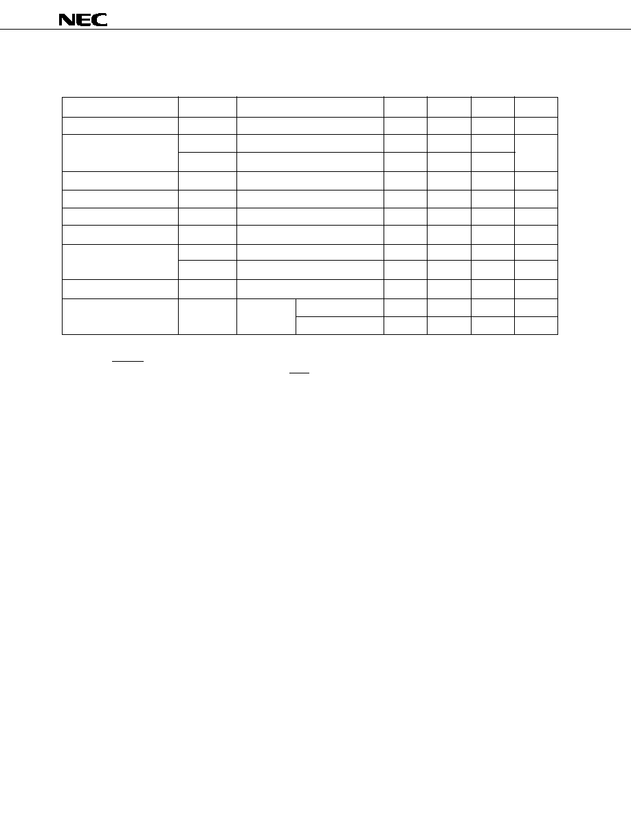
66
µ
PD78323, 78324
DC CHARACTERISTICS (T
A
= ≠10 to +70
∞
C, V
DD
= +5 V
±
10 %, V
SS
= 0 V)
Parameter
Symbol
Test Conditions
MIN.
TYP.
MAX.
Unit
V
IL
0
0.8
V
V
IH1
Note 1
2.2
V
IH2
Note 2
0.8V
DD
V
OL
I
OL
= 2.0 mA
0.45
V
V
OH
I
OH
= ≠400
µ
A
V
DD
≠ 1.0
V
I
LI
0 V
V
I
V
DD
±
10
µ
A
I
LO
0 V
V
O
V
DD
±
10
µ
A
I
DD1
Operating mode
40
75
mA
I
DD2
HALT mode
20
45
mA
V
DDDR
STOP mode
2.5
V
V
DDDR
= 2.5 V
2
10
µ
A
V
DDDR
= 5.0 V
±
10 %
10
50
µ
A
Input voltage low
Output voltage low
Output voltage high
Input leakage current
V
Output leakage current
V
DD
supply current
Data retention voltage
Data retention current
STOP mode
I
DDDR
Input voltage high
Notes 1. Except the pin descried in Note 2.
2. RESET, X1, X2, P20/NMI, P21/INTP0, P22/INTP1, P23/INTP2,P24/INTP3, P25/INTP4, P26/INTP5, P27/
INTP6/TI, P32/SO/SB0, P33/SI/SB1, P34/SCK pins.

67
µ
PD78323, 78324
AC CHARACTERISTICS (T
A
= ≠10 to +70
∞
C, V
DD
= +5 V
±
10 %, V
SS
= 0 V)
Non-consecutive read/write operation (with general-purpose memory connected)
Parameter
Symbol
Test Conditions
MIN.
MAX.
Unit
System clock cycle time
t
CYK
125
250
ns
Address setup time (vs. ASTB
)
t
SAST
32
ns
Address hold time (vs. ASTB
)
t
HSTA
32
ns
RD
delay time from address
t
DAR
85
ns
Address float time from RD
t
FRA
10
ns
Data input time from address
t
DAID
222
ns
Data input time from RD
t
DRID
112
ns
RD
delay time from ASTB
t
DSTR
42
ns
Data hold time (vs. RD
)
t
HRID
0
ns
Address active time from RD
t
DRA
50
ns
RD low-level width
t
WRL
147
ns
ASTB high-level width
t
WSTH
37
ns
WR
delay time from address
t
DAW
85
ns
Data output time from ASTB
t
DSTOD
102
ns
Data output time from WR
t
DWOD
40
ns
WR
delay time from ASTB
t
DSTW
42
ns
Data setup time (vs. WR
)
t
SODW
147
ns
Data hold time (vs. WR
)
t
HWOD
32
ns
ASTB
delay time from WR
t
DWST
42
ns
WR low-level width
t
WWL
147
ns
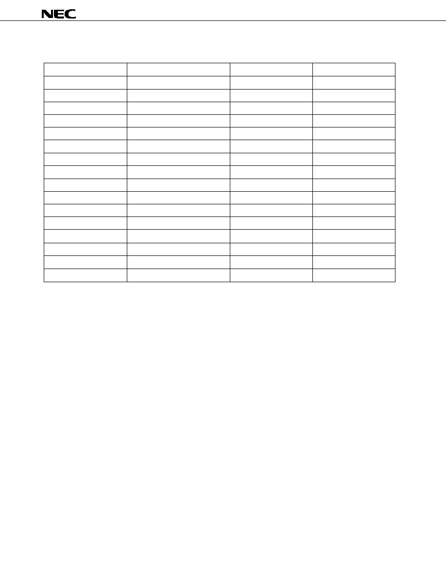
68
µ
PD78323, 78324
t
CYK
Dependent Bus Timing Definition
Parameter
Expression
MIN./MAX.
Unit
t
SAST
0.5T ≠ 30
MIN.
ns
t
HSTA
0.5T ≠ 30
MIN.
ns
t
DAR
T ≠ 40
MIN.
ns
t
DAID
(2.5 + n) T ≠ 90
MAX.
ns
t
DRID
(1.5 + n) T ≠ 75
MAX.
ns
t
DSTR
0.5T ≠ 20
MIN.
ns
t
DRA
0.5T ≠ 12
MIN.
ns
t
WRL
(1.5 + n) T ≠ 40
MIN.
ns
t
WSTH
0.5T ≠ 25
MIN.
ns
t
DAW
T ≠ 40
MIN.
ns
t
DSTOD
0.5T + 40
MAX.
ns
t
DSTW
0.5T ≠ 20
MIN.
ns
t
SODW
1.5T ≠ 40
MIN.
ns
t
HWOD
0.5T ≠ 30
MIN.
ns
t
DWST
0.5T ≠ 20
MIN.
ns
t
WWL
(1.5 + n) T ≠ 40
MIN.
ns
Remarks
1.
T = t
CYK
= 1/f
CLK
(f
CLK
is internal system clock frequency)
2.
n indicates the number of wait cycles defined by user software.
3.
Depends on t
CYK
for the bus timing shown in this table only.
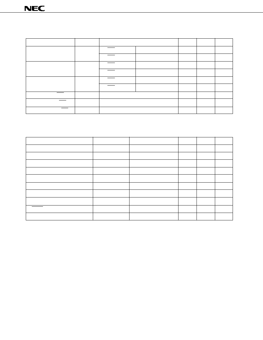
69
µ
PD78323, 78324
SERIAL OPERATION (T
A
= ≠10 to +70
∞
C, V
DD
= +5 V
±
10 %, V
SS
= 0 V)
Parameter
Symbol
Test Conditions
MIN.
MAX.
Unit
SCK output
Internal division by 8
1
µ
s
SCK input
External clock
1
µ
s
SCK output
Internal division by 8
420
ns
SCK input
External clock
420
ns
SCK output
Internal division by 8
420
ns
SCK input
External clock
420
ns
SI setup time (to SCK
)
t
SRXSK
80
ns
SI hold time (from SCK
)
t
HSKRX
80
ns
SO delay time from SCK
t
DSKTX
R = 1 k
, C = 100 pF
210
ns
Serial clock cycle time
Serial clock low-level width
Serial clock high-level width
t
CYSK
t
WSKL
t
WSKH
Parameter
Symbol
Test Conditions
MIN.
MAX.
Unit
NMI high/low-level width
t
WNIH
, t
WNIL
5
µ
s
INTP0 high/low-level width
t
WI0H
, t
WI0L
8T
t
CYK
INTP1 high/low-level width
t
WI1H
, t
WI1L
8T
t
CYK
INTP2 high/low-evel width
t
WI2H
, t
WI2L
8T
t
CYK
NTP3 high/low-level width
t
WI3H
, t
WI3L
8T
t
CYK
NTP4 high/low-level width
t
WI4H
, t
WI4L
8T
t
CYK
INTP5 high/low-level width
t
WI5H
, t
WI5L
8T
t
CYK
INTP6 high/low-level width
t
WI6H
, t
WI6L
8T
t
CYK
RESET high/low-level width
t
WRSH
, t
WRSL
5
µ
s
TI high/low-level width
t
WTIH
, t
WTIL
In TM1 event counter mode
8T
t
CYK
OTHER OPERATION (T
A
= ≠10 to +70
∞
C, V
DD
= +5 V
±
10 %, V
SS
= 0 V)

70
µ
PD78323, 78324
A/D CONVERTER CHARACTERISTICS(T
A
= ≠10 to +70
∞
C, V
DD
= +5 V
±
10 %, V
SS
= AV
SS
= 0 V,
V
DD
≠ 0.5 V
AV
DD
V
DD
)
Parameter
Symbol
Test Conditions
MIN.
TYP.
MAX.
Unit
Resolution
10
bit
Total error
Note 1
4.5 V
AV
REF
AV
DD
±
0.4 %
%FSR
3.4 V
AV
REF
AV
DD
±
0.7
%FSR
Quantization error
±
1/2
LSB
Conversion time
t
CONV
144
t
CYK
Sampling time
t
SAMP
24
t
CYK
Zero scale error
Note 1
4.5 V
AV
REF
AV
DD
±
1.5
±
2.5
LSB
3.4 V
AV
REF
AV
DD
±
1.5
±
4.5
LSB
Full scale error
Note 1
4.5 V
AV
REF
AV
DD
±
1.5
±
2.5
LSB
3.4 V
AV
REF
AV
DD
±
1.5
±
4.5
LSB
Non-linear error
Note 1
4.5 V
AV
REF
AV
DD
±
1.5
±
2.5
LSB
3.4 V
AV
REF
AV
DD
±
1.5
±
4.5
LSB
Analog input voltage
Note 2
V
IAN
≠0.3
AV
DD
V
Reference voltage
AV
REF
3.4
AV
DD
V
AV
REF
current
AI
REF
1.0
3.0
mA
AV
DD
supply current
AI
DD
2.0
6.0
mA
A/D converter data
AV
DDR
= 2.5 V
2.0
10
µ
A
retention current
AV
DDR
= 5 V
±
10 %
10
50
µ
A
STOP mode
AI
DDR
Notes
1. Quantization error excluded.
2. When ≠0.3 V
V
IAN
0 V, the conversion result becomes 000H.
When 0 V < V
IAN
< AV
REF
, the conversion is performed at a resolution of 10 bits.
When AV
REF
V
IAN
AV
DD
, the conversion result is 3FFH.

71
µ
PD78323, 78324
Non-Consecutive Read Operation
Non-Consecutive Write Operation
Higher Address
Higher Address
(CLK)
P50-P57
(Output)
P40-P47
(Input/
Output)
ASTB
(Output)
WR (Output)
Lower Address
(Output)
Undefined
Data (Output)
Lower Address
(Output)
t
WSTH
t
SAST
t
HWOD
t
HSTA
t
DSTOD
t
DWST
t
DSTW
t
DAW
t
DWOD
t
SODW
t
WWL
t
SAST
t
DAID
t
WSTH
t
DSTR
t
HSTA
t
HRID
t
DAR
t
DRID
t
WRL
t
FRA
t
CYK
Hi-Z
Hi-Z
Hi-Z
Hi-Z
t
DRA
Higher Address
Higher Address
Data (Input)
Lower Address
(Output)
Lower Address
(Output)
(CLK)
P50-P57
(Output)
P40-P47
(Input/
Output)
ASTB
(Output)
RD (Output)
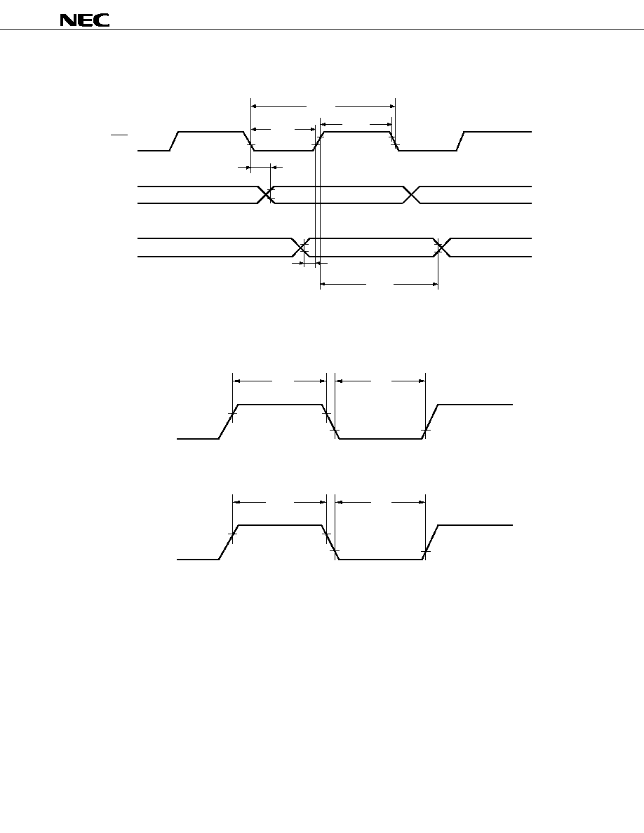
72
µ
PD78323, 78324
Serial Operation
Interrupt Input Timing
t
WSKL
t
CYSK
t
WSKH
t
DSKTX
t
SRXSK
t
HSKRX
SCK
SO
SI
0.8V
DD
0.8V
t
WNIH
t
WNIL
t
WInH
t
WInL
NMI
INTPn
Remarks
n = 0 to 6

73
µ
PD78323, 78324
Reset Input Timing
TI Pin Input Timing
t
WRSH
t
WRSL
0.8V
DD
0.8V
RESET
t
WTIH
t
WTIL
TI
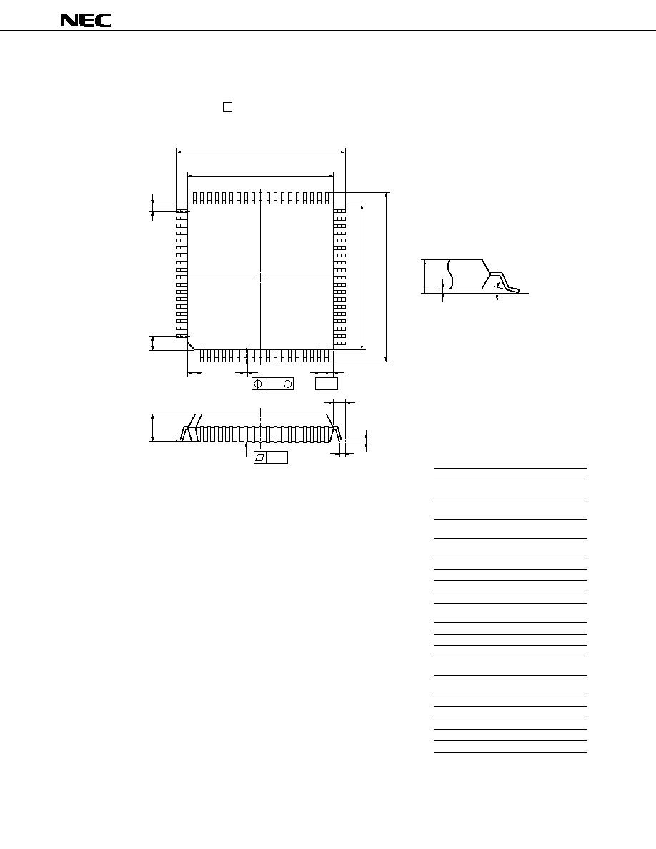
74
µ
PD78323, 78324
10. PACKAGE DRAWINGS
74 PIN PLASTIC QFP ( 20)
ITEM
MILLIMETERS
INCHES
F
1
F
2
I
2.0
1.0
0.20
Q
0.079
0.039
0.008
S74GJ-100-5BJ-3
NOTE
Each lead centerline is located within 0.20 mm (0.008 inch) of
its true position (T.P.) at maximum material condition.
C
20.0±0.2
0.787
M
0.15
0.006
0.1±0.1
0.004±0.004
+0.004
≠0.003
+0.009
≠0.008
A
23.2±0.4
0.913
H
0.40±0.10
0.016+0.004
≠0.005
L
0.8±0.2
0.031+0.009
≠0.008
N
0.10
0.004
P
3.7
0.146
S
4.0 MAX.
0.158 MAX.
+0.10
≠0.05
B
20.0±0.2
0.787+0.009
≠0.008
+0.017
≠0.016
J
1.0 (T.P.)
0.039 (T.P.)
R
5
∞
±5
∞
5
∞
±5
∞
D
23.2±0.4
0.913+0.017
≠0.016
G
1
G
2
2.0
1.0
0.079
0.039
K
1.6±0.2
0.063±0.008
A
B
G
1
H
I
J
C
D
P
N
K
L
M
detail of lead end
M
56
57
37
74
1
19
18
38
F
2
F
1
G
2
S
Q
R

75
µ
PD78323, 78324
P68L-50A1-2
ITEM
MILLIMETERS
INCHES
NOTE
Each lead centerline is located within 0.12
mm (0.005 inch) of its true position (T.P.) at
maximum material condition.
+0.007
≠0.006
A
B
C
D
E
F
G
H
I
J
K
M
N
P
Q
T
U
25.2±0.2
24.20
24.20
25.2±0.2
1.94±0.15
0.6
4.4±0.2
2.8±0.2
0.9 MIN.
3.4
1.27 (T.P.)
0.40±1.0
0.12
23.12±0.20
0.15
R 0.8
0.20
+0.10
≠0.05
0.992±0.008
0.953
0.953
0.992±0.008
0.076
0.024
0.173
0.110
0.035 MIN.
0.134
0.050 (T.P.)
0.016
0.005
0.910
0.006
R 0.031
0.008
+0.009
≠0.008
+0.009
≠0.008
+0.004
≠0.005
+0.004
≠0.002
+0.009
≠0.008
N
K
M
Q
A
U
68
B
D
C
1
F
E
T
P
M
G
H
IJ
68 PIN PLASTIC QFJ ( 950 mil)

76
µ
PD78323, 78324
11. RECOMMENDED SOLDERING CONDITIONS
The
µ
PD78323 and 78324 should be soldered and mounted under the conditions recommended in the table below.
For detail of recommended soldering conditions, refer to the information document Semiconductor Device Mount-
ing Technology Manual (IE1-1207).
For soldering methods and conditions other than those recommended below, contact our salesman.
Table 11-1. Soldering Conditions for Surface Mount Type
µ
PD78323GJ-5BJ
: 74-pin plastic QFP (20
◊
20 mm)
µ
PD78324GJ-
◊◊◊
-5BJ : 74-pin plastic QFP (20
◊
20 mm)
Soldering Method
Soldering Conditions
Package peak temperature: 230
∞
C, Time: 30 sec. max. (at 210
∞
C or above)
Infrared reflow
Number of times: Once, Time limit: 7 days
Note
(thereafter 10 hours prebaking
required at 125
∞
C)
Package peak temperature: 215
∞
C, Time: 40 sec. max. (at 200
∞
C or above)
VPS
Number of times: Once, Time limit: 7 days
Note
(thereafter 10 hours prebaking
required at 125
∞
C)
Pin temperature: 300
∞
C max, Time: 3 sec. max. (Per side of the device)
Recommended
Condition Symbol
Soldering Method
Soldering Conditions
Package peak temperature: 235
∞
C, Time: 30 sec. max. (at 210
∞
C or above)
Number of times: twice or less, Time limit: 7 days
Note
(thereafter 36 hours
prebaking required at 125 ∞C)
<Caution>
(1)
The second reflow should be started after the temperature of the device
which would have been changed by the first reflow has returned to normal.
(2)
Please avoid flux water washing after the first reflow.
Package peak temperature: 215
∞
C, Time: 40 sec. max. (at 200
∞
C or above),
Number of times: twice or less, Time limit: 7 days
Note
(thereafter 36 hours
prebaking required at 125 ∞C)
<Caution>
(1)
The second reflow should be started after the temperature of the device
which would have been changed by the first reflow has returned to normal.
(2)
Please avoid flux water washing after the first reflow.
Pin temperature: 300
∞
C max., Time: 3 sec. max. (Per side of the device))
Recommended
Condition Symbol
Infrared reflow
IR30-367-2
VP15-367-2
µ
PD78323LP
: 68-pin plastic QFJ (
950 mil)
µ
PD78324LP-
◊◊◊
: 68-pin plastic QFJ (
950 mil)
Pin part heating
IR30-107-1
VP15-107-1
VPS
Note For the storage period after dry-pack decompression, storage conditions are max. 25
∞
C, 65 % RH.
Caution Use more than one soldering method should be avoided (except in the case of pin part heating).
Pin part heating

77
µ
PD78323, 78324
µ
PD78324
µ
PD78323
µ
PD78322
µ
PD78320
µ
PD78312A
µ
PD78310A
111
96
250 ns (at 16 MHz operation)
500 ns (at 12 MHz operation)
32768
◊
8 bits
≠≠
16384
◊
8 bits
≠≠
8192
◊
8 bits
≠≠
1024
◊
8 bits
640
◊
8 bits
256
◊
8 bits
64K bytes
16 (including 8 analog inputs)
12 (including 4 analog inputs)
≠≠
1
39
21
39
21
40
24
Real-time pulse unit
Multi-function pulse I/O unit
∑ 18/16-bit free running timer
◊
1
∑ 16-bit presettable up-/down-counter
∑ 16-bit timer/event counter
◊
1
◊
2
∑ 16-bit compare register
◊
6
∑ 16-bit free running counter capture
∑ 18-bit capture register
◊
4
function
◊
2
∑ 18-bit capture/compare register
◊
2
∑ 16-bit interval timer
◊
2
∑ Real-time output port
◊
8
∑ High-precision PWM output
◊
2
∑ Real-time output port : 4 bits
◊
2
Count unit mode 4 (4-multiplication
mode) function available
Counter start function by interval timer
external trigger available
∑ Dedicated on-chip baud rate generator
∑ 8 bits (full-duplex transmission/
∑ UART
...1 channel
reception)
∑ SBI
∑ Dedicated on-chip baud rate generator
∑ 3-wire serial I/O
∑ 2 transfer modes (asynchronous mode,
I/O interface mode)
Eight 10-bit resolution inputs
Four 8-bit resolution inputs
∑ 8 external, 14 internal (shared with external 2)
∑ 4 external, 13 internal
∑ 3-level programmable priority order
∑ 8-level programmable priority order
∑ 3 processing methods (vectored interrupt, context switching and macro service functions)
...1 channel
Internal memory
APPENDIX A. LIST OF 78K/III SERIES PRODUCTS (1/2)
Basic instruction
Minimum instruction execution time
ROM
RAM
Memory space
Input
I/O lines
Output
I/O
Pulse unit
Serial communication interface
A/D converter
Interrupt
Real-time pulse unit
∑ 18/16-bit free running timer
◊
1
∑ 16-bit timer/event counter
◊
1
∑ 16-bit compare register
◊
6
∑ 18-bit capture register
◊
4
∑ 18-bit capture/compare register
◊
2
∑ Real-time output port
◊
8

78
µ
PD78323, 78324
Instruction set
Others
Package
Instructions for
µ
PD78312 and 78310 significantly increased.
LIST OF 78K/III SERIES PRODUCTS (2/2)
Test source
--
µ
PD78324
µ
PD78323
µ
PD78322
µ
PD78320
µ
PD78312A
µ
PD78310A
Internal : 1
Following instructions added for
µ
PD78312 and 78310
∑ MOVW rp1, !addr16 instruction
∑ MOVW !addr16, rp1 instruction
∑ On-chip watchdog timer
∑ Standby function (STOP/HALT)
∑ 20-bit time base counter
∑ Pseudo static RAM refresh function
∑ 64-pin plastic shurink DIP (750 mil)
∑ 68-pin plastic QFJ (
950 mil)
∑ 64-pin plastic QFP (14
◊
20 mm)
∑ 74-pin plastic QFP (20
◊
20 mm)
∑ 64-pin plastic QUIP
∑ 68-pin plastic QFJ (
950 mil)
∑ 68-pin plastic QFJ (
950 mil)
∑ 74-pin plastic QFP (20
◊
20 mm)
∑ 80-pin plastic QFP (14
◊
20 mm)

79
µ
PD78323, 78324
APPENDIX B. TOOLS
B.1
DEVELOPMENT TOOLS
The following development tools are available for system development using the
µ
PD78324.
Language Processor
78K/III series relocatable assembler
(RA78K/III)
78K/III series C compiler (CC78K/III)
Refers to the relocatable assembler which can be used commonly for the 78K/III
series. Equipped with the macro function, the relocatable assembler is aimed at
improved development efficiency.
The assembler is also accompanied by the structured assembler which can describe
the program control structure explicitly, thus making it possible to improve the
productivity and the maintainability of the program.
Host machine
PC-9800 series
IBM PC/AT
TM
and
its compatible
machine
HP9000 series
700
TM
SPARCstation
TM
NEWS
TM
Supply medium
3.5-inch 2HD
5-inch 2HD
3.5-inch 2HC
5-inch 2HC
DAT
Cartridge tape
(QIC-24)
Part number
µ
S5A13RA78K3
µ
S5A10RA78K3
µ
S7B13RA78K3
µ
S7B10RA78K3
µ
S3P16RA78K3
µ
S3K15RA78K3
µ
S3R15RA78K3
OS
MS-DOS
TM
PC DOS
TM
HP-UX
TM
SunOS
TM
NEWS-OS
TM
Part number
µ
S5A13CC78K3
µ
S5A10CC78K3
µ
S7B13CC78K3
µ
S7B10CC78K3
µ
S3P16CC78K3
µ
S3K15CC78K3
µ
S3R15CC78K3
Host machine
PC-9800 series
IBM PC/AT and its
compatible machine
HP9000 series 700
SPARCstation
NEWS
Supply medium
3.5-inch 2HD
5-inch 2HD
3.5-inch 2HC
5-inch 2HC
DAT
Cartridge tape
(QIC-24)
OS
MS-DOS
PC DOS
HP-UX
SunOS
NEWS-OS
Refers to the C compiler which can be commonly used in the 78K/III series. This
compiler is a program converting the programs written in the C language to those
object codes which are executable by microcontrollers. When using this compiler, the
78K/III series relocatable assembler (RA78K/III) is required.
Remark
Relocatable assembler and C compiler operations are assured only on the host machine and the OS
above.

80
µ
PD78323, 78324
PROM Writing Tools
This PROM programmer allows programming, in standalone mode or via operation from a
host computer, of a singlechip microcontroller with on-chip PROM by connection of the
board provided and a separately available programmer adapter.
It can program typical 256K-bit to 4M-bit PROMs.
PROM programmer made by Data I/O Japan Corporation.
PROM programmer adapters for writing programs to the
µ
PD78P324 with a general PROM
programmer such as the PG-1500.
PA-78P324GJ ... For
µ
PD78P324GJ
PA-78P324KC ... For
µ
PD78P324KC
PA-78P324KD ... For
µ
PD78P324KD
PA-78P324LP ... For
µ
PD78P324LP
Ordering Code
(Product Name)
Supply Medium
OS
Host Machine
Connects PG-1500 and host machine via a serial and parallel interface, and controls the
PG-1500 on the host machine.
UNISITE
2900
PG-1500 controller
Software
Hardware
PC-9800 series
MS-DOS
3.5-inch 2HD
µ
S5A13PG1500
5-inch 2HD
µ
S5A10PG1500
IBM PC/AT and its
PC DOS
3.5-inch 2HC
µ
S7B13PG1500
compatible machine
5-inch 2HC
µ
S7B10PG1500
Remark
Operation of the PG-1500 controller is guaranteed only on the host machines and operating systems
quoted above.
PG-1500
PA-78P324GJ
PA-78P324KC
PA-78P324KD
PA-78P324LP

81
µ
PD78323, 78324
Debugging Tools
These are the in-circuit emulators which can be used for the development and
debugging of application systems. Debugging is performed by connecting them to a
host machine. The IE-78327-R can be used commonly for both the
µ
PD78322
subseries and the
µ
PD78328 subseries.
The IE-78320-R can be used for the
µ
PD78322 subseries.
These are the emulation probes for connecting the IE-78327-R or IE-78320-R to a
target system.
EP-78320GJ-R: for 74-pin plastic QFP
EP-78320L-R: for 68-pin plastic QFJ
This program is for controlling the IE-78327-R from a host machine. It can execute
commands automatically, thus enabling more efficient debugging.
Hardware
Software
Host machine
PC-9800 series
IBM PC/AT and its
compatible machine
Supply medium
3.5-inch 2HD
5-inch 2HD
3.5-inch 2HC
5-inch 2HC
Part number
µ
S5A13IE78327
µ
S5A10IE78327
µ
S7B13IE78327
µ
S7B10IE78327
OS
MS-DOS
PC DOS
This program is for controlling the IE-78320-R from a host machine. It can execute
commands automatically, thus enabling more efficient debugging.
Host machine
PC-9800 series
IBM PC/AT and its
compatible machine
Supply medium
3.5-inch 2HD
5-inch 2HD
5-inch 2HC
Part number
µ
S5A13IE78320
µ
S5A10IE78320
µ
S7B10IE78320
OS
MS-DOS
PC DOS
Remarks
1. The operation of each software is assured only on the host machine and the OS above.
2.
µ
PD78322 subseries:
µ
PD78320, 78322, 78P322, 78323, 78324, 78P324, 78320(A), 78320(A1),
78320(A2), 78322(A), 78322(A1), 78322(A2), 78323(A), 78323(A1), 78323(A2),
78324(A), 78324(A1), 78324(A2), 78P324(A), 78P324(A1), 78P324(A2)
µ
PD78328 subseries:
µ
PD78327, 78328, 78P328, 78327(A), 78328(A)
Note
The existing product IE-78320-R is a maintenance product. If you are going to newly purchase an in-circuit
emulator, please use the alternative product IE-78327-R.
IE-78327-R
IE-78320-R
Note
EP-78320GJ-R
EP-78320L-R
IE-78327-R
control program
(IE controller)
IE-78320-R
control program
Note
(IE controller)
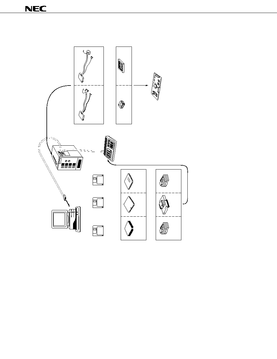
82
µ
PD78323, 78324
Development Tool Configurations
Note
The socket is supplied with the emulation probe.
Remarks
1. It is also possible to use the host machine and the PG-1500
by connecting them directly by the RS-232-C.
2. In the diagram above, representative software supply media
and 3.5-inch FDs.
Host machine
PC-9800 series
IBM PC/AT or its compatible machine
Software
Relocatable assembler
(With structured assembler)
PG-1500
controller
IE controller
PD78P324GJ
PD78P324LP
PD78P324KD
PD78P324KC
PA-78P324GJ
PA-78P324LP
PA-78P324KC
PA-78P324KD
+
+
+
Programmer adapters
PROM-incorporated products
RS-232-C
IE-78327-R
in-circuit emulator
RS-232-C
PG-1500
PROM
programmer
Emulation probes
Socket for connecting the emulation probe
and the target system
EP-78320GJ-R
EP-78320L-R
EV-9200G-74
Socket for plastic QFJ
Target system
µ
µ
µ
µ
Note
83
µ
PD78323, 78324
B.2
EVALUATION TOOLS
To evaluate the functions of the
µ
PD78324, the following tools are made available.
Part Number
EB-78320-98
EB-78320-PC
Function
By connecting to a host machine, it is possible
to evaluate the functions equipped by the
µ
PD78324 in a simple manner. The command
system of this product basically conforms to
that of IE-78327-R and IE-78320-R. Therefore,
it is easy to move to the development work of
application systems by IE-78327-R or IE-
78320-R. In addition a turbo access manager
(
µ
PD71P301)
Note
can be mounted on the
board.
Host Machine
PC-9800 series
IBM PC/AT or its compatible
machine
Real-time OS (RX78K/III)
The RX78K/III is designed to provide a multi-task environment in the field of control
application where real-time operation is required. By using this real-time OS, the
performance of the whole system can be improved by allocating CPU's idle time to
other processings.
The RX78K/III provides the system call based on the
µ
ITRON specifications.
The RX78K/III package provides tools (configurators) for creating RX78K/III's nucleus
and multiple information table.
Host machine
PC-9800 series
IBM PC/AT and its
compatible machine
Supply medium
3.5-inch 2HD
5-inch 2HD
3.5-inch 2HC
5-inch 2HC
Part number
µ
S5A13RX78320
µ
S5A10RX78320
µ
S7B13RX78320
µ
S7B10RX78320
OS
MS-DOS
PC DOS
Caution
To purchase the operating system above, you need to fill in a purchase application form
beforehand and sign a contract allowing you to use the software.
Remark
When using the real-time OS RX78K/III, you need the assembler package RA78K/III (optional) as well.
Note
The turbo access manager (
µ
PD71P301) is a maintenance product.
Cautions
1. This product is not a development tool of
µ
PD78324 application systems.
2. This product is not equipped with the emulation function for executing the ROM incorporated
in the
µ
PD78324.
B.3
EMBEDDED SOFTWARE
The following embedded software programs are available to perform program development and maintenance
more efficiently.
Eeal-time OS

84
µ
PD78323, 78324
Fuzzy knowledge data creation
tools (FE9000, FE9200)
Translator (FT78K3)
Note
Fuzzy inference module
(FI78K/III)
Note
Fuzzy inference debugger
(FD78K/III)
This program supports inputting/editing/evaluating (through simulation) of the fuzzy
knowledge data (fuzzy rules and membership functions).
Fuzzy Inference Development Support System
Host machine
PC-9800 series
IBM PC/AT and its
compatible machine
Supply medium
3.5-inch 2HD
5-inch 2HD
3.5-inch 2HC
5-inch 2HC
Part number
µ
S5A13FE9000
µ
S5A10FE9000
µ
S7B13FE9200
µ
S7B10FE9200
OS
MS-DOS
PC DOS Winsows
TM
This program converts the fuzzy knowledge data obtained with fuzzy knowledge data
creation tools to an assembler source program for RA78K/III.
Host machine
PC-9800 series
IBM PC/AT and its
compatible machine
Supply medium
3.5-inch 2HD
5-inch 2HD
3.5-inch 2HC
5-inch 2HC
Part number
µ
S5A13FT78K3
µ
S5A10FT78K3
µ
S7B13FT78K3
µ
S7B10FT78K3
OS
MS-DOS
PC DOS
Supply medium
3.5-inch 2HD
5-inch 2HD
3.5-inch 2HC
5-inch 2HC
Part number
µ
S5A13FI78K3
µ
S5A10FI78K3
µ
S7B13FI78K3
µ
S7B10FI78K3
OS
MS-DOS
PC DOS
Supply medium
3.5-inch 2HD
5-inch 2HD
3.5-inch 2HC
5-inch 2HC
Part number
µ
S5A13FD78K3
µ
S5A10FD78K3
µ
S7B13FD78K3
µ
S7B10FD78K3
OS
MS-DOS
PC DOS
Host machine
PC-9800 series
IBM PC/AT and its
compatible machine
This program executes fuzzy inference. Fuzzy inference is executed by being linked to
the fuzzy knowledge data converted by the translator.
This is a support software program for evaluating and adjusting the fuzzy knowledge
data at a hardware level by using the in-circuit emulator.
Host machine
PC-9800 series
IIBM PC/AT and its
compatible machine
Note
Under development
85
µ
PD78323, 78324
NOTES FOR CMOS DEVICES
1
PRECAUTION AGAINST ESD FOR SEMICONDUCTORS
Note: Strong electric field, when exposed to a MOS device, can cause destruction
of the gate oxide and ultimately degrade the device operation. Steps must
be taken to stop generation of static electricity as much as possible, and
quickly dissipate it once, when it has occurred. Environmental control must
be adequate. When it is dry, humidifier should be used. It is recommended
to avoid using insulators that easily build static electricity. Semiconductor
devices must be stored and transported in an anti-static container, static
shielding bag or conductive material. All test and measurement tools
including work bench and floor should be grounded. The operator should
be grounded using wrist strap. Semiconductor devices must not be touched
with bare hands. Similar precautions need to be taken for PW boards with
semiconductor devices on it.
2
HANDLING OF UNUSED INPUT PINS FOR CMOS
Note: No connection for CMOS device inputs can be cause of malfunction. If no
connection is provided to the input pins, it is possible that an internal input
level may be generated due to noise, etc., hence causing malfunction. CMOS
devices behave differently than Bipolar or NMOS devices. Input levels of
CMOS devices must be fixed high or low by using a pull-up or pull-down
circuitry. Each unused pin should be connected to V
DD
or GND with a
resistor, if it is considered to have a possibility of being an output pin. All
handling related to the unused pins must be judged device by device and
related specifications governing the devices.
3
STATUS BEFORE INITIALIZATION OF MOS DEVICES
Note: Power-on does not necessarily define initial status of MOS device. Production
process of MOS does not define the initial operation status of the device.
Immediately after the power source is turned ON, the devices with reset
function have not yet been initialized. Hence, power-on does not guarantee
out-pin levels, I/O settings or contents of registers. Device is not initialized
until the reset signal is received. Reset operation must be executed imme-
diately after power-on for devices having reset function.

MS-DOS and Windows are trademarks of Microsoft Corporation.
PC/AT and PC DOS are trademarks of IBM Corporation.
HP9000 series 700 and HP-UX are trademarks of Hewlett-Packard Company.
SPARCstation is a trademark of SPARC International, Inc.
SunOS is a trademark of Sun Microsystems, Inc.
NEWS and NEWS-OS are trademarks of Sony Corporation.
TRON is an abbreviation of The Realtime Operating system Nucleus.
ITRON is an abbreviation of Industrial TRON.
No part of this document may be copied or reproduced in any form or by any means without the prior written
consent of NEC Corporation. NEC Corporation assumes no responsibility for any errors which may appear in this
document.
NEC Corporation does not assume any liability for infringement of patents, copyrights or other intellectual
property rights of third parties by or arising from use of a device described herein or any other liability arising
from use of such device. No license, either express, implied or otherwise, is granted under any patents,
copyrights or other intellectual property rights of NEC Corporation or others.
While NEC Corporation has been making continuous effort to enhance the reliability of its semiconductor devices,
the possibility of defects cannot be eliminated entirely. To minimize risks of damage or injury to persons or
property arising from a defect in an NEC semiconductor device, customer must incorporate sufficient safety
measures in its design, such as redundancy, fire-containment, and anti-failure features.
NEC devices are classified into the following three quality grades:
"Standard", "Special", and "Specific". The Specific quality grade applies only to devices developed based on
a customer designated "quality assurance program" for a specific application. The recommended applications
of a device depend on its quality grade, as indicated below. Customers must check the quality grade of each
device before using it in a particular application.
Standard: Computers, office equipment, communications equipment, test and measurement equipment,
audio and visual equipment, home electronic appliances, machine tools, personal electronic
equipment and industrial robots
Special:
Transportation equipment (automobiles, trains, ships, etc.), traffic control systems, anti-disaster
systems, anti-crime systems, safety equipment and medical equipment (not specifically designed
for life support)
Specific: Aircrafts, aerospace equipment, submersible repeaters, nuclear reactor control systems, life
support systems or medical equipment for life support, etc.
The quality grade of NEC devices in "Standard" unless otherwise specified in NEC's Data Sheets or Data Books.
If customers intend to use NEC devices for applications other than those specified for Standard quality grade,
they should contact NEC Sales Representative in advance.
Anti-radioactive design is not implemented in this product.
M4 94.11
License not needed
:
µ
PD78323
The customer must judge the need for license :
µ
PD78324
The export of these products from Japan is regulated by the Japanese government. The export of some or all of
these products may be prohibited without governmental license. To export or re-export some or all of these
products from a country other than Japan may also be prohibited without a license from that country. Please call
an NEC sales representative.
µ
PD78323, 78324