Document Outline
- COVER
- DESCRIPTION
- FEATURES
- APPLICATION EXAMPLES
- ORDERING INFORMATION
- 78K/III Series Product Development
- PIN CONFIGURATION (TOP VIEW)
- FUNCTIONAL OUTLINE
- DIFFERENCES BETWEEN uPD78363A, 78365A, 78366A, AND 78368A
- BLOCK DIAGRAM
- 1. PIN FUNCTIONS
- 1.1 PORT PINS
- 1.2 PINS OTHER THAN PORT PINS
- 1.3 PIN I/O CIRCUITS AND PROCESSING OF UNUSED PINS
- 2. CPU ARCHITECTURE
- 2.1 MEMORY SPACE
- 2.2 DATA MEMORY ADDRESSING
- 2.3 PROCESSOR REGISTERS
- 2.3.1 Control Registers
- 2.3.2 General-Purpose Registers
- 2.3.3 Special Function Registers (SFR)
- 3. FUNCTIONAL BLOCKS
- 3.1 EXECUTION UNIT (EXU)
- 3.2 BUS CONTROL UNIT (BCU)
- 3.3 ROM/RAM
- 3.4 PORT FUNCTIONS
- 3.5 CLOCK GENERATOR CIRCUIT
- 3.6 REAL-TIME PULSE UNIT (RPU)
- 3.7 REAL-TIME OUTPUT PORT (RTP)
- 3.8 A/D CONVERT
- 3.9 SERIAL INTERFACE
- 3.10 PWM UNIT
- 3.11 WATCHDOG TIMER (WDT)
- 4. INTERRUPT FUNCTIONS
- 4.1 OUTLINE
- 4.2 MACRO SERVICE
- 4.3 CONTEXT SWITCHING
- 4.3.1 Context Switching Function by Interrupt Request
- 4.3.2 Context Switching Function by BRKCS Instruction
- 4.3.3 Restoration from Context Switching
- 5. EXTERNAL DEVICE EXPANSION FUNCTION
- 6. STANDBY FUNCTIONS
- 7. RESET FUNCTION
- 8. INSTRUCTION SET
- 9. EXAMPLE OF SYSTEM CONFIGURATION
- 10. ELECTRICAL SPECIFICATIONS
- 11. PACKAGE DRAWING
- 12. RECOMMENDED SOLDERING CONDITIONS
- APPENDIX A. DIFFERENCES BETWEEN uPD78366A AND uPD78328
- APPENDIX B. TOOLS
- B.1 DEVELOPMENT TOOLS
- B.2 EMBEDDED SOFTWARE

©
1995
DATA SHEET
The information in this document is subject to change without notice.
The mark
shows major revised points.
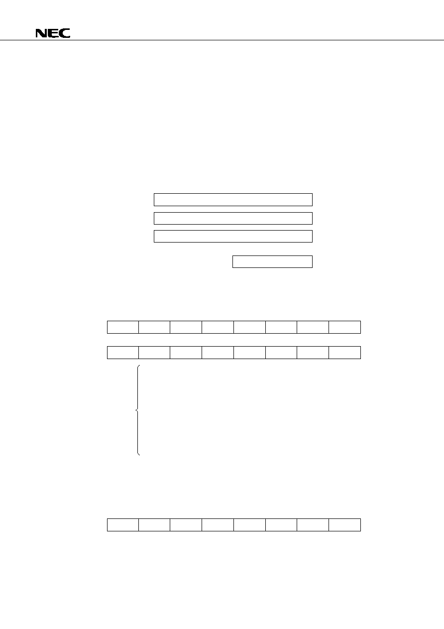
DESCRIPTION
µ
PD78366A is provided with a high-speed, high-performance CPU and powerful operation functions. Unlike the
existing
µ
PD78328,
µ
PD78366A is also provided with a high-resolution PWM signal output function which
substantially contributes to improving the performance of the inverter control.
A PROM model,
µ
PD78P368A, is also available.
Detailed functions, etc. are described in the following user's manual. Be sure to read the manual to design systems.
µ
PD78366A User's Manual Hardware: U10205E
µ
PD78356 User's Manual
: U12117E
FEATURES
∑
Internal 16-bit architecture, external 8-bit data bus
∑
High-speed processing by pipeline control method and high- speed operating clock
∑ Minimum instruction execution time: 125 ns (internal clock: at 16 MHz, external clock: 8 MHz)
∑
Real-time pulse unit for inverter control
∑
10-bit resolution A/D converter: 8 channels
∑
8-/9-/10-/12-bit resolution variable PWM signal output function: 2 channels
∑
Powerful serial interface: 2 channels
∑
Internal memory:
ROM: none (
µ
PD78365A)
24K bytes (
µ
PD78363A)
32K bytes (
µ
PD78366A)
48K bytes (
µ
PD78368A)
RAM: 768 bytes (
µ
PD78363A)
2K bytes (
µ
PD78365A, 78366A, 78368A)
APPLICATION EXAMPLES
∑ Inverter air conditioner
∑ Factory automation fields, such as industrial robots and machine tools.
ORDERING INFORMATION
Part Number
Package
Internal ROM
µ
PD78363AGF-
◊◊◊
-3B9
80-pin plastic QFP (14
◊
20 mm)
Mask ROM
µ
PD78365AGF-3B9
80-pin plastic QFP (14
◊
20 mm)
None
µ
PD78366AGF-
◊◊◊
-3B9
80-pin plastic QFP (14
◊
20 mm)
Mask ROM
µ
PD78368AGF-
◊◊◊
-3B9
80-pin plastic QFP (14
◊
20 mm)
Mask ROM
Remark
◊◊◊
indicates a ROM code suffix.
Unless otherwise specified, the functions and performances of the
µ
PD78366 are described throughout this document.
Document No. U11109EJ2V0DS00 (2nd edition)
Date Published September 1997 N
Printed in Japan
MOS INTEGRATED CIRCUIT
µ
PD78363A,78365A,78366A,78368A
16/8-BIT SINGLE-CHIP MICROCONTROLLERS
©
1995
µ
PD78363A, 78365A, 78366A, 78368A
2
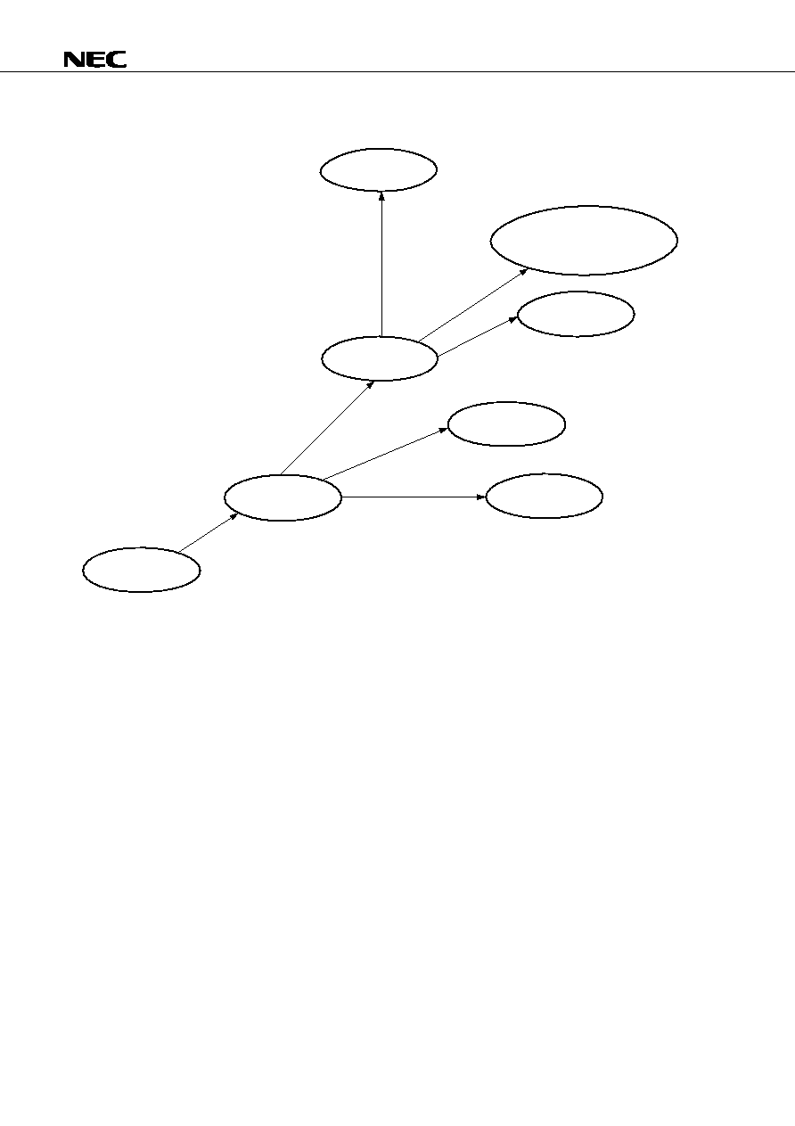
78K/III Series Product Development
High-speed, multi-function,
reinforced interrupt,
10-bit A/D
(for control application in OA and FA fields)
High-performance CPU,
sum-of-products instruction added
Reinforced timer and
A/D, expanded ROM
and RAM
Pulse output function
for inverter control
(for HDD)
(for control application in OA and FA fields)
(for control application in OA and FA fields)
(for inverter)
A/D, D/A relative instruction
added, expanded ROM, RAM
Pulse output function
for inverter control,
expanded ROM, RAM
Reinforced timer,
A/D added
(for control application
in automotive appliance)
(for inverter)
(for camera, HDD)
PD78372 subseries
PD78356 subseries
PD78334 subseries
PD78328 subseries
PD78352A subseries
PD78322 subseries
PD78312A subseries
PD78361A
PD78362A
PD78P364A
µ
µ
µ
µ
µ
µ
µ
µ
µ
µ
µ
µ
µ
µ
µ
PD78366A subseries
µ
PD78363A
PD78365A
PD78366A
PD78368A
PD78P368A
µ
PD78363A, 78365A, 78366A, 78368A
3
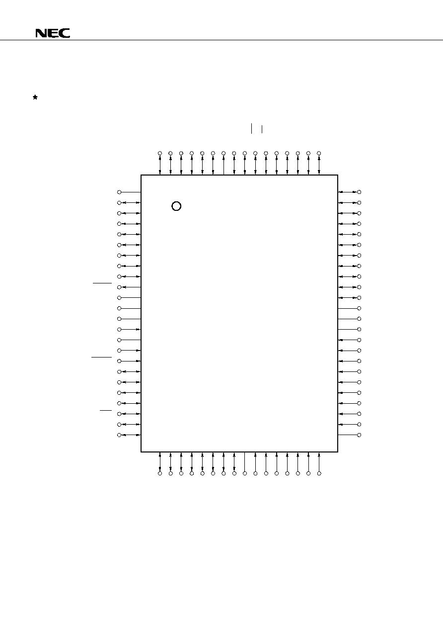
PIN CONFIGURATION (TOP VIEW)
∑
80-pin plastic QFP (14
◊
20 mm)
µ
PD78363AGF-
◊◊◊
-3B9, 78365AGF-3B9, 78366AGF-
◊◊◊
-3B9, 78368AGF-
◊◊◊
-3B9
V
SS
P00/RTP0
P01/RTP1
P02/RTP2
P03/RTP3
P04/PWM0
WDTO
P07/TCLRUD
V
SS
X1
X2
MODE1
RESET
P30/T
X
D0
P31/R
X
D0
P32/SO/SB0
P33/SI/SB1
P34/SCK
P36/R
X
D1
P35/T
X
D1
IC
V
DD
P52/A10
P51/A9
P50/A8
P47/AD7
P46/AD6
P45/AD5
P44/AD4
P43/AD3
P41/AD1
P42/AD2
V
DD
AV
DD
AV
REF
P77/ANI7
P76/ANI6
P75/ANI5
P74/ANI4
P73/ANI3
P72/ANI2
P71/ANI1
AV
SS
P70/ANI0
P40/AD0
V
SS
P10
P11
P12
P13
P14
P15
P16
P17
V
SS
MODE0
P20/NMI
P21/INTP0
P22/INTP1
P23/INTP2
P24/INTP3/TI
P25/INTP4
ASTB
P93
P92
P91/WR
P90/RD
P57/A15
P56/A14
P55/A13
P54/A12
P53/A11
1
2
3
4
5
6
7
8
9
10
11
12
13
14
15
16
17
18
19
20
21
22
23
24
64
63
62
61
60
59
58
57
56
55
54
53
52
51
50
49
48
47
46
45
44
43
42
41
80 79 78 77 76 75 74 73 72 71 70 69 68 67 66 65
25 26 27 28 29 30 31 32 33 34 35 36 37 38 39 40
P85/TO05
P84/TO04
P83/TO03
P82/TO02
P81/TO01
P80/TO00
P05/TCUD/PWM1
P06/TIUD/TO40
Caution Connect the IC pin directly to V
SS
.
Remark
◊◊◊
indicates a ROM code suffix

µ
PD78363A, 78365A, 78366A, 78368A
4
P00-P07
: Port0
P10-P17
: Port1
P20-P25
: Port2
P30-P36
: Port3
P40-P47
: Port4
P50-P57
: Port5
P70-P77
: Port7
P80-P85
: Port8
P90-P93
: Port9
RTP0-RTP3
: Real-time Port
NMI
: Nonmaskable Interrupt
INTP0-INTP4
: Interrupt From Peripherals
TO00-TO05, TO04 : Timer Output
TI
: Timer Input
TIUD
: Timer Input Up Down Counter
TCUD
: Timer Control Up Down Counter
TCLRUD
: Timer Clear Up Down Counter
ANI0-ANI7
: Analog Input
T
X
D0, T
X
D1
: Transmit Data
R
X
D0, R
X
D1
: Receive Data
SI
: Serial Input
SO
: Serial Output
SB0, SB1
: Serial Bus
SCK
: Serial Clock
PWM0, PWM1
: Pulse Width Modulation Output
WDTO
: Watchdog Timer Ouput
MODE0, MODE1
: Mode
AD0-AD7
: Address/Data Bus
A8-A15
: Address Bus
ASTB
: Address Strobe
RD
: Read Strobe
WR
: Write Strobe
RESET
: Reset
X1, X2
: Crystal
AV
DD
: Analog V
DD
AV
SS
: Analog V
SS
AV
REF
: Analog Reference Voltage
V
DD
: Power Supply
V
SS
: Ground
IC
: Internally Connected
µ
PD78363A, 78365A, 78366A, 78368A
5
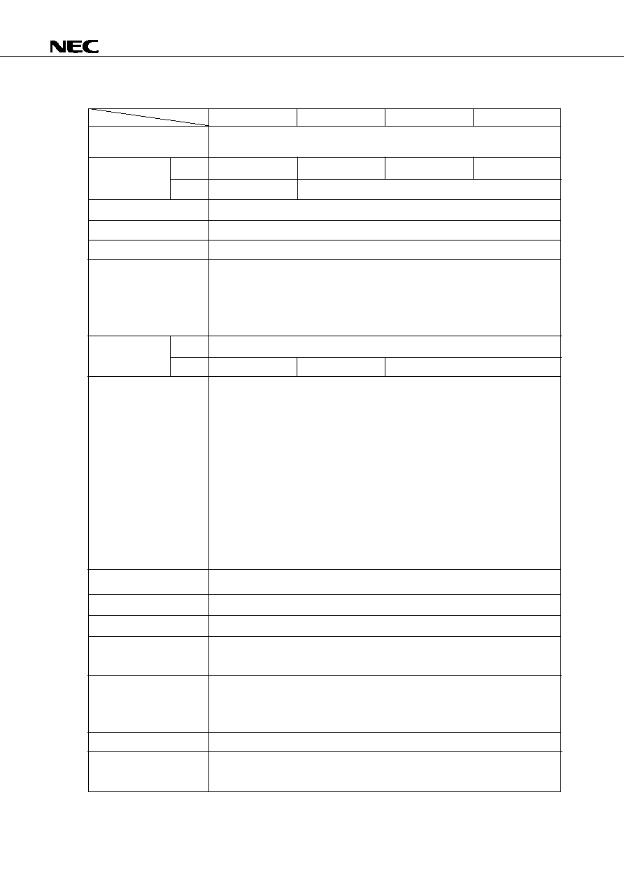
125 ns (internal clock: 16 MHz, external clock: 8 MHz)
24K bytes
None
32K bytes
48K bytes
768 bytes
2K bytes
64K bytes (externally expandable)
8 bits
◊
16
◊
8 banks
115
∑ 16-bit transfer/operation
∑ Multiplication/division (16 bits
◊
16 bits, 32 bits
˜
16 bits)
∑ Bit manipulation
∑ String
∑ Sum-of-products operation (16 bits
◊
16 bits + 32 bits)
∑ Relative operation
14 (of which 8 are shared with analog input)
49
31
49
∑ 16-bit timer
◊
1
10-bit dead time timer
◊
3
16-bit compare register
◊
4
2 kinds of output mode can be selected
Mode 0, set-reset output: 6 channels
Mode 1, buffer output: 6 channels
∑ 16-bit timer
◊
1
16-bit compare register
◊
1
∑ 16-bit timer
◊
1
16-bit capture register
◊
1
16-bit capture/compare register
◊
1
∑ 16-bit timer
◊
1
16-bit capture register
◊
2
16-bit capture/compare register
◊
1
∑ 16-bit timer
◊
1
16-bit compare register
◊
2
16-bit resolution PWM output: 1 channel
Pulse outputs associated with real-time pulse unit: 4 lines
8-/9-/10-/12-bit resolution variable PWM output: 2 channels
10-bit resolution, 8 channels
Dedicated baud rate generator
UART (w/pin selection function):
1 channel
Clocked serial interface/SBI:
1 channel
∑ External: 6, internal: 14 (of which 2 are multiplexed with external)
∑ 4 priority levels can be specified through software
∑ 3 types of interrupt processing modes selectable
(vectored interrupt, macro service, and context switching)
80-pin plastic QFP (14
◊
20 mm)
∑ Watchdog timer
∑ Standby function (HALT and STOP modes)
FUNCTIONAL OUTLINE
Minimum instruction
execution time
Internal memory
ROM
RAM
Memory space
General-purpose registers
Number of basic instructions
Instruction set
I/O lines
Input
I/O
Real-time pulse unit
Real-time output port
PWM unit
A/D converter
Serial interface
Interrupt function
Package
Others
Product name
Item
µ
PD78363A
µ
PD78365A
µ
PD78366A
µ
PD78368A
µ
PD78363A, 78365A, 78366A, 78368A
6
49
Can be set in input or output mode in units
of 8 bits. In external memory expansion
mode, this port functions as multiplexed
address/data bus (AD0-AD7).
Can be set in input or output mode in
1-bit units. In external memory expansion
mode, this port functions as address bus
(A8-A15).
Can be set in input or output mode in
1-bit units. In external memory expansion
mode, P90 outputs RD strobe signal, and
P91 outputs WR strobe signal.
Sets port 4 in input or output mode in units
of 8 bits. In external memory expansion
mode, sets memory expansion width of ports
4 and 5.
Sets port 5 in input or output mode in
1-bit units.
∑ In ordinary operation mode:
MODE0, 1 = LL
∑ In ROM-less mode:
MODE0, 1 = HH
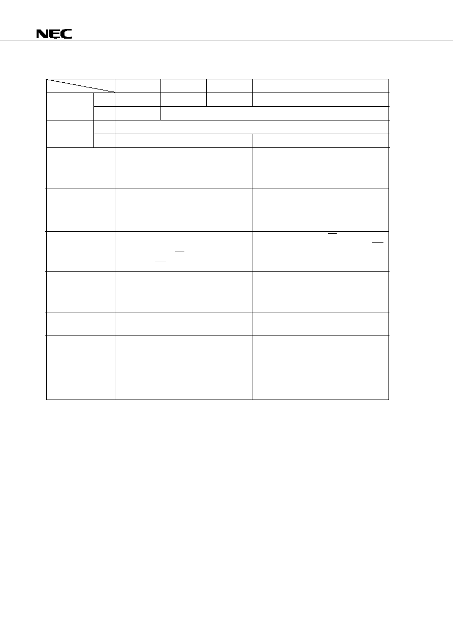
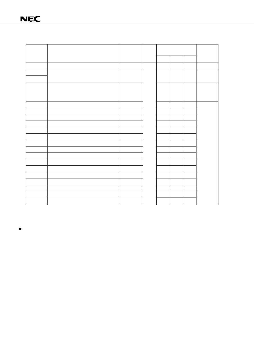
DIFFERENCES BETWEEN
µ
PD78363A, 78365A, 78366A, AND 78368A
ROM
Internal ROM
RAM
Input
I/O lines
I/O
Port 4 (P40-P47)
Port 5 (P50-P57)
Port 9 (P90-P93)
Memory expansion
mode register (MM)
Port 5 mode
register (PM5)
Setting of
MODE0, MODE1
Product name
Item
24K bytes
32K bytes
48K bytes
None
786 bytes
2K bytes
14 (of which 8 are multiplexed with analog input)
31
Always functions as multiplexed address/
data bus (AD0-AD7).
Always functions as address bus (A8-A15)
P90 always functions as RD strobe signal
output pin, and P91 always functions as WR
strobe signal output pin. P92 and P93
function as I/O port lines.
Always fixed to external memory expansion
mode.
None
∑ Always set as follows:
MODE0, 1 = HH
µ
PD78363A
µ
PD78366A
µ
PD78365A
µ
PD78368A
µ
PD78363A, 78365A, 78366A, 78368A
7
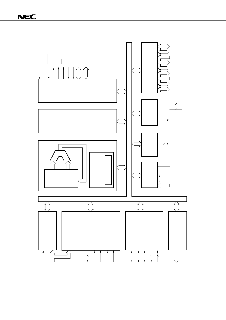
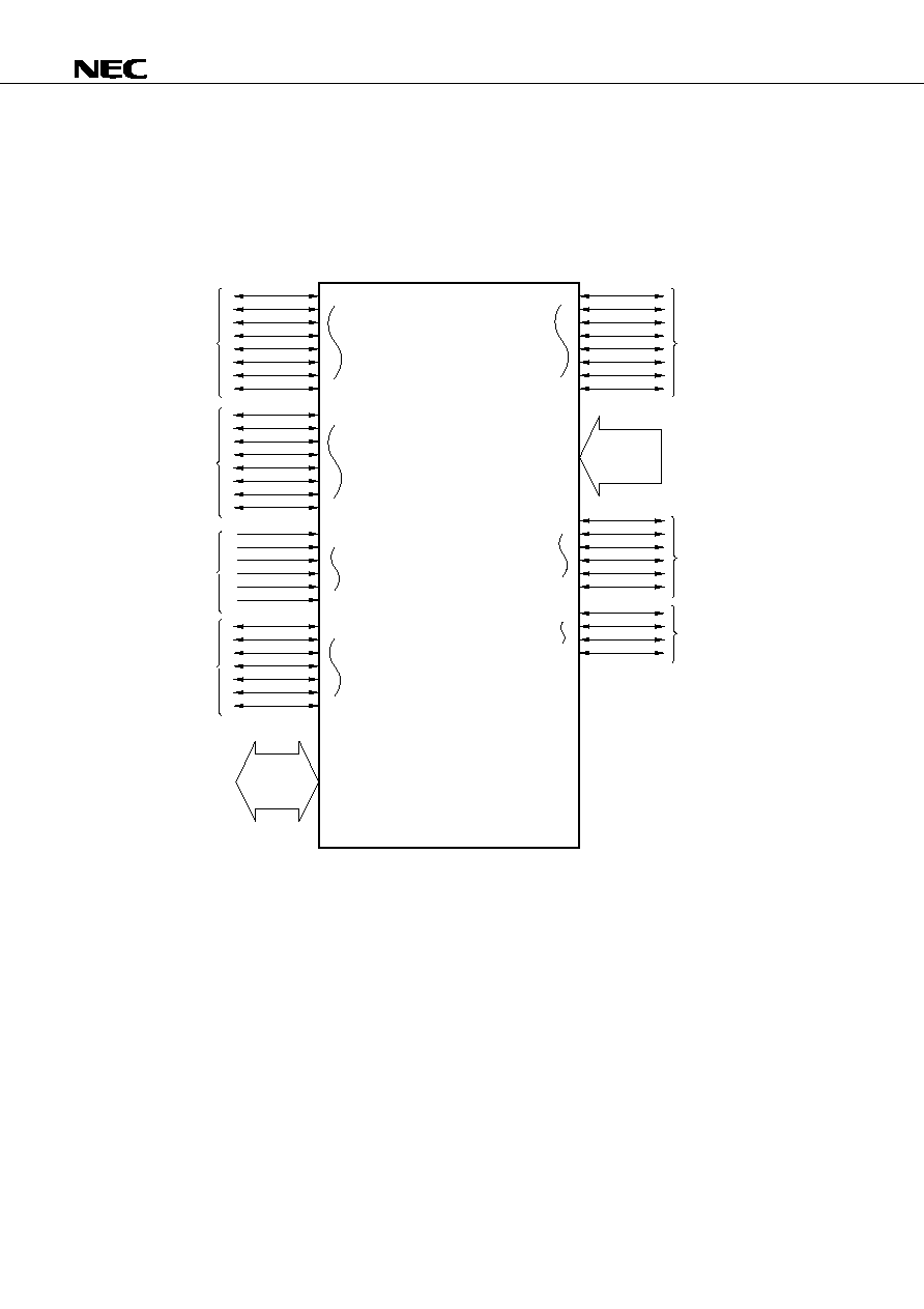
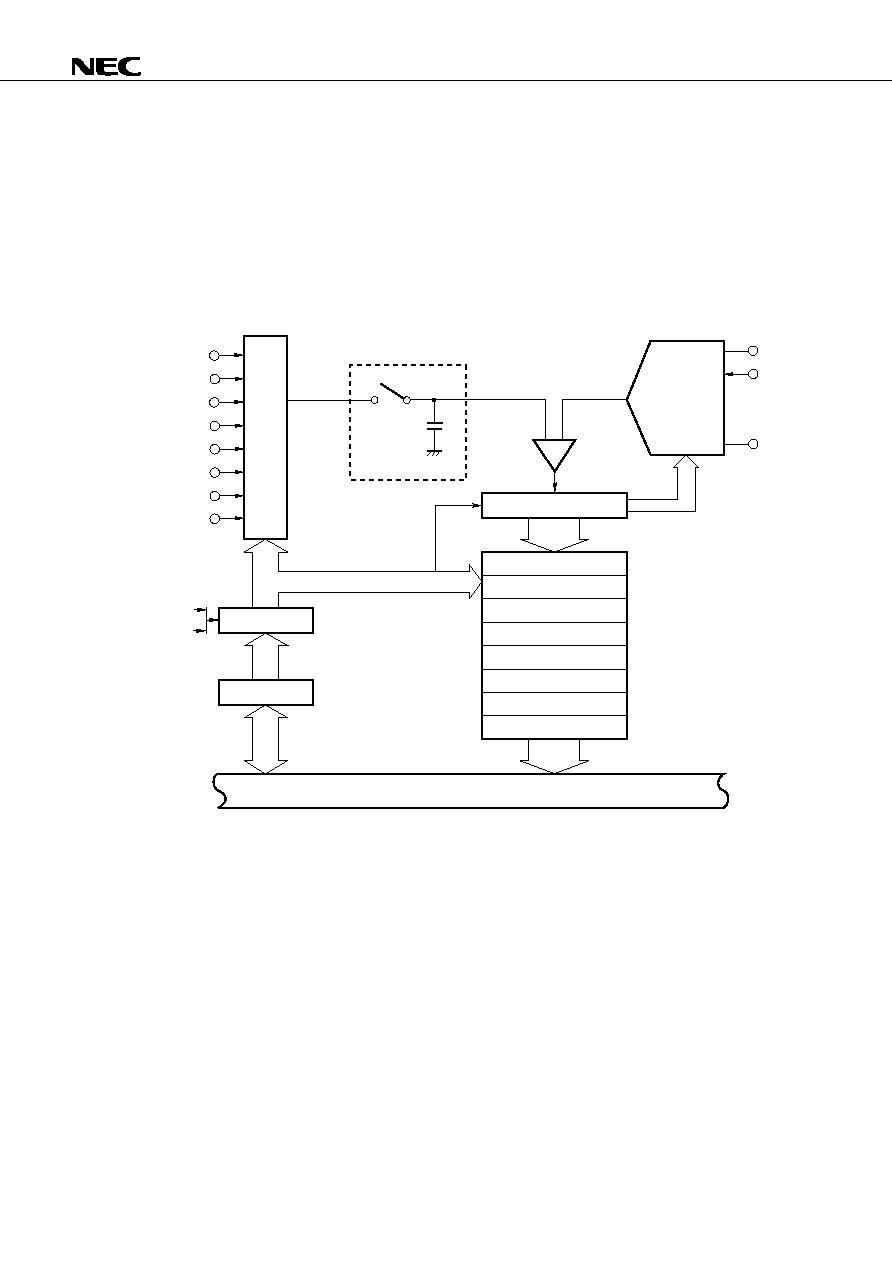
BLOCK DIAGRAM
P0
P1
P2
P3
P4
P5
P6
P7
P8
8
8
6
7
8
8
8
6
4
V
DD
V
SS
WDTO
PWM
AV
DD
AV
SS
AV
REF
INTP2
ANI
TO
TI
TIUD
TCLRUD
TCUD
SCK
SO/SB0
SI/B1
R
X
D
T
X
D
RTP
NMI
INTP
5
5
4
2
2
4
2
4
2
EXU
ROM/RAM
BCU
X1
X2
RESET
ASTB
RD
WR
MODE1
MODE0
A8-A15
AD0-AD7
PROGRAMMABLE
INTERRUPT
CONTROLLER
TIMER/COUNTER
UNIT
(REAL-TIME
PULSE UNIT)
SERIAL
INTERFACE
(SBI)
(UART)
REAL-TIME
OUTPUT PORT
GENERAL
REGISTERS
128
◊
8
&
DATA
MEMORY
128
◊
8
MAIN RAM
MICRO
SEQUENCE
CONTROL
MICRO ROM
A/D
CONVERTER
RWM
WATCHDOG
TIMER
PORT
ALU
ROM
24K
◊
8
32K
◊
8
48K
◊
8
&
PERIPHERAL
RAM
512
◊
8
1792
◊
8
SYSTEM
CONTROL
&
BUS
CONTROL
&
PREFETCH
CONTROL
8
8
8
7
Remark The internal ROM and RAM capacities differ depending on the product.

µ
PD78363A, 78365A, 78366A, 78368A
8
CONTENTS
1.
PIN FUNCTIONS
................................................................................................................................... 10
1.1
PORT PINS ..................................................................................................................................... 10
1.2
PINS OTHER THAN PORT PINS .................................................................................................. 11
1.3
PIN I/O CIRCUITS AND PROCESSING OF UNUSED PINS ....................................................... 13
2.
CPU ARCHITECTURE ............................................................................................................
15
2.1
MEMORY SPACE ........................................................................................................................... 15
2.2
DATA MEMORY ADDRESSING .................................................................................................... 18
2.3
PROCESSOR REGISTERS ........................................................................................................... 20
2.3.1
Control Registers ................................................................................................................. 21
2.3.2
General-Purpose Registers ..................................................................................................22
2.3.3
Special Function Registers (SFR) ........................................................................................ 23
3.
FUNCTIONAL BLOCKS ...........................................................................................................
29
3.1
EXECUTION UNIT (EXU) ............................................................................................................... 29
3.2
BUS CONTROL UNIT (BCU) ......................................................................................................... 29
3.3
ROM/RAM ....................................................................................................................................... 29
3.4
PORT FUNCTIONS ........................................................................................................................ 30
3.5
CLOCK GENERATOR CIRCUIT ................................................................................................... 32
3.6
REAL-TIME PULSE UNIT (RPU) .................................................................................................. 34
3.7
REAL-TIME OUTPUT PORT (RTP) .............................................................................................. 42
3.8
A/D CONVERTER .......................................................................................................................... 43
3.9
SERIAL INTERFACE ..................................................................................................................... 44
3.10 PWM UNIT ...................................................................................................................................... 46
3.11 WATCHDOG TIMER (WDT) .......................................................................................................... 47
4.
INTERRUPT FUNCTIONS
................................................................................................................... 48
4.1
OUTLINE ......................................................................................................................................... 48
4.2
MACRO SERVICE .......................................................................................................................... 49
4.3
CONTEXT SWITCHING ................................................................................................................. 52
4.3.1
Context Switching Function by Interrupt Request ................................................................ 52
4.3.2
Context Switching Function by BRKCS Instruction .............................................................. 53
4.3.3
Restoration from Context Switching .....................................................................................53
5.
EXTERNAL DEVICE EXPANSION FUNCTION
............................................................................. 54
6.
STANDBY FUNCTIONS
...................................................................................................................... 55
7.
RESET FUNCTION
............................................................................................................................... 56
8.
INSTRUCTION SET
.............................................................................................................................. 57
9.
EXAMPLE OF SYSTEM CONFIGURATION ...........................................................................
71
10. ELECTRICAL SPECIFICATIONS ............................................................................................
72

µ
PD78363A, 78365A, 78366A, 78368A
9
11. PACKAGE DRAWING ..............................................................................................................
83
12. RECOMMENDED SOLDERING CONDITIONS ......................................................................
84
APPENDIX A. DIFFERENCES BETWEEN
µ
PD78366A AND
µ
PD78328 ...................................
85
APPENDIX B. TOOLS .....................................................................................................................
86
B.1
DEVELOPMENT TOOLS ............................................................................................................... 86
B.2
EMBEDDED SOFTWARE .............................................................................................................. 91
µ
PD78363A, 78365A, 78366A, 78368A
10
P00-P03
P04
P05
P06
P07
P10-P17
P20
P21
P22
P23
P24
P25
P30
P31
P32
P33
P34
P35
P36
P40-P47
P50-P57
P70-P77
P80-P85
P90
P91
P92
P93
RTP0-RTP3
PWM0
TCUD/PWM1
TIUD/TO40
TCLRUD
≠
NMI
INTP0
INTP1
INTP2
INTP3/TI
INTP4
T
X
D0
R
X
D0
SO/SB0
SI/SB1
SCK
T
X
D1
R
X
D1
AD0-AD7
A8-A15
ANI0-ANI7
TO00-TO05
RD
WR
≠
≠
I/O
I/O
Input
I/O
I/O
I/O
Input
I/O
I/O
Pin name
I/O
Function
Shared by:
Port 0.
8-bit I/O port.
Can be set in input or output mode in 1-bit units.
Port 1.
8-bit I/O port.
Can be set in input or output mode in 1-bit units.
Port 2.
6-bit input port.
Port 3.
7-bit I/O port.
Can be set in input or output mode in 1-bit units.
Port 4.
8-bit I/O Port.
Can be set in input or output mode in 8-bit units.
Port 5.
8-bit I/O port.
Can be set in input or output mode in 1-bit units.
Port 7.
8-bit input port
Port 8.
6-bit I/O port.
Can be set in input or output mode in 1-bit units.
Port 9.
4-bit I/O port.
Can be set in input or output mode in 1-bit units.
1.
PIN FUNCTIONS
1.1
PORT PINS

µ
PD78363A, 78365A, 78366A, 78368A
11
P00-P03
P20
P21
P22
P23
P24/TI
P25
P24/INTP3
P05/PWM1
P06/TO40
P07
P80-P85
P06/TIUD
P70-P77
P30
P35
P31
P36
P34
P33/SB1
P32/SB0
P32/SO
P33/SI
P04
P05/TCUD
≠
P40-P47
P50-P57
≠
P90
P91
RTP0-RTP3
NMI
INTP0
INTP1
INTP2
INTP3
INTP4
TI
TCUD
TIUD
TCLRUD
TO00-TO05
TO40
ANI0-ANI7
T
X
D0
T
X
D1
R
X
D0
R
X
D1
SCK
SI
SO
SB0
SB1
PWM0
PWM1
WDTO
AD0-AD7
A8-A15
ASTB
RD
WR
Real-time output port that outputs pulses in synchronization with trigger
signal from real-time pulse unit.
Non-maskable interrupt request input.
External interrupt request input.
External count clock input to timer 1.
Count operation selection control signal input to up/down counter (timer
4).
External count clock input to up/down counter (timer 4).
Clear signal input to up/down counter (timer 4).
Pulse output from real-time pulse unit.
Analog input to A/D converter.
Serial data output of asynchronous serial interface.
Serial data input of asynchronous serial interface.
Serial clock input/output of clocked serial interface.
Serial data input of clocked serial interface in 3-line mode.
Serial data output of clocked serial interface in 3-line mode.
Serial data input/output of clocked serial interface in SBI mode.
PWM signal output.
Signal output indicating overflow of watchdog timer (generates non-
maskable interrupt).
Multiplexed address/data bus when memory is externally expanded.
Address bus when memory is externally expanded.
Outputs timing signal at which address information output from AD0-AD7
and A8-A15 pins to access external memory is to be latched.
Read strobe signal output to external memory.
Write strobe signal output to external memory.
Output
Input
Input
Output
Input
Output
Input
I/O
Input
Ouput
I/O
Output
Output
I/O
Output
Pin name
I/O
Function
Shared by:
1.2
PINS OTHER THAN PORT PINS (1/2)

µ
PD78363A, 78365A, 78366A, 78368A
12
Pin name
I/O
Function
Shared by:
MODE0
MODE1
RESET
X1
X2
AV
REF
AV
DD
AV
SS
V
DD
V
SS
IC
≠
≠
≠
≠
≠
≠
≠
≠
≠
Control signal input to set operation mode. With
µ
PD78363A, 78366A, and
78368A MODE0 and MODE1 are usually connected to V
SS
. With
µ
PD78365A,
MODE0 and MODE1 are always connected to V
DD
.
System reset input
Crystal oscillator connecting pins for system clock. If a clock is externally
supplied, input it to pin X1. Leave pin X2 open.
A/D converter reference voltage input.
A/D converter analog power supply.
A/D converter GND.
Positive power supply
GND
Internally connected. Connect this pin to V
SS
.
Input
Input
Input
≠
Input
≠
≠
≠
≠
≠
1.2
PINS OTHER THAN PORT PINS (2/2)
µ
PD78363A, 78365A, 78366A, 78368A
13
1.3
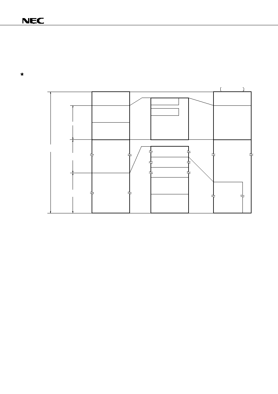
PIN I/O CIRCUITS AND PROCESSING OF UNUSED PINS
Table 1-1 shows the I/O circuit types of the respective pins, and recommended connections of the unused
pins. Figure 1-1 shows the circuits of the respective pins.
Table 1-1. Pin I/O Circuit Type and Recommended Connections of Unused Pins
Pin
I/O circuit type
Recommended connections
P00/RTP0-P03/RTP3
P04/PWM0
P05/TCUD/PWM1
P06/TIUD/TO40
P07/TCLRUD
P10-P17
P20/NMI
P21/INTP0
P22/INTP1
P23/INTP2
P24/INTP3/TI
P25/INTP4
P30/T
X
D0
P31/R
X
D0
P32/SO/SB0
P33/SI/SB1
P34/SCK
P35/T
X
D1
P36/R
X
D1
P40/AD0-P47/AD7
P50/A8-P57/A15
P70/ANI0-P77/ANI7
P80/TO00-P85/TO05
P90/RD
P91/WR
P92, P93
ASTB
WDTO
MODE0, MODE1
RESET
AV
REF
, AV
SS
AV
DD
IC
5-A
2
2-A
5-A
8-A
5-A
9
5-A
5
19
1
2
≠
Input
: Independently connect to V
DD
or V
SS
through resistor
Output : Leave unconnected
Connect to V
SS
Input
: Independently connect to V
DD
or V
SS
through resistor
Output : Leave unconnected
Connect to V
SS
Input
: Independently connect to V
DD
or V
SS
through resistor
Output : Leave unconnected
Connect to V
SS
≠
Connect to V
SS
Connect to V
DD
Connect to V
SS

µ
PD78363A, 78365A, 78366A, 78368A
14
Figure 1-1. Pin I/O Circuits
Type 1
Type 5-A
Type 2
Type 8-A
Type 2-A
Schmitt trigger input with hysteresis characteristics
Type 9
Type 19
Type 5
Schmitt trigger input with hysteresis characteristics
V
DD
P-ch
N-ch
IN
IN
V
DD
P-ch
IN
Pull-up
enable
Data
Output
disable
Intput
enable
N-ch
P-ch
V
DD
IN/OUT
Pull-up
enable
Data
Output
disable
Input
enable
V
DD
P-ch
IN/OUT
V
DD
P-ch
N-ch
V
DD
P-ch
IN/OUT
V
DD
P-ch
N-ch
Pull-up
enable
Data
Output
disable
P-ch
N-ch
IN
+
≠
V
ref
Input
enable
N-ch
OUT
Comparator
(Threshold voltage)
µ
PD78363A, 78365A, 78366A, 78368A
15
2.
CPU ARCHITECTURE
2.1
MEMORY SPACE
The
µ
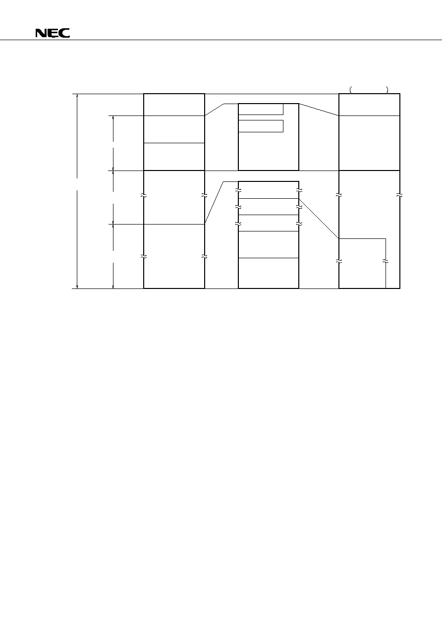
PD78366A can access a memory space of 64K bytes. Figures 2-1 through 2-3 show the memory map.
Figure 2-1. Memory Map (
µ
PD78368A)
Memory space
(64 K
◊
8)
Data memory
Program memory
Data memory
Program memory
Data memory
FEFFH
FFFFH
FF00H
FDFFH
FF00H
F6FFH
F700H
0000H
Special function register
(SFR)
(256
◊
8)
Main RAM
(256
◊
8)
External memory Note
(14080
◊
8)
Internal ROM
(49152
◊
8)
FEFFH
FE80H
FE25H
FE06H
F700H
BFFFH
1000H
0FFFH
0800H
07FFH
0080H
007FH
0040H
003FH
0000H
Program area
Program area
CALLT instruction table area
(64
◊
8)
Vector table area
(64
◊
8)
General-purpose
register (128
◊
8)
MODE0, 1 = HH
ROM-less mode
MODE0, 1 = LL
Macro service
control (32
◊
8)
Data area
(768
◊
8)
External memory
(63232
◊
8)
0FFFH
0000H
BFFFH
C000H
CALLF instruction entry area
(2048
◊
8)
Peripheral RAM
(1792
◊
8)
Note Accessed in external memory expansion mode.
Caution For word access (including stack operations) to the main RAM area (FE00H-FEFFH), the
address that specifies the operand must be an even value.

µ
PD78363A, 78365A, 78366A, 78368A
16
Figure 2-2. Memory Map (
µ
PD78365A, 78366A)
Memory space
(64 K
◊
8)
Data memory
Program memory
Data memory
Program memory
Data memory
FEFFH
FFFFH
FF00H
FDFFH
FF00H
F6FFH
F700H
0000H
Special function register
(SFR)
(256
◊
8)
Main RAM
(256
◊
8)
External memory Note
(30464
◊
8)
Internal ROM
(32768
◊
8)
FEFFH
FE80H
FE25H
FE06H
F700H
7FFFH
1000H
0FFFH
0800H
07FFH
0080H
007FH
0040H
003FH
0000H
Program area
Program area
CALLT instruction table area
(64
◊
8)
Vector table area
(64
◊
8)
General-purpose
register (128
◊
8)
MODE0, 1 = HH
PD78365A
PD78366A in ORM-less mode
µ
µ
µ
MODE0, 1 = LL
( PD78366A)
Macro service
control (32
◊
8)
Data area
(2048
◊
8)
External memory
(63232
◊
8)
0FFFH
0000H
7FFFH
8000H
CALLF instruction entry area
(2048
◊
8)
Peripheral RAM
(1792
◊
8)
Note Accessed in external memory expansion mode.
Caution For word access (including stack operations) to the main RAM area (FE00H-FEFFH), the
address that specifies the operand must be an even value.
µ
PD78363A, 78365A, 78366A, 78368A
17
Figure 2-3. Memory Map (
µ
PD78363A)
Memory space
(64 K
◊
8)
Data memory
Program memory
Data memory
Program memory
Data memory
FEFFH
FFFFH
FF00H
FDFFH
FF00H
FBFFH
FC00H
0000H
Special function register
(SFR)
(256
◊
8)
Main RAM
(256
◊
8)
External memory Note
(39936
◊
8)
Internal ROM
(24576
◊
8)
FEFFH
FE80H
FE25H
FE06H
FC00H
5FFFH
1000H
0FFFH
0800H
07FFH
0080H
007FH
0040H
003FH
0000H
Program area
Program area
CALLT instruction table area
(64
◊
8)
Vector table area
(64
◊
8)
General-purpose
register (128
◊
8)
MODE0, 1 = HH
ROM-less mode
MODE0, 1 = LL
Macro service
control (32
◊
8)
Data area
(768
◊
8)
External memory
(64512
◊
8)
0FFFH
0000H
5FFFH
6000H
CALLF instruction entry area
(2048
◊
8)
Peripheral RAM
(512
◊
8)
Note Accessed in external memory expansion mode.
Caution For word access (including stack operations) to the main RAM area (FE00H-FEFFH), the
address that specifies the operand must be an even value.
µ
PD78363A, 78365A, 78366A, 78368A
18
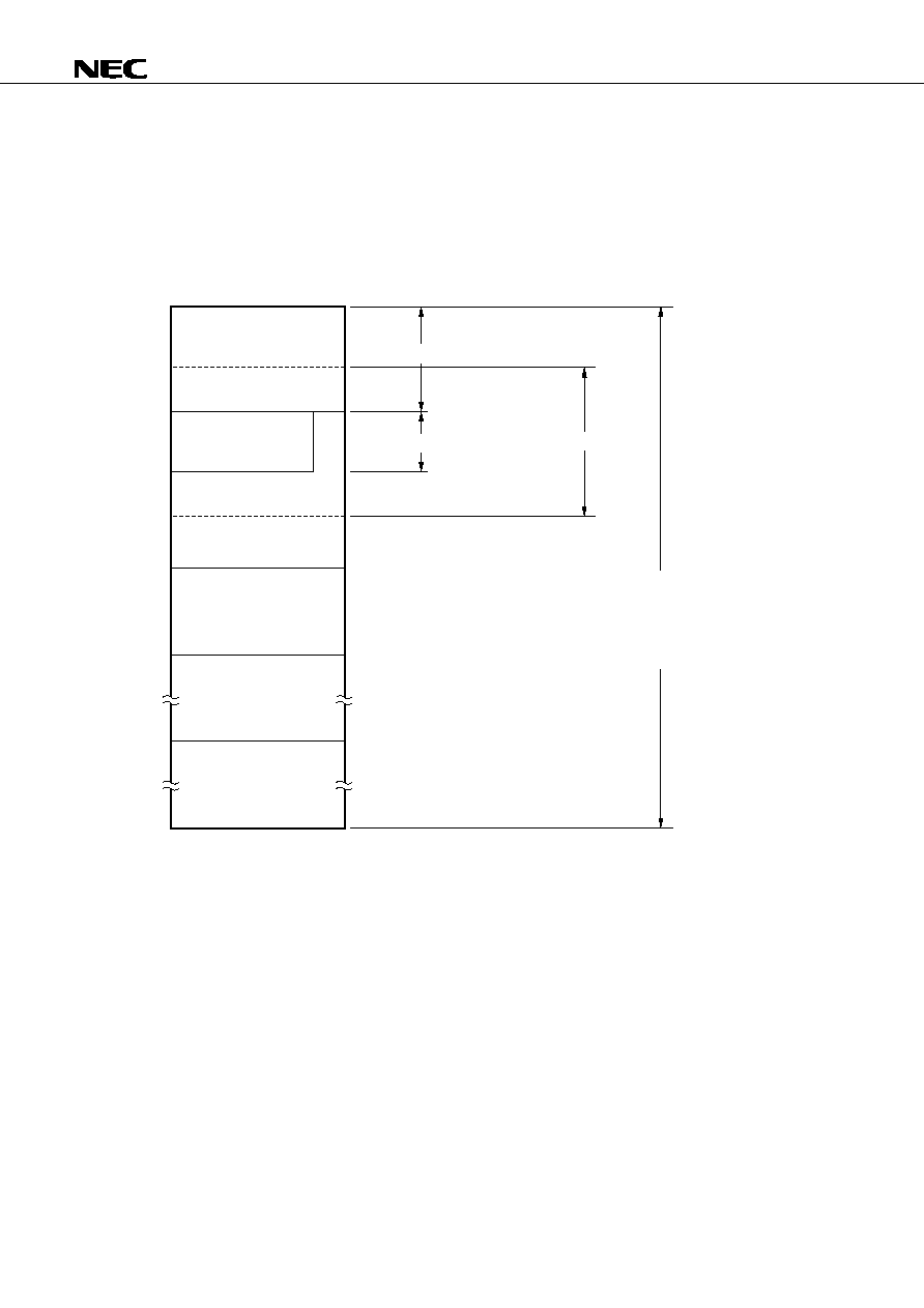
2.2
DATA MEMORY ADDRESSING
The
µ
PD78366A is provided with many addressing modes that improve the operability of the memory and
can be used with high-level languages. Especially, an area of addresses F700H-FFFFH (In the
µ
PD78363A,
FC00H-FFFFH) to which the data memory is mapped can be addressed in a mode peculiar to the functions
provided in this area, including special function registers (SFR) and general-purpose registers.
Figure 2-4. Data Memory Addressing (
µ
PD78368A)
FFFFH
FF20H
FF1FH
FE20H
FE1FH
F700H
F6FFH
FF00H
FEFFH
FE80H
FE7FH
FE00H
FDFFH
6C00H
BFFFH
0000H
Special function
register
(SFR)
General-purpose
register
Main RAM
Peripheral RAM
Internal ROM Note
External memory
SFR addressing
Register addressing
Short direct addressing
Direct addressing
Register indirect addressing
Based addressing
Based indexed addressing
Based indexed addressing
(with displacement)
Note Is external memory in the ROMless mode.
Caution For word access (including stack oprations) to the main RAM area (FE00H-FEFFH), the address
that specifies the operand must be an even value.
µ
PD78363A, 78365A, 78366A, 78368A
19
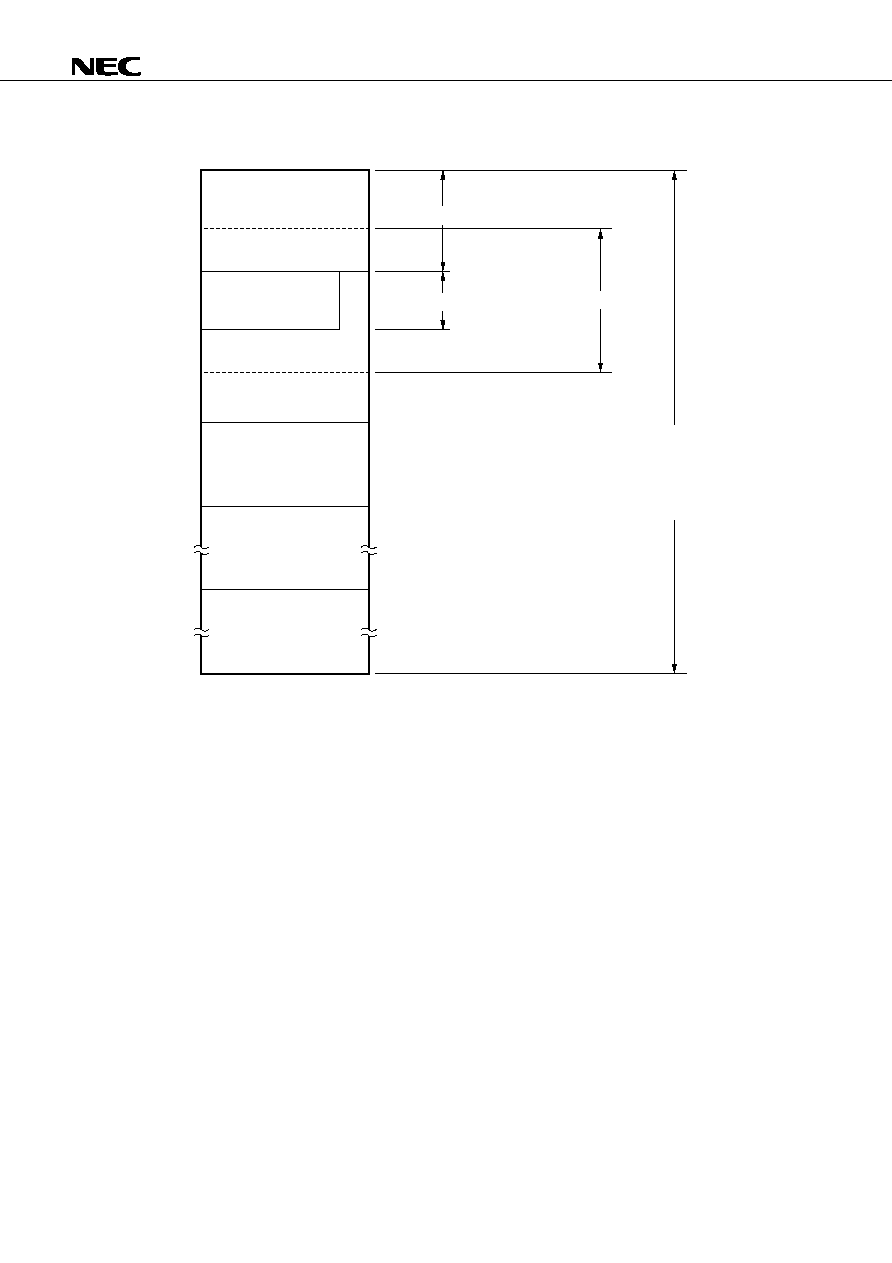
Figure 2-5. Data Memory Addressing (
µ
PD78365A, 78366A)
FFFFH
FF20H
FF1FH
FE20H
FE1FH
F700H
F6FFH
FF00H
FEFFH
FE80H
FE7FH
FE00H
FDFFH
8000H
7FFFH
0000H
Special function
register
(SFR)
General-purpose
register
Main RAM
Peripheral RAM
Internal ROM Note
External memory
SFR addressing
Register addressing
Short direct addressing
Direct addressing
Register indirect addressing
Based addressing
Based indexed addressing
Based indexed addressing
(with displacement)
Note Is external memory in the ROMless mode of the
µ
PD78365A or
µ
PD78366A.
Caution For word access (including stack oprations) to the main RAM area (FE00H-FEFFH), the address
that specifies the operand must be an even value.
µ
PD78363A, 78365A, 78366A, 78368A
20
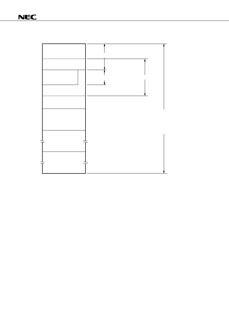
Figure 2-6. Data Memory Addressing (
µ
PD78363A)
FFFFH
FF20H
FF1FH
FE20H
FE1FH
FC00H
FBFFH
FF00H
FEFFH
FE80H
FE7FH
FE00H
FDFFH
6000H
5FFFH
0000H
Special function
register
(SFR)
General-purpose
register
Main RAM
Peripheral RAM
Internal ROM Note
External memory
SFR addressing
Register addressing
Short direct addressing
Direct addressing
Register indirect addressing
Based addressing
Based indexed addressing
Based indexed addressing
(with displacement)
Note Is external memory in the ROMless mode.
Caution For word access (including stack oprations) to the main RAM area (FE00H-FEFFH), the address
that specifies the operand must be an even value.
2.3
PROCESSOR REGISTERS
The
µ
PD78366A is provided with the following three types of processor registers:
∑ Control registers
∑ General-purpose registers
∑ Special function registers (SFRs)
µ
PD78363A, 78365A, 78366A, 78368A
21
2.3.1
Control Registers
(1) Program counter (PC)
This is a 16-bit register that holds an address of the instruction to be executed next.
(2) Program status word (PSW)
This 16-bit register indicates the status of the CPU as a result of instruction execution.
(3) Stack pointer (SP)
This 16-bit register indicates the first address of the stack area (LIFO) of the memory.
(4) CPU control word (CCW)
This 8-bit register is used to control the CPU.
Figure 2-7. Configuration of Control Registers
PC
PSW
SP
CCW
7
0
15
0
TPF
: Table position flag
CCW
0
0
0
0
0
0
TPF
0
7
0
Figure 2-8. Configuration of PSW
PSW
UF
RBS2
RBS1
RBS0
0
0
0
0
15
8
S
Z
RSS
AC
IE
P/V
0
CY
7
0
UF
: User flag
RBS0-RBS2: Register bank select flag
S
: Sign flag (MSB of execution result)
Z
: Zero flag
RSS
: Register set select flag
AC
: Auxiliary carry flag
IE
: Interrupt request enable flag
P/V
: Parity/overflow flag
CY
: Carry flag
Figure 2-9. Configuration of CCW
µ
PD78363A, 78365A, 78366A, 78368A
22
2.3.2
General-Purpose Registers
The
µ
PD78366A is provided with eight banks of general-purpose registers with one bank consisting of 8
words
◊
16 bits. Figure 2-10 shows the configuration of the general-purpose register banks. The general-
purpose registers are mapped to an area of addresses FE80H-FEFFH. Each of these registers can be used
as an 8-bit register. In addition, two registers can be used as one 16-bit register pair (refer to Figure 2-11 ).
These general-purpose registers facilitate complicated multitask processing.
Figure 2-10. Configuration of General-Purpose Register Banks
15
0
RP0
RP1
RP2
RP3
RP4
RP5
RP6
RP7
Bank 7
Bank 1
Bank 0
Figure 2-11. Processing Bits of General-Purpose Registers
RBNK0
RBNK1
RBNK2
RBNK3
RBNK4
RBNK5
RBNK7
RBNK6
R15
R13
R11
R9
R7
R5
R3
R1
R14
R12
R10
R8
R6
R4
R2
R0
RP7
RP6
RP5
RP4
RP3
RP2
RP1
RP0
(FH)
(DH)
(BH)
(9H)
(7H)
(5H)
(3H)
(1H)
(EH)
(CH)
(AH)
(8H)
(6H)
(4H)
(2H)
(0H)
FEFFH
FE80H
8-bit processing
16-bit processing
7
07
0
15
0

µ
PD78363A, 78365A, 78366A, 78368A
23
2.3.3
Special Function Registers (SFR)
Special function registers (SFRs) are registers assigned special functions such as mode registers and control
registers for internal peripheral hardware, and are mapped to a 256-byte address space at FF00H through
FFFFH.
Table 2-1 lists the SFRs. The meanings of the symbols in this table are as follows:
∑ Symbol ................................... Indicates the mnemonic symbol for an SFR.
This mnemonic can be coded in the operand field of an instruction.
∑ R/W ........................................ Indicates whether the SFR can be read or written.
R/W : Read/write
R
: Read only
W
: Write only
∑ Bit units for manipulation ...... Indicates bit units in which the SFR can be manipulated. The SFRs that
can be manipulated in 16-bit units can be coded as an sfrp operand.
Specify an even address for these SFRs.
The SFRs that can be manipulated in 1-bit units can be coded as the
operand of bit manipulation instructions.
∑ On reset ................................. Indicates the status of the register at RESET input.
Cautions 1. Do not access the addresses in the range FF00H through FFFFH to which no special
function register is allocated. If these addresses are accessed, malfunctioning may
occur.
2. Do not write data to the read-only registers. Otherwise, the internal circuit may not
operate normally.
3. When using read data as byte data, process undefined bit(s) first.
4. TOUT and TXS are write-only registers. Do no read these registers.
5. Bits 0, 1, and 4 of SBIC are write-only bits. When these bits are read, they are always
"0".

µ
PD78363A, 78365A, 78366A, 78368A
24
Table 2-1. List of Special Function Registers (1/5)
Bit units for
manipulation
1 bit
8 bits
16 bits
On reset
Address
Special function register (SFR)
Symbol
R/W
Undefined
FF00H
FF01H
FF02H
FF03H
FF04H
FF05H
FF07H
FF08H
FF09H
FF10H
FF11H
FF12H
FF13H
FF14H
FF15H
FF16H
FF17H
FF18H
FF19H
FF1AH
FF1BH
FF1CH
FF1DH
FF1EH
FF1FH
FF20H
FF21H
FF23H
FF25H
FF28H
FF29H
FF2CH
FF2DH
FF2EH
FF2FH
FF30H
FF31H
FF32H
FF33H
Port 0
Port 1
Port 2
Port 3
Port 4
Port 5
Port 7
Port 8
Port 9
Compare register 00
Compare register 01
Compare register 02
Compare register 03
Buffer register CM00
Buffer register CM01
Buffer register CM02
Timer register 0
Port 0 mode register
Port 1 mode register
Port 3 mode register
Port 5 mode register
Port 8 mode register
Port 9 mode register
Reload register
Timer unit mode register 0
Timer unit mode register 1
Compare register 10
Timer register 1
R/W
R
R/W
R
R/W
R
R/W
R/W
R
q
q
q
q
≠
q
q
q
q
≠
q
q
q
q
≠
q
q
q
q
≠
q
q
q
q
≠
q
q
q
q
≠
q
q
q
q
≠
q
q
q
q
≠
q
q
q
q
≠
≠
≠
q
q
≠
≠
q
q
≠
≠
q
q
≠
≠
q
q
≠
≠
q
q
≠
≠
q
q
≠
≠
q
q
≠
≠
q
q
q
q
q
q
≠
q
q
q
q
≠
q
q
q
q
≠
q
q
q
q
≠
q
q
q
q
≠
q
q
q
q
≠
≠
≠
q
q
q
q
q
q
≠
q
q
q
q
≠
≠
≠
q
q
≠
≠
q
q
0000H
FFH
◊
111 1111B
FFH
◊◊
11 1111B
◊◊◊◊
1111B
Undefined
00H
Undefined
0000H
P0
P1
P2
P3
P4
Note
P5
Note
P7
P8
P9
CM00
CM01
CM02
CM03
BFCM00
BFCM01
BFCM02
TM0
PM0
PM1
PM3
PM5
Note
PM8
PM9
DTIME
TUM0
TUM1
CM10
TM1
Note Not provided for the
µ
PD78365A.
µ
PD78363A, 78365A, 78366A, 78368A
25
Table 2-1. List of Special Function Registers (2/5)
Bit units for
manipulation
1 bit
8 bits
16 bits
On reset
Address
Special function register (SFR)
Symbol
R/W
FF34H
FF35H
FF36H
FF37H
FF38H
FF39H
FF3AH
FF3BH
FF3CH
FF3DH
FF40H
FF43H
FF44H
FF45H
FF48H
FF4EH
FF4FH
FF50H
FF51H
FF52H
FF53H
FF54H
FF55H
FF56H
FF57H
FF58H
FF59H
FF5AH
FF5BH
FF5CH
FF5DH
FF5EH
FF5FH
FF60H
FF61H
FF62H
FF68H
Capture/compare register 20
Capture register 20
Timer register 2
Buffer register CM03
External interrupt mode register 0
External interrupt mode register 1
Port 0 mode control register
Port 3 mode control register
Pull-up resistor option register L
Pull-up resistor option register H
Port 8 mode control register
Sampling control register 0
Sampling control register 1
Capture/compare register 30
Capture register 30
Capture register 31
Timer register 3
Compare register 40
Compare register 41
Timer register 4
Timer control register 4
Timer out register
Real-time output port register
Real-time output port mode register
Port read control register
A/D converter mode register
CC20
CT20
TM2
BFCM03
INTM0
INTM1
PMC0
PMC3
PUOL
PUOH
PMC8
SMPC0
SMPC1
CC30
CT30
CT31
TM3
CM40
CM41
TM4
TMC4
TOUT
RTP
RTPM
PRDC
ADM
≠
≠
q
q
≠
≠
q
q
≠
≠
q
q
≠
≠
q
q
q
q
q
q
≠
q
q
q
q
≠
q
q
q
q
≠
q
q
q
q
≠
q
q
q
q
≠
q
q
q
q
≠
q
q
q
q
≠
q
q
q
q
≠
q
q
q
q
≠
≠
≠
q
q
≠
≠
q
q
≠
≠
q
q
≠
≠
q
q
≠
≠
q
q
≠
≠
q
q
≠
≠
q
q
≠
q
q
≠
≠
q
q
≠
q
q
q
q
≠
q
q
q
q
≠
q
q
q
q
≠
q
q
q
q
≠
R/W
R
R/W
R
R/W
R
R/W
W
R/W
Undefined
0000H
Underfined
00H
◊
000 0000B
00H
◊◊
00 0000B
00H
Undefined
0000H
Undefined
0000H
00H
◊◊
01 0101B
Undefined
00H
µ
PD78363A, 78365A, 78366A, 78368A
26
Table 2-1. List of Special Function Registers (3/5)
Bit units for
manipulation
1 bit
8 bits
16 bits
On reset
Address
Special function register (SFR)
Symbol
R/W
FF70H
FF71H
FF72H
FF73H
FF74H
FF75H
FF76H
FF77H
FF78H
FF79H
FF7AH
FF7BH
FF7CH
FF7DH
FF7EH
FF7FH
FF80H
FF82H
FF84H
FF85H
FF86H
FF88H
FF8AH
FF8CH
FF8EH
FFA0H
FFA1H
FFA2H
FFA2H
FFA3H
Slave buffer register 0
Slave buffer register 1
Slave buffer register 2
Slave buffer register 3
Slave buffer register 4
Slave buffer register 5
Master buffer register 0
Master buffer register 1
Master buffer register 2
Master buffer register 3
Master buffer register 4
Master buffer register 5
Timer control register 0
Timer control register 1
Timer control register 2
Timer control register 3
Clocked serial interface mode register
Serial bus interface control register
Baud rate generator control register
Baud rate generator compare register
Serial I/O shift register
Asynchronous serial interface mode register
Asynchronous serial interface status register
Serial receive buffer: UART
Serial transfer shift register: UART
PWM control register 0
PWM control register 1
PWM register 0L
PWM register 0
SBUF0
SBUF1
SBUF2
SBUF3
SBUF4
SBUF5
MBUF0
MBUF1
MBUF2
MBUF3
MBUF4
MBUF5
TMC0
TMC1
TMC2
TMC3
CSIM
SBIC
BRGC
BRG
SIO
ASIM
ASIS
RXB
TXS
PWMC0
PWMC1
PWM0L
PWM0
q
q
q
q
≠
q
q
q
q
≠
q
q
q
q
≠
q
q
q
q
≠
q
q
q
q
≠
q
q
q
q
≠
q
q
q
q
≠
q
q
q
q
≠
q
q
q
q
≠
q
q
q
q
≠
q
q
q
q
≠
q
q
q
q
≠
q
q
q
q
≠
q
q
q
q
≠
q
q
q
q
≠
q
q
q
q
≠
q
q
q
q
≠
q
q
q
q
≠
q
q
q
q
≠
≠
q
q
≠
q
q
q
q
≠
q
q
q
q
≠
q
q
q
q
≠
≠
q
q
≠
≠
q
q
≠
q
q
q
q
≠
q
q
q
q
≠
q
q
q
q
≠
≠
≠
q
q
Undefined
00H
Undefined
80H
00H
Undefined
00H
Undefined
Note Bits 7 and 5
: read/write
Bits 6, 3, and 2 : read-only
Bits 4, 1, and 0 : write-only
R/W
R/W
Note
R/W
R
W
R/W
µ
PD78363A, 78365A, 78366A, 78368A
27
Table 2-1. List of Special Function Registers (4/5)
Bit units for
manipulation
1 bit
8 bits
16 bits
On reset
Address
Special function register (SFR)
Symbol
R/W
q
q
q
q
≠
≠
≠
q
q
q
q
q
q
≠
q
q
q
q
≠
q
q
q
q
≠
≠
≠
q
q
q
q
q
q
≠
≠
≠
q
q
≠
q
q
≠
≠
≠
q
q
≠
q
q
≠
≠
≠
q
q
≠
q
q
≠
≠
≠
q
q
≠
q
q
≠
≠
≠
q
q
≠
q
q
≠
≠
≠
q
q
≠
q
q
≠
≠
≠
q
q
≠
q
q
≠
≠
≠
q
q
≠
q
q
≠
≠
q
q
≠
q
q
q
q
≠
≠
q
q
≠
PWM1L
PWM1
ISPR
IMC
MK0L
MK0
MK0H
ADCR0
ADCR0H
ADCR1
ADCR1H
ADCR2
ADCR2H
ADCR3
ADCR3H
ADCR4
ADCR4H
ADCR5
ADCR5H
ADCR6
ADCR6H
ADCR7
ADCR7H
STBC
Note
CCW
WDM
Note
R/W
R
R/W
R
R/W
Undefined
00H
80H
FFH
FFFFH
FFH
Undefined
0000
◊
000B
00H
FFA4H
FFA4H
FFA5H
FFA8H
FFAAH
FFACH
FFACH
FFADH
FFADH
FFB0H
FFB1H
FFB1H
FFB2H
FFB3H
FFB3H
FFB4H
FFB5H
FFB5H
FFB6H
FFB7H
FFB7H
FFB8H
FFB9H
FFB9H
FFBAH
FFBBH
FFBBH
FFBCH
FFBDH
FFBDH
FFBEH
FFBFH
FFBFH
FFC0H
FFC1H
FFC2H
PWM register 1L
PWM register 1
In-service priority register
Interrupt mode control register
Interrupt mask register 0L
Interrupt mask register 0
Interrupt mask register 0H
A/D conversion result register 0
A/D conversion result register 0H
A/D conversion result register 1
A/D conversion result register 1H
A/D conversion result register 2
A/D conversion result register 2H
A/D conversion result register 3
A/D conversion result register 3H
A/D conversion result register 4
A/D conversion result register 4H
A/D conversion result register 5
A/D conversion result register 5H
A/D conversion result register 6
A/D conversion result register 6H
A/D conversion result register 7
A/D conversion result register 7H
Standby control register
CPU control word
Watchdog timer mode register
Note Can be written when a special instruction is executed.
µ
PD78363A, 78365A, 78366A, 78368A
28
Table 2-1. List of Special Function Registers (5/5)
Bit units for
manipulation
1 bit
8 bits
16 bits
On reset
Address
Special function register (SFR)
Symbol
R/W
Note
C0AAH
Undefined
43H
Memory expansion mode register
Programmable wait control register
External SFR area
Interrupt control register (INTOV3)
Interrupt control register (INTP0/INTCC30)
Interrupt control register (INTP1)
Interrupt control register (INTP2)
Interrupt control register (INTP3/INTCC20)
Interrupt control register (INTP4)
Interrupt control register (INTTM0)
Interrupt control register (INTCM03)
Interrupt control register (INTCM10)
Interrupt control register (INTCM40)
Interrupt control register (INTCM41)
Interrupt control register (INTSER)
Interrupt control register (INTSR)
Interrupt control register (INTST)
Interrupt control register (INTCSI)
Interrupt control register (INTAD)
FFC4H
FFC6H
FFC7H
FFD0H
|
FFDFH
FFE0H
FFE1H
FFE2H
FFE3H
FFE4H
FFE5H
FFE6H
FFE7H
FFE8H
FFE9H
FFEAH
FFEBH
FFECH
FFEDH
FFEEH
FFEFH
MM
PWC
≠
OVIC3
PIC0
PIC1
PIC2
PIC3
PIC4
TMIC0
CMIC03
CMIC10
CMIC40
CMIC41
SERIC
SRIC
STIC
CSIIC
ADIC
q
q
q
q
≠
≠
≠
q
q
q
q
q
q
≠
q
q
q
q
≠
q
q
q
q
≠
q
q
q
q
≠
q
q
q
q
≠
q
q
q
q
≠
q
q
q
q
≠
q
q
q
q
≠
q
q
q
q
≠
q
q
q
q
≠
q
q
q
q
≠
q
q
q
q
≠
q
q
q
q
≠
q
q
q
q
≠
q
q
q
q
≠
q
q
q
q
≠
q
q
q
q
≠
Note The value of the MW register at reset time differs depending on the product.
µ
PD78363A
: 60H
µ
PD78365A, 78366A : 20H
µ
PD78368A
: 00H
R/W

µ
PD78363A, 78365A, 78366A, 78368A
29
3.
FUNCTIONAL BLOCKS
3.1
EXECUTION UNIT (EXU)
EXU controls address computation, arithmetic and logical operations, and data transfer through microprogram.
EXU has an internal main RAM. This RAM can be accessed by instructions faster than the peripheral RAM.
3.2
BUS CONTROL UNIT (BCU)
BCU starts necessary bus cycles according to the physical address obtained by the execution unit (EXU).If
EXU does not request start of the bus cycle, an address is generated to prefetch an instruction. The prefetched
op code is stored in an instruction queue.
3.3
ROM/RAM
The internal ROM and RAM capacities differ depending on the product.
The
µ
PD78363A has a 24-KB ROM and a 512-B peripheral RAM. The
µ
PD78366A has a 32-KB ROM and
a 1792-B peripheral RAM. The
µ
PD78368A has a 48-KB ROM and a 1792-B peripheral RAM. The
µ
PD78365A
does not have a ROM and only has a 1792-B peripheral RAM.
Access to the ROM can be disabled by using the MODE0 and MODE1 pins, in which case an external memory
of 64 KB can be accessed.
µ
PD78363A, 78365A, 78366A, 78368A
30
3.4
PORT FUNCTIONS
The
µ
PD78366A is provided with the ports shown in Figure 3-1 for various control operations.
The functions of each port are listed in Table 3-1. These ports function not only as digital ports but also as
input/output lines of the internal hardware.
Figure 3-1. Port Configuration
P00
P07
P10
P17
P20
P25
P30
P36
8
8
P50
P57
P70-P77
P80
P85
P90
P93
P40-P47
Port 0
Port 1
Port 2
Port 3
Port 4
Port 5
Port 8
Port 7
Port 9
µ
PD78363A, 78365A, 78366A, 78368A
31
Table 3-1. Functions of Each Port
8-bit I/O port. Can be set in input or
output mode in 1-bit units.
8-bit I/O port. Can be set in input or
output mode in 1-bit units.
6-bit input port.
7-bit I/O port. Can be set in input or
output in 1-bit units.
8-bit I/O port. Can be set in input or
output mode in 8-bit units.
8-bit I/O port. Can be set in input or
output mode in 1-bit units.
8-bit input port.
6-bit I/O port. Can be set in input or
output mode in 1-bit units.
4-bit I/O port. Can be set in input or
output mode in 1-bit units.
In control mode, serves as real-time output port (RTP), or
input operation control signal of real-time pulse unit (RPU)
and output PWM signal.
--
Inputs external interrupt and count pulse of real-time pulse
unit (RPU) (fixed to the control mode).
In control mode, inputs/outputs signals of serial interfaces
(UART, CSI).
Address data bus (AD0-AD7) when memory is externally
expanded.
Address bus (A8-A15) when memory is externally expanded.
Input analog signals to A/D converter (fixed to the control
mode).
In control mode, outputs timer of real-time pulse unit (RPU).
Outputs control signal when memory is externally expanded.
Port
Port function
Multiplexed function
Port 0
Port 1
Port 2
Port 3
Port 4
Port 5
Port 7
Port 8
Port 9
µ
PD78363A, 78365A, 78366A, 78368A
32
3.5
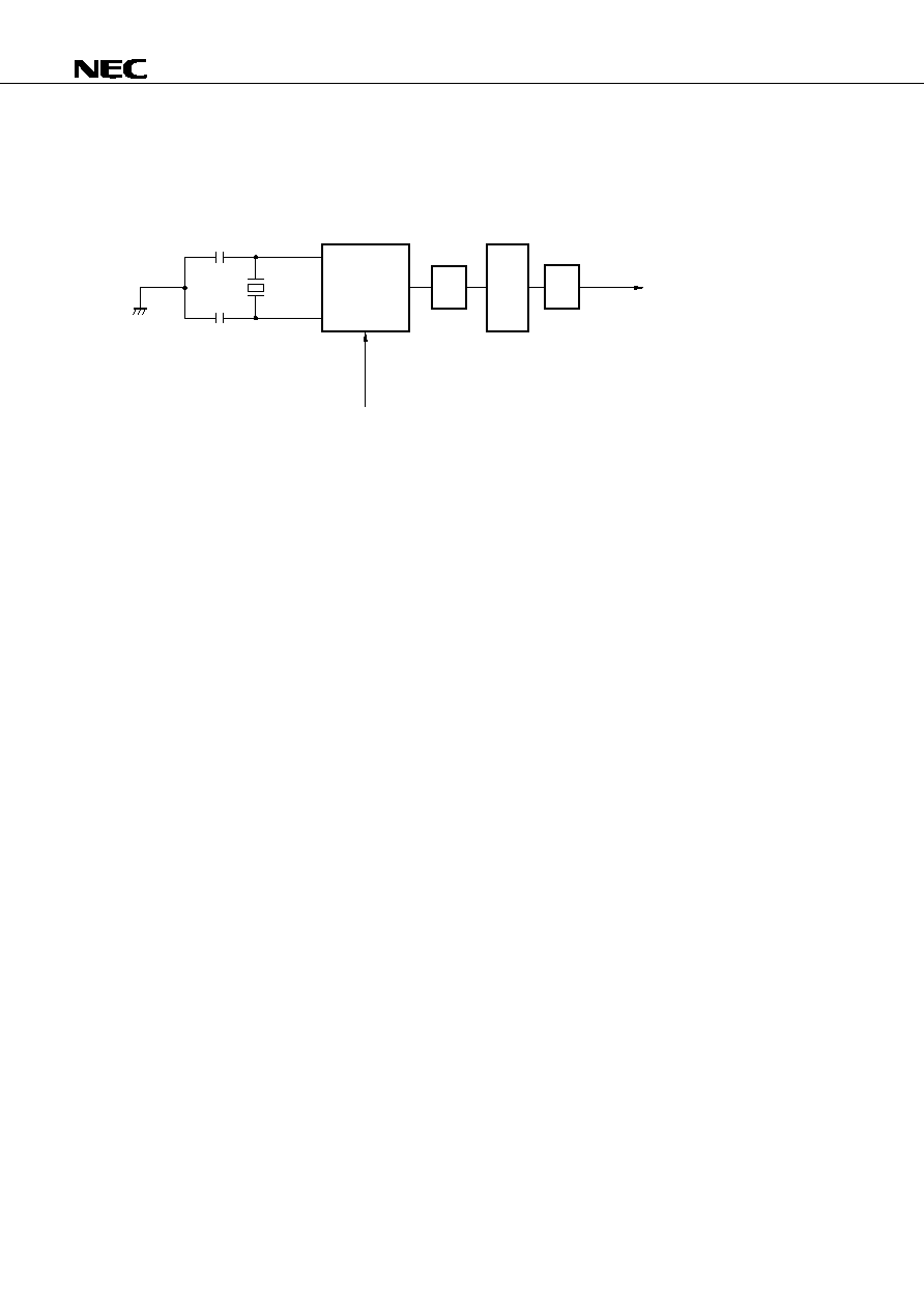
CLOCK GENERATOR CIRCUIT
The clock generator circuit generates and controls the internal system clock (CLK) that is supplied to the CPU.
Figure 3-2. Block Diagram of Clock Generator Circuit
X1
X2
f
XX
or
f
X
f
CLK
1/2
System
cloock
oscillator
circuit
Internal system
clock (CLK)
STOP mode
Frequency
divider
1/2
PLL
control
circuit
Frequency
divider
Remarks 1.
f
XX
: crystal oscillation frequency
2.
f
X
: external clock frequency
3.
f
CLK
: internal system clock frequency
By connecting an 8-MHz crystal resonator across the X1 and X2 pins, an internal system clock of up to 16
MHz (f
CLK
) can be generated.
The system clock oscillation circuit oscillates by using the crystal resonator connected across the X1 and
X2 pins. It stops oscillation in standby mode.
An external clock can also be input. To do so, input the clock signal to the X1 pin and leave the X2 pin open.
Caution
Do not set STOP mode when the external clock is used.

µ
PD78363A, 78365A, 78366A, 78368A
33
Figure 3-3. External Circuit of System Clock Oscillator Circuit
(a) crystal oscillator
(b) external clock
PD78366A
µ
V
SS
X1
X2
PD78366A
µ
X1
X2
Open
Cautions 1. Wire the portion enclosed by dotted line in Figure 3-3 as follows to avoid adverse
influences due to wiring capacity when using the system clock oscillation circuit.
∑ Keep the wiring length as short as possible.
∑ Do not cross the wiring with the other signal line. Make sure that the wiring is not close
to lines through which a high alternating current flows.
∑ Always keep the ground point of the capacitor of the oscillation circuit at the same
potential as V
SS
. Do not ground the circuit to a ground pattern through which a high
current flows.
∑ Do not extract signals from the oscillator circuit.
2. To input an external clock, do not connect a load such as wiring capacitance to the X2
pin.

µ
PD78363A, 78365A, 78366A, 78368A
34
3.6
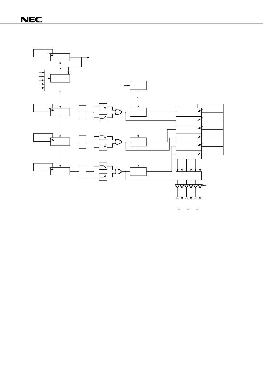
REAL-TIME PULSE UNIT (RPU)
The real-time pulse unit (RPU) can measure pulse intervals and frequencies, and output programmable
pulses (six channels of PWM control signals).
The RPU consists of five 16-bit timers (timers 0 through 4), of which one is provided with a 10-bit dead time
timer, which is ideal for inverter control. In addition, a function to turn off the output by the software or an external
interrupt is also provided.
Each timer has the following features:
∑
Timer 0 : Controls the PWM period of the TO00 through TO05 pins. In addition, operates as a
general-purpose interval timer. Timer 0 has the following five operation modes:
∑ General-purpose interval timer mode
∑ PWM mode 0 (symmetrical triangular wave)
∑ PWM mode 0 (asymmetrical triangular wave)
∑ PWM mode 0 (saw-tooth wave)
∑ PWM mode 1
∑
Timer 1 : Operates as a general-purpose interval timer.
∑
Timers 2, 3 : Has a programmable input sampling circuit that rejects the noise of an input signal,
and a capture function.
∑
Timer 4 : Operates as a general-purpose timer or an up-down counter. When operating as a general-
purpose timer, controls the PWM cycle of the TO40 output pin. Timer 4 has the following
two operation modes:
∑ General-purpose timer mode
∑ Up/down counter mode (UDC mode)
µ
PD78363A, 78365A, 78366A, 78368A
35
The RPU consists of the hardware shown in Table 3-2. Figures 3-4 through 3-12 show the block diagrams
of the respective timers.
Table 3-2. Configuration of Real-Time Pulse Unit (RPU)
16-bit compare register (CM00)
≠
16-bit compare register (CM01)
≠
16-bit compare register (CM02)
≠
16-bit compare register (CM03)
INTCM03
16-bit compare register (CM10)
INTCM10
16-bit capture/compare register (CC20)
INTCC20
16-bit capture register (CT20)
≠
16-bit capture/compare register (CC30)
INTCC30
16-bit capture register (CT30)
≠
16-bit capture register (CT31)
≠
16-bit compare register (CM40)
INTCM40
16-bit compare register (CM41)
INTCM41
Timer 0 16-bit timer (TM0)
Timer 1 16-bit timer (TM1)
Timer 2 16-bit timer (TM2)
Timer 3 16-bit timer (TM3)
Timer 4 16-bit timer (TM4)
Compare
register
coincidence
interrupt
Capture
trigger
Timer
output
Timer
clear
≠
6
INTCM03
≠
≠
INTCM10
INTP3
≠
INTCC20
INTP0
INTP1
≠
INTCC30
INTP4
TCLRUD
INTCM40
≠
1
Timer register
Register
µ
PD78363A, 78365A, 78366A, 78368A
36
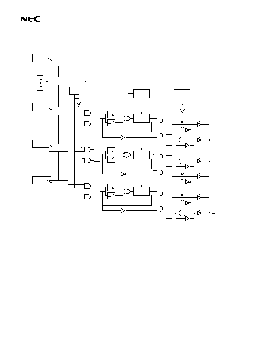
Figure 3-4. Block Diagram of Timer 0 (PWM mode 0 ... symmetrical triangular wave,
asymmetrical triangular wave)
BFCM03
CM03
TM0
BFCM00
CM00
R
S
DTM0
R
S
TO00
(U phase)
Underflow
R
S
TO01
(U phase)
BFCM01
CM01
R
S
DTM1
R
S
TO02
(V phase)
Underflow
R
S
TO03
(V phase)
BFCM02
CM02
R
S
DTM2
R
S
TO04
(W phase)
Underflow
R
S
TO05
(W phase)
INTCM03
INTTM0
16
16
f
CLK
f
CLK
/2
f
CLK
/4
f
CLK
/8
f
CLK
/16
U/D
UP = 0
DOWN = 1
DTIME
f
CLK
10
ALVTO
Output off function
by external interrupt
and software
TM0
: Timer register
ALVTO: Bit 2 of TUM0 register
CM00-CM03
: Compare registers
U/D
: Bit 3 of TMC0 register
BFCM00-BFCM03 : Buffer registers
DTIME
: Reload register
DTM0-DTM2
: Dead time timers
Remark f
CLK
: internal system clock
µ
PD78363A, 78365A, 78366A, 78368A
37
Figure 3-5. Block Diagram of Timer 0 (PWM mode 0 ... saw-tooth wave)
BFCM03
CM03
TM0
BFCM00
CM00
R
S
DTM0
R
S
TO00
(U phase)
Underflow
R
S
TO01
(U phase)
BFCM01
CM01
R
S
DTM1
R
S
TO02
(V phase)
Underflow
R
S
TO03
(V phase)
BFCM02
CM02
R
S
DTM2
R
S
TO04
(W phase)
Underflow
R
S
TO05
(W phase)
INTCM03
16
16
f
CLK
f
CLK
/2
f
CLK
/4
f
CLK
/8
f
CLK
/16
DTIME
f
CLK
10
ALVTO
Output off function
by external interrupt
and software
Clear
TM0
: Timer register
CM00-CM03
: Compare registers
BFCM00-BFCM03 : Buffer registers
DTIME
: Reload register
DTM0-DTM2
: Dead time timers
ALVTO
: Bit 2 of TUM0 register
Remark f
CLK
: internal system clock
µ
PD78363A, 78365A, 78366A, 78368A
38
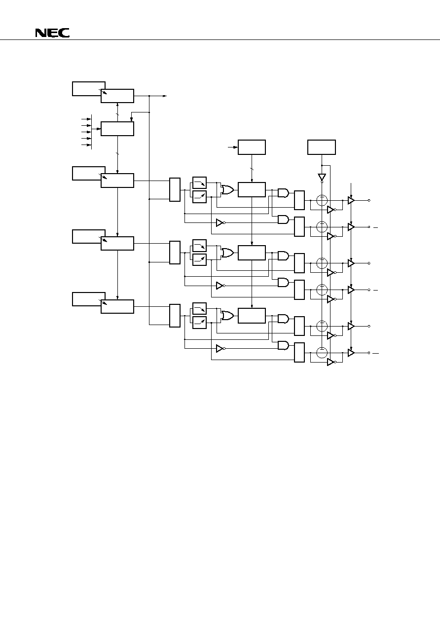
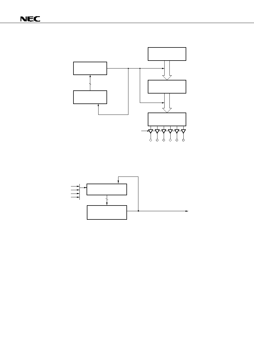
Figure 3-6. Block Diagram of Timer 0 (PWM mode 1)
MBUF1
MBUF0
MBUF3
MBUF2
MBUF5
MBUF4
BFCM03
CM03
TM0
BFCM00
CM00
BFCM01
CM01
BFCM02
CM02
INTCM03
16
16
f
CLK
f
CLK
/2
f
CLK
/4
f
CLK
/8
f
CLK
/16
Clear
DTM0
DTIME
T
DTM1
T
DTM2
T
10
f
CLK
Underflow
Underflow
Underflow
SBUF1
SBUF0
SBUF3
SBUF2
SBUF5
SBUF4
6-bit buffer
register
6-bit buffer
register
6-bit write-only
register
TOUT
Output off function
by external interrupt
and software
TO00
(U phase)
TO02
(V phase)
TO04
(W phase)
TO01
(U phase)
TO03
(V phase)
TO05
(W phase)
TM0
: Timer register
MBUF0-MBUF5 : Master buffer registers
CM00-CM03
: Compare registers
SBUF0-SBUF5 : Slave buffer registers
BFCM00-BFCM03 : Buffer registers
TOUT
: Timer out register
DTIME
: Reload register
DTM0-DTM2
: Dead time timers
Remark f
CLK
: internal system clock
µ
PD78363A, 78365A, 78366A, 78368A
39
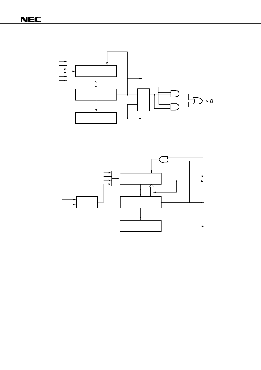
Figure 3-7. Block Diagram of Timer 0 (general-purpose interval timer mode)
Compare register
CM03
Timer register
TM0
16
Master buffer register
(MBUF0)
Slave buffer register
(SBUF0)
Timer out register
(TOUT)
6
6
INTCM03
Clear
Output off function by external
interrupt and software
TO00
TO02
TO04
TO01
TO03
TO05
Figure 3-8. Block Diagram of Timer 1
f
CLK
/4
f
CLK
/8
f
CLK
/16
TI
INTCM10
Clear
16
Timer register
TM1
Compare register
CM10
Remark f
CLK
: internal system clock

µ
PD78363A, 78365A, 78366A, 78368A
40
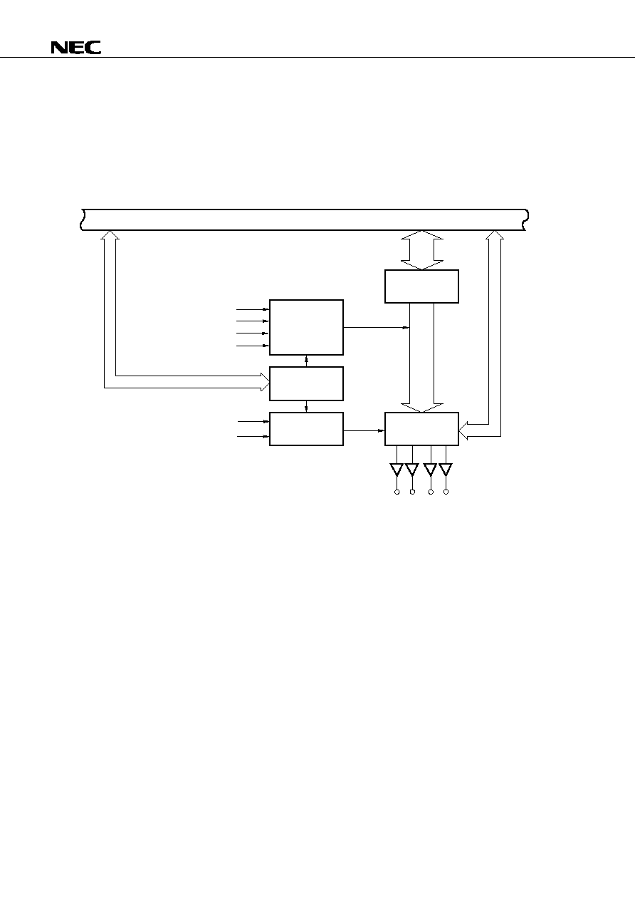
Figure 3-9. Block Diagram of Timer 2
4-point sampling
noise rejection
circuit
Timer register TM2
Capture/compare
register CC20
Capture register CT20
16
f
CLK
/2
2
f
CLK
/2
3
f
CLK
/2
4
f
CLK
/2
5
f
CLK
/2
6
f
CLK
/2
8
f
CLK
/2
9
f
CLK
/2
10
f
CLK
f
CLK
/2
2
f
CLK
/2
3
f
CLK
/2
4
f
CLK
/2
6
f
CLK
/2
7
f
CLK
/2
8
CLR2
INTP3/INTCC20
INTP3
Clear
Remark f
CLK
: internal system clock
Figure 3-10. Block Diagram of Timer 3
4-point sampling
noise rejection
circuit
Timer register TM3
Capture/compare
register CC30
16
f
CLK
/2
2
f
CLK
/2
3
f
CLK
/2
4
f
CLK
/2
5
f
CLK
/2
6
f
CLK
/2
8
f
CLK
f
CLK
/2
2
f
CLK
/2
3
f
CLK
/2
4
CLR3
INTP0/INTCC30
INTP0
4-point sampling
noise rejection
circuit
Capture register CT30
f
CLK
f
CLK
/2
2
f
CLK
/2
3
f
CLK
/2
4
INTP1
INTP1
4-point sampling
noise rejection
circuit
f
CLK
f
CLK
/2
2
f
CLK
/2
3
f
CLK
/2
4
INTP4
INTP4
INTOV3
Clear
Capture register CT31
Remark f
CLK
: internal system clock
µ
PD78363A, 78365A, 78366A, 78368A
41
Figure 3-11. Block Diagram of Timer 4 (General-Purpose Timer Mode)
f
CLK
f
CLK
/2
f
CLK
/4
f
CLK
/8
f
CLK
/16
f
CLK
/32
Timer register
TM4
Compare register
CM40
Compare register
CM41
Clear
INTCM40
Q
S
16
R
INTCM41
ALV40
TO40
Remark f
CLK
: internal system clock
Figure 3-12. Block Diagram of Timer 4 (UDC Mode)
f
CLK
/4
f
CLK
/8
f
CLK
/16
Timer register
TM4
INTCM40
TCLRUD
Compare register
CM40
Compare register
CM41
Up/down
detector
TIUD
Clear
16
INTCM41
TCUD
OVF
UDF
Pre-set
Remark f
CLK
: internal system clock
µ
PD78363A, 78365A, 78366A, 78368A
42
3.7
REAL-TIME OUTPUT PORT (RTP)
The real-time output port is a 4-bit port that can output the contents of the real-time output port register (RTP)
in synchronization with the trigger signal from the real-time pulse unit (RPU). It can output synchronization
pulses of multiple channels.
Also, PWM modulation can be applied to P00-P03.
Figure 3-13. Block Diagram of Real-Time Output Port
4
4
RTP
P03P02 P01P00
PWM0
PWM1
Internal bus
INTCM03 (from RPU)
INTCM10 (from RPU)
INTP0/INTCC30 (from RPU)
Software trigger
Output trigger
control circuit
RTPM
PWM signal
control circuit
Output latch
(P03-P00)
µ
PD78363A, 78365A, 78366A, 78368A
43
3.8
A/D CONVERTER
The
µ
PD78366A contains a high-speed, high-resolution 10-bit analog-to-digital (A/D) converter (conversion
time 12.6
µ
s at an internal clock frequency of 16 MHz). Successive approximation type is adopted. This
converter is provided with eight analog input lines (ANI0-ANI7) and can perform various operations as the
application requires, in select, scan, and mixed modes.
When A/D conversion ends, an internal interrupt (INTAD) occurs. This interrupt can start a macro service
that executes automatic data transfer through hardware.
Figure 3-14. Block Diagram of A/D Converter
ADCR0
ADCR1
ADCR2
ADCR3
ADCR4
ADCR5
ADCR6
ADCR7
ADM (8)
10
8
9
9
0
0
10
10
ANI0
ANI1
ANI2
ANI3
ANI4
ANI5
ANI6
ANI7
INTCM03
INTP2
AV
DD
AV
REF
AV
SS
SAR (10)
Input curcuit
Sample & hold
Resistor
string
Comparator
Controller
(Start trigger)
Internal bus
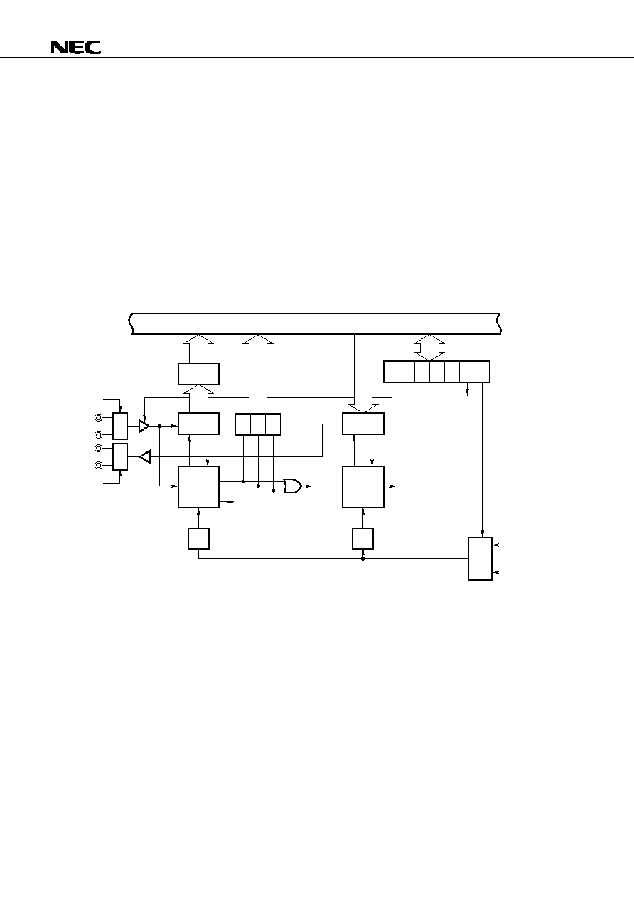
µ
PD78363A, 78365A, 78366A, 78368A
44
3.9
SERIAL INTERFACE
The
µ
PD78366A is provided with the following two independent serial interfaces:
∑
Asynchronous serial interface (UART) (with pin selection function)
∑
Clocked serial interface
∑ 3-line serial I/O mode
∑ Serial bus interface mode (SBI mode)
Since the
µ
PD78366A contains a baud rate generator (BRG), any serial transfer rate can be set regardless
of the operating clock frequency. The baud rate generator is a block to generate the shift clock for the transmit/
receive serial interface, and is used commonly with the two channels of the serial interfaces.
The serial transfer rate can be selected in a range of 110 bps to 38.4 Kbps by the mode register.
Figure 3-15. Block Diagram of Asynchronous Serial Interface
SPS
R
X
D0
R
X
D1
T
X
D0
T
X
D1
SPS
RXB
PE FE OVE
RXE PS1 PS0 CL SL SPS SCK
ASIM
TXS
ASIS
INTSR
INTSER
INTST
1
--
16
1
--
16
f
CLK
/8
Internal bus
Receive
buffer
Receive
shift
register
Receive
control
parity
check
Selector
Selector
Transfer
shift
register
Transfer
control
parity
append
Transfer/
receive
baud rate
generator
output
Selector
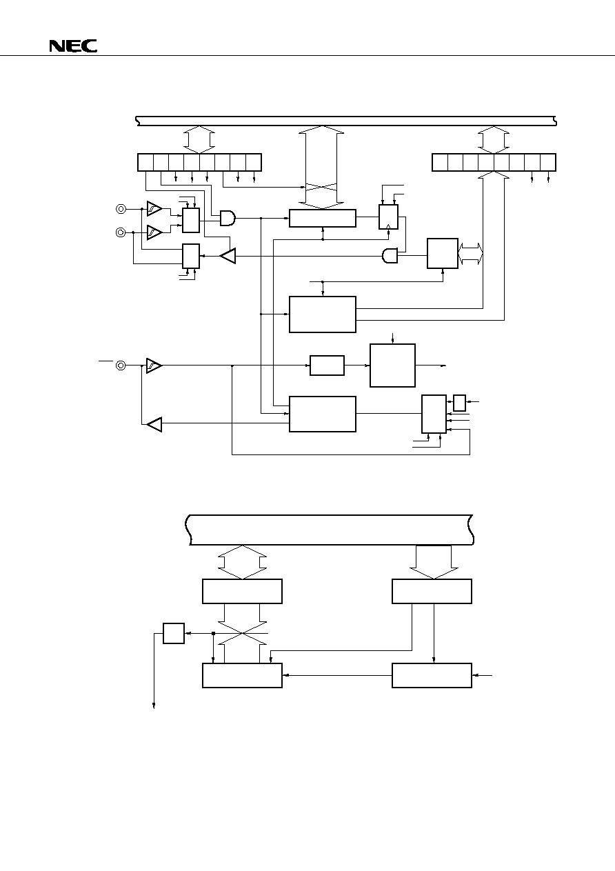
µ
PD78363A, 78365A, 78366A, 78368A
45
Figure 3-16. Block Diagram of Clocked Serial Interface
CTXE
SI/SB1
SO/SB0
MOD1
MOD2
MOD1
SCK
MOD1
MOD2
WUP
INTCSI
1/2
f
CLK
/8
f
CLK
/32
CLS0
CLS1
CMDT
RELT
SBIC
MOD1
MOD2
WUP
CRXE
MOD0 CLS1 CLS0
BSYE
CMDD
ACKT
ACKE
ACKD
RELD CMDT RELT
8
8
8
0
7
D Q
Internal bus
Shift register (SIO)
SO latch
Busy/
acknow-
ledge
detector
circuit
Bus release/
command/
acknowledge
detector
circuit
Serial
clock
counter
Interrupt
signal
generation
control
circuit
Serial clock
control circuit
Baud rate
generator (BRG)
Selector
Selector
Selector
CSIM
Figure 3-17. Block Diagram of Baud Rate Generator
7
0
7
0
BRG
BRGC
f
CLK
/2
TMBRG
1
--
2
Clear
Serial interface
Internal bus
Coincidence
Prescaler
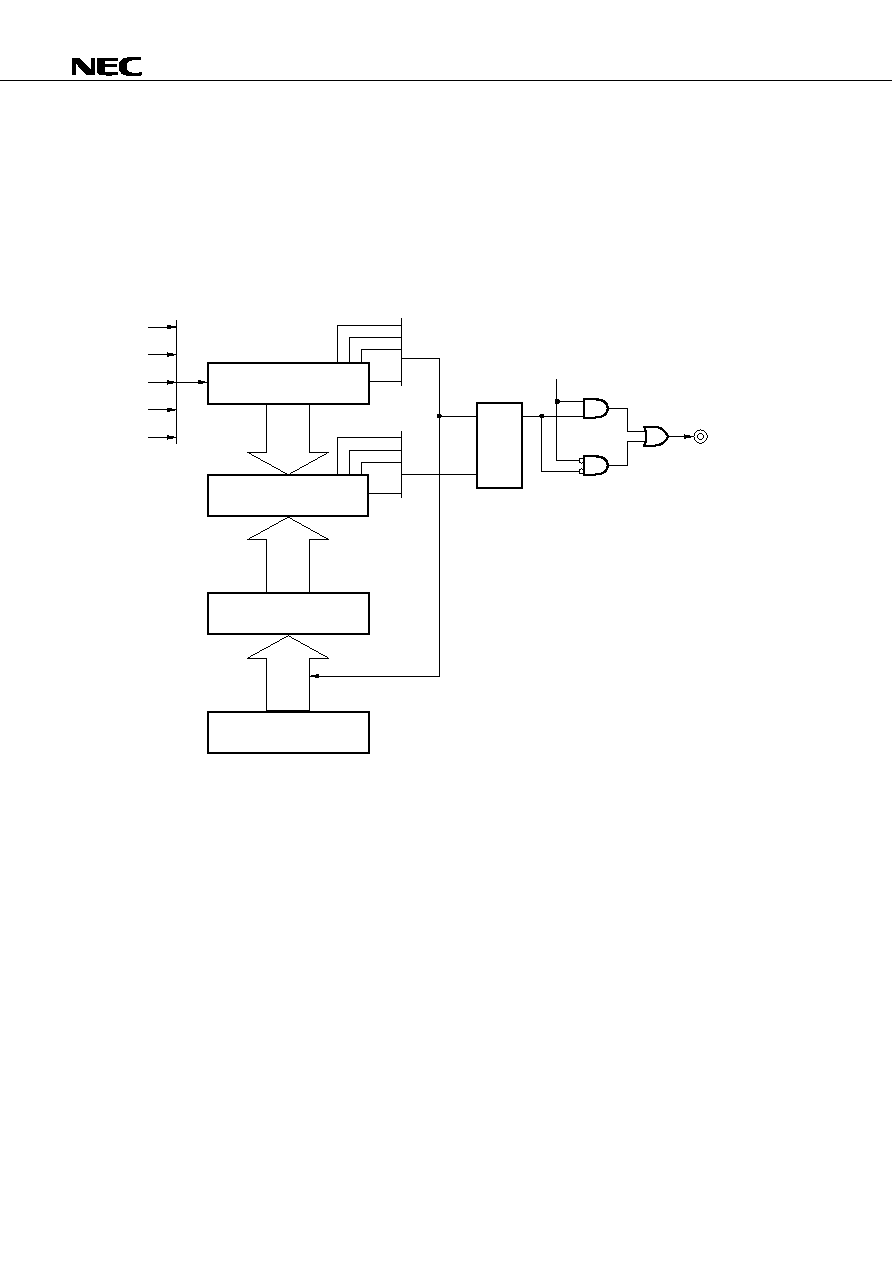
µ
PD78363A, 78365A, 78366A, 78368A
46
3.10
PWM UNIT
The
µ
PD78366A is provided with two lines that output 8-/9-/10-/12-bit resolution variable PWM signals. The
PWM output can be used as a digital-to-analog conversion output by connecting an external lowpass filter, and
ideal for controlling actuators such as motors.
An output of between 244 Hz and 62.5 kHz can be obtaind, depending on the combination of the count clock
(62.5 ns to 1
µ
s) and counter bit length (8, 9, 10, or 12) (at an internal clock frequency of 16 MHz).
Figure 3-18. Block Diagram of PWM Unit
7
8
9
11
0-7
0-8
0-9
0-11
Counter (12)
f
CLK
/16
f
CLK
/8
f
CLK
/4
f
CLK
/2
f
CLK
Overflow
S
R
Q
ALVn
PWMn
Comparator (12)
Compare register CMPn (12)
PWM buffer register n (12)
Coinci-
dence
Remark
n = 0, 1
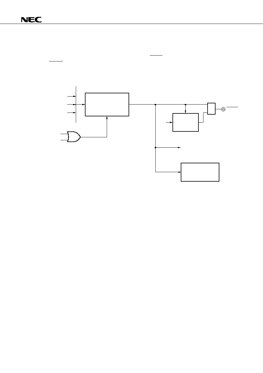
µ
PD78363A, 78365A, 78366A, 78368A
47
3.11
WATCHDOG TIMER (WDT)
The watchdog timer is a free running timer equipped with a non-maskable interrupt function to prevent
program hang-up or deadlock. When an error of the program is detected, the overflow interrupt (INTWDT) of
the watchdog timer occurs and the watchdog timer output pin (WDTO) goes low. By connecting this output pin
to the RESET pin, any malfunctioning of the application system due to program error can be prevented.
Figure 3-19. Block Diagram of Watchdog Timer
f
CLK
/2
13
f
CLK
/2
11
f
CLK
/2
9
WDT CLR
WDT STOP
Clear
Overflow
Clear
f
CLK
INTWDT
Timer
(5 bits)
S
R
Q
WDTO
Overflow
Watchdog timer
(8 bits)
Oscillation
stabilization
time control circuit
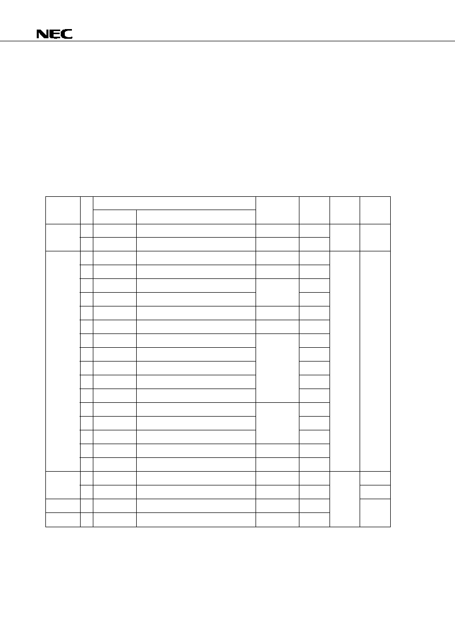
µ
PD78363A, 78365A, 78366A, 78368A
48
4.
INTERRUPT FUNCTIONS
4.1
OUTLINE
The
µ
PD78366A is provided with powerful interrupt functions that can process interrupt requests from the
internal hardware peripherals and external sources. In addition, the following three interrupt processing modes
are available. In addition, four levels of interrupt priority can be specified.
∑ Vectored interrupt processing
∑ Macro service
∑ Context switching
Table 4-1. Interrupt Sources
Note
≠
≠
0
1
2
3
4
5
6
7
8
9
10
11
12
13
14
15
≠
≠
≠
≠
Interrupt source
Name
Trigger
NMI
NMI pin input
INTWDT
Watchdog timer
INTOV3
Overflow of timer 3
INTP0/INTCC30 INTP0 pin input/CC30 coincidence signal
INTP1
INTP1 pin input
INTP2
INTP2 pin input
INTP3/INTCC20 INTP3 pin input/CC20 coincidence signal
INTP4
INTP4 pin input
INTTM0
Underflow of timer 0
INTCM03
CM03 coincidence signal
INTCM10
CM10 coincidence signal
INTCM40
CM40 coincidence signal
INTCM41
CM41 coincidence signal
INTSER
Receive error of UART
INTSR
End of UART reception
INTST
End of UART transfer
INTCSI
End of CSI transfer/reception
INTAD
End of A/D conversion
BRK
BRK instruction
BRKCS
BRKCS instruction
TRAP
Illegal op code trap
RESET
Reset input
Source unit
External
WDT
RPU
External/RPU
External
External/RPU
External
RPU
UART
CSI
A/D
≠
≠
≠
≠
Vector
table
address
0002H
0004H
0006H
0008H
000AH
000CH
000EH
0010H
0012H
0014H
0016H
0018H
001AH
001CH
001EH
0020H
0022H
0024H
003EH
≠
003CH
0000H
Macro
service
None
Provided
None
Context
switching
None
Provided
None
Provided
None
Type
Non-
maskable
Maskable
Software
Exception
Reset
Note Default priority : Priority that takes precedence when two or more maskable interrupts occur at the
same time. 0 is the highest priority, and 15 is the lowest.
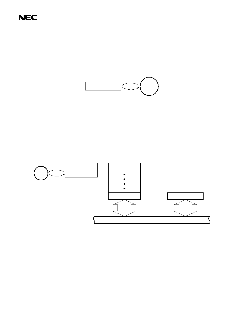
µ
PD78363A, 78365A, 78366A, 78368A
49
4.2
MACRO SERVICE
The
µ
PD78366A has a total of five macro services. Each macro service is described below.
(1) Counter mode: EVTCNT
∑ Operation
(a) Increments or decrements an 8-bit macro service counter (MSC).
(b) A vector interrupt request is generated when MSC reaches 0.
MSC
+1/≠1
∑ Application example: As event counter, or to measure number of times a value is captured
(2) Block transfer mode: BLKTRS
∑ Operation
(a) Transfers data block between a buffer and a SFR specified by SFR pointer (SFRP).
(b) The transfer source and destination can be in SFR or buffer area. The length of the transfer data
can be specified to be byte or word.
(c) The number of times the data is to be transferred (block size) is specified by MSC.
(d) MSC is auto decremented by one each time the macro service has been executed.
(e) When MSC reaches 0, a vector interrupt request is generated.
≠1
SFRP
MSC
SFR
Buffer N
Buffer 1
Internal bus
∑ Application example: To transfer/receive data through serial interface
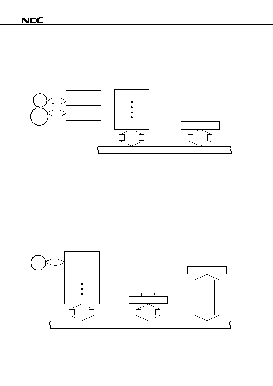
µ
PD78363A, 78365A, 78366A, 78368A
50
(3) Block transfer mode (with memory pointer): BLKTRS-P
∑ Operation
This is the block transfer mode in (2) above with a memory pointer (MEMP). The appended buffer
area of MEMP can be freely set on the memory space.
Remark
Each time the macro service is executed, MEMP is auto incremented (by one for byte
data transfer and by two for word data transfer).
≠1
SFRP
MSC
SFR
MEMP
+1/+2
Buffer N
Buffer 1
Internal bus
∑ Application example: Same as (2)
(4) Data differential mode: DTADIF
∑ Operation
(a) Calculates the difference between the contents of SFR (current value) specified by SFRP and the
contents of SFR saved to the last data buffer (LDB).
(b) Stores the result of the calculation in a predetermined buffer area.
(c) Stores the contents of the current value of the SFR in LDB.
(d) The number of times the data is to be transferred (block size) is specified by MSC. Each time the
macro service is executed, MSC is auto decremented by one.
(e) When MSC reaches 0, a vector interrupt request is generated.
Remark
The differential calculation can be carried out only with 16-bit SFRs.
≠1
SFR
LDB
Buffer N
Buffer 1
Differential calculation
Internal bus
SFRP
MSC
∑ Application example : To measure cycle and pulse width by the capture register of the real-time
pulse unit (RPU)
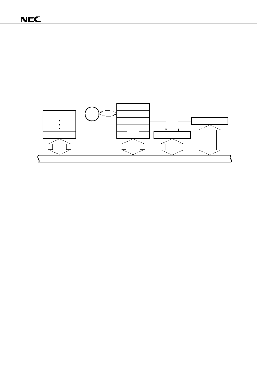
µ
PD78363A, 78365A, 78366A, 78368A
51
(5) Data differential mode (with memory pointer): DTADIF-P
∑ Operation
This is the data differential mode in (4) above with memory pointer (MEMP). By appending MEMP,
the buffer area in which the differential data is to be stored can be set freely on the memory space.
Remarks 1.
The differential calculation can be carried out only with 16-bit SFRs.
2.
The buffer is specified by the result of operation by MEMP and MSC
Note
. MEMP is
not updated after the data has been transferred.
Note MEMP ≠ (MSC
◊
2) + 2
≠1
SFR
MEMP
LDB
SFRP
MSC
Buffer N
Buffer 1
Differential calculation
Internal bus
∑ Application example: Same as (4)
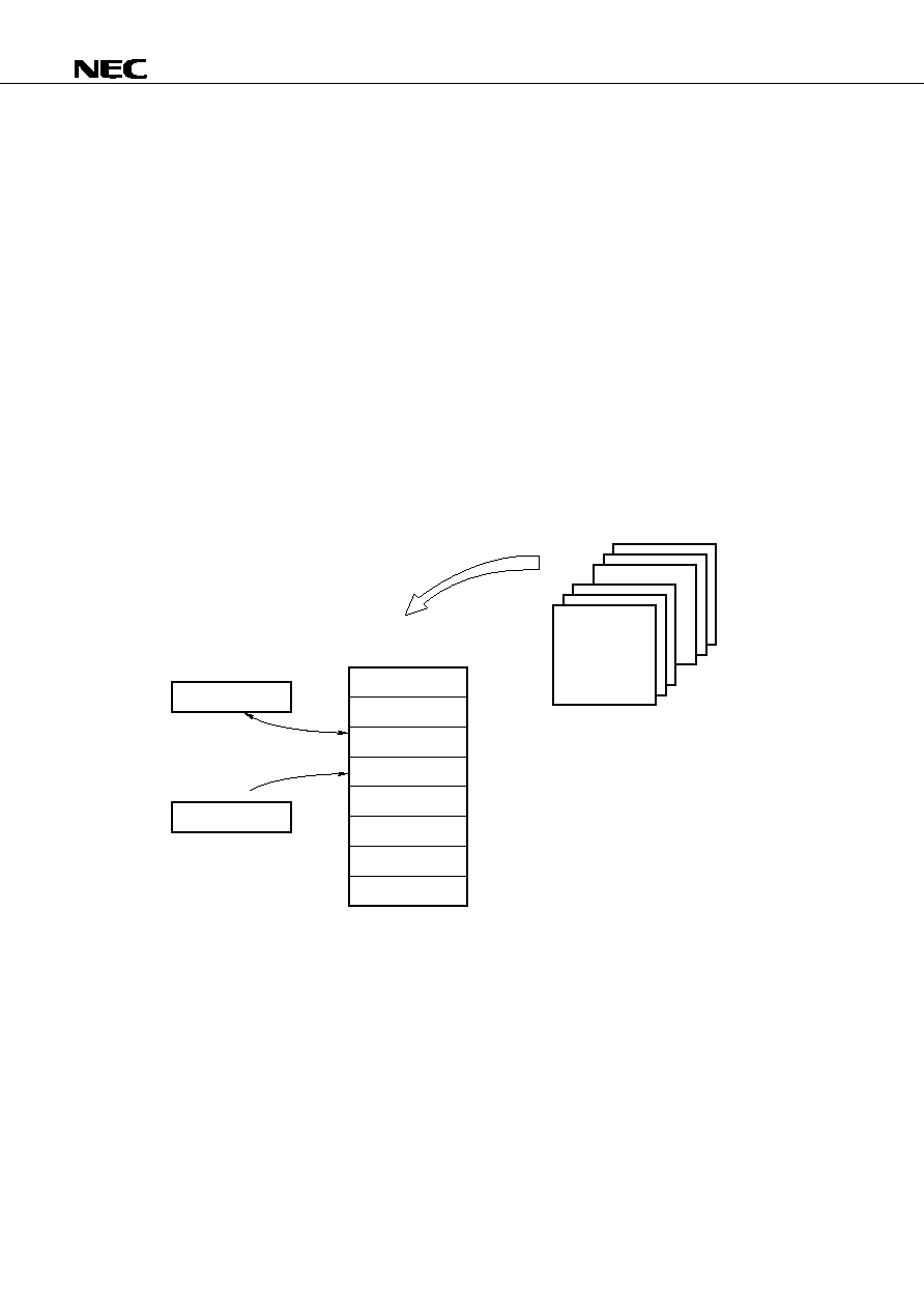
µ
PD78363A, 78365A, 78366A, 78368A
52
4.3
CONTEXT SWITCHING
This function is to select a specific register bank through the hardware, and to branch execution to a vector
address predetermined in the register bank. At the same time, it saves the present contents of the PC and PSW
to the register bank when an interrupt occurs, or when the BRKCS instruction is executed.
4.3.1
Context Switching Function by Interrupt Request
When a context switching enable flag corresponding to each maskable interrupt request is set to 1 in the EI
(interrupt enable) status, the context switching function can be started.
The context switching operation by an interrupt request is performed as follows:
(1) When an interrupt request is generated, a register bank to which the context is to be switched is specified
by the contents of the low-order 3 bits of the row address (even address) of the corresponding vector table.
(2) A predetermined vector address is transferred to the PC in the register bank to which the context is to
be switched, and the contents of the PC and PSW immediately before the switching takes place are saved
to the register bank.
(3) Execution branches to an address indicated by the contents of the PC newly set.
Figure 4-1. Operation of Context Switching
PC
PSW
RP0
RP1
RP2
RP3
RP4
RP5
RP6
RP7
Register Bank
Register Bank
(0-7)
Exchange
Save

µ
PD78363A, 78365A, 78366A, 78368A
53
4.3.2
Context Switching Function by BRKCS Instruction
The context switching function can be started by the BRKCS instruction.
The operation of context switching by an interrupt request is as follows:
(1) An 8-bit register is specified by the operand of the BRKCS instruction, and the register bank to which
the context is to be switched is specified by the contents of this register (only the low-order 3 bits of 8 bits
are valid).
(2) The vector address predetermined in the register bank to which the context is to be switched is transferred
to the PC, and at the same time, the contents of the PC and PSW immediately before the switching takes
place are saved to the register bank.
(3) Execution branches to the contents of the PC newly set.
4.3.3
Restoration from Context Switching
To restore from the switched context, one of the following two instructions are used. Which instruction is
to be executed is determined by the source that has started the context switching.
Table 4-2. Instructions to Restore from Context Switching
Restore instruction
Context switching starting source
RETCS
Occurrence of interrupt
RETCSB
Execution of BRKCS instruction
µ
PD78363A, 78365A, 78366A, 78368A
54
5.
EXTERNAL DEVICE EXPANSION FUNCTION
The
µ
PD78366A can connect external devices (data memory, program memory, and peripheral devices) in
addition to the internal ROM and RAM areas. To connect an external device, the address/data bus and read/
write strobe signals are controlled by using ports 4, 5, and 9.
Table 5-1. Pin Function with External Device Connected
Pin function with external device connected
Function
Name
Multiplexed address/data bus
AD0-AD7
Address bus
A8-A15
Read strobe
RD
Write strobe
WR
Address strobe
ASTB
Pin
P40-P47
P50-P57
P90
P91
ASTB
µ
PD78363A, 78365A, 78366A, 78368A
55
6.
STANDBY FUNCTIONS
The
µ
PD78366A is provided with standby functions to reduce the power consumption of the system. The
standby functions can be effected in the following two modes:
∑ HALT mode ..... In this mode, the operating clock of the CPU is stopped. By using this mode in
combination with an ordinary operation mode, the
µ
PD78366A operates
intermittently to reduce the total power consumption of the system.
∑ STOP mode .... In this mode, the oscillator is stopped, and therefore the entire system is stopped.
Therefore, power consumption can be minimized with only a leakage current
flowing.
Each mode is set through software. Figure 6-1 shows the transition of the status in the standby modes (STOP
and HALT modes).
Figure 6-1. Transition of Standby Status
STOP
HALT
Ordinary
STOP set
RESET released
NMI
HALT set
RESET released
Unmasked interrupt
occurs
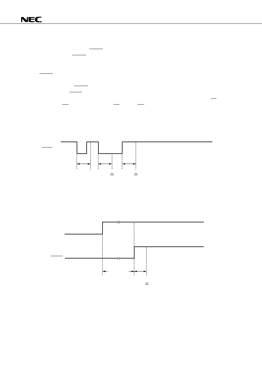
µ
PD78363A, 78365A, 78366A, 78368A
56
7.
RESET FUNCTION
When a low level is input to the RESET pin, the system is reset, and each hardware enters the initial status
(reset status). When the RESET pin goes high, the reset status is released, and program execution is started.
Initialize the contents of each register through program as necessary.
Especially, change the number of cycles of the programmable wait control register as necessary.
The RESET pin is equipped with a noise rejecter circuit of analog delay to prevent malfunctioning due to noise.
Cautions 1. While the RESET pin is active (low level), all the pins go into a high-impedance state
(except WDTO, AV
REF
, AV
DD
, AV
SS
, V
DD
, V
SS
, X1, and X2 pins).
2. When an external RAM is connected, do not connect a pull-up resistor to the P90/RD and
P91/WR pins, because the P90/RD and P91/WR pins may go into a high-impedance state,
resulting in destruction of the contents of the external RAM. In addition, signal contention
occurs on the address/data bus, resulting in damage to the input/output circuit.
Figure 7-1. Accepting Reset Signal
RESET input
Analog
delay
Analog
delay
Analog
delay
Rejected
as noise
Reset
accepted
Reset
released
To effect reset on when power is applied, make sure that sufficient time elapses to stabilize the oscillation
after the power is applied until the reset signal is accepted, as shown in Figure 7-2.
Figure 7-2. Reset on Power Application
V
DD
RESET
Oscillation
stabilization
time
Analog
delay
Reset
released
µ
PD78363A, 78365A, 78366A, 78368A
57
8.
INSTRUCTION SET
Write an operand in the operand field of each instruction according to the description of the instruction
(for details, refer to the Assembler Specifications). Some instructions have two or more operands. Select
one of them. Uppercase characters, +, ≠, #, $, !, [, and ] are keywords and must be written as is.
Write an appropriate numeric value or label as immediate data. To write a label, be sure to write #, $,
!, [, or ].
Table 8-1. Operand Representation and Description
Description
R0, R1, R2, R3, R4, R5, R6, R7, R8, R9, R10, R11, R12, R13, R14, R15
R0, R1, R2, R3, R4, R5, R6, R7
C, B
RP0, RP1, RP2, RP3, RP4, RP5, RP6, RP7
RP0, RP1, RP2, RP3, RP4, RP5, RP6, RP7
DE, HL, VP, UP
Special function register symbol (Refer to Table 2-1.)
Special function register symbol (register that can be manipulated in 16-bit units. Refer to Table
2-1.)
RP0, RP1, RP2, RP3, RP4, RP5/PSW, RP6, RP7
(More than one symbol can be written. However, RP5 can be written only for PUSH and POP
instructions, and PSW can be written only for PUSHU and POPU instructions.)
[DE], [HL], [DE+], [HL+], [DE≠], [HL≠], [VP], [UP]
; register indirect mode
[DE + A], [HL + A], [DE + B], [HL + B], [VP + DE], [VP + HL]
; based indexed mode
[DE + byte], [HL + byte], [VP + byte], [UP + byte], [SP + byte] ; based mode
word[A], word[B], word[DE], word[HL]
; indexed mode
FE20H-FF1FH immediate data or label
FE20H-FF1EH immediate data (however, bit0 = 0) or label (manipulated in 16-bit units)
0000H-FDFFH immediate data or label; relative addressing
0000H-FDFFH immediate data or label; immediate addressing
(However, up to FFFFH can be written for MOV instruction. Only FE00H-FEFFH can be written
for MOVTBLW instruction.)
800H-FFFH immediate data or label
40H-7EH immediate data (however, bit0 = 0)
Note
or label
16-bit immediate data or label
8-bit immediate data or label
3-bit immediate data or label
3-bit immediate data (0-7)
Representation
r
r1
r2
rp
rp1
rp2
sfr
sfrp
post
mem
saddr
saddrp
$ addr16
! addr16
addr11
addr5
word
byte
bit
n
Note Do not access bit0 = 1 (odd address) in word units.
Remarks
1.
rp and rp1 are the same in terms of register name that can be written but are different in code
to be generated.
2.
r, r1, rp, rp1, and post can be written in absolute name (R0-R15, RP0-RP7) and function name
(X, A, C, B, E, D, L, H, AX, BC, DE, HL, VP, and UP).
3.
Immediate addressing can address the entire space. Relative addressing can address only a
range of ≠128 to +127 from the first address of the next instruction.
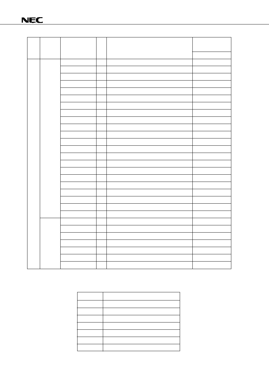
µ
PD78363A, 78365A, 78366A, 78368A
58
Mnemonic
Operand
Byte
Operation
Flag
S
Z
AC P/V CY
MOV
XCH
Instructions
8-bit data transfer
r1, #byte
2
saddr, #byte
3
sfr
Note
, #byte
3
r, r1
2
A, r1
1
A, saddr
2
saddr, A
2
saddr, saddr
3
A, sfr
2
sfr, A
2
A, mem
1-4
mem, A
1-4
A, [saddrp]
2
[saddrp], A
2
A, !addr16
4
!addri16, A
4
PSWL, #byte
3
PSWH, #byte
3
PSWL, A
2
PSWH, A
2
A, PSWL
2
A, PSWH
2
A, r1
1
r, r1
2
A, mem
2-4
A, saddr
2
A, sfr
3
A, [saddrp]
2
saddr, saddr
3
r1
byte
(saddr)
byte
sfr
byte
r
r1
A
r1
A
(saddr)
(saddr)
A
(saddr)
(saddr)
A
sfr
sfr
A
A
(mem)
(mem)
A
A
((saddrp))
((saddrp))
A
A
(addr16)
(addr16)
A
PSW
L
byte
PSW
H
byte
PSW
L
A
PSW
H
A
A
PSW
L
A
PSW
H
A
r1
r
r1
A
(mem)
A
(saddr)
A
sfr
A
((saddrp))
(saddr)
(saddr)
◊
◊
◊
◊
◊
◊
◊
◊
◊
◊
Note When STBC or WDM is written as sfr, this instruction is treated as a dedicated instruction whose number
of bytes is different from that of this instruction.
Remark
For symbols in flag, refer to the table below.
Symbol
Remarks
(Blank)
No change
0
Cleared to 0
1
Set to 1
◊
Set/cleared according to result
P
P/V flag functions as parity flag
V
P/V flag operates as overflow flag
R
Value previously saved is restored
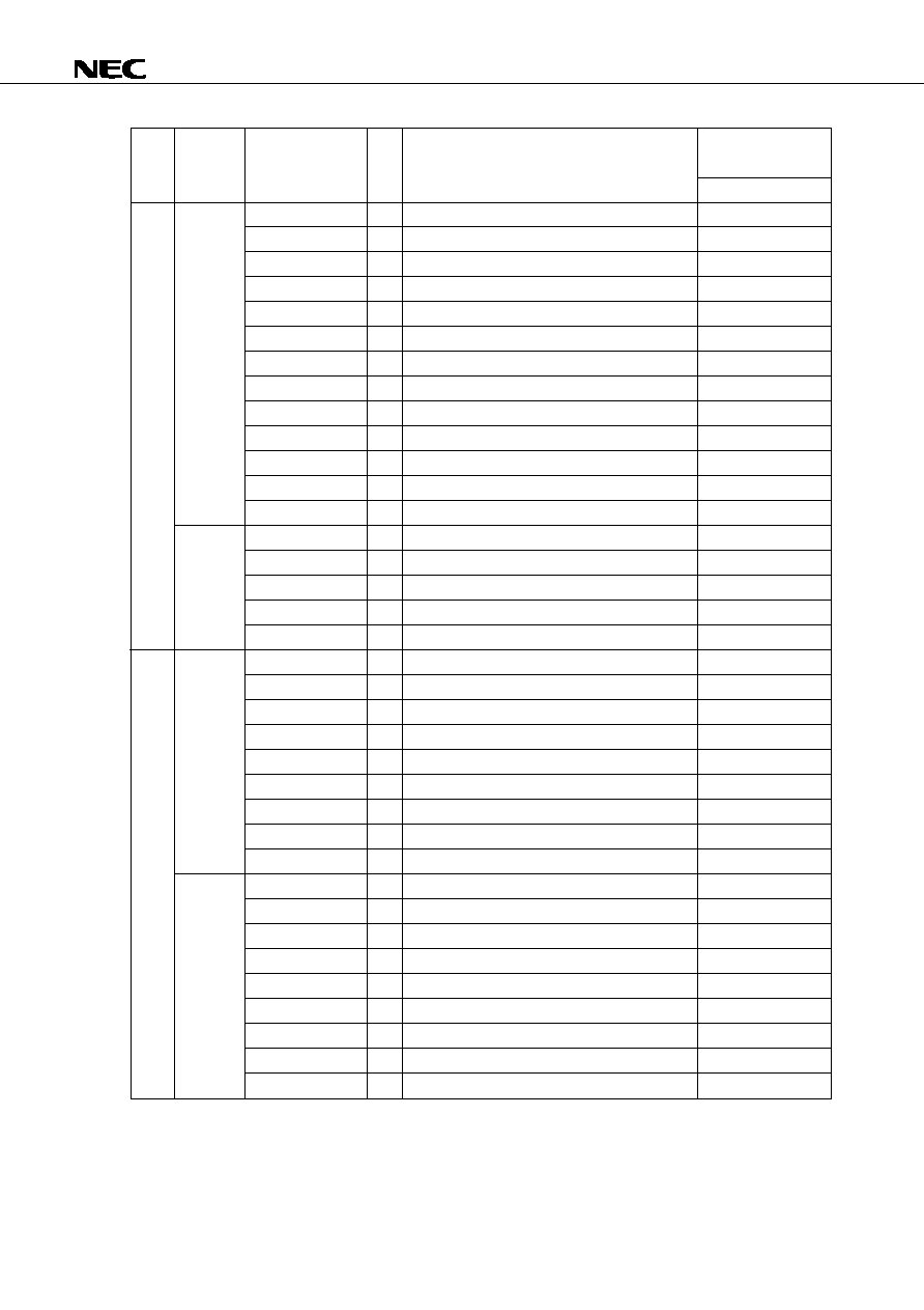
µ
PD78363A, 78365A, 78366A, 78368A
59
Flag
S
Z
AC P/V CY
Mnemonic
Operand
Byte
Operation
Instructions
16-bit data transfer
8-bit operation
rp1, #word
3
saddrp, #word
4
sfrp, #word
4
rp, rp1
2
AX, saddrp
2
saddrp, AX
2
saddrp, saddrp
3
AX, sfrp
2
sfrp, AX
2
rp1, !addr16
4
!addr16, rp1
4
AX, mem
2-4
mem, AX
2-4
AX, saddrp
2
AX, sfrp
3
saddrp, saddrp
3
rp, rp1
2
AX, mem
2-4
A, #byte
2
saddr, #byte
3
sfr, #byte
4
r, r1
2
A, saddr
2
A, sfr
3
saddr, saddr
3
A, mem
2-4
mem, A
2-4
A, #byte
2
saddr, #byte
3
sfr, #byte
4
r, r1
2
A, saddr
2
A, sfr
3
saddr, saddr
3
A, mem
2-4
mem, A
2-4
rp1
word
(saddrp)
word
sfrp
word
rp
rp1
AX
(saddrp)
(saddrp)
AX
(saddrp)
(saddrp)
AX
sfrp
sfrp
AX
rp1
(addr16)
(addr16)
rp1
AX
(mem)
(mem)
AX
AX
(saddrp)
AX
sfrp
(saddrp)
(saddrp)
rp
rp1
AX
(mem)
A, CY
A + byte
(saddr), CY
(saddr) + byte
sfr, CY
sfr + byte
r, CY
r + r1
A, CY
A + (saddr)
A, CY
A + sfr
(saddr), CY
(saddr) + (saddr)
A, CY
A + (mem)
(mem), CY
(mem) + A
A, CY
A + byte + CY
(saddr), CY
(saddr) + byte + CY
sfr, CY
sfr + byte + CY
r, CY
r + r1 + CY
A, CY
A + (saddr) + CY
A, CY
A + sfr + CY
(saddr), CY
(saddr) + (saddr) + CY
A, CY
A + (mem) + CY
(mem), CY
(mem) + A + CY
◊
◊
◊
V
◊
◊
◊
◊
V
◊
◊
◊
◊
V
◊
◊
◊
◊
V
◊
◊
◊
◊
V
◊
◊
◊
◊
V
◊
◊
◊
◊
V
◊
◊
◊
◊
V
◊
◊
◊
◊
V
◊
◊
◊
◊
V
◊
◊
◊
◊
V
◊
◊
◊
◊
V
◊
◊
◊
◊
V
◊
◊
◊
◊
V
◊
◊
◊
◊
V
◊
◊
◊
◊
V
◊
◊
◊
◊
V
◊
◊
◊
◊
V
◊
M O V W
XCHW
ADD
ADDC
µ
PD78363A, 78365A, 78366A, 78368A
60
Flag
S
Z
AC P/V CY
A, CY
A ≠ byte
(saddr), CY
(saddr) ≠ byte
sfr, CY
sfr ≠ byte
r, CY
r ≠ r1
A, CY
A ≠ (saddr)
A, CY
A ≠ sfr
(saddr), CY
(saddr) ≠ (saddr)
A, CY
A ≠ (mem)
(mem), CY
(mem) ≠ A
A, CY
A ≠ byte ≠ CY
(saddr), CY
(saddr) ≠ byte ≠ CY
sfr, CY
sfr ≠ byte ≠ CY
r, CY
r ≠ r1 ≠ CY
A, CY
A ≠ (saddr) ≠ CY
A, CY
A ≠ sfr ≠ CY
(saddr), CY
(saddr) ≠ (saddr) ≠ CY
A, CY
A ≠ (mem) ≠ CY
(mem), CY
(mem) ≠ A ≠ CY
A
A
byte
(saddr)
(saddr)
byte
sfr
sfr
byte
r
r
r1
A
A
(saddr)
A
A
sfr
(saddr)
(saddr)
(saddr)
A
A
(mem)
(mem)
(mem)
A
◊
◊
◊
V
◊
◊
◊
◊
V
◊
◊
◊
◊
V
◊
◊
◊
◊
V
◊
◊
◊
◊
V
◊
◊
◊
◊
V
◊
◊
◊
◊
V
◊
◊
◊
◊
V
◊
◊
◊
◊
V
◊
◊
◊
◊
V
◊
◊
◊
◊
V
◊
◊
◊
◊
V
◊
◊
◊
◊
V
◊
◊
◊
◊
V
◊
◊
◊
◊
V
◊
◊
◊
◊
V
◊
◊
◊
◊
V
◊
◊
◊
◊
V
◊
◊
◊
P
◊
◊
P
◊
◊
P
◊
◊
P
◊
◊
P
◊
◊
P
◊
◊
P
◊
◊
P
◊
◊
P
Mnemonic
Operand
Byte
Operation
Instructions
SUB
SUBC
AND
8-bit operation
A, #byte
2
saddr, #byte
3
sfr, #byte
4
r, r1
2
A, saddr
2
A, sfr
3
saddr, saddr
3
A, mem
2-4
mem, A
2-4
A, #byte
2
saddr, #byte
3
sfr, #byte
4
r, r1
2
A, saddr
2
A, sfr
3
saddr, saddr
3
A, mem
2-4
mem, A
2-4
A, #byte
2
saddr, #byte
3
sfr, #byte
4
r, r1
2
A, saddr
2
A, sfr
3
saddr, saddr
3
A, mem
2-4
mem, A
2-4

µ
PD78363A, 78365A, 78366A, 78368A
61
Flag
S
Z
AC P/V CY
A, #byte
2
saddr, #byte
3
sfr, #byte
4
r, r1
2
A, saddr
2
A, sfr
3
saddr, saddr
3
A, mem
2-4
mem, A
2-4
A, #byte
2
saddr, #byte
3
sfr, #byte
4
r, r1
2
A, saddr
2
A, sfr
3
saddr, saddr
3
A, mem
2-4
mem, A
2-4
A, #byte
2
saddr, #byte
3
sfr, #byte
4
r, r1
2
A, saddr
2
A, sfr
3
saddr, saddr
3
A, mem
2-4
mem, A
2-4
A
A
byte
(saddr)
(saddr)
byte
sfr
sfr
byte
r,
r
r1
A
A
(saddr)
A
A
sfr
(saddr)
(saddr)
(saddr)
A
A
(mem)
(mem)
(mem)
/ A
A
A
byte
(saddr)
(saddr)
byte
sfr
sfr
byte
r
r
r1
A
A
(saddr)
A
A
sfr
(saddr)
(saddr)
(saddr)
A
A
(mem)
(mem)
(mem)
A
A ≠ byte
(saddr) ≠ byte
sfr ≠ byte
r ≠ r1
A ≠ (saddr)
A ≠ sfr
(saddr) ≠ (saddr)
A ≠ (mem)
(mem) ≠ A
◊
◊
P
◊
◊
P
◊
◊
P
◊
◊
P
◊
◊
P
◊
◊
P
◊
◊
P
◊
◊
P
◊
◊
P
◊
◊
P
◊
◊
P
◊
◊
P
◊
◊
P
◊
◊
P
◊
◊
P
◊
◊
P
◊
◊
P
◊
◊
P
◊
◊
◊
V
◊
◊
◊
◊
V
◊
◊
◊
◊
V
◊
◊
◊
◊
V
◊
◊
◊
◊
V
◊
◊
◊
◊
V
◊
◊
◊
◊
V
◊
◊
◊
◊
V
◊
◊
◊
◊
V
◊
Mnemonic
Operand
Byte
Operation
Instructions
OR
XOR
CMP
8-bit operation
µ
PD78363A, 78365A, 78366A, 78368A
62
Flag
S
Z
AC P/V CY
Mnemonic
Operand
Byte
Operation
Instructions
Multiplication
/division
Relative
operation
Signed
multipli-
cation
Sum-of-
products
operation
Sum-of-products
operation with
saturation
ADDW
SUBW
CMPW
MULU
DIVUW
MULUW
DIVUX
MULW
MACW
MACSW
SACW
AX, #word
3
saddrp, #word
4
sfrp, #word
5
rp, rp1
2
AX, saddrp
2
AX, sfrp
3
saddrp, saddrp
3
AX, #word
3
saddrp, #word
4
sfrp, #word
5
rp, rp1
2
AX, saddrp
2
AX, sfrp
3
saddrp, saddrp
3
AX, #word
3
saddrp, #word
4
sfrp, #word
5
rp, rp1
2
AX, saddrp
2
AX, sfrp
3
saddrp, saddrp
3
r1
2
r1
2
rp1
2
rp1
2
rp1
2
n
3
n
3
[DE + ], [HL + ]
4
AX, CY
AX + word
(saddrp), CY
(saddrp) + word
sfrp, CY
sfrp + word
rp, CY
rp + rp1
AX, CY
AX + (saddrp)
AX, CY
AX + sfrp
(saddrp), CY
(saddrp) + (saddrp)
AX, CY
AX ≠ word
(saddrp), CY
(saddrp) ≠ word
sfrp, CY
sfrp ≠ word
rp, CY
rp ≠ rp1
AX, CY
AX ≠ (saddrp)
AX, CY
AX ≠ sfrp
(saddrp), CY
(saddrp) ≠ (saddrp)
AX ≠ word
(saddrp) ≠ word
sfrp ≠ word
rp ≠ rp1
AX ≠ (saddrp)
AX ≠ sfrp
(saddrp) ≠ (saddrp)
AX
AX
◊
r1
AX (quotient), r1 (remainder)
AX
˜
r1
AX (high-order 16 bits), rp1 (low-order 16 bits)
AX
◊
rp1
AXDE (quotient), rp1 (remainder)
AXDE
˜
rp1
AX (high-order 16 bits), rp1 (low-order 16 bits)
AX
◊
rp1
AXDE
(B)
◊
(C) + AXDE
B
B + 2, C
C + 2, n
n ≠ 1
End if n = 0 or P/V = 1
AXDE
(B)
◊
(C) + AXDE
B
B + 2, C
C + 2, n
n ≠ 1
if overflow (P/V = 1) then
AXDE
7FFFFFFFH
if underflow (P/V = 1) then
AXDE
80000000H
end if n = 0 or P/V = 1
AX
AX + | (DE) ≠ (HL) |
DE
DE + 2 HL
HL + 2 C
C ≠ 1
end if C = 0 or cy = 1
◊
◊
◊
V
◊
◊
◊
◊
V
◊
◊
◊
◊
V
◊
◊
◊
◊
V
◊
◊
◊
◊
V
◊
◊
◊
◊
V
◊
◊
◊
◊
V
◊
◊
◊
◊
V
◊
◊
◊
◊
V
◊
◊
◊
◊
V
◊
◊
◊
◊
V
◊
◊
◊
◊
V
◊
◊
◊
◊
V
◊
◊
◊
◊
V
◊
◊
◊
◊
V
◊
◊
◊
◊
V
◊
◊
◊
◊
V
◊
◊
◊
◊
V
◊
◊
◊
◊
V
◊
◊
◊
◊
V
◊
◊
◊
◊
V
◊
◊
◊
◊
V
◊
◊
◊
◊
V
◊
◊
◊
◊
V
◊
16-bit operation
µ
PD78363A, 78365A, 78366A, 78368A
63
r1
1
saddr
2
r1
1
saddr
2
rp2
1
saddrp
3
rp2
1
saddrp
3
r1, n
2
r1, n
2
r1, n
2
r1, n
2
r1, n
2
r1, n
2
rp1, n
2
rp1, n
2
[rp1]
2
[rp1]
2
2
1
Flag
S
Z
AC P/V CY
Mnemonic
Operand
Byte
Operation
Instructions
MOVTBLW
INC
DEC
INCW
DECW
ROR
ROL
RORC
ROLC
SHR
SHL
SHRW
SHLW
ROR4
ROL4
ADJBA
ADJBS
CVTBW
(addr16 + 2)
(addr16), n
n ≠ 1
addr16
addr16 ≠ 2, End if n = 0
r1
r1 + 1
(saddr)
(saddr) + 1
r1
r1 ≠ 1
(saddr)
(saddr) ≠ 1
rp2
rp2 + 1
(saddrp)
(saddrp) + 1
rp2
rp2 ≠ 1
(saddrp)
(saddrp) ≠ 1
(CY, r1
7
r1
0
,
r1
m≠1
r1
m
)
◊
n times
(CY, r1
0
r1
7
,
r1
m+1
r1
m
)
◊
n times
(CY
r1
0
,
r1
7
CY, r1
m≠1
r1
m
)
◊
n times
(CY
r1
7
,
r1
0
CY, r1
m+1
r1
m
)
◊
n times
(CY
r1
0
,
r1
7
0, r1
m≠1
r1
m
)
◊
n times
(CY
r1
7
,
r1
0
0, r1
m+1
r1
m
)
◊
n times
(CY
rp1
0
,
rp1
15
0, rp1
m≠1
rp1
m
)
◊
n times
(CY
rp1
15
,
rp1
0
0, rp1
m+1
rp1
m
)
◊
n times
A
3≠0
(rp1)
3≠0
,
(rp1)
7≠4
A
3≠0
,
(rp1)
3≠0
(rp1)
7≠4
A
3≠0
(rp1)
7≠4
,
(rp1)
3≠0
A
3≠0
,
(rp1)
7≠4
(rp1)
3≠0
Decimal Adjust Accumelator
When A
7
= 0, X
A, A
00H
When A
7
= 1, X
A, A
FFH
Table
shift
◊
◊
◊
V
◊
◊
◊
V
◊
◊
◊
V
◊
◊
◊
V
P
◊
P
◊
P
◊
P
◊
◊
◊
0
P
◊
◊
◊
0
P
◊
◊
◊
0
P
◊
◊
◊
0
P
◊
◊
◊
0
P
◊
Increment/decrement
BCD
adjustment
Data
conversion
Shift rotate
!addr16, n
4
Remarks
1.
n of the shift rotate instruction indicates the number of times the shift rotate instruction is
executed.
2.
The address of the table shift instruction ranges from FE00H to FEFFH.
µ
PD78363A, 78365A, 78366A, 78368A
64
Mnemonic
Operand
Byte
Operation
Flag
S
Z
AC P/V CY
Instructions
CY, saddr.bit
3
CY, sfr.bit
3
CY, A.bit
2
CY, X.bit
2
CY, PSWH.bit
2
CY, PSWL.bit
2
saddr.bit, CY
3
sfr.bit, CY
3
A.bit, CY
2
X.bit, CY
2
PSWH.bit, CY
2
PSWL.bit, CY
2
CY, saddr.bit
3
CY, /saddr.bit
3
CY, sfr.bit
3
CY, /sfr.bit
3
CY, A.bit
2
CY, /A.bit
2
CY, X.bit
2
CY, /X.bit
2
CY, PSWH.bit
2
CY, /PSWH.bit
2
CY, PSWL.bit
2
CY, /PSWL.bit
2
CY, saddr.bit
3
CY, /saddr.bit
3
CY, sfr.bit
3
CY, /sfr.bit
3
CY, A.bit
2
CY, /A.bit
2
CY, X.bit
2
CY, /X.bit
2
CY, PSWH.bit
2
CY, /PSWH.bit
2
CY, PSWL.bit
2
CY, /PSWL.bit
2
CY
(saddr.bit)
CY
sfr.bit
CY
A.bit
CY
X.bit
CY
PSW
H
.bit
CY
PSW
L
.bit
(saddr.bit)
CY
sfr.bit
CY
A.bit
CY
X.bit
CY
PSW
H
.bit
CY
PSW
L
.bit
CY
CY
CY
(saddr.bit)
CY
CY
(saddr.bit)
CY
CY
sfr.bit
CY
CY
sfr.bit
CY
CY
A.bit
CY
CY
A.bit
CY
CY
X.bit
CY
CY
X.bit
CY
CY
PSW
H
.bit
CY
CY
PSW
H
.bit
CY
CY
PSW
L
.bit
CY
CY
PSW
L
.bit
CY
CY
(saddr.bit)
CY
CY
(saddr.bit)
CY
CY
sfr.bit
CY
CY
sfr.bit
CY
CY
A.bit
CY
CY
A.bit
CY
CY
X.bit
CY
CY
X.bit
CY
CY
PSW
H
.bit
CY
CY
PSW
H
.bit
CY
CY
PSW
L
.bit
CY
CY
PSW
L
.bit
MOV1
AND1
OR1
Bit manipulation
◊
◊
◊
◊
◊
◊
◊
◊
◊
◊
◊
◊
◊
◊
◊
◊
◊
◊
◊
◊
◊
◊
◊
◊
◊
◊
◊
◊
◊
◊
◊
◊
◊
◊
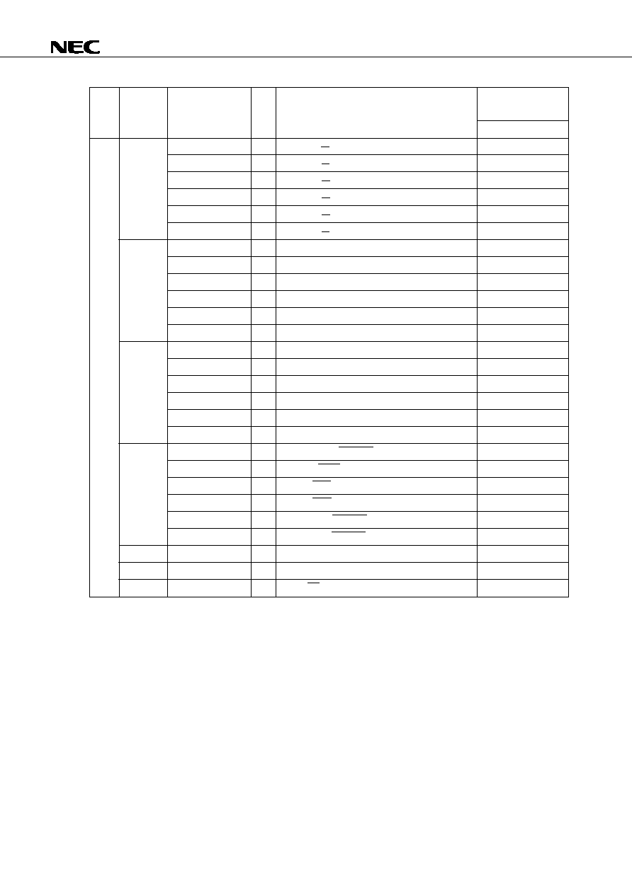
µ
PD78363A, 78365A, 78366A, 78368A
65
Mnemonic
Operand
Byte
Operation
Flag
S
Z
AC P/V CY
Instructions
CY, saddr.bit
3
CY, sfr.bit
3
CY, A.bit
2
CY, X.bit
2
CY, PSWH.bit
2
CY, PSWL.bit
2
saddr.bit
2
sfr.bit
3
A.bit
2
X.bit
2
PSWH.bit
2
PSWL.bit
2
saddr.bit
2
sfr.bit
3
A.bit
2
X.bit
2
PSWH.bit
2
PSWL.bit
2
saddr.bit
3
sfr.bit
3
A.bit
2
X.bit
2
PSWH.bit
2
PSWL.bit
2
CY
1
CY
1
CY
1
CY
CY
(saddr.bit)
CY
CY
sfr.bit
CY
CY
A.bit
CY
CY
X.bit
CY
CY
PSW
H
.bit
CY
CY
PSW
L
.bit
(saddr.bit)
1
sfr.bit
1
A.bit
1
X.bit
1
PSW
H
.bit
1
PSW
L
.bit
1
(saddr.bit)
0
sfr.bit
0
A.bit
0
X.bit
0
PSW
H
.bit
0
PSW
L
.bit
0
(saddr.bit)
(saddr.bit)
sfr.bit
sfr.bit
A.bit
A.bit
X.bit
X.bit
PSW
H
.bit
PSW
H
.bit
PSW
L
.bit
PSW
L
.bit
CY
1
CY
0
CY
CY
◊
◊
◊
◊
◊
◊
◊
◊
◊
◊
◊
◊
◊
◊
◊
◊
◊
◊
◊
◊
◊
1
0
◊
XOR1
SET1
CLR1
NOT1
SET1
CLR1
NOT1
Bit manipulation
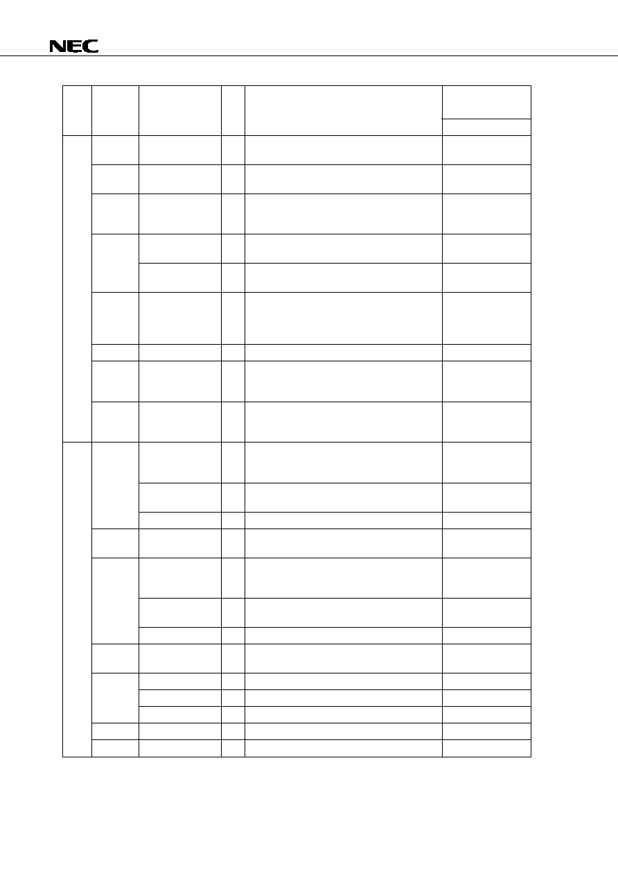
µ
PD78363A, 78365A, 78366A, 78368A
66
Mnemonic
Operand
Byte
Operation
Flag
S
Z
AC P/V CY
Instructions
(SP ≠ 1)
(PC + 3)
H
,
(SP ≠ 2)
(PC + 3)
L
,
PC
addr16, SP
SP ≠ 2
(SP ≠ 1)
(PC + 2)
H
,
(SP ≠ 2)
(PC + 2)
L
,
PC
15 ≠ 11
00001, PC
10 ≠ 0
addr11, SP
SP ≠ 2
(SP ≠ 1)
(PC + 1)
H
,
(SP ≠ 2)
(PC + 1)
L
,
PC
H
(TPF, 00000000, addr5 + 1),
PC
L
(TPF, 00000000, addr5 ), SP
SP ≠ 2
(SP ≠ 1)
(PC + 2)
H
,
(SP ≠ 2)
(PC + 2)
L
,
PC
H
rp1
H
,
PC
L
rp1
L
,
SP
SP ≠ 2
(SP ≠ 1)
(PC + 2)
H
,
(SP ≠ 2)
(PC + 2)
L
,
PC
H
(rp1 + 1), PC
L
(rp1), SP
SP ≠ 2
(SP ≠ 1)
PSW
H
,
(SP ≠ 2)
PSW
L
(SP ≠ 3)
(PC + 1)
H
,
(SP ≠ 4)
(PC + 1)
L
,
PC
L
(003EH), PC
H
(003FH),
SP
SP ≠ 4, IE
0
PC
L
(SP), PC
H
(SP + 1), SP
SP + 2
PC
L
(SP), PC
H
(SP +1)
PSW
L
(SP + 2), PSW
H
(SP + 3)
SP
SP + 4
PC
L
(SP), PC
H
(SP + 1)
PSW
L
(SP + 2), PSW
H
(SP + 3)
SP
SP + 4
(SP ≠ 1)
sfr
H
(SP ≠ 2)
sfr
L
SP
SP ≠ 2
{(SP ≠ 1)
post
H
,
(SP ≠ 2)
post
L
,
SP
SP
≠ 2}
◊
n times
(SP ≠ 1)
PSW
H
,
(SP ≠ 2)
PSW
L
,
SP
SP ≠ 2
{(UP ≠ 1)
post
H
,
(UP ≠ 2)
post
L
,
UP
UP
≠ 2}
◊
n times
sfr
L
(SP)
sfr
H
(SP + 1)
SP
SP + 2
{post
L
(SP), post
H
(SP + 1), SP
SP + 2}
◊
n times
PSW
L
(SP), PSW
H
(SP + 1), SP
SP + 2
{post
L
(UP),post
H
(UP + 1), UP
UP + 2}
◊
n times
SP
word
SP
AX
AX
SP
SP
SP + 1
SP
SP ≠ 1
Stack manipulation
Call/return
!addr16
3
!addr11
2
[addr5]
1
rp1
2
[rp1]
2
1
1
1
1
sfrp
3
post
2
PSW
1
post
2
sfrp
3
post
2
PSW
1
post
2
SP, #word
4
SP, AX
2
AX, SP
2
SP
2
SP
2
R
R
R
R
R
R
R
R
R
R
R
R
R
R
R
CALL
CALLF
CALLT
CALL
BRK
RET
RETB
RETI
PUSH
PUSHU
POP
POPU
MOVW
INCW
DECW
Remark
n of the stack manipulation instruction is the number of registers written as post.
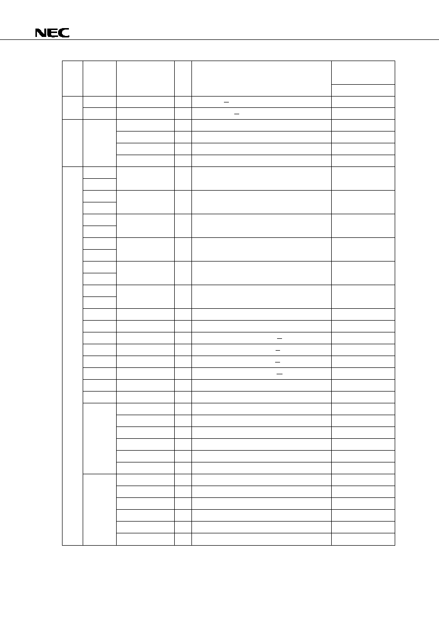
µ
PD78363A, 78365A, 78366A, 78368A
67
(pin level)
(signal level before output buffer)
A
(pin level)
(signal level before output buffer)
PC
addr16
PC
H
rp1
H
,
PC
L
rp1
L
PC
H
(rp1 + 1), PC
L
(rp1)
PC
PC + 2 + jdisp8
PC
PC + 2 + jdisp8 if CY = 1
PC
PC + 2 + jdisp8 if CY = 0
PC
PC + 2 + jdisp8 if Z = 1
PC
PC + 2 + jdisp8 if Z = 0
PC
PC + 2 + jdisp8 if P/V = 1
PC
PC + 2 + jdisp8 if P/V = 0
PC
PC + 2 + jdisp8 if S = 1
PC
PC + 2 + jdisp8 if S = 0
PC
PC + 3 + jdisp8 if (P/V
S) / Z = 0
PC
PC + 3 + jdisp8 if P/V
S= 0
PC
PC + 3 + jdisp8 if P/V
S = 1
PC
PC + 3 + jdisp8 if (P/V
S) / Z = 1
PC
PC + 3 + jdisp8 if Z
CY = 0
PC
PC + 3 + jdisp8 if Z
CY = 1
PC
PC + 3 + jdisp8 if (saddr.bit) = 1
PC
PC + 4 + jdisp8 if sfr.bit = 1
PC
PC + 3 + jdisp8 if A.bit = 1
PC
PC + 3 + jdisp8 if X.bit = 1
PC
PC + 3 + jdisp8 if PSW
H
.bit = 1
PC
PC + 3 + jdisp8 if PSW
L
.bit = 1
PC
PC + 4 + jdisp8 if (saddr.bit) = 0
PC
PC + 4 + jdisp8 if sfr.bit = 0
PC
PC + 3 + jdisp8 if A.bit = 0
PC
PC + 3 + jdisp8 if X.bit = 0
PC
PC + 3 + jdisp8 if PSW
H
.bit = 0
PC
PC + 3 + jdisp8 if PSW
L
.bit = 0
Flag
S
Z
AC P/V CY
Mnemonic
Operand
Byte
Operation
Instructions
Special
Unconditional
branch
Conditional branch
CHKL
CHKLA
BR
BC
BL
BNC
BNL
BZ
BE
BNZ
BNE
BV
BPE
BNV
BPO
BN
BP
BGT
BGE
BLT
BLE
BH
BNH
BT
BF
◊
◊
P
◊
◊
P
sfr
3
sfr
3
!addr16
3
rp1
2
[rp1]
2
$addr16
2
$addr16
2
$addr16
2
$addr16
2
$addr16
2
$addr16
2
$addr16
2
$addr16
2
$addr16
2
$addr16
3
$addr16
3
$addr16
3
$addr16
3
$addr16
3
$addr16
3
saddr.bit, $addr16
3
sfr.bit, $addr16
4
A.bit, $addr16
3
X.bit, $addr16
3
PSWH.bit, $addr16
3
PSWL.bit, $addr16
3
saddr.bit, $addr16
4
sfr.bit, $addr16
4
A.bit, $addr16
3
X.bit, $addr16
3
PSWH.bit, $addr16
3
PSWL.bit, $addr16
3
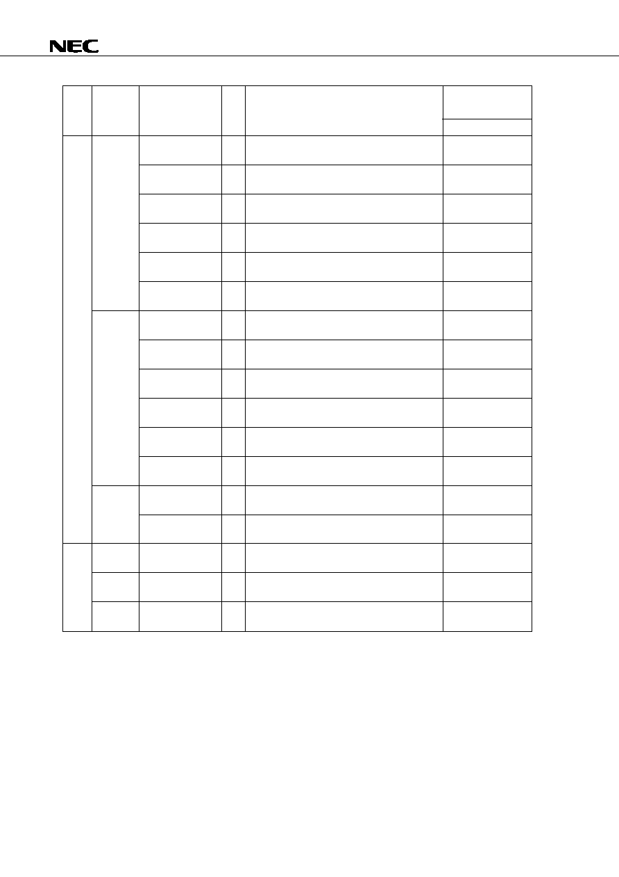
µ
PD78363A, 78365A, 78366A, 78368A
68
Flag
S
Z
AC P/V CY
Mnemonic
Operand
Byte
Operation
Instructions
BTCLR
BFSET
DBNZ
BRKCS
RETCS
RETCSB
Context switching
Conditional branch
PC
PC + 4 + jdisp8 if (saddr.bit) = 1
then reset (saddr.bit)
PC
PC + 4 + jdisp8 if sfr.bit = 1
then reset sfr.bit
PC
PC + 3 + jdisp8 if A.bit = 1
then reset A.bit
PC
PC + 3 + jdisp8 if X.bit = 1
then reset X.bit
PC
PC + 3 + jdisp8 if PSW
H
.bit = 1
then reset PSW
H
.bit
PC
PC + 3 + jdisp8 if PSW
L
.bit = 1
then reset PSW
L
.bit
PC
PC + 4 + jdisp8 if (saddr.bit) = 0
then set (saddr.bit)
PC
PC + 4 + jdisp8 if sfr.bit = 0
then set sfr.bit
PC
PC + 3 + jdisp8 if A.bit = 0
then set A.bit
PC
PC + 3 + jdisp8 if X.bit = 0
then set X.bit
PC
PC + 3 + jdisp8 if PSW
H
.bit = 0
then set PSW
H
.bit
PC
PC + 3 + jdisp8 if PSW
L
.bit = 0
then set PSW
L
.bit
r2
r2 ≠ 1,
then PC
PC + 2 + jdisp8 if 2
0
(saddr)
(saddr) ≠ 1,
then PC
PC + 3 + jdisp8 if (saddr)
0
PC
H
R5, PC
L
R4, R7
PSW
H
,
R6
PSW
L
,
RBS2 ≠ 0
n, RSS
0, IE
0
PC
H
R5, PC
L
R4, R5, R4
addr16
PSW
H
R7, PSW
L
R6
PC
H
R5, PC
L
R4, R5, R4
addr16
PSW
H
R7, PSW
L
R6
◊
◊
◊
◊
◊
◊
◊
◊
◊
◊
R
R
R
R
R
R
R
R
R
R
saddr.bit, $addr16
4
sfr.bit, $addr16
4
A.bit, $addr16
3
X.bit, $addr16
3
PSWH.bit, $addr16
3
PSWL.bit, $addr16
3
saddr.bit, $addr16
4
sfr.bit, $addr16
4
A.bit, $addr16
3
X.bit, $addr16
3
PSWH.bit, $addr16
3
PSWL.bit, $addr16
3
r2, $addr16
2
saddr, $addr16
3
RBn
2
!addr16
3
!addr16
4
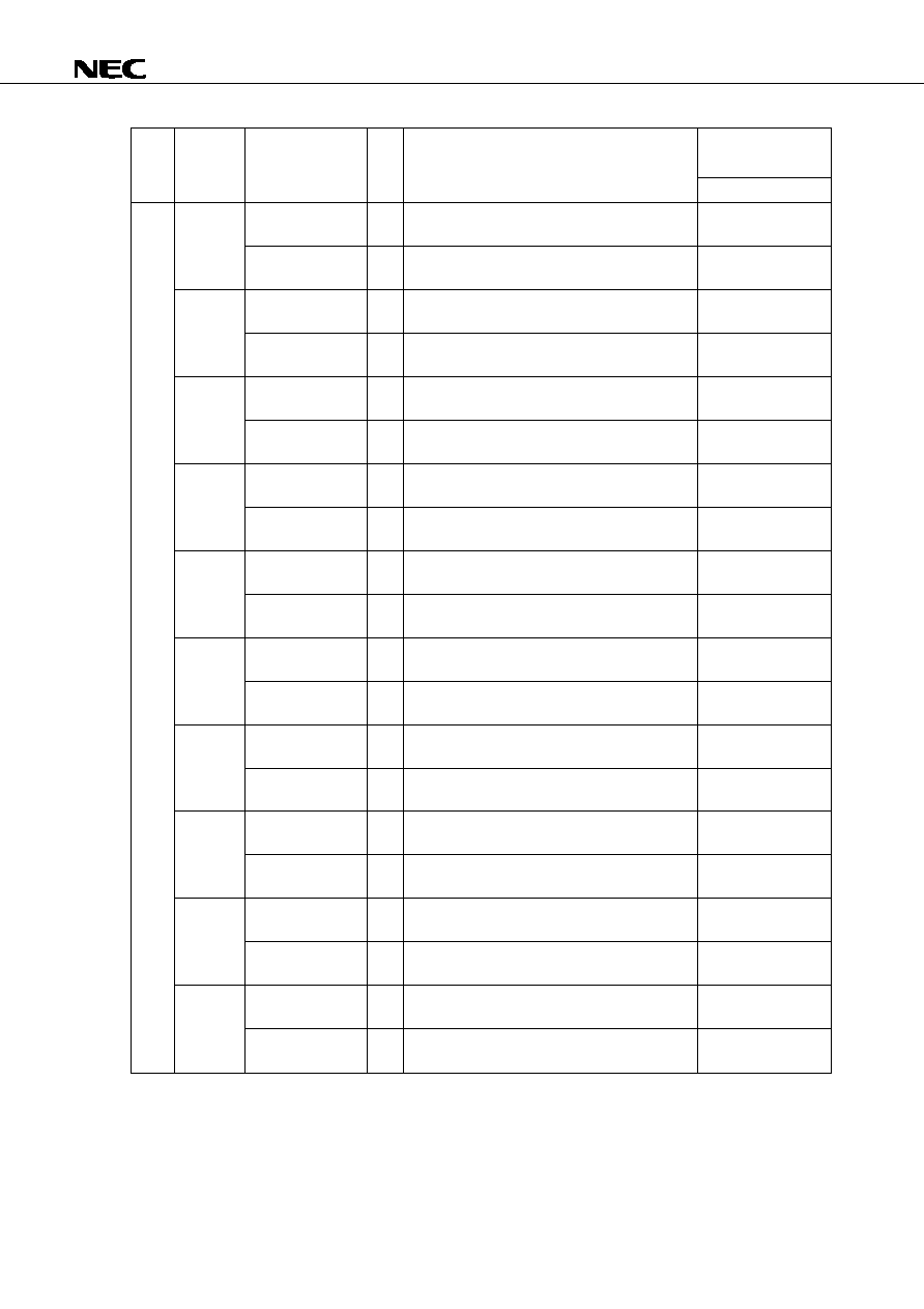
µ
PD78363A, 78365A, 78366A, 78368A
69
Flag
S
Z
AC P/V CY
Mnemonic
Operand
Byte
Operation
Instructions
[DE+], A
2
[DE≠], A
2
[DE+], [HL+]
2
[DE≠], [HL≠]
2
[DE+], A
2
[DE≠], A
2
[DE+], [HL+]
2
[DE≠], [HL≠]
2
[DE+], A
2
[DE≠], A
2
[DE+], [HL+]
2
[DE≠], [HL≠]
2
[DE+], A
2
[DE≠], A
2
[DE+], [HL+]
2
[DE≠], [HL≠]
2
[DE+], A
2
[DE≠], A
2
[DE+], [HL+]
2
[DE≠], [HL≠]
2
(DE+)
A, C
C ≠ 1
End if C = 0
(DE≠)
A, C
C ≠ 1
End if C = 0
(DE+)
(HL+), C
C ≠ 1
End if C = 0
(DE≠)
(HL≠), C
C ≠ 1
End if C = 0
(DE+)
A, C
C ≠ 1
End if C = 0
(DE≠)
A, C
C ≠ 1
End if C = 0
(DE+)
(HL+), C
C ≠ 1
End if C = 0
(DE≠)
(HL≠), C
C ≠ 1
End if C = 0
(DE+) ≠ A, C
C ≠ 1
End if C = 0 or Z = 0
(DE≠) ≠ A, C
C ≠ 1
End if C = 0 or Z = 0
(DE+) ≠ (HL+), C
C ≠ 1
End if C = 0 or Z = 0
(DE≠) ≠ (HL≠), C
C ≠ 1
End if C = 0 or Z = 0
(DE+) ≠ A, C
C ≠ 1
End if C = 0 or Z = 1
(DE≠) ≠ A, C
C ≠ 1
End if C = 0 or Z = 1
(DE+) ≠ (HL+), C
C ≠ 1
End if C = 0 or Z = 1
(DE≠) ≠ (HL≠), C
C ≠ 1
End if C = 0 or Z = 1
(DE+) ≠ A, C
C ≠ 1
End if C = 0 or CY = 0
(DE≠) ≠ A, C
C ≠ 1
End if C = 0 or CY = 0
(DE+) ≠ (HL+), C
C ≠ 1
End if C = 0 or CY = 0
(DE≠) ≠ (HL≠), C
C ≠ 1
End if C = 0 or CY = 0
String
MOVM
MOVBK
XCHM
XCHBK
CMPME
CMPBKE
CMPMNE
CMPBKNE
CMPMC
CMPBKC
◊
◊
◊
V
◊
◊
◊
◊
V
◊
◊
◊
◊
V
◊
◊
◊
◊
V
◊
◊
◊
◊
V
◊
◊
◊
◊
V
◊
◊
◊
◊
V
◊
◊
◊
◊
V
◊
◊
◊
◊
V
◊
◊
◊
◊
V
◊
◊
◊
◊
V
◊
◊
◊
◊
V
◊

µ
PD78363A, 78365A, 78366A, 78368A
70
Flag
S
Z
AC P/V CY
Mnemonic
Operand
Byte
Operation
Instructions
(DE+) ≠ A, C
C ≠ 1
End if C = 0 or CY = 1
(DE≠) ≠ A, C
C ≠ 1
End if C = 0 or CY = 1
(DE+) ≠ (HL+), C
C ≠ 1
End if C = 0 or CY = 1
(DE≠) ≠ (HL≠), C
C ≠ 1
End if C = 0 or CY = 1
STBC
byte
Note
WDM
byte
Note
RSS
RSS
RBS2 ≠ 0
n, RSS
0
RBS2 ≠ 0
n, RSS
1
No Operation
IE
1 (Enable Interruptt)
IE
0 (Disable Interrupt)
CMPMNC
CMPBKNC
MOV
SWRS
SEL
NOP
EI
DI
String
CPU control
[DE+], A
2
[DE≠], A
2
[DE+], [HL+]
2
[DE≠], [HL≠]
2
STBC, #byte
4
WDM, #byte
4
1
RBn
2
RBn, ALT
2
1
1
1
◊
◊
◊
V
◊
◊
◊
◊
V
◊
◊
◊
◊
V
◊
◊
◊
◊
V
◊
Note If the op code of the STBC register and WDM register manipulation instructions is wrong, an op code
trap interrupt occurs.
Operation on trap:
(SP ≠ 1)
PSW
H
, (SP ≠ 2)
PSW
L
,
(SP ≠ 3)
(PC ≠ 4)
H
, (SP ≠ 4)
(PC ≠ 4)
L
,
PC
L
(003CH), PC
H
(003DH),
SP
SP ≠ 4, IE
0
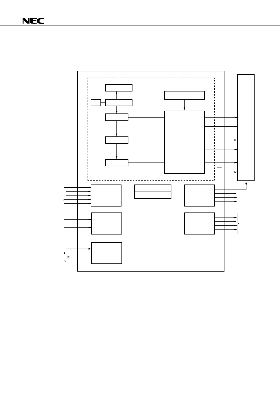
µ
PD78363A, 78365A, 78366A, 78368A
71
9.
EXAMPLE OF SYSTEM CONFIGURATION
Controlling outdoor apparatus of inverter air conditioner
ANI0
ANI1
ANI2
ANI3
ANI4
NMI
INTP1
R
X
D
T
X
D
P41
P40
P43
P42
P01
P00
P03
P02
U/D
U
V
W
W
V
U
CM03
CM00
CM01
CM02
Real-time pulse unit
16-bit timer
Dead time setting register
Inverter
(Analog signal)
AC power
supply monitor
External temperature
Thermal exchange
temperature
Outlet temperature
Inlet temperature
DC monitor
Compressor motor
temperature monitor
10-bit A/D
converter
Programmable
interrupt
controller
Serial
interface
ROM 32K bytes
RAM 2K bytes
General-
purpose port
Real-time
output port
4-way valve
2-way valve
Outdoor fan
motor
Stepping
motor
(electronic
expansion
valve)
TO00
TO01
TO02
TO03
TO04
TO05
Indoor apparatus
controller
Pulse generation
circuit
PD78366A
µ
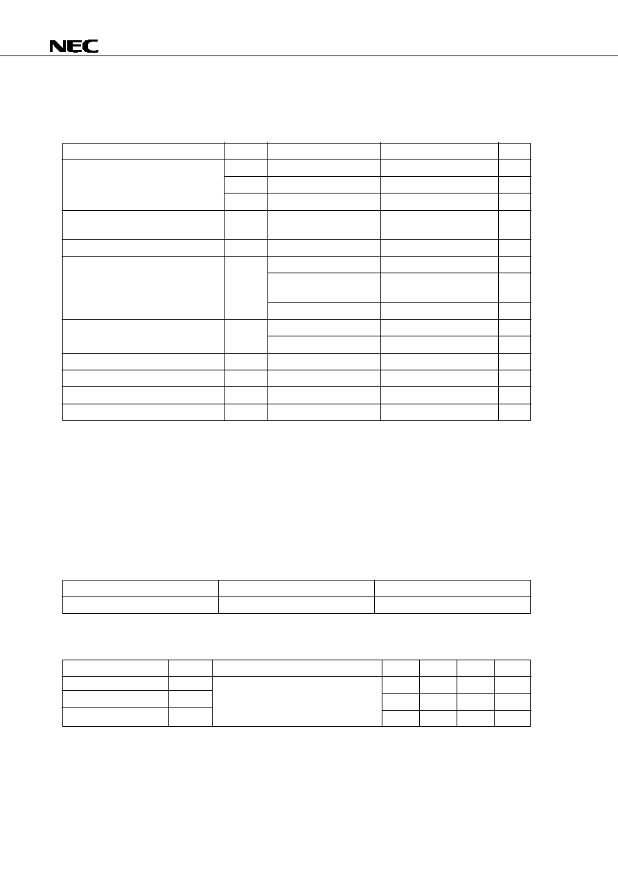
µ
PD78363A, 78365A, 78366A, 78368A
72
10. ELECTRICAL SPECIFICATIONS
Absolute Maximum Ratings (T
A
= 25 ∞C)
Parameter
Symbol
Test conditions
Rating
Unit
Power supply voltage
V
DD
≠0.5 to +7.0
V
AV
DD
≠0.5 to V
DD
+ 0.5
V
AV
SS
≠0.5 to +0.5
V
Input voltage
V
I
Pins other than
≠0.5 to V
DD
+ 0.5
V
P70/ANI0-P77/ANI7
Output voltage
V
O
≠0.5 to V
DD
+ 0.5
V
Low-level output current
I
OL
Note
20
mA
Output pins other than
4.0
mA
those in the note
Total of all output pins
200
mA
High-level output current
I
OH
All output pins
≠3.0
mA
Total of all output pins
≠25
mA
Analog input voltage
V
IAN
P70/ANI0-P77/ANI7 pins
AV
SS
≠ 0.5 to AV
DD
+ 0.5
V
A/D converter reference input voltage
AV
REF
AV
SS
≠ 0.5 to AV
DD
+ 0.5
V
Operating ambient temperature
T
A
≠40 to +85
∞C
Storage temperature
T
stg
≠60 to +150
∞C
Note P00/RTP0-P03/RTP3, P04/PWM0, P05/TCUD/PWM1, P06/TIUD/TO40, P07/TCLRUD, P10-P17, and
P80/TO00-P85/TO05 pins.
Caution Product quality may suffer if the absolute rating is exceeded for any parameter, even
momentarily. In other words, an absolute maxumum rating is a value at which the
possibility of psysical damage to the product cannnot be ruled out. Care must therefore
be taken to ensure that the these ratings are not exceeded during use of the product.
Recommended Operating Conditions
Oscillation frequency
T
A
V
DD
3 MHz
f
XX
8 MHz
≠40 to +85 ∞C
+5.0 V
±
10 %
Capacitance (T
A
= 25 ∞C, V
SS
= V
DD
= 0 V)
Parameter
Symbol
Test conditions
MIN.
TYP.
MAX.
Unit
Input capacitance
C
I
f = 1 MHz
20
pF
Output capacitance
C
O
0 V except measured pins
20
pF
I/O capacitance
C
IO
20
pF

µ
PD78363A, 78365A, 78366A, 78368A
73
Leave unconnected
HCMOS
inverter
X1
X2
V
SS
X2
X1
C1
C2
Oscillator Characteristics (T
A
= ≠40 to +85 ∞C, V
DD
= +5 V
±
10 %, V
SS
= 0 V)
Resonator
Recommended circuit
Parameter
MIN.
MAX.
Unit
Ceramic resonator or
Oscillation frequency (f
XX
)
3
8
MHz
crystal resonator
External clock
X1 input frequency (f
X
)
3
8
MHz
X1 rise/fall time (t
XR
, t
XF
)
0
30
ns
X1 input high-/low-level
40
170
ns
width (t
WXH
, t
WXL
)
Caution When using system clock oscillation circuits, to reduce the effect of the wiring
capacitouce, etc, wire the area indicated by dotted-line as follows:
∑
Make the wiring as short as possible.
∑
Do not allow the wiring to intersect other signal lines. Keep it away from other lines in which
varying high currents flow.
∑
Make sure that the ground point of the oscillation circuit capacitor is always at the same
electric potential as V
SS
. Do not allow the wiring to be grounded to a ground pattern in which
very high currents are flowing.
∑
Do not extract signals from the oscillation circuit.
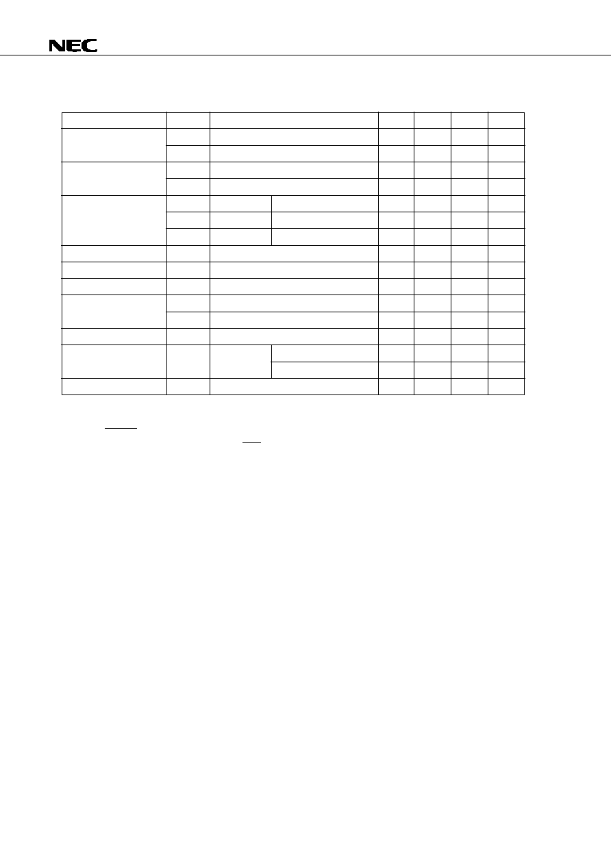
µ
PD78363A, 78365A, 78366A, 78368A
74
DC Characteristics (T
A
= ≠40 to +85 ∞C, V
DD
= +5 V
±
10 %, V
SS
= 0 V)
Parameter
Symbol
Test conditions
MIN.
TYP.
MAX.
Unit
Low-level input voltage
V
IL1
Note 1
0
0.8
V
V
IL2
Note 2
0
0.2V
DD
V
High-level input voltage
V
IH1
Note 1
2.2
V
V
IH2
Note 2
0.8V
DD
V
Low-level output voltage
V
OL1
Note 3
I
OL
= 2.0 mA
0.45
V
V
OL2
Note 4
I
OL
= 15 mA
1.5
V
V
OL3
Note 5
I
OL
= 10 mA
1.5
V
High-level output voltage
V
OH
I
OH
= ≠400
µ
A
V
DD
≠ 1.0
V
Input leakage current
I
LI
0 V
V
I
V
DD
, AV
DD
= V
DD
±
10
µ
A
Output leakage current
I
LO
0 V
V
O
V
DD
, AV
DD
= V
DD
±
10
µ
A
V
DD
supply current
I
DD1
Operating mode
70
120
mA
I
DD2
HALT mode
45
70
mA
Data retention voltage
V
DDDR
STOP mode
2.5
V
Data retention current
I
DDDR
STOP mode
V
DDDR
= 2.5 V
2
10
µ
A
V
DDDR
= 5.0 V
±
10 %
10
50
µ
A
Pull-up resistance
R
L
V
I
= 0 V
15
60
150
k
Notes 1. Pins other than those specified in Note 2.
2. RESET, X1, X2, P20/NMI, P21/INTP0, P22/INTP1, P23/INTP2, P24/INTP3/TI, P25/INTP4, P32/
SO/SB0, P33/SI/SB1 and P34/SCK pins.
3. Pins other than those specified in Notes 4 and 5.
4. P80/TO00-P85/TO05 pins (When I
OL
= 15 mA is in operation, up to three pins can be ON
simultaneously.)
5. P00/RTP0-P03/RTP3, P04/PWM0, P05/TCUD/PWM1, P06/TIUD/TO40 and P07/TCLRUD pins
(When I
OL
= 10 mA is in operation, up to four pins can be ON simultaneously.) as well as P10-P17
pins (When I
OL
= 10 mA is in operation, up to four pins can be ON simultaneously.).
Caution When the P80-P85, P00-P07, and P10-P17 pins are not used under the conditions specified
in Notes 4 and 5, they have the same characteristics as in Note 3.
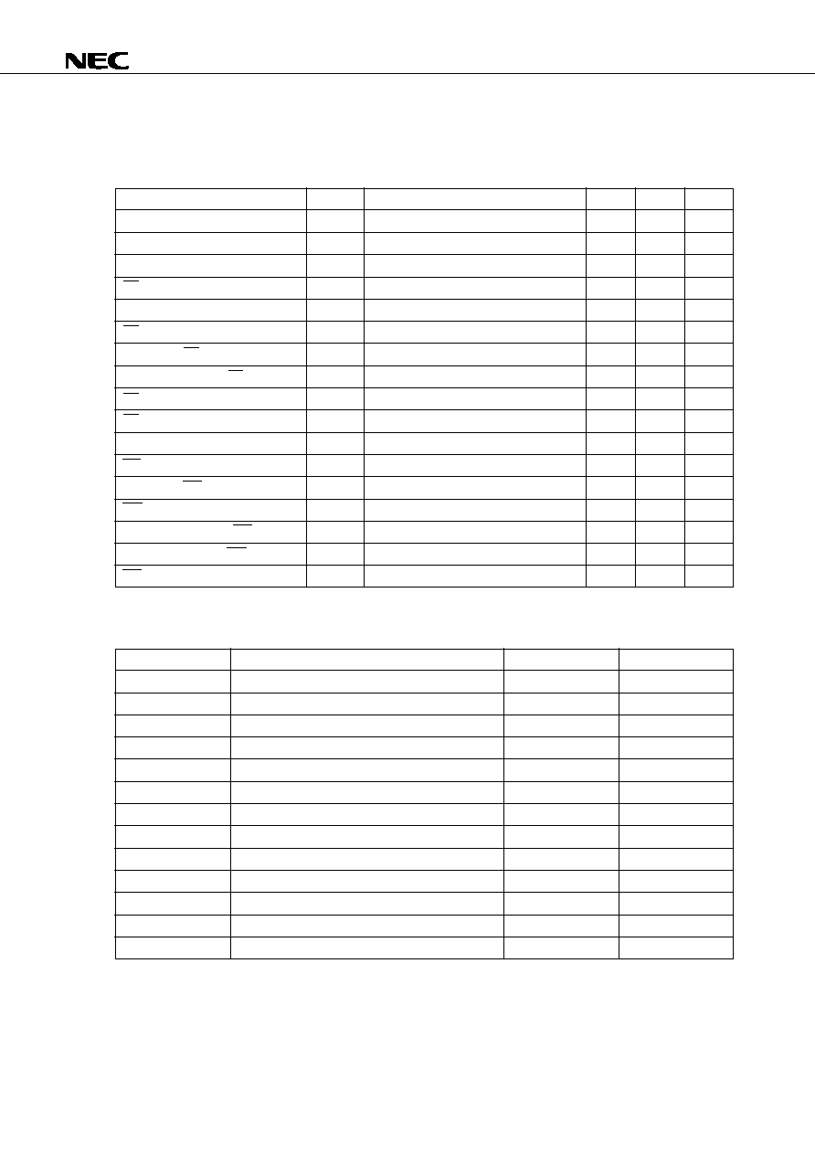
µ
PD78363A, 78365A, 78366A, 78368A
75
AC Characteristics (T
A
= ≠40 to +85 ∞C, V
DD
= +5 V
±
10 %, V
SS
= 0 V, C
L
= 100 pF, f
XX
= 8 MHz)
Read/Write Operation (when general-purpose memory is connected)
Parameter
Symbol
Test conditions
MIN.
MAX.
Unit
System clock cycle time
t
CYK
62.5
166.7
ns
Address setup time (vs. ASTB
)
t
SAST
7
ns
Address hold time (vs. ASTB
)
t
HSTA
11
ns
RD
address float time
t
FRA
24
ns
Address
data input time
t
DAID
100
ns
RD
data input time
t
DRID
49
ns
ASTB
RD
delay time
t
DSTR
15
ns
Data hold time (vs. RD
)
t
HRID
0
ns
RD
address active time
t
DRA
17
ns
RD low-level width
t
WRL
63
ns
ASTB high-level width
t
WSTH
14
ns
WR
data output time
t
DWOD
21
ns
ASTB
WR
delay time
t
DSTW
15
ns
WR
ASTB
delay time
t
DWST
78
ns
Data setup time (vs. WR
)
t
SODW
57
ns
Data hold time (vs. WR
)
t
HWOD
8
ns
WR low-level width
t
WWL
63
ns
t
CYK
-dependent Bus Timing Definition
Parameter
Arithmetic expression
MIN./MAX.
Unit
t
SAST
(0.5 + a) T ≠ 24
MIN.
ns
t
HSTA
0.5T ≠ 20
MIN.
ns
t
WSTH
(0.5 + a) T ≠ 17
MIN.
ns
t
DSTR
0.5T ≠ 16
MIN.
ns
t
WRL
(1.5 + n) T ≠ 30
MIN.
ns
t
DAID
(2.5 + a + n) T ≠ 56
MAX.
ns
t
DRID
(1.5 + n) T ≠ 44
MAX.
ns
t
DRA
0.5T ≠ 14
MIN.
ns
t
DSTW
0.5T ≠ 16
MIN.
ns
t
DWST
1.5T ≠ 15
MIN.
ns
t
WWL
(1.5 + n) T ≠ 30
MIN.
ns
t
DWOD
0.5T ≠ 10
MAX.
ns
t
SODW
(1 + n) T ≠ 5
MIN.
ns
Remarks 1. T = t
CYK
= 1/f
CLK
(f
CLK
refers to the internal system clock frequency.)
2. a becomes 1 when the address wait is inserted. Otherwise, it becomes 0.
3. n refers to the number of wait cycles that is inserted by specifying the PWC register.
4. Only the bus timings indicated in this table depend on t
CYK
.

µ
PD78363A, 78365A, 78366A, 78368A
76
Serial Operation (T
A
= ≠40 to +85 ∞C, V
DD
= +5 V
±
10 %, V
SS
= 0 V)
Parameter
Symbol
Test conditions
MIN.
MAX.
Unit
Serial clock cycle time
t
CYSK
SCK output
Internal 8 dividing
500
ns
SCK input
External clock
500
ns
Serial clock low-level
t
WSKL
SCK output
Internal 8 dividing
210
ns
width
SCK input
External clock
210
ns
Serial clock high-level
t
WSKH
SCK output
Internal 8 dividing
210
ns
width
SCK input
External clock
210
ns
SI setup time (vs. SCK
)
t
SRXSK
80
ns
SI hold time (vs. SCK
)
t
HSKRX
80
ns
SCK
SO delay time
t
DSKTX
R = 1 k
, C = 100 pF
210
ns
Up/Down Counter Operation (T
A
= ≠40 to +85 ∞C, V
DD
= +5 V
±
10 %, V
SS
= 0 V)
Parameter
Symbol
Test conditions
MIN.
MAX.
Unit
TIUD high-/low-level
t
WTIUH
, t
WTIUL
Other than mode 4
2T
ns
width
Mode 4
4T
ns
TCUD high-/low-level
t
WTCUH
, t
WTCUL
Other than mode 4
2T
ns
width
Mode 4
4T
ns
TCLRUD high-/low-level width t
WCLUH
, t
WCLUL
2T
ns
TCUD setup time (vs. TIUD
)
t
STCU
Mode 3
T
ns
TCUD hold time (vs. TIUD
)
t
HTCU
Mode 3
T
ns
TIUD setup time (vs. TCUD)
t
S4TIU
Mode 4
2T
ns
TIUD hold time (vs. TCUD)
t
H4TIU
Mode 4
2T
ns
TIUD & TCUD cycle time
t
CYC
Other than mode 4
4
MHz
t
CYC4
Mode 4
2
MHz
Remark T = t
CYK
= 1/f
CLK
(f
CLK
refers to the internal system clock frequency.)
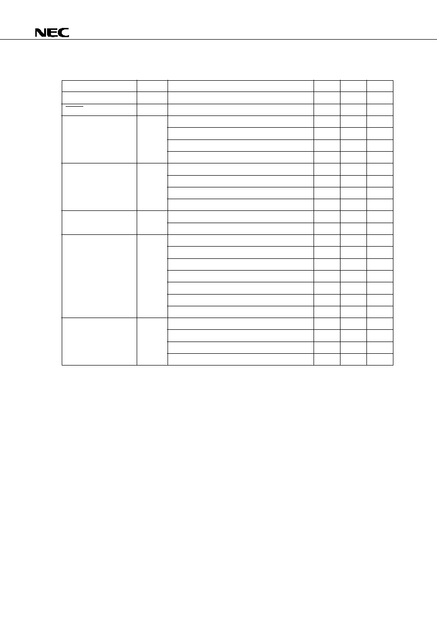
µ
PD78363A, 78365A, 78366A, 78368A
77
Other Operations (T
A
= ≠40 to +85 ∞C, V
DD
= +5 V
±
10 %, V
SS
= 0 V)
Parameter
Symbol
Test conditions
MIN.
MAX.
Unit
NMI high-/low-level width t
WNIH
, t
WNIL
2
µ
s
RESET high-/low-level width t
WRSH
, t
WRSL
1.5
µ
s
INTP0 high-/low-level
t
WI0H
, t
WI0L
Ts = T
250
ns
width
Ts = 4T
1.0
µ
s
Ts = 8T
2.0
µ
s
Ts = 16T
4.0
µ
s
INTP1 high-/low-level
t
WI1H
, t
WI1L
Ts = T
250
ns
width
Ts = 4T
1.0
µ
s
Ts = 8T
2.0
µ
s
Ts = 16T
4.0
µ
s
INTP2 high-/low-level
t
WI2H
, t
WI2L
Ts = T
250
ns
width
Ts = 4T
1.0
µ
s
INTP3(TI) high-/low-
t
WI3H
, t
WI3L
Ts = T
250
ns
level width
Ts = 4T
1.0
µ
s
Ts = 8T
2.0
µ
s
Ts = 16T
4.0
µ
s
Ts = 64T
16.0
µ
s
Ts = 128T
32.0
µ
s
Ts = 256T
64.0
µ
s
INTP4 high-/low-level
t
WI4H
, t
WI4L
Ts = T
250
ns
width
Ts = 4T
1.0
µ
s
Ts = 8T
2.0
µ
s
Ts = 16T
4.0
µ
s
Remarks 1. T = t
CYK
= 1/f
CLK
(f
CLK
refers to the internal system clock frequency.)
2. Ts refers to the input sampling frequency. INTP0-INTP4 can be selected to programmable.
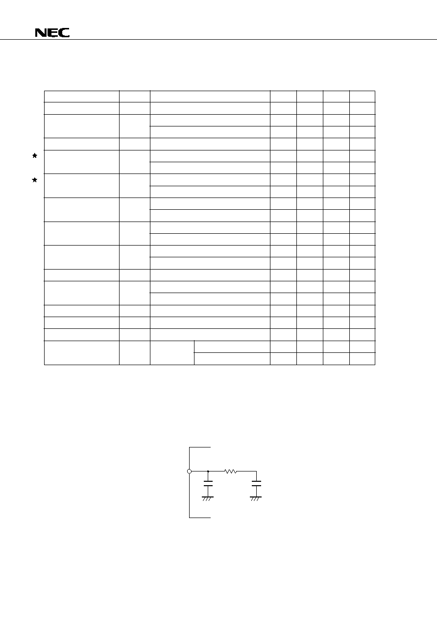
µ
PD78363A, 78365A, 78366A, 78368A
78
A/D Converter Characteristics (T
A
= ≠40 to +85 ∞C, V
DD
= +5 V
±
10 %, V
SS
= AV
SS
= 0 V,
V
DD
≠ 0.5 V
AV
DD
V
DD
)
Parameter
Symbol
Test conditions
MIN.
TYP.
MAX.
Unit
Resolution
10
bit
Total error
Note 1
4.5 V
AV
REF
AV
DD
±
0.4
%FSR
3.4 V
AV
REF
AV
DD
±
0.7
%FSR
Quantization error
±
1/2
LSB
Conversion time
t
CONV
62.5 ns
t
CYK
< 80 ns
208
t
CYK
80 ns
t
CYK
166.6 ns
169
t
CYK
Sampling time
t
SAMP
62.5 ns
t
CYK
< 80 ns
24
t
CYK
80 ns
t
CYK
166.6 ns
20
t
CYK
Zero-scale error
Note 1
4.5 V
AV
REF
AV
DD
±
1.5
±
2.5
LSB
3.4 V
AV
REF
AV
DD
±
1.5
±
4.5
LSB
Full-scale error
Note 1
4.5 V
AV
REF
AV
DD
±
1.5
±
2.5
LSB
3.4 V
AV
REF
AV
DD
±
1.5
±
4.5
LSB
Nonlinearity error
Note 1
4.5 V
AV
REF
AV
DD
±
1.5
±
2.5
LSB
3.4 V
AV
REF
AV
DD
±
1.5
±
4.5
LSB
Analog input voltage
Note 2
V
IAN
≠0.3
AV
REF
+ 0.3
V
Analog input impedance
R
AN
When not sampling
10
M
When sampling
Note 3
Reference voltage
AV
REF
3.4
AV
DD
V
AV
REF1
current
AI
REF
1.0
3.0
mA
AV
DD
supply current
AI
DD
Operating mode
2.0
6.0
mA
A/D converter data
AI
DDDR
STOP mode
AV
DDDR
= 2.5 V
2
10
µ
A
retention current
AV
DDDR
= 5 V
±
10 %
10
50
µ
A
Notes 1. The quantization error is excluded.
2. When ≠0.3 V
V
IAN
0 V, the conversion result becomes 000H.
When 0 V < V
IAN
< AV
REF
, the conversion is performed with the 10-bit resolution.
When AV
REF
V
IAN
+0.3 V, the conversion result becomes 3FFH.
3. The analog input impedance at the time of sampling is the same as the equivalent circuit shown
below. (The values in the diagram are TYP. values; they are not guaranteed values)
Analog input pin
1 k
25 pF
(Input
capacitance
included)
4 pF

µ
PD78363A, 78365A, 78366A, 78368A
79
Cautions 1. When using the P70/ANI0-P77/ANI7 pins for both digital and analog inputs, the previ-
ously described characteristics are not guaranteed. Therefore, ensure that all of the
eight P70/ANI0-P77/ANI7 pins are used either for analog input or digital input.
2. When using the P70/ANI0-P77/ANI7 pins as digital input, make sure to set that AV
DD
= V
DD
,
and AV
SS
= V
SS
.
AC Timing Test Point
0.8 V
DD
or 2.2 V
0.2 V
DD
or 0.8 V
0.8 V
DD
or 2.2 V
0.2 V
DD
or 0.8 V
V
DD
0 V
Test point

µ
PD78363A, 78365A, 78366A, 78368A
80
Read Operation
A8-A15
(Output)
AD0-AD7
(Input/output)
ASTB
(Output)
RD
(Output)
t
WSTH
t
SAST
t
DAID
Hi-Z
Hi-Z
Hi-Z
Hi-Z
High-order address
High-order address
t
CYK
t
HSTA
t
FRA
t
DSTR
t
DRID
t
DRA
t
WRL
t
HRID
Low-order address (Output)
Low-order address (Output)
Data (Input)
(CLK)
Write Operation
A8-A15
(Output)
AD0-AD7
(Output)
ASTB
(Output)
WR
(Output)
t
WSTH
t
SAST
High-order address
High-order address
t
HSTA
t
DSTW
t
DWOD
t
WWL
Low-order address (Output)
Low-order address (Output)
Data (Output)
(CLK)
t
HWOD
t
DWST
Undefined
t
SODW
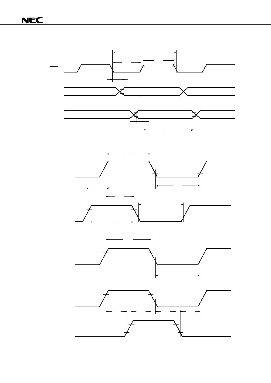
µ
PD78363A, 78365A, 78366A, 78368A
81
Serial Operation
t
CYSK
t
WSKL
t
WSKH
t
DSKTX
t
SRXSK
t
HSKRX
SCK
SO
SI
Up/Down Counter (Timer 4) Input Timing
t
WTIUH
t
STCU
t
HTCU
t
WTIUL
t
WTCUL
t
WTCUH
TIUD
TCUD
t
WCLUH
t
WCLUL
TCLRUD
TIUD
TCUD
t
S4TIU
t
H4TIU
t
S4TIU
t
H4TIU
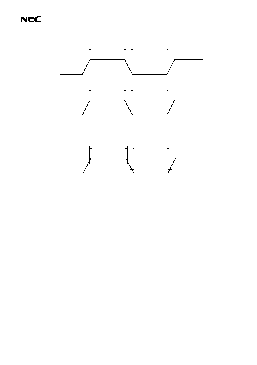
µ
PD78363A, 78365A, 78366A, 78368A
82
Interrupt Input Timing
t
WNIH
t
WNIL
0.8 V
DD
0.2 V
DD
NMI
t
WInH
t
WInL
INTPn
0.8 V
DD
0.2 V
DD
Remark n = 0 to 4
Reset Input Timing
t
WRSH
t
WRSL
0.8 V
DD
0.2 V
DD
RESET
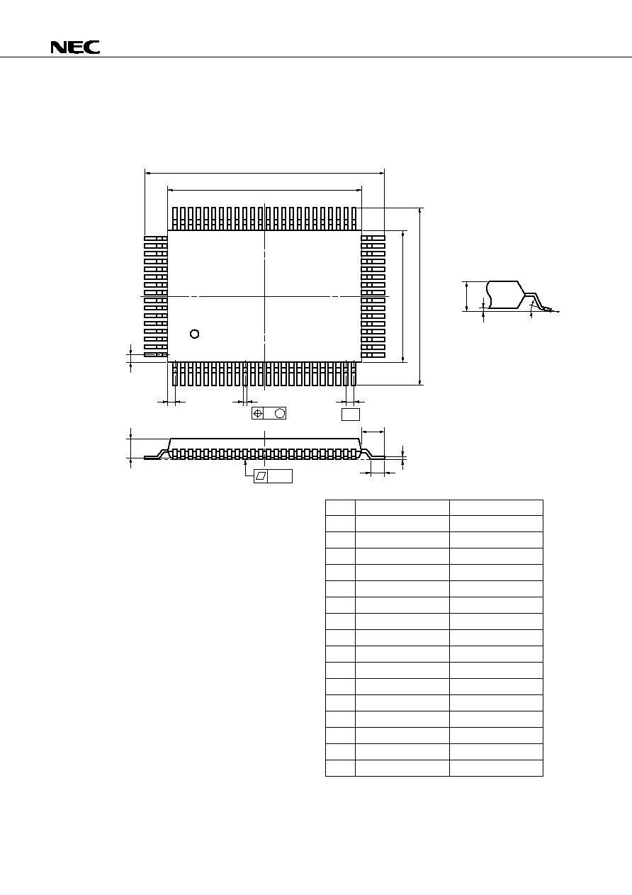
µ
PD78363A, 78365A, 78366A, 78368A
83
11. PACKAGE DRAWING
N
A
M
F
B
64
65
40
K
L
80 PIN PLASTIC QFP (14
◊
20)
80
1
25
24
41
G
D
C
P
detail of lead end
S
Q
5∞±5∞
M
I
H
J
P80GF-80-3B9-2
ITEM
MILLIMETERS
INCHES
A
B
C
D
F
G
H
I
J
K
L
23.6±0.4
14.0±0.2
0.8
0.35±0.10
0.15
20.0±0.2
0.929±0.016
0.039
0.031
0.006
0.031 (T.P.)
0.795
NOTE
M
N
0.15
0.15
1.8±0.2
0.8 (T.P.)
0.006
0.006
+0.004
≠0.003
Each lead centerline is located within 0.15
mm (0.006 inch) of its true position (T.P.) at
maximum material condition.
0.071
0.014
0.551
0.8±0.2
0.031
P
2.7
0.106
0.693±0.016
17.6±0.4
1.0
+0.009
≠0.008
Q
0.1±0.1
0.004±0.004
S
3.0 MAX.
0.119 MAX.
+0.10
≠0.05
+0.009
≠0.008
+0.004
≠0.005
+0.009
≠0.008
+0.008
≠0.009
µ
PD78363A, 78365A, 78366A, 78368A
84
12. RECOMMENDED SOLDERING CONDITIONS
These products should be soldered and mounted under the conditions recommended below.
For details of recommended soldering conditions, refer to the information document Semiconductor Device
Mounting Technology Manual (C10535E).
For soldering methods and conditions other than those recommended, please contact your NEC sales
representative.
Table 12-1. Surface Mount Type Soldering Conditions
µ
PD78363AGF-
◊◊◊
-3B9: 80-Pin Plastic QFP (14
◊
20 mm)
µ
PD78365AGF-3B9
: 80-Pin Plastic QFP (14
◊
20 mm)
µ
PD78366AGF-
◊◊◊
-3B9: 80-Pin Plastic QFP (14
◊
20 mm)
µ
PD78368AGF-
◊◊◊
-3B9: 80-Pin Plastic QFP (14
◊
20 mm)
Soldering method
Infrared reflow
VPS
Wave soldering
Partial heating
Caution Use of more than one soldering method should be avoided (except in the case of partial
heating).
Recommended
condition symbol
IR35-00-3
VP15-00-3
WS60-00-1
≠
Soldering conditions
Package peak temperature: 235 ∞C, Duration: 30 sec. max. (210 ∞C or
above) Number of times: 3 max.
Package peak temperature: 215 ∞C, Duration: 40 sec. max. (200 ∞C or
above) Number of times: 3 max.
Solder bath temperature: 260 ∞C or less, Time: 10 sec. max.,
Number of times: 1, Pre-heating temperature: 120 ∞C max. (Package
surface temperature)
Pin temperature: 300 ∞C or less
Duration: 3 sec. max. (per side of device)

µ
PD78363A, 78365A, 78366A, 78368A
85
APPENDIX A. DIFFERENCES BETWEEN
µ
PD78366A AND
µ
PD78328
Product name
Item
125 ns
internal clock : 8 MHz,
external clock : 16 MHz
250 ns
Minimum instruction
execution time
Internal
memory
ROM
RAM
µ
PD78366A
µ
PD78328
32K bytes
16K bytes
2K bytes
512 bytes
64K bytes (can be externally expanded)
8 bits
◊
16
◊
8 banks
115
111
∑ 16-bit transfer/operation
∑ Multiplication/division (16 bits
◊
16 bits, 32 bits
˜
16 bits)
∑ Bit manipulation
∑ String
Memory space
General-purpose
registers
Number of basic
instructions
Instruction set
--
11 (of which 8 are multiplexed with analog
input)
41
∑ 16-bit timer
◊
3
∑ 16-bit compare register
◊
14
∑ 16-bit capture/compare register
◊
1
∑ Two output modes selectable
Mode 0, set-reset output : 6 channels
toggle output
: 1 channel
Mode 1, buffer output
: 8 channels
4/8 (buffer output in 4-/8-bit units)
8-bit resolution PWM output: 1 channel
∑ Sum-of-products operation
(16 bits
◊
16 bits + 32 bits)
∑ Relative operation
14 (of which 8 are multiplexed with analog
input)
49
∑ 16-bit timer
◊
5
∑ 16-bit compare register
◊
7
∑ 16-bit capture register
◊
3
∑ 16-bit capture/compare register
◊
2
∑ Two output modes selectable
Mode 0, set-reset output : 6 channels
Mode 1, buffer output
: 6 channels
∑ 16-bit resolution PWM output: 1 channel
4 (buffer output in 4-bit units)
8-/9-/10-/12-bit resolution variable PWM
output: 2 channels
10-bit resolution, 8 channels
Dedicated baud rate generator
UART (with pin selection function)
: 1 channel
Clocked serial interface/SBI : 1 channel
∑ External: 6, internal: 14 (2 multiplexed
with external)
∑ 4 programmable priority levels
Real-time pulse unit
Real-time output port
PWM unit
A/D converter
Serial interface
Interrupt function
Test source
PLL control circuit
Package
Others
Input
I/O
Dedicated baud rate generator
UART
: 1 channel
Clocked serial interface/SBI : 1 channel
∑ External: 4, internal: 17
∑ 3 programmable priority levels
∑ Three processing selectable
(vectored interrupt/macro service/context switching)
I/O lines
internal clock : 16 MHz
external clock : 8 MHz
None
Internal: 1
Provided (external 8 MHz
internal: 16 MHz)
None
∑ 80-pin plastic QFP (14
◊
20 mm)
∑ 64-pin plastic shrink DIP
∑ 64-pin plastic QFP (14
◊
20 mm)
∑ Watchdog timer
∑ Standby functions (HALT mode, STOP mode)
µ
PD78363A, 78365A, 78366A, 78368A
86
Host machine
Order code (product name)
PC-9800 series
MS-DOS
IBM PC/AT and its
PC DOS
compatible model
HP9000 series 700
HP-UX
SPARC station
SunOS
NEWS
NEWS-OS
Host machine
Order code (product name)
PC-9800 series
MS-DOS
TM
IBM PC/AT
TM
and its
PC DOS
TM
compatible model
HP9000 series 700
TM
HP-UX
TM
SPARC station
TM
SunOS
TM
NEWS
TM
NEWS-OS
TM
APPENDIX B. TOOLS
B.1 DEVELOPMENT TOOLS
The following development tools are available to support the system development using
µ
PD78366A :
Language Processor
OS
Supply media
3.5" 2HD
µ
S5A13RA78K3
5" 2HD
µ
S5A10RA78K3
3.5" 2HC
µ
S7B13RA78K3
5" 2HC
µ
S7B10RA78K3
DAT
µ
S3P16RA78K3
Cartridge tape
µ
S3K15RA78K3
(QIC-24)
µ
S3R15RA78K3
A relocatable assembler, that can be used commonly for the 78K/III series products. Since this
assembler is provided with macro functions, it enhances the developmnt efficency. A structured
assembler, that can explicitly describe the program control structure, is also supplied, so that
the program productivity and maintainability can be improved.
78K/III series
relocatable assembler
(RA78K3)
This is a C compiler that can be commonly used for 78K/III series.
This program converts the program written in C language to object codes microcomputer can
execute. When using this compiler, the 78K/III series relocatable assembler (RA78K3) is
necessary.
OS
Supply media
3.5" 2HD
µ
S5A13CC78K3
5" 2HD
µ
S5A10CC78K3
3.5" 2HC
µ
S7B13CC78K3
5" 2HC
µ
S7B10CC78K3
DAT
µ
S3P16CC78K3
Cartridge tape
µ
S3K15CC78K3
(QIC-24)
µ
S3R15CC78K3
78K/III series
C compiler
(CC78K3)
Remark The operations of the relocatable assembler and C compiler are guaranteed only on the specified
host machine and OS described above.
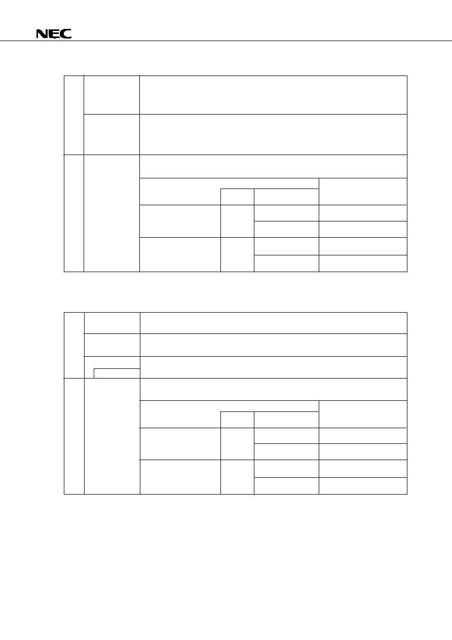
µ
PD78363A, 78365A, 78366A, 78368A
87
This is a PROM programmer that can program PROM-contained single-chip microcontrollers
in standalone mode or under control of a host machine when the accessory board and an
optional programmer adapter are connected. It can also program representative PROMs from
256K-bit to 4M-bit models.
PROM programmer adapters that writes a program to the
µ
PD78P368A on a general-purpose
PROM programmer such as the PG-1500.
PA-78P368GF : for
µ
PD78P368AGF
PA-78P368KL : for
µ
PD78P368AKL
Connects the PG-1500 and a host machine with a serial intrface and a parallel interface to control
the PG-1500 from the host machine.
PG-1500
PA-78P368GF
PA-78P368KL
PG-1500
controller
In-circuit emulator that can be used to develop and debug application systems. Connected to
a host machine for debugging.
I/O emulation board that emulates the peripheral functions of the target device such as I/O ports.
Emulation probe that connects the IE-78350-R to the target system. One conversion socket,
EV-9200G-80, used to connect the target system is supplied as an accessory.
Program that controls the IE-78350-R on the host machine. It can automatically execute
commands, enhancing debugging efficiency.
IE-78350-R
IE-78365-R-EM1
EP-78365GF-R
IE-78350-R
control program
(IE controller)
EV-9200G-80
Host machine
Order code (part number)
PC-9800 series
MS-DOS
IBM PC/AT and
PC DOS
compatible machines
Host machine
Order code (part number)
PC-9800 series
MS-DOS
IBM PC/AT and
PC DOS
compatible machines
PROM Writing Tools
Remark The operation of the PG-1500 controller is guaranteed only on the above host machine and OS.
Debugging Tools (When IE Controller Is Used)
Remark The operation of the IE controller is guaranteed only on the above host machine and OS.
Hardware
Software
Hardware
Software
OS
Supply media
3.5" 2HD
µ
S5A13IE78365A
5" 2HD
µ
S5A10IE78365A
3.5" 2HC
µ
S7B13IE78365A
3.5" 2HC
µ
S7B10IE78365A
OS
Supply media
3.5" 2HD
µ
S5A13PG1500
5" 2HD
µ
S5A10PG1500
3.5" 2HC
µ
S7B13PG1500
3.5" 2HC
µ
S7B10PG1500
µ
PD78363A, 78365A, 78366A, 78368A
88
Development Tool Configuration (When Using IE Controller)
Host machine
PC-9800 series
IBM PC series
EWS
Software
Relocatable
assembler
IE controller
C compiler
PG-1500
controller
Built-in PROM models
µ
PD78P368AGF
µ
PD78P368AKL
+
+
+
Programmer adapter
PA-78P368GF
PA-78P368KL
PG-1500
RS-232-C
RS-232C
PROM
programmer
IE-78350-R
in-circuit emulator
IE-78365-R-EM1
I/O emulation board
(optional)
+
Emulation probe
Conversion socket for connecting
the emulation probe and the target system
Note
Target system
EP-78365GF-R
EV-9200G-80
Note A socket is provided with the emulation probe.
Remarks 1. Host machine and PG-1500 can be directly connected by RS-232-C.
2. 3.5-inch FD represents the supply media of software in this figure.

µ
PD78363A, 78365A, 78366A, 78368A
89
IE-784000-R
IE-78350-R-EM-A
IE-78365-R-EM1
EP-78365GF-R
EV-9200G-80
IE-70000-98-IF-B
IE-70000-98N-IF
IE-70000-PC-IF-B
IE-78000-R-SV3
Integrated debugger
(ID78K3)
Device File
(DF78365)
Debugging Tools (When Integrated Debugger Is Used)
Hardware
Software
In-circuit emulation that can be used to develop and debug the application system. Connected
to a host machine for debugging.
Emulation board that emulates the peripheral functions of the target device such as I/O ports.
I/O emulation board that emulates the peripheral functions of the target device such as I/O ports.
Emulation probe connecting the IE-784000-R to the target system. One conversion socket, EV-
9200G-80, used to connect the target system is supplied as an accessory.
Interface adapter to connect PC-9800 series (except notebook type personal computer) as the
host machine.
Interface adapter and cable to connect PC-9800 series notebook type personal computer as the
host machine.
Interface adapter and cable to connect IBM PC as the host machine.
Interface board to connect EWS as the host machine.
Program controlling the in-circuit emulator for the 78K/III series. Used in combination with a
device file (DF78365). Can debug a program coded in the C language, structured assembly
language, or assembly language at source program level. Can also split the screen of the host
machine into windows on each of which information is displayed, enhancing debugging
efficiency.
Host machine
Order code (part number)
OS
Supply media
PC-9800 series
MS-DOS
3.5" 2HD
µ
SAA13ID78K3
Windows
TM
5" 2HD
µ
SAA10ID78K3
IBM PC/AT and compatible
PC DOS
3.5" 2HC
µ
SAB13ID78K3
machines (Japanese Windows)
Windows
5" 2HC
µ
SAB10ID78K3
IBM PC/AT and compatible
3.5" 2HC
µ
SBB13ID78K3
machines (English Windows)
5" 2HC
µ
SBB10ID78K3
File containing information peculiar to device. Use in combination with an assembler (RA78
K3), C compiler (CC78K3), and integrated debugger (ID78K3).
Host machine
Order code (part number)
OS
Supply media
PC-9800 series
MS-DOS
3.5" 2HD
µ
S5A13DF78365
5" 2HD
µ
S5A10DF78365
IBM PC/AT and compatible
PC DOS
3.5" 2HC
µ
S7B13DF78365
machines
5" 2HC
µ
S7B10DF78365
+
+
Remark The operation of the integrated debugger and device file is guaranteed only on the above host
machine and OS.
µ
PD78363A, 78365A, 78366A, 78368A
90
Development Tool Configuration (When Using Integrated Debugger)
Host machine
PC-9800 series
IBM PC/AT
EWS
IE-70000-98-IF-B
IE-70000-98N-IF
IE-70000-PC-IF-B
Software
Relocatable
assembler
Integrated
debugger
Device file
C compiler
PG-1500
controller
Built-in PROM models
µ
PD78P368AGF
µ
PD78P368AKL
+
+
+
Programmer adapter
PA-78P368GF
PA-78P368KL
PROM programmer
PG-1500
IE-784000-R
in-circuit emulator
IE-78350-R-EM-A
emulation board
(optional)
IE-78365-R-EM1
I/O emulation board
(optional)
+
+
Emulation probe
Conversion socket for connecting
the emulation probe and the target system
Note
Target system
EP-78365GF-R
EV-9200G-80
RS-232C
Note A socket is provided with the emulation probe.
Remarks 1. Desk top-type PC represents host machine in this figure.
2. 3.5-inch FD represents the supply media of software in this figure.
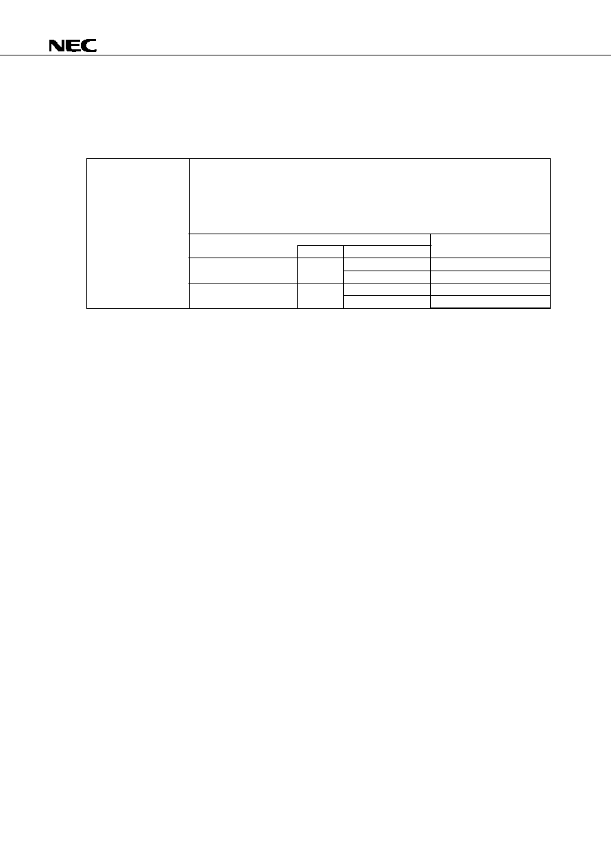
µ
PD78363A, 78365A, 78366A, 78368A
91
B.2 EMBEDDED SOFTWARE
The following embedded software is available for enhancing the efficiency of program development and
maintenance.
REAL-TIME OS
Real-time OS
(RX78K/III)
Note
RX78K/III is intended to implement a multi-tasking environment for use in the control field where
real-time capability is a must. It can allocate the idle time of the CPU to other processing to
improve the overall performance of the system.
RX78K/III provides system calls conforming to the
µ
ITRON specification.
The RX78K/III package supplies a tool (configurator) to create the nucleus of RX78K/III and
multiple information tables.
Host machine
Order code (part number)
OS
Supply media
PC-9800 series
MS-DOS
3.5" 2HD
Pending
5" 2HD
Pending
IBM PC/AT and compatible
PC DOS
3.5" 2HC
Pending
machines
5" 2HC
Pending
Note Under development
Caution Before purchasing this product, you are requested to conclude a contract licensing use by
filling out a specified form.
Remark When using the RX78K/III real-time OS, the RA78K3 assembler package (optional) is necessary.
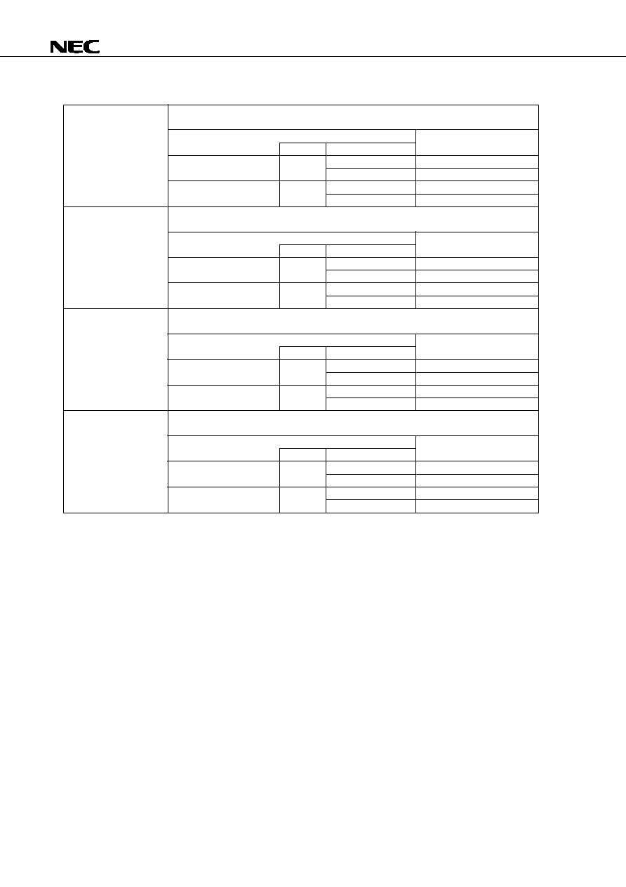
µ
PD78363A, 78365A, 78366A, 78368A
92
Fuzzy Inference Development Support System
Note Under development
Fuzzy knowledge data
creation tool
(FE9000, FE9200)
Translator
(FT78K3)
Note
Fuzzy inference module
(FI78K/III)
Note
Fuzzy inference debugger
(FD78K/III)
Program that supports input/editing and evaluation (simulation) of fuzzy knowledge (fuzzy rules
and membership functions).
Host machine
Order code (part number)
OS
Supply media
PC-9800 series
MS-DOS
3.5" 2HD
µ
S5A13FE9000
5" 2HD
µ
S5A10FE9000
IBM PC/AT and compatible
PC DOS
3.5" 2HC
µ
S7B13FE9200
machines
Windows
5" 2HC
µ
S7B10FE9200
Program that converts the fuzzy knowledge data obtained by using the fuzzy knowledge data
creation tool into assembler source program for the RA78K/III.
Host machine
Order code (part number)
OS
Supply media
PC-9800 series
MS-DOS
3.5" 2HD
µ
S5A13FT78K3
5" 2HD
µ
S5A10FT78K3
IBM PC/AT and compatible
PC DOS
3.5" 2HC
µ
S7B13FT78K3
machines
5" 2HC
µ
S7B10FT78K3
Program that executes fuzzy inference when linked with the fuzzy knowledge data converted
by the translator.
Host machine
Order code (part number)
OS
Supply media
PC-9800 series
MS-DOS
3.5" 2HD
µ
S5A13FI78K3
5" 2HD
µ
S5A10FI78K3
IBM PC/AT and compatible
PC DOS
3.5" 2HC
µ
S7B13FI78K3
machines
5" 2HC
µ
S7B10FI78K3
Support software that evaluates and adjusts the fuzzy knowledge data at the hardware level by
using an in-circuit emulator.
Host machine
Order code (part number)
OS
Supply media
PC-9800 series
MS-DOS
3.5" 2HD
µ
S5A13FD78K3
5" 2HD
µ
S5A10FD78K3
IBM PC/AT and compatible
PC DOS
3.5" 2HC
µ
S7B13FD78K3
machines
5" 2HC
µ
S7B10FD78K3
+

µ
PD78363A, 78365A, 78366A, 78368A
93
[MEMO]

µ
PD78363A, 78365A, 78366A, 78368A
94
NOTES FOR CMOS DEVICES
1
PRECAUTION AGAINST ESD FOR SEMICONDUCTORS
Note: Strong electric field, when exposed to a MOS device, can cause destruction
of the gate oxide and ultimately degrade the device operation. Steps must
be taken to stop generation of static electricity as much as possible, and
quickly dissipate it once, when it has occurred. Environmental control must
be adequate. When it is dry, humidifier should be used. It is recommended
to avoid using insulators that easily build static electricity. Semiconductor
devices must be stored and transported in an anti-static container, static
shielding bag or conductive material. All test and measurement tools
including work bench and floor should be grounded. The operator should
be grounded using wrist strap. Semiconductor devices must not be touched
with bare hands. Similar precautions need to be taken for PW boards with
semiconductor devices on it.
2
HANDLING OF UNUSED INPUT PINS FOR CMOS
Note: No connection for CMOS device inputs can be cause of malfunction. If no
connection is provided to the input pins, it is possible that an internal input
level may be generated due to noise, etc., hence causing malfunction. CMOS
device behave differently than Bipolar or NMOS devices. Input levels of
CMOS devices must be fixed high or low by using a pull-up or pull-down
circuitry. Each unused pin should be connected to V
DD
or GND with a
resistor, if it is considered to have a possibility of being an output pin. All
handling related to the unused pins must be judged device by device and
related specifications governing the devices.
3
STATUS BEFORE INITIALIZATION OF MOS DEVICES
Note: Power-on does not necessarily define initial status of MOS device. Produc-
tion process of MOS does not define the initial operation status of the device.
Immediately after the power source is turned ON, the devices with reset
function have not yet been initialized. Hence, power-on does not guarantee
out-pin levels, I/O settings or contents of registers. Device is not initialized
until the reset signal is received. Reset operation must be executed imme-
diately after power-on for devices having reset function.

µ
PD78363A, 78365A, 78366A, 78368A
95
NEC Electronics Inc. (U.S.)
Santa Clara, California
Tel: 800-366-9782
Fax: 800-729-9288
NEC Electronics (Germany) GmbH
Duesseldorf, Germany
Tel: 0211-65 03 02
Fax: 0211-65 03 490
NEC Electronics (UK) Ltd.
Milton Keynes, UK
Tel: 01908-691-133
Fax: 01908-670-290
NEC Electronics Italiana s.r.1.
Milano, Italy
Tel: 02-66 75 41
Fax: 02-66 75 42 99
NEC Electronics Hong Kong Ltd.
Hong Kong
Tel: 2886-9318
Fax: 2886-9022/9044
NEC Electronics Hong Kong Ltd.
Seoul Branch
Seoul, Korea
Tel: 02-528-0303
Fax: 02-528-4411
NEC Electronics Singapore Pte. Ltd.
United Square, Singapore 1130
Tel: 253-8311
Fax: 250-3583
NEC Electronics Taiwan Ltd.
Taipei, Taiwan
Tel: 02-719-2377
Fax: 02-719-5951
NEC do Brasil S.A.
Sao Paulo-SP, Brasil
Tel: 011-889-1680
Fax: 011-889-1689
NEC Electronics (Germany) GmbH
Benelux Office
Eindhoven, The Netherlands
Tel: 040-2445845
Fax: 040-2444580
NEC Electronics (France) S.A.
Velizy-Villacoublay, France
Tel: 01-30-67 58 00
Fax: 01-30-67 58 99
NEC Electronics (France) S.A.
Spain Office
Madrid, Spain
Tel: 01-504-2787
Fax: 01-504-2860
NEC Electronics (Germany) GmbH
Scandinavia Office
Taeby, Sweden
Tel: 08-63 80 820
Fax: 08-63 80 388
Regional Information
Some information contained in this document may vary from country to country. Before using any NEC
product in your application, please contact the NEC office in your country to obtain a list of authorized
representatives and distributors. They will verify:
∑ Device availability
∑ Ordering information
∑ Product release schedule
∑ Availability of related technical literature
∑ Development environment specifications (for example, specifications for third-party tools and
components, host computers, power plugs, AC supply voltages, and so forth)
∑ Network requirements
In addition, trademarks, registered trademarks, export restrictions, and other legal issues may also vary
from country to country.
J96. 8

µ
PD78363A, 78365A, 78366A, 78368A
2
No part of this document may be copied or reproduced in any form or by any means without the prior written
consent of NEC Corporation. NEC Corporation assumes no responsibility for any errors which may appear in
this document.
NEC Corporation does not assume any liability for infringement of patents, copyrights or other intellectual property
rights of third parties by or arising from use of a device described herein or any other liability arising from use
of such device. No license, either express, implied or otherwise, is granted under any patents, copyrights or other
intellectual property rights of NEC Corporation or others.
While NEC Corporation has been making continuous effort to enhance the reliability of its semiconductor devices,
the possibility of defects cannot be eliminated entirely. To minimize risks of damage or injury to persons or
property arising from a defect in an NEC semiconductor device, customers must incorporate sufficient safety
measures in its design, such as redundancy, fire-containment, and anti-failure features.
NEC devices are classified into the following three quality grades:
"Standard", "Special", and "Specific". The Specific quality grade applies only to devices developed based on a
customer designated "quality assurance program" for a specific application. The recommended applications of
a device depend on its quality grade, as indicated below. Customers must check the quality grade of each device
before using it in a particular application.
Standard: Computers, office equipment, communications equipment, test and measurement equipment,
audio and visual equipment, home electronic appliances, machine tools, personal electronic
equipment and industrial robots
Special:
Transportation equipment (automobiles, trains, ships, etc.), traffic control systems, anti-disaster
systems, anti-crime systems, safety equipment and medical equipment (not specifically designed
for life support)
Specific:
Aircrafts, aerospace equipment, submersible repeaters, nuclear reactor control systems, life
support systems or medical equipment for life support, etc.
The quality grade of NEC devices is "Standard" unless otherwise specified in NEC's Data Sheets or Data Books.
If customers intend to use NEC devices for applications other than those specified for Standard quality grade,
they should contact an NEC sales representative in advance.
Anti-radioactive design is not implemented in this product.
M4 96.5
MS-DOS and windows are either registered trademarks or trademarks of Microsoft
Corporation in the United states and/or other countries.
PC/AT and PC DOS are trademarks of IBM Corporation.
HP9000 series 700 and HP-UX are trademarks of Hewlett-Packard Company.
SPARCstation is a trademark of SPARC International, Inc.
SunOS is a trademark of Sun Microsystems, Inc.
NEWS and NEWS-OS are trademarks of Sony Corporation.
TRON is an abbreviation of The Realtime Operating system Nucleus.
ITRON is an abbreviation of Industrial TRON.
The export of these products from Japan is regulated by the Japanese government. The export of some or all of these products
may be prohibited without governmental license. To export or re-export some or all of these products from a country other than
Japan may also be prohibited without a license from that country. Please call an NEC sales representative.
Lisence not needed
:
µ
PD78365A
The customer must judge the need for license
:
µ
PD78363A, 78366A, 78368A