
MOS INTEGRATED CIRCUIT
m
m
m
m
m
PD784020, 784021
Document No.
U11514EJ1V0DS00 (1st edition)
(Previous No.
IP-3234)
Date Published
July 1996 P
Printed in Japan
16/8-BIT SINGLE-CHIP MICROCOMPUTER
The
m
PD784021 is a product of the
m
PD784026 sub-series in the 78K/IV series. It contains various peripheral
hardware such as RAM, I/O ports, 8-bit resolution A/D and D/A converters, timers, serial interface, and interrupt
functions, as well as a high-speed, high-performance CPU.
The
m
PD784021 is a ROM-less product of the
m
PD784025 or
m
PD784026.
The
m
PD784020 differs from the
m
PD784021 only in its RAM size: 512 bytes are allocated for the
m
PD784020,
while 2048 bytes are allocated for the
m
PD784021.
For specific functions and other detailed information, consult the following user's manual.
This manual is required reading for design work.
m
PD784026 Sub-Series User's Manual, Hardware :
U10898E
78K/IV Series User's Manual, Instruction
: U10905E
FEATURES
∑
78K/IV series
∑
Pin-compatible with the
m
PD78234 sub-series
∑
Minimum instruction execution time: 160 ns
(at 25 MHz)
∑
Number of I/O ports: 46
∑
Timer/counters: 16-bit timer/counter
•
3 units
16-bit timer
•
1 unit
∑
Serial interface: 3 channels
UART/IOE (3-wire serial I/O)
:2 channels
CSI (3-wire serial I/O, SBI) : 1 channel
APPLICATIONS
LBP, automatic-focusing camera, PPC, printer, electronic typewriter, air conditioner, electronic musical instru-
ments, cellular telephone, etc.
This manual describes the
m
m
m
m
m
PD784021 unless otherwise specified.
DATA SHEET
©
1990
1996
∑
PWM outputs: 2
∑
Standby function
HALT/STOP/IDLE mode
∑
Clock frequency division function
∑
Watchdog timer : 1 channel
∑
A/D converter
: 8-bit resolution
•
8 channels
∑
D/A converter
: 8-bit resolution
•
2 channels
∑
Supply voltage : V
DD
= 2.7 to 5.5 V
The information in this document is subject to change without notice.
The mark
H
shows major revised points.

2
m
m
m
m
m
PD784020, 784021
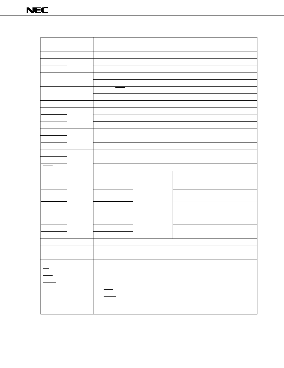
ORDERING INFORMATION
Part number
Package
Internal ROM
Internal RAM
(bytes)
(bytes)
m
PD784020GC-3B9
80-pin plastic QFP (14
•
14 mm)
None
512
m
PD784021GC-3B9
80-pin plastic QFP (14
•
14 mm)
None
2048
m
PD784021GK-BE9
80-pin plastic TQFP (fine pitch) (12
•
12 mm)
None
2048
78K/IV SERIES PRODUCT DEVELOPMENT DIAGRAM
: Product under mass production
: Product under development
: Product under planning
Standard Products Development
ASSP Development
H
H
PD784943 sub-series
PD784908 sub-series
µ
VTR servo, 100-pin, built-in
analog amplifier
ROM: 48K/62K
PD784915 sub-series
µ
100-pin, built-in IEBus
TM
ROM: 96K/128K
µ
80-pin, for CD-ROM
ROM: 56K
PD784054
80-pin, 8-bit A/D, 8-bit D/A
ROM: none/48K/64K
µ
µ
µ
µ
µ
µ
µ
Product containing for
an I
2
C bus interface circuit
80-pin, 8-bit A/D, 8-bit D/A
ROM: 48K/64K/96K/128K
Product containing for
two I
2
C bus interface circuits
100-pin, 8-bit A/D, 8-bit D/A
ROM: 96K/128K
80-pin, 10-bit A/D
ROM: 32K
PD784046 sub-series sub-set
PD784026 sub-series
PD784216 sub-series
µ
80-pin, 10-bit A/D
ROM: 32K/64K
PD784046 sub-series
PD784216Y sub-series
PD784038 sub-series
PD784038Y sub-series
H
3
m
m
m
m
m
PD784020, 784021
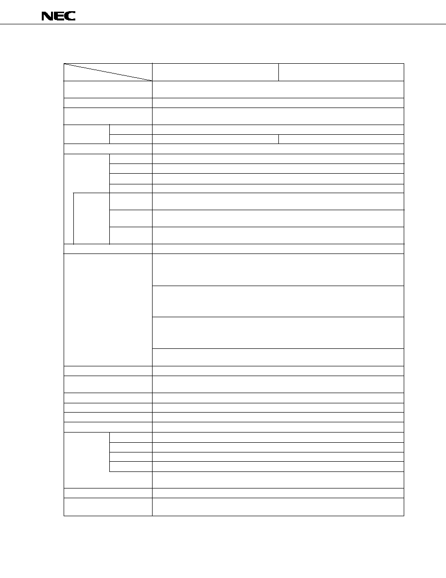
FUNCTIONS
m
PD784020
m
PD784021
113
8 bits
•
16 registers
•
8 banks, or 16 bits
•
8 registers
•
8 banks (memory mapping)
160 ns/320 ns/640 ns/1280 ns (at 25 MHz)
None
512 bytes
2048 bytes
Program and data: 1M byte
46
8
34
4
32
8
8
4 bits
•
2, or 8 bits
•
1
Timer/counter 0:
Timer register
•
1
Pulse output capability
(16 bits)
Capture register
•
1
ð
Toggle output
Compare register
•
2
ð
PWM/PPG output
ð
One-shot pulse output
Timer/counter 1:
Timer register
•
1
Pulse output capability
(8/16 bits)
Capture register
•
1
ð
Real-time output (4 bits
•
2)
Capture/compare register
•
1
Compare register
•
1
Timer/counter 2:
Timer register
•
1
Pulse output capability
(8/16 bits)
Capture register
•
1
ð
Toggle output
Capture/compare register
•
1
ð
PWM/PPG output
Compare register
•
1
Timer 3
:
Timer register
•
1
(8/16 bits)
Compare register
•
1
12-bit resolution
•
2 channels
UART/IOE (3-wire serial I/O) : 2 channels (incorporating baud rate generator)
CSI (3-wire serial I/O, SBI)
: 1 channel
8-bit resolution
•
8 channels
8-bit resolution
•
2 channels
1 channel
HALT/STOP/IDLE mode
23 (16 internal, 7 external (sampling clock variable input: 1)) + BRK instruction
BRK instruction
1 internal, 1 external
15 internal, 6 external
ð
4-level programmable priority
ð
3 operation statuses: vectored interrupt, macro service, context switching
V
DD
= 2.7 to 5.5 V
80-pin plastic QFP (14
•
14 mm)
80-pin plastic TQFP (fine pitch) (12
•
12 mm): for the
m
PD784021 only
Note
Additional function pins are included in the I/O pins.
ROM
RAM
Total
Input
Input/output
Output
Pins with pull-
up resistor
LED direct
drive outputs
Transistor
direct drive
H
H
Product
Item
Number of basic instructions
(mnemonics)
General-purpose register
Minimum instruction execution
time
Internal
memory
Memory space
I/O ports
Additional
function
pins
Note
Real-time output ports
Timer/counter
PWM outputs
Serial interface
A/D converter
D/A converter
Watchdog timer
Standby
Interrupt
Source
Software
Nonmaskable
Maskable
Supply voltage
Package

4
m
m
m
m
m
PD784020, 784021
CONTENTS
1.
DIFFERENCES BETWEEN
m
m
m
m
m
PD784026 SUB-SERIES ...........................................................
6
2.
MAIN DIFFERENCES BETWEEN
m
m
m
m
m
PD784026 AND
m
m
m
m
m
PD78234 SUB-SERIES .....................
7
3.
PIN CONFIGURATION (TOP VIEW) ........................................................................................
8
4.
SYSTEM CONFIGURATION EXAMPLE (PPC) .......................................................................
10
5.
BLOCK DIAGRAM .....................................................................................................................
11
6.
LIST OF PIN FUNCTIONS ........................................................................................................
12
6.1
PORT PINS ......................................................................................................................................
12
6.2
NON-PORT PINS ............................................................................................................................
13
6.3
I/O CIRCUITS FOR PINS AND HANDLING OF UNUSED PINS .................................................
15
7.
CPU ARCHITECTURE ..............................................................................................................
18
7.1
MEMORY SPACE ...........................................................................................................................
18
7.2
CPU REGISTERS ............................................................................................................................
21
7.2.1
General-Purpose Registers ..........................................................................................
21
7.2.2
Control Registers ...........................................................................................................
22
7.2.3
Special Function Registers (SFRs) .............................................................................
23
8.
PERIPHERAL HARDWARE FUNCTIONS ...............................................................................
28
8.1
PORTS .............................................................................................................................................
28
8.2
CLOCK GENERATOR ....................................................................................................................
29
8.3
REAL-TIME OUTPUT PORT ..........................................................................................................
31
8.4
TIMERS/COUNTERS ......................................................................................................................
32
8.5
PWM OUTPUT (PWM0, PWM1) .....................................................................................................
34
8.6
A/D CONVERTER ...........................................................................................................................
35
8.7
D/A CONVERTER ...........................................................................................................................
36
8.8
SERIAL INTERFACE ......................................................................................................................
37
8.8.1
Asynchronous Serial Interface/Three-Wire Serial I/O (UART/IOE) .........................
38
8.8.2
Synchronous Serial Interface (CSI) .............................................................................
40
8.9
EDGE DETECTION FUNCTION .....................................................................................................
41
8.10
WATCHDOG TIMER .......................................................................................................................
42
9.
INTERRUPT FUNCTION ...........................................................................................................
43
9.1
INTERRUPT SOURCE ....................................................................................................................
43
9.2
VECTORED INTERRUPT ...............................................................................................................
45
9.3
CONTEXT SWITCHING ..................................................................................................................
46
9.4
MACRO SERVICE ...........................................................................................................................
46
9.5
EXAMPLES OF MACRO SERVICE APPLICATIONS ..................................................................
47

5
m
m
m
m
m
PD784020, 784021
10. LOCAL BUS INTERFACE .........................................................................................................
49
10.1
MEMORY EXPANSION ..................................................................................................................
49
10.2
MEMORY SPACE ...........................................................................................................................
50
10.3
PROGRAMMABLE WAIT ...............................................................................................................
51
10.4
PSEUDO-STATIC RAM REFRESH FUNCTION ...........................................................................
51
10.5
BUS HOLD FUNCTION ..................................................................................................................
51
11. STANDBY FUNCTION ..............................................................................................................
52
12. RESET FUNCTION ....................................................................................................................
53
13. INSTRUCTION SET ...................................................................................................................
54
14. ELECTRICAL CHARACTERISTICS .........................................................................................
59
15. PACKAGE DRAWINGS ............................................................................................................
80
16. RECOMMENDED SOLDERING CONDITIONS ........................................................................
82
APPENDIX A DEVELOPMENT TOOLS ........................................................................................
83
APPENDIX B RELATED DOCUMENTS .......................................................................................
85
H
H

6
m
m
m
m
m
PD784020, 784021
1. DIFFERENCES BETWEEN
m
m
m
m
m
PD784026 SUB-SERIES
The only difference between the
m
PD784020,
m
PD784021,
m
PD784025, and
m
PD784026 is their capacity of
internal memory, port functions, and part of their packages.
The
m
PD78P4026 is produced by replacing the masked ROM in the
m
PD784025 or
m
PD784026 with 64K-byte one-
time PROM or EPROM. Table 1-1 shows the differences between these products.
Table 1-1 Differences between the
m
m
m
m
m
PD784026 Sub-Series
Product
Item
Internal ROM
Internal RAM
P40-P47
P50-P57
P60-P63
P64, P65
Package
m
PD784020
None
512 bytes
80-pin plastic QFP
(14
•
14 mm)
m
PD784021
2048 bytes
80-pin plastic QFP
(14
•
14 mm)
80-pin plastic
TQFP (fine pitch)
(12
•
12 mm)
m
PD784025
48K bytes
(masked ROM)
m
PD784026
64K bytes
(masked ROM)
m
PD78P4026
64K bytes
(one-time PROM
or EPROM)
80-pin plastic QFP
(14
•
14 mm)
80-pin ceramic
WQFN
(14
•
14 mm)
Functions only as an address/data bus
Functions only as an address bus
Can be switched to an output-only port
or address bus in units of 2 bits, by
using software
Functions only as the RD or WR pin
Can be switched to a general-purpose port or address/data
bus, by using software
Can be switched to a general-purpose port or address bus in
units of 2 bits, by using software
Functions as the RD or WR pin when the local bus interface
is used. Functions as a general-purpose port in other cases.
80-pin plastic QFP (14
•
14 mm)
H

7
m
m
m
m
m
PD784020, 784021
2. MAIN DIFFERENCES BETWEEN
m
m
m
m
m
PD784026 AND
m
m
m
m
m
PD78234 SUB-SERIES
Series
m
PD784026 sub-series
m
PD78234 sub-series
Item
Number of basic instructions
113
65
(mnemonics)
Minimum instruction execution
160 ns
333 ns
time
(at 25 MHz)
(at 12 MHz)
Memory space (program/data)
1M byte in total
64K bytes/1M byte
Timer/counter
16-bit timer/counter
•
1
16-bit timer/counter
•
1
8/16-bit timer/counter
•
2
8-bit timer/counter
•
2
8/16-bit timer
•
1
8-bit timer
•
1
Clock output function
Available
Unavailable
Watchdog timer
Available
Unavailable
Serial interface
UART/IOE (3-wire serial I/O)
•
2 channels
UART
•
1 channel
CSI (3-wire serial I/O, SBI)
•
1 channel
CSI (3-wire serial I/O, SBI)
•
1 channel
Interrupt
Context switching
Available
Unavailable
Priority
4 levels
2 levels
Standby function
3 modes (HALT, STOP, IDLE)
2 modes (HALT, STOP)
Operation clock switching
Selectable from f
XX
/2, f
XX
/4, f
XX
/8, or f
XX
/16
Fixed to f
XX
/2
Pin
MODE pin
Unavailable
To specify ROM-less mode
functions
(always in the high level for the
m
PD78233
or
m
PD78237)
TEST pin
Pin for testing the device
Unavailable
Low level during ordinary use
Package
80-pin plastic QFP (14
•
14 mm)
80-pin plastic QFP (14
•
14 mm)
80-pin plastic TQFP (fine pitch)
94-pin plastic QFP (20
•
20 mm)
(12
•
12 mm): for the
m
PD784021 only
84-pin plastic QFJ (1150
•
1150 mil)
80-pin ceramic WQFN (14
•
14 mm):
94-pin ceramic WQFN (20
•
20 mm):
for the
m
PD78P4026 only
for the
m
PD78P238 only

8
m
m
m
m
m
PD784020, 784021
3. PIN CONFIGURATION (TOP VIEW)
∑
80-pin plastic QFP (14
•
14 mm)
m
PD784020GC-3B9,
m
PD784021GC-3B9
∑
80-pin plastic TQFP (fine pitch) (12
•
12 mm)
m
PD784021GK-BE9
Note
Connect the TEST pin to V
SS
directly.
H
H
60
59
58
57
56
55
54
53
52
51
50
49
48
47
46
45
44
43
42
41
21 22 23 24 25 26 27 28 29 30 31 32 33 34 35 36 37 38 39 40
80 79 78 77 76 75 74 73 72 71 70 69 68 67 66 65 64 63 62 61
P74/ANI4
P73/ANI3
P72/ANI2
P71/ANI1
P70/ANI0
V
DD
P17
P16
P15
P14/T
X
D2/SO2
P13/R
X
D2/SI2
P12/ASCK2/SCK2
P11/PWM1
P10/PWM0
TEST
Note
V
SS
ASTB
AD0
AD1
AD2
P32/SCK0
P33/SO0/SB0
P34/ TO0
P35/ TO1
P36/ TO2
P37/ TO3
RESET
V
DD
X2
X1
V
SS
P00
P01
P02
P03
P04
P05
P06
P07
P67/REFRQ/HLDAK
P66/
WAIT/HLDRQ
WR
RD
P63/A19
P62
/A18
P61/A17
P60/A16
A15
A14
A13
A12
A11
A10
A9
A8
AD7
AD6
AD5
AD4
AD3
P31/
TxD/SO1
P30/RxD/SI1
P27/SI0
P26/INTP5
P25/INTP4
/ASCK/SCK1
P24
/INTP3
P23/INTP2
/CI
P22
/INTP1
P21/INTP0
P20/NMI
AV
REF3
AV
REF2
ANO1
ANO0
AV
SS
AV
REF1
AV
DD
P77/ANI7
P76/ANI6
P75/ANI5
1
2
3
4
5
6
7
8
9
10
11
12
13
14
15
16
17
18
19
20

9
m
m
m
m
m
PD784020, 784021
P00-P07
: Port 0
A8-A19
: Address bus
P10-P17
: Port 1
RD
: Read strobe
P20-P27
: Port 2
WR
: Write strobe
P30-P37
: Port 3
WAIT
: Wait
P60-P63, P66, P67 : Port 6
HLDRQ
: Hold request
P70-P77
: Port 7
HLDAK
: Hold acknowledge
TO0-TO3
: Timer output
ASTB
: Address strobe
CI
: Clock input
REFRQ
: Refresh request
RxD, RxD2
: Receive data
RESET
: Reset
TxD, TxD2
: Transmit data
X1, X2
: Crystal
SCK0-SCK2
: Serial clock
ANI0-ANI7
: Analog input
ASCK, ASCK2
: Asynchronous serial clock
ANO0, ANO1 : Analog output
SI0-SI2
: Serial input
AV
REF1
-AV
REF3
: Reference voltage
SO0-SO2
: Serial output
AV
DD
: Analog power supply
SB0
: Serial bus
AV
SS
: Analog ground
PWM0, PWM1
: Pulse width modulation output
V
DD
: Power supply
NMI
: Non-maskable interrupt
V
SS
: Ground
INTP0-INTP5
: Interrupt from peripherals
TEST
: Test
AD0-AD7
: Address/data bus
1 0
m
m
m
m
m
PD784020, 784021
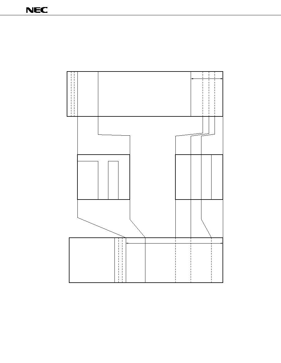
4. SYSTEM CONFIGURATION EXAMPLE (PPC)
Serial
communication
Sensing paper transport
Temperature of the
fusing heater
Brightness of the lamp
Lever for adjusting
the tone of the copy
Lever for compensating
the tone of the copy
Reset
circuit
RESET
ANI3
ANI2
ANI1
ANI0
INTP0
TxD
RD
OE
A17
CE
A8-A16
A8-A16
AD0-AD7
Latch
O0-O7
A0-A7
ASTB
RxD
P11
P15
P16
P17
SCK1
SI1
SO1
P04
P06
P07
P66
PWM0
P00-P03
P33
P34
P35
P36
P37
Driver
Sensing paper
Sensing paper feed
Sensing paper ejection
Sensing the position of the scanner station
Operator
panel
High-voltage
control circuit
Fusing heater
control circuit
Lamp regulator
Drum, toner, and charge for
transfer
Fusing roller
Lamp for lighting the original
Lamp for discharging
(DC stepping motor)
Main motor
M
Clutch for stopping
the scanner station
Clutch for forwarding
the scanner station
Clutch for the resist
shutter
Clutch for manual
feeding
Clutch for cassette
feeding
Solenoid
S L
S L
S L
S L
S L
PD784021
µ
PD74HC573
µ
PD27C1001A
µ
1 1
m
m
m
m
m
PD784020, 784021
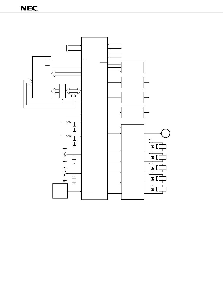
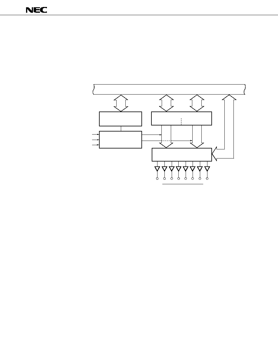
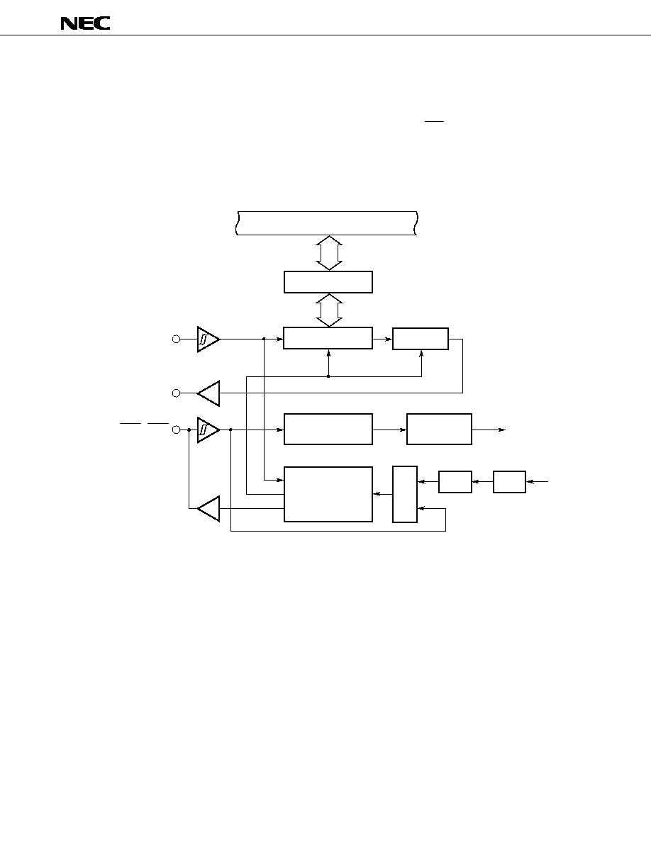
5. BLOCK DIAGRAM
Remark The internal ROM or RAM capacity differs for each product.
NMI
INTP3
TO0
TO1
INTP0
INTP1
INTP2/CI
TO2
TO3
P00-P03
P04-P07
PWM0
PWM1
ANO0
ANO1
AV
REF2
AV
REF3
INTP5
ANI0-ANI7
TxD/SO1
ASCK/SCK1
RxD/SI1
ASCK2/SCK2
SCK0
SO0/SB0
SI0
A8-A15
P00-P07
P20-P27
P10-P17
P30-P37
P60, P67
P70-P77
ASTB
REFRQ/HLDAK
WR
WAIT/HLDRQ
AD0-AD7
RD
A16-A19
P60-P63
X1
X2
RESET
TEST
V
DD
V
SS
AV
DD
AV
REF1
AV
SS
UART/IOE2
Baud-rate
generator
UART/IOE1
Clocked serial
interface
Bus interface
Port 0
Port 1
Port 2
Port 3
Port 6
Port 7
System control
Programmable
interrupt controller
Timer/counter 0
Timer/counter 1
Timer/counter 2
Timer 3
Real-time output
port
PWM
D /A converter
A /D converter
INTP0-INTP5
(16 bits)
(16 bits)
(16 bits)
(16 bits)
78K /IV
CPU core
Watchdog timer
Baud-rate
generator
TxD2/SO2
RxD2/SI2
RAM
1 2
m
m
m
m
m
PD784020, 784021
6. LIST OF PIN FUNCTIONS
6.1 PORT PINS
Function
Port 0 (P0):
ð
8-bit I/O port
ð
Functions as a real-time output port (4 bits
•
2).
ð
Inputs and outputs can be specified bit by bit.
ð
The use of the pull-up resistors can be specified by software for the pins
in the input mode together.
ð
Can drive a transistor.
Port 1 (P1):
ð
8-bit I/O port
ð
Inputs and outputs can be specified bit by bit.
ð
The use of the pull-up resistors can be specified by software for the pins
in the input mode together.
ð
Can drive LED.
Port 2 (P2):
ð
8-bit input-only port
ð
P20 does not function as a general-purpose port (nonmaskable inter-
rupt). However, the input level can be checked by an interrupt service
routine.
ð
The use of the pull-up resistors can be specified by software for pins
P22 to P27 (in units of 6 bits).
ð
The P25/INTP4/ASCK/SCK1 pin functions as the SCK1 output pin by
CSIM1.
Port 3 (P3):
ð
8-bit I/O port
ð
Inputs and outputs can be specified bit by bit.
ð
The use of the pull-up resistors can be specified by software for the pins
in the input mode together.
Port 6 (P6):
ð
P60 to P63 are an output-only port.
ð
Inputs and outputs can be specified bit by bit for pins P66 and P67.
ð
The use of the pull-up resistors can be specified by software for the pins
in the input mode together.
Port 7 (P7):
ð
8-bit I/O port
ð
Inputs and outputs can be specified bit by bit.
I/O
I/O
I/O
Input
I/O
I/O
I/O
Pin
P00-P07
P10
P11
P12
P13
P14
P15-P17
P20
P21
P22
P23
P24
P25
P26
P27
P30
P31
P32
P33
P34-P37
P60-P63
P66
P67
P70-P77
Dual-function
--
PWM0
PWM1
ASCK2/SCK2
RxD2/SI2
TxD2/SO2
--
NMI
INTP0
INTP1
INTP2/CI
INTP3
INTP4/ASCK/SCK1
INTP5
SI0
RxD/SI1
TxD/SO1
SCK0
SO0/SB0
TO0-TO3
A16-A19
WAIT/HLDRQ
REFRQ/HLDAK
ANI0-ANI7
1 3
m
m
m
m
m
PD784020, 784021
6.2 NON-PORT PINS (1/2)
Pin
I/O
Dual-function
Function
TO0-TO3
Output
P34-P37
Timer output
CI
Input
P23/INTP2
Input of a count clock for timer/counter 2
R
X
D
Input
P30/SI1
Serial data input (UART0)
R
X
D2
P13/SI2
Serial data input (UART2)
T
X
D
Output
P31/SO1
Serial data output (UART0)
T
X
D2
P14/SO2
Serial data output (UART2)
ASCK
Input
P25/INTP4/SCK1
Baud rate clock input (UART0)
ASCK2
P12/SCK2
Baud rate clock input (UART2)
SB0
I/O
P33/SO0
Serial data I/O (SBI)
SI0
Input
P27
Serial data input (3-wire serial I/O0)
SI1
P30/R
X
D
Serial data input (3-wire serial I/O1)
SI2
P13/R
X
D2
Serial data input (3-wire serial I/O2)
SO0
Output
P33/SB0
Serial data output (3-wire serial I/O0)
SO1
P31/T
X
D
Serial data output (3-wire serial I/O1)
SO2
P14/T
X
D2
Serial data output (3-wire serial I/O2)
SCK0
I/O
P32
Serial clock I/O (3-wire serial I/O0, SBI)
SCK1
P25/INTP4/ASCK
Serial clock I/O (3-wire serial I/O1)
SCK2
P12/ASCK2
Serial clock I/O (3-wire serial I/O2)
NMI
Input
P20
External interrupt request
--
INTP0
P21
ð
Input of a count clock for timer/counter 1
ð
Capture/trigger signal for CR11 or CR12
INTP1
P22
ð
Input of a count clock for timer/counter 2
ð
Capture/trigger signal for CR22
INTP2
P23/CI
ð
Input of a count clock for timer/counter 2
ð
Capture/trigger signal for CR21
INTP3
P24
ð
Input of a count clock for timer/counter 0
ð
Capture/trigger signal for CR02
INTP4
P25/ASCK/SCK1
--
INTP5
P26
Input of a conversion start trigger for A/D converter
AD0-AD7
I/O
--
Time multiplexing address/data bus (for connecting external memory)
A8-A15
Output
--
High-order address bus (for connecting external memory)
A16-A19
Output
P60-P63
High-order address bus during address expansion (for connecting external memory)
RD
Output
--
Strobe signal output for reading the contents of external memory
WR
Output
--
Strobe signal output for writing on external memory
WAIT
Input
P66/HLDRQ
Wait signal insertion
REFRQ
Output
P67/HLDAK
Refresh pulse output to external pseudo static memory
HLDRQ
Input
P66/WAIT
Input of bus hold request
HLDAK
Output
P67/REFRQ
Output of bus hold response
ASTB
Output
--
Latch timing output of time multiplexing address (A0-A7) (for
connecting external memory)

1 4
m
m
m
m
m
PD784020, 784021
6.2 NON-PORT PINS (2/2)
Pin
I/O
Dual-function
Function
RESET
Input
--
Chip reset
X1
Input
--
Crystal input for system clock oscillation (A clock pulse can also be
X2
--
input to the X1 pin.)
ANI0-ANI7
Input
P70-P77
Analog voltage inputs for the A/D converter
ANO0, ANO1
Output
--
Analog voltage inputs for the D/A converter
AV
REF1
--
--
Application of A/D converter reference voltage
AV
REF2
, AV
REF3
Application of D/A converter reference voltage
AV
DD
Positive power supply for the A/D converter
AV
SS
Ground for the A/D converter
V
DD
Positive power supply
V
SS
Ground
TEST
Directly connect to V
SS
. (The TEST pin is for the IC test.)

1 5
m
m
m
m
m
PD784020, 784021
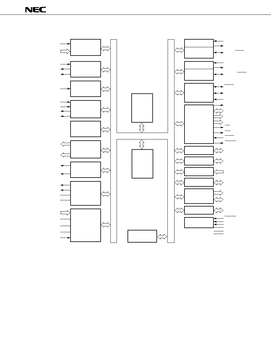
6.3 I/O CIRCUITS FOR PINS AND HANDLING OF UNUSED PINS
Table 6-1 describes the types of I/O circuits for pins and the handling of unused pins.
Fig. 6-1 shows the configuration of these various types of I/O circuits.
Table 6-1 Types of I/O Circuits for Pins and Handling of Unused Pins (1/2)
Note
These pins function as output-only pins depending on the internal circuit, though their I/O type is 5-A.
Pin
I/O circuit type
I/O
Recommended connection method for unused pins
P00-P07
5-A
I/O
Input state : To be connected to V
DD
P10/PWM0
Output state: To be left open
P11/PWM1
P12/ASCK2/SCK2
8-A
P13/RxD2/SI2
5-A
P14/TxD2/SO2
P15-P17
P20/NMI
2
Input
To be connected to V
DD
or V
SS
P21/INTP0
P22/INTP1
2-A
To be connected to V
DD
P23/INTP2/CI
P24/INTP3
P25/INTP4/ASCK/SCK1
8-A
I/O
Input state : To be connected to V
DD
Output state: To be left open
P26/INTP5
2-A
Input
To be connected to V
DD
P27/SI0
P30/RxD/SI1
5-A
I/O
Input state : To be connected to V
DD
P31/TxD/SO1
Output state: To be left open
P32/SCK0
8-A
P33/SO0/SB0
10-A
P34/TO0-P37/TO3
5-A
AD0-AD7
A8-A15
Output
Note
To be left open
P60/A16-P63/A19
RD
WR
P66/WAIT/HLDRQ
I/O
Input state : To be connected to V
DD
P67/REFRQ/HLDAK
Output state: To be left open
P70/ANI0-P77/ANI7
20
Input state : To be connected to V
DD
or V
SS
Output state: To be left open
ANO0, ANO1
12
Output
To be left open
ASTB
4

1 6
m
m
m
m
m
PD784020, 784021
Table 6-1 Types of I/O Circuits for Pins and Handling of Unused Pins (2/2)
Pin
I/O circuit type
I/O
Recommended connection method for unused pins
RESET
2
Input
--
TEST
1
To be connected to V
SS
directly
AV
REF1
-AV
REF3
--
To be connected to V
SS
AV
SS
AV
DD
To be connected to V
DD
Caution When the I/O mode of an I/O dual-function pin is unpredictable, connect the pin to V
DD
through
a resistor of 10 to 100 kilohms (particularly when the voltage of the reset input pin becomes higher
than that of the low level input at power-on or when I/O is switched by software).
Remark Since type numbers are consistent in the 78K series, those numbers are not always serial in each product.
(Some circuits are not included.)

1 7
m
m
m
m
m
PD784020, 784021
Fig. 6-1 I/O Circuits for Pins
Type 1
Type 2-A
Type 2
Type 4
Type 8-A
Type 10-A
Type 5-A
Type 12
Type 20
IN
Schmitt trigger input with hysteresis characteristics
Schmitt trigger input with hysteresis characteristics
IN
V
DD
P
Pull-up
enable
IN
V
DD
P
N
Data
V
DD
P
N
OUT
Output
disable
Push-pull output which can output high impedance
(both the positive and negative channels are off.)
Data
V
DD
P
N
IN/OUT
Output
disable
V
DD
P
Pull-up
enable
Input
enable
Data
V
DD
P
N
IN/OUT
Output
disable
V
DD
P
Pull-up
enable
Data
V
DD
P
N
IN/OUT
Output
disable
V
DD
P
Pull-up
enable
Open
drain
N
P
Analog output
voltage
OUT
Data
Comparator
V
DD
V
REF
P
(Threshold voltage)
P
N
N
IN/OUT
Output
disable
Input
enable
+
≠

1 8
m
m
m
m
m
PD784020, 784021
7. CPU ARCHITECTURE
7.1 MEMORY SPACE
A 1M-byte memory space can be accessed. By using a LOCATION instruction, the mode for mapping internal
data areas (special function registers and internal RAM) can be selected. A LOCATION instruction must always be
executed after a reset, and can be used only once.
(1) When the LOCATION 0 instruction is executed
Internal data areas are mapped to 0FD00H-0FFFFH for the
m
PD784020 and 0F700H-0FFFFH for the
m
PD784021.
(2) When the LOCATION 0FH instruction is executed
Internal data areas are mapped to FFD00H-FFFFFH for the
m
PD784020 and FF700H-FFFFFH for the
m
PD784021.
1 9
m
m
m
m
m
PD784020, 784021
Fig. 7-1
m
mmm
m
PD784020 Memory Map
H
HHH
H
Note
Base area, or entry area based on a reset or interrupt. Internal RAM is excluded in the case of a reset.
Internal RAM
(512 bytes)
External memory
(960K bytes)
General-purpose
registers
(128 bytes)
Macro service control
word area (42 bytes)
CALLF entry area
(2K bytes)
CALLT table area
(64 bytes)
Vector table area
(64 bytes)
Internal RAM
(512 bytes)
External memory
(1,047,808 bytes)
When the LOCATION 0
instruction is executed
Special function registers (SFRs)
(256 bytes)
Data area (512 bytes)
When the LOCATION 0FH
instruction is executed
Special function registers (SFRs)
(256 bytes)
External memory
(64,768 bytes)
Note
Note
FFFFFH
10000H 0FFFFH 0FFDFH 0FFD0H 0FF00H 0FEFFH
0FD00H
0FCFFH
00000H
0FEFFH
0FE80H
0FE7FH
0FE2FH
0FE06H
0FD00H
00FFFH
00800H
007FFH
00080H
0007FH
00040H
0003FH
00000H
FFEFFH
FFE80H
FFE7FH
FFE2FH
FFE06H
FFD00H
00FFFH
00800H
007FFH
00080H
0007FH
FFFFFH FFFDFH FFFD0H FFF00H
FFEFFH
FFD00H
FFCFFH
10000H
0FFFFH
00000H

2 0
m
m
m
m
m
PD784020, 784021
Fig. 7-2
m
mmm
m
PD784021 Memory Map
Note
Base area, or entry area based on a reset or interrupt. Internal RAM is excluded in the case of a reset.
Internal RAM
(2,048 bytes)
External memory
(960K bytes)
General-purpose
registers
(128 bytes)
Macro service control
word area (42 bytes)
Program/data area
(1,536 bytes)
CALLF entry area
(2K bytes)
CALLT table area
(64 bytes)
Vector table area
(64 bytes)
Internal RAM
(2,048 bytes)
External memory
(1,046,272 bytes)
When the LOCATION 0
instruction is executed
Special function registers (SFRs)
(256 bytes)
Data area (512 bytes)
When the LOCATION 0FH
instruction is executed
Special function registers (SFRs)
(256 bytes)
External memory
(63,232 bytes)
Note
Note
FFFFFH
10000H 0FFFFH 0FFDFH 0FFD0H 0FF00H 0FEFFH 0FD00H 0FCFFH
0F700H
0F6FFH
00000H
0FEFFH
0FE80H
0FE7FH
0FE2FH
0FE06H
0FD00H
0FCFFH
0F700H
00FFFH
00800H
007FFH
00080H
0007FH
00040H
0003FH
00000H
FFEFFH
FFE80H
FFE7FH
FFE2FH
FFE06H
FFD00H
FFCFFH
FF700H
00FFFH
00800H
007FFH
00080H
0007FH
FFFFFH FFFDFH FFFD0H
FFF00H
FFEFFH
FF700H
FF6FFH
10000H
0FFFFH
00000H

2 1
m
m
m
m
m
PD784020, 784021
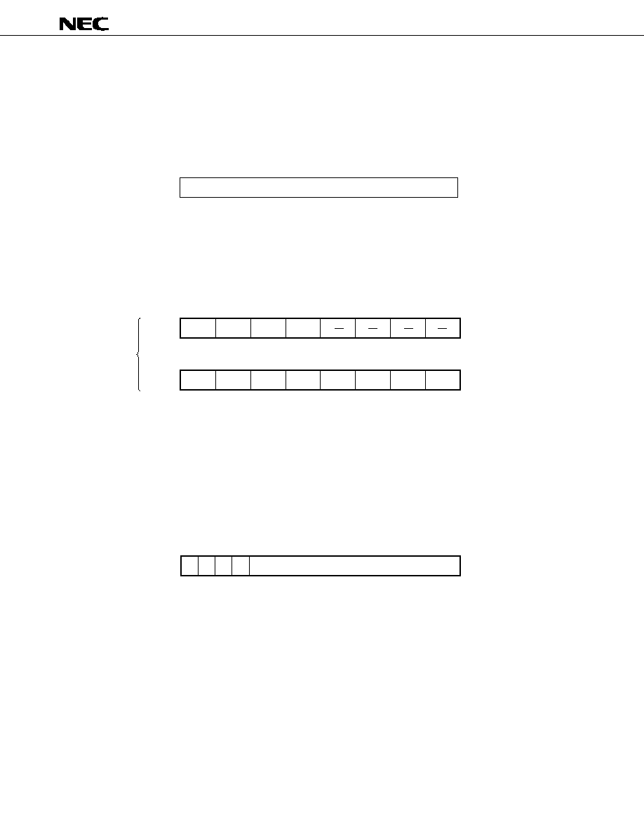
7.2 CPU REGISTERS
7.2.1 General-Purpose Registers
A set of general-purpose registers consists of sixteen general-purpose 8-bit registers. Two 8-bit general-purpose
registers can be combined to form a 16-bit general-purpose register. Moreover, four 16-bit general-purpose registers,
when combined with an 8-bit register for address extension, can be used as 24-bit address specification registers.
Eight banks of this register set are provided. The user can switch between banks by software or the context
switching function.
General-purpose registers other than the V, U, T, and W registers used for address extension are mapped onto
internal RAM.
Fig. 7-3 General-Purpose Register Format
Caution By setting the RSS bit of PSW to 1, R4, R5, R6, R7, RP2, and RP3 can be used as the X, A, C, B,
AX, and BC registers, respectively. However, this function must be used only when using
programs for the 78K/III series.
A (R1)
X (R0)
B (R3)
C (R2)
R5
R4
R7
R6
R9
R8
R11
R10
D (R13)
E (R12)
H (R15)
V
U
T
W
L (R14)
AX (RP0)
BC (RP1)
RP2
RP3
VP (RP4)
UP (RP5)
DE (RP6)
HL (RP7)
VVP (RG4)
UUP (RG5)
TDE (RG6)
WHL (RG7)
The character strings enclosed in
parentheses represent absolute names.
8 banks
2 2
m
m
m
m
m
PD784020, 784021
7.2.2 Control Registers
(1) Program counter (PC)
This register is a 20-bit program counter. The program counter is automatically updated by program execution.
Fig. 7-4 Format of Program Counter (PC)
(2) Program Status Word (PSW)
This register holds the CPU state. The program status word is automatically updated by program execution.
Fig. 7-5 Format of Program Status Word (PSW)
Note
This flag is used to maintain compatibility with the 78K/III series. This flag must be set to 0 when programs
for the 78K/III series are being used.
(3) Stack pointer (SP)
This register is a 24-bit pointer for holding the start address of the stack. The high-order 4 bits must be set
to 0.
Fig. 7-6 Format of Stack Pointer (SP)
19
0
PC
PSWH
PSWL
PSW
15
14
13
12
UF
RBS2
RBS1
RBS0
11
10
9
8
7
6
5
4
3
2
1
0
S
Z
RSS
Note
AC
IE
P/V
0
CY
23
20
0
PC
0
0
0
0

2 3
m
m
m
m
m
PD784020, 784021
7.2.3 Special Function Registers (SFRs)
The special function registers are registers with special functions such as mode registers and control registers
for built-in peripheral hardware. The special function registers are mapped onto the 256-byte space between 0FF00H
and 0FFFFH
Note
.
Note
Applicable when the LOCATION 0 instruction is executed. FFF00H-FFFFFH when the LOCATION 0FH
instruction is executed.
Caution Never attempt to access addresses in this area where no SFR is allocated. Otherwise, the
m
m
m
m
m
PD784021 may be placed in the deadlock state. The deadlock state can be cleared only by a
reset.
Table 7-1 lists the special function registers (SFRs). The titles of the table columns are explained below.
∑
Abbreviation ................... Symbol used to represent a built-in SFR. The abbreviations listed in the table are
reserved words for the NEC assembler (RA78K4). The C compiler (CC78K4) allows
the abbreviations to be used as sfr variables of bit type with the #pragma sfr command.
∑
R/W ................................. Indicates whether each SFR allows read and/or write operations.
R/W : Allows both read and write operations.
R
: Allows read operations only.
W
: Allows write operations only.
∑
Manipulatable bits .......... Indicates the maximum number of bits that can be manipulated whenever an SFR is
manipulated. An SFR that supports 16-bit manipulation can be described in the sfr
operand. For address specification, an even-numbered address must be speci-
fied.
An SFR that supports 1-bit manipulation can be described in a bit manipulation
instruction.
∑
When reset ..................... Indicates the state of each register when RESET is applied.
H

2 4
m
m
m
m
m
PD784020, 784021
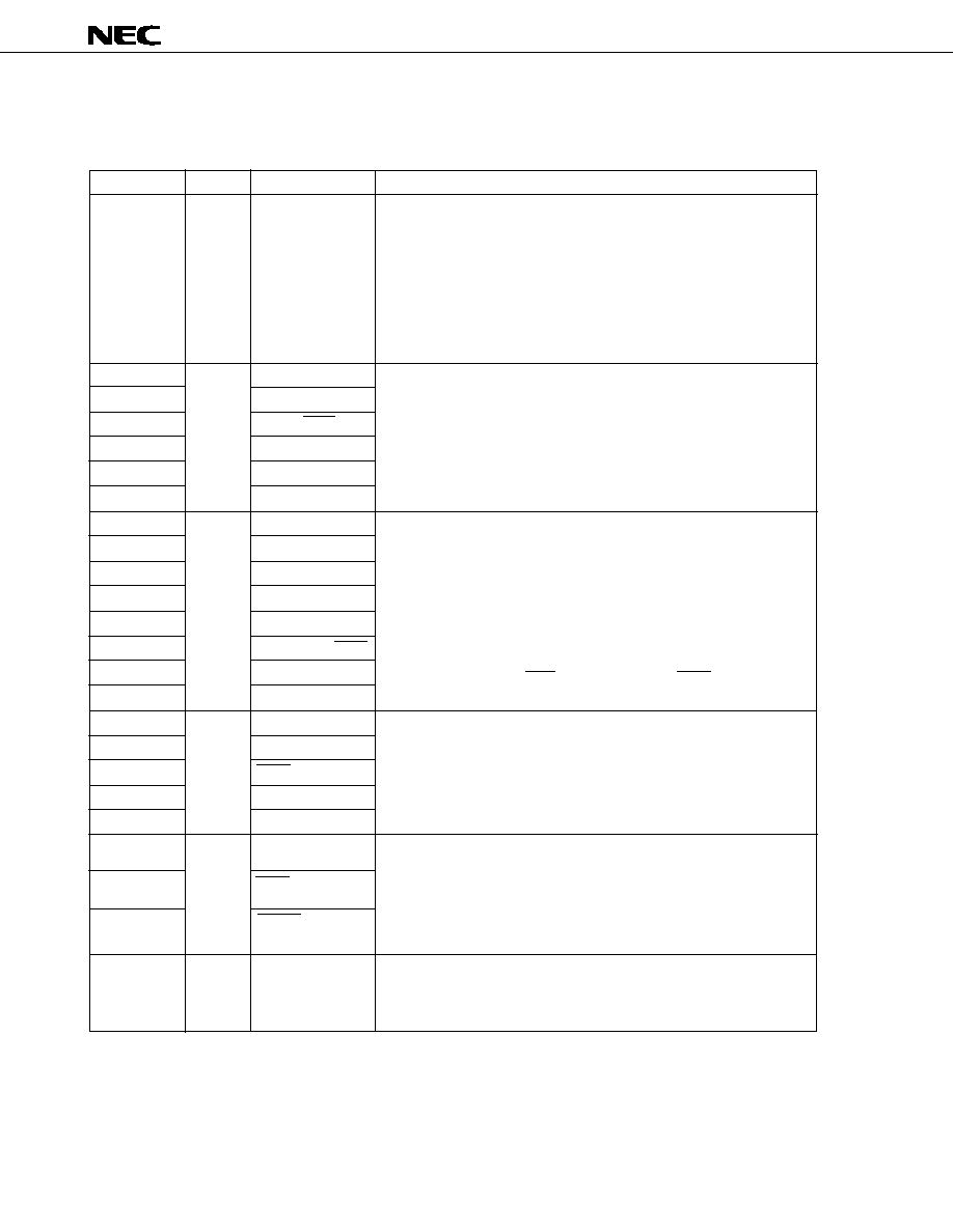
Table 7-1 Special Function Registers (SFRs) (1/4)
Address
Note
Special function register (SFR) name
Abbreviation
R/W
Manipulatable bits
When reset
1 bit
8 bits 16 bits
0FF00H
Port 0
P0
R/W
l
l
≠
Undefined
0FF01H
Port 1
P1
l
l
≠
0FF02H
Port 2
P2
R
l
l
≠
0FF03H
Port 3
P3
R/W
l
l
≠
0FF06H
Port 6
P6
l
l
≠
00H
0FF07H
Port 7
P7
l
l
≠
Undefined
0FF0EH
Port 0 buffer register L P0L
l
l
≠
0FF0FH
Port 0 buffer register H
P0H
l
l
≠
0FF10H
Compare register (timer/counter 0)
CR00
≠
≠
l
0FF12H
Capture/compare register (timer/counter 0)
CR01
≠
≠
l
0FF14H
Compare register L (timer/counter 1)
CR10 CR10W
≠
l
l
0FF15H
Compare register H (timer/counter 1)
≠
≠
≠
0FF16H
Capture/compare register L (timer/counter 1)
CR11 CR11W
≠
l
l
0FF17H
Capture/compare register H (timer/counter 1)
≠
≠
≠
0FF18H
Compare register L (timer/counter 2)
CR20 CR20W
≠
l
l
0FF19H
Compare register H (timer/counter 2)
≠
≠
≠
0FF1AH
Capture/compare register L (timer/counter 2)
CR21 CR21W
≠
l
l
0FF1BH
Capture/compare register H (timer/counter 2)
≠
≠
≠
0FF1CH
Compare register L (timer 3)
CR30 CR30W
≠
l
l
0FF1DH
Compare register H (timer 3)
≠
≠
≠
0FF20H
Port 0 mode register
PM0
l
l
≠
FFH
0FF21H
Port 1 mode register
PM1
l
l
≠
0FF23H
Port 3 mode register
PM3
l
l
≠
0FF26H
Port 6 mode register
PM6
l
l
≠
0FF27H
Port 7 mode register
PM7
l
l
≠
0FF2EH
Real-time output port control register
RTPC
l
l
≠
00H
0FF30H
Capture/compare control register 0
CRC0
≠
l
≠
10H
0FF31H
Timer output control register
TOC
l
l
≠
00H
0FF32H
Capture/compare control register 1
CRC1
≠
l
≠
0FF33H
Capture/compare control register 2
CRC2
≠
l
≠
10H
Note
Applicable when the LOCATION 0 instruction is executed. When the LOCATION 0FH instruction is
executed, F0000H is added to each address.

2 5
m
m
m
m
m
PD784020, 784021
Table 7-1 Special Function Registers (SFRs) (2/4)
Address
Note
Special function register (SFR) name
Abbreviation
R/W
Manipulatable bits
When reset
1 bit
8 bits 16 bits
0FF36H
Capture register (timer/counter 0)
CR02
R
≠
≠
l
0000H
0FF38H
Capture register L (timer/counter 1)
CR12 CR12W
≠
l
l
0FF39H
Capture register H (timer/counter 1)
≠
≠
≠
0FF3AH
Capture register L (timer/counter 2)
CR22 CR22W
≠
l
l
0FF3BH
Capture register H (timer/counter 2)
≠
≠
≠
0FF41H
Port 1 mode control register
PMC1
R/W
l
l
≠
00H
0FF43H
Port 3 mode control register
PMC3
l
l
≠
0FF4EH
Register for optional pull-up resistor
PUO
l
l
≠
0FF50H
Timer register 0
TM0
R
≠
≠
l
0000H
0FF51H
≠
≠
0FF52H
Timer register 1
TM1
TM1W
≠
l
l
0FF53H
≠
≠
≠
0FF54H
Timer register 2
TM2
TM2W
≠
l
l
0FF55H
≠
≠
≠
0FF56H
Timer register 3
TM3
TM3W
≠
l
l
0FF57H
≠
≠
≠
0FF5CH
Prescaler mode register 0
PRM0
R/W
≠
l
≠
11H
0FF5DH
Timer control register 0
TMC0
l
l
≠
00H
0FF5EH
Prescaler mode register 1
PRM1
≠
l
≠
11H
0FF5FH
Timer control register 1
TMC1
l
l
≠
00H
0FF60H
D/A conversion value setting register 0
DACS0
≠
l
≠
0FF61H
D/A conversion value setting register 1
DACS1
≠
l
≠
0FF62H
D/A converter mode register
DAM
l
l
≠
03H
0FF68H
A/D converter mode register
ADM
l
l
≠
00H
0FF6AH
A/D conversion result register
ADCR
R
≠
l
≠
Undefined
0FF70H
PWM control register
PWMC
R/W
l
l
≠
05H
0FF71H
PWM prescaler register
PWPR
≠
l
≠
00H
0FF72H
PWM modulo register 0
PWM0
≠
≠
l
Undefined
0FF74H
PWM modulo register 1
PWM1
≠
≠
l
0FF7DH
One-shot pulse output control register
OSPC
l
l
≠
00H
0FF80H
Serial bus interface control register
SBIC
l
l
≠
0FF82H
Synchronous serial interface mode register
CSIM
l
l
≠
Note
Applicable when the LOCATION 0 instruction is executed. When the LOCATION 0FH instruction is
executed, F0000H is added to each address.
2 6
m
m
m
m
m
PD784020, 784021
Address
Note 1
Special function register (SFR) name
Abbreviation
R/W
Manipulatable bits
When reset
1 bit
8 bits 16 bits
0FF84H
Synchronous serial interface mode register 1
CSIM1
R/W
l
l
≠
00H
0FF85H
Synchronous serial interface mode register 2
CSIM2
l
l
≠
0FF86H
Serial shift register
SIO
≠
l
≠
0FF88H
Asynchronous serial interface mode register
ASIM
l
l
≠
0FF89H
Asynchronous serial interface mode register 2
ASIM2
l
l
≠
0FF8AH
Asynchronous serial interface status register
ASIS
R
l
l
≠
0FF8BH
Asynchronous serial interface status register 2
ASIS2
l
l
≠
0FF8CH
Serial receive buffer: UART0
RXB
≠
l
≠
Undefined
Serial transmission shift register: UART0
TXS
W
≠
l
≠
Serial shift register: IOE1
SIO1
R/W
≠
l
≠
0FF8DH
Serial receive buffer: UART2
RXB2
R
≠
l
≠
Serial transmission shift register: UART2
TXS2
W
≠
l
≠
Serial shift register: IOE2
SIO2
R/W
≠
l
≠
0FF90H
Baud rate generator control register
BRGC
≠
l
≠
00H
0FF91H
Baud rate generator control register 2
BRGC2
≠
l
≠
0FFA0H
External interrupt mode register 0
INTM0
l
l
≠
0FFA1H
External interrupt mode register 1
INTM1
l
l
≠
0FFA4H
Sampling clock selection register
SCS0
≠
l
≠
0FFA8H
In-service priority register
ISPR
R
l
l
≠
0FFAAH
Interrupt mode control register
IMC
R/W
l
l
≠
80H
0FFACH
Interrupt mask register 0L
MK0L MK0
l
l
l
FFFFH
0FFADH
Interrupt mask register 0H
MK0H
l
l
0FFAEH
Interrupt mask register 1L
MK1L
l
l
≠
FFH
0FFC0H
Standby control register
STBC
≠
l
Note 2
≠
30H
0FFC2H
Watchdog timer mode register
WDM
≠
l
Note 2
≠
00H
0FFC4H
Memory expansion mode register
MM
l
l
≠
20H
0FFC5H
Hold mode register
HLDM
l
l
≠
00H
0FFC6H
Clock output mode register
CLOM
l
l
≠
0FFC7H
Programmable wait control register 1
PWC1
≠
l
≠
AAH
0FFC8H
Programmable wait control register 2
PWC2
≠
≠
l
AAAAH
Table 7-1 Special Function Registers (SFRs) (3/4)
Notes 1. Applicable when the LOCATION 0 instruction is executed. When the LOCATION 0FH instruction is
executed, F0000H is added to each address.
2. A write operation can be performed only with special instructions MOV STBC,#byte and MOV
WDM,#byte. Other instructions cannot perform a write operation.

2 7
m
m
m
m
m
PD784020, 784021
Table 7-1 Special Function Registers (SFRs) (4/4)
Note
Applicable when the LOCATION 0 instruction is executed. When the LOCATION 0FH instruction is
executed, F0000H is added to each address.
Address
Note
Special function register (SFR) name
Abbreviation
R/W
Manipulatable bits
When reset
1 bit
8 bits 16 bits
0FFCCH
Refresh mode register
RFM
R/W
l
l
≠
00H
0FFCDH
Refresh area specification register
RFA
l
l
≠
0FFCFH
Oscillation settling time specification register
OSTS
≠
l
≠
0FFD0H-
External SFR area
≠
l
l
≠
≠
0FFDFH
0FFE0H
Interrupt control register (INTP0)
PIC0
l
l
≠
43H
0FFE1H
Interrupt control register (INTP1)
PIC1
l
l
≠
0FFE2H
Interrupt control register (INTP2)
PIC2
l
l
≠
0FFE3H
Interrupt control register (INTP3)
PIC3
l
l
≠
0FFE4H
Interrupt control register (INTC00)
CIC00
l
l
≠
0FFE5H
Interrupt control register (INTC01)
CIC01
l
l
≠
0FFE6H
Interrupt control register (INTC10)
CIC10
l
l
≠
0FFE7H
Interrupt control register (INTC11)
CIC11
l
l
≠
0FFE8H
Interrupt control register (INTC20)
CIC20
l
l
≠
0FFE9H
Interrupt control register (INTC21)
CIC21
l
l
≠
0FFEAH
Interrupt control register (INTC30)
CIC30
l
l
≠
0FFEBH
Interrupt control register (INTP4)
PIC4
l
l
≠
0FFECH
Interrupt control register (INTP5)
PIC5
l
l
≠
0FFEDH
Interrupt control register (INTAD)
ADIC
l
l
≠
0FFEEH
Interrupt control register (INTSER)
SERIC
l
l
≠
0FFEFH
Interrupt control register (INTSR)
SRIC
l
l
≠
Interrupt control register (INTCSI1)
CSIIC1
l
l
≠
0FFF0H
Interrupt control register (INTST)
STIC
l
l
≠
0FFF1H
Interrupt control register (INTCSI)
CSIIC
l
l
≠
0FFF2H
Interrupt control register (INTSER2)
SERIC2
l
l
≠
0FFF3H
Interrupt control register (INTSR2)
SRIC2
l
l
≠
Interrupt control register (INTCSI2)
CSIIC2
l
l
≠
0FFF4H
Interrupt control register (INTST2)
STIC2
l
l
≠

2 8
m
m
m
m
m
PD784020, 784021
8. PERIPHERAL HARDWARE FUNCTIONS
8.1 PORTS
The ports shown in Fig. 8-1 are provided to enable the application of wide-ranging control. Table 8-1 lists the
functions of the ports. For the inputs to port 0 to port 6, a built-in pull-up resistor can be specified by software.
Fig. 8-1 Port Configuration
Port 0
P00
P07
8
Port 1
P10
P17
Port 2
P20-P27
Port 3
P30
P37
Port 6
P60
P63
P66
P67
Port 7
P70
P77

2 9
m
m
m
m
m
PD784020, 784021
Table 8-1 Port Functions
8.2 CLOCK GENERATOR
A circuit for generating the clock signal required for operation is provided. The clock generator includes a frequency
divider; low current consumption can be achieved by operating at a lower internal frequency when high-speed
operation is not necessary.
Fig. 8-2 Block Diagram of Clock Generator
Remark f
XX
: Oscillator frequency or external clock input
f
CLK
: Internal operating frequency
Port name
Pin
Function
Pull-up specification by software
Port 0
P00-P07
∑ Bit-by-bit input/output setting supported
Specified as a batch for all pins placed in
∑ Operable as 4-bit real-time outputs
input mode.
(P00-P03, P04-P07)
∑ Capable of driving transistors
Port 1
P10-P17
∑ Bit-by-bit input/output setting supported
Specified as a batch for all pins placed in
∑ Capable of driving LEDs
input mode.
Port 2
P20-P27
∑ Input port
Specified for the 6 bits (P22-P27) as a batch.
Port 3
P30-P37
∑ Bit-by-bit input/output setting supported
Specified as a batch for all pins placed in
input mode.
Port 6
P60-P63
∑ Output-only port
P66, P67
∑ Bit-by-bit input/output setting supported
Port 7
P70-P77
∑ Bit-by-bit input/output setting supported
--
Specified as a batch for all pins placed in
input mode.
X1
X2
f
XX
/2
f
XX
f
CLK
CPU
Peripheral circuits
Oscillator
UART/IOE
INTP0 noise eliminator
Oscillation settling timer
Selector
1/2
1/2
1/2
1/2
3 0
m
m
m
m
m
PD784020, 784021
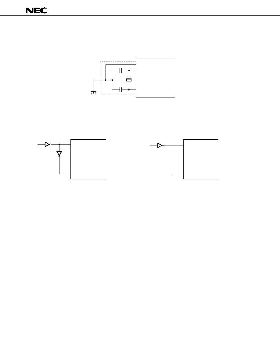
Fig. 8-3 Examples of Using Oscillator
(1) Crystal/ceramic oscillation
(2) External clock
∑
When EXTC bit of OSTS = 1
∑
When EXTC bit of OSTS = 0
Caution When using the clock generator, to avoid problems caused by influences such as stray
capacitance, run all wiring within the area indicated by the dotted lines according to the following
rules:
∑
Minimize the wiring length.
∑
Wires must never cross other signal lines.
∑
Wires must never run near a line carrying a large varying current.
∑
The grounding point of the capacitor of the oscillator circuit must always be at the same
potential as V
SS
. Never connect the capacitor to a ground pattern carrying a large current.
∑
Never extract a signal from the oscillator circuit.
V
SS
X1
X2
PD784021
µ
PD784021
X1
X2
PD74HC04, etc.
µ
µ
X1
X2
Open
PD784021
µ
H
3 1
m
m
m
m
m
PD784020, 784021
8.3 REAL-TIME OUTPUT PORT
The real-time output port outputs data stored in the buffer, synchronized with a timer/counter 1 match interrupt
or external interrupt. Thus, pulse output that is free of jitter can be obtained.
Therefore, the real-time output port is best suited to applications (such as open-loop control over stepping motors)
where an arbitrary pattern is output at arbitrary intervals.
As shown in Fig. 8-4, the real-time output port is built around port 0 and the port 0 buffer register (P0H, P0L).
Fig. 8-4 Block Diagram of Real-Time Output Port
4
4
4
P0L
P0H
Buffer register
8
4
8
P00
P07
Output latch (P0)
Real-time output port
control register
(RTPC)
Output trigger
control circuit
INTP0 (externally)
INTC10 (from timer/counter 1)
INTC11 (from timer/counter 1)
Internal bus

3 2
m
m
m
m
m
PD784020, 784021
Name
Timer/counter 0
Timer/counter 1
Timer/counter 2
Timer 3
Item
Count pulse width
8 bits
≠
l
l
l
16 bits
l
l
l
l
Operating mode
Interval timer
2ch
2ch
2ch
1ch
External event counter
l
l
l
≠
One-shot timer
≠
≠
l
≠
Function
Timer output
2ch
≠
2ch
≠
Toggle output
l
≠
l
≠
PWM/PPG output
l
≠
l
≠
One-shot pulse output
Note
l
≠
≠
≠
Real-time output
≠
l
≠
≠
Pulse width measurement
1 input
1 input
2 inputs
≠
Number of interrupt requests
2
2
2
1
8.4 TIMERS/COUNTERS
Three timer/counter units and one timer unit are incorporated.
Moreover, seven interrupt requests are supported, allowing these units to function as seven timer/counter units.
Table 8-2 Timer/Counter Operation
Note
The one-shot pulse output function makes the level of a pulse output active by software, and makes the
level of a pulse output inactive by hardware (interrupt request signal).
Note that this function differs from the one-shot timer function of timer/counter 2.
H

3 3
m
m
m
m
m
PD784020, 784021
Fig. 8-5 Timer/Counter Block Diagram
Timer/counter 0
Timer/counter 1
Timer/counter 2
Timer 3
Remark OVF: Overflow flag
TO1
f
xx
/8
OVF
TO0
INTP3
INTP3
INTC00
INTC01
Clear information
Prescaler
Selector
Timer register 0
(TM0)
Software trigger
Compare register
(CR00)
Match
Match
Pulse output control
Compare register
(CR01)
Edge
detection
Capture register
(CR02)
TO3
f
xx
/8
OVF
TO2
INTP1
INTP1
INTC20
INTC21
INTP2/C1
INTP2
Clear information
Prescaler
Selector
Timer register 2
(TM2/TM2W)
Edge
detection
Edge
detection
Compare register
(CR20/CR20W)
Match
Match
Capture/compare register
(CR21/CR21W)
Pulse output control
Capture register
(CR22/CR22W)
f
xx
/8
Timer register 3
(TM3/TM3W)
Compare register
(CR30/CR30W)
Prescaler
CSI
Clear
Match
INTC30
H
f
xx
/8
OVF
INTP0
INTP0
INTC10
INTC11
Clear information
Prescaler
Selector
Timer register 1
(TM1/TM1M)
Event input
Compare register
(CR10/CR10W)
Match
Match
Edge
detection
Capture/compare register
(CR11/CR11W)
To real-time
output port
Capture register
(CR12/CR12W)
3 4
m
m
m
m
m
PD784020, 784021
8.5 PWM OUTPUT (PWM0, PWM1)
Two channels of PWM (pulse width modulation) output circuitry with a resolution of 12 bits and a repetition
frequency of 48.8 kHz (f
CLK
= 12.5 MHz) are incorporated. Low or high active level can be selected for the PWM output
channels, independently of each other. This output is best suited to DC motor speed control.
Fig. 8-6 Block Diagram of PWM Output Unit
Remark n = 0, 1
Internal bus
PWM modulo register
PWM control register
(PWMC)
Reload
control
Prescaler
8-bit
down-counter
Pulse control
circuit
4-bit counter
Output
control
PWMn (output pin)
1/256
f
CLK
8
4
16
8
PWMn 15
0
8 7
4 3

3 5
m
m
m
m
m
PD784020, 784021
8.6 A/D CONVERTER
An analog/digital (A/D) converter having 8 multiplexed analog inputs (ANI0-ANI7) is incorporated.
The successive approximation system is used for conversion. The result of conversion is held in the 8-bit A/D
conversion result register (ADCR). Thus, speedy high-precision conversion can be achieved. (The conversion time
is about 10
m
s at f
CLK
= 12.5 MHz.)
A/D conversion can be started in any of the following modes:
∑
Hardware start : Conversion is started by means of trigger input (INTP5).
∑
Software start : Conversion is started by means of bit setting the A/D converter mode register (ADM).
After conversion has started, one of the following modes can be selected:
∑
Scan mode : Multiple analog inputs are selected sequentially to obtain conversion data from all pins.
∑
Select mode : A single analog input is selected at all times to enable conversion data to be obtained
continuously.
ADM is used to specify the above modes, as well as the termination of conversion.
When the result of conversion is transferred to ADCR, an interrupt request (INTAD) is generated. Using this feature,
the results of conversion can be continuously transferred to memory by the macro service.
Fig. 8-7 Block Diagram of A/D Converter
ANI0
ANI7
INTP5
AV
REF1
AV
SS
R/2
R
R/2
8
8
8
Input selector
Tap selector
Sample-and-hold circuit
Voltage comparator
Successive conver-
sion register (SAR)
Series resistor string
Control
circuit
A/ D converter mode
register (ADM)
A/ D conversion
result register (ADCR)
Internal bus
Edge
detector
Conversion
trigger
Trigger enable
INTAD
ANI1
ANI2
ANI3
ANI4
ANI5
ANI6

3 6
m
m
m
m
m
PD784020, 784021
8.7 D/A CONVERTER
Two digital/analog (D/A) converter channels of voltage output type, having a resolution of 8 bits, are incorporated.
A resistor string system is used for conversion. By writing the value to be subject to D/A conversion in the 8-bit
D/A conversion value setting register (DACSn: n = 0, 1), the resulting analog value is output on ANOn
(n = 0, 1). The range of the output voltages is determined by the voltages applied to the AV
REF2
and AV
REF3
pins.
Because of its high output impedance, no current can be obtained from an output pin. When the load impedance
is low, insert a buffer amplifier between the load and the converter.
The impedance of the ANOn pin goes high while the RESET signal is low. DACSn is set to 0 after a reset
is released.
Fig. 8-8 Block Diagram of D/A Converter
Remark
n = 0, 1
8
AV
REF2
R
R
R
R
AV
REF3
ANOn
DACEn
8
DACSn
RESET
Tap selector
Internal bus

3 7
m
m
m
m
m
PD784020, 784021
8.8 SERIAL INTERFACE
Three independent serial interface channels are incorporated.
∑
Asynchronous serial interface (UART)/three-wire serial I/O (IOE)
•
2
∑
Synchronous serial interface (CSI)
•
1
∑ Three-wire serial I/O (IOE)
∑ Serial bus interface (SBI)
So, communication with points external to the system and local communication within the system can be performed
at the same time. (See Fig. 8-9.)
Fig. 8-9 Example Serial Interfaces
Note Handshake line
SB0
SCK
(a) UART + SBI
RS-232-C
driver/
receiver
Port
RxD
TxD
SB0
SCK0
PD75402A (slave)
µ
PD75328 (slave)
µ
PD784021 (master)
µ
PD4711A
µ
V
DD
SB0
LCD
SCK
(UART)
(SBI)
Port
RxD2
TxD2
PD4711A
µ
(UART)
RS-232-C
driver/
receiver
SI
SO
SCK
Port
INT
(b) UART + Three-wire serial I/O
[Three-wire serial I/O]
RS-232-C
driver/
receiver
Port
RxD
TxD
SO0
SI0
SCK0
INTPm
Port
SO1
SI1
INTPn
SCK1
Port
Note
PD75108 (slave)
µ
PD784021 (master)
µ
PD4711A
µ
SI
SO
SCK
Port
INT
Note
PD78014 (slave)
µ
(UART)
3 8
m
m
m
m
m
PD784020, 784021
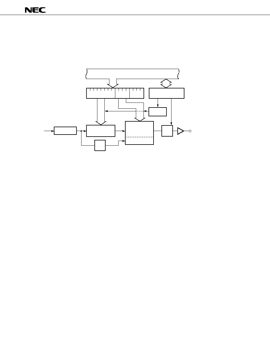
8.8.1 Asynchronous Serial Interface/Three-Wire Serial I/O (UART/IOE)
Two serial interface channels are available; for each channel, asynchronous serial interface mode or three-wire
serial I/O mode can be selected.
(1) Asynchronous serial interface mode
In this mode, 1-byte data is transferred after a start bit.
A baud rate generator is incorporated to enable communication at a wide range of baud rates.
Moreover, the frequency of a clock signal applied to the ASCK pin can be divided to define a baud rate.
With the baud rate generator, the baud rate conforming to the MIDI standard (31.25 kbps) can be obtained.
Fig. 8-10 Block Diagram of Asynchronous Serial Interface Mode
Remark f
XX
: Oscillator frequency or external clock input
n = 0 to 11
m = 16 to 30
RXB, RXB2
TXS, TXS2
INTST, INTST2
INTSR,
INTSR2
INTSER,
INTSER2
1/2m
f
XX
/2
ASCK, ASCK2
TxD, TxD2
RxD, RxD2
1/2
n+1
1/2m
Baud rate generator
Receive
shift register
Receive buffer
Selector
Transmission
control parity
bit addition
Transmission
shift register
Internal bus
Reception
control parity
check
3 9
m
m
m
m
m
PD784020, 784021
(2) Three-wire serial I/O mode
In this mode, the master device makes the serial clock active to start transmission, then transfers 1-byte data
in phase with the clock.
This mode is designed for communication with a device incorporating a conventional synchronous serial interface.
Basically, three lines are used for communication: the serial clock line (SCK) and the two serial data lines (SI
and SO).
In general, a handshake line is required to check the state of communication.
Fig. 8-11 Block Diagram of Three-Wire Serial I/O Mode
Remark f
XX
: Oscillator frequency or external clock input
n = 0 to 11
m = 1, 16 to 30
Serial clock counter
SIO1, SIO2
SI1, SI2
SO1, SO2
SCK1, SCK2
f
XX
/2
INTCSI1,
INTCSI2
Shift register
Output latch
Direction control
circuit
Internal bus
Serial clock
control circuit
Selector
1/m
1/2
n+1
Interrupt signal
generator
4 0
m
m
m
m
m
PD784020, 784021
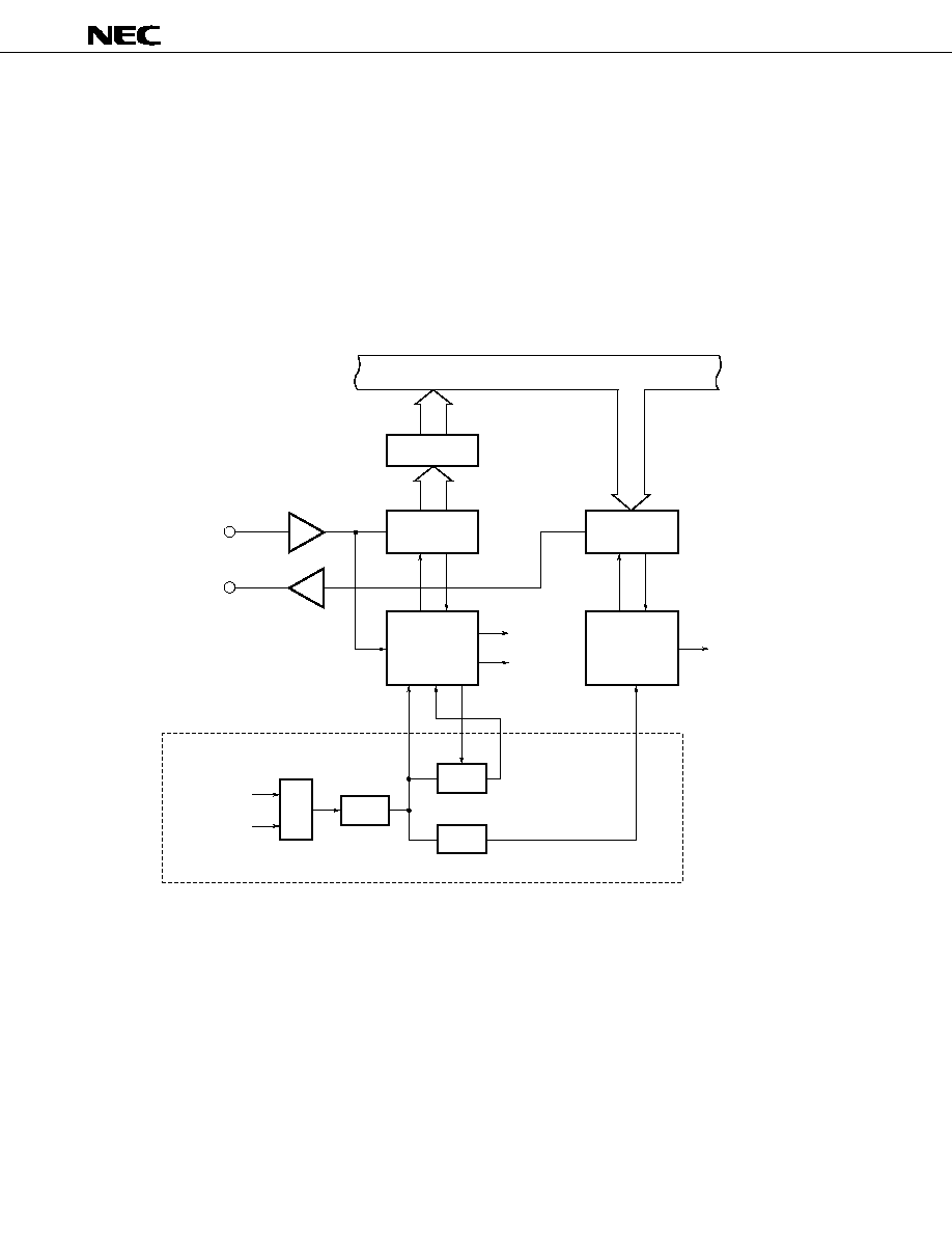
8.8.2 Synchronous Serial Interface (CSI)
With this interface, the master device makes the serial clock active to start transmission, then transfers 1-byte data
in phase with the clock.
Fig. 8-12 Block Diagram of Synchronous Serial Interface
Remark f
CLK
: Internal system clock frequency (system clock frequency/2)
Direction
control circuit
Selector
Shift register
Set
Clear
Output latch
Serial clock
counter
Serial clock
control circuit
Selector
TM 3 output/2
f
CLK
/8
f
CLK
/32
INTCSI
SCK0
SI0
SO0/SB0
Internal bus
Interrupt signal
generation
circuit
Busy/
acknowledge
detection
circuit
Bus release/
command/
acknowledge
detection
circuit
SIO
N-ch open-drain
output enabled
(when SB0 or
SBI mode is used)
4 1
m
m
m
m
m
PD784020, 784021
(1) Three-wire serial I/O mode
This mode is designed for communication with a device incorporating a conventional synchronous serial interface.
Basically, three lines are used for communication: the serial clock line (SCK0) and serial data lines (SI0 and SO0).
In general, a handshake line is required to check the state of communication.
(2) SBI mode
The SBI mode allows communication with more than one device via two lines: the serial clock (SCK0) and serial
bus (SB0). The SBI mode is the standard NEC serial interface.
A master device outputs an address through the SB0 pin to select a slave device with which communication is
to be performed. After a target device is selected, commands and data are transmitted between the master device
and slave device.
8.9 EDGE DETECTION FUNCTION
The interrupt input pins (NMI, INTP0-INTP5) are used to apply not only interrupt requests but also trigger signals
for the built-in circuits. As these pins are triggered by an edge (rising or falling) of an input signal, a function for edge
detection is incorporated. Moreover, a noise suppression function is provided to prevent erroneous edge detection
caused by noise.
Note
INTP0 is used for sampling clock selection.
Pin
Detectable edge
Noise suppression method
NMI
Rising edge or falling edge
Analog delay
INTP0-INTP3
Rising edge or falling edge, or both edges
Clock sampling
Note
INTP4, INTP5
Analog delay

4 2
m
m
m
m
m
PD784020, 784021
8.10 WATCHDOG TIMER
A watchdog timer is incorporated for CPU runaway detection. The watchdog timer, if not cleared by software within
a specified interval, generates a nonmaskable interrupt. Furthermore, once watchdog timer operation is enabled,
it cannot be disabled by software. The user can specify whether priority is placed on an interrupt based on the
watchdog timer or on an interrupt based on the NMI pin.
Fig. 8-13 Block Diagram of Watchdog Timer
f
CLK
/2
21
f
CLK
INTWDT
f
CLK
/2
20
f
CLK
/2
19
f
CLK
/2
17
Timer
Clear signal
Selector
H
4 3
m
m
m
m
m
PD784020, 784021
9. INTERRUPT FUNCTION
Table 9-1 lists the interrupt request handling modes. These modes are selected by software.
Table 9-1 Interrupt Request Handling Modes
9.1 INTERRUPT SOURCE
An interrupt can be issued from any one of the interrupt sources listed in Table 9-2: execution of a BRK instruction,
an operand error, or any of the 23 other interrupt sources.
Four levels of interrupt handling priority can be set. Priority levels can be set to nest control during interrupt handling
or to concurrently generate interrupt requests. Nested macro services, however, are performed without suspension.
When interrupt requests having the same priority level are generated, they are handled according to the default
priority (fixed). (See Table 9-2.)
Handling mode
Handled by
Handling
PC and PSW contents
Vectored interrupt
Software
Branches to a handling routine for execution
The PC and PSW contents are pushed
(arbitrary handling).
to and popped from the stack.
Context switching
Automatically selects a register bank, and
The PC and PSW contents are saved to
branches to a handling routine for execution
and read from a fixed area in the
(arbitrary handling).
register bank.
Macro service
Firmware
Performs operations such as memory-to-I/O-
Maintained
device data transfer (fixed handling).

4 4
m
m
m
m
m
PD784020, 784021
Table 9-2 Interrupt Sources
Remark ASI: Asynchronous serial interface
CSI: Synchronous serial interface
H
Type
Default
Source
Internal/
Macro
priority
Name
Trigger
external
service
Software
≠
BRK instruction
Instruction execution
≠
≠
Operand error
When the MOV STBC,#byte or MOV WDM,#byte instruction is
executed, exclusive OR of the byte operand and byte does not
produce FFH.
Nonmaskable
≠
NMI
Detection of edge input on the pin
External
≠
WDT
Watchdog timer overflow
Internal
Maskable
0 (highest)
INTP0
Detection of edge input on the pin (TM1/TM1W capture trigger)
External
Enabled
1
INTP1
Detection of edge input on the pin (TM2/TM2W capture trigger)
2
INTP2
Detection of edge input on the pin (TM2/TM2W event counter input)
3
INTP3
Detection of edge input on the pin (TM0 capture trigger)
4
INTC00
TM0-CR00 match signal issued
Internal
Enabled
5
INTC01
TM0-CR01 match signal issued
6
INTC10
TM1-CR10 match signal issued (in 8-bit operation mode)
TM1W-CR10W match signal issued (in 16-bit operation mode)
7
INTC11
TM1-CR11 match signal issued (in 8-bit operation mode)
TM1W-CR11W match signal issued (in 16-bit operation mode)
8
INTC20
TM2-CR20 match signal issued (in 8-bit operation mode)
TM2W-CR20W match signal issued (in 16-bit operation mode)
9
INTC21
TM2-CR21 match signal issued (in 8-bit operation mode)
TM2W-CR21W match signal issued (in 16-bit operation mode)
10
INTC30
TM3-CR30 match signal issued (in 8-bit operation mode)
TM3W-CR30W match signal issued (in 16-bit operation mode)
11
INTP4
Detection of edge input on the pin
External
Enabled
12
INTP5
Detection of edge input on the pin
13
INTAD
A/D converter processing completed (ADCR transfer)
Internal
Enabled
14
INTSER
ASI0 reception error
≠
15
INTSR
ASI0 reception completed or CSI1 transfer completed
Enabled
INTCSI1
16
INTST
ASI0 transmission completed
17
INTCSI
CSI0 transfer completed
18
INTSER2
ASI2 reception error
≠
19
INTSR2
ASI2 reception completed or CSI2 transfer completed
Enabled
INTCSI2
20 (lowest)
INTST2
ASI2 transmission completed

4 5
m
m
m
m
m
PD784020, 784021
9.2 VECTORED INTERRUPT
When a branch to an interrupt handling routine occurs, the vector table address corresponding to the interrupt
source is used as the branch address.
Interrupt handling by the CPU consists of the following operations :
∑
When a branch occurs
: Push the CPU status (PC and PSW contents) to the stack.
∑
When control is returned: Pop the CPU status (PC and PSW contents) from the stack.
To return control from the handling routine to the main routine, use the RETI instruction. The branch destination
addresses must be within the range of 0 to FFFFH.
Table 9-3 Vector Table Address
Interrupt source
Vector table address
BRK instruction
003EH
Operand error
003CH
NMI
0002H
WDT
0004H
INTP0
0006H
INTP1
0008H
INTP2
000AH
INTP3
000CH
INTC00
000EH
INTC01
0010H
INTC10
0012H
INTC11
0014H
INTC20
0016H
INTC21
0018H
INTC30
001AH
INTP4
001CH
INTP5
001EH
INTAD
0020H
INTSER
0022H
INTSR
0024H
INTCSI1
INTST
0026H
INTCSI
0028H
INTSER2
002AH
INTSR2
002CH
INTCSI2
INTST2
002EH

4 6
m
m
m
m
m
PD784020, 784021
9.3 CONTEXT SWITCHING
When an interrupt request is generated, or when the BRKCS instruction is executed, an appropriate register bank
is selected by the hardware. Then, a branch to a vector address stored in that register bank occurs. At the same
time, the contents of the current program counter (PC) and program status word (PSW) are stacked in the register
bank.
The branch address must be within the range of 0 to FFFFH.
Fig. 9-1 Context Switching Caused by an Interrupt Request
9.4 MACRO SERVICE
The macro service function enables data transfer between memory and special function registers (SFRs) without
requiring the intervention of the CPU. The macro service controller accesses both memory and SFRs within the same
transfer cycle to directly transfer data without having to perform data fetch.
Since the CPU status is neither saved nor restored, nor is data fetch performed, high-speed data transfer is
possible.
Fig. 9-2 Macro Service
PSW
PC19-16
0000B
PC15-0
Exchange
Save
Save
2
3
4
5
Save
1
6
7
Transfer
(Bits 8 to 11 of
temporary register)
Register bank n (n = 0-7)
Temporary register
A
X
B
C
R5
R4
R7
VP
UP
R6
D
E
H
T
U
V
W
L
Switching between register banks
(RBS0-RBS2
n)
RSS
0
IE
0
Register bank (0-7)
CPU
SFR
Memory
Read
Write
Read
Write
Macro service
controller
Internal bus

4 7
m
m
m
m
m
PD784020, 784021
9.5 EXAMPLES OF MACRO SERVICE APPLICATIONS
(1) Serial interface transmission
Each time a macro service request (INTST) is generated, the next transmission data is transferred from memory
to TXS. When data n (last byte) has been transferred to TXS (that is, once the transmission data storage buffer
becomes empty), a vectored interrupt request (INTST) is generated.
(2) Serial interface reception
Each time a macro service request (INTSR) is generated, reception data is transferred from RXB to memory.
When data n (last byte) has been transferred to memory (that is, once the reception data storage buffer becomes
full), a vectored interrupt request (INTSR) is generated.
Transmission data storage buffer (memory)
INTST
TXS (SFR)
TxD
Data n
Data n-1
Data 2
Data 1
Internal bus
Transmission
shift register
Transmission control
Reception data storage buffer (memory)
INTSR
RXB (SFR)
RxD
Data n
Data n-1
Data 2
Data 1
Internal bus
Reception buffer
Reception
shift register
Reception control
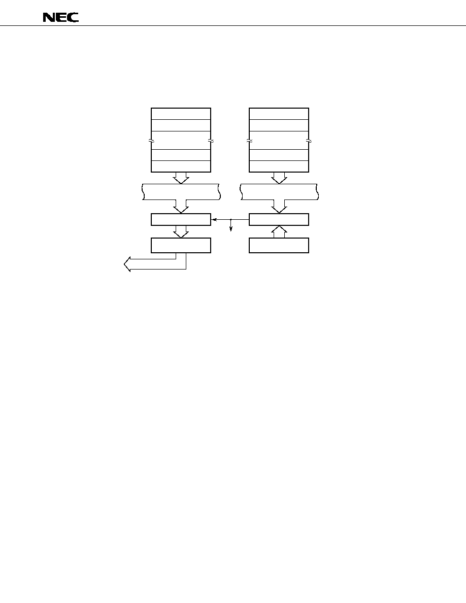
4 8
m
m
m
m
m
PD784020, 784021
(3) Real-time output port
INTC10 and INTC11 function as the output triggers for the real-time output ports. For these triggers, the macro
service can simultaneously set the next output pattern and interval. Therefore, INTC10 and INTC11 can be used
to independently control two stepping motors. They can also be applied to PWM and DC motor control.
Each time a macro service request (INTC10) is generated, a pattern and timing data are transferred to the buffer
register (P0L) and compare register (CR10), respectively. When the contents of timer register 1 (TM1) and CR10
match, another INTC10 is generated, and the P0L contents are transferred to the output latch. When Tn (last
byte) is transferred to CR10, a vectored interrupt request (INTC10) is generated.
For INTC11, the same operation as that performed for INTC10 is performed.
Match
(SFR)
INTC10
P00-P03
(SFR)
Output pattern profile (memory)
Output timing profile (memory)
P
n
P
n≠1
P
2
P
1
Internal bus
P0L
Output latch
CR10
TM1
Internal bus
T
n
T
n≠1
T
2
T
1
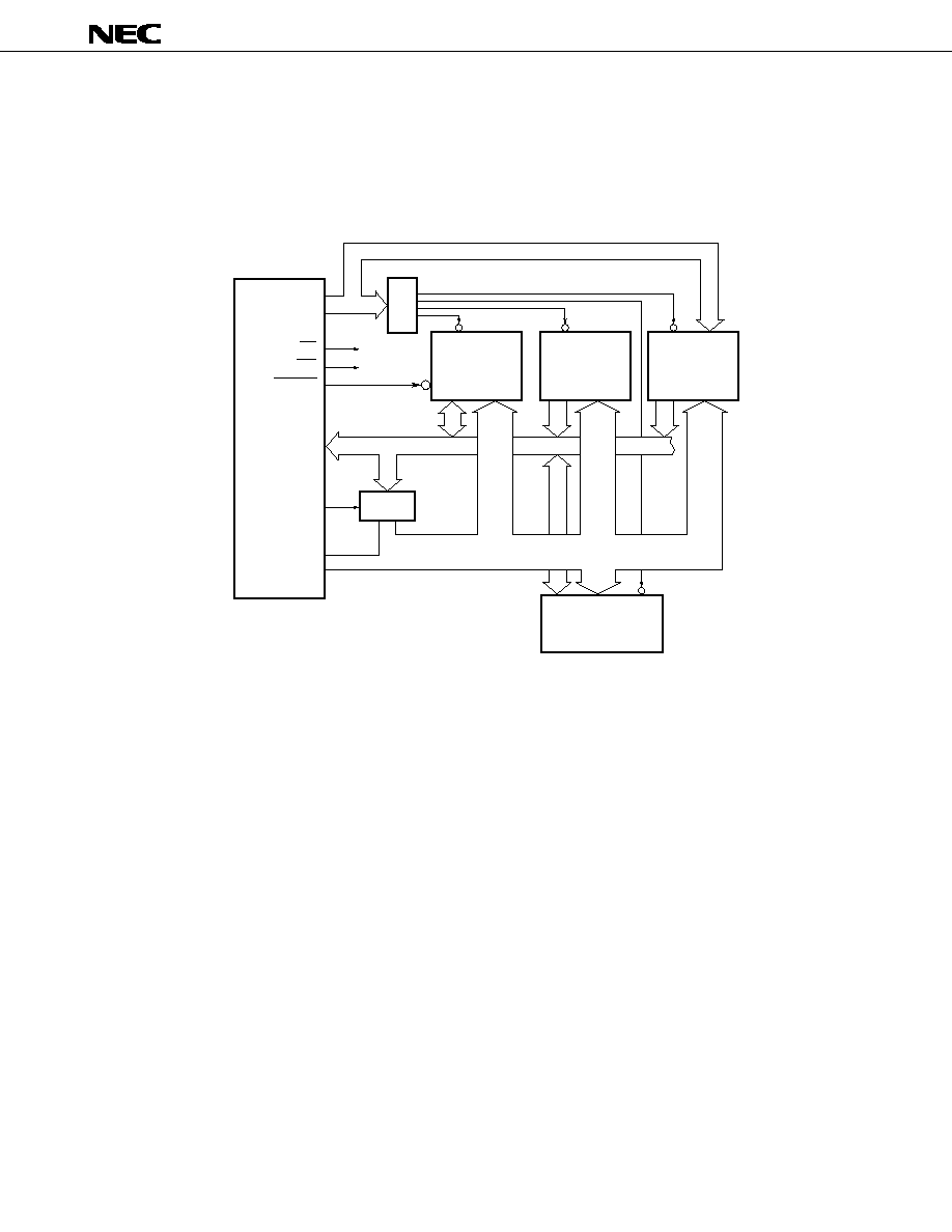
4 9
m
m
m
m
m
PD784020, 784021
10. LOCAL BUS INTERFACE
The local bus interface enables the connection of external memory and I/O devices (memory-mapped I/O). It
supports a 1M-byte memory space. (See Fig. 10-1.)
Fig. 10-1 Example of Local Bus Interface
10.1 MEMORY EXPANSION
By adding external memory, program memory or data memory can be expanded, 64K bytes at a time, to
approximately 1M byte (three steps).
Data bus
Latch
Gate array for I/O
expansion including
Centronics interface
circuit, etc.
RD
WR
REFRQ
AD0-AD7
ASTB
Pseudo SRAM
PROM
PD27C1001A
PD784021
A16-A19
µ
µ
Address bus
Data bus
A8-A15
Decoder
Kanji character
generator
PD24C1000
µ

5 0
m
m
m
m
m
PD784020, 784021
10.2 MEMORY SPACE
The 1M-byte memory space is divided into eight spaces, each having a logical address. Each of these spaces
can be controlled using the programmable wait and pseudo-static RAM refresh functions.
Fig. 10-2 Memory Space
FFFFFH
80000H
7FFFFH
40000H
3FFFFH
20000H
1FFFFH
10000H
0FFFFH
0C000H
0BFFFH
08000H
07FFFH
04000H
03FFFH
00000H
512K bytes
256K bytes
128K bytes
64K bytes
16K bytes
16K bytes
16K bytes
16K bytes

5 1
m
m
m
m
m
PD784020, 784021
10.3 PROGRAMMABLE WAIT
When the memory space is divided into eight spaces, a wait state can be separately inserted for each memory
space while the RD or WR signal is active. This prevents the overall system efficiency from being degraded even
when memory devices having different access times are connected.
In addition, an address wait function that extends the ASTB signal active period is provided to produce a longer
address decode time. (This function is set for the entire space.)
10.4 PSEUDO-STATIC RAM REFRESH FUNCTION
Refresh is performed as follows:
∑
Pulse refresh
: A bus cycle is inserted where a refresh pulse is output on the REFRQ pin at regular
intervals. When the memory space is divided into eight, and a specified area
is being accessed, refresh pulses can also be output on the REFRQ pin as the
memory is being accessed. This can prevent the refresh cycle from suspending
normal memory access.
∑
Power-down self-refresh : In standby mode, a low-level signal is output on the REFRQ pin to maintain the
contents of pseudo-static RAM.
10.5 BUS HOLD FUNCTION
A bus hold function is provided to facilitate connection to devices such as a DMA controller. Suppose that a bus
hold request signal (HLDRQ) is received from an external bus master. In this case, upon the completion of the bus
cycle being performed, the address bus, address/data bus, ASTB, RD, and WR pins are placed in the high-impedance
state, and the bus hold acknowledge signal (HLDAK) is made active to release the bus for the external bus master.
While the bus hold function is being used, the external wait and pseudo-static RAM refresh functions are disabled.
5 2
m
m
m
m
m
PD784020, 784021
11. STANDBY FUNCTION
The standby function allows the power consumption of the chip to be reduced. The following standby modes are
supported:
∑ HALT mode : The CPU operation clock is stopped. By occassionally inserting the HALT mode during normal
operation, the overall average power consumption can be reduced.
∑ IDLE mode : The entire system is stopped, with the exception of the oscillator circuit. This mode consumes
only very little more power than STOP mode, but normal program operation can be restored in
almost as little time as that required to restore normal program operation from HALT mode.
∑ STOP mode : The oscillator is stopped. All operations in the chip stop, such that only leakage current flows.
These modes can be selected by software.
A macro service can be initiated in HALT mode.
Fig. 11-1 Standby Mode Status Transition
Notes 1. INTP4 and INTP5 are applied when not masked.
2. Only when the interrupt request is not masked
Remark NMI is enabled only by external input. The watchdog timer cannot be used to release one of the standby
modes (STOP or IDLE mode).
STOP
(standby)
IDLE
(standby)
Request for masked interrupt
HALT
(standby)
NMI, INTP4, INTP5 input
Note 1
Set STOP
RESET input
Set IDLE
RESET input
NMI, INTP4, INTP5 input
Note 1
Oscillation settling
time elapses
Wait for
oscillation
settling
Program
operation
Macro service request
End of one operation
End of macro service
Macro
service
Set HALT
RESET input
Interrupt request
Note 2
Macro service request
End of one operation

5 3
m
m
m
m
m
PD784020, 784021
12. RESET FUNCTION
Applying a low-level signal to the RESET pin initializes the internal hardware (reset status).
When the RESET input makes a low-to-high transition, the following data is loaded into the program counter (PC):
∑
Eight low-order bits of the PC
: Contents of location at address 0000H
∑
Intermediate eight bits of the PC : Contents of location at address 0001H
∑
Four high-order bits of the PC
: 0
The PC contents are used as a branch destination address. Program execution starts from that address. Therefore,
a reset start can be performed from an arbitrary address.
The contents of each register can be set by software, as required.
The RESET input circuit contains a noise eliminator to prevent malfunctions caused by noise. This noise eliminator
is an analog delay sampling circuit.
Fig. 12-1 Accepting a Reset
For power-on reset, the RESET signal must be held active until the oscillation settling time (approximately 40 ms)
has elapsed.
Fig. 12-2 Power-On Reset
RESET
(input)
Delay
Delay
Delay
Initialize PC
Execute instruction
at reset start address
Internal reset signal
Start reset
End reset
Oscillation settling time
Delay
Initialize PC
Execute instruction at
reset start address
RESET
(input)
Internal reset signal
End reset
V
DD
5 4
m
m
m
m
m
PD784020, 784021
13. INSTRUCTION SET
(1) 8-bit instructions (The instructions enclosed in parentheses are implemented by a combination of
operands, where A is described as r.)
MOV, XCH, ADD, ADDC, SUB, SUBC, AND, OR, XOR, CMP, MULU, DIVUW, INC, DEC, ROR, ROL, RORC,
ROLC, SHR, SHL, ROR4, ROL4, DBNZ, PUSH, POP, MOVM, XCHM, CMPME, CMPMNE, CMPMNC, CMPMC,
MOVBK, XCHBK, CMPBKE, CMPBKNE, CMPBKNC, CMPBKC, CHKL, CHKLA
Table 13-1 Instructions Implemented by 8-Bit Addressing
2nd operand
#byte
A
r
saddr
sfr
!addr16
mem
r3
[WHL+]
n
None
Note 2
r'
saddr'
!!addr24
[saddrp]
PSWL
[WHL≠]
1st operand
[%saddrg]
PSWH
A
(MOV)
(MOV)
MOV
(MOV)
Note 6
MOV
(MOV)
MOV
MOV
(MOV)
ADD
Note 1
(XCH)
XCH
(XCH)
Note 6
(XCH)
(XCH)
XCH
(XCH)
(ADD)
Note 1
(ADD)
Note 1
(ADD)
Notes 1, 6
(ADD)
Note 1
ADD
Note 1
ADD
Note 1
(ADD)
Note 1
r
MOV
(MOV)
MOV
MOV
MOV
MOV
ROR
Note 3
MULU
ADD
Note 1
(XCH)
XCH
XCH
XCH
XCH
DIVUW
(ADD)
Note 1
ADD
Note 1
ADD
Note 1
ADD
Note 1
INC
DEC
saddr
MOV
(MOV)
Note 6
MOV
MOV
INC
ADD
Note 1
(ADD)
Note 1
ADD
Note 1
XCH
DEC
ADD
Note 1
DBNZ
sfr
MOV
MOV
MOV
PUSH
ADD
Note 1
(ADD)
Note 1
ADD
Note 1
POP
CHKL
CHKLA
!addr16
MOV
(MOV)
MOV
!!addr24
ADD
Note 1
mem
MOV
[saddrp]
ADD
Note 1
[%saddrg]
mem3
ROR4
ROL4
r3
MOV
MOV
PSWL
PSWH
B, C
DBNZ
STBC, WDM
MOV
[TDE+]
(MOV)
MOVBK
Note 5
[TDE≠]
(ADD)
Note 1
MOVM
Note 4
Notes 1. ADDC, SUB, SUBC, AND, OR, XOR, and CMP are the same as ADD.
2. There is no second operand, or the second operand is not an operand address.
3. ROL, RORC, ROLC, SHR, and SHL are the same as ROR.
4. XCHM, CMPME, CMPMNE, CMPMNC, and CMPMC are the same as MOVM.
5. XCHBK, CMPBKE, CMPBKNE, CMPBKNC, and CMPBKC are the same as MOVBK.
6. When saddr is saddr2 with this combination, an instruction with a short code exists.

5 5
m
m
m
m
m
PD784020, 784021
(2) 16-bit instructions (The instructions enclosed in parentheses are implemented by a combination of
operands, where AX is described as rp.)
MOVW, XCHW, ADDW, SUBW, CMPW, MULUW, MULW, DIVUX, INCW, DECW, SHRW, SHLW, PUSH, POP,
ADDWG, SUBWG, PUSHU, POPU, MOVTBLW, MACW, MACSW, SACW
Table 13-2 Instructions Implemented by 16-Bit Addressing
2nd operand
#word
AX
rp
saddrp
strp
!addr16
mem
[WHL+]
byte
n
None
Note 2
rp'
saddrp'
!!addr24
[saddrp]
1st operand
[%saddrg]
AX
(MOVW)
(MOVW)
(MOVW)
(MOVW)
Note 3
MOVW
(MOVW)
MOVW
(MOVW)
ADDW
Note 1
(XCHW)
(XCHW)
(XCHW)
Note 3
(XCHW)
XCHW
XCHW
(XCHW)
(ADD)
Note 1
(ADDW)
Note 1
(ADDW)
Notes 1,3
(ADDW)
Note 1
rp
MOVW
(MOVW)
MOVW
MOVW
MOVW
MOVW
SHRW
MULW
Note 4
ADDW
Note 1
(XCHW)
XCHW
XCHW
XCHW
SHLW
INCW
(ADDW)
Note 1
ADDW
Note 1
ADDW
Note 1
ADDW
Note 1
DECW
saddrp
MOVW
(MOVW)
Note 3
MOVW
MOVW
INCW
ADDW
Note 1
(ADDW)
Note 1
ADDW
Note 1
XCHW
DECW
ADDW
Note 1
sfrp
MOVW
MOVW
MOVW
PUSH
ADDW
Note 1
(ADDW)
Note 1
ADDW
Note 1
POP
!addr16
MOVW
(MOVW)
MOVW
MOVTBLW
!!addr24
mem
MOVW
[saddrp]
[%saddrg]
PSW
PUSH
POP
SP
ADDWG
SUBWG
post
PUSH
POP
PUSHU
POPU
[TDE+]
(MOVW)
SACW
byte
MACW
MACSW
Notes 1. SUBW and CMPW are the same as ADDW.
2. There is no second operand, or the second operand is not an operand address.
3. When saddrp is saddrp2 with this combination, an instruction with a short code exists.
4. MULUW and DIVUX are the same as MULW.
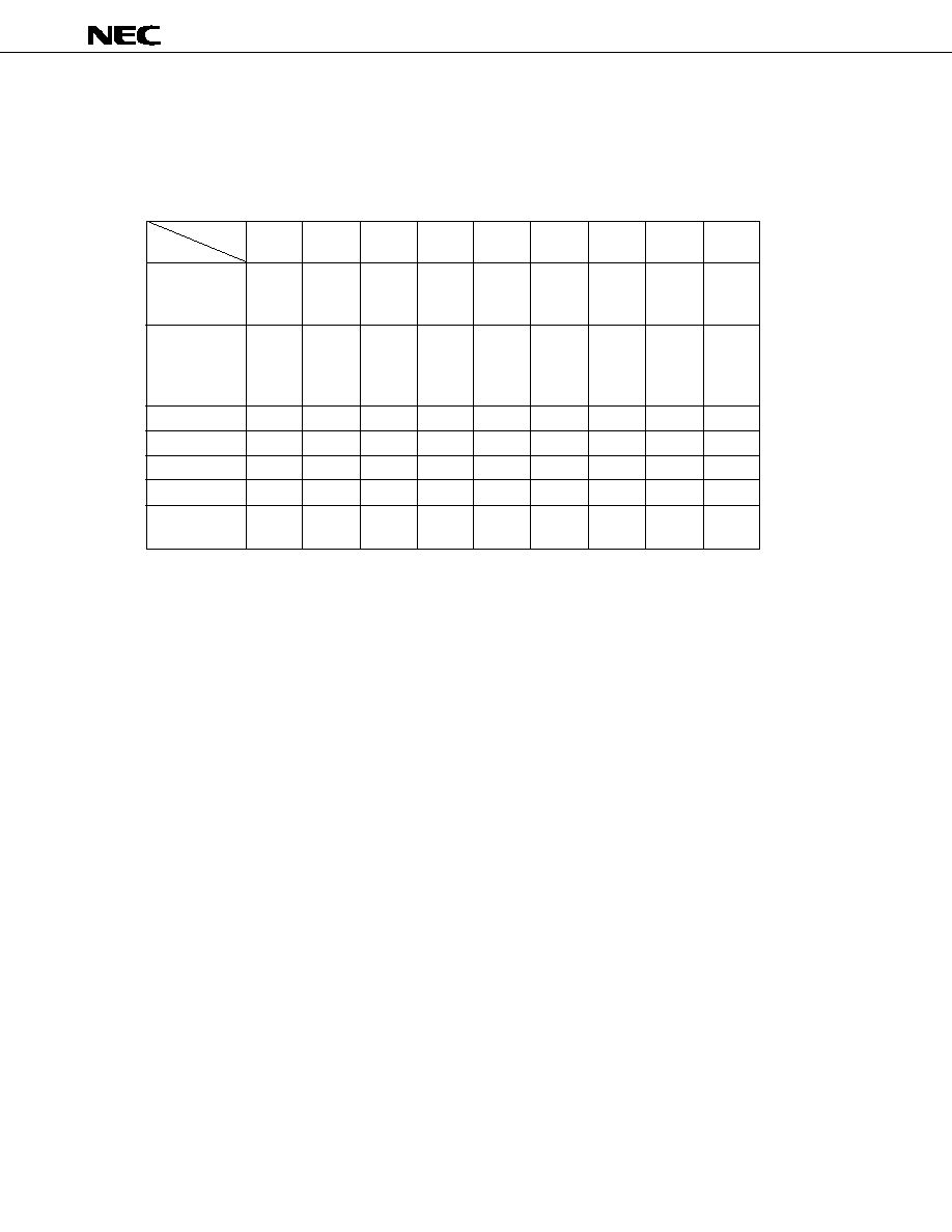
5 6
m
m
m
m
m
PD784020, 784021
(3) 24-bit instructions (The instructions enclosed in parentheses are implemented by a combination of
operands, where WHL is described as rg.)
MOVG, ADDG, SUBG, INCG, DECG, PUSH, POP
Table 13-3 Instructions Implemented by 24-Bit Addressing
2nd operand
#imm24
WHL
rg
saddrg
!!addr24
mem1
[%saddrg]
SP
None
Note
1st operand
rg'
WHL
(MOVG)
(MOVG)
(MOVG)
(MOVG)
(MOVG)
MOVG
MOVG
MOVG
(ADDG)
(ADDG)
(ADDG)
ADDG
(SUBG)
(SUBG)
(SUBG)
SUBG
rg
MOVG
(MOVG)
MOVG
MOVG
MOVG
INCG
ADDG
(ADDG)
ADDG
DECG
SUBG
(SUBG)
SUBG
PUSH
POP
saddrg
(MOVG)
MOVG
!!addr24
(MOVG)
MOVG
mem1
MOVG
[%saddrg]
MOVG
SP
MOVG
MOVG
INCG
DECG
Note
There is no second operand, or the second operand is not an operand address.
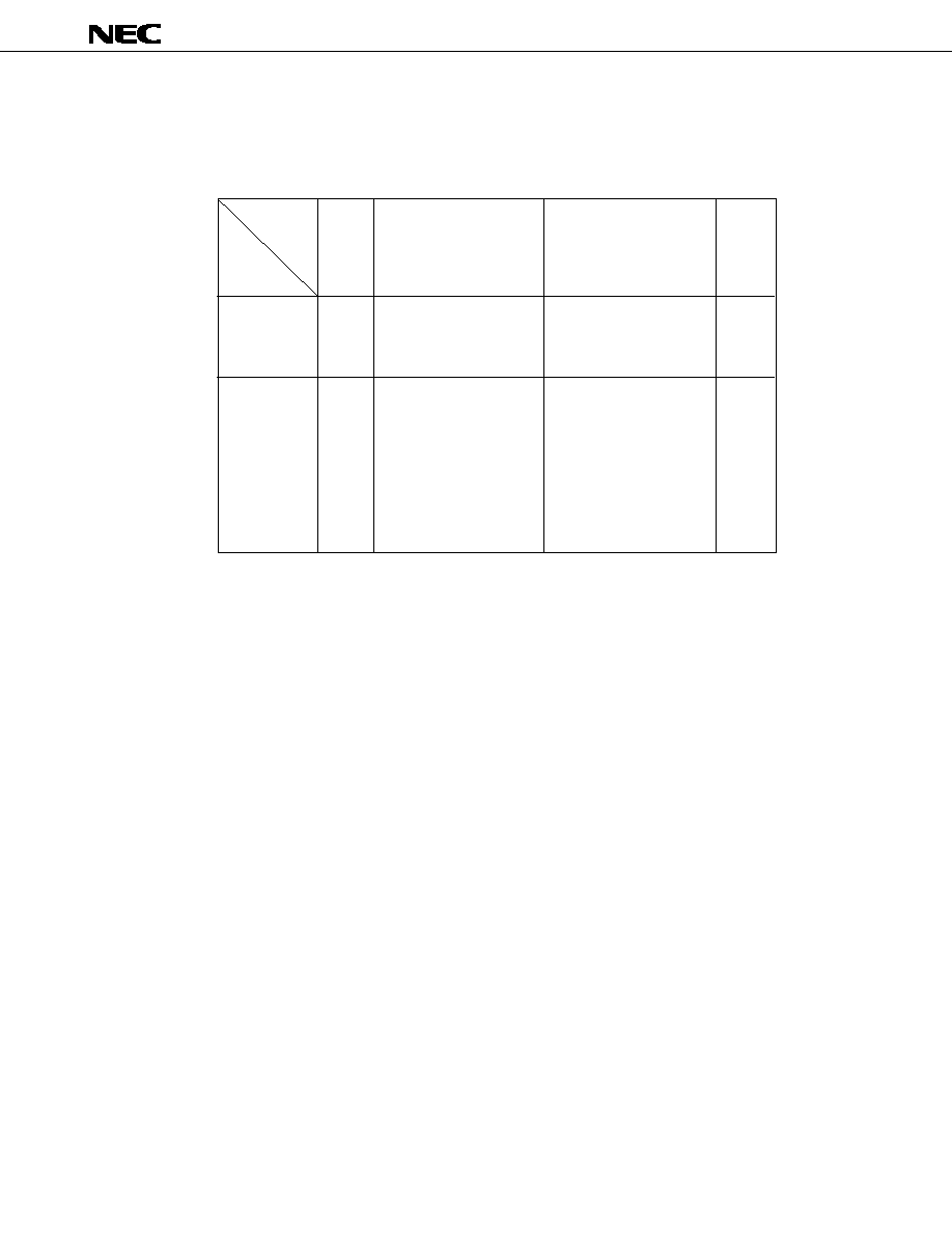
5 7
m
m
m
m
m
PD784020, 784021
(4) Bit manipulation instructions
MOV1, AND1, OR1, XOR1, SET1, CLR1, NOT1, BT, BF, BTCLR, BFSET
Table 13-4 Bit Manipulation Instructions Implemented by Addressing
2nd operand
CY
saddr.bit sfr.bit
/saddr.bit /sfr.bit
None
Note
A.bit X.bit
/A.bit /X.bit
PSWL.bit PSWH.bit
/PSWL.bit /PSWH.bit
mem2.bit
/mem2.bit
1st operand
!addr16.bit !!addr24.bit
/!addr16.bit /!!addr24.bit
CY
MOV1
AND1
NOT1
AND1
OR1
SET1
OR1
CLR1
XOR1
saddr.bit
MOV1
NOT1
sfr.bit
SET1
A.bit
CLR1
X.bit
BF
PSWL.bit
BT
PSWH.bit
BTCLR
mem2.bit
BFSET
!addr16.bit
!!addr24.bit
Note
There is no second operand, or the second operand is not an operand address.

5 8
m
m
m
m
m
PD784020, 784021
(5) Call/return instructions and branch instructions
CALL, CALLF, CALLT, BRK, RET, RETI, RETB, RETCS, RETCSB, BRKCS, BR, BNZ, BNE, BZ, BE, BNC, BNL,
BC, BL, BNV, BPO, BV, BPE, BP, BN, BLT, BGE, BLE, BGT, BNH, BH, BF, BT, BTCLR, BFSET, DBNZ
Table 13-5 Call/Return and Branch Instructions Implemented by Addressing
Instruction
$addr20 $!addr20
!addr16
!!addr20
rp
rg
[rp]
[rg]
!addr11
[addr5]
RBn
None
address
operand
Basic
BC
Note
CALL
CALL
CALL
CALL
CALL
CALL
CALL
CALLF
CALLF
BRKCS
BRK
instruction
BR
BR
BR
BR
BR
BR
BR
BR
RET
RETCS
RETI
RETCSB
RETB
Composite
BF
instruction
BT
BTCLR
BFSET
DBNZ
Note
BNZ, BNE, BZ, BE, BNC, BNL, BL, BNV, BPO, BV, BPE, BP, BN, BLT, BGE, BLE, BGT, BNH, and BH
are the same as BC.
(6) Other instructions
ADJBA, ADJBS, CVTBW, LOCATION, SEL, NOT EI, DI, SWRS
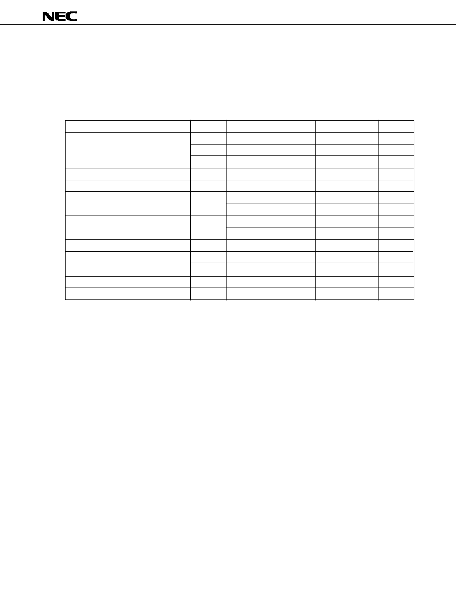
5 9
m
m
m
m
m
PD784020, 784021
14. ELECTRICAL CHARACTERISTICS
The electrical characteristics described in this chapter apply to the products which are improved versions of the
m
PD784020 and
m
PD784021 (other than K-rank products). For K-rank products yet to be improved (K-rank products),
please consult with our sales offices.
H
Parameter
Supply voltage
Input voltage
Output voltage
Low-level output current
High-level output current
A/D converter reference input voltage
D/A converter reference input voltage
Operating ambient temperature
Storage temperature
Conditions
Each pin
Total of all output pins
Each pin
Total of all output pins
Symbol
V
DD
AV
DD
AV
SS
V
I
V
O
I
OL
I
OH
AV
REF1
AV
REF2
AV
REF3
T
A
T
stg
Rating
≠0.5 to +7.0
AV
SS
to V
DD
+ 0.5
≠0.5 to +0.5
≠0.5 to V
DD
+ 0.5
≠0.5 to V
DD
+ 0.5
15
150
≠10
≠100
≠0.5 to V
DD
+ 0.3
≠0.5 to V
DD
+ 0.3
≠0.5 to V
DD
+ 0.3
≠40 to +85
≠65 to +150
Unit
V
V
V
V
V
mA
mA
mA
mA
V
V
V
∞C
∞C
ABSOLUTE MAXIMUM RATINGS (T
A
= 25 ∞C)
Caution Absolute maximum ratings are rated values beyond which some physical damages may be
caused to the product; if any of the parameters in the table above exceeds its rated value even
for a moment, the quality of the product may deteriorate. Be sure to use the product within the
rated values.
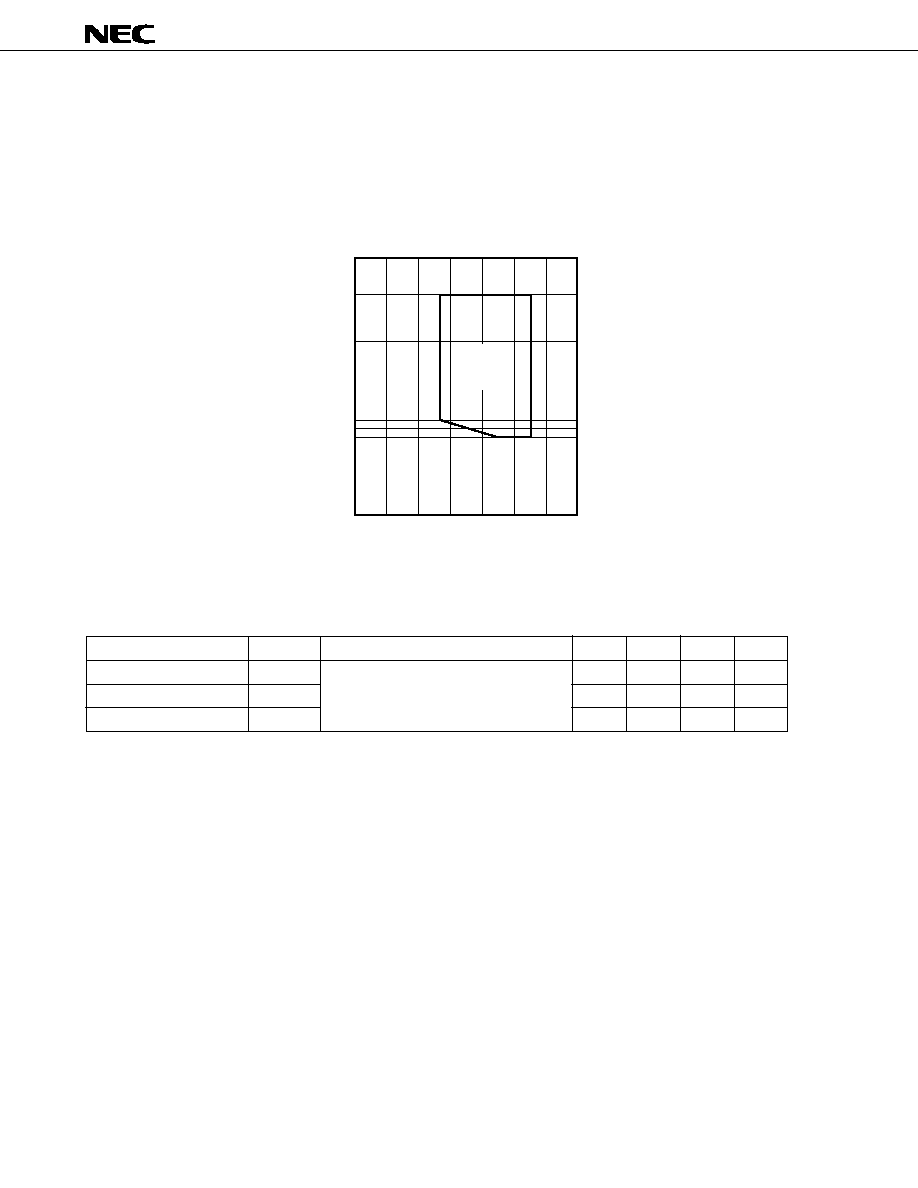
6 0
m
m
m
m
m
PD784020, 784021
OPERATING CONDITIONS
∑
Operating ambient temperature (T
A
): ≠40 to +85 ∞C
∑
Rising and falling time (t
r
, t
f
) (for pins not especially specified): 0 to 200
m
s
∑
Power supply voltage and clock cycle time: See Fig. 14-1.
Fig. 14-1 Relationship between Power Supply Voltage and Clock Cycle Time
CAPACITANCE (T
A
= 25 ∞C, V
DD
= V
SS
= 0 V)
Parameter
Input capacitance
Output capacitance
I/O capacitance
Unit
pF
pF
pF
Max.
10
10
10
Typ.
Min.
Symbol
C
I
C
O
C
IO
Conditions
f = 1 MHz
0 V on pins other than measured pins
10000
4000
1000
125
100
80
10
0
1
2
3
4
5
6
7
Clock cycle time t
CYK
[ns]
Operation
guarantee
range
Power supply voltage [V]
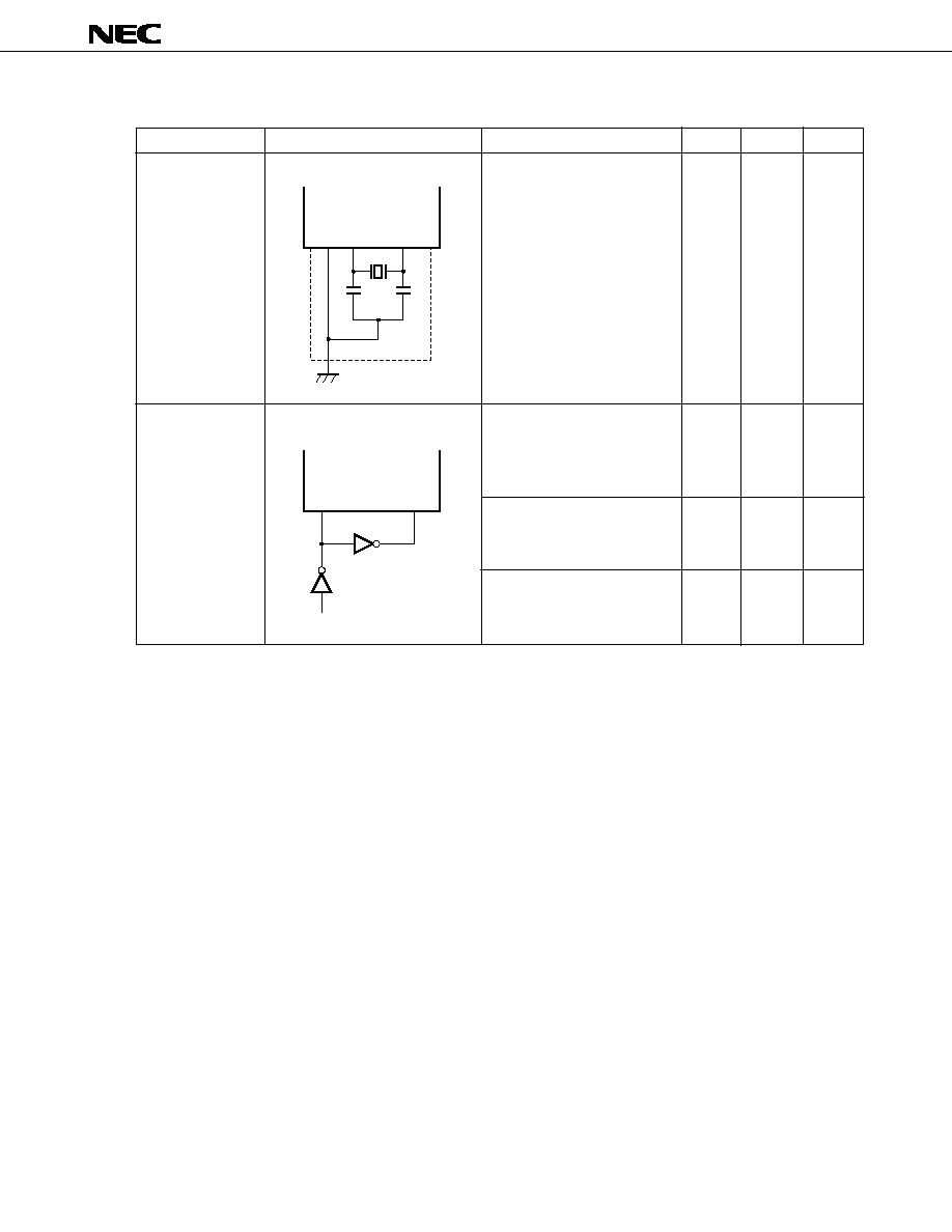
6 1
m
m
m
m
m
PD784020, 784021
OSCILLATOR CHARACTERISTICS (T
A
= ≠40 to +85 ∞C, V
DD
= 4.5 to 5.5 V, V
SS
= 0 V)
Resonator
Ceramic resonator
or crystal
External clock
Recommended circuit
Min.
4
4
0
10
Unit
MHz
MHz
ns
ns
Parameter
Oscillator frequency (f
XX
)
X1 input frequency (f
X
)
X1 input rising and falling times
(t
XR
, t
XF
)
X1 input high-level and low-
level widths (t
WXH
, t
WXL
)
Max.
25
25
10
125
X1
X2
V
SS
C1
C2
X1
X2
HCMOS
Inverter
Caution When using the system clock generator, run wires in the portion surrounded by dotted lines
according to the following rules to avoid effects such as stray capacitance:
∑
Minimize the wiring.
∑
Never cause the wires to cross other signal lines.
∑
Never cause the wires to run near a line carrying a large varying current.
∑
Cause the grounding point of the capacitor of the oscillator circuit to have the same potential
as V
SS
. Never connect the capacitor to a ground pattern carrying a large current.
∑
Never extract a signal from the oscillator.

6 2
m
m
m
m
m
PD784020, 784021
OSCILLATOR CHARACTERISTICS (T
A
= ≠40 to +85 ∞C, V
DD
= 2.7 to 5.5 V, V
SS
= 0 V)
Resonator
Ceramic resonator
or crystal
External clock
Recommended circuit
Min.
4
4
0
10
Unit
MHz
MHz
ns
ns
Parameter
Oscillator frequency (f
XX
)
X1 input frequency (f
X
)
X1 input rising and falling times
(t
XR
, t
XF
)
X1 input high-level and low-
level widths (t
WXH
, t
WXL
)
Max.
16
16
10
125
X1
X2
V
SS
C1
C2
X1
X2
HCMOS
Inverter
Caution When using the system clock generator, run wires in the portion surrounded by dotted lines
according to the following rules to avoid effects such as stray capacitance:
∑
Minimize the wiring.
∑
Never cause the wires to cross other signal lines.
∑
Never cause the wires to run near a line carrying a large varying current.
∑
Cause the grounding point of the capacitor of the oscillator circuit to have the same potential
as V
SS
. Never connect the capacitor to a ground pattern carrying a large current.
∑
Never extract a signal from the oscillator.

6 3
m
m
m
m
m
PD784020, 784021
DC CHARACTERISTICS (T
A
= ≠40 to +85 ∞C, V
DD
= AV
DD
= 2.7 to 5.5 V, V
SS
= AV
SS
= 0 V) (1/2)
Notes 1. X1, X2, RESET, P12/ASCK2/SCK2, P13/RxD2/SI2, P20/NMI, P21/INTP0, P22/INTP1, P23/INTP2/CI,
P24/INTP3, P25/INTP4/ASCK/SCK1, P26/INTP5, P27/SI0, P30/RxD/SI1, P32/SCK0, P33/SO0/SB0,
and TEST
2. AD0 to AD7 and A8 to A15
3. P60/A16 to P63/A19, RD, WR, P66/WAIT/HLDRQ, and P67/REFRQ/HLDAK
4. P00 to P07
5. P10 to P17
Parameter
Low-level input voltage
High-level input voltage
Low-level output voltage
High-level output voltage
X1 low-level input current
X1 high-level input current
Symbol
V
IL1
V
IL2
V
IL3
V
IH1
V
IH2
V
IH3
V
OL1
V
OL2
V
OH1
V
OH2
I
IL
I
IH
Conditions
Pins other than those described in
Notes 1, 2, 3, and 4
Pins described in Notes 1, 2, 3, and 4
V
DD
= +5.0 V
±
10 %
Pins described in Notes 2, 3, and 4
Pins other than those described in Note 1
Pins described in Note 1
V
DD
= +5.0 V
±
10 %
Pins described in Notes 2, 3, and 4
I
OL
= 2 mA
V
DD
= +5.0 V
±
10 %
I
OL
= 8 mA
Pins described in Notes 2 and 5
I
OH
= ≠2 mA
V
DD
= +5.0 V
±
10 %
I
OH
= ≠5 mA
Pins described in Note 4
0 V
£
V
I
£
V
IL2
V
IH2
£
V
I
£
V
DD
Unit
V
V
V
V
V
V
V
V
V
V
m
A
m
A
Min.
≠0.3
≠0.3
≠0.3
0.7V
DD
0.8V
DD
2.2
V
DD
≠ 1.0
2.0
Typ.
Max.
0.3V
DD
0.2V
DD
+0.8
V
DD
+ 0.3
V
DD
+ 0.3
V
DD
+ 0.3
0.4
1.0
≠30
+30

6 4
m
m
m
m
m
PD784020, 784021
DC CHARACTERISTICS (T
A
= ≠40 to +85 ∞C, V
DD
= AV
DD
= 2.7 to 5.5 V, V
SS
= AV
SS
= 0 V) (2/2)
Parameter
Input leakage current
Output leakage current
V
DD
supply current
Pull-up resistance
Symbol
I
LI
I
LO
I
DD1
I
DD2
I
DD3
R
L
Unit
m
A
m
A
m
A
mA
mA
mA
mA
mA
mA
k
W
k
W
Min.
15
15
Typ.
40
12
22
8
Max.
±
10
±
3
±
10
60
25
30
12
12
8
100
160
Conditions
0 V
£
V
I
£
V
DD
Except for the X1 pin when EXTC = 0
0 V
£
V
I
£
V
DD
Analog input pins
0 V
£
V
O
£
V
DD
Operating mode
f
XX
= 25 MHz
f
XX
= 16 MHz
V
DD
= 2.7 to 5.5 V
HALT mode
f
XX
= 25 MHz
f
XX
= 16 MHz
V
DD
= 2.7 to 5.5 V
IDLE mode
f
XX
= 25 MHz
(EXTC = 0)
f
XX
= 16 MHz
V
DD
= 2.7 to 5.5 V
V
I
= 0 V
V
DD
= +5.0 V
±
10 %
V
I
= 0 V
V
DD
= 2.7 to 4.5 V
6 5
m
m
m
m
m
PD784020, 784021
AC CHARACTERISTICS (T
A
= ≠40 to +85 ∞C, V
DD
= AV
DD
= 2.7 to 5.5 V, V
SS
= AV
SS
= 0 V)
(1) Read/write operation (1/2)
Remark
T: T
CYK
(system clock cycle time)
a: 1 when address wait is applied, 0 in other cases
n: number of wait cycles (n
∑
0)
Parameter
Address setup time
ASTB high-level width
Address hold time
(referred to ASTB
ÿ
)
Address hold time
(referred to RD
∑
)
Address
∆
RD
ÿ
delay time
Address float time
(referred to RD
ÿ
)
Address
∆
data input time
ASTB
ÿ
∆
data input time
RD
ÿ
∆
data input time
ASTB
ÿ
∆
RD
ÿ
delay time
Data hold time
(referred to RD
∑
)
RD
∑ ∆
address active time
RD
∑
∆
ASTB
∑
delay time
RD low-level width
Address hold time
(referred to WR
∑
)
Address
∆
WR
ÿ
delay time
ASTB
ÿ
∆
data output delay time
ASTB
ÿ
∆
data output time
ASTB
ÿ
∆
WR
ÿ
output delay time
Symbol
t
SAST
t
WSTH
t
HSTLA
t
HRA
t
DAR
t
FRA
t
DAID
t
DSTID
t
DRID
t
DSTR
t
HRID
t
DRA
t
DRST
t
WRL
t
HWA
t
DAW
t
DSTOD
t
DWOD
t
DSTW
Unit
ns
ns
ns
ns
ns
ns
ns
ns
ns
ns
ns
ns
ns
ns
ns
ns
ns
ns
ns
ns
ns
ns
ns
ns
ns
ns
ns
ns
ns
ns
ns
ns
Min.
(0.5 + a) T ≠ 11
(0.5 + a) T ≠ 15
(0.5 + a) T ≠ 17
(0.5 + a) T ≠ 40
0.5T ≠ 24
0.5T ≠ 34
0.5T ≠ 14
(1 + a) T ≠ 5
(1 + a) T ≠ 10
0.5T ≠ 9
0
0.5T ≠ 2
0.5T ≠ 12
1.5T ≠ 2
1.5T ≠ 12
0.5T ≠ 9
(1.5 + n) T ≠ 30
(1.5 + n) T ≠ 40
0.5T ≠ 14
(1 + a) T ≠ 5
(1 + a) T ≠ 10
0.5T ≠ 9
Max.
0
(2.5 + a + n) T ≠ 37
(2.5 + a + n) T ≠ 52
(2 + n) T ≠ 40
(2 + n) T ≠ 60
(1.5 + n) T ≠ 50
(1.5 + n) T ≠ 70
0.5T + 15
0.5T + 20
0.5T ≠ 11
Conditions
V
DD
= +5.0 V
±
10 %
V
DD
= +5.0 V
±
10 %
V
DD
= +5.0 V
±
10 %
V
DD
= +5.0 V
±
10 %
V
DD
= +5.0 V
±
10 %
V
DD
= +5.0 V
±
10 %
V
DD
= +5.0 V
±
10 %
Upon program
V
DD
= +5.0 V
±
10 %
read
Upon data read
V
DD
= +5.0 V
±
10 %
V
DD
= +5.0 V
±
10 %
V
DD
= +5.0 V
±
10 %
V
DD
= +5.0 V
±
10 %

6 6
m
m
m
m
m
PD784020, 784021
(1) Read/write operation (2/2)
Note
The hold time includes the time for holding V
OH1
and V
OL1
on the load conditions of C
L
= 50 pF and R
L
=
4.7 k
W
.
Remark T:
T
CYK
(system clock cycle time)
n:
number of wait cycles (n
∑
0)
(2) Bus hold timing
Remark T:
T
CYK
(system clock cycle time)
a:
1 when address wait is applied, 0 in other cases
n:
number of wait cycles (n
∑
0)
Parameter
Data setup time
(referred to WR
∑
)
Data hold time
(referred to WR
∑
)
Note
WR
∑
∆
ASTB
∑
delay time
WR low-level width
Symbol
t
SODW
t
HWOD
t
DWST
t
WWL
Unit
ns
ns
ns
ns
ns
ns
ns
Min.
(1.5 + n) T ≠ 30
(1.5 + n) T ≠ 40
0.5T ≠ 5
0.5T ≠ 14
0.5T ≠ 9
(1.5 + n) T ≠ 30
(1.5 + n) T ≠ 40
Max.
Conditions
V
DD
= +5.0 V
±
10 %
V
DD
= +5.0 V
±
10 %
V
DD
= +5.0 V
±
10 %
Parameter
HLDRQ
∑
∆
float delay time
HLDRQ
∑
∆
HLDAK
∑
delay time
Float
∆
HLDAK
∑
delay time
HLDRQ
ÿ
∆
HLDAK
ÿ
delay time
HLDAK
ÿ
∆
active delay time
Symbol
t
FHQC
t
DHQHHAH
t
DCFHA
t
DHQLHAL
t
DHAC
Unit
ns
ns
ns
ns
ns
ns
ns
ns
Min.
1T ≠ 20
1T ≠ 30
Max.
(6 + a + n) T + 50
(7 + a + n) T + 30
(7 + a + n) T + 40
1T + 30
2T + 40
2T + 60
Conditions
V
DD
= +5.0 V
±
10 %
V
DD
= +5.0 V
±
10 %
V
DD
= +5.0 V
±
10 %
6 7
m
m
m
m
m
PD784020, 784021
(3) External wait timing
Remark T:
T
CYK
(system clock cycle time)
a:
1 when address wait is applied, 0 in other cases
n:
number of wait cycles (n
∑
0)
(4) Refresh timing
Remark T: T
CYK
(system clock cycle time)
Parameter
Address
∆
WAIT
ÿ
input time
ASTB
ÿ
∆
WAIT
ÿ
input time
ASTB
ÿ
∆
WAIT hold time
ASTB
ÿ
∆
WAIT
∑
delay time
RD
ÿ
∆
WAIT
ÿ
input time
RD
ÿ
∆
WAIT
ÿ
hold time
RD
ÿ
∆
WAIT
∑
delay time
WAIT
∑
∆
data input time
WAIT
∑
∆
WR
∑
delay time
WAIT
∑ ∆
RD
∑
delay time
WR
ÿ
∆
WAIT
ÿ
input time
WR
ÿ
∆
WAIT hold time
WR
ÿ
∆
WAIT
∑
delay time
Symbol
t
DAWT
t
DSTWT
t
HSTWTH
t
DSTWTH
t
DRWTL
t
HRWT
t
DRWTH
t
DWTID
t
DWTW
t
DWTR
t
DWWTL
t
HWWT
t
DWWTH
Unit
ns
ns
ns
ns
ns
ns
ns
ns
ns
ns
ns
ns
ns
ns
ns
ns
ns
ns
ns
ns
ns
ns
ns
ns
Min.
(0.5 + n) T + 5
(0.5 + n) T + 10
nT + 5
nT + 10
0.5T
0.5T
nT + 5
nT + 10
Max.
(2 + a) T ≠ 40
(2 + a) T ≠ 60
1.5T ≠ 40
1.5T ≠ 60
(1.5 + n) T ≠ 40
(1.5 + n) T ≠ 60
T ≠ 50
T ≠ 70
(1 + n) T ≠ 40
(1 + n) T ≠ 60
0.5T ≠ 5
0.5T ≠ 10
T ≠ 50
T ≠ 75
(1 + n) T ≠ 40
(1 + n) T ≠ 60
Conditions
V
DD
= +5.0 V
±
10 %
V
DD
= +5.0 V
±
10 %
V
DD
= +5.0 V
±
10 %
V
DD
= +5.0 V
±
10 %
V
DD
= +5.0 V
±
10 %
V
DD
= +5.0 V
±
10 %
V
DD
= +5.0 V
±
10 %
V
DD
= +5.0 V
±
10 %
V
DD
= +5.0 V
±
10 %
V
DD
= +5.0 V
±
10 %
V
DD
= +5.0 V
±
10 %
Parameter
Random read/write cycle time
REFRQ low-level pulse width
ASTB
ÿ
∆
REFRQ delay time
RD
∑
∆
REFRQ delay time
WR
∑
∆
REFRQ delay time
REFRQ
∑
∆
ASTB delay time
REFRQ high-level pulse width
Symbol
t
RC
t
WRFQL
t
DSTRFQ
t
DRRFQ
t
DWRFQ
t
DRFQST
t
WRFQH
Unit
ns
ns
ns
ns
ns
ns
ns
ns
ns
Min.
3T
1.5T ≠ 25
1.5T ≠ 30
0.5T ≠ 9
1.5T ≠ 9
1.5T ≠ 9
0.5T ≠ 9
1.5T ≠ 25
1.5T ≠ 30
Max.
Conditions
V
DD
= +5.0 V
±
10 %
V
DD
= +5.0 V
±
10 %

6 8
m
m
m
m
m
PD784020, 784021
SERIAL OPERATION (CSI)
Remarks 1. The values listed in the above table are obtained when f
XX
= 25 MHz and C
L
= 100 pF.
2. t
CYX
= 1/f
XX
3. T: Serial clock frequency specified using software. The minimum value is 16/f
XX
.
Parameter
Serial clock cycle time
(SCK0)
Serial clock low-level width
(SCK0)
Serial clock high-level width
(SCK0)
SI0, SB0 setup time
(referred to SCK0
∑
)
SI0, SB0 hold time
(referred to SCK0
∑
)
SO0, SB0 output delay time
(referred to SCK0
ÿ
)
SO0, SB0 output hold time
(referred to SCK0
∑
)
SB0 high hold time
(referred to SCK0
∑
)
SB0 low setup time
(referred to SCK0
ÿ
)
SB0 low-level width
SB0 high-level width
Symbol
t
CYSK0
t
WSKL0
t
WSKH0
t
SSSK0
t
HSSK0
t
DSBSK1
t
DSBSK2
t
HSBSK1
t
HSBSK2
t
SSBSK
t
WSBL
t
WSBH
Unit
ns
ns
ns
ns
ns
ns
ns
ns
ns
ns
ns
ns
ns
ns
t
CYX
t
CYX
t
CYX
t
CYX
Min.
500
1000
T
210
460
0.5T ≠ 40
210
460
0.5T ≠ 40
80
80
0
0
0.5T
CYSK0
≠ 40
4
4
4
4
Max.
150
400
Conditions
Input
V
DD
= +5.0 V
±
10 %
Output
Input
V
DD
= +5.0 V
±
10 %
Output
Input
V
DD
= +5.0 V
±
10 %
Output
CMOS push-pull output
(three-wire serial I/O mode)
Open-drain output
(SBI mode), R
L
= 1 k
W
During data transfer
SBI mode

6 9
m
m
m
m
m
PD784020, 784021
SERIAL OPERATION (IOE1, IOE2)
Remarks 1. The values listed in the above table are obtained when C
L
= 100 pF.
2. T: Serial clock frequency specified using software. The minimum value is 16/f
XX
.
SERIAL OPERATION (UART, UART2)
Unit
ns
ns
ns
ns
ns
ns
ns
ns
ns
ns
ns
ns
ns
Min.
250
500
T
85
210
0.5T ≠ 40
85
210
0.5T ≠ 40
40
40
0
0.5T
CYSK1
≠ 40
Max.
50
Conditions
Input
V
DD
= +5.0 V
±
10 %
Output
Internal clock divided by 16
Input
V
DD
= +5.0 V
±
10 %
Output
Internal clock divided by 16
Input
V
DD
= +5.0 V
±
10 %
Output
Internal clock divided by 16
During data transfer
Symbol
t
CYSK1
t
WSKL1
t
WSKH1
t
SSSK1
t
HSSK1
t
DSOSK
t
HSOSK
Parameter
Serial clock cycle time
(SCK1, SCK2)
Serial clock low-level width
(SCK1, SCK2)
Serial clock high-level width
(SCK1, SCK2)
SI1, SI2 setup time
(referred to SCK1, SCK2
∑
)
SI1, SI2 hold time
(referred to SCK1, SCK2
∑
)
SO1, SO2 output delay time
(referred to SCK1, SCK2
ÿ
)
SO1, SO2 output hold time
(referred to SCK1, SCK2
∑
)
Parameter
ASCK clock input cycle time
ASCK clock low-level width
ASCK clock high-level width
Symbol
t
CYASK
t
WASKL
t
WASKH
Unit
ns
ns
ns
ns
ns
ns
Min.
125
250
52.5
85
52.5
85
Max.
Conditions
V
DD
= +5.0 V
±
10 %
V
DD
= +5.0 V
±
10 %
V
DD
= +5.0 V
±
10 %
7 0
m
m
m
m
m
PD784020, 784021
OTHER OPERATIONS
Remark t
CYSMP
: sampling clock specified using software
t
CYCPU
: CPU operating clock specified using CPU software
A/D CONVERTER CHARACTERISTICS (T
A
= ≠40 to +85 ∞C, V
DD
= AV
DD
= 3.4 to 5.5 V, +3.4 V
£
AV
REF1
£
AV
DD
,
V
SS
= AV
SS
= 0 V)
Note
Quantization error is excluded. The error is represented in percent with respect to a full-scale value.
Remark t
CYK
: system clock cycle time
Parameter
NMI low-level width
NMI high-level width
INTP0 low-level width
INTP0 high-level width
INTP1-INTP3 and CI low-
level width
INTP1-INTP3 and CI high-
level width
INTP4 and INTP5 low-level
width
INTP4 and INTP5 high-level
width
RESET low-level width
RESET high-level width
Symbol
t
WNIL
t
WNIH
t
WIT0L
t
WIT0H
t
WIT1L
t
WIT1H
t
WIT2L
t
WIT2H
t
WRSL
t
WRSH
Unit
m
s
m
s
ns
ns
ns
ns
m
s
m
s
m
s
m
s
Min.
10
10
3t
CYSMP
+ 10
3t
CYSMP
+ 10
3t
CYCPU
+ 10
3t
CYCPU
+ 10
10
10
10
10
Max.
Conditions
Parameter
Resolution
Total error
Note
Linearity calibration
Note
Quantization error
Conversion time
Sampling time
Analog input voltage
Analog input impedance
AV
REF1
current
AV
DD
supply current
Symbol
t
CONV
t
SAMP
V
IAN
R
AN
AI
REF1
AI
DD1
AI
DD2
Unit
bit
%
%
%
%
LSB
t
CYK
t
CYK
t
CYK
t
CYK
V
M
W
mA
mA
m
A
Min.
8
120
180
24
36
≠0.3
Typ.
1000
0.5
2.0
Max.
1.2
1.0
1.0
0.6
±
1/2
AV
REF1
+ 0.3
1.5
5.0
20
Conditions
V
DD
= AV
DD
= +5.0 V
±
10 %
+3.4 V
£
AV
REF1
£
AV
DD
+2.7 V
£
V
DD
= AV
DD
£
+3.3 V
+2.5 V
£
AV
REF1
£
AV
DD
t
CYK
£
500 ns, FR = 1
t
CYK
£
500 ns, FR = 0
t
CYK
£
500 ns, FR = 1
t
CYK
£
500 ns, FR = 0
f
XX
= 25 MHz
STOP mode, CS = 0
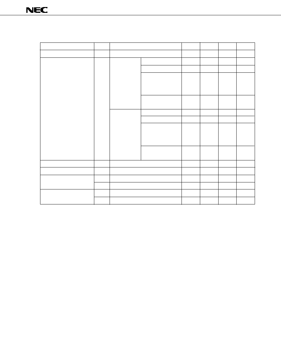
7 1
m
m
m
m
m
PD784020, 784021
D/A CONVERTER CHARACTERISTICS (T
A
= ≠40 to +85 ∞C, AV
REF2
= V
DD
= AV
DD
= 2.7 to 5.5 V, AV
REF3
= V
SS
= AV
SS
= 0 V)
Note
DACS0, DACS1 = 7FH
Parameter
Resolution
Total error
Note
Settling time
Output resistance
Analog reference voltage
Reference supply input
current
Symbol
R
O
AV
REF2
AV
REF3
AI
REF2
AI
REF3
Unit
bit
%
%
%
%
%
%
%
%
m
s
k
W
V
V
mA
mA
Typ.
20
Max.
0.4
0.6
0.6
0.8
0.6
0.8
0.8
1.0
10
V
DD
0.25V
DD
5
0
Conditions
Load condition:
V
DD
= 4.5 to 5.5 V
4 M
W
, 30 pF
V
DD
= 4.5 to 5.5 V
AV
REF2
= 0.75V
DD
AV
REF3
= 0.25V
DD
AV
REF2
= 0.75V
DD
AV
REF3
= 0.25V
DD
Load condition:
V
DD
= 4.5 to 5.5 V
2 M
W
, 30 pF
V
DD
= 4.5 to 5.5 V
AV
REF2
= 0.75V
DD
AV
REF3
= 0.25V
DD
AV
REF2
= 0.75V
DD
AV
REF3
= 0.25V
DD
Load condition: 2 M
W
, 30 pF
Note
Min.
8
0.75V
DD
0
0
≠5

7 2
m
m
m
m
m
PD784020, 784021
DATA RETENTION CHARACTERISTICS (T
A
= ≠40 to +85 ∞C)
Notes 1. When the input voltage for the pins described in Note 2 satisfies the V
IL
and V
IH
conditions in the above
table
2. Pins RESET, P20/NMI, P21/INTP0, P22/INTP1, P23/INTP2/CI, P24/INTP3, P25/INTP4/ASCK/SCK1,
P26/INTP5, P27/SI0, P32/SCK0, and P33/SO0/SB0
AC Timing Test Points
Parameter
Data retention voltage
Data retention current
V
DD
rising time
V
DD
falling time
V
DD
retention time
(referred to STOP mode setting)
STOP release signal input time
Oscillation settling time
Low-level input voltage
High-level input voltage
Symbol
V
DDDR
I
DDDR
t
RVD
t
FVD
t
HVD
t
DREL
t
WAIT
V
IL
V
IH
Unit
V
m
A
m
A
m
s
m
s
ms
ms
ms
ms
V
V
Min.
2.5
200
200
0
0
30
5
0
0.9V
DDDR
Typ.
10
2
Max.
5.5
50
10
0.1V
DDDR
V
DDDR
Conditions
STOP mode
V
DDDR
= 2.5 to 5.5 V
Note 1
V
DDDR
= 2.5 V
Note 1
Crystal
Ceramic resonator
Specified pins
Note 2
V
DD
≠ 1 V
0.45 V
0.8V
DD
or 2.2 V
0.8 V
Test points
0.8V
DD
or 2.2 V
0.8 V
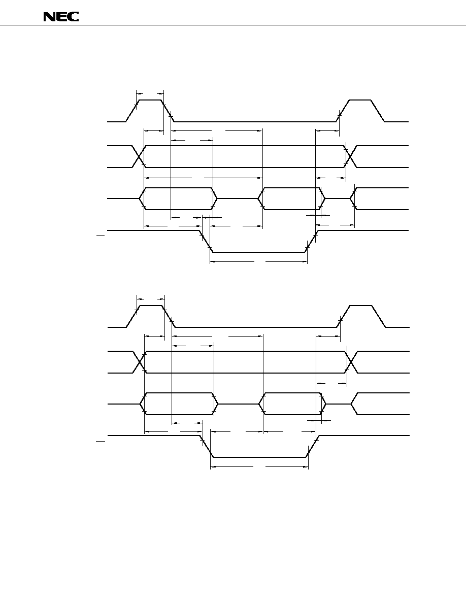
7 3
m
m
m
m
m
PD784020, 784021
Timing Waveform
(1) Read operation
(2) Write operation
t
WSTH
t
DSTID
t
HSTLA
t
SAST
ASTB
A8-A19
AD0-AD7
RD
t
DAID
t
DSTR
t
FRA
t
DAR
t
DRID
t
WRL
t
DRST
t
HRA
t
HRID
t
DRA
ASTB
A8-A19
AD0-AD7
WR
t
WSTH
t
DSTOD
t
HSTLA
t
SAST
t
DSTW
t
DAW
t
DWOD
t
WWL
t
DWST
t
HWA
t
HWOD
t
DSODW

7 4
m
m
m
m
m
PD784020, 784021
Hold Timing
External WAIT Signal Input Timing
(1) Read operation
(2) Write operation
ASTB, A8-A19,
AD0-AD7, RD, WR
HLDRQ
HLDAK
t
FHQC
t
DCFHA
t
DHQHHAH
t
DHQLHAL
t
DHAC
ASTB
A8-A19
AD0-AD7
RD
WAIT
t
DSTWTH
t
HSTWTH
t
DSTWT
t
DAWT
t
DWTID
t
DWTR
t
DRWTL
t
HRWT
t
DRWTH
t
DSTWTH
t
HSTWTH
t
DSTWT
t
DAWT
t
DWTW
t
DWWTL
t
HWWT
t
DWWTH
ASTB
A8-A19
AD0-AD7
WR
WAIT

7 5
m
m
m
m
m
PD784020, 784021
Timing Waveform for Refresh
(1) Random read/write cycle
(2) When a refresh is performed simultaneously with a memory access
(3) Refresh after reading
(4) Refresh after writing
ASTB
WR
RD
t
RC
t
RC
t
RC
t
RC
t
RC
ASTB
RD, WR
REFRQ
t
DSTRFQ
t
WRFQL
t
WRFQH
t
DRFQST
ASTB
RD
REFRQ
t
DRFQST
t
DRRFQ
t
WRFQL
t
DRFQST
t
DWRFQ
t
WRFQL
ASTB
WR
REFRQ
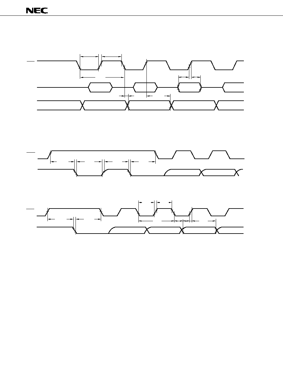
7 6
m
m
m
m
m
PD784020, 784021
Serial Operation (CSI)
(1) Three-wire serial I/O mode
(2) SBI mode
ð
Bus release signal transfer
ð
Command signal transfer
SCK
SI
SO
t
WSKL0
t
WSKH0
t
SSSK0
t
HSSK0
t
DSBSK1
Input data
Output data
t
HSBSK1
t
CYSK0
SCK
SB0
t
HSBSK2
t
WSBL
t
WSBH
t
SSBSK
SCK
SB0
t
HSBSK1
t
SSSK0
Input/Output data
t
HSBSK2
t
SSBSK
t
WSKL0
t
WSKH0
t
CYSK0
t
HSSK0
t
DSBSK2

7 7
m
m
m
m
m
PD784020, 784021
Serial Operation (IOE1, IOE2)
Serial Operation (UART, UART2)
SCK
SI
SO
Input data
Output data
t
WSKL1
t
WSKH1
t
DSOSK
t
SSSK1
t
HSSK1
t
HSOSK
t
CYSK1
ASCK,
ASCK2
t
WASKH
t
WASKL
0.8V
DD
0.8 V
t
CYASK

7 8
m
m
m
m
m
PD784020, 784021
Interrupt Input Timing
Reset Input Timing
NMI
INTP0
CI,
INTP1-INTP3
INTP4, INTP5
t
WNIH
t
WNIL
0.8V
DD
0.8 V
t
WIT0H
t
WIT0L
0.8V
DD
0.8 V
t
WIT1H
t
WIT1L
0.8V
DD
0.8 V
t
WIT2H
t
WIT2L
0.8V
DD
0.8 V
RESET
t
WRSH
t
WRSL
0.8V
DD
0.8 V
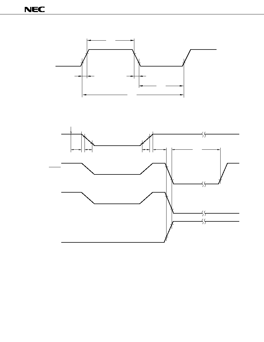
7 9
m
m
m
m
m
PD784020, 784021
External Clock Timing
Data Retention Timing
X1
0.8V
DD
0.8 V
t
XF
t
XR
t
WXL
t
CYX
t
WXH
V
DD
t
HVD
t
FVD
Set STOP mode.
V
DDDR
t
RVD
t
DREL
0.8V
DD
0.8 V
0.8V
DD
0.8 V
0.8V
DD
0.8 V
RESET
NMI
(Released by a falling edge)
NMI
(Released by a rising edge)
t
WAIT

8 0
m
m
m
m
m
PD784020, 784021
15. PACKAGE DRAWINGS
Remark The shape and material of the ES version are the same as those of the corresponding mass-produced
products.
80 PIN PLASTIC QFP (14
◊
14)
ITEM
MILLIMETERS
INCHES
NOTE
Each lead centerline is located within 0.13 mm (0.005 inch) of
its true position (T.P.) at maximum material condition.
L
0.8±0.2
0.031+0.009
≠0.008
M
0.15
0.006
N
0.10
0.004
P
2.7
0.106
A
17.2±0.4
0.677±0.016
B
14.0±0.2
0.551+0.009
≠0.008
C
14.0±0.2
0.551+0.009
≠0.008
D
17.2±0.4
0.677±0.016
F
0.825
0.032
G
0.825
0.032
H
0.30±0.10
0.012+0.004
≠0.005
I
0.13
0.005
J
0.65 (T.P.)
0.026 (T.P.)
Q
0.1±0.1
0.004±0.004
R
5
∞
±5
∞
5
∞
±5
∞
+0.10
≠0.05
+0.004
≠0.003
M
M
L
K
J
H
Q
P
N
R
detail of lead end
I
G
K
1.6±0.2
0.063±0.008
60
61
40
80
1
21
20
41
A
B
C D
F
S
S80GC-65-3B9-4
S
3.0 MAX.
0.119 MAX.
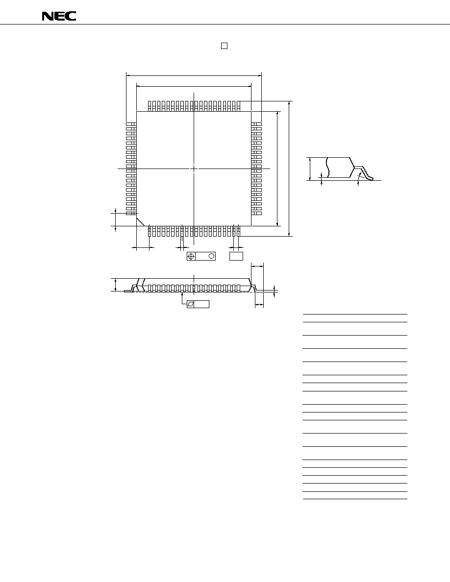
8 1
m
m
m
m
m
PD784020, 784021
80 PIN PLASTIC TQFP (FINE PITCH) ( 12)
ITEM
MILLIMETERS
INCHES
I
J
0.5 (T.P.)
0.10
0.004
0.020 (T.P.)
A
NOTE
Each lead centerline is located within 0.10 mm (0.004 inch) of
its true position (T.P.) at maximum material condition.
S
A
14.0±0.2
0.551+0.009
≠0.008
B
12.0±0.2
0.472+0.009
≠0.008
C
12.0±0.2
0.472+0.009
≠0.008
D
14.0±0.2
0.551+0.009
≠0.008
F
G
1.25
1.25
0.049
0.049
H
0.22
0.009±0.002
P80GK-50-BE9-4
S
1.27 MAX.
0.050 MAX.
K
1.0±0.2
0.039+0.009
≠0.008
L
0.5±0.2
0.020+0.008
≠0.009
M
0.145
0.006±0.002
N
0.10
0.004
P
1.05
0.041
Q
0.05±0.05
0.002±0.002
R
5∞±5∞
5∞±5∞
+0.05
≠0.04
+0.055
≠0.045
B
C
D
J
H
I
G
F
P
N
L
K
M
Q
R
detail of lead end
M
61
60
41
40
21
20
1
80
Remark The shape and material of the ES version are the same as those of the corresponding mass-produced
products.
H

8 2
m
m
m
m
m
PD784020, 784021
16. RECOMMENDED SOLDERING CONDITIONS
The conditions listed below shall be met when soldering the
m
PD784021.
For details of the recommended soldering conditions, refer to our document
SMD Surface Mount Technology
Manual (C10535E).
Please consult with our sales offices in case any other soldering process is used, or in case soldering is done under
different conditions.
Table 16-1 Soldering Conditions for Surface-Mount Devices
(1)
m
m
m
m
m
PD784020GC-3B9 : 80-pin plastic QFP (14
•
14 mm)
m
m
m
m
m
PD784021GC-3B9 : 80-pin plastic QFP (14
•
•
•
•
•
14 mm)
(2)
m
m
m
m
m
PD784021GK-BE9: 80-pin plastic TQFP (fine pitch) (12
•
12 mm)
Note
Exposure limit before soldering after dry-pack package is opened.
Storage conditions: Temperature of 25 ΩC and maximum relative humidity at 65 % or less
Caution Do not apply more than a single process at once, except for "Partial heating method."
H
Soldering conditions
Peak package's surface temperature: 235 ΩC
Reflow time: 30 seconds or less (at 210 ΩC or more)
Maximum allowable number of reflow processes: 3
Peak package's surface temperature: 215 ΩC
Reflow time: 40 seconds or less (at 210 ΩC or more)
Maximum allowable number of reflow processes: 3
Solder temperature: 260 ΩC or less
Flow time: 10 seconds or less
Number of flow process: 1
Preheating temperature: 120 ΩC max. (measured on the package
surface)
Terminal temperature: 300 ΩC or less
Flow time: 3 seconds or less (for each side of device)
Symbol
IR35-00-3
VP15-00-3
WS60-00-1
≠
Soldering process
Infrared ray reflow
VPS
Wave soldering
Partial heating method
Soldering conditions
Peak package's surface temperature: 235 ΩC
Reflow time: 30 seconds or less (at 210 ΩC or more)
Maximum allowable number of reflow processes: 2
Exposure limit
Note
:
7 days (10 hours of pre-baking is required at
125 ΩC afterward.)
<Cautions>
Non-heat resistant trays, such as magazine and taping trays, cannot
be baked before unpacking.
Peak package's surface temperature: 215 ΩC
Reflow time: 40 seconds or less (at 200 ΩC or more)
Maximum allowable number of reflow processes: 2
Exposure limit
Note
:
7 days (10 hours of pre-baking is required at
125 ΩC afterward.)
<Cautions>
Non-heat resistant trays, such as magazine and taping trays, cannot
be baked before unpacking.
Terminal temperature: 300 ΩC or less
Flow time: 3 seconds or less (for each side of device)
Symbol
IR35-107-2
VP15-107-2
≠
Soldering process
Infrared ray reflow
VPS
Partial heating method
8 3
m
m
m
m
m
PD784020, 784021
APPENDIX A DEVELOPMENT TOOLS
The following development tools are available for system development using the
m
PD784021.
Language Processing Software
RA78K4
Note 1
Assembler package for all 78K/IV series models
CC78K4
Note 1
C compiler package for all 78K/IV series models
CC78K4-L
Note 1
C compiler library source file for all 78K/IV series models
PROM Write Tools
PG-1500
PROM programmer
PA-78P4026GC
Programmer adaptor, connects to PG-1500
PA-78P4038GK
PA-78P4026KK
PG-1500 controller
Note 2
Control program for PG-1500
Debugging Tools
IE-784000-R
In-circuit emulator for all
m
PD784026 sub-series models
IE-784000-R-BK
Break board for all 78K/IV series models
IE-784026-R-EM1
Emulation board for evaluating
m
PD784026 sub-series models
IE-784000-R-EM
IE-70000-98-IF-B
Interface adapter when the PC-9800 series computer (other than a notebook)
is used as the host machine
IE-70000-98N-IF
Interface adapter and cable when a PC-9800 series notebook is used as the
host machine
IE-70000-PC-IF-B
Interface adapter when the IBM PC/AT
TM
is used as the host machine
IE-78000-R-SV3
Interface adapter and cable when the EWS is used as the host machine
EP-78230GC-R
Emulation probe for 80-pin plastic QFP (14
•
14 mm) for all
m
PD784026
sub-series
EP-78054GK-R
Emulation probe for 80-pin plastic TQFP (fine pitch) (12
•
12 mm) for all
m
PD784021
EV-9200GC-80
Socket for mounting on target system board made for 80-pin plastic QFP
(14
•
14 mm)
EV-9500GK-80
Adapter for mounting on target system board made for 80-pin plastic TQFP
(fine pitch) (12
•
12 mm)
EV-9900
Tool used to remove the
m
PD78P4026KK-T from the EV-9200GC-80
SM78K4
Note 3
System simulator for all 78K/IV series models
ID78K4
Note 3
Integrated debugger for IE-784000-R
DF784026
Note 4
Device file for all
m
PD784026 sub-series models
Real-time OS
RX78K/IV
Note 4
Real-time OS for 78K/IV series models
MX78K4
Note 2
OS for all 78K/IV series models
Remark The RA78K4, CC78K4, SM78K4, and ID78K4 are used with the DF784026.

8 4
m
m
m
m
m
PD784020, 784021
Notes 1.
∑
Based on PC-9800 series (MS-DOS
TM
)
∑
Based on IBM PC/AT and compatibles (PC DOS
TM
, Windows
TM
, MS-DOS, and IBM DOS
TM
)
∑
Based on HP9000 series 700
TM
(HP-UX
TM
)
∑
Based on SPARCstation
TM
(SunOS
TM
)
∑
Based on NEWS
TM
(NEWS-OS
TM
)
2.
∑
Based on PC-9800 series (MS-DOS)
∑
Based on IBM PC/AT and compatibles (PC DOS, Windows, MS-DOS, and IBM DOS)
3.
∑
Based on PC-9800 series (MS-DOS + Windows)
∑
Based on IBM PC/AT and compatibles (PC DOS, Windows, MS-DOS, and IBM DOS)
∑
Based on HP9000 series 700 (HP-UX)
∑
Based on SPARCstation (SunOS)
4.
∑
Based on PC-9800 series (MS-DOS)
∑
Based on IBM PC/AT and compatibles (PC DOS, Windows, MS-DOS, and IBM DOS)
∑
Based on HP9000 series 700 (HP-UX)
∑
Based on SPARCstation (SunOS)

8 5
m
m
m
m
m
PD784020, 784021
APPENDIX B RELATED DOCUMENTS
Documents Related to Devices
Document name
Document No.
Japanese
English
m
PD784020, 784021 Data Sheet
U11514J
This manual
m
PD784025, 784026 Data Sheet
To be released soon
IP-3230
m
PD78P4026 Data Sheet
To be released soon
IP3231
m
PD784026 Sub-Series User's Manual, Hardware
U10898J
U10898E
m
PD784026 Sub-Series Special Function Registers
U10593J
--
m
PD784026 Sub-Series Application Note, Hardware Basic
U10573J
--
78K/IV Series User's Manual, Instruction
U10905J
IEU-1386
78K/IV Series Instruction Summary Sheet
U10594J
--
78K/IV Series Instruction Set
U10595J
--
78K/IV Series Application Note, Software Basic
U10095J
--
Documents Related to Development Tools (User's Manual)
Document name
Document No.
Japanese
English
RA78K Series Assembler Package
Operation
EEU-809
EEU-1399
Language
EEU-815
EEU-1404
RA78K Series Structured Assembler Preprocessor
EEU-817
EEU-1402
CC78K Series C Compiler
Operation
EEU-656
EEU-1280
Language
EEU-655
EEU-1284
CC78K Series Library Source File
EEU-777
--
PG-1500 PROM Programmer
EEU-651
EEU-1335
PG-1500 Controller PC-9800 Series (MS-DOS) Base
EEU-704
EEU-1291
PG-1500 Controller IBM PC Series (PC DOS) Base
EEU-5008
U10540E
IE-784000-R
EEU-5004
EEU-1534
IE-784026-R-EM1
EEU-5017
EEU-1528
EP-78230
EEU-985
EEU-1515
EP-78054GK-R
EEU-932
EEU-1468
SM78K4 System Simulator Windows Base
Reference
U10093J
U10093E
SM78K Series System Simulator
External Parts User Open
U10092J
U10092E
Interface Specifications
ID78K4 Integrated Debugger
Reference
U10440J
U10440E
Caution The above documents may be revised without notice. Use the latest versions when you design
application systems.

8 6
m
m
m
m
m
PD784020, 784021
Documents Related to Software to Be Incorporated into the Product (User's Manual)
Document name
Document No.
Japanese
English
78K/IV Series Real-Time OS
Basic
U10603J
--
Installation
U10604J
--
Debugger
U10364J
--
OS for 78K/IV Series MX78K4
To be created
--
Other Documents
Document name
Document No.
Japanese
English
IC PACKAGE MANUAL
C10943X
SMD Surface Mount Technology Manual
C10535J
C10535E
Quality Grades on NEC Semiconductor Device
IEI-620
IEI-1209
NEC Semiconductor Device Reliability/Quality Control System
C10983J
C10983E
Electrostatic Discharge (ESD) Test
MEM-539
--
Guide to Quality Assurance for Semiconductor Device
MEI-603
MEI-1202
Guide for Products Related to Micro-Computer: Other Companies
MEI-604
--
Caution The above documents may be revised without notice. Use the latest versions when you design
application systems.

8 7
m
m
m
m
m
PD784020, 784021
[MEMO]
8 8
m
m
m
m
m
PD784020, 784021
MS-DOS and Windows are trademarks of Microsoft Corporation.
IBM DOS, PC/AT, and PC DOS are trademarks of IBM Corporation.
HP9000 series 700 and HP-UX are trademarks of Hewlett-Packard Company.
SPARCstation is a trademark of SPARC International, Inc.
SunOS is a trademark of Sun Microsystems, Inc.
NEWS and NEWS-OS are trademarks of SONY Corporation.
Cautions on CMOS Devices
Countermeasures against static electricity for all MOSs
Caution When handling MOS devices, take care so that they are not electrostatically charged.
Strong static electricity may cause dielectric breakdown in gates. When transporting or storing
MOS devices, use conductive trays, magazine cases, shock absorbers, or metal cases that NEC
uses for packaging and shipping. Be sure to ground MOS devices during assembling. Do not
allow MOS devices to stand on plastic plates or do not touch pins.
Also handle boards on which MOS devices are mounted in the same way.
CMOS-specific handling of unused input pins
Caution Hold CMOS devices at a fixed input level.
Unlike bipolar or NMOS devices, if a CMOS device is operated with no input, an intermediate-
level input may be caused by noise. This allows current to flow in the CMOS device, resulting
in a malfunction. Use a pull-up or pull-down resistor to hold a fixed input level. Since unused
pins may function as output pins at unexpected times, each unused pin should be separately
connected to the V
DD
or GND pin through a resistor.
If handling of unused pins is documented, follow the instructions in the document.
Statuses of all MOS devices at initialization
Caution The initial status of a MOS device is unpredictable when power is turned on.
Since characteristics of a MOS device are determined by the amount of ions implanted in
molecules, the initial status cannot be determined in the manufacture process. NEC has no
responsibility for the output statuses of pins, input and output settings, and the contents of
registers at power on. However, NEC assures operation after reset and items for mode setting
if they are defined.
When you turn on a device having a reset function, be sure to reset the device first.

8 9
m
m
m
m
m
PD784020, 784021
NEC Electronics Inc. (U.S.)
Mountain View, California
Tel: 800-366-9782
Fax: 800-729-9288
NEC Electronics (Germany) GmbH
Duesseldorf, Germany
Tel: 0211-65 03 02
Fax: 0211-65 03 490
NEC Electronics (UK) Ltd.
Milton Keynes, UK
Tel: 01908-691-133
Fax: 01908-670-290
NEC Electronics Italiana s.r.1.
Milano, Italy
Tel: 02-66 75 41
Fax: 02-66 75 42 99
NEC Electronics Hong Kong Ltd.
Hong Kong
Tel: 2886-9318
Fax: 2886-9022/9044
NEC Electronics Hong Kong Ltd.
Seoul Branch
Seoul, Korea
Tel: 02-528-0303
Fax: 02-528-4411
NEC Electronics Singapore Pte. Ltd.
United Square, Singapore 1130
Tel: 253-8311
Fax: 250-3583
NEC Electronics Taiwan Ltd.
Taipei, Taiwan
Tel: 02-719-2377
Fax: 02-719-5951
NEC do Brasil S.A.
Sao Paulo-SP, Brasil
Tel: 011-889-1680
Fax: 011-889-1689
NEC Electronics (Germany) GmbH
Benelux Office
Eindhoven, The Netherlands
Tel: 040-2445845
Fax: 040-2444580
NEC Electronics (France) S.A.
France
Tel: 01-30-67 58 00
Fax: 01-30-67 58 99
NEC Electronics (France) S.A.
Spain Office
Madrid, Spain
Tel: 01-504-2787
Fax: 01-504-2860
NEC Electronics (Germany) GmbH
Scandinavia Office
Taeby Sweden
Tel: 8-63 80 820
Fax: 8-63 80 388
Regional Information
Some information contained in this document may vary from country to country. Before using any NEC
product in your application, please contact the NEC office in your country to obtain a list of authorized
representatives and distributors. They will verify:
∑ Device availability
∑ Ordering information
∑ Product release schedule
∑ Availability of related technical literature
∑ Development environment specifications (for example, specifications for third-party tools and
components, host computers, power plugs, AC supply voltages, and so forth)
∑ Network requirements
In addition, trademarks, registered trademarks, export restrictions, and other legal issues may also vary
from country to country.
J96. 3

9 0
m
m
m
m
m
PD784020, 784021
Some related documents may be preliminary versions. Note that, however, what documents are preliminary is not indicated
in this document.
No part of this document may be copied or reproduced in any form or by any means without the prior written
consent of NEC Corporation. NEC Corporation assumes no responsibility for any errors which may appear in this
document.
NEC Corporation does not assume any liability for infringement of patents, copyrights or other intellectual
property rights of third parties by or arising from use of a device described herein or any other liability arising
from use of such device. No license, either express, implied or otherwise, is granted under any patents,
copyrights or other intellectual property rights of NEC Corporation or others.
While NEC Corporation has been making continuous effort to enhance the reliability of its semiconductor devices,
the possibility of defects cannot be eliminated entirely. To minimize risks of damage or injury to persons or
property arising from a defect in an NEC semiconductor device, customer must incorporate sufficient safety
measures in its design, such as redundancy, fire-containment, and anti-failure features.
NEC devices are classified into the following three quality grades:
"Standard", "Special", and "Specific". The Specific quality grade applies only to devices developed based on
a customer designated "quality assurance program" for a specific application. The recommended applications
of a device depend on its quality grade, as indicated below. Customers must check the quality grade of each
device before using it in a particular application.
Standard: Computers, office equipment, communications equipment, test and measurement equipment,
audio and visual equipment, home electronic appliances, machine tools, personal electronic
equipment and industrial robots
Special: Transportation equipment (automobiles, trains, ships, etc.), traffic control systems, anti-disaster
systems, anti-crime systems, safety equipment and medical equipment (not specifically designed
for life support)
Specific: Aircrafts, aerospace equipment, submersible repeaters, nuclear reactor control systems, life
support systems or medical equipment for life support, etc.
The quality grade of NEC devices in "Standard" unless otherwise specified in NEC's Data Sheets or Data Books.
If customers intend to use NEC devices for applications other than those specified for Standard quality grade,
they should contact NEC Sales Representative in advance.
Anti-radioactive design is not implemented in this product.
M4 94. 11