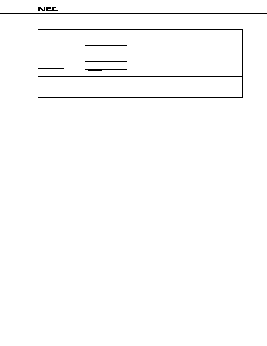
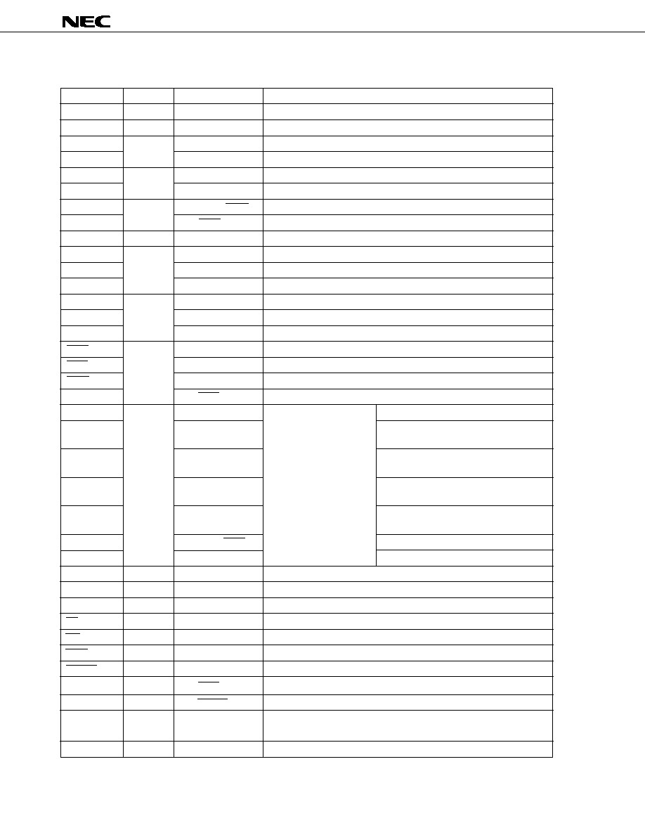
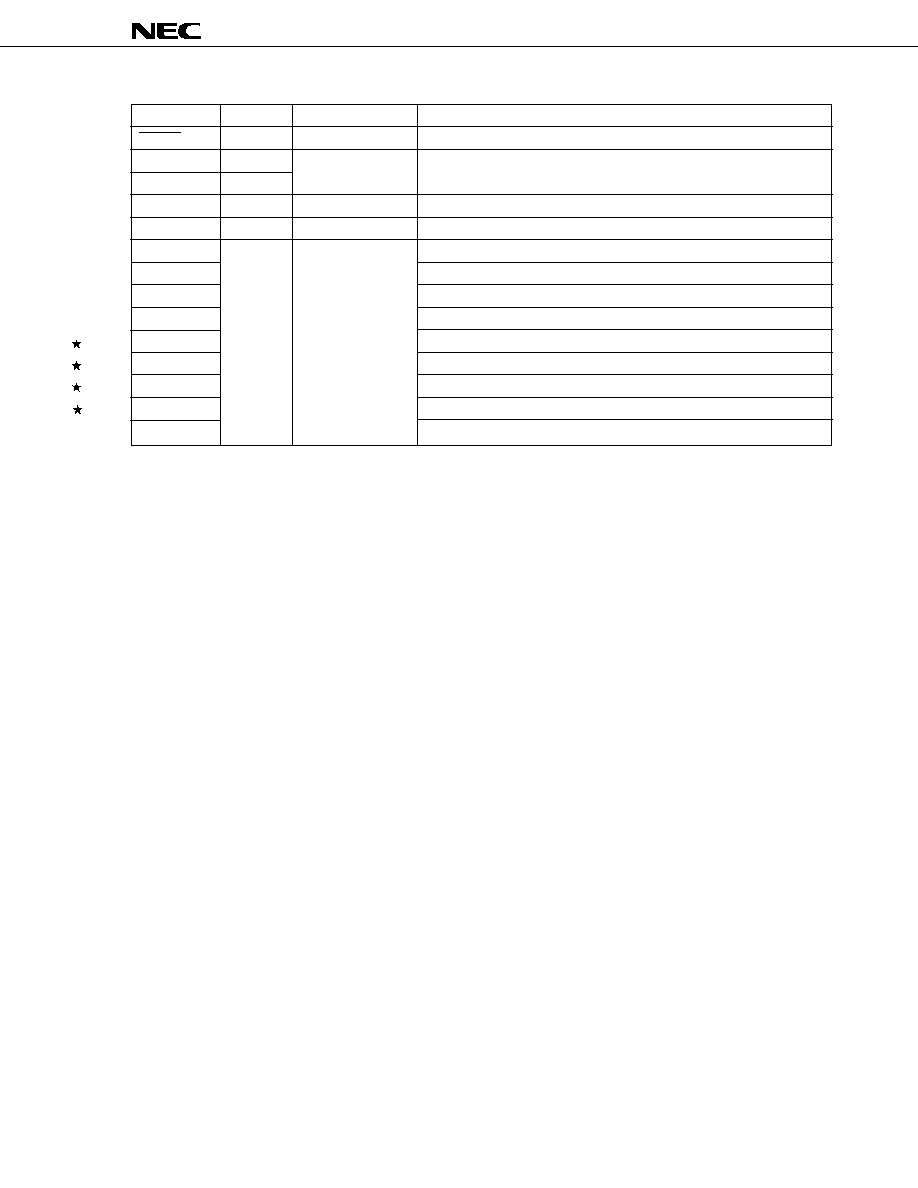
Document Outline
- COVER
- DESCRIPTION
- FEATURES
- APPLICATION FIELDS
- ORDERING INFORMATION
- 78K/IV Series Product Development
- FUNCTIONS
- 1. DIFFERENCES AMONG MODELS IN uPD784038Y SUBSERIES
- 2. MAJOR DIFFERENCES FROM uPD784026 SUBSERIES AND uPD78234 SUBSERIES
- 3. PIN CONFIGURATION (Top View)
- 4. BLOCK DIAGRAM
- 5. PIN FUNCTION
- 5.1 Port Pins
- 5.2 Non-Port Pins
- 5.3 Types of Pin I/O Circuits and Connections for Unused Pins
- 6. CPU ARCHITECTURE
- 6.1 Memory Space
- 6.2 CPU Registers
- 6.2.1 General-purpose registers
- 6.2.2 Control registers
- 6.2.3 Special function registers (SFRs)
- 7. PERIPHERAL HARDWARE FUNCTIONS
- 7.1 Ports
- 7.2 Clock Generation Circuit
- 7.3 Real-Time Output Port
- 7.4 Timer/Counter
- 7.5 PWM Output (PWM0, PWM1)
- 7.6 A/D Converter
- 7.7 D/A Converter
- 7.8 Serial Interface
- 7.8.1 Asynchronous serial interface/3-wire serial I/O (UART/IOE)
- 7.8.2 Clocked serial interface (CSI)
- 7.9 Clock Output Function
- 7.10 Edge Detection Function
- 7.11 Watchdog Timer
- 8. INTERRUPT FUNCTION
- 8.1 Interrupt Sources
- 8.2 Vectored Interrupt
- 8.3 Context Switching
- 8.4 Macro Service
- 8.5 Application Example of Macro Service
- 9. LOCAL BUS INTERFACE
- 9.1 Memory Expansion
- 9.2 Memory Space
- 9.3 Programmable Wait
- 9.4 Pseudo Static RAM Refresh Function
- 9.5 Bus Hold Function
- 10. STANDBY FUNCTION
- 11. RESET FUNCTION
- 12. INSTRUCTION SET
- 13. ELECTRICAL SPECIFICATIONS
- 14. PACKAGE DRAWINGS
- 15. RECOMMENDED SOLDERING CONDITIONS
- APPENDIX A DEVELOPMENT TOOLS
- APPENDIX B RELATED DOCUMENTS
©
1996
DATA SHEET
The mark
5
shows major revised points.
MOS INTEGRATED CIRCUIT
µ
PD784035Y,784036Y,784037Y,784038Y
16-/8-BIT SINGLE-CHIP MICROCONTROLLERS
DESCRIPTION
The
µ
PD784038Y is based on the
µ
PD784038 with an I
2
C bus control function added, and is ideal for audio-visual
applications.
One-time PROM and EPROM versions, such as the
µ
PD78P4038Y, that can operate in the same voltage range
as mask ROM versions, and various development tools are provided.
The functions are explained in detail in the following User's Manual. Be sure to read this manual when designing
your system.
µ
PD784038, 784038Y Subseries User's Manual - Hardware: U11316E
78K/IV Series User's Manual - Instruction:
U10905E
Document No. U10741EJ1V0DS00 (1st edition)
Date Published July 1997 N
Printed in Japan
FEATURES
78K/IV Series
Pin-compatible with
µ
PD78234 Subseries,
µ
PD784026 Subseries, and
µ
PD784038
Subseries
Higher internal memory capacity than
µ
PD78234
Subseries and
µ
PD784026 Subseries
Minimum instruction execution time: 125 ns
(@ 32-MHz operation)
I/O ports: 64
Serial interface: 3 channels
UART/IOE (3-wire serial I/O): 2 channels
CSI (3-wire serial I/O, 2-wire serial I/O, I
2
C bus):
1 channel
Timer/counter 16-bit timer/counter
◊
3 units 16-bit
timer
◊
1 unit
PWM output: 2 outputs
Standby function
HALT/STOP/IDLE mode
Clock division function
Watchdog timer: 1 channel
Clock output function
Selectable from f
CLK
, f
CLK
/2, f
CLK
/4, f
CLK
/8, and
f
CLK
/16
A/D converter: 8-bit resolution
◊
8 channels
D/A converter: 8-bit resolution
◊
2 channels
Supply voltage: V
DD
= 2.7 to 5.5 V
APPLICATION FIELDS
Cellular phones, cordless phones, audio-visual systems, etc.
Unless contextually excluded, references in this document to the
µ
PD784038Y mean
µ
PD784035Y,
µ
PD784036Y,
and
µ
PD784037Y.
The information in this document is subject to change without notice.

µ
PD784035Y, 784036Y, 784037Y, 784038Y
2
ORDERING INFORMATION
Part Number
Package
Internal ROM (Bytes) Internal RAM (Bytes)
µ
PD784035YGC-
◊◊◊
-3B9
80-pin plastic QFP (14
◊
14 mm, 2.7-mm thick)
48 K
2048
µ
PD784035YGC-
◊◊◊
-8BT
80-pin plastic QFP (14
◊
14 mm, 1.4-mm thick)
48 K
2048
µ
PD784035YGK-
◊◊◊
-BE9
Note
80-pin plastic TQFP (fine pitch) (12
◊
12 mm)
48 K
2048
µ
PD784036YGC-
◊◊◊
-3B9
80-pin plastic QFP (14
◊
14 mm, 2.7-mm thick)
64 K
2048
µ
PD784036YGC-
◊◊◊
-8BT
80-pin plastic QFP (14
◊
14 mm, 1.4-mm thick)
64 K
2048
µ
PD784036YGK-
◊◊◊
-BE9
Note
80-pin plastic TQFP (fine pitch) (12
◊
12 mm)
64 K
2048
µ
PD784037YGC-
◊◊◊
-3B9
80-pin plastic QFP (14
◊
14 mm, 2.7-mm thick)
96 K
3584
µ
PD784037YGC-
◊◊◊
-8BT
80-pin plastic QFP (14
◊
14 mm, 1.4-mm thick)
96 K
3584
µ
PD784037YGK-
◊◊◊
-BE9
80-pin plastic TQFP (fine pitch) (12
◊
12 mm)
96 K
3584
µ
PD784038YGC-
◊◊◊
-3B9
80-pin plastic QFP (14
◊
14 mm, 2.7-mm thick)
128 K
4352
µ
PD784038YGC-
◊◊◊
-8BT
80-pin plastic QFP (14
◊
14 mm, 1.4-mm thick)
128 K
4352
µ
PD784038YGK-
◊◊◊
-BE9
80-pin plastic TQFP (fine pitch) (12
◊
12 mm)
128 K
4352
Note
Under development
Remark
◊◊◊
indicates the ROM code suffix.
3
µ
PD784035Y, 784036Y, 784037Y, 784038Y
78K/IV Series Product Development
PD784026
PD784908
PD78F4943
PD784915
PD784928
PD784928Y
PD784046
PD784054
PD784216
PD784216Y
PD784038
PD784038Y
PD784225Y
PD784225
PD784218Y
PD784218
A/D, 16-bit timer,
enhanced power
management
Enhanced internal memory capacity
Pin-compatible with the PD784026
I
2
C bus supported
Multi-master I
2
C bus supported
80-pin, ROM collection added
Multi-master I
2
C bus supported
Enhanced internal memory
capacity, ROM collection added
100-pin, enhanced I/O and
internal memory capacity
On-chip 10-bit A/D
On-chip IEBus
TM
controller
56-Kbyte flash memory
for CD-ROM
Software servo control
On-chip analog circuit for VCRs
Enhanced timer
Multi-master I
2
C bus supported
Enhanced functions
of the PD784915
Standard models
ASSP models
Multi-master I
2
C bus supported
: Under mass production
: Under development
µ
µ
µ
µ
µ
µ
µ
µ
µ
µ
µ
µ
µ
µ
µ
µ
µ
µ
µ
PD784035Y, 784036Y, 784037Y, 784038Y
4
FUNCTIONS
Part Number
µ
PD784035Y
µ
PD784036Y
µ
PD784037Y
µ
PD784038Y
Item
Number of basic instructions
113
(mnemonics)
General-purpose register
8 bits
◊
16 registers
◊
8 banks, or 16 bits
◊
8 registers
◊
8 banks (memory mapping)
Minimum instruction execution
125 ns/250 ns/500 ns/1000 ns (@ 32-MHz operation)
time
Internal memory
ROM
48 KBytes
64 KBytes
96 KBytes
128 KBytes
RAM
2048 Bytes
3584 Bytes
4352 Bytes
Memory space
1 MByte with program and data spaces combined
I/O port
Total
64
Input
8
I/O
56
Pins with pull-
54
up resistor
LEDs direct
24
drive output
Transistor
8
direct drive
Real-time output port
4 bits
◊
2 or 8 bits
◊
1
Timer/counter
Timer/counter 0: Timer register
◊
1
Pulse output
(16 bits)
Capture register
◊
1
∑ Toggle output
Compare register
◊
2
∑ PWM/PPG output
∑ One-shot pulse output
Timer/counter 1: Timer register
◊
1
Pulse output
(8/16 bits)
Capture register
◊
1
∑ Real-time output (4 bits
◊
2)
Capture/compare register
◊
1
Compare register
◊
1
Timer/counter 2: Timer register
◊
1
Pulse output
(8/16 bits)
Capture register
◊
1
∑ Toggle output
Capture/compare register
◊
1
∑ PWM/PPG output
Compare register
◊
1
Timer 3:
Timer register
◊
1
(8/16 bits)
Compare register
◊
1
PWM output
12-bit resolution
◊
2 channels
Serial interface
UART/IOE (3-wire serial I/O)
: 2 channels (on-chip baud rate generator)
CSI (3-wire serial I/O, 2-wire serial I/O, I
2
C bus) : 1 channel
A/D converter
8-bit resolution
◊
8 channels
D/A converter
8-bit resolution
◊
2 channels
Clock output
Selectable from f
CLK
, f
CLK
/2, f
CLK
/4, f
CLK
/8, f
CLK
/16 (can also be used as 1-bit output port)
Watchdog timer
1 channel
Standby
HALT/STOP/IDLE mode
Interrupt
Hardware source
24 (internal: 17, external: 7 (variable sampling clock input: 1))
Software source
BRK instruction, BRKCS instruction, operand error
Non-maskable Internal: 1, external: 1
Maskable
Internal: 16, external: 6
∑ 4 programmable priority levels
∑ 3 processing styles: vectored interrupt/macro service/context switching
Supply voltage
V
DD
= 2.7 to 5.5 V
Package
80-pin plastic QFP (14
◊
14 mm, 2.7-mm thick)
80-pin plastic QFP (14
◊
14 mm, 1.4-mm thick)
80-pin plastic TQFP (fine pitch) (12
◊
12 mm)
Note The pins with ancillary function are included in the I/O pins.
Pins with
ancillary
function
Note

5
µ
PD784035Y, 784036Y, 784037Y, 784038Y
CONTENTS
1.
DIFFERENCES AMONG MODELS IN
µ
PD784038Y SUBSERIES ............................................. 7
2.
MAJOR DIFFERENCES FROM
µ
PD784026 SUBSERIES AND
µ
PD78234 SUBSERIES ........ 8
3.
PIN CONFIGURATION (TOP VIEW) ............................................................................................. 9
4.
BLOCK DIAGRAM ......................................................................................................................... 11
5.
PIN FUNCTION ............................................................................................................................... 12
5.1
Port Pins ................................................................................................................................................ 12
5.2
Non-Port Pins ....................................................................................................................................... 14
5.3
Types of Pin I/O Circuits and Connections for Unused Pins ........................................................ 16
6.
CPU ARCHITECTURE ................................................................................................................... 19
6.1
Memory Space ...................................................................................................................................... 19
6.2
CPU Registers ...................................................................................................................................... 24
6.2.1
General-purpose registers ........................................................................................................ 24
6.2.2
Control registers ........................................................................................................................ 25
6.2.3
Special function registers (SFRs) ............................................................................................. 26
7. PERIPHERAL HARDWARE FUNCTIONS ...................................................................................... 31
7.1
Ports ....................................................................................................................................................... 31
7.2
Clock Generation Circuit ..................................................................................................................... 32
7.3
Real-Time Output Port ......................................................................................................................... 34
7.4
Timer/Counter ....................................................................................................................................... 35
7.5
PWM Output (PWM0, PWM1) .............................................................................................................. 37
7.6
A/D Converter ....................................................................................................................................... 38
7.7
D/A Converter ....................................................................................................................................... 39
7.8
Serial Interface ..................................................................................................................................... 40
7.8.1
Asynchronous serial interface/3-wire serial I/O (UART/IOE) .................................................. 41
7.8.2
Clocked serial interface (CSI) .................................................................................................... 43
7.9
Clock Output Function ........................................................................................................................ 44
7.10 Edge Detection Function .................................................................................................................... 45
7.11 Watchdog Timer ................................................................................................................................... 45
8.
INTERRUPT FUNCTION ................................................................................................................ 46
8.1
Interrupt Sources ................................................................................................................................. 46
8.2
Vectored Interrupt ................................................................................................................................ 48
8.3
Context Switching ................................................................................................................................ 49
8.4
Macro Service ....................................................................................................................................... 49
8.5
Application Example of Macro Service ............................................................................................. 50

µ
PD784035Y, 784036Y, 784037Y, 784038Y
6
9.
LOCAL BUS INTERFACE ............................................................................................................. 52
9.1
Memory Expansion .............................................................................................................................. 52
9.2
Memory Space ...................................................................................................................................... 53
9.3
Programmable Wait ............................................................................................................................. 54
9.4
Pseudo Static RAM Refresh Function .............................................................................................. 54
9.5
Bus Hold Function ............................................................................................................................... 54
10. STANDBY FUNCTION ................................................................................................................... 55
11. RESET FUNCTION ......................................................................................................................... 56
12. INSTRUCTION SET ........................................................................................................................ 57
13. ELECTRICAL SPECIFICATIONS ................................................................................................. 62
14. PACKAGE DRAWINGS ................................................................................................................. 83
15. RECOMMENDED SOLDERING CONDITIONS ............................................................................ 86
APPENDIX A DEVELOPMENT TOOLS .............................................................................................. 88
APPENDIX B RELATED DOCUMENTS ............................................................................................. 90
5
5
7
µ
PD784035Y, 784036Y, 784037Y, 784038Y
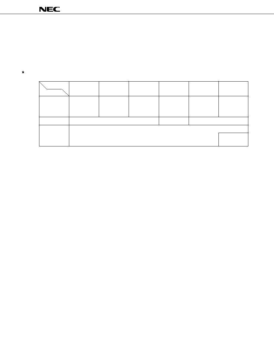
1. DIFFERENCES AMONG MODELS IN
µ
PD784038Y SUBSERIES
The only difference among the
µ
PD784035Y, 784036Y, 784037Y, and 784038Y lies in the internal memory
capacity.
The
µ
PD78P4038Y is provided with a 128-KB one-time PROM or EPROM instead of the mask ROM of the above
models. These differences are summarized in Table 1-1.
Table 1-1. Differences among Models in
µ
PD784038Y Subseries
Part Number
µ
PD784031Y
µ
PD784035Y
µ
PD784036Y
µ
PD784037Y
µ
PD784038Y
µ
PD78P4038Y
Item
Internal ROM
Not available
48 KBytes
64 KBytes
96 KBytes
128 KBytes
128 KBytes
(mask ROM)
(mask ROM)
(mask ROM)
(mask ROM)
(one-time PROM
or EPROM)
Internal RAM
2048 Bytes
3584 Bytes
4352 Bytes
Package
80-pin plastic QFP (14
◊
14 mm, 2.7-mm thick)
80-pin plastic QFP (14
◊
14 mm, 1.4-mm thick)
80-pin plastic TQFP (fine pitch) (12
◊
12 mm)
80-pin ceramic
WQFN (14
◊
14 mm)

µ
PD784035Y, 784036Y, 784037Y, 784038Y
8
2.
MAJOR DIFFERENCES FROM
µ
PD784026 SUBSERIES AND
µ
PD78234 SUBSERIES
Series Name
µ
PD784038Y Subseries
µ
PD784026 Subseries
µ
PD78234 Subseries
Item
µ
PD784038 Subseries
Number of basic instructions
113
65
(mnemonics)
Minimum instruction execution time
125 ns
160 ns
333 ns
(@ 32-MHz operation)
(@ 25-MHz operation)
(@ 12-MHz operation)
Memory space (program/data)
1 MByte combined
64 KBytes/1 MByte
Timer/counter
16-bit timer/counter
◊
1
16-bit timer/counter
◊
1
8-/16-bit timer/counter
◊
2
8-bit timer/counter
◊
2
8-/16-bit timer
◊
1
8-bit timer
◊
1
Clock output function
Provided
None
Watchdog timer
Provided
None
Serial interface
Interrupt
Context
Provided
None
switching
Priority
4 levels
2 levels
Standby function
HALT/STOP/IDLE modes
HALT/STOP modes
Operating clock
Selectable from f
XX
/2, f
XX
/4, f
XX
/8, and f
XX
/16
Fixed to f
XX
/2
Pin function
MODE pin
None
Specifies ROM-less mode
(always high level with
µ
PD78233 and 78237)
TEST pin
Device test pin
None
Usually, low level
Package
Note
µ
PD784038Y Subseries only
UART/IOE (3-wire serial
I/O)
◊
2 channels
CSI (3-wire serial I/O,
2-wire serial I/O, I
2
C
bus
Note
)
◊
1 channel
UART/IOE (3-wire serial
I/O)
◊
2 channels
CSI (3-wire serial I/O, SBI)
◊
1 channel
UART
◊
1 channel
CSI (3-wire serial I/O, SBI)
◊
1 channel
80-pin plastic QFP
(14
◊
14 mm, 2.7-mm
thick)
80-pin plastic QFP (14
◊
14 mm, 1.4-mm thick)
80-pin plastic TQFP (fine
pitch) (12
◊
12 mm)
80-pin ceramic WQFN
(14
◊
14 mm):
µ
PD78P4038Y and
78P4038 only
80-pin plastic QFP
(14
◊
14 mm, 2.7-mm
thick)
80-pin plastic TQFP (fine
pitch) (12
◊
12 mm):
µ
PD784021 only
80-pin ceramic WQFN
(14
◊
14 mm):
µ
PD78P4026 only
80-pin plastic QFP
(14
◊
14 mm, 2.7-mm
thick)
94-pin plastic QFP
(20
◊
20 mm)
84-pin plastic QFJ
(1150
◊
1150 mil)
94-pin ceramic WQFN
(20
◊
20 mm):
µ
PD78P238
only

9
µ
PD784035Y, 784036Y, 784037Y, 784038Y
3.
PIN CONFIGURATION (Top View)
∑ 80-pin plastic QFP (14
◊
14 mm, 2.7-mm thick)
µ
PD784035YGC-
◊◊◊
-3B9, 784036YGC-
◊◊◊
-3B9, 784037YGC-
◊◊◊
-3B9, 784038YGC-
◊◊◊
-3B9
∑ 80-pin plastic QFP (14
◊
14 mm, 1.4-mm thick)
µ
PD784035YGC-
◊◊◊
-8BT, 784036YGC-
◊◊◊
-8BT, 784037YGC-
◊◊◊
-8BT, 784038YGC-
◊◊◊
-8BT
∑ 80-pin plastic TQFP (fine pitch) (12
◊
12 mm)
µ
PD784035YGK-
◊◊◊
-BE9
Note 1
, 784036YGK-
◊◊◊
-BE9
Note 1
, 784037YGK-
◊◊◊
-BE9, 784038YGK-
◊◊◊
-BE9
Notes 1. Under development
2. TEST pin should be connected to V
SS0
directly.
1
2
3
4
5
6
7
8
9
10
11
12
13
14
15
16
17
18
19
20
60
59
58
57
56
55
54
53
52
51
50
49
48
47
46
45
44
43
42
41
80
61
79 78 77 76 75 74 73 72 71 70 69 68 67 66 65 64 63 62
21
40
22 23 24 25 26 27 28 29 30 31 32 33 34 35 36 37 38 39
P32/SCK0/SCL
P33/SO0/SDA
P34/TO0
P35/TO1
P36/TO2
P37/TO3
RESET
V
DD1
X2
X1
V
SS1
P00
P01
P02
P03
P04
P05
P06
P07
P67/REFRQ/HLDAK
P74/ANI4
P73/ANI3
P72/ANI2
P71/ANI1
P70/ANI0
V
DD0
P17
P16
P15
P14/TxD2/SO2
P13/TxD2/SI2
P12/ASCK2/SCK2
P11/PWM1
P10/PWM0
TEST
Note 2
V
SS0
ASTB/CLKOUT
P40/AD0
P41/AD1
P42/AD2
P31/TxD/SO1
P30/RxD/SI1
P27/SI0
P26/INTP5
P25/INTP4/ASCK/SCK1
P24/INTP3
P23/INTP2/CI
P22/INTP1
P21/INTP0
P20/NMI
AV
REF3
AV
REF2
ANO1
ANO0
AV
SS
AV
REF1
AV
DD
P77/ANI7
P76/ANI6
P75/ANI5
P66/WAIT/HLDRQ
P65/WR
P64/RD
P63/A19
P62/A18
P61/A17
P60/A16
P57/A15
P56/A14
P55/A13
P54/A12
P53/A11
P52/A10
P51/A9
P50/A8
P47/AD7
P46/AD6
P45/AD5
P44/AD4
P43/AD3

µ
PD784035Y, 784036Y, 784037Y, 784038Y
10
A8 to A19
: Address Bus
P60 to P67
: Port6
AD0 to AD7
: Address/Data Bus
P70 to P77
: Port7
ANI0 to ANI7
: Analog Input
PWM0, PWM1
: Pulse Width Modulation Output
ANO0, ANO1
: Analog Output
RD
: Read Strobe
ASCK, ASCK2
: Asynchronous Serial Clock
REFRQ
: Refresh Request
ASTB
: Address Strobe
RESET
: Reset
AV
DD
: Analog Power Supply
RxD, RxD2
: Receive Data
AV
REF1
to AV
REF3
: Reference Voltage
SCK0 to SCK2
: Serial Clock
AV
SS
: Analog Ground
SCL
: Serial Clock
CI
: Clock Input
SDA
: Serial Data
CLKOUT
: Clock Output
SI0 to SI2
: Serial Input
HLDAK
: Hold Acknowledge
SO0 to SO2
: Serial Output
HLDRQ
: Hold Request
TEST
: Test
INTP0 to INTP5 : Interrupt from Peripherals
TO0 to TO3
: Timer Output
NMI
: Non-maskable Interrupt
TxD, TxD2
: Transmit Data
P00 to P07
: Port0
V
DD0
to V
DD1
: Power Supply
P10 to P17
: Port1
V
SS0
to V
SS1
: Ground
P20 to P27
: Port2
WAIT
: Wait
P30 to P37
: Port3
WR
: Write Strobe
P40 to P47
: Port4
X1, X2
: Crystal
P50 to P57
: Port5

11
µ
PD784035Y, 784036Y, 784037Y, 784038Y
4.
BLOCK DIAGRAM
Remark The internal ROM and RAM capacities differ depending on the model.
PROGRAMMABLE
INTERRUPT
CONTROLLER
TIMER/COUNTER0
(16 BITS)
TIMER/COUNTER1
(16 BITS)
TIMER/COUNTER2
(16 BITS)
TIMER3
(16 BITS)
REAL-TIME
OUTPUT PORT
PWM
D/A
CONVERTER
A/D
CONVERTER
78K/IV
CPU CORE
ROM
RAM
WATCHDOG
TIMER
UART/IOE2
BAUD-RATE
GENERATOR
UART/IOE1
BAUD-RATE
GENERATOR
CLOCKED
SERIAL
INTERFACE
CLOCK OUTPUT
BUS I/F
PORT0
PORT1
PORT2
PORT3
PORT4
PORT5
PORT6
PORT7
SYSTEM
CONTROL
NMI
INTP0 to INTP5
INTP3
TO0
TO1
INTP0
INTP1
INTP2/CI
TO2
TO3
P00 to P03
P04 to P07
PWM0
PWM1
ANO0
ANO1
AV
REF2
AV
REF3
ANI0 to ANI7
AV
DD
AV
REF1
AV
SS
INTP5
RxD/SI1
TxD/SO1
ASCK/SCK1
RxD2/SI2
TxD2/SO2
ASCK2/SCK2
SCK0/SCL
SO0/SDA
SI0
ASTB/CLKOUT
AD0 to AD7
A8 to A15
A16 to A19
RD
WR
WAIT/HLDRQ
REFRQ/HLDAK
P00 to P07
P10 to P17
P20 to P27
P30 to P37
P40 to P47
P50 to P57
P60 to P67
P70 to P77
RESET
TEST
X1
X2
V
DD0
, V
DD1
V
SS0
, V
SS1

µ
PD784035Y, 784036Y, 784037Y, 784038Y
12
5.
PIN FUNCTION
5.1 Port Pins
Pin Name
I/O
Alternate function
Function
P00 to P07
I/O
≠
Port 0 (P0):
∑ 8-bit I/O port
∑ Can be used as real-time output port (4 bits
◊
2).
∑ Can be set in input or output mode bitwise.
∑ Pins set in input mode can be connected to internal pull-up
resistors by software.
∑ Can drive transistor.
P10
I/O
PWM0
P11
PWM1
P12
ASCK2/SCK2
P13
RxD2/SI2
P14
TxD2/SO2
P15 to P17
≠
P20
Input
NMI
P21
INTP0
P22
INTP1
P23
INTP2/CI
P24
INTP3
P25
INTP4/ASCK/SCK1
P26
INTP5
P27
SI0
P30
I/O
RxD/S1
P31
TxD/SO1
P32
SCK0/SCL
P33
SO0/SDA
P34 to P37
TO0 to TO3
P40 to P47
I/O
AD0 to AD7
Port 4 (P4):
∑ 8-bit I/O port
∑ Can be set in input or output mode bitwise.
∑ Pins set in input mode can be connected to internal pull-up
resistors by software.
∑ Can drive LEDs.
P50 to P57
I/O
A8 to A15
Port 5 (P5):
∑ 8-bit I/O port
∑ Can be set in input or output mode bitwise.
∑ Pins set in input mode can be connected to internal pull-up
resistors by software.
∑ Can drive LEDs.
Port 1 (P1):
∑ 8-bit I/O port
∑ Can be set in input or output mode bitwise.
∑ Pins set in input mode can be connected to internal pull-up
resistors by software.
∑ Can drive LEDs.
Port 2 (P2):
∑ 8-bit input port
∑ P20 cannot be used as general-purpose port pin (non-maskable
interrupt). However, its input level can be checked by interrupt
routine.
∑ P22 through P27 can be connected to internal pull-up resistors
by software in 6-bit units.
∑ P25/INTP4/ASCK/SCK1 pin can operate as SCK1 output pin
if so specified by CSIM1.
Port 3 (P3):
∑ 8-bit I/O port
∑ Can be set in input or output mode bitwise.
∑ Pins set in input mode can be connected to internal pull-up
resistors by software.
13
µ
PD784035Y, 784036Y, 784037Y, 784038Y
Pin Name
I/O
Alternate function
Function
P60 to P63
I/O
A16 to A19
P64
RD
P65
WR
P66
WAIT/HLDRQ
P67
REFRQ/HLDAK
P70 to P77
I/O
AN10 to AN17
Port 7 (P7):
∑ 8-bit I/O port
∑ Can be set in input or output mode bitwise.
Port6 (P6):
∑ 8-bit I/O port
∑ Can be set in input or output mode bitwise.
∑ Pins set in input mode can be connected to internal pull-up
resistors by software.
µ
PD784035Y, 784036Y, 784037Y, 784038Y
14
5.2 Non-Port Pins
Pin Name
I/O
Alternate function
Function
TO0 to TO3
Output
P34 to P37
Timer output
CI
Input
P23/INTP2
Count clock input to timer/counter 2
RxD
Input
P30/SI1
Serial data input (UART0)
RxD2
P13/SI2
Serial data input (UART2)
TxD
Output
P31/SO1
Serial data output (UART0)
TxD2
P14/SO2
Serial data output (UART2)
ASCK
Input
P25/INTP4/SCK1
Baud rate clock input (UART0)
ASCK2
P12/SCK2
Baud rate clock input (UART2)
SDA
I/O
P33/SO0
Serial data input/output (2-wire serial I/O, I
2
C bus)
SI0
Input
P27
Serial data input (3-wire serial I/O0)
SI1
P30/RxD
Serial data input (3-wire serial I/O1)
SI2
P13/RxD2
Serial data input (3-wire serial I/O2)
SO0
Output
P33/SDA
Serial data output (3-wire serial I/O0)
SO1
P31/TxD
Serial data output (3-wire serial I/O1)
SO2
P14/TxD2
Serial data output (3-wire serial I/O2)
SCK0
I/O
P32/SCL
Serial clock input/output (3-wire serial I/O0)
SCK1
P25/INTP4/ASCK
Serial clock input/output (3-wire serial I/O1)
SCK2
P12/ASCK2
Serial clock input/output (3-wire serial I/O2)
SCL
P32/SCK0
Serial clock input/output (2-wire serial I/O, I
2
C bus)
NMI
Input
P20
External interrupt requests
≠
INTP0
P21
∑ Count clock input to timer/counter 1
∑ Capture trigger signal of CR11 or CR12
INTP1
P22
∑ Count clock input to timer/counter 2
∑ Capture trigger signal of CR22
INTP2
P23/CI
∑ Count clock input to timer/counter 2
∑ Capture trigger signal of CR21
INTP3
P24
∑ Count clock input to timer/counter 0
∑ Capture trigger signal of CR02
INTP4
P25/ASCK/SCK1
≠
INTP5
P26
Conversion start trigger input to A/D converter
AD0 to AD7
I/O
P40 to P47
Time-division address/data bus (for external memory connection)
A8 to A15
Output
P50 to P57
Higher address bus (for external memory connection)
A16 to A19
Output
P60 to P63
Higher address when address is extended (for external memory connection)
RD
Output
P64
Read strobe to external memory
WR
Output
P65
Write strobe to external memory
WAIT
Input
P66/HLDRQ
Wait insertion
REFRQ
Output
P67/HLDAK
Refresh pulse output to external pseudo static memory
HLDRQ
Input
P66/WAIT
Bus hold request input
HLDAK
Output
P67/REFRQ
Bus hold acknowledge output
ASTB
Output
CLKOUT
Latch timing output of time-division address (A0 through A7)
(when accessing external memory)
CLKOUT
Output
ASTB
Clock output
15
µ
PD784035Y, 784036Y, 784037Y, 784038Y
Pin Name
I/O
Alternate function
Function
RESET
Input
≠
Chip reset
X1
Input
≠
Crystal connection for system clock oscillation
X2
≠
(Clock can also be input to X1).
ANI0 to ANI7
Input
P70 to P77
Analog voltage input to A/D converter
ANO0, ANO1
Output
≠
Analog voltage output from D/A converter
AV
REF1
≠
≠
Reference voltage to A/D converter
AV
REF2
, AV
REF3
Reference voltage to D/A converter
AV
DD
A/D converter power supply
AV
SS
A/D converter GND
V
DD0
Note1
Positive power supply of the port block
V
DD1
Note1
Positive power supply except for the port block
V
SS0
Note2
GND of the port block
V
SS1
Note2
GND except for the port block
TEST
Directly connect to V
SS0
(IC test pin).
Notes 1. The potential of the V
DD0
pin must be equal to that of the V
DD1
pin.
2. The potential of the V
SS0
pin must be equal to that of the V
SS1
pin.

µ
PD784035Y, 784036Y, 784037Y, 784038Y
16
5.3 Types of Pin I/O Circuits and Connections for Unused Pins
Table 5-1 shows types of pin I/O circuits and the connections for unused pins.
For the input/output circuit of each type, refer to Figure 5-1.
Table 5-1. Types of Pin I/O Circuits and Connections for Unused Pins
Pin Name
I/O Circuit Type
I/O
Recommended Connection for Unused Pins
P00 to P07
5-H
I/O
Input: Connect to V
DD0
P10/PWM0
Output: Open
P11/PWM1
P12/ASCK2/SCK2
8-C
P13/RxD2/SI2
5-H
P14/TxD2/SO2
P15 to P17
P20/NMI
2
Input
Connect to V
DD0
or V
SS0
.
P21/INTP0
P22/INTP1
2-C
Connect to V
DD0
.
P23/INTP2/CI
P24/INTP3
P25/INTP4/ASCK/SCK1
8-C
I/O
Input: Connect to V
DD0
Output: Open
P26/INTP5
2-C
Input
Connect to V
DD0
.
P27/SI0
P30/RxD/SI1
5-H
I/O
Input: Connect to V
DD0
.
P31/TxD/SO1
Output: Open
P32/SCK0/SCL
10-B
P33/SO0/SDA
P34/TO0 to P37/TO3
5-H
P40/AD0 to P47/AD7
P50/A8 to P57/A15
P60/A16 to P63/A19
P64/RD
P65/WR
P66/WAIT/HLDRQ
P67/REFRQ/HLDAK
P70/ANI0 to P77/ANI7
20-A
I/O
Input: Connect to V
DD0
or V
SS0
.
Output: Open
ANO0, ANO1
12
Output
Open
ASTB/CLKOUT
4-B

17
µ
PD784035Y, 784036Y, 784037Y, 784038Y
Pin Name
I/O Circuit Type
I/O
Recommended Connection for Unused Pins
RESET
2
Input
≠
TEST
1-A
Directly connect to V
SS0
.
AV
REF1
to AV
REF3
≠
Connect to V
SS0
.
AV
SS
AV
DD
Connect to V
DD0
.
Caution Connect an I/O pin whose input/output mode is unstable to V
DD0
via a resistor of several 10 k
(especially if the voltage on the reset input pin rises higher than the low-level input level on
power application or when the mode is switched between input and output by software).
Remark Because the circuit type numbers shown in the above table are commonly used with all the models
in the 78K Series, these numbers of some models are not serial (because some circuits are not
provided to some models).
µ
PD784035Y, 784036Y, 784037Y, 784038Y
18
Figure 5-1. Types of Pin I/O Circuits
Type 2
Type 1-A
Type 4-B
Type 5-H
P
IN
V
DD0
V
SS0
N
IN
data
output
disable
P
OUT
V
DD0
N
Type 2-C
IN
P
V
DD0
pullup
enable
Type 8-C
Type 10-B
data
output
disable
P
IN/OUT
V
DD0
N
P
V
DD0
pullup
enable
data
output disable
P
IN/OUT
V
DD0
N
P
V
DD0
pullup
enable
open drain
Type 12
P
N
OUT
Type 20-A
data
output
disable
P
IN/OUT
V
DD0
N
input
enable
+
≠
P
N
AV
REF
(threshold voltage)
Schmitt trigger input with hysteresis characteristics
Push-pull output that can go into a high-impedance
state (with both P-ch and N-ch off)
Schmitt trigger input with hysteresis characteristics
Analog output voltage
Comparator
data
output
disable
P
IN/OUT
V
DD0
N
input
enable
P
V
DD0
pullup
enable
V
SS0
V
SS0
V
SS0
V
SS0
AV
SS
V
SS0
19
µ
PD784035Y, 784036Y, 784037Y, 784038Y
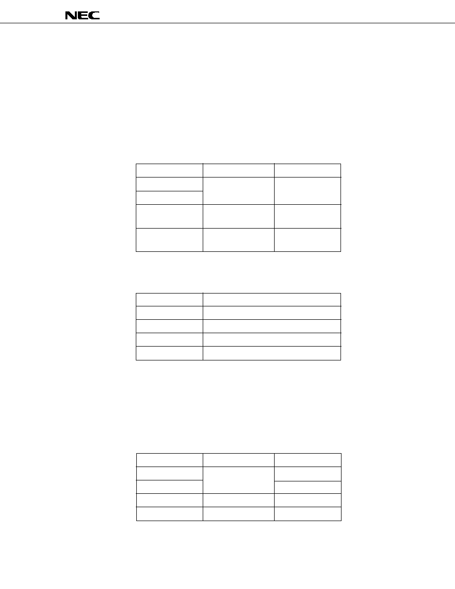
6. CPU ARCHITECTURE
6.1 Memory Space
A memory space of 1 MByte can be accessed. Mapping of the internal data area (special function registers and
internal RAM) can be specified the LOCATION instruction. The LOCATION instruction must be always executed after
RESET cancellation, and must not be used more than once.
(1) When LOCATION 0 instruction is executed
∑ Internal memory
The internal data area and internal ROM area are mapped as follows:
Part Number
Internal Data Area
Internal ROM Area
µ
PD784035Y
0F700H-0FFFFH
00000H-0BFFFH
µ
PD784036Y
00000H-0F6FFH
µ
PD784037Y
0F100H-0FFFFH
00000H-0F0FFH
10000H-17FFFH
µ
PD784038Y
0EE00H-0FFFFH
00000H-0FDFFH
10000H-1FFFFH
Caution The following areas that overlap the internal data area of the internal ROM cannot be used when
the LOCATION 0 instruction is executed.
Part Number
Unusable Area
µ
PD784035Y
≠
µ
PD784036Y
0F700H-0FFFFH (2304 Bytes)
µ
PD784037Y
0F100H-0FFFFH (3840 Bytes)
µ
PD784038Y
0EE00H-0FFFFH (4608 Bytes)
∑ External memory
The external memory is accessed in external memory expansion mode.
(2) When LOCATION 0FH instruction is executed
∑ Internal memory
The internal data area and internal ROM area are mapped as follows:
Part Number
Internal Data Area
Internal ROM Area
µ
PD784035Y
FF700H-FFFFFH
00000H-0BFFFH
µ
PD784036Y
00000H-0FFFFH
µ
PD784037Y
FF100H-FFFFFH
00000H-17FFFH
µ
PD784038Y
FEE00H-FFFFFH
00000H-1FFFFH
∑ External memory
The external memory is accessed in external memory expansion mode.
µ
PD784035Y
, 784036Y
, 784037Y
, 784038Y
20
Figure 6-1. Memory Map of
µ
PD784035Y
Notes 1. Accessed in external memory expansion mode.
2. Base area and entry area for reset or interrupt. However, the internal RAM area is not used as a reset entry area.
Internal ROM
(48 KBytes)
(256 Bytes)
Special function registers (SFR)
External memory
Note 1
(14080 KBytes)
Internal RAM
(2048 Bytes)
External memory
Note 1
(960 KBytes)
Note 1
General-purpose
registers (128 Bytes)
Macro service control word
area (44 Bytes)
Data area (512 Bytes)
Program/data area
(1536 Bytes)
CALLF entry
area (2 KB)
Program/data area
(48 KBytes)
CALLT table
area (64 Bytes)
Vector table area
(64 Bytes)
Internal RAM
(2048 Bytes)
External memory
Note 1
(997120 Bytes)
(256 Bytes)
Internal ROM
(48 KBytes)
On execution of
LOCATION 0 instruction
Special function registers (SFR)
Note 1
On execution of
LOCATION 0FH instruction
H
F
F
F
F
F
H
0
0
0
0
1
H
F
F
F
F
0
H
F
D
F
F
0
H
0
D
F
F
0
H
0
0
F
F
0
H
F
F
E
F
0
H
0
0
7
F
0
H
F
F
6
F
0
H
0
0
0
C
0
H
F
F
F
B
0
H
0
0
0
0
0
H
F
F
E
F
0
H
0
8
E
F
0
H
F
7
E
F
0
H
1
3
E
F
0
H
0
0
D
F
0
H
F
F
C
F
0
H
6
0
E
F
0
H
0
0
7
F
0
H
F
F
F
B
0
H
0
0
0
1
0
H
F
F
F
0
0
H
0
0
8
0
0
H
F
F
7
0
0
H
0
8
0
0
0
H
F
7
0
0
0
H
0
4
0
0
0
H
F
3
0
0
0
H
0
0
0
0
0
H
F
F
E
F
F
H
0
8
E
F
F
H
F
7
E
F
F
H
1
3
E
F
F
H
6
0
E
F
F
H
0
0
D
F
F
H
F
F
C
F
F
H
0
0
7
F
F
H
0
0
0
0
0
H
F
F
F
B
0
H
0
0
0
C
0
H
F
F
F
F
0
H
0
0
0
0
1
H
F
F
6
F
F
H
0
0
7
F
F
H
F
F
F
F
F
H
F
D
F
F
F
H
0
D
F
F
F
H
0
0
F
F
F
H
F
F
E
F
F
Note 2
Note 2
21
µ
PD784035Y
, 784036Y
, 784037Y
, 784038Y
Figure 6-2. Memory Map of
µ
PD784036Y
Notes 1. Accessed in external memory expansion mode.
2. This 2304-Byte area can be used as an internal ROM only when the LOCATION 0FH instruction is executed.
3. On execution of LOCATION 0 instruction: 63232 Bytes, on execution of LOCATION 0FH instruction: 65536 Bytes
4. Base area and entry area for reset or interrupt. However, the internal RAM area is not used as a reset entry area.
Internal ROM
(63232 Bytes)
(256 Bytes)
Special function registers (SFR)
Internal RAM
(2048 Bytes)
External memory
Note 1
(960 KBytes)
Note 1
General-purpose
registers (128 Bytes)
Macro service control word
area (44 Bytes)
Data area (512 Bytes)
Program/data area
(1536 Bytes)
CALLF entry
area (2 KBytes)
Program/data area
Note 3
CALLT table
area (64 Bytes)
Vector table area
(64 Bytes)
Internal RAM
(2048 Bytes)
External memory
Note 1
(980736 Bytes)
(256 Bytes)
Internal ROM
(64 KBytes)
On execution of
LOCATION 0 instruction
Special function registers (SFR)
Note 1
On execution of
LOCATION 0FH instruction
H
F
F
F
F
F
H
0
0
0
0
1
H
F
F
F
F
0
H
F
D
F
F
0
H
0
D
F
F
0
H
0
0
F
F
0
H
F
F
E
F
0
H
0
0
7
F
0
H
F
F
6
F
0
H
0
0
0
0
0
H
F
F
E
F
0
H
0
8
E
F
0
H
F
7
E
F
0
H
1
3
E
F
0
H
0
0
D
F
0
H
F
F
C
F
0
H
6
0
E
F
0
H
0
0
7
F
0
H
F
F
6
F
0
H
0
0
0
1
0
H
F
F
F
0
0
H
0
0
8
0
0
H
F
F
7
0
0
H
0
8
0
0
0
H
F
7
0
0
0
H
0
4
0
0
0
H
F
3
0
0
0
H
0
0
0
0
0
H
F
F
E
F
F
H
0
8
E
F
F
H
F
7
E
F
F
H
1
3
E
F
F
H
6
0
E
F
F
H
0
0
D
F
F
H
F
F
C
F
F
H
0
0
7
F
F
H
0
0
0
0
0
H
F
F
F
F
0
H
0
0
0
0
1
H
F
F
6
F
F
H
0
0
7
F
F
H
F
F
F
F
F
H
F
D
F
F
F
H
0
D
F
F
F
H
0
0
F
F
F
H
F
F
E
F
F
Note 4
Note 4
Note 2
H
F
F
F
F
0
µ
PD784035Y
, 784036Y
, 784037Y
, 784038Y
22
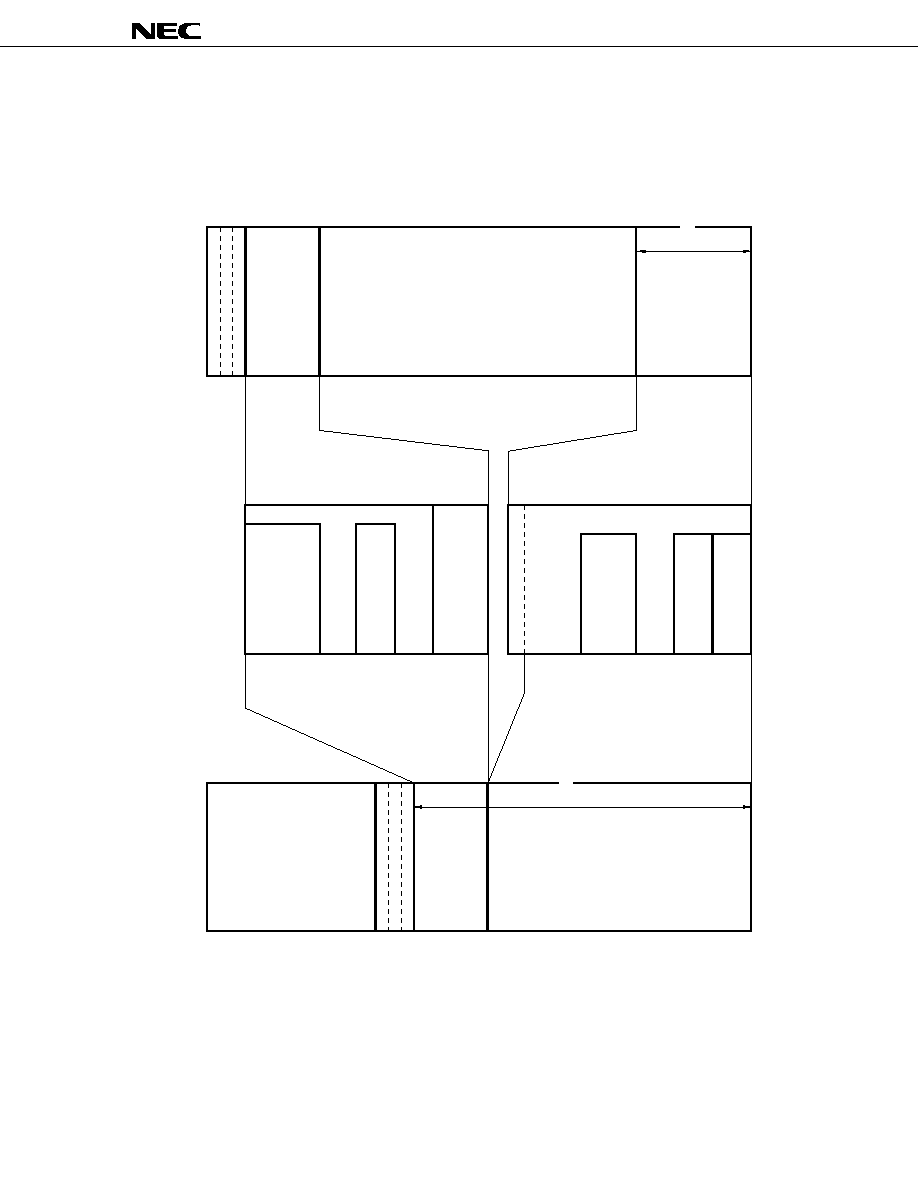
Figure 6-3. Memory Map of
µ
PD784037Y
Internal ROM
(61696 Bytes)
(256 Bytes)
Special function registers (SFR)
Internal RAM
(3584 Bytes)
External memory
Note 1
(928 KBytes)
Note 1
General-purpose
registers (128 Bytes)
Macro service control word
area (44 Bytes)
Data area (512 Bytes)
Program/data area
(3072 Bytes)
CALLF entry
area (2 KBytes)
Program/data area
Note 3
CALLT table
area (64 Bytes)
Vector table area
(64 Bytes)
Internal RAM
(3584 Bytes)
External memory
Note 1
(946432 Bytes)
(256 Bytes)
Internal ROM
(96 KBytes)
On execution of
LOCATION 0 instruction
Special function registers (SFR)
Note 1
On execution of
LOCATION 0FH instruction
H
F
F
F
F
F
H
0
0
0
0
1
H
F
F
F
F
0
H
F
D
F
F
0
H
0
D
F
F
0
H
0
0
F
F
0
H
F
F
E
F
0
H
0
0
1
F
0
H
F
F
0
F
0
H
0
0
0
0
0
H
F
F
E
F
0
H
0
8
E
F
0
H
F
7
E
F
0
H
1
3
E
F
0
H
0
0
D
F
0
H
F
F
C
F
0
H
6
0
E
F
0
H
0
0
1
F
0
H
F
F
0
F
0
H
0
0
0
1
0
H
F
F
F
0
0
H
0
0
8
0
0
H
F
F
7
0
0
H
0
8
0
0
0
H
F
7
0
0
0
H
0
4
0
0
0
H
F
3
0
0
0
H
0
0
0
0
0
H
F
F
E
F
F
H
0
8
E
F
F
H
F
7
E
F
F
H
1
3
E
F
F
H
6
0
E
F
F
H
0
0
D
F
F
H
F
F
C
F
F
H
0
0
1
F
F
H
0
0
0
0
0
H
F
F
F
7
1
H
0
0
0
8
1
H
F
F
0
F
F
H
0
0
1
F
F
H
F
F
F
F
F
H
F
D
F
F
F
H
0
D
F
F
F
H
0
0
F
F
F
H
F
F
E
F
F
Note 4
Note 4
Note 2
H
F
F
F
7
1
Internal ROM
(32768 Bytes)
H
0
0
0
8
1
H
F
F
F
7
1
H
F
F
F
7
1
H
0
0
0
0
1
Notes 1. Accessed in external memory expansion mode.
2. This 3840-Byte area can be used as an internal ROM only when the LOCATION 0FH instruction is executed.
3. On execution of LOCATION 0 instruction: 94464 Bytes, on execution of LOCATION 0FH instruction: 98304 Bytes
4. Base area and entry area for reset or interrupt. However, the internal RAM area is not used as a reset entry area.

23
µ
PD784035Y
, 784036Y
, 784037Y
, 784038Y
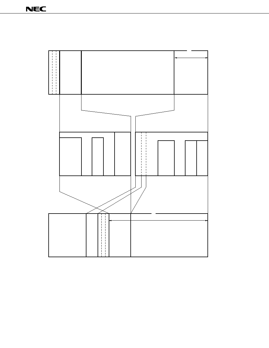
Figure 6-4. Memory Map of
µ
PD784038Y
Notes 1. Accessed in external memory expansion mode.
2. This 4608-Byte area can be used as an internal ROM only when the LOCATION 0FH instruction is executed.
3. On execution of LOCATION 0 instruction: 126464 Bytes, on execution of LOCATION 0FH instruction: 131072 Bytes
4. Base area and entry area for reset or interrupt. However, the internal RAM area is not used as a reset entry area.
Internal ROM
(60928 Bytes)
(256 Bytes)
Special function registers (SFR)
Internal RAM
(4352 Bytes)
External memory
Note 1
(896 KBytes)
Note 1
General-purpose
registers (128 Bytes)
Macro service control word
area (44 Bytes)
Data area (512 Bytes)
Program/data area
(3840 Bytes)
CALLF entry
area (2 KBytes)
Program/data area
Note 3
CALLT table
area (64 Bytes)
Vector table area
(64 Bytes)
Internal RAM
(4352 Bytes)
External memory
Note 1
(912896 Bytes)
(256 Bytes)
Internal ROM
(128 KBytes)
On execution of
LOCATION 0 instruction
Special function registers (SFR)
Note 1
On execution of
LOCATION 0FH instruction
H
F
F
F
F
F
H
0
0
0
0
1
H
F
F
F
F
0
H
F
D
F
F
0
H
0
D
F
F
0
H
0
0
F
F
0
H
F
F
E
F
0
H
0
0
E
E
0
H
F
F
D
E
0
H
0
0
0
0
0
H
F
F
E
F
0
H
0
8
E
F
0
H
F
7
E
F
0
H
1
3
E
F
0
H
0
0
D
F
0
H
F
F
C
F
0
H
6
0
E
F
0
H
0
0
E
E
0
H
F
F
D
E
0
H
0
0
0
1
0
H
F
F
F
0
0
H
0
0
8
0
0
H
F
F
7
0
0
H
0
8
0
0
0
H
F
7
0
0
0
H
0
4
0
0
0
H
F
3
0
0
0
H
0
0
0
0
0
H
F
F
E
F
F
H
0
8
E
F
F
H
F
7
E
F
F
H
1
3
E
F
F
H
6
0
E
F
F
H
0
0
D
F
F
H
F
F
C
F
F
H
0
0
E
E
F
H
0
0
0
0
0
H
F
F
F
F
1
H
0
0
0
0
2
H
F
F
D
E
F
H
0
0
E
E
F
H
F
F
F
F
F
H
F
D
F
F
F
H
0
D
F
F
F
H
0
0
F
F
F
H
F
F
E
F
F
Note 4
Note 4
Note 2
H
F
F
F
F
1
Internal ROM
(65536 Bytes)
H
0
0
0
0
2
H
F
F
F
F
1
H
F
F
F
F
1
H
0
0
0
0
1

µ
PD784035Y, 784036Y, 784037Y, 784038Y
24
6.2 CPU Registers
6.2.1
General-purpose registers
Sixteen 8-bit general-purpose registers are available. Two 8-bit registers can be also used in pairs as a 16-bit
register. Of the 16-bit registers, four can be used in combination with an 8-bit register for address expansion as 24-
bit address specification registers.
Eight banks of these registers are available which can be selected by using software or the context switching
function.
The general-purpose registers except V, U, T, and W registers for address expansion are mapped to the internal
RAM.
Figure 6-5. General-Purpose Register Format
A (R1)
B (R3)
R5
R7
R9
R11
D (R13)
H (R15)
V
U
T
W
VVP (RG4)
UUP (RG5)
TDE (RG6)
WHL (RG7)
X (R0)
C (R2)
R4
R6
R8
R10
E (R12)
L (R14)
AX (RP0)
BC (RP1)
RP2
RP3
VP (RP4)
UP (RP5)
DE (RP6)
HL (RP7)
Parentheses ( ) indicate an absolute name.
8 banks
Caution Registers R4, R5, R6, R7, RP2, and RP3 can be used as X, A, C, B, AX, and BC registers,
respectively, by setting the RSS bit of the PSW to 1. However, use this function only for
recycling the program of the 78K/III Series.
25
µ
PD784035Y, 784036Y, 784037Y, 784038Y
6.2.2 Control registers
(1) Program counter (PC)
The program counter is a 20-bit register whose contents are automatically updated when the program is
executed.
Figure 6-6. Program Counter (PC) Format
(2) Program status word (PSW)
This register holds the statuses of the CPU. Its contents are automatically updated when the program is
executed.
Figure 6-7. Program Status Word (PSW) Format
Note
This flag is provided to maintain compatibility with the 78K/III Series. Be sure to clear this flag to 0, except
when the software for the 78K/III Series is used.
(3) Stack pointer (SP)
This is a 24-bit pointer that holds the first address of the stack. Be sure to write 0 to the higher 4 bits of this
pointer.
Figure 6-8. Stack Pointer (SP) Format
19
0
PC
15
14
13
12
11
10
9
8
UF
RBS2
RBS1
RBS0
≠
≠
≠
≠
PSWH
7
6
5
4
3
2
1
0
S
Z
RSS
Note
AC
IE
P/V
0
CY
PSWL
PSW
23
0
SP
20
0
0
0
0

µ
PD784035Y, 784036Y, 784037Y, 784038Y
26
6.2.3 Special function registers (SFRs)
The special function registers, such as the mode registers and control registers of the internal peripheral hardware,
are registers to which special functions are allocated. These registers are mapped to a 256-Byte space of addresses
0FF00H through 0FFFFH
Note
.
Note
On execution of the LOCATION 0 instruction. FFF00H through FFFFFH on execution of the LOCATION
0FH instruction.
Caution Do not access an address in this area to which no SFR is allocated. If such an address is
accessed by mistake, the
µ
PD784038Y may be in the deadlock status. This deadlock status can
be cleared only by inputting the RESET signal.
Table 6-1 lists the special function registers (SFRs). The meanings of the symbols in this table are as follows:
∑
Symbol ...............................
Symbol indicating an SFR. This symbol is reserved for NEC's assembler
(RA78K4). It can be used as an sfr variable by the #pragma sfr command with
the C compiler (CC78K4).
∑
R/W ....................................
Indicates whether the SFR is read-only, write-only, or read/write.
R/W : Read/write
R
: Read-only
W
: Write-only
∑
Bit units for manipulation ..
Bit units in which the value of the SFR can be manipulated.
SFRs that can be manipulated in 16-bit units can be described as the oper-
and sfrp of an instruction. To specify the address of this SFR, describe an
even address.
SFRs that can be manipulated in 1-bit units can be described as the operand
of a bit manipulation instruction.
∑
After reset ..........................
Indicates the status of the register when the RESET signal has been input.

27
µ
PD784035Y, 784036Y, 784037Y, 784038Y
Table 6-1. Special Function Registers (SFRs)
Address
Note
Special Function Register (SFR) Name
Symbol
R/W
Bit units for manipulation
After reset
1 bit
8 bits
16 bits
0FF00H
Port 0
P0
R/W
≠
Undefined
0FF01H
Port 1
P1
≠
0FF02H
Port 2
P2
R
≠
0FF03H
Port 3
P3
R/W
≠
0FF04H
Port 4
P4
≠
0FF05H
Port 5
P5
≠
0FF06H
Port 6
P6
≠
00H
0FF07H
Port 7
P7
≠
Undefined
0FF0EH
Port 0 buffer register L
P0L
≠
0FF0FH
Port 0 buffer register H
P0H
≠
0FF10H
Compare register (timer/counter 0)
CR00
≠
≠
0FF12H
Capture/compare register (timer/counter 0)
CR01
≠
≠
0FF14H
Compare register L (timer/counter 1)
CR10 CR10W
≠
0FF15H
Compare register H (timer/counter 1)
≠
≠
≠
0FF16H
Capture/compare register L (timer/counter 1)
CR11 CR11W
≠
0FF17H
Capture/compare register H (timer/counter 1)
≠
≠
≠
0FF18H
Compare register L (timer/counter 2)
CR20 CR20W
≠
0FF19H
Compare register H (timer/counter 2)
≠
≠
≠
0FF1AH
Capture/compare register L (timer/counter 2)
CR21 CR21W
≠
0FF1BH
Capture/compare register H (timer/counter 2)
≠
≠
≠
0FF1CH
Compare register L (timer 3)
CR30 CR30W
≠
0FF1DH
Compare register H (timer 3)
≠
≠
≠
0FF20H
Port 0 mode register
PM0
≠
FFH
0FF21H
Port 1 mode register
PM1
≠
0FF23H
Port 3 mode register
PM3
≠
0FF24H
Port 4 mode register
PM4
≠
0FF25H
Port 5 mode register
PM5
≠
0FF26H
Port 6 mode register
PM6
≠
0FF27H
Port 7 mode register
PM7
≠
0FF2EH
Real-time output port control register
RTPC
≠
00H
0FF30H
Capture/compare control register 0
CRC0
≠
≠
10H
0FF31H
Timer output control register
TOC
≠
00H
0FF32H
Capture/compare control register 1
CRC1
≠
≠
0FF33H
Capture/compare control register 2
CRC2
≠
≠
10H
Note
When the LOCATION 0 instruction is executed. When the LOCATION 0FH instruction is executed,
"F0000H" is added to this value.

µ
PD784035Y, 784036Y, 784037Y, 784038Y
28
Address
Note 1
Special Function Register (SFR) Name
Symbol
R/W
Bit units for manipulation
After reset
1 bit
8 bits
16 bits
0FF36H
Capture register (timer/counter 0)
CR02
R
≠
≠
0000H
0FF38H
Capture register L (timer/counter 1)
CR12 CR12W
≠
0FF39H
Capture register H (timer/counter 1)
≠
≠
≠
0FF3AH
Capture register L (timer/counter 2)
CR22 CR22W
≠
0FF3BH
Capture register H (timer/counter 2)
≠
≠
≠
0FF41H
Port 1 mode control register
PMC1
R/W
≠
00H
0FF43H
Port 3 mode control register
PMC3
≠
0FF4EH
Pull-up resistor option register
PUO
≠
0FF50H
Timer register 0
TM0
R
≠
≠
0000H
0FF51H
≠
≠
0FF52H
Timer register 1
TM1 TM1W
≠
0FF53H
≠
≠
≠
0FF54H
Timer register 2
TM2 TM2W
≠
0FF55H
≠
≠
≠
0FF56H
Timer register 3
TM3 TM3W
≠
0FF57H
≠
≠
≠
0FF5CH
Prescaler mode register 0
PRM0
R/W
≠
≠
11H
0FF5DH
Timer control register 0
TMC0
≠
00H
0FF5EH
Prescaler mode register 1
PRM1
≠
≠
11H
0FF5FH
Timer control register 1
TMC1
≠
00H
0FF60H
D/A conversion value setting register 0
DACS0
≠
≠
0FF61H
D/A conversion value setting register 1
DACS1
≠
≠
0FF62H
D/A converter mode register
DAM
≠
03H
0FF68H
A/D converter mode register
ADM
≠
00H
0FF6AH
A/D conversion result register
ADCR
R
≠
≠
Undefined
0FF70H
PWM control register
PWMC
R/W
≠
05H
0FF71H
PWM prescaler register
PWPR
≠
≠
00H
0FF72H
PWM modulo register 0
PWM0
≠
≠
Undefined
0FF74H
PWM modulo register 1
PWM1
≠
≠
0FF7DH
One-shot pulse output control register
OSPC
≠
00H
0FF80H
I
2
C bus control register
IICC
≠
0FF81H
Prescaler mode register for serial clock
SPRM
≠
≠
04H
0FF82H
Clocked serial interface mode register
CSIM
≠
00H
0FF83H
Slave address register
SVA
R/W
Note 2
Note 3
≠
01H
Notes 1. When the LOCATION 0 instruction is executed. When the LOCATION 0FH instruction is executed,
"F0000H" is added to this value.
2. Bit 0 is read-only.
3. Only bit 0 can be manipulated in bit units.
29
µ
PD784035Y, 784036Y, 784037Y, 784038Y
Address
Note 1
Special Function Register (SFR) Name
Symbol
R/W
Bit units for manipulation
After reset
1 bit
8 bits
16 bits
0FF84H
Clocked serial interface mode register 1
CSIM1
R/W
≠
00H
0FF85H
Clocked serial interface mode register 2
CSIM2
≠
0FF86H
Serial shift register
SIO
≠
≠
0FF88H
Asynchronous serial interface mode register
ASIM
≠
0FF89H
Asynchronous serial interface mode register 2
ASIM2
≠
0FF8AH
Asynchronous serial interface status register
ASIS
R
≠
0FF8BH
Asynchronous serial interface status register 2
ASIS2
≠
0FF8CH
Serial receive buffer: UART0
RXB
≠
≠
Undefined
Serial transmit shift register: UART0
TXS
W
≠
≠
Serial shift register: IOE1
SIO1
R/W
≠
≠
0FF8DH
Serial receive buffer: UART2
RXB2
R
≠
≠
Serial transmit shift register: UART2
TXS2
W
≠
≠
Serial shift register: IOE2
SIO2
R/W
≠
≠
0FF90H
Baud rate generator control register
BRGC
≠
≠
00H
0FF91H
Baud rate generator control register 2
BRGC2
≠
≠
0FFA0H
External interrupt mode register 0
INTM0
≠
0FFA1H
External interrupt mode register 1
INTM1
≠
0FFA4H
Sampling clock select register
SCS0
≠
≠
0FFA8H
In-service priority register
ISPR
R
≠
0FFAAH
Interrupt mode control register
IMC
R/W
≠
80H
0FFACH
Interrupt mask register 0L
MK0L MK0
FFFFH
0FFADH
Interrupt mask register 0H
MK0H
0FFAEH
Interrupt mask register 1L
MK1L
≠
FFH
0FFC0H
Standby control register
STBC
≠
Note 2
≠
30H
0FFC2H
Watchdog timer mode register
WDM
≠
Note 2
≠
00H
0FFC4H
Memory expansion mode register
MM
≠
20H
0FFC5H
Hold mode register
HLDM
≠
00H
0FFC6H
Clock output mode register
CLOM
≠
0FFC7H
Programmable wait control register 1
PWC1
≠
≠
AAH
0FFC8H
Programmable wait control register 2
PWC2
≠
≠
AAAAH
Notes 1. When the LOCATION 0 instruction is executed. When the LOCATION 0FH instruction is executed,
"F0000H" is added to this value.
2. Data can be written by using only a dedicated instruction such as "MOV STBC, #byte instruction" and
"MOV WDM, #byte instruction", and cannot be written with any other instructions.
µ
PD784035Y, 784036Y, 784037Y, 784038Y
30
Address
Note
Special Function Register (SFR) Name
Symbol
R/W
Bit units for manipulation
After reset
1 bit
8 bits
16 bits
0FFCCH
Refresh mode register
RFM
R/W
≠
00H
0FFCDH
Refresh area specification register
RFA
≠
0FFCFH
Oscillation stabilization time specification
OSTS
≠
≠
register
0FFD0H-
External SFR area
≠
≠
≠
0FFDFH
0FFE0H
Interrupt control register (INTP0)
PIC0
≠
43H
0FFE1H
Interrupt control register (INTP1)
PIC1
≠
0FFE2H
Interrupt control register (INTP2)
PIC2
≠
0FFE3H
Interrupt control register (INTP3)
PIC3
≠
0FFE4H
Interrupt control register (INTC00)
CIC00
≠
0FFE5H
Interrupt control register (INTC01)
CIC01
≠
0FFE6H
Interrupt control register (INTC10)
CIC10
≠
0FFE7H
Interrupt control register (INTC11)
CIC11
≠
0FFE8H
Interrupt control register (INTC20)
CIC20
≠
0FFE9H
Interrupt control register (INTC21)
CIC21
≠
0FFEAH
Interrupt control register (INTC30)
CIC30
≠
0FFEBH
Interrupt control register (INTP4)
PIC4
≠
0FFECH
Interrupt control register (INTP5)
PIC5
≠
0FFEDH
Interrupt control register (INTAD)
ADIC
≠
0FFEEH
Interrupt control register (INTSER)
SERIC
≠
0FFEFH
Interrupt control register (INTSR)
SRIC
≠
Interrupt control register (INTCSI1)
CSIIC1
≠
0FFF0H
Interrupt control register (INTST)
STIC
≠
0FFF1H
Interrupt control register (INTCSI)
CSIIC
≠
0FFF2H
Interrupt control register (INTSER2)
SERIC2
≠
0FFF3H
Interrupt control register (INTSR2)
SRIC2
≠
Interrupt control register (INTCSI2)
CSIIC2
≠
0FFF4H
Interrupt control register (INTST2)
STIC2
≠
0FFF5H
Interrupt control register (INTSPC)
SPCIC
≠
Note
When the LOCATION 0 instruction is executed. When the LOCATION 0FH instruction is executed,
"F0000H" is added to this value.

31
µ
PD784035Y, 784036Y, 784037Y, 784038Y
7. PERIPHERAL HARDWARE FUNCTIONS
7.1 Ports
The ports shown in Figure 7-1 are provided to make various control operations possible. Table 7-1 shows the
function of each port. Ports 0 through 6 can be connected to internal pull-up resistors by software when inputting.
Figure 7-1. Port Configuration
Port 0
Port 1
Port 3
Port 4
Port 5
Port 6
Port 7
Port 2
P00
P07
P10
P17
P20-P27
P30
P37
P40
P47
P50
P57
P60
P67
P70
P77
8

µ
PD784035Y, 784036Y, 784037Y, 784038Y
32
Table 7-1. Port Functions
Port Name
Pin Name
Function
Specification of Pull-up Resistor
Connection by Software
Port 0
P00 to P07
∑ Can be set in input or output mode in
All port pins in input mode
1-bit units.
∑ Can operate as 4-bit real-time output port
(P00 through P03 and P04 through P07)
∑ Can drive transistor.
Port 1
P10 to P17
∑ Can be set in input or output mode in
All port pins in input mode
1-bit units.
∑ Can drive LEDs.
Port 2
P20 to P27
∑ Input port
In 6-bit units (P22 through P27)
Port 3
P30 to P37
∑ Can be set in input or output mode in
All port pins in input mode
1-bit units.
Port 4
P40 to P47
∑ Can be set in input or output mode in
All port pins in input mode
1-bit units.
∑ Can drive LEDs.
Port 5
P50 to P57
∑ Can be set in input or output mode in
All port pins in input mode
1-bit units.
∑ Can drive LEDs.
Port 6
P60 to P67
∑ Can be set in input or output mode in
All port pins in input mode
1-bit units.
Port 7
P70 to P77
∑ Can be set in input or output mode in
≠
1-bit units.
7.2 Clock Generation Circuit
An on-chip clock generation circuit necessary for operation is provided. This clock generation circuit has a divider
circuit. If high-speed operation is not necessary, the internal operating frequency can be lowered by the divider circuit
to reduce the current consumption.
Figure 7-2. Block Diagram of Clock Generation Circuit
Remark f
XX
: oscillation frequency or external clock input
f
CLK
: internal operating frequency
X1
X2
f
XX
1/2
1/2
1/2
1/2
UART/IOE
INTP0 noise reduction circuit
Oscillation stabilization timer
f
XX
/2
f
CLK
CPU
Peripheral circuit
Oscillation
circuit
Selector

33
µ
PD784035Y, 784036Y, 784037Y, 784038Y
Figure 7-3. Example of Using Oscillation Circuit
(1) Crystal/ceramic oscillation
(2) External clock
∑ EXTC bit of OSTS = 1
∑ EXTC bit of OSTS = 0
Caution When using the clock oscillation circuit, wire the dotted portion in the above figure as follows
to avoid adverse influences of wiring capacitance.
∑
Keep the wiring length as short as possible.
∑
Do not cross the wiring with other signal lines.
∑
Do not route the wiring in the vicinity of lines through which a high alternating current flows.
∑
Always keep the potential at the ground point of the capacitor in the oscillation circuit the same
as V
SS1
. Do not ground to a ground pattern through which a high current flows.
∑
Do not extract signals from the oscillation circuit.
PD784038Y
V
SS1
X1
X2
µ
X1
X2
X1
X2
Open
PD784038Y
µ
PD784038Y
µ
PD74HC04, etc.
µ
µ
PD784035Y, 784036Y, 784037Y, 784038Y
34
7.3
Real-Time Output Port
The real-time output port outputs data stored in a buffer in synchronization with the coincidence interrupt generated
by timer/counter 1 or with an external interrupt. As a result, pulses without jitter can be output.
The real-time output port is therefore ideal for applications where arbitrary patterns must be output at specific
intervals (such as open loop control of a stepping motor).
The real-time output port mainly consists of port 0 and port 0 buffer registers (P0H and P0L) as shown in Figure
7-4.
Figure 7-4. Block Diagram of Real-Time Output Port
Internal bus
8
4
4
4
4
8
Real-time output port
control register (RTPC)
Output trigger
control circuit
INTP0 (from external source)
INTC10 (from timer/counter 1)
INTC11 (from timer/counter 1)
P0H
P0L
Buffer register
Output latch (P0)
P07
P00

35
µ
PD784035Y, 784036Y, 784037Y, 784038Y
7.4
Timer/Counter
Three units of timers/counters and one unit of timer are provided.
Because a total of seven interrupt requests are supported, these timers/counters and timer can be used as seven
units of timers/counters.
Table 7-2. Operations of Timers/Counters
Name
Timer/Counter 0
Timer/Counter 1
Timer/Counter 2
Timer 3
Item
Count width
8 bits
≠
16 bits
Interval timer
2ch
2ch
2ch
1ch
External event counter
≠
One-shot timer
≠
≠
≠
Function
Timer output
2ch
≠
2ch
≠
Toggle output
≠
≠
PWM/PPG output
≠
≠
One-shot pulse output
Note
≠
≠
≠
Real-time output
≠
≠
≠
Pulse width measurement
1 input
1 input
2 inputs
≠
Number of interrupt requests
2
2
2
1
Note
The one-shot pulse output function makes a pulse output level active by software and inactive by hardware
(interrupt request signal).
This function is different in nature from the one-shot timer function of timer/counter 2.
Operation
mode

µ
PD784035Y, 784036Y, 784037Y, 784038Y
36
Figure 7-5. Block Diagram of Timers/Counters
Timer/counter 0
Remark OVF: overflow flag
Prescaler
Edge detection
Selector
Clear control
Timer register 0
(TM0)
Compare register
(CR00)
Compare register
(CR01)
Capture register
(CR02)
Pulse output control
OVF
Software trigger
Match
TO0
TO1
INTC00
INTC01
INTP3
INTP3
f
XX
/8
Prescaler
Edge detection
Selector
Clear control
Compare register
(CR10/CR10W)
Capture/Compare register
(CR11/CR11W)
Capture register
(CR12/CR12W)
OVF
INTC10
INTC11
INTP0
INTP0
f
XX
/8
Event input
Timer register 1
(TM1/TM1W)
Prescaler
Edge detection
Selector
Clear control
Timer register 2
(TM2/TM2W)
Compare register
(CR20/CR20W)
Capture/Compare register
(CR21/CR21W)
Capture register
(CR22/CR22W)
Pulse output control
OVF
TO2
TO3
INTC20
INTC21
INTP1
INTP1
f
XX
/8
Edge detection
INTP2
INTP2/CI
Prescaler
Capture register
(CR30/CR30W)
match
CSI
f
XX
/8
Timer register 3
(TM3/TM3W)
INTC30
Clear
Match
Match
Match
Match
Match
To real-time output port
Timer/counter 1
Timer/counter 2
Timer 3

37
µ
PD784035Y, 784036Y, 784037Y, 784038Y
7.5 PWM Output (PWM0, PWM1)
Two channels of PWM (pulse width modulation) output circuits with a resolution of 12 bits and a repeat frequency
of 62.5 kHz (f
CLK
= 16 MHz) are provided. Both these PWM output channels can select a high or low level as the
active level. These outputs are ideal for controlling the speed of a DC motor.
Figure 7-6. Block Diagram of PWM Output Unit
Internal bus
16
8
Reload
control
4
8
8-bit down counter
Prescaler
Pulse control circuit
4-bit counter
Output
control
1/256
PWMn (output pin)
PWM control
register (PWMC)
0
3
4
7
8
15
PWMn
PWM modulo register
f
CLK
Remark n = 0 or 1
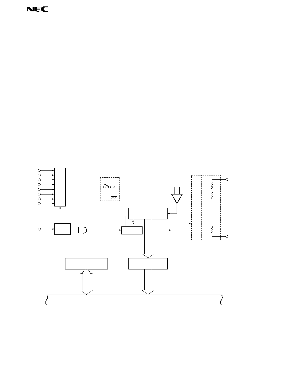
µ
PD784035Y, 784036Y, 784037Y, 784038Y
38
7.6
A/D Converter
An analog-to-digital (A/D) converter with eight multiplexed inputs (ANI0 through ANI7) is provided.
This A/D converter is of successive approximation type. The result of conversion is retained by an 8-bit A/D
conversion result register (ADCR). Therefore, high-speed, high-accuracy conversion can be performed (conversion
time: approx. 7.5
µ
s at f
CLK
= 16 MHz).
A/D conversion can be started in either of the following two modes:
∑ Hardware start: Conversion is started by trigger input (INTP5).
∑ Software start: Conversion is started by setting a bit of the A/D converter mode register (ADM).
After started, the A/D converter operates in the following modes:
∑ Scan mode: Two or more analog inputs are sequentially selected, and data to be converted are obtained from
all the input pins.
∑ Select mode: Only one analog input pin is used to continuously obtain converted values.
These operation modes and whether starting or stopping the A/D converter are specified by the ADM.
When the result of conversion is transferred to the ADCR, interrupt request INTAD is generated. By using this
request and macro service, the converted values can be successively transferred to the memory.
Figure 7-7. Block Diagram of A/D Converter
Internal bus
ANI0
ANI1
ANI2
ANI3
ANI4
ANI5
ANI6
ANI7
INTP5
Input selector
Edge
detection
circuit
Conversion trigger
Sample & hold circuit
Voltage comparator
Successive approximation
register (SAR)
Control
Circuit
INTAD
8
Series resistor string
R/2
Tap selector
R
R/2
AV
REF1
AV
SS
8
Trigger enable
A/D converter mode
register (ADM)
8
A/D conversion result
register (ADCR)
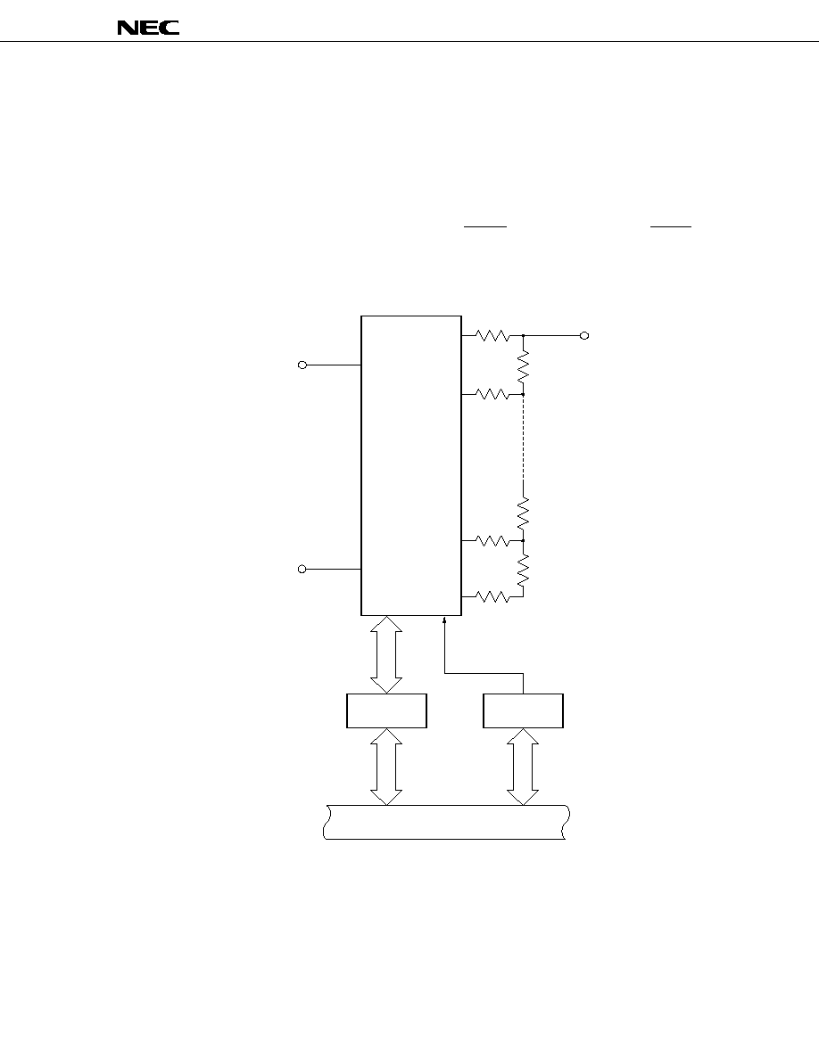
39
µ
PD784035Y, 784036Y, 784037Y, 784038Y
7.7
D/A Converter
Two circuits of digital-to-analog (D/A) converters are provided. These D/A converters are of voltage output type
and have a resolution of 8 bits.
The conversion method is of R-2R resistor ladder type. By writing a value to be output to an 8-bit D/A conversion
value setting register (DACSn: n = 0 or 1), an analog value is output to the ANOn (n = 0 or 1) pin. The output voltage
range is determined by the voltage applied across the AV
REF2
and AV
REF3
pins.
Because the output impedance is high, no current can be extracted from the output. If the impedance of the load
is low, insert a buffer amplifier between the load and output pin.
The ANOn pin goes into a high-impedance state while the RESET signal is low. When the RESET signal is
deasserted, DACSn is cleared to 0.
Figure 7-8. Block Diagram of D/A Converter
Remark n = 0 or 1
AV
REF2
AV
REF3
ANOn
2R
2R
R
2R
R
R
2R
DACSn
DACEn
Internal bus
Selector
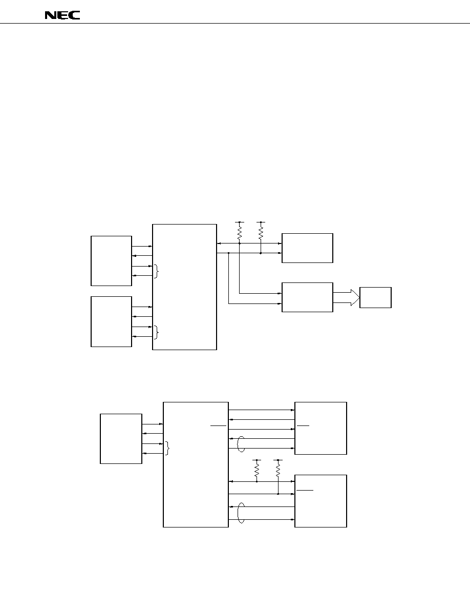
µ
PD784035Y, 784036Y, 784037Y, 784038Y
40
7.8
Serial Interface
Three independent serial interface channels are provided.
∑ Asynchronous serial interface (UART)/3-wire serial I/O (IOE)
◊
2
∑ Clocked serial interface (CSI)
◊
1
∑ 3-wire serial I/O (IOE)
∑ 2-wire serial I/O (IOE)
∑ I
2
C bus interface (I
2
C)
Therefore, communication with an external system and local communication within the system can be simulta-
neously executed (refer to Figure 7-9).
Figure 7-9. Example of Serial Interface
(a) UART + I
2
C
(b) UART + 3-wire serial I/O + 2-wire serial I/O
Note
Handshake line
PD784038Y (master)
PD4711A
RS-232-C
driver/receiver
RS-232-C
driver/receiver
[UART]
[UART]
RxD
TxD
RxD2
TxD2
SDA
SCL
[I
2
C]
LCD
PD6272 (EEPROM
TM
)
V
DD
SDA
SCL
SDA
SCL
V
DD
µ
PD4711A
µ
µ
Port
Port
µ
PD78062Y (slave)
µ
RS-232-C
driver/receiver
[UART]
Port
RxD
TxD
SI
SO
SCK
Port
INT
[3-wire serial I/O]
SO1
SI1
SCK1
INTPm
Port
SB0
SCK0
Port
INT
Note
SDA
SCL
INTPn
Port
V
DD
V
DD
[2-wire serial I/O]
PD784038Y (master)
µ
PD4711A
µ
PD75108 (slave)
µ
PD78014 (slave)
µ
Note
41
µ
PD784035Y, 784036Y, 784037Y, 784038Y
7.8.1
Asynchronous serial interface/3-wire serial I/O (UART/IOE)
Two channels of serial interfaces that can select an asynchronous serial interface mode and 3-wire serial I/O mode
are provided.
(1) Asynchronous serial interface mode
In this mode, data of 1 byte following the start bit is transferred or received.
Because an on-chip baud rate generator is provided, a wide range of baud rates can be set.
Moreover, the clock input to the ASCK pin can be divided to define a baud rate.
When the baud rate generator is used, a baud rate conforming to the MIDI standard (31.25 kbps) can be
also obtained.
Figure 7-10. Block Diagram in Asynchronous Serial Interface Mode
1/2m
1/2m
1/2
n+1
Receive buffer
RXB, RXB2
Receive shift
register
Transmit shift
register
Receive control
parity check
Trnsmit control
Parity append
R
X
D, R
X
D2
T
X
D, T
X
D2
INTSR,
INTSR2
INTSER,
INTSER2
TXS, TXS2
INTST, INTST2
Baud rate generator
f
XX
/2
ASCK, ASCK2
Selector
Internal bus
Remark f
XX
: oscillation frequency or external clock input
n = 0 through 11
m = 16 through 30

µ
PD784035Y, 784036Y, 784037Y, 784038Y
42
(2) 3-wire serial I/O mode
In this mode, the master device starts transfer by making the serial clock active and transfers 1-byte data
in synchronization with this clock.
This mode is used to communicate with a device having the conventional clocked serial interface. Basically,
communication is established by using three lines: one serial clock (SCK) and two serial data (SI and SO)
lines.
Generally, a handshake line is necessary to check the communication state.
Figure 7-11. Block Diagram in 3-wire Serial I/O Mode
Remark f
XX
: oscillation frequency or external clock input
n = 0 through 11
m = 1 or 16 through 30
Internal bus
Direction control circuit
SIO1, SIO2
Shift register
Output latch
Serial clock counter
Serial clock
control circuit
Interrupt signal
generation circuit
1/m
1/2
n+1
INTCSI1,
INTCSI2
SI1, SI2
SO1, SO2
SCK1, SCK2
f
XX
/2
Selector
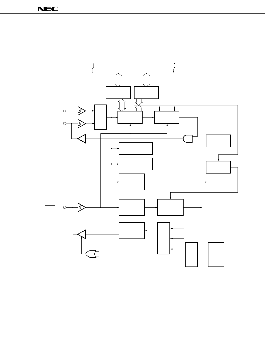
43
µ
PD784035Y, 784036Y, 784037Y, 784038Y
7.8.2
Clocked serial interface (CSI)
In this mode, the master device starts transfer by making the serial clock active and communicates 1-byte data
in synchronization with this clock.
Figure 7-12. Block Diagram of Clocked Serial Interface
Internal bus
Direction
control
register
Slave address
register
Selector
Selector
Selector
Acknowledge
detection
control
Wake-up
control circuit
Prescaler
Shift register
Output latch
Match signal
Set
Reset
SI0
SO0/SDA
N-ch open drain output
(in 2-wire or I
2
C bus mode)
Stop condition
detection circuit
Serial clock
counter
SCK0/SCL
Serial clock
control circuit
N-ch open drain output
(in 2-wire or I
2
C bus mode)
CLS0
CLS1
Timer 3 output
f
XX
/16
f
XX
/2
Interrupt signal
generation
circuit
INTCSI
INTSPC
Start condition
detection circuit
Acknowledge
detection circuit
Remark f
XX
: oscillation frequency or external clock input
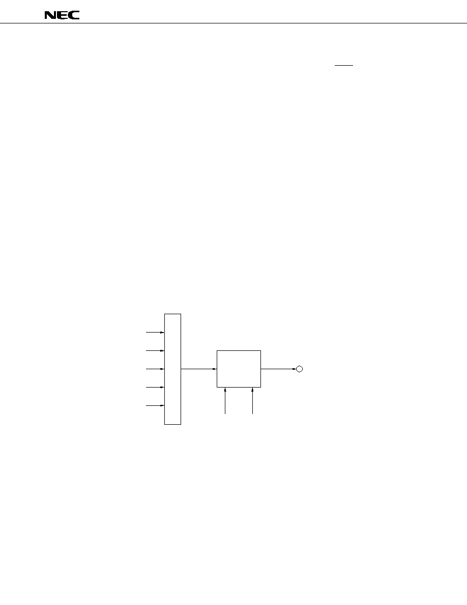
µ
PD784035Y, 784036Y, 784037Y, 784038Y
44
(1) 3-wire serial I/O mode
This mode is to communicate with devices having the conventional clocked serial interface.
Basically, communication is established in this mode with three lines: one serial clock (SCK0) and two serial
data (SI0 and SO0) lines.
Generally, a handshake line is necessary to check the communication status.
(2) 2-wire serial I/O mode
This mode is to transfer 8-bit data by using two lines: serial clock (SCL) and serial data bus (SDA).
Generally, a handshake line is necessary to check the communication status.
(3) I
2
C (Inter IC) bus mode
This mode is to communicate with devices conforming to the I
2
C bus format.
This mode is to transfer 8-bit data with two or more devices by using two lines: serial clock (SCL) and serial
data bus (SDA).
During transfer, a "start condition", "data", and "stop condition" can be output onto the serial data bus. During
reception, these data can be automatically detected by hardware.
7.9
Clock Output Function
The operating clock of the CPU can be divided and output to an external device. The pin that outputs the clock
can also be used as a 1-bit port.
When this function is used, the local bus interface cannot be used because the ASTB and CLKOUT pins are
multiplexed.
Figure 7-13. Block Diagram of Clock Output Function
CLKOUT
Output
control
Output level
Selector
f
CLK
f
CLK
/2
f
CLK
/4
f
CLK
/8
f
CLK
/16
Output enable
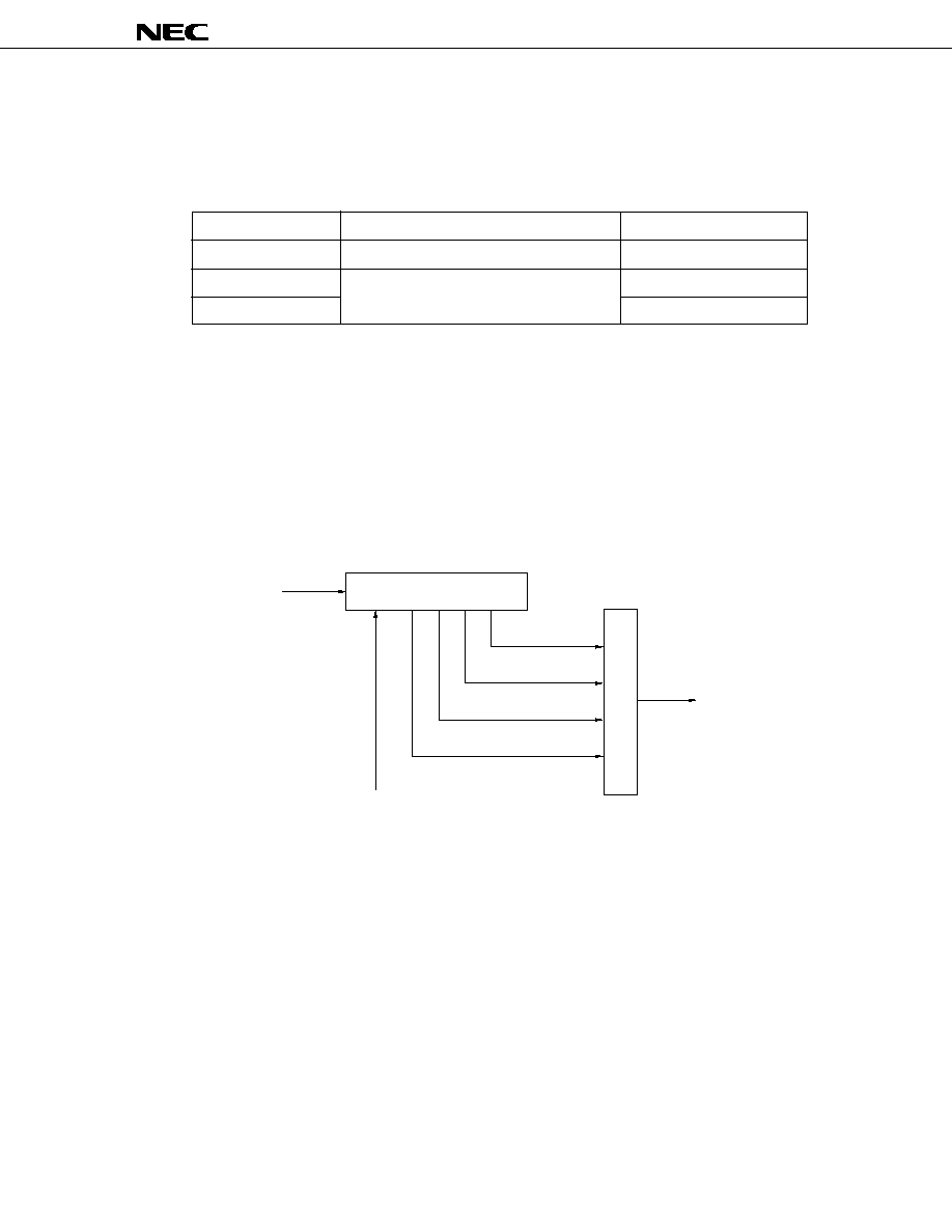
45
µ
PD784035Y, 784036Y, 784037Y, 784038Y
7.10 Edge Detection Function
The interrupt input pins (NMI and INTP0 through INTP5) are used not only to input interrupt requests but also to
input trigger signals to the internal hardware units. Because these pins operate at an edge of the input signal, they
have a function to detect an edge. Moreover, a noise reduction circuit is also provided to prevent erroneous detection
due to noise.
Pin Name
Detectable Edge
Noise Reduction
NMI
Either of rising or falling edge
By analog delay
INTP0-INTP3
Either or both of rising and falling edges
By clock sampling
Note
INTP4, INTP5
By analog delay
Note
INTP0 can select a sampling clock.
7.11 Watchdog Timer
A watchdog timer is provided to detect a hang up of the CPU. This watchdog timer generates a non-maskable
interrupt unless it is cleared by software within a specified interval time. Once enabled to operate, the watchdog timer
cannot be stopped by software. Whether the interrupt by the watchdog timer or the interrupt input from the NMI pin
takes precedence can be specified.
Figure 7-14. Block Diagram of Watchdog Timer
Selector
f
CLK
/2
21
f
CLK
/2
20
f
CLK
/2
19
f
CLK
/2
17
f
CLK
Clear signal
Timer
INTWDT
µ
PD784035Y, 784036Y, 784037Y, 784038Y
46
8.
INTERRUPT FUNCTION
As the servicing in response to an interrupt request, the three types shown in Table 8-1 can be selected by program.
Table 8-1. Servicing of Interrupt Request
Servicing Mode
Entity of Servicing
Servicing
Contents of PC and PSW
Vectored interrupt
Software
Branches and executes servicing routine
Saves to and restores
(servicing is arbitrary).
from stack.
Context switching
Automatically switches register bank,
Saves to or restores from
branches and executes servicing routine
fixed area in register bank
(servicing is arbitrary).
Macro service
Firmware
Executes data transfer between memory
Retained
and I/O (servicing is fixed)
8.1 Interrupt Sources
Table 8-2 shows the interrupt sources available. As shown, interrupts are generated by 24 types of sources,
execution of the BRK instruction or BRKCS instruction, or an operand error.
The priority of interrupt servicing can be set to four levels, so that nesting can be controlled during interrupt servicing
and that which of the two or more interrupts that simultaneously occur should be serviced first. When the macro service
function is used, however, nesting always proceeds.
The default priority is the priority (fixed) of the service that is performed if two or more interrupt requests, having
the same request, simultaneously generate (refer to Table 8-2).

47
µ
PD784035Y, 784036Y, 784037Y, 784038Y
Table 8-2. Interrupt Sources
Type
Default
Source
Internal/
Macro service
Priority
Name
Trigger
External
Software
≠
BRK instruction
Instruction execution
≠
≠
BRKCS instruction
Operand error
If result of exclusive OR between byte of
operand and byte is not FFH when "MOV
STBC, #byte", "MOV WDM, #byte", or
"LOCATION" instruction is executed
Non-maskable
≠
NMI
Detection of pin input edge
External
≠
WDT
Overflow of watchdog timer
Internal
Maskable
0 (highest)
INTP0
Detection of pin input edge
External
(TM1/TM1W capture trigger, TM1/TM1W
event counter input)
1
INTP1
Detection of pin input edge
(TM2/TM2W capture trigger, TM2/TM2W
event counter input)
2
INTP2
Detection of pin input edge
(TM2/TM2W capture trigger , TM2/TM2W
event counter input)
3
INTP3
Detection of pin input edge
(TM0 capture trigger, TM0 event counter input)
4
INTC00
Generation of TM0-CR00 match signal
Internal
5
INTC01
Generation of TM0-CR01 match signal
6
INTC10
Generation of TM1-CR10 match signal
(in 8-bit operation mode)
Generation of TM1W-CR10W match signal
(in 16-bit operation mode)
7
INTC11
Generation of TM1-CR11 match signal
(in 8-bit operation mode)
Generation of TM1W-CR11W match signal
(in 16-bit operation mode)
8
INTC20
Generation of TM2-CR20 match signal
(in 8-bit operation mode)
Generation of TM2W-CR20W match signal
(in 16-bit operation mode)
9
INTC21
Generation of TM2-CR21 match signal
(in 8-bit operation mode)
Generation of TM2W-CR21W match signal
(in 16-bit operation mode)
10
INTC30
Generation of TM3-CR30 match signal
(in 8-bit operation mode)
Generation of TM3W-CR30W match signal
(in 16-bit operation mode)
11
INTP4
Detection of pin input edge
External
12
INTP5
Detection of pin input edge
13
INTAD
End of A/D conversion (transfer of ADCR)
Internal
14
INTSER
Occurrence of ASI0 reception error
≠
15
INTSR
End of ASI0 reception or CSI1 transfer
INTCSI1
16
INTST
End of ASI0 transfer
17
INTCSI
End of CSI1 transfer
18
INTSER2
Occurrence of ASI2 reception error
≠
19
INTSR2
End of ASI2 reception or CSI2 transfer
INTCSI2
20
INTST2
End of ASI2 transfer
21 (lowest)
INTSPC
I
2
C bus stop condition interrupt
Remark ASI: asynchronous serial interface
CSI: clocked serial interface
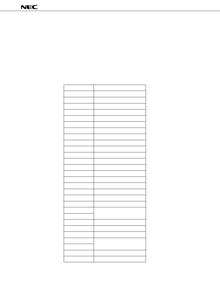
µ
PD784035Y, 784036Y, 784037Y, 784038Y
48
8.2
Vectored Interrupt
Execution branches to a servicing routing by using the memory contents of a vector table address corresponding
to the interrupt source as the address of the branch destination.
So that the CPU performs interrupt servicing, the following operations are performed:
∑ On branching: Saves the status of the CPU (contents of PC and PSW) to stack
∑ On returning: Restores the status of the CPU (contents of PC and PSW) from stack
To return to the main routine from an interrupt service routine, the RETI instruction is used.
The branch destination address is in a range of 0 to FFFFH.
Table 8-3. Vector Table Address
Interrupt Source
Vector Table Address
BRK instruction
003EH
Operand error
003CH
NMI
0002H
WDT
0004H
INTP0
0006H
INTP1
0008H
INTP2
000AH
INTP3
000CH
INTC00
000EH
INTC01
0010H
INTC10
0012H
INTC11
0014H
INTC20
0016H
INTC21
0018H
INTC30
001AH
INTP4
001CH
INTP5
001EH
INTAD
0020H
INTSER
0022H
INTSR
0024H
INTCSI1
INTST
0026H
INTCSI
0028H
INTSER2
002AH
INTSR2
002CH
INTCSI2
INTST2
002EH
INTSPC
0030H
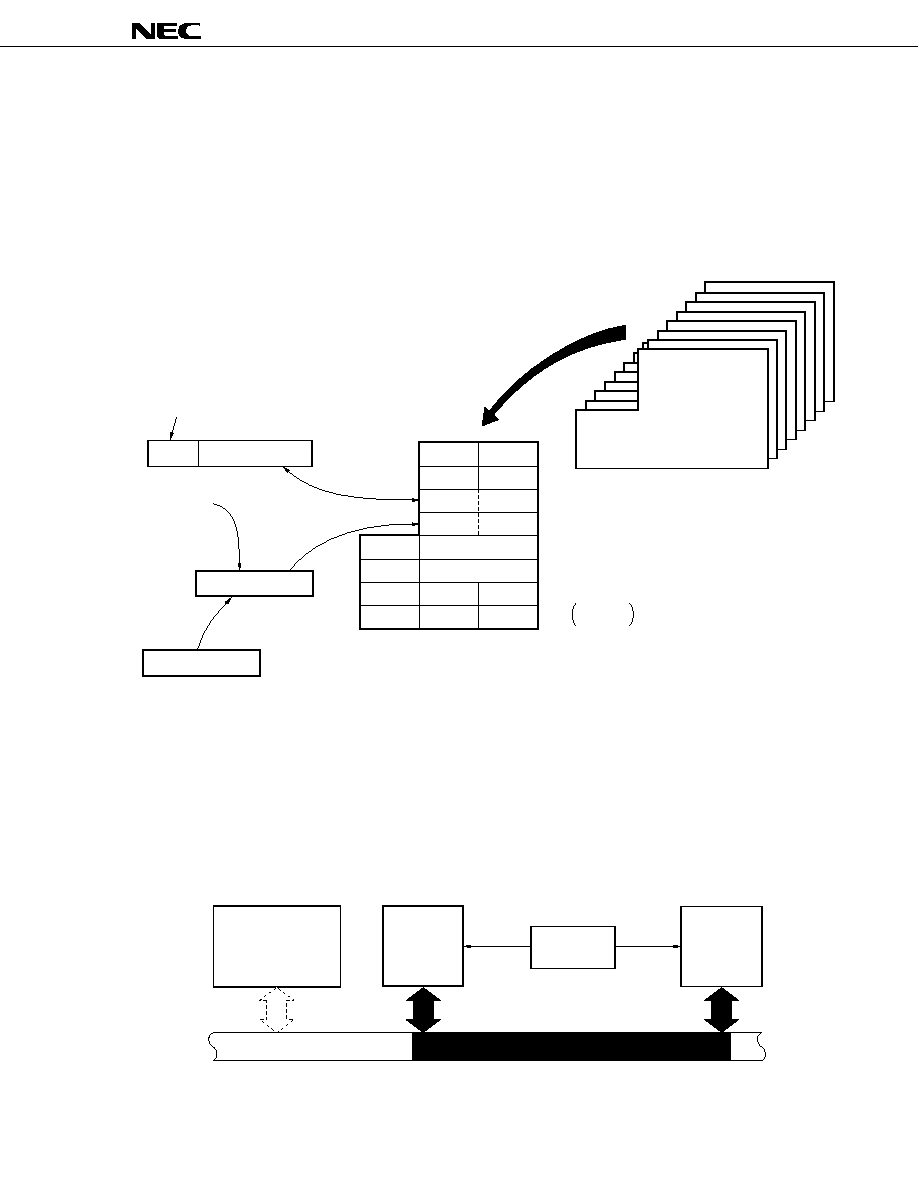
49
µ
PD784035Y, 784036Y, 784037Y, 784038Y
8.3
Context Switching
When an interrupt request is generated or when the BRKCS instruction is executed, a predetermined register bank
is selected by hardware. Context switching is a function that branches execution to a vector address stored in advance
in the register bank, and to stack the current contents of the program counter (PC) and program status word (PSW)
to the register bank.
The branch address is in a range of 0 to FFFFH.
Figure 8-1. Context Switching Operation When Interrupt Request Is Generated
8.4
Macro Service
This function is to transfer data between memory and a special function register (SFR) without intervention by the
CPU. A macro service controller accesses the memory and SFR in the same transfer cycle and directly transfers
data without loading it.
Because this function does not save or restore the status of the CPU, or load data, data can be transferred at high
speeds.
Figure 8-2. Macro Service
Register bank n (n = 0 to 7)
0000B
<7> Transfer
PC19-16
PC15-0
<6> Exchange
<5> Save
<2> Save
Temporary register
<1> Save
PSW
V
U
T
W
A
B
R5
R7
D
H
X
C
R4
R6
E
L
VP
UP
<3> Switching of register bank
(RBS0 to RBS2
n)
Register bank n
(0 to 7)
(bits 8 through 11
of temporary register)
<4> RSS
n
IE
n
CPU
Memory
SFR
Macro service
controller
Read
Write
Write
Read
Internal bus

µ
PD784035Y, 784036Y, 784037Y, 784038Y
50
8.5
Application Example of Macro Service
(1) Transfer of serial interface
Each time macro service request (INTST) is generated, the next transfer data is transferred from memory to TXS.
When data n (last byte) has been transferred to TXS (when the transfer data storage buffer has become empty),
vectored interrupt request (INTST) is generated.
(2) Reception of serial interface
Each time macro service request (INTSR) is generated, the receive data is transferred from RXB to memory. When
data n (last byte) has been transferred to memory (when the receive data storage buffer has become full), vectored
interrupt request (INTSR) is generated.
Transfer data storage buffer (memory)
Data n
Data n≠1
Data 1
Data 2
Internal bus
Transfer shift register TXS(SFR)
Transfer control
INTST
TxD
Receive data storage buffer (memory)
Data n
Data n≠1
Data 1
Data 2
Internal bus
Receive shift register
RXB(SFR)
Reception control
INTSR
RxD
Receive buffer

51
µ
PD784035Y, 784036Y, 784037Y, 784038Y
(3) Real-time output port
INTC10 and INTC11 serve as the output triggers of the real-time output port. The macro services for these
can set the following output pattern and intervals simultaneously. Therefore, INTC10 and INTC11 can control
two stepping motors independently of each other. They can also be used for PWM output or to control DC
motors.
Output timing profile (memory)
T
n
T
n≠1
T
1
T
2
Internal bus
CR10
(SFR)
TM1
INTC10
Output pattern profile (memory)
P
n
P
n≠1
P
1
P
2
Internal bus
P0L
Output latch
(SFR)
Match
P00-P03
Each time macro service request (INTC10) is generated, the pattern and timing are transferred to the buffer register
(P0L) and compare register (CR10), respectively. When the contents of the timer register 1 (TM1) coincide with those
of CR10, INTC10 is generated again, and the contents of P0L are transferred to the output latch. When Tn (last byte)
has transferred to CR10, vectored interrupt request (INTC10) is generated.
The same applies to INTC11.
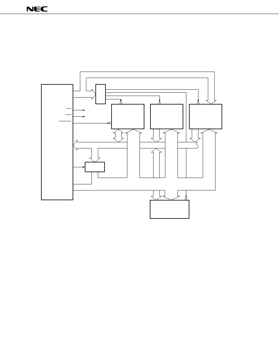
µ
PD784035Y, 784036Y, 784037Y, 784038Y
52
9.
LOCAL BUS INTERFACE
The local bus interface can connect an external memory or I/O (memory mapped I/O) and support a memory space
of 1 MByte (refer to Figure 9-1).
Figure 9-1. Example of Local Bus Interface
9.1
Memory Expansion
The memory capacity can be expanded in seven steps, from 256 Bytes to 1 MByte, by connecting an external
program memory and data memory.
Decoder
Latch
Pseudo SRAM
PROM
PD27C1001A
Character
generator
PD24C1000
Data bus
Address bus
Gate array
I/O expansion
Centronics I/F, etc.
PD784038Y
A16-A19
RD
WR
REFRQ
AD0-AD7
ASTB
A8-A15
µ
µ
µ

53
µ
PD784035Y, 784036Y, 784037Y, 784038Y
9.2
Memory Space
The 1-MByte memory space is divided into eight spaces of logical addresses. Each space can be controlled by
using the programmable wait function and pseudo static RAM refresh function.
Figure 9-2. Memory Space
512 KBytes
256 KBytes
128 KBytes
64 KBytes
16 KBytes
16 KBytes
16 KBytes
16 KBytes
H
F
F
F
F
F
H
0
0
0
0
8
H
F
F
F
F
7
H
0
0
0
0
4
H
F
F
F
F
3
H
0
0
0
0
2
H
F
F
F
F
1
H
0
0
0
0
0
H
F
F
F
3
0
H
0
0
0
4
0
H
F
F
F
7
0
H
0
0
0
8
0
H
F
F
F
B
0
H
0
0
0
C
0
H
F
F
F
F
0
H
0
0
0
0
1

µ
PD784035Y, 784036Y, 784037Y, 784038Y
54
9.3
Programmable Wait
The memory space can be divided into eight spaces and wait states can be independently inserted in each of these
spaces while the RD and WR signals are active. Even when a memory with a different access time is connected,
therefore, the efficiency of the entire system does not drop.
In addition, an address wait function that extends the active period of the ASTB signal is also provided so as to
have a sufficient address decode time (this function can be set to the entire space).
9.4
Pseudo Static RAM Refresh Function
The following refresh operations can be performed:
∑
Pulse refresh: A bus cycle that outputs a refresh pulse to the REFRQ pin at a fixed cycle is inserted. The memory
spaces is divided into eight spaces, and a refresh pulse can be output from the REFRQ pin while a specified
memory space is accessed. Therefore, the normal memory access is not kept to wait by the refresh cycle.
∑
Power-down self-refresh: The low level is output to the REFRQ pin in the standby mode to retain the contents
of the pseudo static RAM.
9.5
Bus Hold Function
A bus hold function is provided to facilitate connection of a DMA controller. When a bus hold request signal
(HLDRQ) is received from an external bus master, the address bus, address/data bus, and ASTB, RD, and WR pins
go into a high-impedance state when the current bus cycle has been completed. This makes the bus hold acknowledge
(HLDAK) signal active, and releases the bus to the external bus master.
Note that, while the bus hold function is used, the external wait function and pseudo static RAM refresh function
cannot be used.
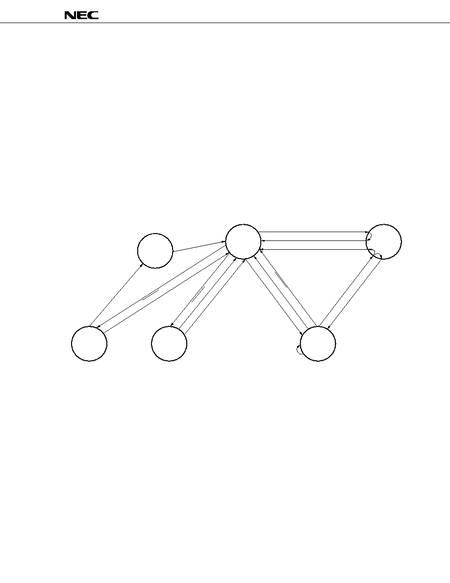
55
µ
PD784035Y, 784036Y, 784037Y, 784038Y
10. STANDBY FUNCTION
This function is to reduce the power dissipation of the chip, and can be used in the following modes:
∑
HALT mode: Stops supply of the operating clock to the CPU. This mode is used in combination with the normal
operation mode for intermittent operation to reduce the average power dissipation.
∑
IDLE mode: Stops the entire system with the oscillation circuit continuing operation. The power dissipation in
this mode is close to that in the STOP mode. However, the time required to restore the normal program operation
from this mode is almost the same as that from the HALT mode.
∑
STOP mode: Stops the oscillator and thereby to stop all the internal operations of the chip. Consequently, the
power dissipation is minimized with only leakage current flowing.
These modes are programmable.
The macro service can be started from the HALT mode.
Figure 10-1. Transition of Standby Status
Waits for
oscillation
stabilization
Program
operation
Macro
service
HALT
(standby)
IDLE
(standby)
STOP
(standby)
Oscillation stabilization
time expires
Macro service request
End of one processing
End of macro service
Macro service request
End of one processing
Interrupt request
Note 2
RESET input
Sets HALT mode
Interrupt request of
masked interrupt
Sets IDLE mode
RESET input
NMI, INTP4, INTP5 input
Note 1
Sets STOP mode
RESET input
NMI, INTP4, INTP5 input
Note 1
Notes 1. When INTP4 and INTP5 are not masked
2. Only interrupt requests that are not masked
Remark Only the externally input NMI is valid. The watchdog timer cannot be used to release the standby mode
(STOP/IDLE mode).

µ
PD784035Y, 784036Y, 784037Y, 784038Y
56
11. RESET FUNCTION
When the low level is input to the RESET pin, the internal hardware is initialized (reset status).
When the RESET pin goes high, the following data are set to the program counter (PC).
∑
Lower 8 bits of PC: contents of address 0000H
∑
Middle 8 bits of PC: contents of address 0001H
∑
Higher 4 bits of PC: 0
Program execution is started from a branch destination address which is the contents of the PC. Therefore, the
system can be reset and started from any address.
Set the contents of each register by program as necessary.
The RESET input circuit has a noise reduction circuit to prevent malfunctioning due to noise. This noise reduction
circuit is a sampling circuit by analog delay.
Figure 11-1. Accepting RESET Signal
Assert the RESET signal active until the oscillation stabilization time (approx. 40 ms) elapses to execute a power-
ON reset operation.
Figure 11-2. Power-ON Reset Operation
Delay
RESET
(input)
Delay
Internal reset signal
Reset starts
Reset ends
Delay
Initialize PC
Executes instruction at
reset start address
RESET
(input)
Internal reset signal
Reset ends
Oscillation stabilization time
Delay
Initialize PC
Executes instruction at
reset start address
V
DD
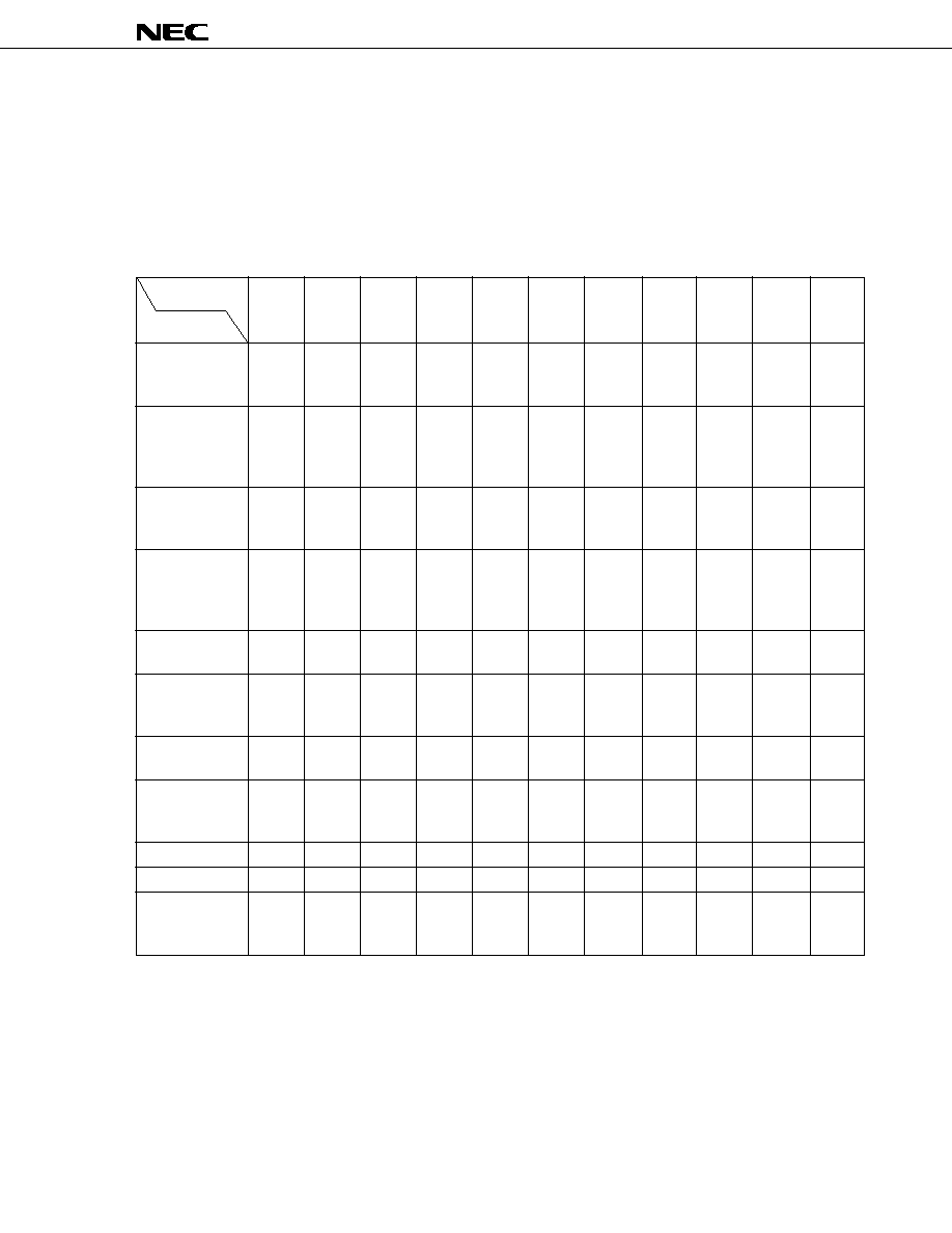
57
µ
PD784035Y, 784036Y, 784037Y, 784038Y
12. INSTRUCTION SET
(1) 8-bit instructions (The instructions in parentheses are combinations realized by describing A as r)
MOV, XCH, ADD, ADDC, SU B, SUBC, AND, OR, XOR, CMP, MULU, DIVUW, INC, DEC, ROR, ROL, RORC,
ROLC, SHR, SHL, ROR4, DBNZ, PUSH, POP, MOVM, XCHM, CMPME, CMPMNE, CMPMNC, CMPMC,
MOVBK, XCHBK, CMPBKE, CMPBKNE, CMPBKNC, CMPBKC, CHIKL, CHKLA
Table 12-1. Instruction List by 8-Bit Addressing
Second Operand
#byte
A
r
saddr
sfr
!addr16
mem
r3
[WHL+]
n
None
Note 2
r'
saddr'
!!addr24
[saddrp]
PSWL
[WHL≠]
First Operand
[%saddrg]
PSWH
A
(MOV)
(MOV)
MOV
(MOV)
Note 6
MOV
(MOV)
MOV
MOV
(MOV)
ADD
Note 1
(XCH)
XCH
(XCH)
Note 6
(XCH)
(XCH)
XCH
(XCH)
(ADD)
Note 1
(ADD)
Note 1
(ADD)
Note 1,6
(ADD)
Note 1
ADD
Note 1
ADD
Note 1
(ADD)
Note 1
r
MOV
(MOV)
MOV
MOV
MOV
MOV
ROR
Note 3
MULU
ADD
Note 1
(XCH)
XCH
XCH
XCH
XCH
DIVUW
(ADD)
Note 1
ADD
Note 1
ADD
Note 1
ADD
Note 1
INC
DEC
saddr
MOV
(MOV)
Note 6
MOV
MOV
INC
ADD
Note 1
(ADD)
Note 1
ADD
Note 1
XCH
DEC
ADD
Note 1
DBNZ
sfr
MOV
MOV
MOV
PUSH
ADD
Note 1
(ADD)
Note 1
ADD
Note 1
POP
CHKL
CHKLA
!addr16
MOV
(MOV)
MOV
!!addr24
ADD
Note 1
mem
MOV
[saddrp]
ADD
Note 1
[%saddrg]
mem3
ROR4
ROL4
r3
MOV
MOV
PSWL
PSWH
B, C
DBNZ
STBC, WDM
MOV
[TDE+]
(MOV)
MOVBK
Note 5
[TDE≠]
(ADD)
Note 1
MOVM
Note 4
Notes 1. The operands of ADDC, SUB, SUBC, AND, OR, XOR, and CMP are the same as that of ADD.
2. Either the second operand is not used, or the second operand is not an operand address.
3. The operands of ROL, RORC, ROLC, SHR, and SHL are the same as that of ROR.
4. The operands of XCHM, CMPME, CMPMNE, CMPMNC, and CMPMC are the same as that of MOVM.
5. The operands of XCHBK, CMPBKE, CMPBKNE, CMPBKNC, and CMPBKC are the same as that of
MOVBK.
6. The code length of some instructions having saddr2 as saddr in this combination is short.
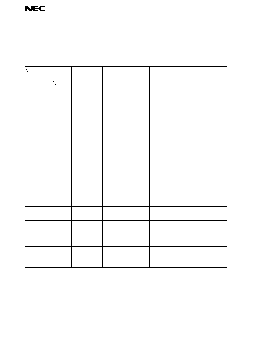
µ
PD784035Y, 784036Y, 784037Y, 784038Y
58
(2) 16-bit instructions (The instructions in parentheses are combinations realized by describing AX as
rp)
MOVW, XCHW, ADDW, SUBW, CMPW, MULUW, MULW, DIVUX, INCW, DECW, SHRW, SHLW, PUSH,
POP, ADDWG, SUBWG, PUSHU, POPU, MOVTBLW, MACW, MACSW, SACW
Table 12-2. Instruction List by 16-Bit Addressing
Second Operand
#word
AX
rp
saddrp
sfrp
!addr16
mem
[WHL+]
byte
n
None
Note 2
rp'
saddrp'
!!addr24
[saddrp]
First Operand
[%saddrg]
AX
(MOVW)
(MOVW)
(MOVW) (MOVW)
Note 3
MOVW
(MOVW)
MOVW
(MOVW)
ADDW
Note 1
(XCHW)
(XCHW) (XCHW)
Note 3
(XCHW)
XCHW
XCHW
(XCHW)
(ADD)
Note 1
(ADDW)
Note 1
(ADDW)
Note 1,3
(ADDW)
Note 1
rp
MOVW
(MOVW)
MOVW
MOVW
MOVW
MOVW
SHRW
MULW
Note 4
ADDW
Note 1
(XCHW)
XCHW
XCHW
XCHW
SHLW
INCW
(ADDW)
Note 1
ADDW
Note 1
ADDW
Note 1
ADDW
Note 1
DECW
saddrp
MOVW
(MOVW)
Note 3
MOVW
MOVW
INCW
ADDW
Note 1
(ADDW)
Note 1
ADDW
Note 1
XCHW
DECW
ADDW
Note 1
sfrp
MOVW
MOVW
MOVW
PUSH
ADDW
Note 1
(ADDW)
Note 1
ADDW
Note 1
POP
!addr16
MOVW
(MOVW)
MOVW
MOVTBLW
!!addr24
mem
MOVW
[saddrp]
[%saddrg]
PSW
PUSH
POP
SP
ADDWG
SUBWG
post
PUSH
POP
PUSHU
POPU
[TDE+]
(MOVW)
SACW
byte
MACW
MACSW
Notes 1. The operands of SUBW and CMPW are the same as that of ADDW.
2. Either the second operand is not used, or the second operand is not an operand address.
3. The code length of some instructions having saddrp2 as saddrp in this combination is short.
4. The operands of MULUW and DIVUX are the same as that of MULW.

59
µ
PD784035Y, 784036Y, 784037Y, 784038Y
(3) 24-bit instructions (The instructions in parentheses are combinations realized by describing WHL
as rg)
MOVG, ADDG, SUBG, INCG, DECG, PUSH, POP
Table 12-3. Instruction List by 24-Bit Addressing
Second Operand
#imm24
WHL
rg
saddrg
!!addr24
mem1
[%saddrg]
SP
None
Note
rg'
First Operand
WHL
(MOVG)
(MOVG)
(MOVG)
(MOVG)
(MOVG)
MOVG
MOVG
MOVG
(ADDG)
(ADDG)
(ADDG)
ADDG
(SUBG)
(SUBG)
(SUBG)
SUBG
rg
MOVG
(MOVG)
MOVG
MOVG
MOVG
INCG
ADDG
(ADDG)
ADDG
DECG
SUBG
(SUBG)
SUBG
PUSH
POP
saddrg
(MOVG)
MOVG
!!addr24
(MOVG)
MOVG
mem1
MOVG
[%saddrg]
MOVG
SP
MOVG
MOVG
INCG
DECG
Note
Either the second operand is not used, or the second operand is not an operand address.
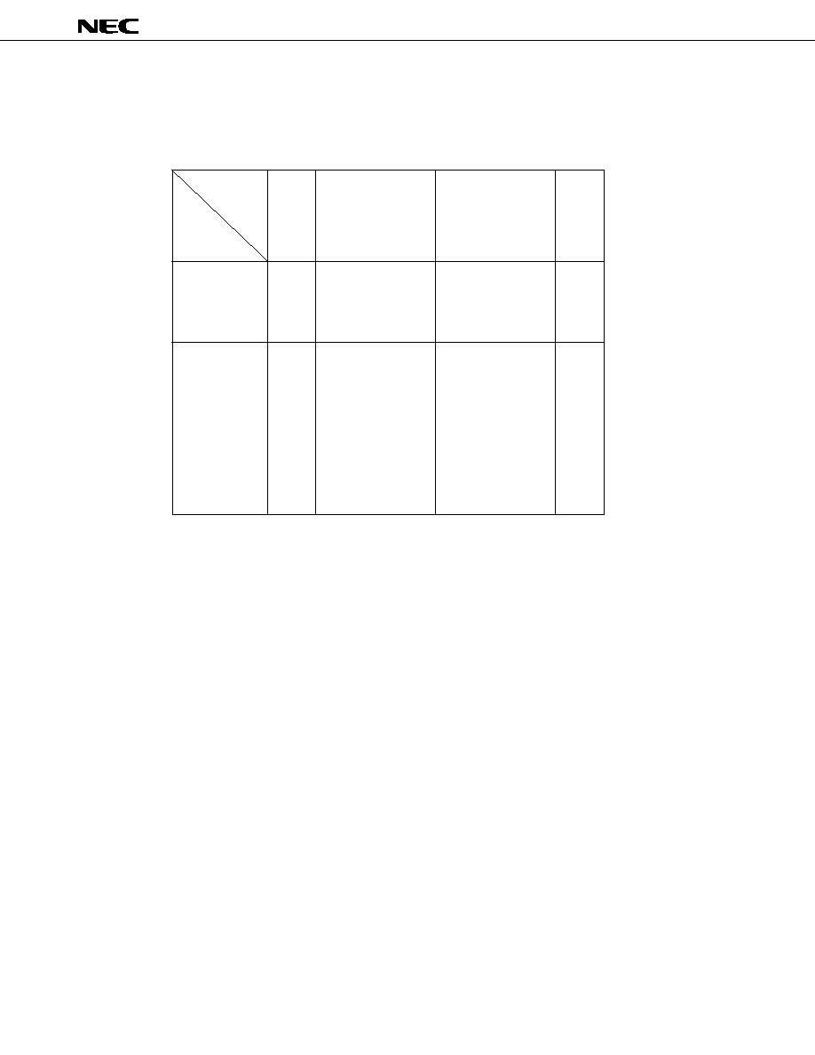
µ
PD784035Y, 784036Y, 784037Y, 784038Y
60
(4) Bit manipulation instructions
MOV1, AND1, OR1, XOR1, SET1, CLR1, NOT1, BT, BF, BTCLR, BFSET
Table 12-4. Bit Manipulation Instructions
Second Operand
CY
saddr.bit sfr.bit
/saddr.bit /sfr. bit
None
Note
A.bit X.bit
/A.bit /X.bit
PSWL.bit PSWH.bit
/PSWL.bit /PSWH.bit
mem2.bit
/mem2.bit
First Operand
!addr16.bit !!addr24.bit
/!addr16.bit /!!addr24.bit
CY
MOV1
AND1
NOT1
AND1
OR1
SET1
OR1
CLR1
XOR1
saddr.bit
MOV1
NOT1
sfr.bit
SET1
A.bit
CLR1
X.bit
BF
PSWL.bit
BT
PSWH.bit
BTCLR
mem2.bit
BFSET
!addr16.bit
!!addr24.bit
Note
Either the second operand is not used, or the second operand is not an
operand address.
61
µ
PD784035Y, 784036Y, 784037Y, 784038Y
(5) Call and return/branch instructions
CALL, CALLF, CALLT, BRK, RET, RETI, RETB, RETCS, RETCSB, BRKCS, BR, BNZ, BNE, BZ, BE, BNC,
BNL, BC, BL, BNV, BPO, BV, BPE, BP, BN, BLT, BGE, BLE, BGT, BNH, BH, BF, BT, BTCLR, BFSET, DBNZ
Table 12-5. Call and Return/Branch Instructions
Operand of Instruction
$addr20 $!addr20 !addr16 !!addr20
rp
rg
[rp]
[rg]
!addr11
[addr5]
RBn
None
Address
Basic instruction
BC
Note
CALL
CALL
CALL
CALL
CALL
CALL
CALL
CALLF
CALLF
BRKCS BRK
BR
BR
BR
BR
BR
BR
BR
BR
RET
RETCS
RETI
RETCSB
RETB
Compound instruction
BF
BT
BTCLR
BFSET
DBNZ
Note
The operands of BNZ, BNE, BZ, BE, BNC, BNL, BL, BNV, BPO, BV, BPE, BP, BN, BLT, BGE, BLE, BGT,
BNH, and BH are the same as BC.
(6) Other instructions
ADJBA, ADJBS, CVTBW, LOCATION, SEL, NOT, EI, DI, SWRS
µ
PD784035Y, 784036Y, 784037Y, 784038Y
62
13. ELECTRICAL SPECIFICATIONS
ABSOLUTE MAXIMUM RATINGS (T
A
= 25
∞
C)
Parameter
Symbol
Conditions
Ratings
Unit
Supply voltage
V
DD
≠0.5 to +7.0
V
AV
DD
AV
SS
to V
DD
+0.5
V
AV
SS
≠0.5 to +0.5
V
Input voltage
V
I
≠0.5 to V
DD
+0.5
V
Output voltage
V
O
≠0.5 to V
DD
+0.5
V
Low-level output
I
OL
Per pin
15
mA
current
Total of all output pins
100
mA
High-level output
I
OH
Per pin
≠10
mA
current
Total of all output pins
≠100
mA
A/D converter reference
AV
REF1
≠0.5 to V
DD
+0.3
V
input voltage
D/A converter reference
AV
REF2
≠0.5 to V
DD
+0.3
V
input voltage
AV
REF3
≠0.5 to V
DD
+0.3
V
Operating ambient
T
A
≠40 to +85
∞
C
temperature
Storage temperature
T
stg
≠65 to +150
∞
C
Caution Absolute maximum ratings are rated values beyond which physical damage will be caused to
the product; if the rated value of any of the parameters in the above table is exceeded, even
momentarily, the quality of the product may deteriorate. Always use the product within its rated
values.

63
µ
PD784035Y, 784036Y, 784037Y, 784038Y
CAPACITANCE (T
A
= 25
∞
C, V
DD
= V
SS
= 0 V)
Parameter
Symbol
Conditions
MIN.
TYP.
MAX.
Unit
Input capacitance
C
I
f = 1 MHz
10
pF
Output capacitance
C
O
Unmeasured pins returned to 0 V.
10
pF
I/O capacitance
C
IO
10
pF
OPERATING CONDITIONS
∑ Operating ambient temperature (T
A
)
: ≠40 to +85
∞
C
∑ Rising time and falling time (tr, tf) (at pins which are not specified) : 0 to 200
µ
s
∑ Power supply voltage and clock cycle time
: See Figure 13-1
Figure 13-1. Power Supply Voltage and Clock Cycle Time
10000
4000
1000
125
100
62.5
10
0
1
2
3
4
5
6
7
Guaranteed
Operating
Range
Power Supply Voltage [V]
Clock Cycle Time t
CYK
[ns]

µ
PD784035Y, 784036Y, 784037Y, 784038Y
64
OSCILLATOR CHARACTERISTICS (T
A
= ≠40 to +85
∞
C, V
DD
= +4.5 to 5.5 V, V
SS
= 0 V)
Resonator
Recommended Circuit
Parameter
MIN.
MAX.
Unit
Ceramic resonator or
Oscillator frequency (f
XX
)
4
32
MHz
crystal resonator
External clock
X1 input frequency (f
X
)
4
32
MHz
X1 input rising/falling time (t
XR
, t
XF
)
0
10
ns
X1 input high-/low-level width
10
125
ns
(t
WXH
, t
WXL
)
Caution When using the system clock oscillator, wiring the area enclosed with the broken line should
be carried out as follows to avoid an adverse effect from wiring capacitance.
∑ Wiring should be as short as possible.
∑ Wiring should not cross other signal lines.
∑ Wiring should not be placed close to a varying high current.
∑ The potential of the oscillator capacitor ground should be the same as V
SS1
. Do not ground
wiring to a ground pattern in which a high current flows.
∑ Do not fetch a signal from the oscillator.
V
SS1
X1
X2
C2
C1
X1
X2
HCMOS inverter

65
µ
PD784035Y, 784036Y, 784037Y, 784038Y
OSCILLATOR CHARACTERISTICS (T
A
= ≠40 to +85
∞
C, V
DD
= +2.7 to 5.5 V, V
SS
= 0 V)
Resonator
Recommended Circuit
Parameter
MIN.
MAX.
Unit
Ceramic resonator or
Oscillator frequency (f
XX
)
4
16
MHz
crystal resonator
External clock
X1 input frequency (f
X
)
4
16
MHz
X1 input rising/falling time (t
XR
, t
XF
)
0
10
ns
X1 input high-/low-level width
10
125
ns
(t
WXH
, t
WXL
)
Caution When using the system clock oscillator, wiring the area enclosed with the broken line should
be carried out as follows to avoid an adverse effect from wiring capacitance.
∑ Wiring should be as short as possible.
∑ Wiring should not cross other signal lines.
∑ Wiring should not be placed close to a varying high current.
∑ The potential of the oscillator capacitor ground should be the same as V
SS1
. Do not ground
wiring to a ground pattern in which a high current flows.
∑ Do not fetch a signal from the oscillator.
V
SS1
X1
X2
C2
C1
X1
X2
HCMOS inverter

µ
PD784035Y, 784036Y, 784037Y, 784038Y
66
DC CHARACTERISTICS (T
A
= ≠40 to +85
∞
C, V
DD
= AV
DD
= +2.7 to 5.5 V, V
SS
= AV
SS
= 0 V) (1/2)
Parameter
Symbol
Conditions
MIN.
TYP.
MAX.
Unit
Low-level input voltage
V
IL1
For pins other than those described in Notes 1, 2,
≠0.3
0.3V
DD
V
3, 4, and 6
V
IL2
For pins described in Notes 1, 2, 3, 4, and 6
≠0.3
0.2V
DD
V
V
IL3
V
DD
= +5.0 V
±
10%
≠0.3
+0.8
V
For pins described in Notes 2, 3, and 4
High-level input voltage
V
IH1
For pins other than those described in Notes 1 and 6
0.7V
DD
V
DD
+0.3
V
V
IH2
For pins described in Notes 1 and 6
0.8V
DD
V
DD
+0.3
V
V
IH3
V
DD
= +5.0 V
±
10%
2.2
V
DD
+0.3
V
For pins described in Notes 2, 3, and 4
Low-level output voltage
V
OL1
I
OL
= 2 mA
0.4
V
For pins other than those described in Note 6
V
OL2
I
OL
= 3 mA
0.4
V
For pins described in Note 6
I
OL
= 6 mA
0.6
V
For pins described in Note 6
V
OL3
V
DD
= +5.0 V
±
10%
1.0
V
I
OL
= 8 mA
For pins described in Notes 2 and 5
High-level output voltage
V
OH1
I
OH
= ≠2 mA
V
DD
≠1.0
V
V
OH2
V
DD
= +5.0 V
±
10%
V
DD
≠1.4
V
I
OH
= ≠5 mA
For pins other than those described in Note 4
X1 low-level input current
I
IL
EXTC = 0
≠30
µ
A
0 V
V
I
V
IL2
X1 high-level input current
I
IH
EXTC = 0
+30
µ
A
V
IH2
V
I
V
DD
Notes 1. X1, X2, RESET, P12/ASCK2/SCK2, P20/NMI, P21/INTP0, P22/INTP1, P23/INTP2/CI, P24/INTP3,
P25/INTP4/ASCK/SCK1, P26/INTP5, P27/SI0, and TEST
2. P40/AD0 to P47/AD7 and P50/A8 to P57/A15
3. P60/A16 to P63/A19, P64/RD, P65/WR, P66/WAIT/HLDRQ, and P67/REFRQ/HLDAK
4. P00 to P07
5. P10 to P17
6. P32/SCK0/SCL and P33/SO0/SDA
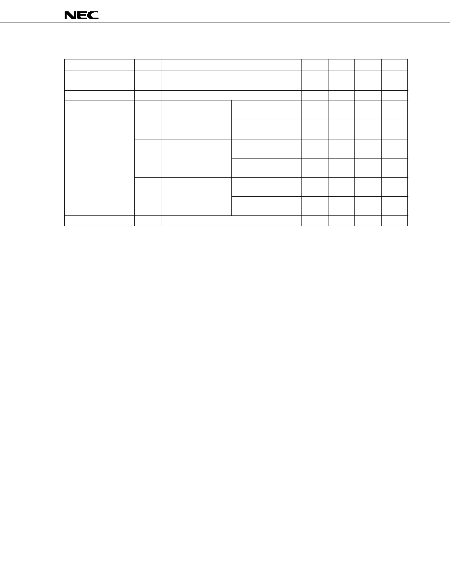
67
µ
PD784035Y, 784036Y, 784037Y, 784038Y
DC CHARACTERISTICS (T
A
= ≠40 to +85
∞
C, V
DD
= AV
DD
= +2.7 to 5.5 V, V
SS
= AV
SS
= 0 V) (2/2)
Parameter
Symbol
Conditions
MIN.
TYP.
MAX.
Unit
Input leakage current
I
LI
0 V
V
I
V
DD
±
10
µ
A
For pins other than pin X1 when EXTC = 0
Output leakage current
I
LO
0 V
V
O
V
DD
±
10
µ
A
V
DD
supply current
I
DD1
Operation mode
f
XX
= 32 MHz
25
45
mA
V
DD
= +5.0 V
±
10%
f
XX
= 16 MHz
12
25
mA
V
DD
= +2.7 to 3.3 V
I
DD2
HALT mode
f
XX
= 32 MHz
13
26
mA
V
DD
= +5.0 V
±
10%
f
XX
= 16 MHz
8
12
mA
V
DD
= +2.7 to 3.3 V
I
DD3
IDLE mode (EXTC = 0)
f
XX
= 32 MHz
12
mA
V
DD
= +5.0 V
±
10%
f
XX
= 16 MHz
8
mA
V
DD
= +2.7 to 3.3 V
Pull-up resistance
R
L
V
I
= 0 V
15
80
k
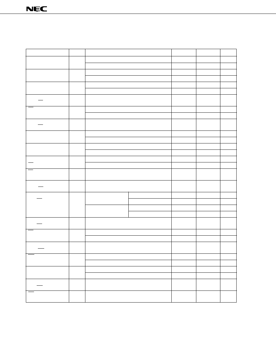
µ
PD784035Y, 784036Y, 784037Y, 784038Y
68
AC CHARACTERISTICS (T
A
= ≠40 to +85
∞
C, V
DD
= AV
DD
= +2.7 to 5.5 V, V
SS
= AV
SS
= 0 V)
(1) Read/write operation (1/2)
Parameter
Symbol
Conditions
MIN.
MAX.
Unit
Address setup time
t
SAST
V
DD
= +5.0 V
±
10%
(0.5+a)T≠15
ns
(0.5+a)T≠31
ns
ASTB high-level width
t
WSTH
V
DD
= +5.0 V
±
10%
(0.5+a)T≠17
ns
(0.5+a)T≠40
ns
Address hold time
t
HSTLA
V
DD
= +5.0 V
±
10%
0.5T≠24
ns
(from ASTB
)
0.5T≠34
ns
Address hold time
t
HRA
0.5T≠14
ns
(from RD
)
RD
delay time from
t
DAR
V
DD
= +5.0 V
±
10%
(1+a)T≠9
ns
address
(1+a)T≠15
ns
Address float time
t
FRA
0
ns
(from RD
)
Data input time from
t
DAID
V
DD
= +5.0 V
±
10%
(2.5+a+n)T≠37
ns
address
(2.5+a+n)T≠52
ns
Data input time from
t
DSTID
V
DD
= +5.0 V
±
10%
(2+n)T≠40
ns
ASTB
(2+n)T≠60
ns
Data input time from
t
DRID
V
DD
= +5.0 V
±
10%
(1.5+n)T≠50
ns
RD
(1.5+n)T≠70
ns
RD
delay time from
t
DSTR
0.5T≠9
ns
ASTB
Data hold time
t
HRID
0
ns
(from RD
)
Address active time
t
DRA
After program is read
V
DD
= +5.0 V
±
10%
0.5T≠8
ns
from RD
0.5T≠12
ns
After data is read
V
DD
= +5.0 V
±
10%
1.5T≠8
ns
1.5T≠12
ns
ASTB
delay time
t
DRST
0.5T≠17
ns
from RD
RD low-level width
t
WRL
V
DD
= +5.0 V
±
10%
(1.5+n)T≠30
ns
(1.5+n)T≠40
ns
Address hold time
t
HWA
0.5T≠14
ns
(from WR
)
WR
delay time from
t
DAW
V
DD
= +5.0 V
±
10%
(1+a)T≠5
ns
address
(1+a)T≠15
ns
Data output delay time
t
DSTOD
V
DD
= +5.0 V
±
10%
0.5T+19
ns
from ASTB
0.5T+35
ns
Data output delay time
t
DWOD
0.5T≠11
ns
from WR
WR
output delay time
t
DSTW
0.5T≠9
ns
from ASTB
Remark T : T
CYK
(system clock cycle time)
a : 1 (during address wait), otherwise, 0
n : Number of wait states (n
0)

69
µ
PD784035Y, 784036Y, 784037Y, 784038Y
(1) Read/write operation (2/2)
Parameter
Symbol
Conditions
MIN.
MAX.
Unit
Data setup time (to WR
)
t
SODW
V
DD
= +5.0 V
±
10%
(1.5+n)T≠30
ns
(1.5+n)T≠40
ns
Data hold time
t
HWOD
V
DD
= +5.0 V
±
10%
0.5T≠5
ns
(from WR
)
Note
0.5T≠25
ns
ASTB
delay time
t
DWST
0.5T≠12
ns
(from WR
)
WR low-level width
t
WWL
V
DD
= +5.0 V
±
10%
(1.5+n)T≠30
ns
(1.5+n)T≠40
ns
Note
The hold time includes the time during which V
OH1
and V
OL1
are held under the load conditions of C
L
=
50 pF and R
L
= 4.7 k
.
Remark T: T
CYK
(system clock cycle time)
n: Number of wait states (n
0)
(2) Bus hold timing
Parameter
Symbol
Conditions
MIN.
MAX.
Unit
Float delay time from
t
FHQC
(6+a+n)T+50
ns
HLDRQ
HLDAK
delay time
t
DHQHHAH
V
DD
= +5.0 V
±
10%
(7+a+n)T+30
ns
from HLDRQ
(7+a+n)T+40
ns
HLDAK
delay time
t
DCFHA
1T+30
ns
from float
HLDAK
delay time
t
DHQLHAL
V
DD
= +5.0 V
±
10%
2T+40
ns
from HLDRQ
2T+60
ns
Active delay time from
t
DHAC
V
DD
= +5.0 V
±
10%
1T≠20
ns
HLDAK
1T≠30
ns
Remark T: T
CYK
(system clock cycle time)
a: 1 (during address wait), otherwise, 0
n: Number of wait states (n
0)

µ
PD784035Y, 784036Y, 784037Y, 784038Y
70
(3) External wait timing
Parameter
Symbol
Conditions
MIN.
MAX.
Unit
WAIT
input time from
t
DAWT
V
DD
= +5.0 V
±
10%
(2+a)T≠40
ns
address
(2+a)T≠60
ns
WAIT
input time from
t
DSTWT
V
DD
= +5.0 V
±
10%
1.5T≠40
ns
ASTB
1.5T≠60
ns
WAIT hold time from
t
HSTWTH
V
DD
= +5.0 V
±
10%
(0.5+n)T+5
ns
ASTB
(0.5+n)T+10
ns
WAIT
delay time from
t
DSTWTH
V
DD
= +5.0 V
±
10%
(1.5+n)T≠40
ns
ASTB
(1.5+n)T≠60
ns
WAIT
input time from
t
DRWTL
V
DD
= +5.0 V
±
10%
T≠50
ns
RD
T≠70
ns
WAIT
hold time from
t
HRWT
V
DD
= +5.0 V
±
10%
nT+5
ns
RD
nT+10
ns
WAIT
delay time from
t
DRWTH
V
DD
= +5.0 V
±
10%
(1+n)T≠40
ns
RD
(1+n)T≠60
ns
Data input time from
t
DWTID
V
DD
= +5.0 V
±
10%
0.5T≠5
ns
WAIT
0.5T≠10
ns
WR
delay time from
t
DWTW
0.5T
ns
WAIT
RD
delay time from
t
DWTR
0.5T
ns
WAIT
WAIT
input time from
t
DWWTL
V
DD
= +5.0 V
±
10%
T≠5
ns
WR
T≠75
ns
WAIT hold time from
t
HWWT
V
DD
= +5.0 V
±
10%
nT+5
ns
WR
nT+10
ns
WAIT
delay time from
t
DWWTH
V
DD
= +5.0 V
±
10%
(1+n)T≠40
ns
WR
(1+n)T≠70
ns
Remark T: T
CYK
(system clock cycle time)
a: 1 (during address wait), otherwise, 0
n: Number of wait states (n
0)
(4) Refresh timing
Parameter
Symbol
Conditions
MIN.
MAX.
Unit
Random read/write cycle
t
RC
3T
ns
time
REFRQ low-level pulse
t
WRFQL
V
DD
= +5.0 V
±
10%
1.5T≠25
ns
width
1.5T≠30
ns
REFRQ delay time from
t
DSTRFQ
0.5T≠9
ns
ASTB
REFRQ delay time from
t
DRRFQ
1.5T≠9
ns
RD
REFRQ delay time from
t
DWRFQ
1.5T≠9
ns
WR
ASTB delay time from
t
DRFQST
0.5T≠15
ns
REFRQ
REFRQ high-level pulse t
WRFQH
V
DD
= +5.0 V
±
10%
1.5T≠25
ns
width
1.5T≠30
ns
Remark T: T
CYK
(system clock cycle time)

71
µ
PD784035Y, 784036Y, 784037Y, 784038Y
SERIAL OPERATION (T
A
= ≠40 to +85
∞
C, V
DD
= +2.7 to 5.5 V, AV
SS
= V
SS
= 0 V)
(1) CSI
Parameter
Symbol
Conditions
MIN.
MAX.
Unit
Serial clock cycle time
t
CYSK0
Input
External clock
10/f
XX
+380
ns
(SCK0)
When SCK0 and SO0 are CMOS I/O
Output
T
µ
s
Serial clock low-level
t
WSKL0
Input
External clock
5/f
XX
+150
ns
width (SCK0)
When SCK0 and SO0 are CMOS I/O
Output
0.5T≠40
µ
s
Serial clock high-level
t
WSKH0
Input
External clock
5/f
XX
+150
ns
width (SCK0)
When SCK0 and SO0 are CMOS I/O
Output
0.5T≠40
µ
s
SI0 setup time
t
SSSK0
40
ns
(to SCK0
)
SI0 hold time
t
HSSK0
5/f
XX
+40
ns
(from SCK0
)
SO0 output delay time
t
DSBSK1
CMOS push-pull output
0
5/f
XX
+150
ns
(from SCK0
)
(3-wire serial I/O mode)
t
DSBSK2
Open-drain output
0
5/f
XX
+400
ns
(2-wire serial I/O mode), R
L
= 1 k
Remarks 1. The values in this table are those when C
L
is 100 pF.
2. T: Serial clock cycle set by software. The minimum value is 16/f
XX
.
3. f
XX
: Oscillation frequency
(2) I
2
C
Parameter
Symbol
Standard mode I
2
C bus
High-speed mode I
2
C bus
Unit
f
XX
= 4 to 32 MHz
f
XX
= 8 to 32 MHz
MIN.
MAX.
MIN.
MAX.
SCL clock frequency
f
SCL
0
100
0
400
kHz
Hold time of SCL clock
t
LOW
4.7
1.3
µ
s
low-level state
Hold time of SCL clock
t
HIGH
4.0
0.6
µ
s
high-level state
Data hold time
t
HD
; DAT
300
300
900
ns
Data setup time
t
SU
; DAT
250
100
ns
Rising time of SDA and
t
R
1000
20+0.1Cb
300
ns
SCL signals
Falling time of SDA and
t
F
300
20+0.1Cb
300
ns
SCL signals
Load capacitance of
Cb
400
400
pF
each bus line
µ
PD784035Y, 784036Y, 784037Y, 784038Y
72
(3) IOE1, IOE2
Parameter
Symbol
Conditions
MIN.
MAX.
Unit
Serial clock cycle time
t
CYSK1
Input
V
DD
= +5.0 V
±
10%
250
ns
(SCK1, SCK2)
500
ns
Output
Internal clock divided by 16
T
ns
Serial clock low-level
t
WSKL1
Input
V
DD
= +5.0 V
±
10%
85
ns
width (SCK1, SCK2)
210
ns
Output
Internal clock divided by 16
0.5T≠40
ns
Serial clock high-level
t
WSKH1
Input
V
DD
= +5.0 V
±
10%
85
ns
width (SCK1, SCK2)
210
ns
Output
Internal clock divided by 16
0.5T≠40
ns
SI1, SI2 setup time
t
SSSK1
40
ns
(to SCK1, SCK2
)
SI1, SI2 hold time
t
HSSK1
40
ns
(from SCK1, SCK2
)
SO1, SO2 output delay time
t
DSOSK
0
50
ns
(from SCK1, SCK2
)
SO1, SO2 output hold time
t
HSOSK
During data transfer
0.5t
CYSK1
≠40
ns
(from SCK1, SCK2
)
Remarks 1. The values in this table are those when C
L
is 100 pF.
2. T: Serial clock cycle set by software. The minimum value is 16/f
XX
.
(4) UART, UART2
Parameter
Symbol
Conditions
MIN.
MAX.
Unit
ASCK clock input cycle
t
CYASK
V
DD
= +5.0 V
±
10%
125
ns
time
250
ns
ASCK clock low-level
t
WASKL
V
DD
= +5.0 V
±
10%
52.5
ns
width
85
ns
ASCK clock high-level
t
WASKH
V
DD
= +5.0 V
±
10%
52.5
ns
width
85
ns
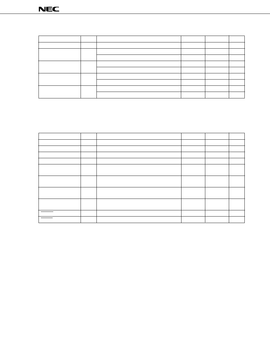
73
µ
PD784035Y, 784036Y, 784037Y, 784038Y
CLOCK OUTPUT OPERATION
Parameter
Symbol
Conditions
MIN.
MAX.
Unit
CLKOUT cycle time
t
CYCL
nT
ns
CLKOUT low-level width
t
CLL
V
DD
= +5.0 V
±
10%
0.5t
CYCL
≠10
ns
0.5t
CYCL
≠20
ns
CLKOUT high-level width
t
CLH
V
DD
= +5.0 V
±
10%
0.5t
CYCL
≠10
ns
0.5t
CYCL
≠20
ns
CLKOUT rising time
t
CLR
V
DD
= +5.0 V
±
10%
10
ns
20
ns
CLKOUT falling time
t
CLF
V
DD
= +5.0 V
±
10%
10
ns
20
ns
Remark n: Divided frequency ratio set by software in the CPU (n = 1, 2, 4, 8, 16)
T: t
CYK
(system clock cycle time)
OTHER OPERATIONS
Parameter
Symbol
Conditions
MIN.
MAX.
Unit
NMI low-level width
t
WNIL
10
µ
s
NMI high-level width
t
WNIH
10
µ
s
INTP0 low-level width
t
WIT0L
3t
CYSMP
+10
ns
INTP0 high-level width
t
WIT0H
3t
CYSMP
+10
ns
INTP1 to INTP3, CI
t
WIT1L
3t
CYCPU
+10
ns
low-level width
INTP1 to INTP3, CI
t
WIT1H
3t
CYCPU
+10
ns
high-level width
INTP4, INTP5 low-level
t
WIT2L
10
µ
s
width
INTP4, INTP5 high-level t
WIT2H
10
µ
s
width
RESET low-level width
t
WRSL
10
µ
s
RESET high-level width
t
WRSH
10
µ
s
Remark t
CYSMP
: Sampling clock set by software
t
CYCPU
: CPU operation clock set by software in the CPU
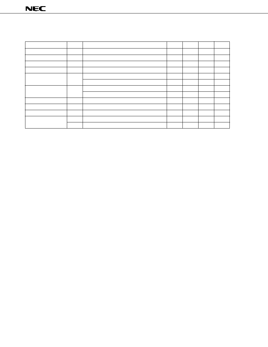
µ
PD784035Y, 784036Y, 784037Y, 784038Y
74
A/D CONVERTER CHARACTERISTICS (T
A
= ≠40 to +85
∞
C, V
DD
= AV
DD
= AV
REF1
= +2.7 to 5.5 V, V
SS
=
AV
SS
= 0 V)
Parameter
Symbol
Conditions
MIN.
TYP.
MAX.
Unit
Resolution
8
bit
Total error
Note
1.0
%
Linearity calibration
Note
0.8
%
Quantization error
±
1/2
LSB
Conversion time
t
CONV
FR = 1
120
t
CYK
FR = 0
180
t
CYK
Sampling time
t
SAMP
FR = 1
24
t
CYK
FR = 0
36
t
CYK
Analog input voltage
V
IAN
≠0.3
AV
REF1
+0.3
V
Analog input impedance
R
AN
1000
M
AV
REF1
current
AI
REF1
0.5
1.5
mA
AV
DD
supply current
AI
DD1
f
XX
= 32 MHz, CS = 1
2.0
5.0
mA
AI
DD2
STOP mode, CS = 0
1.0
20
µ
A
Note
Quantization error is not included. This parameter is indicated as the ratio to the full-scale value.
Remark t
CYK
: System clock cycle time
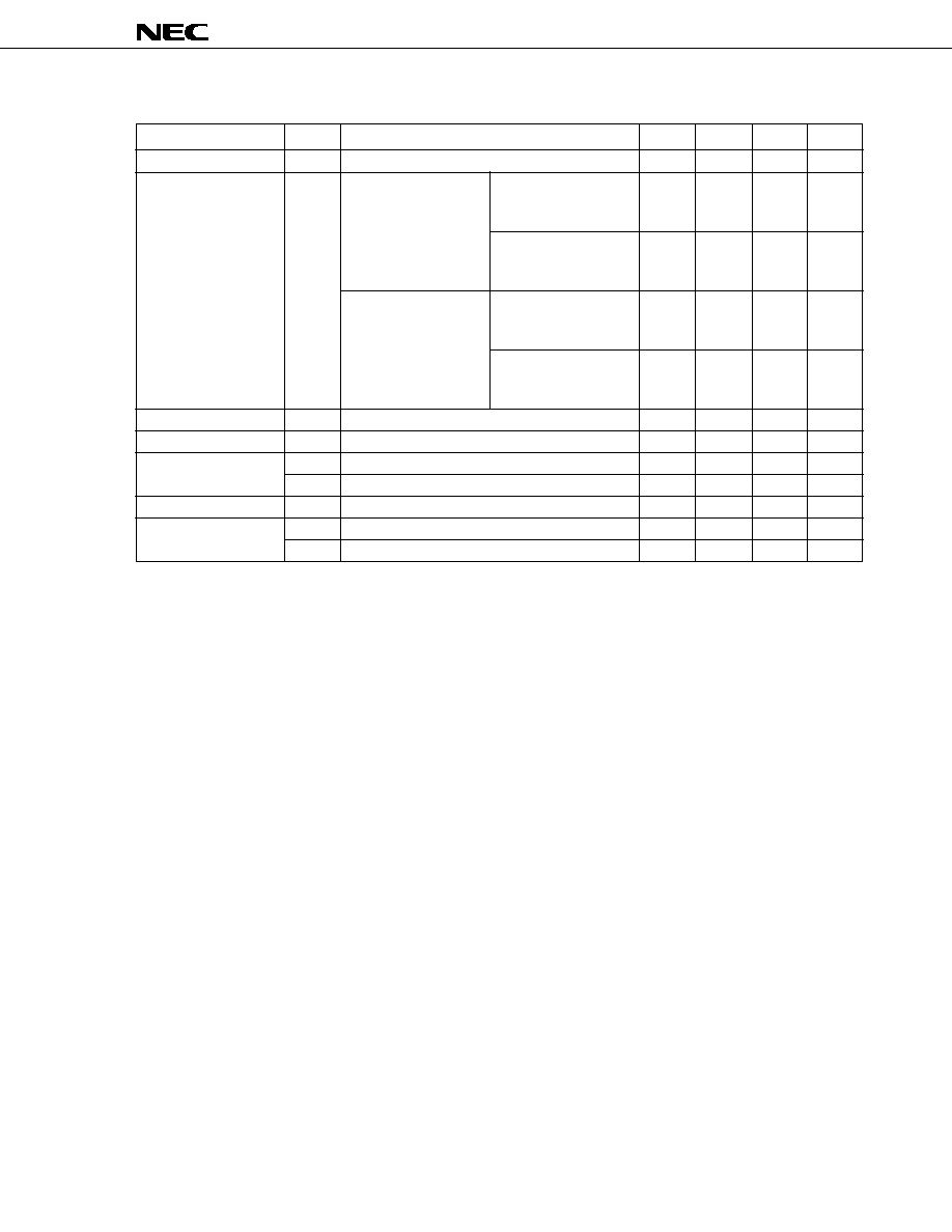
75
µ
PD784035Y, 784036Y, 784037Y, 784038Y
D/A CONVERTER CHARACTERISTICS (T
A
= ≠40 to +85
∞
C, V
DD
= AV
DD
= +2.7 to 5.5 V, V
SS
= AV
SS
= 0 V)
Parameter
Symbol
Conditions
MIN.
TYP.
MAX.
Unit
Resolution
8
bit
Total error
Load conditions:
V
DD
= AV
DD
= AV
REF2
0.6
%
4 M
, 30 pF
= +2.7 to 5.5 V
AV
REF3
= 0 V
V
DD
= AV
DD
= +2.7 to 5.5 V
0.8
%
AV
REF2
= 0.75V
DD
AV
REF3
= 0.25V
DD
Load conditions:
V
DD
= AV
DD
= AV
REF2
0.8
%
2 M
, 30 pF
= +2.7 to 5.5 V
AV
REF3
= 0 V
V
DD
= AV
DD
= +2.7 to 5.5 V
1.0
%
AV
REF2
= 0.75V
DD
AV
REF3
= 0.25V
DD
Settling time
Load conditions: 2 M
, 30 pF
10
µ
s
Output resistance
R
O
DACS0, 1 = 55 H
10
k
Analog reference voltage
AV
REF2
0.75V
DD
V
DD
V
AV
REF3
0
0.25V
DD
V
AV
REF2
, AV
REF3
resistance R
AIREF
DACS0, 1 = 55 H
4
8
k
Reference power supply
AI
REF2
0
5
mA
input current
AI
REF3
≠5
0
mA

µ
PD784035Y, 784036Y, 784037Y, 784038Y
76
DATA RETENTION CHARACTERISTICS (T
A
= ≠40 to +85
∞
C)
Parameter
Symbol
Conditions
MIN.
TYP.
MAX.
Unit
Data retention voltage
V
DDDR
STOP mode
2.5
5.5
V
Data retention current
I
DDDR
V
DDDR
= +2.7 to 5.5 V
10
50
µ
A
V
DDDR
= +2.5 V
2
10
µ
A
V
DD
rising time
t
RVD
200
µ
s
V
DD
falling time
t
FVD
200
µ
s
V
DD
hold time
t
HVD
0
ms
(from STOP mode setting)
STOP release signal
t
DREL
0
ms
input time
Oscillation stabilization
t
WAIT
Crystal resonator
30
ms
wait time
Ceramic resonator
5
ms
Low-level input voltage
V
IL
Specific pins
Note
0
0.1V
DDDR
V
High-level input voltage
V
IH
0.9V
DDDR
V
DDDR
V
Note
RESET, P20/NMI, P21/INTP0, P22/INTP1, P23/INTP2/CI, P24/INTP3, P25/INTP4/ASCK/SCK1, P26/
INTP5, P27/SI0, P32/SCK0/SCL, and P33/SO0/SDA pins
AC TIMING TEST POINTS
0.8V
DD
or 2.2 V
0.8 V
0.8V
DD
or 2.2 V
0.8 V
Test Points
V
DD
≠ 1 V
0.45 V

77
µ
PD784035Y, 784036Y, 784037Y, 784038Y
TIMING WAVEFORM
(1) Read operation
ASTB
A8 to A19
AD0 to AD7
RD
t
WSTH
t
SAST
t
DSTID
t
HSTLA
t
DRST
t
FRA
t
DRID
t
DAR
t
WRL
t
DSTR
t
DAID
t
HRA
t
DRA
t
HRID
(2) Write operation
ASTB
A8 to A19
AD0 to AD7
WR
t
WSTH
t
SAST
t
HSTLA
t
DWST
t
DAW
t
DSTW
t
HWOD
t
DSTOD
t
DWOD
t
SODW
t
WWL
t
HWA
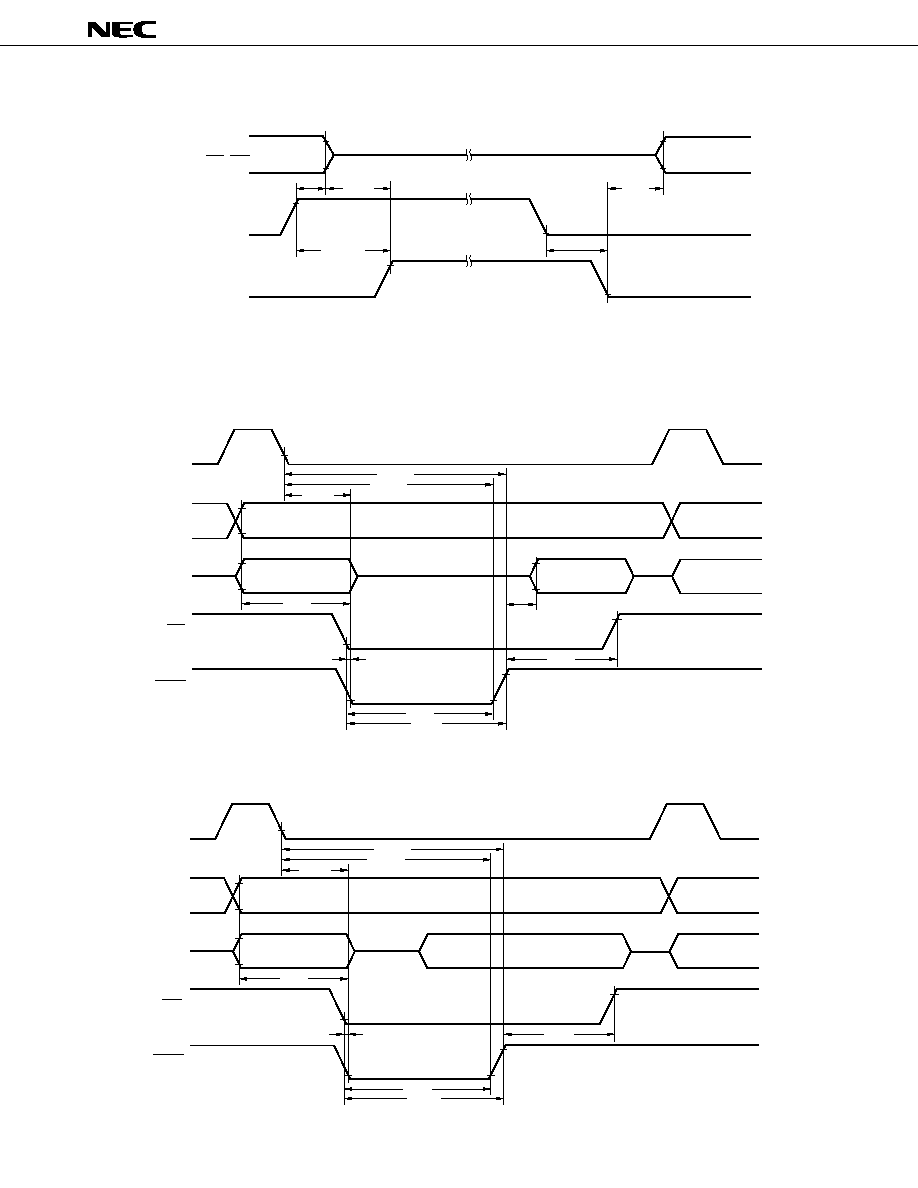
µ
PD784035Y, 784036Y, 784037Y, 784038Y
78
HOLD TIMING
HLDRQ
HLDAK
t
DHQHHAH
t
FHQC
t
DCFHA
t
DHAC
t
DHQLHAL
ADTB, A8 to A19,
AD0 to AD7, RD, WR
EXTERNAL WAIT SIGNAL INPUT TIMING
(1) Read operation
ASTB
A8 to A19
AD0 to AD7
RD
WAIT
t
DSTWT
t
HSTWTH
t
DSTWTH
t
DAWT
t
DWTID
t
DWTR
t
DRWTL
t
HRWT
t
DRWTH
(2) Write operation
ASTB
A8 to A19
AD0 to AD7
WR
WAIT
t
DSTWT
t
HSTWTH
t
DSTWTH
t
DAWT
t
DWTW
t
DWWTL
t
HWWT
t
DWWTH
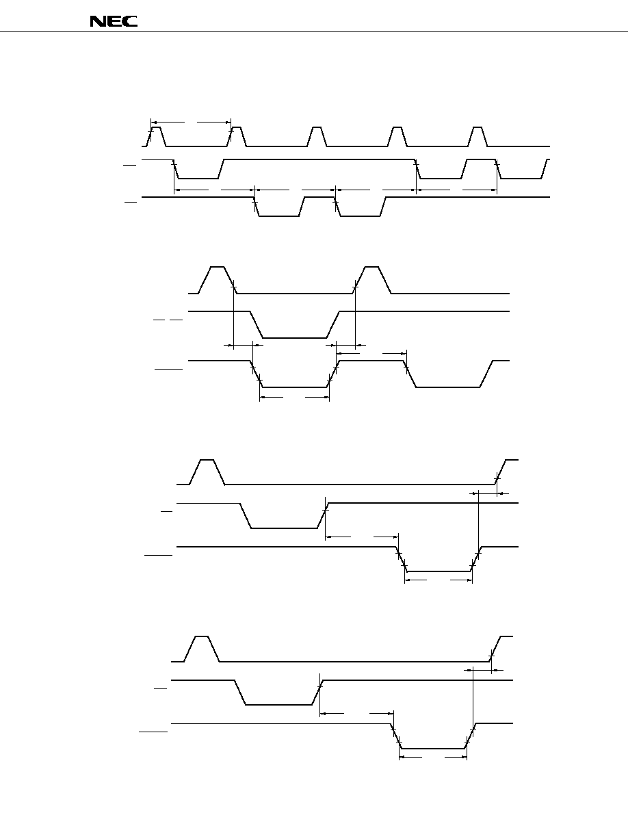
79
µ
PD784035Y, 784036Y, 784037Y, 784038Y
REFRESH TIMING WAVEFORM
(1) Random read/write cycle
ASTB
WR
RD
t
RC
t
RC
t
RC
t
RC
t
RC
(2) When refresh memory is accessed for read and write at the same time
t
WRFQL
ASTB
RD, WR
REFRQ
t
DSTRFQ
t
DRFQST
t
WRFQH
(3) Refresh after read
ASTB
RD
REFRQ
t
DRFQST
t
DRRFQ
t
WRFQL
(4) Refresh after write
ASTB
WR
REFRQ
t
DRFQST
t
DWRFQ
t
WRFQL

µ
PD784035Y, 784036Y, 784037Y, 784038Y
80
SERIAL OPERATION
(1) CSI
SCK
SI
SO
Output data
Input data
t
SSSK0
t
HSSK0
t
DSBSK1
t
WSKL0
t
WSKH0
t
HSBSK1
t
CYSK0
SCL
SDA
t
R
t
F
t
HIGH
t
LOW
t
HD
;
DAT
t
SU
;
DAT
(2) I
2
C
(3) IOE1, IOE2
(4) UART, UART2
SCK
SI
SO
Output data
Input data
t
SSSK1
t
HSSK1
t
DSOSK
t
HSOSK
t
WSKL1
t
WSKH1
t
CYSK1
ASCK,
ASCK2
t
WASKH
t
WASKL
t
CYASK

81
µ
PD784035Y, 784036Y, 784037Y, 784038Y
CLOCK OUTPUT TIMING
INTERRUPT INPUT TIMING
RESET INPUT TIMING
RESET
t
WRSH
t
WRSL
CLKOUT
t
CLH
t
CLL
t
CYCL
t
CLF
t
CLR
NMI
INTP0
CI,
INTP1 to INTP3
INTP4, INTP5
t
WNIH
t
WNIL
t
WIT0H
t
WIT0L
t
WIT1H
t
WIT1L
t
WIT2H
t
WIT2L
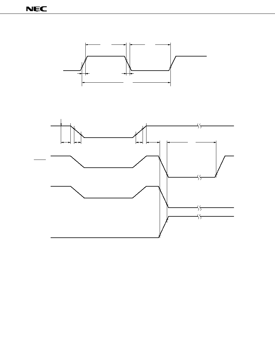
µ
PD784035Y, 784036Y, 784037Y, 784038Y
82
EXTERNAL CLOCK TIMING
DATA RETENTION CHARACTERISTICS
V
DD
RESET
NMI
(Clearing by
falling edge)
NMI
(Clearing by
rising edge)
t
HVD
t
FVD
t
RVD
t
DREL
V
DDDR
STOP mode setting
t
WAIT
X1
t
WXH
t
WXL
t
CYX
t
XF
t
XR

83
µ
PD784035Y, 784036Y, 784037Y, 784038Y
14. PACKAGE DRAWINGS
Remark The shape and material of the ES version are the same as those of the corresponding mass-produced
product.
80 PIN PLASTIC QFP (14
◊
14)
ITEM
MILLIMETERS
INCHES
NOTE
Each lead centerline is located within 0.13 mm (0.005 inch) of
its true position (T.P.) at maximum material condition.
L
0.8±0.2
0.031+0.009
≠0.008
M
0.15
0.006
N
0.10
0.004
P
2.7
0.106
A
17.2±0.4
0.677±0.016
B
14.0±0.2
0.551+0.009
≠0.008
C
14.0±0.2
0.551+0.009
≠0.008
D
17.2±0.4
0.677±0.016
F
0.825
0.032
G
0.825
0.032
H
0.30±0.10
0.012+0.004
≠0.005
I
0.13
0.005
J
0.65 (T.P.)
0.026 (T.P.)
Q
0.1±0.1
0.004±0.004
R
5
∞
±5
∞
5
∞
±5
∞
+0.10
≠0.05
+0.004
≠0.003
M
M
L
K
J
H
Q
P
N
R
detail of lead end
I
G
K
1.6±0.2
0.063±0.008
60
61
40
80
1
21
20
41
A
B
C D
F
S
S80GC-65-3B9-4
S
3.0 MAX.
0.119 MAX.

µ
PD784035Y, 784036Y, 784037Y, 784038Y
84
Remark The shape and material of the ES version are the same as those of the corresponding mass-produced
product.
80 PIN PLASTIC QFP (14
◊
14)
ITEM
MILLIMETERS
INCHES
NOTE
Each lead centerline is located within 0.13 mm (0.005 inch) of
its true position (T.P.) at maximum material condition.
P80GC-65-8BT
F
0.825
0.032
B
14.00±0.20
0.551+0.009
≠0.008
S
1.70 MAX.
0.067 MAX.
M
0.17
0.007+0.001
≠0.003
+0.03
≠0.07
+0.009
≠0.008
C
14.00±0.20
0.551+0.009
≠0.008
A
17.20±0.20
0.677±0.008
G
0.825
0.032
H
0.32±0.06
0.013+0.002
≠0.003
I
0.13
0.005
J
0.65 (T.P.)
0.026 (T.P.)
K
1.60±0.20
0.063±0.008
L
0.80±0.20
0.031+0.009
≠0.008
N
0.10
0.004
P
1.40±0.10
0.055±0.004
Q
0.125±0.075
0.005±0.003
R
3
∞
3
∞
+7
∞
≠3
∞
+7
∞
≠3
∞
D
17.20±0.20
0.677±0.008
41
60
40
61
21
80
20
1
M
S
Q
R
K
M
L
A
B
C
D
J
H
I
F
G
P
N
detail of lead end
5

85
µ
PD784035Y, 784036Y, 784037Y, 784038Y
Remark The shape and material of the ES version are the same as those of the corresponding mass-produced
product.
80 PIN PLASTIC TQFP (FINE PITCH) ( 12)
ITEM
MILLIMETERS
INCHES
I
J
0.5 (T.P.)
0.10
0.004
0.020 (T.P.)
A
NOTE
Each lead centerline is located within 0.10 mm (0.004 inch) of
its true position (T.P.) at maximum material condition.
S
A
14.0±0.2
0.551+0.009
≠0.008
B
12.0±0.2
0.472+0.009
≠0.008
C
12.0±0.2
0.472+0.009
≠0.008
D
14.0±0.2
0.551+0.009
≠0.008
F
G
1.25
1.25
0.049
0.049
H
0.22
0.009±0.002
P80GK-50-BE9-4
S
1.27 MAX.
0.050 MAX.
K
1.0±0.2
0.039+0.009
≠0.008
L
0.5±0.2
0.020+0.008
≠0.009
M
0.145
0.006±0.002
N
0.10
0.004
P
1.05
0.041
Q
0.05±0.05
0.002±0.002
R
5∞±5∞
5∞±5∞
+0.05
≠0.04
+0.055
≠0.045
B
C
D
J
H
I
G
F
P
N
L
K
M
Q
R
detail of lead end
M
61
60
41
40
21
20
1
80

µ
PD784035Y, 784036Y, 784037Y, 784038Y
86
15. RECOMMENDED SOLDERING CONDITIONS
It is recommended that the
µ
PD784035Y, 784036Y, 784037Y, and 784038Y be soldered under the following
conditions.
For details on the recommended soldering conditions, refer to information document "Semiconductor Device
Mounting Technology Manual" (C10535E).
For soldering methods and conditions other than those recommended, please consult an NEC representative.
Caution The soldering conditions for the
µ
PD784035YGK-
◊◊◊
-BE9 and 784036YGK-
◊◊◊
-BE9 are unde-
fined because these products are currently under development.
Table 15-1. Soldering Conditions for Surface Mount Type (1/2)
(1)
µ
PD784035YGC-
◊◊◊
-3B9: 80-pin plastic QFP (14
◊
14 mm, 2.7-mm thick)
µ
PD784036YGC-
◊◊◊
-3B9: 80-pin plastic QFP (14
◊
14 mm, 2.7-mm thick)
µ
PD784037YGC-
◊◊◊
-3B9: 80-pin plastic QFP (14
◊
14 mm, 2.7-mm thick)
µ
PD784038YGC-
◊◊◊
-3B9: 80-pin plastic QFP (14
◊
14 mm, 2.7-mm thick)
Soldering Method
Soldering Conditions
Recommended
Condition Symbol
Infrared ray reflow
Package peak temperature: 235
∞
C, Reflow time: 30 seconds or less (210
∞
C or more)
IR35-00-3
Number of reflow processes: 3 or less
VPS
Package peak temperature: 215
∞
C, Reflow time: 40 seconds or less (200
∞
C or more)
VP15-00-3
Number of reflow processes: 3 or less
Wave soldering
Solder bath temperature: 260
∞
C or less, Flow time: 10 seconds or less,
WS60-00-1
Number of flow processes: 1, Preheating temperature: 120
∞
C max.
(package surface temperature)
Partial heating
Pin temperature: 300
∞
C or less, Flow time: 3 seconds or less
--
(for one side of the a device)
Caution Do not apply two or more different soldering methods to one chip (except for partial heating
method).
(2)
µ
PD784035YGC-
◊◊◊
-8BT: 80-pin plastic QFP (14
◊
14 mm, 1.4-mm thick)
µ
PD784036YGC-
◊◊◊
-8BT: 80-pin plastic QFP (14
◊
14 mm, 1.4-mm thick)
µ
PD784037YGC-
◊◊◊
-8BT: 80-pin plastic QFP (14
◊
14 mm, 1.4-mm thick)
µ
PD784038YGC-
◊◊◊
-8BT: 80-pin plastic QFP (14
◊
14 mm, 1.4-mm thick)
Soldering Method
Soldering Conditions
Recommended
Condition Symbol
Infrared ray reflow
Package peak temperature: 235
∞
C, Reflow time: 30 seconds or less (210
∞
C or more)
IR35-00-2
Number of reflow processes: 2 or less
VPS
Package peak temperature: 215
∞
C, Reflow time: 40 seconds or less (200
∞
C or more)
VP15-00-2
Number of reflow processes: 2 or less
Wave soldering
Solder bath temperature: 260
∞
C or less, Flow time: 10 seconds or less,
WS60-00-1
Number of flow processes: 1, Preheating temperature: 120
∞
C max.
(package surface temperature)
Partial heating
Pin temperature: 300
∞
C or less, Flow time: 3 seconds or less
--
(for one side of the a device)
Caution Do not apply two or more different soldering methods to one chip (except for partial heating
method).

87
µ
PD784035Y, 784036Y, 784037Y, 784038Y
Table 15-1. Soldering Conditions for Surface Mount Type (2/2)
(3)
µ
PD784037YGK-
◊◊◊
-BE9: 80-pin plastic TQFP (fine-pitch) (12
◊
12 mm)
µ
PD784038YGK-
◊◊◊
-BE9: 80-pin plastic TQFP (fine-pitch) (12
◊
12 mm)
Soldering Method
Soldering Conditions
Recommended
Condition Symbol
Infrared ray reflow
Package peak temperature: 235
∞
C, Reflow time: 30 seconds or less (210
∞
C or more)
IR35-107-2
Number of reflow processes: 2 or less
Exposure limit: 7 days
Note
(10 hours of pre-baking is required at 125
∞
C afterward)
VPS
Package peak temperature: 215
∞
C, Reflow time: 40 seconds or less (200
∞
C or more)
VP15-107-2
Number of reflow processes: 2 or less
Exposure limit: 7 days
Note
(10 hours of pre-baking is required at 125
∞
C afterward)
Partial heating
Pin temperature: 300
∞
C or less, Flow time: 3 seconds or less
--
(per side of a device)
Note
Maximum number of days during which the product can be stored at a temperature of 25
∞
C and a relative
humidity of 65% or less after dry-pack package is opened.
Caution Do not apply two or more different soldering methods to one chip (except for partial heating
method).
µ
PD784035Y, 784036Y, 784037Y, 784038Y
88
APPENDIX A DEVELOPMENT TOOLS
The following development tools are available for supporting development of a system using the
µ
PD784038Y.
Language processor software
RA78K4
Note 1
Assembler package common to 78K/IV Series
CC78K4
Note 1
C compiler package common to 78K/IV Series
CC78K4-L
Note 1
C compiler library source file common to 78K/IV Series
PROM writing tool
PG-1500
PROM program writer
PA-78P4026GC
Programmer adapter connected to PG-1500
PA-78P4038GK
PA-78P4026KK
PG-1500 controller
Note 2
PG-1500 control program
Debugging tool
IE-784000-R
In-circuit emulator common to 78K/IV Series
IE-784000-R-BK
Break board common to 78K/IV Series
IE-784038-R-EM1
Emulation board for evaluation of
µ
PD784038Y Subseries
IE-784000-R-EM
IE-70000-98-IF-B
Interface adapter when PC-9800 series (except notebook type) is used as host
machine
IE-70000-98N-IF
Interface adapter and cable when notebook type PC-9800 series is used as host
machine
IE-70000-PC-IF-B
Interface adapter when IBM PC/AT
TM
is used as host machine
IE-78000-R-SV3
Interface adapter and cable when EWS is used as host machine
EP-78230GC-R
Emulation probe for 80-pin plastic QFP (GC-3B9, GC-8BT type) common to
µ
PD784038Y
Subseries
EP-78054GK-R
Emulation probe for 80-pin plastic TQFP (fine pitch) (GK-BE9 type) common to
µ
PD784038Y Subseries
EV-9200GC-80
Socket mounted on board of target system created for 80-pin plastic QFP (GC-3B9,
GC-8BT type)
TGK-080SDW
Adapter mounted on board of target system created for 80-pin plastic TQFP (fine
pitch) (GK-BE9)
EV-9900
Jig used to remove
µ
PD78P4038YKK-T from EV-9200GC-80
SM78K4
Note 3
System simulator common to 78K/IV Series
ID78K4
Note 3
Integrated debugger for IE-784000-R
DF784038
Note 4
Device file for
µ
PD784038Y Subseries
Real-time OS
RX78K/IV
Note 4
Real-time OS for 78K/IV Series
MX78K4
Note 2
OS for 78K/IV Series

89
µ
PD784035Y, 784036Y, 784037Y, 784038Y
Notes. 1.
∑
PC-9800 series (MS-DOS
TM
) base
∑
IBM PC/AT and compatible machine (PC DOS
TM
, Windows
TM
, MS-DOS, IBM DOS
TM
) base
∑
HP9000 series 700
TM
(HP-UX
TM
) base
∑
SPARCstation
TM
(SunOS
TM
) base
∑
NEWS
TM
(NEWS-OS
TM
) base
2.
∑
PC-9800 series (MS-DOS) base
∑
IMB PC/AT and compatible machine (PC DOS, Windows, MS-DOS, IBM DOS) base
3.
∑
PC-9800 series (MS-DOS+Windows) base
∑
IBM PC/AT and compatible machine (PC DOS, Windows, MS-DOS, IBM DOS) base
∑
HP9000 series 700 (HP-UX) base
∑
SPARCstation (SunOS) base
4.
∑
PC-9800 series (MS-DOS) base
∑
IBM PC/AT and compatible machine (PC DOS, Windows, MS-DOS, IBM DOS) base
∑
HP9000 series 700 (HP-UX) base
∑
SPARCstation (SunOS) base
Remarks 1. RA78K4, CC78K4, SM78K4, and ID78K4 are used in combination with DF784038.
2. The TGK-080SDW is a product of TOKYO ELETECH CORPORATION (Tokyo, 03-5295-1661).
Consult an NEC sales representative about purchasing.

µ
PD784035Y, 784036Y, 784037Y, 784038Y
90
APPENDIX B RELATED DOCUMENTS
Documents related to device
Document Name
Document No.
Japanese
English
µ
PD784031Y Data Sheet
U11504J
U11504E
µ
PD784035Y, 784036Y, 784037Y, 784038Y Data Sheet
U10741J
This manual
µ
PD78P4038Y Data Sheet
U10742J
U10742E
µ
PD784038, 784038Y Subseries User's Manual - Hardware
U11316J
U11316J
µ
PD784038Y Subseries Special Function Register Table
U11091J
≠
78K/IV Series User's Manual - Instructions
U10905J
U10905E
78K/IV Series Instruction Table
U10594J
≠
78K/IV Series Instruction Set
U10595J
≠
78K/IV Series Application Note - Software Basics
U10095J
U10095E
Documents related to development tools (User's Manuals)
Document Name
Document No.
Japanese
English
RA78K4 Assembler Package
Operation
U11334J
U11334E
Language
U11162J
--
RA78K Series Structured Assembler Preprocessor
EEU-817
EEU-1402
CC78K4 Series
Operation
EEU-960
--
Language
EEU-961
--
CC78K Series Library Source File
U12322J
--
PG-1500 PROM Programmer
U11940J
EEU-1335
PG-1500 Controller - PC-9800 Series (MS-DOS) Based
EEU-704
EEU-1291
PG-1500 Controller - IBM PC Series (PC DOS) Based
EEU-5008
U10540E
IE-784000-R
EEU-5004
EEU-1534
IE-784038-R-EM1
U11383J
U11383E
EP-78230
EEU-985
EEU-1515
EP-78054GK-R
EEU-932
EEU-1468
SM78K4 System Simulator - Windows Based
Reference
U10093J
U10093E
SM78K Series System Simulator
External component
U10092J
U10092E
user open interface
specification
ID78K4 Integrated Debugger - Windows Based
Reference
U10440J
U10440E
ID78K4 Integrated Debugger HP9000 Series 700
Reference
U11960J
Under preparation
(HP-UX) Based
Caution The contents of the above related documents are subject to change without notice. Be sure
to use the latest edition of a document for designing.
91
µ
PD784035Y, 784036Y, 784037Y, 784038Y
Documents related to embedded software (User's Manual)
Document Name
Document No.
Japanese
English
78K/IV Series Real-Time OS
Basics
U10603J
U10603E
Installation
U10604J
U10604E
Debugger
U10364J
--
78K/IV Series OS MX78K4
Basics
U11779J
--
Other documents
Document Name
Document No.
Japanese
English
IC Package Manual
C10943X
Semiconductor Device Mounting Technology Manual
C10535J
C10535E
Quality Grades on NEC Semiconductor Devices
C11531J
C11531E
NEC Semiconductor Device Reliability/Quality Control System
C10983J
C10983E
Electrostatic Discharge (ESD) Test
MEM-539
--
Guide to Quality Assurance for Semiconductor Devices
C11893J
MEI-1202
Guide to Microcontroller-Related Products by Third Parties
U11416J
--
Caution The contents of the above related documents are subject to change without notice. Be sure
to use the latest edition of a document for designing.

µ
PD784035Y, 784036Y, 784037Y, 784038Y
92
NOTES FOR CMOS DEVICES
1
PRECAUTION AGAINST ESD FOR SEMICONDUCTORS
Note: Strong electric field, when exposed to a MOS device, can cause destruction of
the gate oxide and ultimately degrade the device operation. Steps must be
taken to stop generation of static electricity as much as possible, and quickly
dissipate it once, when it has occurred. Environmental control must be
adequate. When it is dry, humidifier should be used. It is recommended to avoid
using insulators that easily build static electricity. Semiconductor devices
must be stored and transported in an anti-static container, static shielding bag
or conductive material. All test and measurement tools including work bench
and floor should be grounded. The operator should be grounded using wrist
strap. Semiconductor devices must not be touched with bare hands. Similar
precautions need to be taken for PW boards with semiconductor devices on it.
2
HANDLING OF UNUSED INPUT PINS FOR CMOS
Note: No connection for CMOS device inputs can be cause of malfunction. If no
connection is provided to the input pins, it is possible that an internal input level
may be generated due to noise, etc., hence causing malfunction. CMOS device
behave differently than Bipolar or NMOS devices. Input levels of CMOS devices
must be fixed high or low by using a pull-up or pull-down circuitry. Each unused
pin should be connected to V
DD
or GND with a resistor, if it is considered to have
a possibility of being an output pin. All handling related to the unused pins must
be judged device by device and related specifications governing the devices.
3
STATUS BEFORE INITIALIZATION OF MOS DEVICES
Note: Power-on does not necessarily define initial status of MOS device. Production
process of MOS does not define the initial operation status of the device.
Immediately after the power source is turned ON, the devices with reset function
have not yet been initialized. Hence, power-on does not guarantee out-pin
levels, I/O settings or contents of registers. Device is not initialized until the
reset signal is received. Reset operation must be executed immediately after
power-on for devices having reset function.

93
µ
PD784035Y, 784036Y, 784037Y, 784038Y
NEC Electronics Inc. (U.S.)
Santa Clara, California
Tel: 800-366-9782
Fax: 800-729-9288
NEC Electronics (Germany) GmbH
Duesseldorf, Germany
Tel: 0211-65 03 02
Fax: 0211-65 03 490
NEC Electronics (UK) Ltd.
Milton Keynes, UK
Tel: 01908-691-133
Fax: 01908-670-290
NEC Electronics Italiana s.r.1.
Milano, Italy
Tel: 02-66 75 41
Fax: 02-66 75 42 99
NEC Electronics Hong Kong Ltd.
Hong Kong
Tel: 2886-9318
Fax: 2886-9022/9044
NEC Electronics Hong Kong Ltd.
Seoul Branch
Seoul, Korea
Tel: 02-528-0303
Fax: 02-528-4411
NEC Electronics Singapore Pte. Ltd.
United Square, Singapore 1130
Tel: 253-8311
Fax: 250-3583
NEC Electronics Taiwan Ltd.
Taipei, Taiwan
Tel: 02-719-2377
Fax: 02-719-5951
NEC do Brasil S.A.
Sao Paulo-SP, Brasil
Tel: 011-889-1680
Fax: 011-889-1689
NEC Electronics (Germany) GmbH
Benelux Office
Eindhoven, The Netherlands
Tel: 040-2445845
Fax: 040-2444580
NEC Electronics (France) S.A.
Velizy-Villacoublay, France
Tel: 01-30-67 58 00
Fax: 01-30-67 58 99
NEC Electronics (France) S.A.
Spain Office
Madrid, Spain
Tel: 01-504-2787
Fax: 01-504-2860
NEC Electronics (Germany) GmbH
Scandinavia Office
Taeby, Sweden
Tel: 08-63 80 820
Fax: 08-63 80 388
Regional Information
Some information contained in this document may vary from country to country. Before using any NEC
product in your application, please contact the NEC office in your country to obtain a list of authorized
representatives and distributors. They will verify:
∑ Device availability
∑ Ordering information
∑ Product release schedule
∑ Availability of related technical literature
∑ Development environment specifications (for example, specifications for third-party tools and
components, host computers, power plugs, AC supply voltages, and so forth)
∑ Network requirements
In addition, trademarks, registered trademarks, export restrictions, and other legal issues may also vary
from country to country.
J96. 8

µ
PD784035Y, 784036Y, 784037Y, 784038Y
The related documents indicated in this publication may include preliminary versions. However, prelimi-
nary versions are not marked as such.
No part of this document may be copied or reproduced in any form or by any means without the prior written
consent of NEC Corporation. NEC Corporation assumes no responsibility for any errors which may appear in
this document.
NEC Corporation does not assume any liability for infringement of patents, copyrights or other intellectual property
rights of third parties by or arising from use of a device described herein or any other liability arising from use
of such device. No license, either express, implied or otherwise, is granted under any patents, copyrights or other
intellectual property rights of NEC Corporation or others.
While NEC Corporation has been making continuous effort to enhance the reliability of its semiconductor devices,
the possibility of defects cannot be eliminated entirely. To minimize risks of damage or injury to persons or
property arising from a defect in an NEC semiconductor device, customers must incorporate sufficient safety
measures in its design, such as redundancy, fire-containment, and anti-failure features.
NEC devices are classified into the following three quality grades:
"Standard", "Special", and "Specific". The Specific quality grade applies only to devices developed based on a
customer designated "quality assurance program" for a specific application. The recommended applications of
a device depend on its quality grade, as indicated below. Customers must check the quality grade of each device
before using it in a particular application.
Standard: Computers, office equipment, communications equipment, test and measurement equipment,
audio and visual equipment, home electronic appliances, machine tools, personal electronic
equipment and industrial robots
Special:
Transportation equipment (automobiles, trains, ships, etc.), traffic control systems, anti-disaster
systems, anti-crime systems, safety equipment and medical equipment (not specifically designed
for life support)
Specific:
Aircrafts, aerospace equipment, submersible repeaters, nuclear reactor control systems, life
support systems or medical equipment for life support, etc.
The quality grade of NEC devices is "Standard" unless otherwise specified in NEC's Data Sheets or Data Books.
If customers intend to use NEC devices for applications other than those specified for Standard quality grade,
they should contact an NEC sales representative in advance.
Anti-radioactive design is not implemented in this product.
M4 96.5
The export of this product from Japan is regulated by the Japanese government. To export this product may be prohibited
without governmental license, the need for which must be judged by the customer. The export or re-export of this product
from a country other than Japan may also be prohibited without a license from that country. Please call an NEC sales
representative.
Caution Purchase of NEC I
2
C components conveys a license under the Philips I
2
C Patent Rights to use
these components in an I
2
C system, provided that the system conforms to the I
2
C Standard
Specification as defined by Philips.
EEPROM and IEBUS are trademarks of NEC Corporation.
MS-DOS and Windows are either registered trademarks or trademarks of Microsoft Corporatin in the United
States and/or other countries.
IBM DOS, PC/AT, and PC DOS are trademarks of International Business Machines Corporation.
HP9000 series 700 and HP-UX are trademarks of Hewlett-Packard Corporation.
SPARCstation is a trademark of SPARC International, Inc.
SunOS is a trademark of Sun Microsystems, Inc.
NEWS and NEWS-OS are trademarks of Sony Corporation.