Document Outline
- COVER
- DESCRIPTION
- FEATURES
- APPLICATIONS
- ORDERING INFORMATION
- 78K/IV SERIES LINEUP
- FUNCTION LIST
- 1. DIFFERENCES AMONG uPD784046 SUBSERIES
- 2. PIN CONFIGURATION (TOP VIEW)
- 3. SYSTEM CONFIGURATION EXAMPLE (AC SERVO MOTOR CONTROL)
- 4. BLOCK DIAGRAM
- 5. PIN FUNCTIONS
- 5.1 Port Pins
- 5.2 Non-port Pins
- 5.3 Pin I/O Circuits and Recommended Connection of Unused Pins
- 6. CPU ARCHITECTURE
- 6.1 Memory Space
- 6.2 CPU Registers
- 6.2.1 General-purpose registers
- 6.2.2 Control registers
- 6.2.3 Special function registers (SFRs)
- 7. PERIPHERAL HARDWARE FUNCTIONS
- 7.1 Ports
- 7.2 Clock Generator
- 7.3 Real-Time Output Port
- 7.4 Timer
- 7.5 A/DConverter
- 7.6 Serial Interface
- 7.6.1 Asynchronous serial interface/3-wire serial I/O (UART/IOE)
- 7.7 Edge Detection Circuit
- 7.8 Watchdog Timer
- 8. INTERRUPT FUNCTION
- 8.1 Interrupt Source
- 8.2 Vectored Interrupt
- 8.3 Context Switching
- 8.4 Macro Service
- 9. LOCAL BUS INTERFACE
- 9.1 Memory Expansion
- 9.2 Memory Space
- 9.3 Programmable Wait
- 9.4 Bus Sizing Function
- 10. STANDBY FUNCTION
- 11. RESET FUNCTION
- 12. INSTRUCTION SET
- 13. ELECTRICAL SPECIFICATIONS
- 14. PACKAGE DRAWING
- 15. RECOMMENDED SOLDERING CONDITIONS
- APPENDIX A. DEVELOPMENT TOOLS
- APPENDIX B. RELATED DOCUMENTS

©
1996, 1999
DATA SHEET
MOS INTEGRATED CIRCUIT
µ
PD784044, 784046
16-BIT SINGLE-CHIP MICROCONTROLLER
DESCRIPTION
The
µ
PD784046 is a product of the
µ
PD784046 Subseries in the 78K/IV Series.
The
µ
PD784046 is provided with many peripheral hardware functions such as ROM, RAM, I/O port, 10-bit resolution
A/D converter, timer, serial interface, and interrupt functions, in addition to a high-speed, high-performance CPU.
Moreover, a flash memory version,
µ
PD78F4046, that can operate under the same supply voltage as the mask
ROM version, and many development tools are under development.
Detailed function descriptions are provided in the following user's manuals. Be sure to read them before
designing.
µ
PD784046 Subseries User's Manual - Hardware: U11515E
78K/IV Series User's Manual - Instruction:
U10905E
FEATURES
∑ 78K/IV Series
∑ Minimum instruction execution time: 125 ns (@ 16-MHz operation with internal clock)
∑ I/O port:
65
∑ Timer:
16-bit timer/event counter
◊
2 units
16-bit timer
◊
3 units
∑ A/D converter:
10-bit resolution
◊
16 channels
∑ Serial interface
UART/IOE (3-wire serial I/O):
2 channels
∑ Watchdog timer:
1 channel
∑ Standby function
HALT/STOP/IDLE mode
∑ Supply voltage:
V
DD
= 4.5 to 5.5 V
APPLICATIONS
Water heaters, vending machines, etc.
ORDERING INFORMATION
Part Number
Package
Internal ROM (bytes)
Internal RAM (bytes)
µ
PD784044GC-
◊◊◊
-3B9
80-pin plastic QFP (14
◊
14 mm)
32 K
1024
µ
PD784046GC-
◊◊◊
-3B9
80-pin plastic QFP (14
◊
14 mm)
64 K
2048
Remark
◊◊◊
indicates ROM code suffix.
Unless otherwise specified, the
µ
PD784046 is explained as the representative model in this document.
The mark shows major revised points.
Document No. U10951EJ2V0DSJ1 (2nd edition)
Date Published September 2000 N CP(K)
Printed in Japan
The information in this document is subject to change without notice. Before using this document, please
confirm that this is the latest version.
Not all devices/types available in every country. Please check with local NEC representative for
availability and additional information.
µ
PD784044, 784046
2
Data Sheet U10951EJ2V0DS00
78K/IV SERIES LINEUP
ASSP models
Standard models
Enhanced A/D, 16-bit timer,
power management
µ
PD784026
µ
PD784038Y
µ
PD784054
µ
µ
PD784046
µ
PD784038
µ
PD784216/
µ
PD784225Y
µ
PD784218Y/
µ
PD784956A
µ
PD784938
µ
PD784908
µ
PD784976
µ
PD784915
µ
PD784928Y
I
2
C bus supported
Multimaster I
2
C
bus supported
On-chip 10-bit A/D
Multimaster I
2
C bus supported
80 pins, ROM correction added
Multimaster I
2
C bus supported
Expanded internal memory
capacity, ROM correction added
For DC inverter control
On-chip IEBus
TM
controller
On-chip FIP controller/driver
Software servo control,
On-chip analog circuit
for VCR, enhanced timer
For multimaster I
2
C bus
PD784908 with enhanced functions,
expanded internal memory capacity,
ROM correction
Improved functions of PD784915
µ
Expanded internal memory capacity,
pin compatible with PD784026
µ
100 pins, Enhanced I/O, expanded
internal memory capacity
: In mass production
: Under development
µ
PD784225
µ
PD784218/
µ
PD784218A
µ
PD784928
µ
PD784216Y/
µ
PD784216AY
µ
PD784216A
µ
PD784218AY
µ
PD784044, 784046
3
Data Sheet U10951EJ2V0DS00
FUNCTION LIST
Item
Product
µ
PD784044
µ
PD784046
Number of basic
113
instructions (mnemonics)
General-purpose register
8 bits
◊
16 registers
◊
8 banks, or 16 bits
◊
8 registers
◊
8 banks (memory mapping)
Minimum instruction
125 ns (@16-MHz operation with internal clock)
execution time
Internal
ROM
32 Kbytes
64 Kbytes
memory
RAM
1024 bytes
2048 bytes
Memory space
1 Mbyte with program/data combined
I/O port
Total
65 pins
Input
17 pins
I/O
48 pins
Pins with
Pins with 29 pins
ancillary
pull-up
functions
Note
resistors
Real-time output port
4 bits
◊
1
Timer
Timer 0:
Timer counter
◊
1,
Pulse output possible
(16 bits)
capture/compare register
◊
4
∑ Toggle output
∑ Set/reset output
Timer 1:
Timer counter
◊
1,
Pulse output possible
(16 bits)
compare register
◊
2
∑ Toggle output
∑ Set/reset output
Timer/event counter 2: Timer counter
◊
1,
Pulse output possible
(16 bits)
compare register
◊
2
∑ Toggle output
∑ PWM/PPG output
Timer/event counter 3: Timer counter
◊
1,
Pulse output possible
(16 bits)
compare register
◊
2
∑ Toggle output
∑ PWM/PPG output
Timer 4:
Timer counter
◊
1,
Pulse output possible
(16 bits)
compare register
◊
2
∑ Real-time output (4-bit
◊
1)
A/D converter
10-bit resolution
◊
16 channels
Serial interface
UART/IOE (3-wire serial I/O): 2 channels (with baud rate generator)
Watchdog timer
1 channel
Interrupt Hardware source
27 (internal: 23, external: 8 (internal/external: 4))
Software source
BRK instruction, BRKCS instruction, operand error
Non-maskable
Internal: 1, external: 1
Maskable
Internal: 22, external: 7 (internal/external: 4)
∑ 4 levels of programmable priorities
∑ 3 processing formats: vectored interrupt/macro service/context switching
Bus sizing
8-bit/16-bit external data bus width selectable
Standby
HALT/STOP/IDLE mode
Supply voltage
V
DD
= 4.5 to 5.5 V
Package
80-pin plastic QFP (14
◊
14 mm)
Note
The pins with ancillary functions are included in the I/O pins.

µ
PD784044, 784046
4
Data Sheet U10951EJ2V0DS00
CONTENTS
1.
DIFFERENCES AMONG
µ
PD784046 SUBSERIES ........................................................................... 6
2.
PIN CONFIGURATION (TOP VIEW) ................................................................................................... 7
3.
SYSTEM CONFIGURATION EXAMPLE (AC SERVO MOTOR CONTROL) .................................... 9
4.
BLOCK DIAGRAM .............................................................................................................................10
5.
PIN FUNCTIONS ................................................................................................................................ 11
5.1
Port Pins .................................................................................................................................................... 11
5.2
Non-port Pins ............................................................................................................................................ 13
5.3
Pin I/O Circuits and Recommended Connection of Unused Pins ..................................................... 15
6.
CPU ARCHITECTURE .......................................................................................................................17
6.1
Memory Space .......................................................................................................................................... 17
6.2
CPU Registers ........................................................................................................................................... 20
6.2.1
General-purpose registers ............................................................................................................. 20
6.2.2
Control registers ............................................................................................................................. 21
6.2.3
Special function registers (SFRs) .................................................................................................. 22
7.
PERIPHERAL HARDWARE FUNCTIONS ........................................................................................28
7.1
Ports ........................................................................................................................................................... 28
7.2
Clock Generator ........................................................................................................................................ 29
7.3
Real-Time Output Port ............................................................................................................................. 31
7.4
Timer .......................................................................................................................................................... 31
7.5
A/D Converter ........................................................................................................................................... 34
7.6
Serial Interface .......................................................................................................................................... 35
7.6.1
Asynchronous serial interface/3-wire serial I/O (UART/IOE) ....................................................... 36
7.7
Edge Detection Circuit ............................................................................................................................ 38
7.8
Watchdog Timer ........................................................................................................................................ 38
8.
INTERRUPT FUNCTION .................................................................................................................... 39
8.1
Interrupt Source ....................................................................................................................................... 39
8.2
Vectored Interrupt .................................................................................................................................... 41
8.3
Context Switching .................................................................................................................................... 42
8.4
Macro Service ........................................................................................................................................... 43
9.
LOCAL BUS INTERFACE .................................................................................................................46
9.1
Memory Expansion .................................................................................................................................. 47
9.2
Memory Space .......................................................................................................................................... 48
9.3
Programmable Wait .................................................................................................................................. 48
9.4
Bus Sizing Function ................................................................................................................................. 48

µ
PD784044, 784046
5
Data Sheet U10951EJ2V0DS00
10. STANDBY FUNCTION .......................................................................................................................49
11. RESET FUNCTION ............................................................................................................................50
12. INSTRUCTION SET ...........................................................................................................................51
13. ELECTRICAL SPECIFICATIONS ...................................................................................................... 56
14. PACKAGE DRAWING .......................................................................................................................67
15. RECOMMENDED SOLDERING CONDITIONS ................................................................................ 68
APPENDIX A. DEVELOPMENT TOOLS ................................................................................................69
APPENDIX B. RELATED DOCUMENTS ...............................................................................................72

µ
PD784044, 784046
6
Data Sheet U10951EJ2V0DS00
1. DIFFERENCES AMONG
µ
PD784046 SUBSERIES
The only difference between the
µ
PD784044 and
µ
PD784046 is the internal memory capacity.
The
µ
PD78F4046 is a version of the
µ
PD784046 with internal ROM replaced by a flash memory.
The differences are shown in Table 1-1.
Table 1-1. Differences Among
µ
PD784046 Subseries
Part Number
µ
PD784044
µ
PD784046
µ
PD78F4046
Item
Internal ROM
32 Kbytes
64 Kbytes
64 Kbytes
(mask ROM)
(mask ROM)
(flash memory)
Internal RAM
1024 bytes
2048 bytes
Function of pin 57
MODE
MODE/V
PP
µ
PD784044, 784046
7
Data Sheet U10951EJ2V0DS00
2. PIN CONFIGURATION (TOP VIEW)
∑
80-pin plastic QFP (14
◊
14 mm)
µ
PD784044GC-
◊◊◊
-3B9
µ
PD784046GC-
◊◊◊
-3B9
Caution Connect the MODE pin directly to V
SS
.
P70/ANI0
P71/ANI1
P72/ANI2
P73/ANI3
P74/ANI4
P75/ANI5
P76/ANI6
P77/ANI7
AV
REF
AV
DD
V
SS
V
DD
P47/AD7
P46/AD6
P45/AD5
P44/AD4
P43/AD3
P42/AD2
P41/AD1
P40/AD0
1
2
3
4
5
6
7
8
9
10
11
12
13
14
15
16
17
18
19
20
60
59
58
57
56
55
54
53
52
51
50
49
48
47
46
45
44
43
42
41
P22/INTP1/TO01
BWD
P21/INTP0/TO00
MODE
P20/NMI
V
SS
V
DD
P13/TO31
P12/TO30
P11/TO21
P10/TO20
P03/RTP3
P02/RTP2
P01/RTP1
P00/RTP0
P37/ASCK2/SCK2
P36/TxD2/SO2
P35/RxD2/SI2
P34/ASCK/SCK1
P33/TxD/SO1
P50/AD8
P51/AD9
P52/AD10
P53/AD11
P54/AD12
P55/AD13
P56/AD14
P57/AD15
P60/A16
P61/A17
P62/A18
P63/A19
P90/RD
P91/LWR
P92/HWR
P93/ASTB
P94/WAIT
P30/TO10
P31/TO11
P32/RxD/SI1
P87/ANI15
P86/ANI14
P85/ANI13
P84/ANI12
P83/ANI11
P82/ANI10
P81/ANI9
P80/ANI8
AV
SS
V
DD
X2
X1
V
SS
CLKOUT
P27/INTP6/TI3
P26/INTP5/TI2
P25/INTP4
P24/INTP3/TO03
RESET
P23/INTP2/TO02
80 79 78 77 76 75 74 73 72 71 70 69 68 67 66 65 64 63 62 61
21 22 23 24 25 26 27 28 29 30 31 32 33 34 35 36 37 38 39 40

µ
PD784044, 784046
8
Data Sheet U10951EJ2V0DS00
A16 to A19:
Address Bus
AD0 to AD15:
Address/Data Bus
ANI0 to ANI15:
Analog Input
ASCK, ASCK2:
Asynchronous Serial Clock
ASTB:
Address Strobe
AV
DD
:
Analog Power Supply
AV
REF
:
Analog Reference Voltage
AV
SS
:
Analog Ground
BWD:
Bus Width Definition
CLKOUT:
Clock Out
HWR:
High Address Write Strobe
INTP0 to INTP6:
Interrupt from Peripherals
LWR:
Low Address Write Strobe
MODE:
Mode
NMI:
Non-maskable Interrupt
P00 to P03:
Port0
P10 to P13:
Port1
P20 to P27:
Port2
P30 to P37:
Port3
P40 to P47:
Port4
P50 to P57:
Port5
P60 to P63:
Port6
P70 to P77:
Port7
P80 to P87:
Port8
P90 to P94:
Port9
RD:
Read Strobe
RESET:
Reset
RTP0 to RTP3:
Real-Time Port
RxD, RxD2:
Receive Data
SCK1,SCK2:
Serial Clock
SI1, SI2:
Serial Input
SO1, SO2:
Serial Output
TI2, TI3:
Timer Input
TO00 to TO03, TO10, TO11,
TO20,TO21,TO30,TO31:
Timer Output
TxD, TxD2:
Transmit Data
V
DD
:
Power Supply
V
SS
:
Ground
WAIT:
Wait
X1, X2:
Crystal
µ
PD784044, 784046
9
Data Sheet U10951EJ2V0DS00
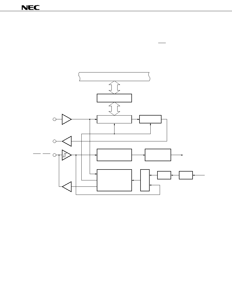
3. SYSTEM CONFIGURATION EXAMPLE (AC SERVO MOTOR CONTROL)
UART
3-wire serial I/O
WDT
PD784046
Control panel
Display
Keypad
I/O port
External
tester
I/O
interface
circuit
CPU-to-CPU communication
ROM
64 Kbytes
RAM
2048 bytes
Macro
service
function
Port
INTP0 to INTP4
ANI8 to ANI15
TO10, TO11,
TO20, TO21
Port
ANI0 to ANI7
INTP5
AD0 to AD15
Limit switch
Driver/switching
circuit
Current/voltage
sensor signal
input circuit
AC motor
Rotary
encoder
Rotary
encoder
interface
Encoder
pulse
counter
µ
µ
PD784044, 784046
10
Data Sheet U10951EJ2V0DS00
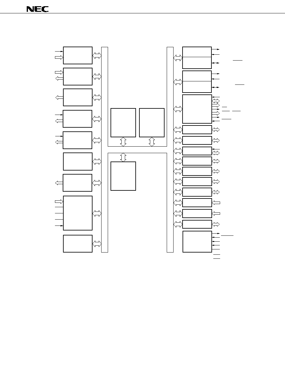
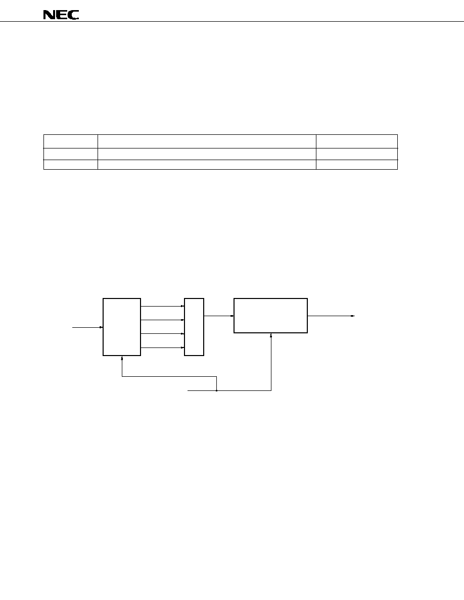
4. BLOCK DIAGRAM
Remark
The internal ROM and RAM capacities vary depending on the product.
Programmable
interrupt
controller
INTP0 to INTP6
NMI
TO00 to TO03
INTP0 to INTP3
TO10, TO11
A/D
converter
AV
DD
AV
SS
AV
REF
INTP4
ANI0 to ANI15
Watchdog
timer
Timer 4
(16 bits)
Timer 1
(16 bits)
Timer 0
(16 bits)
78K/IV
CPU core
ROM
RAM
BUS I/F
BWD
AD0 to AD15
A16 to A19
RD
LWR, HWR
ASTB
WAIT
CLKOUT
RESET
MODE
X1
X2
System
control
P00 to P03
Port 0
Port 1
Port 2
Port 3
Port 4
Port 5
Port 6
Port 7
Port 8
Port 9
P10 to P13
P20
P21 to P27
V
DD
V
SS
P30 to P37
P40 to P47
P50 to P57
P60 to P63
P70 to P77
P80 to P87
P90 to P94
Baud rate
generator
UART/IOE1
Baud rate
generator
UART/IOE2
TxD/SO1
RxD/SI1
ASCK/SCK1
TxD2/SO2
RxD2/SI2
ASCK2/SCK2
Timer/event
counter 2
(16 bits)
TO20, TO21
INTP5/TI2
TO30, TO31
INTP6/TI3
RTP0 to RTP3
Real-time
output port
Timer/event
counter 3
(16 bits)
µ
PD784044, 784046
11
Data Sheet U10951EJ2V0DS00
5. PIN FUNCTIONS
5.1 Port Pins (1/2)
Pin Name
I/O
Alternate Function
Function
P00 to P03
I/O
RTP0 to RTP3
Port 0 (P0):
∑ 4-bit I/O port
∑ Input/output can be specified in 1-bit units.
∑ Pins in input mode can all be connected to pull-up resistors at once
via software.
P10
I/O
TO20
Port 1 (P1):
P11
TO21
∑ 4-bit I/O port
P12
TO30
∑ Input/output can be specified in 1-bit units.
P13
TO31
P20
Input
NMI
Port 2 (P2):
Input only
P21
I/O
INTP0/TO00
∑ 8-bit I/O port
Input/output can be specified in
P22
INTP1/TO01
1-bit units.
P23
INTP2/TO02
P24
INTP3/TO03
P25
INTP4
P26
INTP5/TI2
P27
INTP6/TI3
P30
I/O
TO10
Port 3 (P3):
P31
TO11
∑ 8-bit I/O port
P32
RxD/SI1
∑ Input/output can be specified in 1-bit units.
P33
TxD/SO1
P34
ASCK/SCK1
P35
RxD2/SI2
P36
TxD2/SO2
P37
ASCK2/SCK2
P40 to P47
I/O
AD0 to AD7
Port 4 (P4):
∑ 8-bit I/O port
∑ Input/output can be specified in 1-bit units.
∑ When used as an input port, an on-chip pull-up resistor can be
specified by means of software.
P50 to P57
I/O
AD8 to AD15
Port 5 (P5):
∑ 8-bit I/O port
∑ Input/output can be specified in 1-bit units.
∑ When used as an input port, an on-chip pull-up resistor can be
specified by means of software.
P60 to P63
I/O
A16 to A19
Port 6 (P6):
∑ 4-bit I/O port
∑ Input/output can be specified in 1-bit units.
∑ When used as an input port, an on-chip pull-up resistor can be
specified by means of software.
µ
PD784044, 784046
12
Data Sheet U10951EJ2V0DS00
5.1 Port Pins (2/2)
Pin Name
I/O
Alternate Function
Function
P70 to P77
Input
ANI0 to ANI7
Port 7 (P7):
∑ 8-bit input port
P80 to P87
Input
ANI8 to ANI15
Port 8 (P8):
∑ 8-bit input port
P90
I/O
RD
Port 9 (P9):
P91
LWR
∑ 5-bit I/O port
P92
HWR
∑ Input/output can be specified in 1-bit units.
P93
ASTB
∑ When used as an input port, an on-chip pull-up resistor can be
P94
WAIT
specified by means of software.

µ
PD784044, 784046
13
Data Sheet U10951EJ2V0DS00
5.2 Non-port Pins (1/2)
Pin Name
I/O
Alternate Function
Function
RTP0 to RTP3
Output
P00 to P03
Real-time output
NMI
Input
P20
Non-maskable interrupt request input
INTP0
P21/TO00
External interrupt
Capture trigger signal of CC00
INTP1
P22/TO01
request input
Capture trigger signal of CC01
INTP2
P23/TO02
Capture trigger signal of CC02
INTP3
P24/TO03
Capture trigger signal of CC03
INTP4
P25
Conversion start trigger input of A/D converter
INTP5
P26/TI2
≠
INTP6
P27/TI3
TO00
Output
P21/INTP0
Timer output from timer
TO01
P22/INTP1
TO02
P23/INTP2
TO03
P24/INTP3
TO10
P30
TO11
P31
TO20
P10
TO21
P11
TO30
P12
TO31
P13
TI2
Input
P26/INTP5
External count clock input to timer/event counter 2
TI3
P27/INTP6
External count clock input to timer/event counter 3
RxD
Input
P32/SI1
Serial data input (UART0)
RxD2
P35/SI2
Serial data input (UART2)
TxD
Output
P33/SO1
Serial data output (UART0)
TxD2
P36/SO2
Serial data output (UART2)
ASCK
Input
P34/SCK1
Baud rate clock input (UART0)
ASCK2
P37/SCK2
Baud rate clock input (UART2)
SI1
Input
P32/RxD
Serial data input (3-wire serial I/O1)
SI2
P35/RxD2
Serial data input (3-wire serial I/O2)
SO1
Output
P33/TxD
Serial data output (3-wire serial I/O1)
SO2
P36/TxD2
Serial data output (3-wire serial I/O2)
SCK1
I/O
P34/ASCK
Serial clock input/output (3-wire serial I/O1)
SCK2
P37/ASCK2
Serial clock input/output (3-wire serial I/O2)
AD0 to AD7
I/O
P40 to P47
Lower multiplexed address/data bus for expanding memory externally
AD8 to AD15
Note
I/O
P50 to P57
∑ When 8-bit bus is specified
Higher address bus for expanding memory externally
∑ When external 16-bit bus is specified
Higher multiplexed address/data bus for expanding memory externally
A16 to A19
Note
Output
P60 to P63
Higher address bus for expanding memory externally
RD
Output
P90
Read strobe to external memory
Note
The number of pins used as address bus pins differs depending on the external address space (refer to 9
LOCAL BUS INTERFACE).
µ
PD784044, 784046
14
Data Sheet U10951EJ2V0DS00
5.2 Non-port Pins (2/2)
Pin Name
I/O
Alternate Function
Function
LWR
Output
P91
∑ When external 8-bit bus is specified
Write strobe to external memory
∑ When external 16-bit bus is specified
Write strobe to external memory located at lower position
HWR
P92
Write strobe to external memory located at higher position when external
16-bit bus is specified
ASTB
Output
P93
Timing signal output that externally latches address information output
from AD0 through AD15 pins to access external memory
WAIT
Input
P94
Wait insertion
BWD
Input
≠
Bus width setting
MODE
Input
≠
Connect directly to V
SS
(for specification of IC test mode).
CLKOUT
Output
≠
Clock output. Outputs low level during IDLE mode and STOP mode.
Otherwise, always outputs f
XX
(oscillation frequency).
X1
Input
≠
Connecting crystal resonator for system clock oscillation
X2
≠
≠
(clock can be input to X1).
RESET
Input
≠
Chip reset
ANI0 to ANI7
Input
P70 to P77
Analog voltage input for A/D converter
ANI8 to ANI15
P80 to P87
AV
REF
≠
≠
Reference voltage application for A/D converter
AV
DD
≠
Positive power for A/D converter
AV
SS
≠
GND for A/D converter
V
DD
≠
Positive power supply
V
SS
≠
GND
µ
PD784044, 784046
15
Data Sheet U10951EJ2V0DS00
5.3 Pin I/O Circuits and Recommended Connection of Unused Pins
The input/output circuit type of each pin and recommended connection of unused pins are shown in Table
5-1.
For the I/O circuit type, refer to Figure 5-1.
Table 5-1. Types of Pin I/O Circuits and Recommended Connection of Unused Pins
Pin Name
Input/Output Circuit Type
I/O
Recommended Connection of Unused Pins
P00/RTP0 to P03/RTP3
5-A
I/O
Input: Independently connect to V
DD
or V
SS
via a resistor.
P10/TO20
5
Output: Leave open.
P11/TO21
P12/TO30
P13/TO31
P20/NMI
2
Input
Connect to V
SS
.
P21/INTP0/TO00
8
I/O
Input: Independently connect to V
DD
or V
SS
via a resistor.
P22/INTP1/TO01
Output: Leave open.
P23/INTP2/TO02
P24/INTP3/TO03
P25/INTP4
P26/INTP5/TI2
P27/INTP6/TI3
P30/TO10
5
P31/TO11
P32/RxD/SI1
P33/TxD/SO1
P34/ASCK/SCK1
8
P35/RxD2/SI2
5
P36/TxD2/SO2
P37/ASCK2/SCK2
8
P40/AD0 to P47/AD7
5-A
P50/AD8 to P57/AD15
P60/A16 to P63/A19
P70/ANI0 to P77/ANI7
9
Input
Connect to V
SS
.
P80/ANI8 to P87/ANI15
P90/RD
5-A
I/O
Input: Independently connect to V
DD
or V
SS
via a resistor.
P91/LWR
Output: Leave open.
P92/HWR
P93/ASTB
P94/WAIT
MODE
1
Input
Connect directly to V
SS
.
RESET
2
≠
CLKOUT
3
Output
Leave open.
AV
REF
≠
≠
Connect to V
SS
.
AV
SS
AV
DD
Connect to V
DD
.
Remark
Since type numbers are consistent in the 78K Series, those numbers are not always serial in each product
(some circuits are not included).
µ
PD784044, 784046
16
Data Sheet U10951EJ2V0DS00
Figure 5-1. Pin I/O Circuits
Type 2
Schmitt trigger input with hysteresis characteristics
Type 1
P-ch
IN
V
DD
N-ch
IN
Type 3
Type 5
Data
Output
disable
P-ch
IN/OUT
V
DD
N-ch
Input
enable
Type 5-A
Data
Output
disable
P-ch
IN/OUT
V
DD
N-ch
Input
enable
P-ch
V
DD
Pullup
Enable
Type 8
Data
Output
disable
P-ch
IN/OUT
V
DD
N-ch
IN
Comparator
+
≠
V
REF
(Threshold voltage)
P-ch
N-ch
Input
enable
Type 9
P-ch
OUT
V
DD
N-ch
µ
PD784044, 784046
17
Data Sheet U10951EJ2V0DS00
6. CPU ARCHITECTURE
6.1 Memory Space
A 1-Mbyte memory space can be accessed. The mapping of the internal data area (special function registers
and internal RAM) can be selected by using the LOCATION instruction. The LOCATION instruction must be
executed after the reset release, and must not be used more than once.
(1) When LOCATION 0 instruction is executed
∑
Internal memory
The internal data area and internal ROM area are as follows:
Part Number
Internal Data Area
Internal ROM Area
µ
PD784044
0FB00H to 0FFFFH
00000H to 07FFFH
µ
PD784046
0F700H to 0FFFFH
00000H to 0F5FFH
Caution
0F600H to 0FFFFH of the internal ROM (00000H to 0FFFFH) of the
µ
PD784046 cannot be
used as ROM when the LOCATION 0 instruction is executed (refer to Figure 6-2).
∑
External memory
The external memory is accessed in the external memory expansion mode.
(2) When LOCATION 0FH instruction is executed
∑
Internal memory
The internal data area and internal ROM area are as follows:
Part Number
Internal Data Area
Internal ROM Area
µ
PD784044
FFB00H to FFFFFH
00000H to 07FFFH
µ
PD784046
FF700H to FFFFFH
00000H to 0FFFFH
∑
External memory
The external memory is accessed in the external memory expansion mode.
µ
PD784044, 784046
18
Data Sheet U10951EJ2V0DS00
Figure 6-1.
µ
PD784044 Memory Map
Notes 1. Accessed in the external memory expansion mode.
2. Base area or entry area by reset or interrupt. The internal RAM is not reset.
External memory
Note 1
(960 Kbytes)
Special function registers (SFRs)
Note 1
(256 bytes)
Internal RAM
(1 Kbyte)
Reserved
(1280 bytes)
Internal ROM
(32 Kbytes)
H
General-purpose registers
(128 bytes)
Macro service control
word area (50 bytes)
Data area (512 bytes)
Program/data area
(512 bytes)
Program/data area
(32 Kbytes)
CALLF entry area
(2 Kbytes)
CALLT table area
(64 bytes)
Vector table area
(64 bytes)
When LOCATION 0
instruction is executed
Reserved
(1280 bytes)
External memory
Note 1
(1013248 bytes)
Internal ROM
(32 Kbytes)
When LOCATION 0FH
instruction is executed
Special function registers (SFR
S
)
Note 1
(256 bytes)
Internal RAM
(1 Kbyte)
Note 2
Main RAM
Peripheral
RAM
F
F
F
F
F
H
H
H
H
H
H
0
F
F
0
0
F
0
F
D
D
0
F
0
F
F
F
F
E
0
F
F
F
F
F
1
0
0
0
0
0
H
H
0
F
0
F
B
A
F
F
0
0
H
H
0
F
0
F
6
5
F
F
0
0
H
H
0
F
0
F
0
F
8
7
0
0
H
0
0
0
0
0
External memory
Note 1
(30208 bytes)
H
F
F
E
F
0
H
H
0
F
8
7
E
E
F
F
0
0
H
H
7
6
3
0
E
E
F
F
0
0
H
H
0
F
0
F
D
C
F
F
0
0
H
0
0
B
F
0
H
F
F
F
7
0
H
H
0
F
0
F
0
F
1
0
0
0
H
H
0
F
0
F
8
7
0
0
0
0
H
H
0
F
8
7
0
0
0
0
0
0
H
0
0
0
0
0
H
F
F
E
F
F
H
H
0
F
8
7
E
E
F
F
F
F
H
H
7
6
3
0
E
E
F
F
F
F
H
H
0
F
0
F
D
C
F
F
F
F
H
0
0
B
F
F
H
H
H
H
F
F
0
0
F
D
D
0
F
F
F
F
F
F
F
F
F
F
F
F
H
H
0
F
0
F
6
5
F
F
F
F
H
H
0
F
0
F
0
F
8
7
0
0
H
0
0
0
0
0
H
H
0
F
0
F
0
F
0
F
1
0
H
H
0
F
0
F
B
A
F
F
F
F
Note 2
H
H
0
F
4
3
0
0
0
0
0
0
H
F
F
E
F
F

µ
PD784044, 784046
19
Data Sheet U10951EJ2V0DS00
Figure 6-2.
µ
PD784046 Memory Map
Notes 1. Accessed in the external memory expansion mode.
2. 2560 bytes in this area can be used as internal ROM only when the LOCATION 0FH instruction is
executed.
3. When the LOCATION 0 instruction is executed: 62976 bytes
When the LOCATION 0FH instruction is executed: 65536 bytes
4. Base area or entry area by reset or interrupt. The internal RAM is not reset.
External memory
Note 1
(960 Kbytes)
Note 1
Internal RAM
(2 Kbytes)
Internal ROM
(62976 bytes)
General-purpose registers
(128 bytes)
Macro service control
word area (50 bytes)
Data area (512 bytes)
Program/data area
(1536 bytes)
CALLF entry area
(2 Kbytes)
CALLT table area
(64 bytes)
Vector table area
(64 bytes)
When LOCATION 0
instruction is executed
Reserved
(256 bytes)
External memory
Note 1
(980480 bytes)
Internal ROM
(64 Kbytes)
Special function registers (SFRs)
Note 1
(256 bytes)
Internal RAM
(2 Kbytes)
Special function registers (SFRs)
(256 bytes)
Reserved
(256 bytes)
Program/data area
Note 3
Note 2
Peripheral
RAM
Main RAM
H
0
0
0
0
0
H
F
F
5
F
0
H
0
0
6
F
0
H
F
F
6
F
0
H
F
F
F
F
F
H
F
F
E
F
0
H
0
0
7
F
0
H
0
0
F
F
0
H
0
D
F
F
0
H
F
D
F
F
0
H
F
F
F
F
0
H
0
0
0
0
1
Note 4
H
F
F
E
F
0
H
0
8
E
F
0
H
F
7
E
F
0
H
7
3
E
F
0
H
6
0
E
F
0
H
0
0
D
F
0
H
0
0
7
F
0
H
F
F
C
F
0
H
F
F
5
F
0
H
0
0
0
0
0
H
F
3
0
0
0
H
0
4
0
0
0
H
F
7
0
0
0
H
0
8
0
0
0
H
F
F
7
0
0
H
0
0
8
0
0
H
F
F
F
0
0
H
0
0
0
1
0
H
0
0
0
0
0
H
F
F
F
F
0
H
0
0
0
0
1
H
F
F
5
F
F
H
0
0
6
F
F
H
F
F
6
F
F
H
0
0
7
F
F
H
F
F
F
F
F
H
0
0
F
F
F
H
0
D
F
F
F
H
F
D
F
F
F
H
F
F
E
F
F
H
F
F
E
F
F
H
0
8
E
F
F
H
F
7
E
F
F
H
7
3
E
F
F
H
6
0
E
F
F
H
0
0
D
F
F
H
F
F
C
F
F
H
0
0
7
F
F
H
F
F
F
F
0
Note 4
When LOCATION 0FH
instruction is executed
µ
PD784044, 784046
20
Data Sheet U10951EJ2V0DS00
6.2 CPU Registers
6.2.1 General-purpose registers
Sixteen 8-bit general-purpose registers are provided. Two 8-bit general-purpose registers can be used in
pairs as a 16-bit general-purpose register. Of the 16-bit registers, four can be used in combination with an 8-
bit register for address expansion as 24-bit address specification registers.
Eight banks of register sets are available which can be selected by software or context switching function.
The general-purpose registers except the V, U, T, and W registers for address expansion are mapped to the
internal RAM.
Figure 6-3. General-Purpose Register Format
Caution
R4, R5, R6, R7, RP2, and RP3 can be used as X, A, C, B, AX, and BC registers, respectively, by
setting the RSS bit of the PSW to 1. However, use this function only when using a 78K/III Series
program.
V
U
T
W
A(R1)
B(R3)
R5
R7
R9
R11
D(R13)
H(R15)
R8
R10
E(R12)
L(R14)
VVP(RG4)
UUP(RG5)
TDE(RG6)
WHL(RG7)
X(R0)
C(R2)
R4
R6
VP(RP4)
UP(RP5)
DE(RP6)
HL(RP7)
AX(RP0)
BC(RP1)
RP2
RP3
( ): absolute name
8 banks
µ
PD784044, 784046
21
Data Sheet U10951EJ2V0DS00
6.2.2 Control registers
(1) Program counter (PC)
This is a 20-bit program counter. Its contents are automatically updated as the program is executed.
Figure 6-4. Program Counter (PC) Format
(2) Program status word (PSW)
This register retains the status of the CPU and its contents are automatically updated as the program is
executed.
Figure 6-5. Program Status Word (PSW) Format
Note
This flag is provided for maintaining compatibility with the 78K/III Series. Be sure to clear this flag to
0 other than when using 78K/III Series software.
(3) Stack pointer (SP)
This is a 24-bit pointer that holds the first address of the stack.
Be sure to write 0 to the higher 4 bits of this pointer.
Figure 6-6. Stack Pointer (SP) Format
19
0
PC
SP
0
23
0
0
0
0
20
PSWH
UF
RBS2
RBS1
RBS0
≠
≠
≠
≠
15
14
13
12
11
9
10
8
PSW
PSWL
S
Z
RSS
Note
AC
IE
P/V
0
CY
7
6
5
4
3
1
2
0

µ
PD784044, 784046
22
Data Sheet U10951EJ2V0DS00
6.2.3 Special function registers (SFRs)
The special function registers are registers to which special functions are assigned, such as the mode
registers and control registers of the internal peripheral hardware. These registers are mapped in a 256-byte
space of addresses 0FF00H through 0FFFFH
Note
.
Note
When the LOCATION 0 instruction is executed. FFF00H through FFFFFH when the LOCATION 0FH
instruction is executed.
Caution
Do not access an address in this area to which no SFR is allocated. If an address to which no
SFR is allocated is accessed by mistake, the
µ
PD784046 may be deadlocked. The deadlock status
can be cleared only by inputting the reset signal.
Table 6-1 lists the special function registers (SFRs). The meanings of the items in this table are as follows:
∑ Symbol ................................. Symbol indicating an SFR. These symbols are reserved words for an NEC's
assembler (RA78K4). With a C compiler (CC78K4), they can be used as sfr
variables by using the #pragma sfr directive.
∑ R/W ...................................... Indicates whether the corresponding SFR can be read/written.
R/W:
Read/write
R:
Read only
W:
Write only
∑ Bit Units for Manipulation ... Indicates bit units in which the corresponding SFR can be manipulated.
SFRs that can be manipulated in 16-bit units can be described in operand sfrp.
Describe the even addresses of these SFRs when specifying with an address.
SFRs that can be manipulated in 1-bit units can be described in bit manipulation
instructions.
∑ After Reset .......................... Indicates the status of each register when the RESET signal is input.
µ
PD784044, 784046
23
Data Sheet U10951EJ2V0DS00
Table 6-1. Special Function Register List (1/5)
Address
Note 1
Special Function Register (SFR) Name
Symbol
R/W
Bit Units for Manipulation
After Reset
1 Bit
8 Bits
16 Bits
0FF00H
Port 0
P0
R/W
≠
Undefined
0FF01H
Port 1
P1
≠
0FF02H
Port 2
P2
Note 2
≠
0FF03H
Port 3
P3
R/W
≠
0FF04H
Port 4
P4
≠
0FF05H
Port 5
P5
≠
0FF06H
Port 6
P6
≠
0FF07H
Port 7
P7
R
≠
0FF08H
Port 8
P8
≠
0FF09H
Port 9
P9
R/W
≠
0FF0EH
Port 0 buffer register
P0L
≠
0FF10H
Timer counter 0
TM0
R
≠
≠
0000H
0FF11H
0FF12H
Capture/compare register 00
CC00
R/W
≠
≠
Undefined
0FF13H
0FF14H
Capture/compare register 01
CC01
≠
≠
0FF15H
0FF16H
Capture/compare register 02
CC02
≠
≠
0FF17H
0FF18H
Capture/compare register 03
CC03
≠
≠
0FF19H
0FF1AH
Timer counter 1
TM1
R
≠
≠
0000H
0FF1BH
0FF1CH
Compare register 10
CM10
R/W
≠
≠
Undefined
0FF1DH
0FF1EH
Compare register 11
CM11
≠
≠
0FF1FH
0FF20H
Port 0 mode register
PM0
≠
FFH
0FF21H
Port 1 mode register
PM1
≠
0FF22H
Port 2 mode register
PM2
Note 3
≠
0FF23H
Port 3 mode register
PM3
≠
0FF24H
Port 4 mode register
PM4
≠
0FF25H
Port 5 mode register
PM5
≠
0FF26H
Port 6 mode register
PM6
≠
0FF29H
Port 9 mode register
PM9
≠
0FF2EH
Real-time output port control register
RTPC
≠
00H
0FF2FH
Port read control register
PRDC
≠
Notes 1. When the LOCATION 0 instruction is executed. Add "F0000H" to this value when the LOCATION 0FH
instruction is executed.
2. Bit 0 of P2 can only be read. Bits 1 through 7 can be read/written.
3. Bit 0 of PM2 is fixed to "1" by hardware.
µ
PD784044, 784046
24
Data Sheet U10951EJ2V0DS00
Table 6-1. Special Function Register List (2/5)
Address
Note 1
Special Function Register (SFR) Name
Symbol
R/W
Bit Units for Manipulation
After Reset
1 Bit
8 Bits
16 Bits
0FF30H
Timer unit mode register 0
TUM0
R/W
≠
00H
0FF31H
Timer mode control register
TMC
≠
0FF32H
Timer output control register 0
TOC0
≠
0FF33H
Timer output control register 1
TOC1
≠
0FF34H
Timer unit mode register 2
TUM2
≠
0FF35H
Timer mode control register 2
TMC2
≠
0FF36H
Timer output control register 2
TOC2
≠
0FF37H
Timer mode control register 4
TMC4
≠
0FF38H
Prescaler mode register
PRM
≠
≠
0FF39H
Prescaler mode register 2
PRM2
≠
≠
0FF3AH
Prescaler mode register 4
PRM4
≠
≠
0FF3BH
Noise protection control register
NPC
≠
0FF3CH
External interrupt mode register 0
INTM0
≠
0FF3DH
External interrupt mode register 1
INTM1
≠
0FF3EH
Interrupt valid edge flag register 1
IEF1
≠
Undefined
0FF3FH
Interrupt valid edge flag register 2
IEF2
≠
0FF41H
Port 1 mode control register
PMC1
≠
00H
0FF42H
Port 2 mode control register
PMC2
Note 2
≠
0FF43H
Port 3 mode control register
PMC3
≠
0FF49H
Port 9 mode control register
PMC9
≠
0FF4EH
Pull-up resistor option register L
PUOL
≠
0FF4FH
Pull-up resistor option register H
PUOH
≠
0FF50H
Timer counter 2
TM2
R
≠
≠
0000H
0FF51H
0FF52H
Compare register 20
CM20
R/W
≠
≠
Undefined
0FF53H
0FF54H
Compare register 21
CM21
≠
≠
0FF55H
0FF56H
Timer counter 3
TM3
R
≠
≠
0000H
0FF57H
0FF58H
Compare register 30
CM30
R/W
≠
≠
Undefined
0FF59H
0FF5AH
Compare register 31
CM31
≠
≠
0FF5BH
0FF60H
Timer counter 4
TM4
R
≠
≠
0000H
0FF61H
Notes 1. When the LOCATION 0 instruction is executed. Add "F0000H" to this value when the LOCATION 0FH
instruction is executed.
2. Bits 0, and 5 through 7 of PMC2 are fixed to "0" by hardware.
µ
PD784044, 784046
25
Data Sheet U10951EJ2V0DS00
Table 6-1. Special Function Register List (3/5)
Address
Note
Special Function Register (SFR) Name
Symbol
R/W
Bit Units for Manipulation
After Reset
1 Bit
8 Bits
16 Bits
0FF62H
Compare register 40
CM40
R/W
≠
≠
Undefined
0FF63H
0FF64H
Compare register 41
CM41
≠
≠
0FF65H
0FF6EH
A/D converter mode register
ADM
≠
00H
0FF70H
A/D conversion result register 0
ADCR0
R
≠
≠
Undefined
0FF71H
0FF71H
A/D conversion result register 0H
ADCR0H
≠
≠
0FF72H
A/D conversion result register 1
ADCR1
≠
≠
0FF73H
0FF73H
A/D conversion result register 1H
ADCR1H
≠
≠
0FF74H
A/D conversion result register 2
ADCR2
≠
≠
0FF75H
0FF75H
A/D conversion result register 2H
ADCR2H
≠
≠
0FF76H
A/D conversion result register 3
ADCR3
≠
≠
0FF77H
0FF77H
A/D conversion result register 3H
ADCR3H
≠
≠
0FF78H
A/D conversion result register 4
ADCR4
≠
≠
0FF79H
0FF79H
A/D conversion result register 4H
ADCR4H
≠
≠
0FF7AH
A/D conversion result register 5
ADCR5
≠
≠
0FF7BH
0FF7BH
A/D conversion result register 5H
ADCR5H
≠
≠
0FF7CH
A/D conversion result register 6
ADCR6
≠
≠
0FF7DH
0FF7DH
A/D conversion result register 6H
ADCR6H
≠
≠
0FF7EH
A/D conversion result register 7
ADCR7
≠
≠
0FF7FH
0FF7FH
A/D conversion result register 7H
ADCR7H
≠
≠
0FF84H
Clocked serial interface mode register 1
CSIM1
R/W
≠
00H
0FF85H
Clocked serial interface mode register 2
CSIM2
≠
0FF88H
Asynchronous serial interface mode register
ASIM
≠
0FF89H
Asynchronous serial interface mode register 2
ASIM2
≠
0FF8AH
Asynchronous serial interface status register
ASIS
R
≠
0FF8BH
Asynchronous serial interface status register 2
ASIS2
≠
Note
When the LOCATION 0 instruction is executed. Add "F0000H" to this value when the LOCATION 0FH
instruction is executed.
µ
PD784044, 784046
26
Data Sheet U10951EJ2V0DS00
Table 6-1. Special Function Register List (4/5)
Address
Note 1
Special Function Register (SFR) Name
Symbol
R/W
Bit Units for Manipulation
After Reset
1 Bit
8 Bits
16 Bits
0FF8CH
Serial receive buffer: UART0
RXB
R
≠
≠
Undefined
Serial transmit shift register: UART0
TXS
W
≠
≠
Serial shift register: IOE1
SIO1
R/W
≠
≠
0FF8DH
Serial receive buffer: UART2
RXB2
R
≠
≠
Serial transmit shift register: UART2
TXS2
W
≠
≠
Serial shift register: IOE2
SIO2
R/W
≠
≠
0FF90H
Baud rate generator control register
BRGC
≠
≠
00H
0FF91H
Baud rate generator control register 2
BRGC2
≠
≠
0FFA8H
In-service priority register
ISPR
R
≠
0FFAAH
Interrupt mode control register
IMC
R/W
≠
80H
0FFACH
Interrupt mask register 0L
MK0L
≠
FFH
0FFACH
Interrupt mask register 0
MK0
≠
≠
FFFFH
0FFADH
0FFADH
Interrupt mask register 0H
MK0H
≠
FFH
0FFAEH
Interrupt mask register 1L
MK1L
≠
0FFAEH
Interrupt mask register 1
MK1
≠
≠
FFFFH
0FFAFH
0FFAFH
Interrupt mask register 1H
MK1H
≠
FFH
0FFC0H
Standby control register
Note 2
STBC
≠
≠
30H
0FFC2H
Watchdog timer mode register
Note 2
WDM
≠
≠
00H
0FFC4H
Memory expansion mode register
MM
≠
20H
0FFC7H
Programmable wait control register 1
PWC1
≠
≠
AAH
0FFC8H
Programmable wait control register 2
PWC2
≠
≠
AAAAH
0FFC9H
0FFCAH
Bus width specification register
BW
≠
≠
Note 3
0FFCBH
0FFCFH
Oscillation stabilization time specification register
OSTS
≠
≠
00H
0FFD0H to
External SFR area
≠
≠
Undefined
0FFDFH
0FFE0H
Interrupt control register (INTOV0)
OVIC0
≠
43H
0FFE1H
Interrupt control register (INTOV1)
OVIC1
≠
0FFE2H
Interrupt control register (INTOV4)
OVIC4
≠
0FFE3H
Interrupt control register (INTP0)
PIC0
≠
0FFE4H
Interrupt control register (INTP1)
PIC1
≠
0FFE5H
Interrupt control register (INTP2)
PIC2
≠
Notes 1. When the LOCATION 0 instruction is executed. Add "F0000H" to this value when the LOCATION 0FH
instruction is executed.
2. These registers can be written only by using dedicated instructions MOV STBC, #byte and MOV WDM,
#byte, and cannot be written by any other instructions.
3. The value of this register after reset differs depending on the setting of the BWD pin.
BWD = 0: 0000H
BWD = 1: 00FFH

µ
PD784044, 784046
27
Data Sheet U10951EJ2V0DS00
Table 6-1. Special Function Register List (5/5)
Address
Note
Special Function Register (SFR) Name
Symbol
R/W
Bit Units for Manipulation
After Reset
1 Bit
8 Bits
16 Bits
0FFE6H
Interrupt control register (INTP3)
PIC3
R/W
≠
43H
0FFE7H
Interrupt control register (INTP4)
PIC4
≠
0FFE8H
Interrupt control register (INTP5)
PIC5
≠
0FFE9H
Interrupt control register (INTP6)
PIC6
≠
0FFEAH
Interrupt control register (INTCM10)
CMIC10
≠
0FFEBH
Interrupt control register (INTCM11)
CMIC11
≠
0FFECH
Interrupt control register (INTCM20)
CMIC20
≠
0FFEDH
Interrupt control register (INTCM21)
CMIC21
≠
0FFEEH
Interrupt control register (INTCM30)
CMIC30
≠
0FFEFH
Interrupt control register (INTCM31)
CMIC31
≠
0FFF0H
Interrupt control register (INTCM40)
CMIC40
≠
0FFF1H
Interrupt control register (INTCM41)
CMIC41
≠
0FFF2H
Interrupt control register (INTSER)
SERIC
≠
0FFF3H
Interrupt control register (INTSR)
SRIC
≠
Interrupt control register (INTCSI1)
CSIIC1
≠
0FFF4H
Interrupt control register (INTST)
STIC
≠
0FFF5H
Interrupt control register (INTSER2)
SERIC2
≠
0FFF6H
Interrupt control register (INTSR2)
SRIC2
≠
Interrupt control register (INTCSI2)
CSIIC2
≠
0FFF7H
Interrupt control register (INTST2)
STIC2
≠
0FFF8H
Interrupt control register (INTAD)
ADIC
≠
Note
When the LOCATION 0 instruction is executed. Add "F0000H" to this value when the LOCATION 0FH
instruction is executed.

µ
PD784044, 784046
28
Data Sheet U10951EJ2V0DS00
7. PERIPHERAL HARDWARE FUNCTIONS
7.1 Ports
The
µ
PD784046 has the ports shown in Figure 7-1. These ports can be used for various control operations.
The function of each port is shown in Table 7-1. Ports 0, 4 through 6, and 9 can be connected to an internal
pull-up resistor via software when they are set in the input mode.
Figure 7-1. Port Configuration
Port 0
Port 1
Port 2
Port 3
Port 4
Port 5
Port 6
P00
P03
P10
P13
P20
P27
P30
P37
P40
P47
P50
P57
P60
P63
P70 to P77
8
Port 7
Port 9
P80 to P87
8
Port 8
P90
P94
µ
PD784044, 784046
29
Data Sheet U10951EJ2V0DS00
Table 7-1. Port Function
Port Name
Pin Name
Function
Specification of Pull-Up Resistor by Software
Port 0
P00 to P03
Input/output can be specified in 1-bit units.
All pins in input mode
Port 1
P10 to P13
≠
Port 2
P20 to P27
Input/output can be specified in 1-bit units.
(however, P20 is input-only).
Port 3
P30 to P37
Input/output can be specified in 1-bit units.
Port 4
P40 to P47
All pins in input mode
Port 5
P50 to P57
Port 6
P60 to P63
Port 7
P70 to P77
Input port
≠
Port 8
P80 to P87
Port 9
P90 to P94
Input/output can be specified in 1-bit units.
All pins in input mode
7.2 Clock Generator
The clock generator generates and controls the internal system clock (CLK) to be supplied to the CPU.
Figure 7-2 shows the configuration of this circuit.
Figure 7-2. Block Diagram of Clock Generator
Remark
f
XX
:
crystal/ceramic oscillation frequency
f
X
:
external clock frequency
f
CLK
:
internal system clock frequency
Internal system clock (CLK)
Clock
generator
f
XX
or f
X
f
CLK
X2
X1
Divider
1/2

µ
PD784044, 784046
30
Data Sheet U10951EJ2V0DS00
Figure 7-3. Example of Using Oscillator
(1) Crystal/ceramic oscillation
Caution
When using the clock oscillation circuit, wire the portion enclosed by the dotted line in the above
figure as follows to avoid adverse effects of wiring capacitance.
∑ Keep the wiring length as short as possible.
∑ Do not cross the wiring with the other signal lines.
∑ Do not route the wiring near a signal line through which a high fluctuating current flows.
∑ Always make the ground point of the oscillator capacitor the same potential as V
SS
. Do not
ground the capacitor to a ground pattern through which a high current flows.
∑ Do not fetch signals from the oscillator.
(2) External clock input
(a) EXTC bit of OSTS = 1
(b) EXTC bit of OSTS = 0
PD784046
V
SS
X1
X2
µ
PD74HC04, etc.
PD784046
X1
X2
PD784046
X1
X2
Leave open
µ
µ
µ
µ
PD784044, 784046
31
Data Sheet U10951EJ2V0DS00
7.3 Real-Time Output Port
The real-time output port outputs the data stored in the buffer in synchronization with a match interrupt of
timer 4. This allows jitter-less pulse output to be obtained.
Therefore, it is best suited to applications that output patterns at given intervals (such as stepping motor open
loop control, etc.).
As shown in Figure 7-4, port 0 and the port 0 buffer register form the core of configuration.
Figure 7-4. Block Diagram of Real-Time Output Port
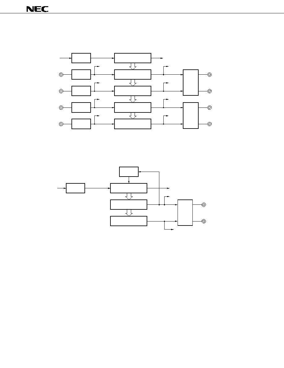
7.4 Timer
The
µ
PD784046 contains two 16-bit timer/event counter units and three 16-bit timer units.
These units support a total of 15 interrupt requests, which enable them to function as 15-channel timers.
Table 7-2. Timer Function
Name
Timer 0
Timer 1
Timer/Event Timer/Event
Timer 4
Item
Counter 2 Counter 3
Operating mode
Interval timer
4ch
2ch
2ch
2ch
2ch
External event counter
≠
≠
≠
Function
Timer output
4ch
2ch
2ch
2ch
≠
Toggle output
≠
Set/reset output
≠
≠
≠
PWM/PPG output
≠
≠
≠
Real-time output
≠
≠
≠
≠
Overflow interrupt
≠
≠
Number of interrupt requests
5
3
2
2
3
Internal Bus
8
Real-time output port
control register (RTPC)
Output trigger
control circuit
INTCM40 (from timer 4)
4
Port 0 buffer
register (P0L)
4
Output latch (P0)
RTP0
RTP3 RTP2 RTP1
4
µ
PD784044, 784046
32
Data Sheet U10951EJ2V0DS00
Figure 7-5. Timer Block Diagram (1/2)
Timer 0
Prescaler: f
CLK
/4, f
CLK
/8, f
CLK
/16, f
CLK
/32, f
CLK
/64
Timer 1
Prescaler: f
CLK
/8, f
CLK
/16, f
CLK
/32, f
CLK
/64, f
CLK
/128
Prescaler
Timer counter 0
(TM0)
f
CLK
INTP0
INTP1
INTP2
INTP3
INTOV0
Edge
detection
Capture/compare register 00
(CC00)
INTP0
INTCC00
Match
TO00
Pulse
output
control
Edge
detection
Capture/compare register 01
(CC01)
INTP1
INTCC01
Match
TO01
Edge
detection
Capture/compare register 02
(CC02)
INTP2
INTCC02
Match
TO02
Pulse
output
control
Edge
detection
Capture/compare register 03
(CC03)
INTP3
INTCC03
Match
TO03
f
CLK
Prescaler
Timer counter 1
(TM1)
Compare register 10
(CM10)
INTCM10
Match
TO10
Pulse
output
control
Compare register 11
(CM11)
INTCM11
Match
TO11
Clear
control
INTOV1
µ
PD784044, 784046
33
Data Sheet U10951EJ2V0DS00
Figure 7-5. Timer Block Diagram (2/2)
Timer/event counter 2
Prescaler: f
CLK
/4, f
CLK
/8, f
CLK
/16, f
CLK
/32, f
CLK
/64
Prescaler: f
CLK
/4, f
CLK
/8, f
CLK
/16, f
CLK
/32, f
CLK
/64
Timer 4
Prescaler: f
CLK
/4, f
CLK
/8, f
CLK
/16, f
CLK
/32, f
CLK
/64
Timer/event counter 3
f
CLK
Prescaler
Timer counter 2
(TM2)
Compare register 20
(CM20)
INTCM20
Match
TO20
Pulse
output
control
Compare register 21
(CM21)
INTCM21
TO21
Clear
control
Selector
TI2/INTP5
Edge
detection
INTP5
Match
f
CLK
Prescaler
Timer counter 3
(TM3)
Compare register 30
(CM30)
INTCM30
TO30
Pulse
output
control
Compare register 31
(CM31)
INTCM31
Match
TO31
Clear
control
Selector
TI3/INTP6
Edge
detection
INTP6
Match
f
CLK
Prescaler
Timer counter 4
(TM4)
Compare register 40
(CM40)
Match
To real-time output port
Compare register 41
(CM41)
Match
INTCM41
Clear
control
INTOV4
INTCM40
µ
PD784044, 784046
34
Data Sheet U10951EJ2V0DS00
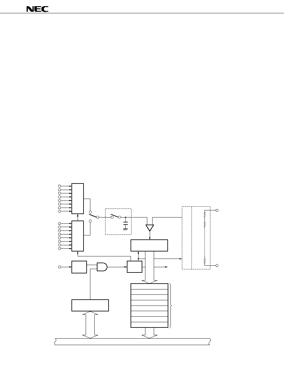
7.5 A/D Converter
The
µ
PD784046 has an analog-to-digital (A/D) converter with 16 multiplexed analog input pins (ANI0 through
ANI15).
This converter is of successive approximation type. The result of conversion is stored and retained in 10-
bit A/D conversion result registers (ADCR0 to ADCR7). Therefore, high-speed, high-accuracy conversion can
be performed (conversion time: about 13
µ
s: f
CLK
= 16-MHz operation).
The A/D conversion operation can be started in the following modes:
∑
Hardware start:
Conversion is started by trigger input (INTP4).
∑
Software start:
Conversion is started by setting a bit of the A/D converter mode register (ADM).
The A/D converter operates in the following modes:
∑
Scan mode:
Sequentially selects two or more analog input pins to obtain data to be converted from all
the pins.
∑
Select mode:
Selects only one analog input pin to obtain successive converted values.
The above modes and stopping the conversion are specified by ADM.
When the result of conversion is transferred to ADCRn (n = 0 to 7), interrupt request INTAD is generated.
By using this interrupt request and by using macro service, the converted value can be successively transferred
to memory.
Figure 7-6. A/D Converter Block Diagram
Internal bus
Input
selector
ANI0
ANI1
ANI2
ANI3
ANI4
ANI5
ANI6
ANI7
Input
selector
ANI8
ANI9
ANI10
ANI11
ANI12
ANI13
ANI14
ANI15
Sample & hold circuit
Successive approximation
register (SAR)
Voltage
comparator
Edge
detection
circuit
INTP4
Control
circuit
Conversion
trigger
INTAD
10
Trigger enable
A/D converter mode register
(ADM)
Series resistor string
R/2
R
R/2
AV
REF
AV
SS
8
10
ADCR0
ADCR1
ADCR2
ADCR3
ADCR4
ADCR5
ADCR6
ADCR7
A/D conversion result register
Tap selector
µ
PD784044, 784046
35
Data Sheet U10951EJ2V0DS00
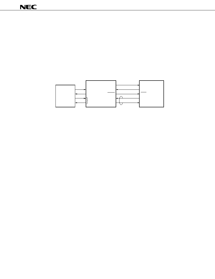
7.6 Serial Interface
Two independent serial interface channels are provided.
∑
Asynchronous serial interface (UART)/3-wire serial I/O (IOE)
◊
2
By using these serial interface channels, communication with an external device and local communication
within a system can be performed at the same time (refer to Figure 7-7).
Figure 7-7. Example of Serial Interface
Note
Handshake line
RxD
TxD
Port
RS-232-C
driver/
receiver
PD4711A
(UART)
PD784046 (master)
SO2
SI2
SCK2
INTPn
Port
SI
SO
SCK
Port
INT
Note
PD78014 (slave)
(3-wire serial I/O)
µ
µ
µ

µ
PD784044, 784046
36
Data Sheet U10951EJ2V0DS00
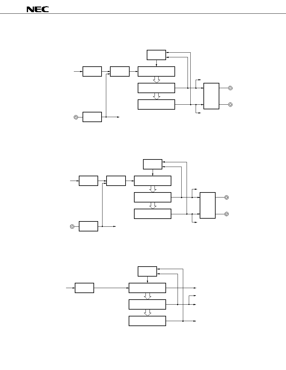
7.6.1 Asynchronous serial interface/3-wire serial I/O (UART/IOE)
Two serial interface channels from which asynchronous serial interface mode and 3-wire serial I/O mode can
be selected are provided.
(1) Asynchronous serial interface mode
In this mode, 1-byte data following a start bit is transferred or received.
The internal baud rate generator allows communication in a wide range of baud rates.
The clock input to the ASCK pin can be divided to define a baud rate.
The baud rate generator can also set a baud rate conforming to the MIDI standard (31.25 kbps).
Figure 7-8. Block Diagram in Asynchronous Serial Interface Mode
Remark
f
CLK
: internal system clock
n = 0 to 11
m = 16 to 30
Internal bus
Receive buffer
RXB, RXB2
Receive shift
register
Transmit shift
register
INTST, INTST2
TXS, TXS2
Transmit control
Parity append
Receive control
Parity check
INTSR,
INTSR2
INTSER,
INTSER2
RxD, RxD2
TxD, TxD2
1/2m
1/2m
1/2
n+1
f
CLK
ASCK, ASCK2
Baud rate generator
Selector
µ
PD784044, 784046
37
Data Sheet U10951EJ2V0DS00
(2) 3-wire serial I/O mode
This mode is to start transmission when the master device makes a serial clock active and to communicate
1-byte data in synchronization with this clock.
The interface in this mode communicates with devices that have conventional clocked serial interface.
Basically, communication is performed by using three lines: serial clock (SCK) and two serial data (SI and
SO) lines. To connect two or more devices, a handshake line is necessary.
Figure 7-9. Block Diagram in 3-Wire Serial I/O Mode
Remark
f
CLK
: internal system clock
n = 0 to 11
m = 1, 16 to 30
Internal bus
Direction control circuit
Shift register
SIO1, SIO2
Output latch
Serial clock counter
Interrupt
generator
INTCSI1,
INTCSI2
Serial clock
control circuit
1/2m
1/2
n+1
f
CLK
SI1, SI2
SO1, SO2
SCK1, SCK2
Selector
µ
PD784044, 784046
38
Data Sheet U10951EJ2V0DS00
7.7 Edge Detection Circuit
The interrupt input pins (NMI and INTP0 through INTP6) input not only interrupt requests but also trigger
signals of the internal hardware. Because all the interrupts and internal hardware operate by detecting specific
edges of the input signals, a function to detect edges is provided. In addition, a noise elimination function is
also provided to prevent detection of a wrong edge due to noise.
Table 7-3. Interrupt Input Pin Noise Elimination
Pin
Detectable Edge
Noise Eliminated by:
NMI
Either rising or falling edge
Analog delay
INTP0 to INTP6
Either rising or falling edge, or both edges
Clock sampling
Note
Note
A sampling clock can be selected.
7.8 Watchdog Timer
A watchdog timer is provided to detect a hang-up of the CPU. This watchdog timer generates a non-maskable
interrupt request unless it is cleared by software within a specified interval time. Once the watchdog timer has
been enable to operate, its operation cannot be stopped by software. Moreover, it can be specified whether
the interrupt request by the watchdog timer or the interrupt request from the NMI pin takes precedence.
Figure 7-10. Block Diagram of Watchdog Timer
Watchdog timer (8 bits)
Overflow
WDT CLR
f
CLK
INTWDT
f
CLK
/2
9
f
CLK
/2
11
f
CLK
/2
12
f
CLK
/2
13
Divider
Selector

µ
PD784044, 784046
39
Data Sheet U10951EJ2V0DS00
8. INTERRUPT FUNCTION
The three types of interrupt servicing shown in Table 8-1 can be selected.
Table 8-1. Interrupt Request Servicing
Servicing Mode
Serviced by:
Servicing
Contents of PC and PSW
Vectored interrupt
Software
Branches to a servicing routine and executes
Saves and restores to/from
(any servicing contents).
stack.
Context switching
Switches automatically with register bank,
Saves or restores to/from
and branches to a servicing routine and executes
fixed area in register bank.
(any servicing contents).
Macro service
Firmware
Executes data transfer between memory and I/O
Retained
(fixed servicing contents).
8.1 Interrupt Source
As interrupt sources, twenty-seven sources listed in Table 8-2, BRK instruction execution, and operand error
are available.
Four priority levels of interrupt servicing can be selected, so that nesting during interrupt servicing and the
levels of interrupt requests that are generated at the same time can be controlled. However, nesting always
advances with macro service (i.e., nesting is not kept pending).
The default priority is the priority (fixed) of the servicing for the interrupt requests that have occurred at the
same time and have the same priority level (refer to Table 8-2).
µ
PD784044, 784046
40
Data Sheet U10951EJ2V0DS00
Table 8-2. Interrupt Sources
Type
Default
Source
Internal/
Macro
Priority
Name
Trigger
External
Service
Software
≠
BRK instruction
Execution of instruction
≠
≠
BRKCS instruction
Operand error
If result of exclusive OR of operand's byte and byte
is not FFH when MOV STBC, #byte instruction, MOV WDM,
#byte instruction, LOCATION instruction are executed
Non-
≠
NMI
Detection of pin input edge
External
maskable
INTWDT
Overflow of watchdog timer
Internal
Maskable
0 (highest)
INTOV0
Overflow of timer 0
1
INTOV1
Overflow of timer 1
2
INTOV4
Overflow of timer 4
3
INTP0
Detection of pin input edge (CC00 capture trigger)
External
INTCC00
Generation of TM0-CC00 match signal
Internal
4
INTP1
Detection of pin input edge (CC01 capture trigger)
External
INTCC01
Generation of TM0-CC01 match signal
Internal
5
INTP2
Detection of pin input edge (CC02 capture trigger)
External
INTCC02
Generation of TM0-CC02 match signal
Internal
6
INTP3
Detection of pin input edge (CC03 capture trigger)
External
INTCC03
Generation of TM0-CC03 match signal
Internal
7
INTP4
Detection of pin input edge
External
(A/D converter conversion start trigger)
8
INTP5
Detection of pin input edge (TM2 event counter input)
9
INTP6
Detection of pin input edge (TM3 event counter input)
10
INTCM10
Generation of TM1 to CM10 match signal
Internal
11
INTCM11
Generation of TM1 to CM11 match signal
12
INTCM20
Generation of TM2 to CM20 match signal
13
INTCM21
Generation of TM2 to CM21 match signal
14
INTCM30
Generation of TM3 to CM30 match signal
15
INTCM31
Generation of TM3 to CM31 match signal
16
INTCM40
Generation of TM4 to CM40 match signal
17
INTCM41
Generation of TM4 to CM41 match signal
18
INTSER
Occurrence of UART0 reception error
19
INTSR
End of UART0 reception
INTCSI1
End of 3-wire serial I/O1 transfer
20
INTST
End of UART0 transmission
21
INTSER2
Occurrence of UART2 reception error
22
INTSR2
End of UART2 reception
INTCSI2
End of 3-wire serial I/O2 transfer
23
INTST2
End of UART2 transmission
24 (lowest)
INTAD
End of A/D converter conversion (transfer to ADCR)

µ
PD784044, 784046
41
Data Sheet U10951EJ2V0DS00
8.2 Vectored Interrupt
The memory contents of a vector table address corresponding to an interrupt source are branched to a
servicing routine as the branch destination address.
The following operations are performed in order for the CPU to service the interrupt:
∑
On branch:
The status of the CPU (contents of PC and PSW) are saved to the stack
∑
On restoring: The status of the CPU is restored from stack
An interrupt request is restored from the servicing routine to the main routine by the RETI instruction.
The branch destination address must be in a range of 0 to FFFFH.
Table 8-3. Vector Table Address
Interrupt Source
Vector Table Address
Interrupt Source
Vector Table Address
BRK instruction
003EH
INTCM10
001AH
Operand error
003CH
INTCM11
001CH
NMI
0002H
INTCM20
001EH
INTWDT
0004H
INTCM21
0020H
INTOV0
0006H
INTCM30
0022H
INTOV1
0008H
INTCM31
0024H
INTOV4
000AH
INTCM40
0026H
INTP0
000CH
INTCM41
0028H
INTCC00
INTSER
002AH
INTP1
000EH
INTSR
002CH
INTCC01
INTCSI1
INTP2
0010H
INTST
002EH
INTCC02
INTSER2
0030H
INTP3
0012H
INTSR2
0032H
INTCC03
INTCSI2
INTP4
0014H
INTST2
0034H
INTP5
0016H
INTAD
0036H
INTP6
0018H
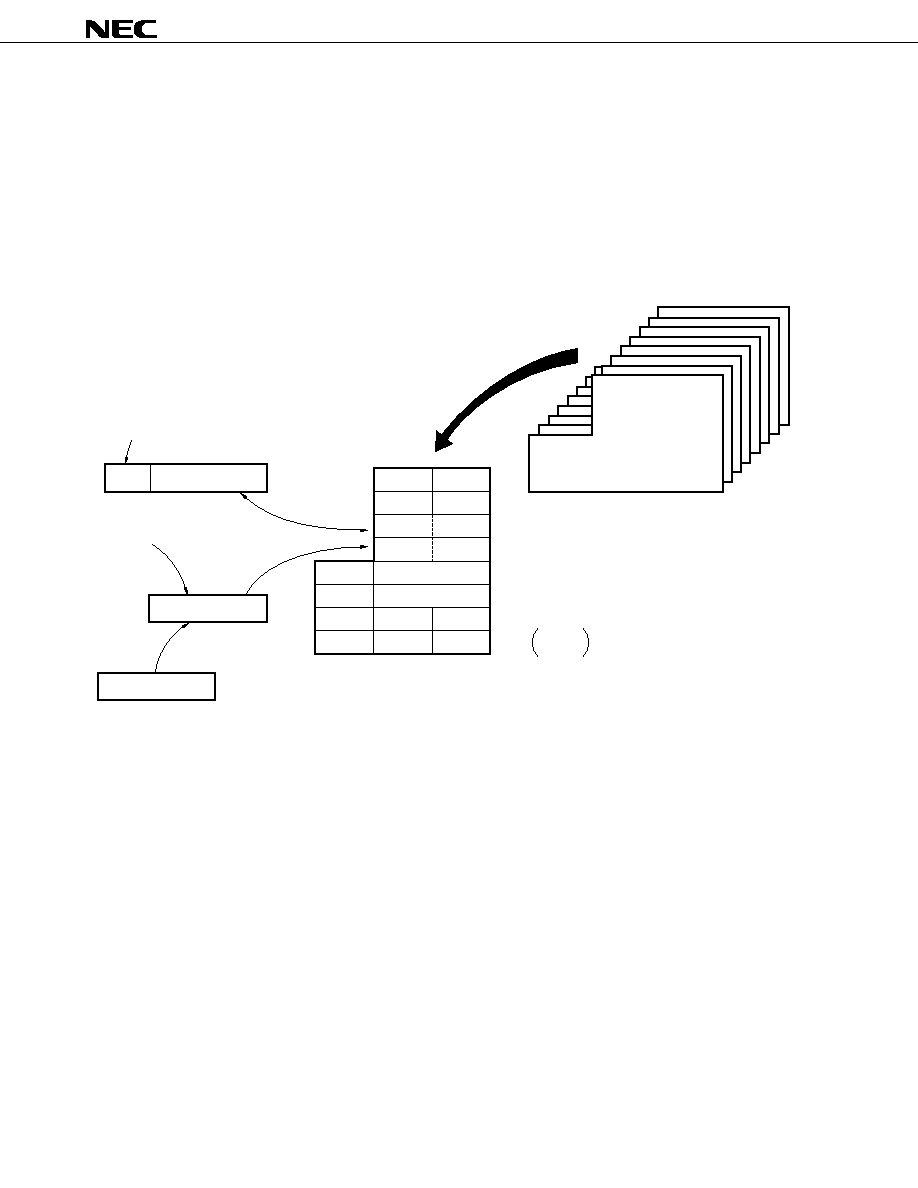
µ
PD784044, 784046
42
Data Sheet U10951EJ2V0DS00
8.3 Context Switching
A specific register bank is selected by hardware when an interrupt request is generated or when the BRKCS
instruction is executed.
When branched to the vector address stored in advance in the selected register bank, the current contents
of the program counter (PC) and program status word (PSW) are stacked in the register bank.
The branch destination address must be in the range of 0 to FFFFH.
Figure 8-1. Context Switching Operation when Interrupt Request Is Generated
V
U
T
W
A
B
R5
R7
D
H
X
C
R4
R6
E
L
VP
UP
Register bank n (n = 0 to 7)
< 3 > Select register bank (RBS0 to RBS2
n)
< 4 > RSS
0
IE
0
< 6 > Exchange
< 5 > Save
< 7 > Transfer
< 1 > Save
0000B
< 2 > Save
(bits 8 through
11 of temporary
register)
Temporary register
PSW
PC19 to 16
PC15 to 0
Register bank
(0 to 7)
µ
PD784044, 784046
43
Data Sheet U10951EJ2V0DS00
8.4 Macro Service
The
µ
PD784046 has a total of seven types of macro service. Each macro service is outlined below.
(1) Counter mode: EVTCNT
∑
Operation (a) Increments or decrements an 8-bit macro service counter (MSC).
(b) A vectored interrupt request is generated when the value of MSC reaches 0.
∑
Application example: Event counter, measurement of number of times of capture
(2) Block transfer mode: BLKTRS
∑
Operation (a) Transfers block of data between the buffer and an SFR specified by the SFR pointer
(SFR.PTR).
(b) The transfer source and destination can be an SFR or buffer area. The length of the data
to be transferred can be specified as byte or word.
(c) The number of times data is to be transferred (block size) is specified by MSC.
(d) MSC is auto-decremented (≠1) each time the macro service is executed.
(e) When the value of MSC reaches 0, a vectored interrupt request is generated.
∑
Application example: Data transmission/reception of serial interface
MSC
+1 / _1
MSC
SFR.PTR
_1
Buffer N
Buffer 1
SFR
Internal bus
µ
PD784044, 784046
44
Data Sheet U10951EJ2V0DS00
(3) Block transfer mode (with memory pointer): BLKTRS-P
∑
Operation This is the block transfer mode in (2) with a memory pointer (MEM.PTR) appended. The
appended buffer area of MEM.PTR can be freely set on the memory space.
Remark
MEM.PTR is auto-incremented (+1: byte data transfer/+2: word data transfer) each time the
macro service has been executed.
∑
Application example: Measurement of period and pulse width by capture register of timer 0
∑
Application example: Same as (2)
(4) Data differential mode: DTADIF
∑
Operation (a) Calculates the difference between the contents of the SFR specified by SFR pointer
(SFR.PTR) (current value) and the contents of the SFR loaded to the last data buffer (LDB).
(b) Stores the result of the calculation in a predetermined buffer area.
(c) Stores the contents of the current value of SFR in LDB.
(d) The number of times the data is to be transferred (block size) is specified by MSC. The
value of MSC is auto-decremented (≠1) each time the macro service is executed.
(e) When the value of MSC reaches 0, a vectored interrupt request is generated.
Remark
The differential calculation can be performed only by an SFR of 16-bit configuration.
MSC
SFR.PTR
_1
Buffer N
Buffer 1
SFR
Internal bus
+1 / +2
MEM.PTR
MSC
SFR.PTR
_1
Buffer N
Buffer 1
SFR
Internal bus
Differential calculation
LDB
µ
PD784044, 784046
45
Data Sheet U10951EJ2V0DS00
(5) Data differential mode (with memory pointer): DTADIF-P
∑
Operation This is the data differential mode in (4) with a memory pointer (MEM.PTR) appended. The
appended MEM.PTR can set a buffer area in which the differential data is to be stored on the
memory space freely.
Remarks 1. The differential calculation can be performed only by an SFR of 16-bit configuration.
2. The buffer is specified by the result of an operation between MEM.PTR and MSC
Note
. The
value of MEM.PTR is not updated after the data has been transferred.
Note
MEM.PTR ≠ (MSC
◊
2) + 2
∑
Application example: Same as (4)
(6) CPU monitoring mode0: SELF0
∑
Operation (a) Checks the internal operation of the CPU.
(b) When the blocks are operating normally, the value given by subtracting 10 from the initial
value is transferred to the SFR specified by the SFR pointer (SFR.PTR).
∑
Application example: Used for self checking of the CPU at initial setting.
(7) CPU monitoring mode1: SELF1
∑
Operation (a) Checks the internal operation of the CPU.
(b) When the blocks are operating normally, the value given by subtracting 8 from the initial
value is transferred to the SFR specified by the SFR pointer (SFR.PTR).
∑
Application example: Used for self checking of the CPU during normal operation.
MSC
SFR.PTR
Buffer N
Buffer 1
LDB
_1
SFR
Internal bus
Differential calculation
MEM.PTR
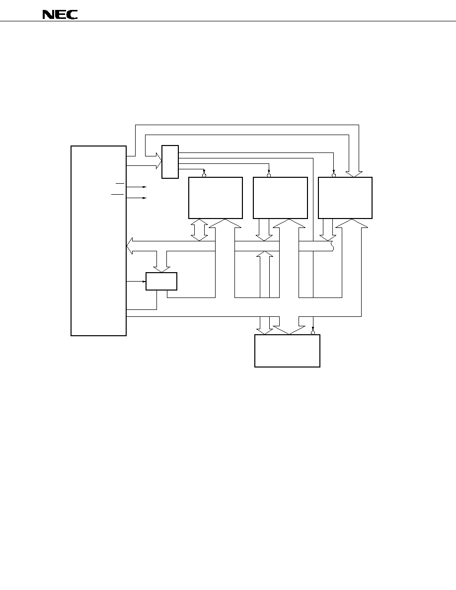
µ
PD784044, 784046
46
Data Sheet U10951EJ2V0DS00
9. LOCAL BUS INTERFACE
The
µ
PD784046 can be connected to an external memory or I/O (memory mapped I/O), supporting a 1-Mbyte
memory space (refer to Figure 9-1).
Figure 9-1. Example of Local Bus Interface (with external 8-bit bus specified)
Address bus
SRAM
PROM
Character
generator
Data bus
AD0 to AD7
AD8 to AD15
ASTB
LWR
RD
A16 to A19
PD784046
Latch
Address bus
Gate array
I/O extension
Centronics I/F, etc.
Decoder
µ
µ
PD784044, 784046
47
Data Sheet U10951EJ2V0DS00
9.1 Memory Expansion
The external program memory or data memory can be expanded from 256 bytes up to 1Mbyte in seven steps.
When an external device is connected, the address/data bus and read/write strobe signals are controlled by
using ports 4 through 6, P90 through P93 pins. The functions of these ports and pins are set by the memory
expansion mode register (MM).
Table 9-1. Setting of Pin Function
Memory Expansion
Pin Function
Mode Register
Port 4
Port 5
Port 6
MM0 to MM3
P40 to P47
P50 to P57
P60 to P63
P90 to P93
Port mode
General-purpose port
External memory
AD0 to AD7
AD8 to AD15 are set stepwise.
A16 through A19 are set
P90: RD
expansion mode
Rest of pins can be used as
stepwise.
P91: LWR
general-purpose port pins.
Rest of pins can be used as
P92: HWR
general-purpose port pins.
P93: ASTB
Remark
AD8 through AD15 are used as address bus.
The number of pins of ports 5 and 6 that are used as address bus pins can be changed according to the size
of the external memory connected (external address space), so that the external memory can be expanded
stepwise. The pins not used as address bus pins can be used as general-purpose I/O port pins (refer to Table
9-2). The external address space can be set in seven steps by MM.
Table 9-2. Operations of Ports 5 and 6 (In External Memory Expansion Mode)
Port 5
Port 6
External address space
P50
P51
P52
P53
P54
P55
P56
P57
P60
P61
P62
P63
General-purpose port
256 bytes or less
Note
AD8
AD9
1 Kbyte or less
Note
AD10
AD11
4 Kbytes or less
Note
AD12
AD13
16 Kbytes or less
Note
AD14
AD15
64 Kbytes or less
A16
A17
256 Kbytes or less
A18
A19
1 Mbyte or less
Note
When the external 16-bit bus is specified, do not set MM such that the external address space is of this size.
Caution
When the external 16-bit bus is specified, set MM such that all the pins of port 5 (P50 through P57)
are used as AD pins (AD8 through AD15).
µ
PD784044, 784046
48
Data Sheet U10951EJ2V0DS00
9.2 Memory Space
The 1-Mbyte memory space is divided into the following eight spaces of logical addresses. Each space can
be controlled by using the programmable wait function and bus sizing function.
Figure 9-2. Memory Space
9.3 Programmable Wait
A wait state can be inserted to each of the eight memory spaces while the RD, LWR, and HWR signals are
active. Even if memories with different access times are connected, therefore, the overall efficiency of the
system is not degraded.
In addition, an address wait function that extends the active period of the ASTB signal is also available to
extend the address decode time (this function can be set to all the spaces).
9.4 Bus Sizing Function
The
µ
PD784046 can change the external data bus width between 8 and 16 bits when an external device is
connected. Even if the memory space is divided by eight, the bus width of each memory space can be specified
independently.
512 Kbytes
256 Kbytes
128 Kbytes
64 Kbytes
16 Kbytes
16 Kbytes
16 Kbytes
16 Kbytes
H
F
F
F
F
F
H
H
0
F
0
F
0
F
0
F
8
7
H
H
0
F
0
F
0
F
0
F
4
3
H
H
0
F
0
F
0
F
0
F
2
1
H
H
0
F
0
F
0
F
0
F
1
0
H
H
0
F
0
F
0
F
C
B
0
0
H
H
0
F
0
F
0
F
8
7
0
0
H
H
0
F
0
F
0
F
4
3
0
0
H
0
0
0
0
0
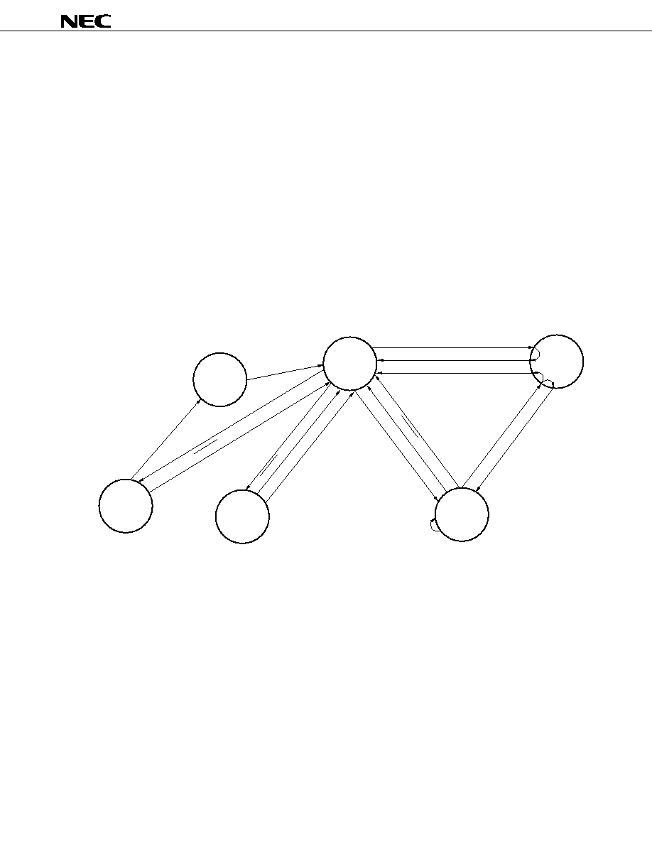
µ
PD784044, 784046
49
Data Sheet U10951EJ2V0DS00
10. STANDBY FUNCTION
The
µ
PD784046 has the following standby function modes that reduce the power consumption of the chip.
∑ HALT mode:
This mode stops the operating clock of the CPU. It can reduce the average power
consumption through intermittent operation by combination of a normal operation and this
mode.
∑ IDLE mode:
This mode stops the entire system with the operation of the oscillator continuing. Normal
program operation can be restored from this mode with the power consumption close to that
in the STOP mode and time equivalent to that in the HALT mode.
∑ STOP mode:
This mode stops the oscillator and stops all the internal operations of the chip to minimize
the power consumption to the level of only leakage current.
These modes are programmable.
Macro service can be started from the HALT mode.
Figure 10-1. Standby Mode Status Transition
Note
Only unmasked interrupt request
Remark
Only external input of NMI is valid. The watchdog timer cannot be used to release the standby mode
(STOP/HALT/IDLE).
Interrupt request
Note
HALT setting
RESET input
IDLE settingNMI
RESET input
Macro service request
End of first servicing
End of macro service
Macro service request
End of first servicing
STOP setting
RESET input
NMI
End of
oscillation
stabilization time
Interrupt request of
masked interrupt
Macro
service
HALT
(standby)
Program
operation
Waits for
oscillation
stabilization
IDLE
(standby)
STOP
(standby)
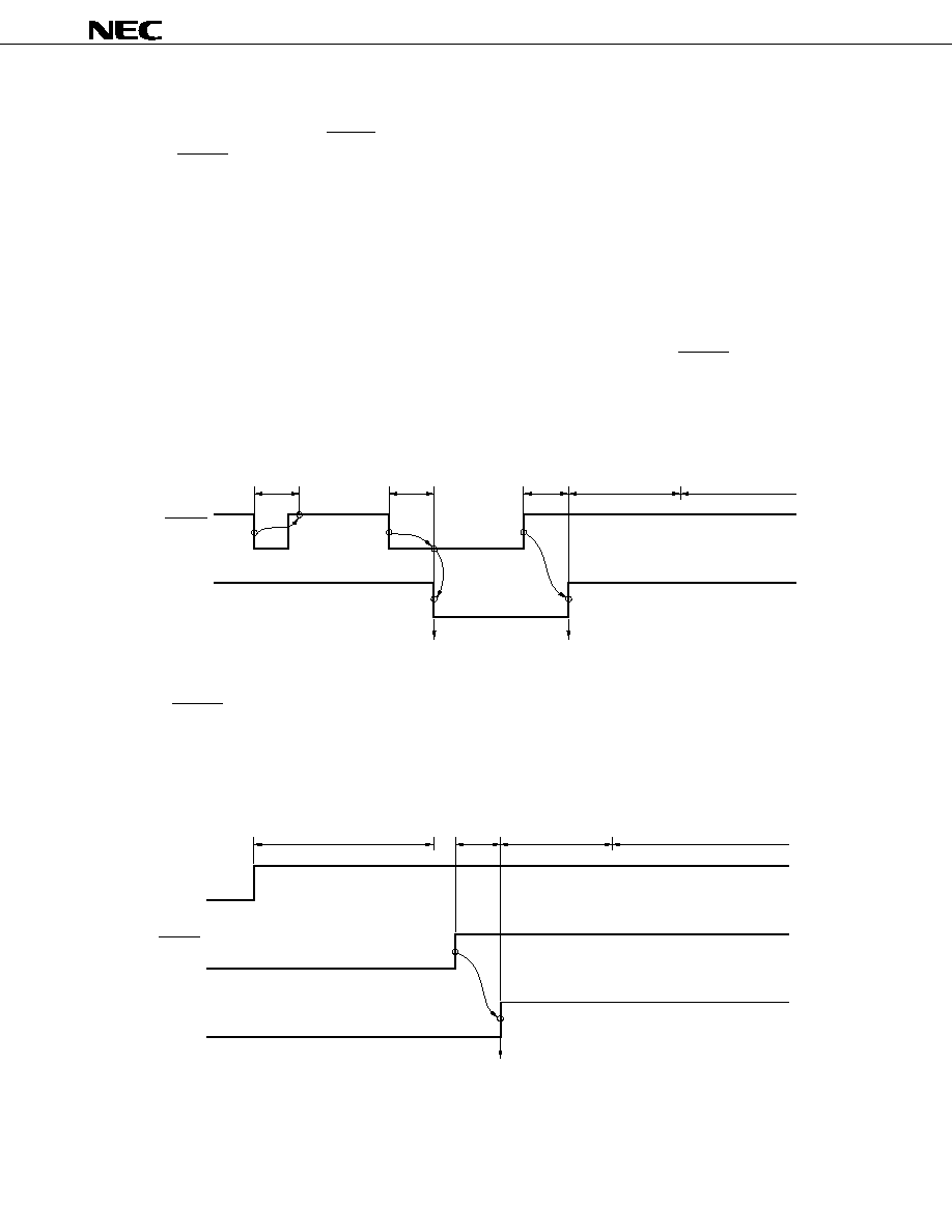
µ
PD784044, 784046
50
Data Sheet U10951EJ2V0DS00
11. RESET FUNCTION
When a low level is input to the RESET pin, the internal hardware is initialized (reset status).
When the RESET signal goes high, the following data is set to the program counter (PC).
∑
Lower 8 bits of PC: contents of address 0000H
∑
Middle 8 bits of PC: contents of address 0001H
∑
Higher 4 bits of PC: 0
The contents of the PC are assumed as a branch destination address and program execution is started from
this address. Therefore, the program can be reset and started from any address.
Set the contents of each register by program as necessary.
To prevent malfunctioning due to noise, a noise elimination circuit is provided to the RESET input circuit.
This noise elimination circuit is a sampling circuit with analog delay.
Figure 11-1. Accepting Reset
Keep the RESET signal active until the oscillation stabilization time (about 40 ms) elapses when executing
a reset operation on power application or when releasing the STOP mode by reset.
Figure 11-2. Reset Operation on Power Application
RESET
(input)
Internal reset signal
Delay
Delay
Delay
PC initialization
Instruction execution
at reset start address
Reset starts
Reset ends
V
DD
RESET
(input)
Internal reset signal
Delay
PC initialization
Instruction execution at reset start address
Oscillation stabilization time
Reset ends
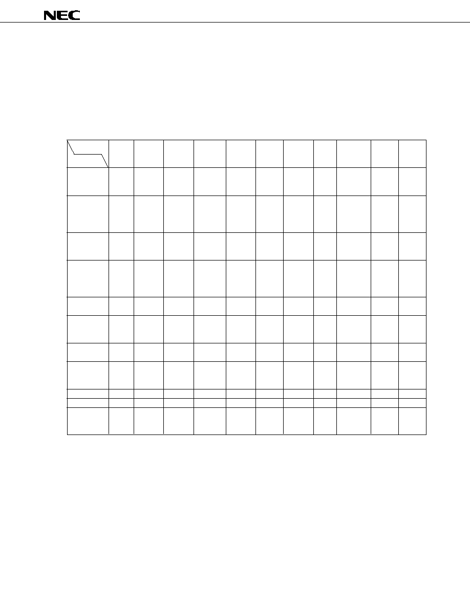
µ
PD784044, 784046
51
Data Sheet U10951EJ2V0DS00
12. INSTRUCTION SET
(1) 8-bit instructions (( ): combination realized by describing A as r)
MOV, XCH, ADD, ADDC, SUB, SUBC, AND, OR, XOR, CMP, MULU, DIVUW, INC, DEC, ROR, ROL, RORC,
ROLC, SHR, SHL, ROR4, ROL4, DBNZ, PUSH, POP, MOVM, XCHM, CMPME, CMPMNE, CMPMNC,
CMPMC, MOVBK, XCHBK, CMPBKE, CMPBKNE, CMPBKNC, CMPBKC, CHKL, CHKLA
Table 12-1. Instruction List for 8-Bit Addressing
2nd Operand
#byte
A
r
saddr
sfr
!addr16
mem
r3
[WHL+]
n
None
Note 2
r'
saddr'
!!addr24
[saddrp]
PSWL
[WHL≠]
1st Operand
[%saddrg]
PSWH
A
(MOV)
(MOV)
MOV
(MOV)
Note 6
MOV
(MOV)
MOV
MOV
(MOV)
ADD
Note 1
(XCH)
XCH
(XCH)
Note 6
(XCH)
(XCH)
XCH
(XCH)
(ADD)
Note 1
(ADD)
Note 1
(ADD)
Note 1, 6
(ADD)
Note 1
ADD
Note 1
ADD
Note 1
(ADD)
Note 1
r
MOV
(MOV)
MOV
MOV
MOV
MOV
ROR
Note 3
MULU
ADD
Note 1
(XCH)
XCH
XCH
XCH
XCH
DIVUW
(ADD)
Note 1
ADD
Note 1
ADD
Note 1
ADD
Note 1
INC
DEC
saddr
MOV
(MOV)
Note 6
MOV
MOV
INC
ADD
Note 1
(ADD)
Note 1
ADD
Note 1
XCH
DEC
ADD
Note 1
DBNZ
sfr
MOV
MOV
MOV
PUSH
ADD
Note 1
(ADD)
Note 1
ADD
Note 1
POP
CHKL
CHKLA
!addr16
MOV
(MOV)
MOV
!!addr24
ADD
Note 1
mem
MOV
[saddrp]
ADD
Note 1
[%saddrg]
mem3
ROR4
ROL4
r3
MOV
MOV
PSWL
PSWH
B, C
DBNZ
STBC, WDM
MOV
[TDE+]
(MOV)
MOVBK
Note 5
[TDE≠]
(ADD)
Note 1
MOVM
Note 4
Notes 1. ADDC, SUB, SUBC, AND, OR, XOR, and CMP are the same as ADD.
2. Either the second operand is not used, or the second operand is not an operand address.
3. ROL, RORC, ROLC, SHR, and SHL are the same as ROR.
4. XCHM, CMPME, CMPMNE, CMPMNC, and CMPMC are the same as MOVM.
5. XCHBK, CMPBKE, CMPBKNE, CMPBKNC, and CMPBKC are the same as MOVBK.
6. If saddr is saddr2 in this combination, some instructions have a short code length.

µ
PD784044, 784046
52
Data Sheet U10951EJ2V0DS00
(2) 16-bit instructions (( ): combination realized by describing AX as rp)
MOVW, XCHW, ADDW, SUBW, CMPW, MULUW, MULW, DIVUX, INCW, DECW, SHRW, SHLW, PUSH,
POP, ADDWG, SUBWG, PUSHU, POPU, MOVTBLW, MACW, MACSW, SACW
Table 12-2. Instruction List for 16-Bit Addressing
2nd Operand
#word
AX
rp
saddrp
sfrp
!addr16
mem
[WHL+]
byte
n
None
Note 2
rp'
saddrp'
!!addr24
[saddrp]
1st Operand
[%saddrg]
AX
(MOVW)
(MOVW)
(MOVW)
(MOVW)
Note 3
MOVW
(MOVW)
MOVW
(MOVW)
ADDW
Note 1
(XCHW)
(XCHW)
(XCHW)
Note 3
(XCHW)
XCHW
XCHW
(XCHW)
(ADDW)
Note 1
(ADDW)
Note 1
(ADDW)
Notes 1, 3
(ADDW)
Note 1
rp
MOVW
(MOVW)
MOVW
MOVW
MOVW
MOVW
SHRW
MULW
Note 4
ADDW
Note 1
(XCHW)
XCHW
XCHW
XCHW
SHLW
INCW
(ADDW)
Note 1
ADDW
Note 1
ADDW
Note 1
ADDW
Note 1
DECW
saddrp
MOVW
(MOVW)
Note 3
MOVW
MOVW
INCW
ADDW
Note 1
(ADDW)
Note 1
ADDW
Note 1
XCHW
DECW
ADDW
Note 1
sfrp
MOVW
MOVW
MOVW
PUSH
ADDW
Note 1
(ADDW)
Note 1
ADDW
Note 1
POP
!addr16
MOVW
(MOVW)
MOVW
MOVTBLW
!!addr24
mem
MOVW
[saddrp]
[%saddrg]
PSW
PUSH
POP
SP
ADDWG
SUBWG
post
PUSH
POP
PUSHU
POPU
[TDE+]
(MOVW)
SACW
byte
MACW
MACSW
Notes 1. SUBW and CMPW are the same as ADDW.
2. Either the second operand is not used, or the second operand is not an operand address.
3. If saddrp is saddrp2 in this combination, some instructions have a short code length.
4. MULUW and DIVUX are the same as MULW.

µ
PD784044, 784046
53
Data Sheet U10951EJ2V0DS00
(3) 24-bit instructions (( ): combination realized by describing WHL as rg)
MOVG, ADDG, SUBG, INCG, DECG, PUSH, POP
Table 12-3. Instruction List for 24-Bit Addressing
2nd Operand
#imm24
WHL
rg
saddrg
!!addr24
mem1
[%saddrg]
SP
None
Note
1st Operand
rg'
WHL
(MOVG)
(MOVG)
(MOVG)
(MOVG)
(MOVG)
MOVG
MOVG
MOVG
(ADDG)
(ADDG)
(ADDG)
ADDG
(SUBG)
(SUBG)
(SUBG)
SUBG
rg
MOVG
(MOVG)
MOVG
MOVG
MOVG
INCG
ADDG
(ADDG)
ADDG
DECG
SUBG
(SUBG)
SUBG
PUSH
POP
saddrg
(MOVG)
MOVG
!!addr24
(MOVG)
MOVG
mem1
MOVG
[%saddrg]
MOVG
SP
MOVG
MOVG
INCG
DECG
Note
Either the second operand is not used, or the second operand is not an operand address.
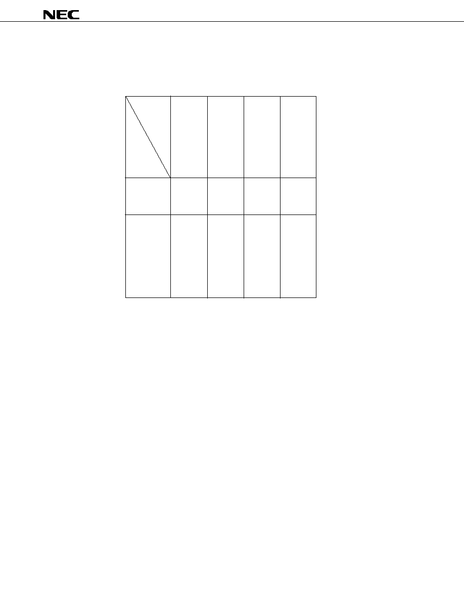
µ
PD784044, 784046
54
Data Sheet U10951EJ2V0DS00
(4) Bit manipulation instructions
MOV1, AND1, OR1, XOR1, SET1, CLR1, NOT1, BT, BF, BCLR, BFSET
Table 12-4. Instruction List for Bit Manipulation Instruction Addressing
2nd Operand
CY
saddr.bit
/saddr.bit
None
Note
sfr.bit
/sfr.bit
A.bit
/A.bit
X.bit
/X.bit
PSWL.bit
/PSWL.bit
PSWH.bit
/PSWH.bit
mem2.bit
/mem2.bit
!addr16.bit
/!addr16.bit
1st Operand
!!addr24.bit
/!!addr24.bit
CY
MOV1
AND1
NOT1
AND1
OR1
SET1
OR1
CLR1
XOR1
saddr.bit
MOV1
NOT1
sfr.bit
SET1
A.bit
CLR1
X.bit
BF
PSWL.bit
BT
PSWH.bit
BTCLR
mem2.bit
BFSET
!addr16.bit
!!addr24.bit
Note
Either the second operand is not used, or the second
operand is not an operand address.
µ
PD784044, 784046
55
Data Sheet U10951EJ2V0DS00
(5) Call return/branch instructions
CALL, CALLF, CALLT, BRK, RET, RETI, RETB, RETCS, RETCSB, BRKCS, BR, BNZ, BNE, BZ, BE, BNC,
BNL, BC, BL, BNV, BPO, BV, BPE, BP, BN, BLT, BGE, BLE, BGT, BNH, BH, BF, BT, BTCLR, BFSET, DBNZ
Table 12-5. Instruction List for Addressing of Call Return/Branch Instructions
Operand of
$addr20
$!addr20
!addr16
!!addr20
rp
rg
[rp]
[rg]
!addr11
[addr5]
RBn
None
instruction
address
Basic
BC
Note
CALL
CALL
CALL
CALL
CALL
CALL
CALL
CALLF
CALLT
BRKCS
BRK
instruction
BR
BR
BR
BR
BR
BR
BR
BR
RET
RETCS
RETI
RETCSB
RETB
Compound
BF
instruction
BT
BTCLR
BFSET
DBNZ
Note
BNZ, BNE, BZ, BE, BNC, BNL, BL, BNV, BPO, BV, BPE, BP, BN, BLT, BGE, BLE, BGT, BNH, and BH are the
same as BC.
(6) Other instructions
ADJBA, ADJBS, CVTBW, LOCATION, SEL, NOT, EI, DI, SWRS
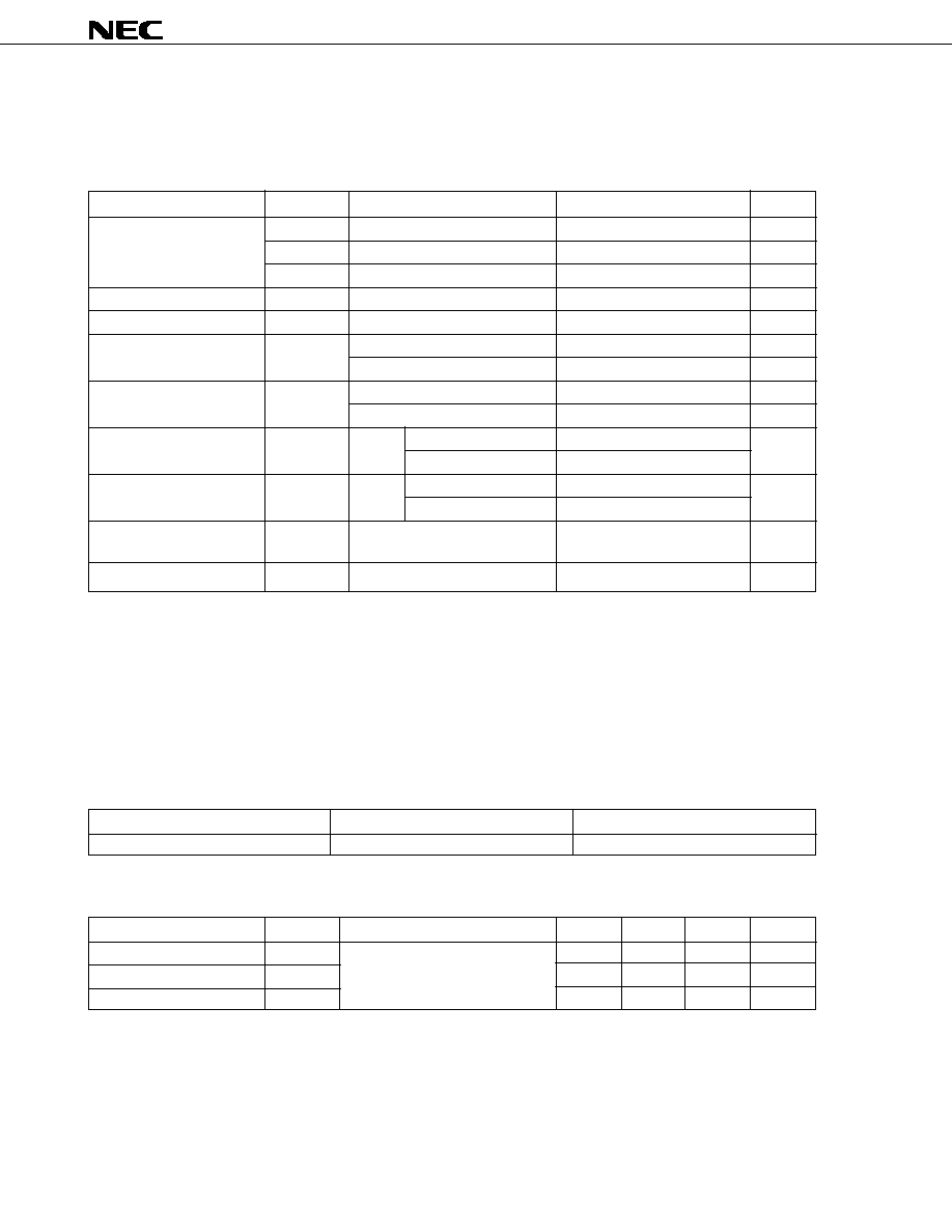
µ
PD784044, 784046
56
Data Sheet U10951EJ2V0DS00
13. ELECTRICAL SPECIFICATIONS
Absolute Maximum Ratings (T
A
= 25∞C)
Parameter
Symbol
Conditions
Ratings
Unit
Supply voltage
V
DD
≠0.5 to +7.0
V
AV
DD
≠0.5 to V
DD
+ 0.5
V
AV
SS
≠0.5 to +0.5
V
Input voltage
V
I
Note 1
≠0.5 to V
DD
+ 0.5
7.0
V
Output voltage
V
O
≠0.5 to V
DD
+ 0.5
V
Output current, low
I
OL
All output pins
15
mA
Total of all output pins
150
mA
Output current, high
I
OH
All output pins
≠10
mA
Total of all output pins
≠100
mA
Analog input voltage
V
IAN
Note 2 AV
DD
> V
DD
≠0.5 to V
DD
+ 0.5
V
V
DD
AV
DD
≠0.5 to AV
DD
+ 0.5
A/D converter reference
AV
REF
AV
DD
> V
DD
≠0.5 to V
DD
+ 0.5
V
input voltage
V
DD
AV
DD
≠0.5 to AV
DD
+ 0.5
Operating ambient
T
A
≠10 to +70
∞C
temperature
Storage temperature
T
stg
≠65 to +150
∞C
Notes 1. Pins other than the pins in Note 2.
2. Pins P70/ANI0 to P77/ANI7, P80/ANI8 to P87/ANI15
Caution
Product quality may suffer if the absolute maximum rating is exceeded even momentarily for
any parameter. That is, the absolute maximum ratings are rated values at which the product is
on the verge of suffering physical damage, and therefore the product must be used under
conditions that the absolute maximum ratings are not exceeded.
Recommended Operating Conditions
Oscillation Frequency
T
A
V
DD
8 MHz
f
XX
32 MHz
≠10 to +70∞C
4.5 to 5.5 V
Capacitance (T
A
= 25∞C, V
SS
= V
DD
= 0 V)
Parameter
Symbol
Conditions
MIN.
TYP.
MAX.
Unit
Input capacitance
C
I
f = 1 MHz
10
pF
Output capacitance
C
O
Unmeasured pins returned to 0 V.
10
pF
I/O capacitance
C
IO
10
pF
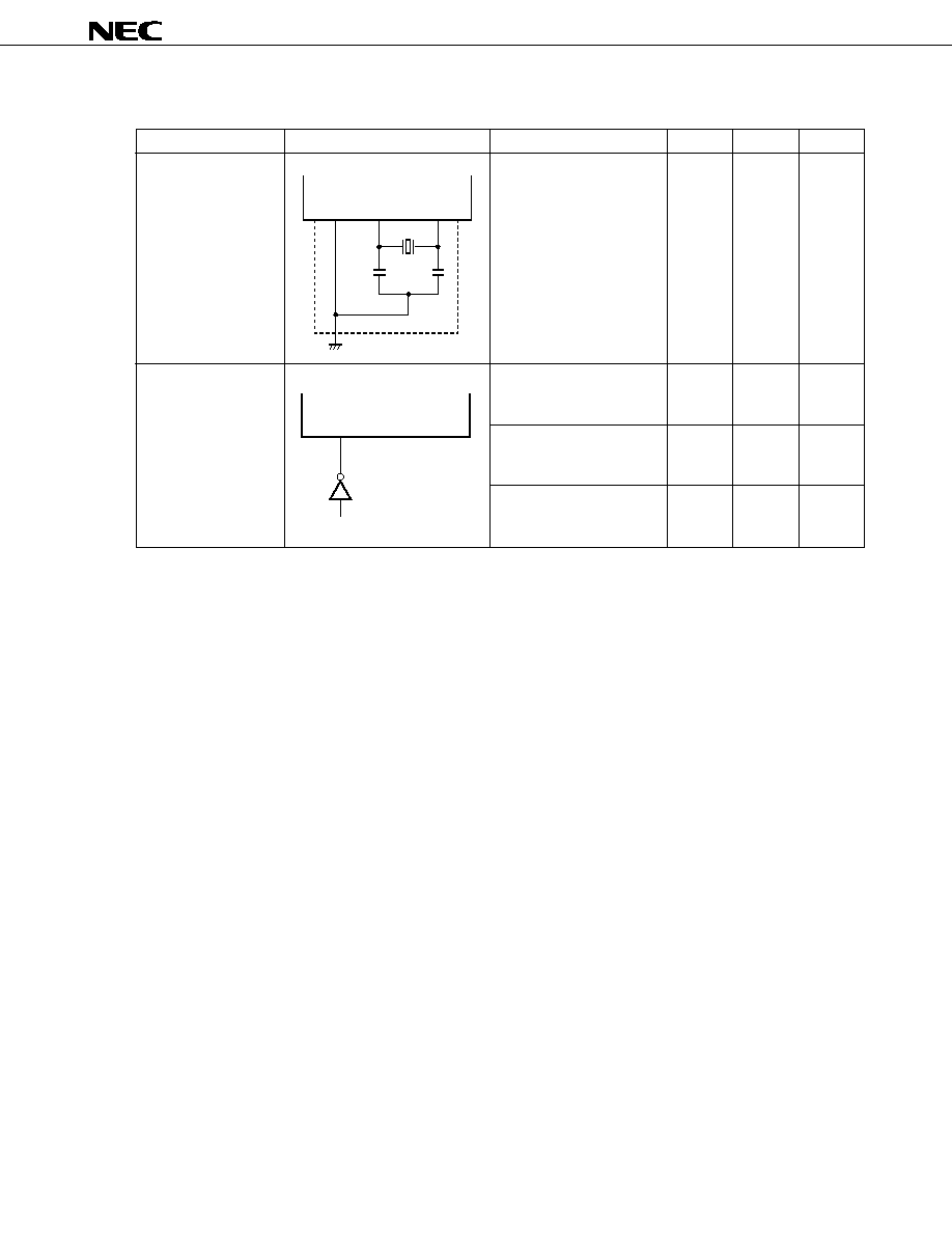
µ
PD784044, 784046
57
Data Sheet U10951EJ2V0DS00
Oscillator Characteristics (T
A
= ≠10 to +70∞C, V
DD
= 4.5 to 5.5 V, V
SS
= 0 V)
Resonator
Recommended Circuit
Item
MIN.
MAX.
Unit
Ceramic resonator or
Oscillation frequency (f
XX
)
8
32
MHz
crystal resonator
External clock
X1 input frequency (f
X
)
8
32
MHz
X1 input rise, fall time
0
5
ns
X1 input high-, low-level
20
105
ns
width
Note
When the EXTC bit of the oscillation stabilization time specification register (OSTS) = 0. Input the reverse
phase clock of the pin X1 to the pin X2 when the EXTC bit = 1.
Caution
When using the system clock oscillator, wire as follows in the area enclosed by the broken lines
in the above figures to prevent an adverse effect from wiring capacitance.
∑
Keep the wiring length as short as possible.
∑
Do not cross the wiring with any other signal lines. Do not route the wiring near a signal line
through which a high fluctuating current flows.
∑
Always make the ground point of the oscillator capacitor the same potential as V
SS
. Do not
ground the capacitor to a ground pattern through which a high current flows.
∑
Do not fetch signals from the oscillator.
C1
C2
V
SS
X1
X2
X1
X2
Open
Note
HCMOS inverter
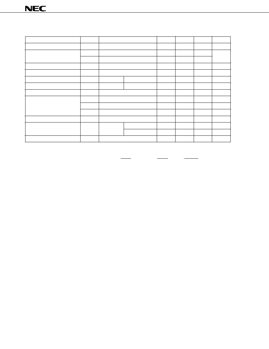
µ
PD784044, 784046
58
Data Sheet U10951EJ2V0DS00
DC Characteristics (T
A
= ≠10 to +70∞C, V
DD
= 4.5 to 5.5 V, V
SS
= 0 V)
Parameter
Symbol
Conditions
MIN.
TYP.
MAX.
Unit
Input voltage, low
V
IL
0
0.8
V
Input voltage, high
V
IH1
Note 1
2.2
V
DD
V
V
IH2
Note 2
0.8V
DD
V
DD
Output voltage, low
V
OL
I
OL
= 2.0 mA
0.45
V
Output voltage, high
V
OH
I
OH
= ≠400
µ
A
V
DD
≠ 1.0
V
Input leakage current
I
LI
Note 3 0 V
V
I
V
DD
±
10
µ
A
Analog pin input leakage current
I
LIAN
Note 4 0 V
V
I
AV
DD
±
1
µ
A
Output leakage current
I
LO
0 V
V
O
V
DD
±
10
µ
A
V
DD
supply current
I
DD1
Operating mode (f
XX
= 32 MHz)
50
80
mA
I
DD2
HALT mode (f
XX
= 32 MHz)
30
60
mA
I
DD3
IDLE mode (f
XX
= 32 MHz)
10
20
mA
Data retention voltage
V
DDDR
STOP mode
2.5
V
Data retention current
I
DDDR
STOP mode V
DDDR
= 2.5 V
2
15
µ
A
V
DDDR
= 5 V
±
10%
15
50
µ
A
Pull-up resistor
R
L
15
40
80
k
Notes 1. Pins other than pins in the Note 2
2. P20/NMI, P21/INTP0/TO00, P22/INTP1/TO01, P23/INTP2/TO02, P24/INTP3/TO03, P25/INTP4, P26/
INTP5/TI2, P27/INTP6/TI3, P34/ASCK/SCK1, P37/ASCK2/SCK2, X1, X2, RESET
3. Input and I/O pins (except X1 and X2, and P70/ANI0 to P77/ANI7, P80/ANI8 to P87/ANI15 used as
analog inputs)
4. Pins P70/ANI0 to P77/ANI7, P80/ANI8 to P87/ANI15 (pins used as analog input, only during the non-
sampling operation)
µ
PD784044, 784046
59
Data Sheet U10951EJ2V0DS00
AC Characteristics (T
A
= ≠10 to +70∞C, V
DD
= 4.5 to 5.5 V, V
SS
= 0 V)
Read/write operation
Parameter
Symbol
Expression
MIN.
MAX.
Unit
System clock cycle time
t
CYK
62.5
250
ns
Address setup time (to ASTB
)
t
SAST
(0.5 + a) T ≠ 20
11.2
ns
Address hold time (from ASTB
)
t
HSTA
0.5T ≠ 20
11.2
ns
ASTB high-level width
t
WSTH
(0.5 + a) T ≠ 17
14.2
ns
RD
delay time from address
t
DAR
(1 + a) T ≠ 15
47.5
ns
Address float time from RD
t
FRA
0
ns
Data input time from address
t
DAID
(2.5 + a + n) T ≠ 56
100.2
ns
Data input time from RD
t
DRID
(1.5 + n) T ≠ 48
45.7
ns
RD
delay time from ASTB
t
DSTR
0.5T ≠ 16
15.3
ns
Data hold time (to RD
)
t
HRID
0
ns
Address active time from RD
t
DRA
0.5T ≠ 14
17.2
ns
RD low-level width
t
WRL
(1.5 + n) T ≠ 30
63.7
ns
LWR, HWR
delay time from address
t
DAW
(1 + a) T ≠ 15
47.5
ns
Data output time from LWR, HWR
t
DWOD
15
ns
LWR, HWR
delay time from ASTB
t
DSTW
0.5T ≠ 16
15.3
ns
Data setup time (to LWR, HWR
)
t
SODW
(1.5 + n) T ≠ 25
68.7
ns
Data hold time (from LWR, HWR
)
t
HWOD
0.5T ≠ 14
17.2
ns
ASTB
delay time from LWR, HWR
t
DWST
1.5T ≠ 15
78.8
ns
LWR, HWR low-level width
t
WWL
(1.5 + n) T ≠ 36
57.7
ns
WAIT
input time from address
t
DAWT
(2 + a) T ≠ 50
75
ns
WAIT
input time from ASTB
t
DSTWT
1.5T ≠ 40
53.7
ns
WAIT hold time from ASTB
t
HSTWT
(1.5 + n) T + 5
98.8
ns
WAIT
delay time from ASTB
t
DSTWTH
(2.5 + n) T ≠ 40
116.2
Note
ns
WAIT
input time from RD
t
DRWT
T ≠ 40
22.5
ns
WAIT hold time from RD
t
HRWT
(1 + n) T + 5
67.5
ns
WAIT
delay time from RD
t
DRWTH
(1 + n) T ≠ 40
85
Note
ns
WAIT
input time from LWR, HWR
t
DWWT
T ≠ 40
22.5
ns
WAIT hold time from LWR, HWR
t
HWWT
(1 + n) T + 5
67.5
ns
WAIT
delay time from LWR, HWR
t
DWWTH
(1 + n) T ≠ 40
85
Note
ns
Note
Specification when an external wait is inserted
Remarks 1. T = t
CYK
= 1/f
CLK
(f
CLK
is internal system clock frequency)
2. a = 1 when an address wait is inserted, otherwise, 0.
3. n indicates the number of the wait cycles by specifying the external wait pins (WAIT) or program-
mable wait control registers 1, 2 (PWC1, PWC2). (n
0. n
1 for t
DSTWTH
, t
DRWTH
, t
DWWTH
).
4. Calculate values in the expression column with the system clock cycle time to be used because
these values depend on the system clock cycle time (t
CYK
= T). The values in the above expression
column are calculated based on T = 62.5 ns.
µ
PD784044, 784046
60
Data Sheet U10951EJ2V0DS00
Serial Operation (T
A
= ≠10 to +70∞C, V
DD
= 4.5 to 5.5 V, V
SS
= 0 V)
Parameter
Symbol
Conditions
MIN.
MAX.
Unit
Serial clock cycle time
t
CYSK
SCK1, SCK2 output
BRG
T
SFT
ns
SCK1, SCK2 input
External clock
500
ns
Serial clock low-level width
t
WSKL
SCK1, SCK2 output
BRG
0.5T
SFT
≠40
ns
SCK1, SCK2 input
External clock
210
ns
Serial clock high-level width
t
WSKH
SCK1, SCK2 output
BRG
0.5T
SFT
≠40
ns
SCK1, SCK2 input
External clock
210
ns
SI1, SI2 setup time
t
SSSK
80
ns
(to SCK1, SCK2
)
SI1, SI2 hold time
t
HSSK
80
ns
(from SCK1, SCK2
)
SO1, SO2 output
t
DSBSK
R = 1 k
, C = 100 pF
0
150
ns
delay time from SCK1, SCK2
Remarks 1. T
SFT
is a value set in software. The minimum value is t
CYK
◊
8.
2. t
CYK
= 1/f
CLK
(f
CLK
is internal system clock frequency)
Other Operations (T
A
= ≠10 to +70∞C, V
DD
= 4.5 to 5.5 V, V
SS
= 0 V)
Parameter
Symbol
Conditions
MIN.
MAX.
Unit
NMI high-, low-level width
t
WNIH
, t
WNIL
10
µ
s
INTP0 to INTP6 high-, low-level width t
WITH
, t
WITL
4
t
CYSMP
TI2, TI3 high-, low-level width
t
WTIH
, t
WTIL
4
t
CYSMP
RESET high-, low-level width
t
WRSH
, t
WRSL
10
µ
s
Remarks 1. t
CYSMP
is a sampling clock set in the noise protection control register (NPC) in software.
When NIn = 0, t
CYSMP
= t
CYK
When NIn = 1, t
CYSMP
= t
CYK
◊
4
2. t
CYK
= 1/f
CLK
(f
CLK
is internal system clock frequency)
3. NIn: Bit n of NPC (n = 0 to 6)
AC Timing Test Points
V
DD
0 V
0.8V
DD
or 2.2 V
0.8 V
0.8V
DD
or 2.2 V
0.8 V
Test points

µ
PD784044, 784046
61
Data Sheet U10951EJ2V0DS00
AD Converter Characteristics (T
A
= ≠10 to +70∞C, V
DD
= 4.5 to 5.5 V, V
SS
= AV
SS
= 0 V,
V
DD
≠ 0.5 V
AV
DD
V
DD
)
Parameter
Symbol
Conditions
MIN.
TYP.
MAX.
Unit
Resolution
10
bit
Total error
Note
4.5 V
AV
REF
AV
DD
±
0.5
%FSR
3.4 V
AV
REF
< 4.5 V
±
0.7
%FSR
Quantization error
±
1/2
LSB
Conversion time
t
CONV
80 ns
t
CYK
250 ns
169
t
CYK
62.5 ns
t
CYK
< 80 ns
208
t
CYK
Sampling time
t
SAMP
80 ns
t
CYK
250 ns
20
t
CYK
62.5 ns
t
CYK
< 80 ns
24
t
CYK
Zero-scale error
Note
4.5 V
AV
REF
AV
DD
±
1.5
±
3.5
LSB
3.4 V
AV
REF
< 4.5 V
±
1.5
±
4.5
LSB
Full-scale error
Note
4.5 V
AV
REF
AV
DD
±
1.5
±
3.5
LSB
3.4 V
AV
REF
< 4.5 V
±
1.5
±
4.5
LSB
Nonlinearity error
Note
4.5 V
AV
REF
AV
DD
±
1.5
±
2.5
LSB
3.4 V
AV
REF
< 4.5 V
±
1.5
±
4.5
LSB
Analog input voltage
V
IAN
≠0.3
AV
REF
+0.3
V
A/D converter reference input
AV
REF
3.4
AV
DD
V
voltage
AV
REF
current
AI
REF
1.0
3.0
mA
AV
DD
supply current
AI
DD
2.0
6.0
mA
A/D converter data retention
AI
DDDR
STOP AV
DDDR
= 2.5 V
2
10
µ
A
current
mode
AV
DDDR
= 5 V
±
10%
10
50
µ
A
Note
The quantization error is excluded.
Remark
t
CYK
= 1/f
CLK
(f
CLK
is internal system clock frequency).
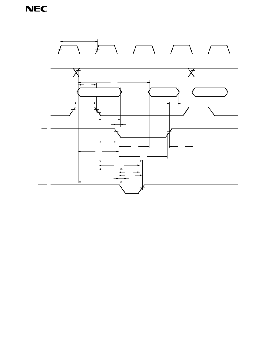
µ
PD784044, 784046
62
Data Sheet U10951EJ2V0DS00
Read Operation (8 bits)
(CLK)
AD8 to AD15
(Output)
AD0 to AD7
(Input/output)
ASTB
(Output)
RD
(Output)
WAIT
(Input)
Higher address
Higher address
Lower address (output)
Data (input)
Lower address (output)
t
CYK
t
WSTH
t
HSTA
t
DSTR
t
DAR
t
WRL
t
DSTWTH
t
HSTWT
t
DSTWT
t
DRWT
t
DAWT
t
HRWT
t
DRWTH
t
DRID
t
DRA
t
FRA
t
HRID
t
SAST
t
DAID
Hi-Z
Hi-Z
Hi-Z
Hi-Z
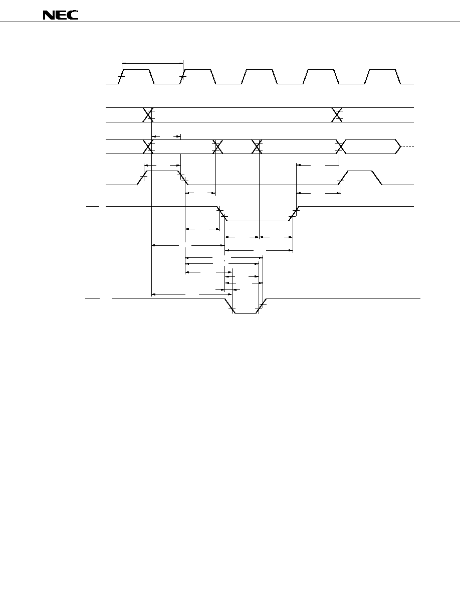
µ
PD784044, 784046
63
Data Sheet U10951EJ2V0DS00
Write Operation (8 bits)
(CLK)
AD8 to AD15
(Output)
AD0 to AD7
(Output)
ASTB
(Output)
LWR
(Output)
WAIT
(Input)
t
CYK
t
DSTWTH
t
HSTWT
t
DSTWT
t
DWWT
t
DAWT
t
HWWT
t
DWWTH
t
DSTW
t
HSTA
t
WSTH
t
SAST
t
HWOD
t
DWST
t
DWOD
t
SODW
t
DAW
t
WWL
Higher address
Higher address
Lower address (Output)
Undefined
Data (Output)
Lower address (Output)
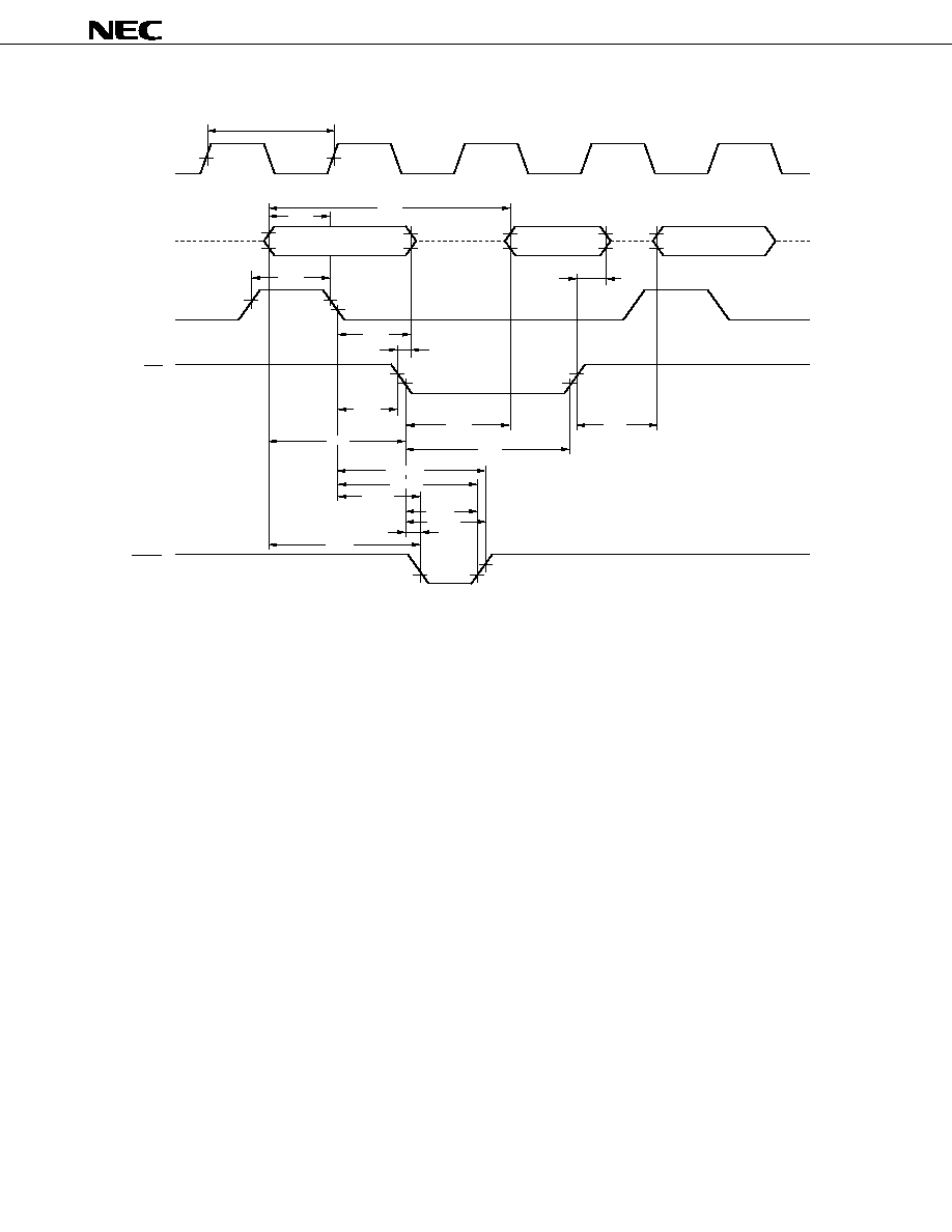
µ
PD784044, 784046
64
Data Sheet U10951EJ2V0DS00
Read Operation (16 bits)
(CLK)
t
CYK
Address (Output)
Data (Input)
Address (Output)
t
WSTH
t
HSTA
t
DSTR
t
DAR
t
WRL
t
DSTWTH
t
HSTWT
t
DSTWT
t
DRWT
t
DAWT
t
HRWT
t
DRWTH
t
DRID
t
DRA
t
FRA
t
HRID
t
SAST
t
DAID
Hi-Z
Hi-Z
Hi-Z
Hi-Z
AD8 to AD15
AD0 to AD7
(Input/output)
ASTB
(Output)
RD
(Output)
WAIT
(Input)
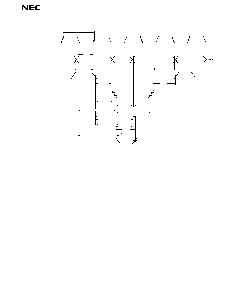
µ
PD784044, 784046
65
Data Sheet U10951EJ2V0DS00
Write Operation (16 bits)
(CLK)
AD8 to AD15
AD0 to AD7
(Output)
ASTB
(Output)
HWR, LWR
(Output)
WAIT
(Input)
t
CYK
t
DSTWTH
t
HSTWT
t
DSTWT
t
DWWT
t
DAWT
t
HWWT
t
DWWTH
t
DSTW
t
HSTA
t
WSTH
t
SAST
t
HWOD
t
DWST
t
DWOD
t
SODW
t
DAW
t
WWL
Address (Output)
Data (Output)
Undefined
Address (Output)
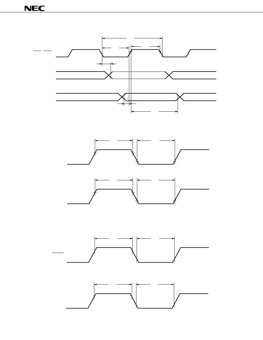
µ
PD784044, 784046
66
Data Sheet U10951EJ2V0DS00
Serial Operation
Interrupt Input Timing
Reset Input Timing
Timer Input Timing
SCK1, SCK2
SO1, SO2
SI1, SI2
t
CYSK
t
WSKL
t
DSBSK
t
SSSK
t
HSSK
t
WSKH
t
WNIH
t
WNIL
0.8V
DD
0.8 V
t
WITH
t
WITL
0.8V
DD
0.8 V
NMI
INTP0 to INTP6
t
WRSH
t
WRSL
0.8V
DD
0.8 V
RESET
t
WTIH
t
WTIL
0.8V
DD
0.8 V
TI2, TI3
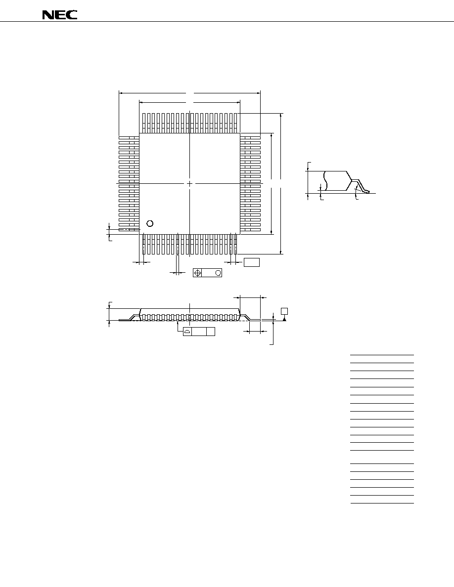
µ
PD784044, 784046
67
Data Sheet U10951EJ2V0DS00
14. PACKAGE DRAWING
Remark
The external dimensions and materials of the ES version are the same as those of mass-produced
version.
80-PIN PLASTIC QFP (14x14)
NOTE
Each lead centerline is located within 0.13 mm of
its true position (T.P.) at maximum material condition.
ITEM
MILLIMETERS
A
B
D
G
17.2
±
0.4
14.0
±
0.2
0.13
0.825
I
17.2
±
0.4
J
C
14.0
±
0.2
H
0.30
±
0.10
0.65 (T.P.)
K
1.6
±
0.2
L
0.8
±
0.2
F
0.825
S80GC-65-3B9-6
N
P
Q
0.10
2.7
±
0.1
0.1
±
0.1
R
S
5
∞±
5
∞
3.0 MAX.
M
0.15
+
0.10
-
0.05
60
61
40
80
1
21
20
41
S
S
N
J
detail of lead end
C D
A
B
R
K
M
L
P
I
S
Q
G
F
M
H

µ
PD784044, 784046
68
Data Sheet U10951EJ2V0DS00
15. RECOMMENDED SOLDERING CONDITIONS
These products should be soldered and mounted under the following recommended conditions.
For the details of the recommended soldering conditions, refer to the document Semiconductor Device
Mounting Technology Manual (C10535E).
For soldering methods and conditions other than those recommended below, contact your NEC
representative.
Table 15-1. Surface Mounting Type Soldering Conditions
(1)
µ
PD784044GC-XXX-3B9: 80-pin plastic QFP (14
◊
14 mm)
Soldering Method
Soldering Condition
Recommended
Condition Symbol
Infrared reflow
Package peak temperature: 235
∞
C, Time: 30 sec. Max. (at 210
∞
C or higher), IR35-00-3
Count: three times or less
VPS
Package peak temperature: 215
∞
C, Time: 40 sec. Max. (at 200
∞
C or higher), VP15-00-3
Count: three times or less
Wave soldering
Solder bath temperature: 260
∞
C Max., Time 10 sec. Max., Count: once,
WS60-00-1
Preheating temperature: 120
∞
C Max. (package surface temperature)
Partial heating
Pin temperature: 300
∞
C Max., Time: 3 sec. Max. (per pin row)
≠
Caution
Do not use different soldering methods together (except for partial heating).
(2)
µ
PD784046GC-XXX-3B9: 80-pin plastic QFP (14
◊
14 mm)
Soldering Method
Soldering Condition
Recommended
Condition Symbol
Infrared reflow
Package peak temperature: 235
∞
C, Time: 30 sec. Max. (at 210
∞
C or higher), IR35-00-2
Count: twice or less
VPS
Package peak temperature: 215
∞
C, Time: 40 sec. Max.
VP15-00-2
(at 200
∞
C or higher), Count: twice or less
Wave soldering
Solder bath temperature: 260
∞
C Max., Time 10 sec. Max., Count: once,
WS60-00-1
Preheating temperature: 120
∞
C Max. (package surface temperature)
Partial heating
Pin temperature: 300
∞
C Max., Time: 3 sec. Max. (per pin row)
≠
Caution
Do not use different soldering methods together (except for partial heating).
µ
PD784044, 784046
69
Data Sheet U10951EJ2V0DS00
APPENDIX A. DEVELOPMENT TOOLS
The following development tools are available for system development using the
µ
PD784046.
Refer to (5) Cautions on using development tools.
(1) Language processing software
RA78K4
Assembler package common to 78K/IV Series
CC78K4
C compiler package common to 78K/IV Series
DF784046
Device file for the
µ
PD784046 Subseries
CC78K4-L
C compiler library source file common to 78K/IV Series
(2) Flash memory writing tools
Flashpro II (Model FL-PR2),
Dedicated flash programmer for microcontrollers incorporating flash memory
Flashpro III (Model FL-PR3,
PG-FP3)
FA-80GC
Adapter for flash memory programming
(3) Debugging tools
∑
When using the IE-78K4-NS in-circuit emulator
IE-78K4-NS
In-circuit emulator common to 78K/IV Series
IE-70000-MC-PS-B
Power supply unit for IE-78K4-NS
IE-70000-98-IF-C
Interface adapter necessary when a PC-9800 series PC (except notebook PC) is used
as host machine (C bus supported)
IE-70000-CD-IF
PC card and interface cable necessary when a PC-9800 series notebook PC is used as
host machine (PCMCIA socket supported)
IE-70000-PC-IF-C
Interface adapter necessary when an IBM PC/AT
TM
compatible machine is used as host
machine (ISA bus supported)
IE-784046-NS-EM1
Emulation board for emulating the
µ
PD784046 Subseries
NP-80GC
Emulation probe for 80-pin plastic QFP (GC-3B9 type)
EV-9200GC-80
Socket to be mounted on the board of the target system for 80-pin plastic QFP (GC-3B9
type)
ID78K4-NS
Integrated debugger for IE-78K4-NS
SM78K4
System simulator common to 78K/IV Series
DF784046
Device file for the
µ
PD784046 Subseries

µ
PD784044, 784046
70
Data Sheet U10951EJ2V0DS00
∑
When using the IE-784000-R in-circuit emulator
IE-784000-R
In-circuit emulator common to 78K/IV Series
IE-70000-98-IF-C
Interface adapter necessary when a PC-9800 series PC (except notebook
PC) is used as host machine (C bus supported)
IE-70000-PC-IF-C
Interface adapter necessary when an IBM PC/AT compatible machine is used
as host machine (ISA bus supported)
IE-70000-PCI-IF
Interface adapter necessary when PC that incorporates PCI bus is used as host
machine
IE-78000-R-SV3
Interface adapter and cable necessary when an EWS is used as host machine
IE-784000-R-EM
Emulation board common to 78K/IV Series
IE-784046-NS-EM1
Emulation board for emulating the
µ
PD784046 Subseries
IE-784046-R-EM1
IE-78K4-R-EX2
Emulation probe conversion board necessary when the IE-784046-NS-EM1 is used in
the IE-784000-R. Not necessary when the IE-784046-R-EM1 is used.
EP-78230GC-R
Emulation probe for 80-pin plastic QFP (GC-3B9 type)
EV-9200GC-80
Socket to be mounted on the board of the target system made for the 80-pin plastic
QFP (GC-3B9 type)
ID78K4
Integrated debugger for IE-784000-R
SM78K4
System simulator common to 78K/IV Series
DF784046
Device file for the
µ
PD784046 Subseries
(4) Real-time OS
RX78K/IV
Real-time OS for 78K/IV Series
MX78K4
OS for 78K/IV Series
µ
PD784044, 784046
71
Data Sheet U10951EJ2V0DS00
(5) Cautions on using development tools
∑
The ID78K4-NS, ID78K4, and SM78K4 are used in combination with the DF784046.
∑
The CC78K4 and RX78K/IV are used in combination with the RA78K4 and DF784046.
∑
FL-PR2, FL-PR3, FA-80GC, and NP-80GC are products of Naito Densei Machida Mfg. Co., Ltd. (TEL: +81-
822-3813). Contact an NEC distributor regarding the purchase of these products.
∑
The host machine and OS suitable for each software are as follows:
Host Machine [OS]
PC
EWS
PC-9800 series [Windows
TM
]
HP9000 series 700
TM
[HP-UX
TM
]
IBM PC/AT compatibles
SPARCstation
TM
[SunOS
TM
, Solaris
TM
]
Software
[Japanese/English Windows]
NEWS
TM
(RISC) [NEWS-OS
TM
]
RA78K4
Note
CC78K4
Note
ID78K4-NS
≠
ID78K4
SM78K4
≠
RX78K/IV
Note
MX78K4
Note
Note
DOS-based software
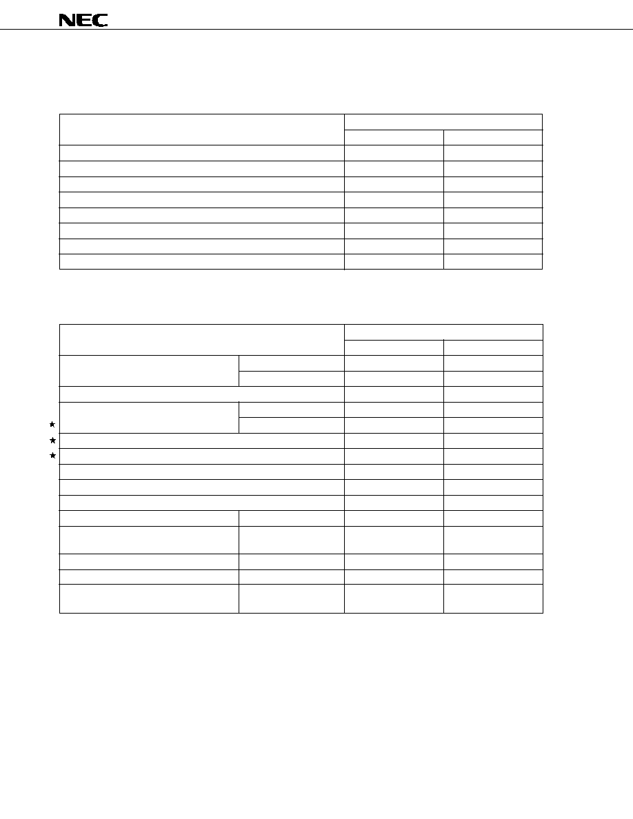
µ
PD784044, 784046
72
Data Sheet U10951EJ2V0DS00
APPENDIX B. RELATED DOCUMENTS
Documents Related to Devices
Document
Document No.
Japanese
English
µ
PD784044, 784046 Data Sheet
U10951J
This manual
µ
PD78F4046 Data Sheet
U11447J
U11447E
µ
PD784046 Subseries User's Manual - Hardware
U11515J
U11515E
µ
PD784046 Subseries Special Function Register Table
U10986J
≠
78K/IV Series User's Manual - Instruction
U10905J
U10905E
78K/IV Series Instruction List
U10594J
≠
78K/IV Series Instruction Set
U10595J
≠
78K/IV Series Application Note - Software Basics
U10095J
U10095E
Documents Related to Development Tools (User's Manuals)
Document
Document No.
Japanese
English
RA78K4 Assembler Package
Operation
U11334J
U11334E
Language
U11162J
U11162E
RA78K4 Structured Assembler Preprocessor
U11743J
U11743E
CC78K4 C Compiler
Operation
U11572J
U11572E
Language
U11571J
U11571E
IE-78K4-NS
U13356J
U13356E
IE-784000-R
U12903J
U12903E
IE-784046-NS-EM1
U13744J
U13744E
IE-784046-R-EM1
U11677J
U11677E
EP-78230
EEU-985
EEU-1515
SM78K4 System Simulator Windows Based
Reference
U10093J
U10093E
SM78K Series System Simulator
External Part User Open U10092J
U10092E
Interface Specifications
ID78K4-NS Integrated Debugger PC Based
Reference
U12796J
U12796E
ID78K4 Integrated Debugger Windows Based
Reference
U10440J
U10440E
ID78K4 Integrated Debugger
Reference
U11960J
U11960E
HP-UX, SunOS, NEWS-OS Based
Caution
The related documents listed above are subject to change without notice. Be sure to use the latest
version of each document for designing.
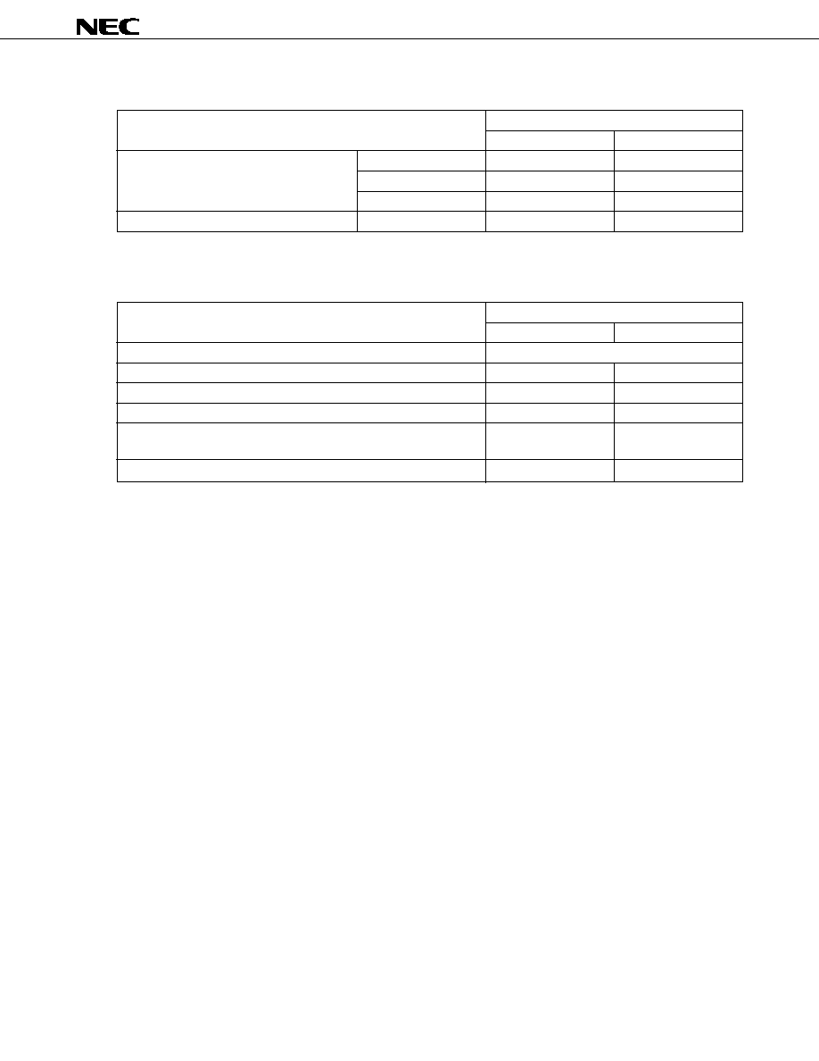
µ
PD784044, 784046
73
Data Sheet U10951EJ2V0DS00
Documents Related to Embedded Software (User's Manual)
Document
Document No.
Japanese
English
78K/IV Series Real-Time OS
Fundamental
U10603J
U10603E
Installation
U10604J
U10604E
Debugger
U10364J
≠
78K/IV Series OS MX78K4
Fundamental
U11779J
≠
Other Documents
Document
Document No.
Japanese
English
SEMICONDUCTORS SELECTION GUIDE Products & Packages (CD-ROM)
X13769X
Semiconductor Device Mounting Technology Manual
C10535J
C10535E
Quality Grades on NEC Semiconductor Devices
C11531J
C11531E
NEC Semiconductor Device Reliability and Quality Control
C10983J
C10983E
Guide to Prevent Damages for Semiconductor Devices by
C11892J
C11892E
Electrostatic Discharge (ESD)
Microcontroller-Related Product Guide - Third Parties
U11416J
≠
Caution
The related documents listed above are subject to change without notice. Be sure to use the latest
version of each document for designing.
µ
PD784044, 784046
74
Data Sheet U10951EJ2V0DS00
NOTES FOR CMOS DEVICES
1
PRECAUTION AGAINST ESD FOR SEMICONDUCTORS
Note:
Strong electric field, when exposed to a MOS device, can cause destruction of the gate oxide and
ultimately degrade the device operation. Steps must be taken to stop generation of static electricity
as much as possible, and quickly dissipate it once, when it has occurred. Environmental control
must be adequate. When it is dry, humidifier should be used. It is recommended to avoid using
insulators that easily build static electricity. Semiconductor devices must be stored and transported
in an anti-static container, static shielding bag or conductive material. All test and measurement
tools including work bench and floor should be grounded. The operator should be grounded using
wrist strap. Semiconductor devices must not be touched with bare hands. Similar precautions need
to be taken for PW boards with semiconductor devices on it.
2
HANDLING OF UNUSED INPUT PINS FOR CMOS
Note:
No connection for CMOS device inputs can be cause of malfunction. If no connection is provided
to the input pins, it is possible that an internal input level may be generated due to noise, etc., hence
causing malfunction. CMOS devices behave differently than Bipolar or NMOS devices. Input levels
of CMOS devices must be fixed high or low by using a pull-up or pull-down circuitry. Each unused
pin should be connected to V
DD
or GND with a resistor, if it is considered to have a possibility of
being an output pin. All handling related to the unused pins must be judged device by device and
related specifications governing the devices.
3
STATUS BEFORE INITIALIZATION OF MOS DEVICES
Note:
Power-on does not necessarily define initial status of MOS device. Production process of MOS
does not define the initial operation status of the device. Immediately after the power source is
turned ON, the devices with reset function have not yet been initialized. Hence, power-on does
not guarantee out-pin levels, I/O settings or contents of registers. Device is not initialized until the
reset signal is received. Reset operation must be executed immediately after power-on for devices
having reset function.
IEBus is a trademark of NEC Corporation.
Windows is either a registered trademark or a trademark of Microsoft Corporation in
the United States and/or other countries.
PC/AT is a trademark of International Business Machines Corporation.
HP9000 Series 700 and HP-UX are trademarks of Hewlett-Packard Company.
SPARCstation is a trademark of SPARC International, Inc.
Solaris and SunOS are trademarks of Sun Microsystems Inc.
NEWS and NEWS-OS are trademarks of Sony Corporation.

µ
PD784044, 784046
75
Data Sheet U10951EJ2V0DS00
Regional Information
Some information contained in this document may vary from country to country. Before using any NEC
product in your application, pIease contact the NEC office in your country to obtain a list of authorized
representatives and distributors. They will verify:
∑
Device availability
∑
Ordering information
∑
Product release schedule
∑
Availability of related technical literature
∑
Development environment specifications (for example, specifications for third-party tools and
components, host computers, power plugs, AC supply voltages, and so forth)
∑
Network requirements
In addition, trademarks, registered trademarks, export restrictions, and other legal issues may also vary
from country to country.
NEC Electronics Inc. (U.S.)
Santa Clara, California
Tel: 408-588-6000
800-366-9782
Fax: 408-588-6130
800-729-9288
NEC Electronics (Germany) GmbH
Duesseldorf, Germany
Tel: 0211-65 03 02
Fax: 0211-65 03 490
NEC Electronics (UK) Ltd.
Milton Keynes, UK
Tel: 01908-691-133
Fax: 01908-670-290
NEC Electronics Italiana s.r.l.
Milano, Italy
Tel: 02-66 75 41
Fax: 02-66 75 42 99
NEC Electronics (Germany) GmbH
Benelux Office
Eindhoven, The Netherlands
Tel: 040-2445845
Fax: 040-2444580
NEC Electronics (France) S.A.
Velizy-Villacoublay, France
Tel: 01-30-67 58 00
Fax: 01-30-67 58 99
NEC Electronics (France) S.A.
Madrid Office
Madrid, Spain
Tel: 91-504-2787
Fax: 91-504-2860
NEC Electronics (Germany) GmbH
Scandinavia Office
Taeby, Sweden
Tel: 08-63 80 820
Fax: 08-63 80 388
NEC Electronics Hong Kong Ltd.
Hong Kong
Tel: 2886-9318
Fax: 2886-9022/9044
NEC Electronics Hong Kong Ltd.
Seoul Branch
Seoul, Korea
Tel: 02-528-0303
Fax: 02-528-4411
NEC Electronics Singapore Pte. Ltd.
United Square, Singapore
Tel: 65-253-8311
Fax: 65-250-3583
NEC Electronics Taiwan Ltd.
Taipei, Taiwan
Tel: 02-2719-2377
Fax: 02-2719-5951
NEC do Brasil S.A.
Electron Devices Division
Guarulhos-SP Brasil
Tel: 55-11-6462-6810
Fax: 55-11-6462-6829
J00.7

µ
PD784044, 784046
The export of this product from Japan is regulated by the Japanese government. To export this product may be prohibited
without governmental license, the need for which must be judged by the customer. The export or re-export of this product
from a country other than Japan may also be prohibited without a license from that country. Please call an NEC sales
representative.
The related documents indicated in this publication may include preliminary versions. However, preliminary
versions are not marked as such.
M8E 00. 4
The information in this document is current as of November, 1999. The information is subject to
change without notice. For actual design-in, refer to the latest publications of NEC's data sheets or
data books, etc., for the most up-to-date specifications of NEC semiconductor products. Not all
products and/or types are available in every country. Please check with an NEC sales representative
for availability and additional information.
No part of this document may be copied or reproduced in any form or by any means without prior
written consent of NEC. NEC assumes no responsibility for any errors that may appear in this document.
NEC does not assume any liability for infringement of patents, copyrights or other intellectual property rights of
third parties by or arising from the use of NEC semiconductor products listed in this document or any other
liability arising from the use of such products. No license, express, implied or otherwise, is granted under any
patents, copyrights or other intellectual property rights of NEC or others.
Descriptions of circuits, software and other related information in this document are provided for illustrative
purposes in semiconductor product operation and application examples. The incorporation of these
circuits, software and information in the design of customer's equipment shall be done under the full
responsibility of customer. NEC assumes no responsibility for any losses incurred by customers or third
parties arising from the use of these circuits, software and information.
While NEC endeavours to enhance the quality, reliability and safety of NEC semiconductor products, customers
agree and acknowledge that the possibility of defects thereof cannot be eliminated entirely. To minimize
risks of damage to property or injury (including death) to persons arising from defects in NEC
semiconductor products, customers must incorporate sufficient safety measures in their design, such as
redundancy, fire-containment, and anti-failure features.
NEC semiconductor products are classified into the following three quality grades:
"Standard", "Special" and "Specific". The "Specific" quality grade applies only to semiconductor products
developed based on a customer-designated "quality assurance program" for a specific application. The
recommended applications of a semiconductor product depend on its quality grade, as indicated below.
Customers must check the quality grade of each semiconductor product before using it in a particular
application.
"Standard": Computers, office equipment, communications equipment, test and measurement equipment, audio
and visual equipment, home electronic appliances, machine tools, personal electronic equipment
and industrial robots
"Special":
Transportation equipment (automobiles, trains, ships, etc.), traffic control systems, anti-disaster
systems, anti-crime systems, safety equipment and medical equipment (not specifically designed
for life support)
"Specific": Aircraft, aerospace equipment, submersible repeaters, nuclear reactor control systems, life
support systems and medical equipment for life support, etc.
The quality grade of NEC semiconductor products is "Standard" unless otherwise expressly specified in NEC's
data sheets or data books, etc. If customers wish to use NEC semiconductor products in applications not
intended by NEC, they must contact an NEC sales representative in advance to determine NEC's willingness
to support a given application.
(Note)
(1) "NEC" as used in this statement means NEC Corporation and also includes its majority-owned subsidiaries.
(2) "NEC semiconductor products" means any semiconductor product developed or manufactured by or for
NEC (as defined above).
∑
∑
∑
∑
∑
∑