 | –≠–ª–µ–∫—Ç—Ä–æ–Ω–Ω—ã–π –∫–æ–º–ø–æ–Ω–µ–Ω—Ç: UPD784216 | –°–∫–∞—á–∞—Ç—å:  PDF PDF  ZIP ZIP |
Document Outline
- COVER
- FEATURES
- ORDERING INFORMATION
- 78K/IV SERIES PRODUCT DEVELOPMENT DIAGRAM
- FUNCTIONS
- 1. DIFFERENCES AMONG MODELS IN uPD784937 SUBSERIES
- 2. PIN CONFIGURATION (TOP VIEW)
- 3. BLOCK DIAGRAM
- 4. LIST OF PIN FUNCTIONS
- 4.1 Port Pins (1/2)
- 4.1 Port Pins (2/2)
- 4.2 Non-Port Pins (1/2)
- 4.2 Non-Port Pins (2/2)
- 4.3 I/O Circuits for Pins and Handling of Unused Pins
- 5. INTERNAL MEMORY SWITCHING (IMS) REGISTER
- 6. FLASH MEMORY PROGRAMMING
- 6.1 Selecting the Transmission Method
- 6.2 Flash Memory Programming Functions
- 6.3 Connecting the Flashpro III
- 7. PACKAGE DRAWINGS
- APPENDIX A DEVELOPMENT TOOLS
- APPENDIX B RELATED DOCUMENTS

The information contained in this document is being issued in advance of the production cycle for the
device. The parameters for the device may change before final production or NEC Corporation, at its own
discretion, may withdraw the device prior to its production.
Document No. U13573EJ1V0PM00 (1st edition)
Date Published August 1998 J CP(K)
Printed in Japan
©
1998
16-BIT SINGLE-CHIP MICROCONTROLLER
PRELIMINARY PRODUCT INFORMATION
MOS INTEGRATED CIRCUIT
µ
µ
µ
µ
PD78F4937
The
µ
PD78F4937, 78K/IV Series' product, is a flash memory version of the
µ
PD784937 with internal masked ROM.
Data can be written to or erased from the flash memory of the
µ
PD78F4937 with the microcontroller mounted on the
printed wiring board.
For specific functions and other detailed information, consult the following user's manuals.
These manuals are required reading for design work.
µ
µ
µ
µ
PD784937 Subseries User's Manual, Hardware :
To be created
78K/IV Series User's Manual, Instruction
:
U10905E
FEATURES
∑
Pin-compatible with mask ROM model (except V
PP
pin)
∑
Flash memory: 192K bytes
∑
Internal RAM: 8,192 bytes
∑ Same operating voltage as mask ROM model (V
DD
= 4.0 to 5.5 V)
ORDERING INFORMATION
Part number
Package
Internal ROM
µ
PD78F4937GC-8EU
100-pin plastic LQFP (fine pitch) (14
◊
14 mm)
Flash memory
µ
PD78F4937GF-3BA
100-pin plastic QFP (14
◊
20 mm)
Flash memory
Preliminary Product Information
2
µ
µ
µ
µ
PD78F4937
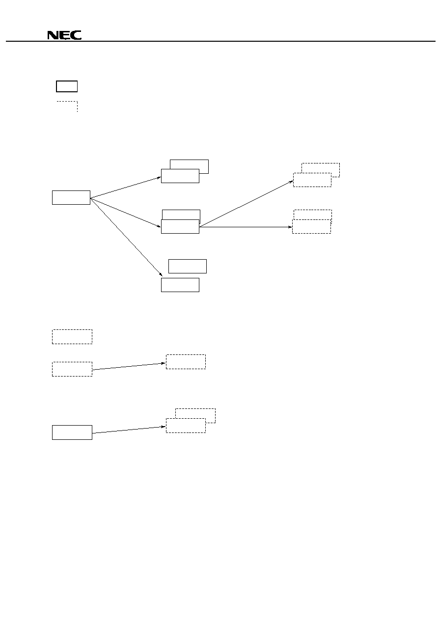
78K/IV SERIES PRODUCT DEVELOPMENT DIAGRAM
: In production
: Under development
Standard Products Development
ASSP Development
PD784026
A/D converters,
16-bit timers, and
power management
functions have been
enhanced.
Internal memory has been expanded.
Pin-compatible with the PD784026
PD784038Y
PD784038
Connectable to the I
2
C bus
100 pins
I/O has been enhanced.
Internal memory has been expanded.
PD784216Y
Connectable to the multimaster I
2
C bus
PD784054
Built-in 10-bit A/D converter
PD784046
80 pins
ROM correction function has been added.
PD784225Y
PD784225
Connectable to the multimaster I
2
C bus
Internal memory has been expanded.
ROM correction function has been added.
PD784218Y
PD784218
Connectable to the multimaster I
2
C bus
µ
µ
µ
µ
µ
µ
µ
µ
µ
µ
µ
µ
PD784216
PD784908
Built-in IEBus
TM
controller
Functions of the PD784915 have been enhanced.
PD784928Y
PD784928
Connectable to the multimaster I
2
C bus
PD784955
DC inverter control
PD784915
Software servo control
Built-in analog circuit for VCR
Timers have been enhanced.
µ
Functions of the PD784908 have been enhanced.
Internal memory has been expanded.
ROM correction function has been added.
PD784937
µ
µ
µ
µ
µ
µ
µ
Preliminary Product Information
3
µ
µ
µ
µ
PD78F4937
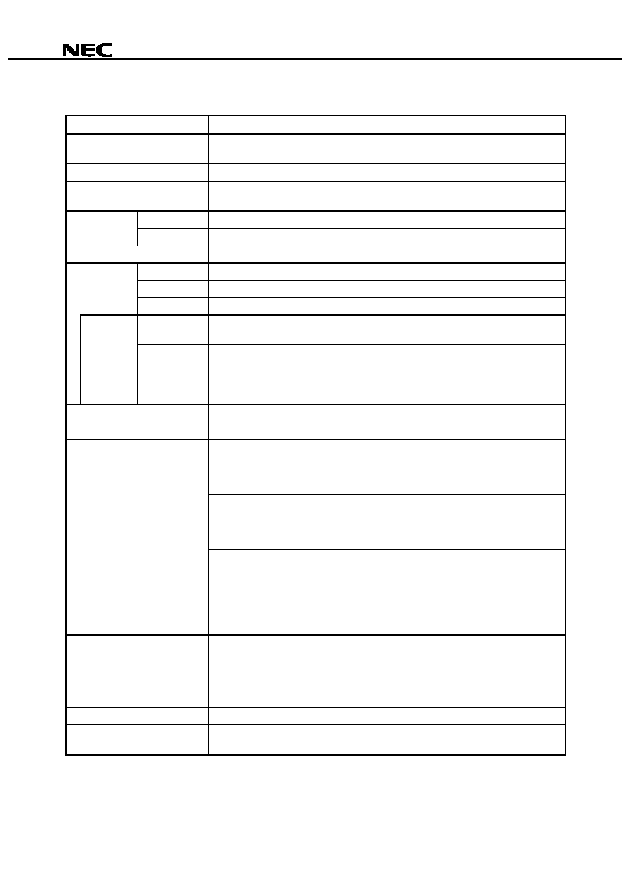
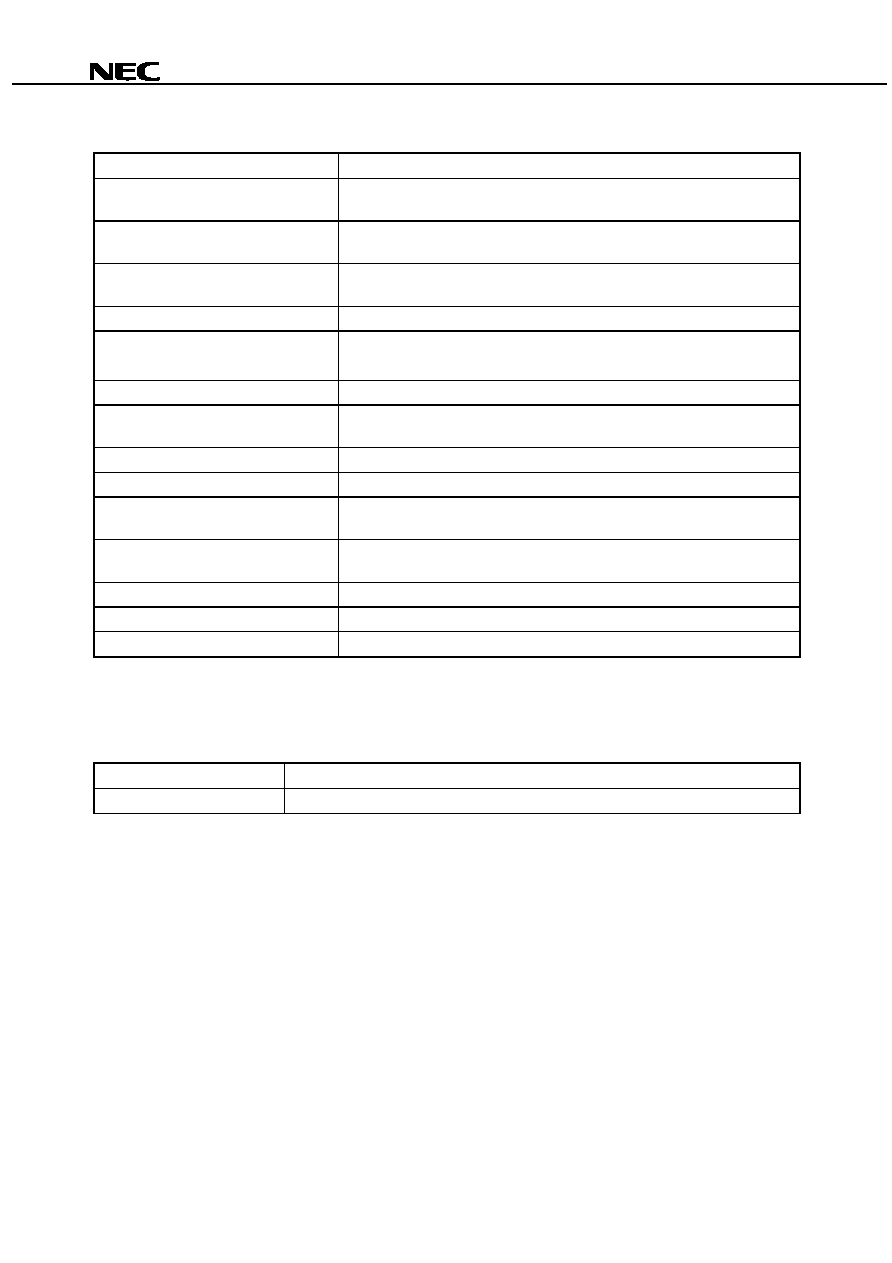
FUNCTIONS
(1/2)
Item
Function
Number of basic instructions
(mnemonics)
113
General-purpose register
8 bits
◊
16 registers
◊
8 banks, or 16 bits
◊
8 registers
◊
8 banks (memory mapping)
Minimum instruction execution
time
160 ns/320 ns/636 ns/1.27
µ
s (at 12.58 MHz)
Flash memory
192K bytes
Internal
memory
RAM
8,192 bytes
Memory space
Program and data: 1M byte
Total
80
Input
8
I/O ports
Input/output
72
LED direct
drive outputs
24
Transistor
direct drive
8
Additional
function
pins
Note
N-ch open
drain
4
Real-time output ports
4 bits
◊
2, or 8 bits
◊
1
IEBus controller
Incorporated (simple version)
Timer/counter 0 :
Timer register
◊
1
Pulse output capability
(16 bits)
Capture register
◊
1
∑
Toggle output
Compare register
◊
2
∑
PWM/PPG output
∑
One-shot pulse output
Timer/counter 1 :
Timer register
◊
1
Real-time output port
(16 bits)
Capture register
◊
1
Capture/compare register
◊
1
Compare register
◊
1
Timer/counter 2 :
Timer register
◊
1
Pulse output capability
(16 bits)
Capture register
◊
1
∑
Toggle output
Capture/compare register
◊
1
∑
PWM/PPG output
Compare register
◊
1
Timer/counter
Timer 3
:
Timer register
◊
1
(16 bits)
Compare register
◊
1
Clock timer
Interrupt requests are generated at 0.5-second intervals. (A clock timer oscillator is
incorporated.)
Either the main clock (12.58 MHz) or real-timer clock (32.768 kHz) can be selected as the
input clock.
Clock output
Selected from f
CLK
, f
CLK
/2, f
CLK
/4, f
CLK
/8, or f
CLK
/16 (can be used as a 1-bit output port)
PWM outputs
12-bit resolution
◊
2 channels
Serial interface
UART/IOE (3-wire serial I/O) : 2 channels (incorporating baud rate generator)
CSI (3-wire serial I/O)
: 2 channels
Note
Additional function pins are included in the I/O pins.
Preliminary Product Information
4
µ
µ
µ
µ
PD78F4937
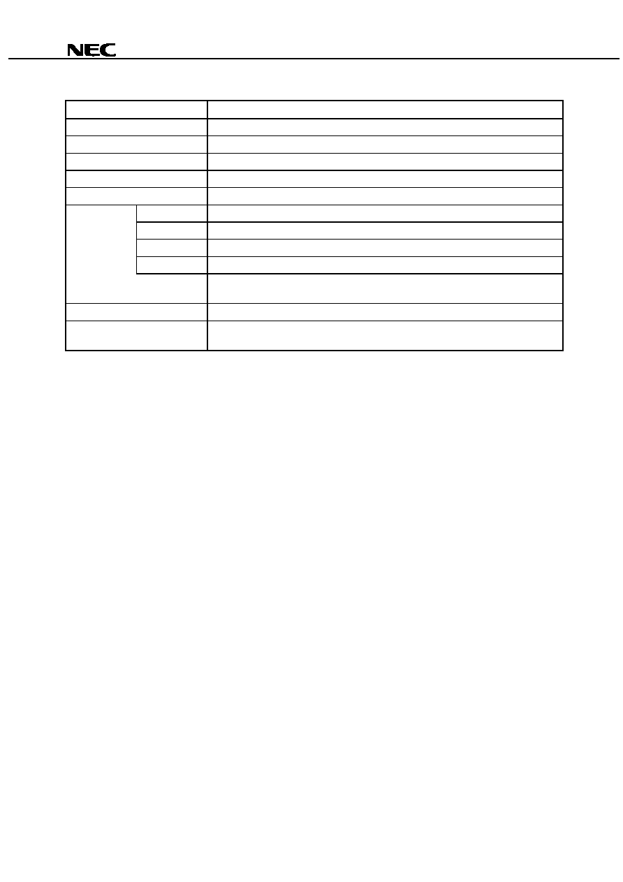
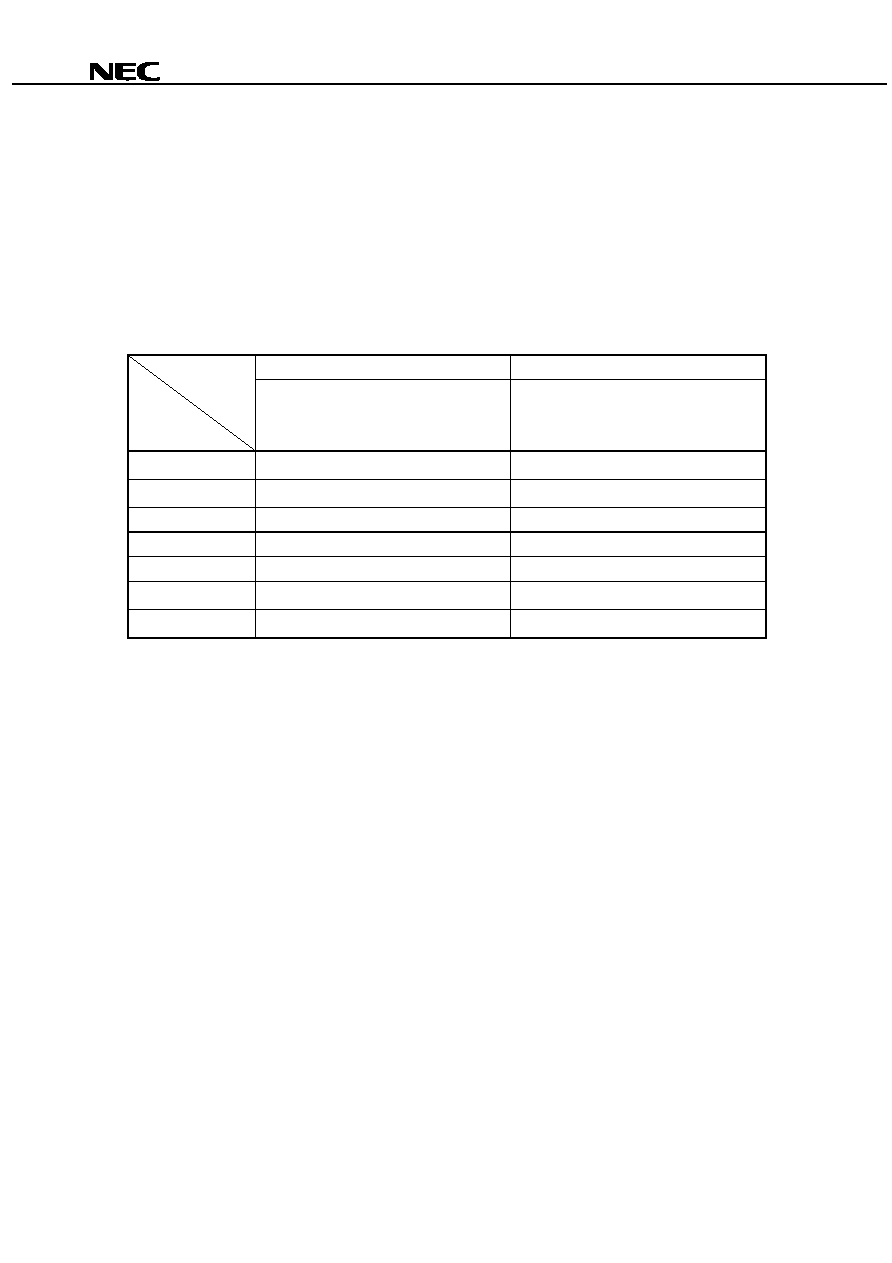
(2/2)
Item
Function
A/D converter
8-bit resolution
◊
8 channels
Watchdog timer
1 channel
ROM correction function
Internal (four correction addresses can be set.)
External expansion function
Provided (up to 1M byte)
Standby
HALT/STOP/IDLE mode
Hardware source
27 (20 internals, 7 externals (sampling clock variable input: 1))
Software
BRK or BRKCS instruction, operand error
Nonmaskable
1 internal, 1 external
Interrupt
Maskable
19 internals, 6 externals
∑
4-level programmable priority
∑
3 operation statuses: vectored interrupt, macro service, context switching
Power supply voltage
V
DD
= 4.0 to 5.5 V
Package
∑
100-pin plastic LQFP (fine pitch) (14
◊
14 mm)
∑
100-pin plastic QFP (14
◊
20 mm)

Preliminary Product Information
5
µ
µ
µ
µ
PD78F4937
CONTENTS
1.
DIFFERENCES AMONG MODELS IN
µ
µ
µ
µ
PD784937 SUBSERIES....................................................6
2.
PIN CONFIGURATION (TOP VIEW) ................................................................................................7
3.
BLOCK DIAGRAM ...........................................................................................................................10
4.
LIST OF PIN FUNCTIONS ...............................................................................................................11
4.1
Port Pins (1/2) ....................................................................................................................................... 11
4.1
Port Pins (2/2) ....................................................................................................................................... 12
4.2
Non-Port Pins (1/2) ............................................................................................................................... 13
4.2
Non-Port Pins (2/2) ............................................................................................................................... 14
4.3
I/O Circuits for Pins and Handling of Unused Pins ........................................................................... 15
5.
INTERNAL MEMORY SWITCHING (IMS) REGISTER....................................................................18
6.
FLASH MEMORY PROGRAMMING................................................................................................19
6.1
Selecting the Transmission Method ................................................................................................... 19
6.2
Flash Memory Programming Functions ............................................................................................. 20
6.3
Connecting the Flashpro III ................................................................................................................. 20
7.
PACKAGE DRAWINGS ...................................................................................................................21
APPENDIX A DEVELOPMENT TOOLS...............................................................................................23
APPENDIX B RELATED DOCUMENTS ..............................................................................................26
Preliminary Product Information
6
µ
µ
µ
µ
PD78F4937
1. DIFFERENCES AMONG MODELS IN
µ
µ
µ
µ
PD784937 SUBSERIES
The only difference among the
µ
PD784935,
µ
PD784936, and
µ
PD784937 models lie in the internal memory
capacity.
The
µ
PD78F4937 has a 192K-byte flash memory instead of the mask ROM featured by the
µ
PD784935,
µ
PD784936, and
µ
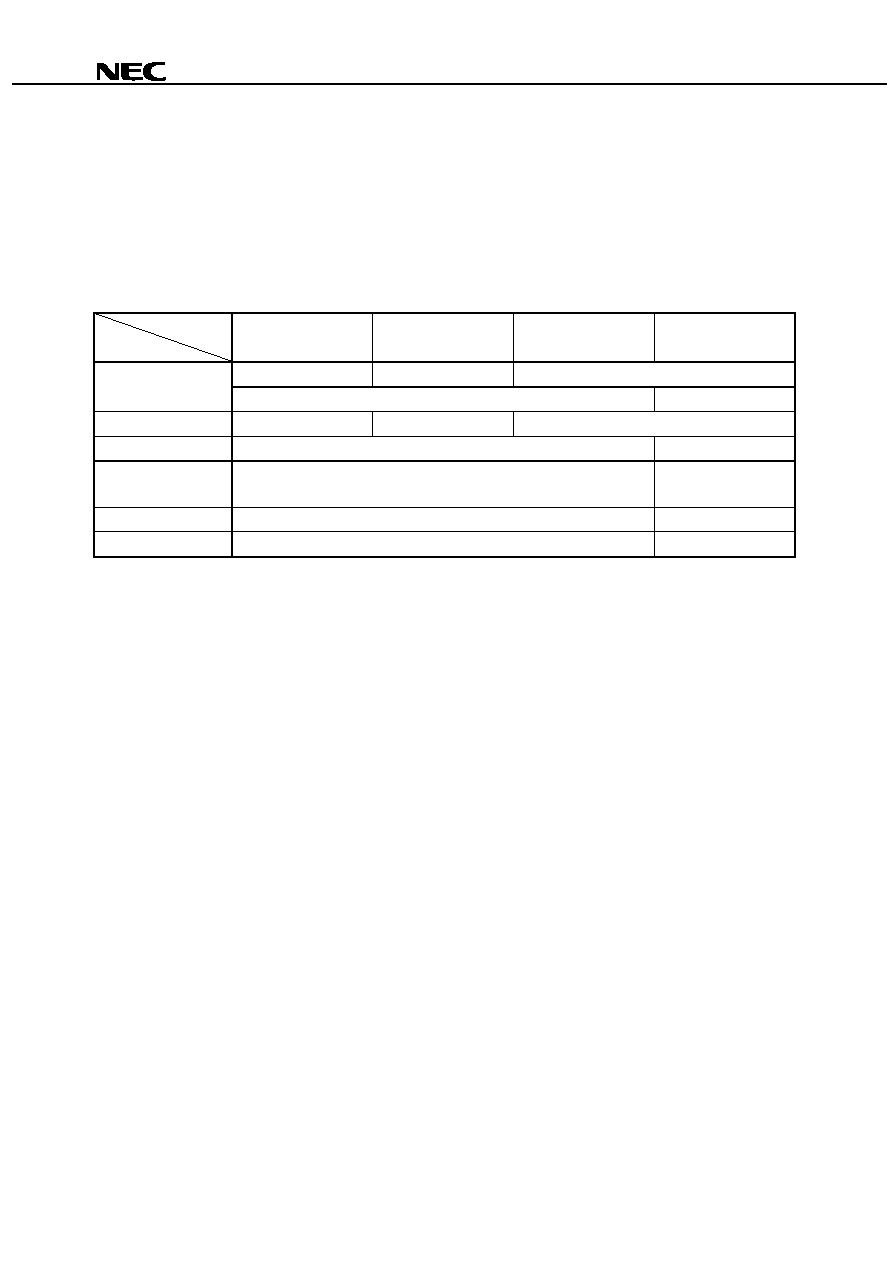
PD784937. Table 1-1 shows the differences among these products.
Table 1-1. Differences Among Models in
µ
µ
µ
µ
PD784937 Subseries
Product
Item
µ
PD784935
µ
PD784936
µ
PD784937
µ
PD78F4937
96K bytes
128K bytes
192K bytes
Internal ROM
Mask ROM
Flash memory
Internal RAM
5,120 bytes
6,656 bytes
8,192 bytes
Regulator
Provided
None
Internal memory
switching register
Note
None
Provided
IC pin
Provided
None
V
PP
pin
None
Provided
Note
The internal flash memory capacity and internal RAM capacity can be changed by setting the internal
memory switching register (IMS).
Preliminary Product Information
7
µ
µ
µ
µ
PD78F4937
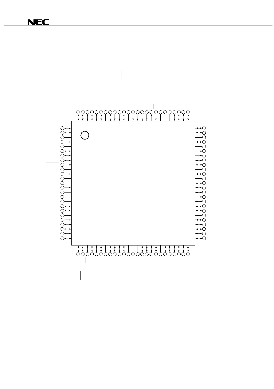
2. PIN CONFIGURATION (TOP VIEW)
∑ 100-pin plastic LQFP (fine pitch) (14
◊
◊
◊
◊
14 mm)
µ
PD78F4937GC-8EU
Cautions 1.
In normal operation, connect the V
PP
pin directly to the V
SS
pin.
2.
Connect the AV
DD
pin directly to the V
DD
pin.
3.
Connect the AV
SS
pin directly to the V
SS
pin.
P73/ANI3
P72/ANI2
P71/ANI1
P70/ANI0
V
PP
PWM1
PWM0
P17
P16
P15
P14/TxD2/SO2
P13/RxD2/SI2
P12/ASCK2/SCK2
P11
P10
ASTB/CLKOUT
P90
P91
P92
P93
P94
P95
P96
P97
P40/AD0
1
2
3
4
5
6
7
8
9
10
11
12
13
14
15
16
17
18
19
20
21
22
23
24
25
75
74
73
72
71
70
69
68
67
66
65
64
63
62
61
60
59
58
57
56
55
54
53
52
51
P37/TO3
P36/TO2
P35/TO1
P34/TO0
P33/SO0
P32/SCK0
P31/TxD/SO1
P30/RxD/SI1
P27/SI0
P26/INTP5
P25/INTP4/ASCK/SCK1
P24/INTP3
P23/INTP2/CI
P22/INTP1
P21/INTP0
P20/NMI
TX
RX
AV
SS
AV
REF1
AV
DD
P77/ANI7
P76/ANI6
P75/ANI5
P74/ANI4
P67/REFRQ/HLDAK
P66/WAIT/HLDRQ
P65/WR
P64/RD
P63/A19
P62/A18
P61/A17
P60/A16
P57/A15
P56/A14
P55/A13
P54/A12
V
SS
V
DD
P53/A11
P52/A10
P51/A9
P50/A8
P47/AD7
P46/AD6
P45/AD5
P44/AD4
P43/AD3
P41/AD1
P42/AD2
P100
P101
P102
P103
P104
P105/SCK3
P106/SI3
P107/SO3
RESET
XT2
XT1
V
SS
X2
X1
REGOFF
REGC
V
DD
P00
P01
P02
P03
P04
P05
P06
P07
100 99 98 97 96 95 94 93 92 91 90 89 88 87 86 85 84 83 82 81 80 79 78 77 76
26 27 28 29 30 31 32 33 34 35 36 37 38 39 40 41 42 43 44 45 46 47 48 49 50
Preliminary Product Information
8
µ
µ
µ
µ
PD78F4937
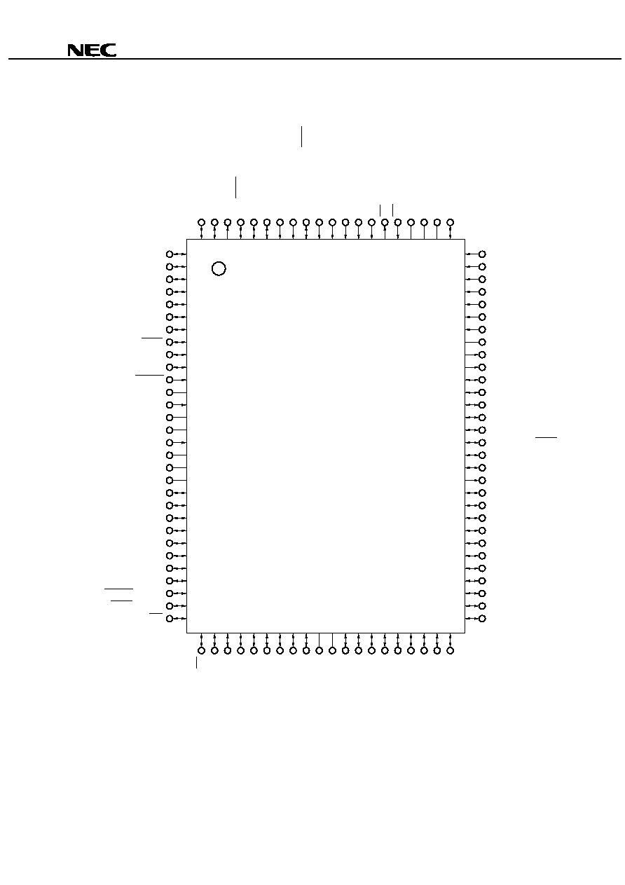
∑ 100-pin plastic QFP (14
◊
◊
◊
◊
20 mm)
µ
PD78F4937GF-3BA
Cautions 1.
In normal operation, connect the V
PP
pin directly to the V
SS
pin.
2.
Connect the AV
DD
pin directly to the V
DD
pin.
3.
Connect the AV
SS
pin directly to the V
SS
pin.
1
2
3
4
5
6
7
8
9
10
11
12
13
14
15
16
17
18
19
20
21
22
23
24
25
26
27
28
29
30
P36/T02
P37/T03
P100
P101
P102
P103
P104
P105/SCK3
P106/SI3
P107/SO3
RESET
XT2
XT1
V
SS
X2
X1
REGOFF
REGC
V
DD
P00
P01
P02
P03
P04
P05
P06
P07
P67/REFRQ/HLDAK
P66/WAIT/HLDRQ
P65/WR
P76/ANI6
P75/ANI5
P74/ANI4
P73/ANI3
P72/ANI2
P71/ANI1
P70/ANI0
V
PP
PWM1
PWM0
P17
P16
P15
P14/TxD2/SO2
P13/RxD2/SI2
P12/ASCK2/SCK2
P11
P10
ASTB/CLKOUT
P90
P91
P92
P93
P94
P95
P96
P97
P40/AD0
P41/AD1
P42/AD2
80
79
78
77
76
75
74
73
72
71
70
69
68
67
66
65
64
63
62
61
60
59
58
57
56
55
54
53
52
51
100 99 98 97 96 95 94 93 92 91 90 89 88 87 86 85 84 83 82 81
31 32 33 34 35 36 37 38 39 40 41 42 43 44 45 46 47 48 49 50
P35/TO1
P34/TO0
P33/SO0
P32/SCK0
P31/TxD/SO1
P30/RxD/SI1
P27/SI0
P26/INTP5
P25/INTP4/ASCK/SCK1
P24/INTP3
P23/INTP2/CI
P22/INTP1
P21/INTP0
P20/NMI
TX
RX
AV
SS
AV
REF1
AV
DD
P77/ANI7
P64/RD
P63/A19
P62/A18
P61/A17
P60/A16
P57/A15
P56/A14
P55/A13
P54/A12
V
SS
V
DD
P53/A11
P52/A10
P51/A9
P50/A8
P47/AD7
P46/AD6
P45/AD5
P44/AD4
P43/AD3

Preliminary Product Information
9
µ
µ
µ
µ
PD78F4937
A8-A19
: Address Bus
PWM0, PWM1
: Pulse Width Modulation Output
AD0-AD7
: Address/Data Bus
RD
: Read Strobe
ANI0-ANI7
: Analog Input
REFRQ
: Refresh Request
ASCK, ASCK2 : Asynchronous Serial Clock
REGC
: Regulator Capacitance
ASTB
: Address Strobe
REGOFF
: Regulator Off
AV
DD
: Analog Power Supply
RESET
: Reset
AV
REF1
: Reference Voltage
RX
: IEBus Receive Data
AV
SS
: Analog Ground
RxD, RxD2
: Receive Data
CI
: Clock Input
SCK0-SCK3
: Serial Clock
CLKOUT
: Clock Output
SI0-SI3
: Serial Input
HLDAK
: Hold Acknowledge
SO0-SO3
: Serial Output
HLDRQ
: Hold Request
TO0-TO3
: Timer Output
INTP0-INTP5
: Interrupt from Peripherals
TX
: IEBus Transmit Data
NMI
: Non-maskable Interrupt
TxD, TxD2
: Transmit Data
P00-P07
: Port 0
V
DD
: Power Supply
P10-P17
: Port 1
V
PP
: Programming Power Supply
P20-P27
: Port 2
V
SS
: Ground
P30-P37
: Port 3
WAIT
: Wait
P40-P47
: Port 4
WR
: Write Strobe
P50-P57
: Port 5
X1, X2
: Crystal (Main System Clock)
P60-P67
: Port 6
XT1, XT2
: Crystal (Watch)
P70-P77
: Port 7
P90-P97
: Port 9
P100-P107
: Port 10
Preliminary Product Information
10
µ
µ
µ
µ
PD78F4937
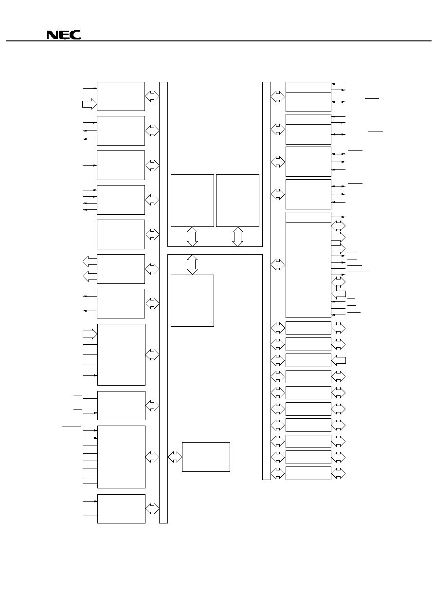
3. BLOCK DIAGRAM
PROGRAMMABLE
INTERRUPT
CONTROLLER
TIMER/COUNTER0
(16 bits)
TIMER/COUNTER1
(16 bits)
TIMER/COUNTER2
(16 bits)
TIMER3
(16 bits)
REAL-TIME
OUTPUT PORT
A/D
CONVERTER
PWM
78 K/IV
CPU CORE
(RAM 512 bytes)
FLASH
MEMORY
(192K bytes)
RAM
(8,192 bytes)
UART/IOE2
UART/IOE1
BAUD-RATE
GENERATOR
BAUD-RATE
GENERATOR
CLOCKED
SERIAL
INTERFACE
CLOCK OUTPUT
BUS I/F
PORT 0
PORT 1
PORT 2
PORT 3
PORT 4
PORT 5
PORT 6
PORT 7
NMI
INTP3
TO0
TO1
INTP0
INTP1
INTP2/CI
TO2
TO3
P00-P03
P04-P07
PWM0
PWM1
AV
DD
AV
REF1
AV
SS
INTP5
ANI0-ANI7
INTP0-INTP5
RxD/SI1
TxD/SO1
ASCK/SCK1
RxD2/SI2
ASCK2/SCK2
TxD2/SO2
SCK0
SO0
SI0
ASTB/CLKOUT
AD0-AD7
A8-A15
A16-A19
RD
WR
WAIT/HLDRQ
REFRQ/HLDAK
D0-D7
CE
A0-A16
OE
PGM
P00-P07
P10-P17
P30-P37
P40-P47
P50-P57
P20-P27
P60-P67
P70-P77
CLOCKED
SERIAL
INTERFACE3
SCK3
SO3
SI3
PORT 9
PORT 10
P90-P97
P100-P107
TX
RX
RESET
X1
X2
REGC
REGOFF
V
PP
V
DD
V
SS
XT1
XT2
SYSTEM
CONTROL
(REGULATOR)
IEBus
CONTROLLER
WATCH
TIMER
WATCHDOG
TIMER
Preliminary Product Information
11
µ
µ
µ
µ
PD78F4937
4. LIST OF PIN FUNCTIONS
4.1
Port Pins (1/2)
Pin
I/O
Dual-function
Function
P00-P07
I/O
-
Port 0 (P0):
∑
8-bit I/O port.
∑
Functions as a real-time output port (4 bits
◊
2).
∑
Inputs and outputs can be specified bit by bit.
∑
The use of pull-up resistors can be simultaneously specified by software
for all pins in input mode.
∑
Can drive a transistor.
P10
-
P11
-
P12
ASCK2/SCK2
P13
RxD2/SI2
P14
TxD2/SO2
P15-P17
I/O
-
Port 1 (P1):
∑
8-bit I/O port.
∑
Inputs and outputs can be specified bit by bit.
∑
The use of pull-up resistors can be simultaneously specified by software
for all pins in input mode.
∑
Can drive LED.
P20
NMI
P21
INTP0
P22
INTP1
P23
INTP2/CI
P24
INTP3
P25
INTP4/ASCK/SCK1
P26
INTP5
P27
Input
SI0
Port 2 (P2):
∑
8-bit input-only port.
∑
P20 does not function as a general-purpose port (nonmaskable interrupt).
However, the input level can be checked by an interrupt service routine.
∑
The use of pull-up resistors can be specified by software for pins P22 to
P27 (in units of 6 bits).
∑
The P25/INTP4/ASCK/SCK1 pin functions as the SCK1 I/O pin by CSIM1.
P30
RxD/SI1
P31
TxD/SO1
P32
SCK0
P33
SO0
P34-P37
I/O
TO0-TO3
Port 3 (P3):
∑
8-bit I/O port.
∑
Inputs and outputs can be specified bit by bit.
∑
The use of pull-up resistors can be simultaneously specified by software
for all pins in input mode.
∑
P32 and P33 can be set as the N-ch open-drain pin.
P40-P47
I/O
AD0-AD7
Port 4 (P4):
∑
8-bit I/O port.
∑
Inputs and outputs can be specified bit by bit.
∑
The use of pull-up resistors can be simultaneously specified by software
for all pins in input mode.
∑
Can drive LED.
Preliminary Product Information
12
µ
µ
µ
µ
PD78F4937
4.1
Port Pins (2/2)
Pin
I/O
Dual-function
Function
P50-P57
I/O
A8-A15
Port 5 (P5):
∑
8-bit I/O port.
∑
Inputs and outputs can be specified bit by bit.
∑
The use of pull-up resistors can be simultaneously specified by software
for all pins in input mode.
∑
Can drive LED.
P60-P63
A16-A19
P64
RD
P65
WR
P66
WAIT/HLDRQ
P67
I/O
REFRQ/HLDAK
Port 6 (P6):
∑
8-bit I/O port.
∑
Inputs and outputs can be specified bit by bit.
∑
The use of pull-up resistors can be simultaneously specified by software
for all pins in input mode.
P70-P77
I/O
ANI0-ANI7
Port 7 (P7):
∑
8-bit I/O port.
∑
Inputs and outputs can be specified bit by bit.
P90-P97
I/O
-
Port 9 (P9):
∑
8-bit I/O port.
∑
Inputs and outputs can be specified bit by bit.
∑
The use of pull-up resistors can be simultaneously specified by software
for all pins in input mode.
P100-P104
-
P105
SCK3
P106
SI3
P107
I/O
SO3
Port 10 (P10):
∑
8-bit I/O port.
∑
Inputs and outputs can be specified bit by bit.
∑
The use of pull-up resistors can be simultaneously specified by software
for all pins in input mode.
∑
P105 and P107 can be set as the N-ch open-drain pin.
Preliminary Product Information
13
µ
µ
µ
µ
PD78F4937
4.2
Non-Port Pins (1/2)
Pin
I/O
Dual-function
Function
TO0-TO3
Output
P34-P37
Timer output
CI
Input
P23/INTP2
Input of a count clock for timer/counter 2
RxD
P30/SI1
Serial data input (UART0)
RxD2
Input
P13/SI2
Serial data input (UART2)
TxD
P31/SO1
Serial data output (UART0)
TxD2
Output
P14/SO2
Serial data output (UART2)
ASCK
P25/INTP4/SCK1
Baud rate clock input (UART0)
ASCK2
Input
P12/SCK2
Baud rate clock input (UART2)
SI0
P27
Serial data input (3-wire serial I/O0)
SI1
P30/RxD
Serial data input (3-wire serial I/O1)
SI2
P13/RxD2
Serial data input (3-wire serial I/O2)
SI3
Input
P106
Serial data input (3-wire serial I/O3)
SO0
P33
Serial data output (3-wire serial I/O0)
SO1
P31/TxD
Serial data output (3-wire serial I/O1)
SO2
P14/TxD2
Serial data output (3-wire serial I/O2)
SO3
Output
P107
Serial data output (3-wire serial I/O3)
SCK0
P32
Serial clock I/O (3-wire serial I/O0)
SCK1
P25/INTP4/ASCK
Serial clock I/O (3-wire serial I/O1)
SCK2
P12/ASCK
Serial clock I/O (3-wire serial I/O2)
SCK3
I/O
P105
Serial clock I/O (3-wire serial I/O3)
NMI
P20
-
INTP0
P21
∑
Input of a count clock for timer/counter 1
∑
Capture/trigger signal for CR11 or CR12
INTP1
P22
∑
Input of a count clock for timer/counter 2
∑
Capture/trigger signal for CR22
INTP2
P23/CI
∑
Input of a count clock for timer/counter 2
∑
Capture/trigger signal for CR21
INTP3
P24
∑
Input of a count clock for timer/counter 0
∑
Capture/trigger signal for CR02
INTP4
P25/ASCK/SCK1
-
INTP5
Input
P26
External interrupt request
Input of a conversion start trigger for A/D converter
AD0-AD7
I/O
P40-P47
Time multiplexing address/data bus (for connecting external memory)
A8-A15
Output
P50-P57
High-order address bus (for connecting external memory)
A16-A19
Output
P60-P63
High-order address during address expansion (for connecting external memory)
RD
Output
P64
Strobe signal output for reading the contents of external memory
WR
Output
P65
Strobe signal output for writing on external memory
WAIT
Input
P66/HLDRQ
Wait signal insertion
REFRQ
Output
P67/HLDAK
Refresh pulse output to external pseudo static memory
HLDRQ
Input
P66/WAIT
Input of bus hold request
HLDAK
Output
P67/REFRQ
Output of bus hold response
ASTB
Output
CLKOUT
Latch timing output of time multiplexing address (A0-A7) (for connecting
external memory)
Preliminary Product Information
14
µ
µ
µ
µ
PD78F4937
4.2
Non-Port Pins (2/2)
Pin
I/O
Dual-function
Function
CLKOUT
Output
ASTB
Clock output
PWM0
Output
-
PWM output 0
PWM1
Output
-
PWM output 1
RX
Input
-
Data input (IEBus)
TX
Output
-
Data output (IEBus)
REGC
-
-
Capacitor connection for stabilizing the regulator output
REGOFF
-
-
Signal for specifying regulator operation
RESET
Input
-
Chip reset
X1
Input
X2
-
-
Crystal input for system clock oscillation (A clock pulse can also be input to the
X1 pin.)
XT1
Input
-
XT2
-
-
Real-time clock connection pin
ANI0-ANI7
Input
P70-P77
Analog voltage inputs for the A/D converter
AV
REF1
Application of A/D converter reference voltage
AV
DD
Positive power supply for the A/D converter
AV
SS
Ground for the A/D converter
V
DD
Positive power supply
V
SS
-
Ground
V
PP
Input
-
This pin is used to set the flash memory programming mode and applies a high
voltage when a program is written or verified. In normal operation mode,
connect this pin directly to the V
SS
pin.
Preliminary Product Information
15
µ
µ
µ
µ
PD78F4937
4.3
I/O Circuits for Pins and Handling of Unused Pins
Table 4-1 describes the types of I/O circuits for pins and the handling of unused pins.
Figure 4-1 shows the configuration of these various types of I/O circuits.
Table 4-1. Types of I/O Circuits for Pins and Handling of Unused Pins (1/2)
Pin
I/O circuit type
I/O
Recommended connection method for unused pins
P00-P07
P10, P11
5-A
P12/ASCK2/SCK2
8-A
P13/RxD2/SI2
P14/TxD2/SO2
P15-P17
5-A
I/O
Input state:
Connect these pins to the V
DD
pin.
Output state:
Leave these pins open.
P20/NMI
P21/INTP0
2
Connect these pins to the V
DD
or V
SS
pin.
P22/INTP1
P23/INTP2/CI
P24/INTP3
2-A
Input
Connect these pins to the V
DD
pin.
P25/INTP4/ASCK/SCK1
8-A
I/O
Input state:
Connect this pin to the V
DD
pin.
Output state:
Leave this pin open.
P26/INTP5
P27/SI0
2-A
Input
Connect these pins to the V
DD
pin.
P30/RxD/SI1
P31/TxD/SO1
5-A
P32/SCK0
P33/SO0
10-A
P34/TO0-P37/TO3
P40/AD0-P47/AD7
P50/A8-P57/A15
P60/A16-P63/A19
P64/RD
P65/WR
P66/WAIT/HLDRQ
P67/REFRQ/HLDAK
5-A
I/O
Input state:
Connect these pins to the V
DD
pin.
Output state:
Leave these pins open.
P70/ANI0-P77/ANI7
20
P90-P97
P100-P104
5-A
P105/SCK3
10-A
P106/SI3
8-A
P107/SO3
10-A
I/O
Input state:
Connect these pins to the V
DD
or V
SS
pin.
Output state:
Leave these pins open.
ASTB/CLKOUT
4
Output
Leave this pin open.
Preliminary Product Information
16
µ
µ
µ
µ
PD78F4937
Table 4-1. Types of I/O Circuits for Pins and Handling of Unused Pins (2/2)
Pin
I/O circuit type
I/O
Recommended connection method for unused pins
RESET
2
Input
-
XT2
-
-
Leave this pin open.
XT1
-
Input
Connect this pin to the V
SS
pin.
REGOFF
1
-
REGC
-
-
Connect these pins to the V
DD
pin.
PWM0, PWM1
3
Output
Leave this pin open.
RX
2
Input
Connect this pin to the V
DD
or V
SS
pin.
TX
3
Output
Leave this pin open.
AV
REF1
AV
SS
Connect these pins to the V
SS
pin.
AV
DD
-
Connect this pin to the V
DD
pin.
V
PP
-
Input
Connect this pin directly to the V
SS
pin.
Caution
When the I/O mode of an I/O dual-function pin is unpredictable, connect the pin to V
DD
through a
resistor of 10 to 100 kilohms (particularly when the voltage of the reset input pin becomes higher
than that of the low level input at power-on or when I/O is switched by software).
Remark
Since type numbers are consistent in the 78K Series, those numbers are not always serial in each
product. (Some circuits are not included.)
Preliminary Product Information
17
µ
µ
µ
µ
PD78F4937
Figure 4-1. I/O Circuits for Pins
Type 1
Type 2-A
IN
V
DD
P
N
Type 2
Schmitt trigger input with hysteresis characteristics
IN
V
DD
P
Pull-up
enable
Type 5-A
IN
Schmitt trigger input with hysteresis characteristics
Type 3
Data
OUT
V
DD
P-ch
N-ch
Type 4
Data
V
DD
P
N
IN/OUT
Output
disable
V
DD
P
Pull-up
enable
Input
enable
Type 8-A
Data
V
DD
P
N
OUT
Output
disable
Push-pull output which can output high impedance
(both the positive and negative channels are off.)
Type 10-A
Data
V
DD
P
N
IN/OUT
Output
disable
V
DD
P
Pull-up
enable
Type 20
Data
V
DD
P
N
IN/OUT
Output
disable
V
DD
P
Pull-up
enable
Open
drain
Type 12
N
P
Analog output
voltage
OUT
Data
Comparator
V
DD
V
REF
P
(Threshold voltage)
P
N
N
IN/OUT
Output
disable
Input
enable
+
≠
Preliminary Product Information
18
µ
µ
µ
µ
PD78F4937
5. INTERNAL MEMORY SWITCHING (IMS) REGISTER
This register enables the software to avoid using part of the internal memory. The IMS register can be set to
establish the same memory mapping as used in ROM products that have different internal memory (ROM and RAM)
configurations.
The IMS register is set using 8-bit memory operation instructions.
A RESET input sets the IMS register to FFH.
Figure 5-1. Internal Memory Switching (IMS) Register
7
1
6
1
5
ROM1
4
ROM0
3
1
2
1
1
RAM1
0
RAM0
IMS
Internal ROM capacity selection
ROM1
ROM0
Internal RAM capacity selection
RAM1
RAM0
0
0
1
1
0
1
0
1
Not to be set
5,120 bytes
6,656 bytes
8,192 bytes
0
0
1
1
0
1
0
1
Not to be set
96K bytes
128K bytes
192K bytes
Address: 0FFFCH
When reset: FFH
W/R
Caution
The IMS is not contained in a mask ROM product (
µ
µ
µ
µ
PD784935,
µ
µ
µ
µ
PD784936, or
µ
µ
µ
µ
PD784937).
The IMS setting to obtain the same memory map as masked ROM products are shown in Table 5-1.
Table 5-1. Internal Memory Switching Register (IMS) Setting Value
Product
IMS setting value
µ
PD784935
DDH
µ
PD784936
EEH
µ
PD784937
FFH
Preliminary Product Information
19
µ
µ
µ
µ
PD78F4937
6. FLASH MEMORY PROGRAMMING
The flash memory can be written even while the device is mounted in the target system (on-board write). To write
a program into the flash memory, connect the dedicated flash writer (Flashpro III) to both the host machine and target
system.
Remark
The Flashpro III is manufactured by Naito Densei Machida Mfg. Co., Ltd.
6.1
Selecting the Transmission Method
The Flashpro III writes into flash memory by means of serial transmission. The transmission method to be used
for writing is selected from those listed in Table 6-1. To select a transmission method, use the format shown in
Figure 6-1, according to the number of V
PP
pulses listed in Table 6-1.
Table 6-1. Transmission Methods
Transmission method
Number of channels
Pins
Number of V
PP
pulses
3-wire serial I/O
1
SCK3/P105
SO3/P107
SI3/P106
0
UART
1
TxD/SO1/P31
RxD/SI1/P30
8
Caution To select a transmission method, always use the corresponding number of V
PP
pulses listed in
Table 6-1.
Figure 6-1. Format of Transmission Method Selection
1
2
n
10 V
V
DD
V
SS
V
DD
V
SS
RESET
V
PP
Preliminary Product Information
20
µ
µ
µ
µ
PD78F4937
6.2
Flash Memory Programming Functions
Flash memory writing and other operations can be performed by transmitting/receiving commands and data
according to the selected transmission method. Table 6-2 lists the main flash memory programming functions.
Table 6-2. Main Flash Memory Programming Functions
Function
Description
Batch erase
Erases the entire contents of memory.
Block erase
Erases the contents of specified memory block.
Batch blank check
Checks that the entire contents of memory have been erased.
Block blank check
Checks that the contents of specified block have been erased.
Data write
Write to the flash memory according to the specified write start address and number of bytes
of data to be written.
Batch verify
Compares the entire contents of memory with the input data.
Block verify
Compares the contents of specified memory block with the input data.
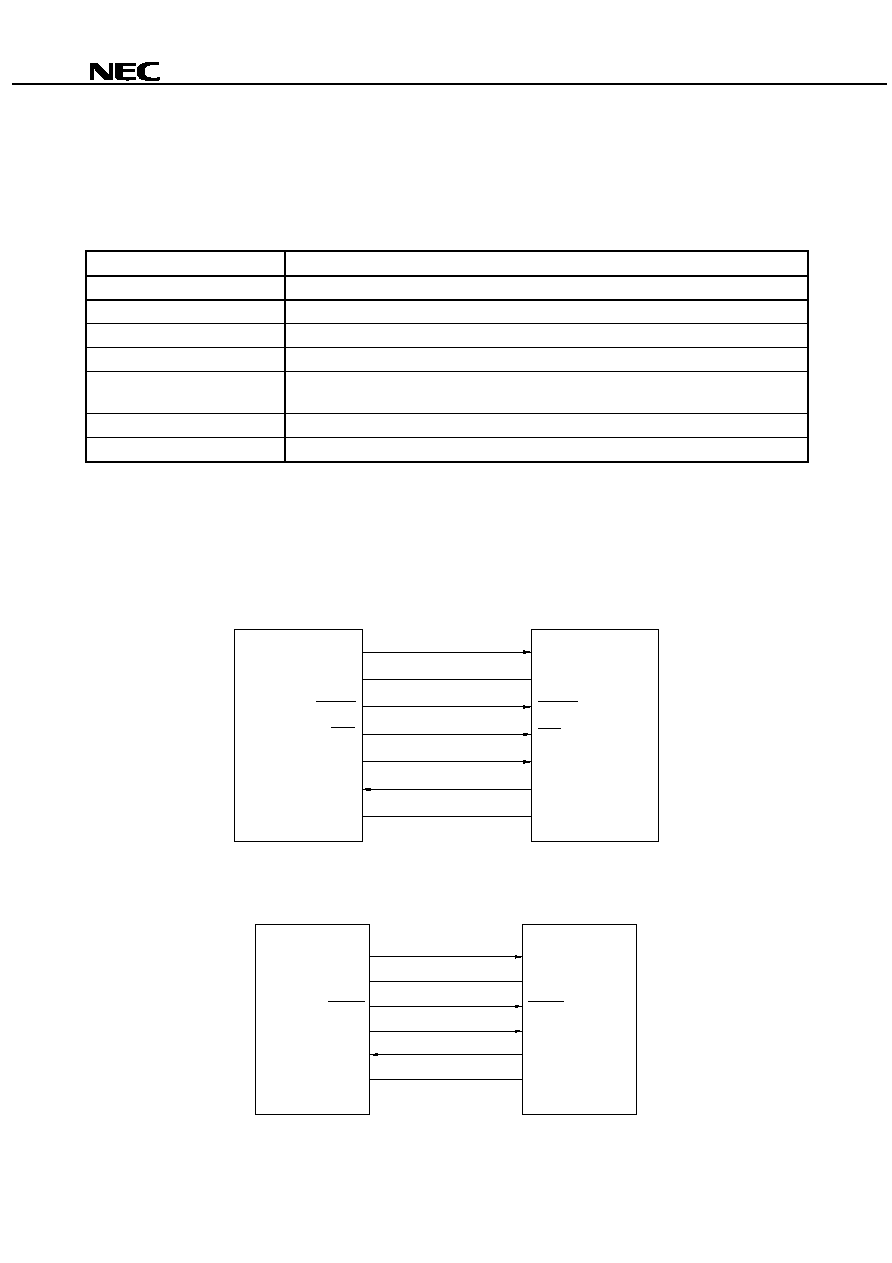
6.3
Connecting the Flashpro III
The connection between the Flashpro III and
µ
PD78F4937 varies with the transmission method. Figures 6-2 and
6-3 show the connection for each transmission method.
Figure 6-2. Flashpro III Connection in 3-Wire Serial I/O Mode
V
PP
V
DD
RESET
SCK
SO
SI
V
SS
V
PP
V
DD
RESET
SCK
SI
SO
V
SS
Flashpro III
PD78F4937
µ
Figure 6-3. Flashpro III Connection in UART Mode
V
PP
V
DD
RESET
SO
SI
V
SS
V
PP
V
DD
RESET
RxD
TxD
V
SS
Flashpro III
PD78F4937
µ
Preliminary Product Information
21
µ
µ
µ
µ
PD78F4937
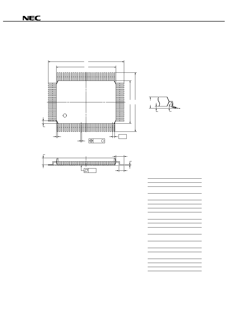
7. PACKAGE DRAWINGS
100PIN PLASTIC QFP (14x20)
ITEM
MILLIMETERS
INCHES
NOTE
Each lead centerline is located within 0.15 mm (0.006 inch) of
its true position (T.P.) at maximum material condition.
P100GF-65-3BA1-3
B
20.0
±
0.2
0.795+0.009
≠0.008
C
14.0
±
0.2
0.551+0.009
≠0.008
D
17.6
±
0.4
0.693
±
0.016
F
0.8
0.031
G
0.6
0.024
H
0.30
±
0.10
0.012
I
0.15
0.006
J
0.65 (T.P.)
0.026 (T.P.)
K
1.8
±
0.2
0.071+0.008
≠0.009
L
0.8
±
0.2
0.031
N
0.10
0.004
Q
0.1
±
0.1
0.004
±
0.004
S
3.0 MAX.
0.119 MAX.
detail of lead end
R
Q
J
K
M
L
N
P
G
F
H
I
M
P
2.7
±
0.1
0.106+0.005
≠0.004
80
81
50
100
1
31
30
51
B
A
C D
S
A
23.6
±
0.4
0.929
±
0.016
M
0.15
0.006
+0.10
≠0.05
R
5
∞±
5
∞
5
∞±
5
∞
+0.004
≠0.005
+0.009
≠0.008
+0.004
≠0.003
REMARK
The shape and material of the ES product is the same as the
mass produced product.
Preliminary Product Information
22
µ
µ
µ
µ
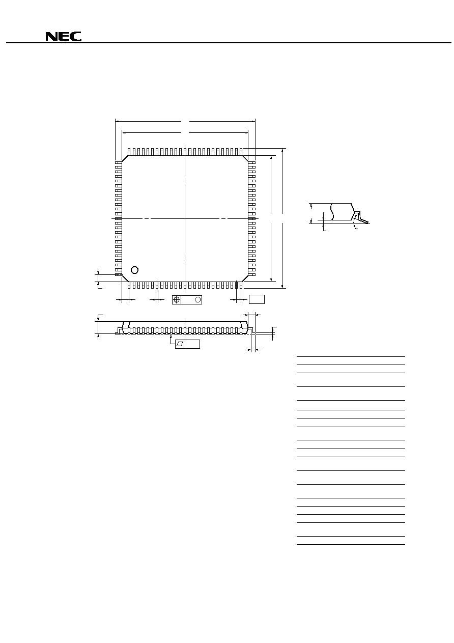
PD78F4937
100 PIN PLASTIC LQFP (FINE PITCH) (14
◊
14)
ITEM
MILLIMETERS
INCHES
NOTE
Each lead centerline is located within 0.08 mm (0.003 inch) of
its true position (T.P.) at maximum material condition.
S100GC-50-8EU
F
1.00
0.039
B
14.00
±
0.20
0.551+0.009
≠0.008
S
1.60 MAX.
0.063 MAX.
L
0.50
±
0.20
0.020+0.008
≠0.009
+0.009
≠0.008
C
14.00
±
0.20
0.551+0.009
≠0.008
A
16.00
±
0.20
0.630
±
0.008
G
1.00
0.039
H
0.22
0.009
±
0.002
I
0.08
0.003
J
0.50 (T.P.)
0.020 (T.P.)
K
1.00
±
0.20
0.039+0.009
≠0.008
N
0.08
0.003
P
1.40
±
0.05
0.055
±
0.002
R
3
∞
3
∞
+7
∞
≠3
∞
+7
∞
≠3
∞
D
16.00
±
0.20
0.630
±
0.008
M
Q
R
K
M
L
J
H
I
F
G
P
N
detail of lead end
M
0.17
0.007+0.001
≠0.003
+0.03
≠0.07
Q
0.10
±
0.05
0.004
±
0.002
+0.05
≠0.04
1
25
26
50
100
76
75
51
C
D
S
A
B
REMARK
The shape and material of the ES product is the same as the
mass produced product.
Preliminary Product Information
23
µ
µ
µ
µ
PD78F4937
APPENDIX A DEVELOPMENT TOOLS
The following development tools are available for system development using the
µ
PD78F4937.
See also (5).
(1) Language processing software
RA78K4
Assembler package used in common with 78K/IV Series
CC78K4
C compiler package used in common with 78K/IV Series
DF784937
Device file for
µ
PD784937 Subseries
CC78K4-L
C compiler library source file used in common with 78K/IV Series
(2) Flash memory write tools
Flashpro Ill
Note
(PG-FPIII)
Flash writer used only for microcontrollers with internal flash memory
FA-100GF
Flash memory writing adapter for 100-pin plastic QFP (GF-3BA type).
Wiring must be performed according to product being used.
FA-100GC
Flash memory writing adapter for 100-pin plastic LQFP (GC-8EU type).
Wiring must be performed according to product being used.
Flashpro III controller
Note
Program controlled by a personal computer and which is supported by Flashpro III.
Runs under Windows
TM
95, etc.
(3) Debugging tools
∑
∑
∑
∑
When using the in-circuit emulator IE-78K4-NS
IE-78K4-NS
In-circuit emulator used in common with 78K/IV Series
IE-70000-MC-PS-B
Power supply unit for IE-78K4-NS
IE-70000-98-IF-C
Interface adapter when the PC-9800 series computer (other than a notebook) is
used as the host machine
IE-70000-CD-IF-C
PC card and interface cable when a PC-9800 series notebook is used as the host
machine
IE-70000-PC-IF-C
Interface adapter when the IBM PC/AT
TM
compatible is used as the host machine
IE-784937-NS-EM1
Note
Emulation board for emulating
µ
PD784937 Subseries
NP-100GF
Emulation probe for 100-pin plastic QFP (GF-3BA type)
NP-100GC
Emulation probe for 100-pin plastic LQFP (GC-8EU type)
EV-9200-GF-100
Socket for mounting on target system board made for 100-pin plastic QFP (GF-
3BA type)
TGC-100SDW
Conversion adapter for connecting the target system board made for 100-pin plastic
LQFP (GC-8EU type) with NP-100GC
ID78K4-NS
Integrated debugger for IE-78K4-NS
SM78K4
System simulator used in common with 78K/IV Series
DF789437
Device file for
µ
PD784937 Subseries
Note
Under development
Preliminary Product Information
24
µ
µ
µ
µ
PD78F4937
∑
∑
∑
∑
When using the in-circuit emulator IE-784000-R
IE-784000-R
In-circuit emulator used in common with 78K/IV Series
IE-70000-98-IF-B
IE-70000-98-IF-C
Interface adapter when the PC-9800 series computer (other than a notebook) is
used as the host machine
IE-70000-98N-IF
Interface adapter and cable when a PC-9800 series notebook is used as the host
machine
IE-70000-PC-IF-B
IE-70000-PC-IF-C
Interface adapter when the IBM PC/AT compatible is used as the host machine
IE-78000-R-SV3
Interface adapter and cable when the EWS is used as the host machine
IE-784937-NS-EM1
Note
IE-784937-R-EM1
Note
Emulation board for emulating
µ
PD784937 Subseries
IE-78400-R-EM
Emulation board used in common with 78K/IV Series
IE-78K4-R-EX2
Note
Conversion board for emulation probes required to use the IE-784937-NS-EM1 on
the IE-784000-R. The board is not needed when the IE-784937-R-EM1 is used.
EP-78064GF-R
Emulation probe for 100-pin plastic QFP (GF-3BA type)
EP-78064GC-R
Emulation probe for 100-pin plastic LQFP (GC-8EU type)
EV-9200GF-100
Socket for mounting on target system board made for 100-pin plastic QFP
(GF-3BA type)
TGC-100SDW
Conversion adapter for connecting the target system board made for 100-pin
plastic LQFP (GC-8EU type) with NP-100GC
ID78K4
Integrated debugger for IE-784000-R
SM78K4
System simulator used in common with 78K/IV Series
DF784937
Device file for
µ
PD784937 Subseries
Note
Under development
(4) Real-time OS
RX78K/IV
Real-time OS for 78K/IV Series
MX78K4
OS for the 78K/IV Series
Preliminary Product Information
25
µ
µ
µ
µ
PD78F4937
(5) Notes when using development tools
∑
The ID78K4-NS, ID78K4, and SM78K4 can be used in combination with the DF784937.
∑
The CC78K4 and RX78K/IV can be used in combination with the RA78K4 and DF784937.
∑
The Flashpro III, FA-100GF, FA-100GC, NP-100GF, and NP-100GC are manufactured by Naito Densei
Machida Mfg. Co., Ltd. (044-822-3813). Consult the NEC sales representative for purchasing.
∑
The TGC-100SDW is a product from TOKYO ELETECH CORPORATION.
Refer to: Daimaru Kogyo, Ltd.
Tokyo Electronic Components Division (03-3820-7112)
Osaka Electronic Components Division (06-244-6672)
∑
The host machines and operating systems corresponding to each software are shown below.
PC
EWS
Host machine
[OS]
Software
PC-9800 series [Windows]
IBM PC/AT compatibles
[Japanese/English Windows]
HP9000 series 700
TM
[HP-UX
TM
]
SPARCstation
TM
[SunOS
TM
, Solaris
TM
]
NEWS
TM
(RISC) [NEWS-OS
TM
]
RA78K4
Note
CC78K4
Note
ID78K4-NS
-
ID78K4
SM78K4
-
RX78K/IV
Note
MX78K4
Note
Note
Software under MS-DOS

Preliminary Product Information
26
µ
µ
µ
µ
PD78F4937
APPENDIX B RELATED DOCUMENTS
∑
∑
∑
∑
Documents Related to Devices
Document No.
Document name
Japanese
English
µ
PD784935, 784936, 784937 Preliminary Product Information
U13572J
To be created
µ
PD78F4937 Preliminary Product Information
U13573J
This manual
µ
PD784937 Subseries User's Manual, Hardware
To be created
To be created
µ
PD784937 Subseries Special Function Registers
To be created
-
78K/IV Series User's Manual, Instruction
U10905J
U10905E
78K/IV Series Instruction Summary Sheet
U10594J
-
78K/IV Series Instruction Set
U10595J
-
78K/IV Series Application Note, Software Basic
U10095J
U10095E
∑
∑
∑
∑
Documents Related to Development Tools (User's Manual)
Document No.
Document name
Japanese
English
Operation
U11334J
U11334E
RA78K Series Assembler Package
Language
U11162J
U11162E
RA78K Series Structured Assembler Preprocessor
U11743J
U11743E
Operation
U11571J
U11571E
CC78K Series C Compiler
Language
U11572J
U11572E
IE-78K4-NS
U13356J
To be created
IE-784000-R
U12903J
EEU-1534
IE-784937-R-EM1
To be created
To be created
IE-784937-NS-EM1
To be created
To be created
EP-78064
EEU-934
EEU-1469
SM78K4 System Simulator Windows Base
Reference
U10093J
U10093E
SM78K Series System Simulator
External Parts User Open
Interface Specifications
U10092J
U10092E
ID78K4-NS Integrated Debugger
Reference
U12796J
U12796E
ID78K4 Integrated Debugger Windows Base
Reference
U10440J
U10440E
ID78K4 Integrated Debugger HP-UX, SunOS, NEWS-OS Base
Reference
U11960J
U11960E
Caution
The above documents may be revised without notice. Use the latest versions when you design
application systems.

Preliminary Product Information
27
µ
µ
µ
µ
PD78F4937
∑
∑
∑
∑
Documents Related to Software to Be Incorporated into the Product (User's Manual)
Document No.
Document name
Japanese
English
Basic
U10603J
U10603E
Installation
U10604J
U10604E
78K/IV Series Real-Time OS
Debugger
U10364J
-
OS for 78K/IV Series MX78K4
U11779J
-
∑
∑
∑
∑
Other Documents
Document No.
Document name
Japanese
English
IC PACKAGE MANUAL
C10943X
SMD Surface Mount Technology Manual
C10535J
C10535E
Quality Grades on NEC Semiconductor Device
C11531J
C11531E
NEC Semiconductor Device Reliability/Quality Control System
C10983J
C10983E
Guide to Prevent Damage for Semiconductor Devices by Electrostatic Discharge (ESD)
C11892J
C11892E
Semiconductor Device Quality Control/Reliability Handbook
C12769J
-
Guide for Products Related to Microcomputer: Other Companies
U11416J
-
Caution
The above documents may be revised without notice. Use the latest versions when you design
application systems.

Preliminary Product Information
28
µ
µ
µ
µ
PD78F4937
[MEMO]

Preliminary Product Information
29
µ
µ
µ
µ
PD78F4937
NOTES FOR CMOS DEVICES
1
PRECAUTION AGAINST ESD FOR SEMICONDUCTORS
Note: Strong electric field, when exposed to a MOS device, can cause destruction
of the gate oxide and ultimately degrade the device operation. Steps must
be taken to stop generation of static electricity as much as possible, and
quickly dissipate it once, when it has occurred. Environmental control must
be adequate. When it is dry, humidifier should be used. It is recommended
to avoid using insulators that easily build static electricity. Semiconductor
devices must be stored and transported in an anti-static container, static
shielding bag or conductive material. All test and measurement tools
including work bench and floor should be grounded. The operator should
be grounded using wrist strap. Semiconductor devices must not be touched
with bare hands. Similar precautions need to be taken for PW boards with
semiconductor devices on it.
2
HANDLING OF UNUSED INPUT PINS FOR CMOS
Note: No connection for CMOS device inputs can be cause of malfunction. If no
connection is provided to the input pins, it is possible that an internal input
level may be generated due to noise, etc., hence causing malfunction. CMOS
devices behave differently than Bipolar or NMOS devices. Input levels of
CMOS devices must be fixed high or low by using a pull-up or pull-down
circuitry. Each unused pin should be connected to V
DD
or GND with a
resistor, if it is considered to have a possibility of being an output pin. All
handling related to the unused pins must be judged device by device and
related specifications governing the devices.
3
STATUS BEFORE INITIALIZATION OF MOS DEVICES
Note: Power-on does not necessarily define initial status of MOS device. Production
process of MOS does not define the initial operation status of the device.
Immediately after the power source is turned ON, the devices with reset
function have not yet been initialized. Hence, power-on does not guarantee
out-pin levels, I/O settings or contents of registers. Device is not initialized
until the reset signal is received. Reset operation must be executed imme-
diately after power-on for devices having reset function.

Preliminary Product Information
30
µ
µ
µ
µ
PD78F4937
IEBus is a trademark of NEC Corporation.
Windows is a registered trademark or a trademark of Microsoft Corporation in the United States and/or other
countries.
PC/AT is a trademark of IBM Corporation.
HP9000 series 700 and HP-UX are trademarks of Hewlett-Packard Company.
SPARCstation is a trademark of SPARC International, Inc.
Solaris and SunOS are trademarks of Sun Microsystems, Inc.
NEWS and NEWS-OS are trademarks of SONY Corporation.

Preliminary Product Information
31
µ
µ
µ
µ
PD78F4937
Regional Information
Some information contained in this document may vary from country to country. Before using any NEC
product in your application, pIease contact the NEC office in your country to obtain a list of authorized
representatives and distributors. They will verify:
∑
Device availability
∑
Ordering information
∑
Product release schedule
∑
Availability of related technical literature
∑
Development environment specifications (for example, specifications for third-party tools and
components, host computers, power plugs, AC supply voltages, and so forth)
∑
Network requirements
In addition, trademarks, registered trademarks, export restrictions, and other legal issues may also vary
from country to country.
NEC Electronics Inc. (U.S.)
Santa Clara, California
Tel: 408-588-6000
800-366-9782
Fax: 408-588-6130
800-729-9288
NEC Electronics (Germany) GmbH
Duesseldorf, Germany
Tel: 0211-65 03 02
Fax: 0211-65 03 490
NEC Electronics (UK) Ltd.
Milton Keynes, UK
Tel: 01908-691-133
Fax: 01908-670-290
NEC Electronics Italiana s.r.1.
Milano, Italy
Tel: 02-66 75 41
Fax: 02-66 75 42 99
NEC Electronics (Germany) GmbH
Benelux Office
Eindhoven, The Netherlands
Tel: 040-2445845
Fax: 040-2444580
NEC Electronics (France) S.A.
Velizy-Villacoublay, France
Tel: 01-30-67 58 00
Fax: 01-30-67 58 99
NEC Electronics (France) S.A.
Spain Office
Madrid, Spain
Tel: 01-504-2787
Fax: 01-504-2860
NEC Electronics (Germany) GmbH
Scandinavia Office
Taeby, Sweden
Tel: 08-63 80 820
Fax: 08-63 80 388
NEC Electronics Hong Kong Ltd.
Hong Kong
Tel: 2886-9318
Fax: 2886-9022/9044
NEC Electronics Hong Kong Ltd.
Seoul Branch
Seoul, Korea
Tel: 02-528-0303
Fax: 02-528-4411
NEC Electronics Singapore Pte. Ltd.
United Square, Singapore 1130
Tel: 65-253-8311
Fax: 65-250-3583
NEC Electronics Taiwan Ltd.
Taipei, Taiwan
Tel: 02-719-2377
Fax: 02-719-5951
NEC do Brasil S.A.
Cumbica-Guarulhos-SP, Brasil
Tel: 011-6465-6810
Fax: 011-6465-6829
J98. 2

µ
µ
µ
µ
PD78F4937
Some related documents may be preliminary versions. Note that, however, what documents are preliminary is not
indicated in this document.
No part of this document may be copied or reproduced in any form or by any means without the prior written
consent of NEC Corporation. NEC Corporation assumes no responsibility for any errors which may appear in this
document.
NEC Corporation does not assume any liability for infringement of patents, copyrights or other intellectual
property rights of third parties by or arising from use of a device described herein or any other liability arising
from use of such device. No license, either express, implied or otherwise, is granted under any patents,
copyrights or other intellectual property rights of NEC Corporation or others.
While NEC Corporation has been making continuous effort to enhance the reliability of its semiconductor devices,
the possibility of defects cannot be eliminated entirely. To minimize risks of damage or injury to persons or
property arising from a defect in an NEC semiconductor device, customers must incorporate sufficient safety
measures in its design, such as redundancy, fire-containment, and anti-failure features.
NEC devices are classified into the following three quality grades:
"Standard", "Special", and "Specific". The Specific quality grade applies only to devices developed based on
a customer designated "quality assurance program" for a specific application. The recommended applications
of a device depend on its quality grade, as indicated below. Customers must check the quality grade of each
device before using it in a particular application.
Standard: Computers, office equipment, communications equipment, test and measurement equipment,
audio and visual equipment, home electronic appliances, machine tools, personal electronic
equipment and industrial robots
Special: Transportation equipment (automobiles, trains, ships, etc.), traffic control systems, anti-disaster
systems, anti-crime systems, safety equipment and medical equipment (not specifically designed
for life support)
Specific: Aircrafts, aerospace equipment, submersible repeaters, nuclear reactor control systems, life
support systems or medical equipment for life support, etc.
The quality grade of NEC devices is "Standard" unless otherwise specified in NEC's Data Sheets or Data Books.
If customers intend to use NEC devices for applications other than those specified for Standard quality grade,
they should contact an NEC sales representative in advance.
Anti-radioactive design is not implemented in this product.
M4 96. 5