Document Outline
- COVER
- DESCRIPTION
- FEATURES
- APPLICATION
- ORDERING INFORMATION
- 78K/IV SERIES LINEUP
- OVERVIEW OF FUNCTIONS
- 1. DIFFERENCES AMONG PRODUCTS IN µPD784938A SUBSERIES
- 2. PIN CONFIGURATION (TOP VIEW)
- 3. BLOCK DIAGRAM
- 4. PIN FUNCTIONS
- 4.1 Port Pins
- 4.2 Non-Port Pins
- 4.3 Pin I/O Circuits and Recommended Connection of Unused Pins
- 5. INTERNAL MEMORY SIZE SWITCHING REGISTER (IMS)
- 6. PROGRAMMING FLASH MEMORY
- 6.1 Selecting Communication Mode
- 6.2 Flash Memory Programming Functions
- 6.3 Connecting Flashpro III
- 7. ELECTRICAL SPECIFICATIONS
- 8. PACKAGE DRAWING
- 9. RECOMMENDED SOLDERING CONDITIONS
- APPENDIX A. DEVELOPMENT TOOLS
- APPENDIX B. RELATED DOCUMENTS

©
1999, 2001
DATA SHEET
2001
MOS INTEGRATED CIRCUITS
16-BIT SINGLE-CHIP MICROCONTROLLER
µ
PD78F4938A
Document No. U14118EJ1V0DS00
Date Published March 2001 N CP(K)
Printed in Japan
DESCRIPTION
The
µPD78F4938A is a product in the µPD784938A Subseries in the 78K/IV Series.
The
µPD78F4938A has flash memory in place of the internal ROM of the µPD784938A. The flash memory
incorporated enables program writing or erasing with the microcontroller mounted on the target board.
Detailed function descriptions are provided in the following user's manuals. Be sure to read them before
designing.
µPD784938A Subseries User's Manual Hardware: U13570E
78K/IV Series User's Manual Instructions:
U10905E
FEATURES
∑
Pin-compatible with mask ROM version (except V
PP
pin)
∑
Flash memory: 256 KB
∑
Internal RAM: 10496 bytes
∑
Serial interface:
4 channels
∑ UART/IOE (3-wire serial I/O): 2 channels (on-chip baud rate generator)
∑ CSI (3-wire serial I/O):
2 channels
∑
On-chip IEBus
TM
controller
∑
Supply voltage: V
DD
= 4.0 to 5.5 V (@12.58 MHz operation)
V
DD
= 3.0 to 5.5 V (@6.29 MHz operation)
APPLICATION
Car audio, etc.
ORDERING INFORMATION
Part Number
Package
Internal ROM
Internal RAM
µPD78F4938AGF-3BA
100-pin plastic QFP (14
◊ 20)
256 KB
10496 bytes
The information in this document is subject to change without notice. Before using this document, please
confirm that this is the latest version.
Not all devices/types available in every country. Please check with local NEC representative for
availability and additional information.
µPD78F4938A
2
Data Sheet U14118EJ1V0DS
78K/IV SERIES LINEUP
PD784026
PD784956A
PD784908
PD784915
PD784928
PD784928Y
PD784046
PD784054
PD784216A
PD784216AY
PD784038
PD784038Y
PD784225Y
PD784225
PD784218AY
PD784218A
Enhanced
A/D converter,
16-bit timer, and
power management
Enhanced internal memory capacity
Pin-compatible with the PD784026
Supports I
2
C bus
Supports multimaster I
2
C bus
80-pin, ROM correction added
Supports multimaster I
2
C bus
Enhanced internal memory
capacity, ROM correction added
100-pin, enhanced I/O and
internal memory capacity
On-chip 10-bit A/D converter
For DC inverter control
On-chip IEBus
TM
controller
Software servo control
On-chip analog circuit for VCRs
Enhanced timer
Supports multimaster I
2
C bus
Enhanced functions
of the PD784915
Standard models
ASSP models
Supports multimaster I
2
C bus
: Products in mass-production
: Products under development
µ
µ
PD784976A
On-chip VFD controller/driver
µ
µ
µ
µ
µ
µ
µ
µ
µ
µ
µ
µ
µ
µ
µ
µ
µ
PD784938A
Enhanced functions of the
PD784908, enhanced
internal memory capacity,
ROM correction added.
µ
µ
PD784967
µ
Enhanced functions of the
PD784938A, enhanced I/O
and internal memory capacity.
Enhanced peripheral functions
µ
Remark
Although VFD (Vacuum Florescent Display is generally used, in some documents, the display is described
as FIP
TM
(Florescent Inidicator Panel). VFD and FIP are functionally equivalent.

3
Data Sheet U14118EJ1V0DS
µPD78F4938A
OVERVIEW OF FUNCTIONS
(1/2)
Part Number
µPD78F4938A
Item
Number of basic instructions (mnemonics) 113
General-purpose registers
8 bits
◊ 32 registers ◊ 8 banks, or 16 bits ◊ 8 registers ◊ 8 banks (memory map)
Minimum instruction execution time
320 ns/636 ns/1.27
µs/2.54 µs (@6.29 MHz operation)
160 ns/320 ns/636 ns/1.27
µs (@12.58 MHz operation)
Internal memory
ROM
256 KB
RAM
10496 bytes
Memory space
1 MB with program and data spaces combined
I/O port
Total
80 pins
Input
8 pins
I/O
72 pins
Pins with
LED direct drive output
24 pins
ancillary
Transistor direct drive
8 pins
function
Note
N-ch open drain drive
4 pins
Real-time output port
4 bits
◊ 2, or 8 bits ◊ 1
IEBus controller
Internal (simple version)
Timer/counter
Timer/event counter 0:
Timer counter
◊ 1
Pulse output possible
(16 bits)
Capture register
◊ 1
∑ Toggle output
Compare register
◊ 2
∑ PWM/PPG output
∑ One-shot pulse output
Timer/event counter 1:
Timer counter
◊ 1
Real-time output port
(16 bits)
Capture register
◊ 1
Capture/compare register
◊ 1
Compare register
◊ 1
Timer/event counter 2:
Timer counter
◊ 1
Pulse output possible
(16 bits)
Capture register
◊ 1
∑ Toggle output
Capture/compare register
◊ 1
∑ PWM/PPG output
Compare register
◊ 1
Timer 3 (16 bits):
Timer counter
◊ 1
Compare register
◊ 1
Watch timer
Generates interrupt request at 0.5-second intervals (On-chip watch clock oscillator)
Main clock (12.58 MHz) or watch clock (32.7 kHz) selectable as input clock
Clock output
Selectable from f
CLK
, f
CLK
/2, f
CLK
/4, f
CLK
/8, or f
CLK
/16 (also usable as 1-bit output port)
PWM output
12-bit resolution
◊ 2 channels
Serial interface
UART/IOE (3-wire serial I/O): 2 channels (on-chip baud rate generator)
CSI (3-wire serial I/O):
2 channels
A/D converter
8-bit resolution
◊ 8 channels
Watchdog timer
1 channel
ROM correction function
Internal (4 points of correction addresses can be set.)
External expansion function
Provided (up to 1 MB)
Note
Pins with ancillary functions are included in the I/O pins.
µPD78F4938A
4
Data Sheet U14118EJ1V0DS
(2/2)
Part Number
µPD78F4938A
Item
Standby
HALT/STOP/IDLE mode
Interrupt
Hardware source
27 (internal: 20, external: 7 (sampling clock variable input: 1))
Software source
BRK instruction, BRKCS instruction, operand error
Non-maskable
Internal: 1, external: 1
Maskable
Internal: 19, external: 6
Four programmable priority levels
Three types of processing formats: Vectored interrupt/macro service/context switching
Supply voltage
∑ V
DD
= 4.0 to 5.5 V (@12.58 MHz operation)
∑ V
DD
= 3.0 to 5.5 V (@6.29 MHz operation)
Package
100-pin plastic QFP (14
◊ 20)

5
Data Sheet U14118EJ1V0DS
µPD78F4938A
CONTENTS
1.
DIFFERENCES AMONG PRODUCTS IN
µPD784938A SUBSERIES ...................................
6
2.
PIN CONFIGURATION (TOP VIEW) ...........................................................................................
7
3.
BLOCK DIAGRAM .........................................................................................................................
9
4.
PIN FUNCTIONS ............................................................................................................................ 10
4.1
Port Pins ................................................................................................................................. 10
4.2
Non-Port Pins ........................................................................................................................ 12
4.3
Pin I/O Circuits and Recommended Connection of Unused Pins .................................
14
5.
INTERNAL MEMORY SIZE SWITCHING REGISTER (IMS) ..................................................
18
6.
PROGRAMMING FLASH MEMORY ............................................................................................ 19
6.1
Selecting Communication Mode .........................................................................................
19
6.2
Flash Memory Programming Functions ............................................................................
20
6.3
Connecting Flashpro III ........................................................................................................ 21
7.
ELECTRICAL SPECIFICATIONS .................................................................................................. 22
8.
PACKAGE DRAWING .................................................................................................................... 42
9.
RECOMMENDED SOLDERING CONDITIONS ...........................................................................
43
APPENDIX A. DEVELOPMENT TOOLS ............................................................................................ 44
APPENDIX B. RELATED DOCUMENTS ........................................................................................... 47
µPD78F4938A
6
Data Sheet U14118EJ1V0DS
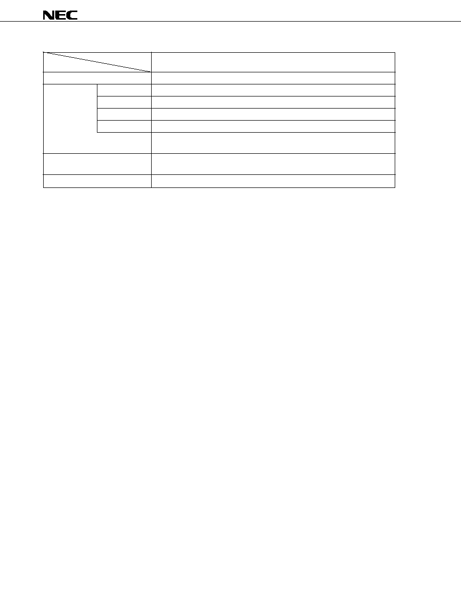
1. DIFFERENCES AMONG PRODUCTS IN
µPD784938A SUBSERIES
The only difference between the
µPD784935A, 784936A, 784937A, and 784938A is the internal memory capacity.
The
µPD78F4938A has a 256 KB flash memory in the place of the mask ROM of the above products. Table 1-
1 shows the differences between these products.
Table 1-1. Differences Among Products in
µPD784938A Subseries
Part Number
µPD784935A
µPD784936A
µPD784937A
µPD784938A
µPD78F4938A
Item
Internal ROM
96 KB
128 KB
192 KB
256 KB
Mask ROM
Flash memory
Internal RAM
5120 bytes
6656 bytes
8192 bytes
10496 bytes
Regulator
Provided
None
Electrical specifications
Refer to the data sheet of each product.
Internal memory size
None
Provided
switching register
Note
IC pin
Provided
None
V
PP
pin
None
Provided
Note
The internal flash memory capacity and internal RAM capacity can be changed by using the internal memory
size switching register (IMS).
Caution There are differences in noise immunity and noise radiation between the flash memory and mask
ROM versions. When pre-producing an application set with the flash memory version and then
mass-producing it with the mask ROM version, be sure to conduct sufficient evaluations for the
commercial samples (not engineering samples) of the mask ROM version.
7
Data Sheet U14118EJ1V0DS
µPD78F4938A
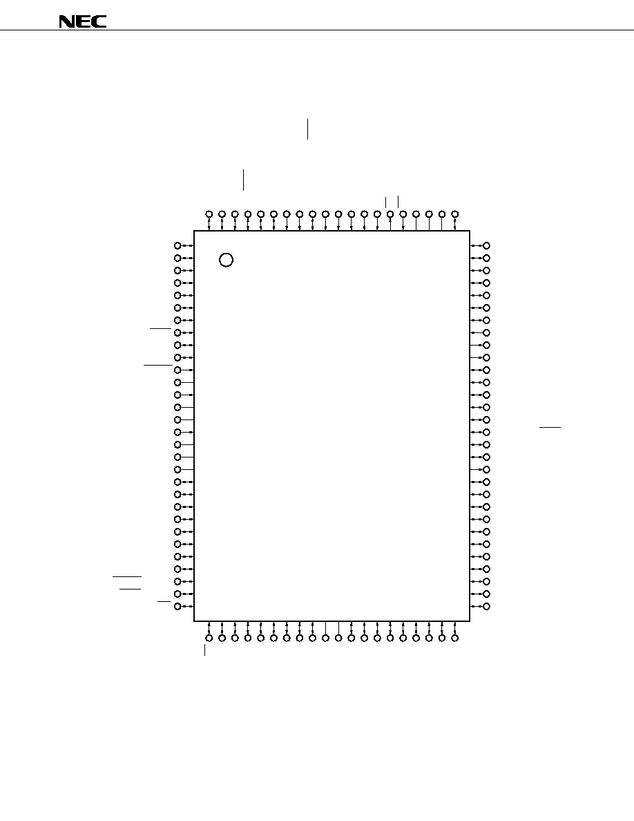
2. PIN CONFIGURATION (TOP VIEW)
∑
100-pin plastic QFP (14
◊ 20)
µPD78F4938AGF-3BA
1
2
3
4
5
6
7
8
9
10
11
12
13
14
15
16
17
18
19
20
21
22
23
24
25
26
27
28
29
30
P36/T02
P37/T03
P100
P101
P102
P103
P104
P105/SCK3
P106/SI3
P107/SO3
RESET
XT2
XT1
V
SS
X2
X1
REGOFF
REGC
V
DD
P00
P01
P02
P03
P04
P05
P06
P07
P67/REFRQ/HLDAK
P66/WAIT/HLDRQ
P65/WR
P76/ANI6
P75/ANI5
P74/ANI4
P73/ANI3
P72/ANI2
P71/ANI1
P70/ANI0
V
PP
PWM1
PWM0
P17
P16
P15
P14/TxD2/SO2
P13/RxD2/SI2
P12/ASCK2/SCK2
P11
P10
ASTB/CLKOUT
P90
P91
P92
P93
P94
P95
P96
P97
P40/AD0
P41/AD1
P42/AD2
80
79
78
77
76
75
74
73
72
71
70
69
68
67
66
65
64
63
62
61
60
59
58
57
56
55
54
53
52
51
100 99 98 97 96 95 94 93 92 91 90 89 88 87 86 85 84 83 82 81
31 32 33 34 35 36 37 38 39 40 41 42 43 44 45 46 47 48 49 50
P35/TO1
P34/TO0
P33/SO0
P32/SCK0
P31/TxD/SO1
P30/RxD/SI1
P27/SI0
P26/INTP5
P25/INTP4/ASCK/SCK1
P24/INTP3
P23/INTP2/CI
P22/INTP1
P21/INTP0
P20/NMI
TX
RX
AV
SS
AV
REF1
AV
DD
P77/ANI7
P64/RD
P63/A19
P62/A18
P61/A17
P60/A16
P57/A15
P56/A14
P55/A13
P54/A12
V
SS
V
DD
P53/A11
P52/A10
P51/A9
P50/A8
P47/AD7
P46/AD6
P45/AD5
P44/AD4
P43/AD3
Cautions 1. In normal operation mode, connect V
PP
pin directly to the V
SS
pin, or pull it down.
In a system where the internal flash memory is rewritten while mounted on board, pull the V
PP
pin down.
When pulling down, connection via a 470
or higher and 10 k
or lower resistor is recommended.
2. Connect the AV
DD
pin directly to V
DD
.
3. Connect the AV
SS
pin directly to V
SS
.
µPD78F4938A
8
Data Sheet U14118EJ1V0DS
A8 to A19:
Address bus
AD0 to AD7:
Address/data bus
ANI0 to ANI7:
Analog input
ASCK, ASCK2:
Asynchronous serial clock
ASTB:
Address strobe
AV
DD
:
Analog power supply
AV
REF1
:
Reference voltage
AV
SS
:
Analog ground
CI:
Clock input
CLKOUT:
Clock output
HLDAK:
Hold acknowledge
HLDRQ:
Hold request
INTP0 to INTP5: Interrupt from peripherals
NMI:
Non-maskable interrupt
P00 to P07:
Port 0
P10 to P17:
Port 1
P20 to P27:
Port 2
P30 to P37:
Port 3
P40 to P47:
Port 4
P50 to P57:
Port 5
P60 to P67:
Port 6
P70 to P77:
Port 7
P90 to P97:
Port 9
P100 to P107:
Port 10
PWM0, PWM1:
Pulse width modulation output
RD:
Read strobe
REFRQ:
Refresh request
REGC:
Regulator capacitance
REGOFF:
Regulator off
RESET:
Reset
RX:
IEBus receive data
RxD, RxD2:
Receive data
SCK0 to SCK3: Serial clock
SI0 to SI3:
Serial input
SO0 to SO3:
Serial output
TO0 to TO3:
Timer output
TX:
IEBus transmit data
TxD, TxD2:
Transmit data
V
DD
:
Power supply
V
PP
:
Programming power supply
V
SS
:
Ground
WAIT:
Wait
WR:
Write strobe
X1, X2:
Crystal (main system clock)
XT1, XT2:
Crystal (watch)
9
Data Sheet U14118EJ1V0DS
µPD78F4938A
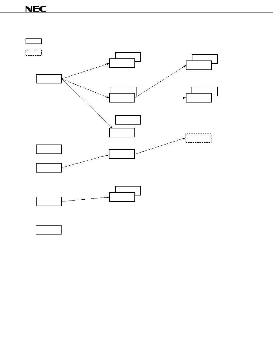
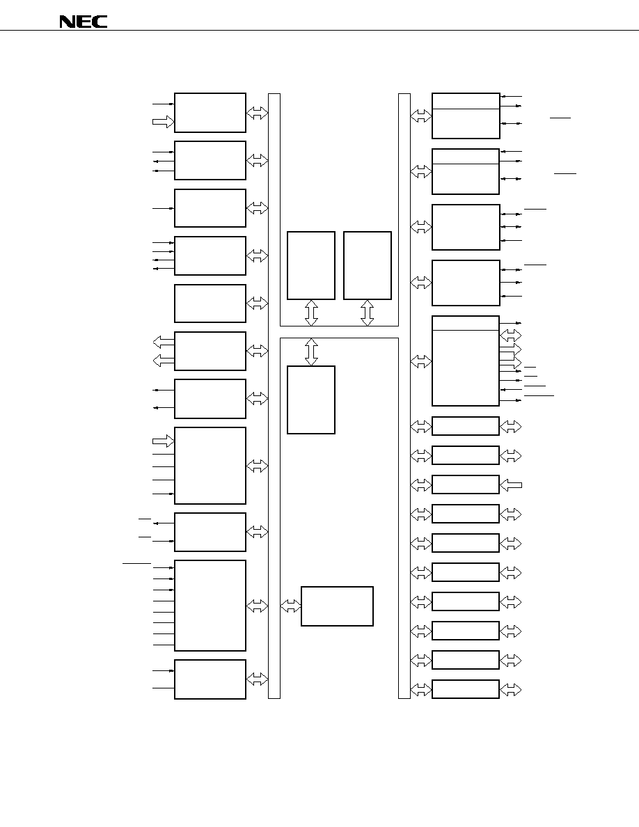
3. BLOCK DIAGRAM
Programmable
interrupt controller
Timer/counter 0
(16 bits)
Timer/counter 1
(16 bits)
Timer/counter 2
(16 bits)
Timer 3
(16 bits)
Real-time
output port
PWM
A/D converter
78K/IV
CPU core
Flash
memory
RAM
Watchdog timer
UART/IOE 2
Baud-rate
generator
UART/IOE 1
Baud-rate
generator
Clocked serial
interface
Clock output
Bus I/F
Port 0
Port 1
Port 2
Port 3
Port 4
Port 5
Port 6
Port 7
NMI
INTP0 to INTP5
INTP3
TO0
TO1
INTP0
INTP1
INTP2/CI
TO2
TO3
P00 to P03
P04 to P07
PWM0
PWM1
IEBus controller
TX
RX
ANI0 to ANI7
AV
DD
AV
REF1
AV
SS
INTP5
RxD/SI1
TxD/SO1
ASCK/SCK1
RxD2/SI2
TxD2/SO2
ASCK2/SCK2
SCK0
SO0
SI0
Clocked serial
interface 3
SCK3
SO3
SI3
ASTB/CLKOUT
AD0 to AD7
A8 to A15
A16 to A19
RD
WR
WAIT/HLDRQ
REFRQ/HLDAK
P00 to P07
P10 to P17
P20 to P27
P30 to P37
P40 to P47
P50 to P57
P60 to P67
P70 to P77
Port 9
Port 10
P90 to P97
P100 to P107
Watch timer
XT1
XT2
RESET
V
PP
X1
X2
REGC
REGOFF
V
DD
V
SS
System control
(regulator)
µPD78F4938A
10
Data Sheet U14118EJ1V0DS
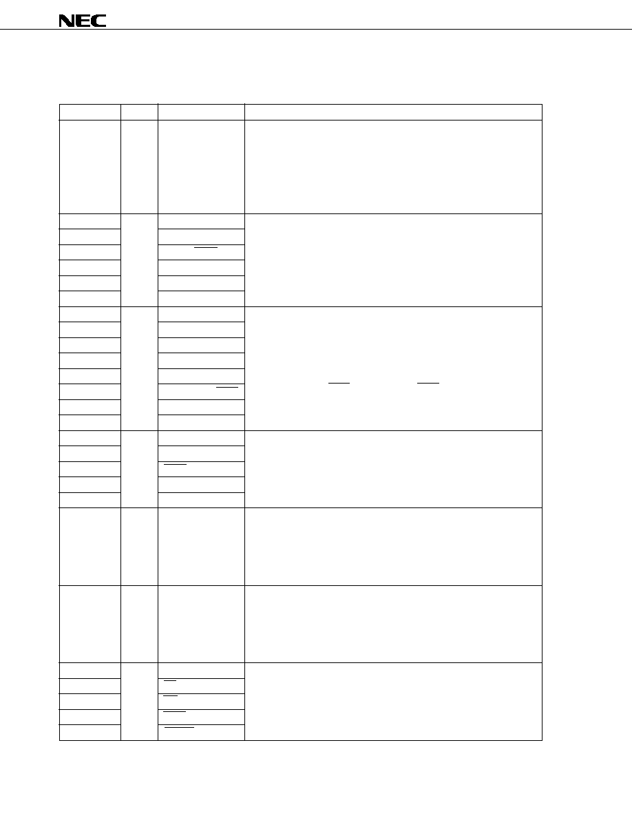
4. PIN FUNCTIONS
4.1 Port Pins (1/2)
Pin Name
I/O
Alternate Function
Function
P00 to P07
I/O
--
P10
I/O
--
P11
--
P12
ASCK2/SCK2
P13
RxD2/SI2
P14
TxD2/SO2
P15 to 17
--
P20
Input
NMI
P21
INTP0
P22
INTP1
P23
INTP2/CI
P24
INTP3
P25
INTP4/ASCK/SCK1
P26
INTP5
P27
SI0
P30
I/O
RxD/SI1
P31
TxD/SO1
P32
SCK0
P33
SO0
P34 to P37
TO0 to TO3
P40 to P47
I/O
AD0 to AD7
P50 to P57
I/O
A8 to A15
P60 to P63
I/O
A16 to A19
P64
RD
P65
WR
P66
WAIT/HLDRQ
P67
REFRQ/HLDAK
Port 0 (P0):
∑ 8-bit I/O port.
∑ Can be used as real-time output port (4 bits
◊ 2).
∑ Input/output can be specified in 1-bit units.
∑ An on-chip pull-up resistor can be specified by means of software for
pins in input mode.
∑ Can drive transistor.
Port 1 (P1):
∑ 8-bit I/O port.
∑ Input/output can be specified in 1-bit units.
∑ An on-chip pull-up resistor can be specified by means of software for pins
in input mode.
∑ Can drive LED.
Port 2 (P2):
∑ 8-bit input port.
∑ P20 cannot be used as general-purpose port pin (non-maskable interrupt).
However, input level can be checked by interrupt routine.
∑ An on-chip pull-up resistor can be specified for P22 to P27 by means of
software in 6-bit units.
∑ P25/INTP4/ASCK/SCK1 pin operates as SCK1 I/O pin if so specified by
CSIM1.
Port 3 (P3):
∑ 8-bit I/O port.
∑ Input/output can be specified in 1-bit units.
∑ An on-chip pull-up resistor can be specified by means of software for pins
in input mode.
∑ P32 and P33 can be specified for N-ch open-drain connection.
Port 5 (P5):
∑ 8-bit I/O port.
∑ Input/output can be specified in 1-bit units.
∑ An on-chip pull-up resistor can be specified by means of software for pins
in input mode.
∑ Can drive LED.
Port 4 (P4):
∑ 8-bit I/O port.
∑ Input/output can be specified in 1-bit units.
∑ An on-chip pull-up resistor can be specified by means of software for pins in
input mode.
∑ Can drive LED.
Port 6 (P6):
∑ 8-bit I/O port.
∑ Input/output can be specified in 1-bit units.
∑ An on-chip pull-up resistor can be specified by means of software for pins
in input mode.

11
Data Sheet U14118EJ1V0DS
µPD78F4938A
4.1 Port Pins (2/2)
Pin Name
I/O
Alternate Function
Function
P70 to P77
I/O
ANI0 to ANI7
P90 to P97
I/O
--
P100 to P104
I/O
--
P105
SCK3
P106
SI3
P107
SO3
Port 7 (P7):
∑ 8-bit I/O port.
∑ Input/output can be specified in 1-bit units.
Port 9 (P9):
∑ 8-bit I/O port.
∑ Input/output can be specified in 1-bit units.
∑ An on-chip pull-up resistor can be specified by means of software for pins in
input mode.
Port 10 (P10):
∑ 8-bit I/O port.
∑ Input/output can be specified in 1-bit units.
∑ An on-chip pull-up resistor can be specified by means of software for pins in
input mode.
∑ P105 and P107 can be specified for N-ch open-drain connection.
µPD78F4938A
12
Data Sheet U14118EJ1V0DS
4.2 Non-Port Pins (1/2)
Pin Name
I/O
Alternate Function
Function
TO0 to TO3
Output
P34 to P37
Timer output
CI
Input
P23/INTP2
Count clock input to timer/counter 2
RxD
Input
P30/SI1
Serial data input (UART0)
RxD2
P13/SI2
Serial data input (UART2)
TxD
Output
P31/SO1
Serial data output (UART0)
TxD2
P14/SO2
Serial data output (UART2)
ASCK
Input
P25/INTP4/SCK1
Baud rate clock input (UART0)
ASCK2
P12/SCK2
Baud rate clock input (UART2)
SI0
Input
P27
Serial data input (3-wire serial I/O0)
SI1
P30/RxD
Serial data input (3-wire serial I/O1)
SI2
P13/RxD2
Serial data input (3-wire serial I/O2)
SI3
P106
Serial data input (3-wire serial I/O3)
SO0
Output
P33
Serial data output (3-wire serial I/O0)
SO1
P31/TxD
Serial data output (3-wire serial I/O1)
SO2
P14/TxD2
Serial data output (3-wire serial I/O2)
SO3
P107
Serial data output (3-wire serial I/O3)
SCK0
I/O
P32
Serial clock input/output (3-wire serial I/O0)
SCK1
P25/INTP4/ASCK
Serial clock input/output (3-wire serial I/O1)
SCK2
P12/ASCK2
Serial clock input/output (3-wire serial I/O2)
SCK3
P105
Serial clock input/output (3-wire serial I/O3)
NMI
Input
P20
External interrupt requests
--
INTP0
P21
∑ Count clock input to timer/counter 1
∑ Capture trigger signal of CR11 or CR12
INTP1
P22
∑ Count clock input to timer/counter 2
∑ Capture trigger signal of CR22
INTP2
P23/CI
∑ Count clock input to timer/counter 2
∑ Capture trigger signal of CR21
INTP3
P24
∑ Count clock input to timer/counter 0
∑ Capture trigger signal of CR02
INTP4
P25/ASCK/SCK1
--
INTP5
P26
Conversion start trigger input of A/D converter
AD0 to AD7
I/O
P40 to P47
Time-division address/data bus (external memory connection)
A8 to A15
Output
P50 to P57
Higher address bus (external memory connection)
A16 to A19
Output
P60 to P63
Higher address for address extension (external memory connection)
RD
Output
P64
Read strobe to external memory
WR
Output
P65
Write strobe to external memory
WAIT
Input
P66/HLDRQ
Wait insertion
REFRQ
Output
P67/HLDAK
Refresh pulse output to external pseudo-static memory
HLDRQ
Input
P66/WAIT
Bus hold request input
HLDAK
Output
P67/REFRQ
Bus hold acknowledge output
ASTB
Output
CLKOUT
Latch timing output of time-division address (A0 to A7) (when external
memory is accessed)
13
Data Sheet U14118EJ1V0DS
µPD78F4938A
4.2 Non-Port Pins (2/2)
Pin Name
I/O
Alternate Function
Function
CLKOUT
Output
ASTB
Clock output
PWM0
Output
--
PWM output 0
PWM1
Output
--
PWM output 1
RX
Input
--
Data input (IEBus)
TX
Output
--
Data output (IEBus)
REGC
--
--
Connecting capacitor for regulation output stabilization/power supply when
regulator is stopped
REGOFF
--
--
Regulator operation specification signal
RESET
Input
--
Chip reset
X1
Input
--
Connecting crystal resonator for system clock oscillation (clock can be also
X2
--
input to X1.)
XT1
Input
--
Watch clock connection
XT2
--
--
ANI0 to ANI7
Input
P70 to P77
Analog voltage input for A/D converter
AV
REF1
--
--
Application of reference voltage for A/D converter
AV
DD
Positive power supply for A/D converter
AV
SS
GND for A/D converter
V
DD
Positive power supply
V
SS
GND
V
PP
Input
Sets flash memory programming mode.
For high voltage application when program is written or verified. In normal
operation mode, connect V
PP
pin directly to the V
SS
pin, or pull it down. In a
system where the internal flash memory is rewritten while mounted on
board, pull the V
PP
pin down. When pulling down, connection via a 470
or higher and 10 k
or lower resistor is recommended.

µPD78F4938A
14
Data Sheet U14118EJ1V0DS
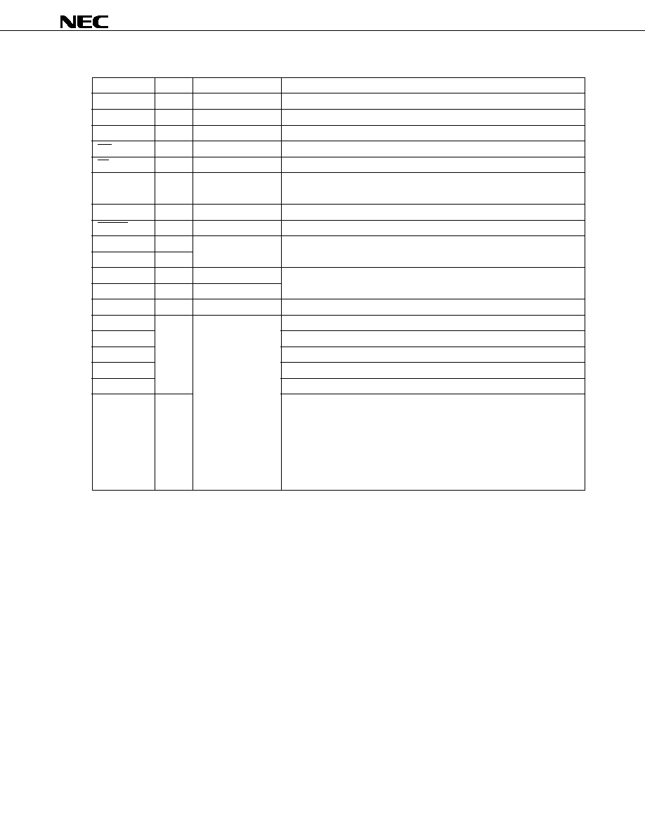
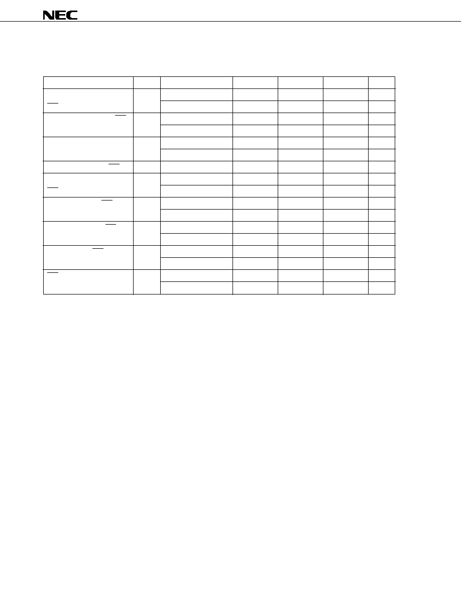
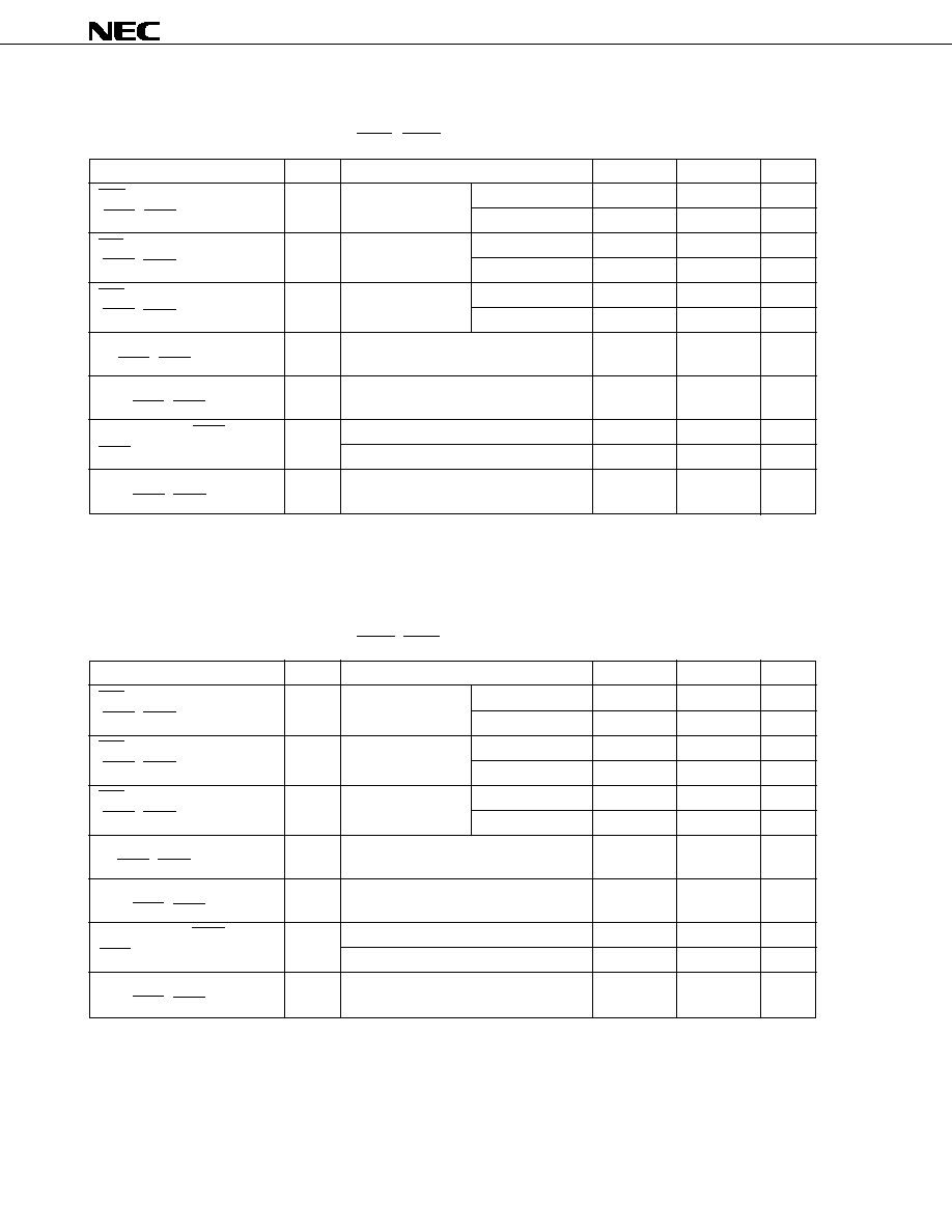
4.3 Pin I/O Circuits and Recommended Connection of Unused Pins
The I/O circuit type of each pin and recommended connection of unused pins are shown in Table 4-1.
For the I/O circuit configuration of each type, refer to Figure 4-1.
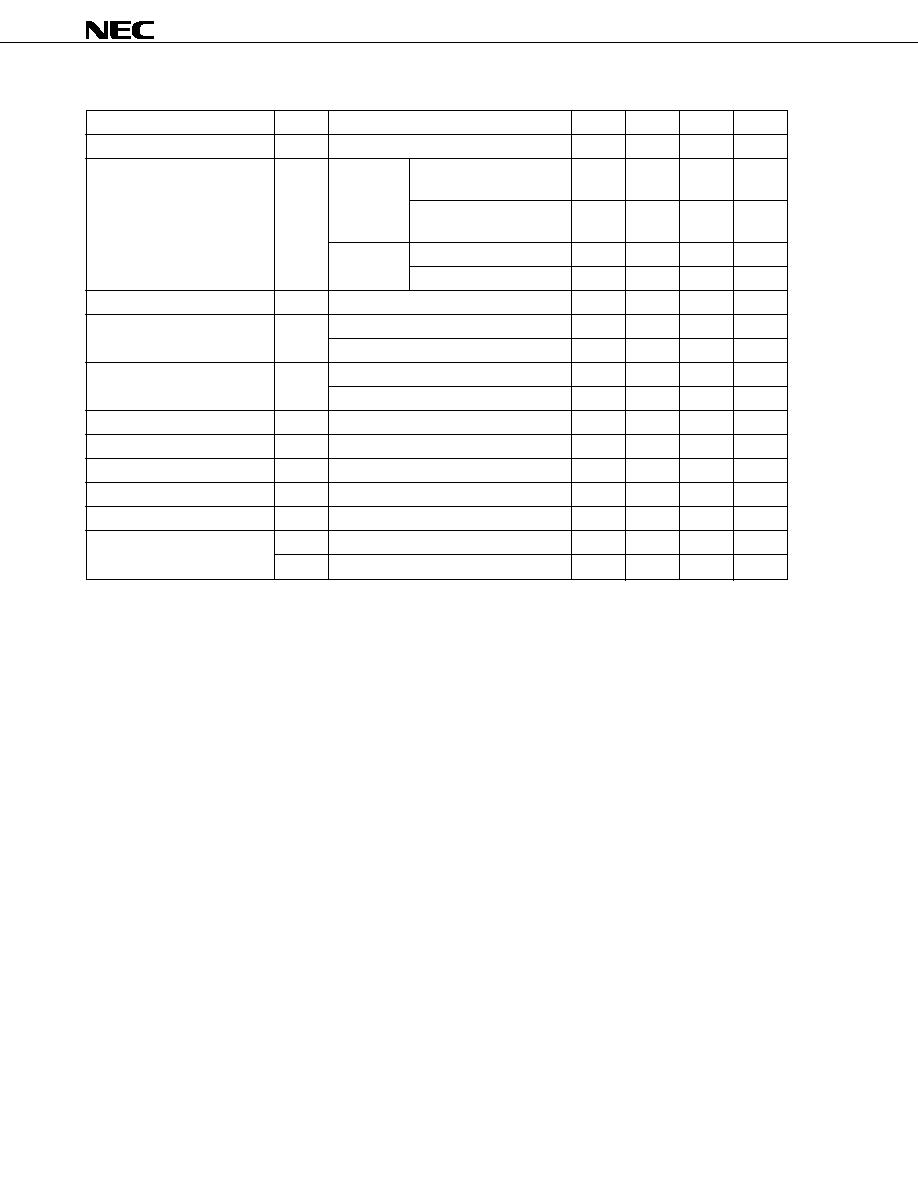
Table 4-1. Types of Pin I/O Circuits and Recommended Connection of Unused Pins (1/2)
Pin Name
I/O Circuit Type
I/O
Recommended Connection of Unused Pins
P00 to P07
5-A
I/O
Input: Connect to V
DD
.
P10, P11
Output: Leave open.
P12/ASCK2/SCK2
8-A
P13/RxD2/SI2
5-A
P14/TxD2/SO2
P15 to P17
P20/NMI
2
Input
Connect to V
DD
or V
SS
.
P21/INTP0
P22/INTP1
2-A
Connect to V
DD
.
P23/INTP2/CI
P24/INTP3
P25/INTP4/ASCK/SCK1
8-A
I/O
Input: Connect to V
DD
.
Output: Leave open.
P26/INTP5
2-A
Input
Connect to V
DD
.
P27/SI0
P30/RxD/SI1
5-A
I/O
Input: Connect to V
DD
.
P31/TxD/SO1
Output: Leave open.
P32/SCK0
10-A
P33/SO0
P34/TO0 to P37/TO3
5-A
P40/AD0 to P47/AD7
P50/A8 to P57/A15
P60/A16 to P63/A19
P64/RD
P65/WR
P66/WAIT/HLDRQ
P67/REFRQ/HLDAK
P70/ANI0 to P77/ANI7
20
I/O
Input: Connect to V
DD
or V
SS
.
P90 to P97
5-A
Output: Leave open.
P100 to P104
P105/SCK3
10-A
P106/SI3
8-A
P107/SO3
10-A
ASTB/CLKOUT
4
Output
Leave open.
RESET
2
Input
--
V
PP
1
Connect directly to V
SS
.
XT2
--
--
Leave open.
XT1
--
Input
Connect directly to V
SS
.
15
Data Sheet U14118EJ1V0DS
µPD78F4938A
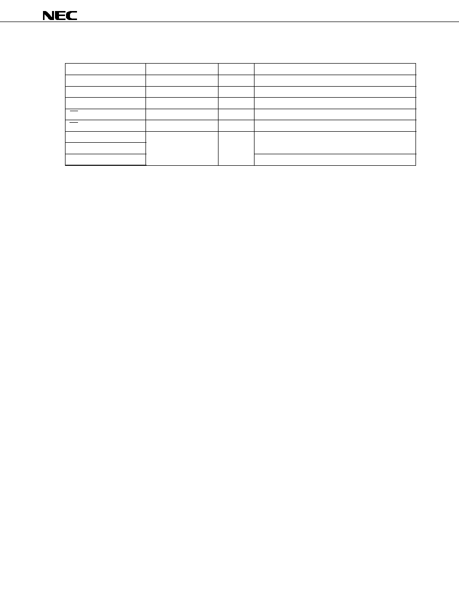
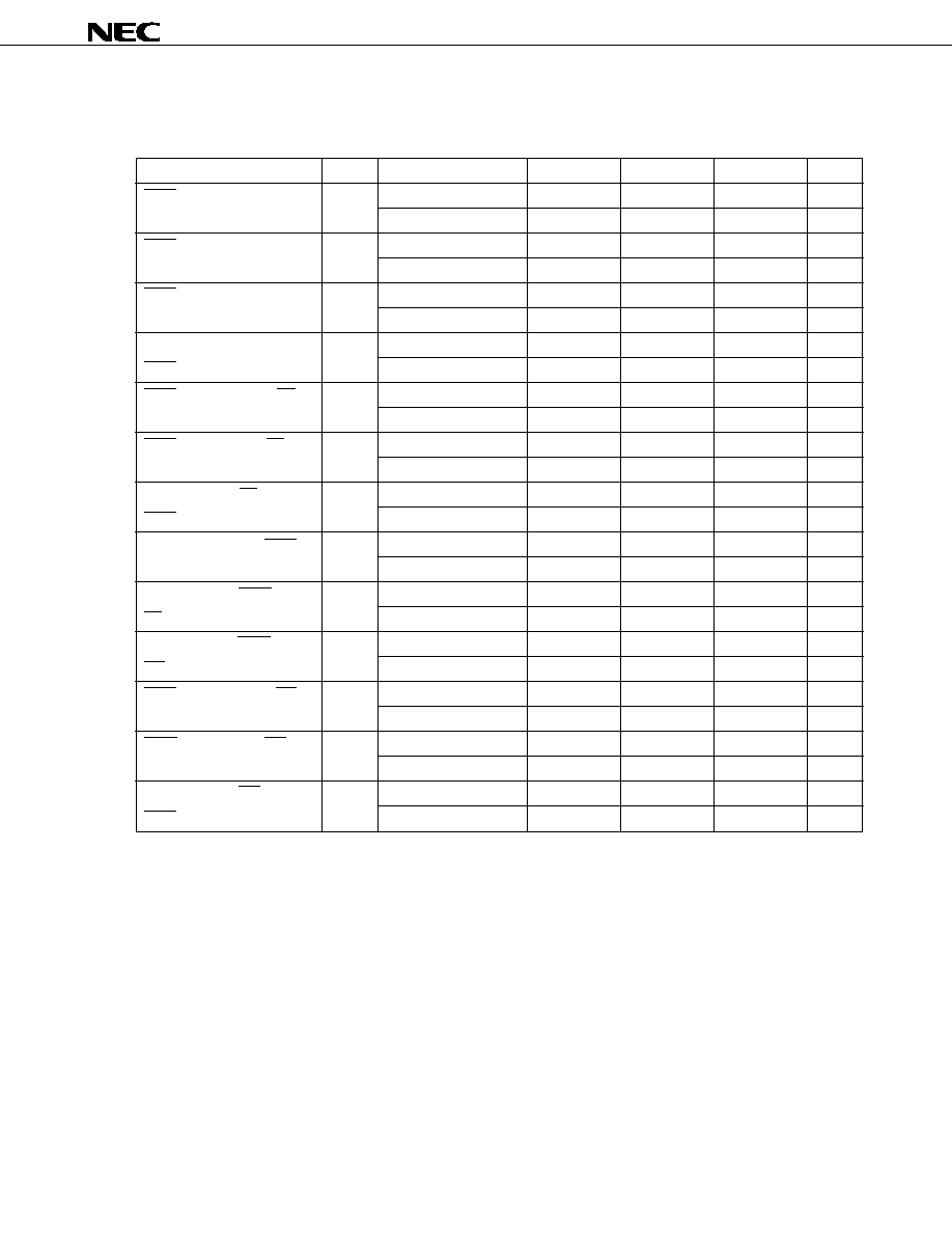
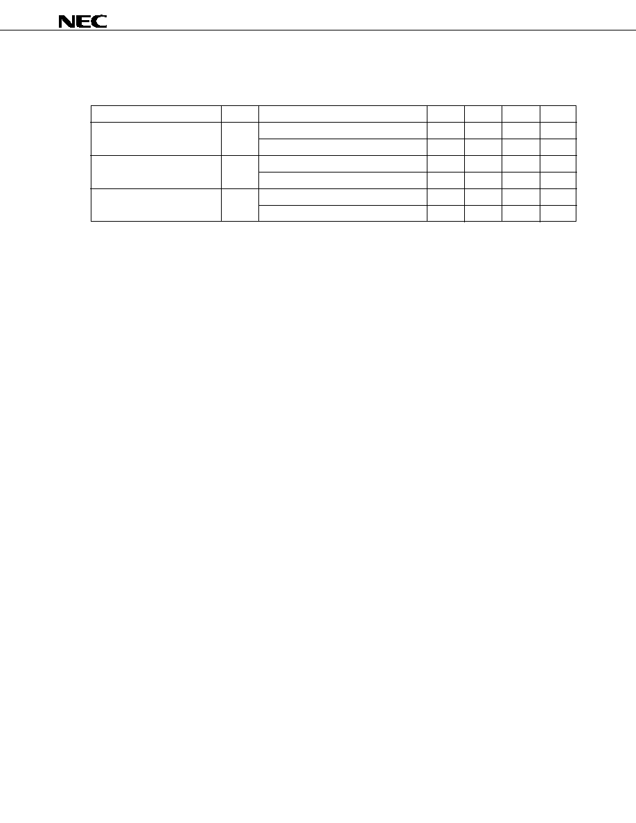
Table 4-1. Types of Pin I/O Circuits and Recommended Connection of Unused Pins (2/2)
Pin Name
I/O Circuit Type
I/O
Recommended Connection of Unused Pins
REGOFF
1
--
Connect directly to V
DD
.
REGC
--
--
Connect to V
DD
.
PWM0, PWM1
3
Output
Leave open.
RX
1
Input
Connect to V
DD
or V
SS
.
TX
3
Output
Leave open.
AV
REF1
--
--
Connect to V
SS
.
AV
SS
AV
DD
Connect to V
DD
.
Caution Connect an I/O pin to V
DD
via a resistor of several 10 k
if the I/O mode of the pin is unstable
(especially if the voltage on the reset pin is higher than the low-level input voltage on power application
or if the mode is changed between input and output by software).
Remark
The circuit type numbers are common for the 78K Series and are not always sequential for one product
(some circuits are not provided).
µPD78F4938A
16
Data Sheet U14118EJ1V0DS
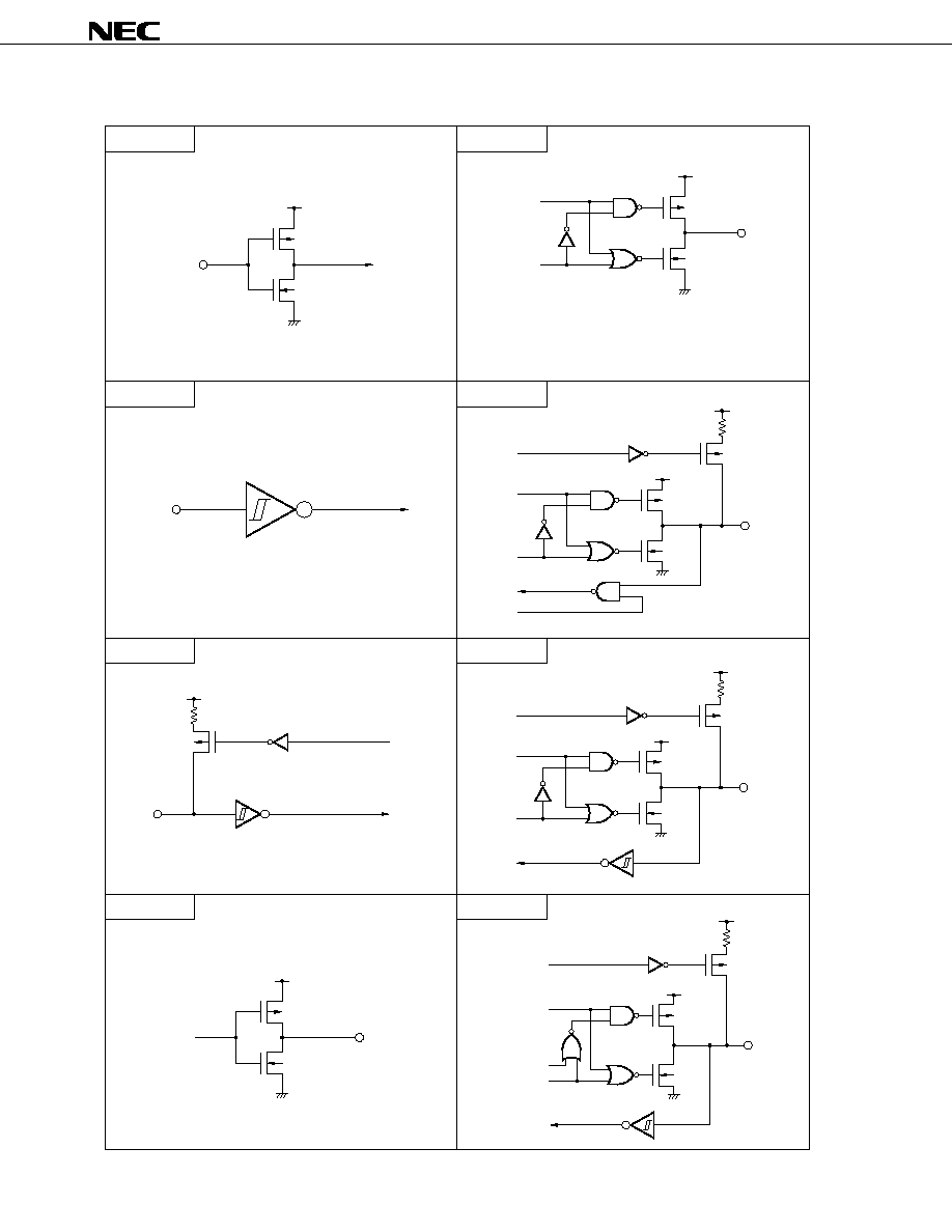
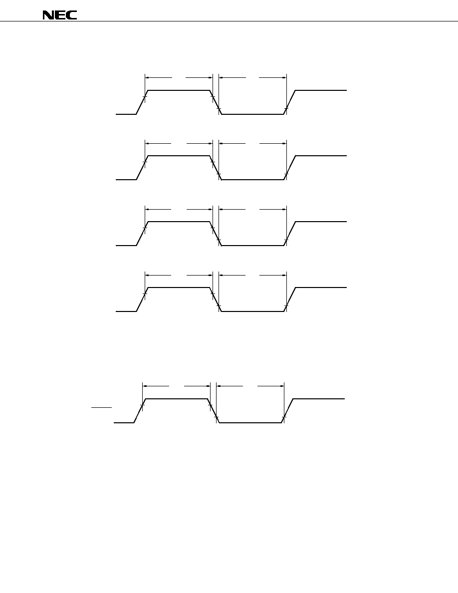
Figure 4-1. Pin I/O Circuits (1/2)
Type 2
Schmitt-triggered input with hysteresis characteristics
Type 1
Type 4
Push-pull output that can go into a high-impedance state
(both P-ch and N-ch are off).
Type 5-A
P
IN
V
DD
N
IN
Data
Output
disable
P
OUT
V
DD
N
Data
Output
disable
P
IN/OUT
V
DD
N
Input
enable
P
V
DD
Pull-up
enable
Type 2-A
Schmitt-triggered input with hysteresis characteristics
IN
P
V
DD
Pull-up
enable
Type 8-A
Type 10-A
Data
Output
disable
P
IN/OUT
V
DD
N
P
V
DD
Pull-up
enable
Data
Output disable
P
IN/OUT
V
DD
N
P
V
DD
Pull-up
enable
Open-drain
Type 3
P-ch
OUT
Data
V
DD
N-ch
17
Data Sheet U14118EJ1V0DS
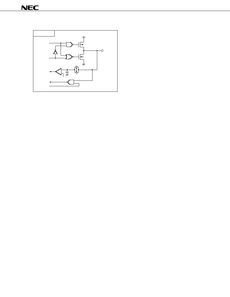
µPD78F4938A
Type 20
Data
Output
disable
P
IN/OUT
V
DD
N
Input
enable
Comparator
+
≠
P
N
V
REF
(threshold voltage)
Figure 4-1. Pin I/O Circuits (2/2)
µPD78F4938A
18
Data Sheet U14118EJ1V0DS
5. INTERNAL MEMORY SIZE SWITCHING REGISTER (IMS)
IMS is a register to prevent a certain part of the internal memory from being used by software. By setting the IMS,
it is possible to establish a memory map that is the same as that of mask ROM version with a different internal memory
(ROM, RAM) capacity.
IMS is set with an 8-bit memory manipulation instruction.
RESET input sets IMS to FFH.
Figure 5-1. Internal Memory Size Switching Register (IMS) Format
IMS
1
7
6
5
4
3
2
1
1
ROM1
ROM0
1
1
RAM1
0
RAM0
Address 0FFFCH
W
After reset FFH
Symbol
ROM1
ROM0
0
0
256 KB
96 KB
128 KB
192 KB
0
1
1
0
1
1
Internal ROM Capacity Selection
RAM1
RAM0
0
0
10496 bytes
5120 bytes
8192 bytes
6656 bytes
0
1
1
0
1
1
Internal RAM Capacity Selection
Caution IMS is not available for mask ROM versions (
µPD784935A, 784936A, 784937A, and 784938A).
The IMS settings to create the same memory map as mask ROM versions are shown in Table 5-1.
Table 5-1. Internal Memory Size Switching Register (IMS) Settings
Relevant Mask ROM Version
IMS Setting
µPD784935A
DDH
µPD784936A
EEH
µPD784937A
FFH
µPD784938A
CCH
Note
Shifting to the flash memory programming mode sets all pins not used for flash memory programming to
the same state as immediately after reset. Therefore, if the external devices do not acknowledge the port
state immediately after reset, handling such as connecting to V
DD
via a resistor or connecting to V
SS
via
a resistor is required.
19
Data Sheet U14118EJ1V0DS
µPD78F4938A
6. PROGRAMMING FLASH MEMORY
Flash memory can be written while mounted on the target system (on-board writing). Connect the dedicated flash
programmer (Flashpro III (part No.: FL-PR3, PG-FP3)) to the host machine and target system for programming.
Moreover, writing to flash memory can also be performed using a flash memory writing adapter connected to Flashpro
III.
Remark
FL-PR3 is a product of Naito Densei Machida Mfg. Co., Ltd.
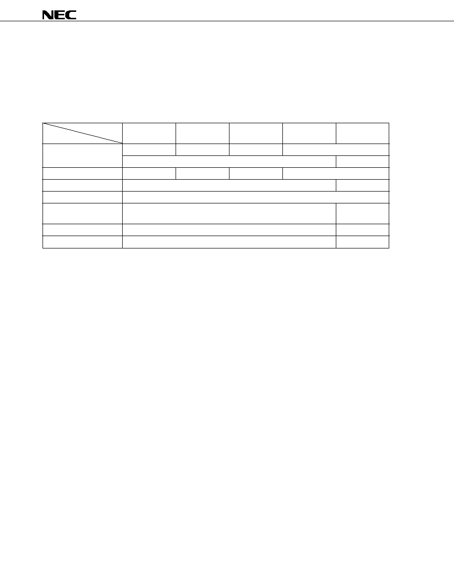
6.1 Selecting Communication Mode
The Flashpro III is used to write data into a flash memory by serial communications. Select the communication
mode for writing from Table 6-1. Figure 6-1 shows the format used to select the communication mode. Each
communication mode is selected with the number of V
PP
pulses shown in Table 6-1.
Table 6-1. Communication Mode
Communication Mode Number of Channels
Pins Used
Number of V
PP
Pulses
3-wire serial I/O 3
SCK3/P105
1
SI3/P106
SO3/P107
SCK0/P32
0
SI0/P27
SO0/P33
SCK3/P105
3
SI3/P106
SO3/P107
P104 (for handshake)
UART 1
RxD/P30
8
TxD/P31
Caution Always select the communication mode using the number of V
PP
pulses shown in Table 6-1.
Figure 6-1. Communication Mode Selection Format
10 V
V
DD
V
SS
V
DD
V
SS
V
PP
RESET
1
2
n
V
PP
pulses
Flash memory write mode
µPD78F4938A
20
Data Sheet U14118EJ1V0DS
6.2 Flash Memory Programming Functions
By transmitting and receiving various commands and data by the selected communication mode, operations such
as writing to the flash memory are performed. Table 6-2 shows the major functions.
Table 6-2. Flash Memory Programming Functions
Function
Description
Area erase
Erase the contents of the specified memory area where one memory block is 16 KB.
Area blank check
Checks the erase state of the specified area.
Data write
Writes to the flash memory based on the start write address and the number of data written (number
of bytes).
Area verify
Compares the data input with the contents of the specified memory area.
Verification for the flash memory entails supplying the data to be verified from an external source via a serial
interface, and then outputting the existence of unmatched data to the external source after referencing the areas or
all of the data. Consequently, the flash memory is not equipped with a read function, and it is not possible for third
parties to read the contents of the flash memory with the use of the verification function.
21
Data Sheet U14118EJ1V0DS
µPD78F4938A
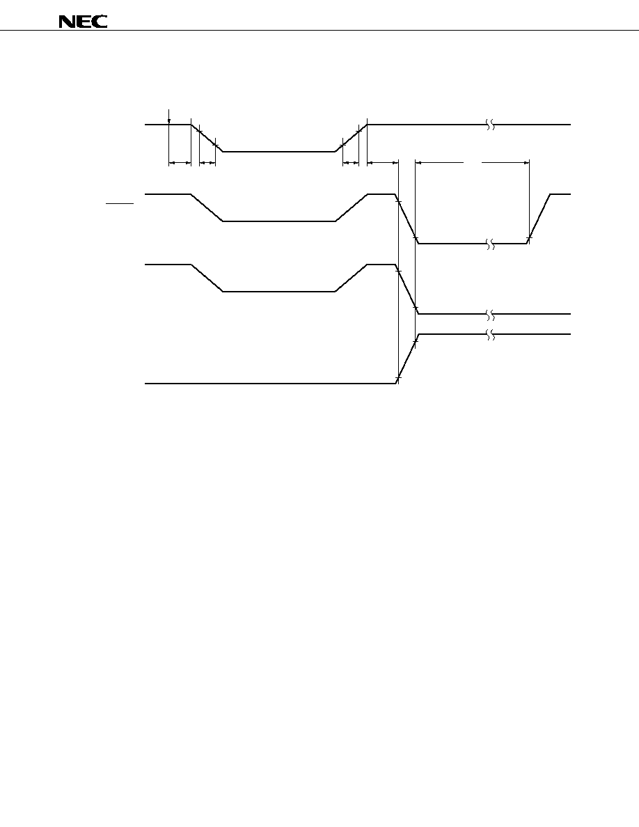
6.3 Connecting Flashpro III
The connection between the Flashpro III and the
µPD78F4938A differs depending on the communication mode
(3-wire serial I/O or UART). Figures 6-2 and 6-3 are the connection diagrams in each case.
Figure 6-2. Flashpro III Connection in 3-Wire Serial I/O Mode
V
PP
V
DD
RESET
SCK
SO
SI
V
PP
V
DD
RESET
SCK
SI
SO
HS
V
SS
P104
Note
V
SS
Flashpro III
PD78F4938A
µ
Note
Only in the handshake communication
Figure 6-3. Flashpro III Connection in UART Mode
V
PP
V
DD
RESET
SO
SI
V
SS
V
PP
V
DD
RESET
RxD
TxD
V
SS
Flashpro III
PD78F4938A
µ

22
Data Sheet U14118EJ1V0DS
µPD78F4938A
7. ELECTRICAL SPECIFICATIONS
Absolute Maximum Ratings (T
A
= 25
∞
C)
Parameter
Symbol
Conditions
Ratings
Unit
Supply voltage
V
DD
≠0.3 to +6.5
V
AV
DD
≠0.3 to V
DD
+ 0.3
V
AV
SS
≠0.3 to V
SS
+ 0.3
V
AV
REF1
A/D converter reference voltage input
≠0.3 to V
DD
+ 0.3
V
Input voltage
V
I2
≠0.3 to +10.5
V
Analog input voltage
V
IAN
Analog input voltage
AV
SS
≠ 0.3 to AV
REF1
+ 0.3
V
Output voltage
V
O
≠0.3 to V
DD
+ 0.3
V
Output current, low
I
OL
Per pin
10
mA
Total for all pins of ports 0, 3, 6, 10 and
50
mA
P54 to P57
Total for all pins of ports 1, 4, 7, 9,
50
mA
P50 to P53, PWM0, PWM1, and TX pins
Output current, high
I
OH
Per pin
≠6
mA
Total for all pins of ports 0, 3, 6, 10,and
≠30
mA
P54 to P57
Total for all pins of ports 1, 4, 7, 9,
≠30
mA
P50 to P53, PWM0, PWM1, and TX pins
Operating ambient temperature
T
A
≠40 to +85
∞C
Storage temperature
T
stg
≠40 to +150
∞C
Caution Product quality may suffer if the absolute maximum rating is exceeded even momentarily for any
parameter. That is, the absolute maximum ratings are rated values at which the product is on the
verge of suffering physical damage, and therefore the product must be used under conditions that
ensure that the absolute maximum ratings are not exceeded.
Remark
Unless specified otherwise, the characteristics of alternate-function pins are the same as those of port pins.
23
Data Sheet U14118EJ1V0DS
µPD78F4938A
Operating Conditions
∑
Clock frequency
Clock Frequency
Supply Voltage
4 MHz
f
XX
12.58 MHz
4.0
V
DD
5.5 V
4 MHz
f
XX
6.29 MHz
3.0
V
DD
5.5 V
∑
Operating ambient temperature (T
A
): ≠40 to +85
∞C
∑
Power supply voltage and clock cycle time: Refer to Figure 7-1
∑
Selection of internal regulator operation (REGOFF pin: low-level input)
Figure 7-1. Power Supply Voltage and Clock Cycle Time
Capacitance (T
A
= 25
∞
C, V
DD
= V
SS
= 0 V)
Parameter
Symbol
Conditions
MIN.
TYP.
MAX.
Unit
Input capacitance
C
IN
f = 1 MHz
15
pF
Output capacitance
C
OUT
Unmeasured pins returned to 0 V.
15
pF
I/O capacitance
C
IO
15
pF
Guaranteed operation range
10000
2000
1000
500
200
159
100
79
0
0
1
2
3
Power supply voltage [V]
Clock cycle time t
CYK
[ns]
4
5
6
1/8 of f
XX
= 2 MHz
f
XX
= 6.29 MHz undivided
f
XX
= 12.58 MHz undivided
24
Data Sheet U14118EJ1V0DS
µPD78F4938A
Main Oscillator Characteristics (T
A
= ≠40 to +85
∞
C, V
DD
= 3.0 to 5.5 V, V
SS
= 0 V)
Parameter
Symbol
Conditions
MIN.
MAX.
Unit
Oscillator frequency
f
XX
Ceramic resonator or
4.0
V
DD
5.5 V
4.0
12.58
MHz
recommended resonator
3.0
V
DD
5.5 V
4.0
6.29
MHz
Caution When using the main clock oscillator, wire as follows to avoid an adverse effect from wiring capacitance.
∑ Keep the wiring length as short as possible.
∑ Do not cross the wiring with the other signal lines.
∑ Do not route the wiring near a signal line through which a high fluctuating current flows.
∑ Always make the ground point of the oscillator capacitor the same potential as V
SS
.
∑ Do not ground the capacitor to a ground pattern through which a high current flows.
∑ Do not fetch signals from the oscillator.
Remarks 1. Connect a 12.582912 MHz or 6.291456 MHz oscillator to operate the internal clock timer with the main
clock.
2. For the resonator selection and oscillator constant, customers are requested to either evaluate the
oscillation themselves or apply to the resonator manufacturer for evaluation.
Clock Oscillator Characteristics (T
A
= ≠40 to +85
∞
C, V
DD
= 3.0 to 5.5 V, V
SS
= 0 V)
Parameter
Symbol
Conditions
MIN.
TYP.
MAX.
Unit
Oscillator frequency
f
XT
Ceramic resonator or crystal resonator
32
32.768
35
kHz
Oscillation stabilization time
f
sxt
4.5
V
DD
5.5 V
1.2
2
s
10
s
Oscillation hold voltage
V
DDXT
3.0
5.5
V
Watch timer operating voltage
V
DDW
3.0
5.5
V
25
Data Sheet U14118EJ1V0DS
µPD78F4938A
DC Characteristics (T
A
= ≠40 to +85
∞
C, V
DD
= AV
DD
= 3.0 to 5.5 V, V
SS
= AV
SS
= 0 V) (1/2)
Parameter
Symbol
Conditions
MIN.
TYP.
MAX.
Unit
Input voltage, low
Note
V
IL1
P10, P11, P13 to P17, P30, P31,
≠0.3
0.3V
DD
V
P34 to P37, P70 to P77, P90 to P97,
P100 to P104, X1, X2, XT1, XT2
V
IL2
P12, P20 to P27, P32, P33, P105 to P107
≠0.3
0.2V
DD
V
RESET
V
IL3
P00 to P07, P40 to P47, 4.5
V
DD
5.5 V
≠0.3
0.8
V
V
IL4
P50 to P57, P60 to P67
≠0.3
0.2V
DD
V
Input voltage, high
V
IH1
P10, P11, P13 to P17, P30, P31,
0.7V
DD
V
DD
+0.3
V
P34 to P37, P70 to P77, P90 to P97,
P100 to P104, X1, X2, XT1, XT2
V
IH2
P12, P20 to P27, P32, P33, P105 to P107
0.8V
DD
V
DD
+0.3
V
RESET
V
IH3
P00 to P07, P40 to P47, 4.5
V
DD
5.5 V
2.2
V
DD
+0.3
V
V
IH4
P50 to P57, P60 to P67
0.7V
DD
0.3V
DD
V
Output voltage, low
V
OL1
I
OL
= 20
µA
0.1
V
I
OL
= 100
µA
0.2
V
I
OL
= 2 mA
0.4
V
V
OL2
I
OL
= 8 mA, P10 to P17,
4.5
V
DD
5.5 V
1.0
V
P40 to P47, P50 to P57
Output voltage, high
V
OH1
I
OH
= ≠20
µA
V
DD
≠0.1
V
I
OL
= ≠100
µA
V
DD
≠0.2
V
I
OL
= ≠2 mA
V
DD
≠1.0
V
V
OH2
I
OL
= ≠5 mA,
4.5 V
V
DD
5.5 V V
DD
≠2.4
V
P10 to P17, P40 to P47,
P50 to P57
Input leakage current, low
I
LIL1
V
IN
= 0 V
For pins other than
10
µA
X1, X2, XT1, and XT2
I
LIL2
X1, X2, XT1, XT2
≠20
µA
Input leakage current, high
I
LIH1
V
IN
= V
DD
For pins other than
10
µA
X1, X2, XT1, and XT2
I
LIH2
X1, X2, XT1, XT2
20
µA
Output leakage current, low
I
LOL1
V
OUT
= 0 V
≠10
µA
Output leakage current, high
I
LOH1
V
OUT
= V
DD
10
µA
Note
These values are valid when the pull-up resistor is off.

26
Data Sheet U14118EJ1V0DS
µPD78F4938A
DC Characteristics (T
A
= ≠40 to +85
∞
C, V
DD
= AV
DD
= 3.0 to 5.5 V, V
SS
= AV
SS
= 0 V) (2/2)
Parameter
Symbol
Conditions
MIN.
TYP.
MAX.
Unit
Power supply current
I
DD1
Operating
f
XX
= 12.58 MHz,
19
38
mA
mode
4.0 V
V
DD
5.5 V
f
XX
= 6.29 MHz,
10
20
mA
3.0 V
V
DD
5.5 V
I
DD2
HALT mode
f
XX
= 12.58 MHz, when
3
6
mA
peripheral clock stops
Note
,
4.0 V
V
DD
5.5 V
f
XX
= 6.29 MHz, when
1.8
3.6
mA
peripheral clock stops
Note
,
3.0 V
V
DD
5.5 V
I
DD3
IDLE mode
f
XX
= 12.58 MHz,
2
4
mA
4.0
V
DD
5.5 V
f
XX
= 6.29 MHz,
1
2
mA
3.0 V
V
DD
5.5 V
Data hold voltage
V
DDDR
STOP mode
2.5
5.5
V
Data hold current
I
DDDR
STOP mode
V
DD
= 2.5 V, subsystem
4
20
µA
clock stops
V
DD
= 5.5 V, subsystem
20
100
µA
clock stops
Pull-up resistor
R
L
V
IN
= 0 V
15
40
80
k
Note
When the main system clock: f
CLK
= f
XX
/8 is selected (set by the standby control register (STBC)) and the watch
timer is operating.
Remark
These values are valid when the internal regulator is on (REGOFF pin = low-level input).
27
Data Sheet U14118EJ1V0DS
µ
PD78F4938A
AC Characteristics (T
A
= ≠40 to +85
∞
C, V
DD
= AV
DD
= 3.0 to 5.5 V, V
SS
= AV
SS
= 0 V)
(1) Read/write operation (1/2)
Parameter
Symbol
Conditions
MIN.
TYP.
MAX.
Unit
Cycle time
t
CYK
4.0
V
DD
5.5 V
79
ns
V
DD
= 3.0 V
159
ns
Address setup time
t
SAST
V
DD
= 5.0 V
(0.5+a) T≠11
ns
(to ASTB
)
V
DD
= 3.0 V
(0.5+a) T≠15
ns
Address hold time
t
HSTLA
V
DD
= 5.0 V
0.5T≠19
ns
(from ASTB
)
V
DD
= 3.0 V
0.5T≠24
ns
ASTB high-level width
t
WSTH
V
DD
= 5.0 V
(0.5+a) T≠17
ns
V
DD
= 3.0 V
(0.5+a) T≠40
ns
Address hold time (from RD
)
t
HRA
V
DD
= 5.0 V
0.5T≠14
ns
V
DD
= 3.0 V
0.5T≠14
ns
Delay time from address to
t
DAR
V
DD
= 5.0 V
(1+a) T≠5
ns
RD
V
DD
= 3.0 V
(1+a) T≠10
ns
Address float time (from RD
)
t
FAR
0
ns
Data input time from address
t
DAID
V
DD
= 5.0 V
(2.5+a+n) T≠37
ns
V
DD
= 3.0 V
(2.5+a+n) T≠52
ns
Data input time from ASTB
t
DSTID
V
DD
= 5.0 V
(2+n) T≠35
ns
V
DD
= 3.0 V
(2+n) T≠50
ns
Data input time from RD
t
DRID
V
DD
= 5.0 V
(1.5+n) T≠40
ns
V
DD
= 3.0 V
(1.5+n) T≠50
ns
Delay time from ASTB
to
t
DSTR
V
DD
= 5.0 V
0.5T≠9
ns
RD
V
DD
= 3.0 V
0.5T≠9
ns
Data hold time (from RD
)
t
HRID
0
ns
Address active time from RD
t
DRA
V
DD
= 5.0 V
0.5T≠2
ns
V
DD
= 3.0 V
0.5T≠12
ns
Delay time from RD
to
t
DRST
V
DD
= 5.0 V
0.5T≠9
ns
ASTB
V
DD
= 3.0 V
0.5T≠9
ns
RD low-level width
t
WRL
V
DD
= 5.0 V
(1.5+n) T≠25
ns
V
DD
= 3.0 V
(1.5+n) T≠30
ns
Remarks 1. T: t
CYK
= 1/f
CLK
(f
CLK
: internal system clock)
2. a: 1 during address wait; otherwise 0
3. n: Number of wait states (n
0)
4. Calculated as T = 79 ns (min.) @ V
DD
= 5.0 V
5. Calculated as T = 159 ns (min.) @ V
DD
= 3.0 V
28
Data Sheet U14118EJ1V0DS
µ
PD78F4938A
AC Characteristics (T
A
= ≠40 to +85
∞
C, V
DD
= AV
DD
= 3.0 to 5.5 V, V
SS
= AV
SS
= 0 V)
(1) Read/write operation (2/2)
Parameter
Symbol
Conditions
MIN.
TYP.
MAX.
Unit
Delay time from address to
t
DAW
V
DD
= 5.0 V
(1+a) T≠5
ns
WR
V
DD
= 3.0 V
(1+a) T≠10
ns
Address hold time (from WR
)
t
HWA
V
DD
= 5.0 V
0.5T≠14
ns
V
DD
= 3.0 V
0.5T≠14
ns
Delay time from ASTB
to
t
DSTOD
V
DD
= 5.0 V
0.5T+15
ns
data output
V
DD
= 3.0 V
0.5T+20
ns
Data output time from WR
t
DWOD
15
ns
Delay time from ASTB
to
t
DSTW
V
DD
= 5.0 V
0.5T≠9
ns
WR
V
DD
= 3.0 V
0.5T≠9
ns
Data setup time (to WR
)
t
SODWR
V
DD
= 5.0 V
(1.5+n) T≠20
ns
V
DD
= 3.0 V
(1.5+n) T≠25
ns
Data hold time (from WR
)
t
HWOD
V
DD
= 5.0 V
0.5T≠14
ns
V
DD
= 3.0 V
0.5T≠14
ns
Delay time from WR
to
t
DWST
V
DD
= 5.0 V
0.5T≠9
ns
ASTB
V
DD
= 3.0 V
0.5T≠9
ns
WR low-level width
t
WWL
V
DD
= 5.0 V
(1.5+n) T≠25
ns
V
DD
= 3.0 V
(1.5+n) T≠30
ns
Remarks 1. T: t
CYK
= 1/f
CLK
(f
CLK
: internal system clock)
2. a: 1 during address wait; otherwise 0
3. n: Number of wait states (n
0)
4. Calculated as T = 79 ns (min.) @ V
DD
= 5.0 V
5. Calculated as T = 159 ns (min.) @ V
DD
= 3.0 V
29
Data Sheet U14118EJ1V0DS
µ
PD78F4938A
AC Characteristics (T
A
= ≠40 to +85
∞
C, V
DD
= AV
DD
= 3.0 to 5.5 V, V
SS
= AV
SS
= 0 V)
(2) External wait timing
Parameter
Symbol
Conditions
MIN.
TYP.
MAX.
Unit
WAIT
input time from
t
DAWT
V
DD
= 5.0 V
(2+a) T≠40
ns
address
V
DD
= 3.0 V
(2+a) T≠60
ns
WAIT
input time from ASTB
t
DSTWT
V
DD
= 5.0 V
1.5T≠40
ns
V
DD
= 3.0 V
1.5T≠60
ns
WAIT hold time from ASTB
t
HSTWTH
V
DD
= 5.0 V
(0.5+n) T+5
ns
V
DD
= 3.0 V
(0.5+n) T+10
ns
Delay time from ASTB
to
t
DSTWTH
V
DD
= 5.0 V
(1.5+a) T≠40
ns
WAIT
V
DD
= 3.0 V
(1.5+a) T≠60
ns
WAIT
input time from RD
t
DRWTL
V
DD
= 5.0 V
T≠40
ns
V
DD
= 3.0 V
T≠60
ns
WAIT hold time from RD
t
HRWT
V
DD
= 5.0 V
nT+5
ns
V
DD
= 3.0 V
nT+10
ns
Delay time from RD
to
t
DRWTH
V
DD
= 5.0 V
(1+n) T≠40
ns
WAIT
V
DD
= 3.0 V
(1+n) T≠60
ns
Data input time from WAIT
t
DWTID
V
DD
= 5.0 V
0.5T≠5
ns
V
DD
= 3.0 V
0.5T≠10
ns
Delay time from WAIT
to
t
DWTR
V
DD
= 5.0 V
0.5T
ns
RD
V
DD
= 3.0 V
0.5T
ns
Delay time from WAIT
to
t
DWTW
V
DD
= 5.0 V
0.5T
ns
WR
V
DD
= 3.0 V
0.5T
ns
WAIT
input time from WR
t
DWWTL
V
DD
= 5.0 V
T≠40
ns
V
DD
= 3.0 V
T≠60
ns
WAIT hold time from WR
t
HWWT
V
DD
= 5.0 V
nT+5
ns
V
DD
= 3.0 V
nT+10
ns
Delay time from WR
to
t
DWWTH
V
DD
= 5.0 V
(1+n) T≠40
ns
WAIT
V
DD
= 3.0 V
(1+n) T≠60
ns
Remarks 1. T: t
CYK
= 1/f
CLK
(f
CLK
: internal system clock)
2. a: 1 during address wait; otherwise 0
3. n: Number of wait states (n
0)
4. Calculated as T = 79 ns (min.) @ V
DD
= 5.0 V
5. Calculated as T = 159 ns (min.) @ V
DD
= 3.0 V

30
Data Sheet U14118EJ1V0DS
µ
PD78F4938A
AC Characteristics (T
A
= ≠40 to +85
∞
C, V
DD
= AV
DD
= 3.0 to 5.5 V, V
SS
= AV
SS
= 0 V)
(3) Bus hold/refresh timing
Parameter
Symbol
Conditions
MIN.
TYP.
MAX.
Unit
Delay time from HLDRQ
t
FHQC
V
DD
= 5.0 V
(2+4+a+n) T+50
ns
to float
V
DD
= 3.0 V
(2+4+a+n) T+50
ns
Delay time from HLDRQ
to
t
DHQHHAH
V
DD
= 5.0 V
(3+4+a+n) T+30
ns
HLDAK
V
DD
= 3.0 V
(3+4+a+n) T+40
ns
Delay time from float to
t
DCFHA
V
DD
= 5.0 V
T+30
ns
HLDAK
V
DD
= 3.0 V
T+30
ns
Delay time from HLDRQ
to
t
DHQLHAL
V
DD
= 5.0 V
2T+40
ns
HLDAK
V
DD
= 3.0 V
2T+60
ns
Delay time from HLDAK
to
t
DHAC
V
DD
= 5.0 V
T≠20
ns
active
V
DD
= 3.0 V
T≠30
ns
Random read/write cycle time
t
RC
V
DD
= 5.0 V
3T
ns
V
DD
= 3.0 V
3T
ns
REFRQ low-level pulse width
t
WRFQL
V
DD
= 5.0 V
1.5T≠25
ns
V
DD
= 3.0 V
1.5T≠30
ns
Delay time from ASTB
to
t
DSTRFQ
V
DD
= 5.0 V
0.5T≠9
ns
REFRQ
V
DD
= 3.0 V
0.5T≠9
ns
Delay time from RD
to
t
DRRFQ
V
DD
= 5.0 V
1.5T≠9
ns
REFRQ
V
DD
= 3.0 V
1.5T≠9
ns
Delay time from WR
to
t
DWRFQ
V
DD
= 5.0 V
1.5T≠9
ns
REFRQ
V
DD
= 3.0 V
1.5T≠9
ns
Delay time from REFRQ
to
t
DRFQST
V
DD
= 5.0 V
0.5T≠9
ns
ASTB
V
DD
= 3.0 V
0.5T≠9
ns
REFRQ high-level pulse width
t
WRFQH
V
DD
= 5.0 V
1.5T≠25
ns
V
DD
= 3.0 V
1.5T≠30
ns
Remarks 1. T: t
CYK
= 1/f
CLK
(f
CLK
: internal system clock)
2. a: 1 during address wait; otherwise 0
3. n: Number of wait states (n
0)
4. Calculated as T = 79 ns (min.) @ V
DD
= 5.0 V
5. Calculated as T = 159 ns (min.) @ V
DD
= 3.0 V
31
Data Sheet U14118EJ1V0DS
µ
PD78F4938A
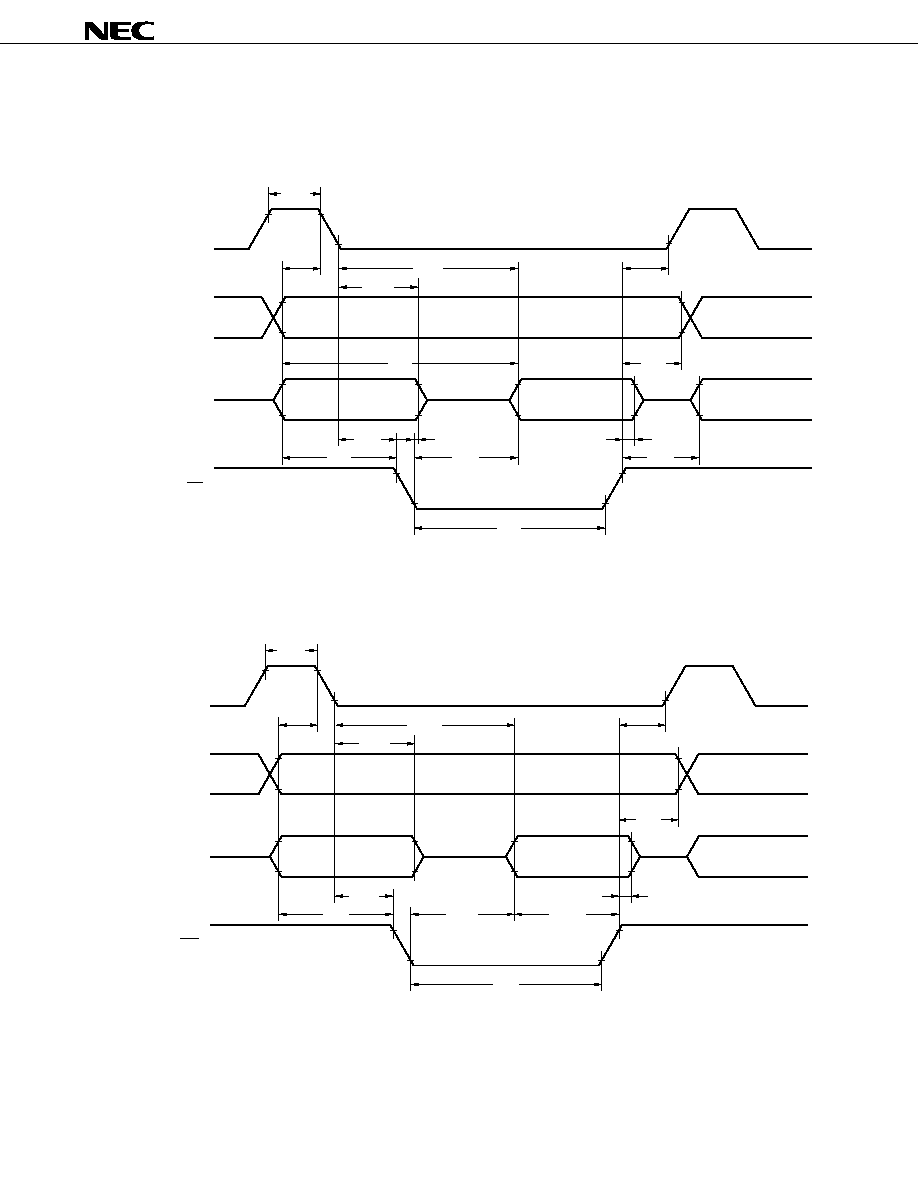
Timing Waveform
(1) Read operation
(2) Write operation
ASTB
A8 to A19
AD0 to AD7
RD
t
WSTH
t
SAST
t
DSTID
t
HSTLA
t
DRST
t
FRA
t
DRID
t
DAR
t
WRL
t
DSTR
t
DAID
t
HRA
t
DRA
t
HRID
ASTB
A8 to A19
AD0 to AD7
WR
t
WSTH
t
SAST
t
HSTLA
t
DWST
t
DAW
t
DSTW
t
HWOD
t
DSTOD
t
DWOD
t
SODWR
t
WWL
t
HWA

32
Data Sheet U14118EJ1V0DS
µ
PD78F4938A
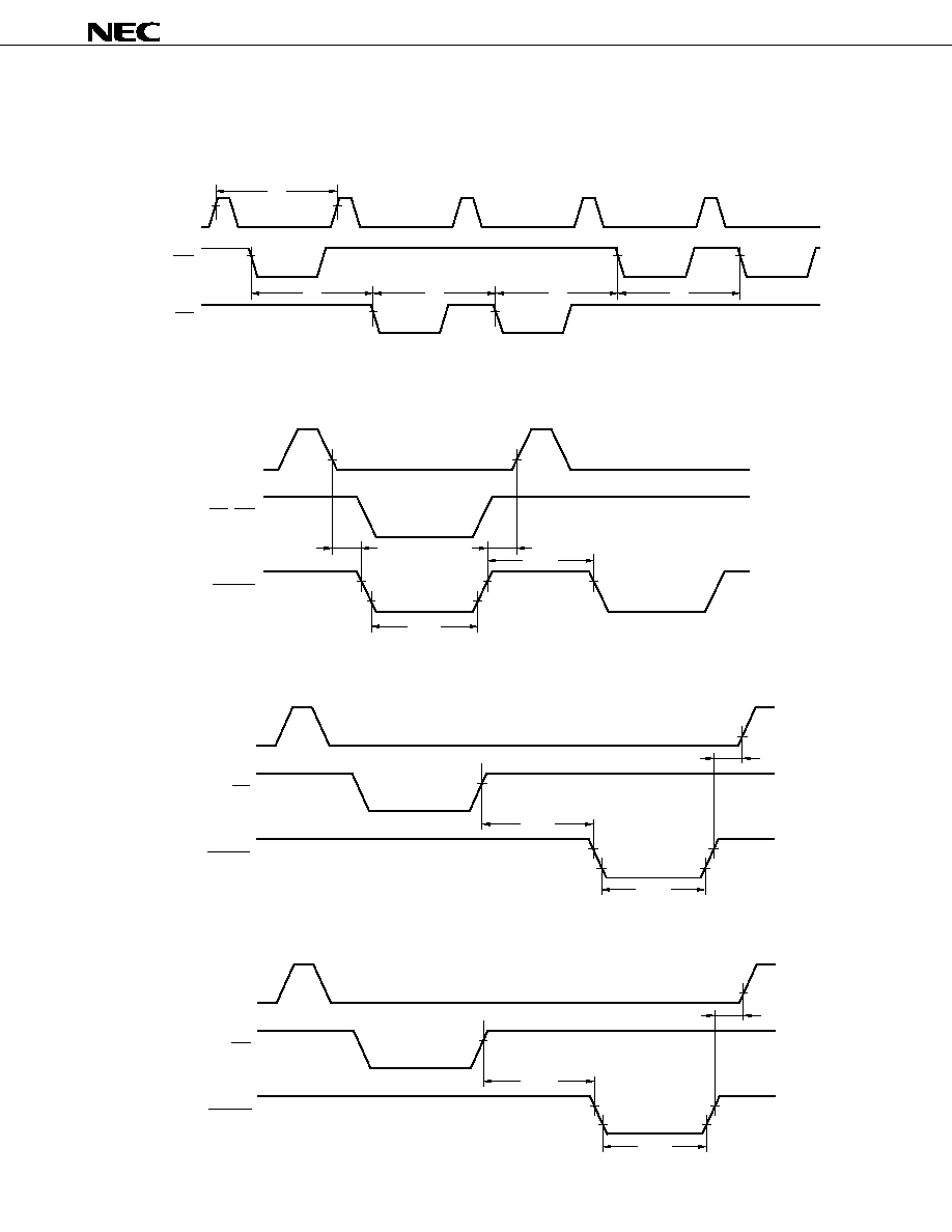
Hold Timing
External Wait Signal Input Timing
(1) Read operation
(2) Write operation
HLDRQ
HLDAK
t
DHQHHAH
t
FHQC
t
DCFHA
t
DHAC
t
DHQLHAL
ASTB, A8 to A19,
AD0 to AD7, RD, WR
ASTB
A8 to A19
AD0 to AD7
RD
WAIT
t
DSTWT
t
HSTWTH
t
DSTWTH
t
DAWT
t
DWTID
t
DWTR
t
DRWTL
t
HRWT
t
DRWTH
ASTB
A8 to A19
AD0 to AD7
WR
WAIT
t
DSTWT
t
HSTWTH
t
DSTWTH
t
DAWT
t
DWTW
t
DWWTL
t
HWWT
t
DWWTH
33
Data Sheet U14118EJ1V0DS
µ
PD78F4938A
Refresh Timing Waveform
(1) Random read/write cycle
(2) When refresh memory is accessed for a read and write at the same time
(3) Refresh after a read
(4) Refresh after a write
ASTB
WR
RD
t
RC
t
RC
t
RC
t
RC
t
RC
t
WRFQL
ASTB
RD, WR
REFRQ
t
DSTRFQ
t
DRFQST
t
WRFQH
ASTB
RD
REFRQ
t
DRFQST
t
DRRFQ
t
WRFQL
ASTB
WR
REFRQ
t
DRFQST
t
DWRFQ
t
WRFQL
34
Data Sheet U14118EJ1V0DS
µPD78F4938A
Serial Operation (T
A
= ≠40 to +85
∞
C, V
DD
= AV
DD
= 3.0 to 5.5 V, V
SS
= AV
SS
= 0 V)
(a) CSI0, CSI3 3-wire serial I/O mode (SCK0, SCK3 ... External clock input)
Parameter
Symbol
Conditions
MIN.
MAX.
Unit
SCK cycle time
t
CYSK0
,
SO0 and SO3 are
f
CLK
= f
XX
8/f
XX
ns
(SCK0, SCK3)
t
CYSK3
CMOS outputs
Except f
CLK
= f
XX
4/f
CLK
ns
SCK low-level width
t
WSKL0
,
SO0 and SO3 are
f
CLK
= f
XX
4/f
XX
≠ 40
ns
(SCK0, SCK3)
t
WSKL3
CMOS outputs
Except f
CLK
= f
XX
2/f
CLK
≠ 40
ns
SCK high-level width
t
WSKH0
,
SO0 and SO3 are
f
CLK
= f
XX
4/f
XX
≠ 40
ns
(SCK0, SCK3)
t
WSKH3
CMOS outputs
Except f
CLK
= f
XX
2/f
CLK
≠ 40
ns
SI0, SI3 setup time
t
SSSK0
,
80
ns
(to SCK0, SCK3
)
t
SSSK3
SI0, SI3 hold time
t
HSSK0
,
1/f
CLK
+ 80
ns
(from SCK0, SCK3
)
t
HSSK3
Delay time from SCK0,
t
DBSK0
,
CMOS output
0
1/f
CLK
+ 150
ns
SCK3
to output
t
DBSK3
N-ch open-drain output (R
L
= 1 k
)
0
1/f
CLK
+ 400
ns
SO0, SO3 output hold time
t
HSBSK0
,
When data is transferred
0.5t
CYSK0
≠ 40,
ns
(from SCK0, SCK3
)
t
HSBSK3
0.5t
CYSK3
≠ 40
Remarks 1. The values in this table are those when CL = 100 pF.
2. f
XX
: External oscillator frequency (f
XX
= 12.58 MHz or f
XX
= 6.29 MHz)
3. f
CLK
: System clock oscillation frequency (selectable from f
XX
, f
XX
/2, f
XX
/4, and f
XX
/8 by the standby control
register (STBC))
(b) CSI0, CSI3 3-wire serial I/O mode (SCK0, SCK3 ... Internal clock output)
Parameter
Symbol
Conditions
MIN.
MAX.
Unit
SCK cycle time
t
CYSK0
,
SO0 and SO3 are
Except f
CLK
= f
XX
/8
8/f
XX
ns
(SCK0, SCK3)
t
CYSK3
CMOS outputs
f
CLK
= f
XX
/8
16/f
XX
ns
SCK low-level width
t
WSKL0
,
SO0 and SO3 are
Except f
CLK
= f
XX
/8
4/f
XX
≠ 40
ns
(SCK0, SCK3)
t
WSKL3
CMOS outputs
f
CLK
= f
XX
/8
8/f
XX
≠ 40
ns
SCK high-level width
t
WSKH0
,
SO0 and SO3 are
Except f
CLK
= f
XX
/8
4/f
XX
≠ 40
ns
(SCK0, SCK3)
t
WSKH3
CMOS outputs
f
CLK
= f
XX
/8
8/f
XX
≠ 40
ns
SI0, SI3 setup time
t
SSSK0
,
80
ns
(to SCK0, SCK3
)
t
SSSK3
SI0, SI3 hold time
t
HSSK0
,
80
ns
(from SCK0, SCK3
)
t
HSSK3
Delay time from SCK0,
t
DBSK0
,
CMOS output
0
150
ns
SCK3
to output
t
DBSK3
N-ch open-drain output (R
L
= 1 k
)
0
400
ns
SO0, SO3 output hold time
t
HSBSK0
,
When data is transferred
0.5t
CYSK0
≠ 40,
ns
(from SCK0, SCK3
)
t
HSBSK3
0.5t
CYSK3
≠ 40
Remarks 1. The values in this table are those when CL = 100 pF.
2. f
XX
: External oscillator frequency (f
XX
= 12.58 MHz or f
XX
= 6.29 MHz)
3. f
CLK
: System clock oscillation frequency (selectable from f
XX
, f
XX
/2, f
XX
/4, and f
XX
/8 by the standby control
register (STBC))
35
Data Sheet U14118EJ1V0DS
µPD78F4938A
Serial Operation (T
A
= ≠40 to +85
∞
C, V
DD
= AV
DD
= 3.0 to 5.5 V, V
SS
= AV
SS
= 0 V)
(c) UART0, UART3 (Asynchronous serial interface mode)
Parameter
Symbol
Conditions
MIN.
TYP.
MAX.
Unit
ASCK0, ASCK2 cycle time
t
CYASK
4.0
V
DD
5.5 V
160
ns
320
ns
ASCK0, ASCK2 low-level width
t
WASKL
4.0
V
DD
5.5 V
65
ns
120
ns
ASCK0, ASCK2 high-level width
t
WASKH
4.0
V
DD
5.5 V
65
ns
120
ns
36
Data Sheet U14118EJ1V0DS
µPD78F4938A
Serial Operation (T
A
= ≠40 to +85
∞
C, V
DD
= AV
DD
= 3.0 to 5.5 V, V
SS
= AV
SS
= 0 V)
(d) IOE1, IOE2 3-wire serial I/O mode (SCK1, SCK2 ... External clock input)
Parameter
Symbol
Conditions
MIN.
MAX.
Unit
SCK cycle time (SCK1, SCK2)
t
CYSK1
4.0
V
DD
5.5 V
640
ns
t
CYSK2
1280
ns
SCK low-level width
t
WSKL1
,
4.0
V
DD
5.5 V
280
ns
(SCK1, SCK2)
t
WSKL2
600
ns
SCK high-level width
t
WSKH1
,
4.0
V
DD
5.5 V
280
ns
(SCK1, SCK2)
t
WSKH2
600
ns
SI1, SI2 setup time
t
SSSK1
,
40
ns
(to SCK1, SCK2
)
t
SSSK2
SI1, SI2 hold time
t
HSSK1
,
40
ns
(from SCK1, SCK2
)
t
HSSK2
Delay time from SCK1, SCK2
t
DSOSK1
,
0
50
ns
to output
t
DSOSK2
SO1, SO2 output hold time
t
HSOSK1
,
When data is transferred
0.5t
CYSK1
≠ 40,
ns
(from SCK1, SCK2
)
t
HSOSK2
0.5t
CYSK2
≠ 40
Remarks 1. The values in this table are those when CL = 100 pF.
2. T: Selected serial clock cycle. The minimum value is 8/f
XX
.
(e) IOE1, IOE2 3-wire serial I/O mode (SCK1, SCK2 ... Internal clock output)
Parameter
Symbol
Conditions
MIN.
MAX.
Unit
SCK cycle time (SCK1, SCK2)
t
CYSK1
T
ns
t
CYSK2
SCK low-level width
t
WSKL1
,
0.5T ≠ 40
ns
(SCK1, SCK2)
t
WSKL2
SCK high-level width
t
WSKH1
,
0.5T ≠ 40
ns
(SCK1, SCK2)
t
WSKH2
SI1, SI2 setup time
t
SSSK1
,
40
ns
(to SCK1, SCK2
)
t
SSSK2
SI1, SI2 hold time
t
HSSK1
,
40
ns
(from SCK1, SCK2
)
t
HSSK2
Delay time from SCK1, SCK2
t
DSOSK1
,
0
50
ns
to output
t
DSOSK2
SO1, SO2 output hold time
t
HSOSK1
,
When data is transferred
0.5t
CYSK1
≠ 40,
ns
(from SCK1, SCK2
)
t
HSOSK2
0.5t
CYSK2
≠ 40
Remarks 1. The values in this table are those when CL = 100 pF.
2. T: Selected serial clock cycle. The minimum value is 8/f
XX
.
37
Data Sheet U14118EJ1V0DS
µPD78F4938A
Other Operations (T
A
= ≠40 to +85
∞
C, V
DD
= AV
DD
= 3.0 to 5.5 V, V
SS
= AV
SS
= 0 V)
Parameter
Symbol
Conditions
MIN.
TYP.
MAX.
Unit
NMI high-/low-level width
t
WNIL
10
µs
t
WNIH
INTP0 high-/low-level width
t
WIT0L
4t
CYSMP
s
t
WIT0H
INTP1 to INTP3, CI high-/
t
WIT1L
4t
CYCPU
s
low-level width
t
WIT1H
INTP4, INTP5 high-/
t
WIT2L
10
µs
low-level width
t
WIT2H
RESET high-/low-level
t
WRSL
10
µs
width
Note
t
WRSH
Note
When the power is turned on or when STOP mode is released by reset, secure the oscillation stabilization wait
time while the RESET is at a low-level width.
When the power is applied, be sure to activate V
DD
in the RESET = low-level state.
Remark
t
CYSMP
: Sampling clock set by software
t
CYCPU
: CPU clock set by software in the CPU
Clock Output Operation (T
A
= ≠40 to +85
∞
C, V
DD
= AV
DD
= 3.0 to 5.5 V, V
SS
= AV
SS
= 0 V)
Parameter
Symbol
Conditions
MIN.
TYP.
MAX.
Unit
CLKOUT cycle time
t
CYCL
nT
79
32000
ns
CLKOUT low-level width
t
CLL
4.5
V
DD
5.5 V
0.5T ≠ 10
ns
0.5T ≠ 20
ns
CLKOUT high-level width
t
CLH
4.5
V
DD
5.5 V
0.5T ≠ 10
ns
0.5T ≠ 20
ns
CLKOUT rise time
t
CLR
4.5
V
DD
5.5 V
10
ns
3.0
V
DD
4.5 V
20
ns
CLKOUT fall time
t
CLF
4.5
V
DD
5.5 V
10
ns
3.0
V
DD
4.5 V
20
ns
Remark
n: Division ratio of clock output frequency, T: t
CYK
= 1/f
CLK
(system clock cycle time)
IEBus Controller Characteristics (T
A
= ≠40 to +85
∞
C, V
DD
= AV
DD
= 4.5 to 5.5 V, V
SS
= AV
SS
= 0 V)
Parameter
Symbol
Conditions
MIN.
TYP.
MAX.
Unit
IEBus system clock frequency
f
s
Mode 1
6.29
MHz
Remark
Although the system clock frequency in the IEBus specifications is 6.0 MHz, in the
µPD784938A, operation
at 6.29 MHz is also guaranteed. Note, however, that operation at 6.0 MHz and 6.29 MHz cannot be used
together.
38
Data Sheet U14118EJ1V0DS
µPD78F4938A
A/D Converter Characteristics (T
A
= ≠40 to +85
∞
C, V
DD
= AV
DD
= AV
REF1
= 3.0 to 5.5 V, V
SS
= AV
SS
= 0 V)
Parameter
Symbol
Conditions
MIN.
TYP.
MAX.
Unit
Resolution
8
bit
Overall error
Note 1
IEAD = 00H 6.29 MHz
f
XX
12.58 MHz
±0.6
%FSR
Note 2
and other than FR = 1
6.29 MHz
f
XX
12.58 MHz
±1.5
%FSR
Note 2
and FR = 1
IEAD = 01H 4.5
V
DD
5.5 V
±1
±2.2
%FSR
Note 2
3.0
V
DD
< 5.5 V
±1.4
±2.6
%FSR
Note 2
Quantization error
±1/2
LSB
Conversion time
t
CONV
FR = 1: 120t
CYK
9.5
480
µs
FR = 0: 240t
CYK
19.1
960
µs
Sampling time
t
SAMP
FR = 1: 18t
CYK
1.4
72
µs
FR = 0: 36t
CYK
2.9
144
µs
Analog input voltage
V
IAN
AV
SS
AV
REF1
V
Analog input impedance
R
AN
1000
M
Reference voltage
AV
REF1
3.0
AV
DD
V
AV
REF1
resistor
R
AVREF1
3.0
10
k
AV
REF1
current
AI
REF1
0.5
1.5
mA
AV
DD
current
AI
DD1
2.0
5.0
mA
AI
DD2
20
mA
Notes 1. Excludes quantization error (
±1/2 LSB).
2. It is indicated as a ratio (%FSR) to the full-scale value.
Caution The analog input pins of the
µPD78F4938A function alternately as the port 7 pins (I/O port pins).
However when using the A/D converter, it is necessary to set all the pins of port 7 to input mode
in order to prevent data from being inverted by the output port operation, thus degrading the A/D
conversion accuracy. At this time, pins cannot be used as output ports even though they are not
used as A/D analog input port.

39
Data Sheet U14118EJ1V0DS
µ
PD78F4938A
SCK1, SCK2
SI1, SI2
SO1, SO2
Output data
Input data
t
SSSK1
t
HSSK1
t
DSOSK
t
HSOSK
t
WSKL1
t
WSKH1
t
CYSK1
SCK0, SCK3
SI0, SI3
SO0, SO3
Output data
Input data
t
SSSKn
t
HSSKn
t
DSBSKn
t
WSKLn
t
WSKHn
t
HSBSKn
t
CYSKn
ASCK0,
ASCK2
t
WASKH
t
WASKL
t
CYASK
CLKOUT
t
CLH
t
CLL
t
CYCL
t
CLF
t
CLR
Serial Operation (CSI, CSI3)
n = 0, 3
Serial Operation (IOE1, IOE2)
Serial Operation (UART0, UART2)
Clock Output Timing
40
Data Sheet U14118EJ1V0DS
µ
PD78F4938A
NMI
INTP0
CI,
INTP1 to INTP3
INTP4, INTP5
t
WNIH
t
WNIL
t
WIT0H
t
WIT0L
t
WIT1H
t
WIT1L
t
WIT2H
t
WIT2L
RESET
t
WRSH
t
WRSL
Interrupt Request Input Timing
Reset Input Timing
41
Data Sheet U14118EJ1V0DS
µ
PD78F4938A
V
DD
RESET
NMI
(Clearing by falling edge)
NMI
(Clearing by rising edge)
t
HVD
t
FVD
t
RVD
t
DREL
V
DDDR
STOP mode setting
t
WAIT
Data Retention Characteristics
42
Data Sheet U14118EJ1V0DS
µ
PD78F4938A
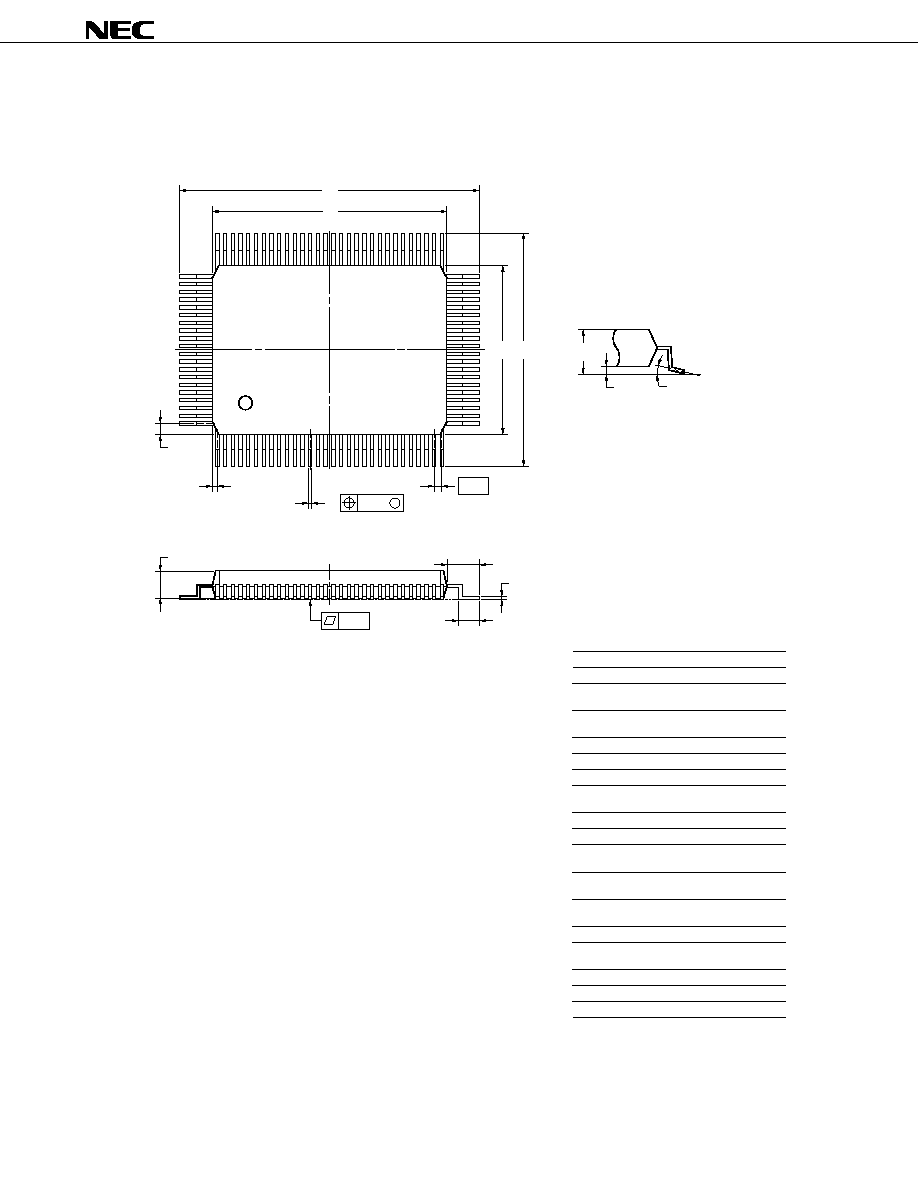
8. PACKAGE DRAWING
Remark
The external dimensions and material of the ES version are the same as those of the mass-produced
version.
100PIN PLASTIC QFP (14x20)
ITEM
MILLIMETERS
INCHES
NOTE
Each lead centerline is located within 0.15 mm (0.006 inch) of
its true position (T.P.) at maximum material condition.
P100GF-65-3BA1-3
B
20.0
±
0.2
0.795+0.009
≠0.008
C
14.0
±
0.2
0.551+0.009
≠0.008
D
17.6
±
0.4
0.693
±
0.016
F
0.8
0.031
G
0.6
0.024
H
0.30
±
0.10
0.012
I
0.15
0.006
J
0.65 (T.P.)
0.026 (T.P.)
K
1.8
±
0.2
0.071+0.008
≠0.009
L
0.8
±
0.2
0.031
N
0.10
0.004
Q
0.1
±
0.1
0.004
±
0.004
S
3.0 MAX.
0.119 MAX.
detail of lead end
R
Q
J
K
M
L
N
P
G
F
H
I
M
P
2.7
±
0.1
0.106+0.005
≠0.004
80
81
50
100
1
31
30
51
B
A
C D
S
A
23.6
±
0.4
0.929
±
0.016
M
0.15
0.006
+0.10
≠0.05
R
5
∞±
5
∞
5
∞±
5
∞
+0.004
≠0.005
+0.009
≠0.008
+0.004
≠0.003

43
Data Sheet U14118EJ1V0DS
µ
PD78F4938A
9. RECOMMENDED SOLDERING CONDITIONS
The
µ
PD78F4938A should be soldered and mounted under the following recommended conditions.
For details of the recommended soldering conditions, refer to the document Semiconductor Device Mounting
Technology Manual (C10535E).
For soldering methods and conditions other than those recommended below, contact an NEC sales representative.
Table 9-1. Surface Mounting Type Soldering Conditions
µ
PD78F4938AGF-3BA: 100-pin plastic QFP (14
◊
20)
Soldering Method
Soldering Conditions
Recommended
Condition Symbol
Infrared reflow
Package peak temperature: 235
∞
C, Time: 30 seconds max. (at 210
∞
C or higher),
IR35-207-2
Count: two times or less, Exposure limit: 7 days
Note
(after that, prebake at
125
∞
C for 20 hours)
VPS
Package peak temperature: 215
∞
C, Time: 40 seconds max. (at 200
∞
C or higher),
VP15-207-2
Count: two times or less, Exposure limit: 7 days
Note
(after that, prebake at 125
∞
C
for 20 hours)
Wave soldering
Solder bath temperature: 260
∞
C max., Time: 10 seconds max., Count: once,
WS60-207-1
Preheating temperature: 120
∞
C max. (package surface temperature),
Exposure limit: 7 days
Note
(after that, prebake at 125
∞
C for 20 hours)
Partial heating
Pin temperature: 300
∞
C max., Time: 3 seconds max. (per pin row)
≠
Note
After opening the dry pack, store it at 25
∞
C or less and 65% RH or less for the allowable storage period.

44
Data Sheet U14118EJ1V0DS
µ
PD78F4938A
APPENDIX A. DEVELOPMENT TOOLS
The following development tools are available for system development using the
µ
PD78F4938A.
Also refer to (5) Cautions on using development tools.
(1) Language processing software
RA78K4
Assembler package common to 78K/IV Series
CC78K4
C compiler package common to 78K/IV Series
DF784937
Device file for
µ
PD784938A Subseries
CC78K4-L
C compiler library source file common to 78K/IV Series
(2) Flash memory writing tools
Flashpro III
Flash programmer for microcontroller with on-chip flash memory
(PG-FP3)
FA-100GF
Flash memory writing adapter for 100-pin plastic QFP (GF-3BA type). Wiring must be performed
according to the product used.
(3) Debugging tools
∑
When IE-78K4-NS in-circuit emulator is used
IE-78K4-NS
In-circuit emulator common to 78K/IV Series
IE-70000-MC-PS-B
Power supply unit for IE-78K4-NS
IE-70000-98-IF-C
Interface adapter used when PC-9800 series (except notebook type) is used as host machine
IE-70000-CD-IF-C
PC card and cable used when PC-9800 series notebook type PC is used as host machine
IE-70000-PC-IF-C
Interface adapter used when IBM PC/AT
TM
or compatible is used as host machine
IE-784937-NS-EM1
Emulation board to emulate
µ
PD784938A Subseries
NP-100GF
Emulation probe for 100-pin plastic QFP (GF-3BA type)
EV-9200GF-100
Socket to be mounted on a target system board made for 100-pin plastic QFP (GF-3BA type)
ID78K4-NS
Integrated debugger for IE-78K4-NS
SM78K4
System simulator common to 78K/IV Series
DF784937
Device file for
µ
PD784938A Subseries
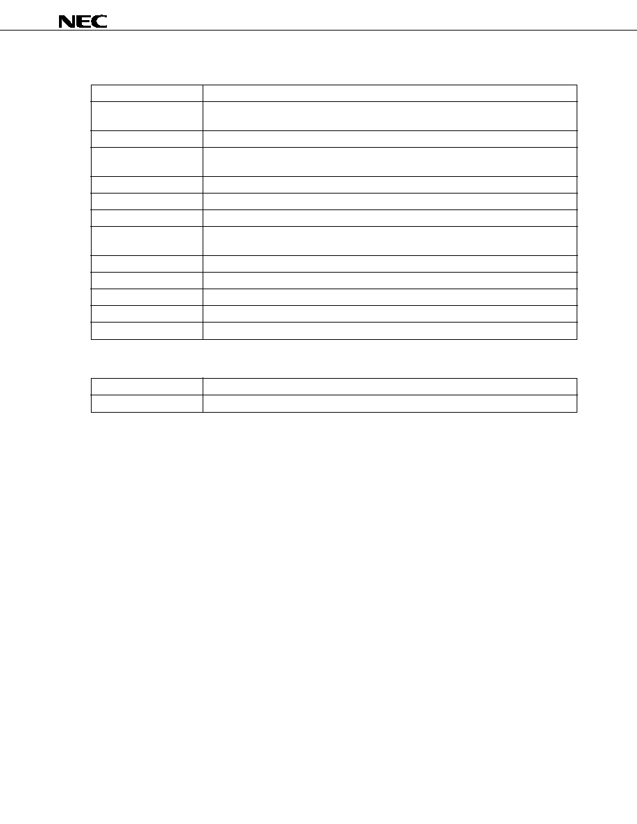
45
Data Sheet U14118EJ1V0DS
µ
PD78F4938A
∑
When IE-784000-R in-circuit emulator is used
IE-784000-R
In-circuit emulator common to 78K/IV Series
IE-70000-98-IF-B
Interface adapter used when PC-9800 series (except notebook type) is used as host machine
IE-70000-98-IF-C
IE-70000-98N-IF
Interface adapter and cable used when PC-9800 series notebook type PC is used as host machine
IE-70000-PC-IF-B
Interface adapter used when IBM PC/AT or compatible is used as host machine
IE-70000-PC-IF-C
IE-78000-R-SV3
Interface adapter and cable used when EWS is used as host machine
IE-784937-NS-EM1
Emulation board to emulate
µ
PD784938A Subseries
IE-784000-R-EM
Emulation board common to 78K/IV Series
IE-78K4-R-EX2
Emulation probe conversion board necessary when using IE-784937-NS-EM1 on IE-784000-R.
Not necessary when using IE-784937-R-EM1
EP-78064GF-R
Emulation probe for 100-pin plastic QFP (GF-3BA type)
EV-9200GF-100
Socket to be mounted on a target system board made for 100-pin plastic QFP (GF-3BA type)
ID78K4
Integrated debugger for IE-784000-R
SM78K4
System simulator common to 78K/IV Series
DF784937
Device file for
µ
PD784938A Subseries
(4) Real-time OS
RX78K/IV
Real-time OS for 78K/IV Series
MX78K4
OS for 78K/IV Series
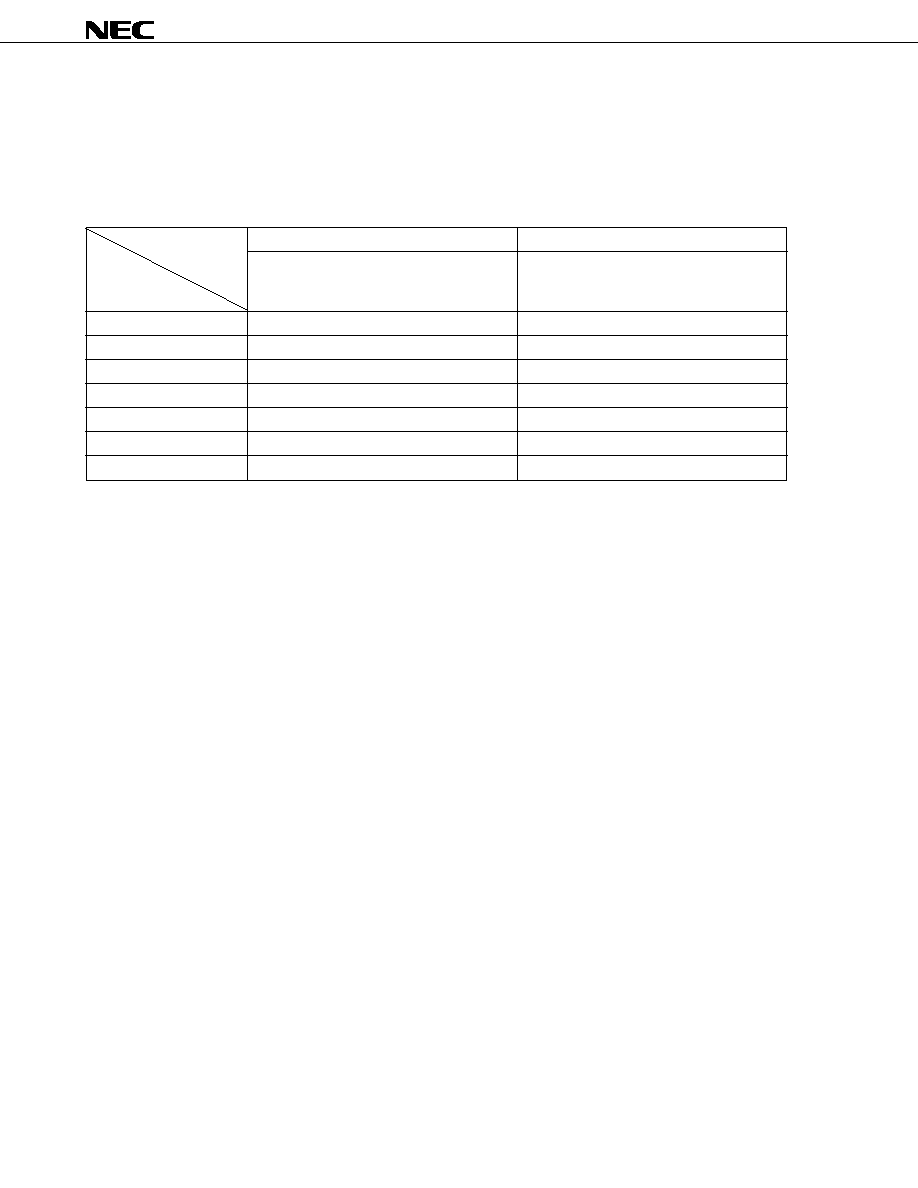
46
Data Sheet U14118EJ1V0DS
µ
PD78F4938A
(5) Cautions on using development tools
∑
The ID78K4-NS, ID78K4, and SM78K4 are used in combination with the DF784937.
∑
The CC78K4 and RX78K/IV are used in combination with the RA78K4 or DF784937.
∑
The Flashpro III, FA-100GF, and NP-100GF are products made by Naito Densei Machida Mfg. Co, Ltd (TEL
+81-44-822-3813).
∑
The host machine and OS suitable for each software are as follows:
Host Machine [OS]
PC
EWS
PC-9800 series [Windows]
HP9000 series 700
TM
[HP-UX
TM
]
IBM PC/AT and compatibles
SPARCstation
TM
[SunOS
TM
, Solaris
TM
]
Software
[Japanese/English Windows]
NEWS
TM
(RISC) [NEWS-OS
TM
]
RA78K4
Note
CC78K4
Note
ID78K4-NS
--
ID78K4
SM78K4
--
RX78K/IV
Note
MX78K4
Note
Note
DOS-based software
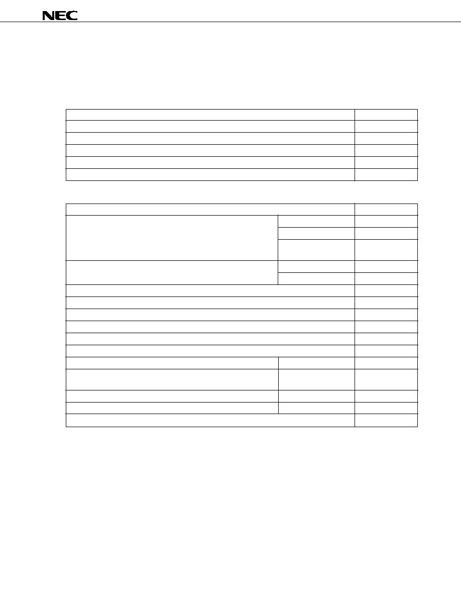
47
Data Sheet U14118EJ1V0DS
µPD78F4938A
APPENDIX B. RELATED DOCUMENTS
The related documents indicated in this publication may include preliminary versions. However, preliminary
versions are not marked as such.
∑
Documents related to devices
Document Name
Document No.
µPD784935A, 784936A, 784937A, 784938A Data Sheet
Under preparation
µPD78F4938A Data Sheet
This document
µPD784938 Subseries User's Manual Hardware
U13987E
78K/IV Series User's Manual Instructions
U10905E
78K/IV Series Application Note Software Basics
U10095E
∑
Documents related to development tools (user's manuals)
Document Name
Document No.
RA78K4 Assembler Package
Language
U11162E
Operation
U11334E
Structured Assembler
U11743E
Preprocessor
CC78K4 C Compiler
Language
U11571E
Operation
U11572E
PG-FP3 Flash Memory Programmer
U13502E
IE-78K4-NS
U13556E
IE-784000-R
U12903E
IE-784937-R-EM1
To be prepared
IE-784937-NS-EM1
To be prepared
EP-78064
EEU-1469
SM78K4 System Simulator Windows Based
Reference
U10093E
SM78K Series System Simulator
External Part User Open
U10092E
Interface Specifications
ID78K4 Integrated Debugger Windows Based
Reference
U10440E
ID78K4-NS Integrated Debugger Windows Based
Reference
U12796E
Project Manager Ver. 3.12 or Later Windows Based
U14610E
Caution The related documents listed above are subject to change without notice. Be sure to use the latest
version of each document for designing.

48
Data Sheet U14118EJ1V0DS
µPD78F4938A
∑
Documents related to embedded software (user's manuals)
Document Name
Document No.
78K/IV Series Real-Time OS
Fundamental
U10603E
Installation
U10604E
∑
Other documents
Document Name
Document No.
SEMICONDUCTOR SELECTION GUIDE Products & Packages (CD-ROM)
X13769X
Semiconductor Device Mounting Technology Manual
C10535E
Quality Grades on NEC Semiconductor Devices
C11531E
NEC Semiconductor Device Reliability/Quality Control System
U10983E
Guide to Prevent Damage for Semiconductor Devices by Electrostatic Discharge (ESD)
C11892E
Caution The related documents listed above are subject to change without notice. Be sure to use the latest
version of each document for designing.

49
Data Sheet U14118EJ1V0DS
µPD78F4938A
[MEMO]
50
Data Sheet U14118EJ1V0DS
µPD78F4938A
NOTES FOR CMOS DEVICES
1
PRECAUTION AGAINST ESD FOR SEMICONDUCTORS
Note:
Strong electric field, when exposed to a MOS device, can cause destruction of the gate oxide and
ultimately degrade the device operation. Steps must be taken to stop generation of static electricity
as much as possible, and quickly dissipate it once, when it has occurred. Environmental control
must be adequate. When it is dry, humidifier should be used. It is recommended to avoid using
insulators that easily build static electricity. Semiconductor devices must be stored and transported
in an anti-static container, static shielding bag or conductive material. All test and measurement
tools including work bench and floor should be grounded. The operator should be grounded using
wrist strap. Semiconductor devices must not be touched with bare hands. Similar precautions need
to be taken for PW boards with semiconductor devices on it.
2
HANDLING OF UNUSED INPUT PINS FOR CMOS
Note:
No connection for CMOS device inputs can be cause of malfunction. If no connection is provided
to the input pins, it is possible that an internal input level may be generated due to noise, etc., hence
causing malfunction. CMOS devices behave differently than Bipolar or NMOS devices. Input levels
of CMOS devices must be fixed high or low by using a pull-up or pull-down circuitry. Each unused
pin should be connected to V
DD
or GND with a resistor, if it is considered to have a possibility of
being an output pin. All handling related to the unused pins must be judged device by device and
related specifications governing the devices.
3
STATUS BEFORE INITIALIZATION OF MOS DEVICES
Note:
Power-on does not necessarily define initial status of MOS device. Production process of MOS
does not define the initial operation status of the device. Immediately after the power source is
turned ON, the devices with reset function have not yet been initialized. Hence, power-on does
not guarantee out-pin levels, I/O settings or contents of registers. Device is not initialized until the
reset signal is received. Reset operation must be executed immediately after power-on for devices
having reset function.
Windows is either a registered trademark or a trademark of Microsoft Corporation in the United States and/
or other countries.
PC/AT is a trademark of International Business Machines Corporation.
HP9000 series 700 and HP-UX are trademarks of Hewlett-Packard Company.
SPARCstation is a trademark of SPARC International, Inc.
Solaris and SunOS are trademarks of Sun Microsystems, Inc.
NEWS and NEWS-OS are trademarks of Sony Corporation.
EEPROM, FIP, and IEBus are trademarks of NEC Corporation.

51
Data Sheet U14118EJ1V0DS
µPD78F4938A
Regional Information
Some information contained in this document may vary from country to country. Before using any NEC
product in your application, pIease contact the NEC office in your country to obtain a list of authorized
representatives and distributors. They will verify:
∑
Device availability
∑
Ordering information
∑
Product release schedule
∑
Availability of related technical literature
∑
Development environment specifications (for example, specifications for third-party tools and
components, host computers, power plugs, AC supply voltages, and so forth)
∑
Network requirements
In addition, trademarks, registered trademarks, export restrictions, and other legal issues may also vary
from country to country.
NEC Electronics Inc. (U.S.)
Santa Clara, California
Tel: 408-588-6000
800-366-9782
Fax: 408-588-6130
800-729-9288
NEC Electronics (Germany) GmbH
Duesseldorf, Germany
Tel: 0211-65 03 02
Fax: 0211-65 03 490
NEC Electronics (UK) Ltd.
Milton Keynes, UK
Tel: 01908-691-133
Fax: 01908-670-290
NEC Electronics Italiana s.r.l.
Milano, Italy
Tel: 02-66 75 41
Fax: 02-66 75 42 99
NEC Electronics (Germany) GmbH
Benelux Office
Eindhoven, The Netherlands
Tel: 040-2445845
Fax: 040-2444580
NEC Electronics (France) S.A.
Velizy-Villacoublay, France
Tel: 01-3067-5800
Fax: 01-3067-5899
NEC Electronics (France) S.A.
Madrid Office
Madrid, Spain
Tel: 091-504-2787
Fax: 091-504-2860
NEC Electronics (Germany) GmbH
Scandinavia Office
Taeby, Sweden
Tel: 08-63 80 820
Fax: 08-63 80 388
NEC Electronics Hong Kong Ltd.
Hong Kong
Tel: 2886-9318
Fax: 2886-9022/9044
NEC Electronics Hong Kong Ltd.
Seoul Branch
Seoul, Korea
Tel: 02-528-0303
Fax: 02-528-4411
NEC Electronics Singapore Pte. Ltd.
Novena Square, Singapore
Tel: 253-8311
Fax: 250-3583
NEC Electronics Taiwan Ltd.
Taipei, Taiwan
Tel: 02-2719-2377
Fax: 02-2719-5951
NEC do Brasil S.A.
Electron Devices Division
Guarulhos-SP, Brasil
Tel: 11-6462-6810
Fax: 11-6462-6829
J01.2

µ
PD78F4938A
M8E 00.4
The information in this document is current as of December, 2000. The information is subject to
change without notice. For actual design-in, refer to the latest publications of NEC's data sheets or
data books, etc., for the most up-to-date specifications of NEC semiconductor products. Not all
products and/or types are available in every country. Please check with an NEC sales representative
for availability and additional information.
No part of this document may be copied or reproduced in any form or by any means without prior
written consent of NEC. NEC assumes no responsibility for any errors that may appear in this document.
NEC does not assume any liability for infringement of patents, copyrights or other intellectual property rights of
third parties by or arising from the use of NEC semiconductor products listed in this document or any other
liability arising from the use of such products. No license, express, implied or otherwise, is granted under any
patents, copyrights or other intellectual property rights of NEC or others.
Descriptions of circuits, software and other related information in this document are provided for illustrative
purposes in semiconductor product operation and application examples. The incorporation of these
circuits, software and information in the design of customer's equipment shall be done under the full
responsibility of customer. NEC assumes no responsibility for any losses incurred by customers or third
parties arising from the use of these circuits, software and information.
While NEC endeavours to enhance the quality, reliability and safety of NEC semiconductor products, customers
agree and acknowledge that the possibility of defects thereof cannot be eliminated entirely. To minimize
risks of damage to property or injury (including death) to persons arising from defects in NEC
semiconductor products, customers must incorporate sufficient safety measures in their design, such as
redundancy, fire-containment, and anti-failure features.
NEC semiconductor products are classified into the following three quality grades:
"Standard", "Special" and "Specific". The "Specific" quality grade applies only to semiconductor products
developed based on a customer-designated "quality assurance program" for a specific application. The
recommended applications of a semiconductor product depend on its quality grade, as indicated below.
Customers must check the quality grade of each semiconductor product before using it in a particular
application.
"Standard": Computers, office equipment, communications equipment, test and measurement equipment, audio
and visual equipment, home electronic appliances, machine tools, personal electronic equipment
and industrial robots
"Special":
Transportation equipment (automobiles, trains, ships, etc.), traffic control systems, anti-disaster
systems, anti-crime systems, safety equipment and medical equipment (not specifically designed
for life support)
"Specific": Aircraft, aerospace equipment, submersible repeaters, nuclear reactor control systems, life
support systems and medical equipment for life support, etc.
The quality grade of NEC semiconductor products is "Standard" unless otherwise expressly specified in NEC's
data sheets or data books, etc. If customers wish to use NEC semiconductor products in applications not
intended by NEC, they must contact an NEC sales representative in advance to determine NEC's willingness
to support a given application.
(Note)
(1) "NEC" as used in this statement means NEC Corporation and also includes its majority-owned subsidiaries.
(2) "NEC semiconductor products" means any semiconductor product developed or manufactured by or for
NEC (as defined above).
∑
∑
∑
∑
∑
∑