Document Outline
- COVER
- DESCRIPTION
- FEATURES
- APPLICATIONS
- ORDERING INFORMATION
- 78K/IV SERIES LINEUP
- OVERVIEW OF FUNCTIONS
- 1. DIFFERENCES AMONG MODELS IN uPD784216A, 784216AY/784218A, 784218AY SUBSERIES
- 2. MAJOR DIFFERENCES FROM uPD78078Y SUBSERIES
- 3. PIN CONFIGURATION (TOP VIEW)
- 4. BLOCK DIAGRAM
- 5. PIN FUNCTIONS
- 5.1 Port Pins
- 5.2 Non-Port Pins
- 5.3 Pin I/O Circuits and Recommended Connections of Unused Pins
- 6. CPU ARCHITECTURE
- 6.1 Memory Space
- 6.2 CPU Registers
- 6.2.1 General-purpose registers
- 6.2.2 Control registers
- 6.2.3 Special function registers (SFRs)
- 7. PERIPHERAL HARDWARE FUNCTIONS
- 7.1 Ports
- 7.2 Clock Generator
- 7.3 Real-Time Output Port
- 7.4 Timer/Event Counter
- 7.5 A/D Converter
- 7.6 D/A Converter
- 7.7 Serial Interface
- 7.7.1 Asynchronous serial interface/3-wire serial I/O (UART/IOE)
- 7.7.2 Clocked serial interface (CSI)
- 7.8 Clock Output Function
- 7.9 Buzzer Output Function
- 7.10 Edge Detection Function
- 7.11 Watch Timer
- 7.12 Watchdog Timer
- 8. INTERRUPT FUNCTIONS
- 8.1 Interrupt Sources
- 8.2 Vectored Interrupt
- 8.3 Context Switching
- 8.4 Macro Service
- 8.5 Application Example of Macro Service
- 9. LOCAL BUS INTERFACE
- 9.1 Memory Expansion
- 9.2 Programmable Wait
- 10. STANDBY FUNCTION
- 11. RESET FUNCTION
- 12. INSTRUCTION SET
- 13. ELECTRICAL SPECIFICATIONS
- 14. PACKAGE DRAWINGS
- 15. RECOMMENDED SOLDERING CONDITIONS
- APPENDIX A. DEVELOPMENT TOOLS
- APPENDIX B. RELATED DOCUMENTS
MOS INTEGRATED CIRCUIT
µ
µ
µ
µ
PD784214A, 784215A, 784216A, 784217A, 784218A, 784214AY, 784215AY, 784216AY, 784217AY, 784218AY
16-BIT SINGLE-CHIP MICROCONTROLLERS
Document No. U14121EJ2V0DS00 (2nd edition)
Date Published August 2000 N CP(K)
Printed in Japan
DATA SHEET
DESCRIPTION
The
µ
PD784214A, 784215A, 784216A, 784217A, and 784218A are products of the
µ
PD784216A/784218A
Subseries in the 78K/IV Series. Besides a high-speed and high performance CPU, these controllers have ROM,
RAM, I/O ports, 8-bit resolution A/D and D/A converters, timers, serial interfaces, a real-time output port, interrupt
functions, and various other peripheral hardware.
The
µ
PD784214AY, 784215AY, 784216AY, 784217AY, and 784218AY are based on the
µ
PD784216Y/784218Y
Subseries with the addition of a multimaster-supporting I
2
C bus interface.
The
µ
PD78F4218A and 78F4218AY, products with a flash memory instead of the internal ROM of mask ROM
versions, and various development tools are also available.
Detailed function descriptions are provided in the following user's manuals. Be sure to read them before
designing.
µ
µ
µ
µ
PD784216A, 784216AY Subseries User's Manual Hardware: U13570E
µ
µ
µ
µ
PD784218A, 784218AY Subseries User's Manual Hardware: U12970E
78K/IV Series User's Manual Instructions:
U10905E
FEATURES
∑
78K/IV Series
∑
Supply voltage: V
DD
= 1.8 to 5.5 V
∑
Standby function
∑
Inherits peripheral functions of
µ
PD78078, 78078Y
Subseries
HALT/STOP/IDLE mode
∑
Minimum instruction execution time
160 ns
In low-power consumption mode: HALT/IDLE mode
(with subsystem clock)
(@f
XX
= 12.5 MHz operation with main system clock)
∑
Clock division function
61
µ
s
∑
Watch timer: 1 channel
(@f
XT
= 32.768 kHz operation with subsystem clock)
∑
Watchdog timer: 1 channel
∑
I/O port: 86 pins
∑
Clock output function
∑
Timer/event counter:
∑
16-bit timer/event counter
◊
1 unit
Selectable from f
XX
, f
XX
/2, f
XX
/2
2
, f
XX
/2
3
, f
XX
/2
4
, f
XX
/2
5
,
f
XX
/2
6
, f
XX
/2
7
, f
XT
∑
8-bit timer/event counter
◊
6 units
∑
Buzzer output function
∑
Serial interface: 3 channels
Selectable from f
XX
/2
10
, f
XX
/2
11
, f
XX
/2
12
, f
XX
/2
13
∑
UART/IOE (3-wire serial I/O): 2 channels
∑
A/D converter: 8-bit resolution
◊
8 channels
∑
CSI (3-wire serial I/O, I
2
C bus supporting
multimaster
Note
): 2 channels
∑
D/A converter: 8-bit resolution
◊
2 channels
Note
µ
PD784216AY/784218AY Subseries only
APPLICATIONS
Cellular phones, PHS, cordless telephones, CD-ROM, AV equipment
Unless otherwise specified, references in this document to the
µ
µ
µ
µ
PD784218A, 784218AY refer to the
µ
µ
µ
µ
PD784214A, 784215A, 784216A, 784217A, 784218A, 784214AY, 784215AY, 784216AY, 784217AY, and
784218AY.
The mark shows major revised points.
2000
The information in this document is subject to change without notice. Before using this document, please
confirm that this is the latest version.
Not all devices/types available in every country. Please check with local NEC representative for
availability and additional information.

Data Sheet U14121EJ2V0DS00
2
µ
µ
µ
µ
PD784214A, 784215A, 784216A, 784217A, 784218A, 784214AY, 784215AY, 784216AY, 784217AY, 784218AY
ORDERING INFORMATION
Part Number
Package
Internal ROM (Bytes)
Internal RAM (Bytes)
µ
PD784214AGC-
◊◊◊
-8EU
100-pin plastic LQFP
(fine pitch) (14
◊
14 mm)
96 K
3,584
µ
PD784214AGF-
◊◊◊
-3BA
100-pin plastic QFP
(14
◊
20 mm)
96 K
3,584
µ
PD784215AGC-
◊◊◊
-8EU
100-pin plastic LQFP
(fine pitch) (14
◊
14 mm)
128 K
5,120
µ
PD784215AGF-
◊◊◊
-3BA
100-pin plastic QFP
(14
◊
20 mm)
128 K
5,120
µ
PD784216AGC-
◊◊◊
-8EU
100-pin plastic LQFP
(fine pitch) (14
◊
14 mm)
128 K
8,192
µ
PD784216AGF-
◊◊◊
-3BA
100-pin plastic QFP
(14
◊
20 mm)
128 K
8,192
µ
PD784217AGC-
◊◊◊
-8EU
100-pin plastic LQFP
(fine pitch) (14
◊
14 mm)
192 K
12,800
µ
PD784217AGF-
◊◊◊
-3BA
100-pin plastic QFP
(14
◊
20 mm)
192 K
12,800
µ
PD784218AGC-
◊◊◊
-8EU
100-pin plastic LQFP
(fine pitch) (14
◊
14 mm)
256 K
12,800
µ
PD784218AGF-
◊◊◊
-3BA
100-pin plastic QFP
(14
◊
20 mm)
256 K
12,800
µ
PD784214AYGC-
◊◊◊
-8EU
100-pin plastic LQFP
(fine pitch) (14
◊
14 mm)
96 K
3,584
µ
PD784214AYGF-
◊◊◊
-3BA
100-pin plastic QFP
(14
◊
20 mm)
96 K
3,584
µ
PD784215AYGC-
◊◊◊
-8EU
100-pin plastic LQFP
(fine pitch) (14
◊
14 mm)
128 K
5,120
µ
PD784215AYGF-
◊◊◊
-3BA
100-pin plastic QFP
(14
◊
20 mm)
128 K
5,120
µ
PD784216AYGC-
◊◊◊
-8EU
100-pin plastic LQFP
(fine pitch) (14
◊
14 mm)
128 K
8,192
µ
PD784216AYGF-
◊◊◊
-3BA
100-pin plastic QFP
(14
◊
20 mm)
128 K
8,192
µ
PD784217AYGC-
◊◊◊
-8EU
100-pin plastic LQFP
(fine pitch) (14
◊
14 mm)
192 K
12,800
µ
PD784217AYGF-
◊◊◊
-3BA
100-pin plastic QFP
(14
◊
20 mm)
192 K
12,800
µ
PD784218AYGC-
◊◊◊
-8EU
100-pin plastic LQFP
(fine pitch) (14
◊
14 mm)
256 K
12,800
µ
PD784218AYGF-
◊◊◊
-3BA
100-pin plastic QFP
(14
◊
20 mm)
256 K
12,800
Remark
◊◊◊
indicates ROM code suffix.
Data Sheet U14121EJ2V0DS00
3
µ
µ
µ
µ
PD784214A, 784215A, 784216A, 784217A, 784218A, 784214AY, 784215AY, 784216AY, 784217AY, 784218AY
78K/IV SERIES LINEUP
PD784026
PD784956A
PD784908
PD784915
PD784928
PD784928Y
PD784046
PD784054
PD784216A
PD784216AY
PD784038
PD784038Y
PD784225Y
PD784225
PD784218AY
PD784218A
Enhanced
A/D converter,
16-bit timer, and
power management
Enhanced internal memory capacity
Pin-compatible with the PD784026
Supports I
2
C bus
Supports multimaster I
2
C bus
80-pin, ROM correction added
Supports multimaster I
2
C bus
Enhanced internal memory
capacity, ROM correction added
100-pin, enhanced I/O and
internal memory capacity
On-chip 10-bit A/D converter
For DC inverter control
On-chip IEBus
TM
controller
Software servo control
On-chip analog circuit for VCRs
Enhanced timer
Supports multimaster I
2
C bus
Enhanced functions
of the PD784915
Standard models
ASSP models
Supports multimaster I
2
C bus
: Products in mass-production
: Products under development
µ
µ
PD784976A
On-chip VFD controller/driver
µ
µ
µ
µ
µ
µ
µ
µ
µ
µ
µ
µ
µ
µ
µ
µ
µ
PD784938A
Enhanced functions of the
PD784908, enhanced
internal memory capacity,
ROM correction added.
µ
µ
PD784967
µ
Enhanced functions of the
PD784938A, enhanced
I/O and internal memory
capacity.
µ
Data Sheet U14121EJ2V0DS00
4
µ
µ
µ
µ
PD784214A, 784215A, 784216A, 784217A, 784218A, 784214AY, 784215AY, 784216AY, 784217AY, 784218AY
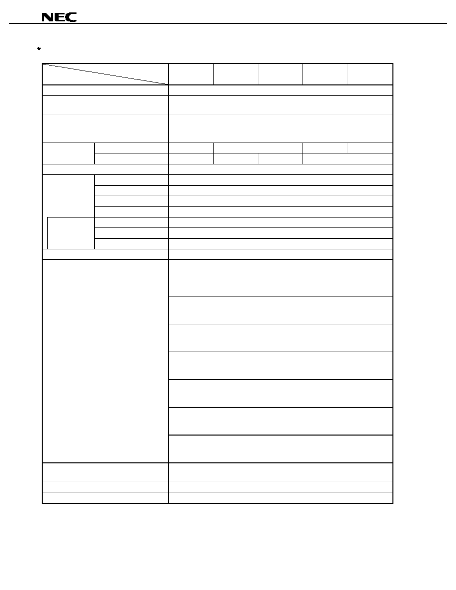
OVERVIEW OF FUNCTIONS (1/2)
Part Number
Item
µ
PD784214A,
µ
PD784214AY
µ
PD784215A,
µ
PD784215AY
µ
PD784216A,
µ
PD784216AY
µ
PD784217A,
µ
PD784217AY
µ
PD784218A,
µ
PD784218AY
Number of basic instructions (mnemonics)
113
General-purpose registers
8 bits
◊
16 registers
◊
8 banks, or 16 bits
◊
8 registers
◊
8 banks (memory
mapping)
Minimum instruction execution time
∑
160 ns/320 ns/640 ns/1,280 ns/2,560 ns (@f
XX
= 12.5 MHz operation with
main system clock)
∑
61
µ
s (@f
XT
= 32.768 kHz operation with subsystem clock)
ROM
96 KB
128 KB
192 KB
256 KB
Internal
memory
RAM
3,584 bytes
5,120 bytes
8,192 bytes
12,800 bytes
Memory space
1 MB with program and data spaces combined
Total
86
CMOS input
8
CMOS I/O
72
I/O ports
N-ch open-drain I/O
6
Pins with pull-up resistor
70
LED direct drive output
22
Pins with
additional
functions
Note 1
Middle-voltage pin
6
Real-time output port
4 bits
◊
2 or 8 bits
◊
1
Timer/event counter:
Timer counter
◊
1
Pulse output
(16-bit)
Capture/compare register
◊
2
∑
PPG output
∑
Square wave output
∑
One-shot pulse output
Timer/event counter 1: Timer counter
◊
1
Pulse output
(8-bit) Compare
register
◊
1
∑
PWM output
∑
Square wave output
Timer/event counter 2: Timer counter
◊
1
Pulse output
(8-bit) Compare
register
◊
1
∑
PWM output
∑
Square wave output
Timer/event counter 5: Timer counter
◊
1
Pulse output
(8-bit) Compare
register
◊
1
∑
PWM output
∑
Square wave output
Timer/event counter 6: Timer counter
◊
1
Pulse output
(8-bit) Compare
register
◊
1
∑
PWM output
∑
Square wave output
Timer/event counter 7: Timer counter
◊
1
Pulse output
(8-bit) Compare
register
◊
1
∑
PWM output
∑
Square wave output
Timer/event counter
Timer/event counter 8: Timer counter
◊
1
Pulse output
(8-bit) Compare
register
◊
1
∑
PWM output
∑
Square wave output
Serial interface
∑
UART/IOE (3-wire serial I/O): 2 channels (on-chip baud rate generator)
∑
CSI (3-wire serial I/O, multimaster supporting I
2
C bus
Note 2
): 1 channel
A/D converter
8-bit resolution
◊
8 channels
D/A converter
8-bit resolution
◊
2 channels
Notes 1. Pins with additional functions are included with the I/O pins.
2.
µ
PD784216AY/784218AY Subseries only
Data Sheet U14121EJ2V0DS00
5
µ
µ
µ
µ
PD784214A, 784215A, 784216A, 784217A, 784218A, 784214AY, 784215AY, 784216AY, 784217AY, 784218AY
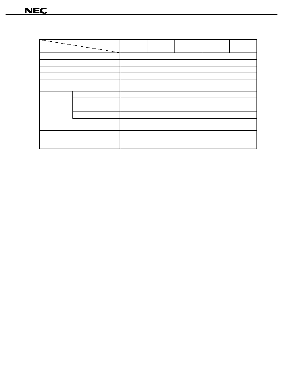
OVERVIEW OF FUNCTIONS (2/2)
Part Number
Item
µ
PD784214A,
µ
PD784214AY
µ
PD784215A,
µ
PD784215AY
µ
PD784216A,
µ
PD784216AY
µ
PD784217A,
µ
PD784217AY
µ
PD784218A,
µ
PD784218AY
Clock output
Selectable from f
XX
, f
XX
/2, f
XX
/2
2
, f
XX
/2
3
, f
XX
/2
4
, f
XX
/2
5
, f
XX
/2
6
, f
XX
/2
7
, f
XT
Buzzer output
Selectable from f
XX
/2
10
, f
XX
/2
11
, f
XX
/2
12
, f
XX
/2
13
Watch timer
1 channel
Watchdog timer
1 channel
Standby
∑
HALT/STOP/IDLE modes
∑
In low power consumption mode (with subsystem clock): HALT/IDLE modes
Hardware sources
29 (internal: 20, external: 9)
Software sources
BRK instruction, BRKCS instruction, operand error
Non-maskable
Internal: 1, external: 1
Interrupt
Maskable
Internal: 19, external: 8
∑
4 programmable priority levels
∑
3 service modes: Vectored interrupt/macro service/context switching
Supply voltage
V
DD
= 1.8 to 5.5 V
Package
100-pin plastic LQFP (fine pitch) (14
◊
14 mm)
100-pin plastic QFP (14
◊
20 mm)

Data Sheet U14121EJ2V0DS00
6
µ
µ
µ
µ
PD784214A, 784215A, 784216A, 784217A, 784218A, 784214AY, 784215AY, 784216AY, 784217AY, 784218AY
CONTENTS
1. DIFFERENCES AMONG MODELS IN
µ
µ
µ
µ
PD784216A, 784216AY/784218A, 784218AY SUBSERIES....... 8
2. MAJOR DIFFERENCES FROM
µ
µ
µ
µ
PD78078Y SUBSERIES ................................................................ 9
3. PIN CONFIGURATION (TOP VIEW).................................................................................................. 10
4. BLOCK DIAGRAM ............................................................................................................................... 13
5. PIN FUNCTIONS .................................................................................................................................. 14
5.1 Port Pins ...................................................................................................................................... 14
5.2 Non-Port Pins .............................................................................................................................. 16
5.3 Pin I/O Circuits and Recommended Connections of Unused Pins ........................................ 18
6. CPU ARCHITECTURE ......................................................................................................................... 22
6.1 Memory Space ............................................................................................................................. 22
6.2 CPU Registers.............................................................................................................................. 29
6.2.1 General-purpose registers ..............................................................................................................29
6.2.2 Control registers..............................................................................................................................30
6.2.3 Special function registers (SFRs)....................................................................................................31
7. PERIPHERAL HARDWARE FUNCTIONS.......................................................................................... 36
7.1 Ports ............................................................................................................................................. 36
7.2 Clock Generator........................................................................................................................... 37
7.3 Real-Time Output Port ................................................................................................................ 39
7.4 Timer/Event Counter ................................................................................................................... 40
7.5 A/D Converter .............................................................................................................................. 42
7.6 D/A Converter .............................................................................................................................. 43
7.7 Serial Interface............................................................................................................................. 44
7.7.1 Asynchronous serial interface/3-wire serial I/O (UART/IOE) ..........................................................45
7.7.2 Clocked serial interface (CSI) .........................................................................................................47
7.8 Clock Output Function................................................................................................................ 49
7.9 Buzzer Output Function.............................................................................................................. 49
7.10 Edge Detection Function .......................................................................................................... 50
7.11 Watch Timer ............................................................................................................................... 50
7.12 Watchdog Timer ........................................................................................................................ 51
8. INTERRUPT FUNCTIONS.................................................................................................................... 52
8.1 Interrupt Sources......................................................................................................................... 52
8.2 Vectored Interrupt ....................................................................................................................... 54
8.3 Context Switching ....................................................................................................................... 55
8.4 Macro Service .............................................................................................................................. 56
8.5 Application Example of Macro Service ..................................................................................... 57

Data Sheet U14121EJ2V0DS00
7
µ
µ
µ
µ
PD784214A, 784215A, 784216A, 784217A, 784218A, 784214AY, 784215AY, 784216AY, 784217AY, 784218AY
9. LOCAL BUS INTERFACE................................................................................................................. 58
9.1 Memory Expansion ..................................................................................................................... 59
9.2 Programmable Wait .................................................................................................................... 59
10. STANDBY FUNCTION ....................................................................................................................... 60
11. RESET FUNCTION ............................................................................................................................ 62
12. INSTRUCTION SET ........................................................................................................................... 63
13. ELECTRICAL SPECIFICATIONS ...................................................................................................... 68
14. PACKAGE DRAWINGS ..................................................................................................................... 88
15. RECOMMENDED SOLDERING CONDITIONS................................................................................ 90
APPENDIX A. DEVELOPMENT TOOLS ................................................................................................ 92
APPENDIX B. RELATED DOCUMENTS................................................................................................ 95
Data Sheet U14121EJ2V0DS00
8
µ
µ
µ
µ
PD784214A, 784215A, 784216A, 784217A, 784218A, 784214AY, 784215AY, 784216AY, 784217AY, 784218AY
1. DIFFERENCES AMONG MODELS IN
µ
µ
µ
µ
PD784216A, 784216AY/784218A, 784218AY
SUBSERIES
The only difference among the
µ
PD784214A, 784215A, 784216A, 784217A, and 784218A lies in the internal
memory capacity.
The
µ
PD784214AY, 784215AY, 784216AY, 784217AY, and 784218AY are models with the addition of an I
2
C bus
control function.
The
µ
PD78F4216A, 78F4216AY, 78F4218A, and 78F4218AY are provided with a 128 KB/256 KB flash memory
instead of the mask ROM of the above models.
These differences are summarized in Table 1-1.
Table 1-1. Differences Among Models in
µ
µ
µ
µ
PD784216A, 784216AY/784218A, 784218AY Subseries
Part Number
Item
µ
PD784214A,
µ
PD784214AY
µ
PD784215A,
µ
PD784215AY
µ
PD784216A,
µ
PD784216AY
µ
PD784217A,
µ
PD784217AY
µ
PD784218A,
µ
PD784218AY
µ
PD78F4216A,
µ
PD78F4216AY
µ
PD78F4218A,
µ
PD78F4218AY
Internal ROM
96 KB
(Mask
ROM)
128 KB (Mask ROM)
192 KB
(Mask
ROM)
256 KB
(Mask
ROM)
128 KB
(Flash
memory)
256 KB
(Flash
memory)
Internal RAM
3,584 bytes
5,120 bytes
8,192 bytes
12,800 bytes
5,120 bytes
12,800
bytes
Internal memory size
switching register
(IMS)
Not provided
Provided
Note
ROM correction
Not provided
Provided
Not
provided
Provided
External access status
function
Not provided
Provided
Not
provided
Provided
Supply voltage
V
DD
= 1.8 to 5.5 V
V
DD
= 1.9 to 5.5 V
Electrical
specifications
Recommended
soldering conditions
Refer to the data sheet for each device.
EXA pin
Not provided
Provided
Not
provided
Provided
TEST pin
Provided
Not provided
V
PP
pin
Not provided
Provided
Note The internal flash memory capacity and internal RAM capacity can be changed using the internal memory
size switching register (IMS).
Caution There are differences in noise immunity and noise radiation between the flash memory and mask
ROM versions. When pre-producing an application set with the flash memory version and then
mass-producing it with the mask ROM version, be sure to conduct sufficient evaluations on the
commercial samples (not engineering samples) of the mask ROM version.
Data Sheet U14121EJ2V0DS00
9
µ
µ
µ
µ
PD784214A, 784215A, 784216A, 784217A, 784218A, 784214AY, 784215AY, 784216AY, 784217AY, 784218AY
2. MAJOR DIFFERENCES FROM
µ
µ
µ
µ
PD78078Y SUBSERIES
Series Name
Item
µ
PD784216A, 784216AY/784218A,
784218AY Subseries
µ
PD78078Y Subseries
CPU
16-bit CPU
8-bit CPU
With main system
clock
160 ns (@12.5 MHz operation)
400 ns (@5.0 MHz operation)
Minimum instruction
execution time
With subsystem clock
61
µ
s (@32.768 kHz operation)
122
µ
s (@32.768 kHz operation)
Memory space
1 MB
64 KB
Total
86
88
CMOS input
8
2
CMOS I/O
72
78
I/O ports
N-ch open-drain I/O
6
8
Pins with pull-up
resistor
70
86
LED direct drive
output
22
16
Pins with
additional
functions
Note 1
Middle-voltage pin
6
8
Timer/counter
∑
16-bit timer/event counter
◊
1 unit
∑
8-bit timer/event counter
◊
6 units
∑
16-bit timer/event counter
◊
1 unit
∑
8-bit timer/event counter
◊
4 units
Serial interface
∑
UART/IOE (3-wire serial I/O)
◊
2
channels
∑
CSI (3-wire serial I/O, multimaster
supporting I
2
C bus
Note 2
)
◊
1 channel
∑
UART/IOE (3-wire serial I/O)
◊
1
channel
∑
CSI (3-wire serial I/O, 2-wire serial
I/O, I
2
C bus)
◊
1 channel
∑
CSI (3-wire serial I/O, 3-wire serial
I/O with automatic transmit/receive
function)
◊
1 channel
NMI pin
Provided
Not provided
Macro service
Provided
Not provided
Context switching
Provided
Not provided
Interrupts
Programmable priority
4 levels
Not provided
Standby function
∑
HALT/STOP/IDLE modes
∑
In low power consumption mode:
HALT/IDLE modes
HALT/STOP modes
Package
∑
100-pin plastic LQFP (fine pitch)
(14
◊
14 mm)
∑
100-pin plastic QFP (14
◊
20 mm)
∑
100-pin plastic LQFP (fine pitch)
(14
◊
14 mm)
∑
100-pin plastic QFP (14
◊
20 mm)
∑
100-pin ceramic WQFN
(14
◊
20 mm) (
µ
PD78P078Y only)
Notes 1. Pins with additional functions are included with the I/O pins.
2.
µ
PD784216AY/784218AY Subseries only
Data Sheet U14121EJ2V0DS00
10
µ
µ
µ
µ
PD784214A, 784215A, 784216A, 784217A, 784218A, 784214AY, 784215AY, 784216AY, 784217AY, 784218AY
3. PIN CONFIGURATION (TOP VIEW)
∑
∑
∑
∑
100-pin plastic LQFP (fine pitch) (14
◊
◊
◊
◊
14 mm)
µ
µ
µ
µ
PD784214AGC-
◊◊◊
◊◊◊
◊◊◊
◊◊◊
-8EU,
µ
µ
µ
µ
PD784215AGC-
◊◊◊
◊◊◊
◊◊◊
◊◊◊
-8EU,
µ
µ
µ
µ
PD784216AGC-
◊◊◊
◊◊◊
◊◊◊
◊◊◊
-8EU,
µ
µ
µ
µ
PD784217AGC-
◊◊◊
◊◊◊
◊◊◊
◊◊◊
-8EU,
µ
µ
µ
µ
PD784218AGC-
◊◊◊
◊◊◊
◊◊◊
◊◊◊
-8EU,
µ
µ
µ
µ
PD784214AYGC-
◊◊◊
◊◊◊
◊◊◊
◊◊◊
-8EU,
µ
µ
µ
µ
PD784215AYGC-
◊◊◊
◊◊◊
◊◊◊
◊◊◊
-8EU,
µ
µ
µ
µ
PD784216AYGC-
◊◊◊
◊◊◊
◊◊◊
◊◊◊
-8EU,
µ
µ
µ
µ
PD784217AYGC-
◊◊◊
◊◊◊
◊◊◊
◊◊◊
-8EU,
µ
µ
µ
µ
PD784218AYGC-
◊◊◊
◊◊◊
◊◊◊
◊◊◊
-8EU
1
2
3
4
5
6
7
8
9
10
11
12
13
14
15
16
17
18
19
20
21
22
23
24
25
75
74
73
72
71
70
69
68
67
66
65
64
63
62
61
60
59
58
57
56
55
54
53
52
51
100
76
P120/RTP0
P121/RTP1
P122/RTP2
P123/RTP3
P124/RTP4
P125/RTP5
P126/RTP6
P127/RTP7
V
DD
X2
X1
V
SS
XT2
XT1
RESET
P00/INTP0
P01/INTP1
P02/INTP2/NMI
P03/INTP3
P04/INTP4
P05/INTP5
P06/INTP6
AV
DD
Note 2
AV
REF0
P10/ANI0
P62/A18
P61/A17
P60/A16
V
SS
P57/A15
P56/A14
P55/A13
P54/A12
P53/A11
P52/A10
P51/A9
P50/A8
P47/AD7
P46/AD6
P45/AD5
P44/AD4
P43/AD3
P42/AD2
P41/AD1
P40/AD0
P87/A7
P86/A6
P85/A5
P84/A4
P83/A3
P95
P94
P93
P92
P91
P90
TEST
Note 1
P37/EXA
Note 5
P36/TI01
P35/TI00
P34/TI2
P33/TI1
P32/TO2
P31/TO1
P30/TO0
P103/TI8/TO8
P102/TI7/TO7
P101/TI6/TO6
P100/TI5/TO5
V
DD
P67/ASTB
P66/WAIT
P65/WR
P64/RD
P63/A19
P11/ANI1
P12/ANI2
P13/ANI3
P14/ANI4
P15/ANI5
P16/ANI6
P17/ANI7
AV
SS
Note 3
P130/ANO0
P131/ANO1
AV
REF1
P70/RxD2/SI2
P71/TxD2/SO2
P72/ASCK2/SCK2
P20/RxD1/SI1
P21/TxD1/SO1
P22/ASCK1/SCK1
P23/PCL
P24/BUZ
P25/SI0/SDA0
Note 4
P26/SO0
P27/SCK0/SCL0
Note 4
P80/A0
P81/A1
P82/A2
77
78
79
80
81
82
83
84
85
86
87
88
89
90
91
92
93
94
95
96
97
98
99
26
50
49
48
47
46
45
44
43
42
41
40
39
38
37
36
35
34
33
32
31
30
29
28
27
Notes 1. Connect the TEST pin to V
SS
directly or via a pull-down resistor. For the pull-down connection, it is
recommended to use a resistor with a resistance ranging from 470
to 10 k
.
2. Connect the AV
DD
pin to V
DD
.
3. Connect the AV
SS
pin to V
SS
.
4. The SCL0 and SDA0 pins are available in
µ
PD784216AY/784218AY Subseries products only.
5. The EXA pin is available in
µ
PD784218A, 784218AY Subseries products only.
Data Sheet U14121EJ2V0DS00
11
µ
µ
µ
µ
PD784214A, 784215A, 784216A, 784217A, 784218A, 784214AY, 784215AY, 784216AY, 784217AY, 784218AY
∑
∑
∑
∑
100-pin plastic QFP (14
◊
◊
◊
◊
20 mm)
µ
µ
µ
µ
PD784214AGF-
◊◊◊
◊◊◊
◊◊◊
◊◊◊
-3BA,
µ
µ
µ
µ
PD784215AGF-
◊◊◊
◊◊◊
◊◊◊
◊◊◊
-3BA,
µ
µ
µ
µ
PD784216AGF-
◊◊◊
◊◊◊
◊◊◊
◊◊◊
-3BA,
µ
µ
µ
µ
PD784217AGF-
◊◊◊
◊◊◊
◊◊◊
◊◊◊
-3BA,
µ
µ
µ
µ
PD784218AGF-
◊◊◊
◊◊◊
◊◊◊
◊◊◊
-3BA,
µ
µ
µ
µ
PD784214AYGF-
◊◊◊
◊◊◊
◊◊◊
◊◊◊
-3BA,
µ
µ
µ
µ
PD784215AYGF-
◊◊◊
◊◊◊
◊◊◊
◊◊◊
-3BA,
µ
µ
µ
µ
PD784216AYGF-
◊◊◊
◊◊◊
◊◊◊
◊◊◊
-3BA,
µ
µ
µ
µ
PD784217AYGF-
◊◊◊
◊◊◊
◊◊◊
◊◊◊
-3BA,
µ
µ
µ
µ
PD784218AYGF-
◊◊◊
◊◊◊
◊◊◊
◊◊◊
-3BA
100
V
SS
P57/A15
P56/A14
P55/A13
P54/A12
P53/A11
P52/A10
P51/A9
P50/A8
P47/AD7
P46/AD6
P45/AD5
P44/AD4
P43/AD3
P42/AD2
P41/AD1
P40/AD0
P87/A7
P86/A6
P85/A5
81
82
83
84
85
86
87
88
89
90
91
92
93
94
95
96
97
98
99
80
79
78
77
76
75
74
73
72
71
70
69
68
67
66
65
64
63
62
61
60
59
58
57
56
55
54
53
52
51
P84/A4
P83/A3
P82/A2
P81/A1
P80/A0
P27/SCK0/SCL0
Note 4
P26/SO0
P25/SI0/SDA0
Note 4
P24/BUZ
P23/PCL
P22/ASCK1/SCK1
P21/TxD1/SO1
P20/RxD1/SI1
P72/ASCK2/SCK2
P71/TxD2/SO2
P70/RxD2/SI2
AV
REF1
P131/ANO1
P130/ANO0
AV
SS
Note 3
P17/ANI7
P16/ANI6
P15/ANI5
P14/ANI4
P13/ANI3
P12/ANI2
P11/ANI1
P10/ANI0
AV
REF0
AV
DD
Note 2
1
2
3
4
5
6
7
8
9
10
11
12
13
14
15
16
17
18
19
20
21
22
23
24
25
26
27
28
29
30
P60/A16
P61/A17
P62/A18
P63/A19
P64/RD
P65/WR
P66/WAIT
P67/ASTB
V
DD
P100/TI5/TO5
P101/TI6/TO6
P102/TI7/TO7
P103/TI8/TO8
P30/TO0
P31/TO1
P32/TO2
P33/TI1
P34/TI2
P35/TI00
P36/TI01
P37/EXA
Note 5
TEST
Note 1
P90
P91
P92
P93
P94
P95
P120/RTP0
P121/RTP1
P122/RTP2
P123/RTP3
P124/RTP4
P125/RTP5
P126/RTP6
P127/RTP7
V
DD
X2
X1
V
SS
XT2
XT1
RESET
P00/INTP0
P01/INTP1
P02/INTP2/NMI
P03/INTP3
P04/INTP4
P05/INTP5
P06/INTP6
31
50
49
48
47
46
45
44
43
42
41
40
39
38
37
36
35
34
33
32
Notes 1. Connect the TEST pin to V
SS
directly or via a pull-down resistor. For the pull-down connection, it is
recommended to use a resistor with a resistance ranging from 470
to 10 k
.
2. Connect the AV
DD
pin to V
DD
.
3. Connect the AV
SS
pin to V
SS
.
4. The SCL0 and SDA0 pins are available in
µ
PD784216AY/784218AY Subseries products only.
5. The EXA pin is available in
µ
PD784218A, 784218AY Subseries products only.

Data Sheet U14121EJ2V0DS00
12
µ
µ
µ
µ
PD784214A, 784215A, 784216A, 784217A, 784218A, 784214AY, 784215AY, 784216AY, 784217AY, 784218AY
A0 to A19:
Address Bus
P120 to P127:
Port 12
AD0 to AD7:
Address/Data Bus
P130, P131:
Port 13
ANI0 to ANI7:
Analog Input
PCL:
Programmable Clock
ANO0, ANO1:
Analog Output
RD:
Read Strobe
ASCK1, ASCK2:
Asynchronous Serial Clock
RESET:
Reset
ASTB:
Address Strobe
RTP0 to RTP7:
Real-time Output Port
AV
DD
:
Analog Power Supply
RxD1, RxD2:
Receive Data
AV
REF0
, AV
REF1
:
Analog Reference Voltage
SCK0 to SCK2:
Serial Clock
AV
SS
:
Analog Ground
SCL0
Note 1
:
Serial Clock
BUZ:
Buzzer Clock
SDA0
Note 1
:
Serial Data
EXA
Note 2
:
External Access Status Output
SI0 to SI2:
Serial Input
INTP0 to INTP6:
Interrupt from Peripherals
SO0 to SO2:
Serial Output
NMI:
Non-maskable Interrupt
TEST:
Test
P00 to P06:
Port 0
TI00, TI01,
P10 to P17:
Port 1
TI1, TI2, TI5 to TI8:
Timer Input
P20 to P27:
Port 2
TO0 to TO2, TO5 to TO8: Timer Output
P30 to P37:
Port 3
TxD1, TxD2:
Transmit Data
P40 to P47:
Port 4
V
DD
:
Power Supply
P50 to P57:
Port 5
V
SS
:
Ground
P60 to P67:
Port 6
WAIT:
Wait
P70 to P72:
Port 7
WR:
Write Strobe
P80 to P87:
Port 8
X1, X2:
Crystal (Main System Clock)
P90 to P95:
Port 9
XT1, XT2:
Crystal (Subsystem Clock)
P100 to P103:
Port 10
Notes 1. The SCL0 and SDA0 pins are available in
µ
PD784216AY/784218AY Subseries products only.
2. The EXA pin is available in
µ
PD784218A, 784218AY Subseries products only.
Data Sheet U14121EJ2V0DS00
13
µ
µ
µ
µ
PD784214A, 784215A, 784216A, 784217A, 784218A, 784214AY, 784215AY, 784216AY, 784217AY, 784218AY
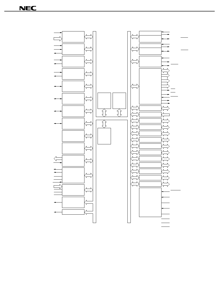
4. BLOCK DIAGRAM
INTP2/NMI
INTP0, INTP1,
INTP3 to INTP6
Programmable
interrupt
controller
Real-time
output port
Timer/event
counter 7
(8 bits)
Timer/event
counter 6
(8 bits)
Timer/event
counter 5
(8 bits)
Timer/event
counter 2
(8 bits)
Timer/event
counter 1
(8 bits)
Timer/event
counter
(16 bits)
Watch timer
Timer/event
counter 8
(8 bits)
Watchdog timer
TI00
TI01
TO0
TI1
TO1
TI2
TO2
TI5/TO5
TI6/TO6
TI7/TO7
TI8/TO8
NMI/INTP2
RTP0 to RTP7
Clock output
control
A/D
converter
AV
DD
AV
SS
PCL
BUZ
AV
REF0
ANI0 to ANI7
D/A
converter
ANO0
AV
SS
P03/INTP3
AV
REF1
ANO1
78K/IV
CPU Core
ROM
RAM
Baud-rate
generator
RxD1/SI1
TxD1/SO1
ASCK1/SCK1
RxD2/SI2
TxD2/SO2
ASCK2/SCK2
SI0/SDA0
SO0
SCK0/SCL0
Bus I/F
UART/IOE1
RD
ASTB
WR
WAIT
A0 to A7
AD0 to AD7
A8 to A15
A16 to A19
Port 1
P10 to P17
Port 0
P00 to P06
Port 2
P20 to P27
Port 3
P30 to P37
Port 4
P40 to P47
Port 5
P50 to P57
Port 6
P60 to P67
Port 7
P70 to P72
Port 8
P80 to P87
Port 9
P90 to P95
Port 10
P100 to P103
Port 12
P120 to P127
Port 13
P130, P131
Buzzer output
System control
RESET
XT2
X1
XT1
X2
V
SS
V
DD
TEST
Clocked
serial
interface
Note 1
Baud-rate
generator
UART/IOE2
EXA
Note 2
Notes 1. This function supports the I
2
C bus interface and is available in
µ
PD784216AY/784218AY Subseries
products only.
2. The EXA pin is available in
µ
PD784218A, 784218AY Subseries products only.
Remark The internal ROM and RAM capacities differ depending on the product.
Data Sheet U14121EJ2V0DS00
14
µ
µ
µ
µ
PD784214A, 784215A, 784216A, 784217A, 784218A, 784214AY, 784215AY, 784216AY, 784217AY, 784218AY
5. PIN FUNCTIONS
5.1 Port Pins (1/2)
Pin Name
I/O
Alternate Function
Function
P00
INTP0
P01
INTP1
P02
INTP2/NMI
P03
INTP3
P04
INTP4
P05
INTP5
P06
I/O
INTP6
Port 0 (P0):
∑
7-bit I/O port
∑
Input/output can be specified in 1-bit units.
∑
Whether specifying input mode or output mode, use of an on-chip
pull-up resistor can be specified in 1-bit units by means of
software.
P10 to P17
Input
ANI0 to ANI7
Port 1 (P1):
∑
8-bit input only port
P20
RxD1/SI1
P21
TxD1/SO1
P22
ASCK1/SCK1
P23
PCL
P24
BUZ
P25
SI0/SDA0
Note 1
P26
SO0
P27
I/O
SCK0/SCL0
Note 1
Port 2 (P2):
∑
8-bit I/O port
∑
Input/output can be specified in 1-bit units.
∑
Whether specifying input mode or output mode, use of an on-chip
pull-up resistor can be specified in 1-bit units by means of
software.
P30
TO0
P31
TO1
P32
TO2
P33
TI1
P34
TI2
P35
TI00
P36
TI01
P37
I/O
EXA
Note 2
Port 3 (P3):
∑
8-bit I/O port
∑
Input/output can be specified in 1-bit units.
∑
Whether specifying input mode or output mode, use of an on-chip
pull-up resistor can be specified in 1-bit units by means of
software.
P40 to P47
I/O
AD0 to AD7
Port 4 (P4):
∑
8-bit I/O port
∑
Input/output can be specified in 1-bit units.
∑
All pins set in input mode can be connected to on-chip pull-up
resistors by means of software.
∑
LEDs can be driven directly.
P50 to P57
I/O
A8 to A15
Port 5 (P5):
∑
8-bit I/O port
∑
Input/output can be specified in 1-bit units.
∑
All pins set in input mode can be connected to on-chip pull-up
resistors by means of software.
∑
LEDs can be driven directly.
Notes 1. This function is available in
µ
PD784216AY/784218AY Subseries products only.
2. This function is available in
µ
PD784218A, 784218AY Subseries products only.
Data Sheet U14121EJ2V0DS00
15
µ
µ
µ
µ
PD784214A, 784215A, 784216A, 784217A, 784218A, 784214AY, 784215AY, 784216AY, 784217AY, 784218AY
5.1 Port Pins (2/2)
Pin Name
I/O
Alternate Function
Function
P60
A16
P61
A17
P62
A18
P63
A19
P64
RD
P65
WR
P66
WAIT
P67
I/O
ASTB
Port 6 (P6):
∑
8-bit I/O port
∑
Input/output can be specified in 1-bit units.
∑
All pins set in input mode can be connected to on-chip pull-up
resistors by means of software.
P70
RxD2/SI2
P71
TxD2/SO2
P72
I/O
ASCK2/SCK2
Port 7 (P7):
∑
3-bit I/O port
∑
Input/output can be specified in 1-bit units.
∑
Whether specifying input mode or output mode, use of an on-chip
pull-up resistor can be specified in 1-bit units by means of
software.
P80 to P87
I/O
A0 to A7
Port 8 (P8):
∑
8-bit I/O port
∑
Input/output can be specified in 1-bit units.
∑
Whether specifying input mode or output mode, use of an on-chip
pull-up resistor can be specified in 1-bit units by means of
software.
∑
The interrupt control flag (KRIF) is set to 1 when a falling edge is
detected at a pin of this port.
P90 to P95
I/O
-
Port 9 (P9):
∑
N-ch open-drain middle-voltage I/O port
∑
6-bit I/O port
∑
Input/output can be specified in 1-bit units.
∑
LEDs can be driven directly.
P100
TI5/TO5
P101
TI6/TO6
P102
TI7/TO7
P103
I/O
TI8/TO8
Port 10 (P10):
∑
4-bit I/O port
∑
Input/output can be specified in 1-bit units.
∑
Whether specifying input mode or output mode, use of an on-chip
pull-up resistor can be specified in 1-bit units by means of
software.
P120 to P127
I/O
RTP0 to RTP7
Port 12 (P12):
∑
8-bit I/O port
∑
Input/output can be specified in 1-bit units.
∑
Whether specifying input mode or output mode, use of an on-chip
pull-up resistor can be specified in 1-bit units by means of
software.
P130, P131
I/O
ANO0, ANO1
Port 13 (P13):
∑
2-bit I/O port
∑
Input/output can be specified in 1-bit units.
Data Sheet U14121EJ2V0DS00
16
µ
µ
µ
µ
PD784214A, 784215A, 784216A, 784217A, 784218A, 784214AY, 784215AY, 784216AY, 784217AY, 784218AY
5.2
Non-Port Pins (1/2)
Pin Name
I/O
Alternate Function
Function
TI00
P35
External count clock input to 16-bit timer counter
TI01
P36
Capture trigger signal input to capture/compare register 00
TI1
P33
External count clock input to 8-bit timer counter 1
TI2
P34
External count clock input to 8-bit timer counter 2
TI5
P100/TO5
External count clock input to 8-bit timer counter 5
TI6
P101/TO6
External count clock input to 8-bit timer counter 6
TI7
P102/TO7
External count clock input to 8-bit timer counter 7
TI8
Input
P103/TO8
External count clock input to 8-bit timer counter 8
TO0
P30
16-bit timer output (shared by 14-bit PWM output)
TO1
P31
TO2
P32
TO5
P100/TI5
TO6
P101/TI6
TO7
P102/TI7
TO8
Output
P103/TI8
8-bit timer output (shared by 8-bit PWM output)
RxD1
P20/SI1
Serial data input (UART1)
RxD2
Input
P70/SI2
Serial data input (UART2)
TxD1
P21/SO1
Serial data output (UART1)
TxD2
Output
P71/SO2
Serial data output (UART2)
ASCK1
P22/SCK1
Baud rate clock input (UART1)
ASCK2
Input
P72/SCK2
Baud rate clock input (UART2)
SI0
P25/SDA0
Note
Serial data input (3-wire serial I/O 0)
SI1
P20/RxD1
Serial data input (3-wire serial I/O 1)
SI2
Input
P70/RxD2
Serial data input (3-wire serial I/O 2)
SO0
P26
Serial data output (3-wire serial I/O 0)
SO1
P21/TxD1
Serial data output (3-wire serial I/O 1)
SO2
Output
P71/TxD2
Serial data output (3-wire serial I/O 2)
SDA0
P25/SI0
Serial data input/output (I
2
C bus)
SCK0
P27/SCL0
Note
Serial clock input/output (3-wire serial I/O 0)
SCK1
P22/ASCK1
Serial clock input/output (3-wire serial I/O 1)
SCK2
P72/ASCK2
Serial clock input/output (3-wire serial I/O 2)
SCL0
I/O
P27/SCK0
Serial clock input/output (I
2
C bus)
NMI
P02/INTP2
Non-maskable interrupt request input
INTP0
P00
INTP1
P01
INTP2
P02/NMI
INTP3
P03
INTP4
P04
INTP5
P05
INTP6
Input
P06
External interrupt request input
Note This function is available in
µ
PD784216AY/784218AY Subseries products only.
Data Sheet U14121EJ2V0DS00
17
µ
µ
µ
µ
PD784214A, 784215A, 784216A, 784217A, 784218A, 784214AY, 784215AY, 784216AY, 784217AY, 784218AY
5.2 Non-Port Pins (2/2)
Pin Name
I/O
Alternate Function
Function
PCL
Output
P23
Clock output (for trimming main system clock and subsystem clock)
BUZ
Output
P24
Buzzer output
RTP0 to RTP7
Output
P120 to P127
Real-time output port that outputs data in synchronization with
trigger
AD0 to AD7
I/O
P40 to P47
Lower address/data bus for expanding memory externally
A0 to A7
P80 to P87
Lower address bus for expanding memory externally
A8 to A15
P50 to P57
Middle address bus for expanding memory externally
A16 to A19
Output
P60 to P63
Higher address bus for expanding memory externally
RD
P64
Strobe signal output for reading from external memory
WR
Output
P65
Strobe signal output for writing to external memory
WAIT
Input
P66
Wait insertion at external memory access
ASTB
Output
P67
Strobe output that externally latches address information output to
ports 4 through 6 and 8 to access external memory
EXA
Note
Output
P37
Status signal output at external memory access
RESET
Input
-
System reset input
X1
Input
X2
-
-
Connecting crystal resonator for main system clock oscillation
XT1
Input
XT2
-
-
Connecting crystal resonator for subsystem clock oscillation
ANI0 to ANI7
Input
P10 to P17
A/D converter analog input
ANO0, ANO1
Output
P130, P131
D/A converter analog output
AV
REF0
A/D converter reference voltage input
AV
REF1
D/A converter reference voltage input
AV
DD
A/D converter positive power supply. Connect to V
DD
.
AV
SS
GND for A/D converter and D/A converter. Connect to V
SS
.
V
DD
Positive power supply
V
SS
GND
TEST
-
-
Connect this pin to V
SS
directly or via a pull-down resistor. For the
pull-down connection, it is recommended to use a resistor with a
resistance ranging from 470
to 10 k
(this pin is for IC test).
Note This function is available in
µ
PD784218A, 784218AY Subseries products only.
Data Sheet U14121EJ2V0DS00
18
µ
µ
µ
µ
PD784214A, 784215A, 784216A, 784217A, 784218A, 784214AY, 784215AY, 784216AY, 784217AY, 784218AY
5.3 Pin I/O Circuits and Recommended Connections of Unused Pins
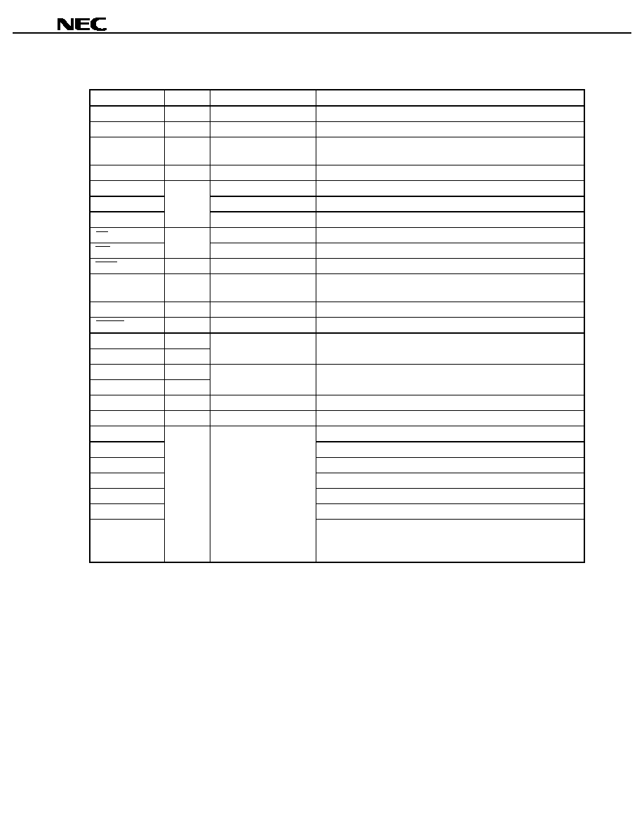
The input/output circuit type of each pin and recommended connections of unused pins are shown in Table 5-1.
For each type of input/output circuit, refer to Figure 5-1.
Table 5-1. Types of Pin Input/Output Circuits and Recommended Connection of Unused Pins (1/2)
Pin Name
I/O Circuit Type
I/O
Recommended Connection of Unused Pins
P00/INTP0
P01/INTP1
P02/INTP2/NMI
P03/INTP3 to P06/INTP6
8-N
I/O
Input:
Independently connect to V
SS
via a resistor
Output: Leave open
P10/ANI0 to P17/ANI7
9
Input
Connect to V
SS
or V
DD
P20/RxD1/SI1
10-K
P21/TxD1/SO1
10-L
P22/ASCK1/SCK1
10-K
P23/PCL
P24/BUZ
10-L
P25/SI0/SDA0
Note 1
10-K
P26/SO0
10-L
P27/SCK0/SCL0
Note 1
10-K
P30/TO0 to P32/TO2
12-E
P33/TI1, P34/TI2
8-N
P35/TI00, P36/TI01
10-M
P37/EXA
Note 2
12-E
P40/AD0 to P47/AD7
P50/A8 to P57/A15
P60/A16 to P63/A19
P64/RD
P65/WR
P66/WAIT
P67/ASTB
5-A
P70/RxD2/SI2
8-N
P71/TxD2/SO2
10-M
P72/ASCK2/SCK2
8-N
P80/A0 to P87/A7
12-E
P90 to P95
13-D
P100/TI5/TO5
P101/TI6/TO6
P102/TI7/TO7
P103/TI8/TO8
8-N
P120/RTP0 to P127/RTP7
12-E
P130/ANO0, P131/ANO1
12-F
I/O
Input:
Independently connect to V
SS
via a resistor
Output: Leave open
Notes 1. This function is available in
µ
PD784216AY/784218AY Subseries products only.
2. This function is available in
µ
PD784218A, 784218AY Subseries products only.

Data Sheet U14121EJ2V0DS00
19
µ
µ
µ
µ
PD784214A, 784215A, 784216A, 784217A, 784218A, 784214AY, 784215AY, 784216AY, 784217AY, 784218AY
Table 5-1. Types of Pin Input/Output Circuits and Recommended Connection of Unused Pins (2/2)
Pin Name
I/O Circuit Type
I/O
Recommended Connection of Unused Pins
RESET
2-G
-
XT1
Input
Connect to V
SS
XT2
16
Leave open
AV
REF0
Connect to V
SS
AV
REF1
AV
DD
Connect to V
DD
AV
SS
Connect to V
SS
TEST
-
-
Connect this pin to V
SS
directly or via a pull-down resistor.
For the pull-down connection, it is recommended to use a resistor
with a resistance ranging from 470
to 10 k
.
Remark Because the circuit type numbers are standardized among the 78K Series products, they are not
sequential in some models (i.e., some circuits are not provided).

Data Sheet U14121EJ2V0DS00
20
µ
µ
µ
µ
PD784214A, 784215A, 784216A, 784217A, 784218A, 784214AY, 784215AY, 784216AY, 784217AY, 784218AY
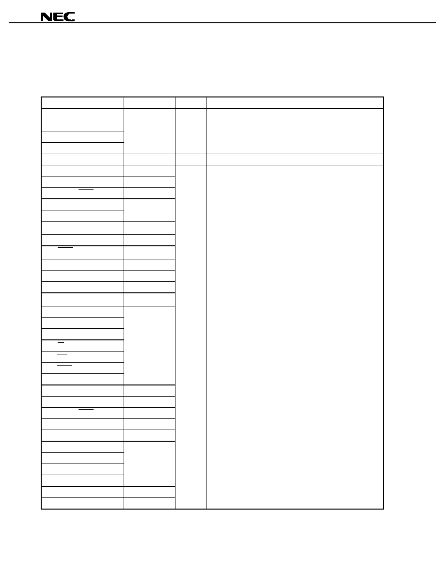
Figure 5-1. Types of Pin I/O Circuits (1/2)
IN
Pullup
enable
Data
Output
disable
Input
enable
V
DD
P-ch
V
DD
P-ch
IN/OUT
N-ch
Pullup
enable
Data
Output
disable
V
DD
P-ch
V
DD
P-ch
IN/OUT
N-ch
Pullup
enable
Data
Open drain
Output disable
V
DD
P-ch
V
DD
P-ch
IN/OUT
N-ch
Pullup
enable
Data
Open drain
Output disable
Output disable
V
DD
P-ch
V
DD
V
SS
P-ch
IN/OUT
N-ch
Pullup
enable
Data
V
DD
P-ch
V
DD
V
SS
P-ch
IN/OUT
N-ch
Pullup
enable
Data
Output
disable
Input
enable
V
DD
P-ch
V
DD
P-ch
IN/OUT
N-ch
P-ch
N-ch
IN
Comparator
+
≠
P-ch
N-ch
Input
enable
Type 2-G
Type 5-A
Type 8-N
Type 9
(Threshold voltage)
Analog output
voltage
Type 12-E
Type 10-M
Type 10-L
Type 10-K
Schmitt-triggered input with hysteresis characteristics
Data Sheet U14121EJ2V0DS00
21
µ
µ
µ
µ
PD784214A, 784215A, 784216A, 784217A, 784218A, 784214AY, 784215AY, 784216AY, 784217AY, 784218AY
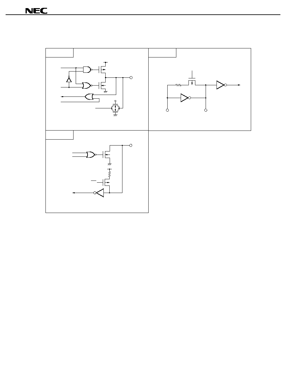
Figure 5-1. Types of Pin I/O Circuits (2/2)
Data
Output disable
Middle-voltage input buffer
IN/OUT
N-ch
P-ch
V
DD
RD
Data
Analog output
voltage
Type 12-F
Type 13-D
Type 16
Output
disable
P-ch
IN/OUT
V
DD
V
SS
V
SS
N-ch
Input
enable
P-ch
N-ch
P-ch
Feedback
cut-off
XT1
XT2
Data Sheet U14121EJ2V0DS00
22
µ
µ
µ
µ
PD784214A, 784215A, 784216A, 784217A, 784218A, 784214AY, 784215AY, 784216AY, 784217AY, 784218AY
6. CPU ARCHITECTURE
6.1 Memory Space
A memory space of 1 MB can be accessed. Mapping of the internal data area (special function registers and
internal RAM) can be specified by the LOCATION instruction. The LOCATION instruction must always be executed
after reset cancellation, and must not be used more than once.
(1) When LOCATION 0H instruction is executed
∑
∑
∑
∑
Internal memory
The internal data area and internal ROM area are mapped as follows.
Part Number
Internal Data Area
Internal ROM Area
µ
PD784214A,
µ
PD784214AY
0F100H to 0FFFFH
00000H to 0F0FFH
10000H to 17FFFH
µ
PD784215A,
µ
PD784215AY
0EB00H to 0FFFFH
00000H to 0EAFFH
10000H to 1FFFFH
µ
PD784216A,
µ
PD784216AY
0DF00H to 0FFFFH
00000H to 0DEFFH
10000H to 1FFFFH
µ
PD784217A,
µ
PD784217AY
00000H to 0CCFFH
10000H to 2FFFFH
µ
PD784218A,
µ
PD784218AY
0CD00H to 0FFFFH
00000H to 0CCFFH
10000H to 3FFFFH
Caution The following areas that overlap the internal data area of the internal ROM cannot be used
when the LOCATION 0H instruction is executed.
Part Number
Unusable Area
µ
PD784214A,
µ
PD784214AY
0F100H to 0FFFFH (3,840 bytes)
µ
PD784215A,
µ
PD784215AY
0EB00H to 0FFFFH (5,376 bytes)
µ
PD784216A,
µ
PD784216AY
0DF00H to 0FFFFH (8,448 bytes)
µ
PD784217A,
µ
PD784217AY
µ
PD784218A,
µ
PD784218AY
0CD00H to 0FFFFH (13,056 bytes)
∑
∑
∑
∑
External memory
The external memory is accessed in external memory expansion mode.
Data Sheet U14121EJ2V0DS00
23
µ
µ
µ
µ
PD784214A, 784215A, 784216A, 784217A, 784218A, 784214AY, 784215AY, 784216AY, 784217AY, 784218AY
(2) When LOCATION 0FH instruction is executed
∑
∑
∑
∑
Internal memory
The internal data area and internal ROM area are mapped as follows.
Part Number
Internal Data Area
Internal ROM Area
µ
PD784214A,
µ
PD784214AY
FF100H to FFFFFH
00000H to 17FFFH
µ
PD784215A,
µ
PD784215AY
FEB00H to FFFFFH
00000H to 1FFFFH
µ
PD784216A,
µ
PD784216AY
FDF00H to FFFFFH
00000H to 1FFFFH
µ
PD784217A,
µ
PD784217AY
00000H to 2FFFFH
µ
PD784218A,
µ
PD784218AY
FCD00H to FFFFFH
00000H to 3FFFFH
∑
∑
∑
∑
External memory
The external memory is accessed in external memory expansion mode.

D
a
ta S
heet U
14121E
J2V
0
D
S
00
24
µ
µ
µ
µ
PD784214A, 784215A, 784216A, 784217A, 784218A, 784214AY, 784215AY, 784216AY, 784217AY, 784218AY
Figure 6-1. Memory Map of
µ
µ
µ
µ
PD784214A, 784214AY
Internal ROM
(61,696 bytes)
(256 bytes)
Special function registers (SFR)
Internal RAM
(3,584 bytes)
External memory
Note 1
(928 KB)
Note 1
General-purpose
registers (128 bytes)
Macro service control word
area (54 bytes)
Data area (512 bytes)
Program/data area
(3,072 bytes)
CALLF entry
area (2 KB)
Program/data area
Note 3
CALLT table
area (64 bytes)
Vector table area
(64 bytes)
Internal RAM
(3,584 bytes)
External memory
Note 1
(980,736 bytes)
(256 bytes)
Internal ROM
(96 KB)
On execution of
LOCATION 0H instruction
Special function registers (SFR)
Note 1
On execution of
LOCATION 0FH instruction
H
F
F
F
F
F
H
0
0
0
0
1
H
F
F
F
F
0
H
F
D
F
F
0
H
0
D
F
F
0
H
0
0
F
F
0
H
F
F
E
F
0
H
0
0
1
F
0
H
F
F
0
F
0
H
0
0
0
0
0
H
F
F
E
F
0
H
0
8
E
F
0
H
F
7
E
F
0
H
B
3
E
F
0
H
0
0
D
F
0
H
F
F
C
F
0
H
6
0
E
F
0
H
0
0
1
F
0
H
F
F
F
7
1
H
0
0
0
1
0
H
F
F
F
0
0
H
0
0
8
0
0
H
F
F
7
0
0
H
0
8
0
0
0
H
F
7
0
0
0
H
0
4
0
0
0
H
F
3
0
0
0
H
0
0
0
0
0
H
F
F
E
F
F
H
0
8
E
F
F
H
F
7
E
F
F
H
B
3
E
F
F
H
6
0
E
F
F
H
0
0
D
F
F
H
F
F
C
F
F
H
0
0
1
F
F
H
0
0
0
0
0
H
F
F
F
7
1
H
0
0
0
8
1
H
F
F
0
F
F
H
0
0
1
F
F
H
F
F
F
F
F
H
F
D
F
F
F
H
0
D
F
F
F
H
0
0
F
F
F
H
F
F
E
F
F
Note 4
Note 4
Note 2
H
F
F
F
7
1
H
0
0
0
8
1
H
F
F
F
7
1
Internal ROM
(32,768 bytes)
H
F
F
0
F
0
H
0
0
0
0
1
Notes 1. Accessed in external memory expansion mode.
2. This 3,840-byte area can be used as an internal ROM only when the LOCATION 0FH instruction is executed.
3. On execution of LOCATION 0H instruction: 94,464 bytes, on execution of LOCATION 0FH instruction: 98,304 bytes
4. Base area and entry area for reset or interrupt. However, the internal RAM area is not used as a reset entry area.

D
a
ta S
heet U
14121E
J2V
0
D
S
00
25
µ
µ
µ
µ
PD784214A, 784215A, 784216A, 784217A, 784218A, 784214AY, 784215AY, 784216AY, 784217AY, 784218AY
Figure 6-2. Memory Map of
µ
µ
µ
µ
PD784215A, 784215AY
Internal ROM
(60,160 bytes)
(256 bytes)
Special function registers (SFR)
Internal RAM
(5,120 bytes)
External memory
Note 1
(896 KB)
Note 1
General-purpose
registers (128 bytes)
Macro service control word
area (54 bytes)
Data area (512 bytes)
Program/data area
(4,608 bytes)
CALLF entry
area (2 KB)
Program/data area
Note 3
CALLT table
area (64 bytes)
Vector table area
(64 bytes)
Internal RAM
(5,120 bytes)
External memory
Note 1
(912,128 bytes)
(256 bytes)
Internal ROM
(128 KB)
On execution of
LOCATION 0H instruction
Special function registers (SFR)
Note 1
On execution of
LOCATION 0FH instruction
H
F
F
F
F
F
H
0
0
0
0
1
H
F
F
F
F
0
H
F
D
F
F
0
H
0
D
F
F
0
H
0
0
F
F
0
H
F
F
E
F
0
H
0
0
B
E
0
H
F
F
A
E
0
H
0
0
0
0
0
H
F
F
E
F
0
H
0
8
E
F
0
H
F
7
E
F
0
H
B
3
E
F
0
H
0
0
D
F
0
H
F
F
C
F
0
H
6
0
E
F
0
H
0
0
B
E
0
H
0
0
0
1
0
H
F
F
F
0
0
H
0
0
8
0
0
H
F
F
7
0
0
H
0
8
0
0
0
H
F
7
0
0
0
H
0
4
0
0
0
H
F
3
0
0
0
H
0
0
0
0
0
H
F
F
E
F
F
H
0
8
E
F
F
H
F
7
E
F
F
H
B
3
E
F
F
H
6
0
E
F
F
H
0
0
D
F
F
H
F
F
C
F
F
H
0
0
B
E
F
H
0
0
0
0
0
H
F
F
F
F
1
H
0
0
0
0
2
H
F
F
A
E
F
H
0
0
B
E
F
H
F
F
F
F
F
H
F
D
F
F
F
H
0
D
F
F
F
H
0
0
F
F
F
H
F
F
E
F
F
Note 4
Note 4
H
F
F
F
F
1
Internal ROM
(65,536 bytes)
H
0
0
0
0
2
H
F
F
F
F
1
H
F
F
F
F
1
Note 2
H
F
F
A
E
0
H
0
0
0
0
1
Notes 1. Accessed in external memory expansion mode.
2. This 5,376-byte area can be used as an internal ROM only when the LOCATION 0FH instruction is executed.
3. On execution of LOCATION 0H instruction: 125,696 bytes, on execution of LOCATION 0FH instruction: 131,072 bytes
4. Base area and entry area for reset or interrupt. However, the internal RAM area is not used as a reset entry area.
D
a
ta S
heet U
14121E
J2V
0
D
S
00
26
µ
µ
µ
µ
PD784214A, 784215A, 784216A, 784217A, 784218A, 784214AY, 784215AY, 784216AY, 784217AY, 784218AY
Figure 6-3. Memory Map of
µ
µ
µ
µ
PD784216A,
784216AY
Internal ROM
(57,088 bytes)
(256 bytes)
Special function registers (SFR)
Internal RAM
(8,192 bytes)
External memory
Note 1
(896 KB)
Note 1
General-purpose
registers (128 bytes)
Macro service control word
area (54 bytes)
Data area (512 bytes)
Program/data area
(7,680 bytes)
CALLF entry
area (2 KB)
Program/data area
Note 3
CALLT table
area (64 bytes)
Vector table area
(64 bytes)
Internal RAM
(8,192 bytes)
External memory
Note 1
(909,056 bytes)
(256 bytes)
Internal ROM
(128 KB)
On execution of
LOCATION 0H instruction
Special function registers (SFR)
Note 1
On execution of
LOCATION 0FH instruction
H
F
F
F
F
F
H
0
0
0
0
1
H
F
F
F
F
0
H
F
D
F
F
0
H
0
D
F
F
0
H
0
0
F
F
0
H
F
F
E
F
0
H
0
0
F
D
0
H
F
F
E
D
0
H
0
0
0
0
0
H
F
F
E
F
0
H
0
8
E
F
0
H
F
7
E
F
0
H
B
3
E
F
0
H
0
0
D
F
0
H
F
F
C
F
0
H
6
0
E
F
0
H
0
0
F
D
0
H
0
0
0
1
0
H
F
F
F
0
0
H
0
0
8
0
0
H
F
F
7
0
0
H
0
8
0
0
0
H
F
7
0
0
0
H
0
4
0
0
0
H
F
3
0
0
0
H
0
0
0
0
0
H
F
F
E
F
F
H
0
8
E
F
F
H
F
7
E
F
F
H
B
3
E
F
F
H
6
0
E
F
F
H
0
0
D
F
F
H
F
F
C
F
F
H
0
0
F
D
F
H
0
0
0
0
0
H
F
F
F
F
1
H
0
0
0
0
2
H
F
F
E
D
F
H
0
0
F
D
F
H
F
F
F
F
F
H
F
D
F
F
F
H
0
D
F
F
F
H
0
0
F
F
F
H
F
F
E
F
F
Note 4
Note 4
H
0
0
0
0
2
H
F
F
F
F
1
H
F
F
F
F
1
Internal ROM
(65,536 bytes)
H
F
F
F
F
1
Note 2
H
F
F
E
D
0
H
0
0
0
0
1
Notes 1. Accessed in external memory expansion mode.
2. This 8,448-byte area can be used as an internal ROM only when the LOCATION 0FH instruction is executed.
3. On execution of LOCATION 0H instruction: 122,624 bytes, on execution of LOCATION 0FH instruction: 131,072 bytes
4. Base area and entry area for reset or interrupt. However, the internal RAM area is not used as a reset entry area.
D
a
ta S
heet U
14121E
J2V
0
D
S
00
27
µ
µ
µ
µ
PD784214A, 784215A, 784216A, 784217A, 784218A, 784214AY, 784215AY, 784216AY, 784217AY, 784218AY
Figure 6- 4. Memory Map of
µ
µ
µ
µ
PD784217A, 784217AY
Notes 1. Accessed in external memory expansion mode.
2. This 13,056-byte area can be used as internal ROM only when the LOCATION 0FH instruction is executed.
3. On execution of LOCATION 0H instruction: 183,552 bytes, on execution of LOCATION 0FH instruction: 196,608 bytes
4. Base area and entry area for reset or interrupt. However, the internal RAM area is not used as a reset entry area.
Internal ROM
(52,480 bytes)
(256 bytes)
Special function registers (SFR)
Internal RAM
(12,800 bytes)
External memory
Note 1
(928 KB)
Note 1
General-purpose
registers (128 bytes)
Macro service control word
area (54 bytes)
Data area (512 bytes)
Program/data area
(12,288 bytes)
CALLF entry
area (2 KB)
Program/data area
Note 3
CALLT table
area (64 bytes)
Vector table area
(64 bytes)
Internal RAM
(12,800 bytes)
External memory
Note 1
(838,912 bytes)
(256 bytes)
Internal ROM
(192 KB)
On execution of
LOCATION 0H instruction
Special function registers (SFR)
Note 1
On execution of
LOCATION 0FH instruction
H
F
F
F
F
F
H
0
0
0
0
1
H
F
F
F
F
0
H
F
D
F
F
0
H
0
D
F
F
0
H
0
0
F
F
0
H
F
F
E
F
0
H
0
0
D
C
0
H
F
F
C
C
0
H
0
0
0
0
0
H
F
F
E
F
0
H
0
8
E
F
0
H
F
7
E
F
0
H
B
3
E
F
0
H
0
0
D
F
0
H
F
F
C
F
0
H
6
0
E
F
0
H
0
0
D
C
0
H
F
F
F
F
2
H
0
0
0
1
0
H
F
F
F
0
0
H
0
0
8
0
0
H
F
F
7
0
0
H
0
8
0
0
0
H
F
7
0
0
0
H
0
4
0
0
0
H
F
3
0
0
0
H
0
0
0
0
0
H
F
F
E
F
F
H
0
8
E
F
F
H
F
7
E
F
F
H
B
3
E
F
F
H
6
0
E
F
F
H
0
0
D
F
F
H
F
F
C
F
F
H
0
0
D
C
F
H
0
0
0
0
0
H
F
F
F
F
2
H
0
0
0
0
3
H
F
F
C
C
F
H
0
0
D
C
F
H
F
F
F
F
F
H
F
D
F
F
F
H
0
D
F
F
F
H
0
0
F
F
F
H
F
F
E
F
F
Note 4
Note 4
Note 2
H
F
F
F
7
1
H
0
0
0
8
1
H
F
F
F
7
1
Internal ROM
(32,768 bytes)
H
F
F
0
F
0
H
0
0
0
0
1
D
a
ta S
heet U
14121E
J2V
0
D
S
00
28
µ
µ
µ
µ
PD784214A, 784215A, 784216A, 784217A, 784218A, 784214AY, 784215AY, 784216AY, 784217AY, 784218AY
Figure 6-5. Memory Map of
µ
µ
µ
µ
PD784218A, 784218AY
Notes 1. Accessed in external memory expansion mode.
2. This 13,056-byte area can be used as an internal ROM only when the LOCATION 0FH instruction is executed.
3. On execution of LOCATION 0H instruction: 249,088 bytes, on execution of LOCATION 0FH instruction: 262,144 bytes
4. Base area and entry area for reset or interrupt. However, the internal RAM area is not used as a reset entry area.
Internal ROM
(52,480 bytes)
(256 bytes)
Special function registers (SFR)
Internal RAM
(12,800 bytes)
External memory
Note 1
(768 KB)
Note 1
General-purpose
registers (128 bytes)
Macro service control word
area (54 bytes)
Data area (512 bytes)
Program/data area
(12,288 bytes)
CALLF entry
area (2 KB)
Program/data area
Note 3
CALLT table
area (64 bytes)
Vector table area
(64 bytes)
Internal RAM
(12,800 bytes)
External memory
Note 1
(773,376 bytes)
(256 bytes)
Internal ROM
(256 KB)
On execution of
LOCATION 0H instruction
Special function registers (SFR)
Note 1
On execution of
LOCATION 0FH instruction
H
F
F
F
F
F
H
0
0
0
0
1
H
F
F
F
F
0
H
F
D
F
F
0
H
0
D
F
F
0
H
0
0
F
F
0
H
F
F
E
F
0
H
0
0
D
C
0
H
F
F
C
C
0
H
0
0
0
0
0
H
F
F
E
F
0
H
0
8
E
F
0
H
F
7
E
F
0
H
B
3
E
F
0
H
0
0
D
F
0
H
F
F
C
F
0
H
6
0
E
F
0
H
0
0
D
C
0
H
0
0
0
1
0
H
F
F
F
0
0
H
0
0
8
0
0
H
F
F
7
0
0
H
0
8
0
0
0
H
F
7
0
0
0
H
0
4
0
0
0
H
F
3
0
0
0
H
0
0
0
0
0
H
F
F
E
F
F
H
0
8
E
F
F
H
F
7
E
F
F
H
B
3
E
F
F
H
6
0
E
F
F
H
0
0
D
F
F
H
F
F
C
F
F
H
0
0
D
C
F
H
0
0
0
0
0
H
F
F
F
F
3
H
0
0
0
0
4
H
F
F
C
C
F
H
0
0
D
C
F
H
F
F
F
F
F
H
F
D
F
F
F
H
0
D
F
F
F
H
0
0
F
F
F
H
F
F
E
F
F
Note 4
Note 4
H
F
F
F
F
3
Internal ROM
(196,608 bytes)
H
0
0
0
0
4
H
F
F
F
F
3
H
F
F
F
F
3
Note 2
H
F
F
C
C
0
H
0
0
0
0
1

Data Sheet U14121EJ2V0DS00
29
µ
µ
µ
µ
PD784214A, 784215A, 784216A, 784217A, 784218A, 784214AY, 784215AY, 784216AY, 784217AY, 784218AY
6.2 CPU Registers
6.2.1 General-purpose registers
Sixteen 8-bit general-purpose registers are available. Two 8-bit registers can also be used in pairs as a 16-bit
register. Of the 16-bit registers, four can be used in combination with an 8-bit register for address expansion as 24-
bit address specification registers.
Eight banks of these register sets are available and can be selected by using software or the context switching
function.
The general-purpose registers except the V, U, T, and W registers for address expansion are mapped to the
internal RAM.
Figure 6-6. General-Purpose Register Format
Caution Registers R4, R5, R6, R7, RP2, and RP3 can be used as the X, A, C, B, AX, and BC registers,
respectively, by setting the RSS bit of the PSW to 1. However, use this function only for
recycling the program of the 78K/III Series.
A (R1)
B (R3)
R5
R7
R9
R11
D (R13)
H (R15)
V
U
T
W
VVP (RG4)
UUP (RG5)
TDE (RG6)
WHL (RG7)
X (R0)
C (R2)
R4
R6
R8
R10
E (R12)
L (R14)
AX (RP0)
BC (RP1)
RP2
RP3
VP (RP4)
UP (RP5)
DE (RP6)
HL (RP7)
Names in parentheses indicate absolute names.
8 banks
Data Sheet U14121EJ2V0DS00
30
µ
µ
µ
µ
PD784214A, 784215A, 784216A, 784217A, 784218A, 784214AY, 784215AY, 784216AY, 784217AY, 784218AY
6.2.2 Control registers
(1) Program counter (PC)
The program counter is a 20-bit register whose contents are automatically updated when the program is
executed.
Figure 6-7. Format of Program Counter (PC)
(2) Program status word (PSW)
This register holds the statuses of the CPU. Its contents are automatically updated when the program is
executed.
Figure 6-8. Format of Program Status Word (PSW)
Note This flag is provided to maintain compatibility with the 78K/III Series. Be sure to clear this flag to 0,
except when the software for the 78K/III Series is used.
(3) Stack pointer (SP)
This is a 24-bit pointer that holds the first address of the stack. Be sure to write 0 to the higher 4 bits of this
pointer.
Figure 6-9. Format of Stack Pointer (SP)
19
0
PC
15
14
13
12
11
10
9
8
UF
RBS2
RBS1
RBS0
≠
≠
≠
≠
PSWH
7
6
5
4
3
2
1
0
S
Z
RSS
Note
AC
IE
P/V
0
CY
PSWL
PSW
23
0
SP
20
0
0
0
0

Data Sheet U14121EJ2V0DS00
31
µ
µ
µ
µ
PD784214A, 784215A, 784216A, 784217A, 784218A, 784214AY, 784215AY, 784216AY, 784217AY, 784218AY
6.2.3 Special function registers (SFRs)
The special function registers, such as the mode registers and control registers of the internal peripheral
hardware, are registers to which special functions are assigned. These registers are mapped to the 256-byte space
of addresses 0FF00H to 0FFFFH
Note
.
Note On execution of the LOCATION 0H instruction. FFF00H to FFFFFH on execution of the LOCATION 0FH
instruction.
Caution Do not access an address in this area to which no SFR is assigned. If such an address is
accessed by mistake, the
µ
µ
µ
µ
PD784218A may enter a deadlocked state. This deadlock state can be
cleared only by inputting the RESET signal.
Table 6-1 lists the special function registers (SFRs). The meanings of the symbols in this table are as follows.
∑
Symbol ................................ Symbol indicating an SFR. This symbol is reserved for NEC's assembler
(RA78K4). It can be used as an sfr variable by means of the #pragma sfr command
in the C compiler (CC78K4).
∑
R/W ..................................... Indicates whether the SFR is read-only, write-only, or read/write.
R/W: Read/write
R: Read-only
W: Write-only
∑
Bit units for manipulation ..... Bit units in which the value of the SFR can be manipulated.
SFRs that can be manipulated in 16-bit units can be described as the operand sfrp
of an instruction. To specify the address of this SFR, describe an even address.
SFRs that can be manipulated in 1-bit units can be described as the operand of a
bit manipulation instruction.
∑
After reset ............................ Indicates the status of the register when the RESET signal has been input.

Data Sheet U14121EJ2V0DS00
32
µ
µ
µ
µ
PD784214A, 784215A, 784216A, 784217A, 784218A, 784214AY, 784215AY, 784216AY, 784217AY, 784218AY
Table 6-1. Special Function Register (SFR) List (1/4)
Bit Units for Manipulation
Address
Note 1
Special Function Register (SFR) Name
Symbol
R/W
1 Bit
8 Bits
16 Bits
After Reset
0FF00H
Port 0
P0
R/W
-
0FF01H
Port 1
P1
R
-
0FF02H
Port 2
P2
-
0FF03H
Port 3
P3
-
0FF04H
Port 4
P4
-
0FF05H
Port 5
P5
-
0FF06H
Port 6
P6
-
0FF07H
Port 7
P7
-
0FF08H
Port 8
P8
-
0FF09H
Port 9
P9
-
0FF0AH
Port 10
P10
-
0FF0CH
Port 12
P12
-
0FF0DH
Port 13
P13
R/W
-
00H
Note 2
0FF10H
0FF11H
16-bit timer counter
TM0
R
-
-
0FF12H
0FF13H
Capture/compare register 00
(16-bit timer/event counter)
CR00
-
-
0FF14H
0FF15H
Capture/compare register 01
(16-bit timer/event counter)
CR01
-
-
0000H
0FF16H
Capture/compare control register 0
CRC0
-
0FF18H
16-bit timer mode control register
TMC0
-
0FF1AH
16-bit timer output control register
TOC0
-
0FF1CH
Prescaler mode register 0
PRM0
-
00H
0FF20H
Port 0 mode register
PM0
-
0FF22H
Port 2 mode register
PM2
-
0FF23H
Port 3 mode register
PM3
-
0FF24H
Port 4 mode register
PM4
-
0FF25H
Port 5 mode register
PM5
-
0FF26H
Port 6 mode register
PM6
-
0FF27H
Port 7 mode register
PM7
-
0FF28H
Port 8 mode register
PM8
-
0FF29H
Port 9 mode register
PM9
-
0FF2AH
Port 10 mode register
PM10
-
0FF2CH
Port 12 mode register
PM12
-
0FF2DH
Port 13 mode register
PM13
R/W
-
FFH
Notes 1. When the LOCATION 0H instruction is executed. Add "F0000H" to this value when the LOCATION
0FH instruction is executed.
2. Because each port is initialized to input mode after reset, "00H" is not actually read. The output latch is
initialized to "0".
Data Sheet U14121EJ2V0DS00
33
µ
µ
µ
µ
PD784214A, 784215A, 784216A, 784217A, 784218A, 784214AY, 784215AY, 784216AY, 784217AY, 784218AY
Table 6-1. Special Function Register (SFR) List (2/4)
Bit Units for Manipulation
Address
Note
Special Function Register (SFR) Name
Symbol
R/W
1 Bit
8 Bits
16 Bits
After Reset
0FF30H
Pull-up resistor option register 0
PU0
-
0FF32H
Pull-up resistor option register 2
PU2
-
0FF33H
Pull-up resistor option register 3
PU3
-
0FF37H
Pull-up resistor option register 7
PU7
-
0FF38H
Pull-up resistor option register 8
PU8
-
0FF3AH
Pull-up resistor option register 10
PU10
-
0FF3CH
Pull-up resistor option register 12
PU12
-
0FF40H
Clock output control register
CKS
-
0FF42H
Port function control register
PF2
-
0FF4EH
Pull-up resistor option register
PUO
R/W
-
00H
0FF50H
8-bit timer counter 1
TM1
-
0FF51H
8-bit timer counter 2
TM2
TM1W
R
-
0FF52H
Compare register 10 (8-bit timer/event counter 1) CR10
-
0FF53H
Compare register 20 (8-bit timer/event counter 2) CR20
CR1W
-
0FF54H
8-bit timer mode control register 1
TMC1
0FF55H
8-bit timer mode control register 2
TMC2
TMC1W
0FF56H
Prescaler mode register 1
PRM1
0FF57H
Prescaler mode register 2
PRM2
PRM1W
R/W
0FF60H
8-bit timer counter 5
TM5
-
0FF61H
8-bit timer counter 6
TM6
TM5W
-
0FF62H
8-bit timer counter 7
TM7
-
0FF63H
8-bit timer counter 8
TM8
TM7W
R
-
0FF64H
Compare register 50 (8-bit timer/event counter 5) CR50
-
0FF65H
Compare register 60 (8-bit timer/event counter 6) CR60
CR5W
-
0FF66H
Compare register 70 (8-bit timer/event counter 7) CR70
-
0FF67H
Compare register 80 (8-bit timer/event counter 8) CR80
CR7W
-
0FF68H
8-bit timer mode control register 5
TMC5
0FF69H
8-bit timer mode control register 6
TMC6
TMC5W
0FF6AH
8-bit timer mode control register 7
TMC7
0FF6BH
8-bit timer mode control register 8
TMC8
TMC7W
0FF6CH
Prescaler mode register 5
PRM5
0FF6DH
Prescaler mode register 6
PRM6
PRM5W
0FF6EH
Prescaler mode register 7
PRM7
0FF6FH
Prescaler mode register 8
PRM8
PRM7W
0000H
0FF70H
Asynchronous serial interface mode register 1
ASIM1
-
0FF71H
Asynchronous serial interface mode register 2
ASIM2
R/W
-
0FF72H
Asynchronous serial interface status register 1
ASIS1
-
0FF73H
Asynchronous serial interface status register 2
ASIS2
R
-
00H
Note When the LOCATION 0H instruction is executed. Add "F0000H" to this value when the LOCATION 0FH
instruction is executed.

Data Sheet U14121EJ2V0DS00
34
µ
µ
µ
µ
PD784214A, 784215A, 784216A, 784217A, 784218A, 784214AY, 784215AY, 784216AY, 784217AY, 784218AY
Table 6-1. Special Function Register (SFR) List (3/4)
Bit Units for Manipulation
Address
Note 1
Special Function Register (SFR) Name
Symbol
R/W
1 Bit
8 Bits
16 Bits
After Reset
Transmit shift register 1
TXS1
W
-
-
0FF74H
Receive buffer register 1
RXB1
R
-
-
Transmit shift register 2
TXS2
W
-
-
0FF75H
Receive buffer register 2
RXB2
R
-
-
FFH
0FF76H
Baud rate generator control register 1
BRGC1
-
0FF77H
Baud rate generator control register 2
BRGC2
-
0FF7AH
Oscillation mode select register
CC
-
0FF80H
A/D converter mode register
ADM
-
0FF81H
A/D converter input select register
ADIS
R/W
-
00H
0FF83H
A/D conversion result register
ADCR
R
-
-
Undefined
0FF84H
D/A conversion value setting register 0
DACS0
-
0FF85H
D/A conversion value setting register 1
DACS1
-
0FF86H
D/A converter mode register 0
DAM0
-
0FF87H
D/A converter mode register 1
DAM1
-
0FF8CH
External bus type select register
EBTS
-
0FF90H
Serial operation mode register 0
CSIM0
-
0FF91H
Serial operation mode register 1
CSIM1
-
0FF92H
Serial operation mode register 2
CSIM2
-
0FF94H
Serial I/O shift register 0
SIO0
-
-
0FF95H
Serial I/O shift register 1
SIO1
-
-
0FF96H
Serial I/O shift register 2
SIO2
-
-
0FF98H
Real-time output buffer register L
RTBL
-
-
0FF99H
Real-time output buffer register H
RTBH
-
-
0FF9AH
Real-time output port mode register
RTPM
-
0FF9BH
Real-time output port control register
RTPC
-
0FF9CH
Watch timer mode control register
WTM
-
0FFA0H
External interrupt rising edge enable register
EGP0
-
0FFA2H
External interrupt falling edge enable register
EGN0
R/W
-
0FFA8H
In-service priority register
ISPR
R
-
0FFA9H
Interrupt select control register
SNMI
-
00H
0FFAAH
Interrupt mode control register
IMC
-
80H
0FFACH
Interrupt mask flag register 0L
MK0L
0FFADH
Interrupt mask flag register 0H
MK0H
MK0
0FFAEH
Interrupt mask flag register 1L
MK1L
0FFAFH
Interrupt mask flag register 1H
MK1H
MK1
FFFFH
0FFB0H
I
2
C bus control register
Note 2
IICC0
-
0FFB2H
Prescaler mode register for serial clock
SPRM0
-
0FFB4H
Slave address register
SVA0
R/W
-
00H
Notes 1. When the LOCATION 0H instruction is executed. Add "F0000H" to this value when the LOCATION
0FH instruction is executed.
2.
µ
PD784216AY/784218AY Subseries only
Data Sheet U14121EJ2V0DS00
35
µ
µ
µ
µ
PD784214A, 784215A, 784216A, 784217A, 784218A, 784214AY, 784215AY, 784216AY, 784217AY, 784218AY
Table 6-1. Special Function Register (SFR) List (4/4)
Bit Units for Manipulation
Address
Note 1
Special Function Register (SFR) Name
Symbol
R/W
1 Bit
8 Bits
16 Bits
After Reset
0FFB6H
I
2
C bus status register
Note 2
IICS0
R
-
0FFB8H
Serial shift register
IIC0
-
00H
0FFC0H
Standby control register
STBC
-
-
30H
0FFC2H
Watchdog timer mode register
WDM
-
-
00H
0FFC4H
Memory expansion mode register
MM
-
20H
0FFC7H
Programmable wait control register 1
PWC1
R/W
-
AAH
0FFCEH
Clock status register
PCS
R
-
32H
0FFCFH
Oscillation stabilization time specification register
OSTS
-
00H
0FFD0H to
0FFDFH
External SFR area
-
-
-
0FFE0H
Interrupt control register (INTWDTM)
WDTIC
-
0FFE1H
Interrupt control register (INTP0)
PIC0
-
0FFE2H
Interrupt control register (INTP1)
PIC1
-
0FFE3H
Interrupt control register (INTP2)
PIC2
-
0FFE4H
Interrupt control register (INTP3)
PIC3
-
0FFE5H
Interrupt control register (INTP4)
PIC4
-
0FFE6H
Interrupt control register (INTP5)
PIC5
-
0FFE7H
Interrupt control register (INTP6)
PIC6
-
0FFE8H
Interrupt control register (INTIIC0/INTCSI0)
CSIIC0
-
0FFE9H
Interrupt control register (INTSER1)
SERIC1
-
0FFEAH
Interrupt control register (INTSR1/INTCSI1)
SRIC1
-
0FFEBH
Interrupt control register (INTST1)
STIC1
-
0FFECH
Interrupt control register (INTSER2)
SERIC2
-
0FFEDH
Interrupt control register (INTSR2/INTCSI2)
SRIC2
-
0FFEEH
Interrupt control register (INTST2)
STIC2
-
0FFEFH
Interrupt control register (INTTM3)
TMIC3
-
0FFF0H
Interrupt control register (INTTM00)
TMIC00
-
0FFF1H
Interrupt control register (INTTM01)
TMIC01
-
0FFF2H
Interrupt control register (INTTM1)
TMIC1
-
0FFF3H
Interrupt control register (INTTM2)
TMIC2
-
0FFF4H
Interrupt control register (INTAD)
ADIC
-
0FFF5H
Interrupt control register (INTTM5)
TMIC5
-
0FFF6H
Interrupt control register (INTTM6)
TMIC6
-
0FFF7H
Interrupt control register (INTTM7)
TMIC7
-
0FFF8H
Interrupt control register (INTTM8)
TMIC8
-
0FFF9H
Interrupt control register (INTWT)
WTIC
-
0FFFAH
Interrupt control register (INTKR)
KRIC
R/W
-
43H
Notes 1. When the LOCATION 0H instruction is executed. Add "F0000H" to this value when the LOCATION
0FH instruction is executed.
2.
µ
PD784216AY/784218AY Subseries only
Data Sheet U14121EJ2V0DS00
36
µ
µ
µ
µ
PD784214A, 784215A, 784216A, 784217A, 784218A, 784214AY, 784215AY, 784216AY, 784217AY, 784218AY
7. PERIPHERAL HARDWARE FUNCTIONS
7.1 Ports
The ports shown in Figure 7-1 are provided to make various control operations possible. Table 7-1 shows the
function of each port. Ports 0, 2 through 8, 10, and 12 can be connected to on-chip pull-up resistors by means of
software when in input mode.
Figure 7-1. Port Configuration
Port 7
Port 0
Port 2
Port 3
Port 4
Port 5
Port 6
Port 1
P70
P72
Pprt 8
P80
P87
Port 12
P120
P127
Port 9
P90
P95
Port 10
P100
P103
Port 13
P130
P131
P00
P06
P10 to P17
P20
P27
P30
P37
P40
P47
P50
P57
P60
P67
8

Data Sheet U14121EJ2V0DS00
37
µ
µ
µ
µ
PD784214A, 784215A, 784216A, 784217A, 784218A, 784214AY, 784215AY, 784216AY, 784217AY, 784218AY
Table 7-1. Port Functions
Port Name
Pin Name
Function
Specification of Pull-up Resistor
Connection by Software
Port 0
P00 to P06
∑
Input/output can be specified in 1-bit units
Can be specified in 1-bit units
Port 1
P10 to P17
∑
Input port
-
Port 2
P20 to P27
∑
Input/output can be specified in 1-bit units
Can be specified in 1-bit units
Port 3
P30 to P37
∑
Input/output can be specified in 1-bit units
Can be specified in 1-bit units
Port 4
P40 to P47
∑
Input/output can be specified in 1-bit units
∑
LEDs can be driven directly
Can be specified in 1-port units
Port 5
P50 to P57
∑
Input/output can be specified in 1-bit units
∑
LEDs can be driven directly
Can be specified in 1-port units
Port 6
P60 to P67
∑
Input/output can be specified in 1-bit units
Can be specified in 1-port units
Port 7
P70 to P72
∑
Input/output can be specified in 1-bit units
Can be specified in 1-bit units
Port 8
P80 to P87
∑
Input/output can be specified in 1-bit units
Can be specified in 1-bit units
Port 9
P90 to P95
∑
N-ch open-drain I/O port
∑
Input/output can be specified in 1-bit units
∑
LEDs can be driven directly
-
Port 10
P100 to P103
∑
Input/output can be specified in 1-bit units
Can be specified in 1-bit units
Port 12
P120 to P127
∑
Input/output can be specified in 1-bit units
Can be specified in 1-bit units
Port 13
P130, P131
∑
Input/output can be specified in 1-bit units
-
7.2 Clock Generator
An on-chip clock generator necessary for operation is provided. This clock generator has a frequency divider. If
high-speed operation is not necessary, the internal operating frequency can be lowered by the frequency divider to
reduce the current consumption.
Figure 7-2. Block Diagram of Clock Generator
XT2
XT1
X1
X2
STOP or bit 2 (MCK)
of the standby control
register (STBC) is set
to 1 when the subclock
is selected as the CPU
clock
Main system
clock
oscillator
Subsystem
clock
oscillator
f
XT
Watch timer,
clock output function
Clock to
peripheral hardware
CPU
clock
(f
CPU
)
Frequency
divider
IDLE
controller
Prescaler
Prescaler
STOP, IDLE
controller
HALT
controller
f
X
f
X
2
f
XX
2
f
XX
2
2
f
XX
2
3
f
XX
Selector
Selector
Internal system
clock
(f
CLK
)
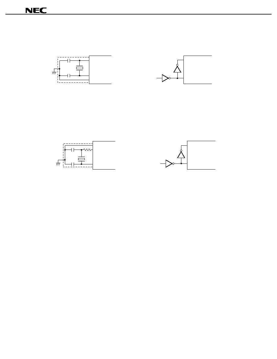
Data Sheet U14121EJ2V0DS00
38
µ
µ
µ
µ
PD784214A, 784215A, 784216A, 784217A, 784218A, 784214AY, 784215AY, 784216AY, 784217AY, 784218AY
Figure 7-3. Example of Using Main System Clock Oscillator
Figure 7-4. Example of Using Subsystem Clock Oscillator
Caution
When using the main system clock and subsystem clock oscillator, wire as follows in the area
enclosed by the broken lines in Figures 7-3 and 7-4 to avoid an adverse effect from wiring
capacitance.
∑
∑
∑
∑
Keep the wiring length as short as possible.
∑
∑
∑
∑
Do not cross the wiring with other signal lines.
∑
∑
∑
∑
Do not route the wiring near a signal line through which a high fluctuating current flows.
∑
∑
∑
∑
Always make the ground point of the oscillator capacitor the same potential as V
SS
. Do not
ground the capacitor to a ground pattern through which a high current flows.
∑
∑
∑
∑
Do not fetch signals from the oscillator.
Note that the subsystem clock oscillator has a low amplification factor to reduce the current
consumption.
External
clock
X2
X1
PD74HCU04
µ
V
SS
X2
X1
Crystal resonator
or
ceramic resonator
(1) Crystal/ceramic oscillation
(2) External clock
32.768
kHz
V
SS
XT2
XT1
XT2
XT1
External
clock
PD74HCU04
µ
(1) Crystal oscillation
(2) External clock

Data Sheet U14121EJ2V0DS00
39
µ
µ
µ
µ
PD784214A, 784215A, 784216A, 784217A, 784218A, 784214AY, 784215AY, 784216AY, 784217AY, 784218AY
7.3 Real-Time Output Port
The real-time output function is to transfer data set in advance to the real-time output buffer register to the output
latch as soon as the timer interrupt or external interrupt has occurred in order to output the data to an external device.
The pins that output the data to the external device constitute a port called a real-time output port.
Because the real-time output port can output signals without jitter, it is ideal for controlling a stepper motor.
Figure 7-5. Block Diagram of Real-Time Output Port
Internal bus
RTPOE
BYTE
EXTR
Output trigger
Controller
Real-time output port
control register (RTPC)
Real-time output
port mode register
(RTPM)
Real-time output port output latch
RTP7∑∑∑∑∑∑∑∑∑∑∑∑∑∑∑∑∑∑∑∑∑∑∑∑∑∑∑∑∑∑∑∑∑∑∑∑∑∑ RTP0
High-order 4 bits of
real-time output
buffer register
(RTBH)
Low-order 4 bits of
real-time output
buffer register
(RTBL)
INTP2TRG
INTTM1
INTTM2
Port 12 output latch
P127∑∑∑∑∑∑∑∑∑∑∑∑∑∑∑∑∑∑∑∑∑∑∑∑∑∑∑∑∑∑∑∑∑∑∑∑∑∑ P120
P12n/RTPn pin output (n = 0 to 7)
P127/ P120/
RTP7 RTP0
∑∑∑∑∑∑∑∑∑∑∑∑∑∑∑∑∑∑∑∑∑∑∑∑∑∑∑∑∑∑∑∑∑∑∑∑∑∑
RTPOE bit
Data Sheet U14121EJ2V0DS00
40
µ
µ
µ
µ
PD784214A, 784215A, 784216A, 784217A, 784218A, 784214AY, 784215AY, 784216AY, 784217AY, 784218AY
7.4 Timer/Event Counter
One unit of 16-bit timer/event counter and six 8-bit timer/event counters are provided.
Because a total of eight interrupt requests are supported, these timer/event counters can be used as eight
timer/counters.
Table 7-2. Operations of Timers
Name
Item
16-Bit
Timer/
Event
Counter
8-Bit
Timer/
Event
Counter 1
8-Bit
Timer/
Event
Counter 2
8-Bit
Timer/
Event
Counter 5
8-Bit
Timer/
Event
Counter 6
8-Bit
Timer/
Event
Counter 7
8-Bit
Timer/
Event
Counter 8
8 bits
-
Count width
16 bits
Interval timer
1 ch
1 ch
1 ch
1 ch
1 ch
1 ch
1 ch
Operation mode
External event counter
Timer output
1 ch
1 ch
1 ch
1 ch
1 ch
1 ch
1 ch
PPG output
-
-
-
-
-
-
PWM output
-
Square wave output
One-shot pulse output
-
-
-
-
-
-
Pulse width measurement
2 inputs
-
-
-
-
-
-
Function
Number of interrupt requests
2
1
1
1
1
1
1
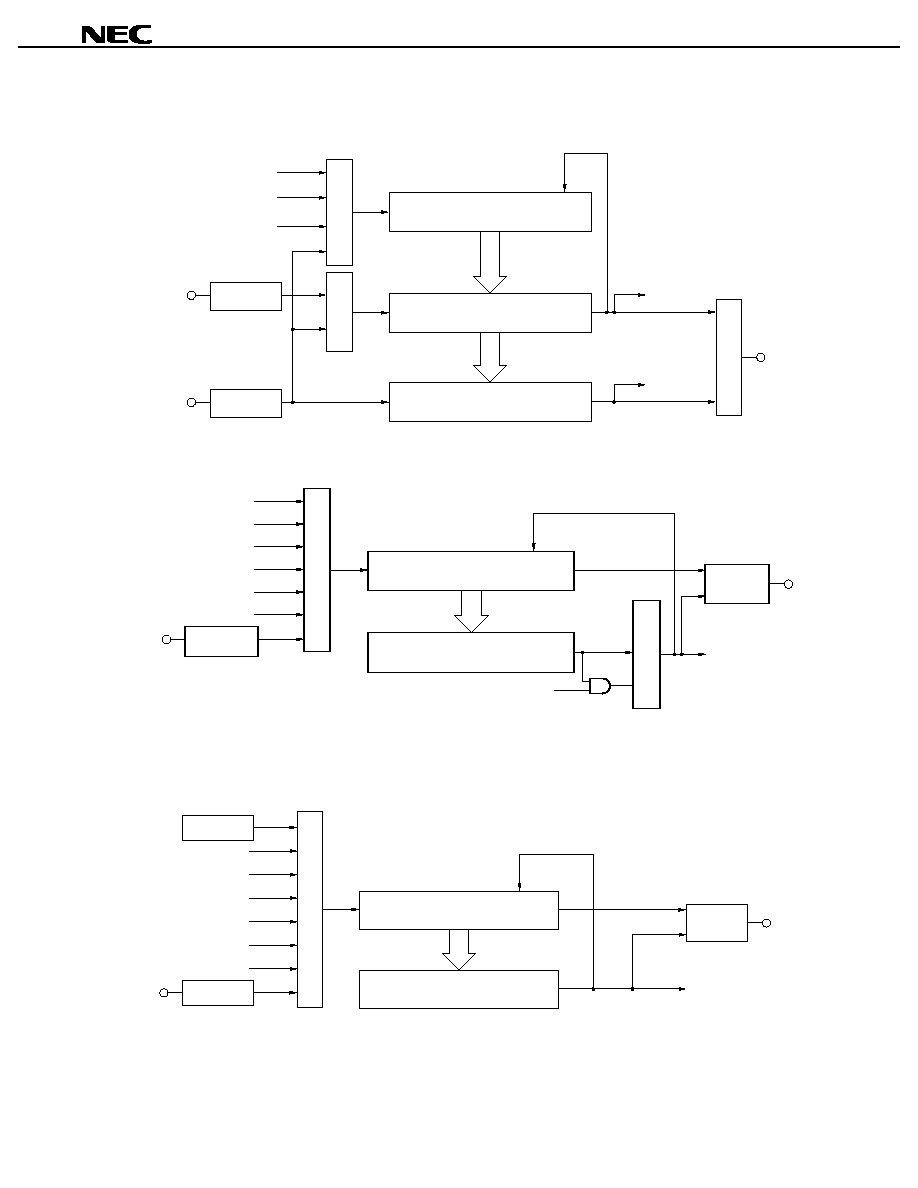
Data Sheet U14121EJ2V0DS00
41
µ
µ
µ
µ
PD784214A, 784215A, 784216A, 784217A, 784218A, 784214AY, 784215AY, 784216AY, 784217AY, 784218AY
Figure 7-6. Block Diagram of Timer/Event Counters
16-bit timer/event counter
8-bit timer/event counter 1, 5, 7
Remarks 1. n = 1, 5, 7
2. OVF: Overflow flag
8-bit timer/event counter 2, 6, 8
Remarks 1. n = 2, 6, 8
2. OVF: Overflow flag
f
XX
/4
f
XX
/16
INTTM3
TI01
TI00
Edge
detector
Edge
detector
16-bit timer counter (TM0)
16-bit capture/compare register 00
(CR00)
16-bit capture/compare register 01
(CR01)
16
16
Clear
INTTM00
INTTM01
TO0
Selector
Selector
Output controller
f
XX
/2
9
f
XX
/2
7
f
XX
/2
5
f
XX
/2
4
f
XX
/2
3
f
XX
/2
2
TIn
8-bit timer counter n
(TMn)
8-bit compare register n0
(CRn0)
8
Clear
OVF
INTTMn + 1
INTTMn
TOn
Edge
detector
Output
controller
Selector
Selector
f
XX
/2
9
f
XX
/2
7
f
XX
/2
5
f
XX
/2
4
f
XX
/2
3
f
XX
/2
2
TIn
TMn ≠ 1
8-bit timer counter n
(TMn)
8-bit compare register n0
(CRn0)
8
Clear
OVF
INTTMn
TOn
Edge detector
Output
controller
Selector
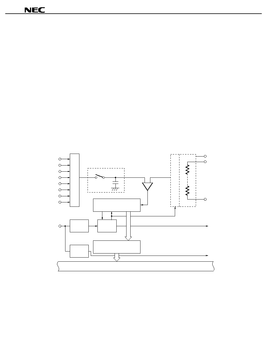
Data Sheet U14121EJ2V0DS00
42
µ
µ
µ
µ
PD784214A, 784215A, 784216A, 784217A, 784218A, 784214AY, 784215AY, 784216AY, 784217AY, 784218AY
7.5 A/D Converter
An A/D converter converts an analog signal input into a digital signal. This microcontroller is provided with an A/D
converter with a resolution of 8 bits and eight channels (ANI0 to ANI7).
This A/D converter is of successive approximation type and the result of conversion is stored in an 8-bit A/D
conversion result register (ADCR).
The A/D converter can be started in the following two ways:
∑
Hardware start
Conversion is started by trigger input (P03).
∑
Software start
Conversion is started by setting the A/D converter mode register (ADM).
One analog input channel is selected from ANI0 to ANI7 for A/D conversion. When A/D conversion is started by
means of hardware start, conversion is stopped after it has been completed. When conversion is started by means
of software start, A/D conversion is repeatedly executed. Each time conversion has been completed, an interrupt
request (INTAD) is generated.
Figure 7-7. Block Diagram of A/D Converter
ANI0
ANI1
ANI2
ANI3
ANI4
ANI5
ANI6
ANI7
Sample & hold circuit
Series resistor string
Voltage comparator
Successive approximation
register (SAR)
A/D conversion result register
(ADCR)
Controller
Edge
detector
INTP3/P03
INTAD
INTP3
AV
SS
AV
REF0
AV
DD
Internal bus
Selector
Tap selector
Edge
detector
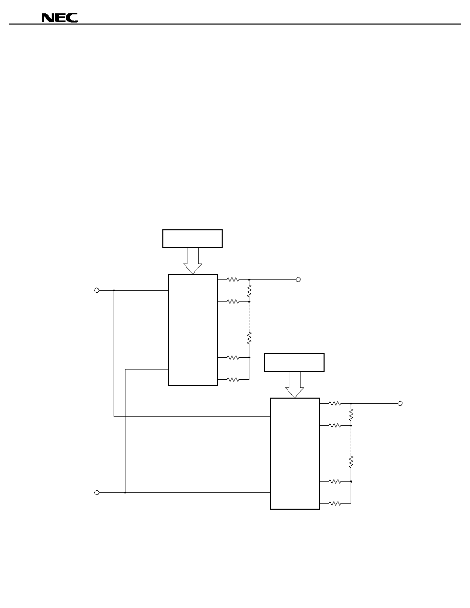
Data Sheet U14121EJ2V0DS00
43
µ
µ
µ
µ
PD784214A, 784215A, 784216A, 784217A, 784218A, 784214AY, 784215AY, 784216AY, 784217AY, 784218AY
7.6 D/A Converter
A D/A converter converts a digital signal input into an analog signal. This microcontroller is provided with a
voltage output type D/A converter with a resolution of 8 bits and two channels.
The conversion method is of R-2R resistor ladder type.
D/A conversion is started by setting DACE0 of D/A converter mode register 0 (DAM0) and DACE1 of D/A
converter mode register 1 (DAM1).
The D/A converter operates in the following two modes:
∑
Normal mode
The converter outputs an analog voltage immediately after it has completed D/A conversion.
∑
Real-time output mode
The converter outputs an analog voltage in synchronization with an output trigger after it has completed D/A
conversion.
Figure 7-8. Block Diagram of D/A Converter
AV
REF1
AV
SS
DACS0
8
2R
2R
R
R
2R
2R
Selector
ANO0
DACS1
8
2R
2R
R
R
2R
2R
Selector
ANO1

Data Sheet U14121EJ2V0DS00
44
µ
µ
µ
µ
PD784214A, 784215A, 784216A, 784217A, 784218A, 784214AY, 784215AY, 784216AY, 784217AY, 784218AY
7.7 Serial Interface
Three independent serial interface channels are provided.
∑
Asynchronous serial interface (UART)/3-wire serial I/O (IOE)
◊
2
∑
Clocked serial interface (CSI)
◊
1
∑
3-wire serial I/O (IOE)
∑
I
2
C bus interface (I
2
C) (
µ
PD784216AY/784218AY Subseries only)
Therefore, communication with an external system and local communication within the system can be
simultaneously executed (refer to Figure 7-9).
Figure 7-9. Example of Serial Interface
(a) UART + I
2
C
(b)
[UART]
[UART]
RS-232-C
driver/receiver
RxD1
TxD1
RS-232-C
driver/receiver
Port
RxD2
TxD2
Port
SDA0
SCL0
[I
2
C]
V
DD
V
DD
SDA
SCL
SDA
SCL
LCD
PD4711A
µ
PD4711A
µ
PD784218AY (master)
µ
PD780078Y (slave)
µ
PD780308Y (slave)
µ
(b) UART + 3-wire serial I/O
PD784218AY (master)
µ
RS-232-C
driver/receiver
[UART]
Port
RxD2
TxD2
PD753106 (slave)
µ
SI
SO
SCK
Port
INT
[3-wire serial I/O]
Note
SO1
SI1
SCK1
INTPm
Port
PD4711A
µ
Note Handshake
line
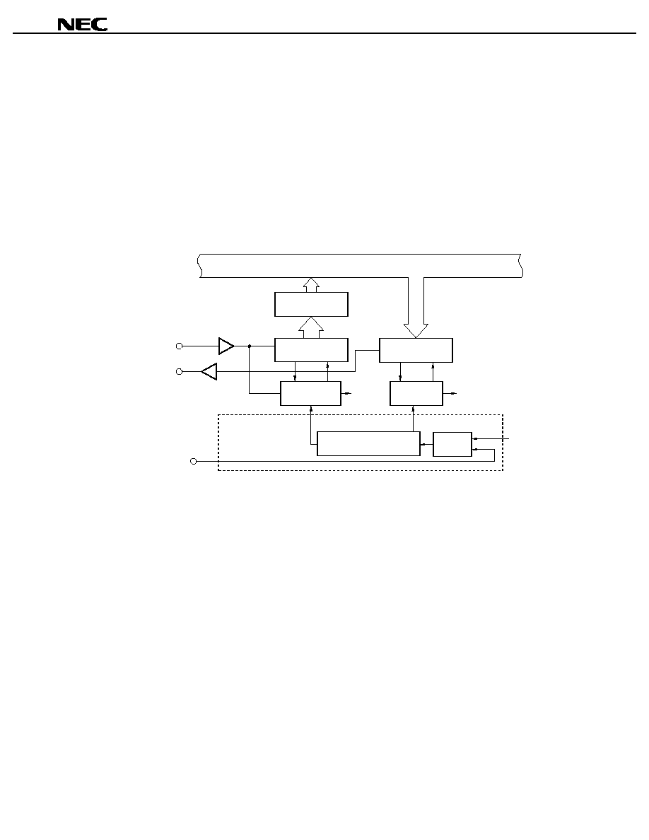
Data Sheet U14121EJ2V0DS00
45
µ
µ
µ
µ
PD784214A, 784215A, 784216A, 784217A, 784218A, 784214AY, 784215AY, 784216AY, 784217AY, 784218AY
7.7.1 Asynchronous serial interface/3-wire serial I/O (UART/IOE)
Two channels of serial interfaces for which an asynchronous serial interface mode and a 3-wire serial I/O mode
can be selected are provided.
(1) Asynchronous serial interface mode
In this mode, data of 1 byte following the start bit is transmitted or received.
Because an on-chip baud rate generator is provided, a wide range of baud rates can be set.
Moreover, the clock input to the ASCK pin can be divided to define a baud rate.
When the baud rate generator is used, a baud rate conforming to the MIDI standard (31.25 kbps) can also be
obtained.
Figure 7-10. Block Diagram in Asynchronous Serial Interface Mode
Internal bus
8
8
8
Receive buffer register
1, 2 (RXB1, RXB2)
Receive shift register
1, 2 (RX1, RX2)
Transmit shift register
1, 2 (TXS1, TXS2)
Receive control
parity check
Transmit control
parity addition
5-bit counter
◊
2 transmit/
receive clock generation
RxD1, RxD2
TxD1, TxD2
ASCK1, ASCK2
Baud rate generator
INTSR1,
INTSR2
INTST1,
INTST2
Selector
f
XX
to f
XX
/2
5
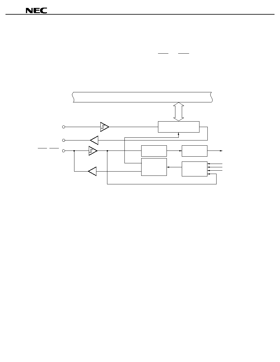
Data Sheet U14121EJ2V0DS00
46
µ
µ
µ
µ
PD784214A, 784215A, 784216A, 784217A, 784218A, 784214AY, 784215AY, 784216AY, 784217AY, 784218AY
(2) 3-wire serial I/O mode
In this mode, the master device starts transfer by making the serial clock active and transfers 1-byte data in
synchronization with this clock.
This mode is used to communicate with a device having a conventional clocked serial interface. Basically,
communication is established by using three lines: serial clocks (SCK1 and SCK2), serial data inputs (SI1 and
SI2), and serial data outputs (SO1 and SO2). To connect two or more devices, a handshake line is
necessary.
Figure 7-11. Block Diagram in 3-Wire Serial I/O Mode
Internal bus
8
Interrupt
generator
Selector
Serial clock
counter
Serial clock
controller
Serial I/O shift register
1, 2 (SIO1, SIO2)
SI1, SI2
SO1, SO2
SCK1, SCK2
INTCSI1,
INTCSI2
TO2
f
XX
/8
f
XX
/16

Data Sheet U14121EJ2V0DS00
47
µ
µ
µ
µ
PD784214A, 784215A, 784216A, 784217A, 784218A, 784214AY, 784215AY, 784216AY, 784217AY, 784218AY
7.7.2 Clocked serial interface (CSI)
In this mode, the master device starts transfer by making the serial clock active and transfers 1-byte data in
synchronization with this clock.
(1) 3-wire serial I/O mode
This mode is to communicate with devices having a conventional clocked serial interface.
Basically, communication is established in this mode with three lines: serial clock (SCK0) serial data input
(SI0), and serial data output (SO0) lines.
Generally, a handshake line is necessary to check the reception status.
Figure 7-12. Block Diagram in 3-Wire Serial I/O Mode
SI0
SO0
SCK0
INTCSI0
TO2
f
XX
/8
f
XX
/16
Internal bus
Interrupt
generator
Selector
Serial clock
counter
Serial clock
controller
Serial I/O shift register 0
(SIO0)
8

Data Sheet U14121EJ2V0DS00
48
µ
µ
µ
µ
PD784214A, 784215A, 784216A, 784217A, 784218A, 784214AY, 784215AY, 784216AY, 784217AY, 784218AY
(2) I
2
C bus (Inter IC) bus mode (supporting multimaster) (
µ
µ
µ
µ
PD784216AY/784218AY Subseries only)
This mode is for communication with devices conforming to the I
2
C bus format.
This mode is for transferring 8-bit data between two or more devices by using two lines: serial clock (SCL0)
and serial data bus (SDA0) lines.
During transmission, a "start condition", "data", and "stop condition" can be output onto the serial data bus.
During reception, these data are automatically detected by hardware.
Figure 7-13. Block Diagram of I
2
C Bus Mode
Internal bus
Direction controller
Slave address register
(SVA0)
8
8
8
SDA0
SCL0
Serial I/O shift
register 0 (SIO0)
Output latch
Wake-up
controller
Start condition/acknowledge
detector
Stop condition
detector
Serial clock counter
Serial clock
controller
Acknowledge
generator
Interrupt
generator
Selector
INTIIC0
TO2/18 to TO2/68
f
XX
/24 to f
XX
/178
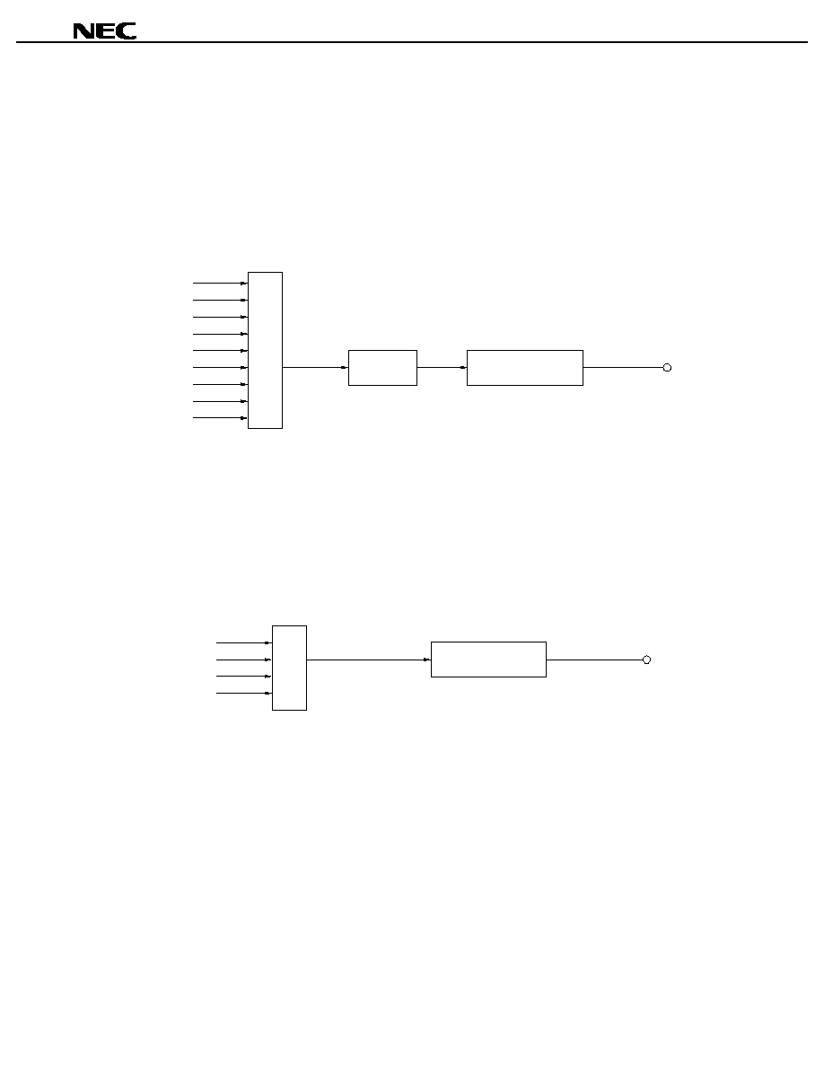
Data Sheet U14121EJ2V0DS00
49
µ
µ
µ
µ
PD784214A, 784215A, 784216A, 784217A, 784218A, 784214AY, 784215AY, 784216AY, 784217AY, 784218AY
7.8 Clock Output Function
Clocks of the following frequencies can be output as clock output.
∑
97.7 kHz/195 kHz/391 kHz/781 kHz/1.56 MHz/3.13 MHz/6.25 MHz/12.5 MHz
(@12.5 MHz operation with main system clock)
∑
32.768 kHz (@32.768 kHz operation with subsystem clock)
Figure 7-14. Block Diagram of Clock Output Function
7.9 Buzzer Output Function
Clocks of the following frequencies can be output as buzzer output.
∑
1.5 kHz/3.1 kHz/6.1 kHz/12.2 kHz (@12.5 MHz operation with main system clock)
Figure 7-15. Block Diagram of Buzzer Output Function
f
XX
f
XX
/2
f
XX
/2
2
f
XX
/2
3
f
XX
/2
4
f
XX
/2
5
f
XX
/2
6
f
XX
/2
7
f
XT
Synchronization
circuit
Output controller
PCL
Selector
f
XX
/2
10
f
XX
/2
11
f
XX
/2
12
f
XX
/2
13
Output controller
BUZ
Selector
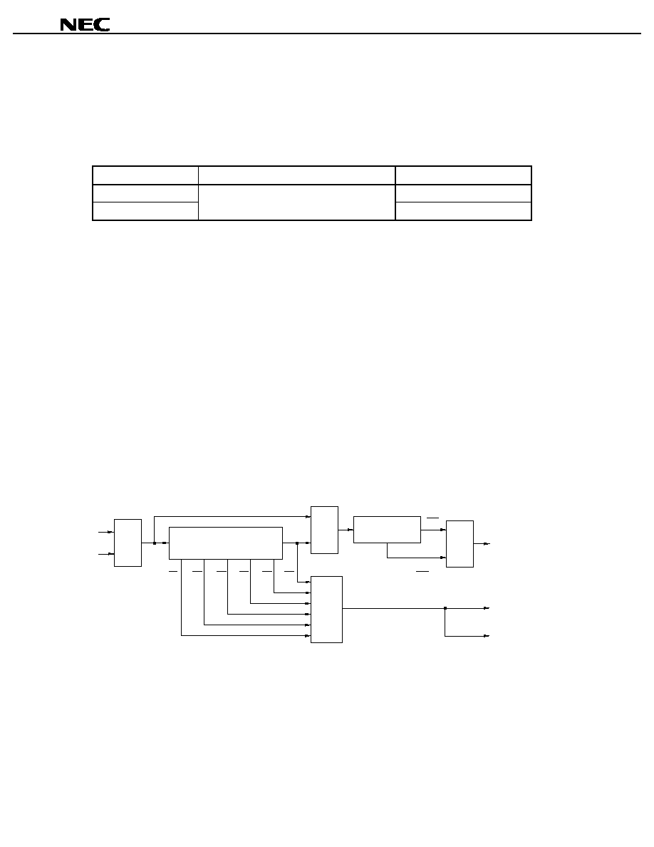
Data Sheet U14121EJ2V0DS00
50
µ
µ
µ
µ
PD784214A, 784215A, 784216A, 784217A, 784218A, 784214AY, 784215AY, 784216AY, 784217AY, 784218AY
7.10 Edge Detection Function
The interrupt input pins (INTP0, INTP1, NMI/INTP2, INTP3 to INTP6) are used not only to input interrupt requests
but also to input trigger signals to the internal hardware units. Because these pins operate at an edge of the input
signal, they have a function to detect an edge. Moreover, a noise elimination function is also provided to prevent
erroneous detection due to noise.
Pin Name
Detectable Edge
Noise Elimination
NMI
By analog delay
INTP0 to INTP6
Either or both of rising and falling edges
-
7.11 Watch Timer
The watch timer has the following functions:
∑
Watch timer
∑
Interval timer
The watch timer and interval timer functions can be used at the same time.
(1) Watch timer
The watch timer sets the WTIF flag of the interrupt control register (WTIC) at time intervals of 0.5 seconds by
using the 32.768 kHz subsystem clock.
(2) Interval timer
The interval timer generates an interrupt request (INTTM3) at predetermined time intervals.
Figure 7-16. Block Diagram of Watch Timer
f
XX
/2
7
Prescaler
f
XT
f
W
2
4
f
W
2
5
f
W
2
6
f
W
2
7
f
W
2
8
f
W
f
W
2
9
5-bit counter
f
W
2
5
f
W
2
14
INTWT
INTTM3
To 16-bit timer/counter
Selector
Selector
Selector
Selector
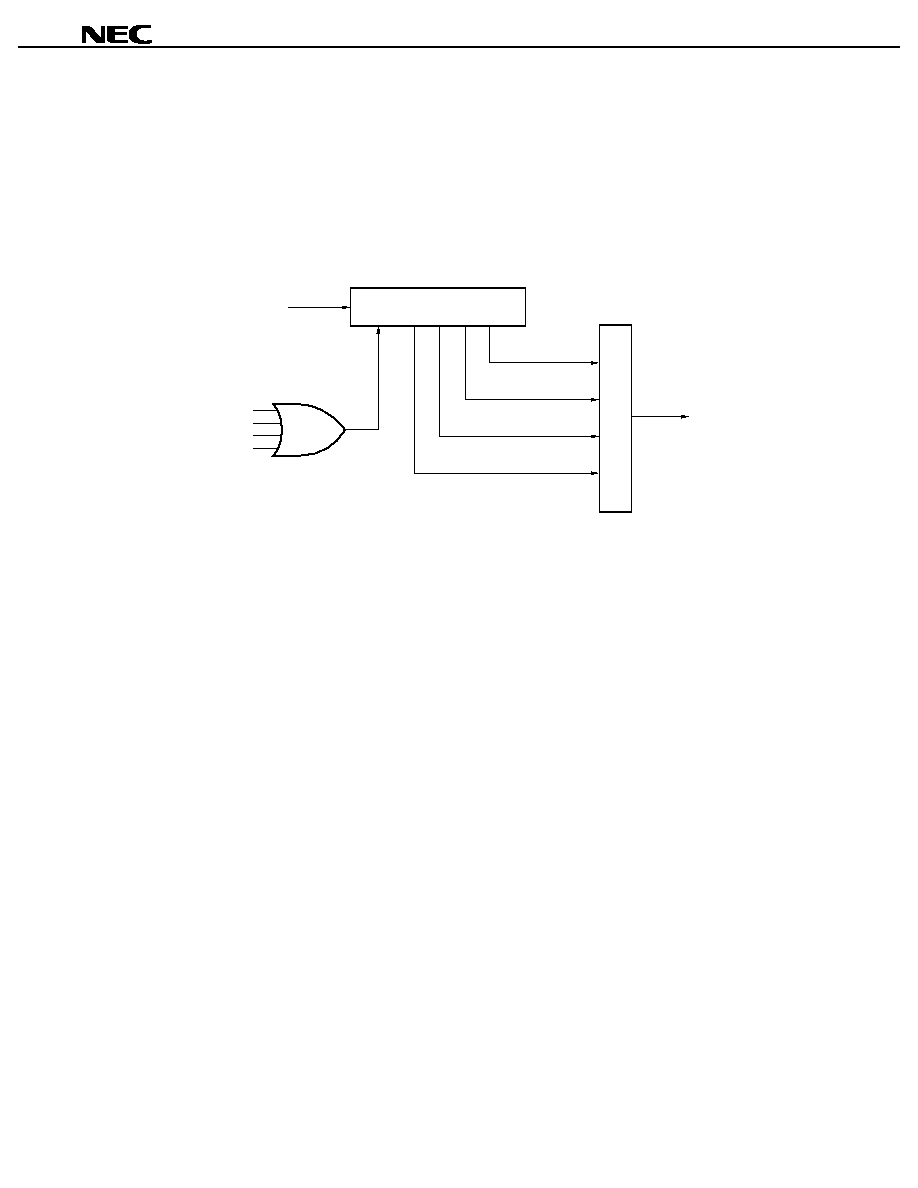
Data Sheet U14121EJ2V0DS00
51
µ
µ
µ
µ
PD784214A, 784215A, 784216A, 784217A, 784218A, 784214AY, 784215AY, 784216AY, 784217AY, 784218AY
7.12 Watchdog Timer
A watchdog timer is provided to detect a CPU runaway. This watchdog timer generates a non-maskable or
maskable interrupt unless it is cleared by software within a specified interval time. Once enabled to operate, the
watchdog timer cannot be stopped by software. Whether the interrupt by the watchdog timer or the interrupt input
from the NMI pin takes precedence can be specified.
Figure 7-17. Block Diagram of Watchdog Timer
Note Write "+" to bit 7 (RUN) of the watchdog timer (WDM)
Remark f
CLK
: Internal system clock (f
XX
to f
XX
/8)
f
CLK
/2
21
f
CLK
/2
20
f
CLK
/2
19
f
CLK
/2
17
f
CLK
INTWDT
HALT
IDLE
STOP
RUN
Note
Timer
Selector
Data Sheet U14121EJ2V0DS00
52
µ
µ
µ
µ
PD784214A, 784215A, 784216A, 784217A, 784218A, 784214AY, 784215AY, 784216AY, 784217AY, 784218AY
8. INTERRUPT FUNCTIONS
The three types of interrupt request servicing shown in Table 8-1 can be selected by program.
Table 8-1. Servicing of Interrupt Request
Servicing Mode
Entity of Servicing
Servicing
Contents of PC and PSW
Vectored interrupt
Branches and executes servicing routine
(servicing is arbitrary)
Saves to and restores from
stack
Context switching
Software
Automatically switches register bank,
branches and executes servicing routine
(servicing is arbitrary)
Saves to or restores from
fixed area in register bank
Macro service
Firmware
Executes data transfer between memory
and I/O (servicing is fixed)
Retained
8.1 Interrupt Sources
Table 8-2 shows the interrupt sources available. As shown, interrupts are generated by 29 types of sources,
execution of the BRK instruction, BRKCS instruction, or an operand error.
The priority of interrupt servicing can be set to four levels, so that nesting can be controlled during interrupt
servicing and so that which of the two or more interrupts that simultaneously occur should be serviced first can be
determined. When the macro service function is used, however, nesting always proceeds.
The default priority is the priority (fixed) of the service that is performed if two or more interrupt requests, having
the same priority, are simultaneously generated (refer to Table 8-2).
Table 8-2. Interrupt Sources (1/2)
Source
Type
Default
Priority
Name
Trigger
Internal/
External
Macro
Service
BRK instruction
Instruction execution
BRKCS instruction
Instruction execution
Software
-
Operand error
If result of exclusive OR between operands byte
and byte is not FFH when "MOV STBC, #byte"
instruction, "MOV WDM, #byte" instruction, or
LOCATION instruction is executed
-
-
NMI
Pin input edge detection
External
Non-maskable
-
INTWDT
Overflow of watchdog timer
Internal
-
0 (highest)
INTWDTM
Overflow of watchdog timer
Internal
1
INTP0
2
INTP1
3
INTP2
4
INTP3
5
INTP4
6
INTP5
7
INTP6
Pin input edge detection
External
INTIIC0
End of I
2
C bus transfer by CSI0
8
INTCSI0
End of 3-wire transfer by CSI0
Maskable
9
INTSER1
Occurrence of UART reception error in ASI1
Internal
Data Sheet U14121EJ2V0DS00
53
µ
µ
µ
µ
PD784214A, 784215A, 784216A, 784217A, 784218A, 784214AY, 784215AY, 784216AY, 784217AY, 784218AY
Table 8-2. Interrupt Sources (2/2)
Source
Type
Default
Priority
Name
Trigger
Internal/
External
Macro
Service
INTSR1
End of UART reception by ASI1
10
INTCSI1
End of 3-wire transfer by CSI1
11
INTST1
End of UART transmission by ASI1
12
INTSER2
Occurrence of UART reception error in ASI2
INTSR2
End of UART reception by ASI2
13
INTCSI2
End of 3-wire transfer by CSI2
14
INTST2
End of UART transmission by ASI2
15
INTTM3
Reference time interval signal from watch timer
16
INTTM00
Signal indicating match between 16-bit timer
counter and capture/compare register (CR00)
17
INTTM01
Signal indicating match between 16-bit timer
counter and capture/compare register (CR01)
18
INTTM1
Occurrence of match signal of 8-bit timer/event
counter 1
19
INTTM2
Occurrence of match signal of 8-bit timer/event
counter 2
20
INTAD
End of conversion by A/D converter
21
INTTM5
Occurrence of match signal of 8-bit timer/event
counter 5
22
INTTM6
Occurrence of match signal of 8-bit timer/event
counter 6
23
INTTM7
Occurrence of match signal of 8-bit timer/event
counter 7
24
INTTM8
Occurrence of match signal of 8-bit timer/event
counter 8
25
INTWT
Overflow of watch timer
Internal
Maskable
26 (lowest)
INTKR
Detection of falling edge of port 8
External
Remarks 1. ASI: Asynchronous Serial Interface
CSI: Clocked Serial Interface
2. There are two interrupt sources for the watchdog timer: non-maskable interrupts (INTWDT) and
maskable interrupts (INTWDTM). Either one (but not both) should be selected for actual use.
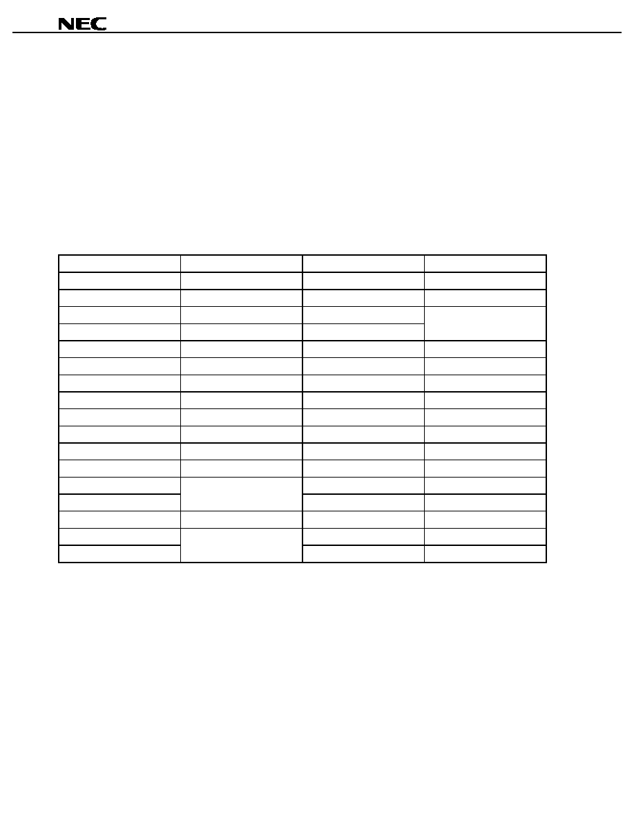
Data Sheet U14121EJ2V0DS00
54
µ
µ
µ
µ
PD784214A, 784215A, 784216A, 784217A, 784218A, 784214AY, 784215AY, 784216AY, 784217AY, 784218AY
8.2 Vectored Interrupt
Execution branches to a servicing routine by using the memory contents of a vector table address corresponding
to the interrupt source as the address of the branch destination.
So that the CPU performs interrupt servicing, the following operations are performed:
∑
On branching: Saves the status of the CPU (contents of PC and PSW) to stack
∑
On returning: Restores the status of the CPU (contents of PC and PSW) from stack
To return to the main routine from an interrupt service routine, the RETI instruction is used.
The branch destination address is in a range of 0 to FFFFH.
Table 8-3. Vector Table Address
Interrupt Source
Vector Table Address
Interrupt Source
Vector Table Address
BRK instruction
003EH
INTST1
001CH
TRAP0 (operand error)
003CH
INTSER2
001EH
NMI
0002H
INSR2
INTWDT (non-maskable)
0004H
INTCSI2
0020H
INTWDTM (maskable)
0006H
INTST2
0022H
INTP0
0008H
INTTM3
0024H
INTP1
000AH
INTTM00
0026H
INTP2
000CH
INTTM01
0028H
INTP3
000EH
INTTM1
002AH
INTP4
0010H
INTTM2
002CH
INTP5
0012H
INTAD
002EH
INTP6
0014H
INTTM5
0030H
INTIIC0
INTTM6
0032H
INTCSI0
0016H
INTTM7
0034H
INTSER1
0018H
INTTM8
0036H
INTSR1
INTWT
0038H
INTCSI1
001AH
INTKR
003AH

Data Sheet U14121EJ2V0DS00
55
µ
µ
µ
µ
PD784214A, 784215A, 784216A, 784217A, 784218A, 784214AY, 784215AY, 784216AY, 784217AY, 784218AY
8.3 Context Switching
When an interrupt request is generated or when the BRKCS instruction is executed, a predetermined register
bank is selected by hardware. Context switching is a function that branches execution to a vector address stored in
advance in the register bank, while at the same time stacking the current contents of the program counter (PC) and
program status word (PSW) to the register bank.
The branch address is in a range of 0 to FFFFH.
Figure 8-1. Context Switching Operation When Interrupt Request Is Generated
Register bank n (n = 0 to 7)
0000B
<7> Transfer
PC19-16
PC15-0
<6> Exchange
<5> Save
<2> Save
Temporary register
<1> Save
PSW
V
U
T
W
A
B
R5
R7
D
H
X
C
R4
R6
E
L
VP
UP
<3> Switching of register bank
(RBS0 to RBS2
n)
Register bank
(0 to 7)
(Bits 8 to 11 of
temporary register)
<4> RSS
0
IE
0
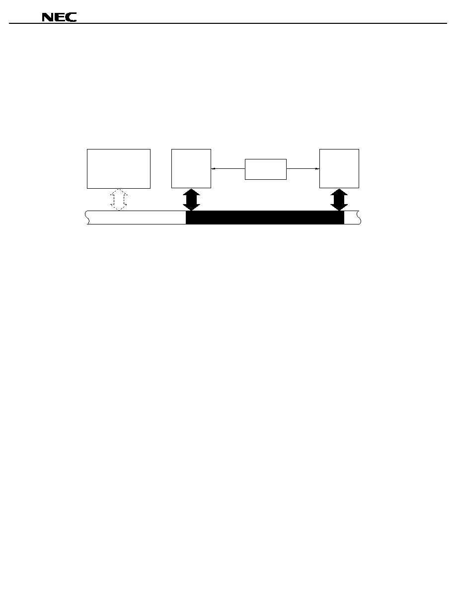
Data Sheet U14121EJ2V0DS00
56
µ
µ
µ
µ
PD784214A, 784215A, 784216A, 784217A, 784218A, 784214AY, 784215AY, 784216AY, 784217AY, 784218AY
8.4 Macro Service
This function is to transfer data between memory and a special function register (SFR) without intervention by the
CPU. A macro service controller accesses the memory and SFR in the same transfer cycle and directly transfers
data without loading it.
Because this function does not save or restore the status of the CPU, or load data, data can be transferred at high
speeds.
Figure 8-2. Macro Service
CPU
Memory
SFR
Macro service
controller
Read
Write
Write
Read
Internal bus
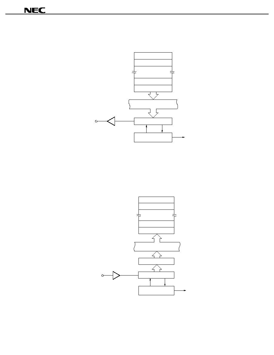
Data Sheet U14121EJ2V0DS00
57
µ
µ
µ
µ
PD784214A, 784215A, 784216A, 784217A, 784218A, 784214AY, 784215AY, 784216AY, 784217AY, 784218AY
8.5 Application Example of Macro Service
(1) Serial interface transmission
Each time macro service requests INTST1 and INTST2 are generated, the next transmit data is transferred
from memory to TXS1 and TXS2. When data n (last byte) has been transferred to TXS1 and TXS2 (when the
transmit data storage buffer has become empty), vectored interrupt requests INTST1 and INTST2 are
generated.
(2) Serial interface reception
Each time macro service requests INTSR1 and INTSR2 are generated, the receive data is transferred from
RXB1 and RXB2 to memory. When data n (last byte) has been transferred to memory (when the receive data
storage buffer has become full), vectored interrupt requests INTSR1 and INTSR2 are generated.
Transmit data storage buffer (memory)
Data n
Data n ≠ 1
Data 1
Data 2
Internal bus
Transmit shift register
TXS1, TXS2 (SFR)
Transmit control
TxD1, TxD2
INTST1, INTST2
Receive data storage buffer (memory)
Data n
Data n ≠ 1
Data 1
Data 2
Internal bus
Receive shift register
RXB1, RXB2 (SFR)
Receive control
INTSR1, INTSR2
RxD1, RxD2
Receive buffer register
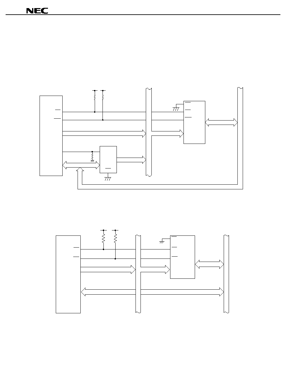
Data Sheet U14121EJ2V0DS00
58
µ
µ
µ
µ
PD784214A, 784215A, 784216A, 784217A, 784218A, 784214AY, 784215AY, 784216AY, 784217AY, 784218AY
9. LOCAL BUS INTERFACE
The local bus interface can connect an external memory or I/O (memory mapped I/O) and support a memory
space of 1 MB (refer to Figure 9-1).
Figure 9-1. Example of Local Bus Interface
(a) Multiplexed bus mode
(b) Separate bus mode
µ
PD784218A
RD
WR
A8 to A19
ASTB
AD0 to AD7
V
DD
Address latch
LE
Q0 to Q7
D0 to D7
OE
SRAM
CS
OE
WE
I/O1 to I/O8
A0 to A19
Data bus
Address bus
V
DD
Address bus
SRAM
Data bus
OE
WE
A0 to A19
CS
I/O1 to I/O8
µ
PD784218A
RD
WR
A0 to A19
AD0 to AD7

Data Sheet U14121EJ2V0DS00
59
µ
µ
µ
µ
PD784214A, 784215A, 784216A, 784217A, 784218A, 784214AY, 784215AY, 784216AY, 784217AY, 784218AY
9.1 Memory Expansion
External program memory and data memory can be connected in two stages: 256 KB and 1 MB.
To connect the external memory, ports 4 through 6 and port 8 are used.
The external memory can be connected in the following two modes:
∑
Multiplexed bus mode: The external memory is connected by using a time-division address/data bus. The
number of ports used when the external memory is connected can be reduced in this
mode.
∑
Separate bus mode:
The external memory is connected by using an address bus and data bus independent
of each other. Because an external latch circuit is not necessary, this mode is useful for
reducing the number of components and mounting area on the printed wiring board.
9.2 Programmable Wait
Wait state(s) can be inserted to the memory space (00000H to FFFFFH) while the RD and WR signals are active.
In addition, there is an address wait function that extends the active period of the ASTB signal to gain the address
decode time.

Data Sheet U14121EJ2V0DS00
60
µ
µ
µ
µ
PD784214A, 784215A, 784216A, 784217A, 784218A, 784214AY, 784215AY, 784216AY, 784217AY, 784218AY
10. STANDBY FUNCTION
This function is to reduce the power consumption of the chip, and can be used in the following modes:
∑
HALT mode:
Stops supply of the operating clock to the CPU. This mode is used in
combination with the normal operation mode for intermittent operation to
reduce the average power consumption.
∑
IDLE mode:
Stops the entire system except for the oscillator, which continues
operating. The power consumption in this mode is close to that in the
STOP mode.
However, the time required to restore the normal program operation
from this mode is almost the same as that from the HALT mode.
∑
STOP
mode:
Stops the main system clock and thereby stops all the internal
operations of the chip. Consequently, the power consumption is
minimized with only leakage current flowing.
∑
Low power consumption mode:
The main system clock is stopped and the subsystem clock is used as
the system clock. The CPU can operate on the subsystem clock to
reduce the current consumption.
∑
Low power consumption HALT mode: This is a standby function in the low power consumption mode and
stops the operation clock of the CPU, to reduce the power consumption
of the entire system.
∑
Low power consumption IDLE mode: This is a standby function in the low power consumption mode and
stops the entire system except the oscillator, to reduce the power
consumption of the entire system.
These modes are programmable.
The macro service can be started from the HALT mode or low power consumption HALT mode. After macro
service processing is executed, the system returns to the HALT mode again.
The transition of the standby status is shown in Figure 10-1.
Data Sheet U14121EJ2V0DS00
61
µ
µ
µ
µ
PD784214A, 784215A, 784216A, 784217A, 784218A, 784214AY, 784215AY, 784216AY, 784217AY, 784218AY
Figure 10-1. Standby Function State Transitions
Notes 1. Only unmasked interrupt requests
2. Only unmasked INTP0 to INTP6, INTWT, key return interrupt (P80 to P87)
Remark NMI is valid only for an external input. The watchdog timer cannot be used for the release of standby
(HALT mode/STOP mode/IDLE mode).
Wait for
stable
oscillation
Normal
operation
(Main system
clock
operation)
Macro
service
HALT
(Standby)
IDLE
(Standby)
Low power
consumption
mode
(Subsystem
clock operation)
Low
power
consumption
HALT mode
(Standby)
Low power
consumption
IDLE mode
(Standby)
STOP
(Standby)
RESET input
Macro service request
One-time processing ends
Macro service ends
Macro service request
One-time processing ends
Interrupt request
RESET input
HALT set
IDLE set
RESET input
NMI, INTP0 to INTP6 input, INTWT,
key return interrupt
Note 2
NMI, INTP0 to INTP6 input,
INTWT, key return interrupt
Note 2
STOP set
Low power consumption
IDLE mode set
RESET input
Low power
consumption mode set
Return to normal operation
NMI, INTP0 to INTP6 input,
INTWT, key return interrupt
Note 2
Low power consumption HALT mode set
RESET input
Interrupt request
Note 1
Interrupt
request for
masked interrupt
Interrupt
request for
masked interrupt
Interrupt
request for
masked
interrupt
Interrupt
request for
masked
interrupt
Interrupt
request for
masked
interrupt
RESET input
RESET input
Macro
service
Macro service request
Macro service request
One-time processing ends
Macro service ends
One-time processing ends
Data Sheet U14121EJ2V0DS00
62
µ
µ
µ
µ
PD784214A, 784215A, 784216A, 784217A, 784218A, 784214AY, 784215AY, 784216AY, 784217AY, 784218AY
11. RESET FUNCTION
When a low-level signal is input to the RESET pin, the system is reset, and each hardware unit is initialized
(reset). During the reset period, oscillation of the main system clock is unconditionally stopped. Consequently, the
current consumption of the entire system can be reduced.
When the RESET signal goes high, the reset status is cleared. And after the oscillation stabilization time (84.0 ms
at 12.5 MHz operation) elapses, the contents of the reset vector table are set to the program counter (PC), execution
branches to an address set to the PC, and program execution is started from that branch address. Therefore, the
program can be reset and started from any address.
Figure 11-1. Oscillation of Main System Clock During Reset Period
The RESET input pin has an analog delay noise eliminator to prevent malfunctioning due to noise.
Figure 11-2. Acknowledgement of Reset Signal
Oscillation is unconditionally
stopped during reset period
Oscillation stabilization time
Main system clock
oscillator
f
CLK
RESET input
Analog delay
Analog delay
Analog
delay
Oscillation
stabilization
time
Time until clock
starts oscillating
RESET input
Internal reset signal
Internal clock
Data Sheet U14121EJ2V0DS00
63
µ
µ
µ
µ
PD784214A, 784215A, 784216A, 784217A, 784218A, 784214AY, 784215AY, 784216AY, 784217AY, 784218AY
12. INSTRUCTION SET
(1) 8-bit instructions (instructions in parentheses are combinations realized by describing A as r)
MOV, XCH, ADD, ADDC, SUB, SUBC, AND, OR, XOR, CMP, MULU, DIVUW, INC, DEC, ROR, ROL, RORC,
ROLC, SHR, SHL, ROR4, ROL4, DBNZ, PUSH, POP, MOVM, XCHM, CMPME, CMPMNE, CMPMNC,
CMPMC, MOVBK, XCHBK, CMPBKE, CMPBKNE, CMPBKNC, CMPBKC
Table 12-1. Instruction List by 8-Bit Addressing
Second Operand
First Operand
#byte
A
r
r'
saddr
saddr'
sfr
!addr16
!!addr24
mem
[saddrp]
[%saddrg]
r3
PSWL
PSWH
[WHL+]
[WHL
-
]
n
None
Note 2
A
(MOV)
ADD
Note 1
(MOV)
(XCH)
(ADD)
Note 1
MOV
XCH
(ADD)
Note 1
(MOV)
Note 6
(XCH)
Note 6
(ADD)
Notes 1, 6
MOV
(XCH)
(ADD)
Note 1
(MOV)
(XCH)
ADD
Note 1
MOV
XCH
ADD
Note 1
MOV
(MOV)
(XCH)
(ADD)
Note 1
r
MOV
ADD
Note 1
(MOV)
(XCH)
(ADD)
Note 1
MOV
XCH
ADD
Note 1
MOV
XCH
ADD
Note 1
MOV
XCH
ADD
Note 1
MOV
XCH
ROR
Note 3
MULU
DIVUW
INC
DEC
saddr
MOV
ADD
Note 1
(MOV)
Note 6
(ADD)
Note 1
MOV
ADD
Note 1
MOV
XCH
ADD
Note 1
INC
DEC
DBNZ
sfr
MOV
ADD
Note 1
MOV
(ADD)
Note 1
MOV
ADD
Note 1
PUSH
POP
!addr16
!!addr24
MOV
(MOV)
ADD
Note 1
MOV
mem
[saddrp]
[%saddrg]
MOV
ADD
Note 1
mem3
ROR4
ROL4
r3
PSWL
PSWH
MOV
MOV
B, C
DBNZ
STBC, WDM
MOV
[TDE+]
[TDE
-
]
(MOV)
Note 6
(ADD)
Note 1
MOVM
Note 4
MOVBK
Note 5
Notes 1. The operands of ADDC, SUB, SUBC, AND, OR, XOR, and CMP are the same as that of ADD.
2. Either the second operand is not used, or the second operand is not an operand address.
3. The operands of ROL, RORC, ROLC, SHR, and SHL are the same as that of ROR.
4. The operands of XCHM, CMPME, CMPMNE, CMPMNC, and CMPMC are the same as that of
MOVM.
5. The operands of XCHBK, CMPBKE, CMPBKNE, CMPBKNC, and CMPBKC are the same as that of
MOVBK.
6. The code length of some instructions having saddr2 as saddr in this combination is short.
Data Sheet U14121EJ2V0DS00
64
µ
µ
µ
µ
PD784214A, 784215A, 784216A, 784217A, 784218A, 784214AY, 784215AY, 784216AY, 784217AY, 784218AY
(2) 16-bit instructions (instructions in parentheses are combinations realized by describing AX as rp)
MOVW, XCHW, ADDW, SUBW, CMPW, MULUW, MULW, DIVUX, INCW, DECW, SHRW, SHLW, PUSH,
POP, ADDWG, SUBWG, PUSHU, POPU, MOVTBLW, MACW, MACSW, SACW
Table 12-2. Instruction List by 16-Bit Addressing
Second Operand
First Operand
#word
AX
rp
rp'
saddrp
saddrp'
sfrp
!addr16
!!addr24
mem
[saddrp]
[%saddrg]
[WHL+]
byte
n
None
Note 2
AX
(MOVW)
ADDW
Note 1
(MOVW)
(XCHW)
(ADD)
Note 1
(MOVW)
(XCHW)
(ADDW)
Note 1
(MOVW)
Note 3
(XCHW)
Note 3
(ADDW)
Notes 1, 3
MOVW
(XCHW)
(ADDW)
Note 1
(MOVW)
XCHW
MOVW
XCHW
(MOVW)
(XCHW)
rp
MOVW
ADDW
Note 1
(MOVW)
(XCHW)
(ADDW)
Note 1
MOVW
XCHW
ADDW
Note 1
MOVW
XCHW
ADDW
Note 1
MOVW
XCHW
ADDW
Note 1
MOVW
SHRW
SHLW
MULU
Note 4
INCW
DECW
saddrp
MOVW
ADDW
Note 1
(MOVW)
Note 3
(ADDW)
Note 1
MOVW
ADDW
Note 1
MOVW
XCHW
ADDW
Note 1
INCW
DECW
sfrp
MOVW
ADDW
Note 1
MOVW
(ADDW)
Note 1
MOVW
ADDW
Note 1
PUSH
POP
!addr16
!!addr24
MOVW
(MOVW)
MOVW
MOVTBLW
mem
[saddrp]
[%saddrg]
MOVW
PSW
PUSH
POP
SP
ADDWG
SUBWG
post
PUSH
POP
PUSHU
POPU
[TDE+]
(MOVW)
SACW
byte
MACW
MACSW
Notes 1. The operands of SUBW and CMPW are the same as that of ADDW.
2. Either the second operand is not used, or the second operand is not an operand address.
3. The code length of some instructions having saddrp2 as saddrp in this combination is short.
4. The operands of MULUW and DIVUX are the same as that of MULW.

Data Sheet U14121EJ2V0DS00
65
µ
µ
µ
µ
PD784214A, 784215A, 784216A, 784217A, 784218A, 784214AY, 784215AY, 784216AY, 784217AY, 784218AY
(3) 24-bit instructions (instructions in parentheses are combinations realized by describing WHL
as rg)
MOVG, ADDG, SUBG, INCG, DECG, PUSH, POP
Table 12-3. Instruction List by 24-Bit Addressing
Second Operand
First Operand
#imm24
WHL
rg
rg'
saddrg
!!addr24
mem1
[%saddrg]
SP
None
Note
WHL
(MOVG)
(ADDG)
(SUBG)
(MOVG)
(ADDG)
(SUBG)
(MOVG)
(ADDG)
(SUBG)
(MOVG)
ADDG
SUBG
(MOVG)
MOVG
MOVG
MOVG
rg
MOVG
ADDG
SUBG
(MOVG)
(ADDG)
(SUBG)
MOVG
ADDG
SUBG
MOVG
MOVG
INCG
DECG
PUSH
POP
saddrg
(MOVG)
MOVG
!!addr24
(MOVG)
MOVG
mem1
MOVG
[%saddrg]
MOVG
SP
MOVG
MOVG
INCG
DECG
Note Either the second operand is not used, or the second operand is not an operand address.
Data Sheet U14121EJ2V0DS00
66
µ
µ
µ
µ
PD784214A, 784215A, 784216A, 784217A, 784218A, 784214AY, 784215AY, 784216AY, 784217AY, 784218AY
(4) Bit manipulation instructions
MOV1, AND1, OR1, XOR1, SET1, CLR1, NOT1, BT, BF, BTCLR, BFSET
Table 12-4. Instruction List by Bit Manipulation Instruction Addressing
Second Operand
First Operand
CY
saddr.bit sfr.bit
A.bit X.bit
PSWL.bit PSWH.bit
mem2.bit
!addr16.bit !!addr24.bit
/saddr.bit /sfr. bit
/A.bit /X.bit
/PSWL.bit /PSWH.bit
/mem2.bit
/!addr16.bit /!!addr24.bit
None
Note
CY
MOV1
AND1
OR1
XOR1
AND1
OR1
NOT1
SET1
CLR1
saddr.bit
sfr.bit
A.bit
X.bit
PSWL.bit
PSWH.bit
mem2.bit
!addr16.bit
!!addr24.bit
MOV1
NOT1
SET1
CLR1
BF
BT
BTCLR
BFSET
Note Either the second operand is not used, or the second operand is not an operand address.
Data Sheet U14121EJ2V0DS00
67
µ
µ
µ
µ
PD784214A, 784215A, 784216A, 784217A, 784218A, 784214AY, 784215AY, 784216AY, 784217AY, 784218AY
(5) Call and return/branch instructions
CALL, CALLF, CALLT, BRK, RET, RETI, RETB, RETCS, RETCSB, BRKCS, BR, BNZ, BNE, BZ, BE, BNC,
BNL, BC, BL, BNV, BPO, BV, BPE, BP, BN, BLT, BGE, BLE, BGT, BNH, BH, BF, BT, BTCLR, BFSET, DBNZ
Table 12-5. Instruction List by Call and Return/Branch Instruction Addressing
Operand of Instruction
Address
$addr20 $!addr20
!addr16
!!addr20
rp
rg
[rp]
[rg]
!addr11
[addr5]
RBn
None
Basic instruction
BC
Note
BR
CALL
BR
CALL
BR
RETCS
RETCSB
CALL
BR
CALL
BR
CALL
BR
CALL
BR
CALL
BR
CALLF
CALLF
BRKCS
BRK
RET
RETI
RETB
Compound instruction
BF
BT
BTCLR
BFSET
DBNZ
Note The operands of BNZ, BNE, BZ, BE, BNC, BNL, BL, BNV, BPO, BV, BPE, BP, BN, BLT, BGE, BLE,
BGT, BNH, and BH are the same as that of BC.
(6) Other instructions
ADJBA, ADJBS, CVTBW, LOCATION, SEL, NOT, EI, DI, SWRS

Data Sheet U14121EJ2V0DS00
68
µ
µ
µ
µ
PD784214A, 784215A, 784216A, 784217A, 784218A, 784214AY, 784215AY, 784216AY, 784217AY, 784218AY
13. ELECTRICAL SPECIFICATIONS
Absolute Maximum Ratings (T
A
= 25
∞
∞
∞
∞
C)
Parameter
Symbol
Conditions
Ratings
Unit
V
DD
-
0.3 to +6.5
V
AV
DD
-
0.3 to V
DD
+ 0.3
V
AV
SS
-
0.3 to V
SS
+ 0.3
V
AV
REF0
A/D converter reference voltage input
-
0.3 to V
DD
+ 0.3
V
Supply voltage
AV
REF1
D/A converter reference voltage input
-
0.3 to V
DD
+ 0.3
V
V
I1
Other than P90 to P95
-
0.3 to V
DD
+ 0.3
V
Input voltage
V
I2
P90 to P95
N-ch open drain
-
0.3 to +12
V
Analog input voltage
V
AN
Analog input pin
AV
SS
-
0.3 to AV
REF0
+ 0.3
V
Output voltage
V
O
-
0.3 to V
DD
+ 0.3
V
Per pin
15
mA
Total of P2, P4 to P8
75
mA
Total of P0, P3, P9, P10, P12, P13
75
mA
Output current, low
I
OL
Total of all pins
100
mA
Per pin
-
10
mA
Output current, high
I
OH
Total of all pins
-
50
mA
Operating ambient
temperature
T
A
-
40 to +85
∞
C
Storage temperature
T
stg
-
65 to +150
∞
C
Caution
Product quality may suffer if the absolute maximum rating is exceeded even momentarily for
any parameter. That is, the absolute maximum ratings are rated values at which the product is
on the verge of suffering physical damage, and therefore the product must be used under
conditions that ensure that the absolute maximum ratings are not exceeded.
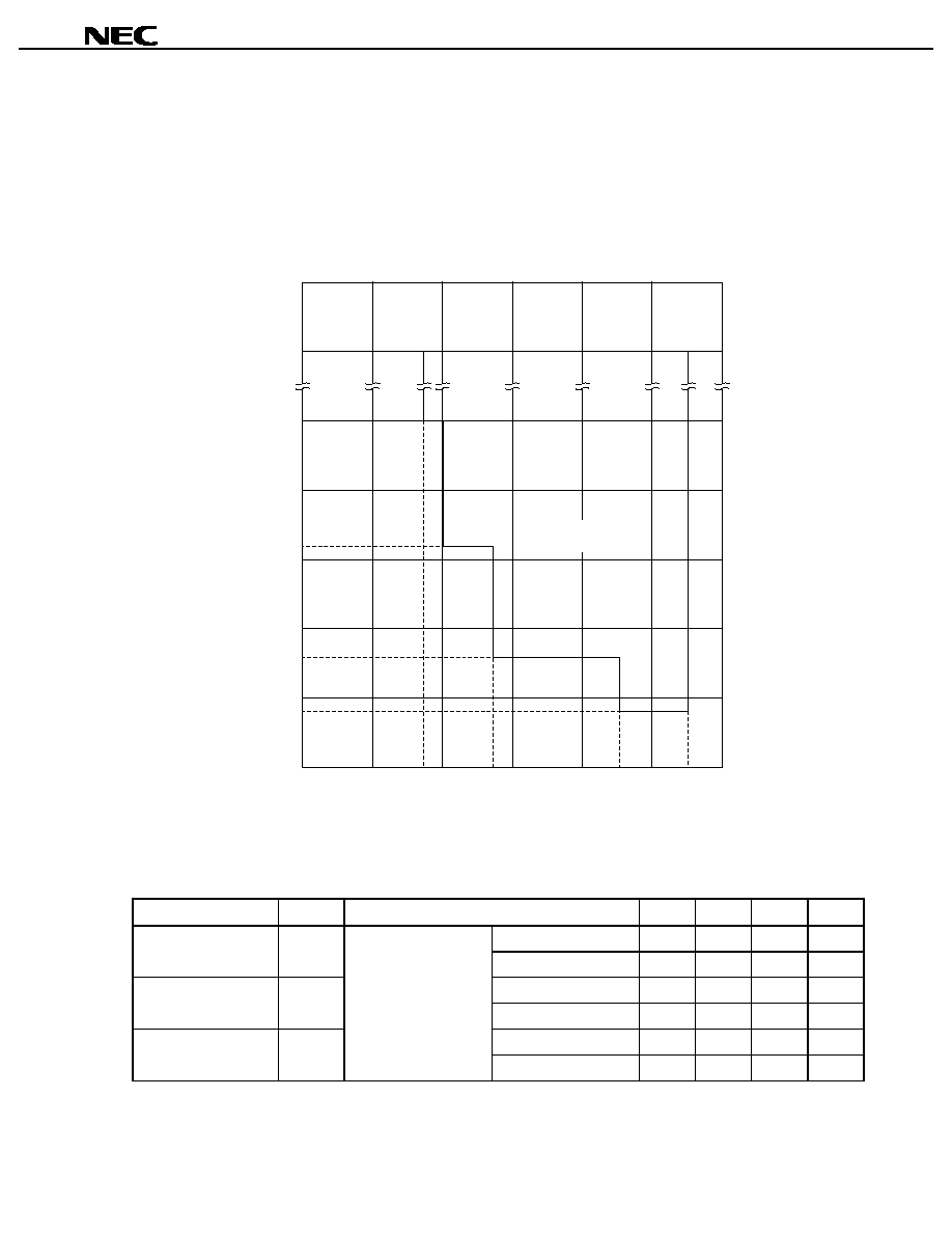
Data Sheet U14121EJ2V0DS00
69
µ
µ
µ
µ
PD784214A, 784215A, 784216A, 784217A, 784218A, 784214AY, 784215AY, 784216AY, 784217AY, 784218AY
Operating Conditions
∑
Operating ambient temperature (T
A
):
-
40 to +85
∞
C
∑
Power supply voltage and clock cycle time: See Figure 13-1
∑
Power supply voltage with subsystem clock operation: V
DD
= 1.8 to 5.5 V
Figure 13-1. Power Supply Voltage and Clock Cycle Time (CPU Clock Frequency: f
CPU
)
Capacitance (T
A
= 25
∞
∞
∞
∞
C, V
DD
= V
SS
= 0 V)
Parameter
Symbol
Conditions
MIN.
TYP.
MAX.
Unit
Other than Port 9
15
pF
Input capacitance
C
I
Port 9
20
pF
Other than Port 9
15
pF
Output capacitance
C
O
Port 9
20
pF
Other than Port 9
15
pF
I/O capacitance
C
IO
f = 1 MHz
Unmeasured pins
returned to 0 V.
Port 9
20
pF
8,000
10,000
500
400
300
320
160
80
200
100
0
0
1
2
3
1.8
2.7
4.5
5.5
Supply voltage [V]
4
5
6
Clock cycle time t
CYK
[ns]
Guaranteed
operating range
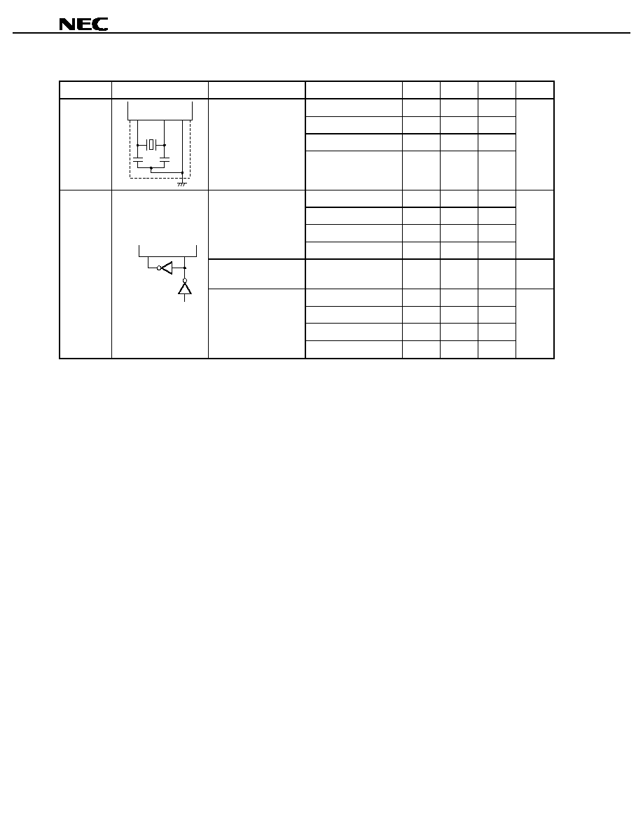
Data Sheet U14121EJ2V0DS00
70
µ
µ
µ
µ
PD784214A, 784215A, 784216A, 784217A, 784218A, 784214AY, 784215AY, 784216AY, 784217AY, 784218AY
Main System Clock Oscillator Characteristics (T
A
=
-
-
-
-
40 to +85
∞
∞
∞
∞
C)
Resonator
Recommended Circuit
Parameter
Conditions
MIN.
TYP.
MAX.
Unit
4.5 V
V
DD
5.5 V
2
12.5
2.7 V
V
DD
< 4.5 V
2
6.25
2.0 V
V
DD
< 2.7 V
2
3.125
Ceramic
resonator
or crystal
resonator
X2
X1 V
SS
Oscillation frequency
(f
X
)
1.8 V
V
DD
< 2.0 V
2
2
MHz
4.5 V
V
DD
5.5 V
2
12.5
2.7 V
V
DD
< 4.5 V
2
6.25
2.0 V
V
DD
< 2.7 V
2
3.125
X1 input frequency (f
X
)
1.8 V
V
DD
< 2.0 V
2
2
MHz
X1 input high-/low-
level width (t
WXH
, t
WXL
)
15
250
ns
4.5 V
V
DD
5.5 V
0
5
2.7 V
V
DD
< 4.5 V
0
10
2.0 V
V
DD
< 2.7 V
0
20
External
clock
X2
X1
PD74HCU04
µ
X1 input rising/falling
time (t
XR
, t
XF
)
1.8 V
V
DD
< 2.0 V
0
30
ns
Cautions 1. When using the main system clock oscillator, wire as follows in the area enclosed by the
broken lines in the above figures to avoid an adverse effect from wiring capacitance.
∑
∑
∑
∑
Keep the wiring length as short as possible.
∑
∑
∑
∑
Do not cross the wiring with other signal lines.
∑
∑
∑
∑
Do not route the wiring near a signal line through which a high fluctuating current flows.
∑
∑
∑
∑
Always make the ground point of the oscillator capacitor the same potential as V
SS
.
∑
∑
∑
∑
Do not ground the capacitor to a ground pattern through which a high current flows.
∑
∑
∑
∑
Do not fetch signals from the oscillator.
2. When the main system clock is stopped and the system is operated by the subsystem clock,
the subsystem clock should be switched back to the main system clock after the oscillation
stabilization time is secured by the program.
Remark For the resonator selection and oscillator constant, users are required to either evaluate the oscillation
themselves or apply to the resonator manufacturer for evaluation.
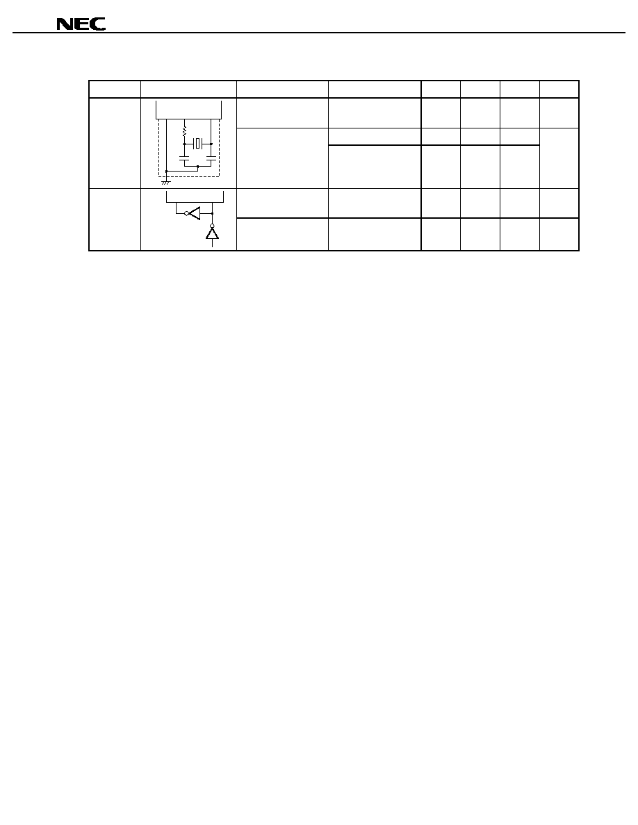
Data Sheet U14121EJ2V0DS00
71
µ
µ
µ
µ
PD784214A, 784215A, 784216A, 784217A, 784218A, 784214AY, 784215AY, 784216AY, 784217AY, 784218AY
Subsystem Clock Oscillator Characteristics (T
A
=
-
-
-
-
40 to +85
∞
∞
∞
∞
C)
Resonator
Recommended Circuit
Parameter
Conditions
MIN.
TYP.
MAX.
Unit
Oscillation frequency
(f
XT
)
32
32.768
35
kHz
4.5 V
V
DD
5.5 V
1.2
2
Crystal
resonator
V
SS
XT2
XT1
Oscillation
stabilization time
Note
1.8 V
V
DD
< 4.5 V
10
s
XT1 input frequency
(f
XT
)
32
35
kHz
External
clock
XT2
XT1
PD74HCU04
µ
XT1 input high-/low-
level width (t
XTH
, t
XTL
)
14.3
15.6
µ
s
Note Time required to stabilize oscillation after applying supply voltage (V
DD
).
Cautions 1. When using the subsystem clock oscillator, wire as follows in the area enclosed by the
broken lines in the above figures to avoid an adverse effect from wiring capacitance.
∑
∑
∑
∑
Keep the wiring length as short as possible.
∑
∑
∑
∑
Do not cross the wiring with other signal lines.
∑
∑
∑
∑
Do not route the wiring near a signal line through which a high fluctuating current flows.
∑
∑
∑
∑
Always make the ground point of the oscillator capacitor the same potential as V
SS
.
∑
∑
∑
∑
Do not ground the capacitor to a ground pattern through which a high current flows.
∑
∑
∑
∑
Do not fetch signals from the oscillator.
2. When the main system clock is stopped and the device is operating on the subsystem clock,
wait until the oscillation stabilization time has been secured by the program before switching
back to the main system clock.
Remark For the resonator selection and oscillator constant, users are required to either evaluate the oscillation
themselves or apply to the resonator manufacturer for evaluation.
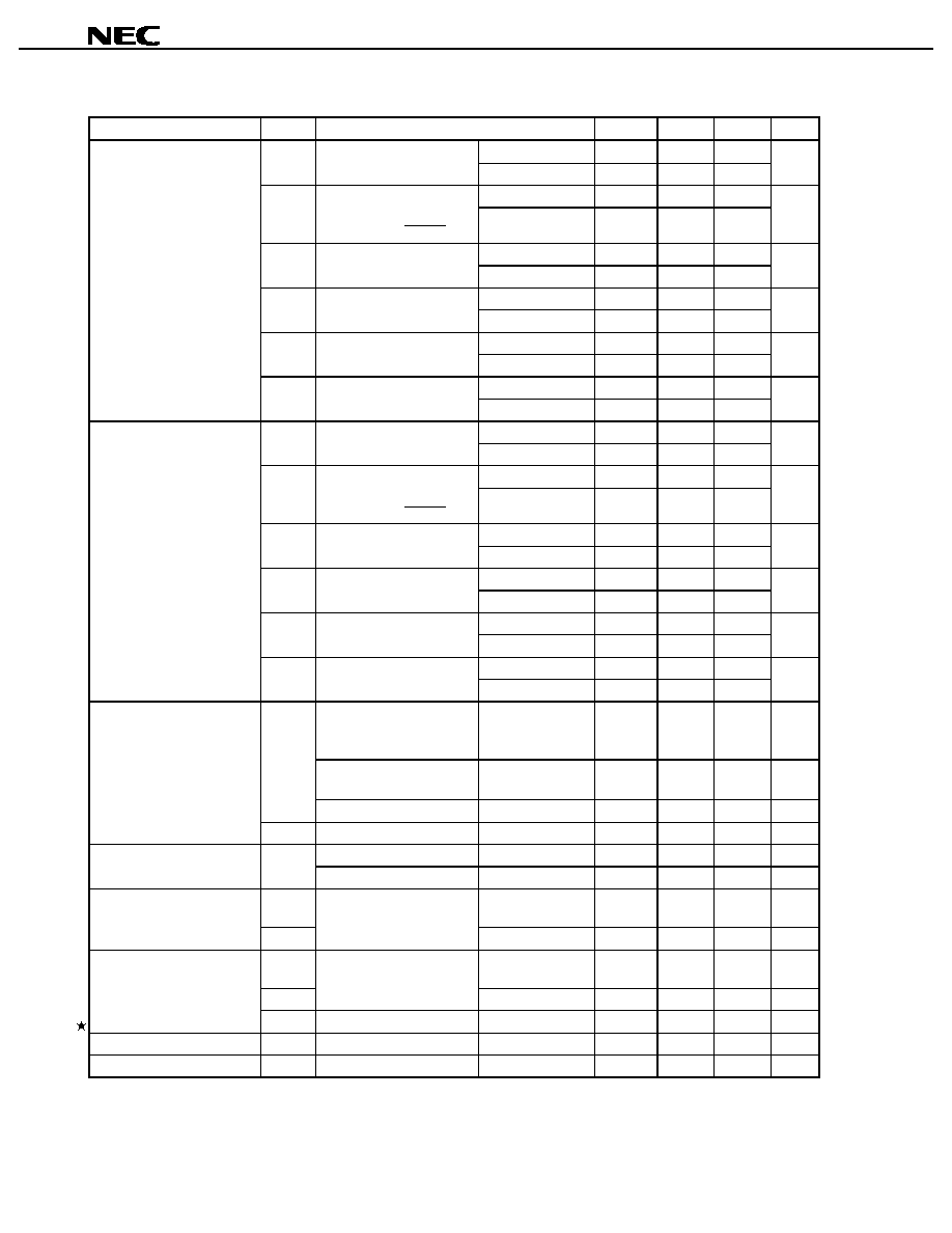
Data Sheet U14121EJ2V0DS00
72
µ
µ
µ
µ
PD784214A, 784215A, 784216A, 784217A, 784218A, 784214AY, 784215AY, 784216AY, 784217AY, 784218AY
DC Characteristics (T
A
=
-
-
-
-
40 to +85
∞
∞
∞
∞
C, V
DD
= AV
DD
= 1.8 to 5.5 V, V
SS
= AV
SS
= 0 V) (1/3)
Parameter
Symbol
Conditions
MIN.
TYP.
MAX.
Unit
2.2 V
V
DD
5.5 V
0
0.3V
DD
V
IL1
Note 1
1.8 V
V
DD
< 2.2 V
0
0.2V
DD
V
2.2 V
V
DD
5.5 V
0
0.2V
DD
V
IL2
P00 to P06, P20, P22, P33,
P34, P70, P72,
P100 to P103, RESET
1.8 V
V
DD
< 2.2 V
0
0.15V
DD
V
2.2 V
V
DD
5.5 V
0
0.3V
DD
V
IL3
P90 to P95
(N-ch open drain)
1.8 V
V
DD
< 2.2 V
0
0.2V
DD
V
2.2 V
V
DD
5.5 V
0
0.3V
DD
V
IL4
P10 to P17, P130, P131
1.8 V
V
DD
< 2.2 V
0
0.2V
DD
V
2.2 V
V
DD
5.5 V
0
0.2V
DD
V
IL5
X1, X2, XT1, XT2
1.8 V
V
DD
< 2.2 V
0
0.1V
DD
V
2.2 V
V
DD
5.5 V
0
0.3V
DD
Input voltage, low
V
IL6
P25, P27
1.8 V
V
DD
< 2.2 V
0
0.2V
DD
V
2.2 V
V
DD
5.5 V
0.7V
DD
V
DD
V
IH1
Note 1
1.8 V
V
DD
< 2.2 V
0.8V
DD
V
DD
V
2.2 V
V
DD
5.5 V
0.8V
DD
V
DD
V
IH2
P00 to P06, P20, P22, P33,
P34, P70, P72,
P100 to P103, RESET
1.8 V
V
DD
< 2.2 V
0.85V
DD
V
DD
V
2.2 V
V
DD
5.5 V
0.7V
DD
12
V
IH3
P90 to P95
(N-ch open drain)
1.8 V
V
DD
< 2.2 V
0.8V
DD
V
DD
V
2.2 V
V
DD
5.5 V
0.7V
DD
V
DD
V
IH4
P10 to P17, P130, P131
1.8 V
V
DD
< 2.2 V
0.8V
DD
V
DD
V
2.2 V
V
DD
5.5 V
0.8V
DD
V
DD
V
IH5
X1, X2, XT1, XT2
1.8 V
V
DD
< 2.2 V
0.85V
DD
V
DD
V
2.2 V
V
DD
5.5 V
0.7V
DD
V
DD
Input voltage, high
V
IH6
P25, P27
1.8 V
V
DD
< 2.2 V
0.8V
DD
V
DD
V
For pins other than
P40 to P47, P50 to P57,
P90 to P95 I
OL
= 1.6 mA
Note 1
4.5 V
V
DD
5.5 V
0.4
V
P40 to P47, P50 to P57
I
OL
= 8 mA
Note 2
4.5 V
V
DD
5.5 V
1.0
V
V
OL1
P90 to P95 I
OL
= 15 mA
Note 2
4.5 V
V
DD
5.5 V
0.8
2.0
V
Output voltage, low
V
OL2
I
OL
= 400
µ
A
Note 2
0.5
V
I
OH
=
-
1 mA
Note 2
4.5 V
V
DD
5.5 V
V
DD
-
1.0
V
Output voltage, high
V
OH1
I
OL
=
-
100
µ
A
Note 2
V
DD
-
0.5
V
I
LIL1
Except X1, X2, XT1,
XT2
-
3
µ
A
Input leakage current, low
I
LIL2
V
IN
= 0 V
X1, X2, XT1, XT2
-
20
µ
A
I
LIH1
Except X1, X2, XT1,
XT2
3
µ
A
I
LIH2
V
IN
= V
DD
X1, X2, XT1, XT2
20
µ
A
Input leakage current, high
I
LIH3
V
IN
= 12 V (N-ch open drain) P90 to P95
20
µ
A
Output leakage current, low
I
LOL1
V
OUT
= 0 V
-
3
µ
A
Output leakage current, high
I
LOH1
V
OUT
= V
DD
3
µ
A
Notes 1. P21, P23, P24, P26, P30 to P32, P35 to P37, P40 to P47, P50 to P57, P60 to P67, P71, P80 to P87,
P120 to P127
2. Per pin
Data Sheet U14121EJ2V0DS00
73
µ
µ
µ
µ
PD784214A, 784215A, 784216A, 784217A, 784218A, 784214AY, 784215AY, 784216AY, 784217AY, 784218AY
DC Characteristics (T
A
=
-
-
-
-
40 to +85
∞
∞
∞
∞
C, V
DD
= AV
DD
= 1.8 to 5.5 V, V
SS
= AV
SS
= 0 V) (2/3)
(1)
µ
µ
µ
µ
PD784214A, 784215A, 784216A, 784214AY, 784215AY, 784216AY
Parameter
Symbol
Conditions
MIN.
TYP.
MAX.
Unit
f
XX
= 12.5 MHz, V
DD
= 5.0 V
±
10%
11
40
mA
f
XX
= 6 MHz, V
DD
= 3.0 V
±
10%
3
17
mA
I
DD1
Operation
mode
f
XX
= 2 MHz, V
DD
= 2.0 V
±
10%
1
8
mA
f
XX
= 12.5 MHz, V
DD
= 5.0 V
±
10%
5
20
mA
f
XX
= 6 MHz, V
DD
= 3.0 V
±
10%
2
8
mA
I
DD2
HALT mode
f
XX
= 2 MHz, V
DD
= 2.0 V
±
10%
0.3
3.5
mA
f
XX
= 12.5 MHz, V
DD
= 5.0 V
±
10%
1
2.5
mA
f
XX
= 6 MHz, V
DD
= 3.0 V
±
10%
0.4
1.3
mA
I
DD3
IDLE mode
f
XX
= 2 MHz, V
DD
= 2.0 V
±
10%
0.2
0.9
mA
f
XX
= 32 kHz, V
DD
= 5.0 V
±
10%
80
200
µ
A
f
XX
= 32 kHz, V
DD
= 3.0 V
±
10%
60
110
µ
A
I
DD4
Operation
mode
Note
f
XX
= 32 kHz, V
DD
= 2.0 V
±
10%
30
100
µ
A
f
XX
= 32 kHz, V
DD
= 5.0 V
±
10%
60
160
µ
A
f
XX
= 32 kHz, V
DD
= 3.0 V
±
10%
20
80
µ
A
I
DD5
HALT
mode
Note
f
XX
= 32 kHz, V
DD
= 2.0 V
±
10%
10
70
µ
A
f
XX
= 32 kHz, V
DD
= 5.0 V
±
10%
50
150
µ
A
f
XX
= 32 kHz, V
DD
= 3.0 V
±
10%
15
70
µ
A
Supply current
I
DD6
IDLE
mode
Note
f
XX
= 32 kHz, V
DD
= 2.0 V
±
10%
5
60
µ
A
Data retention voltage
V
DDDR
HALT, IDLE modes
1.8
5.5
V
V
DD
= 2.0 V
±
10%
2
10
µ
A
Data retention current
I
DDDR
STOP mode
V
DD
= 5.0 V
±
10%
10
50
µ
A
Pull-up resistor
R
L
V
IN
= 0 V
10
30
100
k
Note When main system clock is stopped and subsystem clock is operating.
Remark Unless otherwise specified, the characteristics of alternate-function pins are the same as those of port
pins.
Data Sheet U14121EJ2V0DS00
74
µ
µ
µ
µ
PD784214A, 784215A, 784216A, 784217A, 784218A, 784214AY, 784215AY, 784216AY, 784217AY, 784218AY
DC Characteristics (T
A
=
-
-
-
-
40 to +85
∞
∞
∞
∞
C, V
DD
= AV
DD
= 1.8 to 5.5 V, V
SS
= AV
SS
= 0 V) (3/3)
(2)
µ
µ
µ
µ
PD784217A, 784218A, 784217AY, 784218AY
Parameter
Symbol
Conditions
MIN.
TYP.
MAX.
Unit
f
XX
= 12.5 MHz, V
DD
= 5.0 V
±
10%
11
40
mA
f
XX
= 6 MHz, V
DD
= 3.0 V
±
10%
4
17
mA
I
DD1
Operation
mode
f
XX
= 2 MHz, V
DD
= 2.0 V
±
10%
1
8
mA
f
XX
= 12.5 MHz, V
DD
= 5.0 V
±
10%
6
20
mA
f
XX
= 6 MHz, V
DD
= 3.0 V
±
10%
2
8
mA
I
DD2
HALT mode
f
XX
= 2 MHz, V
DD
= 2.0 V
±
10%
0.4
3.5
mA
f
XX
= 12.5 MHz, V
DD
= 5.0 V
±
10%
1
2.5
mA
f
XX
= 6 MHz, V
DD
= 3.0 V
±
10%
0.4
1.3
mA
I
DD3
IDLE mode
f
XX
= 2 MHz, V
DD
= 2.0 V
±
10%
0.2
0.9
mA
f
XX
= 32 kHz, V
DD
= 5.0 V
±
10%
80
200
µ
A
f
XX
= 32 kHz, V
DD
= 3.0 V
±
10%
60
110
µ
A
I
DD4
Operation
mode
Note
f
XX
= 32 kHz, V
DD
= 2.0 V
±
10%
30
100
µ
A
f
XX
= 32 kHz, V
DD
= 5.0 V
±
10%
60
160
µ
A
f
XX
= 32 kHz, V
DD
= 3.0 V
±
10%
20
80
µ
A
I
DD5
HALT
mode
Note
f
XX
= 32 kHz, V
DD
= 2.0 V
±
10%
10
70
µ
A
f
XX
= 32 kHz, V
DD
= 5.0 V
±
10%
50
150
µ
A
f
XX
= 32 kHz, V
DD
= 3.0 V
±
10%
15
70
µ
A
Supply current
I
DD6
IDLE
mode
Note
f
XX
= 32 kHz, V
DD
= 2.0 V
±
10%
5
60
µ
A
Data retention voltage
V
DDDR
HALT, IDLE modes
1.8
5.5
V
V
DD
= 2.0 V
±
10%
2
10
µ
A
Data retention current
I
DDDR
STOP mode
V
DD
= 5.0 V
±
10%
10
50
µ
A
Pull-up resistor
R
L
V
IN
= 0 V
10
30
100
k
Note When main system clock is stopped and subsystem clock is operating.
Remark Unless otherwise specified, the characteristics of alternate-function pins are the same as those of port
pins.

Data Sheet U14121EJ2V0DS00
75
µ
µ
µ
µ
PD784214A, 784215A, 784216A, 784217A, 784218A, 784214AY, 784215AY, 784216AY, 784217AY, 784218AY
AC Characteristics (T
A
=
-
-
-
-
40 to +85
∞
∞
∞
∞
C, V
DD
= AV
DD
= 1.8 to 5.5 V, V
SS
= AV
SS
= 0 V)
(1) Read/write operation (1/2)
Parameter
Symbol
Conditions
MIN.
TYP.
MAX.
Unit
4.5 V
V
DD
5.5 V
80
ns
2.7 V
V
DD
<
4.5 V
160
ns
2.0 V
V
DD
<
2.7 V
320
ns
Cycle time
t
CYK
1.8 V
V
DD
<
2.0 V
500
ns
V
DD
= 5.0 V
±
10%
(0.5
+
a)T
-
20
ns
V
DD
= 3.0 V
±
10%
(0.5
+
a)T
-
40
ns
Address setup time (to ASTB
)
t
SAST
V
DD
= 2.0 V
±
10%
(0.5
+
a)T
-
80
ns
V
DD
= 5.0 V
±
10%
0.5T
-
19
ns
V
DD
= 3.0 V
±
10%
0.5T
-
24
ns
Address hold time (from ASTB
) t
HSTLA
V
DD
= 2.0 V
±
10%
0.5T
-
34
ns
V
DD
= 5.0 V
±
10%
(0.5
+
a)T
-
17
ns
V
DD
= 3.0 V
±
10%
(0.5
+
a)T
-
40
ns
ASTB high-level width
t
WSTH
V
DD
= 2.0 V
±
10%
(0.5
+
a)T
-
110
ns
V
DD
= 5.0 V
±
10%
0.5T
-
14
ns
V
DD
= 3.0 V
±
10%
0.5T
-
14
ns
Address hold time (from RD
)
t
HRA
V
DD
= 2.0 V
±
10%
0.5T
-
14
ns
V
DD
= 5.0 V
±
10%
(1
+
a)T
-
24
ns
V
DD
= 3.0 V
±
10%
(1
+
a)T
-
35
ns
Delay time from address to RD
t
DAR
V
DD
= 2.0 V
±
10%
(1
+
a)T
-
80
ns
V
DD
= 5.0 V
±
10%
0
ns
V
DD
= 3.0 V
±
10%
0
ns
Address float time (from RD
)
t
FAR
V
DD
= 2.0 V
±
10%
0
ns
V
DD
= 5.0 V
±
10%
(2.5
+
a
+
n)T
-
37
ns
V
DD
= 3.0 V
±
10%
(2.5
+
a
+
n)T
-
52
ns
Data input time from address
t
DAID
V
DD
= 2.0 V
±
10%
(2.5
+
a
+
n)T
-
120
ns
V
DD
= 5.0 V
±
10%
(2
+
n)T
-
35
ns
V
DD
= 3.0 V
±
10%
(2
+
n)T
-
50
ns
Data input time from ASTB
t
DSTID
V
DD
= 2.0 V
±
10%
(2
+
n)T
-
80
ns
V
DD
= 5.0 V
±
10%
(1.5
+
n)T
-
40
ns
V
DD
= 3.0 V
±
10%
(1.5
+
n)T
-
50
ns
Data input time from RD
t
DRID
V
DD
= 2.0 V
±
10%
(1.5
+
n)T
-
90
ns
V
DD
= 5.0 V
±
10%
0.5T
-
9
ns
V
DD
= 3.0 V
±
10%
0.5T
-
9
ns
Delay time from ASTB
to RD
t
DSTR
V
DD
= 2.0 V
±
10%
0.5T
-
20
ns
V
DD
= 5.0 V
±
10%
0
ns
V
DD
= 3.0 V
±
10%
0
ns
Data hold time (from RD
)
t
HRID
V
DD
= 2.0 V
±
10%
0
ns
Remark T: t
CYK
= 1/f
XX
(f
XX
: main system clock frequency)
a: 1 (during address wait), otherwise, 0
n: Number of waits (n
0)
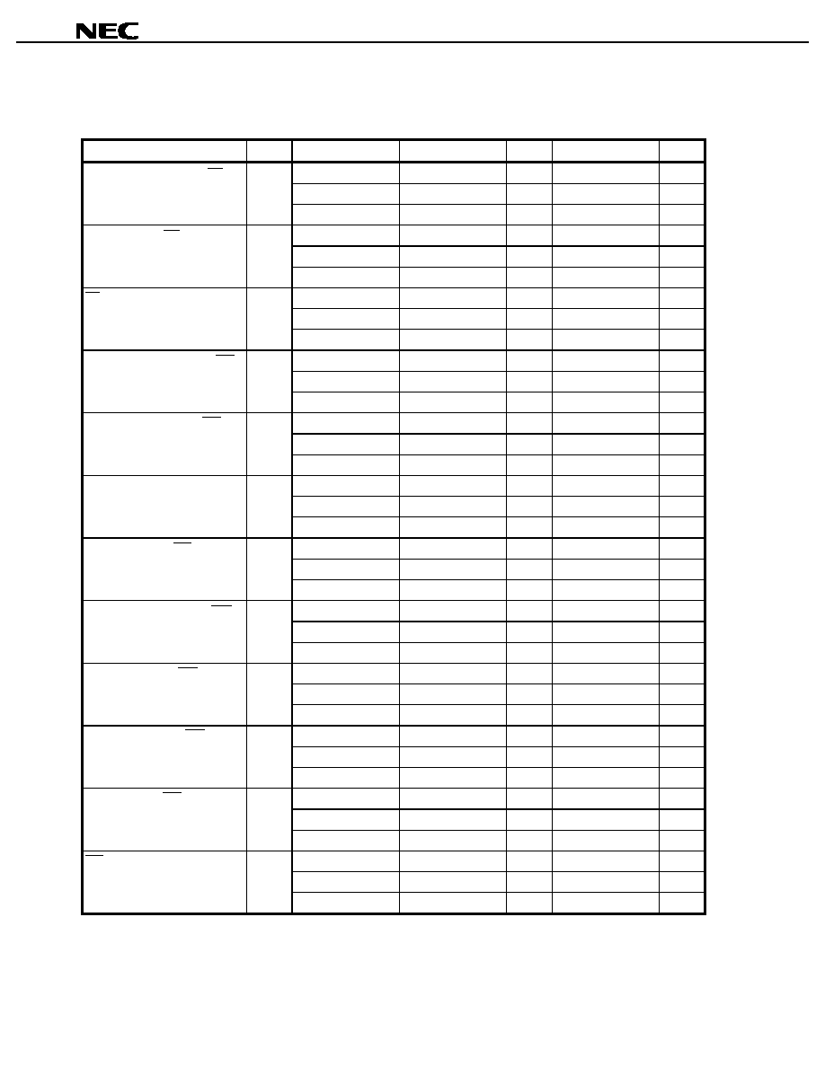
Data Sheet U14121EJ2V0DS00
76
µ
µ
µ
µ
PD784214A, 784215A, 784216A, 784217A, 784218A, 784214AY, 784215AY, 784216AY, 784217AY, 784218AY
AC Characteristics
(1) Read/write operation (2/2)
Parameter
Symbol
Conditions
MIN.
TYP.
MAX.
Unit
V
DD
= 5.0 V
±
10%
0.5T
-
2
ns
V
DD
= 3.0 V
±
10%
0.5T
-
12
ns
Address active time from RD
t
DRA
V
DD
= 2.0 V
±
10%
0.5T
-
35
ns
V
DD
= 5.0 V
±
10%
0.5T
-
9
ns
V
DD
= 3.0 V
±
10%
0.5T
-
9
ns
Delay time from RD
to ASTB
t
DRST
V
DD
= 2.0 V
±
10%
0.5T
-
40
ns
V
DD
= 5.0 V
±
10%
(1.5
+
n)T
-
25
ns
V
DD
= 3.0 V
±
10%
(1.5
+
n)T
-
30
ns
RD low-level width
t
WRL
V
DD
= 2.0 V
±
10%
(1.5
+
n)T
-
25
ns
V
DD
= 5.0 V
±
10%
(1
+
a)T
-
24
ns
V
DD
= 3.0 V
±
10%
(1
+
a)T
-
34
ns
Delay time from address to WR
t
DAW
V
DD
= 2.0 V
±
10%
(1
+
a)T
-
70
ns
V
DD
= 5.0 V
±
10%
0.5T
-
14
ns
V
DD
= 3.0 V
±
10%
0.5T
-
14
ns
Address hold time (from WR
)
t
HRD
V
DD
= 2.0 V
±
10%
0.5T
-
14
ns
V
DD
= 5.0 V
±
10%
0.5T
+
15
ns
V
DD
= 3.0 V
±
10%
0.5T
+
30
ns
Delay time from ASTB
to data
output
t
DSTOD
V
DD
= 2.0 V
±
10%
0.5T
+
240
ns
V
DD
= 5.0 V
±
10%
0.5T
-
30
ns
V
DD
= 3.0 V
±
10%
0.5T
-
30
ns
Delay time from WR
to data
output
t
DWOD
V
DD
= 2.0 V
±
10%
0.5T
-
30
ns
V
DD
= 5.0 V
±
10%
0.5T
-
9
ns
V
DD
= 3.0 V
±
10%
0.5T
-
9
ns
Delay time from ASTB
to WR
t
DSTW
V
DD
= 2.0 V
±
10%
0.5T
-
20
ns
V
DD
= 5.0 V
±
10%
(1.5
+
n)T
-
20
ns
V
DD
= 3.0 V
±
10%
(1.5
+
n)T
-
25
ns
Data setup time (to WR
)
t
SODWR
V
DD
= 2.0 V
±
10%
(1.5
+
n)T
-
70
ns
V
DD
= 5.0 V
±
10%
0.5T
-
14
ns
V
DD
= 3.0 V
±
10%
0.5T
-
14
ns
Data hold time (from WR
)
t
HWOD
V
DD
= 2.0 V
±
10%
0.5T
-
50
ns
V
DD
= 5.0 V
±
10%
0.5T
-
9
ns
V
DD
= 3.0 V
±
10%
0.5T
-
9
ns
Delay time from WR
to ASTB
t
DWST
V
DD
= 2.0 V
±
10%
0.5T
-
30
ns
V
DD
= 5.0 V
±
10%
(1.5
+
n)T
-
25
ns
V
DD
= 3.0 V
±
10%
(1.5
+
n)T
-
30
ns
WR low-level width
t
WWL
V
DD
= 2.0 V
±
10%
(1.5
+
n)T
-
30
ns
Remark T: t
CYK
= 1/f
XX
(f
XX
: main system clock frequency)
a: 1 (during address wait), otherwise, 0
n: Number of wait states (n
0)
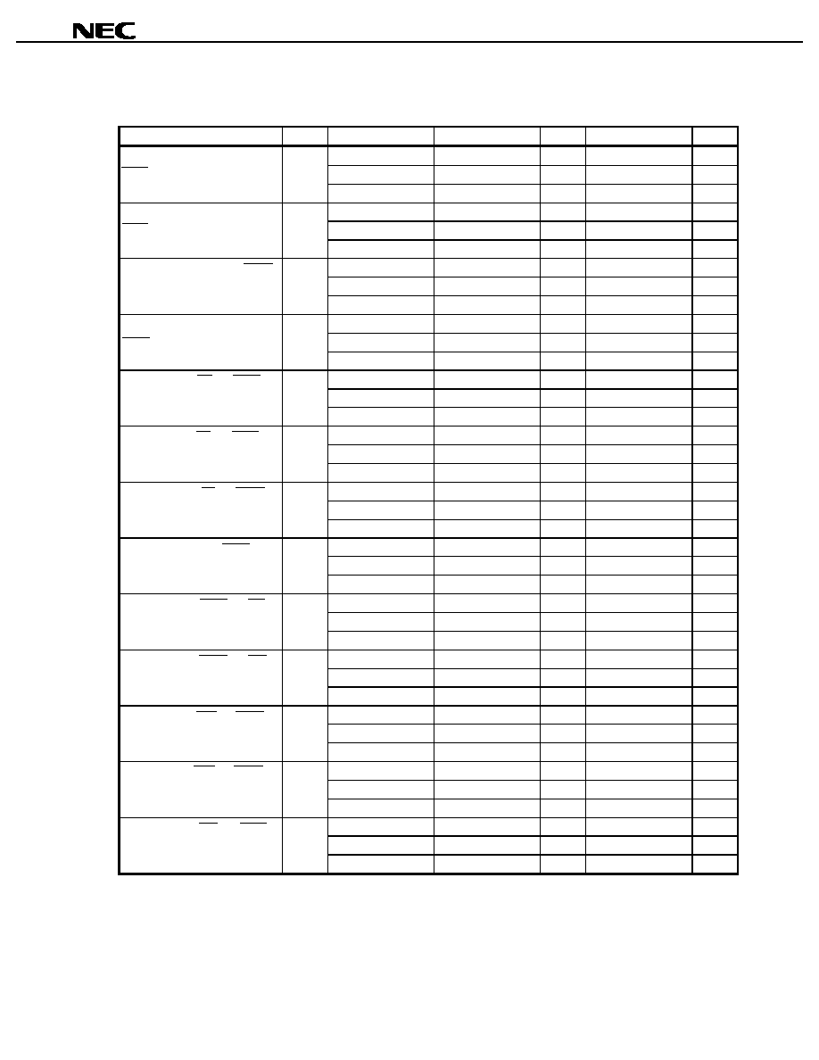
Data Sheet U14121EJ2V0DS00
77
µ
µ
µ
µ
PD784214A, 784215A, 784216A, 784217A, 784218A, 784214AY, 784215AY, 784216AY, 784217AY, 784218AY
AC Characteristics
(2) External wait timing
Parameter
Symbol
Conditions
MIN.
TYP.
MAX.
Unit
V
DD
= 5.0 V
±
10%
(2
+
a)T
-
40
ns
V
DD
= 3.0 V
±
10%
(2
+
a)T
-
60
ns
Input time from address to
WAIT
t
DAWT
V
DD
= 2.0 V
±
10%
(2
+
a)T
-
300
ns
V
DD
= 5.0 V
±
10%
1.5T
-
40
ns
V
DD
= 3.0 V
±
10%
1.5T
-
60
ns
Input time from ASTB
to
WAIT
t
DSTWT
V
DD
= 2.0 V
±
10%
1.5T
-
260
ns
V
DD
= 5.0 V
±
10%
(0.5
+
n)T
+
5
ns
V
DD
= 3.0 V
±
10%
(0.5
+
n)T
+
10
ns
Hold time from ASTB
to WAIT
t
HSTWT
V
DD
= 2.0 V
±
10%
(0.5
+
n)T
+
30
ns
V
DD
= 5.0 V
±
10%
(1.5
+
n)T
-
40
ns
V
DD
= 3.0 V
±
10%
(1.5
+
n)T
-
60
ns
Delay time from ASTB
to
WAIT
t
DSTWTH
V
DD
= 2.0 V
±
10%
(1.5
+
n)T
-
90
ns
V
DD
= 5.0 V
±
10%
T
-
40
ns
V
DD
= 3.0 V
±
10%
T
-
60
ns
Input time from RD
to WAIT
t
DRWTL
V
DD
= 2.0 V
±
10%
T
-
70
ns
V
DD
= 5.0 V
±
10%
nT
+
5
ns
V
DD
= 3.0 V
±
10%
nT
+
10
ns
Hold time from RD
to WAIT
t
HRWT
V
DD
= 2.0 V
±
10%
nT
+
30
ns
V
DD
= 5.0 V
±
10%
(1
+
n)T
-
40
ns
V
DD
= 3.0 V
±
10%
(1
+
n)T
-
60
ns
Delay time from RD
to WAIT
t
DRWTH
V
DD
= 2.0 V
±
10%
(1
+
n)T
-
90
ns
V
DD
= 5.0 V
±
10%
0.5T
-
5
ns
V
DD
= 3.0 V
±
10%
0.5T
-
10
ns
Data input time from WAIT
t
DWTID
V
DD
= 2.0 V
±
10%
0.5T
-
30
ns
V
DD
= 5.0 V
±
10%
0.5T
ns
V
DD
= 3.0 V
±
10%
0.5T
ns
Delay time from WAIT
to RD
t
DWTR
V
DD
= 2.0 V
±
10%
0.5T
+
5
ns
V
DD
= 5.0 V
±
10%
0.5T
ns
V
DD
= 3.0 V
±
10%
0.5T
ns
Delay time from WAIT
to WR
t
DWTW
V
DD
= 2.0 V
±
10%
0.5T
+
5
ns
V
DD
= 5.0 V
±
10%
T
-
40
ns
V
DD
= 3.0 V
±
10%
T
-
60
ns
Input time from WR
to WAIT
t
DWWTL
V
DD
= 2.0 V
±
10%
T
-
90
ns
V
DD
= 5.0 V
±
10%
nT
+
5
ns
V
DD
= 3.0 V
±
10%
nT
+
10
ns
Hold time from WR
to WAIT
t
HWWT
V
DD
= 2.0 V
±
10%
nT
+
30
ns
V
DD
= 5.0 V
±
10%
(1
+
n)T
-
40
ns
V
DD
= 3.0 V
±
10%
(1
+
n)T
-
60
ns
Delay time from WR
to WAIT
t
DWWTH
V
DD
= 2.0 V
±
10%
(1
+
n)T
-
90
ns
Remark T: t
CYK
= 1/f
XX
(f
XX
: main system clock frequency)
a: 1 (during address wait), otherwise, 0
n: Number of wait states (n
0)
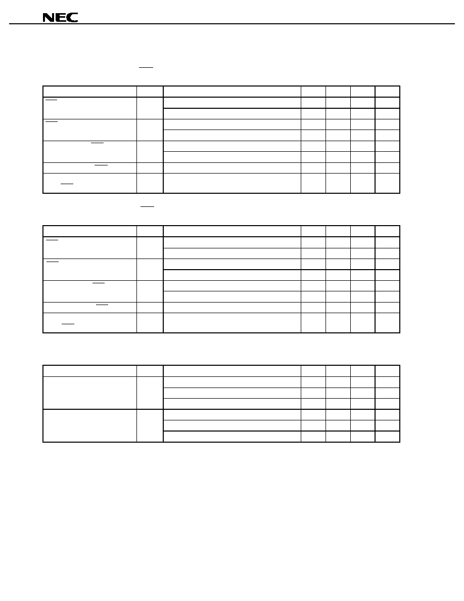
Data Sheet U14121EJ2V0DS00
78
µ
µ
µ
µ
PD784214A, 784215A, 784216A, 784217A, 784218A, 784214AY, 784215AY, 784216AY, 784217AY, 784218AY
Serial Operation (T
A
=
-
-
-
-
40 to +85
∞
∞
∞
∞
C, V
DD
= AV
DD
= 1.8 to 5.5 V, V
SS
= AV
SS
= 0 V)
(a) 3-wire serial I/O mode (SCK: Internal clock output)
Parameter
Symbol
Conditions
MIN.
TYP.
MAX.
Unit
2.7 V
V
DD
5.5 V
800
ns
SCK cycle time
t
KCY1
3,200
ns
2.7 V
V
DD
5.5 V
350
ns
SCK high-/low-level width
t
KH1
,
t
KL1
1,500
ns
2.7 V
V
DD
5.5 V
10
ns
SI setup time (to SCK
)
t
SIK1
30
ns
SI hold time (from SCK
)
t
KSI1
40
ns
SO output delay time
(from SCK
)
t
KSO1
30
ns
(b) 3-wire serial I/O mode (SCK: External clock input)
Parameter
Symbol
Conditions
MIN.
TYP.
MAX.
Unit
2.7 V
V
DD
5.5 V
800
ns
SCK cycle time
t
KCY2
3,200
ns
2.7 V
V
DD
5.5 V
400
ns
SCK high-/low-level width
t
KH2
t
KL2
1,600
ns
2.7 V
V
DD
5.5 V
10
ns
SI setup time (to SCK
)
t
SIK2
30
ns
SI hold time (from SCK
)
t
KSI2
40
ns
SO output delay time
(from SCK
)
t
KSO2
30
ns
(c) UART mode
Parameter
Symbol
Conditions
MIN.
TYP.
MAX.
Unit
4.5 V
V
DD
5.5 V
417
ns
2.7 V
V
DD
< 4.5 V
833
ns
ASCK cycle time
t
KCY3
1,667
ns
4.5 V
V
DD
5.5 V
208
ns
2.7 V
V
DD
< 4.5 V
416
ns
ASCK high-/low-level width
t
KH3
t
KL3
833
ns
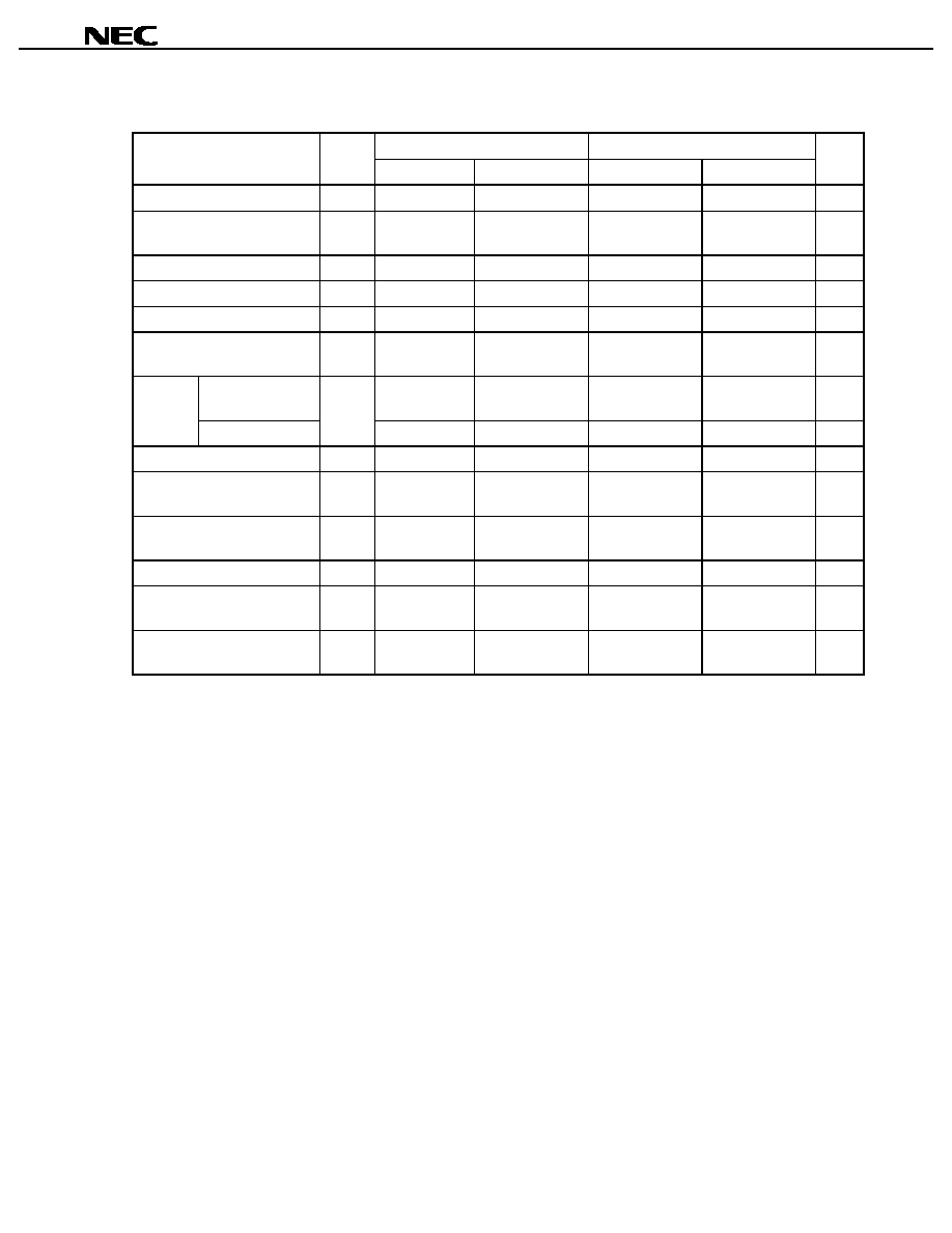
Data Sheet U14121EJ2V0DS00
79
µ
µ
µ
µ
PD784214A, 784215A, 784216A, 784217A, 784218A, 784214AY, 784215AY, 784216AY, 784217AY, 784218AY
(d) I
2
C bus mode
Standard Mode
High-Speed Mode
Parameter
Symbol
MIN.
MAX.
MIN.
MAX.
Unit
SCL0 clock frequency
f
CLK
0
100
0
400
kHz
Bus free time (between stop
and start conditions)
t
BUF
4.7
-
1.3
-
µ
s
Hold time
Note1
t
HD : STA
4.0
-
0.6
-
µ
s
Low-level width of SCL0 clock
t
LOW
4.7
-
1.3
-
µ
s
High-level width of SCL0 clock
t
HIGH
4.0
-
0.6
-
µ
s
Setup time of start/restart
conditions
t
SU : STA
4.7
-
0.6
-
µ
s
When using CBUS-
compatible master
5.0
-
-
-
µ
s
Data hold
time
When using I
2
C bus
t
HD : DAT
0
Note 2
-
0
Note 2
0.9
Note 3
µ
s
Data setup time
t
SU : DAT
250
-
100
Note 4
-
ns
Rise time of SDA0 and SCL0
signals
t
R
-
1,000
20 + 0.1Cb
Note 5
300
ns
Fall time of SDA0 and SCL0
signals
t
F
-
300
20 + 0.1Cb
Note 5
300
ns
Setup time of stop condition
t
SU : STO
4.0
-
0.6
-
µ
s
Pulse width of spike restricted
by input filter
t
SP
-
-
0
50
ns
Load capacitance of each bus
line
Cb
-
400
-
400
pF
Notes 1. For the start condition, the first clock pulse is generated after the hold time.
2. To fill the undefined area of the SCL0 falling edge, it is necessary for the device to provide an internal
SDA0 signal (on V
IHmin.
) with at least 300 ns of hold time.
3. If the device does not extend the SCL0 signal low-level hold time (t
LOW
), only the maximum data hold
time
t
HD : DAT
needs to be satisfied.
4. The high-speed mode I
2
C bus can be used in a standard mode I
2
C bus system. In this case, the
conditions described below must be satisfied.
∑
If the device does not extend the SCL0 signal low-level hold time
t
SU : DAT
250 ns
∑
If the device extends the SCL0 signal low-level hold time
Be sure to transmit the data bit to the SDA0 line before the SCL0 line is released (t
Rmax.
+ t
SU :
DAT
= 1,000 + 250 = 1,250 ns by standard mode I
2
C bus specification)
5. Cb: Total capacitance per bus line (unit: pF)
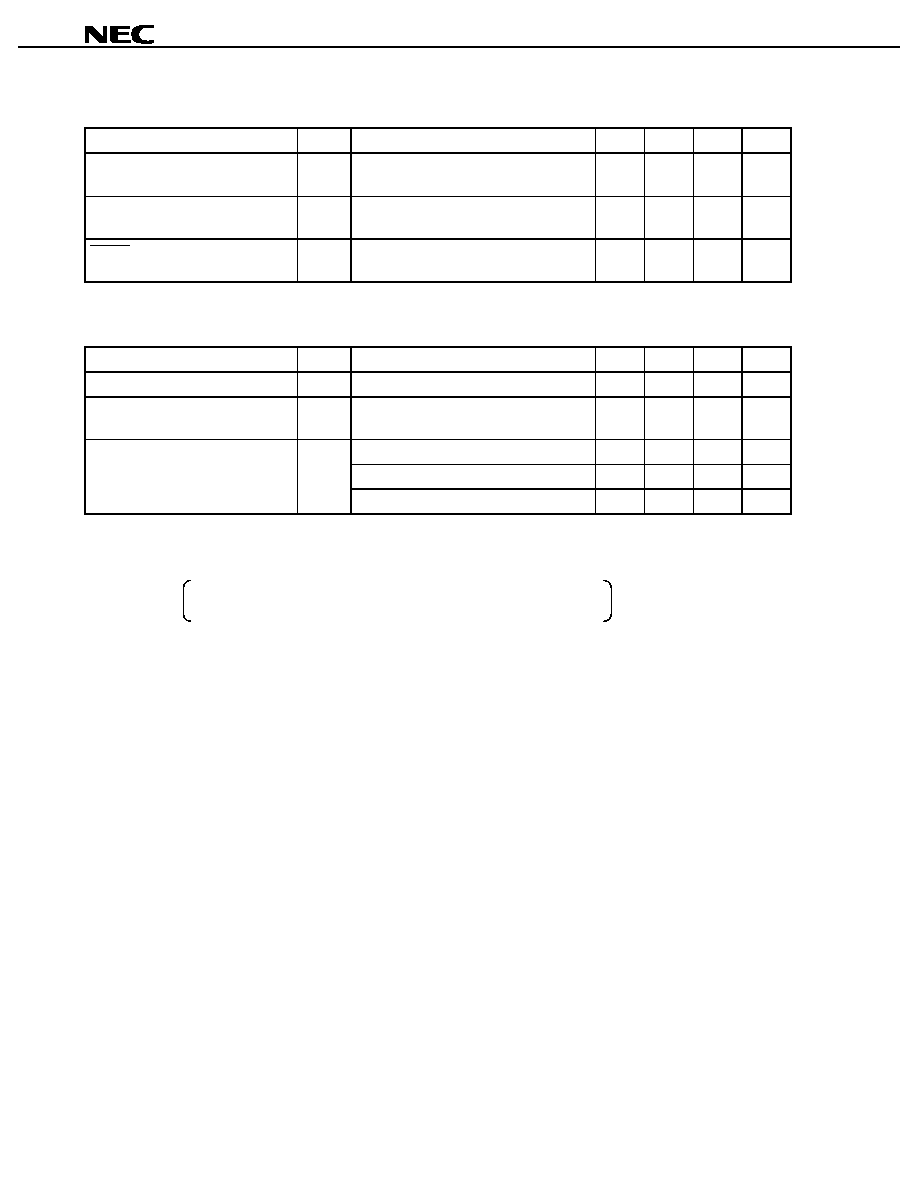
Data Sheet U14121EJ2V0DS00
80
µ
µ
µ
µ
PD784214A, 784215A, 784216A, 784217A, 784218A, 784214AY, 784215AY, 784216AY, 784217AY, 784218AY
Other Operations (T
A
=
-
-
-
-
40 to +85
∞
∞
∞
∞
C, V
DD
= AV
DD
= 1.8 to 5.5 V, V
SS
= AV
SS
= 0 V)
Parameter
Symbol
Conditions
MIN.
TYP.
MAX.
Unit
NMI high-/low-level width
t
WNIL
t
WNIH
10
µ
s
INTP input high-/low-level width
t
WITL
t
WITH
INTP0 to INTP6
100
ns
RESET high-/low-level width
t
WRSL
t
WRSH
10
µ
s
Clock Output Operation (T
A
=
-
-
-
-
40 to +85
∞
∞
∞
∞
C, V
DD
= AV
DD
= 1.8 to 5.5 V, V
SS
= AV
SS
= 0 V)
Parameter
Symbol
Conditions
MIN.
TYP.
MAX.
Unit
PCL cycle time
t
CYCL
4.5 V
V
DD
5.5 V, nT
80
31,250
ns
PCL high-/low-level width
t
CLL
t
CLH
4.5 V
V
DD
5.5 V, 0.5T
-
10
30
15,615
ns
4.5 V
V
DD
5.5 V
5
ns
2.7 V
V
DD
< 4.5 V
10
ns
PCL rise/fall time
t
CLR
t
CLF
1.8 V
V
DD
< 2.7 V
20
ns
Remark T: t
CYK
= 1/f
XX
(f
XX
: Main system clock frequency)
n: Divided frequency ratio set by software in the CPU
∑
When using the main system clock: n = 1, 2, 4, 8, 16, 32, 64, 128
∑
When using the subsystem clock: n = 1
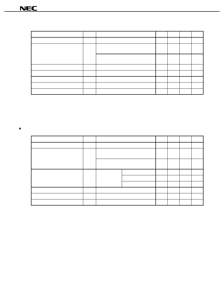
Data Sheet U14121EJ2V0DS00
81
µ
µ
µ
µ
PD784214A, 784215A, 784216A, 784217A, 784218A, 784214AY, 784215AY, 784216AY, 784217AY, 784218AY
A/D Converter Characteristics (T
A
=
-
-
-
-
40 to +85
∞
∞
∞
∞
C, V
DD
= AV
DD
= 1.8 to 5.5 V, V
SS
= AV
SS
= 0 V)
Parameter
Symbol
Conditions
MIN.
TYP.
MAX.
Unit
Resolution
8
8
8
bits
2.7 V
V
DD
5.5 V
2.2 V
AV
REF0
V
DD
±
1.2
%FSR
Overall error
Notes 1, 2
1.8 V
V
DD
< 2.7 V
1.8 V
AV
REF0
V
DD
±
1.6
%FSR
Conversion time
t
CONV
14
144
µ
s
Sampling time
t
SAMP
24/f
XX
µ
s
Analog input voltage
V
IAN
AV
SS
AV
REF0
V
Reference voltage
AV
REF0
1.8
AV
DD
V
Resistance between AV
REF0
and AV
SS
R
AVREF0
When not A/D converting
40
k
Notes 1. Quantization error (
±
1/2 LSB) is not included.
2. Overall error is indicated as a ratio to the full-scale value.
Remark f
XX
: Main system clock frequency
D/A Converter Characteristics (T
A
=
-
-
-
-
40 to +85
∞
∞
∞
∞
C, V
DD
= AV
DD
= 1.8 to 5.5 V, V
SS
= AV
SS
= 0 V)
Parameter
Symbol
Conditions
MIN.
TYP.
MAX.
Unit
Resolution
8
8
8
Bits
R = 10 M
, 2.0 V
AV
REF1
V
DD
,
2.0 V
V
DD
5.5 V
±
0.6
%FSR
Overall error
Notes 1, 2
R = 10 M
, 1.8 V
AV
REF1
V
DD
,
1.8 V
V
DD
2.0 V
±
1.2
%FSR
4.5 V
AV
REF1
5.5 V
10
µ
s
2.7 V
AV
REF1
< 4.5 V
15
µ
s
Settling time
Load conditions:
C = 30 pF
1.8 V
AV
REF1
< 2.7 V
20
µ
s
Output resistance
R
O
DACS0, 1 = 55H
8
k
Reference voltage
AV
REF1
1.8
V
DD
V
AV
REF1
current
AI
REF1
For only 1 channel
2.5
mA
Notes 1. Quantization error (
±
1/2 LSB) is not included.
2. Overall error is indicated as a ratio to the full-scale value.
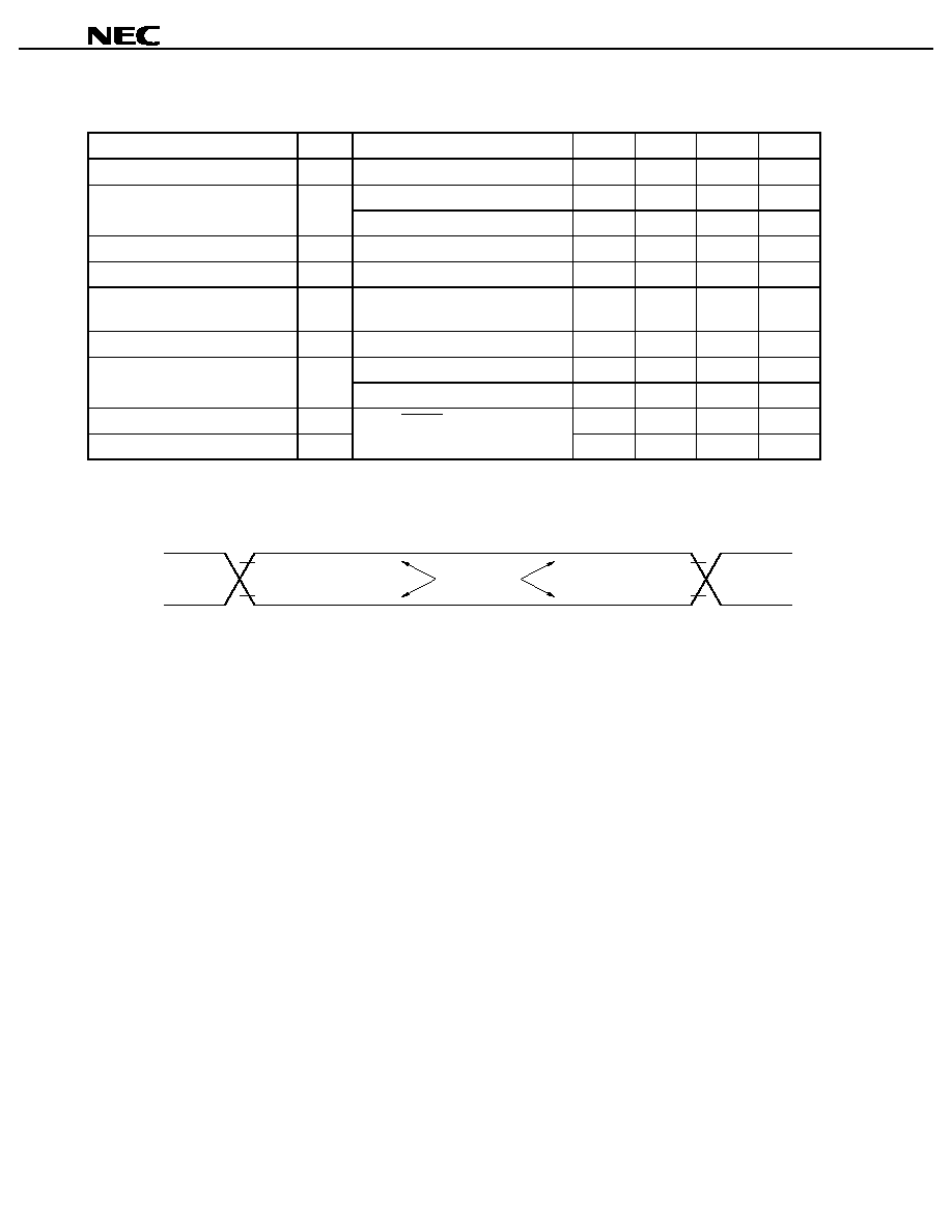
Data Sheet U14121EJ2V0DS00
82
µ
µ
µ
µ
PD784214A, 784215A, 784216A, 784217A, 784218A, 784214AY, 784215AY, 784216AY, 784217AY, 784218AY
Data Retention Characteristics (T
A
=
-
-
-
-
40 to +85
∞
∞
∞
∞
C, V
DD
= AV
DD
= 1.8 to 5.5 V, V
SS
= AV
SS
= 0 V)
Parameter
Symbol
Conditions
MIN.
TYP.
MAX.
Unit
Data retention voltage
V
DDDR
STOP mode
1.8
5.5
V
V
DDDR
= 5.0 V
±
10%
10
50
µ
A
Data retention current
I
DDDR
V
DDDR
= 2.0 V
±
10%
2
10
µ
A
V
DD
rise time
t
RVD
200
µ
s
V
DD
fall time
t
FVD
200
µ
s
V
DD
hold time
(from STOP mode setting)
t
HVD
0
ms
STOP release signal input time
t
DREL
0
ms
Crystal resonator
30
ms
Oscillation stabilization wait time
t
WAIT
Ceramic resonator
5
ms
Low-level input voltage
V
IL
0
0.1V
DDDR
V
High-level input voltage
V
IH
RESET, P00/INTP0 to P06/INTP6
0.9V
DDDR
V
DDDR
V
AC Timing Test Points
0.8V
DD
or 1.8 V
0.8 V
0.8V
DD
or 1.8 V
0.8 V
Test points
V
DD
-
1 V
0.45 V
Data Sheet U14121EJ2V0DS00
83
µ
µ
µ
µ
PD784214A, 784215A, 784216A, 784217A, 784218A, 784214AY, 784215AY, 784216AY, 784217AY, 784218AY
Timing Waveforms
(1) Read operations
Remark The signal is output from pins A0 to A7 when P80 to P87 are unused.
(CLK)
A8 to A19
(Output)
ASTB
(Output)
RD
(Output)
WAIT
(Input)
AD0 to AD7
(Input/output)
t
CYK
Higher address
Hi-Z
Hi-Z
Hi-Z
Higher address
A0 to A7
(Output)
Lower address
Lower address
Data (Input)
Lower address
(Output)
Lower address
(Output)
t
DAID
t
HRA
t
SAST
t
WSTH
t
DSTR
t
DRST
t
DAR
t
DRID
t
WRL
t
DRWTH
t
DSTWT
t
DSTWTH
t
HSTWT
t
HRWT
t
DAWT
t
DWTR
t
HSTLA
t
FAR
t
DWTID
t
DRWTL
t
HRID
t
DRA
t
DSTID
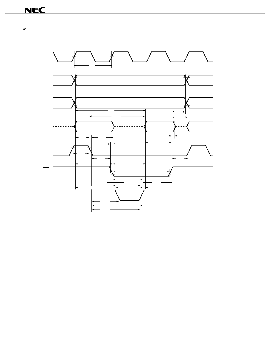
Data Sheet U14121EJ2V0DS00
84
µ
µ
µ
µ
PD784214A, 784215A, 784216A, 784217A, 784218A, 784214AY, 784215AY, 784216AY, 784217AY, 784218AY
(2) Write operation
Remark The signal is output from pins A0 to A7 when P80 to P87 are unused.
(CLK)
A8 to A19
(Output)
ASTB
(Output)
WAIT
(Input)
AD0 to AD7
(Output)
t
CYK
t
DAID
t
HWA
t
SAST
t
WSTH
t
DSTW
t
DWST
t
DAW
t
DWOD
t
WWL
t
DWWTH
t
DSTWT
t
DSTWTH
t
HSTWT
t
HWWT
t
DAWT
t
DWTW
t
HSTLA
t
FAR
t
DWTID
t
DWWTL
t
HWOD
t
DAW
t
DSTOD
t
SODWR
Hi-Z
Hi-Z
Hi-Z
WR
(Output)
Higher address
Higher address
A0 to A7
(Output)
Lower address
Lower address
Data (Output)
Lower address
(Output)
Lower address
(Output)
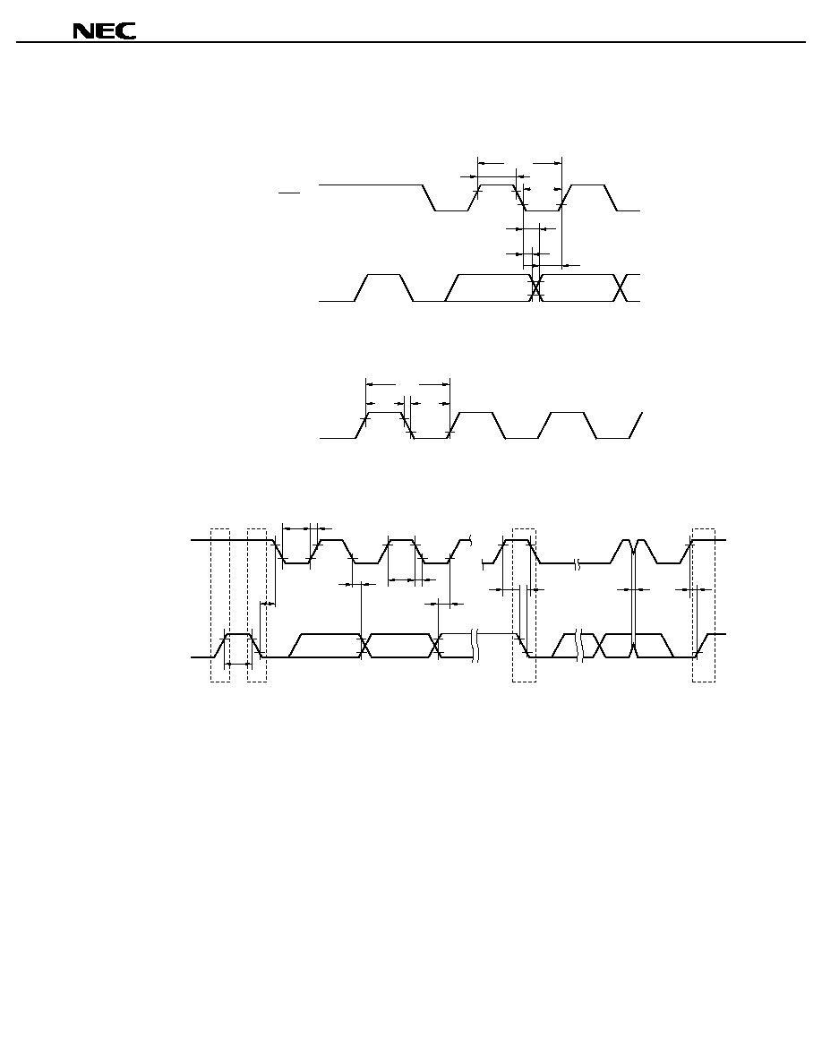
Data Sheet U14121EJ2V0DS00
85
µ
µ
µ
µ
PD784214A, 784215A, 784216A, 784217A, 784218A, 784214AY, 784215AY, 784216AY, 784217AY, 784218AY
Serial Operation
(1) 3-wire serial I/O mode
(2) UART mode
(3) I
2
C bus mode (
µ
µ
µ
µ
PD784216AY/784218AY Subseries only)
SCK
SI/SO
t
KCY1, 2
t
KL1, 2
t
KH1, 2
t
KSO1, 2
t
SIK1, 2
t
KSI1, 2
ASCK
t
KCY3
t
KH3
t
KL3
SCL0
SDA0
t
R
t
HD : DAT
t
HD : STA
t
BUF
t
HIGH
t
SU : DAT
t
F
t
SU : STA
t
HD : STA
t
SP
t
SU : STO
Stop
condition
Start
condition
Restart
condition
Stop
condition
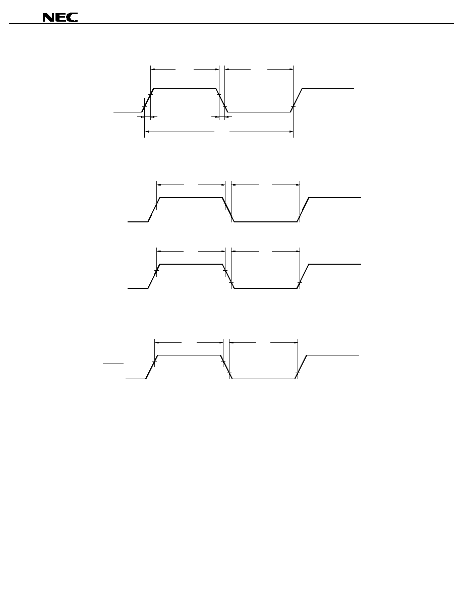
Data Sheet U14121EJ2V0DS00
86
µ
µ
µ
µ
PD784214A, 784215A, 784216A, 784217A, 784218A, 784214AY, 784215AY, 784216AY, 784217AY, 784218AY
Clock Output Timing
Interrupt Input Timing
Reset Input Timing
CLKOUT
t
CLH
t
CLL
t
CYCL
t
CLF
t
CLR
NMI
INTP0 to INTP6
t
WNIH
t
WNIL
t
WITH
t
WITL
RESET
t
WRSH
t
WRSL
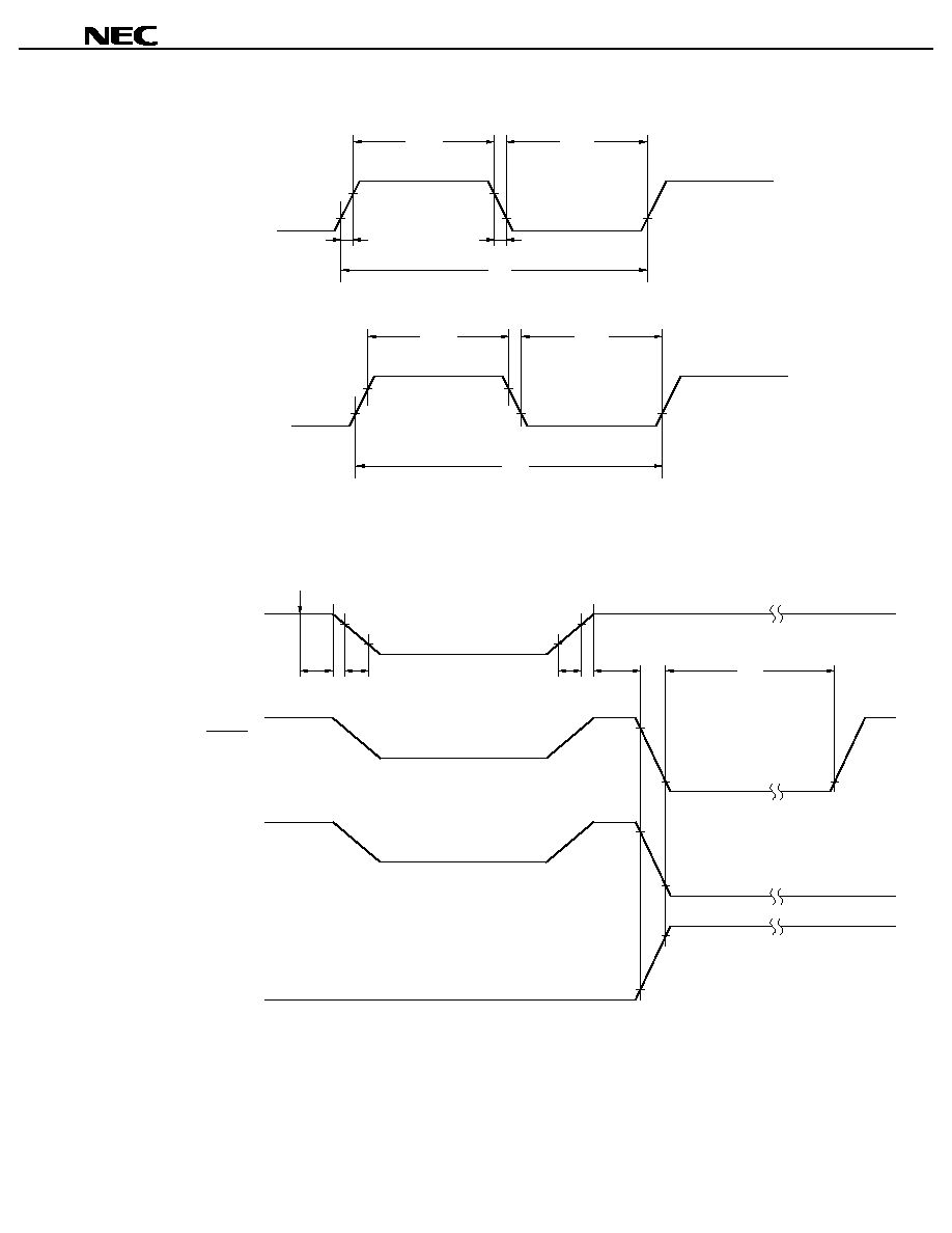
Data Sheet U14121EJ2V0DS00
87
µ
µ
µ
µ
PD784214A, 784215A, 784216A, 784217A, 784218A, 784214AY, 784215AY, 784216AY, 784217AY, 784218AY
Clock Timing
Data Retention Characteristics
X1
t
WXH
t
WXL
1/f
X
t
XF
t
XR
XT1
t
XTH
t
XTL
1/f
XT
V
DD
RESET
NMI
(Cleared by falling edge)
NMI
(Cleared by rising edge)
t
HVD
t
FVD
t
RVD
t
DREL
V
DDDR
STOP mode setting
t
WAIT
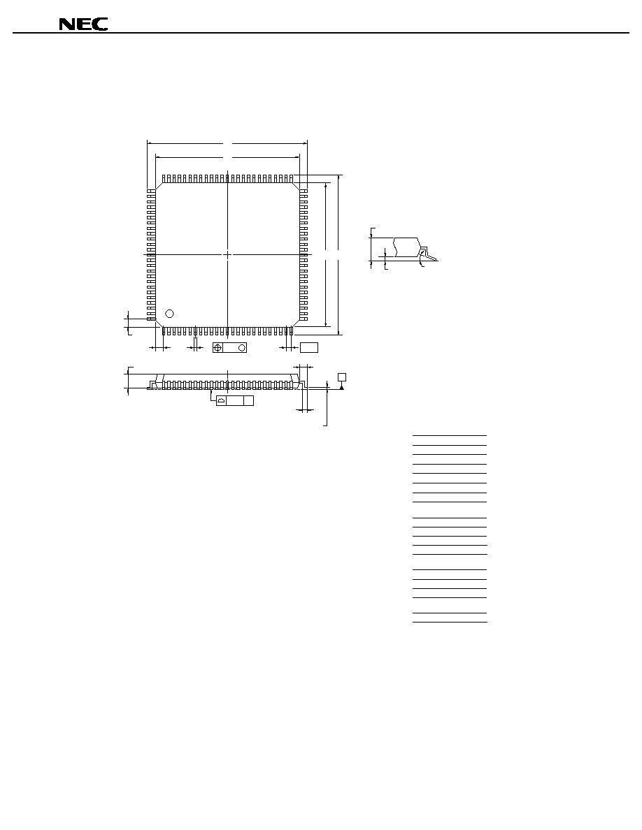
Data Sheet U14121EJ2V0DS00
88
µ
µ
µ
µ
PD784214A, 784215A, 784216A, 784217A, 784218A, 784214AY, 784215AY, 784216AY, 784217AY, 784218AY
14. PACKAGE DRAWINGS
Remark The external dimensions and material of the ES version are the same as those of the mass-produced
version.
100-PIN PLASTIC LQFP (FINE PITCH) (14x14)
NOTE
Each lead centerline is located within 0.08 mm of
its true position (T.P.) at maximum material condition.
ITEM
MILLIMETERS
A
B
D
G
16.00
±
0.20
14.00
±
0.20
0.50 (T.P.)
1.00
J
16.00
±
0.20
K
C
14.00
±
0.20
I
0.08
1.00
±
0.20
L
0.50
±
0.20
F
1.00
N
P
Q
0.08
1.40
±
0.05
0.10
±
0.05
S100GC-50-8EU, 8EA-2
S
1.60 MAX.
H
0.22
+
0.05
-
0.04
M
0.17
+
0.03
-
0.07
R
3
∞+
7
∞
-
3
∞
1
25
26
50
100
76
75
51
S
S
N
J
detail of lead end
C
D
A
B
R
K
M
L
P
I
S
Q
G
F
M
H
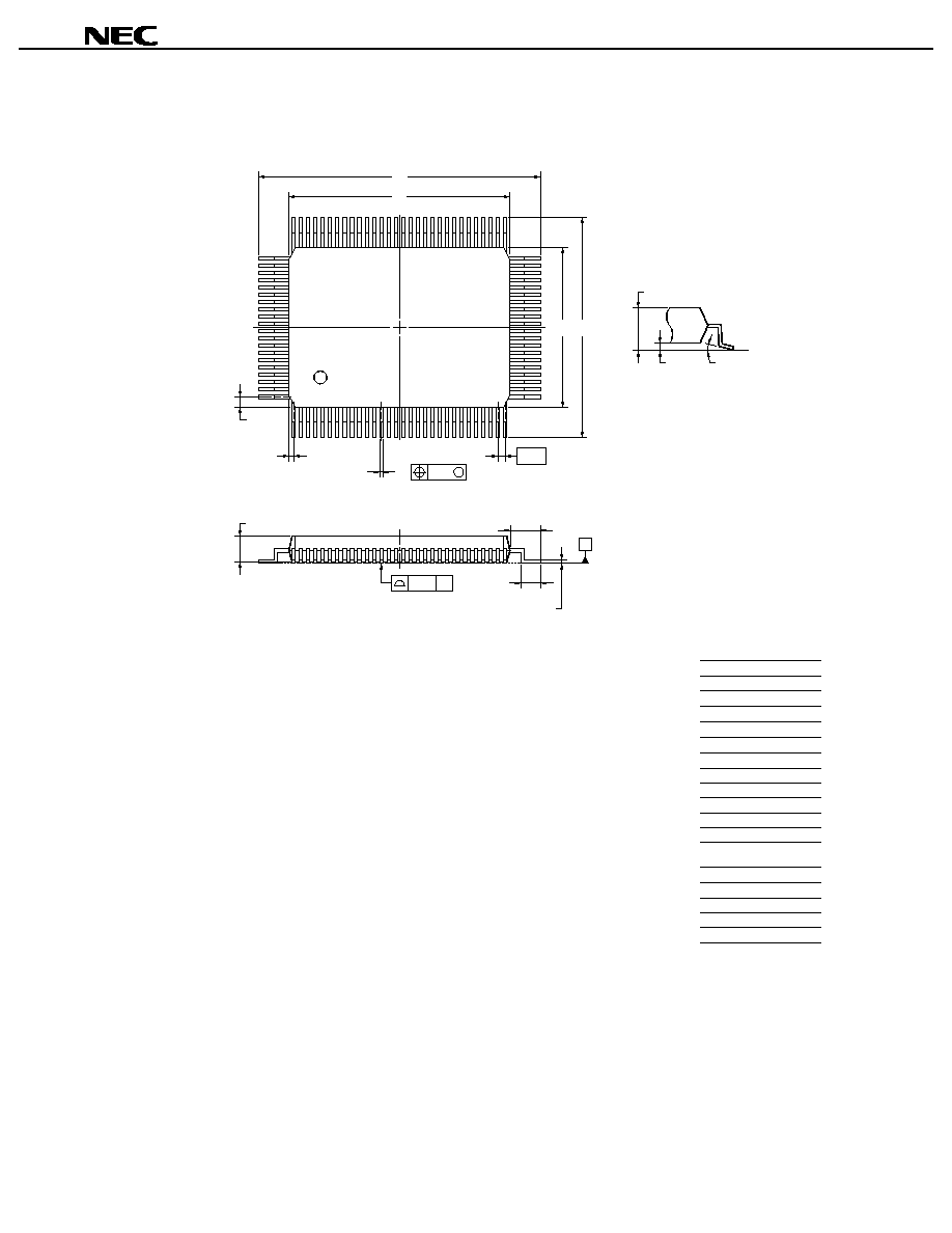
Data Sheet U14121EJ2V0DS00
89
µ
µ
µ
µ
PD784214A, 784215A, 784216A, 784217A, 784218A, 784214AY, 784215AY, 784216AY, 784217AY, 784218AY
Remark The external dimensions and material of the ES version are the same as those of the mass-produced
version.
80
81
50
100
1
31
30
51
100-PIN PLASTIC QFP (14x20)
H
I
J
detail of lead end
M
Q
R
K
M
L
P
S
S
N
G
F
NOTE
Each lead centerline is located within 0.15 mm of
its true position (T.P.) at maximum material condition.
ITEM
MILLIMETERS
A
B
D
G
23.6
±
0.4
20.0
±
0.2
0.30
±
0.10
0.6
H
17.6
±
0.4
I
C
14.0
±
0.2
0.15
J
0.65 (T.P.)
K
1.8
±
0.2
L
0.8
±
0.2
F
0.8
P100GF-65-3BA1-4
N
P
Q
0.10
2.7
±
0.1
0.1
±
0.1
R
5
∞±
5
∞
S
3.0 MAX.
M
0.15
+
0.10
-
0.05
C D
A
B
S
Data Sheet U14121EJ2V0DS00
90
µ
µ
µ
µ
PD784214A, 784215A, 784216A, 784217A, 784218A, 784214AY, 784215AY, 784216AY, 784217AY, 784218AY
15. RECOMMENDED SOLDERING CONDITIONS
The
µ
PD784218A should be soldered and mounted under the following recommended conditions. For the details
of the recommended soldering conditions, refer to the document Semiconductor Device Mounting Technology
Manual (C10535E).
For soldering methods and conditions other than those recommended below, contact your NEC sales
representative.
Table 15-1. Surface Mounting Type Soldering Conditions (1/2)
(1)
µ
µ
µ
µ
PD784214AGC-
◊◊◊
◊◊◊
◊◊◊
◊◊◊
-8EU:100-pin plastic LQFP(fine pitch) (14
◊
◊
◊
◊
14 mm)
µ
µ
µ
µ
PD784215AGC-
◊◊◊
◊◊◊
◊◊◊
◊◊◊
-8EU:100-pin plastic LQFP(fine pitch) (14
◊
◊
◊
◊
14 mm)
µ
µ
µ
µ
PD784216AGC-
◊◊◊
◊◊◊
◊◊◊
◊◊◊
-8EU:100-pin plastic LQFP(fine pitch) (14
◊
◊
◊
◊
14 mm)
µ
µ
µ
µ
PD784217AGC-
◊◊◊
◊◊◊
◊◊◊
◊◊◊
-8EU: 100-pin plastic LQFP (fine pitch) (14
◊
◊
◊
◊
14 mm)
µ
µ
µ
µ
PD784218AGC-
◊◊◊
◊◊◊
◊◊◊
◊◊◊
-8EU: 100-pin plastic LQFP (fine pitch) (14
◊
◊
◊
◊
14 mm)
µ
µ
µ
µ
PD784214AYGC-
◊◊◊
◊◊◊
◊◊◊
◊◊◊
-8EU:100-pin plastic LQFP(fine pitch) (14
◊
◊
◊
◊
14 mm)
µ
µ
µ
µ
PD784215AYGC-
◊◊◊
◊◊◊
◊◊◊
◊◊◊
-8EU:100-pin plastic LQFP(fine pitch) (14
◊
◊
◊
◊
14 mm)
µ
µ
µ
µ
PD784216AYGC-
◊◊◊
◊◊◊
◊◊◊
◊◊◊
-8EU:100-pin plastic LQFP(fine pitch) (14
◊
◊
◊
◊
14 mm)
µ
µ
µ
µ
PD784217AYGC-
◊◊◊
◊◊◊
◊◊◊
◊◊◊
-8EU: 100-pin plastic LQFP (fine pitch) (14
◊
◊
◊
◊
14 mm)
µ
µ
µ
µ
PD784218AYGC-
◊◊◊
◊◊◊
◊◊◊
◊◊◊
-8EU: 100-pin plastic LQFP (fine pitch) (14
◊
◊
◊
◊
14 mm)
Soldering Method
Soldering Conditions
Recommended
Condition Symbol
Infrared reflow
Package peak temperature: 235
∞
C, Time: 30 seconds max. (at 210
∞
C or higher),
Count: Two times or less, Exposure limit: 7 days
Note
(after that, prebake at 125
∞
C
for 10 hours)
IR35-107-2
VPS
Package peak temperature: 215
∞
C, Time: 40 seconds max. (at 200
∞
C or higher),
Count: Two times or less, Exposure limit: 7 days
Note
(after that, prebake at 125
∞
C
for 10 hours)
VP15-107-2
Partial heating
Pin temperature: 300
∞
C max., Time: 3 seconds max. (per pin row)
-
Note After opening the dry pack, store it at 25
∞
C or less and 65% RH or less for the allowable storage period.
Caution Do not use different soldering methods together (except for partial heating).
Data Sheet U14121EJ2V0DS00
91
µ
µ
µ
µ
PD784214A, 784215A, 784216A, 784217A, 784218A, 784214AY, 784215AY, 784216AY, 784217AY, 784218AY
Table 15-1. Surface Mounting Type Soldering Conditions (2/2)
(2)
µ
µ
µ
µ
PD784214AGF-
◊◊◊
◊◊◊
◊◊◊
◊◊◊
-3BA:100-pin plastic QFP(14
◊
◊
◊
◊
20 mm)
µ
µ
µ
µ
PD784215AGF-
◊◊◊
◊◊◊
◊◊◊
◊◊◊
-3BA:100-pin plastic QFP(14
◊
◊
◊
◊
20 mm)
µ
µ
µ
µ
PD784216AGF-
◊◊◊
◊◊◊
◊◊◊
◊◊◊
-3BA:100-pin plastic QFP(14
◊
◊
◊
◊
20 mm)
µ
µ
µ
µ
PD784217AGF-
◊◊◊
◊◊◊
◊◊◊
◊◊◊
-3BA: 100-pin plastic QFP (14
◊
◊
◊
◊
20 mm)
µ
µ
µ
µ
PD784218AGF-
◊◊◊
◊◊◊
◊◊◊
◊◊◊
-3BA: 100-pin plastic QFP (14
◊
◊
◊
◊
20 mm)
µ
µ
µ
µ
PD784214AYGF-
◊◊◊
◊◊◊
◊◊◊
◊◊◊
-3BA:100-pin plastic QFP(14
◊
◊
◊
◊
20 mm)
µ
µ
µ
µ
PD784215AYGF-
◊◊◊
◊◊◊
◊◊◊
◊◊◊
-3BA:100-pin plastic QFP(14
◊
◊
◊
◊
20 mm)
µ
µ
µ
µ
PD784216AYGF-
◊◊◊
◊◊◊
◊◊◊
◊◊◊
-3BA:100-pin plastic QFP(14
◊
◊
◊
◊
20 mm)
µ
µ
µ
µ
PD784217AYGF-
◊◊◊
◊◊◊
◊◊◊
◊◊◊
-3BA: 100-pin plastic QFP (14
◊
◊
◊
◊
20 mm)
µ
µ
µ
µ
PD784218AYGF-
◊◊◊
◊◊◊
◊◊◊
◊◊◊
-3BA: 100-pin plastic QFP (14
◊
◊
◊
◊
20 mm)
Soldering Method
Soldering Conditions
Recommended
Condition Symbol
Infrared reflow
Package peak temperature: 235
∞
C, Time: 30 seconds max. (at 210
∞
C or higher),
Count: Two times or less
IR35-00-2
VPS
Package peak temperature: 215
∞
C, Time: 40 seconds max. (at 200
∞
C or higher),
Count: Two times or less
VP15-00-2
Wave soldering
Solder bath temperature: 260
∞
C max., Time: 10 seconds max., Count: Once,
Preheating temperature: 120
∞
C max. (package surface temperature)
WS60-00-1
Partial heating
Pin temperature: 300
∞
C max., Time: 3 seconds max. (per pin row)
-
Caution Do not use different soldering methods together (except for partial heating).
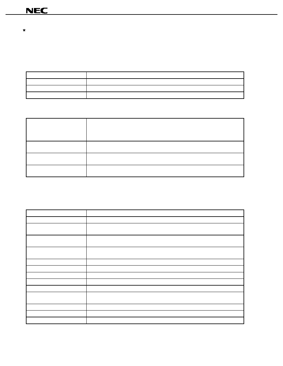
Data Sheet U14121EJ2V0DS00
92
µ
µ
µ
µ
PD784214A, 784215A, 784216A, 784217A, 784218A, 784214AY, 784215AY, 784216AY, 784217AY, 784218AY
APPENDIX A. DEVELOPMENT TOOLS
The following development tools are available for system development using the
µ
PD784218A. Also refer to (5)
Cautions on using development tools.
(1) Language processing software
RA78K4
Assembler package common to 78K/IV Series
CC78K4
C compiler package common to 78K/IV Series
DF784218
Device file common to
µ
PD784216A, 784216AY, 784218A, 784218AY Subseries
CC78K4-L
C compiler library source file common to 78K/IV Series
(2) Flash memory writing tools
Flashpro II
(Model number: FL-PR2),
Flashpro III
(Model number: FL-PR3, PG-FP3)
Dedicated flash programmer for microcontroller incorporating flash memory
FA-100GF
Adapter for writing 100-pin plastic QFP (GF-3BA type) flash memory. Connection must be
performed in accordance with the target product.
FA-100GC
Adapter for writing 100-pin plastic LQFP (GC-8EU type) flash memory. Connection must be
performed in accordance with the target product.
Flashpro II controller,
Flashpro III controller
Control program that runs on a personal computer and is attached to Flashpro II, Flashpro III.
Operates on Windows
TM
95, etc.
(3) Debugging tools
∑
∑
∑
∑
When IE-78K4-NS in-circuit emulator is used
IE-78K4-NS
In-circuit emulator common to 78K/IV Series
IE-70000-MC-PS-B
Power supply unit for IE-78K4-NS
IE-70000-98-IF-C
Interface adapter required when PC-9800 series PC (except notebook type) is used as host
machine (C bus supported)
IE-70000-CD-IF-A
PC card and cable when PC-9800 series notebook PC is used as host machine (PCMCIA
socket supported)
IE-70000-PC-IF-C
Interface adapter required when using IBM PC/AT
TM
compatibles as host machine (ISA bus
supported)
IE-70000-PCI-IF
Interface adapter required when using PC that incorporates PCI bus as host machine
IE-784225-NS-EM1
Emulation board to emulate
µ
PD784216A, 784216AY, 784218A, 784218AY Subseries
NP-100GF
Emulation probe for 100-pin plastic QFP (GF-3BA type)
NP-100GC
Emulation probe for 100-pin plastic LQFP (GC-8EU type)
EV-9200GF-100
Socket to be mounted on a target system board made for 100-pin plastic QFP (GF-3BA type)
TGC-100SDW
Conversion adapter to connect the NP-100GC and a target system board on which a 100-pin
plastic LQFP (GC-8EU type) can be mounted
ID78K4-NS
Integrated debugger for IE-78K4-NS
SM78K4
System simulator common to 78K/IV Series
DF784218
Device file common to
µ
PD784216A, 784216AY, 784218A, 784218AY Subseries
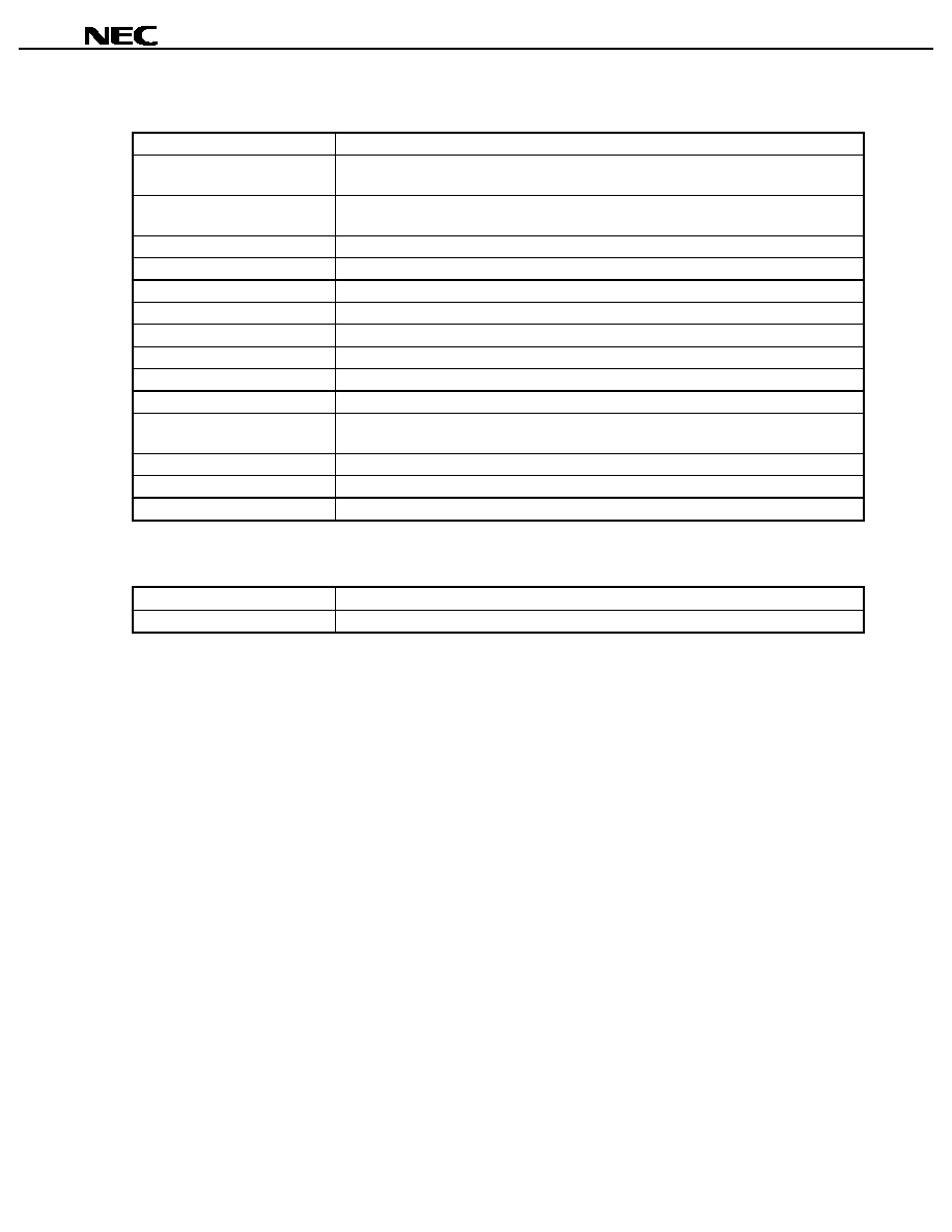
Data Sheet U14121EJ2V0DS00
93
µ
µ
µ
µ
PD784214A, 784215A, 784216A, 784217A, 784218A, 784214AY, 784215AY, 784216AY, 784217AY, 784218AY
∑
∑
∑
∑
When IE-784000-R in-circuit emulator is used
IE-784000-R
In-circuit emulator common to 78K/IV Series
IE-70000-98-IF-C
Interface adapter required when PC-9800 series PC (except notebook type) is used as host
machine (C bus supported)
IE-70000-PC-IF-C
Interface adapter required when using IBM PC/AT and compatibles as host machine (ISA bus
supported)
IE-70000-PCI-IF
Interface adapter required when using PC that incorporates PCI bus as host machine
IE-78000-R-SV3
Interface adapter and cable required when EWS is used as host machine
IE-784225-NS-EM1
Emulation board to emulate
µ
PD784216A, 784216AY, 784218A, 784218AY Subseries
IE-784000-R-EM
Emulation board common to 78K/IV Series
IE-78K4-R-EX3
Emulation probe conversion board required when using IE-784225-NS-EM1 on IE-784000-R.
EP-784218GF-R
Emulation probe for 100-pin plastic QFP (GF-3BA type)
EP-78064GC-R
Emulation probe for 100-pin plastic LQFP (GC-8EU type)
EV-9200GF-100
Socket to be mounted on a target system board made for 100-pin plastic QFP (GF-3BA type)
TGC-100SDW
Conversion adapter to connect the EP-78064GC-R and a target system board on which a
100-pin plastic LQFP (GC-8EU type) can be mounted
ID78K4
Integrated debugger for IE-784000-R
SM78K4
System simulator common to 78K/IV Series
DF784218
Device file common to
µ
PD784216A, 784216AY, 784218A, 784218AY Subseries
(4) Real-time OS
RX78K/IV
Real-time OS for 78K/IV Series
MX78K4
OS for 78K/IV Series
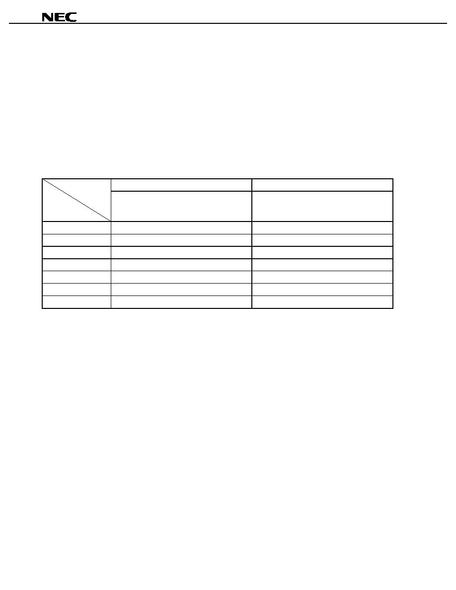
Data Sheet U14121EJ2V0DS00
94
µ
µ
µ
µ
PD784214A, 784215A, 784216A, 784217A, 784218A, 784214AY, 784215AY, 784216AY, 784217AY, 784218AY
(5) Cautions on using development tools
∑
The ID78K4-NS, ID78K4, and SM78K4 are used in combination with the DF784218.
∑
The CC78K4 and RX78K/IV are used in combination with the RA78K4 and DF784218.
∑
The FL-PR2, FL-PR3, FA-100GF, FA-100GC, NP-100GF, and NP-100GC are products made by Naito
Densei Machida Mfg. Co., Ltd. (TEL: +81-44-822-3813).
∑
The TGC-100SDW is a product made by TOKYO ELETECH CORPORATION.
For further information, contact Daimaru Kogyo, Ltd.
Tokyo Electronic Division (TEL: +81-3-3820-7112)
Osaka Electronic Division (TEL: +81-6-6244-6672)
∑
For third party development tools, see the Single-Chip Microcontroller Development Tool Selection Guide
(U11069E).
∑
The host machine and OS suitable for each software are as follows:
PC
EWS
Host Machine
[OS]
Software
PC-9800 series [Windows]
IBM PC/AT and compatibles
[Japanese/English Windows]
HP9000 Series 700
TM
[HP-UX
TM
]
SPARCstation
TM
[SunOS
TM
, Solaris
TM
]
NEWS
TM
(RISC) [NEWS-OS
TM
]
RA78K4
Note
CC78K4
Note
ID78K4-NS
-
ID78K4
SM78K4
-
RX78K/IV
Note
MX78K4
Note
Note DOS-based software
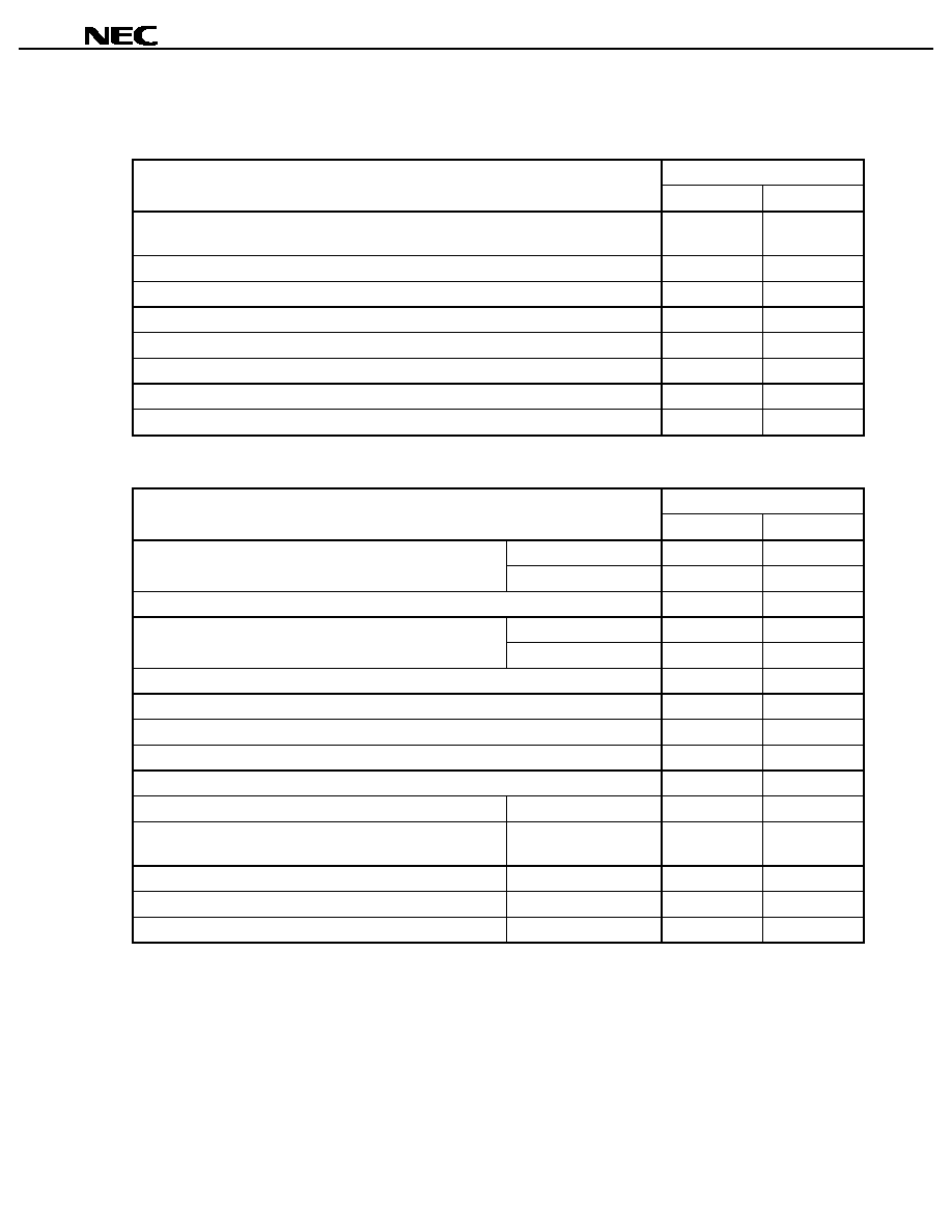
Data Sheet U14121EJ2V0DS00
95
µ
µ
µ
µ
PD784214A, 784215A, 784216A, 784217A, 784218A, 784214AY, 784215AY, 784216AY, 784217AY, 784218AY
APPENDIX B. RELATED DOCUMENTS
Documents related to devices
Document No.
Document Name
English
Japanese
µ
PD784214A, 784215A, 784216A, 784217A, 784218A, 784214AY, 784215AY, 784216AY,
784217AY, 784218AY Data Sheet
This document
U14121J
µ
PD78F4216A, 78F4216AY, 78F4218A, 78F4218AY Data Sheet
To be prepared
To be prepared
µ
PD784216A, 784216AY Subseries User's Manual Hardware
U13570E
U13570J
µ
PD784218A, 784218AY Subseries User's Manual Hardware
U12970E
U12970J
78K/IV Series User's Manual Instructions
U10905E
U10905J
78K/IV Series Instruction Table
-
U10594J
78K/IV Series Instruction Set
-
U10595J
78K/IV Series Application Note Software Basics
-
U10095J
Documents related to development tools (user's manuals)
Document No.
Document Name
English
Japanese
Language
U11162E
U11162J
RA78K4 Assembler Package
Operation
U11334E
U11334J
RA78K Structured Assembler Preprocessor
U11743E
U11743J
Language
U11571E
U11571J
CC78K4 C Compiler
Operation
U11572E
U11572J
IE-78K4-NS
U13356E
U13356J
IE-784000-R
U12903E
U12903J
IE-784218-R-EM1
U12155E
U12155J
IE-784225-NS-EM1
U13742E
U13742J
EP-78064
EEU-1469
EEU-934
SM78K4 System Simulator Windows Based
Reference
U10093E
U10093J
SM78K Series System Simulator
External Part User Open
Interface Specifications
U10092E
U10092J
ID78K4-NS Integrated Debugger PC Based
Reference
U12796E
U12796J
ID78K4 Integrated Debugger Windows Based
Reference
U10440E
U10440J
ID78K4 Integrated Debugger HP-UX, SunOS, NEWS-OS based
Reference
U11960E
U11960J
Caution
The related documents listed above are subject to change without notice. Be sure to use the
latest version of each document for designing.
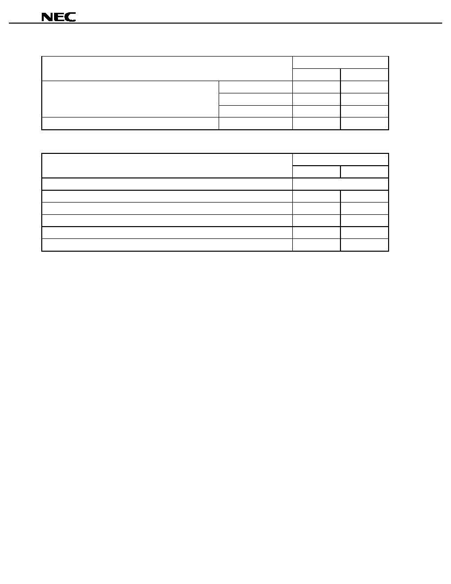
Data Sheet U14121EJ2V0DS00
96
µ
µ
µ
µ
PD784214A, 784215A, 784216A, 784217A, 784218A, 784214AY, 784215AY, 784216AY, 784217AY, 784218AY
Documents related to embedded software (user's manuals)
Document No.
Document Name
English
Japanese
Fundamental
U10603E
U10603J
Installation
U10604E
U10604J
78K/IV Series Real-Time OS
Debugger
-
U10364J
78K/IV Series OS MX78K4
Fundamental
-
U11779J
Other documents
Document No.
Document Name
English
Japanese
SEMICONDUCTOR SELECTION GUIDE Products & Packages (CD-ROM)
X13769X
Semiconductor Device Mounting Technology Manual
C10535E
C10535J
Quality Grades on NEC Semiconductor Devices
C11531E
C11531J
NEC Semiconductor Device Reliability/Quality Control System
C10983E
C10983J
Guide to Prevent Damage for Semiconductor Devices by Electrostatic Discharge (ESD)
C11892E
C11892J
Guide to Microcomputer-Related Products by Third Party
-
U11416J
Caution
The related documents listed above are subject to change without notice. Be sure to use the
latest version of each document for designing.
Data Sheet U14121EJ2V0DS00
97
µ
µ
µ
µ
PD784214A, 784215A, 784216A, 784217A, 784218A, 784214AY, 784215AY, 784216AY, 784217AY, 784218AY
NOTES FOR CMOS DEVICES
1
PRECAUTION AGAINST ESD FOR SEMICONDUCTORS
Note:
Strong electric field, when exposed to a MOS device, can cause destruction of the gate oxide and
ultimately degrade the device operation. Steps must be taken to stop generation of static electricity
as much as possible, and quickly dissipate it once, when it has occurred. Environmental control
must be adequate. When it is dry, humidifier should be used. It is recommended to avoid using
insulators that easily build static electricity. Semiconductor devices must be stored and transported
in an anti-static container, static shielding bag or conductive material. All test and measurement
tools including work bench and floor should be grounded. The operator should be grounded using
wrist strap. Semiconductor devices must not be touched with bare hands. Similar precautions need
to be taken for PW boards with semiconductor devices on it.
2
HANDLING OF UNUSED INPUT PINS FOR CMOS
Note:
No connection for CMOS device inputs can be cause of malfunction. If no connection is provided
to the input pins, it is possible that an internal input level may be generated due to noise, etc., hence
causing malfunction. CMOS devices behave differently than Bipolar or NMOS devices. Input levels
of CMOS devices must be fixed high or low by using a pull-up or pull-down circuitry. Each unused
pin should be connected to V
DD
or GND with a resistor, if it is considered to have a possibility of
being an output pin. All handling related to the unused pins must be judged device by device and
related specifications governing the devices.
3
STATUS BEFORE INITIALIZATION OF MOS DEVICES
Note:
Power-on does not necessarily define initial status of MOS device. Production process of MOS
does not define the initial operation status of the device. Immediately after the power source is
turned ON, the devices with reset function have not yet been initialized. Hence, power-on does
not guarantee out-pin levels, I/O settings or contents of registers. Device is not initialized until the
reset signal is received. Reset operation must be executed immediately after power-on for devices
having reset function.

Data Sheet U14121EJ2V0DS00
98
µ
µ
µ
µ
PD784214A, 784215A, 784216A, 784217A, 784218A, 784214AY, 784215AY, 784216AY, 784217AY, 784218AY
Regional Information
Some information contained in this document may vary from country to country. Before using any NEC
product in your application, pIease contact the NEC office in your country to obtain a list of authorized
representatives and distributors. They will verify:
∑
Device availability
∑
Ordering information
∑
Product release schedule
∑
Availability of related technical literature
∑
Development environment specifications (for example, specifications for third-party tools and
components, host computers, power plugs, AC supply voltages, and so forth)
∑
Network requirements
In addition, trademarks, registered trademarks, export restrictions, and other legal issues may also vary
from country to country.
NEC Electronics Inc. (U.S.)
Santa Clara, California
Tel: 408-588-6000
800-366-9782
Fax: 408-588-6130
800-729-9288
NEC Electronics (Germany) GmbH
Duesseldorf, Germany
Tel: 0211-65 03 02
Fax: 0211-65 03 490
NEC Electronics (UK) Ltd.
Milton Keynes, UK
Tel: 01908-691-133
Fax: 01908-670-290
NEC Electronics Italiana s.r.l.
Milano, Italy
Tel: 02-66 75 41
Fax: 02-66 75 42 99
NEC Electronics (Germany) GmbH
Benelux Office
Eindhoven, The Netherlands
Tel: 040-2445845
Fax: 040-2444580
NEC Electronics (France) S.A.
Velizy-Villacoublay, France
Tel: 01-30-67 58 00
Fax: 01-30-67 58 99
NEC Electronics (France) S.A.
Madrid Office
Madrid, Spain
Tel: 91-504-2787
Fax: 91-504-2860
NEC Electronics (Germany) GmbH
Scandinavia Office
Taeby, Sweden
Tel: 08-63 80 820
Fax: 08-63 80 388
NEC Electronics Hong Kong Ltd.
Hong Kong
Tel: 2886-9318
Fax: 2886-9022/9044
NEC Electronics Hong Kong Ltd.
Seoul Branch
Seoul, Korea
Tel: 02-528-0303
Fax: 02-528-4411
NEC Electronics Singapore Pte. Ltd.
United Square, Singapore
Tel: 65-253-8311
Fax: 65-250-3583
NEC Electronics Taiwan Ltd.
Taipei, Taiwan
Tel: 02-2719-2377
Fax: 02-2719-5951
NEC do Brasil S.A.
Electron Devices Division
Guarulhos-SP Brasil
Tel: 55-11-6462-6810
Fax: 55-11-6462-6829
J00.7

Data Sheet U14121EJ2V0DS00
99
µ
µ
µ
µ
PD784214A, 784215A, 784216A, 784217A, 784218A, 784214AY, 784215AY, 784216AY, 784217AY, 784218AY
IEBus is a trademark of NEC Corporation.
Windows is either a registered trademark or a trademark of Microsoft Corporation in the United States and/or
other countries.
PC/AT is a trademark of International Business Machines Corporation.
HP9000 series 700 and HP-UX are trademarks of Hewlett-Packard Company.
SPARCstation is a trademark of SPARC International, Inc.
Solaris and SunOS are trademarks of Sun Microsystems, Inc.
NEWS and NEWS-OS are trademarks of Sony Corporation.

µ
µ
µ
µ
PD784214A, 784215A, 784216A, 784217A, 784218A, 784214AY, 784215AY, 784216AY, 784217AY, 784218AY
The related documents indicated in this publication may include preliminary versions. However, preliminary
versions are not marked as such.
Purchase of NEC I
2
C components conveys a license under the Philips I
2
C Patent Rights to use these components
in an I
2
C system, provided that the system conforms to the I
2
C Standard Specification as defined by Philips.
M8E 00. 4
The information in this document is current as of August, 2000. The information is subject to
change without notice. For actual design-in, refer to the latest publications of NEC's data sheets or
data books, etc., for the most up-to-date specifications of NEC semiconductor products. Not all
products and/or types are available in every country. Please check with an NEC sales representative
for availability and additional information.
No part of this document may be copied or reproduced in any form or by any means without prior
written consent of NEC. NEC assumes no responsibility for any errors that may appear in this document.
NEC does not assume any liability for infringement of patents, copyrights or other intellectual property rights of
third parties by or arising from the use of NEC semiconductor products listed in this document or any other
liability arising from the use of such products. No license, express, implied or otherwise, is granted under any
patents, copyrights or other intellectual property rights of NEC or others.
Descriptions of circuits, software and other related information in this document are provided for illustrative
purposes in semiconductor product operation and application examples. The incorporation of these
circuits, software and information in the design of customer's equipment shall be done under the full
responsibility of customer. NEC assumes no responsibility for any losses incurred by customers or third
parties arising from the use of these circuits, software and information.
While NEC endeavours to enhance the quality, reliability and safety of NEC semiconductor products, customers
agree and acknowledge that the possibility of defects thereof cannot be eliminated entirely. To minimize
risks of damage to property or injury (including death) to persons arising from defects in NEC
semiconductor products, customers must incorporate sufficient safety measures in their design, such as
redundancy, fire-containment, and anti-failure features.
NEC semiconductor products are classified into the following three quality grades:
"Standard", "Special" and "Specific". The "Specific" quality grade applies only to semiconductor products
developed based on a customer-designated "quality assurance program" for a specific application. The
recommended applications of a semiconductor product depend on its quality grade, as indicated below.
Customers must check the quality grade of each semiconductor product before using it in a particular
application.
"Standard": Computers, office equipment, communications equipment, test and measurement equipment, audio
and visual equipment, home electronic appliances, machine tools, personal electronic equipment
and industrial robots
"Special":
Transportation equipment (automobiles, trains, ships, etc.), traffic control systems, anti-disaster
systems, anti-crime systems, safety equipment and medical equipment (not specifically designed
for life support)
"Specific": Aircraft, aerospace equipment, submersible repeaters, nuclear reactor control systems, life
support systems and medical equipment for life support, etc.
The quality grade of NEC semiconductor products is "Standard" unless otherwise expressly specified in NEC's
data sheets or data books, etc. If customers wish to use NEC semiconductor products in applications not
intended by NEC, they must contact an NEC sales representative in advance to determine NEC's willingness
to support a given application.
(Note)
(1) "NEC" as used in this statement means NEC Corporation and also includes its majority-owned subsidiaries.
(2) "NEC semiconductor products" means any semiconductor product developed or manufactured by or for
NEC (as defined above).
∑
∑
∑
∑
∑
∑
The export of this product from Japan is regulated by the Japanese government. To export this product may be prohibited
without governmental license, the need for which must be judged by the customer. The export or re-export of this product
from a country other than Japan may also be prohibited without a license from that country. Please call an NEC sales
representative.