Document Outline
- COVER
- DESCRIPTION
- FEATURES
- APPLICATION FIELDS
- ORDERING INFORMATION
- PRODUCT DEVELOPMENT OF VCR-SERVO MICROCONTROLLERS
- FUNCTION LIST
- PIN CONFIGURATION (Top View)
- INTERNAL BLOCK DIAGRAM
- SYSTEM CONFIGURATION EXAMPLE
- 1. DIFFERENCE BETWEEN uPD784928 SUBSERIES AND 784928Y SUBSERIES
- 2. PIN FUNCTION
- 2.1 Port Pins
- 2.2 Pins Other Than Port Pins
- 2.3 I/O Circuits of Pins and Processing of Unused Pins
- 3. INTERNAL BLOCK FUNCTION
- 3.1 CPU Registers
- 3.1.1 General-purpose registers
- 3.1.2 Other CPU registers
- 3.2 Memory Space
- 3.3 Special Function Registers (SFRs)
- 3.4 Ports
- 3.5 Real-Time Output Port
- 3.6 Super Timer Unit
- 3.7 Serial Interface
- 3.8 A/D Converter
- 3.9 VCR Analog Circuits
- 3.10 Watch Function
- 3.11 Clock Output Function
- 3.12 Buzzer Output Function
- 4. INTERNAL/EXTERNAL CONTROL FUNCTION
- 4.1 Interrupt Function
- 4.1.1 Vectored interrupt
- 4.1.2 Context switching
- 4.1.3 Macro service
- 4.1.4 Application example of macro service
- 4.2 Standby Function
- 4.3 Clock Generation Circuit
- 4.4 Reset Function
- 5. INSTRUCTION SET
- 6. ELECTRICAL SPECIFICATIONS
- 7. PACKAGE DRAWING
- 8. RECOMMENDED SOLDERING CONDITIONS
- APPENDIX A. DEVELOPMENT TOOLS
- APPENDIX B. RELATED DOCUMENTS
©
1997,1999
DATA SHEET
µ
PD784927, 784928, 784927Y, 784928Y
DESCRIPTION
The
µ
PD784927 and 784928 are members of the NEC 78K/IV Series of microcontrollers equipped with a high-
speed, high-performance 16-bit CPU for VCR software servo control.
The
µ
PD784927Y and 784928Y are based on the
µ
PD784928 with the addition of an I
2
C bus interface compatible
with multi-master.
They contain many peripheral hardware units ideal for VCR control, such as a multi-function timer unit (super timer
unit) for software servo control and VCR analog circuits.
Flash memory models, the
µ
PD78F4928 and
µ
PD78F4928Y, are under development.
The functions of the
µ
PD784927 is described in detail in the following User's Manual. Be sure to read this
manual before designing your system.
µ
PD784928, 784928Y Subseries User's Manual - Hardware
: U12648E
78K/IV Series User's Manual - Instruction
: U10905E
FEATURES
∑
High instruction execution speed realized by 16-bit CPU core
∑
Minimum instruction execution time: 250 ns (with 8 MHz internal clock)
∑
High internal memory capacity
Item
Part Number
µ
PD784927, 784927Y
µ
PD784928, 784928Y
Internal ROM capacity
96K bytes
128K bytes
Internal RAM capacity
2048 bytes
3584 bytes
∑
VCR analog circuits conforming to VHS Standard
∑
CTL amplifier
∑
DFG amplifier
∑
Reel FG comparator (2 channels)
∑
RECCTL driver (rewritable)
∑
DPG amplifier
∑
CSYNC comparator
∑
CFG amplifier
∑
DPFG separation circuit (ternary separation circuit)
∑
Timer unit (super timer unit) for servo control
∑
Serial interface : 3 channels
∑
3-wire serial I/O : 2 channels
∑
I
2
C bus interface: 1 channel
∑
A/D converter: 12 channels (conversion time: 10
µ
s)
∑
Low-frequency oscillation mode: main system clock frequency = internal clock frequency
∑
Low-power consumption mode: CPU can operate with a subsystem clock.
∑
Supply voltage range: V
DD
= +2.7 to 5.5 V
∑
Hardware watch function: watch operation at low voltage (V
DD
= 2.7 V (MIN.)) and low current consumption
Unless otherwise specified, the
µ
PD784927 is treated as the representative model throughout this document.
16-BIT SINGLE-CHIP MICROCONTROLLER
MOS INTEGRATED CIRCUIT
The mark shows major revised points.
Document No. U12255EJ2V0DS00 (2nd edition)
Date Published December 1999 N CP(K)
Printed in Japan
The information in this document is subject to change without notice. Before using this document, please
confirm that this is the latest version.
Not all devices/types available in every country. Please check with local NEC representative for availability
and additional information.

µ
PD784927, 784928, 784927Y, 784928Y
2
Data Sheet U12255EJ2V0DS00
APPLICATION FIELDS
Stationary VCR, video camera, In-TV VCR
ORDERING INFORMATION
(1)
µ
PD784928 subseries
Part Number
Package
µ
PD784927GC-
◊◊◊
-8EU
Note
100-pin plastic LQFP (fine pitch) (14
◊
14 mm)
µ
PD784927GF-
◊◊◊
-3BA
100-pin plastic QFP (14
◊
20 mm)
µ
PD784928GC-
◊◊◊
-8EU
Note
100-pin plastic LQFP (fine pitch) (14
◊
14 mm)
µ
PD784928GF-
◊◊◊
-3BA
100-pin plastic QFP (14
◊
20 mm)
(2)
µ
PD784928Y subseries
Part Number
Package
µ
PD784927YGC-
◊◊◊
-8EU
Note
100-pin plastic LQFP (fine pitch) (14
◊
14 mm)
µ
PD784927YGF-
◊◊◊
-3BA
100-pin plastic QFP (14
◊
20 mm)
µ
PD784928YGC-
◊◊◊
-8EU
Note
100-pin plastic LQFP (fine pitch) (14
◊
14 mm)
µ
PD784928YGF-
◊◊◊
-3BA
100-pin plastic QFP (14
◊
20 mm)
Note
Under development
Remark
◊◊◊
indicates ROM code suffix.
PRODUCT DEVELOPMENT OF VCR-SERVO MICROCONTROLLERS
The product development of VCR-servo microcontrollers is shown below. Enclosed in a frame are subseries
names.
The Y subseries is a collection of products supporting the I
2
C bus.
Products under mass production
Products under development
78K/IV series
78K/I series
100-pin QFP. With flash memory.
Expanded internal memory capacity.
More powerful analog amplifier. Improved VCR functions.
Increased I/O. High-current port added.
I
2
C function added (Y model only).
80-pin QFP
PD784928
µ
PD784915
µ
PD78148
µ
PD78138
µ
PD784928Y
µ
100-pin QFP
Expanded internal RAM capacity. Operational amplifier,
watch function, multiplier added.
100-pin QFP.
Expanded internal memory capacity.
Internal analog amplifier. Reinforced super timer.
Low-power consumption mode added.
3
µ
PD784927, 784928, 784927Y, 784928Y
Data Sheet U12255EJ2V0DS00
µ
PD784927, 784927Y
µ
PD784928, 784928Y
96K bytes
128K bytes
2048 bytes
3584 bytes
16 MHz (internal clock: 8 MHz)
Low frequency oscillation mode : 8 MHz (internal clock: 8 MHz)
Low power consumption mode : 32.768 kHz (subsystem clock)
250 ns (with 8 MHz internal clock)
74
input : 20
I/O
: 54 (including 8 ports for LED direct drive)
11 (including one each for pseudo V
SYNC
, head amplifier switch, and chrominance rotation)
Timer/counter
Compare register
Capture register
Remark
TM0 (16 bits)
3
--
TM1 (16 bits)
3
1
FRC (22 bits)
--
6
TM3 (16 bits)
2
1
UDC (5 bits)
1
--
EC (8 bits)
4
--
For HSW signal generation
EDV (8 bits)
1
--
For CFG signal division
Input signal
Number of bits
Measurable cycle
Operating edge
CFG
22
125 ns to 524 ms
DFG
22
125 ns to 524 ms
HSW
16
1
µ
s to 65.5 ms
V
SYNC
22
125 ns to 524 ms
CTL
16
1
µ
s to 65.5 ms
T
REEL
22
125 ns to 524 ms
S
REEL
22
125 ns to 524 ms
∑
V
SYNC
separation circuit, H
SYNC
separation circuit
∑
VISS detection, wide aspect detection circuits
∑
Field identification circuit
∑
Head amplifier switch/chrominance rotation output circuit
Timer
Compare register
Capture register
TM2 (16 bits)
1
--
TM4 (16 bits)
1 (capture/compare)
1
TM5 (16 bits)
1
--
∑
16-bit resolution : 3 channels (carrier frequency: 62.5 kHz)
∑
8-bit resolution
: 3 channels (carrier frequency: 62.5 kHz)
3-wire serial I/O: 2 channels (BUSY/STRB control: 1 channel)
∑
I
2
C bus interface: 1 channel (
µ
PD784928Y subseries only)
8-bit resolution
◊
12 channels, conversion time: 10
µ
s
FUNCTION LIST (1/2)
Part Number
Item
Internal ROM capacity
Internal RAM capacity
Operating clock
Minimum instruction e x e c u -
tion time
I/O port
Real-time output port
Timer/counter
Capture register
VCR special
circuit
General-purpose
timer
PWM output
Serial interface
A/D converter
Super
timer unit
µ
PD784927, 784928, 784927Y, 784928Y
4
Data Sheet U12255EJ2V0DS00
FUNCTION LIST (2/2)
Part Number
Item
Analog circuit
Interrupt sources
External
Internal
Standby function
Watch function
Buzzer output function
Supply voltage
Package
µ
PD784927, 784927Y
µ
PD784928, 784928Y
∑
CTL amplifier
∑
RECCTL driver (rewritable)
∑
DFG amplifier, DPG amplifier, CFG amplifier
∑
DPFG separation circuit (ternary separation circuit)
∑
Reel FG comparator (2 channels)
∑
CSYNC comparator
4 levels (programmable), vectored interrupt, macro service, context switching
9 (including NMI)
22 (including software interrupt)
23 (including software interrupt)
HALT mode/STOP mode/low power consumption mode/low power consumption HALT mode
STOP mode can be released by input of valid edge of NMI pin, watch interrupt (INTW), or INTP1/
INTP2/KEY0-KEY4 pins
0.5-second measurement, low-voltage operation (V
DD
= 2.7 V)
1.95 kHz, 3.91 kHz, 7.81 kHz, 15.6 kHz (Internal clock: 8 MHz)
2.048 kHz, 4.096 kHz, 32.768 kHz (Subsystem clock: 32.768 kHz)
V
DD
= +2.7 to 5.5 V
∑ 100-pin plastic LQFP (fine pitch)(14
◊
14 mm)
Note
∑ 100-pin plastic QFP (14
◊
20 mm)
Note
Under development
5
µ
PD784927, 784928, 784927Y, 784928Y
Data Sheet U12255EJ2V0DS00
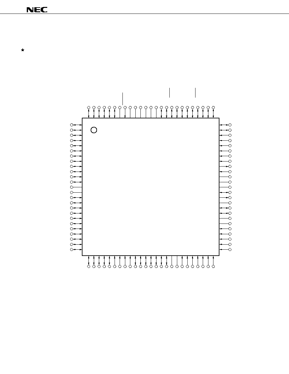
PIN CONFIGURATION (Top View)
∑
100-pin plastic LQFP (fine pitch)(14
◊
14 mm)
µ
PD784927GC-
◊◊◊
-8EU
Note 1
, 784928GC-
◊◊◊
-8EU
Note 1
µ
PD784928YGC-
◊◊◊
-8EU, 784928YGC-
◊◊◊
-8EU
Note 1
Notes 1. Under development
2. Pins SCL and SDA are provided for the
µ
PD784928Y subseries only.
Caution Directly connect the IC (Internally Connected) pins to V
SS
in the normal operation mode.
P65/HWIN/DPGMON
P64/BUZ/DFGMON
P103/CSYNCIN
P102/REEL0IN/INTP3
P101/REEL1IN
DFGIN
P100/DPGIN
CFGCPIN
CFGAMP0
CFGIN
AV
DD1
AV
SS1
VREFC
CTLOUT2
CTLOUT1
CTLIN
RECCTL
-
RECCTL
+
CTLDLY
AV
SS2
P113/ANI11
P112/ANI10
P111/ANI9
P110/ANI8
P77/ANI7
P84/PWM2/SDA
Note 2
P83/ROTC
P82/HASW
P80
P57
P56
P55
P54
P53
P52
P51
P50
V
SS
V
DD
P47
P46
P45
P44
P43
P42
P41
P40
P07
P06
P05
P04
P03
P02
P01
P00
P23/INTP2
P22/INTP1
P21/INTP0
P20/NMI
P90/ENV
P91/KEY0
P92/KEY1
P93/KEY2
P94/KEY3
P95/KEY4
P96
AV
DD2
AV
REF
P70/ANI0
P71/ANI1
P72/ANI2
P73/ANI3
P74/ANI4
P75/ANI5
P76/ANI6
P85/PWM3/SCL
Note 2
P86/PTO10
P87/PTO11
P30/PTO00
P31/PTO01
P32/PTO02
IC
RESET
X1
X2
V
SS
XT2
XT1
V
DD
P33/SI2/BUSY
P34/SO2
P35/SCK2
P36/PWM1
P37/PWM0
P63/SI1
P62/SO1
P61/SCK1/BUZ
P60/STRB/CLO
P67/PWM5/CTLMON
P66/PWM4/CFGMON
1
2
3
4
5
6
7
8
9
10
11
12
13
14
15
16
17
18
19
20
21
22
23
24
25
75
74
73
72
71
70
69
68
67
66
65
64
63
62
61
60
59
58
57
56
55
54
53
52
51
100 99 98 97 96 95 94 93 92 91 90 89 88 87 86 85 84 83 82 81
26 27 28 29 30 31 32 33 34 35 36 37 38 39 40 41 42 43 44 45
80 79 78 77 76
46 47 48 49 50