 | –≠–ª–µ–∫—Ç—Ä–æ–Ω–Ω—ã–π –∫–æ–º–ø–æ–Ω–µ–Ω—Ç: UPD789314 | –°–∫–∞—á–∞—Ç—å:  PDF PDF  ZIP ZIP |
Document Outline
- COVER
- FEATURES
- APPLICATIONS
- ORDERING INFORMATION
- 78K/0S SERIES LINEUP
- OVERVIEW OF FUNCTIONS
- 1. PIN CONFIGURATION (TOP VIEW)
- 2. BLOCK DIAGRAM
- 3. PIN FUNCTIONS
- 3.1 Port Pins
- 3.2 Non-Port Pins
- 3.3 Pin I/O Circuits and Recommended Connection of Unused Pins
- 4. MEMORY SPACE
- 5. PERIPHERAL HARDWARE FUNCTIONS
- 5.1 Ports
- 5.2 Clock Generator
- 5.3 Timer
- 5.4 Serial Interface
- 5.4.1 Serial interface 10 (SIO10)
- 5.4.2 Serial interface 20 (SIO20)
- 5.5 LCD Controller/Driver
- 6. INTERRUPT FUNCTIONS
- 7. STANDBY FUNCTION
- 8. RESET FUNCTION
- 9. MASK OPTIONS
- 10. OVERVIEW OF INSTRUCTION SET
- 10.1 Conventions
- 10.1.1 Operand expressions and description methods
- 10.1.2 Description of çOperationé column
- 10.1.3 Description of çFlagé column
- 10.2 List of Operations
- 11. ELECTRICAL SPECIFICATIONS
- 12. CHARACTERISTICS CURVES OF LCD CONTROLLER/DRIVER (REFERENCE VALUES)
- 13. PACKAGE DRAWINGS
- 14. RECOMMENDED SOLDERING CONDITIONS
- APPENDIX A. DEVELOPMENT TOOLS
- APPENDIX B. RELATED DOCUMENTS
DATA SHEET
8-BIT SINGLE-CHIP MICROCONTROLLER
MOS INTEGRATED CIRCUIT
µ
µ
µ
µPD789304, 789306, 789314, 789316
Document No. U14384EJ1V0DS00 (1st edition)
Date Published March 2001 N CP(K)
Printed in Japan
The information in this document is subject to change without notice. Before using this document, please
confirm that this is the latest version.
Not all devices/types available in every country. Please check with local NEC representative for
availability and additional information.
The mark shows major revised points.
The
µPD789304, 789306, 789314, and 789316 belong to the µPD789306, 789316 Subseries (for LCD drivers) in
the 78K/0S Series.
Flash memory versions (
µPD78F9306, 78F9316) that can be operated using the same power supply voltage as
mask ROM versions are available, along with various development tools.
Detailed function descriptions are provided in the following user's manuals. Be sure to read them before
designing.
µ
µ
µ
µPD789306, 789316 Subseries User's Manual: U14800E
78K/0S Series User's Manual Instructions:
U11047E
FEATURES
∑ ROM and RAM capacities
Data Memory
Item
Part Number
Program Memory (ROM)
Internal High-Speed RAM
LCD Display RAM
µPD789304, 789314
8 KB
µPD789306, 789316
16 KB
512 bytes
24 bytes
∑ Main system clock
Ceramic/crystal oscillation:
µPD789304, 789306
RC oscillation:
µPD789314, 789316
∑ I/O ports: 23
∑ Serial interface: 2 channels
Switchable between 3-wire serial I/O mode and UART mode: 1 channel
3-wire serial I/O mode:
1 channel
∑ LCD controller/driver
Segment signals: 24, common signals: 4
∑ Timer: 5 channels
∑ Power supply voltage: V
DD
= 1.8 to 5.5 V
APPLICATIONS
Remote control devices, healthcare equipment, etc.
©
1996, 1999
1999

µ
µ
µ
µ
PD789304, 789306, 789314, 789316
2
Data Sheet U14384EJ1V0DS
ORDERING INFORMATION
Part Number
Package
µPD789304GC-◊◊◊-AB8
64-pin plastic QFP (14
◊ 14)
µPD789304GK-◊◊◊-9ET
64-pin plastic TQFP (12
◊ 12)
µPD789306GC-◊◊◊-AB8
64-pin plastic QFP (14
◊ 14)
µPD789306GK-◊◊◊-9ET
64-pin plastic TQFP (12
◊ 12)
µPD789314GC-◊◊◊-AB8
64-pin plastic QFP (14
◊ 14)
µPD789314GK-◊◊◊-9ET
64-pin plastic TQFP (12
◊ 12)
µPD789316GC-◊◊◊-AB8
64-pin plastic QFP (14
◊ 14)
µPD789316GK-◊◊◊-9ET
64-pin plastic TQFP (12
◊ 12)
Remark
◊◊◊ indicates ROM code suffix.

µ
µ
µ
µ
PD789304, 789306, 789314, 789316
Data Sheet U14384EJ1V0DS
3
78K/0S SERIES LINEUP
The products in the 78K/0S Series are listed below. The names enclosed in boxes are subseries names.
Products under development
Products in mass production
PD789014
Small-scale package, general-purpose applications
78K/0S
Series
28-pin
PD789014 with enhanced timer and increased ROM, RAM capacity
On-chip UART and capable of low voltage (1.8 V) operation
PD789074 with added subsystem clock
LCD drive
Inverter control
44-pin
PD789842
On-chip inverter controller and UART
ASSP
80-pin
80-pin
PD789446
PD789456
PD789436
PD789417A
PD789407A
PD789426
PD789306
PD789316
PD789426 with enhanced A/D
PD789446 with enhanced A/D converter
A/D converter and resistance division type LCD (28
◊
4)
A/D converter and on-chip voltage booster type LCD (15
◊
4)
PD789407A with enhanced A/D converter
A/D converter and on-chip voltage booster type LCD (5
◊
4)
RC oscillation version of the PD789306
On-chip voltage booster type LCD (24
◊
4)
64-pin
64-pin
64-pin
64-pin
64-pin
64-pin
PD789146
PD789156
44-pin
Small-scale package, general-purpose applications and A/D converter
44-pin
30-pin
30-pin
30-pin
30-pin
PD789124A
PD789134A
PD789177
PD789167
30-pin
30-pin
PD789104A
PD789114A
PD789167 with enhanced A/D converter
PD789104A with enhanced timer
PD789124A with enhanced A/D converter
RC oscillation version of the PD789104A
PD789104A with enhanced A/D converter
PD789026 with added A/D converter and multiplier
PD789104A with added EEPROM
TM
PD789146 with enhanced A/D converter
PD789177Y
PD789167Y
Y subseries products support SMB.
Dot LCD drive
20-pin
PD789860
PD789840
44-pin
44-pin
PD789800
20-pin
PD789861
For keyless entry, on-chip POC and key return circuit
For keypad, on-chip POC
For PC keyboard, on-chip USB function
RC oscillation version of the PD789860
52-pin
52-pin
For remote controller, with SIO and resistance division type LCD
For remote controller, with A/D converter and on-chip voltage booster type LCD
88-pin
PD789830
PD789835
144-pin
Segments: 40, commons: 16
Segment/common outputs: 96
42-/44-pin
44-pin
PD789046
PD789074
PD789026
30-pin
PD789026 with enhanced timer
VFD drive
52-pin
PD789871
Total display outputs: 25
PD789488
A/D converter and on-chip voltage booster type LCD (28
◊
4)
80-pin
PD789488 with added remote control receiver and resistance division type LCD
80-pin
PD789327
PD789803
64-pin
PD789467
PD789477
For PC keyboard, on-chip USB HUB function
µ
µ
µ
µ
µ
µ
µ
µ
µ
µ
µ
µ
µ
µ
µ
µ
µ
µ
µ
µ
µ
µ
µ
µ
µ
µ
µ
µ
µ
µ
µ
µ
µ
µ
µ
µ
µ
µ
µ
µ
µ
µ
µ
µ
µ
µ
µ
µ
µ
µ
µ
µ
µ
µ
µ
µ
PD789304, 789306, 789314, 789316
4
Data Sheet U14384EJ1V0DS
The major functional differences among the subseries are listed below.
V
DD
Function
Subseries Name
ROM
Capacity
8-Bit 16-Bit Watch WDT
8-Bit
A/D
10-Bit
A/D
Serial
Interface
I/O MIN.
Value
Remarks
µPD789046
16 K
1 ch
µPD789026
4 K to 16 K
34
µPD789074
2 K to 8 K
1 ch
1 ch
24
Small-scale
package,
general-
purpose
applications
µPD789014
2 K to 4 K
2 ch
-
-
-
-
1 ch (UART:
1 ch)
22
-
µPD789177
-
8 ch
µPD789167
16 K to 24 K
3 ch
1 ch
8 ch
-
31
-
µPD789156
-
4 ch
µPD789146
8 K to 16 K
4 ch
-
On-chip
EEPROM
µPD789134A
-
4 ch
µPD789124A
4 ch
-
RC-oscillation
version
µPD789114A
-
4 ch
Small-
scale
package,
general-
purpose
applications
and A/D
converter
µPD789104A
2 K to 8 K
1 ch
1 ch
-
1 ch
4 ch
-
1 ch (UART:
1 ch)
20
1.8 V
-
Inverter
control
µPD789842
8 K to 16 K
3 ch
Note
1 ch
1 ch
8 ch
-
1 ch (UART:
1 ch)
30 4.0 V
-
VFD drive
µPD789871
4 K to 8 K
3 ch
≠
1 ch
1 ch
≠
≠
1 ch
33 2.7 V
≠
µPD789488
32 K
8 ch
2 ch (UART:
1 ch)
45
µPD789417A
-
7 ch
µPD789407A
12 K to
24 K
3 ch
7 ch
-
43
µPD789456
≠
6 ch
µPD789446
6 ch
≠
30
µPD789436
≠
6 ch
µPD789426
12 K to
16 K
6 ch
1 ch (UART:
1 ch)
40
-
µPD789316
RC-oscillation
version
LCD drive
µPD789306
8 K to 16 K
2 ch
1 ch
1 ch
1 ch
≠
≠
2 ch (UART:
1 ch)
23
1.8 V
≠
µPD789835
24 K to
60 K
6 ch
≠
3 ch
28 1.8 V
Dot LCD
drive
µPD789830
24 K
1 ch
1 ch
1 ch
1 ch
≠
≠
1 ch (UART:
1 ch)
30 2.7 V
-
µPD789477
24 K
3 ch
1 ch
8 ch
2 ch (UART:
1 ch)
45
µPD789467
1 ch
≠
18
µPD789327
4 K to 24 K
1 ch
1 ch
21
1.8 V On-chip LCD
µPD789803
8 K to 16 K
41 3.6 V
µPD789800
≠
2 ch (USB:
1 ch)
31 4.0 V
-
µPD789840
8 K
4 ch
1 ch
29 2.8 V
µPD789861
RC-oscillation
version,
on-chip
EEPROM
ASSP
µPD789860
4 K
2 ch
≠
-
1 ch
-
≠
≠
14 1.8 V
On-chip
EEPROM
Note 10-bit timer: 1 channel
µ
µ
µ
µ
PD789304, 789306, 789314, 789316
Data Sheet U14384EJ1V0DS
5
OVERVIEW OF FUNCTIONS
Item
µPD789304
µPD789306
µPD789314
µPD789316
ROM
8 KB
16 KB
8 KB
16 KB
High-speed RAM
512 bytes
Internal
memory
LCD display RAM
24 bytes
Main system clock
(oscillation frequency)
Ceramic/crystal oscillation (1.0 to 5.0 MHz)
RC oscillation (2.0 to 4.0 MHz)
Subsystem clock
(oscillation frequency)
Crystal oscillation (32.768 kHz)
0.4
µs/1.6 µs
(@ 5.0 MHz operation with main system
clock)
0.5
µs/2.0 µs
(@ 4.0 MHz operation with main system
clock)
Minimum instruction execution time
122
µs (@ 32.768 kHz operation with subsystem clock)
General-purpose registers
8 bits
◊ 8 registers
Instruction set
∑ 16-bit operation
∑ Bit manipulation (set, reset, test)
I/O ports
Total:
23
∑ CMOS I/O:
19
∑ N-ch open drain:
4
Timers
∑ 16-bit timer:
1 channel
∑ 8-bit timer/event counter: 2 channels
∑ Watch timer:
1 channel
∑ Watchdog timer:
1 channel
Serial interface
∑ Switchable between 3-wire serial I/O mode and UART mode: 1 channel
∑ 3-wire serial I/O mode:
1 channel
LCD controller/driver
∑ Segment signal outputs: 24 (Max.)
∑ Common signal outputs: 4 (Max.)
Maskable
Internal: 9, External: 5
Vectored interrupt
sources
Non-maskable
Internal: 1
Power supply voltage
V
DD
= 1.8 to 5.5 V
Operating ambient temperature
T
A
= ≠40 to +85
∞C
Package
∑ 64-pin plastic QFP (14 ◊ 14)
∑ 64-pin plastic TQFP (12 ◊ 12)

µ
µ
µ
µ
PD789304, 789306, 789314, 789316
6
Data Sheet U14384EJ1V0DS
CONTENTS
1.
PIN CONFIGURATION (TOP VIEW) ..................................................................................................................... 7
2.
BLOCK DIAGRAM ................................................................................................................................................ 9
3.
PIN FUNCTIONS ................................................................................................................................................. 10
3.1
Port Pins ................................................................................................................................................... 10
3.2
Non-Port Pins ........................................................................................................................................... 11
3.3
Pin I/O Circuits and Recommended Connection of Unused Pins ............................................................. 12
4.
MEMORY SPACE................................................................................................................................................ 14
5.
PERIPHERAL HARDWARE FUNCTIONS .......................................................................................................... 15
5.1
Ports ......................................................................................................................................................... 15
5.2
Clock Generator........................................................................................................................................ 16
5.3
Timer......................................................................................................................................................... 17
5.4
Serial Interface.......................................................................................................................................... 22
5.5
LCD Controller/Driver................................................................................................................................ 25
6.
INTERRUPT FUNCTIONS................................................................................................................................... 27
7.
STANDBY FUNCTION ........................................................................................................................................ 29
8.
RESET FUNCTION.............................................................................................................................................. 29
9.
MASK OPTIONS ................................................................................................................................................. 29
10. OVERVIEW OF INSTRUCTION SET .................................................................................................................. 30
10.1
Conventions.............................................................................................................................................. 30
10.2
List of Operations...................................................................................................................................... 32
11. ELECTRICAL SPECIFICATIONS ....................................................................................................................... 37
12. CHARACTERISTICS CURVES OF LCD CONTROLLER/DRIVER (REFERENCE VALUES)............................ 54
13. PACKAGE DRAWINGS ...................................................................................................................................... 56
14. RECOMMENDED SOLDERING CONDITIONS................................................................................................... 58
APPENDIX A. DEVELOPMENT TOOLS ................................................................................................................. 59
APPENDIX B. RELATED DOCUMENTS................................................................................................................. 61
µ
µ
µ
µ
PD789304, 789306, 789314, 789316
Data Sheet U14384EJ1V0DS
7
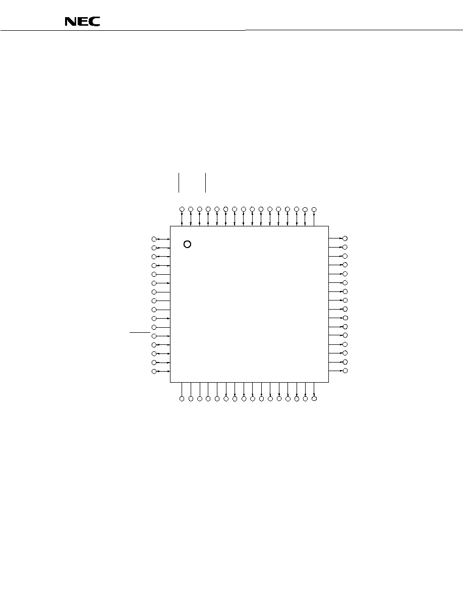
1. PIN CONFIGURATION (TOP VIEW)
64-pin plastic QFP (14
◊
◊
◊
◊ 14)
64-pin plastic TQFP (12
◊
◊
◊
◊ 12)
µPD789304GC-◊◊◊-AB8
µPD789304GK-◊◊◊-9ET
µPD789306GC-◊◊◊-AB8
µPD789306GK-◊◊◊-9ET
µPD789314GC-◊◊◊-AB8
µPD789314GK-◊◊◊-9ET
µPD789316GC-◊◊◊-AB8
µPD789316GK-◊◊◊-9ET
1
2
3
4
5
6
7
8
9
10
11
12
13
14
15
16
17 18 19 20 21 22 23 24 25 26 27 28 29 30 31
64 63 62 61 60 59 58 57 56 55 54 53 52 51 50 49
48
47
46
45
44
43
42
41
40
39
38
37
36
35
34
33
P50
P51
P52
P53
IC
XT1
XT2
V
DD
V
SS
X1 (CL1)
X2 (CL2)
RESET
P00/KR0
P01/KR1
P02/KR2
P03/KR3
32
CAPH
CAPL
V
LC0
V
LC1
V
LC2
COM0
COM1
COM2
COM3
S0
S1
S2
S3
S4
S5
S6
S22
S21
S20
S19
S18
S17
S16
S15
S14
S13
S12
S11
S10
S9
S8
S7
P20/SCK10
P21/SO10
P22/SI10
P23/SCK20/ASCK20
P24/SO20/TxD20
P25/SI20/RxD20
P26/TO20
P30/INTP0/CPT20
P31/INTP1/TO30/TMI40
P32/INTP2/TO40
P33/INTP3
P10
P11
P12
P13
S23
Caution Connect the IC (Internally Connected) pin directly to the V
SS
pin.
Remark Pin names enclosed in parentheses are when using the
µPD789314, 789316.

µ
µ
µ
µ
PD789304, 789306, 789314, 789316
8
Data Sheet U14384EJ1V0DS
ASCK20:
Asynchronous serial input
RESET:
Reset
CAPH, CAPL:
LCD power supply capacitance control
RxD20:
Receive data
CL1, CL2:
RC oscillator
S0 to S23:
Segment output
COM0 to COM3:
Common output
SCK10, SCK20:
Serial clock
CPT20:
Capture trigger input
SI10, SI20:
Serial input
IC:
Internally connected
SO10, SO20:
Serial output
INTP0 to INTP3:
External interrupt input
TMI40:
Timer input
KR0 to KR3:
Key return
TO20, TO30, TO40:
Timer output
P00 to P03:
Port 0
TxD20:
Transmit data
P10 to P13:
Port 1
V
DD
:
Power supply
P20 to P26:
Port 2
V
LC0
to V
LC2
:
LCD power supply
P30 to P33:
Port 3
V
SS
:
Ground
P50 to P53:
Port 5
X1, X2:
Crystal/ceramic oscillator
XT1, XT2:
Crystal oscillator
µ
µ
µ
µ
PD789304, 789306, 789314, 789316
Data Sheet U14384EJ1V0DS
9
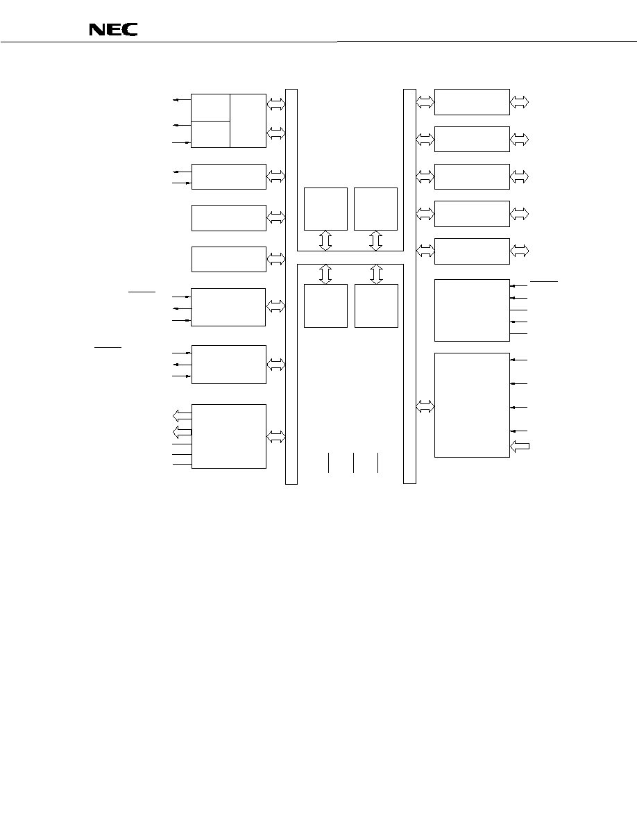
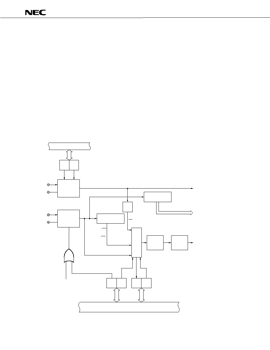
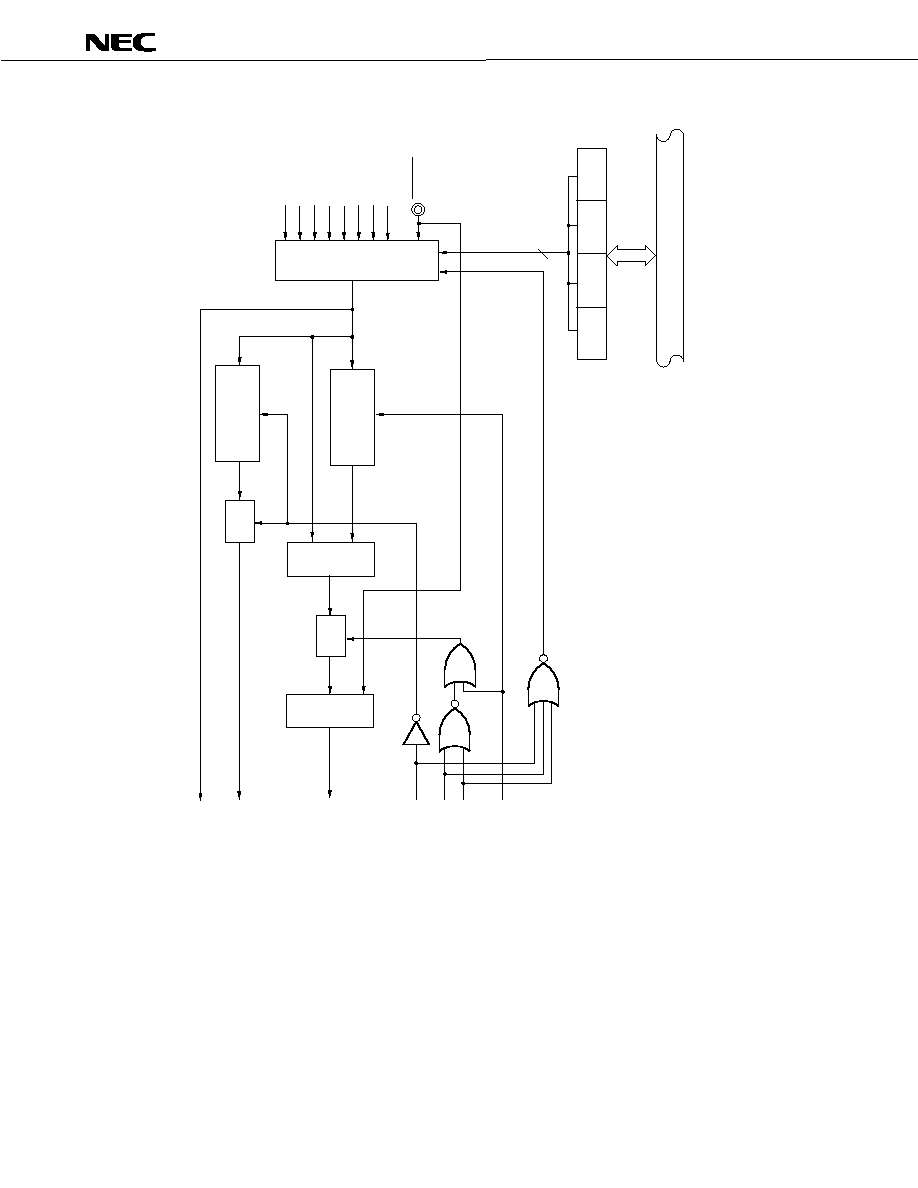
2. BLOCK DIAGRAM
V
DD
V
SS
IC
78K/0S
CPU core
ROM
TO30/TMI40/P31
8-bit
timer 30
P00 to P03
Port 0
P10 to P13
Port 1
P20 to P26
Port 2
P30 to P33
Port 3
P50 to P53
Port 5
TMI40/TO30/P31
TO20/P26
16-bit timer 20
Watch timer
Watchdog timer
Serial
interface 20
SCK20/ASCK20/P23
SI20/RxD20/P25
SO20/TxD20/P24
S0 to S23
COM0 to COM3
RAM
RAM space
for
LCD data
8-bit
timer/event
counter 40
Cascaded
16-bit
timer/event
counter
TO40/P32
CPT20/P30
Serial
interface 10
SCK10/P20
SI10/P22
SO10/P21
V
LC0
to V
LC2
CAPH
CAPL
LCD
controller driver
System control
RESET
X1 (CL1)
X2 (CL2)
XT1
XT2
Interrupt control
INTP0/P30
INTP1/P31
INTP2/P32
INTP3/P33
KR0/P00 to
KR3/P03
Remark Pin names enclosed in parentheses are when using the
µPD789314, 789316.
µ
µ
µ
µ
PD789304, 789306, 789314, 789316
10
Data Sheet U14384EJ1V0DS
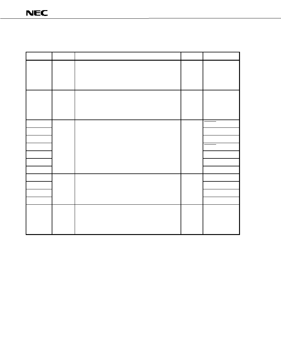
3. PIN FUNCTIONS
3.1 Port Pins
Pin Name
I/O
Function
After Reset
Alternate Function
P00 to P03
I/O
Port 0.
4-bit I/O port.
Input/output can be specified in 1-bit units.
When used as an input port, an on-chip pull-up resistor can be
specified in port units by software.
Input
KR0 to KR3
P10 to P13
I/O
Port 1.
4-bit I/O port.
Input/output can be specified in 1-bit units.
When used as an input port, an on-chip pull-up resistor can be
specified in port units by software.
Input
≠
P20
SCK10
P21
SO10
P22
SI10
P23
SCK20/ASCK20
P24
SO20/TxD20
P25
SI20/RxD20
P26
I/O
Port 2.
7-bit I/O port.
Input/output can be specified in 1-bit units.
When used as an input port, an on-chip pull-up resistor can be
specified in 1-bit units by software.
Input
TO20
P30
INTP0/CPT20
P31
INTP1/TO30/TMI40
P32
INTP2/TO40
P33
I/O
Port 3.
4-bit I/O port.
Input/output can be specified in 1-bit units.
When used as an input port, an on-chip pull-up resistor can be
specified in 1-bit units by software.
Input
INTP3
P50 to P53
I/O
Port 5.
4-bit I/O port.
Input/output can be specified in 1-bit units.
An on-chip pull-up resistor can be specified in bit units by the
mask option.
Input
≠
µ
µ
µ
µ
PD789304, 789306, 789314, 789316
Data Sheet U14384EJ1V0DS
11
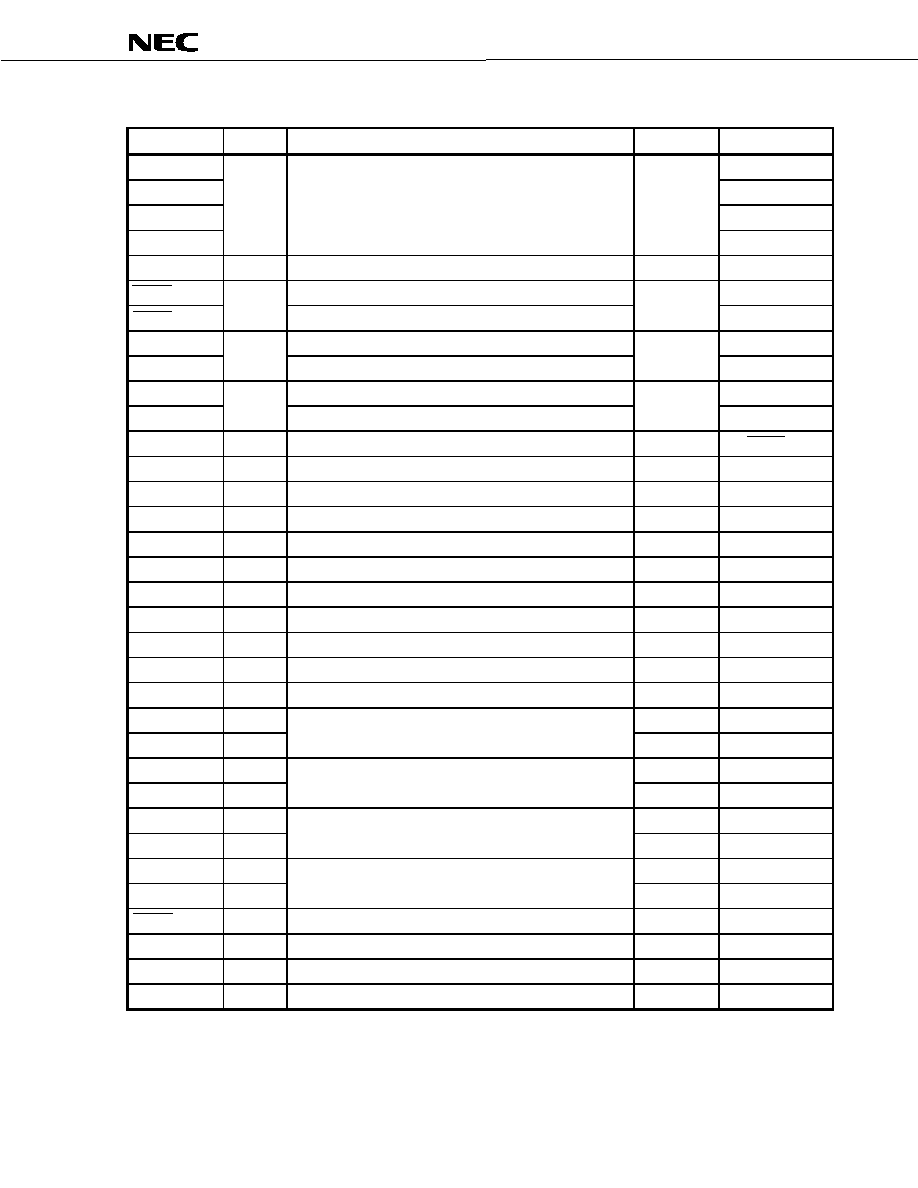
3.2 Non-Port Pins
Pin Name
I/O
Function
After Reset
Alternate Function
INTP0
P30/CPT20
INTP1
P31/TO30/TMI40
INTP2
P32/TO40
INTP3
Input
External interrupt input for which the valid edge (rising edge,
falling edge, or both rising and falling edges) can be specified
Input
P33
KR0 to KR3
Input
Key return signal detection
Input
P00 to P03
SCK10
Serial clock input/output for serial interface (SIO10)
P20
SCK20
I/O
Serial clock input/output for serial interface (SIO20)
Input
P23/ASCK20
SI10
Serial data input for SIO10 serial interface
P22
SI20
Input
Serial data input for SIO20 serial interface
Input
P25/RxD20
SO10
Serial data output for SIO10 serial interface
P21
SO20
Output
Serial data output for SIO20 serial interface
Input
P24/TxD20
ASCK20
Input
Serial clock input for asynchronous serial interface
Input
P23/SCK20
RxD20
Input
Serial data input for asynchronous serial interface
Input
P25/SI20
TxD20
Output
Serial data output for asynchronous serial interface
Input
P24/SO20
TO20
Output
16-bit timer (TM20) output
Input
P26
CPT20
Input
Capture edge input
Input
P30/INTP0
TO30
Output
8-bit timer (TM30) output
Input
P31/INTP1/TMI40
TO40
Output
8-bit timer (TM40) output
Input
P32/INTP2
TMI40
Input
External count clock input to 8-bit timer (TM40)
Input
P31/INTP1/TO30
S0 to S23
Output
Segment signal output for LCD controller/driver
Output
≠
COM0 to COM3 Output
Common signal output for LCD controller/driver
Output
≠
V
LC0
to V
LC2
≠
LCD drive voltage
≠
≠
CAPH
≠
≠
≠
CAPL
≠
Connection pin for LCD driver's capacitor
≠
≠
X1
Note 1
Input
≠
≠
X2
Note 1
≠
Connecting crystal resonator for main system clock oscillation
≠
≠
CL1
Note 2
Input
≠
≠
CL2
Note 2
≠
Connections to resistor (R) and capacitor (C) for main system
clock oscillation
≠
≠
XT1
Input
≠
≠
XT2
≠
Connecting crystal resonator for subsystem clock oscillation
≠
≠
RESET
Input
System reset input
Input
≠
V
DD
≠
Positive power supply
≠
≠
V
SS
≠
Ground potential
≠
≠
IC
≠
Internally connected. Connect directly to V
SS
.
≠
≠
Notes 1.
µPD789304, 789306 only
2.
µPD789314, 789316 only
µ
µ
µ
µ
PD789304, 789306, 789314, 789316
12
Data Sheet U14384EJ1V0DS
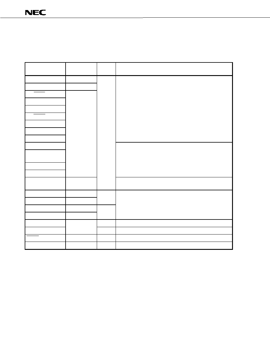
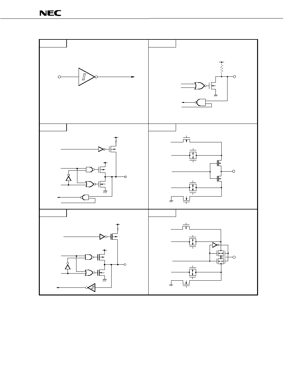
3.3 Pin I/O Circuits and Recommended Connection of Unused Pins
The I/O circuit type of each pin and recommended connection of unused pins are shown in Table 3-1.
For the I/O circuit configuration of each type, refer to Figure 3-1.
Table 3-1. Types of Pin I/O Circuits and Recommended Connection of Unused Pins
Pin Name
I/O
Circuit Type
I/O
Recommended Connection of Unused Pins
P00/KR0 to P03/KR3
8-A
P10 to P13
5-A
P20/SCK10
P21/SO10
P22/SI10
P23/SCK20/ASCK20
P24/SO20/TxD20
P25/SI20/RxD20
P26/TO20
Input: Independently connect to V
DD
or V
SS
via a resistor.
Output: Leave open.
P30/INTP0/CPT20
P31/INTP1/TO30/
TMI40
P32/INTP2/TO40
P33/INTP3
8-A
Input: Independently connect to V
SS
via a resistor.
Output: Leave open.
P50 to P53
13-W
I/O
Input: Independently connect to V
DD
via a resistor.
Output: Leave open.
S0 to S23
17
COM0 to COM3
18
Output
V
LC0
to V
LC2
≠
CAPH, CAPL
≠
≠
Leave open.
XT1
Input
Connect to V
SS
.
XT2
≠
≠
Leave open.
RESET
2
Input
≠
IC
≠
≠
Directly connect to V
SS
.
µ
µ
µ
µ
PD789304, 789306, 789314, 789316
Data Sheet U14384EJ1V0DS
13
Figure 3-1. Pin I/O Circuits
Type 2
Type 13-W
Schmitt-triggered input with hysteresis characteristics
IN
V
SS
Output data
Output disable
IN/OUT
V
DD
N-ch
Middle-voltage input buffer
Input enable
Pull-up resistor
(mask option)
Type 5-A
Type 17
Pull-up
enable
V
DD
P-ch
P-ch
IN/OUT
Data
Output
disable
Input
enable
V
DD
N-ch
V
SS
P-ch
N-ch
P-ch
N-ch
N-ch
N-ch
data
OUT
V
LC0
V
LC1
SEG
V
LC2
P-ch
P-ch
Type 8-A
Type 18
Pull-up
enable
V
DD
P-ch
Data
V
DD
P-ch
Output
disable
IN/OUT
N-ch
V
SS
P-ch
N-ch
P-ch
N-ch
P-ch
N-ch
P-ch
N-ch
P-ch
N-ch
V
LC1
COM
data
V
LC0
V
LC2
OUT
µ
µ
µ
µ
PD789304, 789306, 789314, 789316
14
Data Sheet U14384EJ1V0DS
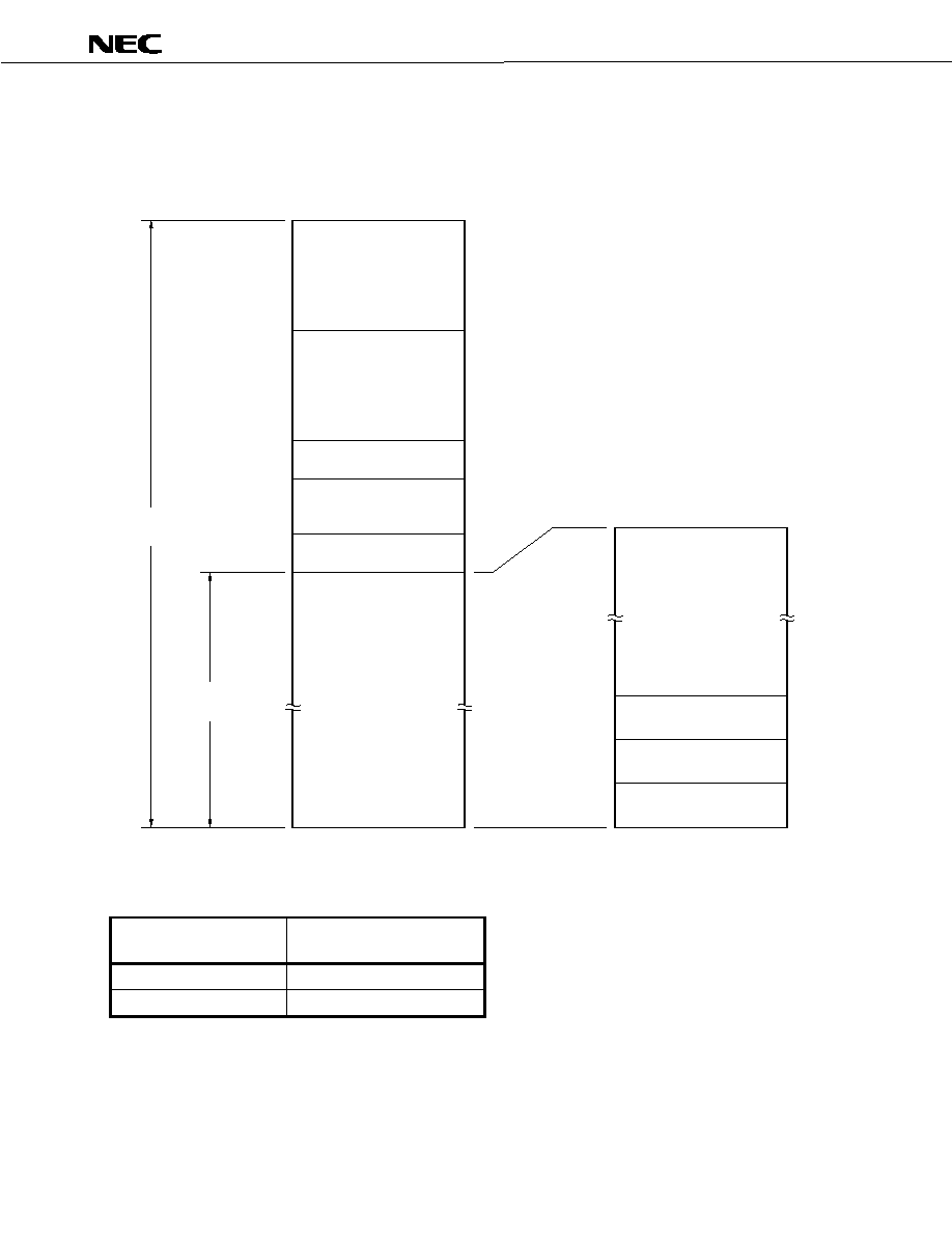
4. MEMORY SPACE
Figure 4-1 shows the memory map of the
µPD789304, 789306, 789314, and 789316.
Figure 4-1. Memory Map
nnnnH+1
nnnnH
Special function registers
(SFR)
256
◊
8 bits
Internal high-speed RAM
512
◊
8 bits
LCD display RAM
24
◊
4 bits
FFFFH
FF00H
FEFFH
FD00H
FCFFH
0000H
Program memory
space
Data memory
space
nnnnH
0000H
Program area
0080H
007FH
Program area
0040H
003FH
CALLT table area
Reserved
0022H
0021H
Vector table area
Internal ROM
Note
FA18H
FA17H
FA00H
F9FFH
Reserved
Note The internal ROM capacity depends on the product (see the following table).
Part Number
Last Address of Internal ROM
nnnnH
µPD789304, 789314
1FFFH
µPD789306, 789316
3FFFH
µ
µ
µ
µ
PD789304, 789306, 789314, 789316
Data Sheet U14384EJ1V0DS
15
5. PERIPHERAL HARDWARE FUNCTIONS
5.1 Ports
The I/O ports are listed below.
∑ CMOS I/O:
19
∑ N-ch open-drain I/O:
4
Table 5-1. Port Functions
Port Name
Pin Name
Function
Port 0
P00 to P03
I/O port. Input/output can be specified in 1-bit units.
When used as an input port, an on-chip pull-up resistor can be specified by software.
Port 1
P10 to P13
I/O port. Input/output can be specified in 1-bit units.
When used as an input port, an on-chip pull-up resistor can be specified by software.
Port 2
P20 to P26
I/O port. Input/output can be specified in 1-bit units.
When used as an input port, an on-chip pull-up resistor can be specified by software.
Port 3
P30 to P33
I/O port. Input/output can be specified in 1-bit units.
When used as an input port, an on-chip pull-up resistor can be specified by software.
Port 5
P50 to P53
I/O port. Input/output can be specified in 1-bit units.
An on-chip pull-up resistor can be specified by the mask option.
µ
µ
µ
µ
PD789304, 789306, 789314, 789316
16
Data Sheet U14384EJ1V0DS
5.2 Clock Generator
The specifications of the main system clock generator differ depending on the product as shown below.
(1) Main system clock generator
∑ Ceramic/crystal oscillation:
µPD789304, 789306
This generator's oscillation frequency range is 1.0 to 5.0 MHz. The minimum instruction execution time
can be changed from 0.4 to 1.6
µs (@ 5.0 MHz operation).
∑ RC oscillation:
µPD789314, 789316
This generator's oscillation frequency range is 2.0 to 4.0 MHz. The minimum instruction execution time
can be changed from 0.5 to 2.0
µs (@ 4.0 MHz operation).
(2) Subsystem clock generator (crystal oscillation)
This generator's oscillation frequency is 32.768 kHz. The minimum instruction execution time is 122
µs (@
32.768 kHz operation).
Figure 5-1. Block Diagram of Clock Generator
Subsystem
clock oscillator
f
XT
X1 (CL1)
X2 (CL2)
XT1
XT2
Main system
clock oscillator
f
X
(f
cc
)
Prescaler
f
X
2
2
f
CC
2
2
f
XT
2
1/2
Prescaler
Watch timer
LCD controller/driver
Clock to peripheral
hardware
CPU clock
(f
CPU
)
Standby
controller
Wait
controller
Selector
STOP
MCC PCC1
CLS CSS0
Internal bus
Sub oscillation mode register
(SCKM)
FRC SCC
Internal bus
Subsystem clock control
register (CSS)
Processor clock control
register (PCC)
)
(
Remark Pins names enclosed in parentheses are when using the RC oscillation (
µPD789314, 789316).

µ
µ
µ
µ
PD789304, 789306, 789314, 789316
Data Sheet U14384EJ1V0DS
17
5.3 Timer
Five timer channels are incorporated.
∑ 16-bit timer (TM20):
1 channel
∑ 8-bit timer (TM30, TM40): 2 channels
∑ Watch timer (WT):
1 channel
∑ Watchdog timer (WTM):
1 channel
Table 5-2. Timer Operation
TM20
TM30
TM40
WT
WTM
Interval time
1 channel
1 channel
1 channel
1 channel
1 channel
Operation
mode
External event counter
≠
1 channel
1 channel
≠
≠
Timer output
1 output
1 output
1 output
≠
≠
Square wave output
≠
1 output
1 output
≠
≠
Function
Interrupt request
1
1
1
1
1
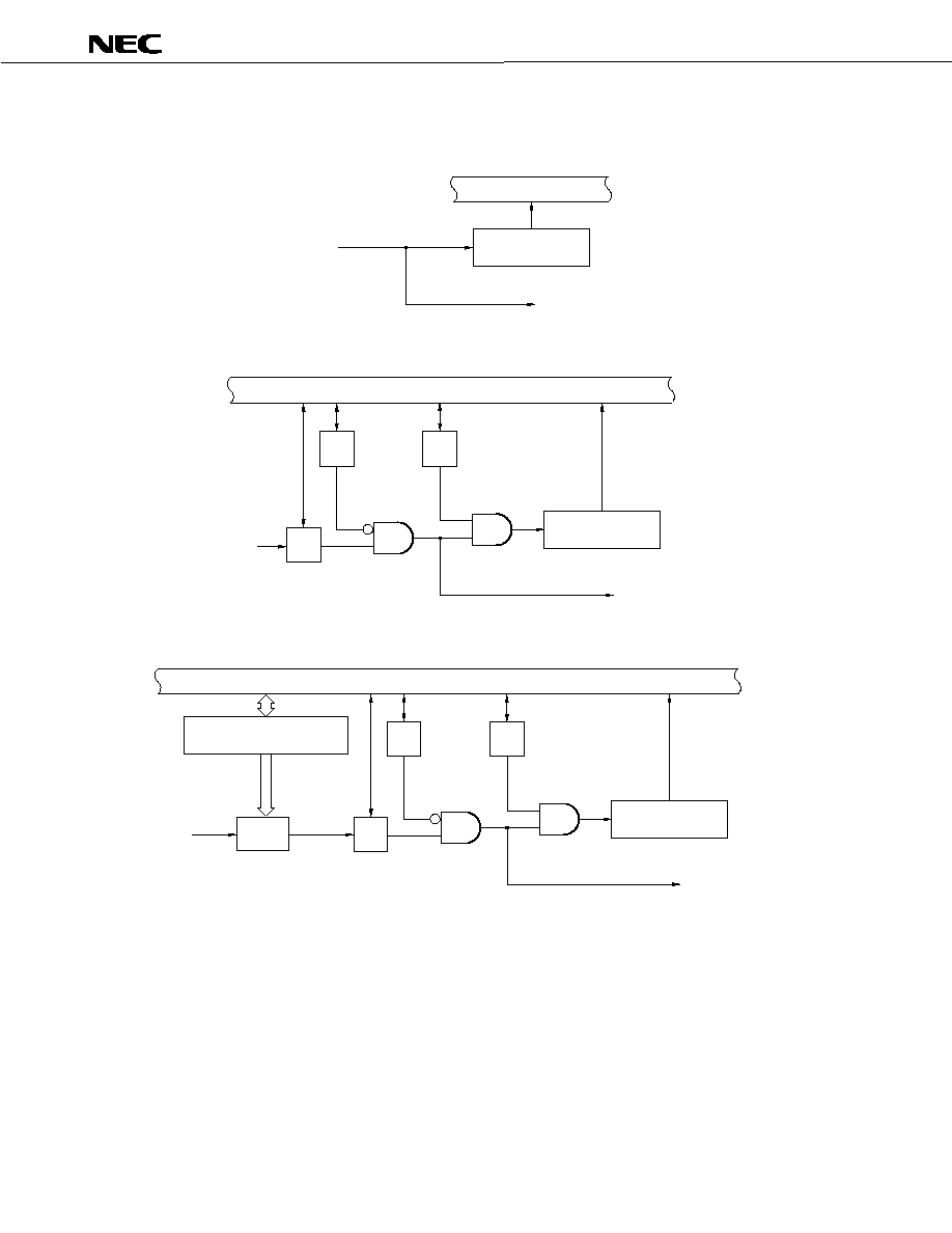
Figure 5-2. Block Diagram of 16-Bit Timer (TM20)
CPT20/P30
/INTP0
Internal bus
Internal bus
16-bit timer mode control
register 20 (TMC20)
16-bit timer mode control
register 20 (TMC20)
TOF20 CPT201 CPT200 TOC20 TCL201 TCL200 TOE20
Selector
f
CLK
f
CLK
/2
2
Edge
detector
16-bit capture
register 20 (TCP20)
16-bit counter
read buffer
16-bit timer counter 20 (TM20)
16-bit compare register 20 (CR20)
Match
OVF
F/F
TOD20
TO20/P26
INTTM20
P26
output latch
PM26
f
CLK
/2
5
f
CLK
/2
7
Remark f
CLK
: f
X
or f
CC
µ
µ
µ
µ
P
D
7893
04,
7
8930
6
,
7
8
9
3
1
4
,
78
931
6
18
Data S
h
e
e
t U
1
4
3
8
4
E
J
1V
0DS
TCE30
TCL300 TMD300
TCL301
8-bit timer mode
control register 30
(TMC30)
Selector
Decoder
Selector
Selector
8-bit compare
register 30 (CR30)
8-bit timer counter 30
(TM30)
Selector
Internal reset signal
Timer 40 match signal
(during cascade connection mode)
Timer 30 match signal
(during cascade connection mode)
From Figure 5-4 (D)
Count operation start signal
(during cascade connection mode)
INTTM30
f
CLK
/2
4
f
CLK
/2
8
Timer 40 interrupt request signal
(from Figure 5-4 (B))
Carrier clock
(during carrier generator mode)
or timer 40 output signal
(during mode other than carrier generator mode)
(from Figure 5-4 (C))
Clear
Cascade connection mode
Match
From Figure 5-4 (E)
To Figure 5-4 (F)
To Figure 5-4 (G)
Internal bus
OVF
Timer 30 match signal
(during carrier generator mode)
Bit 7 of TM40
(from Figure 5-4 (A))
TOE30
PM30
P30
output latch
TO30/P31/
INTP1/TMI40
Figure 5-3. Block Diagram of Timer 30 (TM30)
Remark f
CLK
: f
X
or f
CC
µ
µ
µ
µ
P
D
7893
04,
7
8930
6
,
7
8
9
3
1
4
,
78
931
6
Data S
h
e
e
t U
1
4
3
8
4
E
J
1V
0DS
19
TCE40 TCL402 TCL401 TCL400 TMD401 TMD400 TOE40
8-bit timer mode control
register 40 (TMC40)
Decoder
8-bit timer counter 40 (TM40)
F/F
TM30 match signal
(during cascade connection mode)
Count operation start signal to timer 30
(during cascade connection mode)
TM40 timer counter match signal
(during cascade connection mode)
Clear
8-bit compare
register 40 (CR40)
Selector
Output control circuit
Note
RMC40 NRZB40 NRZ40
Carrier generator output
control register 40 (TCA40)
To Figure 5-3 (D)
count clock input
signal to TM30
Internal reset signal
INTTM40
To Figure 5-3 (A)
Bit 7 of TM40
(during cascade connection mode)
From Figure 5-3 (F)
To Figure 5-3 (E)
Match
TO40/P32/INTP2
To Figure 5-3 (C)
Carrier clock (during carrier generator mode)
or timer 40 output signal
(during mode other than carrier generator mode)
Reset
Carrier generator mode
PWM mode
Cascade connection mode
8-bit compare
register H40 (CRH40)
Internal bus
Selector
OVF
To Figure 5-3 (B)
Timer 40 interrupt request signal
From Figure 5-3 (G)
Timer counter match signal from timer 30
(during carrier generator mode)
f
CLK
/2
3
f
CLK
/2
7
TMI40/P31/
INTP1/TO30
TMI/2
TMI/2
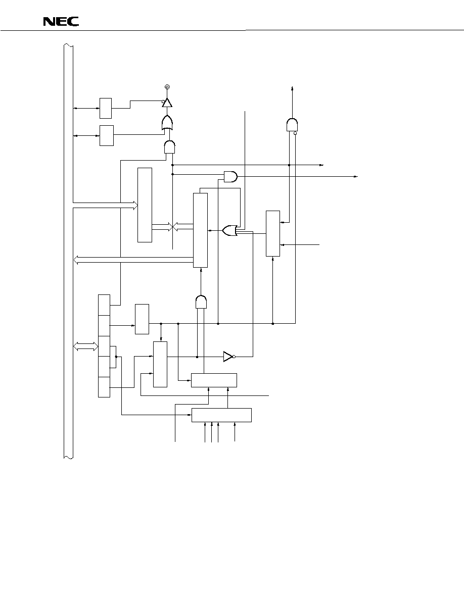
2
TMI/2
3
Prescaler
Figure 5-4. Block Diagram of Timer 40 (TM40)
Note For details, see Figure 5-5.
Remark f
CLK
: f
X
or f
CC

µ
µ
µ
µ
PD789304, 789306, 789314, 789316
20
Data Sheet U14384EJ1V0DS
Figure 5-5. Block Diagram of Output Controller (Timer 40)
F/F
RMC40
NRZ40
TOE40
PM32
P32
output latch
Selector
TO40/P32/
INTP2
Carrier generator mode
Carrier clock
(during carrier generator mode)
or timer 40 output signal
(during mode other than carrier
generator mode)
Figure 5-6. Block Diagram of Watch Timer (WT)
f
CLK
/2
7
f
XT
f
W
f
W
2
4
f
W
2
5
f
W
2
6
f
W
2
7
f
W
2
8
f
W
2
9
Clear
9-bit prescaler
Clear
5-bit counter
INTWT
INTWTI
WTM7 WTM6 WTM5 WTM4 WTM1 WTM0
Watch timer mode
control register (WTM)
Internal bus
Selector
Selector
Remark f
CLK
: f
X
or f
CC
µ
µ
µ
µ
PD789304, 789306, 789314, 789316
Data Sheet U14384EJ1V0DS
21
Figure 5-7. Block Diagram of Watchdog Timer (WTM)
Internal bus
Internal bus
Prescaler
f
CLK
2
6
f
CLK
2
8
f
CLK
2
10
3
7-bit counter
Clear
WDTIF
WDTMK
WDCS2 WDCS1 WDCS0
Watchdog timer clock
select register (WDCS)
Watchdog timer mode
register (WDTM)
WDTM4 WDTM3
INTWDT
maskable
interrupt request
RESET
INTWDT
non-maskable
interrupt request
f
CLK
2
4
RUN
Selector
Controller
Remark f
CLK
: f
X
or f
CC

µ
µ
µ
µ
PD789304, 789306, 789314, 789316
22
Data Sheet U14384EJ1V0DS
5.4 Serial Interface
5.4.1 Serial interface 10 (SIO10)
Serial interface 10 (SIO10) has the following two types of modes.
∑ Operation stop mode
∑ 3-wire serial I/O mode
Internal bus
SI10/P22
Serial operation mode
register 10 (CSIM10)
CSIE10
TPS101
TPS100
DIR10
CSCK10
Serial shift register 10
(SIO10)
SO10/P21
PM21
PM20
SCK10/P20
Serial clock counter
Interrupt request
generator
Clock controller
INTCSI10
F/F
TPS101
TPS100
f
CLK
/2
2
f
CLK
/2
3
f
CLK
/2
4
f
CLK
/2
5
Selector
Selector
Figur
e 5-
8. B
l
o
ck D
i
agr
a
m of S
e
r
i
al I
n
ter
f
ac
e 10
Re
m
a
rk
f
CL
K
: f
X
or f
CC
µ
µ
µ
µ
PD789304, 789306, 789314, 789316
Data Sheet U14384EJ1V0DS
23
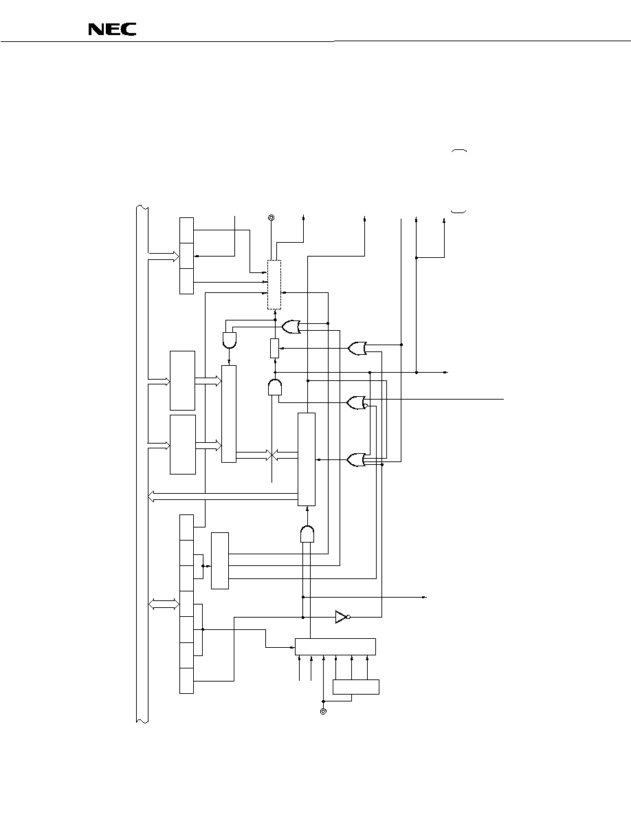
5.4.2 Serial interface 20 (SIO20)
Serial interface 20 (SIO20) has the following three types of modes.
∑ Operation stop mode
∑ Asynchronous serial interface (UART) mode
∑ 3-wire serial I/O mode
PE20
FE20
OVE20
INTSR20/INTCSI20
RxD20/SI20/
P25
TxD20/SO20/
P24
PM24
PM23
TXE20
RXE20
PS201
PS200
CL20
SL20
INTST20
CSIE20
DIR20
CSCK20
TPS203
TPS202
TPS201
TPS200
4
CSIE20
TXE20
RXE20
CSCK20
ASCK20/SCK20/
P23
f
X
/2 to f
X
/2
8
Internal bus
Internal bus
Receive buffer register 20
(RXB20/SIO20)
Direction controller
Receive shift register 20
(RXS20)
Reception
controller
Asynchronous serial interface
status register 20 (ASIS20)
Direction controller
Asynchronous serial interface
mode register 20 (ASIM20)
Transmission
controller
SCK20 output controller
Baud rate generator
Note
Baud rate generator control
register 20 (BRGC20)
Serial interface mode
register 20 (CSIM20)
Transmit shift register 20
(TXS20/SIO20)
Figur
e 5-
9. B
l
o
ck D
i
agr
a
m of S
e
r
i
al I
n
ter
f
ac
e 20
Note
See
Figur
e 5-1
0
for
the
conf
igur
atio
n of
the
bau
d rate
gen
erat
or.
µ
µ
µ
µ
P
D
7893
04,
7
8930
6
,
7
8
9
3
1
4
,
78
931
6
24
Data S
h
e
e
t U
1
4
3
8
4
E
J
1V
0DS
Clock for receive detection
Transmit shift clock
Receive shift clock
Receive detection
TXE20
RXE20
CSIE20
1/2
1/2
Transmit clock
counter
Receive clock
counter
4
f
XX
/2
f
XX
/2
3
f
XX
/2
4
f
XX
/2
5
f
XX
/2
6
f
XX
/2
7
f
XX
/2
8
f
XX
/2
2
SCK20/ASCK20/P20
TPS203 TPS202 TPS201 TPS200
Baud rate generator control
register 20 (BRGC20)
Internal bus
Selector
Selector
Selector
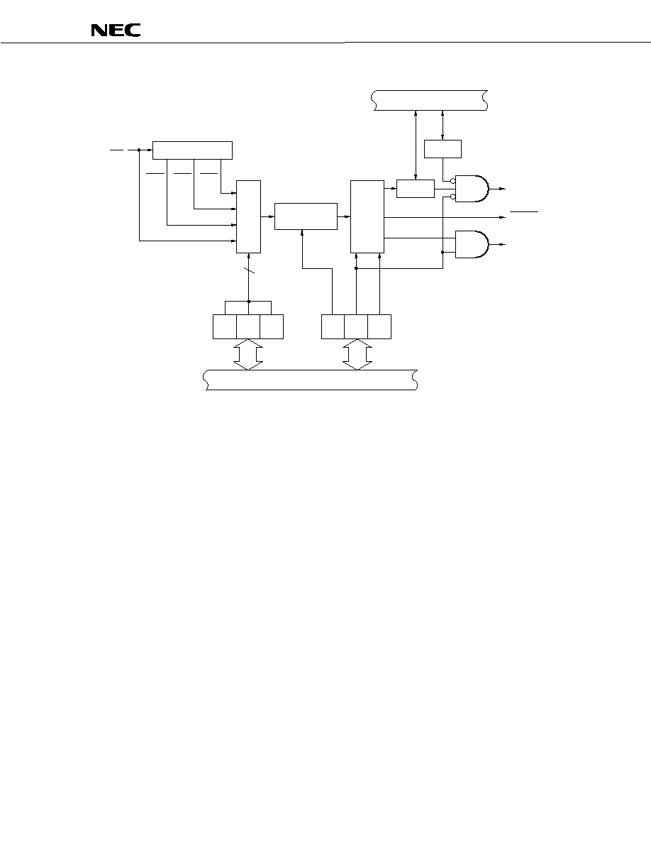
Figure 5-10. Block Diagram of Baud Rate Generator 20

µ
µ
µ
µ
PD789304, 789306, 789314, 789316
Data Sheet U14384EJ1V0DS
25
5.5 LCD Controller/Driver
The LCD controller/driver has the following functions.
(1) Enables automatic output of segment signals and common signals by automatically reading from display data
memory.
(2) Two types of display modes can be selected:
∑ 1/3 duty (1/3 bias)
∑ 1/4 duty (1/3 bias)
(3) Any of four frame frequency settings can be selected for each display mode.
(4) There are up to 24 segment signal outputs (S0 to S23) and four common signal outputs (COM0 to COM3).
(5) Operation using the subsystem clock is also supported.

µ
µ
µ
µ
P
D
7893
04,
7
8930
6
,
7
8
9
3
1
4
,
78
931
6
26
Data S
h
e
e
t U
1
4
3
8
4
E
J
1V
0DS
Internal bus
LCDC03 LCDC02 LCDC01 LCDC00
2
2
Prescaler
LCD
clock
selector
Selector
f
LCD
f
LCD
2
6
f
LCD
2
7
f
LCD
2
8
f
LCD
2
9
LCD clock control
register 0 (LCDC0)
LCDON0
VAON0 LIPS0
LCDM02 LCDM01 LCDM00
LCD display mode
register 0 (LCDM0)
LCD drive voltage controller
V
LC2
V
LC1
V
LC0
Segment
driver
Common driver
COM0 COM1 COM2 COM3
3
3 2 1 0
3 2 1 0
6 5
7
4
FA00H
Display data memory
LCDON0
Selector
Segment
driver
3 2 1 0
3 2 1 0
6 5
7
4
FA17H
LCDON0
S23
Timing
controller
f
CLK
/2
5
f
CLK
/2
6
f
CLK
/2
7
f
XT
S0
Voltage
amplifier circuit
GAIN
LCD voltage amplifier
control register 0 (LCDVA0)
∑ ∑ ∑ ∑ ∑ ∑ ∑ ∑ ∑ ∑
∑ ∑ ∑ ∑ ∑ ∑ ∑ ∑ ∑ ∑
CAPL
CAPH
Selector
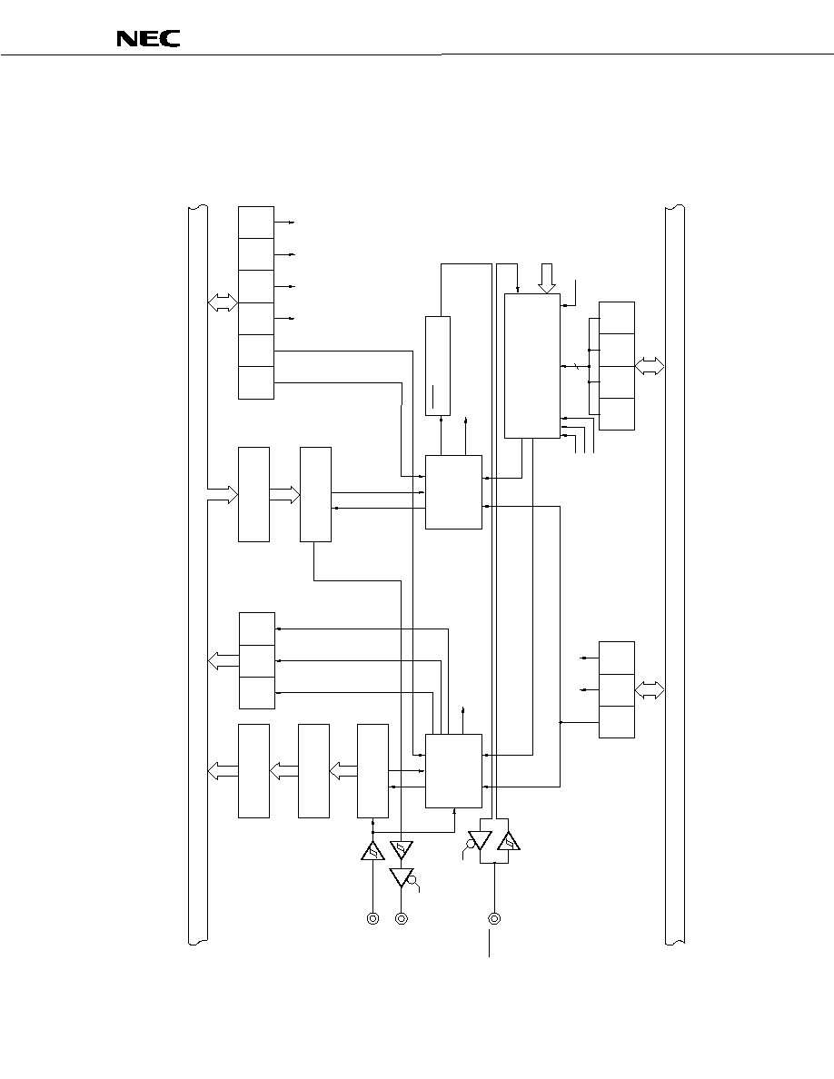
Figure 5-11. Block Diagram of LCD Controller/Driver
Remark f
CLK
: f
X
or f
CC

µ
µ
µ
µ
PD789304, 789306, 789314, 789316
Data Sheet U14384EJ1V0DS
27
6. INTERRUPT FUNCTIONS
A total of 15 interrupt sources divided into the following two types are provided.
∑ Non-maskable: 1
∑ Maskable:
14
Table 6-1. Interrupt Source List
Interrupt Source
Interrupt Type
Priority
Note 1
Name
Trigger
Internal/
External
Vector Table
Address
Basic
Configuration
Type
Note 2
Non-
maskable
≠
INTWDT
Watchdog timer overflow (with
watchdog timer mode 1 selected)
(A)
0
INTWDT
Watchdog timer overflow (with interval
timer mode selected)
Internal
0004H
(B)
1
INTP0
0006H
2
INTP1
0008H
3
INTP2
000AH
4
INTP3
Pin input edge detection
External
000CH
(C)
INTSR20
End of serial interface 20 UART
reception
5
INTCSI20
End of serial interface 20 3-wire SIO
transfer reception
000EH
6
INTCSI10
End of serial interface 10 3-wire SIO
transfer reception
0010H
7
INTST20
End of serial interface 20 UART
transmission
0012H
8
INTWTI
Watch timer interval timer interrupt
0014H
9
INTTM20
Generation of match signal of 16-bit
timer 20
0016H
10
INTTM30
Generation of match signal of 8-bit
timer 30
0018H
11
INTTM40
Generation of match signal of 8-bit
timer/event counter 40
001AH
12
INTWT
Watch timer interrupt
Internal
001EH
(B)
Maskable
13
INTKR00
Key return signal detection
External
0020H
(C)
Notes 1. Default priority is the priority order when several maskable interrupt requests are generated at the
same time. 0 is the highest order and 13 is the lowest order.
2. Basic configuration types (A) to (C) correspond to (A) to (C) in Figure 6-1.
Remark Two watchdog timer interrupt sources (INTWDT): a non-maskable interrupt and a maskable interrupt
(internal), are available, either of which can be selected.
µ
µ
µ
µ
PD789304, 789306, 789314, 789316
28
Data Sheet U14384EJ1V0DS
Figure 6-1. Basic Configuration of Interrupt Function
(A) Internal non-maskable interrupt
Internal bus
Interrupt request
Vector table
address generator
Standby release signal
(B) Internal maskable interrupt
Internal bus
MK
IF
Interrupt request
IE
Vector table
address generator
Standby release signal
(C) External maskable interrupt
Internal bus
INTM0, INTM1, KRM00
MK
IF
IE
Vector table
address generator
Standby release signal
Edge
detector
Interrupt request
INTM0: External interrupt mode register 0
INTM1: External interrupt mode register 1
KRM00: Key return mode register 00
IF:
Interrupt request flag
IE:
Interrupt enable flag
MK:
Interrupt mask flag
µ
µ
µ
µ
PD789304, 789306, 789314, 789316
Data Sheet U14384EJ1V0DS
29
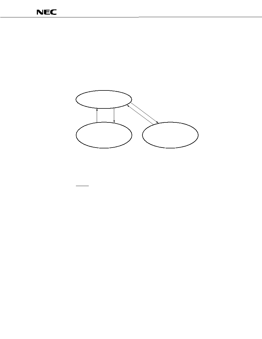
7. STANDBY FUNCTION
The following two standby modes are available for further reduction of system current consumption.
∑ HALT mode: In this mode, the CPU operation clock is stopped. The average current consumption can be
reduced by intermittent operation by combining this mode with the normal operation.
∑ STOP mode: In this mode, oscillation of the main system clock is stopped. All operations performed on the
main system clock are suspended resulting in extremely small power consumption.
Figure 7-1. Standby Function
System clock operation
STOP mode
Main system clock
oscillation stopped
HALT mode
Clock supply to CPU
halted, oscillation
maintained
(
(
(
(
STOP
instruction
HALT instruction
Interrupt
request
Interrupt
request
8. RESET FUNCTION
The following two reset methods are available.
∑ External reset by RESET pin
∑ Internal reset by watchdog timer program loop time detection
9. MASK OPTIONS
The
µPD789304, 789306, 789314, and 789316 have the following mask options.
∑ Mask options for P50 to P53
An on-chip pull-up resistor can be selected.
<1> Specifies on-chip pull-up resistor in 1-bit units.
<2> Does not specify on-chip pull-up resistor.
µ
µ
µ
µ
PD789304, 789306, 789314, 789316
30
Data Sheet U14384EJ1V0DS
10. OVERVIEW OF INSTRUCTION SET
This section lists the instruction set for the
µPD789304, 789306, 789314, and 789316.
10.1 Conventions
10.1.1 Operand expressions and description methods
Operands are described in "Operand" column of each instruction in accordance with the description method of the
instruction operand expression (see the assembler specifications for details). When there are two or more description
methods, select one of them. Uppercase letters and symbols, #, !, $, and [ ] are key words and are described as they
are. The meaning of each symbol is described below.
∑ # : Immediate data specification
∑ $ : Relative address specification
∑ ! : Absolute address specification
∑ [ ] : Indirect address specification
For immediate data, enter an appropriate numeric value or a label. When using a label, be sure to enter the #, !, $
and [ ] symbols.
For operand register expressions, r and rp, either function names (X, A, C, etc.) or absolute names (names in
parenthesis in the table below, R0, R1, R2, etc.) can be used for the description.
Table 10-1. Operand Expressions and Description Methods
Expression
Description Method
r
rp
sfr
X (R0), A (R1), C (R2), B (R3), E (R4), D (R5), L (R6), H (R7)
AX (RP0), BC (RP1), DE (RP2), HL (RP3)
Special function register symbol
saddr
saddrp
FE20H to FF1FH: immediate data or label
FE20H to FF1FH: immediate data or label (even addresses only)
addr16
addr5
0000H to FFFFH: immediate data or label
(even addresses only for 16-bit data transfer instruction)
0040H to 007FH: immediate data or label (even addresses only)
word
byte
bit
16-bit immediate data or label
8-bit immediate data or label
3-bit immediate data or label

µ
µ
µ
µ
PD789304, 789306, 789314, 789316
Data Sheet U14384EJ1V0DS
31
10.1.2 Description of "Operation" column
A:
A register; 8-bit accumulator
X:
X register
B:
B register
C:
C register
D:
D register
E:
E register
H:
H register
L:
L register
AX:
AX register pair; 16-bit accumulator
BC:
BC register pair
DE:
DE register pair
HL:
HL register pair
PC:
Program counter
SP:
Stack pointer
PSW:
Program status word
CY:
Carry flag
AC:
Auxiliary carry flag
Z:
Zero flag
IE:
Interrupt request enable flag
NMIS:
Flag indicating non-maskable interrupt servicing in progress
( ):
Memory contents indicated by address or register contents in parenthesis
X
H
, X
L
:
Higher 8 bits and lower 8 bits of 16-bit register
:
Logical product (AND)
:
Logical sum (OR)
:
Exclusive logical sum (exclusive OR)
:
Inverted data
addr16:
16-bit immediate data or label
jdisp8:
Signed 8-bit data (displacement value)
10.1.3 Description of "Flag" column
(Blank):
Unchanged
0:
Cleared to 0
1:
Set to 1
◊:
Set/cleared according to the result
R:
Previously saved value is restored
µ
µ
µ
µ
PD789304, 789306, 789314, 789316
32
Data Sheet U14384EJ1V0DS
10.2 List of Operations
Flags
Mnemonic
Operand
Bytes
Clocks
Operation
Z AC CY
r, #byte
3
6
r
byte
saddr, #byte
3
6
(saddr)
byte
sfr, #byte
3
6
sfr
byte
A, r
Note 1
2
4
A
r
r, A
Note 1
2
4
r
A
A, saddr
2
4
A
(saddr)
saddr, A
2
4
(saddr)
A
A, sfr
2
4
A
sfr
sfr, A
2
4
sfr
A
A, !addr16
3
8
A
(addr16)
!addr16, A
3
8
(addr16)
A
PSW, #byte
3
6
PSW
byte
◊
◊ ◊
A, PSW
2
4
A
PSW
PSW, A
2
4
PSW
A
◊
◊ ◊
A, [DE]
1
6
A
(DE)
[DE], A
1
6
(DE)
A
A, [HL]
1
6
A
(HL)
[HL], A
1
6
(HL)
A
A, [HL + byte]
2
6
A
(HL + byte)
MOV
[HL + byte], A
2
6
(HL + byte)
A
A, X
1
4
A
X
A, r
Note 2
2
6
A
r
A, saddr
2
6
A
(saddr)
A, sfr
2
6
A
(sfr)
A, [DE]
1
8
A
(DE)
A, [HL]
1
8
A
(HL)
XCH
A, [HL + byte]
2
8
A
(HL + byte)
rp, #word
3
6
rp
word
AX, saddrp
2
6
AX
(saddrp)
saddrp, AX
2
8
(saddrp)
AX
AX, rp
Note 3
1
4
AX
rp
MOVW
rp, AX
Note 3
1
4
rp
AX
XCHW
AX, rp
Note 3
1
8
AX
rp
Notes 1. Except r = A
2. Except r = A, X
3. rp = BC, DE and HL only
Remark One instruction clock cycle is one CPU clock cycle (f
CPU
) selected via the processor clock control
register (PCC).

µ
µ
µ
µ
PD789304, 789306, 789314, 789316
Data Sheet U14384EJ1V0DS
33
Flags
Mnemonic
Operand
Bytes
Clocks
Operation
Z AC CY
A, #byte
2
4
A, CY
A + byte
◊
◊ ◊
saddr, #byte
3
6
(saddr), CY
(saddr) + byte
◊
◊ ◊
A, r
2
4
A, CY
A + r
◊
◊ ◊
A, saddr
2
4
A, CY
A + (saddr)
◊
◊ ◊
A, !addr16
3
8
A, CY
A + (addr16)
◊
◊ ◊
A, [HL]
1
6
A, CY
A + (HL)
◊
◊ ◊
ADD
A, [HL + byte]
2
6
A, CY
A + (HL + byte)
◊
◊ ◊
A, #byte
2
4
A, CY
A + byte + CY
◊
◊ ◊
saddr, #byte
3
6
(saddr), CY
(saddr) + byte + CY
◊
◊ ◊
A, r
2
4
A, CY
A + r + CY
◊
◊ ◊
A, saddr
2
4
A, CY
A + (saddr) + CY
◊
◊ ◊
A, !addr16
3
8
A, CY
A + (addr16) + CY
◊
◊ ◊
A, [HL]
1
6
A, CY
A + (HL) + CY
◊
◊ ◊
ADDC
A, [HL + byte]
2
6
A, CY
A + (HL + byte) + CY
◊
◊ ◊
A, #byte
2
4
A, CY
A ≠ byte
◊
◊ ◊
saddr, #byte
3
6
(saddr), CY
(saddr) ≠ byte
◊
◊ ◊
A, r
2
4
A, CY
A ≠ r
◊
◊ ◊
A, saddr
2
4
A, CY
A ≠ (saddr)
◊
◊ ◊
A, !addr16
3
8
A, CY
A ≠ (addr16)
◊
◊ ◊
A, [HL]
1
6
A, CY
A ≠ (HL)
◊
◊ ◊
SUB
A, [HL + byte]
2
6
A, CY
A ≠ (HL + byte)
◊
◊ ◊
A, #byte
2
4
A, CY
A ≠ byte ≠ CY
◊
◊ ◊
saddr, #byte
3
6
(saddr), CY
(saddr) ≠ byte ≠ CY
◊
◊ ◊
A, r
2
4
A, CY
A ≠ r ≠ CY
◊
◊ ◊
A, saddr
2
4
A, CY
A ≠ (saddr) ≠ CY
◊
◊ ◊
A, !addr16
3
8
A, CY
A ≠ (addr16) ≠ CY
◊
◊ ◊
A, [HL]
1
6
A, CY
A ≠ (HL) ≠ CY
◊
◊ ◊
SUBC
A, [HL + byte]
2
6
A, CY
A ≠ (HL + byte) ≠ CY
◊
◊ ◊
A, #byte
2
4
A
A byte
◊
saddr, #byte
3
6
(saddr)
(saddr) byte
◊
A, r
2
4
A
A r
◊
A, saddr
2
4
A
A (saddr)
◊
A, !addr16
3
8
A
A (addr16)
◊
A, [HL]
1
6
A
A (HL)
◊
AND
A, [HL + byte]
2
6
A
A (HL + byte)
◊
Remark One instruction clock cycle is one CPU clock cycle (f
CPU
) selected via the processor clock control
register (PCC).
µ
µ
µ
µ
PD789304, 789306, 789314, 789316
34
Data Sheet U14384EJ1V0DS
Flags
Mnemonic
Operand
Bytes
Clocks
Operation
Z AC CY
A, #byte
2
4
A
A byte
◊
saddr, #byte
3
6
(saddr)
(saddr) byte
◊
A, r
2
4
A
A r
◊
A, saddr
2
4
A
A (saddr)
◊
A, !addr16
3
8
A
A (addr16)
◊
A, [HL]
1
6
A
A (HL)
◊
OR
A, [HL + byte]
2
6
A
A (HL + byte)
◊
A, #byte
2
4
A
A byte
◊
saddr, #byte
3
6
(saddr)
(saddr) byte
◊
A, r
2
4
A
A r
◊
A, saddr
2
4
A
A (saddr)
◊
A, !addr16
3
8
A
A (addr16)
◊
A, [HL]
1
6
A
A (HL)
◊
XOR
A, [HL + byte]
2
6
A
A (HL + byte)
◊
A, #byte
2
4
A ≠ byte
◊
◊ ◊
saddr, #byte
3
6
(saddr) ≠ byte
◊
◊ ◊
A, r
2
4
A ≠ r
◊
◊ ◊
A, saddr
2
4
A ≠ (saddr)
◊
◊ ◊
A, !addr16
3
8
A ≠ (addr16)
◊
◊ ◊
A, [HL]
1
6
A ≠ (HL)
◊
◊ ◊
CMP
A, [HL + byte]
2
6
A ≠ (HL + byte)
◊
◊ ◊
ADDW
AX, #word
3
6
AX, CY
AX + word
◊
◊ ◊
SUBW
AX, #word
3
6
AX, CY
AX ≠ word
◊
◊ ◊
CMPW
AX, #word
3
6
AX ≠ word
◊
◊ ◊
r
2
4
r
r + 1
◊
◊
INC
saddr
2
4
(saddr)
(saddr) + 1
◊
◊
r
2
4
r
r ≠ 1
◊
◊
DEC
saddr
2
4
(saddr)
(saddr) ≠ 1
◊
◊
INCW
rp
1
4
rp
rp + 1
DECW
rp
1
4
rp
rp ≠ 1
ROR
A, 1
1
2
(CY, A
7
A
0
, A
m ≠ 1
A
m
)
◊ 1 time
◊
ROL
A, 1
1
2
(CY, A
0
A
7
, A
m + 1
A
m
)
◊ 1 time
◊
RORC
A, 1
1
2
(CY
A
0
, A
7
CY, A
m ≠ 1
A
m
)
◊ 1 time
◊
ROLC
A, 1
1
2
(CY
A
7
, A
0
CY, A
m + 1
A
m
)
◊ 1 time
◊
Remark One instruction clock cycle is one CPU clock cycle (f
CPU
) selected via the processor clock control
register (PCC).

µ
µ
µ
µ
PD789304, 789306, 789314, 789316
Data Sheet U14384EJ1V0DS
35
Flags
Mnemonic
Operand
Bytes
Clocks
Operation
Z AC CY
saddr. bit
3
6
(saddr. bit)
1
sfr. bit
3
6
sfr. bit
1
A. bit
2
4
A. bit
1
PSW. bit
3
6
PSW. bit
1
◊
◊ ◊
SET1
[HL]. bit
2
10
(HL). bit
1
saddr. bit
3
6
(saddr. bit)
0
sfr. bit
3
6
sfr. bit
0
A. bit
2
4
A. bit
0
PSW. bit
3
6
PSW. bit
0
◊
◊ ◊
CLR1
[HL]. bit
2
10
(HL). bit
0
SET1
CY
1
2
CY
1
1
CLR1
CY
1
2
CY
0
0
NOT1
CY
1
2
CY
CY
◊
CALL
!addr16
3
6
(SP ≠ 1)
(PC + 3)
H
, (SP ≠ 2)
(PC + 3)
L
,
PC
addr16, SP SP ≠ 2
CALLT
[addr5]
1
8
(SP ≠ 1)
(PC + 1)
H
, (SP ≠ 2)
(PC + 1)
L
,
PC
H
(00000000, addr5 + 1),
PC
L
(00000000, addr5),
SP
SP ≠ 2
RET
1
6
PC
H
(SP + 1), PC
L
(SP),
SP
SP + 2
RETI
1
8
PC
H
(SP + 1), PC
L
(SP),
PSW
(SP + 2), SP SP + 3,
NMIS
0
R
R R
PSW
1
2
(SP ≠ 1)
PSW, SP SP ≠ 1
PUSH
rp
1
4
(SP ≠ 1)
rp
H
, (SP ≠ 2)
rp
L
,
SP
SP ≠ 2
PSW
1
4
PSW
(SP), SP SP + 1
R
R R
POP
rp
1
6
rp
H
(SP + 1), rp
L
(SP),
SP
SP + 2
SP, AX
2
8
SP
AX
MOVW
AX, SP
2
6
AX
SP
!addr16
3
6
PC
addr16
$addr16
2
6
PC
PC + 2 + jdisp8
BR
AX
1
6
PC
H
A, PC
L
X
Remark One instruction clock cycle is one CPU clock cycle (f
CPU
) selected via the processor clock control
register (PCC).

µ
µ
µ
µ
PD789304, 789306, 789314, 789316
36
Data Sheet U14384EJ1V0DS
Flags
Mnemonic
Operand
Bytes
Clocks
Operation
Z AC CY
BC
$addr16
2
6
PC
PC + 2 + jdisp8 if CY = 1
BNC
$addr16
2
6
PC
PC + 2 + jdisp8 if CY = 0
BZ
$addr16
2
6
PC
PC + 2 + jdisp8 if Z = 1
BNZ
$addr16
2
6
PC
PC + 2 + jdisp8 if Z = 0
saddr. bit, $addr16
4
10
PC
PC + 4 + jdisp8
if (saddr. bit) = 1
sfr. bit, $addr16
4
10
PC
PC + 4 + jdisp8 if sfr. bit = 1
A. bit, $addr16
3
8
PC
PC + 3 + jdisp8 if A. bit = 1
BT
PSW. bit, $addr16
4
10
PC
PC + 4 + jdisp8 if PSW. bit = 1
saddr. bit, $addr16
4
10
PC
PC + 4 + jdisp8
if (saddr. bit) = 0
sfr. bit, $addr16
4
10
PC
PC + 4 + jdisp8 if sfr. bit = 0
A. bit, $addr16
3
8
PC
PC + 3 + jdisp8 if A. bit = 0
BF
PSW. bit, $addr16
4
10
PC
PC + 4 + jdisp8 if PSW. bit = 0
B, $addr16
2
6
B
B ≠ 1, then
PC
PC + 2 + jdisp8 if B 0
C, $addr16
2
6
C
C ≠ 1, then
PC
PC + 2 + jdisp8 if C 0
DBNZ
saddr, $addr16
3
8
(saddr)
(saddr) ≠ 1, then
PC
PC + 3 + jdisp8 if (saddr) 0
NOP
1
2
No Operation
EI
3
6
IE
1 (Enable Interrupt)
DI
3
6
IE
0 (Disable Interrupt)
HALT
1
2
Set HALT Mode
STOP
1
2
Set STOP Mode
Remark One instruction clock cycle is one CPU clock cycle (f
CPU
) selected via the processor clock control
register (PCC).

µ
µ
µ
µ
PD789304, 789306, 789314, 789316
Data Sheet U14384EJ1V0DS
37
11. ELECTRICAL SPECIFICATIONS
Absolute Maximum Ratings (T
A
= 25
∞
∞
∞
∞C)
Parameter
Symbol
Conditions
Ratings
Unit
Power supply voltage
V
DD
≠0.3 to +6.5
V
V
I1
P00 to P03, P10 to P13, P20 to P26, P30 to
P33, X1 (CL1), X2 (CL2), XT1, XT2, RESET
≠0.3 to V
DD
+ 0.3
Note
V
N-ch open drain
≠0.3 to +13
V
Input voltage
V
I2
P50 to P53
On-chip pull-up resistor
≠0.3 to V
DD
+ 0.3
Note
V
Output voltage
V
O
≠0.3 to V
DD
+ 0.3
Note
V
Per pin
≠10
mA
Output current, high
I
OH
Total for all pins
≠30
mA
Per pin
30
mA
Output current, low
I
OL
Total for all pins
160
mA
Operating ambient temperature
T
A
≠40 to +85
∞C
Storage temperature
T
stg
≠65 to +150
∞C
Note 6.5 V or less
Caution Product quality may suffer if the absolute maximum rating is exceeded even momentarily for
any parameter. That is, the absolute maximum ratings are rated values at which the product is
on the verge of suffering physical damage, and therefore the product must be used under
conditions that ensure that the absolute maximum ratings are not exceeded.
Remarks 1. Pin names enclosed in parentheses are when using the
µPD789304, 789306.
2. Unless specified otherwise, the characteristics of alternate-function pins are the same as those of
port pins.
µ
µ
µ
µ
PD789304, 789306, 789314, 789316
38
Data Sheet U14384EJ1V0DS
Main System Clock Oscillator Characteristics
Ceramic/crystal oscillation (
µ
µ
µ
µPD789304, 789306)
(T
A
= ≠40 to +85
∞C, V
DD
= 1.8 to 5.5 V)
Resonator
Recommended Circuit
Parameter
Conditions
MIN.
TYP.
MAX.
Unit
Oscillation frequency (f
X
)
Note
1
1.0
5.0
MHz
Ceramic
resonator
X1
X2
IC
C1
C2
Oscillation stabilization
time
Note 2
After V
DD
reaches
oscillation voltage
range MIN.
4
ms
Oscillation frequency
Note 1
1.0
5.0
MHz
V
DD
= 4.5 to 5.5 V
10
ms
Crystal
resonator
X1
X2
IC
C1
C2
Oscillation stabilization
time
Note 2
30
ms
X1 input frequency (f
X
)
Note 1
1.0
5.0
MHz
X2
X1
X1 input high-/low-level
width (t
XH
, t
XL
)
85
500
ns
X1 input frequency (f
X
)
Note 1
V
DD
= 2.7 to 5.5 V
1.0
5.0
MHz
External
clock
X2
OPEN
X1
X1 input high-/low-level
width (t
XH
, t
XL
)
V
DD
= 2.7 to 5.5 V
85
500
ns
Notes 1. Indicates only oscillator characteristics. Refer to AC Characteristics for instruction execution time.
2. Time required to stabilize oscillation after reset or STOP mode release. Use a resonator whose
oscillation stabilizes within the oscillation stabilization wait time.
Cautions 1. When using the main system clock oscillator, wire as follows in the area enclosed by the
broken lines in the above figures to avoid an adverse effect from wiring capacitance.
∑ Keep the wiring length as short as possible.
∑ Do not cross the wiring with the other signal lines.
∑ Do not route the wiring near a signal line through which a high fluctuating current flows.
∑ Always make the ground point of the oscillator capacitor the same potential as V
SS
.
∑ Do not ground the capacitor to a ground pattern through which a high current flows.
∑ Do not fetch signals from the oscillator.
2. When the main system clock is stopped and the device is operating on the subsystem
clock, wait until the oscillation stabilization time has been secured by the program before
switching back to the main system clock.
Remark For the resonator selection and oscillator constant, customers are requested to either evaluate the
oscillation themselves or apply to the resonator manufacturer for evaluation.
µ
µ
µ
µ
PD789304, 789306, 789314, 789316
Data Sheet U14384EJ1V0DS
39
RC oscillation (
µ
µ
µ
µPD789314, 789316)
(T
A
= ≠40 to +85
∞C, V
DD
= 1.8 to 5.5 V)
Resonator
Recommended Circuit
Parameter
Conditions
MIN.
TYP.
MAX.
Unit
Oscillation frequency
(f
CC
)
Note 1
2.0
4.0
MHz
V
DD
= 2.7 to 5.5 V
32
µs
RC
resonator
CL2
CL1
Oscillation stabilization
time
Note 2
128
µs
CL1 input frequency
(f
CC
)
Note 1
1.0
4.0
MHz
CL1
CL2
CL1 input high-/low-level
width (t
XH
, t
XL
)
100
500
ns
CL1 input frequency
(f
CC
)
Note 1
V
DD
= 2.7 to 5.5 V
1.0
4.0
MHz
External
clock
CL1
CL2
OPEN
CL1 input high-/low-level
width (t
XH
, t
XL
)
V
DD
= 2.7 to 5.5 V
100
500
ns
Notes 1. Indicates only oscillator characteristics. Refer to AC Characteristics for instruction execution time.
2. Time required to stabilize oscillation after reset or STOP mode release.
Cautions 1. When using the main system clock oscillator, wire as follows in the area enclosed by the
broken lines in the above figure to avoid an adverse effect from wiring capacitance.
∑ Keep the wiring length as short as possible.
∑ Do not cross the wiring with the other signal lines.
∑ Do not route the wiring near a signal line through which a high fluctuating current flows.
∑ Always make the ground point of the oscillator capacitor the same potential as V
SS
.
∑ Do not ground the capacitor to a ground pattern through which a high current flows.
∑ Do not fetch signals from the oscillator.
2. When the main system clock is stopped and the device is operating on the subsystem
clock, wait until the oscillation stabilization time has been secured by the program before
switching back to the main system clock.

µ
µ
µ
µ
PD789304, 789306, 789314, 789316
40
Data Sheet U14384EJ1V0DS
RC Oscillation Frequency Characteristics (T
A
= ≠40 to +85
∞
∞
∞
∞C)
Parameter
Symbol
Conditions
MIN.
TYP.
MAX.
Unit
f
CC1
V
DD
= 2.7 to 5.5 V
1.5
2.0
2.5
MHz
f
CC2
V
DD
= 1.8 to 3.6 V
0.5
2.0
2.5
MHz
f
CC3
R = 11.0 k
, C = 22 pF
Target: 2 MHz
V
DD
= 1.8 to 5.5 V
0.5
2.0
2.5
MHz
f
CC4
V
DD
= 2.7 to 5.5 V
2.5
3.0
3.5
MHz
f
CC5
V
DD
= 1.8 to 3.6 V
0.75
3.0
3.5
MHz
f
CC6
R = 6.8 k
, C = 22 pF
Target: 3 MHz
V
DD
= 1.8 to 5.5 V
0.75
3.0
3.5
MHz
f
CC7
V
DD
= 2.7 to 5.5 V
3.5
4.0
4.7
MHz
f
CC8
V
DD
= 1.8 to 3.6 V
1.0
4.0
4.7
MHz
Oscillation frequency
f
CC9
R = 4.7 k
, C = 22 pF
Target: 4 MHz
V
DD
= 1.8 to 5.5 V
1.0
4.0
4.7
MHz
Remarks 1. Set the RC to one of the above nine values so that the typical value of the oscillation frequency is
within 2.0 to 4.0 MHz.
2. The resistor (R) and capacitor (C) error is not included.
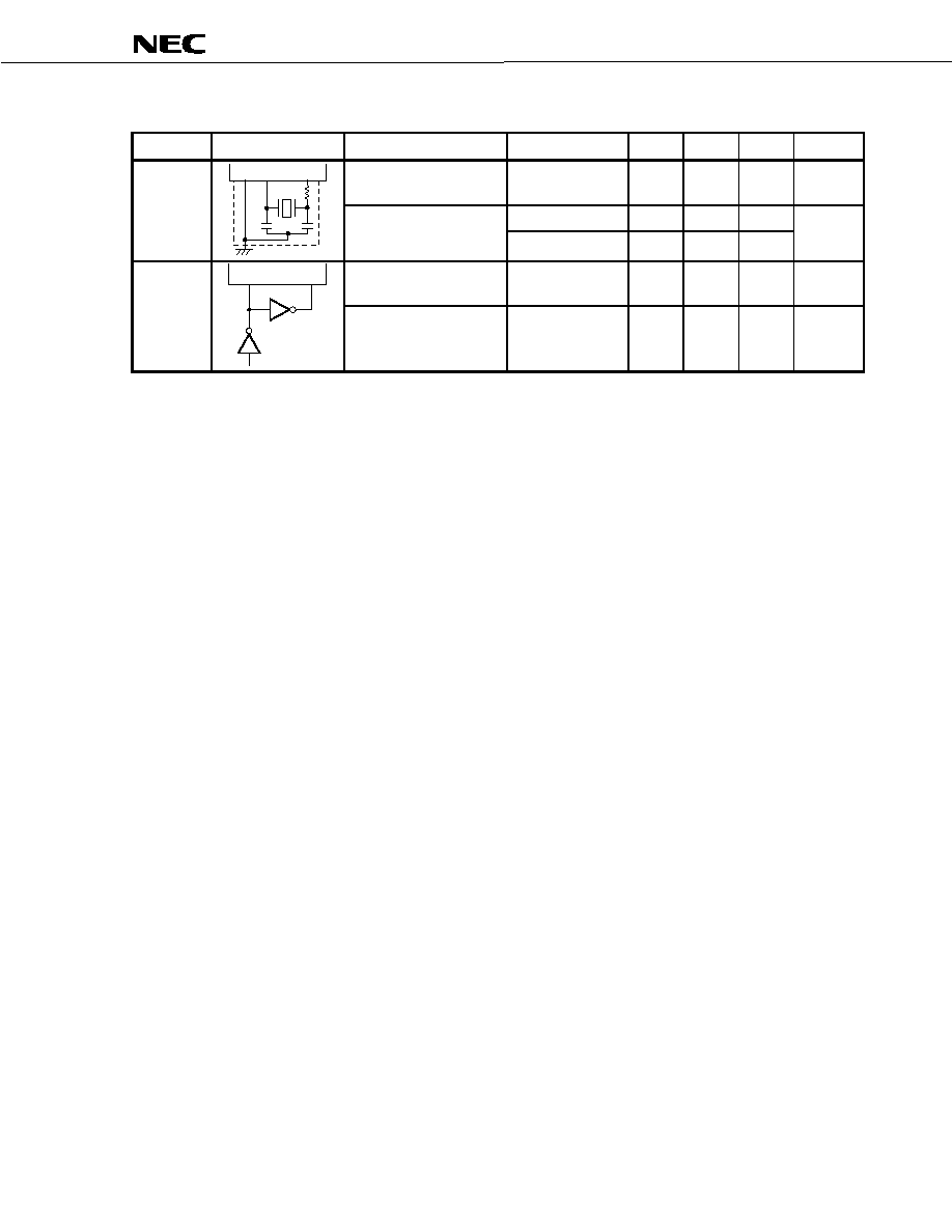
µ
µ
µ
µ
PD789304, 789306, 789314, 789316
Data Sheet U14384EJ1V0DS
41
Subsystem Clock Oscillator Characteristics (T
A
= ≠40 to +85
∞
∞
∞
∞C, V
DD
= 1.8 to 5.5 V)
Resonator
Recommended Circuit
Parameter
Conditions
MIN.
TYP.
MAX.
Unit
Oscillation frequency
(f
XT
)
Note 1
32
32.768
35
kHz
V
DD
= 4.5 to 5.5 V
1.2
2
Crystal
resonator
XT2
XT1
IC
C4
C3
R
Oscillation stabilization
time
Note 2
10
s
XT1 input frequency
(f
XT
)
Note 1
32
35
kHz
External
clock
XT1
XT2
XT1 input high-/low-level
width (t
XTH
, t
XTL
)
14.3
15.6
µs
Notes 1. Indicates only oscillator characteristics. Refer to AC Characteristics for instruction execution time.
2. Time required to stabilize oscillation after V
DD
reaches oscillation voltage range MIN.
Cautions 1. When using the subsystem clock oscillator, wire as follows in the area enclosed by the
broken lines in the above figure to avoid an adverse effect from wiring capacitance.
∑ Keep the wiring length as short as possible.
∑ Do not cross the wiring with the other signal lines.
∑ Do not route the wiring near a signal line through which a high fluctuating current flows.
∑ Always make the ground point of the oscillator capacitor the same potential as V
SS
.
∑ Do not ground the capacitor to a ground pattern through which a high current flows.
∑ Do not fetch signals from the oscillator.
2. The subsystem clock oscillator is designed as a low-amplitude circuit for reducing current
consumption, and is more prone to malfunction due to noise than the main system clock
oscillator. Particular care is therefore required with the wiring method when the subsystem
clock is used.
Remark For the resonator selection and oscillator constant, customers are requested to either evaluate the
oscillation themselves or apply to the resonator manufacturer for evaluation.

µ
µ
µ
µ
PD789304, 789306, 789314, 789316
42
Data Sheet U14384EJ1V0DS
DC Characteristics (T
A
= ≠40 to +85
∞
∞
∞
∞C, V
DD
= 1.8 to 5.5 V) (1/4)
Parameter
Symbol
Conditions
MIN.
TYP.
MAX.
Unit
Per pin
10
mA
Output current, low
I
OL
All pins
80
mA
Per pin
≠1
mA
Output current, high
I
OH
All pins
≠15
mA
V
DD
= 2.7 to 5.5 V
0.7V
DD
V
DD
V
V
IH1
P10 to P13
0.9V
DD
V
DD
V
V
DD
= 2.7 to 5.5 V
0.7V
DD
12
V
N-ch open
drain
0.9V
DD
12
V
V
DD
= 2.7 to 5.5 V
0.7V
DD
V
DD
V
V
IH2
P50 to
P53
On-chip pull-
up resistor
0.9V
DD
V
DD
V
V
DD
= 2.7 to 5.5 V
0.8V
DD
V
DD
V
V
IH3
RESET, P00 to P03,
P20 to P26, P30 to P33
0.9V
DD
V
DD
V
V
DD
= 4.5 to 5.5 V
V
DD
≠ 0.5
V
DD
V
Input voltage, high
V
IH4
X1 (CL1), X2 (CL2),
XT1, XT2
V
DD
≠ 0.1
V
DD
V
V
DD
= 2.7 to 5.5 V
0
0.3V
DD
V
V
IL1
P10 to P13
0
0.1V
DD
V
V
DD
= 2.7 to 5.5 V
0
0.3V
DD
V
V
IL2
P50 to P53
0
0.1V
DD
V
V
DD
= 2.7 to 5.5 V
0
0.2V
DD
V
V
IL3
RESET, P00 to P03,
P20 to P26, P30 to P33
0
0.1V
DD
V
V
DD
= 4.5 to 5.5 V
0
0.4
V
Input voltage, low
V
IL4
X1 (CL1), X2 (CL2),
XT1, XT2
0
0.1
V
V
DD
= 4.5 to 5.5 V, I
OH
= ≠1 mA
V
DD
≠ 1.0
V
Output voltage, high
V
OH
V
DD
= 1.8 to 5.5 V, I
OH
= ≠100
µA
V
DD
≠ 0.5
V
4.5
V
DD
5.5 V,
I
OL
= 10 mA
1.0
V
V
OL1
P00 to P03, P10 to P13,
P20 to P26, P30 to P33
1.8
V
DD
< 4.5 V,
I
OL
= 400
µA
0.5
V
4.5
V
DD
< 5.5 V,
I
OL
= 10 mA
1.0
V
Output voltage, low
V
OL2
P50 to P53
1.8
V
DD
< 4.5 V,
I
OL
= 1.6 mA
0.4
V
Remarks 1. Pin names enclosed in parentheses are when using the
µPD789314, 789316.
2. Unless specified otherwise, the characteristics of alternate-function pins are the same as those of
port pins.
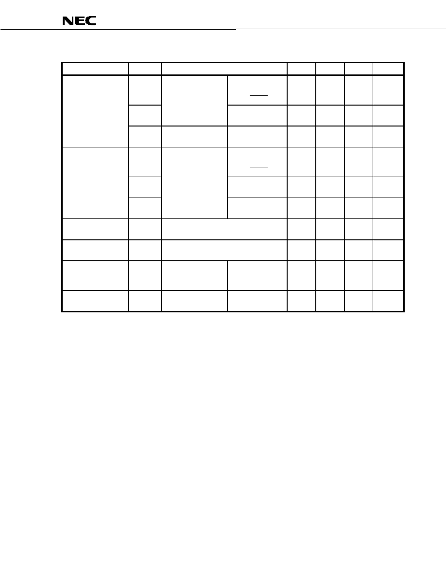
µ
µ
µ
µ
PD789304, 789306, 789314, 789316
Data Sheet U14384EJ1V0DS
43
DC Characteristics (T
A
= ≠40 to +85
∞
∞
∞
∞C, V
DD
= 1.8 to 5.5 V) (2/4)
Parameter
Symbol
Conditions
MIN.
TYP.
MAX.
Unit
I
LIH1
P00 to P03, P10 to
P13, P20 to P26, P30
to P33, RESET
3
µA
I
LIH2
V
IN
= V
DD
X1 (CL1), X2 (CL2),
XT1, XT2
20
µA
Input leakage current,
high
I
LIH3
V
IN
= 12 V
P50 to P53
(N-ch open drain)
20
µA
I
LIL1
P00 to P03, P10 to
P13, P20 to P26, P30
to P33, RESET
≠3
µA
I
LIL2
X1 (CL1), X2 (CL2),
XT1, XT2
≠20
µA
Input leakage current,
low
I
LIL3
V
IN
= 0 V
P50 to P53
(N-ch open drain)
≠3
Note
µA
Output leakage current,
high
I
LOH
V
OUT
= V
DD
3
µA
Output leakage current,
low
I
LOL
V
OUT
= 0 V
≠3
µA
Software pull-up
resistor
R
1
V
IN
= 0 V
P00 to P03, P10 to
P13, P20 to P26,
P30 to P33
50
100
200
k
Mask option pull-up
resistor
R
2
V
IN
= 0 V
P50 to P53
10
30
60
k
Note If there is no on-chip pull-up resistor for P50 to P53 (specified by the mask option), if P50 to P53 have
been set to input mode when a read instruction is executed to read from P50 to P53, a low-level input
leakage current of up to ≠30
µA flows during only one cycle. At all other times, the maximum leakage
current is ≠3
µA.
Remarks 1. Pin names enclosed in parentheses are when using the
µPD789314, 789316.
2. Unless specified otherwise, the characteristics of alternate-function pins are the same as those of
port pins.
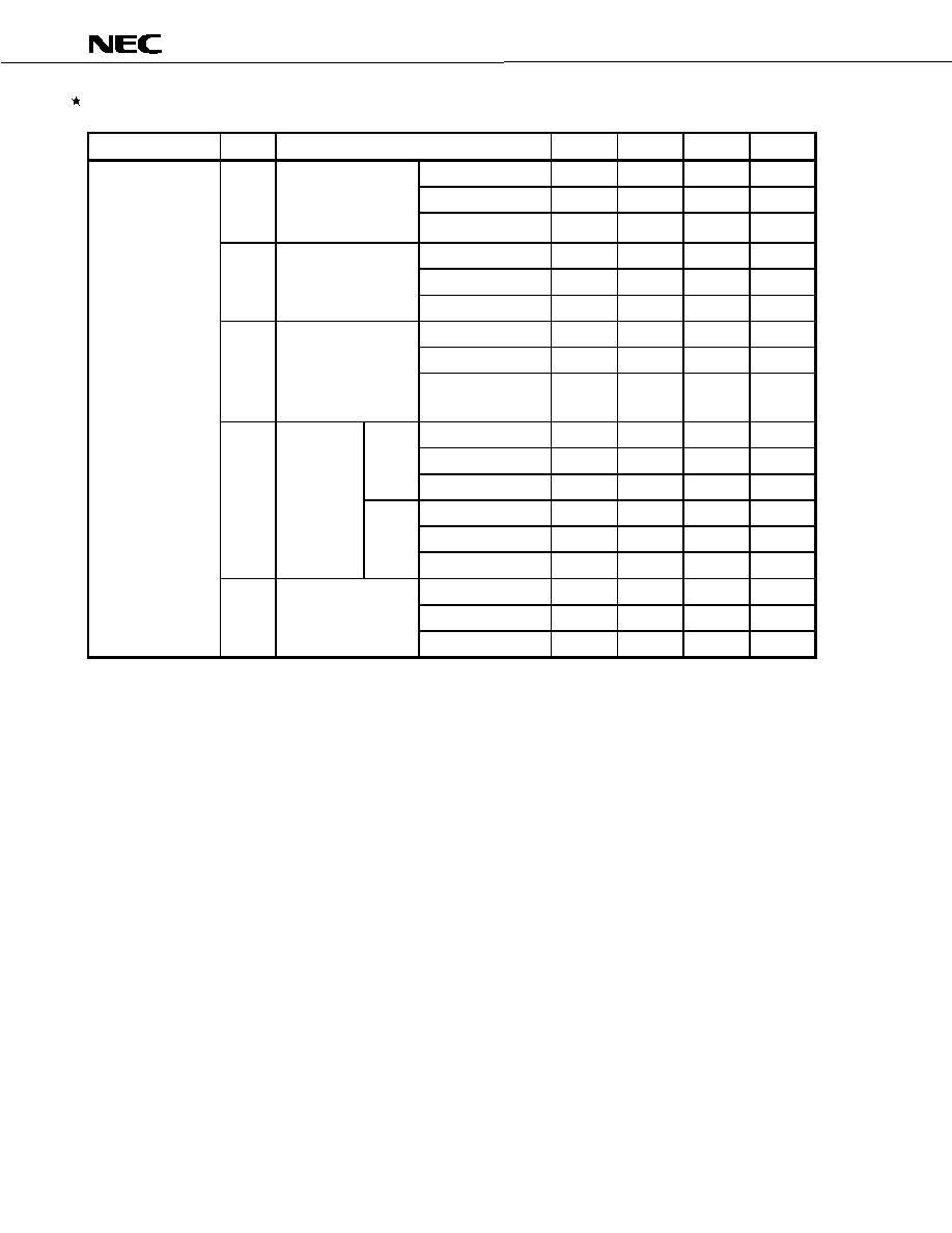
µ
µ
µ
µ
PD789304, 789306, 789314, 789316
44
Data Sheet U14384EJ1V0DS
DC Characteristics (T
A
= ≠40 to +85
∞
∞
∞
∞C, V
DD
= 1.8 to 5.5 V) (3/4)
Parameter
Symbol
Conditions
MIN.
TYP.
MAX.
Unit
V
DD
= 5.0 V
±10%
Note 2
1.8
2.9
mA
V
DD
= 3.0 V
±10%
Note 3
0.36
0.9
mA
I
DD1
5.0 MHz crystal
oscillation operation
mode
(C1 = C2 = 22 pF)
V
DD
= 2.0 V
±10%
Note 3
0.16
0.45
mA
V
DD
= 5.0 V
±10%
Note 2
0.96
1.92
mA
V
DD
= 3.0 V
±10%
Note 3
0.26
0.76
mA
I
DD2
5.0 MHz crystal
oscillation HALT mode
(C1 = C2 = 22 pF)
V
DD
= 2.0 V
±10%
Note 3
0.1
0.34
mA
V
DD
= 5.0 V
±10%
30
58
µA
V
DD
= 3.0 V
±10%
9
26
µA
I
DD3
32.768 kHz crystal
oscillation operation
mode
Note 4
(C3 = C4 = 22 pF,
R1 = 220 k
)
V
DD
= 2.0 V
±10%
4
12
µA
V
DD
= 5.0 V
±10%
25
48
µA
V
DD
= 3.0 V
±10%
7
20
µA
LCD
not
operating
V
DD
= 2.0 V
±10%
4
10
µA
V
DD
= 5.0 V
±10%
28
57
µA
V
DD
= 3.0 V
±10%
9.6
27.8
µA
I
DD4
32.768 kHz
crystal
oscillation
HALT
mode
Note 4
(C3 = C4 =
22 pF,
R1 = 220 k
)
LCD
operating
Note 5
V
DD
= 2.0 V
±10%
6
16
µA
V
DD
= 5.0 V
±10%
0.1
10
µA
V
DD
= 3.0 V
±10%
0.05
5.0
µA
Power supply
current
Note 1
(Ceramic/crystal
oscillation)
I
DD5
STOP mode
Note 6
V
DD
= 2.0 V
±10%
0.05
3.0
µA
Notes 1. The port current (including the current that flows to the on-chip pull-up resistor) is not included.
2. High-speed mode operation (when processor clock control register (PCC) is set to 00H)
3. Low-speed mode operation (when PCC is set to 02H)
4. When the main system clock is stopped
5. This is the total current that flows when the LCD controller/driver is operating (LCDON0 = 1, VAON0 =
1, LIPS0 = 1). The power supply current when the LCD is not operating (LCDON0 = 0, VAON0 = 1,
LIPS0 = 0) is included in I
DD2
.
6. This is the current when the LCD voltage booster circuit is stopped (LCDON0 = 0, VAON0 = 1).
Remark Unless specified otherwise, the characteristics of alternate-function pins are the same as those of port
pins.

µ
µ
µ
µ
PD789304, 789306, 789314, 789316
Data Sheet U14384EJ1V0DS
45
DC Characteristics (T
A
= ≠40 to +85
∞
∞
∞
∞C, V
DD
= 1.8 to 5.5 V) (4/4)
Parameter
Symbol
Conditions
MIN.
TYP.
MAX.
Unit
V
DD
= 5.0 V
±10%
Note 2
1.65
3.0
mA
V
DD
= 3.0 V
±10%
Note 3
0.65
1.44
mA
I
DD1
4.0 MHz RC oscillation
operation mode
(R = 4.7 k
, C = 22 pF)
V
DD
= 2.0 V
±10%
Note 3
0.38
1.05
mA
V
DD
= 5.0 V
±10%
Note 2
1.1
2.29
mA
V
DD
= 3.0 V
±10%
Note 3
0.6
1.28
mA
I
DD2
4.0 MHz RC oscillation
HALT mode
(R = 4.7 k
, C = 22 pF)
V
DD
= 2.0 V
±10%
Note 3
0.35
0.82
mA
V
DD
= 5.0 V
±10%
30
58
µA
V
DD
= 3.0 V
±10%
9
26
µA
I
DD3
32.768 kHz crystal
oscillation operation
mode
Note 4
(C3 = C4 = 22 pF,
R1 = 220 k
)
V
DD
= 2.0 V
±10%
4
12
µA
V
DD
= 5.0 V
±10%
25
48
µA
V
DD
= 3.0 V
±10%
7
20
µA
LCD
not
operating
V
DD
= 2.0 V
±10%
4
10
µA
V
DD
= 5.0 V
±10%
28
57
µA
V
DD
= 3.0 V
±10%
9.6
27.8
µA
I
DD4
32.768 kHz
crystal
oscillation
HALT
mode
Note 4
(C3 = C4 =
22 pF,
R1 = 220 k
)
LCD
operating
Note 5
V
DD
= 2.0 V
±10%
6
16
µA
V
DD
= 5.0 V
±10%
0.1
10
µA
V
DD
= 3.0 V
±10%
0.05
5.0
µA
Power supply
current
Note 1
(RC oscillation)
I
DD5
STOP mode
Note 6
V
DD
= 2.0 V
±10%
0.05
3.0
µA
Notes 1. The port current (including the current that flows to the on-chip pull-up resistor) is not included.
2. High-speed mode operation (when processor clock control register (PCC) is set to 00H)
3. Low-speed mode operation (when PCC is set to 02H)
4. When the main system clock is stopped
5. This is the total current that flows when the LCD controller/driver is operating (LCDON0 = 1, VAON0 =
1, LIPS0 = 1). The power supply current when the LCD is not operating (LCDON0 = 0, VAON0 = 1,
LIPS0 = 0) is included in I
DD2
.
6. This is the current when the LCD voltage booster circuit is stopped (LCDON0 = 0, VAON0 = 1).
Remark Unless specified otherwise, the characteristics of alternate-function pins are the same as those of port
pins.

µ
µ
µ
µ
PD789304, 789306, 789314, 789316
46
Data Sheet U14384EJ1V0DS
AC Characteristics
(1) Basic operation (T
A
= ≠40 to +85
∞
∞
∞
∞C, V
DD
= 1.8 to 5.5 V)
Parameter
Symbol
Conditions
MIN.
TYP.
MAX.
Unit
V
DD
= 2.7 to 5.5 V
0.4
8.0
µs
Operating with main
system clock
1.6
8.0
µs
Cycle time (minimum
instruction execution
time)
T
CY1
Operating with subsystem clock
114
122
125
µs
V
DD
= 2.7 to 5.5 V
0
4
MHz
TMI40 input frequency
f
TMI
0
275
kHz
V
DD
= 2.7 to 5.5 V
0.1
µs
TMI40 input high-/low-
level width
t
TIMH
,
t
TIML
1.8
µs
Interrupt input high-
/low-level width
t
INTH
,
t
INTL
INTP0 to INTP3
10
µs
Key return input low-
level width
t
KRL
KR00 to KR03
10
µs
RESET low-level width
t
RSL
10
µs
T
CY
vs. V
DD
(main system clock)
Power supply voltage V
DD
(V)
1
2
3
4
5
6
0.1
0.4
0.5
1.0
2.0
10
20
60
Cycle time
T
CY
[ s]
Guaranteed
operation range
µ
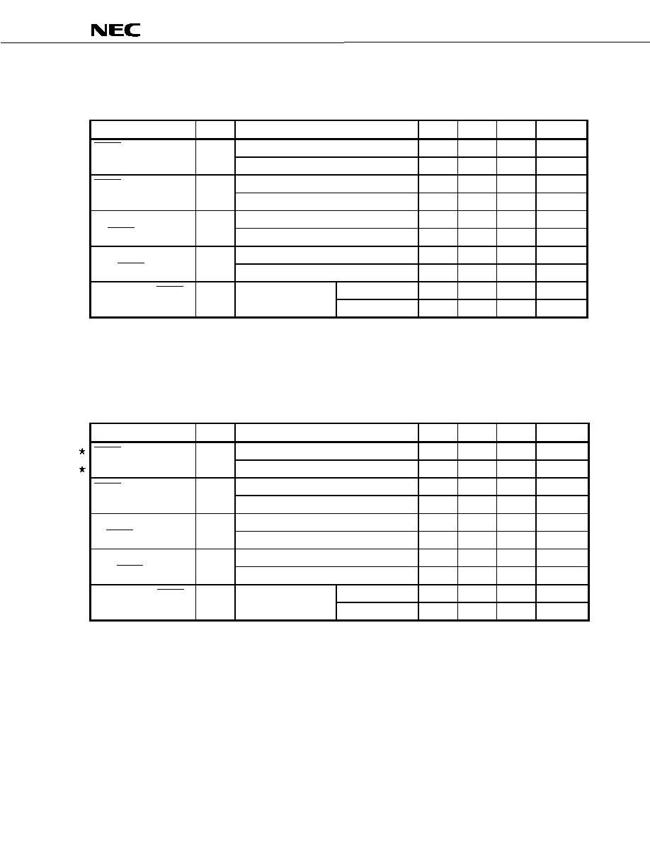
µ
µ
µ
µ
PD789304, 789306, 789314, 789316
Data Sheet U14384EJ1V0DS
47
(2) Serial interface 10, 20 (SIO10, SIO20) (T
A
= ≠40 to +85
∞
∞
∞
∞C, V
DD
= 1.8 to 5.5 V)
(a) 3-wire serial I/O mode (internal clock output)
Parameter
Symbol
Conditions
MIN.
TYP.
MAX.
Unit
V
DD
= 2.7 to 5.5 V
800
ns
SCKn0 cycle time
t
KCY1
3200
ns
V
DD
= 2.7 to 5.5 V
t
KCY1
/2≠50
ns
SCKn0 high-/low-level
width
t
KH1
,
t
KL1
t
KCY1
/2≠150
ns
V
DD
= 2.7 to 5.5 V
150
ns
SIn0 setup time
(to SCKn0
)
t
SIK1
500
ns
V
DD
= 2.7 to 5.5 V
400
ns
SIn0 hold time
(from SCKn0
)
t
SI1
600
ns
V
DD
= 2.7 to 5.5 V
0
250
ns
Delay time from SCKn0
to SOn0 output
t
SO1
R = 1 k
, C = 100 pF
Note
0
1000
ns
Note R and C are the load resistance and load capacitance of the SOn0 output lines.
Remark n = 1, 2
(b) 3-wire serial I/O mode (external clock input)
Parameter
Symbol
Conditions
MIN.
TYP.
MAX.
Unit
V
DD
= 2.7 to 5.5 V
800
ns
SCKn0 cycle time
t
KCY2
3200
ns
V
DD
= 2.7 to 5.5 V
400
ns
SCKn0 high-/low-level
width
t
KH2
,
t
KL2
1600
ns
V
DD
= 2.7 to 5.5 V
100
ns
SIn0 setup time
(to SCKn0
)
t
SIK2
150
ns
V
DD
= 2.7 to 5.5 V
400
ns
SIn0 hold time
(from SCKn0
)
t
SI2
600
ns
V
DD
= 2.7 to 5.5 V
0
300
ns
Delay time from SCKn0
to SOn0 output
t
SO2
R = 1 k
, C = 100 pF
Note
0
1000
ns
Note R and C are the load resistance and load capacitance of the SOn0 output lines.
Remark n = 1, 2

µ
µ
µ
µ
PD789304, 789306, 789314, 789316
48
Data Sheet U14384EJ1V0DS
(c) UART mode (SIO20 only) (dedicated baud rate generator output)
Parameter
Symbol
Conditions
MIN.
TYP.
MAX.
Unit
V
DD
= 2.7 to 5.5 V
78125
bps
Transfer rate
19531
bps
(d) UART mode (SIO20 only) (external clock input)
Parameter
Symbol
Conditions
MIN.
TYP.
MAX.
Unit
V
DD
= 2.7 to 5.5 V
800
ns
ASCK20 cycle time
t
KCY3
3200
ns
V
DD
= 2.7 to 5.5 V
400
ns
ASCK20 high-/low-
level width
t
KH3
,
t
KL3
1600
ns
V
DD
= 2.7 to 5.5 V
39063
bps
Transfer rate
9766
bps
ASCK20 rise/fall time
t
R
,
t
F
1
µs
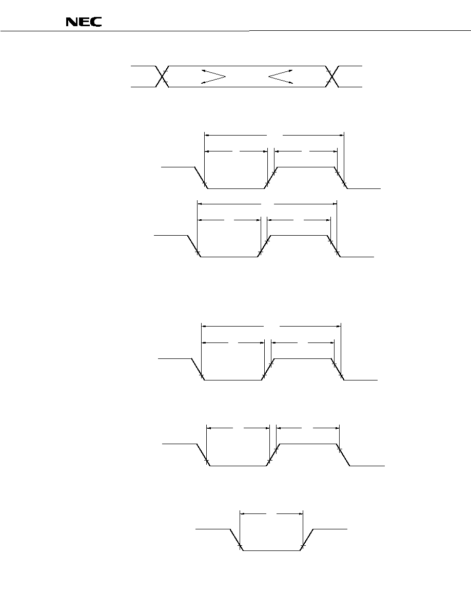
µ
µ
µ
µ
PD789304, 789306, 789314, 789316
Data Sheet U14384EJ1V0DS
49
AC Timing Test Points (excluding X1 (CL1) and XT1 inputs)
0.8V
DD
0.2V
DD
Test points
0.8V
DD
0.2V
DD
Clock Timing
1/f
CLK
t
XL
t
XH
X1 (CL1) input
V
IH4
(MIN.)
V
IL4
(MAX.)
1/f
XT
t
XTL
t
XTH
XT1 input
V
IH5
(MIN.)
V
IL5
(MAX.)
Remark f
CLK
: f
X
or f
CC
TMI Timing
1/f
TMI
t
TIL
t
TIH
TMI40 input
Interrupt Input Timing
INTP0 to INTP3
t
INTL
t
INTH
Key Return Input Timing
KR00 to KR03
t
KRL
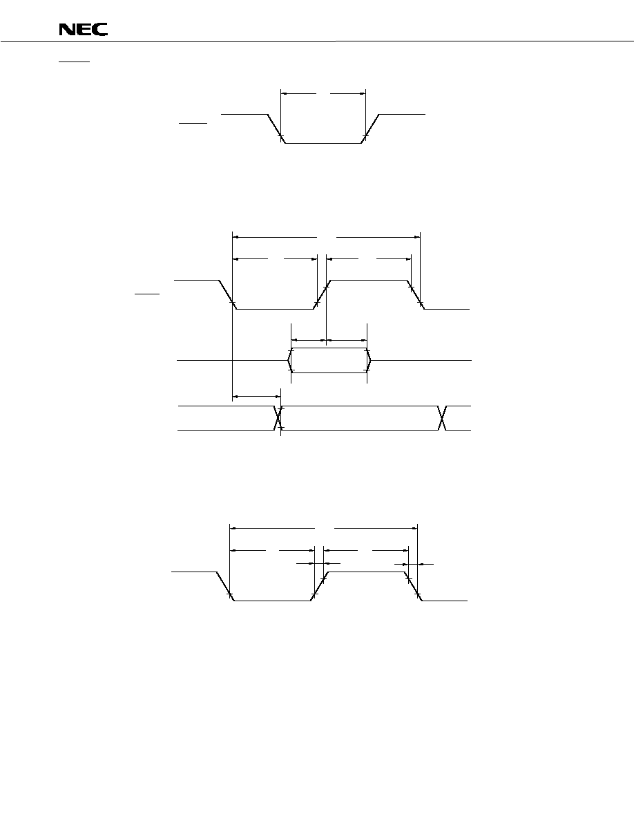
µ
µ
µ
µ
PD789304, 789306, 789314, 789316
50
Data Sheet U14384EJ1V0DS
RESET Input Timing
RESET
t
RSL
Serial Transfer Timing
3-wire serial I/O mode:
t
KCYm
t
KLm
t
KHm
SCKn0
t
SIKm
t
KSIm
t
KSOm
Input data
Output data
SIn0
SOn0
Remark n, m = 1, 2
UART mode (external clock input):
t
KCY3
t
KL3
t
KH3
ASCK20
t
R
t
F
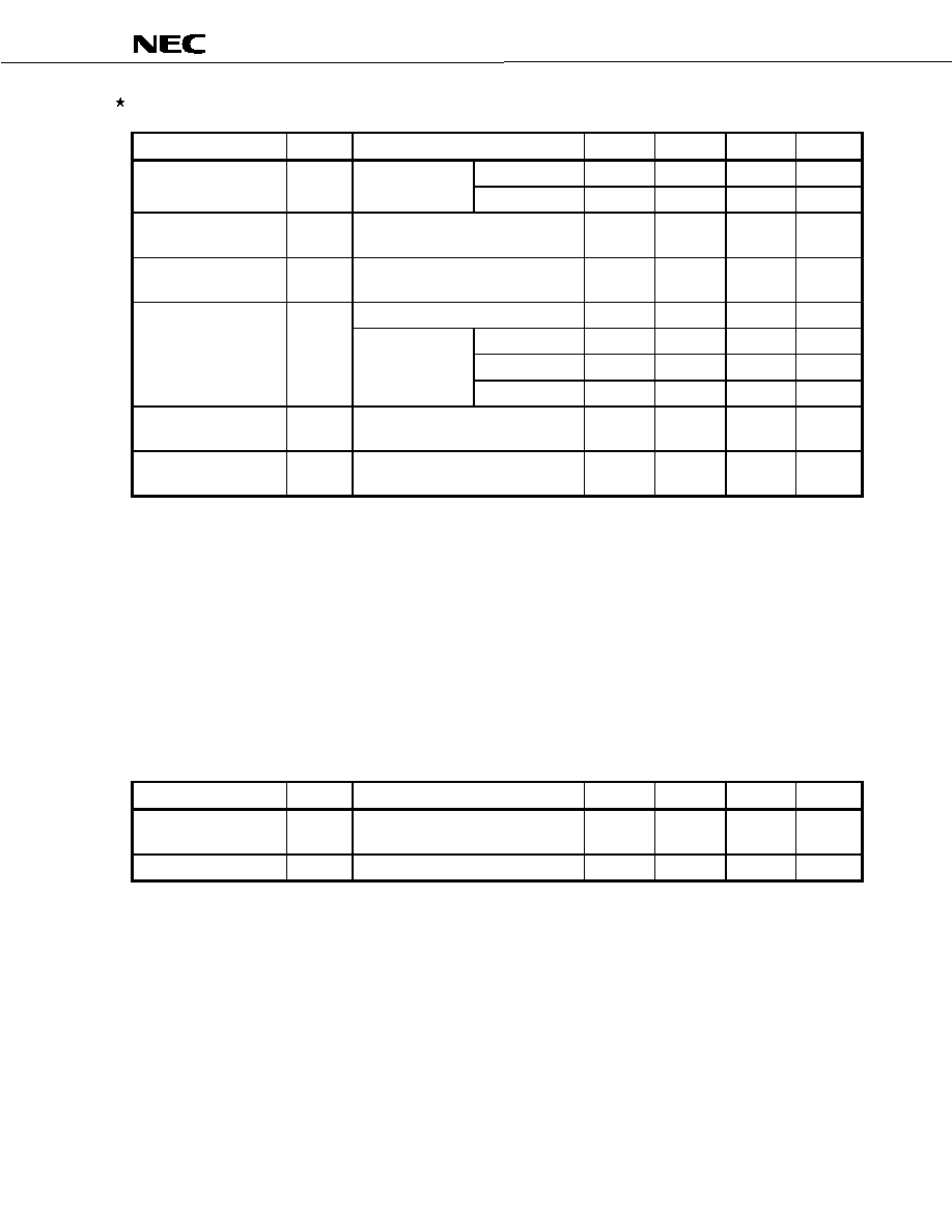
µ
µ
µ
µ
PD789304, 789306, 789314, 789316
Data Sheet U14384EJ1V0DS
51
LCD Characteristics (T
A
= ≠40 to +85
∞
∞
∞
∞C, V
DD
= 1.8 to 5.5 V)
Parameter
Symbol
Conditions
MIN.
TYP.
MAX.
Unit
GAIN = 1
0.84
1.0
1.165
V
LCD output voltage
variation range
V
LCD2
c1 to c4 = 0.47
µF
GAIN = 0
1.26
1.5
1.74
V
Doubler output
V
LCD1
c1 to c4 = 0.47
µF
2V
LCD2
≠ 0.1
2.0V
LCD2
2.0V
LCD2
V
Tripler output
V
LCD0
c1 to c4 = 0.47
µF
3V
LCD2
≠ 0.15
3.0V
LCD2
3.0V
LCD2
V
GAIN = 0
0.5
s
5.0
V
DD
5.5 V
2.0
s
4.5
V
DD
< 5.0 V
1.0
s
Voltage boost wait
time
Note 1
t
VAWAIT
GAIN = 1
1.8
V
DD
< 4.5 V
0.5
s
LCD output voltage
differential
Note 2
(common)
V
ODC
I
O
=
±5
µA
0
±0.2
V
LCD output voltage
differential
Note 2
(segment)
V
ODS
I
O
=
±1
µA
0
±0.2
V
Notes 1. This is the wait time from when voltage boosting is started (VAON0 = 1) until display is enabled
(LCDON0 = 0).
2. The voltage differential is the difference between the segment and common signal output's actual and
ideal output voltages.
Remark c1: Capacitor connected between CAPH and CAPL
c2: Capacitor connected between V
LC0
and ground
c3: Capacitor connected between V
LC1
and ground
c4: Capacitor connected between V
LC2
and ground
Data Memory STOP Mode Low Supply Voltage Data Retention Characteristics (T
A
= ≠40 to +85
∞
∞
∞
∞C)
Parameter
Symbol
Conditions
MIN.
TYP.
MAX.
Unit
Data retention power
supply voltage
V
DDDR
1.8
5.5
V
Release signal set time
t
SREL
0
µs
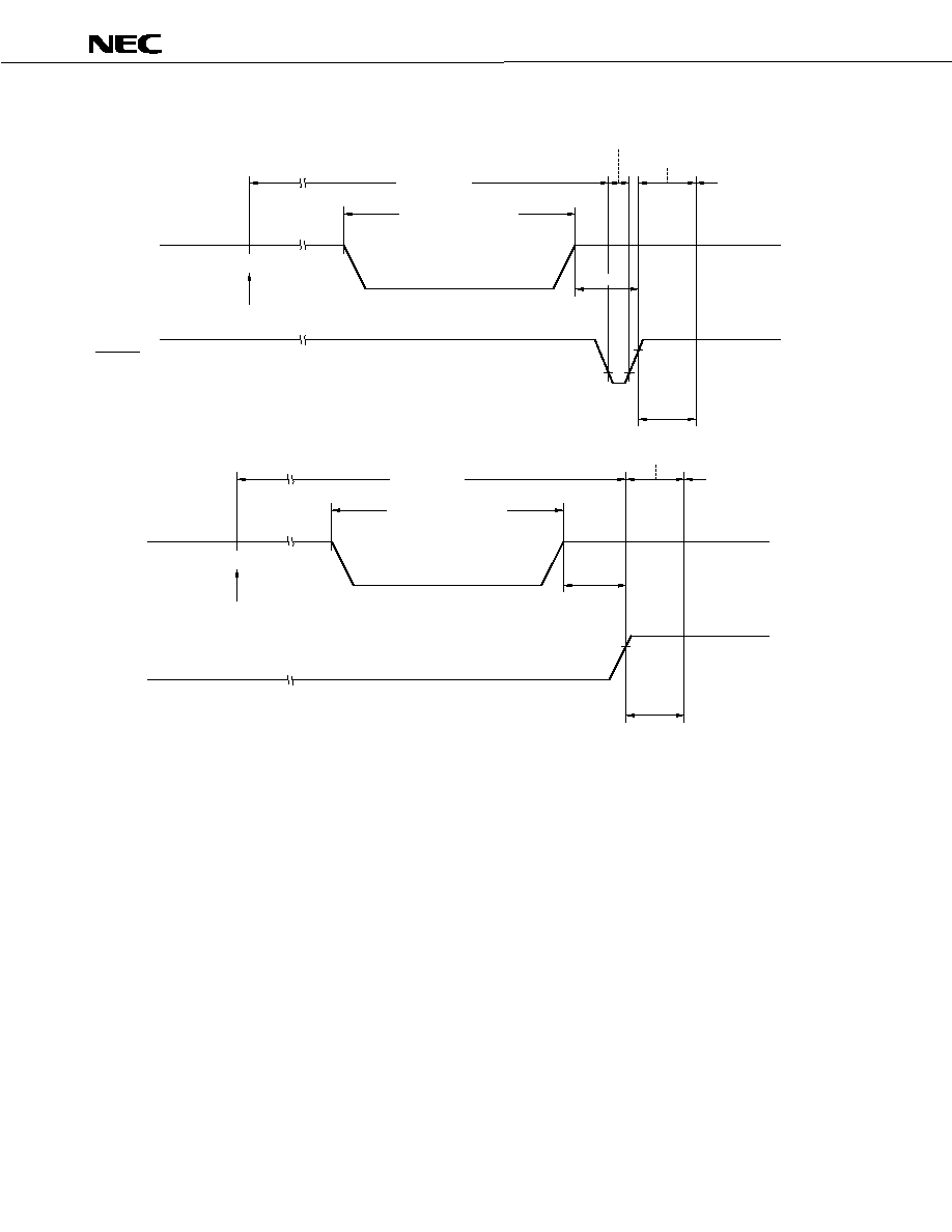
µ
µ
µ
µ
PD789304, 789306, 789314, 789316
52
Data Sheet U14384EJ1V0DS
Data Retention Timing
V
DD
Data retention mode
STOP mode
HALT mode
Internal reset operation
Operation mode
t
SREL
t
WAIT
STOP instruction execution
V
DDDR
RESET
V
DD
Data retention mode
STOP mode
HALT mode
Operation mode
t
SREL
t
WAIT
STOP instruction execution
V
DDDR
Standby release signal
(interrupt request)
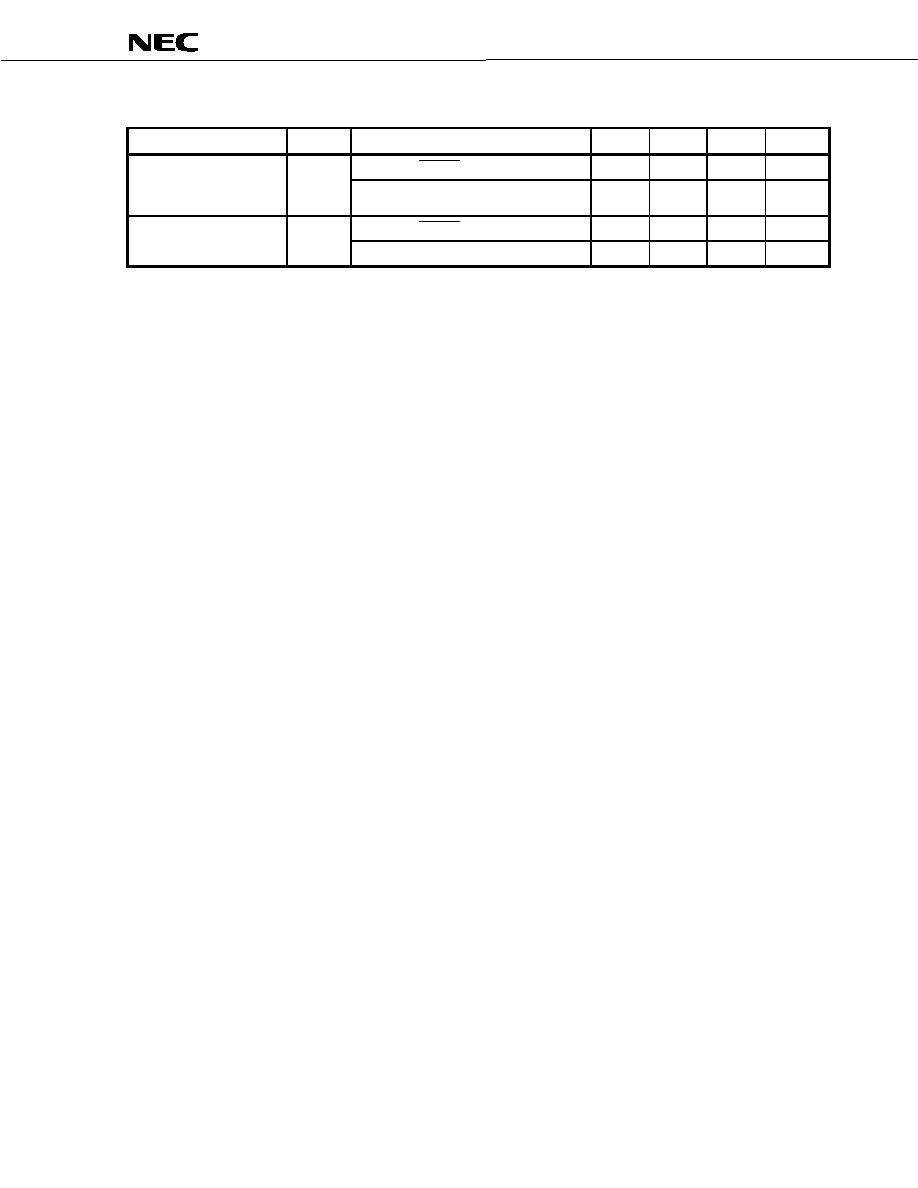
µ
µ
µ
µ
PD789304, 789306, 789314, 789316
Data Sheet U14384EJ1V0DS
53
Oscillation Stabilization Wait Time (T
A
= ≠40 to +85
∞
∞
∞
∞C, V
DD
= 1.8 to 5.5 V)
Parameter
Symbol
Conditions
MIN.
TYP.
MAX.
Unit
Release by RESET
2
15
/f
X
s
Oscillation stabilization wait
time
Note 1
(ceramic/crystal
oscillation)
t
WAIT
Release by interrupt
Note 2
s
Release by RESET
2
7
/f
CC
s
Oscillation stabilization wait
time (RC oscillation)
t
WAIT
Release by interrupt
2
7
/f
CC
s
Notes 1. Use a resonator whose oscillation stabilizes within the oscillation stabilization wait time.
2. Selection of 2
12
/f
X
, 2
15
/f
X
, or 2
17
/f
X
is possible with bits 0 to 2 (OSTS0 to OSTS2) of the oscillation
stabilization time select register (OSTS).
Remarks 1. f
X
: Main system clock oscillation frequency (ceramic/crystal oscillation)
2. f
CC
: Main system clock oscillation frequency (RC oscillation)
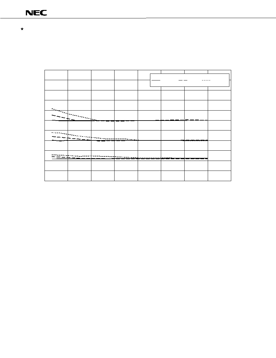
µ
µ
µ
µ
PD789304, 789306, 789314, 789316
54
Data Sheet U14384EJ1V0DS
12. CHARACTERISTICS CURVES OF LCD CONTROLLER/DRIVER (REFERENCE VALUES)
(1) Characteristics curves of voltage boost stabilization time
The following shows the characteristics curves of the time from the start of voltage boost (VAON0 = 1) and
the changes in the LCD output voltage (when GAIN is set to 1 (using the 3 V display panel))
LCD Output Voltage/Voltage Boost Time
Voltage boost time [ms]
V
LCD0
V
LCD1
V
LCD2
0
0
1
0.5
1.5
2
2.5
3
3.5
4
4.5
5
5.5
500
1000
1500
2000
2500
3000
3500
4000
LCD output voltage [V]
V
DD
= 4.5 V
V
DD
= 5 V
V
DD
= 5.5 V
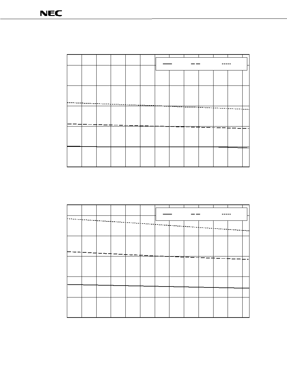
µ
µ
µ
µ
PD789304, 789306, 789314, 789316
Data Sheet U14384EJ1V0DS
55
(2) Temperature characteristics of LCD output voltage
The following shows the temperature characteristics curves of LCD output voltage.
LCD Output Voltage/Temperature (When GAIN = 1)
Temperature [
∞
C]
-
40
-
30
-
20
-
10
0
10
20
30
40
50
60
70
80
0
1
2
3
4
5
LCD output voltage [V]
V
LCD2
V
LCD1
V
LCD0
LCD Output Voltage/Temperature (When GAIN = 0)
Temperature [
∞
C]
-
40
-
30
-
20
-
10
0
10
20
30
40
50
60
70
80
0
1
2
3
4
5
LCD output voltage [V]
V
LCD2
V
LCD1
V
LCD0
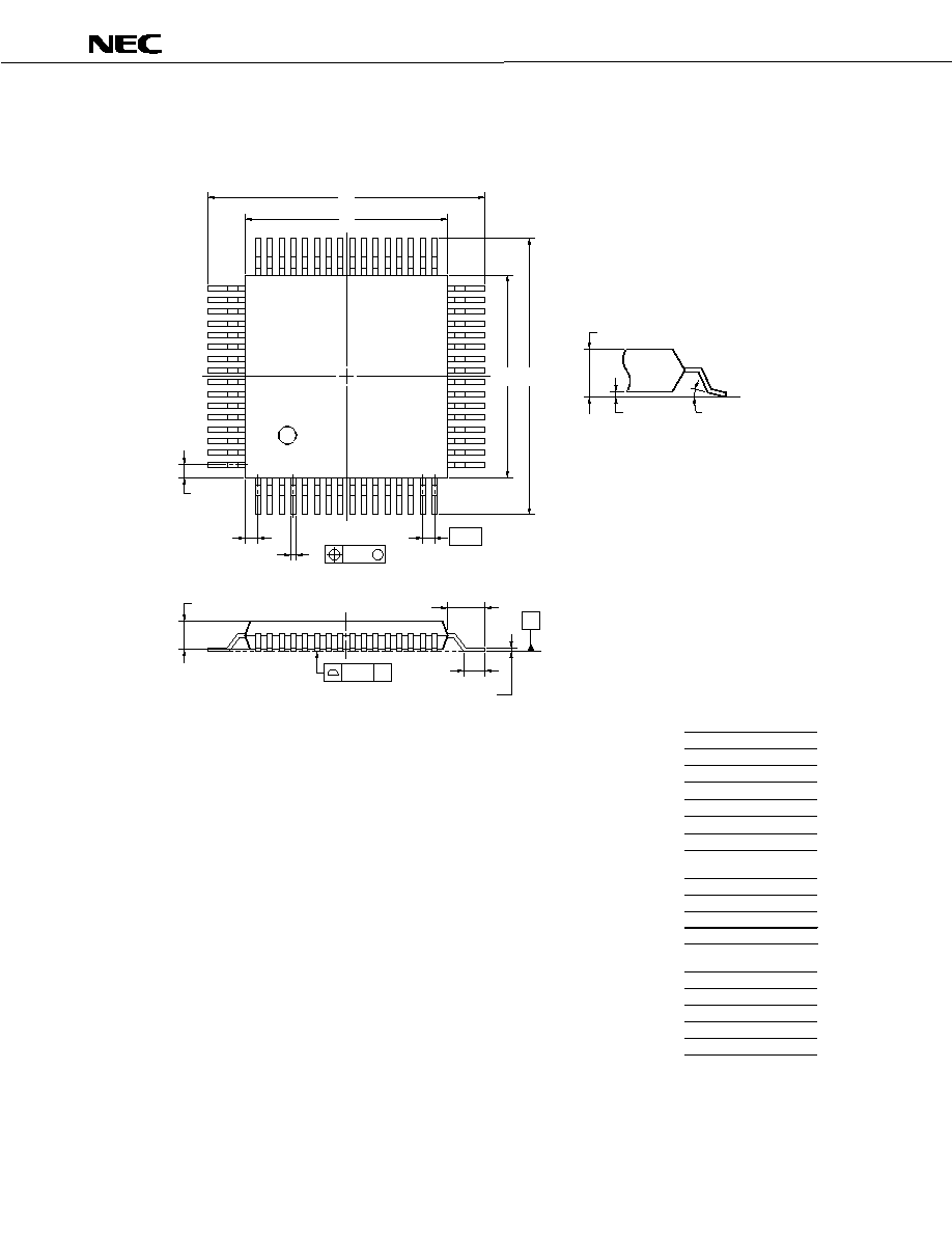
µ
µ
µ
µ
PD789304, 789306, 789314, 789316
56
Data Sheet U14384EJ1V0DS
13. PACKAGE DRAWINGS
48
49
32
64
1
17
16
33
64-PIN PLASTIC QFP (14x14)
NOTE
Each lead centerline is located within 0.15 mm of
its true position (T.P.) at maximum material condition.
ITEM
MILLIMETERS
A
B
D
G
17.6
±
0.4
14.0
±
0.2
0.8 (T.P.)
1.0
J
17.6
±
0.4
K
P64GC-80-AB8-5
C
14.0
±
0.2
I
0.15
1.8
±
0.2
L
0.8
±
0.2
F
1.0
N
P
Q
0.10
2.55
±
0.1
0.1
±
0.1
R
S
5
∞±
5
∞
2.85 MAX.
H
0.37
+
0.08
-
0.07
M
0.17
+
0.08
-
0.07
S
S
N
J
detail of lead end
C D
A
B
R
K
M
L
P
I
S
Q
G
F
M
H
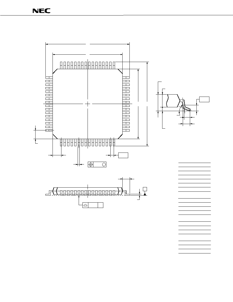
µ
µ
µ
µ
PD789304, 789306, 789314, 789316
Data Sheet U14384EJ1V0DS
57
48
32
33
64
1
17
16
49
S
S
64-PIN PLASTIC TQFP (12x12)
ITEM
MILLIMETERS
G
1.125
A
14.0
±
0.2
C
12.0
±
0.2
D
F
1.125
14.0
±
0.2
B
12.0
±
0.2
N
0.10
P
Q
0.1
±
0.05
1.0
S
R
3
∞+
4
∞
-
3
∞
R
H
K
J
Q
G
I
S
P
detail of lead end
NOTE
Each lead centerline is located within 0.13 mm of
its true position (T.P.) at maximum material condition.
M
H
0.32
+
0.06
-
0.10
I
0.13
J
K
1.0
±
0.2
0.65 (T.P.)
L
0.5
M
0.17
+
0.03
-
0.07
P64GK-65-9ET-2
T
U
0.6
±
0.15
0.25
F
M
A
B
C
D
N
T
L
U
1.1
±
0.1
µ
µ
µ
µ
PD789304, 789306, 789314, 789316
58
Data Sheet U14384EJ1V0DS
14. RECOMMENDED SOLDERING CONDITIONS
The
µPD789304, 789306, 789314, and µPD789316 should be soldered and mounted under the following
recommended conditions.
For the details of the recommended soldering conditions, refer to the document Semiconductor Device Mounting
Technology Manual (C10535E).
For soldering methods and conditions other than those recommended below, contact an NEC sales representative.
Table 14-1. Surface Mounting Type Soldering Conditions
µ
µ
µ
µPD789304GC-◊◊◊
◊◊◊
◊◊◊
◊◊◊-AB8: 64-pin plastic QFP (14 ◊◊◊◊ 14)
µ
µ
µ
µPD789306GC-◊◊◊
◊◊◊
◊◊◊
◊◊◊-AB8: 64-pin plastic QFP (14 ◊◊◊◊ 14)
µ
µ
µ
µPD789314GC-◊◊◊
◊◊◊
◊◊◊
◊◊◊-AB8: 64-pin plastic QFP (14 ◊◊◊◊ 14)
µ
µ
µ
µPD789316GC-◊◊◊
◊◊◊
◊◊◊
◊◊◊-AB8: 64-pin plastic QFP (14 ◊◊◊◊ 14)
Soldering Method
Soldering Conditions
Recommended
Condition Symbol
Infrared reflow
Package peak temperature: 235∞C, Time: 30 seconds max. (at 210∞C or
higher), Count: three times or less
IR35-00-3
VPS
Package peak temperature: 215∞C, Time: 40 seconds max. (at 200∞C or
higher), Count: three times or less
VP15-00-3
Wave soldering
Solder bath temperature: 260∞C max., Time: 10 seconds max., Count:
Once, Preheating temperature: 120∞C max. (package surface temperature)
WS60-00-1
Partial heating
Pin temperature: 300∞C max. Time: 3 seconds max. (per pin row)
--
Caution Do not use different soldering method together (except for partial heating).
µ
µ
µ
µPD789304GK-◊◊◊
◊◊◊
◊◊◊
◊◊◊-9ET: 64-pin plastic TQFP (fine pitch) (12 ◊◊◊◊ 12)
µ
µ
µ
µPD789306GK-◊◊◊
◊◊◊
◊◊◊
◊◊◊-9ET: 64-pin plastic TQFP (fine pitch) (12 ◊◊◊◊ 12)
µ
µ
µ
µPD789314GK-◊◊◊
◊◊◊
◊◊◊
◊◊◊-9ET: 64-pin plastic TQFP (fine pitch) (12 ◊◊◊◊ 12)
µ
µ
µ
µPD789316GK-◊◊◊
◊◊◊
◊◊◊
◊◊◊-9ET: 64-pin plastic TQFP (fine pitch) (12 ◊◊◊◊ 12)
Soldering Method
Soldering Conditions
Recommended
Condition Symbol
Infrared reflow
Package peak temperature: 235∞C, Time: 30 seconds max. (at 210∞C or
higher), Count: two times or less, Exposure limit: 7 days
Note
(after that,
prebake at 125∞C for 10 hours)
IR35-107-2
VPS
Package peak temperature: 215∞C, Time: 40 seconds max. (at 200∞C or
higher), Count: two times or less, Exposure limit: 7 days
Note
(after that,
prebake at 125∞C for 10 hours)
VP15-107-2
Partial heating
Pin temperature: 300∞C max. Time: 3 seconds max. (per pin row)
--
Note After opening the dry pack, store it at 25∞C or less and 65% RH or less for the allowable storage period.
Caution Do not use different soldering method together (except for partial heating).
µ
µ
µ
µ
PD789304, 789306, 789314, 789316
Data Sheet U14384EJ1V0DS
59
APPENDIX A. DEVELOPMENT TOOLS
The following development tools are available for system development using the
µPD789304, 789306, 789314,
and 789316.
Language Processing Software
RA78K0S
Notes 1, 2, 3
Assembler package common to 78K/0S Series
CC78K0S
Notes 1, 2, 3
C compiler package common to 78K/0S Series
DF789306
Notes 1, 2, 3
Device file for
µPD789306, 789316 Subseries
CC78K0S-L
Notes 1, 2, 3
C compiler library source file common to 78K/0S Series
Flash Memory Writing Tools
Flashpro III
(Part No. FL-PR3
Note 4
, PG-FP3)
Flash programmer dedicated to on-chip flash memory microcontroller
FA-64GC
Note 4
Flash memory writing adapter for 64-pin plastic QFP (GC-AB8 type)
FA-64GK
Note 4
Flash memory writing adapter for 64-pin plastic TQFP (fine pitch) (GK-9ET type)
Debugging Tools
IE-78K0S-NS
In-circuit emulator
This is an in-circuit emulator for debugging hardware and software of application system
using the 78K/0S Series. It supports the integrated debugger (ID78K0S-NS). It is used with
an AC adapter, emulation probe, and interface adapter for connecting the host machine.
IE-70000-MC-PS-B
AC adapter
This is the adapter for supplying power from an AC-100 to 240 V outlet.
IE-70000-98-IF-C
Interface adapter
This adapter is needed when PC-9800 series PC (except notebook type) is used as the host
machine for an IE-78K0S-NS (supports C bus).
IE-70000-CD-IF-A
PC card interface
This PC card and interface cable are needed when a PC-9800 series notebook-type PC is
used as the host machine for an IE-78K0S-NS (supports PCMCIA socket).
IE-70000-PC-IF-C
Interface adapter
This adapter is needed when an IBM PC/ATTM or compatible PC is used as the host
machine for an IE-78K0S-NS (supports ISA bus).
IE-70000-PCI-IF-A
Interface adapter
This adapter is needed when a PC that includes a PCI bus is used as the host machine for
an IE-78K0S-NS.
IE-789306-NS-EM1
Emulation board
This is an emulation board for emulating the peripheral hardware inherent to the device. It is
used with an in-circuit emulator.
NP-64GC
Note 4
This is a board that is used to connect an in-circuit emulator to the target system. It is for
64-pin plastic QFP (GC-AB8 type).
NP-64GK
Note 4
This is a board that is used to connect an in-circuit emulator to the target system. It is for
64-pin plastic TQFP (GK-9ET type).
SM78K0S
Notes 1, 2
System simulator common to 78K/0S Series
ID78K0S-NS
Notes 1, 2
Integrated debugger common to 78K/0S Series
DF789306
Notes 1, 2
Device file for
µPD789306, 789316 Subseries
Real-Time OS
MX78K0S
Notes 1, 2
OS for 78K/0S Series

µ
µ
µ
µ
PD789304, 789306, 789314, 789316
60
Data Sheet U14384EJ1V0DS
Notes 1. Based on PC-9800 series (Japanese Windows)
2. Based on IBM PC/AT compatible (Japanese/English Windows)
3. Based on HP9000 series 700TM (HP-UXTM), SPARCstationTM (SunOSTM, SolarisTM), or NEWSTM
(NEWS-OSTM)
4. This product is manufactured by Naito Densei Machida Mfg. Co., Ltd. (TEL +81-44-822-3813).
Remark The RA78K0S, CC78K0S, and SM78K0S are used in combination with the DF789306.
µ
µ
µ
µ
PD789304, 789306, 789314, 789316
Data Sheet U14384EJ1V0DS
61
APPENDIX B. RELATED DOCUMENTS
Documents Related to Devices
Document Name
Document No.
µPD789304, 789306, 789314, 789316 Data Sheet
This manual
µPD78F9306, 78F9316 Data Sheet
To be prepared
µPD789306, 789316 Subseries User's Manual
U14800E
78K/0S Series User's Manual Instructions
U11047E
Documents Related to Development Tools (User's Manuals)
Document Name
Document No.
Operation
U11622E
Language
U11599E
RA78K0S Assembler Package
Structured Assembly
Language
U11623E
Operation
U11816E
CC78K0S C Compiler
Language
U11817E
SM78K0S, SM78K0 System Simulator Ver. 2.10 or Later Windows Based
Operation
U14611E
SM78K Series System Simulator Ver. 2.10 or Later
External Part User Open
Interface Specifications
U15006E
ID-78K0-NS, ID78K0S-NS Integrated Debugger Ver. 2.20 or Later Windows
Based
Operation
U14910E
IE-78K0S-NS In-Circuit Emulator
U13549E
IE-789306-NS-EM1 Emulation Board
To be prepared
Documents Related to Embedded Software (User's Manual)
Document Name
Document No.
78K/0S Series OS MX78K0S
Fundamental
U12938E
Other Related Documents
Document Name
Document No.
SEMICONDUCTOR SELECTION GUIDE Products & Packages (CD-ROM)
X13769X
Semiconductor Device Mounting Technology Manual
C10535E
Quality Grades on NEC Semiconductor Devices
C11531E
NEC Semiconductor Device Reliability/Quality Control System
C10983E
Guide to Prevent Damage for Semiconductor Devices by Electrostatic Discharge (ESD)
C11892E
Caution The related documents listed above are subject to change without notice. Be sure to use the
latest version of each document for designing.
µ
µ
µ
µ
PD789304, 789306, 789314, 789316
62
Data Sheet U14384EJ1V0DS
NOTES FOR CMOS DEVICES
1
PRECAUTION AGAINST ESD FOR SEMICONDUCTORS
Note:
Strong electric field, when exposed to a MOS device, can cause destruction of the gate oxide and
ultimately degrade the device operation. Steps must be taken to stop generation of static electricity
as much as possible, and quickly dissipate it once, when it has occurred. Environmental control
must be adequate. When it is dry, humidifier should be used. It is recommended to avoid using
insulators that easily build static electricity. Semiconductor devices must be stored and transported
in an anti-static container, static shielding bag or conductive material. All test and measurement
tools including work bench and floor should be grounded. The operator should be grounded using
wrist strap. Semiconductor devices must not be touched with bare hands. Similar precautions need
to be taken for PW boards with semiconductor devices on it.
2
HANDLING OF UNUSED INPUT PINS FOR CMOS
Note:
No connection for CMOS device inputs can be cause of malfunction. If no connection is provided
to the input pins, it is possible that an internal input level may be generated due to noise, etc., hence
causing malfunction. CMOS devices behave differently than Bipolar or NMOS devices. Input levels
of CMOS devices must be fixed high or low by using a pull-up or pull-down circuitry. Each unused
pin should be connected to V
DD
or GND with a resistor, if it is considered to have a possibility of
being an output pin. All handling related to the unused pins must be judged device by device and
related specifications governing the devices.
3
STATUS BEFORE INITIALIZATION OF MOS DEVICES
Note:
Power-on does not necessarily define initial status of MOS device. Production process of MOS
does not define the initial operation status of the device. Immediately after the power source is
turned ON, the devices with reset function have not yet been initialized. Hence, power-on does
not guarantee out-pin levels, I/O settings or contents of registers. Device is not initialized until the
reset signal is received. Reset operation must be executed immediately after power-on for devices
having reset function.
EEPROM is a trademark of NEC Corporation.
Windows is either a registered trademark or a trademark of Microsoft Corporation in the United States and/or
other countries.
PC/AT is a trademark of International Business Machines Corporation.
HP9000 series 700 and HP-UX are trademarks of Hewlett-Packard Company.
SPARCstation is a trademark of SPARC International, Inc.
Solaris and SunOS are trademarks of Sun Microsystems, Inc.
NEWS and NEWS-OS are trademarks of Sony Corporation.

µ
µ
µ
µ
PD789304, 789306, 789314, 789316
Data Sheet U14384EJ1V0DS
63
Regional Information
Some information contained in this document may vary from country to country. Before using any NEC
product in your application, pIease contact the NEC office in your country to obtain a list of authorized
representatives and distributors. They will verify:
∑
Device availability
∑
Ordering information
∑
Product release schedule
∑
Availability of related technical literature
∑
Development environment specifications (for example, specifications for third-party tools and
components, host computers, power plugs, AC supply voltages, and so forth)
∑
Network requirements
In addition, trademarks, registered trademarks, export restrictions, and other legal issues may also vary
from country to country.
NEC Electronics Inc. (U.S.)
Santa Clara, California
Tel: 408-588-6000
800-366-9782
Fax: 408-588-6130
800-729-9288
NEC Electronics (Germany) GmbH
Duesseldorf, Germany
Tel: 0211-65 03 02
Fax: 0211-65 03 490
NEC Electronics (UK) Ltd.
Milton Keynes, UK
Tel: 01908-691-133
Fax: 01908-670-290
NEC Electronics Italiana s.r.l.
Milano, Italy
Tel: 02-66 75 41
Fax: 02-66 75 42 99
NEC Electronics (Germany) GmbH
Benelux Office
Eindhoven, The Netherlands
Tel: 040-2445845
Fax: 040-2444580
NEC Electronics (France) S.A.
Velizy-Villacoublay, France
Tel: 01-3067-5800
Fax: 01-3067-5899
NEC Electronics (France) S.A.
Madrid Office
Madrid, Spain
Tel: 091-504-2787
Fax: 091-504-2860
NEC Electronics (Germany) GmbH
Scandinavia Office
Taeby, Sweden
Tel: 08-63 80 820
Fax: 08-63 80 388
NEC Electronics Hong Kong Ltd.
Hong Kong
Tel: 2886-9318
Fax: 2886-9022/9044
NEC Electronics Hong Kong Ltd.
Seoul Branch
Seoul, Korea
Tel: 02-528-0303
Fax: 02-528-4411
NEC Electronics Singapore Pte. Ltd.
Novena Square, Singapore
Tel: 253-8311
Fax: 250-3583
NEC Electronics Taiwan Ltd.
Taipei, Taiwan
Tel: 02-2719-2377
Fax: 02-2719-5951
NEC do Brasil S.A.
Electron Devices Division
Guarulhos-SP, Brasil
Tel: 11-6462-6810
Fax: 11-6462-6829
J01.2

µ
µ
µ
µ
PD789304, 789306, 789314, 789316
The export of this product from Japan is regulated by the Japanese government. To export this product may be prohibited
without governmental license, the need for which must be judged by the customer. The export or re-export of this product
from a country other than Japan may also be prohibited without a license from that country. Please call an NEC sales
representative.
M8E 00.4
The information in this document is current as of December, 2000. The information is subject to
change without notice. For actual design-in, refer to the latest publications of NEC's data sheets or
data books, etc., for the most up-to-date specifications of NEC semiconductor products. Not all
products and/or types are available in every country. Please check with an NEC sales representative
for availability and additional information.
No part of this document may be copied or reproduced in any form or by any means without prior
written consent of NEC. NEC assumes no responsibility for any errors that may appear in this document.
NEC does not assume any liability for infringement of patents, copyrights or other intellectual property rights of
third parties by or arising from the use of NEC semiconductor products listed in this document or any other
liability arising from the use of such products. No license, express, implied or otherwise, is granted under any
patents, copyrights or other intellectual property rights of NEC or others.
Descriptions of circuits, software and other related information in this document are provided for illustrative
purposes in semiconductor product operation and application examples. The incorporation of these
circuits, software and information in the design of customer's equipment shall be done under the full
responsibility of customer. NEC assumes no responsibility for any losses incurred by customers or third
parties arising from the use of these circuits, software and information.
While NEC endeavours to enhance the quality, reliability and safety of NEC semiconductor products, customers
agree and acknowledge that the possibility of defects thereof cannot be eliminated entirely. To minimize
risks of damage to property or injury (including death) to persons arising from defects in NEC
semiconductor products, customers must incorporate sufficient safety measures in their design, such as
redundancy, fire-containment, and anti-failure features.
NEC semiconductor products are classified into the following three quality grades:
"Standard", "Special" and "Specific". The "Specific" quality grade applies only to semiconductor products
developed based on a customer-designated "quality assurance program" for a specific application. The
recommended applications of a semiconductor product depend on its quality grade, as indicated below.
Customers must check the quality grade of each semiconductor product before using it in a particular
application.
"Standard": Computers, office equipment, communications equipment, test and measurement equipment, audio
and visual equipment, home electronic appliances, machine tools, personal electronic equipment
and industrial robots
"Special":
Transportation equipment (automobiles, trains, ships, etc.), traffic control systems, anti-disaster
systems, anti-crime systems, safety equipment and medical equipment (not specifically designed
for life support)
"Specific": Aircraft, aerospace equipment, submersible repeaters, nuclear reactor control systems, life
support systems and medical equipment for life support, etc.
The quality grade of NEC semiconductor products is "Standard" unless otherwise expressly specified in NEC's
data sheets or data books, etc. If customers wish to use NEC semiconductor products in applications not
intended by NEC, they must contact an NEC sales representative in advance to determine NEC's willingness
to support a given application.
(Note)
(1) "NEC" as used in this statement means NEC Corporation and also includes its majority-owned subsidiaries.
(2) "NEC semiconductor products" means any semiconductor product developed or manufactured by or for
NEC (as defined above).
∑
∑
∑
∑
∑
∑