 | –≠–ª–µ–∫—Ç—Ä–æ–Ω–Ω—ã–π –∫–æ–º–ø–æ–Ω–µ–Ω—Ç: UPD789327 | –°–∫–∞—á–∞—Ç—å:  PDF PDF  ZIP ZIP |
Document Outline
- COVER
- FEATURES
- APPLICATIONS
- ORDERING INFORMATION
- 78K/0S SERIES LINEUP
- OVERVIEW OF FUNCTIONS
- 1. PIN CONFIGURATION (TOP VIEW)
- 2. BLOCK DIAGRAM
- 3. PIN FUNCTIONS
- 3.1 Port Pins
- 3.2 Non-Port Pins
- 3.3 Pin I/O Circuits and Recommended Connection of Unused Pins
- 4. CPU ARCHITECTURE
- 4.1 Memory Space
- 4.2 Data Memory Addressing
- 4.3 Processor Registers
- 5. PERIPHERAL HARDWARE FUNCTIONS
- 5.1 Ports
- 5.2 Clock Generator
- 5.3 8-Bit Timer 30, 40
- 5.4 Watch Timer
- 5.5 Watchdog Timer
- 5.6 Serial Interface 10
- 5.7 LCD Controller/Driver
- 6. INTERRUPT FUNCTION
- 6.1 Interrupt Types
- 6.2 Interrupt Sources and Configuration
- 6.3 Interrupt Function Control Registers
- 7. STANDBY FUNCTION
- 7.1 Standby Function
- 7.2 Standby Function Control Register
- 8. RESET FUNCTION
- 8.1 Reset Function
- 8.2 Power Failure Detection Function
- 9. MASK OPTION
- 10. INSTRUCTION SET OVERVIEW
- 10.1 Conventions
- 10.2 Operations
- 11. ELECTRICAL SPECIFICATIONS
- 12. PACKAGE DRAWING
- APPENDIX A. DEVELOPMENT TOOLS
- APPENDIX B. RELATED DOCUMENTS
The information contained in this document is being issued in advance of the production cycle for the
device. The parameters for the device may change before final production or NEC Corporation, at its own
discretion, may withdraw the device prior to its production.
Not all devices/types available in every country. Please check with local NEC representative for
availability and additional information.
MOS INTEGRATED CIRCUIT
µ
µ
µ
µ
PD789322,789324,789326,789327
8-BIT SINGLE-CHIP MICROCONTROLLER
Document No. U14673EJ1V0PM00 (1st edition)
Date Published March 2000 NS CP(K)
Printed in Japan
PRELIMINARY PRODUCT INFORMATION
The
µ
PD789322, 789324, 789326, and 789327 are
µ
PD789327 Subseries (designed for remote controller with on-
chip LCD) product in the 78K/0S Series.
In addition to an 8-bit CPU, they have on-chip hardware for a remote controller with on-chip LCD, Including a LCD
controller/driver, a serial interface, a key return signal detection circuit, and timers with carrier generator that can
easily output waveforms for infrared remote control.
The
µ
PD78F9328, a product with on-chip flash memory which can operate on the same supply voltage as for
masked ROM products and various development tools are also under development.
Detailed function descriptions are provided in the following user's manuals. Be sure to read them before
designing.
µ
µ
µ
µ
PD789327, 789467 Subseries User's Manual: To be prepared
78K/0S Series User's Manual Instructions:
U11047E
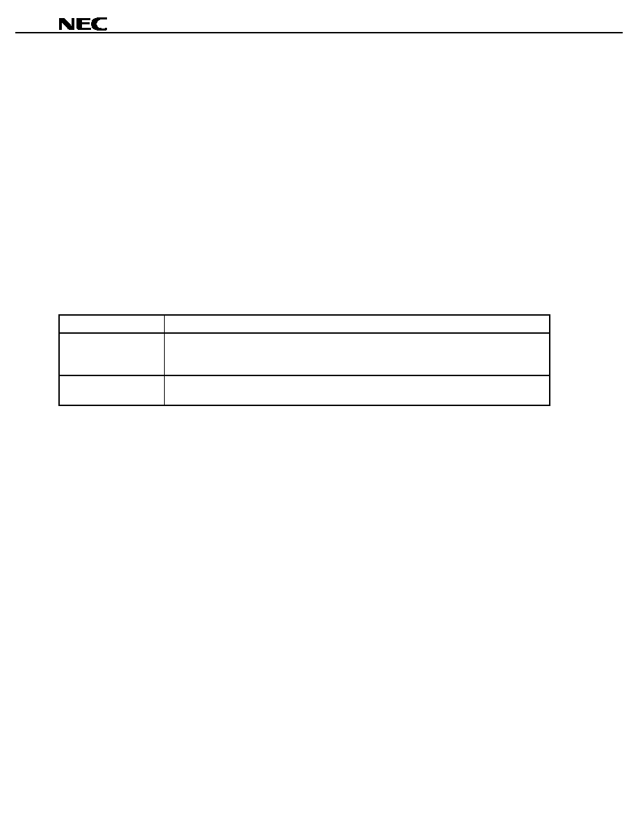
FEATURES
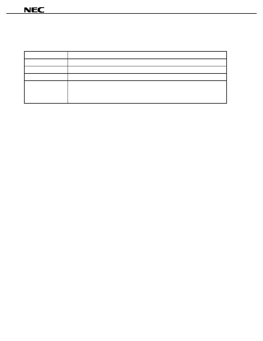
∑
ROM and RAM size
Data Memory
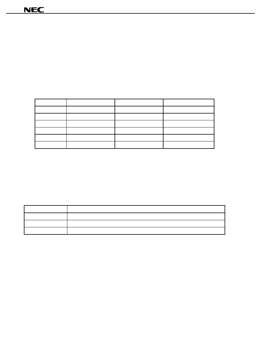
Item
Part Number
Program memory
(ROM)
Internal High-Speed
RAM
LCD display RAM
Packege
µ
PD789322
4 K bytes
µ
PD789324
8 K bytes
256 bytes
µ
PD789326
16 K bytes
µ
PD789327
24 K bytes
512 bytes
24 bytes
52-pin plastic LQFP
(10◊10 mm)
∑
Variable minimum instruction execution time: High speed (0.4
µ
s: @5.0-MHz operation with main system clock),
low speed (1.6
µ
s: @5.0-MHz operation with main system clock), and ultra low speed (122
µ
s: @32.768-kHz
operation with subsystem clock)
∑
I/O ports: 21
∑
Serial interface (3-wire serial I/O mode): 1 channel
∑
LCD controller/driver
Segment signals: 24
Common signals: 4
∑
Timer: 4 channels
∑
Supply voltage: V
DD
= 1.8 to 5.5 V
APPLICATIONS
Remote-control devices, healthcare equipment, etc.
2000

Preliminary Product Information U14673EJ1V0PM00
2
µ
µ
µ
µ
PD789322,789324,789326,789327
ORDERING INFORMATION
Part Number
Package
µ
PD789322GB-xxx-8ET
52-pin plastic LQFP (10
◊
10 mm)
µ
PD789324GB-xxx-8ET
52-pin plastic LQFP (10
◊
10 mm)
µ
PD789326GB-xxx-8ET
52-pin plastic LQFP (10
◊
10 mm)
µ
PD789327GB-xxx-8ET
52-pin plastic LQFP (10
◊
10 mm)
Remark xxx Indicates ROM code suffix.
Preliminary Product Information U14673EJ1V0PM00
3
µ
µ
µ
µ
PD789322,789324,789326,789327
78K/0S SERIES LINEUP
The products in the 78K/0S Series are listed below. The names enclosed in boxes are subseries names
.
78K/0S
series
Small, general-purpose
Small, general-purpose + A/D
For inverter control
For driving LCD
For ASSP
44 pins
44 pins
42/44 pins
28 pins
44 pins
30 pins
30 pins
30 pins
30 pins
30 pins
30 pins
44 pins
Products under mass production
Products under development
Y subseries supports SMB.
PD789014
80 pins
80 pins
64 pins
64 pins
64 pins
64 pins
64 pins
64 pins
44 pins
44 pins
20 pins
20 pins
µ
PD789026
µ
PD789046
PD789026 with subsystem clock added
PD789014 with timer reinforced and ROM and RAM expanded
UART. Low-voltage (1.8-V) operation
PD789167 with improved A/D
PD789104A with improved timer
PD789146 with improved A/D
PD789104A with EEPROM added
PD789124A with improved A/D
RC oscillation model of PD789104A
PD789104A with improved A/D
PD789026 with A/D and multiplier added
PD789407A with improved A/D
PD789456 with improved I/O
PD789446 with improved A/D
PD789426 with improved display output
PD789426 with improved A/D
PD789306 with A/D added
RC oscillation model of PD789306
Basic subseries for driving LCD
For PC keyboard. Internal USB function
For key pad. Internal POC
RC oscillation model of PD789860
For keyless entry. Internal POC and key return circuit
Internal inverter control circuit and UART
µ
PD789104A
µ
PD789114A
µ
PD789842
µ
PD789124A
µ
PD789134A
µ
PD789146
µ
PD789156
µ
PD789167
µ
PD789177
µ
PD789306
µ
PD789316
µ
PD789426
µ
PD789436
µ
PD789860
µ
PD789861
µ
PD789840
µ
PD789800
µ
PD789446
µ
PD789456
µ
PD789167Y
µ
PD789177Y
µ
µ
µ
µ
µ
µ
µ
µ
µ
µ
µ
µ
µ
µ
µ
µ
µ
µ
µ
PD789407A
µ
PD789417A
µ
88 pins
Segment: 40 pins, common: 16 pins
PD789830
µ
144 pins
Segment/common output: 96 pins
PD789835
µ
For driving Dot LCD
52 pins
52 pins
For remote controller. Internal LCD controller/driver
PD789327
µ
PD789467
µ
PD789327 with A/D added
µ

Preliminary Product Information U14673EJ1V0PM00
4
µ
µ
µ
µ
PD789322,789324,789326,789327
The major differences between subseries are shown below.
Timer
ROM
Capacity
8-bit
16-bit
Watch
WDT
8-bit
A/D
10-bit
A/D
Serial Interface
I/O
V
DD
MIN
Value
Remark
µ
PD789046 16 K
1 ch
µ
PD789026 4 K-16 K
1 ch
1 ch
34 pins
Small,
general-
purpose
µ
PD789014 2 K-4 K
2 ch
-
-
1 ch
-
-
1 ch (UART:1 ch)
22 pins
1.8 V
-
µ
PD789177
-
8 ch
µ
PD789167
16 K-24 K
3 ch
1 ch
8 ch
-
31 pins
-
µ
PD789156
-
4 ch
µ
PD789146
8 K-16 K
4 ch
-
Internal
EEPROM
µ
PD789134A
4 ch
µ
PD789124A
4 ch
-
RC oscillation
version
µ
PD789114A
-
4 ch
Small,
general-
purpose
+ A/D
µ
PD789104A
2 K-8 K
1 ch
1 ch
-
1 ch
4 ch
-
1 ch (UART: 1 ch)
20 pins
1.8 V
-
For
inverter
control
µ
PD789842 8 K-16 K
3 ch
Note
1 ch
1 ch
8 ch
-
1 ch (UART: 1 ch) 30 pins
4.0 V
-
µ
PD789417A
7 ch
µ
PD789407A
12 K-24 K
3 ch
7 ch
-
43 pins
µ
PD789456
-
6 ch
µ
PD789446
6 ch
-
30 pins
µ
PD789436
-
6 ch
µ
PD789426
12 K-16 K
6 ch
1 ch (UART: 1 ch)
40 pins
-
µ
PD789316
RC oscillation
version
For LCD
driving
µ
PD789306
8 K to
16K
2 ch
1 ch
1 ch
1 ch
-
-
2 ch (UART: 1 ch) 23 pins
1.8 V
-
µ
PD789835 24 K-60 K
6 ch
-
2 ch
1 ch
27 pins
1.8 V
For Dot
LCD
driving
µ
PD789830 24 K
1 ch
1 ch
1 ch
1 ch
-
-
1 ch (UART: 1 ch) 30 pins
2.7 V
-
µ
PD789467
1 ch
-
18 pins
µ
PD789327
4 K-24 K
2 ch
-
1 ch
1 ch
-
1 ch
21 pins
1.8 V
Internal
LCD
µ
PD789800
-
2 ch (USB: 1 ch)
31 pins
4.0 V
µ
PD789840
8 K
1 ch
4 ch
1 ch
29 pins
2.8 V
-
µ
PD789861
RC oscillation
version,
Internal
EEPROM
ASSP
µ
PD789860
4 K
2 ch
-
-
1 ch
-
-
-
14 pins
1.8 V
Internal
EEPROM
Note 10-bit timer: 1 channel
Function
Subseries Name
Preliminary Product Information U14673EJ1V0PM00
5
µ
µ
µ
µ
PD789322,789324,789326,789327
OVERVIEW OF FUNCTIONS
Item
µ
PD789322
µ
PD789324
µ
PD789326
µ
PD789327
ROM
4 Kbytes
8 Kbytes
16 Kbytes
24 Kbytes
High-speed RAM
256 bytes
512 bytes
Internal memory
LCD display RAM
24 bytes
Main system clock
(oscillation frequency)
Ceramic/crystal resonator (1.0 to 5.0 MHz)
Subsystem clock
(oscillation frequency)
Crystal resonator (32.768 kHz)
0.4
µ
s/1.6
µ
s (@5.0-MHz operation with main system clock)
Minimum instruction execution time
122
µ
s (@32.768-kHz operation with subsystem clock)
General-purpose registers
8 bits
◊
8 registers
Instruction set
∑
16-bit operations
∑
Bit manipulation (set, reset, test) etc.
I/O ports
Total:
21
CMOS I/O:
21
Timers
∑
8-bit timer:
2 channels
∑
Watch timer:
1 channel
∑
Watchdog timer: 1 channel
Timer outputs
1
Serial interface
3-wire serial I/O mode: 1 channel
LCD controller/driver
∑
Segment signal outputs: 24
∑
Common signal outputs: 4
Maskable
Internal: 6, External: 2
Vectored interrupt
sources
Non-maskable
Internal: 1
Reset
∑
Reset by RESET signal input
∑
Internal reset by watchdog timer
∑
Reset via power-on-clear circuit
Supply voltage
V
DD
= 1.8 to 5.5 V
Operating ambient temperature
T
A
=
-
40 to +85
∞
C
Package
52-pin plastic LQFP (10
◊
10 mm)

Preliminary Product Information U14673EJ1V0PM00
6
µ
µ
µ
µ
PD789322,789324,789326,789327
CONTENTS
1. PIN CONFIGURATION (TOP VIEW)..................................................................................................... 8
2. BLOCK DIAGRAM ................................................................................................................................. 9
3. PIN FUNCTIONS .................................................................................................................................. 10
3.1 Port Pins ....................................................................................................................................... 10
3.2 Non-Port Pins............................................................................................................................... 11
3.3 Pin I/O Circuits and Recommended Connection of Unused Pins .......................................... 12
4. CPU ARCHITECTURE ......................................................................................................................... 14
4.1 Memory Space ............................................................................................................................. 14
4.2 Data Memory Addressing ........................................................................................................... 15
4.3 Processor Registers.................................................................................................................... 16
5. PERIPHERAL HARDWARE FUNCTIONS.......................................................................................... 20
5.1 Ports ............................................................................................................................................. 20
5.2 Clock Generator........................................................................................................................... 26
5.3 8-Bit Timer 30, 40......................................................................................................................... 31
5.4 Watch Timer ................................................................................................................................. 41
5.5 Watchdog Timer .......................................................................................................................... 44
5.6 Serial Interface 10 ........................................................................................................................ 46
5.7 LCD Controller/Driver.................................................................................................................. 50
6. INTERRUPT FUNCTION ...................................................................................................................... 56
6.1 Interrupt Types ............................................................................................................................ 56
6.2 Interrupt Sources and Configuration ........................................................................................ 56
6.3 Interrupt Function Control Registers ........................................................................................ 59
7. STANDBY FUNCTION ......................................................................................................................... 65
7.1 Standby Function ........................................................................................................................ 65
7.2 Standby Function Control Register........................................................................................... 67
8. RESET FUNCTION............................................................................................................................... 68
8.1 Reset Function............................................................................................................................. 68
8.2 Power Failure Detection Function ............................................................................................. 70
9. MASK OPTION ...................................................................................................................................... 71
10. INSTRUCTION SET OVERVIEW ...................................................................................................... 72
10.1 Conventions............................................................................................................................... 72
10.2 Operations.................................................................................................................................. 74
11. ELECTRICAL SPECIFICATIONS ...................................................................................................... 79
12. PACKAGE DRAWING......................................................................................................................... 90

Preliminary Product Information U14673EJ1V0PM00
7
µ
µ
µ
µ
PD789322,789324,789326,789327
APPENDIX A. DEVELOPMENT TOOLS ................................................................................................ 91
APPENDIX B. RELATED DOCUMENTS................................................................................................ 93
Preliminary Product Information U14673EJ1V0PM00
8
µ
µ
µ
µ
PD789322,789324,789326,789327
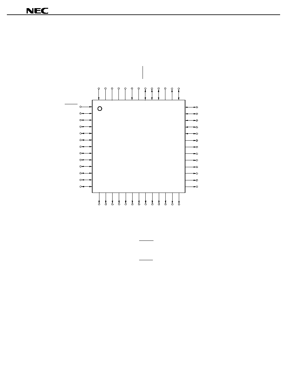
1. PIN CONFIGURATION (TOP VIEW)
52-pin plastic LQFP (10
◊
◊
◊
◊
10 mm)
µ
µ
µ
µ
PD789322GB-xxx-8ET
µ
µ
µ
µ
PD789324GB-xxx-8ET
µ
µ
µ
µ
PD789326GB-xxx-8ET
µ
µ
µ
µ
PD789327GB-xxx-8ET
RESET
P60/TO40
P43/KR03
P42/KR02
P41/KR01
P40/KR00
P03
P02
P01
P00
INT/P61
X1
X2
V
DD
V
SS
XT2
XT1
IC0
P20/SCK10
P21/SO10
P22/SI10
V
LC0
52 51 50 49 48 47 46 45 44 43 42
14 15 16 17 18 19 20 21 21 23 24
1
2
3
4
5
6
7
8
9
10
11
39
38
37
36
35
34
33
32
31
30
29
P11
P10
P81/S21
P82/S20
P83/S19
P84/S18
P85/S17
S16
S15
S14
S13
S12
S11
S10
S9
COM0
COM1
COM2
COM3
S0
S1
S2
S3
S4
S5
S6
S7
S8
S23
P80/S22
12
13
28
27
41 40
25 26
Caution Connect the IC0 (Internally Connected) pin directly to V
SS
.
COM0 to COM3: Common Output
RESET:
Reset
IC0:
Internally connected
S0 to S23:
Segment Output
INT:
Interrupt from Peripherals
SCK10:
Serial Clock Input/Output
KR00 to KR03:
Key Return
SI10:
Serial Data Input
P00 to P03:
Port 0
SO10:
Serial Data Output
P10, P11:
Port 1
V
DD
:
Power Supply
P20 to P22:
Port 2
V
LC0
:
Power Supply for LCD
P40 to P43:
Port 4
V
SS
:
Ground
P60, P61:
Port 6
X1, X2:
Crystal (Main system clock)
P80 to P85:
Port 8
XT1, XT2:
Crystal (Sabsystem clock)
TO40:
Timer Output
Preliminary Product Information U14673EJ1V0PM00
9
µ
µ
µ
µ
PD789322,789324,789326,789327
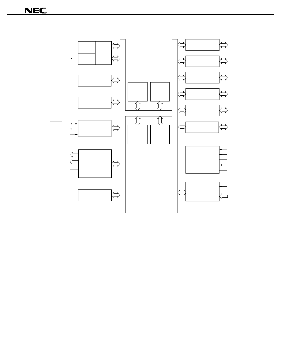
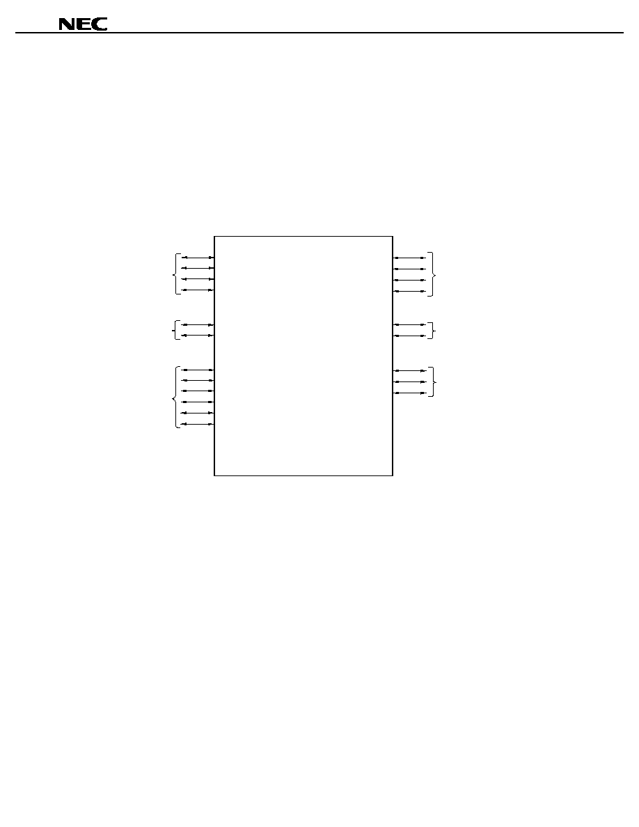
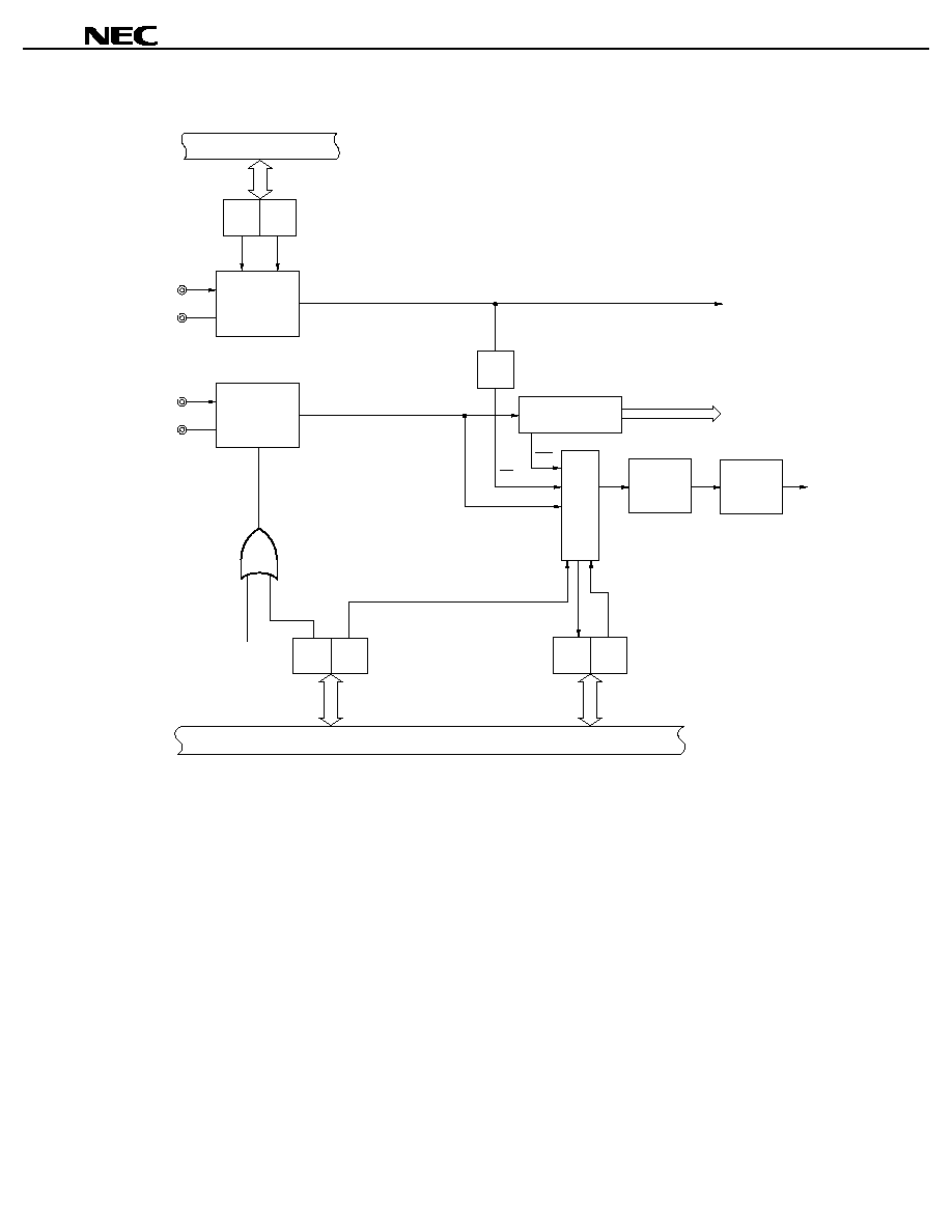
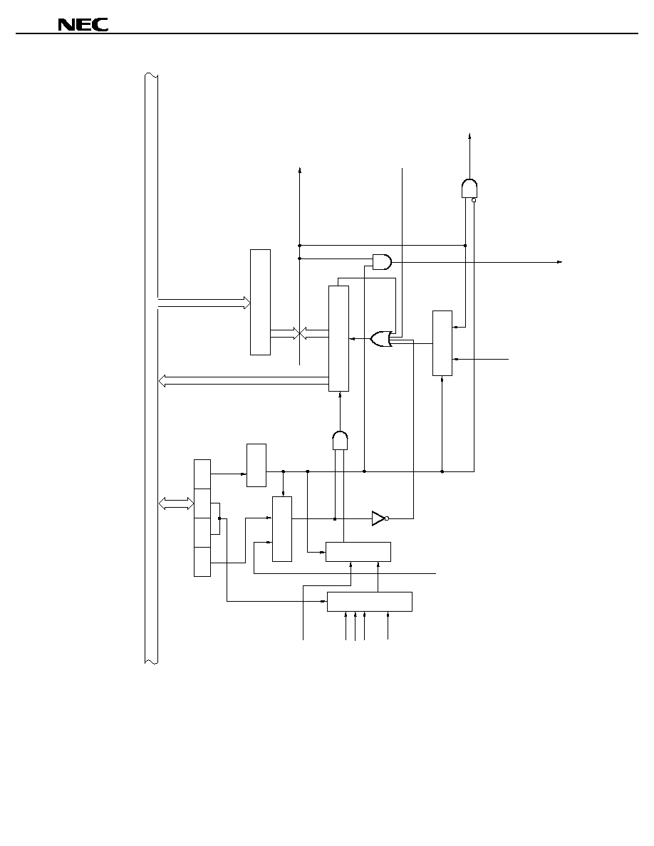
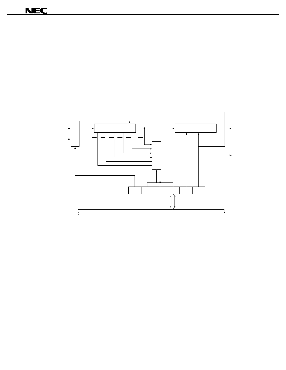
2. BLOCK DIAGRAM
V
DD
V
SS
IC0
78K/0S
CPU core
ROM
8-bit
timer 30
P00 to P03
Port 0
P10, P11
Port 1
P20 to P22
Port 2
P40 to P43
Port 4
P60, P61
Port 6
Watchdog timer
S0 to S23
COM0 to COM3
RAM
RAM
space for
LCD data
8-bit
timer 40
Cascaded
16-bit
timer
Serial interface 10
SCK10/P20
SI10/P22
SO10/P21
V
LC0
LCD
controller/driver
System control
RESET
X1
X2
XT1
XT2
Interrupt control
KR00/P40 to
KR03/P43
INT/P61
P80 to P85
Port 8
Watch timer
TO40/P60
Power-on clear
Remark The Internal ROM and RAM capacities differ depending on the product.
Preliminary Product Information U14673EJ1V0PM00
10
µ
µ
µ
µ
PD789322,789324,789326,789327
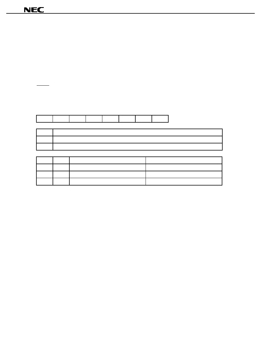
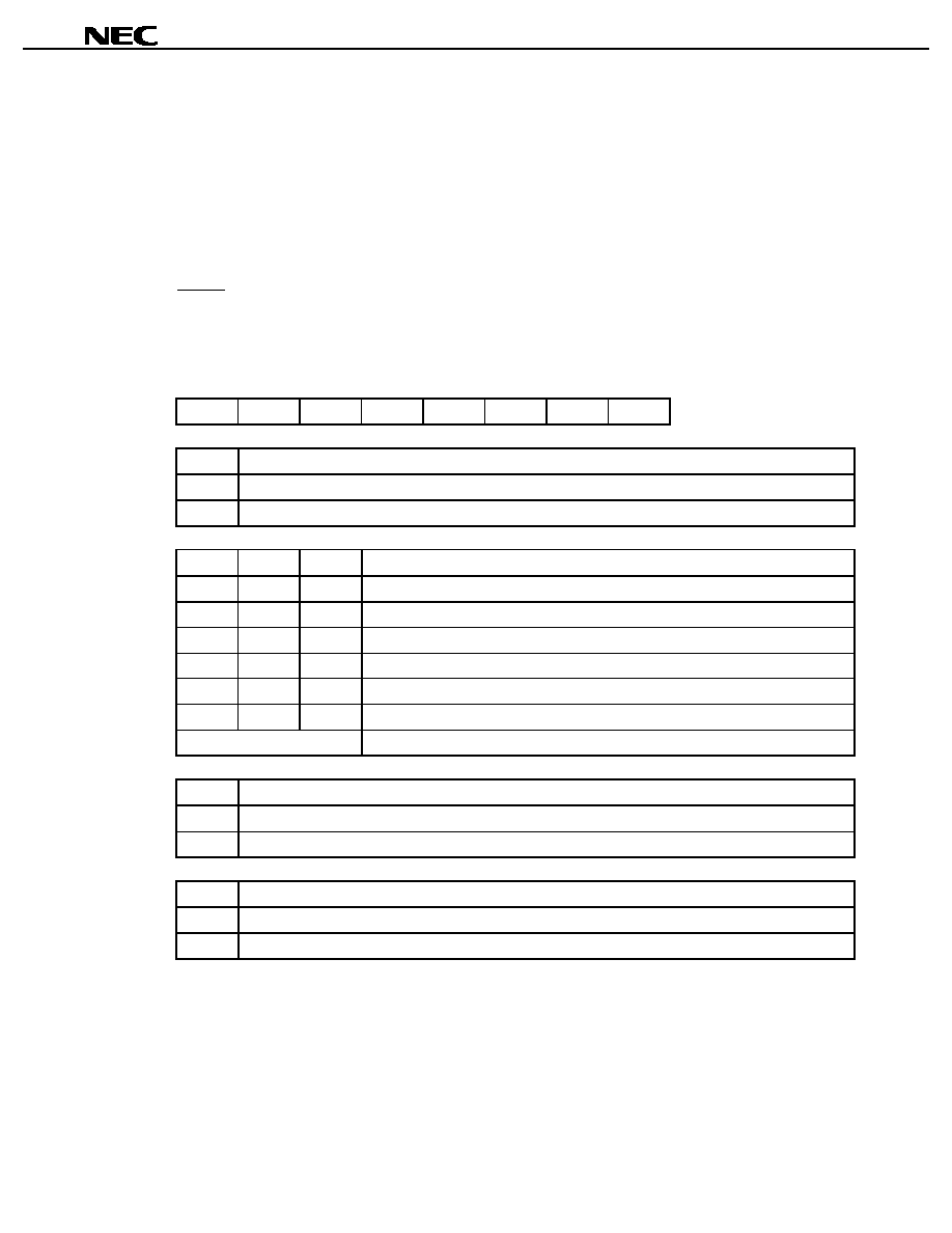
3. PIN FUNCTIONS
3.1 Port Pins
Pin Name
I/O
Function
After Reset
Alternate Function
P00 to P03
I/O
Port 0.
This is a 4-bit I/O port.
Input/output can be specified in 1-bit units.
When used as an input port, on-chip pull-up resistors can be
specified for the whole port using pull-up resistor option
register 0 (PU0).
Input
-
P10, P11
I/O
Port 1.
This is a 2-bit I/O port.
Input/output can be specified in 1-bit units.
When used as an input port, on-chip pull-up resistors can be
specified for the whole port using pull-up resistor option
register 0 (PU0).
Input
-
P20
SCK10
P21
SO10
P22
I/O
Port 2.
This is a 3-bit I/O port.
Input/output can be specified in 1-bit units.
When used as an input port, on-chip pull-up resistors can be
specified in 1-bit units using pull-up resistor option register 2
(PUB2).
Input
SI10
P40 to P43
I/O
Port 4.
This is a 4-bit I/O port.
Input/output can be specified in 1-bit units.
When used as an input port, on-chip pull-up resistors can be
specified for the whole port using pull-up resistor option
register 0 (PU0), or key return mode register 00 (KRM00).
Input
KR00 to KR03
P60
TO40
P61
I/O
Port 6.
This is a 2-bit I/O port.
Input/output can be specified in 1-bit units.
Input
INT
P80 to P85
I/O
Port 8.
This is a 6-bit I/O port.
Input/output can be specified in 1-bit units.
Low-level
output
S22 to S17

Preliminary Product Information U14673EJ1V0PM00
11
µ
µ
µ
µ
PD789322,789324,789326,789327
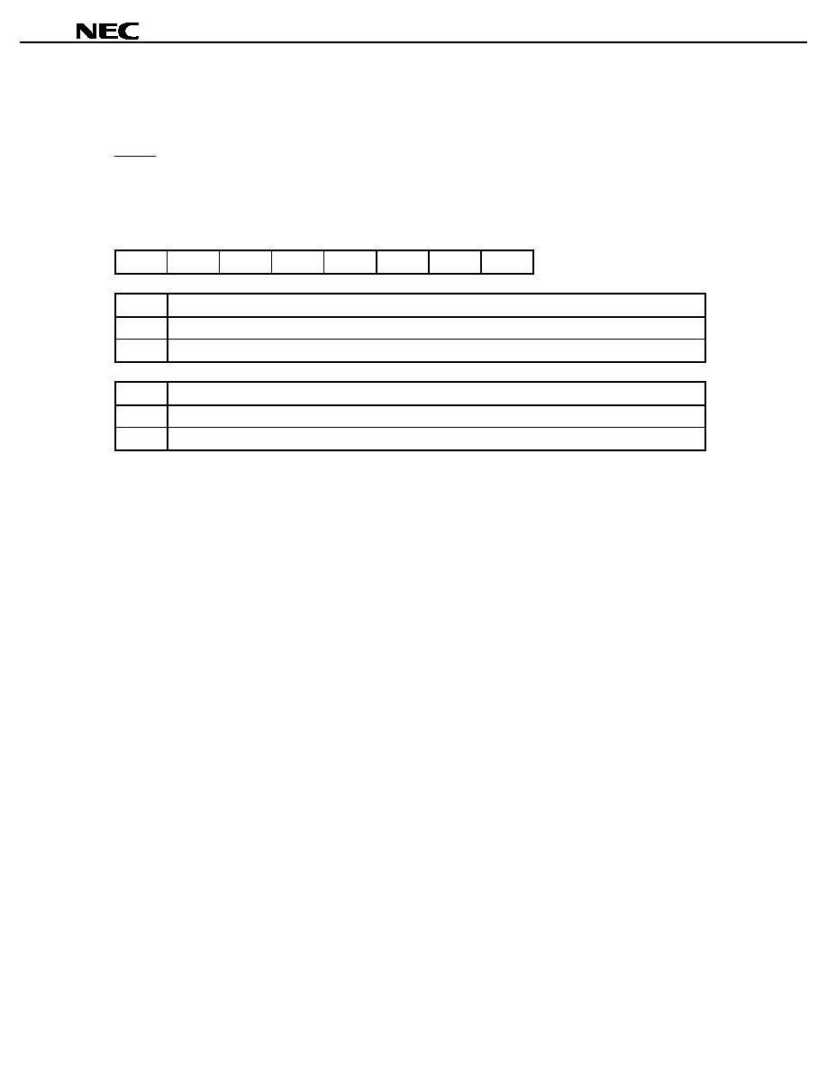
3.2
Non-Port Pins
Pin Name
I/O
Function
After Reset
Alternate Function
INT
Input
External interrupt input for which the valid edge (rising edge,
falling edge, or both rising and falling edges) can be specified.
Input
P61
KR00 to KR03
Input
Key return signal detection
Input
P40 to P43
TO40
Output
8-bit timer 40 output
Input
P60
SCK10
I/O
Serial clock input/output of serial interface 10
Input
P20
SI10
Input
Serial data input of serial interface 10
Input
P22
SO10
Output
Serial data output of serial interface 10
Input
P21
S0 to S16
-
S17 to S22
P85 to P80
S23
Output
LCD controller/driver segment signal outputs
Low-level
output
-
COM0 to COM3
Output
LCD controller/driver common signal outputs
Low-level
output
-
V
LC0
-
LCD drive voltage
-
-
X1
Input
-
-
X2
-
Connecting crystal resonator for main system clock oscillation
-
-
XT1
Input
-
-
XT2
-
Connecting crystal resonator for subsystem clock oscillation
-
-
RESET
Input
System reset input
Input
-
V
DD
-
Positive power supply
-
-
V
SS
-
Ground potential
-
-
IC0
-
Internally connected. Connect to V
SS
directly.
-
-

Preliminary Product Information U14673EJ1V0PM00
12
µ
µ
µ
µ
PD789322,789324,789326,789327
3.3 Pin I/O Circuits and Recommended Connection of Unused Pins
The I/O circuit type of each pin and recommended connection of unused pins is shown in Table 3-1.
For the input/output circuit configuration of each type, refer to Figure 3-1.
Table 3-1. Types of Pin I/O Circuits and Recommended Connection of Unused Pins
Pin Name
I/O Circuit Type
I/O
Recommend Connection of Unused Pins
P00 to P03
P10, P11
5-A
P20/SCK10
8-A
P21/SO10
5-A
P22/SI10
P40/KR00 to P43/KR03
8-A
P60/TO40
5
Input: Independently connect to V
DD
or V
SS
via a resistor.
Output: Leave open.
P61/INT
8
Input: Independently connect to V
SS
via a resistor.
Output: Leave open.
P80/S22 to P85/S17
17-G
I/O
Input: Independently connect to V
DD
or V
SS
via a resistor.
Output: Leave open.
S0 to S16, S23
17-D
COM0 to COM3
18-B
Output
V
LC0
-
Leave open.
XT1
Input
Connect to V
SS
.
XT2
-
-
Leave open.
RESET
2
Input
-
IC0
-
-
Connect directly to V
SS
directly.
Figure 3-1. I/O Circuit Type (1/2)
Type 2
Type 5
Schmitt-triggered input with hysteresis characteristics.
IN
P-ch
IN/OUT
Data
Output
disable
Input
enable
V
DD
N-ch
V
SS

Preliminary Product Information U14673EJ1V0PM00
13
µ
µ
µ
µ
PD789322,789324,789326,789327
Figure 3-1. I/O Circuit Type (2/2)
Type 5-A
Type 8
Pull-up
enable
V
DD
P-ch
P-ch
IN/OUT
Data
Output
disable
Input
enable
V
DD
N-ch
V
SS
Data
V
DD
P-ch
Output
disable
IN/OUT
N-ch
V
SS
Type 8-A
Type 17-D
Pull-up
enable
V
DD
P-ch
Data
V
DD
P-ch
Output
disable
IN/OUT
N-ch
V
SS
P-ch
N-ch
P-ch
N-ch
N-ch
N-ch
data
OUT
V
LC0
V
LC1
SEG
V
LC2
P-ch
P-ch
V
SS
Type 17-G
Type 18-B
P-ch
N-ch
P-ch
N-ch
N-ch
N-ch
data
V
LC0
V
LC1
SEG
V
LC2
P-ch
P-ch
V
SS
P-ch
IN/OUT
Data
Output
disable
Input
enable
V
DD
N-ch
V
SS
P-ch
N-ch
P-ch
N-ch
P-ch
N-ch
P-ch
N-ch
data
P-ch
N-ch
V
LC1
V
LC0
V
LC2
OUT
COM
V
SS
Remark V
LC1
: V
LC0
◊
2/3, V
LC2
: V
LC0
/3

Preliminary Product Information U14673EJ1V0PM00
14
µ
µ
µ
µ
PD789322,789324,789326,789327
4. CPU ARCHITECTURE
4.1 Memory Space
The
µ
PD789322, 789324, 789326, and 789327 are provided with 64 Kbytes of accessible memory space. Figure
4-1 shows the memory map.
Figure 4-1. Memory Map
n n n n H
+
1
n n n n H
Special function registers
256
◊
8 bits
Internal high-speed RAM
LCD display RAM
24
◊
8 bits
F F F F H
F F 0 0 H
F E F F H
0 0 0 0 H
Program
memory space
Data memory
space
n n n n H
0 0 0 0 H
Program area
0 0 8 0 H
0 0 7 F H
Program area
0 0 4 0 H
0 0 3 F H
CALLT table area
Reserved
0 0 1 4 H
0 0 1 3 H
Vector table area
Internal ROM
F A 1 8 H
F A 1 7 H
F A 0 0 H
F 9 F F H
Reserved
Note
Note
mmmmH
mmmmH
-
1
Note The internal ROM capacity and internal high-speed RAM capacity depend on the products (see the next
table).
Relevant Product Name
Internal ROM Last Address
nnnnH
Internal High-Speed RAM Start Address
mmmmH
µ
PD789322
0FFFH
µ
PD789324
1FFFH
FE00H
µ
PD789326
3FFFH
µ
PD789327
5FFFH
FD00H
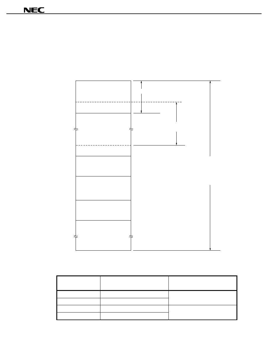
Preliminary Product Information U14673EJ1V0PM00
15
µ
µ
µ
µ
PD789322,789324,789326,789327
4.2 Data Memory Addressing
The
µ
PD789322, 789324, 789326, and 789327 are provided with a variety of addressing modes to improve the
operability of the memory. In the area that incorporates data memory (FD00H to FFFFH) in particular, specific
addressing modes that correspond to the particular functions of an area, such as the special function registers
(SFRs), are available. Figure 4-2 shows the data memory addressing modes.
Figure 4-2. Data Memory Addressing Modes
Special function registers (SFRs)
256
◊
8 bits
Internal high-speed RAM
LCD display RAM
24
◊
8 bits
F F F F H
0 0 0 0 H
Direct addressing
Register indirect
addressing
Based addressing
F F 0 0 H
F E F F H
F F 2 0 H
F F 1 F H
F E 2 0 H
F E 1 F H
SFR addressing
Short direct
addressing
mmmmH
mmmmH
-
1
F A 1 8 H
F A 1 7 H
Reserved
F A 0 0 H
F 9 F F H
Reserved
Internal ROM
Note
Note
n n n n H
+
1
n n n n H
Note The internal ROM capacity and internal high-speed RAM capacity depend on the products (see the next
table).
Relevant Product Name
Internal ROM Last Address
nnnnH
Internal High-Speed RAM Start Address
mmmmH
µ
PD789322
0FFFH
µ
PD789324
1FFFH
FE00H
µ
PD789326
3FFFH
µ
PD789327
5FFFH
FD00H

Preliminary Product Information U14673EJ1V0PM00
16
µ
µ
µ
µ
PD789322,789324,789326,789327
4.3 Processor Registers
4.3.1 Control registers
(1) Program counter (PC)
The PC is a 16-bit register that holds the address information of the next program to be executed.
Figure 4-3. Program Counter Configuration
0
15
PC14
PC15
PC
PC13 PC12 PC11 PC10
PC9
PC8
PC7
PC6
PC5
PC4
PC3
PC2
PC1
PC0
(2) Program status word (PSW)
The PSW is an 8-bit register that indicates the status of the CPU according to the results of instruction execution.
Figure 4-4. Program Status Word Configuration
IE
Z
0
AC
0
0
1
CY
7
0
(a) Interrupt enable flag (IE)
This flag controls the interrupt request acknowledgement of the CPU.
(b) Zero flag (Z)
This flag is set (1) if the result of an operation is zero; otherwise it is reset (0).
(c) Auxiliary carry flag (AC)
AC is set (1) if the result of the operation has a carry from bit 3 or a borrow at bit 3; otherwise it is reset (0).
(d) Carry flag (CY)
CY is used to indicate whether an overflow or underflow has occurred during the execution of a subtract or
add instruction.
(3) Stack pointer (SP)
The SP is a 16-bit register that holds the start address of the stack area. Only the internal RAM area (FD00H to
FEFFH) can be specified as the stack area.
Figure 4-5. Stack Pointer Configuration
0
15
SP14
SP15
SP
SP13 SP12 SP11 SP10
SP9
SP8
SP7
SP6
SP5
SP4
SP3
SP2
SP1
SP0
Caution RESET input makes the SP contents undefined, so be sure to initialize the SP before instruction
execution.
Preliminary Product Information U14673EJ1V0PM00
17
µ
µ
µ
µ
PD789322,789324,789326,789327
4.3.2 General-purpose registers
The
µ
PD789322, 789324, 789326, and 789327 have eight 8-bit general-purpose registers (X, A, C, B, E, D, L, and
H).
These registers can be used either singly as 8-bit registers or in pairs as 16-bit registers (AX, BC, DE, and HL),
and can be described in terms of function names (X, A, C, B, E, D, L, H, AX, BC, DE, and HL) and absolute names
(R0 to R7 and RP0 to RP3).
Figure 4-6. General-Purpose Register Configuration
(a) Absolute register names
R7
R6
R5
R4
R3
R2
R1
R0
8-bit processing
7
0
RP3
RP2
RP1
RP0
16-bit processing
15
0
(b) Functional register names
H
L
D
E
B
C
A
X
8-bit processing
7
0
HL
DE
BC
AX
16-bit processing
15
0
Preliminary Product Information U14673EJ1V0PM00
18
µ
µ
µ
µ
PD789322,789324,789326,789327
4.3.3 Special function registers (SFRs)
Special function registers are used as peripheral hardware mode registers and control registers, and are mapped
in the 256-byte space from FF00H to FFFFH.
Note that the bit number of a bit name that is a reserved word in the RA78K0S and defined under the header file
"sfrbit.h" in the CC78K0S appears enclosed in a circle in the register formats. Refer to the register formats in 5.
PERIPHERAL HARDWARE FUNCTIONS.
Table 4-1. Special Function Registers (1/2)
Bit Unit for Manipulation
Address
Special Function Register (SFR) Name
Symbol
R/W
1 Bit
8 Bits
16 Bits
After
Reset
FF00H
Port 0
P0
-
FF01H
Port 1
P1
-
FF02H
Port 2
P2
-
FF03H
port 4
P4
-
FF05H
Port 6
P6
-
FF08H
Port 8
P8
-
00H
FF20H
Port mode register 0
PM0
-
FF21H
Port mode register 1
PM1
-
FF22H
Port mode register 2
PM2
-
FF24H
Port mode register 4
PM4
-
FF26H
Port mode register 6
PM6
-
FF28H
Port mode register 8
PM8
-
FFH
FF32H
Pull-up resistor option register B2
PUB2
-
FF4AH
Watch timer mode control register
WTM
-
FF58H
Port function register 8
PF8
R/W
-
00H
FF63H
8-bit compare register 30
CR30
W
-
-
Undefined
FF64H
8-bit timer counter 30
TM30
R
-
-
FF65H
8-bit timer mode control register 30
TMC30
R/W
-
00H
FF66H
8-bit compare register 40
CR40
-
-
FF67H
8-bit H width compare register 40
CRH40
W
-
-
Undefined
FF68H
8-bit timer counter 40
TM40
R
-
-
FF69H
8-bit timer mode control register 40
TMC40
R/W
-
FF6AH
Carrier generator output control register 40
TCA40
W
-
-
FF72H
Serial operation mode register 10
CSIM10
-
00H
FF74H
Transmission/reception shift register 10
SIO10
-
Undefined
FFB0H
LCD display mode register 0
LCDM0
-
FFB2H
LCD clock control register 0
LCDC0
-
00H
FFDDH Power-on-clear register 1
POCF1
R/W
-
00H
Note
Note This value is 04H only after a power-on-clear reset.
Preliminary Product Information U14673EJ1V0PM00
19
µ
µ
µ
µ
PD789322,789324,789326,789327
Table 4-1. Special Function Registers (2/2)
Bit Unit for Manipulation
Address
Special Function Register (SFR) Name
Symbol
R/W
1 Bit
8 Bits
16 Bits
After
Reset
FFE0H
Interrupt request flag register 0
IF0
-
00H
FFE4H
Interrupt mask flag register 0
MK0
-
FFH
FFECH External interrupt mode register 0
INTM0
-
-
FFF0H
Subclock oscillation mode register
SCKM
-
FFF2H
Subclock control register
CSS
-
FFF5H
Key return mode register 00
KRM00
-
FFF7H
Pull-up resistor option register 0
PU0
-
FFF9H
Watchdog timer mode register
WDTM
-
00H
FFFAH
Oscillation stabilization time selection register
OSTS
-
-
04H
FFFBH
Processor clock control register
PCC
R/W
-
02H
Preliminary Product Information U14673EJ1V0PM00
20
µ
µ
µ
µ
PD789322,789324,789326,789327
5. PERIPHERAL HARDWARE FUNCTIONS
5.1 Ports
5.1.1 Port functions
Various kinds of control operations are possible using the ports provided in the
µ
PD789322, 789324, 789326, and
789327. These ports are illustrated in Figure 5-1 and their functions are listed in Table 5-1.
A number of alternate functions are also provided, except for those ports functioning as digital I/O ports. Refer to
3. PIN FUNCTIONS for details of the alternate function pins.
Figure 5-1. Ports
P40
P00
P03
Port 0
Port 1
P10
Port 4
P43
P11
Port 2
P20
P22
Port 6
P60
P61
P80
Port 8
P85
Preliminary Product Information U14673EJ1V0PM00
21
µ
µ
µ
µ
PD789322,789324,789326,789327
Table 5-1. Port Functions
Port Name
Pin Name
Function
Port 0
P00 to P03
This is an I/O port for which input and output can be specified in 1-bit units.
When used as an input port, on-chip pull-up resistors can be specified using pull-up
resistor option register 0 (PU0).
Port 1
P10, P11
This is an I/O port for which input and output can be specified in 1-bit units.
When used as an input port, on-chip pull-up resistors can be specified using pull-up
resistor option register 0 (PU0).
Port 2
P20 to P22
This is an I/O port for which input and output can be specified in 1-bit units.
When used as an input port, on-chip pull-up resistors can be specified using pull-up
resistor option register B2 (PUB2).
Port 4
P40 to P43
This is an I/O port for which input and output can be specified in 1-bit units.
When used as an input port, on-chip pull-up resistors can be specified using pull-up
resistor option register 0 (PU0), or key return mode register 00 (KRM00).
Port 6
P60, P61
This is an I/O port for which input and output can be specified in 1-bit units.
Port 8
P80 to P85
This is an I/O port for which input and output can be specified in 1-bit units.

Preliminary Product Information U14673EJ1V0PM00
22
µ
µ
µ
µ
PD789322,789324,789326,789327
5.1.2 Port configuration
The ports consist of the following hardware.
Table 5-2. Port Configuration
Item
Configuration
Control registers
Port mode registers (PMm: m = 0 to 2, 4, 6, 8)
Pull-up resistor option registers (PU0, PUB2)
Port function register 8 (PF8)
Ports
Total: 21 (CMOS I/O: 21)
Pull-up resistors
Total: 13 (software control: 13)
Figure 5-2. Basic Configuration of CMOS Port
WR
PUm
PU
◊
WR
PORTm
WR
PORTm
WR
PMm
Output latch
Pmn
PMmn
V
DD
P-ch
Pmn
Internal bus
Selector
Caution Figure 5-2 shows the basic configuration of a CMOS I/O port. This configuration differs
depending on the functions of alternate function pins. Also, an on-chip pull-up resistor can be
connected to port 4 by means of a setting in key return mode register 00 (KRM00).
Remark PU
◊
:
Pull-up resistor option register (
◊
= 0, B2)
PMmn: Bit n of port mode register m (m = 0 to 2, 4, 6, 8 n = 0 to 5)
Pmn:
Bit n of port m
RD:
Port read signal
WR:
Port write signal

Preliminary Product Information U14673EJ1V0PM00
23
µ
µ
µ
µ
PD789322,789324,789326,789327
5.1.3 Port function control registers
The ports are controlled by the following three types of registers.
∑
Port mode registers (PM0 to PM2, PM4, PM6, PM8)
∑
Pull-up resistor option registers (PU0, PUB2)
∑
Port function register 8 (PF8)
(1) Port mode registers (PM0 to PM2, PM4, PM6, PM8)
Input and output can be specified in 1-bit units.
These registers can be set using a 1-bit or 8-bit memory manipulation instruction.
RESET input sets these registers to FFH.
When using the port pins as their alternate functions, set the port mode register and the output latch as shown
in Table 5-3.
Caution Because P61 functions alternately as an external interrupt input, when the output level
changes after the output mode of the port function is specified, the interrupt request flag will
be inadvertently set. Therefore, be sure to preset the interrupt mask flag (PMK0) before
using the port in output mode.
Figure 5-3. Port Mode Register Format
Symbol
7
6
5
4
3
2
1
0
Address
After reset
R/W
PM0
1
1
1
1
PM03
PM02
PM01
PM00
FF20H
FFH
R/W
PM1
1
1
1
1
1
1
PM11
PM10
FF21H
FFH
R/W
PM2
1
1
1
1
1
PM22
PM21
PM20
FF22H
FFH
R/W
PM4
1
1
1
1
PM43
PM42
PM41
PM40
FF24H
FFH
R/W
PM6
1
1
1
1
1
1
PM61
PM60
FF26H
FFH
R/W
PM8
1
1
PM85
PM84
PM83
PM82
PM81
PM80
FF28H
FFH
R/W
PMmn
Pmn pin input/output mode selection
(m = 0 to 2, 4, 6, 8 n = 0 to 5)
0
Output mode (output buffer on)
1
Input mode (output buffer off)

Preliminary Product Information U14673EJ1V0PM00
24
µ
µ
µ
µ
PD789322,789324,789326,789327
Table 5-3. Port Mode Registers and Output Latch Settings When Using Alternate Functions
Alternate Function
Pin Name
Name
I/O
PM
◊◊
P
◊◊
Input
1
◊
P20
SCK10
Output
0
1
P21
SO10
Output
0
1
P22
SI10
Input
1
◊
P40 to P43
KR00 to KR03
Input
1
◊
P60
TO40
Output
0
0
P61
INT
Input
1
◊
P80 to P85
S22 to S17
Note
Output
◊
◊
Note When using P80 to P85 pins as S22 to S17, set port function register 8 (PF8) to 3FH.
Remark
◊
: don't
care
PM
◊◊
: Port mode register
P
◊◊
:
Port output latch
(2) Pull-up resistor option register 0 (PU0)
This register sets whether to use on-chip pull-up resistors for ports 0, 1, and 4 on a port by port basis. An on-
chip pull-up resistor can be used only for those bits set to the input mode of a port for which the use of the on-
chip pull-up resistor has been specified using PU0.
For those bits set to the output mode, on-chip pull-up resistors cannot be used, regardless of the setting of
PU0. This also applies to alternate-function pins used as output pins.
PU0 is set using a 1-bit or 8-bit memory manipulation instruction.
RESET input sets this register to 00H.
Figure 5-4. Format of Pull-Up Resistor Option Register 0
Symbol
7
6
5
<4>
3
2
<1>
<0>
Address
After reset
R/W
PU0
0
0
0
PU04
0
0
PU01
PU00
FFF7H
00H
R/W
PU0m
Port m on-chip pull-up resistor selection
(m = 0, 1, 4)
0
An on-chip pull-up resistor is not connected
1
An on-chip pull-up resistor is connected
Caution Always set bits 2, 3, and 5 to 7 to 0.

Preliminary Product Information U14673EJ1V0PM00
25
µ
µ
µ
µ
PD789322,789324,789326,789327
(3) Pull-up resistor option register B2 (PUB2)
This register sets whether to use on-chip pull-up resistors for P20 to P22 in bit units. An on-chip pull-up
resistor can be used only for those bits set to the input mode of a port for which the use of the on-chip pull-up
resistor has been specified using PUB2.
For those bits set to the output mode, on-chip pull-up resistors cannot be used, regardless of the setting of
PUB2. This also applies to alternate-function pins used as output pins.
PUB2 is set using a 1-bit or 8-bit memory manipulation instruction.
RESET input sets this register to 00H.
Figure 5-5. Format of Pull-Up Resistor Option Register B2
Symbol
7
6
5
4
3
<2>
<1>
<0>
Address
After reset
R/W
PUB2
0
0
0
0
0
PUB22
PUB21
PUB20
FF32H
00H
R/W
PUB2n
P2n on-chip pull-up resistor selection
(n = 0 to 2)
0
An on-chip pull-up resistor is not connected
1
An on-chip pull-up resistor is connected
Caution Always set bits 3 to 7 to 0.
(4) Port function register 8 (PF8)
This register sets the port function of port 8 in 1-bit units.
The pins of port 8 are selected as either LCD segment signal outputs or general-purpose port pins according
to the setting of PF8.
PF8 can be set using a 1-bit or 8-bit memory manipulation instruction.
RESET input sets this register to 00H.
Figure 5-6. Format of Port Function Register 8
Symbol
7
6
5
4
3
2
1
0
Address
After reset
R/W
PF8
0
0
PF85
PF84
PF83
PF82
PF81
PF80
FF58H
00H
R/W
PF8n
P8n port function (n = 0 to 5)
0
Operates as a general-purpose port
1
Operates as an LCD segment signal output
Preliminary Product Information U14673EJ1V0PM00
26
µ
µ
µ
µ
PD789322,789324,789326,789327
5.2 Clock Generator
5.2.1 Clock generator function
The clock generator generates the clock pulse to be supplied to the CPU and peripheral hardware.
There are two types of system clock oscillators:
∑
Main system clock oscillator (ceramic/crystal resonator)
This circuit generates a frequency of 1.0 to 5.0 MHz. Oscillation can be stopped by executing the STOP
instruction or by means of a processor clock control register (PCC) setting.
∑
Subsystem clock oscillator
This circuit generates a frequency of 32.768 kHz. Oscillation can be stopped using the subclock oscillation
mode register (SCKM).
5.2.2 Clock generator configuration
The clock generator consists of the following hardware.
Table 5-4. Clock Generator Configuration
Item
Configuration
Control registers
Processor clock control register (PCC)
Subclock oscillation mode register (SCKM)
Subclock control register (CSS)
Oscillators
Main system clock oscillator
Subsystem clock oscillator
Preliminary Product Information U14673EJ1V0PM00
27
µ
µ
µ
µ
PD789322,789324,789326,789327
Figure 5-7. Clock Generator Block Diagram
Subsystem
clock
oscillatior
f
XT
X1
X2
XT1
XT2
Main system
clock
oscillator
f
X
f
X
2
2
f
XT
2
1/2
Prescaler
Watch timer
LCD controller/driver
Clock to peripheral hardware
CPU clock
(f
CPU
)
Standby
control
circuit
Wait
control
circuit
Selector
STOP
MCC PCC1
CLS CSS0
Internal bus
Subclock oscillation mode
register (SCKM)
FRC SCC
Internal bus
Subclock control
register (CSS)
Processor clock control
register (PCC)
Preliminary Product Information U14673EJ1V0PM00
28
µ
µ
µ
µ
PD789322,789324,789326,789327
5.2.3 Clock generator control registers
The clock generator is controlled by the following three registers.
∑
Processor clock control register (PCC)
∑
Subclock oscillation mode register (SCKM)
∑
Subclock control register (CSS)
(1) Processor clock control register (PCC)
This register is used to select the CPU clock and set the frequency division ratio.
PCC is set using a 1-bit or 8-bit memory manipulation instruction.
RESET input sets this register to 02H.
Figure 5-8. Format of Processor Clock Control Register
Symbol
<7>
6
5
4
3
2
1
0
Address
After reset
R/W
PCC
MCC
0
0
0
0
0
PCC1
0
FFFBH
02H
R/W
MCC
Main system clock oscillator operation control
0
Operation enabled
1
Operation stopped
CSS0
PCC1
CPU clock (f
CPU
) selection
Note
Minimum instruction execution time: 2f
CPU
0
0
f
X
(0.2
µ
s)
0.4
µ
s
0
1
f
X
/2
2
(0.8
µ
s)
1.6
µ
s
1
◊
f
XT
/2 (61
µ
s)
122
µ
s
Note The CPU clock is selected by a combination of flag settings in the PCC and CSS registers. (Refer to
5.2.3 (3) Subclock control register (CSS).)
Cautions 1. Always set bits 0 and 2 to 6 to 0.
2. MCC can be set only when the subsystem clock is selected as the CPU clock. Setting
MCC to 1 while the main system clock is operating is invalid.
Remarks 1. f
X
: Main system clock oscillation frequency
2. f
XT
: Subsystem clock oscillation frequency
3. The parenthesized values apply to operation at f
X
= 5.0 MHz or f
XT
= 32.768 kHz.

Preliminary Product Information U14673EJ1V0PM00
29
µ
µ
µ
µ
PD789322,789324,789326,789327
(2) Subclock oscillation mode register (SCKM)
This register is used to select a feedback resistor for the subsystem clock and control the oscillation of the
clock.
SCKM is set using a 1-bit or 8-bit memory manipulation instruction.
RESET input sets this register to 00H.
Figure 5-9. Format of Subclock Oscillation Mode Register
Symbol
7
6
5
4
3
2
1
<0>
Address
After reset
R/W
SCKM
0
0
0
0
0
0
FRC
SCC
FFF0H
00H
R/W
FRC
Feedback resistor selection
0
An on-chip feedback resistor is used
1
An on-chip feedback resistor is not used
SCC
Control of subsystem clock oscillator operation
0
Operation enabled
1
Operation stopped
Caution Always set bits 2 to 7 to 0.
Preliminary Product Information U14673EJ1V0PM00
30
µ
µ
µ
µ
PD789322,789324,789326,789327
(3) Subclock control register (CSS)
This register is used to specify whether the main system or subsystem clock oscillator is selected and to
indicate the operating status of the CPU clock.
CSS is set using a 1-bit or 8-bit memory manipulation instruction.
RESET input sets this register to 00H.
Figure 5-10. Format of Subclock Control Register
Symbol
7
6
5
4
3
2
1
0
Address
After reset
R/W
CSS
0
0
CLS
CSS0
0
0
0
0
FFF2H
00H
R/W
Note
CLS
CPU clock operating status
0
Operating on the output of the (divided) main system clock
1
Operating on the output of the subsystem clock
CSS0
Selection of main system clock or subsystem clock oscillator
0
Main system clock oscillator (divided) output
1
Subsystem clock oscillator output
Note Bit 5 is read-only.
Caution Always set bits 0 to 3, 6, and 7 to 0.

Preliminary Product Information U14673EJ1V0PM00
31
µ
µ
µ
µ
PD789322,789324,789326,789327
5.3 8-Bit Timer 30, 40
5.3.1 Functions of 8-bit timer 30, 40
The 8-bit timer in the
µ
PD789322, 789324, 789326, and 789327 have 2 channels (timer 30 and timer 40). The
operation modes in the following table are possible by means of mode register settings.
Table 5-5. List of Modes
Channel
Mode
Timer 30
Timer 40
8-bit timer counter mode
(discrete mode)
16-bit timer counter mode
(cascade connection mode)
Carrier generator mode
PWM output mode
≠
(1) 8-bit timer counter mode (discrete mode)
The timer can be used for the following functions in this mode.
∑
8-bit resolution interval timer
∑
8-bit resolution square wave output (timer 40 only)
(2) 16-bit timer counter mode (cascade connection mode)
These timers can be used for 16-bit timer operations via a cascade connection.
The timer can be used for the following functions in this mode.
∑
16-bit resolution interval timer
∑
16-bit resolution square wave output
(3) Carrier generator mode
In this mode the carrier clock generated by timer 40 is output in the cycle set by timer 30.
(4) PWM output mode
In this mode, a pulse with an arbitrary duty ratio, which is set by timer 40, is output.
Preliminary Product Information U14673EJ1V0PM00
32
µ
µ
µ
µ
PD789322,789324,789326,789327
5.3.2 Configuration of 8-bit timer 30, 40
8-bit timers 30 and 40 consist of the following hardware.
Table 5-6. Configuration of 8-Bit Timer 30, 40
Item
Configuration
Timer counter
8 bits
◊
2 (TM30, TM40)
Registers
Compare registers: 8 bits
◊
3 (CR30, CR40, CRH40)
Timer outputs
1 (TO40)
Control registers
8-bit timer mode control register 30 (TMC30)
8-bit timer mode control register 40 (TMC40)
Carrier generator output control register 40 (TCA40)
Port mode register 6 (PM6)
P
r
el
i
m
i
nary P
r
oduct Informati
on U
14673E
J1V
0
P
M
00
33
µ
µ
µ
µ
P
D
789322,789324,789326,789327
TCE30
TCL300 TMD300
TCL301
8-bit timer mode control registedr 30
(TMC30)
Selector
Decoder
Selector
Selector
8-bit compare register 30
(CR30)
8-bit timer counter 30
(TM30)
Selector
Internal reset signal
Timer 40 match signal
(in cascade connection mode)
Timer 30 match signal
(in cascade connection mode)
From Figure 5-12 (D)
Count operation start signal
(for cascade connection)
INTTM30
f
X
/2
6
f
X
/2
8
Timer 40 interrupt request signal
(from Figure 5-12 (B))
Carrier clock (in carrier generator mode)
or timer 40 output signal
(in other than carrier generator mode)
(from Figure 5-12 (C))
Clear
Cascade connection mode
Match
From Figure 5-12 (E)
To Figure 5-12 (F)
To Figure 5-12 (G)
Figure 5-11. Block Diagram of Timer 30
Internal bus
OVF
Timer 30 match signal
(in carrier generator mode)
Bit 7 of TM40
(from Figure
5-12 (A))
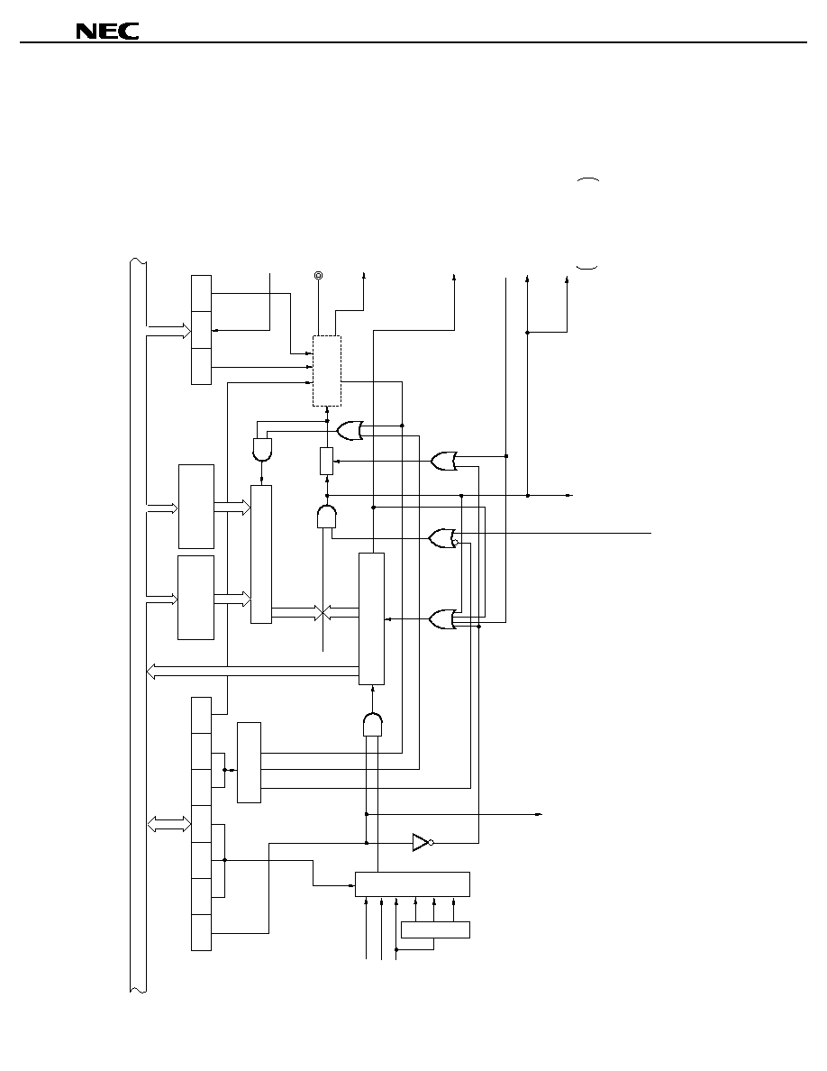
P
r
el
i
m
i
nary P
r
oduct Informati
on U
14673E
J1V
0
P
M
00
34
µ
µ
µ
µ
P
D
789322,789324,789326,789327
TCE40 TCL402 TCL401 TCL400 TMD401 TMD400 TOE40
8-bit timer mode control
register 40 (TMC40)
Decoder
8-bit timer counter 40
(TM40)
F/F
TM30 match signal
(in cascade connection mode)
Count operation start signal to timer 30
(in cascade connection mode)
TM40 timer counter match signal
(in cascade connection mode)
Clear
f
X
f
X
/2
2
8-bit compare
register 40 (CR40)
Selector
Output control
circuit
Note
RMC40 NRZB40 NRZ40
Carrier generator output
control register 40 (TCA40)
To Figure 5-11 (D)
count clock input
signal to TM30
Internal reset signal
INTTM40
Bit 7 of TM40
(in cascade connection mode)
To Figure 5-11 (A)
To Figure 5-11 (F)
To Figure 5-11 (E)
Match
TO40/P60
To Figure 5-11 (C)
Carrier clock (in carrier generator mode)
or timer 40 output signal
(in other than carrier generator mode)
Reset
Carrier generator mode
PWM mode
Cascade connection mode
Figure 5-12. Block Diagram of Timer 40
Note Refer to Figure 5-13 for details.
8-bit H width compare
register 40 (CRH40)
Internal bus
Selector
OVF
Prescaler
f
X
/2
f
X
/2
2
f
X
/2
3
f
X
/2
4
Timer 40 interrupt request signal
To Figure 5-11 (B)
Timer counter match signal from
timer 30 (in carrier generator mode)
From Figure 5-11 (G)
Preliminary Product Information U14673EJ1V0PM00
35
µ
µ
µ
µ
PD789322,789324,789326,789327
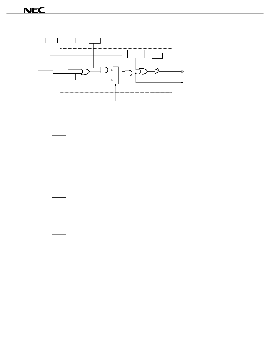
Figure 5-13. Block Diagram of Output Control Circuit (Timer 40)
F/F
RMC40
NRZ40
TOE40
PM60
P60
output latch
Selector
TO40/P60
Carrier generator mode
Carrier clock (in carrier generator mode)
or timer 40 output signal
(in other than carrier generator mode)
(1) 8-bit compare register 30 (CR30)
A value specified in CR30 is compared with the count value in 8-bit timer counter 30 (TM30), and if they
match, an interrupt request (INTTM30) is generated.
CR30 is set using an 8-bit memory manipulation instruction.
RESET input makes this register undefined.
Caution CR30 cannot be used in carrier generator mode or PWM output mode.
(2) 8-bit compare register 40 (CR40)
A value specified in CR40 is compared with the count value in 8-bit timer counter 40 (TM40), and if they
match, an interrupt request (INTTM40) is generated. When operating as a 16-bit timer in cascade
connection with TM30, an interrupt request (INTTM40) is only generated if both CR30 and TM30, and CR40
and TM40 match simultaneously (INTTM30 is not issued).
CR40 is set using an 8-bit memory manipulation instruction.
RESET input makes this register undefined.
(3) 8-bit H width compare register (CRH40)
In carrier generator mode or PWM output mode, a timer output high-level width can be set by writing a value
to CRH40.
CRH40 is set using an 8-bit memory manipulation instruction.
RESET input makes this register undefined.

Preliminary Product Information U14673EJ1V0PM00
36
µ
µ
µ
µ
PD789322,789324,789326,789327
(4) 8-bit timer counter 30, 40 (TM30, TM40)
This is an 8-bit register for counting the count pulses.
TM30 and TM40 can be read with a 1-bit or 8-bit memory manipulation instruction.
RESET input sets these registers to 00H.
The conditions under which TM30 and TM40 are cleared to 00H are listed below.
(a) Discrete mode
(i)
TM30
∑
Upon a reset
∑
When TCE30 (bit 7 of 8-bit timer mode control register 30 (TMC30)) is cleared to 0
∑
Upon a match between TM30 and CR30
∑
If the TM30 count value overflows
(ii) TM40
∑
Upon a reset
∑
When TCE40 (bit 7 of 8-bit timer mode control register 40 (TMC40)) is cleared to 0
∑
Upon a match between TM40 and CR40
∑
If the TM40 count value overflows
(b) Cascade connection mode (TM30 and TM40 cleared to 00H simultaneously)
∑
Upon a reset
∑
When the TCE40 flag is cleared to 0
∑
Upon a simultaneous match between TM30 and CR30, and TM40 and CR40
∑
If the TM30 and TM40 count values overflow simultaneously
(c) Carrier generator/PWM output mode (TM40 only)
∑
Upon a reset
∑
When the TCE40 flag is cleared to 0
∑
Upon a match between TM40 and CR40
∑
Upon a match between TM40 and CRH40
∑
If the TM40 count value overflows

Preliminary Product Information U14673EJ1V0PM00
37
µ
µ
µ
µ
PD789322,789324,789326,789327
5.3.3 8-bit timer 30, 40 control registers
8-bit timers 30 and 40 are controlled by the following 4 registers.
∑
8-bit timer mode control register 30 (TMC30)
∑
8-bit timer mode control register 40 (TMC40)
∑
Carrier generator output control register 40 (TCA40)
∑
Port mode register 6 (PM6)
Preliminary Product Information U14673EJ1V0PM00
38
µ
µ
µ
µ
PD789322,789324,789326,789327
(1) 8-bit timer mode control register 30 (TMC30)
This register is used to control the timer 30 count clock and operation mode settings.
TMC30 is set using a 1-bit or 8-bit memory manipulation instruction.
RESET input sets this register to 00H.
Figure 5-14. Format of 8-Bit Timer Mode Control Register 30
Symbol
<7>
6
5
4
3
2
1
0
Address
After reset
R/W
TMC30
TCE30
0
0
TCL301
TCL300
0
TMD300
0
FF65H
00H
R/W
TCE30
TM30 count control operation
Note 1
0
TM30 count value cleared and operation stopped
1
Count operation starts
TCL301
TCL300
Timer 30 count clock selection
0
0
f
X
/2
6
(78.1
kHz)
0
1
f
X
/2
8
(19.5 kHz)
1
0
Timer 40 match signal
1
1
Carrier clock (in carrier generator mode) or timer 40 output signal (in other than carrier generator
mode)
TMD300
TMD401
TMD400
Timer 30, timer 40 operation mode selection
Note 2
0
0
0
Discrete mode
1
0
1
Cascade connection mode
0
1
1
Carrier generator mode
0
1
0
PWM output mode
Other than above
Setting prohibited
Notes 1. The TCE30 setting will be ignored in cascade mode because in this case the count operation is
controlled by TCE40 (bit 7 of TMC40).
2. The operation mode selection is made using a combination of TMC30 and TMC40 register settings.
Caution In cascade connection mode, the timer 40 output signal is forcibly selected for the count
clock.
Remarks 1. f
X
: Main system clock oscillation frequency
2. The parenthesized values apply to operation at f
X
= 5.0 MHz
Preliminary Product Information U14673EJ1V0PM00
39
µ
µ
µ
µ
PD789322,789324,789326,789327
(2) 8-bit timer mode control register 40 (TMC40)
This register is used to control the timer 40 count clock and operation mode settings.
TMC40 is set using a 1-bit or 8-bit memory manipulation instruction.
RESET input sets this register to 00H.
Figure 5-15. Format of 8-Bit Timer Mode Control Register 40
Symbol
<7>
6
5
4
3
2
1
<0>
Address
After reset
R/W
TMC40
TCE40
0
TCL402
TCL401
TCL400
TMD401
TMD400
TOE40
FF69H
00H
R/W
TCE40
TM40 count control operation
Note 1
0
TM40 count value cleared and operation stopped (in cascade connection mode, the count value of TM30 is
cleared at the same time)
1
Count operation starts (in cascade connection mode, the count operation of TM30 starts at the same time)
TCL402
TCL401
TCL400
Timer 40 count clock selection
0
0
0
f
X
(5 MHz)
0
0
1
f
X
/2
2
(1.25 MHz)
0
1
0
f
X
/2 (2.5 MHz)
0
1
1
f
X
/2
2
(1.25 MHz)
1
0
0
f
X
/2
3
(625 kHz)
1
0
1
f
X
/2
4
(313 kHz)
Other than above
Setting prohibited
TMD300
TMD401
TMD400
Timer 30, timer 40 operation mode selection
Note 2
0
0
0
Discrete mode
1
0
1
Cascade connection mode
0
1
1
Carrier generator mode
0
1
0
PWM output mode
Other than above
Setting prohibited
TOE40
Timer output control
0
Output disabled (port mode)
1
Output enabled
Notes 1. The TCE30 setting will be ignored in cascade mode because in this case the count operation is
controlled by TCE40 (bit 7 of TMC40).
2. The operation mode selection is made using a combination of TMC30 and TMC40 register settings.
Remarks 1. f
X
: Main system clock oscillation frequency
2. The parenthesized values apply to operation at f
X
= 5.0 MHz
Preliminary Product Information U14673EJ1V0PM00
40
µ
µ
µ
µ
PD789322,789324,789326,789327
(3) Carrier generator output control register 40 (TCA40)
This register is used to set the timer output data in the carrier generator mode.
TCA40 is set using a 1-bit or 8-bit memory manipulation instruction.
RESET input sets this register to 00H.
Figure 5-16. Format of Carrier Generator Output Control Register 40
Symbol
7
6
5
4
3
<2>
<1>
<0>
Address
After reset
R/W
TCA40
0
0
0
0
0
RMC40
NRZB40
NRZ40
FF6AH
00H
W
RMC40
Remote controller output control
0
When NRZ40 = 1, a carrier pulse is output to the TO40/P60 pin
1
When NRZ40 = 1, a high level is output to the TO40/P60 pin
NRZB40
This bit stores the data that NRZ40 will output next. Data is transferred to NRZ40 upon the generation of a
timer 30 match signal.
NRZ40
No return, zero data
0
A low level is output (the carrier clock is stopped)
1
A carrier pulse is output
Caution TCA40 cannot be set with a 1-bit memory manipulation instruction.
Be sure to set it with an 8-bit memory manipulation instruction.
(4) Port mode register 6 (PM6)
This register is used to set port 6 to input or output in 1-bit units.
When the TO40/P60 pin is used as a timer output, set the PM60 and P60 output latches to 0.
PM6 is set using a 1-bit or 8-bit memory manipulation instruction.
RESET input sets this register to FFH.
Figure 5-17. Format of Port Mode Register 6
Symbol
7
6
5
4
3
2
1
0
Address
After reset
R/W
PM6
1
1
1
1
1
1
PM61
PM60
FF26H
FFH
R/W
PM6n
Input/output mode of pin P6n (n = 0, 1)
0
Output mode (output buffer on)
1
Input mode (output buffer off)
Preliminary Product Information U14673EJ1V0PM00
41
µ
µ
µ
µ
PD789322,789324,789326,789327
5.4 Watch Timer
5.4.1 Watch timer functions
The watch timer has the following functions.
∑
Watch timer
∑
Interval timer
The watch and interval timers can be used at the same time.
Figure 5-18 shows a block diagram of the watch timer.
Figure 5-18. Watch Timer Block Diagram
f
X
/2
7
f
XT
Selector
f
W
f
W
2
4
f
W
2
5
f
W
2
6
f
W
2
7
f
W
2
8
f
W
2
9
Clear
9-bit prescaler
Selector
Clear
5-bit counter
INTWT
INTWTI
WTM7 WTM6 WTM5 WTM4 WTM1 WTM0
Watch timer mode control
register (WTM)
Internal bus
Preliminary Product Information U14673EJ1V0PM00
42
µ
µ
µ
µ
PD789322,789324,789326,789327
(1) Watch timer
An interrupt request (INTWT) is generated at 0.5-second intervals using the 4.19-MHz main system clock or
32.768-kHz subsystem clock.
Caution
When the main system clock is operating at 5.0 MHz, it cannot be used to generate a 0.5-second
interval. In this case, the subsystem clock, which operates at 32.768 kHz, should be used
instead.
(2) Interval timer
The interval timer is used to generate an interrupt request (INTWTI) at preset intervals.
Table 5-7. Interval Time of Interval Timer
Interval Time
At f
X
= 5.0 MHz Operation
At f
X
= 4.19 MHz Operation
At f
XT
= 32.768 kHz Operation
2
4
◊
1/f
W
409.6
µ
s
488
µ
s
488
µ
s
2
5
◊
1/f
W
819.2
µ
s
977
µ
s
977
µ
s
2
6
◊
1/f
W
1.64 ms
1.95 ms
1.95 ms
2
7
◊
1/f
W
3.28 ms
3.91 ms
3.91 ms
2
8
◊
1/f
W
6.55 ms
7.81 ms
7.81 ms
2
9
◊
1/f
W
13.1 ms
15.6 ms
15.6 ms
Remarks 1. f
W
: Watch timer clock frequency (f
X
/2
7
or f
XT
)
2. f
X
: Main system clock oscillation frequency
3. f
XT
: Subsystem clock oscillation frequency
5.4.2 Watch timer configuration
The watch timer consists of the following hardware.
Table 5-8. Watch Timer Configuration
Item
Configuration
Counter
5 bits
◊
1
Prescaler
9 bits
◊
1
Control register
Watch timer mode control register (WTM)
Preliminary Product Information U14673EJ1V0PM00
43
µ
µ
µ
µ
PD789322,789324,789326,789327
5.4.3 Watch timer control register
The following register controls the watch timer.
∑
Watch timer mode control register (WTM)
(1) Watch timer mode control register (WTM)
This register is used to enable/disable the count clock and operation of the watch timer and set the interval
time of the prescaler and operation control of the 5-bit counter.
WTM is set using a 1-bit or 8-bit memory manipulation instruction.
RESET input sets this register to 00H.
Figure 5-19. Format of Watch Timer Mode Control Register
Symbol
7
6
5
4
3
2
<1>
<0>
Address
After reset
R/W
WTM
WTM7
WTM6
WTM5
WTM4
0
0
WTM1
WTM0
FF4AH
00H
R/W
WTM7
Watch timer count clock (f
W
) selection
0
f
X
/2
7
(39.1 kHz)
1
f
XT
(32.768 kHz)
WTM6
WTM5
WTM4
Prescaler interval time selection
0
0
0
2
4
/f
W
0
0
1
2
5
/f
W
0
1
0
2
6
/f
W
0
1
1
2
7
/f
W
1
0
0
2
8
/f
W
1
0
1
2
9
/f
W
Other than above
Setting prohibited
WTM1
5-bit counter operation control
0
Cleared after operation stopped
1
Start
WTM0
Watch timer operation enable
0
Operation stopped (both prescaler and timer cleared)
1
Operation enabled
Remarks 1. f
W
: Watch timer clock frequency (f
X
/2
7
or f
XT
)
2. f
X
: Main system clock oscillation frequency
3. f
XT
: Subsystem clock oscillation frequency
4. The parenthesized values apply to operation at f
X
= 5.0 MHz or f
XT
= 32.768 kHz.

Preliminary Product Information U14673EJ1V0PM00
44
µ
µ
µ
µ
PD789322,789324,789326,789327
5.5 Watchdog Timer
5.5.1 Watchdog timer functions
The watchdog timer has the following functions.
(1) Watchdog timer
The watchdog timer is used to detect a program runaway. If a runaway is detected, either a non-maskable
interrupt or the RESET signal can be generated.
(2) Interval timer
The interval timer is used to generate interrupts at preset intervals.
5.5.2 Watchdog timer configuration
The watchdog timer consists of the following hardware.
Table 5-9. Watchdog Timer Configuration
Item
Configuration
Control register
Watchdog timer mode register (WDTM)
Figure 5-20. Watchdog Timer Block Diagram
Internal bus
Internal bus
7-bit counter
Control circuit
Clear
WDTIF
WDTMK
Watchdog timer mode register
(WDTM)
WDTM4 WDTM3
INTWDT
maskable
interrupt request
RESET
INTWDT
non-maskable
interrupt request
f
X
2
4
RUN

Preliminary Product Information U14673EJ1V0PM00
45
µ
µ
µ
µ
PD789322,789324,789326,789327
5.5.3 Watchdog timer control register
The watchdog timer is controlled by the following register.
∑
Watchdog timer mode register (WDTM)
(1) Watchdog timer mode register (WDTM)
This register is used to set the watchdog timer operation mode and whether to enable or disable counting.
WDTM is set using a 1-bit or 8-bit memory manipulation instruction.
RESET input sets this register to 00H.
Figure 5-21. Format of Watchdog Timer Mode Register
Symbol
<7>
6
5
4
3
2
1
0
Address
After reset
R/W
WDTM
RUN
0
0
WDTM4
WDTM3
0
0
0
FFF9H
00H
R/W
RUN
Watchdog timer operation selection
Note 1
0
Counting stopped
1
Counter cleared and counting starts
WDTM4
WDTM3
Watchdog timer operation mode selection
Note 2
0
0
Operation stopped
0
1
Interval timer mode (when an overflow occurs, a maskable interrupt is generated)
Note 3
1
0
Watchdog timer mode 1 (when an overflow occurs, a non-maskable interrupt is generated)
1
1
Watchdog timer mode 2 (when an overflow occurs, a reset operation is activated)
Notes 1. Once the RUN bit has been set (1), it is impossible to clear it (0) by software. Consequently, once
counting begins, it cannot be stopped by any means other than RESET input.
2. Once WDTM3 and WDTM4 have been set (1), it is impossible to clear them (0) by software.
3. The interval timer starts operating as soon as the RUN bit is set to 1.
Cautions 1. When the RUN bit is set to 1, and the watchdog timer is cleared, the actual overflow time
will be up to 0.8% shorter than the time specified by the watchdog timer clock selection
register.
2. To use watchdog timer mode 1 or 2, be sure to set WDTM4 to 1 after confirming that
WDTIF (bit 0 of interrupt request flag 0 (IF0)) has been set to 0. If WDTIF is 1, selecting
watchdog timer mode 1 or 2 causes a non-maskable interrupt to be generated the instant
rewriting ends.
Preliminary Product Information U14673EJ1V0PM00
46
µ
µ
µ
µ
PD789322,789324,789326,789327
5.6 Serial Interface 10
5.6.1 Functions of serial interface 10
Serial interface 10 has the following two modes.
∑
Operation stopped mode
∑
3-wire serial I/O mode
(1) Operation stopped mode
This mode is used to minimize power consumption when serial transfer is not performed.
(2) 3-wire serial I/O mode (switchable between MSB-first and LSB-first transmission)
This mode is used to transmit 8-bit data, using three lines: a serial clock line (SCK10) and two serial data lines
(SI10 and SO10).
As 3-wire serial I/O mode supports simultaneous transmission and reception, the time required for data
processing can be reduced.
In 3-wire serial I/O mode, it is possible to select whether 8-bit data transmission begins with the MSB or LSB,
allowing serial interface 10 to be connected to any device regardless of whether that device is designed for
MSB-first or LSB-first transmission.
3-wire serial I/O mode is effective for connecting peripheral I/O circuits and display controllers having
conventional clock synchronous serial interfaces, such as those of the 75XL, 78K, and 17K Series devices.
5.6.2 Configuration of serial interface 10
Serial interface 10 consists of the following hardware.
Table 5-10. Configuration of Serial Interface 10
Item
Configuration
Register
Transmission/reception shift register 10 (SIO10)
Control register
Serial operation mode register 10 (CSIM10)
(1) Transmission/reception shift register 10 (SIO10)
This is an 8-bit register used for parallel/serial data conversion and for serial transmission or reception in
synchronization with the serial clock.
SIO10 is set using an 8-bit memory manipulation instruction.
RESET input makes this register undefined.
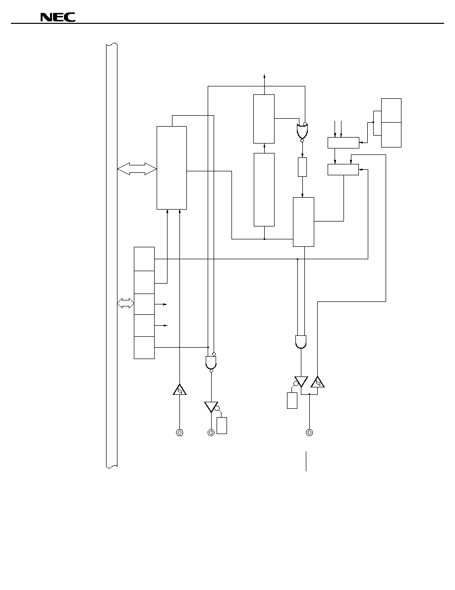
P
r
el
i
m
i
nary P
r
oduct Informati
on U
14673E
J1V
0
P
M
00
47
µ
µ
µ
µ
P
D
789322,789324,789326,789327
Internal bus
SI10/P22
Serial operation mode register 10
(CSIM10)
CSIE10 TPS101 TPS100 DIR10 CSCK10
Transmission/reception shift
register 10 (SIO10)
SO10/P21
PM21
PM20
SCK10/P20
Serial clock counter
Interrupt request
generator
Clock control
circuit
Selector
Selector
INTCSI10
F/F
TPS101 TPS100
f
X
/2
2
f
X
/2
3
Figure 5-22. Block Diagram of Serial Interface 10

Preliminary Product Information U14673EJ1V0PM00
48
µ
µ
µ
µ
PD789322,789324,789326,789327
5.6.3 Control register for serial interface 10
Serial interface 10 is controlled by the following register.
∑
Serial operation mode register 10 (CSIM10)
Figure 5-23. Format of Serial Operation Mode Register 10
Symbol
<7>
6
5
4
3
2
1
0
Address
After reset
R/W
CSIM10
CSIE10
0
TPS101
TPS100
0
DIR10
CSCK10
0
FF72H
00H
R/W
CSIE10
3-wire serial I/O mode operation control
0
Operation stopped
1
Operation enabled
TPS101
TPS100
Selection of count clock when internal clock selected
0
0
f
X
/2
2
(1.25 MHz)
0
1
f
X
/2
3
(625 kHz)
Other than above
Setting prohibited
DIR10
First-bit specification
0
MSB
1
LSB
CSCK10
SIO10 clock selection
0
External clock pulse input to the SCK10 pin
1
Internal clock selected with TPS100, TPS101
Cautions 1. Bits 0, 3 and 6 must be fixed to 0.
2. Be sure to switch to operation mode after stopping the serial transmission/reception
operation.
Remarks 1. f
X
: Main system clock oscillation frequency
2. The parenthesized values apply to operation at f
X
= 5.0 MHz.
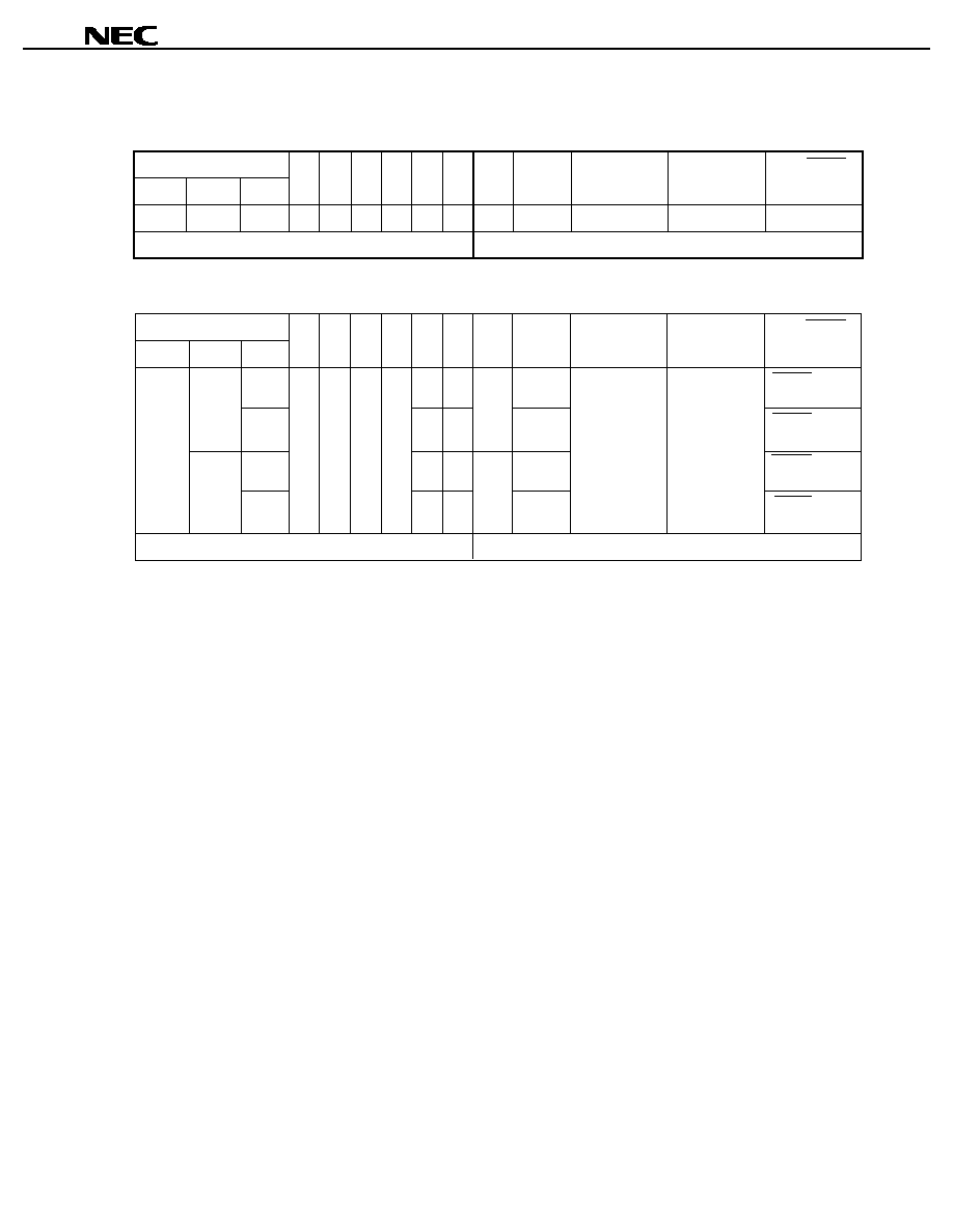
Preliminary Product Information U14673EJ1V0PM00
49
µ
µ
µ
µ
PD789322,789324,789326,789327
Table 5-11. Operation Mode Settings for Serial Interface 10
(1) Operation stopped mode
First
Bit
P22/SI10
Pin Function
P21/SO10
Pin Function
P20/SCK10
Pin Function
P22
P21
P20
CSIE10
0
CSIM10
DIR10
◊
CSCK10
◊
PM22
◊
Note 1
P22
◊
Note 1
PM21
◊
Note 1
P21
◊
Note 1
PM20
◊
Note 1
P20
◊
Note 1
Shift
Clock
Setting prohibited
Other than above
-
-
(2) 3-wire serial I/O mode
First
Bit
P22/SI10
Pin Function
P21/SO10
Pin Function
P20/SCK10
Pin Function
MSB
LSB
SI10
Note 2
SO10
(CMOS output)
SCK10 input
SCK10 output
SCK10 input
SCK10 output
CSIE10
1
CSIM10
DIR10
0
1
CSCK10
0
1
0
1
PM22
1
Note 2
P22
◊
Note 2
PM21
0
P21
1
PM20
1
0
1
0
P20
◊
1
◊
1
Shift
Clock
External
clock
Internal
clock
External
clock
Internal
clock
Setting prohibited
Other than above
Notes 1. Can be used freely as a port
2. Can be used as P22 (CMOS I/O) only when transmitting
Remark
◊
: don't care
Preliminary Product Information U14673EJ1V0PM00
50
µ
µ
µ
µ
PD789322,789324,789326,789327
5.7 LCD Controller/Driver
5.7.1 LCD controller/driver functions
The LCD controller/driver incorporated in the
µ
PD789322, 789324, 789326, and 789327 has the following
features.
(1) Segment and common signals based on the automatic reading of the display data memory can be
automatically output
(2) Four types of frame frequencies are selectable
(3) 24 segment signal outputs (S0 to S23), 4 common signal outputs (COM0 to COM3)
(4) Operation with a subsystem clock is possible
The maximum number of displayable pixels is shown in Table 5-12 below.
Table 5-12. Maximum Number of Display Pixels
Bias Method
Time Division
Common Signals Used
Maximum Number of Display Pixels
1/3
4
COM0 to COM3
96 (24 segments
◊
4 commons)
Note The LCD panel of the figure
consists of 12 rows with 2 segments per row.
5.7.2 LCD controller/driver configuration
The LCD controller/driver consists of the following hardware.
Table 5-13. Configuration of LCD Controller/Driver
Item
Configuration
Display outputs
Segment signals: 24
Common signals: 4
Control registers
LCD display mode register 0 (LCDM0)
LCD clock control register 0 (LCDC0)
Port function register 8 (PF8)
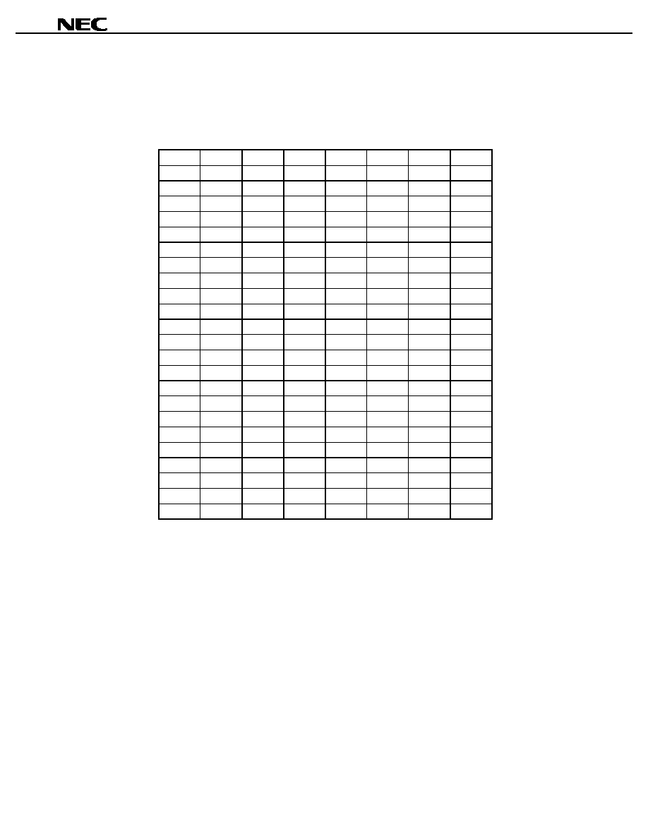
Preliminary Product Information U14673EJ1V0PM00
51
µ
µ
µ
µ
PD789322,789324,789326,789327
The correspondence with the LCD display RAM is shown in Figure 5-24 below.
Figure 5-24. Correspondence with LCD Display RAM
Address
Bit
Segment
7
6
5
4
3
2
1
0
FA17H
0
0
0
0
S23
FA16H
0
0
0
0
S22
FA15H
0
0
0
0
S21
FA14H
0
0
0
0
S20
FA13H
0
0
0
0
S19
FA12H
0
0
0
0
S18
FA11H
0
0
0
0
S17
FA10H
0
0
0
0
S16
FA0FH
0
0
0
0
S15
FA0EH
0
0
0
0
S14
FA0DH
0
0
0
0
S13
FA0CH
0
0
0
0
S12
FA0BH
0
0
0
0
S11
FA0AH
0
0
0
0
S10
FA09H
0
0
0
0
S9
FA08H
0
0
0
0
S8
FA07H
0
0
0
0
S7
FA06H
0
0
0
0
S6
FA05H
0
0
0
0
S5
FA04H
0
0
0
0
S4
FA03H
0
0
0
0
S3
FA02H
0
0
0
0
S2
FA01H
0
0
0
0
S1
FA00H
0
0
0
0
S0
Common
COM3
COM2
COM1
COM0
Remark Bits 4 to 7 are fixed to 0.
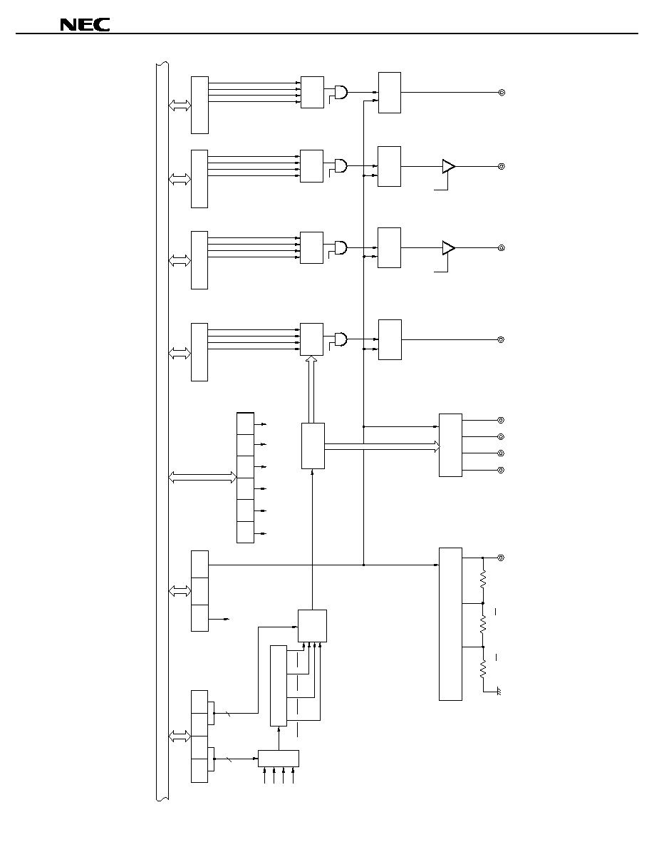
P
r
el
i
m
i
nary P
r
oduct Informati
on U
14673E
J1V
0
P
M
00
52
µ
µ
µ
µ
P
D
789322,789324,789326,789327
Internal bus
LCDC03 LCDC02 LCDC01 LCDC00
2
2
Selector
Prescaker
LCD clock
selection
circuit
Selector
f
CLK
2
6
f
CLK
2
7
f
CLK
2
8
f
CLK
2
9
LCD clock control register 0
(LCDC0)
LCDON0
VAON0
LCD display mode
register 0 (LCDM0)
LCD drive voltage control circuit
V
LC0
V
LC0
V
LC0
Segment
driver
Common driver
COM0 COM1 COM2 COM3
3 2 1 0
3 2 1 0
6 5
7
4
FA00H
Display data memory
LCDON0
Selector
Segment
driver
3 2 1 0
3 2 1 0
6 5
7
4
FA16H
LCDON0
S22/P80
Timing
controller
f
X
/2
5
f
X
/2
6
f
X
/2
7
f
XT
S0
. . . . .
. . . . . . . . . .
f
CLK
1
3
2
3
V
SS
R
LCD
R
LCD
R
LCD
Selector
Segment
driver
3 2 1 0
3 2 1 0
6 5 4
FA17H
LCDON0
S23
PF85 PF84 PF83 PF82
PF80
PF81
Port function
register 8 (PF8)
PF80
Selector
Segment
driver
3 2 1 0
3 2 1 0
6 5
7
4
FA11H
LCDON0
S17/P85
PF85
. . .
. . . .
. . . . .
f
LCD
LIPS0
Figure 5-25. LCD Controller/Driver Block Diagram
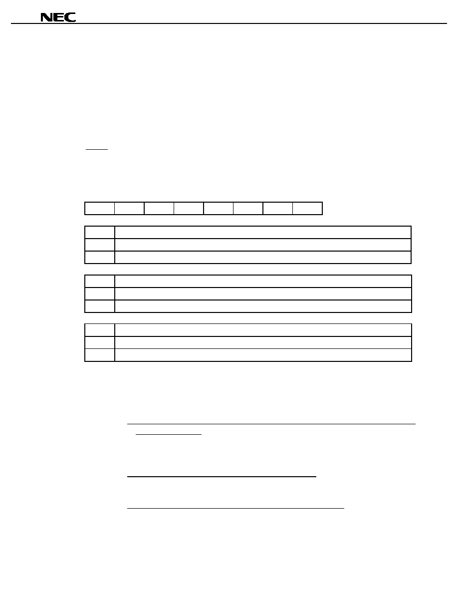
Preliminary Product Information U14673EJ1V0PM00
53
µ
µ
µ
µ
PD789322,789324,789326,789327
5.7.3 LCD controller/driver control registers
The LCD controller/driver is controlled by the following three registers.
∑
LCD display mode register 0 (LCDM0)
∑
LCD clock control register 0 (LCDC0)
∑
Port function register 8 (PF8)
(1) LCD display mode register 0 (LCDM0)
This register is used to enable/disable operation, and set the operation mode and the supply of power for LCD drive.
LCDM0 is set using a 1-bit or 8-bit memory manipulation instruction.
RESET input sets this register to 00H.
Figure 5-26. Format of LCD Display Mode Register 0
Symbol
<7>
<6>
5
<4>
3
2
1
0
Address
After reset
R/W
LCDM0 LCDON0
VAON0
0
LIPS0
0
0
0
0
FFB0H
00H
R/W
LCDON0
LCD display enable/disable
0
Display off (all segment outputs are unselected for signal output)
1
Display on
VAON0
LCD controller/driver operation mode
Note
0
No internal booster (for 2.7- to 5.5-V display)
1
Internal booster enabled (for 1.8- to 5.5-V display)
LIPS0
Supply of power for LCD drive
Note
0
Power not supplied for LCD drive
1
Power supplied for LCD drive
Note To reduce power consumption when the LCD display is not being used, set VAON0 and LIPS0 to 0.
Cautions 1. Always set bits 0 to 3 and 5 to 0.
2. When manipulating VAON0, observe following procedure.
A. When internal booster is stopped after changing to the display off condition from the
display on condition
1) Set the display off condition by setting LCDON0 = 0.
2) Set all segment buffers and common buffers to output disabled by setting LIPS0 = 0.
3) Stop the booster by setting VAON0 = 0.
B. When the booster is stopped in the display on condition
This is prohibited. Be sure to stop the booster after changing to the display off
condition.
C. When the display is turned on from the booster-stoped condition
1) Wait about 500 ms after starting the booster by setting VAON0 = 1.
2) Set all segment buffers and common buffers to signal output unselected by setting
LIPS0 = 1.
3) Set the display on condition by setting LCDON0 = 1.
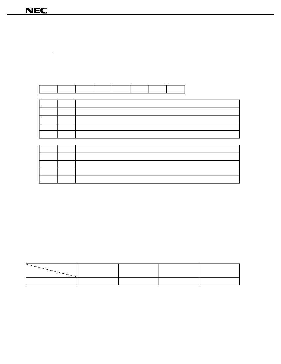
Preliminary Product Information U14673EJ1V0PM00
54
µ
µ
µ
µ
PD789322,789324,789326,789327
(2) LCD clock control register (LCDC0)
This register is used to set the internal and LCD clocks. The frame frequency is determined by the number of
LCD clock time divisions.
LCDC0 is set using a 1-bit or 8-bit memory manipulation instruction.
RESET input sets this register to 00H.
Figure 5-27. Format of LCD Clock Control Register 0
Symbol
7
6
5
4
3
2
1
0
Address
After reset
R/W
LCDC0
0
0
0
0
LCDC03
LCDC02
LCDC01
LCDC00
FFB2H
00H
R/W
LCDC03
LCDC02
Internal clock (f
CLK
) selection
Note
0
0
f
XT
(32.768 kHz)
0
1
f
X
/2
5
(156.3 kHz)
1
0
f
X
/2
6
(78.1 kHz)
1
1
f
X
/2
7
(39.1 kHz)
LCDC01
LCDC00
LCD clock (f
LCD
) selection
0
0
f
CLK
/2
6
0
1
f
CLK
/2
7
1
0
f
CLK
/2
8
1
1
f
CLK
/2
9
Note Select f
X
so that a clock of at least 32 kHz is set for the internal clock f
CLK
.
Remarks 1. f
X
: Main system clock oscillation frequency
2. f
XT
: Subsystem clock oscillation frequency
3. The parenthesized values apply to operation at f
X
= 5.0 MHz or f
XT
= 32.768 kHz
Caution
Always set bits 4 to 7 to 0.
Examples of the frame frequencies when the internal clock is f
XT
(32.768 kHz) are shown in Table 5-14 below.
Table 5-14. Frame Frequency (Hz)
LCD Clock (f
LCD
)
Time Division
f
XT
/2
9
(64 Hz)
f
XT
/2
8
(128 Hz)
f
XT
/2
7
(256 Hz)
f
XT
/2
6
(512 Hz)
4
16
32
64
128
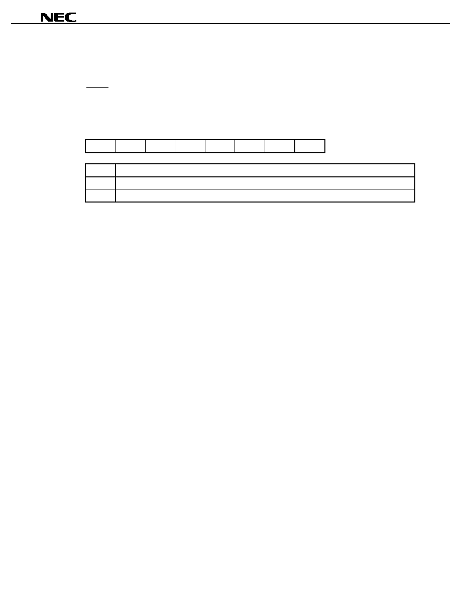
Preliminary Product Information U14673EJ1V0PM00
55
µ
µ
µ
µ
PD789322,789324,789326,789327
(3) Port function register 8 (PF8)
This register is used to select whether S17/P85 to S22/P80 are used as LCD segment signal outputs or
general-purpose ports.
PF8 is set using a 1-bit or 8-bit memory manipulation instruction.
RESET input sets this register to 00H.
Figure 5-28. Format of Port Function Register 8
Symbol
7
6
5
4
3
2
1
0
Address
After reset
R/W
PF8
0
0
PF85
PF84
PF83
PF82
PF81
PF80
FF58H
00H
R/W
PF8n
Port function of P8n (n = 0 to 5)
0
Operates as a general-purpose port
1
Operates as an LCD segment signal output

Preliminary Product Information U14673EJ1V0PM00
56
µ
µ
µ
µ
PD789322,789324,789326,789327
6. INTERRUPT FUNCTION
6.1 Interrupt Types
Two types of interrupts are supported.
(1) Non-maskable interrupts
Non-maskable interrupt requests are acknowledged unconditionally, i.e. even when interrupts are disabled.
These interrupts take precedence over all other interrupts and are not subject to interrupt priority control.
A non-maskable interrupt causes the generation of the standby release signal.
An interrupt from the watchdog timer is the only non-maskable interrupt source supported in the
µ
PD789322,
789324, 789326, and 789327.
(2) Maskable interrupts
Maskable interrupts are subject to mask control. If two or more maskable interrupts occur simultaneously, the
default priority listed in Table 6-1 applies.
A maskable interrupt causes the generation of the standby release signal.
Maskable interrupts from 2 external and 6 internal sources are supported in the
µ
PD789322, 789324, 789326,
and 789327.
6.2 Interrupt Sources and Configuration
The
µ
PD789322, 789324, 789326, and 789327 support a total of 9 maskable and non-maskable interrupt
sources (see Table 6-1).
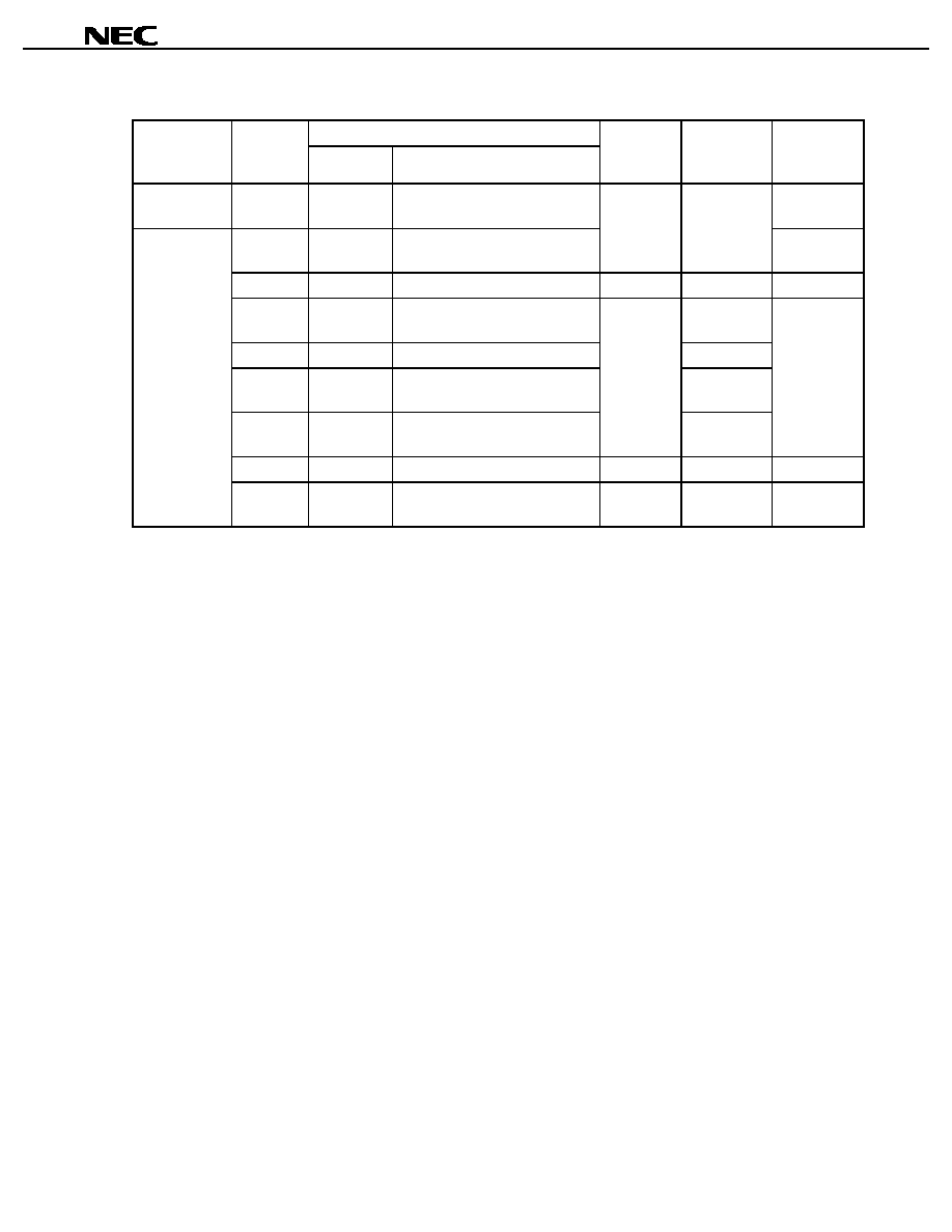
Preliminary Product Information U14673EJ1V0PM00
57
µ
µ
µ
µ
PD789322,789324,789326,789327
Table 6-1. Interrupt Sources
Interrupt Source
Interrupt Type
Default
Priority
Note 1
Name
Trigger
Internal/
External
Vector Table
Address
Basic
Configuration
Type
Note 2
Non-maskable
-
INTWDT
Watchdog timer overflow (with
watchdog timer mode 1 selected)
(A)
0
INTWDT
Watchdog timer overflow (with
interval timer mode selected)
Internal
0004H
(B)
1
INTP0
Pin input edge detection
External
0006H
(C)
2
INTCSI10
End of serial interface 10 3-wire
SIO transfer reception
0008H
3
INTWT
Watch timer interrupt
000AH
4
INTTM30
Generation of 8-bit timer 30
matching signal
000CH
5
INTTM40
Generation of 8-bit timer 40
matching signal
Internal
000EH
(B)
6
INTKR00
Key return signal detection
External
0010H
(C)
Maskable
7
INTWTI
Watch timer interval timer
interrupt
Internal
0012H
(B)
Notes 1. Default priority is the priority order when more than one maskable interrupt request is generated at the
same time. 0 is the highest priority and 7 is the lowest.
2. Basic configuration types (A), (B), and (C) correspond to (A), (B), and (C) in Figure 6-1.
Remark Only one of the two watchdog timer interrupt sources, non-maskable or maskable (internal), can be
selected.
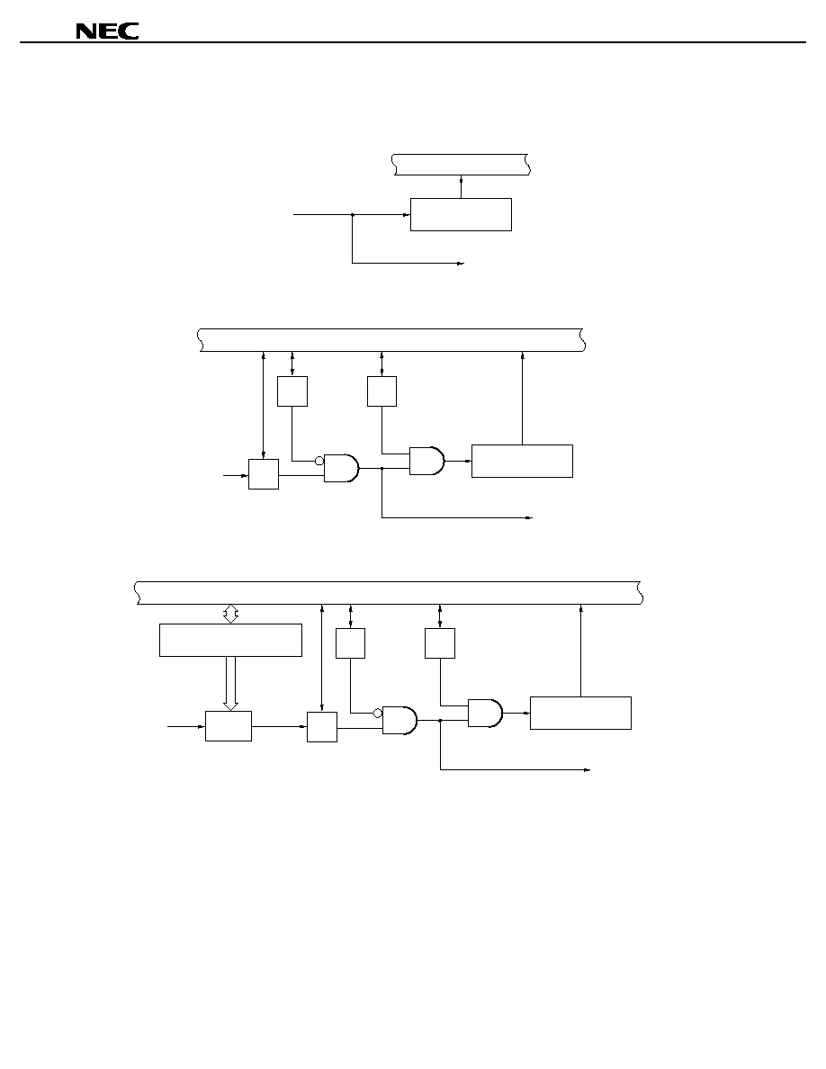
Preliminary Product Information U14673EJ1V0PM00
58
µ
µ
µ
µ
PD789322,789324,789326,789327
Figure 6-1. Basic Configuration of Interrupt Function
(A) Internal non-maskable interrupt
Internal bus
Interrupt request
Vector table
address generator
Standby release signal
(B) Internal maskable interrupt
Internal bus
MK
IF
Interrupt request
IE
Vector table
address generator
Standby release signal
(C) External maskable interrupt
Internal bus
INTM0, KRM00
MK
IF
IE
Vector table
address generator
Standby release signal
Edge
detection
circuit
Interrupt request
INTM0: External interrupt mode register 0
KRM00: Key return mode register 00
IF:
Interrupt request flag
IE:
Interrupt enable flag
MK:
Interrupt mask flag
Preliminary Product Information U14673EJ1V0PM00
59
µ
µ
µ
µ
PD789322,789324,789326,789327
6.3 Interrupt Function Control Registers
Interrupts are controlled by the following five registers.
∑
Interrupt request flag register 0 (IF0)
∑
Interrupt mask flag register 0 (MK0)
∑
External interrupt mode register 0 (INTM0)
∑
Program status word (PSW)
∑
Key return mode register 00 (KRM00)
Table 6-2 lists the interrupt requests and the corresponding interrupt request and interrupt mask flags.
Table 6-2. Interrupt Request Signals and Corresponding Flags
Interrupt Request Signal
Interrupt Request Flag
Interrupt Mask Flag
INTWDT
INTP0
INTCSI0
INTWT
INTTM30
INTTM40
INTKR00
INTWTI
WDTIF
PIF0
CSIIF0
WTIF
TMIF30
TMIF40
KRIF00
WTIIF
WDTMK
PMK0
CSIMK0
WTMK
TMMK30
TMMK40
KRMK00
WTIMK

Preliminary Product Information U14673EJ1V0PM00
60
µ
µ
µ
µ
PD789322,789324,789326,789327
(1) Interrupt request flag register 0 (IF0)
An interrupt request flag is set (1) when the corresponding interrupt request is generated, or when an
instruction is executed. It is cleared (0) when the interrupt request is acknowledged, when the RESET signal
is input, or when an instruction is executed.
IF0 is set using a 1-bit or 8-bit memory manipulation instruction.
RESET input sets this register to 00H.
Figure 6-2. Format of Interrupt Request Flag Register 0
Symbol
<7>
<6>
<5>
<4>
<3>
<2>
<1>
<0>
Address
After reset
R/W
IF0
WTIIF
KRIF00
TMIF40
TMIF30
WTIF
CSIIF0
PIF0
WDTIF
FFE0H
00H
R/W
◊◊IF◊
Interrupt request flag
0
No interrupt request signal generated
1
An interrupt request signal is generated and an interrupt request made
Cautions 1. The WDTIF flag can be read/written only when the watchdog timer is being used as an
interval timer. It must be cleared to 0 if the watchdog timer is used in watchdog timer
mode 1 or 2.
2. Because P61 functions alternately as an external interrupt, when the output level
changes after the output mode of the port function is specified, the interrupt request flag
will be inadvertently set. Therefore, be sure to preset the interrupt mask flag (PMK0)
before using the port in output mode.
Preliminary Product Information U14673EJ1V0PM00
61
µ
µ
µ
µ
PD789322,789324,789326,789327
(2) Interrupt mask flag register 0 (MK0)
Interrupt mask flags are used to enable and disable the corresponding maskable interrupts.
MK0 is set using a 1-bit or 8-bit memory manipulation instruction.
RESET input sets this register to FFH.
Figure 6-3. Format of Interrupt Mask Flag Register 0
Symbol
<7>
<6>
<5>
<4>
<3>
<2>
<1>
<0>
Address
After reset
R/W
MK0
WTIMK
KRMK00 TMMK40 TMMK30
WTMK
CSIMK0
PMK0
WDTMK
FFE4H
FFH
R/W
◊◊MK
Interrupt servicing control
0
Interrupt servicing enabled
1
Interrupt servicing disabled
Cautions 1. When the watchdog timer is being used in watchdog timer mode 1 or 2, any attempt to
read the WDTMK flag results in an undefined value being detected.
2. Because P61 functions alternately as an external interrupt, when the output level
changes after the output mode of the port function is specified, the interrupt request flag
will be inadvertently set. Therefore, be sure to preset the interrupt mask flag (PMK0)
before using the port in output mode.
Preliminary Product Information U14673EJ1V0PM00
62
µ
µ
µ
µ
PD789322,789324,789326,789327
(3) External interrupt mode register 0 (INTM0)
This register is used to specify the valid edge for INTP0.
INTM0 is set using an 8-bit memory manipulation instruction.
RESET input sets this register to 00H.
Figure 6-4. Format of External Interrupt Mode Register 0
Symbol
7
6
5
4
3
2
1
0
Address
After reset
R/W
INTM0
0
0
0
0
ES01
ES00
0
0
FFECH
00H
R/W
ES01
ES00
INTP0 valid edge selection
0
0
Falling edge
0
1
Rising edge
1
0
Setting prohibited
1
1
Both rising and falling edges
Cautions 1. Always set bits 0, 1, and 4 to 7 to 0.
2. Before setting INTM0, set (1) the interrupt mask flag (PMK0) to disable interrupts.
To enable interrupts, clear (0) the interrupt request flag (PIF0), then clear (0) the interrupt
mask flag (PMK0).

Preliminary Product Information U14673EJ1V0PM00
63
µ
µ
µ
µ
PD789322,789324,789326,789327
(4) Program status word (PSW)
The program status word is used to hold the instruction execution results and the current status of the
interrupt requests. The IE flag, used to enable and disable maskable interrupts, is mapped to the PSW.
The PSW can be read and written in 8-bit units, as well as in 1-bit units by using bit manipulation instructions
and dedicated instructions (EI and DI). When a vector interrupt is acknowledged, the PSW is automatically
saved to the stack, and the IE flag is reset (0).
RESET input sets the PSW to 02H.
Figure 6-5. Program Status Word Configuration
IE
Z
0
AC
0
0
1
CY
PSW
Symbol
After reset
02H
7
6
5
4
3
2
1
0
Used in the execution of ordinary instructions
IE
0
1
Disabled
Enabled
Interrupt acknowledgement enable/disable
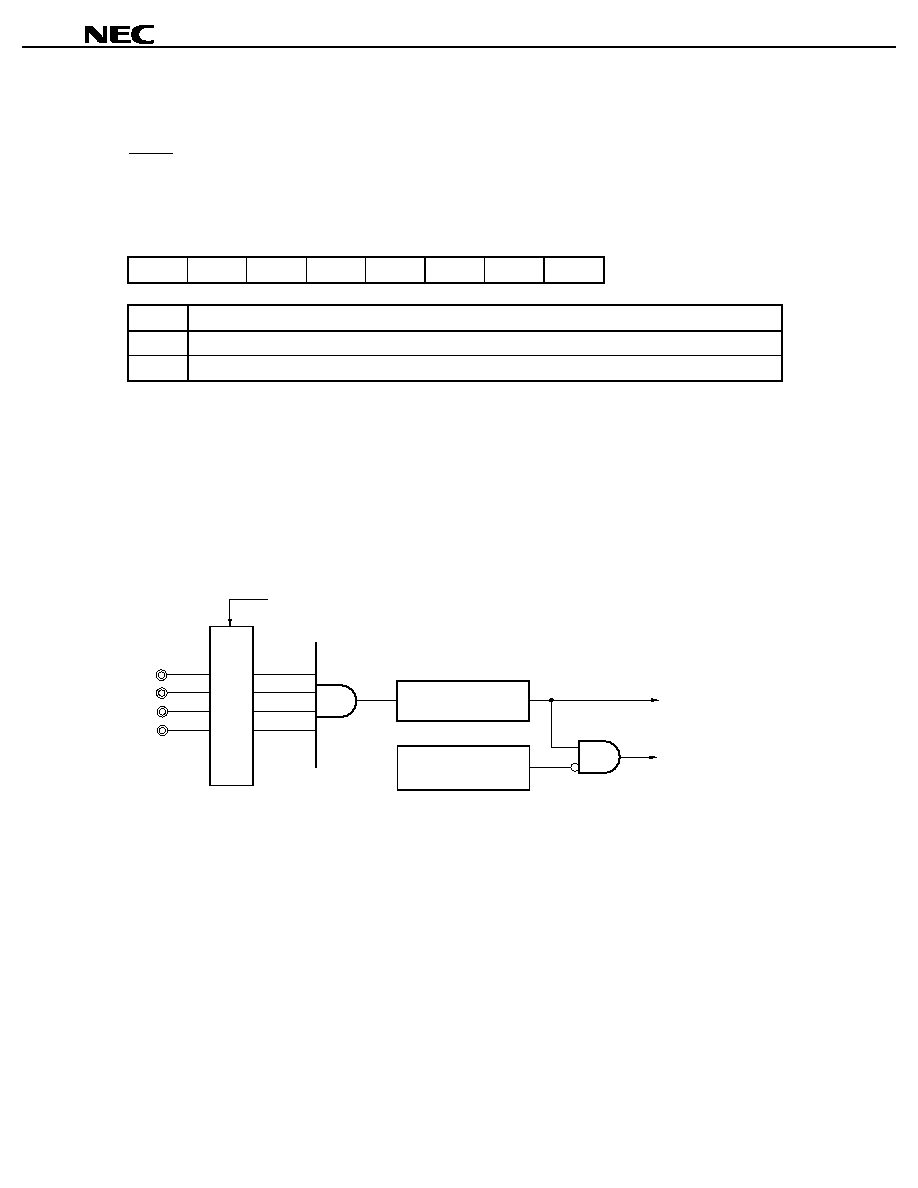
Preliminary Product Information U14673EJ1V0PM00
64
µ
µ
µ
µ
PD789322,789324,789326,789327
(5) Key return mode register 00 (KRM00)
This register is used to set the pin that is to detect the key return signal (rising edge of port 4).
KRM00 is set using a 1-bit or 8-bit memory manipulation instruction.
RESET input sets this register to 00H.
Figure 6-6. Format of Key Return Mode Register 00
Symbol
7
6
5
4
3
2
1
0
Address
After reset
R/W
KRM00
0
0
0
0
0
0
0
KRM000
FFF5H
00H
R/W
KRM000
Key return signal detection control
0
Key return signal not detected
1
Key return signal detected (port 4 falling edge detection)
Cautions 1. Always set bits 1 to 7 to 0.
2. Before setting KRM00, set (1) bit 6 (KRMK00) of MK0 to disable interrupts. To enable
interrupts, clear (0) KRMK00 after clearing (0) bit 6 (KRIF00) of IF0.
3. On-chip pull-up resistors are automatically connected in input mode to the pins specified
for key return signal detection (P40 to P43). Although these resistors are disconnected
when the mode changes to output, key return signal detection continues unchanged.
Figure 6-7. Block Diagram of Falling Edge Detection Circuit
Falling edge
detection circuit
KRMK00
KRIF00 setting signal
Standby release signal
Key return mode register 00
(KRM00)
Note
Selector
P40/KR00
P41/KR01
P42/KR02
P43/KR03
Note For selecting the pin to be used as falling edge input.

Preliminary Product Information U14673EJ1V0PM00
65
µ
µ
µ
µ
PD789322,789324,789326,789327
7. STANDBY FUNCTION
7.1 Standby Function
A standby function is incorporated to minimize the system's power consumption. There are two standby modes:
HALT and STOP.
The HALT and STOP modes are selected using the HALT and STOP instructions.
(1) HALT mode
In this mode, the CPU operating clock is stopped. The average current consumption can be reduced by
intermittent operation combining this mode with the normal operation mode.
(2) STOP mode
In this mode, main system clock oscillation is stopped. All operations performed with the main system clock
are suspended, thus minimizing power consumption.
Caution
When shifting to STOP mode, execute the STOP instruction after first stopping the operation
of the hardware.

Preliminary Product Information U14673EJ1V0PM00
66
µ
µ
µ
µ
PD789322,789324,789326,789327
Table 7-1. Operation Statuses in HALT Mode
HALT Mode Operation Status During Main
System Clock Operation
HALT Mode Operation Status During Subsystem
Clock Operation
Item
Subsystem Clock
Operating
Subsystem Clock
Stopped
Main System Clock
Operating
Main System Clock
Stopped
Main system clock
Can be oscillated
Oscillation stopped
CPU
Operation stopped
Ports (output latches)
Status before HALT mode setting retained
8-bit timer 30, 40
Operable
Operation stopped
Watch timer
Operable
Operable
Note 1
Operable
Operable
Note 2
Watchdog timer
Operable
Operation stopped
Power-on-clear circuit
Operable
Key return circuit
Operable
Serial interface 10
Operable
Operable
Note 3
LCD controller/driver
Operable
Note 4
Operable
Notes 1, 4
Operable
Note 4
Operable
Notes 2, 4
External interrupts
Operable
Note 5
Notes 1. Operation is enabled when the main system clock is selected
2. Operation is enabled when the subsystem clock is selected
3. Operation is enabled only when an external clock is selected
4. The HALT instruction can be set after display instruction execution
5. Operation is enabled only for a maskable interrupt that is not masked
Table 7-2. Operation Statuses in STOP Mode
STOP Mode Operation Status During Main System Clock Operation
Item
Subsystem Clock Operating
Subsystem Clock Stopped
Main system clock
Oscillation stopped
CPU
Operation stopped
Ports (output latches)
Status before STOP mode setting retained
8-bit timer 30, 40
Operation stopped
Watch timer
Operable
Note 1
Operation stopped
Watchdog timer
Operation stopped
Power-on-clear circuit
Operable
Key return circuit
Operable
Serial interface 10
Operable
Note 2
LCD controller/driver
Operable
Note 1
Operation stopped
External interrupts
Operable
Note 3
Notes 1. Operation is enabled when the subsystem clock is selected.
2. Operation is enabled only when an external clock is selected.
3. Operation is enabled only for a maskable interrupt that is not masked

Preliminary Product Information U14673EJ1V0PM00
67
µ
µ
µ
µ
PD789322,789324,789326,789327
7.2 Standby Function Control Register
The oscillation stabilization time selection register (OSTS) is used to control the wait time from the time STOP
mode is released by an interrupt request until oscillation stabilizes.
OSTS is set using an 8-bit memory manipulation instruction.
RESET input sets this register to 04H. Note that the time required for oscillation to stabilize after RESET input or
the release of STOP mode by POC will be taken as the time selected by mask option (2
15
/f
X
, or 2
17
/f
X
) (refer to 9.
MASK OPTION for mask option details) .
Figure 7-1. Format of Oscillation Stabilization Time Selection Register
Symbol
7
6
5
4
3
2
1
0
Address
After reset
R/W
OSTS
0
0
0
0
0
OSTS2
OSTS1
OSTS0
FFFAH
04H
R/W
OSTS2
OSTS1
OSTS0
Oscillation stabilization time selection
0
0
0
2
12
/f
X
(819
µ
s)
0
1
0
2
15
/f
X
(6.55 ms)
1
0
0
2
17
/f
X
(26.2 ms)
Other than above
Setting prohibited
Caution The wait time required after releasing STOP mode does not include the time ("a" in the following
figure) required for the clock oscillation to restart after STOP mode is released, regardless of
whether STOP mode is released by RESET input or interrupt.
STOP mode release
X1 pin voltage
waveform
V
SS
a
Remarks 1. f
X
: Main system clock oscillation frequency
2. The parenthesized values apply to operation at f
X
= 5.0 MHz.
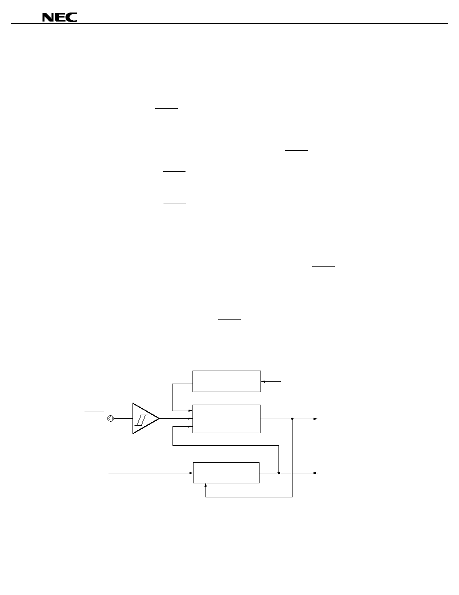
Preliminary Product Information U14673EJ1V0PM00
68
µ
µ
µ
µ
PD789322,789324,789326,789327
8. RESET FUNCTION
8.1 Reset Function
The
µ
PD789322, 789324, 789326, and 789327 can be reset using the following three signals.
(1) External reset signal input via RESET pin
(2) Internal reset by watchdog timer runaway time detection
(3) Internal reset using power-on-clear circuit (POC)
The external and internal reset signals are functionally equivalent. When RESET is input, program execution
begins from the addresses written at addresses 0000H and 0001H.
If a low-level signal is applied to the RESET pin, or if the watchdog timer overflows, a reset occurs, causing each
item of the hardware to enter the states listed in Table 8-1. While a reset is being applied, or while the oscillation
frequency is stabilizing immediately after the end of a reset sequence, each pin remains in the high-impedance state.
If a high-level signal is applied to the RESET pin, the reset sequence is terminated, and program execution begins
once the oscillation stabilization time has elapsed. A reset sequence caused by a watchdog timer overflow is
terminated automatically and again program execution begins upon the elapse of the oscillation stabilization time.
Reset by power-ON clear is cleared if the supply voltage rises beyond a specific level, and the program execution is
started after the oscillation stabilization time has elapsed.
Cautions 1. To use an external reset sequence, input a low-level signal to the RESET pin for at least 10
µ
µ
µ
µ
s.
2. When a reset is used to release STOP mode, the data of when STOP mode was entered is
retained during the reset sequence, except for the port pins, which are in the high-impedance
state.
3. The oscillation stabilization time after RESET input or the release of STOP mode by POC can
be selected from 2
15
/f
X
or 2
17
/f
X
by mask option (refer to 9. MASK OPTION).
Figure 8-1. Reset Function Block Diagram
RESET
Count clock
Reset control circuit
Watchdog timer
Stop
Over-
flow
Reset signal
Interrupt function
V
DD
Power-on-clear circuit
Preliminary Product Information U14673EJ1V0PM00
69
µ
µ
µ
µ
PD789322,789324,789326,789327
Table 8-1. Status of Hardware After Reset
Hardware
Status After Reset
Program counter (PC)
Note 1
Contents of reset
vector table (0000H,
0001H) set
Stack pointer (SP)
Undefined
Program status word (PSW)
02H
Data memory
Undefined
Note 2
RAM
General-purpose registers
Undefined
Note 2
Ports (P0 to P2, P4, P6, P8) (output latches)
00H
Port mode registers (PM0 to PM2, PM4, PM6, PM8)
FFH
Port function register 8 (PF8)
00H
Pull-up resistor option registers (PU0, PUB2)
00H
Processor clock control register (PCC)
02H
Subclock oscillation mode register (SCKM)
00H
Subclock control register (CSS)
00H
Oscillation stabilization time selection register (OSTS)
04H
Timer counters (TM30, TM40)
00H
Compare registers (CR30, CR40, CRH40)
Undefined
Mode control registers (TMC30, TMC40)
00H
8-bit timer 30, 40
Carrier generator output control register (TCA40)
00H
Watch timer
Mode control register (WTM)
00H
Watchdog timer
Mode register (WDTM)
00H
Serial operation mode register 10 (CSIM10)
00H
Serial interface 10
Transmission/reception shift register 10 (SIO10)
Undefined
Display mode register 0 (LCDM0)
00H
LCD controller/driver
Clock control register 0 (LCDC0)
00H
Power-on-clear circuit
Power-on-clear register 1 (POCF1)
00H
Note 3
Request flag register 0 (IF0)
00H
Mask flag register 0 (MK0)
FFH
External interrupt mode register 0 (INTM0)
00H
Interrupts
Key return mode register 00 (KRM00)
00H
Notes 1. While a reset signal is being input, and during the oscillation stabilization period, only the contents of
the PC will be undefined; the remainder of the hardware will be the same state as after reset.
2. In standby mode, RAM enters the hold state after reset.
3. The value is 04H only after a power-on-clear reset.

Preliminary Product Information U14673EJ1V0PM00
70
µ
µ
µ
µ
PD789322,789324,789326,789327
8.2 Power Failure Detection Function
When a reset is generated via the power-on-clear circuit, bit 2 (POCOF1) of the power-on-clear register (POCF1)
is set (1). This bit is then cleared (0) by an instruction written to POCF1. After a power-on-clear reset (i.e. after
program execution has started from address 0000H), a power failure can be detected by detecting POCOF1.
Figure 8-2. Format of Power-on-Clear Register 1
Symbol
7
6
5
4
3
2
1
0
Address
After reset
R/W
POCF1
0
0
0
0
0
POCOF1
0
0
FFDDH
00H
Note
R/W
POCOF1
Power-on-clear generation status detection
0
Power-on-clear not generated, or cleared by write operation
1
Power-on-clear reset generated
Note The value is 04H only after a power-on-clear reset.

Preliminary Product Information U14673EJ1V0PM00
71
µ
µ
µ
µ
PD789322,789324,789326,789327
9. MASK OPTION
The
µ
PD789322, 789324, 789326, and 789327 have the following mask option.
∑ Oscillation stabilization wait time
The oscillation stabilization wait time after the release of STOP mode by RESET or POC can be selected.
<1> 2
15
/f
X
<2> 2
17
/f
X
Preliminary Product Information U14673EJ1V0PM00
72
µ
µ
µ
µ
PD789322,789324,789326,789327
10. INSTRUCTION SET OVERVIEW
The instruction set for the
µ
PD789322, 789324, 789326, and 789327 are listed in this section.
10.1 Conventions
10.1.1 Operand formats and descriptions
The description made in the operand field of each instruction conforms to the operand format for the instructions
listed below (the details conform to the assembly specification). If more than one operand format is listed for an
instruction, one is selected. Uppercase letters, #, !, $, and brackets [ ] are used to specify keywords, which must be
written exactly as they appear. The meanings of these special characters are as follows:
∑
#: Immediate data specification
∑
$: Relative address specification
∑
!: Absolute address specification
∑
[ ]: Indirect address specification
Immediate data should be described using appropriate values or labels. The specification of values and labels
must be accompanied by #, !, $, or [ ].
Operand registers, expressed as r or rp in the formats, can be described using both functional names (X, A, C,
etc.) and absolute names (R0, R1, R2, and other names listed in Table 5-1 below).
Table 10-1. Operand Formats and Descriptions
Format
Description
r
rp
sfr
X (R0), A (R1), C (R2), B (R3), E (R4), D (R5), L (R6), H (R7)
AX (RP0), BC (RP1), DE (RP2), HL (RP3)
Special function register symbol
saddr
saddrp
FE20H to FF1FH
Immediate data or label
FE20H to FF1FH
Immediate data or label (even addresses only)
addr16
addr5
0000H to FFFFH
Immediate data or label
(only even addresses for 16-bit data transfer instructions)
0040H to 007FH
Immediate data or label (even addresses only)
word
byte
bit
16-bit immediate data or label
8-bit immediate data or label
3-bit immediate data or label
Remark For details concerning special function register symbols, refer to Table 4-1 Special Function
Registers.

Preliminary Product Information U14673EJ1V0PM00
73
µ
µ
µ
µ
PD789322,789324,789326,789327
10.1.2 Operation field definitions
A:
A register (8-bit accumulator)
X: X
register
B: B
register
C: C
register
D: D
register
E: E
register
H: H
register
L: L
register
AX:
AX register pair (16-bit accumulator)
BC:
BC register pair
DE:
DE register pair
HL:
HL register pair
PC: Program
counter
SP: Stack
pointer
PSW:
Program status word
CY:
Carry flag
AC:
Auxiliary carry flag
Z:
Zero flag
IE:
Interrupt request enable flag
NMIS:
Flag to indicate that a non-maskable interrupt is being processed
():
Contents of a memory location indicated by a parenthesized address or register name
X
H
, X
L
: Higher and lower 8 bits of a 16-bit register
:
Logical product (AND)
:
Logical sum (OR)
:
Exclusive OR
:
Inverted data
addr16: 16-bit immediate data or label
jdisp8:
Signed 8-bit data (displacement value)
10.1.3 Flag operation field definitions
(Blank): No change
0:
Clear to 0
1:
Set to 1
◊
:
Set or clear according to the result
R:
Restore to the previous value
Preliminary Product Information U14673EJ1V0PM00
74
µ
µ
µ
µ
PD789322,789324,789326,789327
10.2 Operations
Flag
Mnemonic
Operand
Byte
Clock
Operation
Z AC CY
r, #byte
3
6
r
byte
saddr , #byte
3
6
(saddr)
byte
sfr, #byte
3
6
sfr
byte
A, r
Note 1
2
4
A
r
r, A
Note 1
2
4
r
A
A, saddr
2
4
A
(saddr)
saddr, A
2
4
(saddr)
A
A, sfr
2
4
A
sfr
sfr, A
2
4
sfr
A
A, !addr16
3
8
A
(addr16)
!addr16, A
3
8
(addr16)
A
PSW, #byte
3
6
PSW
byte
◊ ◊ ◊
A, PSW
2
4
A
PSW
PSW, A
2
4
PSW
A
◊ ◊ ◊
A, [DE]
1
6
A
(DE)
[DE], A
1
6
(DE)
A
A, [HL]
1
6
A
(HL)
[HL], A
1
6
(HL)
A
A, [HL + byte]
2
6
A
(HL + byte)
MOV
[HL + byte], A
2
6
(HL + byte)
A
A, X
1
4
A
X
A, r
Note 2
2
6
A
r
A, saddr
2
6
A
(saddr)
A, sfr
2
6
A
(sfr)
A, [DE]
1
8
A
(DE)
A, [HL]
1
8
A
(HL)
XCH
A, [HL + byte]
2
8
A
(HL + byte)
rp, #word
3
6
rp
word
AX, saddrp
2
6
AX
(saddrp)
saddrp, AX
2
8
(saddrp)
AX
AX, rp
Note 3
1
4
AX
rp
MOVW
rp, AX
Note 3
1
4
rp
AX
XCHW
AX, rp
Note 3
1
8
AX
rp
Notes 1. Except when r = A.
2. Except when r = A or X.
3. Only when rp = BC, DE, or HL.
Remark The instruction clock cycle is based on the CPU clock (f
CPU
) specified by the processor clock control
register (PCC).
Preliminary Product Information U14673EJ1V0PM00
75
µ
µ
µ
µ
PD789322,789324,789326,789327
Flag
Mnemonic
Operand
Byte
Clock
Operation
Z AC CY
A, #byte
2
4
A, CY
A + byte
◊ ◊ ◊
saddr, #byte
3
6
(saddr), CY
(saddr) + byte
◊ ◊ ◊
A, r
2
4
A, CY
A + r
◊ ◊ ◊
A, saddr
2
4
A, CY
A + (saddr)
◊ ◊ ◊
A, !addr16
3
8
A, CY
A + (addr16)
◊ ◊ ◊
A, [HL]
1
6
A, CY
A + (HL)
◊ ◊ ◊
ADD
A, [HL + byte]
2
6
A, CY
A + (HL + byte)
◊ ◊ ◊
A, #byte
2
4
A, CY
A + byte + CY
◊ ◊ ◊
saddr, #byte
3
6
(saddr), CY
(saddr) + byte + CY
◊ ◊ ◊
A, r
2
4
A, CY
A + r + CY
◊ ◊ ◊
A, saddr
2
4
A, CY
A + (saddr) + CY
◊ ◊ ◊
A, !addr16
3
8
A, CY
A + (addr16) + CY
◊ ◊ ◊
A, [HL]
1
6
A, CY
A + (HL) + CY
◊ ◊ ◊
ADDC
A, [HL + byte]
2
6
A, CY
A + (HL + byte) + CY
◊ ◊ ◊
A, #byte
2
4
A, CY
A
-
byte
◊ ◊ ◊
saddr, #byte
3
6
(saddr), CY
(saddr)
-
byte
◊ ◊ ◊
A, r
2
4
A, CY
A
-
r
◊ ◊ ◊
A, saddr
2
4
A, CY
A
-
(saddr)
◊ ◊ ◊
A, !addr16
3
8
A, CY
A
-
(addr16)
◊ ◊ ◊
A, [HL]
1
6
A, CY
A
-
(HL)
◊ ◊ ◊
SUB
A, [HL + byte]
2
6
A, CY
A
-
(HL + byte)
◊ ◊ ◊
A, #byte
2
4
A, CY
A
-
byte
-
CY
◊ ◊ ◊
saddr, #byte
3
6
(saddr), CY
(saddr)
-
byte
-
CY
◊ ◊ ◊
A, r
2
4
A, CY
A
-
r
-
CY
◊ ◊ ◊
A, saddr
2
4
A, CY
A
-
(saddr)
-
CY
◊ ◊ ◊
A, !addr16
3
8
A, CY
A
-
(addr16)
-
CY
◊ ◊ ◊
A, [HL]
1
6
A, CY
A
-
(HL)
-
CY
◊ ◊ ◊
SUBC
A, [HL + byte]
2
6
A, CY
A
-
(HL + byte)
-
CY
◊ ◊ ◊
A, #byte
2
4
A
A
byte
◊
saddr, #byte
3
6
(saddr)
(saddr)
byte
◊
A, r
2
4
A
A
r
◊
A, saddr
2
4
A
A
(saddr)
◊
A, !addr16
3
8
A
A
(addr16)
◊
A, [HL]
1
6
A
A
(HL)
◊
AND
A, [HL + byte]
2
6
A
A
(HL + byte)
◊
Remark The instruction clock cycle is based on the CPU clock (f
CPU
) specified by the processor clock control
register (PCC).
Preliminary Product Information U14673EJ1V0PM00
76
µ
µ
µ
µ
PD789322,789324,789326,789327
Flag
Mnemonic
Operand
Byte
Clock
Operation
Z AC CY
A, #byte
2
4
A
A
byte
◊
saddr, #byte
3
6
(saddr)
(saddr)
byte
◊
A, r
2
4
A
A
r
◊
A, saddr
2
4
A
A
(saddr)
◊
A, !addr16
3
8
A
A
(addr16)
◊
A, [HL]
1
6
A
A
(HL)
◊
OR
A, [HL + byte]
2
6
A
A
(HL + byte)
◊
A, #byte
2
4
A
A
byte
◊
saddr, #byte
3
6
(saddr)
(saddr)
byte
◊
A, r
2
4
A
A
r
◊
A, saddr
2
4
A
A
(saddr)
◊
A, !addr16
3
8
A
A
(addr16)
◊
A, [HL]
1
6
A
A
(HL)
◊
XOR
A, [HL + byte]
2
6
A
A
(HL + byte)
◊
A, #byte
2
4
A
-
byte
◊ ◊ ◊
saddr, #byte
3
6
(saddr)
-
byte
◊ ◊ ◊
A, r
2
4
A
-
r
◊ ◊ ◊
A, saddr
2
4
A
-
(saddr)
◊ ◊ ◊
A, !addr16
3
8
A
-
(addr16)
◊ ◊ ◊
A, [HL]
1
6
A
-
(HL)
◊ ◊ ◊
CMP
A, [HL + byte]
2
6
A
-
(HL + byte)
◊ ◊ ◊
ADDW
AX, #word
3
6
AX, CY
AX + word
◊ ◊ ◊
SUBW
AX, #word
3
6
AX, CY
AX
-
word
◊ ◊ ◊
CMPW
AX, #word
3
6
AX
-
word
◊ ◊ ◊
r
2
4
r
r + 1
◊ ◊
INC
saddr
2
4
(saddr)
(saddr) + 1
◊ ◊
r
2
4
r
r
-
1
◊ ◊
DEC
saddr
2
4
(saddr)
(saddr)
-
1
◊ ◊
INCW
rp
1
4
rp
rp + 1
DECW
rp
1
4
rp
rp
-
1
ROR
A, 1
1
2
(CY, A
7
A
0
, A
m
-
1
A
m
)
◊
1
◊
ROL
A, 1
1
2
(CY, A
0
A
7
, A
m+1
A
m
)
◊
1
◊
RORC
A, 1
1
2
(CY
A
0
, A
7
CY, A
m
-
1
A
m
)
◊
1
◊
ROLC
A, 1
1
2
(CY
A
7
, A
0
CY, A
m+1
A
m
)
◊
1
◊
Remark The instruction clock cycle is based on the CPU clock (f
CPU
) specified by the processor clock control
register (PCC).
Preliminary Product Information U14673EJ1V0PM00
77
µ
µ
µ
µ
PD789322,789324,789326,789327
Flag
Mnemonic
Operand
Byte
Clock
Operation
Z AC CY
saddr.bit
3
6
(saddr.bit)
1
sfr.bit
3
6
sfr.bit
1
A.bit
2
4
A.bit
1
PSW.bit
3
6
PSW bit
1
◊ ◊ ◊
SET1
[HL].bit
2
10
(HL).bit
1
saddr.bit
3
6
(saddr.bit)
0
sfr.bit
3
6
sfr.bit
0
A.bit
2
4
A.bit
0
PSW.bit
3
6
PSW.bit
0
◊ ◊ ◊
CLR1
[HL].bit
2
10
(HL).bit
0
SET1
CY
1
2
CY
1
1
CLR1
CY
1
2
CY
0
0
NOT1
CY
1
2
CY
CY
◊
CALL
!addr16
3
6
(SP
-
1)
(PC + 3)
H
, (SP
-
2)
(PC + 3)
L
,
PC
addr16, SP
SP
-
2
CALLT
[addr5]
1
8
(SP
-
1)
(PC + 1)
H
, (SP
-
2)
(PC + 1)
L
,
PC
H
(00000000, addr5 + 1),
PC
L
(00000000, addr5),
SP
SP
-
2
RET
1
6
PC
H
(SP + 1), PC
L
(SP),
SP
SP + 2
RETI
1
8
PC
H
(SP + 1), PC
L
(SP),
PSW
(SP + 2), SP
SP + 3,
NMIS
0
R
R
R
PSW
1
2
(SP
-
1)
PSW, SP
SP
-
1
PUSH
rp
1
4
(SP
-
1)
rp
H
, (SP
-
2)
rp
L
,
SP
SP
-
2
PSW
1
4
PSW
(SP), SP
SP + 1
R
R
R
POP
rp
1
6
rp
H
(SP + 1), rp
L
(SP),
SP
SP + 2
SP, AX
2
8
SP
AX
MOVW
AX, SP
2
6
AX
SP
!addr16
3
6
PC
addr16
$addr16
2
6
PC
PC + 2 + jdisp8
BR
AX
1
6
PC
H
A, PC
L
X
Remark The instruction clock cycle is based on the CPU clock (f
CPU
) specified by the processor clock control
register (PCC).

Preliminary Product Information U14673EJ1V0PM00
78
µ
µ
µ
µ
PD789322,789324,789326,789327
Flag
Mnemonic
Operand
Byte
Clock
Operation
Z AC CY
BC
$addr16
2
6
PC
PC + 2 + jdisp8 if CY = 1
BNC
$addr16
2
6
PC
PC + 2 + jdisp8 if CY = 0
BZ
$addr16
2
6
PC
PC + 2 + jdisp8 if Z = 1
BNZ
$addr16
2
6
PC
PC + 2 + jdisp8 if Z = 0
saddr.bit, $addr16
4
10
PC
PC + 4 + jdisp8
if (saddr.bit) = 1
sfr.bit, $addr16
4
10
PC
PC + 4 + jdisp8 if sfr.bit = 1
A.bit, $addr16
3
8
PC
PC + 3 + jdisp8 if A.bit = 1
BT
PSW.bit, $addr16
4
10
PC
PC + 4 + jdisp8 if PSW.bit = 1
saddr.bit, $addr16
4
10
PC
PC + 4 + jdisp8
if (saddr.bit) = 0
sfr.bit, $addr16
4
10
PC
PC + 4 + jdisp8 if sfr.bit = 0
A.bit, $addr16
3
8
PC
PC + 3 + jdisp8 if A.bit = 0
BF
PSW.bit, $addr16
4
10
PC
PC + 4 + disp8 if PSW.bit = 0
B, $addr16
2
6
B
B
-
1, then
PC
PC + 2 + jdisp8 if B
0
C, $addr16
2
6
C
C
-
1, then
PC
PC + 2 + jdisp8 if C
0
DBNZ
saddr, $addr16
3
8
(saddr)
(saddr)
-
1, then
PC
PC + 3 + jdisp8 if (saddr)
0
NOP
1
2
No Operation
EI
3
6
IE
1 (Enable Interrupt)
DI
3
6
IE
0 (Disable Interrupt)
HALT
1
2
Set HALT Mode
STOP
1
2
Set STOP Mode
Remark The instruction clock cycle is based on the CPU clock (f
CPU
) specified by the processor clock control
register (PCC).
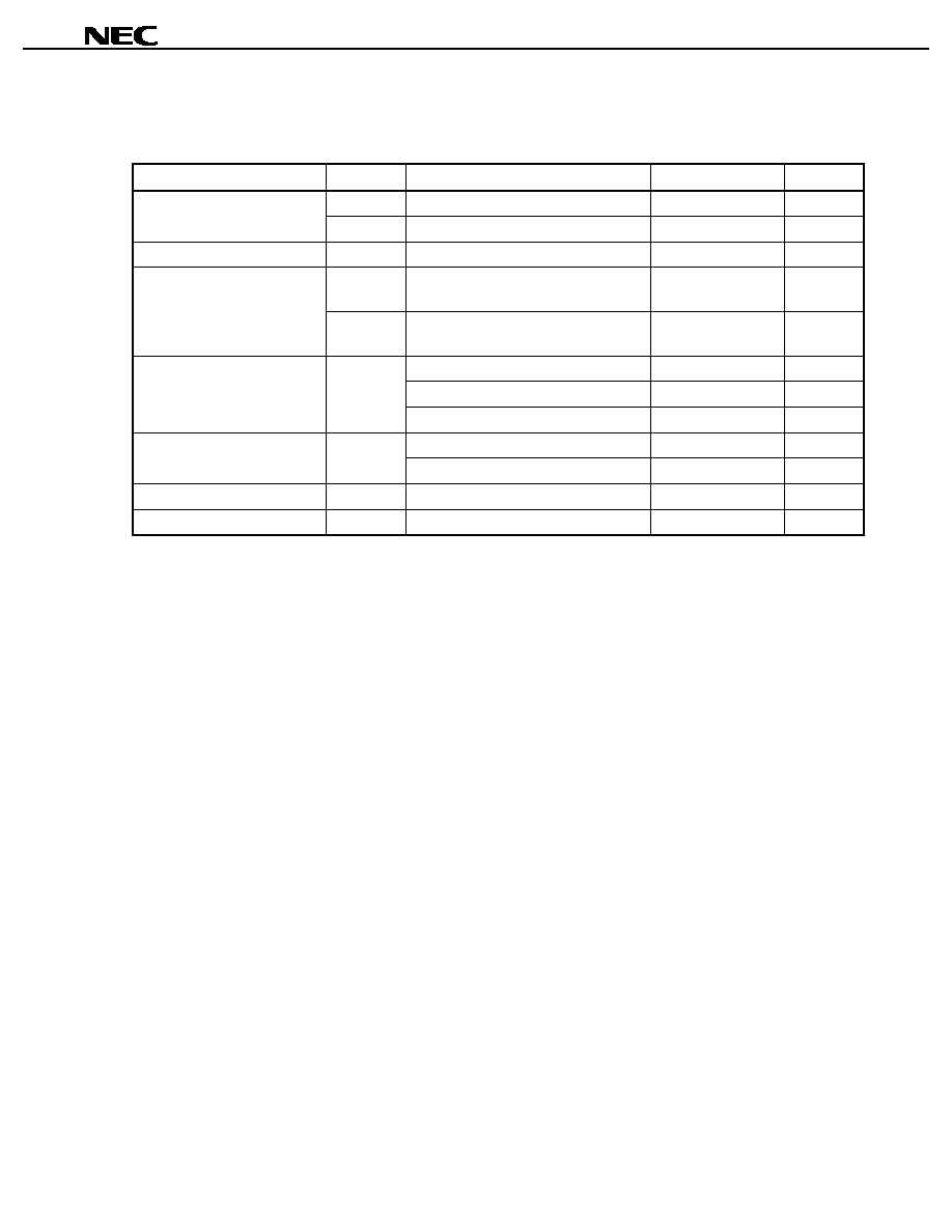
Preliminary Product Information U14673EJ1V0PM00
79
µ
µ
µ
µ
PD789322,789324,789326,789327
11. ELECTRICAL SPECIFICATIONS
Absolute Maximum Ratings (T
A
= 25
∞
∞
∞
∞
C)
Parameter
Symbol
Conditions
Ratings
Unit
V
DD
-
0.3 to +6.5
V
Supply voltage
V
LC0
-
0.3 to +6.5
V
Input voltage
V
I
-
0.3 to V
DD
+ 0.3
Note
V
V
O1
P00 to P03, P10, P11, P20 to P22,
P40 to P43, P60, P61
-
0.3 to V
DD
+ 0.3
Note
V
Output voltage
V
O2
COM0 to COM3, S0 to S16,
P80/S22 to P85/S17, S23
-
0.3 to V
LC0
+ 0.3
Note
V
Pin P60/TO40
-
30
mA
Per pin (except P60/TO40)
-
10
mA
Output current, high
I
OH
Total for all pins (except P60/TO40)
-
30
mA
Per pin
30
mA
Output current, low
I
OL
Total for all pins
80
mA
Operating ambient temperature
T
A
-
40 to +85
∞
C
Storage temperature
T
stg
-
65 to +150
∞
C
Note 6.5 V or lower
Caution
Product quality may suffer if the absolute maximum rating is exceeded even momentarily for
any parameter. That is, the absolute maximum ratings are rated values at which the product is
on the verge of suffering physical damage, and therefore the product must be used under
conditions that ensure that the absolute maximum ratings are not exceeded.
Remark Unless specified otherwise, the characteristics of alternate-function pins are the same as those of port
pins.
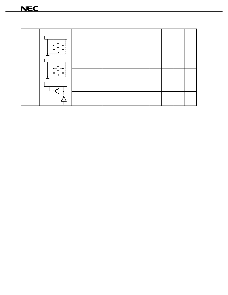
Preliminary Product Information U14673EJ1V0PM00
80
µ
µ
µ
µ
PD789322,789324,789326,789327
Main System Clock Oscillator Characteristics
(T
A
=
-
-
-
-
40 to +85∞C, V
DD
= 1.8 to 5.5 V)
Resonator
Recommended Circuit
Parameter
Conditions
MIN.
TYP.
MAX.
Unit
Oscillation frequency
(f
X
)
Note 1
1.0
5.0
MHz
Ceramic
resonator
X1
X2
V
DD
C1
C2
Oscillation
stabilization time
Note 2
After V
DD
has reached the MIN.
oscillation voltage range
4
ms
Oscillation frequency
(f
X
)
Note 1
1.0
5.0
MHz
Crystal
resonator
X1
X2
IC
C1
C2
Oscillation
stabilization time
Note 2
30
ms
X1 input frequency
(f
X
)
Note 1
1.0
5.0
MHz
External
clock
X2
X1
X1 input high-/low-
level width (t
XH
, t
XL
)
85
500
ns
Notes 1. Indicates only oscillator characteristics. Refer to AC Characteristics for instruction execution time.
2. Time required to stabilize oscillation after reset or STOP mode release.
Cautions 1. When using the main system clock oscillator, wire as follows in the area enclosed by the
broken lines in the above figures to avoid an adverse effect from wiring capacitance.
∑
∑
∑
∑
Keep the wiring length as short as possible.
∑
∑
∑
∑
Do not cross the wiring with other signal lines.
∑
∑
∑
∑
Do not route the wiring near a signal line through which a high fluctuating current flows.
∑
∑
∑
∑
Always make the ground point of the oscillator capacitor the same potential as V
SS
.
∑
∑
∑
∑
Do not ground the capacitor to a ground pattern through which a high current flows.
∑
∑
∑
∑
Do not fetch signals from the oscillator.
2. When the main system clock is stopped and the device is operating on the subsystem clock,
wait until the oscillation stabilization time has been secured by the program before switching
back to the main system clock.
Remark For the resonator selection and oscillator constant, customers are requested to either evaluate the
oscillation themselves or apply to the resonator manufacturer for evaluation.

Preliminary Product Information U14673EJ1V0PM00
81
µ
µ
µ
µ
PD789322,789324,789326,789327
Subsystem Clock Oscillator Characteristics (T
A
=
-
-
-
-
40 to +85∞C, V
DD
= 1.8 to 5.5 V)
Resonator
Recommended Circuit
Parameter
Conditions
MIN.
TYP.
MAX.
Unit
Oscillation frequency
(f
XT
)
Note 1
32
32.768
35
kHz
V
DD
= 4.5 to 5.5 V
1.2
2
Crystal
resonator
XT2
XT1
IC
C4
C3
R
Oscillation
stabilization time
Note 2
10
s
XT1 input frequency
(f
XT
)
Note 1
32
35
kHz
External
clock
XT1
XT2
XT1 input high-/low-
level width (t
XTH
, t
XTL
)
14.3
15.6
µ
s
Notes 1. Indicates only oscillator characteristics. Refer to AC Characteristics for instruction execution time.
2. The time required for oscillation to stabilize after V
DD
reaches the MIN. oscillation voltage range. Use a
resonator to stabilize oscillation during the oscillation wait time.
Cautions 1. When using the subsystem clock oscillator, wire as follows in the area enclosed by the
broken lines in the above figures to avoid an adverse effect from wiring capacitance.
∑
∑
∑
∑
Keep the wiring length as short as possible.
∑
∑
∑
∑
Do not cross the wiring with the other signal lines.
∑
∑
∑
∑
Do not route the wiring near a signal line through which a high fluctuating current flows.
∑
∑
∑
∑
Always make the ground point of the oscillator capacitor the same potential as V
SS
.
∑
∑
∑
∑
Do not ground the capacitor to a ground pattern through which a high current flows.
∑
∑
∑
∑
Do not fetch signals from the oscillator.
2. The subsystem clock oscillator is designed as a low-amplitude circuit for reducing current
consumption, and is more prone to malfunction due to noise than the main system clock
oscillator. Particular care is therefore required with the wiring method when the subsystem
clock is used.
Remark For the resonator selection and oscillator constant, customers are requested to either evaluate the
oscillation themselves or apply to the resonator manufacturer for evaluation.

Preliminary Product Information U14673EJ1V0PM00
82
µ
µ
µ
µ
PD789322,789324,789326,789327
DC Characteristics (T
A
=
-
-
-
-
40 to +85∞C, V
DD
= 1.8 to 5.5 V) (1/2)
Parameter
Symbol
Conditions
MIN.
TYP.
MAX.
Unit
Per pin
10
mA
Output current, low
I
OL
Total for all pins
80
mA
Per pin (except P60/TO40)
-
1
mA
P60/TO40
V
DD
= 3.0 V, V
OH
= 1.0 V
-
7
-
15
-
24
mA
Output current, high
I
OH
Total for all pins (except P60/TO40)
-
15
mA
V
DD
= 2.7 to 5.5 V
0.7 V
DD
V
DD
V
V
IH1
P00 to P03, P10, P11,
P21, P22, P60
0.9 V
DD
V
DD
V
V
DD
= 2.7 to 5.5 V
0.8 V
DD
V
DD
V
V
IH2
RESET, P20, P40 to P43,
P61
0.9 V
DD
V
DD
V
V
IH3
X1, X2
V
DD
-
0.1
V
DD
V
Input voltage, high
V
IH4
XT1, XT2
V
DD
-
0.1
V
DD
V
V
DD
= 2.7 to 5.5 V
0
0.3 V
DD
V
V
IL1
P00 to P03, P10, P11,
P21, P22, P60
0
0.1 V
DD
V
V
DD
= 2.7 to 5.5 V
0
0.2 V
DD
V
V
IL2
RESET, P20, P40 to P43,
P61
0
0.1 V
DD
V
V
IL3
X1, X2
0
0.1
V
Input voltage, low
V
IL4
XT1, XT2
0
0.1
V
V
OH11
1.8
V
DD
5.5 V,
I
OH
=
-
100
µ
A
V
DD
-
0.5
V
V
OH12
P00 to P03, P10, P11,
P20 to P22, P40 to P43,
P61
1.8
V
DD
5.5 V,
I
OH
=
-
500
µ
A
V
DD
-
0.7
V
V
OH21
1.8
V
DD
5.5 V,
I
OH
=
-
400
µ
A
V
DD
-
0.5
V
V
OH22
P60/TO40
1.8
V
DD
5.5 V,
I
OH
=
-
2 mA
V
DD
-
0.7
V
V
OH31
1.8
V
DD
5.5 V,
I
OH
=
-
100
µ
A
V
LC0
-
0.5
V
Output voltage, high
V
OH32
P80/S22 to P85/S17
1.8
V
DD
5.5 V,
I
OH
=
-
500
µ
A
V
LC0
-
0.7
V
V
OL11
1.8
V
DD
5.5 V,
I
OL
= 400
µ
A
0.5
V
V
OL12
P00 to P03, P10, P11,
P20 to P22, P40 to P43,
P60, P61
1.8
V
DD
5.5 V,
I
OL
= 2 mA
0.7
V
V
OL21
1.8
V
LC0
5.5 V,
I
OL
= 400
µ
A
0.5
V
Output voltage, low
V
OL22
P80/S22 to P85/S17
1.8
V
LC0
5.5 V,
I
OL
= 2 mA
0.7
V
Remark Unless specified otherwise, the characteristics of alternate-function pins are the same as those of port
pins.
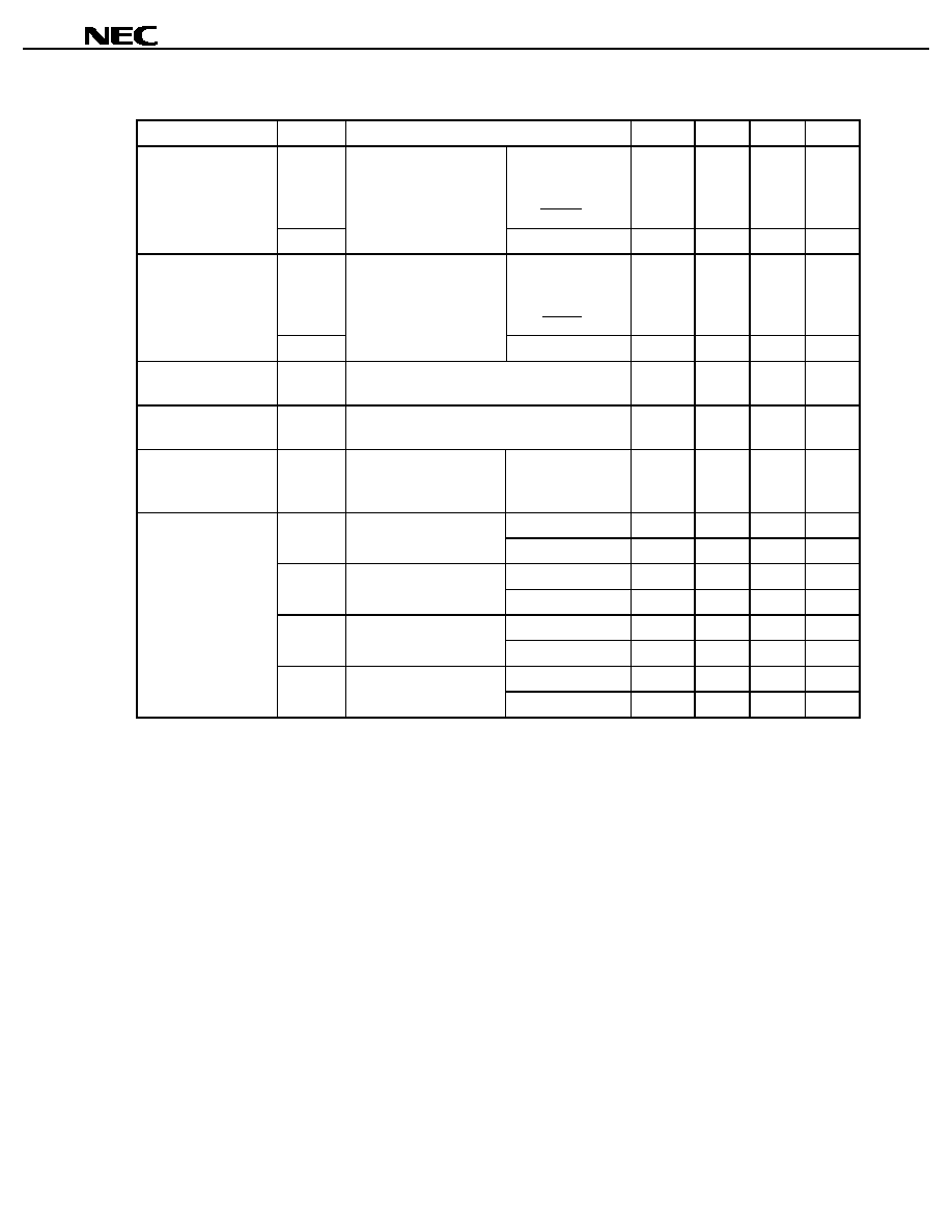
Preliminary Product Information U14673EJ1V0PM00
83
µ
µ
µ
µ
PD789322,789324,789326,789327
DC Characteristics (T
A
= ≠40 to +85∞C, V
DD
= 1.8 to 5.5 V) (2/2)
Parameter
Symbol
Conditions
MIN.
TYP.
MAX.
Unit
I
LIH1
P00 to P03, P10,
P11, P20 to P22,
P40 to P43, P60,
P61, RESET
3
µ
A
Input leakage current,
high
I
LIH2
V
IN
= V
DD
X1, X2, XT1, XT2
20
µ
A
I
LIL1
P00 to P03, P10,
P11, P20 to P22,
P40 to P43, P60,
P61, RESET
-
3
µ
A
Input leakage current,
low
I
LIL2
V
IN
= 0 V
X1, X2, XT1, XT2
-
20
µ
A
Output leakage current,
high
I
LOH
V
OUT
= V
DD
3
µ
A
Output leakage current,
low
I
LOL
V
OUT
= 0 V
-
3
µ
A
Software pull-up
resistors
R
1
V
IN
= 0 V
P00 to P03, P10,
P11, P20 to P22,
P40 to P43
50
100
200
k
V
DD
= 5.5 V
Note 2
2.0
4.0
mA
I
DD1
5.0-MHz crystal oscillation
operating mode
V
DD
= 3.3 V
Note 3
0.6
1.2
mA
V
DD
= 5.5 V
1.1
2.2
mA
I
DD2
5.0-MHz crystal oscillation
HALT mode
V
DD
= 3.3 V
0.4
0.8
mA
V
DD
= 5.5 V
25
55
µ
A
I
DD3
32.768-kHz crystal
oscillation HALT mode
Note 4
V
DD
= 3.3 V
5
25
µ
A
V
DD
= 5.5 V
1
10
µ
A
Supply current
Note 1
Ceramic/crystal
oscillation
I
DD4
STOP mode
V
DD
= 3.3 V
1
5
µ
A
Notes 1. Current flowing through ports (including current flowing through on-chip pull-up resistors) is not
included.
2. High-speed operation (when the processor clock control register (PCC) is set to 00H).
3. Low-speed operation (when PCC is set to 02H)
4. When the main system clock is stopped.
Remark Unless specified otherwise, the characteristics of alternate-function pins are the same as those of port
pins.
Preliminary Product Information U14673EJ1V0PM00
84
µ
µ
µ
µ
PD789322,789324,789326,789327
AC Characteristics
(1) Basic operation (T
A
=
-
-
-
-
40 to +85∞C, V
DD
= 1.8 to 5.5 V)
Parameter
Symbol
Conditions
MIN.
TYP.
MAX.
Unit
V
DD
= 2.7 to 5.5 V
0.4
8.0
µ
s
Cycle time
(Min. instruction execution time)
T
CY
1.6
8.0
µ
s
Interrupt input
high-/low-level width
t
INTH
,
t
INTL
INT
10
µ
s
Key return pin
low-level width
t
KRIL
KR00 to KR03
10
µ
s
RESET low-level width
t
RSL
10
µ
s
T
CY
vs. V
DD
(Main System Clock)
Supply voltage V
DD
(V)
1
2
3
4
5
6
0.1
0.4
0.5
1.0
2.0
10
20
60
Cycle time T
CY
[ s]
Guaranteed
operation
range
µ
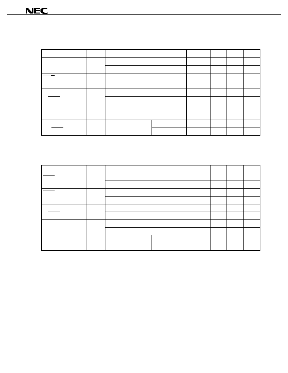
Preliminary Product Information U14673EJ1V0PM00
85
µ
µ
µ
µ
PD789322,789324,789326,789327
(2) Serial interface 10 (T
A
= ≠40 to +85∞C, V
DD
= 1.8 to 5.5 V)
(a) 3-wire serial I/O mode (Internal clock output)
Parameter
Symbol
Conditions
MIN.
TYP.
MAX.
Unit
V
DD
= 2.7 to 5.5 V
800
ns
SCK10 cycle time
t
KCY1
3,200
ns
V
DD
= 2.7 to 5.5 V
t
KCY1
/2
-
50
ns
SCK10 high-/low-level
width
t
KH1
,
t
KL1
t
KCY1
/2
-
150
ns
V
DD
= 2.7 to 5.5 V
150
ns
SI10 setup time
(to SCK10
)
t
SIK1
500
ns
V
DD
= 2.7 to 5.5 V
400
ns
SI10 hold time
(from SCK10
)
t
KSI1
800
ns
V
DD
= 2.7 to 5.5 V
0
250
ns
SO10 output delay time
from SCK10
t
KSO1
R = 1 k
, C = 100 pF
Note
250
1,000
ns
Note R and C are the load resistance and load capacitance of the SO10 output line.
(b) 3-wire serial I/O mode (External clock input)
Parameter
Symbol
Conditions
MIN.
TYP.
MAX.
Unit
V
DD
= 2.7 to 5.5 V
900
ns
SCK10 cycle time
t
KCY2
3,500
ns
V
DD
= 2.7 to 5.5 V
400
ns
SCK10 high-/low-level
width
t
KH2
,
t
KL2
1,600
ns
V
DD
= 2.7 to 5.5 V
100
ns
SI10 setup time
(to SCK10
)
t
SIK2
150
ns
V
DD
= 2.7 to 5.5 V
400
ns
SI10 hold time
(from SCK10
)
t
KSI2
600
ns
V
DD
= 2.7 to 5.5 V
0
300
ns
SO10 output delay time
from SCK10
t
KSO2
R = 1 k
, C = 100 pF
Note
250
1,000
ns
Note R and C are the load resistance and load capacitance of the SO10 output line.
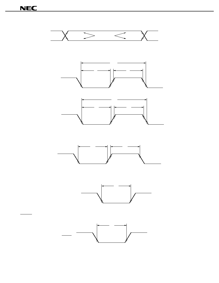
Preliminary Product Information U14673EJ1V0PM00
86
µ
µ
µ
µ
PD789322,789324,789326,789327
AC Timing Measurement Point (excluding X1, XT1 input)
0.8 V
DD
0.2 V
DD
Test points
0.8 V
DD
0.2 V
DD
Clock Timing
1/f
X
t
XL
t
XH
X1 input
V
IH3
(MIN.)
V
IL3
(MAX.)
1/f
XT
t
XTL
t
XTH
XT1 input
V
IH4
(MIN.)
V
IL4
(MAX.)
Interrupt Input Timing
INT
t
INTL
t
INTH
Key Return Input Timing
KR00 to KR03
t
KRIL
RESET Input Timing
RESET
t
RSL

Preliminary Product Information U14673EJ1V0PM00
87
µ
µ
µ
µ
PD789322,789324,789326,789327
Serial Transfer Timing
3-wire serial I/O mode:
t
KCYn
t
KLn
t
KHn
SCK10
t
SIKn
t
KSIn
t
KSOn
Input data
Output data
SI10
SO10
Remark n = 1, 2
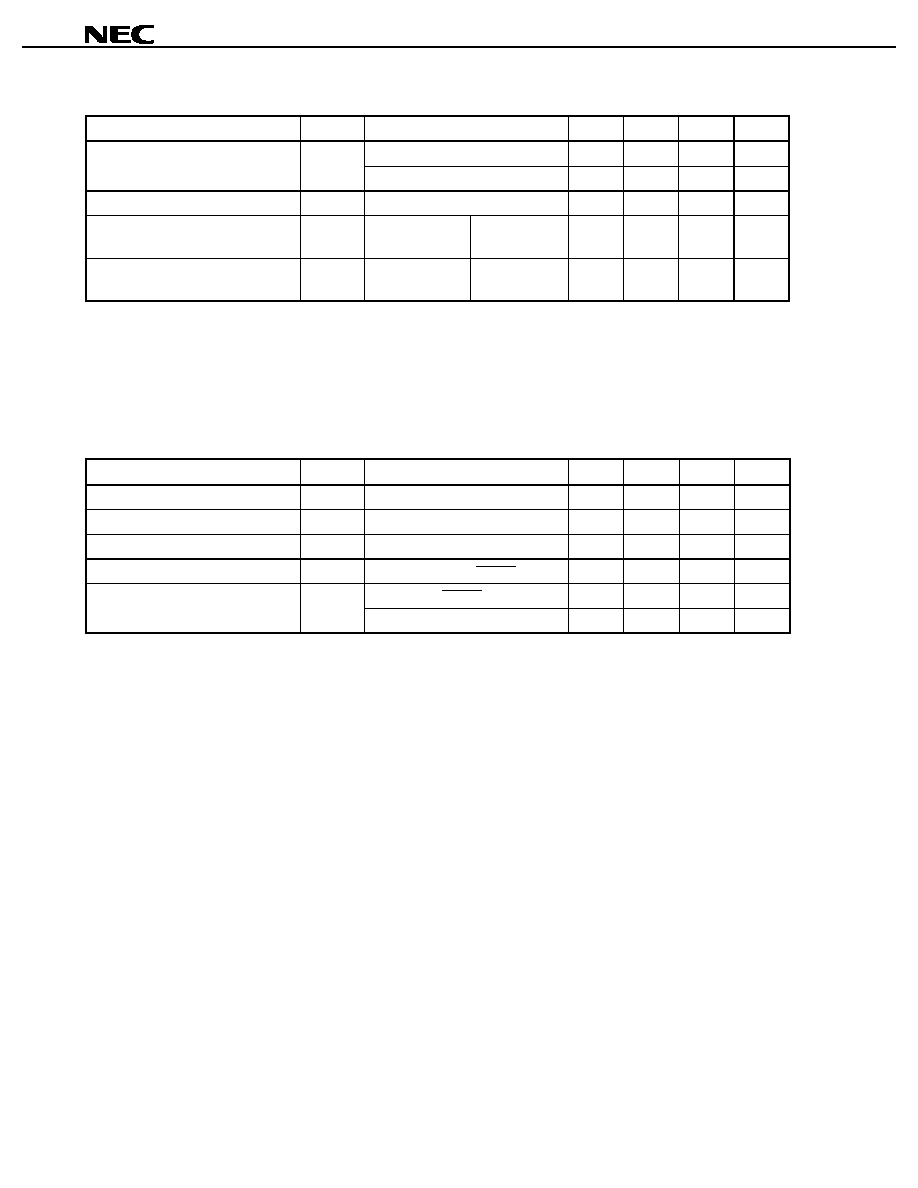
Preliminary Product Information U14673EJ1V0PM00
88
µ
µ
µ
µ
PD789322,789324,789326,789327
LCD Characteristics (T
A
=
-
-
-
-
40 to +85∞C, V
DD
= 1.8 to 5.5 V)
Parameter
Symbol
Conditions
MIN.
TYP.
MAX.
Unit
VAON0
Note 1
= 1
1.8
5.5
V
LCD drive voltage
V
LC0
VAON0
Note 1
= 0
2.7
5.5
V
LCD division resistance
R
LCD
50
100
200
k
LCD output voltage differential
Note 2
(common)
V
ODC
I
O
=
±
5
µ
A
1/3 bias
0
±
0.2
V
LCD output voltage differential
Note 2
(segment)
V
ODS
I
O
=
±
1
µ
A
1/3 bias
0
±
0.2
V
Notes 1. Bit 6 of LCD display mode register 0 (LCDM0)
2. The voltage differential is the difference between the output voltage and the ideal value of the segment
and common signal outputs.
Data Memory STOP Mode Low Supply Voltage Data Retention Characteristics
(T
A
=
-
-
-
-
40 to +85∞C, V
DD
= 1.8 to 5.5 V)
Parameter
Symbol
Conditions
MIN.
TYP.
MAX.
Unit
Data retention supply voltage
V
DDDR
1.8
3.6
V
Low voltage detection (POC) voltage
V
POC
Response time: 2 ms
Note 1
1.8
1.9
2.0
V
Power supply rise time
t
Pth
V
DD
: 0 V
1.8 V
0.01
100
ms
Release signal set time
t
SREL
STOP cancelled by RESET
10
µ
s
Cancelled by RESET
Note 3
s
Oscillation stabilization wait time
Note 2
t
WAIT
Cancelled by interrupt request
Note 4
s
Notes 1. The response time is the time until the output is inverted following detection of voltage by POC, or the
time until operation stabilizes after the shift from the operation stopped state to the operating state.
2. The oscillation stabilization time is the amount of time the CPU operation is stopped in order to avoid
unstable operation at the start of oscillation. Program operation does not start until both the oscillation
stabilization time and the time until oscillation starts have elapsed.
3. 2
15
/f
X
or 2
17
/f
X
can be selected using the mask option (refer to 9. MASK OPTION).
4. 2
12
/f
X
, 2
15
/f
X
, or 2
17
/f
X
can be selected using bits 0 to 2 (OSTS0 to OSTS2) of the oscillation stabilization
time selection register (OSTS) (refer to 7.2 Standby Function Control Register).
Remark f
X
: Main system clock oscillation frequency
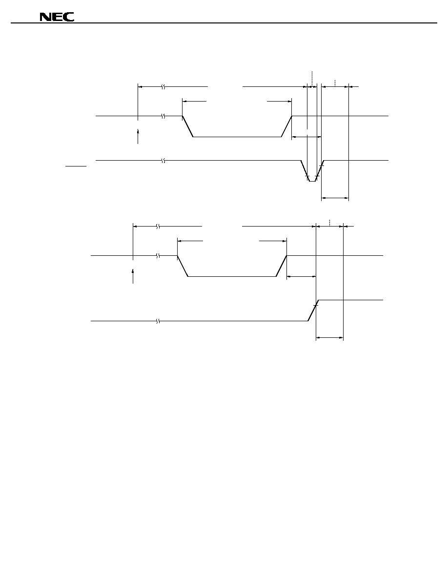
Preliminary Product Information U14673EJ1V0PM00
89
µ
µ
µ
µ
PD789322,789324,789326,789327
Data Retention Timing
V
DD
Data retention mode
STOP mode
HALT mode
Internal reset operation
Operating mode
t
SREL
t
WAIT
STOP instruction execution
V
DDDR
RESET
V
DD
Data retention mode
STOP mode
HALT mode
Operating mode
t
SREL
t
WAIT
STOP instruction execution
V
DDDR
Standby release signal
(interrupt request)

Preliminary Product Information U14673EJ1V0PM00
90
µ
µ
µ
µ
PD789322,789324,789326,789327
12. PACKAGE DRAWING
M
41
42
27
52
1
14
13
28
S
N
S
J
detail of lead end
R
K
M
I
S
L
T
P
Q
G
F
H
52-PIN PLASTIC LQFP (10x10)
ITEM
MILLIMETERS
A
B
D
G
12.0
±
0.2
10.0
±
0.2
0.13
1.1
I
12.0
±
0.2
J
C
10.0
±
0.2
H
0.32
±
0.06
0.65 (T.P.)
1.0
±
0.2
K
L
0.5
F
1.1
N
P
Q
0.10
1.4
0.1
±
0.05
T
0.25
S
1.5
±
0.1
U
0.6
±
0.15
S52GB-65-8ET-1
M
0.17
+
0.03
-
0.05
R
3
∞+
4
∞
-
3
∞
A
B
C
D
U
Preliminary Product Information U14673EJ1V0PM00
91
µ
µ
µ
µ
PD789322,789324,789326,789327
APPENDIX A. DEVELOPMENT TOOLS
The following development tools are available for system development using the
µ
PD789322, 789324, 789326,
and 789327.
Language Processing Software
RA78K0S
Notes 1, 2, 3
Assembler package common to 78K/0S Series
CC78K0S
Notes 1, 2 ,3
C compiler package common to 78K/0S Series
DF789328
Notes 1, 2, 3, 5
Device file for
µ
PD789327 Subseries
CC78K/0S≠L
Notes 1, 2, 3
C compiler library source file common to 78K/0S Series
Flash Memory Writing Tools
Flashpro III
(Part number: FL-PR3
Note 4
, PG-FP3)
Dedicated flash memory programmer
FA-52GB
Notes 4, 5
Adapter for writing to flash memory designed for 52-pin plastic LQFP (GB-8ET type)
Debugging Tools
IE-78K0S-NS
In-circuit emulator
In-circuit emulator to debug hardware or software when application systems using the
78K/0S Series are developed. The IE-78K0S-NS supports an integrated debugger
(ID78K0S-NS). The IE-78K0S-NS is used in combination with an interface adapter for
connection to an AC adapter, emulation probe, or host machine.
IE-70000-MC-PS-B
AC adapter
AC adapter to supply power from a 100- to 240-V AC outlet.
IE-70000-98-IF-C
Interface adapter
Interface adapter required when using a PC-9800 Series computer (except notebook type)
as the host machine for the IE-78K0S-NS (C bus supported).
IE-70000-CD-IF-A
PC card interface
PC card and interface cable required when a notebook PC is used as the host machine for
the IE-78K0S-NS (PCMCIA socket supported).
IE-70000-PC-IF-C
Interface adapter
Interface adapter required when using an IBM PC/ATTM or compatible as the host machine
for the IE-78K0S-NS (ISA bus supported).
IE-70000-PCI-IF
Interface adapter
Interface adapter required when using a PC incorporating a PCI bus as the host machine
for the IE-78K0S-NS.
IE-789328-NS-EM1
Note 5
Emulation board
Emulation board to emulate the peripheral hardware specific to the device. The IE-
789328-NS-EM1 is used in combination with the in-circuit emulator.
NP-52GB
Notes 4, 5
Board to connect an in-circuit emulator to the target system. This board is dedicated for a
52-pin plastic LQFP (GB-8ET type).
SM78K0S
Notes 1, 2
System simulator common to 78K/0S Series
ID78K0S-NS
Notes 1, 2
Integrated debugger common to 78K/0S Series
DF789328
Notes 1, 2, 5
Device file for
µ
PD789327 Subseries
Notes 1. Based on the PC-9800 series (Japanese WindowsTM)
2. Based on IBM PC/AT or compatibles (Japanese/English Windows)
3. Based on the HP9000 series 700TM (HP-UXTM), SPARCstationTM (SunOSTM, SolarisTM), and NEWSTM
(NEWS-OSTM)
4. Manufactured by Naito Densei Machida Mfg. Co, Ltd. (+81-44-822-3813).
5. Under development
Remark The RA78K0S, CC78K0S, and SM78K0S are used in combination with the DF789328 device file.

Preliminary Product Information U14673EJ1V0PM00
92
µ
µ
µ
µ
PD789322,789324,789326,789327
Real-Time OS
MX78K0S
Notes 1, 2
OS for 78K/0S Series
Notes 1. Based on the PC-9800 series (Japanese Windows)
2. Based on IBM PC/AT or compatibles (Japanese/English Windows)

Preliminary Product Information U14673EJ1V0PM00
93
µ
µ
µ
µ
PD789322,789324,789326,789327
APPENDIX B. RELATED DOCUMENTS
Documents Related to Devices
Document No.
Document Name
Japanese
English
µ
PD789322, 789324, 789326, 789327 Preliminary Product Information
U14673J
This document
µ
PD78F9328 Preliminary Product Information
U14411J
U14411E
µ
PD789327, 789467 Subseries User's Manual
To be prepared
To be prepared
78K/0S Series User's Manual Instructions
U11047J
U11047E
Documents Related to Development Tools (User's Manual)
Document No.
Document Name
Japanese
English
Operation
U11622J
U11622E
Assembly Language
U11599J
U11599E
RA78K0S Assembler Package
Structured Assembly Language
U11623J
U11623E
Operation
U11816J
U11816E
CC78K0S C Compiler
Language
U11817J
U11817E
SM78K0S System Simulator Windows Based
Reference
U11489J
U11489E
SM78K Series System Simulator
External Part User Open
Interface Specifications
U10092J
U10092E
ID78K0S-NS Integrated Debugger Windows Based
Reference
U12901J
U12901E
IE-78K0S-NS In-circuit Emulator
U13549J
U13549E
IE-789328-NS-EM1 Emulation Board
To be prepared
To be prepared
Documents Related to Embedded Software (User's Manual)
Document No.
Document Name
Japanese
English
78K/0S Series OS MX78K0S
Fundamental
U12938J
U12938E
Other Documents
Document No.
Document Name
English
Japanese
SEMICONDUCTORS SELECTION GUIDE Products & Packages (CD-ROM)
X13769X
Semiconductor Device Mounting Technology Manual
C10535J
C10535E
Quality Grades on NEC Semiconductor Devices
C11531J
C11531E
NEC Semiconductor Device Reliability/Quality Control System
C10983J
C10983E
Guide to Prevent Damage for Semiconductor Devices by Electrostatic Discharge (ESD)
C11892J
C11892E
Guide to Microcontroller-Related Products by Third Parties
U11416J
-
Caution The related documents listed above are subject to change without notice. Be sure to use the
latest version of each document for designing.

Preliminary Product Information U14673EJ1V0PM00
94
µ
µ
µ
µ
PD789322,789324,789326,789327
NOTES FOR CMOS DEVICES
1
PRECAUTION AGAINST ESD FOR SEMICONDUCTORS
Note:
Strong electric field, when exposed to a MOS device, can cause destruction of the gate oxide and
ultimately degrade the device operation. Steps must be taken to stop generation of static electricity
as much as possible, and quickly dissipate it once, when it has occurred. Environmental control
must be adequate. When it is dry, humidifier should be used. It is recommended to avoid using
insulators that easily build static electricity. Semiconductor devices must be stored and transported
in an anti-static container, static shielding bag or conductive material. All test and measurement
tools including work bench and floor should be grounded. The operator should be grounded using
wrist strap. Semiconductor devices must not be touched with bare hands. Similar precautions need
to be taken for PW boards with semiconductor devices on it.
2
HANDLING OF UNUSED INPUT PINS FOR CMOS
Note:
No connection for CMOS device inputs can be cause of malfunction. If no connection is provided
to the input pins, it is possible that an internal input level may be generated due to noise, etc., hence
causing malfunction. CMOS devices behave differently than Bipolar or NMOS devices. Input levels
of CMOS devices must be fixed high or low by using a pull-up or pull-down circuitry. Each unused
pin should be connected to V
DD
or GND with a resistor, if it is considered to have a possibility of
being an output pin. All handling related to the unused pins must be judged device by device and
related specifications governing the devices.
3
STATUS BEFORE INITIALIZATION OF MOS DEVICES
Note:
Power-on does not necessarily define initial status of MOS device. Production process of MOS
does not define the initial operation status of the device. Immediately after the power source is
turned ON, the devices with reset function have not yet been initialized. Hence, power-on does
not guarantee out-pin levels, I/O settings or contents of registers. Device is not initialized until the
reset signal is received. Reset operation must be executed immediately after power-on for devices
having reset function.
EEPROM is a trademark of NEC Corporation.
Windows is either a registered trademark or a trademark of Microsoft Corporation in the United States and/or
other countries.
PC/AT is a trademark of International Business Machines Corporation.
HP9000 series 700 and HP-UX are trademarks of Hewlett-Packard Company.
SPARCstation is a trademark of SPARC International, Inc.
Solaris and SunOS are trademarks of Sun Microsystems, Inc.
NEWS and NEWS-OS are trademarks of Sony Corporation.

Preliminary Product Information U14673EJ1V0PM00
95
µ
µ
µ
µ
PD789322,789324,789326,789327
Regional Information
Some information contained in this document may vary from country to country. Before using any NEC
product in your application, pIease contact the NEC office in your country to obtain a list of authorized
representatives and distributors. They will verify:
∑
Device availability
∑
Ordering information
∑
Product release schedule
∑
Availability of related technical literature
∑
Development environment specifications (for example, specifications for third-party tools and
components, host computers, power plugs, AC supply voltages, and so forth)
∑
Network requirements
In addition, trademarks, registered trademarks, export restrictions, and other legal issues may also vary
from country to country.
NEC Electronics Inc. (U.S.)
Santa Clara, California
Tel: 408-588-6000
800-366-9782
Fax: 408-588-6130
800-729-9288
NEC Electronics (Germany) GmbH
Duesseldorf, Germany
Tel: 0211-65 03 02
Fax: 0211-65 03 490
NEC Electronics (UK) Ltd.
Milton Keynes, UK
Tel: 01908-691-133
Fax: 01908-670-290
NEC Electronics Italiana s.r.l.
Milano, Italy
Tel: 02-66 75 41
Fax: 02-66 75 42 99
NEC Electronics (Germany) GmbH
Benelux Office
Eindhoven, The Netherlands
Tel: 040-2445845
Fax: 040-2444580
NEC Electronics (France) S.A.
Velizy-Villacoublay, France
Tel: 01-30-67 58 00
Fax: 01-30-67 58 99
NEC Electronics (France) S.A.
Spain Office
Madrid, Spain
Tel: 91-504-2787
Fax: 91-504-2860
NEC Electronics (Germany) GmbH
Scandinavia Office
Taeby, Sweden
Tel: 08-63 80 820
Fax: 08-63 80 388
NEC Electronics Hong Kong Ltd.
Hong Kong
Tel: 2886-9318
Fax: 2886-9022/9044
NEC Electronics Hong Kong Ltd.
Seoul Branch
Seoul, Korea
Tel: 02-528-0303
Fax: 02-528-4411
NEC Electronics Singapore Pte. Ltd.
United Square, Singapore 1130
Tel: 65-253-8311
Fax: 65-250-3583
NEC Electronics Taiwan Ltd.
Taipei, Taiwan
Tel: 02-2719-2377
Fax: 02-2719-5951
NEC do Brasil S.A.
Electron Devices Division
Rodovia Presidente Dutra, Km 214
07210-902-Guarulhos-SP Brasil
Tel: 55-11-6465-6810
Fax: 55-11-6465-6829
J99.1

µ
µ
µ
µ
PD789322,789324,789326,789327
The export of this product from Japan is regulated by the Japanese government. To export this product may be prohibited
without governmental license, the need for which must be judged by the customer. The export or re-export of this product
from a country other than Japan may also be prohibited without a license from that country. Please call an NEC sales
representative.
∑
The information contained in this document is being issued in advance of the production cycle for the
device. The parameters for the device may change before final production or NEC Corporation, at its own
discretion, may withdraw the device prior to its production.
∑
No part of this document may be copied or reproduced in any form or by any means without the prior written
consent of NEC Corporation. NEC Corporation assumes no responsibility for any errors which may appear in
this document.
∑
NEC Corporation does not assume any liability for infringement of patents, copyrights or other intellectual property
rights of third parties by or arising from use of a device described herein or any other liability arising from use
of such device. No license, either express, implied or otherwise, is granted under any patents, copyrights or other
intellectual property rights of NEC Corporation or others.
∑
Descriptions of circuits, software, and other related information in this document are provided for illustrative
purposes in semiconductor product operation and application examples. The incorporation of these circuits,
software, and information in the design of the customer's equipment shall be done under the full responsibility
of the customer. NEC Corporation assumes no responsibility for any losses incurred by the customer or third
parties arising from the use of these circuits, software, and information.
∑
While NEC Corporation has been making continuous effort to enhance the reliability of its semiconductor devices,
the possibility of defects cannot be eliminated entirely. To minimize risks of damage or injury to persons or
property arising from a defect in an NEC semiconductor device, customers must incorporate sufficient safety
measures in its design, such as redundancy, fire-containment, and anti-failure features.
∑
NEC devices are classified into the following three quality grades:
"Standard", "Special", and "Specific". The Specific quality grade applies only to devices developed based on a
customer designated "quality assurance program" for a specific application. The recommended applications of
a device depend on its quality grade, as indicated below. Customers must check the quality grade of each device
before using it in a particular application.
Standard: Computers, office equipment, communications equipment, test and measurement equipment,
audio and visual equipment, home electronic appliances, machine tools, personal electronic
equipment and industrial robots
Special: Transportation equipment (automobiles, trains, ships, etc.), traffic control systems, anti-disaster
systems, anti-crime systems, safety equipment and medical equipment (not specifically designed
for life support)
Specific: Aircraft, aerospace equipment, submersible repeaters, nuclear reactor control systems, life
support systems or medical equipment for life support, etc.
The quality grade of NEC devices is "Standard" unless otherwise specified in NEC's Data Sheets or Data Books.
If customers intend to use NEC devices for applications other than those specified for Standard quality grade,
they should contact an NEC sales representative in advance.
M5 98. 8