Document Outline
- COVER
- DESCRIPTION
- FEATURES
- ORDERING INFORMATION
- PIN CONFIGURATION (TOP VIEW)
- BLOCK DIAGRAM
- 1. PIN FUNCTIONS
- 1.1 LIST OF PIN FUNCTION
- 1.2 PIN INPUT/OUTPUT CIRCUITS
- 1.3 PIN MASK OPTIONS
- 1.4 RECOMMENDED CONNECTION OF UNUSED PINS
- 2. DIFFERENCES BETWEEN uPD78C10A AND uPD78C11A, 78C12A
- 3. RESET OPERATIONS
- 4. INSTRUCTION SET
- 4.1 IDENTIFIER/DESCRIPTION OF OPERAND
- 4.2 SYMBOL DESCRIPTION OF OPERATION CODE
- 4.3 INSTRUCTION EXECUTION TIME
- 5. LIST OF MODE REGISTERS
- 6. ELECTRICAL SPECIFICATIONS
- 7. CHARACTERISTIC CURVES (REFERENCE VALUES)
- 8. DIFFERENCES IN 87AD SERIES PRODUCTS
- 9. PACKAGE INFORMATION
- 10. RECOMMENDED SOLDERING CONDITIONS
- APPENDIX DEVELOPMENT TOOLS

The mark 5 shows major revised points.
8-BIT SINGLE-CHIP MICROCOMPUTER (WITH A/D CONVERTER)
MOS INTEGRATED CIRCUIT
DATA SHEET
The information in this document is subject to change without notice.
DATA SHEET
Document No. IC-2678C
(O. D. No. IC-7769E)
Date Published February 1995 P
Printed in Japan
DESCRIPTION
The
µ
PD78C11A is a CMOS 8-bit microprocessor which can integrate 16-bit ALU, ROM, RAM, an A/D converter,
a multi-function timer/event counter, and a general-purpose serial interface into a single chip, then expand the
memory (ROM/RAM) up to 60K bytes externally. The
µ
PD78C10A is a ROM-less product of the
µ
PD78C11A, and can
directly address the external memory up to 64k bytes. The
µ
PD78C12A is a product which has more built-in ROM
capacity than the
µ
PD78C11A, and its memory (ROM/RAM) can be externally extended up to 56K bytes. The
µ
PD78C10A,
µ
PD78C11A, and
µ
PD78C12A operated at low power consumption, because they have a CMOS
construction. Also, they can hold data with low power consumption by using standby function.
On-chip PROM products,
µ
PD78CP14 and
µ
PD78CP18 which are ideal for evaluation or preproduction use during
system development, early start-up and short-run multiple-device production of application sets, are available.
FEATURES
∑
Abundant 159 types of instructions : 87AD series instruction set, multiplication/division instructions,
16-bit operation instructions
∑
Instruction cycle : 0.8
µ
s (at 15 MHz operation)
∑
On-chip ROM : 4096W
◊
8 (
µ
PD78C11A), 8192W
◊
8 (
µ
PD78C12A)
Non (
µ
PD78C10A)
∑
On-chip RAM : 256W
◊
8
∑
High-precision 8-bit A/D converter : 8 analog inputs
∑
General-purpose serial interface : Asynchronous, synchronous, I/O interface mode
∑
Multi-function 16-bit timer/event counter
∑
Two 8-bit timers
∑
I/O lines : 32 (
µ
PD78C10A), 44 (
µ
PD78C11A, 78C12A)
∑
Interrupt function (external - 3, internal - 8) : Non-maskable interrupt
◊
1, maskable interrupt
◊
10
∑
Standby function : HALT mode, hardware/software STOP mode
∑
Zero-cross detection function : (2 inputs)
∑
On-chip pull-up resistor (port A, B, C:
µ
PD78C11A, 78C12A only) by mask option
Caution
The
µ
PD78C10A does not hava a mask option.
µ
PD78C10A, 78C11A, 78C12A
©
1990

2
µ
PD78C10A,78C11A,78C12A
ORDERING INFORMATION
Ordering Code
Package
On-Chip ROM
µ
PD78C10ACW
64-pin plastic shrink DIP (750 mil)
None
µ
PD78C10AGF-3BE
64-pin plastic QFP (14
◊
20 mm)
None
µ
PD78C10AGQ-36
64-pin plastic QUIP
None
µ
PD78C10AL
68-pin plastic QFJ ( 950 mil)
None
µ
PD78C11ACW-
◊◊◊
64-pin plastic shirink DIP (750 mil)
Mask ROM
µ
PD78C11AGF-
◊◊◊
-3BE
64-pin plastic QFP (14
◊
20 mm)
Mask ROM
µ
PD78C11AGQ-
◊◊◊
-36
64-pin plastic QUIP
Mask ROM
µ
PD78C11AGQ-
◊◊◊
-37
64-pin plastic QUIP straight
Mask ROM
µ
PD78C11AL-
◊◊◊
68-pin plastic QFJ ( 950 mil)
Mask ROM
µ
PD78C12ACW-
◊◊◊
64-pin plastic shrink DIP (750 mil)
Mask ROM
µ
PD78C12AGF-
◊◊◊
-3BE
64-pin plastic QFP (14
◊
20 mm)
Mask ROM
µ
PD78C12AGQ-
◊◊◊
-36
64-pin plastic QUIP
Mask ROM
µ
PD78C12AGQ-
◊◊◊
-37
64-pin plastic QUIP straight
Mask ROM
µ
PD78C12AL-
◊◊◊
68-pin plastic QFJ ( 950 mil)
Mask ROM
3
µ
PD78C10A,78C11A,78C12A
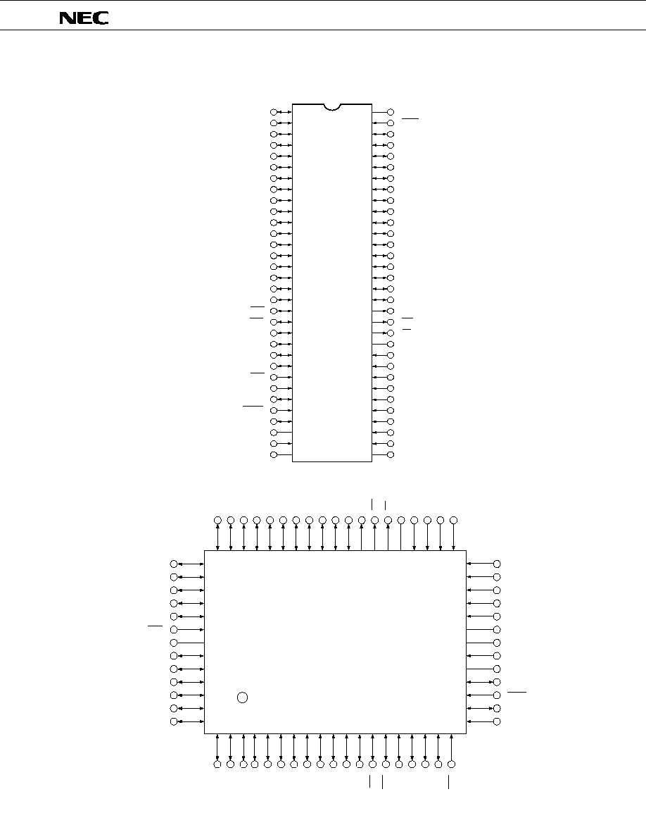
m
PIN CONFIGURATION (TOP VIEW)
∑
For
µ
PD78C10ACW,
µ
PD78C10AGQ-36,
µ
PD78C11ACW-
◊◊◊
,
µ
PD78C11AGQ-
◊◊◊
-36/37,
µ
PD78C12ACW-
◊◊◊
,
µ
PD78C12AGQ-
◊◊◊
-36/37.
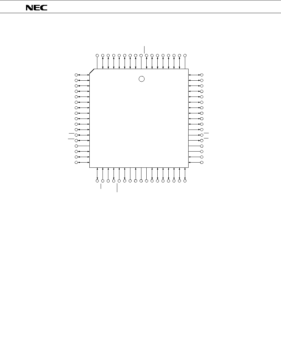
∑
For
µ
PD78C10AGF-3BE,
µ
PD78C11AGF-
◊◊◊
-3BE,
µ
PD78C12AGF-
◊◊◊
-3BE
AN4
AN3
AN2
AN1
AN0
AV
SS
V
SS
X1
X2
MODE0
RESET
MODE1
INT1
48
47
46
45
44
43
42
41
40
39
38
37
36
35
34
33
32
31
30
29
28
27
26
25
24
23
22
21
20
52
53
54
55
56
57
58
59
60
61
62
63
64
PA0
PA1
PD3
PD4
PD5
PD6
PD7
STOP
V
DD
PA2
PA3
PA4
PA5
4
5
6
7
8
9
10
11
12
13
14
15
16
17
18
19
PF3
PF2
PF1
PF0
ALE
WR
RD
AV
DD
V
AREF
AN7
AN6
AN5
PF7
PF6
PF5
PF4
51
50
49
1
2
3
PB1
PB2
PB3
PB4
PB5
PB6
PB7
PC0/T
X
D
PC1/R
X
D
PC2/SCK
PC3/INT2
PC4/TO
PC5/CI
PC6/CO0
PC7/CO1
NM1
PA6
PA7
PB0
PD2
PD1
PD0
1
PA0
2
PA1
3
PA2
4
PA3
5
PA4
6
PA5
7
PA6
8
PA7
9
PB0
10
PB1
11
PB2
12
PB3
13
PB4
14
PB5
15
PB6
16
PB7
17
PC0/T
X
D
18
PC1/R
X
D
19
PC2/SCK
20
PC3/INT2
21
PC4/TO
22
PC5/CI
23
PC6/CO0
24
PC7/CO1
25
NMI
26
INT1
27
MODE1
28
RESET
29
MODE0
30
X2
31
X1
32
V
SS
64
63
62
61
60
59
58
57
56
55
54
53
52
51
50
49
48
47
46
45
44
43
42
41
40
39
38
37
36
35
34
33
V
DD
STOP
PD7
PD6
PD5
PD4
PD3
PD2
PD1
PD0
PF7
PF6
PF5
PF4
PF3
PF2
PF1
PF0
ALE
WR
RD
AV
DD
V
AREF
AN7
AN6
AN5
AN4
AN3
AN2
AN1
AN0
AV
SS
4
µ
PD78C10A,78C11A,78C12A
∑
For
µ
PD78C10AL,
µ
PD78C11AL-
◊◊◊
,
µ
PD78C12AL-
◊◊◊
IC
PA6
PA5
PA4
PA3
PA2
PA1
PA0
V
DD
STOP
PD7
PD6
PD5
PD4
PD3
PD2
IC
PA7
PB0
PB1
PB2
PB3
PB4
PB5
PB6
PB7
PC0/T
X
D
PC1/R
X
D
PC2/SCK
PC3/INT2
IC
PC4/TO
PC5/CI
PC6/CO0
PD1
PD0
PF7
PF6
PF5
PF4
PF3
PF2
PF1
PF0
ALE
WR
RD
AV
DD
IC
V
AREF
AN7
9
8
7
6
5
4
3
2
1
68 67 66 65 64 63 62 61
60
59
58
57
56
55
54
53
52
51
50
49
48
47
46
45
44
27 28 29 30 31 32 33 34 35 36 37 38 39 40 41 42 43
10
11
12
13
14
15
16
17
18
19
20
21
22
23
24
25
26
PC7/C01
NMI
INT1
MODE1
RESET
MODE0
X2
X1
V
SS
AV
SS
AN0
AN1
AN2
AN3
AN4
AN5
AN6
5
µ
PD78C10A,78C11A,78C12A
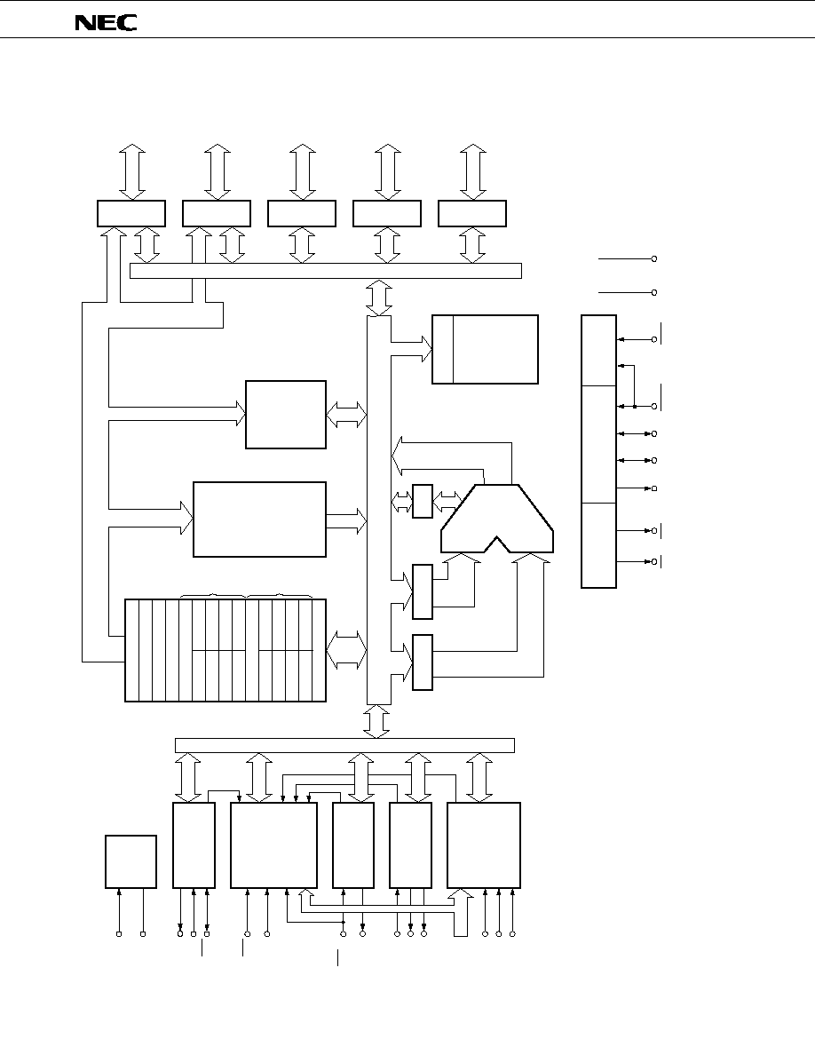
SERIAL I/O
X1
ALU
(8/16)
PC0/T
X
D
X2
PC1/R
X
D
PC2/SCK
OSC
INT.
CONTROL
NMI
INT1
8
8
4
8
TIMER
TIMER/
EVENT COUNTER
8
8
8
PC3/INT2/TI
PC4/TO
PC5/CI
PC6/CO0
PC7/CO1
A/D
CONVERTER
V
AREF
AV
DD
AV
SS
8
LATCH
INC/DEC
PC
SP
EA
EA'
V
A
B
C
D
E
H
L
V'
A'
B'
C'
D'
E'
H'
L'
BUFFER
8
16
12/
13
PROGRAM*1
MEMORY
DATA
MEMORY
(256-BYTE)
8/16
INST.REG
LATCH
LATCH
16
16
INTERNAL DATA BUS
16
16
16
6
INST.
DECODER
8
8
STAND BY
CONTROL
SYSTEM
CONTROL
READ/WRITE
CONTROL
RESET
V
SS
V
DD
STOP
MODE0
MODE1
ALE
WR
RD
POR
T F
8
8
8
POR
T D
8
8
8
POR
T C
8
PC7-0*2
8
POR
T B
8
PB7-0*2
8
POR
T A
8
PA7-0*2
8
16
AN7-0
PSW
PD7-0/
AD7-0
PF7-0/
AB15-8
MAIN
G.R
ALT
G.R
8
8
BLOCK DIAGRAM
*
1. It depends on a product type.
The
µ
PD78C11A has 4K bytes, and the
µ
PD78C12A has 8K
bytes.
The
µ
PD78C10A does not incorporate a program memory.
2. An on-chip pull-up resistor is available by mask option
(
µ
PD78C11A, 78C12A only).

6
µ
PD78C10A,78C11A,78C12A
CONTENTS
1.
PIN FUNCTIONS .....................................................................................................................................
7
1.1
LIST OF PIN FUNCTION ................................................................................................................................
7
1.2
PIN INPUT/OUTPUT CIRCUITS ....................................................................................................................
9
1.3
PIN MASK OPTIONS ......................................................................................................................................
14
1.4
RECOMMENDED CONNECTION OF UNUSED PINS ..................................................................................
14
2.
DIFFERENCES BETWEEN
µ
PD78C10A AND
µ
PD78C11A, 78C12A ................................................... 15
3.
RESET OPERATIONS ............................................................................................................................. 17
4.
INSTRUCTION SET ................................................................................................................................. 20
4.1
IDENTIFIER/DESCRIPTION OF OPERAND ...................................................................................................
20
4.2
SYMBOL DESCRIPTION OF OPERATION CODE .........................................................................................
21
4.3
INSTRUCTION EXECUTION TIME ................................................................................................................
22
5.
LIST OF MODE REGISTERS .................................................................................................................. 34
6.
ELECTRICAL SPECIFICATIONS ............................................................................................................. 35
7.
CHARACTERISTIC CURVES (REFERENCE VALUES) ......................................................................... 47
8.
DIFFERENCES IN 87AD SERIES PRODUCTS ...................................................................................... 50
9.
PACKAGE INFORMATION ..................................................................................................................... 54
10. RECOMMENDED SOLDERING CONDITIONS ...................................................................................... 60
APPENDIX DEVELOPMENT TOOLS ............................................................................................................ 62
7
µ
PD78C10A,78C11A,78C12A
Strobe signal to latch externally the lower address information which is output to PD7 to
PD0 pins to access external memory. When RESET signal is either low or in the hardware
STOP mode, this signal becomes output high-impedance.
Strobe signal which is output for write operation of external memory. It becomes high in
any cycle other than the data write machine cycle of external memory. When RESET signal
is either low or in the hardware STOP mode, this signal becomes output high-impedance.
Strobe signal which is output for read operation of external memory. It becomes high in any
cycle other than the read machine cycle of external memory. When RESET signal is either
low or in the hardware STOP mode, this signal becomes output high-impedance.
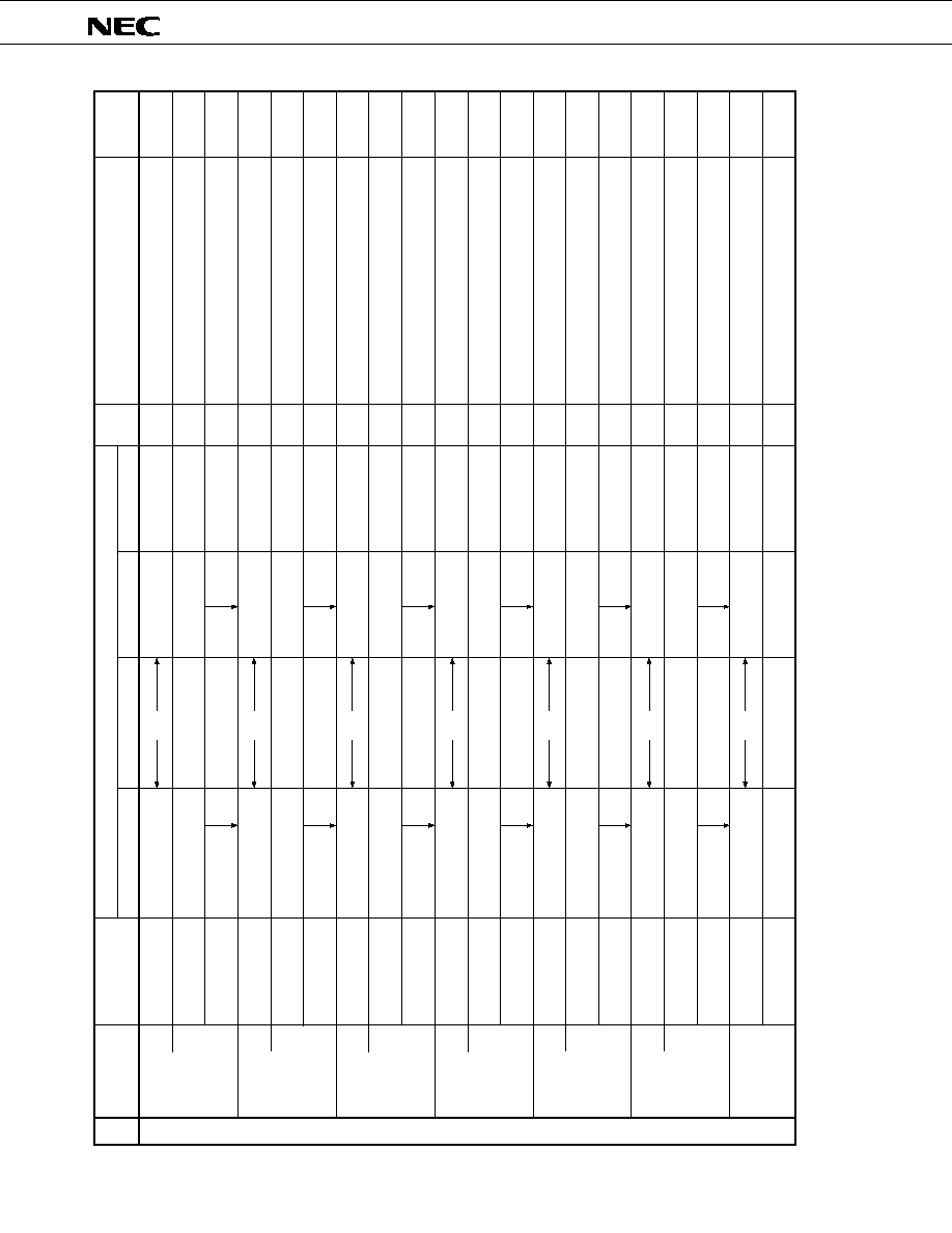
1.
PIN FUNCTIONS
1.1
LIST OF PIN FUNCTION (1/2)
Function
Pin Name
I/O
PB7 to PB0
(Port B)
Receive Data
Input pin for serial data.
Input-output/
Input
Transmit Data
Output pin for serial data.
Serial Clock
Input-output pin for serial clock.
It becomes output clock for the internal
clock use, and input for the external.
Interrupt Request/Timer Input
Maskable interrut input pin of the edge
trigger (falling edge), or an external clock
input pin for a timer. Also, it can be used
as a zero-cross detection pin for AC
input.
Timer Output
Square wave defining one cycle of internal
clock or timer counter time as half cycle
is output.
Counter Input
External pulse input pin to timer/event
counter.
Counter Output 0, 1
Programmable rectangle wave output by
timer/event counter.
Address/Data Bus
When external memory is used, it be-
comes multiplexed address/data bus.
Port D
8-bit input-output port, which can specify
input-output in byte units (
µ
PD78C11A).
Port F
8-bit input-output port, which can specify
input-output bit-wise.
Address Bus
When external memory is used, it be-
comes address bus.
Port C
8-bit input-output port,
which can specify input/ output bit-wise.
PA7 to PA0
(Port A)
8-bit input-output port, which can specify input/output bit-wise.
8-bit input-output port, which can specify input/output bit-wise.
Input/Output
Input/Output
Input-output/
Output
PC0/T
X
D
PC1/RxD
PC2/SCK
Input-output/
Input-output
PC3/INT2/TI
Input-output/
Input/Input
Input-output/
Output
PC4/TO
PC5/CI
Input-output/
Input
PC6/CO0
PC7/CO1
Input-output/
Output
PD7 to PD0/
AD7 to AD0
Input-output/
Input-output
PF7 to PF0/
AB15 to AB8
Input-output/
Output
WR
(Write Strobe)
Output
RD
(Read Strobe)
Output
ALE
(Address Latch
Enable)
Output

8
µ
PD78C10A,78C11A,78C12A
µ
PD78C11A and 78C12A sets MODE0 pin to "0" (low level), and MODE1 pin to "1" (high
level*)
µ
PD78C10A allows you to set MODE0, MODE1 pins to select 4K, 16K, or 64K bytes for the
size of the memory which is installed externally.
MODE0
MODE1
External Memory
0
0
4K bytes
1
0
16K bytes
1
1
64K bytes
Also, when each of MODE0 and MODE1 pins is set to "1"*, it is synchronized to ALE to output
a control signal.
1.1
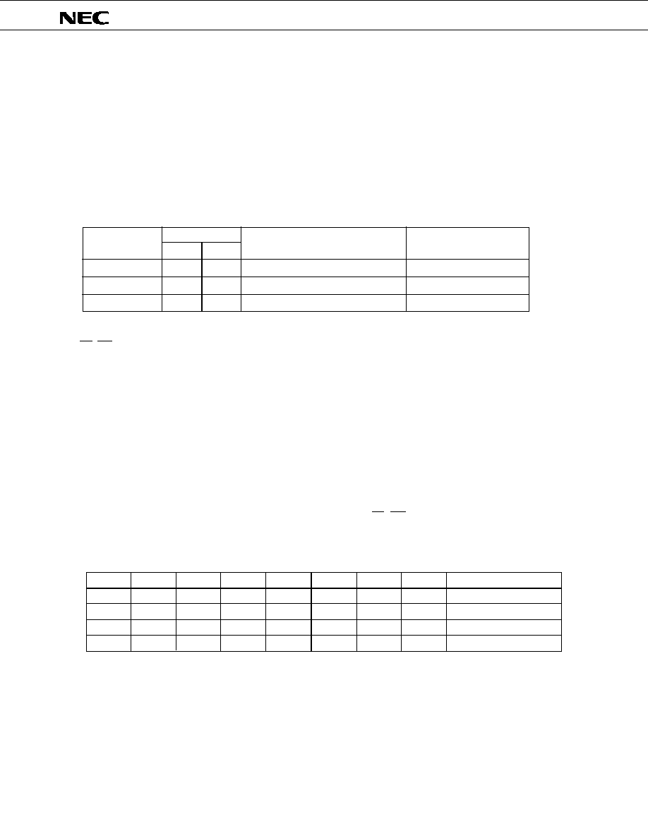
LIST OF PIN FUNCTION (2/2)
Function
Pin Name
I/O
Input-output
MODE0
MODE1
(Mode)
Input
Control signal input pin in hardware STOP mode. The oscillation stops when a clock is
supplied from outside.
8 pins of analog input to A/D converter. AN7 to AN4 can be used as edge detection (falling
edge) input.
*
Pull-up. Pull-up resister R is 4 [k
]
R
0.4 t
CYC
[k
] (t
CYC
is ns unit).
Remarks The
µ
PD78C11A and
µ
PD78C12A are pull-up resistor incorporation specifiable by mask option at ports
A, B and C.
NMI
(Non-Maskable
Interrupt)
INT1
( I n t e r r u p t
Request)
Input
Non-maskable interrupt input pin of the edge trigger (falling edge)
A maskable interrupt input pin of the edge trigger (rising edge). Also, it can be used as a
zero-cross detection pin for AC input.
Input
AN7 to AN0
(Analog Input)
V
AREF
(Reference
Voltage)
Input
A common pin serving both as a standard voltage input pin for A/D converter and as a
control pin for A/D converter operation.
AV
DD
(Analog V
DD
)
Power supply pin for A/D converter.
AV
SS
(Analog V
SS
)
GND pin for A/D converter.
X1, X2
(Crystal)
RESET
(Reset)
STOP
(Stop)
V
DD
V
SS
Crystal connection pins for system clock oscillation. X1 should be input when a clock is
supplied from outside. Input the clock of the reverse phase of X1 to X2.
Input
Low-level active system reset input.
Positive power supply pin.
GND pin.
5
9
µ
PD78C10A,78C11A,78C12A
PA7 to PA0
5
RESET
2
PB7 to PB0
5
RD
4
PC1 to PC0
5
WR
4
PC2/SCK
8
ALE
4
PC3/INT2
10
STOP
2
PC7 to PC4
5
MODE0
11
PD7 to PD0
5
MODE1
11
PF7 to PF0
5
AN3 to AN0
7
NMI
5
AN7 to AN4
12
INT1
2
V
AREF
13
Pin Name
Pin Name
Type No.
Type No.
Table 1-2 Pin Type No. (
µ
PD78C11A and 78C12A)
PA7 to PA0
5-A
RESET
2
PB7 to PB0
5-A
RD
4
PC1 to PC0
5-A
WR
4
PC2/SCK
8-A
ALE
4
PC3/INT2
10-A
STOP
2
PC7 to PC4
5-A
MODE0
11
PD7 to PD0
5
MODE1
11
PF7 to PF0
5
AN3 to AN0
7
NMI
2
AN7 to AN4
12
INT1
9
V
AREF
13
Pin Name
Pin Name
Type No.
Type No.
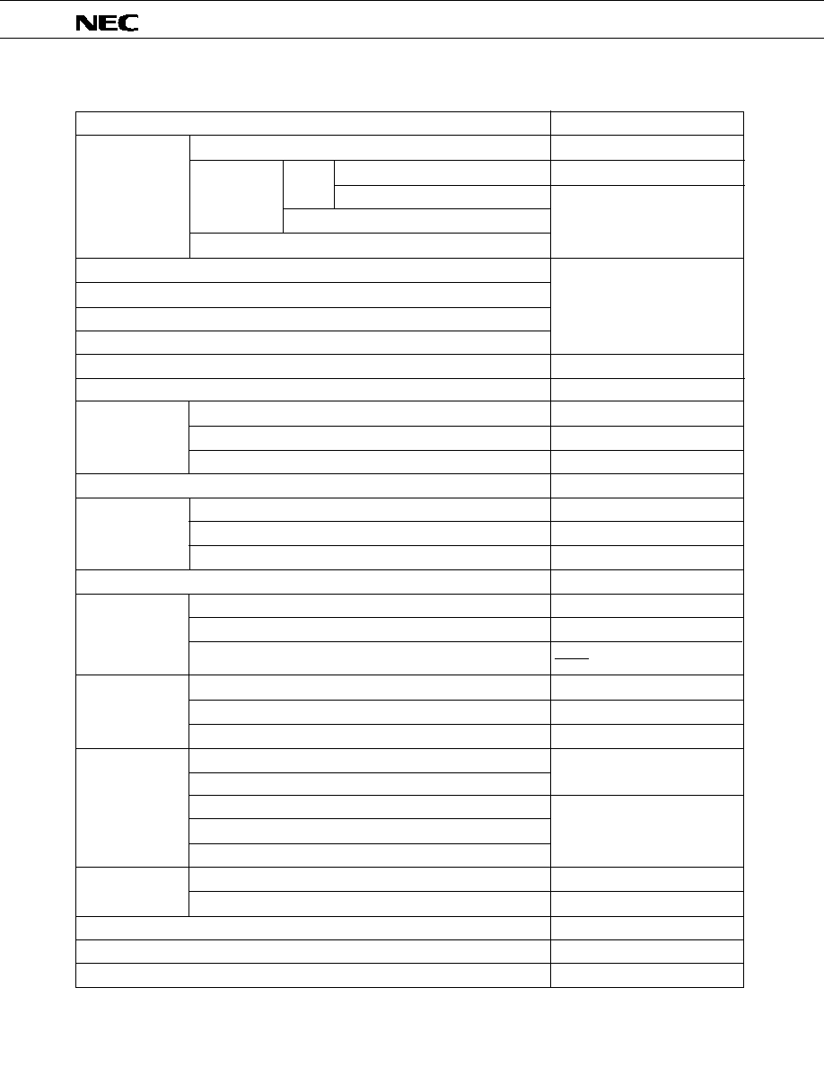
1.2
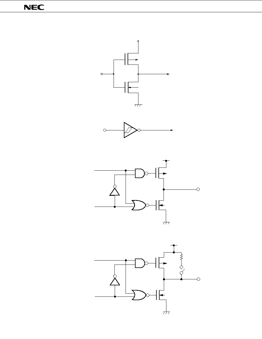
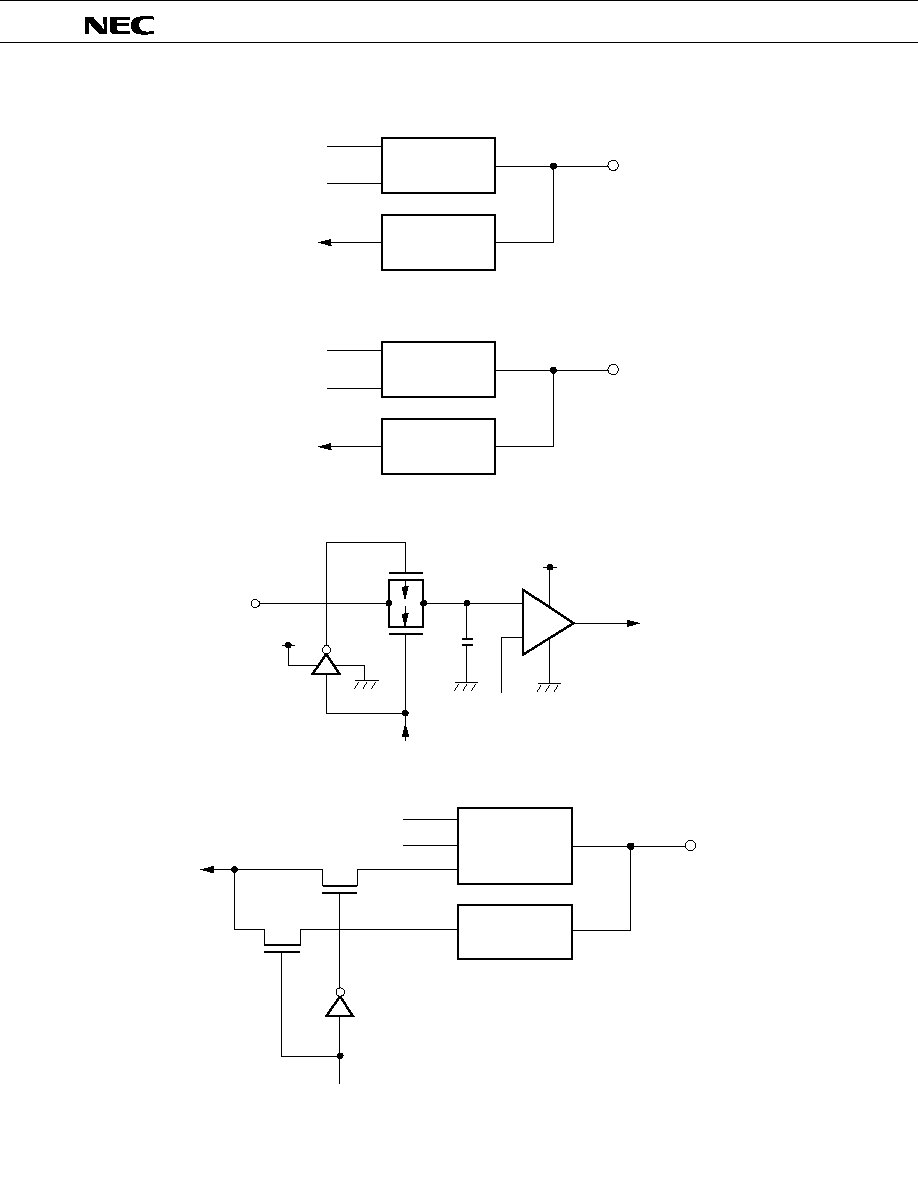
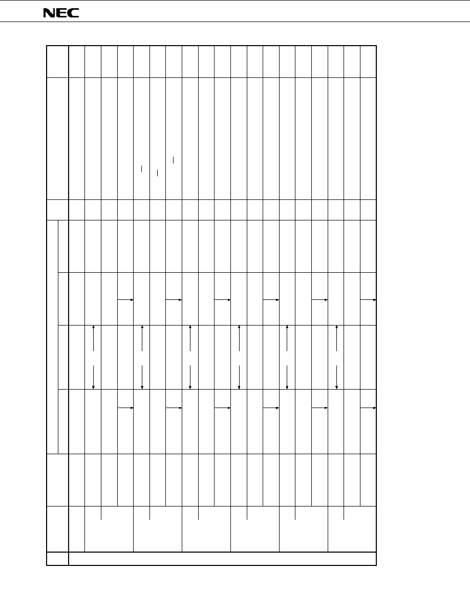
PIN INPUT/OUTPUT CIRCUITS
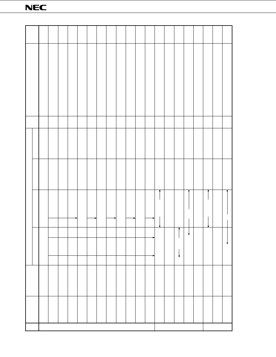
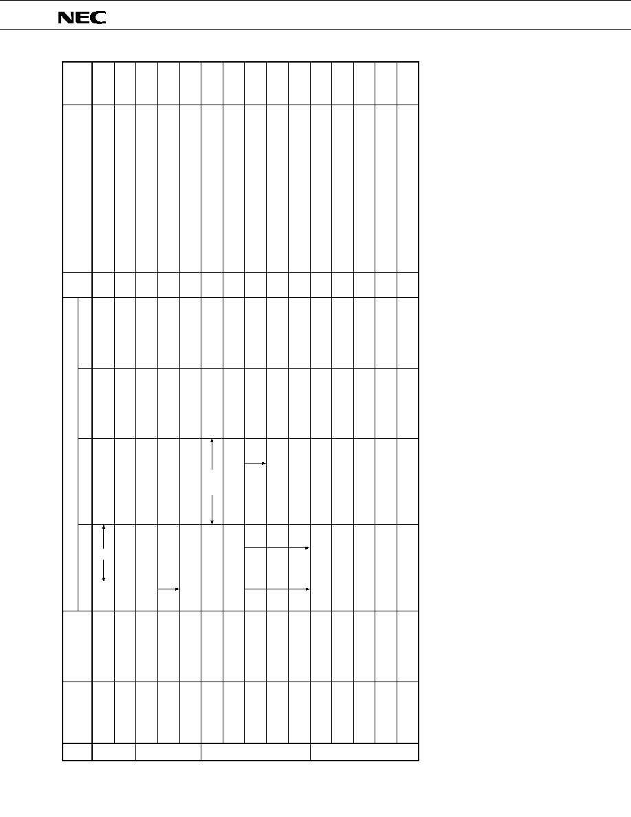
Tables 1-1 and 1-2, and figures (1) to (15) show input- output circuits of each pin in a partially simplified form.
Table 1-1 Pin Type No. (
µ
PD78C10A)
10
µ
PD78C10A,78C11A,78C12A
(1)
Type 1
(2)
Type 2
(3)
Type 4
(4)
Type 4-A
V
P-ch
output disable
N-ch
OUT
DD
output data
P-ch
output disable
N-ch
OUT
V
DD
output data
V
DD
P-
IN
N-
ch
ch
IN
11
µ
PD78C10A,78C11A,78C12A
(5)
Type 5
(6)
Type 5-A
(7)
Type 7
(8)
Type 8
Type5
Type2
output data
output disable
IN/OUT
MCC
IN/OUT
output data
output disable
Type4
Type1
IN/OUT
output data
output disable
Type4-A
Type1
P-ch
N-ch
AV
DD
AV
DD
AV
SS
Sampling
C
+
-
Reference Voltage
(From Voltage Tap of Series Resistance String)
IN
AV
SS
12
µ
PD78C10A,78C11A,78C12A
(9)
Type 8-A
(10) Type 9
(11) Type 10
Type1
IN
self bias
enable
data
Type5
Type9
output data
output disable
IN/OUT
MCC
self bias
enable
Type5-A
Type2
output data
output disable
IN/OUT
MCC

13
µ
PD78C10A,78C11A,78C12A
(12) Type 10-A
(13) Type 11
(14) Type 12
(15) Type 13
Type5-A
Type9
output data
output disable
IN/OUT
MCC
self bias
enable
Type1
N-ch
output data
IN/OUT
IN
Type7
Type2
Edge Detector
Type1
IN
AV
SS
STOP Mode

14
µ
PD78C10A,78C11A,78C12A
PA7 to PA0
PB7 to PB0
PC7 to PC0
PD7 to PD0
PF7 to PF0
RD
WR
ALE
STOP
INT1, NMI
AV
DD
AV
AREF
AV
SS
AN7 to AN0
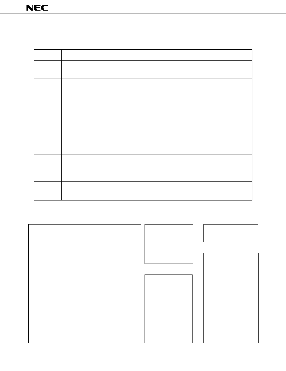
1.3
PIN MASK OPTIONS
µ
PD78C11A and 78C12A has the following mask options, which can be selected bit-wise according to the
application.
Cautions
1. Zero-cross function can not be operated normally if pull-up resistor is incorporated
in PC3.
2.
µ
PD78C10A has no mask option.
Pin Name
Mask Options
PA7 to PA0
PB7 to PB0
PC7 to PC0
Pull-up resistor incorporated
Pull-up resistor not incorporated
1.4
RECOMMENDED CONNECTION OF UNUSED PINS
Recommended Connection
Pin
Connect to V
SS
or V
DD
via resistor
Leave open
Connect to AV
SS
or AV
DD
Connect to V
DD
Connect to V
SS
or V
DD
Connect to V
DD
Connect to V
SS
15
µ
PD78C10A,78C11A,78C12A
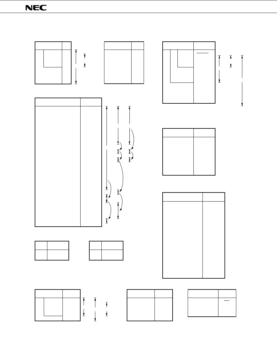
PF7
PF6
PF5
PF4
PF3
PF2
PF1
PF0
External Memory
Port
Port
Port
Port
Port
Port
Port
Port
Maximam 256 bytes
Port
Port
Port
Port
AB11
AB10
AB9
AB8
Maximum 4K bytes
Port
Port
AB13
AB12
AB11
AB10
AB9
AB8
Maximum 16K bytes
AB15
AB14
AB13
AB12
AB11
AB10
AB9
AB8
Maximum 56K/60K bytes*
External memory is accessed by using PD7 to PD0 (multiplexed address/data bus), PF7 to PF0 (address bus), and
the RD, WR, and ALE signals. When 4K-byte or 16K-byte external memory is accessed PF7 to PF0 not used as address
lines can be used as general purpose input/output ports.
The size of external memory can be specified by MODE0 and MODE1 pin setting. Preset each bit of MEMORY
MAPPING reisters MM2, MM1, and MM0 to "0".
(2)
µ
PD78C11A and 78C12A
The
µ
PD78C11A has an on-chip mask programmable ROM at addresses 0000H to 0FFFH and RAM at addresses
FF00H to FFFFH. Externally, memory can be extended up to 60K bytes (addresses 1000H to FEFFH) in steps. The
µ
PD78C12A has an on-chip mask programmable ROM at address 0000H to 1FFFH and RAM at address FF00H to
FFFFH. Externally, memory can be extended up to 56K bytes (address 2000H to FEFFH) in steps. The size of the
external extension memory can be selected from among no external memory, 256 bytes, 4K bytes, 16K bytes, and
56K/60K bytes* by MEMORY MAPPING register setting. External memory can be accessed by using PD7 to PD0
(multiplexed address/data bus), PF7 to PF0 (address bus), and the RD, WR, and ALE signals. Programs and data
can be stored in external memory. PF7 to PF0 become address lines corresponding to the size of external memory.
The remaining pins can be used as general purpose input/output ports.
2. DIFFERENCES BETWEEN
µ
PD78C10A AND
µ
PD78C11A, 78C12A
The difference between the
µ
PD78C10A and
µ
PD78C11A, 78C12A is whether or not there is an on-chip mask
programmable ROM. The memory map differs accordingly as described below.
(1)
µ
PD78C10A
Since the
µ
PD78C10A does not have an on-chip ROM, all memory, except the on-chip RAM area (addresses FF00H
to FFFFH) can be installed outside. The size of this external memory can be selected from among 4K bytes (0000H
to 0FFFH), 16K bytes (0000H to 3FFFH), and 64K bytes (0000H to FEFFH) by MODE0 and MODE1 pin setting as shown
in the following table and Fig. 2-1.
4K bytes access
16K bytes access
64K bytes access
MODE1
0
0
1
MODE0
0
1
1
4K bytes (address 0000H to 0FFFH)
16K bytes (address 0000H to 3FFFH)
64K bytes (address 0000H to FEFFH)
Address FF00H to FFFFH
Address FF00H to FFFFH
Address FF00H to FFFFH
Control Pin
Operation Mode
External Memory
On-Chip RAM
*
µ
PD78C11A: 60K bytes,
µ
PD78C12A: 56K bytes

16
µ
PD78C10A,78C11A,78C12A
Fig. 2-1
µ
PD78C10A Memory Map
Not Used
Not Used
FFFFH
FF00H
0000H
0FFFH
3FFFH
4K Bytes Access
16K Bytes Access
64K Bytes Access
MODE0 = 1
MODE1 = 1
MODE0 = 1
MODE1 = 0
MODE0 = 0
MODE1 = 0
A
B
C
J
K
L
1
2
3
:
;
C
D
E
L
M
N
"
+
,
4
5
=
F
G
O
P
External
Memory
On-Chip RAM
External
Memory
On-Chip RAM
External
Memory
On-Chip RAM

17
µ
PD78C10A,78C11A,78C12A
3.
RESET OPERATIONS
When RESET Input becomes low, the system reset is activated to create the following status.
∑
INTERRUPT ENABLE F/F is reset and interrupt is disabled.
∑
All the interrupt mask registers are set (1) and interrupt is masked.
∑
An interrupt request flag is reset (0) and hold interrupt is eliminated.
∑
Each bit of PSW is reset (0).
∑
0000H is loaded into the program counter (PC).
∑
The MODE A, MODE B, MODE C, and MODE F registers are set to FFH and the bits (MM0, 1, and 2) of the MODE
CONTROL C and MEMORY MAPPING registers are respectively reset (0), then all the
ports (A, B, C, D, and F) become input port (output high-impedance).
∑
All the test flags but SB flag are reset (0).
∑
A timer mode register is set to FFH, and TIMER F/F is reset.
∑
The mode register (ETMM, EOM) of a timer/event counter is reset (0).
∑
The serial mode high register(SMH) of serial interface is reset (0), while the serial mode low register (SML) is
set to 48H.
∑
The A/D channel mode register of the A/D converter is reset (0).
∑
WR, RD, ALE signals become high-impedance.
∑
The ZC1, ZC2 bits of the zero-cross mode register (ZCM) are set (1).
∑
The internal timing generator is initialized.
∑
Data memory and the following register contents are undefined:
Stack pointer (SP)
Expansion accumulator (EA, EA'), accumulator (A, A')
General register (B, C, D, E, H, L, B', C', D', E', H', L')
Output latch of each port
TIMER REG0, 1 (TM0, TM1)
TIMER/EVENT COUNTER REG0, 1 (ETM0, ETM1)
RAE bit of MEMORY MAPPING register
SB flag of test flag
When RESET input becomes high, the reset status is released. Then, execution of the program is started from
0000H. The contents of various kinds of registers must be initialized or re-initialized in the program, if necessary.
Table 3-1 shows the state of each hardware after reset.
Table 3-2 shows the state of each pin after reset.
18
µ
PD78C10A,78C11A,78C12A
FFH
0
Undefined
Timer mode register (TMM)
Timer
Timer F/F
Timer register (TM0, TM1)
Timer/event counter mode register (ETMM)
Timer/event counter output mode register (EOM)
Timer/event counter Timer/event counter register (ETM0, ETM1)
Timer/event counter capture register (ECPT)
Timer/event counter (ECNT)
Serial mode high register (SMH)
Serial mode low register (SML)
A/D channel mode register (ANM)
MM register (MM3; RAE bit)
Zero cross mode register (ZC1, ZC2 bits)
Table 3-1 State of Each Hardware after Reset
Expansion accumulator (EA, EA')
Accumulator (A, A')
General register (B, C, D, E, H, L, B', C', D', E', H', L')
Working register vector register (V, V')
Program counter (PC)
Stack pointer (SP)
Mode register (MA, MB, MC, MF)
Port
MCC register
MM register (bits MM0 to MM2)
Output latch of each port
INTERRUPT ENABLE F/F
Interrupt
Request flag
Mask register
Test flag (except SB flag)
Power-on reset
Standby flag (SB)
Standby mode
Hardware
Reset input during normal operation
Internal data
memory
0000H
Undefined
FFH
00H
0
Undefined
0
0
FFH
0
1
Previous contents held.
Contents immediately before
RESET input held
00H
Undefined
00H
48H
00H
Undefined
1
Undefined
Serial interface
State after Reset
Reset input
during normal
operation
Reset input in standby mode
Writing
by CPU
Write address data
Address data other than the aboove
Power-on reset
Previous contents held.
Undefined
Previous contents held.
Operation other than writing by CPU

19
µ
PD78C10A,78C11A,78C12A
WR
RD
ALE
All ports (PA, PB, PC, PD, PF)
High-impedance
State after Reset
Pin
Table 3-2 State of Each Pin after Reset
20
µ
PD78C10A,78C11A,78C12A
Identifier
Description
r
V, A, B, C, D, E, H, L
r1
EAH, EAL, B, C, D, E, H, L
r2
A, B, C
sr
PA, PB, PC, PD, PF, MKH, MKL, ANM, SMH, SML, EOM, ETMM, TMM, MM, MCC, MA, MB, MC, MF,
TXB, TM0, TM1, ZCM
sr1
PA, PB, PC, PD, PF, MKH, MKL, ANM, SMH, EOM, TMM, RXB, CR0, CR1, CR2, CR3
sr2
PA, PB, PC, PD, PF, MKH, MKL, ANM, SMH, EOM, TMM
sr3
ETM0, ETM1
sr4
ECNT, ECPT
rp
SP, B, D, H
rp1
V, B, D, H, EA
rp2
SP, B, D, H, EA
rp3
B, D, H
rpa
B, D, H, D+, H+, D≠, H≠
rpa1
B, D, H
rpa2
B, D, H, D+, H+, D≠, H≠, D+byte, H+A, H+B, H+EA, H+byte
rpa3
D, H, D++, H++, D+byte, H+A, H+B, H+EA, H+byte
wa
8 bit immediate data
word
16 bit immediate data
byte
8 bit immediate data
bit
3 bit immediate data
f
CY, HC, Z
irf
NMI*, FT0, FT1, F1, F2, FE0, FE1, FEIN, FAD, FSR, FST, ER, OV, AN4, AN5, AN6, AN7, SB
Remarks
1. sr to sr4 (special register)
2. rp to rp3 (register pair)
4. f (flag)
PA
:
PORT A
ETMM :
TIMER/EVENT
PB
:
PORT B
COUNTER MODE
PC
:
PORT C
EOM
:
TIMER/EVENT
PD
:
PORT D
COUNTER OUTPUT
PF
:
PORT F
MODE
MA
:
MODE A
ANM
:
A/D CHANNEL MODE
MB
:
MODE B
CR0
:
A/D CONVERSION
MC
:
MODE C
to
RESULT 0 to 3
MCC
:
MODE CONTROL C
CR3
MF
:
MODE F
TXB
:
T
X
BUFFER
MM
:
MEMORY MAPPING
RXB
:
R
X
BUFFER
TM0
:
TIMER REG0
SMH
:
SERIAL MODE High
TM1
:
TIMER REG1
SML
:
SERIAL MODE Low
TMM
:
TIMER MODE
MKH
:
MASK High
ETM0 :
TIMER/EVENT
MKL
:
MASK Low
COUNTER REG0
ZCM
:
ZERO CROSS MODE
ETM1 :
TIMER/EVENT
COUNTER REG1
ECNT
:
TIMER/EVENT
COUNTER UPCOUNTER
ECPT
:
TIMER/EVENT
COUNTER CAPTURE
SP
:
STACK POINTER
B
:
BC
D
:
DE
H
:
HL
V
:
VA
EA
:
EXTENDED
ACCUMULATOR
3. rpa to rpa3 (rp addressing)
B
:
(BC)
D
:
(DE)
H
:
(HL)
D+
:
(DE)+
H+
:
(HL)+
D≠
:
(DE)≠
H≠
:
(HL)≠
D++
:
(DE)++
H++
:
(HL)++
D + byte :
(DE + byte)
H + A
:
(HL + A)
H + B
:
(HL + B)
H + EA
:
(HL + EA)
H + byte :
(HL + byte)
NMI
:
NMI INPUT
FT0
:
INTFT0
FT1
:
INTFT1
F1
:
INTF1
F2
:
INTF2
FE0
:
INTFE0
FE1
:
INTFE1
FEIN
:
INTFEIN
FAD
:
INTFAD
FSR
:
INTFSR
FST
:
INTFST
ER
:
ERROR
OV
:
OVERFLOW
AN4
:
ANALOG INPUT 4 to 7
to
AN7
SB
:
STANDBY
CY
:
CARRY
HC
:
HALF CARRY
Z
:
ZERO
5. irf (interrupt flag)
4.
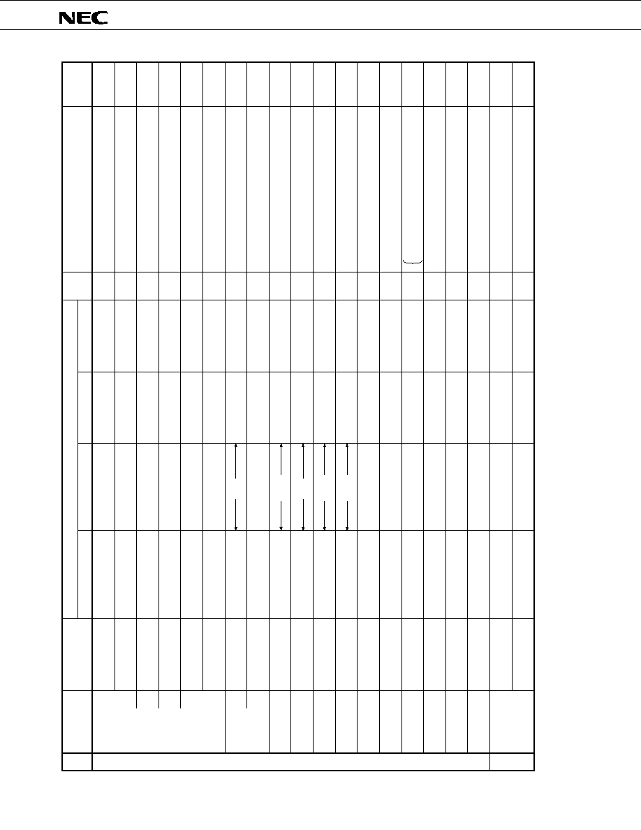
INSTRUCTION SET
4.1
IDENTIFIER/DESCRIPTION OF OPERAND
*
NMI can also be described as FNMI.
21
µ
PD78C10A,78C11A,78C12A
4.2
SYMBOL DESCRIPTION OF OPERATION CODE
R
2
0
0
0
0
1
1
1
1
R
1
0
0
1
1
0
0
1
1
R
0
0
1
0
1
0
1
0
1
reg
V
A
B
C
D
E
H
L
S
5
0
0
0
0
0
0
0
0
0
0
0
0
0
0
0
0
0
0
0
0
0
0
0
1
1
1
1
1
S
4
0
0
0
0
0
0
0
0
0
0
0
0
0
1
1
1
1
1
1
1
1
1
1
0
0
0
0
0
S
3
0
0
0
0
0
0
0
1
1
1
1
1
1
0
0
0
0
0
0
1
1
1
1
0
0
0
0
1
S
2
0
0
0
0
1
1
1
0
0
0
0
1
1
0
0
0
0
1
1
0
0
0
0
0
0
0
0
0
S
1
0
0
1
1
0
1
1
0
0
1
1
0
0
0
0
1
1
0
1
0
0
1
1
0
0
1
1
0
S
0
0
1
0
1
1
0
1
0
1
0
1
0
1
0
1
0
1
0
1
0
1
0
1
0
1
0
1
0
Special-reg
PA
PB
PC
PD
PF
MKH
MKL
ANM
SMH
SML
EOM
ETMM
TMM
MM
MCC
MA
MB
MC
MF
TXB
RXB
TM0
TM1
CR0
CR1
CR2
CR3
ZCM
r
r1
sr
U
0
0
1
special-reg
ETM0
ETM1
V
0
0
1
special-reg
ECNT
ECPT
P
2
0
0
0
0
1
P
1
0
0
1
1
0
P
0
0
1
0
1
0
reg-pair
SP
BC
DE
HL
EA
Q
2
0
0
0
0
1
Q
1
0
0
1
1
0
Q
0
0
1
0
1
0
reg-pair
VA
BC
DE
HL
EA
F
2
0
0
0
1
F
1
0
1
1
0
F
0
0
0
1
0
flag
CY
HC
Z
sr3
sr4
rp
rp1
f
irf
I
4
0
0
0
0
0
0
0
0
0
0
0
0
0
1
1
1
1
1
I
3
0
0
0
0
0
0
0
0
1
1
1
1
1
0
0
0
0
0
I
2
0
0
0
0
1
1
1
1
0
0
0
0
1
0
0
0
0
1
I
1
0
0
1
1
0
0
1
1
0
0
1
1
0
0
0
1
1
0
I
0
0
1
0
1
0
1
0
1
0
1
0
1
0
0
1
0
1
0
INTF
NMI
FT0
FT1
F1
F2
FE0
FE1
FEIN
FAD
FSR
FST
ER
OV
AN4
AN5
AN6
AN7
SB
T
2
0
0
0
0
1
1
1
1
T
1
0
0
1
1
0
0
1
1
T
0
0
1
0
1
0
1
0
1
reg
EAH
EAL
B
C
D
E
H
L
rpa
A
2
0
0
0
0
1
1
1
1
0
1
1
1
1
A
1
0
0
1
1
0
0
1
1
1
0
0
1
1
A
0
0
1
0
1
0
1
0
1
1
0
1
0
1
addressing
(BC)
(DE)
(HL)
(DE)+
(HL)+
(DE)-
(HL)-
(DE + byte)
(HL + A)
(HL + B)
(HL + EA)
(HL + byte)
A
3
0
0
0
0
0
0
0
0
1
1
1
1
1
C
2
0
0
1
1
0
1
1
1
1
C
1
1
1
0
0
1
0
0
1
1
C
0
0
1
0
1
1
0
1
0
1
addressing
(DE)
(HL)
(DE)++
(HL)++
(DE + byte)
(HL + A)
(HL + B)
(HL + EA)
(HL + byte)
C
3
0
0
0
0
1
1
1
1
1
rpa3
r
r2
rpa
rpa1
rpa2
sr
sr1
sr2
rp
rp2
rp3

22
µ
PD78C10A,78C11A,78C12A
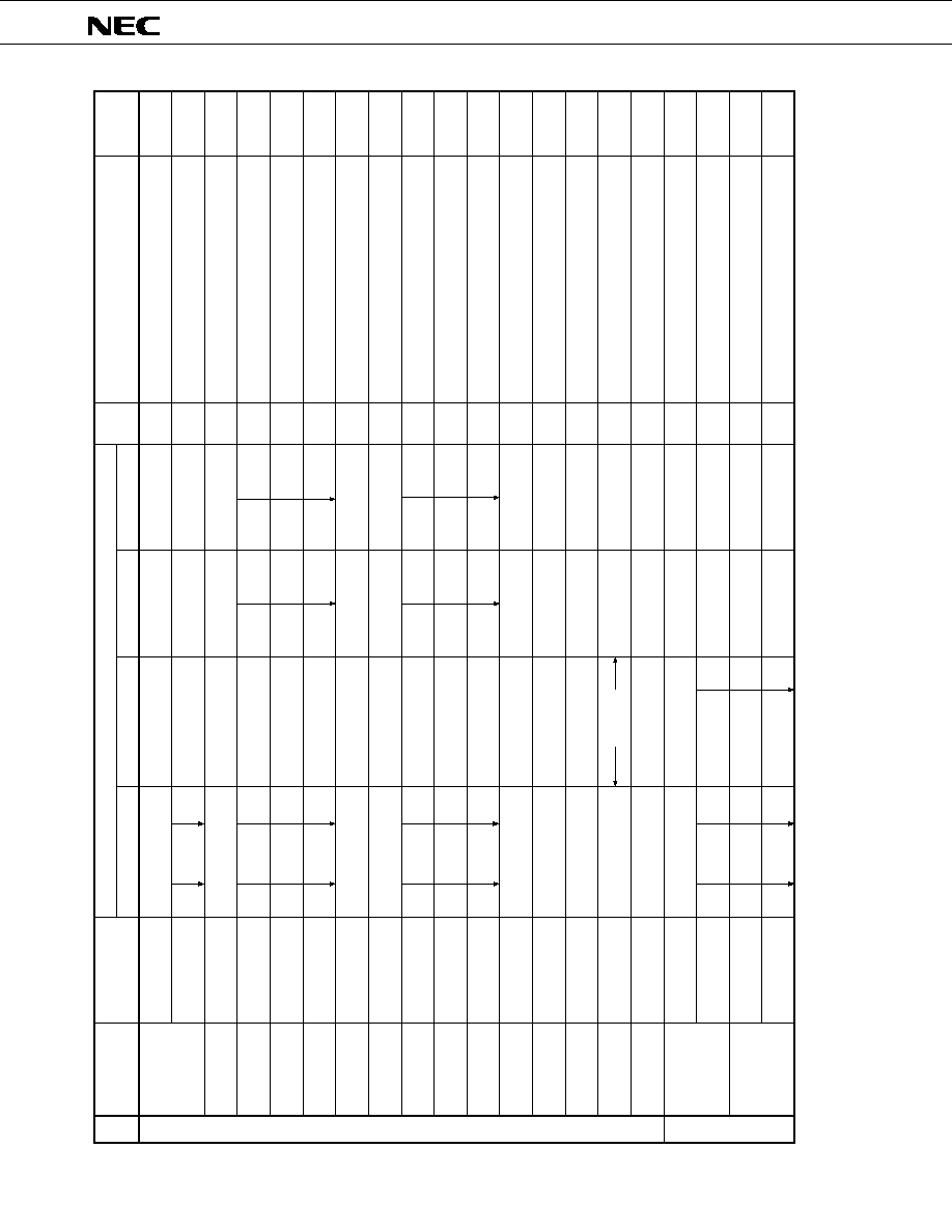
4.3
INSTRUCTION EXECUTION TIME
1 state shown here is composed of 3 clock cycles. When a clock cycle of 15 MHz is used, the execution time should
be 200 ns (= 3
◊
1/15
µ
s). In this case, the 4-state instruction which is the minimum execution time should be execution
time of 0.8
µ
s.
23
µ
PD78C10A,78C11A,78C12A
Note
1. Instruction Group
2. 16-bit data transfer instructions
Note 1
Mnemonic
Operand
B1
B2
B3
B4
Operation Code
State
Operation
Skip
Condition
8-bit data transfer instructions
MOV
*
*
MVI
r1, A
A, r1
sr, A
A, sr1
r, word
word, r
r, byte
*
sr2, byte
MVIW
*
wa, byte
MVIX
rpa1, byte
*
STAW
*
wa
LDAW
*
wa
STAX
*
rpa2
LDAX
*
rpa2
EXX
EXA
EXH
BLOCK
DMOV
rp3, EA
EA, rp3
0 0 0 1 1 T
2
T
1
T
0
0 0 0 0 1 T
2
T
1
T
0
0 1 0 0 1 1 0 1
0 1 0 0 1 1 0 0
0 1 1 1 0 0 0 0
0 1 1 1 0 0 0 0
0 1 1 0 1 R
2
R
1
R
0
0 1 1 0 0 1 0 0
0 1 1 1 0 0 0 1
0 1 0 0 1 0 A
1
A
0
0 1 1 0 0 0 1 1
0 0 0 0 0 0 0 1
A
3
0 1 1 1 A
2
A
1
A
0
A
3
0 1 0 1 A
2
A
1
A
0
0 0 0 1 0 0 0 1
0 0 0 1 0 0 0 0
0 1 0 1 0 0 0 0
0 0 1 1 0 0 0 1
1 0 1 1 0 1 P
1
P
0
1 0 1 0 0 1 P
1
P
0
1 1 S
5
S
4
S
3
S
2
S
1
S
0
1 1 S
5
S
4
S
3
S
2
S
1
S
0
0 1 1 0 1 R
2
R
1
R
0
0 1 1 1 1 R
2
R
1
R
0
Data
S
3
0 0 0 0 S
2
S
1
S
0
Offset
Data
Offset
Offset
Data*1
Data*1
Low Adrs
Low Adrs
Data
Data
High Adrs
High Adrs
r1
A
A
r1
sr
A
A
sr1
r
(word)
(word)
r
4
r
byte
sr2
byte
(V. wa)
byte
(rpa1)
byte
(V. wa)
A
A
(V. wa)
(rpa2)
A
A
(rpa2)
B
B', C
C', D
D'
E
E', H
H', L
L'
V, A
V', A', EA
EA'
(DE)
(HL) , C
C ≠ 1
End if borrow
rp3
L
EAL, rp3
H
EAH
EAL
rp3
L
, EAH
rp3
H
H, L
H', L'
4
10
10
17
17
7
14
13
10
10
10
7/13*3
7/13*3
4
4
4
13
(C + 1)
4
4
Note 2
+
+
24
µ
PD78C10A,78C11A,78C12A
Note
1. Instruction Group
2. 8-bit operation instructions (register)
Note 1
Mnemonic
Operand
B1
B2
B3
B4
Operation Code
State
Operation
Skip
Condition
16-bit data transfer instructions
DMOV
STEAX
sr3, EA
EA, sr4
word
word
word
word
rpa3
word
LDED
word
LHLD
word
LSPD
word
LDEAX
rpa3
PUSH
rp1
POP
*
rp1
LXI
TABLE
ADD
ADC
0 1 0 0 1 0 0 0
0 1 1 1 0 0 0 0
0 1 0 0 1 0 0 0
1 0 1 1 0 Q
2
Q
1
Q
0
1 0 1 0 0 Q
2
Q
1
Q
0
0 P
2
P
1
P
0
0 1 0 0
0 1 0 0 1 0 0 0
0 1 1 0 0 0 0 0
0 0 0 1 1 1 1 0
0 0 1 0 1 1 1 0
0 0 1 1 1 1 1 0
0 0 0 0 1 1 1 0
Data*2
Low Adrs
Low Adrs
High Adrs
High Adrs
sr3
EA
(word)
C, (word + 1)
B
(word)
E, (word + 1)
D
(word)
L, (word + 1)
H
(word)
SP
L
, (word + 1)
SP
H
(rpa3)
EAL, (rpa3 + 1)
EAH
C
(word), B
(word + 1)
E
(word), D
(word + 1)
L
(word), H
(word + 1)
SP
L
(word), SP
H
(word + 1)
EAL
(rpa3), EAH
(rpa3 + 1)
(SP ≠ 1)
rp1
H
, (SP ≠ 2)
rp1
L
rp2
word
C
(PC + 3 + A)
20
20
20
20
20
20
20
20
8
8
8
SBCD
SDED
SHLD
SSPD
LBCD
rp2, word
A, r
r, A
A, r
r, A
Note 2
0 1 1 1 0 0 0 0
0 1 0 0 1 0 0 0
1 1 0 1 0 0 1 U
0
1 1 0 0 0 0 0 V
0
1 0 0 1 C
3
C
2
C
1
C
0
0 0 0 1 1 1 1 1
0 0 1 0 1 1 1 1
0 0 1 1 1 1 1 1
0 0 0 0 1 1 1 1
1 0 0 0 C
3
C
2
C
1
C
0
Low Byte
1 0 1 0 1 0 0 0
1 1 0 0 0 R
2
R
1
R
0
0 1 0 0
1 1 0 1
0 1 0 1
Data*2
High Byte
14
14
14/20
13
10
10
17
8
SP
SP ≠ 2
B
(PC + 3 + A + 1)
A
A + r
r
r + A
A
A + r + CY
r
r + A + CY
rp1
L
(SP), rp1
H
(SP + 1)
SP
SP + 2
EA
sr4
*3
14/20
*3
25
µ
PD78C10A,78C11A,78C12A
Note
Instruction Group
Note
Mnemonic
Operand
B1
B2
B3
B4
Operation Code
State
Operation
Skip
Condition
8-bit operation instructions (register)
ADDNC
SUBNB
A, r
r, A
A, r
r, A
A, r
r, A
A, r
r, A
ANA
A, r
r, A
ORA
A, r
r, A
XRA
A, r
r, A
GTA
LTA
NEA
0 1 1 0 0 0 0 0
A
A + r
A
A ≠ r
r
r ≠ A
A
A ≠ r ≠ CY
r
r ≠ A ≠ CY
A
A ≠ r
r
r ≠ A
A
A
r
8
8
8
SUB
SBB
A, r
A, r
r, A
A, r
r, A
1 0 1 0 0 R
2
R
1
R
0
0 0 1 0
0 0 1 1
1 1 1 0
0 1 1 0
8
A ≠ r
r ≠ A
r
r + A
r, A
1 1 1 0
0 1 1 0
1 1 1 1
0 1 1 1
1 0 1 1
0 0 1 1
1 0 0 0 1 R
2
R
1
R
0
0 0 0 0
1 0 0 1
0 0 0 1
1 0 0 1 0 R
2
R
1
R
0
0 0 0 1
1 0 1 0 1 R
2
R
1
R
0
0 0 1 0
1 0 1 1
8
8
8
8
8
8
8
8
8
8
8
r
r
A
A
A
r
8
8
8
8
8
r
r
A
A
A
r
r
r
A
A ≠ r ≠ 1
r ≠ A ≠ 1
A ≠ r
r ≠ A
No Carry
No Carry
No
Borrow
No
Borrow
No Zero
No Zero
Borrow
Borrow
No
Borrow
No
Borrow
26
µ
PD78C10A,78C11A,78C12A
Note
Instruction Group
Note
Mnemonic
Operand
B1
B2
B3
B4
Operation Code
State
Operation
Skip
Condition
8-bit operation instructions (memory)
EQA
ADDNCX
A, r
r, A
A, r
A, r
rpa
rpa
rpa
rpa
SBBX
rpa
rpa
ANAX
rpa
rpa
XRAX
rpa
rpa
LTAX
EQAX
0 1 1 0 0 0 0 0
A ≠ r
A
r
A
r
A
A + (rpa)
A
A + (rpa)
A
A ≠ (rpa)
A
A ≠ (rpa) ≠ CY
OFFA
ADDX
rpa
rpa
1 1 1 1 1 R
2
R
1
R
0
0 1 1 1
1 1 0 0
1 1 0 1
A ≠ (rpa)
A
(rpa)
r ≠ A
rpa
1 1 0 0
1 1 0 1
1 1 0 1
1 0 1 0
1 1 1 0
1 0 1 1
1 0 0 1
1 1 1 0
1 1 1 1
8
8
8
8
11
A
A ≠ (rpa)
A
A
(rpa)
A
A
(rpa)
A ≠ (rpa)
A ≠ (rpa)
A
(rpa)
Zero
Zero
No Carry
No
Borrow
Zero
No Zero
Zero
No
Borrow
ONA
ADCX
SUBX
SUBNBX
ORAX
GTAX
NEAX
ONAX
OFFAX
0 1 1 1 0 0 0 0
1 1 0 0 0 A
2
A
1
A
0
1 1 1 1
1 0 0 0 1 A
2
A
1
A
0
1 0 0 1 0 A
2
A
1
A
0
1 0 1 0 1 A
2
A
1
A
0
1 0 1 1
A
A + (rpa) + CY
11
11
11
11
11
11
11
11
11
11
11
11
11
11
No Zero
Zero
Borrow
No Zero
8-bit operation
instructions (register)
A ≠ (rpa) ≠ 1
A
A
(rpa)
rpa
rpa
27
µ
PD78C10A,78C11A,78C12A
Note
Instruction Group
Note
Mnemonic
Operand
B1
B2
B3
B4
Operation Code
State
Operation
Skip
Condition
Immediate data operation instructions
ACI
*
*
ADINC
A, byte
r, byte
sr2, byte
A, byte
r, byte
sr2, byte
A, byte
*
r, byte
sr2, byte
SUI
A, byte
*
r, byte
sr2, byte
SBI
*
SUINB
ANI
A, byte
r, byte
0 1 0 0 0 1 1 0
0 1 1 1 0 1 0 0
0 1 1 0
0 1 0 1 0 1 1 0
0 1 1 1 0 1 0 0
0 0 1 0 0 1 1 0
0 1 1 1 0 1 0 0
0 1 1 0 0 1 1 0
0 1 1 1 0 1 0 0
0 1 1 1 0 1 1 0
0 1 1 1 0 1 0 0
0 0 1 1 0 1 1 0
0 1 1 1 0 1 0 0
0 0 0 0 0 1 1 1
0 1 1 1 0 1 0 0
S
3
1 0 0 0 S
2
S
1
S
0
0 1 0 1 0 R
2
R
1
R
0
Data
Data
Data
Data
A
A + byte
r
r + byte
sr2
sr2 + byte
A
A + byte + CY
r
r + byte + CY
sr2
sr2 + byte + CY
7
A
A + byte
r
r + byte
sr2
sr2 + byte
A
A ≠ byte
r
r ≠ byte
sr2
sr2 ≠ byte
A
A ≠ byte ≠ CY
r
r ≠ byte ≠ CY
A
A ≠ byte
sr2
sr2 ≠ byte
A
A
byte
r
r
byte
r
r ≠ byte
20
11
20
7
11
20
11
20
7
7
ADI
A, byte
r, byte
sr2, byte
A, byte
r, byte
sr2, byte
0 1 1 0
0 1 1 0
0 1 1 0
0 1 1 0
0 1 1 0
Data
0 1 0 0 0 R
2
R
1
R
0
Data
S
3
1 0 1 0 S
2
S
1
S
0
0 0 1 0 0 R
2
R
1
R
0
S
3
0 1 0 0 S
2
S
1
S
0
0 1 1 0 0 R
2
R
1
R
0
S
3
1 1 0 0 S
2
S
1
S
0
Data
0 1 1 1 0 R
2
R
1
R
0
S
3
1 1 1 0 S
2
S
1
S
0
Data
0 0 1 1 0 R
2
R
1
R
0
S
3
0 1 1 0 S
2
S
1
S
0
Data
Data
Data
Data
Data
11
7
7
7
11
20
sr2
sr2 ≠ byte ≠ CY
11
20
No
Borrow
No
Borrow
No
Borrow
No Carry
No Carry
No Carry
Data
*
*
0 0 0 0 1 R
2
R
1
R
0
11
28
µ
PD78C10A,78C11A,78C12A
Note
Instruction Group
Note
Mnemonic
Operand
B1
B2
B3
B4
Operation Code
State
Operation
Skip
Condition
Immediate data operation instructions
*
*
GTI
A, byte
r, byte
sr2, byte
A, byte
r, byte
sr2, byte
A, byte
*
r, byte
sr2, byte
LTI
A, byte
*
r, byte
sr2, byte
NEI
*
EQI
0 1 1 0 0 1 0 0
0 0 0 1 0 1 1 1
0 1 1 0
0 0 0 1 0 1 1 0
0 1 1 1 0 1 0 0
0 0 1 0 0 1 1 1
0 1 1 1 0 1 0 0
0 0 1 1 0 1 1 1
0 1 1 1 0 1 0 0
0 1 1 0 0 1 1 1
0 1 1 1 0 1 0 0
0 1 1 1 0 1 1 1
0 1 1 1 0 1 0 0
0 0 0 1 0 R
2
R
1
R
0
Data
Data
Data
Data
A
A
byte
r
r
byte
sr2
sr2
byte
A
A
byte
r
r
byte
sr2
sr2
byte
A ≠ byte≠ 1
r ≠ byte ≠ 1
sr2 ≠ byte ≠ 1
A ≠ byte
r ≠ byte
sr2 ≠ byte
A ≠ byte
sr2 ≠ byte
r ≠ byte
sr2 ≠ byte
A ≠ byte
11
11
11
ORI
A, byte
r, byte
sr2, byte
A, byte
r, byte
sr2, byte
0 1 1 0
0 1 1 0
0 1 1 0
0 1 1 0
0 1 1 0
Data
Data
S
3
0 0 1 0 S
2
S
1
S
0
0 0 1 0 1 R
2
R
1
R
0
S
3
0 1 0 1 S
2
S
1
S
0
0 0 1 1 1 R
2
R
1
R
0
S
3
0 1 1 1 S
2
S
1
S
0
Data
0 1 1 0 1 R
2
R
1
R
0
S
3
1 1 0 1 S
2
S
1
S
0
Data
0 1 1 1 1 R
2
R
1
R
0
S
3
1 1 1 1 S
2
S
1
S
0
Data
Data
Data
11
11
r ≠ byte
11
No Zero
Data
*
ANI
sr2, byte
XRI
Zero
0 1 1 1 0 1 0 0
S
3
0 0 0 1 S
2
S
1
S
0
0 0 0 1 1 R
2
R
1
R
0
S
3
0 0 1 1 S
2
S
1
S
0
Data
20
sr2
sr2
byte
7
20
7
20
7
14
7
14
7
14
7
14
Zero
Zero
No
Borrow
No Zero
No Zero
Borrow
Borrow
Borrow
No
Borrow
No
Borrow
29
µ
PD78C10A,78C11A,78C12A
Note
Instruction Group
Note
Mnemonic
Operand
B1
B2
B3
B4
Operation Code
State
Operation
Skip
Condition
Working register operation instructions
OFFI
*
*
ADDW
A, byte
r, byte
sr2, byte
A, byte
r, byte
sr2, byte
wa
wa
wa
SBBW
wa
wa
wa
ORAW
LTAW
EQAW
wa
wa
0 1 0 0 0 1 1 1
0 1 1 1 0 1 0 0
0 1 1 0
0 1 0 1 0 1 1 1
0 1 1 1 0 1 0 0
0 1 1 1 0 1 0 0
S
3
1 0 0 1 S
2
S
1
S
0
0 1 0 1 1 R
2
R
1
R
0
Data
offset
A
byte
r
byte
sr2
byte
A
byte
r
byte
sr2
byte
7
A
A +(V. wa)
A
A + (V. wa) + CY
A
A + (V. wa)
A
A ≠ (V. wa)
A
A ≠ (V. wa)
A
A
(V. wa)
A
A
(V. wa)
A ≠ (V. wa)
A ≠ (V. wa)
A
(V. wa)
A ≠ (V. wa)
14
11
14
14
14
14
14
ONI
wa
wa
wa
wa
wa
wa
0 1 1 0
Data
0 1 0 0 1 R
2
R
1
R
0
Data
S
3
1 0 1 1 S
2
S
1
S
0
1 1 0 1
Data
11
7
14
14
14
14
Borrow
No
Borrow
No
Borrow
No Carry
Immediate data
operation instructions
ADCW
ADDNCW
SUBW
SUBNBW
ANAW
XRAW
GTAW
NEAW
ONAW
1 1 0 0 0 0 0 0
1 0 1 0
1 1 1 0
1 1 1 1
1 0 1 1
1 0 0 0 1 0 0 0
1 0 0 1
1 0 0 1 0 0 0 0
1 0 1 0 1 0 0 0
1 0 1 1
1 1 1 0
1 1 1 1
1 1 0 0
14
14
14
A
A
(V. wa)
14
14
14
A ≠ (V. wa) ≠ 1
A
A ≠ (V. wa) ≠ CY
No Zero
No Zero
No Zero
Zero
Zero
Zero
No Zero
Zero
No Zero

30
µ
PD78C10A,78C11A,78C12A
Note
Instruction Group
Note
Mnemonic
Operand
B1
B2
B3
B4
Operation Code
State
Operation
Skip
Condition
Working register operation instructions
LTIW
*
*
EQIW
wa
wa, byte
wa, byte
wa, byte
wa, byte
wa, byte
wa, byte
wa, byte
wa, byte
DADD
EA, r2
EA, rp3
EA, rp3
ESUB
DSUBNB
DOR
EA, rp3
EA, rp3
0 1 1 1 0 1 0 0
0 0 0 0 0 1 0 1
0 0 0 1
Data
A
(V. wa)
(V. wa)
(V. wa)
byte
(V. wa)
(V. wa)
byte
(V. wa) ≠ byte ≠ 1
(V. wa) ≠ byte
(V. wa) ≠ byte
(V. wa) ≠ byte
(V. wa)
byte
(V. wa)
byte
EA
EA + r2
EA
EA + rp3 +CY
EA
EA + rp3
EA
EA ≠ r2
EA
EA
rp3
EA
EA
rp3
EA
EA
rp3
EA
EA ≠ rp3
19
13
13
13
13
11
11
OFFAW
EA, rp3
EA, r2
EA, rp3
EA, rp3
EA, rp3
EA, rp3
0 1 1 1
1 1 0 1 1 0 0 0
Offset
19
11
11
11
11
Borrow
No
Borrow
No
Borrow
No Carry
ONIW
OFFIW
EADD
DADC
DADDNC
DSUB
DSBB
DAN
DXR
1 1 0 1
1 0 1 0
1 1 1 1
1 0 1 1
1 0 0 1
13
11
11
EA
EA ≠ rp3
11
11
11
EA
EA ≠ rp3 ≠ CY
EA
EA + rp3
Zero
Zero
Zero
No Zero
ANIW
*
ORIW
GTIW
NEIW
*
*
*
*
0 0 1 0
0 0 1 1
0 1 0 0
0 1 0 1
0 1 1 1 0 0 0 0
0 1 0 0
0 0 0 0
0 1 0 0
0 1 0 0 0 0 R
1
R
0
1 1 0 0 0 1 P
1
P
0
0 1 1 0 0 0 R
1
R
0
1 1 1 0 0 1 P
1
P
0
1 0 0 1 0 1 P
1
P
0
1 0 0 0 1 1 P
1
P
0
0 1 1 0
Offset
14
13
No Zero
16-bit operation instructions
31
µ
PD78C10A,78C11A,78C12A
Note
1. Instruction Group
2. Multiplication/division instructions
3. Other operation instructions
Note 1
Mnemonic
Operand
B1
B2
B3
B4
Operation Code
State
Operation
Skip
Condition
DON
MUL
EA, rp3
r2
INX
wa
rp
EA
DCRW
DAA
CLC
0 1 1 1 0 1 0 0
EA ≠ rp3 ≠ 1
EA ≠ rp3
EA ≠ rp3
EA ≠ rp3
EA
rp3
EA
rp3
EA
A
◊
r2
EA
EA
˜
r2, r2
Remainder
r2
r2 + 1
(V. wa)
(V. wa) + 1
EA
EA + 1
r2
r2 ≠ 1
(V. wa)
(V. wa) ≠ 1
CY
1
CY
0
A
A + 1
Decimal Adjust Accumulator
11
11
11
59
4
DGT
r2
wa
rp
EA
Offset
11
16
Borrow
No
Borrow
Carry
DIV
INR
INRW
DCR
DCX
STC
NEGA
32
16
rp
rp ≠ 1
EA
EA ≠ 1
rp
rp + 1
Zero
Zero
No Zero
DLT
DNE
DEQ
DOFF
*
0 0 1 0 0 0 0 0
0 0 1 0 1 1 R
1
R
0
0 0 1 1 1 0 1 0
11
11
16-bit operation instructions
EA, rp3
EA, rp3
EA, rp3
EA, rp3
EA, rp3
r2
r2
0 1 0 0 1 0 0 0
0 1 0 0 0 0 R
1
R
0
0 0 P
1
P
0
0 0 1 0
1 0 1 0 1 0 0 0
0 1 0 1 0 0 R
1
R
0
0 0 1 1 0 0 0 0
0 0 P
1
P
0
0 0 1 1
1 0 1 0 1 0 0 1
0 1 1 0 0 0 0 1
0 1 0 0 1 0 0 0
1 0 1 0 1 1 P
1
P
0
1 0 1 1
1 1 1 0
1 1 1 1
1 1 0 0
1 1 0 1
0 0 1 1
Offset
0 0 1 0 1 0 1 0
0 0 1 0 1 0 1 1
7
7
4
7
7
4
8
8
8
No Zero
Carry
Borrow
Borrow
Note 2
Increment/decrement instructions
Note 3
*
32
µ
PD78C10A,78C11A,78C12A
Note
Instruction Group
Note
Mnemonic
Operand
B1
B2
B3
B4
Operation Code
State
Operation
Skip
Condition
SLL
SLLC
r2
DSLL
EA
EA
EA
JB
JEA
CALB
0 1 0 0 1 0 0 0
Rotate Left Digit
Rotate Right Digit
r2
m + 1
r2
m
, r2
0
CY, CY
r2
7
r2
m ≠ 1
r2
m
, r2
7
CY, CY
r2
0
r2
m + 1
r2
m
, r2
0
0, CY
r2
7
r2
m ≠ 1
r2
m
, r2
7
0, CY
r2
0
r2
m + 1
r2
m
, r2
0
0, CY
r2
7
r2
m ≠ 1
r2
m
, r2
7
0, CY
r2
0
EA
n + 1
EA
n
, EA
0
CY, CY
EA
15
EA
n ≠ 1
EA
n
, EA
15
CY, CY
EA
0
EA
n ≠ 1
EA
n
, EA
15
0, CY
EA
0
PC
word
PC
H
B, PC
L
C
PC
EA
8
RLD
word
17
Carry
SLRC
DRLL
DRLR
JMP
JR
CALL
CALF
PC
PC + 1 + jdisp 1
PC
PC + 2 + jdisp
EA
n + 1
EA
n
, EA
0
0, CY
EA
15
RRD
RLL
RLR
SLR
*
0 0 0 0 0 1 R
1
R
0
17
Rotation/shift instructions
r2
r2
r2
r2
r2
EA
0 1 0 1 0 1 0 0
0 0 1 0 0 0 0 1
1 1
0 1 0 0 1 1 1
0 1 0 0 1 0 0 0
0 1 0 0 0 0 0 0
0 0 1 1 1 0 0 0
Low Adrs
0 0 1 0 1 0 0 1
Carry
Jump instructions
Call Instructions
DSLR
word
JRE
word
*
*
*
word
word
0 1 0 0 1 0 0 0
0 1 1 1 1
jdisp 1
jdisp
fa
0 0 1 0 1 0 0 0
Low Adrs
0 1 R
1
R
0
1 0 0 1
0 0 R
1
R
0
0 0 1 0 0 1 R
1
R
0
0 0 R
1
R
0
0 0 R
1
R
0
1 0 1 1 0 1 0 0
0 0 0 0
1 0 1 0 0 1 0 0
0 0 0 0
High Adrs
High Adrs
8
8
8
8
8
8
8
8
8
10
4
10
10
8
13
(SP ≠ 1)
(PC + 3)
H
, (SP ≠ 2)
(PC + 3)
L
(SP ≠ 1)
(PC + 2)
H
, (SP ≠ 2)
(PC + 2)
L
PC
word, SP
SP ≠ 2
PC
H
B, PC
L
C, SP
SP ≠ 2
(SP ≠ 1)
(PC + 2)
H
, (SP ≠ 2)
(PC + 2)
L
PC
15 ≠ 11
00001, PC
10 ≠ 0
fa, SP
SP ≠ 2
17
16
33
µ
PD78C10A,78C11A,78C12A
* 1. Data is B2 if rpa2 = D + byte, H + byte.
2. Data is B3 if rpa3 = D + byte, H + byte.
3. In the State item, a figure is in the right side of slash if rpa2 and rpa3 are D + byte, H + A, H + B, H + EA, H + byte.
Remarks
The idle state when each instruction is skipped is different from the execution state as shown below.
1-byte instruction
:
4 states
3-byte instruction (with *)
:
10 states
2-byte instruction (with *)
:
7 states
3-byte instruction
:
11 states
2-byte instruction
:
8 states
4-byte instruction
:
14 states
Note
1.
Instruction Group
2.
Call instructions
Note 1
Mnemonic
Operand
B1
B2
B3
B4
Operation Code
State
Operation
Skip
Condition
RETI
SK
word
f
NOP
irf
HLT
1 0 0
(SP ≠ 1)
(PC + 1)
H
, (SP ≠ 2)
(PC + 1)
L
PC
L
(SP), PC
H
(SP + 1)
PC
L
(SP), PC
H
(SP + 1), SP
SP +2
PC
L
(SP), PC
H
(SP + 1)
Skip if (V. wa) bit = 1
Skip if f = 1
Skip if f = 0
Skip if irf = 1, then reset irf
Skip if irf = 0
Enable Interrupt
Disable Interrupt
Set Halt Mode
10
13
10
8
CALT
Offset
16
12
Uncondi-
tional skip
f = 1
SKN
SKIT
SKNIT
DI
STOP
Set Stop Mode
No Operation
(V. wa)bit
= 1
SOFTI
RET
RETS
BIT
*
0 0 0 0 1 F
2
F
1
F
0
16
10
bit, wa
f
irf
0 1 0 0 1 0 0 0
0 0 0 0 0 0 0 0
1 0 1 0 1 0 1 0
1 0 1 1 1 0 1 0
0 1 0 0 1 0 0 0
0 1 0 0 1 0 0 0
0 0 0 1
1 0 1 1 1 0 1 1
0 0 1 1 1 0 1 1
4
4
4
Note 2
CPU control instructions
EI
0 1 1 1 0 0 1 0
1 0 1 1 1 0 0 0
1 0 0 1
0 1 1 0 0 0 1 0
0 1 0 1 1 B
2
B
1
B
0
ta
0 1 0 I
4
I
3
I
2
I
1
I
0
0 1 1 I
4
I
3
I
2
I
1
I
0
PC
L
(128 + 2ta), PC
H
(129 + 2ta), SP
SP ≠ 2
(SP ≠ 1)
PSW, (SP ≠ 2)
(PC + 1)
H
, (SP ≠ 3)
(PC + 1)
L
, PC
0060H, SP
SP ≠ 3
Reset irf, if irf = 1
8
8
8
12
SP
SP + 2
PC
PC + n
PSW
(SP + 2), SP
SP + 3
f = 0
irf = 1
irf = 0
Return
instructions
Skip instructions
34
µ
PD78C10A,78C11A,78C12A
Read/
Name of Mode Registers
Function
Write
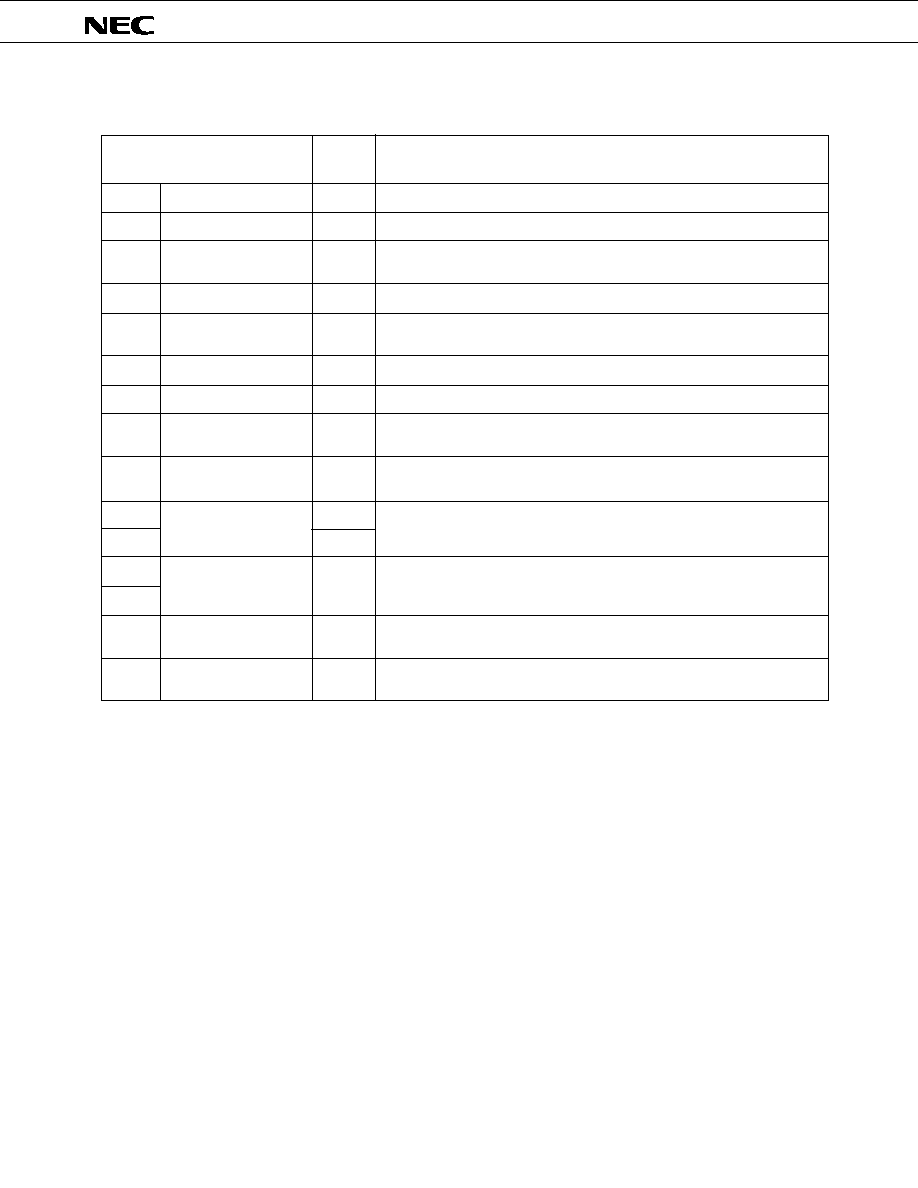
MA
MODE A register
W
Specifies bit-wise the input/output of the port A.
MB
MODE B register
W
Specifies bit-wise the input/output of the port B.
MODE CONTROL
C register
MC
MODE C register
W
Specifies bit-wise the input/output of the port C which is in port mode.
MEMORY MAPPING
register
MF
MODE F register
W
Specifies bit-wise the input/output of the port F which is in port mode.
TMM
Timer mode register
R/W
Specifies operating mode of timer.
Timer/event counter
mode register
Timer/event counter
output mode register
SML
W
Serial mode register
Specifies the operating mode of serial interface.
SMH
R/W
MKL
Interrupt mask register
R/W
Specifies the enable/disable of the interrupt request.
MKH
A/D channel mode
register
Zero-cross mode
register
5.
LIST OF MODE REGISTERS
ZCM
W
Specifies the operation of zero-cross detector circuit.
ANM
R/W
Specifies the operating mode of A/D converter.
EOM
R/W
Control the output level of CO0 and CO1.
ETMM
W
Specifies the operating mode of timer/event counter.
MM
W
Specifies the port/extension mode of port D and port F.
MCC
W
Specifies bit-wise the port/control mode of the port C.

35
µ
PD78C10A,78C11A,78C12A
6.
ELECTRICAL SPECIFICATIONS
ABSOLUTE MAXIMUM RATINGS (T
A
= 25
∞
C)
PARAMETER
SYMBOL
TEST CONDITIONS
RATING
UNIT
V
DD
≠0.5 to +7.0
V
Power supply voltage
AV
DD
AV
SS
to V
DD
+0.5
V
AV
SS
≠0.5 to +0.5
V
Input voltage
V
I
≠0.5 to V
DD
+0.5
V
Output voltage
V
O
≠0.5 to V
DD
+0.5
V
All output pins
4.0
mA
Output current low
Total of all output pins
100
mA
All output pins
≠2.0
mA
Output current high
Total of all output pins
≠50
mA
A/D converter reference
input voltage
Operating ambient
T
A
≠40 to +85
∞
C
temperature
Storage temperature
T
stg
≠65 to +150
∞
C
Caution
Even if one of the parameters exceeds its absolute maximum rating even momentarily, the quality of
the product may be degraded. The absolute maximum rating therefore specifies the upper or lower limit
of the value at which the product can be used without physical damages. Be sure not to exceed or fall
below this value when using the product.
I
OL
I
OH
V
AREF
≠0.5 to AV
DD
+0.3
V
5

36
µ
PD78C10A,78C11A,78C12A
RESONATOR
RECOMMENDED CIRCUIT
PARAMETER
TEST CONDITIONS
MIN.
MAX.
UNIT
5.8
15
MHz
A/D converter not
used
X1 rise time,
fall time (t
r
, t
f
)
X1 input high, low
level width (t
H
, t
L
)
OSCILLATOR CHARACTERISTICS
(T
A
= ≠40 to +85
∞
C, V
DD
= AV
DD
= +5.0 V
±
10 %, V
SS
= AV
SS
= 0 V,
V
DD
≠0.8 V
AV
DD
V
DD
, 3.4 V
V
AREF
AV
DD
)
4
15
MHz
MAKER
PRODUCT NAME
CSA7.37MT
CST7.37MTW
CSA12.0MT
CST12.0MTW
CSA15.00MX001
FCR8.0MC
FCR10.0MC
FCR12.0OMC
FCR15.0MC
RECOMMENDED CONSTANTS
C1[pF]
30
On-chip
30
On-chip
15
On-chip
C2[pF]
30
On-chip
30
On-chip
15
On-chip
Murata Mfg. Co., Ltd
TDK Corp.
*
2. When a crystal oscillator is used, the following external capacitance is
recommended.
C1 = C2 = 10 pF
A/D converter not
used
A/D converter used
Oscillator frequency (f
XX
)
X1 input frequency (f
X
)
Cautions
1. Place oscillator circuit as close as possible to X1, X2 pins.
2. Ensure that no other signal lines pass through the shadow area.
0
20
ns
20
250
ns
A/D converter used
5.8
15
MHz
4
15
MHz
External
clock
Ceramic*1
or
crystal
resonator*2
*
1. The ceramic oscillators and external capacitance given in the following
table are recommended.
X1
X2
C2
C1
X1
X2
HCMOS
Inverter

37
µ
PD78C10A,78C11A,78C12A
CAPACITANCE (T
A
= 25
∞
C, V
DD
= V
SS
= 0 V)
PARAMETER
SYMBOL
TEST CONDITIONS
MIN.
TYP.
MAX.
UNIT
Input capacitance
C
I
10
pF
f
C
= 1 MHz
Output capacitance
C
O
20
pF
Unmeasured pins returned to 0 V
Input-output capacitance
C
IO
20
pF
38
µ
PD78C10A,78C11A,78C12A
DC CHARACTERISTICS (T
A
= ≠40 to +85
∞
C, V
DD
= AV
DD
= +5.0 V
±
10 %, V
SS
= AV
SS
= 0 V)
PARAMETER
SYMBOL
TEST CONDITIONS
MIN.
TYP.
MAX.
UNIT
All except RESET, STOP, NMI,
SCK, INT1, TI, AN4 to AN7
RESET, STOP, NMI, SCK, INT1,
TI, AN4 to AN7
All except RESET, STOP, NMI,
SCK, INT1, TI, AN4 to AN7, X1, X2
RESET, STOP, NMI, SCK, INT1,
TI, AN4 to AN7, X1, X2
Output voltage low
V
OL
I
OL
= 2.0 mA
0.45
V
V
DD
V
≠1.0
V
DD
V
≠0.5
Input current
I
I
INT1*1, TI(PC3)*2
; 0 V
V
I
V
DD
±
200
µ
A
All except INT1, TI (PC3),
±
10
µ
A
0 V
V
I
V
DD
Output leakage
±
10
µ
A
current
AI
DD1
Operating mode f
XX
= 15 MHz
0.5
1.3
mA
AI
DD2
STOP mode
10
20
µ
A
I
DD1
Operating mode f
XX
= 15 MHz
13
25
mA
I
DD2
HALT mode f
XX
= 15 MHz
7
13
mA
Data retention
Hardware/software STOP mode
2.5
V
voltage
Hardware/software*3
V
DDDR
= 2.5 V
1
15
µ
A
STOP mode
V
DDDR
= 5 V
±
10%
10
50
µ
A
Pull-up resistor*4
Ports A, B and C
3.5 V
V
DD
5.5 V,
17
27
75
k
V
I
= 0 V
Caution
For a detailed description of the hardware STOP mode, refer to the 87AD Series
mPD78C18 User's
Manual.
*
1. If self-bias should be generated by ZCM register.
2. If the control mode is set by MCC register, and self-bias should be generated by ZCM register.
3. If self-bias is not generated.
4.
µ
PD78C11A and 78C12A only.
Input voltage low
Input voltage
high
Output voltage
high
Input leakage
current
AV
DD
power
supply current
V
DD
power
supply current
Data retention
current
V
IL2
I
LI
I
LO
V
IL1
V
1IH
V
IH2
V
OH
0 V
V
O
V
DD
R
L
I
DDDR
V
DDDR
0
0.2 V
DD
V
0
0.8
V
2.2
V
DD
V
I
OH
= ≠1.0 mA
I
OH
= ≠100
µ
A
0.8 V
DD
V
DD
V
39
µ
PD78C10A,78C11A,78C12A
AC CHARACTERISTICS (T
A
= ≠40 to +85
∞
C, V
DD
= AV
DD
= +5.0 V
±
10 %, V
SS
= AV
SS
= 0 V)
Read/write Operation:
f
XX
= 15 MHz, C
L
= 100 pF
RD low level width
t
RR
f
XX
= 15 MHz
f
XX
= 15 MHz, C
L
= 100 pF
PARAMETER
SYMBOL
TEST CONDITIONS
MIN.
MAX.
UNIT
X1 input cycle time
t
CYC
66
250
ns
Address setup time (to ALE
)
t
AL
30
ns
Address hold time (from ALE
)
t
LA
f
XX
= 15 MHz, CL = 100 pF
35
ns
RD
delay time from address
t
AR
100
ns
Address float time from RD
t
AFR
C
L
= 100 pF
20
ns
Data input time from address
t
AD
250
ns
Data input time from ALE
t
LDR
135
ns
Data input time from RD
t
RD
120
ns
RD
delay time from ALE
t
LR
15
ns
Data hold time (from RD
)
t
RDH
C
L
= 100 pF
0
ns
ALE
delay time from RD
t
RL
f
XX
= 15 MHz, C
L
= 100 pF
80
ns
In Data Read
215
ns
f
XX
= 15 MHz, C
L
= 100 pF
In OP Code Fetch
415
ns
f
XX
= 15 MHz, C
L
= 100 pF
ALE high level width
t
LL
f
XX
= 15 MHz, C
L
= 100 pF
90
ns
M1 setup time (to ALE
)
t
ML
30
ns
M1 hold time (from ALE
)
t
LM
35
ns
IO/M setup time (to ALE
)
t
IL
30
ns
IO/M hold time (from ALE
)
t
LI
35
ns
t
AW
100
ns
Data output time from ALE
t
LDW
180
ns
Data output time from WR
t
WD
C
L
= 100 pF
100
ns
WR
delay time from ALE
t
LW
15
ns
Data setup time (to WR
)
t
DW
165
ns
Data hold time (from WR
)
t
WDH
f
XX
= 15 MHz, C
L
= 100 pF
60
ns
ALE
delay time from WR
t
WL
80
ns
WR low level width
t
WW
215
ns
WR
delay time from address
40
µ
PD78C10A,78C11A,78C12A
PARAMETER
SYMBOL
TEST CONDITIONS
MIN.
MAX.
UNIT
SCK input
*1
800
ns
*2
400
ns
SCK output
1.6
µ
s
SCK input
*1
335
ns
*2
160
ns
SCK output
700
ns
SCK input
*1
335
ns
*2
160
ns
SCK output
700
ns
R
X
D setup time (to SCK
)
t
RXK
*1
80
ns
R
X
D hold time (from SCK
)
t
KRX
*1
80
ns
T
X
D delay time from SCK
t
KTX
*1
210
ns
Serial Operation :
*
1. If clock rate is
◊
1 in asynchronous mode, synchronous mode, or I/O interface mode.
2. If clock rate is
◊
16 or
◊
64 in asynchronous mode.
Remarks
The numeric values in the table are those when f
XX
= 15 MHz, C
L
= 100 pF.
Zero-Cross Characteristics :
PARAMETER
SYMBOL
TEST CONDITIONS
MIN.
MAX.
UNIT
Zero-cross detection input
V
ZX
1
1.8
VAC
P-P
Zero-cross accuracy
A
ZX
±
135
mV
Zero-cross detection input
0.05
1
kHz
frequency
Other Operation :
PARAMETER
SYMBOL
TEST CONDITIONS
MIN.
MAX.
UNIT
TI high, low level width
t
TIH
, t
TIL
6
t
CYC
CI high, low level width
t
CI1H
, t
CI1L
Event count mode
6
t
CYC
t
CI2H
,t
CI2L
Pulse width test mode
48
t
CYC
NMI high, low level width
t
NIH
, t
NIL
10
µ
s
INT1 high, low level width
t
I1H
, t
I1L
36
t
CYC
INT2 high, low level width
t
I2H
, t
I2L
36
t
CYC
AN4 to AN7, low level width
t
ANH
, t
ANL
36
t
CYC
RESET high, low level width
t
RSH
, t
RSL
10
µ
s
SCK cycle time
t
CYK
SCK low level width
t
KKL
SCK high level width
t
KKH
f
ZX
AC combination
60 Hz sine wave
41
µ
PD78C10A,78C11A,78C12A
A/D CONVERTER CHARACTERISTICS (T
A
= ≠40 to +85
∞
C, V
DD
= +5.0 V
±
10 %, V
SS
= AV
SS
= 0 V,
V
DD
≠0.5 V
AV
DD
V
DD
, 3.4 V
V
AREF
AV
DD
)
PARAMETER
SYMBOL
TEST CONDITIONS
MIN.
TYP.
MAX.
UNIT
Resolution
8
Bits
3.4 V
V
AREF
AV
DD
, 66 ns
t
CYC
170 ns
±
0.8%
FSR
4.0 V
V
AREF
AV
DD
, 66 ns
t
CYC
170 ns
±
0.6%
FSR
T
A
= ≠10 to +70
∞
C,
±
0.4%
FSR
4.0 V
V
AREF
AV
DD
, 66 ns
t
CYC
170 ns
66 ns
t
CYC
110 ns
576
t
CYC
110 ns
t
CYC
170 ns
432
t
CYC
66 ns
t
CYC
110 ns
96
t
CYC
110 ns
t
CYC
170 ns
72
t
CYC
Analog input voltage
V
IAN
AN0 to AN7 (including unused pins)
≠0.3
V
AREF
+0.3
V
Analog input
50
M
impedance
Reference voltage
V
AREF
3.4
AV
DD
V
I
AREF1
Operating mode
1.5
3.0
mA
I
AREF2
STOP mode
0.7
1.5
mA
AI
DD1
Operating mode f
XX
= 15 MHz
0.5
1.3
mA
AI
DD2
STOP mode
10
20
µ
A
*
Quantization error (
±
1/2 LSB) is not included.
AC Timing Test Point
2.2 V
0.8 V
2.2 V
0.8 V
Test Points
V
DD
≠ 1.0 V
0.45 V
R
AN
Absolute accuracy*
Conversion time
t
CONV
Sampling time
t
SAMP
V
AREF
current
AV
DD
power supply
current
5

42
µ
PD78C10A,78C11A,78C12A
t
CYC
-Dependent AC Characteristics Expression
t
CYK
t
KKL
t
KKH
t
RR
PARAMETER
EXPRESSION
MIN./MAX.
UNIT
t
AL
2T ≠ 100
MIN.
ns
t
LA
T ≠ 30
MIN.
ns
t
AR
3T ≠ 100
MIN.
ns
t
AD
7T ≠ 220
MAX.
ns
t
LDR
5T ≠ 200
MAX.
ns
t
RD
4T ≠ 150
MAX.
ns
t
LR
T ≠ 50
MIN.
ns
t
RL
2T ≠ 50
MIN.
ns
4T ≠ 50 (In data read)
MIN.
ns
7T ≠ 50 (In OP code fetch)
t
LL
2T ≠ 40
MIN.
ns
t
ML
2T ≠ 100
MIN.
ns
t
LM
T ≠ 30
MIN.
ns
t
IL
2T ≠ 100
MIN.
ns
t
LI
T ≠ 30
MIN.
ns
t
AW
3T ≠ 100
MIN.
ns
t
LDW
T + 110
MAX.
ns
t
LW
T ≠ 50
MIN.
ns
t
DW
4T ≠ 100
MIN.
ns
t
WDH
2T ≠ 70
MIN.
ns
t
WL
2T ≠ 50
MIN.
ns
t
WW
4T ≠ 50
MIN.
ns
12T (SCK input)*1/6T (SCK input)*2
MIN.
ns
24T (SCK output)
5T + 5 (SCK input)*1/2.5T + 5 (SCK input)*2
MIN.
ns
12T ≠ 100 (SCK output)
5T + 5 (SCK input)*1/2.5T + 5 (SCK input)*2
MIN.
ns
12T ≠ 100 (SCK output)
*
1. If clock rate is
◊
1, in asynchronous mode, synchronous mode, or I/O interface mode.
2. If clock rate is 16
◊
64, in asynchronous mode.
Cautions
1. T = tCYC = 1/fXX
2. Other items which are not listed in this table are not dependent on oscillator frequency (fXX).
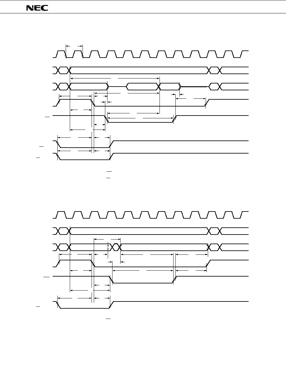
43
µ
PD78C10A,78C11A,78C12A
Timing Waveform
Read operation
*
1. When MODE1 pin is pulled up, M1 signal is output to MODE1 pin in the 1st OP code fetch cycle.
2. When MODE0 pin is pulled up, IO/M signal is output to MODE0 pin in sr to sr2 register read cycle.
Write operation
*
3. When MODE0 pin is pulled up, IO/M signal is output to MODE0 pin in sr to sr2 register write cycle.
X1
PF7 - 0
PD7 - 0
ALE
MODE1
(M1)*1
MODE0
(IO/M)*2
t
CYC
Address (Upper)
Address (Lower)
t
RDH
Read Data
t
LDR
t
AD
t
RL
t
RD
t
RR
t
AFR
t
LA
t
LL
t
AR
t
AL
t
LR
t
ML
t
IL
t
LM
t
LI
Address (Upper)
Address (Lower)
t
LDW
t
LA
t
LL
t
AL
t
WD
t
DW
t
WDH
t
WL
t
WW
t
LW
t
LI
t
AW
t
IL
Write Data
X1
PF7 - 0
PD7 - 0
ALE
RD
WR
MODE0
(IO/M)*3
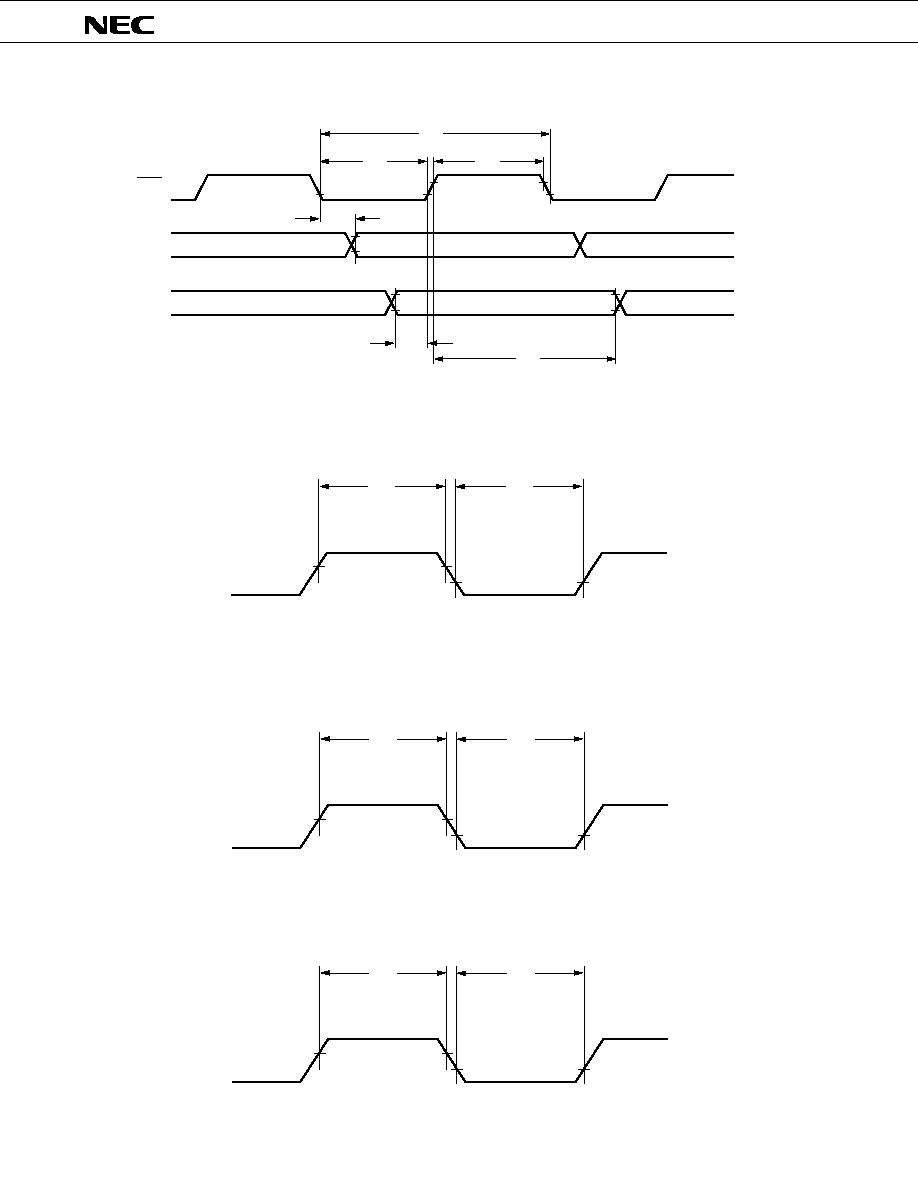
44
µ
PD78C10A,78C11A,78C12A
Serial Operation
Timer/Event Counter Input Timing
Timer Input Timing
t
CYK
t
KKL
t
KKH
t
RXK
t
KRX
t
KTX
SCK
T
X
D
R
X
D
TI
t
TIL
t
TIH
CI
t
CI1L
t
CI1H
Event Counter Mode
CI
t
CI2L
t
CI2H
Pulse Width Test Mode
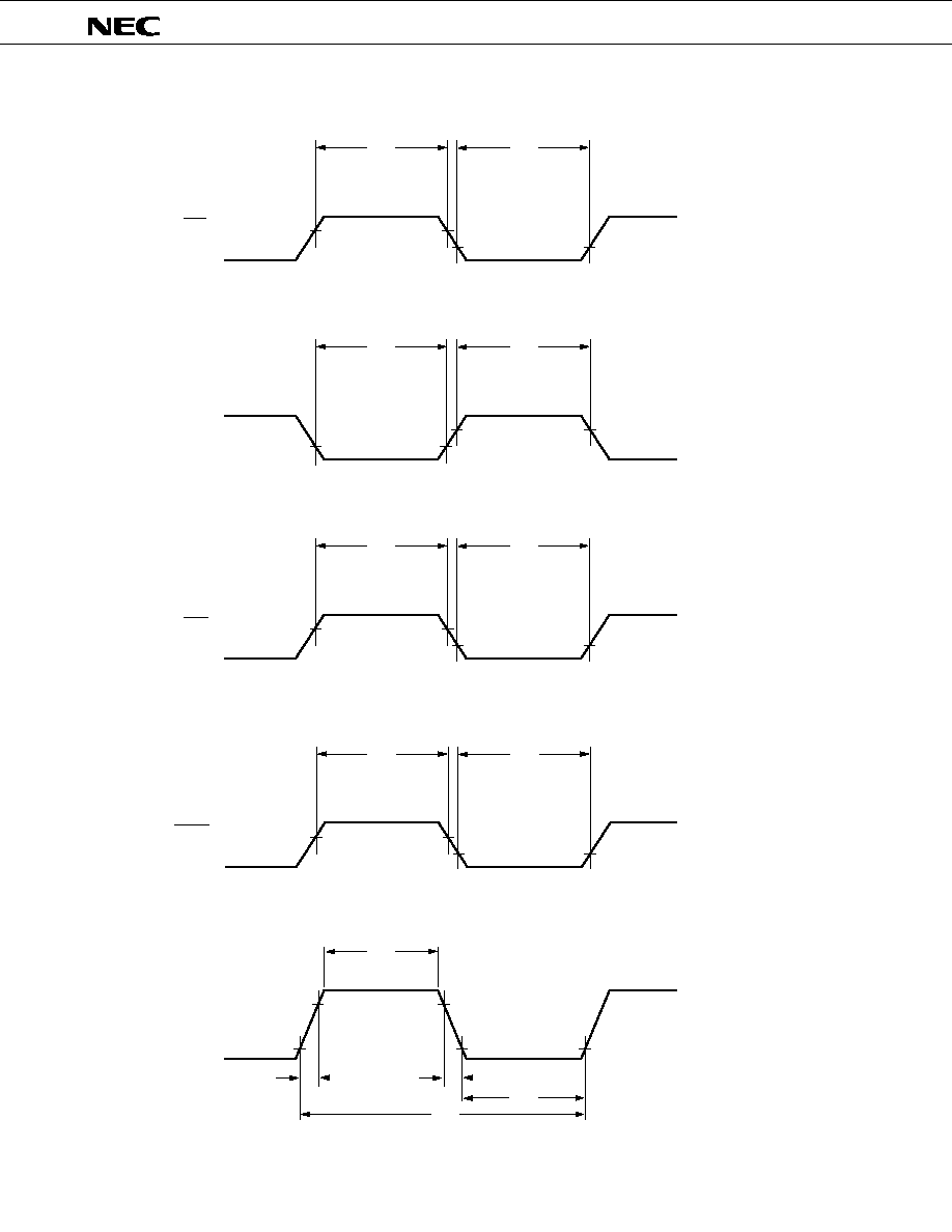
45
µ
PD78C10A,78C11A,78C12A
Interrupt Input Timing
External Clock Timing
RESET
t
RSL
t
RSH
0.8 V
DD
0.2 V
DD
Reset Input Timing
NMI
t
NIL
t
NIH
INT1
INT2
t
I1H
t
I1L
t
I2L
t
I2H
X1
t
CYC
0.8 V
DD
0.8 V
t
f
t
r
t
H
t
H
46
µ
PD78C10A,78C11A,78C12A
DATA MEMORY STOP MODE LOW POWER SUPPLY VOLTAGE DATA RETENTION CHARACTERISTICS
(T
A
= ≠40 to +85
∞
C)
PARAMETER
SYMBOL
TEST CONDITIONS
MIN.
TYP.
MAX.
UNIT
Data retention power
2.5
5.5
V
supply voltage
V
DDDR
= 2.5 V
1
15
µ
A
V
DDDR
= 5 V
±
10%
10
50
µ
A
V
DD
rise/fall time
t
RVD
, t
FVD
200
µ
s
STOP setup time
12T +0.5
µ
s
(to V
DD
)
STOP hold time
12T +0.5
µ
s
(from V
DD
)
Data Retention Timing
90 %
STOP
V
DD
V
DDDR
t
RVD
10 %
t
FVD
t
SSTVD
t
HVDST
V
IH2
V
IL2
V
DDDR
t
SSTVD
t
HVDST
Data retention power
supply current
I
DDDR
5
47
µ
PD78C10A,78C11A,78C12A
I
DD1
, I
DD2
vs f
XX
7.
CHARACTERISTIC CURVES (REFERENCE VALUES)
I
DD1
, I
DD2
vs V
DD
20
15
10
5
0
4.5
5.0
5.5
(T
A
= 25 ∞C, f
XX
= 15 MHz)
I
DD1
(TYP.)
I
DD2
(TYP.)
Power Supply Voltage V
DD
[V]
V
DD
Power Supply Current I
DD1
, I
DD2
[mA]
(T
A
= 25 ∞C, V
DD
= 5 V)
Oscillator Frequency f
XX
[MHz]
V
DD
Power Supply Current I
DD1
, I
DD2
[mA]
30
20
10
0
5
10
15
I
DD1
(TYP.)
I
DD2
(TYP.)
6
48
µ
PD78C10A,78C11A,78C12A
I
OL
vs V
OL
I
OH
vs V
OH
2.5
2.0
1.5
1.0
0.5
0
0.1
0.2
0.3
0.4
0.5
(T
A
= 25 ∞C, V
DD
= 5 V)
TYP.
Output Voltage Low V
OL
[V]
Output Current Low I
OL
[mA]
≠1.5
≠1.0
≠0.5
0
0.1
0.2
0.3
0.4
0.5
(T
A
= 25 ∞C, V
DD
= 5 V)
Power Supply Voltage ≠ Output Voltage High V
DD
≠ V
OH
[V]
Output Current High I
OH
[mA]
TYP.
49
µ
PD78C10A,78C11A,78C12A
I
DDDR
vs V
DDDR
10
8
6
4
2
0
2
3
4
5
6
(T
A
= 25 ∞C)
TYP.
Data Retention Power Supply Voltage V
DDDR
[V]
Data Retention Power Supply Current I
DDDR
[
A]
µ

50
µ
PD78C10A,78C11A,78C12A
I
AREF2
8.
DIFFERENCES IN 87AD SERIES PRODUCTS (1/2)
Item
159 kinds (STOP instruction
added)
158 kinds
Number of instructions
µ
PD7810, 7811*1
µ
PD7810H, 7811H
µ
PD78C10, 78C11*1
Product Name
On-chip RAM
256
◊
8 bits
Nnmber of special registers
27
28 (ZCM register added)
Operating frequency
Power supply voltage
Operating temperature range
Standby function
Thirty-two bytes of the on-chip RAM 256 bytes of data
are held by low power supply voltage (3.2 V)
Number of HALT instruction state
11
12
HALT
mode
CPU operation
ALE
M3 T2 cycle repeated
High level
Stop
Low level
Zero crossing detector self-bias
control
Self-bias control impossible
NMI, RESET noise elimination
method
By clock sampling
By analog delay
Operation stop possible
(V
AREF
pin operation)
Operation stop impossible
A/D converter operation control
0.4%
(T
A
= ≠10 to +70
∞
C,
V
AREF
= 4.0V to AV
DD
)
0.6%
(T
A
= ≠40 to +85
∞
C,
V
AREF
= 4.0V to AV
DD
)
0.8%
(T
A
= ≠40 to +85
∞
C
V
AREF
= 3.4V to AV
DD
)
A/D converter absolute accuracy
(Unit: FSR)
V
AREF
voltage range
AV
CC
to 0.5V to AV
CC
3.4 V to AV
DD
AI
CC
/AI
DD1
0V to V
AREF
Analog input voltage range
6 mA Typ.
0.5 mA Typ.
AI
DD2
--
10
µ
A Typ.
I
AREF
/I
AREF1
0.5 mA Typ.
2.0 mA Typ.
1.5 mA Typ.
--
0.7 mA Typ.
0.4% (T
A
= ≠10 to +50
∞
C)
0.6% (T
A
= ≠40 to +85
∞
C)
Three kinds: HALT mode,
software STOP mode, and
hardware STOP mode. All
data of on-chip RAM are
held by low power supply
voltage (2.5V) in software/
hardware STOP mode.
0.4% (T
A
= ≠10 to +70
∞
C)*3
10 to 12 MHz
5 V
±
5 %
≠10 to +70
∞
C
4 to 10 MHz
5 V
±
10 %
≠40 to +85
∞
C
4 to 15 MHz
5 V
±
10 %
≠10 to +70
∞
C
4 to 15 MHz*2
5 V
±
10 %
≠40 to +85
∞
C
Self-bias control possible (by
ZCM register specification)
* 1.
µ
PD7810, 7811, 78C10 and 78C11 are maintenance products.
2.
K, E, P masks apply from 4 MHz to 12 MHz.
3.
The
µ
PD7810HG and 7811HG G masks,
µ
PD7810HCW and 7811HCW K masks apply T
A
= 0 to +70
∞
C.
On-chip ROM
ROM less (
µ
PD7810)
4K
◊
8 bits (
µ
PD7811)
ROM less (
µ
PD7810H)
4K
◊
8 bits (
µ
PD7811H)
ROM less (
µ
PD78C10)
4K
◊
8 bits (
µ
PD78C11)
51
µ
PD78C10A,78C11A,78C12A
4 to 15 MHz
5 V
±
10 %
≠40 to +85
∞
C
6 to 15 MHz
5 V
±
5 %
≠40 to +85
∞
C
4 to 15 MHz
5 V
±
10 %
≠40 to +85
∞
C
0.7 mA Typ.
µ
PD78C10A, 78C11A,
78C12A
µ
PD78CP14
µ
PD78CP18
3.4V to AV
DD
≠0.3 V to V
AREF
+ 0.3 V
0V to V
AREF
≠0.3 V to V
AREF
+ 0.3 V
1.5 mA Typ.
10
µ
A Typ.
0.5mA Typ.
Self-bias control possible
(by ZCM register specification)
12
STOP
Low level
28 (ZCM register added)
256
◊
8 bits
1024
◊
8 bits
159 kinds (STOP instruction added)
Operation stop impossible (V
AREF
pin operation)
By analog delay
Three kinds: Halt mode, software STOP mode, and hardware STOP mode. All data of
on-chip RAM are held by low power supply voltage (2.5 V) in software/hardware STOP
mode.
0.4% (T
A
= ≠10 to +70
∞
C, V
AREF
= 4.0 V to AV
DD
)
0.6% (T
A
= ≠40 to +85
∞
C, V
AREF
= 4.0 V to AV
DD
)
0.8% (T
A
= ≠40 to +85
∞
C, V
AREF
= 3.4 V to AV
DD
)
32K
◊
8 bits (PROM)
16K
◊
8 bits (PROM)
ROM less
(
µ
PD78C10A)
4K
◊
8 bits (
µ
PD78C11A)
8K
◊
8 bits (
µ
PD78C12A)
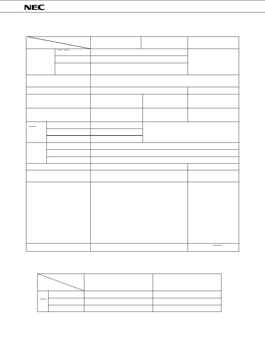
52
µ
PD78C10A,78C11A,78C12A
20T
10T + 80
10T ≠ 80
Item
µ
PD7810, 7811*1
µ
PD7810H, 7811H
µ
PD78C10, 78C11*1
DIFFERENCES IN 87AD SERIES PRODUCTS (2/2)
Zero is output at the pin specified by the address bus.
Other pins are high impedance.
Impossible
On-chip pull-up register
(Mask option)
Device configuration
NMOS
CMOS
3.2 mA (≠10 to +70
∞
C) MAX.
3.5 mA (≠40 to +85
∞
C) MAX.
Standby current
Current consumption
Cycle time input
Low level width
High level width
*5
SCK
(Unit: ns)
T
LDW
T
WD
T
DW
Bus
timing
(Unit: ns)
T + 110
100
4T ≠ 100
Hardware STOP mode restrictions
--
Yes
Asyncronous mode restrictions
during external SCK input.
No
Yes
64-pin plastic shrink DIP
64-pin plastic QUIP
straight*8
64-pin plastic QUIP
64-pin plastic QFP
(14
◊
20 mm, 2.05 mm
thickness)
64-pin plastic QFP
(14
◊
20 mm, 2.70 mm
thickness)
68-pin plastic QFJ
Package
Pin connection*10
V
CC
(64-pin), V
DD
(63-pin)
V
DD
(64-pin), STOP (63-pin)
RD/WR
ALE
PD/PF*4
High-impedance
* 1.
µ
PD7810, 7811, 78C10 and 78C11 are maintenance products.
4.
For
µ
PD7810, 7810H, 78C10 and 78C10A.
5.
For the asyncronous mode with clock
rate x1, syncronous mode, and I/O
interface mode
For the asyncronous mode with clock
rate
◊
16 and
◊
64
Cycle time input
Low level width
High level width
SCK
12T
5T + 5
5T + 5
6T
2.5T + 5
2.5T + 5
Remarks
T = t
CYC
= 1/f
xx
203.2 mA (≠10 to +70
∞
C) MAX.
223.5 mA (≠40 to +85
∞
C) MAX.
Operation
during RESET
Product Name
(Unit : ns)
64-pin plastic shrink DIP
64-pin plastic QUIP straight*7
64-pin plastic QUIP
Output
High level
3.2 mA MAX.
50
µ
A MAX.
(V
DD
= 5 V
±
10 %)
203.2 mA MAX.
25 mA MAX.
5

53
µ
PD78C10A,78C11A,78C12A
CMOS
µ
PD78C10A, 78C11A,
78C12A
µ
PD78CP14
µ
PD78CP18
64-pin plastic shrink DIP
64-pin plastic QUIP
64-pin plastic QFP (14
◊
20
mm, 2.70 mm thickness)
68-pin plastic QFJ
64-pin ceramic shrink DIP
with window
64-pin ceramic QUIP with
window
64-pin ceramic WQFN
T + 110
T + 130
110
140
4T ≠ 100
4T ≠ 140
Yes*6
No
Only
µ
PD78C11A, 78C12A
possible (ports A, B, C)
Impossible
High-impedance
*5
No
64-pin plastic shrink DIP
64-pin plastic QUIP straight*9
64-pin plastic QUIP
64-pin plastic QFP (14
◊
20
mm, 2.70 mm thickness)
68-pin plastic QFJ
64-pin plastic shrink DIP
64-pin plastic QUIP
64-pin plastic QFP (14
◊
20
mm, 2.70 mm thickness)
64-pin ceramic shrink DIP
with window
64-pin ceramic WQFN
1 mA MAX.
(V
DD
= 5 V
±
5 %)
50
µ
A MAX.
(V
DD
= 5 V
±
10 %)
25 mA MAX.
32 mA MAX.
35 mA MAX.
50
µ
A MAX.
(V
DD
= 5 V
±
10 %)
V
DD
(64-pin), STOP (63-pin)
*
6. K mask products only
7.
µ
PD7811, 7811H only
8.
µ
PD78C11, only
9.
µ
PD78C11A, 78C12A only
10. Items in the parentheses are the pin numbers for the 64-pin plastic shrink DIP, 64-pin plastic QUIP straight
and 64-pin plastic QUIP.
Caution
Since the oscillator characteristics, I/O level, and some internal operation timing are different, be careful
when studying direct replacement of the
mPD78C10A, 78C11A, 78C12A and
µ
PD7810, 7811, 7810H,
7811H, 78C10, 78C11.
5
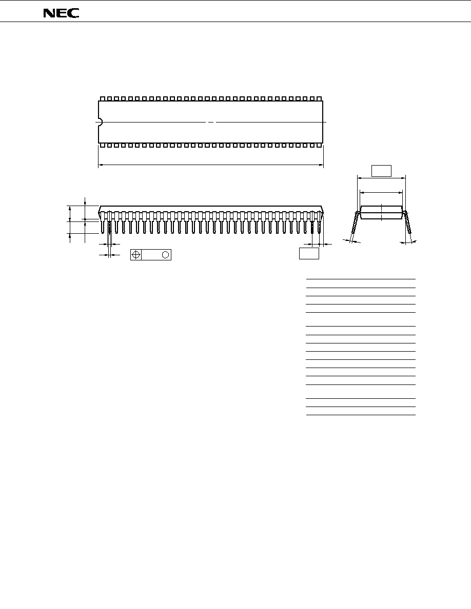
54
µ
PD78C10A,78C11A,78C12A
A
I
J
G
H
F
D
N
M
C
B
M
R
64
33
32
1
K
L
NOTE
Each lead centerline is located within 0.17 mm (0.007 inch) of
its true position (T.P.) at maximum material condition.
P64C-70-750A,C-1
ITEM
MILLIMETERS
INCHES
A
B
C
D
F
G
H
I
J
K
58.68 MAX.
1.778 (T.P.)
3.2±0.3
0.51 MIN.
4.31 MAX.
1.78 MAX.
L
M
0.17
0.25
19.05 (T.P.)
5.08 MAX.
17.0
N
0~15∞
0.50±0.10
0.9 MIN.
R
2.311 MAX.
0.070 MAX.
0.020
0.035 MIN.
0.126±0.012
0.020 MIN.
0.170 MAX.
0.200 MAX.
0.750 (T.P.)
0.669
0.010
0.007
0~15∞
+0.004
≠0.003
0.070 (T.P.)
1)
Item "K" to center of leads when formed parallel.
2)
+0.10
≠0.05
+0.004
≠0.005
64 PIN PLASTIC SHRINK DIP (750 mil)
9.
PACKAGE INFORMATION
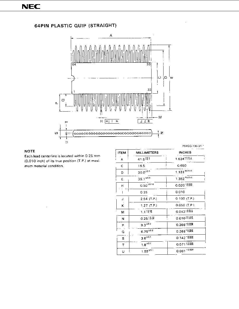
55
µ
PD78C10A,78C11A,78C12A
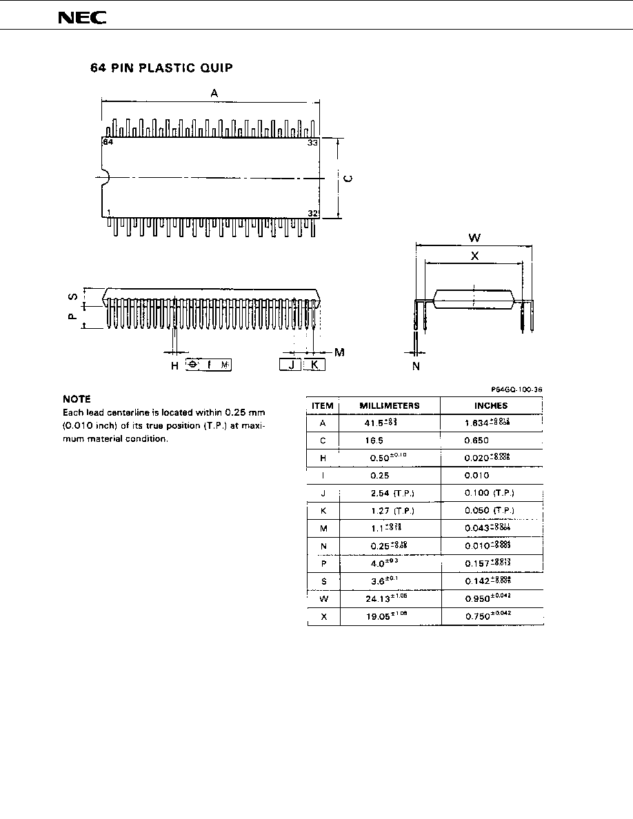
56
µ
PD78C10A,78C11A,78C12A
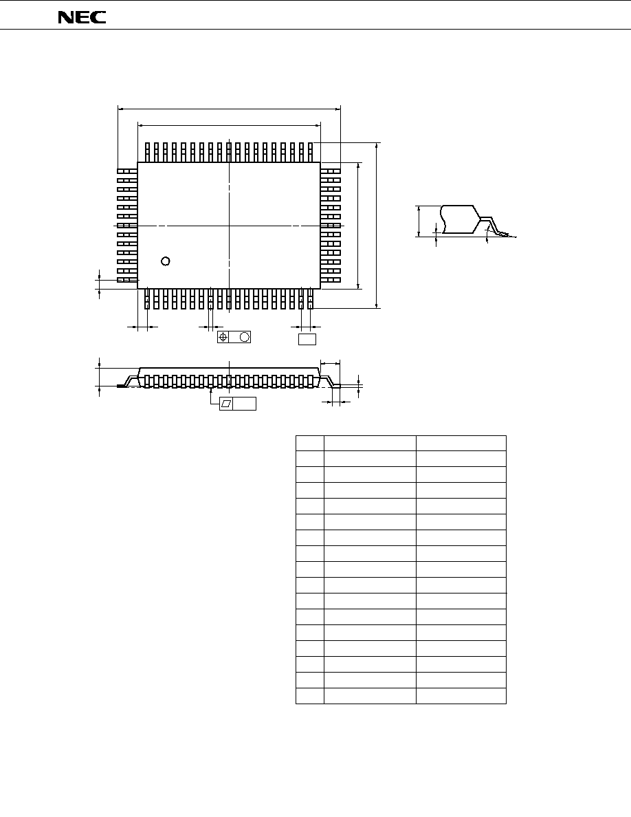
57
µ
PD78C10A,78C11A,78C12A
64PIN PLASTIC QFP (14
◊
20) (UNIT: mm)
N
A
M
F
B
51
52
32
K
L
64
1
20
19
33
P
D
C
detail of lead end
S
Q
5∞±5∞
G
M
I
H
J
P64GF-100-3B8,3BE,3BR-1
ITEM
MILLIMETERS
INCHES
A
B
C
D
F
G
H
I
J
K
L
23.6±0.4
14.0±0.2
1.0
0.40±0.10
0.20
20.0±0.2
0.929±0.016
0.039
0.039
0.008
0.039 (T.P.)
0.795
NOTE
M
N
0.12
0.15
1.8±0.2
1.0 (T.P.)
0.005
0.006
+0.004
≠0.003
Each lead centerline is located within 0.20
mm (0.008 inch) of its true position (T.P.) at
maximum material condition.
0.071
0.016
0.551
0.8±0.2
0.031
P
2.7
0.106
0.693±0.016
17.6±0.4
1.0
+0.009
≠0.008
Q
0.1±0.1
0.004±0.004
S
3.0 MAX.
0.119 MAX.
+0.10
≠0.05
+0.009
≠0.008
+0.004
≠0.005
+0.009
≠0.008
+0.008
≠0.009
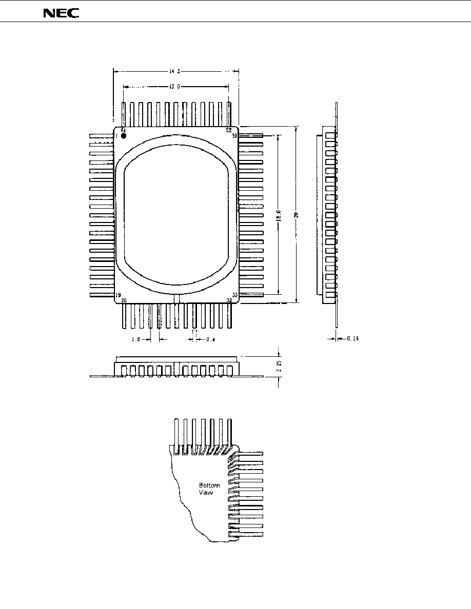
58
µ
PD78C10A,78C11A,78C12A
ES 64PIN CERAMIC QFP (REFERENCE DRAWING) (UNIT: mm)
Cautions
1.
The metal cap is connected to
pin 26 and is V
SS
(GND) level.
2.
The bottom leads are tilted.
3.
Since cutting of the end of the
leads is no process-controlled,
the lead length is unspecified.

59
µ
PD78C10A,78C11A,78C12A
68PIN PLASTIC QFJ (
950 mil) (UNIT: mm)
P68L-50A1-2
ITEM
MILLIMETERS
INCHES
NOTE
Each lead centerline is located within 0.12
mm (0.005 inch) of its true position (T.P.) at
maximum material condition.
+0.007
≠0.006
A
B
C
D
E
F
G
H
I
J
K
M
N
P
Q
T
U
25.2±0.2
24.20
24.20
25.2±0.2
1.94±0.15
0.6
4.4±0.2
2.8±0.2
0.9 MIN.
3.4
1.27 (T.P.)
0.40±1.0
0.12
23.12±0.20
0.15
R 0.8
0.20
+0.10
≠0.05
0.992±0.008
0.953
0.953
0.992±0.008
0.076
0.024
0.173
0.110
0.035 MIN.
0.134
0.050 (T.P.)
0.016
0.005
0.910
0.006
R 0.031
0.008
+0.009
≠0.008
+0.009
≠0.008
+0.004
≠0.005
+0.004
≠0.002
+0.009
≠0.008
N
K
M
Q
A
U
68
B
D
C
1
F
E
T
P
M
G
H
IJ
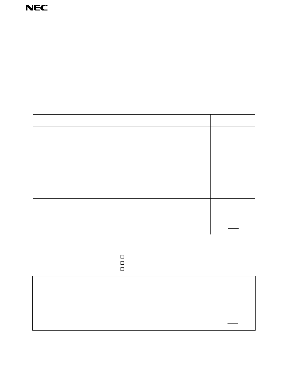
60
µ
PD78C10A, 78C11A, 78C12A
5
10. RECOMMENDED SOLDERING CONDITIONS
The
µ
PD78C10A, 78C11A, and 78C12A should be soldered and mounted under the conditions recommended in
the table below.
For detail of recommended soldering conditions, refer to the information document "Semiconductor Device
Mounting Technology Manual" (IEI-1207).
For soldering methods and conditions other than those recommended below, contact our sales personnel.
Table 10-1 Surface Mounting Type Soldering Conditions
(1)
µ
PD78C10AGF-3BE
: 64-pin plastic QFP (14
◊
20 mm)
µ
PD78C11AGF-
◊◊◊
-3BE : 64-pin plastic QFP (14
◊
20 mm)
µ
PD78C12AGF-
◊◊◊
-3BE : 64-pin plastic QFP (14
◊
20 mm)
Soldering Conditions
Soldering Method
Infrared reflow
Package peak temperature : 235
∞
C, Duration : 30 sec. max. (210
∞
C min.), Number of times : 2 max.
<Points to note>
(1) Start the second reflow after the device temperature by the first
reflow returns to normal.
(2) Flux washing by the water after the first reflow should be avoided.
Recommended
Condition Symbol
Package peak temperature : 215
∞
C, Duration : 40 sec. max. (200
∞
C min.), Number of times : 2 max.
<Points to note>
(1) Start the second reflow after the device temperature by the first
reflow returns to normal.
(2) Flux washing by the water after the first reflow should be avoided.
Solder bath temperature : 260
∞
C max., Duration : 10 sec. max.,
Number of times : 1
Pre-heating temperature : 120
∞
C max. (package surface tempera-
ture)
WS60-00-1
VP15-00-2
IR35-00-2
VPS
Wave soldering
Pin temperature : 300
∞
C max.,
Duration: 3 sec. max. (per device side)
Pin part heating
(2)
µ
PD78C10AL
:
68-pin plastic QFJ ( 950 mil)
µ
PD78C11AL-
◊◊◊
:
68-pin plastic QFJ ( 950 mil)
µ
PD78C12AL-
◊◊◊
:
68-pin plastic QFJ ( 950 mil)
Recommended
Condition Symbol
Package peak temperature : 230
∞
C, Duration : 30 sec. max.
(210
∞
C min.), Number of times : 1
IR30-00-1
Package peak temperature : 215
∞
C, Duration : 40 sec. max.
(200
∞
C min.), Number of times : 1
VP15-00-1
Pin temperature : 300
∞
C max., Duration : 3 sec. max. (per device
side)
Infrared reflow
VPS
Pin part heating
Soldering Method
Soldering Conditions
Caution
Do not use two or more soldering methods in combination (except the pin part heating method).
Caution
Do not use two or more soldering methods in combination (except the pin part heating method).
61
µ
PD78C10A, 78C11A, 78C12A
Table 10-2 Inserted Type Soldering Conditions
(1)
µ
PD78C10ACW
: 64-pin plastic shrink DIP (750 mil)
µ
PD78C11ACW-
◊◊◊
: 64-pin plastic shrink DIP (750 mil)
µ
PD78C12ACW-
◊◊◊
: 64-pin plastic shrink DIP (750 mil)
µ
PD78C10AGQ-36
: 64-pin plastic QUIP
µ
PD78C11AGQ-
◊◊◊
-36
: 64-pin plastic QUIP
µ
PD78C12AGQ-
◊◊◊
-36
: 64-pin plastic QUIP
Soldering Method
Soldering Conditions
Wave soldering
(pin only)
Solder bath temperature: 260
∞
C max.
Duration: 10 sec. max.
Pin part heating
Pin temperature: 300
∞
C max.
Duration: 3 sec. max. (per pin)
Caution
Ensure that the application of wave soldering is limited to
the pins and no solder touches the main unit directly.
(2)
µ
PD78C11AGQ-
◊◊◊
-37
: 64-pin plastic QUIP straight
µ
PD78C12AGQ-
◊◊◊
-37
: 64-pin plastic QUIP straight
Soldering Conditions
Pin temperature: 300
∞
C max.
Duration: 3 sec. max. (per pin)
Pin part heating
Soldering Method
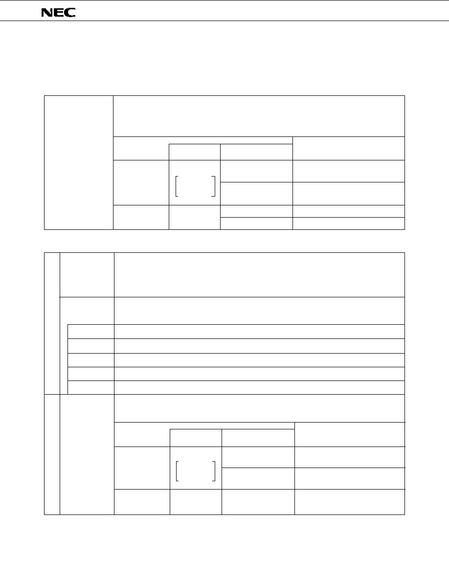
62
µ
PD78C10A,78C11A,78C12A
APPENDIX DEVELOPMENT TOOLS
The following development tools are available to develop a system which uses 87AD series products.
Language Processor
Supply Medium
OS
MS-DOS
Ver. 2.11
to
Ver. 5.00A*
PC DOS
(Ver. 3.1)
Software
Hardware
Supply Medium
This is a program which converts a program written in mnemonic to an object code that micro-
computer execution is possible.
Besides, it contains a function to automatically create a symbol/table, and optimize a branch
instruction.
87AD series
relocatable assembler
(RA87)
PC-9800 series
IBM PC/AT
TM
µ
S5A13RA87
µ
S5A10RA87
Ordering Code (Product Name)
Host Machine
With an provided board and an optional programmer adapter connected, this PROM programmer
can manipulate from a stand-alone or host machine to perform programming on single-chip
microcomputer which incorporates PROM.
It is also capable of programming a typical PROM ranging from 256K to 4M bits.
PG-1500
PA-78CP14CW/
GF/GQ/KB/L
PA-78CP14CW
PA-78CP14GF
PA-78CP14GQ
PA-78CP14KB
PA-78CP14L
PROM programmer adapter for
µ
PD78CP14/78CP18. Used by connecting to PG-1500.
For
µ
PD78CP14CW, 78CP14DW, 78CP18CW, 78CP18DW
For
µ
PD78CP14GF-3BE, 78CP18GF-3BE
For
µ
PD78CP14G-36, 78CP14R, 78CP18GQ-36
For
µ
PD78CP14KB, 78CP18KB
For
µ
PD78CP14L
Connected PG-1500 to a host machine by using serial and parallel interface, to control the PG-
1500 on a host machine.
PC-9800 series
IBM PC/AT
Host Machine
µ
S5A13PG1500
µ
S5A10PG1500
µ
S7B10PG1500
Ordering Code (Product Name)
3.5-inch 2HD
5-inch 2HC
PG-1500
controller
5
3.5-inch 2HD
5-inch 2HD
5-inch 2HD
µ
S7B13RA87
µ
S7B10RA87
3.5-inch 2HC
5-inch 2HC
* Ver. 5.00/5.00A has a task swap function, but this function cannot be used with this software.
Remarks
Operation of assemblers and the PG-1500 controller are guaranteed only on the host machines and
operating systems quoted above.
OS
MS-DOS
TM
Ver. 2.11
to
Ver. 5.00A*
PC DOS
TM
(Ver. 3.1)
PROM Write Tools

63
µ
PD78C10A,78C11A,78C12A
OS
MS-DOS
Ver. 2.11
to
Ver. 3.30D
PC DOS
(Ver. 3.1)
Debugging tools
An in-circuit emulator (IE-78C11-M) is available as a program debugging tool for 87AD series. The following table
shows its system configuration.
The IE-78C11-M is an in-circuit emulator which works with 87AD series.
Only the IE-78C11-M should be used for a plastic QUIP package, while it should be used with a
conversion socket for a plastic shrink DIP package.
It can be connected to a host machine to perform efficient debugging.
Conversion sockets for plastic shrink DIP.
Used in combination with the IE-78C11-M.
64-pin LCC socket. Can be used as a substitute for 64-pin plastic QFP products with window in
combination with the
µ
PD78CP14KB/78CP18KB.
Connects the IE-78C11-M to host machine by using the RS-232-C, then controls the IE-78C11-M
on host machine.
Hardware
Supply Medium
Software
Remarks
Operation of the IE controller is guaranteed only on the host machine and operating systems quoted
above.
IE-78C11-M
EV-9001-64
EV-9200G-64
IE-78C11-M
control program
(IE controller)
PC-9800 series
IBM PC/AT
Host Machine
µ
S5A13IE78C11
µ
S5A10IE78C11
µ
S7B10IE78C11
Ordering Code (Product Name)
5-inch 2HD
3.5-inch 2HD
5-inch 2HC

64
µ
PD78C10A,78C11A,78C12A
[MEMO]

65
µ
PD78C10A,78C11A,78C12A
NOTES FOR CMOS DEVICES
1
PRECAUTION AGAINST ESD FOR SEMICONDUCTORS
Note: Strong electric field, when exposed to a MOS device, can cause destruction of
the gate oxide and ultimately degrade the device operation. Steps must be
taken to stop generation of static electricity as much as possible, and quickly
dissipate it once, when it has occurred. Environmental control must be
adequate. When it is dry, humidifier should be used. It is recommended to
avoid using insulators that easily build static electricity. Semiconductor
devices must be stored and transported in an anti-static container, static
shielding bag or conductive material. All test and measurement tools including
work bench and floor should be grounded. The operator should be grounded
using wrist strap. Semiconductor devices must not be touched with bare
hands. Similar precautions need to be taken for PW boards with semiconductor
devices on it.
2
HANDLING OF UNUSED INPUT PINS FOR CMOS
Note: No connection for CMOS device inputs can be cause of malfunction. If no
connection is provided to the input pins, it is possible that an internal input
level may be generated due to noise, etc., hence causing malfunction. CMOS
device behave differently than Bipolar or NMOS devices. Input levels of CMOS
devices must be fixed high or low by using a pull-up or pull-down circuitry. Each
unused pin should be connected to V
DD
or GND with a resistor, if it is considered
to have a possibility of being an output pin. All handling related to the unused
pins must be judged device by device and related specifications governing the
devices.
3
STATUS BEFORE INITIALIZATION OF MOS DEVICES
Note: Power-on does not necessarily define initial status of MOS device. Production
process of MOS does not define the initial operation status of the device.
Immediately after the power source is turned ON, the devices with reset
function have not yet been initialized. Hence, power-on does not guarantee
out-pin levels, I/O settings or contents of registers. Device is not initialized
until the reset signal is received. Reset operation must be executed immedi-
ately after power-on for devices having reset function.

No part of this document may be copied or reproduced in any form or by any means without the prior written
consent of NEC Corporation. NEC Corporation assumes no responsibility for any errors which may appear in this
document.
NEC Corporation does not assume any liability for infringement of patents, copyrights or other intellectual
property rights of third parties by or arising from use of a device described herein or any other liability arising
from use of such device. No license, either express, implied or otherwise, is granted under any patents,
copyrights or other intellectual property rights of NEC Corporation or others.
While NEC Corporation has been making continuous effort to enhance the reliability of its semiconductor devices,
the possibility of defects cannot be eliminated entirely. To minimize risks of damage or injury to persons or
property arising from a defect in an NEC semiconductor device, customer must incorporate sufficient safety
measures in its design, such as redundancy, fire-containment, and anti-failure features.
NEC devices are classified into the following three quality grades:
"Standard", "Special", and "Specific". The Specific quality grade applies only to devices developed based on
a customer designated "quality assurance program" for a specific application. The recommended applications
of a device depend on its quality grade, as indicated below. Customers must check the quality grade of each
device before using it in a particular application.
Standard: Computers, office equipment, communications equipment, test and measurement equipment,
audio and visual equipment, home electronic appliances, machine tools, personal electronic
equipment and industrial robots
Special:
Transportation equipment (automobiles, trains, ships, etc.), traffic control systems, anti-disaster
systems, anti-crime systems, safety equipment and medical equipment (not specifically designed
for life support)
Specific: Aircrafts, aerospace equipment, submersible repeaters, nuclear reactor control systems, life
support systems or medical equipment for life support, etc.
The quality grade of NEC devices in "Standard" unless otherwise specified in NEC's Data Sheets or Data Books.
If customers intend to use NEC devices for applications other than those specified for Standard quality grade,
they should contact NEC Sales Representative in advance.
Anti-radioactive design is not implemented in this product.
M4 94.11
MS-DOS is a trademark of Microsoft Corporation.
PC/AT and PC DOS are trademarks of IBM Corporation.
The customer must judge :
µ
PD78C11ACW-
◊◊◊
, 78C11AGF-
◊◊◊
-3BE, 78C11AGQ-
◊◊◊
-36, 78C11AGQ-
◊◊◊
-37,
the need for license
µ
PD78C11AL-
◊◊◊
, 78C12ACW-
◊◊◊
, 78C12AGF-
◊◊◊
-3BE, 78C12AGQ-
◊◊◊
-36,
µ
PD78C12AGQ-
◊◊◊
-37, 78C12AL-
◊◊◊
License not needed :
µ
PD78C10ACW, 78C10AGF-3BE, 78C10AGQ-36, 78C10AL
The export of these products from Japan is regulated by the Japanese government. The export of some or all of these products
may be prohibited without governmental license. To export or re-export some or all of these products from a country other
than Japan may also be prohibited without a license from that country. Please call an NEC sales representative.
µ
PD78C10A,78C11A,78C12A