Document Outline
- COVER
- FEATURES
- ORDERING INFORMATION
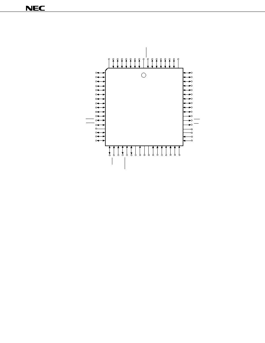
- Pin Configuration (Top View)
- Block Diagram
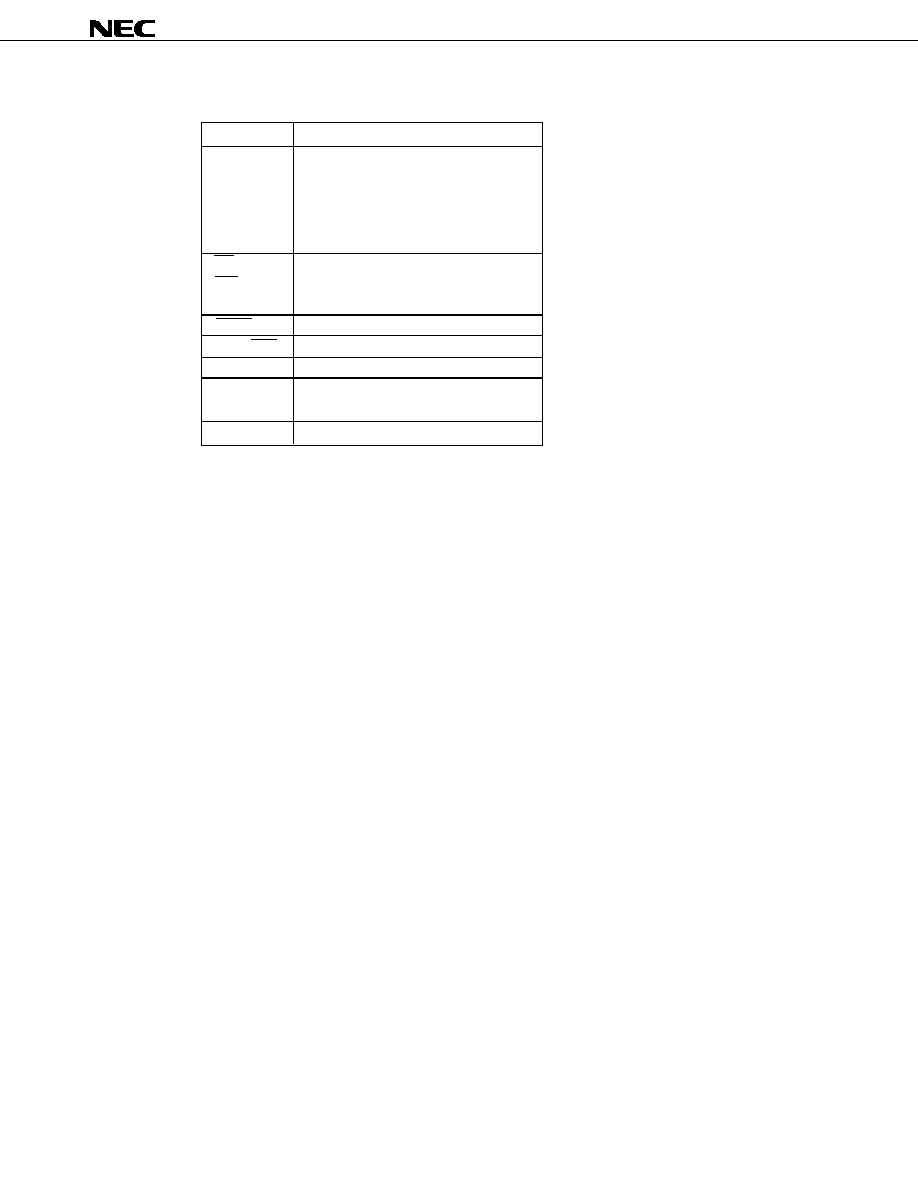
- 1. DIFFERENCES BETWEEN uPD78C14(A) AND uPD78C14
- 2. PIN FUNCTIONS
- 2.1 Pin Function List
- 2.2 Pin Input/Output Circuits
- 2.3 Recommended Connections for Unused Pins
- 3. INSTRUCTION SET
- 3.1 Operand Expression Format/Description Method
- 3.2 Instruction Code Description
- 3.3 Instruction Execution Time
- 4. LIST OF MODE REGISTERS
- 5. ELECTRICAL SPECIFICATIONS
- 6. CHARACTERISTIC CURVES (reference value)
- 7. PACKAGE DRAWINGS
- 8. RECOMMENDED SOLDERING CONDITIONS
- APPENDIX DEVELOPMENT TOOLS

©
1994
The
µ
PD78C14(A) is a single-chip, CMOS 8-bit microcontroller in which a 16-bit ALU, a ROM, a RAM, an A/D converter,
a multifunction timer/event counter, and a serial interface are all integrated. Moreover, a 48-Kbyte external expansion
memory (ROM/RAM) can be connected.
Since the
µ
PD78C14(A) uses the CMOS construction, its operations are performed with low power consumption. By
using the standby function, functions such as data retention are performed with lower power consumption.
For details on functions, refer to the User's Manual listed below. Please read it before starting design work.
87AD series
µ
PD78C18 User's Manual: IEU-1314
FEATURES
High reliability as compared with
µ
PD78C14
159 instructions: 87AD instruction set
Multiply and divide instructions, 16-bit arithmetic operation instructions
Instruction cycle: 0.8
µ
s at 15 MHz
Internal ROM: 16384 W x 8
Internal RAM: 256 W x 8
Direct addressing to an external memory (ROM/RAM) up to 64 Kbytes
Highly accurate 8-bit A/D converter: Eight analog inputs
General-purpose serial interface: Asynchronous, synchronous, and I/O interface modes
Multifunction 16-bit timer/event counter
Two 8-bit timers
I/O lines: 44
Interrupt functions: Three external, eight internal
∑ Non-maskable interrupt: 1
∑ Maskable interrupts: 10
Zero-cross detection function (two inputs)
Standby functions: HALT mode, Hardware/software STOP mode
ORDERING INFORMATION
Part number
Package
Quality grade
µ
PD78C14G(A)-xxx-36
64-pin plastic QUIP
Special
µ
PD78C14GF(A)-xxx-3BE
64-pin plastic QFP (14 x 20 mm)
Special
µ
PD78C14L(A)-xxx
68-pin plastic QFJ (950 x 950 mil)
Special
Remark xxx is a ROM code suffix.
Document No. IC-2813B
(O.D. No. IC-8242B)
Date Published May 1995 P
Printed in Japan
µ
PD78C14(A)
MOS INTEGRATED CIRCUIT
8-BIT SINGLE-CHIP MICROCONTROLLER (WITH A/D CONVERTER)
Please refer to "Quality grade on NEC Semiconductor Devices" (Document number IEI-1209) published by
NEC Corporation to know the specification of quality grade on the devices and its recommended applications.
©
1991
H
The mark shows revised points.
*
DATA SHEET
The information in this document is subject to change without notice.

2
µ
PD78C14(A)
PA0
PA1
PA2
PA3
PA4
PA5
PA6
PA7
PB1
PB2
PB3
PB4
PB5
PB6
PB7
PC0/TxD
PC1/RxD
PC3/INT2
PC4/TO
PC5/CI
PC6/CO0
PC7/CO1
NMI
INT1
MODE1
RESET
MODE0
X2
X1
V
SS
PB0
PC2/SCK
1
2
3
4
5
6
7
8
10
11
12
13
14
15
16
17
18
20
21
22
23
24
25
26
27
28
29
30
31
32
9
19
V
DD
STOP
PD7
PD6
PD5
PD4
PD3
PD2
PD0
PF7
PF6
PF5
PF4
PF3
PF2
PF1
PF0
WR
RD
AV
DD
V
AREF
AN7
AN6
AN5
AN4
AN3
AN2
AN1
AN0
AV
SS
PD1
ALE
64
63
62
61
60
59
58
57
55
54
53
52
51
50
49
48
47
45
44
43
42
41
40
39
38
37
36
35
34
33
56
46
PD78C14G(A)-XXX-36
µ
PD2
PD1
PD0
PF7
PF6
PF5
PF4
PF3
PF2
PF1
PF0
ALE
WR
RD
AV
DD
V
AREF
AN7
AN6
AN5
PA6
PA7
PB0
PB1
PB2
PB3
PB4
PB5
PB6
PB7
PC0/TxD
PC1/RxD
PC2/SCK
PC3/INT2
PC4/TO
PC5/CI
PC6/CO0
PC7/CO1
NMI
PD3
52
PD4
53
PD5
54
PD6
55
PD7
56
STOP
57
V
DD
58
PA0
59
PA1
60
PA2
61
PA3
62
PA4
63
PA5
641 2 3 4 5 6 7 8 9 10 11 12 13 141516 1718 19
51 50 49 48 47 46 454443 42 41 40 39 38 37 36 35 34 33
AN4
AN3
AN2
AN1
AN0
AV
SS
V
SS
X1
X2
MODE0
RESET
MODE1
INT1
32
31
30
29
28
27
26
25
24
23
22
21
20
µ
PD78C14GF(A)-XXX-3BE
Pin Configuration (Top View)
µ
PD78C14(A)
3
IC
PA6
PA5
PA4
PA3
PA2
PA1
PA0
V
DD
STOP
PD7
PD6
PD5
PD4
PD3
PD2
IC
PC7/CO1
NMI
INT1
MODE1
RESET
MODE0
X2
X1
V
SS
AV
SS
AN0
AN1
AN2
AN3
AN4
AN5
AN6
PA7
10
PB0
11
PB1
12
PB2
13
PB3
14
PB4
15
PB5
16
PB6
17
PB7
18
PC0/TxD
19
PC1/RxD
20
PC2/SCK
21
PC3/INT2
22
2728 29 30 3132 33 34 35 36 37 38 39 4041 42 43
9 8 7 6 5 4 3 2 1 68 67 66 6564 63 62 61
PD1
PD0
PF7
PF6
PF5
PF4
PF3
PF2
PF1
PF0
ALE
WR
RD
60
59
58
57
56
55
54
53
52
51
50
49
48
µ
PD78C14L(A)-XXX
IC
23
PC4/TO
24
PC5/CI
25
PC6/CO0
26
AV
DD
47
IC
46
V
AREF
45
AN7
44
4
µ
PD78C14(A)
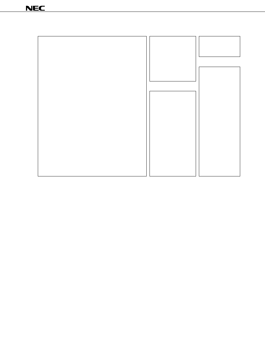
Block Diagram
PF7-0/AB15-8
PD7-0/AD7-0
PC7-0
PB7-0
PA7-0
8
8
8
8
8
PORT A
PORT B
PORT C
PORT D
PORT F
8
8
8
8
8
8
8
8
8
16
16
6
8
16
14
16
16
16
16
8
8
8
8
8
8
8/16
8
INST.REG
INST.
DECODER
DATA
MEMORY
(256-BYTE)
PROGRAM
MEMORY
(16 K-BYTE)
MAIN
G.R
ALT
G.R
INTERNAL DATA BUS
ALU
(8/16)
PSW
LATCH
LATCH
8
STANDBY
CONTROL
SYSTEM
CONTROL
READ/WRITE
CONTROL
V
SS
V
DD
STOP
RESET
MODE1 MODE0
ALE
WR
RD
LATCH
INC/DEC
PC
SP
EA
V
B
D
H
A
C
E
L
EA'
V'
B'
D'
H'
A'
C'
E'
L'
BUFFER
OSC
SERIAL I/O
INT.
CONTROL
TIMER
TIMER
EVENT
COUNTER
A/D
CONVERTER
X1
X2
PC0/TxD
PC1/RxD
PC2/SCK
NMI
INT1
PC3/INT2/TI
PC4/TO
PC5/CI
AV
SS
PC7/CO1
PC6/CO0
AN7-0
8
V
AREF
V
DD
Note
Note
DATA MEMORY can only be used when RAE bit of MM register is set to 1.
External memory is necessary when 0 is set.
4

µ
PD78C14(A)
5
CONTENTS
1.
DIFFERENCES BETWEEN
µ
PD78C14(A) AND
µ
PD78C14 ...................................................6
2.
PIN FUNCTIONS ......................................................................................................................7
2.1
Pin Function List ......................................................................................................................... 7
2.2
Pin Input/Output Circuits ........................................................................................................... 9
2.3
Recommended Connections for Unused Pins ....................................................................... 13
3.
INSTRUCTION SET ................................................................................................................14
3.1
Operand Expression Format/Description Method .................................................................14
3.2
Instruction Code Description ..................................................................................................16
3.3
Instruction Execution Time ...................................................................................................... 17
4.
LIST OF MODE REGISTERS .................................................................................................29
5.
ELECTRICAL SPECIFICATIONS ..........................................................................................30
6.
CHARACTERISTIC CURVES (reference value) ................................................................... 41
7.
PACKAGE DRAWINGS .........................................................................................................44
8.
RECOMMENDED SOLDERING CONDITIONS .....................................................................47
APPENDIX DEVELOPMENT TOOLS ............................................................................................49
6
µ
PD78C14(A)
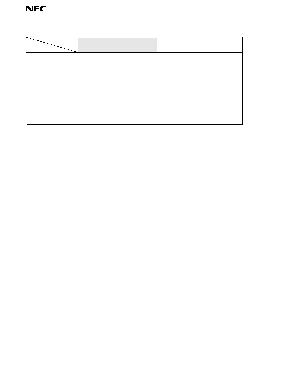
1. DIFFERENCES BETWEEN
µ
PD78C14(A) AND
µ
PD78C14
Part number
µ
PD78C14(A)
µ
PD78C14
Item
Quality grade
Special
Standard
Electrical
Input leakage current
Input leakage current
specifications
(AN7-0;
±
1
µ
A (MAX.)
AN7-0;
±
10
µ
A (MAX.)
Package
∑ 64-pin plastic QUIP
∑ 64-pin plastic shrink DIP
∑ 64-pin plastic QFP
∑ 64-pin plastic QUIP
(14 x 20 mm, thickness: 2.05 mm)
∑ 64-pin plastic QUIP (straight)
∑ 68-pin plastic QFJ
∑ 64-pin plastic QFP
(14 x 20 mm, thickness: 2.05 mm)
∑ 64-pin plastic QFP
(14 x 20 mm, thickness: 2.70 mm)
∑ 68-pin plastic QFJ
µ
PD78C14(A)
7
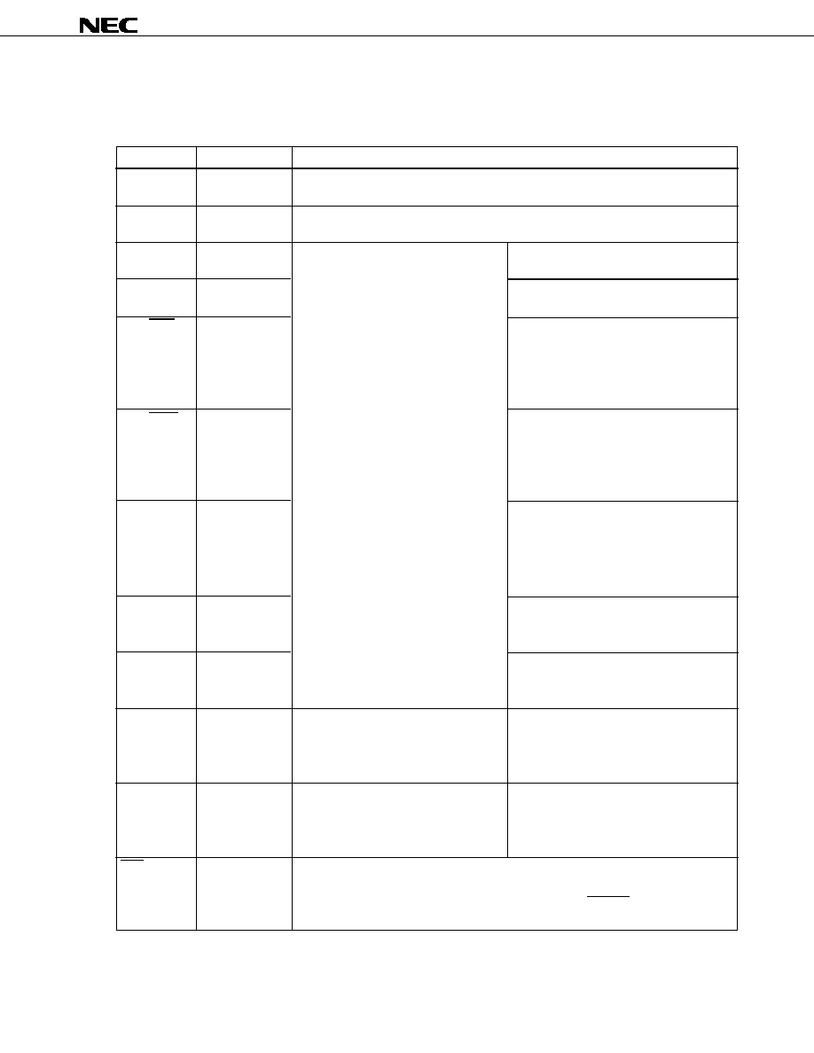
2. PIN FUNCTIONS
2.1 Pin Function List
Pin
Input/Output
Function
PA7-PA0
Input/Output
These 8 pins constitute an 8-bit I/O port and input/output can be specified in bit
(Port A)
units.
PB7-PB0
Input/Output
These 8 pins constitute an 8-bit I/O port and input/output can be specified in bit
(Port B)
units.
PC0/TxD
Input/Output,
Port C
Transmit Data
Output
These 8 pins constitute an 8-bit I/O
This pin outputs serial data.
PC1/RxD
Input/Output,
port and input/output can be specified
Receive Data
Input
in bit units.
This pin inputs serial data.
PC2/SCK
Input/Output,
Serial Clock
Input/Output
This pin inputs/outputs serial clock. It be-
comes an output pin when an internal
clock is used or an input pin when an
external clock is used.
PC3/INT2/TI
Input/Output,
Interrupt Request/Timer Input
Input, Input
This pin inputs edge triggering (falling
edge) maskable interrupt or external
clock for timer. This pin is also shared
with zero-cross detection pin for AC input.
PC4/TO
Input/Output,
Timer Output
Output
This pin outputs square waves in which
one cycle of the internal clock forms a
half cycle, indicating the timer's counting
time.
PC5/CI
Input/Output,
Counter Input
Input
This pin inputs external pulse for timer/
event counter.
PC6/CO0
Input/Output,
Counter Output 0,1
PC7/CO1
Output
This pin outputs programmable square
wave by timer/event counter.
PD7-PD0/
Input/Output,
Port D
Address/Data Bus
AD7-AD0
Input/Output
These 8 pins constitute an 8-bit I/O
These pins function as multiplexed
port and input/output can be
address/data bus when using an
specified in byte units.
external memory.
PF7-PF0/
Input/Output,
Port F
Address Bus
AB15-AB8
Output
These 8 pins constitute an 8-bit I/O
These pins function as address bus when
port and input/output can be specified
using an external memory.
in bit units.
WR
Output
This is a strobe signal output to write data in external memory. This signal
(Write
becomes high level except during the data write machine cycle for external memory.
Strobe)
This signal becomes output high impedance when the RESET signal is low or in
the hardware STOP mode.
8
µ
PD78C14(A)
(Continued)
Pin
Input/Output
Function
RD
Output
This is a strobe signal output to read data from external memory. This signal
(Read
becomes high level except during the data read machine cycle for external memory.
Strobe)
This signal becomes output high impedance when the RESET signal is low or in
the hardware STOP mode.
ALE
Output
This is a strobe signal to externally latch the low-order address information
(Address
output to pins PD7-PD0 to access the external memory. This signal becomes
Latch
output high impedance when the RESET signal is low or in the hardware STOP
Enable)
mode.
MODE0
Input/Output
Set the MODE0 pin to 0 (low level) and MODE1 pin to 1 (high level)
Note
.
MODE1
When both pins MODE0 and MODE1 are set to 1
Note
, these pins synchronize to
(Mode)
the ALE and a control signal is output.
NMI
Input
This pin inputs the edge triggering (falling edge) nonmaskable interrupt.
(Non-
Maskable
Interrupt)
INT1
Input
This pin inputs edge triggering (rising edge) maskable interrupt. This pin is also
(Interrupt
shared with zero-cross detection pin for AC input.
Request)
AN7-AN0
Input
These eight pins input analog signals for the A/D converter. Pins AN7-AN4 can
(Analog
be used as edge detection (falling edge) input.
Input)
V
AREF
Input
This pin inputs the reference voltage for the A/D converter and controls the
(Reference
operation for the A/D converter.
Voltage)
AV
DD
Power supply pin for the A/D converter
(Analog
V
DD
)
AV
SS
Ground pin for the A/D converter
(Analog
V
SS
)
X1, X2
These are crystal connecting pins for the system clock oscillation. When a clock
(Crystal)
is externally supplied, input it through pin X1. Input the clock to X1 and its reverse
phase to X2.
RESET
Input
This pin inputs the active-low reset input signal.
(Reset)
STOP
Input
This pin inputs control signal of the hardware STOP mode. When the low level
(Stop)
of this signal is input, the oscillator stops to operate.
V
DD
Positive power supply pin
V
SS
Ground pin
Note
Pull-up with the following external resistor:
4 (k
)
R
0.4 t
CYC
(k
)
t
CYC
(unit: ns)
Example
4 (k
)
R
26 (k
): t
CYC
= 66 (ns) at 15 MHz
4 (k
)
R
33 (k
): t
CYC
= 83 (ns) at 12 MHz
µ
PD78C14(A)
9
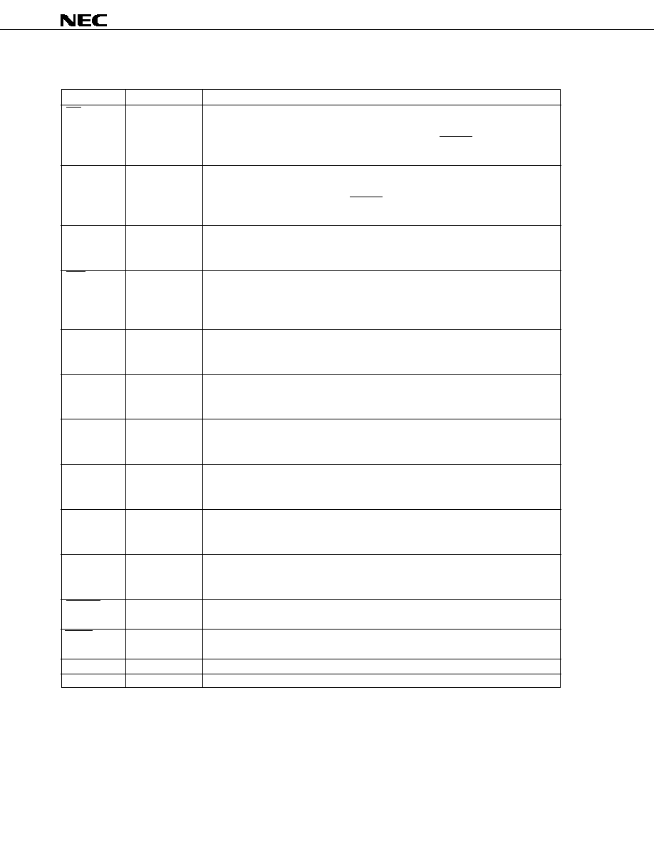
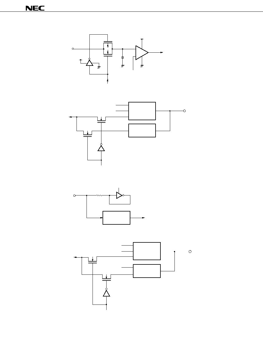
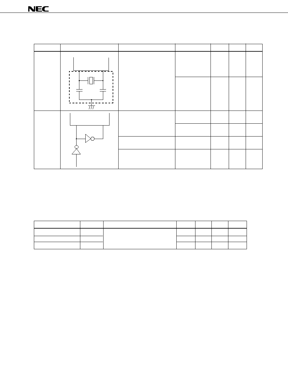
2.2 Pin Input/Output Circuits
Schematic input/output circuits of the pins are shown in Table 2-1 and figures from (1) to (11).
Table 2-1. Name of Type No.
Pin
Type No.
Pin
Type No.
PA0-7
5
RESET
2
PB0-7
5
RD
4
PC0-1
5
WR
4
PC2/SCK
8
ALE
4
PC3/INT2
10
STOP
2
PC4-7
5
MODE0
11
PD0-7
5
MODE1
11
PF0-7
5
AN0-3
7
NMI
2
AN4-7
12
INT1
9
V
AREF
13

10
µ
PD78C14(A)
Type 4
IN/OUT
output data
output disable
Type 1
IN
P-ch
V
DD
OUT
N-ch
output data
output disable
N-ch
P-ch
V
DD
IN
(1) Type 1
(2) Type 2
(3) Type 4
(4) Type 5
µ
PD78C14(A)
11
IN/OUT
Type 5
Type 9
N-ch
N-ch
MCC
output data
output disable
self bias
enable
IN/OUT
Type 5
Type 2
output data
output disable
N-ch
N-ch
MCC
+
≠
AV
SS
AV
DD
AV
SS
AV
DD
IN
P-ch
N-ch
sampling
C
reference voltage
(from voltage tap of serial resistor string)
(5) Type 7
(6) Type 8
(7) Type 9
(8) Type 10
IN
Type 1
self bias
enable
data
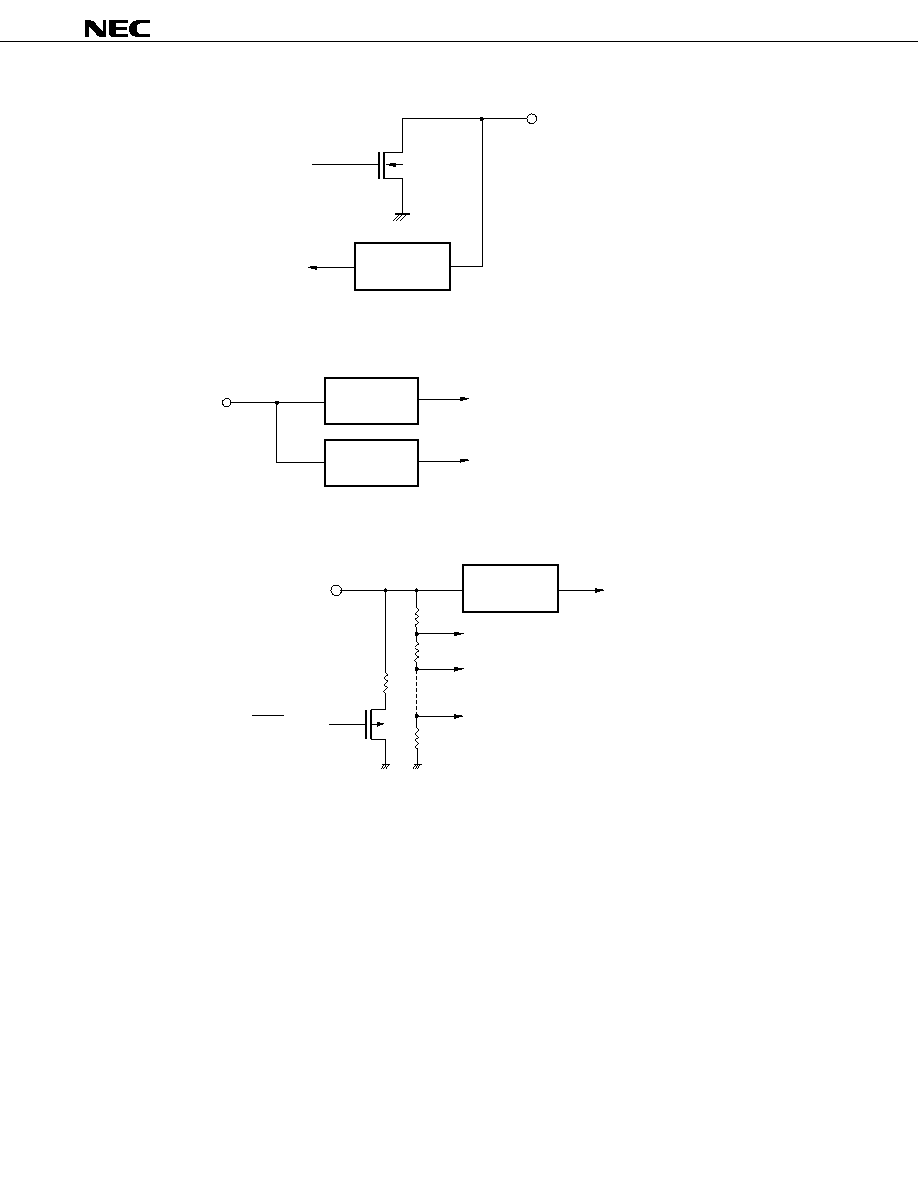
12
µ
PD78C14(A)
Type 1
IN
AV
SS
STOP Mode
P-ch
(9) Type 11
(10) Type 12
(11) Type 13
Type 7
Type 2
IN
edge detection circuit
output data
Type 1
N-ch
IN/OUT
µ
PD78C14(A)
13
2.3 Recommended Connections for Unused Pins
Pin
Recommended connection
PA7-0
PB7-0
PC7-0
Connect to V
DD
or V
SS
via resistor.
PD7-0
PF7-0
RD
WR
Leave unconnected.
ALE
STOP
V
DD
INT1, NMI
Connect to V
DD
or V
SS
.
AV
DD
Connect to V
DD
.
V
AREF
Connect to V
SS
.
AV
SS
AN7-0
Connect to AV
SS
or AV
DD
.

14
µ
PD78C14(A)
3. INSTRUCTION SET
3.1 Operand Expression Format/Description Method
Expression format
Description method
r
V, A, B, C, D, E, H, L
r1
EAH, EAL, B, C, D, E, H, L
r2
A, B, C
sr
PA, PB, PC, PD, PF, MKH, MKL, ANM, SMH, SML, EOM, ETMM, TMM, MM, MCC, MA, MB,
MC, MF, TXB, TM0, TM1, ZCM
sr1
PA, PB, PC, PD, PF, MKH, MKL, ANM, SMH, EOM, TMM, RXB, CR0, CR1, CR2, CR3
sr2
PA, PB, PC, PD, PF, MKH, MKL, ANM, SMH, EOM, TMM
sr3
ETM0, ETM1
sr4
ECNT, ECPT
rp
SP, B, D, H
rp1
V, B, D, H, EA
rp2
SP, B, D, H, EA
rp3
B, D, H
rpa
B, D, H, D+, H+, D≠, H≠
rpa1
B, D, H
rpa2
B, D, H, D+, H+, D≠, H≠, D+byte, H+A, H+B, H+EA, H+byte
rpa3
D, H, D++, H++, D+byte, H+A, H+B, H+EA, H+byte
wa
8-bit immediate data
word
16-bit immediate data
byte
8-bit immediate data
bit
3-bit immediate data
f
CY, HC, Z
irf
NMI
Note
, FT0, FT1, F1, F2, FE0, FE1, FEIN, FAD, FSR, FST, ER, OV, AN4, AN5, AN6, AN7,
SB
Note NMI can be also described as FNMI.
µ
PD78C14(A)
15
Remarks
1. sr to sr4 (special register)
2. rp to rp3 (register pair)
4. f (flag)
PA
: PORT A
ETMM : TIMER/EVENT
SP
: STACK POINTER
CY
: CARRY
PB
: PORT B
COUNTER MODE
B
: BC
HC : HALF CARRY
PC
: PORT C
EOM
: TIMER/EVENT
D
: DE
Z
: ZERO
PD
: PORT D
COUNTER OUTPUT
H
: HL
PF
: PORT F
MODE
V
: VA
5. irf (interrupt flag)
MA
: MODE A
ANM
: A/D CHANNEL MODE
EA
: EXTENDED
NMI : NMI INPUT
MB
: MODE B
CR0
: A/D CONVERSION
ACCUMULATOR
FT0 : INTFT0
MC
: MODE C
to
RESULT 0 to 3
FT1 : INTFT1
MCC : MODE CONTROL C
CR3
3. rpa to rpa3 (rp addressing)
F1
: INTF1
MF
: MODE F
TXB
: Tx BUFFER
B
: (BC)
F2
: INTF2
MM
: MEMORY MAPPING
RXB
: Rx BUFFER
D
: (DE)
FE0 : INTFE0
TM0
: TIMER REG0
SMH
: SERIAL MODE High
H
: (HL)
FE1 : INTFE1
TM1
: TIMER REG1
SML
: SERIAL MODE Low
D+
: (DE)+
FEIN: INTFEIN
TMM : TIMER MODE
MKH
: MASK High
H+
: (HL)+
FAD : INTFAD
ETM0 : TIMER/EVENT
MKL
: MASK Low
D≠
: (DE)≠
FSR : INTFSR
COUNTER REG0
ZCM
: ZERO CROSS MODE
H≠
: (HL)≠
FST : INTFST
ETM1 : TIMER/EVENT
D++
: (DE)++
ER
: ERROR
COUNTER REG1
H++
: (HL)++
OV : OVERFLOW
ECNT : TIMER/EVENT
D+byte : (DE+byte)
AN4 : ANALOG INPUT
COUNTER UPCOUNTER
H+A
: (HL+A)
to
4 to 7
ECPT : TIMER/EVENT
H+B
: (HL+B)
AN7
COUNTER CAPTURE
H+EA : (HL+EA)
SB
: STANDBY
H+byte : (HL+byte)

16
µ
PD78C14(A)
r
R
2
R
1
R
0
reg
0
0
0
0
1
1
1
1
0
0
1
1
0
0
1
1
0
1
0
1
0
1
0
1
V
A
B
C
D
E
H
L
r1
T
2
T
1
T
0
reg
0
0
0
0
1
1
1
1
0
0
1
1
0
0
1
1
0
1
0
1
0
1
0
1
EAH
EAL
B
C
D
E
H
L
rpa
A
3
A
2
A
1
addressing
0
0
0
0
0
0
0
0
1
1
1
1
1
0
0
0
0
1
1
1
1
0
1
1
1
1
0
0
1
1
0
0
1
1
1
0
0
1
1
(BC)
(DE)
(HL)
(DE)
+
(HL)
+
(DE)
≠
(HL)
≠
(DE+byte)
(HL+A)
(HL+B)
(HL+EA)
(HL+byte)
A
0
0
1
0
1
0
1
0
1
1
0
1
0
1
rpa
rpa1
rpa2
r2
sr
S
5
S
4
S
3
0
0
0
0
0
0
0
0
0
0
0
0
0
0
0
0
0
0
0
0
0
0
0
1
1
1
1
1
0
0
0
0
0
0
0
0
0
0
0
0
0
1
1
1
1
1
1
1
1
1
1
0
0
0
0
0
0
0
0
0
0
0
0
1
1
1
1
1
1
0
0
0
0
0
0
1
1
1
1
0
0
0
0
1
S
2
0
0
0
0
1
1
1
0
0
0
0
1
1
0
0
0
0
1
1
0
0
0
0
0
0
0
0
0
Special-reg
PA
PB
PC
PD
PF
MKH
MKL
ANM
SMH
SML
EOM
ETMM
TMM
MM
MCC
MA
MB
MC
MF
TXB
RXB
TM0
TM1
CR0
CR1
CR2
CR3
ZCM
S
1
0
0
1
1
0
1
1
0
0
1
1
0
0
0
0
1
1
0
1
0
0
1
1
0
0
1
1
0
S
0
0
1
0
1
1
0
1
0
1
0
1
0
1
0
1
0
1
0
1
0
1
0
1
0
1
0
1
0
sr1
sr2
r
rpa3
C
3
C
2
C
1
0
0
0
0
1
1
1
1
1
0
0
1
1
0
1
1
1
1
1
1
0
0
1
0
0
1
1
C
0
0
1
0
1
1
0
1
0
1
addressing
(DE)
(HL)
(DE)
++
(HL)
++
(DE+byte)
(HL+A)
(HL+B)
(HL+EA)
(HL+byte)
irf
I
3
I
2
I
1
0
0
0
0
0
0
0
0
1
1
1
1
1
0
0
0
0
0
0
0
0
0
1
1
1
1
0
0
0
0
1
0
0
0
0
1
0
0
1
1
0
0
1
1
0
0
1
1
0
0
0
1
1
0
I
0
0
1
0
1
0
1
0
1
0
1
0
1
0
0
1
0
1
0
INTF
NMI
FT0
FT1
F1
F2
FE0
FE1
FEIN
FAD
FSR
FST
ER
OV
AN4
AN5
AN6
AN7
SB
I
4
0
0
0
0
0
0
0
0
0
0
0
0
0
1
1
1
1
1
sr3
U
0
0
1
Special-reg
ETM0
ETM1
sr4
V
0
0
1
Special-reg
ECNT
ECPT
P
2
P
1
P
0
reg-pair
0
0
0
0
1
0
0
1
1
0
0
1
0
1
0
SP
BC
DE
HL
EA
rp
Q
2
Q
1
Q
0
reg-pair
0
0
0
0
1
0
0
1
1
0
0
1
0
1
0
VA
BC
DE
HL
EA
rp1
F
2
F
1
F
0
flag
0
0
0
1
0
1
1
0
0
0
1
0
--
CY
HC
Z
f
rp
rp2
rp3
sr
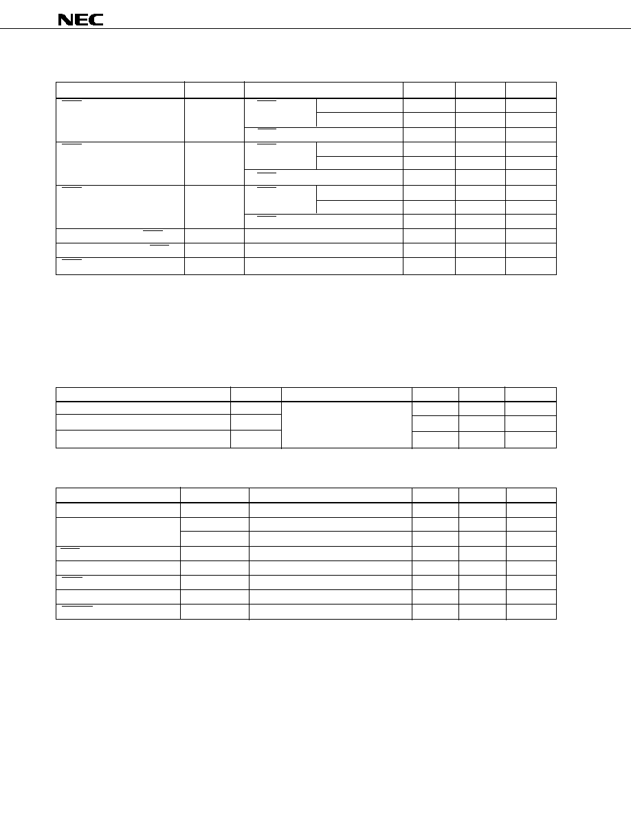
3.2 Instruction Code Description

µ
PD78C14(A)
17
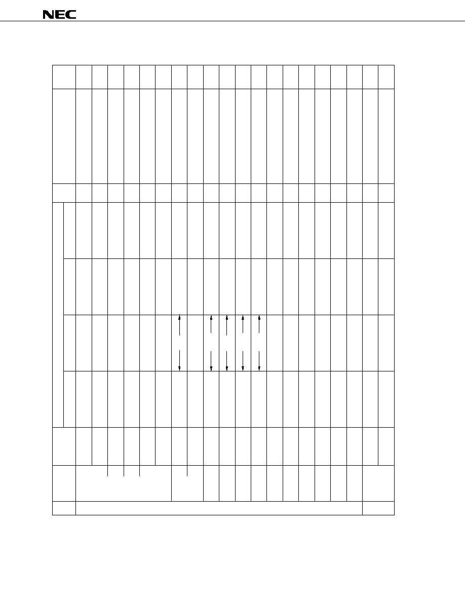
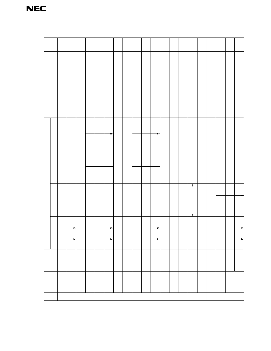
3.3 Instruction Execution Time
In the following table, one state consists of three clock cycles. So, when the 15 MHz clock is used, one state becomes
200 ns (= 3 x 1/15
µ
s). Execution time of the 4-state instruction, the shortest instruction, becomes 0.8
µ
s.
18
µ
PD78C14(A)
Instruc-
tion group
Instruction code
Mnemonic
Operand
State
Operation
Skip
condition
B1
B2
B3
B4
r1, A
0 0 0 1 1 T
2
T
1
T
0
4
r1
A
A, r1
0 0 0 0 1 T
2
T
1
T
0
4
A
r1
*
*
1 1 S
5
S
4
S
3
S
2
S
1
S
0
sr, A
0 1 0 0 1 1 0 1
10
sr
A
MOV
A, sr1
r, word
word, r
1 1 S
5
S
4
S
3
S
2
S
1
S
0
0 1 0 0 1 1 0 0
0 1 1 0 1 R
2
R
1
R
0
0 1 1 1 0 0 0 0
0 1 1 1 1 R
2
R
1
R
0
0 1 1 1 0 0 0 0
Data
Low Adrs
Low Adrs
High Adrs
High Adrs
10
A
sr1
17
r
(word)
17
(word)
r
8-bit data transfer
16-bit data
transfer
MVI
MVIW
MVIX
STAW
LDAW
STAX
LDAX
EXX
EXA
EXH
BLOCK
DMOV
*
*
*
*
*
*
*
r, byte
0 1 1 0 1 R
2
R
1
R
0
sr2, byte
0 1 1 0 0 1 0 0
wa, byte
0 1 1 1 0 0 0 1
rpa1, byte
0 1 0 0 1 0 A
1
A
0
0 1 1 0 0 0 1 1
wa
0 0 0 0 0 0 0 1
wa
A
3
0 1 1 1 A
2
A
1
A
0
rpa2
A
3
0 1 0 1 A
2
A
1
A
0
rpa2
0 0 0 1 0 0 0 1
0 0 0 1 0 0 0 0
0 1 0 1 0 0 0 0
0 0 1 1 0 0 0 1
1 0 1 1 0 1 P
1
P
0
1 0 1 0 0 1 P
1
P
0
S
3
0 0 0 0 S
2
S
1
S
0
Offset
Data
Offset
Offset
Data
Data
Note 1
Note 1
Data
Data
7
14
13
10
10
10
7/13
7/13
4
4
4
13
(C+1)
4
4
Note 3
Note 3
r
byte
sr2
byte
(V. wa)
byte
(rpa1)
byte
(V. wa)
A
A
(V. wa)
(rpa2)
A
A
(rpa2)
B
B', C
C', D
D'
E
E', H
H', L
L'
V, A
V', A', EA
EA'
H, L
H', L'
(DE)+
(HL)+, C
C≠1
End if borrow
rp3
L
EAL, rp3
H
EAH
EAL
rp3
L
, EAH
rp3
H
{
rp3, EA
EA, rp3
µ
PD78C14(A)
19
Instruc-
tion group
Instruction code
Mnemonic
Operand
State
Operation
Skip
condition
B1
B2
B3
B4
sr3, EA
0 1 0 0 1 0 0 0
14
sr3
EA
EA, sr4
1 1 0 0 0 0 0 V
0
14
EA
sr4
0 0 0 1 1 1 1 0
word
0 1 1 1 0 0 0 0
20
(word)
C, (word+1)
B
SBCD
word
word
word
0 0 1 0 1 1 1 0
0 0 1 1 1 1 1 0
0 0 0 0 1 1 1 0
Low Adrs
High Adrs
20
(word)
E, (word+1)
D
20
(word)
L, (word+1)
H
20
(word)
SP
L
, (word+1)
SP
H
16-bit data transfer
8-bit arithmetic
operation (register)
STEAX
LDED
LHLD
LSPD
LDEAX
PUSH
POP
LXI
TABLE
ADD
ADC
*
rpa3
0 1 0 0 1 0 0 0
word
0 1 1 1 0 0 0 0
word
word
word
0 1 0 0 1 0 0 0
rpa3
1 0 1 1 0 Q
2
Q
1
Q
0
rp1
1 0 1 0 0 Q
2
Q
1
Q
0
rp1
0 P
2
P
1
P
0
0 1 0 0
0 1 0 0 1 0 0 0
0 1 1 0 0 0 0 0
0 1 0 0
1 1 0 1
0 1 0 1
0 0 0 1 1 1 1 1
Low Byte
Data
14/20
20
20
20
20
14/20
13
10
10
17
8
8
8
8
Note 3
(rpa3)
EAL, (rpa3+1)
EAH
C
(word), B
(word+1)
E
(word), D
(word+1)
L
(word), H
(word+1)
SP
L
(word), SP
H
(word+1)
EAL
(rpa3), EAH
(rpa3+1)
(SP≠1)
rp1
H
, (SP≠2)
rp1
L
SP
SP≠2
rp1
L
(SP), rp1
H
(SP+1)
SP
SP+2
rp2
word
C
(PC+3+A)
B
(PC+3+A+1)
A
A+r
r
r+A
A
A+r+CY
r
r+A+CY
DMOV
SDED
SHLD
SSPD
LBCD
rp2, word
A, r
r, A
A, r
r, A
1 1 0 1 0 0 1 U
0
1 1 0 0 0 R
2
R
1
R
0
1 0 1 0 1 0 0 0
1 0 0 0 C
3
C
2
C
1
C
0
0 0 1 0 1 1 1 1
0 0 1 1 1 1 1 1
0 0 0 0 1 1 1 1
1 0 0 1 C
3
C
2
C
1
C
0
Note 2
Low Adrs
Data
Note 2
High Adrs
High Byte
Note 3

20
µ
PD78C14(A)
Instruc-
tion group
Instruction code
Mnemonic
Operand
State
Operation
Skip
condition
B1
B2
B3
B4
A, r
0 1 1 0 0 0 0 0
8
A
A+r
r, A
0 0 1 0
8
r
r+A
1 1 1 0
A, r
8
A
A≠r
r, A
A, r
r, A
0 1 1 0
1 1 1 1
0 1 1 1
8
r
r≠A
8
A
A≠r≠CY
8
r
r≠A≠CY
8-bit arithmetic operation (register)
ANA
ORA
XRA
GTA
LTA
NEA
A, r
r, A
A, r
r, A
A, r
r, A
1 0 0 1 0 R
2
R
1
R
0
A, r
0 0 0 1
r, A
0 0 1 1
1 1 1 0
0 1 1 0
0 0 1 1
8
8
8
8
8
8
8
8
8
8
8
8
8
8
A
A≠r
r
r≠A
A
A r
r
r A
A
A r
r
r A
A
A r
r
r A
A≠r≠1
r≠A≠1
A≠r
r≠A
A≠r
r≠A
ADDNC
SUB
SBB
SUBNB
A, r
A, r
r, A
A, r
r, A
1 0 1 0 0 R
2
R
1
R
0
1 0 1 1
0 0 1 0
0 0 0 1
1 0 0 0 1 R
2
R
1
R
0
0 0 0 0
1 0 0 1
1 0 1 1
1 0 1 0 1 R
2
R
1
R
0
No Zero
r, A
<
<
>
>
>
>
No Zero
Borrow
Borrow
No
Borrow
No
Borrow
No
Borrow
No
Carry
No
Carry
No
Borrow

µ
PD78C14(A)
21
Instruc-
tion group
Instruction code
Mnemonic
Operand
State
Operation
Skip
condition
B1
B2
B3
B4
A, r
0 1 1 0 0 0 0 0
8
A≠r
r, A
0 1 1 1
8
r≠A
1 1 0 0
A, r
8
A r
A, r
rpa
rpa
1 1 0 1
1 1 0 0 0 A
2
A
1
A
0
1 1 0 1
8
A r
11
A
A+(rpa)
11
A
A+(rpa)+CY
8-bit arithmetic operation (memory)
SBBX
ANAX
XRAX
GTAX
LTAX
NEAX
rpa
rpa
rpa
rpa
rpa
rpa
1 0 0 1 0 A
2
A
1
A
0
rpa
1 0 1 0 1 A
2
A
1
A
0
rpa
1 1 0 0
1 1 0 1
1 1 1 0
11
11
11
11
11
11
11
11
11
11
11
11
11
A
A+(rpa)
A
A≠(rpa)
A
A≠(rpa)≠CY
A
A≠(rpa)
A
A (rpa)
A
A (rpa)
A
A (rpa)
A≠(rpa)≠1
A≠(rpa)
A≠(rpa)
A≠(rpa)
A (rpa)
EQA
ONA
ADDX
ADDNCX
rpa
rpa
rpa
rpa
1 1 1 1 1 R
2
R
1
R
0
1 1 1 1
1 1 1 0
1 0 0 1
1 1 1 1
1 0 1 1
1 0 0 0 1 A
2
A
1
A
0
1 0 1 0
1 0 1 1
Zero
rpa
<
>
No Zero
Zero
Borrow
No
Borrow
No
Carry
Zero
No
Borrow
No Zero
Zero
Zero
No Zero
<
<
>
<
OFFA
ADCX
SUBX
SUBNBX
ORAX
EQAX
ONAX
OFFAX
0 1 1 1 0 0 0 0
A (rpa)
<
8-bit arithmetic
operation (register)

22
µ
PD78C14(A)
Instruc-
tion group
Instruction code
Mnemonic
Operand
State
Operation
Skip
condition
B1
B2
B3
B4
A, byte
0 1 0 0 0 1 1 0
7
A
A+byte
r, byte
0 1 1 1 0 1 0 0
11
r
r+byte
*
*
0 1 0 0 0 R
2
R
1
R
0
sr2, byte
0 1 1 0
20
sr2
sr2+byte
ADI
A, byte
r, byte
sr2, byte
S
3
1 0 0 0 S
2
S
1
S
0
0 1 0 1 0 1 1 0
0 1 1 1 0 1 0 0
0 1 1 0
Data
7
A
A+byte+CY
11
r
r+byte+CY
20
sr2
sr2+byte+CY
Arithmetic operation of immediate data
ACI
ADINC
SUI
SBI
SUINB
ANI
*
*
*
*
*
A, byte
0 0 1 0 0 1 1 0
r, byte
0 1 1 1 0 1 0 0
sr2, byte
0 1 1 0
A, byte
0 1 1 0 0 1 1 0
0 1 1 1 0 1 0 0
r, byte
0 1 1 0
sr2, byte
0 1 1 1 0 1 1 0
A, byte
0 1 1 1 0 1 0 0
r, byte
0 1 1 0
0 0 1 1 0 1 1 0
0 1 1 1 0 1 0 0
0 1 1 0
0 0 0 0 0 1 1 1
0 1 1 1 0 1 0 0
Data
Data
7
11
20
7
11
20
7
11
20
7
11
20
7
11
A
A+byte
r
r+byte
sr2
sr2+byte
A
A≠byte
r
r≠byte
sr2
sr2≠byte
A
A≠byte≠CY
r
r≠byte≠CY
sr2
sr2≠byte≠CY
A
A≠byte
r
r≠byte
sr2
sr2≠byte
r
r byte
sr2, byte
A, byte
r, byte
sr2, byte
A, byte
r, byte
Data
Data
Data
Data
0 1 0 1 0 R
2
R
1
R
0
S
3
1 0 1 0 S
2
S
1
S
0
Data
0 0 1 0 0 R
2
R
1
R
0
S
3
0 1 0 0 S
2
S
1
S
0
0 1 1 0 0 R
2
R
1
R
0
S
3
1 1 0 0 S
2
S
1
S
0
0 1 1 1 0 R
2
R
1
R
0
S
3
1 1 1 0 S
2
S
1
S
0
0 0 1 1 0 R
2
R
1
R
0
S
3
0 1 1 0 S
2
S
1
S
0
0 0 0 0 1 R
2
R
1
R
0
Data
Data
Data
Data
Data
Data
No
Carry
No
Borrow
No
Carry
No
Carry
No
Borrow
No
Borrow
<
<
A
A byte

µ
PD78C14(A)
23
Instruc-
tion group
Instruction code
Mnemonic
Operand
State
Operation
Skip
condition
B1
B2
B3
B4
sr2, byte
0 1 1 0 0 1 0 0
sr2
sr2 byte
A, byte
0 0 0 1 0 1 1 1
A
A byte
*
*
0 0 0 1 1 R
2
R
1
R
0
r, byte
0 1 1 1 0 1 0 0
20
r
r byte
ANI
sr2, byte
A, byte
r, byte
S
3
0 0 1 1 S
2
S
1
S
0
0 1 1 0
0 0 0 1 0 1 1 0
0 1 1 1 0 1 0 0
Data
7
sr2
sr2 byte
11
A
A byte
20
Arithmetic operation of immediate data
ORI
XRI
GTI
LTI
NEI
EQI
*
*
*
*
sr2, byte
0 1 1 0
A, byte
0 0 1 0 0 1 1 1
r, byte
0 1 1 1 0 1 0 0
sr2, byte
0 1 1 0
0 0 1 1 0 1 1 1
A, byte
0 1 1 1 0 1 0 0
r, byte
0 1 1 0
sr2, byte
0 1 1 0 0 1 1 1
A, byte
0 1 1 1 0 1 0 0
0 1 1 0
0 1 1 1 0 1 1 1
0 1 1 1 0 1 0 0
0 1 1 0
Data
Data
7
11
20
7
11
14
7
11
A≠byte≠1
r≠byte≠1
sr2≠byte≠1
A≠byte
r≠byte
sr2≠byte
A≠byte
r≠byte
sr2≠byte
A≠byte
r≠byte
sr2≠byte
r, byte
sr2, byte
A, byte
r, byte
sr2, byte
Data
Data
Data
0 0 0 1 0 R
2
R
1
R
0
S
3
0 0 1 0 S
2
S
1
S
0
Data
0 0 1 0 1 R
2
R
1
R
0
S
3
0 1 0 1 S
2
S
1
S
0
0 0 1 1 1 R
2
R
1
R
0
S
3
0 1 1 1 S
2
S
1
S
0
0 1 1 0 1 R
2
R
1
R
0
S
3
1 1 0 1 S
2
S
1
S
0
0 1 1 1 1 R
2
R
1
R
0
S
3
1 1 1 1 S
2
S
1
S
0
Data
Data
Data
Data
Data
Zero
No
Zero
Borrow
<
S
3
0 0 0 1 S
2
S
1
S
0
Data
14
7
11
14
7
11
14
<
<
<
<
r
r byte
<
sr2
sr2 byte
<
Zero
Zero
No
Zero
No
Zero
Borrow
Borrow
No
Borrow
No
Borrow
No
Borrow

24
µ
PD78C14(A)
Instruc-
tion group
Instruction code
Mnemonic
Operand
State
Operation
Skip
condition
B1
B2
B3
B4
A, byte
0 1 0 0 0 1 1 1
7
A byte
r, byte
0 1 1 1 0 1 0 0
11
r byte
*
*
0 1 0 0 1 R
2
R
1
R
0
sr2, byte
0 1 1 0
14
sr2 byte
ONI
A, byte
r, byte
sr2, byte
S
3
1 0 0 1 S
2
S
1
S
0
0 1 0 1 0 1 1 1
0 1 1 1 0 1 0 0
0 1 1 0
7
A byte
11
r byte
14
sr2 byte
Arithmetic operation of
immediate data
OFFI
ADCW
SBBW
ORAW
LTAW
ONAW
wa
0 1 1 1 0 1 0 0
wa
wa
wa
wa
wa
wa
wa
Data
14
14
14
14
14
14
14
14
14
14
14
14
14
14
A
A+(V.wa)
A
A+(V.wa)+CY
A
A+(V.wa)
A
A≠(V.wa)
A
A≠(V.wa)
A
A (V.wa)
A
A (V.wa)
A
A (V.wa)
A≠(V.wa)≠1
A≠(V.wa)
A≠(V.wa)
A≠(V.wa)
A (V.wa)
wa
wa
wa
wa
wa
wa
Data
0 1 0 1 1 R
2
R
1
R
0
S
3
1 0 1 1 S
2
S
1
S
0
Data
1 1 0 1
1 0 1 0
1 1 1 1
1 0 1 1
1 0 0 1
1 0 0 1 0 0 0 0
1 0 1 1
1 1 1 0
1 1 0 0
Data
offset
No
Zero
Zero
No
Borrow
No
Zero
Borrow
<
EQAW
NEAW
XRAW
GTAW
SUBNBW
ANAW
ADDNCW
SUBW
ADDW
1 1 0 0 0 0 0 0
1 1 1 0
1 0 0 0 1 0 0 0
1 0 1 0 1 0 0 0
1 1 1 1
No
Zero
No
Borrow
No
Carry
No
Zero
No
Zero
Zero
Zero
Zero
<
<
<
<
<
<
<
>
>
A
A≠(V.wa)≠CY
Arithmetic operation of working register
µ
PD78C14(A)
25
Instruc-
tion group
Instruction code
Mnemonic
Operand
State
Operation
Skip
condition
B1
B2
B3
B4
wa
0 1 1 1 0 1 0 0
14
A (V.wa)
wa, byte
Offset
19
(V.wa)
(V.wa) byte
wa, byte
19
(V.wa)
(V.wa) byte
wa, byte
wa, byte
wa, byte
13
(V.wa)≠byte≠1
13
(V.wa)≠byte
13
(V.wa)≠byte
16-bit arithmetic operation
OFFIW
DADD
DADDNC
ESUB
DSUB
DSBB
wa, byte
wa, byte
wa, byte
EA, r2
EA, rp3
EA, rp3
1 0 1 0
EA, rp3
0 1 1 0 0 0 R
1
R
0
EA, r2
1 0 0 0 1 1 P
1
P
0
1 0 0 1
13
13
13
11
11
11
11
11
11
11
11
11
11
(V.wa)≠byte
(V.wa) byte
(V.wa) byte
EA
EA+r2
EA
EA+rp3
EA
EA+rp3+CY
EA
EA+rp3
EA
EA≠r2
EA
EA≠rp3
EA
EA≠rp3≠CY
EA
EA≠rp3
EA
EA rp3
OFFAW
ORIW
LTIW
EQIW
EA, rp3
EA, rp3
EA, rp3
EA, rp3
1 1 0 1 1 0 0 0
1 0 1 1
1 1 1 1
1 1 0 1
0 1 0 0 0 0 R
1
R
0
1 1 1 0 0 1 P
1
P
0
EA, rp3
<
>
Zero
Borrow
No
Borrow
No
Carry
No
Borrow
No Zero
Zero
Zero
No Zero
<
<
>
GTIW
NEIW
ONIW
EADD
DADC
DSUBNB
DAN
DOR
0 0 1 1
EA
EA rp3
Arithmetic operation of working register
ANIW
1 0 0 1 0 1 P
1
P
0
EA, rp3
DXR
11
EA
EA rp3
0 0 0 0 0 1 0 1
0 0 0 1
0 0 1 0
0 1 1 0
0 1 0 0
0 1 0 1
0 1 1 1
0 1 1 1 0 0 0 0
0 0 0 0
0 1 0 0
*
*
*
*
*
*
*
*
0 1 0 0
Data
Offset
<<
<
1 1 0 0 0 1 P
1
P
0
26
µ
PD78C14(A)
Instruc-
tion group
Instruction code
Mnemonic
Operand
State
Operation
Skip
condition
B1
B2
B3
B4
EA, rp3
0 1 1 1 0 1 0 0
11
EA≠rp3≠1
EA, rp3
Offset
11
EA≠rp3
EA, rp3
11
EA≠rp3
EA, rp3
EA, rp3
EA, rp3
11
EA≠rp3
11
EA rp3
11
EA rp3
Decrement/Increment
INR
INX
DCR
DCRW
DCX
DAA
r2
r2
r2
wa
rp
EA
r2
wa
0 0 1 0 1 0 1 1
0 0 1 0 1 0 1 0
32
59
4
16
7
7
4
16
7
7
4
8
8
EA
A
◊
r2
EA
EA˜r2, r2
The Remainder
r2
r2+1
(V.wa)
(V.wa)+1
rp
rp+1
EA
EA+1
r2
r2≠1
(V.wa)
(V.wa)≠1
rp
rp≠1
EA
EA≠1
Decimal Adjust Accumulator
CY
1
DGT
DNE
DON
MUL
rp
1 0 1 0 1 1 P
1
P
0
EA
<
Carry
Borrow
No
Borrow
No Zero
Zero
Zero
No Zero
<
DEQ
DOFF
DIV
INRW
STC
CLC
NEGA
CY
0
16-bit arithmetic operation
DLT
0 0 1 1 1 0 1 0
8
A
A+1
0 1 0 0 1 0 0 0
*
*
Multiply/
divide
Other arithmetic
operation
0 1 0 1 0 0 R
1
R
0
0 0 1 0 0 0 0 0
0 1 0 0 1 0 0 0
0 1 1 0 0 0 0 1
1 0 1 0 1 0 0 1
0 1 0 0 0 0 R
1
R
0
0 0 P
1
P
0
0 0 1 0
1 0 1 0 1 0 0 0
0 0 P
1
P
0
0 0 1 1
0 0 1 1 0 0 0 0
Offset
1 1 0 1
1 1 0 0
1 1 1 0
1 1 1 1
0 0 1 1
0 0 1 0 1 1 R
1
R
0
1 0 1 1
Carry
Borrow
Borrow
µ
PD78C14(A)
27
Instruc-
tion group
Instruction code
Mnemonic
Operand
State
Operation
Skip
condition
B1
B2
B3
B4
0 1 0 0 1 0 0 0
17
Rotate Left Digit
17
Rotate Right Digit
r2
8
r2
m+1
r2
m
, r2
0
CY, CY
r2
7
r2
r2
r2
8
r2
m--1
r2
m
, r2
7
CY, CY
r2
0
8
r2
m+1
r2
m
, r2
0
0, CY
r2
7
8
r2
m--1
r2
m
, r2
7
0, CY
r2
0
Jump
DRLL
DSLL
JMP
JB
JR
JEA
r2
r2
EA
EA
EA
EA
word
0 0 1 0 1 0 0 1
8
8
8
8
8
8
10
4
10
10
8
16
17
r2
m+1
r2
m
, r2
0
0, CY
r2
7
r2
m--1
r2
m
, r2
7
0, CY
r2
0
EA
n+1
EA
n
, EA
0
CY, CY
EA
15
EA
n--1
EA
n
, EA
15
CY, CY
EA
0
EA
n+1
EA
n
, EA
0
0, CY
EA
15
EA
n--1
EA
n
, EA
15
0, CY
EA
0
PC
word
PC
H
B, PC
L
C
PC
PC+1+jdisp 1
PC
PC+2+jdisp
PC
EA
(SP≠1)
(PC+3)
H
, (SP≠2)
(PC+3)
L
PC
word, SP
SP≠2
RLD
RLL
SLL
SLLC
word
0 0 1 1 1 0 0 0
word
Carry
RLR
SLR
SLRC
DRLR
CALL
CALB
CALF
(SP≠1)
(PC+2)
H
, (SP≠2)
(PC+2)
L
PC
H
B, PC
L
C, SP
SP≠2
Rotation shift
RRD
13
(SP≠1)
(PC+2)
H
, (SP≠2)
(PC+2)
L
PC
15≠11
00001, PC
10≠0
fa, SP
SP≠2
*
*
Call
0 1 0 1 0 1 0 0
0 1 0 0 0 0 0 0
0 1 0 0 1 0 0 0
0 1 0 0 1 1 1
1 0 1 1 0 1 0 0
1 0 1 0 0 1 0 0
0 0 0 0
1 1
0 0 1 0 0 0 0 1
Low Adrs
0 0 R
1
R
0
0 0 1 0 0 1 R
1
R
0
0 1 R
1
R
0
0 0 R
1
R
0
0 0 R
1
R
0
0 0 0 0 0 1 R
1
R
0
1 0 0 1
Carry
DSLR
JRE
*
*
word
word
0 1 1 1 1
0 1 0 0 1 0 0 0
jdisp 1
fa
0 0 1 0 1 0 0 0
jdisp
Low Adrs
High Adrs
High Adrs
0 0 0 0

28
µ
PD78C14(A)
Instruc-
tion group
Instruction code
Mnemonic
Operand
State
Operation
Skip
condition
B1
B2
B3
B4
1 0 0
16
(SP≠1)
(PC+1)
H
, (SP≠ 2)
(PC+1)
L
, PC
L
(128+2ta), PC
H
(129+2ta), SP
SP≠ 2
16
(SP≠1)
PSW, (SP≠2)
(PC+1)
H
, (SP≠3)
(PC+1)
L
, PC
0060H, SP
SP≠3
word
10
1 0 1 1 1 0 0 0
0 1 1 0 0 0 1 0
bit, wa
10
13
10
Skip if (V.wa) bit = 1
SKIT
NOP
DI
HLT
STOP
f
f
irf
irf
8
8
8
8
4
4
4
12
12
Skip if f = 1
Skip if f = 0
Skip if irf = 1, then reset irf
Skip if irf = 0
Reset irf, if irf = 1
No Operation
Enable Interrupt
Disable Interrupt
Set Halt Mode
Set Stop Mode
CALT
RET
RETI
SK
Uncondi-
tional
RETS
BIT
SKN
SKNIT
Skip
SOFT1
*
1 0 1 1 1 0 1 0
0 1 0 0 1 0 0 0
(V.wa)
bit = 1
EI
Offset
0 1 1 1 0 0 1 0
1 0 0 1
Call
Return
CPU operation
0 1 0 0 1 0 0 0
0 0 0 0 0 0 0 0
1 0 1 0 1 0 1 0
0 1 0 1 1 B
2
B
1
B
0
0 1 0 0 1 0 0 0
ta
0 0 1 1 1 0 1 1
1 0 1 1 1 0 1 1
0 1 0 I
4
I
3
I
2
I
1
I
0
0 1 1 I
4
I
3
I
2
I
1
I
0
0 0 0 0 1 F
2
F
1
F
0
0 0 0 1
f = 1
f = 0
irf = 1
irf = 0
PC
L
(SP), PC
H
(SP+1)
SP
SP+2
PC
L
(SP), PC
H
(SP+1), SP
SP+2
PC
PC+n
Notes 1. B2 (Data) is applied for rpa2 = D + byte or H + byte.
2. B3 (Data) is applied for rpa3 = D + byte or H + byte.
3. In the "state" column, data to the right of the slash applies when rpa2 or rpa3 is D + byte, H + A, H + B, H + EA, or H + byte.
Remark When the instructions below are skipped, the number of idle states is as listed below and differs from the number of execution states.
1-byte instruction
2-byte (with *)
2-byte
: 4-state
: 7-state
: 8-state
3-byte instruction (with *)
3-byte
4-byte
: 10-state
: 11-state
: 14-state
PC
L
(SP), PC
H
(SP+1)
PSW
(SP+2), SP
SP+3
µ
PD78C14(A)
29
4. LIST OF MODE REGISTERS
Name of mode register
Read/Write
Function
MA
MODE A
W
Specifies input/output of Port A in bit units
MB
MODE B
W
Specifies input/output of Port B in bit units
MCC
MODE CONTROL C
W
Specifies port/control mode of Port C in bit units
MC
MODE C
W
Specifies input/output of Port C set in the port mode in bit units
MM
MEMORY MAPPING
W
Specifies port/expansion mode of Ports D and F
MF
MODE F
W
Specifies input/output of Port F set in the port mode in bit units
TMM
Timer mode
R/W
Specifies operation mode of the timer
ETMM
Timer/Event
W
Specifies operation mode of the Timer Event Counter
Counter Mode
EOM
Timer/Event
R/W
Controls output level of CO0 and CO1
Counter Output Mode
SML
Serial Mode
W
Specifies operation mode of the serial interface
SMH
R/W
MKL
Interrupt Mask
R/W
Specifies interrupt request enable/disable
MKH
ANM
A/D Channel Mode
R/W
Specifies operation mode of the A/D converter
ZCM
Zero-cross Mode
W
Specifies operation mode of the zero-cross detection circuit

µ
PD78C14(A)
30
5. ELECTRICAL SPECIFICATIONS
ABSOLUTE MAXIMUM RATINGS (T
A
= 25 ∞C)
Parameter
Symbol
Test Condition
Ratings
Unit
Power Supply Voltage
V
DD
≠0.5 to +7.0
V
AV
DD
AV
SS
to V
DD
+ 0.5
V
AV
SS
≠0.5 to +0.5
V
Input Voltage
V
I
≠0.5 to V
DD
+ 0.5
V
Output Voltage
V
O
≠0.5 to V
DD
+ 0.5
V
Output Current Low
I
OL
All Output Pin
4.0
mA
All Output Pin Total
100
mA
Output Current High
I
OH
All Output Pin
≠2.0
mA
All Output Pin Total
≠50
mA
A/D Converter
V
AREF
≠0.5 to AV
DD
+ 0.3
V
Reference Input Voltage
Operating Ambient
T
A
≠40 to +85
∞C
Temperature
Storage Temperature
T
stg
≠65 to +150
∞C
Caution
If any of the parameters exceeds the absolute maximum ratings even for a moment, this may damage
product quality. The absolute maximum ratings are values that may physically damage the product. You
must use the product within the specified ratings.
*
µ
PD78C14(A)
31
Oscillation Characteristics (T
A
= ≠40 to +85 ∞C, V
DD
= AV
DD
= +5.0 V
±
10 %, V
SS
= AV
SS
= 0 V,
V
DD
≠ 0.8 V
AV
DD
V
DD
, 3.4 V
V
AREF
AV
DD
)
Resonator
Recommended Circuits
Parameter
Test Conditions
MIN.
MAX.
UNIT
Ceramic
Oscillation Frequency (fxx) A/D Converter
4
15
MHz
Resonator
Not used
or
Crystal
Resonator
Note
A/D Converter
5.8
15
MHz
Used
External
X1 Input Frequency
A/D Converter
4
15
MHz
Clock
(fx)
Not used
A/D Converter
5.8
15
MHz
Used
X1 Input
0
20
ns
Rise, Fall Time (t
r
, t
f
)
X1 Input High, Low
20
250
ns
Level Width (t¯
H
, t¯
L
)
Cautions
1. Oscillator circuit should be in the nearest area from X1 and X2 pins.
2. Do not place other signal lines within the area enclosed with broken lines.
Note
For a crystal resonator, the following external capacitances are recommended: C1 = C2 = 10 pF
CAPACITANCE (T
A
= 25 ∞C, V
DD
= V
SS
= 0 V)
Parameter
Symbol
Test Condition
MIN.
TYP.
MAX.
UNIT
Input Capacitance
C
I
f
C
= 1 MHz
10
pF
Output Capacitance
C
O
Unmeasured pins returned to 0 V
20
pF
I/O Capacitance
C
IO
20
pF
X1
X2
C1
C2
X1
X2
HCMOS
Inverter

µ
PD78C14(A)
32
DC CHARACTERISTICS (T
A
= ≠40 to +85 ∞C, V
DD
= AV
DD
= +5.0 V
±
10 %, V
SS
= AV
SS
= 0 V)
Parameter
Symbol
Test Condition
MIN.
TYP.
MAX.
UNIT
Input Low Voltage
V
IL1
All except RESET, STOP, NMI, SCK, INT1,
0
0.8
V
TI, AN7 to AN4
V
IL2
RESET, STOP, NMI, SCK, INT1, TI, AN7 to AN4 0
0.2V
DD
V
Input High Voltage
V
IH1
All except RESET, STOP, NMI, SCK, INT1,
2.2
V
DD
V
TI, AN7 to AN4, X1, X2
V
IH2
RESET, STOP, NMI, SCK, INT1, TI, AN7 to
0.8V
DD
V
DD
V
AN4, X1, X2
Output Low Voltage
V
OL
I
OL
= 2.0 mA
0.45
V
Output High Voltage
V
OH
I
OH
= ≠1.0 mA
V
DD
≠
1.0
V
I
OH
= ≠100
µ
A
V
DD
≠
0.5
V
Input Current
I
I
INT1
Note 1
, TI (PC3)
Note 2
; 0 V
V
I
V
DD
±
200
µ
A
Input Leakage
I
LI
All except INT1, TI (PC3), AN7 to AN0; 0 V
V
I
V
DD
±
10
µ
A
Current
AN7 to AN0; 0 V
V
I
V
DD
±
1
µ
A
Output Leakage
I
LO
0 V
V
O
V
DD
±
10
µ
A
Current
AV
DD
Supply
AI
DD1
Operation Mode f
xx
= 15 MHz
0.5
1.3
mA
Current
AI
DD2
STOP Mode
10
20
µ
A
V
DD
Supply Current
I
DD1
Operation mode f
xx
= 15 MHz
16
30
mA
I
DD2
HALT Mode f
xx
= 15 MHz
8
15
mA
Data Retention
V
DDDR
Hardware/Software STOP Mode
2.5
V
Voltage
Data Retention
I
DDDR
Hardware/Software
Note 3
V
DDDR
= 2.5 V
1
15
µ
A
Current
STOP Mode
V
DDDR
= 5 V
±
10 %
10
50
µ
A
Notes 1.
When self-bias is generated by ZCM register.
2.
When set in the control mode by MCC register and self-bias is generated by ZCM register.
3.
When self-bias is not generated.

µ
PD78C14(A)
33
AC CHARACTERISTICS (T
A
= ≠40 to +85 ∞C, V
DD
= AV
DD
= +5.0 V
±
10 %, V
SS
= AV
SS
= 0 V)
READ/WRITE OPERATION:
Parameter
Symbol
Test Condition
MIN.
MAX.
UNIT
X1 Input Cycle Time
t
CYC
66
250
ns
Address Setup Time to ALE
t
AL
f
xx
= 15 MHz, C
L
= 150 pF
30
ns
Address Hold Time after ALE
t
LA
35
ns
Address
RD
Delay Time
t
AR
100
ns
RD
Address Floating Time
t
AFR
C
L
= 150 pF
20
ns
Address
Data Input Time
t
AD
f
xx
= 15 MHz, CL = 150 pF
250
ns
ALE
Data Input Time
t
LDR
135
ns
RD
Data Input Time
t
RD
120
ns
ALE
RD
Delay Time
t
LR
15
ns
Data Hold Time after RD
t
RDH
C
L
= 150 pF
0
ns
RD
ALE
Delay Time
t
RL
f
xx
= 15 MHz, C
L
= 150 pF
80
ns
RD Width Low
t
RR
Data Read
215
ns
f
xx
= 15 MHz, C
L
= 150 pF
OP code Fetch
415
ns
f
xx
= 15 MHz, C
L
= 150 pF
ALE Width High
t
LL
f
xx
= 15 MHz, C
L
= 150 pF
90
ns
M1 Setup Time to ALE
t
ML
f
xx
= 15 MHz
30
ns
M1 Hold Time after ALE
t
LM
35
ns
IO/M Setup Time to ALE
t
IL
30
ns
IO/M Hold Time after ALE
t
LI
35
ns
Address
WR
Delay Time
t
AW
f
xx
= 15 MHz, C
L
= 150 pF
100
ns
ALE
Data Output Time
t
LDW
180
ns
WR
Data Output Time
t
WD
C
L
= 150 pF
100
ns
ALE
WR
Delay Time
t
LW
f
xx
= 15 MHz, C
L
= 150 pF
15
ns
Data Setup Time to WR
t
DW
165
ns
Data Hold Time after WR
t
WDH
60
ns
WR
ALE
Delay Time
t
WL
80
ns
WR Width Low
t
WW
215
ns
µ
PD78C14(A)
34
SERIAL OPERATION:
Parameter
Symbol
Test Condition
MIN.
MAX.
UNIT
SCK Cycle Time
t
CYK
SCK Input
Note 1
800
ns
Note 2
400
ns
SCK Output
1.6
µ
s
SCK Width Low
t
KKL
SCK Input
Note 1
335
ns
Note 2
160
ns
SCK Output
700
ns
SCK Width High
t
KKH
SCK Input
Note 1
335
ns
Note 2
160
ns
SCK Output
700
ns
RxD Setup Time to SCK
t
RXK
Note 1
80
ns
RxD Hold Time After SCK
t
KRX
Note 1
80
ns
SCK
TxD Delay Time
t
KTX
Note 1
210
ns
Notes 1.
In case of x1 clock rate in asynchronous mode, synchronous mode, or I/O interface mode.
2.
In case of x16 or x64 clock rate in asynchronous mode.
Remark The numeric values in the table apply when f
XX
= 15 MHz, C
L
= 150 pF.
ZERO-CROSS CHARACTERISTICS:
Parameter
Symbol
Test Condition
MIN.
MAX.
UNIT
Zero-Cross Detection Input
V
ZX
AC Coupled
1
1.8
VAC
P≠P
Zero-Cross Accuracy
A
ZX
60-Hz Sine Wave
±
135
mV
Zero-Cross Detection Input Frequency
f
ZX
0.05
1
kHz
OTHER OPERATION:
Parameter
Symbol
Test Condition
MIN.
MAX.
UNIT
TI Width High, Low
t
TIH
, t
TIL
6
t
CYC
CI Width High, Low
t
CI1H
, t
CI1L
Event Counter Mode
6
t
CYC
t
CI2H
, t
CI2L
Pulse Width Measurement Mode
48
t
CYC
NMI Width High, Low
t
NIH
, t
NIL
10
µ
s
INT1 Width High, Low
t
I1H
, t
I1L
36
t
CYC
INT2 Width High, Low
t
I2H
, t
I2L
36
t
CYC
AN7-4 Width High, Low
t
ANH
, t
ANL
36
t
CYC
RESET Width High, Low
t
RSH
, t
RSL
10
µ
s
µ
PD78C14(A)
35
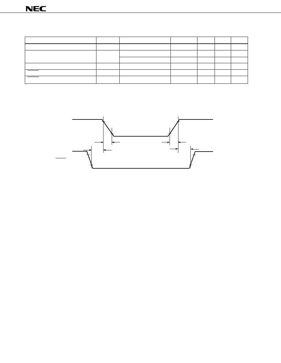
2.2 V
V
DD
≠ 1.0 V
0.45 V
0.8 V
2.2 V
0.8 V
Test points
A/D CONVERTER CHARACTERISTICS: (T
A
= ≠40 to +85 ∞C, V
DD
= +5.0 V
±
10 %, V
SS
= AV
SS
= 0 V,
V
DD
≠ 0.5 V
AV
DD
V
DD
, 3.4 V
V
AREF
AV
DD
)
Parameter
Symbol
Test Condition
MIN.
TYP.
MAX.
UNIT
Resolution
8
Bits
Absolute Accuracy
Note
3.4 V
V
AREF
AV
DD
, 66 ns
t
CYC
170 ns
±
0.8 %
FSR
4.0 V
V
AREF
AV
DD
, 66 ns
t
CYC
170 ns
±
0.6 %
FSR
T
A
= ≠10 to +70 ∞C,
±
0.4 %
FSR
4.0 V
V
AREF
AV
DD
, 66 ns
t
CYC
170 ns
Conversion time
t
CONV
66 ns
t
CYC
110 ns
576
t
CYC
110 ns
t
CYC
170 ns
432
t
CYC
Sampling Time
t
SAMP
66 ns
t
CYC
110 ns
96
t
CYC
110 ns
t
CYC
170 ns
72
t
CYC
Analog Input Voltage
V
IAN
AN7-0 (include unused pins)
0
V
AREF
V
Analog Input Impedance R
AN
50
M
Reference Voltage
V
AREF
3.4
AV
DD
V
V
AREF
Current
I
AREF1
Operation mode
1.5
3.0
mA
I
AREF2
STOP mode
0.7
1.5
mA
AV
DD
Supply Current
AI
DD1
Operation mode, f
xx
= 15 MHz
0.5
1.3
mA
AI
DD2
STOP mode
10
20
µ
A
Note Except quantization error (i.e.
±
1/2 LSB).
AC TIMING TEST POINTS
*

µ
PD78C14(A)
36
AC CHARACTERISTIC CALCULATING EXPRESSION depending on t
CYC
Symbol
Calculating Expression
MIN./MAX.
UNIT
t
AL
2T ≠ 100
MIN.
ns
t
LA
T ≠ 30
MIN.
ns
t
AR
3T ≠ 100
MIN.
ns
t
AD
7T ≠ 220
MAX.
ns
t
LDR
5T ≠ 200
MAX.
ns
t
RD
4T ≠ 150
MAX.
ns
t
LR
T ≠ 50
MIN.
ns
t
RL
2T ≠ 50
MIN.
ns
t
RR
4T ≠ 50 (Data Read)
MIN.
ns
7T ≠ 50 (OP Code Fetch)
t
LL
2T ≠ 40
MIN.
ns
t
ML
2T ≠ 100
MIN.
ns
t
LM
T ≠ 30
MIN.
ns
t
IL
2T ≠ 100
MIN.
ns
t
LI
T ≠ 30
MIN.
ns
t
AW
3T ≠ 100
MIN.
ns
t
LDW
T + 110
MAX.
ns
t
LW
T ≠ 50
MIN.
ns
t
DW
4T ≠ 100
MIN.
ns
t
WDH
2T ≠ 70
MIN.
ns
t
WL
2T ≠ 50
MIN.
ns
t
WW
4T ≠ 50
MIN.
ns
t
CYK
6T (SCK Input)
Note 1
/12T (SCK Input)
Note 2
MIN.
ns
24T (SCK Output)
t
KKL
2.5T + 5 (SCK Input)
Note 1
/5T + 5 (SCK Input)
Note 2
MIN.
ns
12T ≠ 100 (SCK Output)
t
KKH
2.5T + 5 (SCK Input)
Note 1
/5T + 5 (SCK Input)
Note 2
MIN.
ns
12T ≠ 100 (SCK Output)
Notes 1.
In case of x16 or x64 clock rate in asynchronous mode.
2.
In case of x1 clock rate in asynchronous mode, synchronous mode, or I/O interface mode.
Remarks
1.
T = t
CYC
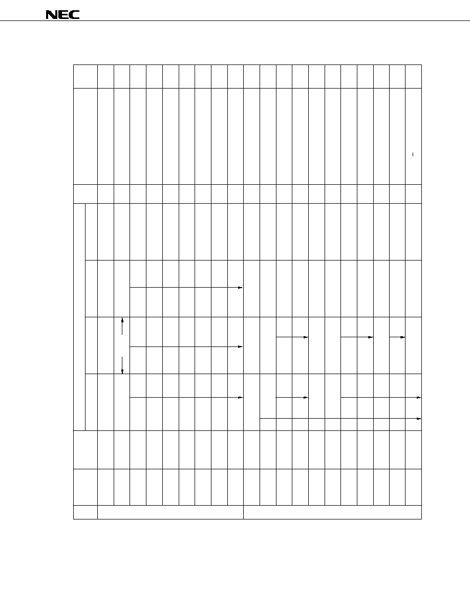
= 1/f
xx
2.
Symbols that cannot be found in this table do not depend on the oscillation frequency (f
xx
).
µ
PD78C14(A)
37
t
CYC
t
AD
t
LL
t
LA
t
LDR
t
RDH
t
RL
t
RR
t
RD
t
AFR
t
LR
t
AR
t
AL
t
LM
t
LI
t
ML
t
IL
X1
PF7-0
PD7-0
ALE
RD
MODE1
(M1)
Note 1
MODE0
(IO/M)
Note 2
address (high-order)
address (low-order)
read data
Timing Waveform
Read Operation
Write Operation
Notes 1. M1 signal is output to MODE1 pin at first OP code fetch cycle if MODE1 pin is pulled up.
2. IO/M signal is output to MODE0 pin at sr to sr2 register read cycle if MODE0 pin is pulled up.
3. IO/M signal is output to MODE0 pin at sr to sr2 register write cycle if MODE0 pin is pulled up.
t
LL
t
LA
t
DW
t
WDH
t
WL
t
WW
t
WD
t
LW
t
AW
t
AL
t
LI
t
IL
X1
PF7-0
PD7-0
ALE
WR
MODE0
(IO/M)
Note 3
address (high-order)
write data
t
LDW
address (low-order)

µ
PD78C14(A)
38
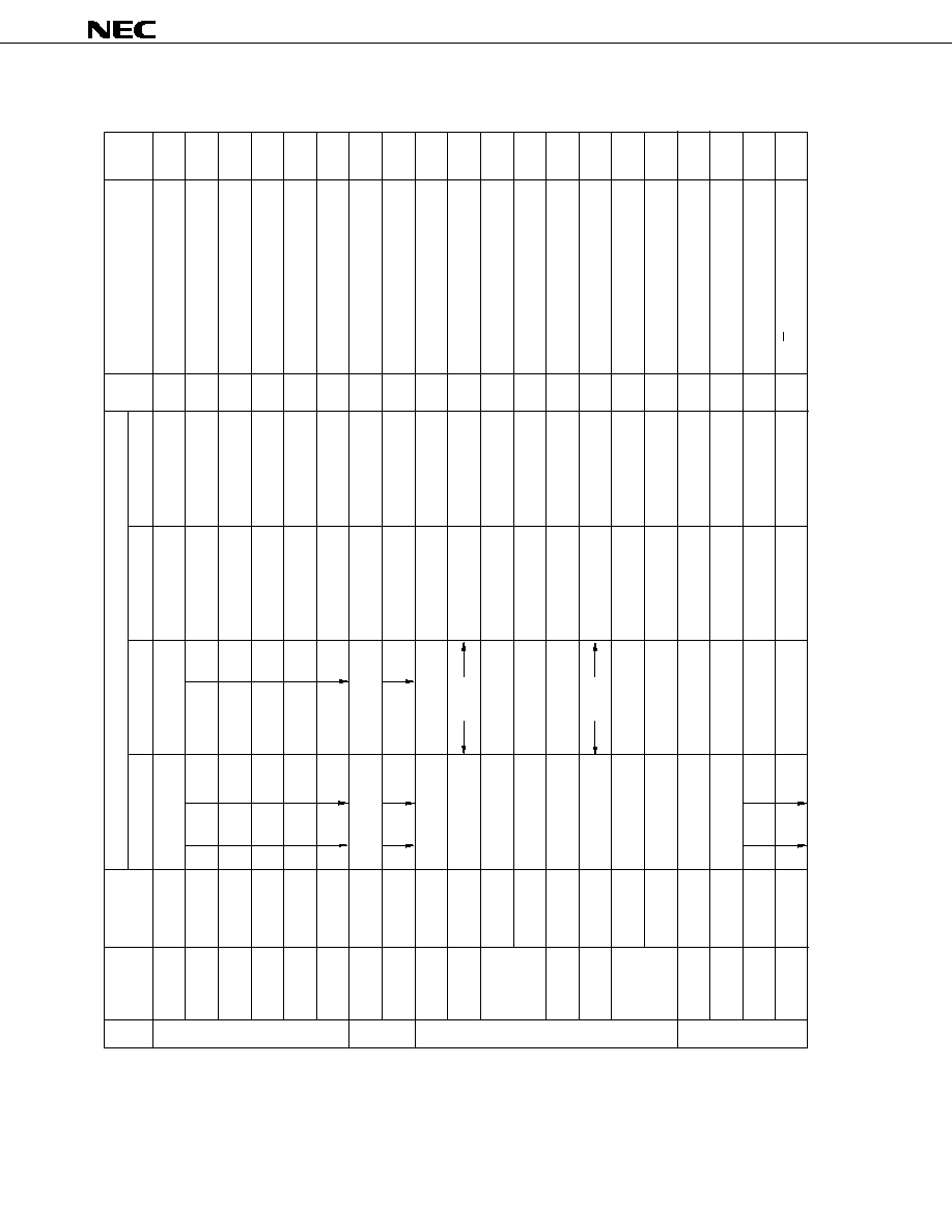
t
TIL
TI
t
TIH
Serial Operation
Timer Input Timing
Timer/Event Counter Input Timing
t
KKL
t
KKH
t
CYK
t
KRX
SCK
T
X
D
R
X
D
t
KTX
t
RXK
t
CI1L
CI
t
CI2L
CI
t
CI2H
Event Counter Mode
Pulse Width Measurement Mode
t
CI1H

µ
PD78C14(A)
39
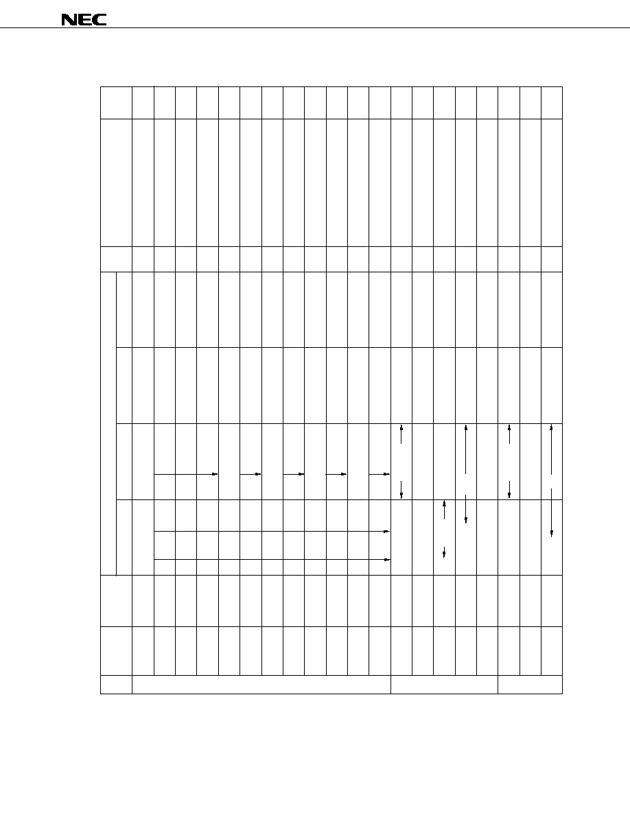
Interrupt Input Timing
RESET Input Timing
External Clock Timing
t
NIL
NMI
t
NIH
t
I2L
INT2
t
I2H
INT1
t
I1H
t
I1L
X1
t
H
0.8V
DD
0.8 V
t
t
t
L
t
CYC
r
f
t
RSL
RESET
t
RSH
0.8V
DD
0.2V
DD
µ
PD78C14(A)
40
Data Memory STOP Mode Low Supply Voltage Data Retention Characteristics (T
A
= ≠40 to +85 ∞C)
Parameter
Symbol
Test Condition
MIN.
TYP.
MAX.
UNIT
Data retention power supply voltage
V
DDDR
2.5
5.5
V
Data retention power supply current
I
DDDR
V
DDDR
= 2.5 V
1
15
µ
A
V
DDDR
= 5 V
±
10 %
10
50
µ
A
V
DD
rise, fall time
t
RVD
, t
FVD
200
µ
s
STOP setup time to V
DD
t
SSTVD
12T
Note
+ 0.5
µ
s
STOP hold time to V
DD
t
HVDST
12T
Note
+ 0.5
µ
s
Note T = t
CYC
= 1/f
xx
Data Retention Timing
*
V
DD
STOP
t
FVD
t
SSTVD
V
DDDR
t
RVD
t
HVDST
V
IH2
V
IL2
90 %
10 %

µ
PD78C14(A)
41
6. CHARACTERISTIC CURVES (reference value)
0
4.5
5.0
5.5
6.0
10
15
20
I
DD1
(TYP.)
I
DD1
, I
DD2
vs V
DD
(T
A
= 25 ∞C, f
XX
= 15 MHz)
Supply Voltage V
DD
[V]
V
DD
Supply Current I
DD1
, I
DD2
[mA]
I
DD1
(TYP.)
0
5
10
15
0
10
20
I
DD1
, I
DD2
vs f
XX
(T
A
= 25 ∞C, V
DD
= 5 V)
Oscillation Frequency f
XX
[MHz]
V
DD
Supply Current I
DD1
, I
DD2
[mA]
0
5
25
30
I
DD2
(TYP.)
30
I
DD2
(TYP.)
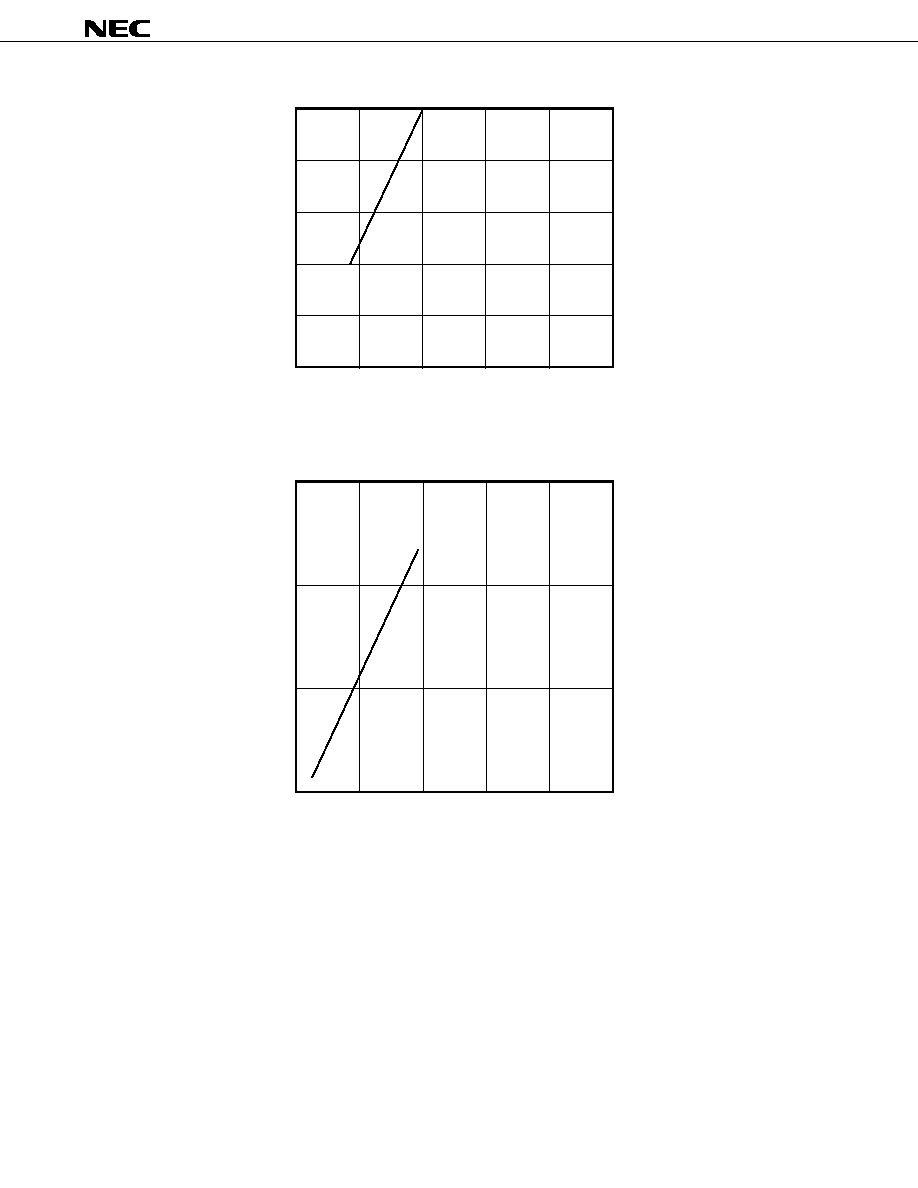
µ
PD78C14(A)
42
0
0.1
0.2
0.3
0.4
1.0
1.5
2.0
TYP.
I
OL
vs V
OL
(T
A
= 25 ∞C, V
DD
= 5 V)
Output Low Voltage V
OL
[V]
Output Low Current I
OL
[mA]
0
0.5
2.5
0.5
0
0.1
0.2
0.3
0.4
≠ 1.0
≠ 1.5
TYP.
I
OH
vs V
OH
(T
A
= 25 ∞C, V
DD
= 5 V)
Supply Voltage ≠ Output High Voltage V
DD
≠ V
OH
[V]
Output High Current I
OH
[mA]
0
≠ 0.5
0.5

µ
PD78C14(A)
43
0
2
3
4
5
4
6
8
TYP.
I
DDDR
vs V
DDDR
(T
A
= 25 ∞C)
Data Retention Supply Voltage V
DDDR
[V]
Data Retention Supply Current I
DDDR
[
A]
0
2
10
6
µ

µ
PD78C14(A)
44
7. PACKAGE DRAWINGS
H
I
M
C
P
A
64
1
32
33
M
N
J
K
S
W
X
P64GQ-100-36
ITEM
MILLIMETERS
INCHES
A
C
H
I
J
K
M
N
P
S
W
1.27 (T.P.)
0.25
16.5
0.100 (T.P.)
0.050 (T.P.)
0.010
0.157
1.634
NOTE
X
4.0
0.750
Each lead centerline is located within 0.25 mm
(0.010 inch) of its true position (T.P.) at maxi-
mum material condition.
0.142
0.043
0.020
24.13
0.950
0.010
0.25
2.54 (T.P.)
+0.004
≠0.005
+0.011
≠0.006
+0.012
≠0.008
+0.004
≠0.005
41.5
+0.3
≠0.2
0.50
+0.10
≠
1.1
+0.25
≠0.15
+0.10
≠0.05
+0.3
≠
3.6
+0.1
≠
+1.05
≠
19.05
+1.05
≠
0.650
+0.004
≠0.003
+0.013
≠0.012
+0.042
≠
+0.042
≠
64 PIN PLASTIC QUIP

µ
PD78C14(A)
45
N
A
M
F
B
51
52
32
K
L
64 PIN PLASTIC QFP (14
◊
20)
64
1
20
19
33
P
D
C
detail of lead end
S
Q
5∞±5∞
G
M
I
H
J
P64GF-100-3B8,3BE,3BR-1
ITEM
MILLIMETERS
INCHES
A
B
C
D
F
G
H
I
J
K
L
23.6±0.4
14.0±0.2
1.0
0.40±0.10
0.20
20.0±0.2
0.929±0.016
0.039
0.039
0.008
0.039 (T.P.)
0.795
NOTE
M
N
0.12
0.15
1.8±0.2
1.0 (T.P.)
0.005
0.006
+0.004
≠0.003
Each lead centerline is located within 0.20
mm (0.008 inch) of its true position (T.P.) at
maximum material condition.
0.071
0.016
0.551
0.8±0.2
0.031
P
2.7
0.106
0.693±0.016
17.6±0.4
1.0
+0.009
≠0.008
Q
0.1±0.1
0.004±0.004
S
3.0 MAX.
0.119 MAX.
+0.10
≠0.05
+0.009
≠0.008
+0.004
≠0.005
+0.009
≠0.008
+0.008
≠0.009

µ
PD78C14(A)
46
P68L-50A1-2
ITEM
MILLIMETERS
INCHES
NOTE
Each lead centerline is located within 0.12
mm (0.005 inch) of its true position (T.P.) at
maximum material condition.
+0.007
≠0.006
A
B
C
D
E
F
G
H
I
J
K
M
N
P
Q
T
U
25.2±0.2
24.20
24.20
25.2±0.2
1.94±0.15
0.6
4.4±0.2
2.8±0.2
0.9 MIN.
3.4
1.27 (T.P.)
0.40±1.0
0.12
23.12±0.20
0.15
R 0.8
0.20
+0.10
≠0.05
0.992±0.008
0.953
0.953
0.992±0.008
0.076
0.024
0.173
0.110
0.035 MIN.
0.134
0.050 (T.P.)
0.016
0.005
0.910
0.006
R 0.031
0.008
+0.009
≠0.008
+0.009
≠0.008
+0.004
≠0.005
+0.004
≠0.002
+0.009
≠0.008
N
K
M
Q
A
U
68
B
D
C
1
F
E
T
P
M
G
H
IJ
68 PIN PLASTIC QFJ ( 950 mil)
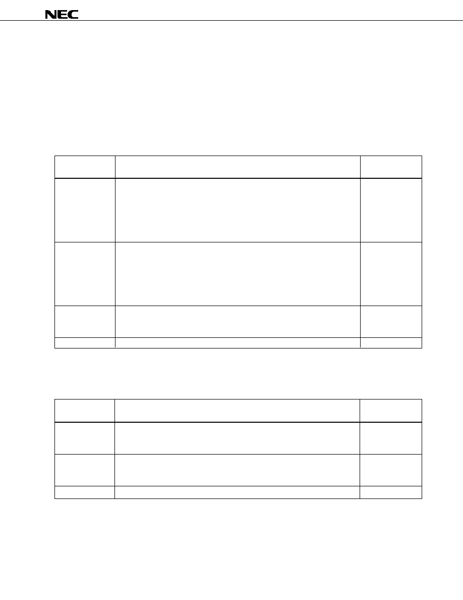
µ
PD78C14(A)
47
8. RECOMMENDED SOLDERING CONDITIONS
Solder the
µ
PD78C14(A) under the recommended conditions listed below.
For details of the recommended conditions for soldering, please refer to Semiconductor Device Mounting Technology
Manual (IEI-1207).
Consult an NEC sales representative about soldering methods and soldering conditions other than listed below.
Table 8-1. Soldering Conditions for Surface Mount Type
(1)
µ
PD78C14GF(A)-xxx-3BE: 64-pin plastic QFP (14 x 20 mm)
Soldering Method Soldering Conditions
Recommended
Condition Symbol
Infrared reflow
Package peak temperature: 235 ∞C, Time: Within 30 s (at 210 ∞C or higher),
IR35-00-2
Count: Twice or less
<Attention>
(1) Perform the second reflow when the device temperature has come down
to the room temperature from the heating from the first reflow.
(2) Do not wash the soldered portion with the flux following the first reflow.
VPS
Package peak temperature: 215 ∞C, Time: Within 40 s (at 200 ∞C or higher),
VP15-00-2
Count: Twice or less
<Attention>
(1) Perform the second reflow when the device temperature has come down
to the room temperature from the heating from the first reflow.
(2) Do not wash the soldered portion with the flux following the first reflow.
Wave soldering
Soldering bath temperature: 260 ∞C or less, Time: Within 10 s,
WS60-00-1
Count: Once, Preheating temperature: 120 ∞C MAX.
(package surface temperature)
Partial heating
Pin temperature: 300 ∞C or less, Time: Within 3 s (per pin row)
--
Caution Do not use several soldering methods together (except partial heating).
(2)
µ
PD78C14L (A)-xxx: 68-pin plastic QFJ (950 x 950 mil)
Soldering Method Soldering Conditions
Recommended
Condition Symbol
Infrared reflow
Package peak temperature: 230 ∞C, Time: Within 30 s (at 210 ∞C or higher),
IR30-107-1
Count: Once, Maximum number of days: Seven
Note
(after seven days,
prebaking at 125 ∞C is required for 10 hours)
VPS
Package peak temperature: 215 ∞C, Time: Within 40 s (at 200 ∞C or higher),
VP15-107-1
Count: Once, Maximum number of days: Seven
Note
(after seven days,
prebaking at 125 ∞C is required for 10 hours)
Partial heating
Pin temperature: 300 ∞C or less, Time: Within 3 s (per pin row)
--
Note
Number of storage days under the storage conditions of 25 ∞C and 65 % RH or less after the dry pack is opened.
Caution
Do not use several soldering methods together (except partial heating).
*

µ
PD78C14(A)
48
Table 8-2. Soldering Conditions for Hole-Through Type
µ
PD78C14G(A)-xxx-36: 64-pin plastic QUIP
Soldering Method
Soldering Conditions
Wave Soldering (pin part only)
Soldering bath temperature: 260 ∞C or less, Time: Within 10 s
Partial heating
Pin temperature: 300 ∞C or less, Time: Within 3 s (per pin row)
Caution
Apply wave soldering only to pins and be careful not to bring solder directly in contact with the package.
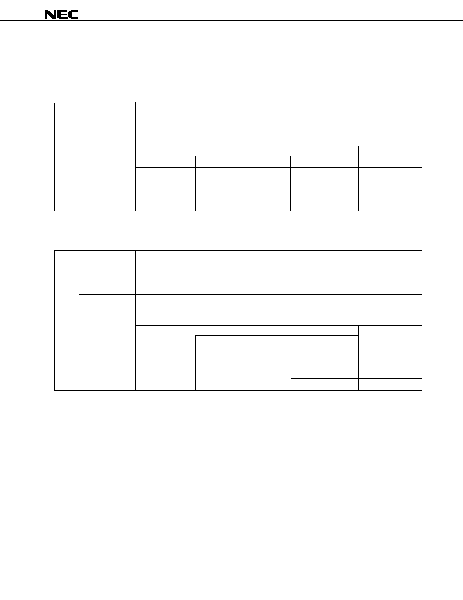
µ
PD78C14(A)
49
APPENDIX DEVELOPMENT TOOLS
The following development tools are provided for system development using the
µ
PD78C14(A):
Language processor
87AD series
This relocatable assembler is a program which converts a program written in mnemonics
relocatable assembler
into object code that can be executed by microcontroller.
(RA87)
In addition, it contains the automatic function of symbol table generation and branch
instruction optimization processing.
Host machine
Ordering code
OS
Distribution media
(product name)
PC-9800 series
MS-DOS
TM
3.5-inch 2HD
µ
S5A13RA87
(Ver. 2.11 to Ver. 5.00A
Note
)
5-inch 2HD
µ
S5A10RA87
IBM PC/AT
TM
PC DOS
TM
3.5-inch 2HC
µ
S7B13RA87
(Ver. 3.1)
5-inch 2HC
µ
S7B10RA87
PROM write tools
Hard-
PG-1500
PG-1500 is a PROM programmer which enables you to program single chip microcontrollers
ware
containing PROM by stand-alone or host machine operation by connecting an attached
board and optional programmer adapter to PG-1500. It also enables you to program typical
PROM devices of 256 Kbits to 4 Mbits.
PA-78CP14GQ
PROM programmer adapter for the
µ
PD78CP14(A) and connected to PG-1500 for use.
Soft-
PG-1500
PG-1500 and a host machine are connected by a serial or parallel interface and PG-1500 is
ware
controller
controlled on the host machine.
Host machine
Ordering code
OS
Distribution media
(product name)
PC-9800 series
MS-DOS
3.5-inch 2HD
µ
S5A13PG1500
(Ver. 2.11 to Ver. 5.00A
Note
)
5-inch 2HD
µ
S5A10PG1500
IBM PC/AT
PC DOS
3.5-inch 2HD
µ
S7B13PG1500
(Ver. 3.1)
5-inch 2HC
µ
S7B10PG1500
Note Ver. 5.00/500A have task swap function. However, this function is not supported by this software.
Remark
Operations of the assembler and PG-1500 controller are guaranteed only on the host machines under the
operating systems listed above.
*

µ
PD78C14(A)
50
Debugging tools
In-circuit emulator (IE-78C11-M) is provided for
µ
PD78C14(A) program debugging tools. The system configuration is
listed below:
Hard-
IE-78C11-M
IE-78C11-M is an in-circuit emulator for the 87AD series.
ware
IE-78C11-M can be connected to a host machine efficient debugging.
Soft-
IE-78C11-M
IE-78C11-M and a host machine are connected by RS-232-C and IE-78C11-M is controlled
ware
control program
on the host machine.
(IE controller)
Host machine
Ordering code
OS
Distribution media
(product name)
PC-9800 series
MS-DOS
3.5-inch 2HD
µ
S5A13IE78C11
(Ver. 2.11 to Ver. 3.30D)
5-inch 2HD
µ
S5A10IE78C11
IBM PC/AT
PC DOS
5-inch 2HC
µ
S7B10IE78C11
(Ver. 3.1)
Remark
Operation of IE controller is guaranteed only on the host machine under the operating systems listed above.

µ
PD78C14(A)
51
NOTES FOR CMOS DEVICES
(1)
PRECAUTION AGAINST ESD FOR SEMICONDUCTORS
Note:
Strong electric field, when exposed to a MOS device, can cause destruction of the gate
oxide and ultimately degrade the device operation. Steps must be taken to stop generation
of static electricity as much as possible, and quickly dissipate it once, when it has occurred.
Environmental control must be adequate. When it is dry, humidifier should be used. It is
recommended to avoid using insulators that easily build static electricity. Semiconductor
devices must be stored and transported in an anti-static container, static shielding bag or
conductive material. All test and measurement tools including work bench and floor
should be grounded. The operator should be grounded using wrist strap. Semiconductor
devices must not be touched with bare hands. Similar precautions need to be taken for PW
boards with semiconductor devices on it.
(2)
HANDLING OF UNUSED INPUT PINS FOR CMOS
Note:
No connection for CMOS device inputs can be cause of malfunction. If no connection is
provided to the input pins, it is possible that an internal input level may be generated due
to noise, etc., hence causing malfunction. CMOS device behave differently than Bipolar or
NMOS devices. Input levels of CMOS devices must be fixed high or low by using a pull-up
or pull-down circuitry. Each unused pin should be connected to V
DD
or GND with a resistor,
if it is considered to have a possibility of being an output pin. All handling related to the
unused pins must be judged device by device and related specifications governing the
devices.
(3)
STATUS BEFORE INITIALIZATION OF MOS DEVICES
Note:
Power-on does not necessarily define initial status of MOS device. Production process of
MOS does not define the initial operation status of the device. Immediately after the power
source is turned ON, the devices with reset function have not yet been initialized. Hence,
power-on does not guarantee out-pin levels, I/O settings or contents of registers. Device
is not initialized until the reset signal is received. Reset operation must be executed
immediately after power-on for devices having reset function.
MS-DOS is a trademark of Microsoft Corporation.
PC/AT and PC DOS are trademarks of IBM Corporation.

µ
PD78C14(A)
52
No part of this document may be copied or reproduced in any form or by any means without the prior written
consent of NEC Corporation. NEC Corporation assumes no responsibility for any errors which may appear in this
document.
NEC Corporation does not assume any liability for infringement of patents, copyrights or other intellectual
property rights of third parties by or arising from use of a device described herein or any other liability arising
from use of such device. No license, either express, implied or otherwise, is granted under any patents,
copyrights or other intellectual property rights of NEC Corporation or others.
While NEC Corporation has been making continuous effort to enhance the reliability of its semiconductor devices,
the possibility of defects cannot be eliminated entirely. To minimize risks of damage or injury to persons or
property arising from a defect in an NEC semiconductor device, customer must incorporate sufficient safety
measures in its design, such as redundancy, fire-containment, and anti-failure features.
NEC devices are classified into the following three quality grades:
"Standard", "Special", and "Specific". The Specific quality grade applies only to devices developed based on
a customer designated "quality assurance program" for a specific application. The recommended applications
of a device depend on its quality grade, as indicated below. Customers must check the quality grade of each
device before using it in a particular application.
Standard: Computers, office equipment, communications equipment, test and measurement equipment,
audio and visual equipment, home electronic appliances, machine tools, personal electronic
equipment and industrial robots
Special:
Transportation equipment (automobiles, trains, ships, etc.), traffic control systems, anti-disaster
systems, anti-crime systems, safety equipment and medical equipment (not specifically designed
for life support)
Specific: Aircrafts, aerospace equipment, submersible repeaters, nuclear reactor control systems, life
support systems or medical equipment for life support, etc.
The quality grade of NEC devices in "Standard" unless otherwise specified in NEC's Data Sheets or Data Books.
If customers intend to use NEC devices for applications other than those specified for Standard quality grade,
they should contact NEC Sales Representative in advance.
Anti-radioactive design is not implemented in this product.
M4 94.11
The export of this product from Japan is regulated by the Japanese government. To export this product may be
prohibited without governmental license, the need for which must be judged by the customer. The export or re-
export of this product from a country other than Japan may also be prohibited without a license from that country.
Please call an NEC sales representative.