Document Outline
- COVER
- FEATURES
- ORDERING INFORMATION
- PIN CONFIGURATION (TOP VIEW)
- BLOCK DIAGRAM
- 1. PIN FUNCTIONS
- 1.1 LIST OF PIN FUNCTION
- 1.2 PIN INPUT/OUTPUT CIRCUITS
- 1.3 PIN MASK OPTIONS
- 1.4 UNUSED PIN CONNECTIONS
- 2. INTERNAL BLOCK FUNCTIONS
- 2.1 REGISTERS
- 2.2 ARITHMETIC LOGIC UNIT (ALU) ...16 BITS
- 2.3 PROGRAM STATUS WORD (PSW)
- 2.4 MEMORY
- 2.5 PORT FUNCTIONS
- 2.6 TIMER
- 2.7 TIMER/EVENT COUNTER
- 2.8 SERIAL INTERFACE
- 2.9 ANALOG/DIGITAL CONVERTER
- 2.10 ZERO-CROSS DETECTOR
- 3. INTERRUPT FUNCTIONS
- 3.1 INTERRUPT CONTROL CIRCUIT CONFIGURATION
- 3.2 NON-MASKABLE INTERRUPT OPERATION
- 3.3 MASKABLE INTERRUPT OPERATION
- 3.4 INTERRUPT OPERATION BY SOFTI INSTRUCTION
- 4. STANDBY FUNCTIONS
- 4.1 HALT MODE
- 4.2 HALT MODE RELEASE
- 4.3 SOFTWARE STOP MODE
- 4.4 SOFTWARE STOP MODE RELEASE
- 4.5 HARDWARE STOP MODE
- 4.6 HARDWARE STOP MODE RELEASE
- 4.7 LOW SUPPLY VOLTAGE DATA RETENTION MODE
- 5. RESET OPERATIONS
- 6. INSTRUCTION SET
- 6.1 IDENTIFIER/DESCRIPTION OF OPERAND
- 6.2 SYMBOL DESCRIPTION OF INSTRUCTION CODE
- 6.3 INSTRUCTION EXECUTION TIME
- 7. LIST OF MODE REGISTERS
- 8. ELECTRICAL SPECIFICATIONS
- 9. CHARACTERISTIC CURVES
- 10. PACKAGE DRAWINGS
- 11. RECOMMENDED SOLDERING CONDITIONS
- 12. DIFFERENCES AMONG uPD78C18, uPD78C14, AND uPD78C12A
- APPENDIX DEVELOPMENT TOOLS

©
1995
DATA SHEET
µ
PD78C17, 78C18
The information in this document is subject to change without notice.
The mark 5 shows revised points.
Document No.
IC-2789B
(O.D.No.
IC-8048B)
Date Published
June 1995 P
Printed in Japan
8-BIT SINGLE-CHIP MICROCONTROLLER (WITH A/D CONVERTER)
The
µ
PD78C18 is an 8-bit CMOS microcontroller which integrates 16-bit ALU, ROM, RAM, an A/D converter, a
multi-function timer/event counter, and a general-purpose serial interface onto a single chip, and whose memory
(ROM/RAM) is externally expandable up to 31 Kbytes. The
µ
PD78C18 can operate at low power consumption
because of its CMOS architecure and is provided with a standby function that enables data retention with an even
lower power consumption.
The
µ
PD78C17 is the ROM-less version of the
µ
PD78C18. Its memory (ROM/RAM) is expandable externally up
to 63 Kbytes.
A detailed explanation of the functions is provided in the user's manual listed below. It should be read before
starting design work.
87AD Series
µ
PD78C18 User's Manual: IEU-1314
FEATURES
∑ 159 types of instructions: 87AD series instruction set plus multiply/divide and 16-bit operation instructions
∑ Instruction cycle: 0.8
µ
s (at 15-MHz operation)
∑ Internal ROM: 32768 x 8 bits (
µ
PD78C18 only)
∑ Internal RAM: 1024 x 8 bits
∑ Up to 64 Kbytes of memory (ROM/RAM) can be directly addressed.
∑ High-resolution 8-bit A/D converter: 8 analog inputs
∑ General-purpose serial interface: Asynchronous, synchronous, I/O interface modes
∑ Multi-function 16-bit timer/event counter
∑ Two 8-bit timers
∑ I/O lines
Input/output ports
: 28 (
µ
PD78C17), 40 (
µ
PD78C18)
Edge detection inputs : 4
∑ 11 interrupt functions External : 3, Internal: 8 (Non-maskable: 1, Maskable: 10)
∑ Zero-cross detection function: (2 inputs)
∑ Standby function: HALT mode, hardware/software STOP mode
∑ Mask option pull-up resistors can be incorporated into Ports A, B, and C. (
µ
PD78C18 only)
ORDERING INFORMATION
Part Number
Package
µ
PD78C17CW
64-pin plastic shrink DIP (750 mils)
µ
PD78C17GF-3BE
64-pin plastic QFP (14 x 20 mm)
µ
PD78C17GQ-36
64-pin plastic QUIP
µ
PD78C18CW-xxx
64-pin plastic shrink DIP (750 mils)
µ
PD78C18GF-xxx-3BE
64-pin plastic QFP (14 x 20 mm)
µ
PD78C18GQ-xxx-36
64-pin plastic QUIP
1990
MOS INTEGRATED CIRCUIT

2
µ
PD78C17,78C18
1
PA0
2
PA1
3
PA2
4
PA3
5
PA4
6
PA5
7
PA6
8
PA7
9
PB0
10
PB1
11
PB2
12
PB3
13
PB4
14
PB5
15
PB6
16
PB7
17
PC0/T
X
D
18
PC1/R
X
D
19
PC2/SCK
20
PC3/INT2
21
PC4/TO
22
PC5/CI
23
PC6/CO0
24
PC7/CO1
25
NMI
26
INT1
27
MODE1
28
RESET
29
MODE0
30
X2
31
X1
32
V
SS
64
63
62
61
60
59
58
57
56
55
54
53
52
51
50
49
48
47
46
45
44
43
42
41
40
39
38
37
36
35
34
33
V
DD
STOP
PD7
PD6
PD5
PD4
PD3
PD2
PD1
PD0
PF7
PF6
PF5
PF4
PF3
PF2
PF1
PF0
ALE
WR
RD
AV
DD
AV
AREF
AN7
AN6
AN5
AN4
AN3
AN2
AN1
AN0
AV
SS
PIN CONFIGURATION (TOP VIEW)
m
m
µ
PD78C17CW,
µ
PD78C17GQ-36
µ
PD78C18CW-xxx,
µ
PD78C18GQ-xxx-36

3
µ
PD78C17,78C18
AN4
AN3
AN2
AN1
AN0
AV
SS
V
SS
X1
X2
MODE0
RESET
MODE1
INT1
48
47
46
45
44
43
42
41
40
39
38
37
36
35
34
33
32
31
30
29
28
27
26
25
24
23
22
21
20
52
53
54
55
56
57
58
59
60
61
62
63
64
PA0
PA1
PD3
PD4
PD5
PD6
PD7
STOP
V
DD
PA2
PA3
PA4
PA5
4
5
6
7
8
9
10
11
12
13
14
15
16
17
18
19
PF3
PF2
PF1
PF0
ALE
WR
RD
AV
DD
V
AREF
AN7
AN6
AN5
PF7
PF6
PF5
PF4
51
50
49
1
2
3
PB1
PB2
PB3
PB4
PB5
PB6
PB7
PC0/T
X
D
PC1/R
X
D
PC2/SCK
PC3/INT2
PC4/TO
PC5/CI
PC6/CO0
PC7/CO1
NMI
PA6
PA7
PB0
PD2
PD1
PD0
µ
PD78C17GF-3BE
µ
PD78C18GF-xxx-3BE

4
µ
PD78C17,78C18
SERIAL I/O
X1
ALU
(8/16)
PC0/T
X
D
X2
PC1/R
X
D
PC2/SCK
OSC
INT.
CONTROL
NMI
INT1
8
8
4
8
TIMER
TIMER/EVENT
COUNTER
8
8
8
PC3/INT2/TI
PC4/TO
PC5/CI
PC6/CO0
PC7/CO1
A/D
CONVERTER
V
AREF
AV
DD
AV
SS
8
LATCH
INC/DEC
PC
SP
EA
EA'
V
A
B
C
D
E
H
L
V'
A'
B'
C'
D'
E'
H'
L'
BUFFER
10
16
15
PROGRAMNote 1
MEMORY
(32-KBYTE)
DATANote 4
MEMORY
(1-KBYTE)
8/16
INST.REG
LATCH
LATCH
16
16
INTERNAL DATA BUS
16
16
16
6
INST.
DECODER
8
8
STAND BY
CONTROL
SYSTEM
CONTROL
READ/WRITE
CONTROL
RESET
V
SS
V
DD
STOP
MODE0
MODE1
ALE
WR
RD
POR
T F
8
8
8
POR
T D
8
8
8
POR
T C
8
PC7-0Note 3
8
POR
T B
8
PB7-0Note 3
8
POR
T A
8
PA7-0Note 3
8
16
AN7-0
PSW
PD7-0/
AD7-0Note 2
PF7-0/
AB15-8Note 2
MAIN
G.R
ALT
G.R
BLOCK DIAGRAM
Notes 1.
Program memory is not incorporated in the
µ
PD78C17.
2.
PF3 to PF0 and PD7 to PD0 are operated only as AB11
to AB8 and AD7 to AD0 in the
µ
PD78C17.
3.
Pull-up resistor can be incorporated by the mask
option in the
µ
PD78C18.
4.
Can be used only when RAE bit of MM register is 1.
When it is 0, an external memory is necessary.

5
µ
PD78C17,78C18
CONTENTS
1.
PIN FUNCTIONS ..........................................................................................................................................
7
1.1
LIST OF PIN FUNCTION ......................................................................................................................................7
1.2
PIN INPUT/OUTPUT CIRCUITS ..........................................................................................................................9
1.3
PIN MASK OPTIONS .........................................................................................................................................15
1.4
UNUSED PIN CONNECTIONS ..........................................................................................................................15
2.
INTERNAL BLOCK FUNCTIONS ..............................................................................................................16
2.1
REGISTERS .........................................................................................................................................................16
2.2
ARITHMETIC LOGIC UNIT (ALU) .....................................................................................................................17
2.3
PROGRAM STATUS WORD (PSW) .................................................................................................................. 17
2.4
MEMORY ............................................................................................................................................................19
2.5
PORT FUNCTIONS .............................................................................................................................................22
2.6
TIMER ..................................................................................................................................................................31
2.7
TIMER/EVENT COUNTER .................................................................................................................................34
2.8
SERIAL INTERFACE ...........................................................................................................................................41
2.9
ANALOG/DIGITAL CONVERTER ......................................................................................................................52
2.10 ZERO-CROSS DETECTOR .................................................................................................................................55
3.
INTERRUPT FUNCTIONS .........................................................................................................................57
3.1
INTERRUPT CONTROL CIRCUIT CONFIGURATION ...................................................................................... 58
3.2
NON-MASKABLE INTERRUPT OPERATION ...................................................................................................61
3.3
MASKABLE INTERRUPT OPERATION ............................................................................................................63
3.4
INTERRUPT OPERATION BY SOFTI INSTRUCTION ...................................................................................... 64
4.
STANDBY FUNCTIONS ............................................................................................................................65
4.1
HALT MODE .......................................................................................................................................................65
4.2
HALT MODE RELEASE ......................................................................................................................................66
4.3
SOFTWARE STOP MODE .................................................................................................................................68
4.4
SOFTWARE STOP MODE RELEASE ................................................................................................................ 68
4.5
HARDWARE STOP MODE .................................................................................................................................69
4.6
HARDWARE STOP MODE RELEASE ...............................................................................................................70
4.7
LOW SUPPLY VOLTAGE DATA RETENTION MODE ..................................................................................... 71
5.
RESET OPERATIONS ................................................................................................................................72
6.
INSTRUCTION SET ...................................................................................................................................73
6.1
IDENTIFIER/DESCRIPTION OF OPERAND ...................................................................................................... 73
6.2
SYMBOL DESCRIPTION OF INSTRUCTION CODE ........................................................................................ 74
6.3
INSTRUCTION EXECUTION TIME ...................................................................................................................75
7.
LIST OF MODE REGISTERS .....................................................................................................................87
8.
ELECTRICAL SPECIFICATIONS ................................................................................................................88
9.
CHARACTERISTIC CURVES .....................................................................................................................99
10. PACKAGE DRAWINGS ...........................................................................................................................102

6
µ
PD78C17,78C18
11. RECOMMENDED SOLDERING CONDITIONS ...................................................................................... 105
12. DIFFERENCES AMONG
µ
PD78C18,
µ
PD78C14, AND
µ
PD78C12A ....................................................106
APPENDIX. DEVELOPMENT TOOLS ..........................................................................................................107

7
µ
PD78C17,78C18
1.
PIN FUNCTIONS
1.1
LIST OF PIN FUNCTION (1/2)
Function
Pin Name
I/O
PA7 to PA0
(Port A)
Input-output
8-bit input-output port, which can specify input/output (Port A) bit-wise.
8-bit input-output port, which can specify input/output (Port B) bit-wise.
PB7 to PB0
(Port B)
Input-output
Port C
8-bit input-output port,
which can specify input/output bit-wise.
PC1/RxD
Receive Data
Input pin for serial data.
Input-output/
Input
PC0/T
X
D
Input-output/
Output
Transmit Data
Output pin for serial data.
Serial Clock
Input-output pin for serial clock.
It becomes output pin for the internal clock
use, and input pin for the external.
PC2/SCK
Interrupt Request/Timer Input
Maskable interrupt input pin of the
edge trigger (falling edge), or an
external clock input pin for a timer.
Also, it can be used as a zero-cross
detection pin for AC input.
Input-output/
Input/Input
PC3/INT2/TI
PC4/TO
Timer Output
Square wave defining one cycle of
internal clock or timer counter time as
half cycle is output.
Input-output/
Output
Input-output/
Input
PC5/CI
Counter Input
External pulse input pin to timer/event
counter.
PC6/CO0
PC7/CO1
Counter Output 0, 1
Programmable square wave output by
timer/event counter.
Input-output/
Output
PD7 to PD0/
AD7 to AD0
Input-output/
Input-output
Address/Data Bus
When external memory is used, it
becomes multiplexed address/data bus.
Port D
8-bit input-output port, which can specify
input/output in byte units (
µ
PD78C18).
PF7 to PF0/
AB15 to AB8
Input-output/
Output
Port F
8-bit input-output port, which can specify
input/output bit-wise.
Address Bus
When external memory is used, it
becomes address bus.
Output
Strobe signal which is output for write operation of external memory. It becomes high
in any cycle other than the data write machine cycle of external memory. When RESET
signal is either low or in the hardware STOP mode, this signal becomes output high-
impedance.
WR
(Write Strobe)
Output
RD
(Read Strobe)
Output
ALE
(Address Latch
Enable)
Strobe signal which is output for read operation of external memory. It becomes high in
any cycle other than the read machine cycle of external memory. When RESET signal is
either low or in the hardware STOP mode, this signal becomes output high-impedance.
Strobe signal to latch externally the lower address information which is output to PD7 to
PD0 pins to access external memory. When RESET signal is either low or in the hardware
STOP mode, this signal becomes output high-impedance.
Input-output/
Input-output

8
µ
PD78C17,78C18
X1, X2
(Crystal)
RESET
(Reset)
STOP
(Stop)
V
DD
V
SS
1.1
LIST OF PIN FUNCTION (2/2)
Function
Pin Name
I/O
Input-output
The
µ
PD78C18 sets MODE0 pin to "0" (low level), and MODE1 pin to "1" (high level).
Note
The
µ
PD78C17 allows you to set MODE0, MODE1 pins to select 4 K, 16 K, or 63 Kbytes for
the size of the memory which is installed externally.
MODE0
MODE1
External Memory
0
0
4 Kbytes
1
0
16 Kbytes
1
1
63 Kbytes
Also, when each of MODE0 and MODE1 pins is set to "1"
Note
, it is synchronized to ALE to
output a control signal.
Non-maskable interrupt input pin of the edge trigger (falling edge)
A maskable interrupt input pin of the edge trigger (rising edge). Also, it can be used as a
zero-cross detection pin for AC input.
8 pins of analog input to A/D converter. AN7 to AN4 can be used as edge detection
(falling edge) input.
A common pin serving both as a reference voltage input pin for A/D converter and as a
control pin for A/D converter operation.
Power supply pin for A/D converter.
GND pin for A/D converter.
Crystal connection pins for system clock oscillation. X1 should be input when a clock is
supplied from outside. Inverted clock of X1 should be input to X2.
Low-level active system reset input.
Control signal input pin in hardware STOP mode. The oscillation stops when the low-
level is input.
Positive power supply pin.
GND pin.
MODE0
MODE1
(Mode)
NMI
(Non-Maskable
Interrupt)
Input
INT1
(Interrupt
Request)
AN7 to AN0
(Analog Input)
Input
Input
Input
V
AREF
(Reference
Voltage)
AV
DD
(Analog V
DD
)
AV
SS
(Analog V
SS
)
Input
Input
Note
Connect a pull-up resistor. Resistance R should be 4 [k
]
R
0.4t
CYC
[k
] (t
CYC
is in nanoseconds).
Remark
The
µ
PD78C18 can incorporate (mask option) pull-up resistors on to ports A, B, and C.

9
µ
PD78C17,78C18
PA7 to PA0
5-A
RESET
2
PB7 to PB0
5-A
RD
4
PC1 and PC0
5-A
WR
4
PC2/SCK
8-A
ALE
4
PC3/INT2
10-A
STOP
2
PC7 to PC4
5-A
MODE0
11
PD7 to PD0
5
MODE1
11
PF7 to PF0
5
AN3 to AN0
7
NMI
2
AN7 to AN4
12
INT1
9
V
AREF
13
PA7 to PA0
5
RESET
2
PB7 to PB0
5
RD
4
PC1 and PC0
5
WR
4
PC2/SCK
8
ALE
4
PC3/INT2
10
STOP
2
PC7 to PC4
5
MODE0
11
AD7 to AD0
5
MODE1
11
AB11 to AB8
5
AN3 to AN0
7
PF7 to PF4
5
AN7 to AN4
12
NMI
2
V
AREF
13
INT1
9
Pin Name
Pin Name
Type No.
Type No.
1.2
PIN INPUT/OUTPUT CIRCUITS
Table 1-1 and 1-2, and figures (1) to (15) show input/output circuits of each pin in a schematic form.
Table 1-1 Pin Type No. for
µ
PD78C17
Table 1-2 Pin Type No. for
µ
PD78C18
Pin Name
Pin Name
Type No.
Type No.

10
µ
PD78C17,78C18
P-ch
output disable
N-ch
OUT
V
DD
output data
V
P-ch
output disable
N-ch
OUT
DD
output data
V
DD
P-
IN
N-
ch
ch
IN
(1)
Type 1
(2)
Type 2
(3)
Type 4
(4)
Type 4-A

11
µ
PD78C17,78C18
P-ch
N-ch
AV
DD
AV
DD
AV
SS
Sampling
C
+
≠
Reference Voltage
(from Voltage Tap of Serial Resistance String)
IN
(5)
Type 5
(6)
Type 5-A
(7)
Type 7
(8)
Type 8
IN/OUT
output data
output disable
Type 4
Type 1
IN/OUT
output data
output disable
Type 4-A
Type 1
Type 5
Type 2
output data
output disable
IN/OUT
MCC
N-ch
N-ch

12
µ
PD78C17,78C18
(9)
Type 8-A
(10) Type 9
(11) Type 10
Type 2
IN
self bias
enable
data
Type 5-A
Type 2
output data
output disable
IN/OUT
MCC
N-ch
N-ch
Type 5
Type 9
output data
output disable
IN/OUT
MCC
self bias
enable
N-ch
N-ch

13
µ
PD78C17,78C18
(12) Type 10-A
(13) Type 11
(14) Type 12
Type 1
N-ch
output data
IN/OUT
IN
Type 7
Type 2
Edge Detector
Type 5-A
Type 9
output data
output disable
IN/OUT
MCC
self bias
enable
N-ch
N-ch

14
µ
PD78C17,78C18
Type 1
IN
AV
SS
STOP Mode
P-ch
(15) Type 13

15
µ
PD78C17,78C18
1.3
PIN MASK OPTIONS
The
µ
PD78C18 has the following mask options, which can be selected bit-wise according to the application.
Pin Name
Mask Options
PA7 to PA0
PB7 to PB0
PC7 to PC0
PD7 to PD0
PF7 to PF0
RD
WR
ALE
STOP
INT1, NMI
AV
DD
AV
AREF
AV
SS
AN7 to AN0
Recommended Connection
Pin
Connect to V
DD
Connect to V
SS
or V
DD
Connect to V
DD
Connect to V
SS
Connect to AV
SS
or AV
DD
Leave open
Connect to V
SS
or V
DD
via a resistor
Cautions
1.
Zero-cross detection function will not operate properly if pull-up resistor is incorporated in PC3.
2.
The
µ
PD78C17 has no mask option.
1.4
UNUSED PIN CONNECTIONS
PA7 to PA0
PB7 to PB0
PC7 to PC0
Pull-up resistor can be incorporated
5

16
µ
PD78C17,78C18
2.
INTERNAL BLOCK FUNCTIONS
2.1
REGISTERS
The central registers are the sixteen 8-bit registers and four 16-bit registers shown in Fig. 2-1.
Fig. 2-1 Register Configuration
(a)
General registers (B, C, D, E, H, L)
There are two sets of general registers (MAIN: B, C, D, E, H, L; ALT: B', C', D', E', H', L'). They function
as auxiliary registers for the accumulator, and have a data pointer function as register pairs (BC, DE, HL;
B'C', D'E', H'L'). In particular, four register pairs DE, D'E', HL, and H'L', have a base register function.
When the two sets are used, if an interrupt occurs in one set, the register contents are saved into the
other register set without saving them into the memory so that interrupt servicing can be carried out. The
other set of registers can also be used as data pointer expansion registers. Two addressing modes, single-
step automatic increment/decrement modes and a two-step automatic increment mode, are available for
the register pairs, DE, HL, D'E', and H'L', so that the processing time can be reduced. BC, DE, and HL can
be simultaneously replaced with the ALT register by means of the EXX instruction. The HL register can be
independently replaced with the ALT register by means of the EXH instruction.
(b) Working register vector register (V)
When a working area is set in the memory space, the high-order 8 bits of the memory address are
selected using the V register and the low-order 8 bits are addressed by the immediate data in the instruc-
tion. Thus, the memory area specified with the V register can be used as working registers with a 256 x 8-
bit configuration.
Because a working register can be specified with a 1-byte address field, program reduction is possible
by using the working area for software flags, parameters, and counters. The V register can be replaced
with the ALT register paired with an accumulator by means of the EXA instruction.
PC
SP
15
15
0
0
0
EA
0
7
7
V
B
D
H
A
C
E
L
15
0
0
EA'
0
7
7
V'
B'
D'
H'
A'
C'
E'
L'
MAIN
ALT

17
µ
PD78C17,78C18
(c)
Accumulator (A)
In the
µ
PD78C17 and 78C18, because an accumulator type architecture is used, 8-bit data processing
such as 8-bit arithmetic and logical operation instructions is mainly performed by this accumulator.
This accumulator can be replaced with the ALT register paired with the vector register (V) by means of
the EXA instruction.
(d) Expansion accumulator (EA)
16-bit data processing such as 16-bit arithmetic and logical operation instructions is mainly performed
by EA.
This accumulator can be replaced with the ALT register EA' by means of the EXA instruction.
(e)
Program counter (PC)
This is a 16-bit register which holds information on the next program address to be executed. This
register is normally incremented automatically according to the number of bytes of the instruction to be
fetched. When an instruction associated with a branch is executed, immediate data or register contents are
loaded. RESET input clears this counter to 0000H.
(f)
Stack pointer (SP)
This is a 16-bit register which holds the start address of the memory stack area (LIFO format).
SP contents are decremented when a CALL or PUSH instruction is executed or an interrupt is generated,
and incremented when a RETURN or POP instruction is executed.
2.2
ARITHMETIC LOGIC UNIT (ALU) ...16 BITS
The ALU executes data processing such as 8-bit arithmetic and logical operations, shift and rotation, data
processing such as 16-bit arithmetic and logical operations and shift operations, 8-bit multiplication and 16-bit
by 8-bit division.
2.3
PROGRAM STATUS WORD (PSW)
This word consists of 6 types of flags which are set/reset according to instruction execution results. Three of
these flags (Z, HC, and CY) can be tested by an instruction. PSW contents are automatically saved to the stack
when an interrupt (external, internal, or SOFTI instruction) is generated, and restored by the RETI instruction.
RESET input resets all bits to (0).
Fig. 2-2 PSW Configuration
(a)
Z (Zero)
When the operation result is zero, this flag is set (1). In all other cases, it is reset (0).
(b) SK (Skip)
When the skip condition is satisfied, this flag is set (1). If the condition is not satisfied, it is reset (0).
(c)
HC (Half Carry)
If an 8-bit operation generates a carry out of bit 3 or a borrow into bit 3, this flag is set (1). In all other
cases, it is reset (0).
(d) L1
When the "MVI A, byte" instruction is stacked, this flag is set (1). In all other cases, it is reset (0).
7
6
5
4
3
2
1
0
0
Z
SK
HC
L1
L0
0
CY

18
µ
PD78C17,78C18
(e)
L0
When the "MVI L, byte;LXI H, word" instruction is stacked, this flag is set (1). In all other cases, it is
reset (0).
(f)
CY (Carry)
When a 16-bit operation generates a carry out of or a borrow into bit 7 or 15, this flag is set (1). In all
other cases, it is reset (0).
When one of 35 types of ALU instructions, rotation instructions, or carry manipulation instructions is
executed, various flags are affected as shown in Table 2-1.
Table 2-1 Flag Operations
ADDX
ADCX
SUBX
SBBX
ANAX
ORAX
XRAX
ADDNCX
SUBNBX
GTAX
LTAX
ONAX
OFFAX
NEAX
EQAX
ADI
ACI
SUI
SBI
ANI
ORI
XRI
ADINC
SUINB
GTI
LTI
ONI
OFFI
NEI
EQI
immediate
reg, memory
Operation
skip
D3
L1
D6
Z
D5
SK
D4
HC
D2
L0
D0
CY
RLR
RLL
SLR
SLL
DRLR
DRLL
DSLR
DSLL
SLRC
SLLC
STC
CLC
MVI
A, byte
MVI
L, byte
LXI
H, word
BIT
SK
SKN
SKIT
SKN IT
RETS
Other All instructions
0
0
0
0
0
0
q
q
0
0
0
0
q
q
0
0
0
0
q
0
0
0
0
0
q
q
0
q
0
0
0
q
q
1
0
0
q
q
0
1
0
q
q
q
q
q
0
1
q
0
0
q
q
0
q
q
q
1
0
0
q
q
q
0
0
0
q
........
Affected
(Set or Reset)
1 ........
Set
0 ........
Reset
........
No affected
q
ANIW
ORIW
GTIW
LTIW
ONIW
OFFIW
NEIW
EQIW
ADDW
ADCW
SUBW
SBBW
ANAW
ORAW
XRAW
ADDNCW
SUBNBW
GTAW
LTAW
ONAW
OFFAW
NEAW
EQAW
INRW
DCRW
ADD
ADC
SUB
SBB
DADD
DADC
DSUB
DSBB
EADD
ESUB
ANA
ORA
XRA
DAN
DOR
DXR
ADDNC
SUBNB
GTA
LTA
DADDNC
DSUBNB
DGT
DLT
ONA
OFFA
DON
DOFF
NEA
EQA
DNE
DEQ
INR
DCR
DAA
0
0
0
0
q

19
µ
PD78C17,78C18
2.4
MEMORY
The
µ
PD78C17 and 78C18 can address a maximum of 64 Kbytes of memory. The memory maps are shown in
Figs. 2-3 and 2-4. The external memory area and the internal RAM area can be freely used as program memory
and data memory. Because the access timing for internal memory and external memory are the same, pro-
cessing can be executed at high speeds.
(a)
Interrupt start addresses
The interrupt start addresses are all fixed as follows:
NMI ....................... 0004H
INTT0/INTT1 ......... 0008H
INT1/INT2 ............. 0010H
INTE0/INTE1 ......... 0018H
INTEIN/INTAD ...... 0020H
INTSR/INTST ........ 0028H
SOFTI .................... 0060H
(b) Call address table
The call address of a 1-byte call instruction (CALT) can be stored in the 64-byte area (for 32 call ad-
dresses) from address 0080H to address 00BFH.
(c)
Specific memory area
The reset start address, interrupt start addresses, and the call table are allocated to addresses 0000H to
00BFH, and this area takes account of these in use. Addresses 0800H to 0FFFH are directly addressable by
a 2-byte call instruction (CALF).
The
µ
PD78C18 has on-chip mask programmable ROM in addresses 0000H to 7FFFH.
(d) Internal data memory area
1-Kbyte RAM is incorporated in addresses FC00H to FFFFH. The RAM contents are retained for 1-Kbyte
internal data memory area in standby operation.
(e)
External memory area
With the
µ
PD78C17, the external memory can be expanded in steps in 63-Kbyte area (0000H to FBFFH)
by setting the MODE0 and MODE1 pins (see Table 2-3).
With the
µ
PD78C18, the external memory can be expanded in steps in 31-Kbyte area (8000H to FBFFH)
by setting the MEMORY MAPPING register (see Fig. 2-13).
The external memory is accessed using AD7 to AD0 (multiplexed address/data bus), AB7 to AB0 (ad-
dress bus), and the RD, WR, and ALE signals. Both programs and data can be stored in the external
memory.
(f) Working register area
A 256-byte working register area can be set in any memory location (specified by the V register) and
working register addressing is possible.

20
µ
PD78C17,78C18
FBFFH
FC00H
FFFFH
0080H
00BFH
External Memory
64512
◊
8 Bits
Internal RAM
Note
1024
◊
8 Bits
0000H
0000H
0004H
RESET
NMI
0008H
INTT0/INTT1
0010H
INT1/INT2
0018H
INTE0/INTE1
0020H
INTEIN/INTAD
0028H
INTSR/INTST
0060H
SOFTI
LOW ADRS
HIGH ADRS
LOW ADRS
HIGH ADRS
LOW ADRS
HIGH ADRS
0081H
0082H
0083H
00BEH
t = 0
t = 1
t = 31
Call
Table
Standby
Area
Fig. 2-3
µ
PD78C17 Memory Map
Note Can only be used when the RAE bit of the MM register is 1.

21
µ
PD78C17,78C18
FBFFH
FC00H
FFFFH
0080H
00BFH
External Memory
31744
◊
8 Bits
Internal RAM
Note
1024
◊
8 Bits
0000H
0000H
0004H
RESET
NMI
0008H
INTT0/INTT1
0010H
INT1/INT2
0018H
INTE0/INTE1
0020H
INTEIN/INTAD
0028H
INTSR/INTST
0060H
SOFTI
LOW ADRS
HIGH ADRS
LOW ADRS
HIGH ADRS
LOW ADRS
HIGH ADRS
0081H
0082H
0083H
00BEH
t = 0
t = 1
t = 31
Call
Table
Internal ROM
32768
◊
8 Bits
7FFFH
8000H
00C0H
USER'S AREA
7FFFH
Standby
Area
Fig. 2-4
µ
PD78C18 Memory Map
Note Can only be used when the RAE bit of the MM register is 1.

22
µ
PD78C17,78C18
2.5
PORT FUNCTIONS
(1)
PA7 to PA0 (PORT A)
This is an 8-bit input/output port which has input/output buffer and output latch functions. Port A can
be set as to input or output bit-wise using the MODE A register. And
µ
PD78C18 port A pull-up resistor
specification is performed bit-wise by mask option.
Port A is set as follows when setting the input port or after reset.
High-impedance : Without pull-up resistor
High level
: With pull-up resistor
Fig. 2-5 Port A
(a)
When specified as output port (MAn = 0)
The output latch is effective, enabling data exchange by a transfer instruction between the output latch
and the accumulator. Direct bit setting/resetting of output latch contents is possible by an arithmetic or
logical operation instruction without the use of an accumulator. Once data is written to the output latch,
the data is held until a port A manipulation instruction is executed or the data is reset.
Fig. 2-6 Port A Specified as Output Port
Note Only
µ
PD78C18
V
DD
Internal Bus
MA
n
Latch
WR
M
Output
Latch
WR
P
RD
O
RD
I
Output
Buffer
Mask OptionNote
PA
n
V
DD
Internal Bus
Output
Latch
WR
P
RD
O
Mask OptionNote
PA
n
Note Only
µ
PD78C18

23
µ
PD78C17,78C18
(b) When specified as input port (MAn = 1)
PA line contents can be loaded into an accumulator by a transfer instruction. They can also be directly
tested bit-wise by an arithmetic or logical operation instruction without the use of an accumulator.
Fig. 2-7 Port A Specified as Input Port
Actual execution of an instruction which manipulates port A is performed in 8-bit units. If a port A read
instruction (MOV A, PA) is executed, the input line contents of the port specified for input and the output
latch contents of the port specified for output are loaded into an accumulator. When a port A write instruc-
tion (MOV PA, A) is executed, data is written to the output latch of both ports specified for input and
output. However, the output latch contents of a bit specified as an input port cannot be loaded to the
accumulator and are not output to an external pin (which functions as input pin), because the output buffer
is off.
∑
MODE A register (MA)
8-bit register which specifies port A input/output.
Port A input/output can be specified bit-wise. If the MODE A register corresponding bit is set (1),
this register is input, and if the bit is reset (0), this register is output.
After RESET input or in the hardware STOP mode, all the bits are set, and port A is in the input
mode resulting in the below status.
High-impedance : Without pull-up resistor
High level
: With pull-up resistor
Fig. 2-8 MODE A Register Format
7
6
5
4
3
2
1
0
MA 7
MA 6
MA 5
MA 4
MA 3
MA 2
MA 1
MA 0
0
1
(n = 0 to 7)
Note Only
µ
PD78C18
PA
n
= Output
PA
n
= Input
V
DD
Internal Bus
Output
Latch
WR
P
RD
I
Mask OptionNote
PA
n

24
µ
PD78C17,78C18
(2)
PB7 to PB0 (PORT B)
Like port A, port B is an 8-bit input/output port with input/output buffer and output latch functions. Port B
can be set as an input or output port bit-wise using the MODE B register (MB).
µ
PD78C18 port B pull-up
resistor specification is performed bit-wise by mask option.
Port B is set as follows when setting the input port or after reset.
High-impedance : Without pull-up resistor
High level
: With pull-up resistor
As with port A, direct bit setting/resetting of port B output latch contents is possible by an arithmetic or
logical operation instruction without the use of an accumulator. Data transfer to/from an accumulator is
also possible.
∑
MODE B Register (MB)
Like the MODE A register, the MODE B register is an 8-bit register which specifies port B input/
output bit-wise.
After RESET input or in the hardware STOP mode, all the bits are set (1), and port B is in the input
mode resulting in the status below.
High-impedance : Without pull-up resistor
High level
: With pull-up resistor
Fig. 2-9 Mode B Register Format
MB 7
MB 6
MB 5
MB 4
MB 3
MB 2
MB 1
(n = 0 to 7)
PB
n
= Output
PB
n
= Input
MB 0
7
6
5
4
3
2
1
0
0
1

25
µ
PD78C17,78C18
MCC
n
= 1
MC
n
= x
MCC
n
= 0
MCC
n
= 0
Output
Output
Output
Output
Output
Output
Output
Output
MC
n
= 1
Input
Input
Input
Input
Input
Input
Input
Input
T
X
D output
R
X
D inpit
SCK input/output
INT2/TI input
TO output
CI input
CO0 output
CO1 output
PC0
PC1
PC2
PC3
PC4
PC5
PC6
PC7
(3)
PC7 to PC0 (PORT C)
Port C (PC7 to PC0) is an 8-bit special input/output port which functions as various control signals as
well as general-purpose input/output ports in which input/output is set bit-wise like port A. These are
switched over bit-wise according to the setting of the MODE C register and MODE CONTROL C register as
shown below.
Table 2-2 Operation of PC7 to PC0
(n = 0 to 7)
µ
PD78C18 port C pull-up resistor specification is performed bit-wise by mask option.
In the operation when data is set in the general-purpose input/output ports, as with port A, direct bit
setting/resetting/testing of port C output latch contents is possible by an arithmetic or logical operation
instruction without the use of an accumulator. Data transfer to/from an accumulator is also possible.
∑
MODE CONTROL C Register (MCC)
8-bit register which specifies the port C port/ control signal input/output mode bit-wise.
If the MODE CONTROL C register corresponding bits are set (1), PC7 to PC0 are in the control signal
input/output mode, and if these are reset (0), in the port mode.
After RESET input or in the hardware STOP mode, all the bits of the MODE CONTROL C register are
reset (0), and the port mode is set.

26
µ
PD78C17,78C18
Fig. 2-10 MODE CONTROL C Register Format
7
6
5
4
3
2
1
0
MCC7 MCC6 MCC5 MCC4 MCC3 MCC2 MCC1 MCC0
PC0 = T
X
D output
PC0
= Port mode
PC1
= Port mode
1
PC1 = R
X
D input
PC2 = SCK input/output
PC2= Port mode
1
PC3
= Port mode
1
PC3 = INT2/TI input
PC4= TO output
PC4
= Port mode
1
PC7
= Port mode
1
PC7 = CO1 output
PC6 = CO0 output
PC6= Port mode
1
PC5
= Port mode
PC5 = CI input
0
1
0
0
0
0
0
1
0
0

27
µ
PD78C17,78C18
∑
MODE C register (MC)
The MODE C register is an 8-bit register by which, like the MODE A register of port A, port C input/
output specification is performed bit-wise.
Contents of the MODE C register corresponding to the bits set to the control mode by the MODE
CONTROL C register are ignored.
After RESET input or in the hardware STOP mode, all bits of the MODE C register are set (1). And
this time, because all bits of the MODE CONTROL C register are reset (0), port C becomes an input
port and the below state is set.
High-impedance : Without pull-up resistor
High level
: With pull-up resistor
Fig. 2-11 MODE C register Format
7
6
5
4
3
2
1
0
MC 7
MC 6
MC 5
MC 4
MC 3
MC 2
MC 1
MC 0
(n = 0 to 7)
(4)
PD7 to PD0 (PORT D)
s
µ
PD78C17
Can be used for address/data bus. These have no functions as a port.
s
µ
PD78C18
8-bit general-purpose input/output ports also used as multiplexed address/data bus. These ports can be
specified for input/output in byte units (8-bit units) as general-purpose input/output ports, and function as
multiplexed address/data bus when external expansion memory is connected. This switchover is per-
formed by the MEMORY MAPPING register.
In the operation when data is set in the general-purpose input/output ports, unless input/output is
specified in byte units, as with port A, direct bit setting/resetting/testing of port F output latch contents is
possible by an arithmetic or logical operation instruction without the use of an accumulator. Data transfer
to/from an accumulator is also possible.
PC
n
= Output
PC
n
= Input
1
0

28
µ
PD78C17,78C18
When this is set as general-purpose input/output ports, as with port A, direct bit setting/resetting/ testing
of port C output latch contents is possible by an arithmetic or logical operation instruction without the use
of an accumulator. Data transfer to/from an accumulator is also possible.
∑
µ
PD78C17 MEMORY MAPPING register (MM)
A register which controls internal RAM access permission.
Bit 3 (RAE) of the MEMORY MAPPING register controls whether or not internal RAM is permitted.
When internal RAM is used in external extension and external memory is used in the area, RAE bit
is set to "0" and internal RAM access is prohibited.
Contents of RAE bit is retained, even if RESET signal is input in the normal operation. However, at
power-on reset, RAE bit is undefined and RAE bit should be initialized by an instruction.
Fig. 2-12
µ
PD78C17 MEMORY MAPPING Register Format
(5)
PF7 to PF0 (PORT F)
s
µ
PD78C17
General-purpose input/output ports also used as address bus.
These pins function as address outputs corresponding to the size of externally installed memory accord-
ing to the MODE0 and MODE1 pin settings.
Pins which are not used for address output can be used for general-purpose input/output ports which
have the same port function as for port A. Input/output setting is performed by the MODE F register.
Table 2-3 Operation of
µ
PD78C17's PF7 to PF0
MODE1
MODE0
PF 7
PF 6
PF 5
PF 4
PF 3
PF 2
PF 1
PF 0
External Address
Space
0
0
Port
Port
Port
Port
AB11
AB10
AB9
AB8
4 Kbytes
0
1
Port
Port
AB13
AB12
AB11
AB10
AB9
AB8
16 Kbytes
1
0
Setting prohibited
1
1
AB15 AB14 AB13
AB12 AB11
AB10
AB9
AB8
63 Kbytes
7
6
5
4
3
2
1
0
RAE
0
0
0
Internal RAM Access
Disable
0
Enable
1

29
µ
PD78C17,78C18
PF7
PF6
PF5
PF4
PF3
PF2
PF1
PF0
External Memory
Port
Port
Port
Port
Port
Port
Port
Port
Maximum 256 bytes
Port
Port
Port
Port
AB11
AB10
AB9
AB8
Maximum 4 Kbytes
Port
Port
AB13
AB12
AB11
AB10
AB9
AB8
Maximum 16 Kbytes
AB15
AB14
AB13
AB12
AB11
AB10
AB9
AB8
Maximum 31 Kbytes
s
µ
PD78C18
8-bit general-purpose input/output ports also used as address bus.
Can specify input/output bit-wise as general-purpose input/output ports, and address signal is output
according to external extension memory size when the external expansion memory of 256 bytes or greater
is accessed.
This switchover is performed by the MEMORY MAPPING and MODE F registers.
When this is set as general-purpose input/ourput ports, as with port A, direct bit setting/resetting/testing
of port C output latch contents is possible by an arithmetic or logical operation instruction without the use
of an accumulator. Data transfer to/from an accumulator is also possible.
∑
µ
PD78C18 MEMORY MAPPING register (MM)
4-bit register which specifies PD7 to PD0 and PF7 to PF0 port/extension mode and controls internal
RAM access permission.
Bits 0, 1, and 2 (MM0, MM1, MM2) in the MEMORY MAPPING register control specification of PD7
to PD0 port/extension mode, input/output, and PF7 to PF0 address line.
When bits MM1 and MM2 in the MEMORY MAPPING register are "0", PD7 to PD0 and PF7 to PF0
are set as general-purpose input/output port, input/output of PD7 to PD0 is specified by MM0, and
input/output of PF7 to PF0 is specified by the MODE F register.
4 types of external extension memory (256 bytes, 4 Kbytes, 16 Kbytes, and 31 Kbytes) can be
selected, and ports which are not used for address line are used as general-purpose input/output
ports.
Bit 3 (RAE) of the MEMORY MAPPING register controls whether or not the access to internal RAM is
permitted.
When internal RAM is not used in external extension and external memory uses the area, RAE bit is
set to "0" and internal RAM access is prohibited.
After RESET input or in the hardware STOP mode, bits MM0, MM1, and MM2 of the MEMORY
MAPPING register are reset (0), and PD7 to PD0 become input ports (high-impedance).
Even if the RESET signal is input in the normal operation, contents of the RAE bit are retained.
However, the RAE bit is undefined after power-on reset, the RAE bit should be initialized by an
instruction.

30
µ
PD78C17,78C18
Fig. 2-13
µ
PD78C18 MEMORY MAPPING Register Format
7
6
5
4
3
2
1
0
RAE
MM2
MM1
MM0
0
0
0 0 1
0
Port
mode
Single
chip
PD7 to PD0 = Extension
mode
PF7 to PF0 = Port mode
PD7 to PD0 = Input port
PF7 to PF0 = Port mode
PD7 to PD0 = Output port
PF7 to PF0 = Port mode
Disable
Enable
1
Internal RAM Access
∑
MODE F register (MF)
The MODE F register specifies port F input/output in the same way as for the MODE A register in
port A. However, contents of the MODE F register corresponding to port F bits specified as address
line by the MEMORY MAPPING register are in the output mode.
After RESET input or in the hardware STOP mode, all the bits of the MODE F register are set (1) and
port F is an input port (high-impedance).
Fig. 2-14 MODE F Register Format
7
6
5
4
3
2
1
0
MF 7
MF 6
MF 5
MF 4
MF 3
MF 2
MF 1
MF 0
0
(n = 0 to 7)
Extension
mode
Extension
mode
Extension
mode
Exten-
sion
mode
PD7 to PD0 =
PF3 to PF0 =
PF7 to PF4 = Port mode
PD7 to PD0 =
PF5 to PF0 =
PF7 and PF6 = Port mode
16 Kbytes
4 Kbytes
PD7 to PD0 =
PF7 to PF0 =
0
1
0
1
1
0
256 bytes
1
0
0
31 Kbytes
1
1
1
PF
n
= Output
PF
n
= Input
0
1

31
µ
PD78C17,78C18
2.6
TIMER
This is an interval timer which has two 8-bit timers (TIMER0, TIMER1). These are programmable indepen-
dently. By cascading these can also be used as 16-bit interval timer, and can be used for counting TI input.
The timer is composed of TIMER0 and TIMER1, as shown in 2-15, including 8-bit TIMER REG (TM0, TM1), 8-
bit COMPARATOR, 8-bit UPCOUNTER, and TIMER F/F. Input selection, timer operation and TO output are
controlled by the timer mode register (TMM).
In TIMER0,
12
(1
µ
s: 12-MHz operation) and
384
(32
µ
s: 12-MHz operation) internal clock and TI input are
input. In TIMER1, not only these inputs but also TIMER0 match signal are input.
Because TIMER0 operates in the same way as TIMER1, TIMER0 operation is described below.
At first, a count value is set in TIMER REG0, and TIMER0 input and TIMER0 start data (bit 4 in the timer
mode register = "0") are set in the timer mode register to start TIMER0. The UPCOUNTER is incremented one
input at a time. The COMPARATOR always compares contents of the incremented UPCOUNTER with those of
TIMER REG0, and if these match, the match signal (internal interrupt: INTT0) is generated. This match clears
contents of UPCOUNTER and increment starts again from 00H. Therefore, the interval is set by count time,
which is a count value set by TIMER REG0. This allows the timer to operate as an interval timer which gener-
ates interrupts repeatedly.
By setting (1) bit 1 (MKT0) of the interrupt mask register (MKL), internal interrupt (INTT0) is disabled.
The TO output has timers COMPARATOR match signal and TIMER F/F complemented by
3
(250 ns: 12-MHz
operation) internal clocks, and can obtain a square wave which has a half period of the count time or
3
. By
setting the timer/event counter mode register (ETMM), this output can be used for the timer event counter
reference time.
By setting the serial mode register (SMH), the timer can be used as the serial clock (SCK) in serial interface.

32
µ
PD78C17,78C18
Internal Bus
UPCOUNTER
COMPARATOR
TIMER REG 0
(TM0)
TIMER0
UPCOUNTER
COMPARATOR
TIMER REG 1
(TM1)
TIMER1
INTT0
Clear
Clear
INTT1
TIMER
F/F
3
Timer/Event Counter
Serial Interface
PC4/TO
12
384
12
384
PC3/TI
Fig. 2-15 Timer Block Diagram
Remarks
1.
3
= f
XX
x 1/3
2.
12
= f
XX
x 1/12
Where, f
XX
= oscillation frequency (MHz)
3.
384
= f
XX
x 1/384

33
µ
PD78C17,78C18
(1)
Timer mode register (TMM)
This is an 8-bit register which controls TIMER0, TIMER1, and TIMER F/F operation (see Fig. 2-16).
The timer mode register bits 0 and 1 (TF0, TF1) control the TIMER F/F operating mode, bits 2 and 3
(CK00, CK01) control TIMER0 input clock, bit 4 (TS0) controls TIMER0 operation. Bits 5 and 6 (CK10, CK11)
control TIMER1 input clock, and bit 7 (TS1) controls TIMER1 operation.
TS0 and TS1 bits clear these UPCOUNTERs to 00H by "1", and stop increment. By changing "1" to "0",
the UPCOUNTER starts increment from 00H.
The internal clock (
3
) divides the oscillator frequency by 3, the internal clock (
12
) divides it by 12, and
the internal clock (
384
) divides it by 384.
After RESET input, the timer mode register is set to FFH, the UPCOUNTERs in TIMER0 and TIMER1 are
cleared in the suspended state, and TIMER F/F is reset.
Fig. 2-16 Timer Mode Register (TMM) Format
7
6
5
4
3
2
1
0
TS1
CK11
CK10
TS0
CK01
CK00
TF1
TF0
TIMER0 COMPARATOR match signal
TIMER1 COMPARATOR match signal
Internal clock (
3
)
TIMER F/F reset
0
0
0
1
1
0
1
1
TIMER F/F Input, Operating Mode
TMM
Disable
0
0
0
1
1
0
1
1
TIMER0 Input Clock
Internal clock (
12
)
Internal clock (
384
)
TI input
TIMER0 Operation
Reset
Increment
0
1
TIMER0 COMPARATOR match signal
0
0
0
1
1
0
1
1
TIMER0 Input Clock
Internal clock (
12
)
Internal clock (
384
)
TI input
TIMER1 Operation
Reset
Increment
0
1

34
µ
PD78C17,78C18
2.7
TIMER/EVENT COUNTER
The
µ
PD78C17 and 78C18 have a 16-bit multi-function timer/event counter having the following functions.
o Interval timer
o External event counter
o Frequency measurement
o Pulse width measurement
o Programmable square wave output
o One pulse output
The timer/event counters are composed of 16-bit timer/event counter upcounter (ECNT), timer/event counter
capture register (ECPT), comparator, timer/event counter REG0 and REG1 (ETM0, ETM1), control circuits for
I/O, interrupt, and clear.
ECNT is a 16-bit upcounter which counts an input pulse, and cleared by the clear control circuit.
The ECPT register is a 16-bit buffer register which retains the contents of ECNT. The timing to latch contents
of ECNT by the ECPT register is the falling edge of CI input when input to ECNT is an internal clock, and is the
falling edge of TO output when input to ECNT is CI input.
The ETM0 and ETM1 registers are two 16-bit registers which set a number of counts and data is exchanged
by 16-bit data transfer instructions via an extended accumulator.
The comparator compares contents of ECNT with contents of the ETM0 and ETM1 registers, and if these
match, a match signal is generated.
The interrupt control circuit controls interrupts from the timer/event counter. The following interrupt sources
are generated. These are generated by three signals: the ECNT and ETM0 register match signal (INTE0), the
ECNT and ETM1 register match signal (INTE1), and the CI input or timer output (TO) falling edge (INTEIN).

35
µ
PD78C17,78C18
Timer/event Counter
Capture Reg. (ECPT)
Timer/event Counter
Capture Reg. (ECNT)
Input
Control
Clear
Control
Internal Bus
Internal Bus
Comparator
Timer/event Counter
REG1 (ETM1)
Comparator
Timer/event Counter
REG0 (ETM0)
Mode Register
(ETMM, EOM)
Edge
Detection
EIN
CP1
CP0
Output
Control
Interrupt
Control
INTE0
INTE1
INTEIN
PC7/CO1
PC6/CO0
12
PC5/CI
TO
Fig. 2-17 Timer/Event Counter Block Diagram
Remarks
12
= f
XX
x 1/12, where f
XX
= oscillation frequency (MHz)

36
µ
PD78C17,78C18
Next, using pulse width measurement as an example, the operation is described.
This operation purpose is measurement for high-level width of external pulse input to CI. This is performed
by setting the timer/event counter mode register (ETMM) to 09H.
ECNT continues internal clock (
12
) count while CI is high. If the external pulse which is input to CI falls, the
contents of ECNT are transferred to the ECPT register. ECNT is cleared and an internal interrupt (INTEIN) is
generated (see Fig. 2-18). Therefore, using contents of the ECPT register and internal clock period, the pulse
width is measured.
Fig. 2-18 Pulse Width Measurement
CI Input
Reference
Clock (
12
)
ECNT Input
EIN Interrupt
Clear ECNT
Transfer ECNT contents to ECPT register

37
µ
PD78C17,78C18
The
µ
PD78C17 and 78C18 have an output control circuit which outputs pulses which can be changed in pulse
width and period by interlocking with the timer/event counter.
The output control circuit outputs are CO0 output and CO1 output. Because these share the same configura-
tion, CO0 output is described. Fig. 2-19 shows the CO0 configuration. CO0 output is a master-slave type output.
The first phase level F/F (LV0) retains the level which is output next, and the second phase output latch outputs
the LV0 level to off-chip.
By setting the timer/event counter output mode register (EOM), LV0 can be set/reset. LV0 has a level inver-
sion pin (INV) and LV0 level can be inverted at the output time by setting the timer/event counter mode regis-
ter.
Timing when the output latch outputs LV0 level to off-chip is performed by output timing of the timer/event
counter mode register setting.
Fig. 2-19 Output Control Circuit
PC6/CO0
O
CK
R
S
INV
Q
LV0
Level Flipflop
LRE1
Output Latch
LD0
LO0
CP0
CP1
CI
D
LRE0

38
µ
PD78C17,78C18
Next, the operation which outputs a square wave to the CO0 pin is described.
At first, after ECNT is cleared, a count value (ETM0 < ETM1) is set in the ETM0 and ETM1 registers, and data
for LV0 initial status specification and to enable LV0 level inversion is set in the timer/event counter output
mode register.
In the timer/event counter mode register, by setting an input to ECNT to
12
(1
µ
s: 12-MHz operation) internal
clock, the ECNT clear mode to the ECNT and ETM1 register match signal, and CO0 pin output timing to the
ECNT and ETM0 register match signal or ECNT and ETM1 register match signal, the timer/event counter starts
operation.
ECNT is incremented one
12
internal clock at a time, the comparator compares incremented ECNT with the
ETM0 and ETM1 registers, and if these match, the match signal (CP0, CP1) is generated. By this match signal,
LV0 level is output to the CO0 pin, and LV0 level is inverted.
ECNT is cleared by the ECNT and ETM1 register match signal (CP1), ECNT increments again from 0000H,
and the above-mentioned steps are repeated (see Fig. 2-20).
Therefore, a programmable square wave which has the ETM0 and ETM1 register count as a pulse width is
output.
Fig. 2-20 Square Wave Output
Remarks
ETM0 register = m
ETM1 register = n
(m < n: m and n are count values.)
0
Reference
Clock (
12
)
CP0
CP1
CO0
m
n0
m
n0
Start

39
µ
PD78C17,78C18
(1)
Timer/event counter mode register (ETMM)
This is an 8-bit register which controls the timer/event counter (see Fig. 2-21).
The timer/event counter mode register bits 0 and 1 (ET0, ET1) control the timer event counter upcounter
(ECNT) input clock, bits 2 and 3 (EM0, EM1) control the ECNT clear mode, bits 4 and 5 (CO00, CO01)
control output timing when the output latch contents are output to the counter output0 (CO0). Bits 6 and 7
(CO10, CO11) control CO1 output timing.
The internal clock (
12
) divides the oscillation frequency by 12.
After RESET input or in the hardware STOP mode, the timer/event counter mode register is reset to 00H.
Fig. 2-21 Timer/Event Counter Mode Register Format
7
6
5
4
3
2
1
0
CO11
CO10
CO01
CO00
EM 1
EM 0
ET 1
ET 0
Internal clock (
12
)
12
while CI input is in the high level
CI input
CI input while TO is in the high level
0
0
0
1
1
0
1
1
ECNT Input Clock
ETMM
0
0
ECNT Clear Mode
Stop after clear
Free running
Clear a full count at a time
0
1
Clear by matching ECNT and ETM1
1
1
1
0
Clear at the fall of CI input (ET1 = 0)
Clear the fall of TO
(ET1 = 1)
0
1
CO0 Output Timing
ECNT and ETM0 match
Setting prohibited
ECNT and ETM0 match, or
CI input fall
0
ECNT and ETM0 match, or
ECNT and ETM1 match
0
1
CO1 Output Timing
ECNT and ETM1 match
Setting prohibited
ECNT and ETM1 match, or
CI input fall
1
0
ECNT and ETM0 match, or
ECNT and ETM1 match
0
0
1
1
0
1
0
1
1

40
µ
PD78C17,78C18
(2)
Timer/event counter output mode register (EOM)
This is an 8-bit register which controls the timer/event counters CO0 and CO1 (Counter Output 0, 1)
operating mode.
The timer/event counter output mode register bits 0 and 4 (LO0, LO1) control whether or not LV0 and
LV1 level are output to the CO0 and CO1 pins, bits 1 and 5 (LD0, LD1) control whether or not LV0 and LV1
level are inverted at an output timing specified by the timer/event counter mode register, bits 2, 3, 6, and 7
(LRE0, LRE1, LRE2, LRE3) control LV0 and LV1 setting/resetting.
Bits LO0, LO1, LRE0, LRE1, LRE2, and LRE3 are automatically reset (0) after individual operations.
After RESET input or in the hardware STOP mode, the timer/event counter output mode register is reset
to 00H.
Fig. 2-22 Timer/Event Counter Output Mode Register (EOM) Format
7
6
5
4
3
2
1
0
LRE3
LRE2
LD 1
LO 1
LRE1
LRE0
LD 0
LO 0
LV0 Data Output
Output contents of LV0
No operation
0
1
LV0 Level Inversion
Enable
Disable
0
1
Setting prohibited
1
0
1
1
LV0 Set/Reset
No operation
Resets LV0
Sets LV0
LV1Data Output
Output contents of LV1
No operation
LV1 Level Inversion
Enable
Disable
0
1
Setting prohibited
LV1 Set/Reset
No operation
Resets LV1
Sets LV1
1
0
0
0
0
1
0
0
1
1
0
1
0
1

41
µ
PD78C17,78C18
2.8
SERIAL INTERFACE
The
µ
PD78C17 and 78C18 have the serial interface using the transmit/receive method by start/stop bit. The
three types of operating modes are shown below.
∑ Asynchronous (start-stop) mode : Establishes data bit synchronization and character synchronization
by start bit.
∑ Synchronous mode
: Data transfer is performed in synchronization with the serial clock.
∑ I/O interface mode
: As for serial data transfer in the
µ
PD7801/78C06A etc., data transfer
is performed in synchronization with the serial clock.
The serial interface block is composed of the serial data input (RxD), serial data output (TxD), 3 serial clock
input/output (SCK) pins, transfer control block, two 8-bit serial registers for transmission and reception, and 8-
bit transmission buffer and reception buffer (see Fig. 2-23).
As the serial registers and buffers for transmission and reception are provided, transmission or reception is
individually performed (full-duplex double buffer transmitter/receiver).
However, the serial clock (SCK) is shared in transmission and reception, and half-duplex transmission/
reception is performed in the synchronous mode and I/O mode.
Fig. 2-23 Serial Interface Block Diagram
Remarks
24
= f
XX
x 1/24
Where, f
XX
= oscillation frequency (MHz)
384
= f
XX
x 1/384
Internal Bus
INTSR
Receive Buffer (RXB)
Serial Mode Register
(SML, SMH)
Transmit Buffer (TXB)
Serial Register (S°P)
Serial Register (P°S)
PC1/R
◊
D
PC2/SCK
SK1, SK2
24
384
TO Output
PC0/T
◊
D
ER
Control
Reception
Transmission
Control
INTST

42
µ
PD78C17,78C18
Start Bit
D0
D1
DN
Parity Bit
Stop Bit
N = 6, 7
(1) Asynchronous mode
In case of the asynchronous mode, clock rate, character length, number of stop bits, parity enable, and
odd or even parity specifications can be controlled by the serial mode register (SML).
Transmission operation is enabled by setting (1) bit 2 (TxE) of the serial mode register (SMH).
If data is written to the transmission buffer by the "MOV TXB, A" instruction and preceding data transfer
is terminated, contents of the transmission buffer are transferred to the serial register automatically. The
start bit (1 bit), parity bit (odd/even number, no parity), and stop bit (1 or 2 bits) are automatically added to
data which is transferred to the serial register. And this data is transmitted from the TxD pin starting from
the least significant bit (LSB).
If the transmit buffer is empty, the internal interrupt (INTST) is generated.
Transmission data is transmitted from the TxD pin at the fall of SCK in the transfer speed of x1, x1/16, or
x1/64 serial clock (SCK).
The maximum data transfer speed in transmission is set by SCK and clock rate in 12-MHz operation as
shown below.
When TxE is "0" or the serial register has no transmitted data, the TxD pin is in the marking state (1).
By setting bit 2 (MKST) of the interrupt mask register (MKH), the internal interrupt (INTST) is disabled.
Fig. 2-24 Asynchronous Data Format
Internal Clock
Data Transfer
Speed
External Clock
Data Transfer
Speed
SCK
SCK
Clock Rate
SCK
x1
x16
x64
500 kbps
125 kbps
31.25 kbps
660 kbps
125 kbps
31.25 kbps
500 kHz
660 kHz
2 MHz
2 MHz

43
µ
PD78C17,78C18
0
0
1
1
0
1
0
1
Fig. 2-25 Serial Mode Register Format in Asynchronous Mode
7
6
5
4
3
2
1
0
S 2
S1
EP
PEN
L 2
L 1
B 2
B 1
SML
x1
x16
x64
Clock Rate
Character Length
8 bits
Setting prohibited
Setting prohibited
7 bits
0
1
Parity Enable
Disable
Enable
0
1
Even Parity Generation/Check
Odd number
Even number
Number of Stop Bits
2 bits
Setting prohibited
1 bit
Setting prohibited
7
6
5
4
3
2
1
0
0
0
0
0
RxE
TxE
SK2
SK1
SMH
SCK Selection
External clock
Internal clock (TO output)
Internal clock (
384
)
Internal clock (
24
)
Transmission Enable
Reception Enable
0
1
1
1
0
1
0
0
1
1
0
1
0
1
0
0
1
1
0
1
0
1
0
1
1
0
Disable
Enable
Enable
Disable

44
µ
PD78C17,78C18
Receive operation is enabled by setting (1) bit 3 (RxE) of the serial mode register (SMH).
The start bit is confirmed by detecting the low level of RxD input and the low level after 1 or 2 bits.
Reception is performed by sampling character bit, parity bit, and stop bit following the low level. When
data specified in the serial register from RxD is input, data is transferred to the receive buffer. If the receive
buffer is full, the internal interrupt (INTSR) is generated.
By setting (1) bit 1 (MKSR) of the interrupt mask register (MKH), the internal interrupt (INTSR) is
disabled.
In reception, odd or even parity is checked (when PEN bit = 1). If data do not match (parity error), if
stop bit is low (framing error), or if the next data is transferred to the receive buffer when the receive
buffer is full (overrun error), the error flag is set (1).
However, because error interrupt mechanism is not provided, test is executed by the skip instruction
(SKIT, SKNIT).
The serial clock (SCK) can be selected as an external or internal clock by the serial mode register (SMH).
Three types of
24
,
384
, or TO outputs can be selected as internal clock. This clock can be output to off-
chip. Or the external serial clock can be input.
By using the internal clock (TO output) as SCK, the data transfer speed can be flexibly changed by
program.
The maximum data transfer speed in reception is set by SCK and the clock rate in 12-MHz operation as
shown below.
Internal Clock
Data Transfer
Speed
External Clock
Data Transfer
Speed
SCK
SCK
Clock Rate
SCK
500 kbps
125 kbps
31.25 kbps
125 kbps
31.25 kbps
500 kHz
2 MHz
2 MHz
660 kHz
1 MHz
660 kbps
1 Mbps
Note1
Notes
1. If data of transfer speed 660 kbps to 1 Mbps is received, 2 stop bits are required.
2. In x1 clock rate, RxD and SCK synchronization needs to be externally established.
For an example, when data is transferred in the data transfer speed of 110 to 9600 bps, when the timer
input clock is set as internal clock (
12
), the timer count value (C) is shown below.
Data Transfer
Speed (bps)
Oscillation Frequency
(MHz)
N
7.3728
14.7456
11.0592
64
16
64
16
16
64
9600
4800
2400
1200
600
300
150
110
2
4
8
16
32
64
128
175
C =
≠
1
2
4
8
16
32
44
C =
3
6
12
24
48
96
192
262
≠
≠
3
6
12
24
48
65
C =
4
8
16
32
64
128
256
370
1
2
4
8
16
32
64
88
C =
C =
C =
x1
Note2
x16
x64

45
µ
PD78C17,78C18
(2)
Synchronous mode
In the synchronous mode, data transfer is performed with 8-bit character length fixed, and with no parity
bit. Therefore, the serial mode register (SML) is set to 0CH (see Fig. 2-26).
Transmission operation is enabled by setting (1) bit 3 (TxE) of the serial mode register (SMH).
If data is written to the transmit buffer by the "MOV TXB, A" instruction and preceding data transfer is
terminated, the contents of the transmit buffer are automatically transferred to the serial register and
converted to serial data, and data starting from LSB are transmitted from TxD at the falling edge of SCK.
The serial data is transferred in the same rate as for SCK.
Data transfer speed in transmission is maximum 500 kbps when an internal clock is used for SCK and
maximum 1 Mbps when an external clock is used (12-MHz operation).
When data is transferred from the transmit buffer to the serial register and the transmit buffer is
empty, the internal interrupt (INTST) is generated.
When TxE is "0" or the serial register has no transmitted data, the TxD pin is in the marking state (1).
Fig. 2-26 Serial Mode Register Format in Synchronous Mode
7
6
5
4
3
2
1
0
0
0
0
0
1
1
0
0
SML
Synchronous Operation
Character Length 8-Bit Fixed
Parity Disable
7
6
5
4
3
2
1
0
0
0
0
SE
RxE
TxE
SK 1
SMH
SCK Selection
External clock
Internal clock (TO output)
Internal clock (
384
)
Internal clock (
24
)
Transmission Enable
0
1
Reception Enable
Disable
Enable
SK 2
0
1
Search Mode
Disable
Enable
0
0
1
1
0
1
0
1
Disable
0
Enable
1

46
µ
PD78C17,78C18
In the synchronous mode, 2 types of receive operation can be selected. This mode can be controlled by
SE bit of the serial mode register (SMH).
By setting SE bit (1), the search mode is set. On each 1-bit reception from the RxD pin, the contents of
the serial register are transferred to the receive buffer and the internal interrupt (INTSR) is generated.
Because the
µ
PD78C17(A)/78C18(A) don't have a synchronous character detection circuit by hardware, a
synchronous character detection is required by software.
If receive synchronization is established after a synchronous character is detected, SE bit is reset (0).
By resetting the SE bit, the character mode is set. On each 8-bit data reception, the contents of the serial
register are transferred to the receive buffer and the internal interrupt (INTSR) is generated.
By setting (1) MKSR bit of the interrupt mask register, the internal interrupt (INTSR) is disabled.
In the synchronous mode, data is output from TxD at the falling edge of SCK, and data is input from
RxD at the rising edge of SCK.
SCK can be selected as an internal clock or external clock by setting the serial mode register (SMH).
Data transfer speed in reception is maximum 500 kbps when an internal clock is used for SCK and
maximum 660 kbps when an external clock is used (12-MHz operation).

47
µ
PD78C17,78C18
(3)
I/O interface mode
When input/output is extended to off-chip or I/O controllers (A/D converter, liquid crystal display
controller, etc.) are connected to this chip, this mode is effective.
In the I/O interface mode, data transfer is performed starting from the most significant bit (MSB) with
8-bit character length fixed, and with no parity bits. Therefore, the serial mode register (SML) should be
set to 0CH and bit 5 (IOE) of the serial mode register (SMH) is set to "1".
This mode establishes synchronization by controlled SCK (8 cycles of the serial clock) and SCK should
be high except during data transfer.
The transmission operation is enabled by setting (1) bit 2 (TxE) of the serial mode register (SMH).
If data is written by the "MOV TXB, A" instruction, data is transferred to the serial register automati-
cally, and is output from TxD at the falling edge of controlled SCK. The transmit buffer is empty, the
internal interrupt (INTST) is generated.
Data transfer speed in transmission is maximum 500 kbps when an internal clock is used for SCK and
maximum 1 Mbps when an external clock is used (12-MHz operation).
The reception operation is enabled by setting (1) bit 3 (RxE) of the serial mode register (SMH), and
receive data is input to the serial register at the rising edge of controlled SCK. When the serial register
receives 8-bit data, data is transferred from the serial register to the receive buffer and the internal inter-
rupt (INTSR) is generated.
SCK can be selected as an internal clock or external clock by the serial mode register (SMH).
Data transfer speed in reception is maximum 500 kbps when an internal clock is used for SCK and
maximum 660 kbps when an external clock is used for SCK (12-MHz operation). 6 states or more is re-
quired in 8th SCK high-level width.

48
µ
PD78C17,78C18
Fig. 2-27 Serial Mode Register Format
in I/O Interface Mode
7
6
5
4
3
2
1
0
0
0
0
0
1
1
0
0
SML
Synchronous Operation
Character Length 8-Bit Fixed
Parity Disable
7
6
5
4
3
2
1
0
0
TSK
1
0
RxE
TxE
SK 1
SMH
SCK Selection
External clock
Internal clock (TO output)
Internal clock (
384
)
Internal clock (
24
)
Transmission Enable
0
1
Reception Enable
Disable
Enable
SK 2
I/O Interface Mode
0
1
SCK Trigger
Disable
Enable
0
0
1
1
0
1
0
1
Disable
1
Enable
0

49
µ
PD78C17,78C18
(4)
Serial mode register (SML, SMH)
These are two 8-bit registers which control the serial interface operation (see Figs. 2-28 and 2-29).
The serial mode low register (SML) bits 0 and 1 (B1, B2) control switchover of the asynchronous mode
and synchronous operation and clock rate in the asynchronous mode, bits 2 and 3 (L1, L2) control charac-
ter length, bit 4 (PEN) controls parity enable, bit 5 (EP) controls odd or even parity, and bits 6 and 7 (S1,
S2) control a number of stop bits.
After RESET input or in the hardware STOP mode, the serial mode low register (SML) is set to 48H.
The serial mode high register (SMH) bits 0 and 1 (SK1, SK2) control whether an internal clock or
external clock is used as the serial clock (SCK), bit 2 (TxE) controls the transmission operation, bit 3 (RxE)
controls the reception operation, bit 4 (SE) controls whether or not the search mode is set in the synchro-
nous mode. Bit 5 (IOE) controls whether the synchronous mode or I/O interface mode is set, and bit 6
(TSK) starts the serial clock when data is received using the internal clock in the I/O interface mode. The
TSK bit is automatically reset (0) after the serial clock starts.
When the serial clock is specified as an internal clock, the SCK value is determined by the following
expressions.
Internal clock (
24
):
SCK = f
XX
/24
Internal clock (
384
):
SCK = f
XX
/384
Internal clock (TO output):
Timer input clock is
12
:
SCK = f
XX
/(24 x C)
Timer input clock is
384
:
SCK = f
XX
/(768 x C)
TIMER F/F input is
3
:
SCK = f
XX
/6
However, f
XX
is set in the oscillation frequency, SCK is set in the serial clock, and C is set in the timer
count value.
When TIMER F/F input is
3
in case of the internal clock (TO output), the asynchronous mode can only be
used when the clock rate is 16 or 64.
After RESET input or in the hardware STOP mode, the serial mode high register (SMH) is reset to 00H.

50
µ
PD78C17,78C18
Fig. 2-28 Serial Mode Low Register (SML) Format
7
6
5
4
3
2
1
0
S 2
S1
EP
PEN
L 2
L 1
B 2
B 1
0
Clock Rate
x 1
x 16
x 64
Synchronous Operation
1
0
1
1
0
1
0
Character Length
8 bits
0
0
0
1
1
0
1
1
Setting prohibited
Setting prohibited
7 bits
Parity Enable
0
1
Disable
Enable
0
1
Even Parity Generation/Check
Odd number
Even number
Number of Stop Bits
2 bits
0
0
0
1
1
0
1
1
Setting prohibited
1 bit
Setting prohibited

51
µ
PD78C17,78C18
Fig. 2-29 Serial Mode High Register (SMH) Format
7
6
5
4
3
2
1
0
0
TSK
IOE
SE
RxE
TxE
SK 1
SCK Selection
External clock
0
0
0
1
1
0
1
1
Internal clock (TO output)
Internal clock (
384
)
Internal clock (
24
)
SK 2
Transmission Enable
0
1
Disable
Enable
0
1
Reception Enable
Disable
Enable
0
1
Search Mode
Disable
Enable
0
1
I/O interface Mode
Disable
Enable
0
1
SCK Trigger
Disable
Enable

52
µ
PD78C17,78C18
2.9
ANALOG/DIGITAL CONVERTER
The
µ
PD78C17 and 78C18 have on-chip 8-bit high-speed and high-resolution analog/digital (A/D) converter
with 8-multiplexed analog input (AN7 to AN0), and 4 "Conversion Result" registers (CR0 to CR3) to retain a
conversion result. This A/D converter uses the successive approximation method.
In the A/D converter operation, either the scan mode or select mode can be selected by software.
In the select mode, one of analog inputs is selected by the A/D channel mode register before starting A/D
conversion. Conversion values are stored to CR0 through CR3 sequentially. In the scan mode, Analog conver-
sion values AN0 to AN3 or AN4 to AN7 are stored to CR0 through CR3 sequentially. This mode switchover is
specified by the A/D channel mode register.
In case of the select mode, one of the analog inputs is selected by the A/D channel mode register and the A/
D conversion starts. Conversion values are stored to CR0 through CR3 sequentially. When four CR registers are
set to conversion values, the internal interrupt (INTAD) is generated. The A/D converter continues A/D conver-
sion and sequential storage of conversion values beginning with CR0 until the A/D channel mode register is
changed.
In case of the scan mode, the analog input AN0 to AN3 (ANI2 = 0) or AN4 to AN7 (ANI2 = 1) can be selected.
If bit 3 (ANI2) of the A/D channel mode register is set to "0", analog inputs AN0, AN1, AN2, AN3 and AN0
are selected in that order. These input A/D conversion values CR0, CR1, CR2, CR3, and CR0 are stored in that
order. If ANI2 of the A/D channel mode register is set to "1", analog inputs AN4, AN5, AN6, AN7, and AN4 are
selected in that order, and these input A/D conversion values CR0, CR1, CR2, CR3, and CR0 in that order. In the
scan mode, like in the select mode, when four CR registers are set to conversion values, the internal interrupt
(INTAD) is generated.
In the scan mode, too, the above-mentioned operation is repeated until the A/D channel mode register is
changed.
By setting (1) bit 0 (MKAD) of the interrupt mask register (MKH), the internal interrupt (INTAD) is disabled.

53
µ
PD78C17,78C18
Fig. 2-30 A/D Converter Block Diagram
Caution
Capacitors should be connected to the analog input pins and reference voltage input pins in order
to prevent mulfunction due to noise.
Internal Bus
CR0
8
8
CR1
8
8
CR2
8
8
CR3
8
8
8
A/D
CONVERTER
MULTIPLEXER
AN0
AN1
AN2
AN3
AN4
AN5
AN6
AN7
AV
AV
V
DD
SS
AREF
AV
SS
V
SS
V
AREF
AN
n
µ
PD78C17
µ
PD78C18
100 to 1000 pF
Analog
Input
100 to 1000 pF
Reference
Voltage
Input

54
µ
PD78C17,78C18
AN0
AN1
AN2
AN3
AN4
AN5
AN6
AN7
(1)
A/D channel mode register (ANM)
This is an 8-bit register which controls A/D converter operation. Bit 0 (MS) of the A/D channel mode
register controls the operating mode, bits 1, 2, and 3 (ANI0, ANI1, ANI2) controls A/D conversion input, and
bit 4 (FR) controls A/D operation according to change of the oscillator frequency.
In the A/D channel mode register, the operating mode specification is written, and the contents of this
register are read. Therefore, in the A/D interrupt generation, analog input data distinction is possible.
After RESET input or in the hardware STOP mode, the A/D channel mode register is set to 00H.
Fig. 2-31 A/D Channel Mode Register Format
7
6
5
4
3
2
1
0
FR
ANI2
ANI1
ANI0
MS
Operating Mode Specification
Select mode
Scan mode
0
1
1
0
1
0
1
1
1
1
0
0
0
0
0
1
0
1
0
1
0
1
0
1
0
1
Analog Input Specification
Oscillator frequency
9 MHz
(144 states)
1
Oscillator frequency > 9 MHz
(192 states)
0
(2)
A/D converter operation control method
The A/D converter can stop conversion operation by controlling the V
AREF
input voltage. If a voltage
greater than V
IH1
is input to the V
AREF
pin, the A/D converter starts conversion operation and the conversion
results are guaranteed in V
AREF
= 3.4 V to AV
DD
. If the V
AREF
pin input voltage is set to less than V
IL1
during
the conversion operation, the A/D converter conversion operation stops. At this time, contents of CR0 to
CR3 are undefined.
Even if the V
AREF
input voltage is changed for A/D converter stop control, the A/D channel mode
register (ANM) is not affected. Therefore, if the V
AREF
input voltage is greater than 3.4 V, the A/D converter
restarts operation beginning with storage of conversion values to CR0 in the mode directly before the stop
state is set.
Even if the V
AREF
input voltage level is changed, the detection function of AN4 to AN7 input edge is not
affected.
Caution
When V
AREF
is low, inputs AN0 to AN7 in the range of AV
SS
to AV
DD
are necessary.

55
µ
PD78C17,78C18
2.10 ZERO-CROSS DETECTOR
The INT1 pin and INT2/TI (shared as PC3) pin can be made to execute zero-cross detection operations by
setting the zero-cross mode register.
The zero-cross detector has a self-bias type high-gain amplifier. It biases the input to the switching point and
generates digital displacement in response to a small input displacement.
Fig. 2-32 Zero-Cross Detector
The zero-cross detector detects a negative-to-positive or positive-to-negative transition of the AC signal
input through an external capacitor and generates a digital pulse which changes from 0 to 1 or 1 to 0 at each
transition point.
Fig. 2-33 Zero-Cross Detection Signal
AC Input signal
Zero-Cross
Detection Signal
To Internal Circuit
Self Bias Circuit
enable
INT 1
INT 2 / TI
1 F
External
Capacitor
AC Input Signal
µ
PD78C17, 78C18
µ

56
µ
PD78C17,78C18
A digital pulse generated in the zero-cross detector of the INT1 pin is sent to the interrupt control circuit. The
INTF1 interrupt request flag is set at the zero-cross point from the negative to the positive state of the AC
signal (rising edge), and if INT1 interrupt is enabled, interrupt servicing is started. A digital pulse generated in
the INT2/TI pin zero-cross detector is sent to the interrupt control circuit and interrupt servicing can be started
at the zero-cross point from the positive to the negative state of the AC signal (falling edge) as with the INT1
pin, and can also be used as a timer input clock.
The format of the zero-cross mode register (ZCM), which controls self-bias for zero-cross detection of the
INT1 and INT2/TI pins, is shown in Fig. 2-34.
Fig. 2-34 Zero-Cross Mode Register Format
7
6
5
4
3
2
1
0
ZC2
ZC1
INT1 Pin
Generates self-bias
Does not generate self-bias
0
1
ZCM
INT2/T1 Pin
Generates self-bias
Does not generate self bias
0
1
When the ZC1 and ZC2 bits of the zero-cross mode register are set to "0", a self-bias for zero-cross detection
of each pin is not generated and each pin responds as a normal digital input.
When the ZC1 and ZC2 bits are set to "1", a self-bias is generated and an AC input signal zero-cross can be
detected by connecting a capacitor to each pin. Each pin with ZC1 and ZC2 bits set to "1" can be directly driven
without the use of an external capacitor. In this case, each pin responds as a digital input. However, an input
load current is necessary and an external circuit output driver must be considered. Thus, when no zero-cross
detection is executed and each pin is used simply as an interrupt input or timer input, the ZC1 and ZC2 bits of
the zero-cross mode register should be set to "0".
RESET input sets both the ZC1 and ZC2 bits to "1" and a self-bias is generated.
The zero-cross function of the INT2/TI (shared as PC3) pin can operate only when the control mode is
specified by the MODE CONTROL C register (MCC). In the port mode, the zero-cross detection function does
not operate.
Caution
Unlike other CMOS circuits, a supply current is always present in the zero-cross detector because
of its operation points. This also applies in the standby modes (HALT and software/hardware STOP
modes). Thus, when the zero-cross detector is operated (with self-bias generation: ZCX = 1),
slightly more current flows than without zero-cross detector operation, and its effect is greater in
the software/hardware STOP mode.

57
µ
PD78C17,78C18
Interrupt
External/
Priority
Interrupt Request
Address
Internal
1
4
NMI
Falling edge
External
2
8
INTT0
Match signal from TIMER0
Internal
INTT1
Match signal from TIMER1
3
16
INT1
Rising edge
External
INT2
Falling edge
4
24
INTE0
Match signal from timer/event counter
Internal
INTE1
Match signal from timer/event counter
5
32
INTEIN CI pin or TO fall signal
Internal
INTAD
A/D converter interrupt
6
40
INTSR
Serial reception interrupt
Internal
INTST
Serial transmission interrupt
3.
INTERRUPT FUNCTIONS
There are 3 kinds of external interrupt request and 8 kinds of internal interrupt requests. The 11 kinds of
interrupt requests are divided into 6 groups, each of which is assigned a different priority and interrupt ad-
dress.
The priority of these interrupt sources and interrupt addresses are as follows.

58
µ
PD78C17,78C18
3.1
INTERRUPT CONTROL CIRCUIT CONFIGURATION
The interrupt control circuit consists of a request register, a mask register, a priority control, a test control,
an interrupt enable F/F, and a test flag register (see Fig. 3-1).
Fig. 3-1 Interrupt Control Circuit Block Diagram
NMI
INTT0
INTT1
INT1
INT2
INTE0
INTE1
INTEIN
INTAD
INTSR
INTST
OV
ER
AN7 to AN4
SB
TEST
FLAG
REGISTER
T.F
INTFNMI
MASK
REGISTER
T.F
INTFNMI
TEST
CONTROL
PRIORITY
CONTROL
SOFTI
INT.
ADR
EI
DI
S
R
Q
ENABLE
SOFTI
INTFNMI
Internal
Bus
Interrupt
Generation
REQUEST
REGISTER
Skip Control

59
µ
PD78C17,78C18
(a) REQUEST REGISTER
This register consists of 11 interrupt request flags which are set by the different interrupt requests. A flag is
reset when an interrupt request is acknowledged or a skip instruction (SKIT or SKNIT) is executed. RESET
input resets all flags.
There are 11 types of interrupt request flags.
∑ INTFNMI
Set (1) by a falling edge input to the NMI pin. Unlike other interrupt request flags, this flag cannot be
tested by a skip instruction.
∑ INTFT0
Set (1) by TIMER0 COMPARATOR match signal.
∑ INTFT1
Set (1) by TIMER1 COMPARATOR match signal.
∑ INTF1
Set (1) by a rising edge input to the INT1 pin.
∑ INTF2
Set (1) by a falling edge input to the INT2 pin.
∑ INTFE0
Set (1) by a match signal when timer/event counter ECNT and ETM0 register contents match.
∑ INTFE1
Set (1) by a match signal when timer/event counter ECNT and ETM1 register contents match.
∑ INTFEIN
Set (1) by a falling edge of the timer/event counter CI input or timer output (TO).
∑ INTFAD
Set (1) when A/D converter conversion values are transferred to the four registers CR0 to CR3.
∑ INTFSR
Set (1) when the serial interface receive buffer becomes full.
∑ INTFST
Set (1) when the serial interface transmit buffer becomes empty.
(b) MASK REGISTER
This is a 10-bit mask register which handles all interrupt requests except non-maskable interrupts (NMI). It
can be set (1) or reset (0) bit-wise by an instruction. An interrupt request is masked (disabled) or enabled when
the corresponding bit of the mask register is "1" or "0", respectively.
All bits of the mask register are set by RESET input and all interrupt requests except non-maskable inter-
rupts are masked. All bits of the mask register are set in the hardware STOP mode.

60
µ
PD78C17,78C18
Fig. 3-2 Mask Register (MKL, MKH) Format
0
1
INTST mask release
INTST mask
0
1
INTSR mask release
INTSR mask
0
1
INTAD mask release
INTAD mask
6
MKE1
5
MKE0
4
MK2
3
MK1
2
MKT1
1
MKT0
0
----
7
MKEIN
MKL
0
1
INTT0 mask release
INTT0 mask
0
1
INTT1 mask release
INTT1 mask
0
1
INT1 mask release
INT1 mask
0
1
INT2 mask release
INT2 mask
0
1
INTE0 mask release
INTE0 mask
0
1
INTE1 mask release
INTE1 mask
0
1
INTEIN mask release
INTEIN mask
6
----
5
----
4
----
3
----
2
MKST
1
MKSR
0
MKAD
7
----
MKH

61
µ
PD78C17,78C18
(c) PRIORITY CONTROL circuit
This circuit controls the 6 priority levels described earlier. If two or more interrupt request flags are set
simultaneously, the interrupt with the highest priority according to the priority is acknowledged.
(d) TEST CONTROL circuit
This circuit comes into operation when a skip instruction (SKIT or SKNIT) is executed to test interrupt
request flags (except INTFNMI) for each interrupt source, NMI pin states, and test flags.
(e) INTERRUPT ENABLE F/F (IE F/F)
This is a flip-flop which is set by the EI instruction and reset by the DI instruction. This flip-flop is reset
when an interrupt is acknowledged, and by RESET input, too. Interrupts are enabled when this flip-flop is set,
and disabled when it is reset.
(f) TEST FLAG REGISTER
This register consists of 7 test flags which do not generate interrupt requests. These flags are tested or
reset by the skip instructions (SKIT, SKNIT).
∑ OV
Set (1) when the timer/event counter ECNT overflows.
∑ ER
Set (1) in the event of a parity error, framing error or overrun error in serial interface.
∑ SB
Set (1) if V
DD
pin increases from a level lower than specified to a level higher than specified.
∑ AN7 to AN4
Set (1) by a falling edge input to pins AN7 to AN4.
3.2
NON-MASKABLE INTERRUPT OPERATION
When the interrupt request flag (INTFNMI) is set by a falling edge input to the NMI pin, a non-maskable
interrupt is acknowledged by means of the following procedure irrespective of the EI/DI state (see Fig. 3-3).
(i)
A check is made to see if INTFNMI is set at the end of each instruction. If INTFNMI is set, a non-
maskable interrupt is acknowledged and INTFNMI is reset.
(ii) When the non-maskable interrupt is acknowledged, the IE F/F is reset and all interrupts except for non-
maskable interrupts and the SOFTI instruction are placed in the disabled state (DI state).
(iii) PSW, PC high byte, and PC low byte are saved into the stack memory in that order.
(iv) The program jumps to the interrupt address (0004H).
These interrupt operations are automatically carried out in 16 states.
The interrupt request flag (INTFNMI) cannot be tested by the skip instruction. However, the NMI pin status
can be tested by the skip instruction (SKIT NMI, SKNIT NMI). Therefore, by testing the NMI pin status with the
skip instructions in several times in the non-maskable interrupt service routine, noise of comparatively long
period or periodical noise can be removed. The NMI pin status is not changed even if the status is tested by
the skip instruction.

62
µ
PD78C17,78C18
Fig. 3-3 Interrupt Operation Procedure
NMI?
N
DI status?
All masked?
N
N
Unmasked INTF
◊
check
Number of
set flags
2 or more
0
1
Y
N
Y
Y
Y
INTFNMI reset
Other
Interrupts
Hold
Priority check
Highest Priority Interrupt
Both interrupts
of the same level are
non-masked?
INTF
◊
reset
Next Instruction
IE F/F reset
PSW and PC saved
to stack memory
PC
Interrupt address
Instruction End

63
µ
PD78C17,78C18
3.3
MASKABLE INTERRUPT OPERATION
Interrupt requests except non-maskable interrupts and the SOFTI instruction are maskable interrupts which
can be enabled/disabled (IE F/F set/reset) by the EI/DI instructions and can be masked individually by means of
the mask register.
When an external maskable interrupt is recognized as a normal interrupt signal by an active level input for
more than the specified time, an interrupt request flag is set. If an internal interrupt request is generated, an
interrupt request flag is immediately set. Once the interrupt request flag is set, both the external and internal
interrupts are serviced using the following procedure (see Fig. 3-3).
(i) In the EI state (IE F/F = 1), a check is made to see if the interrupt request flag has been set at the end
checked at end of each instruction. If the flag has been set, the interrupt cycle starts. However, interrupt
requests masked by the mask register are not checked.
(ii) If two or more interrupt request flags have been set simultaneously, their priorities are checked. The
interrupt with the highest priority is acknowledged and the others are held pending.
(iii) When an interrupt request is acknowledged, the interrupt request flag is automatically reset. If two types
of interrupt requests with the same priority have both been unmasked by the mask register, the interrupt
request flag is not reset. This is because the two types are identified by software at a later stage.
(iv) When an interrupt request is acknowledged, the IE F/F is reset, and all interrupts except non-maskable
interrupts and the SOFTI instruction are placed in the disabled state (DI state).
(v) The PSW, upper PC byte, and lower PC byte are saved to the stack memory in that order.
(vi) The program jumps to the interrupt address.
These interrupt operations are automatically carried out in 16 states.
The pending interrupt requests are acknowledged if there are no other interrupt requests of higher priority
when interrupts are enabled by execution of the EI instruction.
With maskable interrupts there are two types of interrupt requests with the same priority and same interrupt
address. Unmasking both types, unmasking one type, or masking both kinds can be selected by setting the
mask register.
(1) When both types are unmasked
The corresponding bits of the mask register for two types of interrupt requests are both set to "0". In this
case, the interrupt request is the logical sum of the two interrupt request flags.
If an interrupt request is acknowledged in accordance with the interrupt operation as a result of setting one
or both interrupt request flags having the same priority and the program jumps to the interrupt address, the
interrupt request flag is not reset. Therefore, the interrupt request is identified by executing a skip instruction
which tests the interrupt request flag at the beginning of the interrupt service routine, and the interrupt request
flag is reset.
(2) When one type is unmasked
For two types of interrupt requests having the same priority, the corresponding bit of the mask register for
the interrupt request to be unmasked is set to "0" and the other bit is set to "1". In this case, if an interrupt
request is generated by setting the unmasked interrupt request flag and that interrupt request is acknowledged
in accordance with the interrupt operation, the interrupt request flag is automatically reset.
When the masked interrupt request flag is set, that interrupt request is held pending. When the pending
interrupt request is unmasked, it is acknowledged if there are no other interrupt requests of higher priority in
the interrupt enable state.
(3) When both types are masked
The corresponding bits of the mask register for two types of interrupt request are both set to "1". In this
case, the interrupt requests are held pending are not acknowledged when the interrupt request flag is set.
When the pending interrupt requests are unmasked, they are acknowledged if there are no other interrupt
requests of higher priority in the interrupt enabled state.

64
µ
PD78C17,78C18
3.4
INTERRUPT OPERATION BY SOFTI INSTRUCTION
When the SOFTI instruction is executed, the program jumps unconditionally to the interrupt address
(0060H). The SOFTI instruction interrupt is not affected by the IE F/F, and the IE F/F is not affected when this
instruction is executed.
The servicing procedure for an interrupt generated by the SOFTI instruction is as follows:
(i)
The PSW, upper PC byte, and lower PC byte are saved to the stack memory in that order.
(ii) The program jumps to the interrupt address (0060H).
Caution
If the skip condition is satisfied by the instruction (arithmetic or logical operation, increment/
decrement, shift, skip, or RETS instruction) immediately before the SOFTI instruction, the SOFTI
instruction is executed and not skipped. When SOFTI instruction is executed, the SK flag of the
PSW is saved as set (1) to the stack area. Thus, when the return is made from the SOFTI service
routine, the PSW SK flag remains set and the instruction following the SOFTI instruction is skipped.

65
µ
PD78C17,78C18
4.
STANDBY FUNCTIONS
Three standby modes are available for the
µ
PD78C17 and 78C18 to save power consumption in the program
standby mode (the HALT mode, software STOP mode, and hardware STOP mode).
4.1
HALT MODE
When the HLT instruction is executed, the HALT mode is set unless the interrupt request flag of the un-
masked interrupt is set. In the HALT mode the CPU clock stops and program execution also stops. However,
the contents of all registers and internal RAM just before the stoppage are retained. In the HALT mode, the
timer, timer/event counter, serial interface, A/D converter, and interrupt control circuit are operational.
Table 4-1 shows the status of the
µ
PD78C17 and 78C18 output pins in the HALT mode.
Table 4-1 Output Pin Statuses
Output Pin
Single Chip
Note1
External Expansion
PA7 to PA0
Data retained
Data retained
PB7 to PB0
Data retained
Data retained
PC7 to PC0
Data retained
Data retained
PD7 to PD0
Data retained
High-impedance
PF7 to PF0
Data retained
Next address retained
Note2
Data retained
Note3
WR, RD
High-level
High-level
ALE
High-level
High-level
Notes 1.
µ
PD78C18 only
2. Address output pin
3. Port data output pin
Caution
Because an interrupt request flag is used to release the HALT mode, HLT instruction execution does
not set the HALT mode if even a single interrupt request flag for an unmasked interrupt is set.
Thus, when setting the HALT mode when there is a possibility that an interrupt request flag may
have been set (when there is a pending interrupt), one of the following procedures should be
followed: First process the pending interrupt; or, reset the interrupt request flag by executing a
skip instruction; or, mask all interrupts except those used to release the HALT mode.

66
µ
PD78C17,78C18
4.2
HALT MODE RELEASE
(1) Release by RESET signal
When the RESET signal changes from the high to low level in the HALT mode, the HALT mode is released
and the reset state is set. When the RESET signal returns to the high level, the CPU starts program execution
at address 0.
When the RESET signal is input, the RAM contents are retained but the contents of other registers are
undefined.
Fig. 4-1 HALT Mode Release Timing (RESET Signal Input)
CPU
OSC
RESET
HALT
Address 0 Instruction Execution

67
µ
PD78C17,78C18
(2) Release by interrupt request flag
The HALT mode is released if at least one interrupt request flag is set by the generation of a non-maskable
interrupt (NMI) or one of ten unmasked maskable interrupts (INTT0, INTT1, INT1, INT2, INTE0, INTE1, INTEIN,
INTAD, INTST, and INTSR).
When the HALT mode is released by a non-maskable interrupt, the instruction following the HLT instruction
is not executed and the program jumps to the interrupt address (0004H) irrespective of the interrupt enabled/
disabled (EI/DI) state.
When the HALT mode is released by a maskable interrupt, operation after release differs depending on
whether the EI or DI state is set.
(i)
EI state
The instruction following the HLT instruction is not executed and the program jumps to the corresponding
interrupt address.
Fig. 4-2 HALT Mode Release Timing (in EI State)
CPU
Operation
OSC
INTF
◊
HLT
Interrupt Execution Interrupt Routine
(ii) DI state
Execution restarts with the instruction following the HLT instruction (without jumping to the interrupt
address). Because the interrupt request flag used for release remains set, it should be reset by a skip
instruction when required.
Fig. 4-3 HALT Mode Release Timing (in DI State)
CPU
Operation
OSC
INTF
◊
HLT
Following Instruction
Execution

68
µ
PD78C17,78C18
4.3
SOFTWARE STOP MODE
When the STOP instruction is executed, the software STOP mode is set unless the interrupt request flag for
an unmasked external interrupt is set. In the software STOP mode, all clocks stop. When this mode is set,
program execution stops and the contents of all registers and internal RAM are retained (the timer upcounter is
cleared to 00H). Only the NMI and RESET signals used to release the software STOP mode are valid, and all
other functions stop.
The statuses of the
µ
PD78C17 and 78C18 output pins in the software STOP mode are the same as for the
HALT mode, as shown in Table 4-1.
Cautions
1.
Internal interrupts should be masked before executing the STOP instruction to prevent errors
due to an internal interrupt during the oscillation stabilization time at release of the software
STOP mode.
2.
The TIMER1 match signal is used as the signal to start CPU operation to secure an oscillation
stabilization period after the software STOP mode has been released by setting the non-
maskable interrupt request flag. Thus, it is necessary to set a count value in TIMER REG which
takes account of the oscillation stabilization time, and to set the timer mode register to the
timer operating state, before executing the STOP instruction.
4.4
SOFTWARE STOP MODE RELEASE
(1) Release by RESET signal
When the RESET signal changes from the high to low level in the software STOP mode, the software STOP
mode is released and clock oscillation starts as soon as the reset state is set. When the RESET signal is driven
high after oscillation has stabilized, the CPU starts program execution at address 0.
When the RESET signal changes from the high to low level, clock oscillation starts but it takes time for
oscillation to stabilize. The RESET signal low-level width must therefore be longer than the oscillation stabiliza-
tion time.
When the RESET signal is input, the RAM contents are retained but the contents of other registers are
undefined.
Fig. 4-4 Software STOP Mode Release Timing (RESET Input)
CPU
Operation
OSC
RESET
STOP
Address 0 Instruction Execution
If the software STOP mode is released by the RESET signal, program execution starts at address 0 as in the
case of a normal power-on reset. The SB (Standby) flag can be used to identify the program execution mode.
The SB flag is set (1) when the V
DD
pin rises from the specified low level or below to the specified high level or
above, and is reset (0) by executing a skip instruction. Thus, by testing the SB flag using a skip instruction in
the program executed after RESET input, a set SB flag indicates a power-on start, and a reset SB flag indicates
a start due to release of the software STOP mode.

69
µ
PD78C17,78C18
CPU
Operation
OSC
INTFNMI
STOP
Interrupt Execution
Wait (Programmable)
Interrupt Routine
TIMER1
Match Signal
(2) Release by interrupt request flag
When the non-maskable interrupt request flag is set in the software STOP mode, the software STOP mode is
released and simultaneously clock oscillation starts. When clock oscillation starts, the timer upcounter starts
counting up from 00H in accordance with the setting before execution of the STOP instruction. CPU operation
is started by a match signal (wait time taking account of the oscillation stabilization time) from the TIMER1
UPCOUNTER. In this case, the UPCOUNTER match signal does not set the interrupt request flag. The timer
mode register of the timer after generation of the match signal is set to FFH and timer operation is stopped.
After the elapse of the oscillation stabilization time, the program jumps to the interrupt address (0004H)
irrespective of the interrupt enabled/disabled (EI/DI) state and without executing the instruction following the
STOP instruction.
FIg. 4-5 Software STOP Mode Release Timing
4.5
HARDWARE STOP MODE
When the STOP signal changes from the high to low level, the hardware STOP mode is set. In this mode all
clocks stop. When the hardware STOP mode is set, program execution stops and the internal RAM contents
just before stoppage are retained, and the STOP signal used to release the hardware STOP mode is valid. All
other functions stop and the reset state is set.
In the hardware STOP mode, the
µ
PD78C17 and 78C18 output pins become high-impedance.

70
µ
PD78C17,78C18
4.6
HARDWARE STOP MODE RELEASE
When the STOP signal changes from the low to high level in the hardware STOP mode, the hardware STOP
mode is released and simultaneously clock oscillation starts. After the elapse of the wait time (approximately
65 ms at 12 MHz) which takes account of the oscillation stabilization time, the CPU starts program execution at
address 0 (see Fig. 4-6).
Fig. 4-6 Hardware STOP Mode Release Timing
CPU
Operation
Instruction
Execution
Address 0 Instruction
Execution
STOP
OSC
Wait
approx. 65 ms/12 MHz
The hardware STOP mode is not released by a high-to-low transition of the RESET signal. When the STOP
signal changes from low to high while the RESET signal is low, the hardware STOP mode is released and clock
oscillation starts. If the RESET signal returns from the low to high level, the CPU starts program execution at
address 0 without waiting for the elapse of the oscillation stabilization time (see Fig. 4-7). For also the case
where the RESET signal changes from high to low immediately after the hardware STOP mode is released (the
STOP signal changes from low to high), the program is executed when the RESET signal returns from low to
high (see Fig. 4-8).
The oscillation stabilization time should therefore be taken into account when returning the RESET signal to
the high level.
After RESET signal input RAM contents are retained, but the contents of other registers are undefined.

71
µ
PD78C17,78C18
Fig. 4-7 Hardware STOP Mode Release Timing
Fig. 4-8 Hardware STOP Mode Release Timing
In the case of a hardware STOP mode release, as with a release of the software STOP mode by means of the
RESET signal, it is possible to differentiate between a power-on start and a start due to release of the hardware
STOP mode by testing the SB flag using a skip instruction.
4.7
LOW SUPPLY VOLTAGE DATA RETENTION MODE
The low supply voltage data retention mode can be set by decreasing the V
DD
supply voltage to 2.5 V after
setting the software/hardware STOP mode. RAM contents can be retained with lower power consumption than
in the software/hardware STOP mode.
Caution
The software/hardware STOP mode should not be released while in the low supply voltage data
retention mode. V
DD
must be raised to the normal operating voltage before the release is per-
formed.
CPU
Operation
Instruction
Execution
Address 0 Instruction
Execution
STOP
OSC
Wait
RESET
CPU
Operation
Instruction
Execution
Address 0 Instruction
Execution
STOP
OSC
Wait
RESET

72
µ
PD78C17,78C18
5.
RESET OPERATIONS
When RESET input becomes low, then system reset is activated to create the following status.
o INTERRUPT ENABLE F/F is reset and interrupt is disabled.
o All the interrupt mask registers are set (1) and interrupt is masked.
o An interrupt request flag is reset (0) and pended interrupt is eliminated.
o All PSWs are reset (0).
o 0000H is loaded into the program counter (PC).
o The MODE A, MODE B, MODE C, and MODE F registers are set to FFH and the bits (MM0, 1, and 2) of the
MODE CONTROL C and MEMORY MAPPING registers are respectively reset (0), then all the
ports (A, B, C, D, and F) become input port (high-impedance).
o All the test flags but SB flag are reset (0).
o A timer mode register is set to FFH, and TIMER F/F is reset.
o The mode register (ETMM, EOM) of a timer/event counter is reset (0).
o The serial mode high register (SMH) of serial interface is reset (0), while the serial mode low register
(SML) is set to 48H.
o The A/D channel mode register of the A/D converter is reset (0).
o WR, RD, ALE signals become high-impedance.
o The ZC1, ZC2 bits of the zero-cross mode register (ZCM) are set (1).
o Data memory and the following register contents are undefined.
o The internal timing generator is initialized.
Stack pointer (SP)
Expansion accumulator (EA, EA'), accumulator (A, A')
General register (B, C, D, E, H, L, B', C', D', E', H', L')
Output latch of each port
TIMER REG0, 1 (TM0, TM1)
TIMER/EVENT COUNTER REG0, 1 (ETM0, ETM1)
RAE bit of MEMORY MAPPING register
SB flag of test flag
When RESET input becomes high, the reset status is released. Then, execution of the program is started
from 0000H. The contents of various kinds of registers must be initialized or re-initialized in the program, if
necessary.

73
µ
PD78C17,78C18
Note NMI can also be described as FNMI.
Identifier
Description
r
V, A, B, C, D, E, H, L
r1
EAH, EAL, B, C, D, E, H, L
r2
A, B, C
sr
PA, PB, PC, PD, PF, MKH, MKL, ANM, SMH, SML, EOM, ETMM, TMM, MM, MCC, MA, MB, MC, MF,
TXB, TM0, TM1, ZCM
sr1
PA, PB, PC, PD, PF, MKH, MKL, ANM, SMH, EOM, TMM, RXB, CR0, CR1, CR2, CR3
sr2
PA, PB, PC, PD, PF, MKH, MKL, ANM, SMH, EOM, TMM
sr3
ETM0, ETM1
sr4
ECMT, ECPT
rp
SP, B, D, H
rp1
V, B, D, H, EA
rp2
SP, B, D, H, EA
rp3
B, D, H
rpa
B, D, H, D+, H+, D≠, H≠
rpa1
B, D, H
rpa2
B, D, H, D+, H+, D≠, H≠, D+byte, H+A, H+B, H+EA, H+byte
rpa3
D, H, D++, H++, D+byte, H+A, H+B, H+EA, H+byte
wa
8-bit immediate data
word
16-bit immediate data
byte
8-bit immediate data
bit
3-bit immediate data
f
CY, HC, Z
irf
NMI
Note
, FT0, FT1, F1, F2, FE0, FE1, FEIN, FAD, FSR, FST, ER, OV, AN4, AN5, AN6, AN7, SB
Remarks
1. sr to sr4 (special register)
2. rp to rp3 (register pair)
4. f (flag)
PA
:
PORT A
ETMM :
TIMER/EVENT
PB
:
PORT B
COUNTER MODE
PC
:
PORT C
EOM
:
TIMER/EVENT
PD
:
PORT D
COUNTER OUTPUT
PF
:
PORT F
MODE
MA
:
MODE A
ANM
:
A/D CHANNEL MODE
MB
:
MODE B
CR0
:
A/D CONVERSION
MC
:
MODE C
to
RESULT 0 to 3
MCC
:
MODE CONTROL C
CR3
MF
:
MODE F
TXB
:
T
X
BUFFER
MM
:
MEMORY MAPPING
RXB
:
R
X
BUFFER
TM0
:
TIMER REG0
SMH
:
SERIAL MODE High
TM1
:
TIMER REG1
SML
:
SERIAL MODE Low
TMM
:
TIMER MODE
MKH
:
MASK High
ETM0 :
TIMER/EVENT
MKL
:
MASK Low
COUNTER REG0
ZCM
:
ZERO CROSS MODE
ETM1 :
TIMER/EVENT
COUNTER REG1
ECNT
:
TIMER/EVENT
COUNTER UPCOUNTER
ECPT
:
TIMER/EVENT
COUNTER CAPTURE
SP
:
STACK POINTER
B
:
BC
D
:
DE
H
:
HL
V
:
VA
EA
:
EXTENDED
ACCUMULATOR
B
:
(BC)
D
:
(DE)
H
:
(HL)
D+
:
(DE)+
H+
:
(HL)+
D≠
:
(DE)≠
H≠
:
(HL)≠
D++
:
(DE)++
H++
:
(HL)++
D + byte :
(DE + byte)
H + A
:
(HL + A)
H + B
:
(HL + B)
H + EA
:
(HL + EA)
H + byte :
(HL + byte)
NMI
:
NMI INPUT
FT0
:
INTFT0
FT1
:
INTFT1
F1
:
INTF1
F2
:
INTF2
FE0
:
INTFE0
FE1
:
INTFE1
FEIN
:
INTFEIN
FAD
:
INTFAD
FSR
:
INTFSR
FST
:
INTFST
ER
:
ERROR
OV
:
OVERFLOW
AN4
:
ANALOG INPUT 4 to 7
to
AN7
SB
:
STANDBY
CY
:
CARRY
HC
:
HALF CARRY
Z
:
ZERO
5. irf (interrupt flag)
6.
INSTRUCTION SET
6.1
IDENTIFIER/DESCRIPTION OF OPERAND
3. rpa to rpa3 (rp addressing)

74
µ
PD78C17,78C18
6.2
SYMBOL DESCRIPTION OF INSTRUCTION CODE
R
2
0
0
0
0
1
1
1
1
R
1
0
0
1
1
0
0
1
1
R
0
0
1
0
1
0
1
0
1
reg
V
A
B
C
D
E
H
L
S
5
0
0
0
0
0
0
0
0
0
0
0
0
0
0
0
0
0
0
0
0
0
0
0
1
1
1
1
1
S
4
0
0
0
0
0
0
0
0
0
0
0
0
0
1
1
1
1
1
1
1
1
1
1
0
0
0
0
0
S
3
0
0
0
0
0
0
0
1
1
1
1
1
1
0
0
0
0
0
0
1
1
1
1
0
0
0
0
1
S
2
0
0
0
0
1
1
1
0
0
0
0
1
1
0
0
0
0
1
1
0
0
0
0
0
0
0
0
0
S
1
0
0
1
1
0
1
1
0
0
1
1
0
0
0
0
1
1
0
1
0
0
1
1
0
0
1
1
0
S
0
0
1
0
1
1
0
1
0
1
0
1
0
1
0
1
0
1
0
1
0
1
0
1
0
1
0
1
0
Special-reg
PA
PB
PC
PD
PF
MKH
MKL
ANM
SMH
SML
EOM
ETMM
TMM
MM
MCC
MA
MB
MC
MF
TXB
RXB
TM0
TM1
CR0
CR1
CR2
CR3
ZCM
r
r1
sr
U
0
0
1
special-reg
ETM0
ETM1
V
0
0
1
special-reg
ECNT
ECPT
P
2
0
0
0
0
1
P
1
0
0
1
1
0
P
0
0
1
0
1
0
reg-pair
SP
BC
DE
HL
EA
Q
2
0
0
0
0
1
Q
1
0
0
1
1
0
Q
0
0
1
0
1
0
reg-pair
VA
BC
DE
HL
EA
F
2
0
0
0
1
F
1
0
1
1
0
F
0
0
0
1
0
flag
CY
HC
Z
sr3
sr4
rp
rp1
f
irf
I
4
0
0
0
0
0
0
0
0
0
0
0
0
0
1
1
1
1
1
I
3
0
0
0
0
0
0
0
0
1
1
1
1
1
0
0
0
0
0
I
2
0
0
0
0
1
1
1
1
0
0
0
0
1
0
0
0
0
1
I
1
0
0
1
1
0
0
1
1
0
0
1
1
0
0
0
1
1
0
I
0
0
1
0
1
0
1
0
1
0
1
0
1
0
0
1
0
1
0
INTF
NMI
FT0
FT1
F1
F2
FE0
FE1
FEIN
FAD
FSR
FST
ER
OV
AN4
AN5
AN6
AN7
SB
T
2
0
0
0
0
1
1
1
1
T
1
0
0
1
1
0
0
1
1
T
0
0
1
0
1
0
1
0
1
reg
EAH
EAL
B
C
D
E
H
L
rpa
A
2
0
0
0
0
1
1
1
1
0
1
1
1
1
A
1
0
0
1
1
0
0
1
1
1
0
0
1
1
A
0
0
1
0
1
0
1
0
1
1
0
1
0
1
addressing
(BC)
(DE)
(HL)
(DE)+
(HL)+
(DE)-
(HL)-
(DE + byte)
(HL + A)
(HL + B)
(HL + EA)
(HL + byte)
A
3
0
0
0
0
0
0
0
0
1
1
1
1
1
C
2
0
0
1
1
0
1
1
1
1
C
1
1
1
0
0
1
0
0
1
1
C
0
0
1
0
1
1
0
1
0
1
addressing
(DE)
(HL)
(DE)++
(HL)++
(DE + byte)
(HL + A)
(HL + B)
(HL + EA)
(HL + byte)
C
3
0
0
0
0
1
1
1
1
1
rpa3
r
r2
rpa
rpa1
rpa2
sr
sr1
sr2
rp
rp2
rp3

75
µ
PD78C17,78C18
6.3
INSTRUCTION EXECUTION TIME
One state indicated in this section consists of three clock cycles. For example, one state takes 200 ns (1/15
ns
◊
3) at 15-MHz operation, and when executing a 4-state instruction, the minimum execution time is 0.8
µ
s.

76
µ
PD78C17,78C18
Note 1
Mnemonic
Operand
B1
B2
B3
B4
Instruction Code
State
Operation
Skip
Condition
8-bit data transfer instructions
MOV
*
*
MVI
r1, A
A, r1
sr, A
A, sr1
r, word
word, r
r, byte
*
sr2, byte
MVIW
*
wa, byte
MVIX
rpa1, byte
*
STAW
*
wa
LDAW
*
wa
STAX
*
rpa2
LDAX
*
rpa2
EXX
EXA
EXH
BLOCK
DMOV
rp3, EA
EA, rp3
0 0 0 1 1 T
2
T
1
T
0
0 0 0 0 1 T
2
T
1
T
0
0 1 0 0 1 1 0 1
0 1 0 0 1 1 0 0
0 1 1 1 0 0 0 0
0 1 1 1 0 0 0 0
0 1 1 0 1 R
2
R
1
R
0
0 1 1 0 0 1 0 0
0 1 1 1 0 0 0 1
0 1 0 0 1 0 A
1
A
0
0 1 1 0 0 0 1 1
0 0 0 0 0 0 0 1
A
3
0 1 1 1 A
2
A
1
A
0
A
3
0 1 0 1 A
2
A
1
A
0
0 0 0 1 0 0 0 1
0 0 0 1 0 0 0 0
0 1 0 1 0 0 0 0
0 0 1 1 0 0 0 1
1 0 1 1 0 1 P
1
P
0
1 0 1 0 0 1 P
1
P
0
1 1 S
5
S
4
S
3
S
2
S
1
S
0
1 1 S
5
S
4
S
3
S
2
S
1
S
0
0 1 1 0 1 R
2
R
1
R
0
0 1 1 1 1 R
2
R
1
R
0
Data
S
3
0 0 0 0 S
2
S
1
S
0
Offset
Data
Offset
Offset
Data*
1
Data*
1
Low Adrs
Low Adrs
Data
Data
High Adrs
High Adrs
r1
A
A
r1
sr
A
A
sr1
r
(word)
(word)
r
4
r
byte
sr2
byte
(V. wa)
byte
(rpa1)
byte
(V. wa)
A
A
(V. wa)
(rpa2)
A
A
(rpa2)
B
B', C
C', D
D'
E
E', H
H', L
L'
V, A
V', A', EA
EA'
(DE)
(HL) , C
C ≠ 1
End if borrow
rp3
L
EAL, rp3
H
EAH
EAL
rp3
L
, EAH
rp3
H
H, L
H', L'
4
10
10
17
17
7
14
13
10
10
10
7/13*
3
7/13*
3
4
4
4
13
(C + 1)
4
4
Note 2
+
+
Notes
1.
Instruction Group
2.
16-bit data transfer instructions

77
µ
PD78C17,78C18
Notes
1.
Instruction Group
2.
8-bit operation instructions (register)
Note 1
Mnemonic
Operand
B1
B2
B3
B4
Instruction Code
State
Operation
Skip
Condition
16-bit data transfer instructions
DMOV
STEAX
sr3, EA
EA, sr4
word
word
word
word
rpa3
word
LDED
word
LHLD
word
LSPD
word
LDEAX
rpa3
PUSH
rp1
POP
*
rp1
LXI
TABLE
ADD
ADC
0 1 0 0 1 0 0 0
0 1 1 1 0 0 0 0
0 1 0 0 1 0 0 0
1 0 1 1 0 Q
2
Q
1
Q
0
1 0 1 0 0 Q
2
Q
1
Q
0
0 P
2
P
1
P
0
0 1 0 0
0 1 0 0 1 0 0 0
0 1 1 0 0 0 0 0
0 0 0 1 1 1 1 0
0 0 1 0 1 1 1 0
0 0 1 1 1 1 1 0
0 0 0 0 1 1 1 0
Data*
2
Low Adrs
Low Adrs
High Adrs
High Adrs
sr3
EA
(word)
C, (word + 1)
B
(word)
E, (word + 1)
D
(word)
L, (word + 1)
H
(word)
SP
L
, (word + 1)
SP
H
(rpa3)
EAL, (rpa3 + 1)
EAH
C
(word), B
(word + 1)
E
(word), D
(word + 1)
L
(word), H
(word + 1)
SP
L
(word), SP
H
(word + 1)
EAL
(rpa3), EAH
(rpa3 + 1)
(SP ≠ 1)
rp1
H
, (SP ≠ 2)
rp1
L
rp2
word
C
(PC + 3 + A)
20
20
20
20
20
20
20
20
8
8
8
SBCD
SDED
SHLD
SSPD
LBCD
rp2, word
A, r
r, A
A, r
r, A
Note 2
0 1 1 1 0 0 0 0
0 1 0 0 1 0 0 0
1 1 0 1 0 0 1 U
0
1 1 0 0 0 0 0 V
0
1 0 0 1 C
3
C
2
C
1
C
0
0 0 0 1 1 1 1 1
0 0 1 0 1 1 1 1
0 0 1 1 1 1 1 1
0 0 0 0 1 1 1 1
1 0 0 0 C
3
C
2
C
1
C
0
Low Byte
1 0 1 0 1 0 0 0
1 1 0 0 0 R
2
R
1
R
0
0 1 0 0
1 1 0 1
0 1 0 1
Data*
2
High Byte
14
14
14/20
3
*
14/20
3
*
13
10
10
17
8
SP
SP ≠ 2
B
(PC + 3 + A + 1)
A
A + r
r
r + A
A
A + r + CY
r
r + A + CY
rp1
L
(SP), rp1
H
(SP + 1)
SP
SP + 2
EA
sr4

78
µ
PD78C17,78C18
Note
Instruction Group
Note
Mnemonic
Operand
B1
B2
B3
B4
Instruction Code
State
Operation
Skip
Condition
8-bit operation instructions (register)
ADDNC
SUBNB
A, r
r, A
A, r
r, A
A, r
r, A
A, r
r, A
ANA
A, r
r, A
ORA
A, r
r, A
XRA
A, r
r, A
GTA
LTA
NEA
0 1 1 0 0 0 0 0
A
A + r
A
A ≠ r
r
r ≠ A
A
A ≠ r ≠ CY
r
r ≠ A ≠ CY
A
A ≠ r
r
r ≠ A
A
A
r
8
8
8
SUB
SBB
A, r
A, r
r, A
A, r
r, A
1 0 1 0 0 R
2
R
1
R
0
0 0 1 0
0 0 1 1
1 1 1 0
0 1 1 0
8
A ≠ r
r ≠ A
r
r + A
r, A
1 1 1 0
0 1 1 0
1 1 1 1
0 1 1 1
1 0 1 1
0 0 1 1
1 0 0 0 1 R
2
R
1
R
0
0 0 0 0
1 0 0 1
0 0 0 1
1 0 0 1 0 R
2
R
1
R
0
0 0 0 1
1 0 1 0 1 R
2
R
1
R
0
0 0 1 0
1 0 1 1
8
8
8
8
8
8
8
8
8
8
8
r
r
A
A
A
r
8
8
8
8
8
r
r
A
A
A
r
r
r
A
A ≠ r ≠ 1
r ≠ A ≠ 1
A ≠ r
r ≠ A
No Carry
No Carry
No
Borrow
No
Borrow
No Zero
No Zero
Borrow
Borrow
No
Borrow
No
Borrow

79
µ
PD78C17,78C18
Note
Instruction Group
Note
Mnemonic
Operand
B1
B2
B3
B4
Instruction Code
State
Operation
Skip
Condition
8-bit operation instructions (memory)
EQA
ADDNCX
A, r
r, A
A, r
A, r
rpa
rpa
rpa
rpa
SBBX
rpa
rpa
ANAX
rpa
rpa
XRAX
rpa
rpa
LTAX
EQAX
0 1 1 0 0 0 0 0
A ≠ r
A
r
A
r
A
A + (rpa)
A
A + (rpa)
A
A ≠ (rpa)
A
A ≠ (rpa) ≠ CY
OFFA
ADDX
rpa
rpa
1 1 1 1 1 R
2
R
1
R
0
0 1 1 1
1 1 0 0
1 1 0 1
A ≠ (rpa)
A
(rpa)
r ≠ A
rpa
1 1 0 0
1 1 0 1
1 1 0 1
1 0 1 0
1 1 1 0
1 0 1 1
1 0 0 1
1 1 1 0
1 1 1 1
8
8
8
8
11
A
A ≠ (rpa)
A
A
(rpa)
A
A
(rpa)
A ≠ (rpa)
A ≠ (rpa)
A
(rpa)
Zero
Zero
No Carry
No
Borrow
Zero
No Zero
Zero
No
Borrow
ONA
ADCX
SUBX
SUBNBX
ORAX
GTAX
NEAX
ONAX
OFFAX
0 1 1 1 0 0 0 0
1 1 0 0 0 A
2
A
1
A
0
1 1 1 1
1 0 0 0 1 A
2
A
1
A
0
1 0 0 1 0 A
2
A
1
A
0
1 0 1 0 1 A
2
A
1
A
0
1 0 1 1
A
A + (rpa) + CY
11
11
11
11
11
11
11
11
11
11
11
11
11
11
No Zero
Zero
Borrow
No Zero
8-bit operation
instructions (register)
A ≠ (rpa) ≠ 1
A
A
(rpa)
rpa
rpa

80
µ
PD78C17,78C18
Note
Instruction Group
Note
Mnemonic
Operand
B1
B2
B3
B4
Instruction Code
State
Operation
Skip
Condition
Immediate data operation instructions
ACI
*
*
ADINC
A, byte
r, byte
sr2, byte
A, byte
r, byte
sr2, byte
A, byte
*
r, byte
sr2, byte
SUI
A, byte
*
r, byte
sr2, byte
SBI
*
SUINB
ANI
A, byte
r, byte
0 1 0 0 0 1 1 0
0 1 1 1 0 1 0 0
0 1 1 0
0 1 0 1 0 1 1 0
0 1 1 1 0 1 0 0
0 0 1 0 0 1 1 0
0 1 1 1 0 1 0 0
0 1 1 0 0 1 1 0
0 1 1 1 0 1 0 0
0 1 1 1 0 1 1 0
0 1 1 1 0 1 0 0
0 0 1 1 0 1 1 0
0 1 1 1 0 1 0 0
0 0 0 0 0 1 1 1
0 1 1 1 0 1 0 0
S
3
1 0 0 0 S
2
S
1
S
0
0 1 0 1 0 R
2
R
1
R
0
Data
Data
Data
Data
A
A + byte
r
r + byte
sr2
sr2 + byte
A
A + byte + CY
r
r + byte + CY
sr2
sr2 + byte + CY
7
A
A + byte
r
r + byte
sr2
sr2 + byte
A
A ≠ byte
r
r ≠ byte
sr2
sr2 ≠ byte
A
A ≠ byte ≠ CY
r
r ≠ byte ≠ CY
A
A ≠ byte
sr2
sr2 ≠ byte
A
A
byte
r
r
byte
r
r ≠ byte
20
11
20
7
11
20
11
20
7
7
ADI
A, byte
r, byte
sr2, byte
A, byte
r, byte
sr2, byte
0 1 1 0
0 1 1 0
0 1 1 0
0 1 1 0
0 1 1 0
Data
0 1 0 0 0 R
2
R
1
R
0
Data
S
3
1 0 1 0 S
2
S
1
S
0
0 0 1 0 0 R
2
R
1
R
0
S
3
0 1 0 0 S
2
S
1
S
0
0 1 1 0 0 R
2
R
1
R
0
S
3
1 1 0 0 S
2
S
1
S
0
Data
0 1 1 1 0 R
2
R
1
R
0
S
3
1 1 1 0 S
2
S
1
S
0
Data
0 0 1 1 0 R
2
R
1
R
0
S
3
0 1 1 0 S
2
S
1
S
0
Data
Data
Data
Data
Data
11
7
7
7
11
20
sr2
sr2 ≠ byte ≠ CY
11
20
No
Borrow
No
Borrow
No
Borrow
No Carry
No Carry
No Carry
Data
*
*
0 0 0 0 1 R
2
R
1
R
0
11

81
µ
PD78C17,78C18
Note
Instruction Group
Note
Mnemonic
Operand
B1
B2
B3
B4
Instruction Code
State
Operation
Skip
Condition
Immediate data operation instructions
*
*
GTI
A, byte
r, byte
sr2, byte
A, byte
r, byte
sr2, byte
A, byte
*
r, byte
sr2, byte
LTI
A, byte
*
r, byte
sr2, byte
NEI
*
EQI
0 1 1 0 0 1 0 0
0 0 0 1 0 1 1 1
0 1 1 0
0 0 0 1 0 1 1 0
0 1 1 1 0 1 0 0
0 0 1 0 0 1 1 1
0 1 1 1 0 1 0 0
0 0 1 1 0 1 1 1
0 1 1 1 0 1 0 0
0 1 1 0 0 1 1 1
0 1 1 1 0 1 0 0
0 1 1 1 0 1 1 1
0 1 1 1 0 1 0 0
0 0 0 1 0 R
2
R
1
R
0
Data
Data
Data
Data
A
A
byte
r
r
byte
sr2
sr2
byte
A
A
byte
r
r
byte
sr2
sr2
byte
A ≠ byte≠ 1
r ≠ byte ≠ 1
sr2 ≠ byte ≠ 1
A ≠ byte
r ≠ byte
sr2 ≠ byte
A ≠ byte
sr2 ≠ byte
r ≠ byte
sr2 ≠ byte
A ≠ byte
11
11
11
ORI
A, byte
r, byte
sr2, byte
A, byte
r, byte
sr2, byte
0 1 1 0
0 1 1 0
0 1 1 0
0 1 1 0
0 1 1 0
Data
Data
S
3
0 0 1 0 S
2
S
1
S
0
0 0 1 0 1 R
2
R
1
R
0
S
3
0 1 0 1 S
2
S
1
S
0
0 0 1 1 1 R
2
R
1
R
0
S
3
0 1 1 1 S
2
S
1
S
0
Data
0 1 1 0 1 R
2
R
1
R
0
S
3
1 1 0 1 S
2
S
1
S
0
Data
0 1 1 1 1 R
2
R
1
R
0
S
3
1 1 1 1 S
2
S
1
S
0
Data
Data
Data
11
11
r ≠ byte
11
No Zero
Data
*
ANI
sr2, byte
XRI
Zero
0 1 1 1 0 1 0 0
S
3
0 0 0 1 S
2
S
1
S
0
0 0 0 1 1 R
2
R
1
R
0
S
3
0 0 1 1 S
2
S
1
S
0
Data
20
sr2
sr2
byte
7
20
7
20
7
14
7
14
7
14
7
14
Zero
Zero
No
Borrow
No Zero
No Zero
Borrow
Borrow
Borrow
No
Borrow
No
Borrow

82
µ
PD78C17,78C18
Note
Instruction Group
Note
Mnemonic
Operand
B1
B2
B3
B4
Instruction Code
State
Operation
Skip
Condition
Working register operation instructions
OFFI
*
*
ADDW
A, byte
r, byte
sr2, byte
A, byte
r, byte
sr2, byte
wa
wa
wa
SBBW
wa
wa
wa
ORAW
LTAW
EQAW
wa
wa
0 1 0 0 0 1 1 1
0 1 1 1 0 1 0 0
0 1 1 0
0 1 0 1 0 1 1 1
0 1 1 1 0 1 0 0
0 1 1 1 0 1 0 0
S
3
1 0 0 1 S
2
S
1
S
0
0 1 0 1 1 R
2
R
1
R
0
Data
offset
A
byte
r
byte
sr2
byte
A
byte
r
byte
sr2
byte
7
A
A + (V. wa)
A
A + (V. wa) + CY
A
A + (V. wa)
A
A ≠ (V. wa)
A
A ≠ (V. wa)
A
A
(V. wa)
A
A
(V. wa)
A ≠ (V. wa)
A ≠ (V. wa)
A
(V. wa)
A ≠ (V. wa)
14
11
14
14
14
14
14
ONI
wa
wa
wa
wa
wa
wa
0 1 1 0
Data
0 1 0 0 1 R
2
R
1
R
0
Data
S
3
1 0 1 1 S
2
S
1
S
0
1 1 0 1
Data
11
7
14
14
14
14
Borrow
No
Borrow
No
Borrow
No Carry
Immediate data
operation instructions
ADCW
ADDNCW
SUBW
SUBNBW
ANAW
XRAW
GTAW
NEAW
ONAW
1 1 0 0 0 0 0 0
1 0 1 0
1 1 1 0
1 1 1 1
1 0 1 1
1 0 0 0 1 0 0 0
1 0 0 1
1 0 0 1 0 0 0 0
1 0 1 0 1 0 0 0
1 0 1 1
1 1 1 0
1 1 1 1
1 1 0 0
14
14
14
A
A
(V. wa)
14
14
14
A ≠ (V. wa) ≠ 1
A
A ≠ (V. wa) ≠ CY
No Zero
No Zero
No Zero
Zero
Zero
Zero
No Zero
Zero
No Zero

83
µ
PD78C17,78C18
Note
Mnemonic
Operand
B1
B2
B3
B4
Instruction Code
State
Operation
Skip
Condition
Working register operation instructions
LTIW
*
*
EQIW
wa
wa, byte
wa, byte
wa, byte
wa, byte
wa, byte
wa, byte
wa, byte
wa, byte
DADD
EA, r2
EA, rp3
EA, rp3
ESUB
DSUBNB
DOR
EA, rp3
EA, rp3
0 1 1 1 0 1 0 0
0 0 0 0 0 1 0 1
0 0 0 1
Data
A
(V. wa)
(V. wa)
(V. wa)
byte
(V. wa)
(V. wa)
byte
(V. wa) ≠ byte ≠ 1
(V. wa) ≠ byte
(V. wa) ≠ byte
(V. wa) ≠ byte
(V. wa)
byte
(V. wa)
byte
EA
EA + r2
EA
EA + rp3 +CY
EA
EA + rp3
EA
EA ≠ r2
EA
EA
rp3
EA
EA
rp3
EA
EA
rp3
EA
EA ≠ rp3
19
13
13
13
13
11
11
OFFAW
EA, rp3
EA, r2
EA, rp3
EA, rp3
EA, rp3
EA, rp3
0 1 1 1
1 1 0 1 1 0 0 0
Offset
19
11
11
11
11
Borrow
No
Borrow
No
Borrow
No Carry
ONIW
OFFIW
EADD
DADC
DADDNC
DSUB
DSBB
DAN
DXR
1 1 0 1
1 0 1 0
1 1 1 1
1 0 1 1
1 0 0 1
13
11
11
EA
EA ≠ rp3
11
11
11
EA
EA ≠ rp3 ≠ CY
EA
EA + rp3
Zero
Zero
Zero
No Zero
ANIW
*
ORIW
GTIW
NEIW
*
*
*
*
*
0 0 1 0
0 0 1 1
0 1 0 0
0 1 0 1
0 1 1 1 0 0 0 0
0 1 0 0
0 0 0 0
0 1 0 0
0 1 0 0 0 0 R
1
R
0
1 1 0 0 0 1 P
1
P
0
0 1 1 0 0 0 R
1
R
0
1 1 1 0 0 1 P
1
P
0
1 0 0 1 0 1 P
1
P
0
1 0 0 0 1 1 P
1
P
0
0 1 1 0
Offset
14
13
No Zero
16-bit operation instructions
Note
Instruction Group

84
µ
PD78C17,78C18
Note 1
Mnemonic
Operand
B1
B2
B3
B4
Instruction Code
State
Operation
Skip
Condition
DON
MUL
EA, rp3
r2
INX
wa
rp
EA
DCRW
DAA
CLC
0 1 1 1 0 1 0 0
EA ≠ rp3 ≠ 1
EA ≠ rp3
EA ≠ rp3
EA ≠ rp3
EA
rp3
EA
rp3
EA
A
◊
r2
EA
EA
˜
r2, r2
Remainder
r2
r2 + 1
(V. wa)
(V. wa) + 1
EA
EA + 1
r2
r2 ≠ 1
(V. wa)
(V. wa) ≠ 1
CY
1
CY
0
A
A + 1
Decimal Adjust Accumulator
11
11
11
59
4
DGT
r2
wa
rp
EA
Offset
11
16
Borrow
No
Borrow
Carry
DIV
INR
INRW
DCR
DCX
STC
NEGA
32
16
rp
rp ≠ 1
EA
EA ≠ 1
rp
rp + 1
Zero
Zero
No Zero
DLT
DNE
DEQ
DOFF
*
0 0 1 0 0 0 0 0
0 0 1 0 1 1 R
1
R
0
0 0 1 1 1 0 1 0
11
11
16-bit operation instructions
EA, rp3
EA, rp3
EA, rp3
EA, rp3
EA, rp3
r2
r2
0 1 0 0 1 0 0 0
0 1 0 0 0 0 R
1
R
0
0 0 P
1
P
0
0 0 1 0
1 0 1 0 1 0 0 0
0 1 0 1 0 0 R
1
R
0
0 0 1 1 0 0 0 0
0 0 P
1
P
0
0 0 1 1
1 0 1 0 1 0 0 1
0 1 1 0 0 0 0 1
0 1 0 0 1 0 0 0
1 0 1 0 1 1 P
1
P
0
1 0 1 1
1 1 1 0
1 1 1 1
1 1 0 0
1 1 0 1
0 0 1 1
Offset
0 0 1 0 1 0 1 0
0 0 1 0 1 0 1 1
7
7
4
7
7
4
8
8
8
No Zero
Carry
Borrow
Borrow
Note 2
Addition/subtraction instructions
Note 3
*
Note
1.
Instruction Group
2.
Multiply/divide instructions
3.
Other operation instructions

85
µ
PD78C17,78C18
Note
Instruction Group
Note
Mnemonic
Operand
B1
B2
B3
B4
Instruction Code
State
Operation
Skip
Condition
SLL
SLLC
r2
DSLL
EA
EA
EA
JB
JEA
CALB
0 1 0 0 1 0 0 0
Rotate Left Digit
Rotate Right Digit
r2
m + 1
r2
m
, r2
0
CY, CY
r2
7
r2
m ≠ 1
r2
m
, r2
7
CY, CY
r2
0
r2
m + 1
r2
m
, r2
0
0, CY
r2
7
r2
m ≠ 1
r2
m
, r2
7
0, CY
r2
0
r2
m + 1
r2
m
, r2
0
0, CY
r2
7
r2
m ≠ 1
r2
m
, r2
7
0, CY
r2
0
EA
n + 1
EA
n
, EA
0
CY, CY
EA
15
EA
n ≠ 1
EA
n
, EA
15
CY, CY
EA
0
EA
n ≠ 1
EA
n
, EA
15
0, CY
EA
0
PC
word
PC
H
B, PC
L
C
PC
EA
8
RLD
word
17
Carry
SLRC
DRLL
DRLR
JMP
JR
CALL
CALF
PC
PC + 1 + jdisp 1
PC
PC + 2 + jdisp
EA
n + 1
EA
n
, EA
0
0, CY
EA
15
RRD
RLL
RLR
SLR
*
0 0 0 0 0 1 R
1
R
0
17
Rotation/shift instructions
r2
r2
r2
r2
r2
EA
0 1 0 1 0 1 0 0
0 0 1 0 0 0 0 1
1 1
0 1 0 0 1 1 1
0 1 0 0 1 0 0 0
0 1 0 0 0 0 0 0
0 0 1 1 1 0 0 0
Low Adrs
0 0 1 0 1 0 0 1
Carry
Jump instructions
Call Instructions
DSLR
word
JRE
word
*
*
*
word
word
0 1 0 0 1 0 0 0
0 1 1 1 1
jdisp 1
jdisp
fa
0 0 1 0 1 0 0 0
Low Adrs
0 1 R
1
R
0
1 0 0 1
0 0 R
1
R
0
0 0 1 0 0 1 R
1
R
0
0 0 R
1
R
0
0 0 R
1
R
0
1 0 1 1 0 1 0 0
0 0 0 0
1 0 1 0 0 1 0 0
0 0 0 0
High Adrs
High Adrs
8
8
8
8
8
8
8
8
8
10
4
10
10
8
13
(SP ≠ 1)
(PC + 3)
H
, (SP ≠ 2)
(PC + 3)
L
(SP ≠ 1)
(PC + 2)
H
, (SP ≠ 2)
(PC + 2)
L
PC
word, SP
SP ≠ 2
PC
H
B, PC
L
C, SP
SP ≠ 2
(SP ≠ 1)
(PC + 2)
H
, (SP ≠ 2)
(PC + 2)
L
PC
15 ≠ 11
00001, PC
10 ≠ 0
fa, SP
SP ≠ 2
17
16

86
µ
PD78C17,78C18
* 1. Data is B2 if rpa2 = D + byte, H + byte.
2. Data is B3 if rpa3 = D + byte, H + byte.
3. In the State item, a figure is in the right side of slash if rpa2 and rpa3 are D + byte, H + A, H + B, H + EA, H + byte.
Remarks
The idle state when each instruction is skipped is different from the execution state as shown below.
1-byte instruction
:
4 states
3-byte instruction (with *)
:
10 states
2-byte instruction (with *)
:
7 states
3-byte instruction
:
11 states
2-byte instruction
:
8 states
4-byte instruction
:
14 states
Notes
1.
Instruction Group
2.
Call instructions
Note 1
Mnemonic
Operand
B1
B2
B3
B4
Instruction Code
State
Operation
Skip
Condition
RETI
SK
word
f
NOP
irf
HLT
1 0 0
(SP ≠ 1)
(PC + 1)
H
, (SP ≠ 2)
(PC + 1)
L
PC
L
(SP), PC
H
(SP + 1)
PC
L
(SP), PC
H
(SP + 1), SP
SP + 2
PC
L
(SP), PC
H
(SP + 1)
Skip if (V. wa) bit = 1
Skip if f = 1
Skip if f = 0
Skip if irf = 1, then reset irf
Skip if irf = 0
Enable Interrupt
Disable Interrupt
Set Halt Mode
10
13
10
8
CALT
Offset
16
12
Uncondi-
tional skip
f = 1
SKN
SKIT
SKNIT
DI
STOP
Set Stop Mode
No Operation
(V. wa)bit
= 1
SOFTI
RET
RETS
BIT
*
0 0 0 0 1 F
2
F
1
F
0
16
10
bit, wa
f
irf
0 1 0 0 1 0 0 0
0 0 0 0 0 0 0 0
1 0 1 0 1 0 1 0
1 0 1 1 1 0 1 0
0 1 0 0 1 0 0 0
0 1 0 0 1 0 0 0
0 0 0 1
1 0 1 1 1 0 1 1
0 0 1 1 1 0 1 1
4
4
4
Note 2
CPU control instructions
EI
0 1 1 1 0 0 1 0
1 0 1 1 1 0 0 0
1 0 0 1
0 1 1 0 0 0 1 0
0 1 0 1 1 B
2
B
1
B
0
ta
0 1 0 I
4
I
3
I
2
I
1
I
0
0 1 1 I
4
I
3
I
2
I
1
I
0
PC
L
(128 + 2ta), PC
H
(129 + 2ta), SP
SP ≠ 2
(SP ≠ 1)
PSW, (SP ≠ 2)
(PC + 1)
H
, (SP ≠ 3)
(PC + 1)
L
, PC
0060H, SP
SP ≠ 3
Reset irf, if irf = 1
8
8
8
12
SP
SP + 2
PC
PC + n
PSW
(SP + 2), SP
SP + 3
f = 0
irf = 1
irf = 0
Return
instructions
Skip instructions

87
µ
PD78C17,78C18
7.
LIST OF MODE REGISTERS
5
Read/
Name of Mode Registers
Function
Write
MA
MODE A register
W
Specifies bit-wise the input/output of the port A.
MB
MODE B register
W
Specifies bit-wise the input/output of the port B.
MCC
MODE CONTROL
W
Specifies bit-wise the port/control mode of the port C.
C register
MC
MODE C register
W
Specifies bit-wise the input/output of the port C which is in port mode.
MM
MEMORY MAPPING
W
Specifies the port/expansion mode of port D and port F.
register
MF
MODE F register
W
Specifies bit-wise the input/output of the port F which is in port mode.
TMM
Timer mode register
R/W
Specifies operating mode of timer.
ETMM
Timer/event counter
W
Specifies the operating mode of timer/event counter.
mode register
EOM
Timer/event counter
R/W
Control the output level of CO0 and CO1.
output mode register
SML
W
Serial mode register
Specifies the operating mode of serial interface.
SMH
R/W
MKL
Interrupt mask register
R/W
Specifies the enable/disable of the interrupt request.
MKH
ANM
A/D channel mode
R/W
Specifies the operating mode of A/D converter.
register
ZCM
Zero-cross mode
W
Specifies the operation of zero-cross detector circuit.
register

88
µ
PD78C17,78C18
8.
ELECTRICAL SPECIFICATIONS
ABSOLUTE MAXIMUM RATINGS (T
A
= 25
∞
C)
PARAMETER
SYMBOL
TEST CONDITIONS
RATINGS
UNIT
Power supply voltage
V
DD
≠0.5 to +7.0
V
AV
DD
AV
SS
to V
DD
+ 0.5
V
AV
SS
≠0.5 to +0.5
V
Input voltage
V
I
≠0.5 to V
DD
+ 0.5
V
Output voltage
V
O
≠0.5 to V
DD
+ 0.5
V
Output current, low
I
OL
Per pin
4.0
mA
Total of all output pins
100
mA
Output current, high
I
OH
Per pin
≠2.0
mA
Total of all output pins
≠50
mA
A/D converter reference
V
AREF
≠0.5 to AV
DD
+ 0.3
V
input voltage
Operating ambient
T
A
≠40 to +85
∞
C
temperature
Storage temperature
T
stg
≠65 to +150
∞
C
Caution If the absolute maximum rating of even one of the above parameters is exceeded even momentarily, the
quality of the product may be degraded. The absolute maximum ratings, therefore, specify the values
exceeding which the product may be physically damaged. Be sure to use the product with these rated
values never exceeded.
5
5
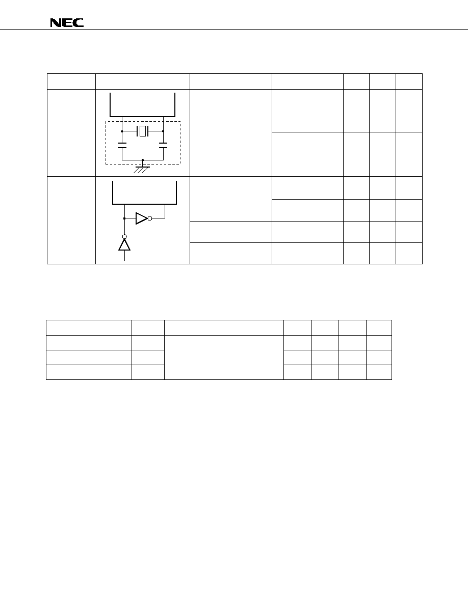
89
µ
PD78C17,78C18
Cautions
1.
Place the oscillator as close as possible to X1, X2 pins.
2.
Ensure that no other signal lines are routed through the area enclosed with dotted lines.
CAPACITANCE (T
A
= 25
∞
C, V
DD
= V
SS
= 0 V)
PARAMETER
SYMBOL
TEST CONDITIONS
MIN.
TYP.
MAX.
UNIT
Input capacitance
C
I
f
C
= 1 MHz
10
pF
Unmeasured pins
Output capacitance
C
O
returned to 0 V
20
pF
Input-output capacitance
C
IO
20
pF
OSCILLATOR CHARACTERISTICS
(T
A
= ≠40 to +85
∞
C, V
DD
= AV
DD
= +5.0 V
±
10 %, V
SS
= AV
SS
= 0 V,
V
DD
≠ 0.8 V
AV
DD
V
DD
, 3.4 V
V
AREF
AV
DD
)
X1
X2
HCMOS
Inverter
RESONATOR
RECOMMENDED CIRCUIT
PARAMETER
TEST CONDITIONS
MIN.
MAX.
UNIT
Ceramic
Oscillation frequency
A/D converter not
4
15
MHz
or
(f
XX
)
used
crystal
resonator
A/D converter used
5.8
15
MHz
External
X1 input frequency
A/D converter not
4
15
MHz
clock
(f
X
)
used
A/D converter used
5.8
15
MHz
X1 rise time,
0
20
ns
fall time (t
r
, t
f
)
X1 input high, low
20
250
ns
level width (t
ÿH
, t
ÿL
)
X1
X2
C2
C1

90
µ
PD78C17,78C18
DC CHARACTERISTICS (T
A
= ≠40 to +85
∞
C, V
DD
= AV
DD
= +5.0 V
±
10 %, V
SS
= AV
SS
= 0 V)
PARAMETER
SYMBOL
TEST CONDITIONS
MIN.
TYP.
MAX.
UNIT
Input voltage, low
V
IL1
All except RESET, STOP, NMI,
0
0.8
V
SCK, INT1, TI, AN7 to AN4
V
IL2
RESET, STOP, NMI, SCK, INT1,
0
0.2V
DD
V
TI, AN7 to AN4
Input voltage,
V
IH1
All except RESET, STOP, NMI,
2.2
V
DD
V
high
SCK, INT1, TI, AN7 to AN4, X1, X2
V
IH2
RESET, STOP, NMI, SCK, INT1,
0.8V
DD
V
DD
V
TI, AN7 to AN4, X1, X2
Output voltage, low
V
OL
I
OL
= 2.0 mA
0.45
V
Output voltage,
V
OH
I
OH
= ≠1.0 mA
V
DD
V
high
≠ 1.0
I
OH
= ≠100
µ
A
V
DD
V
≠ 0.5
Input current
I
I
INT1
Note1
, TI (PC3)
Note2
; 0 V
V
I
V
DD
±
200
µ
A
Input leakage
I
LI
All except INT1, TI (PC3); 0 V
V
I
V
DD
±
10
µ
A
current
Output leakage
I
LO
0 V
V
O
V
DD
±
10
µ
A
current
AV
DD
power
AI
DD1
Operating mode f
XX
= 15 MHz
0.5
1.3
mA
supply current
AI
DD2
STOP mode
10
20
µ
A
V
DD
power
I
DD1
Operating mode f
XX
= 15 MHz
16
30
mA
supply current
I
DD2
HALT mode f
XX
= 15 MHz
7
13
mA
Data retention
V
DDDR
Hardware/software STOP mode
2.5
V
voltage
Data retention
I
DDDR
Hardware/software
Note3
V
DDDR
= 2.5 V
1
15
µ
A
current
STOP mode
V
DDDR
= 5 V
±
10 %
10
50
µ
A
Pull-up resistor
R
L
Ports A, B, and C
3.5 V
V
DD
5.5 V,
17
27
75
k
V
I
= 0 V
Notes 1. If self-bias should be generated by ZCM register.
2. If the control mode is set by MCC register, and self-bias should be generated by ZCM register.
3. If self-bias is not generated.

91
µ
PD78C17,78C18
AC CHARACTERISTICS (T
A
= ≠40 to +85
∞
C, V
DD
= AV
DD
= +5.0 V
±
10 %, V
SS
= AV
SS
= 0 V)
Read/write Operation:
PARAMETER
SYMBOL
TEST CONDITIONS
MIN.
MAX.
UNIT
X1 input cycle time
t
CYC
66
250
ns
Address setup time (to ALE
)
t
AL
f
XX
= 15 MHz, CL = 100 pF
30
ns
Address hold time (from ALE
)
t
LA
35
ns
RD
delay time from address
t
AR
100
ns
Address float time from RD
t
AFR
C
L
= 100 pF
20
ns
Data input time from address
t
AD
f
XX
= 15 MHz, C
L
= 100 pF
250
ns
Data input time from ALE
t
LDR
135
ns
Data input time from RD
t
RD
120
ns
RD
delay time from ALE
t
LR
15
ns
Data hold time (from RD
)
t
RDH
C
L
= 100 pF
0
ns
ALE
delay time from RD
t
RL
f
XX
= 15 MHz, C
L
= 100 pF
80
ns
RD low-level width
t
RR
In Data Read
215
ns
f
XX
= 15 MHz, C
L
= 100 pF
In OP Code Fetch
415
ns
f
XX
= 15 MHz, C
L
= 100 pF
ALE high-level width
t
LL
f
XX
= 15 MHz, C
L
= 100 pF
90
ns
M1 setup time (to ALE
)
t
ML
f
XX
= 15 MHz
30
ns
M1 hold time (from ALE
)
t
LM
35
ns
IO/M setup time (to ALE
)
t
IL
30
ns
IO/M hold time (from ALE
)
t
LI
35
ns
WR
delay time from address
t
AW
f
XX
= 15 MHz, C
L
= 100 pF
100
ns
Data output time from ALE
t
LDW
180
ns
Data output time from WR
t
WD
C
L
= 100 pF
100
ns
WR
delay time from ALE
t
LW
f
XX
= 15 MHz, C
L
= 100 pF
15
ns
Data setup time (to WR
)
t
DW
165
ns
Data hold time (from WR
)
t
WDH
60
ns
ALE
delay time from WR
t
WL
80
ns
WR low-level width
t
WW
215
ns

92
µ
PD78C17,78C18
Serial Operation :
PARAMETER
SYMBOL
TEST CONDITIONS
MIN.
MAX.
UNIT
SCK cycle time
t
CYK
SCK input
Note1
800
ns
Note2
400
ns
SCK output
1.6
µ
s
SCK low-level width
t
KKL
SCK input
Note1
335
ns
Note2
160
ns
SCK output
700
ns
SCK high-level width
t
KKH
SCK input
Note1
335
ns
Note2
160
ns
SCK output
700
ns
R
X
D setup time (to SCK
)
t
RXK
Note1
80
ns
R
X
D hold time (from SCK
)
t
KRX
Note1
80
ns
T
X
D delay time from SCK
t
KTX
Note1
210
ns
Notes 1. If clock rate is
◊
1 in asynchronous mode, synchronous mode, or I/O interface mode.
2. If clock rate is
◊
16 or
◊
64 in asynchronous mode.
Remark
The numeric values in the table are those when f
XX
= 15 MHz, C
L
= 100 pF.
Zero-Cross Characteristics :
PARAMETER
SYMBOL
TEST CONDITIONS
MIN.
MAX.
UNIT
Zero-cross detection input
V
ZX
AC combination
1
1.8
VAC
P-P
60-Hz sine wave
Zero-cross accuracy
A
ZX
±
135
mV
Zero-cross detection input
f
ZX
0.05
1
kHz
frequency
Other Operation :
PARAMETER
SYMBOL
TEST CONDITIONS
MIN.
MAX.
UNIT
TI high, low-level width
t
TIH
, t
TIL
6
t
CYC
CI high, low-level width
t
CI1H
, t
CI1L
Event count mode
6
t
CYC
t
CI2H
,t
CI2L
Pulse width test mode
48
t
CYC
NMI high, low-level width
t
NIH
, t
NIL
10
µ
s
INT1 high, low-level width
t
I1H
, t
I1L
36
t
CYC
INT2 high, low-level width
t
I2H
, t
I2L
36
t
CYC
AN7 to AN4, low-level width
t
ANH
, t
ANL
36
t
CYC
RESET high, low-level width
t
RSH
, t
RSL
10
µ
s

93
µ
PD78C17,78C18
A/D CONVERTER CHARACTERISTICS (T
A
= ≠40 to +85
∞
C, V
DD
= +5.0 V
±
10 %, V
SS
= AV
SS
= 0 V,
V
DD
≠ 0.5 V
AV
DD
V
DD
, 3.4 V
V
AREF
AV
DD
)
PARAMETER
SYMBOL
TEST CONDITIONS
MIN.
TYP.
MAX.
UNIT
Resolution
8
Bits
Absolute accuracy
Note
3.4 V
V
AREF
AV
DD
, 66 ns
t
CYC
170 ns
±
0.8 %
FSR
4.0 V
V
AREF
AV
DD
, 66 ns
t
CYC
170 ns
±
0.6 %
FSR
T
A
= ≠10 to +70
∞
C,
±
0.4 %
FSR
4.0 V
V
AREF
AV
DD
, 66 ns
t
CYC
170 ns
Conversion time
t
CONV
66 ns
t
CYC
110 ns
576
t
CYC
110 ns
t
CYC
170 ns
432
t
CYC
Sampling time
t
SAMP
66 ns
t
CYC
110 ns
96
t
CYC
110 ns
t
CYC
170 ns
72
t
CYC
Analog input voltage
V
IAN
AN7 to AN0 (including unused pins)
≠0.3
V
AREF
+ 0.3
V
Analog input
R
AN
50
M
impedance
Reference voltage
V
AREF
3.4
AV
DD
V
V
AREF
current
I
AREF1
Operating mode
1.5
3.0
mA
I
AREF2
STOP mode
0.7
1.5
mA
AV
DD
power supply
AI
DD1
Operating mode f
XX
= 15 MHz
0.5
1.3
mA
current
AI
DD2
STOP mode
10
20
µ
A
Note Quantization error (
±
1/2 LSB) is not included.
AC Timing Test Point
2.2 V
0.8 V
2.2 V
0.8 V
Test Points
V
DD
≠ 1.0 V
0.45 V
5

94
µ
PD78C17,78C18
PARAMETER
EXPRESSION
MIN./MAX.
UNIT
t
AL
2T ≠ 100
MIN.
ns
t
LA
T ≠ 30
MIN.
ns
t
AR
3T ≠ 100
MIN.
ns
t
AD
7T ≠ 220
MAX.
ns
t
LDR
5T ≠ 200
MAX.
ns
t
RD
4T ≠ 150
MAX.
ns
t
LR
T ≠ 50
MIN.
ns
t
RL
2T ≠ 50
MIN.
ns
t
RR
4T ≠ 50 (In data read)
MIN.
ns
7T ≠ 50 (In OP code fetch)
t
LL
2T ≠ 40
MIN.
ns
t
ML
2T ≠ 100
MIN.
ns
t
LM
T ≠ 30
MIN.
ns
t
IL
2T ≠ 100
MIN.
ns
t
LI
T ≠ 30
MIN.
ns
t
AW
3T ≠ 100
MIN.
ns
t
LDW
T + 110
MAX.
ns
t
LW
T ≠ 50
MIN.
ns
t
DW
4T ≠ 100
MIN.
ns
t
WDH
2T ≠ 70
MIN.
ns
t
WL
2T ≠ 50
MIN.
ns
t
WW
4T ≠ 50
MIN.
ns
t
CYK
6T (SCK input)
Note1
/12T (SCK input)
Note2
MIN.
ns
24T (SCK output)
t
KKL
2.5T + 5 (SCK input)
Note1
/5T + 5 (SCK input)
Note2
MIN.
ns
12T ≠ 100 (SCK output)
t
KKH
2.5T + 5 (SCK input)
Note1
/5T + 5 (SCK input)
Note2
MIN.
ns
12T ≠ 100 (SCK output)
Notes 1. If clock rate is
◊
16,
◊
64 in asynchronous mode.
2. If clock rate is
◊
1, in asynchronous mode, synchronous mode, or I/O interface mode.
Remarks
1.
T = t
CYC
= 1/f
XX
2.
Other items which are not listed in this table are not dependent on oscillator frequency (f
XX
).
t
CYC
-Dependent AC Characteristics Expression

95
µ
PD78C17,78C18
MODE1
(M1)
X1
PF7 to PF0
PD7 to PD0
ALE
Note1
MODE0
(IO/M)
t
CYC
Address (Upper)
Address (Lower)
t
RDH
Read Data
t
LDR
t
AD
t
RL
t
RD
t
RR
t
AFR
t
LA
t
LL
t
AR
t
AL
t
LR
t
ML
t
IL
t
LM
t
LI
Address (Upper)
t
LDW
t
LA
t
LL
t
AL
t
WD
t
DW
t
WDH
t
WL
t
WW
t
LW
t
LI
t
AW
t
IL
Write Data
Note2
X1
PF7 to PF0
PD7 to PD0
ALE
RD
WR
MODE0
(IO/M)
Note
Address (Lower)
TIMING WAVEFORM
Read Operation
Notes 1. When MODE1 pin is pulled up, M1 signal is output to MODE1 pin in the 1st OP code fetch cycle.
2. When MODE0 pin is pulled up, IO/M signal is output to MODE0 pin in sr to sr2 register read cycle.
Write Operation
Note
When MODE0 pin is pulled up, IO/M signal is output to MODE0 pin in sr to sr2 register write cycle.

96
µ
PD78C17,78C18
Serial Operation
Timer/event Counter Input Timing
Timer Input Timing
t
CYK
t
KKL
t
KKH
t
RXK
t
KRX
t
KTX
SCK
T
X
D
R
X
D
TI
t
TIL
t
TIH
CI
t
CI1L
t
CI1H
Event Counter Mode
CI
t
CI2L
t
CI2H
Pulse Width Test Mode

97
µ
PD78C17,78C18
X1
t
CYC
t
H
0.8V
DD
0.8 V
t
f
t
r
t
L
RESET
t
RSL
t
RSH
0.8V
DD
0.2V
DD
Interrupt Input Timing
External Clock Timing
Reset Input Timing
NMI
t
NIL
t
NIH
INT1
INT2
t
I1H
t
I1L
t
I2L
t
I2H

98
µ
PD78C17,78C18
DATA MEMORY STOP MODE LOW POWER SUPPLY VOLTAGE DATA RETENTION (T
A
= ≠40 to +85
∞
C)
PARAMETER
SYMBOL
TEST CONDITIONS
MIN.
TYP.
MAX.
UNIT
Data retention power
V
DDDR
2.5
5.5
V
supply voltage
Data retention power
I
DDDR
V
DDDR
= 2.5 V
1
15
µ
A
supply current
V
DDDR
= 5 V
±
10 %
10
50
µ
A
V
DD
rise/fall time
t
RVD
, t
FVD
200
µ
s
STOP setup time
t
SSTVD
12T + 0.5
µ
s
(to V
DD
)
STOP hold time
t
HVDST
12T + 0.5
µ
s
(from V
DD
)
Data Retention Timing
90 %
STOP
V
DD
V
DDDR
t
RVD
10 %
t
FVD
t
SSTVD
t
HVDST
V
IH2
V
IL2
5

99
µ
PD78C17,78C18
9.
CHARACTERISTIC CURVES
I
DD1
, I
DD2
vs V
DD
I
DD1
, I
DD2
vs f
XX
30
25
20
15
10
5
0
0
4.5
5.0
5.5
(T
A
= 25 ∞C, f
XX
= 15 MHz)
I
DD1
(TYP.)
I
DD2
(TYP.)
Power Supply Voltage V
DD
[V]
V
DD
Power Supply Current I
DD1
, I
DD2
[mA]
(T
A
= 25 ∞C, V
DD
= 5 V)
Oscillation Frequency f
XX
[MHz]
V
DD
Power Supply Current I
DD1
, I
DD2
[mA]
30
20
10
0
0
5
10
15
I
DD1
(TYP.)
I
DD2
(TYP.)

100
µ
PD78C17,78C18
I
OL
vs V
OL
I
OH
vs V
OH
2.5
2.0
1.5
1.0
0.5
0
0
0.1
0.2
0.3
0.4
0.5
(T
A
= 25 ∞C, V
DD
= 5 V)
TYP.
Output Voltage Low V
OL
[V]
Output Current Low I
OL
[mA]
≠1.5
≠1.0
≠0.5
0
0
0.1
0.2
0.3
0.4
0.5
(T
A
= 25 ∞C, V
DD
= 5 V)
Power Supply Voltage ≠ Output Voltage High V
DD
≠ V
OH
[V]
Output Current High I
OH
[mA]
TYP.

101
µ
PD78C17,78C18
I
DDDR
vs V
DDDR
10
8
6
4
2
0
0
2
3
4
5
6
(T
A
= 25 ∞C)
TYP.
Data Retention Power Supply Voltage V
DDDR
[V]
Data Retention Power Supply Current I
DDDR
[
µ
A]

102
µ
PD78C17,78C18
10. PACKAGE DRAWINGS
A
I
J
G
H
F
D
N
M
C
B
M
R
64
33
32
1
K
L
NOTE
Each lead centerline is located within 0.17 mm (0.007 inch) of
its true position (T.P.) at maximum material condition.
P64C-70-750A,C-1
ITEM
MILLIMETERS
INCHES
A
B
C
D
F
G
H
I
J
K
58.68 MAX.
1.778 (T.P.)
3.2±0.3
0.51 MIN.
4.31 MAX.
1.78 MAX.
L
M
0.17
0.25
19.05 (T.P.)
5.08 MAX.
17.0
N
0~15∞
0.50±0.10
0.9 MIN.
R
2.311 MAX.
0.070 MAX.
0.020
0.035 MIN.
0.126±0.012
0.020 MIN.
0.170 MAX.
0.200 MAX.
0.750 (T.P.)
0.669
0.010
0.007
0~15∞
+0.004
≠0.003
0.070 (T.P.)
1)
Item "K" to center of leads when formed parallel.
2)
+0.10
≠0.05
+0.004
≠0.005
64 PIN PLASTIC SHRINK DIP (750 mil)

103
µ
PD78C17,78C18
N
A
M
F
B
51
52
32
K
L
64 PIN PLASTIC QFP (14
◊
20)
64
1
20
19
33
P
D
C
detail of lead end
S
Q
5∞±5∞
G
M
I
H
J
P64GF-100-3B8,3BE,3BR-1
ITEM
MILLIMETERS
INCHES
A
B
C
D
F
G
H
I
J
K
L
23.6±0.4
14.0±0.2
1.0
0.40±0.10
0.20
20.0±0.2
0.929±0.016
0.039
0.039
0.008
0.039 (T.P.)
0.795
NOTE
M
N
0.12
0.15
1.8±0.2
1.0 (T.P.)
0.005
0.006
+0.004
≠0.003
Each lead centerline is located within 0.20
mm (0.008 inch) of its true position (T.P.) at
maximum material condition.
0.071
0.016
0.551
0.8±0.2
0.031
P
2.7
0.106
0.693±0.016
17.6±0.4
1.0
+0.009
≠0.008
Q
0.1±0.1
0.004±0.004
S
3.0 MAX.
0.119 MAX.
+0.10
≠0.05
+0.009
≠0.008
+0.004
≠0.005
+0.009
≠0.008
+0.008
≠0.009

104
µ
PD78C17,78C18
64 PIN PLASTIC QUIP (UNIT: mm)
H
I
M
C
P
A
64
1
32
33
M
N
J
K
S
W
X
P64GQ-100-36
ITEM
MILLIMETERS
INCHES
A
C
H
I
J
K
M
N
P
S
W
1.27 (T.P.)
0.25
16.5
0.100 (T.P.)
0.050 (T.P.)
0.010
0.157
1.634
NOTE
X
4.0
0.750
Each lead centerline is located within 0.25 mm
(0.010 inch) of its true position (T.P.) at maxi-
mum material condition.
0.142
0.043
0.020
24.13
0.950
0.010
0.25
2.54 (T.P.)
+0.004
≠0.005
+0.011
≠0.006
+0.012
≠0.008
+0.004
≠0.005
41.5
+0.3
≠0.2
0.50
+0.10
≠
1.1
+0.25
≠0.15
+0.10
≠0.05
+0.3
≠
3.6
+0.1
≠
+1.05
≠
19.05
+1.05
≠
0.650
+0.004
≠0.003
+0.013
≠0.012
+0.042
≠
+0.042
≠

105
µ
PD78C17,78C18
Package peak temperature: 215
∞
C,
Time: Within 40 s (at 200
∞
C or higher), Count:
Twice or less
<Attention>
(1) Perform the second reflow when the
device temperature has come down to
the room temperature from the heating
by the first reflow.
(2) Do not wash the soldered portion with
flux following the first reflow.
Package peak temperature: 235
∞
C,
Time: Within 30 s (at 210
∞
C or higher), Count:
Twice or less
<Attention>
(1) Perform the second reflow when the
device temperature has come down to
the room temperature from the heating
by the first reflow.
(2) Do not wash the soldered portion with
flux following the first reflow.
11. RECOMMENDED SOLDERING CONDITIONS
This
µ
PD78C17 and 78C18 should be soldered and mounted under the following recommended conditions.
For details of the conditions, refer to the document "Surface Device Mounting Technology Manual" (IEI-
1207).
For soldering methods and conditions other than those recommended below, contact an NEC sales repre-
sentative.
Table 11-1 Surface Mounting Type Soldering Conditions
µ
PD78C17GF-3BE:
64-pin plastic QFP (14
◊
20 mm)
µ
PD78C18GF-
◊◊◊
-3BE: 64-pin plastic QFP (14
◊
20 mm)
Recommended
Soldering Method
Soldering Conditions
Condition Symbol
Infrared ray reflow
IR35-00-2
VSP
VP15-00-2
Wave soldering
WS60-00-1
Partial heating
≠≠
Caution
Do not use several soldering methods in combination (except partial heating).
Table 11-2 Through-Hole Type Soldering Condition
µ
PD78C17CW:
64-pin plastic shrink DIP (750 mils)
µ
PD78C18CW-
◊◊◊
:
64-pin plastic shrink DIP (750 mils)
µ
PD78C17GQ-36:
64-pin plastic QUIP
µ
PD78C18GQ-
◊◊◊
-36: 64-pin plastic QUIP
Soldering Method
Soldering Conditions
Wave soldering (pin only)
Solder bath temperature: 260
∞
C or lower, Time: Within 10 s
Partial heating
Pin temperature: 300
∞
C or lower, Time: Within 3 s (per pin)
Caution
Wave soldering must be applied to pins only, and care must be taken to prevent solder from
coming into direct with the package body.
5
Solder bath temperature: 260
∞
C or lower,
Time: Within 10 s, Count: Once, Preheating
temperature: 120
∞
C MAX.
(package surface temperature)
Pin temperature: 300
∞
C or lower,
Time: Within 3 s (per pin row)

106
µ
PD78C17,78C18
12. DIFFERENCES AMONG
µ
PD78C18,
µ
PD78C14, AND
µ
PD78C12A
µ
PD78C14
16 K
◊
8
No on-chip pull-up resistor
∑ 64-pin plastic shrink DIP
(750 mil)
∑ 64-pin plastic QFP
(14
◊
20 mm)
∑ 64-pin plastic QUIP
∑ 64-pin plastic QUIP
(straight)
Part Number
Item
Internal ROM
Internal RAM
Port A to Port C
Package
µ
PD78C18
32 K
◊
8
1 K
◊
8
On-chip pull-up resistor
selectable bit-wise by mask
option
∑ 64-pin plastic shrink DIP
(750 mil)
∑ 64-pin plastic QFP
(14
◊
20 mm)
∑ 64-pin plastic QUIP
µ
PD78C12A
8 K
◊
8
On-chip pull-up resistor
selectable bit-wise by mask
option
∑ 64-pin plastic shrink DIP
(750 mil)
∑ 64-pin plastic QFP
(14
◊
20 mm)
∑ 64-pin plastic QUIP
∑ 64-pin plastic QUIP
(straight)
∑ 68-pin plastic QFJ
256
◊
8

107
µ
PD78C17,78C18
APPENDIX DEVELOPMENT TOOLS
The following development tools are available to develop a system which uses the
µ
PD78C17 or 78C18.
Language Processor
5
Ordering Code (Product Name)
µ
S5A13RA87
µ
S5A10RA87
µ
S7B13RA87
µ
S7B10RA87
Host Machine
PC-9800
series
IBM PC/AT
TM
This is a program which converts a program written in mnemonic to an object code for which
microcontroller execution is possible.
Besides, it contains a function to automatically create a symbol table, and optimize a branch
instruction.
87AD series
relocatable assembler
(RA87)
PG-1500
PA-78CP14CW/
GF/GQ
PA-78CP14CW
PA-78CP14GF
PA-78CP14GQ
PG-1500
controller
With a provided board and an optional programmer adapter connected, this PROM programmer
can manipulate from a stand-alone or host machine to perform programming on single-chip
microcontroller which incorporates PROM.
It is also capable of programming a typical PROM ranging from 256 K to 4 Mbits.
PROM programmer adapter for the
µ
PD78CP18. Used by connecting to PG-1500.
For the
µ
PD78CP18CW
For the
µ
PD78CP18GF-3BE
For the
µ
PD78CP18GQ-36
Connected PG-1500 to a host machine by using serial and parallel interfaces, to control the PG-
1500 on a host machine.
Hardware
Note
Ver. 5.00/5.00A are provided with the task swap function, but it cannot be used with this software.
Remark
Operation of assemblers and the PG-1500 controller are guaranteed only on the host machines and
operating systems shown above.
Ordering Code (Product Name)
µ
S5A13PG1500
µ
S5A10PG1500
µ
S7B10PG1500
Host Machine
PC-9800
series
IBM PC/AT
OS
MS-DOS
Ver. 2.11
to
Ver. 5.00A
Note
PC DOS
(Ver. 3.1)
Soft
ware
PROM Write Tools
OS
MS-DOS
TM
Ver. 2.11
to
Ver. 5.00A
Note
PC DOS
TM
(Ver. 3.1)
Supply Medium
3.5-inch 2HD
5-inch 2HD
3.5-inch 2HC
5-inch 2HC
Supply Medium
3.5-inch 2HD
5-inch 2HD
5-inch 2HC

108
µ
PD78C17,78C18
Debugging tools
An in-circuit emulator (IE-78C11-M) is available as a program debugging tool for the
µ
PD78C17 and 78C18.
The following table shows its system configuration.
The IE-78C11-M is an in-circuit emulator which works with 87AD series.
It can be connected to a host machine to perform efficient debugging.
Connects the IE-78C11-M to host machine by using the RS-232C, then controls the IE-78C11-M on
host machine.
IE-78C11-M
IE-78C11-M
control program
(IE controller)
Ordering Code (Product Name)
µ
S5A13IE78C11
µ
S5A10IE78C11
µ
S7B10IE78C11
Supply Medium
3.5-inch 2HD
5-inch 2HD
5-inch 2HC
Host Machine
PC-9800
series
IBM PC/AT
OS
MS-DOS
Ver. 2.11
to
Ver. 3.30D
PC DOS
(Ver. 3.1)
Soft
ware
Remark
Operation of the IE controller is guaranteed only on the host machine and operating systems quoted
above.
Hardware

109
µ
PD78C17,78C18
NOTES FOR CMOS DEVICES
1
PRECAUTION AGAINST ESD FOR SEMICONDUCTORS
Note: Strong electric field, when exposed to a MOS device, can cause destruction of
the gate oxide and ultimately degrade the device operation. Steps must be
taken to stop generation of static electricity as much as possible, and quickly
dissipate it once, when it has occurred. Environmental control must be
adequate. When it is dry, humidifier should be used. It is recommended to
avoid using insulators that easily build static electricity. Semiconductor
devices must be stored and transported in an anti-static container, static
shielding bag or conductive material. All test and measurement tools including
work bench and floor should be grounded. The operator should be grounded
using wrist strap. Semiconductor devices must not be touched with bare
hands. Similar precautions need to be taken for PW boards with semiconductor
devices on it.
2
HANDLING OF UNUSED INPUT PINS FOR CMOS
Note: No connection for CMOS device inputs can be cause of malfunction. If no
connection is provided to the input pins, it is possible that an internal input
level may be generated due to noise, etc., hence causing malfunction. CMOS
device behave differently than Bipolar or NMOS devices. Input levels of CMOS
devices must be fixed high or low by using a pull-up or pull-down circuitry. Each
unused pin should be connected to V
DD
or GND with a resistor, if it is considered
to have a possibility of being an output pin. All handling related to the unused
pins must be judged device by device and related specifications governing the
devices.
3
STATUS BEFORE INITIALIZATION OF MOS DEVICES
Note: Power-on does not necessarily define initial status of MOS device. Production
process of MOS does not define the initial operation status of the device.
Immediately after the power source is turned ON, the devices with reset
function have not yet been initialized. Hence, power-on does not guarantee
out-pin levels, I/O settings or contents of registers. Device is not initialized
until the reset signal is received. Reset operation must be executed immedi-
ately after power-on for devices having reset function.
MS-DOS is a trademark of Microsoft Corporation.
PC/AT and PC DOS are trademarks of IBM Corporation.

µ
PD78C17,78C18
No part of this document may be copied or reproduced in any form or by any means without the prior written
consent of NEC Corporation. NEC Corporation assumes no responsibility for any errors which may appear in this
document.
NEC Corporation does not assume any liability for infringement of patents, copyrights or other intellectual
property rights of third parties by or arising from use of a device described herein or any other liability arising
from use of such device. No license, either express, implied or otherwise, is granted under any patents,
copyrights or other intellectual property rights of NEC Corporation or others.
While NEC Corporation has been making continuous effort to enhance the reliability of its semiconductor devices,
the possibility of defects cannot be eliminated entirely. To minimize risks of damage or injury to persons or
property arising from a defect in an NEC semiconductor device, customer must incorporate sufficient safety
measures in its design, such as redundancy, fire-containment, and anti-failure features.
NEC devices are classified into the following three quality grades:
"Standard", "Special", and "Specific". The Specific quality grade applies only to devices developed based on
a customer designated "quality assurance program" for a specific application. The recommended applications
of a device depend on its quality grade, as indicated below. Customers must check the quality grade of each
device before using it in a particular application.
Standard: Computers, office equipment, communications equipment, test and measurement equipment,
audio and visual equipment, home electronic appliances, machine tools, personal electronic
equipment and industrial robots
Special:
Transportation equipment (automobiles, trains, ships, etc.), traffic control systems, anti-disaster
systems, anti-crime systems, safety equipment and medical equipment (not specifically designed
for life support)
Specific: Aircrafts, aerospace equipment, submersible repeaters, nuclear reactor control systems, life
support systems or medical equipment for life support, etc.
The quality grade of NEC devices in "Standard" unless otherwise specified in NEC's Data Sheets or Data Books.
If customers intend to use NEC devices for applications other than those specified for Standard quality grade,
they should contact NEC Sales Representative in advance.
Anti-radioactive design is not implemented in this product.
M4 94.11
License not needed:
µ
PD78C17CW, 78C17GF-3BE, and 78C17GQ-36
The customer must judge
the need for license:
µ
PD78C18CW-
◊◊◊
, 78C18GF-
◊◊◊
-3BE, and 78C18GQ-
◊◊◊
-36
The export of these products from Japan is regulated by the Japanese government. The export of some or all of
these products may be prohibited without governmental license. To export or re-export some or all of these
products from a country other than Japan may also be prohibited without a license from that country. Please call
an NEC sales representative.