Document Outline
- COVER
- INTRODUCTION
- CHAPTER 1 OUTLINE (uPD780078 SUBSERIES)
- 1.1 Expanded-Specification Products and Conventional Products
- 1.2 Features
- 1.3 Applications
- 1.4 Ordering Information
- 1.5 Pin Configuration (Top View)
- 1.6 78K/0 Series Lineup
- 1.7 Block Diagram
- 1.8 Outline of Functions
- 1.9 Mask Options
- CHAPTER 2 OUTLINE (uPD780078Y SUBSERIES)
- 2.1 Expanded-Specification Products and Conventional Products
- 2.2 Features
- 2.3 Applications
- 2.4 Ordering Information
- 2.5 Pin Configuration (Top View)
- 2.6 78K/0 Series Lineup
- 2.7 Block Diagram
- 2.8 Outline of Functions
- 2.9 Mask Options
- CHAPTER 3 PIN FUNCTIONS (uPD780078 SUBSERIES)
- 3.1 Pin Function List
- 3.2 Description of Pin Functions
- 3.2.1 P00 to P03 (Port 0)
- 3.2.2 P10 to P17 (Port 1)
- 3.2.3 P20 to P25 (Port 2)
- 3.2.4 P30 to P36 (Port 3)
- 3.2.5 P40 to P47 (Port 4)
- 3.2.6 P50 to P57 (Port 5)
- 3.2.7 P64 to P67 (Port 6)
- 3.2.8 P70 to P75 (Port 7)
- 3.2.9 P80 (Port 8)
- 3.2.10 AVREF
- 3.2.11 AVSS
- 3.2.12 RESET#
- 3.2.13 X1 and X2
- 3.2.14 XT1 and XT2
- 3.2.15 VDD0 and VDD1
- 3.2.16 VSS0 and VSS1
- 3.2.17 VPP (flash memory versions only)
- 3.2.18 IC (mask ROM version only)
- 3.3 Pin I/O Circuits and Recommended Connection of Unused Pins
- CHAPTER 4 PIN FUNCTIONS (uPD780078Y SUBSERIES)
- 4.1 Pin Function List
- 4.2 Description of Pin Functions
- 4.2.1 P00 to P03 (Port 0)
- 4.2.2 P10 to P17 (Port 1)
- 4.2.3 P20 to P25 (Port 2)
- 4.2.4 P30 to P36 (Port 3)
- 4.2.5 P40 to P47 (Port 4)
- 4.2.6 P50 to P57 (Port 5)
- 4.2.7 P64 to P67 (Port 6)
- 4.2.8 P70 to P75 (Port 7)
- 4.2.9 P80 (Port 8)
- 4.2.10 AVREF
- 4.2.11 AVSS
- 4.2.12 RESET#
- 4.2.13 X1 and X2
- 4.2.14 XT1 and XT2
- 4.2.15 VDD0 and VDD1
- 4.2.16 VSS0 and VSS1
- 4.2.17 VPP (flash memory versions only)
- 4.2.18 IC (mask ROM version only)
- 4.3 Pin I/O Circuits and Recommended Connection of Unused Pins
- CHAPTER 5 CPU ARCHITECTURE
- 5.1 Memory Spaces
- 5.1.1 Internal program memory space
- 5.1.2 Internal data memory space
- 5.1.3 Special function register (SFR) area
- 5.1.4 External memory space
- 5.1.5 Data memory addressing
- 5.2 Processor Registers
- 5.2.1 Control registers
- 5.2.2 General-purpose registers
- 5.2.3 Special function registers (SFR)
- 5.3 Instruction Address Addressing
- 5.3.1 Relative addressing
- 5.3.2 Immediate addressing
- 5.3.3 Table indirect addressing
- 5.3.4 Register addressing
- 5.4 Operand Address Addressing
- 5.4.1 Implied addressing
- 5.4.2 Register addressing
- 5.4.3 Direct addressing
- 5.4.4 Short direct addressing
- 5.4.5 Special function register (SFR) addressing
- 5.4.6 Register indirect addressing
- 5.4.7 Based addressing
- 5.4.8 Based indexed addressing
- 5.4.9 Stack addressing
- CHAPTER 6 PORT FUNCTIONS
- 6.1 Port Functions
- 6.2 Port Configuration
- 6.2.1 Port 0
- 6.2.2 Port 1
- 6.2.3 Port 2
- 6.2.4 Port 3 (uPD780078 Subseries)
- 6.2.5 Port 3 (uPD780078Y Subseries)
- 6.2.6 Port 4
- 6.2.7 Port 5
- 6.2.8 Port 6
- 6.2.9 Port 7
- 6.2.10 Port 8
- 6.3 Port Function Control Registers
- 6.4 Port Function Operations
- 6.4.1 Writing to I/O port
- 6.4.2 Reading from I/O port
- 6.4.3 Operations on I/O port
- 6.5 Selection of Mask Option
- CHAPTER 7 CLOCK GENERATOR
- 7.1 Clock Generator Functions
- 7.2 Clock Generator Configuration
- 7.3 Clock Generator Control Registers
- 7.4 System Clock Oscillator
- 7.4.1 Main system clock oscillator
- 7.4.2 Subsystem clock oscillator
- 7.4.3 When subsystem clock is not used
- 7.5 Clock Generator Operations
- 7.5.1 Main system clock operations
- 7.5.2 Subsystem clock operations
- 7.6 Changing System Clock and CPU Clock Settings
- 7.6.1 Time required for switchover between system clock and CPU clock
- 7.6.2 System clock and CPU clock switching procedure
- CHAPTER 8 16-BIT TIMER/EVENT COUNTERS 00, 01
- 8.1 Functions of 16-Bit Timer/Event Counters 00, 01
- 8.2 Configuration of 16-Bit Timer/Event Counters 00, 01
- 8.3 Registers to Control 16-Bit Timer/Event Counters 00, 01
- 8.4 Operation of 16-Bit Timer/Event Counters 00, 01
- 8.4.1 Interval timer operation
- 8.4.2 External event counter operation
- 8.4.3 Pulse width measurement operations
- 8.4.4 Square-wave output operation
- 8.4.5 PPG output operation
- 8.5 Program List
- 8.5.1 Interval timer
- 8.5.2 Pulse width measurement by free-running counter and one capture register
- 8.5.3 Two pulse widths measurement by free-running counter
- 8.5.4 Pulse width measurement by restart
- 8.5.5 PPG output
- 8.6 Cautions for 16-Bit Timer/Event Counters 00, 01
- CHAPTER 9 8-BIT TIMER/EVENT COUNTERS 50, 51
- 9.1 Functions of 8-Bit Timer/Event Counters 50, 51
- 9.2 Configuration of 8-Bit Timer/Event Counters 50, 51
- 9.3 Registers to Control 8-Bit Timer/Event Counters 50, 51
- 9.4 Operation of 8-Bit Timer/Event Counters 50, 51
- 9.4.1 8-bit interval timer operation
- 9.4.2 External event counter operation
- 9.4.3 Square-wave output (8-bit resolution) operation
- 9.4.4 8-bit PWM output operation
- 9.4.5 Interval timer (16-bit) operations
- 9.5 Program List
- 9.5.1 Interval timer (8-bit)
- 9.5.2 External event counter
- 9.5.3 Interval timer (16-bit)
- 9.6 Cautions for 8-Bit Timer/Event Counters 50, 51
- CHAPTER 10 WATCH TIMER
- 10.1 Watch Timer Functions
- 10.2 Watch Timer Configuration
- 10.3 Register to Control Watch Timer
- 10.4 Watch Timer Operations
- 10.4.1 Watch timer operation
- 10.4.2 Interval timer operation
- 10.5 Cautions for Watch Timer
- CHAPTER 11 WATCHDOG TIMER
- 11.1 Watchdog Timer Functions
- 11.2 Watchdog Timer Configuration
- 11.3 Registers to Control Watchdog Timer
- 11.4 Watchdog Timer Operations
- 11.4.1 Watchdog timer operation
- 11.4.2 Interval timer operation
- CHAPTER 12 CLOCK OUTPUT/BUZZER OUTPUT CONTROLLER
- 12.1 Clock Output/Buzzer Output Controller Functions
- 12.2 Configuration of Clock Output/Buzzer Output Controller
- 12.3 Registers to Control Clock Output/Buzzer Output Controller
- 12.4 Operation of Clock Output/Buzzer Output Controller
- 12.4.1 Operation as clock output
- 12.4.2 Operation as buzzer output
- CHAPTER 13 A/D CONVERTER
- 13.1 A/D Converter Functions
- 13.2 A/D Converter Configuration
- 13.3 Registers Used in A/D Converter
- 13.4 A/D Converter Operation
- 13.4.1 Basic operations of A/D converter
- 13.4.2 Input voltage and conversion results
- 13.4.3 A/D converter operation mode
- 13.5 How to Read A/D Converter Characteristics Table
- 13.6 Cautions for A/D Converter
- CHAPTER 14 SERIAL INTERFACE UART0
- 14.1 Functions of Serial Interface UART0
- 14.2 Configuration of Serial Interface UART0
- 14.3 Registers to Control Serial Interface UART0
- 14.4 Operation of Serial Interface UART0
- 14.4.1 Operation stop mode
- 14.4.2 Asynchronous serial interface (UART) mode
- 14.4.3 Infrared data transfer mode
- CHAPTER 15 SERIAL INTERFACE UART2
- 15.1 Functions of Serial Interface UART2
- 15.2 Configuration of Serial Interface UART2
- 15.3 Registers to Control Serial Interface UART2
- 15.4 Operation of Serial Interface UART2
- 15.4.1 Operation stop mode
- 15.4.2 Asynchronous serial interface (UART) mode
- 15.4.3 Multi-processor transfer mode
- 15.4.4 Infrared data transfer (IrDA) mode
- CHAPTER 16 SERIAL INTERFACE SIO3
- 16.1 Functions of Serial Interface SIO3
- 16.2 Configuration of Serial Interface SIO3
- 16.3 Registers to Control Serial Interface SIO3
- 16.4 Operation of Serial Interface SIO3
- 16.4.1 Operation stop mode
- 16.4.2 3-wire serial I/O mode
- CHAPTER 17 SERIAL INTERFACE CSI1
- 17.1 Functions of Serial Interface CSI1
- 17.2 Configuration of Serial Interface CSI1
- 17.3 Registers to Control Serial Interface CSI1
- 17.4 Operation of Serial Interface CSI1
- 17.4.1 Operation stop mode
- 17.4.2 3-wire serial I/O mode
- CHAPTER 18 SERIAL INTERFACE IIC0 (uPD780078Y SUBSERIES ONLY)
- 18.1 Functions of Serial Interface IIC0
- 18.2 Configuration of Serial Interface IIC0
- 18.3 Registers to Control Serial Interface IIC0
- 18.4 I2C Bus Mode Functions
- 18.5 I2C Bus Definitions and Control Methods
- 18.5.1 Start conditions
- 18.5.2 Addresses
- 18.5.3 Transfer direction specification
- 18.5.4 Acknowledge (ACK#) signal
- 18.5.5 Stop condition
- 18.5.6 Wait signal (WAIT#)
- 18.5.7 Interrupt request (INTIIC0) generation timing and wait control
- 18.5.8 Address match detection method
- 18.5.9 Error detection
- 18.5.10 Extension code
- 18.5.11 Arbitration
- 18.5.12 Wake-up function
- 18.5.13 Communication reservation
- 18.5.14 Other cautions
- 18.5.15 Communication operations
- 18.5.16 Timing of I2C interrupt request (INTIIC0) occurrence
- 18.6 Timing Charts
- CHAPTER 19 INTERRUPT FUNCTIONS
- 19.1 Interrupt Function Types
- 19.2 Interrupt Sources and Configuration
- 19.3 Interrupt Function Control Registers
- 19.4 Interrupt Servicing Operations
- 19.4.1 Non-maskable interrupt request acknowledgment operation
- 19.4.2 Maskable interrupt request acknowledgment operation
- 19.4.3 Software interrupt request acknowledgment operation
- 19.4.4 Multiple interrupt servicing
- 19.4.5 Interrupt request hold
- CHAPTER 20 EXTERNAL DEVICE EXPANSION FUNCTION
- 20.1 External Device Expansion Function
- 20.2 External Device Expansion Function Control Registers
- 20.3 External Device Expansion Function Timing
- 20.4 Example of Connection with Memory
- CHAPTER 21 STANDBY FUNCTION
- 21.1 Standby Function and Configuration
- 21.1.1 Standby function
- 21.1.2 Standby function control register
- 21.2 Standby Function Operations
- 21.2.1 HALT mode
- 21.2.2 STOP mode
- CHAPTER 22 RESET FUNCTION
- CHAPTER 23 uPD78F0078, 78F0078Y
- 23.1 Memory Size Switching Register
- 23.2 Internal Expansion RAM Size Switching Register
- 23.3 Flash Memory Characteristics
- 23.3.1 Programming environment
- 23.3.2 Communication mode
- 23.3.3 On-board pin processing
- 23.3.4 Connection of adapter for flash writing
- CHAPTER 24 INSTRUCTION SET
- 24.1 Legend Used in Operation List
- 24.1.1 Operand identifiers and specification methods
- 24.1.2 Description of çoperationé column
- 24.1.3 Description of çflag operationé column
- 24.2 Operation List
- 24.3 Instructions Listed by Addressing Type
- CHAPTER 25 ELECTRICAL SPECIFICATIONS (EXPANDED-SPECIFICATION PRODUCTS OF uPD780076, 780078, 78F0078)
- CHAPTER 26 ELECTRICAL SPECIFICATIONS (EXPANDED-SPECIFICATION PRODUCTS OF uPD780076Y, 780078Y, 78F0078Y)
- CHAPTER 27 ELECTRICAL SPECIFICATIONS (CONVENTIONAL PRODUCTS)
- CHAPTER 28 PACKAGE DRAWINGS
- CHAPTER 29 RECOMMENDED SOLDERING CONDITIONS
- APPENDIX A DIFFERENCES BETWEEN uPD78018F, 780024A, 780034A, AND 780078 SUBSERIES
- APPENDIX B DEVELOPMENT TOOLS
- B.1 Software Package
- B.2 Language Processing Software
- B.3 Control Software
- B.4 Flash Memory Writing Tools
- B.5 Debugging Tools (Hardware)
- B.5.1 When using the in-circuit emulator IE-78K0-NS or IE-78K0-NS-A
- B.5.2 When using the in-circuit emulator IE-78001-R-A
- B.6 Debugging Tools (Software)
- APPENDIX C NOTES ON TARGET SYSTEM DESIGN
- APPENDIX D REGISTER INDEX
- D.1 Register Index (In Alphabetical Order with Respect to Register Names)
- D.2 Register Index (In Alphabetical Order with Respect to Register Symbol)
- APPENDIX E REVISION HISTORY
- E.1 Major Revisions in This Edition
- E.2 Revision History up to Previous Edition

µ
PD780078, 780078Y Subseries
8-Bit Single-Chip Microcontrollers
µPD780076
µPD780078
µPD78F0078
µPD780076Y
µPD780078Y
µPD78F0078Y
Document No. U14260EJ3V1UD00 (3rd edition)
Date Published August 2004 N CP(K)
Printed in Japan
User's Manual
2000, 2003

2
User's Manual U14260EJ3V1UD
[MEMO]

3
User's Manual U14260EJ3V1UD
EEPROM, FIP, and IEBus are trademarks of NEC Electronics Corporation.
Windows and Windows NT are either registered trademarks or trademarks of Microsoft Corporation in the
United States and/or other countries.
PC/AT is a trademark of International Business Machines Corporation.
HP9000 Series 700 and HP-UX are trademarks of Hewlett-Packard Company.
SPARCstation is a trademark of SPARC International, Inc.
Solaris and SunOS are trademarks of Sun Microsystems, Inc.
1
2
3
4
VOLTAGE APPLICATION WAVEFORM AT INPUT PIN
Waveform distortion due to input noise or a reflected wave may cause malfunction. If the input of the
CMOS device stays in the area between V
IL
(MAX) and V
IH
(MIN) due to noise, etc., the device may
malfunction. Take care to prevent chattering noise from entering the device when the input level is fixed,
and also in the transition period when the input level passes through the area between V
IL
(MAX) and
V
IH
(MIN).
HANDLING OF UNUSED INPUT PINS
Unconnected CMOS device inputs can be cause of malfunction. If an input pin is unconnected, it is
possible that an internal input level may be generated due to noise, etc., causing malfunction. CMOS
devices behave differently than Bipolar or NMOS devices. Input levels of CMOS devices must be fixed
high or low by using pull-up or pull-down circuitry. Each unused pin should be connected to V
DD
or GND
via a resistor if there is a possibility that it will be an output pin. All handling related to unused pins must
be judged separately for each device and according to related specifications governing the device.
PRECAUTION AGAINST ESD
A strong electric field, when exposed to a MOS device, can cause destruction of the gate oxide and
ultimately degrade the device operation. Steps must be taken to stop generation of static electricity as
much as possible, and quickly dissipate it when it has occurred. Environmental control must be
adequate. When it is dry, a humidifier should be used. It is recommended to avoid using insulators that
easily build up static electricity. Semiconductor devices must be stored and transported in an anti-static
container, static shielding bag or conductive material. All test and measurement tools including work
benches and floors should be grounded. The operator should be grounded using a wrist strap.
Semiconductor devices must not be touched with bare hands. Similar precautions need to be taken for
PW boards with mounted semiconductor devices.
STATUS BEFORE INITIALIZATION
Power-on does not necessarily define the initial status of a MOS device. Immediately after the power
source is turned ON, devices with reset functions have not yet been initialized. Hence, power-on does
not guarantee output pin levels, I/O settings or contents of registers. A device is not initialized until the
reset signal is received. A reset operation must be executed immediately after power-on for devices
with reset functions.
NOTES FOR CMOS DEVICES

4
User's Manual U14260EJ3V1UD
These commodities, technology or software, must be exported in accordance
with the export administration regulations of the exporting country.
Diversion contrary to the law of that country is prohibited.
Purchase of NEC Electronics I
2
C components conveys a license under the Philips I
2
C Patent Rights to use these
components in an I
2
C system, provided that the system conforms to the I
2
C Standard Specification as defined by Philips.

5
User's Manual U14260EJ3V1UD
The information in this document is current as of August, 2004. The information is subject to
change without notice. For actual design-in, refer to the latest publications of NEC Electronics data
sheets or data books, etc., for the most up-to-date specifications of NEC Electronics products. Not
all products and/or types are available in every country. Please check with an NEC Electronics sales
representative for availability and additional information.
No part of this document may be copied or reproduced in any form or by any means without the prior
written consent of NEC Electronics. NEC Electronics assumes no responsibility for any errors that may
appear in this document.
NEC Electronics does not assume any liability for infringement of patents, copyrights or other intellectual
property rights of third parties by or arising from the use of NEC Electronics products listed in this document
or any other liability arising from the use of such products. No license, express, implied or otherwise, is
granted under any patents, copyrights or other intellectual property rights of NEC Electronics or others.
Descriptions of circuits, software and other related information in this document are provided for illustrative
purposes in semiconductor product operation and application examples. The incorporation of these
circuits, software and information in the design of a customer's equipment shall be done under the full
responsibility of the customer. NEC Electronics assumes no responsibility for any losses incurred by
customers or third parties arising from the use of these circuits, software and information.
While NEC Electronics endeavors to enhance the quality, reliability and safety of NEC Electronics products,
customers agree and acknowledge that the possibility of defects thereof cannot be eliminated entirely. To
minimize risks of damage to property or injury (including death) to persons arising from defects in NEC
Electronics products, customers must incorporate sufficient safety measures in their design, such as
redundancy, fire-containment and anti-failure features.
NEC Electronics products are classified into the following three quality grades: "Standard", "Special" and
"Specific".
The "Specific" quality grade applies only to NEC Electronics products developed based on a customer-
designated "quality assurance program" for a specific application. The recommended applications of an NEC
Electronics product depend on its quality grade, as indicated below. Customers must check the quality grade of
each NEC Electronics product before using it in a particular application.
"Standard": Computers, office equipment, communications equipment, test and measurement equipment, audio
and visual equipment, home electronic appliances, machine tools, personal electronic equipment
and industrial robots.
"Special":
Transportation equipment (automobiles, trains, ships, etc.), traffic control systems, anti-disaster
systems, anti-crime systems, safety equipment and medical equipment (not specifically designed
for life support).
"Specific": Aircraft, aerospace equipment, submersible repeaters, nuclear reactor control systems, life
support systems and medical equipment for life support, etc.
The quality grade of NEC Electronics products is "Standard" unless otherwise expressly specified in NEC
Electronics data sheets or data books, etc. If customers wish to use NEC Electronics products in applications
not intended by NEC Electronics, they must contact an NEC Electronics sales representative in advance to
determine NEC Electronics' willingness to support a given application.
(Note)
(1) "NEC Electronics" as used in this statement means NEC Electronics Corporation and also includes its
majority-owned subsidiaries.
(2) "NEC Electronics products" means any product developed or manufactured by or for NEC Electronics (as
defined above).
∑
∑
∑
∑
∑
∑
M8E 02. 11-1

6
User's Manual U14260EJ3V1UD
Regional Information
∑
Device availability
∑
Ordering information
∑
Product release schedule
∑
Availability of related technical literature
∑
Development environment specifications (for example, specifications for third-party tools and
components, host computers, power plugs, AC supply voltages, and so forth)
∑
Network requirements
In addition, trademarks, registered trademarks, export restrictions, and other legal issues may also vary
from country to country.
[GLOBAL SUPPORT]
http://www.necel.com/en/support/support.html
NEC Electronics America, Inc. (U.S.)
Santa Clara, California
Tel: 408-588-6000
800-366-9782
NEC Electronics Hong Kong Ltd.
Hong Kong
Tel: 2886-9318
NEC Electronics Hong Kong Ltd.
Seoul Branch
Seoul, Korea
Tel: 02-558-3737
NEC Electronics Shanghai Ltd.
Shanghai, P.R. China
Tel: 021-5888-5400
NEC Electronics Taiwan Ltd.
Taipei, Taiwan
Tel: 02-2719-2377
NEC Electronics Singapore Pte. Ltd.
Novena Square, Singapore
Tel: 6253-8311
J04.1
NEC Electronics (Europe) GmbH
Duesseldorf, Germany
Tel: 0211-65030
∑
Sucursal en EspaÒa
Madrid, Spain
Tel: 091-504 27 87
VÈlizy-Villacoublay, France
Tel: 01-30-67 58 00
∑
Succursale FranÁaise
∑
Filiale Italiana
Milano, Italy
Tel: 02-66 75 41
∑
Branch The Netherlands
Eindhoven, The Netherlands
Tel: 040-244 58 45
∑
Tyskland Filial
Taeby, Sweden
Tel: 08-63 80 820
∑
United Kingdom Branch
Milton Keynes, UK
Tel: 01908-691-133
Some information contained in this document may vary from country to country. Before using any NEC
Electronics product in your application, pIease contact the NEC Electronics office in your country to
obtain a list of authorized representatives and distributors. They will verify:

7
User's Manual U14260EJ3V1UD
INTRODUCTION
Readers
This manual is intended for user engineers who wish to understand the functions of the
µPD780078, 780078Y Subseries and design and develop application systems and
programs for these devices.
µPD780078 Subseries:
µPD780076, 780078, 78F0078
µPD780078Y Subseries: µPD780076Y, 780078Y, 78F0078Y
Purpose
This manual is intended to give users an understanding of the functions described in the
Organization below.
Organization
The
µPD780078, 780078Y Subseries manual is separated into two parts: this manual
and the instructions edition (common to the 78K/0 Series).
µPD780078, 780078Y
78K/0 Series
Subseries User's Manual
Instructions
(This Manual)
User's Manual
∑ Pin functions
∑ CPU functions
∑ Internal block functions
∑ Instruction set
∑ Interrupts
∑ Explanation of each instruction
∑ Other on-chip peripheral functions
∑ Electrical specifications
How To Read This Manual It is assumed that the readers of this manual have general knowledge of electrical
engineering, logic circuits, and microcontrollers.
∑
To gain a general understanding of functions:
Read this manual in the order of the CONTENTS. The mark shows major revised
points.
∑
How to interpret the register format:
For a bit number enclosed in a square, the bit name is defined as a reserved word
in the RA78K0, and is defined as an sfr variable using the #pragma sfr directive
in the CC78K0.
∑
To check the details of a register when you know the register name:
Refer to APPENDIX D REGISTER INDEX.
∑
To know the details of the 78K/0 Series instruction functions:
Refer to the 78K/0 Series Instructions User's Manual (U12326E).
∑
To know the electrical specifications of the
µPD780078, 780078Y Subseries:
Refer to CHAPTER 25 ELECTRICAL SPECIFICATIONS (EXPANDED-
SPECIFICATION PRODUCTS OF
µPD780076, 780078, 78F0078), CHAPTER 26
ELECTRICAL SPECIFICATIONS (EXPANDED-SPECIFICATION PRODUCTS
OF
µPD780076Y, 780078Y, 78F0078Y), and CHAPTER 27 ELECTRICAL
SPECIFICATIONS (CONVENTIONAL PRODUCTS).
8
User's Manual U14260EJ3V1UD
Differences Between
µPD780078 and 780078Y Subseries
The configuration of the serial interface differs in
µPD780078 and 780078Y Subseries products.
Subseries
µPD780078 Subseries
µPD780078Y Subseries
Item
Configuration of
UART0
1 ch
1 ch
serial interface
UART2/SIO3
1 ch
1 ch
CSI1
1 ch
1 ch
IIC0
None
1 ch
Chapter Organization
This manual divides the descriptions for the subseries into different chapters as shown
below. Read only the chapters related to the device you are using.
Chapter
µPD780078 Subseries
µPD780078Y Subseries
Chapter 1
Outline (
µPD780078 Subseries)
--
Chapter 2
Outline (
µPD780078Y Subseries)
--
Chapter 3
Pin Functions (
µPD780078 Subseries)
--
Chapter 4
Pin Functions (
µPD780078Y Subseries)
--
Chapter 5
CPU Architecture
Chapter 6
Port Functions
Chapter 7
Clock Generator
Chapter 8
16-Bit Timer/Event Counters 00, 01
Chapter 9
8-Bit Timer/Event Counters 50, 51
Chapter 10
Watch Timer
Chapter 11
Watchdog Timer
Chapter 12
Clock Output/Buzzer Output Controller
Chapter 13
A/D Converter
Chapter 14
Serial Interface UART0
Chapter 15
Serial Interface UART2
Chapter 16
Serial Interface SIO3
Chapter 17
Serial Interface CSI1
Chapter 18
Serial Interface IIC0 (
µPD780078Y Subseries only)
--
Chapter 19
Interrupt Functions
Chapter 20
External Device Expansion Function
Chapter 21
Standby Function
Chapter 22
Reset Function
Chapter 23
µPD78F0078, 78F0078Y
Chapter 24
Instruction Set
Chapter 25
Electrical Specifications (Expanded-Specification
--
Products of
µPD780076, 780078, 78F0078)
Chapter 26
Electrical Specifications (Expanded-Specification
--
Products of
µPD780076Y, 780078Y, 78F0078Y)
Chapter 27
Electrical Specifications (Conventional Products)
Chapter 28
Package Drawings
Chapter 29
Recommended Soldering Conditions

9
User's Manual U14260EJ3V1UD
Conventions
Data significance:
Higher digits on the left and lower digits on the right
Active low representation:
◊◊◊ (overscore over pin or signal name)
Note:
Footnote for item marked with Note in the text
Caution:
Information requiring particular attention
Remark:
Supplementary information
Numerical representation: Binary
∑∑∑
◊◊◊◊ or ◊◊◊◊B
Decimal
∑∑∑
◊◊◊◊
Hexadecimal
∑∑∑
◊◊◊◊H
Related Documents
The related documents indicated in this publication may include preliminary versions.
However, preliminary versions are not marked as such.
Documents Related to Devices
Document Name
Document No.
µPD780078, 780078Y Subseries User's Manual
This manual
78K/0 Series Instructions User's Manual
U12326E
78K/0 Series Basics (I) Application Note
U12704E
Documents Related to Development Tools (Software) (User's Manuals)
Document Name
Document No.
RA78K0 Assembler Package
Operation
U14445E
Language
U14446E
Structured Assembly Language
U11789E
CC78K0 C Compiler
Operation
U14297E
Language
U14298E
SM78K Series System Simulator Ver.2.30 or
Operation (Windows
TM
Based)
U15373E
Later
External Part User Open Interface Specifications
U15802E
ID78K Series Integrated Debugger Ver.2.30 or Later
Operation (Windows Based)
U15185E
Project Manager Ver.3.12 or Later (Windows Based)
U14610E
Documents Related to Development Tools (Hardware) (User's Manuals)
Document Name
Document No.
IE-78K0-NS In-Circuit Emulator
U13731E
IE-78K0-NS-A In-Circuit Emulator
U14889E
IE-78K0-NS-PA Performance Board
U16109E
IE-780078-NS-EM1 Emulation Board
U16226E
IE-78001-R-A In-Circuit Emulator
U14142E
Caution
The above documents are subject to change without prior notice. Be sure to use the latest
version of each document for designing.
10
User's Manual U14260EJ3V1UD
Documents Related to Flash Memory Programming
Document Name
Document No.
PG-FP3 Flash Memory Programmer User's Manual
U13502E
PG-FP4 Flash Memory Programmer User's Manual
U15260E
Other Documents
Document Name
Document No.
SEMICONDUCTOR SELECTION GUIDE ≠ Products and Packages ≠
X13769X
Semiconductor Device Mount Manual
Note
Quality Grades on NEC Semiconductor Devices
C11531E
NEC Semiconductor Device Reliability/Quality Control System
C10983E
Guide to Prevent Damage for Semiconductor Devices by Electrostatic Discharge (ESD)
C11892E
Note See the "Semiconductor Device Mount Manual" website (http://www.necel.com/pkg/en/mount/index.html).
Caution
The above documents are subject to change without prior notice. Be sure to use the latest
version of each document for designing.

11
User's Manual U14260EJ3V1UD
CONTENTS
CHAPTER 1 OUTLINE (
µPD780078 SUBSERIES) ........................................................................
19
1.1
Expanded-Specification Products and Conventional Products ......................................
19
1.2
Features ................................................................................................................................
20
1.3
Applications .........................................................................................................................
21
1.4
Ordering Information ...........................................................................................................
21
1.5
Pin Configuration (Top View) ..............................................................................................
22
1.6
78K/0 Series Lineup .............................................................................................................
24
1.7
Block Diagram ......................................................................................................................
26
1.8
Outline of Functions ............................................................................................................
27
1.9
Mask Options .......................................................................................................................
28
CHAPTER 2 OUTLINE (
µPD780078Y SUBSERIES) ......................................................................
29
2.1
Expanded-Specification Products and Conventional Products ......................................
29
2.2
Features ................................................................................................................................
30
2.3
Applications .........................................................................................................................
31
2.4
Ordering Information ...........................................................................................................
31
2.5
Pin Configuration (Top View) ..............................................................................................
32
2.6
78K/0 Series Lineup .............................................................................................................
34
2.7
Block Diagram ......................................................................................................................
36
2.8
Outline of Functions ............................................................................................................
37
2.9
Mask Options .......................................................................................................................
38
CHAPTER 3 PIN FUNCTIONS (
µPD780078 SUBSERIES) ..........................................................
39
3.1
Pin Function List ..................................................................................................................
39
3.2
Description of Pin Functions ..............................................................................................
42
3.2.1
P00 to P03 (Port 0) ...................................................................................................................
42
3.2.2
P10 to P17 (Port 1) ...................................................................................................................
42
3.2.3
P20 to P25 (Port 2) ...................................................................................................................
42
3.2.4
P30 to P36 (Port 3) ...................................................................................................................
43
3.2.5
P40 to P47 (Port 4) ...................................................................................................................
44
3.2.6
P50 to P57 (Port 5) ...................................................................................................................
44
3.2.7
P64 to P67 (Port 6) ...................................................................................................................
44
3.2.8
P70 to P75 (Port 7) ...................................................................................................................
45
3.2.9
P80 (Port 8) ...............................................................................................................................
46
3.2.10 AV
REF
.........................................................................................................................................
46
3.2.11 AV
SS
..........................................................................................................................................
46
3.2.12 RESET ......................................................................................................................................
46
3.2.13 X1 and X2 .................................................................................................................................
46
3.2.14 XT1 and XT2 .............................................................................................................................
46
3.2.15 V
DD0
and V
DD1
............................................................................................................................
46
3.2.16 V
SS0
and V
SS1
............................................................................................................................
46
3.2.17 V
PP
(flash memory versions only) .............................................................................................
46

12
User's Manual U14260EJ3V1UD
3.2.18 IC (mask ROM version only) .....................................................................................................
47
3.3
Pin I/O Circuits and Recommended Connection of Unused Pins ...................................
48
CHAPTER 4 PIN FUNCTIONS (
µPD780078Y SUBSERIES) .........................................................
52
4.1
Pin Function List ..................................................................................................................
52
4.2
Description of Pin Functions ..............................................................................................
55
4.2.1
P00 to P03 (Port 0) ...................................................................................................................
55
4.2.2
P10 to P17 (Port 1) ...................................................................................................................
55
4.2.3
P20 to P25 (Port 2) ...................................................................................................................
55
4.2.4
P30 to P36 (Port 3) ...................................................................................................................
56
4.2.5
P40 to P47 (Port 4) ...................................................................................................................
57
4.2.6
P50 to P57 (Port 5) ...................................................................................................................
57
4.2.7
P64 to P67 (Port 6) ...................................................................................................................
57
4.2.8
P70 to P75 (Port 7) ...................................................................................................................
58
4.2.9
P80 (Port 8) ...............................................................................................................................
59
4.2.10 AV
REF
.........................................................................................................................................
59
4.2.11 AV
SS
..........................................................................................................................................
59
4.2.12 RESET ......................................................................................................................................
59
4.2.13 X1 and X2 .................................................................................................................................
59
4.2.14 XT1 and XT2 .............................................................................................................................
59
4.2.15 V
DD0
and V
DD1
............................................................................................................................
59
4.2.16 V
SS0
and V
SS1
............................................................................................................................
59
4.2.17 V
PP
(flash memory versions only) .............................................................................................
59
4.2.18 IC (mask ROM version only) .....................................................................................................
60
4.3
Pin I/O Circuits and Recommended Connection of Unused Pins ...................................
61
CHAPTER 5 CPU ARCHITECTURE ................................................................................................
64
5.1
Memory Spaces ....................................................................................................................
64
5.1.1
Internal program memory space ...............................................................................................
67
5.1.2
Internal data memory space .....................................................................................................
68
5.1.3
Special function register (SFR) area .........................................................................................
68
5.1.4
External memory space ............................................................................................................
68
5.1.5
Data memory addressing ..........................................................................................................
69
5.2
Processor Registers ............................................................................................................
72
5.2.1
Control registers ........................................................................................................................
72
5.2.2
General-purpose registers ........................................................................................................
75
5.2.3
Special function registers (SFR) ...............................................................................................
77
5.3
Instruction Address Addressing ........................................................................................
81
5.3.1
Relative addressing ...................................................................................................................
81
5.3.2
Immediate addressing ...............................................................................................................
82
5.3.3
Table indirect addressing ..........................................................................................................
83
5.3.4
Register addressing ..................................................................................................................
84
5.4
Operand Address Addressing ............................................................................................
85
5.4.1
Implied addressing ....................................................................................................................
85
5.4.2
Register addressing ..................................................................................................................
86
5.4.3
Direct addressing ......................................................................................................................
87

13
User's Manual U14260EJ3V1UD
5.4.4
Short direct addressing .............................................................................................................
88
5.4.5
Special function register (SFR) addressing ...............................................................................
89
5.4.6
Register indirect addressing ......................................................................................................
90
5.4.7
Based addressing .....................................................................................................................
91
5.4.8
Based indexed addressing ........................................................................................................
92
5.4.9
Stack addressing .......................................................................................................................
93
CHAPTER 6 PORT FUNCTIONS .....................................................................................................
94
6.1
Port Functions ......................................................................................................................
94
6.2
Port Configuration ...............................................................................................................
97
6.2.1
Port 0 .........................................................................................................................................
97
6.2.2
Port 1 .........................................................................................................................................
99
6.2.3
Port 2 .........................................................................................................................................
100
6.2.4
Port 3 (
µPD780078 Subseries) ................................................................................................. 104
6.2.5
Port 3 (
µPD780078Y Subseries) ............................................................................................... 107
6.2.6
Port 4 .........................................................................................................................................
110
6.2.7
Port 5 .........................................................................................................................................
112
6.2.8
Port 6 .........................................................................................................................................
113
6.2.9
Port 7 .........................................................................................................................................
115
6.2.10 Port 8 .........................................................................................................................................
117
6.3
Port Function Control Registers ........................................................................................
118
6.4
Port Function Operations ....................................................................................................
125
6.4.1
Writing to I/O port ......................................................................................................................
125
6.4.2
Reading from I/O port ...............................................................................................................
125
6.4.3
Operations on I/O port ..............................................................................................................
125
6.5
Selection of Mask Option ....................................................................................................
126
CHAPTER 7 CLOCK GENERATOR ................................................................................................
127
7.1
Clock Generator Functions .................................................................................................
127
7.2
Clock Generator Configuration ..........................................................................................
127
7.3
Clock Generator Control Registers ....................................................................................
129
7.4
System Clock Oscillator ......................................................................................................
133
7.4.1
Main system clock oscillator ......................................................................................................
133
7.4.2
Subsystem clock oscillator ........................................................................................................
134
7.4.3
When subsystem clock is not used ...........................................................................................
137
7.5
Clock Generator Operations ...............................................................................................
138
7.5.1
Main system clock operations ...................................................................................................
139
7.5.2
Subsystem clock operations .....................................................................................................
140
7.6
Changing System Clock and CPU Clock Settings ............................................................
140
7.6.1
Time required for switchover between system clock and CPU clock ........................................
140
7.6.2
System clock and CPU clock switching procedure ...................................................................
141
CHAPTER 8 16-BIT TIMER/EVENT COUNTERS 00, 01 .............................................................
142
8.1
Functions of 16-Bit Timer/Event Counters 00, 01 .............................................................
142
8.2
Configuration of 16-Bit Timer/Event Counters 00, 01 .......................................................
143

14
User's Manual U14260EJ3V1UD
8.3
Registers to Control 16-Bit Timer/Event Counters 00, 01 ................................................
148
8.4
Operation of 16-Bit Timer/Event Counters 00, 01 .............................................................
158
8.4.1
Interval timer operation .............................................................................................................
158
8.4.2
External event counter operation ..............................................................................................
161
8.4.3
Pulse width measurement operations .......................................................................................
163
8.4.4
Square-wave output operation ..................................................................................................
171
8.4.5
PPG output operation ................................................................................................................
173
8.5
Program List .........................................................................................................................
176
8.5.1
Interval timer .............................................................................................................................
177
8.5.2
Pulse width measurement by free-running counter and one capture register ...........................
178
8.5.3
Two pulse widths measurement by free-running counter ..........................................................
179
8.5.4
Pulse width measurement by restart .........................................................................................
181
8.5.5
PPG output ................................................................................................................................
182
8.6
Cautions for 16-Bit Timer/Event Counters 00, 01 .............................................................
183
CHAPTER 9 8-BIT TIMER/EVENT COUNTERS 50, 51 ...............................................................
187
9.1
Functions of 8-Bit Timer/Event Counters 50, 51 ...............................................................
187
9.2
Configuration of 8-Bit Timer/Event Counters 50, 51 .........................................................
189
9.3
Registers to Control 8-Bit Timer/Event Counters 50, 51 ..................................................
191
9.4
Operation of 8-Bit Timer/Event Counters 50, 51 ...............................................................
196
9.4.1
8-bit interval timer operation ......................................................................................................
196
9.4.2
External event counter operation ..............................................................................................
199
9.4.3
Square-wave output (8-bit resolution) operation .......................................................................
200
9.4.4
8-bit PWM output operation ......................................................................................................
201
9.4.5
Interval timer (16-bit) operations ...............................................................................................
205
9.5
Program List .........................................................................................................................
206
9.5.1
Interval timer (8-bit) ...................................................................................................................
206
9.5.2
External event counter ..............................................................................................................
207
9.5.3
Interval timer (16-bit) .................................................................................................................
208
9.6
Cautions for 8-Bit Timer/Event Counters 50, 51 ...............................................................
209
CHAPTER 10 WATCH TIMER .........................................................................................................
210
10.1 Watch Timer Functions .......................................................................................................
210
10.2 Watch Timer Configuration .................................................................................................
211
10.3 Register to Control Watch Timer ........................................................................................
211
10.4 Watch Timer Operations .....................................................................................................
213
10.4.1 Watch timer operation ...............................................................................................................
213
10.4.2 Interval timer operation .............................................................................................................
213
10.5 Cautions for Watch Timer ...................................................................................................
214
CHAPTER 11 WATCHDOG TIMER .................................................................................................
215
11.1 Watchdog Timer Functions .................................................................................................
215
11.2 Watchdog Timer Configuration ..........................................................................................
216
11.3 Registers to Control Watchdog Timer ...............................................................................
216
11.4 Watchdog Timer Operations ...............................................................................................
218

15
User's Manual U14260EJ3V1UD
11.4.1 Watchdog timer operation .........................................................................................................
218
11.4.2 Interval timer operation .............................................................................................................
219
CHAPTER 12 CLOCK OUTPUT/BUZZER OUTPUT CONTROLLER ...........................................
220
12.1 Clock Output/Buzzer Output Controller Functions ..........................................................
220
12.2 Configuration of Clock Output/Buzzer Output Controller ................................................
221
12.3 Registers to Control Clock Output/Buzzer Output Controller .........................................
221
12.4 Operation of Clock Output/Buzzer Output Controller ......................................................
224
12.4.1 Operation as clock output .........................................................................................................
224
12.4.2 Operation as buzzer output .......................................................................................................
224
CHAPTER 13 A/D CONVERTER .....................................................................................................
225
13.1 A/D Converter Functions .....................................................................................................
225
13.2 A/D Converter Configuration ..............................................................................................
226
13.3 Registers Used in A/D Converter .......................................................................................
228
13.4 A/D Converter Operation .....................................................................................................
232
13.4.1 Basic operations of A/D converter .............................................................................................
232
13.4.2 Input voltage and conversion results .........................................................................................
234
13.4.3 A/D converter operation mode ..................................................................................................
235
13.5 How to Read A/D Converter Characteristics Table ...........................................................
238
13.6 Cautions for A/D Converter .................................................................................................
241
CHAPTER 14 SERIAL INTERFACE UART0 ..................................................................................
247
14.1 Functions of Serial Interface UART0 ..................................................................................
247
14.2 Configuration of Serial Interface UART0 ...........................................................................
249
14.3 Registers to Control Serial Interface UART0 .....................................................................
250
14.4 Operation of Serial Interface UART0 ..................................................................................
255
14.4.1 Operation stop mode .................................................................................................................
255
14.4.2 Asynchronous serial interface (UART) mode ............................................................................
255
14.4.3 Infrared data transfer mode .......................................................................................................
264
CHAPTER 15 SERIAL INTERFACE UART2 ..................................................................................
268
15.1 Functions of Serial Interface UART2 ..................................................................................
268
15.2 Configuration of Serial Interface UART2 ...........................................................................
270
15.3 Registers to Control Serial Interface UART2 .....................................................................
272
15.4 Operation of Serial Interface UART2 ..................................................................................
281
15.4.1 Operation stop mode .................................................................................................................
281
15.4.2 Asynchronous serial interface (UART) mode ............................................................................
282
15.4.3 Multi-processor transfer mode ..................................................................................................
297
15.4.4 Infrared data transfer (IrDA) mode ............................................................................................
303
CHAPTER 16 SERIAL INTERFACE SIO3 ......................................................................................
310
16.1 Functions of Serial Interface SIO3 .....................................................................................
310

16
User's Manual U14260EJ3V1UD
16.2 Configuration of Serial Interface SIO3 ...............................................................................
311
16.3 Registers to Control Serial Interface SIO3 ........................................................................
311
16.4 Operation of Serial Interface SIO3 ......................................................................................
314
16.4.1 Operation stop mode .................................................................................................................
314
16.4.2 3-wire serial I/O mode ...............................................................................................................
315
CHAPTER 17 SERIAL INTERFACE CSI1 ......................................................................................
318
17.1 Functions of Serial Interface CSI1 ......................................................................................
318
17.2 Configuration of Serial Interface CSI1 ...............................................................................
318
17.3 Registers to Control Serial Interface CSI1 .........................................................................
319
17.4 Operation of Serial Interface CSI1 ......................................................................................
323
17.4.1 Operation stop mode .................................................................................................................
323
17.4.2 3-wire serial I/O mode ...............................................................................................................
323
CHAPTER 18 SERIAL INTERFACE IIC0 (
µPD780078Y SUBSERIES ONLY) ........................... 333
18.1 Functions of Serial Interface IIC0 .......................................................................................
333
18.2 Configuration of Serial Interface IIC0 .................................................................................
336
18.3 Registers to Control Serial Interface IIC0 ..........................................................................
338
18.4 I
2
C Bus Mode Functions .....................................................................................................
348
18.4.1 Pin configuration .......................................................................................................................
348
18.5 I
2
C Bus Definitions and Control Methods .........................................................................
349
18.5.1 Start conditions .........................................................................................................................
349
18.5.2 Addresses .................................................................................................................................
350
18.5.3 Transfer direction specification ..................................................................................................
350
18.5.4 Acknowledge (ACK) signal ........................................................................................................
351
18.5.5 Stop condition ...........................................................................................................................
352
18.5.6 Wait signal (WAIT) ....................................................................................................................
353
18.5.7 Interrupt request (INTIIC0) generation timing and wait control .................................................
355
18.5.8 Address match detection method .............................................................................................
356
18.5.9 Error detection ...........................................................................................................................
356
18.5.10 Extension code ..........................................................................................................................
356
18.5.11 Arbitration ..................................................................................................................................
357
18.5.12 Wake-up function ......................................................................................................................
358
18.5.13 Communication reservation ......................................................................................................
359
18.5.14 Other cautions ...........................................................................................................................
361
18.5.15 Communication operations .......................................................................................................
362
18.5.16 Timing of I
2
C interrupt request (INTIIC0) occurrence ...............................................................
370
18.6 Timing Charts .......................................................................................................................
388
CHAPTER 19 INTERRUPT FUNCTIONS ........................................................................................
395
19.1 Interrupt Function Types .....................................................................................................
395
19.2 Interrupt Sources and Configuration .................................................................................
395
19.3 Interrupt Function Control Registers .................................................................................
400
19.4 Interrupt Servicing Operations ...........................................................................................
406
19.4.1 Non-maskable interrupt request acknowledgment operation ....................................................
406

17
User's Manual U14260EJ3V1UD
19.4.2 Maskable interrupt request acknowledgment operation ............................................................
409
19.4.3 Software interrupt request acknowledgment operation .............................................................
411
19.4.4 Multiple interrupt servicing ........................................................................................................
412
19.4.5 Interrupt request hold ................................................................................................................
415
CHAPTER 20 EXTERNAL DEVICE EXPANSION FUNCTION .....................................................
416
20.1 External Device Expansion Function .................................................................................
416
20.2 External Device Expansion Function Control Registers ..................................................
418
20.3 External Device Expansion Function Timing ....................................................................
420
20.4 Example of Connection with Memory ................................................................................
425
CHAPTER 21 STANDBY FUNCTION ..............................................................................................
426
21.1 Standby Function and Configuration .................................................................................
426
21.1.1 Standby function .......................................................................................................................
426
21.1.2 Standby function control register ...............................................................................................
427
21.2 Standby Function Operations .............................................................................................
428
21.2.1 HALT mode ...............................................................................................................................
428
21.2.2 STOP mode ..............................................................................................................................
431
CHAPTER 22 RESET FUNCTION ...................................................................................................
434
22.1 Reset Function .....................................................................................................................
434
CHAPTER 23
µPD78F0078, 78F0078Y ............................................................................................. 438
23.1 Memory Size Switching Register ........................................................................................
439
23.2 Internal Expansion RAM Size Switching Register ............................................................
440
23.3 Flash Memory Characteristics ............................................................................................
441
23.3.1 Programming environment ........................................................................................................
441
23.3.2 Communication mode ...............................................................................................................
442
23.3.3 On-board pin processing ...........................................................................................................
445
23.3.4 Connection of adapter for flash writing ......................................................................................
448
CHAPTER 24 INSTRUCTION SET ..................................................................................................
452
24.1 Legend Used in Operation List ...........................................................................................
453
24.1.1 Operand identifiers and specification methods .........................................................................
453
24.1.2 Description of "operation" column .............................................................................................
454
24.1.3 Description of "flag operation" column .......................................................................................
454
24.2 Operation List .......................................................................................................................
455
24.3 Instructions Listed by Addressing Type ...........................................................................
463
CHAPTER 25 ELECTRICAL SPECIFICATIONS (EXPANDED-SPECIFICATION
PRODUCTS OF
µPD780076, 780078, 78F0078)................................................... 467
CHAPTER 26 ELECTRICAL SPECIFICATIONS (EXPANDED-SPECIFICATION
PRODUCTS OF
µPD780076Y, 780078Y, 78F0078Y) ............................................ 498

18
User's Manual U14260EJ3V1UD
CHAPTER 27 ELECTRICAL SPECIFICATIONS (CONVENTIONAL PRODUCTS) .....................
527
CHAPTER 28 PACKAGE DRAWINGS ..............................................................................................
556
CHAPTER 29 RECOMMENDED SOLDERING CONDITIONS .........................................................
559
APPENDIX A DIFFERENCES BETWEEN
µPD78018F, 780024A, 780034A,
AND 780078 SUBSERIES ..........................................................................................
561
APPENDIX B DEVELOPMENT TOOLS ..........................................................................................
564
B.1
Software Package ................................................................................................................
567
B.2
Language Processing Software .........................................................................................
567
B.3
Control Software ..................................................................................................................
568
B.4
Flash Memory Writing Tools ...............................................................................................
568
B.5
Debugging Tools (Hardware) ..............................................................................................
569
B.5.1
When using the in-circuit emulator IE-78K0-NS or IE-78K0-NS-A ............................................
569
B.5.2
When using the in-circuit emulator IE-78001-R-A .....................................................................
570
B.6
Debugging Tools (Software) ...............................................................................................
571
APPENDIX C NOTES ON TARGET SYSTEM DESIGN ...................................................................
575
APPENDIX D REGISTER INDEX .....................................................................................................
580
D.1
Register Index (In Alphabetical Order with Respect to Register Names) .......................
580
D.2
Register Index (In Alphabetical Order with Respect to Register Symbol) .....................
583
APPENDIX E REVISION HISTORY .................................................................................................
586
E.1
Major Revisions in This Edition ..........................................................................................
586
E.2
Revision History up to Previous Edition ...........................................................................
589
19
User's Manual U14260EJ3V1UD
CHAPTER 1 OUTLINE (
µPD780078 SUBSERIES)
1.1 Expanded-Specification Products and Conventional Products
The expanded-specification products and conventional products refer to the following products.
Expanded-specification products: Products with a rank
Note
other than K
Mask ROM and flash memory versions for which orders were received on or
after February 1, 2002
Conventional products:
Products with rank
Note
K
Products other than the above expanded-specification products
Note The rank is indicated by the 5th digit from the left in the lot number marked on the package.
Expanded-specification products and conventional products differ in the operating frequency ratings. Table 1-1
shows the differences between these products.
Table 1-1. Differences Between Expanded-Specification Products and Conventional Products
Power Supply Voltage (V
DD
)
Guaranteed Operating Speed (Operating Frequency)
Conventional Products
Expanded-Specification Products
4.5 to 5.5 V
8.38 MHz (0.238
µs)
12 MHz (0.166
µs)
4.0 to 5.5 V
8.38 MHz (0.238
µs)
8.38 MHz (0.238
µs)
3.0 to 5.5 V
5 MHz (0.4
µs)
8.38 MHz (0.238
µs)
2.7 to 5.5 V
5 MHz (0.4
µs)
5 MHz (0.4
µs)
1.8 to 5.5 V
1.25 MHz (1.6
µs)
1.25 MHz (1.6
µs)
Remark The parenthesized values indicate the minimum instruction execution time.
Lot number
Year
code
Rank
Week
code

20
CHAPTER 1 OUTLINE (
µPD780078 SUBSERIES)
User's Manual U14260EJ3V1UD
1.2 Features
∑
Minimum instruction execution time changeable from high speed (expanded-specification products 0.166
µs:
@ 12 MHz operation with main system clock, conventional products 0.238
µs: @ 8.38 MHz operation with main
system clock) to ultra-low speed (122
µs: @ 32.768 kHz operation with subsystem clock)
∑
General-purpose registers: 8 bits
◊ 32 registers (8 bits ◊ 8 registers ◊ 4 banks)
∑
Internal memory
Type
Program Memory
Data Memory
Part Number
(ROM)
High-Speed RAM
Expansion RAM
µPD780076
Mask ROM
48 KB
1024 bytes
1024 bytes
µPD780078
60 KB
µPD78F0078
Flash memory
60 KB
Note
Note The capacity of the internal flash memory can be changed by means of the memory size switching register
(IMS).
∑
External memory expansion space: 64 KB (on-chip external device expansion function)
∑
Instruction set suited to system control
∑ Bit manipulation possible in all address spaces
∑ Multiply and divide instructions
∑
52 I/O ports: (Four N-ch open-drain ports)
∑
Timer: 6 channels
∑ 16-bit timer/event counter: 2 channels
∑ 8-bit timer/event counter:
2 channels
∑ Watch timer:
1 channel
∑ Watchdog timer:
1 channel
∑
Serial interface:
3 channels
∑ 3-wire serial I/O mode:
1 channel
∑ UART mode:
1 channel
∑ 3-wire serial I/O/UART mode selectable: 1 channel
∑
10-bit resolution A/D converter: 8 channels
∑
Vectored interrupt sources: 25
∑
Two types of on-chip clock oscillators (main system clock and subsystem clock)
∑
Power supply voltage: V
DD
= 1.8 to 5.5 V

21
CHAPTER 1 OUTLINE (
µPD780078 SUBSERIES)
User's Manual U14260EJ3V1UD
1.3 Applications
Personal computers, air conditioners, dashboards, car audio, etc.
1.4 Ordering Information
Part Number
Package
Internal ROM
µPD780076GC-◊◊◊-8BS
64-pin plastic LQFP (14
◊ 14)
Mask ROM
µPD780076GC-◊◊◊-AB8
64-pin plastic QFP (14
◊ 14)
Mask ROM
µPD780076GK-◊◊◊-9ET
64-pin plastic TQFP (12
◊ 12)
Mask ROM
µPD780078GC-◊◊◊-8BS
64-pin plastic LQFP (14
◊ 14)
Mask ROM
µPD780078GC-◊◊◊-AB8
64-pin plastic QFP (14
◊ 14)
Mask ROM
µPD780078GK-◊◊◊-9ET
64-pin plastic TQFP (12
◊ 12)
Mask ROM
µPD78F0078GC-8BS
64-pin plastic LQFP (14
◊ 14)
Flash memory
µPD78F0078GC-AB8
64-pin plastic QFP (14
◊ 14)
Flash memory
µPD78F0078GK-9ET
64-pin plastic TQFP (12
◊ 12)
Flash memory
Remark
◊◊◊ indicates ROM code suffix.
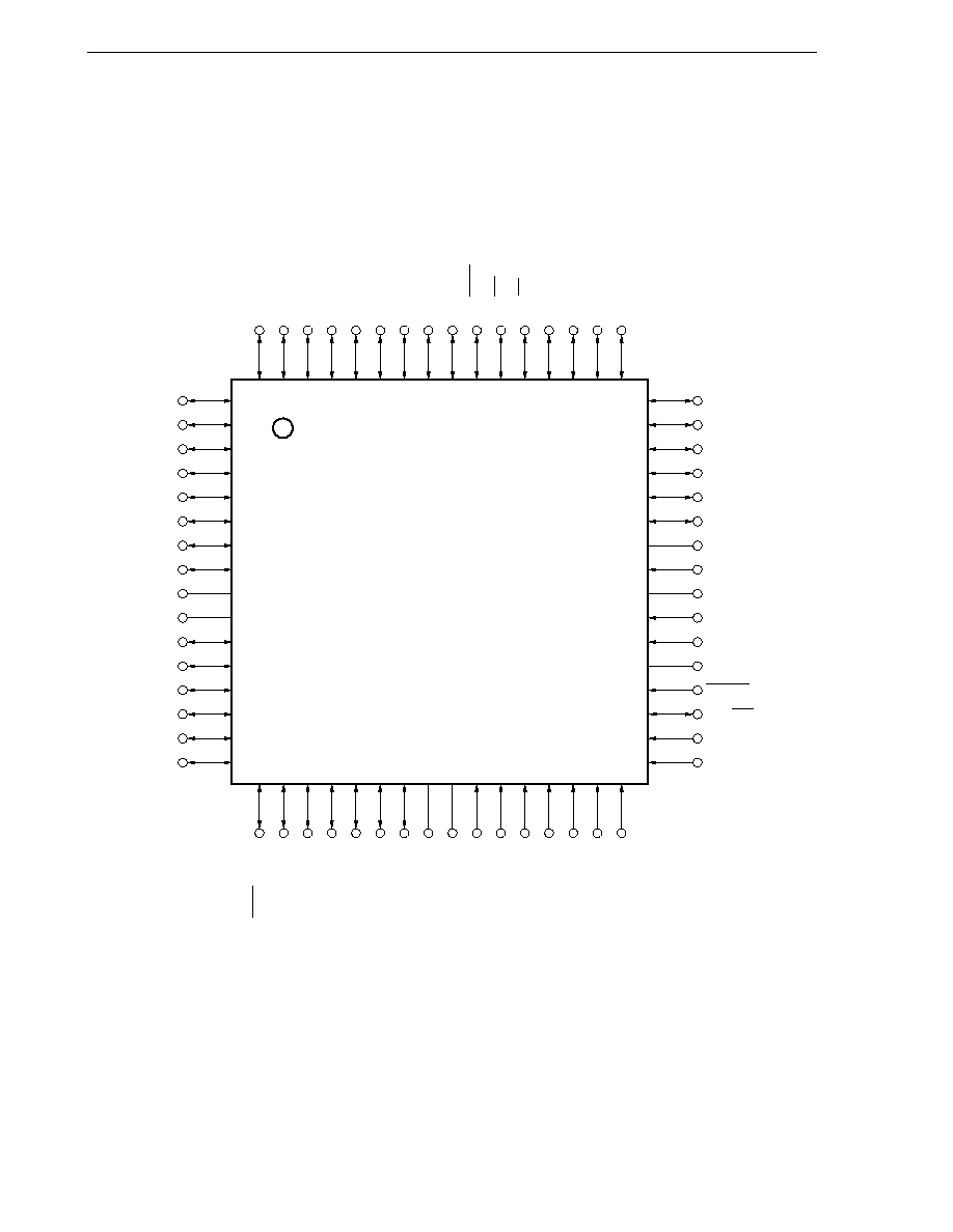
22
CHAPTER 1 OUTLINE (
µPD780078 SUBSERIES)
User's Manual U14260EJ3V1UD
1.5 Pin Configuration (Top View)
∑
64-pin plastic LQFP (14
◊ 14)
∑
64-pin plastic QFP (14
◊ 14)
∑
64-pin plastic TQFP (12
◊ 12)
1
2
3
4
5
6
7
8
9
10
11
12
13
14
15
16
48
47
46
45
44
43
42
41
40
39
38
37
36
35
34
33
64 63 62 61 60 59 58 57 56 55 54 53 52 51 50 49
17 18 19 20 21 22 23 24 25 26 27 28 29 30 31 32
P50/A8
P51/A9
P52/A10
P53/A11
P54/A12
P55/A13
P56/A14
P57/A15
V
SS0
V
DD0
P30
P31
P32
P33
P34/SI3/T
X
D2
P35/SO3/R
X
D2
P71/TI010
P70/TI000/TO00
P03/INTP3/ADTRG
P02/INTP2
P01/INTP1
P00/INTP0
V
SS1
X1
X2
IC (V
PP
)
XT1
XT2
RESET
P80/SS1
AV
REF
P10/ANI0
P47/AD7
P46/AD6
P45/AD5
P44/AD4
P43/AD3
P42/AD2
P41/AD1
P40/AD0
P67/ASTB
P66/WAIT
P65/WR
P64/RD
P75/BUZ/TI001/TO01
P74/PCL/TI011
P73/TI51/TO51
P72/TI50/TO50
P36/SCK3/ASCK2
P20/SI1
P21/SO1
P22/SCK1
P23/RxD0
P24/TxD0
P25/ASCK0
V
DD1
AV
SS
P17/ANI7
P16/ANI6
P15/ANI5
P14/ANI4
P13/ANI3
P12/ANI2
P11/ANI1
Cautions 1. Connect the IC (internally connected) pin directly to V
SS0
or
V
SS1
.
2. Connect the AV
SS
pin to V
SS0
.
Remarks 1. When these devices are used in applications that require the reduction of noise generated from an
on-chip microcontroller, the implementation of noise measures is recommended, such as supplying
V
DD0
and V
DD1
independently, connecting V
SS0
and V
SS1
independently to ground lines, and so on.
2. Pin connection in parentheses is intended for the
µPD78F0078.

23
CHAPTER 1 OUTLINE (
µPD780078 SUBSERIES)
User's Manual U14260EJ3V1UD
PCL:
Programmable clock
RD:
Read strobe
RESET:
Reset
R
X
D0, R
X
D2:
Receive data
SCK1, SCK3:
Serial clock
SI1, SI3:
Serial input
SO1, SO3:
Serial output
SS1:
Serial interface chip select input
TI000, TI010, TI001,
TI011, TI50, TI51:
Timer input
TO00, TO01, TO50,
TO51:
Timer output
T
X
D0, T
X
D2:
Transmit data
V
DD0
, V
DD1
:
Power supply
V
PP
:
Programming power supply
V
SS0
, V
SS1
:
Ground
WAIT:
Wait
WR:
Write strobe
X1, X2:
Crystal (main system clock)
XT1, XT2:
Crystal (subsystem clock)
A8 to A15:
Address bus
AD0 to AD7:
Address/data bus
ADTRG:
AD trigger input
ANI0 to ANI7:
Analog input
ASCK0, ASCK2:
Asynchronous serial clock
ASTB:
Address strobe
AV
REF
:
Analog reference voltage
AV
SS
:
Analog ground
BUZ:
Buzzer clock
IC:
Internally connected
INTP0 to INTP3:
External interrupt input
P00 to P03:
Port 0
P10 to P17:
Port 1
P20 to P25:
Port 2
P30 to P36:
Port 3
P40 to P47:
Port 4
P50 to P57:
Port 5
P64 to P67:
Port 6
P70 to P75:
Port 7
P80:
Port 8
24
CHAPTER 1 OUTLINE (
µPD780078 SUBSERIES)
User's Manual U14260EJ3V1UD
1.6 78K/0 Series Lineup
The 78K/0 Series product lineup is illustrated below. Part numbers in the boxes indicate subseries names.
Remark
VFD (Vacuum Fluorescent Display) is referred to as FIP
TM
(Fluorescent Indicator Panel) in some
documents, but the functions of the two are the same.
PD78083
PD78018F
PD78018FY
PD78014H
EMI-noise reduced version of the PD78018F
Basic subseries for control
On-chip UART, capable of operating at low voltage (1.8 V)
µ
µ
µ
µ
42/44-pin
64-pin
64-pin
52-pin
52-pin version of the PD780024A
µ
µ
PD780024AS
µ
52-pin
52-pin version of the PD780034A
PD780034AS
PD78054 with IEBus
TM
controller
PD78054 with enhanced serial I/O
PD78078Y with enhanced serial I/O and limited functions
PD78054 with timer and enhanced external interface
64-pin
64-pin
80-pin
80-pin
80-pin
EMI-noise reduced version of the PD78054
PD78018F with UART and D/A converter, and enhanced I/O
PD780034A
PD780988
PD780034AY
µ
µ
µ
64-pin
PD780024A with expanded RAM
PD780024A with enhanced A/D converter
µ
µ
µ
µ
On-chip inverter control circuit and UART. EMI-noise reduced.
PD78064
PD78064B
PD780308
100-pin
100-pin
100-pin
PD780308Y
PD78064Y
80-pin
78K/0
Series
LCD drive
PD78064 with enhanced SIO, and expanded ROM and RAM
EMI-noise reduced version of the PD78064
Basic subseries for driving LCDs, on-chip UART
Bus interface supported
µ
µ
µ
µ
µ
µ
µ
µ
µ
PD78018F with enhanced serial I/O
µ
µ
80-pin
100-pin
100-pin
Products in mass production
Products under development
Y subseries products are compatible with I
2
C bus.
ROMless version of the PD78078
µ
100-pin
µ
µ
100-pin
EMI-noise reduced version of the PD78078
µ
Inverter control
PD780208
100-pin
VFD drive
PD78044F with enhanced I/O and VFD C/D. Display output total: 53
µ
µ
PD78098B
µ
100-pin
PD780024A
PD780024AY
µ
µ
µ
80-pin
80-pin
PD780852
PD780828B
µ
µ
For automobile meter driver. On-chip CAN controller
100-pin
PD780958
µ
For industrial meter control
On-chip automobile meter controller/driver
Meter control
80-pin
On-chip IEBus controller
80-pin
On-chip controller compliant with J1850 (Class 2)
PD780833Y
µ
PD780948
On-chip CAN controller
µ
64-pin
PD780078
PD780078Y
µ
µ
PD780034A with timer and enhanced serial I/O
PD78054
PD78054Y
PD78058F
PD78058FY
µ
µ
µ
µ
PD780058
PD780058Y
µ
µ
PD78070A
PD78070AY
PD78078
PD78078Y
PD780018AY
µ
µ
µ
µ
µ
Control
PD78075B
µ
PD780065
µ
µ
PD78044H
PD780232
80-pin
80-pin
For panel control. On-chip VFD C/D. Display output total: 53
PD78044F with N-ch open-drain I/O. Display output total: 34
µ
µ
PD78044F
80-pin
Basic subseries for driving VFD. Display output total: 34
µ
µ
120-pin
PD780308 with enhanced display function and timer. Segment signal output: 40 pins max.
PD780318
PD780328
120-pin
120-pin
PD780308 with enhanced display function and timer. Segment signal output: 32 pins max.
PD780308 with enhanced display function and timer. Segment signal output: 24 pins max.
µ
µ
PD780338
µ
µ
PD780308 with enhanced display function and timer. Segment signal output: 40 pins max.
µ
µ
µ
On-chip CAN controller
Specialized for CAN controller function
80-pin
PD780703AY
µ
PD780702Y
µ
64-pin
PD780816
µ
PD780344 with enhanced A/D converter
100-pin
100-pin
µ
PD780344
PD780344Y
PD780354
PD780354Y
µ
µ
µ
µ
25
CHAPTER 1 OUTLINE (
µPD780078 SUBSERIES)
User's Manual U14260EJ3V1UD
The major functional differences between the subseries are shown below.
∑
Subseries without the suffix Y
Function
ROM
Timer
8-Bit 10-Bit 8-Bit
Serial Interface
I/O
External
Subseries Name
Capacity
8-Bit 16-Bit Watch WDT
A/D
A/D
D/A
Expansion
Control
µPD78075B 32 KB to 40 KB 4 ch 1 ch 1 ch 1 ch 8 ch
≠
2 ch 3 ch (UART: 1 ch)
88
1.8 V
Yes
µPD78078 48 KB to 60 KB
µPD78070A
≠
61
2.7 V
µPD780058 24 KB to 60 KB 2 ch
3 ch (time-division UART: 1 ch)
68
1.8 V
µPD78058F 48 KB to 60 KB
3 ch (UART: 1 ch)
69
2.7 V
µPD78054 16 KB to 60 KB
2.0 V
µPD780065 40 KB to 48 KB
≠
4 ch (UART: 1 ch)
60
2.7 V
µPD780078 48 KB to 60 KB
2 ch
≠
8 ch
3 ch (UART: 2 ch)
52
1.8 V
µPD780034A 8 KB to 32 KB
1 ch
3 ch (UART: 1 ch)
51
µPD780024A
8 ch
≠
µPD780034AS
≠
4 ch
39
≠
µPD780024AS
4 ch
≠
µPD78014H
8 ch
2 ch
53
Yes
µPD78018F 8 KB to 60 KB
µPD78083 8 KB to 16 KB
≠
≠
1 ch (UART: 1 ch)
33
≠
Inverter
µPD780988 16 KB to 60 KB 3 ch Note
≠
1 ch
≠
8 ch
≠
3 ch (UART: 2 ch)
47
4.0 V
Yes
control
VFD
µPD780208 32 KB to 60 KB 2 ch 1 ch 1 ch 1 ch 8 ch
≠
≠
2 ch
74
2.7 V
≠
drive
µPD780232 16 KB to 24 KB 3 ch
≠
≠
4 ch
40
4.5 V
µPD78044H 32 KB to 48 KB 2 ch 1 ch 1 ch
8 ch
1 ch
68
2.7 V
µPD78044F 16 KB to 40 KB
2 ch
LCD
µPD780354 24 KB to 32 KB 4 ch 1 ch 1 ch 1 ch
≠
8 ch
≠
3 ch (UART: 1 ch)
66
1.8 V
≠
drive
µPD780344
8 ch
≠
µPD780338 48 KB to 60 KB 3 ch 2 ch
≠
10 ch 1 ch 2 ch (UART: 1 ch)
54
µPD780328
62
µPD780318
70
µPD780308 48 KB to 60 KB 2 ch 1 ch
8 ch
≠
≠
3 ch (time-division UART: 1 ch)
57
2.0 V
µPD78064B 32 KB
2 ch (UART: 1 ch)
µPD78064 16 KB to 32 KB
Bus
µPD780948 60 KB
2 ch
2 ch
1 ch
1 ch
8 ch
≠
≠
3 ch (UART: 1 ch)
79
4.0 V
Yes
interface
µPD78098B 40 KB to 60 KB
1 ch
2 ch
69
2.7 V
≠
supported
µPD780816 32 KB to 60 KB
2 ch
12 ch
≠
2 ch (UART: 1 ch)
46
4.0 V
Meter control
µPD780958 48 KB to 60 KB 4 ch 2 ch
≠
1 ch
≠
≠
≠
2 ch (UART: 1 ch)
69
2.2 V
≠
Dashboard
µPD780852 32 KB to 40 KB 3 ch 1 ch 1 ch 1 ch 5 ch
≠
≠
3 ch (UART: 1 ch)
56
4.0 V
≠
control
µPD780828B 32 KB to 60 KB
59
Note
16-bit timer: 2 channels
10-bit timer: 1 channel
V
DD
MIN.
Value
26
CHAPTER 1 OUTLINE (
µPD780078 SUBSERIES)
User's Manual U14260EJ3V1UD
1.7 Block Diagram
Remarks 1. The internal ROM capacities differ depending on the product.
2. Pin connection in parentheses is intended for the
µPD78F0078.
16-bit timer/
event counter 00
TI000/TO00/P70
TI010/P71
Serial
interface CSI1
SI1/P20
SO1/P21
SCK1/P22
Serial
interface SIO3
SI3/P34
SO3/P35
SCK3/P36
RxD0/P23
TxD0/P24
ASCK0/P25
ANI0/P10 to
ANI7/P17
UART0
Interrupt
control
16-bit timer/
event counter 01
TI001/TO01/P75
TI011/P74
8-bit timer/
event counter 50
TI50/TO50/P72
TI51/TO51/P73
8-bit timer/
event counter 51
Watch timer
Watchdog timer
8
A/D converter
78K/0
CPU
core
Internal
high-speed
RAM
1024 bytes
Internal
expansion
RAM
1024 bytes
ROM
flash
memory
Port 0
P00 to P03
4
Port 1
P10 to P17
Port 2
P20 to P25
6
Port 3
P30 to P36
7
Port 4
P40 to P47
8
Port 5
P50 to P57
8
Port 6
P64 to P67
4
Port 7
P70 to P75
6
Port 8
External
access
P80
WR/P65
A8/P50 to
A15/P57
RD/P64
WAIT/P66
System
control
RESET
X1
8
AD0/P40 to
AD7/P47
X2
XT1
XT2
8
RxD2/P35
TxD2/P34
ASCK2/P36
UART2
SS1/P80
V
DD1
V
SS0
IC
(V
PP
)
V
DD0
V
SS1
WR/P65
ASTB/P67
8
Clock/buzzer
output control
PCL/P74
BUZ/P75
ADTRG/P03
AV
REF
AV
SS
INTP0/P00 to
INTP3/P03
4
27
CHAPTER 1 OUTLINE (
µPD780078 SUBSERIES)
User's Manual U14260EJ3V1UD
1.8 Outline of Functions
Part Number
µPD780076
µPD780078
µPD78F0078
Item
Internal memory
ROM
48 KB
60 KB
60 KB
Note 1
(Mask ROM)
(Mask ROM)
(Flash memory)
High-speed RAM
1024 bytes
Expansion RAM
1024 bytes
Memory space
64 KB
General-purpose registers
8 bits
◊ 32 registers (8 bits ◊ 8 registers ◊ 4 banks)
Minimum instruction
Minimum instruction execution time selection function
execution time
When main system
∑ 0.166
µs/0.333 µs/0.666 µs/1.33 µs/2.66 µs (@ 12 MHz operation, expanded-
clock selected
specification products only)
∑ 0.238
µs/0.477 µs/0.954 µs/1.90 µs/3.81 µs (@ 8.38 MHz operation)
When subsystem
122
µs (@ 32.768 kHz operation)
clock selected
Instruction set
∑ 16-bit operation
∑ Multiply/divide (8 bits
◊ 8 bits, 16 bits ˜ 8 bits)
∑ Bit manipulation (set, reset, test, and Boolean operation)
∑ BCD adjust, etc.
I/O ports
Total:
52
∑ CMOS input:
8
∑ CMOS I/O:
40
∑ N-ch open-drain I/O (5 V tolerant):
4
Timer
∑ 16-bit timer/event counter: 2 channels
∑ 8-bit timer/event counter: 2 channels
∑ Watch timer:
1 channel
∑ Watchdog timer:
1 channel
Timer output
4 outputs (8-bit PWM output enabled: 2)
Clock output
∑ 93.7 kHz, 187 kHz, 375 kHz, 750 kHz, 1.5 MHz, 3 MHz, 6 MHz, 12 MHz
(12 MHz with main system clock, expanded-specification products only)
∑ 65.5 kHz, 131 kHz, 262 kHz, 524 kHz, 1.05 MHz, 2.10 MHz, 4.19 MHz, 8.38 MHz
(8.38 MHz with main system clock)
∑ 32.768 kHz (32.768 kHz with subsystem clock)
Buzzer output
∑ 1.46 kHz, 2.92 kHz, 5.85 kHz, 11.7 kHz
(12 MHz with main system clock, expanded-specification products only)
∑ 1.02 kHz, 2.05 kHz, 4.10 kHz, 8.19 kHz (8.38 MHz with main system clock)
A/D converter
∑ 10-bit resolution
◊ 8 channels
∑ Low-voltage operation: AV
REF
= 2.2 to 5.5 V
Serial interface
∑ 3-wire serial I/O mode:
1 channel
∑ UART mode:
1 channel
∑ 3-wire serial I/O/UART mode selectable
Note 2
: 1 channel
Vectored interrupt
Maskable
Internal: 18, External: 5
source
Non-maskable
Internal: 1
Software
1
Power supply voltage
V
DD
= 1.8 to 5.5 V
Operating ambient temperature
T
A
= ≠40 to +85
∞C
Package
∑ 64-pin plastic LQFP (14
◊ 14)
∑ 64-pin plastic QFP (14
◊ 14)
∑ 64-pin plastic TQFP (12
◊ 12)
Notes 1. The capacity of the internal flash memory can be changed by means of the memory size switching register
(IMS).
2. Select either of the functions of these alternate-function pins.
28
CHAPTER 1 OUTLINE (
µPD780078 SUBSERIES)
User's Manual U14260EJ3V1UD
The following table outlines the timer/event counters (for details, refer to CHAPTER 8 16-BIT TIMER/EVENT
COUNTERS 00, 01, CHAPTER 9 8-BIT TIMER/EVENT COUNTERS 50, 51, CHAPTER 10 WATCH TIMER, and
CHAPTER 11 WATCHDOG TIMER).
16-Bit Timer/Event
8-Bit Timer/Event
Watch Timer
Watchdog Timer
Counters 00, 01
Counters 50, 51
TM00
TM01
TM50
TM51
Operation
Interval timer
1 channel 1 channel 1 channel 1 channel
1 channel
Note 1
1 channel
Note 2
mode
External event counter
1 channel 1 channel 1 channel 1 channel
≠
≠
Function
Timer output
1 output
1 output
1 output
1 output
≠
≠
PPG output
1 output
1 output
≠
≠
≠
≠
PWM output
≠
≠
1 output
1 output
≠
≠
Pulse width measurement
2 inputs
2 inputs
≠
≠
≠
≠
Square wave output
1 output
1 output
1 output
1 output
≠
≠
Interrupt source
2
2
1
1
1
1
Note 3
Notes 1. The watch timer can be used both as a watch timer and an interval timer at the same time.
2. The watchdog timer can be used as either a watchdog timer or interval timer. Select one of the functions.
3. A non-maskable interrupt or maskable interrupt (internal) can be selected for the watchdog timer interrupt
(INTWDT).
1.9 Mask Options
The mask ROM versions (
µPD780076 and 780078) provide pull-up resistor mask options which allow users to
specify whether to connect a pull-up resistor to a specific port pin when the user places an order for device production.
Using the mask option when pull-up resistors are required reduces the number of components to add to the device,
resulting in board space saving.
The mask options provided in the
µPD780078 Subseries are shown in Table 1-2.
Table 1-2. Mask Options of Mask ROM Versions
Pin Name
Mask Option
P30 to P33
Pull-up resistor connection can be specified in 1-bit units.

29
User's Manual U14260EJ3V1UD
CHAPTER 2 OUTLINE (
µPD780078Y SUBSERIES)
2.1 Expanded-Specification Products and Conventional Products
The expanded-specification products and conventional products refer to the following products.
Expanded-specification products: Products with a rank
Note
other than K
Mask ROM and flash memory versions for which orders were received on or
after February 1, 2002
Conventional products:
Products with rank
Note
K
Products other than the above expanded-specification products
Note The rank is indicated by the 5th digit from the left in the lot number marked on the package.
Expanded-specification products and conventional products differ in the operating frequency ratings. Table 2-1
shows the differences between these products.
Table 2-1. Differences Between Expanded-Specification Products and Conventional Products
Power Supply Voltage (V
DD
)
Guaranteed Operating Speed (Operating Frequency)
Conventional Products
Expanded-Specification Products
4.0 to 5.5 V
8.38 MHz (0.238
µs)
8.38 MHz (0.238
µs)
3.0 to 5.5 V
5 MHz (0.4
µs)
8.38 MHz (0.238
µs)
2.7 to 5.5 V
5 MHz (0.4
µs)
5 MHz (0.4
µs)
1.8 to 5.5 V
1.25 MHz (1.6
µs)
1.25 MHz (1.6
µs)
Remark The parenthesized values indicate the minimum instruction execution time.
Lot number
Year
code
Rank
Week
code
30
CHAPTER 2 OUTLINE (
µPD780078Y SUBSERIES)
User's Manual U14260EJ3V1UD
2.2 Features
∑
Minimum instruction execution time changeable from high speed (0.238
µs: @ 8.38 MHz operation with main
system clock) to ultra-low speed (122
µs: @ 32.768 kHz operation with subsystem clock)
∑
General-purpose registers: 8 bits
◊ 32 registers (8 bits ◊ 8 registers ◊ 4 banks)
∑
Internal memory
Type
Program Memory
Data Memory
Part Number
(ROM)
High-Speed RAM
Expansion RAM
µPD780076Y
Mask ROM
48 KB
1024 bytes
1024 bytes
µPD780078Y
60 KB
µPD78F0078Y
Flash memory
60 KB
Note
Note The capacity of the internal flash memory can be changed by means of the memory size switching register
(IMS).
∑
External memory expansion space: 64 KB (on-chip external device expansion function)
∑
Instruction set suited to system control
∑ Bit manipulation possible in all address spaces
∑ Multiply and divide instructions
∑
52 I/O ports: (Four N-ch open-drain ports)
∑
Timer: 6 channels
∑ 16-bit timer/event counter: 2 channels
∑ 8-bit timer/event counter: 2 channels
∑ Watch timer:
1 channel
∑ Watchdog timer:
1 channel
∑
Serial interface:
4 channels
∑ 3-wire serial mode:
1 channel
∑ UART mode:
1 channel
∑ 3-wire serial I/O/UART mode selectable: 1 channel
∑ I
2
C mode:
1 channel
∑
10-bit resolution A/D converter: 8 channels
∑
Vectored interrupt sources: 26
∑
Two types of on-chip clock oscillators (main system clock and subsystem clock)
∑
Power supply voltage: V
DD
= 1.8 to 5.5 V

31
CHAPTER 2 OUTLINE (
µPD780078Y SUBSERIES)
User's Manual U14260EJ3V1UD
2.3 Applications
Personal computers, air conditioners, dashboards, car audio, etc.
2.4 Ordering Information
Part Number
Package
Internal ROM
µPD780076YGC-◊◊◊-8BS
64-pin plastic LQFP (14
◊ 14)
Mask ROM
µPD780076YGC-◊◊◊-AB8
64-pin plastic QFP (14
◊ 14)
Mask ROM
µPD780076YGK-◊◊◊-9ET
64-pin plastic TQFP (12
◊ 12)
Mask ROM
µPD780078YGC-◊◊◊-8BS
64-pin plastic LQFP (14
◊ 14)
Mask ROM
µPD780078YGC-◊◊◊-AB8
64-pin plastic QFP (14
◊ 14)
Mask ROM
µPD780078YGK-◊◊◊-9ET
64-pin plastic TQFP (12
◊ 12)
Mask ROM
µPD78F0078YGC-8BS
64-pin plastic LQFP (14
◊ 14)
Flash memory
µPD78F0078YGC-AB8
64-pin plastic QFP (14
◊ 14)
Flash memory
µPD78F0078YGK-9ET
64-pin plastic TQFP (12
◊ 12)
Flash memory
Remark
◊◊◊ indicates ROM code suffix.
32
CHAPTER 2 OUTLINE (
µPD780078Y SUBSERIES)
User's Manual U14260EJ3V1UD
2.5 Pin Configuration (Top View)
∑
64-pin plastic LQFP (14
◊ 14)
∑
64-pin plastic QFP (14
◊ 14)
∑
64-pin plastic TQFP (12
◊ 12)
Cautions 1. Connect the IC (internally connected) pin directly to V
SS0
or V
SS1
.
2. Connect the AV
SS
pin to V
SS0
.
Remarks 1. When these devices are used in applications that require the reduction of noise generated from an
on-chip microcontroller, the implementation of noise measures is recommended, such as supplying
V
DD0
and V
DD1
independently, connecting V
SS0
and V
SS1
independently to ground lines, and so on.
2. Pin connection in parentheses is intended for the
µPD78F0078Y.
1
2
3
4
5
6
7
8
9
10
11
12
13
14
15
16
P50/A8
P51/A9
P52/A10
P53/A11
P54/A12
P55/A13
P56/A14
P57/A15
V
SS0
V
DD0
P30
P31
P32/SDA0
P33/SCL0
P34/SI3/T
X
D2
P35/SO3/R
X
D2
P36/SCK3/ASCK2
P20/SI1
P21/SO1
P22/SCK1
P23/RxD0
P24/TxD0
P25/ASCK0
V
DD1
AV
SS
P17/ANI7
P16/ANI6
P15/ANI5
P14/ANI4
P13/ANI3
P12/ANI2
P11/ANI1
48
47
46
45
44
43
42
41
40
39
38
37
36
35
34
33
P71/TI010
P70/TI000/TO00
P03/INTP3/ADTRG
P02/INTP2
P01/INTP1
P00/INTP0
V
SS1
X1
X2
IC (V
PP
)
XT1
XT2
RESET
P80/SS1
AV
REF
P10/ANI0
17 18 19 20 21 22
23
24 25
26 27 28 29 30
31 32
64 63 62 61 60 59
58
57 56
55 54 53 52 51
50 49
P47/AD7
P46/AD6
P45/AD5
P44/AD4
P43/AD3
P42/AD2
P41/AD1
P40/AD0
P67/ASTB
P66/WAIT
P65/WR
P64/RD
P75/BUZ/TI001/TO01
P74/PCL/TI011
P73/TI51/TO51
P72/TI50/TO50

33
CHAPTER 2 OUTLINE (
µPD780078Y SUBSERIES)
User's Manual U14260EJ3V1UD
PCL:
Programmable clock
RD:
Read strobe
RESET:
Reset
R
X
D0, R
X
D2:
Receive data
SCK1, SCK3, SCL0: Serial clock
SDA0:
Serial data
SI1, SI3:
Serial input
SO1, SO3:
Serial output
SS1:
Serial interface chip select input
TI000, TI010, TI001,
TI011, TI50, TI51:
Timer input
TO00, TO01, TO50,
TO51:
Timer output
T
X
D0, T
X
D2:
Transmit data
V
DD0
, V
DD1
:
Power supply
V
PP
:
Programming power supply
V
SS0
, V
SS1
:
Ground
WAIT:
Wait
WR:
Write strobe
X1, X2:
Crystal (main system clock)
XT1, XT2:
Crystal (subsystem clock)
A8 to A15:
Address bus
AD0 to AD7:
Address/data bus
ADTRG:
AD trigger input
ANI0 to ANI7:
Analog input
ASCK0, ASCK2:
Asynchronous serial clock
ASTB:
Address strobe
AV
REF
:
Analog reference voltage
AV
SS
:
Analog ground
BUZ:
Buzzer clock
IC:
Internally connected
INTP0 to INTP3:
External interrupt input
P00 to P03:
Port 0
P10 to P17:
Port 1
P20 to P25:
Port 2
P30 to P36:
Port 3
P40 to P47:
Port 4
P50 to P57:
Port 5
P64 to P67:
Port 6
P70 to P75:
Port 7
P80:
Port 8

34
CHAPTER 2 OUTLINE (
µPD780078Y SUBSERIES)
User's Manual U14260EJ3V1UD
2.6 78K/0 Series Lineup
The 78K/0 Series product lineup is illustrated below. Part numbers in the boxes indicate subseries names.
Remark
VFD (Vacuum Fluorescent Display) is referred to as FIP (Fluorescent Indicator Panel) in some
documents, but the functions of the two are the same.
PD78083
PD78018F
PD78018FY
PD78014H
EMI-noise reduced version of the PD78018F
Basic subseries for control
On-chip UART, capable of operating at low voltage (1.8 V)
µ
µ
µ
µ
42/44-pin
64-pin
64-pin
52-pin
52-pin version of the PD780024A
µ
µ
PD780024AS
µ
52-pin
52-pin version of the PD780034A
PD780034AS
PD78054 with IEBus controller
PD78054 with enhanced serial I/O
PD78078Y with enhanced serial I/O and limited functions
PD78054 with timer and enhanced external interface
64-pin
64-pin
80-pin
80-pin
80-pin
EMI-noise reduced version of the PD78054
PD78018F with UART and D/A converter, and enhanced I/O
PD780034A
PD780988
PD780034AY
µ
µ
µ
64-pin
PD780024A with expanded RAM
PD780024A with enhanced A/D converter
µ
µ
µ
µ
On-chip inverter control circuit and UART. EMI-noise reduced.
PD78064
PD78064B
PD780308
100-pin
100-pin
100-pin
PD780308Y
PD78064Y
80-pin
78K/0
Series
LCD drive
PD78064 with enhanced SIO, and expanded ROM and RAM
EMI-noise reduced version of the PD78064
Basic subseries for driving LCDs, on-chip UART
Bus interface supported
µ
µ
µ
µ
µ
µ
µ
µ
µ
PD78018F with enhanced serial I/O
µ
µ
80-pin
100-pin
100-pin
Products in mass production
Products under development
Y subseries products are compatible with I
2
C bus.
ROMless version of the PD78078
µ
100-pin
µ
µ
100-pin
EMI-noise reduced version of the PD78078
µ
Inverter control
PD780208
100-pin
VFD drive
PD78044F with enhanced I/O and VFD C/D. Display output total: 53
µ
µ
PD78098B
µ
100-pin
PD780024A
PD780024AY
µ
µ
µ
80-pin
80-pin
PD780852
PD780828B
µ
µ
For automobile meter driver. On-chip CAN controller
100-pin
PD780958
µ
For industrial meter control
On-chip automobile meter controller/driver
Meter control
80-pin
On-chip IEBus controller
80-pin
On-chip controller compliant with J1850 (Class 2)
PD780833Y
µ
PD780948
On-chip CAN controller
µ
64-pin
PD780078
PD780078Y
µ
µ
PD780034A with timer and enhanced serial I/O
PD78054
PD78054Y
PD78058F
PD78058FY
µ
µ
µ
µ
PD780058
PD780058Y
µ
µ
PD78070A
PD78070AY
PD78078
PD78078Y
PD780018AY
µ
µ
µ
µ
µ
Control
PD78075B
µ
PD780065
µ
µ
PD78044H
PD780232
80-pin
80-pin
For panel control. On-chip VFD C/D. Display output total: 53
PD78044F with N-ch open-drain I/O. Display output total: 34
µ
µ
PD78044F
80-pin
Basic subseries for driving VFD. Display output total: 34
µ
µ
120-pin
PD780308 with enhanced display function and timer. Segment signal output: 40 pins max.
PD780318
PD780328
120-pin
120-pin
PD780308 with enhanced display function and timer. Segment signal output: 32 pins max.
PD780308 with enhanced display function and timer. Segment signal output: 24 pins max.
µ
µ
PD780338
µ
µ
PD780308 with enhanced display function and timer. Segment signal output: 40 pins max.
µ
µ
µ
On-chip CAN controller
Specialized for CAN controller function
80-pin
PD780703AY
µ
PD780702Y
µ
64-pin
PD780816
µ
PD780344 with enhanced A/D converter
100-pin
100-pin
µ
PD780344
PD780344Y
PD780354
PD780354Y
µ
µ
µ
µ

35
CHAPTER 2 OUTLINE (
µPD780078Y SUBSERIES)
User's Manual U14260EJ3V1UD
The major functional differences between the subseries are shown below.
∑
Subseries with the suffix Y
Function
ROM
Timer
8-Bit 10-Bit 8-Bit
Serial Interface
I/O
V
DD
External
Subseries Name
Capacity
8-Bit 16-Bit Watch WDT
A/D
A/D
D/A
MIN. Value Expansion
Control
µPD78078Y
48 KB to 60 KB
4 ch
1 ch
1 ch
1 ch
8 ch
--
2 ch 3 ch (UART: 1 ch,
88
1.8 V
Yes
µPD78070AY
--
I
2
C: 1 ch)
61
2.7 V
µPD780018AY 48 KB to 60 KB
--
3 ch (I
2
C: 1 ch)
88
µPD780058Y
24 KB to 60 KB
2 ch
2 ch 3 ch (time-division
68
1.8 V
UART: 1 ch, I
2
C: 1 ch)
µPD78058FY
48 KB to 60 KB
3 ch (UART: 1 ch,
69
2.7 V
µPD78054Y
16 KB to 60 KB
I
2
C: 1 ch)
2.0 V
µPD780078Y
48 KB to 60 KB
2 ch
--
8 ch
--
4 ch (UART: 2 ch,
52
1.8 V
I
2
C: 1 ch)
µPD780034AY 8 KB to 32 KB
1 ch
3 ch (UART: 1 ch,
51
µPD780024AY
8 ch
--
I
2
C: 1 ch)
µPD78018FY
8 KB to 60 KB
2 ch (I
2
C: 1 ch)
53
LCD
µPD780354Y
24 KB to 32 KB
4 ch
1 ch
1 ch
1 ch
--
8 ch
--
4 ch (UART: 1 ch,
66
1.8 V
--
drive
µPD780344Y
8 ch
--
I
2
C: 1 ch)
µPD780308Y
48 KB to 60 KB
2 ch
3 ch (time-division
57
2.0 V
UART: 1 ch, I
2
C: 1 ch)
µPD78064Y
16 KB to 32 KB
2 ch (UART: 1 ch,
I
2
C: 1 ch)
Bus
µPD780702Y
60 KB
3 ch
2 ch
1 ch
1 ch 16 ch
--
--
4 ch (UART: 1 ch,
67
3.5 V
--
interface µPD780703AY 59.5 KB
I
2
C: 1 ch)
supported
µPD780833Y
60 KB
65
4.5 V
Remark
The functions of the subseries without the suffix Y and the subseries with the suffix Y are the same, except
for the serial interface (if a subseries without the suffix Y is available).
36
CHAPTER 2 OUTLINE (
µPD780078Y SUBSERIES)
User's Manual U14260EJ3V1UD
2.7 Block Diagram
Remarks 1. The internal ROM capacities differ depending on the product.
2. Pin connection in parentheses is intended for the
µPD78F0078Y.
16-bit timer/
event counter 00
TI000/TO00/P70
TI010/P71
Serial
interface CSI1
SI1/P20
SO1/P21
SCK1/P22
Serial
interface SIO3
SI3/P34
SO3/P35
SCK3/P36
RxD0/P23
TxD0/P24
ASCK0/P25
ANI0/P10 to
ANI7/P17
I
2
C bus
UART0
Interrupt
control
SCL0/P33
SDA0/P32
16-bit timer/
event counter 01
TI001/TO01/P75
TI011/P74
8-bit timer/
event counter 50
TI50/TO50/P72
TI51/TO51/P73
8-bit timer/
event counter 51
Watch timer
Watchdog timer
8
A/D converter
78K/0
CPU
core
Internal
high-speed
RAM
1024 bytes
Internal
expansion
RAM
1024 bytes
Port 0
P00 to P03
4
Port 1
P10 to P17
Port 2
P20 to P25
6
Port 3
P30 to P36
7
Port 4
P40 to P47
8
Port 5
P50 to P57
8
Port 6
P64 to P67
4
Port 7
P70 to P75
6
Port 8
External
access
P80
WR/P65
A8/P50 to
A15/P57
RD/P64
WAIT/P66
System
control
RESET
X1
8
AD0/P40 to
AD7/P47
X2
XT1
XT2
8
RxD2/P35
TxD2/P34
ASCK2/P36
UART2
SS1/P80
V
DD1
V
SS0
IC
(V
PP
)
V
DD0
V
SS1
WR/P65
ASTB/P67
8
Clock/buzzer
output control
PCL/P74
BUZ/P75
ADTRG/P03
AV
REF
AV
SS
INTP0/P00 to
INTP3/P03
4
ROM
flash
memory
37
CHAPTER 2 OUTLINE (
µPD780078Y SUBSERIES)
User's Manual U14260EJ3V1UD
2.8 Outline of Functions
Part Number
µPD780076Y
µPD780078Y
µPD78F0078Y
Item
Internal memory
ROM
48 KB
60 KB
60 KB
Note 1
(Mask ROM)
(Mask ROM)
(Flash memory)
High-speed RAM
1024 bytes
Expansion RAM
1024 bytes
Memory space
64 KB
General-purpose registers
8 bits
◊ 32 registers (8 bits ◊ 8 registers ◊ 4 banks)
Minimum instruction
Minimum instruction execution time selection function
execution time
When main system
0.238
µs/0.477 µs/0.954 µs/1.90 µs/3.81 µs (@ 8.38 MHz operation)
clock selected
When subsystem
122
µs (@ 32.768 kHz operation)
clock selected
Instruction set
∑ 16-bit operation
∑ Multiply/divide (8 bits
◊ 8 bits, 16 bits ˜ 8 bits)
∑ Bit manipulation (set, reset, test, and Boolean operation)
∑ BCD adjust, etc.
I/O ports
Total:
52
∑ CMOS input:
8
∑ CMOS I/O:
40
∑ N-ch open-drain I/O (5 V tolerant):
4
Timer
∑ 16-bit timer/event counter: 2 channels
∑ 8-bit timer/event counter: 2 channels
∑ Watch timer:
1 channel
∑ Watchdog timer:
1 channel
Timer output
4 outputs (8-bit PWM output enabled: 2)
Clock output
∑ 65.5 kHz, 131 kHz, 262 kHz, 524 kHz, 1.05 MHz, 2.10 MHz, 4.19 MHz, 8.38 MHz
(8.38 MHz with main system clock)
∑ 32.768 kHz (32.768 kHz with subsystem clock)
Buzzer output
1.02 kHz, 2.05 kHz, 4.10 kHz, 8.19 kHz (8.38 MHz with main system clock)
A/D converter
∑ 10-bit resolution
◊ 8 channels
∑ Low-voltage operation: AV
REF
= 2.2 to 5.5 V
Serial interface
∑ 3-wire serial I/O mode:
1 channel
∑ UART mode:
1 channel
∑ 3-wire serial I/O/UART mode selectable
Note 2
: 1 channel
∑ I
2
C bus mode:
1 channel
Vectored interrupt
Maskable
Internal: 19, External: 5
source
Non-maskable
Internal: 1
Software
1
Power supply voltage
V
DD
= 1.8 to 5.5 V
Operating ambient temperature
T
A
= ≠40 to +85
∞C
Package
∑ 64-pin plastic LQFP (14
◊ 14)
∑ 64-pin plastic QFP (14
◊ 14)
∑ 64-pin plastic TQFP (12
◊ 12)
Notes 1. The capacity of the internal flash memory can be changed by means of the memory size switching register
(IMS).
2. Select either of the functions of these alternate-function pins.

38
CHAPTER 2 OUTLINE (
µPD780078Y SUBSERIES)
User's Manual U14260EJ3V1UD
The following table outlines the timer/event counters (for details, refer to CHAPTER 8 16-BIT TIMER/EVENT
COUNTERS 00, 01, CHAPTER 9 8-BIT TIMER/EVENT COUNTERS 50, 51, CHAPTER 10 WATCH TIMER, and
CHAPTER 11 WATCHDOG TIMER).
16-Bit Timer/Event
8-Bit Timer/Event
Watch Timer
Watchdog Timer
Counters 00, 01
Counters 50, 51
TM00
TM01
TM50
TM51
Operation
Interval timer
1 channel 1 channel 1 channel 1 channel
1 channel
Note 1
1 channel
Note 2
mode
External event counter
1 channel 1 channel 1 channel 1 channel
≠
≠
Function
Timer output
1 output
1 output
1 output
1 output
≠
≠
PPG output
1 output
1 output
≠
≠
≠
≠
PWM output
≠
≠
1 output
1 output
≠
≠
Pulse width measurement
2 inputs
2 inputs
≠
≠
≠
≠
Square wave output
1 output
1 output
1 output
1 output
≠
≠
Interrupt source
2
2
1
1
1
1
Note 3
Notes 1. The watch timer can be used both as a watch timer and an interval timer at the same time.
2. The watchdog timer can be used as either a watchdog timer or interval timer. Select one of the functions.
3. A non-maskable interrupt or maskable interrupt (internal) can be selected for the watchdog timer interrupt
(INTWDT).
2.9 Mask Options
The mask ROM versions (
µPD780076Y and 780078Y) provide pull-up resistor mask options which allow users
to specify whether to connect a pull-up resistor to a specific port pin when the user places an order for device
production. Using this mask option when pull-up resistors are required reduces the number of components to add
to the device, resulting in board space saving.
The mask options provided in the
µPD780078Y Subseries are shown in Table 2-2.
Table 2-2. Mask Options of Mask ROM Versions
Pin Name
Mask Option
P30 and P31
Pull-up resistor connection can be specified in 1-bit units.
39
User's Manual U14260EJ3V1UD
Pin Name
I/O
Function
After Reset
Alternate
Function
P00
I/O
Input
INTP0
P01
INTP1
P02
INTP2
P03
INTP3/ADTRG
P10 to P17
Input
Port 1
Input
ANI0 to ANI7
8-bit input-only port.
P20
I/O
Input
SI1
P21
SO1
P22
SCK1
P23
RxD0
P24
TxD0
P25
ASCK0
P30
I/O
Input
--
P31
P32
P33
P34
SI3/T
X
D2
P35
SO3/R
X
D2
P36
SCK3/ASCK2
P40 to P47
I/O
Port 4
Input
AD0 to AD7
8-bit I/O port
Input/output mode can be specified in 1-bit units.
An on-chip pull-up resistor can be used by setting software.
Interrupt request flag (KRIF) is set to 1 by falling edge
detection.
P50 to P57
I/O
Port 5
Input
A8 to A15
8-bit I/O port
LEDs can be driven directly.
Input/output mode can be specified in 1-bit units.
An on-chip pull-up resistor can be used by setting software.
P64
I/O
Input
RD
P65
WR
P66
WAIT
P67
ASTB
CHAPTER 3 PIN FUNCTIONS (
µPD780078 SUBSERIES)
3.1 Pin Function List
(1) Port pins (1/2)
Port 0
4-bit I/O port
Input/output mode can be specified in 1-bit units.
An on-chip pull-up resistor can be used by setting software.
Port 2
6-bit I/O port
Input/output mode can be specified in 1-bit units.
An on-chip pull-up resistor can be used by setting software.
Port 3
7-bit I/O
port
Input/output mode
can be specified in
1-bit units.
N-ch open-drain I/O port
An on-chip pull-up resistor can be
specified by a mask option
(mask ROM version only).
LEDs can be driven directly.
An on-chip pull-up resistor can be
used by setting software.
Port 6
4-bit I/O port
Input/output mode can be specified in 1-bit units.
An on-chip pull-up resistor can be used by setting software.
40
CHAPTER 3 PIN FUNCTIONS (
µPD780078 SUBSERIES)
User's Manual U14260EJ3V1UD
(1) Port pins (2/2)
Pin Name
I/O
Function
After Reset
Alternate
Function
P70
I/O
Input
TI000/TO00
P71
TI010
P72
TI50/TO50
P73
TI51/TO51
P74
TI011/PCL
P75
TI001/TO01/BUZ
P80
I/O
Input
SS1
(2) Non-port pins (1/2)
Pin Name
I/O
Function
After Reset
Alternate
Function
INTP0
Input
Input
P00
INTP1
P01
INTP2
P02
INTP3
P03/ADTRG
SI1
Input
Serial interface serial data input
Input
P20
SI3
P34/T
X
D2
SO1
Output
Serial interface serial data output
Input
P21
SO3
P35/R
X
D2
SCK1
I/O
Serial interface serial clock input/output
Input
P22
SCK3
P36/ASCK2
SS1
Input
Serial interface chip select input
Input
P80
R
X
D0
Input
Asynchronous serial interface serial data input
Input
P23
R
X
D2
P35/SO3
T
X
D0
Output
Asynchronous serial interface serial data output
Input
P24
T
X
D2
P34/SI3
ASCK0
Input
Asynchronous serial interface serial clock input
Input
P25
ASCK2
P36/SCK3
TI000
Input
External count clock input to 16-bit timer/event counter 00.
Input
P70/TO00
Capture trigger input to capture registers (CR000, CR010)
of 16-bit timer/event counter 00
TI010
Capture trigger input to capture register (CR000) of 16-bit
P71
timer/event counter 00
TI001
External count clock input to 16-bit timer/event counter 01.
P75/TO01/BUZ
Capture trigger input to capture registers (CR001, CR011)
of 16-bit timer/event counter 01
External interrupt request input with specifiable valid edges
(rising edge, falling edge, both rising and falling edges)
Port 7
6-bit I/O port
Input/output mode can be specified in 1-bit units.
An on-chip pull-up resistor can be used by setting software.
Port 8
1-bit I/O port
Input/output mode can be specified in 1-bit units.
An on-chip pull-up resistor can be used by setting software.

41
CHAPTER 3 PIN FUNCTIONS (
µPD780078 SUBSERIES)
User's Manual U14260EJ3V1UD
(2) Non-port pins (2/2)
Pin Name
I/O
Function
After Reset
Alternate
Function
TI011
Input
Capture trigger input to capture register (CR001) of 16-bit
Input
P74/PCL
timer/event counter 01
TI50
External count clock input to 8-bit timer/event counter 50
P72/TO50
TI51
External count clock input to 8-bit timer/event counter 51
P73/TO51
TO00
Output
16-bit timer/event counter 00 output
Input
P70/TI000
TO01
16-bit timer/event counter 01 output
P75/TI001/BUZ
TO50
8-bit timer/event counter 50 output
P72/TI50
TO51
8-bit timer/event counter 51 output
P73/TI51
PCL
Output
Clock output (for main system clock and subsystem clock
Input
P74/TI011
trimming)
BUZ
Output
Buzzer output
Input
P75/TI001/TO01
AD0 to AD7
I/O
Lower address/data bus when expanding external memory
Input
P40 to P47
A8 to A15
Output
Higher address bus when expanding external memory
Input
P50 to P57
RD
Output
Strobe signal output for read operation from external memory
Input
P64
WR
Strobe signal output for write operation from external memory
P65
WAIT
Input
Wait insertion when accessing external memory
Input
P66
ASTB
Output
Strobe output externally latching address information
Input
P67
output to ports 4 and 5 to access external memory
ANI0 to ANI7
Input
A/D converter analog input
Input
P10 to P17
ADTRG
Input
A/D converter trigger signal input
Input
P03/INTP3
AV
REF
Input
A/D converter reference voltage input and analog power supply
--
--
AV
SS
--
A/D converter ground potential. Connect to V
SS0
or V
SS1
.
--
--
RESET
Input
System reset input
Input
--
X1
Input
Resonator connection for main system clock
--
--
X2
--
--
--
XT1
Input
Resonator connection for subsystem clock
--
--
XT2
--
--
--
V
DD0
--
Positive power supply for ports
--
--
V
DD1
--
Positive power supply (other than ports)
--
--
V
SS0
--
Ground potential for ports
--
--
V
SS1
--
Ground potential (other than ports)
--
--
IC
--
Internally connected. Connect directly to V
SS0
or V
SS1
.
--
--
V
PP
--
Flash memory programming mode setting.
--
--
High-voltage application for program write/verify

42
CHAPTER 3 PIN FUNCTIONS (
µPD780078 SUBSERIES)
User's Manual U14260EJ3V1UD
3.2 Description of Pin Functions
3.2.1 P00 to P03 (Port 0)
P00 to P03 function as a 4-bit I/O port. Besides serving as an I/O port, they also function as external interrupt
inputs and an A/D converter external trigger input.
The following operating modes can be specified in 1-bit units.
(1) Port mode
These pins function as a 4-bit I/O port.
P00 to P03 can be specified as input or output in 1-bit units using port mode register 0 (PM0). On-chip pull-up
resistors can be connected by setting pull-up resistor option register 0 (PU0).
(2) Control mode
In this mode, these pins function as external interrupt request inputs and an A/D converter external trigger input.
(a) INTP0 to INTP3
INTP0 to INTP3 are external interrupt request input pins for which the valid edge can be specified (rising
edge, falling edge, or both rising and falling edges).
(b) ADTRG
A/D converter external trigger input pin.
Caution
When P03 is used as an A/D converter external trigger input, specify the valid edge by
using bits 1 and 2 (EGA00, EGA01) of the A/D converter mode register (ADM0) and set the
interrupt mask flag (PMK3) to 1.
3.2.2 P10 to P17 (Port 1)
P10 to P17 function as an 8-bit input-only port. Besides serving as an input port, they also function as A/D converter
analog inputs.
The following operating modes can be specified in 1-bit units.
(1) Port mode
These pins function as an 8-bit input-only port.
(2) Control mode
These pins function as A/D converter analog input pins (ANI0 to ANI7). When using these pins as analog input
pins, see (4) ANI0/P10 to ANI7/P17 in 13.6 Cautions for A/D Converter.
3.2.3 P20 to P25 (Port 2)
P20 to P25 function as a 6-bit I/O port. Besides serving as an I/O port, they function as data I/O and clock I/O for
serial interfaces CSI1 and UART0.
The following operating modes can be specified in 1-bit units.
(1) Port mode
These pins function as a 6-bit I/O port. They can be specified as input or output in 1-bit units using port mode
register 2 (PM2). On-chip pull-up resistors can be connected by setting pull-up resistor option register 2 (PU2).

43
CHAPTER 3 PIN FUNCTIONS (
µPD780078 SUBSERIES)
User's Manual U14260EJ3V1UD
(2) Control mode
These pins function as data I/O and clock I/O for serial interfaces CSI1 and UART0.
(a) SI1
Serial data input pin for serial interface CSI1.
(b) SO1
Serial data output pin for serial interface CSI1.
(c) SCK1
Serial clock I/O pin for serial interface CSI1.
(d) R
X
D0
Serial data input pin for serial interface UART0.
(e) T
X
D0
Serial data output pin for serial interface UART0.
(f)
ASCK0
Serial clock input pin for serial interface UART0.
3.2.4 P30 to P36 (Port 3)
P30 to P36 function as a 7-bit I/O port. Besides serving as an I/O port, they also function as data I/O and clock
I/O for serial interfaces SIO3 and UART2.
P30 to P33 can drive LEDs directly.
The following operating modes can be specified in 1-bit units.
(1) Port mode
These pins function as a 7-bit I/O port. They can be specified as input or output in 1-bit units using port mode
register 3 (PM3). P30 to P33 are N-ch open drain I/O pins. On-chip pull-up resistors can be connected via a
mask option (mask ROM version only). On-chip pull-up resistors can be connected to P34 to P36 by setting pull-
up resistor option register 3 (PU3).
(2) Control mode
These pins function as data I/O and clock I/O for serial interfaces SIO3 and UART2.
(a) SI3
Serial data input pin for serial interface SIO3.
(b) SO3
Serial data output pin for serial interface SIO3.
(c) SCK3
Serial clock I/O pin for serial interface SIO3.
(d) R
X
D2
Serial data input pin for serial interface UART2.

44
CHAPTER 3 PIN FUNCTIONS (
µPD780078 SUBSERIES)
User's Manual U14260EJ3V1UD
(e) T
X
D2
Serial data output pin for serial interface UART2.
(f)
ASCK2
Serial clock input pin for serial interface UART2.
3.2.5 P40 to P47 (Port 4)
P40 to P47 function as an 8-bit I/O port. Besides serving as an I/O port, they also function as an address/data
bus.
The interrupt request flag (KRIF) can be set to 1 by detecting a falling edge.
The following operating modes can be specified.
Caution
When using the falling edge detection interrupt (INTKR), be sure to set the memory expansion
mode register (MEM) to 01H.
(1) Port mode
These pins function as an 8-bit I/O port. They can be specified as input or output in 1-bit units using port mode
register 4 (PM4). On-chip pull-up resistors can be connected by setting pull-up resistor option register 4 (PU4).
(2) Control mode
These ports function as the lower address/data bus pins (AD0 to AD7) in external memory expansion mode.
3.2.6 P50 to P57 (Port 5)
P50 to P57 function as an 8-bit I/O port. Besides serving as an I/O port, they also function as an address bus.
Port 5 can drive LEDs directly.
The following operating modes can be specified.
(1) Port mode
These pins function as an 8-bit I/O port. They can be specified as input or output in 1-bit units using port mode
register 5 (PM5). On-chip pull-up resistors can be connected by setting pull-up resistor option register 5 (PU5).
(2) Control mode
These ports function as the higher address bus pins (A8 to A15) in external memory expansion mode.
3.2.7 P64 to P67 (Port 6)
P64 to P67 function as a 4-bit I/O port. Besides serving as an I/O port, they are also used for control in external
memory expansion mode.
The following operating modes can be specified.
(1) Port mode
These pins function as a 4-bit I/O port. They can be specified as input or output in 1-bit units using port mode
register 6 (PM6).
On-chip pull-up resistors can be connected by setting pull-up resistor option register 6 (PU6).
(2) Control mode
These pins function as control signal output pins (RD, WR, WAIT, ASTB) in external memory expansion mode.
Caution
When external wait is not used in external memory expansion mode, P66 can be used as an
I/O port.

45
CHAPTER 3 PIN FUNCTIONS (
µPD780078 SUBSERIES)
User's Manual U14260EJ3V1UD
3.2.8 P70 to P75 (Port 7)
P70 to P75 function as a 6-bit I/O port. Besides serving as an I/O port, they also function as timer I/O, clock output,
and buzzer output.
The following operating modes can be specified in 1-bit units.
(1) Port mode
These pins function as a 6-bit I/O port. They can be specified as input or output in 1-bit units using port mode
register 7 (PM7). On-chip pull-up resistors can be connected by setting pull-up resistor option register 7 (PU7).
P70 and P71 are also capture trigger signal input pins of 16-bit timer/event counters 00 and 01 with a valid edge
input.
(2) Control mode
These pins function as timer I/O, clock output, and buzzer output.
(a) TI000
External count clock input pin to 16-bit timer/event counter 00 and capture trigger signal input pin to the 16-
bit timer/event counter 00 capture registers (CR000, CR010).
(b) TI001
External count clock input pin to 16-bit timer/event counter 01 and capture trigger signal input pin to the 16-
bit timer/event counter 01 capture registers (CR001, CR011).
(c) TI010
Capture trigger signal input pin to the 16-bit timer/event counter 00 capture register (CR000).
(d) TI011
Capture trigger signal input pin to the 16-bit timer/event counter 01 capture register (CR001).
(e) TI50 and TI51
External count clock input pins to 8-bit timer/event counters 50 and 51.
(f)
TO00, TO01, TO50, and TO51
Timer output pins.
(g) PCL
Clock output pin.
(h) BUZ
Buzzer output pin.

46
CHAPTER 3 PIN FUNCTIONS (
µPD780078 SUBSERIES)
User's Manual U14260EJ3V1UD
3.2.9 P80 (Port 8)
P80 is a 1-bit I/O port. Besides serving as an I/O port, it also functions as the chip select input of serial interface
CSI1. The following operating modes can be specified in 1-bit units.
(1) Port mode
This pin functions as a 1-bit I/O port. It can be specified as input or output in 1-bit units using port mode register
8 (PM8).
An on-chip pull-up resistor can be connected by setting pull-up resistor option register 8 (PU8).
(2) Control mode
This pin functions as the chip select input pin (SS1) of serial interface CSI1.
3.2.10 AV
REF
This is the A/D converter reference voltage input pin. This pin is also used for the analog power supply. When
using the A/D converter, supply power to this pin.
When the A/D converter is not used, connect this pin directly to V
SS0
or V
SS1
.
3.2.11 AV
SS
This is the ground potential pin of the A/D converter. Use the same potential as that of the V
SS0
pin or V
SS1
pin
even when not using the A/D converter.
3.2.12 RESET
This is an active-low system reset input pin.
3.2.13 X1 and X2
Resonator connection pins for main system clock.
For an external clock supply, input the clock signal to X1 and its inverted signal to X2.
3.2.14 XT1 and XT2
Resonator connection pins for subsystem clock.
For an external clock supply, input the clock signal to XT1 and its inverted signal to XT2.
3.2.15 V
DD0
and V
DD1
V
DD0
is the positive power supply pin for the ports.
V
DD1
is the positive power supply pin for other than the ports.
3.2.16 V
SS0
and V
SS1
V
SS0
is the ground potential pin for the ports.
V
SS1
is the ground potential pin for other than the ports.
3.2.17 V
PP
(flash memory versions only)
High-voltage application pin for flash memory programming mode setting and program write/verify.
Handle in either of the following ways.
∑ Independently connect a 10 k
pull-down resistor.
∑ Set the jumper on the board so that this pin is connected directly to the dedicated flash programmer in
programming mode and directly to V
SS0
or V
SS1
in normal operation mode.
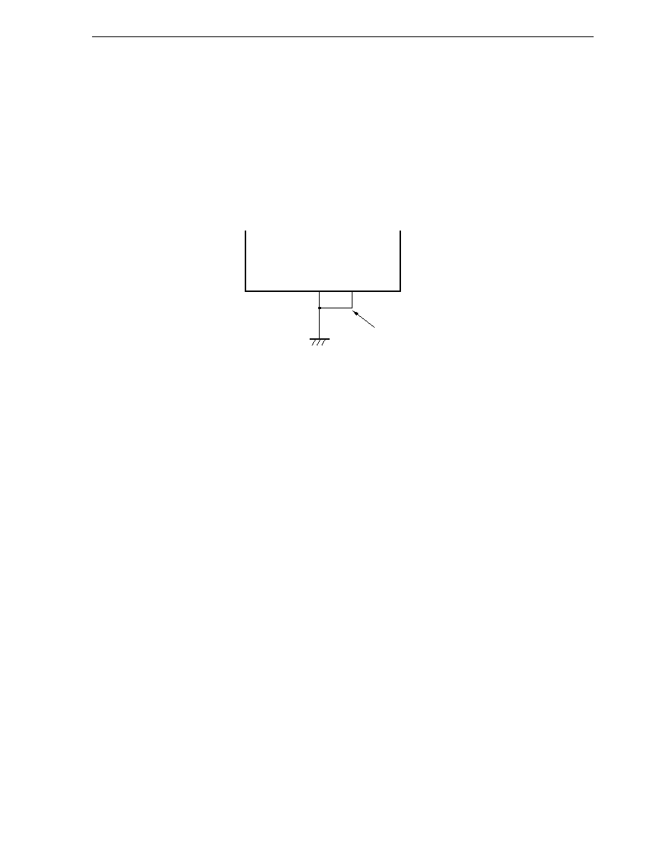
47
CHAPTER 3 PIN FUNCTIONS (
µPD780078 SUBSERIES)
User's Manual U14260EJ3V1UD
As short as possible
IC
V
SS0
or
V
SS1
When there is a potential difference between the V
PP
pin and V
SS0
pin or V
SS1
pin because the wiring between the
two pins is too long or external noise is input to the V
PP
pin, the user program may not operate normally.
3.2.18 IC (mask ROM version only)
The IC (internally connected) pin is provided to set the test mode to check the
µPD780078 Subseries at delivery.
Connect it directly to V
SS0
or
V
SS1
with the shortest possible wiring in the normal operating mode.
When there is a potential difference between the IC pin and V
SS0
pin or V
SS1
pin because the wiring between the
two pins is too long or external noise is input to the IC pin, the user program may not operate normally.
∑ Connect IC pin to V
SS0
or V
SS1
pin directly.

48
CHAPTER 3 PIN FUNCTIONS (
µPD780078 SUBSERIES)
User's Manual U14260EJ3V1UD
3.3 Pin I/O Circuits and Recommended Connection of Unused Pins
Table 3-1 shows the types of pin I/O circuits and the recommended connections of unused pins.
Refer to Figure 3-1 for the configuration of the I/O circuit of each type.
Table 3-1. Pin I/O Circuit Types (1/2)
Pin Name
I/O Circuit Type
I/O
Recommended Connection of Unused Pins
P00/INTP0 to P02/INTP2
8-C
I/O
Input:
Independently connect to V
SS0
or V
SS1
via a resistor.
P03/INTP3/ADTRG
Output: Leave open.
P10/ANI0 to P17/ANI7
25
Input
Connect directly to V
DD0
, V
DD1
, V
SS0
, or V
SS1
.
P20/SI1
8-C
I/O
Input:
Independently connect to V
DD0
, V
DD1
, V
SS0
, or V
SS1
P21/SO1
5-H
via a resistor.
P22/SCK1
8-C
Output: Leave open.
P23/RxD0
P24/TxD0
5-H
P25/ASCK0
8-C
P30, P31
13-Q
Input:
Connect directly to V
SS0
or V
SS1
.
(for mask ROM version)
Output: Leave open at low-level output with the output latch
P30, P31
13-P
of the port set to 0.
(for flash memory version)
P32, P33
13-S
(for mask ROM version)
P32, P33
13-R
(for flash memory version)
P34/SI3/T
X
D2
8-C
Input:
Independently connect to V
DD0
, V
DD1
, V
SS0
, or V
SS1
P35/SO3/R
X
D2
via a resistor.
P36/SCK3/ASCK2
Output: Leave open.
P40/AD0 to P47/AD7
5-H
Input:
Independently connect to V
DD0
or V
DD1
via a resistor.
Output: Leave open.

49
CHAPTER 3 PIN FUNCTIONS (
µPD780078 SUBSERIES)
User's Manual U14260EJ3V1UD
Table 3-1. Pin I/O Circuit Types (2/2)
Pin Name
I/O Circuit Type
I/O
Recommended Connection of Unused Pins
P50/A8 to P57/A15
5-H
I/O
Input:
Independently connect to V
DD0
, V
DD1
, V
SS0
, or
P64/RD
V
SS1
via a resistor.
P65/WR
Output:
Leave open.
P66/WAIT
P67/ASTB
P70/TI000/TO00
8-C
P71/TI010
P72/TI50/TO50
P73/TI51/TO51
P74/TI011/PCL
P75/TI001/TO01/BUZ
P80/SS1
Input:
Connect to V
SS0
or V
SS1
via a resistor.
Output:
Leave open.
RESET
2
Input
--
XT1
16
Connect directly to V
DD0
or V
DD1
.
XT2
--
Leave open.
AV
REF
--
Connect directly to V
SS0
or V
SS1
.
AV
SS
IC (for mask ROM version)
V
PP
Independently connect a 10 k
pull-down resistor or
(for flash memory version)
connect directly to V
SS0
or V
SS1
.
50
CHAPTER 3 PIN FUNCTIONS (
µPD780078 SUBSERIES)
User's Manual U14260EJ3V1UD
Figure 3-1. Pin I/O Circuits (1/2)
Type 2
Schmitt-triggered input with hysteresis characteristics
IN
Type 8-C
Data
Output
disable
P-ch
IN/OUT
V
DD0
N-ch
P-ch
V
DD0
Pull-up
enable
Type 5-H
Data
Output
disable
P-ch
IN/OUT
V
DD0
N-ch
Input
enable
P-ch
V
DD0
Pull-up
enable
Type 13-Q
Data
Output disable
IN/OUT
N-ch
V
DD0
Mask
option
Data
Output disable
IN/OUT
N-ch
Data
Output disable
IN/OUT
N-ch
Type 13-P
Input
enable
V
SS0
Input
enable
V
SS0
Type 13-R
V
SS0
V
SS0
V
SS0
51
CHAPTER 3 PIN FUNCTIONS (
µPD780078 SUBSERIES)
User's Manual U14260EJ3V1UD
Figure 3-1. Pin I/O Circuits (2/2)
P-ch
Feedback
cut-off
XT1
XT2
Type 13-S
Type 16
Data
Output disable
IN/OUT
N-ch
Input
enable
Comparator
+
--
P-ch
N-ch
V
REF
(threshold voltage)
V
SS0
Type 25
V
SS0
IN
V
DD0
Mask
option
52
User's Manual U14260EJ3V1UD
CHAPTER 4 PIN FUNCTIONS (
µPD780078Y SUBSERIES)
4.1 Pin Function List
(1) Port pins (1/2)
Pin Name
I/O
Function
After Reset
Alternate
Function
P00
I/O
Input
INTP0
P01
INTP1
P02
INTP2
P03
INTP3/ADTRG
P10 to P17
Input
Port 1
Input
ANI0 to ANI7
8-bit input-only port.
P20
I/O
Input
SI1
P21
SO1
P22
SCK1
P23
RxD0
P24
TxD0
P25
ASCK0
P30
I/O
Input
--
P31
P32
SDA0
P33
SCL0
P34
SI3/T
X
D2
P35
SO3/R
X
D2
P36
SCK3/ASCK2
P40 to P47
I/O
Port 4
Input
AD0 to AD7
8-bit I/O port
Input/output mode can be specified in 1-bit units.
An on-chip pull-up resistor can be used by setting software.
Interrupt request flag (KRIF) is set to 1 by falling edge
detection.
P50 to P57
I/O
Port 5
Input
A8 to A15
8-bit I/O port
LEDs can be driven directly.
Input/output mode can be specified in 1-bit units.
An on-chip pull-up resistor can be used by setting software.
P64
I/O
Input
RD
P65
WR
P66
WAIT
P67
ASTB
Port 0
4-bit I/O port
Input/output mode can be specified in 1-bit units.
An on-chip pull-up resistor can be used by setting software.
Port 2
6-bit I/O port
Input/output mode can be specified in 1-bit units.
An on-chip pull-up resistor can be used by setting software.
Port 3
7-bit I/O port
Input/output
mode can be
specified in 1-bit
units.
N-ch open-drain I/O port
On-chip pull-up resistor can be
specified by mask option (P30 and
P31 are mask ROM version only).
LEDs can be driven directly.
An on-chip pull-up resistor can be
used by setting software.
Port 6
4-bit I/O port
Input/output mode can be specified in 1-bit units.
An on-chip pull-up resistor can be used by setting software.

53
CHAPTER 4 PIN FUNCTIONS (
µPD780078Y SUBSERIES)
User's Manual U14260EJ3V1UD
(1) Port pins (2/2)
Pin Name
I/O
Function
After Reset
Alternate
Function
P70
I/O
Input
TI000/TO00
P71
TI010
P72
TI50/TO50
P73
TI51/TO51
P74
TI011/PCL
P75
TI001/TO01/BUZ
P80
I/O
Input
SS1
(2) Non-port pins (1/2)
Pin Name
I/O
Function
After Reset
Alternate
Function
INTP0
Input
Input
P00
INTP1
P01
INTP2
P02
INTP3
P03/ADTRG
SI1
Input
Serial interface serial data input
Input
P20
SO1
Output
Serial interface serial data output
Input
P21
SDA0
I/O
Serial interface serial data input/output
Input
P32
SCK1
I/O
Serial interface serial clock input/output
Input
P22
SCK3
P30/ASCK2
SCL0
P33
SS1
Input
Serial interface chip select input
Input
P80
R
X
D0
Input
Asynchronous serial interface serial data input
Input
P23
R
X
D2
P35/SO3
T
X
D0
Output
Asynchronous serial interface serial data output
Input
P24
T
X
D2
P34/SI3
ASCK0
Input
Asynchronous serial interface serial clock input
Input
P25
ASCK2
P36/SCK3
TI000
Input
External count clock input to 16-bit timer/event counter 00.
Input
P70/TO00
Capture trigger input to capture registers (CR000, CR010) of
16-bit timer/event counter 00
TI010
Capture trigger input to capture register (CR000) of 16-bit
P71
timer/event counter 00
TI001
External count clock input to 16-bit timer/event counter 01.
P75/TO01/BUZ
Capture trigger input to capture registers (CR001, CR011)
of 16-bit timer/event counter 01
Port 7
6-bit I/O port
Input/output mode can be specified in 1-bit units.
An on-chip pull-up resistor can be used by setting software.
External interrupt request input with specifiable valid edges
(rising edge, falling edge, both rising and falling edges)
Port 8
1-bit I/O port
Input/output mode can be specified in 1-bit units.
An on-chip pull-up resistor can be used by setting software.

54
CHAPTER 4 PIN FUNCTIONS (
µPD780078Y SUBSERIES)
User's Manual U14260EJ3V1UD
(2) Non-port pins (2/2)
Pin Name
I/O
Function
After Reset
Alternate
Function
TI011
Input
Capture trigger input to capture register (CR001) of 16-bit
Input
P74/PCL
timer/event counter 01
TI50
External count clock input to 8-bit timer/event counter 50
P72/TO50
TI51
External count clock input to 8-bit timer/event counter 51
P73/TO51
TO00
Output
16-bit timer/event counter 00 output
Input
P70/TI000
TO01
16-bit timer/event counter 01 output
P75/TI001/BUZ
TO50
8-bit timer/event counter 50 output
P72/TI50
TO51
8-bit timer/event counter 51 output
P73/TI51
PCL
Output
Clock output (for main system clock and subsystem clock
Input
P74/TI011
trimming)
BUZ
Output
Buzzer output
Input
P75/TI001/TO01
AD0 to AD7
I/O
Lower address/data bus when expanding external memory
Input
P40 to P47
A8 to A15
Output
Higher address bus when expanding external memory
Input
P50 to P57
RD
Output
Strobe signal output for read operation from external memory
Input
P64
WR
Strobe signal output for write operation from external memory
P65
WAIT
Input
Wait insertion when accessing external memory
Input
P66
ASTB
Output
Strobe output externally latching address information
Input
P67
output to ports 4 and 5 to access external memory
ANI0 to ANI7
Input
A/D converter analog input
Input
P10 to P17
ADTRG
Input
A/D converter trigger signal input
Input
P03/INTP3
AV
REF
Input
A/D converter reference voltage input and analog power supply
--
--
AV
SS
--
A/D converter ground potential. Connect to V
SS0
or V
SS1
.
--
--
RESET
Input
System reset input
Input
--
X1
Input
Resonator connection for main system clock
--
--
X2
--
--
--
XT1
Input
Resonator connection for subsystem clock
--
--
XT2
--
--
--
V
DD0
--
Positive power supply for ports
--
--
V
DD1
--
Positive power supply (other than ports)
--
--
V
SS0
--
Ground potential for ports
--
--
V
SS1
--
Ground potential (other than ports)
--
--
IC
--
Internally connected. Connect directly to V
SS0
or V
SS1
.
--
--
V
PP
--
Flash memory programming mode setting.
--
--
High-voltage application for program write/verify

55
CHAPTER 4 PIN FUNCTIONS (
µPD780078Y SUBSERIES)
User's Manual U14260EJ3V1UD
4.2 Description of Pin Functions
4.2.1 P00 to P03 (Port 0)
P00 to P03 function as a 4-bit I/O port. Besides serving as an I/O port, they also function as external interrupt
inputs and an A/D converter external trigger input.
The following operating modes can be specified in 1-bit units.
(1) Port mode
These pins function as a 4-bit I/O port.
P00 to P03 can be specified as input or output in 1-bit units using port mode register 0 (PM0). On-chip pull-up
resistors can be connected by setting pull-up resistor option register 0 (PU0).
(2) Control mode
In this mode, these pins function as external interrupt request inputs and an A/D converter external trigger input.
(a) INTP0 to INTP3
INTP0 to INTP3 are external interrupt request input pins for which the valid edge can be specified (rising
edge, falling edge, or both rising and falling edges).
(b) ADTRG
A/D converter external trigger input pin.
Caution
When P03 is used as an A/D converter external trigger input, specify the valid edge by
using bits 1 and 2 (EGA00, EGA01) of the A/D converter mode register (ADM0) and set the
interrupt mask flag (PMK3) to 1.
4.2.2 P10 to P17 (Port 1)
P10 to P17 function as an 8-bit input-only port. Besides serving as an input port, they also function as A/D converter
analog inputs.
The following operating modes can be specified in 1-bit units.
(1) Port mode
These pins function as an 8-bit input-only port.
(2) Control mode
These pins function as A/D converter analog input pins (ANI0 to ANI7). When using these pins as analog input
pins, see (4) ANI0/P10 to ANI7/P17 in 13.6 Cautions for A/D Converter.
4.2.3 P20 to P25 (Port 2)
P20 to P25 function as a 6-bit I/O port. Besides serving as an I/O port, they function as data I/O and clock I/O for
serial interfaces CSI1 and UART0.
The following operating modes can be specified in 1-bit units.
(1) Port mode
These pins function as a 6-bit I/O port. They can be specified as input or output in 1-bit units using port mode
register 2 (PM2). On-chip pull-up resistors can be connected by setting pull-up resistor option register 2 (PU2).

56
CHAPTER 4 PIN FUNCTIONS (
µPD780078Y SUBSERIES)
User's Manual U14260EJ3V1UD
(2) Control mode
These pins function as data I/O and clock I/O for serial interfaces CSI1 and UART0.
(a) SI1
Serial data input pin for serial interface CSI1.
(b) SO1
Serial data output pin for serial interface CSI1.
(c) SCK1
Serial clock I/O pin for serial interface CSI1.
(d) R
X
D0
Serial data input pin for serial interface UART0.
(e) T
X
D0
Serial data output pin for serial interface UART0.
(f)
ASCK0
Serial clock input pin for serial interface UART0.
4.2.4 P30 to P36 (Port 3)
P30 to P36 function as a 7-bit I/O port. Besides serving as an I/O port, they also function as data I/O and clock
I/O for serial interfaces SIO3 and UART2.
P30 to P33 can drive LEDs directly.
The following operating modes can be specified in 1-bit units.
(1) Port mode
These pins function as a 7-bit I/O port. They can be specified as input or output in 1-bit units using port mode
register 3 (PM3). P30 to P33 are N-ch open drain I/O pins. Mask ROM version can contain pull-up resistors
in P30 and P31 with the mask option. On-chip pull-up resistors can be connected to P34 to P36 by setting pull-
up resistor option register 3 (PU3).
(2) Control mode
These pins function as data I/O and clock I/O for serial interfaces SIO3 and UART2.
(a) SI3
Serial data input pin for serial interface SIO3.
(b) SO3
Serial data output pin for serial interface SIO3.
(c) SCK3
Serial clock I/O pin for serial interface SIO3.
(d) R
X
D2
Serial data input pin for serial interface UART2.

57
CHAPTER 4 PIN FUNCTIONS (
µPD780078Y SUBSERIES)
User's Manual U14260EJ3V1UD
(e) T
X
D2
Serial data output pin for serial interface UART2.
(f)
ASCK2
Serial clock input pin for serial interface UART2.
4.2.5 P40 to P47 (Port 4)
P40 to P47 function as an 8-bit I/O port. Besides serving as an I/O port, they also function as an address/data
bus.
The interrupt request flag (KRIF) can be set to 1 by detecting a falling edge.
The following operating modes can be specified.
Caution
When using the falling edge detection interrupt (INTKR), be sure to set the memory expansion
mode register (MEM) to 01H.
(1) Port mode
These pins function as an 8-bit I/O port. They can be specified as input or output in 1-bit units using port mode
register 4 (PM4). On-chip pull-up resistors can be connected by setting pull-up resistor option register 4 (PU4).
(2) Control mode
These ports function as the lower address/data bus pins (AD0 to AD7) in external memory expansion mode.
4.2.6 P50 to P57 (Port 5)
P50 to P57 function as an 8-bit I/O port. Besides serving as an I/O port, they also function as an address bus.
Port 5 can drive LEDs directly.
The following operating modes can be specified.
(1) Port mode
These pins function as an 8-bit I/O port. They can be specified as input or output in 1-bit units using port mode
register 5 (PM5). On-chip pull-up resistors can be connected by setting pull-up resistor option register 5 (PU5).
(2) Control mode
These ports function as the higher address bus pins (A8 to A15) in external memory expansion mode.
4.2.7 P64 to P67 (Port 6)
P64 to P67 function as a 4-bit I/O port. Besides serving as an I/O port, they are also used for control in external
memory expansion mode.
The following operating modes can be specified.
(1) Port mode
These pins function as a 4-bit I/O port. They can be specified as input or output in 1-bit units using port mode
register 6 (PM6).
On-chip pull-up resistors can be connected by setting pull-up resistor option register 6 (PU6).
(2) Control mode
These pins function as control signal output pins (RD, WR, WAIT, ASTB) in external memory expansion mode.
Caution
When external wait is not used in external memory expansion mode, P66 can be used as an
I/O port.

58
CHAPTER 4 PIN FUNCTIONS (
µPD780078Y SUBSERIES)
User's Manual U14260EJ3V1UD
4.2.8 P70 to P75 (Port 7)
P70 to P75 function as a 6-bit I/O port. Besides serving as an I/O port, they also function as timer I/O, clock output,
and buzzer output.
The following operating modes can be specified in 1-bit units.
(1) Port mode
These pins function as a 6-bit I/O port. They can be specified as input or output in 1-bit units using port mode
register 7 (PM7). On-chip pull-up resistors can be connected by setting pull-up resistor option register 7 (PU7).
P70 and P71 are also capture trigger signal input pins of 16-bit timer/event counters 00 and 01 with a valid edge
input.
(2) Control mode
These pins function as timer I/O, clock output, and buzzer output.
(a) TI000
External count clock input pin to 16-bit timer/event counter 00 and capture trigger signal input pin to the 16-
bit timer/event counter 00 capture registers (CR000, CR010).
(b) TI001
External count clock input pin to 16-bit timer/event counter 01 and capture trigger signal input pin to the 16-
bit timer/event counter 01 capture registers (CR001, CR011).
(c) TI010
Capture trigger signal input pin to the 16-bit timer/event counter 00 capture register (CR000).
(d) TI011
Capture trigger signal input pin to the 16-bit timer/event counter 01 capture register (CR001).
(e) TI50 and TI51
External count clock input pins to 8-bit timer/event counters 50 and 51.
(f)
TO00, TO01, TO50, and TO51
Timer output pins.
(g) PCL
Clock output pin.
(h) BUZ
Buzzer output pin.

59
CHAPTER 4 PIN FUNCTIONS (
µPD780078Y SUBSERIES)
User's Manual U14260EJ3V1UD
4.2.9 P80 (Port 8)
P80 is a 1-bit I/O port. Besides serving as an I/O port, it also functions as the chip select input of serial interface
CSI1. The following operating modes can be specified in 1-bit units.
(1) Port mode
This pin functions as a 1-bit I/O port. It can be specified as input or output in 1-bit units using port mode register
8 (PM8).
An on-chip pull-up resistor can be connected by setting pull-up resistor option register 8 (PU8).
(2) Control mode
This pin functions as the chip select input pin (SS1) of serial interface CSI1.
4.2.10 AV
REF
This is the A/D converter reference voltage input pin. This pin is also used for the analog power supply. When
using the A/D converter, supply power to this pin.
When the A/D converter is not used, connect this pin directly to V
SS0
or V
SS1
.
4.2.11 AV
SS
This is the ground potential pin of the A/D converter. Use the same potential as that of the V
SS0
pin or V
SS1
pin
even when not using the A/D converter.
4.2.12 RESET
This is an active-low system reset input pin.
4.2.13 X1 and X2
Resonator connection pins for main system clock.
For an external clock supply, input the clock signal to X1 and its inverted signal to X2.
4.2.14 XT1 and XT2
Resonator connection pins for subsystem clock.
For an external clock supply, input the clock signal to XT1 and its inverted signal to XT2.
4.2.15 V
DD0
and V
DD1
V
DD0
is the positive power supply pin for the ports.
V
DD1
is the positive power supply pin for other than the ports.
4.2.16 V
SS0
and V
SS1
V
SS0
is the ground potential pin for the ports.
V
SS1
is the ground potential pin for other than the ports.
4.2.17 V
PP
(flash memory versions only)
High-voltage application pin for flash memory programming mode setting and program write/verify.
Handle in either of the following ways.
∑ Independently connect a 10 k
pull-down resistor.
∑ Set the jumper on the board so that this pin is connected directly to the dedicated flash programmer in
programming mode and directly to V
SS0
or V
SS1
in normal operation mode.
60
CHAPTER 4 PIN FUNCTIONS (
µPD780078Y SUBSERIES)
User's Manual U14260EJ3V1UD
As short as possible
IC
V
SS0
or
V
SS1
When there is a potential difference between the V
PP
pin and V
SS0
pin or V
SS1
pin because the wiring between the
two pins is too long or external noise is input to the V
PP
pin, the user program may not operate normally.
4.2.18 IC (mask ROM version only)
The IC (internally connected) pin is provided to set the test mode to check the
µPD780078Y Subseries at delivery.
Connect it directly to V
SS0
or
V
SS1
with the shortest possible wiring in the normal operating mode.
When there is a potential difference between the IC pin and V
SS0
pin or V
SS1
pin because the wiring between the
two pins is too long or external noise is input to the IC pin, the user program may not operate normally.
∑ Connect IC pin to V
SS0
or V
SS1
pin directly.
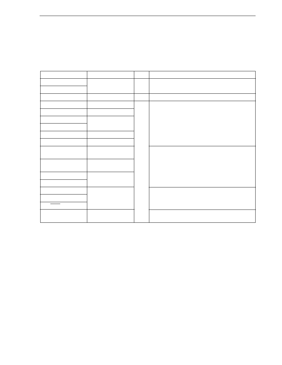
61
CHAPTER 4 PIN FUNCTIONS (
µPD780078Y SUBSERIES)
User's Manual U14260EJ3V1UD
4.3 Pin I/O Circuits and Recommended Connection of Unused Pins
Table 4-1 shows the types of pin I/O circuits and the recommended connections of unused pins.
Refer to Figure 4-1 for the configuration of the I/O circuit of each type.
Table 4-1. Pin I/O Circuit Types (1/2)
Pin Name
I/O Circuit Type
I/O
Recommended Connection of Unused Pins
P00/INTP0 to P02/INTP2
8-C
I/O
Input:
Independently connect to V
SS0
or V
SS1
via a resistor.
P03/INTP3/ADTRG
Output: Leave open.
P10/ANI0 to P17/ANI7
25
Input
Connect directly to V
DD0
, V
DD1
, V
SS0
, or V
SS1
.
P20/SI1
8-C
I/O
Input:
Independently connect to V
DD0
, V
DD1
, V
SS0
, or V
SS1
P21/SO1
5-H
via a resistor.
P22/SCK1
8-C
Output: Leave open.
P23/RxD0
P24/TxD0
5-H
P25/ASCK0
8-C
P30, P31
13-Q
Input:
Connect directly to V
SS0
or V
SS1
.
(for mask ROM version)
Output: Leave open at low-level output with the output
P30, P31
13-P
latch of the port set to 0.
(for flash memory version)
P32/SDA0
13-R
P33/SCL0
P34/SI3/T
X
D2
8-C
Input:
Independently connect to V
DD0
, V
DD1
, V
SS0
, or V
SS1
P35/SO3/R
X
D2
via a resistor.
P36/SCK3/ASCK2
Output: Leave open.
P40/AD0 to P47/AD7
5-H
Input:
Independently connect to V
DD0
or V
DD1
via a resistor.
Output: Leave open.
62
CHAPTER 4 PIN FUNCTIONS (
µPD780078Y SUBSERIES)
User's Manual U14260EJ3V1UD
Table 4-1. Pin I/O Circuit Types (2/2)
Pin Name
I/O Circuit Type
I/O
Recommended Connection of Unused Pins
P50/A8 to P57/A15
5-H
I/O
Input:
Independently connect to V
DD0
, V
DD1
, V
SS0
, or V
SS1
P64/RD
via a resistor.
P65/WR
Output:
Leave open.
P66/WAIT
P67/ASTB
P70/TI000/TO00
8-C
P71/TI010
P72/TI50/TO50
P73/TI51/TO51
P74/TI011/PCL
P75/TI001/TO01/BUZ
P80/SS1
Input:
Connect to V
SS0
or V
SS1
via a resistor.
Output:
Leave open.
RESET
2
Input
--
XT1
16
Connect directly to V
DD0
or V
DD1
.
XT2
--
Leave open.
AV
REF
--
Connect directly to V
SS0
or V
SS1
.
AV
SS
IC (for mask ROM version)
V
PP
Independently connect a 10 k
pull-down resistor or
(for flash memory version)
connect directly to V
SS0
or V
SS1
.

63
CHAPTER 4 PIN FUNCTIONS (
µPD780078Y SUBSERIES)
User's Manual U14260EJ3V1UD
Figure 4-1. Pin I/O Circuits
Type 2
Schmitt-triggered input with hysteresis characteristics
IN
Type 8-C
Data
Output
disable
P-ch
IN/OUT
V
DD0
N-ch
P-ch
V
DD0
Pull-up
enable
Type 5-H
Data
Output
disable
P-ch
IN/OUT
V
DD0
N-ch
Input
enable
P-ch
V
DD0
Pull-up
enable
Type 13-Q
Data
Output disable
IN/OUT
N-ch
V
DD0
Mask
option
Data
Output disable
IN/OUT
N-ch
Data
Output disable
IN/OUT
N-ch
Type 13-P
Input
enable
V
SS0
Input
enable
V
SS0
Type 13-R
V
SS0
V
SS0
V
SS0
P-ch
Feedback
cut-off
XT1
XT2
Type 16
Input
enable
Comparator
+
--
P-ch
N-ch
V
REF
(threshold voltage)
Type 25
V
SS0
IN
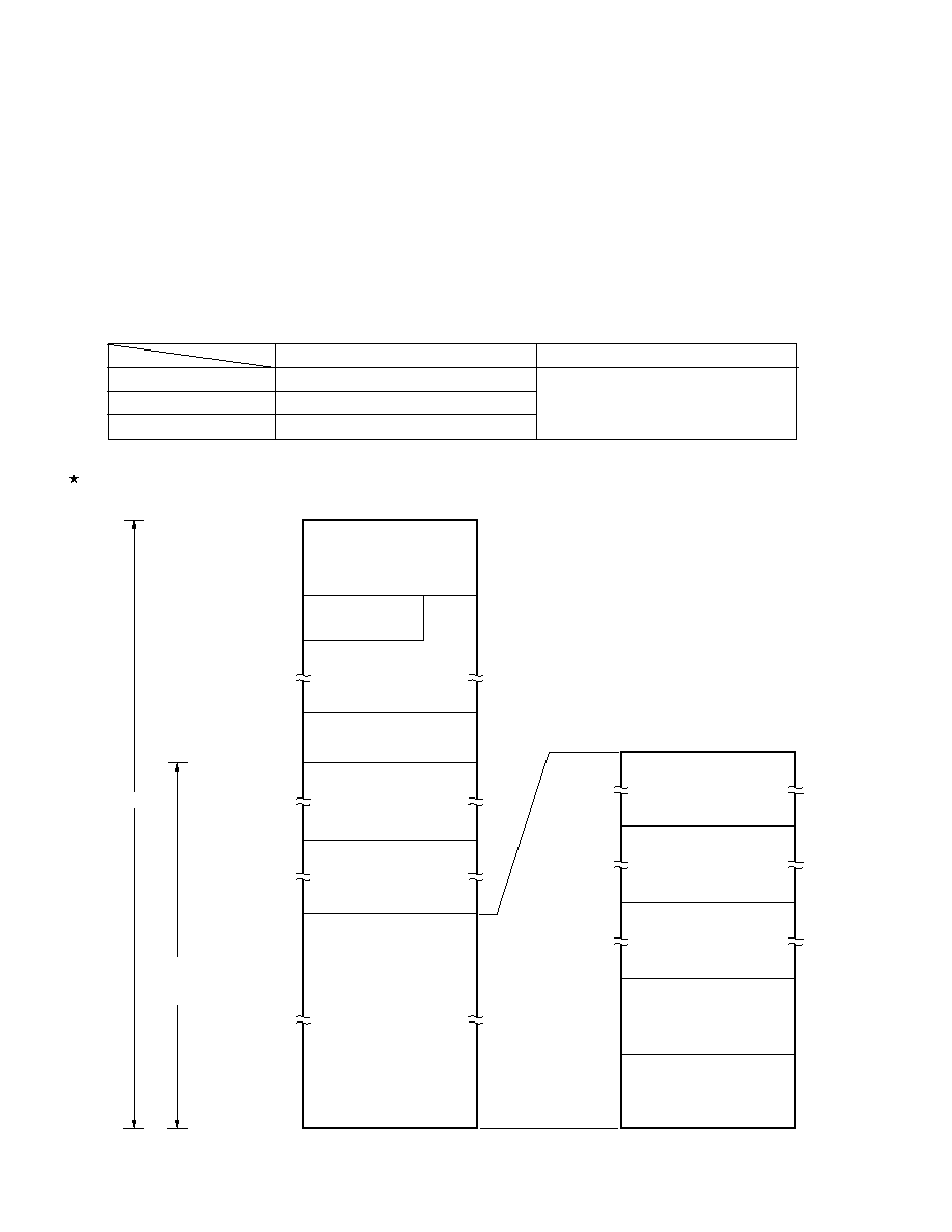
64
User's Manual U14260EJ3V1UD
CHAPTER 5 CPU ARCHITECTURE
5.1 Memory Spaces
Products in the
µPD780078, 780078Y Subseries can each access a 64 KB memory space.
Figures 5-1 to 5-3 show the memory maps.
Caution
The initial value of the memory size switching register (IMS) and internal expansion RAM size
switching register (IXS) of all products (
µPD780078, 780078Y Subseries) is fixed (IMS = CFH,
IXS = 0CH). Therefore, set the value corresponding to each product as indicated below.
Value of IMS
Value of IXS
µPD780076, 780076Y
CCH
0AH
µPD780078, 780078Y
CFH
µPD78F0078, 78F0078Y
Value corresponding to mask ROM version
Figure 5-1. Memory Map (
µPD780076, 780076Y)
Special function
registers (SFRs)
256
◊ 8 bits
Internal high-speed RAM
1024
◊ 8 bits
Reserved
General-purpose
registers
32
◊ 8 bits
Internal expansion RAM
1024
◊ 8 bits
External memory
13312
◊ 8 bits
Internal ROM
49152
◊ 8 bits
ROM/RAM space
in which instructions
can be fetched
Data memory
space
Vector table area
CALLT table area
Program area
CALLF entry area
Program area
FFFFH
F F 0 0 H
FEFFH
F 8 0 0 H
F7FFH
1000H
0FFFH
0800H
07FFH
0040H
003FH
0080H
007FH
0000H
BFFFH
C000H
BFFFH
F 4 0 0 H
F3FFH
0 0 0 0 H
FEE0H
FEDFH
FB00H
FAFFH

65
CHAPTER 5 CPU ARCHITECTURE
User's Manual U14260EJ3V1UD
Figure 5-2. Memory Map (
µPD780078, 780078Y)
Special function
registers (SFRs)
256
◊ 8 bits
Internal high-speed RAM
1024
◊ 8 bits
Reserved
General-purpose
registers
32
◊ 8 bits
Internal expansion RAM
1024
◊ 8 bits
External memory
1024
◊ 8 bits
Internal ROM
61440
◊ 8 bits
Data memory
space
Vector table area
CALLT table area
Program area
CALLF entry area
Program area
FFFFH
F F 0 0 H
FEFFH
F 8 0 0 H
F7FFH
1000H
0FFFH
0800H
07FFH
0040H
003FH
0080H
007FH
0000H
EFFFH
F000H
EFFFH
F 4 0 0 H
F3FFH
0 0 0 0 H
FEE0H
FEDFH
FB00H
FAFFH
ROM/RAM space
in which instructions
can be fetched
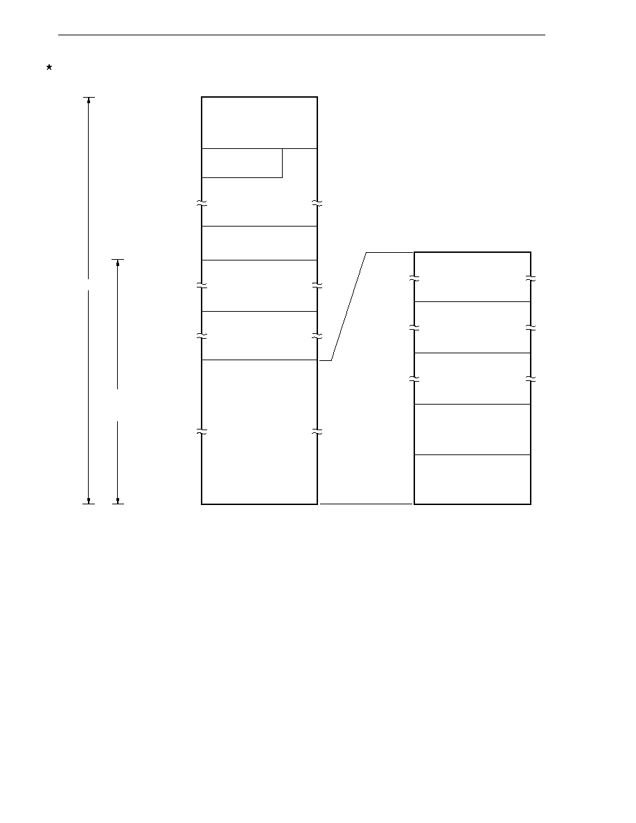
66
CHAPTER 5 CPU ARCHITECTURE
User's Manual U14260EJ3V1UD
Figure 5-3. Memory Map (
µPD78F0078, 78F0078Y)
Special function
registers (SFRs)
256
◊ 8 bits
Internal high-speed RAM
1024
◊ 8 bits
Reserved
General-purpose
registers
32
◊ 8 bits
Internal expansion RAM
1024
◊ 8 bits
External memory
1024
◊ 8 bits
Flash memory
61440
◊ 8 bits
Data memory
space
Vector table area
CALLT table area
Program area
CALLF entry area
Program area
FFFFH
F F 0 0 H
FEFFH
F 8 0 0 H
F7FFH
1000H
0FFFH
0800H
07FFH
0040H
003FH
0080H
007FH
0000H
EFFFH
F000H
EFFFH
F 4 0 0 H
F3FFH
0 0 0 0 H
FEE0H
FEDFH
FB00H
FAFFH
ROM/RAM space
in which instructions
can be fetched
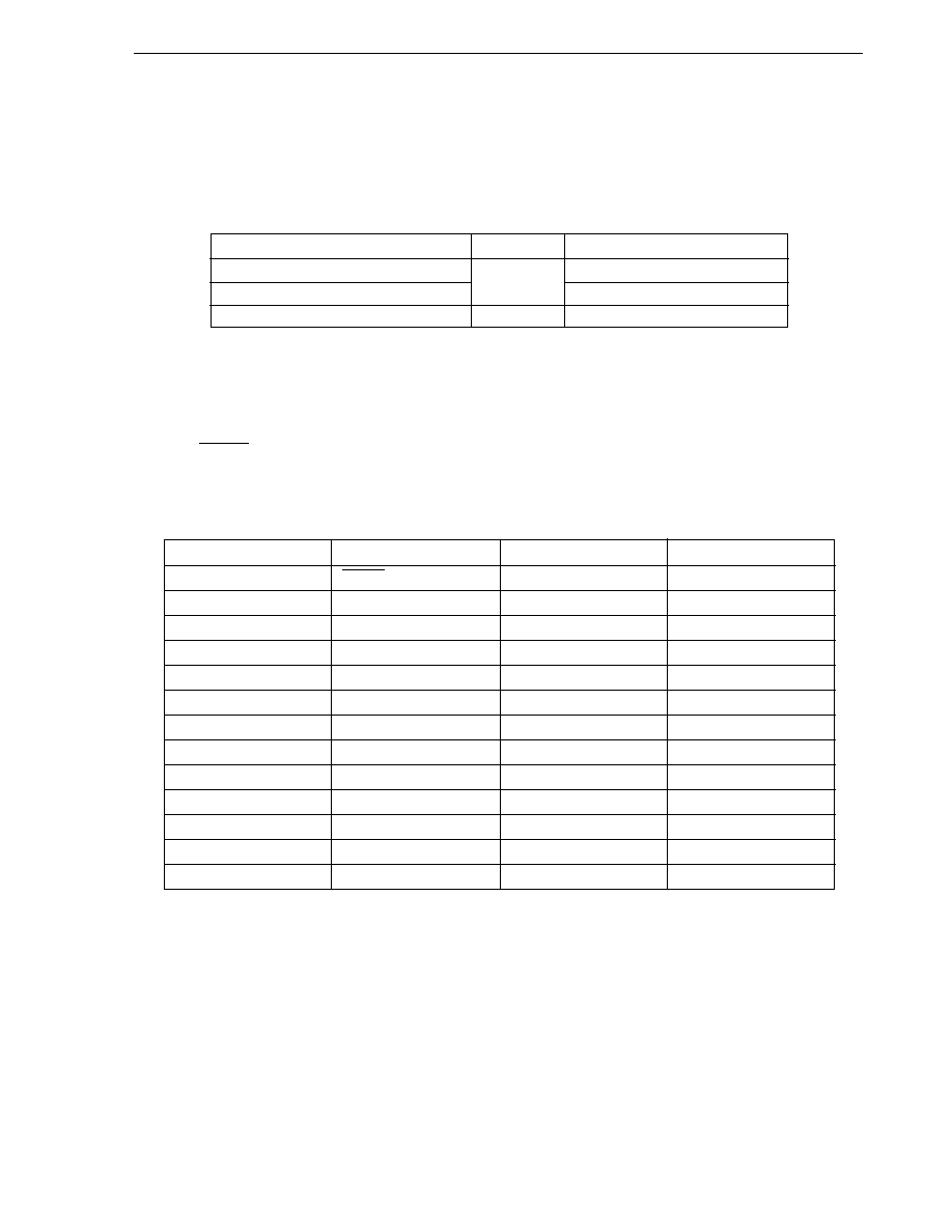
67
CHAPTER 5 CPU ARCHITECTURE
User's Manual U14260EJ3V1UD
5.1.1 Internal program memory space
The internal program memory space contains the program and table data. Normally, it is addressed with the
program counter (PC).
The
µPD780078, 780078Y Subseries incorporate internal ROM (mask ROM or flash memory), as listed below.
Table 5-1. Internal Memory Capacity
Part Number
Type
Capacity
µPD780076, 780076Y
Mask ROM
49152
◊ 8 bits (0000H to BFFFH)
µPD780078, 780078Y
61440
◊ 8 bits (0000H to EFFFH)
µPD78F0078, 78F0078Y
Flash memory
61440
◊ 8 bits (0000H to EFFFH)
The internal program memory space is divided into the following three areas.
(1) Vector table area
The 64-byte area 0000H to 003FH is reserved as a vector table area. The program start addresses for branch
upon RESET input or interrupt request generation are stored in the vector table area. Of the 16-bit address, the
lower 8 bits are stored at even addresses and the higher 8 bits are stored at odd addresses.
Table 5-2. Vector Table
Vector Table Address
Interrupt Source
0000H
RESET input
0004H
INTWDT
0006H
INTP0
0008H
INTP1
000AH
INTP2
000CH
INTP3
000EH
INTSER0
0010H
INTSR0
0012H
INTST0
0014H
INTCSI1
0016H
INTCSI3
0018H
INTIIC0
Note
001AH
INTWTI
Vector Table Address
Interrupt Source
001CH
INTTM000
001EH
INTTM010
0020H
INTTM50
0022H
INTTM51
0024H
INTAD0
0026H
INTWT
0028H
INTKR
002AH
INTSER2
002CH
INTSR2
002EH
INTST2
0030H
INTTM001
0032H
INTTM011
003EH
BRK
Note
µPD780078Y Subseries only
(2) CALLT instruction table area
The 64-byte area 0040H to 007FH can store the subroutine entry address of a 1-byte call instruction (CALLT).
(3) CALLF instruction entry area
The area 0800H to 0FFFH can perform a direct subroutine call with a 2-byte call instruction (CALLF).

68
CHAPTER 5 CPU ARCHITECTURE
User's Manual U14260EJ3V1UD
5.1.2 Internal data memory space
The
µPD780078, 780078Y Subseries incorporate the following on-chip high-speed RAMs.
(1) Internal high-speed RAM
The 1024-byte area FB00H to FEFFH is allocated to the internal high-speed RAM. The 32-byte area FEE0H to
FEFFH is allocated to four general-purpose register banks composed of eight 8-bit registers.
This area cannot be used as a program area in which instructions are written for execution.
The internal high-speed RAM can also be used as a stack memory.
(2) Internal expansion RAM
The 1024-byte area F400H to F7FFH is allocated to the internal expansion RAM.
Like the internal high-speed RAM, the internal expansion RAM can be used as a normal data area, but it can
also be used as a program area in which instructions are written for execution.
The internal expansion RAM cannot be used as a stack memory.
5.1.3 Special function register (SFR) area
On-chip peripheral hardware special function registers (SFR) are allocated in the area FF00H to FFFFH (refer to
5.2.3 Special function registers (SFR) and Table 5-3 Special Function Register List).
Caution Do not access addresses where an SFR is not assigned.
5.1.4 External memory space
The external memory space is accessible using the memory expansion mode register (MEM). External memory
space can store program, table data, etc., and allocate peripheral devices.
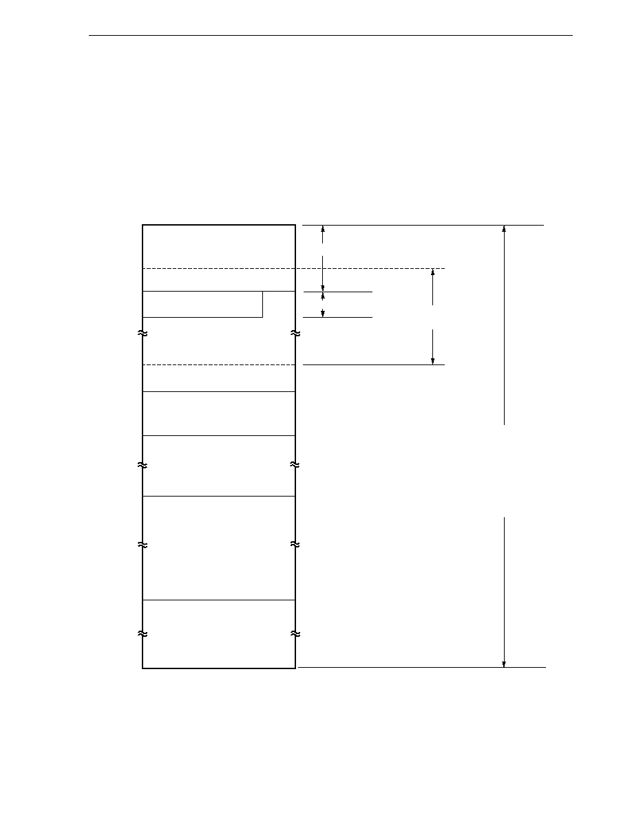
69
CHAPTER 5 CPU ARCHITECTURE
User's Manual U14260EJ3V1UD
5.1.5 Data memory addressing
Addressing refers to the method of specifying the address of the instruction to be executed next or the address
of the register or memory relevant to the execution of instructions.
Several addressing modes are provided for addressing the memory relevant to the execution of instructions for
the
µPD780078, 780078Y Subseries, based on operability and other considerations. For areas containing data
memory in particular, special addressing methods designed for the functions of special function registers (SFR) and
general-purpose registers are available for use. Figures 5-4 to 5-6 show the correspondence between data memory
and addressing. For details of each addressing mode, see 5.4 Operand Address Addressing.
Figure 5-4. Correspondence Between Data Memory and Addressing (
µPD780076, 780076Y)
0000H
General-purpose registers
32
◊ 8 bits
Internal ROM
49152
◊ 8 bits
External memory
13312
◊ 8 bits
C000H
BFFFH
F400H
F3FFH
FEE0H
FEDFH
FF00H
FEFFH
FFFFH
Internal high-speed RAM
1024
◊ 8 bits
Reserved
FB00H
FAFFH
FF20H
FF1FH
FE20H
FE1FH
Special function
registers (SFRs)
256
◊ 8 bits
SFR addressing
Register addressing
Short direct
addressing
Direct addressing
Register indirect
addressing
Based addressing
Based indexed
addressing
F800H
F7FFH
Internal expansion RAM
1024
◊ 8 bits

70
CHAPTER 5 CPU ARCHITECTURE
User's Manual U14260EJ3V1UD
Figure 5-5. Correspondence Between Data Memory and Addressing (
µPD780078, 780078Y)
0000H
General-purpose registers
32
◊ 8 bits
Internal ROM
61440
◊ 8 bits
External memory
1024
◊ 8 bits
F000H
EFFFH
F400H
F3FFH
FEE0H
FEDFH
FF00H
FEFFH
FFFFH
Internal high-speed RAM
1024
◊ 8 bits
Reserved
FB00H
FAFFH
FF20H
FF1FH
FE20H
FE1FH
Special function
registers (SFRs)
256
◊ 8 bits
SFR addressing
Register addressing
Short direct
addressing
Direct addressing
Register indirect
addressing
Based addressing
Based indexed
addressing
F800H
F7FFH
Internal expansion RAM
1024
◊ 8 bits

71
CHAPTER 5 CPU ARCHITECTURE
User's Manual U14260EJ3V1UD
Figure 5-6. Correspondence Between Data Memory and Addressing (
µPD78F0078, 78F0078Y)
0000H
General-purpose registers
32
◊ 8 bits
Flash memory
61440
◊ 8 bits
External memory
1024
◊ 8 bits
F000H
EFFFH
F400H
F3FFH
FEE0H
FEDFH
FF00H
FEFFH
FFFFH
Internal high-speed RAM
1024
◊ 8 bits
Reserved
FB00H
FAFFH
FF20H
FF1FH
FE20H
FE1FH
Special function
registers (SFRs)
256
◊ 8 bits
SFR addressing
Register addressing
Short direct
addressing
Direct addressing
Register indirect
addressing
Based addressing
Based indexed
addressing
F800H
F7FFH
Internal expansion RAM
1024
◊ 8 bits

72
CHAPTER 5 CPU ARCHITECTURE
User's Manual U14260EJ3V1UD
5.2 Processor Registers
The
µPD780078, 780078Y Subseries incorporate the following processor registers.
5.2.1 Control registers
The control registers control the program sequence, statuses and stack memory. The control registers consist
of a program counter (PC), a program status word (PSW) and a stack pointer (SP).
(1) Program counter (PC)
The program counter is a 16-bit register which holds the address information of the next program to be executed.
In normal operation, the PC is automatically incremented according to the number of bytes of the instruction to
be fetched. When a branch instruction is executed, immediate data and register contents are set.
RESET input sets the reset vector table values at addresses 0000H and 0001H to the program counter.
Figure 5-7. Program Counter Format
15
0
PC PC15 PC14 PC13 PC12 PC11 PC10 PC9 PC8 PC7 PC6 PC5 PC4 PC3 PC2 PC1 PC0
(2) Program status word (PSW)
The program status word is an 8-bit register consisting of various flags to be set/reset by instruction execution.
Program status word contents are automatically stacked upon interrupt request generation or PUSH PSW instruction
execution and are automatically reset upon execution of the RETB, RETI and POP PSW instructions.
RESET input sets the PSW to 02H.
Figure 5-8. Program Status Word Format
7
0
PSW
IE
Z
RBS1
AC
RBS0
0
ISP
CY

73
CHAPTER 5 CPU ARCHITECTURE
User's Manual U14260EJ3V1UD
(a) Interrupt enable flag (IE)
This flag controls the interrupt request acknowledgment operations of the CPU.
When IE is 0 the interrupt disabled (DI) state is set, and only non-maskable interrupt requests become
acknowledgeable. Other interrupt requests are all disabled.
When IE is 1 the interrupt enabled (EI) state is set and interrupt request acknowledgment enable is controlled
by the in-service priority flag (ISP), the interrupt mask flag corresponding to each interrupt source and the
priority specification flag.
IE is reset (0) upon DI instruction execution or interrupt acknowledgment and is set (1) upon EI instruction
execution.
(b) Zero flag (Z)
When the operation result is zero, this flag is set (1). It is reset (0) in all other cases.
(c) Register bank select flags (RBS0 and RBS1)
These are 2-bit flags used to select one of the four register banks.
The 2-bit information which indicates the register bank selected by SEL RBn instruction execution is stored
in these flags.
(d) Auxiliary carry flag (AC)
If the operation result has a carry from bit 3 or a borrow at bit 3, this flag is set (1). It is reset (0) in all other
cases.
(e) In-service priority flag (ISP)
This flag manages the priority of acknowledgeable maskable vectored interrupts. When this flag is 0, low-
level vectored interrupt requests specified by the priority specification flag register (PR0L, PR0H, PR1L)
(refer to 19.3 (3) Priority specification flag registers (PR0L, PR0H, PR1L)) are disabled for acknowledgment.
Actual interrupt request acknowledgment is controlled by the interrupt enable flag (IE).
(f)
Carry flag (CY)
This flag stores an overflow or underflow upon add/subtract instruction execution. It stores the shift-out value
upon rotate instruction execution and functions as a bit accumulator during bit manipulation instruction
execution.
(3) Stack pointer (SP)
This is a 16-bit register used to hold the start address of the memory stack area. Only the internal high-speed
RAM area (FB00H to FEFFH) can be set as the stack area.

74
CHAPTER 5 CPU ARCHITECTURE
User's Manual U14260EJ3V1UD
Figure 5-9. Stack Pointer Format
15
0
SP SP15 SP14 SP13 SP12 SP11 SP10 SP9 SP8 SP7 SP6 SP5 SP4 SP3 SP2 SP1 SP0
The SP is decremented ahead of write (save) to the stack memory and is incremented after read (reset) from
the stack memory.
Each stack operation saves/resets data as shown in Figures 5-10 and 5-11.
Caution
Since RESET input makes the SP contents undefined, be sure to initialize the SP before using
the stack memory.
Figure 5-10. Data to Be Saved to Stack Memory
(a) PUSH rp instruction (when SP is FEE0H)
(b) CALL, CALLF, CALLT instructions (when SP is FEE0H)
(c) Interrupt, BRK instruction (when SP is FEE0H)
FEE0H
Register pair upper
Register pair lower
FEDEH
SP
SP
FEE0H
FEDFH
FEDEH
FEE0H
FEE0H
FEDFH
FEDEH
PC15 to PC8
PC7 to PC0
FEDEH
SP
SP
FEE0H
FEE0H
FEDFH
FEDEH
PSW
PC15 to PC8
FEDDH
SP
SP
FEDDH
PC7 to PC0

75
CHAPTER 5 CPU ARCHITECTURE
User's Manual U14260EJ3V1UD
Figure 5-11. Data to Be Restored from Stack Memory
(a) POP rp instruction (when SP is FEDEH)
(b) RET instruction (when SP is FEDEH)
(c) RETI, RETB instructions (when SP is FEDDH)
5.2.2 General-purpose registers
General-purpose registers are mapped at particular addresses (FEE0H to FEFFH) of the data memory. They
consist of 4 banks, each bank consisting of eight 8-bit registers (X, A, C, B, E, D, L, and H).
Each register can be used as an 8-bit register, and two 8-bit registers can also be used in pairs as a 16-bit register
(AX, BC, DE, and HL).
They can be described in terms of function names (X, A, C, B, E, D, L, H, AX, BC, DE, and HL) and absolute names
(R0 to R7 and RP0 to RP3).
Register banks to be used for instruction execution are set by the CPU control instruction (SEL RBn). Because
of the 4-register bank configuration, an efficient program can be created by switching between a register for normal
processing and a register for interrupts for each bank.
FEE0H
Register pair upper
Register pair lower
FEDEH
SP
SP
FEE0H
FEDFH
FEDEH
FEE0H
FEE0H
FEDFH
FEDEH
PC15 to PC8
PC7 to PC0
FEDEH
SP
SP
FEE0H
FEE0H
FEDFH
FEDEH
PSW
PC15 to PC8
FEDDH
SP
SP
FEDDH
PC7 to PC0

76
CHAPTER 5 CPU ARCHITECTURE
User's Manual U14260EJ3V1UD
Figure 5-12. General-Purpose Register Configuration
(a) Absolute name
(b) Function name
BANK0
BANK1
BANK2
BANK3
FEFFH
FEF8H
FEE0H
RP3
RP2
RP1
RP0
R7
15
0
7
0
R6
R5
R4
R3
R2
R1
R0
16-bit processing
8-bit processing
FEF0H
FEE8H
BANK0
BANK1
BANK2
BANK3
FEFFH
FEF8H
FEE0H
HL
DE
BC
AX
H
15
0
7
0
L
D
E
B
C
A
X
16-bit processing
8-bit processing
FEF0H
FEE8H

77
CHAPTER 5 CPU ARCHITECTURE
User's Manual U14260EJ3V1UD
5.2.3 Special function registers (SFR)
Unlike a general-purpose register, each special function register has a special function.
They are allocated in the area FF00H to FFFFH.
The special function registers can be manipulated like the general-purpose registers, with operation, transfer and
bit manipulation instructions. The manipulatable bit units, 1, 8, and 16, depend on the special function register type.
Each manipulation bit unit can be specified as follows.
∑ 1-bit manipulation
Describe the symbol reserved by assembler for the 1-bit manipulation instruction operand (sfr.bit).
This manipulation can also be specified with an address.
∑ 8-bit manipulation
Describe the symbol reserved by assembler for the 8-bit manipulation instruction operand (sfr).
This manipulation can also be specified with an address.
∑ 16-bit manipulation
Describe the symbol reserved by assembler for the 16-bit manipulation instruction operand (sfrp).
When addressing an address, describe an even address.
Table 5-3 gives a list of the special function registers. The meanings of items in the table are as follows.
∑ Symbol
Symbol indicating the address of a special function register. It is a reserved word in the RA78K0, and is defined
as an sfr variable using the #pragma sfr directive in the CC78K0. When using the RA78K0, ID78K0-NS, ID78K0,
or SM78K0, symbols can be written as an instruction operand.
∑ R/W
Indicates whether the corresponding special function register can be read or written.
R/W: Read/write
R:
Read only
W:
Write only
∑ Manipulatable bit units
Indicates the manipulatable bit unit (1, 8, or 16). "≠" indicates a bit unit for which manipulation is not possible.
∑ After reset
Indicates each register status upon RESET input.
78
CHAPTER 5 CPU ARCHITECTURE
User's Manual U14260EJ3V1UD
Table 5-3. Special Function Register List (1/3)
Address
Special Function Register (SFR) Name
Symbol
R/W
Manipulatable Bit Unit
After Reset
1 Bit
8 Bits 16 Bits
FF00H
Port register 0
P0
R/W
--
00H
FF01H
Port register 1
P1
R
--
Undefined
FF02H
Port register 2
P2
R/W
--
00H
FF03H
Port register 3
P3
--
FF04H
Port register 4
P4
--
FF05H
Port register 5
P5
--
FF06H
Port register 6
P6
--
FF07H
Port register 7
P7
--
FF08H
Port register 8
P8
--
FF0AH
16-bit timer capture/compare register 000
CR000
--
--
Undefined
FF0BH
FF0CH
16-bit timer capture/compare register 010
CR010
--
--
FF0DH
FF0EH
16-bit timer counter 00
TM00
R
--
--
0000H
FF0FH
FF10H
8-bit timer compare register 50
CR50
R/W
--
--
Undefined
FF11H
8-bit timer compare register 51
CR51
--
--
FF12H
8-bit timer counter 50
TM5
TM50
R
--
00H
FF13H
8-bit timer counter 51
TM51
--
FF14H
Transmit buffer register 2
TXB2
R/W
--
--
FFH
FF15H
Receive buffer register 2
RXB2
R
--
--
FFH
FF16H
A/D conversion result register 0
ADCR0
--
--
0000H
FF17H
--
--
FF18H
Transmit shift register 0
TXS0
W
--
--
FFH
Receive buffer register 0
RXB0
R
--
--
FF19H
Transmit buffer register 1
SOTB1
R/W
--
--
Undefined
FF1AH
Serial I/O shift register 1
SIO1
R
--
--
FF1BH
Serial I/O shift register 3
SIO3
R/W
--
--
FF1FH
IIC shift register 0
Note
IIC0
--
--
00H
FF20H
Port mode register 0
PM0
--
FFH
FF22H
Port mode register 2
PM2
--
FF23H
Port mode register 3
PM3
--
FF24H
Port mode register 4
PM4
--
FF25H
Port mode register 5
PM5
--
FF26H
Port mode register 6
PM6
--
FF27H
Port mode register 7
PM7
--
FF28H
Port mode register 8
PM8
--
Note
µPD780078Y Subseries only

79
CHAPTER 5 CPU ARCHITECTURE
User's Manual U14260EJ3V1UD
Table 5-3. Special Function Register List (2/3)
Address
Special Function Register (SFR) Name
Symbol
R/W
Manipulatable Bit Unit
After Reset
1 Bit
8 Bits 16 Bits
FF30H
Pull-up resistor option register 0
PU0
R/W
--
00H
FF32H
Pull-up resistor option register 2
PU2
--
FF33H
Pull-up resistor option register 3
PU3
--
FF34H
Pull-up resistor option register 4
PU4
--
FF35H
Pull-up resistor option register 5
PU5
--
FF36H
Pull-up resistor option register 6
PU6
--
FF37H
Pull-up resistor option register 7
PU7
--
FF38H
Pull-up resistor option register 8
PU8
--
FF40H
Clock output select register
CKS
--
FF41H
Watch timer operation mode register
WTM
--
FF42H
Watchdog timer clock select register
WDCS
--
--
FF47H
Memory expansion mode register
MEM
--
FF48H
External interrupt rising edge enable register
EGP
--
FF49H
External interrupt falling edge enable register
EGN
--
FF60H
16-bit timer mode control register 00
TMC00
--
FF61H
Prescaler mode register 00
PRM00
--
--
FF62H
Capture/compare control register 00
CRC00
--
FF63H
16-bit timer output control register 00
TOC00
--
FF64H
16-bit timer mode control register 01
TMC01
--
FF65H
Prescaler mode register 01
PRM01
--
--
FF66H
Capture/compare control register 01
CRC01
--
FF67H
16-bit timer output control register 01
TOC01
--
FF68H
16-bit timer capture/compare register 001
CR001
--
--
Undefined
FF69H
FF6AH
16-bit timer capture/compare register 011
CR011
--
--
FF6BH
FF6CH
16-bit timer counter 01
TM01
R
--
--
0000H
FF6DH
FF70H
8-bit timer mode control register 50
TMC50
R/W
--
00H
FF71H
Timer clock select register 50
TCL50
--
--
FF78H
8-bit timer mode control register 51
TMC51
--
FF79H
Timer clock select register 51
TCL51
--
--
FF80H
A/D converter mode register 0
ADM0
--
FF81H
Analog input channel specification register 0
ADS0
--
--
FF90H
Asynchronous serial interface mode register 2
ASIM2
--
FF91H
Transfer mode specification register 2
TRMC2
--
02H
FF92H
Clock select register 2
CKSEL2
--
--
00H
FF93H
Baud rate generator control register 2
BRGC2
--
--

80
CHAPTER 5 CPU ARCHITECTURE
User's Manual U14260EJ3V1UD
Table 5-3. Special Function Register List (3/3)
Address
Special Function Register (SFR) Name
Symbol
R/W
Manipulatable Bit Unit
After Reset
1 Bit
8 Bits 16 Bits
FF94H
Asynchronous serial interface status register 2
ASIS2
R
--
--
00H
FF95H
Asynchronous serial interface transmit status register 2
ASIF2
--
--
FFA0H
Asynchronous serial interface mode register 0
ASIM0
R/W
--
FFA1H
Asynchronous serial interface status register 0
ASIS0
R
--
--
FFA2H
Baud rate generator control register 0
BRGC0
R/W
--
--
FFA8H
IIC control register 0
Note 1
IICC0
--
FFA9H
IIC status register 0
Note 1
IICS0
R
--
FFAAH
IIC transfer clock select register 0
Note 1
IICCL0
R/W
--
FFABH
Slave address register 0
Note 1
SVA0
--
--
FFB0H
Serial operation mode register 1
CSIM1
--
FFB1H
Serial clock select register 1
CSIC1
--
10H
FFB8H
Serial operation mode register 3
CSIM3
--
00H
FFE0H
Interrupt request flag register 0L
IF0
IF0L
FFE1H
Interrupt request flag register 0H
IF0H
FFE2H
Interrupt request flag register 1L
IF1L
--
FFE4H
Interrupt mask flag register 0L
MK0
MK0L
FFH
FFE5H
Interrupt mask flag register 0H
MK0H
FFE6H
Interrupt mask flag register 1L
MK1L
--
FFE8H
Priority level specification flag register 0L
PR0
PR0L
FFE9H
Priority level specification flag register 0H
PR0H
FFEAH
Priority level specification flag register 1L
PR1L
--
FFF0H
Memory size switching register
IMS
--
--
CFH
Note 2
FFF4H
Internal expansion RAM size switching register
IXS
--
--
0CH
Note 3
FFF8H
Memory expansion wait setting register
MM
--
10H
FFF9H
Watchdog timer mode register
WDTM
--
00H
FFFAH
Oscillation stabilization time select register
OSTS
--
--
04H
FFFBH
Processor clock control register
PCC
--
Notes 1.
µPD780078Y Subseries only
2. Although the default value of this register is CFH, set the value corresponding to each product as
indicated below.
µPD780076, 780076Y:
CCH
µPD780078, 780078Y:
CFH
µPD78F0078, 78F0078Y: Value for mask ROM version
3. Although the default value of this register is 0CH, initialize this register to 0AH.
81
CHAPTER 5 CPU ARCHITECTURE
User's Manual U14260EJ3V1UD
5.3 Instruction Address Addressing
An instruction address is determined by program counter (PC) contents and is normally incremented (+1 for each
byte) automatically according to the number of bytes of an instruction to be fetched each time another instruction is
executed. When a branch instruction is executed, the branch destination information is set to the PC and branched
by the following addressing (for details of instructions, refer to 78K/0 Series Instructions User's Manual (U12326E)).
5.3.1 Relative addressing
[Function]
The value obtained by adding 8-bit immediate data (displacement value: jdisp8) of an instruction code to the
start address of the following instruction is transferred to the program counter (PC) and branched. The
displacement value is treated as signed two's complement data (≠128 to +127) and bit 7 becomes a sign bit.
In other words, relative addressing consists of relative branching from the start address of the following instruction
to the ≠128 to +127 range.
This function is carried out when the BR $addr16 instruction or a conditional branch instruction is executed.
[Illustration]
15
0
PC
+
15
0
8
7
6
S
15
0
PC
jdisp8
When S = 0, all bits of are 0.
When S = 1, all bits of are 1.
PC indicates the start address
of the instruction after the BR instruction.
...
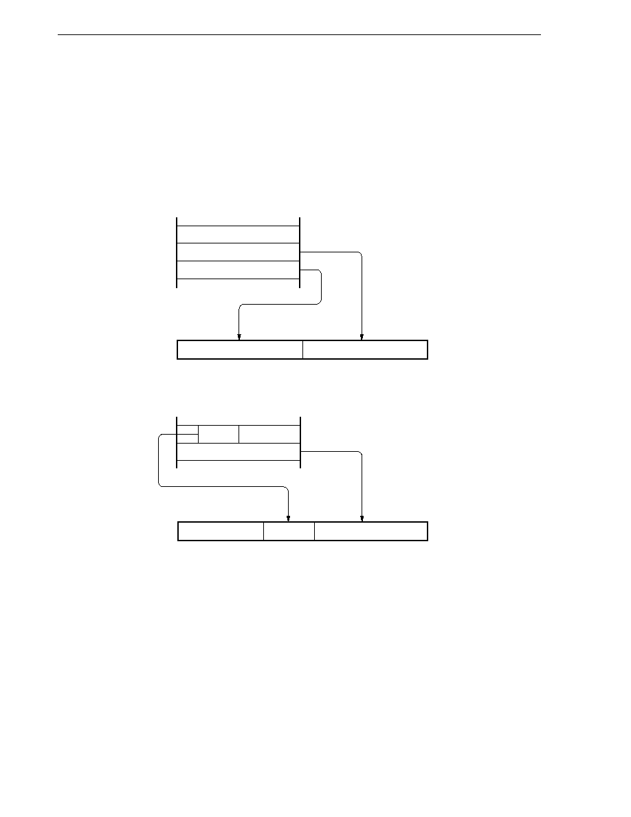
82
CHAPTER 5 CPU ARCHITECTURE
User's Manual U14260EJ3V1UD
5.3.2 Immediate addressing
[Function]
Immediate data in the instruction word is transferred to the program counter (PC) and branched.
This function is carried out when the CALL !addr16 or BR !addr16 or CALLF !addr11 instruction is executed.
CALL !addr16 and BR !addr16 instructions can be branched to the entire memory space. The CALLF !addr11
instruction is branched to the 0800H to 0FFFH area.
[Illustration]
In the case of CALL !addr16 and BR !addr16 instructions
In the case of CALLF !addr11 instruction
15
0
PC
8 7
7
0
CALL or BR
Low Addr.
High Addr.
15
0
PC
8 7
7
0
fa
10≠8
11 10
0
0
0
0
1
6
4
3
CALLF
fa
7≠0
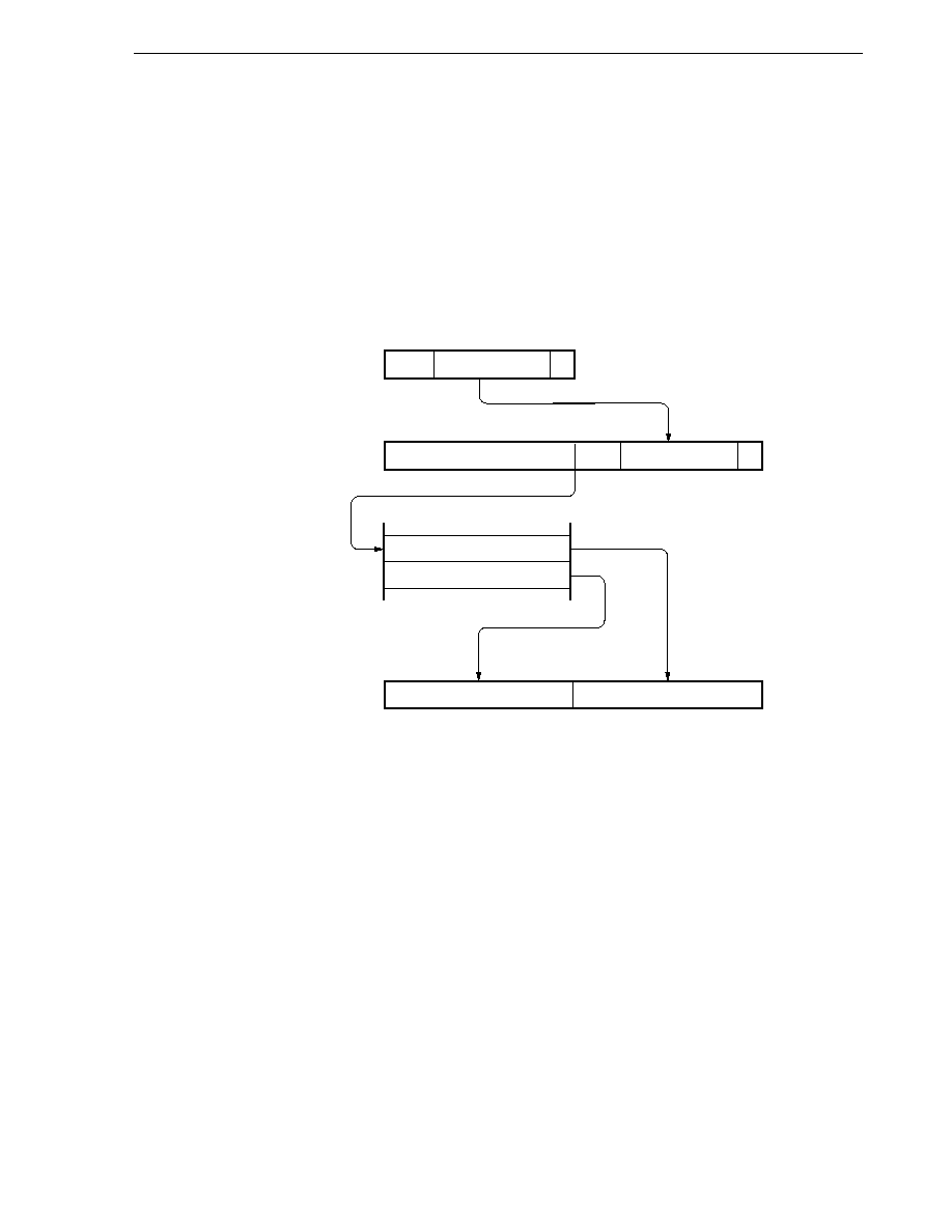
83
CHAPTER 5 CPU ARCHITECTURE
User's Manual U14260EJ3V1UD
5.3.3 Table indirect addressing
[Function]
Table contents (branch destination address) of the particular location to be addressed by bits 1 to 5 of the
immediate data of an operation code are transferred to the program counter (PC) and branched.
This function is carried out when the CALLT [addr5] instruction is executed.
This instruction references the address stored in the memory table from 40H to 7FH, and allows branching to
the entire memory space.
[Illustration]
15
1
15
0
PC
7
0
Low Addr.
High Addr.
Memory (Table)
Effective address + 1
Effective address
0
1
0
0
0
0
0
0
0
0
8
7
8
7
6
5
0
0
1
1
1
7
6
5
1
0
ta
4--0
Operation code
84
CHAPTER 5 CPU ARCHITECTURE
User's Manual U14260EJ3V1UD
5.3.4 Register addressing
[Function]
Register pair (AX) contents to be specified with an instruction word are transferred to the program counter (PC)
and branched.
This function is carried out when the BR AX instruction is executed.
[Illustration]
7
0
rp
0
7
A
X
15
0
PC
8
7

85
CHAPTER 5 CPU ARCHITECTURE
User's Manual U14260EJ3V1UD
5.4 Operand Address Addressing
The following methods are available to specify the register and memory (addressing) which undergo manipulation
during instruction execution.
5.4.1 Implied addressing
[Function]
The register which functions as an accumulator (A, AX) in the general-purpose register area is automatically
(implicitly) addressed.
Of the
µPD780078, 780078Y Subseries instruction words, the following instructions employ implied addressing.
Instruction
Register to Be Specified by Implied Addressing
MULU
Register A for multiplicand and register AX for product storage
DIVUW
Register AX for dividend and quotient storage
ADJBA/ADJBS
Register A for storage of numeric values which become decimal correction targets
ROR4/ROL4
Register A for storage of digit data which undergoes digit rotation
[Operand format]
Because implied addressing can be automatically employed with an instruction, no particular operand format is
necessary.
[Description example]
In the case of MULU X
With an 8-bit
◊ 8-bit multiply instruction, the product of register A and register X is stored in AX. In this example,
the A and AX registers are specified by implied addressing.
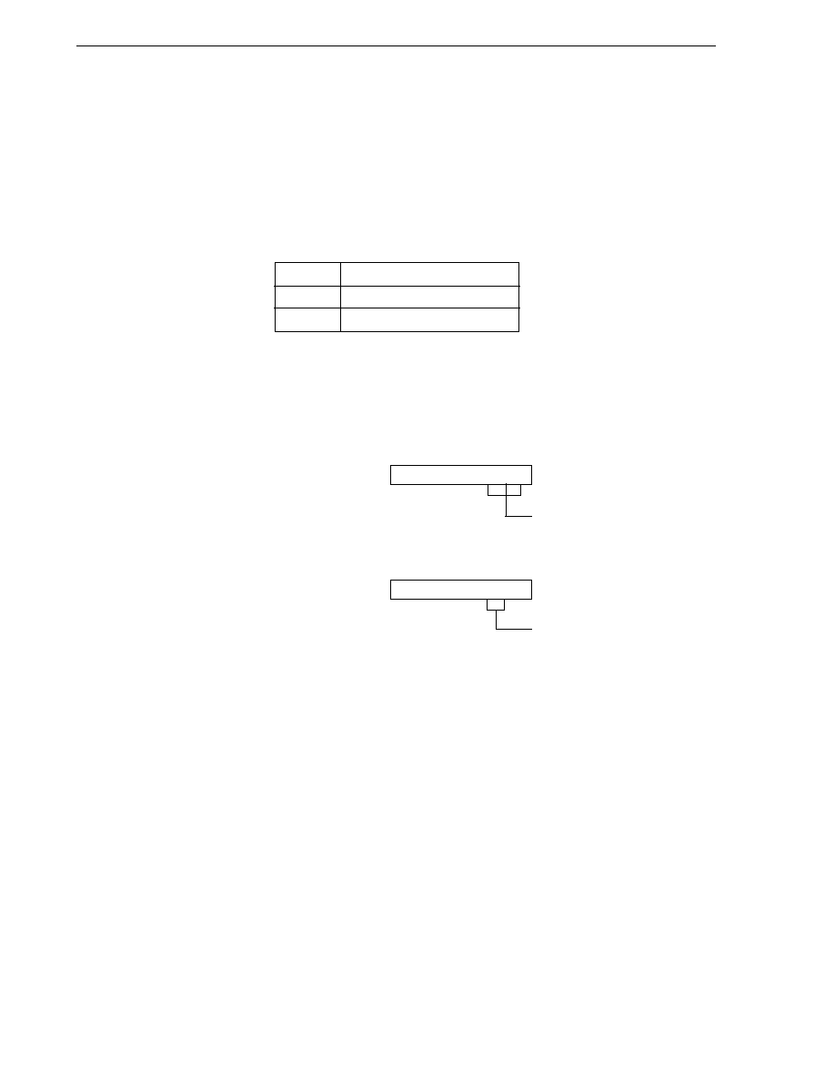
86
CHAPTER 5 CPU ARCHITECTURE
User's Manual U14260EJ3V1UD
5.4.2 Register addressing
[Function]
The general-purpose register to be specified is accessed as an operand with the register specify code (Rn and
RPn) of an instruction word in the registered bank specified by the register bank select flags (RBS0 and RBS1).
Register addressing is carried out when an instruction with the following operand format is executed. When an
8-bit register is specified, one of the eight registers is specified with 3 bits in the operation code.
[Operand format]
Identifier
Description
r
X, A, C, B, E, D, L, H
rp
AX, BC, DE, HL
`r' and `rp' can be described by absolute names (R0 to R7 and RP0 to RP3) as well as function names (X, A,
C, B, E, D, L, H, AX, BC, DE, and HL).
[Description example]
MOV A, C; when selecting C register as r
Operation code
0 1 1 0 0 0 1 0
Register specify code
INCW DE; when selecting DE register pair as rp
Operation code
1 0 0 0 0 1 0 0
Register specify code
87
CHAPTER 5 CPU ARCHITECTURE
User's Manual U14260EJ3V1UD
5.4.3 Direct addressing
[Function]
The memory to be manipulated is addressed with immediate data in an instruction word becoming an operand
address.
[Operand format]
Identifier
Description
addr16
Label or 16-bit immediate data
[Description example]
MOV A, !0FE00H; when setting !addr16 to FE00H
Operation code
1 0 0 0 1 1 1 0
Opcode
0 0 0 0 0 0 0 0
00H
1 1 1 1 1 1 1 0
FEH
[Illustration]
Memory
0
7
addr16 (lower)
addr16 (higher)
Opcode
88
CHAPTER 5 CPU ARCHITECTURE
User's Manual U14260EJ3V1UD
5.4.4 Short direct addressing
[Function]
The memory to be manipulated in the fixed space is directly addressed with 8-bit data in an instruction word.
This addressing is applied to the 256-byte space FE20H to FF1FH. Internal RAM and special function registers
(SFR) are mapped at FE20H to FEFFH and FF00H to FF1FH, respectively.
If the SFR area (FF00H to FF1FH) where short direct addressing is applied, ports which are frequently accessed
in a program and compare and capture registers of the timer/event counter are mapped, and these SFRs can
be manipulated with a small number of bytes and clocks.
When 8-bit immediate data is at 20H to FFH, bit 8 of an effective address is set to 0. When it is at 00H to 1FH,
bit 8 is set to 1. Refer to the [Illustration] below.
[Operand format]
Identifier
Description
saddr
Label or immediate data indicating FE20H to FF1FH
saddrp
Label or immediate data indicating FE20H to FF1FH (even address only)
[Description example]
MOV 0FE30H, A; when transferring the value in register A to saddr (FE30H)
Operation code
1 1 1 1 0 0 1 0
Opcode
0 0 1 1 0 0 0 0
30H (saddr-offset)
[Illustration]
When 8-bit immediate data is 20H to FFH,
= 0
When 8-bit immediate data is 00H to 1FH,
= 1
15
0
Short direct memory
Effective Address
1
1
1
1
1
1
1
8 7
0
7
Opcode
saddr-offset

89
CHAPTER 5 CPU ARCHITECTURE
User's Manual U14260EJ3V1UD
5.4.5 Special function register (SFR) addressing
[Function]
The memory-mapped special function register (SFR) is addressed with 8-bit immediate data in an instruction
word.
This addressing is applied to the 240-byte spaces FF00H to FFCFH and FFE0H to FFFFH. However, the SFRs
mapped at FF00H to FF1FH can be accessed with short direct addressing.
[Operand format]
Identifier
Description
sfr
Special function register name
sfrp
16-bit manipulatable special function register name (even address only)
[Description example]
MOV PM0, A; when selecting PM0 (FF20H) as sfr
Operation code
1 1 1 1 0 1 1 0
Opcode
0 0 1 0 0 0 0 0
20H (sfr-offset)
[Illustration]
15
0
SFR
Effective address
1
1
1
1
1
1
1
8 7
0
7
Opcode
sfr-offset
1

90
CHAPTER 5 CPU ARCHITECTURE
User's Manual U14260EJ3V1UD
5.4.6 Register indirect addressing
[Function]
Register pair contents specified with a register pair specify code in an instruction word of the register bank
specified by the register bank select flags (RBS0 and RBS1) serve as an operand address for addressing the
memory to be manipulated. This addressing can be carried out for all the memory spaces.
[Operand format]
Identifier
Description
--
[DE], [HL]
[Description example]
MOV A, [DE]; when selecting [DE] as register pair
Operation code
1 0 0 0 0 1 0 1
[Illustration]
16
0
8
D
7
E
0
7
7 0
A
DE
The contents of the memory
addressed are transferred.
Memory
The memory address
specified with the
register pair DE
91
CHAPTER 5 CPU ARCHITECTURE
User's Manual U14260EJ3V1UD
5.4.7 Based addressing
[Function]
8-bit immediate data is added as offset data to the contents of the base register, that is, the HL register pair in
an instruction word of the register bank specified by the register bank select flags (RBS0 and RBS1) and the
sum is used to address the memory. Addition is performed by expanding the offset data as a positive number
to 16 bits. A carry from the 16th bit is ignored. This addressing can be carried out for all the memory spaces.
[Operand format]
Identifier
Description
--
[HL + byte]
[Description example]
MOV A, [HL + 10H]; when setting byte to 10H
Operation code
1 0 1 0 1 1 1 0
0 0 0 1 0 0 0 0
[Illustration]
HL
16
0
8 7
H
L
A
7
0
7
0
Memory
The contents of the
addressed memory
is transferred.
+10
92
CHAPTER 5 CPU ARCHITECTURE
User's Manual U14260EJ3V1UD
5.4.8 Based indexed addressing
[Function]
The B or C register contents specified in an instruction are added to the contents of the base register, that is,
the HL register pair in an instruction word of the register bank specified by the register bank select flags (RBS0
and RBS1) and the sum is used to address the memory. Addition is performed by expanding the B or C register
contents as a positive number to 16 bits. A carry from the 16th bit is ignored. This addressing can be carried
out for all the memory spaces.
[Operand format]
Identifier
Description
--
[HL + B], [HL + C]
[Description example]
In the case of MOV A, [HL + B] (selecting the B register)
Operation code
1 0 1 0 1 0 1 1
[Illustration]
HL
16
0
8 7
H
L
A
7
0
7
0
Memory
7
0
+
B
The contents of the
addressed memory
is transferred.
93
CHAPTER 5 CPU ARCHITECTURE
User's Manual U14260EJ3V1UD
5.4.9 Stack addressing
[Function]
The stack area is indirectly addressed with the stack pointer (SP) contents.
This addressing method is automatically employed when the PUSH, POP, subroutine call and return instructions
are executed or the register is saved/reset upon generation of an interrupt request.
Stack addressing can be used to address the internal high-speed RAM area only.
[Description example]
In the case of PUSH DE (saving the DE register)
Operation code
1 0 1 1 0 1 0 1
[Illustration]
FEE0H
FEE0H
FEDFH
FEDEH
D
E
FEDEH
SP
SP
7
0
Memory
94
User's Manual U14260EJ3V1UD
CHAPTER 6 PORT FUNCTIONS
6.1 Port Functions
The
µPD780078, 780078Y Subseries incorporate eight input ports and 44 I/O ports. Figure 6-1 shows the port
configuration. Every port is capable of 1-bit and 8-bit manipulations and can carry out considerably varied control
operations. Besides port functions, the ports can also serve as on-chip hardware I/O pins.
Figure 6-1. Port Types
Port 0
P00
Port 1
P10
P17
Port 2
P20
P25
Port 3
P30
P36
Port 6
Port 5
P50
P57
P64
P67
Port 7
P70
P75
Port 4
P40
P47
P03
Port 8
P80
95
CHAPTER 6 PORT FUNCTIONS
User's Manual U14260EJ3V1UD
Table 6-1. Port Functions (
µPD780078 Subseries)
Pin Name
P00
P01
P02
P03
P10 to P17
P20
P21
P22
P23
P24
P25
P30
P31
P32
P33
P34
P35
P36
P40 to P47
P50 to P57
P64
P65
P66
P67
P70
P71
P72
P73
P74
P75
P80
Function
Port 0
4-bit I/O port.
Input/output mode can be specified in 1-bit units.
An on-chip pull-up resistor can be used by setting software.
Port 1
8-bit input-only port.
Port 2
6-bit I/O port.
Input/output mode can be specified in 1-bit units.
An on-chip pull-up resistor can be used by setting software.
Port 3
N-ch open-drain I/O port.
7-bit I/O port.
An on-chip pull-up resistor can be specified by a
Input/output mode can be specified
mask option (mask ROM version only).
in 1-bit units.
LEDs can be driven directly.
An on-chip pull-up resistor can be used by setting
software.
Port 4
8-bit I/O port.
Input/output mode can be specified in 1-bit units.
An on-chip pull-up resistor can be used by setting software.
Interrupt request flag (KRIF) is set to 1 by falling edge detection.
Port 5
8-bit I/O port.
LEDs can be driven directly.
Input/output mode can be specified in 1-bit units.
An on-chip pull-up resistor can be used by setting software.
Port 6
4-bit I/O port.
Input/output mode can be specified in 1-bit units.
An on-chip pull-up resistor can be used by setting software.
Port 7
6-bit I/O port.
Input/output mode can be specified in 1-bit units.
An on-chip pull-up resistor can be used by setting software.
Port 8
1-bit I/O port.
Input/output mode can be specified in 1-bit units.
An on-chip pull-up resistor can be used by setting software.
Alternate
Function
INTP0
INTP1
INTP2
INTP3/ADTRG
ANI0 to ANI7
SI1
SO1
SCK1
RxD0
TxD0
ASCK0
--
SI3/T
X
D2
SO3/R
X
D2
SCK3/ASCK2
AD0 to AD7
A8 to A15
RD
WR
WAIT
ASTB
TI000/TO00
TI010
TI50/TO50
TI51/TO51
TI011/PCL
TI001/TO01/BUZ
SS1
96
CHAPTER 6 PORT FUNCTIONS
User's Manual U14260EJ3V1UD
Table 6-2. Port Functions (
µPD780078Y Subseries)
Alternate
Function
INTP0
INTP1
INTP2
INTP3/ADTRG
ANI0 to ANI7
SI1
SO1
SCK1
RxD0
TxD0
ASCK0
--
SDA0
SCL0
SI3/T
X
D2
SO3/R
X
D2
SCK3/ASCK2
AD0 to AD7
A8 to A15
RD
WR
WAIT
ASTB
TI000/TO00
TI010
TI50/TO50
TI51/TO51
TI011/PCL
TI001/TO01/BUZ
SS1
Pin Name
P00
P01
P02
P03
P10 to P17
P20
P21
P22
P23
P24
P25
P30
P31
P32
P33
P34
P35
P36
P40 to P47
P50 to P57
P64
P65
P66
P67
P70
P71
P72
P73
P74
P75
P80
Function
Port 0
4-bit I/O port.
Input/output mode can be specified in 1-bit units.
An on-chip pull-up resistor can be used by setting software.
Port 1
8-bit input-only port.
Port 2
6-bit I/O port
Input/output mode can be specified in 1-bit units.
An on-chip pull-up resistor can be used by setting software.
Port 3
N-ch open-drain I/O port.
7-bit I/O port.
An on-chip pull-up resistor can be specified by a
Input/output mode can be specified
mask option (P30 and P31 are mask ROM version
in 1-bit units.
only). LEDs can be driven directly.
An on-chip pull-up resistor can be used by setting
software.
Port 4
8-bit I/O port.
Input/output mode can be specified in 1-bit units.
An on-chip pull-up resistor can be used by setting software.
Interrupt request flag (KRIF) is set to 1 by falling edge detection.
Port 5
8-bit I/O port.
LEDs can be driven directly.
Input/output mode can be specified in 1-bit units.
An on-chip pull-up resistor can be used by setting software.
Port 6
4-bit I/O port.
Input/output mode can be specified in 1-bit units.
An on-chip pull-up resistor can be used by setting software.
Port 7
6-bit I/O port.
Input/output mode can be specified in 1-bit units.
An on-chip pull-up resistor can be used by setting software.
Port 8
1-bit I/O port.
Input/output mode can be specified in 1-bit units.
An on-chip pull-up resistor can be used by setting software.

97
CHAPTER 6 PORT FUNCTIONS
User's Manual U14260EJ3V1UD
6.2 Port Configuration
A port consists of the following hardware.
Table 6-3. Port Configuration
Item
Configuration
Control registers
Port mode register (PMm: m = 0, 2 to 8)
Port register (Pm: m = 0 to 8)
Pull-up resistor option register (PUm: m = 0, 2 to 8)
Ports
Total: 52 ports (8 inputs, 44 I/O)
Pull-up resistor
∑ Mask ROM version
Total: 44 (software control: 40, mask option: 4
Note
)
∑ Flash memory version Total: 40
Note Two for the
µPD780078Y Subseries.
6.2.1 Port 0
Port 0 is a 4-bit I/O port with an output latch. Port 0 can be set to the input or output mode in 1-bit units using
port mode register 0 (PM0). An on-chip pull-up resistor can be connected to P00 to P03 in 1-bit units using pull-up
resistor option register 0 (PU0).
This port can also be used for external interrupt request input and A/D converter external trigger input.
RESET input sets port 0 to input mode.
Figure 6-2 shows a block diagram of port 0.
Cautions 1. Port 0 functions alternately as an external interrupt request input pin. If the output mode of
the port function is specified and the output level of the port is changed while interrupts are
not disabled by the external interrupt rising edge enable register (EGP) and external interrupt
falling edge enable register (EGN), the interrupt request flag is set. Thus, when the output
mode is used, set the interrupt mask flag to 1.
2. When the external interrupt request function is switched to the port function, edge detection
may be performed. Therefore, set bit n (EGPn) of EGP and bit n (EGNn) of EGN to 0 before
selecting the port mode.
3. When using P03/INTP3/ADTRG as an A/D converter external trigger input, specify valid edges
by setting bits 1 and 2 (EGA00 and EGA01) of A/D converter mode register 0 (ADM0) and set
the interrupt mask flag (PMK3) to 1.
Remark
n = 0 to 3
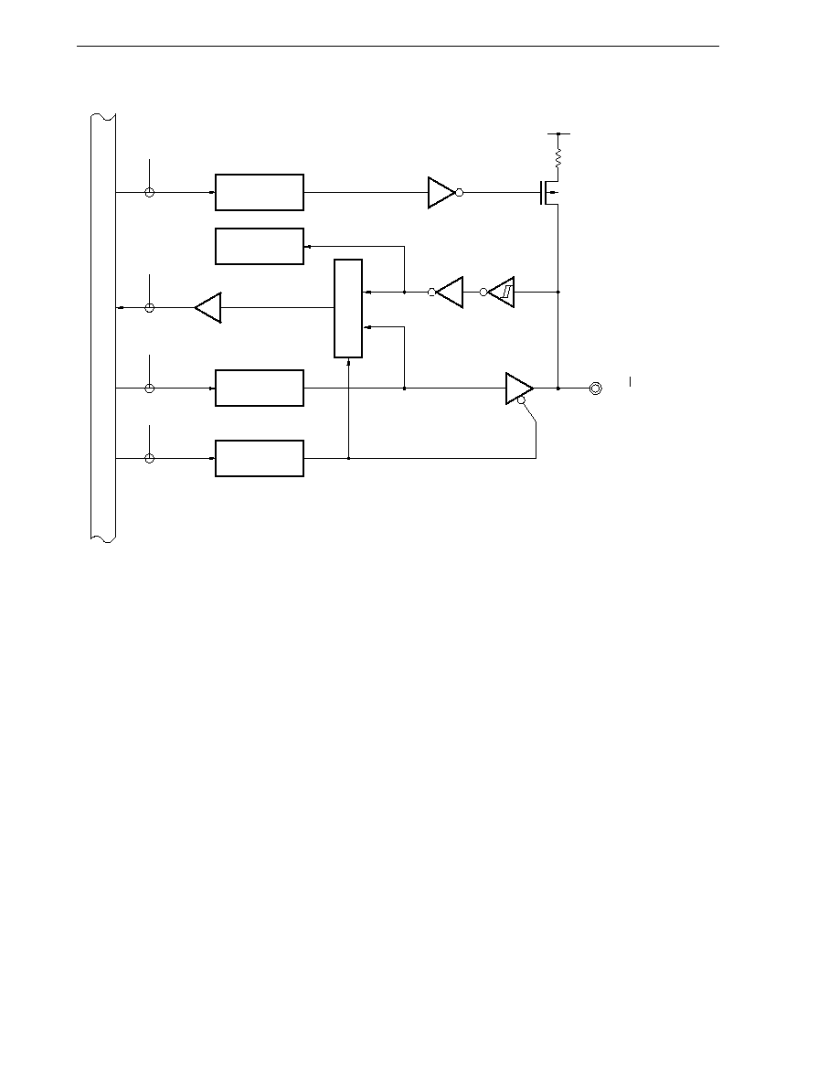
98
CHAPTER 6 PORT FUNCTIONS
User's Manual U14260EJ3V1UD
Figure 6-2. Block Diagram of P00 to P03
PU0:
Pull-up resistor option register 0
PM0:
Port mode register 0
RD:
Read signal
WR
◊◊: Write signal
V
DD0
P-ch
P00/INTP0
P02/INTP2,
P03/INTP3/ADTRG
WR
PU
RD
WR
PORT
WR
PM
PU00 to PU03
Alternate
function
Output latch
(P00 to P03)
PM00 to PM03
Internal bus
Selector
PU0
PM0
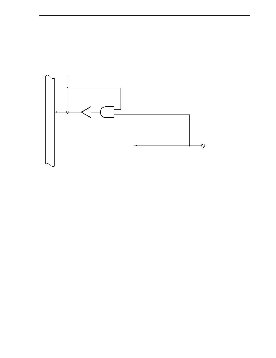
99
CHAPTER 6 PORT FUNCTIONS
User's Manual U14260EJ3V1UD
6.2.2 Port 1
Port 1 is an 8-bit input-only port.
This port can also be used for A/D converter analog input.
Figure 6-3 shows a block diagram of port 1.
Figure 6-3. Block Diagram of P10 to P17
RD: Read signal
RD
P10/ANI0 to P17/ANI7
A/D converter
Internal bus
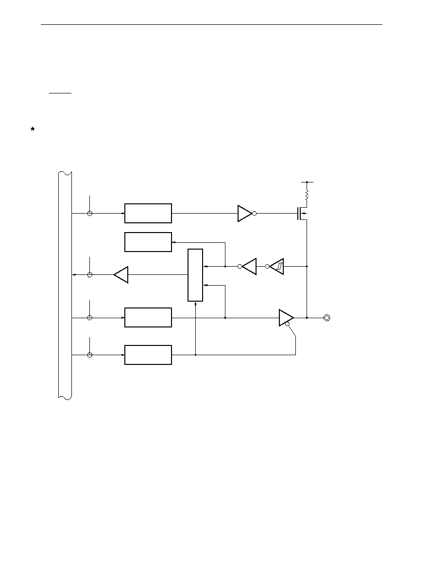
100
CHAPTER 6 PORT FUNCTIONS
User's Manual U14260EJ3V1UD
6.2.3 Port 2
Port 2 is a 6-bit I/O port with an output latch. Port 2 can be set to the input or output mode in 1-bit units using
port mode register 2 (PM2). An on-chip pull-up resistor can be connected to P20 to P25 in 1-bit units using pull-up
resistor option register 2 (PU2).
This port can also be used for serial interface data I/O and clock I/O.
RESET input sets port 2 to input mode.
Figures 6-4 to 6-7 show block diagrams of port 2.
Caution
When using P22/SCK1 as a general-purpose port, set bit 4 (CKP1) of serial clock select register
1 (CSIC1) to 1.
Figure 6-4. Block Diagram of P20, P23, and P25
PU2:
Pull-up resistor option register 2
PM2:
Port mode register 2
RD:
Read signal
WR
◊◊: Write signal
V
DD0
P-ch
P20/SI1,
P23/RxD0,
P25/ASCK0
WR
PU
RD
WR
PORT
WR
PM
PU20, PU23,
PU25
Alternate
function
Output latch
(P20, P23, P25)
PM20, PM23,
PM25
Internal bus
Selector
PU2
PM2
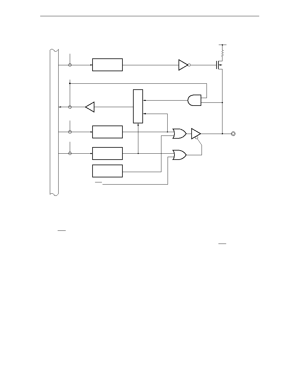
101
CHAPTER 6 PORT FUNCTIONS
User's Manual U14260EJ3V1UD
Figure 6-5. Block Diagram of P21
PU2:
Pull-up resistor option register 2
PM2:
Port mode register 2
RD:
Read signal
WR
◊◊: Write signal
SS1:
3-wire SIO chip select signal
Caution
P21/SO1 has a function to forcibly turn off the output buffer via SS1 (3-wire SIO chip
select signal).
Internal bus
P21/SO1
WR
PU
RD
WR
PORT
WR
PM
PU21
Output latch
(P21)
PM21
SS1
Alternate
function
V
DD0
P-ch
Selector
PU2
PM2
102
CHAPTER 6 PORT FUNCTIONS
User's Manual U14260EJ3V1UD
Figure 6-6. Block Diagram of P22
PU2:
Pull-up resistor option register 2
PM2:
Port mode register 2
RD:
Read signal
WR
◊◊: Write signal
P22/SCK1
WR
PU
RD
WR
PORT
WR
PM
PU22
Output latch
(P22)
PM22
Alternate
function
Alternate
function
V
DD0
P-ch
Internal bus
Selector
PU2
PM2
103
CHAPTER 6 PORT FUNCTIONS
User's Manual U14260EJ3V1UD
Figure 6-7. Block Diagram of P24
PU2:
Pull-up resistor option register 2
PM2:
Port mode register 2
RD:
Read signal
WR
◊◊: Write signal
P24/TxD0
WR
PU
RD
WR
PORT
WR
PM
PU24
Output latch
(P24)
PM24
Alternate
function
V
DD0
P-ch
Internal bus
Selector
PU2
PM2

104
CHAPTER 6 PORT FUNCTIONS
User's Manual U14260EJ3V1UD
6.2.4 Port 3 (
µPD780078 Subseries)
Port 3 is a 7-bit I/O port with an output latch. Port 3 can be set to the input or output mode in 1-bit units using
port mode register 3 (PM3).
This port has the following functions related to pull-up resistors. These functions differ depending on the port's
higher 3 bits/lower 4 bits, and whether the product is a mask ROM version or a flash memory version.
Table 6-4. Pull-Up Resistor of Port 3 (
µPD780078 Subseries)
Higher 3 Bits (P34 to P36 Pins)
Lower 4 Bits (P30 to P33 Pins)
Mask ROM version
An on-chip pull-up resistor can be
An on-chip pull-up resistor can be specified
connected in 1-bit units by PU3
in 1-bit units by a mask option
Flash memory version
An on-chip pull-up resistor is not provided
PU3: Pull-up resistor option register 3
The P30 to P33 pins can drive LEDs directly.
The P34 to P36 pins can also be used for serial interface data I/O and clock I/O.
RESET input sets port 3 to input mode.
Figures 6-8 to 6-10 show block diagrams of port 3.
Figure 6-8. Block Diagram of P30 and P31 (
µPD780078 Subseries)
PM3:
Port mode register 3
RD:
Read signal
WR
◊◊: Write signal
RD
PM30, PM31
P30, P31
N-ch
WR
PORT
Output latch
(P30, P31)
WR
PM
V
DD0
Selector
Internal bus
Mask option resistor
Mask ROM version only
No pull-up resistor for
flash memory version
PM3
105
CHAPTER 6 PORT FUNCTIONS
User's Manual U14260EJ3V1UD
Figure 6-9. Block Diagram of P32 and P33 (
µPD780078 Subseries)
PM3:
Port mode register 3
RD:
Read signal
WR
◊◊: Write signal
RD
PM32, PM33
P32, P33
N-ch
WR
PORT
WR
PM
V
DD0
Output latch
(P32, P33)
Selector
Internal bus
Mask option resistor
Mask ROM version only
No pull-up resistor for
flash memory version
PM3
106
CHAPTER 6 PORT FUNCTIONS
User's Manual U14260EJ3V1UD
Figure 6-10. Block Diagram of P34 to P36 (
µPD780078 Subseries)
PU3:
Pull-up resistor option register 3
PM3:
Port mode register 3
RD:
Read signal
WR
◊◊: Write signal
V
DD0
P-ch
P34/SI3/TxD2,
P35/SO3/RxD2,
P36/SCK3/ASCK2
WR
PU
RD
WR
PORT
WR
PM
PU34 to PU36
Alternate
function
Output latch
(P34 to P36)
PM34 to PM36
Alternate
function
Selector
Internal bus
PU3
PM3

107
CHAPTER 6 PORT FUNCTIONS
User's Manual U14260EJ3V1UD
6.2.5 Port 3 (
µPD780078Y Subseries)
Port 3 is a 7-bit I/O port with an output latch. Port 3 can be set to the input or output mode in 1-bit units using
port mode register 3 (PM3).
This port has the following functions related to pull-up resistors. These functions differ depending on the bit location
and whether the product is a mask ROM version or a flash memory version.
Table 6-5. Pull-Up Resistor of Port 3 (
µPD780078Y Subseries)
P34 to P36 Pins
P30 and P31 Pins
Mask ROM version
An on-chip pull-up resistor can
An on-chip pull-up resistor can be specified
be connected in 1-bit units by
in 1-bit units by mask option
Flash memory version
PU3
An on-chip pull-up resistor is not provided
PU3: Pull-up resistor option register 3
Caution
The P32 and P33 pins have no pull-up resistor.
The P30 to P33 pins can drive LEDs directly.
The P32 to P36 pins can also be used for serial interface data I/O and clock I/O.
RESET input sets port 3 to input mode.
Figures 6-11 to 6-13 show block diagrams of port 3.
Figure 6-11. Block Diagram of P30 and P31 (
µPD780078Y Subseries)
PM3:
Port mode register 3
RD:
Read signal
WR
◊◊: Write signal
RD
PM30, PM31
P30, P31
N-ch
WR
PORT
WR
PM
V
DD0
Output latch
(P30, P31)
Selector
Internal bus
Mask option resistor
Mask ROM version only
No pull-up resistor for
flash memory version
PM3

108
CHAPTER 6 PORT FUNCTIONS
User's Manual U14260EJ3V1UD
Figure 6-12. Block Diagram of P32 and P33 (
µPD780078Y Subseries)
PM3:
Port mode register 3
RD:
Read signal
WR
◊◊: Write signal
RD
PM32, PM33
Alternate
function
P32/SDA0,
P33/SCL0
N-ch
WR
PORT
Output latch
(P32, P33)
WR
PM
Internal bus
Selector
PM3
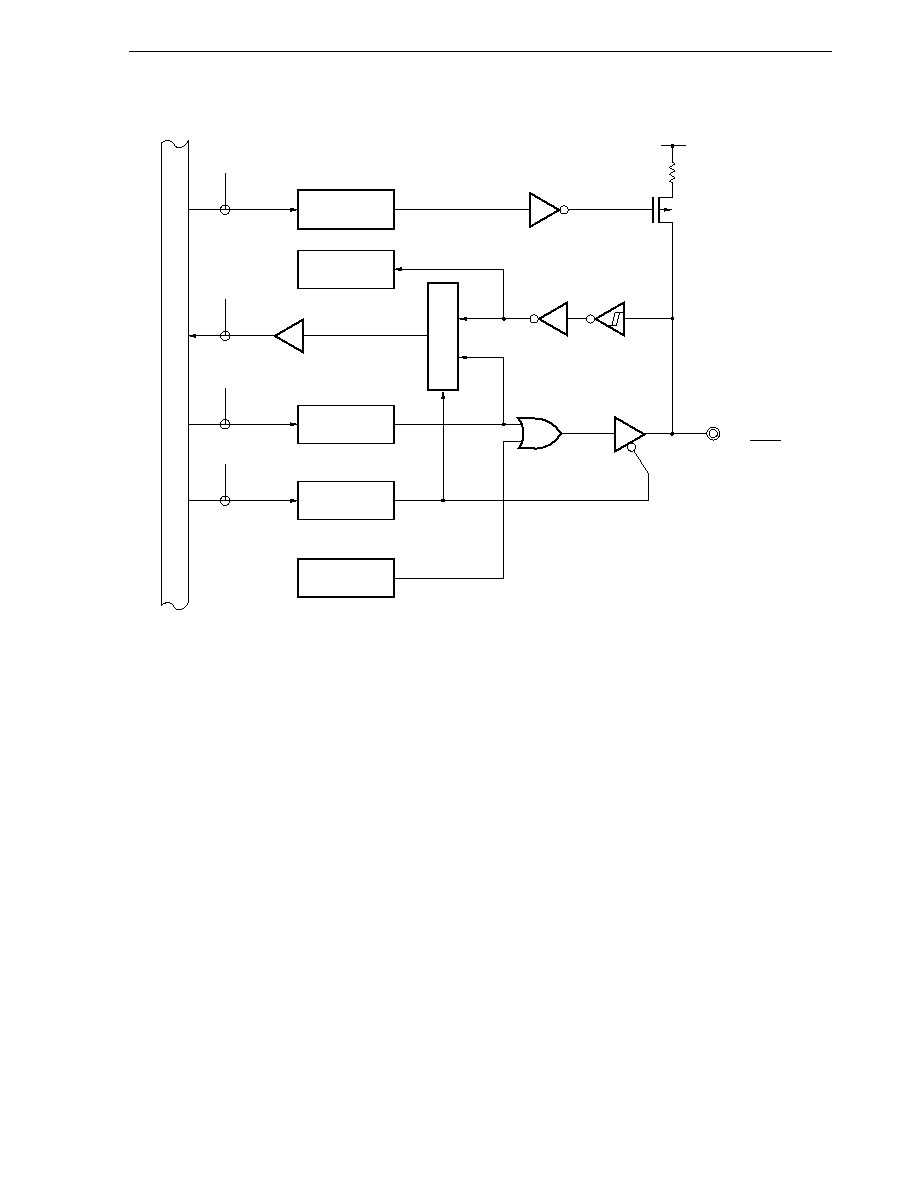
109
CHAPTER 6 PORT FUNCTIONS
User's Manual U14260EJ3V1UD
Figure 6-13. Block Diagram of P34 to P36 (
µPD780078Y Subseries)
PU3:
Pull-up resistor option register 3
PM3:
Port mode register 3
RD:
Read signal
WR
◊◊: Write signal
V
DD0
P-ch
P34/SI3/TxD2,
P35/SO3/RxD2,
P36/SCK3/ASCK2
WR
PU
RD
WR
PORT
WR
PM
PU34 to PU36
Output latch
(P34 to P36)
PM34 to PM36
Alternate
function
Alternate
function
Internal bus
Selector
PU3
PM3
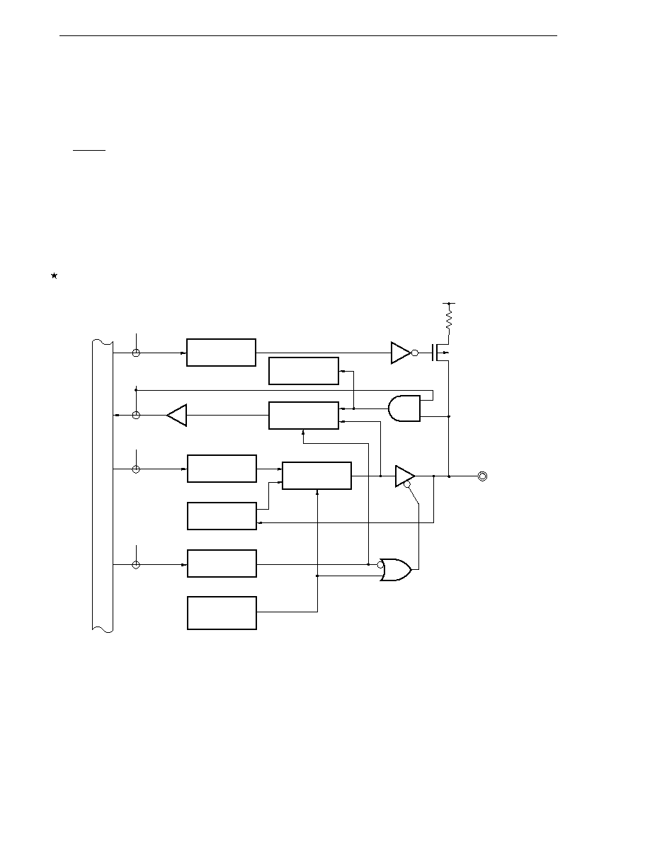
110
CHAPTER 6 PORT FUNCTIONS
User's Manual U14260EJ3V1UD
6.2.6 Port 4
Port 4 is an 8-bit I/O port with an output latch. Port 4 can be set to the input or output mode in 1-bit units using
port mode register 4 (PM4). An on-chip pull-up resistor can be connected to P40 to P47 in 1-bit units using pull-up
resistor option register 4 (PU4).
The interrupt request flag (KRIF) can be set to 1 by detecting falling edges.
This port can also be used as an address/data bus in external memory expansion mode.
RESET input sets port 4 to input mode.
Figures 6-14 and 6-15 show a block diagram of port 4 and a block diagram of the falling edge detector, respectively.
Cautions 1. An on-chip pull-up resistor is not disconnected even if the external memory expansion mode
is set when PU4n = 1 (n = 0 to 7).
2. When using the falling edge detection interrupt (INTKR), be sure to set the memory expansion
mode register (MEM) to 01H.
Figure 6-14. Block Diagram of P40 to P47
PU4:
Pull-up resistor option register 4
PM4:
Port mode register 4
RD:
Read signal
WR
◊◊: Write signal
Internal bus
RD
P40/AD0
to
P47/AD7
P-ch
WR
PU
WR
PORT
WR
PM
PU40 to PU47
Alternate
function
Selector
V
DD0
Output latch
(P40 to P47)
PM40 to PM47
Alternate
function
Selector
Memory expansion
mode register
(MEM)
PM4
PU4
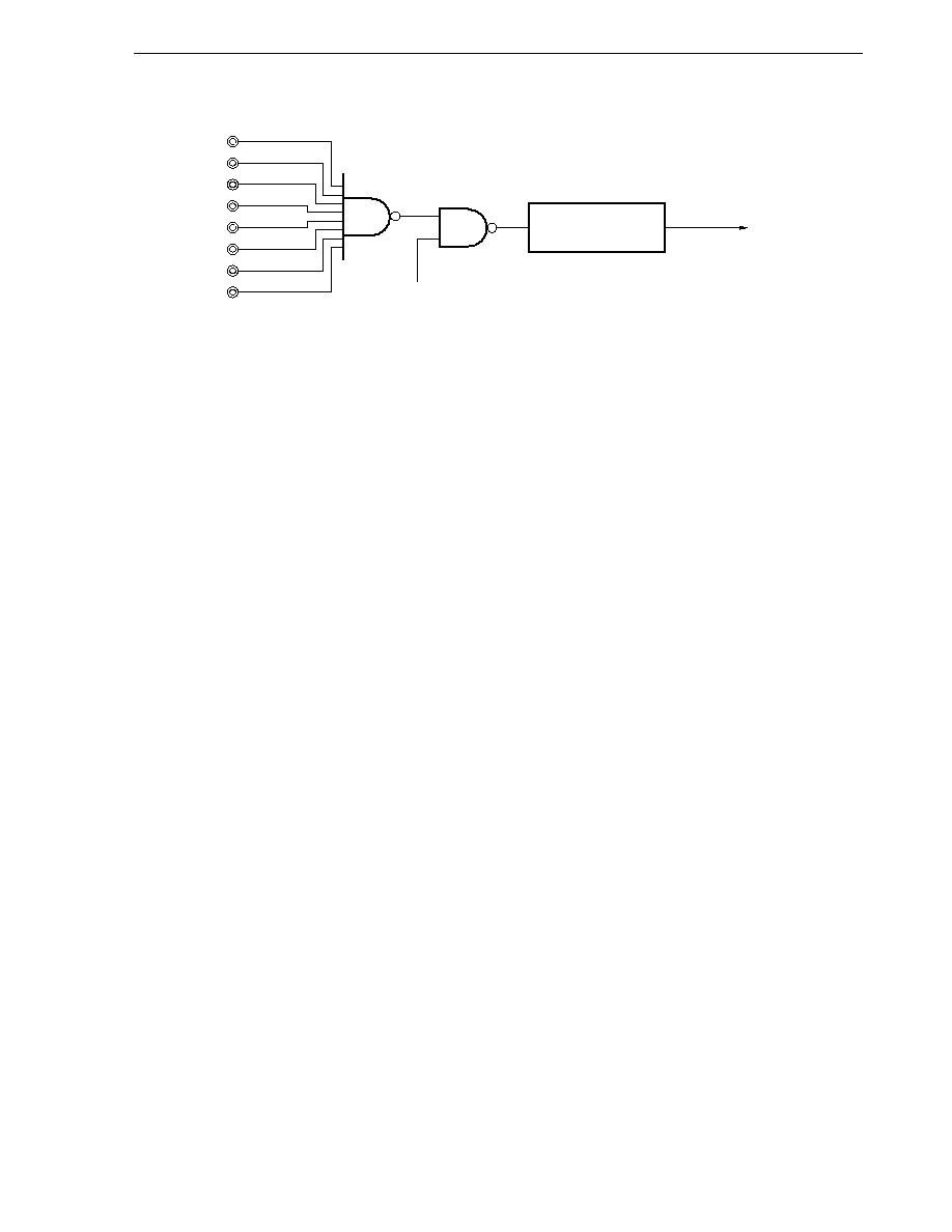
111
CHAPTER 6 PORT FUNCTIONS
User's Manual U14260EJ3V1UD
Figure 6-15. Block Diagram of Falling Edge Detector
P40
P41
P42
P43
P44
P45
P46
P47
INTKR
Falling edge detector
1 when MEM = 01H

112
CHAPTER 6 PORT FUNCTIONS
User's Manual U14260EJ3V1UD
6.2.7 Port 5
Port 5 is an 8-bit I/O port with an output latch. Port 5 can be set to the input or output mode in 1-bit units using
port mode register 5 (PM5). An on-chip pull-up resistor can be connected to P50 to P57 in 1-bit units using pull-up
resistor option register 5 (PU5).
Port 5 can drive LEDs directly.
This port can also be used as an address bus in external memory expansion mode.
RESET input sets port 5 to input mode.
Figure 6-16 shows a block diagram of port 5.
Caution
An on-chip pull-up resistor is not disconnected even if the external memory expansion mode
is set when PU5n = 1 (n = 0 to 7).
Figure 6-16. Block Diagram of P50 to P57
PU5:
Pull-up resistor option register 5
PM5:
Port mode register 5
RD:
Read signal
WR
◊◊: Write signal
Internal bus
RD
P50/A8
to
P57/A15
P-ch
WR
PU
WR
PORT
WR
PM
PU50 to PU57
V
DD0
Selector
Output latch
(P50 to P57)
PM50 to PM57
Alternate
function
Selector
PM5
Memory expansion
mode register
(MEM)
PU5
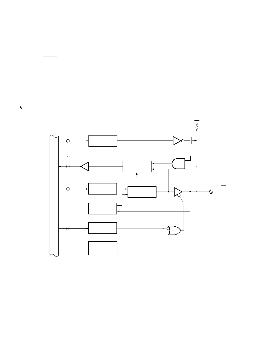
113
CHAPTER 6 PORT FUNCTIONS
User's Manual U14260EJ3V1UD
6.2.8 Port 6
Port 6 is a 4-bit I/O port with an output latch. Port 6 can be set to the input or output mode in 1-bit units using
port mode register 6 (PM6). An on-chip pull-up resistor can be connected to P64 to P67 in 1-bit units using pull-up
resistor option register 6 (PU6).
This port can also be used for control signal output in external memory expansion mode.
RESET input sets port 6 to input mode.
Figures 6-17 and 6-18 show block diagrams of port 6.
Cautions 1. An on-chip pull-up resistor is not disconnected even if the external memory expansion mode
is set when PU6n = 1 (n = 4 to 7).
2. When external wait is not used in external memory expansion mode, P66 can be used as an
I/O port.
Figure 6-17. Block Diagram of P64, P65, and P67
PU6:
Pull-up resistor option register 6
PM6:
Port mode register 6
RD:
Read signal
WR
◊◊: Write signal
Internal bus
RD
P64/RD,
P65/WR,
P67/ASTB
P-ch
WR
PU
WR
PORT
WR
PM
PU64, PU65, PU67
V
DD0
Selector
Output latch
(P64, P65, P67)
PM64, PM65, PM67
Alternate
function
Selector
PM6
Memory expansion
mode register
(MEM)
PU6
114
CHAPTER 6 PORT FUNCTIONS
User's Manual U14260EJ3V1UD
Figure 6-18. Block Diagram of P66
PU6:
Pull-up resistor option register 6
PM6:
Port mode register 6
RD:
Read signal
WR
◊◊: Write signal
Internal bus
RD
P66/WAIT
P-ch
WR
PU
WR
PORT
WR
PM
PU66
PM66
V
DD0
Output latch
(P66)
Alternate
function
Selector
Selector
Memory expansion
mode register (MEM)
PU6
PM6

115
CHAPTER 6 PORT FUNCTIONS
User's Manual U14260EJ3V1UD
6.2.9 Port 7
Port 7 is a 6-bit I/O port with an output latch. Port 7 can be set to the input or output mode in 1-bit units using
port mode register 7 (PM7). An on-chip pull-up resistor can be connected to P70 to P75 in 1-bit units using pull-up
resistor option register 7 (PU7).
This port can also be used for timer I/O, clock output, and buzzer output.
RESET input sets port 7 to input mode.
Figures 6-19 and 6-20 show block diagrams of port 7.
Figure 6-19. Block Diagram of P70 and P72 to P75
PU7:
Pull-up resistor option register 7
PM7:
Port mode register 7
RD:
Read signal
WR
◊◊: Write signal
V
DD0
P-ch
P70/TI000/TO00,
P72/TI50/TO50,
P73/TI51/TO51,
P74/TI011/PCL,
P75/TI001/TO01/BUZ
WR
PU
RD
WR
PORT
WR
PM
PU70, PU72 to PU75
Alternate
function
Alternate
function
Output latch
(P70, P72 to P75)
PM70, PM72 to PM75
Internal bus
Selector
PU7
PM7
116
CHAPTER 6 PORT FUNCTIONS
User's Manual U14260EJ3V1UD
Figure 6-20. Block Diagram of P71
PU7:
Pull-up resistor option register 7
PM7:
Port mode register 7
RD:
Read signal
WR
◊◊: Write signal
V
DD0
P-ch
P71/TI010
WR
PU
RD
WR
PORT
WR
PM
PU71
PM71
Output latch
(P71)
Alternate
function
Internal bus
Selector
PU7
PM7
117
CHAPTER 6 PORT FUNCTIONS
User's Manual U14260EJ3V1UD
6.2.10 Port 8
Port 8 is a 1-bit I/O port with an output latch. Port 8 can be set to the input or output mode in 1-bit units using
port mode register 8 (PM8). An on-chip pull-up resistor can be connected to P80 in 1-bit units using pull-up resistor
option register 8 (PU8).
This port can also be used for serial interface chip select input.
RESET input sets port 8 to input mode.
Figure 6-21 shows a block diagram of port 8.
Figure 6-21. Block Diagram of P80
PU8:
Pull-up resistor option register 8
PM8:
Port mode register 8
RD:
Read signal
WR
◊◊: Write signal
V
DD0
P-ch
P80/SS1
WR
PU
RD
WR
PORT
WR
PM
PU80
PM80
Output latch
(P80)
Alternate
function
Internal bus
Selector
PU8
PM8

118
CHAPTER 6 PORT FUNCTIONS
User's Manual U14260EJ3V1UD
6.3 Port Function Control Registers
The following three types of registers control the ports.
∑
Port mode registers (PM0, PM2 to PM8)
∑
Port registers (P0 to P8)
∑
Pull-up resistor option registers (PU0, PU2 to PU8)
(1) Port mode registers (PM0, PM2 to PM8)
These registers are used to set port input/output in 1-bit units.
PM0 and PM2 to PM8 are independently set by a 1-bit or 8-bit memory manipulation instruction.
RESET input sets PM0 and PM2 to PM8 to FFH.
When using a port pin as its alternate-function pin, set the port mode registers and output latches as shown in
Table 6-6.
Cautions 1. Pins P10 and P17 are input-only pins.
2. Port 0 functions alternately as an external interrupt request input pin. If the output mode
of the port function is specified and the output level of the port is changed while interrupts
are not disabled by the external interrupt rising edge enable register (EGP) and external
interrupt falling edge enable register (EGN), the interrupt request flag is set. When the
output mode is used, therefore, the interrupt mask flag should be set to 1 beforehand.
3. If a port has an alternate function pin and it is used as an alternate output function, set the
corresponding output latches (P0 and P2 to P8) to 0.
119
CHAPTER 6 PORT FUNCTIONS
User's Manual U14260EJ3V1UD
Figure 6-22. Format of Port Mode Register (PM0, PM2 to PM8)
Address: FF20H After reset: FFH R/W
Symbol
7
6
5
4
3
2
1
0
PM0
1
1
1
1
PM03
PM02
PM01
PM00
Address: FF22H After reset: FFH R/W
Symbol
7
6
5
4
3
2
1
0
PM2
1
1
PM25
PM24
PM23
PM22
PM21
PM20
Address: FF23H After reset: FFH R/W
Symbol
7
6
5
4
3
2
1
0
PM3
1
PM36
PM35
PM34
PM33
PM32
PM31
PM30
Address: FF24H After reset: FFH R/W
Symbol
7
6
5
4
3
2
1
0
PM4
PM47
PM46
PM45
PM44
PM43
PM42
PM41
PM40
Address: FF25H After reset: FFH R/W
Symbol
7
6
5
4
3
2
1
0
PM5
PM57
PM56
PM55
PM54
PM53
PM52
PM51
PM50
Address: FF26H After reset: FFH R/W
Symbol
7
6
5
4
3
2
1
0
PM6
PM67
PM66
PM65
PM64
1
1
1
1
Address: FF27H After reset: FFH R/W
Symbol
7
6
5
4
3
2
1
0
PM7
1
1
PM75
PM74
PM73
PM72
PM71
PM70
Address: FF28H After reset: FFH R/W
Symbol
7
6
5
4
3
2
1
0
PM8
1
1
1
1
1
1
1
PM80
PMmn
Pmn pin I/O mode selection (m = 0, 2 to 8: n = 0 to 7)
0
Output mode (output buffer on)
1
Input mode (output buffer off)

120
CHAPTER 6 PORT FUNCTIONS
User's Manual U14260EJ3V1UD
Table 6-6. Port Mode Registers and Output Latch Settings When Alternate Function Is Used (1/2)
Pin Name
P00 to P02
P03
P10 to P17
P20
P21
P22
P23
P24
P25
P32
P33
P34
P35
P36
P40 to P47
P50 to P57
P64
P65
P66
P67
Alternate Function
PM
◊◊
1
1
1
1 (fix)
1
0
1
0
1
0
1
0
0
1
0
0
1
1
0
1
1
Note 2
P
◊◊
◊
◊
◊
◊
◊
0
◊
0
◊
0
◊
0
0
◊
0
0
◊
◊
0
◊
◊
Note 2
Name
INTP0 to INTP2
INTP3
ADTRG
ANI0 to ANI7
SI1
SO1
SCK1
RxD0
TxD0
ASCK0
SDA0
Note 1
SCL0
Note 1
SI3
TxD2
SO3
RxD2
SCK3
ASCK2
AD0 to AD7
A8 to A15
RD
WR
WAIT
ASTB
I/O
Input
Input
Input
Input
Input
Output
Input
Output
Input
Output
Input
I/O
I/O
Input
Output
Output
Input
Input
Output
Input
I/O
Output
Output
Output
Input
Output
◊
Note 2
◊
Note 2
◊
Note 2
◊
Note 2
◊
Note 2
Notes 1.
µPD780078Y Subseries only
2. When using the P40 to P47, P50 to P57, and P64 to P67 pins as alternate-function pins, set the function
using the memory expansion mode register (MEM).
Remark
◊:
Don't care
PM
◊◊: Port mode register
P
◊◊:
Port register (port output latch)

121
CHAPTER 6 PORT FUNCTIONS
User's Manual U14260EJ3V1UD
Table 6-6. Port Mode Registers and Output Latch Settings When Alternate Function Is Used (2/2)
Pin Name
P70
P71
P72
P73
P74
P75
P80
Alternate Function
PM
◊◊
1
0
1
1
0
1
0
1
0
1
0
0
1
P
◊◊
◊
0
◊
◊
0
◊
0
◊
0
◊
0
0
◊
Name
TI000
TO00
TI010
TI50
TO50
TI51
TO51
TI011
PCL
TI001
TO01
BUZ
SS1
I/O
Input
Output
Input
Input
Output
Input
Output
Input
Output
Input
Output
Output
Input
Remark
◊:
Don't care
PM
◊◊: Port mode register
P
◊◊:
Port register (port output latch)
122
CHAPTER 6 PORT FUNCTIONS
User's Manual U14260EJ3V1UD
(2) Port registers (P0 to P8)
These registers write the data that is output from the chip when data is output from a port.
If the data is read in the input mode, the pin level is read. If it is read in the output mode, the value of the output
latch is read.
P0 to P8 are set by a 1-bit or 8-bit memory manipulation instruction.
RESET input clears P0 to P8 to 00H (but P1 is undefined).
Figure 6-23. Format of Port Register
Pmn
m = 0 to 8; n = 0 to 7
Output data control (in output mode)
Input data read (in input mode)
0
Output 0
Input low level
1
Output 1
Input high level
7
0
Symbol
P0
6
0
5
0
4
0
3
P03
2
P02
1
P01
0
P00
Address
FF00H
After reset
00H (output latch)
R/W
R/W
7
P17
P1
6
P16
5
P15
4
P14
3
P13
2
P12
1
P11
0
P10
FF01H
00H (output latch)
R/W
R
7
0
P2
6
0
5
P25
4
P24
3
P23
2
P22
1
P21
0
P20
FF02H
Undefined
7
0
P3
6
P36
5
P35
4
P34
3
P33
2
P32
1
P31
0
P30
FF03H
00H (output latch)
R/W
7
P47
P4
6
P46
5
P45
4
P44
3
P43
2
P42
1
P41
0
P40
FF04H
00H (output latch)
R/W
7
P57
P5
6
P56
5
P55
4
P54
3
P53
2
P52
1
P51
0
P50
FF05H
00H (output latch)
R/W
7
P67
P6
6
P66
5
P65
4
P64
3
0
2
0
1
0
0
0
FF06H
00H (output latch)
R/W
7
0
P7
6
0
5
P75
4
P74
3
P73
2
P72
1
P71
0
P70
FF07H
00H (output latch)
R/W
7
0
P8
6
0
5
0
4
0
3
0
2
0
1
0
0
P80
FF08H
00H (output latch)
R/W

123
CHAPTER 6 PORT FUNCTIONS
User's Manual U14260EJ3V1UD
(3) Pull-up resistor option registers (PU0, PU2 to PU8)
These registers are used to set whether to connect an on-chip pull-up resistor at each port or not. By setting
PU0 and PU2 to PU8, the on-chip pull-up resistors of the port pins corresponding to the bits in PU0 and PU2
to PU8 can be connected.
PU0 and PU2 to PU8 are set by a 1-bit or 8-bit memory manipulation instruction.
RESET input sets PU0 and PU2 to PU8 to 00H.
Cautions 1. The P10 and P17 pins do not incorporate a pull-up resistor.
2. Pins P30 to P33 (in the
µPD780078Y Subseries, P30 and P31 pins) can be connected to a
pull-up resistor via a mask option only for mask ROM versions.
3. When PUm is set to 1, the on-chip pull-up resistor is connected irrespective of the input/
output mode. When using in output mode, set the bit of PUm to 0 (m = 0, 2 to 8).
124
CHAPTER 6 PORT FUNCTIONS
User's Manual U14260EJ3V1UD
Figure 6-24. Format of Pull-Up Resistor Option Register (PU0, PU2 to PU8)
Address: FF30H After reset: 00H R/W
Symbol
7
6
5
4
3
2
1
0
PU0
0
0
0
0
PU03
PU02
PU01
PU00
Address: FF32H After reset: 00H R/W
Symbol
7
6
5
4
3
2
1
0
PU2
0
0
PU25
PU24
PU23
PU22
PU21
PU20
Address: FF33H After reset: 00H R/W
Symbol
7
6
5
4
3
2
1
0
PU3
0
PU36
PU35
PU34
0
0
0
0
Address: FF34H After reset: 00H R/W
Symbol
7
6
5
4
3
2
1
0
PU4
PU47
PU46
PU45
PU44
PU43
PU42
PU41
PU40
Address: FF35H After reset: 00H R/W
Symbol
7
6
5
4
3
2
1
0
PU5
PU57
PU56
PU55
PU54
PU53
PU52
PU51
PU50
Address: FF36H After reset: 00H R/W
Symbol
7
6
5
4
3
2
1
0
PU6
PU67
PU66
PU65
PU64
0
0
0
0
Address: FF37H After reset: 00H R/W
Symbol
7
6
5
4
3
2
1
0
PU7
0
0
PU75
PU74
PU73
PU72
PU71
PU70
Address: FF38H After reset: 00H R/W
Symbol
7
6
5
4
3
2
1
0
PU8
0
0
0
0
0
0
0
PU80
PUmn
Pmn pin on-chip pull-up resistor selection (m = 0, 2 to 8: n = 0 to 7)
0
On-chip pull-up resistor not connected
1
On-chip pull-up resistor connected

125
CHAPTER 6 PORT FUNCTIONS
User's Manual U14260EJ3V1UD
6.4 Port Function Operations
Port operations differ depending on whether the input or output mode is set, as shown below.
Caution
In the case of 1-bit memory manipulation instruction, although a single bit is manipulated, the
port is accessed in 8-bit units. Therefore, on a port with a mixture of input and output pins,
the output latch contents for pins specified as input are undefined, even for bits other than
the manipulated bit.
6.4.1 Writing to I/O port
(1) Output mode
A value is written to the output latch by a transfer instruction, and the output latch contents are output from the
pin.
Once data is written to the output latch, it is retained until data is written to the output latch again.
When a reset is input, the data in the output latch is cleared.
(2) Input mode
A value is written to the output latch by a transfer instruction, but since the output buffer is off, the pin status does
not change.
Once data is written to the output latch, it is retained until data is written to the output latch again.
6.4.2 Reading from I/O port
(1) Output mode
The output latch contents are read by a transfer instruction. The output latch contents do not change.
(2) Input mode
The pin status is read by a transfer instruction. The output latch contents do not change.
6.4.3 Operations on I/O port
(1) Output mode
An operation is performed on the output latch contents, and the result is written to the output latch. The output
latch contents are output from the pins.
Once data is written to the output latch, it is retained until data is written to the output latch again.
When a reset is input, the data in the output latch is cleared.
(2) Input mode
The pin level is read and an operation is performed on its contents. The result of the operation is written to the
output latch, but since the output buffer is off, the pin status does not change.

126
CHAPTER 6 PORT FUNCTIONS
User's Manual U14260EJ3V1UD
6.5 Selection of Mask Option
The following mask option is provided in the mask ROM versions. The flash memory versions have no mask options.
Table 6-7. Comparison Between Mask ROM Version and Flash Memory Version
Pin Name
Mask ROM Version
Flash Memory Version
Mask option for pins P30 to P33
Note
On-chip pull-up resistors specifiable in 1-bit
Cannot specify an on-chip pull-up
units
resistor
Note For
µPD780078Y Subseries products, only the P30 and P31 pins can incorporate a pull-up resistor.

127
User's Manual U14260EJ3V1UD
CHAPTER 7 CLOCK GENERATOR
7.1 Clock Generator Functions
The clock generator generates the clock to be supplied to the CPU and peripheral hardware.
The following two system clock oscillators are available.
(1) Main system clock oscillator
This circuit oscillates a clock with the following frequencies.
∑ 1 to 8.38 MHz: Conventional product of
µPD780078 Subseries and µPD780078Y Subseries
∑ 1 to 12 MHz:
Expanded-specification product of
µPD780078 Subseries
Oscillation can be stopped by executing the STOP instruction or setting the processor clock control register
(PCC).
(2) Subsystem clock oscillator
The circuit oscillates a clock with a frequency of 32.768 kHz. Oscillation cannot be stopped. If the subsystem
clock oscillator is not used, the internal feedback resistor can be disabled by the processor clock control register
(PCC). This enables a reduction of power consumption in the STOP mode.
7.2 Clock Generator Configuration
The clock generator consists of the following hardware.
Table 7-1. Clock Generator Configuration
Item
Configuration
Control registers
Processor clock control register (PCC)
Oscillation stabilization time select register (OSTS)
Oscillators
Main system clock oscillator
Subsystem clock oscillator
Controllers
Prescaler
Standby controller
Wait controller
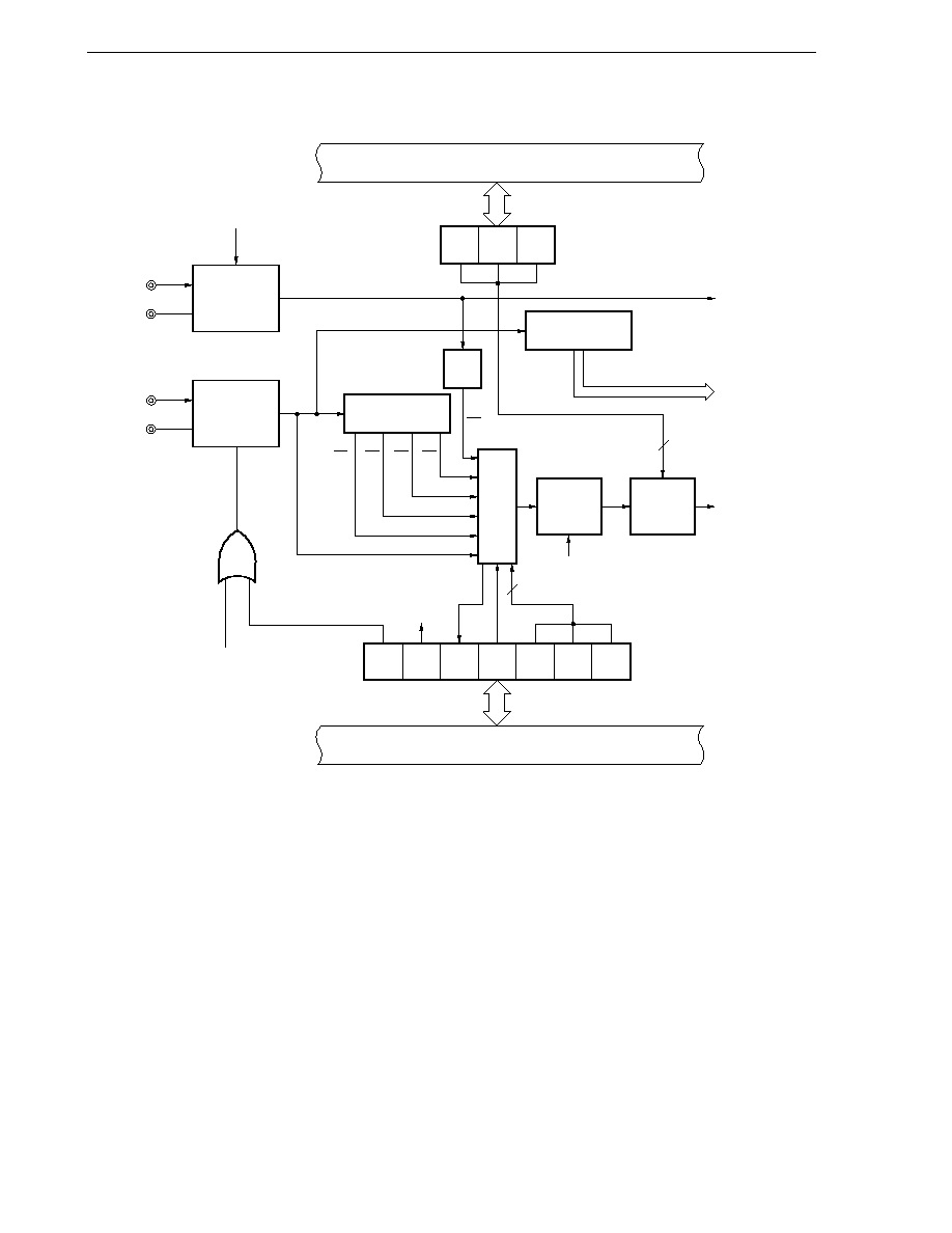
128
CHAPTER 7 CLOCK GENERATOR
User's Manual U14260EJ3V1UD
Figure 7-1. Block Diagram of Clock Generator
XT1
XT2
FRC
Subsystem
clock
oscillator
f
XT
Main system
clock
oscillator
f
X
Prescaler
f
X
2
f
X
2
2
f
X
2
3
f
X
2
4
f
XT
2
1/2
Prescaler
Standby
controller
HALT
Wait
controller
3
3
STOP
MCC FRC
CLS
OSTS2 OSTS1 OSTS0
CSS PCC2 PCC1 PCC0
Oscillation stabilization
time select register (OSTS)
X1
X2
Watch timer,
clock output
function
Clock to
peripheral
hardware
CPU clock
(f
CPU
)
Processor clock control register
(PCC)
Internal bus
Internal bus
Selector

129
CHAPTER 7 CLOCK GENERATOR
User's Manual U14260EJ3V1UD
7.3 Clock Generator Control Registers
The clock generator is controlled by the following two registers.
∑ Processor clock control register (PCC)
∑ Oscillation stabilization time select register (OSTS)
(1) Processor clock control register (PCC)
PCC selects the CPU clock and the division ratio, sets main system clock oscillator operation/stop and sets
whether to use the subsystem clock oscillator internal feedback resistor
Note
.
PCC is set by a 1-bit or 8-bit memory manipulation instruction.
RESET input sets PCC to 04H.
Note The feedback resistor is required to control the bias point of the oscillation waveform so that the bias point
is in the middle of the power supply voltage.
When the subsystem clock is not used, the power consumption in the STOP mode can be reduced by setting
bit 6 (FRC) of PCC to 1 (refer to Figure 7-7 Subsystem Clock Feedback Resistor).

130
CHAPTER 7 CLOCK GENERATOR
User's Manual U14260EJ3V1UD
Figure 7-2. Format of Processor Clock Control Register (PCC)
Address: FFFBH After reset: 04H R/W
Note 1
Symbol
7
6
5
4
3
2
1
0
PCC
MCC
FRC
CLS
CSS
0
PCC2
PCC1
PCC0
MCC
Main system clock oscillation control
Note 2
0
Oscillation possible
1
Oscillation stopped
FRC
Subsystem clock feedback resistor selection
0
Internal feedback resistor used
1
Internal feedback resistor not used
Note 3
CLS
CPU clock status
0
Main system clock
1
Subsystem clock
CSS
PCC2
PCC1
PCC0
CPU clock (f
CPU
) selection
0
0
0
0
f
X
0
0
1
f
X
/2
0
1
0
f
X
/2
2
0
1
1
f
X
/2
3
1
0
0
f
X
/2
4
1
0
0
0
f
XT
/2
0
0
1
0
1
0
0
1
1
1
0
0
Other than above
Setting prohibited
Notes 1. Bit 5 is read only.
2. When the CPU is operating on the subsystem clock, MCC should be used to stop the main system clock
oscillation. The STOP instruction should not be used.
3. This bit can be set to 1 only when the subsystem clock is not used.
Cautions 1. Be sure to set bit 3 to 0.
2. When the external clock is input, MCC should not be set.
This is because the X2 pin is connected to V
DD1
via a pull-up resistor.
Remarks 1. f
X
: Main system clock oscillation frequency
2. f
XT
: Subsystem clock oscillation frequency

131
CHAPTER 7 CLOCK GENERATOR
User's Manual U14260EJ3V1UD
The fastest instructions of the
µPD780078 and 780078Y Subseries are carried out in two CPU clocks. The
relationship between the CPU clock (f
CPU
) and minimum instruction execution time is shown in Table 7-2.
Table 7-2. Relationship Between CPU Clock and Minimum Instruction Execution Time
CPU Clock (f
CPU
)
Minimum Instruction Execution Time: 2/f
CPU
f
X
= 8.38 MHz
f
X
= 12 MHz
Note
f
XT
= 32.768 kHz
f
X
0.238
µs
0.166
µs
-
f
X
/2
0.477
µs
0.333
µs
-
f
X
/2
2
0.954
µs
0.666
µs
-
f
X
/2
3
1.90
µs
1.33
µs
-
f
X
/2
4
3.81
µs
2.66
µs
-
f
XT
/2
-
-
122
µs
Note Expanded-specification products of
µPD780078 Subseries only
Remark
f
X
: Main system clock oscillation frequency
f
XT
: Subsystem clock oscillation frequency

132
CHAPTER 7 CLOCK GENERATOR
User's Manual U14260EJ3V1UD
(2) Oscillation stabilization time select register (OSTS)
This register is used to select the oscillation stabilization time from when reset is effected or STOP mode is
released to when oscillation is stabilized.
OSTS is set by an 8-bit memory manipulation instruction.
RESET input sets OSTS to 04H. Thus, when releasing the STOP mode by RESET input, the time required to
release is 2
17
/fx.
Figure 7-3. Format of Oscillation Stabilization Time Select Register (OSTS)
Address: FFFAH After reset: 04H R/W
Symbol
7
6
5
4
3
2
1
0
OSTS
0
0
0
0
0
OSTS2
OSTS1
OSTS0
OSTS2
OSTS1
OSTS0
Selection of oscillation stabilization time
f
X
= 8.38 MHz
f
X
= 12 MHz
Note
0
0
0
2
12
/f
X
488
µs
341
µs
0
0
1
2
14
/f
X
1.95 ms
1.36 ms
0
1
0
2
15
/f
X
3.91 ms
2.73 ms
0
1
1
2
16
/f
X
7.82 ms
5.46 ms
1
0
0
2
17
/f
X
15.6 ms
10.9 ms
Other than above
Setting prohibited
Note Expanded-specification products of
µPD780078 Subseries only.
Caution
The wait time when STOP mode is released does not include the time ("a" in the figure below)
from when STOP mode is released until the clock starts oscillation.
This also applies when RESET is input and an interrupt request is generated.
Remark
f
X
: Main system clock oscillation frequency
a
STOP mode is released
Voltage waveform
of X1 pin
133
CHAPTER 7 CLOCK GENERATOR
User's Manual U14260EJ3V1UD
7.4 System Clock Oscillator
7.4.1 Main system clock oscillator
The main system clock oscillator oscillates with a crystal resonator or a ceramic resonator (8.38 MHz TYP.)
connected to the X1 and X2 pins.
External clocks can be input to the main system clock oscillator. In this case, input a clock signal to the X1 pin
and an inverted-phase clock signal to the X2 pin.
Figure 7-4 shows an external circuit of the main system clock oscillator.
Figure 7-4. External Circuit of Main System Clock Oscillator
(a) Crystal and ceramic oscillation
(b) External clock
Crystal resonator or
ceramic resonator
X2
V
SS1
X1
X2
X1
External
clock
Caution
Do not execute the STOP instruction and do not set MCC (bit 7 of processor clock control
register (PCC)) to 1 if an external clock is input. This is because when the STOP instruction
is executed or MCC is set to 1, the main system clock operation stops and the X2 pin is connected
to V
DD1
via a pull-up resistor.
134
CHAPTER 7 CLOCK GENERATOR
User's Manual U14260EJ3V1UD
7.4.2 Subsystem clock oscillator
The subsystem clock oscillator oscillates with a crystal resonator (32.768 kHz TYP.) connected to the XT1 and
XT2 pins.
External clocks can be input to the subsystem clock oscillator. In this case, input a clock signal to the XT1 pin
and an inverted-phase clock signal to the XT2 pin.
Figure 7-5 shows an external circuit of the subsystem clock oscillator.
Figure 7-5. External Circuit of Subsystem Clock Oscillator
(a) Crystal oscillation
(b) External clock
32.768
kHz
XT2
XT1
External
clock
XT2
V
SS1
XT1
Cautions are listed on the next page.
135
CHAPTER 7 CLOCK GENERATOR
User's Manual U14260EJ3V1UD
Caution
1. When using the main system clock oscillator and subsystem clock oscillator, wire as follows
in the area enclosed by broken lines in Figures 7-4 and 7-5 to avoid an adverse effect from
wiring capacitance.
∑ Keep the wiring length as short as possible.
∑ Do not cross the wiring with other signal lines. Do not route the wiring near a signal line
through which a high fluctuating current flows.
∑ Always make the ground point of the oscillator capacitor the same potential as V
SS1
. Do
not ground the capacitor to a ground pattern through which a high current flows.
∑ Do not fetch signals from the oscillator.
Note that the subsystem clock oscillator is designed as a low-amplitude circuit for reducing
power consumption.
Figure 7-6 shows examples of incorrect resonator connection.
Figure 7-6. Examples of Incorrect Resonator Connection (1/2)
(a) Too long wiring
(b) Crossed signal line
Remark
When using the subsystem clock, replace X1 and X2 with XT1 and XT2, respectively. Also, insert
resistors in series on the XT2 side.
V
SS1
V
SS1
X2
X1
X2
X1
PORTn
(n = 0 to 8)

136
CHAPTER 7 CLOCK GENERATOR
User's Manual U14260EJ3V1UD
Figure 7-6. Examples of Incorrect Resonator Connection (2/2)
(c) Wiring near high fluctuating current
(d) Current flowing through ground line of
oscillator (potential at points A, B, and
C fluctuates)
(e) Signals are fetched
Remark
When using the subsystem clock, replace X1 and X2 with XT1 and XT2, respectively. Also, insert
resistors in series on the XT2 side.
Caution
2. When X2 and XT1 are wired in parallel, the crosstalk noise of X2 may increase with XT1,
resulting in malfunction.
To prevent that from occurring, it is recommended to wire X2 and XT1 so that they are not
in parallel, and to connect the IC pin between X2 and XT1 directly to V
SS1
.
X2
V
SS1
X1
High current
X2
X1
V
SS1
A
B
C
Pnm
V
DD0
High current
V
SS1
X2
X1
137
CHAPTER 7 CLOCK GENERATOR
User's Manual U14260EJ3V1UD
7.4.3 When subsystem clock is not used
If it is not necessary to use the subsystem clock for low power consumption operations and watch operations,
connect the XT1 and XT2 pins as follows.
XT1: Connect directly to V
DD0
or V
DD1
XT2: Leave open
In this state, however, some current may leak via the internal feedback resistor of the subsystem clock oscillator
when the main system clock stops. To minimize leakage current, the above internal feedback resistor can be removed
by setting bit 6 (FRC) of the processor clock control register (PCC). In this case also, connect the XT1 and XT2 pins
as described above.
Figure 7-7. Subsystem Clock Feedback Resistor
FRC
P-ch
Feedback resistor
XT1
XT2
Remark
The feedback resistor is required to control the bias point of the oscillation waveform so that the bias
point is in the middle of the power supply voltage.

138
CHAPTER 7 CLOCK GENERATOR
User's Manual U14260EJ3V1UD
7.5 Clock Generator Operations
The clock generator generates the following types of clocks and controls the CPU operating mode including the
standby mode.
∑ Main system clock f
X
∑ Subsystem clock f
XT
∑ CPU clock f
CPU
∑ Clock to peripheral hardware
The following clock generator functions and operations are determined by the processor clock control register
(PCC).
(a) Upon generation of the RESET signal, the lowest speed mode of the main system clock (3.81
µs @ 8.38 MHz
operation) is selected (PCC = 04H). Main system clock oscillation stops while a low level is applied to the RESET
pin.
(b) With the main system clock selected, one of the five levels of minimum instruction execution time (0.166
µs, 0.333
µs, 0.666 µs, 1.33 µs, 2.66 µs: @ 12 MHz operation
Note
, 0.238
µs, 0.476 µs, 0.954 µs, 1.90 µs, 3.81 µs: @ 8.38
MHz operation) can be selected by setting PCC.
(c) With the main system clock selected, two standby modes, the STOP and HALT modes, are available. To reduce
power consumption in the STOP mode, the subsystem clock feedback resistor can be disconnected to stop the
subsystem clock.
(d) PCC can be used to select the subsystem clock and to operate the system with low power consumption (122
µs @ 32.768 kHz operation).
(e) With the subsystem clock selected, main system clock oscillation can be stopped via PCC. The HALT mode
can be used. However, the STOP mode cannot be used (subsystem clock oscillation cannot be stopped).
(f)
The main system clock is divided and supplied to the peripheral hardware. The subsystem clock is supplied to
the watch timer and clock output functions only. Thus the watch function and the clock output function can also
be continued in the standby state. However, since all other peripheral hardware operate with the main system
clock, the peripheral hardware also stops if the main system clock is stopped (except external input clock
operation).
Note Expanded-specification products of
µPD780078 Subseries only
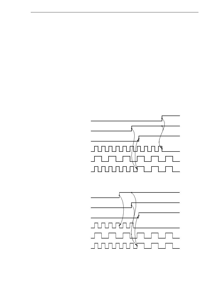
139
CHAPTER 7 CLOCK GENERATOR
User's Manual U14260EJ3V1UD
7.5.1 Main system clock operations
When operating with the main system clock (with bit 5 (CLS) of the processor clock control register (PCC) set to
0), the following operations are carried out by PCC setting.
(a) Because the operation-guaranteed instruction execution speed depends on the power supply voltage, the
minimum instruction execution time can be changed by bits 0 to 2 (PCC0 to PCC2) of PCC.
(b) When bit 4 (CSS) of PCC is set to 1 when operating with the main system clock, if bit 7 (MCC) of PCC is set
to 1 after the operation has been switched to the subsystem clock (CLS = 1), the main system clock oscillation
stops (see Figure 7-8 (1)).
(c) If bit 7 (MCC) of PCC is set to 1 when operating with the main system clock, the main system clock oscillation
does not stop. When bit 4 (CSS) of PCC is set to 1 and the operation is switched to the subsystem clock (CLS
= 1) after that, the main system clock oscillation stops (see Figure 7-8 (2)).
Figure 7-8. Main System Clock Stop Function
(1) Operation when MCC is set after setting CSS with main system clock operation
MCC
CSS
CLS
Main system clock oscillation
Subsystem clock oscillation
CPU clock
(2) Operation when CSS is set after setting MCC with main system clock operation
Main system clock oscillation
Subsystem clock oscillation
CPU clock
MCC
CSS
CLS
Oscillation does not stop

140
CHAPTER 7 CLOCK GENERATOR
User's Manual U14260EJ3V1UD
7.5.2 Subsystem clock operations
When operating with the subsystem clock (with bit 5 (CLS) of the processor clock control register (PCC) set to
1), the following operations are carried out.
(a) The minimum instruction execution time remains constant (122
µs @ 32.768 kHz operation) irrespective of bits
0 to 2 (PCC0 to PCC2) of PCC.
(b) Watchdog timer counting stops.
Caution
Do not execute the STOP instruction while the subsystem clock is in operation.
7.6 Changing System Clock and CPU Clock Settings
7.6.1 Time required for switchover between system clock and CPU clock
The system clock and CPU clock can be switched over by means of bits 0 to 2 (PCC0 to PCC2) and bit 4 (CSS)
of the processor clock control register (PCC).
The actual switchover operation is not performed directly after writing to the PCC; operation continues on the pre-
switchover clock for several instructions (see Table 7-3).
Determination as to whether the system is operating on the main system clock or the subsystem clock is performed
by bit 5 (CLS) of the PCC register.
Table 7-3. Maximum Time Required for CPU Clock Switchover
Remark
One instruction is the minimum instruction execution time with the pre-switchover CPU clock.
Caution
Selection of the CPU clock cycle division ratio (PCC0 to PCC2) and switchover from the main
system clock to the subsystem clock (changing CSS from 0 to 1) should not be set simultaneously.
Simultaneous setting is possible, however, for selection of the CPU clock cycle division ratio
(PCC0 to PCC2) and switchover from the subsystem clock to the main system clock (changing
CSS from 1 to 0).
Set Value Before
Set Value After Switchover
Switchover
CSS PCC2 PCC1 PCC0 CSS PCC2 PCC1 PCC0 CSS PCC2 PCC1 PCC0 CSS PCC2 PCC1 PCC0 CSS PCC2 PCC1 PCC0 CSS PCC2 PCC1 PCC0 CSS PCC2 PCC1 PCC0
0
0
0
0
0
0
0
1
0
0
1
0
0
0
1
1
0
1
0
0
1
◊
◊
◊
0
0
0
0
16 instructions
16 instructions
16 instructions
16 instructions
f
X
/2f
XT
instruction
0
0
1
8 instructions
8 instructions
8 instructions
8 instructions
f
X
/4f
XT
instruction
0
1
0
4 instructions
4 instructions
4 instructions
4 instructions
f
X
/8f
XT
instruction
0
1
1
2 instructions
2 instructions
2 instructions
2 instructions
f
X
/16f
XT
instruction
1
0
0
1 instruction
1 instruction
1 instruction
1 instruction
f
X
/32f
XT
instruction
1
◊
◊
◊
1 instruction
1 instruction
1 instruction
1 instruction
1 instruction

141
CHAPTER 7 CLOCK GENERATOR
User's Manual U14260EJ3V1UD
7.6.2 System clock and CPU clock switching procedure
This section describes procedure for switching between the system clock and CPU clock.
Figure 7-9. System Clock and CPU Clock Switching
<1>
The CPU is reset by setting the RESET signal to low level after power-on. After that, when reset is released
by setting the RESET signal to high level, the main system clock starts oscillation. At this time, the oscillation
stabilization time (2
17
/f
X
) is secured automatically.
After that, the CPU starts executing instructions at the minimum speed of the main system clock (3.81
µs @
8.38 MHz operation).
<2>
After the lapse of sufficient time for the V
DD
voltage to increase to enable operation at maximum speeds, PCC
is rewritten and maximum-speed operation is carried out.
<3>
Upon detection of a decrease of the V
DD
voltage due to an interrupt request signal, the main system clock is
switched to the subsystem clock (which must be in an oscillation stable state).
<4>
Upon detection of V
DD
voltage reset due to an interrupt, 0 is set to the MCC and oscillation of the main system
clock is started. After the lapse of the time required for stabilization of oscillation, PCC is rewritten and the
maximum-speed operation is resumed.
Caution
When the main system clock is stopped and the device is operating on the subsystem clock,
wait until the oscillation stabilization time has been secured by the program before switching
back to the main system clock.
System clock
CPU clock
Interrupt request signal
RESET
V
DD
f
X
f
X
f
XT
f
X
Lowest-
speed
operation
Highest-
speed
operation
Subsystem
clock
operation
High-speed
operation
Wait (15.6 ms: @8.38 MHz operation)
Internal reset operation

142
User's Manual U14260EJ3V1UD
CHAPTER 8 16-BIT TIMER/EVENT COUNTERS 00, 01
8.1 Functions of 16-Bit Timer/Event Counters 00, 01
16-bit timer/event counters 00, 01 have the following functions.
(1) Interval timer
16-bit timer/event counters 00, 01 generate interrupt requests at the preset time interval.
∑ Number of counts: 2 to 65536
(2) External event counter
16-bit timer/event counters 00, 01 can measure the number of pulses with a high-/low-level width of a signal input
externally.
∑ Valid level pulse width: 16/f
X
or more
(3) Pulse width measurement
16-bit timer/event counters 00, 01 can measure the pulse width of an externally input signal.
∑ Valid level pulse width: 2/f
X
or more
(4) Square-wave output
16-bit timer/event counters 00, 01 can output a square wave with any selected frequency.
∑ Cycle: (2
◊ 2 to 65536 ◊ 2) ◊ count clock cycle
(5) PPG output
16-bit timer/event counters 00, 01 can output a square wave that have arbitrary cycle and pulse width.
∑ 2 < Pulse width < Cycle
(FFFF + 1) H
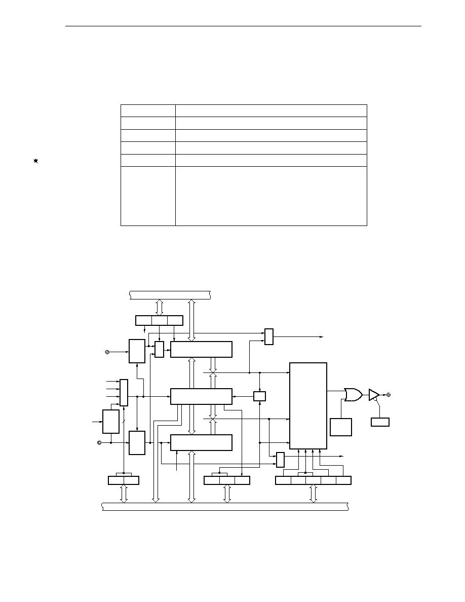
143
CHAPTER 8 16-BIT TIMER/EVENT COUNTERS 00, 01
User's Manual U14260EJ3V1UD
8.2 Configuration of 16-Bit Timer/Event Counters 00, 01
16-bit timer/event counters 00, 01 consist of the following hardware.
Table 8-1. Configuration of 16-Bit Timer/Event Counters 00, 01
Item
Configuration
Timer counter
16-bit timer counter 0n (TM0n)
Register
16-bit timer capture/compare registers 00n, 01n (CR00n, CR01n)
Timer input
TI00n, TI01n
Timer output
TO0n, output controller
Control registers
16-bit timer mode control register 0n (TMC0n)
Capture/compare control register 0n (CRC0n)
16-bit timer output control register 0n (TOC0n)
Prescaler mode register 0n (PRM0n)
Port mode register 7 (PM7)
Port register 7 (P7)
Remark
n = 0, 1
Figures 8-1 and 8-2 show the block diagrams.
Figure 8-1. Block Diagram of 16-Bit Timer/Event Counter 00
Note TI000 input and TO00 output cannot be used at the same time.
Capture/compare control
register 00 (CRC00)
Prescaler mode
register 00 (PRM00)
16-bit timer output
control register 00
(TOC00)
16-bit timer mode
control register 00
(TMC00)
Internal bus
TI010/P71
f
X
f
X
/2
2
f
X
/2
6
f
X
/2
3
TI000/TO00/P70
Note
2
Noise
elimi-
nator
PRM010 PRM000
CRC020
Match
Match
Clear
Noise
elimi-
nator
Noise
elimi-
nator
CRC020 CRC010 CRC000
INTTM000
TO00/TI000/
P70
Note
INTTM010
Internal bus
TMC003 TMC002 OVF00
TOC040 LVS00 LVR00 TOC010 TOE00
Output latch
(P70)
PM70
Selector
Selector
Selector
Selector
16-bit timer capture/compare
register 010 (CR010)
16-bit timer counter 00
(TM00)
16-bit timer capture/compare
register 000 (CR000)
Output
controller
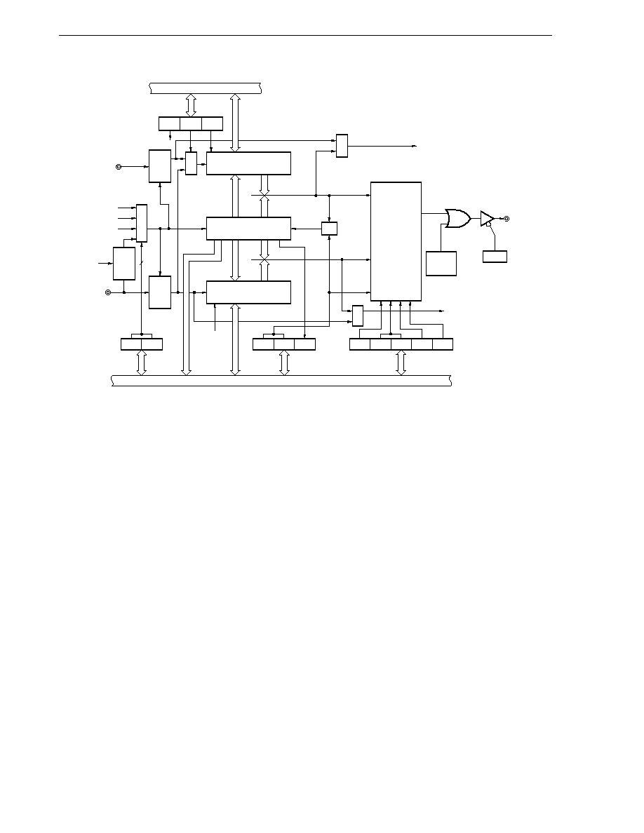
144
CHAPTER 8 16-BIT TIMER/EVENT COUNTERS 00, 01
User's Manual U14260EJ3V1UD
Figure 8-2. Block Diagram of 16-Bit Timer/Event Counter 01
Note TI001 input and TO01 output cannot be used at the same time.
TI011/PCL/P74
f
X
/2
f
X
/2
3
f
X
/2
9
f
X
/2
3
TI001/TO01/
BUZ/P75
Note
2
PRM011 PRM001
CRC021
CRC021 CRC011 CRC001
INTTM001
INTTM011
TMC013 TMC012 OVF01
TOC041 LVS01 LVR01 TOC011 TOE01
TO01/TI001/
BUZ/P75
Note
PM75
Capture/compare control
register 01 (CRC01)
Prescaler mode
register 01 (PRM01)
16-bit timer output
control register 01
(TOC01)
16-bit timer mode
control register 01
(TMC01)
Internal bus
Noise
elimi-
nator
Match
Match
Clear
Noise
elimi-
nator
Noise
elimi-
nator
Internal bus
Output latch
(P75)
Selector
Selector
Selector
Selector
16-bit timer capture/compare
register 011 (CR011)
16-bit timer counter 01
(TM01)
16-bit timer capture/compare
register 001 (CR001)
Output
controller
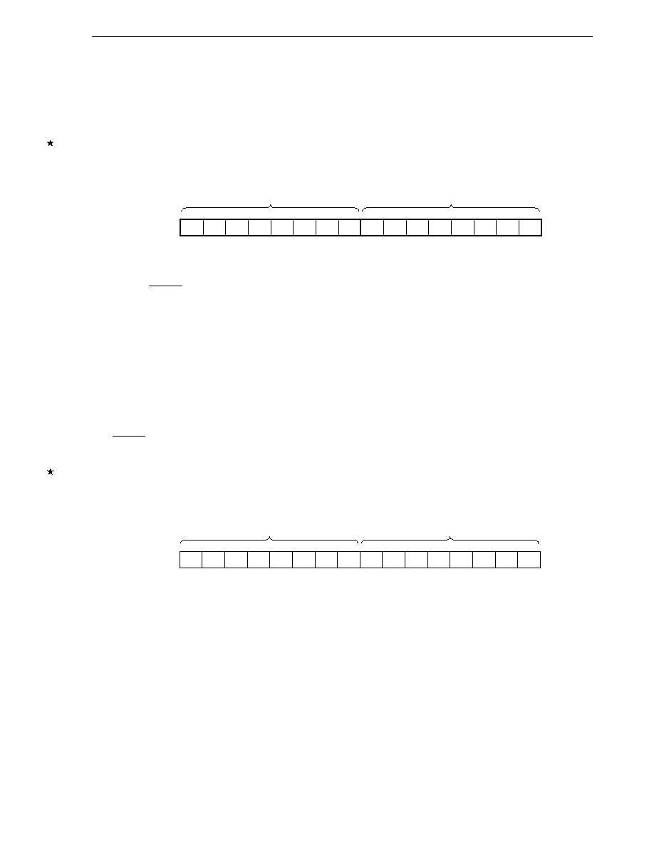
145
CHAPTER 8 16-BIT TIMER/EVENT COUNTERS 00, 01
User's Manual U14260EJ3V1UD
(1) 16-bit timer counter 0n (TM0n)
TM0n is a 16-bit read-only register that counts count pulses.
The counter is incremented in synchronization with the rising edge of the count clock. If the count value is read
during operation, input of the count clock is temporarily stopped, and the count value at that point is read.
Figure 8-3. Format of 16-Bit Timer Counter 0n (TM0n)
The count value is reset to 0000H in the following cases.
<1> At RESET input
<2> If TMC0n3 and TMC0n2 are cleared
<3> If the valid edge of TI00n is input in the clear & start mode entered by inputting the valid edge of TI00n
<4> If TM0n and CR00n match in the clear & start mode entered on a match between TM0n and CR00n
(2) 16-bit timer capture/compare register 00n (CR00n)
CR00n is a 16-bit register which has the functions of both a capture register and a compare register. Whether
it is used as a capture register or as a compare register is set by bit 0 (CRC00n) of capture/compare control register
0n (CRC0n).
CR00n is set by a 16-bit memory manipulation instruction.
RESET input clears CR00n to 0000H.
Figure 8-4. Format of 16-Bit Timer Capture/Compare Register 00n (CR00n)
∑ When CR00n is used as a compare register
The value set in CR00n is constantly compared with the 16-bit timer/counter 0n (TM0n) count value, and an
interrupt request (INTTM00n) is generated if they match. It can also be used as the register that holds the
interval time when TM0n is set to interval timer operation.
∑ When CR00n is used as a capture register
It is possible to select the valid edge of the TI00n pin or the TI01n pin as the capture trigger. Setting of the TI00n
or TI01n valid edge is performed by means of prescaler mode register 0n (PRM0n) (refer to Table 8-2).
TM0n
(n = 0, 1)
Symbol
FF0FH (TM00)
FF6DH (TM01)
FF0EH (TM00)
FF6CH (TM01)
Address: FF0EH, FF0FH (TM00), FF6CH, FF6DH (TM01) After reset: 0000H R
CR00n
(n = 0, 1)
Symbol
FF0BH (CR000)
FF69H (CR001)
FF0AH (CR000)
FF68H (CR001)
Address: FF0AH, FF0BH (CR000), FF68H, FF69H (CR001) After reset: 0000H R/W
146
CHAPTER 8 16-BIT TIMER/EVENT COUNTERS 00, 01
User's Manual U14260EJ3V1UD
Table 8-2. CR00n Capture Trigger and Valid Edges of TI00n and TI01n Pins
(1) TI00n pin valid edge selected as capture trigger (CRC01n = 1, CRC00n = 1)
CR00n Capture Trigger
TI00n Pin Valid Edge
ES01n
ES00n
Falling edge
Rising edge
0
1
Rising edge
Falling edge
0
0
No capture operation
Both rising and falling edges
1
1
(2) TI01n pin valid edge selected as capture trigger (CRC01n = 0, CRC00n = 1)
CR00n Capture Trigger
TI01n Pin Valid Edge
ES11n
ES10n
Falling edge
Falling edge
0
0
Rising edge
Rising edge
0
1
Both rising and falling edges
Both rising and falling edges
1
1
Remarks 1. Setting ES01n, ES00n = 1, 0 and ES11n, ES10n = 1, 0 is prohibited.
2. ES01n, ES00n:
Bits 5 and 4 of prescaler mode register 0n (PRM0n)
ES11n, ES10n:
Bits 7 and 6 of prescaler mode register 0n (PRM0n)
CRC01n, CRC00n: Bits 1 and 0 of capture/compare control register 0n (CRC0n)
3. n = 0, 1
Cautions 1. Set CR00n to a value other than 0000H in the clear & start mode entered on a match between
TM0n and CR00n. However, in the free-running mode and in the clear & start mode using
the valid edge of the TI00n pin, if CR00n is set to 0000H, an interrupt request (INTTM00n)
is generated when CR00n changes from 0000H to 0001H following overflow (FFFFH).
2. If the new value of CR00n is less than the value of 16-bit timer counter 0n (TM0n), TM0n
continues counting, overflows, and then starts counting from 0 again. If the new value of
CR00n is less than the old value, therefore, the timer must be reset to be restarted after the
value of CR00n is changed.
3. When P70 is used as the input pin for the valid edge of TI000, it cannot be used as a timer
output (TO00). Moreover, when P70 is used as TO00, it cannot be used as the input pin for
the valid edge of TI000.
4. When P75 is used as the input pin for the valid edge of TI001, it cannot be used as a timer
output (TO01). Moreover, when P75 is used as TO01, it cannot be used as the input pin for
the valid edge of TI001.
5. When CR00n is used as a capture register, read data is undefined if the register read time
and capture trigger input conflict (the capture data itself is the correct value). If count stop
input and capture trigger input conflict, the captured data is undefined.

147
CHAPTER 8 16-BIT TIMER/EVENT COUNTERS 00, 01
User's Manual U14260EJ3V1UD
(3) 16-bit timer capture/compare register 01n (CR01n)
CR01n is a 16-bit register which has the functions of both a capture register and a compare register. Whether it
is used as a capture register or a compare register is set by bit 2 (CRC02n) of capture/compare control register 0n
(CRC0n).
CR01n is set by a 16-bit memory manipulation instruction.
RESET input clears CR01n to 0000H.
Figure 8-5. Format of 16-Bit Timer Capture/Compare Register 01n (CR01n)
∑ When CR01n is used as a compare register
The value set in CR01n is constantly compared with the 16-bit timer counter 0n (TM0n) count value, and an
interrupt request (INTTM01n) is generated if they match.
∑ When CR01n is used as a capture register
It is possible to select the valid edge of the TI00n pin as the capture trigger. The TI00n valid edge is set by
means of prescaler mode register 0n (PRM0n) (refer to Table 8-3).
Table 8-3. CR01n Capture Trigger and Valid Edge of TI00n Pin (CRC02n = 1)
CR01n Capture Trigger
TI00n Pin Valid Edge
ES01n
ES00n
Falling edge
Falling edge
0
0
Rising edge
Rising edge
0
1
Both rising and falling edges
Both rising and falling edges
1
1
Remarks 1. Setting ES01n, ES00n = 1, 0 is prohibited.
2. ES01n, ES00n: Bits 5 and 4 of prescaler mode register 0n (PRM0n)
CRC02n:
Bit 2 of capture/compare control register 0n (CRC0n)
3. n = 0, 1
Cautions 1. If CR01n is set to 0000H, an interrupt request (INTTM01n) is generated when CR01n changes
from 0000H to 0001H following overflow (FFFFH). INTTM01n is generated after the match
between TM0n and CR01n or after the valid edge of the TI00n pin is detected.
2. When CR01n is used as a capture register, read data is undefined if the register read time
and capture trigger input conflict (the capture data itself is the correct value). If count stop
input and capture trigger input conflict, the captured data is undefined.
Remark
n = 0, 1
CR01n
(n = 0, 1)
Symbol
FF0DH (CR010)
FF6BH (CR011)
FF0CH (CR010)
FF6AH (CR011)
Address: FF0CH, FF0DH (CR010), FF6AH, FF6BH (CR011) After reset: 0000H R/W

148
CHAPTER 8 16-BIT TIMER/EVENT COUNTERS 00, 01
User's Manual U14260EJ3V1UD
8.3 Registers to Control 16-Bit Timer/Event Counters 00, 01
The following six types of registers are used to control 16-bit timer/event counters 00, 01.
∑ 16-bit timer mode control register 0n (TMC0n)
∑ Capture/compare control register 0n (CRC0n)
∑ 16-bit timer output control register 0n (TOC0n)
∑ Prescaler mode register 0n (PRM0n)
∑ Port mode register 7 (PM7)
∑ Port register 7 (P7)
Remark
n = 0, 1
(1) 16-bit timer mode control register 0n (TMC0n: n = 0, 1)
This register sets the 16-bit timer operating mode, the 16-bit timer counter 0n (TM0n) clear mode, and output
timing, and detects an overflow.
TMC0n is set by a 1-bit or 8-bit memory manipulation instruction.
RESET input clears TMC0n to 00H.
Caution
16-bit timer counter 0n (TM0n) starts operation at the moment TMC0n2 and TMC0n3 (operation
stop mode) are set to a value other than 0, 0, respectively. Set TMC0n2 and TMC0n3 to 0, 0
to stop the operation.
149
CHAPTER 8 16-BIT TIMER/EVENT COUNTERS 00, 01
User's Manual U14260EJ3V1UD
Figure 8-6. Format of 16-Bit Timer Mode Control Register 00 (TMC00)
TMC003 TMC002
Operating mode
TO00 inversion timing selection
Interrupt request generation
and clear mode selection
0
0
Operation stop
No change
Not generated
(TM00 cleared to 0)
0
1
Free-running mode
Match between TM00 and
CR000 or match between
TM00 and CR010
1
0
Clear & start on TI000 pin
--
valid edge
1
1
Clear & start on match between
Match between TM00 and
TM00 and CR000
CR000 or match between
TM00 and CR010
OVF00
Overflow detection of 16-bit timer counter 00 (TM00)
0
Overflow not detected
1
Overflow detected
Cautions 1. To write different data to TMC00, stop the timer operation before writing.
2. The timer operation must be stopped before writing to bits other than the OVF00 flag.
3. Set the valid edge of the TI000/TO00/P70 pin with prescaler mode register 00 (PRM00).
4. If any of the following modes is selected: the mode in which clear & start occurs on match
between TM00 and CR000, the mode in which clear & start occurs at the TI000 pin valid edge,
or free-running mode, when the set value of CR000 is FFFFH and the TM00 value changes
from FFFFH to 0000H, the OVF00 flag is set to 1.
Remarks 1. TO00:
16-bit timer/event counter 00 output pin
2. TI000: 16-bit timer/event counter 00 input pin
3. TM00: 16-bit timer counter 00
4. CR000: 16-bit timer capture/compare register 000
5. CR010: 16-bit timer capture/compare register 010
Generated on match
between TM00 and CR000,
or match between TM00 and
CR010
7
0
6
0
5
0
4
0
3
TMC003
2
TMC002
1
0
0
OVF00
Symbol
TMC00
Address: FF60H After reset: 00H R/W
150
CHAPTER 8 16-BIT TIMER/EVENT COUNTERS 00, 01
User's Manual U14260EJ3V1UD
Figure 8-7. Format of 16-Bit Timer Mode Control Register 01 (TMC01)
TMC013 TMC012
Operating mode
TO01 output timing selection
Interrupt request generation
and clear mode selection
0
0
Operation stop
No change
Not generated
(TM01 cleared to 0)
0
1
Free-running mode
Match between TM01 and
CR001 or match between
TM01 and CR011
1
0
Clear & start on TI001 pin
--
valid edge
1
1
Clear & start on match between
Match between TM01 and
TM01 and CR001
CR001 or match between
TM01 and CR011
OVF01
Overflow detection of 16-bit timer counter 01 (TM01)
0
Overflow not detected
1
Overflow detected
Cautions 1. To write different data to TMC01, stop the timer operation before writing.
2. The timer operation must be stopped before writing to bits other than the OVF01 flag.
3. Set the valid edge of the TI001/TO01/BUZ/P75 pin with prescaler mode register 01 (PRM01).
4. If any of the following modes is selected: the mode in which clear & start occurs on match
between TM01 and CR001, the mode in which clear & start occurs at the TI001 pin valid edge,
or free-running mode, when the set value of CR001 is FFFFH and the TM01 value changes
from FFFFH to 0000H, the OVF01 flag is set to 1.
Remarks 1. TO01:
16-bit timer/event counter 01 output pin
2. TI001: 16-bit timer/event counter 01 input pin
3. TM01: 16-bit timer counter 01
4. CR001: 16-bit timer capture/compare register 001
5. CR011: 16-bit timer capture/compare register 011
Generated on match
between TM01 and CR001,
or match between TM01 and
CR011
7
0
6
0
5
0
4
0
3
TMC013
2
TMC012
1
0
0
OVF01
Symbol
TMC01
Address: FF64H After reset: 00H R/W
151
CHAPTER 8 16-BIT TIMER/EVENT COUNTERS 00, 01
User's Manual U14260EJ3V1UD
(2) Capture/compare control register 0n (CRC0n: n = 0, 1)
This register controls the operation of the 16-bit timer capture/compare registers (CR00n, CR01n).
CRC0n is set by a 1-bit or 8-bit memory manipulation instruction.
RESET input clears CRC0n to 00H.
Figure 8-8. Format of Capture/Compare Control Register 00 (CRC00)
Address: FF62H After reset: 00H R/W
Symbol
7
6
5
4
3
2
1
0
CRC00
0
0
0
0
0
CRC020
CRC010
CRC000
CRC020
CR010 operating mode selection
0
Operate as compare register
1
Operate as capture register
CRC010
CR000 capture trigger selection
0
Capture on valid edge of TI010 pin
1
Capture on valid edge of TI000 pin by reverse phase
CRC000
CR000 operating mode selection
0
Operate as compare register
1
Operate as capture register
Cautions 1. The timer operation must be stopped before setting CRC00.
2. When the clear & start mode entered on a match between TM00 and CR000 is selected by
16-bit timer mode control register 00 (TMC00), CR000 should not be specified as a capture
register.
3. If both the rising and falling edges have been selected as the valid edges of the TI000 pin,
capture is not performed.
4. To ensure the reliability of the capture operation, the capture trigger requires a pulse longer
than two cycles of the count clock selected by prescaler mode register 00 (PRM00) (refer
to Figure 8-22).

152
CHAPTER 8 16-BIT TIMER/EVENT COUNTERS 00, 01
User's Manual U14260EJ3V1UD
Figure 8-9. Format of Capture/Compare Control Register 01 (CRC01)
Address: FF66H After reset: 00H R/W
Symbol
7
6
5
4
3
2
1
0
CRC01
0
0
0
0
0
CRC021
CRC011
CRC001
CRC021
CR011 operating mode selection
0
Operate as compare register
1
Operate as capture register
CRC011
CR001 capture trigger selection
0
Capture on valid edge of TI011 pin
1
Capture on valid edge of TI001 pin by reverse phase
CRC001
CR001 operating mode selection
0
Operate as compare register
1
Operate as capture register
Cautions 1. The timer operation must be stopped before setting CRC01.
2. When the clear & start mode entered on a match between TM01 and CR001 is selected by
16-bit timer mode control register 01 (TMC01), CR001 should not be specified as a capture
register.
3. If both the rising and falling edges have been selected as the valid edges of the TI001 pin,
capture is not performed.
4. To ensure the reliability of the capture operation, the capture trigger requires a pulse longer
than two cycles of the count clock selected by prescaler mode register 01 (PRM01) (refer
to Figure 8-22).
153
CHAPTER 8 16-BIT TIMER/EVENT COUNTERS 00, 01
User's Manual U14260EJ3V1UD
(3) 16-bit timer output control register 0n (TOC0n: n = 0, 1)
This register controls the operation of the 16-bit timer/event counter output controller. It sets timer output F/F set/
reset, output inversion enable/disable, and 16-bit timer/event counter 0n timer output enable/disable.
TOC0n is set by a 1-bit or 8-bit memory manipulation instruction.
RESET input clears TOC0n to 00H.
Figure 8-10. Format of 16-Bit Timer Output Control Register 00 (TOC00)
Address: FF63H After reset: 00H R/W
Symbol
7
6
5
4
3
2
1
0
TOC00
0
0
0
TOC040
LVS00
LVR00
TOC010
TOE00
TOC040
Timer output F/F control by match of CR010 and TM00
0
Inversion operation disabled
1
Inversion operation enabled
LVS00
LVR00
16-bit timer/event counter 00 timer output F/F status setting
0
0
No change
0
1
Timer output F/F reset (0)
1
0
Timer output F/F set (1)
1
1
Setting prohibited
TOC010
Timer output F/F control by match of CR000 and TM00
0
Inversion operation disabled
1
Inversion operation enabled
TOE00
16-bit timer/event counter 00 output control
0
Output disabled (output set to level 0)
1
Output enabled
Cautions 1. The timer operation must be stopped before setting other than TOC040.
2. If LVS00 and LVR00 are read after data is set, they will be 0.
3. Bits 5 to 7 of TOC00 must be set to 0.
154
CHAPTER 8 16-BIT TIMER/EVENT COUNTERS 00, 01
User's Manual U14260EJ3V1UD
Figure 8-11. Format of 16-Bit Timer Output Control Register 01 (TOC01)
Address: FF67H After reset: 00H R/W
Symbol
7
6
5
4
3
2
1
0
TOC01
0
0
0
TOC041
LVS01
LVR01
TOC011
TOE01
TOC041
Timer output F/F control by match of CR011 and TM01
0
Inversion operation disabled
1
Inversion operation enabled
LVS01
LVR01
16-bit timer/event counter 01 timer output F/F status setting
0
0
No change
0
1
Timer output F/F reset (0)
1
0
Timer output F/F set (1)
1
1
Setting prohibited
TOC011
Timer output F/F control by match of CR001 and TM01
0
Inversion operation disabled
1
Inversion operation enabled
TOE01
16-bit timer/event counter 01 output control
0
Output disabled (output set to level 0)
1
Output enabled
Cautions 1. The timer operation must be stopped before setting TOC041.
2. If LVS01 and LVR01 are read after data is set, they will be 0.
3. Bits 5 to 7 of TOC01 must be set to 0.
155
CHAPTER 8 16-BIT TIMER/EVENT COUNTERS 00, 01
User's Manual U14260EJ3V1UD
(4) Prescaler mode register 0n (PRM0n: n = 0, 1)
This register is used to set the 16-bit timer counter 0n (TM0n) count clock and TI00n, TI01n pin input valid edges.
PRM0n is set by an 8-bit memory manipulation instruction.
RESET input clears PRM0n to 00H.
Figure 8-12. Format of Prescaler Mode Register 00 (PRM00)
Address: FF61H After reset: 00H R/W
Symbol
7
6
5
4
3
2
1
0
PRM00
ES110
ES100
ES010
ES000
0
0
PRM010
PRM000
ES110
ES100
TI010 pin valid edge selection
0
0
Falling edge
0
1
Rising edge
1
0
Setting prohibited
1
1
Both falling and rising edges
ES010
ES000
TI000 pin valid edge selection
0
0
Falling edge
0
1
Rising edge
1
0
Setting prohibited
1
1
Both falling and rising edges
PRM010
PRM000
Count clock selection
f
X
= 8.38 MHz
f
X
= 12 MHz
Note 1
0
0
f
X
8.38 MHz
12 MHz
0
1
f
X
/2
2
2.09 MHz
3 MHz
1
0
f
X
/2
6
130 kHz
187 kHz
1
1
TI000 pin valid edge
Notes 2, 3
Notes 1. Expanded-specification products of
µPD780078 Subseries only.
2. The external clock requires a pulse two cycles longer than internal clock (f
X
/2
3
).
3. When the valid edge of the TI000 pin is selected, the main system clock is used as the sampling clock
for noise elimination. The valid edge of the TI000 pin can be used only when the main system clock
is operating.
Cautions 1. Always set data to PRM00 after stopping the timer operation.
2. If the valid edge of the TI000 pin is to be set as the count clock, do not set the clear & start
mode and the capture trigger at the valid edge of the TI000 pin.
3. When P70 is used as the valid edge of the TI000 pin, it cannot be used as the timer output
(TO00 pin), and when used as the TO00 pin, it cannot be used as the valid edge of the TI000
pin.
4. If the TI000 or TI010 pin is high level immediately after system reset, the rising edge is
immediately detected after the rising edge or both the rising and falling edges are set as
the valid edge(s) of the TI000 pin or TI010 pin to enable the operation of 16-bit timer counter
00 (TM00). Be careful when pulling up the TI000 pin or the TI010 pin. However, when re-
enabling operation after the operation has been stopped once, the rising edge is not
detected.
Remarks 1. f
X
: Main system clock oscillation frequency
2. TI000 or TI010 pin: 16-bit timer/event counter 00 input pin
156
CHAPTER 8 16-BIT TIMER/EVENT COUNTERS 00, 01
User's Manual U14260EJ3V1UD
Figure 8-13. Format of Prescaler Mode Register 01 (PRM01)
Address: FF65H After reset: 00H R/W
Symbol
7
6
5
4
3
2
1
0
PRM01
ES111
ES101
ES011
ES001
0
0
PRM011
PRM001
ES111
ES101
TI011 pin valid edge selection
0
0
Falling edge
0
1
Rising edge
1
0
Setting prohibited
1
1
Both falling and rising edges
ES011
ES001
TI001 pin valid edge selection
0
0
Falling edge
0
1
Rising edge
1
0
Setting prohibited
1
1
Both falling and rising edges
PRM011
PRM001
Count clock selection
f
X
= 8.38 MHz
f
X
= 12 MHz
Note 1
0
0
f
X
/2
4.19 MHz
6 MHz
0
1
f
X
/2
3
1.04 MHz
1.5 MHz
1
0
f
X
/2
9
16.36 kHz
23.43 kHz
1
1
TI001 pin valid edge
Notes 2, 3
Notes 1. Expanded-specification products of
µPD780078 Subseries only.
2. The external clock requires a pulse two cycles longer than internal clock (f
X
/2
3
).
3. When the valid edge of the TI001 pin is selected, the main system clock is used as the sampling clock
for noise elimination. The valid edge of the TI001 pin can be used only when the main system clock
is operating.
Cautions 1. Always set data to PRM01 after stopping the timer operation.
2. If the valid edge of the TI001 pin is to be set as the count clock, do not set the clear & start
mode and the capture trigger at the valid edge of the TI001 pin.
3. When P75 is used as the valid edge of the TI001 pin, it cannot be used as the timer output
(TO01 pin), and when used as the TO01 pin, it cannot be used as the valid edge of the TI001
pin.
4. If the TI001 or TI011 pin is high level immediately after system reset, the rising edge is
immediately detected after the rising edge or both the rising and falling edge are set as the
valid edge(s) of the TI001 pin or TI011 pin to enable the operation of 16-bit timer counter
01 (TM01). Be careful when pulling up the TI001 pin or the TI011 pin. However, when re-
enabling operation after the operation has been stopped once, the rising edge is not
detected.
Remarks 1. f
X
: Main system clock oscillation frequency
2. TI001 or TI011 pin: 16-bit timer/event counter 01 input pin
157
CHAPTER 8 16-BIT TIMER/EVENT COUNTERS 00, 01
User's Manual U14260EJ3V1UD
(5) Port mode register 7 (PM7)
This register sets port 7 input/output in 1-bit units.
When using the P70/TO00/TI000 and P75/TO01/TI001/BUZ pins for timer output, set PM70 and PM75, and the
output latches of P70 and P75 to 0.
When using the P70/TO00/TI000 and P75/TO01/TI001/BUZ pins for timer input, set PM70 and PM75 to 1.
At this time, the output latches of P70 and P75 can be either 0 or 1.
PM7 is set by a 1-bit or 8-bit memory manipulation instruction.
RESET input sets PM7 to FFH.
Figure 8-14. Format of Port Mode Register 7 (PM7)
7
1
6
1
5
PM75
4
PM74
3
PM73
2
PM72
1
PM71
0
PM70
Symbol
PM7
Address: FF27H After reset: FFH R/W
PM7n
0
1
P7n pin I/O mode selection (n = 0 to 5)
Output mode (output buffer on)
Input mode (output buffer off)
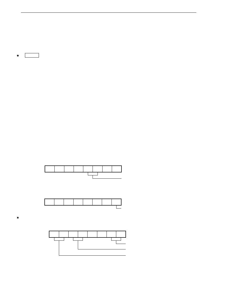
158
CHAPTER 8 16-BIT TIMER/EVENT COUNTERS 00, 01
User's Manual U14260EJ3V1UD
8.4 Operation of 16-Bit Timer/Event Counters 00, 01
8.4.1 Interval timer operation
Setting 16-bit timer mode control register 0n (TMC0n) and capture/compare control register 0n (CRC0n) as shown
in Figure 8-15 allows operation as an interval timer.
Setting
The basic operation setting procedure is as follows.
<1> Set the CRC0n register (see Figure 8-15 for the set value).
<2> Set any value to the CR00n register.
<3> Set the count clock by using the PRM0n register.
<4> Set the TMC0n register to start the operation (see Figure 8-15 for the set value).
Remark
For how to enable the INTTM00n interrupt, see CHAPTER 19 INTERRUPT FUNCTIONS.
Interrupt requests are generated repeatedly using the count value set in 16-bit timer capture/compare register 00n
(CR00n) beforehand as the interval.
When the count value of 16-bit timer counter 0n (TM0n) matches the value set to CR00n, counting continues with
the TM0n value cleared to 0 and the interrupt request signal (INTTM00n) is generated.
The count clock of the 16-bit timer/event counter can be selected using bits 0 and 1 (PRM00n, PRM01n) of prescaler
mode register 0n (PRM0n).
Figure 8-15. Control Register Settings for Interval Timer Operation
(a) 16-bit timer mode control register 0n (TMC0n)
(b) Capture/compare control register 0n (CRC0n)
(c) Prescaler mode register 0n (PRM0n)
Remark 0/1: Setting 0 or 1 allows another function to be used simultaneously with the interval timer. See the
description of the respective control registers for details.
n = 0, 1
7
0
6
0
5
0
4
0
TMC0n3
1
TMC0n2
1
1
0
OVFn0
0
TMC0n
Clears and starts on match between TM0n and CR00n.
7
0
6
0
5
0
4
0
3
0
CRC02n
0/1
CRC01n
0/1
CRC00n
0
CRC0n
CR00n used as compare register
ES11n
0/1
ES10n
0/1
ES01n
0/1
ES00n
0/1
3
0
2
0
PRM01n
0/1
PRM00n
0/1
PRM0n
Selects count clock.
Setting invalid (setting "10" is prohibited.)
Setting invalid (setting "10" is prohibited.)
159
CHAPTER 8 16-BIT TIMER/EVENT COUNTERS 00, 01
User's Manual U14260EJ3V1UD
Figure 8-16. Interval Timer Configuration Diagram
Notes 1. The values outside parentheses apply to 16-bit timer/event counter 00, and the values in parentheses
apply to 16-bit timer/event counter 01.
2. OVF0n is 1 only when 16-bit timer capture/compare register 00n is set to FFFFH.
Figure 8-17. Timing of Interval Timer Operation
Remarks 1. Interval time = (N + 1)
◊ t
N = 0001H to FFFFH
2. n = 0, 1
16-bit timer capture/compare
register 00n
16-bit timer counter 0n
OVF0n
Note 2
Clear
circuit
INTTM00n
f
X
(f
X
/2)
Note 1
f
X
/2
2
(f
X
/2
3
)
Note 1
f
X
/2
6
(f
X
/2
9
)
Note 1
TI000/TO00/P70
(TI001/TO01/BUZ/P75)
Note 1
Selector
Noise
eliminator
f
X
/2
3
Count clock
t
TM0n count value
CR00n
INTTM00n
0000H
0001H
N
0000H 0001H
N
0000H 0001H
N
N
N
N
N
Timer operation enabled
Clear
Clear
Interrupt acknowledged
Interrupt acknowledged
160
CHAPTER 8 16-BIT TIMER/EVENT COUNTERS 00, 01
User's Manual U14260EJ3V1UD
When the compare register is changed during timer count operation, if the value after 16-bit timer capture/
compare register 00n (CR00n) is changed is smaller than that of 16-bit timer counter 0n (TM0n), TM0n continues
counting, overflows and then restarts counting from 0. Thus, if the value (M) after the CR00n change is smaller
than that (N) before the change, it is necessary to restart the timer after changing CR00n.
Figure 8-18. Timing After Change of Compare Register During Timer Count Operation
CR00n
N
M
Count clock
TM0n count value
X ≠ 1
X
FFFFH
0000H
0001H
0002H
Remark
N > X > M
n = 0, 1
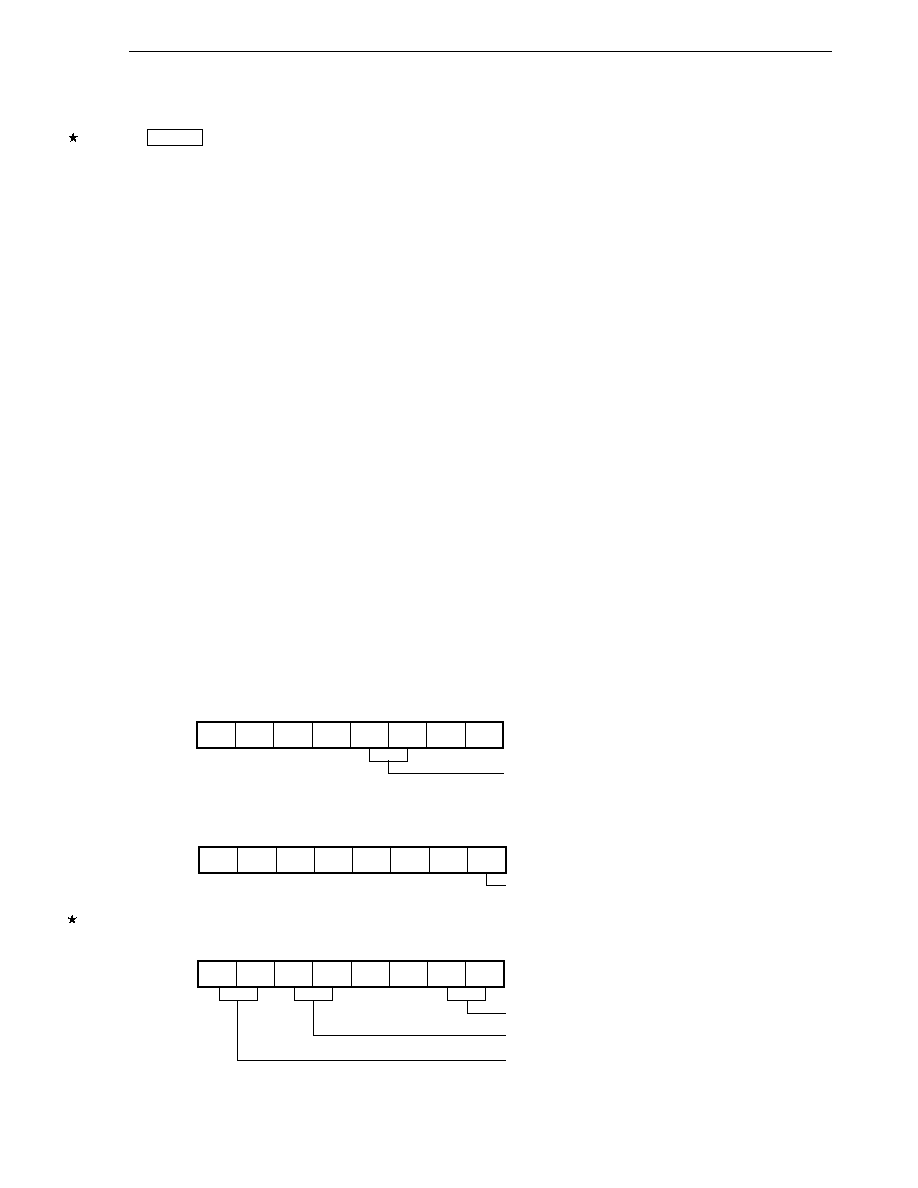
161
CHAPTER 8 16-BIT TIMER/EVENT COUNTERS 00, 01
User's Manual U14260EJ3V1UD
8.4.2 External event counter operation
Setting
The basic operation setting procedure is as follows.
<1> Set the CRC0n register (see Figure 8-19 for the set value).
<2> Set the count clock by using the PRM0n register.
<3> Set any value to the CR00n register (0000H cannot be set).
<4> Set the TMC0n register to start the operation (see Figure 8-19 for the set value).
Remarks 1. For the setting of the TI00n pin, see 8.3 (5) Port mode register 7 (PM7).
2. For how to enable the INTTM00n interrupt, see CHAPTER 19 INTERRUPT FUNCTIONS.
The external event counter counts the number of external clock pulses to be input to the TI00n pin with using 16-
bit timer counter 0n (TM0n).
TM0n is incremented each time the valid edge specified by prescaler mode register 0n (PRM0n) is input.
When the TM0n count value matches the 16-bit timer capture/compare register 00n (CR00n) value, TM0n is cleared
to 0 and the interrupt request signal (INTTM00n) is generated.
Input a value other than 0000H to CR00n (a count operation with a pulse cannot be carried out).
The rising edge, the falling edge, or both edges can be selected using bits 4 and 5 (ES00n and ES01n) of prescaler
mode register 0n (PRM0n).
Because an operation is carried out only when the valid level of the TI00n pin is detected twice after sampling with
the internal clock (f
X
/2
3
), noise with a short pulse width can be eliminated.
Caution
When used as an external event counter, the P70/TI000/TO00 or P75/TI001/TO01/BUZ pin cannot
be used as a timer output (TO00, TO01).
Figure 8-19. Control Register Settings in External Event Counter Mode (with Rising Edge Specified)
(a) 16-bit timer mode control register 0n (TMC0n)
(b) Capture/compare control register 0n (CRC0n)
(c) Prescaler mode register 0n (PRM0n)
Remark 0/1: Setting 0 or 1 allows another function to be used simultaneously with the external event counter.
See the description of the respective control registers for details.
n = 0, 1
7
0
6
0
5
0
4
0
TMC0n3
1
TMC0n2
1
1
0
OVF0n
0
TMC0n
Clears and starts on match between TM0n and CR00n.
7
0
6
0
5
0
4
0
3
0
CRC02n
0/1
CRC01n
0/1
CRC00n
0
CRC0n
CR00n used as compare register
ES11n
0/1
ES10n
0/1
ES01n
0
ES00n
1
3
0
2
0
PRM01n
1
PRM00n
1
PRM0n
Selects external clock.
Specifies rising edge for pulse width detection.
Setting invalid (setting "10" is prohibited.)

162
CHAPTER 8 16-BIT TIMER/EVENT COUNTERS 00, 01
User's Manual U14260EJ3V1UD
Figure 8-20. External Event Counter Configuration Diagram
16-bit timer capture/compare
register 00n
16-bit timer counter 0n (TM0n)
Internal bus
Match
Clear
OVF0n
Note
INTTM00n
Noise eliminator
f
X
/2
3
Valid edge of TI00n
Note OVF0n is 1 only when 16-bit timer capture/compare register 00n is set to FFFFH.
Figure 8-21. External Event Counter Operation Timing (with Rising Edge Specified)
TI00n pin input
TM0n count value
CR00n
INTTM00n
0000H 0001H 0002H 0003H 0004H 0005H
N≠1
N
0000H 0001H 0002H 0003H
N
Caution
When reading the external event counter count value, TM0n should be read.
Remark
n = 0, 1
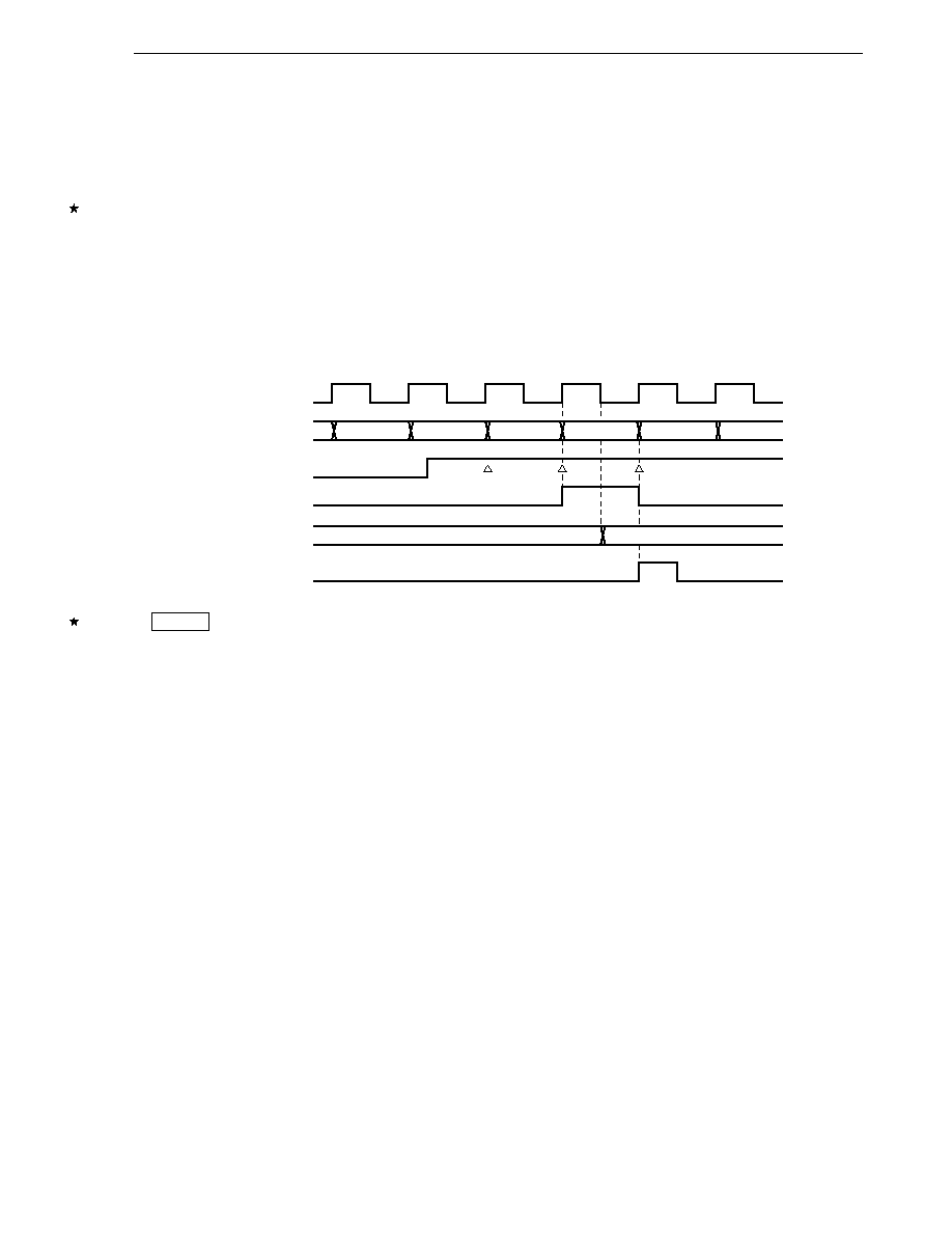
163
CHAPTER 8 16-BIT TIMER/EVENT COUNTERS 00, 01
User's Manual U14260EJ3V1UD
8.4.3 Pulse width measurement operations
It is possible to measure the pulse width of the signals input to the TI00n pin and TI01n pin using
16-bit timer counter 0n (TM0n).
There are two measurement methods: measuring with TM0n used in free-running mode, and measuring by
restarting the timer in synchronization with the edge of the signal input to the TI00n pin.
When an interrupt occurs, read the valid value of the capture register, check the overflow flag, and then calculate
the necessary pulse width. Clear the overflow flag after checking it.
The capture operation is not performed until the signal pulse width is sampled in the count clock cycle selected
by prescaler mode register 0n (PRM0n) and the valid level of the TI00n or TI01n pin is detected twice, thus eliminating
noise with a short pulse width.
Figure 8-22. CR01n Capture Operation with Rising Edge Specified
Setting
The basic operation setting procedure is as follows.
<1> Set the CRC0n register (see Figures 8-23, 8-26, 8-28, and 8-30 for the set value).
<2> Set the count clock by using the PRM0n register.
<3> Set the TMC0n register to start the operation (see Figures 8-23, 8-26, 8-28, and 8-30 for the set value).
Caution
To use two capture registers, set the TI00n and TI01n pins.
Remarks 1. For the setting of the TI00n (or TI01n) pin, see 8.3 (5) Port mode register 7 (PM7).
2. For how to enable the INTTM00n (or INTTM01n) interrupt, see CHAPTER 19 INTERRUPT
FUNCTIONS.
3. n = 0, 1
Count clock
TM0n
TI00n
Rising edge detection
CR01n
INTTM01n
N
- 3
N
- 2
N
- 1
N
N + 1
N

164
CHAPTER 8 16-BIT TIMER/EVENT COUNTERS 00, 01
User's Manual U14260EJ3V1UD
(1) Pulse width measurement with free-running counter and one capture register
When 16-bit timer counter 0n (TM0n) is operated in free-running mode, and the edge specified by prescaler mode
register 0n (PRM0n) is input to the TI00n pin, the value of TM0n is taken into 16-bit timer capture/compare register
01n (CR01n) and an external interrupt request signal (INTTM01n) is set.
The both falling and rising edges can be specified by bits 4 and 5 (ES00n and ES01n) of PRM0n.
Sampling is performed with the count clock selected by PRM0n, and a capture operation is only performed when
a valid level of the TI00n pin is detected twice, thus eliminating noise with a short pulse width.
Figure 8-23. Control Register Settings for Pulse Width Measurement with Free-Running Counter
and One Capture Register (When TI00n and CR01n Are Used)
(a) 16-bit timer mode control register 0n (TMC0n)
(b) Capture/compare control register 0n (CRC0n)
(c) Prescaler mode register 0n (PRM0n)
Remark 0/1: Setting 0 or 1 allows another function to be used simultaneously with pulse width measurement.
See the description of the respective control registers for details.
n = 0, 1
7
0
6
0
5
0
4
0
3
0
CRC02n
1
CRC01n
0/1
CRC00n
0
CRC0n
CR00n used as compare register
CR01n used as capture register
ES11n
0/1
ES10n
0/1
ES01n
1
ES00n
1
3
0
2
0
PRM01n
0/1
PRM00n
0/1
PRM0n
Selects count clock (setting "11" is prohibited).
Specifies both edges for pulse width detection.
Setting invalid (setting "10" is prohibited.)
7
0
6
0
5
0
4
0
TMC0n3
0
TMC0n2
1
1
0
OVF0n
0
TMC0n
Free-running mode
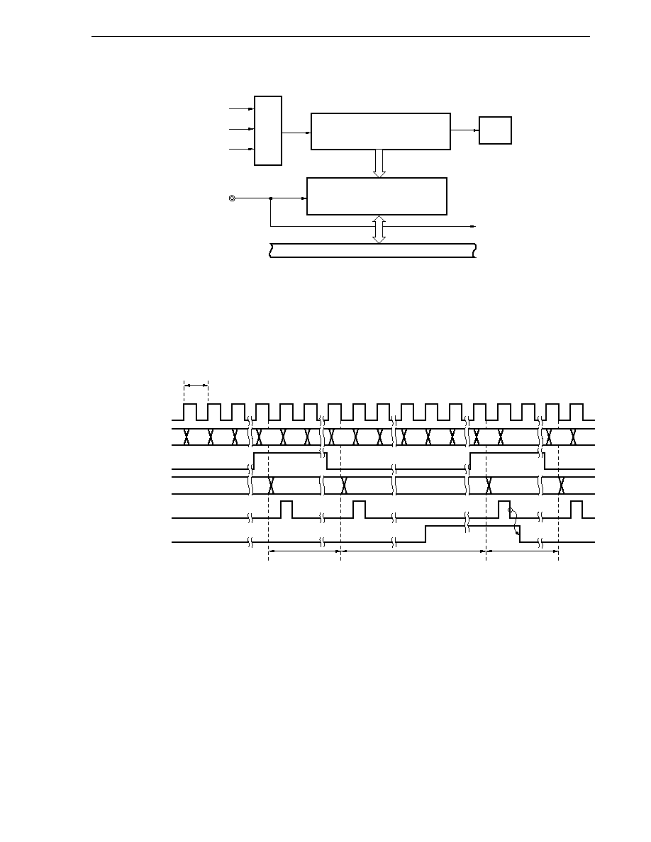
165
CHAPTER 8 16-BIT TIMER/EVENT COUNTERS 00, 01
User's Manual U14260EJ3V1UD
Figure 8-24. Configuration Diagram for Pulse Width Measurement with Free-Running Counter
Note Values outside parentheses apply to 16-bit timer/event counter 00, and values in parentheses apply to 16-
bit timer/event counter 01.
Figure 8-25. Timing of Pulse Width Measurement Operation with Free-Running Counter
and One Capture Register (with Both Edges Specified)
Note OVF0n must be cleared by software.
Remark
n = 0, 1
f
X
(f
X
/2)
Note
f
X
/2
2
(f
X
/2
3
)
Note
f
X
/2
6
(f
X
/2
9
)
Note
TI000/TO00/P70
(TI001/TO01/BUZ/P75)
Note
16-bit timer/counter 0n
OVF0n
16-bit timer capture/compare
register 01n
Internal bus
INTTM01n
Selector
t
0000H
0000H
FFFFH
0001H
D0
D0
(D1 -- D0)
◊ t
(D3 -- D2)
◊ t
(10000H -- D1 + D2)
◊ t
D1
D2
D3
D2
D3
D0 + 1
D1
D1 + 1
Note
Count clock
TM0n count value
TI00n pin input
CR01n capture value
INTTM01n
OVF0n
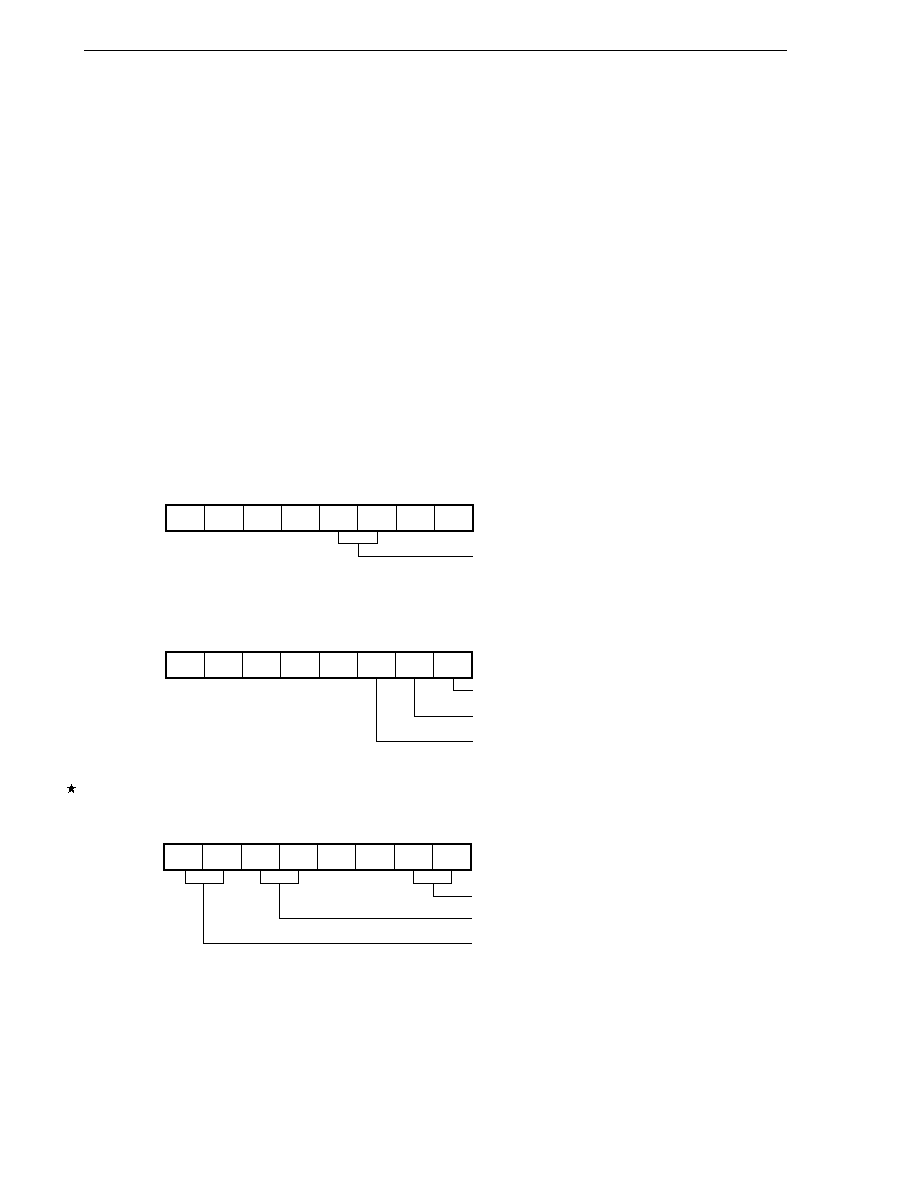
166
CHAPTER 8 16-BIT TIMER/EVENT COUNTERS 00, 01
User's Manual U14260EJ3V1UD
(2) Measurement of two pulse widths with free-running counter
When 16-bit timer counter 0n (TM0n) is operated in free-running mode, it is possible to simultaneously measure
the pulse widths of the two signals input to the TI00n pin and the TI01n pin.
When the edge specified by bits 4 and 5 (ES00n and ES01n) of prescaler mode register 0n (PRM0n) is input
to the TI00n pin, the value of TM0n is taken into 16-bit timer capture/compare register 01n (CR01n) and an
interrupt request signal (INTTM01n) is set.
Also, when the edge specified by bits 6 and 7 (ES10n and ES11n) of PRM0n is input to the TI01n pin, the value
of TM0n is taken into 16-bit timer capture/compare register 00n (CR00n) and an external interrupt request signal
(INTTM00n) is set.
The both falling and rising edges can be specified as the valid edges for the TI00n pin and the TI01n pin by bits
4 and 5 (ES00n and ES01n) and bits 6 and 7 (ES10n and ES11n) of PRM0n, respectively.
Sampling is performed with the count clock cycle selected by prescaler mode register 0n (PRM0n), and a capture
operation is only performed when a valid level of the TI00n pin or TI01n pin is detected twice, thus eliminating
noise with a short pulse width.
Figure 8-26. Control Register Settings for Measurement of Two Pulse Widths with Free-Running Counter
(a) 16-bit timer mode control register 0n (TMC0n)
(b) Capture/compare control register 0n (CRC0n)
(c) Prescaler mode register 0n (PRM0n)
Remark 0/1: Setting 0 or 1 allows another function to be used simultaneously with pulse width measurement.
See the description of the respective control registers for details.
n = 0, 1
7
0
6
0
5
0
4
0
TMC0n3
0
TMC0n2
1
1
0
OVF0n
0
TMC0n
Free-running mode
7
0
6
0
5
0
4
0
3
0
CRC02n
1
CRC01n
0
CRC00n
1
CRC0n
CR00n used as capture register
Captures valid edge of TI01n pin to CR00n
CR01n used as capture register
ES11n
1
ES10n
1
ES01n
1
ES00n
1
3
0
2
0
PRM01n
0/1
PRM00n
0/1
PRM0n
Selects count clock (setting "11" is prohibited).
Specifies both edges for pulse width detection.
Specifies both edges for pulse width detection.

167
CHAPTER 8 16-BIT TIMER/EVENT COUNTERS 00, 01
User's Manual U14260EJ3V1UD
Figure 8-27. Timing of Pulse Width Measurement Operation with Free-Running Counter
(with Both Edges Specified)
t
0000H
0000H
FFFFH
0001H
D0
D0
(D1 -- D0)
◊ t
(D3 -- D2)
◊ t
(10000H -- D1 + D2)
◊ t
(10000H -- D1 + (D2 + 1))
◊ t
D1
D2 + 1
D1
D2
D2
D3
D0 + 1
D1
D1 + 1
D2 + 1 D2 + 2
Note
TI01n pin input
CR00n capture value
INTTM01n
INTTM00n
OVF0n
Count clock
TM0n count value
TI00n pin input
CR01n capture value
Note OVF0n must be cleared by software.
Remark
n = 0, 1
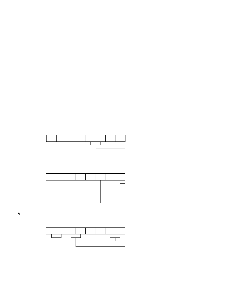
168
CHAPTER 8 16-BIT TIMER/EVENT COUNTERS 00, 01
User's Manual U14260EJ3V1UD
(3) Pulse width measurement with free-running counter and two capture registers
When 16-bit timer counter 0n (TM0n) is operated in free-running mode, it is possible to measure the pulse width
of the signal input to the TI00n pin.
When the rising or falling edge specified by bits 4 and 5 (ES00n and ES01n) of prescaler mode register 0n
(PRM0n) is input to the TI00n pin, the value of TM0n is taken into 16-bit timer capture/compare register 01n
(CR01n) and an interrupt request signal (INTTM01n) is set.
Also, when the inverse edge to that of the capture operation to CR01n is input, the value of TM0n is taken into
16-bit timer capture/compare register 00n (CR00n).
Sampling is performed with the count clock cycle selected by prescaler mode register 0n (PRM0n), and a capture
operation is only performed when a valid level of the TI00n pin is detected twice, thus eliminating noise with a
short pulse width.
Caution
If the valid edge of the TI00n pin is specified to be both the rising and falling edges, 16-bit timer
capture/compare register 00n (CR00n) cannot perform the capture operation.
Figure 8-28. Control Register Settings for Pulse Width Measurement with Free-Running Counter and
Two Capture Registers (with Rising Edge Specified)
(a) 16-bit timer mode control register 0n (TMC0n)
(b) Capture/compare control register 0n (CRC0n)
(c) Prescaler mode register 0n (PRM0n)
Remark 0/1: Setting 0 or 1 allows another function to be used simultaneously with pulse width measurement.
See the description of the respective control registers for details.
n = 0, 1
7
0
6
0
5
0
4
0
TMC0n3
0
TMC0n2
1
1
0
OVF0n
0
TMC0n
Free-running mode
7
0
6
0
5
0
4
0
3
0
CRC02n
1
CRC01n
1
CRC00n
1
CRC0n
CR00n used as capture register
Captures to CR00n at edge reverse
to valid edge of TI00n pin.
CR01n used as capture register
ES11n
0/1
ES10n
0/1
ES01n
0
ES00n
1
3
0
2
0
PRM01n
0/1
PRM00n
0/1
PRM0n
Selects count clock (setting "11" is prohibited).
Specifies rising edge for pulse width detection.
Setting invalid (setting "10" is prohibited.)
169
CHAPTER 8 16-BIT TIMER/EVENT COUNTERS 00, 01
User's Manual U14260EJ3V1UD
Figure 8-29. Timing of Pulse Width Measurement Operation with Free-Running Counter
and Two Capture Registers (with Rising Edge Specified)
t
0000H
0000H
FFFFH
0001H
D0
D0
D2
D1
D3
D2
D3
D1
D0 + 1
D2 + 1
D1 + 1
INTTM01n
OVF0n
CR00n capture value
Count clock
TM0n count value
TI00n pin input
CR01n capture value
(D1 -- D0)
◊ t
(D3 -- D2)
◊ t
(10000H -- D1 + D2)
◊ t
Note
Note OVF0n must be cleared by software.
(4) Pulse width measurement by means of restart
When input of a valid edge to the TI00n pin is detected, the count value of 16-bit timer/counter 0n (TM0n) is taken
into 16-bit timer capture/compare register 01n (CR01n), and then the pulse width of the signal input to the TI00n
pin is measured by clearing TM0n and restarting the count.
The edge specification can be selected from two types, rising or falling edges, by bits 4 and 5 (ES00n and ES01n)
of prescaler mode register 0n (PRM0n).
Sampling is performed with the count clock cycle selected by prescaler mode register 0n (PRM0n) and a capture
operation is only performed when a valid level of the TI00n pin is detected twice, thus eliminating noise with a
short pulse width.
Caution
If the valid edge of the TI00n pin is specified to be both the rising and falling edges, 16-bit timer
capture/compare register 00n (CR00n) cannot perform the capture operation.
Remark
n = 0, 1

170
CHAPTER 8 16-BIT TIMER/EVENT COUNTERS 00, 01
User's Manual U14260EJ3V1UD
Figure 8-30. Control Register Settings for Pulse Width Measurement by Means of Restart
(with Rising Edge Specified)
(a) 16-bit timer mode control register 0n (TMC0n)
(b) Capture/compare control register 0n (CRC0n)
(c) Prescaler mode register 0n (PRM0n)
Figure 8-31. Timing of Pulse Width Measurement Operation by Means of Restart
(with Rising Edge Specified)
t
0000H
0001H
0000H
0001H
0000H 0001H
D0
D0
D2
D1
D2
D1
D1
◊ t
D2
◊ t
INTTM01n
CR00n capture value
Count clock
TM0n count value
TI00n pin input
CR01n capture value
Remark
n = 0, 1
7
0
6
0
5
0
4
0
TMC0n3
1
TMC0n2
0
1
0
OVF0n
0
TMC0n
Clears and starts at valid edge of TI00n pin.
7
0
6
0
5
0
4
0
3
0
CRC02n
1
CRC01n
1
CRC00n
1
CRC0n
CR00n used as capture register
Captures to CR00n at edge reverse
to valid edge of TI00n pin.
CR01n used as capture register
ES11n
0/1
ES10n
0/1
ES01n
0
ES00n
1
3
0
2
0
PRM01n
0/1
PRM00n
0/1
PRM0n
Selects count clock (setting "11" is prohibited).
Specifies rising edge for pulse width detection.
Setting invalid (setting "10" is prohibited.)

171
CHAPTER 8 16-BIT TIMER/EVENT COUNTERS 00, 01
User's Manual U14260EJ3V1UD
8.4.4 Square-wave output operation
Setting
The basic operation setting procedure is as follows.
<1> Set the count clock by using the PRM0n register.
<2> Set the CRC0n register (see Figure 8-32 for the set value).
<3> Set the TOC0n register (see Figure 8-32 for the set value).
<4> Set any value to the CR00n register (0000H cannot be set).
<5> Set the TMC0n register to start the operation (see Figure 8-32 for the set value).
Remarks 1. For the setting of the TO0n pin, see 8.3 (5) Port mode register 7 (PM7).
2. For how to enable the INTTM00n interrupt, see CHAPTER 19 INTERRUPT FUNCTIONS.
A square wave with any selected frequency can be output at intervals determined by the count value preset to
16-bit timer capture/compare register 00n (CR00n).
The TO0n pin output status is reversed at intervals determined by the count value preset to CR00n + 1 by setting
bit 0 (TOE0n) and bit 1 (TOC01n) of 16-bit timer output control register 0n (TOC0n) to 1. This enables a square wave
with any selected frequency to be output.
Figure 8-32. Control Register Settings in Square-Wave Output Mode (1/2)
(a) 16-bit timer mode control register 0n (TMC0n)
(b) Capture/compare control register 0n (CRC0n)
Remark
n = 0, 1
7
0
6
0
5
0
4
0
TMC0n3
1
TMC0n2
1
1
0
OVF0n
0
TMC0n
Clears and starts on match between TM0n and CR00n.
7
0
6
0
5
0
4
0
3
0
CRC02n
0/1
CRC01n
0/1
CRC00n
0
CRC0n
CR00n used as compare register

172
CHAPTER 8 16-BIT TIMER/EVENT COUNTERS 00, 01
User's Manual U14260EJ3V1UD
7
0
6
0
5
0
TOC04n
0
LVS0n
0/1
LVR0n
0/1
TOC01n
1
TOE0n
1
TOC0n
Enables TO0n output.
Reverses output on match between TM0n and CR00n.
Specifies initial value of TO0n output F/F (setting "11" is prohibited).
Does not reverse output on match between TM0n and CR01n.
ES11n
0/1
ES10n
0/1
ES01n
0/1
ES00n
0/1
3
0
2
0
PRM01n
0/1
PRM00n
0/1
PRM0n
Selects count clock.
Setting invalid (setting "10" is prohibited.)
Setting invalid (setting "10" is prohibited.)
Figure 8-32. Control Register Settings in Square-Wave Output Mode (2/2)
(c) 16-bit timer output control register 0n (TOC0n)
(d) Prescaler mode register 0n (PRM0n)
Remark 0/1: Setting 0 or 1 allows another function to be used simultaneously with square-wave output. See
the description of the respective control registers for details.
n = 0, 1
Figure 8-33. Square-Wave Output Operation Timing
Count clock
TM0n count value
CR00n
INTTM00n
TO0n pin output
0000H 0001H 0002H
N≠1
N
0000H 0001H 0002H
N≠1
N
0000H
N
Remark
n = 0, 1

173
CHAPTER 8 16-BIT TIMER/EVENT COUNTERS 00, 01
User's Manual U14260EJ3V1UD
8.4.5 PPG output operation
Setting 16-bit timer mode control register 0n (TMC0n) and capture/compare control register 0n (CRC0n) as shown
in Figure 8-34 allows operation as PPG (Programmable Pulse Generator) output.
Setting
The basic operation setting procedure is as follows.
<1> Set the CRC0n register (see Figure 8-34 for the set value).
<2> Set any value to the CR00n register as the cycle.
<3> Set any value to the CR01n register as the duty factor.
<4> Set the TOC0n register (see Figure 8-34 for the set value).
<5> Set the count clock by using the PRM0n register.
<6> Set the TMC0n register to start the operation (see Figure 8-34 for the set value).
Remarks 1. For the setting of the TO0n pin, see 8.3 (5) Port mode register 7 (PM7).
2. For how to enable the INTTM00n interrupt, see CHAPTER 19 INTERRUPT FUNCTIONS.
In the PPG output operation, square waves are output from the TO0n pin with the pulse width and the cycle that
correspond to the count values set beforehand in 16-bit timer capture/compare register 01n (CR01n) and in 16-bit
timer capture/compare register 00n (CR00n), respectively.
Remark
n = 0, 1
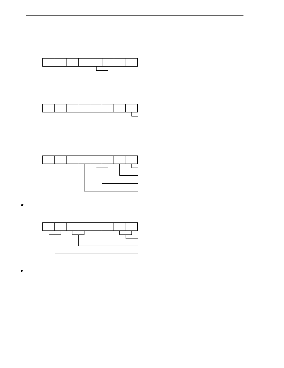
174
CHAPTER 8 16-BIT TIMER/EVENT COUNTERS 00, 01
User's Manual U14260EJ3V1UD
Figure 8-34. Control Register Settings for PPG Output Operation
(a) 16-bit timer mode control register 0n (TMC0n)
(b) Capture/compare control register 0n (CRC0n)
(c) 16-bit timer output control register 0n (TOC0n)
(d) Prescaler mode register 0n (PRM0n)
Cautions 1. CR00n and CR01n values in the following range should be set to:
0000H
CR01n < CR00n
FFFFH
2. The cycle of the pulse generated via PPG output (CR00n setting value + 1) has a duty of
(CR01n setting value + 1)/(CR00n setting value + 1).
Remarks 1.
◊ : Don't care
2. n = 0, 1
7
0
6
0
5
0
4
0
TMC0n3
1
TMC0n2
1
1
0
OVF0n
0
TMC0n
Clears and starts on match between TM0n and CR00n.
7
0
6
0
5
0
4
0
3
0
CRC02n
0
CRC01n
◊
CRC00n
0
CRC0n
CR00n used as compare register
CR01n used as compare register
ES11n
0/1
ES10n
0/1
ES01n
0/1
ES00n
0/1
3
0
2
0
PRM01n
0/1
PRM00n
0/1
PRM0n
Selects count clock.
Setting invalid (setting "10" is prohibited.)
Setting invalid (setting "10" is prohibited.)
7
0
6
0
5
0
TOC04n
1
LVS0n
0/1
LVR0n
0/1
TOC01n
1
TOE0n
1
TOC0n
Enables TO0n output.
Reverses output on match between TM0n and CR00n.
Specifies initial value of TO0n output F/F (setting "11" is prohibited).
Reverses output on match between TM0n and CR01n.
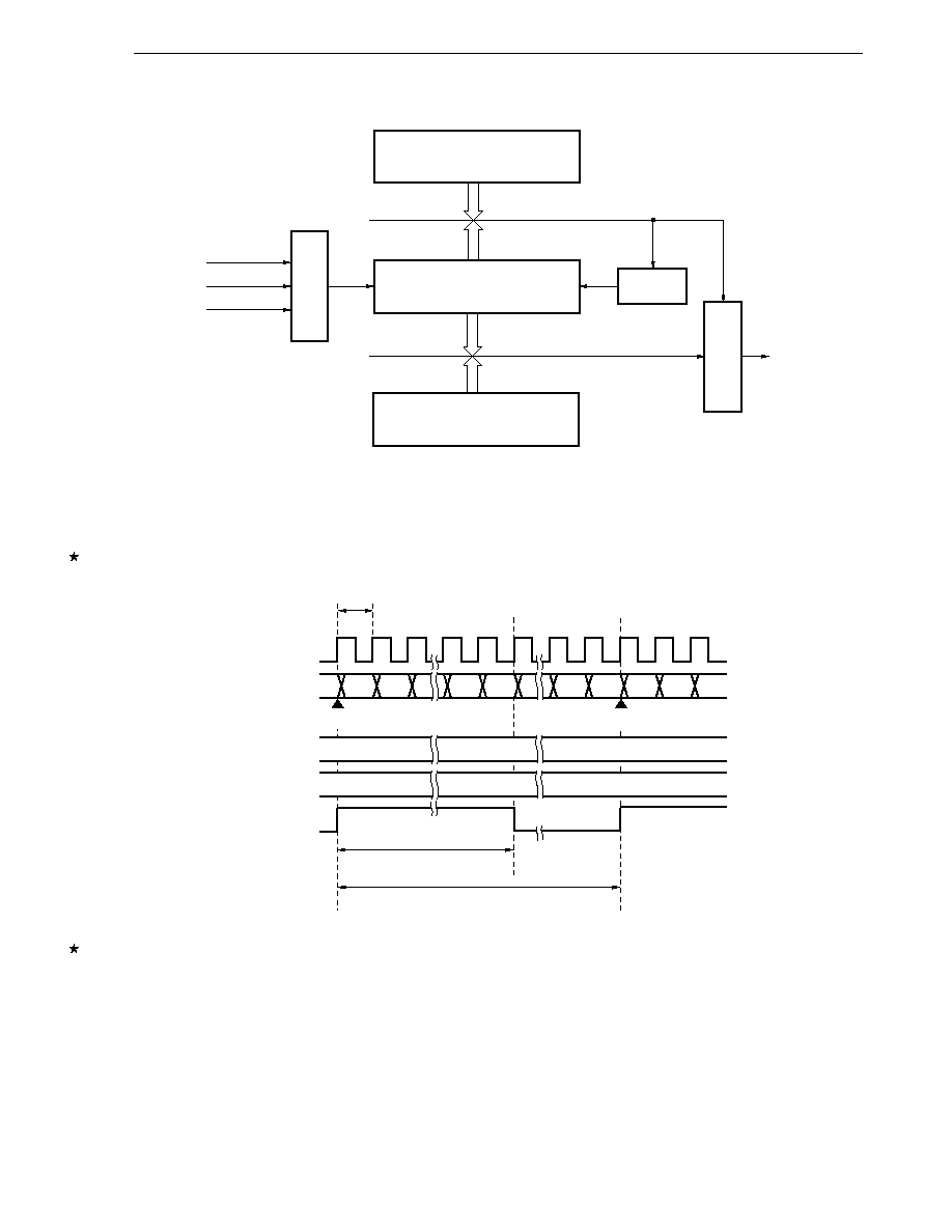
175
CHAPTER 8 16-BIT TIMER/EVENT COUNTERS 00, 01
User's Manual U14260EJ3V1UD
Figure 8-35. PPG Output Configuration Diagram
Note Values outside parentheses apply to 16-bit timer/event counter 00, and values in the parentheses apply
to 16-bit timer/event counter 01.
Figure 8-36. PPG Output Operation Timing
Remark
0000H
M < N FFFFH
n = 0, 1
16-bit timer capture/
compare register 00n
16-bit timer counter 0n
Clear
circuit
f
X
(f
X
/2)
Note
f
X
/2
2
(f
X
/2
3
)
Note
f
X
/2
6
(f
X
/2
9
)
Note
16-bit timer capture/compare
register 01n
TO00/TI000/P70
(TO01/TI001/P75)
Note
Selector
Output controller
t
0000H
0000H 0001H
0001H
M
- 1
Count clock
TM0n count value
TO0n
Pulse width: (M + 1)
◊ t
1 cycle: (N + 1)
◊ t
N
CR00n capture value
CR01n capture value
M
M
N
- 1
N
N
Clear
Clear

176
CHAPTER 8 16-BIT TIMER/EVENT COUNTERS 00, 01
User's Manual U14260EJ3V1UD
8.5 Program List
Caution
The following sample program is shown as an example to describe the operation of
semiconductor products and their applications. Therefore, when applying the following
information to your devices, design the devices after performing evaluation under your own
responsibility.

177
CHAPTER 8 16-BIT TIMER/EVENT COUNTERS 00, 01
User's Manual U14260EJ3V1UD
8.5.1 Interval timer
/*******************************************************************************/
/* */
/* Setting example of timer 00 interval timer mode */
/* Cycle set to 130 as intervalTM00 (at 8.38 MHz for 1 ms) */
/* Variable ppgdata prepared as rewrite data area */
/* : Cycle (if 0000, no change) */
/* ppgdata to be checked at every INTTM000, and changed if required. */
/* Therefore, if change is required, set the change data in ppgdata. */
/* When changed, ppgdata cleared to 0000. */
/* */
/*******************************************************************************/
#pragma sfr
#pragma EI
#pragma DI
#define intervalTM00 130
/* Cycle data to be set to CR000 */
#pragma interrupt INTTM000 intervalint rb2
unsigned int ppgdata;
/* Data area to be set to timer 00 */
void main(void)
{
PCC = 0x0;
/* Set high-speed operation mode */
ppgdata = 0;
/* Set port */
/* Set the following to output */
P7 = 0b11111110;
/* Clear P70 */
PM7.0 = 0;
/* Set P70 as output */
/* Set interrupt */
TMMK000 = 0;
/* Cancel INTTM000 interrupt mask */
/* Set timer 00 */
PRM00 = 0b00000010;
/* Count clock is fx/2^6 */
CRC00 = 0b00000000;
/* Set CR000 and CR010 to compare register */
CR000 = intervalTM00;
/* Set cycle initial value to CR000 */
TOC00 = 0b00000111;
/* Invert on match with CR000, initial value L */
TMC00 = 0b00001100;
/* Clear & start on match between TM00 and CR000 */
EI();
while(1);
/* Loop as dummy here */
}
/* Timer 00 interrupt function */
void intervalint()
{
unsigned int work;
/***************************************************/
/* */
/* Define variables required for interrupt here */
/* */
/***************************************************/
work = ppgdata;
if (work != 0)
{
CR000 = work;
ppgdata = 0;
if (work == 0xffff)
{
TMC00 = 0b00000000;
/* Stop timer */
}
}
/***********************************************************/
/* */
/* Describe processing required for interrupt below */
/* */
/***********************************************************/
}

178
CHAPTER 8 16-BIT TIMER/EVENT COUNTERS 00, 01
User's Manual U14260EJ3V1UD
8.5.2 Pulse width measurement by free-running counter and one capture register
/******************************************************************************/
/* */
/* Timer 00 operation sample */
/* Pulse width measurement example by free-running and CR010 */
/* Measurement results to be up to 16 bits and not checked for errors */
/* data[0]: End flag */
/* data[1]: Measurement results (pulse width) */
/* data[2]: Previous read value */
/* */
/******************************************************************************/
#pragma sfr
#pragma EI
#pragma DI
#pragma interrupt INTTM010 intervalint rb2
unsigned int data[3];
/* Data area */
void main(void)
{
unsigned int length;
PCC = 0x0;
/* Set high-speed operation mode */
data[0] = 0;
data[1] = 0;
data[2] = 0;
/* Set port */
PM7.0 = 1;
/* Set P70 as input */
/* Set interrupt */
TMMK010 = 0;
/* Cancel INTTM010 interrupt mask */
/* Set timer 00 */
PRM00 = 0b00110010;
/* Both rising and falling edges for TI000 */
/* Count clock is fx/2^6 */
CRC00 = 0b00000100;
/* Set CR010 to capture register */
TMC00 = 0b00000100;
/* Start in free-run mode */
EI();
while(1){
/* Dummy loop */
while(data[0] == 0);
/* Wait for measurement completion */
DI();
/* Disable interrupt for exclusive operation */
length = data[1];
/* Read measurement results */
data[0] = 0;
/* Clear end flag */
EI();
/* Exclusive operation completed */
}
}
/* Timer 00 interrupt function */
void intervalint()
{
unsigned int work;
/*****************************************************/
/* */
/* Define variables required for interrupt here */
/* */
/*****************************************************/
work = CR010;
/* Read capture value */
data[1] = work - data[2];
/* Calculate and update interval */
data[2] = work;
/* Update read value */
data[0] = 0xffff;
/* Set measurement completion flag*/
/***********************************************************/
/* */
/* Describe processing required for interrupt below */
/* */
/***********************************************************/
}

179
CHAPTER 8 16-BIT TIMER/EVENT COUNTERS 00, 01
User's Manual U14260EJ3V1UD
8.5.3 Two pulse widths measurement by free-running counter
/******************************************************************************/
/* */
/* Timer 00 operation sample */
/* Two-pulse-width measurement sample by free-running */
/* Measurement results to be up to 16 bits and not checked for errors */
/* Result area at TI000 side */
/* data[0]: End flag */
/* data[1]: Measurement results (pulse width) */
/* data[2]: Previous read value */
/* Result area at TI010 side */
/* data[3]: End flag */
/* data[4]: Measurement results (pulse width) */
/* data[5]: Previous read value */
/* */
/******************************************************************************/
#pragma sfr
#pragma EI
#pragma DI
#pragma interrupt INTTM000 intervalint rb2
#pragma interrupt INTTM010 intervalint2 rb2
unsigned int data[6];
/* Data area */
void main(void)
{
unsigned int length,length2;
PCC = 0x0;
/* Set high-speed operation mode */
data[0] = 0;
/* Clear data area */
data[1] = 0;
data[2] = 0;
data[3] = 0;
data[4] = 0;
data[5] = 0;
/* Set port */
PM7.0 = 1;
/* Set P70 as input */
PM7.1 = 1;
/* Set P71 as input */
/* Set interrupt */
TMMK010 = 0;
/* Cancel INTTM010 interrupt mask */
TMMK000 = 0;
/* Cancel INTTM000 interrupt mask */
/* Set timer 00 */
PRM00 = 0b11110010;
/* Both rising and falling edges */
/* Count clock is fx/2^6 */
CRC00 = 0b00000101;
/* Set CR000 and CR010 to capture register */
TMC00 = 0b00000100;
/* Start in free-run mode */
EI();
while(1){
/* Dummy loop */
if(data[0] != 0)
/* TI000 measurement completion check */
{
TMMK010 = 1;
/* INTTM010 interrupt disabled for
exclusive operation */
length = data[1];
/* Read measurement results */
data[0] = 0;
/* Clear end flag */
TMMK010 = 0;
/* Exclusive operation completed */
}
if(data[3] != 0)
/* TI010 measurement completion check */
{
TMMK000 = 1;
/* INTTM000 interrupt disabled for
exclusive operation */
length2 = data[4];
/* Read measurement results */
data[3] = 0;
/* Clear end flag */
TMMK000 = 0;
/* Exclusive operation completed */
}
}
}

180
CHAPTER 8 16-BIT TIMER/EVENT COUNTERS 00, 01
User's Manual U14260EJ3V1UD
/* INTTM000 interrupt function */
void intervalint()
{
unsigned int work;
/******************************************************/
/* */
/* Define variables required for interrupt here */
/* */
/******************************************************/
work = CR000;
/* Read capture value */
data[4] = work - data[5];
/* Calculate and update interval */
data[5] = work;
/* Update read value */
data[3] = 0xffff;
/* Set measurement completion flag */
/********************************************************/
/* */
/* Describe processing required for interrupt below */
/* */
/********************************************************/
}
/* INTTM010 interrupt function */
void intervalint2()
{
unsigned int work;
/******************************************************/
/* */
/* Define variables required for interrupt here */
/* */
/******************************************************/
work = CR010;
/* Read capture value */
data[1] = work - data[2];
/* Calculate and update interval */
data[2] = work;
/* Update read value */
data[0] = 0xffff;
/* Set measurement completion flag */
/********************************************************/
/* */
/* Describe processing required for interrupt below */
/* */
/********************************************************/
}

181
CHAPTER 8 16-BIT TIMER/EVENT COUNTERS 00, 01
User's Manual U14260EJ3V1UD
8.5.4 Pulse width measurement by restart
/**************************************************************************/
/* */
/* Timer 00 operation sample */
/* Pulse width measurement example by restart */
/* Measurement results up to 16 bits, not to be checked for errors */
/* data[0]: End flag */
/* data[1]: Measurement results (pulse width) */
/* data[2]: Previous read value */
/* */
/**************************************************************************/
#pragma sfr
#pragma EI
#pragma DI
#pragma interrupt INTTM010 intervalint rb2
unsigned int data[3];
/* Data area */
void main(void)
{
unsigned int length;
PCC = 0x0;
/* Set high-speed operation mode */
data[0] = 0;
data[1] = 0;
data[2] = 0;
/* Set port */
PM7.0 = 1;
/* Set P70 as input */
/* Set interrupt */
TMMK010 = 0;
/* Cancel INTTM010 interrupt mask */
/* Set timer 00 */
PRM00 = 0b00110010;
/* Both rising and falling edges */
/* Count clock is fx/2^6 */
CRC00 = 0b00000100;
/* Set CR010 to capture register */
TMC00 = 0b00001000;
/* Clear & start at TI000 valid edge */
EI();
while(1){
/* Dummy loop */
if(data[0] != 0)
/* Wait for TI000 measurement completion */
{
TMMK010 = 1;
/* Disable INTTM010 for exclusive
operation */
length = data[1]+data[2];
/* Cycle calculation based on
measurement results */
data[0] = 0;
/* Clear end flag */
TMMK010 = 0;
/* Exclusive operation completed */
}
}
}
/* Timer00 interrupt function */
void intervalint()
{
/******************************************************/
/* */
/* Define variables required for interrupt here */
/* */
/******************************************************/
data[2] = data[1];
/* Update old data */
data[1] = CR010;
/* Update read value */
data[0] = 0xffff;
/* Set measurement completion flag*/
/********************************************************/
/* */
/* Describe processing required for interrupt below */
/* */
/********************************************************/
}

182
CHAPTER 8 16-BIT TIMER/EVENT COUNTERS 00, 01
User's Manual U14260EJ3V1UD
8.5.5 PPG output
/******************************************************************************/
/* */
/* Timer 00 PPG mode setting example */
/* Cycle set to 130 as intervalTM00 */
/* Active period set to 65 as active_time */
/* Array ppgdata prepared as data area for rewriting */
/* [0]: Active period (0000: no change, 0xffff: stop) */
/* [1]: Cycle (0000: no change) */
/* ppgdata to be checked at every INTTM000, and changed if required. */
/* Therefore, if change is required, set the change data in ppgdata. */
/* When changed, ppgdata cleared to 0000. */
/* */
/******************************************************************************/
#pragma sfr
#pragma EI
#pragma DI
#define intervalTM00 130
/* Cycle data to be set to CR000 */
#define active_time 65
/* Initial value data of CR010 */
#pragma interrupt INTTM000 ppgint rb2
unsigned int ppgdata[2];
/* Data area to be set to timer 00 */
void main(void)
{
PCC = 0x0;
/* Set high-speed operation mode */
ppgdata[0] = 0;
ppgdata[1] = 0;
/* Set port */
P7 = 0b11111110;
/* Clear P70 */
PM7.0 = 0;
/* Set P70 to output */
/* Set interrupt */
TMMK000 = 0;
/* Cancel INTTM000 interrupt mask */
/* Set timer 00 */
PRM00 = 0b00000010;
/* Count clock is fx/2^6 */
CRC00 = 0b00000000;
/* Set CR000 and CR010 to compare register */
CR000 = intervalTM00;
/* Set initial value of cycle */
CR010 = active_time;
/* Set initial value of active period */
TOC00 = 0b00010111;
/* Inverted on match between CR000 and CR010,
initial value L */
TMC00 = 0b00001100;
/* Clear & start on match between TM00 and CR000 */
EI();
while(1);
}
/* Timer 00 interrupt function */
void ppgint()
{
unsigned int work;
work = ppgdata[0];
if (work != 0)
{
CR010 = work;
ppgdata[0] = 0;
if (work == 0xffff)
{
TMC00 = 0b00000000;
/* Stop timer */
}
}
work = ppgdata[1];
if (work != 0)
{
CR000 = work;
ppgdata[1]=0;
}
}

183
CHAPTER 8 16-BIT TIMER/EVENT COUNTERS 00, 01
User's Manual U14260EJ3V1UD
8.6 Cautions for 16-Bit Timer/Event Counters 00, 01
(1) Timer start errors
An error of up to one clock may occur in the time required for a match signal to be generated after timer start.
This is because 16-bit timer counter 0n (TM0n) is started asynchronously to the count clock.
Figure 8-37. Start Timing of 16-Bit Timer Counter 0n (TM0n)
(2) 16-bit timer capture/compare register setting
In the clear & start mode entered on a match between TM0n and CR00n, set a value other than 0000H to 16-
bit timer capture/compare register 00n (CR00n). This means a 1-pulse count operation cannot be performed
when 16-bit timer/event counter 0n is used as an external event counter.
(3) Capture register data retention timing
The values of 16-bit timer capture/compare registers 00n and 01n (CR00n and CR01n) are not guaranteed after
16-bit timer/event counter 0n has been stopped.
(4) Valid edge setting
Set the valid edge of the TI00n pin after setting bits 2 and 3 (TMC0n2 and TMC0n3) of 16-bit timer mode control
register 0n (TMC0n) to 0, 0, respectively, and then stopping the timer operation. The valid edge is set by bits
4 and 5 (ES00n and ES01n) of prescaler mode register 0n (PRM0n).
Remark
n = 0, 1
TM0n count value
0000H
0001H
0002H
0004H
Count clock
Timer start
0003H
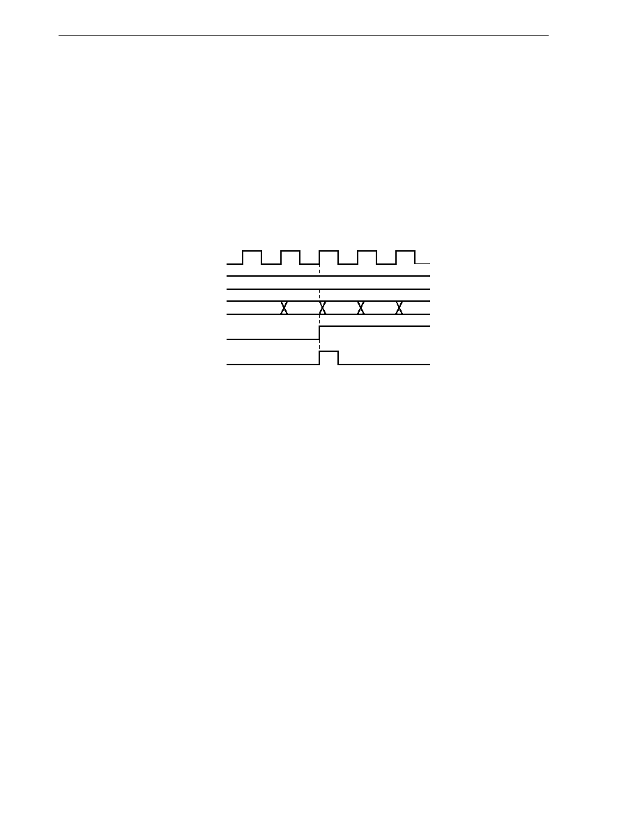
184
CHAPTER 8 16-BIT TIMER/EVENT COUNTERS 00, 01
User's Manual U14260EJ3V1UD
(5) Operation of OVF0n flag
<1>
The OVF0n flag is also set to 1 in the following case.
Either of the clear & start mode entered on a match between TM0n and CR00n, clear & start at the valid
edge of the TI00n pin, or free-running mode is selected.
CR00n is set to FFFFH.
When TM0n is counted up from FFFFH to 0000H.
Figure 8-38. Operation Timing of OVF0n Flag
Count clock
CR00n
TM0n
OVF0n
INTTM00n
FFFFH
FFFEH
FFFFH
0000H
0001H
<2>
Even if the OVF0n flag is cleared before the next count clock is counted (before TM0n becomes 0001H)
after the occurrence of a TM0n overflow, the OVF0 flag is reset newly and clear is disabled.
(6) Conflicting operations
<1>
When the 16-bit timer capture/compare register (CR00n/CR01n) is used as a compare register, if the write
period and the match timing of 16-bit timer counter 0n (TM0n) conflict, match determination is not
successfully done. Do not perform a write operation of CR00n/CR01n near the match timing.
<2>
If the read period and capture trigger input conflict when CR00n/CR01n is used as a capture register,
capture trigger input has priority. The data read from CR00n/CR01n is undefined.
Remark
n = 0, 1

185
CHAPTER 8 16-BIT TIMER/EVENT COUNTERS 00, 01
User's Manual U14260EJ3V1UD
Figure 8-39. Capture Register Data Retention Timing
(7) Timer operation
<1>
Even if 16-bit timer counter 0n (TM0n) is read, the value is not captured by 16-bit timer capture/compare
register 01n (CR01n).
<2>
Regardless of the CPU's operation mode, when the timer stops, the signals input to pins TI00n/TI01n are
not acknowledged.
(8) Capture operation
<1>
If the TI00n pin is specified as the valid edge of the count clock, a capture operation by the capture register
specified as the trigger for the TI00n pin is not possible.
<2>
If both the rising and falling edges are selected as the valid edges of the TI00n pin, capture is not performed.
<3>
To ensure the reliability of the capture operation, the capture trigger requires a pulse longer than two cycles
of the count clock selected by prescaler mode register 0n (PRM0n).
<4>
The capture operation is performed at the fall of the count clock. An interrupt request input (INTTM0nn),
however, occurs at the rise of the next count clock.
(9) Compare operation
<1>
When the 16-bit timer capture/compare register (CR00n/CR01n) is overwritten during timer operation,
match interrupt may be generated or the clear operation may not be performed normally if that value is
close to or large than the timer value.
<2>
The capture operation may not be performed for CR00n/CR01n set in compare mode even if a capture
trigger is input.
Remark
n = 0, 1
Count clock
TM0n count value
Edge input
INTTM01n
Capture read signal
CR01n capture value
N
N + 1
N + 2
M
M + 1
M + 2
X
N + 1
M + 1
Read value not guaranteed
though capture operation performed
Capture

186
CHAPTER 8 16-BIT TIMER/EVENT COUNTERS 00, 01
User's Manual U14260EJ3V1UD
(10) Edge detection
<1>
If the TI00n pin or the TI01n pin is high level immediately after system reset and the rising edge or both
the rising and falling edges are specified as the valid edge for the TI00n pin or TI01n pin to enable 16-bit
timer counter 0n (TM0n) operation, a rising edge is detected immediately. Be careful when pulling up the
TI00n pin or the TI01n pin. However, the rising edge is not detected at restart after the operation has been
stopped once.
<2>
The sampling clock used to eliminate noise differs when the valid edge of the TI00n pin is used as the count
clock and when it is used as a capture trigger. In the former case, the count clock is f
X
/2
3
, and in the latter
case the count clock is selected by prescaler mode register 0n (PRM0n). The capture operation is not
performed until the valid edge is sampled and the valid level is detected twice, thus eliminating noise with
a short pulse width.
(11) STOP mode or main system clock stop mode setting
Except when the TI00n, TI01n pin input is selected, stop the timer operation before setting STOP mode or main
system clock stop mode; otherwise the timer may malfunction when the main system clock starts.
Remark
n = 0, 1

187
User's Manual U14260EJ3V1UD
CHAPTER 9 8-BIT TIMER/EVENT COUNTERS 50, 51
9.1 Functions of 8-Bit Timer/Event Counters 50, 51
8-bit timer/event counters 50, 51 (TM50, TM51) have the following two modes.
(1) Mode using 8-bit timer/event counters 50, 51 alone (discrete mode)
The timer operates as 8-bit timer/event counter 50 or 51.
It has the following functions.
<1>
Interval timer
Interrupt requests are generated at the preset interval.
∑
Number of counts: 1 to 256
<2>
External event counter
The number of pulses with high/low level widths of the signal input externally can be measured.
<3>
Square-wave output
A square wave with an arbitrary frequency can be output.
∑
Cycle: (1
◊ 2 to 256 ◊ 2) ◊ Cycles of count clock
<4>
PWM output
A pulse with an arbitrary duty ratio can be output.
∑
Cycle:
Count clock
◊ 256
∑
Duty ratio: Set value of compare register/256
(2) Mode using cascade connection (16-bit resolution: cascade connection mode)
The timer operates as a 16-bit timer/event counter by combining two 8-bit timer/event counters.
It has the following functions.
∑
Interval timer with 16-bit resolution
∑
External event counter with 16-bit resolution
∑
Square-wave output with 16-bit resolution
Figures 9-1 and 9-2 show block diagrams of 8-bit timer/event counters 50 and 51.
188
CHAPTER 9 8-BIT TIMER/EVENT COUNTERS 50, 51
User's Manual U14260EJ3V1UD
Figure 9-1. Block Diagram of 8-Bit Timer/Event Counter 50
Figure 9-2. Block Diagram of 8-Bit Timer/Event Counter 51
Notes 1. The respective combinations, TI50 and TO50 pins, and TI51 and TO51 pins, cannot be used at the same
time.
2. Timer output F/F
3. PWM output F/F
Output latch
(P72)
PM72
TO50/TI50/
P72
Note 1
Internal bus
8-bit timer compare
register 50 (CR50)
TI50/TO50/P72
Note 1
f
X
/2
4
f
X
/2
6
f
X
/2
8
f
X
/2
10
f
X
f
X
/2
2
Match
Mask circuit
OVF
Clear
3
Selector
TCL502 TCL501 TCL500
Timer clock selection
register 50 (TCL50)
Internal bus
TCE50 TMC506 TMC504 LVS50 LVR50 TMC501 TOE50
Invert
level
8-bit timer mode control
register 50 (TMC50)
S
R
S
Q
R
INV
Selector
INTTM50
Note 2
Note 3
Selector
8-bit timer
counter 50 (TM50)
Selector
Output latch
(P73)
PM73
TO51/TI51/
P73
Note 1
Internal bus
TI51/TO51/P73
Note 1
f
X
/2
3
f
X
/2
5
f
X
/2
7
f
X
/2
9
f
X
/2
Match
Mask circuit
OVF
Clear
3
TCL512 TCL511 TCL510
Timer clock selection
register 51 (TCL51)
Internal bus
TCE51 TMC516 TMC514 LVS51 LVR51 TMC511 TOE51
Invert
level
8-bit timer mode control
register 51 (TMC51)
S
R
Q
R
INV
Selector
INTTM51
Selector
Selector
Selector
8-bit timer
compare register
51 (CR51)
8-bit timer
counter 51
(TM51)
S
f
X
/2
11
Note 2
Note 3
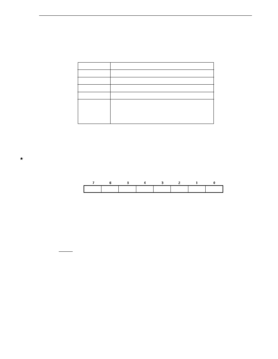
189
CHAPTER 9 8-BIT TIMER/EVENT COUNTERS 50, 51
User's Manual U14260EJ3V1UD
9.2 Configuration of 8-Bit Timer/Event Counters 50, 51
8-bit timer/event counters 50, 51 consist of the following hardware.
Table 9-1. Configuration of 8-Bit Timer/Event Counters 50, 51
Item
Configuration
Timer counter
8-bit timer counter 5n (TM5n)
Register
8-bit timer compare register 5n (CR5n)
Timer input
TI5n
Timer output
TO5n
Control registers
Timer clock select register 5n (TCL5n)
8-bit timer mode control register 5n (TMC5n)
Port mode register 7 (PM7)
Port register 7 (P7)
(1) 8-bit timer counter 5n (TM5n: n = 0, 1)
TM5n is an 8-bit read-only register that counts the count pulses.
The counter is incremented in synchronization with the rising edge of the count clock.
Figure 9-3. Format of 8-Bit Timer Counter 5n (TM5n)
When TM50 and TM51 can be connected in cascade and used as a 16-bit timer, they can be read by a 16-bit
memory manipulation instruction. However, since they are connected by an internal 8-bit bus, TM50 and TM51
are read separately twice in that order. Thus, take reading during the count change into consideration and
compare them by reading twice.
When the count value is read during operation, the count clock input is temporarily stopped
Note
, and then the count
value is read.
In the following situations, count value is set to 00H.
<1>
RESET input
<2>
When TCE5n is cleared
<3>
When TM5n and CR5n match in the clear & start mode entered on a match between TM5n and CR5n.
Note An error may occur in the count. Select a count clock that has a high/low level longer than two cycles
of the CPU clock.
Caution
In cascade connection mode, the count value is reset to 0000H when TCE50 of the lowest timer
is cleared.
Remark
n = 0, 1
Symbol
TM5n
(n = 0, 1)
Address: FF12H (TM50), FF13H (TM51) After reset: 00H R
190
CHAPTER 9 8-BIT TIMER/EVENT COUNTERS 50, 51
User's Manual U14260EJ3V1UD
(2) 8-bit timer compare register 5n (CR5n: n = 0, 1)
When CR5n is used as a compare register in other than PWM mode, the value set in CR5n is constantly compared
with the 8-bit timer counter (TM5n) count value, and an interrupt request (INTTM5n) is generated if they match.
In PWM mode, the TO5n pin goes to the active level by the overflow of TM5n. When the values of TM5n and
CR5n match, the TO5n pin goes to the inactive level.
It is possible to rewrite the value of CR5n within 00H to FFH during a count operation.
When TM50 and TM51 can be connected in cascade and used as a 16-bit timer, CR50 and CR51 operate as
a 16-bit compare register. This register compares the count value with the register value, and if the values match,
an interrupt request (INTTM50) is generated. The INTTM51 interrupt request is also generated at this time. Thus,
mask the INTTM51 interrupt request.
CR5n is set by an 8-bit memory manipulation instruction.
CR5n is undefined when RESET is input.
Figure 9-4. Format of 8-Bit Timer Compare Register 5n (CR5n)
Cautions 1. CR5n can be rewritten in PWM mode only once per cycle.
2. In cascade connection mode, stop the timer operation before setting data.
Remark
n = 0, 1
Symbol
CR5n
(n = 0, 1)
Address: FF10H (CR50), FF11H (CR51) After reset: Undefined R/W
191
CHAPTER 9 8-BIT TIMER/EVENT COUNTERS 50, 51
User's Manual U14260EJ3V1UD
9.3 Registers to Control 8-Bit Timer/Event Counters 50, 51
The following four types of registers are used to control 8-bit timer/event counters 50, 51.
∑ Timer clock select register 5n (TCL5n)
∑ 8-bit timer mode control register 5n (TMC5n)
∑ Port mode register 7 (PM7)
∑ Port register 7 (P7)
Remark
n = 0, 1
(1) Timer clock select register 5n (TCL5n: n = 0, 1)
This register sets the count clock of 8-bit timer/event counter 5n and the valid edge of TI50, TI51 input.
TCL5n is set by an 8-bit memory manipulation instruction.
RESET input clears TCL5n to 00H.
Figure 9-5. Format of Timer Clock Select Register 50 (TCL50)
Address: FF71H After reset: 00H R/W
Symbol
7
6
5
4
3
2
1
0
TCL50
0
0
0
0
0
TCL502
TCL501
TCL500
TCL502
TCL501
TCL500
Count clock selection
f
X
= 8.38 MHz
f
X
= 12 MHz
Note
0
0
0
TI50 falling edge
-
-
0
0
1
TI50 rising edge
-
-
0
1
0
f
X
8.38 MHz
12 MHz
0
1
1
f
X
/2
2
2.09 MHz
3 MHz
1
0
0
f
X
/2
4
523 kHz
750 kHz
1
0
1
f
X
/2
6
131 kHz
187 kHz
1
1
0
f
X
/2
8
32.7 kHz
46.8 kHz
1
1
1
f
X
/2
10
8.18 kHz
11.7 kHz
Note Expanded-specification products of
µPD780078 Subseries only.
Cautions 1. When rewriting TCL50 to other data, stop the timer operation beforehand.
2. Be sure to set bits 3 to 7 to 0.
Remarks 1. When cascade connection is used, only TCL50 is valid for count clock setting.
2. f
X
: Main system clock oscillation frequency

192
CHAPTER 9 8-BIT TIMER/EVENT COUNTERS 50, 51
User's Manual U14260EJ3V1UD
Figure 9-6. Format of Timer Clock Select Register 51 (TCL51)
Address: FF79H After reset: 00H R/W
Symbol
7
6
5
4
3
2
1
0
TCL51
0
0
0
0
0
TCL512
TCL511
TCL510
TCL512
TCL511
TCL510
Count clock selection
f
X
= 8.38 MHz
f
X
= 12 MHz
Note
0
0
0
TI51 falling edge
-
-
0
0
1
TI51 rising edge
-
-
0
1
0
f
X
/2
4.19 MHz
6 MHz
0
1
1
f
X
/2
3
1.04 MHz
1.5 MHz
1
0
0
f
X
/2
5
261 kHz
375 kHz
1
0
1
f
X
/2
7
65.4 kHz
93.7 kHz
1
1
0
f
X
/2
9
16.3 kHz
23.4 kHz
1
1
1
f
X
/2
11
4.09 kHz
5.85 kHz
Note Expanded-specification products of
µPD780078 Subseries only.
Cautions 1. When rewriting TCL51 to other data, stop the timer operation beforehand.
2. Be sure to set bits 3 to 7 to 0.
Remarks 1. When cascade connection is used, only TCL50 is valid for count clock setting.
2. f
X
: Main system clock oscillation frequency
(2) 8-bit timer mode control register 5n (TMC5n: n = 0, 1)
TMC5n is a register that makes the following six settings.
<1>
8-bit timer counter 5n (TM5n) count operation control
<2>
8-bit timer counter 5n (TM5n) operating mode selection
<3>
Discrete mode/cascade connection mode selection (TMC51 only)
<4>
Timer output F/F (flip-flop) status setting
<5>
Active level selection in timer F/F control or PWM (free-running) mode
<6>
Timer output control
TMC5n is set by a 1-bit or 8-bit memory manipulation instruction.
RESET input clears TMC5n to 00H.

193
CHAPTER 9 8-BIT TIMER/EVENT COUNTERS 50, 51
User's Manual U14260EJ3V1UD
Figure 9-7. Format of 8-Bit Timer Mode Control Register 50 (TMC50)
Address: FF70H After reset: 00H R/W
Symbol
7
6
5
4
3
2
1
0
TMC50
TCE50
TMC506
0
0
LVS50
LVR50
TMC501
TOE50
TCE50
TM50 count operation control
0
After clearing to 0, count operation disabled (prescaler disabled)
1
Count operation start
TMC506
TM50 operating mode selection
0
Clear and start mode by match between TM50 and CR50
1
PWM (free-running) mode
LVS50
LVR50
Timer output F/F status setting
0
0
No change
0
1
Timer output F/F reset (0)
1
0
Timer output F/F set (1)
1
1
Setting prohibited
TMC501
In other modes (TMC506 = 0)
In PWM mode (TMC506 = 1)
Timer F/F control
Active level selection
0
Inversion operation disabled
Active high
1
Inversion operation enabled
Active low
TOE50
Timer output control
0
Output disabled (port mode)
1
Output enabled
Cautions 1. The settings of LVS50 and LVR50 are valid in modes other than the PWM mode.
2. Do not set <1> to <3> below at the same time. Set as follows.
<1> TMC501 and TMC506:
Setting of operation mode
<2> Set TOE50 for output enable: Timer output enable
<3> Set TCE50
Set LVS50 and LVR50 before <3>.
3. Stop operation before rewriting TMC506.
Remarks 1. In PWM mode, PWM output will be inactive because TCE50 = 0.
2. If LVS50 and LVR50 are read, 0 is read.
3. The values of the TMC506, LVS50, LVR50, TMC501, and TOE50 bits are reflected to the TO50
output regardless of the value of TCE50.

194
CHAPTER 9 8-BIT TIMER/EVENT COUNTERS 50, 51
User's Manual U14260EJ3V1UD
Figure 9-8. Format of 8-Bit Timer Mode Control Register 51 (TMC51)
Address: FF78H After reset: 00H R/W
Symbol
7
6
5
4
3
2
1
0
TMC51
TCE51
TMC516
0
TMC514
LVS51
LVR51
TMC511
TOE51
TCE51
TM51 count operation control
0
After clearing to 0, count operation disabled (prescaler disabled)
1
Count operation start
TMC516
TM51 operating mode selection
0
Clear and start mode by match between TM51 and CR51
1
PWM (free-running) mode
TMC514
Discrete mode/cascade connection mode selection
0
Discrete mode
1
Cascade connection mode (TM50: Lower timer, TM51: Higher timer)
LVS51
LVR51
Timer output F/F status setting
0
0
No change
0
1
Timer output F/F reset (0)
1
0
Timer output F/F set (1)
1
1
Setting prohibited
TMC511
In other modes (TMC516 = 0)
In PWM mode (TMC516 = 1)
Timer F/F control
Active level selection
0
Inversion operation disabled
Active high
1
Inversion operation enabled
Active low
TOE51
Timer output control
0
Output disabled (port mode)
1
Output enabled
Cautions 1. The settings of LVS51 and LVR51 are valid in modes other than the PWM mode.
2. Do not set <1> to <3> below at the same time. Set as follows.
<1> TMC511, TMC516, and TMC514: Setting of operation mode
<2> Set TOE51 for output enable:
Timer output enable
<3> Set TCE51
Set LVS51 and LVR51 before <3>.
3. Stop operation before rewriting TMC516.
Remarks 1. In PWM mode, PWM output will be inactive because TCE51 = 0.
2. If LVS51 and LVR51 are read, 0 is read.
3. The values of the TMC516, LVS51, LVR51, TMC514, TMC511, and TOE51 bits are reflected to
the TO51 output regardless of the value of TCE51.

195
CHAPTER 9 8-BIT TIMER/EVENT COUNTERS 50, 51
User's Manual U14260EJ3V1UD
(3) Port mode register 7 (PM7)
This register sets port 7 input/output in 1-bit units.
When using the P72/TO50/TI50 and P73/TI51/TO51 pins for timer output, set PM72 and PM73, and the output
latches of P72 and P73 to 0.
When using the P72/TO50/TI50 and P73/TI51/TO51 pins for timer input, set PM72 and PM73 to 1. At this time,
the output latches of P72 and P73 can be either 0 or 1.
PM7 is set by a 1-bit or 8-bit memory manipulation instruction.
RESET input sets PM7 to FFH.
Figure 9-9. Format of Port Mode Register 7 (PM7)
Address: FF27H After reset: FFH R/W
Symbol
7
6
5
4
3
2
1
0
PM7
1
1
PM75
PM74
PM73
PM72
PM71
PM70
PM7n
P7n pin I/O mode selection (n = 0 to 5)
0
Output mode (output buffer on)
1
Input mode (output buffer off)

196
CHAPTER 9 8-BIT TIMER/EVENT COUNTERS 50, 51
User's Manual U14260EJ3V1UD
9.4 Operation of 8-Bit Timer/Event Counters 50, 51
9.4.1 8-bit interval timer operation
The 8-bit timer/event counters operate as interval timers that generate interrupt requests repeatedly at intervals
of the count value preset to 8-bit timer compare register 5n (CR5n).
When the count value of 8-bit timer counter 5n (TM5n) matches the value set to CR5n, counting continues with
the TM5n value cleared to 0 and an interrupt request signal (INTTM5n) is generated.
The count clock of TM5n can be selected with bits 0 to 2 (TCL5n0 to TCL5n2) of timer clock select register 5n
(TCL5n).
Setting
<1> Set each register.
∑ TCL5n: Select count clock.
∑ CR5n:
Compare value
∑ TMC5n: Count operation stop, clear & start mode on match between TM5n and CR5n.
(TMC5n = 0000
◊◊◊0B ◊ = don't care)
<2>
After TCE5n = 1 is set, count operation starts.
<3>
If the values of TM5n and CR5n match, INTTM5n is generated (TM5n is cleared to 00H).
<4>
INTTM5n is generated repeatedly at the same interval. Set TCE5n to 0 to stop the count operation.
Remark
n = 0, 1
Figure 9-10. Interval Timer Operation Timing (1/3)
(a) Basic operation
Remarks 1. Interval time = (N + 1)
◊ t
N = 00H to FFH
2. n = 0, 1
t
Count clock
TM5n count value
CR5n
TCE5n
INTTM5n
Count start
Clear
Clear
00H
01H
N
00H
01H
N
00H
01H
N
N
N
N
N
Interrupt acknowledged
Interrupt acknowledged
Interval time
Interval time
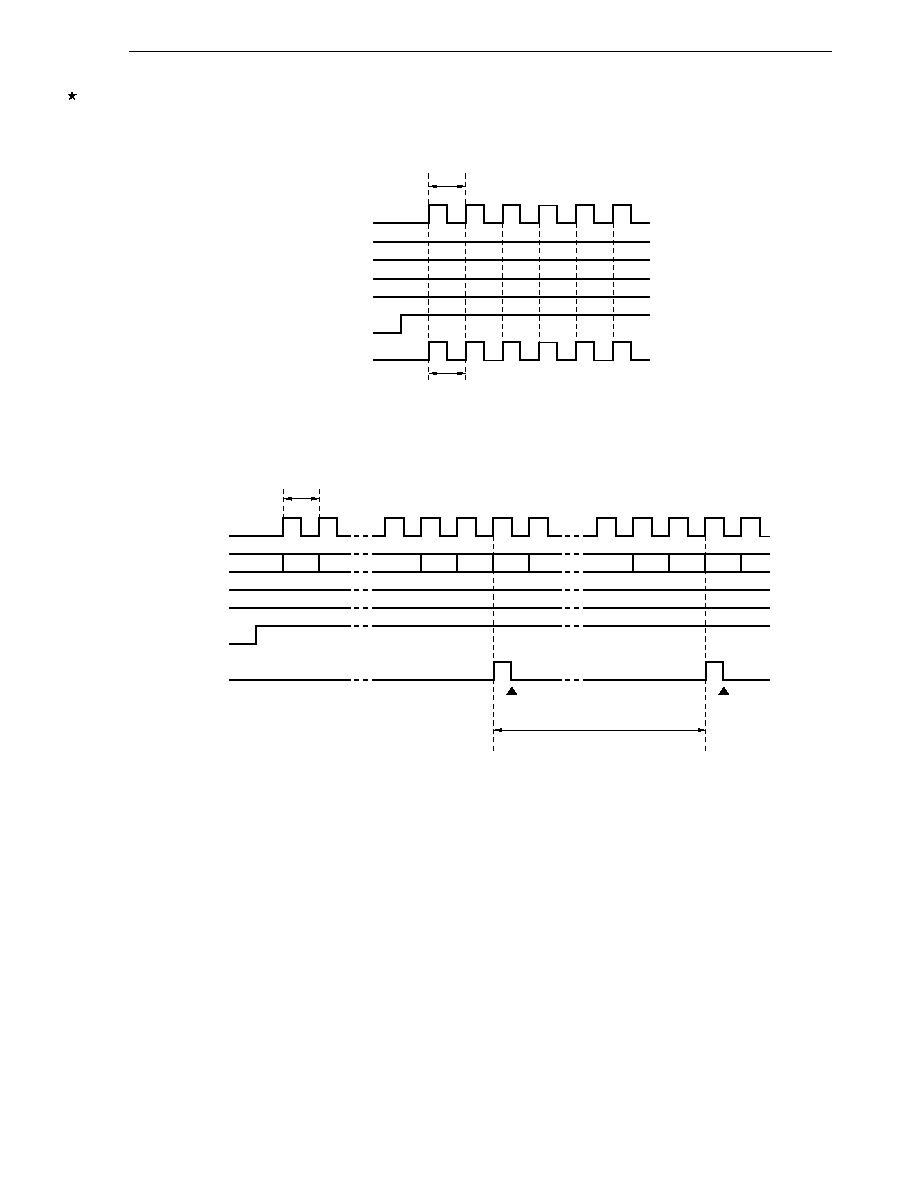
197
CHAPTER 9 8-BIT TIMER/EVENT COUNTERS 50, 51
User's Manual U14260EJ3V1UD
Figure 9-10. Interval Timer Operation Timing (2/3)
(b) When CR5n = 00H
t
Interval time
Count clock
TM5n
CR5n
TCE5n
INTTM5n
00H
00H
00H
00H
00H
(c) When CR5n = FFH
t
Count clock
TM5n
CR5n
TCE5n
INTTM5n
01H
FEH
FFH
00H
FEH
FFH
00H
FFH
FFH
FFH
Interval time
Interrupt
acknowledged
Interrupt acknowledged
Remark
n = 0, 1
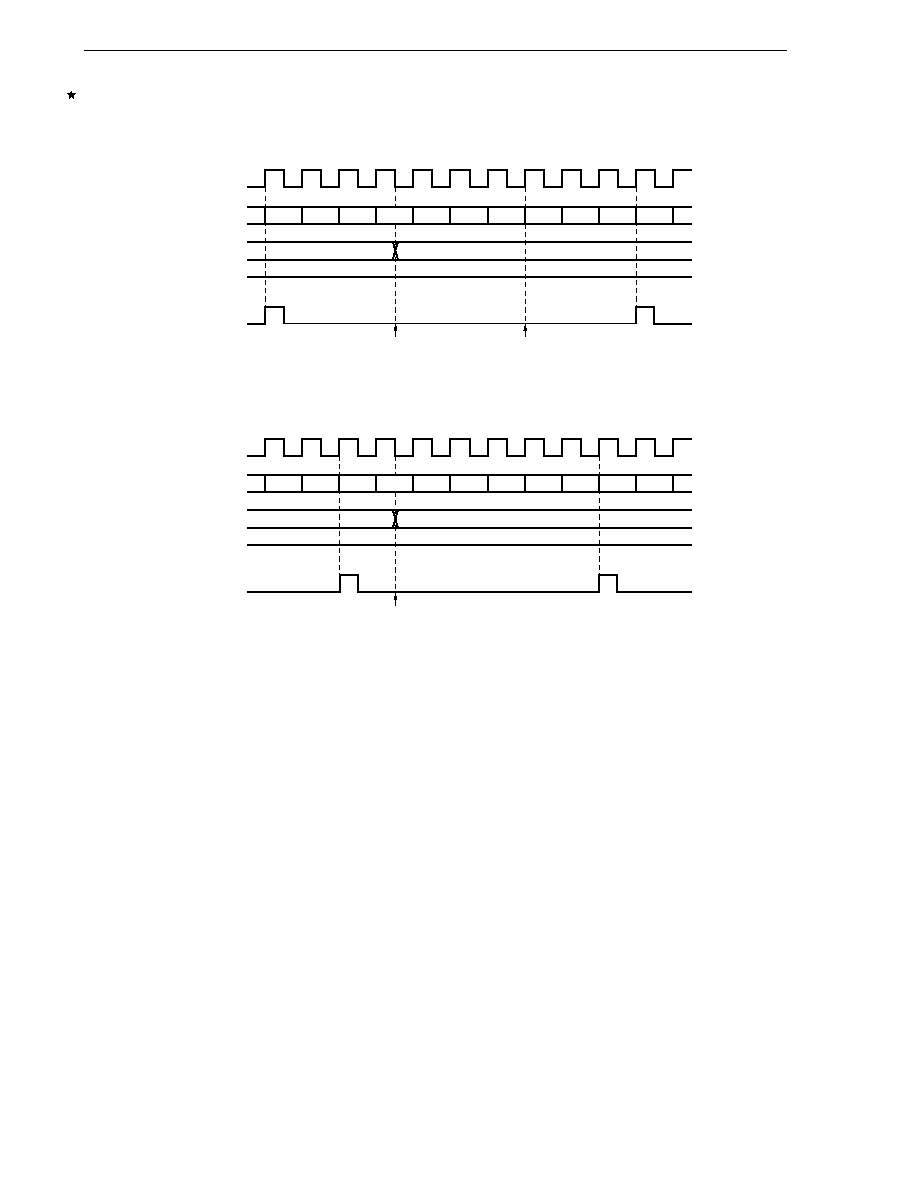
198
CHAPTER 9 8-BIT TIMER/EVENT COUNTERS 50, 51
User's Manual U14260EJ3V1UD
Figure 9-10. Interval Timer Operation Timing (3/3)
(d) Operated by CR5n transition (M < N)
Count clock
TM5n
CR5n
TCE5n
INTTM5n
00H
N
N
M
N
FFH
00H
M
00H
M
CR5n transition
TM5n overflows since M < N
H
(e) Operated by CR5n transition (M > N)
Count clock
TM5n
CR5n
TCE5n
INTTM5n
N ≠ 1
N
N
00H
01H
N
M ≠ 1
M
00H
01H
M
CR5n transition
H
Remark
n = 0, 1
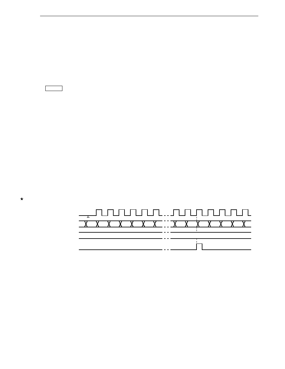
199
CHAPTER 9 8-BIT TIMER/EVENT COUNTERS 50, 51
User's Manual U14260EJ3V1UD
9.4.2 External event counter operation
The external event counter counts the number of external clock pulses to be input to TI5n using 8-bit timer counter
5n (TM5n).
TM5n is incremented each time the valid edge specified by timer clock select register 5n (TCL5n) is input. Either
the rising or falling edge can be selected.
When the TM5n count value matches the value of 8-bit timer compare register 5n (CR5n), TM5n is cleared to 0
and an interrupt request signal (INTTM5n) is generated.
Whenever the TM5n count value matches the value of CR5n, INTTM5n is generated.
Setting
<1> Set each register.
∑ Set the port mode register (PM72 or PM73)
Note
to 1
∑ TCL5n: Edge selection of TI5n input
Rising edge of TI5n
TCL5n = 00H
Falling edge of TI5n
TCL5n = 01H
∑ CR5n:
Compare value
∑ TMC5n: Count operation stop, clear & start mode on match between TM5n and CR5n, timer F/F inverted
operation disable, timer output disable
(TMC5n = 0000
◊◊00B, ◊ = don't care)
<2> When TCE5n = 1 is set, the number of pulses input from TI5n is counted.
<3> When the values of TM5n and CR5n match, INTTM5n is generated (TM5n is cleared to 00H).
<4> Each time the values of TM5n and CR5n match, INTTM5n is generated.
Note 8-bit timer/event counter 50: PM72
8-bit timer/event counter 51: PM73
Figure 9-11. External Event Counter Operation Timing (with Rising Edge Specified)
TI5n
TM5n count value
CR5n
INTTM5n
00H
01H
02H
03H
04H
05H
N
-
1
N
00H
01H
02H
03H
N
Count start
Remarks 1. N = 00H to FFH
2. n = 0, 1

200
CHAPTER 9 8-BIT TIMER/EVENT COUNTERS 50, 51
User's Manual U14260EJ3V1UD
9.4.3 Square-wave output (8-bit resolution) operation
A square wave with any selected frequency is output at intervals determined by the value preset to 8-bit timer
compare register 5n (CR5n).
The TO5n pin output status is reversed at intervals determined by the count value preset to CR5n by setting bit
0 (TOE5n) of 8-bit timer mode control register 5n (TMC5n) to 1. This enables a square wave with any selected
frequency to be output (duty = 50%).
Setting
<1> Set each register.
∑ Set port output latches (P72, P73)
Note
and port mode registers (PM72, PM73)
Note
to 0.
∑ TCL5n: Select count clock
∑ CR5n:
Compare value
∑ TMC5n: Count operation stop, clear & start mode on match between TM5n and CR5n
LVS5n
LVR5n
Timer Output F/F Status Setting
1
0
High-level output
0
1
Low-level output
Timer output F/F reverse enable
Timer output enable
TOE5n = 1
(TMC5n = 00001011B or 00000111B)
<2> After TCE5n = 1 is set, the count operation starts.
<3> Timer output F/F is reversed by match between TM5n and CR5n. After INTTM5n is generated, TM5n is
cleared to 00H.
<4> Timer output F/F is reversed at the same interval and a square wave is output from TO5n.
The frequency is as follows.
∑ Frequency = 1/2t (N + 1)
(N = 00H to FFH)
Note 8-bit timer/event counter 50: P72, PM72
8-bit timer/event counter 51: P73, PM73
Remark
n = 0, 1
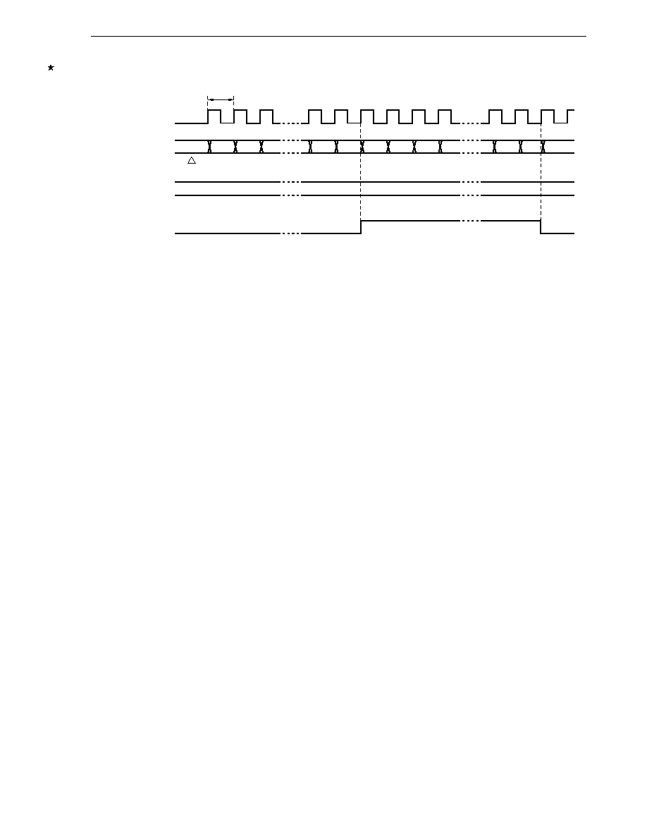
201
CHAPTER 9 8-BIT TIMER/EVENT COUNTERS 50, 51
User's Manual U14260EJ3V1UD
Figure 9-12. Square-Wave Output Operation Timing
Count clock
TM5n count value
CR5n
TO5n
Note
Count start
00H
01H
02H
N ≠ 1
N
00H
01H
02H
N ≠ 1
N
00H
N
t
Note The TO5n output initial value can be set by bits 2 and 3 (LVR5n, LVS5n) of 8-bit timer mode control register
5n (TMC5n).
Remarks 1. N = 00H to FFH
2. n = 0, 1
9.4.4 8-bit PWM output operation
The 8-bit timer/event counter operates as PWM output when bit 6 (TMC5n6) of 8-bit timer mode control register
5n (TMC5n) is set to 1.
The duty ratio pulse is determined by the value set to 8-bit timer compare register 5n (CR5n).
Set the active level width of the PWM pulse to CR5n. The active level can be selected with bit 1 (TMC5n1) of TMC5n.
The count clock can be selected with bits 0 to 2 (TCL5n0 to TCL5n2) of timer clock select register 5n (TCL5n).
PWM output enable/disable can be selected with bit 0 (TOE5n) of TMC5n.
Caution
CR5n can be rewritten in PWM mode only once per cycle.
Remark
n = 0, 1

202
CHAPTER 9 8-BIT TIMER/EVENT COUNTERS 50, 51
User's Manual U14260EJ3V1UD
(1) PWM output basic operation
Setting
<1>
Set each register.
∑ Set port output latches (P72, P73)
Note
and port mode registers (PM72, PM73)
Note
to 0.
∑ TCL5n: Count clock selection
∑ CR5n:
Compare value
∑ TMC5n: Count operation stop, PWM mode selection, timer output F/F not changed
TMC5n1
Active Level Selection
0
Active high
1
Active low
Timer output enabled
(TMC5n = 01000001B or 01000011B)
<2>
When TCE5n = 1 is set, the count operation is started.
To stop the count operation, set TCE5n to 0.
Note 8-bit timer/event counter 50: P72, PM72
8-bit timer/event counter 51: P73, PM73
PWM output operation
<1>
PWM output (output from TO5n) outputs an inactive level until an overflow occurs.
<2>
When an overflow occurs, the active level is output. The active level is output until CR5n matches the count
value of 8-bit timer counter 5n (TM5n).
<3>
When CR5n matches the count value, the inactive level is output. The inactive level is output until an
overflow occurs again.
<4>
Operations <2> and <3> are repeated until the count operation stops.
<5>
When the count operation is stopped by setting TCE5n = 0, PWM output becomes the inactive level.
For details of timing, see Figures 9-13 and 9-14.
The cycle, active-level width, and duty are as follows.
∑
Cycle = 2
8
t
∑
Active-level width = Nt
∑
Duty = N/2
8
(N = 00H to FFH)
Remark
n = 0, 1
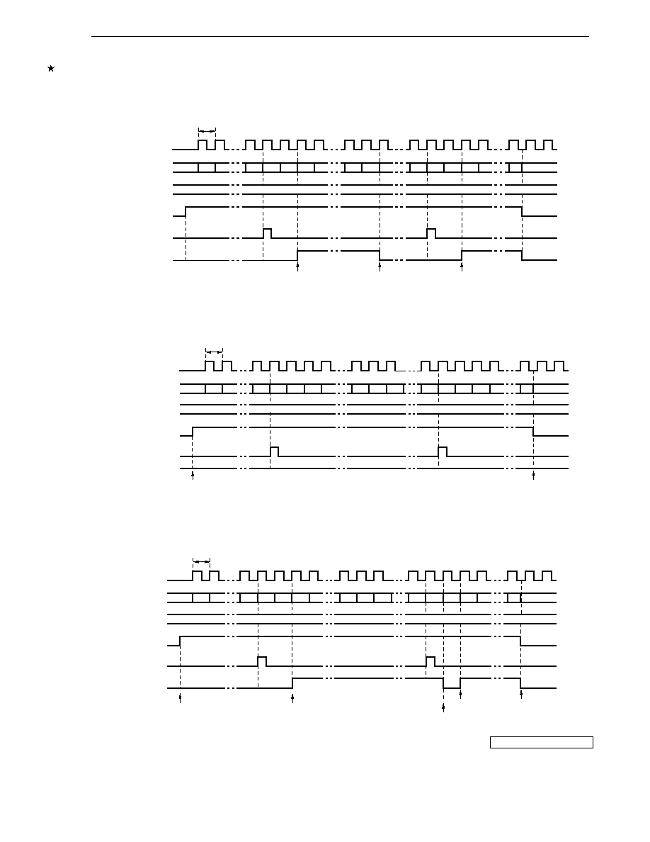
203
CHAPTER 9 8-BIT TIMER/EVENT COUNTERS 50, 51
User's Manual U14260EJ3V1UD
Figure 9-13. PWM Output Operation Timing
(a) Basic operation (active level = H)
Count clock
TM5n
CR5n
TCE5n
INTTM5n
TO5n
00H 01H
FFH 00H 01H 02H
N N+1
FFH 00H 01H 02H
M
00H
N
<2> Active level
Active level
<3> Inactive level
<5>
<1>
t
(b) CR5n = 0
Count clock
TM5n
CR5n
TCE5n
INTTM5n
TO5n L
Inactive level
Inactive level
01H
00H
FFH 00H 01H 02H
N N+1
FFH 00H 01H 02H
M 00H
00H
N+2
t
(c) CR5n = FFH
TM5n
Count clock
CR5n
TCE5n
INTTM5n
TO5n
01H
00H
FFH 00H 01H 02H
N N+1
FFH 00H 01H 02H
M 00H
FFH
N+2
Inactive level
Active level
Inactive level
Active level
Inactive level
t
Remarks 1. <1> to <3> and <5> in Figure 9-13 (a) correspond to <1> to <3> and <5> in PWM output operation
in 9.4.4 (1) PWM output basic operation.
2. n = 0, 1
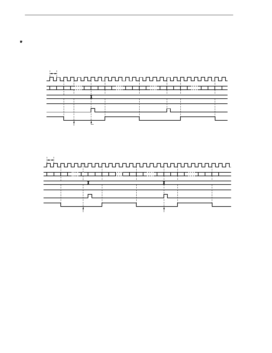
204
CHAPTER 9 8-BIT TIMER/EVENT COUNTERS 50, 51
User's Manual U14260EJ3V1UD
(2) Operation with CR5n changed
Figure 9-14. Timing of Operation with CR5n Changed
(a) CR5n value is changed from N to M before clock rising edge of FFH
Value is transferred to CR5n at overflow immediately after change.
Count clock
TM5n
CR5n
TCE5n
INTTM5n
TO5n
<1> CR5n change (N
M)
N N + 1 N + 2
FFH 00H 01H
M M + 1 M + 2
FFH 00H 01H 02H
M M + 1 M + 2
N
02H
M
H
<2>
t
(b) CR5n value is changed from N to M after clock rising edge of FFH
Value is transferred to CR5n at second overflow.
Count clock
TM5n
CR5n
TCE5n
INTTM5n
TO5n
N
N + 1 N + 2
FFH 00H 01H
N
N + 1 N + 2
FFH 00H 01H 02H
N
02H
N
H
M
M M + 1 M + 2
<1> CR5n change (N
M)
<2>
t
Caution
When reading from CR5n between <1> and <2> in Figure 9-14, the value read differs from the
actual value (read value: M, actual value of CR5n: N).
Remark
n = 0, 1
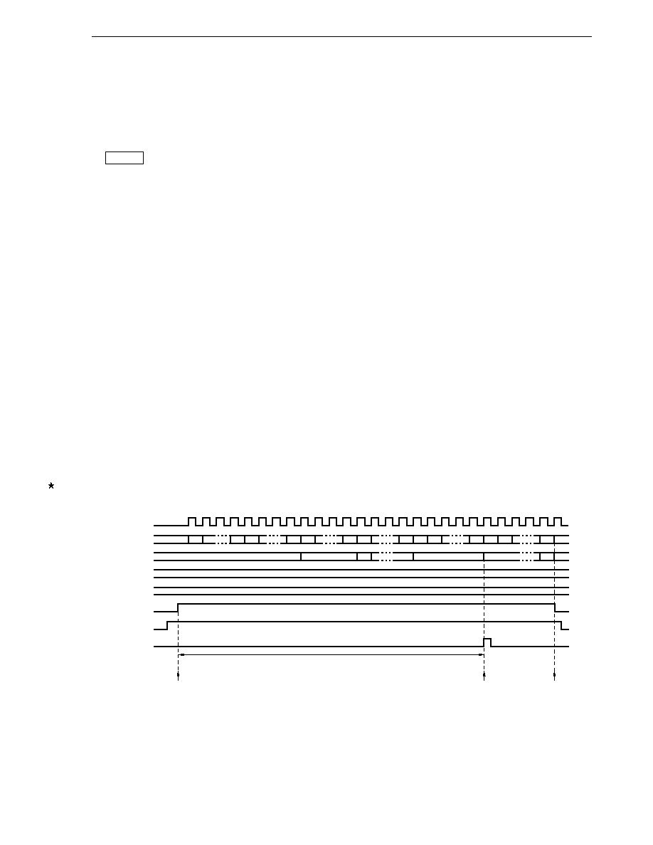
205
CHAPTER 9 8-BIT TIMER/EVENT COUNTERS 50, 51
User's Manual U14260EJ3V1UD
9.4.5 Interval timer (16-bit) operations
When bit 4 (TMC514) of 8-bit timer mode control register 51 (TMC51) is set to 1, the 16-bit resolution timer/counter
mode is entered.
The 8-bit timer/event counter operates as an interval timer that generates interrupt requests repeatedly at intervals
of the count value preset to the 8-bit timer compare registers (CR50, CR51).
Setting
<1> Set each register.
∑ TCL50:
Select count clock for TM50.
Cascade-connected TM51 need not be selected.
∑ CR50, CR51:
Compare value (each value can be set to 00H to FFH)
∑ TMC50, TMC51: Select the clear & start mode entered on a match between TM50 and CR50 (TM51 and
CR51).
TM50
TMC50 = 0000◊◊◊0B ◊: don't care
TM51
TMC51 = 0001◊◊◊0B ◊: don't care
<2> When TMC51 is set to TCE51 = 1 and then TMC50 is set to TCE50 = 1, the count operation starts.
<3> When the values of TM50 and CR50 of the cascade-connected timer match, INTTM50 of TM50 is generated
(TM50 and TM51 are cleared to 00H).
<4> INTTM5n is generated repeatedly at the same interval.
Cautions 1. Stop the timer operation without fail before setting the compare registers (CR50, CR51).
2. INTTM51 of TM51 is generated when the TM51 count value matches CR51, even if cascade
connection is used. Be sure to mask TM51 to disable interrupts.
3. Set TCE50 and TCE51 in order of TM51 then TM50.
4. Count restart/stop can only be controlled by setting TCE50 of TM50 to 1/0.
Figure 9-15 shows an example of 16-bit resolution cascade connection mode timing.
Figure 9-15. 16-Bit Resolution Cascade Connection Mode
Count clock
TM50
TM51
CR50
CR51
TCE50
TCE51
INTTM50
Operation enable
Count start
Interval time
00H
01H
N N+1
FFH 00H
FFH 00H
FFH 00H 01H
N 00H 01H
A 00H
00H
01H
02H
M≠1 M
00H
B 00H
N
M
Interrupt request
generation,
counter clear
Operation
stop

206
CHAPTER 9 8-BIT TIMER/EVENT COUNTERS 50, 51
User's Manual U14260EJ3V1UD
9.5 Program List
Caution
The following sample program is shown as an example to describe the operation of semiconductor
products and their applications. Therefore, when applying the following information to your
devices, design the devices after performing evaluation under your own responsibility.
9.5.1 Interval timer (8-bit)
/*************************************************************************************/
/* */
/* Timer 50 operation sample */
/* Interval timer setting example (frequency change by interrupt processing) */
/* data[0]: Data set flag (value changed when other than 00) */
/* data[1]: Set data */
/* */
/*************************************************************************************/
#pragma sfr
#pragma EI
#pragma DI
#pragma interrupt INTTM50 intervalint rb2
unsigned char data[2];
/* Data area */
void main(void)
{
PCC = 0x0;
/* Set high-speed operation mode */
data[0] = 0;
/* Clear data area */
data[1] = 0;
/* Set port */
P7 = 0b11111011;
/* When using TO50 */
PM7.2 = 0;
/* Set P72 to output */
/* Set interrupt */
TMMK50 = 0;
/* Clear INTTM50 interrupt mask */
/* Set timer 50 */
TMC50 = 0b00000111;
/* Clear & start mode, initial value L */
TCL50 = 0b00000101;
/* Both rising and falling edges */
/* Count clock is fx/2^6 */
CR50 = 131;
/* Set interval to 1 ms as initial value */
TCE50 = 1;
/* Timer start */
EI();
while(1);
/* Dummy loop */
}
/* INTTM50 interrupt function */
void intervalint()
{
if(data[0] != 0)
{
CR50 = data[1];
/* Set new set value */
data[0] = 0;
/* Clear request flag */
}
}

207
CHAPTER 9 8-BIT TIMER/EVENT COUNTERS 50, 51
User's Manual U14260EJ3V1UD
9.5.2 External event counter
/***************************************************************/
/* */
/* Timer 50 operation sample */
/* Event counter setting example */
/* data: Count up flag */
/* */
/***************************************************************/
#pragma sfr
#pragma EI
#pragma DI
#pragma interrupt INTTM50 intervalint rb2
unsigned char data;
/* Data area */
void main(void)
{
PCC = 0x0;
/* Set high-speed operation mode */
data = 0;
/* Clear data area */
/* Set port */
PM7.2 = 1;
/* Set P72 to input */
/* Set interrupt */
TMMK50 = 0;
/* Clear INTTM50 interrupt mask */
/* Set timer 50 */
TMC50 = 0b00000000;
/* Clear & start mode */
TCL50 = 0b00000001;
/* Specify rising edge of TI50 */
CR50 = 0x10;
/* Set N = 16 as initial value */
TCE50 = 1;
/* Timer start */
EI();
/*************************************************************/
/* */
/* Describe the processing to be executed */
/* */
/*************************************************************/
while(data == 0);
/* Wait for count up */
/*************************************************************/
/* */
/* Describe the processing after count up below */
/* */
/*************************************************************/
}
/* INTTM50 interrupt function */
void intervalint()
{
data = 0xff;
/* Set count up flag */
TCE50 = 0;
/* Timer stop */
}

208
CHAPTER 9 8-BIT TIMER/EVENT COUNTERS 50, 51
User's Manual U14260EJ3V1UD
9.5.3 Interval timer (16-bit)
/***************************************************************/
/* */
/* Timer 5 operation sample */
/* Cascade connection setting example */
/* */
/***************************************************************/
#pragma sfr
#pragma EI
#pragma DI
#define intervalTM5 130
/* Cycle data to be set to CR */
#pragma interrupt INTTM50 ppgint rb2
unsigned char ppgdata[2];
/* Data area to be set to timer 5 */
void main(void)
{
int
interval;
interval = intervalTM5;
PCC = 0x0;
/* Select high-speed operation mode */
ppgdata[0] = 0;
/* Clear CR50 data */
ppgdata[1] = 0;
/* Clear CR51 data */
/* Set port */
P7 = 0b11111011;
/* Clear P72 */
PM7.2 = 0;
/* Set P72 to output */
/* Set interrupt */
TMMK50 = 0;
/* Clear INTTM50 interrupt mask */
TMMK51 = 1;
/* Set INTTM51 interrupt mask */
/* Set timer 5 */
TCL50 = 0b00000101;
/* Count clock is fx/2^6 */
CR50 = interval & 0xff;
/* Set lower compare register to CR50 */
CR51 = interval >> 8;
/* Set higher compare register to CR51 */
TMC50 = 0b00000111;
/* Inverted on match, initial value L */
TMC51 = 0b00010000;
/* Cascade mode */
TCE51 = 1;
TCE50 = 1;
/* Timer starts */
EI();
while(1);
}
/* Timer 5 interrupt function */
void ppgint()
{
unsigned int work;
work = ppgdata[0]+ppgdata[1]*0x100;
if (work != 0)
{
TCE50 =0;
CR51 = work >> 8;
CR50 = work & 0xff;
ppgdata[0] = 0;
ppgdata[1] = 0;
if (work != 0xffff)
{
TCE50 = 1;
/* Timer resumes */
}
}
}
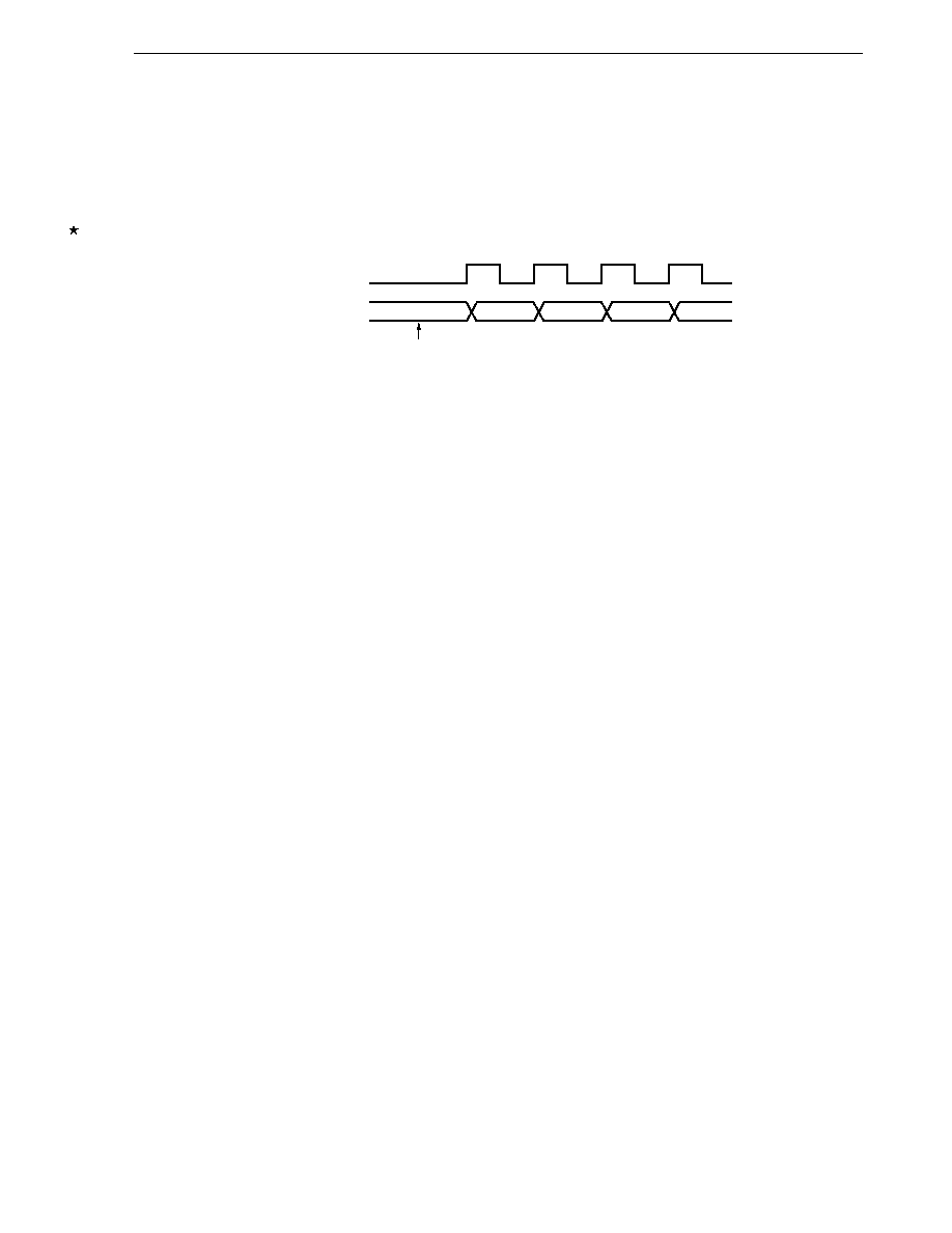
209
CHAPTER 9 8-BIT TIMER/EVENT COUNTERS 50, 51
User's Manual U14260EJ3V1UD
9.6 Cautions for 8-Bit Timer/Event Counters 50, 51
(1) Timer start errors
An error of up to one clock may occur in the time required for a match signal to be generated after timer start.
This is because 8-bit timer counter 5n (TM5n) is started asynchronously to the count pulse.
Figure 9-16. Start Timing of 8-Bit Timer Counter 5n (TM5n)
Count pulse
TM5n count value
00H
01H
02H
03H
04H
Timer start
(2) Setting STOP mode or main system clock stop mode
Except when TI5n input is selected, always set TCE5n = 0 before setting the STOP mode or main system clock
stop mode.
The timer may malfunction when the main system clock starts oscillating.
(3) TM5n (n = 0, 1) reading during timer operation
When reading TM5n during operation, the count clock stops temporarily, so select a count clock with a high/low-
level waveform longer than two cycles of the CPU clock. For example, in the case where the CPU clock (f
CPU
)
is fx, when the selected count clock is fx/4 or below, it can be read.
Remark
n = 0, 1

210
User's Manual U14260EJ3V1UD
CHAPTER 10 WATCH TIMER
10.1 Watch Timer Functions
The watch timer has the following functions.
(1) Watch timer
When the main system clock or subsystem clock is used, interrupt requests (INTWT) are generated at 2
14
/f
W
second or 2
5
/f
W
second intervals.
(2) Interval timer
Interrupt requests (INTWTI) are generated at the preset time interval.
For the interval time, refer to Table 10-2.
The watch timer and the interval timer can be used simultaneously.
Figure 10-1 shows the watch timer block diagram.
Figure 10-1. Watch Timer Block Diagram
Remark
f
W
: Watch timer clock frequency (f
X
/2
7
or f
XT
)
f
X
: Main system clock oscillation frequency
f
XT
: Subsystem clock oscillation frequency
f
WX
: f
W
or f
W
/2
9
f
X
/2
7
f
XT
Selector
Selector
f
W
f
W
2
4
f
W
2
5
f
W
2
6
f
W
2
7
f
W
2
8
f
W
2
9
Clear
9-bit prescaler
Clear
5-bit counter
INTWT
INTWTI
WTM7 WTM6 WTM5 WTM4
WTM1
WTM3
WTM0
Watch timer operation
mode register (WTM)
Internal bus
Selector
f
WX
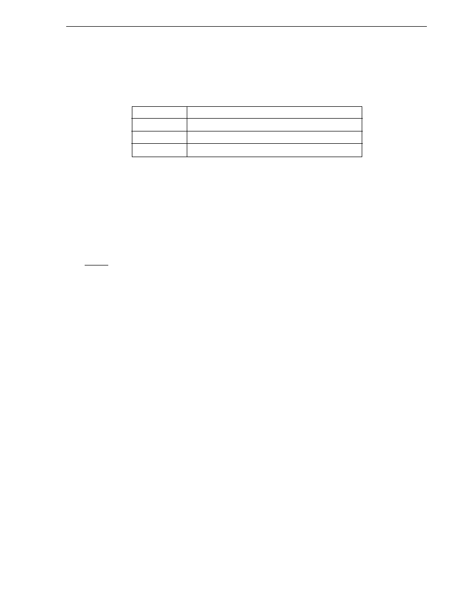
211
CHAPTER 10 WATCH TIMER
User's Manual U14260EJ3V1UD
10.2 Watch Timer Configuration
The watch timer consists of the following hardware.
Table 10-1. Watch Timer Configuration
Item
Configuration
Counter
5 bits
◊ 1
Prescaler
9 bits
◊ 1
Control register
Watch timer operation mode register (WTM)
10.3 Register to Control Watch Timer
The watch timer is controlled by the watch timer operation mode register (WTM).
∑ Watch timer operation mode register (WTM)
This register sets the watch timer count clock, enables/disables operation, sets the prescaler interval time,
controls the 5-bit counter operation, and sets the watch timer interrupt request time.
WTM is set by a 1-bit or 8-bit memory manipulation instruction.
RESET input clears WTM to 00H.
212
CHAPTER 10 WATCH TIMER
User's Manual U14260EJ3V1UD
Figure 10-2. Format of Watch Timer Operation Mode Register (WTM)
Address: FF41H After reset: 00H R/W
Symbol
7
6
5
4
3
2
1
0
WTM
WTM7
WTM6
WTM5
WTM4
WTM3
0
WTM1
WTM0
WTM7
Watch timer count clock selection
0
f
X
/2
7
(65.4 kHz: f
X
= 8.38 MHz, 93.7 kHz: f
X
= 12 MHz
Note
)
1
f
XT
(32.768 kHz: f
XT
= 32.768 kHz)
WTM6
WTM5
WTM4
Prescaler interval time selection
0
0
0
2
4
/f
W
0
0
1
2
5
/f
W
0
1
0
2
6
/f
W
0
1
1
2
7
/f
W
1
0
0
2
8
/f
W
1
0
1
2
9
/f
W
Other than above
Setting prohibited
WTM3
Interrupt request time of watch timer
0
2
14
/f
W
1
2
5
/f
W
WTM1
5-bit counter operation control
0
Clear after operation stop
1
Start
WTM0
Watch timer operation enable
0
Operation stopped (both prescaler and timer cleared)
1
Operation enabled
Note Expanded-specification products of
µPD780078 Subseries only.
Caution Do not change the count clock, interval time, and interrupt request time (by using bits 3 to 7
(WTM3 to WTM7) of WTM) while the watch timer is operating.
Remarks 1. f
W
:
Watch timer clock frequency (f
X
/2
7
or f
XT
)
2. f
X
:
Main system clock oscillation frequency
3. f
XT
: Subsystem clock oscillation frequency

213
CHAPTER 10 WATCH TIMER
User's Manual U14260EJ3V1UD
10.4 Watch Timer Operations
10.4.1 Watch timer operation
The watch timer generates an interrupt request (INTWT) at specific time intervals (2
14
/f
W
seconds or 2
5
/f
W
seconds)
by using the main system clock or subsystem clock. The interrupt request is generated at the following time intervals
(where WTM3 = 0).
∑ If main system clock (8.38 MHz) is selected: 0.25 seconds
∑ If subsystem clock (32.768 kHz) is selected: 0.5 seconds
When bit 0 (WTM0) and bit 1 (WTM1) of the watch timer operation mode register (WTM) are set to 1, the count
operation starts, and when these bits are set to 0, the 5-bit counter is cleared and the count operation stops.
When the interval timer is simultaneously operated, a zero-second start can be achieved for the watch timer by
setting WTM1 to 1 after clearing it to 0. In this case, however, the 9-bit prescaler is not cleared. Therefore, an error
up to 2
9
/f
W
seconds occurs in the first overflow (INTWT) after the zero-second start.
Remark
f
W
: Watch timer clock frequency (f
X
/2
7
or f
XT
)
10.4.2 Interval timer operation
The watch timer operates as interval timer that generates interrupt requests (INTWTI) repeatedly at an interval
of the preset count value.
The interval time can be selected with bits 4 to 6 (WTM4 to WTM6) of the watch timer operation mode register
(WTM). When bit 0 (WTM0) of WTM is set to 1, the count operation starts. When this bit is cleared to 0, the count
operation stops.
Table 10-2. Interval Timer Interval Time
WTM6
WTM5
WTM4
Interval
When Operated at
When Operated at
When Operated at
When Operated at
Time
f
X
= 12 MHz
Note
f
X
= 8.38 MHz
f
X
= 4.19 MHz
f
XT
= 32.768 kHz
0
0
0
2
4
/f
W
170
µs
244
µs
488
µs
488
µs
0
0
1
2
5
/f
W
341
µs
488
µs
977
µs
976
µs
0
1
0
2
6
/f
W
682
µs
977
µs
1.95 ms
1.95 ms
0
1
1
2
7
/f
W
1.36 ms
1.95 ms
3.91 ms
3.90 ms
1
0
0
2
8
/f
W
2.73 ms
3.91 ms
7.82 ms
7.81 ms
1
0
1
2
9
/f
W
5.46 ms
7.82 ms
15.6 ms
15.6 ms
Other than above
Setting prohibited
Note Expanded-specification products of
µPD780078 Subseries only.
Remark
f
W
: Watch timer clock frequency (f
X
/2
7
or f
XT
)
f
X
: Main system clock oscillation frequency
f
XT
: Subsystem clock oscillation frequency
214
CHAPTER 10 WATCH TIMER
User's Manual U14260EJ3V1UD
Figure 10-3. Operation Timing of Watch Timer/Interval Timer
Remark
f
W
: Watch timer clock frequency (f
X
/2
7
or f
XT
)
n: The number of interval timer operations
10.5 Cautions for Watch Timer
When operation of the watch timer and 5-bit counter is enabled by the watch timer operation mode register (WTM)
(by setting bits 0 (WTM0) and 1 (WTM1) of WTM to 1), the interval until the first interrupt request (INTWT) is generated
after the register is set does not exactly match the specification made with bit 3 (WTM3) of WTM. This is because
there is a delay of one 11-bit prescaler output cycle until the 5-bit counter starts counting. Subsequently, however,
the INTWT signal is generated at the specified intervals.
Figure 10-4. Example of Generation of Watch Timer Interrupt Request (INTWT)
(When Interrupt Period = 0.5 s)
It takes 0.515625 seconds for the first INTWT to be generated (2
9
◊ 1/32768 = 0.015625 s longer). INTWT is
then generated every 0.5 seconds.
0H
Start
Overflow
Overflow
5-bit counter
Count clock
Watch timer
interrupt INTWT
Interval timer
interrupt INTWTI
Interrupt time of watch timer
(2
14
/f
W
or 2
5
/f
W
sec.)
Interval time
(T)
T
Interrupt time of watch timer
(2
14
/f
W
or 2
5
/f
W
sec.)
n x T
n x T
0.5 s
0.5 s
0.515625 s
WTM0, WTM1
INTWT
215
User's Manual U14260EJ3V1UD
CHAPTER 11 WATCHDOG TIMER
11.1 Watchdog Timer Functions
The watchdog timer has the following functions.
(1) Watchdog timer
The watchdog timer detects a program loop. Upon detection of a program loop, a non-maskable interrupt request
or RESET can be generated.
For the loop detection time, refer to Table 11-2.
(2) Interval timer
Interrupt requests are generated at the preset time intervals.
For the interval time, refer to Table 11-3.
Caution
Select the watchdog timer mode or the interval timer mode using the watchdog timer mode
register (WDTM). (The watchdog timer and the interval timer cannot be used simultaneously.)
Figure 11-1 shows a block diagram of the watchdog timer.
Figure 11-1. Watchdog Timer Block Diagram
WDT mode signal
Watchdog timer clock
select register (WDCS)
Watchdog timer mode
register (WDTM)
f
X
/2
8
f
X
RUN
INTWDT
RESET
3
WDCS2 WDCS1 WDCS0
RUN WDTM4 WDTM3
Clock
input
controller
Divider
circuit
Divided
clock
selector
Output
controller
Division mode
selector
Internal bus

216
CHAPTER 11 WATCHDOG TIMER
User's Manual U14260EJ3V1UD
11.2 Watchdog Timer Configuration
The watchdog timer consists of the following hardware.
Table 11-1. Watchdog Timer Configuration
Item
Configuration
Control registers
Watchdog timer clock select register (WDCS)
Watchdog timer mode register (WDTM)
11.3 Registers to Control Watchdog Timer
The following two registers are used to control the watchdog timer.
∑ Watchdog timer clock select register (WDCS)
∑ Watchdog timer mode register (WDTM)
(1) Watchdog timer clock select register (WDCS)
This register sets the overflow time of the watchdog timer and the interval timer.
WDCS is set by an 8-bit memory manipulation instruction.
RESET input clears WDCS to 00H.
Figure 11-2. Format of Watchdog Timer Clock Select Register (WDCS)
Address: FF42H After reset: 00H R/W
Symbol
7
6
5
4
3
2
1
0
WDCS
0
0
0
0
0
WDCS2
WDCS1
WDCS0
WDCS2
WDCS1
WDCS0
Overflow time of watchdog timer/interval timer
f
X
= 8.38 MHz
f
X
= 12 MHz
Note
0
0
0
2
12
/f
X
488
µs
341
µs
0
0
1
2
13
/f
X
977
µs
682
µs
0
1
0
2
14
/f
X
1.95 ms
1.36 ms
0
1
1
2
15
/f
X
3.91 ms
2.73 ms
1
0
0
2
16
/f
X
7.82 ms
5.46 ms
1
0
1
2
17
/f
X
15.6 ms
10.9 ms
1
1
0
2
18
/f
X
31.2 ms
21.8 ms
1
1
1
2
20
/f
X
125 ms
87.3 ms
Note Expanded-specification products of
µPD780078 Subseries only.
Remark
f
X
: Main system clock oscillation frequency
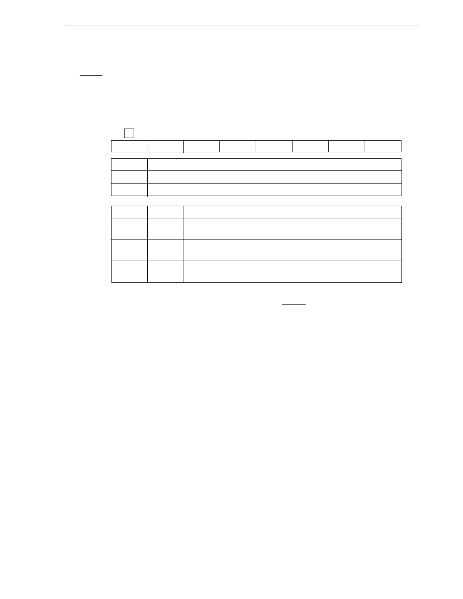
217
CHAPTER 11 WATCHDOG TIMER
User's Manual U14260EJ3V1UD
(2) Watchdog timer mode register (WDTM)
This register sets the watchdog timer operating mode and enables/disables counting.
WDTM is set by a 1-bit or 8-bit memory manipulation instruction.
RESET input clears WDTM to 00H.
Figure 11-3. Format of Watchdog Timer Mode Register (WDTM)
Address: FFF9H After reset: 00H R/W
Symbol
7
6
5
4
3
2
1
0
WDTM
RUN
0
0
WDTM4
WDTM3
0
0
0
RUN
Watchdog timer operation mode selection
Note 1
0
Count stop
1
Counter is cleared and counting starts
WDTM4
WDTM3
Watchdog timer operation mode selection
Note 2
0
◊
Interval timer mode
Note 3
(Maskable interrupt request occurs upon generation of overflow)
1
0
Watchdog timer mode 1
(Non-maskable interrupt request occurs upon generation of overflow)
1
1
Watchdog timer mode 2
(Reset operation is activated upon generation of overflow)
Notes 1. Once set to 1, RUN cannot be cleared to 0 by software.
Thus, once counting starts, it can only be stopped by RESET input.
2. Once set to 1, WDTM3 and WDTM4 cannot be cleared to 0 by software.
3. The watchdog timer starts operation as an interval timer when RUN is set to 1.
Caution
When RUN is set to 1 so that the watchdog timer is cleared, the actual overflow time is up to
2
8
/f
X
seconds shorter than the time set by the watchdog timer clock select register (WDCS).
Remark
◊: Don't care

218
CHAPTER 11 WATCHDOG TIMER
User's Manual U14260EJ3V1UD
11.4 Watchdog Timer Operations
11.4.1 Watchdog timer operation
When bit 4 (WDTM4) of the watchdog timer mode register (WDTM) is set to 1, the watchdog timer is operated to
detect a program loop.
The loop detection time interval is selected with bits 0 to 2 (WDCS0 to WDCS2) of the watchdog timer clock select
register (WDCS). The watchdog timer starts by setting bit 7 (RUN) of WDTM to 1. After the watchdog timer is started,
set RUN to 1 within the set loop time interval. The watchdog timer can be cleared and counting started by setting
RUN to 1.
If RUN is not set to 1 and the loop detection time is exceeded, system reset or a non-maskable interrupt request
is generated according to the value of bit 3 (WDTM3) of WDTM.
The watchdog timer continues operating in the HALT mode but it stops in the STOP mode. Thus, set RUN to 1
before the STOP mode is set, clear the watchdog timer and then execute the STOP instruction.
Cautions 1. The actual loop detection time may be shorter than the set time by up to 2
8
/f
X
seconds.
2. When the subsystem clock is selected for the CPU clock, the watchdog timer count operation
is stopped.
Table 11-2. Watchdog Timer Loop Detection Time
Loop Detection Time
When Operated at
When Operated at
f
X
= 8.38 MHz
f
X
= 12 MHz
Note
2
12
/f
X
488
µs
341
µs
2
13
/f
X
977
µs
682
µs
2
14
/f
X
1.95 ms
1.36 ms
2
15
/f
X
3.91 ms
2.73 ms
2
16
/f
X
7.82 ms
5.46 ms
2
17
/f
X
15.6 ms
10.9 ms
2
18
/f
X
31.2 ms
21.8 ms
2
20
/f
X
125 ms
87.3 ms
Note Expanded-specification products of
µPD780078 Subseries only.
Remark
f
X
: Main system clock oscillation frequency

219
CHAPTER 11 WATCHDOG TIMER
User's Manual U14260EJ3V1UD
11.4.2 Interval timer operation
The watchdog timer operates as an interval timer that generates interrupt requests repeatedly at an interval of the
preset count value when bit 4 (WDTM4) of the watchdog timer mode register (WDTM) is set to 0.
The interval time of the interval timer is selected with bits 0 to 2 (WDCS0 to WDCS2) of the watchdog timer clock
select register (WDCS). When bit 7 (RUN) of WDTM is set to 1, the watchdog timer operates as an interval timer.
When the watchdog timer operates as an interval timer, the interrupt mask flag (WDTMK) and priority specification
flag (WDTPR) are validated and the maskable interrupt request (INTWDT) can be generated. Among the maskable
interrupts, INTWDT has the highest priority at default.
The interval timer continues operating in the HALT mode but it stops in STOP mode. Thus, set RUN to 1 before
the STOP mode is set, clear the interval timer and then execute the STOP instruction.
Cautions 1. Once bit 4 (WDTM4) of WDTM is set to 1 (this selects the watchdog timer mode), the interval
timer mode is not set unless RESET is input.
2. The interval time just after setting WDTM may be shorter than the set time by up to 2
8
/f
X
seconds.
3. When the subsystem clock is selected for the CPU clock, the watchdog timer count operation
is stopped.
Table 11-3. Interval Timer Interval Time
Interval Time
When Operated at
When Operated at
f
X
= 8.38 MHz
f
X
= 12 MHz
Note
2
12
/f
X
488
µs
341
µs
2
13
/f
X
977
µs
682
µs
2
14
/f
X
1.95 ms
1.36 ms
2
15
/f
X
3.91 ms
2.73 ms
2
16
/f
X
7.82 ms
5.46 ms
2
17
/f
X
15.6 ms
10.9 ms
2
18
/f
X
31.2 ms
21.8 ms
2
20
/f
X
125 ms
87.3 ms
Note Expanded-specification products of
µPD780078 Subseries only.
Remark
f
X
: Main system clock oscillation frequency
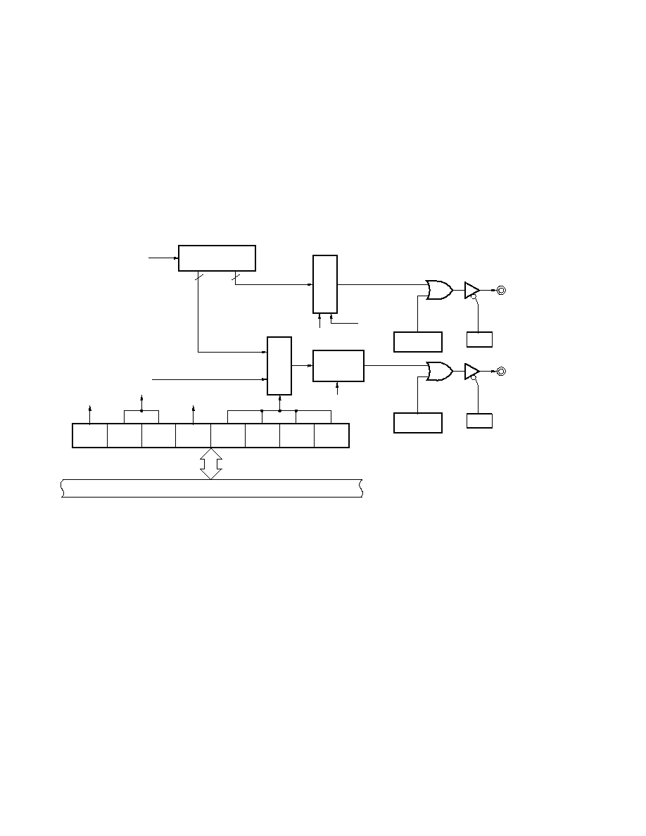
220
User's Manual U14260EJ3V1UD
CHAPTER 12 CLOCK OUTPUT/BUZZER OUTPUT CONTROLLER
12.1 Clock Output/Buzzer Output Controller Functions
Clock output is used for carrier output during remote controlled transmission and clock output for supply to
peripheral ICs. The clock selected by the clock output select register (CKS) is output.
In addition, buzzer output is used for square-wave output of the buzzer frequency selected by CKS.
Figure 12-1 shows the block diagram of the clock output/buzzer output controller.
Figure 12-1. Block Diagram of Clock Output/Buzzer Output Controller
f
X
f
X
/2
10
to f
X
/2
13
f
X
to f
X
/2
7
f
XT
BZOE
BCS1
BCS0
CLOE
CLOE
BZOE
8
4
PCL/TI011/
P74
BUZ/TI001/
TO01/P75
BCS0, BCS1
CCS3
CCS2
CCS1
CCS0
PM75
PM74
Clock
controller
Output latch
(P75)
Output latch
(P74)
Internal bus
Selector
Clock output select register (CKS)
Selector
Prescaler

221
CHAPTER 12 CLOCK OUTPUT/BUZZER OUTPUT CONTROLLER
User's Manual U14260EJ3V1UD
12.2 Configuration of Clock Output/Buzzer Output Controller
The clock output/buzzer output controller consists of the following hardware.
Table 12-1. Configuration of Clock Output/Buzzer Output Controller
Item
Configuration
Control registers
Clock output select register (CKS)
Port mode register (PM7)
Port register 7 (P7)
12.3 Registers to Control Clock Output/Buzzer Output Controller
The following three registers are used to control the clock output/buzzer output controller.
∑ Clock output select register (CKS)
∑ Port mode register (PM7)
∑ Port register 7 (P7)
(1) Clock output select register (CKS)
This register sets output enable/disable for clock output (PCL) and for the buzzer frequency output (BUZ), and
sets the output clock.
CKS is set by a 1-bit or 8-bit memory manipulation instruction.
RESET input clears CKS to 00H.
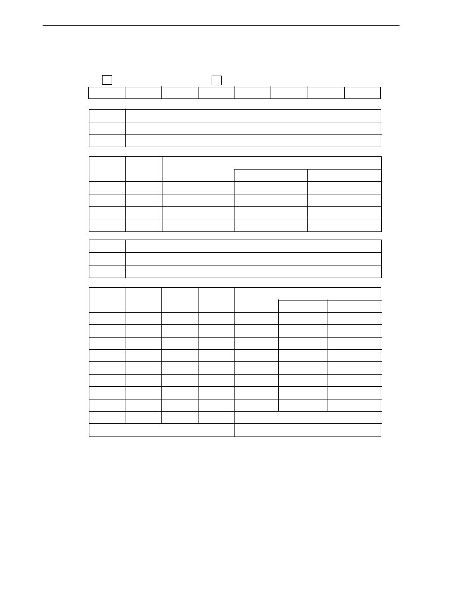
222
CHAPTER 12 CLOCK OUTPUT/BUZZER OUTPUT CONTROLLER
User's Manual U14260EJ3V1UD
Figure 12-2. Format of Clock Output Select Register (CKS)
Address: FF40H After reset: 00H R/W
Symbol
7
6
5
4
3
2
1
0
CKS
BZOE
BCS1
BCS0
CLOE
CCS3
CCS2
CCS1
CCS0
BZOE
BUZ output enable/disable specification
0
Stop clock divider operation. BUZ fixed to low level.
1
Enable clock divider operation. BUZ output enabled.
BCS1
BCS0
BUZ output clock selection
f
X
= 8.38 MHz
f
X
= 12 MHz
Note
0
0
f
X
/2
10
8.18 kHz
11.7 kHz
0
1
f
X
/2
11
4.09 kHz
5.85 kHz
1
0
f
X
/2
12
2.04 kHz
2.92 kHz
1
1
f
X
/2
13
1.02 kHz
1.46 kHz
CLOE
PCL output enable/disable specification
0
Stop clock divider operation. PCL fixed to low level.
1
Enable clock divider operation. PCL output enabled.
CCS3
CCS2
CCS1
CCS0
PCL output clock selection
f
X
= 8.38 MHz
f
X
= 12 MHz
Note
0
0
0
0
f
X
8.38 MHz
12 MHz
0
0
0
1
f
X
/2
4.19 MHz
6 MHz
0
0
1
0
f
X
/2
2
2.09 MHz
3 MHz
0
0
1
1
f
X
/2
3
1.04 MHz
1.5 MHz
0
1
0
0
f
X
/2
4
523 kHz
750 kHz
0
1
0
1
f
X
/2
5
261 kHz
375 kHz
0
1
1
0
f
X
/2
6
130 kHz
187 kHz
0
1
1
1
f
X
/2
7
65.4 kHz
93.7 kHz
1
0
0
0
f
XT
(32.768 kHz)
Other than above
Setting prohibited
Note Expanded-specification products of
µPD780078 Subseries only.
Remarks 1. f
X
: Main system clock oscillation frequency
2. f
XT
: Subsystem clock oscillation frequency
3. Figures in parentheses are for operation with f
XT
= 32.768 kHz.
223
CHAPTER 12 CLOCK OUTPUT/BUZZER OUTPUT CONTROLLER
User's Manual U14260EJ3V1UD
(2) Port mode register 7 (PM7)
This register sets port 7 input/output in 1-bit units.
When using the P74/PCL/TI011 pin for clock output and the P75/BUZ/TI001/TO01 pin for buzzer output, set PM74
and PM75, and the output latches of P74 and P75 to 0.
PM7 is set by a 1-bit or 8-bit memory manipulation instruction.
RESET input sets PM7 to FFH.
Figure 12-3. Format of Port Mode Register 7 (PM7)
Address: FF27H After reset: FFH R/W
Symbol
7
6
5
4
3
2
1
0
PM7
1
1
PM75
PM74
PM73
PM72
PM71
PM70
PM7n
P7n pin I/O mode selection (n = 0 to 5)
0
Output mode (output buffer on)
1
Input mode (output buffer off)
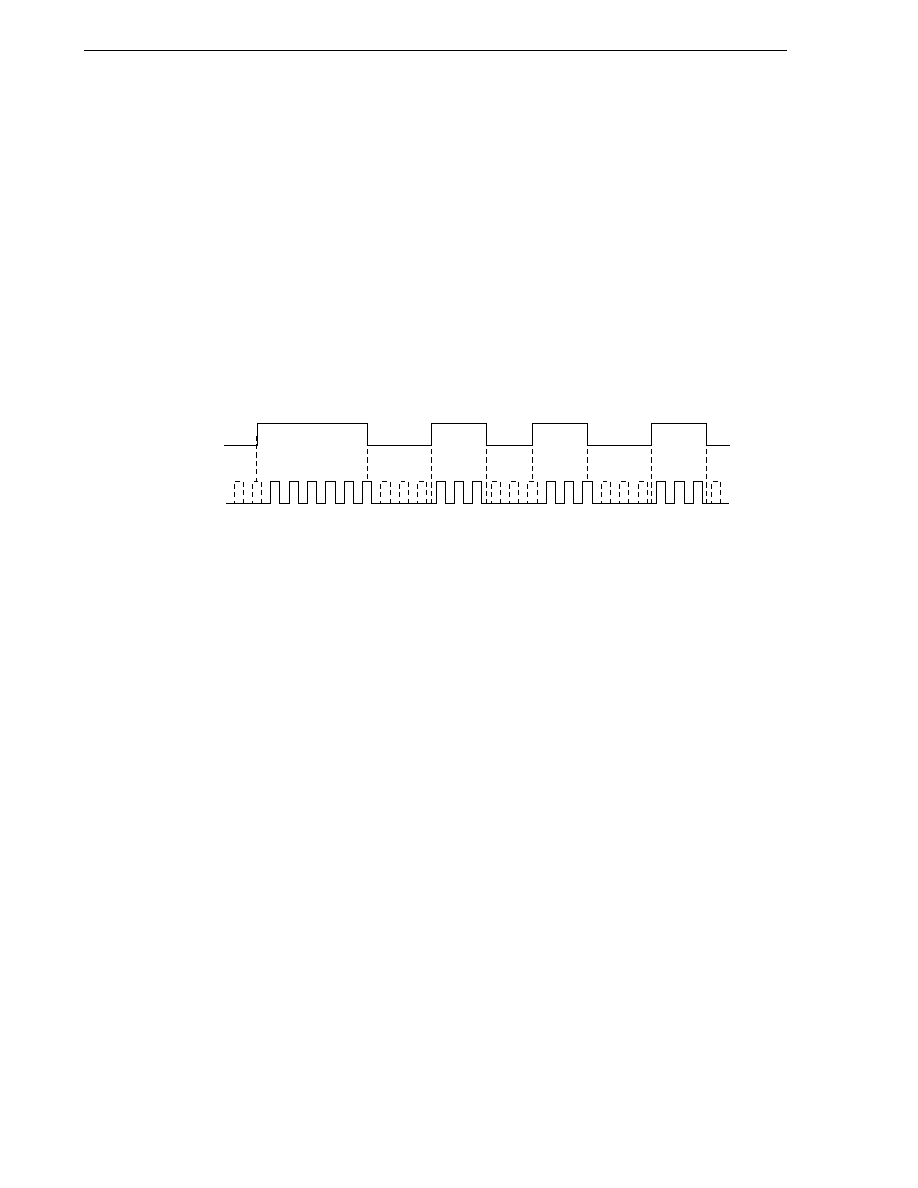
224
CHAPTER 12 CLOCK OUTPUT/BUZZER OUTPUT CONTROLLER
User's Manual U14260EJ3V1UD
12.4 Operation of Clock Output/Buzzer Output Controller
12.4.1 Operation as clock output
The clock pulse is output using the following procedure.
<1> Select the clock pulse output frequency using bits 0 to 3 (CCS0 to CCS3) of the clock output select register
(CKS) (clock pulse output in disabled state).
<2> Set bit 4 (CLOE) of CKS to 1, and enable clock output.
Remark
The clock output controller is designed not to output pulses with a small width during output enable/
disable switching of the clock output. As shown in Figure 12-4, be sure to start output from the low period
of the clock (marked with * in the figure). When stopping output, do so after securing the high level of
the clock.
Figure 12-4. Remote Control Output Application Example
CLOE
Clock output
*
*
12.4.2 Operation as buzzer output
The buzzer frequency is output using the following procedure.
<1> Select the buzzer output frequency using bits 5 and 6 (BCS0, BCS1) of the clock output select register (CKS)
(buzzer output in disabled state).
<2> Set bit 7 (BZOE) of CKS to 1 to enable buzzer output.
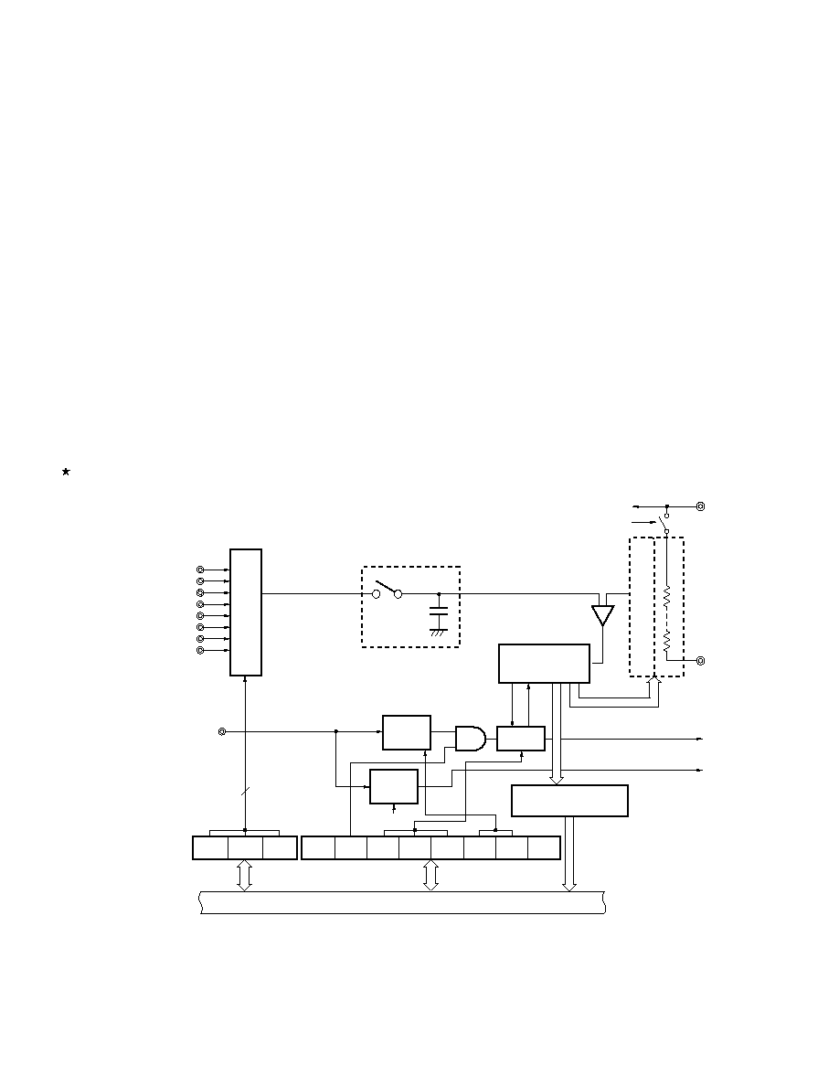
225
User's Manual U14260EJ3V1UD
CHAPTER 13 A/D CONVERTER
13.1 A/D Converter Functions
The A/D converter is a 10-bit resolution converter that converts analog inputs into digital signals. It can control
up to 8 analog input channels (ANI0 to ANI7).
(1) Hardware start
Conversion is started by trigger input (ADTRG: rising edge, falling edge, or both rising and falling edges can
be specified).
(2) Software start
Conversion is started by setting A/D converter mode register 0 (ADM0).
Select one channel for analog input from ANI0 to ANI7 to start A/D conversion. In the case of hardware start, the
A/D converter stops when A/D conversion is completed, and an interrupt request (INTAD0) is generated. In the case
of software start, A/D conversion is repeated. Each time an A/D conversion operation ends, an interrupt request
(INTAD0) is generated.
Figure 13-1. Block Diagram of 10-Bit A/D Converter
Note The valid edge of an external interrupt is specified by bit 3 of the EGP and EGN registers (see Figure 19-
5 Format of External Interrupt Rising Edge Enable Register (EGP), External Interrupt Falling Edge
Enable Register (EGN)).
Sample & hold circuit
Voltage comparator
Successive
approximation
register (SAR)
Controller
Edge
detector
Edge
detector
ADTRG/INTP3/P03
3
A/D conversion result
register 0 (ADCR0)
AV
SS
INTAD0
INTP3
Trigger
enable
Analog input channel
specification register 0 (ADS0)
A/D converter
mode register 0 (ADM0)
Internal bus
Note
ADS02
ANI0/P10
ANI1/P11
ANI2/P12
ANI3/P13
ANI4/P14
ANI5/P15
ANI6/P16
ANI7/P17
ADS01 ADS00
ADCS0 TRG0 FR02 FR01 FR00 EGA01 EGA00 ADCE0
AV
REF
ADCS bit
Selector
T
ap selector
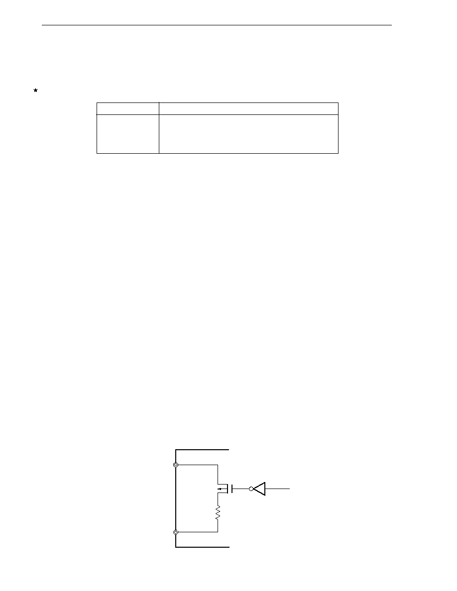
226
CHAPTER 13 A/D CONVERTER
User's Manual U14260EJ3V1UD
13.2 A/D Converter Configuration
The A/D converter consists of the following hardware.
Table 13-1. Registers of A/D Converter Used on Software
Item
Configuration
Registers
Successive approximation register (SAR)
A/D conversion result register 0 (ADCR0)
A/D converter mode register 0 (ADM0)
Analog input channel specification register 0 (ADS0)
(1) ANI0 to ANI7 pins
These are the analog input pins of the 8-channel A/D converter. They input analog signals to be converted into
digital signals. Pins other than the one selected as the analog input pin by the analog input channel specification
register 0 (ADS0) can be used as input port pins.
Cautions 1. Use ANI0 to ANI7 input voltages within the specification range. If a voltage higher than or
equal to AV
REF
or lower than or equal to AV
SS
is applied (even if within the absolute maximum
rating range), the conversion value of that or equal to channel will be undefined and the
conversion values of other channels may also be affected.
2. Analog input (ANI0 to ANI7) pins are alternate-function pins that can also be used as input
port pins (P10 to P17). When A/D conversion is performed by selecting any one of ANI0
to ANI7, do not access port 1 during conversion, as this may cause a lower conversion
resolution.
3. When a digital pulse is applied to a pin adjacent to the pin in the process of A/D conversion,
A/D conversion values may not be obtained as expected due to coupling noise. Thus, do
not apply a pulse to a pin adjacent to the pin in the process of A/D conversion.
(2) Sample & hold circuit
The sample & hold circuit samples the input signal of the analog input pin selected by the selector when A/D
conversion is started, and holds the sampled analog input voltage value during A/D conversion.
(3) Series resistor string
The series resistor string is connected between AV
REF
and AV
SS
, and generates a voltage to be compared with
the analog input signal.
Figure 13-2. Circuit Configuration Diagram of Series Resistor String
AV
REF
AV
SS
P-ch
Series resistor string
ADCS0

227
CHAPTER 13 A/D CONVERTER
User's Manual U14260EJ3V1UD
(4) Voltage comparator
The voltage comparator compares the sampled analog input voltage and the output voltage of the series resistor
string.
(5) Successive approximation register (SAR)
This register compares the sampled analog voltage and the voltage of the series resistor string, and converts
the result, starting from the most significant bit (MSB).
When the voltage value is converted into a digital value down to the least significant bit (LSB) (end of A/D
conversion), the contents of the SAR register are transferred to A/D conversion result register 0 (ADCR0).
(6) A/D conversion result register 0 (ADCR0)
The result of A/D conversion is loaded from the successive approximation register (SAR) to this register each
time A/D conversion is completed, and the ADCR0 register holds the result of A/D conversion in its higher 10
bits (the lower 6 bits are fixed to 0).
(7) Controller
After A/D conversion has been completed, INTAD0 is generated.
(8) AV
REF
pin
This pin inputs an analog power/reference voltage to the A/D converter. When using the A/D converter, supply
the power. Connect directly to V
SS0
or V
SS1
when the A/D converter is not used.
The signal input to ANI0 to ANI7 is converted into a digital signal, based on the voltage applied across AV
REF
and AV
SS
.
Caution
A series resistor string is connected between the AV
REF
and AV
SS
pins. Therefore, when the
output impedance of the reference voltage is too high, it seems as if the AV
REF
pin and the
series resistor string are connected in series. This may cause a greater reference voltage
error.
(9) AV
SS
pin
This is the ground potential pin of the A/D converter. Always use this pin at the same potential as that of the
V
SS
pin even when the A/D converter is not used.
(10) ADTRG pin
This pin is used to start the A/D converter by hardware.
(11) A/D converter mode register 0 (ADM0)
This register is used to set the conversion time of the analog input signal to be converted, and to start or stop
the conversion operation.
(12) Analog input channel specification register 0 (ADS0)
This register is used to specify the port that inputs the analog voltage to be converted into a digital signal.

228
CHAPTER 13 A/D CONVERTER
User's Manual U14260EJ3V1UD
13.3 Registers Used in A/D Converter
The A/D converter uses the following three registers.
∑ A/D converter mode register 0 (ADM0)
∑ Analog input channel specification register 0 (ADS0)
∑ A/D conversion result register 0 (ADCR0)
(1) A/D converter mode register 0 (ADM0)
This register sets the conversion time for the analog input to be A/D converted, conversion start/stop, and the
external trigger.
ADM0 is set by a 1-bit or 8-bit memory manipulation instruction.
RESET input clears ADM0 to 00H.
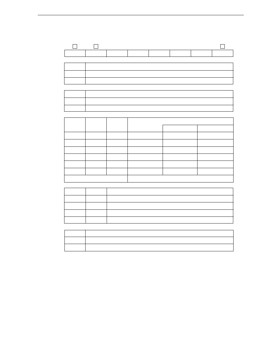
229
CHAPTER 13 A/D CONVERTER
User's Manual U14260EJ3V1UD
Figure 13-3. Format of A/D Converter Mode Register 0 (ADM0)
Address: FF80H After reset: 00H R/W
Symbol
7
6
5
4
3
2
1
0
ADM0
ADCS0
TRG0
FR02
FR01
FR00
EGA01
EGA00
ADCE0
ADCS0
A/D conversion operation control
0
Stop conversion operation.
1
Enable conversion operation.
TRG0
Software start/hardware start selection
0
Software start
1
Hardware start
FR02
FR01
FR00
Conversion time selection
Note 1
f
X
= 8.38 MHz
f
X
= 12 MHz
Note 2
0
0
0
144/f
X
17.1
µs
12.0
µs
0
0
1
120/f
X
14.3
µs
10.0
µs
Note 4
0
1
0
96/f
X
11.4
µs
Note 3
8.0
µs
Note 4
1
0
0
72/f
X
8.5
µs
Note 3
6.0
µs
Note 4
1
0
1
60/f
X
7.1
µs
Note 3
5.0
µs
Note 4
1
1
0
48/f
X
5.7
µs
Note 3
4.0
µs
Note 4
Other than above
Setting prohibited
EGA01
EGA00
Edge specification of external trigger signal
0
0
No edge detection
0
1
Falling edge detection
1
0
Rising edge detection
1
1
Both falling and rising edge detection
ADCE0
Boost reference voltage generator for A/D converter circuit control
Note 5
0
Stop operation of boost reference voltage generator.
1
Enable operation of boost reference voltage generator.
Notes 1. Set the A/D conversion time as follows.
∑ When operated at f
X
= 12 MHz (V
DD
= 4.5 to 5.5 V):
12
µs or more
∑ When operated at f
X
= 8.38 MHz (V
DD
= 4.0 to 5.5 V): 14
µs or more
2. Expanded-specification products of
µPD780078 Subseries only.
3. Setting is prohibited because the A/D conversion time is less than 14
µs.
4. Setting is prohibited because the A/D conversion time is less than 12
µs.
5. The on-chip booster is provided to realize low-voltage operation. The circuit that generates the
reference voltage for boosting is controlled by ADCE0 and it takes 14
µs for operation to stabilize after
it is started. Therefore, by waiting for at least 14
µs to elapse before setting ADCS0 to 1 after ADCE0
has been set to 1, the conversion results are valid from the first result.
Remark
f
X
: Main system clock oscillation frequency
230
CHAPTER 13 A/D CONVERTER
User's Manual U14260EJ3V1UD
Table 13-2. ADCS0 and ADCE0 Settings
ADCS0
ADCE0
A/D Conversion Operation
0
0
Stop (DC power consumption path does not exist)
0
1
Conversion wait mode (only the reference voltage generator consumes power)
1
0
Conversion mode (the reference voltage generator stops operation
Note
)
1
1
Conversion mode (the reference voltage generator operates)
Note The first data immediately after A/D conversion has started must not be used.
Figure 13-4. Timing Chart When Boost Reference Voltage Generator Is Used
Note The time from the rising of the ADCE0 bit to the rising of the ADCS0 bit must be 14
µs or longer to stabilize
the reference voltage.
Cautions 1. When rewriting FR00 to FR02 to other than the same data, stop A/D conversion once
beforehand.
2. Before clearing ADCE0, clear ADCS0.
ADCE0
Conversion
operation
Conversion
operation
Conversion
wait
Conversion
stop
Note
Boost reference
voltage
ADCS0
Boost reference voltage generator: Operates
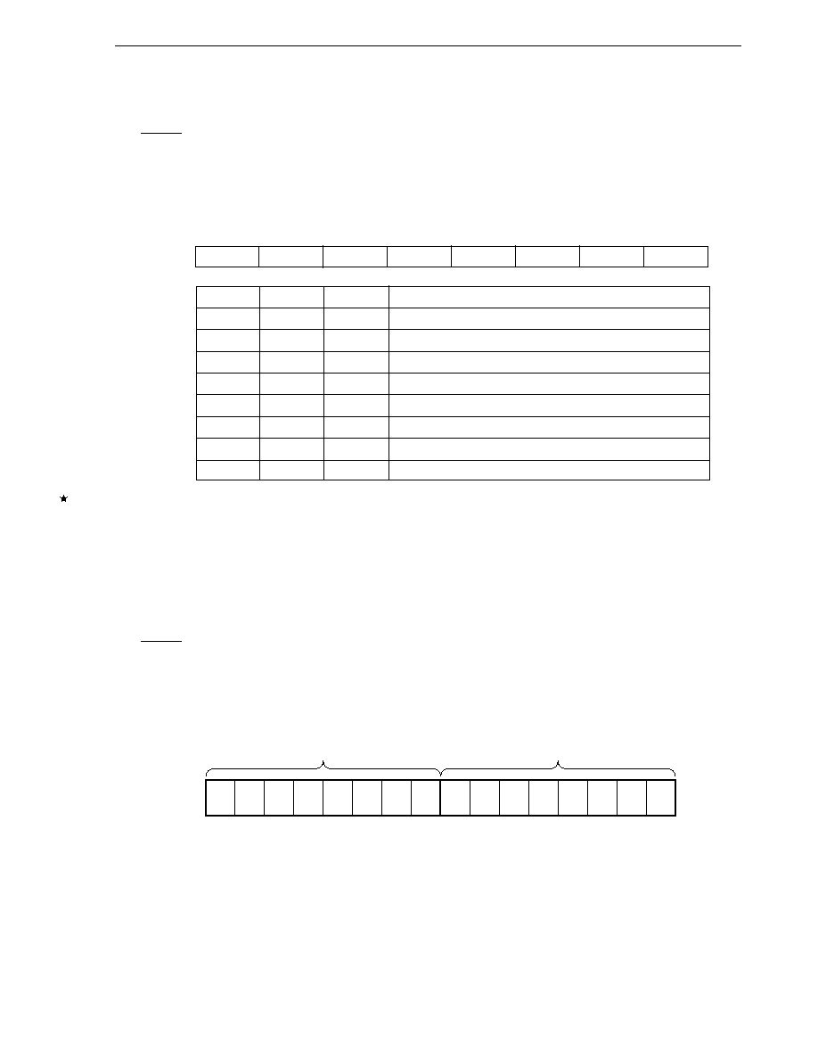
231
CHAPTER 13 A/D CONVERTER
User's Manual U14260EJ3V1UD
(2) Analog input channel specification register 0 (ADS0)
This register specifies the analog voltage input port for A/D conversion.
ADS0 is set by an 8-bit memory manipulation instruction.
RESET input clears ADS0 to 00H.
Figure 13-5. Format of Analog Input Channel Specification Register 0 (ADS0)
Address: FF81H After reset: 00H R/W
Symbol
7
6
5
4
3
2
1
0
ADS0
0
0
0
0
0
ADS02
ADS01
ADS00
ADS02
ADS01
ADS00
Analog input channel specification
0
0
0
ANI0
0
0
1
ANI1
0
1
0
ANI2
0
1
1
ANI3
1
0
0
ANI4
1
0
1
ANI5
1
1
0
ANI6
1
1
1
ANI7
Caution
Be sure to clear bits 3 to 7 to 0.
(3) A/D conversion result register 0 (ADCR0)
This is a 16-bit register that stores the A/D conversion results. The lower 6 bits are fixed to 0. Each time A/D
conversion ends, the conversion result is loaded from the successive approximation register (SAR) and held by
this register. The most significant bit (MSB) is stored in ADCR0 first. The higher 8 bits of the conversion results
are stored in FF17H. The lower 2 bits of the conversion results are stored in FF16H.
ADCR0 is read by a 16-bit memory manipulation instruction.
RESET input sets ADCR0 to 0000H.
Figure 13-6. Format of A/D Conversion Result Register 0 (ADCR0)
Caution
When A/D converter mode register 0 (ADM0) and analog input channel specification register
0 (ADS0) are written, the contents of ADCR0 may become undefined. Read the conversion
result following conversion completion before writing to ADM0 and ADS0. Using a timing other
than the above may cause an incorrect conversion result to be read.
0
0
0
0
0
0
ADCR0
Symbol
FF17H
FF16H
Address: FF16H, FF17H After reset: 0000H R

232
CHAPTER 13 A/D CONVERTER
User's Manual U14260EJ3V1UD
13.4 A/D Converter Operation
13.4.1 Basic operations of A/D converter
<1> Select one channel for A/D conversion using analog input channel specification register 0 (ADS0).
<2> Set bit 0 (ADCE0) of A/D converter mode register 0 (ADM0) to 1 and wait for 14
µs or longer.
<3> Set bit 7 (ADCS0) of the ADM0 register to 1 to start the A/D conversion operation.
(<4> to <10> are operations performed by hardware)
<4> The voltage input to the selected analog input channel is sampled by the sample & hold circuit.
<5> When sampling has been done for a certain time, the sample & hold circuit is placed in the hold state and
the input analog voltage is held until the A/D conversion operation is finished.
<6> Bit 9 of the successive approximation register (SAR) is set. The series resistor string voltage tap is set to
(1/2) AV
REF
by the tap selector.
<7> The voltage difference between the series resistor string voltage tap and analog input is compared by the
voltage comparator. If the analog input is greater than (1/2) AV
REF
, the MSB of SAR remains set. If the analog
input is smaller than (1/2) AV
REF
, the MSB is reset.
<8> Next, bit 8 of SAR is automatically set, and the operation proceeds to the next comparison. The series resistor
string voltage tap is selected according to the preset value of bit 9, as described below.
∑ Bit 9 = 1: (3/4) AV
REF
∑ Bit 9 = 0: (1/4) AV
REF
The voltage tap and analog input voltage are compared and bit 8 of SAR is manipulated as follows.
∑ Analog input voltage
Voltage tap: Bit 8 = 1
∑ Analog input voltage < Voltage tap: Bit 8 = 0
<9> Comparison is continued in this way up to bit 0 of SAR.
<10> Upon completion of the comparison of 10 bits, an effective digital result value remains in SAR, and the result
value is transferred to and latched in A/D conversion result register 0 (ADCR0).
At the same time, the A/D conversion end interrupt request (INTAD0) can also be generated.
<11> Repeat steps <4> to <10>, until ADCS0 is cleared to 0.
To stop the A/D converter, clear ADCS0 to 0.
To restart A/D conversion from the status of ADCE0 = 1, start from <3>. To restart A/D conversion from
the status of ADCE0 = 0, however, start from <2>.
Cautions 1. If bit 7 (ADCS0) of A/D converter mode register 0 (ADM0) is set to 1 without setting bit 0
(ADCE0) to 1, the first A/D conversion value immediately after A/D conversion has been
started may not satisfy the rated value. Take measures such as polling the A/D conversion
end interrupt request (INTAD0) and removing the first conversion results.
The same may apply if ADCS0 is set to 1 without the lapse of a wait time of 14
µs (MIN.) after
ADCE0 has been set to 1. Make sure that the specified wait time elapses.
2. The A/D converter stops operation in standby mode.

233
CHAPTER 13 A/D CONVERTER
User's Manual U14260EJ3V1UD
Figure 13-7. Basic Operation of A/D Converter
A/D conversion operations are performed continuously until bit 7 (ADCS0) of A/D converter mode register 0 (ADM0)
is reset (0) by software.
If a write operation is performed to ADM0 or analog input channel specification register 0 (ADS0) during an A/D
conversion operation, the conversion operation is initialized, and if ADCS0 is set (1), conversion starts again from
the beginning.
RESET input sets A/D conversion result register 0 (ADCR0) to 0000H.
Confirm the conversion results by referring to the A/D conversion end interrupt request flag (ADIF0).
Conversion time
Setting ADCS0 to 1, external trigger,
or overwriting ADS0
A/D conversion start delay time
Sampling
A/D conversion
Undefined
Conversion
result
Conversion
result
A/D converter
operation
SAR
ADCR0
INTAD0
ADCS0
Sampling time
200H
300H
or
100H
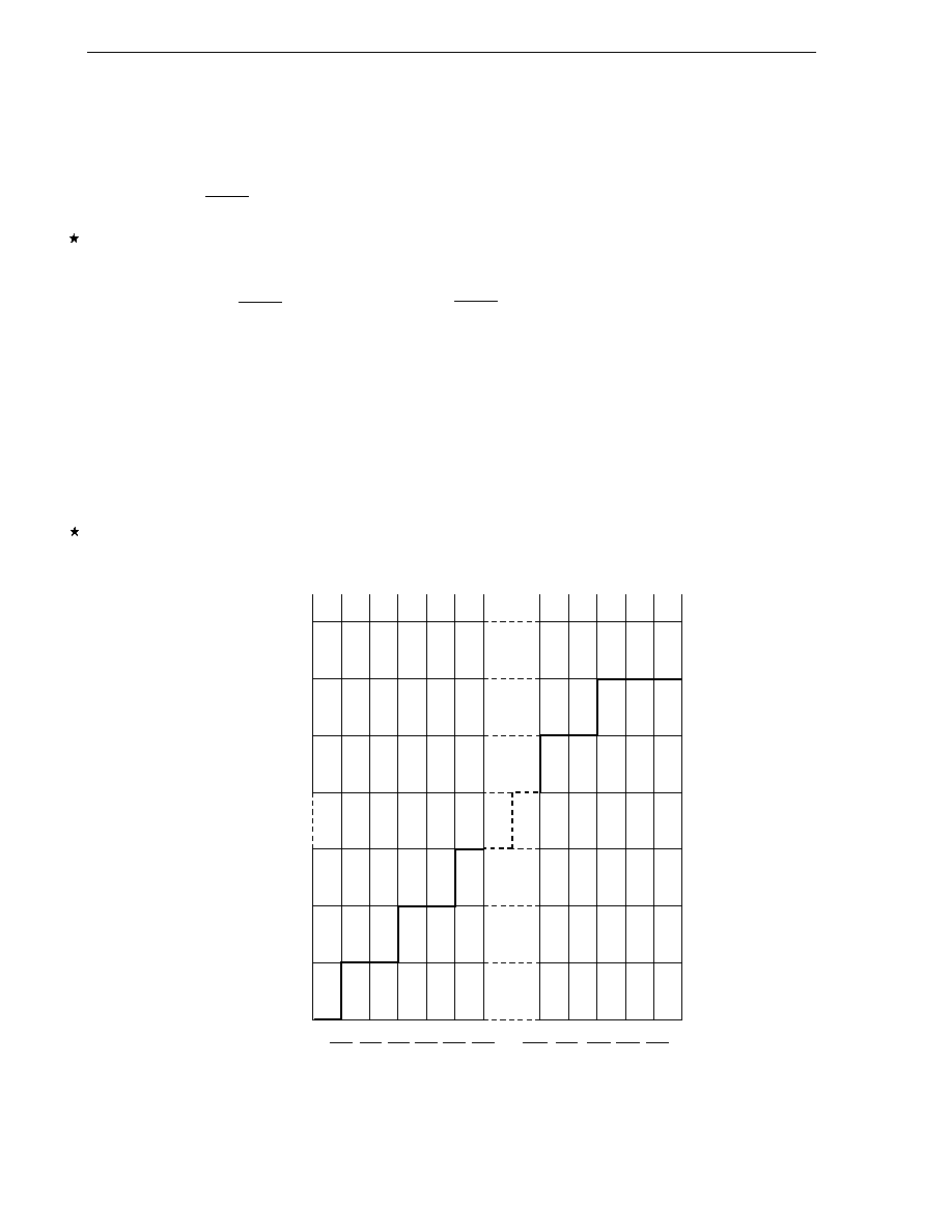
234
CHAPTER 13 A/D CONVERTER
User's Manual U14260EJ3V1UD
13.4.2 Input voltage and conversion results
The relationship between the analog input voltage input to the analog input pins (ANI0 to ANI7) and the logical
A/D conversion result (stored in A/D conversion result register 0 (ADCR0)) is shown by the following expression.
SAR = INT (
V
AIN
◊ 1024 + 0.5)
AV
REF
ADCR0 = SAR
◊ 64
or
(ADCR0 ≠ 0.5)
◊
AV
REF
V
AIN
< (ADCR0 + 0.5)
◊
AV
REF
1024
1024
where,
INT( ):
Function that returns integer part of value in parentheses
V
AIN
:
Analog input voltage
AV
REF
:
AV
REF
pin voltage
ADCR0:
A/D conversion result register 0 (ADCR0) value
SAR:
Successive approximation register
Figure 13-8 shows the relationship between the analog input voltage and the A/D conversion result.
Figure 13-8. Relationship Between Analog Input Voltage and A/D Conversion Result
1023
1022
1021
3
2
1
0
A/D conversion result
(ADCR0)
1
2048
1
1024
3
2048
2
1024
5
2048
3
1024
2043
2048
1022
1024
2045
2048
1023
1024
2047
2048
1
Input voltage/AV
REF
SAR
ADCR0
FFC0H
FF80H
FF40H
00C0H
0080H
0040H
0000H

235
CHAPTER 13 A/D CONVERTER
User's Manual U14260EJ3V1UD
13.4.3 A/D converter operation mode
Select one analog input channel from among ANI0 to ANI7 using analog input channel specification register 0
(ADS0) to start A/D conversion.
A/D conversion can be started in either of the following two ways.
∑ Hardware start: Conversion is started by trigger input (rising edge, falling edge, or both rising and falling edges
enabled).
∑ Software start: Conversion is started by setting A/D converter mode register 0 (ADM0).
When A/D conversion is complete, the interrupt request signal (INTAD0) is generated.
(1) A/D conversion by hardware start
When bit 6 (TRG0) and bit 7 (ADCS0) of A/D converter mode register 0 (ADM0) are set to 1 after bit 0 (ADCE0)
is set to 1, the A/D conversion standby state is set. When the external trigger signal (ADTRG) is input, A/D
conversion of the voltage applied to the analog input pin specified by analog input channel specification register
0 (ADS0) starts.
Upon the end of A/D conversion, the conversion result is stored in A/D conversion result register 0 (ADCR0),
and the interrupt request signal (INTAD0) is generated. After one A/D conversion operation is started and
finished, the A/D conversion operation is not started until a new external trigger signal is input.
If ADM0 and ADS0 are rewritten during A/D conversion, the converter suspends A/D conversion and waits for
a new external trigger signal to be input. When the external trigger input signal is reinput, A/D conversion is
restarted from the beginning. If ADS0 is rewritten during A/D conversion standby, A/D conversion restarts from
the beginning when the following external trigger input signal is input.
If 1 is written to ADCS0 again during A/D conversion, the A/D conversion in progress is discontinued and the
A/D conversion is restarted from the beginning when the next external trigger input signal is input.
If 0 is written to ADCS0 during A/D conversion, the A/D conversion operation stops immediately. At this time,
the conversion result is undefined.
Caution
When P03/INTP3/ADTRG is used as the external trigger input (ADTRG), specify the valid edge
using bits 1 and 2 (EGA00, EGA01) of A/D converter mode register 0 (ADM0) and set the
interrupt mask flag (PMK3) to 1.
236
CHAPTER 13 A/D CONVERTER
User's Manual U14260EJ3V1UD
Figure 13-9. A/D Conversion by Hardware Start (When Falling Edge Is Specified)
Remarks 1. n = 0, 1, ......, 7
2. m = 0, 1, ......, 7
A/D conversion
ADCR0
ADTRG
INTAD0
ADM0 set
ADCE0 = 1, ADCS0 = 1, TRG0 = 1
ADS0 rewrite
Standby state
ANIn
ANIn
Standby
state
ANIn
Standby state
ANIm
ANIm
ANIm
ANIn
ANIn
ANIn
ANIm
ANIm
Undefined

237
CHAPTER 13 A/D CONVERTER
User's Manual U14260EJ3V1UD
(2) A/D conversion by software start
When bit 6 (TRG0) and bit 7 (ADCS0) of A/D converter mode register 0 (ADM0) are set to 0 and 1, respectively,
after bit 0 (ADCE0) is set to 1, A/D conversion of the voltage applied to the analog input pin specified by analog
input channel specification register 0 (ADS0) starts.
Upon the end of A/D conversion, the conversion result is stored in A/D conversion result register 0 (ADCR0),
and the interrupt request signal (INTAD0) is generated. After one A/D conversion operation is started and
finished, the next conversion operation is immediately started. A/D conversion operations are repeated until new
data is written to ADS0.
If ADM0 and ADS0 are rewritten during A/D conversion, the converter suspends A/D conversion and A/D
conversion of the selected analog input channel restarts from the beginning.
If 1 is written to ADCS0 again during A/D conversion, the A/D conversion in progress is discontinued and the
A/D conversion is restarted from the beginning.
If 0 is written to ADCS0 during A/D conversion, the A/D conversion operation stops immediately. At this time,
the conversion result is undefined.
Figure 13-10. A/D Conversion by Software Start
Remarks 1. n = 0, 1, ......, 7
2. m = 0, 1, ......, 7
ADM0 set
ADCE0 = 1, ADCS0 = 1, TRG0 = 0
ADS0 rewrite
ADCS0 = 0
A/D conversion
ADCR0
INTAD0
ANIn
ANIn
ANIn
ANIm
ANIm
Stop
ANIn
ANIn
ANIm
Undefined
Conversion suspended;
Conversion results are not stored
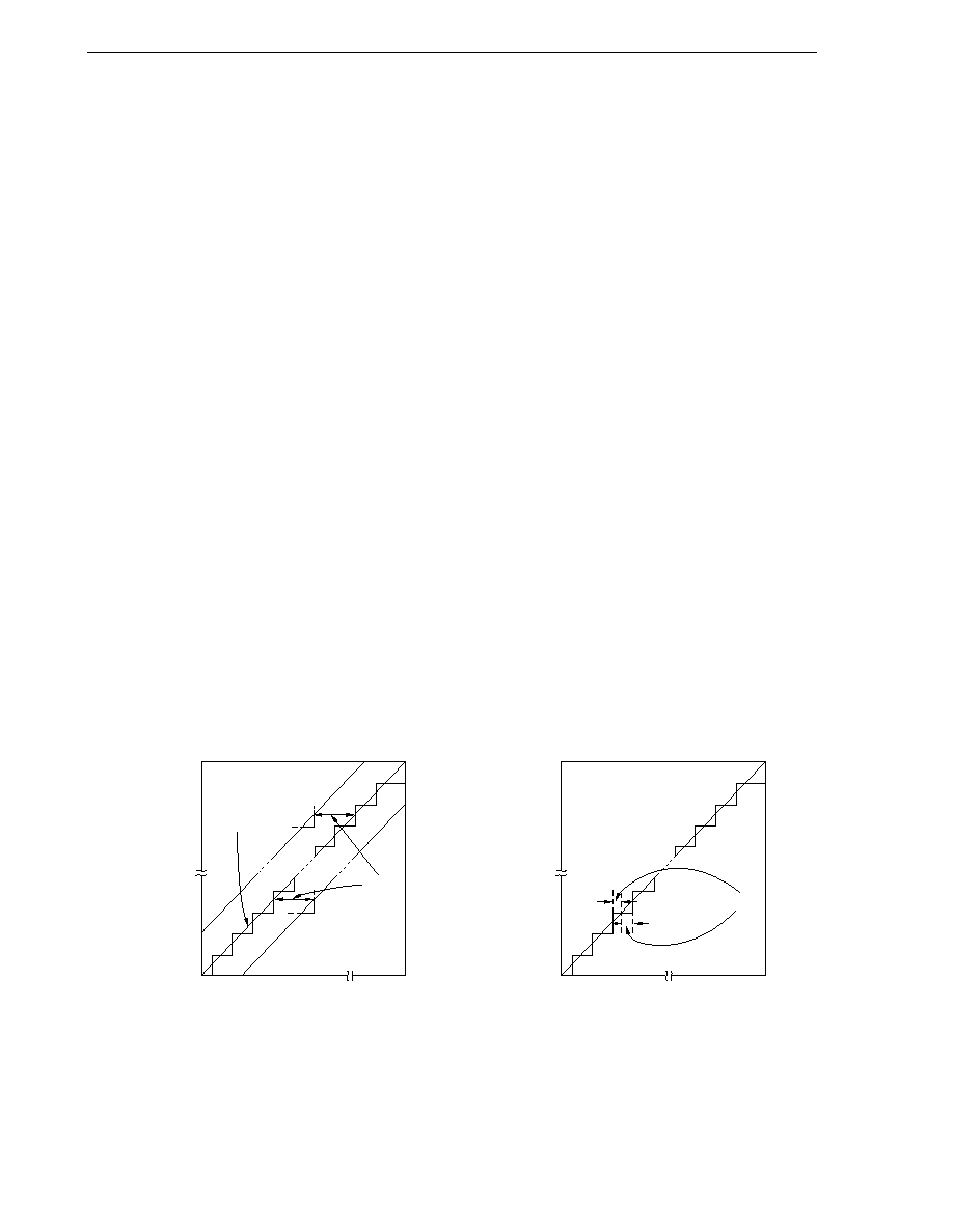
238
CHAPTER 13 A/D CONVERTER
User's Manual U14260EJ3V1UD
13.5 How to Read A/D Converter Characteristics Table
Here, special terms unique to the A/D converters are explained.
(1) Resolution
This is the minimum analog input voltage that can be identified. That is, the percentage of the analog input voltage
per 1 bit of digital output is called 1 LSB (Least Significant Bit). The percentage of 1 LSB with respect to the
full scale is expressed by %FSR (Full Scale Range).
When the resolution is 10 bits,
1 LSB = 1/2
10
= 1/1024
= 0.098%FSR
Accuracy has no relation to resolution, but is determined by overall error.
(2) Overall error
This shows the maximum error value between the actual measured value and the theoretical value.
Zero-scale error, full-scale error, integral linearity error, differential linearity error and errors that are combinations
of these express the overall error.
Note that the quantization error is not included in the overall error in the characteristics table.
(3) Quantization error
When analog values are converted to digital values, a
±1/2 LSB error naturally occurs. In an A/D converter, an
analog input voltage in a range of
±1/2 LSB is converted to the same digital code, so a quantization error cannot
be avoided.
Note that the quantization error is not included in the overall error, zero-scale error, full-scale error, integral
linearity error, and differential linearity error in the characteristics table.
Figure 13-11. Overall Error
Figure 13-12. Quantization Error
Ideal line
0......0
1......1
Digital output
Overall
error
Analog input
AV
REF
0
0......0
1......1
Digital output
Quantization error
1/2 LSB
1/2 LSB
Analog input
AV
REF
0
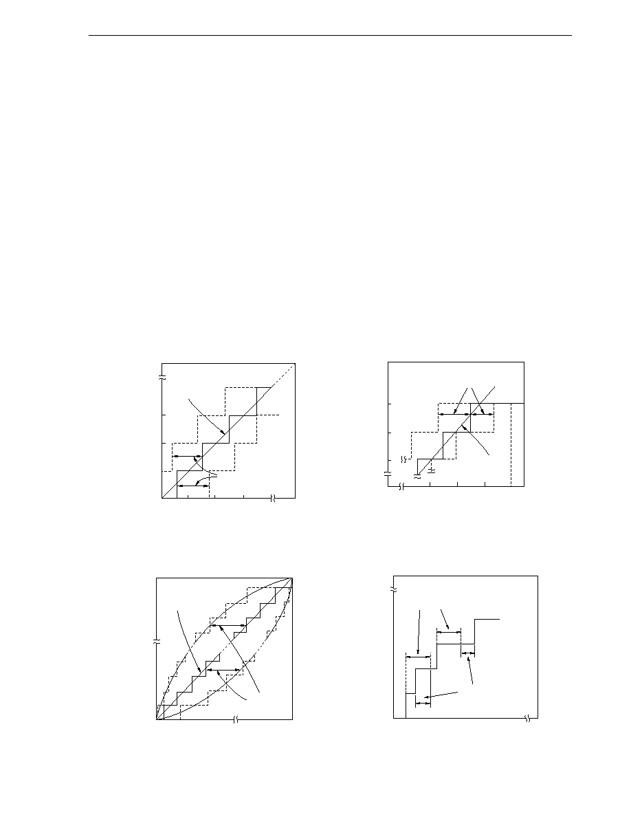
239
CHAPTER 13 A/D CONVERTER
User's Manual U14260EJ3V1UD
(4) Zero-scale error
This shows the difference between the actual measured value of the analog input voltage and the theoretical
value (1/2 LSB) when the digital output changes from 0......000 to 0......001. If the actual measured value is
greater than the theoretical value, it shows the difference between the actual measured value of the analog input
voltage and the theoretical value (3/2 LSB) when the digital output changes from 0......001 to 0......010.
(5) Full-scale error
This shows the difference between the actual measured value of the analog input voltage and the theoretical
value (full scale ≠ 3/2 LSB) when the digital output changes from 1......110 to 1......111.
(6) Integral linearity error
This shows the degree to which the conversion characteristics deviate from the ideal linear relationship. It
expresses the maximum value of the difference between the actual measured value and the ideal straight line
when the zero-scale error and full-scale error are 0.
(7) Differential linearity error
Although the ideal output width for a given code is 1 LSB, this value shows the difference between the actual
measured value and the ideal value of the width when outputting a particular code.
Figure 13-13. Zero-Scale Error
Figure 13-14. Full-Scale Error
Figure 13-15. Integral Linearity Error
Figure 13-16. Differential Linearity Error
111
011
010
001
Zero-scale error
Ideal line
000
0
1
2
3
AV
REF
Digital output (lo
w
er 3 bits)
Analog input (LSB)
111
110
101
000
0
AV
REF
AV
REF
≠1
AV
REF
≠2
AV
REF
≠3
Digital output (lo
w
er 3 bits)
Analog input (LSB)
Ideal line
Full-scale error
0
AV
REF
Digital output
Analog input
Integral
linearity
error
Ideal line
1......1
0......0
0
AV
REF
Digital output
1......1
0......0
Ideal width of 1 LSB
Differential
linearity error
Analog input

240
CHAPTER 13 A/D CONVERTER
User's Manual U14260EJ3V1UD
(8) Conversion time
This expresses the time from when sampling is started to the time when the digital output is obtained.
The sampling time is included in the conversion time in the characteristics table.
(9) Sampling time
This is the time the analog switch is turned on for the analog voltage to be sampled by the sample & hold circuit.
Sampling
time
Conversion time

241
CHAPTER 13 A/D CONVERTER
User's Manual U14260EJ3V1UD
13.6 Cautions for A/D Converter
(1) Power consumption in standby mode
The A/D converter stops operating in the standby mode. At this time, power consumption can be reduced by
setting bit 7 (ADCS0) of A/D converter mode register 0 (ADM0) to 0 (see Figure 13-2).
(2) Input range of ANI0 to ANI7
The input voltages of ANI0 to ANI7 should be within the rated range. In particular, if a voltage of AV
REF
or higher
or AV
SS
or lower is input (even if within the absolute maximum rating range), the conversion value of that channel
will be undefined and the conversion values of other channels may also be affected.
(3) Conflicting operations
<1>
Conflict between A/D conversion result register 0 (ADCR0) write and ADCR0 read by instruction upon the
end of conversion
ADCR0 read is given priority. After the read operation, the new conversion result is written to ADCR0.
<2>
Conflict between ADCR0 write and external trigger signal input upon the end of conversion
The external trigger signal is not acknowledged during A/D conversion. Therefore, the external trigger
signal is not acknowledged during ADCR0 write.
<3>
Conflict between ADCR0 write and A/D converter mode register 0 (ADM0) write or analog input channel
specification register 0 (ADS0) write
ADM0 or ADS0 write is given priority. ADCR0 write is not performed, nor is the conversion end interrupt
request signal (INTAD0) generated.
(4) ANI0/P10 to ANI7/P17
<1>
The analog input pins (ANI0 to ANI7) also function as input port pins (P10 to P17).
When A/D conversion is performed with any of pins ANI0 to ANI7 selected, do not access port 1 while
conversion is in progress, as this may reduce the conversion resolution.
<2>
If digital pulses are applied to the pin adjacent to a pin in the process of A/D conversion, the expected
A/D conversion value may not be obtainable due to coupling noise. Therefore, avoid applying pulses to
the pin adjacent to a pin undergoing A/D conversion.
(5) Input impedance of ANI0 to ANI7 pins
This A/D converter executes sampling by charging the internal sampling capacitor for approximately 1/8 of the
conversion time.
Therefore, only the leakage current flows during other than sampling, and the current for charging the capacitor
flows during sampling. The input impedance therefore varies and has no meaning.
To achieve sufficient sampling, it is recommended that the output impedance of the analog input source be 10
k
or less, or attach a capacitor of around 100 pF to the ANI0 to ANI7 pins (see Figure 13-22).
(6) AV
REF
pin input impedance
A series resistor string of several tens of k
is connected between the AV
REF
pin and the AV
SS
pin.
Therefore, when the output impedance of the reference voltage is too high, it seems as if the AV
REF
pin and the
series resistor string are connected in series. This may cause a greater reference voltage error.
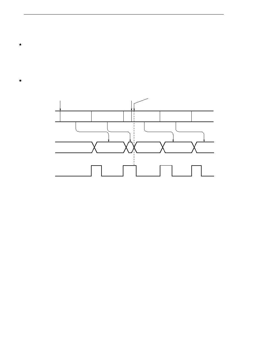
242
CHAPTER 13 A/D CONVERTER
User's Manual U14260EJ3V1UD
(7) Interrupt request flag (ADIF0)
The interrupt request flag (ADIF0) is not cleared even if analog input channel specification register 0 (ADS0) is
changed.
Therefore, if an analog input pin is changed during A/D conversion, the A/D conversion result and ADIF0 for the
pre-change analog input may be set just before the ADS0 rewrite. Caution is therefore required since, at this
time, when ADIF0 is read immediately just after the ADS0 rewrite, ADIF0 is set despite the fact that the A/D
conversion for the post-change analog input has not finished.
When A/D conversion is restarted after it is stopped, clear ADIF0 before restart.
Figure 13-17. A/D Conversion End Interrupt Request Generation Timing
Remarks 1. n = 0, 1, ......, 7
2. m = 0, 1, ......, 7
(8) Conversion results just after A/D conversion start
If bit 7 (ADCS0) of A/D converter mode register 0 (ADM0) is set to 1 without setting bit 0 (ADCE0) to 1, the
A/D conversion value immediately after A/D conversion has been started may not satisfy the rated value. Take
measures such as polling the A/D conversion end interrupt request (INTAD0) and removing the first conversion
results.
The same may apply if ADCS0 is set to 1 without a lapse of a wait time of 14
µs (MIN.) after ADCE0 has been
set to 1. Make sure that the specified wait time elapses.
(9) A/D conversion result register 0 (ADCR0) read operation
When A/D converter mode register 0 (ADM0) and analog input channel specification register 0 (ADS0) are written,
the contents of ADCR0 may become undefined. Read the conversion result following conversion completion
before writing to ADM0 and ADS0. Using a timing other than the above may cause an incorrect conversion result
to be read.
ADM0 rewrite
(start of ANIn conversion)
ADIF is set but ANIm
conversion has not finished.
A/D conversion
ADCR0
ADIF0
ANIn
ANIn
ANIm
ANIm
ANIn
Undefined
ANIm
ANIm
ADS0 rewrite
(start of ANIm conversion)

243
CHAPTER 13 A/D CONVERTER
User's Manual U14260EJ3V1UD
(10) Timing at which A/D conversion result is undefined
The A/D conversion value may be undefined if the timing of completion of A/D conversion and the timing of
stopping the A/D conversion conflict. Therefore, read the A/D conversion result before stopping the A/D
operation.
Figure 13-18 shows the timing of reading the conversion result.
Figure 13-18. Timing of Reading Conversion Result (When Conversion Result Is Undefined)
(11) Notes on board design
Locate analog circuits as far away from digital circuits as possible on the board because the analog circuits may
be affected by the noise of the digital circuits. In particular, do not cross an analog signal line with a digital signal
line, or wire an analog signal line in the vicinity of a digital signal line. Otherwise, the A/D conversion
characteristics may be affected by the noise of the digital line.
Connect AV
SS0
and V
SS0
at one location on the board where the voltages are stable.
Normal conversion result
Undefined value
A/D conversion complete
A/D conversion complete
Normal conversion result is read.
A/D conversion
is stopped.
Undefined value
is read.
ADCR0
INTAD0
ADCS0
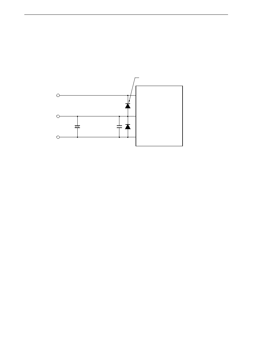
244
CHAPTER 13 A/D CONVERTER
User's Manual U14260EJ3V1UD
(12) AV
REF
pin
Connect a capacitor to the AV
REF
pin to minimize conversion errors due to noise. If an A/D conversion operation
has been stopped and is then started, the voltage applied to the AV
REF
pin becomes unstable, causing the
accuracy of the A/D conversion to drop. To prevent this, also connect a capacitor to the AV
REF
pin.
Figure 13-19 shows an example of connecting a capacitor.
Figure 13-19. Example of Connecting Capacitor to AV
REF
Pin
Remark
C1: 4.7
µF to 10 µF (reference value)
C2: 0.01
µF to 0.1 µF (reference value)
Connect C2 as close to the pin as possible.
AV
REF
V
DD0
Clamp using a diode with a low
V
F
(0.3 V or lower).
AV
SS
C
2
C
1
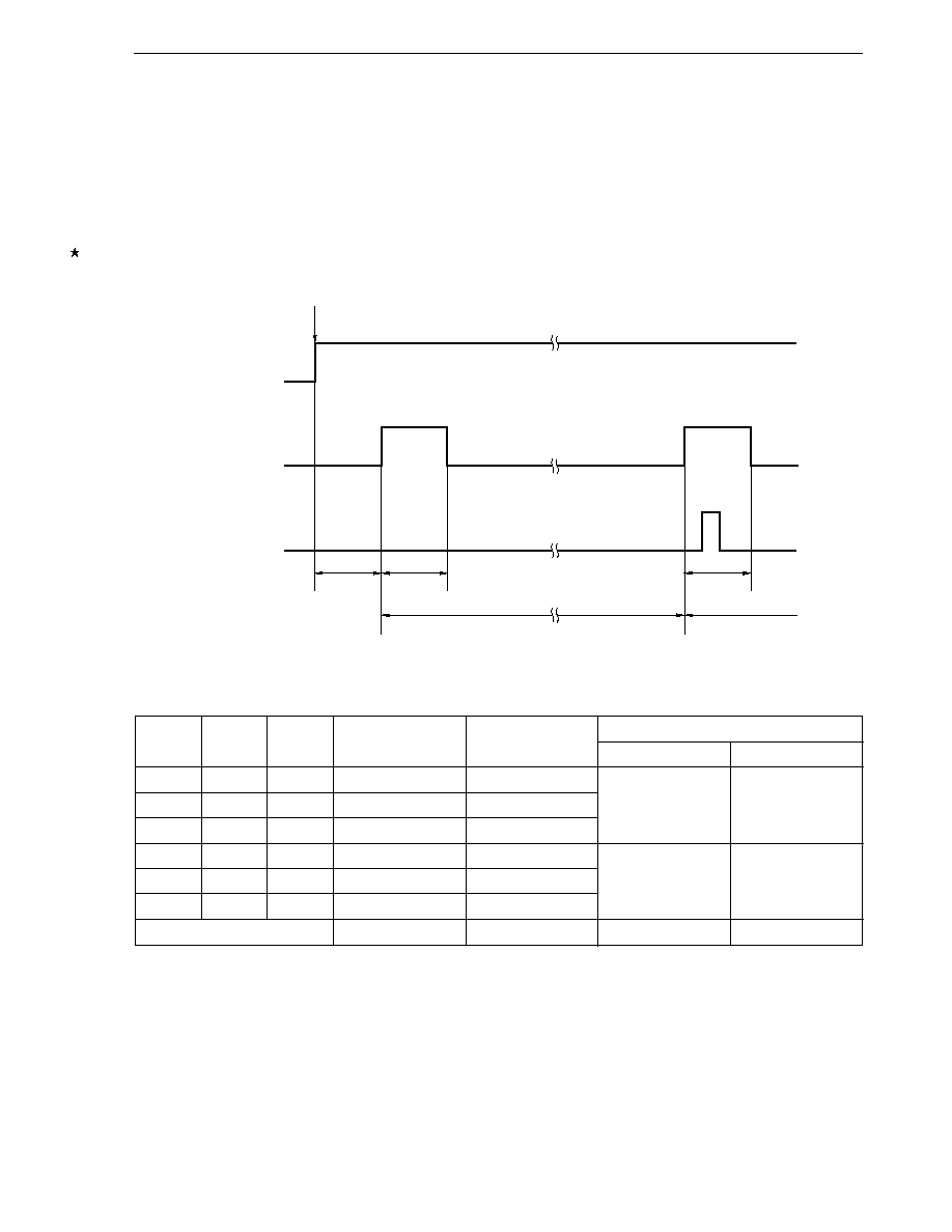
245
CHAPTER 13 A/D CONVERTER
User's Manual U14260EJ3V1UD
ADCS0
Conversion time
Conversion time
A/D
conversion
start delay
time
Sampling
time
Sampling timing
INTAD0
ADCS0
1, external trigger, or ADS0 rewrite
Sampling
time
(13) A/D converter sampling time and A/D conversion start delay time
The sampling time of the A/D converter varies depending on the values set in A/D converter mode register 0
(ADM0). There is a delay time from when the A/D converter is enabled for operation until sampling is actually
performed.
For the sets in which a strict A/D conversion time is required, note the contents described in Figure 13-20 and
Table 13-3.
Figure 13-20. Timing of A/D Converter Sampling and A/D Conversion Start Delay
Table 13-3. Sampling Time and A/D Conversion Start Delay Time of A/D Converter
FR02
FR01
FR00
Conversion Time
Note 1
Sampling Time
A/D Conversion Start Delay Time
MIN.
MAX.
0
0
0
144/f
X
20/f
X
0.5/f
CPU
+ 6/f
X
0.5/f
CPU
+ 8/f
X
0
0
1
120/f
X
16/f
X
0
1
0
96/f
X
12/f
X
1
0
0
72/f
X
10/f
X
0.5/f
CPU
+ 3/f
X
0.5/f
CPU
+ 4/f
X
1
0
1
60/f
X
8/f
X
1
1
0
48/f
X
6/f
X
Other than above
Setting prohibited
-
-
-
Notes 1. Set the A/D conversion time as follows.
∑ When operated at f
X
= 12 MHz
Note 2
(V
DD
= 4.5 to 5.5 V): 12
µs or more
∑ When operated at f
X
= 8.38 MHz (V
DD
= 4.0 to 5.5 V):
14
µs or more
2. Expanded-specification products of
µPD780078 Subseries only.
Remark
f
X
:
Main system clock oscillation frequency
f
CPU
: CPU clock frequency
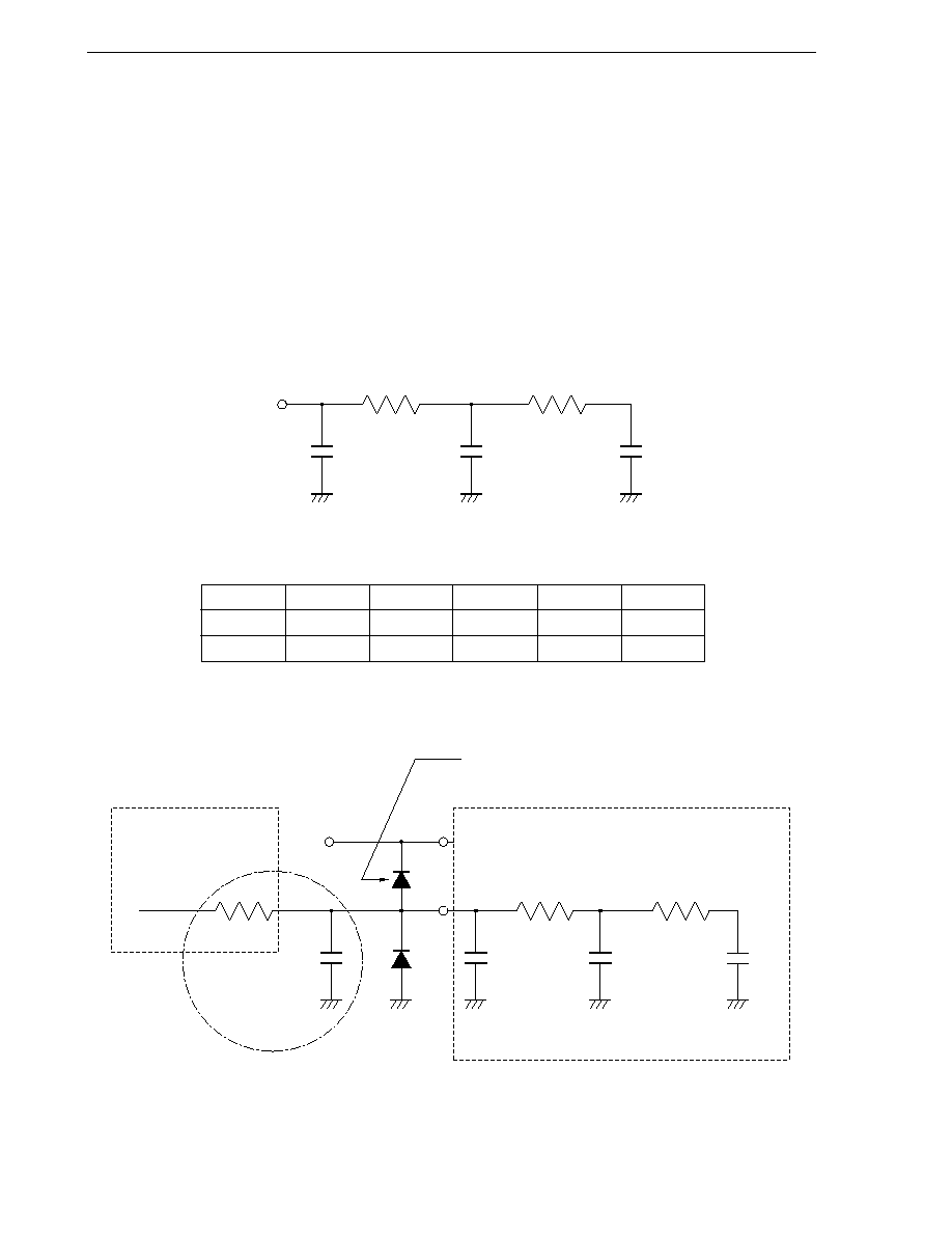
246
CHAPTER 13 A/D CONVERTER
User's Manual U14260EJ3V1UD
(14) Internal equivalent circuit of ANI0 to ANI7 pins and permissible signal source impedance
To complete sampling within the sampling time with sufficient A/D conversion accuracy, the impedance of the
signal source such as a sensor must be sufficiently low. Figure 13-21 shows the internal equivalent circuit of
the ANI0 to ANI7 pins.
If the impedance of the signal source is high, connect capacitors with a high capacitance to the ANI0 to ANI7
pins. An example of this is shown in Figure 13-22. In this case, however, the microcontroller cannot follow an
analog signal with a high differential coefficient because a lowpass filter is created.
To convert a high-speed analog signal or to convert an analog signal in the scan mode, insert a low-impedance
buffer.
Figure 13-21. Internal Equivalent Circuit of Pins ANI0 to ANI7
Table 13-4. Resistances and Capacitances of Equivalent Circuit (Reference Values)
AV
REF
R1
R2
C1
C2
C3
2.7 V
12 k
8 k
8 pF
3 pF
2 pF
4.5 V
4 k
2.7 k
8 pF
1.4 pF
2 pF
Caution
The resistances and capacitances in Table 13-4 are not guaranteed values.
Figure 13-22. Example of Connection When Signal Source Impedance Is High
Remark
n = 0 to 7
C3
C2
R2
R1
C1
ANIn
C3
C2
R2
R1
<Sensor internal circuit>
If a noise of AV
REF
or higher or AV
SS
or lower
may be generated, clamp using a diode with
a low V
F
(0.3 V or lower).
<Microcontroller internal circuit>
R0
ANIn
AV
REF
C1
C0
Lowpass filter
is created.
Output impedance
of sensor
C0
0.1 F
µ
Reference
voltage input

247
User's Manual U14260EJ3V1UD
CHAPTER 14 SERIAL INTERFACE UART0
14.1 Functions of Serial Interface UART0
Serial interface UART0 has the following three modes.
(1) Operation stop mode
This mode is used when serial transfers are not performed to reduce power consumption.
For details, see 14.4.1 Operation stop mode.
(2) Asynchronous serial interface (UART) mode (fixed to LSB first)
This mode enables full-duplex operation wherein one byte of data after the start bit is transmitted and received.
The on-chip baud rate generator dedicated to UART enables communications using a wide range of selectable
baud rates. The communication range is between 1.2 kbps and 131 kbps (when operated at f
X
= 8.38 MHz).
In addition, a baud rate (39 kbps max. (when operated at f
X
= 1.25 MHz)) can also be defined by dividing the
clock input to the ASCK0 pin.
The UART baud rate generator can also be used to generate a MIDI-standard baud rate (31.25 kbps).
For details, see 14.4.2 Asynchronous serial interface (UART) mode.
(3) Infrared data transfer mode
For details, see 14.4.3 Infrared data transfer mode.
Figure 14-1 shows a block diagram of serial interface UART0.

248
CHAPTER 14 SERIAL INTERFACE UART0
User's Manual U14260EJ3V1UD
Figure 14-1. Block Diagram of Serial Interface UART0
Note For the configuration of the baud rate generator, refer to Figure 14-2.
Figure 14-2. Block Diagram of Baud Rate Generator
Remark
TXE0: Bit 7 of asynchronous serial interface mode register 0 (ASIM0)
RXE0: Bit 6 of asynchronous serial interface mode register 0 (ASIM0)
Internal bus
Receive
buffer
register 0
(RXB0)
RxD0/P23
TxD0/P24
PM24
Output latch
(P24)
PE0 FE0 OVE0
Asynchronous serial
interface status
register 0 (ASIS0)
INTSER0
INTST0
Baud rate
generator
Note
ASK0/P25
f
X
/2 to f
X
/2
7
TXE0 RXE0 PS01 PS00 CL0
SL0 ISRM0 IRDAM0
Asynchronous serial interface
mode register 0 (ASIM0)
INTSR0
Receive
controller
(parity
check)
Transmit
shift
register 0
(TXS0)
Transmit
controller
(parity
addition)
Receive
shift
register 0
(RX0)
TPS01
TPS02
5-bit counter
Start bit
sampling clock
TPS00
ASCK0/P25
f
X
/2 to f
X
/2
7
Selector
Internal bus
3
4
MDL03
Baud rate generator
control register 0 (BRGC0)
MDL02 MDL01 MDL00
Encoder
Transmit clock
TXE0
5-bit counter
Receive clock
RXE0
Start bit detection
1/2
Match
Match
1/2

249
CHAPTER 14 SERIAL INTERFACE UART0
User's Manual U14260EJ3V1UD
14.2 Configuration of Serial Interface UART0
Serial interface UART0 includes the following hardware.
Table 14-1. Configuration of Serial Interface UART0
Item
Configuration
Registers
Transmit shift register 0 (TXS0)
Receive shift register 0 (RX0)
Receive buffer register 0 (RXB0)
Control registers
Asynchronous serial interface mode register 0 (ASIM0)
Asynchronous serial interface status register 0 (ASIS0)
Baud rate generator control register 0 (BRGC0)
Port mode register 2 (PM2)
Port register 2 (P2)
(1) Transmit shift register 0 (TXS0)
This is a register for setting transmit data. Data written to TXS0 is transmitted as serial data.
When the data length is set as 7 bits, bits 0 to 6 of the data written to TXS0 are transferred as transmit data.
Writing data to TXS0 starts the transmit operation.
TXS0 can be written by an 8-bit memory manipulation instruction. It cannot be read.
RESET input sets TXS0 to FFH.
Caution
Do not write to TXS0 during a transmit operation.
The same address is assigned to TXS0 and receive buffer register 0 (RXB0), so a read operation
reads values from RXB0.
(2) Receive shift register 0 (RX0)
This register converts serial data input via the RxD0 pin to parallel data. When one byte of data is received at
this register, the receive data is transferred to receive buffer register 0 (RXB0).
RX0 cannot be manipulated directly by a program.
(3) Receive buffer register 0 (RXB0)
This register is used to hold receive data. When one byte of data is received, one byte of new receive data is
transferred from the receive shift register (RX0).
When the data length is set as 7 bits, receive data is sent to bits 0 to 6 of RXB0. In this case, the MSB of RXB0
is always 0.
RXB0 can be read by an 8-bit memory manipulation instruction. It cannot be written.
RESET input sets RXB0 to FFH.
Caution
The same address is assigned to RXB0 and transmit shift register 0 (TXS0), so during a write
operation, values are written to TXS0.

250
CHAPTER 14 SERIAL INTERFACE UART0
User's Manual U14260EJ3V1UD
(4) Transmission controller
The transmission controller controls transmit operations, such as adding a start bit, parity bit, and stop bit to data
that is written to transmit shift register 0 (TXS0), based on the values set to asynchronous serial interface mode
register 0 (ASIM0).
(5) Reception controller
The reception controller controls receive operations based on the values set to asynchronous serial interface
mode register 0 (ASIM0). During a receive operation, it performs error checking, such as for parity errors, and
sets various values to asynchronous serial interface status register 0 (ASIS0) according to the type of error that
is detected.
14.3 Registers to Control Serial Interface UART0
Serial interface UART0 uses the following five registers for control functions.
∑ Asynchronous serial interface mode register 0 (ASIM0)
∑ Asynchronous serial interface status register 0 (ASIS0)
∑ Baud rate generator control register 0 (BRGC0)
∑ Port mode register 2 (PM2)
∑ Port register 2 (P2)
(1) Asynchronous serial interface mode register 0 (ASIM0)
This is an 8-bit register that controls serial interface UART0's serial transfer operations.
ASIM0 is set by a 1-bit or 8-bit memory manipulation instruction.
RESET input clears ASIM0 to 00H.
Figure 14-3 shows the format of ASIM0.
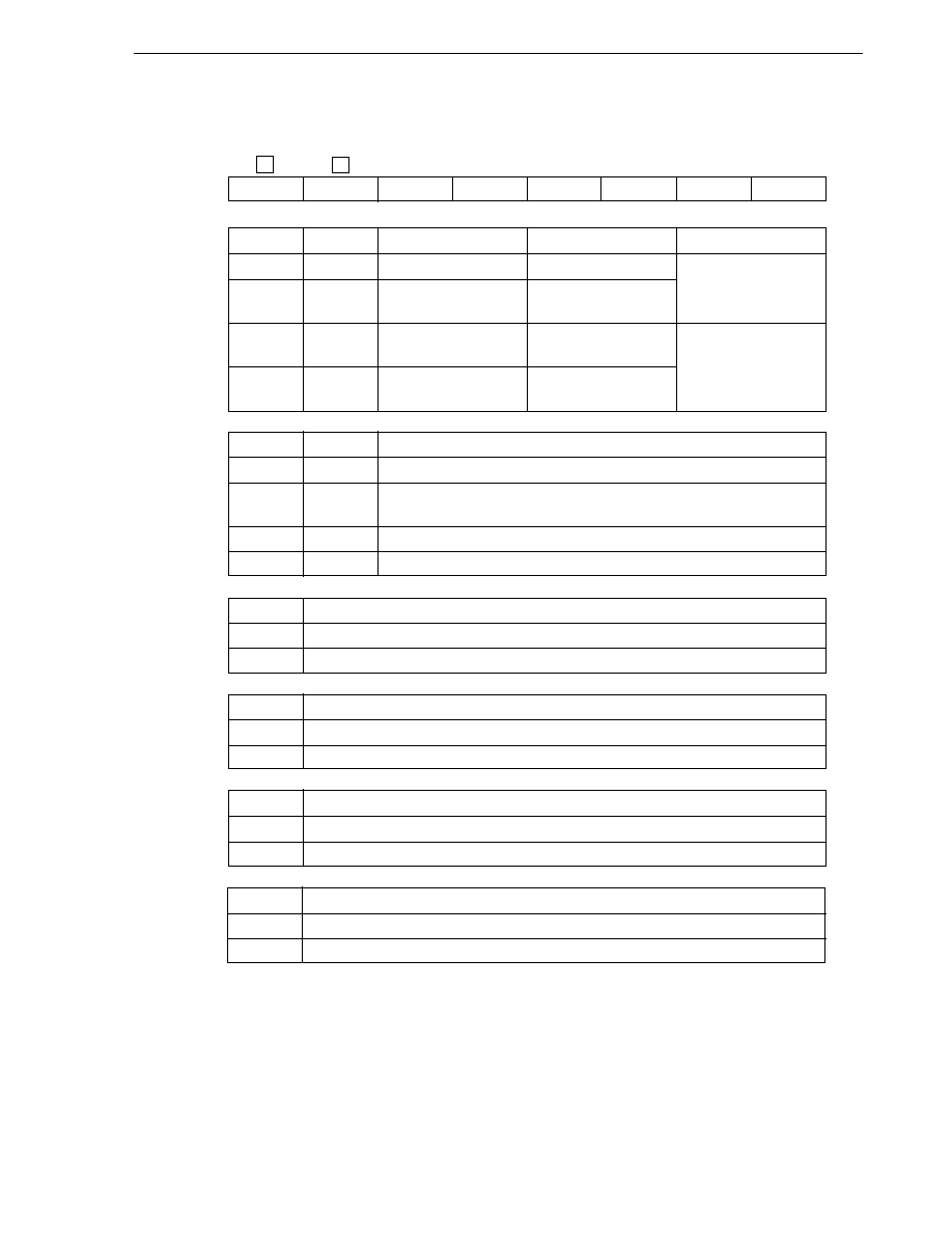
251
CHAPTER 14 SERIAL INTERFACE UART0
User's Manual U14260EJ3V1UD
Figure 14-3. Format of Asynchronous Serial Interface Mode Register 0 (ASIM0)
Address: FFA0H After reset: 00H R/W
Symbol
7
6
5
4
3
2
1
0
ASIM0
TXE0
RXE0
PS01
PS00
CL0
SL0
ISRM0
IRDAM0
TXE0
RXE0
Operation mode
RxD0/P23 pin function
TxD0/P24 pin function
0
0
Operation stop
Port function (P23)
Port function (P24)
0
1
UART mode
Serial function (RxD0)
(receive only)
1
0
UART mode
Port function (P23)
Serial function (TxD0)
(transmit only)
1
1
UART mode
Serial function (RxD0)
(transmit and receive)
PS01
PS00
Parity bit specification
0
0
No parity
0
1
Zero parity always added during transmission
No parity detection during reception (parity errors do not occur)
1
0
Odd parity
1
1
Even parity
CL0
Character length specification
0
7 bits
1
8 bits
SL0
Stop bit length specification for transmit data
0
1 bit
1
2 bits
ISRM0
Receive completion interrupt control when error occurs
0
Receive completion interrupt request is issued when an error occurs
1
Receive completion interrupt request is not issued when an error occurs
IRDAM0
Mode specification
Note 1
0
UART (transmit/receive) mode
1
Infrared data transfer (transmit/receive) mode
Note 2
Notes 1. The UART/infrared data transfer mode operation is controlled by TXE0 and RXE0.
2. When using infrared data transfer mode, be sure to set baud rate generator control register 0 (BRGC0)
to 10H.
Caution
Before writing different data to ASIM0, stop operation.
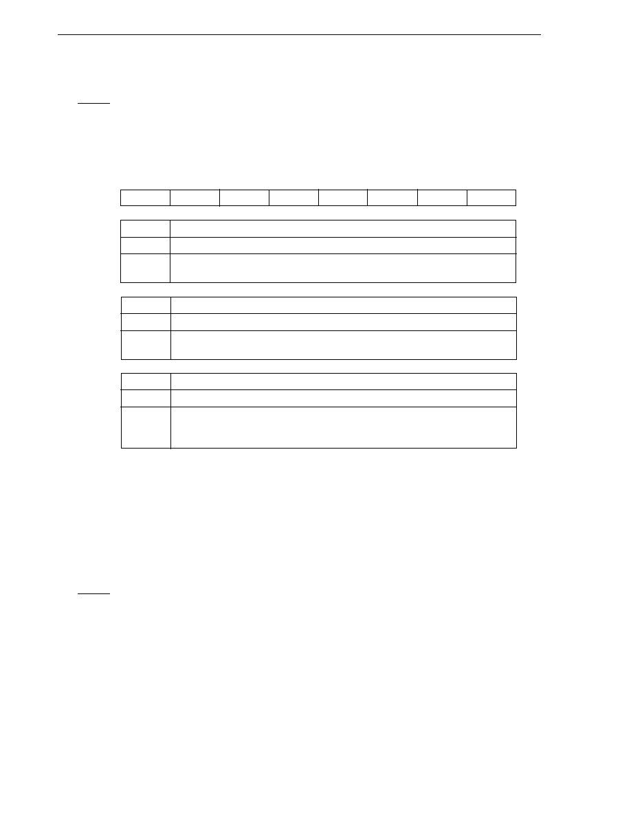
252
CHAPTER 14 SERIAL INTERFACE UART0
User's Manual U14260EJ3V1UD
(2) Asynchronous serial interface status register 0 (ASIS0)
When a receive error occurs in UART mode, this register indicates the type of error.
ASIS0 can be read by an 8-bit memory manipulation instruction.
RESET input clears ASIS0 to 00H.
Figure 14-4. Format of Asynchronous Serial Interface Status Register 0 (ASIS0)
Address: FFA1H After reset: 00H R
Symbol
7
6
5
4
3
2
1
0
ASIS0
0
0
0
0
0
PE0
FE0
OVE0
PE0
Parity error flag
0
No parity error
1
Parity error
(Parity of transmit data does not match)
FE0
Framing error flag
0
No framing error
1
Framing error
Note 1
(Stop bit not detected)
OVE0
Overrun error flag
0
No overrun error
1
Overrun error
Note 2
(Next receive operation was completed before data was read from receive buffer register
0 (RXB0))
Notes 1. Even if the stop bit length is set to two bits by setting bit 2 (SL0) of asynchronous serial interface mode
register 0 (ASIM0), stop bit detection during a receive operation only applies to a stop bit length of
1 bit.
2. When an overrun error has occurred, further overrun errors will continue to occur until the contents
of receive buffer register 0 (RXB0) are read.
(3) Baud rate generator control register 0 (BRGC0)
This register sets the serial clock for the serial interface.
BRGC0 is set by an 8-bit memory manipulation instruction.
RESET input clears BRGC0 to 00H.
Figure 14-5 shows the format of BRGC0.
253
CHAPTER 14 SERIAL INTERFACE UART0
User's Manual U14260EJ3V1UD
Figure 14-5. Format of Baud Rate Generator Control Register 0 (BRGC0)
Address: FFA2H After reset: 00H R/W
Symbol
7
6
5
4
3
2
1
0
BRGC0
0
TPS02
TPS01
TPS00
MDL03
MDL02
MDL01
MDL00
TPS02
TPS01
TPS00
Source clock selection for 5-bit counter
n
0
0
0
External clock input to ASCK0
0
0
0
1
f
X
/2
1
0
1
0
f
X
/2
2
2
0
1
1
f
X
/2
3
3
1
0
0
f
X
/2
4
4
1
0
1
f
X
/2
5
5
1
1
0
f
X
/2
6
6
1
1
1
f
X
/2
7
7
MDL03
MDL02
MDL01
MDL00
Output clock selection for baud rate generator
k
0
0
0
0
f
SCK0
/16
0
0
0
0
1
f
SCK0
/17
1
0
0
1
0
f
SCK0
/18
2
0
0
1
1
f
SCK0
/19
3
0
1
0
0
f
SCK0
/20
4
0
1
0
1
f
SCK0
/21
5
0
1
1
0
f
SCK0
/22
6
0
1
1
1
f
SCK0
/23
7
1
0
0
0
f
SCK0
/24
8
1
0
0
1
f
SCK0
/25
9
1
0
1
0
f
SCK0
/26
10
1
0
1
1
f
SCK0
/27
11
1
1
0
0
f
SCK0
/28
12
1
1
0
1
f
SCK0
/29
13
1
1
1
0
f
SCK0
/30
14
1
1
1
1
Setting prohibited
--
Cautions 1. Writing to BRGC0 during a communication operation may cause abnormal output from the
baud rate generator and disable further communication operations. Therefore, do not write
to BRGC0 during a communication operation.
2. Set BRGC0 to 10H when using in infrared data transfer mode.
Remarks 1. f
X
:
Main system clock oscillation frequency
2. f
SCK0
: Source clock for 5-bit counter
3. n:
Value set via TPS00 to TPS02 (0
n 7)
4. k:
Value set via MDL00 to MDL03 (0
k 14)
5. The equation for the baud rate is as follows.
[Baud rate] =
f
X
[Hz]
2
n+1
(k + 16)
254
CHAPTER 14 SERIAL INTERFACE UART0
User's Manual U14260EJ3V1UD
(4) Port mode register 2 (PM2)
Port mode register 2 is used to set input/output of port 2 in 1-bit units.
To use the P24/TxD0 pin as a serial data output, set PM24 and the output latch of P24 to 0.
To use the P23/RxD0 pin as a serial data input, and the P25/ASCK0 pin as a clock input, set PM23 and PM25
to 1. At this time, the output latches of P23 and P25 can be either 0 or 1.
PM2 is set by a 1-bit or 8-bit memory manipulation instruction.
RESET input sets PM2 to FFH.
Figure 14-6. Format of Port Mode Register 2 (PM2)
Address: FF22H After reset: FFH R/W
Symbol
7
6
5
4
3
2
1
0
PM2
1
1
PM25
PM24
PM23
PM22
PM21
PM20
PM2n
I/O mode selection of P2n pin (n = 0 to 5)
0
Output mode (output buffer on)
1
Input mode (output buffer off)
255
CHAPTER 14 SERIAL INTERFACE UART0
User's Manual U14260EJ3V1UD
14.4 Operation of Serial Interface UART0
This section explains the three modes of serial interface UART0.
14.4.1 Operation stop mode
Because serial transfer is not performed in this mode, the power consumption can be reduced.
In addition, pins can be used as ordinary ports. To set the operation stop mode, clear bits 7 and 6 (TXE0 and
RXE0) of ASIM0 to 0.
(1) Register to be used
Operation stop mode is set by asynchronous serial interface mode register 0 (ASIM0).
ASIM0 is set by a 1-bit or 8-bit memory manipulation instruction.
RESET input clears ASIM0 to 00H.
Address: FFA0H After reset: 00H R/W
Symbol
7
6
5
4
3
2
1
0
ASIM0
TXE0
RXE0
PS01
PS00
CL0
SL0
ISRM0
IRDAM0
TXE0
RXE0
Operation mode
RxD0/P23 pin function
TxD0/P24 pin function
0
0
Operation stop
Port function (P23)
Port function (P24)
14.4.2 Asynchronous serial interface (UART) mode
This mode enables full-duplex operation wherein one byte of data after the start bit is transmitted or received.
The on-chip baud rate generator dedicated to UART enables communications using a wide range of selectable
baud rates. The communication range is between 1.2 kbps and 131 kbps (when operated at f
X
= 8.38 MHz). The
baud rate (39 kbps max. (when operated at f
X
= 1.25 MHz)) can be defined by dividing the input clock to the ASCK0
pin.
The UART baud rate generator can also be used to generate a MIDI-standard baud rate (31.25 kbps).
(1) Registers to be used
∑ Asynchronous serial interface mode register 0 (ASIM0)
∑ Asynchronous serial interface status register 0 (ASIS0)
∑ Baud rate generator control register 0 (BRGC0)
∑ Port mode register 2 (PM2)
∑ Port register 2 (P2)
The basic procedure of setting an operation in the UART mode is as follows.
<1> Set the BRGC0 register (see Figure 14-5).
<2> Set bits 5 to 1 (PS01, PS00, CL0, SL0, and ISRM0) of the ASIM0 register and clear bit 0 (IRDAM0) to 0
(see Figure 14-3).
<3> Set bit 7 (TXE0) of the ASIM0 register to 1.
Transmission is enabled.
<4> Set bit 6 (RXE0) of the ASIM0 register to 1.
Reception is enabled.
<5> Write data to the TXS0 register.
Data transmission is started.
Caution Take relationship with the other party of communication when setting the port mode register
and port register.
256
CHAPTER 14 SERIAL INTERFACE UART0
User's Manual U14260EJ3V1UD
The relationship between the register settings and pins is shown below.
Table 14-2. Relationship Between Register Settings and Pins (UART Mode)
ASIM0
PM23 P23 PM24 P24
Operation Mode
Pin Function
TXE0
RXE0
PS01
PS00
CL0
SL0
ISRM0 IRDAM0
P23/
P24/
RxD0
TxD0
0
1
0/1
0/1
0/1
◊
0/1
0
1
◊
◊
Note
◊
Note
Reception
RxD0
P24
1
0
0/1
0/1
0/1
0/1
◊
0
◊
Note
◊
Note
0
0
Transmission
P23
TxD0
1
1
0/1
0/1
0/1
0/1
0/1
0
1
◊
0
0
Transmission/reception RxD0
TxD0
Note Can be set as port function.
Remark
◊: don't care, ASIM0: Asynchronous serial interface mode register 0,
PM
◊◊: Port mode register, P◊◊: Port output latch
The transmit/receive clock that is used to generate the baud rate is obtained by dividing the main system clock.
∑
Transmit/receive clock generation for baud rate by using main system clock
The main system clock is divided to generate the transmit/receive clock. The baud rate generated from the
main system clock is determined according to the following formula.
[Baud rate] =
f
X
[Hz]
2
n+1
(k + 16)
f
X
:
Main system clock oscillation frequency
When ASCK0 is selected as the source clock of the 5-bit counter, substitute the input clock frequency
to the ASCK0 pin for f
X
in the above expression.
n:
Value set via TPS00 to TPS02 (0
n 7, see Figure 14-5)
k:
Value set via MDL00 to MDL03 (0
k 14, see Figure 14-5)
257
CHAPTER 14 SERIAL INTERFACE UART0
User's Manual U14260EJ3V1UD
Table 14-3. Relationship Between Main System Clock and Baud Rate Error
Baud Rate
f
X
= 8.3886 MHz
f
X
= 8.000 MHz
f
X
= 7.3728 MHz
f
X
= 5.000 MHz
f
X
= 4.1943 MHz
(bps)
BRGC0
ERR (%)
BRGC0
ERR (%)
BRGC0
ERR (%)
BRGC0
ERR (%)
BRGC0
ERR (%)
600
≠
≠
≠
≠
≠
≠
≠
≠
7BH
1.14
1200
7BH
1.10
7AH
0.16
78H
0
70H
1.73
6BH
1.14
2400
6BH
1.10
6AH
0.16
68H
0
60H
1.73
5BH
1.14
4800
5BH
1.10
5AH
0.16
58H
0
50H
1.73
4BH
1.14
9600
4BH
1.10
4AH
0.16
48H
0
40H
1.73
3BH
1.14
19200
3BH
1.10
3AH
0.16
38H
0
30H
1.73
2BH
1.14
31250
31H
≠1.3
30H
0
2DH
1.70
24H
0
21H
≠1.3
38400
2BH
1.10
2AH
0.16
28H
0
20H
1.73
1BH
1.14
76800
1BH
1.10
1AH
0.16
18H
0
10H
1.73
≠
≠
115200
12H
1.10
11H
2.12
10H
0
≠
≠
≠
≠
Remark
f
X
: Main system clock oscillation frequency
∑
Error tolerance range for baud rate
The error for the baud rate depends on the number of bits per frame and the 5-bit counter's division ratio
[1/(16 + k)].
Figure 14-7 shows an example of the baud rate error tolerance range.
Figure 14-7. Error Tolerance (When k = 0), Including Sampling Errors
Baud rate error tolerance (when k = 0) =
±15.5
◊ 100 = 4.8438 (%)
320
Caution
The above error tolerance value is the value calculated based on the ideal sample point. In
the actual design, allow margins that include errors of timing for detecting a start bit.
Remark
T: 5-bit counter's source clock cycle
Basic timing
START
D0
D7
P
STOP
High-speed limit timing
START
D0
D7
P
STOP
Low-speed limit timing
START
D0
D7
P
STOP
32T
64T
256T
288T
320T
352T
Ideal
sampling
point
304T
336T
30.45T
60.9T
304.5T
15.5T
15.5T
0.5T
Sampling error
33.55T
67.1T
301.95T
335.5T
258
CHAPTER 14 SERIAL INTERFACE UART0
User's Manual U14260EJ3V1UD
(2) Communication operations
(a) Data format and waveform example
Figures 14-8 and 14-9 show the format and waveform example of the transmit/receive data.
Figure 14-8. Example of Transmit/Receive Data Format in Asynchronous Serial Interface
D0
D1
D2
D3
D4
D5
D6
D7
Start
bit
Parity
bit
Stop bit
1 data frame
Character bits
1 data frame consists of the following bits.
∑ Start bit ............. 1 bit
∑ Character bits ... 7 bits or 8 bits (LSB first)
∑ Parity bit ........... Even parity, odd parity, zero parity, or no parity
∑ Stop bit(s) ......... 1 bit or 2 bits
Asynchronous serial interface mode register 0 (ASIM0) is used to set the character bit length, parity selection,
and stop bit length within each data frame.
When "7 bits" is selected as the number of character bits, only the lower 7 bits (bits 0 to 6) are valid, so that
during a transmission the highest bit (bit 7) is ignored and during reception the highest bit (bit 7) must be
set to 0.

259
CHAPTER 14 SERIAL INTERFACE UART0
User's Manual U14260EJ3V1UD
Figure 14-9. Example of UART Transmit/Receive Data Waveform
1. Character bit: 8 bits, Parity bit: Even parity, Stop bit: 1 bit, Communication data: 55H
1 data frame
Start
D0
D1
D2
D3
D4
D5
D6
D7
Parity
Stop
2. Character bit: 7 bits, Parity bit: Odd parity, Stop bit: 2 bits, Communication data: 36H
1 data frame
Start
D0
D1
D2
D3
D4
D5
D6
Parity
Stop
Stop
3. Character bit: 8 bits, Parity bit: None, Stop bit: 1 bit, Communication data: 87H
1 data frame
Start
D0
D1
D2
D3
D4
D5
D6
D7
Stop
Baud rate generator control register 0 (BRGC0) is used to set the serial transfer rate.
If a receive error occurs, information about the receive error can be ascertained by reading asynchronous
serial interface status register 0 (ASIS0).

260
CHAPTER 14 SERIAL INTERFACE UART0
User's Manual U14260EJ3V1UD
(b) Parity types and operations
The parity bit is used to detect bit errors in communication data. Usually, the same type of parity bit is used
by the transmitting and receiving sides. When odd parity or even parity is set, errors in the parity bit (the
odd-number bit) can be detected. When zero parity or no parity is set, errors are not detected.
(i)
Even parity
∑ During transmission
The number of bits in transmit data that includes a parity bit is controlled so that there are an even
number of character bits whose value is 1. The value of the parity bit is as follows.
If the transmit data contains an odd number of character bits whose value is 1: the parity bit is "1"
If the transmit data contains an even number of character bits whose value is 1: the parity bit is "0"
∑ During reception
The number of character bits whose value is 1 is counted in the receive data that includes a parity
bit, and a parity error occurs when the counted result is an odd number.
(ii) Odd parity
∑ During transmission
The number of bits in transmit data that includes a parity bit is controlled so that there is an odd number
of character bits whose value is 1. The value of the parity bit is as follows.
If the transmit data contains an odd number of character bits whose value is 1: the parity bit is "0"
If the transmit data contains an even number of character bits whose value is 1: the parity bit is "1"
∑ During reception
The number of character bits whose value is 1 is counted in the receive data that includes a parity
bit, and a parity error occurs when the counted result is an even number.
(iii) Zero parity
During transmission, the parity bit is set to "0" regardless of the transmit data.
During reception, the parity bit is not checked. Therefore, no parity errors will occur regardless of
whether the parity bit is a "0" or a "1".
(iv) No parity
No parity bit is added to the transmit data.
During reception, receive data is regarded as having no parity bit. Since there is no parity bit, no parity
errors will occur.
261
CHAPTER 14 SERIAL INTERFACE UART0
User's Manual U14260EJ3V1UD
(c) Transmission
The transmit operation is enabled if bit 7 (TXE0) of asynchronous serial interface mode register 0 (ASIM0)
is set to 1, and the transmit operation is started when transmit data is written to transmit shift register 0 (TXS0).
A start bit, parity bit, and stop bit(s) are automatically added to the data.
Starting the transmit operation shifts out the data in TXS0, thereby emptying TXS0, after which a transmit
completion interrupt request (INTST0) is issued.
Transmission is stopped until the data to be transmitted next is written to TXS0.
The timing of the transmit completion interrupt request is shown in Figure 14-10. INTST0 occurs as soon
as the last stop bit has been output.
Figure 14-10. Timing of Asynchronous Serial Interface Transmit Completion Interrupt Request
(i)
Stop bit length: 1 bit
(ii) Stop bit length: 2 bits
Caution
Do not rewrite asynchronous serial interface mode register 0 (ASIM0) during a transmit
operation. Rewriting the ASIM0 register during a transmit operation may disable further
transmit operations (in such cases, enter a RESET to restore normal operation).
TxD0 (output)
D0
D1
D2
D6
D7
Parity
Stop
Start
INTST0
TxD0 (output)
D0
D1
D2
D6
D7
Parity
Start
INTST0
Stop
262
CHAPTER 14 SERIAL INTERFACE UART0
User's Manual U14260EJ3V1UD
(d) Reception
The receive operation performs level detection.
The receive operation is enabled when 1 is set to bit 6 (RXE0) of asynchronous serial interface mode register
0 (ASIM0), and the input via the RxD0 pin is sampled.
The serial clock specified by baud rate generator control register 0 (BRGC0) is used to sample the RxD0
pin.
When the RxD0 pin goes low, the 5-bit counter of the baud rate generator begins counting and the start timing
signal for data sampling is output when half of the specified baud rate time has elapsed. If sampling the
RxD0 pin input at this start timing signal yields a low-level result, a start bit is recognized, after which the
5-bit counter is initialized and starts counting and data sampling begins. After the start bit is recognized,
the character data, parity bit, and one-bit stop bit are detected, at which point reception of one data frame
is completed.
Once reception of one data frame is completed, the receive data in the shift register is transferred to receive
buffer register 0 (RXB0) and INTSR0 (receive completion interrupt request) occurs.
If the RXE0 bit is reset (to 0) during a receive operation, the receive operation is stopped immediately. At
this time, the contents of RXB0 and ASIS0 do not change, nor does INTSR0 or INTSER0 (receive error
interrupt request) occur.
Figure 14-11 shows the timing of the asynchronous serial interface receive completion interrupt request.
Figure 14-11. Timing of Asynchronous Serial Interface Receive Completion Interrupt Request
Caution
If the receive operation is enabled with the RxD0 pin input at the low level, the receive
operation is immediately started. Make sure the RxD0 pin input is at the high level before
enabling the receive operation.
RxD0 (input)
D0
D1
D2
D6
D7
Parity
Stop
Start
INTSR0
263
CHAPTER 14 SERIAL INTERFACE UART0
User's Manual U14260EJ3V1UD
(e) Receive errors
Three types of errors can occur during a receive operation: a parity error, framing error, or overrun error.
If, as the result of data reception, an error flag is set in asynchronous serial interface status register 0 (ASIS0),
a receive error interrupt request (INTSER0) will occur. Receive error interrupts are generated before the
receive completion interrupt request (INTSR0). Table 14-4 lists the causes behind receive errors.
As part of receive error interrupt request (INTSER0) servicing, the contents of ASIS0 can be read to determine
which type of error occurred during the receive operation (see Table 14-4 and Figure 14-12).
The contents of ASIS0 are reset (to 0) when receive buffer register 0 (RXB0) is read or when the next data
is received (if the next data contains an error, its error flag will be set).
Table 14-4. Causes of Receive Errors
Receive Error
Cause
Parity error
Parity specified does not match parity of receive data
Framing error
Stop bit was not detected
Overrun error
Reception of the next data was completed before data was read from receive buffer
register 0 (RXB0)
Figure 14-12. Receive Error Timing
RxD0 (input)
D0
D1
D2
D6
D7
Parity
Stop
Start
INTSR0
Note
INTSER0
(When framing/overrun error occurs)
INTSER0
(When parity error occurs)
Note Even if a receive error occurs when the ISRM0 bit has been set (1), INTSR0 does not occur.
Cautions 1. The contents of asynchronous serial interface status register 0 (ASIS0) are reset (to
0) when receive buffer register 0 (RXB0) is read or when the next data is received. To
obtain information about the error, be sure to read the contents of ASIS0 before reading
RXB0.
2. Be sure to read the contents of receive buffer register 0 (RXB0) after the receive
completion interrupt request has occurred even when a receive error has occurred. If
RXB0 is not read after the receive completion interrupt request has occurred, overrun
errors will occur during the next data receive operations and the receive error status
will remain until the contents of RXB0 are read.
264
CHAPTER 14 SERIAL INTERFACE UART0
User's Manual U14260EJ3V1UD
14.4.3 Infrared data transfer mode
In infrared data transfer mode, pulses can be output and received in the data format shown in (2).
(1) Registers to be used
∑ Asynchronous serial interface mode register 0 (ASIM0)
∑ Asynchronous serial interface status register 0 (ASIS0)
∑ Baud rate generator control register 0 (BRGC0)
∑ Port mode register 2 (PM2)
∑ Port register 2 (P2)
The relationship between the register settings and pins is shown below.
Table 14-5. Relationship Between Register Settings and Pins (Infrared Data Transfer Mode)
ASIM0
PM23 P23 PM24 P24
Operation Mode
Pin Function
TXE0
RXE0
PS01
PS00
CL0
SL0
ISRM0 IRDAM0
P23/
P24/
RxD0
TxD0
0
1
0/1
0/1
0/1
◊
0/1
0
1
◊
◊
Note
◊
Note
Reception
RxD0
P24
1
0
0/1
0/1
0/1
0/1
◊
0
◊
Note
◊
Note
0
0
Transmission
P23
TxD0
1
1
0/1
0/1
0/1
0/1
0/1
0
1
◊
0
0
Transmission/reception RxD0
TxD0
Note Can be set as port function.
Caution When using infrared data transfer mode, set baud rate generator control register 0 (BRGC0) to
10H.
Remark
◊: don't care, ASIM0: Asynchronous serial interface mode register 0,
PM
◊◊: Port mode register, P◊◊: Port output latch
(2) Data format
Figure 14-13 compares the data format used in UART mode with that used in infrared data transfer mode.
The IR (infrared) frame corresponds to the bit string of the UART frame, which consists of pulses that include
a start bit, eight data bits, and a stop bit.
The length of the electrical pulses that are used to transmit and receive in an IR frame is 3/16 the length of the
cycle time for one bit (i.e., the "bit time"). This pulse (whose width is 3/16 the length of one bit time) rises from
the middle of the bit time (see the figure below).
Bit time
Pulse width = 3/16 bit time

265
CHAPTER 14 SERIAL INTERFACE UART0
User's Manual U14260EJ3V1UD
Figure 14-13. Data Format Comparison Between Infrared Data Transfer Mode and UART Mode
(3) Relationship between main system clock and baud rate
Table 14-6 shows the relationship between the main system clock and the baud rate.
Table 14-6. Relationship Between Main System Clock and Baud Rate
f
X
= 8.3886 MHz
f
X
= 8.000 MHz
f
X
= 7.3728 MHz
f
X
= 5.000 MHz
f
X
= 4.1943 MHz
Baud rate
131031 bps
125000 bps
115200 bps
78125 bps
65536 bps
(4) Bit rate and pulse width
Table 14-7 lists the bit rate, bit rate error tolerance, and pulse width values.
Table 14-7. Bit Rate and Pulse Width Values
Bit Rate
Bit Rate Error Tolerance
Pulse Width Minimum Value
3/16 Pulse Width
Maximum Pulse Width
<Nominal Value>
(kbps)
(% of Bit Rate)
(
µs)
Note 2
(
µs)
(
µs)
115.2
Note 1
+/≠ 0.87
1.41
1.63
2.71
Notes 1. Operation with f
X
= 7.3728 MHz
2. When a digital noise eliminator is used in a microcontroller operating at 1.41 MHz or above.
Caution
When using in infrared data transfer mode, set baud rate generator control register 0 (BRGC0)
to 10H.
Remark
f
X
: Main system clock oscillation frequency
0
Start bit
1
D0
0
D1
1
D2
0
D3
0
D4
1
D5
1
D6
0
D7
1
Stop bit
UART frame
Data bits
Start bit
1
0
1
0
0
1
1
0
Stop bit
IR frame
Data bits
Pulse width =
3/16 bit time
Bit time
0
1
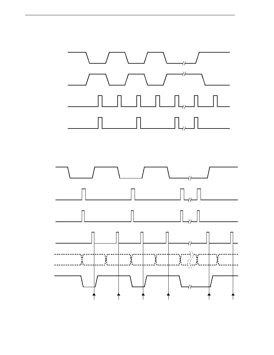
266
CHAPTER 14 SERIAL INTERFACE UART0
User's Manual U14260EJ3V1UD
(5) Input data and internal signals
∑
Transmit operation timing
∑
Receive operation timing
Data reception is delayed for one-half of the specified baud rate.
UART
output data
UART
(Inverted data)
Infrared data transfer
enable signal
TxD0 pin
output signal
Start bit
Stop bit
UART
transfer data
RxD0 input
Edge detection
Sampling clock
Start bit
Stop bit
Receive rate
Conversion data
Sampling timing
267
CHAPTER 14 SERIAL INTERFACE UART0
User
'
s Manual U14260EJ3V1UD
Table 14-8. Register Settings
Note
Can be set as port function.
Caution
When using the infrared data transfer mode, set the BRGC0 register to 10H.
Remark
◊: Don't care, ASIM0: Asynchronous serial interface mode register 0
BRGC0: Baud rate generator control register 0, PMxx: Port mode register, Pxx: Output latch of port
ASIM0
TXE0
0
RXE0
0
PS01
◊
PS00
◊
CL0
◊
SL0
◊
ISRM0
◊
IRDAM0
◊
TPS02
◊
TPS01
◊
Other than above
TPS00
◊
MDL03
◊
MDL02
◊
MDL01
◊
MDL00
◊
P23/RxD0
P23
P24/TxD0
P24
PM23
◊
Note
P23
◊
Note
PM24
◊
Note
P24
◊
Note
Pin Function
Operation
Mode
Stop
BRGC0
(1) Operation stop mode
ASIM0
TXE0
0
1
1
RXE0
1
0
1
PS01
0/1
0/1
0/1
PS00
0/1
0/1
0/1
CL0
0/1
0/1
0/1
SL0
◊
0/1
0/1
ISRM0
0/1
◊
0/1
IRDAM0
0
0
0
TPS02
0/1
0/1
0/1
TPS01
0/1
0/1
0/1
Other than above
TPS00
0/1
0/1
0/1
MDL03
0/1
0/1
0/1
MDL02
0/1
0/1
0/1
MDL01
0/1
0/1
0/1
MDL00
0/1
0/1
0/1
P23/RxD0
RxD0
P23
RxD0
P24/TxD0
P24
TxD0
TxD0
PM23
1
◊
Note
1
P23
◊
◊
Note
◊
PM24
◊
Note
0
0
P24
◊
Note
0
0
Pin Function
Operation
Mode
Receive
Transmit
Transmit
/receive
BRGC0
(2) Asynchronous serial interface (UART) mode
Setting prohibited
ASIM0
TXE0
0
1
1
RXE0
1
0
1
PS01
0/1
0/1
0/1
PS00
0/1
0/1
0/1
CL0
0/1
0/1
0/1
SL0
◊
0/1
0/1
ISRM0
0/1
◊
0/1
IRDAM0
1
1
1
TPS02
0
0
0
TPS01
0
0
0
Other than above
TPS00
1
1
1
MDL03
0
0
0
MDL02
0
0
0
MDL01
0
0
0
MDL00
0
0
0
P23/RxD0
RxD0
P23
RxD0
P24/TxD0
P24
TxD0
TxD0
PM23
1
◊
Note
1
P23
◊
◊
Note
◊
PM24
◊
Note
0
0
P24
◊
Note
0
0
Pin Function
Operation
Mode
Receive
Transmit
Transmit
/receive
BRGC0
(3) Infrared data transfer mode
Setting prohibited
Setting prohibited

268
User's Manual U14260EJ3V1UD
CHAPTER 15 SERIAL INTERFACE UART2
Serial interface UART2/SIO3 can be used in asynchronous serial interface (UART) mode or 3-wire serial I/O mode.
Caution
Do not enable UART2 and SIO3 at the same time.
15.1 Functions of Serial Interface UART2
Serial interface UART2 has the following four modes.
(1) Operation stop mode
This mode is used when serial transfers are not performed to reduce power consumption.
For details, see 15.4.1 Operation stop mode.
(2) Asynchronous serial interface (UART) mode (fixed to LSB first)
This mode enables full-duplex operation wherein one byte of data after the start bit is transmitted and received.
The on-chip baud rate generator dedicated to UART enables communications using a wide range of selectable
baud rates. In addition, a baud rate can also be defined by dividing the clock input to the ASCK0 pin.
The UART baud rate generator can also be used to generate a MIDI-standard baud rate (31.25 kbps).
For details, see 15.4.2 Asynchronous serial interface (UART) mode.
(3) Multi-processor transfer mode (fixed to LSB first)
In this mode data can be transferred to or received from two or more processors.
For details, see 15.4.3 Multi-processor transfer mode.
(4) Infrared data transfer (IrDA) mode (fixed to LSB first)
In this mode, pulses can be output or received in the data format of IrDA specification. This mode can be used
to transfer data with another digital device such as a personal computer.
For details, see 15.4.4 Infrared data transfer (IrDA) mode.
Figure 15-1 shows a block diagram of serial interface UART2.
CHAPTER 15 SERIAL INTERFACE UART2
269
User's Manual U14260EJ3V1UD
Figure 15-1. Block Diagram of Serial Interface UART2
Note For the configuration of the baud rate generator, refer to Figure 15-2.
Figure 15-2. Block Diagram of Baud Rate Generator
Remark
TXE2: Bit 7 of asynchronous serial interface mode register 2 (ASIM2)
RXE2: Bit 6 of asynchronous serial interface mode register 2 (ASIM2)
RXB2
RX2
R
X
D2/SO3/P35
T
X
D2/SI3/P34
PE2 FE2 OVE2
TXS2
INTSER2
INTST2
f
X
/2 to f
X
/2
7
TXE2 RXE2 PS21 PS20 CL2
SL2 ISEM2
POWER2
INTSR2
ASCK2/SCK3/P36
TXB2
MPR2
Internal bus
Asynchronous serial
interface status
register 2 (ASIS2)
Asynchronous serial
interface mode
register 2 (ASIM2)
Baud rate
generator
Note
Receive
buffer
register 2
Receive
shift
register 2
Receive
controller
(parity
check)
Transmit
shift
register 2
Transmit
controller
(parity
addition)
Transmit
buffer
register 2
PM34
Output latch
(PM34)
MDL26
MDL27
8-bit counter
Start bit
sampling clock
MDL24
ASCK2/SCK3/P36
f
X
/2 to f
X
/2
7
Selector
Internal bus
8
MDL23
Baud rate generator
control register 2 (BRGC2)
MDL22 MDL21 MDL20
Encoder
Transmit clock
TXE2
8-bit counter
Receive clock
RXE2
Start bit detection
1/2
Match
Match
1/2
MDL25

CHAPTER 15 SERIAL INTERFACE UART2
270
User's Manual U14260EJ3V1UD
15.2 Configuration of Serial Interface UART2
Serial interface UART2 includes the following hardware.
Table 15-1. Configuration of Serial Interface UART2
Item
Configuration
Registers
Transmit shift register 2 (TXS2)
Receive shift register 2 (RX2)
Transmit buffer register 2 (TXB2)
Receive buffer register 2 (RXB2)
Control registers
Asynchronous serial interface mode register 2 (ASIM2)
Asynchronous serial interface status register 2 (ASIS2)
Asynchronous serial interface transmit status register 2 (ASIF2)
Baud rate generator control register 2 (BRGC2)
Clock select register 2 (CKSEL2)
Transfer mode specification register 2 (TRMC2)
Port mode register 3 (PM3)
Port register 3 (P3)
(1) Transmit shift register 2 (TXS2)
This register transmits the data transferred from transmit buffer register 2 (TXB2), as serial data from the TxD2
pin.
The value of this register is set to FFH if bits 7 and 6 (TXE2) of asynchronous serial interface mode register 2
(ASIM2) are cleared to 0.
TXS2 cannot be manipulated directly by a program.
(2) Receive shift register 2 (RX2)
This register converts serial data input via the RxD2 pin to parallel data. When one byte of data is received at
this register, the receive data is transferred to receive buffer register 2 (RXB2).
RX2 cannot be manipulated directly by a program.
(3) Transmit buffer register 2 (TXB2)
This register sets data to be transmitted. The data written to TXB2 is transferred to transmit shift register 2 (RX2)
and transmitted from the TxD2 pin as serial data.
No data can be written to TXB2 if bit 1 (TXBF) of transmit status register 2 (ASIF2) is 1.
TXB2 is set by an 8-bit memory manipulation instruction.
RESET input sets TXB2 to FFH.
(4) Receive buffer register 2 (RXB2)
This register holds receive data. When one byte of data is received, one byte of new receive data is transferred
from the receive shift register (RX2).
When the data length is set as 7 bits, receive data is transferred to bits 0 to 6 of RXB2. In this case, the MSB
of RXB2 is always 0.
If an overrun error (OVE2) occurs, however, the receive data is not transferred to RXB2 but is discarded.
RXB2 can be read by an 8-bit memory manipulation instruction. It cannot be written.
The value of this register is also initialized to FFH at RESET input or by clearing bit 7 (POWER2) of asynchronous
serial interface mode register 2 (ASIM2) to 0.

CHAPTER 15 SERIAL INTERFACE UART2
271
User's Manual U14260EJ3V1UD
(5) Transmission controller
The transmission controller controls transmit operations, such as adding a start bit, parity bit, and stop bit to data
that is written to transmit shift register 2 (TXS2), based on the values set to asynchronous serial interface mode
register 2 (ASIM2).
(6) Reception controller
The reception controller controls receive operations based on the values set to asynchronous serial interface
mode register 2 (ASIM2). During a receive operation, it performs error checking, such as for parity errors, and
sets various values to asynchronous serial interface status register 2 (ASIS2) according to the type of error that
is detected.

CHAPTER 15 SERIAL INTERFACE UART2
272
User's Manual U14260EJ3V1UD
15.3 Registers to Control Serial Interface UART2
Serial interface UART2 uses the following eight registers for control functions.
∑ Asynchronous serial interface mode register 2 (ASIM2)
∑ Asynchronous serial interface status register 2 (ASIS2)
∑ Asynchronous serial interface transmit status register 2 (ASIF2)
∑ Baud rate generator control register 2 (BRGC2)
∑ Clock select register 2 (CKSEL2)
∑ Transfer mode specification register 2 (TRMC2)
∑ Port mode register 3 (PM3)
∑ Port register 3 (P3)
(1) Asynchronous serial interface mode register 2 (ASIM2)
This is an 8-bit register that controls serial interface UART2's serial transfer operations.
ASIM2 is set by a 1-bit or 8-bit memory manipulation instruction.
RESET input clears ASIM2 to 00H.
Figure 15-3. Format of Asynchronous Serial Interface Mode Register 2 (ASIM2) (1/2)
Address: FF90H After reset: 00H R/W
Symbol
7
6
5
4
3
2
1
0
ASIM2
POWER2
TXE2
RXE2
PS21
PS20
CL2
SL2
ISEM2
POWER2
Clock operation enable/stop
0
Stop clock operation. Power consumption decreases and latch in UART2 is
asynchronously reset (T
X
D2 pin is low).
1
Enable clock operation (T
X
D2 pin is high).
Note 1
TXE2
Note 2
Transmission enable/stop
0
Stop transmission (transmission circuit is synchronously reset).
1
Enable transmission.
RXE2
Note 3
Reception enable/stop
0
Stop reception (reception circuit is synchronously reset).
1
Enable reception.
Notes 1. In the infrared data transfer (IrDA) mode, the TxD2 pin is at the low level.
2. To transmit data with UART2, first specify the clock operation (set POWER2 to 1 and then TXE2 to
1), wait for the duration of 2 clocks
Note 4
, and then write the transmit data to transmit buffer register
2 (TXB2). To stop transmission by UART2, specify stopping transmission (TXE2 = 0), wait for the
duration of 2 clocks
Note 4
, and then stop the clock operation (POWER2 = 0).
3. To receive data with UART2, first specify the clock operation (set POWER2 to 1 and then RXE2 to
1), wait for the duration of 2 clocks
Note 4
, and then start reception. To stop reception by UART2, specify
stopping reception (RXE2 = 0), wait for the duration of 2 clocks
Note 4
, and then stop the clock operation
(POWER2 = 0).
4. The clock is the output clock of the 8-bit counter or the output clock of the baud rate generator.

CHAPTER 15 SERIAL INTERFACE UART2
273
User's Manual U14260EJ3V1UD
Figure 15-3. Format of Asynchronous Serial Interface Mode Register 2 (ASIM2) (2/2)
PS21
Note 1
PS20
Note 1
Parity bit specification
Transmission
Reception
0
0
Do not output parity bit.
Reception without parity
0
1
Output 0 parity.
Reception as 0 parity
Note 2
1
0
Output odd parity.
Identified as odd parity.
1
1
Output even parity.
Identified as even parity.
CL2
Note 3
Data character length specification
0
7 bits
1
8 bits
SL2
Note 4
Specification of number of stop bits for transmission
0
1 bit
1
2 bits
ISEM2
Note 5
Reception error interrupt signal control
0
INTSR2 is generated
1
INTSER2 is generated
Notes 1. To specify a parity bit, stop transmission and reception (TXE2 = 0 and RXE2 = 0) before rewriting
PS21 and PS20.
2. The parity is not identified with this setting. Therefore, bit 2 (PE2) of asynchronous serial interface
status register 2 (ASIS2) is not set and the error interrupt does not occur.
3. To specify a data character length, stop transmission and reception (TXE2 = 0 and RXE2 = 0) before
rewriting CL2.
4. To specify the number of stop bits, stop transmission (TXE2 = 0) before rewriting SL2. Reception
is always performed on the assumption that the number of stop bits is 1.
5. To specify an interrupt that occurs in case of an error, stop reception (RXE2 = 0) before rewriting
ISEM2.
CHAPTER 15 SERIAL INTERFACE UART2
274
User's Manual U14260EJ3V1UD
(2) Asynchronous serial interface status register 2 (ASIS2)
ASIS2 is a register used to display the error type when a reception error occurs in UART mode.
ASIS2 is read by an 8-bit memory manipulation instruction.
RESET input clears ASIS2 to 00H.
Figure 15-4. Format of Asynchronous Serial Interface Status Register 2 (ASIS2)
Address: FF94H After reset: 00H R
Symbol
7
6
5
4
3
2
1
0
ASIS2
0
0
0
0
MPR2
Note 1
PE2
Note 1
FE2
Note 1
OVE2
Note 1
MPR2
ID reception status flag (during reception in multi-processor transfer mode)
Note 2
0
Multi-processor appended bit "1" is not received.
1
Multi-processor appended bit "1" is received.
PE2
Parity error flag
0
No parity error
1
Parity error
(Parity of transmit data does not match
Note 3
)
FE2
Framing error flag
0
No framing error
1
Framing error
Note 4
(Stop bit not detected)
OVE2
Overrun error flag
0
No overrun error
1
Overrun error
Note 5
(Next receive operation was completed before data was read from receive buffer register
2 (RXB2))
Notes 1. These bits are reset to 0 if bit 7 (POWER2) of asynchronous serial interface mode register 2 (ASIM2)
is reset to 0.
2. This flag is affected only if the multi-processor transfer mode is selected by using bits 6 and 7 (TRM02
and TRM12) of transfer mode specification register 2 (TRMC2).
3. The operation of the parity error flag is affected by the set values of bits 3 and 4 (PS20 and PS21)
of ASIM2.
4. Even if the stop bit length is set to two bits by setting bit 2 (SL2) of ASIM2, stop bit detection during
a receive operation only applies to a stop bit length of 1 bit.
5. Be sure to read the contents of receive buffer register 2 (RXB2) when an overrun error has occurred.
Until the contents of RXB2 are read, further overrun errors will occur when receiving data. The next
receive data is not written to receive buffer register 2 (RXB2) and is discarded.

CHAPTER 15 SERIAL INTERFACE UART2
275
User's Manual U14260EJ3V1UD
(3) Asynchronous serial interface transmit status register 2 (ASIF2)
This register indicates the status of transmission.
ASIF2 is set by an 8-bit memory manipulation instruction.
RESET input clears ASIF2 to 00H.
Figure 15-5. Format of Asynchronous Serial Interface Transmit Status Register 2 (ASIF2)
Address: FF95H After reset: 00H R
Symbol
7
6
5
4
3
2
1
0
ASIF2
0
0
0
0
0
0
TXBF
TXSF
TXBF
Transmit buffer data flag
0
∑ If bit 7 (POWER2) or bit 6 (TXE2) of asynchronous serial interface mode register 2
(ASIM2) is cleared to 0
∑ If data is transferred to transmit shift register 2 (TXS2)
1
If data is written to transmit buffer register 2 (TXB2) (if data exists in TXB2)
TXSF
Transmit shift register data flag
0
∑ If bit 7 (POWER2) or bit 6 (TXE2) of asynchronous serial interface mode register 2
(ASIM2) is cleared to 0
∑ If no more data is transferred from transmit buffer register 2 (TXB2) after completion
of transfer.
1
If data is transferred from transmit buffer register 2 (TXB2) (during transmission)
Cautions 1. To start successive transmission, be sure to check that TXBF is 0 after the first byte of data
has been written to transmit buffer register 2 (TXB2), then write the second byte of data to
TXB2.
2. When successive transmission is in progress, the processing of writing to TXB2 can be
confirmed by checking the value of TXSF after the transmit completion interrupt.
∑ TXSF = 1: Successive transmission in progress. One-byte data can be written.
∑ TXSF = 0: Successive transmission is complete. Two-byte data can be written.
When writing, note Caution 1 above.
3. To initialize (to set TXE2 to 0 or POWER2 to 0) during successive transmission, make sure
that TXSF is 0 after the transmit completion interrupt, then initialize.
CHAPTER 15 SERIAL INTERFACE UART2
276
User's Manual U14260EJ3V1UD
(4) Baud rate generator control register 2 (BRGC2)
This register sets the serial clock for the serial interface.
BRGC2 is set by an 8-bit memory manipulation instruction.
RESET input clears BRGC2 to 00H.
Figure 15-6. Format of Baud Rate Generator Control Register 2 (BRGC2)
Address: FF93H After reset: 00H R/W
Symbol
7
6
5
4
3
2
1
0
BRGC2
MDL27
MDL26
MDL25
MDL24
MDL23
MDL22
MDL21
MDL20
Output clock
MDL27
MDL26
MDL25
MDL24
MDL23
MDL22
MDL21
MDL20
selection for baud
k
rate generator
0
0
0
0
0
◊
◊
◊
Setting prohibited
--
0
0
0
0
1
0
0
0
f
SCK2
/8
8
0
0
0
0
1
0
0
1
f
SCK2
/9
9
0
0
0
0
1
0
1
0
f
SCK2
/10
10
0
0
0
0
1
0
1
1
f
SCK2
/11
11
0
0
0
0
1
1
0
0
f
SCK2
/12
12
0
0
0
0
1
1
0
1
f
SCK2
/13
13
0
0
0
0
1
1
1
0
f
SCK2
/14
14
0
0
0
0
1
1
1
1
f
SCK2
/15
15
0
0
0
1
0
0
0
0
f
SCK2
/16
16
.
.
.
.
.
.
.
.
.
.
.
.
.
.
.
.
.
.
.
.
.
.
.
.
.
.
.
.
.
.
1
1
1
1
1
1
1
1
f
SCK2
/255
255
Caution
Writing to BRGC2 during a communication operation may cause abnormal output from the
baud rate generator and disable further communication operations. Therefore, do not write
to BRGC2 during a communication operation.
Before rewriting BRGC2, clear bits 5 and 6 (RXE2 and TXE2) of asynchronous serial interface
mode register 2 (ASIM2) to 0.
Remarks 1. f
SCK2
: Source clock for 8-bit counter
Set by bits 4 to 6 (TPS20 to TPS22) of clock select register 2 (CKSEL2)
2. k:
Value set via MDL27 to MDL20 (8
k 255)
3. n:
Value set via TPS22 to TPS20 (0
n 7)
4. The equation for the baud rate is as follows.
f
X
[Baud rate] = [Hz]
2
n+1
◊ k
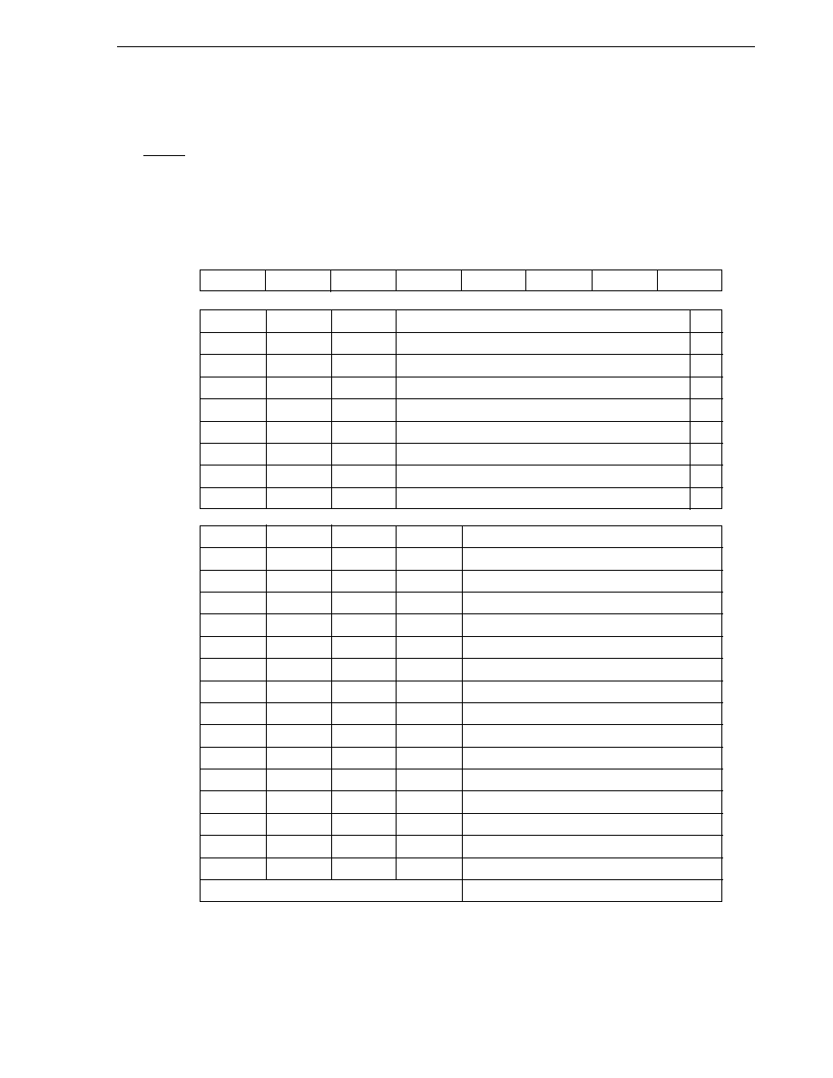
CHAPTER 15 SERIAL INTERFACE UART2
277
User's Manual U14260EJ3V1UD
(5) Clock select register 2 (CKSEL2)
This 8-bit register is used to select the input clock for the baud rate of UART2 and the transmit pulse width of
IrDA.
CKSEL2 is set by an 8-bit memory manipulation instruction.
RESET input clears CKSEL2 to 00H.
Figure 15-7. Format of Clock Select Register 2 (CKSEL2)
Address: FF92H After reset: 00H R/W
Symbol
7
6
5
4
3
2
1
0
CKSEL2
0
TPS22
Note
TPS21
Note
TPS20
Note
TPW23
TPW22
TPW21
TPW20
TPS22
TPS21
TPS20
Source clock of 8-bit counter
n
0
0
0
External clock input to ASCK2
0
0
0
1
f
X
/2
1
0
1
0
f
X
/2
2
2
0
1
1
f
X
/2
3
3
1
0
0
f
X
/2
4
4
1
0
1
f
X
/2
5
5
1
1
0
f
X
/2
6
6
1
1
1
f
X
/2
7
7
TPW23
TPW22
TPW21
TPW20
Selection of IrDA transmit pulse width of 1-bit data
0
0
1
0
Width of two f
SCK2
clocks
0
0
1
1
Width of three f
SCK2
clocks
0
1
0
0
Width of four f
SCK2
clocks
0
1
0
1
Width of five f
SCK2
clocks
0
1
1
0
Width of six f
SCK2
clocks
0
1
1
1
Width of seven f
SCK2
clocks
1
0
0
0
Width of eight f
SCK2
clocks
1
0
0
1
Width of nine f
SCK2
clocks
1
0
1
0
Width of ten f
SCK2
clocks
1
0
1
1
Width of 11 f
SCK2
clocks
1
1
0
0
Width of 12 f
SCK2
clocks
1
1
0
1
Width of 13 f
SCK2
clocks
1
1
1
0
Width of 14 f
SCK2
clocks
1
1
1
1
Width of 15 f
SCK2
clocks
0
0
0
0
Width of 16 f
SCK2
clocks
Other than above
Setting prohibited
Note
To rewrite TPS20 to TPS22, clear bit 7 (POWER2) of asynchronous serial interface mode register 2
(ASIM2) to 0.

CHAPTER 15 SERIAL INTERFACE UART2
278
User's Manual U14260EJ3V1UD
Cautions 1. If data is written to CKSEL2 during a communication operation, the output of the baud rate
generator is disturbed and the communication cannot be performed correctly. Therefore,
do not rewrite CKSEL2 during communication.
2. To transfer data in the infrared data transfer (IrDA) mode, the following conditions must be
satisfied when the transmit pulse width is specified.
(Condition)
1.41
µs
Transmit pulse width
<
Transfer rate
Set values of bits 0 to 3
Set values of bits 0 to 7
(TPW20 to TPW23) of CKSEL2
(MDL20 to MDL27) of BRGC2
Example If the transmit pulse width is set to the width of three f
SCK2
clocks (TPW23 to TPW20
= 0, 0, 1, 1)
Remark
f
X
:
Main system clock oscillation frequency
f
SCK2
: Source clock of 8-bit counter
T
X
D2 pin
Input clock
1-bit cycle
3-clock width
Pulse output starts from
the center of the 1-bit cycle.

CHAPTER 15 SERIAL INTERFACE UART2
279
User's Manual U14260EJ3V1UD
(6) Transfer mode specification register 2 (TRMC2)
This 8-bit register is used to specify the transfer mode, switch the interrupt source of INTST2, enable or disable
occurrence of the receive completion interrupt in the multi-processor transfer mode, and specify the multi-
processor transfer appended bit.
TRMC2 is set by a 1-bit or 8-bit memory manipulation instruction.
RESET input sets TRMC2 to 02H.
Figure 15-8. Format of Transfer Mode Specification Register 2 (TRMC2)
Address: FF91H After reset: 02H R/W
Symbol
7
6
5
4
3
2
1
0
TRMC2
TRM12
Note 1
TRM02
Note 1
0
0
ISMD2
0
MPIEN2
MPS2
Note 2
TRM12
TRM02
Transfer mode
0
0
UART transfer mode
Note 3
0
1
Multi-processor transfer mode
Note 3
1
0
Infrared data transfer (IrDA) mode
Note 3
1
1
MPIEN2
Receive completion interrupt enable/disable in multi-processor transfer mode
Note 4
Condition
INTSR2 enable/disable
Note 5
0
Notes 6, 7
If "0" is written to this bit
Disabled
1
∑ If bit 7 (POWER2) or bit 6 (TXE2) of
Enabled
asynchronous serial interface mode
register 2 (ASIM2) is cleared to 0
∑ If bit data has been received with multi-
processor appended bit of "1"
ISMD2
Note 8
Switching interrupt source of INTST2
0
INTST2 occurs when transmission completed
1
INTST2 occurs when data transfer completed
MPS2
Setting of multi-processor transmission appended bit
Note 4
0
Appends "0" as and transmits multi-processor appended bit (during data transmission).
1
Appends "1" as and transmits multi-processor appended bit (during ID transmission).
Notes 1. Before rewriting TRM12 and TRM02, clear bits 6 (TXE2) and 5 (RXE2) of asynchronous serial interface
mode register 2 (ASIM2) to 0.
2. Before setting a value to MPS2, confirm that bit 1 (TXBF) of asynchronous serial interface transmit
status register 2 (ASIF2) is cleared to 0. Before writing transmit data to transmit buffer register 2
(TXB2), specify whether "0" or "1" is appended as the multi-processor appended bit.
3. The setting of bits 0 to 4 (ISEM2, SL2, CL2, PS20, and PS21) of ASIM2 is valid in all the transfer modes.
4. The specification by MPIEN2 and MPS2 is valid only when bit 7 (TRM12) is cleared to 0 and bit 6
(TRM02) is set to 1 (i.e., when the multi-processor transfer mode is set).

CHAPTER 15 SERIAL INTERFACE UART2
280
User's Manual U14260EJ3V1UD
Notes 5. Enabling or disabling the occurrence of the receive completion interrupt (INTSR2) in the case of an
error is affected by the setting of bit 0 (ISEM2) of ASIM2.
6. Even if MPIEN is cleared to 0, reception is started when the start bit is detected, in order to detect
address (ID) reception. At this time, an error in the receive data is not detected if the multi-processor
appended bit is "0". If data "1" is received by mistake, due to bit slip or other cause, when the multi-
processor appended bit is detected, however, ID reception is detected. Consequently, the error in
the receive data is identified, and the error interrupt signal may be generated and the error flag set.
7. When bit 7 (POWER2) and bit 5 (RXE2) of ASIM2 have not been set to 1, MPIEN2 cannot be cleared
to 0 (remain 1) even if 0 is written to it.
8. Before setting ISMD2, clear bit 6 (TXE2) of asynchronous serial interface mode register 2 (ASIM2)
to 0.
Remark
When receiving data in the multi-processor transfer mode, the receive completion interrupt (INTSR2)
occurs, regardless of the value of MPIEN2, if data with the multi-processor appended bit set to "1" is
received. Usually, this receive data is an address (ID) that indicates the other party of communication.
The subsequent receive data can be ignored and the occurrence of an unnecessary receive completion
interrupt (INTSR2) can be disabled by comparing this received ID with the ID of the microcontroller
(for which software processing is necessary) and clearing MPIEN2 if the two IDs do not match.
(7) Port mode register 3 (PM3)
PM3 is a register that sets the input/output of port 3 in 1-bit units.
To use the P34/TxD2/SI3 pin as a serial data output, set PM34 and the output latch of P34 to 0.
To use the P35/RxD2/SO3 pin as a serial data input, and the P36/ASCK2/SCK3 pin as a clock input, set PM35
and PM36 to 1. At this time, the output latches of P35 and P36 can be either 0 or 1.
PM3 is set by a 1-bit or 8-bit memory manipulation instruction.
RESET input sets PM3 to FFH.
Figure 15-9. Format of Port Mode Register 3 (PM3)
Address: FF23H After reset: FFH R/W
Symbol
7
6
5
4
3
2
1
0
PM3
1
PM36
PM35
PM34
PM33
PM32
PM31
PM30
PM3n
I/O mode selection of P3n pin (n = 0 to 6)
0
Output mode (output buffer on)
1
Input mode (output buffer off)
CHAPTER 15 SERIAL INTERFACE UART2
281
User's Manual U14260EJ3V1UD
15.4 Operation of Serial Interface UART2
This section explains the four modes of serial interface UART2.
15.4.1 Operation stop mode
Because serial transfer is not performed in this mode, the power consumption can be reduced.
In addition, pins can be used as ordinary ports. To set the operation stop mode, clear bits 7, 6, and 5 (POWER2,
TXE2, and RXE2) of ASIM2 to 0.
(1) Register to be used
Operation stop mode is set by asynchronous serial interface mode register 2 (ASIM2).
ASIM2 is set by a 1-bit or 8-bit memory manipulation instruction.
RESET input clears ASIM2 to 00H.
Address: FF90H After reset: 00H R/W
Symbol
7
6
5
4
3
2
1
0
ASIM2
POWER2
TXE2
RXE2
PS21
PS20
CL2
SL2
ISEM2
POWER2
Clock operation enable/stop
0
Stop clock operation. Power consumption decreases and latch in UART2 is
asynchronously reset (T
X
D2 pin is low).
TXE2
Note 1
Transmission enable/stop
0
Stop transmission (transmission circuit is synchronously reset).
RXE2
Note 1
Reception enable/stop
0
Stop reception (reception circuit is synchronously reset).
Notes 1. To stop serial transmission/reception, wait for the duration of 2 clocks
Note 2
after specifying stopping
the transmission/reception (TXE2 = 0 or RXE2 = 0), and then stop the clock operation (POWER2
= 0).
2. The clock is the output clock of the 8-bit counter or the output clock of the baud rate generator.

CHAPTER 15 SERIAL INTERFACE UART2
282
User's Manual U14260EJ3V1UD
15.4.2 Asynchronous serial interface (UART) mode
This mode enables full-duplex operation wherein one byte of data after the start bit is transmitted or received.
The on-chip baud rate generator dedicated to UART enables communications using a wide range of selectable
baud rates.
The UART baud rate generator can also be used to generate a MIDI-standard baud rate (31.25 kbps).
(1) Registers to be used
∑ Asynchronous serial interface mode register 2 (ASIM2)
∑ Asynchronous serial interface status register 2 (ASIS2)
∑ Baud rate generator control register 2 (BRGC2)
∑ Asynchronous serial interface transmit status register 2 (ASIF2)
∑ Clock select register 2 (CKSEL2)
∑ Transfer mode specification register 2 (TRMC2)
∑ Port mode register 3 (PM3)
∑ Port register 3 (P3)
The basic procedure of setting an operation in the UART mode is as follows.
<1> Set the CKSEL2 register (see Figure 15-7).
<2> Set the BRGC2 register (see Figure 15-6).
<3> Clear bits 7 and 6 (TRM12 and TRM02) of the TRMC2 register to 0 and set bit 3 (ISMD2) (see Figure 15-8).
<4> Set bits 4 to 0 (PS21, PS20, CL2, SL2, and ISEM2) of the ASIM2 register (see Figure 15-3).
<5> Set bit 7 (POWER2) of the ASIM2 register to 1.
<6> Set bit 6 (TXE2) of the ASIM2 register to 1.
Transmission is enabled.
<7> Set bit 5 (RXE2) of the ASIM2 register to 1.
Reception is enabled.
<8> Write data to TXB2.
Data transmission is started.
Caution Take relationship with the other party of communication when setting the port mode register
and port register.
The relationship between the register settings and pins is shown below.
Table 15-2. Relationship Between Register Settings and Pins (UART Mode)
ASIM2
TRMC2
PM34
P34
PM35
P35 Operation Pin Function
POW TXE2 RXE2 PS21 PS20
CL2
SL2
ISEM2 TRM12 TRM02 ISMD2 MPIEN2 MPS2
Mode
P34/
P35/
ER2
SI3/
SO3/
TxD2
RxD2
1
0
1
0/1
0/1
0/1
◊
0/1
0
0
◊
◊
◊
◊
Note
◊
Note
1
◊
Reception P34
RxD2
1
1
0
0/1
0/1
0/1
0/1
◊
0
0
0/1
◊
◊
0
0
◊
Note
◊
Note
Transmission TxD2
P35
1
1
1
0/1
0/1
0/1
0/1
0/1
0
0
0/1
◊
◊
0
0
1
◊
Transmission/ TxD2
RxD2
reception
Note
Can be set as port function.
Caution When using UART2, stop the operation of SIO3 (bit 7 (CSIE3) of serial operation mode register 3
(CSIM3) = 0).
Remark
◊: don't care, ASIM2: Asynchronous serial interface mode register 2,
TRMC2: Transfer mode specification register 2, PM
◊◊: Port mode register,
P
◊◊: Port output latch

CHAPTER 15 SERIAL INTERFACE UART2
283
User's Manual U14260EJ3V1UD
The transmit/receive clock that is used to generate the baud rate is obtained by dividing the main system
clock.
∑ Transmit/receive clock generation for baud rate by using main system clock
The main system clock is divided to generate the transmit/receive clock. The baud rate generated from
the main system clock is determined according to the following formula.
[Baud rate] =
f
X
[Hz]
2
n+1
◊ k
f
X
: Main system clock oscillation frequency
When ASCK2 is selected as the source clock of the 8-bit counter, substitute the input clock frequency
to ASCK2 pin for f
X
in the above expression.
n: Value set via TPS20 to TPS22 (0
n 7, see Figure 15-7)
k: Value set via MDL27 to MDL20 (8
k 255, see Figure 15-6)
∑ Baud rate error
The baud rate error can be calculated by the following expression.
[Baud rate error] =
Baud rate [bps]
◊ 100 ≠ 100 [%]
Targeted baud rate [bps]
Table 15-3 shows an example of the relationship between the main system clock and a baud rate.
Table 15-3. Relationship Between Main System Clock and Baud Rate
Baud Rate [bps]
f
X
= 7.37 MHz
f
X
= 5.0 MHz
f
X
= 4.19 MHz
n
k
Error (%)
n
k
Error (%)
n
k
Error (%)
300
7
96
≠0.04
7
65
0.16
6
109
0.11
600
7
48
≠0.04
6
65
0.16
5
109
0.11
1200
7
24
≠0.04
5
65
0.16
4
109
0.11
2400
6
24
≠0.04
4
65
0.16
3
109
0.11
4800
5
24
≠0.04
3
65
0.16
2
109
0.11
9600
4
24
≠0.04
2
65
0.16
1
109
0.11
19200
3
24
≠0.04
1
65
0.16
≠
≠
≠
31250
1
59
≠0.07
1
40
0
≠
≠
≠
38400
2
24
≠0.04
≠
≠
≠
≠
≠
≠
76800
1
24
≠0.04
≠
≠
≠
≠
≠
≠
Remark
f
X
: Main system clock oscillation frequency
n: Value set by TPS20 to TPS22 (0
n 7)
k:
Value set by MDL27 to MDL20 (8
k 255)
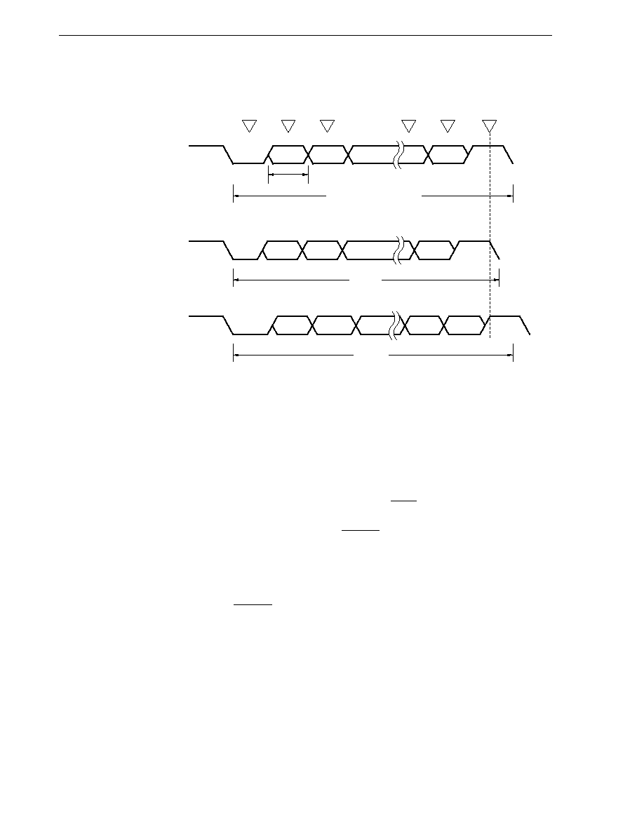
CHAPTER 15 SERIAL INTERFACE UART2
284
User's Manual U14260EJ3V1UD
∑ Permissible baud rate range for reception
Figure 15-10. Minimum Permissible Data Frame Length and Maximum Permissible Data Frame Length
As shown in the timing chart in Figure 15-10, the latch timing of the receive data is determined by the
counter set by using baud rate generator control register 2 (BRGC2) after the start bit has been detected.
If the last data (stop bit) is received within this latch timing, the data can be correctly received.
This latch timing has a margin of two clocks.
Take reception of 11-bit data as an example.
1 bit data length of UART2: FL = (Brate)
≠1
Minimum permissible data frame length: FLmin = 11
◊ FL ≠
k ≠ 2
◊ FL
2k
=
21k + 2
◊ FL
2k
Therefore, the maximum receivable baud rate of the transmission destination is as follows.
BRmax = (FLmin/11)
≠1
=
22k
Brate
21k + 2
Start
D0
FL
D1
Stop
D7
P
Start
D0
D1
Stop
D7
P
FLmin
Start
D0
D1
Stop
D7
P
FLmax
Data frame length
of UART2
Minimum permissible
data frame length
Maximum permissible
data frame length
1 data frame (11
◊ FL)

CHAPTER 15 SERIAL INTERFACE UART2
285
User's Manual U14260EJ3V1UD
Similarly, the maximum permissible data frame length is as follows.
10
FLmax = 11
◊ FL ≠
k + 2
◊ FL
11
2k
=
21k ≠ 2
◊ FL
2k
FLmax =
21k ≠ 2
◊ FL ◊ 11
20k
Therefore, the minimum receivable baud rate of the transmission destination is as follows.
BRmin = (FLmax/11)
≠1
=
20k
Brate
21k ≠ 2
Remark
Brate: Baud rate of UART2
k:
Value set by MDL27 to MDL20 (8
k 255)
FL:
1 bit data length
From the above expressions for the maximum and minimum baud rates, the permissible error of the baud
rate between UART2 and the transmission destination can be calculated as follows.
Table 15-4. Maximum Permissible Baud Rate Error and Minimum Permissible Baud Rate Error
k
Maximum Permissible Baud Rate Error (%)
Minimum Permissible Baud Rate Error (%)
8
+3.53
≠3.61
20
+4.26
≠4.31
50
+4.56
≠4.58
100
+4.66
≠4.67
255
+4.72
≠4.73
Caution
The above error tolerance value is the value calculated based on the ideal sample point.
In the actual design, allow margins that include errors of timing for detecting a start
bit.
Remark
k: Value set by MDL27 to MDL20 (8
k 255)
The accuracy of reception is dependent upon the number of bits in one frame, input clock frequency, and
division ratio k (the higher the input clock frequency and the higher the division ratio k, the higher the
accuracy).
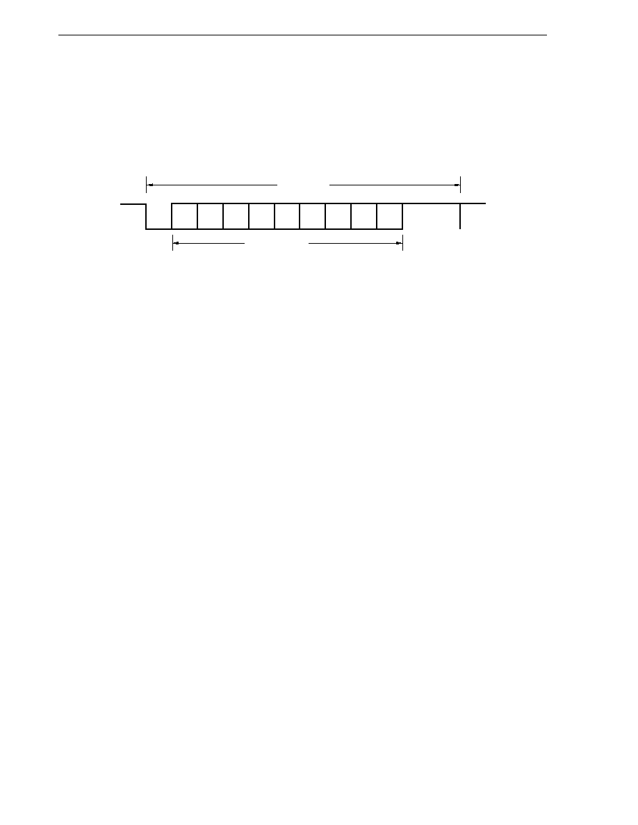
CHAPTER 15 SERIAL INTERFACE UART2
286
User's Manual U14260EJ3V1UD
(2) Communication operations
(a) Data format and waveform example
Figures 15-11 and 15-12 show the format and waveform example of the transmit/receive data.
Figure 15-11. Example of Transmit/Receive Data Format in Asynchronous Serial Interface
D0
D1
D2
D3
D4
D5
D6
D7
Start
bit
Parity
bit
Stop bit
1 data frame
Character bits
1 data frame consists of the following bits.
∑ Start bit ............. 1 bit
∑ Character bits ... 7 bits or 8 bits (LSB first)
∑ Parity bit ........... Even parity, odd parity, zero parity, or no parity
∑ Stop bit(s) ......... 1 bit or 2 bits
Asynchronous serial interface mode register 2 (ASIM2) is used to set the character bit length, parity selection,
and stop bit length within each data frame.
When "7 bits" is selected as the number of character bits, only the lower 7 bits (bits 0 to 6) are valid, so that
during a transmission the highest bit (bit 7) is ignored and during reception the highest bit (bit 7) must be
set to 0.
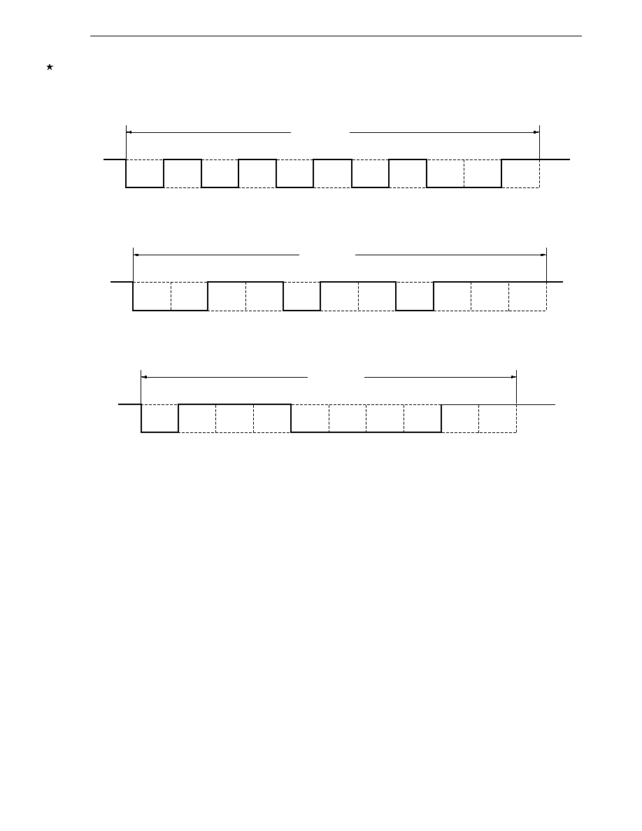
CHAPTER 15 SERIAL INTERFACE UART2
287
User's Manual U14260EJ3V1UD
Figure 15-12. Example of UART Transmit/Receive Data Waveform
1. Character bit: 8 bits, Parity bit: Even parity, Stop bit: 1 bit, Communication data: 55H
1 data frame
Start
D0
D1
D2
D3
D4
D5
D6
D7
Parity
Stop
2. Character bit: 7 bits, Parity bit: Odd parity, Stop bit: 2 bits, Communication data: 36H
1 data frame
Start
D0
D1
D2
D3
D4
D5
D6
Parity
Stop
Stop
3. Character bit: 8 bits, Parity bit: None, Stop bit: 1 bit, Communication data: 87H
1 data frame
Start
D0
D1
D2
D3
D4
D5
D6
D7
Stop
Baud rate generator control register 2 (BRGC2) and clock select register 2 (CKSEL2) are used to set the
serial transfer rate.
If a receive error occurs, information about the receive error can be ascertained by reading asynchronous
serial interface status register 2 (ASIS2).

CHAPTER 15 SERIAL INTERFACE UART2
288
User's Manual U14260EJ3V1UD
(b) Parity types and operations
The parity bit is used to detect bit errors in communication data. Usually, the same type of parity bit is used
by the transmitting and receiving sides. When odd parity or even parity is set, errors in the parity bit (the
odd-number bit) can be detected. When zero parity or no parity is set, errors are not detected.
(i)
Even parity
∑ During transmission
The number of character bits in transmit data that includes a parity bit is controlled so that there are
an even number of bits whose value is 1. The value of the parity bit is as follows.
If the transmit data contains an odd number of character bits whose value is 1: the parity bit is "1"
If the transmit data contains an even number of character bits whose value is 1: the parity bit is "0"
∑ During reception
The number of character bits whose value is 1 is counted in the receive data that includes a parity
bit, and a parity error occurs when the counted result is an odd number.
(ii) Odd parity
∑ During transmission
The number of character bits in transmit data that includes a parity bit is controlled so that there is
an odd number of bits whose value is 1. The value of the parity bit is as follows.
If the transmit data contains an odd number of character bits whose value is 1: the parity bit is "0"
If the transmit data contains an even number of character bits whose value is 1: the parity bit is "1"
∑ During reception
The number of character bits whose value is 1 is counted in the receive data that includes a parity
bit, and a parity error occurs when the counted result is an even number.
(iii) Zero parity
During transmission, the parity bit is set to "0" regardless of the transmit data.
During reception, the parity bit is not checked. Therefore, no parity errors will occur regardless of
whether the parity bit is a "0" or a "1".
(iv) No parity
No parity bit is added to the transmit data.
During reception, receive data is regarded as having no parity bit. Since there is no parity bit, no parity
errors will occur.

CHAPTER 15 SERIAL INTERFACE UART2
289
User's Manual U14260EJ3V1UD
(c) Transmission
If the UART transfer mode is selected by using transfer mode specification register 2 (TRMC2) and bit 7
(POWER2) of asynchronous serial interface mode register 2 (ASIM2) is set to 1, the T
X
D2 pin outputs a high
level. If bit 6 (TXE2) of ASIM2 is set to 1 next, transmission is enabled. Transmission can be started by
writing transmit data to transmit buffer register 2 (TXB2). The start bit, parity bit, and stop bit are automatically
appended to the transmit data.
When transmission has been started, the data in TXB2 is transferred to transmit shift register 2 (TXS2) and
is sequentially output to the T
X
D2 pin, starting from the LSB. If the data to be transmitted next has been
written to TXB2 by the time transmission is complete, transmitting the next data is started. If no more data
has been written to TXB2, transmission is stopped until the next data is written.
Figure 15-13 illustrates the timing of the transmit interrupt.
Figure 15-13. Timing of Asynchronous Serial Interface Transmit Completion Interrupt Request
(i)
Stop bit length: 1 bit, TRMC2: ISMD2 = 0
TxD2 (output)
D0
D1
D2
D6
D7
Parity
Stop
Start
INTST2
(ii) Stop bit length: 2 bits, TRMC2: ISMD2 = 0
T
X
D2 (output)
INTST2
D0
Start
D1
D2
D6
D7
Parity
Stop
(iii) Successive transmission, Stop bit length: 2 bits, TRMC2: ISMD2 = 1
INTST2
D0
D0
Start
If next transmit data is
written to TXB2
Start
D1
D7
Parity
Stop
TxD2 (output)
Remark
TRMC2: Transfer mode specification register 2
ISMD2:
Bit 3 of TRMC2
CHAPTER 15 SERIAL INTERFACE UART2
290
User's Manual U14260EJ3V1UD
Caution
Do not rewrite asynchronous serial interface mode register 2 (ASIM2) during a transmit
operation. Rewriting the ASIM2 register during a transmit operation may disable further
transmit operations (in such cases, input a RESET to restore normal operation).
(d) Successive transmission
The next transmit data can be written to transmit buffer register 2 (TXB2) as soon as transmit shift register
2 (TXB2) has started its shift operation. Consequently, even while an interrupt is being serviced after one
data frame has been transmitted, data can be successively transmitted.
To successively transmit data, be sure to check, by using asynchronous serial interface transmit status
register 2 (ASIF2), the transmission status and whether writing to TXB2 is enabled or disabled, and then
write the data to TXB2.
The following table shows the relationship between the transmission status and writing to TXB2.
Table 15-5. Writing to TXBF and TXB2 (When Successive Transmission Is Started)
TXBF
Writing to TXB2 When Successive Transmission Is Started
0
Enabled
1
Disabled
Caution
When starting successive transmission, write the first byte of data to transmit buffer
register 2 (TXB2), and then make sure to write data to TXB2 again.
Remark
TXBF: Bit 1 of ASIF2
Table 15-6. Writing to TXSF and TXB2 (When Successive Transmission Is in Progress)
TXSF
Writing to TXB2 When Successive Transmission Is in Progress
0
Two-byte writing or transmit completion processing enabled
1
One-byte writing enabled
Cautions 1. When successive transmission is in progress, the processing of writing to TXB2 can
be confirmed by checking the value of TXSF after the transmit completion interrupt.
∑ TXSF = 1: Successive transmission in progress. One-byte data can be written.
∑ TXSF = 0: Successive transmission is complete. Two-byte data can be written.
When writing, note the Caution in Table 15-5.
2. To initialize (to set TXE2 to 0 or POWER2 to 0) during successive transmission, make
sure that TXSF is 0 after the transmit completion interrupt, then initialize.
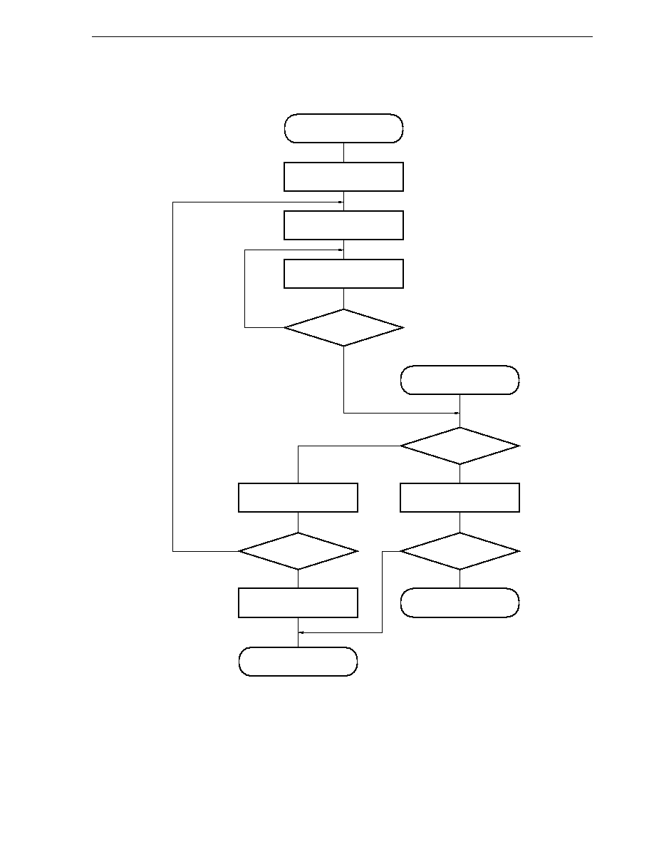
CHAPTER 15 SERIAL INTERFACE UART2
291
User's Manual U14260EJ3V1UD
Figure 15-14 shows the processing flow of successive transmission.
Figure 15-14. Processing Flow of Successive Transmission
START
Set various registers
Write data to TXB2
Read ASIF2
Interrupt occurred
Read ASIF2
TXSF = 0?
TXSF = 1?
Read ASIF2
Completion of
transmission processing
Write data to TXB2
Wait for occurrence
of interrupt
Required number
of writes performed?
TXBF = 0?
No
No
No
No
Yes
Yes
Yes
Yes
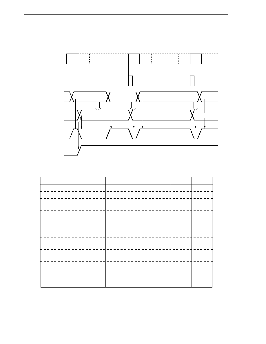
CHAPTER 15 SERIAL INTERFACE UART2
292
User's Manual U14260EJ3V1UD
The following figures and tables show the timing of starting and completing successive transmission.
Figure 15-15. Timing of Starting Successive Transmission
Start Stop
Start
Parity
Data (1)
FF
Data (2)
Data (3)
Data (1)
FF
<2>
<3>
<4>
<5>
Data (1)
Data transfer
Data transfer
INTST2
TXB2
TXS2
TXBF
TXSF
Data transfer
Data (2)
T
X
D2 (output)
Data (1)
Start Parity
Stop
Data (3)
<1>
Table 15-7. Timing of Starting Successive Transmission
Transmission Procedure
Internal Operation
TXBF
TXSF
Set transmission mode.
<1> Starts transmission unit.
0
0
Write data (1).
1
0
<2> Generates start bit and starts
0
1
transmitting data (1).
Read ASIF2 (to confirm TXBF = 0)
1
1
and write data (2).
(during transmission)
<3> Interrupt (INTST2) occurs.
0
1
Read ASIF2 (to confirm TXBF = 0)
1
1
and write data (3).
<4> Generates start bit and starts
transmitting data (2).
(during transmission)
<5> Interrupt (INTST2) occurs.
0
1
Read ASIF2 (to confirm TXBF = 0)
1
1
and write data (3).
Remarks 1. <1> to <5> in this table correspond to <1> to <5> in Figure 15-15.
2. TXBF: Bit 1 (transmit buffer data flag) of asynchronous serial interface transmit status register
2 (ASIF2)
TXSF: Bit 0 of ASIF2 (transmit shift register data flag)
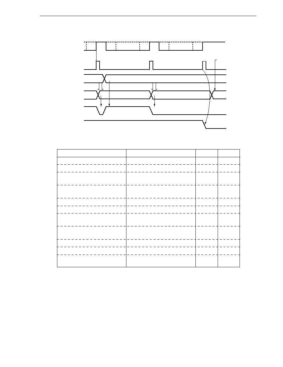
CHAPTER 15 SERIAL INTERFACE UART2
293
User's Manual U14260EJ3V1UD
Figure 15-16. Timing of Completing Successive Transmission
FF
INTST2
TXB2
TXS2
TXSF
TXBF
FF
T
X
D2 (output)
Parity
Parity
Parity
Stop
Stop
Stop
Start
Start
Data (n
- 1)
Data (n
- 1)
<1>
<2>
<4>
<3>
<5>
<6>
Data (n
- 1)
Data (n)
Data (n
- 1)
Data (n)
POWER2 or
TXE2 is cleared.
Data
transfer
Data
transfer
Table 15-8. Timing of Completing Successive Transmission
Transmission Procedure
Internal Operation
TXBF
TXSF
<1> Data (n≠2) is transmitted.
1
1
<2> Interrupt (INTST2) occurs.
0
1
Read ASIF2 (to confirm TXBF = 0)
1
1
and write data (n).
<3> Generates start bit and starts
transmitting data (n≠1).
(during transmission)
<4> Interrupt (INTST2) occurs.
0
1
Read ASIF2 (to confirm TXBF = 0).
1
1
No data to be written.
<5> Generates start bit and starts
transmitting data (n).
(during transmission)
<6> Interrupt (INTST2) occurs.
0
0
Read ASIF2 (to confirm TXBF = 0)
Initializes internal circuit.
and clear POWER2 or TXE2.
Remarks 1. <1> to <6> in this table correspond to <1> to <6> in Figure 15-16.
2. TXBF:
Bit 1 (transmit buffer data flag) of asynchronous serial interface transmission status
register 2 (ASIF2)
TXSF:
Bit 0 of ASIF2 (transmit shift register data flag)
POWER2: Bit 7 of asynchronous serial interface mode register 2 (ASIM2)
TXE2:
Bit 6 of ASIM2
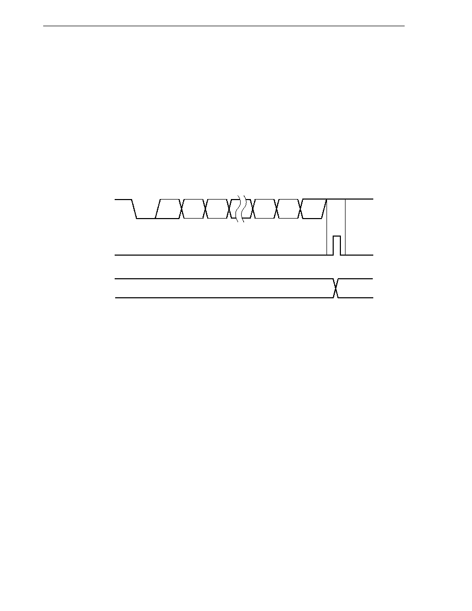
CHAPTER 15 SERIAL INTERFACE UART2
294
User's Manual U14260EJ3V1UD
(d) Reception
The interface enters the reception wait status if the UART transfer mode is specified by using transfer mode
specification register 2 (TRMC2) and bit 5 (RXE2) of asynchronous serial interface mode register 2 (ASIM2)
is set to 1 after bit 7 (POWER2) has been set to 1. In this status, the R
X
D2 pin is monitored to detect the
start bit. When the start bit is detected, reception is started, and serial data is sequentially stored in receive
shift register 2 (RX2) at the specified baud rate.
When the stop bit is received, a receive completion interrupt (INTSR2) occurs and, at the same time, the
data in RX2 is written to receive buffer register 2 (RXB2). If an overrun error (OVE2) occurs, however, the
receive data is not written to RXB2 but discarded. Even if a parity error (PE2) or framing error (FE2) occurs
during reception, reception continues up to the position at which the stop bit is received, and an error interrupt
(INTSR2/INTSER2) occurs after completion of reception.
Figure 15-17. Timing of Asynchronous Serial Interface Receive Completion Interrupt Request
RxD2 (input)
D0
D1
D2
D6
D7
Parity
Stop
Start
INTSR2
RXB2
Caution
During reception, the number of stop bits is always 1. A second stop bit is ignored.
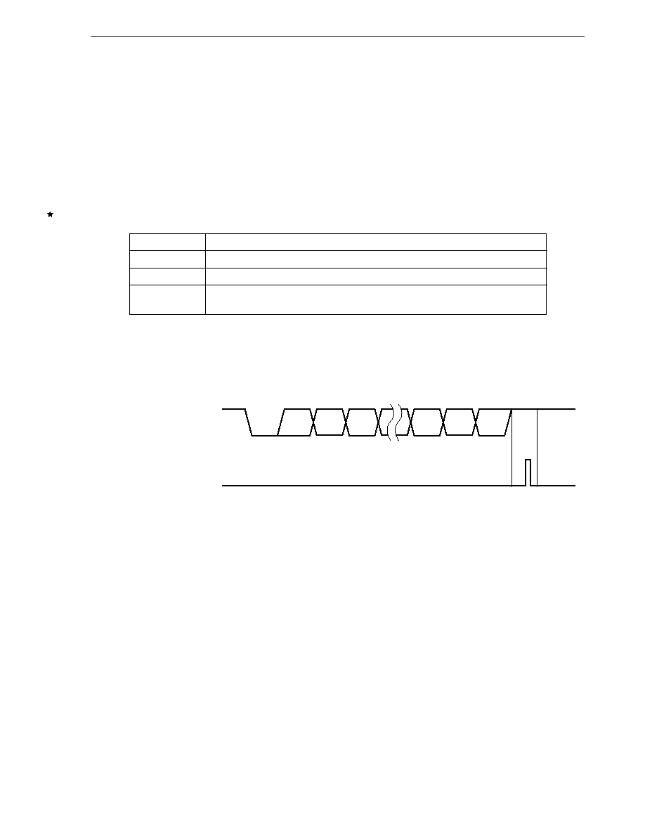
CHAPTER 15 SERIAL INTERFACE UART2
295
User's Manual U14260EJ3V1UD
(e) Receive errors
Three types of errors can occur during a receive operation: a parity error, framing error, or overrun error.
If, as the result of data reception, an error flag is set in asynchronous serial interface status register 2 (ASIS2),
a receive error interrupt request (INTSR2/INTSER2) will occur. Table 15-9 lists the causes behind receive
errors.
As part of receive error interrupt request (INTSR2/INTSER2) servicing, the contents of ASIS2 can be read
to determine which type of error occurred during the receive operation (see Table 15-9 and Figure 15-18).
The contents of ASIS2 are reset (to 0) when receive buffer register 2 (RXB2) is read or when the next data
is received (if the next data contains an error, its error flag will be set).
Table 15-9. Causes of Receive Errors
Receive Error
Cause
Parity error
Specified parity does not match parity of receive data
Framing error
Stop bit was not detected
Overrun error
Reception of the next data was completed before data was read from receive buffer
register 2 (RXB2)
Caution
Even if data is written to TXB2 when data remains in transmit buffer register 2 (TXB2), an
overrun error will not occur.
Figure 15-18. Receive Error Timing
Cautions 1. The contents of asynchronous serial interface status register 2 (ASIS2) are reset (to
0) when receive buffer register 2 (RXB2) is read or when the next data is received. To
obtain information about the error, be sure to read the contents of ASIS2 before reading
RXB2.
2. Be sure to read the contents of receive buffer register 2 (RXB2) even when a receive
error has occurred. Overrun errors will occur during the next data receive operations
and the receive error status will remain until the contents of RXB2 are read.
Note The interrupts can be divided into INTSR2 and INTSER2 by setting bit 0 (ISEM2) of asynchronous
serial interface mode register 2 (ASIM2) to 1.
RxD0 (input)
D0
D1
D2
D6
D7
Parity
STOP
START
INTSR2 or INTSER2
Note

CHAPTER 15 SERIAL INTERFACE UART2
296
User's Manual U14260EJ3V1UD
Figure 15-19. INTSR2 and INTSER2
(1) If ISEM2 is cleared to 0 (error interrupt is included in INTSR2)
(a) No error at reception
(b) Error at reception
INTSR2
INTSER2
INTSR2
INTSER2
(2) If ISEM2 is set to 1 (to separate INTSR2 and INTSER2)
(a) No error at reception
(b) Error at reception
INTSR2
INTSER2
INTSR2
INTSER2

CHAPTER 15 SERIAL INTERFACE UART2
297
User's Manual U14260EJ3V1UD
15.4.3 Multi-processor transfer mode
In this mode, data can be transferred to or received from two or more processors.
(1) Registers to be used
∑ Asynchronous serial interface mode register 2 (ASIM2)
∑ Asynchronous serial interface status register 2 (ASIS2)
∑ Baud rate generator control register 2 (BRGC2)
∑ Asynchronous serial interface transmit status register 2 (ASIF2)
∑ Clock select register 2 (CKSEL2)
∑ Transfer mode specification register 2 (TRMC2)
∑ Port mode register 3 (PM3)
∑ Port register 3 (P3)
The basic procedure of setting an operation in the multi-processor transfer mode is as follows.
<1> Set the CKSEL2 register (see Figure 15-7).
<2> Set the BRGC2 register (see Figure 15-6).
<3> Set bits 7 and 6 (TRM12 and TRM02) of the TRMC2 register to 0 and 1, and set bits 3, 1, and 0 (ISMD2,
MPIEN2, and MPS2) (see Figure 15-8).
<4> Set bits 4 to 0 (PS21, PS20, CL2, SL2, and ISEM2) of the ASIM2 register (see Figure 15-3).
<5> Set bit 7 (POWER2) of the ASIM2 register to 1.
<6> Set bit 6 (TXE2) of the ASIM2 register to 1.
Transmission is enabled.
<7> Set bit 5 (RXE2) of the ASIM2 register to 1.
Reception is enabled.
<8> Write data to TXB2.
Data transmission is started.
Caution Take relationship with the other party of communication when setting the port mode register
and port register.
The relationship between the register settings and pins is shown below.
Table 15-10. Relationship Between Register Settings and Pins (Multi-Processor Transfer Mode)
ASIM2
TRMC2
PM34
P34
PM35
P35 Operation Pin Function
POW TXE2 RXE2 PS21 PS20
CL2
SL2
ISEM2 TRM12 TRM02 ISMD2 MPIEN2 MPS2
Mode
P34/
P35/
ER2
SI3/
SO3/
TxD2
RxD2
1
0
1
0/1
0/1
0/1
◊
0/1
0
1
◊
0/1
0/1
◊
Note
◊
Note
1
◊
Reception P34
RxD2
1
1
0
0/1
0/1
0/1
0/1
◊
0
1
0/1
0/1
0/1
0
0
◊
Note
◊
Note
Transmission TxD2
P35
1
1
1
0/1
0/1
0/1
0/1
0/1
0
1
0/1
0/1
0/1
0
0
1
◊
Transmission/ TxD2
RxD2
reception
Note
Can be set as port function.
Caution When using UART2, stop the operation of SIO3 (bit 7 (CSIE3) of serial operation mode register 3
(CSIM3) = 0).
Remark
◊: don't care, ASIM2: Asynchronous serial interface mode register 2,
TRMC2: Transfer mode specification register 2, PM
◊◊: Port mode register,
P
◊◊: Port output latch
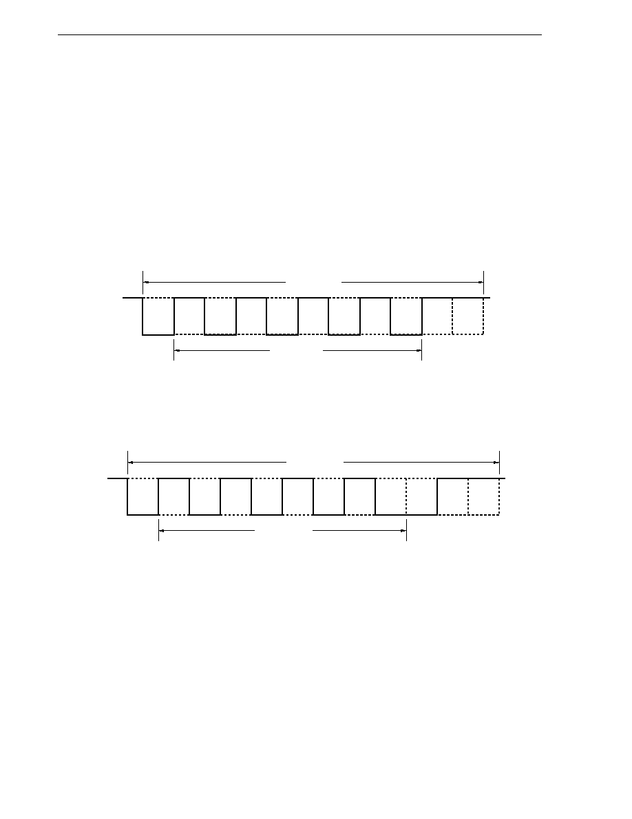
CHAPTER 15 SERIAL INTERFACE UART2
298
User's Manual U14260EJ3V1UD
For an explanation how to generate the transmit/receive clock for the baud rate and details of the permissible error
range of the baud rate, refer to (1) Registers to be used in 15.4.2 Asynchronous serial interface (UART) mode.
(2) Communication operations
(a) Data format
Figure 15-20 shows an example of the transmit/receive data format.
Figure 15-20. Example of Transmit/Receive Data Format in Multi-Processor Transfer Mode
(1) ID transfer (multi-processor appended bit = 1) format
Character bit: 8 bits, No parity, Stop bit: 1 bit,
Communication data: 55H
D0
Start
bit
Stop
bit
D1
D2
D3
D4
D5
D6
D7
Appended
bit
1 data frame
Character bit
(2) Data transfer (multi-processor appended bit = 0) format
Character bit: 8 bits, Parity bit: odd parity,
Stop bit: 1 bit, Communication data: 55H
D0
D1
D2
D3
D4
D5
D6
D7
Start
bit
Stop
bit
Parity
bit
Appended
bit
1 data frame
Character bit
Caution
If parity is specified, the parity bit is output after the multi-processor appended bit.
In this case, the multi-processor appended bit is subject to parity calculation during
both transmission and reception.

CHAPTER 15 SERIAL INTERFACE UART2
299
User's Manual U14260EJ3V1UD
One data frame consists of the following bits:
∑
Start bit ........................................... 1 bit
∑
Character bit ................................... 7/8 bits (LSB first)
∑
Multi-processor appended bit ........ 1 bit (set to 1 or 0)
∑
Parity bit .......................................... Even/odd/0/none
∑
Stop bit ........................................... 1/2 bits
The character bit length, parity, and stop bit length in one data frame are selected by asynchronous interface
mode register 2 (ASIM2). Data is transferred starting from the LSB.
The multi-processor appended bit of transmit data is specified by transfer mode specification register 2
(TRMC2).
The serial transfer rate is selected by baud rate generator control register 2 (BRGC2) and clock select register
2 (CKSEL2).
If an error occurs when receiving serial data, the error can be determined by reading the status of
asynchronous serial interface status register 2 (ASIS2).

CHAPTER 15 SERIAL INTERFACE UART2
300
User's Manual U14260EJ3V1UD
(b) Transmission
If the multi-processor transfer mode is set by using transfer mode specification register 2 (TRMC2) and bit
7 (POWER2) of asynchronous serial interface mode register 2 (ASIM2) is set to 1, the TxD2 pin outputs a
high level. If bit 6 (TXE2) of ASIM2 is set to 1 next, transmission is enabled. Transmission (ID transmission)
can be started by setting bit 0 (MPS2) of TRMC2 to 1 and writing transmit data to transmit buffer register
2 (TXB2).
Next, confirm that bit 1 (TXBF) of asynchronous serial interface transmit status register 2 (ASIF2) is 0. Then
clear MPS and write transmit data to TXB2 (data transmission). The start bit, multi-processor transfer
appended bit, parity bit, and stop bit are automatically appended to the data.
When transmission is started, the data in TXB2 is transferred to transmit shift register 2 (TXS2) and
sequentially output to the TxD2 pin, starting from the LSB. If the data to be transmitted next has been written
to TXB2 by the time transmission is complete, transmitting the next data is started. If no more data has been
written to TXB2, transmission is stopped until new transmit data is written.
Figure 15-21 shows the timing of a transmit interrupt.
Figure 15-21. Timing of Transmit Completion Interrupt Request in Multi-Processor Transfer Mode
D0
Start
Start
D7
MPS2
Stop Start
MPS2
Stop
D0
D7
...
...
FF
Data 1 (ID)
Data 2 (data)
Data 3 (data)
FF
TxD2 (output)
INTST2
TXB2
TXS2
CPU
MPS2
MPS2
1
MPS2
0
TXB2
data 1 (ID)
TXB2
data 2 (data)
TXB2
data 3 (data)
ID transmit frame
Data transmit frame
Data 1 (ID data)
Data 2 (data)
Data transfer
Data transfer
Caution
Before writing transmit data to TXB2, confirm that TXBF = 0 and set or clear the MPS bit.
If the MPS bit is set or cleared with TXBF = 1, the set data of the MPS bit may be appended
to the transmit data currently in TXB2 and transferred.

CHAPTER 15 SERIAL INTERFACE UART2
301
User's Manual U14260EJ3V1UD
(c) Reception
The interface enters the reception wait status if the multi-processor transfer mode is specified by using
transfer mode specification register 2 (TRMC2) and bit 7 (POWER2) of asynchronous serial interface mode
register 2 (ASIM2) is set to 1 and then bit 5 (RXE2) is set to 1. In this status, the R
X
D2 pin is monitored
to detect the start bit. When the start bit is detected, reception is started, and serial data is sequentially
stored in receive shift register 2 (RX2) at the specified baud rate.
If data with the multi-processor appended bit set to "1" is received (ID reception), a receive completion
interrupt (INTSR2) occurs after the stop bit has been detected and, at the same time, the data in RX2 is written
to receive buffer register 2 (RXB2). At this time, bit 3 (MPR2) of asynchronous serial interface register 2
(ASIS2) is set to 1. After it has been confirmed that MPR2 is 1, the ID of the receive data and the ID of
the microprocessor are compared (for which software processing is necessary). If the two IDs match, the
interface prepares for the next reception and waits for the next receive completion interrupt (INTSR2). If
the IDs do not match, clear bit 1 (MPIEN2) of transfer mode specification register 2 (TRMC2) to 0. This makes
receive data other than ID invalid and prevents occurrence of an unwanted receive completion interrupt
(INTSR2).
Figure 15-22. Timing of Receive Completion Interrupt Request in Multi-Processor Transfer Mode (1/2)
(1) If receive data matches ID
D0
Start
Start
Stop
Start
Stop
D7
...
...
MPR2
MPR2
D0
D7
D0
FF
Data 1 (ID)
Data 2 (data)
RxD2 (input)
INTSR2
RXB2
MPIEN2
CPU
MPR2
MPR2
1
RXB2
data 1 (ID)
RXB2
data 2 (data)
1
IDs match. Prepares for reception and
waits for INTSR2.
ID receive frame
Data receive frame
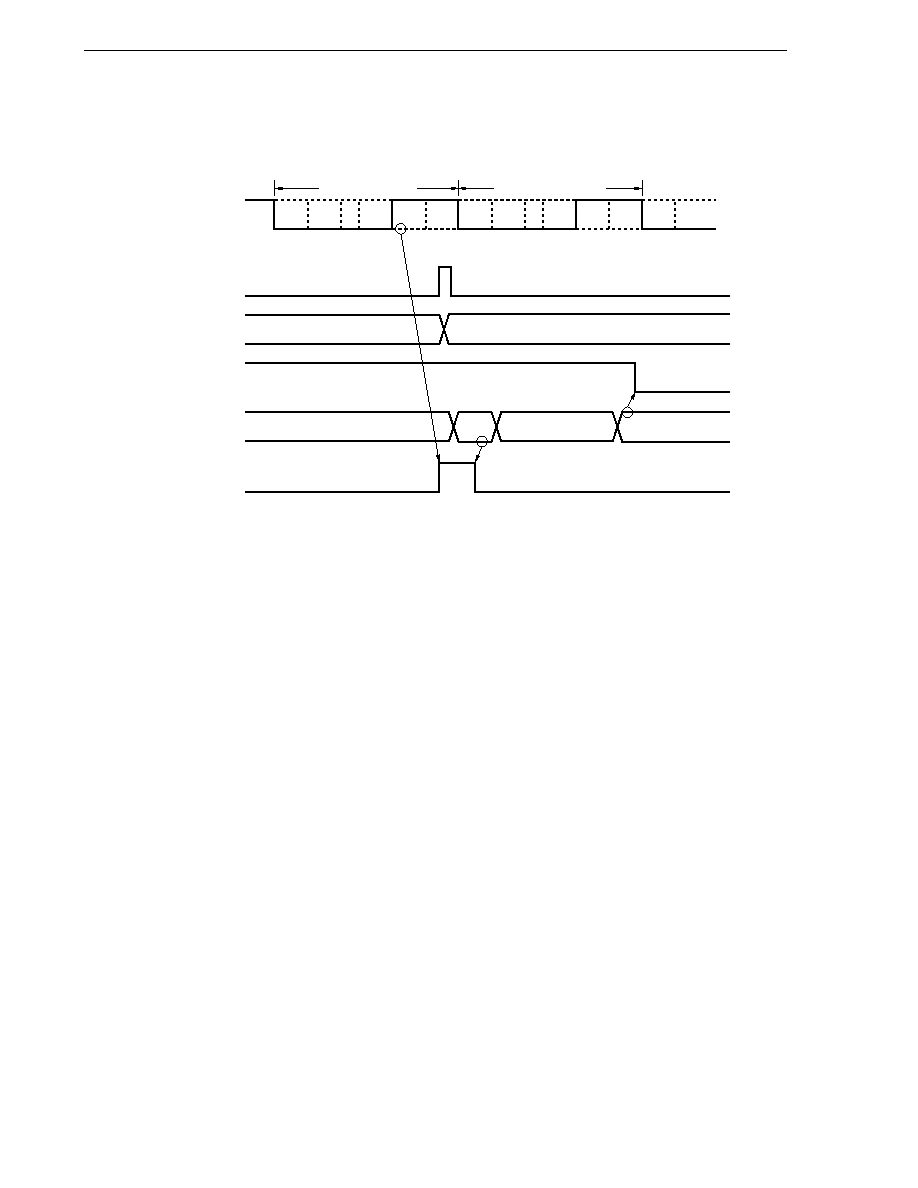
CHAPTER 15 SERIAL INTERFACE UART2
302
User's Manual U14260EJ3V1UD
Figure 15-22. Timing of Receive Completion Interrupt Request in Multi-Processor Transfer Mode (2/2)
(2) If receive data does not match ID
D0
...
...
Start
Start
Start
Stop
D7
MPR2 Stop
MPR2
D0
D7
D0
Data 1 (ID)
IDs do not match.
FF
R
X
D2 (input)
INTSR2
RXB2
MPIEN2
CPU
MPR2
MPR2
1
RXB2
data 1 (ID)
Clears MPIEN2
1
ID receive frame
Data receive frame

CHAPTER 15 SERIAL INTERFACE UART2
303
User's Manual U14260EJ3V1UD
15.4.4 Infrared data transfer (IrDA) mode
In this mode, pulses can be output, transmitted, or received in the data format of the IrDA specifications. This
mode can be used to transmit or receive data to or from a digital device such as a personal computer.
(1) Registers to be used
∑ Asynchronous serial interface mode register 2 (ASIM2)
∑ Asynchronous serial interface status register 2 (ASIS2)
∑ Baud rate generator control register 2 (BRGC2)
∑ Asynchronous serial interface transmit status register 2 (ASIF2)
∑ Clock select register 2 (CKSEL2)
∑ Transfer mode specification register 2 (TRMC2)
∑ Port mode register 3 (PM3)
∑ Port register 3 (P3)
The relationship between the register settings and pins is shown below.
Table 15-11. Relationship Between Register Settings and Pins (Infrared Data Transfer (IrDA) Mode)
ASIM2
TRMC2
PM34
P34
PM35
P35 Operation Pin Function
POW TXE2 RXE2 PS21 PS20
CL2
SL2
ISEM2 TRM12 TRM02 ISMD2 MPIEN2 MPS2
Mode
P34/
P35/
ER2
SI3/
SO3/
TxD2
RxD2
1
0
1
0/1
0/1
0/1
◊
0/1
1
◊
◊
◊
◊
◊
Note
◊
Note
1
◊
Reception P34
RxD2
1
1
0
0/1
0/1
0/1
0/1
◊
1
◊
0/1
◊
◊
0
0
◊
Note
◊
Note
Transmission TxD2
P35
1
1
1
0/1
0/1
0/1
0/1
0/1
1
◊
0/1
◊
◊
0
0
1
◊
Transmission/ TxD2
RxD2
reception
Note
Can be set as port function.
Cautions 1.
When using UART2, stop the operation of SIO3 (bit 7 (CSIE3) of serial operation mode register
3 (CSIM3) = 0).
2.
To transfer data in the infrared data transfer (IrDA) mode, the following conditional expression
must be satisfied for the transmit pulse width.
(Conditional expression)
1.41
µs
Transmit pulse width (set values of TPW20 to TPW23) < Transfer rate (set values of
MDL20 to MDL27)
Remark
◊: don't care, ASIM2: Asynchronous serial interface mode register 2,
TRMC2: Transfer mode specification register 2, PM
◊◊: Port mode register,
P
◊◊: Port output latch, TPW20 to TPW23: Bits 0 to 3 of clock select register 2 (CKSEL2),
MDL20 to MDL27: Bits 0 to 7 of baud rate generator control register 2 (BRGC2)
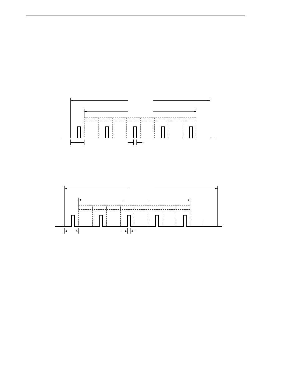
CHAPTER 15 SERIAL INTERFACE UART2
304
User's Manual U14260EJ3V1UD
(2) Communication operation
(a) Data format
Figure 15-23 shows the format of transmit/receive data.
Figure 15-23. Example of Transmit/Receive Data Format in Infrared Data Transfer (IrDA) Mode
(1) IrDA standard format
(Character bit: 8 bits, Parity bit: None, Stop bit: 1 bit, Communication data: 55H)
D0
D1
D2
D3
D4
D5
D6
D7
1 data frame
Character bit
Bit time
Pulse width
Start
bit
Stop
bit
(2) Other format
(Character bit: 7 bits, Parity bit: Even parity, Stop bit: 2 bits, Communication data: 55H)
D0
D1
D2
D3
D4
D5
D6
Parity
1 data frame
Character bit
Bit time
Pulse width
Start
bit
Stop
bit

CHAPTER 15 SERIAL INTERFACE UART2
305
User's Manual U14260EJ3V1UD
One data frame consists of the following bits:
∑
Start bit .............. 1 bit
∑
Character bit ...... 7/8 bits (LSB first)
∑
Parity bit ............. Odd/even/0/None
∑
Stop bit .............. 1/2 bits
The character bit length, parity, and stop bit length in one data frame are specified by using asynchronous
serial interface mode register 2 (ASIM2). Data is transferred starting from the LSB.
The length of the electric pulse transmitted or received in one data frame can be specified by using bits 0
to 3 (TPW20 to TPW23) of clock select register 2 (CKSEL2). Usually, the pulse length is 1.41
µs (rated
minimum pulse width) to lower the power consumption. The pulse bit rises at the center of a bit cycle.

CHAPTER 15 SERIAL INTERFACE UART2
306
User's Manual U14260EJ3V1UD
(b) Transmission
If the infrared data transfer (IrDA) mode is set by using transfer mode specification register 2 (TRMC2) and
bit 7 (POWER2) of asynchronous serial interface mode register 2 (ASIM2) is set to 1, clock operation is
enabled, and the T
X
D2 pin outputs a low level. If bit 6 (TXE2) of ASIM2 is set to 1 next, transmission is
enabled. Transmission can be started by writing transmit data to transmit buffer register 2 (TXB2). The start
bit, parity bit, and stop bit are automatically appended to the data.
When transmission is started, the data in TXB2 is transferred to transmit shift register 2 (TXS2) and
sequentially output to the T
X
D2 pin, starting from the LSB. If the data to be transmitted next has been written
to TXB2 by the time transmission is complete, transmitting the next data is started. If no more data has been
written to TXB2, transmission is stopped until new transmit data is written.
Figure 15-24 shows the timing of a transmit interrupt.
Figure 15-24. Timing of Transmit Completion Interrupt Request in Infrared Data Transfer (IrDA) Mode
(1) Character bit: 8 bits, Parity bit: Odd parity, Stop bit: 1 bit,
Communication data: 7DH, TRMC2: ISMD2 = 0
D0
D1
D2
D3
D4
D5
D6
D7
Parity
Start
Stop
T
X
D2 (output)
INTST2
(2) Character bit: 8 bits, Parity bit: Even parity, Stop bit: 2 bits,
Communication data: 9BH, TRMC2: ISMD2 = 0
D0
Start
Parity
Stop
D1
D2
D3
D4
D5
D6
D7
T
X
D2 (output)
INTST2
Remark
TRMC2: Transfer mode specification register 2
ISMD2: Bit 3 of TRMC2
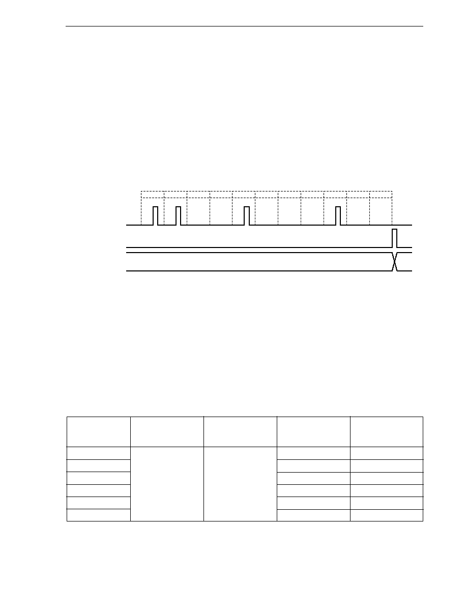
CHAPTER 15 SERIAL INTERFACE UART2
307
User's Manual U14260EJ3V1UD
(c) Reception
The interface enters the reception wait status if the infrared data transfer (IrDA) mode is specified by using
transfer mode specification register 2 (TRMC2) and bit 7 (POWER2) of asynchronous serial interface mode
register 2 (ASIM2) is set to 1 and then bit 5 (RXE2) is set to 1. In this status, the R
X
D2 pin is monitored
to detect the start bit. When the start bit is detected, reception is started, and serial data is sequentially
stored in receive shift register 2 (RX2) at the specified baud rate.
When the stop bit is received, the data in RX2 is written to receive buffer register 2 (RXB2). If an overrun
error (OVE2) occurs, however, the receive data is not written to RXB2 but discarded. Even if a parity error
(PE2) or framing error (FE2) occurs during reception, reception continues up to the position at which the
stop bit is received, and an error interrupt (INTSR2/INTSER2) occurs after completion of reception.
Figure 15-25. Timing of Receive Completion Interrupt Request in Infrared Data Transfer (IrDA) Mode
D0
Start
Parity
Stop
D1
D2
D3
D4
D5
D6
D7
R
X
D2 (input)
INTSR2
RXB2
76H
Cautions 1. Be sure to read receive buffer register 2 (RXB2) even if a reception error has occurred.
Otherwise, an overrun error will occur when the next data is received, and the reception
error status will persist.
2. The number of stop bits is always 1 during reception. A second stop bit is ignored.
(d) Bit rate and pulse width
Table 15-12 shows the bit rate and pulse width in the infrared data transfer (IrDA) mode.
The rated minimum pulse width is 1.41
µs, and the maximum pulse width is the sum of 3/16 of the bit rate
and 2.5% of the bit cycle or 1.08
µs, whichever is greater.
Table 15-12. Bit Rate and Pulse Width
Bit Rate (bps)
Allowable Bit Rate Error
Minimum Pulse Width
Nominal Value of
Maximum Pulse Width
(% of Bit Rate)
(
µs)
3/16 of Pulse Width
(
µs)
(
µs)
2400
+/≠0.87
1.41
78.13
88.55
9600
19.53
22.13
19200
9.77
11.07
38400
4.88
5.96
57600
3.26
4.34
115200
1.63
2.71

CHAPTER 15 SERIAL INTERFACE UART2
308
User
'
s Manual U14260EJ3V1UD
Table 15-13. Register Settings (1/2)
Notes 1. When using UART2, stop the SIO3 operation.
2. Can be set as port function.
Remark
◊: Don't care, CSIM3: Serial operation mode register 3, ASIM2: Asynchronous serial interface mode register 2,
TRMC2: Transfer mode specification register 2, PM
◊◊: Port mode register, P◊◊: Output latch of port
ASIM2
CSIM3
CSIE3
0
Note 1
POWER2
0
TXE2
0
RXE2
0
PS21
◊
PS20
◊
CL2
◊
SL2
◊
ISEM2
◊
TRM12
◊
TRM02
◊
ISMD2
◊
MPIEN2
◊
MPS2
◊
P34/SI3/TxD2
P34
P35/SO3/RxD2
P35
PM34
◊
Note 2
P34
◊
Note 2
PM35
◊
Note 2
P35
◊
Note 2
Pin Function
Operation
Mode
Stop
TRMC2
Other than above
Other than above
(1)
Operation stop mode
ASIM2
CSIM3
CSIE3
0
Note 1
0
Note 1
0
Note 1
POWER2
1
1
1
TXE2
0
1
1
RXE2
1
0
1
PS21
0/1
0/1
0/1
PS20
0/1
0/1
0/1
CL2
0/1
0/1
0/1
SL2
◊
0/1
0/1
ISEM2
0/1
◊
0/1
TRM12
0
0
0
TRM02
0
0
0
ISMD2
◊
0/1
0/1
MPIEN2
◊
◊
◊
MPS2
◊
◊
◊
P34/SI3/TxD2
P34
TxD2
TxD2
P35/SO3/RxD2
RxD2
P35
RxD2
PM34
◊
Note 2
0
0
P34
◊
Note 2
0
0
PM35
1
◊
Note 2
1
P35
◊
◊
Note 2
◊
Pin Function
Operation
Mode
Receive
Transmit
Transmit/receive
TRMC2
(2) Asynchronous serial interface (UART) mode
Setting prohibited
Setting prohibited
CHAPTER 15 SERIAL INTERFACE UART2
309
User
'
s Manual U14260EJ3V1UD
Table 15-13. Register Settings (2/2)
Notes 1. When using UART2, stop the SIO3 operation.
2. Can be set as port function.
Caution
When transferring in infrared data transfer (IrDA) mode, the following conditional expression must be satisfied for specification of the transmit
pulse width.
(Conditional expression) 1.41
µs Transmit pulse width (set values of TPW20 to TPW23 in CKSEL2 register) < Transfer rate (set values of MDL20
to MDL27 in BRGC2 register)
Remark
◊: Don't care, CSIM3: Serial operation mode register 3, ASIM2: Asynchronous serial interface mode register 2,
TRMC2: Transfer mode specification register 2, CKSEL2: Clock select register 2, BRGC2: Baud rate generator control register 2,
PM
◊◊: Port mode register, P◊◊: Output latch of port
ASIM2
CSIM3
CSIE3
0
Note 1
0
Note 1
0
Note 1
POWER2
1
1
1
TXE2
0
1
1
RXE2
1
0
1
PS21
0/1
0/1
0/1
PS20
0/1
0/1
0/1
CL2
0/1
0/1
0/1
SL2
◊
0/1
0/1
ISEM2
0/1
◊
0/1
TRM12
0
0
0
TRM02
1
1
1
ISMD2
◊
0/1
0/1
MPIEN2
0/1
0/1
0/1
MPS2
0/1
0/1
0/1
P34/SI3/TxD2
P34
TxD2
TxD2
P35/SO3/RxD2
RxD2
P35
RxD2
PM34
◊
Note 2
0
0
P34
◊
Note 2
0
0
PM35
1
◊
Note 2
1
P35
◊
◊
Note 2
◊
TRMC2
(3) Multi-processor transfer mode
ASIM2
POWER2
1
1
1
TXE2
0
1
1
RXE2
1
0
1
PS21
0/1
0/1
0/1
PS20
0/1
0/1
0/1
CL2
0/1
0/1
0/1
SL2
◊
0/1
0/1
ISEM2
0/1
◊
0/1
TRM12
1
1
1
TRM02
◊
◊
◊
ISMD2
◊
0/1
0/1
MPIEN2
◊
◊
◊
MPS2
◊
◊
◊
P34/SI3/TxD2
P34
TxD2
TxD2
P35/SO3/RxD2
RxD2
P35
RxD2
PM34
◊
Note 2
0
0
P34
◊
Note 2
0
0
PM35
1
◊
Note 2
1
P35
◊
◊
Note 2
◊
TRMC2
(4) Infrared data transfer (IrDA) mode
Pin Function
Other than above
Other than above
CSIM3
CSIE3
0
Note 1
0
Note 1
0
Note 1
Pin Function
Operation
Mode
Receive
Transmit
Transmit/receive
Operation
Mode
Receive
Transmit
Transmit/receive
Setting prohibited
Setting prohibited
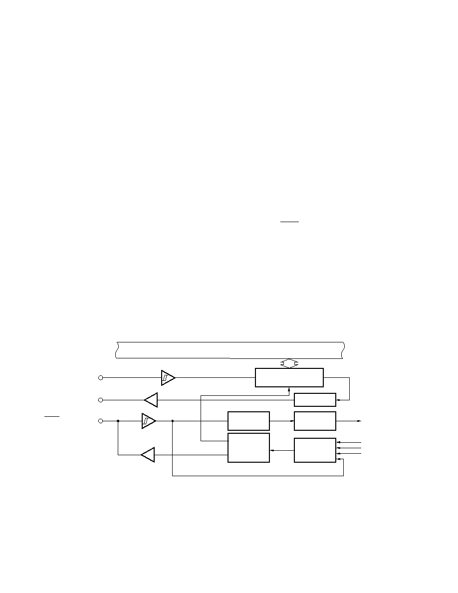
310
User's Manual U14260EJ3V1UD
CHAPTER 16 SERIAL INTERFACE SIO3
Serial interface UART2/SIO3 can be used in the asynchronous serial interface (UART) mode or 3-wire serial I/O
mode.
Caution
Do not enable UART2 and SIO3 at the same time.
16.1 Functions of Serial Interface SIO3
The serial interface SIO3 has the following two modes.
(1) Operation stop mode
This mode is used when serial transfers are not performed to reduce power consumption. For details, see 16.4.1
Operation stop mode.
(2) 3-wire serial I/O mode (fixed as MSB first)
This is an 8-bit data transfer mode using three lines: a serial clock line (SCK3), serial output line (SO3), and
serial input line (SI3).
Since simultaneous transmit and receive operations are enabled in 3-wire serial I/O mode, the processing time
for data transfers is reduced.
The first bit of the serially transferred 8-bit data is fixed as the MSB.
3-wire serial I/O mode can be used when connecting an IC incorporating a clocked serial interface, or a display
controller, etc. For details, see 16.4.2 3-wire serial I/O mode.
Figure 16-1 shows a block diagram of serial interface SIO3.
Figure 16-1. Block Diagram of Serial Interface SIO3
Internal bus
8
Selector
Serial I/O shift register
3 (SIO3)
SI3/T
X
D2/P34
SO3/R
X
D2/P35
SCK3/ASCK2/P36
INTCSI3
f
X
/2
3
f
X
/2
4
f
X
/2
5
Output latch
Serial clock
controller
Serial clock
counter
Interrupt
request signal
generator

CHAPTER 16 SERIAL INTERFACE SIO3
311
User's Manual U14260EJ3V1UD
16.2 Configuration of Serial Interface SIO3
Serial interface SIO3 includes the following hardware.
Table 16-1. Configuration of Serial Interface SIO3
Item
Configuration
Register
Serial I/O shift register 3 (SIO3)
Interrupt request signal generator
Serial clock controller
Control registers
Serial operation mode register 3 (CSIM3)
Port mode register 3 (PM3)
Port register 3 (P3)
(1) Serial I/O shift register 3 (SIO3)
This is an 8-bit register that performs parallel-serial conversion and serial transmit/receive (shift operations)
synchronized with the serial clock.
When bit 7 (CSIE3) of serial operation mode register 3 (CSIM3) is set to 1, a serial operation can be started by
writing data to or reading data from SIO3.
When transmitting, data written to SIO3 is output to the serial output (SO3).
When receiving, data is read from the serial input (SI3) and written to SIO3.
SIO3 is set by an 8-bit memory manipulation instruction.
RESET input makes SIO3 undefined.
Caution
Do not access SIO3 during a transfer operation unless the access is triggered by a transfer
start (read operations are disabled when MODE3 = 0 and write operations are disabled when
MODE3 = 1).
16.3 Registers to Control Serial Interface SIO3
Serial interface SIO3 is controlled by the following three registers.
∑ Serial operation mode register 3 (CSIM3)
∑ Port mode register 3 (PM3)
∑ Port register 3 (P3)
(1) Serial operation mode register 3 (CSIM3)
This register is used to set SIO3's serial clock and operation modes, and to enable/disable operation of SIO3.
CSIM3 is set by a 1-bit or 8-bit memory manipulation instruction.
RESET input clears CSIM3 to 00H.
CHAPTER 16 SERIAL INTERFACE SIO3
312
User's Manual U14260EJ3V1UD
Figure 16-2. Format of Serial Operation Mode Register 3 (CSIM3)
Address: FFB8H After reset: 00H R/W
Symbol
7
6
5
4
3
2
1
0
CSIM3
CSIE3
0
0
0
0
MODE3
SCL31
SCL30
CSIE3
Enable/disable specification for SIO3
Shift register operation
Serial counter
Port
0
Operation disabled
Clear
Port function
Note 1
1
Operation enabled
Count operation enabled
Serial function + port function
Note 2
MODE3
Transfer operation modes and flags
Operation mode
Transfer start trigger
SO3/P35/RxD2 pin function
0
Transmit/transmit and receive mode
Write to SIO3
SO3
1
Receive-only mode
Read from SIO3
P35
Note 3
SCL31
SCL30
Clock selection
f
X
= 8.38 MHz
f
X
= 12 MHz
Note 4
0
0
External clock input to SCK3
≠
≠
0
1
f
X
/2
3
1.04 MHz
1.50 MHz
1
0
f
X
/2
4
523 kHz
750 kHz
1
1
f
X
/2
5
261 kHz
375 kHz
Notes 1. When CSIE3 = 0 (SIO3 operation stopped status), the SI3, SO3, and SCK3 pins can be used as UART2
or for port functions.
2. When CSIE3 = 1 (SIO3 operation enabled status), the SI3 pin can be used as a port pin if only the
transmit function is used, and the SO3 pin can be used as a port pin if only the receive-only mode
is used.
3. When MODE3 = 1 (receive-only mode), the SO3 pin can be used for port functions.
4. Expanded-specification products of
µPD780078 Subseries only.
Caution
Do not rewrite the value of CSIM3 during transfer. However, CSIE3 can be rewritten using a
1-bit memory manipulation instruction.
Remark
f
X
: Main system clock oscillation frequency

CHAPTER 16 SERIAL INTERFACE SIO3
313
User's Manual U14260EJ3V1UD
(2) Port mode register 3 (PM3)
PM3 is a register that sets the input/output of port 3 in 1-bit units.
To use the P35/SO3/RxD2 pin as a serial data output, set PM35 and the output latch of P35 to 0.
To use the P34/SI3/TxD2 pin as a serial data input, and the P36/ASCK2/SCK3 pin as a clock input, set PM34
to 1.
At this time, the output latches of P34 and P36 can be either 0 or 1.
PM3 is set by a 1-bit or 8-bit memory manipulation instruction.
RESET input sets PM3 to FFH.
Figure 16-3. Format of Port Mode Register 3 (PM3)
Address: FF23H After reset: FFH R/W
Symbol
7
6
5
4
3
2
1
0
PM3
1
PM36
PM35
PM34
PM33
PM32
PM31
PM30
PM3n
I/O mode selection of P3n pin (n = 0 to 6)
0
Output mode (output buffer on)
1
Input mode (output buffer off)
CHAPTER 16 SERIAL INTERFACE SIO3
314
User's Manual U14260EJ3V1UD
16.4 Operation of Serial Interface SIO3
This section explains the two modes of serial interface SIO3.
16.4.1 Operation stop mode
Because serial transfer is not performed during this mode, the power consumption can be reduced.
In addition, pins can be used as normal I/O ports. To set the operation stop mode, clear bit 7 (CSIE3) of CSIM3
to 0.
(1) Register to be used
Operation stop mode is set by serial operation mode register 3 (CSIM3).
CSIM3 is set by a 1-bit or 8-bit memory manipulation instruction.
RESET input clears CSIM3 to 00H.
Address: FFB8H After reset: 00H R/W
Symbol
7
6
5
4
3
2
1
0
CSIM3
CSIE3
0
0
0
0
MODE3
SCL31
SCL30
CSIE3
SIO3 operation enable/disable specification
Shift register operation
Serial counter
Port
0
Operation disabled
Clear
Port function
Note
Note When CSIE3 = 0 (SIO3 operation stopped status), the SI3, SO3, and SCK3 pins can be used as UART2
or for port functions.
CHAPTER 16 SERIAL INTERFACE SIO3
315
User's Manual U14260EJ3V1UD
16.4.2 3-wire serial I/O mode
The 3-wire serial I/O mode can be used when connecting a peripheral IC incorporating a clocked serial interface,
a display controller, etc.
This mode executes communication via three lines: a serial clock line (SCK3), serial output line (SO3), and serial
input line (SI3).
(1) Registers to be used
∑ Serial operation mode register 3 (CSIM3)
∑ Port mode register 3 (PM3)
∑ Port register 3 (P3)
The basic procedure of setting an operation in the 3-wire serial I/O mode is as follows.
<1> Set bits 2 to 0 (MODE3, SCL31, and SCL30) of the CSIM3 register (see Figure 16-2).
<2> Set bit 7 (CSIE3) of the CSIM3 register to 1.
Transmission/reception is enabled.
<3> Write data to the SIO3 register.
Data transmission/reception is started.
Read data from the SIO3 register.
Data reception is started.
Caution Take relationship with the other party of communication when setting the port mode register
and port register.
The relationship between the register settings and pins is shown below.
Table 16-2. Relationship Between Register Settings and Pins (3-Wire Serial I/O Mode)
CSIM3
PM34
P34
PM35
P35
PM36
P36
Operation Mode
Pin Function
CSIE3 MODE3 SCL31 SCL30
P34/
P35/
P36/
SI3/
SO3/
SCK3/
TxD2
RxD2 ASCK2
1
1
0
0
1
◊
◊
Note
◊
Note
1
◊
Slave reception
SI3
P35
SCK3
input
1
0
0
0
◊
Note
◊
Note
0
0
1
◊
Slave transmission
P34
SO3
SCK3
input
1
0
0
0
1
◊
0
0
1
◊
Slave transmission/
SI3
SO3
SCK3
reception
input
1
1
Other
1
◊
◊
Note
◊
Note
0
0
Master reception
SI3
P35
SCK3
than above
output
1
0
◊
Note
◊
Note
0
0
0
0
Master transmission
P34
SO3
SCK3
output
1
0
1
◊
0
0
0
0
Master transmission/
SI3
SO3
SCK3
reception
output
Note
Can be set as port function.
Caution When using SIO3, stop the operation of UART2 (bit 7 (POWER2) of asynchronous serial interface
mode register 2 (ASIM2) = 0).
Remark
◊: don't care, CSIM3: Serial operation mode register 3, PM◊◊: Port mode register,
P
◊◊: Port output latch

CHAPTER 16 SERIAL INTERFACE SIO3
316
User's Manual U14260EJ3V1UD
(2) Transfer start
A serial transfer starts when the following two conditions have been satisfied and transfer data has been set (or
read) to serial I/O shift register 3 (SIO3).
<Transfer start conditions>
∑ SIO3 operation control bit (CSIE3) = 1
∑ After an 8-bit serial transfer, either the internal serial clock is stopped or SCK3 is set to high level.
<Transfer start timing>
∑ Transmit/transmit and receive mode (MODE3 = 0)
Transfer starts when writing to SIO3.
∑ Receive-only mode (MODE3 = 1)
Transfer starts when reading from SIO3.
Caution
After data has been written to SIO3, transfer will not start even if the CSIE3 bit value is set
to 1.
(3) Communication operations
In the 3-wire serial I/O mode, data is transmitted and received in 8-bit units. Each bit of data is transmitted or
received in synchronization with the serial clock.
Serial I/O shift register 3 (SIO3) is shifted in synchronization with the falling edge of the serial clock. Transmission
data is held in the SO3 latch and is output from the SO3 pin. Data that is received via the SI3 pin in synchronization
with the rising edge of the serial clock is latched to SIO3.
Figure 16-4. Timing of 3-Wire Serial I/O Mode
(4) Transfer completion
Completion of an 8-bit transfer automatically stops the serial transfer operation and the interrupt request flag
(CSIIF3) is set.
SI3
DI7
DI6
DI5
DI4
DI3
DI2
DI1
DI0
CSIIF3
SCK3
1
SO3
DO7
DO6
DO5
DO4
DO3
DO2
DO1
DO0
2
3
4
5
6
7
8
Transfer completion
Transfer starts in synchronization with the SCK3 falling edge
Latched to SIO3 at the SCK3 rising edge
CHAPTER 16 SERIAL INTERFACE SIO3
317
User
'
s Manual U14260EJ3V1UD
Table 16-3. Register Settings
Notes 1. When using SIO3, stop the UART2 operation.
2. Can be set as port function.
Remark
◊: Don't care, ASIM2: Asynchronous serial interface mode register 2, CSIM3: Serial operation mode register 3,
PM
◊◊: Port mode register, P◊◊: Output latch of port
ASIM2
POWER2
0
Note 1
CSIM3
PM34
◊
Note 2
P34
◊
Note 2
PM35
◊
Note 2
P35
◊
Note 2
PM36
◊
Note 2
P36
◊
Note 2
CSIE3
0
MODE3
◊
SCL31
◊
SCL30
◊
P34/SI3/TxD2
P34
P35/SO3/RxD2
P35
P36/SCK3/ASCK2
P36
Pin Function
Operation
Mode
Stop
Other than above
(1) Operation stop mode
(2) 3-wire serial I/O mode
Setting prohibited
ASIM2
POWER2
0
Note 1
0
Note 1
0
Note 1
0
Note 1
0
Note 1
0
Note 1
CSIM3
PM34
1
◊
Note 2
1
1
◊
Note 2
1
P34
◊
◊
Note 2
◊
◊
◊
Note 2
◊
PM35
◊
Note 2
0
0
◊
0
0
P35
◊
Note 2
0
0
◊
0
0
PM36
1
1
1
0
0
0
P36
◊
◊
◊
0
0
0
CSIE3
1
1
1
1
1
1
MODE3
1
0
0
1
0
0
SCL31
0
0
0
SCL30
0
0
0
P34/SI3/TxD2
SI3
P34
SI3
SI3
P34
SI3
P35/SO3/RxD2
P35
SO3
SO3
P35
SO3
SO3
P36/SCK3/ASCK2
SCK3 input
SCK3 input
SCK3 input
SCK3 output
SCK3 output
SCK3 output
Pin Function
Other than above
Other than above
Setting prohibited
Operation
Mode
Slave receive
Slave transmit
Slave transmit/receive
Master receive
Master transmit
Master transmit/receive

318
User's Manual U14260EJ3V1UD
CHAPTER 17 SERIAL INTERFACE CSI1
17.1 Functions of Serial Interface CSI1
Serial interface CSI1 has the following two modes.
(1) Operation stop mode
This mode is used when serial transfer is not performed. In this mode, the power consumption can be reduced.
For details, see 17.4.1 Operation stop mode.
(2) 3-wire serial I/O mode (MSB/LSB-first selectable)
This mode is used to transfer 8-bit data by using three lines: a serial clock line (SCK1) and two serial data lines
(SI1 and SO1).
The processing time of data transfer can be shortened in the 3-wire serial I/O mode because transmission and
reception can be simultaneously executed. In addition, whether 8-bit data is transferred with the MSB or LSB
first can be specified, so this interface can be connected to any device.
The 3-wire serial I/O mode can be used when connecting ICs and display controllers having a clocked serial
interface. For details, see 17.4.2 3-wire serial I/O mode.
17.2 Configuration of Serial Interface CSI1
Serial interface CSI1 includes the following hardware.
Table 17-1. Configuration of Serial Interface CSI1
Item
Configuration
Registers
Transmit buffer register 1 (SOTB1)
Serial I/O shift register 1 (SIO1)
Transmit controller
Clock start/stop controller & clock phase controller
Control registers
Serial operation mode register 1 (CSIM1)
Serial clock select register 1 (CSIC1)
Port mode register 2 (PM2)
Port register 2 (P2)
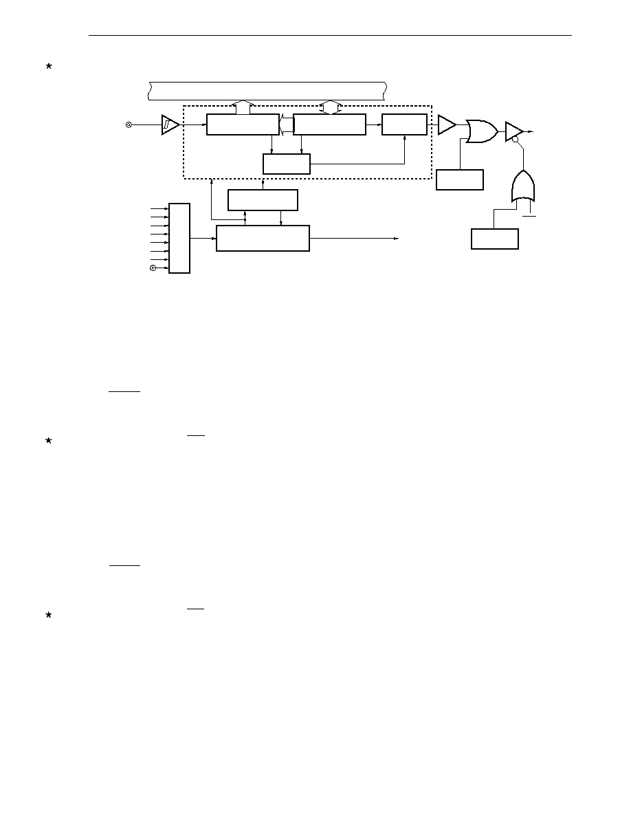
CHAPTER 17 SERIAL INTERFACE CSI1
319
User's Manual U14260EJ3V1UD
Figure 17-1. Block Diagram of Serial Interface CSI1
(1) Transmit buffer register 1 (SOTB1)
This register sets transmit data.
Transmission is started by writing data to SOTB1 when bit 7 (CSIE1) and bit 6 (TRMD1) of serial operation mode
register 1 (CSIM1) are 1.
The data written to SOTB1 is converted from parallel data into serial data by serial I/O shift register 1, and output
to the serial output (SO1) pin.
SOTB1 can be written or read by an 8-bit memory manipulation instruction.
RESET input makes SOTB1 undefined.
Cautions 1. Do not access SOTB1 when CSOT1 = 1 (during serial communication).
2. The SS1 pin can be used in the slave mode. For details of the transmission/reception
operation, see 17.4.2 (2) Communication operation.
(2) Serial I/O shift register 1 (SIO1)
This is an 8-bit register that converts data from parallel into serial or vice versa.
The reception status is entered by reading data from SIO1 if bit 7 (CSIE1) of serial operation mode register 1
(CSIM1) is 1.
During reception, data is read from the serial input pin (SI1) to SIO1.
SIO1 can be read by an 8-bit memory manipulation instruction.
RESET input makes SIO1 undefined.
Cautions 1. Do not access SIO1 when CSOT1 = 1 (during serial communication).
2. The SS1 pin can be used in the slave mode. For details of the transmission/reception
operation, see 17.4.2 (2) Communication operation.
17.3 Registers to Control Serial Interface CSI1
Serial interface CSI1 is controlled by the following four registers.
∑ Serial operation mode register 1 (CSIM1)
∑ Serial clock select register 1 (CSIC1)
∑ Port mode register 2 (PM2)
∑ Port register 2 (P2)
8
8
8
Output latch
(P21)
PM21
SS1
SO1/P21
INTCSI1
SI1/P20
f
X
/2
f
X
/2
2
f
X
/2
3
f
X
/2
4
f
X
/2
5
f
X
/2
6
f
X
/2
7
SCK1/P22
Output
selector
Internal bus
Serial I/O shift
register 1 (SIO1)
Transmit buffer
register 1 (SOTB1)
Output latch
Transmit controller
Clock start/stop controller &
clock phase controller
Transmit data
controller
Selector
CHAPTER 17 SERIAL INTERFACE CSI1
320
User's Manual U14260EJ3V1UD
(1) Serial operation mode register 1 (CSIM1)
This register is used to select the operation mode and enable or disable operation.
CSIM1 is set by a 1-bit or 8-bit memory manipulation instruction.
RESET input clears CSIM1 to 00H.
Figure 17-2. Format of Serial Operation Mode Register 1 (CSIM1)
Address: FFB0H After reset: 00H R/W
Note 1
Symbol
7
6
5
4
3
2
1
0
CSIM1
CSIE1
TRMD1
SSE1
DIR1
0
0
0
CSOT1
CSIE1
Control of operation in 3-wire serial I/O mode
0
Operation disabled
Note 2
and internal circuit is asynchronously reset
Note 3
.
1
Operation enabled.
TRMD1
Note 4
Selection of transmit/receive mode
0
Note 5
Receive-only mode (transmission disabled).
1
Transmit/receive mode
SSE1
Notes 6, 7
Specification of whether SS1 pin is used
0
Do not use SS1 pin.
1
Use SS1 pin.
DIR1
Note 6
Specification of first bit
0
MSB
1
LSB
CSOT1
Communication status flag
0
Communication is stopped.
1
Communication is in progress.
Notes 1. Bit 0 is a read-only bit.
2. When using the SI1/P20, SO1/P21, SCK1/P22, and SS1/P80 pins as general-purpose port pins, see
Caution 2 in Figure 17-3 and Table 17-2.
3. Bit 0 (CSOT1) of CSIM1 and serial I/O shift register 1 (SIO1) are reset.
4. Do not rewrite TRMD1 when CSOT1 = 1 (during serial communication).
5. The SO1 output is fixed to the low level when TRMD1 is 0. Reception is started when data is read
from SIO1.
6. Do not rewrite these bits when CSOT1 = 1 (during serial communication).
7. Before setting this bit to 1, fix the input level of the SS1 pin to 0 or 1.

CHAPTER 17 SERIAL INTERFACE CSI1
321
User's Manual U14260EJ3V1UD
(2) Serial clock select register 1 (CSIC1)
This register is used to specify the data transmission/reception timing and set a serial clock.
CSIC1 is set by a 1-bit or 8-bit memory manipulation instruction.
RESET input sets CSIC1 to 10H.
Figure 17-3. Format of Serial Clock Select Register 1 (CSIC1)
Address: FFB1H After reset: 10H R/W
Symbol
7
6
5
4
3
2
1
0
CSIC1
0
0
0
CKP1
DAP1
CKS12
CKS11
CKS10
CKP1
DAP1
Specification of data transmission/reception timing
Type
0
0
1
0
1
2
1
0
3
1
1
4
CKS12
CKS11
CKS10
CSI1 serial clock selection
Mode
f
X
= 8.38 MHz
f
X
= 12 MHz
Note
0
0
0
f
X
/2
4.19 MHz
6 MHz
Master mode
0
0
1
f
X
/2
2
2.09 MHz
3 MHz
0
1
0
f
X
/2
3
1.04 MHz
1.5 MHz
0
1
1
f
X
/2
4
523.75 kHz
750 kHz
1
0
0
f
X
/2
5
261.87 kHz
375 kHz
1
0
1
f
X
/2
6
130.94 kHz
187.5 kHz
1
1
0
f
X
/2
7
65.47 kHz
93.75 kHz
1
1
1
External clock
Slave mode
Note Expanded-specification products of
µPD780078 Subseries only.
D7
D6
D5
D4
D3
D2
D1
D0
SCK1
SO1
SI1 input timing
D7
D6
D5
D4
D3
D2
D1
D0
SCK1
SO1
SI1 input timing
D7
D6
D5
D4
D3
D2
D1
D0
SCK1
SO1
SI1 input timing
D7
D6
D5
D4
D3
D2
D1
D0
SCK1
SO1
SI1 input timing
CHAPTER 17 SERIAL INTERFACE CSI1
322
User's Manual U14260EJ3V1UD
Cautions 1.
Do not write to CSIC1 when CSIE1 = 1 (operation enabled).
2.
When using the P22/SCK1 pin as a general-purpose port pin, set CKP1 to 1.
3.
The phase type of the data clock is type 3 after reset.
Remark fx: Main system clock oscillation frequency
(3) Port mode registers 2 and 8 (PM2, PM8)
PM2 and PM8 are registers that set input/output of ports 2 and 8 in 1-bit units.
When using the P21/SO1 pin as a serial data output, set PM21 and the output latch of P21 to 0.
When using the P20/SI1 pin as a serial data input, the P22/SCK1 pin as a clock input, and the P80/SS1 pin as
a chip select input, set PM20, PM22, and PM80 to 1.
At this time, the output latches of P20, P22, and P80 can be either 0 or 1.
PM2 and PM8 are set by a 1-bit or 8-bit memory manipulation instruction.
RESET input sets PM2 and PM8 to FFH.
Figure 17-4. Format of Port Mode Register 2 (PM2)
Address: FF22H After reset: FFH R/W
Symbol
7
6
5
4
3
2
1
0
PM2
1
1
PM25
PM24
PM23
PM22
PM21
PM20
PM2n
I/O mode selection of P2n pin (n = 0 to 5)
0
Output mode (output buffer on)
1
Input mode (output buffer off)
Figure 17-5. Format of Port Mode Register 8 (PM8)
Address: FF28H After reset: FFH R/W
Symbol
7
6
5
4
3
2
1
0
PM8
1
1
1
1
1
1
1
PM80
PM80
I/O mode selection of P80 pin
0
Output mode (output buffer on)
1
Input mode (output buffer off)

CHAPTER 17 SERIAL INTERFACE CSI1
323
User's Manual U14260EJ3V1UD
17.4 Operation of Serial Interface CSI1
The following describes the two modes of serial interface CSI1.
17.4.1 Operation stop mode
Serial communication is not executed in this mode, so the power consumption can be reduced.
In addition, the P20/SI1, P21/SO1, P22/SCK1, and P80/SS1 pins can be used as ordinary I/O port pins in this mode.
To set the operation stop mode, clear bit 7 (CSIE1) of CSIM1 to 0.
(1) Register to be used
The operation stop mode is set by serial operation mode register 1 (CSIM1).
CSIM1 is set by a 1-bit or 8-bit memory manipulation instruction.
RESET input clears CSIM1 to 00H.
Address: FFB0H After reset: 00H R/W
Symbol
7
6
5
4
3
2
1
0
CSIM1
CSIE1
TRMD1
SSE1
DIR1
0
0
0
CSOT1
CSIE1
Control of operation in 3-wire serial I/O mode
0
Operation disabled
Note 1
and internal circuit is asynchronously reset
Note 2
.
Notes 1. When using the SI1/P20, SO1/P21, SCK1/P22, and SS1/P80 pins as general-purpose port pins, see
Caution 2 in Figure 17-3 and Table 17-2.
2. Bit 0 (CSOT1) of CSIM1 and serial I/O shift register 1 (SIO1) are reset.
17.4.2 3-wire serial I/O mode
The 3-wire serial I/O mode can be used when connecting ICs and display controllers having a conventional clocked
serial interface.
In this mode, communication is executed by using three lines: serial clock (SCK1), serial output (SO1), and serial
input (SI1) lines.
(1) Registers to be used
∑ Serial operation mode register 1 (CSIM1)
∑ Serial clock select register 1 (CSIC1)
∑ Port mode register 2 (PM2)
∑ Port register 2 (P2)
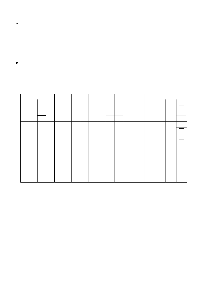
CHAPTER 17 SERIAL INTERFACE CSI1
324
User's Manual U14260EJ3V1UD
The basic procedure of setting an operation in the 3-wire serial I/O mode is as follows.
<1> Set the CSIC1 register (see Figure 17-3).
<2> Set bits 6 to 4 and 0 (TRMD1, SSE1, DIR1, and CSOT1) of the CSIM1 register (see Figure 17-2).
<3> Set bit 7 (CSIE1) of the CSIM1 register to 1.
Transmission/reception is enabled.
<4> Write data to the SOTB1 register.
Data transmission/reception is started.
Read data from the SIO1 register.
Data reception is started.
Caution Take relationship with the other party of communication when setting the port mode register
and port register.
The relationship between the register settings and pins is shown below.
Table 17-2. Relationship Between Register Settings and Pins (3-Wire Serial I/O Mode)
CSIM1
PM20 P20 PM21 P21 PM22 P22 PM80 P80
Operation
Pin Function
CSIE1 TRMD1 SSE1 DIR1
Mode
P20/
P21/
P22/
P80/
SI1
SO1
SCK1
SS1
1
0
0
0/1
1
◊
◊
Note 1
◊
Note 1
1
◊
◊
Note 1
◊
Note 1
Slave
SI1
P21
SCK1
P80
1
1
◊
reception
Note 2
input
Note 2
SS1
1
1
0
0/1
◊
Note 1
◊
Note 1
0
0
1
◊
◊
Note 1
◊
Note 1
Slave
P20
SO1
SCK1
P80
1
1
◊
transmission
Note 2
input
Note 2
SS1
1
1
0
0/1
1
◊
0
0
1
◊
◊
Note 1
◊
Note 1
Slave
SI1
SO1
SCK1
P80
1
1
◊
transmission/
input
Note 2
SS1
reception
Note 2
1
0
0
0/1
1
◊
◊
Note 1
◊
Note 1
1
◊
◊
Note 1
◊
Note 1
Master
SI1
P21
SCK1
P80
reception
output
1
1
0
0/1
◊
Note 1
◊
Note 1
0
0
1
◊
◊
Note 1
◊
Note 1
Master
P20
SO1
SCK1
P80
transmission
output
1
1
0
0/1
1
◊
0
0
1
◊
◊
Note 1
◊
Note 1
Master
SI1
SO1
SCK1
P80
transmission/
output
reception
Notes 1. Can be set as port function.
2. To use the slave mode, set CKS12, CKS11, and CKS10 to 1, 1, 1.
Remark
◊: don't care, CSIM1: Serial operation mode register 1,
CKS12, CKS11, CKS10: Bits 2 to 0 of serial clock select register 1 (CSIC1)

CHAPTER 17 SERIAL INTERFACE CSI1
325
User's Manual U14260EJ3V1UD
(2) Communication operation
In the 3-wire serial I/O mode, data is transmitted or received in 8-bit units. Each bit of data is transmitted or
received in synchronization with the serial clock.
Data can be transmitted or received if bit 6 (TRMD1) of serial operation mode register 1 (CSIM1) is 1.
Transmission/reception is started when a value is written to transmit buffer register 1 (SOTB1). Data can be
received when bit 6 (TRMD1) of serial operation mode register 1 (CSIM1) is 0. Reception is started when data
is read from serial I/O shift register 1 (SIO1).
However, if bit 5 (SSE1) of CSIM1 is set to 1 in slave mode, the operation is as follows.
<1> Low level input to the SS1 pin
Transmission/reception is started when SOTB1 is written, or reception is started when SIO1 is read.
<2> High level input to the SS1 pin
Transmission/reception or reception is held, therefore, even if SOTB1 is written or SIO1 is read,
transmission/reception or reception will not be started.
<3> Data is written to SOTB1 or data is read from SIO1 while a high level is input to the SS1 pin, then a low
level is input to the SS1 pin
Transmission/reception or reception is started.
<4> A high level is input to the SS1 pin during transmission/reception or transmission
Transmission/reception or reception is suspended.
After communication has been started, bit 0 (CSOT1) of CSIM1 is set to 1. When communication of 8-bit data
has been completed, a communication completion interrupt request flag (CSIIF1) is set, and CSOT1 is cleared
to 0. Then the next communication is enabled.
Cautions 1. Do not access the control register and data register when CSOT1 = 1 (during serial
communication).
2. When bit 5 (SSE1) of CSIM1 is set to 1 in slave mode, input a low level to the SS1 pin one
clock or more before the clock operation starts.
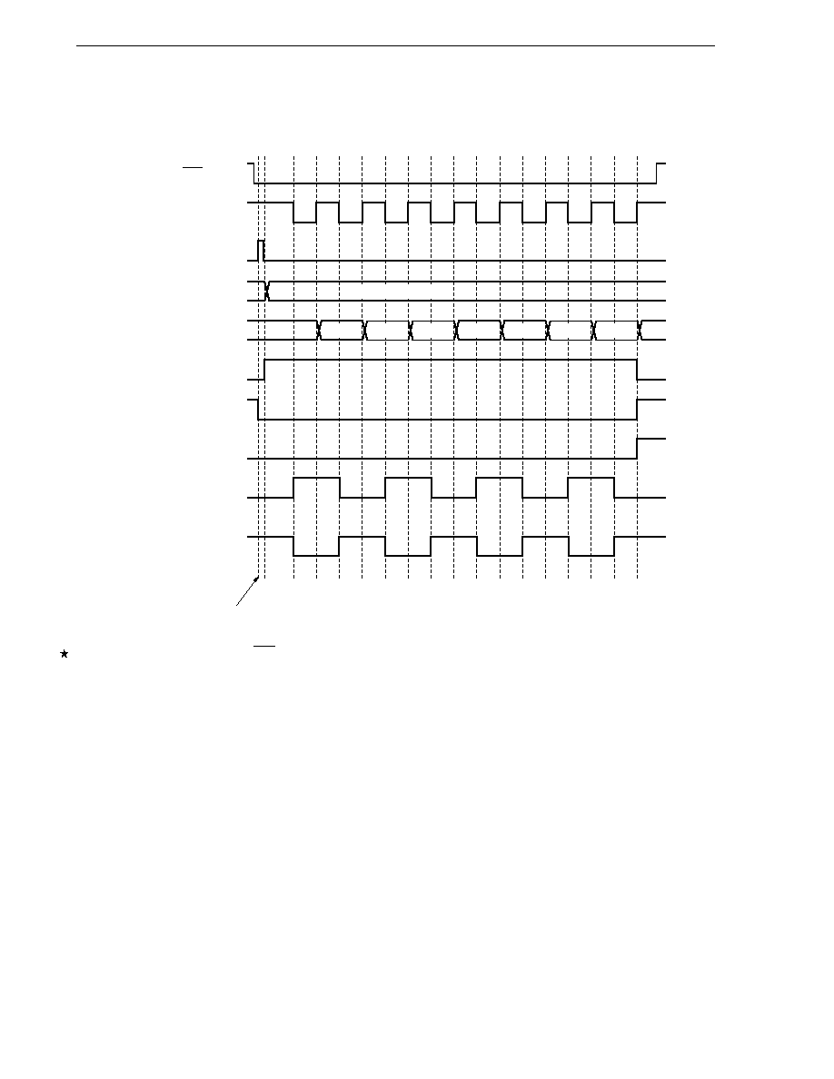
CHAPTER 17 SERIAL INTERFACE CSI1
326
User's Manual U14260EJ3V1UD
Figure 17-6. Timing of 3-Wire Serial I/O Mode (1/2)
(1) Transmission/reception timing (Type 1; TRMD1 = 1, DIR1 = 0, CKP1 = 0, DAP1 = 0, SSE1 = 1
Note
)
AAH
ABH
56H
ADH
5AH
B5H
6AH
D5H
55H (communication data)
55H is written to SOTB1.
SS1
Note
SCK1
Read/write trigger
SOTB1
SIO1
CSOT1
INTCSI1
CSIIF1
SO1
SI1 (receives AAH)
Note The SSE1 flag and SS1 pin are used in the slave mode.
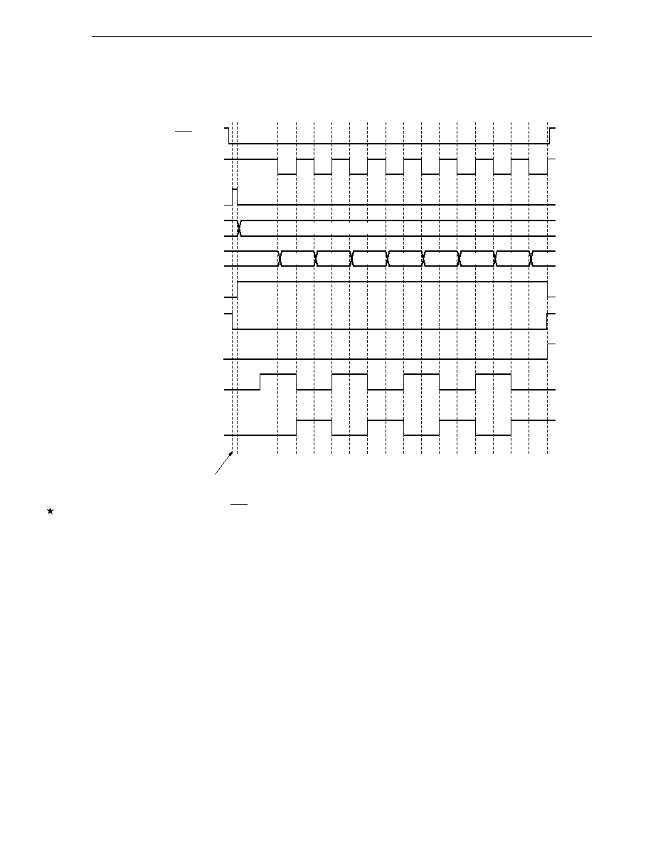
CHAPTER 17 SERIAL INTERFACE CSI1
327
User's Manual U14260EJ3V1UD
Figure 17-6. Timing of 3-Wire Serial I/O Mode (2/2)
(2) Transmission/reception timing (Type 2; TRMD1 = 1, DIR1 = 0, CKP1 = 0, DAP1 = 1, SSE1 = 1
Note
)
ABH
56H
ADH
5AH
B5H
6AH
D5H
55H is written to SOTB1.
SS1
Note
SCK1
SOTB1
Read/write trigger
SIO1
CSOT1
INTCSI1
CSIIF1
SO1
AAH
55H (communication data)
SI1 (inputs AAH)
Note The SSE1 flag and SS1 pin are used in the slave mode.
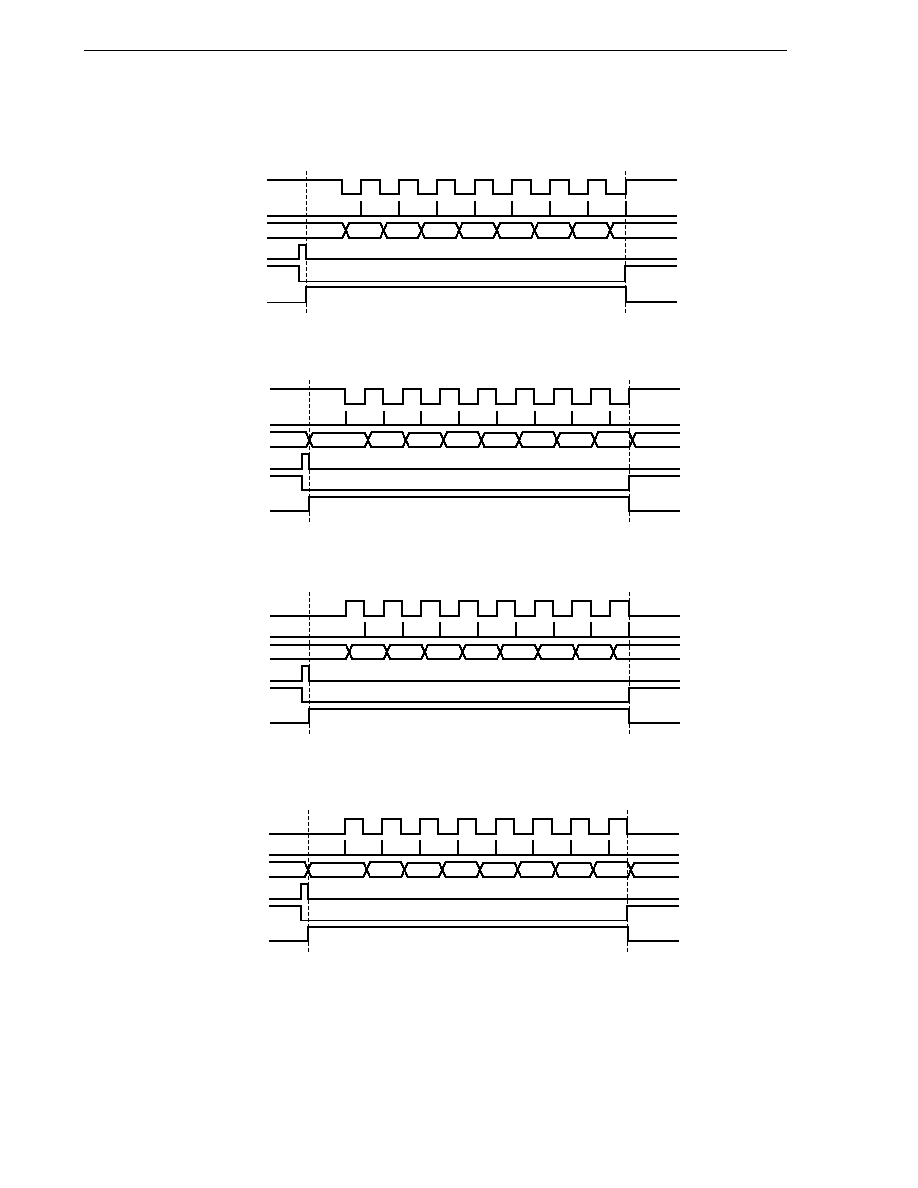
CHAPTER 17 SERIAL INTERFACE CSI1
328
User's Manual U14260EJ3V1UD
Figure 17-7. Timing of Clock/Data Phase
(a) Type 1; CKP1 = 0, DAP1 = 0
(b) Type 2; CKP1 = 0, DAP1 = 1
(c) Type 3; CKP1 = 1, DAP1 = 0
(d) Type 4; CKP1 = 1, DAP1 = 1
D7
D6
D5
D4
D3
D2
D1
D0
SCK1
SO1
Writing to SOTB1 or
reading from SIO1
SI1 capture
CSIIF1
CSOT1
D7
D6
D5
D4
D3
D2
D1
D0
SCK1
SO1
Writing to SOTB1 or
reading from SIO1
SI1 capture
CSIIF1
CSOT1
D7
D6
D5
D4
D3
D2
D1
D0
SCK1
SO1
Writing to SOTB1 or
reading from SIO1
SI1 capture
CSIIF1
CSOT1
D7
D6
D5
D4
D3
D2
D1
D0
SCK1
SO1
Writing to SOTB1 or
reading from SIO1
SI1 capture
CSIIF1
CSOT1
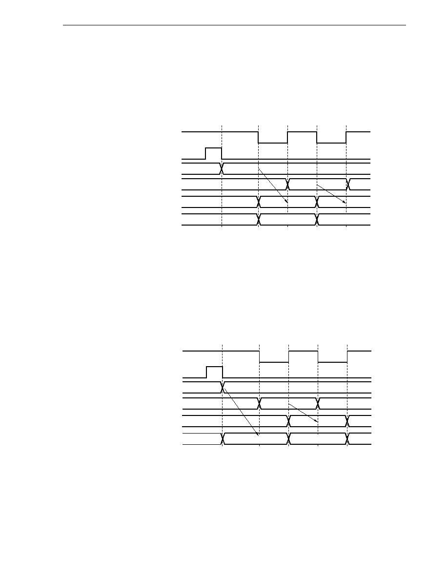
CHAPTER 17 SERIAL INTERFACE CSI1
329
User's Manual U14260EJ3V1UD
(3) Timing of output to SO1 pin (first bit)
When communication is started, the value of transmit buffer register 1 (SOTB1) is output from the SO1 pin. The
following describes the output operation of the first bit at this time.
Figure 17-8. Output Operation of First Bit
(1) CKP1 = 0, DAP1 = 0 (or CKP1 = 1, DAP1 = 0)
The first bit is directly latched to the output latch from the SOTB1 register at the falling (or rising) edge of SCK1,
passed through the output selector and output from the SO1 pin. The value of the SOTB1 register is transferred
to the SIO1 register at the next rising (or falling) edge of SCK1 and the data shifts by one bit. Simultaneously,
the first bit of the received data is passed through the SI1 pin and stored in the SIO1 register.
The second and subsequent bits are latched to the output latch at the next falling (or rising) edge of SCK1 and
the respective data is output from the SO1 pin.
(2) CKP1 = 0, DAP1 = 1 (or CKP1 = 1, DAP1 = 1)
The first bit is output from the SO1 pin directly from the SOTB1 register through the output selector at the falling
edge of the write signal of SOTB1 or the read signal of the SIO1 register. The value of the SOTB1 register is
transferred to the SIO1 register at the next falling (or rising) edge of SCK1 and shifts by one bit. Simultaneously,
the first bit of the received data is stored in the SIO1 register through the SI1 pin.
The second and subsequent bits are latched to the output latch from SIO1 at the next rising (or falling) edge of
SCK1 and the data is output from the SO1 pin.
SCK1
SOTB1
SIO1
Output latch
SO1
Writing to SOTB1 or
reading from SIO1
First bit
2nd bit
First bit
2nd bit
3rd bit
SCK1
SOTB1
SIO1
Output latch
SO1
Writing to SOTB1 or
reading from SIO1

CHAPTER 17 SERIAL INTERFACE CSI1
330
User's Manual U14260EJ3V1UD
(4) Output value of SO1 pin (last bit)
After communication has been completed, the SO1 pin holds the output value of the last bit.
Figure 17-9. Output Value of SO1 Pin (Last Bit)
(1) Type 1; CKP1 = 0 and DAP1 = 0 (or CKP1 = 1, DAP1 = 0)
(2) Type 2; CKP1 = 0 and DAP1 = 1 (or CKP1 = 1, DAP1 = 1)
SCK1
SOTB1
SIO1
SO1
Output latch
Writing to SOTB1 or
reading from SIO1
(
Next request is issued.)
Last bit
SCK1
SOTB1
SIO1
SO1
Output latch
Writing to SOTB1 or
reading from SIO1
(
Next request is issued.)
Last bit
CHAPTER 17 SERIAL INTERFACE CSI1
331
User's Manual U14260EJ3V1UD
(5) SO1 output
The status of the SO1 output is as follows if bit 7 (CSIE1) of serial operation mode register 1 (CSIM1) is cleared
to 0.
Table 17-3. SO1 Output Status
TRMD1
DAP1
DIR1
SO1 Output
Note 1
TRMD1 = 0
Note 2
≠
≠
Low-level output
Note 2
TRMD1 = 1
DAP1 = 0
≠
SO1 latch value (low-level output)
DAP1 = 1
DIR1 = 0
Bit 7 value of SOTB1
DIR1 = 1
Bit 0 value of SOTB1
Notes 1. The PM21, P21, and SSE1 bits and the SS1 pin must also be set to actually produce an output from
the SO1/P21 pin.
2. Status after reset
Caution If a value is written to the TRMD1, DAP1, and DIR1 bits, the output value of the SO1 bit changes.
CHAPTER 17 SERIAL INTERFACE CSI1
332
User
'
s Manual U14260EJ3V1UD
Table 17-4. Register Settings
Note Can be set as port function.
Remark
◊: Don't care, CSIM1: Serial operation mode register 1, CSIC1: Serial clock select register 1,
PM
◊◊: Port mode register, P◊◊: Output latch of port
CSIM1
CSIE1
0
TRMD1
0
SSE1
◊
DIR1
◊
CKP1
1
DAP1
0
CKS12
0
CKS11
0
CKS10
0
PM20
◊
Note
P20
◊
Note
PM21
◊
Note
P21
◊
Note
PM22
◊
Note
P22
◊
Note
P21/SO1
P21
P20/SI1
P20
P22/SCK1
P22
Pin Function
Operation
Mode
Stop
CSIC1
(1) Operation stop mode
(2) 3-wire serial I/O mode
Setting prohibited
Other than above
CSIM1
CSIE1
1
1
1
1
1
1
TRMD1
0
1
1
0
1
1
SSE1
◊
◊
◊
◊
◊
◊
DIR1
0/1
0/1
0/1
0/1
0/1
0/1
CKP1
0/1
0/1
0/1
0/1
0/1
0/1
DAP1
0/1
0/1
0/1
0/1
0/1
0/1
CKS12
1
1
1
CKS11
1
1
1
CKS10
1
1
1
PM20
1
◊
Note
1
1
◊
Note
1
P20
◊
◊
Note
◊
◊
◊
Note
◊
PM21
◊
Note
0
0
◊
Note
0
0
P21
◊
Note
0
0
◊
Note
0
0
PM22
1
1
1
0
0
0
P22
◊
◊
◊
0
0
0
P21/SO1
P21
SO1
SO1
P21
SO1
SO1
P20/SI1
SI1
P20
SI1
SI1
P20
SI1
P22/SCK1
SCK1 input
SCK1 input
SCK1 input
SCK1 output
SCK1 output
SCK1 output
Pin Function
Operation
Mode
Slave receive
Slave transmit
Slave transmit/receive
Master receive
Master transmit
Master transmit/receive
CSIC1
Setting prohibited
Other than above
Other than above

333
User's Manual U14260EJ3V1UD
CHAPTER 18 SERIAL INTERFACE IIC0 (
µPD780078Y SUBSERIES ONLY)
18.1 Functions of Serial Interface IIC0
Serial interface IIC0 has the following two modes.
(1) Operation stop mode
This mode is used when serial transfers are not performed. It can therefore be used to reduce power consumption.
(2) I
2
C bus mode (multimaster supported)
This mode is used for 8-bit data transfers with several devices via two lines: a serial clock (SCL0) line and a
serial data bus (SDA0) line.
The transfer rate is as follows.
∑ 97.5 kHz (standard mode) or 350 kHz (high-speed mode): When operated at f
X
= 8.38 MHz
This mode complies with the I
2
C bus format and can output "start condition", "data", and "stop condition" data
segments when transmitting via the serial data bus. These data segments are automatically detected by hardware
during reception.
Since SCL0 and SDA0 are open-drain outputs, the IIC0 requires pull-up resistors for the serial clock line (SCL0)
and the serial data bus line (SDA0).
Figure 18-1 shows a block diagram of serial interface IIC0.

334
CHAPTER 18 SERIAL INTERFACE IIC0 (
µ
PD780078Y SUBSERIES ONLY)
User's Manual U14260EJ3V1UD
Figure 18-1. Block Diagram of Serial Interface IIC0
Internal bus
Slave address
register 0 (SVA0)
Noise
eliminator
SDA0/P32
IIC shift
register 0 (IIC0)
ACK detector
PM32
Output latch
(P32)
Start condition
detector
Stop condition
detector
Serial clock
counter
Serial clock
controller
Noise
eliminator
SCL0/P33
N-ch open
-drain output
Prescaler
N-ch open
-drain output
Internal bus
f
X
Serial clock
wait controller
CLD0 DAD0 SMC0 DFC0 CL00
Interrupt request
signal generator
Wake-up
controller
ACK output
circuit
Data hold
time correction
circuit
CL00
D Q
SO0 latch
SET
CLEAR
Match signal
IICE0 LREL0 WREL0 SPIE0 WTIM0 ACKE0 STT0 SPT0
MSTS0 ALD0 EXC0 COI0 TRC0 ADKD0 STD0 SPD0
IIC transfer clock select
register 0 (IICCL0)
INTIIC0
IIC status register 0
(IICS0)
IIC control register 0
(IICC0)
PM33
Output latch
(P33)

335
CHAPTER 18 SERIAL INTERFACE IIC0 (
µPD780078Y SUBSERIES ONLY)
User's Manual U14260EJ3V1UD
Figure 18-2 shows a serial bus configuration example.
Figure 18-2. Serial Bus Configuration Example Using I
2
C Bus
SDA0
SCL0
SDA0
+V
DD0
+V
DD0
SCL0
SDA0
SCL0
Slave CPU3
Address 2
SDA0
SCL0
Slave IC
Address 3
SDA0
SCL0
Slave IC
Address N
Serial data bus
Serial clock
Master CPU2
Slave CPU2
Address 1
Master CPU1
Slave CPU1
Address 0
336
CHAPTER 18 SERIAL INTERFACE IIC0 (
µPD780078Y SUBSERIES ONLY)
User's Manual U14260EJ3V1UD
18.2 Configuration of Serial Interface IIC0
Serial interface IIC0 includes the following hardware.
Table 18-1. Configuration of Serial Interface IIC0
Item
Configuration
Registers
IIC shift register 0 (IIC0)
Slave address register 0 (SVA0)
Control registers
IIC control register 0 (IICC0)
IIC status register 0 (IICS0)
IIC transfer clock select register 0 (IICCL0)
Port mode register 3 (PM3)
Port register 3 (P3)
(1) IIC shift register 0 (IIC0)
IIC0 is used to convert 8-bit serial data to 8-bit parallel data and vice versa in synchronization with the serial clock.
IIC0 can be used for both transmission and reception.
Write and read operations to IIC0 are used to control the actual transmit and receive operations.
IIC0 is set by an 8-bit memory manipulation instruction.
RESET input clears IIC0 to 00H.
Figure 18-3. Format of IIC Shift Register 0 (IIC0)
Address: FF1FH After reset: 00H R/W
Symbol
7
6
5
4
3
2
1
0
IIC0
Caution
Do not write data to IIC0 during data transfer.
(2) Slave address register 0 (SVA0)
This register sets local addresses when in slave mode.
SVA0 is set by an 8-bit memory manipulation instruction.
RESET input clears SVA0 to 00H.
Figure 18-4. Format of Slave Address Register 0 (SVA0)
Address: FFABH After reset: 00H R/W
Symbol
7
6
5
4
3
2
1
0
SVA0
0
Note
Note Bit 0 is fixed to 0.

337
CHAPTER 18 SERIAL INTERFACE IIC0 (
µPD780078Y SUBSERIES ONLY)
User's Manual U14260EJ3V1UD
(3) SO0 latch
The SO0 latch is used to retain the SDA0 pin's output level.
(4) Wake-up controller
This circuit generates an interrupt request when the address received by this register matches the address value
set to slave address register 0 (SVA0) or when an extension code is received.
(5) Prescaler
This selects the sampling clock to be used.
(6) Serial clock counter
This counter counts the serial clocks that are output or input during transmit/receive operations and is used to
verify that 8-bit data was transmitted or received.
(7) Interrupt request signal generator
This circuit controls the generation of interrupt request signals (INTIIC0).
An I
2
C interrupt request is generated by the following two triggers.
∑ Falling edge of eighth or ninth clock of the serial clock (set by WTIM0 bit
Note
)
∑ Interrupt request generated when a stop condition is detected (set by SPIE0 bit
Note
)
Note WTIM0 bit: Bit 3 of IIC control register 0 (IICC0)
SPIE0 bit: Bit 4 of IIC control register 0 (IICC0)
(8) Serial clock controller
In master mode, this circuit generates the clock output via the SCL0 pin from a sampling clock.
(9) Serial clock wait controller
This circuit controls the wait timing.
(10) ACK output circuit, stop condition detector, start condition detector, and ACK detector
These circuits are used to output and detect various control signals.
(11) Data hold time correction circuit
This circuit generates the hold time for data corresponding to the falling edge of the serial clock.

338
CHAPTER 18 SERIAL INTERFACE IIC0 (
µPD780078Y SUBSERIES ONLY)
User's Manual U14260EJ3V1UD
18.3 Registers to Control Serial Interface IIC0
Serial interface IIC0 is controlled by the following five registers.
∑ IIC control register 0 (IICC0)
∑ IIC status register 0 (IICS0)
∑ IIC transfer clock select register 0 (IICCL0)
∑ Port mode register 3 (PM3)
∑ Port register 3 (P3)
(1) IIC control register 0 (IICC0)
This register is used to enable/stop I
2
C operations, set wait timing, and set other I
2
C operations.
IICC0 is set by a 1-bit or 8-bit memory manipulation instruction.
RESET input clears IICC0 to 00H.
339
CHAPTER 18 SERIAL INTERFACE IIC0 (
µPD780078Y SUBSERIES ONLY)
User's Manual U14260EJ3V1UD
Figure 18-5. Format of IIC Control Register 0 (IICC0) (1/4)
Address: FFA8H After reset: 00H R/W
Symbol
7
6
5
4
3
2
1
0
IICC0
IICE0
LREL0
WREL0
SPIE0
WTIM0
ACKE0
STT0
SPT0
IICE0
I
2
C operation enable
0
Stop operation. Reset IIC status register 0 (IICS0). Stop internal operation.
1
Enable operation.
Condition for clearing (IICE0 = 0)
Condition for setting (IICE0 = 1)
∑ Cleared by instruction
∑ Set by instruction
∑ When RESET is input
LREL0
Exit from communications
0
Normal operation
1
This exits from the current communications operation and sets standby mode. This setting is
automatically cleared after being executed. Its uses include cases in which a locally irrelevant
extension code has been received.
The SCL0 and SDA0 lines go into the high impedance state.
The following flags of IIC status register 0 (IICS0) and IIC control register 0 (IICC0) are cleared.
∑ STD0 ∑ ACKD0 ∑ TRC0 ∑ COI0 ∑ EXC0 ∑ MSTS0 ∑ STT0 ∑ SPT0
The standby mode following exit from communications remains in effect until the following communications entry
conditions are met.
∑ After a stop condition is detected, restart is in master mode.
∑ An address match or extension code reception occurs after the start condition.
Condition for clearing (LREL0 = 0)
Note
Condition for setting (LREL0 = 1)
∑ Automatically cleared after execution
∑ Set by instruction
∑ When RESET is input
WREL0
Cancel wait
0
Do not cancel wait.
1
Cancel wait. This setting is automatically cleared after wait is canceled.
When WREL0 is set (wait canceled) during the wait period at the ninth clock pulse in the transmission status
(TRC0 = 1), the SDA0 line goes into the high impedance state (TRC0 = 0).
Condition for clearing (WREL0 = 0)
Note
Condition for setting (WREL0 = 1)
∑ Automatically cleared after execution
∑ Set by instruction
∑ When RESET is input
SPIE0
Enable/disable generation of interrupt request when stop condition is detected
0
Disable
1
Enable
Condition for clearing (SPIE0 = 0)
Note
Condition for setting (SPIE0 = 1)
∑ Cleared by instruction
∑ Set by instruction
∑ When RESET is input
Note This flag's signal is invalid when IICE0 = 0.
340
CHAPTER 18 SERIAL INTERFACE IIC0 (
µPD780078Y SUBSERIES ONLY)
User's Manual U14260EJ3V1UD
Figure 18-5. Format of IIC Control Register 0 (IICC0) (2/4)
WTIM0
Control of wait and interrupt request generation
0
Interrupt request is generated at the eighth clock's falling edge.
Master mode:
After output of eight clocks, clock output is set to low level and wait is set.
Slave mode:
After input of eight clocks, the clock is set to low level and wait is set for master device.
1
Interrupt request is generated at the ninth clock's falling edge.
Master mode:
After output of nine clocks, clock output is set to low level and wait is set.
Slave mode:
After input of nine clocks, the clock is set to low level and wait is set for master device.
This bit's setting is invalid during an address transfer and is valid after the transfer is completed. When in master
mode, a wait is inserted at the falling edge of the ninth clock during address transfers. For a slave device that
has received a local address, a wait is inserted at the falling edge of the ninth clock after an ACK signal is issued.
When the slave device has received an extension code, a wait is inserted at the falling edge of the eighth clock.
Condition for clearing (WTIM0 = 0)
Note
Condition for setting (WTIM0 = 1)
∑ Cleared by instruction
∑ Set by instruction
∑ When RESET is input
ACKE0
Acknowledgment control
0
Disable acknowledgment.
1
Enable acknowledgment. During the ninth clock period, the SDA0 line is set to low level. However,
the ACK is invalid during address transfers and is valid when EXC0 = 1.
Condition for clearing (ACKE0 = 0)
Note
Condition for setting (ACKE0 = 1)
∑ Cleared by instruction
∑ Set by instruction
∑ When RESET is input
Note This flag's signal is invalid when IICE0 = 0.

341
CHAPTER 18 SERIAL INTERFACE IIC0 (
µPD780078Y SUBSERIES ONLY)
User's Manual U14260EJ3V1UD
Figure 18-5. Format of IIC Control Register 0 (IICC0) (3/4)
STT0
Start condition trigger
0
Do not generate a start condition.
1
When bus is released (during STOP mode):
Generate a start condition (for starting as master). The SDA0 line is changed from high level to low
level and then the start condition is generated. Next, after the rated amount of time has elapsed,
SCL0 is changed to low level.
When bus is not used:
This trigger functions as a start condition reservation flag. When set, it releases the bus and then
automatically generates a start condition.
Wait status (during master mode):
Generate a restart condition after wait is released.
Cautions concerning set timing
∑ For master reception:
Cannot be set during transfer. Can be set only in the waiting period when ACKE0
has been set to 0 and slave has been notified of final reception.
∑ For master transmission: A start condition may not be generated normally during the ACK period.
Therefore, set it during the waiting period.
∑ Cannot be set at the same time as SPT0.
Condition for clearing (STT0 = 0)
Condition for setting (STT0 = 1)
∑ Cleared by loss in arbitration
∑ Set by instruction
∑ Cleared after start condition is generated by master
device
∑ Cleared by LREL0 = 1 (exit from communications)
∑ When IICE0 = 0 (operation stop)
∑ When RESET is input
Remark
Bit 1 (STT0) is 0 when read after data has been set.

342
CHAPTER 18 SERIAL INTERFACE IIC0 (
µPD780078Y SUBSERIES ONLY)
User's Manual U14260EJ3V1UD
Figure 18-5. Format of IIC Control Register 0 (IICC0) (4/4)
SPT0
Stop condition trigger
0
Stop condition is not generated.
1
Stop condition is generated (termination of master device's transfer).
After the SDA0 line goes to low level, either set the SCL0 line to high level or wait until it goes to
high level. Next, after the rated amount of time has elapsed, the SDA0 line changes from low level
to high level and a stop condition is generated.
Cautions concerning set timing
∑ For master reception:
Cannot be set during transfer.
Can be set only in the waiting period when ACKE0 has been set to 0 and slave has
been notified of final reception.
∑ For master transmission:
A stop condition cannot be generated normally during the ACK0 period. Therefore,
set it during the waiting period.
∑ Cannot be set at the same time as STT0.
∑ SPT0 can be set only when in master mode.
Note
∑ When WTIM0 has been set to 0, if SPT0 is set during the wait period that follows output of eight clocks, note
that a stop condition will be generated during the high level period of the ninth clock.
When a ninth clock must be output, WTIM0 should be changed from 0 to 1 during the wait period following
output of eight clocks, and SPT0 should be set during the wait period that follows output of the ninth clock.
Condition for clearing (SPT0 = 0)
Condition for setting (SPT0 = 1)
∑ Cleared by loss in arbitration
∑ Set by instruction
∑ Automatically cleared after stop condition is detected
∑ Cleared by LREL0 = 1 (exit from communications)
∑ When IICE0 = 0 (operation stop)
∑ When RESET is input
Note Set SPT0 only in master mode. However, SPT0 must be set and a stop condition generated before the
first stop condition is detected following the switch to the operation enabled status. For details, see 18.5.14
Other cautions.
Caution
When bit 3 (TRC0) of IIC status register 0 (IICS0) is set to 1, WREL0 is set during the ninth clock
and wait is canceled, after which TRC0 is cleared and the SDA0 line is set to high impedance.
Remark
Bit 0 (SPT0) becomes 0 when it is read after data setting.

343
CHAPTER 18 SERIAL INTERFACE IIC0 (
µPD780078Y SUBSERIES ONLY)
User's Manual U14260EJ3V1UD
(2) IIC status register 0 (IICS0)
This register indicates the status of I
2
C.
IICS0 is read by a 1-bit or 8-bit memory manipulation instruction.
RESET input clears IICS0 to 00H.
Figure 18-6. Format of IIC Status Register 0 (IICS0) (1/3)
Address: FFA9H After reset: 00H R
Symbol
7
6
5
4
3
2
1
0
IICS0
MSTS0
ALD0
EXC0
COI0
TRC0
ACKD0
STD0
SPD0
MSTS0
Master device status
0
Slave device status or communication standby status
1
Master device communication status
Condition for clearing (MSTS0 = 0)
Condition for setting (MSTS0 = 1)
∑ When a stop condition is detected
∑ When a start condition is generated
∑ When ALD0 = 1 (arbitration loss)
∑ Cleared by LREL0 = 1 (exit from communications)
∑ When IICE0 changes from 1 to 0 (operation stop)
∑ When RESET is input
ALD0
Detection of arbitration loss
0
This status means either that there was no arbitration or that the arbitration result was a "win".
1
This status indicates the arbitration result was a "loss". MSTS0 is cleared.
Condition for clearing (ALD0 = 0)
Condition for setting (ALD0 = 1)
∑ Automatically cleared after IICS0 is read
Note
∑ When the arbitration result is a "loss".
∑ When IICE0 changes from 1 to 0 (operation stop)
∑ When RESET is input
EXC0
Detection of extension code reception
0
Extension code was not received.
1
Extension code was received.
Condition for clearing (EXC0 = 0)
Condition for setting (EXC0 = 1)
∑ When a start condition is detected
∑ When the higher 4 bits of the received
∑ When a stop condition is detected
address data are either "0000" or "1111"
∑ Cleared by LREL0 = 1 (exit from communications)
(set at the rising edge of the eighth clock).
∑ When IICE0 changes from 1 to 0 (operation stop)
∑ When RESET is input
Note This register is also cleared when a bit manipulation instruction is executed for bits other than IICS0.
Remark
LREL0: Bit 6 of IIC control register 0 (IICC0)
IICE0:
Bit 7 of IIC control register 0 (IICC0)

344
CHAPTER 18 SERIAL INTERFACE IIC0 (
µPD780078Y SUBSERIES ONLY)
User's Manual U14260EJ3V1UD
Figure 18-6. Format of IIC Status Register 0 (IICS0) (2/3)
COI0
Detection of matching addresses
0
Addresses do not match.
1
Addresses match.
Condition for clearing (COI0 = 0)
Condition for setting (COI0 = 1)
∑ When a start condition is detected
∑ When the received address matches the local
∑ When a stop condition is detected
address (slave address register 0 (SVA0))
∑ Cleared by LREL0 = 1 (exit from communications)
(set at the rising edge of the eighth clock).
∑ When IICE0 changes from 1 to 0 (operation stop)
∑ When RESET is input
TRC0
Detection of transmit/receive status
0
Receive status (other than transmit status). The SDA0 line is set to high impedance.
1
Transmit status. The value in the SO0 latch is enabled for output to the SDA0 line (valid starting at
the falling edge of the first byte's ninth clock).
Condition for clearing (TRC0 = 0)
Condition for setting (TRC0 = 1)
<Both master and slave>
Master
∑ When a stop condition is detected
∑ When a start condition is generated
∑ Cleared by LREL0 = 1 (exit from communications)
∑ When "0" is output to the first byte's LSB
∑ When IICE0 changes from 1 to 0 (operation stop)
(transfer direction specification bit)
∑ Cleared by WREL0 = 1
Note
(wait cancel)
Slave
∑ When ALD0 changes from 0 to 1 (arbitration loss)
∑ When "1" is input to the first byte's LSB
∑ When RESET is input
(transfer direction specification bit)
<Master>
∑ When "1" is output to the first byte's LSB
(transfer direction specification bit)
<Slave>
∑ When a start condition is detected
∑ When "0" is input to the first byte's LSB
(transfer direction specification bit)
<When not used for communication>
Note If the wait status is canceled by setting bit 5 (WREL0) of IIC control register 0 (IICC0) to 1 at the ninth
clock when bit 3 (TRC0) of IIC status register 0 (IICS0) is 1, TRC0 is cleared, and the SDA0 line goes
into a high-impedance state.
Remark
LREL0: Bit 6 of IIC control register 0 (IICC0)
IICE0:
Bit 7 of IIC control register 0 (IICC0)
345
CHAPTER 18 SERIAL INTERFACE IIC0 (
µPD780078Y SUBSERIES ONLY)
User's Manual U14260EJ3V1UD
Figure 18-6. Format of IIC Status Register 0 (IICS0) (3/3)
ACKD0
Detection of ACK
0
ACK was not detected.
1
ACK was detected.
Condition for clearing (ACKD0 = 0)
Condition for setting (ACKD0 = 1)
∑ When a stop condition is detected
∑ After the SDA0 line is set to low level at the
∑ At the rising edge of the next byte's first clock
rising edge of the SCL0's ninth clock
∑ Cleared by LREL0 = 1 (exit from communications)
∑ When IICE0 changes from 1 to 0 (operation stop)
∑ When RESET is input
STD0
Detection of start condition
0
Start condition was not detected.
1
Start condition was detected. This indicates that the address transfer period is in effect.
Condition for clearing (STD0 = 0)
Condition for setting (STD0 = 1)
∑ When a stop condition is detected
∑ When a start condition is detected
∑ At the rising edge of the next byte's first clock
following address transfer
∑ Cleared by LREL0 = 1 (exit from communications)
∑ When IICE0 changes from 1 to 0 (operation stop)
∑ When RESET is input
SPD0
Detection of stop condition
0
Stop condition was not detected.
1
Stop condition was detected. The master device's communication was terminated and the bus was
released.
Condition for clearing (SPD0 = 0)
Condition for setting (SPD0 = 1)
∑ At the rising edge of the address transfer byte's
∑ When a stop condition is detected
first clock following setting of this bit and
detection of a start condition
∑ When IICE0 changes from 1 to 0 (operation stop)
∑ When RESET is input
Remark
LREL0: Bit 6 of IIC control register 0 (IICC0)
IICE0:
Bit 7 of IIC control register 0 (IICC0)

346
CHAPTER 18 SERIAL INTERFACE IIC0 (
µPD780078Y SUBSERIES ONLY)
User's Manual U14260EJ3V1UD
(3) IIC transfer clock select register 0 (IICCL0)
This register is used to set the transfer clock for the I
2
C bus.
IICCL0 is set by a 1-bit or 8-bit memory manipulation instruction.
RESET input clears IICCL0 to 00H.
Figure 18-7. Format of IIC Transfer Clock Select Register 0 (IICCL0) (1/2)
Address: FFAAH After reset: 00H R/W
Note
Symbol
7
6
5
4
3
2
1
0
IICCL0
0
0
CLD0
DAD0
SMC0
DFC0
0
CL00
CLD0
Detection of SCL0 line level (valid only when IICE0 = 1)
0
SCL0 line was detected at low level.
1
SCL0 line was detected at high level.
Condition for clearing (CLD0 = 0)
Condition for setting (CLD0 = 1)
∑ When the SCL0 line is at low level
∑ When the SCL0 line is at high level
∑ When IICE0 = 0 (operation stop)
∑ When RESET is input
DAD0
Detection of SDA0 line level (valid only when IICE0 = 1)
0
SDA0 line was detected at low level.
1
SDA0 line was detected at high level.
Condition for clearing (DAD0 = 0)
Condition for setting (DAD0 = 1)
∑ When the SDA0 line is at low level
∑ When the SDA0 line is at high level
∑ When IICE0 = 0 (operation stop)
∑ When RESET is input
SMC0
Operation mode switching
0
Operation in standard mode
1
Operation in high-speed mode
Condition for clearing (SMC0 = 0)
Condition for setting (SMC0 = 1)
∑ Cleared by instruction
∑ Set by instruction
∑ When RESET is input
Note Bits 4 and 5 are read-only bits.
Remark
IICE0: Bit 7 of IIC control register 0 (IICC0)

347
CHAPTER 18 SERIAL INTERFACE IIC0 (
µPD780078Y SUBSERIES ONLY)
User's Manual U14260EJ3V1UD
Figure 18-7. Format of IIC Transfer Clock Select Register 0 (IICCL0) (2/2)
DFC0
Control of digital filter operation
Note 1
0
Digital filter off
1
Digital filter on
CL00
Selection of transfer rate
Standard mode
High-speed mode
f
X
= 8.38 MHz
f
X
= 8.38 MHz
0
f
X
/44
190.4 kHz
Note 2
f
X
/24
350 kHz
1
f
X
/86
97.5 kHz
Notes 1. The digital filter can be used when in high-speed mode. The response time is slower when the digital
filter is used.
2. The transfer rate in standard mode must not be set when f
X
is more than 100 kHz.
Caution
Stop serial transfer once before rewriting CL00 to other than the same value.
Remarks 1. f
X
: Main system clock oscillation frequency
2. The transfer clock does not change in the high-speed mode even if DFC0 is turned on and off.
(4) Port mode register 3 (PM3)
PM3 is a register that set the input/output of port 3 in 1-bit units.
To use the P32/SDA0 pin as serial data I/O and the P33/SCL0 pin as clock I/O, set PM32 and PM33, and the
output latches of P32 and P33 to 0.
PM3 is set by a 1-bit or 8-bit memory manipulation instruction.
RESET input sets PM3 to FFH.
Figure 18-8. Format of Port Mode Register 3 (PM3)
Address: FF23H After reset: FFH R/W
Symbol
7
6
5
4
3
2
1
0
PM3
1
PM36
PM35
PM34
PM33
PM32
PM31
PM30
PM3n
I/O mode selection of P3n pin (n = 0 to 6)
0
Output mode (output buffer on)
1
Input mode (output buffer off)
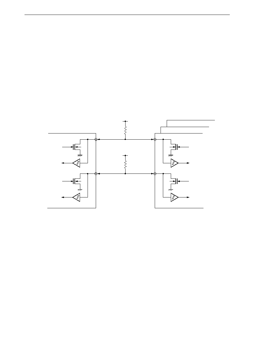
348
CHAPTER 18 SERIAL INTERFACE IIC0 (
µPD780078Y SUBSERIES ONLY)
User's Manual U14260EJ3V1UD
18.4 I
2
C Bus Mode Functions
18.4.1 Pin configuration
The serial clock pin (SCL0) and serial data bus pin (SDA0) are configured as follows.
(1) SCL0 ∑∑∑∑∑∑∑∑∑ This pin is used for serial clock input and output.
This pin is an N-ch open-drain output for both master and slave devices. Input is Schmitt input.
(2) SDA0 ∑∑∑∑∑∑∑∑∑ This pin is used for serial data input and output.
This pin is an N-ch open-drain output for both master and slave devices. Input is Schmitt input.
Since outputs from the serial clock line and the serial data bus line are N-ch open-drain outputs, an external pull-
up resistor is required.
Figure 18-9. Pin Configuration Diagram
V
DD0
V
SS0
V
SS0
V
SS0
V
SS0
SCL0
SDA0
SCL0
SDA0
V
DD0
Clock output
Master device
(Clock input)
Data output
Data input
(Clock output)
Clock input
Data output
Data input
Slave device

349
CHAPTER 18 SERIAL INTERFACE IIC0 (
µPD780078Y SUBSERIES ONLY)
User's Manual U14260EJ3V1UD
18.5 I
2
C Bus Definitions and Control Methods
The following section describes the I
2
C bus's serial data communication format and the signals used by the I
2
C
bus. Figure 18-10 shows the transfer timing for the "start condition", "data", and "stop condition" output via the I
2
C
bus's serial data bus.
Figure 18-10. I
2
C Bus Serial Data Transfer Timing
The master device outputs the start condition, slave address, and stop condition.
The acknowledge signal (ACK) can be output by either the master or slave device (normally, it is output by the
device that receives 8-bit data).
The serial clock (SCL0) is continuously output by the master device. However, in the slave device, the SCL0's
low level period can be extended and a wait can be inserted.
18.5.1 Start conditions
A start condition is met when the SCL0 pin is at high level and the SDA0 pin changes from high level to low level.
The start conditions for the SCL0 pin and SDA0 pin are signals that the master device outputs to the slave device
when starting a serial transfer. When the device is used as a slave, start conditions can be detected.
Figure 18-11. Start Conditions
A start condition is output when bit 1 (STT0) of IIC control register 0 (IICC0) is set (to 1) after a stop condition has
been detected (SPD0: Bit 0 = 1 in IIC status register 0 (IICS0)). When a start condition is detected, bit 1 (STD0) of
IICS0 is set (to 1).
1-7
8
9
1-7
8
9
1-7
8
9
SCL0
SDA0
Start
condition
Address
R/W
ACK
Data
Data
Stop
condition
ACK
ACK
H
SCL0
SDA0
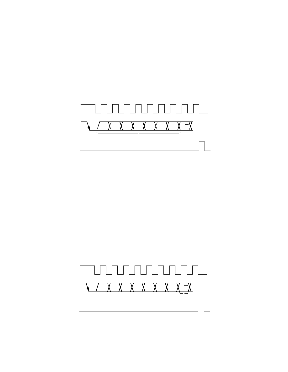
350
CHAPTER 18 SERIAL INTERFACE IIC0 (
µPD780078Y SUBSERIES ONLY)
User's Manual U14260EJ3V1UD
18.5.2 Addresses
The address is defined by the 7 bits of data that follow the start condition.
An address is a 7-bit data segment that is output in order to select one of the slave devices that are connected
to the master device via the bus lines. Therefore, each slave device connected via the bus lines must have a unique
address.
The slave devices include hardware that detects the start condition and checks whether or not the 7-bit address
data matches the data values stored in slave address register 0 (SVA0). If the address data matches the SVA0 values,
the slave device is selected and communicates with the master device until the master device transmits a start
condition or stop condition.
Figure 18-12. Address
Note INTIIC0 is not issued if data other than a local address or extension code is received during slave device
operation.
The slave address and the eighth bit, which specifies the transfer direction as described in 18.5.3 Transfer
direction specification below, are together written to IIC shift register 0 (IIC0) and are then output. Received
addresses are written to IIC0.
The slave address is assigned to the higher 7 bits of IIC0.
18.5.3 Transfer direction specification
In addition to the 7-bit address data, the master device sends 1 bit that specifies the transfer direction. When this
transfer direction specification bit has a value of "0", it indicates that the master device is transmitting data to a slave
device. When the transfer direction specification bit has a value of "1", it indicates that the master device is receiving
data from a slave device.
Figure 18-13. Transfer Direction Specification
Note INTIIC0 is not issued if data other than a local address or extension code is received during slave device
operation.
Address
SCL0
1
SDA0
INTIIC0
Note
2
3
4
5
6
7
8
9
A6
A5
A4
A3
A2
A1
A0
R/W
SCL0
1
SDA0
INTIIC0
2
3
4
5
6
7
8
9
A6
A5
A4
A3
A2
A1
A0
R/W
Transfer direction specification
Note

351
CHAPTER 18 SERIAL INTERFACE IIC0 (
µPD780078Y SUBSERIES ONLY)
User's Manual U14260EJ3V1UD
18.5.4 Acknowledge (ACK) signal
The acknowledge (ACK) signal is used by the transmitting and receiving devices to confirm serial data reception.
The receiving device returns one ACK signal for each 8 bits of data it receives. The transmitting device normally
receives an ACK signal after transmitting 8 bits of data. However, when the master device is the receiving device,
it does not output an ACK signal after receiving the final data to be transmitted. The transmitting device detects whether
or not an ACK signal is returned after it transmits 8 bits of data. When an ACK signal is returned, the reception is
judged as normal and processing continues. If the slave device does not return an ACK signal, the master device
outputs either a stop condition or a restart condition and then stops the current transmission. Failure to return an
ACK signal may be caused by the following two factors.
(a) Reception was not performed normally.
(b) The final data was received.
When the receiving device sets the SDA0 line to low level during the ninth clock, the ACK signal becomes active
(normal receive response).
When bit 2 (ACKE0) of IIC control register 0 (IICC0) is set to 1, automatic ACK signal generation is enabled.
Transmission of the eighth bit following the 7 address data bits causes bit 3 (TRC0) of IIC status register 0 (IICS0)
to be set. When this TRC0 bit's value is "0", it indicates receive mode. Therefore, ACKE0 should be set to 1.
When the slave device is receiving (when TRC0 = 0), if the slave devices does not need to receive any more data
after receiving several bytes, setting ACKE0 to 0 will prevent the master device from starting transmission of the
subsequent data.
Similarly, when the master device is receiving (when TRC0 = 0) and the subsequent data is not needed and when
either a restart condition or a stop condition should therefore be output, setting ACKE0 to 0 will prevent the ACK signal
from being returned. This prevents the MSB data from being output via the SDA0 line (i.e., stops transmission) during
transmission from the slave device.
Figure 18-14. ACK Signal
When the local address is received, an ACK signal is automatically output in sync with the falling edge of the SCL0's
eighth clock regardless of the ACKE0 value. No ACK signal is output if the received address is not a local address.
The ACK signal output method during data reception is based on the wait timing setting, as described below.
∑ When 8-clock wait is selected: ACK signal is output when ACKE0 is set to 1 before wait cancellation.
(WTIM0 = 0)
∑ When 9-clock wait is selected: ACK signal is automatically output at the falling edge of the SCL0's eighth clock
(WTIM0 = 1)
if ACKE0 has already been set to 1.
SCL0
1
SDA0
2
3
4
5
6
7
8
9
A6
A5
A4
A3
A2
A1
A0
R/W ACK

352
CHAPTER 18 SERIAL INTERFACE IIC0 (
µPD780078Y SUBSERIES ONLY)
User's Manual U14260EJ3V1UD
18.5.5 Stop condition
When the SCL0 pin is at high level, changing the SDA0 pin from low level to high level generates a stop condition.
A stop condition is a signal that the master device outputs to the slave device when serial transfer has been
completed. When the device is used as a slave, stop conditions can be detected.
Figure 18-15. Stop Condition
A stop condition is generated when bit 0 (SPT0) of IIC control register 0 (IICC0) is set (to 1). When the stop condition
is detected, bit 0 (SPD0) of IIC status register 0 (IICS0) is set (to 1) and INTIIC0 is generated when bit 4 (SPIE0)
of IICC0 is set (to 1).
H
SCL0
SDA0

353
CHAPTER 18 SERIAL INTERFACE IIC0 (
µPD780078Y SUBSERIES ONLY)
User's Manual U14260EJ3V1UD
18.5.6 Wait signal (WAIT)
The wait signal (WAIT) is used to notify the communication partner that a device (master or slave) is preparing
to transmit or receive data (i.e., is in a wait state).
Setting the SCL0 pin to low level notifies the communication partner of the wait status. When wait status has been
canceled for both the master and slave devices, the next data transfer can begin.
Figure 18-16. Wait Signal (1/2)
(1) When master device has a nine-clock wait and slave device has an eight-clock wait
(master transmits, slave receives, and ACKE0 = 1)
SCL0
6
SDA0
7
8
9
1
2
3
SCL0
IIC0
6
H
7
8
1
2
3
D2
D1
D0
ACK
D7
D6
D5
9
IIC0
SCL0
ACKE0
Master
Master returns to high
impedance but slave
is in wait state (low level).
Wait after output
of ninth clock
IIC0 data write (cancel wait)
Slave
Wait after output
of eighth clock
Wait signal
from slave
Wait signal
from master
FFH is written to IIC0 or WREL0 is set to 1
Transfer lines
354
CHAPTER 18 SERIAL INTERFACE IIC0 (
µPD780078Y SUBSERIES ONLY)
User's Manual U14260EJ3V1UD
Figure 18-16. Wait Signal (2/2)
(2) When master and slave devices both have a nine-clock wait
(master transmits, slave receives, and ACKE0 = 1)
Remark
ACKE0: Bit 2 of IIC control register 0 (IICC0)
WREL0: Bit 5 of IIC control register 0 (IICC0)
A wait may be automatically generated depending on the setting of bit 3 (WTIM0) of IIC control register 0 (IICC0).
Normally, the receiving side cancels the wait status when bit 5 (WREL0) of IICC0 is set to 1 or when FFH is written
to IIC shift register 0 (IIC0), and the transmitting side cancels the wait status when data is written to IIC0.
The master device can also cancel the wait status via either of the following methods.
∑ By setting bit 1 (STT0) of IICC0 to 1
∑ By setting bit 0 (SPT0) of IICC0 to 1
SCL0
6
SDA0
7
8
9
1
2
3
SCL0
IIC0
6
H
7
8
1
2
3
D2
D1
D0
ACK
D7
D6
D5
9
IIC0
SCL0
ACKE0
Master
Master and slave both wait
after output of ninth clock
IIC0 data write (cancel wait)
Slave
FFH is written to IIC0 or WREL0 is set to 1
Output according to previously set ACKE0 value
Transfer lines
Wait signal from
master and slave
Wait signal
from slave
355
CHAPTER 18 SERIAL INTERFACE IIC0 (
µPD780078Y SUBSERIES ONLY)
User's Manual U14260EJ3V1UD
18.5.7 Interrupt request (INTIIC0) generation timing and wait control
The setting of bit 3 (WTIM0) of IIC control register 0 (IICC0) determines the timing by which INTIIC0 is generated
and the corresponding wait control, as shown in Table 18-2.
Table 18-2. INTIIC0 Generation Timing and Wait Control
WTIM0
During Slave Device Operation
During Master Device Operation
Address
Data Reception
Data Transmission
Address
Data Reception
Data Transmission
0
9
Notes 1, 2
8
Note 2
8
Note 2
9
8
8
1
9
Notes 1, 2
9
Note 2
9
Note 2
9
9
9
Notes 1. The slave device's INTIIC0 signal and wait period occurs at the falling edge of the ninth clock only when
there is a match with the address set to slave address register 0 (SVA0).
At this point, ACK is output regardless of the value set to IICC0's bit 2 (ACKE0). For a slave device
that has received an extension code, INTIIC0 occurs at the falling edge of the eighth clock.
However, if the address does not match after restart, INTIIC0 is generated at the falling edge of the
9th clock, but wait does not occur.
2. If the received address does not match the contents of slave address register 0 (SVA0) and extension
code is not received, neither INTIIC0 nor a wait occurs.
Remark
The numbers in the table indicate the number of the serial clock's clock signals. Interrupt requests and
wait control are both synchronized with the falling edge of these clock signals.
(1) During address transmission/reception
∑ Slave device operation:
Interrupt and wait timing are determined depending on the conditions described in
Notes 1 and 2 above, regardless of the WTIM0 bit.
∑ Master device operation: Interrupt and wait timing occur at the falling edge of the ninth clock regardless of
the WTIM0 bit.
(2) During data reception
∑ Master/slave device operation: Interrupt and wait timing are determined according to the WTIM0 bit.
(3) During data transmission
∑ Master/slave device operation: Interrupt and wait timing are determined according to the WTIM0 bit.
(4) Wait cancellation method
The four wait cancellation methods are as follows.
∑ By setting bit 5 (WREL0) of IIC control register 0 (IICC0) to 1
∑ By writing to IIC shift register 0 (IIC0)
∑ By setting a start condition (setting bit 1 (STT0) of IICC0 to 1)
Note
∑ By setting a stop condition (setting bit 0 (SPT0) of IICC0 to 1)
Note
Note Master only.
When an 8-clock wait has been selected (WTIM0 = 0), the output level of ACK must be determined prior to wait
cancellation.

356
CHAPTER 18 SERIAL INTERFACE IIC0 (
µPD780078Y SUBSERIES ONLY)
User's Manual U14260EJ3V1UD
(5) Stop condition detection
INTIIC0 is generated when a stop condition is detected (only when SPIE0 = 1).
18.5.8 Address match detection method
In I
2
C bus mode, the master device can select a particular slave device by transmitting the corresponding slave
address.
Address match can be detected automatically by hardware. An interrupt request (INTIIC0) occurs when a local
address has been set to slave address register 0 (SVA0) and when the address set to SVA0 matches the slave address
sent by the master device, or when an extension code has been received.
18.5.9 Error detection
In I
2
C bus mode, the status of the serial data bus (SDA0) during data transmission is captured by IIC shift register
0 (IIC0) of the transmitting device, so the IIC0 data prior to transmission can be compared with the transmitted IIC0
data to enable detection of transmission errors. A transmission error is judged as having occurred when the compared
data values do not match.
18.5.10 Extension code
(1) When the higher 4 bits of the receive address are either "0000" or "1111", the extension code reception flag
(EXC0) is set for extension code reception and an interrupt request (INTIIC0) is issued at the falling edge of
the eighth clock. The local address stored in slave address register 0 (SVA0) is not affected.
(2) If "111110
◊◊" is set to SVA0 by a 10-bit address transfer and "111110◊◊" is transferred from the master device,
the results are as follows. Note that INTIIC0 occurs at the falling edge of the eighth clock.
∑ Higher four bits of data match: EXC0 = 1
Note
∑ Seven bits of data match:
COI0 = 1
Note
Note EXC0: Bit 5 of IIC status register 0 (IICS0)
COI0: Bit 4 of IIC status register 0 (IICS0)
(3) Since the processing after the interrupt request occurs differs according to the data that follows the extension
code, such processing is performed by software.
For example, after the extension code is received, if you do not wish to operate the target device as a slave
device, you can set bit 6 (LREL0) of IIC control register 0 (IICC0) to 1 to set the standby mode for the next
communication operation.
Table 18-3. Extension Code Bit Definitions
Slave Address
R/W Bit
Description
0000 000
0
General call address
0000 000
1
Start byte
0000 001
◊
CBUS address
0000 010
◊
Address that is reserved for different bus format
1111 0
◊◊
◊
10-bit slave address specification

357
CHAPTER 18 SERIAL INTERFACE IIC0 (
µPD780078Y SUBSERIES ONLY)
User's Manual U14260EJ3V1UD
18.5.11 Arbitration
When several master devices simultaneously output a start condition (when STT0 is set to 1 before STD0 is set
to 1
Note
), communication among the master devices is performed as the number of clocks are adjusted until the data
differs. This kind of operation is called arbitration.
When one of the master devices loses in arbitration, an arbitration loss flag (ALD0) in IIC status register 0 (IICS0)
is set (1) via the timing by which the arbitration loss occurred, and the SCL0 and SDA0 lines are both set to high
impedance, which releases the bus.
The arbitration loss is detected based on the timing of the next interrupt request (the eighth or ninth clock, when
a stop condition is detected, etc.) and the ALD0 = 1 setting that has been made by software.
For details of interrupt request timing, see 18.5.16 Timing of I
2
C interrupt request (INTIIC0) occurrence.
Note STD0: Bit 1 of IIC status register 0 (IICS0)
STT0: Bit 1 of IIC control register 0 (IICC0)
Figure 18-17. Arbitration Timing Example
Master 1
Master 2
Transfer lines
SCL0
SDA0
SCL0
SDA0
SCL0
SDA0
Master 1 loses arbitration
Hi-Z
Hi-Z

358
CHAPTER 18 SERIAL INTERFACE IIC0 (
µPD780078Y SUBSERIES ONLY)
User's Manual U14260EJ3V1UD
Table 18-4. Status During Arbitration and Interrupt Request Generation Timing
Status During Arbitration
Interrupt Request Generation Timing
During address transmission
At falling edge of eighth or ninth clock following byte transfer
Note 1
Read/write data after address transmission
During extension code transmission
Read/write data after extension code transmission
During data transmission
During ACK signal transfer period after data transmission
When restart condition is detected during data transfer
When stop condition is detected during data transfer
When stop condition is output (when SPIE0 = 1)
Note 2
When data is at low level while attempting to output a
At falling edge of eighth or ninth clock following byte transfer
Note 1
restart condition
When stop condition is detected while attempting to
When stop condition is output (when SPIE0 = 1)
Note 2
output a restart condition
When data is at low level while attempting to output a
At falling edge of eighth or ninth clock following byte transfer
Note 1
stop condition
When SCL0 is at low level while attempting to output a
restart condition
Notes 1. When WTIM0 (bit 3 of IIC control register 0 (IICC0)) = 1, an interrupt request occurs at the falling edge
of the ninth clock. When WTIM0 = 0 and the extension code's slave address is received, an interrupt
request occurs at the falling edge of the eighth clock.
2. When there is a chance that arbitration will occur, set SPIE0 = 1 for master device operation.
Remark
SPIE0: Bit 4 of IIC control register 0 (IICC0)
18.5.12 Wake-up function
The I
2
C bus slave function is a function that generates an interrupt request (INTIIC0) when a local address and
extension code have been received.
This function makes processing more efficient by preventing unnecessary interrupt requests from occurring when
addresses do not match.
When a start condition is detected, wake-up standby mode is set. This wake-up standby mode is in effect while
addresses are transmitted due to the possibility that an arbitration loss may change the master device (which has
output a start condition) to a slave device.
However, when a stop condition is detected, bit 4 (SPIE0) of IIC control register 0 (IICC0) is set regardless of the
wake-up function, and this determines whether interrupt requests are enabled or disabled.

359
CHAPTER 18 SERIAL INTERFACE IIC0 (
µPD780078Y SUBSERIES ONLY)
User's Manual U14260EJ3V1UD
18.5.13 Communication reservation
To start master device communications when not currently using a bus, a communication reservation can be made
to enable transmission of a start condition when the bus is released. There are two modes under which the bus is
not used.
∑ When arbitration results in neither master nor slave operation
∑ When an extension code is received and slave operation is disabled (ACK is not returned and the bus was
released when bit 6 (LREL0) of IIC control register 0 (IICC0) was set to 1).
If bit 1 (STT0) of IICC0 is set (1) while the bus is not used (after a stop condition is detected), a start condition
is automatically generated and wait status is set. When the bus release is detected (when a stop condition is detected),
writing to IIC shift register 0 (IIC0) causes the master address transfer to start. At this point, bit 4 (SPIE0) of IICC0
should be set (1).
When STT0 has been set (1), the operation mode (as start condition or as communication reservation) is determined
according to the bus status.
∑ If the bus has been released ........................................... a start condition is generated
∑ If the bus has not been released (standby mode) .......... communication reservation
Check whether the communication reservation operates or not by using MSTS0 (bit 7 of IIC status register 0 (IICS0))
after SST0 is set and the wait time elapses.
The wait periods, which should be set via software, are listed in Table 18-5. These wait periods can be set via
the settings for bits 3 and 0 (SMC0 and CL00) in IIC transfer clock select register 0 (IICCL0).
Table 18-5. Wait Periods
SMC0
CL00
Wait Period
0
0
26 clocks
0
1
46 clocks
1
0
16 clocks
1
1
Figure 18-18 shows the communication reservation timing.
360
CHAPTER 18 SERIAL INTERFACE IIC0 (
µPD780078Y SUBSERIES ONLY)
User's Manual U14260EJ3V1UD
Figure 18-18. Communication Reservation Timing
Remark
IIC0:
IIC shift register 0
STT0: Bit 1 of IIC control register 0 (IICC0)
STD0: Bit 1 of IIC status register 0 (IICS0)
SPD0: Bit 0 of IIC status register 0 (IICS0)
Communication reservations are accepted via the following timing. After bit 1 (STD0) of IIC status register 0 (IICS0)
is set to 1, a communication reservation can be made by setting bit 1 (STT0) of IIC control register 0 (IICC0) to 1
before a stop condition is detected.
Figure 18-19. Timing for Accepting Communication Reservations
Figure 18-20 shows the communication reservation protocol.
SCL0
SDA0
STD0
SPD0
Standby mode
2
1
3
4
5
6
2
1
3
4
5
6
7
8
9
SCL0
SDA0
STT0 = 1
Program processing
Hardware processing
Write to
IIC0
Set SPD0
and INTIIC0
Communication
reservation
Set
STD0
Output by master with bus mastership
361
CHAPTER 18 SERIAL INTERFACE IIC0 (
µPD780078Y SUBSERIES ONLY)
User's Manual U14260EJ3V1UD
Figure 18-20. Communication Reservation Protocol
Note The communication reservation operation executes a write to IIC shift register 0 (IIC0) when a stop condition
interrupt request occurs.
Remark
STT0:
Bit 1 of IIC control register 0 (IICC0)
MSTS0: Bit 7 of IIC status register 0 (IICS0)
IIC0:
IIC shift register 0
18.5.14 Other cautions
After a reset, when changing from a mode in which no stop condition has been detected (the bus has not been
released) to a master device communication mode, first generate a stop condition to release the bus, then perform
master device communication.
When using multiple masters, it is not possible to perform master device communication when the bus has not
been released (when a stop condition has not been detected).
Use the following sequence for generating a stop condition.
(a) Set IIC transfer clock select register 0 (IICCL0).
(b) Set (1) bit 7 (IICE0) of IIC control register 0 (IICC0).
(c) Set (1) bit 0 (SPT0) of IICC0.
DI
SET1 STT0
Define communication
reservation
Wait
Cancel communication
reservation
No
Yes
MOV IIC0, #
◊◊H
EI
MSTS0 = 0?
(Communication reservation)
Note
(Generate start condition)
Sets STT0 flag (communication reservation)
Secures wait period set by software (see Table 18-5).
Confirmation of communication reservation
Clear user flag
IIC0 write operation
Defines that communication reservation is in effect
(defines and sets user flag to any part of RAM)
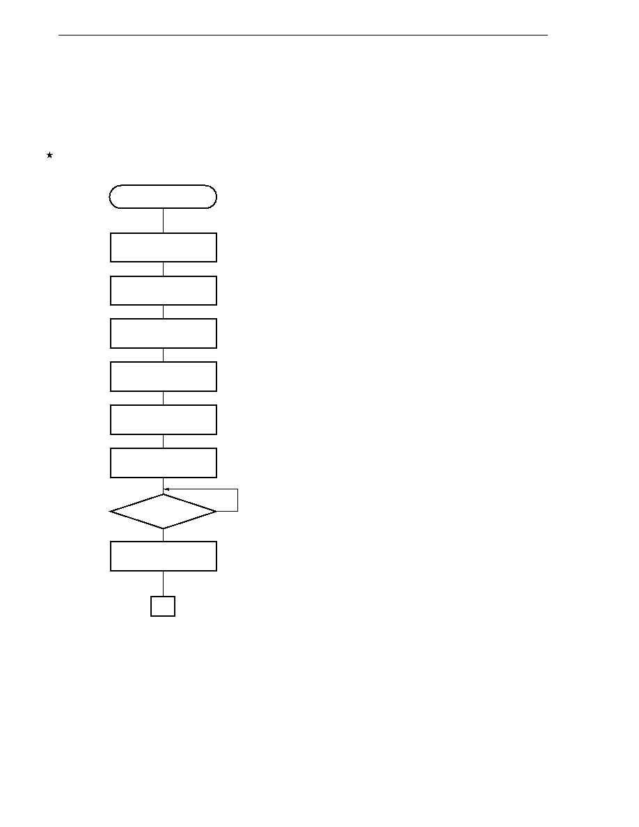
362
CHAPTER 18 SERIAL INTERFACE IIC0 (
µPD780078Y SUBSERIES ONLY)
User's Manual U14260EJ3V1UD
18.5.15 Communication operations
(1) Master operations
The procedure of controlling slave EEPROM
TM
using the
µPD780078Y Subseries as the master of the I
2
C bus
is as follows.
Figure 18-21. Master Operation Flowchart (1/5)
Issue start condition.
STT0 = 1
Set transfer clock.
IICCL0
◊◊H
Set port (mode and data).
PM32, PM33
1, P32, P33 0
Set port.
PM32, PM33
0
Set IIC control register 0.
IICE0 = WTIM0 = 1
Issue stop condition.
SPT0 = 1
Set interrupt.
IICIF0, IICMK0
0
SPD0 = 1?
A
START
No
Yes
First perform initialization to use I
2
C.
Set the port that functions alternately as the
pins to be used. First set the port in the input
mode, and clear the output latch to 0.
Specify the operation mode, turn on/off the
digital filter, and specify the transfer rate.
Set a 9-clock wait and enable operation.
Set the port in the output mode to enable
output of I
2
C.
Clear the interrupt request of I
2
C.
Clear the mask to enable the interrupt when
using the interrupt.
Issue the stop condition before starting
operation, and release the bus.
Wait until the bus is released.
If the stop condition is detected, the bus is
released and can be used. Declare use of
the bus by issuing the start condition.
If the stop condition cannot be detected, the
chances are the connected pin is driving the
bus low.
In this case, refer to Remark.
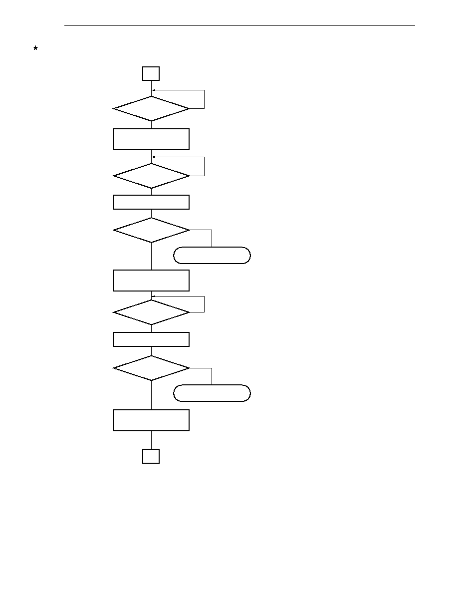
363
CHAPTER 18 SERIAL INTERFACE IIC0 (
µPD780078Y SUBSERIES ONLY)
User's Manual U14260EJ3V1UD
Figure 18-21. Master Operation Flowchart (2/5)
ACKD0 = 1?
Transmit EEPROM higher address.
IIC0
EEPROM higher address
Transmit EEPROM lower address.
IIC0
EEPROM lower address
Transfer slave address.
IIC0
address, R/W (0)
INTIIC0 = 1?
Clear INTIIC0.
Clear INTIIC0.
B
ACKD0 = 1?
End (no slave)
No
No
No
End (no acknowledgment)
A
STD0 = 1?
No
Yes
Yes
Yes
Yes
Yes
INTIIC0 = 1?
No
Wait until the start condition is detected and
the bus is ready.
Specify writing and transfer the address of
the slave (EEPROM).
Wait until transfer is completed.
Clear INTIIC0 to poll INTIIC0 without using
an interrupt.
If ACK is not sent, it means that the
specified slave does not exist. End
processing.
If a slave does exist, divide the address of
EEPROM (2 bytes) into two, and start
transmitting the address from the higher
byte.
Each time transmission is completed, check
ACK.
Transmit the lower address.
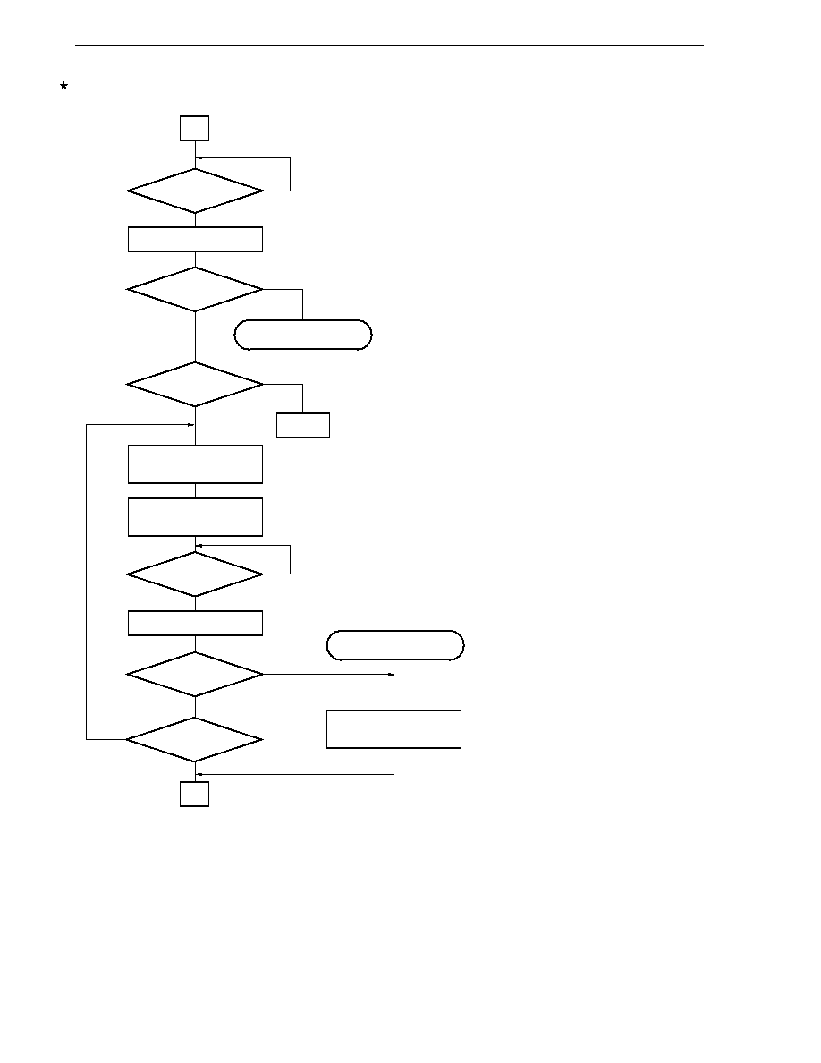
364
CHAPTER 18 SERIAL INTERFACE IIC0 (
µPD780078Y SUBSERIES ONLY)
User's Manual U14260EJ3V1UD
Figure 18-21. Master Operation Flowchart (3/5)
ACKD0 = 1?
Transmission?
TRC0 = 1?
Transmit write data.
IIC0
Data
Prepare write data.
INTIIC0 = 1?
Clear INTIIC0.
Clear INTIIC0.
B
Reception
C
ACKD0 = 1?
Transfer end?
End
End (no acknowledgment)
Set error flag.
No
No
No
No
No
INTIIC0 = 1?
Yes
Yes
Yes
Yes
Yes
Yes
When writing data to EEPROM, continue
writing data.
When reading data from EEPROM, start
reception processing.
Prepare data to be written to EEPROM, and
transmit it to EEPROM.
Each time data has been transmitted, the
slave returns ACK. If any error occurs
before transmission of the necessary data is
completed, ACK may not be returned. In
this case, end transfer.
In the case of an error, set the error flag as
shown on the left, and release the bus.

365
CHAPTER 18 SERIAL INTERFACE IIC0 (
µPD780078Y SUBSERIES ONLY)
User's Manual U14260EJ3V1UD
Figure 18-21. Master Operation Flowchart (4/5)
Transfer slave address.
IIC0
address, R/W (1)
Issue stop condition.
SPT0 = 1
INTIIC0 = 1?
Clear INTIIC0.
D
Reception
ACKD0 = 1?
END
No
Issue start condition.
STT0 = 1
STD0 = 1?
No
No
End (no acknowledgment)
When transmission is completed, issue the
stop condition to notify the slave of
completion of transmission.
For reception, the data transfer direction
must be changed. Issue the start condition
again and redo (restart) communication.
Because the master receives data this time,
set the R/W bit to 1 and transmit an
address.
C
SPD0 = 1?
No
Yes
Yes
Yes
Yes
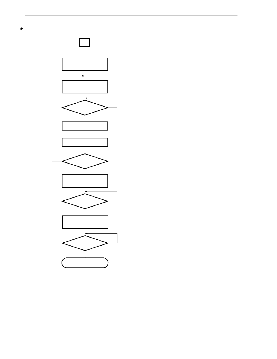
366
CHAPTER 18 SERIAL INTERFACE IIC0 (
µPD780078Y SUBSERIES ONLY)
User's Manual U14260EJ3V1UD
Figure 18-21. Master Operation Flowchart (5/5)
Remark
While the slave is outputting a low level to the data line, the master cannot issue the stop condition. This
happens if EEPROM is not reset, even though the microcontroller is reset, because of supply voltage
fluctuation during communication (reading from EEPROM). In this case, the EEPROM continues
sending data, and may output a low level to the data line. Because the structure of I
2
C does not allow
the master to forcibly make the data line high, the master cannot issue the stop condition.
To avoid this phenomenon, it is possible to use a clock line as a port, output a dummy clock from the
port, continue reading data from EEPROM by inputting the dummy clock, and complete reading with
some EEPROMs (because the data line goes high when reading is completed, the master can issue
the stop condition. After that, the status of EEPROM can be controlled). At this time, the port
corresponding to the data line must always be in the high-impedance state (high-level output).
Re-set IIC control register 0.
ACKE0 = 1, WTIM0 = 0
Issue stop condition.
SPT0 = 1
Re-set IIC control register 0.
ACKE0 = 0, WREL0 = WTIM0 = 1
SPD0 = 1?
D
END
No
Remaining data?
Yes
Start data reception.
IIC0
0FFH
INTIIC0 = 1?
No
No
Set so that ACK is automatically returned
after an 8-clock wait (set ACKE0 so that
ACK is returned except when the last data
is received. Specify an 8-clock wait so that
automatic returning of ACK can be cleared
when the last data is received).
Write dummy data to IIC0 and start
reception (reception can also be started
when WREL0 = 1).
Reception is completed when INTIIC0
occurs.
Save the received data to a buffer.
When reception of data is completed,
disable automatic returning of ACK, set a 9-
clock wait, cancel wait in the ACK cycle,
and stop at the 9th clock. As a result, ACK
is not returned to the slave. This indicates
the completion of reception. Issue the stop
condition and end communication.
Save receive data.
Clear INTIIC0.
Yes
Yes
INTIIC0 = 1?
No
Yes
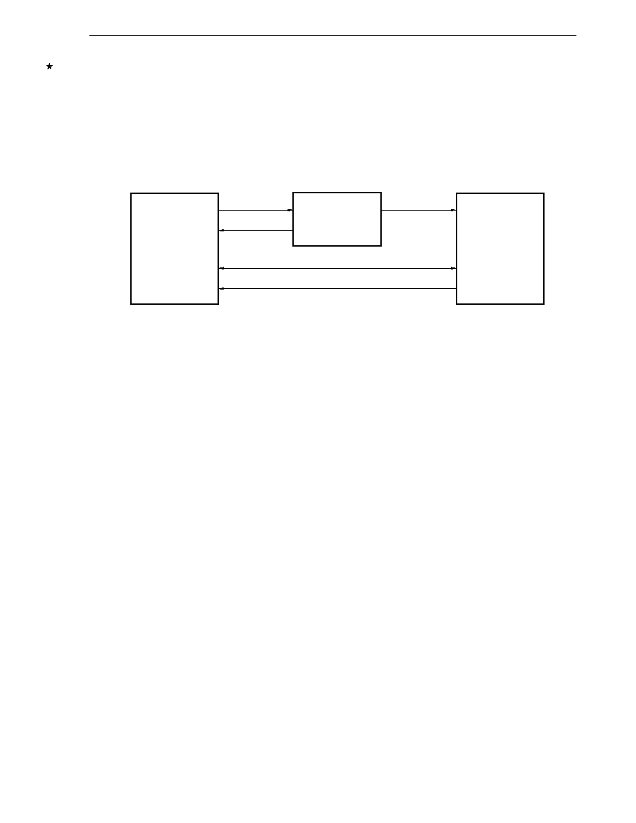
367
CHAPTER 18 SERIAL INTERFACE IIC0 (
µPD780078Y SUBSERIES ONLY)
User's Manual U14260EJ3V1UD
(2) Slave operation
The processing procedure of the slave operation is as follows.
Basically, the slave operation is event-driven. Therefore, processing by the INTIIC0 interrupt (processing that
must substantially change the operation status such as detection of a stop condition during communication) is
necessary.
In the following explanation, it is assumed that the extension code is not supported for data communication. It
is also assumed that the INTIIC0 interrupt servicing only performs status transition processing, and that actual
data communication is performed by the main processing.
Therefore, data communication processing is performed by preparing the following three flags and passing them
to the main processing instead of INTIIC0.
<1> Communication mode flag
This flag indicates the following two communication statuses.
∑ Clear mode:
Status in which data communication is not performed
∑ Communication mode: Status in which data communication is performed (from valid address detection
to stop condition detection, no detection of ACK from master, address mismatch)
<2> Ready flag
This flag indicates that data communication is enabled. Its function is the same as the INTIIC0 interrupt for
ordinary data communication. This flag is set by interrupt servicing and cleared by the main processing.
Clear this flag by interrupt servicing when communication is started. However, the ready flag is not set by
interrupt servicing when the first data is transmitted. Therefore, the first data is transmitted without the flag
being cleared (an address match is interpreted as a request for the next data).
<3> Communication direction flag
This flag indicates the direction of communication. Its value is the same as TRC0.
IIC0
Interrupt servicing
Main processing
INTIIC0
Flag
Setting
Data
Setting
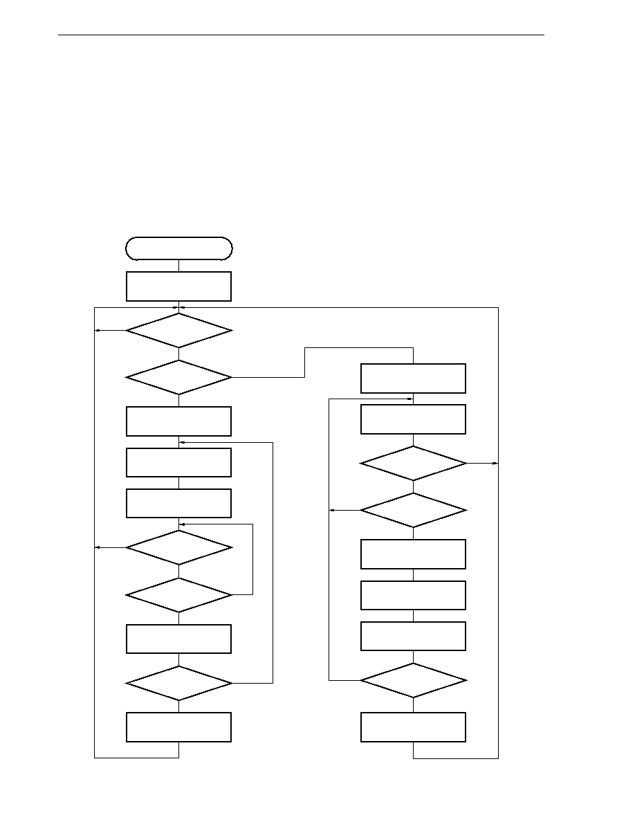
368
CHAPTER 18 SERIAL INTERFACE IIC0 (
µPD780078Y SUBSERIES ONLY)
User's Manual U14260EJ3V1UD
The main processing of the slave operation is explained next.
Start serial interface IIC0 and wait until communication is enabled. When communication is enabled, execute
communication by using the communication mode flag and ready flag (processing of the stop condition and start
condition is performed by an interrupt. Here, check the status by using the flags).
The transmission operation is repeated until the master no longer returns ACK. If ACK is not returned from the
master, communication is completed.
For reception, the necessary amount of data is received. When communication is completed, ACK is not returned
as the next data. After that, the master issues a stop condition or restart condition. Exit from the communication
status occurs in this way.
Figure 18-22. Slave Operation Flowchart (1/2)
Communication
direction flag = 1?
IIC0
data
IICC0
◊◊H
IICE0 = 1
Data processing
Clear ready flag.
WREL0 = 1
Clear communication mode flag.
WTIM0 = 1
Communication mode?
Ready?
ACKD0 = 1?
No
No
No
No
Communication mode?
Yes
Yes
Yes
Yes
Yes
START
No
No
No
Ready?
Data processing
WREL0 = 1
ACKE0 = WTIM0 = 1
Clear ready flag.
ACKE0 = 0
WREL0 = 1
Read data.
Communication ends?
Communication mode?
Yes
Yes
Yes
No
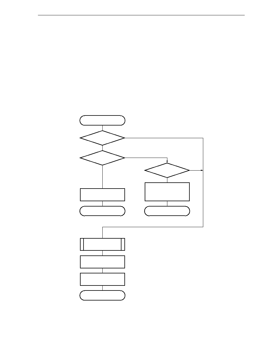
369
CHAPTER 18 SERIAL INTERFACE IIC0 (
µPD780078Y SUBSERIES ONLY)
User's Manual U14260EJ3V1UD
An example of the processing procedure of the slave with the INTIIC0 interrupt is explained below (processing
is performed assuming that no extension code is used).
The INTIIC0 interrupt checks the status, and the following operations are performed.
<1> Communication is stopped if the stop condition is issued.
<2> If the start condition is issued, the address is checked and communication is completed if the address does
not match. If the address matches, the communication mode is set, wait is cancelled, and processing returns
from the interrupt (the ready flag is cleared).
<3> For data transmit/receive, only the ready flag is set. Processing returns from the interrupt with the IIC0 bus
remaining in the wait status.
Remark
<1> to <3> above correspond to <1> to <3> in Figure 18-22 Slave Operation Flowchart (2/2).
Figure 18-22. Slave Operation Flowchart (2/2)
STD0 = 1
Clear communication
mode flag.
LREL0 = 1
End processing
Yes
Yes
Yes
<2>
<3>
<1>
SPD0 = 1
No
No
Generate INTIIC0
Complete interrupt servicing.
Set ready flag
Complete interrupt servicing.
COI0 = 1?
Communication direction
flag
TRC0
Set communication mode flag
and clear ready flag.
Complete interrupt servicing.
No
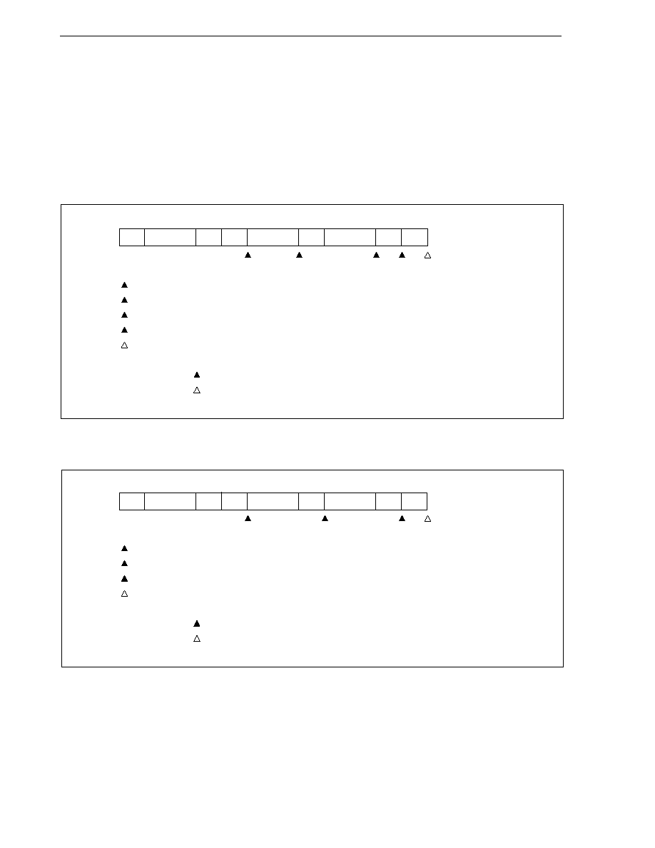
CHAPTER 18 SERIAL INTERFACE IIC0 (
µPD780078Y SUBSERIES ONLY)
370
User's Manual U14260EJ3V1UD
SPT0 = 1
SPT0 = 1
18.5.16 Timing of I
2
C interrupt request (INTIIC0) occurrence
The INTIIC0 interrupt request timing and the IIC status register 0 (IICS0) settings corresponding to that timing are
described below.
(1) Master device operation
(a) Start ~ Address ~ Data ~ Data ~ Stop (normal transmission/reception)
(i)
When WTIM0 = 0
ST
AD6-AD0
RW
AK
D7-D0
AK
D7-D0
AK
SP
1
2
3
4
5
1 : IICS0 = 1000
◊110B
2 : IICS0 = 1000
◊000B
3 : IICS0 = 1000
◊000B (Sets WTIM0)
4 : IICS0 = 1000
◊◊00B (Sets SPT0)
5 : IICS0 = 00000001B
Remark
: Always generated
: Generated only when SPIE0 = 1
◊ : Don't care
(ii) When WTIM0 = 1
ST
AD6-AD0
RW
AK
D7-D0
AK
D7-D0
AK
SP
1
2
3
4
1 : IICS0 = 1000
◊110B
2 : IICS0 = 1000
◊100B
3 : IICS0 = 1000
◊◊00B (Sets SPT0)
4 : IICS0 = 00000001B
Remark
: Always generated
: Generated only when SPIE0 = 1
◊ : Don't care
CHAPTER 18 SERIAL INTERFACE IIC0 (
µPD780078Y SUBSERIES ONLY)
371
User's Manual U14260EJ3V1UD
STT0 = 1
SPT0 = 1
STT0 = 1
SPT0 = 1
(b) Start ~ Address ~ Data ~ Start ~ Address ~ Data ~ Stop (restart)
(i)
When WTIM0 = 0
ST
AD6-AD0
RW
AK
D7-D0
AK
ST
AD6-AD0
RW
AK
D7-D0
AK
SP
1
2
3
4
5
6
7
1 : IICS0 = 1000
◊110B
2 : IICS0 = 1000
◊000B (Sets WTIM0)
3 : IICS0 = 1000
◊◊00B (Clears WTIM0, sets STT0)
4 : IICS0 = 1000
◊110B
5 : IICS0 = 1000
◊000B (Sets WTIM0)
6 : IICS0 = 1000
◊◊00B (Sets SPT0)
7 : IICS0 = 00000001B
Remark
: Always generated
: Generated only when SPIE0 = 1
◊ : Don't care
(ii) When WTIM0 = 1
ST
AD6-AD0
RW
AK
D7-D0
AK
ST
AD6-AD0
RW
AK
D7-D0
AK
SP
1
2
3
4
5
1 : IICS0 = 1000
◊110B
2 : IICS0 = 1000
◊◊00B (Sets STT0)
3 : IICS0 = 1000
◊110B
4 : IICS0 = 1000
◊◊00B (Sets SPT0)
5 : IICS0 = 00000001B
Remark
: Always generated
: Generated only when SPIE0 = 1
◊ : Don't care
CHAPTER 18 SERIAL INTERFACE IIC0 (
µPD780078Y SUBSERIES ONLY)
372
User's Manual U14260EJ3V1UD
SPT0 = 1
SPT0 = 1
(c) Start ~ Code ~ Data ~ Data ~ Stop (extension code transmission)
(i)
When WTIM0 = 0
ST
AD6-AD0
RW
AK
D7-D0
AK
D7-D0
AK
SP
1
2
3
4
5
1 : IICS0 = 1010
◊110B
2 : IICS0 = 1010
◊000B
3 : IICS0 = 1010
◊000B (Sets WTIM0)
4 : IICS0 = 1010
◊◊00B (Sets SPT0)
5 : IICS0 = 00000001B
Remark
: Always generated
: Generated only when SPIE0 = 1
◊ : Don't care
(ii) When WTIM0 = 1
ST
AD6-AD0
RW
AK
D7-D0
AK
D7-D0
AK
SP
1
2
3
4
1 : IICS0 = 1010
◊110B
2 : IICS0 = 1010
◊100B
3 : IICS0 = 1010
◊◊00B (Sets SPT0)
4 : IICS0 = 00001001B
Remark
: Always generated
: Generated only when SPIE0 = 1
◊ : Don't care
CHAPTER 18 SERIAL INTERFACE IIC0 (
µPD780078Y SUBSERIES ONLY)
373
User's Manual U14260EJ3V1UD
(2) Slave device operation (slave address data reception time (matches with SVA0))
(a) Start ~ Address ~ Data ~ Data ~ Stop
(i)
When WTIM0 = 0
ST
AD6-AD0
RW
AK
D7-D0
AK
D7-D0
AK
SP
1
2
3
4
1 : IICS0 = 0001
◊110B
2 : IICS0 = 0001
◊000B
3 : IICS0 = 0001
◊000B
4 : IICS0 = 00000001B
Remark
: Always generated
: Generated only when SPIE0 = 1
◊ : Don't care
(ii) When WTIM0 = 1
ST
AD6-AD0
RW
AK
D7-D0
AK
D7-D0
AK
SP
1
2
3
4
1 : IICS0 = 0001
◊110B
2 : IICS0 = 0001
◊100B
3 : IICS0 = 0001
◊◊00B
4 : IICS0 = 00000001B
Remark
: Always generated
: Generated only when SPIE0 = 1
◊ : Don't care
CHAPTER 18 SERIAL INTERFACE IIC0 (
µPD780078Y SUBSERIES ONLY)
374
User's Manual U14260EJ3V1UD
(b) Start ~ Address ~ Data ~ Start ~ Address ~ Data ~ Stop
(i)
When WTIM0 = 0 (after restart, matches with SVA0)
ST
AD6-AD0
RW
AK
D7-D0
AK
ST
AD6-AD0
RW
AK
D7-D0
AK
SP
1
2
3
4
5
1 : IICS0 = 0001
◊110B
2 : IICS0 = 0001
◊000B
3 : IICS0 = 0001
◊110B
4 : IICS0 = 0001
◊000B
5 : IICS0 = 00000001B
Remark
: Always generated
: Generated only when SPIE0 = 1
◊ : Don't care
(ii) When WTIM0 = 1 (after restart, matches with SVA0)
ST
AD6-AD0
RW
AK
D7-D0
AK
ST
AD6-AD0
RW
AK
D7-D0
AK
SP
1
2
3
4
5
1 : IICS0 = 0001
◊110B
2 : IICS0 = 0001
◊◊00B
3 : IICS0 = 0001
◊110B
4 : IICS0 = 0001
◊◊00B
5 : IICS0 = 00000001B
Remark
: Always generated
: Generated only when SPIE0 = 1
◊ : Don't care

CHAPTER 18 SERIAL INTERFACE IIC0 (
µPD780078Y SUBSERIES ONLY)
375
User's Manual U14260EJ3V1UD
(c) Start ~ Address ~ Data ~ Start ~ Code ~ Data ~ Stop
(i)
When WTIM0 = 0 (after restart, extension code reception)
ST
AD6-AD0
RW
AK
D7-D0
AK
ST
AD6-AD0
RW
AK
D7-D0
AK
SP
1
2
3
4
5
1 : IICS0 = 0001
◊110B
2 : IICS0 = 0001
◊000B
3 : IICS0 = 0010
◊010B
4 : IICS0 = 0010
◊000B
5 : IICS0 = 00000001B
Remark
: Always generated
: Generated only when SPIE0 = 1
◊ : Don't care
(ii) When WTIM0 = 1 (after restart, extension code reception)
ST
AD6-AD0
RW
AK
D7-D0
AK
ST
AD6-AD0
RW
AK
D7-D0
AK
SP
1
2
3
4
5
6
1 : IICS0 = 0001
◊110B
2 : IICS0 = 0001
◊◊00B
3 : IICS0 = 0010
◊010B
4 : IICS0 = 0010
◊110B
5 : IICS0 = 0010
◊◊00B
6 : IICS0 = 00000001B
Remark
: Always generated
: Generated only when SPIE0 = 1
◊ : Don't care
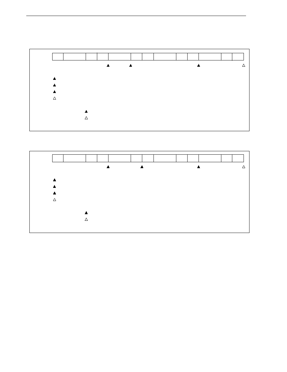
CHAPTER 18 SERIAL INTERFACE IIC0 (
µPD780078Y SUBSERIES ONLY)
376
User's Manual U14260EJ3V1UD
(d) Start ~ Address ~ Data ~ Start ~ Address ~ Data ~ Stop
(i)
When WTIM0 = 0 (after restart, does not match with address (= not extension code))
ST
AD6-AD0
RW
AK
D7-D0
AK
ST
AD6-AD0
RW
AK
D7-D0
AK
SP
1
2
3
4
1 : IICS0 = 0001
◊110B
2 : IICS0 = 0001
◊000B
3 : IICS0 = 00000
◊10B
4 : IICS0 = 00000001B
Remark
: Always generated
: Generated only when SPIE0 = 1
◊ : Don't care
(ii) When WTIM0 = 1 (after restart, does not match with address (= not extension code))
ST
AD6-AD0
RW
AK
D7-D0
AK
ST
AD6-AD0
RW
AK
D7-D0
AK
SP
1
2
3
4
1 : IICS0 = 0001
◊110B
2 : IICS0 = 0001
◊◊00B
3 : IICS0 = 00000
◊10B
4 : IICS0 = 00000001B
Remark
: Always generated
: Generated only when SPIE0 = 1
◊ : Don't care
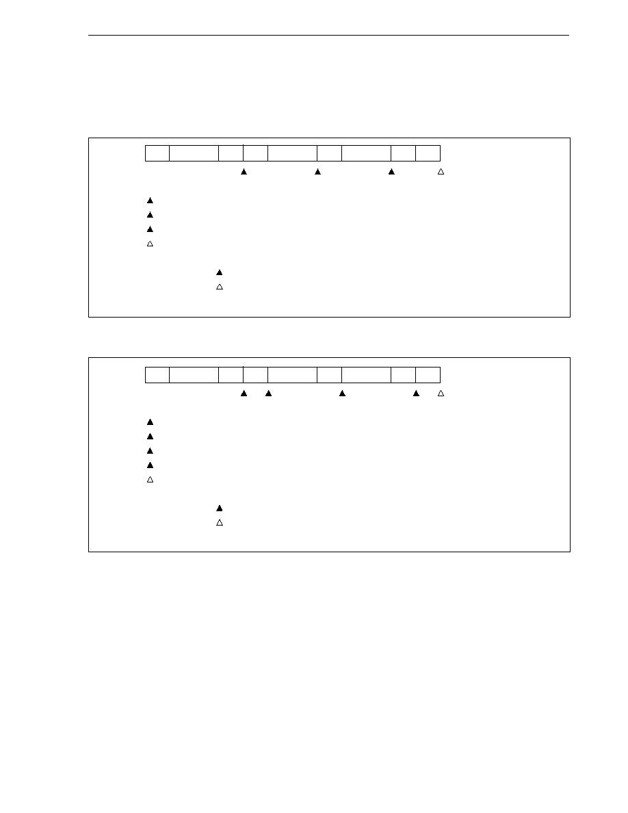
CHAPTER 18 SERIAL INTERFACE IIC0 (
µPD780078Y SUBSERIES ONLY)
377
User's Manual U14260EJ3V1UD
(3) Slave device operation (when receiving extension code)
(a) Start ~ Code ~ Data ~ Data ~ Stop
(i)
When WTIM0 = 0
ST
AD6-AD0
RW
AK
D7-D0
AK
D7-D0
AK
SP
1
2
3
4
1 : IICS0 = 0010
◊010B
2 : IICS0 = 0010
◊000B
3 : IICS0 = 0010
◊000B
4 : IICS0 = 00000001B
Remark
: Always generated
: Generated only when SPIE0 = 1
◊ : Don't care
(ii) When WTIM0 = 1
ST
AD6-AD0
RW
AK
D7-D0
AK
D7-D0
AK
SP
1
2
3
4
5
1 : IICS0 = 0010
◊010B
2 : IICS0 = 0010
◊110B
3 : IICS0 = 0010
◊100B
4 : IICS0 = 0010
◊◊00B
5 : IICS0 = 00000001B
Remark
: Always generated
: Generated only when SPIE0 = 1
◊ : Don't care
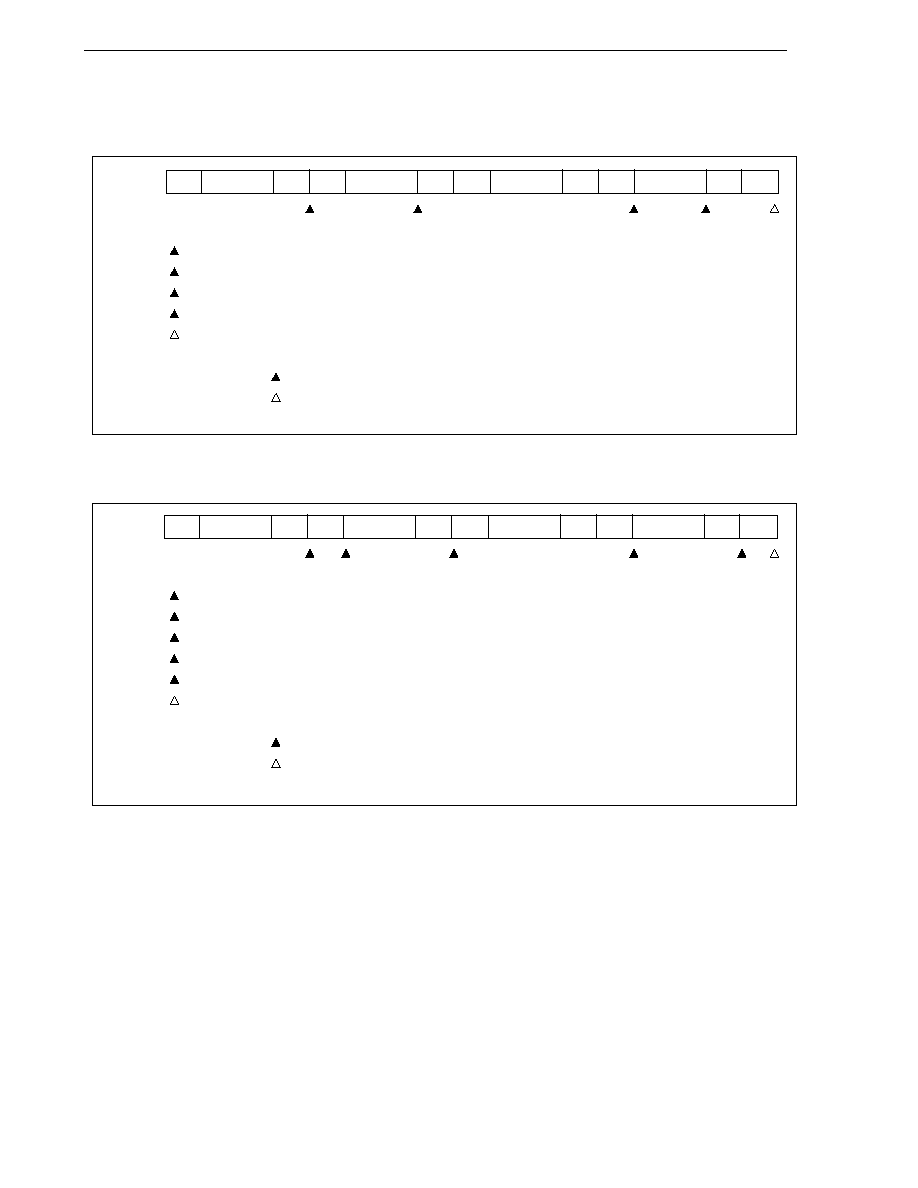
CHAPTER 18 SERIAL INTERFACE IIC0 (
µPD780078Y SUBSERIES ONLY)
378
User's Manual U14260EJ3V1UD
(b) Start ~ Code ~ Data ~ Start ~ Address ~ Data ~ Stop
(i)
When WTIM0 = 0 (after restart, matches with SVA0)
ST
AD6-AD0
RW
AK
D7-D0
AK
ST
AD6-AD0
RW
AK
D7-D0
AK
SP
1
2
3
4
5
1 : IICS0 = 0010
◊010B
2 : IICS0 = 0010
◊000B
3 : IICS0 = 0001
◊110B
4 : IICS0 = 0001
◊000B
5 : IICS0 = 00000001B
Remark
: Always generated
: Generated only when SPIE0 = 1
◊ : Don't care
(ii) When WTIM0 = 1 (after restart, matches with SVA0)
ST
AD6-AD0
RW
AK
D7-D0
AK
ST
AD6-AD0
RW
AK
D7-D0
AK
SP
1
2
3
4
5
6
1 : IICS0 = 0010
◊010B
2 : IICS0 = 0010
◊110B
3 : IICS0 = 0010
◊◊00B
4 : IICS0 = 0001
◊110B
5 : IICS0 = 0001
◊◊00B
6 : IICS0 = 00000001B
Remark
: Always generated
: Generated only when SPIE0 = 1
◊ : Don't care
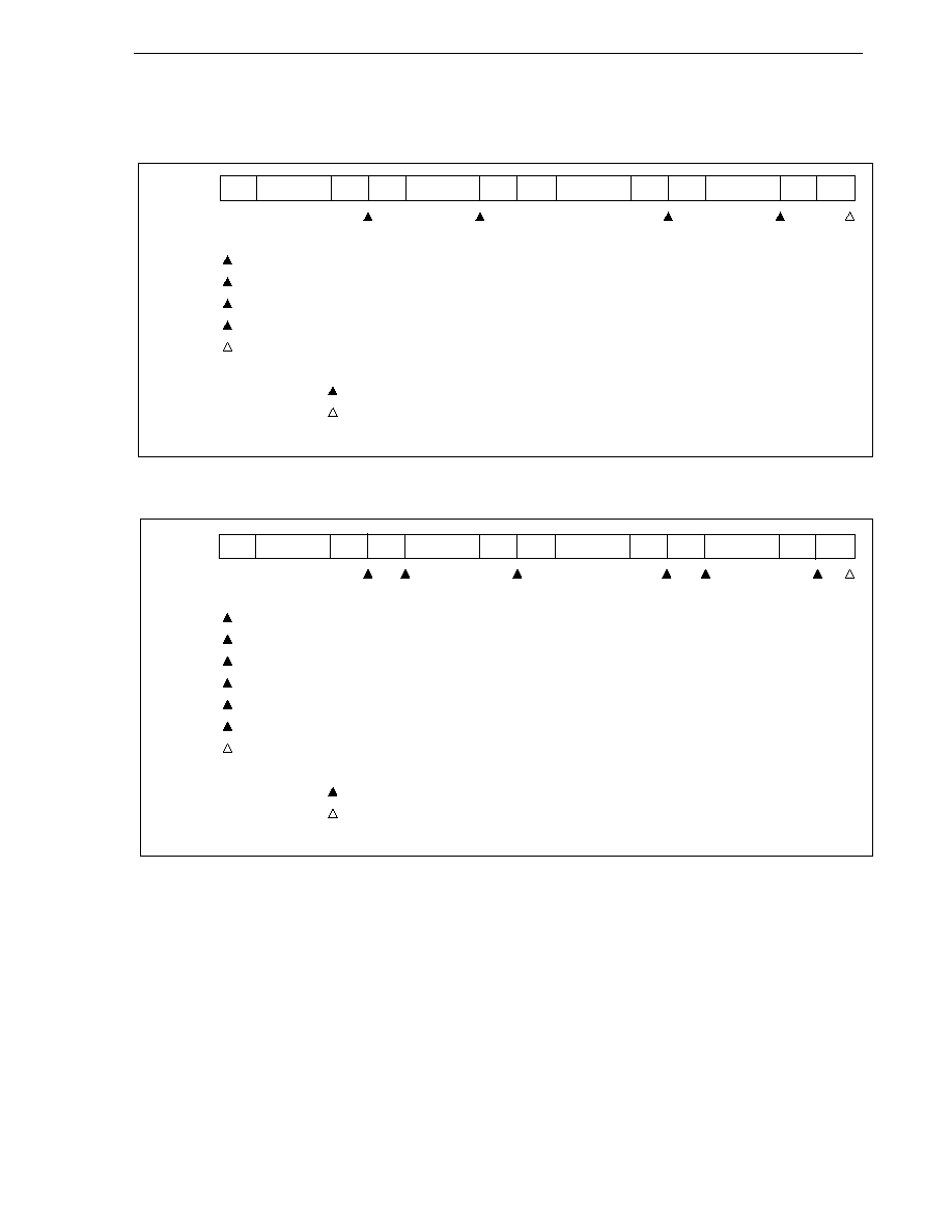
CHAPTER 18 SERIAL INTERFACE IIC0 (
µPD780078Y SUBSERIES ONLY)
379
User's Manual U14260EJ3V1UD
(c) Start ~ Code ~ Data ~ Start ~ Code ~ Data ~ Stop
(i)
When WTIM0 = 0 (after restart, extension code reception)
ST
AD6-AD0
RW
AK
D7-D0
AK
ST
AD6-AD0
RW
AK
D7-D0
AK
SP
1
2
3
4
5
1 : IICS0 = 0010
◊010B
2 : IICS0 = 0010
◊000B
3 : IICS0 = 0010
◊010B
4 : IICS0 = 0010
◊000B
5 : IICS0 = 00000001B
Remark
: Always generated
: Generated only when SPIE0 = 1
◊ : Don't care
(ii) When WTIM0 = 1 (after restart, extension code reception)
ST
AD6-AD0
RW
AK
D7-D0
AK
ST
AD6-AD0
RW
AK
D7-D0
AK
SP
1
2
3
4
5
6
7
1 : IICS0 = 0010
◊010B
2 : IICS0 = 0010
◊110B
3 : IICS0 = 0010
◊◊00B
4 : IICS0 = 0010
◊010B
5 : IICS0 = 0010
◊110B
6 : IICS0 = 0010
◊◊00B
7 : IICS0 = 00000001B
Remark
: Always generated
: Generated only when SPIE0 = 1
◊ : Don't care
CHAPTER 18 SERIAL INTERFACE IIC0 (
µPD780078Y SUBSERIES ONLY)
380
User's Manual U14260EJ3V1UD
(d) Start ~ Code ~ Data ~ Start ~ Address ~ Data ~ Stop
(i)
When WTIM0 = 0 (after restart, does not match with address (= not extension code))
ST
AD6-AD0
RW
AK
D7-D0
AK
ST
AD6-AD0
RW
AK
D7-D0
AK
SP
1
2
3
4
1 : IICS0 = 0010
◊010B
2 : IICS0 = 0010
◊000B
3 : IICS0 = 00000
◊10B
4 : IICS0 = 00000001B
Remark
: Always generated
: Generated only when SPIE0 = 1
◊ : Don't care
(ii) When WTIM0 = 1 (after restart, does not match with address (= not extension code))
ST
AD6-AD0
RW
AK
D7-D0
AK
ST
AD6-AD0
RW
AK
D7-D0
AK
SP
1
2
3
4
5
1 : IICS0 = 0010
◊010B
2 : IICS0 = 0010
◊110B
3 : IICS0 = 0010
◊◊00B
4 : IICS0 = 00000
◊10B
5 : IICS0 = 00000001B
Remark
: Always generated
: Generated only when SPIE0 = 1
◊ : Don't care
(4) Operation without communication
(a) Start ~ Code ~ Data ~ Data ~ Stop
ST
AD6-AD0
RW
AK
D7-D0
AK
D7-D0
AK
SP
1
1 : IICS0 = 00000001B
Remark
: Generated only when SPIE0 = 1
CHAPTER 18 SERIAL INTERFACE IIC0 (
µPD780078Y SUBSERIES ONLY)
381
User's Manual U14260EJ3V1UD
(5) Arbitration loss operation (operation as slave after arbitration loss)
(a) When arbitration loss occurs during transmission of slave address data
(i)
When WTIM0 = 0
ST
AD6-AD0
RW
AK
D7-D0
AK
D7-D0
AK
SP
1
2
3
4
1 : IICS0 = 0101
◊110B (Example When ALD0 is read during interrupt servicing)
2 : IICS0 = 0001
◊000B
3 : IICS0 = 0001
◊000B
4 : IICS0 = 00000001B
Remark
: Always generated
: Generated only when SPIE0 = 1
◊ : Don't care
(ii) When WTIM0 = 1
ST
AD6-AD0
RW
AK
D7-D0
AK
D7-D0
AK
SP
1
2
3
4
1 : IICS0 = 0101
◊110B (Example When ALD0 is read during interrupt servicing)
2 : IICS0 = 0001
◊100B
3 : IICS0 = 0001
◊◊00B
4 : IICS0 = 00000001B
Remark
: Always generated
: Generated only when SPIE0 = 1
◊ : Don't care

CHAPTER 18 SERIAL INTERFACE IIC0 (
µPD780078Y SUBSERIES ONLY)
382
User's Manual U14260EJ3V1UD
(b) When arbitration loss occurs during transmission of extension code
(i)
When WTIM0 = 0
ST
AD6-AD0
RW
AK
D7-D0
AK
D7-D0
AK
SP
1
2
3
4
1 : IICS0 = 0110
◊010B (Example When ALD0 is read during interrupt servicing)
2 : IICS0 = 0010
◊000B
3 : IICS0 = 0010
◊000B
4 : IICS0 = 00000001B
Remark
: Always generated
: Generated only when SPIE0 = 1
◊ : Don't care
(ii) When WTIM0 = 1
ST
AD6-AD0
RW
AK
D7-D0
AK
D7-D0
AK
SP
1
2
3
4
5
1 : IICS0 = 0110
◊010B (Example When ALD0 is read during interrupt servicing)
2 : IICS0 = 0010
◊110B
3 : IICS0 = 0010
◊100B
4 : IICS0 = 0010
◊◊00B
5 : IICS0 = 00000001B
Remark
: Always generated
: Generated only when SPIE0 = 1
◊ : Don't care
CHAPTER 18 SERIAL INTERFACE IIC0 (
µPD780078Y SUBSERIES ONLY)
383
User's Manual U14260EJ3V1UD
(6) Operation when arbitration loss occurs (no communication after arbitration loss)
(a) When arbitration loss occurs during transmission of slave address data (when WTIM0 = 1)
ST
AD6-AD0
RW
AK
D7-D0
AK
D7-D0
AK
SP
1
2
1 : IICS0 = 01000110B (Example When ALD0 is read during interrupt servicing)
2 : IICS0 = 00000001B
Remark
: Always generated
: Generated only when SPIE0 = 1
(b) When arbitration loss occurs during transmission of extension data
ST
AD6-AD0
RW
AK
D7-D0
AK
D7-D0
AK
SP
1
2
1 : IICS0 = 0110
◊010B (Example When ALD0 is read during interrupt servicing)
Sets LREL0 = 1 by software
2 : IICS0 = 00000001B
Remark
: Always generated
: Generated only when SPIE0 = 1
◊ : Don't care
CHAPTER 18 SERIAL INTERFACE IIC0 (
µPD780078Y SUBSERIES ONLY)
384
User's Manual U14260EJ3V1UD
(c) When arbitration loss occurs during transmission of data
(i)
When WTIM0 = 0
ST
AD6-AD0
RW
AK
D7-D0
AK
D7-D0
AK
SP
1
2
3
1 : IICS0 = 10001110B
2 : IICS0 = 01000000B (Example When ALD0 is read during interrupt servicing)
3 : IICS0 = 00000001B
Remark
: Always generated
: Generated only when SPIE0 = 1
(ii) When WTIM0 = 1
ST
AD6-AD0
RW
AK
D7-D0
AK
D7-D0
AK
SP
1
2
3
1 : IICS0 = 10001110B
2 : IICS0 = 01000100B (Example When ALD0 is read during interrupt servicing)
3 : IICS0 = 00000001B
Remark
: Always generated
: Generated only when SPIE0 = 1
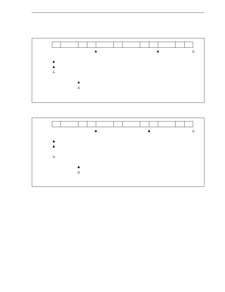
CHAPTER 18 SERIAL INTERFACE IIC0 (
µPD780078Y SUBSERIES ONLY)
385
User's Manual U14260EJ3V1UD
(d) When loss occurs due to restart condition during data transfer
(i)
Not extension code (Example: unmatches with SVA0, WTIM0 = 1)
ST
AD6-AD0
RW
AK
D7-Dn
ST
AD6-AD0
RW
AK
D7-D0
AK
SP
1
2
3
1 : IICS0 = 1000
◊110B
2 : IICS0 = 01000110B (Example When ALD0 is read during interrupt servicing)
3 : IICS0 = 00000001B
Remark
: Always generated
: Generated only when SPIE0 = 1
◊ : Don't care
n = 6 to 0
(ii) Extension code
ST
AD6-AD0
RW
AK
D7-Dn
ST
AD6-AD0
RW
AK
D7-D0
AK
SP
1
2
3
1 : IICS0 = 1000
◊110B
2 : IICS0 = 0110
◊010B (Example When ALD0 is read during interrupt servicing)
Sets LREL0 = 1 by software
3 : IICS0 = 00000001B
Remark
: Always generated
: Generated only when SPIE0 = 1
◊ : Don't care
n = 6 to 0
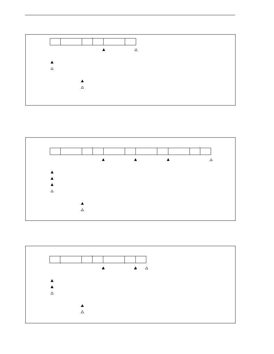
CHAPTER 18 SERIAL INTERFACE IIC0 (
µPD780078Y SUBSERIES ONLY)
386
User's Manual U14260EJ3V1UD
(e) When loss occurs due to stop condition during data transfer
ST
AD6-AD0
RW
AK
D7-Dn
SP
1
2
1 : IICS0 = 1000
◊110B
2 : IICS0 = 01000001B
Remark
: Always generated
: Generated only when SPIE0 = 1
◊ : Don't care
n = 6 to 0
(f)
When arbitration loss occurs due to low-level data when attempting to generate a restart condition
(i)
When WTIM0 = 1
ST
AD6-AD0
RW
AK
D7-D0
AK
D7-D0
AK
D7-D0
AK
SP
1
2
3
4
1 : IICS0 = 1000
◊110B
2 : IICS0 = 1000
◊100B (Sets STT0)
3 : IICS0 = 01000100B (Example When ALD0 is read during interrupt servicing)
4 : IICS0 = 00000001B
Remark
: Always generated
: Generated only when SPIE0 = 1
◊ : Don't care
(g) When arbitration loss occurs due to a stop condition when attempting to generate a restart condition
(i)
When WTIM0 = 1
ST
AD6-AD0
RW
AK
D7-D0
AK
SP
1
2
3
1 : IICS0 = 1000
◊110B
2 : IICS0 = 1000
◊◊00B (Sets STT0)
3 : IICS0 = 01000001B
Remark
: Always generated
: Generated only when SPIE0 = 1
◊ : Don't care
STT0 = 1
STT0 = 1

CHAPTER 18 SERIAL INTERFACE IIC0 (
µPD780078Y SUBSERIES ONLY)
387
User's Manual U14260EJ3V1UD
(h) When arbitration loss occurs due to low-level data when attempting to generate a stop condition
(i)
When WTIM0 = 1
ST
AD6-AD0
RW
AK
D7-D0
AK
D7-D0
AK
D7-D0
AK
SP
1
2
3
4
1 : IICS0 = 1000
◊110B
2 : IICS0 = 1000
◊◊00B (Sets SPT0)
3 : IICS0 = 01000000B (Example When ALD0 is read during interrupt servicing)
4 : IICS0 = 00000001B
Remark
: Always generated
: Generated only when SPIE0 = 1
◊ : Don't care
SPT0 = 1

CHAPTER 18 SERIAL INTERFACE IIC0 (
µPD780078Y SUBSERIES ONLY)
388
User's Manual U14260EJ3V1UD
18.6 Timing Charts
When using the I
2
C bus mode, the master device outputs an address via the serial bus to select one of several
slave devices as its communication partner.
After outputting the slave address, the master device transmits the TRC0 bit (bit 3 of IIC status register 0 (IICS0)),
which specifies the data transfer direction, and then starts serial communication with the slave device.
Figures 18-23 and 18-24 show timing charts of the data communication.
IIC shift register 0 (IIC0)'s shift operation is synchronized with the falling edge of the serial clock (SCL0). The
transmit data is transferred to the SO0 latch and is output (MSB first) via the SDA0 pin.
Data input via the SDA0 pin is captured into IIC0 at the rising edge of SCL0.
CHAPTER 18 SERIAL INTERFACE IIC0 (
µPD780078Y SUBSERIES ONLY)
389
User's Manual U14260EJ3V1UD
Figure 18-23. Example of Master to Slave Communication
(When 9-Clock Wait Is Selected for Both Master and Slave) (1/3)
(1) Start condition ~ address
Note To cancel slave wait, write "FFH" to IIC0 or set WREL0.
IIC0
ACKD0
STD0
SPD0
WTIM0
H
H
L
L
L
L
H
H
H
L
L
ACKE0
MSTS0
STT0
SPT0
WREL0
INTIIC0
TRC0
IIC0
ACKD0
STD0
SPD0
WTIM0
ACKE0
MSTS0
STT0
SPT0
WREL0
INTIIC0
TRC0
SCL0
SDA0
Processing by master device
Transfer lines
Processing by slave device
1
2
3
4
5
6
7
8
9
4
3
2
1
A6
A5
A4
A3
A2
A1
A0
W
ACK
D4
D5
D6
D7
IIC0
address
IIC0
data
IIC0
FFH
Transmit
Start condition
Receive
(When EXC0 = 1)
Note
Note

CHAPTER 18 SERIAL INTERFACE IIC0 (
µPD780078Y SUBSERIES ONLY)
390
User's Manual U14260EJ3V1UD
Figure 18-23. Example of Master to Slave Communication
(When 9-Clock Wait Is Selected for Both Master and Slave) (2/3)
(2) Data
Note To cancel slave wait, write "FFH" to IIC0 or set WREL0.
IIC0
ACKD0
STD0
SPD0
WTIM0
H
H
L
L
L
L
L
L
H
H
H
H
L
L
L
L
L
ACKE0
MSTS0
STT0
SPT0
WREL0
INTIIC0
TRC0
IIC0
ACKD0
STD0
SPD0
WTIM0
ACKE0
MSTS0
STT0
SPT0
WREL0
INTIIC0
TRC0
SCL0
SDA0
Processing by master device
Transfer lines
Processing by slave device
1
9
8
2
3
4
5
6
7
8
9
3
2
1
D7
D0
D6
D5
D4
D3
D2
D1
D0
D5
D6
D7
IIC0
data
IIC0
FFH Note
IIC0
FFH Note
IIC0
data
Transmit
Receive
Note
Note
CHAPTER 18 SERIAL INTERFACE IIC0 (
µPD780078Y SUBSERIES ONLY)
391
User's Manual U14260EJ3V1UD
Figure 18-23. Example of Master to Slave Communication
(When 9-Clock Wait Is Selected for Both Master and Slave) (3/3)
(3) Stop condition
Note To cancel slave wait, write "FFH" to IIC0 or set WREL0.
IIC0
ACKD0
STD0
SPD0
WTIM0
H
H
L
L
L
L
H
H
H
L
ACKE0
MSTS0
STT0
SPT0
WREL0
INTIIC0
TRC0
IIC0
ACKD0
STD0
SPD0
WTIM0
ACKE0
MSTS0
STT0
SPT0
WREL0
INTIIC0
TRC0
SCL0
SDA0
Processing by master device
Transfer lines
Processing by slave device
1
2
3
4
5
6
7
8
9
2
1
D7
D6
D5
D4
D3
D2
D1
D0
A5
A6
IIC0
data
IIC0
address
IIC0
FFH Note
IIC0
FFH Note
Stop
condition
Start
condition
Transmit
Note
Note
(When SPIE0 = 1)
Receive
(When SPIE0 = 1)
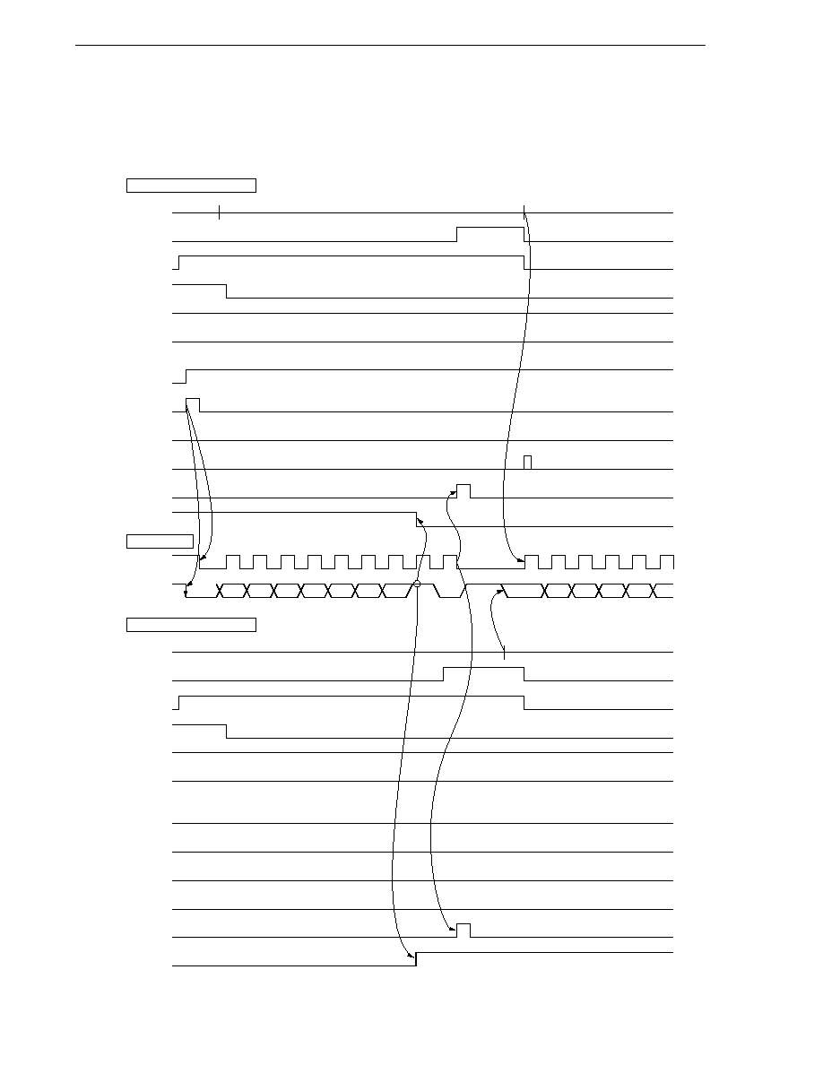
CHAPTER 18 SERIAL INTERFACE IIC0 (
µPD780078Y SUBSERIES ONLY)
392
User's Manual U14260EJ3V1UD
Figure 18-24. Example of Slave to Master Communication
(When 9-Clock Wait Is Selected for Both Master and Slave) (1/3)
(1) Start condition ~ address
Note To cancel master wait, write "FFH" to IIC0 or set WREL0.
IIC0
ACKD0
STD0
SPD0
WTIM0
H
H
L
L
H
H
L
ACKE0
MSTS0
STT0
L
L
SPT0
WREL0
INTIIC0
TRC0
IIC0
ACKD0
STD0
SPD0
WTIM0
ACKE0
MSTS0
STT0
SPT0
WREL0
INTIIC0
TRC0
SCL0
SDA0
Processing by master device
Transfer lines
Processing by slave device
1
2
3
4
5
6
7
8
9
4
5
6
3
2
1
A6
A5
A4
A3
A2
A1
A0
R
D4
D3
D2
D5
D6
D7
IIC0
address
IIC0
FFH Note
Note
IIC0
data
Start condition
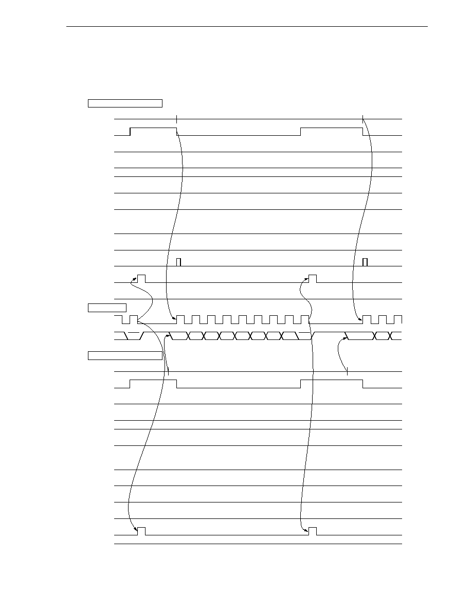
CHAPTER 18 SERIAL INTERFACE IIC0 (
µPD780078Y SUBSERIES ONLY)
393
User's Manual U14260EJ3V1UD
Figure 18-24. Example of Slave to Master Communication
(When 9-Clock Wait Is Selected for Both Master and Slave) (2/3)
(2) Data
Note To cancel master wait, write "FFH" to IIC0 or set WREL0.
IIC0
ACKD0
STD0
SPD0
WTIM0
H
H
H
L
L
L
L
L
L
H
H
H
L
L
L
L
L
ACKE0
MSTS0
STT0
SPT0
WREL0
INTIIC0
TRC0
IIC0
ACKD0
STD0
SPD0
WTIM0
ACKE0
MSTS0
STT0
SPT0
WREL0
INTIIC0
TRC0
SCL0
SDA0
Processing by master device
Transfer lines
Processing by slave device
1
8
9
2
3
4
5
6
7
8
9
3
2
1
D7
D0
ACK
D6
D5
D4
D3
D2
D1
D0
ACK
D5
D6
D7
Note
Note
Receive
Transmit
IIC0
data
IIC0
data
IIC0
FFH Note
IIC0
FFH Note
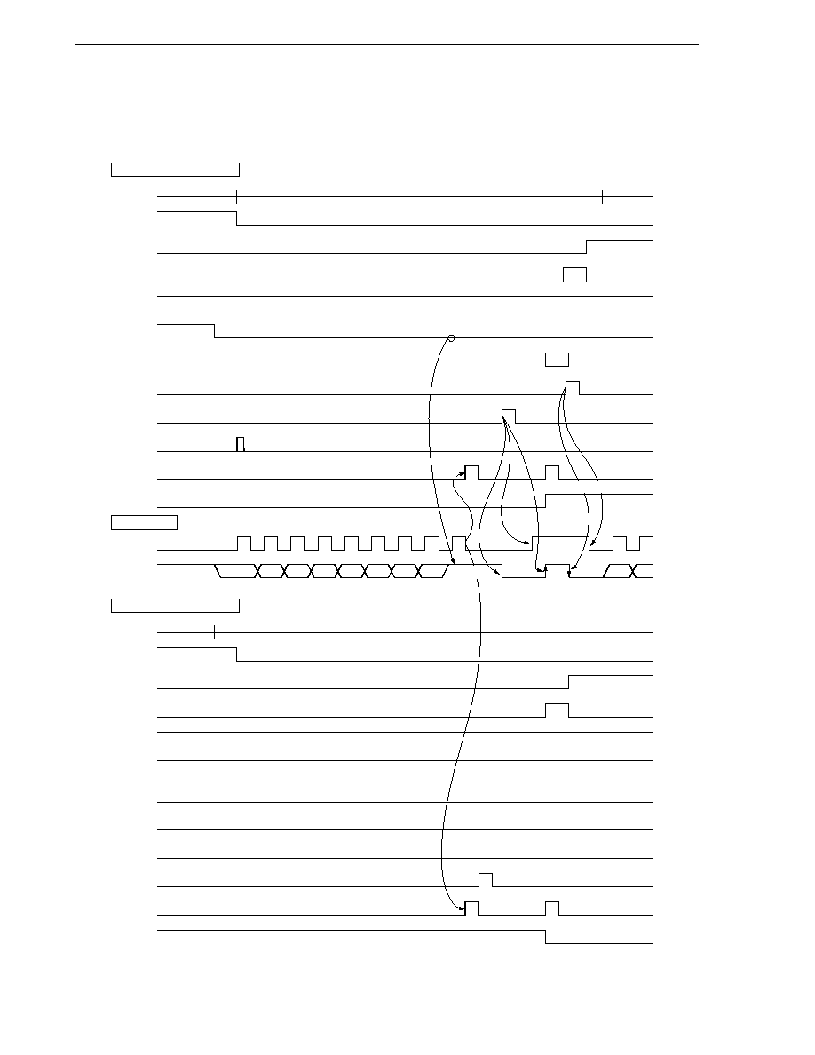
CHAPTER 18 SERIAL INTERFACE IIC0 (
µPD780078Y SUBSERIES ONLY)
394
User's Manual U14260EJ3V1UD
Figure 18-24. Example of Slave to Master Communication
(When 9-Clock Wait Is Selected for Both Master and Slave) (3/3)
(3) Stop condition
Note To cancel master wait, write "FFH" to IIC0 or set WREL0.
IIC0
ACKD0
STD0
SPD0
WTIM0
H
H
L
L
L
H
ACKE0
MSTS0
STT0
SPT0
WREL0
INTIIC0
TRC0
IIC0
ACKD0
STD0
SPD0
WTIM0
ACKE0
MSTS0
STT0
SPT0
WREL0
INTIIC0
TRC0
SCL0
SDA0
Processing by master device
Transfer lines
Processing by slave device
1
2
3
4
5
6
7
8
9
2
1
D7
D6
D5
D4
D3
D2
D1
D0
A5
A6
IIC0
address
IIC0
FFH Note
Note
IIC0
data
Stop
condition
Start
condition
(When SPIE0 = 1)
N
-ACK
(When SPIE0 = 1)

395
User's Manual U14260EJ3V1UD
CHAPTER 19 INTERRUPT FUNCTIONS
19.1 Interrupt Function Types
The following three types of interrupt functions are used.
(1) Non-maskable interrupts
A non-maskable interrupt is acknowledged even when interrupts are disabled. It does not undergo priority control
and is given top priority over all other interrupt requests. However, interrupt requests are held pending during
non-maskable interrupt servicing.
A non-maskable interrupt generates a standby release signal and releases the HALT mode during main system
clock operation.
The only non-maskable interrupt in the
µPD780078 Subseries is the interrupt from the watchdog timer.
(2) Maskable interrupts
These interrupts undergo mask control. Maskable interrupts can be divided into a high interrupt priority group
and a low interrupt priority group by setting the priority specification flag registers (PR0L, PR0H, PR1L).
High priority interrupts can be serviced preferentially to low priority interrupts (multiple interrupt servicing). If two
or more interrupts with the same priority are generated simultaneously, each interrupt has a predetermined priority
(see Table 19-1).
A standby release signal is generated and the STOP mode and HALT mode are released.
Five external interrupt requests and 18 internal interrupt requests (19 internal interrupt requests for the
µPD780078Y Subseries) are incorporated as maskable interrupts.
(3) Software interrupts
A software interrupt is a vectored interrupt that is generated by executing the BRK instruction. It is acknowledged
even when interrupts are disabled. A software interrupt does not undergo interrupt priority control.
19.2 Interrupt Sources and Configuration
A total of 25 interrupt sources (26 interrupt sources for the
µPD780078Y Subseries) exist among non-maskable,
maskable, and software interrupts (see Table 19-1).
Remark
A non-maskable interrupt or maskable interrupt (internal) can be selected as the watchdog timer interrupt
source (INTWDT).
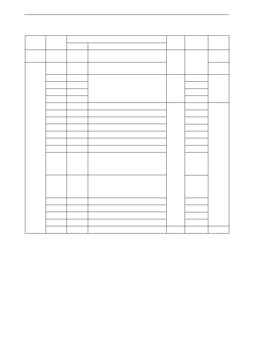
CHAPTER 19 INTERRUPT FUNCTIONS
396
User's Manual U14260EJ3V1UD
Table 19-1. Interrupt Source List (1/2)
Type of
Default
Interrupt Source
Internal/
Vector Table
Interrupt
Priority
Note 1
Name
Trigger
External
Address
Non-
--
INTWDT
Watchdog timer overflow (non-maskable
Internal
0004H
(A)
maskable
interrupt selected)
Maskable
0
INTWDT
Watchdog timer overflow (interval timer
(B)
selected)
1
INTP0
Pin input edge detection
External
0006H
(C)
2
INTP1
0008H
3
INTP2
000AH
4
INTP3
000CH
5
INTSER0
Generation of UART0 reception error
Internal
000EH
(B)
6
INTSR0
End of UART0 reception
0010H
7
INTST0
End of UART0 transmission
0012H
8
INTCSI1
End of CSI1 communication
0014H
9
INTCSI3
End of SIO3 communication
0016H
10
INTIIC0
Note 3
End of IIC0 communication
0018H
11
INTWTI
Reference time interval signal from watch timer
001AH
12
INTTM000
Match of TM00 and CR000
001CH
(when compare register is specified)
Detection of valid edge of TI010
(when capture register is specified)
13
INTTM010
Match of TM00 and CR010
001EH
(when compare register is specified)
Detection of valid edge of TI000
(when capture register is specified)
14
INTTM50
Match of TM50 and CR50
0020H
15
INTTM51
Match of TM51 and CR51
0022H
16
INTAD0
End of conversion by A/D converter
0024H
17
INTWT
Watch timer overflow
0026H
18
INTKR
Falling edge detection of port 4
External
0028H
(D)
Notes 1. The default priority is the priority order when two or more maskable interrupt requests are generated
simultaneously. 0 is the highest and 23 is the lowest.
2. Basic configuration types (A) to (E) correspond to (A) to (E) in Figure 19-1.
3.
µPD780078Y Subseries only.
Basic
Configuration
Type
Note 2

CHAPTER 19 INTERRUPT FUNCTIONS
397
User's Manual U14260EJ3V1UD
Table 19-1. Interrupt Source List (2/2)
Type of
Default
Interrupt Source
Internal/
Vector Table
Interrupt
Priority
Note 1
Name
Trigger
External
Address
Maskable
19
INTSER2
Generation of UART2 reception error
Internal
002AH
(B)
20
INTSR2
End of UART2 reception
002CH
21
INTST2
Note 3
End of UART2 transmission
Note 4
/data transfer
Note 5
002EH
22
INTTM001
Match of TM01 and CR001
0030H
(when compare register is specified)
Detection of valid edge of TI011
(when capture register is specified)
23
INTTM011
Match of TM01 and CR011
0032H
(when compare register is specified)
Detection of valid edge of TI001
(when capture register is specified)
Software
--
BRK
BRK instruction execution
--
003EH
(E)
Notes 1. The default priority is the priority order when two or more maskable interrupt requests are generated
simultaneously. 0 is the highest and 23 is the lowest.
2. Basic configuration types (A) to (E) correspond to (A) to (E) in Figure 19-1.
3. Interrupt sources can be selected by the transmit interrupt signal select flag (ISMD2).
4. An interrupt request signal is generated when all the data in transmit buffer register 2 (TXB2) has been
transmitted.
5. An interrupt request signal is generated when data transfer is completed from TXB2 to the transmit shift
register (TXS2).
Basic
Configuration
Type
Note 2
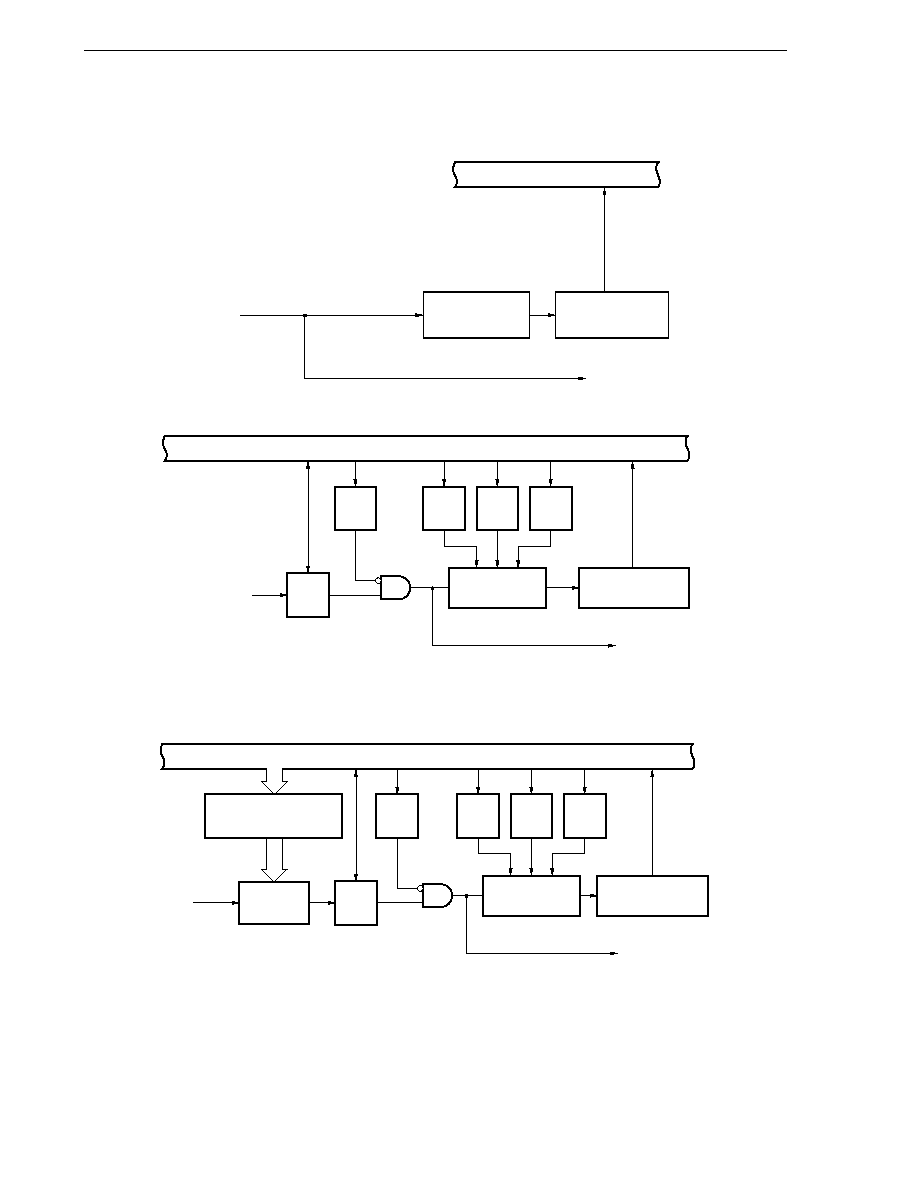
CHAPTER 19 INTERRUPT FUNCTIONS
398
User's Manual U14260EJ3V1UD
Figure 19-1. Basic Configuration of Interrupt Function (1/2)
(A) Internal non-maskable interrupt
(B) Internal maskable interrupt
(C) External maskable interrupt (INTP0 to INTP3)
Internal bus
Interrupt
request
Priority controller
Vector table
address generator
Standby release signal
Internal bus
Interrupt
request
IF
MK
IE
PR
ISP
Priority
controller
Vector table
address generator
Standby release signal
Internal bus
Interrupt
request
IF
MK
IE
PR
ISP
Priority
controller
Vector table
address generator
Standby release signal
External interrupt edge
enable register
(EGP, EGN)
Edge
detector
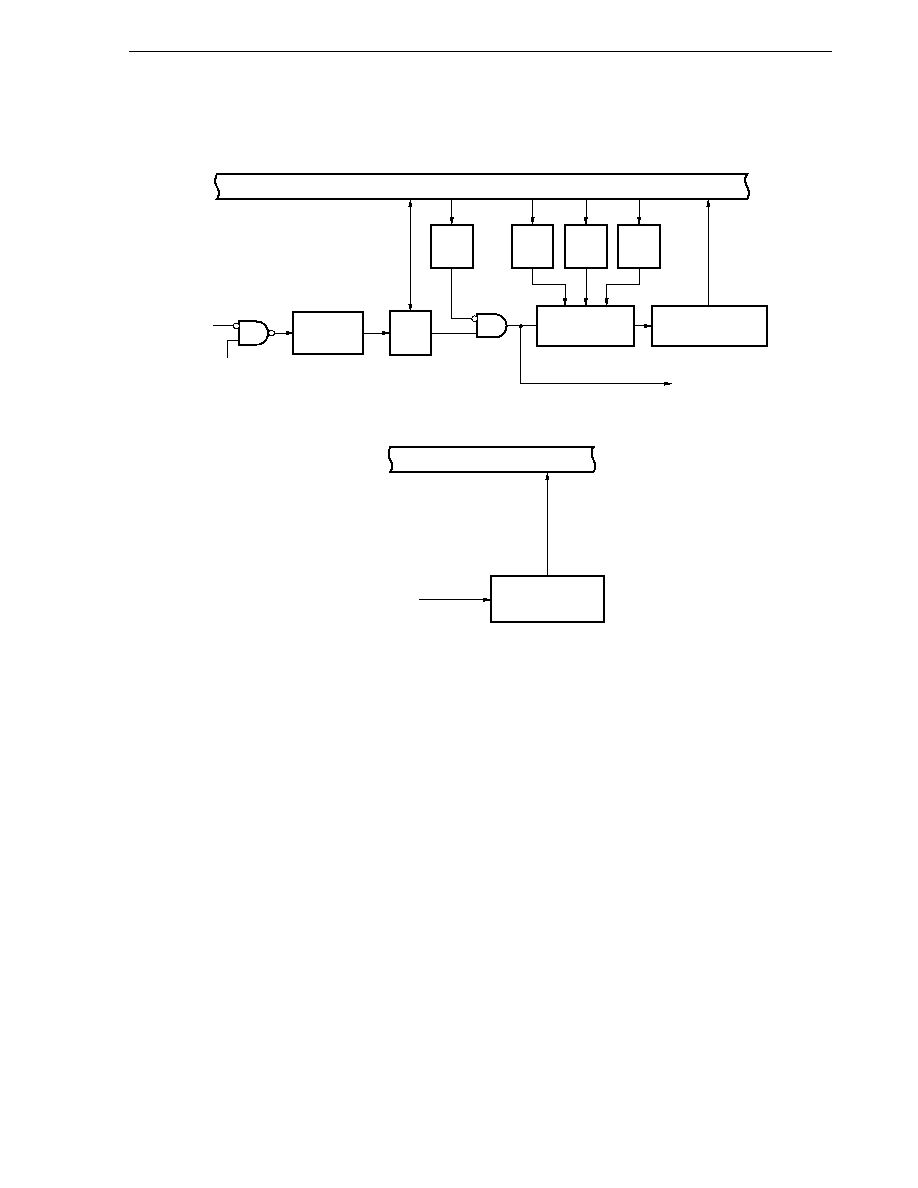
CHAPTER 19 INTERRUPT FUNCTIONS
399
User's Manual U14260EJ3V1UD
Figure 19-1. Basic Configuration of Interrupt Function (2/2)
(D) External maskable interrupt (INTKR)
(E) Software interrupt
IF:
Interrupt request flag
IE:
Interrupt enable flag
ISP:
In-service priority flag
MK:
Interrupt mask flag
PR:
Priority specification flag
MEM: Memory expansion mode register
IF
MK
IE
PR
ISP
Internal bus
Interrupt
request
Priority
controller
Vector table
address generator
Standby release signal
Falling
edge
detector
1 when MEM = 01H
Internal bus
Interrupt
request
Vector table
address generator

CHAPTER 19 INTERRUPT FUNCTIONS
400
User's Manual U14260EJ3V1UD
19.3 Interrupt Function Control Registers
The following 6 types of registers are used to control the interrupt functions.
∑
Interrupt request flag register (IF0L, IF0H, IF1L)
∑
Interrupt mask flag register (MK0L, MK0H, MK1L)
∑
Priority specification flag register (PR0L, PR0H, PR1L)
∑
External interrupt rising edge enable register (EGP)
∑
External interrupt falling edge enable register (EGN)
∑
Program status word (PSW)
Table 19-2 gives a list of interrupt request flags, interrupt mask flags, and priority specification flags corresponding
to interrupt request sources.
Table 19-2. Flags Corresponding to Interrupt Request Sources
Interrupt Source
Interrupt Request Flag
Interrupt Mask Flag
Priority Specification Flag
Register
Register
Register
INTWDT
WDTIF
Note 1
IF0L
WDTMK
Note 1
MK0L
WDTPR
Note 1
PR0L
INTP0
PIF0
PMK0
PPR0
INTP1
PIF1
PMK1
PPR1
INTP2
PIF2
PMK2
PPR2
INTP3
PIF3
PMK3
PPR3
INTSER0
SERIF0
SERMK0
SERPR0
INTSR0
SRIF0
SRMK0
SRPR0
INTST0
STIF0
STMK0
STPR0
INTCSI1
CSIIF1
IF0H
CSIMK1
MK0H
CSIPR1
PR0H
INTCSI3
CSIIF3
CSIMK3
CSIPR3
INTIIC0
Note 2
IICIF0
Note 2
IICMK0
Note 2
IICPR0
Note 2
INTWTI
WTIIF0
WTIMK0
WTIPR0
INTTM000
TMIF000
TMMK000
TMPR000
INTTM010
TMIF010
TMMK010
TMPR010
INTTM50
TMIF50
TMMK50
TMPR50
INTTM51
TMIF51
TMMK51
TMPR51
INTAD0
ADIF0
IF1L
ADMK0
MK1L
ADPR0
PR1L
INTWT
WTIF
WTMK
WTPR
INTKR
KRIF
KRMK
KRPR
INTSER2
SERIF2
SERMK2
SERPR2
INTSR2
SRIF2
SRMK2
SRPR2
INTST2
STIF2
STMK2
STPR2
INTTM001
TMIF001
TMMK001
TMPR001
INTTM011
TMIF011
TMMK011
TMPR011
Notes 1. Interrupt control flag when watchdog timer is used as interval timer
2.
µPD780078Y Subseries only
CHAPTER 19 INTERRUPT FUNCTIONS
401
User's Manual U14260EJ3V1UD
(1) Interrupt request flag registers (IF0L, IF0H, IF1L)
An interrupt request flag is set to 1 when the corresponding interrupt request is generated or an instruction is
executed. It is cleared to 0 when an instruction is executed upon acknowledgment of an interrupt request or upon
RESET input.
When an interrupt is acknowledged, the interrupt request flag is automatically cleared, and then the interrupt
routine is executed.
IF0L, IF0H, and IF1L are set by a 1-bit or 8-bit memory manipulation instruction. When IF0L and IF0H are
combined to form 16-bit register IF0, they are read by a 16-bit memory manipulation instruction.
RESET input clears IF0L, IF0H, and IF1L to 00H.
Figure 19-2. Format of Interrupt Request Flag Register (IF0L, IF0H, IF1L)
Address: FFE0H After reset: 00H R/W
Symbol
7
6
5
4
3
2
1
0
IF0L
STIF0
SRIF0
SERIF0
PIF3
PIF2
PIF1
PIF0
WDTIF
Address: FFE1H After reset: 00H R/W
Symbol
7
6
5
4
3
2
1
0
IF0H
TMIF51
TMIF50
TMIF010
TMIF000
WTIIF0
IICIF0
Note
CSIIF3
CSIIF1
Address: FFE2H After reset: 00H R/W
Symbol
7
6
5
4
3
2
1
0
IF1L
TMIF011
TMIF001
STIF2
SRIF2
SERIF2
KRIF
WTIF
ADIF0
XXIFX
Interrupt request flag
0
No interrupt request signal is generated
1
Interrupt request signal is generated, interrupt request status
Note
Incorporated only in the
µPD780078Y Subseries. Be sure to set 0 for the µPD780078 Subseries.
Cautions 1. The WDTIF flag is R/W enabled only when the watchdog timer is used as an interval timer.
If watchdog timer mode 1 is used, set the WDTIF flag to 0.
2. When operating a timer, serial interface, or A/D converter after standby release, operate it
after clearing the interrupt request flag, because interrupt request flags may be set by noise.
3. When manipulating a flag of the interrupt request flag register, use a 1-bit memory
manipulation instruction (CLR1). When describing in C language, use a bit manipulation
instruction such as "IF0L.0 = 0;" or "_asm("clr1 IF0L, 0");" because the compiled assembler
must be a 1-bit memory manipulation instruction (CLR1).
If a program is described in C language using an 8-bit memory manipulation instruction
such as "IF0L &= 0xfe;" and compiled, it becomes the assembler of three instructions.
mov a, IF0L
and a, #0FEH
mov IF0L, a
In this case, even if the request flag of another bit of the same interrupt request flag register
(IF0L) is set to 1 at the timing between "mov a, IF0L" and "mov IF0L, a", the flag is cleared
to 0 at "mov IF0L, a". Therefore, care must be exercised when using an 8-bit memory
manipulation instruction in C language.

CHAPTER 19 INTERRUPT FUNCTIONS
402
User's Manual U14260EJ3V1UD
(2) Interrupt mask flag registers (MK0L, MK0H, MK1L)
The interrupt mask flags are used to enable/disable the corresponding maskable interrupt servicing.
MK0L, MK0H, and MK1L are set by a 1-bit or 8-bit memory manipulation instruction. When MK0L and MK0H
are combined to form 16-bit register MK0, they are set by a 16-bit memory manipulation instruction.
RESET input sets MK0L, MK0H, and MK1L to FFH.
Figure 19-3. Format of Interrupt Mask Flag Register (MK0L, MK0H, MK1L)
Address: FFE4H After reset: FFH R/W
Symbol
7
6
5
4
3
2
1
0
MK0L
STMK0
SRMK0
SERMK0
PMK3
PMK2
PMK1
PMK0
WDTMK
Address: FFE5H After reset: FFH R/W
Symbol
7
6
5
4
3
2
1
0
MK0H
TMMK51
TMMK50
TMMK010
TMMK000
WTIMK0
IICMK0
Note
CSIMK3
CSIMK1
Address: FFE6H After reset: FFH R/W
Symbol
7
6
5
4
3
2
1
0
MK1L
TMMK011
TMMK001
STMK2
SRMK2
SERMK2
KRMK
WTMK
ADMK0
XXMKX
Interrupt servicing control
0
Interrupt servicing enabled
1
Interrupt servicing disabled
Note
Incorporated only in the
µPD780078Y Subseries. Be sure to set 1 for the µPD780078 Subseries.
Cautions 1. If the watchdog timer is used in watchdog timer mode 1, the contents of the WDTMK flag
become undefined when read.
2. Because port 0 pins have an alternate function as external interrupt request inputs, when
the output level is changed by specifying the output mode of the port function, an interrupt
request flag is set. Therefore, the interrupt mask flag should be set to 1 before using the
output mode.
CHAPTER 19 INTERRUPT FUNCTIONS
403
User's Manual U14260EJ3V1UD
(3) Priority specification flag registers (PR0L, PR0H, PR1L)
The priority specification flag registers are used to set the corresponding maskable interrupt priority order.
PR0L, PR0H, and PR1L are set by a 1-bit or 8-bit memory manipulation instruction. If PR0L and PR0H are
combined to form 16-bit register PR0, they are set by a 16-bit memory manipulation instruction.
RESET input sets PR0L, PR0H, and PR1L to FFH.
Figure 19-4. Format of Priority Specification Flag Register (PR0L, PR0H, PR1L)
Address: FFE8H After reset: FFH R/W
Symbol
7
6
5
4
3
2
1
0
PR0L
STPR0
SRPR0
SERPR0
PPR3
PPR2
PPR1
PPR0
WDTPR
Address: FFE9H After reset: FFH R/W
Symbol
7
6
5
4
3
2
1
0
PR0H
TMPR51
TMPR50
TMPR010
TMPR000
WTIPR0
IICPR0
Note
CSIPR3
CSIPR1
Address: FFEAH After reset: FFH R/W
Symbol
7
6
5
4
3
2
1
0
PR1L
TMPR011
TMPR001
STPR2
SRPR2
SERPR2
KRPR
WTPR
ADPR0
XXPRX
Priority level selection
0
High priority level
1
Low priority level
Note
Incorporated only in the
µPD780078Y Subseries. Be sure to set 1 for the µPD780078 Subseries.
Caution
When the watchdog timer is used in watchdog timer mode 1, set the WDTPR flag to 1.

CHAPTER 19 INTERRUPT FUNCTIONS
404
User's Manual U14260EJ3V1UD
(4) External interrupt rising edge enable register (EGP), external interrupt falling edge enable register (EGN)
These registers specify the valid edge for INTP0 to INTP3.
EGP and EGN are set by a 1-bit or 8-bit memory manipulation instruction.
RESET input clears EGP and EGN to 00H.
Figure 19-5. Format of External Interrupt Rising Edge Enable Register (EGP) and
External Interrupt Falling Edge Enable Register (EGN)
Address: FF48H After reset: 00H R/W
Symbol
7
6
5
4
3
2
1
0
EGP
0
0
0
0
EGP3
EGP2
EGP1
EGP0
Address: FF49H After reset: 00H R/W
Symbol
7
6
5
4
3
2
1
0
EGN
0
0
0
0
EGN3
EGN2
EGN1
EGN0
EGPn
EGNn
INTPn pin valid edge selection (n = 0 to 3)
0
0
Edge detection disabled
0
1
Falling edge
1
0
Rising edge
1
1
Both rising and falling edges
Table 19-3 shows the ports corresponding to EGPn and EGNn.
Table 19-3. Ports Corresponding to EGPn and EGNn
Detection Enable Register
Edge Detection Port
Interrupt Request Signal
EGP0
EGN0
P00
INTP0
EGP1
EGN1
P01
INTP1
EGP2
EGN2
P02
INTP2
EGP3
EGN3
P03
INTP3
Caution When the function is switched from external interrupt request to port, edge detection
may be performed. Therefore, clear EGPn and EGNn to 0 before switching to the port
mode.
Remark
n = 0 to 3

CHAPTER 19 INTERRUPT FUNCTIONS
405
User's Manual U14260EJ3V1UD
(5) Program status word (PSW)
The program status word is a register used to hold the instruction execution results and the current status for
an interrupt request. An IE flag to set maskable interrupt enable/disable and an ISP flag to control nesting
processing are mapped to the PSW.
Besides 8-bit read/write, this register can be operated by bit manipulation and dedicated (EI and DI) instructions.
When a vectored interrupt request is acknowledged, if the BRK instruction is executed, the contents of the PSW
are automatically saved into a stack and the IE flag is reset to 0. If a maskable interrupt request is acknowledged,
the contents of the priority specification flag of the acknowledged interrupt are transferred to the ISP flag. The
PSW contents are also saved into the stack with the PUSH PSW instruction. They are reset from the stack with
the RETI, RETB, and POP PSW instructions.
RESET input sets PSW to 02H.
Figure 19-6. Format of Program Status Word
7
IE
6
Z
5
RBS1
4
AC
3
RBS0
2
0
1
ISP
0
CY
PSW
After reset
02H
ISP
High-priority interrupt servicing (low-priority
interrupts disabled)
IE
0
1
Disable
Priority of interrupt currently being serviced
Interrupt request acknowledgment enable/disable
Used when normal instruction is executed
Enable
Interrupt request not acknowledged, or low-
priority interrupt servicing (all maskable
interrupts enabled)
0
1

CHAPTER 19 INTERRUPT FUNCTIONS
406
User's Manual U14260EJ3V1UD
19.4 Interrupt Servicing Operations
19.4.1 Non-maskable interrupt request acknowledgment operation
A non-maskable interrupt request is unconditionally acknowledged even in an interrupt acknowledgment disabled
state. It does not undergo interrupt priority control and has the highest priority of all interrupts.
If a non-maskable interrupt request is acknowledged, the contents are saved into the stacks in the order of PSW,
then PC, the IE flag and ISP flag are reset (0), and the contents of the vector table are loaded into the PC and branched.
This disables the acknowledgment of multiple interrupts.
A new non-maskable interrupt request generated during execution of a non-maskable interrupt servicing program
is acknowledged after the current non-maskable interrupt servicing program is terminated (following RETI instruction
execution) and one main routine instruction has been executed. However, if a new non-maskable interrupt request
is generated twice or more during non-maskable interrupt servicing program execution, only one non-maskable
interrupt request is acknowledged after termination of the non-maskable interrupt servicing program.
Figures 19-7, 19-8, and 19-9 show the flowchart of non-maskable interrupt request generation through
acknowledgment, the acknowledgment timing of a non-maskable interrupt request, and the acknowledgment
operation when multiple non-maskable interrupt requests are generated, respectively.
Caution Be sure to use the RETI instruction to restore processing from the non-maskable interrupt.
CHAPTER 19 INTERRUPT FUNCTIONS
407
User's Manual U14260EJ3V1UD
Figure 19-7. Flowchart of Non-Maskable Interrupt Request Generation to Acknowledgment
Figure 19-8. Non-Maskable Interrupt Request Acknowledgment Timing
Start
WDTM4 = 1
(with watchdog timer
mode selected)?
Overflow in WDT?
WDT interrupt
servicing?
Interrupt
control register not
accessed?
Interval timer
No
Reset processing
No
Interrupt request generation
Start of interrupt servicing
Interrupt request held pending
No
No
No
Yes
Yes
Yes
Yes
Yes
WDTM: Watchdog timer mode register
WDT: Watchdog timer
WDTM3 = 0
(with non-maskable
interrupt selected)?
Instruction
Instruction
PSW, PC save, jump
to interrupt servicing
Interrupt service
program
CPU processing
WDTIF
Interrupt request generated during this interval is acknowledged at .
WDTIF: Watchdog timer interrupt request flag
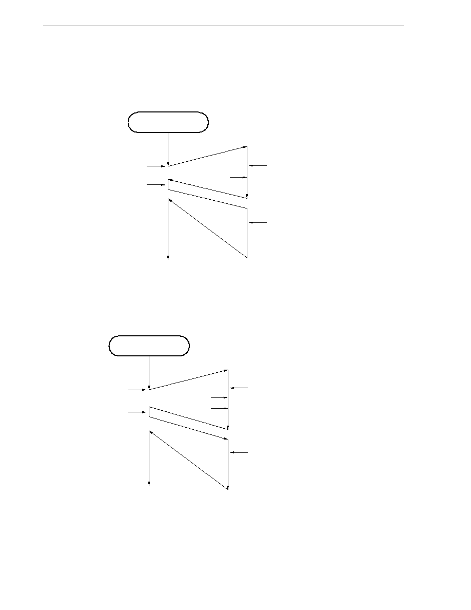
CHAPTER 19 INTERRUPT FUNCTIONS
408
User's Manual U14260EJ3V1UD
Figure 19-9. Non-Maskable Interrupt Request Acknowledgment Operation
(a) If a non-maskable interrupt request is generated during non-maskable interrupt servicing program
execution
(b) If two non-maskable interrupt requests are generated during non-maskable interrupt servicing program
execution
Main routine
NMI request <1>
Execution of 1 instruction
NMI request <2>
Execution of NMI request <1>
NMI request <2> held pending
Servicing of pending NMI request <2>
Main routine
NMI request <1>
Execution of 1 instruction
Execution of NMI request <1>
NMI request <2> held pending
NMI request <3> held pending
Servicing of pending NMI request <2>
NMI request <3> not acknowledged
(Although two or more NMI requests have been generated,
only one request is acknowledged.)
NMI request <2>
NMI request <3>

CHAPTER 19 INTERRUPT FUNCTIONS
409
User's Manual U14260EJ3V1UD
19.4.2 Maskable interrupt request acknowledgment operation
A maskable interrupt request becomes acknowledgeable when an interrupt request flag is set to 1 and the mask
(MK) flag corresponding to that interrupt request is cleared to 0. A vectored interrupt request is acknowledged if
interrupts are enabled (when the IE flag is set to 1). However, a low-priority interrupt request is not acknowledged
during servicing of a higher priority interrupt request (when the ISP flag is reset to 0).
Moreover, even if the EI instruction is executed during execution of a non-maskable interrupt servicing program,
neither non-maskable interrupt requests nor maskable interrupt requests are acknowledged.
The times from generation of a maskable interrupt request until interrupt servicing is performed are listed in Table
19-4 below.
For the interrupt request acknowledgment timing, see Figures 19-11 and 19-12.
Table 19-4. Times from Generation of Maskable Interrupt Request Until Servicing
Minimum Time
Maximum Time
Note
When
◊◊PR = 0
7 clocks
32 clocks
When
◊◊PR = 1
8 clocks
33 clocks
Note If an interrupt request is generated just before a divide instruction, the wait time becomes longer.
Remark
1 clock: 1/f
CPU
(f
CPU
: CPU clock)
If two or more maskable interrupt requests are generated simultaneously, the request with a higher priority level
specified by the priority specification flag is acknowledged first. If two or more interrupt requests have the same priority
level, the request with the highest default priority is acknowledged first.
An interrupt request that is held pending is acknowledged when it becomes acknowledgeable.
Figure 19-10 shows the interrupt request acknowledgment algorithm.
If a maskable interrupt request is acknowledged, the contents are saved into the stacks in the order of PSW, then
PC, the IE flag is reset (0), and the contents of the priority specification flag corresponding to the acknowledged
interrupt are transferred to the ISP flag. Further, the vector table data determined for each interrupt request is loaded
into the PC and branched.
Return from an interrupt is possible using the RETI instruction.
CHAPTER 19 INTERRUPT FUNCTIONS
410
User's Manual U14260EJ3V1UD
Figure 19-10. Interrupt Request Acknowledgment Processing Algorithm
◊◊IF:
Interrupt request flag
◊◊MK: Interrupt mask flag
◊◊PR: Priority specification flag
IE:
Flag that controls acknowledgment of maskable interrupt requests (1 = Enable, 0 = Disable)
ISP:
Flag that indicates the priority level of the interrupt currently being serviced (0 = High-priority interrupt
servicing, 1 = No interrupt request received, or low-priority interrupt servicing)
Start
◊◊IF = 1?
◊◊MK = 0?
◊◊PR = 0?
IE = 1?
ISP = 1?
Interrupt request held pending
Yes
Yes
No
No
Yes (Interrupt request generation)
Yes
No (Low priority)
No
No
Yes
Yes
No
IE = 1?
No
Any high-priority
interrupt request among those
simultaneously generated
with
◊◊PR = 0?
Yes (High priority)
No
Yes
Yes
No
Vectored interrupt servicing
Interrupt request held pending
Interrupt request held pending
Interrupt request held pending
Interrupt request held pending
Interrupt request held pending
Interrupt request held pending
Vectored interrupt servicing
Any high-priority
interrupt request among
those simultaneously
generated?
Any interrupt
request among those
simultaneously generated
with
◊◊PR = 0?
CHAPTER 19 INTERRUPT FUNCTIONS
411
User's Manual U14260EJ3V1UD
Figure 19-11. Interrupt Request Acknowledgment Timing (Minimum Time)
Remark
1 clock: 1/f
CPU
(f
CPU
: CPU clock)
Figure 19-12. Interrupt Request Acknowledgment Timing (Maximum Time)
Remark
1 clock: 1/f
CPU
(f
CPU
: CPU clock)
19.4.3 Software interrupt request acknowledgment operation
A software interrupt request is acknowledged by BRK instruction execution. Software interrupts cannot be disabled.
If a software interrupt request is acknowledged, the contents are saved into the stacks in the order of the program
status word (PSW), then program counter (PC), the IE flag is reset (0), and the contents of the vector table (003EH,
003FH) are loaded into the PC and branched.
Return from a software interrupt is possible with the RETB instruction.
Caution
Do not use the RETI instruction for returning from a software interrupt.
8 clocks
7 clocks
Instruction
Instruction
PSW and PC save,
jump to interrupt
servicing
Interrupt servicing
program
CPU processing
◊◊IF
(
◊◊PR = 1)
◊◊IF
(
◊◊PR = 0)
6 clocks
33 clocks
32 clocks
Instruction
Divide instruction
PSW and PC save,
jump to interrupt
servicing
Interrupt servicing
program
CPU processing
◊◊IF
(
◊◊PR = 1)
◊◊IF
(
◊◊PR = 0)
6 clocks
25 clocks
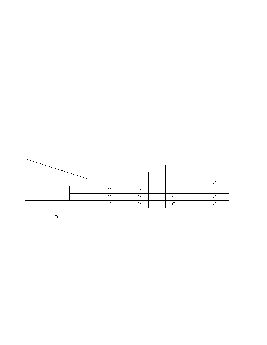
CHAPTER 19 INTERRUPT FUNCTIONS
412
User's Manual U14260EJ3V1UD
19.4.4 Multiple interrupt servicing
Multiple interrupt servicing occurs when an interrupt request is acknowledged during execution of another interrupt.
Multiple interrupt servicing does not occur unless the interrupt request acknowledgment enable state is selected
(IE = 1) (except non-maskable interrupts). When an interrupt request is received, interrupt request acknowledgment
becomes disabled (IE = 0). Therefore, to enable multiple interrupt servicing, it is necessary to set (1) the IE flag with
the EI instruction during interrupt servicing to enable interrupt acknowledgment.
Moreover, even if interrupts are enabled, multiple interrupt servicing may not be enabled, this being subject to
interrupt priority control. Two types of priority control are available: default priority control and programmable priority
control. Programmable priority control is used for multiple interrupt servicing.
In the interrupt enabled state, if an interrupt request with a priority equal to or higher than that of the interrupt
currently being serviced is generated, it is acknowledged for multiple interrupt servicing. If an interrupt with a priority
lower than that of the interrupt currently being serviced is generated during interrupt servicing, it is not acknowledged
for multiple interrupt servicing.
Interrupt requests that are not enabled because of the interrupt disabled state or they have a lower priority are
held pending. When servicing of the current interrupt ends, the pending interrupt request is acknowledged following
execution of at least one main processing instruction.
Multiple interrupt servicing is not possible during non-maskable interrupt servicing.
Table 19-5 shows relationship between interrupt requests enabled for multiple interrupt servicing and Figure 19-
13 shows multiple interrupt servicing examples.
Table 19-5. Relationship Between Interrupt Requests Enabled for Multiple Interrupt Servicing
Multiple Interrupt
Non-Maskable
Maskable Interrupt Request
Software
Request
Interrupt Request
PR = 0
PR = 1
Interrupt
Interrupt Being Serviced
IE = 1
IE = 0
IE = 1
IE = 0
Request
Non-maskable interrupt
◊
◊
◊
◊
◊
Maskable interrupt
ISP = 0
◊
◊
◊
ISP = 1
◊
◊
Software interrupt
◊
◊
Remarks 1.
: Multiple interrupt servicing enabled
2.
◊: Multiple interrupt servicing disabled
3. ISP and IE are flags contained in the PSW.
ISP = 0: An interrupt with higher priority is being serviced.
ISP = 1: No interrupt request has been acknowledged, or an interrupt with a lower priority is being
serviced.
IE = 0:
Interrupt request acknowledgment is disabled.
IE = 1:
Interrupt request acknowledgment is enabled.
4. PR is a flag contained in PR0L, PR0H, and PR1L.
PR = 0: Higher priority level
PR = 1: Lower priority level
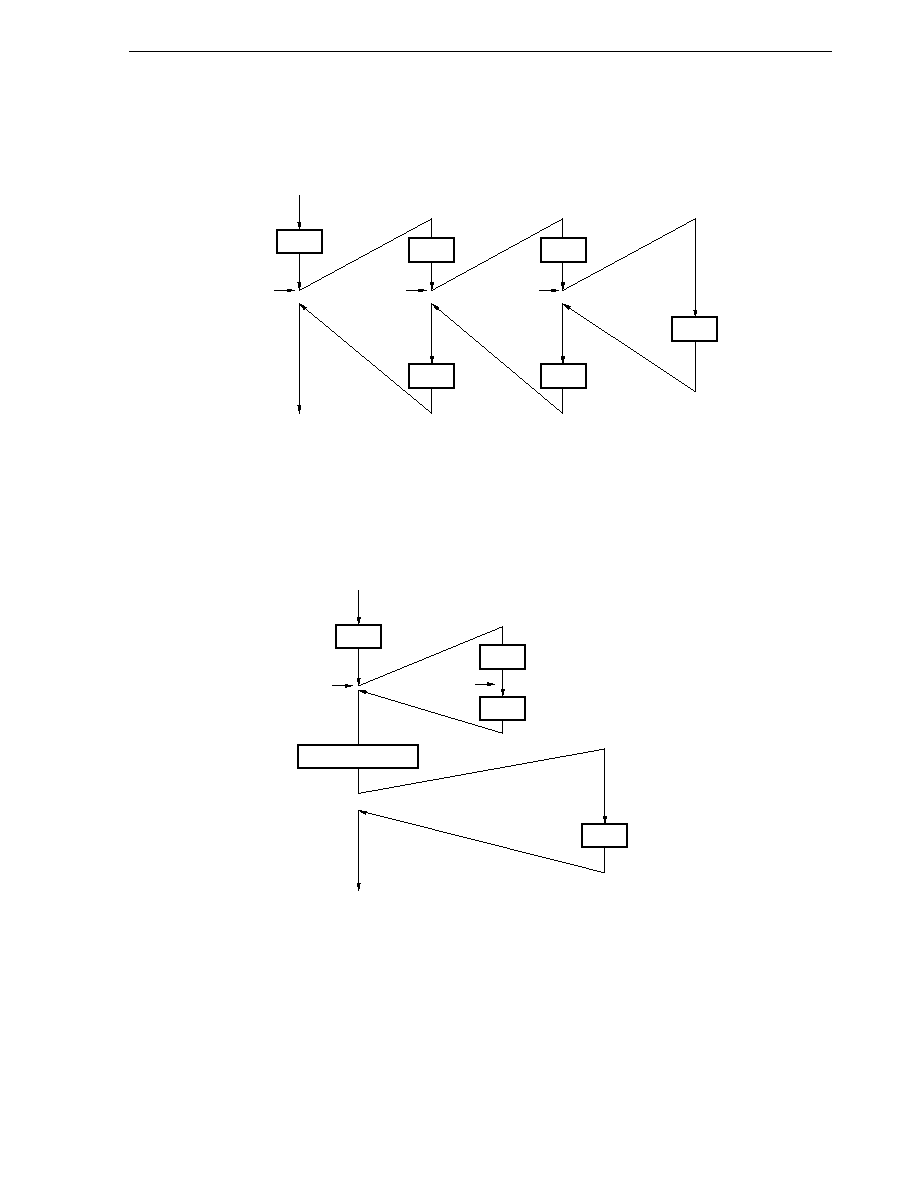
CHAPTER 19 INTERRUPT FUNCTIONS
413
User's Manual U14260EJ3V1UD
Figure 19-13. Examples of Multiple Interrupt Servicing (1/2)
Example 1. Multiple interrupt servicing occurs twice
During servicing of interrupt INTxx, two interrupt requests, INTyy and INTzz, are acknowledged, and multiple
interrupt servicing takes place. Before each interrupt request is acknowledged, the EI instruction must always be
issued to enable interrupt request acknowledgment.
Example 2. Nesting does not occur due to priority control
Interrupt request INTyy issued during servicing of interrupt INTxx is not acknowledged because its priority is lower
than that of INTxx, and multiple interrupt servicing does not take place. The INTyy interrupt request is held pending,
and is acknowledged following execution of one main processing instruction.
PR = 0:
Higher priority level
PR = 1:
Lower priority level
IE = 0:
Interrupt request acknowledgment disabled
Main processing
INTxx servicing
INTyy servicing
INTzz servicing
EI
EI
EI
RETI
RETI
RETI
INTxx
(PR = 1)
INTyy
(PR = 0)
INTzz
(PR = 0)
IE = 0
IE = 1
IE = 1
IE = 1
IE = 0
IE = 0
Main processing
INTxx servicing
INTyy servicing
INTxx
(PR = 0)
INTyy
(PR = 1)
EI
RETI
IE = 0
IE = 1
IE = 1
IE = 0
EI
1 instruction execution
RETI

CHAPTER 19 INTERRUPT FUNCTIONS
414
User's Manual U14260EJ3V1UD
Figure 19-13. Examples of Multiple Interrupt Servicing (2/2)
Example 3. Multiple interrupt servicing does not occur because interrupts are not enabled
Interrupts are not enabled during servicing of interrupt INTxx (EI instruction is not issued), so interrupt request INTyy
is not acknowledged and multiple interrupt servicing does not take place. The INTyy interrupt request is held pending,
and is acknowledged following execution of one main processing instruction.
PR = 0:
Higher priority level
IE = 0:
Interrupt request acknowledgment disabled
Main processing
INTxx servicing INTyy servicing
EI
1 instruction execution
RETI
RETI
INTxx
(PR = 0)
INTyy
(PR = 0)
IE = 0
IE = 1
IE = 1
IE = 0

CHAPTER 19 INTERRUPT FUNCTIONS
415
User's Manual U14260EJ3V1UD
19.4.5 Interrupt request hold
There are instructions where, even if an interrupt request is issued for them while another instruction is being
executed, request acknowledgment is held pending until the end of execution of the next instruction. These
instructions (interrupt request hold instructions) are listed below.
∑
MOV PSW, #byte
∑
MOV A, PSW
∑
MOV PSW, A
∑
MOV1 PSW. bit, CY
∑
MOV1 CY, PSW. bit
∑
AND1 CY, PSW. bit
∑
OR1 CY, PSW. bit
∑
XOR1 CY, PSW. bit
∑
SET1 PSW. bit
∑
CLR1 PSW. bit
∑
RETB
∑
RETI
∑
PUSH PSW
∑
POP PSW
∑
BT PSW. bit, $addr16
∑
BF PSW. bit, $addr16
∑
BTCLR PSW. bit, $addr16
∑
EI
∑
DI
∑
Manipulation instructions for the IF0L, IF0H, IF1L, MK0L, MK0H, MK1L, PR0L, PR0H, and PR1L registers
Caution
The BRK instruction is not one of the above-listed interrupt request hold instructions. However,
the software interrupt activated by executing the BRK instruction causes the IE flag to be cleared
to 0. Therefore, even if a maskable interrupt request is generated during execution of the BRK
instruction, the interrupt request is not acknowledged. However, a non-maskable interrupt
request is acknowledged.
Figure 19-14 shows the timing at which interrupt requests are held pending.
Figure 19-14. Interrupt Request Hold
Remarks 1. Instruction N: Interrupt request hold instruction
2. Instruction M: Instruction other than interrupt request hold instruction
3. The
◊◊PR (priority level) values do not affect the operation of ◊◊IF (interrupt request).
Instruction N
Instruction M
Save PSW and PC, jump
to interrupt servicing
Interrupt servicing
program
CPU processing
◊◊IF
416
User's Manual U14260EJ3V1UD
CHAPTER 20 EXTERNAL DEVICE EXPANSION FUNCTION
Use the expanded-specification products of the
µPD780076, 780078, and 78F0078, under the conventional-
specification conditions (f
X
= 8.38 MHz: V
DD
= 4.0 to 5.5 V, f
X
= 5 MHz: V
DD
= 2.7 to 5.5 V, f
X
= 1.25 MHz: V
DD
= 1.8
to 5.5 V).
The external device expansion function cannot be used under the expanded-specification conditions (high-speed
operation).
20.1 External Device Expansion Function
The external device expansion function connects external devices to areas other than the internal ROM, RAM,
and SFR. Connection of external devices uses ports 4 to 6. Ports 4 to 6 control address/data, read/write strobe,
wait, address strobe, etc.
Table 20-1. Pin Functions in External Memory Expansion Mode
Pin Function When External Device Is Connected
Alternate Function
Name
Function
AD0 to AD7
Multiplexed address/data bus
P40 to P47
A8 to A15
Address bus
P50 to P57
RD
Read strobe signal
P64
WR
Write strobe signal
P65
WAIT
Wait signal
P66
ASTB
Address strobe signal
P67
Table 20-2. State of Port 4 to 6 Pins in External Memory Expansion Mode
Caution
When the external wait function is not used, the WAIT pin can be used as a port in all modes.
Port
Port 4
Port 5
Port 6
External Expansion Mode
0 to 7
0 1 2 3 4 5 6 7
4
5
6
7
Single-chip mode
Port
Port
Port
256-byte expansion mode
Address/data
Port
RD, WR, WAIT, ASTB
4 KB expansion mode
Address/data
Address Port
RD, WR, WAIT, ASTB
16 KB expansion mode
Address/data
Address Port
RD, WR, WAIT, ASTB
Full-address mode
Address/data
Address
RD, WR, WAIT, ASTB
CHAPTER 20 EXTERNAL DEVICE EXPANSION FUNCTION
417
User's Manual U14260EJ3V1UD
The memory maps when the external device expansion function is used are as follows.
Figure 20-1. Memory Map When Using External Device Expansion Function
(a) Memory map of
µPD780076, 780076Y, and of
µPD78F0078, 78F0078Y when flash memory size
is 48 KB
(b) Memory map of
µPD780078, 780078Y and of
µPD78F0078, 78F0078Y when flash memory size
is 60 KB
SFR
Internal high-speed RAM
Internal expansion RAM
Full-address mode
(when MM2 to MM0 = 111)
or
16 KB expansion mode
(when MM2 to MM0 = 101)
4 KB expansion mode
(when MM2 to MM0 = 100)
256-byte expansion mode
(when MM2 to MM0 = 011)
Single-chip mode
FFFFH
FF00H
FEFFH
FB00H
FAFFH
F400H
F3FFH
D000H
CFFFH
C100H
C0FFH
C000H
BFFFH
0000H
FFFFH
FF00H
FEFFH
FB00H
FAFFH
F400H
F3FFH
F100H
F0FFH
F000H
EFFFH
0000H
SFR
Internal high-speed RAM
Internal expansion RAM
Full-address mode
(when MM2 to MM0 = 111)
or
16 KB expansion mode
(when MM2 to MM0 = 101)
or
4 KB expansion mode
(when MM2 to MM0 = 100)
256-byte expansion mode
(when MM2 to MM0 = 011)
Single-chip mode
F800H
F7FFH
F800H
F7FFH
Reserved
Reserved
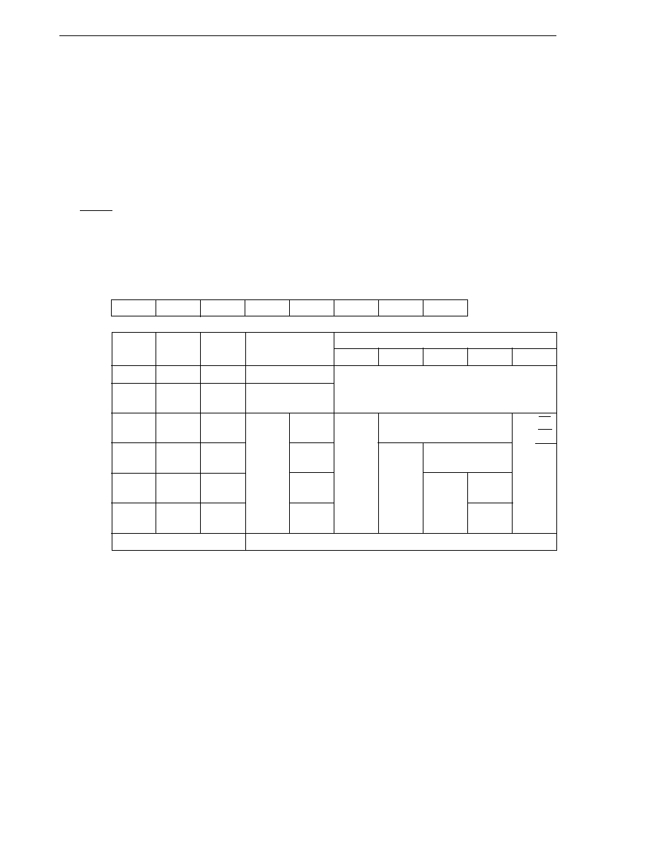
CHAPTER 20 EXTERNAL DEVICE EXPANSION FUNCTION
418
User's Manual U14260EJ3V1UD
20.2 External Device Expansion Function Control Registers
The external device expansion function is controlled by the following two registers.
∑
Memory expansion mode register (MEM)
∑
Memory expansion wait setting register (MM)
(1) Memory expansion mode register (MEM)
MEM sets the external expansion area.
MEM is set by a 1-bit or 8-bit memory manipulation instruction.
RESET input clears MEM to 00H.
Figure 20-2. Format of Memory Expansion Mode Register (MEM)
Address: FF47H After reset: 00H R/W
Symbol
7
6
5
4
3
2
1
0
MEM
0
0
0
0
0
MM2
MM1
MM0
MM2
MM1
MM0
Single-Chip/Memory
P40 to P47, P50 to P57, P64 to P67 Pin State
Expansion Mode Selection P40 to P47 P50 to P53 P54, P55 P56, P57 P64 to P67
0
0
0
Single-chip mode
Port mode
0
0
1
Port 4 falling edge
detection mode
0
1
1
Memory
256-byte
AD0 to AD7 Port mode
P64 = RD
expansion mode
P65 = WR
1
0
0
mode
Note
4 KB
A8 to A11 Port mode
P66 =WAIT
mode
P67 = ASTB
1
0
1
16 KB
A12, A13
Port mode
mode
1
1
1
Full-address
A14, A15
mode
Other than above
Setting prohibited
Caution
When using the falling edge detection function of port 4, be sure to set MEM to 01H.
(Note is shown in the next page.)

CHAPTER 20 EXTERNAL DEVICE EXPANSION FUNCTION
419
User's Manual U14260EJ3V1UD
Note When the CPU accesses the external memory expansion area, the lower bits of the address to be accessed
are output to the specified pins (except in the full-address mode).
Figure 20-3. Pins Specified for Address (with
µPD780076 and 780076Y)
External Expansion Mode
Address Accessed
Pins Specified for Address
by CPU
A15 A14 A13 A12 A11 A10 A9
A8 AD7 AD6 AD5 AD4 AD3 AD2 AD1 AD0
256-byte expansion mode
C000H
(1)
(1)
(0)
(0)
(0)
(0)
(0)
(0)
0
0
0
0
0
0
0
0
C001H
(1)
(1)
(0)
(0)
(0)
(0)
(0)
(0)
0
0
0
0
0
0
0
1
C055H
(1)
(1)
(0)
(0)
(0)
(0)
(0)
(0)
0
1
0
1
0
1
0
1
C0FEH
(1)
(1)
(0)
(0)
(0)
(0)
(0)
(0)
1
1
1
1
1
1
1
0
C0FFH
(1)
(1)
(0)
(0)
(0)
(0)
(0)
(0)
1
1
1
1
1
1
1
1
4 KB expansion mode
C000H
(1)
(1)
(0)
(0)
0
0
0
0
0
0
0
0
0
0
0
0
C001H
(1)
(1)
(0)
(0)
0
0
0
0
0
0
0
0
0
0
0
1
C100H
(1)
(1)
(0)
(0)
0
0
0
1
0
0
0
0
0
0
0
0
CFFFH
(1)
(1)
(0)
(0)
1
1
1
1
1
1
1
1
1
1
1
1
16 KB expansion mode
C000H
(1)
(1)
0
0
0
0
0
0
0
0
0
0
0
0
0
0
D000H
(1)
(1)
0
1
0
0
0
0
0
0
0
0
0
0
0
0
E000H
(1)
(1)
1
0
0
0
0
0
0
0
0
0
0
0
0
0
F000H
(1)
(1)
1
1
0
0
0
0
0
0
0
0
0
0
0
0
F3FFH
(1)
(1)
1
1
0
0
1
1
1
1
1
1
1
1
1
1
Full-address mode
C000H
1
1
0
0
0
0
0
0
0
0
0
0
0
0
0
0
C001H
1
1
0
0
0
0
0
0
0
0
0
0
0
0
0
1
F3FFH
1
1
1
1
0
0
1
1
1
1
1
1
1
1
1
1
Remark
The value in ( ) is not actually output. This pin can be used as a port pin.
(2) Memory expansion wait setting register (MM)
MM sets the number of waits.
MM is set by a 1-bit or 8-bit memory manipulation instruction.
RESET input sets MM to 10H.
Figure 20-4. Format of Memory Expansion Wait Setting Register (MM)
Address: FFF8H After reset: 10H R/W
Symbol
7
6
5
4
3
2
1
0
MM
0
0
PW1
PW0
0
0
0
0
PW1
PW0
Wait control
0
0
No wait
0
1
Wait (one wait state inserted)
1
0
Setting prohibited
1
1
Wait control by external wait pin
Cautions 1.
To control wait by the external wait pin, be sure to set the WAIT/P66 pin to input
mode (set bit 6 (PM66) of port mode register 6 (PM6) to 1).
2.
When wait is not controlled by the external wait pin, the WAIT/P66 pin can be
used as an I/O port pin.

CHAPTER 20 EXTERNAL DEVICE EXPANSION FUNCTION
420
User's Manual U14260EJ3V1UD
20.3 External Device Expansion Function Timing
The timing control signal output pins in the external memory expansion mode are as follows.
(1) RD pin (Alternate function: P64)
Read strobe signal output pin. The read strobe signal is output when data is read and instructions are fetched
from external memory.
During internal memory read, the read strobe signal is not output (maintains high level).
(2) WR pin (Alternate function: P65)
Write strobe signal output pin. The write strobe signal is output when data is written to external memory.
During internal memory write, the write strobe signal is not output (maintains high level).
(3) WAIT pin (Alternate function: P66)
External wait signal input pin.
When the external wait is not used, the WAIT pin can be used as an I/O port pin.
During internal memory access, the external wait signal is ignored.
(4) ASTB pin (Alternate function: P67)
Address strobe signal output pin. The address strobe signal is output regardless of data access and instruction
fetch from external memory.
During internal memory access, the address strobe signal is output.
(5) AD0 to AD7, A8 to A15 pins (Alternate function: P40 to P47, P50 to P57)
Address/data signal output pins. A valid signal is output or input during data accesses and instruction fetches
from external memory.
These signals change even during internal memory access (output values are undefined).
The timing charts are shown in Figures 20-5 to 20-8.

CHAPTER 20 EXTERNAL DEVICE EXPANSION FUNCTION
421
User's Manual U14260EJ3V1UD
Figure 20-5. Instruction Fetch from External Memory
(a) No wait (PW1, PW0 = 0, 0) setting
(b) Wait (PW1, PW0 = 0, 1) setting
(c) External wait (PW1, PW0 = 1, 1) setting
RD
ASTB
AD0 to AD7
A8 to A15
Lower address
Instruction code
Higher address
RD
ASTB
AD0 to AD7
A8 to A15
Internal wait signal
(1-clock wait)
Lower address
Instruction code
Higher address
RD
ASTB
AD0 to AD7
A8 to A15
WAIT
Lower address
Instruction code
Higher address

CHAPTER 20 EXTERNAL DEVICE EXPANSION FUNCTION
422
User's Manual U14260EJ3V1UD
Figure 20-6. External Memory Read Timing
(a) No wait (PW1, PW0 = 0, 0) setting
(b) Wait (PW1, PW0 = 0, 1) setting
(c) External wait (PW1, PW0 = 1, 1) setting
RD
ASTB
AD0 to AD7
A8 to A15
Lower address
Read data
Higher address
RD
ASTB
AD0 to AD7
A8 to A15
Internal wait signal
(1-clock wait)
Lower address
Read data
Higher address
RD
ASTB
AD0 to AD7
A8 to A15
WAIT
Lower address
Read data
Higher address
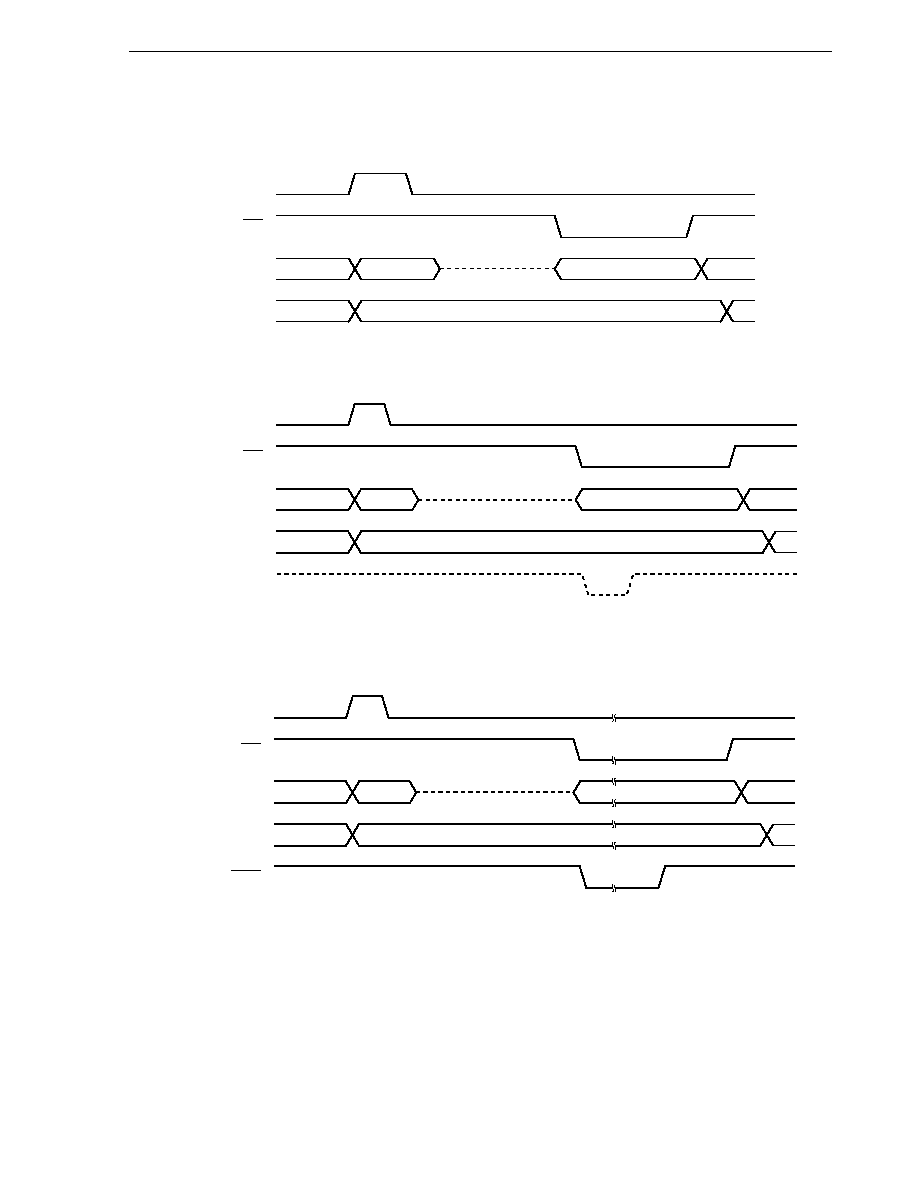
CHAPTER 20 EXTERNAL DEVICE EXPANSION FUNCTION
423
User's Manual U14260EJ3V1UD
Figure 20-7. External Memory Write Timing
(a) No wait (PW1, PW0 = 0, 0) setting
(b) Wait (PW1, PW0 = 0, 1) setting
(c) External wait (PW1, PW0 = 1, 1) setting
WR
ASTB
AD0 to AD7
A8 to A15
Lower address
Write data
Higher address
Hi-Z
WR
ASTB
AD0 to AD7
A8 to A15
Internal wait signal
(1-clock wait)
Lower
address
Write data
Higher address
Hi-Z
WR
ASTB
AD0 to AD7
A8 to A15
WAIT
Lower
address
Write data
Higher address
Hi-Z
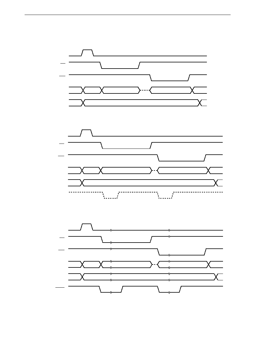
CHAPTER 20 EXTERNAL DEVICE EXPANSION FUNCTION
424
User's Manual U14260EJ3V1UD
Figure 20-8. External Memory Read-Modify-Write Timing
(a) No wait (PW1, PW0 = 0, 0) setting
(b) Wait (PW1, PW0 = 0, 1) setting
(c) External wait (PW1, PW0 = 1, 1) setting
Remark
The read-modify-write timing is the operation when a bit manipulation instruction is executed.
Read data
Write data
Higher address
Hi-Z
Lower
address
RD
ASTB
AD0 to AD7
A8 to A15
WR
RD
ASTB
AD0 to AD7
A8 to A15
Hi-Z
WR
Write data
Higher address
Internal wait signal
(1-clock wait)
Read data
Lower
address
WAIT
Hi-Z
RD
ASTB
AD0 to AD7
A8 to A15
WR
Write data
Higher address
Read data
Lower
address

CHAPTER 20 EXTERNAL DEVICE EXPANSION FUNCTION
425
User's Manual U14260EJ3V1UD
20.4 Example of Connection with Memory
This section provides an example of connecting the
µPD780078 with the external memory (SRAM) in Figure 20-
9. In addition, the external device expansion function is used in the full-address mode, the addresses from 0000H
to EFFFH (60 KB) are allocated to internal ROM, and the addresses after F000H are allocated to SRAM.
Figure 20-9. Connection Example of
µPD780078 and Memory
RD
WR
A8 to A14
ASTB
AD0 to AD7
V
DD0
74HC573
LE
D0 to D7
OE
Q0 to Q7
PD43256B
CS
OE
WE
I/O1 to I/O8
A0 to A14
Data bus
PD780078
Address bus
µ
µ

426
User's Manual U14260EJ3V1UD
CHAPTER 21 STANDBY FUNCTION
21.1 Standby Function and Configuration
21.1.1 Standby function
The standby function is designed to decrease power consumption of the system. The following two modes are
available.
(1) HALT mode
HALT instruction execution sets the HALT mode. The HALT mode stops the CPU operation clock. If the main
system clock oscillator or subsystem clock oscillator is operating before the HALT mode is set, oscillation of each
clock continues. In this mode, power consumption is not decreased as much as in the STOP mode. However,
the HALT mode is effective to restart operation immediately upon an interrupt request and to carry out intermittent
operations.
(2) STOP mode
STOP instruction execution sets the STOP mode. In the STOP mode, the main system clock oscillator stops,
stopping the whole system, thereby considerably reducing the CPU power consumption.
Data memory low-voltage hold (down to V
DD
= 1.6 V) is possible. Thus, the STOP mode is effective to hold data
memory contents with ultra-low power consumption.
Because this mode can be released upon an interrupt request, it enables intermittent operations to be carried
out. However, because a wait time is required to stabilize oscillation after the STOP mode is released, select
the HALT mode if it is necessary to start processing immediately upon an interrupt request.
In either of these two modes, all the contents of registers, flags and data memory just before the standby mode
is set are held. The I/O port output latches and output buffer statuses are also held.
Cautions 1. The STOP mode can be used only when the system operates with the main system clock
(subsystem clock oscillation cannot be stopped). The HALT mode can be used with either
the main system clock or the subsystem clock.
2. When operation is transferred to the STOP mode, be sure to stop operation of the peripheral
hardware operating with the main system clock before executing the STOP instruction.
3. The following sequence is recommended for reducing the power consumption of the A/D
converter when the standby function is used: First clear bit 7 (ADCS0) of A/D converter mode
register 0 (ADM0) to 0 to stop the A/D conversion operation, and then execute the HALT or
STOP instruction.
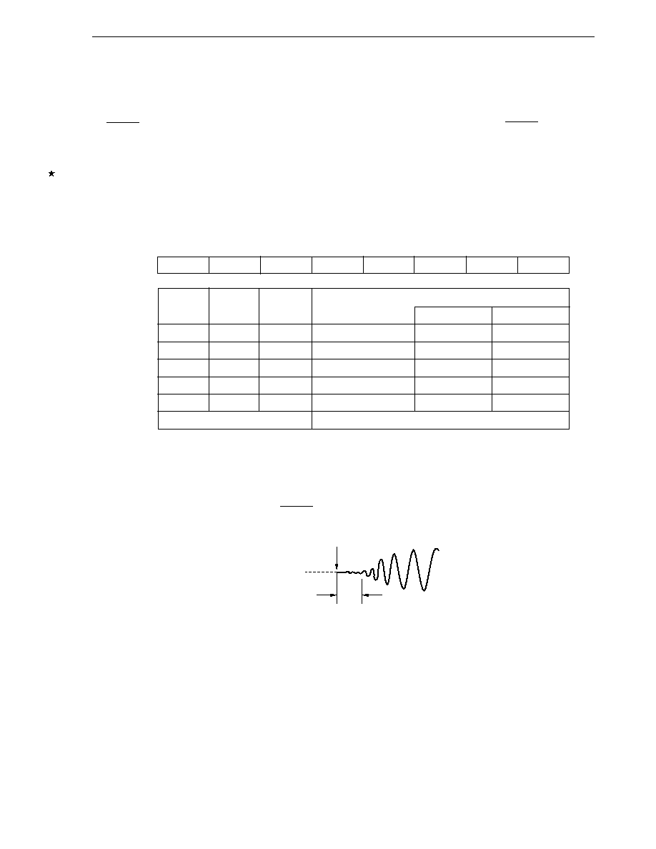
CHAPTER 21 STANDBY FUNCTION
427
User's Manual U14260EJ3V1UD
21.1.2 Standby function control register
The wait time after the STOP mode is released upon an interrupt request is controlled by the oscillation stabilization
time select register (OSTS).
OSTS is set by an 8-bit memory manipulation instruction.
RESET input sets OSTS to 04H. Therefore, when the STOP mode is released by inputting RESET, it takes 2
17
/
f
X
until release.
Remark
For the registers that start, stop, or select the clock, see CHAPTER 7 CLOCK GENERATOR.
Figure 21-1. Format of Oscillation Stabilization Time Select Register (OSTS)
Address: FFFAH After reset: 04H R/W
Symbol
7
6
5
4
3
2
1
0
OSTS
0
0
0
0
0
OSTS2
OSTS1
OSTS0
OSTS2
OSTS1
OSTS0
Selection of Oscillation Stabilization Time
f
X
= 8.38 MHz
f
X
= 12 MHz
Note
0
0
0
2
12
/f
X
488
µs
341
µs
0
0
1
2
14
/f
X
1.95 ms
1.36 ms
0
1
0
2
15
/f
X
3.91 ms
2.73 ms
0
1
1
2
16
/f
X
7.82 ms
5.46 ms
1
0
0
2
17
/f
X
15.6 ms
10.9 ms
Other than above
Setting prohibited
Note Expanded-specification products of
µPD780078 Subseries only.
Caution The wait time after the STOP mode is released does not include the time (see "a" in the illustration
below) from STOP mode release to clock oscillation start. This applies regardless of whether
STOP mode is released by RESET input or by interrupt request generation.
STOP mode release
X1 pin voltage
waveform
a
Remark
f
X
: Main system clock oscillation frequency
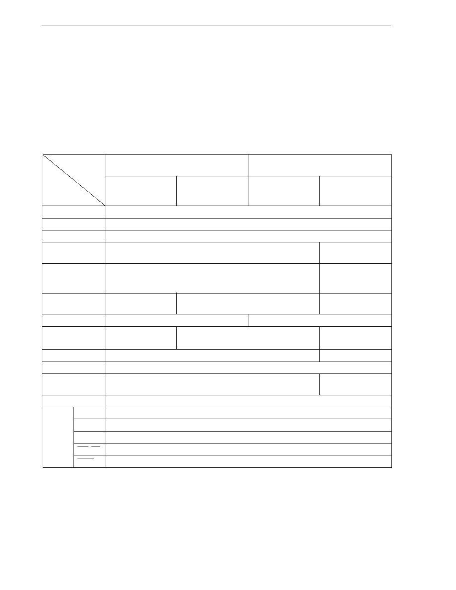
CHAPTER 21 STANDBY FUNCTION
428
User's Manual U14260EJ3V1UD
21.2 Standby Function Operations
21.2.1 HALT mode
(1) HALT mode setting and operating statuses
The HALT mode is set by executing the HALT instruction. It can be set with the main system clock or the
subsystem clock.
The operating statuses in the HALT mode are described below.
Table 21-1. HALT Mode Operating Statuses
HALT Mode
HALT Instruction Execution when
HALT Instruction Execution when
Setting
Using Main System Clock
Using Subsystem Clock
Without subsystem
With subsystem
With main system
With main system
Item
clock
Note 1
clock
Note 2
clock oscillation
clock oscillation
stopped
Clock generator
Both main system clock and subsystem clock can be oscillated. Clock supply to CPU stops.
CPU
Operation stops.
Ports (output latches) Status before HALT mode setting is held.
16-bit timer/event
Operable
Stop
counters 00, 01
8-bit timer/event
Operable
Operable when TI50,
counters 50, 51
TI51 are selected as
count clock.
Watch timer
Operable when f
X
/2
7
is
Operable
Operable when f
XT
is
selected as count clock
selected as count clock.
Watchdog timer
Operable
Operation stops.
Clock output
Operable when f
X
to f
X
/2
7
is Operable
Operable when f
XT
is
selected as output clock
selected as output clock.
Buzzer output
Operable
BUZ is at low level.
A/D converter
Stop
Serial interface
Operable
Operable during
external clock input.
External interrupt
Operable
Bus line
AD0 to AD7 High impedance
during
A8 to A15
Status before HALT mode setting is held.
external
ASTB
Low level
expansion
WR, RD
High level
WAIT
High impedance
Notes 1. Including case when external clock is not supplied.
2. Including case when external clock is supplied.
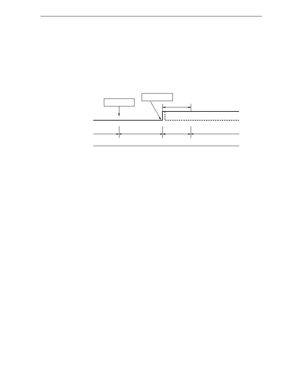
CHAPTER 21 STANDBY FUNCTION
429
User's Manual U14260EJ3V1UD
(2) HALT mode release
The HALT mode can be released by the following three sources.
(a) Release by unmasked interrupt request
When an unmasked interrupt request is generated, the HALT mode is released. If interrupt acknowledgment
is enabled, vectored interrupt servicing is carried out. If interrupt acknowledgment is disabled, the instruction
at the next address is executed.
Figure 21-2. HALT Mode Release by Interrupt Request Generation
Remarks 1. The broken lines indicate the case when the interrupt request that released the standby mode
is acknowledged.
2. The wait times are as follows:
∑ When vectored interrupt servicing is carried out:
8 or 9 clocks
∑ When vectored interrupt servicing is not carried out: 2 or 3 clocks
(b) Release by non-maskable interrupt request
When a non-maskable interrupt request is generated, the HALT mode is released and vectored interrupt
servicing is carried out whether interrupt acknowledgment is enabled or disabled.
However, a non-maskable interrupt request is not generated during operation with the subsystem clock.
HALT instruction
Wait
Wait
Operation mode
HALT mode
Operation mode
Oscillation
Clock
Standby release
signal
Interrupt request
CPU status
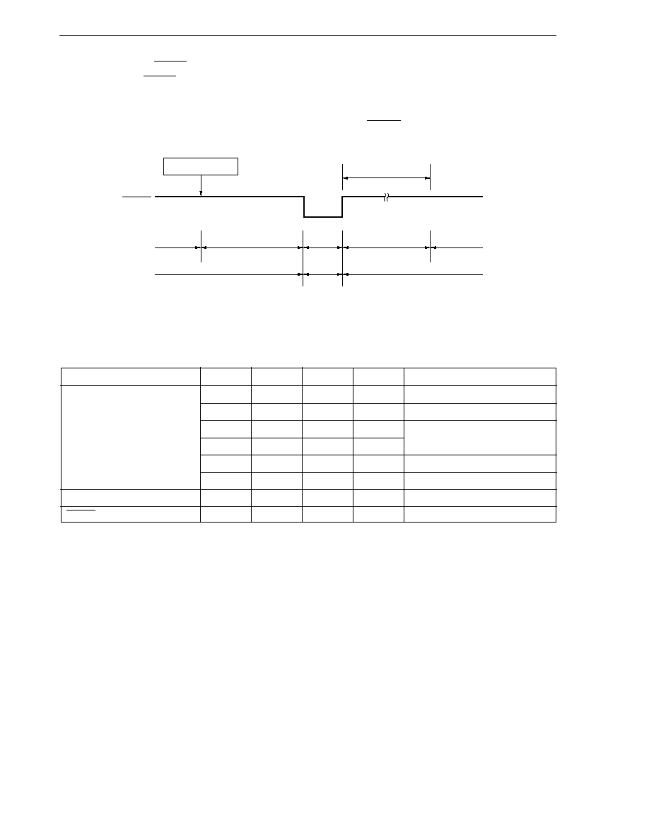
CHAPTER 21 STANDBY FUNCTION
430
User's Manual U14260EJ3V1UD
(c) Release by RESET input
When the RESET signal is input, HALT mode is released. And, as in the case with normal reset operation,
the program is executed after branch to the reset vector address.
Figure 21-3. HALT Mode Release by RESET Input
Remarks 1. f
X
: Main system clock oscillation frequency
2. Values in parentheses are for operation with f
X
= 8.38 MHz.
Table 21-2. Operation in Response to Interrupt Request in HALT Mode
Release Source
MK
◊◊
PR
◊◊
IE
ISP
Operation
Maskable interrupt request
0
0
0
◊
Next address instruction execution
0
0
1
◊
Interrupt servicing execution
0
1
0
1
Next address instruction execution
0
1
◊
0
0
1
1
1
Interrupt servicing execution
1
◊
◊
◊
HALT mode hold
Non-maskable interrupt request
--
--
◊
◊
Interrupt servicing execution
RESET input
--
--
◊
◊
Reset processing
◊: Don't care
HALT instruction
Wait
(2
17
/f
X
: 15.6 ms)
Oscillation stabilization
wait status
Operating mode
HALT mode
Operating
mode
Oscillation
stop
Clock
RESET
signal
Oscillation
Oscillation
Reset
period
CPU status

CHAPTER 21 STANDBY FUNCTION
431
User's Manual U14260EJ3V1UD
21.2.2 STOP mode
(1) STOP mode setting and operating status
The STOP mode is set by executing the STOP instruction. It can be set only with the main system clock.
Cautions 1. When the STOP mode is set, the X2 pin is internally connected to V
DD1
via a pull-up resistor
to minimize the leakage current at the crystal oscillator. Thus, do not use the STOP mode
in a system where an external clock is used for the main system clock.
2. Because the interrupt request signal is used to clear the standby mode, if there is an
interrupt source with the interrupt request flag set and the interrupt mask flag reset, the
standby mode is immediately cleared if set. Thus, the STOP mode is reset to the HALT mode
immediately after execution of the STOP instruction. The operating mode is set after the
wait set using the oscillation stabilization time select register (OSTS).
The operating statuses in the STOP mode are described in Table 21-3 below.
Table 21-3. STOP Mode Operating Statuses
STOP Mode Setting
With Subsystem Clock
Without Subsystem Clock
Item
Clock generator
Only main system clock oscillation is stopped.
CPU
Operation stops.
Ports (output latches)
Status before STOP mode setting is held.
16-bit timer/event counters 00, 01
Operation stops.
8-bit timer/event counters 50, 51
Operable only when TI50, TI51 are selected as count clock.
Watch timer
Operable when f
XT
is selected as
Operation stops.
count clock.
Watchdog timer
Operation stops.
Clock output
Operable when f
XT
is selected as
PCL is at low level.
output clock.
Buzzer output
BUZ is at low level.
A/D converter
Operation stops.
Serial interface
Other than UART0, 2
Operable only when externally supplied clock is specified as the serial clock.
UART0, 2
Operation stops. (Transmit shift register 0, 2 (TXS0, TXS2), receive shift register
0, 2 (RX0, RX2), receive buffer register 0, 2 (RXB0, RXB2) and transmit buffer
register 2 (TXB2) hold the value just before the clock stopped.)
External interrupt
Operable
Bus line during
AD0 to AD7
High impedance
external expansion
A8 to A15
Status before STOP mode setting is held.
ASTB
Low level
WR, RD
High level
WAIT
High impedance
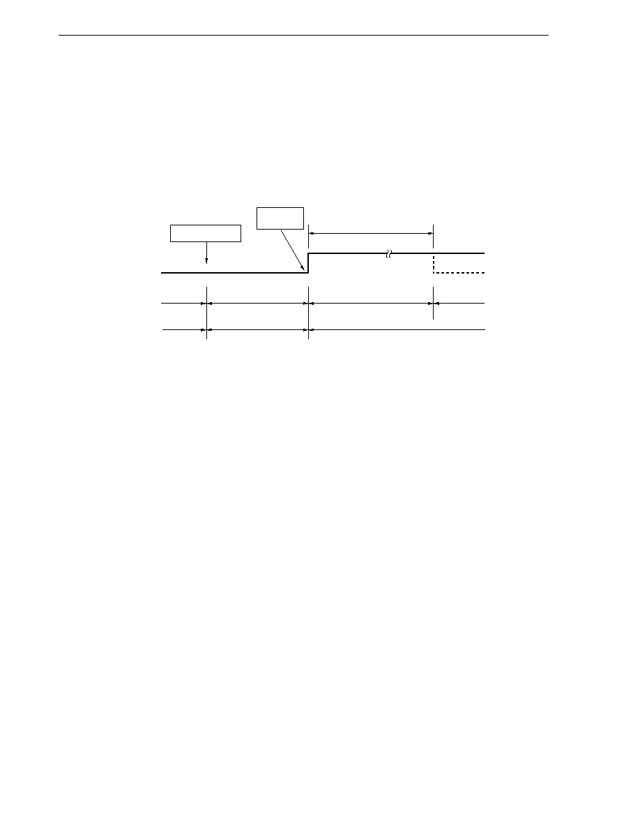
CHAPTER 21 STANDBY FUNCTION
432
User's Manual U14260EJ3V1UD
(2) STOP mode release
The STOP mode can be released by the following two sources.
(a) Release by unmasked interrupt request
When an unmasked interrupt request is generated, the STOP mode is released. If interrupt acknowledgment
is enabled after the lapse of oscillation stabilization time, vectored interrupt service is carried out. If interrupt
acknowledgment is disabled, the instruction at the next address is executed.
Figure 21-4. STOP Mode Release by Interrupt Request Generation
Remark
The broken lines indicate the case when the interrupt request that released the standby status
is acknowledged.
STOP instruction
Wait
(Time set by OSTS)
Oscillation stabilization
wait status
Operating mode
STOP mode
Operating
mode
Oscillation
Clock
Standby release
signal
Oscillation stop
Oscillation
Interrupt
request
CPU status
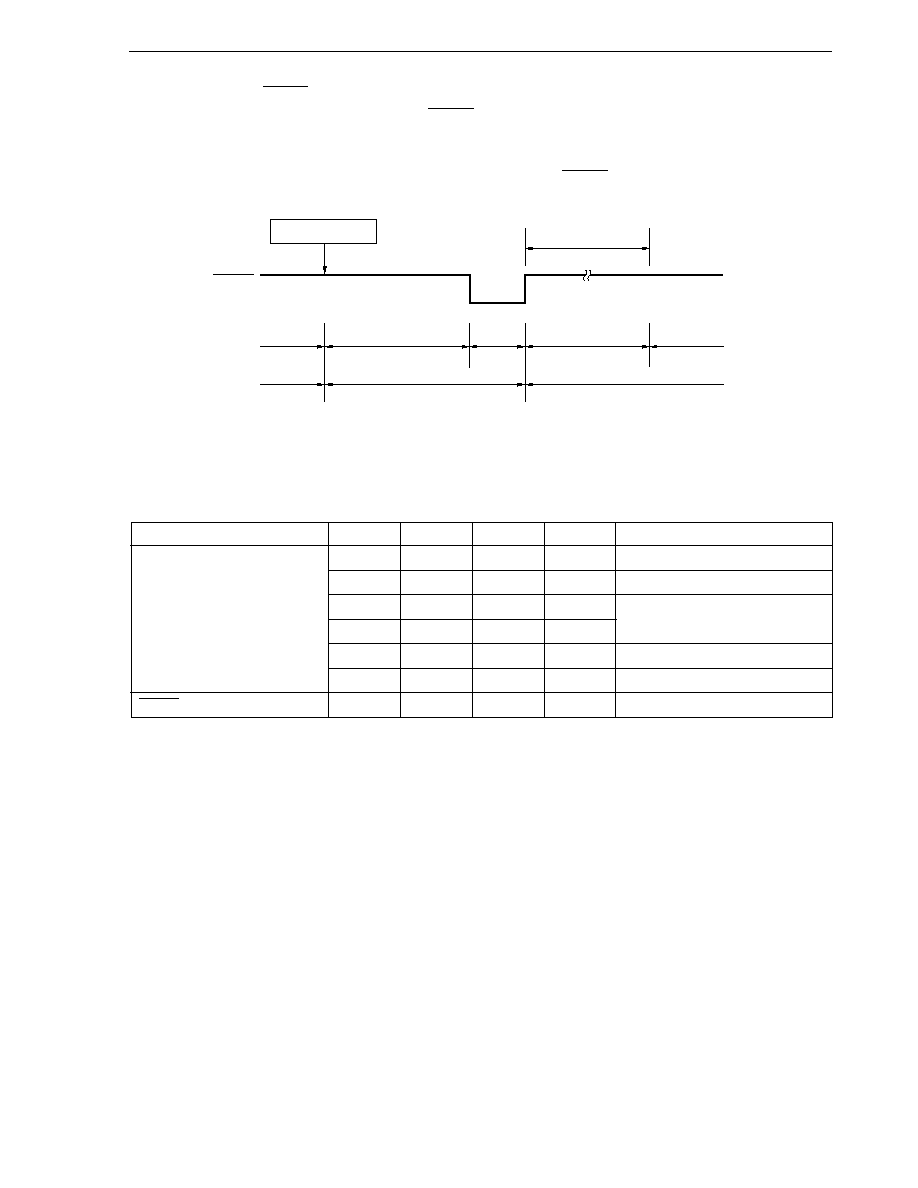
CHAPTER 21 STANDBY FUNCTION
433
User's Manual U14260EJ3V1UD
(b) Release by RESET input
The STOP mode is released when the RESET signal is input, and the reset operation is carried out after
the lapse of oscillation stabilization time.
Figure 21-5. STOP Mode Release by RESET Input
Remarks 1. f
X
: Main system clock oscillation frequency
2. Values in parentheses are for operation with f
X
= 8.38 MHz.
Table 21-4. Operation in Response to Interrupt Request in STOP Mode
Release Source
MK
◊◊
PR
◊◊
IE
ISP
Operation
Maskable interrupt request
0
0
0
◊
Next address instruction execution
0
0
1
◊
Interrupt servicing execution
0
1
0
1
Next address instruction execution
0
1
◊
0
0
1
1
1
Interrupt servicing execution
1
◊
◊
◊
STOP mode hold
RESET input
--
--
◊
◊
Reset processing
◊: Don't care
STOP instruction
Wait
(2
17
/f
X
: 15.6 ms)
Oscillation stabilization
wait status
Operating mode
STOP mode
Operating
mode
Oscillation stop
Clock
RESET
signal
Oscillation
Oscillation
Reset
period
CPU status
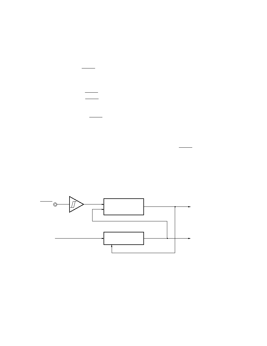
434
User's Manual U14260EJ3V1UD
CHAPTER 22 RESET FUNCTION
22.1 Reset Function
The following two operations are available to generate the reset signal.
(1) External reset input via RESET pin
(2) Internal reset by watchdog timer program loop time detection
External reset and internal reset have no functional differences. In both cases, program execution starts at the
address at 0000H and 0001H by RESET input.
When a low level is input to the RESET pin or the watchdog timer overflows, a reset is applied and each hardware
is set to the status shown in Table 22-1. Each pin is high impedance during reset input or during the oscillation
stabilization time just after reset release.
When a high level is input to the RESET pin, the reset is released and program execution starts after the lapse
of oscillation stabilization time (2
17
/f
X
). The reset applied by watchdog timer overflow is automatically released after
the reset and program execution starts after the lapse of oscillation stabilization time (2
17
/f
X
) (see Figures 22-2 to
22-4).
Cautions 1. For an external reset, input a low level for 10
µs or more to the RESET pin.
2. During reset input, main system clock oscillation remains stopped but subsystem clock
oscillation continues.
3. When the STOP mode is released by reset, the STOP mode contents are held during reset
input. However, the port pins become high impedance.
Figure 22-1. Reset Function Block Diagram
RESET
Count clock
Reset controller
Watchdog timer
Stop
Overflow
Reset signal
Interrupt function
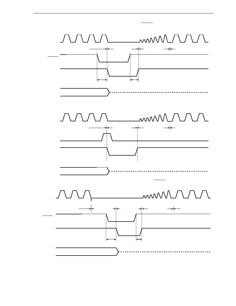
CHAPTER 22 RESET FUNCTION
435
User's Manual U14260EJ3V1UD
Figure 22-2. Timing of Reset by RESET Input
Figure 22-3. Timing of Reset Due to Watchdog Timer Overflow
Figure 22-4. Timing of Reset in STOP Mode by RESET Input
Delay
Delay
Hi-Z
Normal operation
Reset period
(Oscillation stop)
Oscillation
stabilization
time wait
Normal operation
(Reset processing)
X1
RESET
Internal
reset signal
Port pin
Hi-Z
Normal operation
Reset period
(Oscillation stop)
Oscillation
stabilization
time wait
Normal operation
(Reset processing)
X1
Watchdog
timer
overflow
Internal
reset signal
Port pin
Delay
Delay
Hi-Z
Normal operation
Oscillation
stabilization
time wait
Normal operation
(Reset processing)
X1
RESET
Internal
reset signal
Port pin
Stop status
(Oscillation stop)
STOP instruction execution
Reset period
(Oscillation stop)

CHAPTER 22 RESET FUNCTION
436
User's Manual U14260EJ3V1UD
Table 22-1. Hardware Statuses After Reset Acknowledgment (1/2)
Hardware
Status After Reset
Acknowledgment
Note 1
Program counter (PC)
Contents of reset vector table
(0000H, 0001H) are set.
Stack pointer (SP)
Undefined
Program status word (PSW)
02H
RAM
Data memory
Undefined
Note 2
General-purpose registers
Undefined
Note 2
Port registers 0 to 8 (P0 to P8) (output latches)
00H (undefined only for P1)
Port mode registers 0, 2 to 8 (PM0, PM2 to PM8)
FFH
Pull-up resistor option registers 0, 2 to 8 (PU0, PU2 to PU8)
00H
Processor clock control register (PCC)
04H
Memory size switching register (IMS)
CFH
Note 3
Internal expansion RAM size switching register (IXS)
0CH
Note 4
Memory expansion mode register (MEM)
00H
Memory expansion wait setting register (MM)
10H
Oscillation stabilization time select register (OSTS)
04H
16-bit timer/event counters
Timer counters 00, 01 (TM00, TM01)
0000H
00, 01
Capture/compare registers 000, 001, 010, 011
Undefined
(CR000, CR001, CR010, CR011)
Prescaler mode registers 00, 01 (PRM00, PRM01)
00H
Capture/compare control registers 00, 01 (CRC00, CRC01)
00H
Mode control registers 00, 01 (TMC00, TMC01)
00H
Output control registers 00, 01 (TOC00, TOC01)
00H
8-bit timer/event counters
Timer counters 50, 51 (TM50, TM51)
00H
50, 51
Compare registers 50, 51 (CR50, CR51)
Undefined
Clock select registers 50, 51 (TCL50, TCL51)
00H
Mode control registers 50, 51 (TMC50, TMC51)
00H
Watch timer
Operation mode register (WTM)
00H
Watchdog timer
Clock select register (WDCS)
00H
Mode register (WDTM)
00H
Notes 1. During reset input or oscillation stabilization time wait, only the PC contents among the hardware
statuses become undefined. All other hardware statuses remain unchanged after reset.
2. When a reset is executed in the standby mode, the pre-reset status is held even after reset.
3. Although the initial value is CFH, set the following value for each version.
µPD780076, 780076Y:
CCH
µPD780078, 780078Y:
CFH
µPD78F0078, 78F0078Y: Value for mask ROM versions
4. Although the default value of this register is 0CH, initialize this register to 0AH.

CHAPTER 22 RESET FUNCTION
437
User's Manual U14260EJ3V1UD
Table 22-1. Hardware Statuses After Reset Acknowledgment (2/2)
Hardware
Status After Reset
Acknowledgment
Clock output/buzzer output controller
Clock output select register (CKS)
00H
A/D converter
Conversion result register 0 (ADCR0)
0000H
Mode register 0 (ADM0)
00H
Analog input channel specification register 0 (ADS0)
00H
Serial interface UART0
Asynchronous serial interface mode register 0 (ASIM0)
00H
Asynchronous serial interface status register 0 (ASIS0)
00H
Baud rate generator control register 0 (BRGC0)
00H
Transmit shift register 0 (TXS0)
FFH
Receive buffer register 0 (RXB0)
Serial interface UART2
Asynchronous serial interface mode register 2 (ASIM2)
00H
Transfer mode specification register 2 (TRMC2)
02H
Clock select register 2 (CKSEL2)
00H
Baud rate generator control register 2 (BRGC2)
00H
Asynchronous serial interface status register 2 (ASIS2)
00H
Asynchronous serial interface transmit status register 2 (ASIF2)
00H
Transmit buffer register 2 (TXB2)
FFH
Receive buffer register 2 (RXB2)
FFH
Serial interface SIO3
Shift register 3 (SIO3)
Undefined
Operation mode register 3 (CSIM3)
00H
Serial interface CSI1
Transmit buffer register 1 (SOTB1)
Undefined
Shift register 1(SIO1)
Undefined
Operation mode register 1 (CSIM1)
00H
Clock select register 1 (CSIC1)
10H
Serial interface IIC0
Note
Transfer clock select register 0 (IICCL0)
00H
Shift register 0 (IIC0)
00H
Control register 0 (IICC0)
00H
Status register 0 (IICS0)
00H
Slave address register 0 (SVA0)
00H
Interrupt
Request flag registers (IF0L, IF0H, IF1L)
00H
Mask flag registers (MK0L, MK0H, MK1L)
FFH
Priority specification flag registers (PR0L, PR0H, PR1L)
FFH
External interrupt rising edge enable register (EGP)
00H
External interrupt falling edge enable register (EGN)
00H
Note
Provided only in the
µPD780078Y Subseries.

438
User's Manual U14260EJ3V1UD
CHAPTER 23
µPD78F0078, 78F0078Y
The
µPD78F0078 and 78F0078Y are provided as the flash memory versions of the µPD780078, 780078Y
Subseries.
The
µPD78F0078 and 78F0078Y are products that incorporate flash memory in which the program can be written,
erased, and rewritten while it is mounted on the board.
Writing to flash memory can be performed with the memory mounted on the target system (on board). A dedicated
flash programmer is connected to the target system to perform writing.
The following can be considered as the development environment and the applications using flash memory.
∑
Software can be altered after the
µPD78F0078 and 78F0078Y are solder-mounted on the target system.
∑
Small scale production of various models is made easier by differentiating software.
∑
Data adjustment in starting mass production is made easier.
Table 23-1 shows the differences between the
µPD78F0078 and 78F0078Y and the mask ROM versions.
Table 23-1. Differences Between
µPD78F0078 and Mask ROM Versions
Item
µPD78F0078
µPD780076
µPD780078
Internal ROM configuration
Flash memory
Mask ROM
Internal ROM capacity
60 KB
Note 1
48 KB
60 KB
Mask option to specify on-chip
Not possible
Possible
pull-up resistors of pins P30 to
P33
Note 2
IC pin
None
Available
V
PP
pin
Available
None
Electrical specifications,
Refer to the chapters of electrical specifications and recommended soldering
recommended soldering conditions
conditions.
Notes 1. The same capacity as the mask ROM versions can be specified by means of the memory size switching
register (IMS).
2. The P30 and P31 pins are provided only in the
µPD780078Y Subseries.
Caution
There are differences in noise immunity and noise radiation between the flash memory and
mask ROM versions. When pre-producing an application set with the flash memory version and
then mass-producing it with the mask ROM version, be sure to conduct sufficient evaluations
for the commercial samples (not engineering samples) of the mask ROM versions.
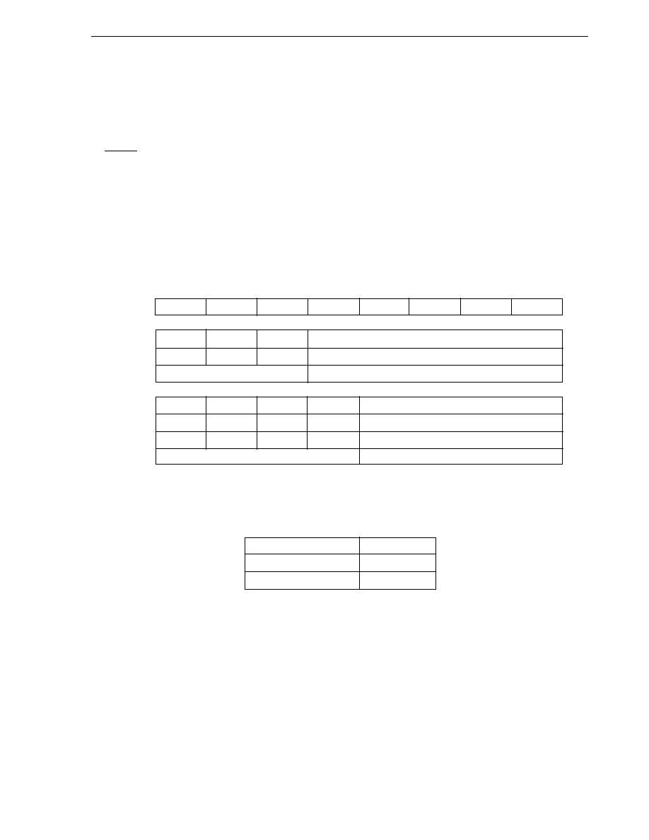
CHAPTER 23
µPD78F0078, 78F0078Y
439
User's Manual U14260EJ3V1UD
23.1 Memory Size Switching Register
The
µPD78F0078 and 78F0078Y allow users to select the internal memory capacity using the memory size
switching register (IMS) so that the same memory map as that of mask ROM versions with a different internal memory
capacity can be achieved.
IMS is set by an 8-bit memory manipulation instruction.
RESET input sets IMS to CFH.
Caution
Be sure to set the values of the target mask ROM version as the initial setting of the program.
Reset input initializes IMS to CFH. Also be sure to set the values of the target mask ROM version
after reset.
Figure 23-1. Format of Memory Size Switching Register (IMS)
Address: FFF0H After reset: CFH R/W
Symbol
7
6
5
4
3
2
1
0
IMS
RAM2
RAM1
RAM0
0
ROM3
ROM2
ROM1
ROM0
RAM2
RAM1
RAM0
Internal high-speed RAM capacity selection
1
1
0
1024 bytes
Other than above
Setting prohibited
ROM3
ROM2
ROM1
ROM0
Internal ROM capacity selection
1
1
0
0
48 KB
1
1
1
1
60 KB
Other than above
Setting prohibited
The IMS settings to obtain the same memory map as mask ROM versions are shown in Table 23-2.
Table 23-2. Memory Size Switching Register Settings
Target Mask ROM Versions
IMS Setting
µPD780076, 780076Y
CCH
µPD780078, 780078Y
CFH
Caution
When using the mask ROM versions, be sure to set IMS to the value indicated in Table 23-2.

CHAPTER 23
µPD78F0078, 78F0078Y
440
User's Manual U14260EJ3V1UD
23.2 Internal Expansion RAM Size Switching Register
The internal expansion RAM size switching register (IXS) is used to set the internal expansion RAM capacity.
IXS is set by an 8-bit memory manipulation instruction.
RESET input sets IXS to 0CH.
Caution
Be sure to set IXS to 0AH as the initial setting of the program. Reset input initializes IXS to 0CH,
so be sure to set IXS to 0AH after reset. Set the mask ROM versions in the same manner.
Figure 23-2. Format of Internal Expansion RAM Size Switching Register (IXS)
Address: FFF4H After reset: 0CH R/W
Symbol
7
6
5
4
3
2
1
0
IXS
0
0
0
IXRAM4
IXRAM3
IXRAM2
IXRAM1
IXRAM0
IXRAM4
IXRAM3
IXRAM2
IXRAM1
IXRAM0
Internal expansion RAM capacity selection
0
1
0
1
0
1024 bytes
Other than above
Setting prohibited

CHAPTER 23
µPD78F0078, 78F0078Y
441
User's Manual U14260EJ3V1UD
23.3 Flash Memory Characteristics
Flash memory programming is performed by connecting a dedicated flash programmer (Flashpro III (part no. FL-
PR3, PG-FP3)/Flashpro IV (part no. FL-PR4, PG-FP4)) to the target system with the flash memory mounted on the
target system (on-board). A flash memory writing adapter (program adapter), which is a target board used exclusively
for programming, is also provided.
Remark FL-PR3, FL-PR4, and the program adapter are products made by Naito Densei Machida Mfg. Co., Ltd.
(TEL +81-45-475-4191).
Programming using flash memory has the following advantages.
∑
Software can be modified after the microcontroller is solder-mounted on the target system.
∑
Distinguishing software facilities low-quantity, varied model production
∑
Easy data adjustment when starting mass production
23.3.1 Programming environment
The following shows the environment required for
µPD78F0078, 78F0078Y flash memory programming.
When Flashpro III or Flashpro IV is used as a dedicated flash programmer, a host machine is required to control
the dedicated flash programmer. Communication between the host machine and flash programmer is performed via
RS-232C/USB (Rev. 1.1).
For details, refer to the manuals of Flashpro III/Flashpro IV.
Remark USB is supported by Flashpro IV only.
Figure 23-3. Environment for Writing Program to Flash Memory
Note IIC is supported by the
µPD78F0078Y only.
RS-232C
USB
Dedicated flash programmer
PD78F0078,
PD78F0078Y
V
PP
V
DD
V
SS
RESET
SIO/UART/IIC
Note
Host machine
PG-FP4
(Flash Pro4)
Cxxxxxx
Bxxxxx
Axxxx
XXX YYY
XXXXX
XXXXXX
XXXX
XXXX
Y
YYY
STATVE
µ
µ
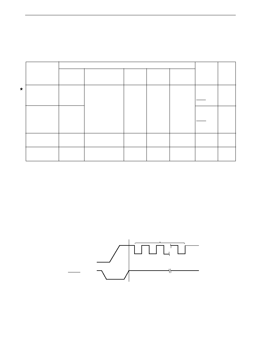
CHAPTER 23
µPD78F0078, 78F0078Y
442
User's Manual U14260EJ3V1UD
23.3.2 Communication mode
Use the communication mode shown in Table 23-3 to perform communication between the dedicated flash
programmer and the
µPD78F0078, 78F0078Y.
Table 23-3. Communication Mode List
Communication
Standard (TYPE) Setting
Note 1
Pins Used
Number of
Mode
Port
Speed
On Target
Frequency
Multiply
V
PP
Pulses
(COMM PORT)
(SIO CLOCK)
(CPU CLOCK) (Flashpro Clock)
Rate
(Multiple Rate)
3-wire serial I/O
SIO-ch1
2.4 kHz to 625 kHz
Note 2
Optional
1 to 10 MHz
Note 2
1.0
SI3/P34
1
(SIO3)
(SIO ch-1)
(100 Hz to 1.25 MHz)
Note 2
SO3/P35
SCK3/P36
3-wire serial I/O
SIO-H/S
SI3/P34
3
(SIO3)
(SIO ch-3 +
SO3/P35
with handshake
handshake)
SCK3/P36
P31 (HS)
I
2
C bus
Note 3
IIC-ch0
10 k to 100 k Baud
Note 2
Optional
1 to 10 MHz
Note 2
1.0
SDA0/P32
4
(IIC0)
(IIC ch-0)
(50 kHz)
SCL0/P33
UART
UART-ch0
4800 to 76800 Baud
Notes 2, 4
Optional
1 to 10 MHz
Note 2
1.0
R
X
D0/P23
8
(UART0)
(UART ch-0)
(4800 to 76800 bps)
Notes 2, 4
T
X
D0/P24
Notes 1. Selection items for Standard settings on Flashpro IV (TYPE settings on Flashpro III).
2. The possible setting range differs depending on the voltage. For details, refer to CHAPTERS 25 to 27.
3.
µPD78F0078Y only
4. Because factors other than the baud rate error, such as the signal waveform slew, also affect UART
communication, thoroughly evaluate the slew as well as the baud rate error.
Remark Items enclosed in parentheses in the setting item column are the set value and set item of Flashpro III
when they differ from those of Flashpro IV.
Figure 23-4. Communication Mode Selection Format
10 V
V
PP
V
PP
pulse
Flash memory write mode
RESET
V
DD
V
SS
V
DD
V
SS

CHAPTER 23
µPD78F0078, 78F0078Y
443
User's Manual U14260EJ3V1UD
Figure 23-5. Example of Connection with Dedicated Flash Programmer (1/2)
(a) 3-wire serial I/O (SIO3)
Dedicated flash programmer
V
PP
V
DD
/RESET
SCK
SO/TxD
SI/RxD
CLK
GND
V
PP
V
DD0
Note 1
, V
DD1
Note 1
, AV
REF
RESET
SCK3
SI3
SO3
X1
Note 2
V
SS0
, V
SS1
, AV
SS
PD78F0078, 78F0078Y
µ
(b) 3-wire serial I/O (SIO3) with handshake
V
PP
V
DD
/RESET
SCK
SO/TxD
SI/RxD
H/S
GND
V
PP
V
DD0
Note 1
, V
DD1
Note 1
, AV
REF
RESET
SCK3
SI3
SO3
P31 (HS)
CLK
X1
Note 2
V
SS0
,
V
SS1
, AV
SS
PD78F0078, 78F0078Y
µ
Dedicated flash programmer
(c) UART (UART0)
V
PP
V
DD
/RESET
SO/T
X
D
SI/R
X
D
CLK
GND
V
PP
V
DD0
Note 1
, V
DD1
Note 1
, AV
REF
RESET
R
X
D0
T
X
D0
X1
Note 2
V
SS0
, V
SS1
, AV
SS
PD78F0078, 78F0078Y
Dedicated flash programmer
µ
Notes 1. Even if power is supplied on board, the V
DD0
and V
DD1
pins must be connected to V
DD
of the dedicated
flash programmer. Supply the V
DD
voltage before programming is started.
2. The X1 pin can be supplied on board. In this case, the pin does not need to be connected to the dedicated
flash programmer.
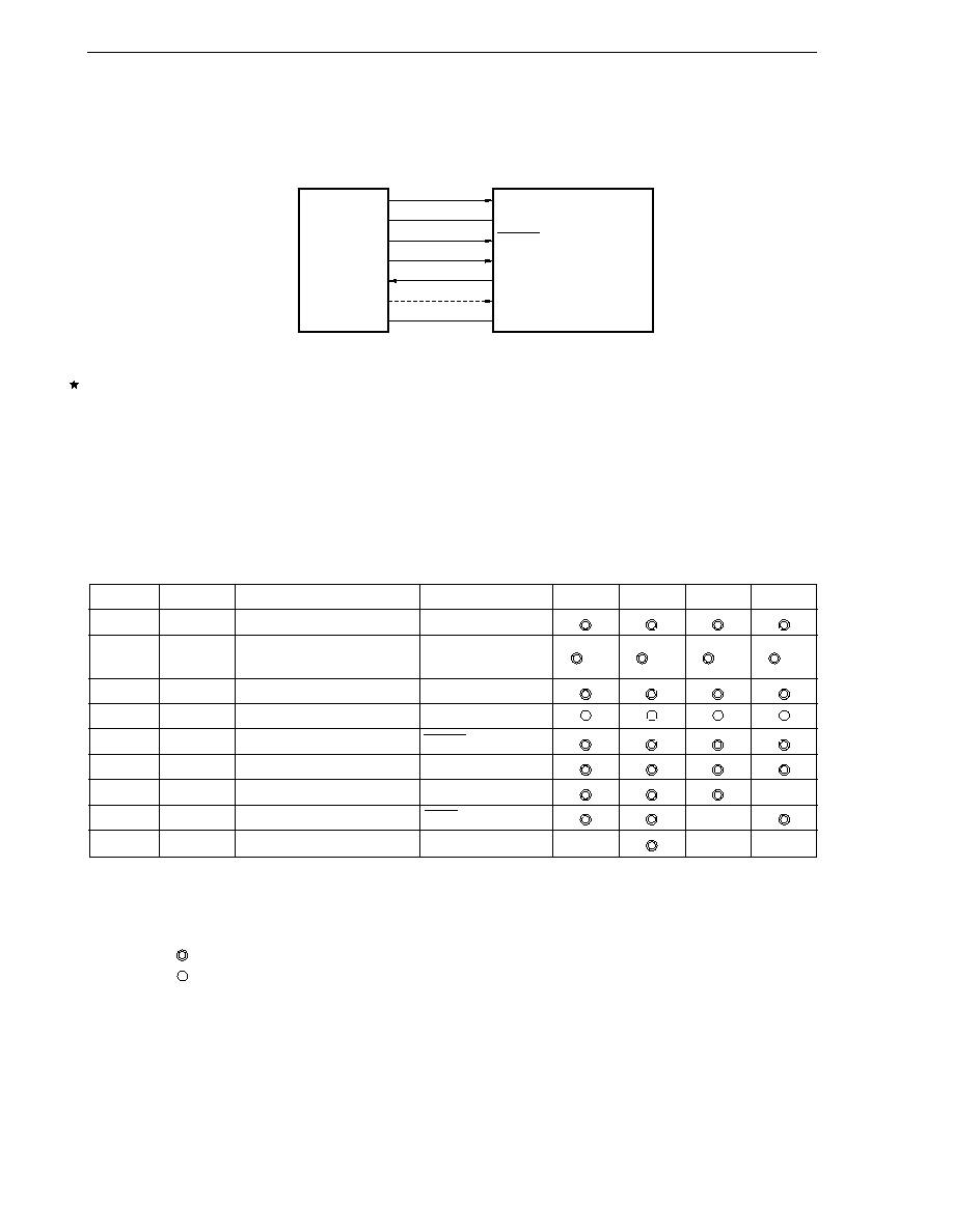
CHAPTER 23
µPD78F0078, 78F0078Y
444
User's Manual U14260EJ3V1UD
Figure 23-5. Example of Connection with Dedicated Flash Programmer (2/2)
(d) I
2
C bus (IIC0)
V
PP
V
DD
/RESET
SCK
SI/RxD
CLK
GND
V
PP
V
DD0
Note 1
, V
DD1
Note 1
, AV
REF
RESET
SCL0
SDA0
X1
Note 2
V
SS0
, V
SS1
, AV
SS
PD78F0078, 78F0078Y
Dedicated flash programmer
µ
Notes 1. Even if power is supplied on board, the V
DD0
and V
DD1
pins must be connected to V
DD
of the dedicated
flash programmer. Supply the V
DD
voltage before programming is started.
2. The X1 pin can be supplied on board. In this case, the pin does not need to be connected to the dedicated
flash programmer.
If Flashpro III/Flashpro IV is used as the dedicated flash programmer, the following signals are generated for the
µPD78F0078, 78F0078Y. For details, refer to the manual of Flashpro III/Flashpro IV.
Table 23-4. Pin Connection List
Signal Name
I/O
Pin Function
Pin Name
SIO3
SIO3 (HS)
UART0
IIC0
Note 1
V
PP
Output
Write voltage
V
PP
V
DD
I/O
V
DD
voltage generation/voltage V
DD0
, V
DD1
, AV
REF
Note 2
Note 2
Note 2
Note 2
monitoring
GND
≠
Ground
V
SS0
, V
SS1
, AV
SS
CLK
Output
Clock output
X1
/RESET
Output
Reset signal
RESET
SI/R
X
D
Input
Reception signal
SO3/TxD0/SDA0
Note 1
SO/T
X
D
Output
Transmission signal
SI3/RxD0
◊
SCK
Output
Transfer clock
SCK3/SCL0
Note 1
◊
H/S
Input
Handshake signal
P31 (HS)
◊
◊
◊
Notes 1.
µPD78F0078Y only
2. V
DD
voltage must be supplied before programming is started.
Remark
: Pin must be connected.
: If the signal is supplied on the target board, pin does not need to be connected.
◊
: Pin does not need to be connected.
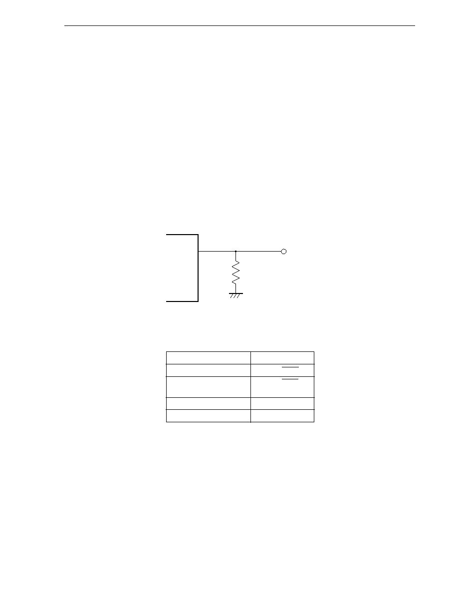
CHAPTER 23
µPD78F0078, 78F0078Y
445
User's Manual U14260EJ3V1UD
23.3.3 On-board pin processing
When performing programming on the target system, provide a connector on the target system to connect the
dedicated flash programmer.
An on-board function that allows switching between normal operation mode and flash memory programming mode
may be required in some cases.
<V
PP
pin>
In normal operation mode, input 0 V to the V
PP
pin. In flash memory programming mode, a write voltage of 10.0
V (TYP.) is supplied to the V
PP
pin, so perform the following.
(1) Connect a pull-down resistor (RV
PP
= 10 k
) to the V
PP
pin.
(2) Use the jumper on the board to switch the V
PP
pin input to either the programmer or directly to GND.
A V
PP
pin connection example is shown below.
Figure 23-6. V
PP
Pin Connection Example
<Serial interface pin>
The following shows the pins used by the serial interface.
Note
µPD78F0078Y only
When connecting the dedicated flash programmer to a serial interface pin that is connected to another device
on-board, signal conflict or abnormal operation of the other device may occur. Care must therefore be taken with
such connections.
Serial Interface
Pins Used
3-wire serial I/O (SIO3)
SI3, SO3, SCK3
3-wire serial I/O (SIO3)
SI3, SO3, SCK3,
with handshake
P31 (HS)
UART (UART0)
R
X
D0, T
X
D0
I
2
C bus (IIC0)
Note
SDA0, SCL0
PD78F0078, 78F0078Y
V
PP
Connection pin of dedicated
flash programmer
Pull-down resistor (RV
PP
)
µ
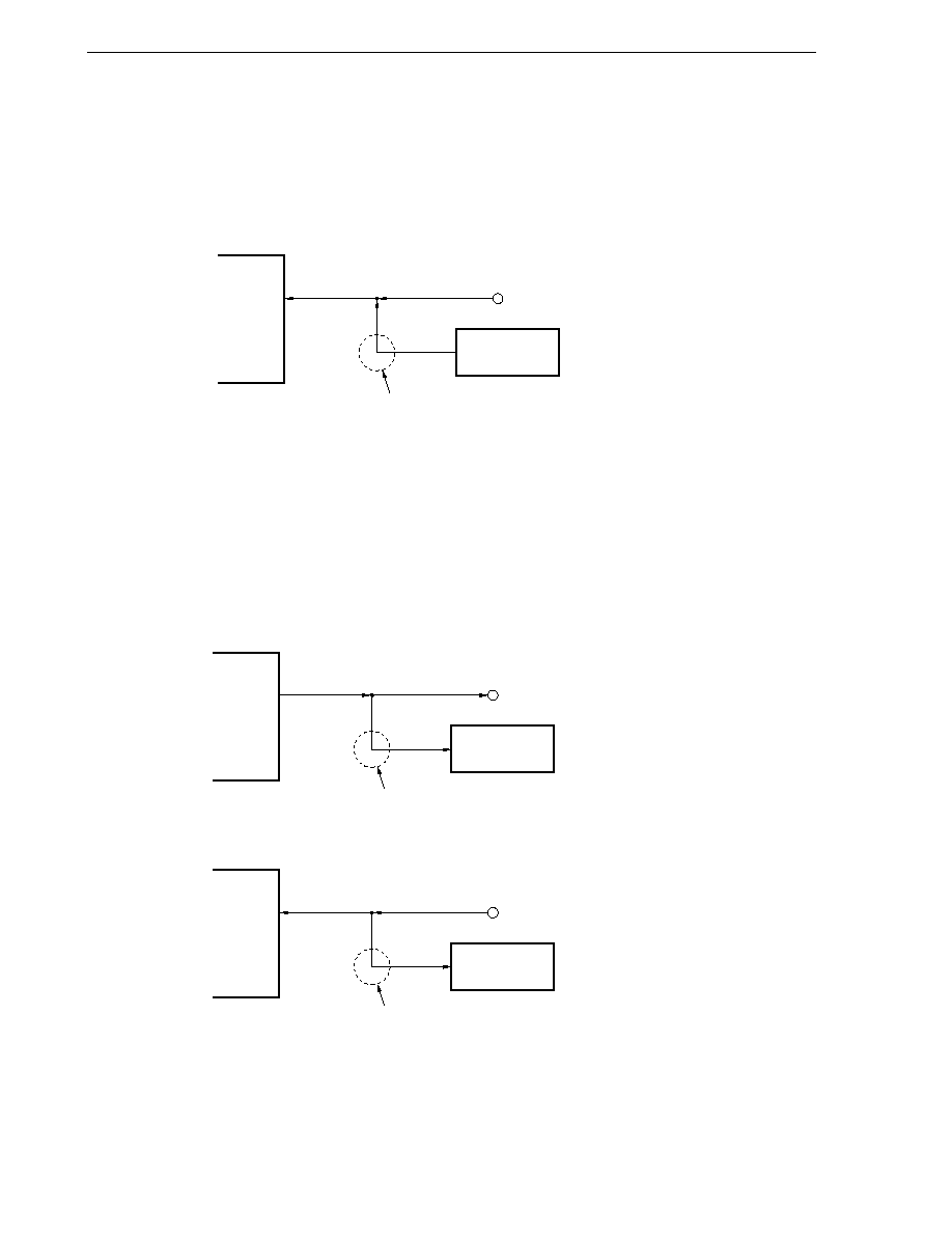
CHAPTER 23
µPD78F0078, 78F0078Y
446
User's Manual U14260EJ3V1UD
(1) Signal conflict
If the dedicated flash programmer (output) is connected to a serial interface pin (input) that is connected to
another device (output), a signal conflict occurs. To prevent this, isolate the connection with the other device
or set the other device to the output high impedance status.
Figure 23-7. Signal Conflict (Input Pin of Serial Interface)
(2) Abnormal operation of other device
If the dedicated flash programmer (output or input) is connected to a serial interface pin (input or output) that
is connected to another device (input), a signal is output to the device, which may cause an abnormal operation.
To prevent this abnormal operation, isolate the connection with the other device or set so that the input signals
to the other device are ignored.
Figure 23-8. Abnormal Operation of Other Device
Input pin
Signal conflict
Connection pin of dedicated
flash programmer
Other device
Output pin
In the flash memory programming mode, the signal output by another
device and the signal sent by the dedicated flash programmer conflict,
therefore, isolate the signal of the other device.
PD78F0078, 78F0078Y
µ
If the signal output by the PD78F0078, 78F0078Y affects another
device in the flash memory programming mode, isolate the signals of the
other device.
If the signal output by the dedicated flash programmer affects another
device in the flash memory programming mode, isolate the signals of the
other device.
PD78F0078, 78F0078Y
PD78F0078, 78F0078Y
Pin
Connection pin of dedicated
flash programmer
Other device
Input pin
µ
Pin
Connection pin of dedicated
flash programmer
Other device
Input pin
µ
µ
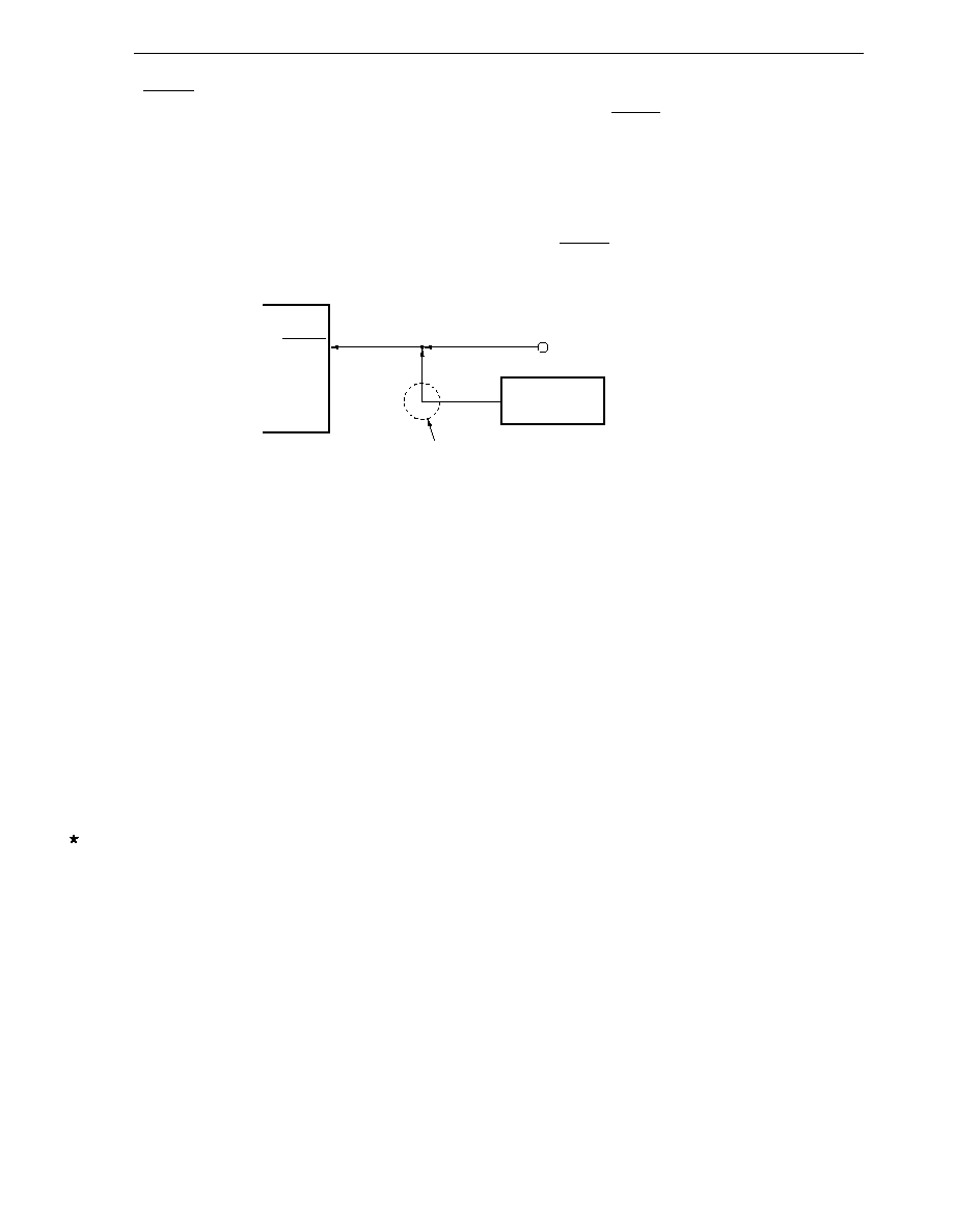
CHAPTER 23
µPD78F0078, 78F0078Y
447
User's Manual U14260EJ3V1UD
<RESET pin>
If the reset signal of the dedicated flash programmer is connected to the RESET pin connected to the reset signal
generator on-board, a signal conflict occurs. To prevent this, isolate the connection with the reset signal generator.
If the reset signal is input from the user system in the flash memory programming mode, a normal programming
operation cannot be performed. Therefore, do not input reset signals from other than the dedicated flash
programmer.
Figure 23-9. Signal Conflict (RESET Pin)
<Port pins>
When the
µPD78F0078 and 78F0078Y enter the flash memory programming mode, all the pins other than those
that communicate with the flash programmer are in the same status as immediately after reset.
If the external device does not recognize initial statuses such as the output high impedance status, therefore,
connect the external device to V
DD0
or V
SS0
via a resistor.
<Oscillator>
When using the on-board clock, connect X1, X2, XT1, and XT2 as required in the normal operation mode.
When using the clock output of the flash programmer, connect it directly to X1, disconnecting the main oscillator
on-board, and leave the X2 pin open. The subsystem clock conforms to the normal operation mode.
<Power supply>
To use the power output from the flash programmer, connect the V
DD0
and V
DD1
pins to V
DD
of the flash
programmer, and the V
SS0
and V
SS1
pins to GND of the flash programmer.
To use the on-board power supply, make connections that accord with the normal operation mode.
However, because the voltage is monitored by the flash programmer, be sure to connect the V
DD0
, V
DD1
, V
SS0
,
and V
SS1
pins to V
DD
and GND of the flash programmer.
Supply the same power as in the normal operation mode to the other power supply pins (AV
REF
and AV
SS
).
RESET
Connection pin of dedicated
flash programmer
Reset signal generator
Signal conflict
Output pin
The signal output by the reset signal generator and the signal output from
the dedicated flash programmer conflict in the flash memory programming
mode, so isolate the signal of the reset signal generator.
PD78F0078, 78F0078Y
µ
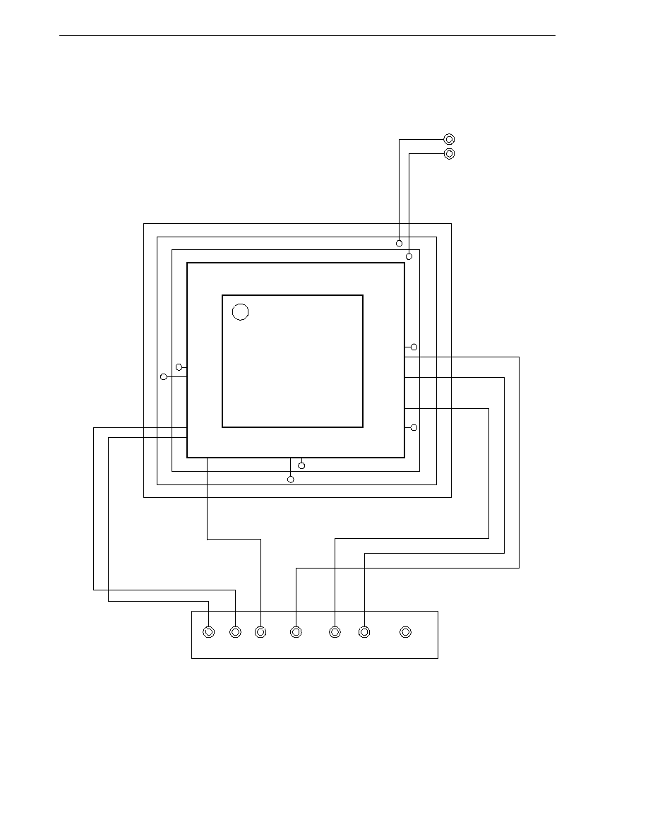
CHAPTER 23
µPD78F0078, 78F0078Y
448
User's Manual U14260EJ3V1UD
23.3.4 Connection of adapter for flash writing
The following shows the recommended connection example when the adapter for flash writing is used.
Figure 23-10. Wiring Example for Adapter for Flash Writing with 3-Wire Serial I/O (SIO3)
GND
VDD
LVDD (VPP2)
SI
SO
SCK
CLK
/RESET
V
PP
RESERVE/HS
WRITER INTERFACE
VDD (2.7 to 5.5 V)
GND
1
2
3
4
5
6
7
8
9
10
11
12
13
14
15
16
48
47
46
45
44
43
42
41
40
39
38
37
36
35
34
33
64 63 62 61 60 59 58 57 56 55 54 53 52 51 50 49
17 18 19 20 21 22 23 24 25 26 27 28 29 30 31 32
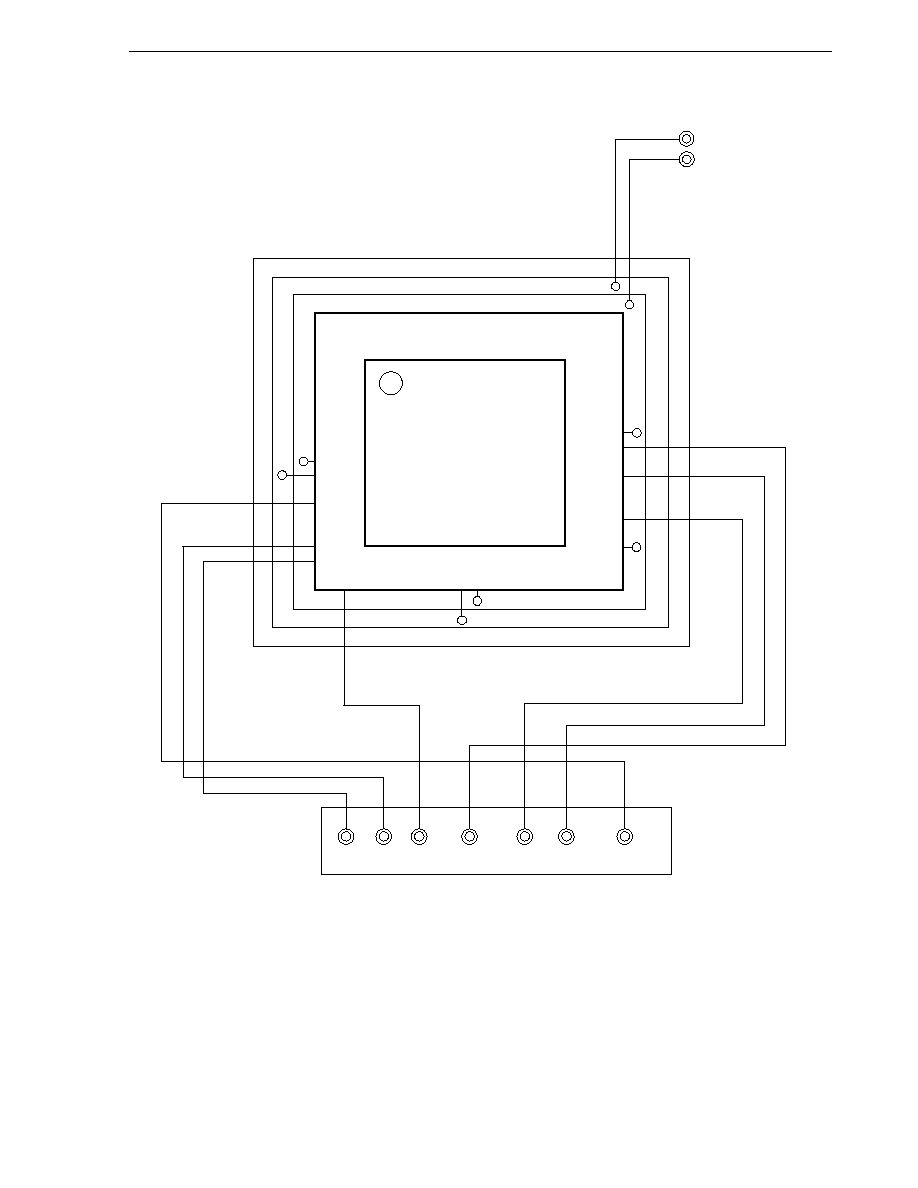
CHAPTER 23
µPD78F0078, 78F0078Y
449
User's Manual U14260EJ3V1UD
Figure 23-11. Wiring Example for Adapter for Flash Writing with 3-Wire Serial I/O (SIO3) with Handshake
GND
VDD
LVDD (VPP2)
SI
SO
SCK
CLK
/RESET V
PP
RESERVE/HS
WRITER INTERFACE
VDD (2.7 to 5.5 V)
GND
1
2
3
4
5
6
7
8
9
10
11
12
13
14
15
16
48
47
46
45
44
43
42
41
40
39
38
37
36
35
34
33
64 63 62 61 60 59 58 57 56 55 54 53 52 51 50 49
17 18 19 20 21 22 23 24 25 26 27 28 29 30 31 32
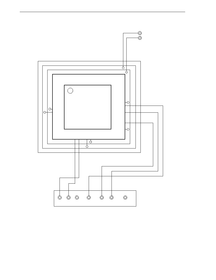
CHAPTER 23
µPD78F0078, 78F0078Y
450
User's Manual U14260EJ3V1UD
Figure 23-12. Wiring Example for Adapter for Flash Writing with UART (UART0)
GND
VDD
LVDD (VPP2)
SI
SO
SCK
CLK
/RESET V
PP
RESERVE/HS
WRITER INTERFACE
VDD (2.7 to 5.5 V)
GND
1
2
3
4
5
6
7
8
9
10
11
12
13
14
15
16
48
47
46
45
44
43
42
41
40
39
38
37
36
35
34
33
64 63 62 61 60 59 58 57 56 55 54 53 52 51 50 49
17 18 19 20 21 22 23 24 25 26 27 28 29 30 31 32

CHAPTER 23
µPD78F0078, 78F0078Y
451
User's Manual U14260EJ3V1UD
Figure 23-13. Wiring Example for Adapter for Flash Writing with I
2
C Bus (IIC0) (
µPD78F0078Y Only)
GND
VDD
LVDD (VPP2)
SI
SO
SCK
CLK
/RESET V
PP
RESERVE/HS
WRITER INTERFACE
VDD (2.7 to 5.5 V)
GND
1
2
3
4
5
6
7
8
9
10
11
12
13
14
15
16
48
47
46
45
44
43
42
41
40
39
38
37
36
35
34
33
64 63 62 61 60 59 58 57 56 55 54 53 52 51 50 49
17 18 19 20 21 22 23 24 25 26 27 28 29 30 31 32

452
User's Manual U14260EJ3V1UD
CHAPTER 24 INSTRUCTION SET
This chapter lists each instruction set of the
µPD780078, 780078Y Subseries in table form. For details of the
operation and operation code of each instruction, refer to the separate document 78K/0 Series Instructions User's
Manual (U12326E).

CHAPTER 24 INSTRUCTION SET
453
User's Manual U14260EJ3V1UD
24.1 Legend Used in Operation List
24.1.1 Operand identifiers and specification methods
Operands are written in the "Operand" column of each instruction in accordance with the specification method of
the instruction operand identifier (refer to the assembler specifications for details). When there are two or more
methods, select one of them. Uppercase letters and the symbols #, !, $ and [ ] are keywords and must be written
as they are. Each symbol has the following meaning.
∑ #:
Immediate data specification
∑ !:
Absolute address specification
∑ $:
Relative address specification
∑ [ ]: Indirect address specification
In the case of immediate data, describe an appropriate numeric value or a label. When using a label, be sure to
write the #, !, $, and [ ] symbols.
For operand register identifiers, r and rp, either function names (X, A, C, etc.) or absolute names (names in
parentheses in the table below, R0, R1, R2, etc.) can be used for specification.
Table 24-1. Operand Identifiers and Specification Methods
Identifier
Specification Method
r
X (R0), A (R1), C (R2), B (R3), E (R4), D (R5), L (R6), H (R7)
rp
AX (RP0), BC (RP1), DE (RP2), HL (RP3)
sfr
Special function register symbol
Note
sfrp
Special function register symbol (16-bit manipulatable register, even addresses only)
Note
saddr
FE20H to FF1FH Immediate data or labels
saddrp
FE20H to FF1FH Immediate data or labels (even address only)
addr16
0000H to FFFFH Immediate data or labels
(Only even addresses for 16-bit data transfer instructions)
addr11
0800H to 0FFFH Immediate data or labels
addr5
0040H to 007FH Immediate data or labels (even address only)
word
16-bit immediate data or label
byte
8-bit immediate data or label
bit
3-bit immediate data or label
RBn
RB0 to RB3
Note Addresses from FFD0H to FFDFH cannot be accessed with these operands.
Remark
For special function register symbols, refer to Table 5-3 Special Function Register List.

CHAPTER 24 INSTRUCTION SET
454
User's Manual U14260EJ3V1UD
24.1.2 Description of "operation" column
A:
A register; 8-bit accumulator
X:
X register
B:
B register
C:
C register
D:
D register
E:
E register
H:
H register
L:
L register
AX:
AX register pair; 16-bit accumulator
BC:
BC register pair
DE:
DE register pair
HL:
HL register pair
PC:
Program counter
SP:
Stack pointer
PSW:
Program status word
CY:
Carry flag
AC:
Auxiliary carry flag
Z:
Zero flag
RBS:
Register bank select flag
IE:
Interrupt request enable flag
( ):
Memory contents indicated by address or register contents in parentheses
X
H
, X
L
: Higher 8 bits and lower 8 bits of 16-bit register
:
Logical product (AND)
:
Logical sum (OR)
:
Exclusive logical sum (exclusive OR)
:
Inverted data
addr16: 16-bit immediate data or label
jdisp8: Signed 8-bit data (displacement value)
24.1.3 Description of "flag operation" column
(Blank): Not affected
0:
Cleared to 0
1:
Set to 1
◊:
Set/cleared according to the result
R:
Previously saved value is restored

CHAPTER 24 INSTRUCTION SET
455
User's Manual U14260EJ3V1UD
24.2 Operation List
Clocks
Flag
Note 1
Note 2
Z AC CY
MOV
r, #byte
2
4
≠
r
byte
saddr, #byte
3
6
7
(saddr)
byte
sfr, #byte
3
≠
7
sfr
byte
A, r
Note 3
1
2
≠
A
r
r, A
Note 3
1
2
≠
r
A
A, saddr
2
4
5
A
(saddr)
saddr, A
2
4
5
(saddr)
A
A, sfr
2
≠
5
A
sfr
sfr, A
2
≠
5
sfr
A
A, !addr16
3
8
9 + n
A
(addr16)
!addr16, A
3
8
9 + m
(addr16)
A
PSW, #byte
3
≠
7
PSW
byte
◊ ◊ ◊
A, PSW
2
≠
5
A
PSW
PSW, A
2
≠
5
PSW
A
◊ ◊ ◊
A, [DE]
1
4
5 + n
A
(DE)
[DE], A
1
4
5 + m
(DE)
A
A, [HL]
1
4
5 + n
A
(HL)
[HL], A
1
4
5 + m
(HL)
A
A, [HL + byte]
2
8
9 + n
A
(HL + byte)
[HL + byte], A
2
8
9 + m
(HL + byte)
A
A, [HL + B]
1
6
7 + n
A
(HL + B)
[HL + B], A
1
6
7 + m
(HL + B)
A
A, [HL + C]
1
6
7 + n
A
(HL + C)
[HL + C], A
1
6
7 + m
(HL + C)
A
XCH
A, r
Note 3
1
2
≠
A
r
A, saddr
2
4
6
A
(saddr)
A, sfr
2
≠
6
A
(sfr)
A, !addr16
3
8
10 + n + m
A
(addr16)
A, [DE]
1
4
6 + n + m
A
(DE)
A, [HL]
1
4
6 + n + m
A
(HL)
A, [HL + byte]
2
8
10 + n + m
A
(HL + byte)
A, [HL + B]
2
8
10 + n + m
A
(HL + B)
A, [HL + C]
2
8
10 + n + m
A
(HL + C)
Notes 1. When the internal high-speed RAM area is accessed or an instruction with no data access is executed.
2. When an area except the internal high-speed RAM area is accessed.
3. Except "r = A"
Remarks 1. One instruction clock cycle is one cycle of the CPU clock (f
CPU
) selected by the processor clock control
register (PCC).
2. The number of clocks applies when there is a program in the internal ROM.
3. n is the number of waits when external memory expansion area is read from.
4. m is the number of waits when external memory expansion area is written to.
Mnemonic
Operands
Bytes
Operation
Instruction
Group
8-bit data
transfer

CHAPTER 24 INSTRUCTION SET
456
User's Manual U14260EJ3V1UD
Clocks
Flag
Note 1
Note 2
Z AC CY
MOVW
rp, #word
3
6
≠
rp
word
saddrp, #word
4
8
10
(saddrp)
word
sfrp, #word
4
≠
10
sfrp
word
AX, saddrp
2
6
8
AX
(saddrp)
saddrp, AX
2
6
8
(saddrp)
AX
AX, sfrp
2
≠
8
AX
sfrp
sfrp, AX
2
≠
8
sfrp
AX
AX, rp
Note 3
1
4
≠
AX
rp
rp, AX
Note 3
1
4
≠
rp
AX
AX, !addr16
3
10
12 + 2n AX
(addr16)
!addr16, AX
3
10
12 + 2m (addr16)
AX
XCHW
AX, rp
Note 3
1
4
≠
AX
rp
ADD
A, #byte
2
4
≠
A, CY
A + byte
◊ ◊ ◊
saddr, #byte
3
6
8
(saddr), CY
(saddr) + byte
◊ ◊ ◊
A, r
Note 4
2
4
≠
A, CY
A + r
◊ ◊ ◊
r, A
2
4
≠
r, CY
r + A
◊ ◊ ◊
A, saddr
2
4
5
A, CY
A + (saddr)
◊ ◊ ◊
A, !addr16
3
8
9 + n
A, CY
A + (addr16)
◊ ◊ ◊
A, [HL]
1
4
5 + n
A, CY
A + (HL)
◊ ◊ ◊
A, [HL + byte]
2
8
9 + n
A, CY
A + (HL + byte)
◊ ◊ ◊
A, [HL + B]
2
8
9 + n
A, CY
A + (HL + B)
◊ ◊ ◊
A, [HL + C]
2
8
9 + n
A, CY
A + (HL + C)
◊ ◊ ◊
ADDC
A, #byte
2
4
≠
A, CY
A + byte + CY
◊ ◊ ◊
saddr, #byte
3
6
8
(saddr), CY
(saddr) + byte + CY
◊ ◊ ◊
A, r
Note 4
2
4
≠
A, CY
A + r + CY
◊ ◊ ◊
r, A
2
4
≠
r, CY
r + A + CY
◊ ◊ ◊
A, saddr
2
4
5
A, CY
A + (saddr) + CY
◊ ◊ ◊
A, !addr16
3
8
9 + n
A, CY
A + (addr16) + CY
◊ ◊ ◊
A, [HL]
1
4
5 + n
A, CY
A + (HL) + CY
◊ ◊ ◊
A, [HL + byte]
2
8
9 + n
A, CY
A + (HL + byte) + CY
◊ ◊ ◊
A, [HL + B]
2
8
9 + n
A, CY
A + (HL + B) + CY
◊ ◊ ◊
A, [HL + C]
2
8
9 + n
A, CY
A + (HL + C) + CY
◊ ◊ ◊
Notes 1. When the internal high-speed RAM area is accessed or an instruction with no data access is executed.
2. When an area except the internal high-speed RAM area is accessed
3. Only when rp = BC, DE or HL
4. Except "r = A"
Remarks 1. One instruction clock cycle is one cycle of the CPU clock (f
CPU
) selected by the processor clock control
register (PCC).
2. The number of clocks applies when there is a program in the internal ROM.
3. n is the number of waits when external memory expansion area is read from.
4. m is the number of waits when external memory expansion area is written to.
Mnemonic
Operands
Bytes
Operation
Instruction
Group
16-bit
data
transfer
8-bit
operation
CHAPTER 24 INSTRUCTION SET
457
User's Manual U14260EJ3V1UD
Clocks
Flag
Note 1
Note 2
Z AC CY
SUB
A, #byte
2
4
≠
A, CY
A ≠ byte
◊ ◊ ◊
saddr, #byte
3
6
8
(saddr), CY
(saddr) ≠ byte
◊ ◊ ◊
A, r
Note 3
2
4
≠
A, CY
A ≠ r
◊ ◊ ◊
r, A
2
4
≠
r, CY
r ≠ A
◊ ◊ ◊
A, saddr
2
4
5
A, CY
A ≠ (saddr)
◊ ◊ ◊
A, !addr16
3
8
9 + n
A, CY
A ≠ (addr16)
◊ ◊ ◊
A, [HL]
1
4
5 + n
A, CY
A ≠ (HL)
◊ ◊ ◊
A, [HL + byte]
2
8
9 + n
A, CY
A ≠ (HL + byte)
◊ ◊ ◊
A, [HL + B]
2
8
9 + n
A, CY
A ≠ (HL + B)
◊ ◊ ◊
A, [HL + C]
2
8
9 + n
A, CY
A ≠ (HL + C)
◊ ◊ ◊
SUBC
A, #byte
2
4
≠
A, CY
A ≠ byte ≠ CY
◊ ◊ ◊
saddr, #byte
3
6
8
(saddr), CY
(saddr) ≠ byte ≠ CY
◊ ◊ ◊
A, r
Note 3
2
4
≠
A, CY
A ≠ r ≠ CY
◊ ◊ ◊
r, A
2
4
≠
r, CY
r ≠ A ≠ CY
◊ ◊ ◊
A, saddr
2
4
5
A, CY
A ≠ (saddr) ≠ CY
◊ ◊ ◊
A, !addr16
3
8
9 + n
A, CY
A ≠ (addr16) ≠ CY
◊ ◊ ◊
A, [HL]
1
4
5 + n
A, CY
A ≠ (HL) ≠ CY
◊ ◊ ◊
A, [HL + byte]
2
8
9 + n
A, CY
A ≠ (HL + byte) ≠ CY
◊ ◊ ◊
A, [HL + B]
2
8
9 + n
A, CY
A ≠ (HL + B) ≠ CY
◊ ◊ ◊
A, [HL + C]
2
8
9 + n
A, CY
A ≠ (HL + C) ≠ CY
◊ ◊ ◊
AND
A, #byte
2
4
≠
A
A byte
◊
saddr, #byte
3
6
8
(saddr)
(saddr) byte
◊
A, r
Note 3
2
4
≠
A
A r
◊
r, A
2
4
≠
r
r A
◊
A, saddr
2
4
5
A
A (saddr)
◊
A, !addr16
3
8
9 + n
A
A (addr16)
◊
A, [HL]
1
4
5 + n
A
A (HL)
◊
A, [HL + byte]
2
8
9 + n
A
A (HL + byte)
◊
A, [HL + B]
2
8
9 + n
A
A (HL + B)
◊
A, [HL + C]
2
8
9 + n
A
A (HL + C)
◊
Notes 1. When the internal high-speed RAM area is accessed or an instruction with no data access is executed.
2. When an area except the internal high-speed RAM area is accessed
3. Except "r = A"
Remarks 1. One instruction clock cycle is one cycle of the CPU clock (f
CPU
) selected by the processor clock control
register (PCC).
2. The number of clocks applies when there is a program in the internal ROM.
3. n is the number of waits when external memory expansion area is read from.
Mnemonic
Operands
Bytes
Operation
Instruction
Group
8-bit
operation
CHAPTER 24 INSTRUCTION SET
458
User's Manual U14260EJ3V1UD
Clocks
Flag
Note 1
Note 2
Z AC CY
OR
A, #byte
2
4
≠
A
A byte
◊
saddr, #byte
3
6
8
(saddr)
(saddr) byte
◊
A, r
Note 3
2
4
≠
A
A r
◊
r, A
2
4
≠
r
r A
◊
A, saddr
2
4
5
A
A (saddr)
◊
A, !addr16
3
8
9 + n
A
A (addr16)
◊
A, [HL]
1
4
5 + n
A
A (HL)
◊
A, [HL + byte]
2
8
9 + n
A
A (HL + byte)
◊
A, [HL + B]
2
8
9 + n
A
A (HL + B)
◊
A, [HL + C]
2
8
9 + n
A
A (HL + C)
◊
XOR
A, #byte
2
4
≠
A
A byte
◊
saddr, #byte
3
6
8
(saddr)
(saddr) byte
◊
A, r
Note 3
2
4
≠
A
A r
◊
r, A
2
4
≠
r
r A
◊
A, saddr
2
4
5
A
A (saddr)
◊
A, !addr16
3
8
9 + n
A
A (addr16)
◊
A, [HL]
1
4
5 + n
A
A (HL)
◊
A, [HL + byte]
2
8
9 + n
A
A (HL + byte)
◊
A, [HL + B]
2
8
9 + n
A
A (HL + B)
◊
A, [HL + C]
2
8
9 + n
A
A (HL + C)
◊
CMP
A, #byte
2
4
≠
A ≠ byte
◊ ◊ ◊
saddr, #byte
3
6
8
(saddr) ≠ byte
◊ ◊ ◊
A, r
Note 3
2
4
≠
A ≠ r
◊ ◊ ◊
r, A
2
4
≠
r ≠ A
◊ ◊ ◊
A, saddr
2
4
5
A ≠ (saddr)
◊ ◊ ◊
A, !addr16
3
8
9 + n
A ≠ (addr16)
◊ ◊ ◊
A, [HL]
1
4
5 + n
A ≠ (HL)
◊ ◊ ◊
A, [HL + byte]
2
8
9 + n
A ≠ (HL + byte)
◊ ◊ ◊
A, [HL + B]
2
8
9 + n
A ≠ (HL + B)
◊ ◊ ◊
A, [HL + C]
2
8
9 + n
A ≠ (HL + C)
◊ ◊ ◊
Notes 1. When the internal high-speed RAM area is accessed or an instruction with no data access is executed.
2. When an area except the internal high-speed RAM area is accessed
3. Except "r = A"
Remarks 1. One instruction clock cycle is one cycle of the CPU clock (f
CPU
) selected by the processor clock control
register (PCC).
2. The number of clocks applies when there is a program in the internal ROM.
3. n is the number of waits when external memory expansion area is read from.
Mnemonic
Operands
Bytes
Operation
Instruction
Group
8-bit
operation

CHAPTER 24 INSTRUCTION SET
459
User's Manual U14260EJ3V1UD
Clocks
Flag
Note 1
Note 2
Z AC CY
ADDW
AX, #word
3
6
≠
AX, CY
AX + word
◊ ◊ ◊
SUBW
AX, #word
3
6
≠
AX, CY
AX ≠ word
◊ ◊ ◊
CMPW
AX, #word
3
6
≠
AX ≠ word
◊ ◊ ◊
MULU
X
2
16
≠
AX
A ◊ X
DIVUW
C
2
25
≠
AX (Quotient), C (Remainder)
AX ˜ C
INC
r
1
2
≠
r
r + 1
◊ ◊
saddr
2
4
6
(saddr)
(saddr) + 1
◊ ◊
DEC
r
1
2
≠
r
r ≠ 1
◊ ◊
saddr
2
4
6
(saddr)
(saddr) ≠ 1
◊ ◊
INCW
rp
1
4
≠
rp
rp + 1
DECW
rp
1
4
≠
rp
rp ≠ 1
ROR
A, 1
1
2
≠
(CY, A
7
A
0
, A
m ≠ 1
A
m
)
◊ 1 time
◊
ROL
A, 1
1
2
≠
(CY, A
0
A
7
, A
m + 1
A
m
)
◊ 1 time
◊
RORC
A, 1
1
2
≠
(CY
A
0
, A
7
CY, A
m ≠ 1
A
m
)
◊ 1 time
◊
ROLC
A, 1
1
2
≠
(CY
A
7
, A
0
CY, A
m + 1
A
m
)
◊ 1 time
◊
ROR4
[HL]
2
10
12 + n + m
A
3 ≠ 0
(HL)
3 ≠ 0
, (HL)
7 ≠ 4
A
3 ≠ 0
,
(HL)
3 ≠ 0
(HL)
7 ≠ 4
ROL4
[HL]
2
10
12 + n + m
A
3 ≠ 0
(HL)
7 ≠ 4
, (HL)
3 ≠ 0
A
3 ≠ 0
,
(HL)
7 ≠ 4
(HL)
3 ≠ 0
ADJBA
2
4
≠
Decimal Adjust Accumulator after
◊ ◊ ◊
Addition
ADJBS
2
4
≠
Decimal Adjust Accumulator after
◊ ◊ ◊
Subtract
MOV1
CY, saddr.bit
3
6
7
CY
(saddr.bit)
◊
CY, sfr.bit
3
≠
7
CY
sfr.bit
◊
CY, A.bit
2
4
≠
CY
A.bit
◊
CY, PSW.bit
3
≠
7
CY
PSW.bit
◊
CY, [HL].bit
2
6
7 + n
CY
(HL).bit
◊
saddr.bit, CY
3
6
8
(saddr.bit)
CY
sfr.bit, CY
3
≠
8
sfr.bit
CY
A.bit, CY
2
4
≠
A.bit
CY
PSW.bit, CY
3
≠
8
PSW.bit
CY
◊ ◊
[HL].bit, CY
2
6
8 + n + m
(HL).bit
CY
Notes 1. When the internal high-speed RAM area is accessed or an instruction with no data access is executed.
2. When an area except the internal high-speed RAM area is accessed
Remarks 1. One instruction clock cycle is one cycle of the CPU clock (f
CPU
) selected by the processor clock control
register (PCC).
2. The number of clocks applies when there is a program in the internal ROM.
3. n is the number of waits when external memory expansion area is read from.
4. m is the number of waits when external memory expansion area is written to.
Mnemonic
Operands
Bytes
Operation
Instruction
Group
16-bit
operation
Increment/
decrement
BCD
adjust
Bit
manipu-
late
Multiply/
divide
Rotate
CHAPTER 24 INSTRUCTION SET
460
User's Manual U14260EJ3V1UD
Clocks
Flag
Note 1
Note 2
Z AC CY
AND1
CY, saddr.bit
3
6
7
CY
CY (saddr.bit)
◊
CY, sfr.bit
3
≠
7
CY
CY sfr.bit
◊
CY, A.bit
2
4
≠
CY
CY A.bit
◊
CY, PSW.bit
3
≠
7
CY
CY PSW.bit
◊
CY, [HL].bit
2
6
7 + n
CY
CY (HL).bit
◊
OR1
CY, saddr.bit
3
6
7
CY
CY (saddr.bit)
◊
CY, sfr.bit
3
≠
7
CY
CY sfr.bit
◊
CY, A.bit
2
4
≠
CY
CY A.bit
◊
CY, PSW.bit
3
≠
7
CY
CY PSW.bit
◊
CY, [HL].bit
2
6
7 + n
CY
CY (HL).bit
◊
XOR1
CY, saddr.bit
3
6
7
CY
CY (saddr.bit)
◊
CY, sfr.bit
3
≠
7
CY
CY sfr.bit
◊
CY, A.bit
2
4
≠
CY
CY A.bit
◊
CY, PSW. bit
3
≠
7
CY
CY PSW.bit
◊
CY, [HL].bit
2
6
7 + n
CY
CY (HL).bit
◊
SET1
saddr.bit
2
4
6
(saddr.bit)
1
sfr.bit
3
≠
8
sfr.bit
1
A.bit
2
4
≠
A.bit
1
PSW.bit
2
≠
6
PSW.bit
1
◊ ◊ ◊
[HL].bit
2
6
8 + n + m
(HL).bit
1
CLR1
saddr.bit
2
4
6
(saddr.bit)
0
sfr.bit
3
≠
8
sfr.bit
0
A.bit
2
4
≠
A.bit
0
PSW.bit
2
≠
6
PSW.bit
0
◊ ◊ ◊
[HL].bit
2
6
8 + n + m
(HL).bit
0
SET1
CY
1
2
≠
CY
1
1
CLR1
CY
1
2
≠
CY
0
0
NOT1
CY
1
2
≠
CY
CY
◊
Notes 1. When the internal high-speed RAM area is accessed or an instruction with no data access is executed.
2. When an area except the internal high-speed RAM area is accessed
Remarks 1. One instruction clock cycle is one cycle of the CPU clock (f
CPU
) selected by the processor clock control
register (PCC).
2. The number of clocks applies when there is a program in the internal ROM.
3. n is the number of waits when external memory expansion area is read from.
4. m is the number of waits when external memory expansion area is written to.
Mnemonic
Operands
Bytes
Operation
Instruction
Group
Bit
manipu-
late

CHAPTER 24 INSTRUCTION SET
461
User's Manual U14260EJ3V1UD
Clocks
Flag
Note 1
Note 2
Z AC CY
CALL
!addr16
3
7
≠
(SP ≠ 1)
(PC + 3)
H
, (SP ≠ 2)
(PC + 3)
L
,
PC
addr16, SP SP ≠ 2
CALLF
!addr11
2
5
≠
(SP ≠ 1)
(PC + 2)
H
, (SP ≠ 2)
(PC + 2)
L
,
PC
15 ≠ 11
00001, PC
10 ≠ 0
addr11,
SP
SP ≠ 2
CALLT
[addr5]
1
6
≠
(SP ≠ 1)
(PC + 1)
H
, (SP ≠ 2)
(PC + 1)
L
,
PC
H
(00000000, addr5 + 1),
PC
L
(00000000, addr5),
SP
SP ≠ 2
BRK
1
6
≠
(SP ≠ 1)
PSW, (SP ≠ 2) (PC + 1)
H
,
(SP ≠ 3)
(PC + 1)
L
, PC
H
(003FH),
PC
L
(003EH), SP SP ≠ 3, IE 0
RET
1
6
≠
PC
H
(SP + 1), PC
L
(SP),
SP
SP + 2
RETI
1
6
≠
PC
H
(SP + 1), PC
L
(SP),
R
R
R
PSW
(SP + 2), SP SP + 3
RETB
1
6
≠
PC
H
(SP + 1), PC
L
(SP),
R
R
R
PSW
(SP + 2), SP SP + 3
PUSH
PSW
1
2
≠
(SP ≠ 1)
PSW, SP SP ≠ 1
rp
1
4
≠
(SP ≠ 1)
rp
H
, (SP ≠ 2)
rp
L
,
SP
SP ≠ 2
POP
PSW
1
2
≠
PSW
(SP), SP SP + 1
R
R
R
rp
1
4
≠
rp
H
(SP + 1), rp
L
(SP),
SP
SP + 2
MOVW
SP, #word
4
≠
10
SP
word
SP, AX
2
≠
8
SP
AX
AX, SP
2
≠
8
AX
SP
BR
!addr16
3
6
≠
PC
addr16
$addr16
2
6
≠
PC
PC + 2 + jdisp8
AX
2
8
≠
PC
H
A, PC
L
X
BC
$addr16
2
6
≠
PC
PC + 2 + jdisp8 if CY = 1
BNC
$addr16
2
6
≠
PC
PC + 2 + jdisp8 if CY = 0
BZ
$addr16
2
6
≠
PC
PC + 2 + jdisp8 if Z = 1
BNZ
$addr16
2
6
≠
PC
PC + 2 + jdisp8 if Z = 0
Notes 1. When the internal high-speed RAM area is accessed or an instruction with no data access is executed.
2. When an area except the internal high-speed RAM area is accessed
Remarks 1. One instruction clock cycle is one cycle of the CPU clock (f
CPU
) selected by the processor clock control
register (PCC).
2. The number of clocks applies when there is a program in the internal ROM.
Uncondi-
tional
branch
Stack
manipu-
late
Conditional
branch
Call/return
Mnemonic
Operands
Bytes
Operation
Instruction
Group
CHAPTER 24 INSTRUCTION SET
462
User's Manual U14260EJ3V1UD
Clocks
Flag
Note 1
Note 2
Z AC CY
BT
saddr.bit, $addr16
3
8
9
PC
PC + 3 + jdisp8 if (saddr.bit) = 1
sfr.bit, $addr16
4
≠
11
PC
PC + 4 + jdisp8 if sfr.bit = 1
A.bit, $addr16
3
8
≠
PC
PC + 3 + jdisp8 if A.bit = 1
PSW.bit, $addr16
3
≠
9
PC
PC + 3 + jdisp8 if PSW.bit = 1
[HL].bit, $addr16
3
10
11 + n
PC
PC + 3 + jdisp8 if (HL).bit = 1
BF
saddr.bit, $addr16
4
10
11
PC
PC + 4 + jdisp8 if (saddr.bit) = 0
sfr.bit, $addr16
4
≠
11
PC
PC + 4 + jdisp8 if sfr.bit = 0
A.bit, $addr16
3
8
≠
PC
PC + 3 + jdisp8 if A.bit = 0
PSW.bit, $addr16
4
≠
11
PC
PC + 4 + jdisp8 if PSW.bit = 0
[HL].bit, $addr16
3
10
11 + n
PC
PC + 3 + jdisp8 if (HL).bit = 0
BTCLR
saddr.bit, $addr16
4
10
12
PC
PC + 4 + jdisp8 if (saddr.bit) = 1
then reset (saddr.bit)
sfr.bit, $addr16
4
≠
12
PC
PC + 4 + jdisp8 if sfr.bit = 1
then reset sfr.bit
A.bit, $addr16
3
8
≠
PC
PC + 3 + jdisp8 if A.bit = 1
then reset A.bit
PSW.bit, $addr16
4
≠
12
PC
PC + 4 + jdisp8 if PSW.bit = 1
◊ ◊ ◊
then reset PSW.bit
[HL].bit, $addr16
3
10
12 + n + m
PC
PC + 3 + jdisp8 if (HL).bit = 1
then reset (HL).bit
DBNZ
B, $addr16
2
6
≠
B
B ≠ 1, then
PC
PC + 2 + jdisp8 if B 0
C, $addr16
2
6
≠
C
C ≠1, then
PC
PC + 2 + jdisp8 if C 0
saddr, $addr16
3
8
10
(saddr)
(saddr) ≠ 1, then
PC
PC + 3 + jdisp8 if (saddr) 0
SEL
RBn
2
4
≠
RBS1, 0
n
NOP
1
2
≠
No Operation
EI
2
≠
6
IE
1 (Enable Interrupt)
DI
2
≠
6
IE
0 (Disable Interrupt)
HALT
2
6
≠
Set HALT Mode
STOP
2
6
≠
Set STOP Mode
Notes 1. When the internal high-speed RAM area is accessed or an instruction with no data access is executed.
2. When an area except the internal high-speed RAM area is accessed
Remarks 1. One instruction clock cycle is one cycle of the CPU clock (f
CPU
) selected by the processor clock control
register (PCC).
2. The number of clocks applies when there is a program in the internal ROM.
3. n is the number of waits when external memory expansion area is read from.
4. m is the number of waits when external memory expansion area is written to.
Mnemonic
Operands
Bytes
Operation
Instruction
Group
CPU
control
Condi-
tional
branch

CHAPTER 24 INSTRUCTION SET
463
User's Manual U14260EJ3V1UD
24.3 Instructions Listed by Addressing Type
(1) 8-bit instructions
MOV, XCH, ADD, ADDC, SUB, SUBC, AND, OR, XOR, CMP, MULU, DIVUW, INC, DEC, ROR, ROL, RORC,
ROLC, ROR4, ROL4, PUSH, POP, DBNZ

CHAPTER 24 INSTRUCTION SET
464
User's Manual U14260EJ3V1UD
Note Except r = A
Second Operand
[HL + byte]
#byte
A
r
Note
sfr
saddr !addr16 PSW
[DE]
[HL]
[HL + B] $addr16
1
None
First Operand
[HL + C]
A
ADD
MOV
MOV
MOV
MOV
MOV
MOV
MOV
MOV
ROR
ADDC
XCH
XCH
XCH
XCH
XCH
XCH
XCH
ROL
SUB
ADD
ADD
ADD
ADD
ADD
RORC
SUBC
ADDC
ADDC ADDC
ADDC ADDC
ROLC
AND
SUB
SUB
SUB
SUB
SUB
OR
SUBC
SUBC
SUBC
SUBC
SUBC
XOR
AND
AND
AND
AND
AND
CMP
OR
OR
OR
OR
OR
XOR
XOR
XOR
XOR
XOR
CMP
CMP
CMP
CMP
CMP
r
MOV
MOV
INC
ADD
DEC
ADDC
SUB
SUBC
AND
OR
XOR
CMP
B, C
DBNZ
sfr
MOV
MOV
saddr
MOV
MOV
DBNZ
INC
ADD
DEC
ADDC
SUB
SUBC
AND
OR
XOR
CMP
!addr16
MOV
PSW
MOV
MOV
PUSH
POP
[DE]
MOV
[HL]
MOV
ROR4
ROL4
[HL + byte]
MOV
[HL + B]
[HL + C]
X
MULU
C
DIVUW

CHAPTER 24 INSTRUCTION SET
465
User's Manual U14260EJ3V1UD
(2) 16-bit instructions
MOVW, XCHW, ADDW, SUBW, CMPW, PUSH, POP, INCW, DECW
Second Operand
#word
AX
rp
Note
sfrp
saddrp
!addr16
SP
None
First Operand
AX
ADDW
MOVW
MOVW
MOVW
MOVW
MOVW
SUBW
XCHW
CMPW
rp
MOVW
MOVW
Note
INCW
DECW
PUSH
POP
sfrp
MOVW
MOVW
saddrp
MOVW
MOVW
!addr16
MOVW
SP
MOVW
MOVW
Note Only when rp = BC, DE, HL
(3) Bit manipulation instructions
MOV1, AND1, OR1, XOR1, SET1, CLR1, NOT1, BT, BF, BTCLR
Second Operand
A.bit
sfr.bit
saddr.bit
PSW.bit
[HL].bit
CY
$addr16
None
First Operand
A.bit
MOV1
BT
SET1
BF
CLR1
BTCLR
sfr.bit
MOV1
BT
SET1
BF
CLR1
BTCLR
saddr.bit
MOV1
BT
SET1
BF
CLR1
BTCLR
PSW.bit
MOV1
BT
SET1
BF
CLR1
BTCLR
[HL].bit
MOV1
BT
SET1
BF
CLR1
BTCLR
CY
MOV1
MOV1
MOV1
MOV1
MOV1
SET1
AND1
AND1
AND1
AND1
AND1
CLR1
OR1
OR1
OR1
OR1
OR1
NOT1
XOR1
XOR1
XOR1
XOR1
XOR1

CHAPTER 24 INSTRUCTION SET
466
User's Manual U14260EJ3V1UD
(4) Call instructions/branch instructions
CALL, CALLF, CALLT, BR, BC, BNC, BZ, BNZ, BT, BF, BTCLR, DBNZ
Second Operand
AX
!addr16
!addr11
[addr5]
$addr16
First Operand
Basic instruction
BR
CALL
CALLF
CALLT
BR
BR
BC
BNC
BZ
BNZ
Compound
BT
instruction
BF
BTCLR
DBNZ
(5) Other instructions
ADJBA, ADJBS, BRK, RET, RETI, RETB, SEL, NOP, EI, DI, HALT, STOP
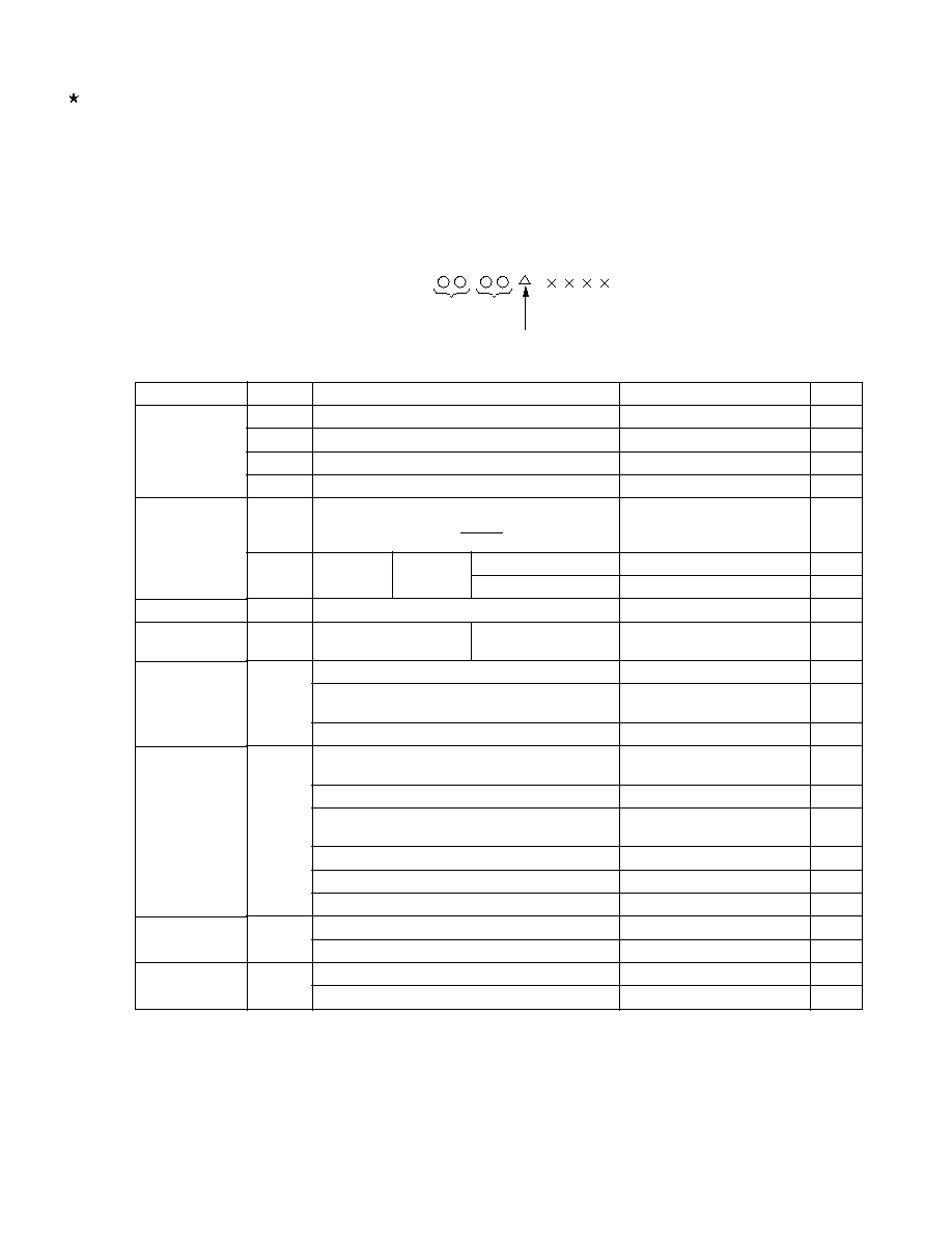
467
User's Manual U14260EJ3V1UD
CHAPTER 25 ELECTRICAL SPECIFICATIONS
(EXPANDED-SPECIFICATION PRODUCTS OF
µPD780076, 780078, 78F0078)
Target products:
µPD780076, 780078, 78F0078 for which orders were received after February 1, 2002 (Products
with a rank
Note
other than K)
Note The rank is indicated by the 5th digit from the left in the lot number marked on the package.
Absolute Maximum Ratings (T
A
= 25
∞C)
Parameter
Supply voltage
Input voltage
Output voltage
Analog input
voltage
Output
current, high
Output
current, low
Operating ambient
temperature
Storage
temperature
Symbol
V
DD
V
PP
AV
REF
AV
SS
V
I1
V
I2
V
O
V
AN
I
OH
I
OL
T
A
T
stg
Conditions
µPD78F0078 only, Note 2
P00 to P03, P10 to P17, P20 to P25, P34 to P36,
P40 to P47, P50 to P57, P64 to P67, P70 to P75,
P80, X1, X2, XT1, XT2, RESET
P30 to P33
N-ch open- No pull-up resistor
drain
Pull-up resistor
P10 to P17
Analog input pin
Per pin
Total for P00 to P03, P40 to P47, P50 to P57,
P64 to P67, P70 to P75, P80
Total for P20 to P25, P30 to P36
Per pin for P00 to P03, P20 to P25, P34 to P36,
P40 to P47, P64 to P67, P70 to P75, P80
Per pin for P30 to P33, P50 to P57
Total for P00 to P03, P40 to P47, P64 to P67,
P70 to P75, P80
Total for P20 to P25
Total for P30 to P36
Total for P50 to P57
During normal operation
During flash memory programming
µPD780076, 780078
µPD78F0078
Ratings
-0.3 to +6.5
-0.5 to +10.5
-0.3 to V
DD
+ 0.3
Note 1
-0.3 to +0.3
-0.3 to V
DD
+ 0.3
Note 1
-0.3 to +6.5
-0.3 to V
DD
+ 0.3
Note 1
-0.3 to V
DD
+ 0.3
Note 1
AV
SS
- 0.3 to AV
REF
+ 0.3
Note 1
and
-0.3 to V
DD
+ 0.3
Note 1
-10
-15
-15
20
30
50
20
100
100
-40 to +85
+10 to +40
-65 to +150
-40 to +125
Unit
V
V
V
V
V
V
V
V
V
mA
mA
mA
mA
mA
mA
mA
mA
mA
∞C
∞C
∞C
∞C
Note 1. 6.5 V or below
(Note 2 is explained on the next page.)
Caution Product quality may suffer if the absolute maximum rating is exceeded even momentarily for any
parameter. That is, the absolute maximum ratings are rated values at which the product is on the
verge of suffering physical damage, and therefore the product must be used under conditions that
ensure that the absolute maximum ratings are not exceeded.
Remark
Unless otherwise specified, the characteristics of alternate-function pins are the same as those of port pins.
Lot number
Year
code
Rank
Week
code
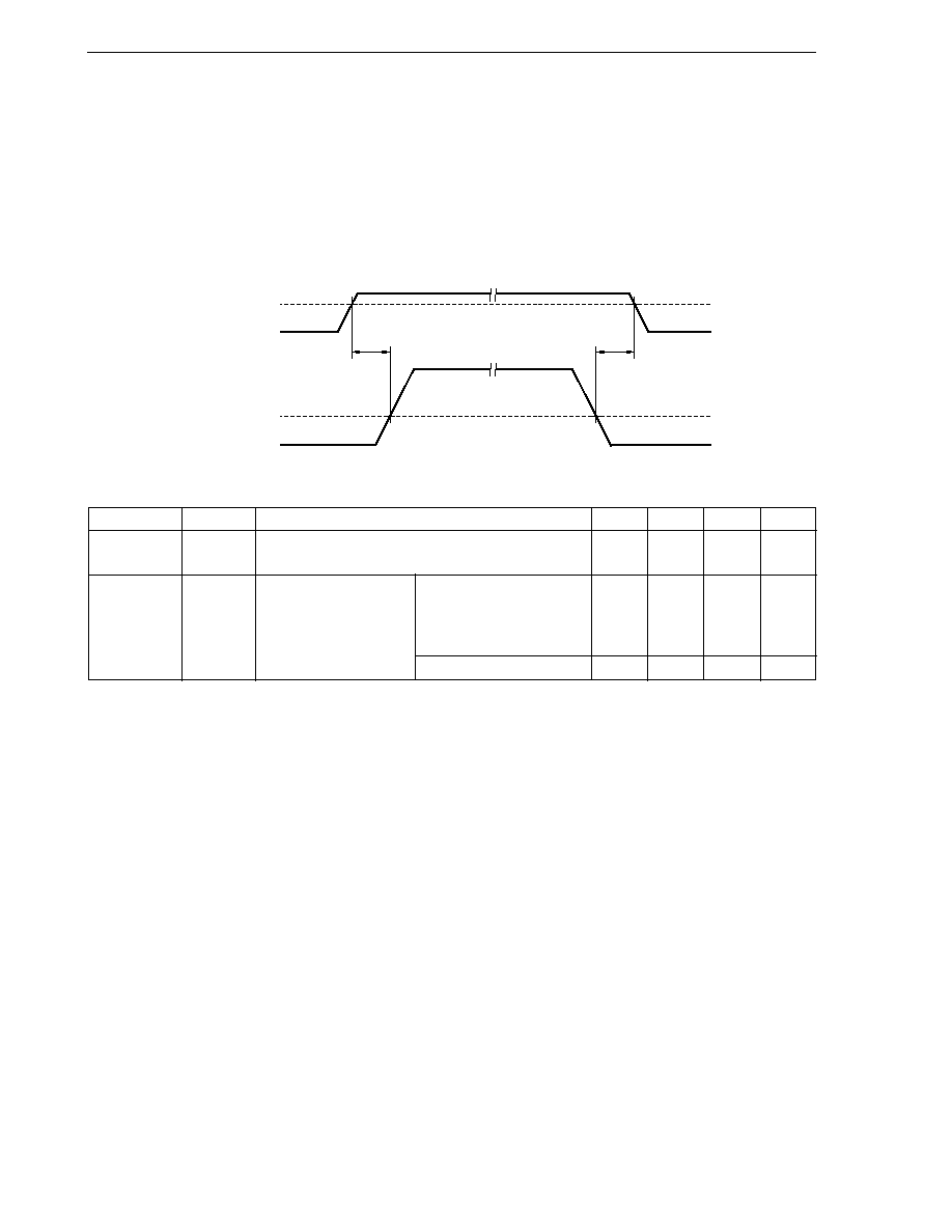
468
CHAPTER 25 ELECTRICAL SPECIFICATIONS (EXPANDED-SPECIFICATION PRODUCTS OF
µPD780076, 780078, 78F0078)
User's Manual U14260EJ3V1UD
Note 2.
Make sure that the following conditions of the V
PP
voltage application timing are satisfied when the flash
memory is written.
∑ When supply voltage rises
V
PP
must exceed V
DD
10
µs or more after V
DD
has reached the lower-limit value (2.7 V) of the
operating voltage range (see a in the figure below).
∑ When supply voltage drops
V
DD
must be lowered 10
µs or more after V
PP
falls below the lower-limit value (2.7 V) of the
operating voltage range of V
DD
(see b in the figure below).
Capacitance (T
A
= 25
∞
C, V
DD
= V
SS
= 0 V)
Parameter
Symbol
Conditions
MIN.
TYP.
MAX.
Unit
Input
C
IN
f = 1 MHz
15
pF
capacitance
Unmeasured pins returned to 0 V.
I/O
C
IO
f = 1 MHz
P00 to P03, P20 to P25,
15
pF
capacitance
Unmeasured pins
P34 to P36, P40 to P47,
returned to 0 V.
P50 to P57, P64 to P67,
P70 to P75, P80
P30 to P33
20
pF
Remark
Unless otherwise specified, the characteristics of alternate-function pins are the same as those of port pins.
2.7 V
V
DD
0 V
0 V
V
PP
2.7 V
a
b
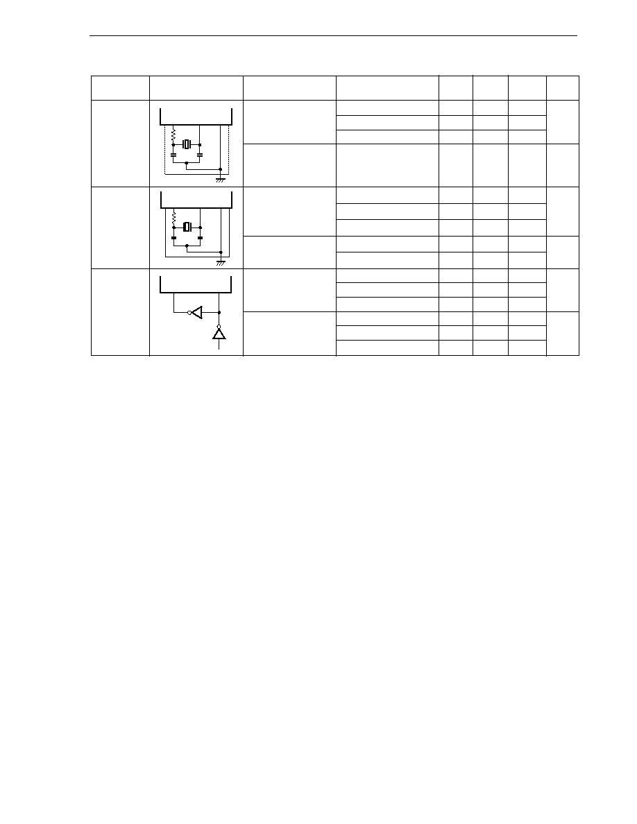
469
CHAPTER 25 ELECTRICAL SPECIFICATIONS (EXPANDED-SPECIFICATION PRODUCTS OF
µPD780076, 780078, 78F0078)
User's Manual U14260EJ3V1UD
Main System Clock Oscillator Characteristics (T
A
= ≠40 to +85
∞
C, V
DD
= 1.8 to 5.5 V)
Notes 1. Indicates only oscillator characteristics. Refer to AC Characteristics for instruction execution time.
2. Time required to stabilize oscillation after reset or STOP mode release.
Cautions
1. When using the main system clock oscillator, wire as follows in the area enclosed by the broken
lines in the above figures to avoid an adverse effect from wiring capacitance.
∑ Keep the wiring length as short as possible.
∑ Do not cross the wiring with the other signal lines.
∑ Do not route the wiring near a signal line through which a high fluctuating current flows.
∑ Always make the ground point of the oscillator capacitor the same potential as V
SS1
.
∑ Do not ground the capacitor to a ground pattern through which a high current flows.
∑ Do not fetch signals from the oscillator.
2. When the main system clock is stopped and the system is operating on the subsystem clock,
wait until the oscillation stabilization time has been secured by the program before switching
back to the main system clock.
Resonator
Recommended
Parameter
Conditions
MIN.
TYP.
MAX.
Unit
Circuit
Ceramic
Oscillation
4.5 V
V
DD
5.5 V
1.0
12.0
MHz
resonator
frequency (f
X
)
Note 1
3.0 V
V
DD
< 4.5 V
1.0
8.38
1.8 V
V
DD
< 3.0 V
1.0
5.0
Oscillation
After V
DD
reaches
4
ms
stabilization time
Note 2
oscillation voltage range
MIN.
Crystal
Oscillation
4.5 V
V
DD
5.5 V
1.0
12.0
MHz
resonator
frequency (f
X
)
Note 1
3.0 V
V
DD
< 4.5 V
1.0
8.38
1.8 V
V
DD
< 3.0 V
1.0
5.0
Oscillation
4.0 V
V
DD
5.5 V
10
ms
stabilization time
Note 2
1.8 V
V
DD
< 4.0 V
30
External
X1 input
4.5 V
V
DD
5.5 V
1.0
12.0
MHz
clock
frequency (f
X
)
Note 1
3.0 V
V
DD
< 4.5 V
1.0
8.38
1.8 V
V
DD
< 3.0 V
1.0
5.0
X1 input
4.5 V
V
DD
5.5 V
38
500
ns
high-/low-level width
3.0 V
V
DD
< 4.5 V
50
500
(t
XH
, t
XL
)
1.8 V
V
DD
< 3.0 V
85
500
X2
X1
C2
Rd
C1
X1
V
SS1
X2
C2
Rd
C1
X1
V
SS1
X2
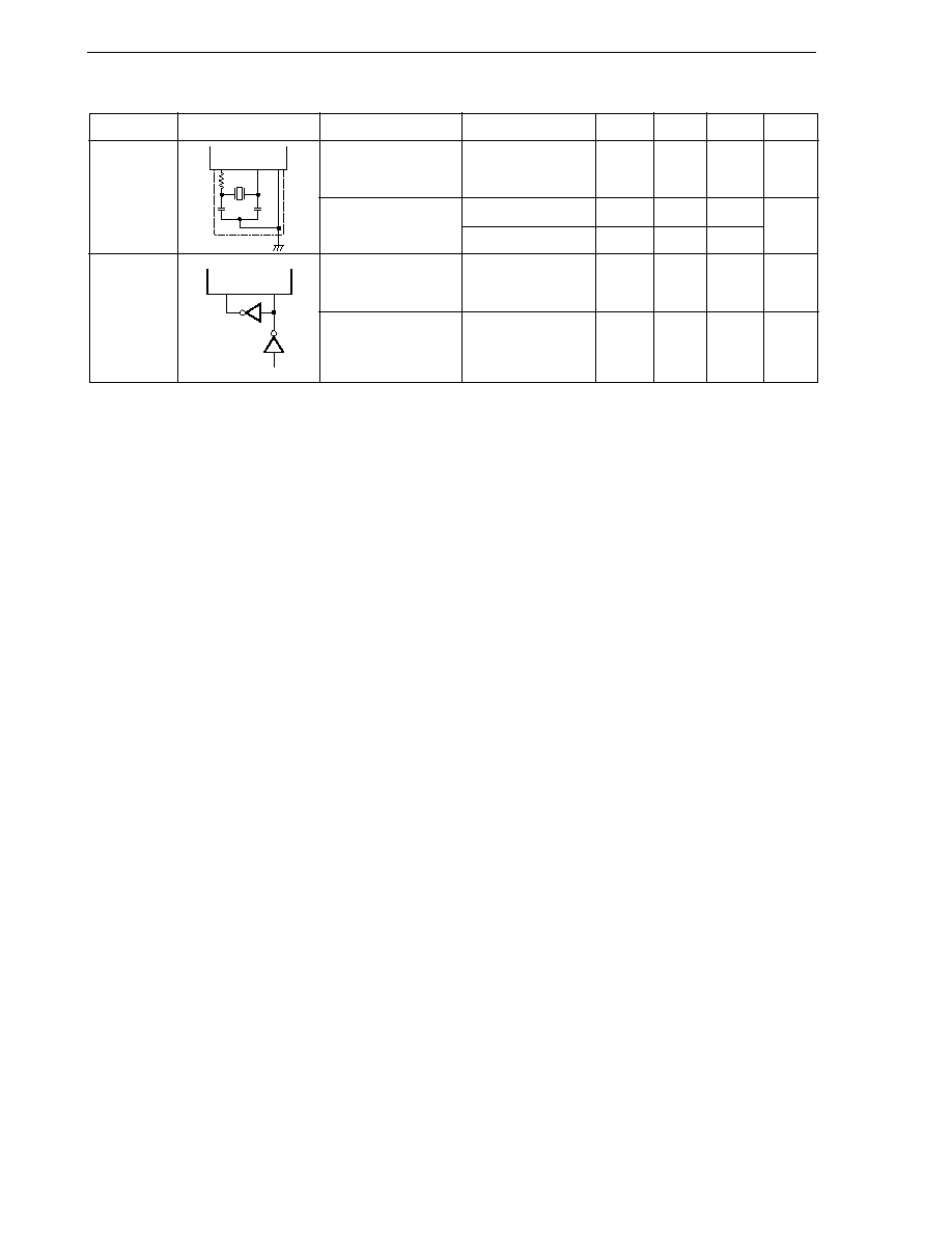
470
CHAPTER 25 ELECTRICAL SPECIFICATIONS (EXPANDED-SPECIFICATION PRODUCTS OF
µPD780076, 780078, 78F0078)
User's Manual U14260EJ3V1UD
Subsystem Clock Oscillator Characteristics
(T
A
= ≠40 to +85
∞C, V
DD
= 1.8 to 5.5 V)
Notes 1. Indicates only oscillator characteristics. Refer to AC Characteristics for instruction execution time.
2. Time required to stabilize oscillation after V
DD
reaches oscillation voltage range MIN.
Cautions
1. When using the subsystem clock oscillator, wire as follows in the area enclosed by the broken
lines in the above figure to avoid an adverse effect from wiring capacitance.
∑ Keep the wiring length as short as possible.
∑ Do not cross the wiring with the other signal lines.
∑ Do not route the wiring near a signal line through which a high fluctuating current flows.
∑ Always make the ground point of the oscillator capacitor the same potential as V
SS1
.
∑ Do not ground the capacitor to a ground pattern through which a high current flows.
∑ Do not fetch signals from the oscillator.
2. The subsystem clock oscillator is designed as a low-amplitude circuit for reducing power
consumption, and is more prone to malfunction due to noise than the main system clock
oscillator. Particular care is therefore required with the wiring method when the subsystem
clock is used.
MIN.
32
32
Resonator
Crystal
resonator
External
clock
Parameter
Oscillation
frequency (f
XT
)
Note 1
Oscillation
stabilization time
Note 2
XT1 input
frequency (f
XT
)
Note 1
XT1 input
high-/low-level width
(t
XTH
, t
XTL
)
Conditions
4.0 V
V
DD
5.5 V
1.8 V
V
DD
< 4.0 V
TYP.
32.768
1.2
MAX.
35
2
10
38.5
Unit
kHz
s
kHz
Recommended Circuit
12
15
µs
XT1
XT2
C3
XT2 XT1 V
SS1
Rd
C4

471
CHAPTER 25 ELECTRICAL SPECIFICATIONS (EXPANDED-SPECIFICATION PRODUCTS OF
µPD780076, 780078, 78F0078)
User's Manual U14260EJ3V1UD
Recommended Oscillator Constant
(1)
µPD780076, 780078
(a) Main system clock: Ceramic resonator (T
A
= ≠40 to +85
∞
C)
Manufacturer
Part Number
Frequency
Recommended Circuit Constant
Oscillation Voltage Range
(MHz)
C1 (pF)
C2 (pF)
Rd (k
)
MIN. (V)
MAX. (V)
Murata Mfg.
CSBFB1M00J58
1.00
150
150
0
1.8
5.5
Co., Ltd.
CSBLA1M00J58
1.00
150
150
0
1.8
5.5
CSTCC2M00G56
2.00
On-chip
On-chip
0
1.8
5.5
CSTLS2M00G56
2.00
On-chip
On-chip
0
1.8
5.5
CSTCC3M58G53
3.58
On-chip
On-chip
0
1.8
5.5
CSTLS3M58G53
3.58
On-chip
On-chip
0
1.8
5.5
CSTCR4M00G53
4.00
On-chip
On-chip
0
1.8
5.5
CSTLS4M00G53
4.00
On-chip
On-chip
0
1.8
5.5
CSTCR4M19G53
4.19
On-chip
On-chip
0
1.8
5.5
CSTLS4M19G53
4.19
On-chip
On-chip
0
1.8
5.5
CSTCR4M91G53
4.91
On-chip
On-chip
0
1.8
5.5
CSTLS4M91G53
4.91
On-chip
On-chip
0
1.8
5.5
CSTCR5M00G53
5.00
On-chip
On-chip
0
2.7
5.5
CSTLS5M00G53
5.00
On-chip
On-chip
0
2.7
5.5
CSTCE8M00G52
8.00
On-chip
On-chip
0
3.0
5.5
CSTLS8M00G53
8.00
On-chip
On-chip
0
3.0
5.5
CSTCE8M38G52
8.38
On-chip
On-chip
0
3.0
5.5
CSTLS8M38G53
8.38
On-chip
On-chip
0
3.0
5.5
CSTCE10M0G52
10.00
On-chip
On-chip
0
4.5
5.5
CSTLS10M0G53
10.00
On-chip
On-chip
0
4.5
5.5
CSTCE12M0G52
12.00
On-chip
On-chip
0
4.5
5.5
CSTLA12M0T55
12.00
On-chip
On-chip
0
4.5
5.5
TDK
CCR3.5MC5
3.58
On-chip
On-chip
0
1.8
5.5
CCR4.0MC5
4.00
On-chip
On-chip
0
1.8
5.5
CCR4.19MC5
4.19
On-chip
On-chip
0
1.8
5.5
CCR5.0MC5
5.00
On-chip
On-chip
0
2.7
5.5
CCR6.0MC5
6.00
On-chip
On-chip
0
2.7
5.5
CCR8.0MC5
8.00
On-chip
On-chip
0
3.0
5.5
CCR8.38MC5
8.38
On-chip
On-chip
0
3.0
5.5
CCR10.0MC5
10.00
On-chip
On-chip
0
4.5
5.5
CCR12.0MC5
12.00
On-chip
On-chip
0
4.5
5.5
Caution
The oscillator constant is a reference value based on evaluation in specific environments by the
resonator manufacturer. If the oscillator characteristics need to be optimized in the actual
application, request the resonator manufacturer for evaluation on the implementation circuit.
Note that the oscillation voltage and oscillation frequency merely indicate the characteristics of
the oscillator. Use the internal operation conditions of the
µPD780078 Subseries within the
specifications of the DC and AC characteristics.
472
CHAPTER 25 ELECTRICAL SPECIFICATIONS (EXPANDED-SPECIFICATION PRODUCTS OF
µPD780076, 780078, 78F0078)
User's Manual U14260EJ3V1UD
(1)
µPD780076, 780078
(b) Main system clock: Crystal resonator (T
A
= ≠10 to +70
∞
C)
(c) Subsystem clock: Crystal resonator (T
A
= ≠40 to +85
∞
C)
Caution
The oscillator constant is a reference value based on evaluation in specific environments by the
resonator manufacturer. If the oscillator characteristics need to be optimized in the actual
application, request the resonator manufacturer for evaluation on the implementation circuit.
Note that the oscillation voltage and oscillation frequency merely indicate the characteristics of
the oscillator. Use the internal operation conditions of the
µPD780078 Subseries within the
specifications of the DC and AC characteristics.
Manufacturer
KINSEKI, Ltd.
Part Number
HC-49/U-S
Frequency
(MHz)
4.19
8.38
C1 (pF)
18
27
C2 (pF)
18
27
MIN. (V)
1.9
3.0
MAX. (V)
5.5
5.5
Recommended Circuit Constant
Oscillation Voltage Range
Rd (k
)
4.7
0
Manufacturer
Seiko Epson
Corporation
Part Number
C-022RX
MC-206
MC-306
Frequency
(kHz)
32.768
32.768
32.768
C1 (pF)
15
15
15
C2 (pF)
15
15
15
MIN. (V)
1.8
1.8
1.8
MAX. (V)
5.5
5.5
5.5
Recommended Circuit Constant
Oscillation Voltage Range
Rd (k
)
330
330
330

473
CHAPTER 25 ELECTRICAL SPECIFICATIONS (EXPANDED-SPECIFICATION PRODUCTS OF
µPD780076, 780078, 78F0078)
User's Manual U14260EJ3V1UD
(2)
µPD78F0078
Main system clock: Ceramic resonator (T
A
= ≠40 to +85
∞
C)
Manufacturer
Part Number
Frequency
Recommended Circuit Constant
Oscillation Voltage Range
(MHz)
C1 (pF)
C2 (pF)
R1 (k
)
MIN. (V)
MAX. (V)
Murata Mfg.
CSBFB1M00J58
1.00
100
100
3.3
1.8
5.5
Co., Ltd.
CSBLA1M00J58
1.00
100
100
3.3
1.8
5.5
CSTCC2M00G56
2.00
On-chip
On-chip
0
1.8
5.5
CSTLS2M00G56
2.00
On-chip
On-chip
0
1.8
5.5
CSTCC3M58G53
3.58
On-chip
On-chip
0
1.8
5.5
CSTLS3M58G53
3.58
On-chip
On-chip
0
1.8
5.5
CSTCR4M00G53
4.00
On-chip
On-chip
0
1.8
5.5
CSTLS4M00G53
4.00
On-chip
On-chip
0
1.8
5.5
CSTCR4M19G53
4.19
On-chip
On-chip
0
1.8
5.5
CSTLS4M19G53
4.19
On-chip
On-chip
0
1.8
5.5
CSTCR4M91G53
4.91
On-chip
On-chip
0
1.8
5.5
CSTLS4M91G53
4.91
On-chip
On-chip
0
1.8
5.5
CSTCR5M00G53
5.00
On-chip
On-chip
0
2.7
5.5
CSTLS5M00G53
5.00
On-chip
On-chip
0
2.7
5.5
CSTCE8M00G52
8.00
On-chip
On-chip
0
3.0
5.5
CSTLS8M00G53
8.00
On-chip
On-chip
0
3.0
5.5
CSTCE8M38G52
8.38
On-chip
On-chip
0
3.0
5.5
CSTLS8M38G53
8.38
On-chip
On-chip
0
3.0
5.5
CSTCE10M0G52
10.00
On-chip
On-chip
0
4.5
5.5
CSTLS10M0G53
10.00
On-chip
On-chip
0
4.5
5.5
CSTLS10M0G55093
10.00
On-chip
On-chip
0
4.5
5.5
CSTCE12M0G52
12.00
On-chip
On-chip
0
4.5
5.5
CSTLA12M0T55
12.00
On-chip
On-chip
0
4.5
5.5
Caution
The oscillator constant is a reference value based on evaluation in specific environments by the
resonator manufacturer. If the oscillator characteristics need to be optimized in the actual
application, request the resonator manufacturer for evaluation on the implementation circuit.
Note that the oscillation voltage and oscillation frequency merely indicate the characteristics of
the oscillator. Use the internal operation conditions of the
µPD780078 Subseries within the
specifications of the DC and AC characteristics.
Remark For the resonator selection and oscillator constant, users are requested to either evaluate the oscillation
themselves or apply to the resonator manufacturer for evaluation.

474
CHAPTER 25 ELECTRICAL SPECIFICATIONS (EXPANDED-SPECIFICATION PRODUCTS OF
µPD780076, 780078, 78F0078)
User's Manual U14260EJ3V1UD
DC Characteristics (T
A
= ≠40 to +85
∞
C, V
DD
= 1.8 to 5.5 V)
Parameter
Symbol
Conditions
MIN.
TYP.
MAX.
Unit
Output current,
I
OH
Per pin
≠1
mA
high
All pins
≠15
mA
Output current,
I
OL
Per pin for P00 to P03, P20 to P25, P34 to P36,
10
mA
low
P40 to P47, P64 to P67, P70 to P75, P80
Per pin for P30 to P33, P50 to P57
15
mA
Total for P00 to P03, P40 to P47, P64 to P67, P70 to P75, P80
20
mA
Total for P20 to P25
10
mA
Total for P30 to P36
70
mA
Total for P50 to P57
70
mA
Input voltage,
V
IH1
P10 to P17, P21, P24,
2.7 V
V
DD
5.5 V
0.7V
DD
V
DD
V
high
P40 to P47, P50 to P57,
1.8 V
V
DD
< 2.7 V
0.8V
DD
V
DD
V
P64 to P67
V
IH2
P00 to P03, P20, P22, P23, P25,
2.7 V
V
DD
5.5 V
0.8V
DD
V
DD
V
P34 to P36, P70 to P75, P80, RESET 1.8 V V
DD
< 2.7 V
0.85V
DD
V
DD
V
V
IH3
P30 to P33
2.7 V
V
DD
5.5 V
0.7V
DD
5.5
V
(N-ch open-drain)
1.8 V
V
DD
< 2.7 V
0.8V
DD
5.5
V
V
IH4
X1, X2
2.7 V
V
DD
5.5 V
V
DD
≠
0.5
V
DD
V
1.8 V
V
DD
< 2.7 V
V
DD
≠
0.2
V
DD
V
V
IH5
XT1, XT2
4.0 V
V
DD
5.5 V
0.8V
DD
V
DD
V
1.8 V
V
DD
< 4.0 V
0.9V
DD
V
DD
V
Input voltage,
V
IL1
P10 to P17, P21, P24,
2.7 V
V
DD
5.5 V
0
0.3V
DD
V
low
P40 to P47, P50 to P57,
1.8 V
V
DD
< 2.7 V
0
0.2V
DD
V
P64 to P67
V
IL2
P00 to P03, P20, P22, P23, P25,
2.7 V
V
DD
5.5 V
0
0.2V
DD
V
P34 to P36, P70 to P75, P80, RESET 1.8 V
V
DD
< 2.7 V
0
0.15V
DD
V
V
IL3
P30 to P33
4.0 V
V
DD
5.5 V
0
0.3V
DD
V
(N-ch open-drain)
2.7 V
V
DD
< 4.0 V
0
0.2V
DD
V
1.8 V
V
DD
< 2.7 V
0
0.1V
DD
V
V
IL4
X1, X2
2.7 V
V
DD
5.5 V
0
0.4
V
1.8 V
V
DD
< 2.7 V
0
0.2
V
V
IL5
XT1, XT2
4.0 V
V
DD
5.5 V
0
0.2V
DD
V
1.8 V
V
DD
< 4.0 V
0
0.1V
DD
V
Output voltage,
V
OH1
4.0 V
V
DD
5.5 V, I
OH
= ≠1 mA
V
DD
≠
1.0
V
DD
V
high
1.8 V
V
DD
< 4.0 V, I
OH
= ≠100
µA
V
DD
≠
0.5
V
DD
V
Output voltage,
V
OL1
P30 to P33
4.0 V
V
DD
5.5 V,
2.0
V
low
I
OL
= 15 mA
V
OL2
P50 to P57
4.0 V
V
DD
5.5 V,
0.4
2.0
V
I
OL
= 15 mA
V
OL3
P00 to P03, P20 to P25, P34 to P36,
4.0 V
V
DD
5.5 V,
0.4
V
P40 to P47, P64 to P67, P70 to P75, P80
I
OL
= 1.6 mA
V
OL4
I
OL
= 400
µA
0.5
V
Remark
Unless otherwise specified, the characteristics of alternate-function pins are the same as those of port pins.
475
CHAPTER 25 ELECTRICAL SPECIFICATIONS (EXPANDED-SPECIFICATION PRODUCTS OF
µPD780076, 780078, 78F0078)
User's Manual U14260EJ3V1UD
DC Characteristics (T
A
= ≠40 to +85
∞
C, V
DD
= 1.8 to 5.5 V)
Parameter
Symbol
Conditions
MIN.
TYP.
MAX.
Unit
Input leakage
I
LIH1
V
IN
= V
DD
P00 to P03, P10 to P17, P20 to P25,
3
µA
current, high
P34 to P36, P40 to P47, P50 to P57,
P64 to P67, P70 to P75, P80,
RESET
I
LIH2
X1, X2, XT1, XT2
20
µA
I
LIH3
V
IN
= 5.5 V
P30 to P33
3
µA
Input leakage
I
LIL1
V
IN
= 0 V
P00 to P03, P10 to P17, P20 to P25,
≠3
µA
current, low
P34 to P36, P40 to P47, P50 to P57,
P64 to P67, P70 to P75, P80,
RESET
I
LIL2
X1, X2, XT1, XT2
≠20
µA
I
LIL3
P30 to P33
≠3
µA
Output leakage
I
LOH
V
OUT
= V
DD
3
µA
current, high
Output leakage
I
LOL
V
OUT
= 0 V
≠3
µA
current, low
Mask option
R
1
V
IN
= 0 V,
15
30
90
k
pull-up resistance
P30, P31, P32, P33
(mask ROM
version only)
Software pull-
R
2
V
IN
= 0 V,
15
30
90
k
up resistance
P00 to P03, P20 to P25, P34 to P36, P40 to P47,
P50 to P57, P64 to P67, P70 to P75, P80
V
PP
(IC)
V
PP1
During normal operation
0
0.2V
DD
V
power supply
voltage
Remark Unless otherwise specified, the characteristics of alternate-function pins are the same as those of port pins.

476
CHAPTER 25 ELECTRICAL SPECIFICATIONS (EXPANDED-SPECIFICATION PRODUCTS OF
µPD780076, 780078, 78F0078)
User's Manual U14260EJ3V1UD
DC Characteristics (T
A
= ≠40 to +85
∞
C, V
DD
= 1.8 to 5.5 V)
(1)
µPD780076, 780078
Parameter
Symbol
Conditions
MIN.
TYP.
MAX.
Unit
Power supply
I
DD1
Note 2
12.0 MHz
V
DD
= 5.0 V
±10%
Note 3
When A/D converter is
9.0
18.0
mA
current
Note 1
crystal oscillation
stopped
operating mode
When A/D converter is
10.0
20.0
mA
operating
8.38 MHz
V
DD
= 5.0 V
±10%
Note 3
When A/D converter is
5.5
11.0
mA
crystal oscillation
stopped
operating mode
When A/D converter is
6.5
13.0
mA
operating
V
DD
= 3.0 V + 10%
Notes 3, 6
When A/D converter is
3.5
7.0
mA
stopped
When A/D converter is
4.5
9.0
mA
operating
5.00 MHz
V
DD
= 3.0 V
±10%
Note 3
When A/D converter is
2.0
4.0
mA
crystal oscillation
stopped
operating mode
When A/D converter is
3.0
6.0
mA
operating
V
DD
= 2.0 V
±10%
Note 4
When A/D converter is
0.4
1.5
mA
stopped
When A/D converter is
1.4
4.2
mA
operating
I
DD2
12.0 MHz
V
DD
= 5.0 V
±10%
Note 3
When peripheral functions
2.5
5.0
mA
crystal oscillation
are stopped
HALT mode
When peripheral functions
11.5
mA
are operating
8.38 MHz
V
DD
= 5.0 V
±10%
Note 3
When peripheral functions
1.1
2.2
mA
crystal oscillation
are stopped
HALT mode
When peripheral functions
4.7
mA
are operating
V
DD
= 3.0 V + 10%
Notes 3, 6
When peripheral functions
0.7
1.4
mA
are stopped
When peripheral functions
4.5
mA
are operating
5.00 MHz
V
DD
= 3.0 V
±10%
Note 3
When peripheral functions
0.35
0.7
mA
crystal oscillation
are stopped
HALT mode
When peripheral functions
1.7
mA
are operating
V
DD
= 2.0 V
±10%
Note 4
When peripheral functions
0.15
0.4
mA
are stopped
When peripheral functions
1.1
mA
are operating
I
DD3
32.768 kHz crystal oscillation
V
DD
= 5.0 V
±10%
40
80
µA
operating mode
Note 5
V
DD
= 3.0 V
±10%
20
40
µA
V
DD
= 2.0 V
±10%
10
20
µA
I
DD4
32.768 kHz crystal oscillation
V
DD
= 5.0 V
±10%
30
60
µA
HALT mode
Note 5
V
DD
= 3.0 V
±10%
6
18
µA
V
DD
= 2.0 V
±10%
2
10
µA
I
DD5
STOP mode
Note 7
V
DD
= 5.0 V
±10%
0.1
30
µA
V
DD
= 3.0 V
±10%
0.05
10
µA
V
DD
= 2.0 V
±10%
0.05
10
µA

477
CHAPTER 25 ELECTRICAL SPECIFICATIONS (EXPANDED-SPECIFICATION PRODUCTS OF
µPD780076, 780078, 78F0078)
User's Manual U14260EJ3V1UD
Notes 1. Total current through the internal power supply (V
DD0
, V
DD1
).
2. I
DD1
includes the peripheral operating current (except the current through the pull-up resistors of ports).
3. When the processor clock control register (PCC) is set to 00H.
4. When PCC is set to 02H.
5. When main system clock operation is stopped.
6. The values show the specifications when V
DD
= 3.0 to 3.3 V. The value in the TYP. column shows the
specifications when V
DD
= 3.0 V.
7. When the main system clock and subsystem clock are stopped.
478
CHAPTER 25 ELECTRICAL SPECIFICATIONS (EXPANDED-SPECIFICATION PRODUCTS OF
µPD780076, 780078, 78F0078)
User's Manual U14260EJ3V1UD
DC Characteristics (T
A
= ≠40 to +85
∞
C, V
DD
= 1.8 to 5.5 V)
(2)
µPD78F0078
Parameter
Symbol
Conditions
MIN.
TYP.
MAX.
Unit
Power supply
I
DD1
Note 2
12.0 MHz
V
DD
= 5.0 V
±10%
Note 3
When A/D converter is
17.0
34.0
mA
current
Note 1
crystal oscillation
stopped
operating mode
When A/D converter is
18.0
36.0
mA
operating
8.38 MHz
V
DD
= 5.0 V
±10%
Note 3
When A/D converter is
10.5
21.0
mA
crystal oscillation
stopped
operating mode
When A/D converter is
11.5
23.0
mA
operating
V
DD
= 3.0 V + 10%
Notes 3, 6
When A/D converter is
7.0
14.0
mA
stopped
When A/D converter is
8.0
16.0
mA
operating
5.00 MHz
V
DD
= 3.0 V
±10%
Note 3
When A/D converter is
4.5
9.0
mA
crystal oscillation
stopped
operating mode
When A/D converter is
5.5
11.0
mA
operating
V
DD
= 2.0 V
±10%
Note 4
When A/D converter is
1.0
2.0
mA
stopped
When A/D converter is
2.0
6.0
mA
operating
I
DD2
12.0 MHz
V
DD
= 5.0 V
±10%
Note 3
When peripheral functions
2.5
5.0
mA
crystal oscillation
are stopped
HALT mode
When peripheral functions
11.5
mA
are operating
8.38 MHz
V
DD
= 5.0 V
±10%
Note 3
When peripheral functions
1.2
2.4
mA
crystal oscillation
are stopped
HALT mode
When peripheral functions
5.0
mA
are operating
V
DD
= 3.0 V + 10%
Notes 3, 6
When peripheral functions
0.7
1.4
mA
are stopped
When peripheral functions
4.5
mA
are operating
5.00 MHz
V
DD
= 3.0 V
±10%
Note 3
When peripheral functions
0.4
0.8
mA
crystal oscillation
are stopped
HALT mode
When peripheral functions
1.7
mA
are operating
V
DD
= 2.0 V
±10%
Note 4
When peripheral functions
0.2
0.4
mA
are stopped
When peripheral functions
1.1
mA
are operating
I
DD3
32.768 kHz crystal oscillation
V
DD
= 5.0 V
±10%
115
230
µA
operating mode
Note 5
V
DD
= 3.0 V
±10%
95
190
µA
V
DD
= 2.0 V
±10%
75
150
µA
I
DD4
32.768 kHz crystal oscillation
V
DD
= 5.0 V
±10%
30
60
µA
HALT mode
Note 5
V
DD
= 3.0 V
±10%
6
18
µA
V
DD
= 2.0 V
±10%
2
10
µA
I
DD5
STOP mode
Note 7
V
DD
= 5.0 V
±10%
0.1
30
µA
V
DD
= 3.0 V
±10%
0.05
10
µA
V
DD
= 2.0 V
±10%
0.05
10
µA

479
CHAPTER 25 ELECTRICAL SPECIFICATIONS (EXPANDED-SPECIFICATION PRODUCTS OF
µPD780076, 780078, 78F0078)
User's Manual U14260EJ3V1UD
Notes 1. Total current through the internal power supply (V
DD0
, V
DD1
).
2. I
DD1
includes the peripheral operating current (except the current through the pull-up resistors of ports).
3. When the processor clock control register (PCC) is set to 00H.
4. When PCC is set to 02H.
5. When main system clock operation is stopped.
6. The values show the specifications when V
DD
= 3.0 to 3.3 V. The value in the TYP. column shows the
specifications when V
DD
= 3.0 V.
7. When the main system clock and subsystem clock are stopped.
480
CHAPTER 25 ELECTRICAL SPECIFICATIONS (EXPANDED-SPECIFICATION PRODUCTS OF
µPD780076, 780078, 78F0078)
User's Manual U14260EJ3V1UD
AC Characteristics
(1) Basic operation
(T
A
= ≠40 to +85
∞
C, V
DD
= 1.8 to 5.5 V)
Parameter
Symbol
Conditions
MIN.
TYP.
MAX.
Unit
Cycle time
T
CY
Operating with
4.5 V
V
DD
5.5 V
0.166
16
µs
(Min. instruction
main system clock
3.0 V
V
DD
< 4.5 V
0.238
16
µs
execution time)
2.7 V
V
DD
< 3.0 V
0.4
16
µs
1.8 V
V
DD
< 2.7 V
1.6
16
µs
Operating with subsystem clock
103.9
Note 1
122
125
µs
TI000, TI010, TI001,
t
TIH0
, t
TIL0
3.0 V
V
DD
5.5 V
2/f
sam
+ 0.1
Note 2
µs
TI011 input high-/low-
2.7 V
V
DD
< 3.0 V
2/f
sam
+ 0.2
Note 2
µs
level width
1.8 V
V
DD
< 2.7 V
2/f
sam
+ 0.5
Note 2
µs
TI50, TI51 input
f
TI5
2.7 V
V
DD
5.5 V
0
4
MHz
frequency
1.8 V
V
DD
< 2.7 V
0
275
kHz
TI50, TI51 input
t
TIH5
, t
TIL5
2.7 V
V
DD
5.5 V
100
ns
high-/low-level
1.8 V
V
DD
< 2.7 V
1.8
µs
width
Interrupt request
t
INTH
, t
INTL
INTP0 to INTP3,
2.7 V
V
DD
5.5 V
1
µs
input high-/low-
P40 to P47
1.8 V
V
DD
< 2.7 V
2
µs
level width
RESET
t
RSL
2.7 V
V
DD
5.5 V
10
µs
low-level width
1.8 V
V
DD
< 2.7 V
20
µs
Notes
1. Value when the external clock is used. When a crystal resonator is used, it is 114
µs (MIN.).
2. Selection of f
sam
= f
X
, f
X
/4, f
X
/64 is possible using bits 0 and 1 (PRM000, PRM010) of prescaler mode
register 00 (PRM00). Selection of f
sam
= f
X
/2, f
X
/8, f
X
/512 is possible using bits 0 and 1 (PRM001, PRM011)
of prescaler mode register 01 (PRM01). However, if the TI000 or TI001 valid edge is selected as the count
clock, the value becomes f
sam
= f
X
/8.
481
CHAPTER 25 ELECTRICAL SPECIFICATIONS (EXPANDED-SPECIFICATION PRODUCTS OF
µPD780076, 780078, 78F0078)
User's Manual U14260EJ3V1UD
T
CY
vs. V
DD
(main system clock operation)
5.0
1.0
2.0
1.6
0.4
0.238
0.166
0.1
Supply voltage V
DD
[V]
Cycle time T
CY
[s
]
µ
0
10.0
1.0
2.0
3.0
4.0
5.0
6.0
1.8
5.5
2.7
4.5
Operation
guaranteed
range
16.0
482
CHAPTER 25 ELECTRICAL SPECIFICATIONS (EXPANDED-SPECIFICATION PRODUCTS OF
µPD780076, 780078, 78F0078)
User's Manual U14260EJ3V1UD
(2) Read/write operation (T
A
= ≠40 to +85
∞
C, V
DD
= 4.0 to 5.5 V)
(1/3)
Parameter
Symbol
Conditions
MIN.
MAX.
Unit
ASTB high-level width
t
ASTH
0.3t
CY
ns
Address setup time
t
ADS
20
ns
Address hold time
t
ADH
6
ns
Data input time from address
t
ADD1
(2 + 2n)t
CY
≠ 54
ns
t
ADD2
(3 + 2n)t
CY
≠ 60
ns
Address output time from RD
t
RDAD
0
100
ns
Data input time from RD
t
RDD1
(2 + 2n)t
CY
≠ 87
ns
t
RDD2
(3 + 2n)t
CY
≠ 93
ns
Read data hold time
t
RDH
0
ns
RD low-level width
t
RDL1
(1.5 + 2n)t
CY
≠ 33
ns
t
RDL2
(2.5 + 2n)t
CY
≠ 33
ns
Input time from RD
to WAIT
t
RDWT1
t
CY
≠ 43
ns
t
RDWT2
t
CY
≠ 43
ns
Input time from WR
to WAIT
t
WRWT
t
CY
≠ 25
ns
WAIT low-level width
t
WTL
(0.5 + n)t
CY
+ 10
(2 + 2n)t
CY
ns
Write data setup time
t
WDS
60
ns
Write data hold time
t
WDH
6
ns
WR low-level width
t
WRL1
(1.5 + 2n)t
CY
≠ 15
ns
Delay time from ASTB
to RD
t
ASTRD
6
ns
Delay time from ASTB
to WR
t
ASTWR
2t
CY
≠ 15
ns
Delay time from
t
RDAST
0.8t
CY
≠ 15
1.2t
CY
ns
RD
to ASTB at external fetch
Address hold time from
t
RDADH
0.8t
CY
≠ 15
1.2t
CY
+ 30
ns
RD
at external fetch
Write data output time from RD
t
RDWD
40
ns
Write data output time from WR
t
WRWD
10
60
ns
Address hold time from WR
t
WRADH
0.8t
CY
≠ 15
1.2t
CY
+ 30
ns
Delay time from WAIT
to RD
t
WTRD
0.8t
CY
2.5t
CY
+ 25
ns
Delay time from WAIT
to WR
t
WTWR
0.8t
CY
2.5t
CY
+ 25
ns
Caution
T
CY
can only be used when the MIN. value is 0.238
µs.
Remarks
1.
t
CY
= T
CY
/4
2.
n indicates the number of waits.
3.
C
L
= 100 pF (C
L
indicates the load capacitance of the AD0 to AD7, A8 to A15, RD, WR, WAIT, and
ASTB pins.)

483
CHAPTER 25 ELECTRICAL SPECIFICATIONS (EXPANDED-SPECIFICATION PRODUCTS OF
µPD780076, 780078, 78F0078)
User's Manual U14260EJ3V1UD
(2) Read/write operation (T
A
= ≠40 to +85
∞
C, V
DD
= 2.7 to 4.0 V)
(2/3)
Parameter
Symbol
Conditions
MIN.
MAX.
Unit
ASTB high-level width
t
ASTH
0.3t
CY
ns
Address setup time
t
ADS
30
ns
Address hold time
t
ADH
10
ns
Input time from address to data
t
ADD1
(2 + 2n)t
CY
≠ 108
ns
t
ADD2
(3 + 2n)t
CY
≠ 120
ns
Output time from RD
to address
t
RDAD
0
200
ns
Input time from RD
to data
t
RDD1
(2 + 2n)t
CY
≠ 148
ns
t
RDD2
(3 + 2n)t
CY
≠ 162
ns
Read data hold time
t
RDH
0
ns
RD low-level width
t
RDL1
(1.5 + 2n)t
CY
≠ 40
ns
t
RDL2
(2.5 + 2n)t
CY
≠ 40
ns
Input time from RD
to WAIT
t
RDWT1
t
CY
≠ 75
ns
t
RDWT2
t
CY
≠ 60
ns
Input time from WR
to WAIT
t
WRWT
t
CY
≠ 50
ns
WAIT low-level width
t
WTL
(0.5 + 2n)t
CY
+ 10
(2 + 2n)t
CY
ns
Write data setup time
t
WDS
60
ns
Write data hold time
t
WDH
10
ns
WR low-level width
t
WRL1
(1.5 + 2n)t
CY
≠ 30
ns
Delay time from ASTB
to RD
t
ASTRD
10
ns
Delay time from ASTB
to WR
t
ASTWR
2t
CY
≠ 30
ns
Delay time from
t
RDAST
0.8t
CY
≠ 30
1.2t
CY
ns
RD
to ASTB at external fetch
Hold time from
t
RDADH
0.8t
CY
≠ 30
1.2t
CY
+ 60
ns
RD
to address at external fetch
Write data output time from RD
t
RDWD
40
ns
Write data output time from WR
t
WRWD
20
120
ns
Hold time from WR
to address
t
WRADH
0.8t
CY
≠ 30
1.2t
CY
+ 60
ns
Delay time from WAIT
to RD
t
WTRD
0.5t
CY
2.5t
CY
+ 50
ns
Delay time from WAIT
to WR
t
WTWR
0.5t
CY
2.5t
CY
+ 50
ns
Caution
T
CY
can only be used when the MIN. value is 0.4
µs.
Remarks
1.
t
CY
= T
CY
/4
2.
n indicates the number of waits.
3.
C
L
= 100 pF (C
L
indicates the load capacitance of the AD0 to AD7, A8 to A15, RD, WR, WAIT, and
ASTB pins.)

484
CHAPTER 25 ELECTRICAL SPECIFICATIONS (EXPANDED-SPECIFICATION PRODUCTS OF
µPD780076, 780078, 78F0078)
User's Manual U14260EJ3V1UD
(2) Read/write operation (T
A
= ≠40 to +85
∞
C, V
DD
= 1.8 to 2.7 V)
(3/3)
Parameter
Symbol
Conditions
MIN.
MAX.
Unit
ASTB high-level width
t
ASTH
0.3t
CY
ns
Address setup time
t
ADS
120
ns
Address hold time
t
ADH
20
ns
Input time from address to data
t
ADD1
(2 + 2n)t
CY
≠ 233
ns
t
ADD2
(3 + 2n)t
CY
≠ 240
ns
Output time from RD
to address
t
RDAD
0
400
ns
Input time from RD
to data
t
RDD1
(2 + 2n)t
CY
≠ 325
ns
t
RDD2
(3 + 2n)t
CY
≠ 332
ns
Read data hold time
t
RDH
0
ns
RD low-level width
t
RDL1
(1.5 + 2n)t
CY
≠ 92
ns
t
RDL2
(2.5 + 2n)t
CY
≠ 92
ns
Input time from RD
to WAIT
t
RDWT1
t
CY
≠ 350
ns
t
RDWT2
t
CY
≠ 132
ns
Input time from WR
to WAIT
t
WRWT
t
CY
≠ 100
ns
WAIT low-level width
t
WTL
(0.5 + 2n)t
CY
+ 10
(2 + 2n)t
CY
ns
Write data setup time
t
WDS
60
ns
Write data hold time
t
WDH
20
ns
WR low-level width
t
WRL1
(1.5 + 2n)t
CY
≠ 60
ns
Delay time from ASTB
to RD
t
ASTRD
20
ns
Delay time from ASTB
to WR
t
ASTWR
2t
CY
≠ 60
ns
Delay time from
t
RDAST
0.8t
CY
≠ 60
1.2t
CY
ns
RD
to ASTB at external fetch
Hold time from
t
RDADH
0.8t
CY
≠ 60
1.2t
CY
+ 120
ns
RD
to address at external fetch
Write data output time from RD
t
RDWD
40
ns
Write data output time from WR
t
WRWD
40
240
ns
Hold time from WR
to address
t
WRADH
0.8t
CY
≠ 60
1.2t
CY
+ 120
ns
Delay time from WAIT
to RD
t
WTRD
0.5t
CY
2.5t
CY
+ 100
ns
Delay time from WAIT
to WR
t
WTWR
0.5t
CY
2.5t
CY
+ 100
ns
Caution
T
CY
can only be used when the MIN. value is 1.6
µs.
Remarks
1.
t
CY
= T
CY
/4
2.
n indicates the number of waits.
3.
C
L
= 100 pF (C
L
indicates the load capacitance of the AD0 to AD7, A8 to A15, RD, WR, WAIT, and
ASTB pins.)
485
CHAPTER 25 ELECTRICAL SPECIFICATIONS (EXPANDED-SPECIFICATION PRODUCTS OF
µPD780076, 780078, 78F0078)
User's Manual U14260EJ3V1UD
(3) Serial interface (T
A
= ≠40 to +85
∞
C, V
DD
= 1.8 to 5.5 V)
(a) SIO3 3-wire serial I/O mode (SCK3 ... Internal clock output)
Parameter
Symbol
Conditions
MIN.
TYP.
MAX.
Unit
SCK3 cycle time
t
KCY1
4.5 V
V
DD
5.5 V
666
ns
3.0 V
V
DD
< 4.5 V
954
ns
2.7 V
V
DD
< 3.0 V
1600
ns
1.8 V
V
DD
< 2.7 V
3200
ns
SCK3 high-/
t
KH1
, t
KL1
3.0 V
V
DD
5.5 V
t
KCY1
/2 ≠ 50
ns
low-level width
1.8 V
V
DD
< 3.0 V
t
KCY1
/2 ≠ 100
ns
SI3 setup time
t
SIK1
3.0 V
V
DD
5.5 V
100
ns
(to SCK3
)
2.7 V
V
DD
< 3.0 V
150
ns
1.8 V
V
DD
< 2.7 V
300
ns
SI3 hold time
t
KSI1
4.5 V
V
DD
5.5 V
300
ns
(from SCK3
)
1.8 V
V
DD
< 4.5 V
400
ns
Delay time from
t
KSO1
C = 100 pF
Note
4.5 V
V
DD
5.5 V
200
ns
SCK3
to SO3 output
1.8 V
V
DD
< 4.5 V
300
ns
Note C is the load capacitance of the SCK3 and SO3 output lines.
(b) SIO3 3-wire serial I/O mode (SCK3 ... External clock input)
Parameter
Symbol
Conditions
MIN.
TYP.
MAX.
Unit
SCK3 cycle time
t
KCY2
4.5 V
V
DD
5.5 V
666
ns
3.0 V
V
DD
< 4.5 V
800
ns
2.7 V
V
DD
< 3.0 V
1600
ns
1.8 V
V
DD
< 2.7 V
3200
ns
SCK3 high-/
t
KH2
, t
KL2
4.5 V
V
DD
5.5 V
333
ns
low-level width
3.0 V
V
DD
< 4.5 V
400
ns
2.7 V
V
DD
< 3.0 V
800
ns
1.8 V
V
DD
< 2.7 V
1600
ns
SI3 setup time
t
SIK2
100
ns
(to SCK3
)
SI3 hold time
t
KSI2
4.5 V
V
DD
5.5 V
300
ns
(from SCK3
)
1.8 V
V
DD
< 4.5 V
400
ns
Delay time from
t
KSO2
C = 100 pF
Note
4.5 V
V
DD
5.5 V
200
ns
SCK3
to SO3 output
1.8 V
V
DD
< 4.5 V
300
ns
Note C is the load capacitance of the SO3 output line.
486
CHAPTER 25 ELECTRICAL SPECIFICATIONS (EXPANDED-SPECIFICATION PRODUCTS OF
µPD780076, 780078, 78F0078)
User's Manual U14260EJ3V1UD
(c) CSI1 3-wire serial I/O mode (SCK1 ... Internal clock output)
Parameter
Symbol
Conditions
MIN.
TYP.
MAX.
Unit
SCK1 cycle time
t
KCY3
4.0 V
V
DD
5.5 V
200
ns
2.7 V
V
DD
< 4.0 V
500
ns
1.8 V
V
DD
< 2.7 V
1
µs
SCK1 high-/low-level
t
KH3
, t
KL3
4.0 V
V
DD
5.5 V
t
KCY3
/2 ≠ 5
ns
width
2.7 V
V
DD
< 4.0 V
t
KCY3
/2 ≠ 20
ns
1.8 V
V
DD
< 2.7 V
t
KCY3
/2 ≠ 30
ns
SI1 setup time
t
SIK3
25
ns
(to SCK1
)
SI1 hold time
t
KSI3
110
ns
(from SCK1
)
Delay time from SCK1
t
KSO3
C = 100 pF
Note
150
ns
to SO1 output
Note C is the load capacitance of the SCK1 and SO1 output lines.
(d) CSI1 3-wire serial I/O mode (SCK1 ... External clock input)
Parameter
Symbol
Conditions
MIN.
TYP.
MAX.
Unit
SCK1 cycle time
t
KCY4
4.0 V
V
DD
5.5 V
200
ns
2.7 V
V
DD
< 4.0 V
500
ns
1.8 V
V
DD
< 2.7 V
1
µs
SCK1 high-/low-level
t
KH4
, t
KL4
4.0 V
V
DD
5.5 V
100
ns
width
2.7 V
V
DD
< 4.0 V
250
ns
1.8 V
V
DD
< 2.7 V
500
ns
SI1 setup time
t
SIK4
25
ns
(to SCK1
)
SI1 hold time
t
KSI4
110
ns
(from SCK1
)
Delay time from SCK1
t
KSO4
C = 100 pF
Note
150
ns
to
SO1 output
Note C is the load capacitance of the SO1 output line.
(e) UART0 (dedicated baud rate generator output)
Parameter
Symbol
Conditions
MIN.
TYP.
MAX.
Unit
Transfer rate
4.5 V
V
DD
5.5 V
187500
bps
3.0 V
V
DD
< 4.5 V
131031
bps
2.7 V
V
DD
< 3.0 V
78125
bps
1.8 V
V
DD
< 2.7 V
39063
bps
487
CHAPTER 25 ELECTRICAL SPECIFICATIONS (EXPANDED-SPECIFICATION PRODUCTS OF
µPD780076, 780078, 78F0078)
User's Manual U14260EJ3V1UD
(f)
UART0 (external clock input)
Parameter
Symbol
Conditions
MIN.
TYP.
MAX.
Unit
ASCK0 cycle time
t
KCY5
4.0 V
V
DD
5.5 V
800
ns
2.7 V
V
DD
< 4.0 V
1600
ns
1.8 V
V
DD
< 2.7 V
3200
ns
ASCK0 high-/low-level
t
KH5
, t
KL5
4.0 V
V
DD
5.5 V
400
ns
width
2.7 V
V
DD
< 4.0 V
800
ns
1.8 V
V
DD
< 2.7 V
1600
ns
Transfer rate
4.0 V
V
DD
5.5 V
39063
bps
2.7 V
V
DD
< 4.0 V
19531
bps
1.8 V
V
DD
< 2.7 V
9766
bps
(g) UART0 (infrared data transfer mode)
Parameter
Symbol
Conditions
MIN.
TYP.
MAX.
Unit
Transfer rate
4.0 V
V
DD
5.5 V
131031
bps
Bit rate tolerance
4.0 V
V
DD
5.5 V
±0.87
%
Output pulse width
4.0 V
V
DD
5.5 V
1.2
0.24/fbr
Note
µs
Input pulse width
4.0 V
V
DD
5.5 V
4/f
X
µs
Note fbr: Specified baud rate
(h) UART2 (dedicated baud rate generator output)
Parameter
Symbol
Conditions
MIN.
TYP.
MAX.
Unit
Transfer rate
4.0 V
V
DD
5.5 V
262062
bps
2.7 V
V
DD
< 4.0 V
156250
bps
1.8 V
V
DD
< 2.7 V
62500
bps
(i)
UART2 (external clock input)
Parameter
Symbol
Conditions
MIN.
TYP.
MAX.
Unit
ASCK2 cycle time
t
KCY6
4.0 V
V
DD
5.5 V
800
ns
2.7 V
V
DD
< 4.0 V
1600
ns
1.8 V
V
DD
< 2.7 V
3200
ns
ASCK2 high-/low-level
t
KH6
, t
KL6
4.0 V
V
DD
5.5 V
400
ns
width
2.7 V
V
DD
< 4.0 V
800
ns
1.8 V
V
DD
< 2.7 V
1600
ns
Transfer rate
4.0 V
V
DD
5.5 V
78125
bps
2.7 V
V
DD
< 4.0 V
39063
bps
1.8 V
V
DD
< 2.7 V
19531
bps

488
CHAPTER 25 ELECTRICAL SPECIFICATIONS (EXPANDED-SPECIFICATION PRODUCTS OF
µPD780076, 780078, 78F0078)
User's Manual U14260EJ3V1UD
(j)
UART2 (infrared data transfer mode)
Parameter
Symbol
Conditions
MIN.
TYP.
MAX.
Unit
Transfer rate
4.0 V
V
DD
5.5 V
262062
bps
Bit rate tolerance
4.0 V
V
DD
5.5 V
±0.87
%
Output pulse width
4.0 V
V
DD
5.5 V
1.2
0.24/fbr
Note
µs
Input pulse width
4.0 V
V
DD
5.5 V
4/f
X
µs
Note fbr: Specified baud rate
A/D Converter Characteristics (T
A
= ≠40 to +85
∞
C, 2.2 V
AV
REF
V
DD
5.5 V, AV
SS
= V
SS
= 0 V)
Parameter
Symbol
Conditions
MIN.
TYP.
MAX.
Unit
Resolution
10
10
10
bit
Overall error
Note
4.0 V
AV
REF
5.5 V
±0.2
±0.4
%FSR
2.7 V
AV
REF
< 4.0 V
±0.3
±0.6
%FSR
2.2 V
AV
REF
< 2.7 V
±0.6
±1.2
%FSR
Conversion time
t
CONV
4.5 V
AV
REF
5.5 V
12
96
µs
4.0 V
AV
REF
< 4.5 V
14
96
µs
2.7 V
AV
REF
< 4.0 V
17
96
µs
2.2 V
AV
REF
< 2.7 V
28
96
µs
Zero-scale error
Note
4.0 V
AV
REF
5.5 V
±0.4
%FSR
2.7 V
AV
REF
< 4.0 V
±0.6
%FSR
2.2 V
AV
REF
< 2.7 V
±1.2
%FSR
Full-scale error
Note
4.0 V
AV
REF
5.5 V
±0.4
%FSR
2.7 V
AV
REF
< 4.0 V
±0.6
%FSR
2.2 V
AV
REF
< 2.7 V
±1.2
%FSR
Integral linear error
4.0 V
AV
REF
5.5 V
±2.5
LSB
2.7 V
AV
REF
< 4.0 V
±4.5
LSB
2.2 V
AV
REF
< 2.7 V
±8.5
LSB
Differential linear error
4.0 V
AV
REF
5.5 V
±1.5
LSB
2.7 V
AV
REF
< 4.0 V
±2.0
LSB
2.2 V
AV
REF
< 2.7 V
±3.5
LSB
Analog input impedance
During sampling
100
k
Other than during sampling
10
M
Analog input voltage
V
AIN
0
AV
REF
V
AV
REF
resistance
R
REF
During A/D conversion
20
40
k
Note Overall error excluding quantization error (
±1/2 LSB). This value is indicated as a ratio to the full-scale value.
Remark
FSR: Full-scale range
489
CHAPTER 25 ELECTRICAL SPECIFICATIONS (EXPANDED-SPECIFICATION PRODUCTS OF
µPD780076, 780078, 78F0078)
User's Manual U14260EJ3V1UD
Data Memory STOP Mode Low Supply Voltage Data Retention Characteristics (T
A
= ≠40 to +85
∞
C)
Parameter
Symbol
Conditions
MIN.
TYP.
MAX.
Unit
Data retention power
V
DDDR
1.6
5.5
V
supply voltage
Data retention power
I
DDDR
Subsystem clock stop (XT1 = V
DD
) and
0.1
30
µA
supply current
feedback resistor disconnected
Release signal set time
t
SREL
0
µs
Oscillation stabilization
t
WAIT
Release by RESET
2
17
/fx
s
wait time
Release by interrupt request
Note
s
Note Selection of 2
12
/f
X
and 2
14
/f
X
to 2
17
/f
X
is possible using bits 0 to 2 (OSTS0 to OSTS2) of the oscillation
stabilization time select register (OSTS).
Flash Memory Programming Characteristics (T
A
= +10 to +40
∞
C, V
DD
= 2.7 to 5.5 V, V
SS
= AV
SS
= 0 V)
(1) Write erase characteristics
Parameter
Symbol
Conditions
MIN.
TYP.
MAX.
Unit
Operating frequency
f
X
4.5 V
V
DD
5.5 V
1.0
10.0
MHz
3.0 V
V
DD
< 4.5 V
1.0
8.38
MHz
2.7 V
V
DD
< 3.0 V
1.0
5.00
MHz
V
PP
supply voltage
V
PP2
During flash memory programming
9.7
10.0
10.3
V
V
DD
supply current
I
DD
When
f
X
= 10.0 MHz V
DD
= 5.0 V
±10%
29
mA
V
PP
= V
PP2
f
X
= 8.38 MHz V
DD
= 5.0 V
±10%
24
mA
V
DD
= 3.0 V
±10%
17
mA
V
PP
supply current
I
PP
When V
PP
= V
PP2
75
100
mA
Step erase time
Note 1
T
er
0.99
1.0
1.01
s
Overall erase time per area
Note 2
T
era
When step erase time = 1 s
20
s/area
Step write time
T
wr
50
100
µs
Overall write time per word
Note 3
T
wrw
When step write time = 100
µs
1000
µs
Number of rewrites per area
Note 4
C
erwr
1 erase + 1 write after erase = 1 rewrite
20
Times/area
Notes
1. The recommended setting value of the step erase time is 1 s.
2. The prewrite time before erasure and the erase verify time (writeback time) are not included.
3. The actual write time per word is 100
µs longer. The internal verify time during or after a write is not
included.
4. When a product is first written after shipment, "erase
write" and "write only" are both taken as one
rewrite.
Example:
P: Write, E: Erase
Shipped product
PEPEP: 3 rewrites
Shipped product
EPEPEP: 3 rewrites

490
CHAPTER 25 ELECTRICAL SPECIFICATIONS (EXPANDED-SPECIFICATION PRODUCTS OF
µPD780076, 780078, 78F0078)
User's Manual U14260EJ3V1UD
(2) Serial write operation characteristics
Parameter
Symbol
Conditions
MIN.
TYP.
MAX.
Unit
Set time from V
DD
to V
PP
t
DP
10
µs
Release time from V
PP
to RESET
t
PR
1.0
µs
V
PP
pulse input start time from
t
RP
1.0
µs
RESET
V
PP
pulse high-/low-level width
t
PW
8.0
µs
V
PP
pulse input end time from
t
RPE
20
ms
RESET
V
PP
pulse low-level input voltage
V
PPL
0.8V
DD
V
DD
1.2V
DD
V
V
PP
pulse high-level input voltage
V
PPH
9.7
10.0
10.3
V

491
CHAPTER 25 ELECTRICAL SPECIFICATIONS (EXPANDED-SPECIFICATION PRODUCTS OF
µPD780076, 780078, 78F0078)
User's Manual U14260EJ3V1UD
Timing Chart
AC Timing Test Points (Excluding X1, XT1 Inputs)
Clock Timing
TI Timing
t
XL
t
XH
1/f
X
V
IH4
(MIN.)
V
IL4
(MAX.)
t
XTL
t
XTH
1/f
XT
V
IH5
(MIN.)
V
IL5
(MAX.)
X1 input
XT1 input
t
TIL0
t
TIH0
TI000, TI010, TI001, TI011
1/f
TI5
t
TIH5
t
TIL5
TI50, TI51
0.8V
DD
0.2V
DD
Test points
0.8V
DD
0.2V
DD
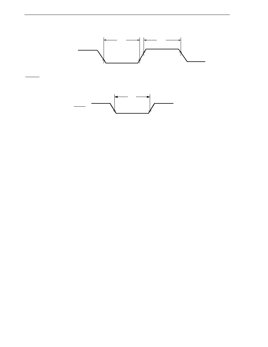
492
CHAPTER 25 ELECTRICAL SPECIFICATIONS (EXPANDED-SPECIFICATION PRODUCTS OF
µPD780076, 780078, 78F0078)
User's Manual U14260EJ3V1UD
t
RSL
RESET
INTP0 to INTP3
t
INTL
t
INTH
Interrupt Request Input Timing
RESET Input Timing
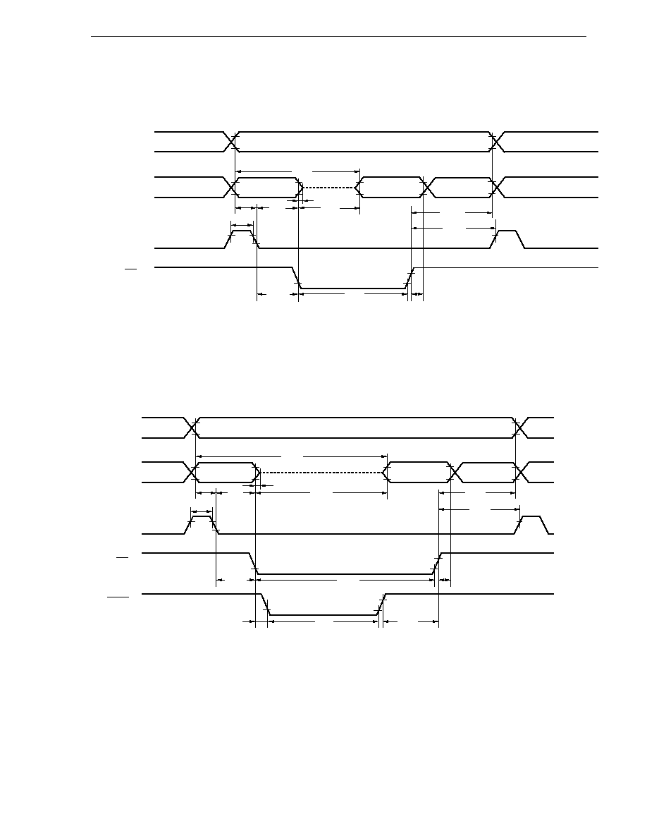
493
CHAPTER 25 ELECTRICAL SPECIFICATIONS (EXPANDED-SPECIFICATION PRODUCTS OF
µPD780076, 780078, 78F0078)
User's Manual U14260EJ3V1UD
Read/Write Operation
External fetch (no wait):
External fetch (wait insertion):
A8 to A15
AD0 to AD7
ASTB
RD
Higher 8-bit address
Lower 8-bit address
t
ADD1
Hi-Z
t
ADS
t
ASTH
t
ADH
t
RDAD
t
RDD1
Instruction code
t
RDADH
t
RDAST
t
ASTRD
t
RDL1
t
RDH
WAIT
t
RDWT1
t
WTL
t
WTRD
A8 to A15
AD0 to AD7
ASTB
RD
Higher 8-bit address
Lower 8-bit address
t
ADD1
Hi-Z
t
ADS
t
ASTH
t
ADH
t
RDD1
t
RDAD
Instruction code
t
RDADH
t
RDAST
t
ASTRD
t
RDL1
t
RDH
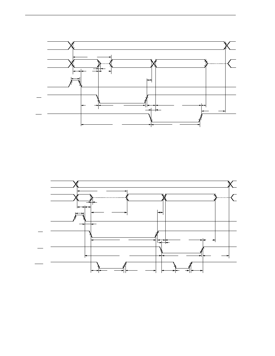
494
CHAPTER 25 ELECTRICAL SPECIFICATIONS (EXPANDED-SPECIFICATION PRODUCTS OF
µPD780076, 780078, 78F0078)
User's Manual U14260EJ3V1UD
External data access (no wait):
External data access (wait insertion):
A8 to A15
AD0 to AD7
ASTB
RD
Higher 8-bit address
Lower 8-bit
address
t
ADD2
t
ADS
t
ASTH
t
ADH
t
RDAD
t
RDD2
Read data
t
ASTRD
WR
t
ASTWR
Write data
Hi-Z
t
WDH
t
WRADH
t
WDS
t
WRWD
t
WRL1
t
RDH
t
RDL2
t
RDWT2
t
WTL
t
WRWT
t
WTL
t
WTWR
t
WTRD
WAIT
t
RDWD
Hi-Z
A8 to A15
AD0 to AD7
ASTB
RD
Higher 8-bit address
Lower 8-bit address
t
ADD2
Hi-Z
t
ADS
t
ASTH
t
ADH
t
RDD2
t
RDAD
Read data
t
ASTRD
t
RDWD
WR
t
ASTWR
Write data
Hi-Z
t
WDH
t
WRADH
t
WDS
t
WRWD
t
WRL1
t
RDH
t
RDL2

495
CHAPTER 25 ELECTRICAL SPECIFICATIONS (EXPANDED-SPECIFICATION PRODUCTS OF
µPD780076, 780078, 78F0078)
User's Manual U14260EJ3V1UD
Data Retention Timing (STOP Mode Release by RESET)
t
SREL
t
WAIT
V
DD
RESET
STOP instruction execution
STOP mode
Data retention mode
Internal reset operation
HALT mode
Operating mode
V
DDDR
Data Retention Timing (Standby Release Signal: STOP Mode Release by Interrupt Request Signal)
t
SREL
t
WAIT
V
DD
STOP instruction execution
STOP mode
Data retention mode
HALT mode
Operating mode
Standby release signal
(interrupt request)
V
DDDR
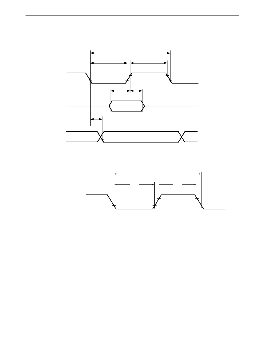
496
CHAPTER 25 ELECTRICAL SPECIFICATIONS (EXPANDED-SPECIFICATION PRODUCTS OF
µPD780076, 780078, 78F0078)
User's Manual U14260EJ3V1UD
Serial Transfer Timing
3-wire serial I/O mode:
UART mode (external clock input):
t
KCYn
t
KHn
t
KLn
ASCK0, ASCK2
t
KCYn
t
KLn
t
KHn
SCK1, SCK3
SI1, SI3
SO1, SO3
t
SIKn
t
KSIn
t
KSOn
Input data
Output data
Remark n = 1 to 4
Remark n = 5, 6

497
CHAPTER 25 ELECTRICAL SPECIFICATIONS (EXPANDED-SPECIFICATION PRODUCTS OF
µPD780076, 780078, 78F0078)
User's Manual U14260EJ3V1UD
Flash Write Mode Setting Timing
Notes 1. 3-wire serial I/O (SIO3) type
2. UART (UART0) type
3. Handshake (when 3-wire serial I/O (SIO3) type is used)
V
DD
V
DD
0 V
V
DD
RESET (input)
0 V
V
PPH
0 V
V
PP
V
PPL
t
RP
t
PR
t
DP
t
PW
t
PW
t
RPE
0 V
SCK3
Note 1
0 V
0 V
0 V
SI3
Note 1
/RxD0
Note 2
SO3
Note 1
/TxD0
Note 2
P31 (HS)
Note 3
Reset command
V
IL
V
IL

498
User's Manual U14260EJ3V1UD
CHAPTER 26 ELECTRICAL SPECIFICATIONS
(EXPANDED-SPECIFICATION PRODUCTS OF
µPD780076Y, 780078Y, 78F0078Y)
Target products:
µPD780076Y, 780078Y, 78F0078Y for which orders were received after February 1, 2002
(Products with a rank
Note
other than K)
Note The rank is indicated by the 5th digit from the left in the lot number marked on the package.
Absolute Maximum Ratings (T
A
= 25
∞C)
Parameter
Supply voltage
Input voltage
Output voltage
Analog input
voltage
Output
current, high
Output
current, low
Operating ambient
temperature
Storage
temperature
Symbol
V
DD
V
PP
AV
REF
AV
SS
V
I1
V
I2
V
O
V
AN
I
OH
I
OL
T
A
T
stg
Conditions
µPD78F0078Y only, Note 2
P00 to P03, P10 to P17, P20 to P25, P34 to P36,
P40 to P47, P50 to P57, P64 to P67, P70 to P75,
P80, X1, X2, XT1, XT2, RESET
P30 to P33
N-ch open- No pull-up resistor
drain
Pull-up resistor
P10 to P17
Analog input pin
Per pin
Total for P00 to P03, P40 to P47, P50 to P57,
P64 to P67, P70 to P75, P80
Total for P20 to P25, P30 to P36
Per pin for P00 to P03, P20 to P25, P34 to P36,
P40 to P47, P64 to P67, P70 to P75, P80
Per pin for P30 to P33, P50 to P57
Total for P00 to P03, P40 to P47, P64 to P67,
P70 to P75, P80
Total for P20 to P25
Total for P30 to P36
Total for P50 to P57
During normal operation
During flash memory programming
µPD780076Y, 780078Y
µPD78F0078Y
Ratings
-0.3 to +6.5
-0.5 to +10.5
-0.3 to V
DD
+ 0.3
Note 1
-0.3 to +0.3
-0.3 to V
DD
+ 0.3
Note 1
-0.3 to +6.5
-0.3 to V
DD
+ 0.3
Note 1
-0.3 to V
DD
+ 0.3
Note 1
AV
SS
- 0.3 to AV
REF
+ 0.3
Note 1
and
-0.3 to V
DD
+ 0.3
Note 1
-10
-15
-15
20
30
50
20
100
100
-40 to +85
+10 to +40
-65 to +150
-40 to +125
Unit
V
V
V
V
V
V
V
V
V
mA
mA
mA
mA
mA
mA
mA
mA
mA
∞C
∞C
∞C
∞C
Lot number
Year
code
Rank
Week
code
Note 1. 6.5 V or below
(Note 2 is explained on the next page.)
Caution Product quality may suffer if the absolute maximum rating is exceeded even momentarily for any
parameter. That is, the absolute maximum ratings are rated values at which the product is on the verge
of suffering physical damage, and therefore the product must be used under conditions that ensure
that the absolute maximum ratings are not exceeded.
Remark
Unless otherwise specified, the characteristics of alternate-function pins are the same as those of port pins.
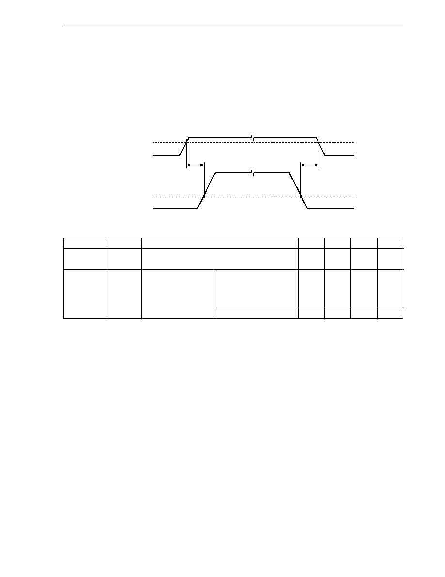
499
CHAPTER 26 ELECTRICAL SPECIFICATIONS (EXPANDED-SPECIFICATION PRODUCTS OF
µPD780076Y, 780078Y, 78F0078Y)
User's Manual U14260EJ3V1UD
Note 2.
Make sure that the following conditions of the V
PP
voltage application timing are satisfied when the flash
memory is written.
∑ When supply voltage rises
V
PP
must exceed V
DD
10
µs or more after V
DD
has reached the lower-limit value (2.7 V) of the
operating voltage range (see a in the figure below).
∑ When supply voltage drops
V
DD
must be lowered 10
µs or more after V
PP
falls below the lower-limit value (2.7 V) of the
operating voltage range of V
DD
(see b in the figure below).
Capacitance (T
A
= 25
∞
C, V
DD
= V
SS
= 0 V)
Parameter
Symbol
Conditions
MIN.
TYP.
MAX.
Unit
Input
C
IN
f = 1 MHz
15
pF
capacitance
Unmeasured pins returned to 0 V.
I/O
C
IO
f = 1 MHz
P00 to P03, P20 to P25,
15
pF
capacitance
Unmeasured pins
P34 to P36, P40 to P47,
returned to 0 V.
P50 to P57, P64 to P67,
P70 to P75, P80
P30 to P33
20
pF
Remark
Unless otherwise specified, the characteristics of alternate-function pins are the same as those of port pins.
2.7 V
V
DD
0 V
0 V
V
PP
2.7 V
a
b

500
CHAPTER 26 ELECTRICAL SPECIFICATIONS (EXPANDED-SPECIFICATION PRODUCTS OF
µPD780076Y, 780078Y, 78F0078Y)
User's Manual U14260EJ3V1UD
Main System Clock Oscillator Characteristics (T
A
= ≠40 to +85
∞
C, V
DD
= 1.8 to 5.5 V)
Notes 1. Indicates only oscillator characteristics. Refer to AC Characteristics for instruction execution time.
2. Time required to stabilize oscillation after reset or STOP mode release.
Cautions
1. When using the main system clock oscillator, wire as follows in the area enclosed by the broken
lines in the above figures to avoid an adverse effect from wiring capacitance.
∑ Keep the wiring length as short as possible.
∑ Do not cross the wiring with the other signal lines.
∑ Do not route the wiring near a signal line through which a high fluctuating current flows.
∑ Always make the ground point of the oscillator capacitor the same potential as V
SS1
.
∑ Do not ground the capacitor to a ground pattern through which a high current flows.
∑ Do not fetch signals from the oscillator.
2. When the main system clock is stopped and the system is operating on the subsystem clock,
wait until the oscillation stabilization time has been secured by the program before switching
back to the main system clock.
Resonator
Recommended
Parameter
Conditions
MIN.
TYP.
MAX.
Unit
Circuit
Ceramic
Oscillation
3.0 V
V
DD
5.5 V
1.0
8.38
MHz
resonator
frequency (f
X
)
Note 1
1.8 V
V
DD
< 3.0 V
1.0
5.0
Oscillation
After V
DD
reaches
4
ms
stabilization time
Note 2
oscillation voltage range
MIN.
Crystal
Oscillation
3.0 V
V
DD
5.5 V
1.0
8.38
MHz
resonator
frequency (f
X
)
Note 1
1.8 V
V
DD
< 3.0 V
1.0
5.0
Oscillation
3.0 V
V
DD
5.5 V
10
ms
stabilization time
Note 2
1.8 V
V
DD
< 3.0 V
30
External
X1 input
3.0 V
V
DD
5.5 V
1.0
8.38
MHz
clock
frequency (f
X
)
Note 1
1.8 V
V
DD
< 3.0 V
1.0
5.0
X1 input
3.0 V
V
DD
5.5 V
50
500
ns
high-/low-level width
(t
XH
, t
XL
)
1.8 V
V
DD
< 3.0 V
85
500
X2
X1
C2
Rd
C1
X1
V
SS1
X2
C2
Rd
C1
X1
V
SS1
X2

501
CHAPTER 26 ELECTRICAL SPECIFICATIONS (EXPANDED-SPECIFICATION PRODUCTS OF
µPD780076Y, 780078Y, 78F0078Y)
User's Manual U14260EJ3V1UD
Subsystem Clock Oscillator Characteristics
(T
A
= ≠40 to +85
∞C, V
DD
= 1.8 to 5.5 V)
Notes 1. Indicates only oscillator characteristics. Refer to AC Characteristics for instruction execution time.
2. Time required to stabilize oscillation after V
DD
reaches oscillation voltage range MIN.
Cautions
1. When using the subsystem clock oscillator, wire as follows in the area enclosed by the broken
lines in the above figure to avoid an adverse effect from wiring capacitance.
∑ Keep the wiring length as short as possible.
∑ Do not cross the wiring with the other signal lines.
∑ Do not route the wiring near a signal line through which a high fluctuating current flows.
∑ Always make the ground point of the oscillator capacitor the same potential as V
SS1
.
∑ Do not ground the capacitor to a ground pattern through which a high current flows.
∑ Do not fetch signals from the oscillator.
2. The subsystem clock oscillator is designed as a low-amplitude circuit for reducing power
consumption, and is more prone to malfunction due to noise than the main system clock
oscillator. Particular care is therefore required with the wiring method when the subsystem
clock is used.
MIN.
32
32
Resonator
Crystal
resonator
External
clock
Parameter
Oscillation
frequency (f
XT
)
Note 1
Oscillation
stabilization time
Note 2
XT1 input
frequency (f
XT
)
Note 1
XT1 input
high-/low-level width
(t
XTH
, t
XTL
)
Conditions
3.0 V
V
DD
5.5 V
1.8 V
V
DD
< 3.0 V
TYP.
32.768
1.2
MAX.
35
2
10
38.5
Unit
kHz
s
kHz
Recommended Circuit
12
15
µs
XT1
XT2
C3
XT2 XT1 V
SS1
Rd
C4

502
CHAPTER 26 ELECTRICAL SPECIFICATIONS (EXPANDED-SPECIFICATION PRODUCTS OF
µPD780076Y, 780078Y, 78F0078Y)
User's Manual U14260EJ3V1UD
Recommended Oscillator Constant
(1)
µPD780076Y, 780078Y
(a) Main system clock: Ceramic resonator (T
A
= ≠40 to +85
∞
C)
Manufacturer
Part Number
Frequency
Recommended Circuit Constant
Oscillation Voltage Range
(MHz)
C1 (pF)
C2 (pF)
Rd (k
)
MIN. (V)
MAX. (V)
Murata Mfg.
CSBFB1M00J58
1.00
150
150
0
1.8
5.5
Co., Ltd.
CSBLA1M00J58
1.00
150
150
0
1.8
5.5
CSTCC2M00G56
2.00
On-chip
On-chip
0
1.8
5.5
CSTLS2M00G56
2.00
On-chip
On-chip
0
1.8
5.5
CSTCC3M58G53
3.58
On-chip
On-chip
0
1.8
5.5
CSTLS3M58G53
3.58
On-chip
On-chip
0
1.8
5.5
CSTCR4M00G53
4.00
On-chip
On-chip
0
1.8
5.5
CSTLS4M00G53
4.00
On-chip
On-chip
0
1.8
5.5
CSTCR4M19G53
4.19
On-chip
On-chip
0
1.8
5.5
CSTLS4M19G53
4.19
On-chip
On-chip
0
1.8
5.5
CSTCR4M91G53
4.91
On-chip
On-chip
0
1.8
5.5
CSTLS4M91G53
4.91
On-chip
On-chip
0
1.8
5.5
CSTCR5M00G53
5.00
On-chip
On-chip
0
2.7
5.5
CSTLS5M00G53
5.00
On-chip
On-chip
0
2.7
5.5
CSTCE8M00G52
8.00
On-chip
On-chip
0
3.0
5.5
CSTLS8M00G53
8.00
On-chip
On-chip
0
3.0
5.5
CSTCE8M38G52
8.38
On-chip
On-chip
0
3.0
5.5
CSTLS8M38G53
8.38
On-chip
On-chip
0
3.0
5.5
TDK
CCR3.5MC5
3.58
On-chip
On-chip
0
1.8
5.5
CCR4.0MC5
4.00
On-chip
On-chip
0
1.8
5.5
CCR4.19MC5
4.19
On-chip
On-chip
0
1.8
5.5
CCR5.0MC5
5.00
On-chip
On-chip
0
2.7
5.5
CCR6.0MC5
6.00
On-chip
On-chip
0
2.7
5.5
CCR8.0MC5
8.00
On-chip
On-chip
0
3.0
5.5
CCR8.38MC5
8.38
On-chip
On-chip
0
3.0
5.5
Caution
The oscillator constant is a reference value based on evaluation in specific environments by the
resonator manufacturer. If the oscillator characteristics need to be optimized in the actual
application, request the resonator manufacturer for evaluation on the implementation circuit.
Note that the oscillation voltage and oscillation frequency merely indicate the characteristics of
the oscillator. Use the internal operation conditions of the
µPD780078Y Subseries within the
specifications of the DC and AC characteristics.
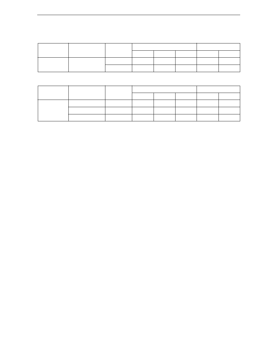
503
CHAPTER 26 ELECTRICAL SPECIFICATIONS (EXPANDED-SPECIFICATION PRODUCTS OF
µPD780076Y, 780078Y, 78F0078Y)
User's Manual U14260EJ3V1UD
(1)
µPD780076Y, 780078Y
(b) Main system clock: Crystal resonator (T
A
= ≠10 to +70
∞
C)
(c) Subsystem clock: Crystal resonator (T
A
= ≠40 to +85
∞
C)
Caution
The oscillator constant is a reference value based on evaluation in specific environments by the
resonator manufacturer. If the oscillator characteristics need to be optimized in the actual
application, request the resonator manufacturer for evaluation on the implementation circuit.
Note that the oscillation voltage and oscillation frequency merely indicate the characteristics of
the oscillator. Use the internal operation conditions of the
µPD780078Y Subseries within the
specifications of the DC and AC characteristics.
Manufacturer
KINSEKI, Ltd.
Part Number
HC-49/U-S
Frequency
(MHz)
4.19
8.38
C1 (pF)
18
27
C2 (pF)
18
27
MIN. (V)
1.9
3.0
MAX. (V)
5.5
5.5
Recommended Circuit Constant
Oscillation Voltage Range
Rd (k
)
4.7
0
Manufacturer
Seiko Epson
Corporation
Part Number
C-022RX
MC-206
MC-306
Frequency
(kHz)
32.768
32.768
32.768
C1 (pF)
15
15
15
C2 (pF)
15
15
15
MIN. (V)
1.8
1.8
1.8
MAX. (V)
5.5
5.5
5.5
Recommended Circuit Constant
Oscillation Voltage Range
Rd (k
)
330
330
330

504
CHAPTER 26 ELECTRICAL SPECIFICATIONS (EXPANDED-SPECIFICATION PRODUCTS OF
µPD780076Y, 780078Y, 78F0078Y)
User's Manual U14260EJ3V1UD
(2)
µPD78F0078Y
Main system clock: Ceramic resonator (T
A
= ≠40 to +85
∞
C)
Manufacturer
Part Number
Frequency
Recommended Circuit Constant
Oscillation Voltage Range
(MHz)
C1 (pF)
C2 (pF)
R1 (k
)
MIN. (V)
MAX. (V)
Murata Mfg.
CSBFB1M00J58
1.00
100
100
3.3
1.8
5.5
Co., Ltd.
CSBLA1M00J58
1.00
100
100
3.3
1.8
5.5
CSTCC2M00G56
2.00
On-chip
On-chip
0
1.8
5.5
CSTLS2M00G56
2.00
On-chip
On-chip
0
1.8
5.5
CSTCC3M58G53
3.58
On-chip
On-chip
0
1.8
5.5
CSTLS3M58G53
3.58
On-chip
On-chip
0
1.8
5.5
CSTCR4M00G53
4.00
On-chip
On-chip
0
1.8
5.5
CSTLS4M00G53
4.00
On-chip
On-chip
0
1.8
5.5
CSTCR4M19G53
4.19
On-chip
On-chip
0
1.8
5.5
CSTLS4M19G53
4.19
On-chip
On-chip
0
1.8
5.5
CSTCR4M91G53
4.91
On-chip
On-chip
0
1.8
5.5
CSTLS4M91G53
4.91
On-chip
On-chip
0
1.8
5.5
CSTCR5M00G53
5.00
On-chip
On-chip
0
2.7
5.5
CSTLS5M00G53
5.00
On-chip
On-chip
0
2.7
5.5
CSTCE8M00G52
8.00
On-chip
On-chip
0
3.0
5.5
CSTLS8M00G53
8.00
On-chip
On-chip
0
3.0
5.5
CSTCE8M38G52
8.38
On-chip
On-chip
0
3.0
5.5
CSTLS8M38G53
8.38
On-chip
On-chip
0
3.0
5.5
Caution
The oscillator constant is a reference value based on evaluation in specific environments by the
resonator manufacturer. If the oscillator characteristics need to be optimized in the actual
application, request the resonator manufacturer for evaluation on the implementation circuit.
Note that the oscillation voltage and oscillation frequency merely indicate the characteristics of
the oscillator. Use the internal operation conditions of the
µPD780078Y Subseries within the
specifications of the DC and AC characteristics.
Remark For the resonator selection and oscillator constant, users are requested to either evaluate the oscillation
themselves or apply to the resonator manufacturer for evaluation.

505
CHAPTER 26 ELECTRICAL SPECIFICATIONS (EXPANDED-SPECIFICATION PRODUCTS OF
µPD780076Y, 780078Y, 78F0078Y)
User's Manual U14260EJ3V1UD
DC Characteristics (T
A
= ≠40 to +85
∞
C, V
DD
= 1.8 to 5.5 V)
Parameter
Symbol
Conditions
MIN.
TYP.
MAX.
Unit
Output current,
I
OH
Per pin
≠1
mA
high
All pins
≠15
mA
Output current,
I
OL
Per pin for P00 to P03, P20 to P25, P34 to P36,
10
mA
low
P40 to P47, P64 to P67, P70 to P75, P80
Per pin for P30 to P33, P50 to P57
15
mA
Total for P00 to P03, P40 to P47, P64 to P67, P70 to P75, P80
20
mA
Total for P20 to P25
10
mA
Total for P30 to P36
70
mA
Total for P50 to P57
70
mA
Input voltage,
V
IH1
P10 to P17, P21, P24,
2.7 V
V
DD
5.5 V
0.7V
DD
V
DD
V
high
P40 to P47, P50 to P57,
1.8 V
V
DD
< 2.7 V
0.8V
DD
V
DD
V
P64 to P67
V
IH2
P00 to P03, P20, P22, P23, P25,
2.7 V
V
DD
5.5 V
0.8V
DD
V
DD
V
P34 to P36, P70 to P75, P80, RESET 1.8 V V
DD
< 2.7 V
0.85V
DD
V
DD
V
V
IH3
P30 to P33
2.7 V
V
DD
5.5 V
0.7V
DD
5.5
V
(N-ch open-drain)
1.8 V
V
DD
< 2.7 V
0.8V
DD
5.5
V
V
IH4
X1, X2
2.7 V
V
DD
5.5 V
V
DD
≠
0.5
V
DD
V
1.8 V
V
DD
< 2.7 V
V
DD
≠
0.2
V
DD
V
V
IH5
XT1, XT2
4.0 V
V
DD
5.5 V
0.8V
DD
V
DD
V
1.8 V
V
DD
< 4.0 V
0.9V
DD
V
DD
V
Input voltage,
V
IL1
P10 to P17, P21, P24,
2.7 V
V
DD
5.5 V
0
0.3V
DD
V
low
P40 to P47, P50 to P57,
1.8 V
V
DD
< 2.7 V
0
0.2V
DD
V
P64 to P67
V
IL2
P00 to P03, P20, P22, P23, P25,
2.7 V
V
DD
5.5 V
0
0.2V
DD
V
P34 to P36, P70 to P75, P80, RESET 1.8 V
V
DD
< 2.7 V
0
0.15V
DD
V
V
IL3
P30 to P33
4.0 V
V
DD
5.5 V
0
0.3V
DD
V
(N-ch open-drain)
2.7 V
V
DD
< 4.0 V
0
0.2V
DD
V
1.8 V
V
DD
< 2.7 V
0
0.1V
DD
V
V
IL4
X1, X2
2.7 V
V
DD
5.5 V
0
0.4
V
1.8 V
V
DD
< 2.7 V
0
0.2
V
V
IL5
XT1, XT2
4.0 V
V
DD
5.5 V
0
0.2V
DD
V
1.8 V
V
DD
< 4.0 V
0
0.1V
DD
V
Output voltage,
V
OH1
4.0 V
V
DD
5.5 V, I
OH
= ≠1 mA
V
DD
≠
1.0
V
DD
V
high
1.8 V
V
DD
< 4.0 V, I
OH
= ≠100
µA
V
DD
≠
0.5
V
DD
V
Output voltage,
V
OL1
P30 to P33
4.0 V
V
DD
5.5 V,
2.0
V
low
I
OL
= 15 mA
V
OL2
P50 to P57
4.0 V
V
DD
5.5 V,
0.4
2.0
V
I
OL
= 15 mA
V
OL3
P00 to P03, P20 to P25, P34 to P36,
4.0 V
V
DD
5.5 V,
0.4
V
P40 to P47, P64 to P67, P70 to P75, P80
I
OL
= 1.6 mA
V
OL4
I
OL
= 400
µA
0.5
V
Remark
Unless otherwise specified, the characteristics of alternate-function pins are the same as those of port pins.
506
CHAPTER 26 ELECTRICAL SPECIFICATIONS (EXPANDED-SPECIFICATION PRODUCTS OF
µPD780076Y, 780078Y, 78F0078Y)
User's Manual U14260EJ3V1UD
DC Characteristics (T
A
= ≠40 to +85
∞
C, V
DD
= 1.8 to 5.5 V)
Parameter
Symbol
Conditions
MIN.
TYP.
MAX.
Unit
Input leakage
I
LIH1
V
IN
= V
DD
P00 to P03, P10 to P17, P20 to P25,
3
µA
current, high
P34 to P36, P40 to P47, P50 to P57,
P64 to P67, P70 to P75, P80,
RESET
I
LIH2
X1, X2, XT1, XT2
20
µA
I
LIH3
V
IN
= 5.5 V
P30 to P33
3
µA
Input leakage
I
LIL1
V
IN
= 0 V
P00 to P03, P10 to P17, P20 to P25,
≠3
µA
current, low
P34 to P36, P40 to P47, P50 to P57,
P64 to P67, P70 to P75, P80,
RESET
I
LIL2
X1, X2, XT1, XT2
≠20
µA
I
LIL3
P30 to P33
≠3
µA
Output leakage
I
LOH
V
OUT
= V
DD
3
µA
current, high
Output leakage
I
LOL
V
OUT
= 0 V
≠3
µA
current, low
Mask option
R
1
V
IN
= 0 V,
15
30
90
k
pull-up resistance
P30, P31
(mask ROM
version only)
Software pull-
R
2
V
IN
= 0 V,
15
30
90
k
up resistance
P00 to P03, P20 to P25, P34 to P36, P40 to P47,
P50 to P57, P64 to P67, P70 to P75, P80
V
PP
(IC)
V
PP1
During normal operation
0
0.2V
DD
V
power supply
voltage
Remark Unless otherwise specified, the characteristics of alternate-function pins are the same as those of port pins.

507
CHAPTER 26 ELECTRICAL SPECIFICATIONS (EXPANDED-SPECIFICATION PRODUCTS OF
µPD780076Y, 780078Y, 78F0078Y)
User's Manual U14260EJ3V1UD
DC Characteristics (T
A
= ≠40 to +85
∞
C, V
DD
= 1.8 to 5.5 V)
(1)
µPD780076Y, 780078Y
Parameter
Symbol
Conditions
MIN.
TYP.
MAX.
Unit
Power supply
I
DD1
Note 2
8.38 MHz
V
DD
= 5.0 V
±10%
Note 3
When A/D converter is
5.5
11.0
mA
current
Note 1
crystal oscillation
stopped
operating mode
When A/D converter is
6.5
13.0
mA
operating
V
DD
= 3.0 V + 10%
Notes 3, 6
When A/D converter is
3.5
7.0
mA
stopped
When A/D converter is
4.5
9.0
mA
operating
5.00 MHz
V
DD
= 3.0 V
±10%
Note 3
When A/D converter is
2.0
4.0
mA
crystal oscillation
stopped
operating mode
When A/D converter is
3.0
6.0
mA
operating
V
DD
= 2.0 V
±10%
Note 4
When A/D converter is
0.4
1.5
mA
stopped
When A/D converter is
1.4
4.2
mA
operating
I
DD2
8.38 MHz
V
DD
= 5.0 V
±10%
Note 3
When peripheral functions
1.1
2.2
mA
crystal oscillation
are stopped
HALT mode
When peripheral functions
4.7
mA
are operating
V
DD
= 3.0 V + 10%
Notes 3, 6
When peripheral functions
0.7
1.4
mA
are stopped
When peripheral functions
4.5
mA
are operating
5.00 MHz
V
DD
= 3.0 V
±10%
Note 3
When peripheral functions
0.35
0.7
mA
crystal oscillation
are stopped
HALT mode
When peripheral functions
1.7
mA
are operating
V
DD
= 2.0 V
±10%
Note 4
When peripheral functions
0.15
0.4
mA
are stopped
When peripheral functions
1.1
mA
are operating
I
DD3
32.768 kHz crystal oscillation
V
DD
= 5.0 V
±10%
40
80
µA
operating mode
Note 5
V
DD
= 3.0 V
±10%
20
40
µA
V
DD
= 2.0 V
±10%
10
20
µA
I
DD4
32.768 kHz crystal oscillation
V
DD
= 5.0 V
±10%
30
60
µA
HALT mode
Note 5
V
DD
= 3.0 V
±10%
6
18
µA
V
DD
= 2.0 V
±10%
2
10
µA
I
DD5
STOP mode
Note 7
V
DD
= 5.0 V
±10%
0.1
30
µA
V
DD
= 3.0 V
±10%
0.05
10
µA
V
DD
= 2.0 V
±10%
0.05
10
µA
Notes 1. Total current through the internal power supply (V
DD0
, V
DD1
).
2. I
DD1
includes the peripheral operating current (except the current through the pull-up resistors of ports).
3. When the processor clock control register (PCC) is set to 00H.
4. When PCC is set to 02H.
5. When main system clock operation is stopped.
6. The values show the specifications when V
DD
= 3.0 to 3.3 V. The value in the TYP. column shows the
specifications when V
DD
= 3.0 V.
7. When the main system clock and subsystem clock are stopped.
508
CHAPTER 26 ELECTRICAL SPECIFICATIONS (EXPANDED-SPECIFICATION PRODUCTS OF
µPD780076Y, 780078Y, 78F0078Y)
User's Manual U14260EJ3V1UD
DC Characteristics (T
A
= ≠40 to +85
∞
C, V
DD
= 1.8 to 5.5 V)
(2)
µPD78F0078Y
Parameter
Symbol
Conditions
MIN.
TYP.
MAX.
Unit
Power supply
I
DD1
Note 2
8.38 MHz
V
DD
= 5.0 V
±10%
Note 3
When A/D converter is
10.5
21.0
mA
current
Note 1
crystal oscillation
stopped
operating mode
When A/D converter is
11.5
23.0
mA
operating
V
DD
= 3.0 V + 10%
Notes 3, 6
When A/D converter is
7.0
14.0
mA
stopped
When A/D converter is
8.0
16.0
mA
operating
5.00 MHz
V
DD
= 3.0 V
±10%
Note 3
When A/D converter is
4.5
9.0
mA
crystal oscillation
stopped
operating mode
When A/D converter is
5.5
11.0
mA
operating
V
DD
= 2.0 V
±10%
Note 4
When A/D converter is
1.0
2.0
mA
stopped
When A/D converter is
2.0
6.0
mA
operating
I
DD2
8.38 MHz
V
DD
= 5.0 V
±10%
Note 3
When peripheral functions
1.2
2.4
mA
crystal oscillation
are stopped
HALT mode
When peripheral functions
5.0
mA
are operating
V
DD
= 3.0 V + 10%
Notes 3, 6
When peripheral functions
0.7
1.4
mA
are stopped
When peripheral functions
4.5
mA
are operating
5.00 MHz
V
DD
= 3.0 V
±10%
Note 3
When peripheral functions
0.4
0.8
mA
crystal oscillation
are stopped
HALT mode
When peripheral functions
1.7
mA
are operating
V
DD
= 2.0 V
±10%
Note 4
When peripheral functions
0.2
0.4
mA
are stopped
When peripheral functions
1.1
mA
are operating
I
DD3
32.768 kHz crystal oscillation
V
DD
= 5.0 V
±10%
115
230
µA
operating mode
Note 5
V
DD
= 3.0 V
±10%
95
190
µA
V
DD
= 2.0 V
±10%
75
150
µA
I
DD4
32.768 kHz crystal oscillation
V
DD
= 5.0 V
±10%
30
60
µA
HALT mode
Note 5
V
DD
= 3.0 V
±10%
6
18
µA
V
DD
= 2.0 V
±10%
2
10
µA
I
DD5
STOP mode
Note 7
V
DD
= 5.0 V
±10%
0.1
30
µA
V
DD
= 3.0 V
±10%
0.05
10
µA
V
DD
= 2.0 V
±10%
0.05
10
µA
Notes 1. Total current through the internal power supply (V
DD0
, V
DD1
).
2. I
DD1
includes the peripheral operating current (except the current through the pull-up resistors of ports).
3. When the processor clock control register (PCC) is set to 00H.
4. When PCC is set to 02H.
5. When main system clock operation is stopped.
6. The values show the specifications when V
DD
= 3.0 to 3.3 V. The value in the TYP. column shows the
specifications when V
DD
= 3.0 V.
7. When the main system clock and subsystem clock are stopped.
509
CHAPTER 26 ELECTRICAL SPECIFICATIONS (EXPANDED-SPECIFICATION PRODUCTS OF
µPD780076Y, 780078Y, 78F0078Y)
User's Manual U14260EJ3V1UD
AC Characteristics
(1) Basic operation
(T
A
= ≠40 to +85
∞
C, V
DD
= 1.8 to 5.5 V)
Parameter
Symbol
Conditions
MIN.
TYP.
MAX.
Unit
Cycle time
T
CY
Operating with
3.0 V
V
DD
5.5 V
0.238
16
µs
(Min. instruction
main system clock
2.7 V
V
DD
< 3.0 V
0.4
16
µs
execution time)
1.8 V
V
DD
< 2.7 V
1.6
16
µs
Operating with subsystem clock
103.9
Note 1
122
125
µs
TI000, TI010, TI001,
t
TIH0
, t
TIL0
3.0 V
V
DD
5.5 V
2/f
sam
+ 0.1
Note 2
µs
TI011 input high-/low-
2.7 V
V
DD
< 3.0 V
2/f
sam
+ 0.2
Note 2
µs
level width
1.8 V
V
DD
< 2.7 V
2/f
sam
+ 0.5
Note 2
µs
TI50, TI51 input
f
TI5
2.7 V
V
DD
5.5 V
0
4
MHz
frequency
1.8 V
V
DD
< 2.7 V
0
275
kHz
TI50, TI51 input
t
TIH5
, t
TIL5
2.7 V
V
DD
5.5 V
100
ns
high-/low-level
1.8 V
V
DD
< 2.7 V
1.8
µs
width
Interrupt request
t
INTH
, t
INTL
INTP0 to INTP3,
2.7 V
V
DD
5.5 V
1
µs
input high-/low-
P40 to P47
1.8 V
V
DD
< 2.7 V
2
µs
level width
RESET
t
RSL
2.7 V
V
DD
5.5 V
10
µs
low-level width
1.8 V
V
DD
< 2.7 V
20
µs
Notes
1. Value when the external clock is used. When a crystal resonator is used, it is 114
µs (MIN.).
2. Selection of f
sam
= f
X
, f
X
/4, f
X
/64 is possible using bits 0 and 1 (PRM000, PRM010) of prescaler mode
register 00 (PRM00). Selection of f
sam
= f
X
/2, f
X
/8, f
X
/512 is possible using bits 0 and 1 (PRM001, PRM011)
of prescaler mode register 01 (PRM01). However, if the TI000 or TI001 valid edge is selected as the count
clock, the value becomes f
sam
= f
X
/8.

510
CHAPTER 26 ELECTRICAL SPECIFICATIONS (EXPANDED-SPECIFICATION PRODUCTS OF
µPD780076Y, 780078Y, 78F0078Y)
User's Manual U14260EJ3V1UD
T
CY
vs. V
DD
(main system clock operation)
5.0
1.0
2.0
1.6
0.4
0.238
0.1
Supply voltage V
DD
[V]
Cycle time T
CY
[s
]
µ
0
10.0
1.0
2.0
3.0
4.0
5.0
6.0
1.8
5.5
2.7
Operation
guaranteed
range
16.0

511
CHAPTER 26 ELECTRICAL SPECIFICATIONS (EXPANDED-SPECIFICATION PRODUCTS OF
µPD780076Y, 780078Y, 78F0078Y)
User's Manual U14260EJ3V1UD
(2) Read/write operation (T
A
= ≠40 to +85
∞
C, V
DD
= 4.0 to 5.5 V)
(1/3)
Parameter
Symbol
Conditions
MIN.
MAX.
Unit
ASTB high-level width
t
ASTH
0.3t
CY
ns
Address setup time
t
ADS
20
ns
Address hold time
t
ADH
6
ns
Data input time from address
t
ADD1
(2 + 2n)t
CY
≠ 54
ns
t
ADD2
(3 + 2n)t
CY
≠ 60
ns
Address output time from RD
t
RDAD
0
100
ns
Data input time from RD
t
RDD1
(2 + 2n)t
CY
≠ 87
ns
t
RDD2
(3 + 2n)t
CY
≠ 93
ns
Read data hold time
t
RDH
0
ns
RD low-level width
t
RDL1
(1.5 + 2n)t
CY
≠ 33
ns
t
RDL2
(2.5 + 2n)t
CY
≠ 33
ns
Input time from RD
to WAIT
t
RDWT1
t
CY
≠ 43
ns
t
RDWT2
t
CY
≠ 43
ns
Input time from WR
to WAIT
t
WRWT
t
CY
≠ 25
ns
WAIT low-level width
t
WTL
(0.5 + n)t
CY
+ 10
(2 + 2n)t
CY
ns
Write data setup time
t
WDS
60
ns
Write data hold time
t
WDH
6
ns
WR low-level width
t
WRL1
(1.5 + 2n)t
CY
≠ 15
ns
Delay time from ASTB
to RD
t
ASTRD
6
ns
Delay time from ASTB
to WR
t
ASTWR
2t
CY
≠ 15
ns
Delay time from
t
RDAST
0.8t
CY
≠ 15
1.2t
CY
ns
RD
to ASTB at external fetch
Address hold time from
t
RDADH
0.8t
CY
≠ 15
1.2t
CY
+ 30
ns
RD
at external fetch
Write data output time from RD
t
RDWD
40
ns
Write data output time from WR
t
WRWD
10
60
ns
Address hold time from WR
t
WRADH
0.8t
CY
≠ 15
1.2t
CY
+ 30
ns
Delay time from WAIT
to RD
t
WTRD
0.8t
CY
2.5t
CY
+ 25
ns
Delay time from WAIT
to WR
t
WTWR
0.8t
CY
2.5t
CY
+ 25
ns
Caution
T
CY
can only be used when the MIN. value is 0.238
µs.
Remarks
1.
t
CY
= T
CY
/4
2.
n indicates the number of waits.
3.
C
L
= 100 pF (C
L
indicates the load capacitance of the AD0 to AD7, A8 to A15, RD, WR, WAIT, and
ASTB pins.)

512
CHAPTER 26 ELECTRICAL SPECIFICATIONS (EXPANDED-SPECIFICATION PRODUCTS OF
µPD780076Y, 780078Y, 78F0078Y)
User's Manual U14260EJ3V1UD
(2) Read/write operation (T
A
= ≠40 to +85
∞
C, V
DD
= 2.7 to 4.0 V)
(2/3)
Parameter
Symbol
Conditions
MIN.
MAX.
Unit
ASTB high-level width
t
ASTH
0.3t
CY
ns
Address setup time
t
ADS
30
ns
Address hold time
t
ADH
10
ns
Input time from address to data
t
ADD1
(2 + 2n)t
CY
≠ 108
ns
t
ADD2
(3 + 2n)t
CY
≠ 120
ns
Output time from RD
to address
t
RDAD
0
200
ns
Input time from RD
to data
t
RDD1
(2 + 2n)t
CY
≠ 148
ns
t
RDD2
(3 + 2n)t
CY
≠ 162
ns
Read data hold time
t
RDH
0
ns
RD low-level width
t
RDL1
(1.5 + 2n)t
CY
≠ 40
ns
t
RDL2
(2.5 + 2n)t
CY
≠ 40
ns
Input time from RD
to WAIT
t
RDWT1
t
CY
≠ 75
ns
t
RDWT2
t
CY
≠ 60
ns
Input time from WR
to WAIT
t
WRWT
t
CY
≠ 50
ns
WAIT low-level width
t
WTL
(0.5 + 2n)t
CY
+ 10
(2 + 2n)t
CY
ns
Write data setup time
t
WDS
60
ns
Write data hold time
t
WDH
10
ns
WR low-level width
t
WRL1
(1.5 + 2n)t
CY
≠ 30
ns
Delay time from ASTB
to RD
t
ASTRD
10
ns
Delay time from ASTB
to WR
t
ASTWR
2t
CY
≠ 30
ns
Delay time from
t
RDAST
0.8t
CY
≠ 30
1.2t
CY
ns
RD
to ASTB at external fetch
Hold time from
t
RDADH
0.8t
CY
≠ 30
1.2t
CY
+ 60
ns
RD
to address at external fetch
Write data output time from RD
t
RDWD
40
ns
Write data output time from WR
t
WRWD
20
120
ns
Hold time from WR
to address
t
WRADH
0.8t
CY
≠ 30
1.2t
CY
+ 60
ns
Delay time from WAIT
to RD
t
WTRD
0.5t
CY
2.5t
CY
+ 50
ns
Delay time from WAIT
to WR
t
WTWR
0.5t
CY
2.5t
CY
+ 50
ns
Caution
T
CY
can only be used when the MIN. value is 0.4
µs.
Remarks
1.
t
CY
= T
CY
/4
2.
n indicates the number of waits.
3.
C
L
= 100 pF (C
L
indicates the load capacitance of the AD0 to AD7, A8 to A15, RD, WR, WAIT, and
ASTB pins.)
513
CHAPTER 26 ELECTRICAL SPECIFICATIONS (EXPANDED-SPECIFICATION PRODUCTS OF
µPD780076Y, 780078Y, 78F0078Y)
User's Manual U14260EJ3V1UD
(2) Read/write operation (T
A
= ≠40 to +85
∞
C, V
DD
= 1.8 to 2.7 V)
(3/3)
Parameter
Symbol
Conditions
MIN.
MAX.
Unit
ASTB high-level width
t
ASTH
0.3t
CY
ns
Address setup time
t
ADS
120
ns
Address hold time
t
ADH
20
ns
Input time from address to data
t
ADD1
(2 + 2n)t
CY
≠ 233
ns
t
ADD2
(3 + 2n)t
CY
≠ 240
ns
Output time from RD
to address
t
RDAD
0
400
ns
Input time from RD
to data
t
RDD1
(2 + 2n)t
CY
≠ 325
ns
t
RDD2
(3 + 2n)t
CY
≠ 332
ns
Read data hold time
t
RDH
0
ns
RD low-level width
t
RDL1
(1.5 + 2n)t
CY
≠ 92
ns
t
RDL2
(2.5 + 2n)t
CY
≠ 92
ns
Input time from RD
to WAIT
t
RDWT1
t
CY
≠ 350
ns
t
RDWT2
t
CY
≠ 132
ns
Input time from WR
to WAIT
t
WRWT
t
CY
≠ 100
ns
WAIT low-level width
t
WTL
(0.5 + 2n)t
CY
+ 10
(2 + 2n)t
CY
ns
Write data setup time
t
WDS
60
ns
Write data hold time
t
WDH
20
ns
WR low-level width
t
WRL1
(1.5 + 2n)t
CY
≠ 60
ns
Delay time from ASTB
to RD
t
ASTRD
20
ns
Delay time from ASTB
to WR
t
ASTWR
2t
CY
≠ 60
ns
Delay time from
t
RDAST
0.8t
CY
≠ 60
1.2t
CY
ns
RD
to ASTB at external fetch
Hold time from
t
RDADH
0.8t
CY
≠ 60
1.2t
CY
+ 120
ns
RD
to address at external fetch
Write data output time from RD
t
RDWD
40
ns
Write data output time from WR
t
WRWD
40
240
ns
Hold time from WR
to address
t
WRADH
0.8t
CY
≠ 60
1.2t
CY
+ 120
ns
Delay time from WAIT
to RD
t
WTRD
0.5t
CY
2.5t
CY
+ 100
ns
Delay time from WAIT
to WR
t
WTWR
0.5t
CY
2.5t
CY
+ 100
ns
Caution
T
CY
can only be used when the MIN. value is 1.6
µs.
Remarks
1.
t
CY
= T
CY
/4
2.
n indicates the number of waits.
3.
C
L
= 100 pF (C
L
indicates the load capacitance of the AD0 to AD7, A8 to A15, RD, WR, WAIT, and
ASTB pins.)

514
CHAPTER 26 ELECTRICAL SPECIFICATIONS (EXPANDED-SPECIFICATION PRODUCTS OF
µPD780076Y, 780078Y, 78F0078Y)
User's Manual U14260EJ3V1UD
(3) Serial interface (T
A
= ≠40 to +85
∞
C, V
DD
= 1.8 to 5.5 V)
(a) SIO3 3-wire serial I/O mode (SCK3 ... Internal clock output)
Parameter
Symbol
Conditions
MIN.
TYP.
MAX.
Unit
SCK3 cycle time
t
KCY1
3.0 V
V
DD
5.5 V
954
ns
2.7 V
V
DD
< 3.0 V
1600
ns
1.8 V
V
DD
< 2.7 V
3200
ns
SCK3 high-/
t
KH1
, t
KL1
3.0 V
V
DD
5.5 V
t
KCY1
/2 ≠ 50
ns
low-level width
1.8 V
V
DD
< 3.0 V
t
KCY1
/2 ≠ 100
ns
SI3 setup time
t
SIK1
3.0 V
V
DD
5.5 V
100
ns
(to SCK3
)
2.7 V
V
DD
< 3.0 V
150
ns
1.8 V
V
DD
< 2.7 V
300
ns
SI3 hold time
t
KSI1
400
ns
(from SCK3
)
Delay time from
t
KSO1
C = 100 pF
Note
300
ns
SCK3
to SO3 output
Note C is the load capacitance of the SCK3 and SO3 output lines.
(b) SIO3 3-wire serial I/O mode (SCK3 ... External clock input)
Parameter
Symbol
Conditions
MIN.
TYP.
MAX.
Unit
SCK3 cycle time
t
KCY2
3.0 V
V
DD
5.5 V
800
ns
2.7 V
V
DD
< 3.0 V
1600
ns
1.8 V
V
DD
< 2.7 V
3200
ns
SCK3 high-/
t
KH2
, t
KL2
3.0 V
V
DD
5.5 V
400
ns
low-level width
2.7 V
V
DD
< 3.0 V
800
ns
1.8 V
V
DD
< 2.7 V
1600
ns
SI3 setup time
t
SIK2
100
ns
(to SCK3
)
SI3 hold time
t
KSI2
400
ns
(from SCK3
)
Delay time from
t
KSO2
C = 100 pF
Note
300
ns
SCK3
to SO3 output
Note C is the load capacitance of the SO3 output line.

515
CHAPTER 26 ELECTRICAL SPECIFICATIONS (EXPANDED-SPECIFICATION PRODUCTS OF
µPD780076Y, 780078Y, 78F0078Y)
User's Manual U14260EJ3V1UD
(c) CSI1 3-wire serial I/O mode (SCK1 ... Internal clock output)
Parameter
Symbol
Conditions
MIN.
TYP.
MAX.
Unit
SCK1 cycle time
t
KCY3
4.0 V
V
DD
5.5 V
200
ns
2.7 V
V
DD
< 4.0 V
500
ns
1.8 V
V
DD
< 2.7 V
1
µs
SCK1 high-/low-level
t
KH3
, t
KL3
4.0 V
V
DD
5.5 V
t
KCY3
/2 ≠ 5
ns
width
2.7 V
V
DD
< 4.0 V
t
KCY3
/2 ≠ 20
ns
1.8 V
V
DD
< 2.7 V
t
KCY3
/2 ≠ 30
ns
SI1 setup time
t
SIK3
25
ns
(to SCK1
)
SI1 hold time
t
KSI3
110
ns
(from SCK1
)
Delay time from SCK1
t
KSO3
C = 100 pF
Note
150
ns
to SO1 output
Note C is the load capacitance of the SCK1 and SO1 output lines.
(d) CSI1 3-wire serial I/O mode (SCK1 ... External clock input)
Parameter
Symbol
Conditions
MIN.
TYP.
MAX.
Unit
SCK1 cycle time
t
KCY4
4.0 V
V
DD
5.5 V
200
ns
2.7 V
V
DD
< 4.0 V
500
ns
1.8 V
V
DD
< 2.7 V
1
µs
SCK1 high-/low-level
t
KH4
, t
KL4
4.0 V
V
DD
5.5 V
100
ns
width
2.7 V
V
DD
< 4.0 V
250
ns
1.8 V
V
DD
< 2.7 V
500
ns
SI1 setup time
t
SIK4
25
ns
(to SCK1
)
SI1 hold time
t
KSI4
110
ns
(from SCK1
)
Delay time from SCK1
t
KSO4
C = 100 pF
Note
150
ns
to
SO1 output
Note C is the load capacitance of the SO1 output line.
(e) UART0 (dedicated baud rate generator output)
Parameter
Symbol
Conditions
MIN.
TYP.
MAX.
Unit
Transfer rate
3.0 V
V
DD
5.5 V
131031
bps
2.7 V
V
DD
< 3.0 V
78125
bps
1.8 V
V
DD
< 2.7 V
39063
bps
516
CHAPTER 26 ELECTRICAL SPECIFICATIONS (EXPANDED-SPECIFICATION PRODUCTS OF
µPD780076Y, 780078Y, 78F0078Y)
User's Manual U14260EJ3V1UD
(f)
UART0 (external clock input)
Parameter
Symbol
Conditions
MIN.
TYP.
MAX.
Unit
ASCK0 cycle time
t
KCY5
4.0 V
V
DD
5.5 V
800
ns
2.7 V
V
DD
< 4.0 V
1600
ns
1.8 V
V
DD
< 2.7 V
3200
ns
ASCK0 high-/low-level
t
KH5
, t
KL5
4.0 V
V
DD
5.5 V
400
ns
width
2.7 V
V
DD
< 4.0 V
800
ns
1.8 V
V
DD
< 2.7 V
1600
ns
Transfer rate
4.0 V
V
DD
5.5 V
39063
bps
2.7 V
V
DD
< 4.0 V
19531
bps
1.8 V
V
DD
< 2.7 V
9766
bps
(g) UART0 (infrared data transfer mode)
Parameter
Symbol
Conditions
MIN.
TYP.
MAX.
Unit
Transfer rate
4.0 V
V
DD
5.5 V
131031
bps
Bit rate tolerance
4.0 V
V
DD
5.5 V
±0.87
%
Output pulse width
4.0 V
V
DD
5.5 V
1.2
0.24/fbr
Note
µs
Input pulse width
4.0 V
V
DD
5.5 V
4/f
X
µs
Note fbr: Specified baud rate
(h) UART2 (dedicated baud rate generator output)
Parameter
Symbol
Conditions
MIN.
TYP.
MAX.
Unit
Transfer rate
4.0 V
V
DD
5.5 V
262062
bps
2.7 V
V
DD
< 4.0 V
156250
bps
1.8 V
V
DD
< 2.7 V
62500
bps
(i)
UART2 (external clock input)
Parameter
Symbol
Conditions
MIN.
TYP.
MAX.
Unit
ASCK2 cycle time
t
KCY6
4.0 V
V
DD
5.5 V
800
ns
2.7 V
V
DD
< 4.0 V
1600
ns
1.8 V
V
DD
< 2.7 V
3200
ns
ASCK2 high-/low-level
t
KH6
, t
KL6
4.0 V
V
DD
5.5 V
400
ns
width
2.7 V
V
DD
< 4.0 V
800
ns
1.8 V
V
DD
< 2.7 V
1600
ns
Transfer rate
4.0 V
V
DD
5.5 V
78125
bps
2.7 V
V
DD
< 4.0 V
39063
bps
1.8 V
V
DD
< 2.7 V
19531
bps

517
CHAPTER 26 ELECTRICAL SPECIFICATIONS (EXPANDED-SPECIFICATION PRODUCTS OF
µPD780076Y, 780078Y, 78F0078Y)
User's Manual U14260EJ3V1UD
(j)
UART2 (infrared data transfer mode)
Parameter
Symbol
Conditions
MIN.
TYP.
MAX.
Unit
Transfer rate
4.0 V
V
DD
5.5 V
262062
bps
Bit rate tolerance
4.0 V
V
DD
5.5 V
±0.87
%
Output pulse width
4.0 V
V
DD
5.5 V
1.2
0.24/fbr
Note
µs
Input pulse width
4.0 V
V
DD
5.5 V
4/f
X
µs
Note fbr: Specified baud rate
(k) I
2
C bus mode
Parameter
Symbol
Standard Mode
High-Speed Mode
Unit
MIN.
MAX.
MIN.
MAX.
SCL0 clock frequency
f
SCL
0
100
0
400
kHz
Bus free time
t
BUF
4.7
--
1.3
--
µs
(between stop and start condition)
Hold time
Note 1
t
HD:STA
4.0
--
0.6
--
µs
SCL0 clock low-level width
t
LOW
4.7
--
1.3
--
µs
SCL0 clock high-level width
t
HIGH
4.0
--
0.6
--
µs
Start/restart condition setup time
t
SU:STA
4.7
--
0.6
--
µs
Data hold time
CBUS compatible master
t
HD:DAT
5.0
--
--
--
µs
I
2
C bus
0
Note 2
--
0
Note 2
0.9
Note 3
µs
Data setup time
t
SU:DAT
250
--
100
Note 4
--
ns
SDA0 and SCL0 signal rise time
t
R
--
1000
20 + 0.1Cb
Note 5
300
ns
SDA0 and SCL0 signal fall time
t
F
--
300
20 + 0.1Cb
Note 5
300
ns
Stop condition setup time
t
SU:STO
4.0
--
0.6
--
µs
Capacitive load per each bus line
Cb
--
400
--
400
pF
Spike pulse width controlled by input filter
t
SP
--
--
0
50
ns
Notes 1. On a start condition, the first clock pulse is generated after the hold period.
2. To fill the undefined area of the SCL0 falling edge, it is necessary for the device to internally provide an
SDA0 signal (with V
IHmin.
of the SCL0 signal) with at least 300 ns of hold time.
3. If the device does not extend the SCL0 signal low hold time (t
LOW
), only the maximum data hold time t
HD:DAT
needs to be fulfilled.
4. The high-speed mode I
2
C bus is available in a standard mode I
2
C bus system. At this time, the conditions
described below must be satisfied.
∑ If the device does not extend the SCL0 signal low state hold time
t
SU:DAT
250 ns
∑ If the device extends the SCL0 signal low state hold time
Be sure to transmit the next data bit to the SDA0 line before the SCL0 line is released (t
Rmax.
+ t
SU:DAT
= 1000 + 250 = 1250 ns by standard mode I
2
C bus specification).
5. Cb: Total capacitance per bus line (unit: pF)

518
CHAPTER 26 ELECTRICAL SPECIFICATIONS (EXPANDED-SPECIFICATION PRODUCTS OF
µPD780076Y, 780078Y, 78F0078Y)
User's Manual U14260EJ3V1UD
A/D Converter Characteristics (T
A
= ≠40 to +85
∞
C, 2.2 V
AV
REF
V
DD
5.5 V, AV
SS
= V
SS
= 0 V)
Parameter
Symbol
Conditions
MIN.
TYP.
MAX.
Unit
Resolution
10
10
10
bit
Overall error
Note
4.0 V
AV
REF
5.5 V
±0.2
±0.4
%FSR
2.7 V
AV
REF
< 4.0 V
±0.3
±0.6
%FSR
2.2 V
AV
REF
< 2.7 V
±0.6
±1.2
%FSR
Conversion time
t
CONV
4.0 V
AV
REF
5.5 V
14
96
µs
2.7 V
AV
REF
< 4.0 V
17
96
µs
2.2 V
AV
REF
< 2.7 V
28
96
µs
Zero-scale error
Note
4.0 V
AV
REF
5.5 V
±0.4
%FSR
2.7 V
AV
REF
< 4.0 V
±0.6
%FSR
2.2 V
AV
REF
< 2.7 V
±1.2
%FSR
Full-scale error
Note
4.0 V
AV
REF
5.5 V
±0.4
%FSR
2.7 V
AV
REF
< 4.0 V
±0.6
%FSR
2.2 V
AV
REF
< 2.7 V
±1.2
%FSR
Integral linear error
4.0 V
AV
REF
5.5 V
±2.5
LSB
2.7 V
AV
REF
< 4.0 V
±4.5
LSB
2.2 V
AV
REF
< 2.7 V
±8.5
LSB
Differential linear error
4.0 V
AV
REF
5.5 V
±1.5
LSB
2.7 V
AV
REF
< 4.0 V
±2.0
LSB
2.2 V
AV
REF
< 2.7 V
±3.5
LSB
Analog input impedance
During sampling
100
k
Other than during sampling
10
M
Analog input voltage
V
AIN
0
AV
REF
V
AV
REF
resistance
R
REF
During A/D conversion
20
40
k
Note Overall error excluding quantization error (
±1/2 LSB). This value is indicated as a ratio to the full-scale value.
Remark
FSR: Full-scale range
Data Memory STOP Mode Low Supply Voltage Data Retention Characteristics (T
A
= ≠40 to +85
∞
C)
Parameter
Symbol
Conditions
MIN.
TYP.
MAX.
Unit
Data retention power
V
DDDR
1.6
5.5
V
supply voltage
Data retention power
I
DDDR
Subsystem clock stop (XT1 = V
DD
) and
0.1
30
µA
supply current
feedback resistor disconnected
Release signal set time
t
SREL
0
µs
Oscillation stabilization
t
WAIT
Release by RESET
2
17
/fx
s
wait time
Release by interrupt request
Note
s
Note Selection of 2
12
/f
X
and 2
14
/f
X
to 2
17
/f
X
is possible using bits 0 to 2 (OSTS0 to OSTS2) of the oscillation
stabilization time select register (OSTS).
519
CHAPTER 26 ELECTRICAL SPECIFICATIONS (EXPANDED-SPECIFICATION PRODUCTS OF
µPD780076Y, 780078Y, 78F0078Y)
User's Manual U14260EJ3V1UD
Flash Memory Programming Characteristics (T
A
= +10 to +40
∞
C, V
DD
= 2.7 to 5.5 V, V
SS
= AV
SS
= 0 V)
(1) Write erase characteristics
Parameter
Symbol
Conditions
MIN.
TYP.
MAX.
Unit
Operating frequency
f
X
3.0 V
V
DD
5.5 V
1.0
8.38
MHz
2.7 V
V
DD
< 3.0 V
1.0
5.00
MHz
V
PP
supply voltage
V
PP2
During flash memory programming
9.7
10.0
10.3
V
V
DD
supply current
I
DD
When
f
X
= 8.38 MHz V
DD
= 5.0 V
±10%
24
mA
V
PP
= V
PP2
V
DD
= 3.0 V
±10%
17
mA
f
X
= 5.00 MHz V
DD
= 3.0 V
±10%
12
mA
V
PP
supply current
I
PP
When V
PP
= V
PP2
75
100
mA
Step erase time
Note 1
T
er
0.99
1.0
1.01
s
Overall erase time per area
Note 2
T
era
When step erase time = 1 s
20
s/area
Step write time
T
wr
50
100
µs
Overall write time per word
Note 3
T
wrw
When step write time = 100
µs
1000
µs
Number of rewrites per area
Note 4
C
erwr
1 erase + 1 write after erase = 1 rewrite
20
Times/area
Notes
1. The recommended setting value of the step erase time is 1 s.
2. The prewrite time before erasure and the erase verify time (writeback time) are not included.
3. The actual write time per word is 100
µs longer. The internal verify time during or after a write is not
included.
4. When a product is first written after shipment, "erase
write" and "write only" are both taken as one
rewrite.
Example:
P: Write, E: Erase
Shipped product
PEPEP: 3 rewrites
Shipped product
EPEPEP: 3 rewrites
(2) Serial write operation characteristics
Parameter
Symbol
Conditions
MIN.
TYP.
MAX.
Unit
Set time from V
DD
to V
PP
t
DP
10
µs
Release time from V
PP
to RESET
t
PR
1.0
µs
V
PP
pulse input start time from
t
RP
1.0
µs
RESET
V
PP
pulse high-/low-level width
t
PW
8.0
µs
V
PP
pulse input end time from
t
RPE
20
ms
RESET
V
PP
pulse low-level input voltage
V
PPL
0.8V
DD
V
DD
1.2V
DD
V
V
PP
pulse high-level input voltage
V
PPH
9.7
10.0
10.3
V
520
CHAPTER 26 ELECTRICAL SPECIFICATIONS (EXPANDED-SPECIFICATION PRODUCTS OF
µPD780076Y, 780078Y, 78F0078Y)
User's Manual U14260EJ3V1UD
Timing Chart
AC Timing Test Points (Excluding X1, XT1 Inputs)
Clock Timing
TI Timing
t
XL
t
XH
1/f
X
V
IH4
(MIN.)
V
IL4
(MAX.)
t
XTL
t
XTH
1/f
XT
V
IH5
(MIN.)
V
IL5
(MAX.)
X1 input
XT1 input
t
TIL0
t
TIH0
TI000, TI010, TI001, TI011
1/f
TI5
t
TIH5
t
TIL5
TI50, TI51
0.8V
DD
0.2V
DD
Test points
0.8V
DD
0.2V
DD

521
CHAPTER 26 ELECTRICAL SPECIFICATIONS (EXPANDED-SPECIFICATION PRODUCTS OF
µPD780076Y, 780078Y, 78F0078Y)
User's Manual U14260EJ3V1UD
t
RSL
RESET
INTP0 to INTP3
t
INTL
t
INTH
Interrupt Request Input Timing
RESET Input Timing
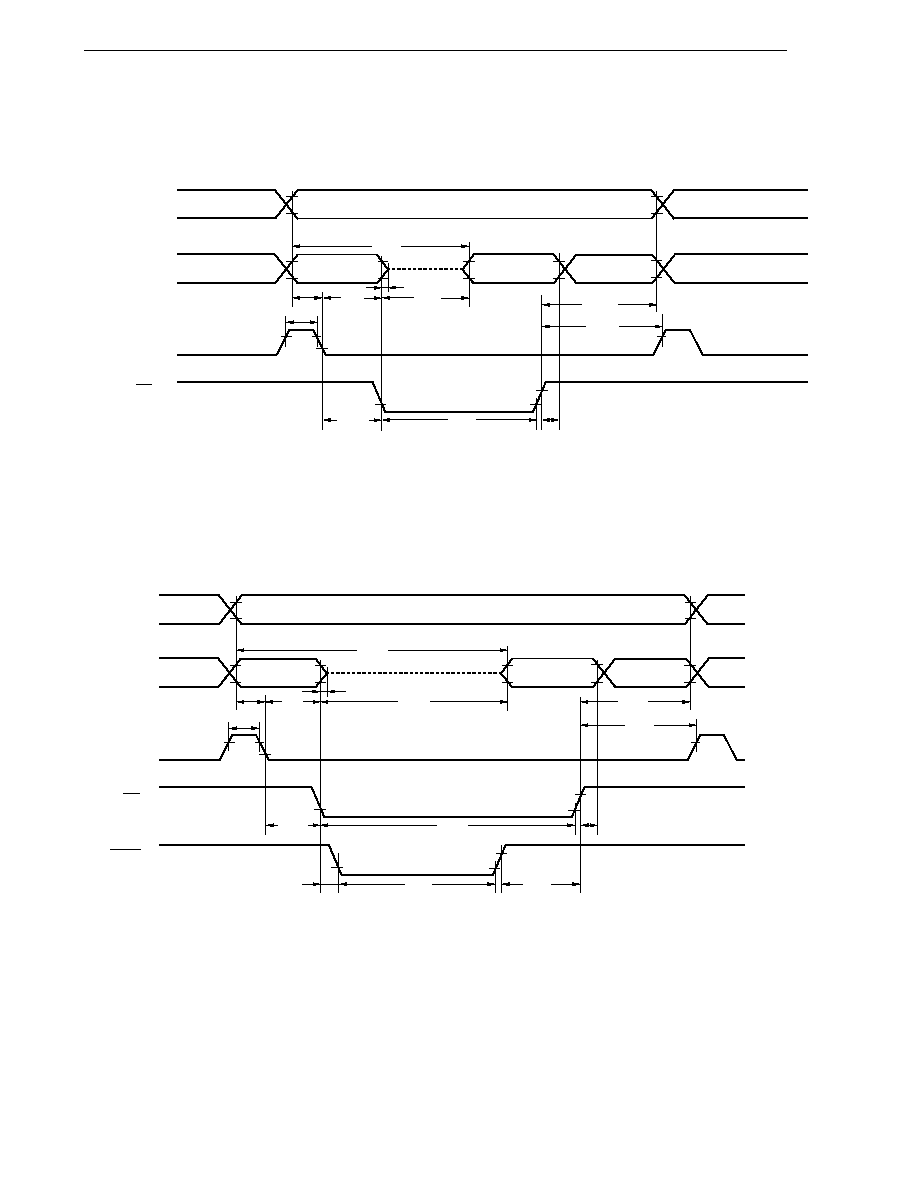
522
CHAPTER 26 ELECTRICAL SPECIFICATIONS (EXPANDED-SPECIFICATION PRODUCTS OF
µPD780076Y, 780078Y, 78F0078Y)
User's Manual U14260EJ3V1UD
Read/Write Operation
External fetch (no wait):
External fetch (wait insertion):
A8 to A15
AD0 to AD7
ASTB
RD
Higher 8-bit address
Lower 8-bit address
t
ADD1
Hi-Z
t
ADS
t
ASTH
t
ADH
t
RDAD
t
RDD1
Instruction code
t
RDADH
t
RDAST
t
ASTRD
t
RDL1
t
RDH
WAIT
t
RDWT1
t
WTL
t
WTRD
A8 to A15
AD0 to AD7
ASTB
RD
Higher 8-bit address
Lower 8-bit address
t
ADD1
Hi-Z
t
ADS
t
ASTH
t
ADH
t
RDD1
t
RDAD
Instruction code
t
RDADH
t
RDAST
t
ASTRD
t
RDL1
t
RDH
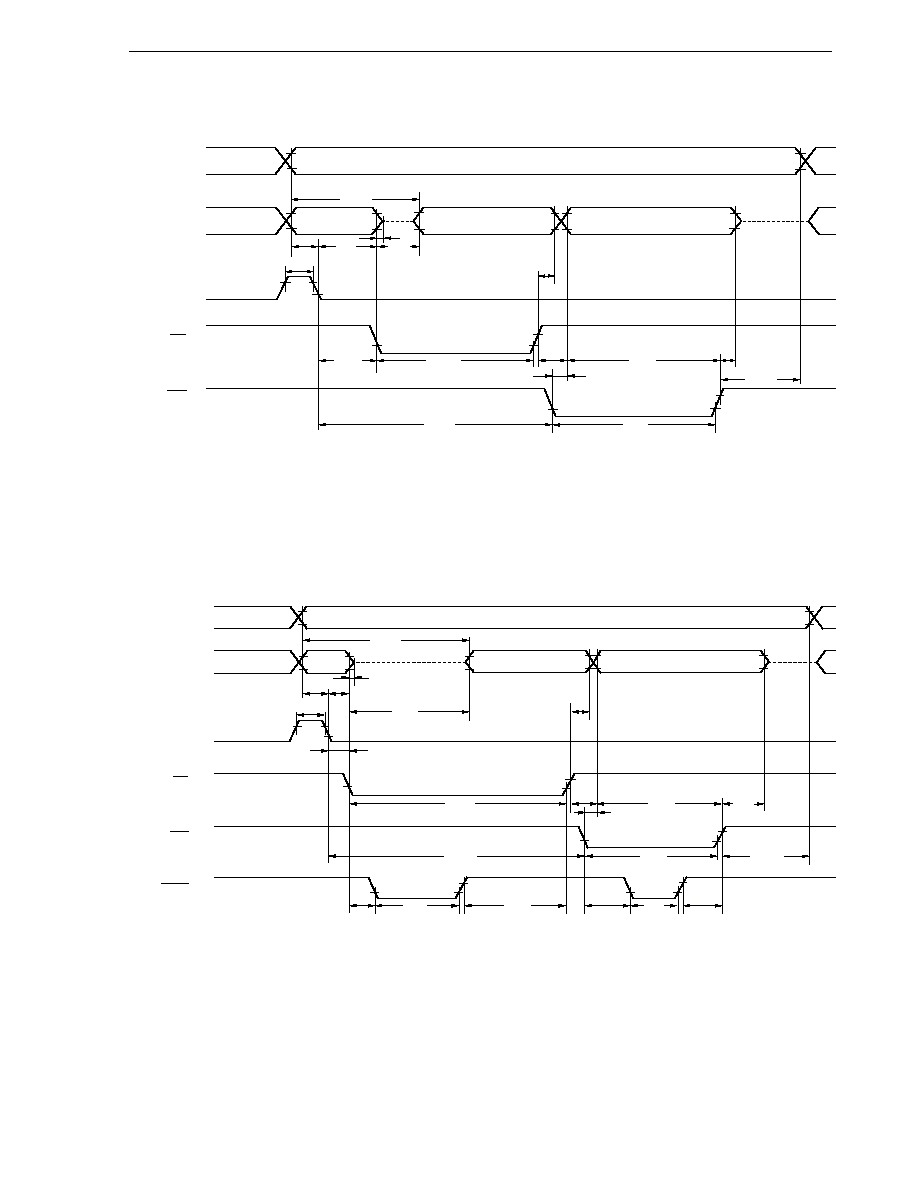
523
CHAPTER 26 ELECTRICAL SPECIFICATIONS (EXPANDED-SPECIFICATION PRODUCTS OF
µPD780076Y, 780078Y, 78F0078Y)
User's Manual U14260EJ3V1UD
External data access (no wait):
External data access (wait insertion):
A8 to A15
AD0 to AD7
ASTB
RD
Higher 8-bit address
Lower 8-bit
address
t
ADD2
t
ADS
t
ASTH
t
ADH
t
RDAD
t
RDD2
Read data
t
ASTRD
WR
t
ASTWR
Write data
Hi-Z
t
WDH
t
WRADH
t
WDS
t
WRWD
t
WRL1
t
RDH
t
RDL2
t
RDWT2
t
WTL
t
WRWT
t
WTL
t
WTWR
t
WTRD
WAIT
t
RDWD
Hi-Z
A8 to A15
AD0 to AD7
ASTB
RD
Higher 8-bit address
Lower 8-bit address
t
ADD2
Hi-Z
t
ADS
t
ASTH
t
ADH
t
RDD2
t
RDAD
Read data
t
ASTRD
t
RDWD
WR
t
ASTWR
Write data
Hi-Z
t
WDH
t
WRADH
t
WDS
t
WRWD
t
WRL1
t
RDH
t
RDL2
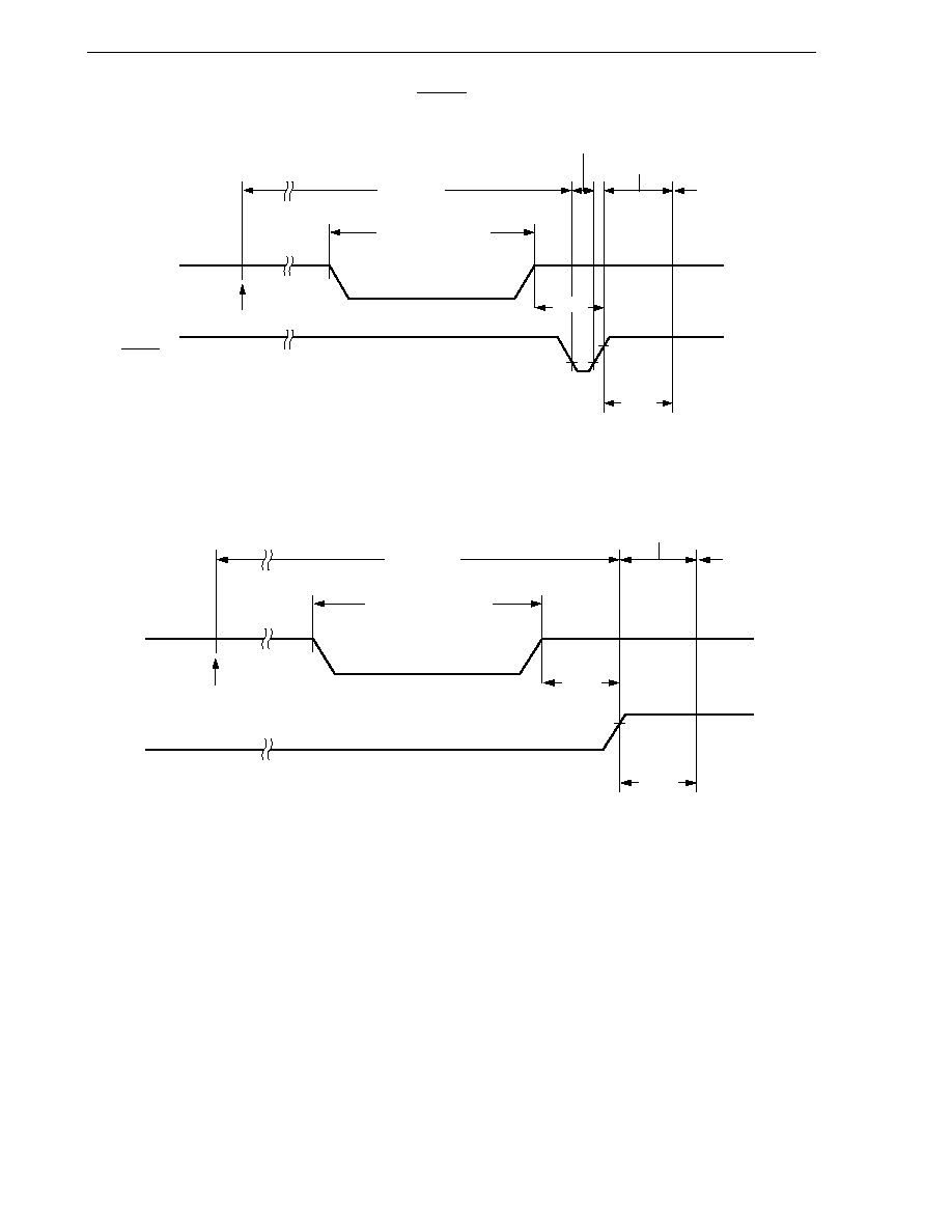
524
CHAPTER 26 ELECTRICAL SPECIFICATIONS (EXPANDED-SPECIFICATION PRODUCTS OF
µPD780076Y, 780078Y, 78F0078Y)
User's Manual U14260EJ3V1UD
Data Retention Timing (STOP Mode Release by RESET)
t
SREL
t
WAIT
V
DD
RESET
STOP instruction execution
STOP mode
Data retention mode
Internal reset operation
HALT mode
Operating mode
V
DDDR
Data Retention Timing (Standby Release Signal: STOP Mode Release by Interrupt Request Signal)
t
SREL
t
WAIT
V
DD
STOP instruction execution
STOP mode
Data retention mode
HALT mode
Operating mode
Standby release signal
(interrupt request)
V
DDDR

525
CHAPTER 26 ELECTRICAL SPECIFICATIONS (EXPANDED-SPECIFICATION PRODUCTS OF
µPD780076Y, 780078Y, 78F0078Y)
User's Manual U14260EJ3V1UD
Serial Transfer Timing
3-wire serial I/O mode:
UART mode (external clock input):
t
KCYn
t
KHn
t
KLn
ASCK0, ASCK2
I
2
C bus mode:
SCL0
SDA0
t
HD:STA
t
BUF
t
HD:DAT
t
HIGH
t
F
t
SU:DAT
t
SU:STA
t
HD:STA
t
SP
t
SU:STO
t
R
t
LOW
Stop
condition
Start
condition
Stop
condition
Restart
condition
Remark n = 1 to 4
Remark n = 5, 6
t
KCYn
t
KLn
t
KHn
SCK1, SCK3
SI1, SI3
SO1, SO3
t
SIKn
t
KSIn
t
KSOn
Input data
Output data
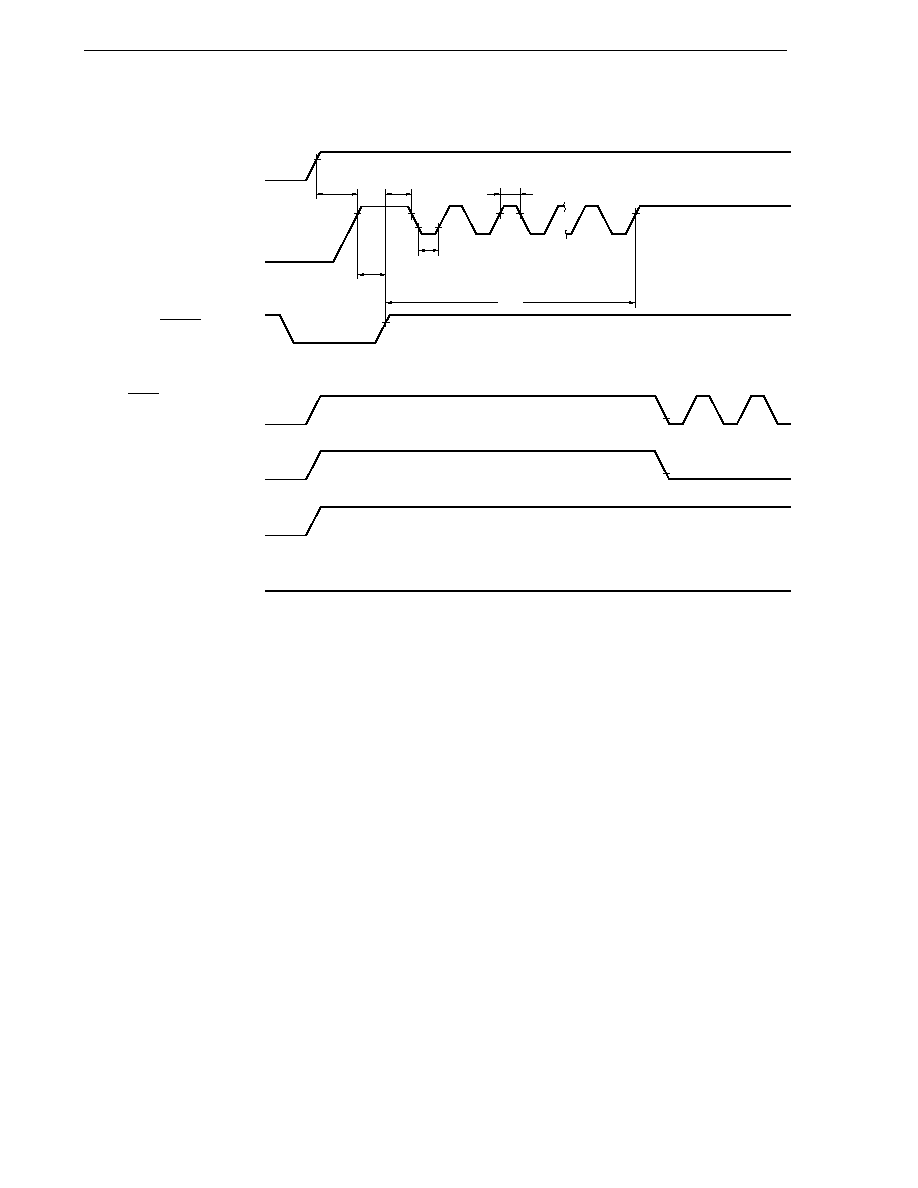
526
CHAPTER 26 ELECTRICAL SPECIFICATIONS (EXPANDED-SPECIFICATION PRODUCTS OF
µPD780076Y, 780078Y, 78F0078Y)
User's Manual U14260EJ3V1UD
Flash Write Mode Setting Timing
Notes 1. 3-wire serial I/O (SIO3) type
2. I
2
C bus (IIC0) type
3. UART (UART0) type
4. Handshake (when 3-wire serial I/O (SIO3) type is used)
V
DD
V
DD
0 V
V
DD
RESET (input)
0 V
V
PPH
0 V
V
PP
V
PPL
t
RP
t
PR
t
DP
t
PW
t
PW
t
RPE
0 V
SCK3
Note 1
/SCL0
Note 2
0 V
0 V
0 V
SI3
Note 1
/RxD0
Note 3
SO3
Note 1
/TxD0
Note 3
/SDA0
Note 2
P31 (HS)
Note 4
Reset command
V
IL
V
IL
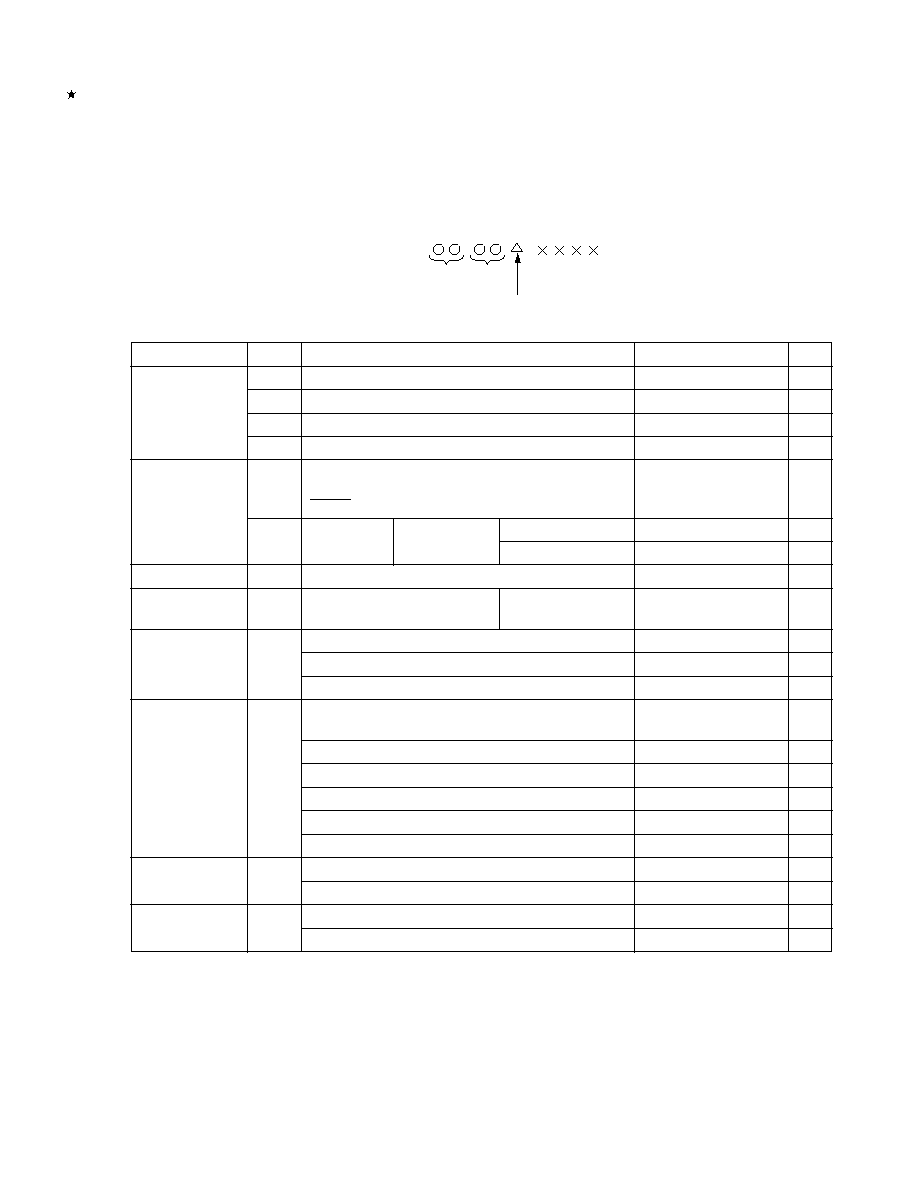
527
User's Manual U14260EJ3V1UD
CHAPTER 27 ELECTRICAL SPECIFICATIONS (CONVENTIONAL PRODUCTS)
Target products:
µPD780076, 780078, 780076Y, 780078Y, 78F0078, 78F0078Y for which orders were received
before January 31, 2002 (Products with a rank
Note
K)
Note The rank is indicated by the 5th digit from the left in the lot number marked on the package.
Absolute Maximum Ratings (T
A
= 25
∞
C)
Parameter
Symbol
Conditions
Ratings
Unit
Supply voltage
V
DD
≠0.3 to +6.5
V
V
PP
µPD78F0078, 78F0078Y only, Note 2
≠0.5 to +10.5
V
AV
REF
≠0.3 to V
DD
+ 0.3
Note 1
V
AV
SS
≠0.3 to +0.3
V
Input voltage
V
I1
P00 to P03, P10 to P17, P20 to P25, P34 to P36, P40 to P47,
≠0.3 to V
DD
+ 0.3
Note 1
V
P50 to P57, P64 to P67, P70 to P75, P80, X1, X2, XT1, XT2,
RESET
V
I2
P30 to P33
N-ch open-drain
No pull-up resistor
≠0.3 to +6.5
V
Pull-up resistor
≠0.3 to V
DD
+ 0.3
Note 1
V
Output voltage
V
O
≠0.3 to V
DD
+ 0.3
Note 1
V
Analog input voltage
V
AN
P10 to P17
Analog input pin
AV
SS
≠ 0.3 to AV
REF
+ 0.3
Note 1
V
and ≠0.3 to V
DD
+ 0.3
Note 1
Output current,
I
OH
Per pin
≠10
mA
high
Total for P00 to P03, P40 to P47, P50 to P57, P64 to P67, P70 to P75, P80
≠15
mA
Total for P20 to P25, P30 to P36
≠15
mA
Output current,
I
OL
Per pin for P00 to P03, P20 to P25, P34 to P36, P40 to
20
mA
low
P47, P64 to P67, P70 to P75, P80
Per pin for P30 to P33, P50 to P57
30
mA
Total for P00 to P03, P40 to P47, P64 to P67, P70 to P75, P80
50
mA
Total for P20 to P25
20
mA
Total for P30 to P36
100
mA
Total for P50 to P57
100
mA
Operating ambient
T
A
During normal operation
≠40 to +85
∞C
temperature
During flash memory programming
+10 to +40
∞C
Storage
T
stg
µPD780076, 780078, 780076Y, 780078Y
≠65 to +150
∞C
temperature
µPD78F0078, 78F0078Y
≠40 to +125
∞C
Note 1. 6.5 V or below
(Note 2 is explained on the next page.)
Caution Product quality may suffer if the absolute maximum rating is exceeded even momentarily for any
parameter. That is, the absolute maximum ratings are rated values at which the product is on the
verge of suffering physical damage, and therefore the product must be used under conditions that
ensure that the absolute maximum ratings are not exceeded.
Remark
Unless otherwise specified, the characteristics of alternate-function pins are the same as those of port pins.
Lot number
Year
code
Rank
Week
code

528
CHAPTER 27 ELECTRICAL SPECIFICATIONS (CONVENTIONAL PRODUCTS)
User's Manual U14260EJ3V1UD
Note 2. Make sure that the following conditions of the V
PP
voltage application timing are satisfied when the flash
memory is written.
∑
When supply voltage rises
V
PP
must exceed V
DD
10
µs or more after V
DD
has reached the lower-limit value (2.7 V) of the
operating voltage range (see a in the figure below).
∑
When supply voltage drops
V
DD
must be lowered 10
µs or more after V
PP
falls below the lower-limit value (2.7 V) of the
operating voltage range of V
DD
(see b in the figure below).
Capacitance (T
A
= 25
∞
C, V
DD
= V
SS
= 0 V)
Parameter
Symbol
Conditions
MIN.
TYP.
MAX.
Unit
Input
C
IN
f = 1 MHz
15
pF
capacitance
Unmeasured pins returned to 0 V.
I/O
C
IO
f = 1 MHz
P00 to P03, P20 to P25,
15
pF
capacitance
Unmeasured pins
P34 to P36, P40 to P47,
returned to 0 V.
P50 to P57, P64 to P67,
P70 to P75, P80
P30 to P33
20
pF
Remark Unless otherwise specified, the characteristics of alternate-function pins are the same as those of port pins.
2.7 V
V
DD
0 V
0 V
V
PP
2.7 V
a
b
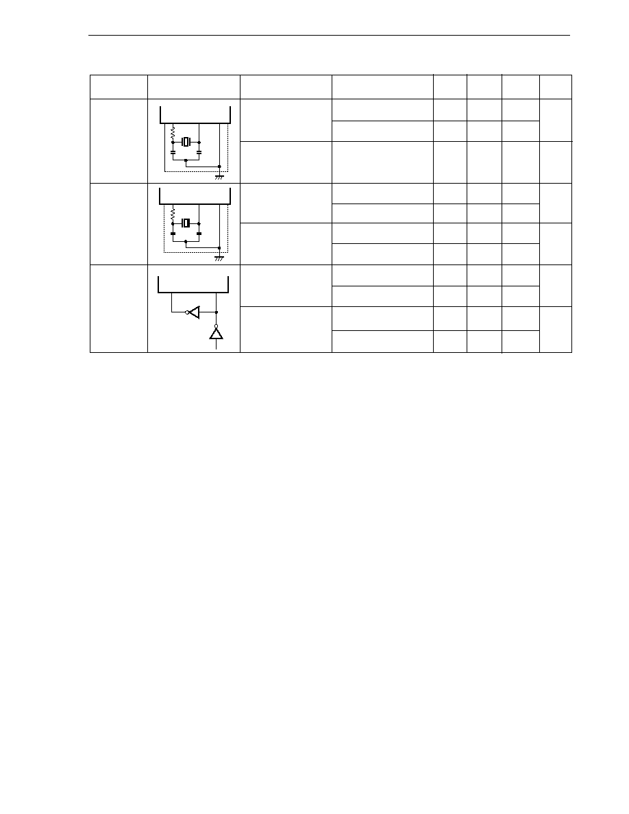
529
CHAPTER 27 ELECTRICAL SPECIFICATIONS (CONVENTIONAL PRODUCTS)
User's Manual U14260EJ3V1UD
Main System Clock Oscillator Characteristics (T
A
= ≠40 to +85
∞
C, V
DD
= 1.8 to 5.5 V)
Notes 1. Indicates only oscillator characteristics. Refer to AC Characteristics for instruction execution time.
2. Time required to stabilize oscillation after reset or STOP mode release.
Cautions
1. When using the main system clock oscillator, wire as follows in the area enclosed by the broken
lines in the above figures to avoid an adverse effect from wiring capacitance.
∑ Keep the wiring length as short as possible.
∑ Do not cross the wiring with the other signal lines.
∑ Do not route the wiring near a signal line through which a high fluctuating current flows.
∑ Always make the ground point of the oscillator capacitor the same potential as V
SS1
.
∑ Do not ground the capacitor to a ground pattern through which a high current flows.
∑ Do not fetch signals from the oscillator.
2. When the main system clock is stopped and the system is operating on the subsystem clock,
wait until the oscillation stabilization time has been secured by the program before switching
back to the main system clock.
Resonator
Recommended
Parameter
Conditions
MIN.
TYP.
MAX.
Unit
Circuit
Ceramic
Oscillation
4.0 V
V
DD
5.5 V
1.0
8.38
MHz
resonator
frequency (f
X
)
Note 1
1.8 V
V
DD
< 4.0 V
1.0
5.0
Oscillation
After V
DD
reaches
4
ms
stabilization time
Note 2
oscillation voltage range
MIN.
Crystal
Oscillation
4.0 V
V
DD
5.5 V
1.0
8.38
MHz
resonator
frequency (f
X
)
Note 1
1.8 V
V
DD
< 4.0 V
1.0
5.0
Oscillation
4.0 V
V
DD
5.5 V
10
ms
1.8 V
V
DD
< 4.0 V
30
stabilization time
Note 2
External
X1 input
4.0 V
V
DD
5.5 V
1.0
8.38
MHz
clock
frequency (f
X
)
Note 1
1.8 V
V
DD
< 4.0 V
1.0
5.0
X1 input
4.0 V
V
DD
5.5 V
50
500
ns
high-/low-level width
(t
XH
, t
XL
)
1.8 V
V
DD
< 4.0 V
85
500
X2
X1
C2
Rd
C1
X1
V
SS1
X2
C2
Rd
C1
X1
V
SS1
X2
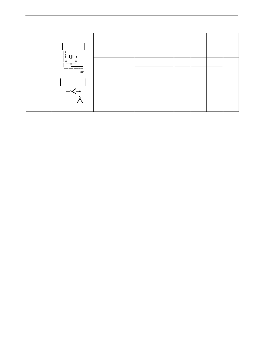
530
CHAPTER 27 ELECTRICAL SPECIFICATIONS (CONVENTIONAL PRODUCTS)
User's Manual U14260EJ3V1UD
Subsystem Clock Oscillator Characteristics
(T
A
= ≠40 to +85
∞C, V
DD
= 1.8 to 5.5 V)
Notes 1. Indicates only oscillator characteristics. Refer to AC Characteristics for instruction execution time.
2. Time required to stabilize oscillation after V
DD
reaches oscillation voltage range MIN.
Cautions
1. When using the subsystem clock oscillator, wire as follows in the area enclosed by the broken
lines in the above figure to avoid an adverse effect from wiring capacitance.
∑ Keep the wiring length as short as possible.
∑ Do not cross the wiring with the other signal lines.
∑ Do not route the wiring near a signal line through which a high fluctuating current flows.
∑ Always make the ground point of the oscillator capacitor the same potential as V
SS1
.
∑ Do not ground the capacitor to a ground pattern through which a high current flows.
∑ Do not fetch signals from the oscillator.
2. The subsystem clock oscillator is designed as a low-amplitude circuit for reducing power
consumption, and is more prone to malfunction due to noise than the main system clock
oscillator. Particular care is therefore required with the wiring method when the subsystem
clock is used.
MIN.
32
32
Resonator
Crystal
resonator
External
clock
Parameter
Oscillation
frequency (f
XT
)
Note 1
Oscillation
stabilization time
Note 2
XT1 input
frequency (f
XT
)
Note 1
XT1 input
high-/low-level width
(t
XTH
, t
XTL
)
Conditions
4.0 V
V
DD
5.5 V
1.8 V
V
DD
< 4.0 V
TYP.
32.768
1.2
MAX.
35
2
10
38.5
Unit
kHz
s
kHz
Recommended Circuit
12
15
µs
XT1
XT2
C3
XT2 XT1 V
SS1
Rd
C4
531
CHAPTER 27 ELECTRICAL SPECIFICATIONS (CONVENTIONAL PRODUCTS)
User's Manual U14260EJ3V1UD
Recommended Oscillator Constant
(1)
µPD780076, 780078, 780076Y, 780078Y
(a) Main system clock: Ceramic resonator (T
A
= ≠40 to +85
∞
C)
Manufacturer
Part Number
Frequency
Recommended Circuit Constant
Oscillation Voltage Range
(MHz)
C1 (pF)
C2 (pF)
Rd (k
)
MIN. (V)
MAX. (V)
Murata Mfg.
CSBFB1M00J58
1.00
150
150
0
1.8
5.5
Co., Ltd.
CSBLA1M00J58
1.00
150
150
0
1.8
5.5
CSTCC2M00G56
2.00
On-chip
On-chip
0
1.8
5.5
CSTLS2M00G56
2.00
On-chip
On-chip
0
1.8
5.5
CSTCC3M58G53
3.58
On-chip
On-chip
0
1.8
5.5
CSTLS3M58G53
3.58
On-chip
On-chip
0
1.8
5.5
CSTCR4M00G53
4.00
On-chip
On-chip
0
1.8
5.5
CSTLS4M00G53
4.00
On-chip
On-chip
0
1.8
5.5
CSTCR4M19G53
4.19
On-chip
On-chip
0
1.8
5.5
CSTLS4M19G53
4.19
On-chip
On-chip
0
1.8
5.5
CSTCR4M91G53
4.91
On-chip
On-chip
0
1.8
5.5
CSTLS4M91G53
4.91
On-chip
On-chip
0
1.8
5.5
CSTCR5M00G53
5.00
On-chip
On-chip
0
2.7
5.5
CSTLS5M00G53
5.00
On-chip
On-chip
0
2.7
5.5
CSTCE8M00G52
8.00
On-chip
On-chip
0
3.0
5.5
CSTLS8M00G53
8.00
On-chip
On-chip
0
3.0
5.5
CSTCE8M38G52
8.38
On-chip
On-chip
0
3.0
5.5
CSTLS8M38G53
8.38
On-chip
On-chip
0
3.0
5.5
TDK
CCR3.5MC5
3.58
On-chip
On-chip
0
1.8
5.5
CCR4.0MC5
4.00
On-chip
On-chip
0
1.8
5.5
CCR4.19MC5
4.19
On-chip
On-chip
0
1.8
5.5
CCR5.0MC5
5.00
On-chip
On-chip
0
2.7
5.5
CCR6.0MC5
6.00
On-chip
On-chip
0
2.7
5.5
CCR8.0MC5
8.00
On-chip
On-chip
0
3.0
5.5
CCR8.38MC5
8.38
On-chip
On-chip
0
3.0
5.5
Caution
The oscillator constant is a reference value based on evaluation in specific environments by the
resonator manufacturer. If the oscillator characteristics need to be optimized in the actual
application, request the resonator manufacturer for evaluation on the implementation circuit.
Note that the oscillation voltage and oscillation frequency merely indicate the characteristics of
the oscillator. Use the internal operation conditions of the
µPD780078, 780078Y Subseries within
the specifications of the DC and AC characteristics.

532
CHAPTER 27 ELECTRICAL SPECIFICATIONS (CONVENTIONAL PRODUCTS)
User's Manual U14260EJ3V1UD
(1)
µPD780076, 780078, 780076Y, 780078Y
(b) Main system clock: Crystal resonator (T
A
= ≠10 to +70
∞
C)
(c) Subsystem clock: Crystal resonator (T
A
= ≠40 to +85
∞
C)
Caution
The oscillator constant is a reference value based on evaluation in specific environments by the
resonator manufacturer. If the oscillator characteristics need to be optimized in the actual
application, request the resonator manufacturer for evaluation on the implementation circuit.
Note that the oscillation voltage and oscillation frequency merely indicate the characteristics of
the oscillator. Use the internal operation conditions of the
µPD780078, 780078Y Subseries within
the specifications of the DC and AC characteristics.
Manufacturer
KINSEKI, Ltd.
Part Number
HC-49/U-S
Frequency
(MHz)
4.19
8.38
C1 (pF)
18
27
C2 (pF)
18
27
MIN. (V)
1.9
3.0
MAX. (V)
5.5
5.5
Recommended Circuit Constant
Oscillation Voltage Range
Rd (k
)
4.7
0
Manufacturer
Seiko Epson
Corporation
Part Number
C-022RX
MC-206
MC-306
Frequency
(kHz)
32.768
32.768
32.768
C1 (pF)
15
15
15
C2 (pF)
15
15
15
MIN. (V)
1.8
1.8
1.8
MAX. (V)
5.5
5.5
5.5
Recommended Circuit Constant
Oscillation Voltage Range
Rd (k
)
330
330
330

533
CHAPTER 27 ELECTRICAL SPECIFICATIONS (CONVENTIONAL PRODUCTS)
User's Manual U14260EJ3V1UD
(2)
µPD78F0078, 78F0078Y
Main system clock: Ceramic resonator (T
A
= ≠40 to +85
∞
C)
Manufacturer
Part Number
Frequency
Recommended Circuit Constant
Oscillation Voltage Range
(MHz)
C1 (pF)
C2 (pF)
R1 (k
)
MIN. (V)
MAX. (V)
Murata Mfg.
CSBFB1M00J58
1.00
100
100
3.3
1.8
5.5
Co., Ltd.
CSBLA1M00J58
1.00
100
100
3.3
1.8
5.5
CSTCC2M00G56
2.00
On-chip
On-chip
0
1.8
5.5
CSTLS2M00G56
2.00
On-chip
On-chip
0
1.8
5.5
CSTCC3M58G53
3.58
On-chip
On-chip
0
1.8
5.5
CSTLS3M58G53
3.58
On-chip
On-chip
0
1.8
5.5
CSTCR4M00G53
4.00
On-chip
On-chip
0
1.8
5.5
CSTLS4M00G53
4.00
On-chip
On-chip
0
1.8
5.5
CSTCR4M19G53
4.19
On-chip
On-chip
0
1.8
5.5
CSTLS4M19G53
4.19
On-chip
On-chip
0
1.8
5.5
CSTCR4M91G53
4.91
On-chip
On-chip
0
1.8
5.5
CSTLS4M91G53
4.91
On-chip
On-chip
0
1.8
5.5
CSTCR5M00G53
5.00
On-chip
On-chip
0
2.7
5.5
CSTLS5M00G53
5.00
On-chip
On-chip
0
2.7
5.5
CSTCE8M00G52
8.00
On-chip
On-chip
0
3.0
5.5
CSTLS8M00G53
8.00
On-chip
On-chip
0
3.0
5.5
CSTCE8M38G52
8.38
On-chip
On-chip
0
3.0
5.5
CSTLS8M38G53
8.38
On-chip
On-chip
0
3.0
5.5
Caution
The oscillator constant is a reference value based on evaluation in specific environments by the
resonator manufacturer. If the oscillator characteristics need to be optimized in the actual
application, request the resonator manufacturer for evaluation on the implementation circuit.
Note that the oscillation voltage and oscillation frequency merely indicate the characteristics of
the oscillator. Use the internal operation conditions of the
µPD780078, 780078Y Subseries within
the specifications of the DC and AC characteristics.
Remark For the resonator selection and oscillator constant, users are requested to either evaluate the oscillation
themselves or apply to the resonator manufacturer for evaluation.
534
CHAPTER 27 ELECTRICAL SPECIFICATIONS (CONVENTIONAL PRODUCTS)
User's Manual U14260EJ3V1UD
DC Characteristics (T
A
= ≠40 to +85
∞
C, V
DD
= 1.8 to 5.5 V)
Parameter
Symbol
Conditions
MIN.
TYP.
MAX.
Unit
Output current,
I
OH
Per pin
≠1
mA
high
All pins
≠15
mA
Output current,
I
OL
Per pin for P00 to P03, P20 to P25, P34 to P36,
10
mA
low
P40 to P47, P64 to P67, P70 to P75, P80
Per pin for P30 to P33, P50 to P57
15
mA
Total for P00 to P03, P40 to P47, P64 to P67, P70 to P75, P80
20
mA
Total for P20 to P25
10
mA
Total for P30 to P36
70
mA
Total for P50 to P57
70
mA
Input voltage,
V
IH1
P10 to P17, P21, P24,
2.7 V
V
DD
5.5 V
0.7V
DD
V
DD
V
high
P40 to P47, P50 to P57,
1.8 V
V
DD
< 2.7 V
0.8V
DD
V
DD
V
P64 to P67
V
IH2
P00 to P03, P20, P22, P23, P25,
2.7 V
V
DD
5.5 V
0.8V
DD
V
DD
V
P34 to P36, P70 to P75, P80, RESET 1.8 V V
DD
< 2.7 V
0.85V
DD
V
DD
V
V
IH3
P30 to P33
2.7 V
V
DD
5.5 V
0.7V
DD
5.5
V
(N-ch open-drain)
1.8 V
V
DD
< 2.7 V
0.8V
DD
5.5
V
V
IH4
X1, X2
2.7 V
V
DD
5.5 V
V
DD
≠
0.5
V
DD
V
1.8 V
V
DD
< 2.7 V
V
DD
≠
0.2
V
DD
V
V
IH5
XT1, XT2
4.0 V
V
DD
5.5 V
0.8V
DD
V
DD
V
1.8 V
V
DD
< 4.0 V
0.9V
DD
V
DD
V
Input voltage,
V
IL1
P10 to P17, P21, P24,
2.7 V
V
DD
5.5 V
0
0.3V
DD
V
low
P40 to P47, P50 to P57,
1.8 V
V
DD
< 2.7 V
0
0.2V
DD
V
P64 to P67
V
IL2
P00 to P03, P20, P22, P23, P25,
2.7 V
V
DD
5.5 V
0
0.2V
DD
V
P34 to P36, P70 to P75, P80, RESET 1.8 V
V
DD
< 2.7 V
0
0.15V
DD
V
V
IL3
P30 to P33
4.0 V
V
DD
5.5 V
0
0.3V
DD
V
(N-ch open-drain)
2.7 V
V
DD
< 4.0 V
0
0.2V
DD
V
1.8 V
V
DD
< 2.7 V
0
0.1V
DD
V
V
IL4
X1, X2
2.7 V
V
DD
5.5 V
0
0.4
V
1.8 V
V
DD
< 2.7 V
0
0.2
V
V
IL5
XT1, XT2
4.0 V
V
DD
5.5 V
0
0.2V
DD
V
1.8 V
V
DD
< 4.0 V
0
0.1V
DD
V
Output voltage,
V
OH1
4.0 V
V
DD
5.5 V, I
OH
= ≠1 mA
V
DD
≠
1.0
V
DD
V
high
1.8 V
V
DD
< 4.0 V, I
OH
= ≠100
µA
V
DD
≠
0.5
V
DD
V
Output voltage,
V
OL1
P30 to P33
4.0 V
V
DD
5.5 V,
2.0
V
low
I
OL
= 15 mA
V
OL2
P50 to P57
4.0 V
V
DD
5.5 V,
0.4
2.0
V
I
OL
= 15 mA
V
OL3
P00 to P03, P20 to P25, P34 to P36,
4.0 V
V
DD
5.5 V,
0.4
V
P40 to P47, P64 to P67, P70 to P75, P80
I
OL
= 1.6 mA
V
OL4
I
OL
= 400
µA
0.5
V
Remark
Unless otherwise specified, the characteristics of alternate-function pins are the same as those of port pins.

535
CHAPTER 27 ELECTRICAL SPECIFICATIONS (CONVENTIONAL PRODUCTS)
User's Manual U14260EJ3V1UD
DC Characteristics (T
A
= ≠40 to +85
∞
C, V
DD
= 1.8 to 5.5 V)
Parameter
Symbol
Conditions
MIN.
TYP.
MAX.
Unit
Input leakage
I
LIH1
V
IN
= V
DD
P00 to P03, P10 to P17, P20 to P25,
3
µA
current, high
P34 to P36, P40 to P47, P50 to P57,
P64 to P67, P70 to P75, P80,
RESET
I
LIH2
X1, X2, XT1, XT2
20
µA
I
LIH3
V
IN
= 5.5 V
P30 to P33
Note
3
µA
Input leakage
I
LIL1
V
IN
= 0 V
P00 to P03, P10 to P17, P20 to P25,
≠3
µA
current, low
P34 to P36, P40 to P47, P50 to P57,
P64 to P67, P70 to P75, P80,
RESET
I
LIL2
X1, X2, XT1, XT2
≠20
µA
I
LIL3
P30 to P33
Note
≠3
µA
Output leakage
I
LOH
V
OUT
= V
DD
3
µA
current, high
Output leakage
I
LOL
V
OUT
= 0 V
≠3
µA
current, low
Mask option
R
1
V
IN
= 0 V,
15
30
90
k
pull-up resistance
P30, P31, P32
Note
, P33
Note
(mask ROM
version only)
Software pull-
R
2
V
IN
= 0 V,
15
30
90
k
up resistance
P00 to P03, P20 to P25, P34 to P36, P40 to P47,
P50 to P57, P64 to P67, P70 to P75, P80
V
PP
(IC)
V
PP1
During normal operation
0
0.2V
DD
V
power supply
voltage
Note
µPD780076, 780078 only
Remark Unless otherwise specified, the characteristics of alternate-function pins are the same as those of port pins.

536
CHAPTER 27 ELECTRICAL SPECIFICATIONS (CONVENTIONAL PRODUCTS)
User's Manual U14260EJ3V1UD
DC Characteristics (T
A
= ≠40 to +85
∞
C, V
DD
= 1.8 to 5.5 V)
(1)
µPD780076, 780078, 780076Y, 780078Y
Parameter
Symbol
Conditions
MIN.
TYP.
MAX.
Unit
Power supply
I
DD1
Note 2
8.38 MHz
V
DD
= 5.0 V
±10%
Note 3
When A/D converter is
5.5
11.0
mA
current
Note 1
crystal oscillation
stopped
operating mode
When A/D converter is
6.5
13.0
mA
operating
5.00 MHz
V
DD
= 3.0 V
±10%
Note 3
When A/D converter is
2.0
4.0
mA
crystal oscillation
stopped
operating mode
When A/D converter is
3.0
6.0
mA
operating
V
DD
= 2.0 V
±10%
Note 4
When A/D converter is
0.4
1.5
mA
stopped
When A/D converter is
1.4
4.2
mA
operating
I
DD2
8.38 MHz
V
DD
= 5.0 V
±10%
Note 3
When peripheral functions
1.1
2.2
mA
crystal oscillation
are stopped
HALT mode
When peripheral functions
4.7
mA
are operating
5.00 MHz
V
DD
= 3.0 V
±10%
Note 3
When peripheral functions
0.35
0.7
mA
crystal oscillation
are stopped
HALT mode
When peripheral functions
1.7
mA
are operating
V
DD
= 2.0 V
±10%
Note 4
When peripheral functions
0.15
0.4
mA
are stopped
When peripheral functions
1.1
mA
are operating
I
DD3
32.768 kHz crystal oscillation
V
DD
= 5.0 V
±10%
40
80
µA
operating mode
Note 5
V
DD
= 3.0 V
±10%
20
40
µA
V
DD
= 2.0 V
±10%
10
20
µA
I
DD4
32.768 kHz crystal oscillation
V
DD
= 5.0 V
±10%
30
60
µA
HALT mode
Note 5
V
DD
= 3.0 V
±10%
6
18
µA
V
DD
= 2.0 V
±10%
2
10
µA
I
DD5
STOP mode
Note 6
V
DD
= 5.0 V
±10%
0.1
30
µA
V
DD
= 3.0 V
±10%
0.05
10
µA
V
DD
= 2.0 V
±10%
0.05
10
µA
Notes 1. Total current through the internal power supply (V
DD0
, V
DD1
).
2. I
DD1
includes the peripheral operating current (except the current through the pull-up resistors of ports).
3. When the processor clock control register (PCC) is set to 00H.
4. When PCC is set to 02H.
5. When main system clock operation is stopped.
6. When the main system clock and subsystem clock are stopped.

537
CHAPTER 27 ELECTRICAL SPECIFICATIONS (CONVENTIONAL PRODUCTS)
User's Manual U14260EJ3V1UD
DC Characteristics (T
A
= ≠40 to +85
∞
C, V
DD
= 1.8 to 5.5 V)
(2)
µPD78F0078, 78F0078Y
Parameter
Symbol
Conditions
MIN.
TYP.
MAX.
Unit
Power supply
I
DD1
Note 2
8.38 MHz
V
DD
= 5.0 V
±10%
Note 3
When A/D converter is
10.5
21.0
mA
current
Note 1
crystal oscillation
stopped
operating mode
When A/D converter is
11.5
23.0
mA
operating
5.00 MHz
V
DD
= 3.0 V
±10%
Note 3
When A/D converter is
4.5
9.0
mA
crystal oscillation
stopped
operating mode
When A/D converter is
5.5
11.0
mA
operating
V
DD
= 2.0 V
±10%
Note 4
When A/D converter is
1.0
2.0
mA
stopped
When A/D converter is
2.0
6.0
mA
operating
I
DD2
8.38 MHz
V
DD
= 5.0 V
±10%
Note 3
When peripheral functions
1.2
2.4
mA
crystal oscillation
are stopped
HALT mode
When peripheral functions
5.0
mA
are operating
5.00 MHz
V
DD
= 3.0 V
±10%
Note 3
When peripheral functions
0.4
0.8
mA
crystal oscillation
are stopped
HALT mode
When peripheral functions
1.7
mA
are operating
V
DD
= 2.0 V
±10%
Note 4
When peripheral functions
0.2
0.4
mA
are stopped
When peripheral functions
1.1
mA
are operating
I
DD3
32.768 kHz crystal oscillation
V
DD
= 5.0 V
±10%
115
230
µA
operating mode
Note 5
V
DD
= 3.0 V
±10%
95
190
µA
V
DD
= 2.0 V
±10%
75
150
µA
I
DD4
32.768 kHz crystal oscillation
V
DD
= 5.0 V
±10%
30
60
µA
HALT mode
Note 5
V
DD
= 3.0 V
±10%
6
18
µA
V
DD
= 2.0 V
±10%
2
10
µA
I
DD5
STOP mode
Note 6
V
DD
= 5.0 V
±10%
0.1
30
µA
V
DD
= 3.0 V
±10%
0.05
10
µA
V
DD
= 2.0 V
±10%
0.05
10
µA
Notes 1. Total current through the internal power supply (V
DD0
, V
DD1
).
2. I
DD1
includes the peripheral operating current (except the current through the pull-up resistors of ports).
3. When the processor clock control register (PCC) is set to 00H.
4. When PCC is set to 02H.
5. When main system clock operation is stopped.
6. When the main system clock and subsystem clock are stopped.
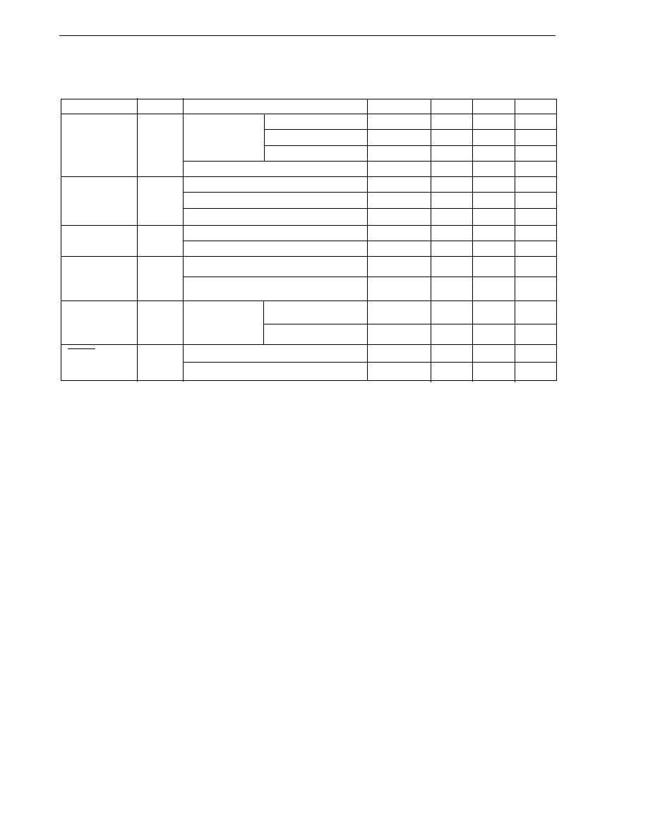
538
CHAPTER 27 ELECTRICAL SPECIFICATIONS (CONVENTIONAL PRODUCTS)
User's Manual U14260EJ3V1UD
AC Characteristics
(1) Basic operation
(T
A
= ≠40 to +85
∞
C, V
DD
= 1.8 to 5.5 V)
Notes 1. Value when the external clock is used. When a crystal resonator is used, it is 114
µs (MIN.).
2. Selection of f
sam
= f
X
, f
X
/4, f
X
/64 is possible using bits 0 and 1 (PRM000, PRM010) of prescaler mode register
00 (PRM00). Selection of f
sam
= f
X
/2, f
X
/8, f
X
/512 is possible using bits 0 and 1 (PRM001, PRM011) of
prescaler mode register 01 (PRM01). However, if the TI000 or TI001 valid edge is selected as the count
clock, the value becomes f
sam
= f
X
/8.
Parameter
Symbol
Conditions
MIN.
TYP.
MAX.
Unit
Cycle time
T
CY
Operating with
0.238
16
µs
(Min. instruction
main system clock
0.4
16
µs
execution time)
1.6
16
µs
Operating with subsystem clock
103.9
Note 1
122
125
µs
TI000, TI010, TI001,
t
TIH0
, t
TIL0
3.5 V
V
DD
5.5 V
2/f
sam
+ 0.1
Note 2
µs
TI011 input high-/low-
2.7 V
V
DD
< 3.5 V
2/f
sam
+ 0.2
Note 2
µs
level width
1.8 V
V
DD
< 2.7 V
2/f
sam
+ 0.5
Note 2
µs
TI50, TI51 input
f
TI5
2.7 V
V
DD
5.5 V
0
4
MHz
frequency
1.8 V
V
DD
< 2.7 V
0
275
kHz
TI50, TI51 input
t
TIH5
, t
TIL5
2.7 V
V
DD
5.5 V
100
ns
high-/low-level
1.8 V
V
DD
< 2.7 V
1.8
µs
width
Interrupt request
t
INTH
, t
INTL
INTP0 to INTP3,
2.7 V
V
DD
5.5 V
1
µs
input high-/low-
P40 to P47
1.8 V
V
DD
< 2.7 V
2
µs
level width
RESET
t
RSL
2.7 V
V
DD
5.5 V
10
µs
low-level width
1.8 V
V
DD
< 2.7 V
20
µs
4.0 V
V
DD
5.5 V
2.7 V
V
DD
< 4.0 V
1.8 V
V
DD
< 2.7 V

539
CHAPTER 27 ELECTRICAL SPECIFICATIONS (CONVENTIONAL PRODUCTS)
User's Manual U14260EJ3V1UD
T
CY
vs. V
DD
(main system clock operation)
5.0
1.0
2.0
1.6
0.4
0.238
0.1
0
10.0
1.0
2.0
3.0
4.0
5.0
6.0
1.8
5.5
2.7
Operation
guaranteed
range
16.0
Cycle time T
CY
[ s]
µ
Supply voltage V
DD
[V]

540
CHAPTER 27 ELECTRICAL SPECIFICATIONS (CONVENTIONAL PRODUCTS)
User's Manual U14260EJ3V1UD
(2) Read/write operation (T
A
= ≠40 to +85
∞
C, V
DD
= 4.0 to 5.5 V)
(1/3)
Parameter
Symbol
Conditions
MIN.
MAX.
Unit
ASTB high-level width
t
ASTH
0.3t
CY
ns
Address setup time
t
ADS
20
ns
Address hold time
t
ADH
6
ns
Data input time from address
t
ADD1
(2 + 2n)t
CY
≠ 54
ns
t
ADD2
(3 + 2n)t
CY
≠ 60
ns
Address output time from RD
t
RDAD
0
100
ns
Data input time from RD
t
RDD1
(2 + 2n)t
CY
≠ 87
ns
t
RDD2
(3 + 2n)t
CY
≠ 93
ns
Read data hold time
t
RDH
0
ns
RD low-level width
t
RDL1
(1.5 + 2n)t
CY
≠ 33
ns
t
RDL2
(2.5 + 2n)t
CY
≠ 33
ns
Input time from RD
to WAIT
t
RDWT1
t
CY
≠ 43
ns
t
RDWT2
t
CY
≠ 43
ns
Input time from WR
to WAIT
t
WRWT
t
CY
≠ 25
ns
WAIT low-level width
t
WTL
(0.5 + n)t
CY
+ 10
(2 + 2n)t
CY
ns
Write data setup time
t
WDS
60
ns
Write data hold time
t
WDH
6
ns
WR low-level width
t
WRL1
(1.5 + 2n)t
CY
≠ 15
ns
Delay time from ASTB
to RD
t
ASTRD
6
ns
Delay time from ASTB
to WR
t
ASTWR
2t
CY
≠ 15
ns
Delay time from
t
RDAST
0.8t
CY
≠ 15
1.2t
CY
ns
RD
to ASTB at external fetch
Address hold time from
t
RDADH
0.8t
CY
≠ 15
1.2t
CY
+ 30
ns
RD
at external fetch
Write data output time from RD
t
RDWD
40
ns
Write data output time from WR
t
WRWD
10
60
ns
Address hold time from WR
t
WRADH
0.8t
CY
≠ 15
1.2t
CY
+ 30
ns
Delay time from WAIT
to RD
t
WTRD
0.8t
CY
2.5t
CY
+ 25
ns
Delay time from WAIT
to WR
t
WTWR
0.8t
CY
2.5t
CY
+ 25
ns
Remarks
1.
t
CY
= T
CY
/4
2.
n indicates the number of waits.
3.
C
L
= 100 pF (C
L
indicates the load capacitance of the AD0 to AD7, A8 to A15, RD, WR, WAIT, and
ASTB pins.)

541
CHAPTER 27 ELECTRICAL SPECIFICATIONS (CONVENTIONAL PRODUCTS)
User's Manual U14260EJ3V1UD
(2) Read/write operation (T
A
= ≠40 to +85
∞
C, V
DD
= 2.7 to 4.0 V)
(2/3)
Parameter
Symbol
Conditions
MIN.
MAX.
Unit
ASTB high-level width
t
ASTH
0.3t
CY
ns
Address setup time
t
ADS
30
ns
Address hold time
t
ADH
10
ns
Input time from address to data
t
ADD1
(2 + 2n)t
CY
≠ 108
ns
t
ADD2
(3 + 2n)t
CY
≠ 120
ns
Output time from RD
to address
t
RDAD
0
200
ns
Input time from RD
to data
t
RDD1
(2 + 2n)t
CY
≠ 148
ns
t
RDD2
(3 + 2n)t
CY
≠ 162
ns
Read data hold time
t
RDH
0
ns
RD low-level width
t
RDL1
(1.5 + 2n)t
CY
≠ 40
ns
t
RDL2
(2.5 + 2n)t
CY
≠ 40
ns
Input time from RD
to WAIT
t
RDWT1
t
CY
≠ 75
ns
t
RDWT2
t
CY
≠ 60
ns
Input time from WR
to WAIT
t
WRWT
t
CY
≠ 50
ns
WAIT low-level width
t
WTL
(0.5 + 2n)t
CY
+ 10
(2 + 2n)t
CY
ns
Write data setup time
t
WDS
60
ns
Write data hold time
t
WDH
10
ns
WR low-level width
t
WRL1
(1.5 + 2n)t
CY
≠ 30
ns
Delay time from ASTB
to RD
t
ASTRD
10
ns
Delay time from ASTB
to WR
t
ASTWR
2t
CY
≠ 30
ns
Delay time from
t
RDAST
0.8t
CY
≠ 30
1.2t
CY
ns
RD
to ASTB at external fetch
Hold time from
t
RDADH
0.8t
CY
≠ 30
1.2t
CY
+ 60
ns
RD
to address at external fetch
Write data output time from RD
t
RDWD
40
ns
Write data output time from WR
t
WRWD
20
120
ns
Hold time from WR
to address
t
WRADH
0.8t
CY
≠ 30
1.2t
CY
+ 60
ns
Delay time from WAIT
to RD
t
WTRD
0.5t
CY
2.5t
CY
+ 50
ns
Delay time from WAIT
to WR
t
WTWR
0.5t
CY
2.5t
CY
+ 50
ns
Remarks
1.
t
CY
= T
CY
/4
2.
n indicates the number of waits.
3.
C
L
= 100 pF (C
L
indicates the load capacitance of the AD0 to AD7, A8 to A15, RD, WR, WAIT, and
ASTB pins.)
542
CHAPTER 27 ELECTRICAL SPECIFICATIONS (CONVENTIONAL PRODUCTS)
User's Manual U14260EJ3V1UD
(2) Read/write operation (T
A
= ≠40 to +85
∞
C, V
DD
= 1.8 to 2.7 V)
(3/3)
Parameter
Symbol
Conditions
MIN.
MAX.
Unit
ASTB high-level width
t
ASTH
0.3t
CY
ns
Address setup time
t
ADS
120
ns
Address hold time
t
ADH
20
ns
Input time from address to data
t
ADD1
(2 + 2n)t
CY
≠ 233
ns
t
ADD2
(3 + 2n)t
CY
≠ 240
ns
Output time from RD
to address
t
RDAD
0
400
ns
Input time from RD
to data
t
RDD1
(2 + 2n)t
CY
≠ 325
ns
t
RDD2
(3 + 2n)t
CY
≠ 332
ns
Read data hold time
t
RDH
0
ns
RD low-level width
t
RDL1
(1.5 + 2n)t
CY
≠ 92
ns
t
RDL2
(2.5 + 2n)t
CY
≠ 92
ns
Input time from RD
to WAIT
t
RDWT1
t
CY
≠ 350
ns
t
RDWT2
t
CY
≠ 132
ns
Input time from WR
to WAIT
t
WRWT
t
CY
≠ 100
ns
WAIT low-level width
t
WTL
(0.5 + 2n)t
CY
+ 10
(2 + 2n)t
CY
ns
Write data setup time
t
WDS
60
ns
Write data hold time
t
WDH
20
ns
WR low-level width
t
WRL1
(1.5 + 2n)t
CY
≠ 60
ns
Delay time from ASTB
to RD
t
ASTRD
20
ns
Delay time from ASTB
to WR
t
ASTWR
2t
CY
≠ 60
ns
Delay time from
t
RDAST
0.8t
CY
≠ 60
1.2t
CY
ns
RD
to ASTB at external fetch
Hold time from
t
RDADH
0.8t
CY
≠ 60
1.2t
CY
+ 120
ns
RD
to address at external fetch
Write data output time from RD
t
RDWD
40
ns
Write data output time from WR
t
WRWD
40
240
ns
Hold time from WR
to address
t
WRADH
0.8t
CY
≠ 60
1.2t
CY
+ 120
ns
Delay time from WAIT
to RD
t
WTRD
0.5t
CY
2.5t
CY
+ 100
ns
Delay time from WAIT
to WR
t
WTWR
0.5t
CY
2.5t
CY
+ 100
ns
Remarks
1.
t
CY
= T
CY
/4
2.
n indicates the number of waits.
3.
C
L
= 100 pF (C
L
indicates the load capacitance of the AD0 to AD7, A8 to A15, RD, WR, WAIT, and
ASTB pins.)
543
CHAPTER 27 ELECTRICAL SPECIFICATIONS (CONVENTIONAL PRODUCTS)
User's Manual U14260EJ3V1UD
(3) Serial interface (T
A
= ≠40 to +85
∞
C, V
DD
= 1.8 to 5.5 V)
(a) SIO3 3-wire serial I/O mode (SCK3 ... Internal clock output)
Parameter
Symbol
Conditions
MIN.
TYP.
MAX.
Unit
SCK3 cycle time
t
KCY1
4.0 V
V
DD
5.5 V
954
ns
2.7 V
V
DD
< 4.0 V
1600
ns
1.8 V
V
DD
< 2.7 V
3200
ns
SCK3 high-/
t
KH1
, t
KL1
4.0 V
V
DD
5.5 V
t
KCY1
/2 ≠ 50
ns
low-level width
1.8 V
V
DD
< 4.0 V
t
KCY1
/2 ≠ 100
ns
SI3 setup time
t
SIK1
4.0 V
V
DD
5.5 V
100
ns
(to SCK3
)
2.7 V
V
DD
< 4.0 V
150
ns
1.8 V
V
DD
< 2.7 V
300
ns
SI3 hold time
t
KSI1
400
ns
(from SCK3
)
Delay time from
t
KSO1
C = 100 pF
Note
300
ns
SCK3
to SO3 output
Note C is the load capacitance of the SCK3 and SO3 output lines.
(b) SIO3 3-wire serial I/O mode (SCK3 ... External clock input)
Parameter
Symbol
Conditions
MIN.
TYP.
MAX.
Unit
SCK3 cycle time
t
KCY2
4.0 V
V
DD
5.5 V
800
ns
2.7 V
V
DD
< 4.0 V
1600
ns
1.8 V
V
DD
< 2.7 V
3200
ns
SCK3 high-/
t
KH2
, t
KL2
4.0 V
V
DD
5.5 V
400
ns
low-level width
2.7 V
V
DD
< 4.0 V
800
ns
1.8 V
V
DD
< 2.7 V
1600
ns
SI3 setup time
t
SIK2
100
ns
(to SCK3
)
SI3 hold time
t
KSI2
400
ns
(from SCK3
)
Delay time from
t
KSO2
C = 100 pF
Note
300
ns
SCK3
to SO3 output
Note C is the load capacitance of the SO3 output line.
544
CHAPTER 27 ELECTRICAL SPECIFICATIONS (CONVENTIONAL PRODUCTS)
User's Manual U14260EJ3V1UD
(c) CSI1 3-wire serial I/O mode (SCK1 ... Internal clock output)
Parameter
Symbol
Conditions
MIN.
TYP.
MAX.
Unit
SCK1 cycle time
t
KCY3
4.0 V
V
DD
5.5 V
200
ns
2.7 V
V
DD
< 4.0 V
500
ns
1.8 V
V
DD
< 2.7 V
1
µs
SCK1 high-/low-level
t
KH3
, t
KL3
4.0 V
V
DD
5.5 V
t
KCY3
/2 ≠ 5
ns
width
2.7 V
V
DD
< 4.0 V
t
KCY3
/2 ≠ 20
ns
1.8 V
V
DD
< 2.7 V
t
KCY3
/2 ≠ 30
ns
SI1 setup time
t
SIK3
25
ns
(to SCK1
)
SI1 hold time
t
KSI3
110
ns
(from SCK1
)
Delay time from SCK1
t
KSO3
C = 100 pF
Note
150
ns
to SO1 output
Note C is the load capacitance of the SCK1 and SO1 output lines.
(d) CSI1 3-wire serial I/O mode (SCK1 ... External clock input)
Parameter
Symbol
Conditions
MIN.
TYP.
MAX.
Unit
SCK1 cycle time
t
KCY4
4.0 V
V
DD
5.5 V
200
ns
2.7 V
V
DD
< 4.0 V
500
ns
1.8 V
V
DD
< 2.7 V
1
µs
SCK1 high-/low-level
t
KH4
, t
KL4
4.0 V
V
DD
5.5 V
100
ns
width
2.7 V
V
DD
< 4.0 V
250
ns
1.8 V
V
DD
< 2.7 V
500
ns
SI1 setup time
t
SIK4
25
ns
(to SCK1
)
SI1 hold time
t
KSI4
110
ns
(from SCK1
)
Delay time from SCK1
t
KSO4
C = 100 pF
Note
150
ns
to
SO1 output
Note C is the load capacitance of the SO1 output line.
(e) UART0 (dedicated baud rate generator output)
Parameter
Symbol
Conditions
MIN.
TYP.
MAX.
Unit
Transfer rate
4.0 V
V
DD
5.5 V
131031
bps
2.7 V
V
DD
< 4.0 V
78125
bps
1.8 V
V
DD
< 2.7 V
39063
bps
545
CHAPTER 27 ELECTRICAL SPECIFICATIONS (CONVENTIONAL PRODUCTS)
User's Manual U14260EJ3V1UD
(f)
UART0 (external clock input)
Parameter
Symbol
Conditions
MIN.
TYP.
MAX.
Unit
ASCK0 cycle time
t
KCY5
4.0 V
V
DD
5.5 V
800
ns
2.7 V
V
DD
< 4.0 V
1600
ns
1.8 V
V
DD
< 2.7 V
3200
ns
ASCK0 high-/low-level
t
KH5
, t
KL5
4.0 V
V
DD
5.5 V
400
ns
width
2.7 V
V
DD
< 4.0 V
800
ns
1.8 V
V
DD
< 2.7 V
1600
ns
Transfer rate
4.0 V
V
DD
5.5 V
39063
bps
2.7 V
V
DD
< 4.0 V
19531
bps
1.8 V
V
DD
< 2.7 V
9766
bps
(g) UART0 (infrared data transfer mode)
Parameter
Symbol
Conditions
MIN.
TYP.
MAX.
Unit
Transfer rate
4.0 V
V
DD
5.5 V
131031
bps
Bit rate tolerance
4.0 V
V
DD
5.5 V
±0.87
%
Output pulse width
4.0 V
V
DD
5.5 V
1.2
0.24/fbr
Note
µs
Input pulse width
4.0 V
V
DD
5.5 V
4/f
X
µs
Note fbr: Specified baud rate
(h) UART2 (dedicated baud rate generator output)
Parameter
Symbol
Conditions
MIN.
TYP.
MAX.
Unit
Transfer rate
4.0 V
V
DD
5.5 V
262062
bps
2.7 V
V
DD
< 4.0 V
156250
bps
1.8 V
V
DD
< 2.7 V
62500
bps
(i)
UART2 (external clock input)
Parameter
Symbol
Conditions
MIN.
TYP.
MAX.
Unit
ASCK2 cycle time
t
KCY6
4.0 V
V
DD
5.5 V
800
ns
2.7 V
V
DD
< 4.0 V
1600
ns
1.8 V
V
DD
< 2.7 V
3200
ns
ASCK2 high-/low-level
t
KH6
, t
KL6
4.0 V
V
DD
5.5 V
400
ns
width
2.7 V
V
DD
< 4.0 V
800
ns
1.8 V
V
DD
< 2.7 V
1600
ns
Transfer rate
4.0 V
V
DD
5.5 V
78125
bps
2.7 V
V
DD
< 4.0 V
39063
bps
1.8 V
V
DD
< 2.7 V
19531
bps

546
CHAPTER 27 ELECTRICAL SPECIFICATIONS (CONVENTIONAL PRODUCTS)
User's Manual U14260EJ3V1UD
(j)
UART2 (infrared data transfer mode)
Parameter
Symbol
Conditions
MIN.
TYP.
MAX.
Unit
Transfer rate
4.0 V
V
DD
5.5 V
262062
bps
Bit rate tolerance
4.0 V
V
DD
5.5 V
±0.87
%
Output pulse width
4.0 V
V
DD
5.5 V
1.2
0.24/fbr
Note
µs
Input pulse width
4.0 V
V
DD
5.5 V
4/f
X
µs
Note fbr: Specified baud rate
(k) I
2
C bus mode (
µPD780076Y, 780078Y, 78F0078Y only)
Parameter
Symbol
Standard Mode
High-Speed Mode
Unit
MIN.
MAX.
MIN.
MAX.
SCL0 clock frequency
f
SCL
0
100
0
400
kHz
Bus free time
t
BUF
4.7
--
1.3
--
µs
(between stop and start condition)
Hold time
Note 1
t
HD:STA
4.0
--
0.6
--
µs
SCL0 clock low-level width
t
LOW
4.7
--
1.3
--
µs
SCL0 clock high-level width
t
HIGH
4.0
--
0.6
--
µs
Start/restart condition setup time
t
SU:STA
4.7
--
0.6
--
µs
Data hold time
CBUS compatible master
t
HD:DAT
5.0
--
--
--
µs
I
2
C bus
0
Note 2
--
0
Note 2
0.9
Note 3
µs
Data setup time
t
SU:DAT
250
--
100
Note 4
--
ns
SDA0 and SCL0 signal rise time
t
R
--
1000
20 + 0.1Cb
Note 5
300
ns
SDA0 and SCL0 signal fall time
t
F
--
300
20 + 0.1Cb
Note 5
300
ns
Stop condition setup time
t
SU:STO
4.0
--
0.6
--
µs
Capacitive load per each bus line
Cb
--
400
--
400
pF
Spike pulse width controlled by input filter
t
SP
--
--
0
50
ns
Notes 1. On a start condition, the first clock pulse is generated after the hold period.
2. To fill the undefined area of the SCL0 falling edge, it is necessary for the device to internally provide an
SDA0 signal (with V
IHmin.
of the SCL0 signal) with at least 300 ns of hold time.
3. If the device does not extend the SCL0 signal low hold time (t
LOW
), only the maximum data hold time t
HD:DAT
needs to be fulfilled.
4. The high-speed mode I
2
C bus is available in a standard mode I
2
C bus system. At this time, the conditions
described below must be satisfied.
∑ If the device does not extend the SCL0 signal low state hold time
t
SU:DAT
250 ns
∑ If the device extends the SCL0 signal low state hold time
Be sure to transmit the next data bit to the SDA0 line before the SCL0 line is released (t
Rmax.
+ t
SU:DAT
= 1000 + 250 = 1250 ns by standard mode I
2
C bus specification).
5. Cb: Total capacitance per bus line (unit: pF)
547
CHAPTER 27 ELECTRICAL SPECIFICATIONS (CONVENTIONAL PRODUCTS)
User's Manual U14260EJ3V1UD
A/D Converter Characteristics (T
A
= ≠40 to +85
∞
C, 2.2 V
AV
REF
V
DD
5.5 V, AV
SS
= V
SS
= 0 V)
Parameter
Symbol
Conditions
MIN.
TYP.
MAX.
Unit
Resolution
10
10
10
bit
Overall error
Note
4.0 V
AV
REF
5.5 V
±0.2
±0.4
%FSR
2.7 V
AV
REF
< 4.0 V
±0.3
±0.6
%FSR
2.2 V
AV
REF
< 2.7 V
±0.6
±1.2
%FSR
Conversion time
t
CONV
4.0 V
AV
REF
5.5 V
14
96
µs
2.7 V
AV
REF
< 4.0 V
19
96
µs
2.2 V
AV
REF
< 2.7 V
28
96
µs
Zero-scale error
Note
4.0 V
AV
REF
5.5 V
±0.4
%FSR
2.7 V
AV
REF
< 4.0 V
±0.6
%FSR
2.2 V
AV
REF
< 2.7 V
±1.2
%FSR
Full-scale error
Note
4.0 V
AV
REF
5.5 V
±0.4
%FSR
2.7 V
AV
REF
< 4.0 V
±0.6
%FSR
2.2 V
AV
REF
< 2.7 V
±1.2
%FSR
Integral linear error
4.0 V
AV
REF
5.5 V
±2.5
LSB
2.7 V
AV
REF
< 4.0 V
±4.5
LSB
2.2 V
AV
REF
< 2.7 V
±8.5
LSB
Differential linear error
4.0 V
AV
REF
5.5 V
±1.5
LSB
2.7 V
AV
REF
< 4.0 V
±2.0
LSB
2.2 V
AV
REF
< 2.7 V
±3.5
LSB
Analog input impedance
During sampling
100
k
Other than during sampling
10
M
Analog input voltage
V
AIN
0
AV
REF
V
AV
REF
resistance
R
REF
During A/D conversion
20
40
k
Note Overall error excluding quantization error (
±1/2 LSB). This value is indicated as a ratio to the full-scale value.
Remark FSR: Full-scale range
Data Memory STOP Mode Low Supply Voltage Data Retention Characteristics (T
A
= ≠40 to +85
∞
C)
Parameter
Symbol
Conditions
MIN.
TYP.
MAX.
Unit
Data retention power
V
DDDR
1.6
5.5
V
supply voltage
Data retention power
I
DDDR
Subsystem clock stop (XT1 = V
DD
) and
0.1
30
µA
supply current
feedback resistor disconnected
Release signal set time
t
SREL
0
µs
Oscillation stabilization
t
WAIT
Release by RESET
2
17
/fx
s
wait time
Release by interrupt request
Note
s
Note Selection of 2
12
/f
X
and 2
14
/f
X
to 2
17
/f
X
is possible using bits 0 to 2 (OSTS0 to OSTS2) of the oscillation
stabilization time select register (OSTS).
548
CHAPTER 27 ELECTRICAL SPECIFICATIONS (CONVENTIONAL PRODUCTS)
User's Manual U14260EJ3V1UD
Flash Memory Programming Characteristics (T
A
= +10 to +40
∞
C, V
DD
= 2.7 to 5.5 V, V
SS
= AV
SS
= 0 V)
(1) Write erase characteristics
Parameter
Symbol
Conditions
MIN.
TYP.
MAX.
Unit
Operating frequency
f
X
4.0 V
V
DD
5.5 V
1.0
8.38
MHz
2.7 V
V
DD
< 4.0 V
1.0
5.00
MHz
V
PP
supply voltage
V
PP2
During flash memory programming
9.7
10.0
10.3
V
V
DD
supply current
I
DD
When
f
X
= 8.38 MHz
V
DD
= 5.0 V
±10%
24
mA
V
PP
= V
PP2
f
X
= 5.00 MHz
V
DD
= 3.0 V
±10%
12
mA
V
PP
supply current
I
PP
When V
PP
= V
PP2
75
100
mA
Step erase time
Note 1
T
er
0.99
1.0
1.01
s
Overall erase time per
T
era
When step erase time = 1 s
20
s/area
area
Note 2
Step write time
T
wr
50
100
µs
Overall write time per
T
wrw
When step write time = 100
µs
1000
µs
word
Note 3
Number of rewrites per
C
erwr
1 erase + 1 write after erase = 1 rewrite
20
Times/area
area
Note 4
Notes 1. The recommended setting value of the step erase time is 1 s.
2. The prewrite time before erasure and the erase verify time (writeback time) are not included.
3. The actual write time per word is 100
µs longer. The internal verify time during or after a write is not included.
4. When a product is first written after shipment, "erase
write" and "write only" are both taken as one rewrite.
Example:
P: Write, E: Erase
Shipped product
PEPEP: 3 rewrites
Shipped product
EPEPEP: 3 rewrites
(2) Serial write operation characteristics
Parameter
Symbol
Conditions
MIN.
TYP.
MAX.
Unit
Set time from V
DD
to V
PP
t
DP
10
µs
Release time from V
PP
to RESET
t
PR
1.0
µs
V
PP
pulse input start time from
t
RP
1.0
µs
RESET
V
PP
pulse high-/low-level width
t
PW
8.0
µs
V
PP
pulse input end time from
t
RPE
20
ms
RESET
V
PP
pulse low-level input voltage
V
PPL
0.8V
DD
V
DD
1.2V
DD
V
V
PP
pulse high-level input voltage
V
PPH
9.7
10.0
10.3
V
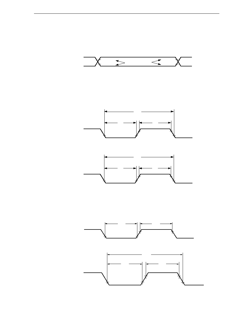
549
CHAPTER 27 ELECTRICAL SPECIFICATIONS (CONVENTIONAL PRODUCTS)
User's Manual U14260EJ3V1UD
Timing Chart
AC Timing Test Points (Excluding X1, XT1 Inputs)
Clock Timing
TI Timing
t
XL
t
XH
1/f
X
V
IH4
(MIN.)
V
IL4
(MAX.)
t
XTL
t
XTH
1/f
XT
V
IH5
(MIN.)
V
IL5
(MAX.)
X1 input
XT1 input
t
TIL0
t
TIH0
TI000, TI010, TI001, TI011
1/f
TI5
t
TIH5
t
TIL5
TI50, TI51
0.8V
DD
0.2V
DD
Test points
0.8V
DD
0.2V
DD
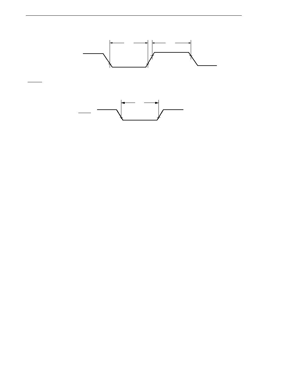
550
CHAPTER 27 ELECTRICAL SPECIFICATIONS (CONVENTIONAL PRODUCTS)
User's Manual U14260EJ3V1UD
t
RSL
RESET
INTP0 to INTP3
t
INTL
t
INTH
Interrupt Request Input Timing
RESET Input Timing
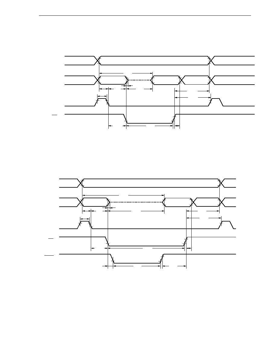
551
CHAPTER 27 ELECTRICAL SPECIFICATIONS (CONVENTIONAL PRODUCTS)
User's Manual U14260EJ3V1UD
Read/Write Operation
External fetch (no wait):
External fetch (wait insertion):
A8 to A15
AD0 to AD7
ASTB
RD
Higher 8-bit address
Lower 8-bit address
t
ADD1
Hi-Z
t
ADS
t
ASTH
t
ADH
t
RDAD
t
RDD1
Instruction code
t
RDADH
t
RDAST
t
ASTRD
t
RDL1
t
RDH
WAIT
t
RDWT1
t
WTL
t
WTRD
A8 to A15
AD0 to AD7
ASTB
RD
Higher 8-bit address
Lower 8-bit address
t
ADD1
Hi-Z
t
ADS
t
ASTH
t
ADH
t
RDD1
t
RDAD
Instruction code
t
RDADH
t
RDAST
t
ASTRD
t
RDL1
t
RDH
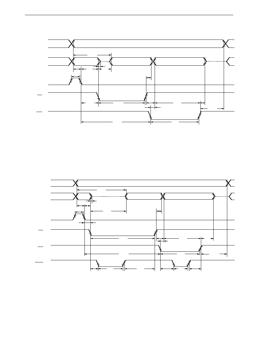
552
CHAPTER 27 ELECTRICAL SPECIFICATIONS (CONVENTIONAL PRODUCTS)
User's Manual U14260EJ3V1UD
External data access (no wait):
External data access (wait insertion):
A8 to A15
AD0 to AD7
ASTB
RD
Higher 8-bit address
Lower 8-bit
address
t
ADD2
t
ADS
t
ASTH
t
ADH
t
RDAD
t
RDD2
Read data
t
ASTRD
WR
t
ASTWR
Write data
Hi-Z
t
WDH
t
WRADH
t
WDS
t
WRWD
t
WRL1
t
RDH
t
RDL2
t
RDWT2
t
WTL
t
WRWT
t
WTL
t
WTWR
t
WTRD
WAIT
t
RDWD
Hi-Z
A8 to A15
AD0 to AD7
ASTB
RD
Higher 8-bit address
Lower 8-bit address
t
ADD2
Hi-Z
t
ADS
t
ASTH
t
ADH
t
RDD2
t
RDAD
Read data
t
ASTRD
t
RDWD
WR
t
ASTWR
Write data
Hi-Z
t
WDH
t
WRADH
t
WDS
t
WRWD
t
WRL1
t
RDH
t
RDL2

553
CHAPTER 27 ELECTRICAL SPECIFICATIONS (CONVENTIONAL PRODUCTS)
User's Manual U14260EJ3V1UD
Data Retention Timing (STOP Mode Release by RESET)
t
SREL
t
WAIT
V
DD
RESET
STOP instruction execution
STOP mode
Data retention mode
Internal reset operation
HALT mode
Operating mode
V
DDDR
Data Retention Timing (Standby Release Signal: STOP Mode Release by Interrupt Request Signal)
t
SREL
t
WAIT
V
DD
STOP instruction execution
STOP mode
Data retention mode
HALT mode
Operating mode
Standby release signal
(interrupt request)
V
DDDR
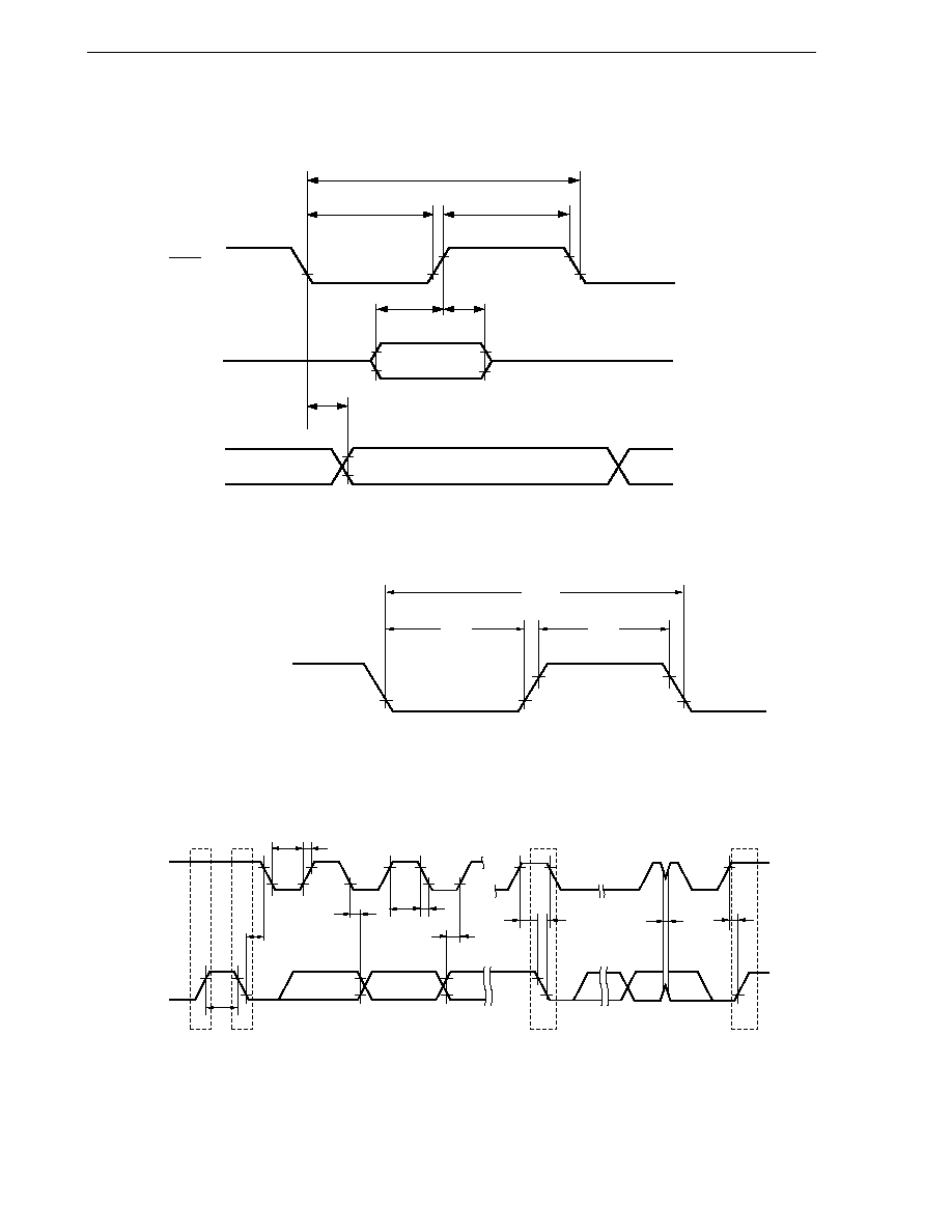
554
CHAPTER 27 ELECTRICAL SPECIFICATIONS (CONVENTIONAL PRODUCTS)
User's Manual U14260EJ3V1UD
Serial Transfer Timing
3-wire serial I/O mode:
UART mode (external clock input):
t
KCYn
t
KHn
t
KLn
ASCK0, ASCK2
I
2
C bus mode (
SCL0
SDA0
t
HD:STA
t
BUF
t
HD:DAT
t
HIGH
t
F
t
SU:DAT
t
SU:STA
t
HD:STA
t
SP
t
SU:STO
t
R
t
LOW
Stop
condition
Start
condition
Stop
condition
Restart
condition
Remark n = 1 to 4
Remark n = 5, 6
t
KCYn
t
KLn
t
KHn
SCK1, SCK3
SI1, SI3
SO1, SO3
t
SIKn
t
KSIn
t
KSOn
Input data
Output data
µPD780076Y, 780078Y, 78F0078Y only):
555
CHAPTER 27 ELECTRICAL SPECIFICATIONS (CONVENTIONAL PRODUCTS)
User's Manual U14260EJ3V1UD
Flash Write Mode Setting Timing
Notes 1. 3-wire serial I/O (SIO3) type
2. I
2
C bus (IIC0) type (
µPD78F0078Y only)
3. UART (UART0) type
4. Handshake (when 3-wire serial I/O (SIO3) type is used)
V
DD
V
DD
0 V
V
DD
RESET (input)
0 V
V
PPH
0 V
V
PP
V
PPL
t
RP
t
PR
t
DP
t
PW
t
PW
t
RPE
0 V
SCK3
Note 1
/SCL0
Note 2
0 V
0 V
0 V
SI3
Note 1
/RxD0
Note 3
SO3
Note 1
/TxD0
Note 3
/SDA0
Note 2
P31 (HS)
Note 4
Reset command
V
IL
V
IL
556
User's Manual U14260EJ3V1UD
CHAPTER 28 PACKAGE DRAWINGS
Remark The external dimensions and materials of the ES version are the same as those of the mass-produced
version.
64-PIN PLASTIC LQFP (14x14)
NOTE
Each lead centerline is located within 0.20 mm of
its true position (T.P.) at maximum material condition.
ITEM
MILLIMETERS
A
B
D
G
17.2
±0.2
14.0
±0.2
0.8 (T.P.)
1.0
J
17.2
±0.2
K
C
14.0
±0.2
I
0.20
1.6
±0.2
L
0.8
F
1.0
N
P
Q
0.10
1.4
±0.1
0.127
±0.075
U
0.886
±0.15
R
S
3
∞
1.7 MAX.
T
0.25
P64GC-80-8BS
H
0.37+0.08
-0.07
M
0.17+0.03
-0.06
S
N
J
T
detail of lead end
C
D
A
B
K
M
I
S
P
R
L
U
Q
G
F
M
H
+4∞
-3∞
1
64
49
17
32
16
48
33
S
557
CHAPTER 28 PACKAGE DRAWINGS
User's Manual U14260EJ3V1UD
Remark The external dimensions and materials of the ES version are the same as those of the mass-produced
version.
48
49
32
64
1
17
16
33
64-PIN PLASTIC QFP (14x14)
NOTE
Each lead centerline is located within 0.15 mm of
its true position (T.P.) at maximum material condition.
ITEM
MILLIMETERS
A
B
D
G
17.6
±0.4
14.0
±0.2
0.8 (T.P.)
1.0
J
17.6
±0.4
K
P64GC-80-AB8-5
C
14.0
±0.2
I
0.15
1.8
±0.2
L
0.8
±0.2
F
1.0
N
P
Q
0.10
2.55
±0.1
0.1
±0.1
R
S
5
∞±5∞
2.85 MAX.
H
0.37+0.08
-0.07
M
0.17+0.08
-0.07
S
S
N
J
detail of lead end
C D
A
B
R
K
M
L
P
I
S
Q
G
F
M
H
558
CHAPTER 28 PACKAGE DRAWINGS
User's Manual U14260EJ3V1UD
Remark The external dimensions and materials of the ES version are the same as those of the mass-produced
version.
48
32
33
64
1
17
16
49
S
S
64-PIN PLASTIC TQFP (12x12)
ITEM
MILLIMETERS
G
1.125
A
14.0
±0.2
C
12.0
±0.2
D
F
1.125
14.0
±0.2
B
12.0
±0.2
N
0.10
P
Q
0.1
±0.05
1.0
S
R
3
∞+4∞
-3∞
R
H
K
J
Q
G
I
S
P
detail of lead end
NOTE
Each lead centerline is located within 0.13 mm of
its true position (T.P.) at maximum material condition.
M
H
0.32+0.06
-0.10
I
0.13
J
K
1.0
±0.2
0.65 (T.P.)
L
0.5
M
0.17 +0.03
-0.07
P64GK-65-9ET-3
T
U
0.6
±0.15
0.25
F
M
A
B
C
D
N
T
L
U
1.1
±0.1
559
User's Manual U14260EJ3V1UD
CHAPTER 29 RECOMMENDED SOLDERING CONDITIONS
The
µPD780078, 780078Y Subseries should be soldered and mounted under the following recommended
conditions.
For soldering methods and conditions other than those recommended below, contact an NEC Electronics sales
representative.
For technical information, see the following website.
Semiconductor Device Mount Manual (http://www.necel.com/pkg/en/mount/index.html)
Table 29-1. Surface Mounting Type Soldering Conditions (1/2)
(1)
µPD780076GC-◊◊◊-8BS:
64-pin plastic LQFP (14
◊ 14)
µPD780078GC-◊◊◊-8BS:
64-pin plastic LQFP (14
◊ 14)
µPD780076YGC-◊◊◊-8BS: 64-pin plastic LQFP (14 ◊ 14)
µPD780078YGC-◊◊◊-8BS: 64-pin plastic LQFP (14 ◊ 14)
µPD78F0078GC-8BS:
64-pin plastic LQFP (14
◊ 14)
µPD78F0078YGC-8BS:
64-pin plastic LQFP (14
◊ 14)
µPD780076GC-◊◊◊-AB8:
64-pin plastic QFP (14
◊ 14)
µPD780078GC-◊◊◊-AB8:
64-pin plastic QFP (14
◊ 14)
µPD780076YGC-◊◊◊-AB8: 64-pin plastic QFP (14 ◊ 14)
µPD780078YGC-◊◊◊-AB8: 64-pin plastic QFP (14 ◊ 14)
Soldering Method
Soldering Conditions
Recommended
Condition Symbol
Infrared reflow
Package peak temperature: 235
∞C, Time: 30 seconds max. (at 210∞C or higher),
IR35-00-2
Count: Two times or less
VPS
Package peak temperature: 215
∞C, Time: 40 seconds max. (at 200∞C or higher),
VP15-00-2
Count: Two times or less
Wave soldering
Solder bath temperature: 260
∞C max., Time: 10 seconds max., Count: Once,
WS60-00-1
Preheating temperature: 120
∞C max. (package surface temperature)
Partial heating
Pin temperature: 300
∞C max., Time: 3 seconds max. (per pin row)
--
Caution
Do not use different soldering methods together (except for partial heating).
(2)
µPD78F0078GC-AB8:
64-pin plastic QFP (14
◊ 14)
µPD78F0078YGC-AB8:
64-pin plastic QFP (14
◊ 14)
Soldering Method
Soldering Conditions
Recommended
Condition Symbol
Infrared reflow
Package peak temperature: 235
∞C, Time: 30 seconds max. (at 210∞C or higher),
IR35-00-3
Count: Three times or less
VPS
Package peak temperature: 215
∞C, Time: 40 seconds max. (at 200∞C or higher),
VP15-00-3
Count: Three times or less
Wave soldering
Solder bath temperature: 260
∞C max., Time: 10 seconds max., Count: Once,
WS60-00-1
Preheating temperature: 120
∞C max. (package surface temperature)
Partial heating
Pin temperature: 300
∞C max., Time: 3 seconds max. (per pin row)
--
Caution
Do not use different soldering methods together (except for partial heating).

560
CHAPTER 29 RECOMMENDED SOLDERING CONDITIONS
User's Manual U14260EJ3V1UD
Table 29-1. Surface Mounting Type Soldering Conditions (2/2)
(3)
µPD780076GK-◊◊◊-9ET:
64-pin plastic TQFP (12
◊ 12)
µPD780078GK-◊◊◊-9ET:
64-pin plastic TQFP (12
◊ 12)
µPD780076YGK-◊◊◊-9ET: 64-pin plastic TQFP (12 ◊ 12)
µPD780078YGK-◊◊◊-9ET: 64-pin plastic TQFP (12 ◊ 12)
Soldering Method
Soldering Conditions
Recommended
Condition Symbol
Infrared reflow
Package peak temperature: 235
∞C, Time: 30 seconds max. (at 210∞C or higher),
IR35-107-2
Count: Two times or less, Exposure limit: 7 days
Note
(after that, prebake at
125
∞C for 10 hours)
VPS
Package peak temperature: 215
∞C, Time: 40 seconds max. (at 200∞C or higher),
VP15-107-2
Count: Two times or less, Exposure limit: 7 days
Note
(after that, prebake at
125
∞C for 10 hours)
Wave soldering
Solder bath temperature: 260
∞C max., Time: 10 seconds max., Count: Once,
WS60-107-1
Preheating temperature: 120
∞C max. (package surface temperature),
Exposure limit: 7 days
Note
(after that, prebake at 125
∞C for 10 hours)
Partial heating
Pin temperature: 300
∞C max., Time: 3 seconds max. (per pin row)
--
Note After opening the dry pack, store it at 25
∞C or less and 65% RH or less for the allowable storage period.
Caution
Do not use different soldering methods together (except for partial heating).
(4)
µPD78F0078GK-9ET:
64-pin plastic TQFP (12
◊ 12)
µPD78F0078YGK-9ET: 64-pin plastic TQFP (12 ◊ 12)
Soldering Method
Soldering Conditions
Recommended
Condition Symbol
Infrared reflow
Package peak temperature: 235
∞C, Time: 30 seconds max. (at 210∞C or higher),
IR35-103-2
Count: Two times or less, Exposure limit: 3 days
Note
(after that, prebake at
125
∞C for 10 hours)
VPS
Package peak temperature: 215
∞C, Time: 40 seconds max. (at 200∞C or higher),
VP15-103-2
Count: Two times or less, Exposure limit: 3 days
Note
(after that, prebake at
125
∞C for 10 hours)
Wave soldering
Solder bath temperature: 260
∞C max., Time: 10 seconds max., Count: Once,
WS60-103-1
Preheating temperature: 120
∞C max. (package surface temperature),
Exposure limit: 3 days
Note
(after that, prebake at 125
∞C for 10 hours)
Partial heating
Pin temperature: 300
∞C max., Time: 3 seconds max. (per pin row)
--
Note After opening the dry pack, store it at 25
∞C or less and 65% RH or less for the allowable storage period.
Caution
Do not use different soldering methods together (except for partial heating).

561
User's Manual U14260EJ3V1UD
APPENDIX A DIFFERENCES BETWEEN
µPD78018F, 780024A, 780034A, AND 780078 SUBSERIES
Tables A-1 and A-2 show the major differences between the
µPD78018F, 780024A, 780034A, and 780078
Subseries.
Table A-1. Major Differences Between
µPD78018F, 780024A, 780034A, and 780078 Subseries (Hardware)
Name
Item
EMI noise reduction
Internal I
2
C bus version
(Y subseries)
PROM version
Flash memory version
ROM
Internal high-speed RAM
Internal expansion RAM
Minimum instruction execution
time
Number of I/O ports
Timer
A/D converter
Serial
interface
operating
mode
Timer output
Package
Device file
Emulation board
Electrical specifications
Recommended soldering
conditions
µPD78018F Subseries
Note
µPD780024A, 780034A
µPD780078 Subseries
Subseries
Not provided
Provided
Provided
Provided (multi-master supported)
µPD78P018F
Not provided
Not provided
µPD78F0034A, 78F0034B
µPD78F0078
8 KB to 60 KB
8 KB to 32 KB
48 KB, 60 KB
512, 1024 bytes
512, 1024 bytes
1024 bytes
512, 1024 bytes
Not provided
1024 bytes
0.4
µs (10 MHz)
0.24
µs (8.38 MHz), 0.16 µs
(12 MHz, expanded-specification products only)
53
51
52
16 bits: 1, 8 bits: 2,
16 bits: 1, 8 bits: 2,
16 bits: 2, 8 bits: 2,
Watch timer: 1,
Watch timer: 1,
Watch timer: 1,
Watchdog timer: 1
Watchdog timer: 1
Watchdog timer: 1
8 bits
◊ 8
∑ 8 bits
◊ 8
10 bits
◊ 8
(
µPD780024A Subseries)
∑ 10 bits
◊ 8
(
µPD780034A Subseries)
3-wire/2-wire/SBI: 1,
3-wire: 2, UART: 1
3-wire: 1, UART: 1,
3-wire (automatic
3-wire/UART: 1
transmission/reception): 1
3-wire/2-wire/I
2
C: 1,
3-wire: 2, UART: 1,
3-wire: 1, UART: 1,
3-wire (automatic
Multi-master I
2
C: 1
3-wire/UART: 1,
transmission/reception): 1
Multi-master I
2
C: 1
3 (14-bit PWM output possible: 2)
3 (8-bit PWM output possible: 2)
4 (8-bit PWM output possible: 2)
∑ 64-pin SDIP (19.05 mm (750))
∑ 64-pin SDIP (19.05 mm (750))
∑ 64-pin QFP (14
◊ 14)
∑ 64-pin QFP (14
◊ 14)
∑ 64-pin QFP (14
◊ 14)
∑ 64-pin TQFP (12
◊ 12)
∑ 64-pin LQFP (12
◊ 12)
∑ 64-pin TQFP (12
◊ 12)
∑ 64-pin LQFP (14
◊ 14)
∑ 64-pin LQFP (14
◊ 14)
∑ 64-pin LQFP (10
◊ 10)
∑ 73-pin FBGA (9
◊ 9)
DF78014
DF780034
DF780078
IE-78014-R-EM-A,
IE-780034-NS-EM1
IE-780078-NS-EM1
IE-78018-NS-EM1
Refer to the data sheet or user's manual (with electrical specifications) of each product.
Subseries
without suffix Y
Subseries with
suffix Y
Note Maintenance product
562
APPENDIX A DIFFERENCES BETWEEN
µPD78018F, 780024A, 780034A, AND 780078 SUBSERIES
User's Manual U14260EJ3V1UD
Table A-2. Major Differences Between
µPD78018F, 780024A, 780034A, and 780078 Subseries (Software) (1/2)
Name
Item
A/D converter
16-bit timer/event counter
Interval timer
PWM output
PPG output
Pulse width measurement
External event counter
Square wave output
Count clock
Control register
Output control register
Compare/capture register
Prescaler mode register
Capture/compare control
register
Interrupt
µPD78018F Subseries
Note 1
µPD780024A, 780034A
µPD780078 Subseries
Subseries
--
Take the appropriate measures for the first A/D
conversion result immediately after the A/D conversion
operation is started (ADCS0 is set to 1), such as
discarding it, because it may not satisfy the rating.
However, if a wait time of
14
µs (MIN.) has been
secured after ADCE0 was
set to 1 before starting
operation (ADCS0 is set to
1), the first data can be
used.
1 ch
1 ch
2 ch
TM0
TM0
TM00
TM01
--
--
--
f
X
/2, f
X
/2
2
, f
X
/2
3
, TI0
f
X
, f
X
/2
2
, f
X
/2
6
, TI00
f
X
, f
X
/2
2
,
f
X
/2, f
X
/2
3
f
X
/2
6
, TI000
f
X
/2
9
, TI001
TMC0
TMC0
TMC00
TMC01
TOC0
TOC0
TOC00
TOC01
CR00, CR01 (Capture only)
CR00, CR01
CR000, CR010
CR001, CR011
TCL0
Note 2
PRM0
PRM00
PRM01
--
CRC0
CRC00
CRC01
INTTM0
INTTM00, INTTM01
INTTM000,
INTTM001,
INTTM010
INTTM011
Notes 1. Maintenance product
2. TCL0: Timer clock select register 0
563
APPENDIX A DIFFERENCES BETWEEN
µPD78018F, 780024A, 780034A, AND 780078 SUBSERIES
User's Manual U14260EJ3V1UD
Table A-2. Major Differences Between
µPD78018F, 780024A, 780034A, and 780078 Subseries (Software) (2/2)
Name
Item
8-bit timer/event counter
Unit mode
Interval timer
External event counter
Square wave output
PWM output
Cascade connection mode
Interval timer
External event counter
Square wave output
Count clock
Control register
Output control register
Clock select register
Interrupt
µPD78018F Subseries
Note
µPD780024A, 780034A
µPD780078 Subseries
Subseries
2 ch
2 ch
TM1
TM2
TM50
TM51
--
TMC1
TMC50
TMC51
TOC1
TMC50
TMC51
TCL1
TCL50
TCL51
INTTM1
INTTM2
INTTM50
INTTM51
f
X
/2
2
, f
X
/2
3
,
f
X
/2
4
, f
X
/2
5
,
f
X
/2
6
, f
X
/2
7
,
f
X
/2
8
, f
X
/2
9
,
f
X
/2
10
, f
X
2
12
,
TI1
f
X
/2
2
, f
X
/2
3
,
f
X
/2
4
, f
X
/2
5
,
f
X
/2
6
, f
X
/2
7
,
f
X
/2
8
, f
X
/2
9
,
f
X
/2
10
, f
X
/2
12
,
TI2
f
X
, f
X
/2
2
, f
X
/2
4
, f
X
/2
6
, f
X
/2
8
,
f
X
/2
10
, TI50
f
X
/2, f
X
/2
3
, f
X
/2
5
, f
X
/2
7
, f
X
/2
9
,
f
X
/2
11
, TI51
Note Maintenance product

564
User's Manual U14260EJ3V1UD
APPENDIX B DEVELOPMENT TOOLS
The following development tools are available for the development of systems that employ the
µPD780078 and
780078Y Subseries.
Figure B-1 shows the development tool configuration.
∑
Support for PC98-NX series
Unless otherwise specified, products compatible with IBM PC/AT
TM
computers are compatible with PC98-NX
series computers. When using PC98-NX series computers, refer to the explanation for IBM PC/AT computers.
∑
Windows
Unless otherwise specified, "Windows" means the following OSs.
∑ Windows 3.1
∑ Windows 95
∑ Windows 98
∑ Windows 2000
∑ Windows NT
TM
Ver.4.0
565
APPENDIX B DEVELOPMENT TOOLS
User's Manual U14260EJ3V1UD
Figure B-1. Development Tool Configuration (1/2)
(1) When using the in-circuit emulator IE-78K0-NS or IE-78K0-NS-A
Notes 1. The C library source file is not included in the software package.
2. The project manager is included in the assembler package.
The project manager is only used for Windows.
Language processing software
∑ Assembler package
∑ C compiler package
∑ Device file
∑ C library source file
Note 1
Debugging software
∑ Integrated debugger
∑ System simulator
Host machine (PC or EWS)
Interface adapter,
PC card interface, etc.
In-circuit emulator
Emulation board
Emulation probe
Conversion socket or
conversion adapter
Target system
Flash programmer
Flash memory
write adapter
Flash memory
∑ Software package
∑ Project manager
(Windows only)
Note 2
Software package
Flash memory
write environment
Control software
I/O board
Performance board
Power supply unit
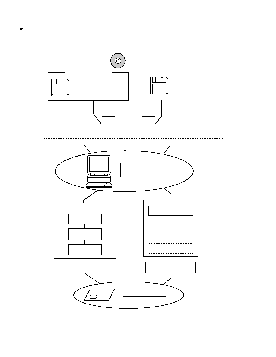
566
APPENDIX B DEVELOPMENT TOOLS
User's Manual U14260EJ3V1UD
Figure B-1. Development Tool Configuration (2/2)
(2) When using the in-circuit emulator IE-78001-R-A
Notes 1. The C library source file is not included in the software package.
2. The project manager is included in the assembler package.
The project manager is only used for Windows.
Language processing software
∑ Assembler package
∑ C compiler package
∑ Device file
∑ C compiler source file
Note 1
Debugging software
∑ Integrated debugger
∑ System simulator
Host machine (PC or EWS)
Interface adapter,
PC card interface, etc.
In-circuit emulator
Emulation board
Emulation probe
Conversion socket or
conversion adapter
Target system
Flash programmer
Flash memory
write adapter
Flash memory
∑ Software package
∑ Project manager
(Windows only)
Note 2
Software package
Flash memory
write environment
Control software
I/O board
Emulation probe
conversion board
Performance board

567
APPENDIX B DEVELOPMENT TOOLS
User's Manual U14260EJ3V1UD
B.1 Software Package
SP78K0
This package contains various software tools for 78K/0 Series development.
Software package
The following tools are included.
RA78K0, CC78K0, ID78K0-NS, SM78K0, and various device files
Part Number:
µS◊◊◊◊SP78K0
Remark
◊◊◊◊ in the part number differs depending on the OS used.
µS◊◊◊◊SP78K0
◊◊◊◊
Host Machine
OS
Supply Medium
AB17
PC-9800 series,
Windows (Japanese version)
CD-ROM
BB17
IBM PC/AT compatibles
Windows (English version)
B.2 Language Processing Software
RA78K0
Assembler package
CC78K0
C compiler package
DF780078
Note 1
Device file
CC78K0-L
Note 2
C library source file
Notes 1. The DF780078 can be used in common with the RA78K0, CC78K0, SM78K0, ID78K0-NS, and RX78K0.
2. CC78K0-L is not included in the software package (SP78K0).
This assembler converts programs written in mnemonics into object codes executable
with a microcontroller.
Further, this assembler is provided with functions capable of automatically creating
symbol tables and branch instruction optimization.
This assembler should be used in combination with device file (DF780078) (sold
separately).
<Precaution when using RA78K0 in PC environment>
This assembler package is a DOS-based application. It can also be used in Windows,
however, by using the project manager (included in the assembler package) on
Windows.
Part Number:
µS◊◊◊◊RA78K0
This compiler converts programs written in C language into object codes executable with
a microcontroller.
This compiler should be used in combination with an assembler package and device file
(both sold separately).
<Precaution when using CC78K0 in PC environment>
This C compiler package is a DOS-based application. It can also be used in Windows,
however, by using the project manager (included in the assembler package) on
Windows.
Part Number:
µS◊◊◊◊CC78K0
This file contains information peculiar to the device.
This device file should be used in combination with tool (RA78K0, CC78K0, SM78K0,
ID78K0-NS, and RX78K0) (all sold separately).
The corresponding OS and host machine differ depending on the tool used.
Part Number:
µS◊◊◊◊DF780078
This is a source file of functions configuring the object library included in the C compiler
package.
This file is required to match the object library included in C compiler package to the
user's specifications.
It does not depend on the operating environment because it is a source file.
Part Number:
µS◊◊◊◊CC78K0-L
568
APPENDIX B DEVELOPMENT TOOLS
User's Manual U14260EJ3V1UD
Remark
◊◊◊◊ in the part number differs depending on the host machine and OS used.
µS◊◊◊◊RA78K0
µS◊◊◊◊CC78K0
◊◊◊◊
Host Machine
OS
Supply Medium
AB13
PC-9800 series,
Windows (Japanese version)
3.5-inch 2HD FD
BB13
IBM PC/AT compatibles
Windows (English version)
AB17
Windows (Japanese version)
CD-ROM
BB17
Windows (English version)
3P17
HP9000 series 700
TM
HP-UX
TM
(Rel. 10.10)
3K17
SPARCstation
TM
SunOS
TM
(Rel. 4.1.4),
Solaris
TM
(Rel. 2.5.1)
µS◊◊◊◊DF780078
µS◊◊◊◊CC78K0-L
◊◊◊◊
Host Machine
OS
Supply Medium
AB13
PC-9800 series,
Windows (Japanese version)
3.5-inch 2HD FD
BB13
IBM PC/AT compatibles
Windows (English version)
3P16
HP9000 series 700
HP-UX (Rel. 10.10)
DAT
3K13
SPARCstation
SunOS (Rel. 4.1.4),
3.5-inch 2HD FD
3K15
Solaris (Rel. 2.5.1)
1/4-inch CGMT
B.3 Control Software
Project manager
This is control software designed to enable efficient user program development in the
Windows environment. All operations used in development of a user program, such as
starting the editor, building, and starting the debugger, can be performed from the project
manager.
<Caution>
The project manager is included in the assembler package (RA78K0).
It can only be used in Windows.
B.4 Flash Memory Writing Tools
Flashpro III
(part number: FL-PR3, PG-FP3)
Flashpro IV
(part number: FL-PR4, PG-FP4)
Flash programmer
FA-64GC-8BS-A
FA-64GC
FA-64GK-9ET
Flash memory writing adapter
Remark
FL-PR3, FL-PR4, FA-64GC-8BS-A, FA-64GC, and FA-64GK-9ET are products of Naito Densei Machida
Mfg. Co., Ltd.
Contact: +81-45-475-4191 Naito Densei Machida Mfg. Co., Ltd.
Flash programmer dedicated to microcontrollers with on-chip flash memory.
Flash memory writing adapter used connected to the Flashpro III and Flashpro IV.
∑ FA-64GC-8BS-A: 64-pin plastic LQFP (GC-8BS type)
∑ FA-64GC:
64-pin plastic QFP (GC-AB8 type)
∑ FA-64GK-9ET:
64-pin plastic TQFP (GK-9ET type)
569
APPENDIX B DEVELOPMENT TOOLS
User's Manual U14260EJ3V1UD
B.5 Debugging Tools (Hardware)
B.5.1 When using the in-circuit emulator IE-78K0-NS or IE-78K0-NS-A
IE-78K0-NS
In-circuit emulator
IE-78K0-NS-PA
Performance board
IE-78K0-NS-A
In-circuit emulator
IE-70000-MC-PS-B
Power supply unit
IE-70000-98-IF-C
Interface adapter
IE-70000-CD-IF-A
PC card interface
IE-70000-PC-IF-C
Interface adapter
IE-70000-PCI-IF-A
Interface adapter
IE-780078-NS-EM1
Emulation board
NP-64GC
Emulation probe
EV-9200GC-64
Conversion socket
(See Figures B-2 and B-3)
NP-64GC-TQ
NP-H64GC-TQ
Emulation probe
TGC-064SAP
Conversion adapter
NP-64GK
NP-H64GK-TQ
Emulation probe
TGK-064SBW
Conversion adapter
(See Figure B-4)
Remarks 1. NP-64CW, NP-64GC, NP-64GC-TQ, NP-H64GC-TQ, NP-64GK, and NP-H64GK-TQ are products
of Naito Densei Machida Mfg. Co., Ltd.
Contact: +81-45-475-4191 Naito Densei Machida Mfg. Co., Ltd.
2. TGK-064SBW and TGC-064SAP are products of TOKYO ELETECH CORPORATION.
Contact: Daimaru Kogyo, Ltd. Phone: Tokyo +81-3-3820-7112 Electronics Dept.
Osaka +81-6-6244-6672 Electronics 2nd Dept.
3. EV-9200GC-64 is sold in five-unit sets.
4. TGK-064SBW and TGC-064SAP are sold in single units.
The in-circuit emulator serves to debug hardware and software when developing
application systems using a 78K/0 Series product. It corresponds to the integrated
debugger (ID78K0-NS). This emulator should be used in combination with a power
supply unit, emulation probe, and interface adapter which is required to connect this
emulator to the host machine.
This board is connected to the IE-78K0-NS to expand its functions. Adding this
board adds a coverage function and enhances debugging functions such as tracer
and timer functions.
A combination of the IE-78K0-NS and IE-78K0-NS-PA.
This adapter is used for supplying power from a receptacle of 100 V to 240 V AC.
This adapter is required when using a PC-9800 series computer (except notebook
type) as the host machine (C bus compatible).
This is PC card and interface cable required when using a notebook-type computer
as the host machine (PCMCIA socket compatible).
This adapter is required when using an IBM PC/AT compatible computer as the host
machine (ISA bus compatible).
This adapter is required when using a computer with a PCI bus as the host machine.
This board emulates the operations of the peripheral hardware peculiar to a device. It
should be used in combination with an in-circuit emulator.
This probe is used to connect the in-circuit emulator to a target system and is
designed for use with a 64-pin plastic QFP (GC-AB8 type) and 64-pin plastic LQFP
(GC-8BS type).
This conversion socket connects the NP-64GC to a target system board designed for
a 64-pin plastic QFP (GC-AB8 type) and 64-pin plastic LQFP (GC-8BS type).
This probe is used to connect the in-circuit emulator to a target system and is
designed for use with a 64-pin plastic QFP (GC-AB8 type) and 64-pin plastic LQFP
(GC-8BS type).
This conversion adapter connects the NP-64GC-TQ or NP-H64GK-TQ to a target
system board designed for a 64-pin plastic QFP (GC-AB8 type) and 64-pin plastic
LQFP (GC-8BS type).
This probe is used to connect the in-circuit emulator to a target system and is
designed for use with a 64-pin plastic TQFP (GK-9ET type).
This conversion adapter connects the NP-64GK or NP-H64GK-TQ to a target system
board designed for a 64-pin plastic TQFP (GK-9ET type).
570
APPENDIX B DEVELOPMENT TOOLS
User's Manual U14260EJ3V1UD
B.5.2 When using the in-circuit emulator IE-78001-R-A
IE-78001-R-A
In-circuit emulator
IE-70000-98-IF-C
Interface adapter
IE-70000-PC-IF-C
Interface adapter
IE-70000-PCI-IF-A
Interface adapter
IE-780078-NS-EM1
Emulation board
IE-78K0-R-EX1
Emulation probe
conversion board
EP-78240GC-R
Note
Emulation probe
EV-9200GC-64
Conversion socket
(See Figures B-2 and B-3)
EP-78012GK-R
Emulation probe
TGK-064SBW
Conversion adapter
(See Figure B-4)
Note Maintenance product
Remarks 1. TGK-064SBW is a product of TOKYO ELETECH CORPORATION.
Contact: Daimaru Kogyo, Ltd. Phone: Tokyo +81-3-3820-7112 Electronics Dept.
Osaka +81-6-6244-6672 Electronics 2nd Dept.
2. EV-9200GC-64 is sold in five-unit sets.
3. TGK-064SBW is sold in single units.
The in-circuit emulator serves to debug hardware and software when developing
application systems using a 78K/0 Series product. It corresponds to the integrated
debugger (ID78K0). This emulator should be used in combination with an emulation
probe and interface adapter, which is required to connect this emulator to the host
machine.
This adapter is required when using a PC-9800 series computer (except notebook
type) as the host machine (C bus compatible).
This adapter is required when using an IBM PC/AT compatible computer as the host
machine (ISA bus compatible).
This adapter is required when using a computer with a PCI bus as the host machine.
This board emulates the operations of the peripheral hardware peculiar to a device.
It should be used in combination with an in-circuit emulator and emulation probe
conversion board.
This board is required when using the IE-780078-NS-EM1 on the IE-78001-R-A.
This probe is used to connect the in-circuit emulator to a target system and is
designed for use with a 64-pin plastic QFP (GC-AB8 type) and 64-pin plastic LQFP
(GC-8BS type).
This conversion socket connects the EP-78240GC-R to a target system board
designed for a 64-pin plastic QFP (GC-AB8 type) and 64-pin plastic LQFP (GC-8BS
type).
This probe is used to connect the in-circuit emulator to a target system and is
designed for use with a 64-pin plastic TQFP (GK-9ET type).
This conversion adapter connects the EP-78012GK-R to a target system board
designed for a 64-pin plastic TQFP (GK-9ET type).
571
APPENDIX B DEVELOPMENT TOOLS
User's Manual U14260EJ3V1UD
B.6 Debugging Tools (Software)
SM78K0
This is a system simulator for the 78K/0 Series. The SM78K0 is Windows-based
System simulator
software.
It is used to perform debugging at the C source level or assembler level while simulating
the operation of the target system on a host machine.
Use of the SM78K0 allows the execution of application logical testing and performance
testing on an independent basis from hardware development, thereby providing higher
development efficiency and software quality.
The SM78K0 should be used in combination with the device file (DF780078) (sold
separately).
Part Number:
µS◊◊◊◊SM78K0
ID78K0-NS
This debugger supports the in-circuit emulators for the 78K/0 Series. The
Integrated debugger
ID78K0-NS is Windows-based software.
(supporting in-circuit emulators
It has improved C-compatible debugging functions and can display the results of
IE-78K0-NS and IE-78K0-NS-A)
tracing with the source program using an integrating window function that associates
ID78K0
the source program, disassemble display, and memory display with the trace result.
Integrated debugger
It should be used in combination with the device file (sold separately).
(supporting in-circuit emulator
IE-78001-R-A)
Part Number:
µS◊◊◊◊ID78K0-NS, µS◊◊◊◊ID78K0
Remark
◊◊◊◊ in the part number differs depending on the host machine and OS used.
µS◊◊◊◊SM78K0
µS◊◊◊◊ID78K0-NS
µS◊◊◊◊ID78K0
◊◊◊◊
Host Machine
OS
Supply Medium
AB13
IBM PC/AT compatibles
Windows (Japanese version)
3.5-inch 2HD FD
BB13
Windows (English version)
AB17
Windows (Japanese version)
CD-ROM
BB17
Windows (English version)
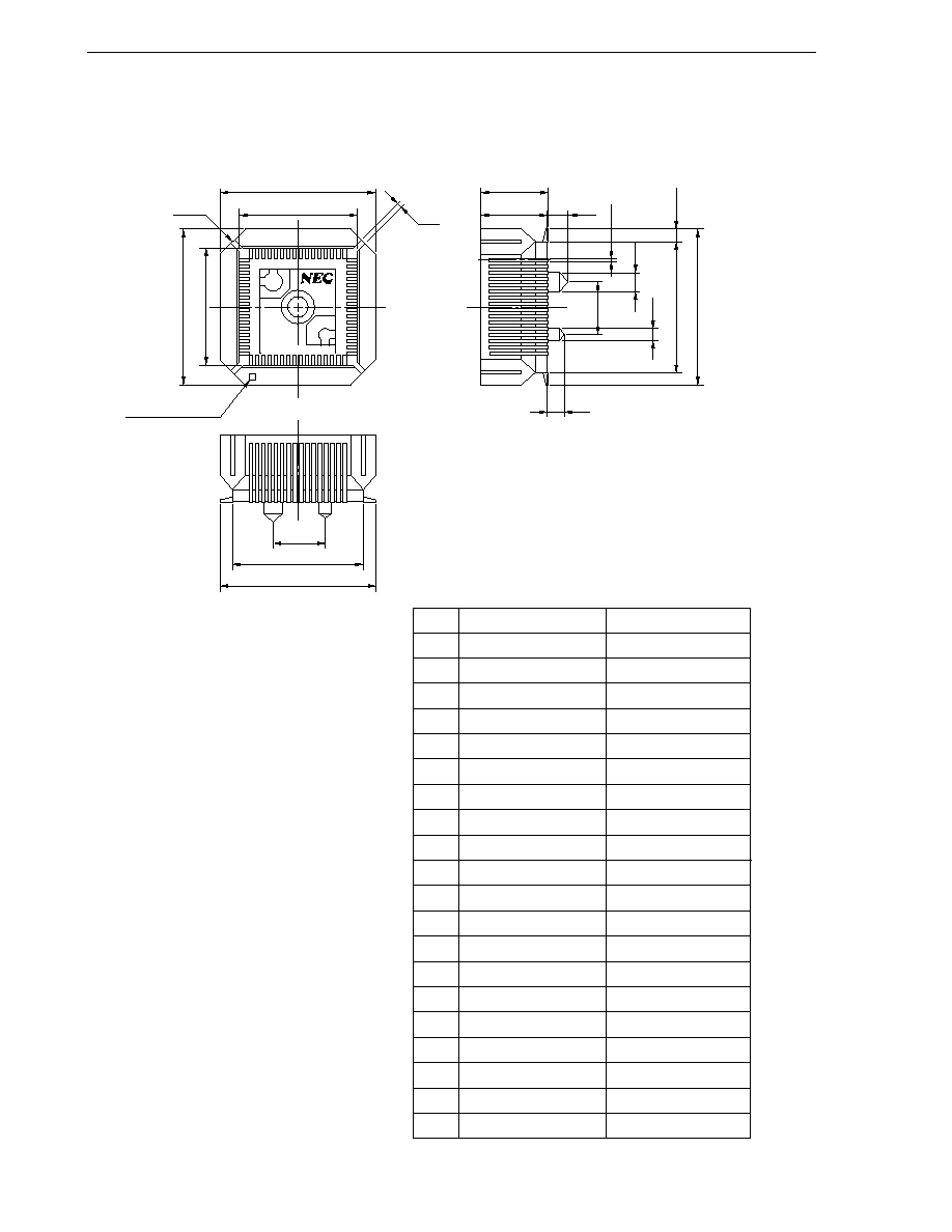
572
APPENDIX B DEVELOPMENT TOOLS
User's Manual U14260EJ3V1UD
Conversion Socket (EV-9200GC-64) Package Drawing and Recommended Board Mounting Pattern
Figure B-2. EV-9200GC-64 Package Drawing (for Reference Only)
A
F
1
E
EV-9200GC-64
B
D
C
M
N
L
K
R
Q
I
H
P
O
S
T
J
G
No.1 pin index
EV-9200GC-64-G0E
ITEM
MILLIMETERS
INCHES
A
B
C
D
E
F
G
H
I
J
K
L
M
N
O
P
Q
R
S
T
18.8
14.1
14.1
18.8
4-C 3.0
0.8
6.0
15.8
18.5
6.0
15.8
18.5
8.0
7.8
2.5
2.0
1.35
0.35
±0.1
2.3
1.5
0.74
0.555
0.555
0.74
4-C 0.118
0.031
0.236
0.622
0.728
0.236
0.622
0.728
0.315
0.307
0.098
0.079
0.053
0.014
0.091
0.059
+0.004
≠0.005
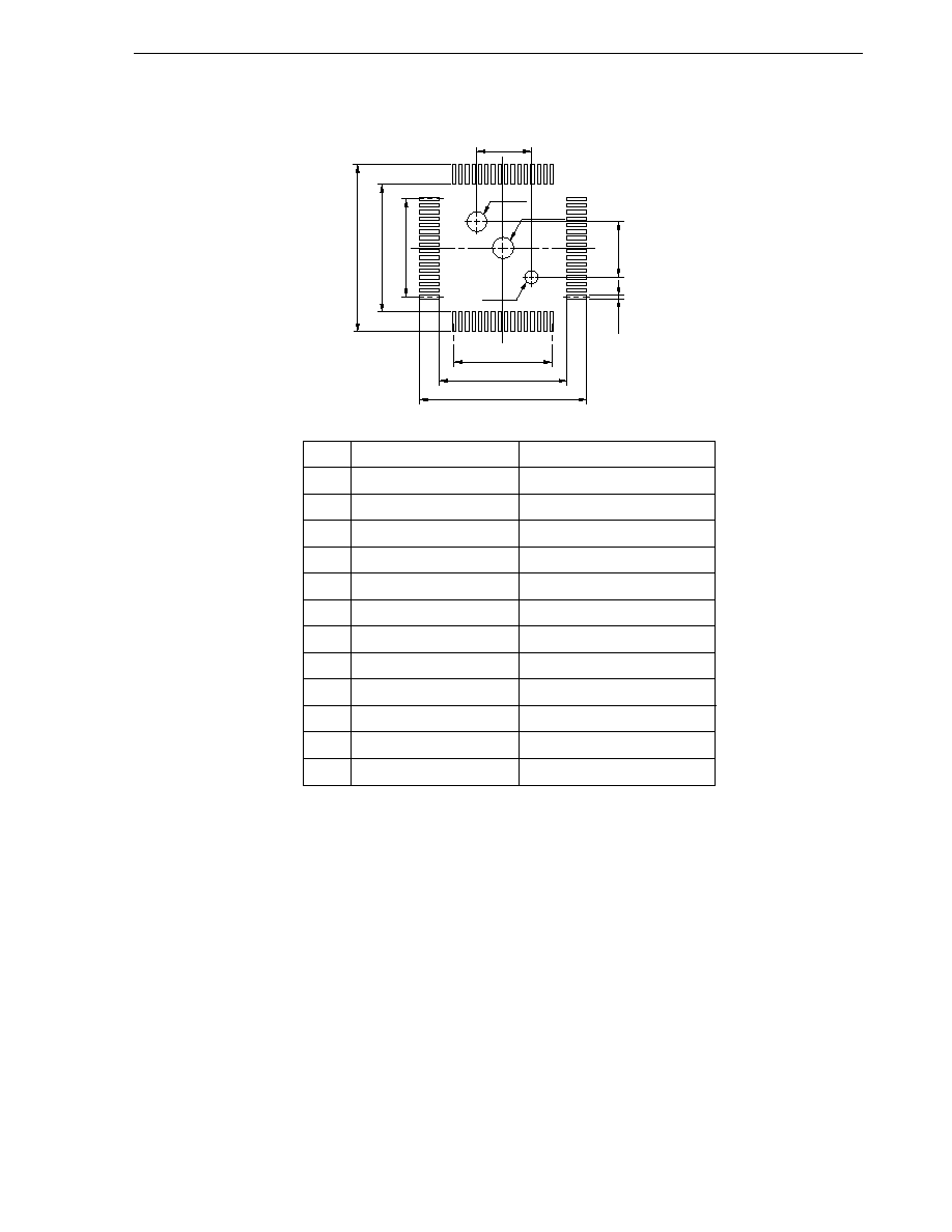
573
APPENDIX B DEVELOPMENT TOOLS
User's Manual U14260EJ3V1UD
Figure B-3. EV-9200GC-64 Recommended Board Mounting Pattern (for Reference Only)
F
E
D
G
H
I
J
K
L
C
B
A
0.031
◊ 0.591=0.472
0.031
◊ 0.591=0.472
EV-9200GC-64-P1E
ITEM
MILLIMETERS
INCHES
A
B
C
D
E
F
G
H
I
J
K
L
19.5
14.8
14.8
19.5
6.00≠0.08
6.00≠0.08
0.5≠0.02
2.36≠0.03
2.2≠0.1
1.57≠0.03
0.768
0.583
0.583
0.768
0.236
0.236
0.197
0.093
0.087
0.062
0.8≠0.02
◊ 15=12.0≠0.05
0.8≠0.02
◊ 15=12.0≠0.05
+0.002
--0.001
+0.003
--0.002
+0.002
--0.001
+0.003
--0.002
+0.004
--0.003
+0.004
--0.003
+0.001
--0.002
+0.001
--0.002
+0.004
--0.005
+0.001
--0.002
Dimensions of mount pad for EV-9200 and that for
target device (QFP) may be different in some parts.
For the recommended mount pad dimensions for
QFP, refer to "Semiconductor Device Mount
Manual" (http://www.necel.com/pkg/en/mount/index.
html).
Caution
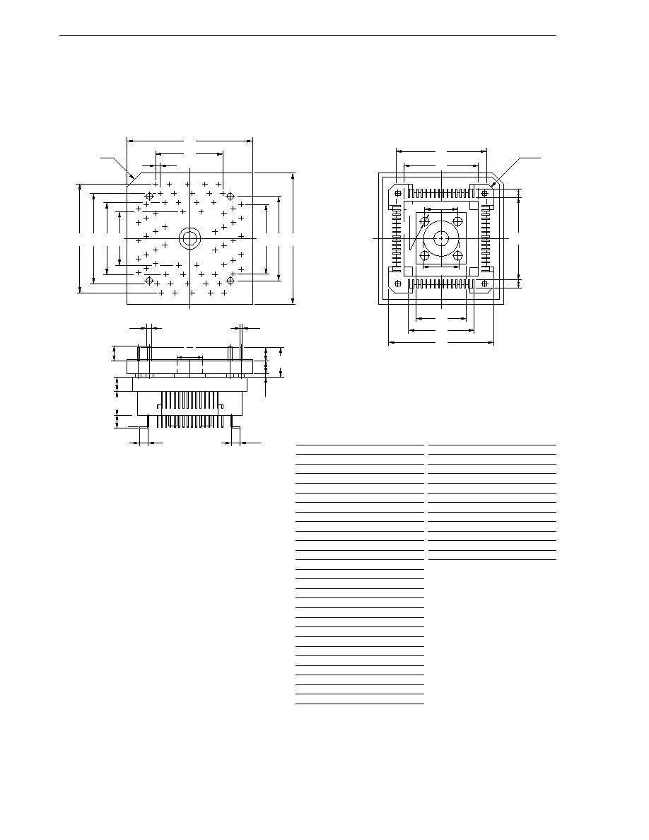
574
APPENDIX B DEVELOPMENT TOOLS
User's Manual U14260EJ3V1UD
Conversion Adapter (TGK-064SBW) Package Drawing
Figure B-4. TGK-064SBW Package Drawing (for Reference Only)
ITEM
MILLIMETERS
INCHES
b
1.85
0.073
c
3.5
0.138
a
0.3
0.012
d
2.0
0.079
h
5.9
0.232
i
0.8
0.031
j
2.4
0.094
e
3.9
0.154
f
1.325
g
1.325
0.052
0.052
ITEM
MILLIMETERS
INCHES
B
0.65x15=9.75
0.026x0.591=0.384
C
0.65
0.026
A
18.4
0.724
D
H
0.65x15=9.75
0.026x0.591=0.384
I
11.85
0.467
J
18.4
0.724
E
10.15
0.400
F
12.55
0.494
K
C 2.0
C 0.079
L
12.45
0.490
M
Q
11.1
0.437
R
1.45
0.057
S
1.45
0.057
N
7.7
0.303
O
10.02
P
14.92
0.587
0.394
W
5.3
0.209
X
4-C 1.0
4-C 0.039
Y
3.55
0.140
T
4- 1.3
4- 0.051
U
1.8
V
5.0
0.197
0.071
Z
0.9
0.035
7.75
10.25
0.305
0.404
G
14.95
0.589
k
2.7
0.106
TGK-064SBW-G1E
H
A
h
a
g
Z
c
L
Q
N
B
C
I
J
K
G F E D
M
X
R
S
W
O
P
Protrusion height
U
T
V
k
j
i
Y
e
d
b
f
Note Product by TOKYO ELETECH CORPORATION.

575
User's Manual U14260EJ3V1UD
APPENDIX C NOTES ON TARGET SYSTEM DESIGN
The following shows the conditions when connecting the emulation probe and conversion adapter. Consider the
shape of the components to be mounted on the target system and follow the configurations below when designing
the system.
Among the products described in this appendix, NP-64GC-TQ, NP-H64GC-TQ, NP-64GK, and NP-H64GK-TQ are
products of Naito Densei Machida Mfg. Co., Ltd. and TGC-064SAP and TGK-064SBW are products of TOKYO
ELETECH CORPORATION.
Table C-1. Distance Between IE System and Conversion Adapter
Emulation Probe
Conversion Adapter
Distance Between IE System and Conversion Adapter
NP-64GC-TQ
TGC-064SAP
170 mm
NP-H64GC-TQ
370 mm
NP-64GK
TGK-064SBW
170 mm
NP-H64GK-TQ
370 mm
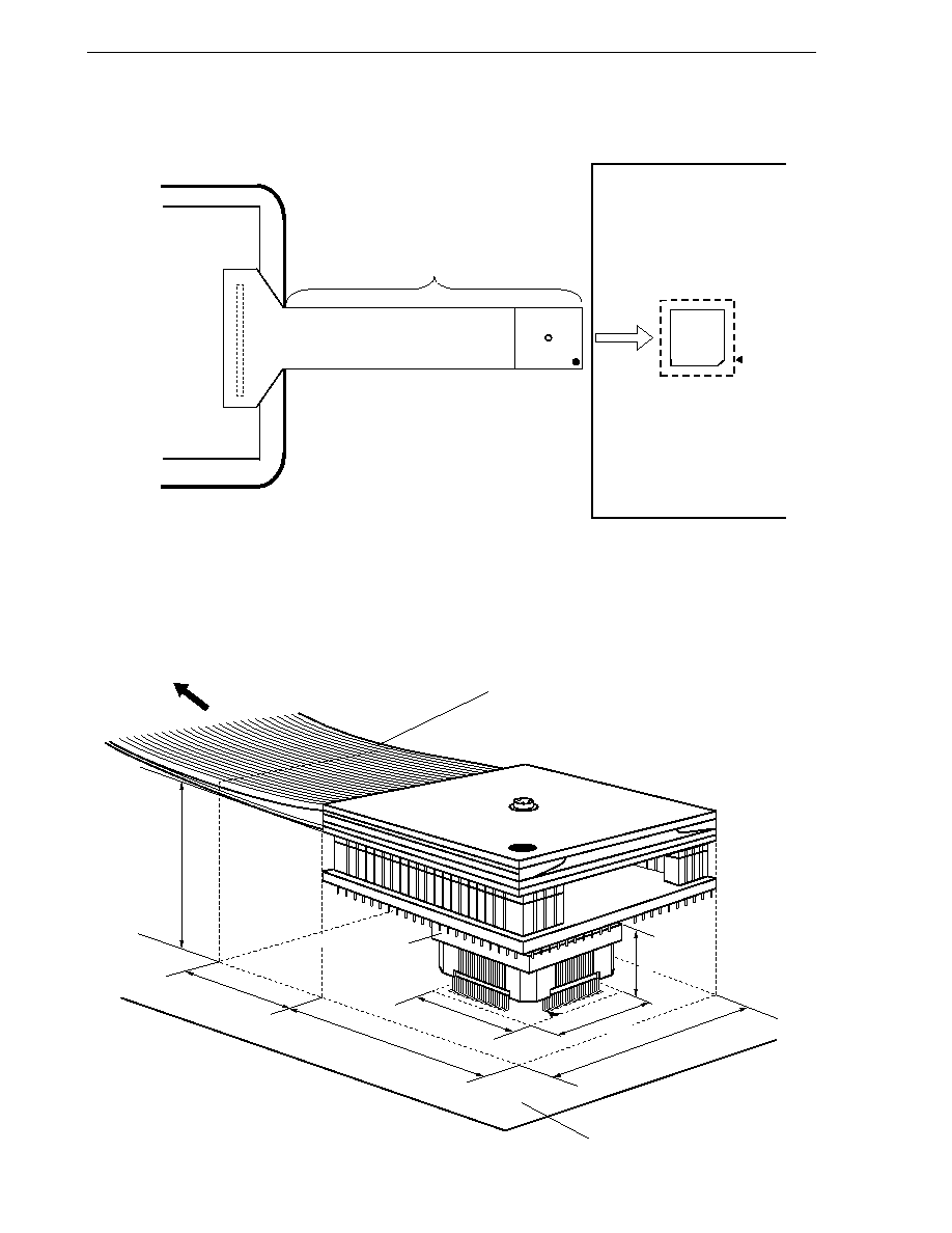
576
APPENDIX C NOTES ON TARGET SYSTEM DESIGN
User's Manual U14260EJ3V1UD
Figure C-1. Distance Between In-Circuit Emulator and Conversion Adapter (64GC)
Note The above distance shows when the NP-64GC-TQ is used. When the NP-H64GC-TQ is used, the distance
is 370 mm.
Figure C-2. Connection Conditions of Target System (NP-64GC-TQ)
Emulation probe
NP-64GC-TQ
Emulation board
IE-780078-NS-EM1
23 mm
25 mm
40 mm
34 mm
Target system
20.65 mm
Pin 1
11 mm
20.65 mm
Conversion adapter
TGC-064SAP
170 mm
Note
In-circuit emulator
IE-78K0-NS or IE-78K0-NS-A
Emulation board
IE-780078-NS-EM1
Conversion adapter: TGC-064SAP
Target system
Emulation probe
NP-64GC-TQ, NP-H64GC-TQ
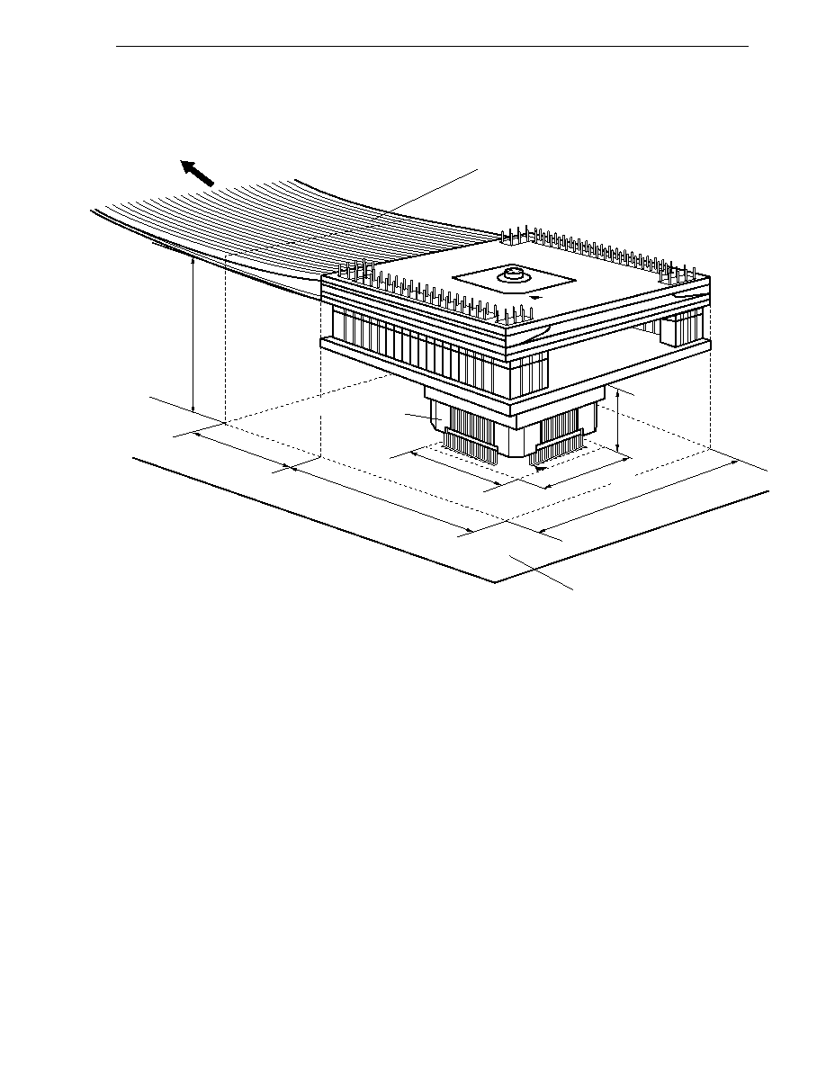
577
APPENDIX C NOTES ON TARGET SYSTEM DESIGN
User's Manual U14260EJ3V1UD
Figure C-3. Connection Conditions of Target System (NP-H64GC-TQ)
Emulation probe
NP-H64GC-TQ
Emulation board
IE-780078-NS-EM1
23 mm
23 mm
42 mm
45 mm
20.65 mm
Target system
20.65 mm
Pin 1
11 mm
Conversion adapter
TGC-064SAP

578
APPENDIX C NOTES ON TARGET SYSTEM DESIGN
User's Manual U14260EJ3V1UD
Figure C-4. Distance Between In-Circuit Emulator and Conversion Adapter (64GK)
Note The above distance shows when the NP-64GK is used. When the NP-H64GK-TQ is used, the distance is
370 mm.
Figure C-5. Connection Conditions of Target System (NP-64GK)
Emulation probe
NP-64GK
Emulation board
IE-780078-NS-EM1
21.95 mm
40 mm
34 mm
Target system
18.4 mm
Pin 1
11 mm
25 mm
18.4 mm
Conversion adapter
TGK-064SBW
170 mm
Note
In-circuit emulator
IE-78K0-NS or IE-78K0-NS-A
Emulation board
IE-780078-NS-EM1
Conversion adapter TGK-064SBW
Target system
Emulation probe
NP-64GK, NP-H64GK-TQ
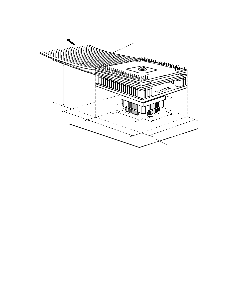
579
APPENDIX C NOTES ON TARGET SYSTEM DESIGN
User's Manual U14260EJ3V1UD
Figure C-6. Connection Conditions of Target System (NP-H64GK-TQ)
Emulation probe
NP-H64GK-TQ
Emulation board
IE-780078-NS-EM1
42 mm
45 mm
18.4 mm
11 mm
Target system
18.4 mm
Pin 1
21.95 mm
23 mm
Conversion adapter
TGK-064SBW

580
User's Manual U14260EJ3V1UD
APPENDIX D REGISTER INDEX
D.1 Register Index (In Alphabetical Order with Respect to Register Names)
[A]
A/D conversion result register 0 (ADCR0) ... 231
A/D converter mode register 0 (ADM0) ... 228
Analog input channel specification register 0 (ADS0) ... 231
Asynchronous serial interface mode register 0 (ASIM0) ... 250
Asynchronous serial interface mode register 2 (ASIM2) ... 272
Asynchronous serial interface status register 0 (ASIS0) ... 252
Asynchronous serial interface status register 2 (ASIS2) ... 274
Asynchronous serial interface transmit status register 2 (ASIF2) ... 275
[B]
Baud rate generator control register 0 (BRGC0) ... 252
Baud rate generator control register 2 (BRGC2) ... 276
[C]
Capture/compare control register 00 (CRC00) ... 151
Capture/compare control register 01 (CRC01) ... 151
Clock output select register (CKS) ... 221
Clock select register 2 (CKSEL2) ... 277
[E]
8-bit timer compare register 50 (CR50) ... 190
8-bit timer compare register 51 (CR51) ... 190
8-bit timer counter 50 (TM50) ... 189
8-bit timer counter 51 (TM51) ... 189
8-bit timer mode control register 50 (TMC50) ... 192
8-bit timer mode control register 51 (TMC51) ... 192
External interrupt falling edge enable register (EGN) ... 404
External interrupt rising edge enable register (EGP) ... 404
[I]
IIC control register 0 (IICC0) ... 338
IIC shift register 0 (IIC0) ... 336
IIC status register 0 (IICS0) ... 343
IIC transfer clock select register 0 (IICCL0) ... 346
Internal expansion RAM size switching register (IXS) ... 440
Interrupt mask flag register 0H (MK0H) ... 402
Interrupt mask flag register 0L (MK0L) ... 402
Interrupt mask flag register 1L (MK1L) ... 402
Interrupt request flag register 0H (IF0H) ... 401
Interrupt request flag register 0L (IF0L) ... 401
Interrupt request flag register 1L (IF1L) ... 401

581
APPENDIX D REGISTER INDEX
User's Manual U14260EJ3V1UD
[M]
Memory expansion mode register (MEM) ... 418
Memory expansion wait setting register (MM) ... 419
Memory size switching register (IMS) ... 439
[O]
Oscillation stabilization time select register (OSTS) ... 132, 427
[P]
Port mode register 0 (PM0) ... 118
Port mode register 2 (PM2) ... 118, 254, 322
Port mode register 3 (PM3) ... 118, 280, 313, 347
Port mode register 4 (PM4) ... 118
Port mode register 5 (PM5) ... 118
Port mode register 6 (PM6) ... 118
Port mode register 7 (PM7) ... 118, 157, 195, 223
Port mode register 8 (PM8) ... 118, 322
Port register 0 (P0) ... 122
Port register 1 (P1) ... 122
Port register 2 (P2) ... 122
Port register 3 (P3) ... 122
Port register 4 (P4) ... 122
Port register 5 (P5) ... 122
Port register 6 (P6) ... 122
Port register 7 (P7) ... 122
Port register 8 (P8) ... 122
Prescaler mode register 00 (PRM00) ... 155
Prescaler mode register 01 (PRM01) ... 155
Priority specification flag register 0H (PR0H) ... 403
Priority specification flag register 0L (PR0L) ... 403
Priority specification flag register 1L (PR1L) ... 403
Processor clock control register (PCC) ... 129
Program status word (PSW) ... 72, 405
Pull-up resistor option register 0 (PU0) ... 123
Pull-up resistor option register 2 (PU2) ... 123
Pull-up resistor option register 3 (PU3) ... 123
Pull-up resistor option register 4 (PU4) ... 123
Pull-up resistor option register 5 (PU5) ... 123
Pull-up resistor option register 6 (PU6) ... 123
Pull-up resistor option register 7 (PU7) ... 123
Pull-up resistor option register 8 (PU8) ... 123
[R]
Receive buffer register 0 (RXB0) ... 249
Receive buffer register 2 (RXB2) ... 270

582
APPENDIX D REGISTER INDEX
User's Manual U14260EJ3V1UD
[S]
Serial clock select register 1 (CSIC1) ... 321
Serial I/O shift register 1 (SIO1) ... 319
Serial I/O shift register 3 (SIO3) ... 311
Serial operation mode register 1 (CSIM1) ... 320
Serial operation mode register 3 (CSIM3) ... 311
16-bit timer capture/compare register 000 (CR000) ... 145
16-bit timer capture/compare register 001 (CR001) ... 145
16-bit timer capture/compare register 010 (CR010) ... 147
16-bit timer capture/compare register 011 (CR011) ... 147
16-bit timer counter 00 (TM00) ... 145
16-bit timer counter 01 (TM01) ... 145
16-bit timer mode control register 00 (TMC00) ... 148
16-bit timer mode control register 01 (TMC01) ... 148
16-bit timer output control register 00 (TOC00) ... 153
16-bit timer output control register 01 (TOC01) ... 153
Slave address register 0 (SVA0) ... 336
[T]
Timer clock select register 50 (TCL50) ... 191
Timer clock select register 51 (TCL51) ... 191
Transfer mode specification register 2 (TRMC2) ... 279
Transmit buffer register 1 (SOTB1) ... 319
Transmit buffer register 2 (TXB2) ... 270
Transmit shift register 0 (TXS0) ... 249
[W]
Watch timer operation mode register (WTM) ... 211
Watchdog timer clock select register (WDCS) ... 216
Watchdog timer mode register (WDTM) ... 217

583
APPENDIX D REGISTER INDEX
User's Manual U14260EJ3V1UD
D.2 Register Index (In Alphabetical Order with Respect to Register Symbol)
[A]
ADCR0:
A/D conversion result register 0 ... 231
ADM0:
A/D converter mode register 0 ... 228
ADS0:
Analog input channel specification register 0 ... 231
ASIF2:
Asynchronous serial interface transmit status register 2 ... 275
ASIM0:
Asynchronous serial interface mode register 0 ... 250
ASIM2:
Asynchronous serial interface mode register 2 ... 272
ASIS0:
Asynchronous serial interface status register 0 ... 252
ASIS2:
Asynchronous serial interface status register 2 ... 274
[B]
BRGC0: Baud rate generator control register 0 ... 252
BRGC2: Baud rate generator control register 2 ... 276
[C]
CKS:
Clock output select register ... 221
CKSEL2: Clock select register 2 ... 277
CR000:
16-bit timer capture/compare register 000 ... 145
CR001:
16-bit timer capture/compare register 001 ... 145
CR010:
16-bit timer capture/compare register 010 ... 147
CR011:
16-bit timer capture/compare register 011 ... 147
CR50:
8-bit timer compare register 50 ... 190
CR51:
8-bit timer compare register 51 ... 190
CRC00:
Capture/compare control register 00 ... 151
CRC01:
Capture/compare control register 01 ... 151
CSIC1:
Serial clock select register 1 ... 321
CSIM1:
Serial operation mode register 1 ... 320
CSIM3:
Serial operation mode register 3 ... 311
[E]
EGN:
External interrupt falling edge enable register ... 404
EGP:
External interrupt rising edge enable register ... 404
[I]
IF0H:
Interrupt request flag register 0H ... 401
IF0L:
Interrupt request flag register 0L ... 401
IF1L:
Interrupt request flag register 1L ... 401
IIC0:
IIC shift register 0 ... 336
IICC0:
IIC control register 0 ... 338
IICCL0:
IIC transfer clock select register 0 ... 346
IICS0:
IIC status register 0 ... 343
IMS:
Memory size switching register ... 439
IXS:
Internal expansion RAM size switching register ... 440

584
APPENDIX D REGISTER INDEX
User's Manual U14260EJ3V1UD
[M]
MEM:
Memory expansion mode register ... 418
MK0H:
Interrupt mask flag register 0H ... 402
MK0L:
Interrupt mask flag register 0L ... 402
MK1L:
Interrupt mask flag register 1L ... 402
MM:
Memory expansion wait setting register ... 419
[O]
OSTS:
Oscillation stabilization time select register ... 132, 427
[P]
P0:
Port register 0 ... 122
P1:
Port register 1 ... 122
P2:
Port register 2 ... 122
P3:
Port register 3 ... 122
P4:
Port register 4 ... 122
P5:
Port register 5 ... 122
P6:
Port register 6 ... 122
P7:
Port register 7 ... 122
P8:
Port register 8 ... 122
PCC:
Processor clock control register ... 129
PM0:
Port mode register 0 ... 118
PM2:
Port mode register 2 ... 118, 254, 322
PM3:
Port mode register 3 ... 118, 280, 313, 347
PM4:
Port mode register 4 ... 118
PM5:
Port mode register 5 ... 118
PM6:
Port mode register 6 ... 118
PM7:
Port mode register 7 ... 118, 157, 195, 223
PM8:
Port mode register 8 ... 118, 322
PR0H:
Priority specification flag register 0H ... 403
PR0L:
Priority specification flag register 0L ... 403
PR1L:
Priority specification flag register 1L ... 403
PRM00:
Prescaler mode register 00 ... 155
PRM01:
Prescaler mode register 01 ... 155
PSW:
Program status word ... 72, 405
PU0:
Pull-up resistor option register 0 ... 123
PU2:
Pull-up resistor option register 2 ... 123
PU3:
Pull-up resistor option register 3 ... 123
PU4:
Pull-up resistor option register 4 ... 123
PU5:
Pull-up resistor option register 5 ... 123
PU6:
Pull-up resistor option register 6 ... 123
PU7:
Pull-up resistor option register 7 ... 123
PU8:
Pull-up resistor option register 8 ... 123
[R]
RXB0:
Receive buffer register 0 ... 249
RXB2:
Receive buffer register 2 ... 270

585
APPENDIX D REGISTER INDEX
User's Manual U14260EJ3V1UD
[S]
SIO1:
Serial I/O shift register 1 ... 319
SIO3:
Serial I/O shift register 3 ... 311
SOTB1:
Transmit buffer register 1 ... 319
SVA0:
Slave address register 0 ... 336
[T]
TCL50:
Timer clock select register 50 ... 191
TCL51:
Timer clock select register 51 ... 191
TM00:
16-bit timer counter 00 ... 145
TM01:
16-bit timer counter 01 ... 145
TM50:
8-bit timer counter 50 ... 189
TM51:
8-bit timer counter 51 ... 189
TMC00:
16-bit timer mode control register 00 ... 148
TMC01:
16-bit timer mode control register 01 ... 148
TMC50:
8-bit timer mode control register 50 ... 192
TMC51:
8-bit timer mode control register 51 ... 192
TOC00:
16-bit timer output control register 00 ... 153
TOC01:
16-bit timer output control register 01 ... 153
TRMC2: Transfer mode specification register 2 ... 279
TXB2:
Transmit buffer register 2 ... 270
TXS0:
Transmit shift register 0 ... 249
[W]
WDCS:
Watchdog timer clock select register ... 216
WDTM:
Watchdog timer mode register ... 217
WTM:
Watch timer operation mode register ... 211

586
User's Manual U14260EJ3V1UD
APPENDIX E REVISION HISTORY
E.1 Major Revisions in This Edition
(1/3)
Page
Description
U14260EJ3V0UD00
U14260EJ3V1UD00
p. 360
Modification of Figure 18-18 Communication Reservation Timing
p. 366
Modification of Figure 18-21 Master Operation Flowchart (5/5)
pp. 443, 444
Division of Note in previous edition of Figure 23-5 Example of Connection with Dedicated Flash
Programmer to Notes 1 and 2 and modification of contents
p. 447
Addition of description on voltage monitoring of dedicated flash programmer to <Power supply> in
23.3.3 On-board pin processing
U14260EJ2V0UD00
U14260EJ3V0UD00
Throughout
Addition of expanded-specification products to
µPD780078Y Subseries
Modification of name of the following special function registers (SFR)
∑ Ports 0 to 8
Port registers 0 to 8
p. 29
Addition of 2.1 Expanded-Specification Products and Conventional Products
p. 78
Modification of value after reset of port register 1 (P1) in Table 5-3 Special Function Register List
p. 110
Modification of Figure 6-14 Block Diagram of P40 to P47
p. 112
Modification of Figure 6-16 Block Diagram of P50 to P57
p. 113
Modification of Figure 6-17 Block Diagram of P64, P65, and P67
p. 114
Modification of Figure 6-18 Block Diagram of P66
p. 118
Addition of port registers (P0 to P8) to 6.3 Port Function Control Registers
Addition of the following figures
p. 145
∑ Figure 8-3 Format of 16-Bit Timer Counter 0n (TM0n)
p. 145
∑ Figure 8-4 Format of 16-Bit Timer Capture/Compare Register 00n (CR00n)
p. 147
∑ Figure 8-5 Format of 16-Bit Timer Capture/Compare Register 01n (CR01n)
Addition of register setting method to the following sections
p. 158
∑ 8.4.1 Interval timer operation
p. 161
∑ 8.4.2 External event counter operation
p. 163
∑ 8.4.3 Pulse width measurement operations
p. 171
∑ 8.4.4 Square-wave output operation
p. 173
∑ 8.4.5 PPG output operation
Addition of settings of prescaler mode register 0n (PRM0n) to the following figures
p. 158
∑ Figure 8-15 Control Register Settings for Interval Timer Operation
p. 161
∑ Figure 8-19 Control Register Settings in External Event Counter Mode (with Rising Edge
Specified)
p. 164
∑ Figure 8-23 Control Register Settings for Pulse Width Measurement with Free-Running Counter
and One Capture Register (When TI00n and CR01n Are Used)
p. 166
∑ Figure 8-26 Control Register Settings for Measurement of Two Pulse Widths with Free-Running
Counter
p. 168
∑ Figure 8-28 Control Register Settings for Pulse Width Measurement with Free-Running Counter
and Two Capture Registers (with Rising Edge Specified)
p. 170
∑ Figure 8-30 Control Register Settings for Pulse Width Measurement by Means of Restart (with
Rising Edge Specified)
p. 172
∑ Figure 8-32 Control Register Settings in Square-Wave Output Mode
p. 174
∑ Figure 8-34 Control Register Settings for PPG Output Operation

587
APPENDIX E REVISION HISTORY
User's Manual U14260EJ3V1UD
(2/3)
Page
Description
Modification of the following figures
p. 159
∑ Figure 8-17 Timing of Interval Timer Operation
p. 175
∑ Figure 8-36 PPG Output Operation Timing
p. 183
∑ Figure 8-37 Start Timing of 16-Bit Timer Counter 0n (TM0n)
Addition of the following figures
p. 189
∑ Figure 9-3 Format of 8-Bit Timer Counter 5n (TM5n)
p. 190
∑ Figure 9-4 Format of 8-Bit Timer Compare Register 5n (CR5n)
Modification of the following figures
pp. 196 to 198
∑ Figure 9-10 Interval Timer Operation Timing
p. 199
∑ Figure 9-11 External Event Counter Operation Timing (with Rising Edge Specified)
p. 201
∑ Figure 9-12 Square-Wave Output Operation Timing
p. 203
∑ Figure 9-13 PWM Output Operation Timing
p. 204
∑ Figure 9-14 Timing of Operation with CR5n Changed
p. 205
∑ Figure 9-15 16-Bit Resolution Cascade Connection Mode
p. 209
∑ Figure 9-16 Start Timing of 8-Bit Timer Counter 5n (TM5n)
p. 202
Modification of description on cycle and duty, and addition of active level width to 9.4.4 8-bit PWM
output operation
p. 214
Addition of 10.5 Cautions for Watch Timer and Figure 10-4 Example of Generation of Watch
Timer Interrupt Request (INTWT) (When Interrupt Period = 0.5 s)
p. 225
Modification of Figure 13-1 Block Diagram of 10-Bit A/D Converter
p. 226
Modification of part of description in 13.2 A/D Converter Configuration
p. 228
Shift of description of A/D conversion result register 0 (ADCR0) to 13.3 Registers Used in A/D
Converter
p. 232
Modification of part of description in 13.4.1 Basic operations of A/D converter
p. 234
Addition of description of successive approximation register (SAR) to 13.4.2 Input voltage and
conversion results
Modification of the following figures
p. 236
∑ Figure 13-9 A/D Conversion by Hardware Start (When Falling Edge Is Specified)
p. 237
∑ Figure 13-10 A/D Conversion by Software Start
p. 242
∑ Figure 13-17 A/D Conversion End Interrupt Request Generation Timing
p. 243
Modification of part of description in (10) Timing at which A/D conversion result is undefined in 13.6
Cautions for A/D Converter
p. 245
Addition of Figure 13-20 Timing of A/D Converter Sampling and A/D Conversion Start Delay
p. 255
Modification of description in (1) Registers to be used in 14.4.2 Asynchronous serial interface
(UART) mode
p. 259
Addition of Figure 14-9 Example of UART Transmit/Receive Data Waveform
p. 263
Modification of Table 14-4 Causes of Receive Errors
p. 264
Modification of description in (1) Registers to be used in 14.4.3 Infrared data transfer mode
p. 282
Modification of description in (1) Registers to be used in 15.4.2 Asynchronous serial interface
(UART) mode
p. 287
Addition of Figure 15-12 Example of UART Transmit/Receive Data Waveform
p. 295
Modification of Table 15-9 Causes of Receive Errors
p. 297
Modification of description in (1) Registers to be used in 15.4.3 Multi-processor transfer mode
p. 303
Modification of description in (1) Registers to be used in 15.4.4 Infrared data transfer (IrDA) mode

588
APPENDIX E REVISION HISTORY
User's Manual U14260EJ3V1UD
(3/3)
Page
Description
p. 315
Modification of description in (1) Registers to be used in 16.4.2 3-wire serial I/O mode
p. 317
Modification of Table 16-3 Register Settings
p. 319
Partial modification of Figure 17-1 Block Diagram of Serial Interface CSI1
p. 321
Partial modification of Figure 17-3 Format of Serial Clock Select Register 1 (CSIC1)
p. 324
Modification of description in (1) Registers to be used in 17.4.2 3-wire serial I/O mode
p. 331
Addition of (5) SO1 output to 17.4.2 3-wire serial I/O mode
pp. 362 to 366
Modification of Figure 18-21 Master Operation Flowchart
p. 367
Modification of (2) Slave operation in 18.5.15 Communication operations
p. 404
Addition of Table 19-3 Ports Corresponding to EGPn and EGNn
p. 406
Modification of part of description in 19.4.1 Non-maskable interrupt request acknowledgment
operation
p. 409
Modification of part of description in 19.4.2 Maskable interrupt request acknowledgment operation
p. 419
Addition of Note to Figure 20-2 Format of Memory Expansion Mode Register (MEM) and addition of
Figure 20-3 Pins Specified for Address (with
µPD780076 and 780076Y)
p. 442
Partial modification of Table 23-3 Communication Mode List
p. 467
Revision of CHAPTER 25 ELECTRICAL SPECIFICATIONS (EXPANDED-SPECIFICATION PRODUCTS
OF
µPD780076, 780078, 78F0078)
p. 498
Addition of CHAPTER 26 ELECTRICAL SPECIFICATIONS (EXPANDED-SPECIFICATION PRODUCTS
OF
µPD780076Y, 780078Y, 78F0078Y)
p. 527
Revision of CHAPTER 27 ELECTRICAL SPECIFICATIONS (CONVENTIONAL PRODUCTS)
p. 559
Partial modification of Table 29-1 Surface Mounting Type Soldering Conditions
pp. 564, 565
Deletion of B.7 Embedded Software and B.8 System Upgrade from Former In-circuit Emulator for
in previous edition
78K/0 Series to IE-78001-R-A in the previous edition

589
APPENDIX E REVISION HISTORY
User's Manual U14260EJ3V1UD
E.2 Revision History up to Previous Edition
The history of revisions made up to this edition is shown below.
(1/4)
Edition
Contents
Applied to:
2nd
Addition of the following package
∑ 64-pin plastic LQFP (GC-8BS type)
Addition of expanded-specification products to the
µPD780078 Subseries
Addition of 1.1 Expanded-Specification Products and Conventional Products
Modification of voltage operation range of A/D converter in 1.8 Outline of
Functions
Modification of voltage operation range of A/D converter in 2.7 Outline of
Functions
Addition of description about pin processing in 3.2.17 V
PP
(flash memory version
only)
Modification of I/O circuit types of P32 and P33 in Table 3-1 Pin I/O Circuit
Types
Addition of description about pin processing in 4.2.17 V
PP
(flash memory version
only)
Addition of description about programming area in 5.1.2 (1) Internal high-speed
RAM and (2) Internal expansion RAM
Modification of Figure 5-10 Data to Be Saved to Stack Memory and Figure 5-11
Data to Be Restored from Stack Memory
Modification of [Description example] in 5.4.4 Short direct addressing
Addition of [Illustration] in 5.4.7 Based addressing, 5.4.8 Based indexed
addressing, and 5.4.9 Stack addressing
Modification of port block diagrams (Figure 6-2 Block Diagram of P00 to P03 to
Figure 6-21 Block Diagram of P80)
Addition of Table 6-6 Port Mode Registers and Output Latch Setting When
Alternate Function Is Used
Addition of description of internal feedback resistor and oscillation stabilization
time select register (OSTS) in 7.3 Clock Generator Control Register
Deletion of 8.5.6 One-shot pulse output operation in the previous edition
Modification of Figure 8-1 Block Diagram of 16-Bit Timer/Event Counter 00
and Figure 8-2 Block Diagram of 16-Bit Timer/Event Counter 01
Change of Table 8-2 TI00n Pin Valid Edge and CR00n, CR01n Capture Trigger
and Table 8-3 TI01n Pin Valid Edge and CR00n Capture Trigger in the
previous edition to Table 8-2 CR00n Capture Trigger and Valid Edges of TI00n
and TI01n Pins and Table 8-3 CR01n Capture Trigger and Valid Edge of TI00n
Pin (CRC02n = 1)
Change of explanation order of each function in 8.4 Operation of 16-Bit Timer/
Event Counters 00, 01
Addition of Figure 8-31 PPG Output Configuration Diagram and Figure 8-32
PPG Output Operation Timing
Throughout
CHAPTER 1 OUTLINE
(
µPD780078 SUBSERIES)
CHAPTER 2 OUTLINE
(
µPD780078Y
SUBSERIES)
CHAPTER 3 PIN
FUNCTION (
µPD780078
SUBSERIES)
CHAPTER 4 PIN
FUNCTION (
µPD780078Y
SUBSERIES)
CHAPTER 5 CPU
ARCHITECTURE
CHAPTER 6 PORT
FUNCTIONS
CHAPTER 7 CLOCK
GENERATOR
CHAPTER 8 16-BIT
TIMER/EVENT
COUNTERS 00, 01
590
APPENDIX E REVISION HISTORY
User's Manual U14260EJ3V1UD
(2/4)
Edition
Contents
Applied to:
2nd
Addition of 8.5 Program List
Modification of 8.6 (3) Capture register data retention timing
Addition of (11) STOP mode or main system clock stop mode setting
Modification of Figure 9-1 Block Diagram of 8-Bit Timer/Event Counter 50 and
Figure 9-2 Block Diagram of 8-Bit Timer/Event Counter 51
Deletion of Caution in Figure 9-5 Format of 8-Bit Timer Mode Control Register
50 (TMC50) and Figure 9-6 Format of 8-Bit Timer Mode Control Register 51
(TMC51)
Addition of [Setting] in 9.4.2 External event counter operation
Addition of description about frequency to [Setting] in 9.4.3 Square-wave output
(8-bit resolution) operation
Addition of descriptions about frequency and duty ratio to [Setting] in 9.4.4 8-bit
PWM output operation
Addition of 9.5 Program List
Deletion of 9.6 (2) Operation after compare register transition during timer
count operation in the previous edition
Deletion of oscillation stabilization time select register (OSTS) from 11.4
Registers to Control Watchdog Timer in the previous edition
Modification of Figure 12-1 Block Diagram of Clock Output/Buzzer Output
Controller
Addition of Figure 13-2 Format of A/D Conversion Result Register 0 (ADCR0)
Modification of description in 13.2 (3) Sample & hold circuit and (4) Voltage
comparator, and addition of (9) ADTRG pin
Addition of Table 13-2 ADCS0 and ADCE0 Settings and Figure 13-4 Timing
Chart When Boost Reference Voltage Generator Is Used
Addition of Table 13-3 Sampling Time and A/D Conversion Start Delay Time
of A/D Converter
Deletion of 13.6 (4) Noise countermeasures (those deleted are added to Figure
13-20 Example of Connecting Capacitor to AV
REF
Pin and Figure 13-22
Example of Connection When Signal Source Impedance Is High)
Addition of (13) Input impedance of ANI0 to ANI7 pins
Modification of Figure 14-1 Block Diagram of Serial Interface UART0
Shift of description about asynchronous serial interface status register 0 (ASIS0)
from 14.3 Registers to Control Serial Interface UART0 to 14.2 Configuration
of Serial Interface UART0
Addition of Caution in Figure 14-7 Error Tolerance (When k = 0), Including
Sampling Errors
Modification of Caution in Figure 14-10 Timing of Asynchronous Serial
Interface Receive Completion Interrupt Request
Addition of (1) Registers to be used and (3) Relationship between main
system clock and baud rate in 14.4.3 Infrared data transfer mode
Addition of Table 14-6 Register Settings
CHAPTER 8 16-BIT
TIMER/EVENT
COUNTERS 00, 01
CHAPTER 9 8-BIT TIMER/
EVENT COUNTERS 50, 51
CHAPTER 11
WATCHDOG TIMER
CHAPTER 12 CLOCK
OUTPUT/BUZZER
OUTPUT CONTROLLER
CHAPTER 13 A/D
CONVERTER
CHAPTER 14 SERIAL
INTERFACE UART0

591
APPENDIX E REVISION HISTORY
User's Manual U14260EJ3V1UD
(3/4)
Edition
Contents
Applied to:
2nd
Modification of Figure 15-1 Block Diagram of Serial Interface UART2
Shift of descriptions about asynchronous serial interface status register 2 (ASIS2)
and asynchronous serial interface transmit status register 2 (ASIF2) from 15.3
Registers to Control Serial Interface UART2 to 15.2 Configuration of Serial
Interface UART2
Modification of Caution 1 and addition of Cautions 2 and 3 in Figure 15-4
Format of Asynchronous Serial Interface Transmit Status Register 2 (ASIF2)
Addition of Notes 7 and 8 in Figure 15-8 Format of Transfer Mode
Specification Register 2 (TRMC2)
Modification of error values in Table 15-2 Relationship Between Main System
Clock and Baud Rate
Addition of Caution in Table 15-3 Maximum Permissible Baud Rate Error and
Minimum Permissible Baud Rate Error
Modification of the INTST2 timing in (ii) and (iii) of Figure 15-12 Timing of
Asynchronous Serial Interface Transmit Completion Interrupt Request
Division of Table 15-6 Transmission Status and Writing to TXB2 in the
previous edition into Table 15-4 Writing to TXBF and TXB2 (When Successive
Transmission Is Started) and Table 15-5 Writing to TXSF and TXB2 (When
Successive Transmission Is in Progress)
Modification of Figure 15-14 Timing of Starting Successive Transmission
Modification of Figure 15-15 Timing of Completing Successive Transmission
Modification of Figure 15-17 Receive Error Timing
Addition of Table 15-10 Register Settings
Modification of Figure 16-1 Block Diagram of Serial Interface SIO3
Addition of Notes 3 and 4 in Figure 16-2 Format of Serial Operation Mode
Register 3 (CSIM3)
Addition of Table 16-2 Register Settings
Modification of Figure 17-1 Block Diagram of Serial Interface CSI1
Addition of description about SS1 pin in 17.4.2 (2) Communication operation
Modification of Figure 17-6 Timing of 3-Wire Serial I/O Mode
Modification of Figure 17-8 Output Operation of First Bit
Modification of Figure 17-9 Output Value of SO1 Pin (Last Bit)
Deletion of 17.4.2 (6) SCK1 pin and (7) SO1 pin in the previous edition
Addition of Table 17-2 Register Settings
Modification of Figure 18-1 Block Diagram of Serial Interface IIC0
Incorporation of 18.3 (4) IIC shift register 0 (IIC0) and (5) Slave address
register 0 (SVA0) in the previous edition into 18.2 (1) IIC shift register 0 (IIC0)
and (2) Slave address register 0 (SVA0), respectively
Addition of description to "Transfer Lines" in Figure 18-16 Wait Signal
Addition of descriptions to Notes 1 and 2 in Table 18-2 INTIIC0 Timing and Wait
Control
Modification of Figure 18-21 Master Operation Flowchart and Figure 18-22
Slave Operation Flowchart
CHAPTER 15 SERIAL
INTERFACE UART2
CHAPTER 16 SERIAL
INTERFACE SIO3
CHAPTER 17 SERIAL
INTERFACE CSI1
CHAPTER 18 SERIAL
INTERFACE IIC0
(
µPD780078Y SUBSERIES
ONLY)

592
APPENDIX E REVISION HISTORY
User's Manual U14260EJ3V1UD
(4/4)
Edition
Contents
Applied to:
2nd
Modification of 18.5.16 (3) (d) (ii) When WTIM0 = 1 (after restart, does not
match with address (= not extension code))
Modification of (1) Start condition ~ address and (2) Data in Figure 18-23
Example of Master to Slave Communication (When 9-Clock Wait Is Selected
for Both Master and Slave)
Modification of Figure 18-24 Example of Slave to Master Communication
(When 9-Clock Wait Is Selected for Both Master and Slave)
Modification of (E) Software interrupt in Figure 19-1 Basic Configuration of
Interrupt Function
Addition of Cautions 3 and 4 in Figure 19-2 Format of Interrupt Request Flag
Register (IF0L, IF0H, IF1L)
Addition of Caution in Figure 19-5 Format of External Interrupt Rising Edge
Enable Register (EGP), External Interrupt Falling Edge Enable Register
(EGN)
Addition of description and Remark in 19.4.1 Non-maskable interrupt request
acknowledgment operation
Addition of description in 19.4.2 Maskable interrupt acknowledgment operation
Addition of item to Table 19-4 Interrupt Requests Enabled for Multiple
Interrupt Servicing
Addition of description about when using expanded-specification products
Addition of clock output and buzzer output in Table 21-1 HALT Mode Operating
Statuses
Modification of clock output in Table 21-3 STOP Mode Operating Statuses
Modification of chapter
Addition of chapters
Addition of Table A-2 Major Differences Between
µPD78018F, 780024A,
780034A, and 780078 Subseries (Software)
Modification of chapter
Addition of chapters
CHAPTER 18 SERIAL
INTERFACE IIC0
(
µPD780078Y SUBSERIES
ONLY)
CHAPTER 19 INTERRUPT
FUNCTIONS
CHAPTER 20 EXTERNAL
DEVICE EXPANSION
FUNCTION
CHAPTER 21 STANDBY
FUNCTION
CHAPTER 23
µPD78F0078, 78F0078Y
CHAPTER 25
ELECTRICAL
SPECIFICATIONS
CHAPTER 26 PACKAGE
DRAWINGS
CHAPTER 27
RECOMMENDED
SOLDERING CONDITIONS
APPENDIX A
DIFFERENCES BETWEEN
µPD78018F, 780024A,
780034A, AND 780078
SUBSERIES
APPENDIX B
DEVELOPMENT TOOLS
APPENDIX C NOTES ON
TARGET SYSTEM DESIGN
APPENDIX E REVISION
HISTORY