
Document No. U16228EJ2V0UD00 (2nd edition)
Date Published November 2003 N CP(K)
Printed in Japan
2002
µ
PD780131
µ
PD780131(A)
µ
PD780131(A1)
µ
PD780131(A2)
µ
PD780132
µ
PD780132(A)
µ
PD780132(A1)
µ
PD780132(A2)
µ
PD780133
µ
PD780133(A)
µ
PD780133(A1)
µ
PD780133(A2)
µ
PD780134
µ
PD780134(A)
µ
PD780134(A1)
µ
PD780134(A2)
µ
PD780136
µ
PD780136(A)
µ
PD780136(A1)
µ
PD780136(A2)
µ
PD780138
µ
PD780138(A)
µ
PD780138(A1)
µ
PD780138(A2)
µ
PD78F0134
µ
PD78F0134(A)
µ
PD78F0134(A1)
µ
PD78F0138
µ
PD78F0138(A)
µ
PD78F0138(A1)
78K0/KE1
8-Bit Single-Chip Microcontrollers
User's Manual

User's Manual U16228EJ2V0UD
2
[MEMO]

User's Manual U16228EJ2V0UD
3
NOTES FOR CMOS DEVICES
1
PRECAUTION AGAINST ESD FOR SEMICONDUCTORS
Note:
Strong electric field, when exposed to a MOS device, can cause destruction of the gate oxide and
ultimately degrade the device operation. Steps must be taken to stop generation of static electricity
as much as possible, and quickly dissipate it once, when it has occurred. Environmental control
must be adequate. When it is dry, humidifier should be used. It is recommended to avoid using
insulators that easily build static electricity. Semiconductor devices must be stored and transported
in an anti-static container, static shielding bag or conductive material. All test and measurement
tools including work bench and floor should be grounded. The operator should be grounded using
wrist strap. Semiconductor devices must not be touched with bare hands. Similar precautions need
to be taken for PW boards with semiconductor devices on it.
2
HANDLING OF UNUSED INPUT PINS FOR CMOS
Note:
No connection for CMOS device inputs can be cause of malfunction. If no connection is provided
to the input pins, it is possible that an internal input level may be generated due to noise, etc., hence
causing malfunction. CMOS devices behave differently than Bipolar or NMOS devices. Input levels
of CMOS devices must be fixed high or low by using a pull-up or pull-down circuitry. Each unused
pin should be connected to V
DD
or GND with a resistor, if it is considered to have a possibility of
being an output pin. All handling related to the unused pins must be judged device by device and
related specifications governing the devices.
3
STATUS BEFORE INITIALIZATION OF MOS DEVICES
Note:
Power-on does not necessarily define initial status of MOS device. Production process of MOS
does not define the initial operation status of the device. Immediately after the power source is
turned ON, the devices with reset function have not yet been initialized. Hence, power-on does
not guarantee out-pin levels, I/O settings or contents of registers. Device is not initialized until the
reset signal is received. Reset operation must be executed immediately after power-on for devices
having reset function.
EEPROM is a trademark of NEC Electronics Corporation.
Windows and Windows NT are either registered trademarks or trademarks of Microsoft Corporation in the
United States and/or other countries.
PC/AT is a trademark of International Business Machines Corporation.
HP9000 series 700 and HP-UX are trademarks of Hewlett-Packard Company.
SPARCstation is a trademark of SPARC International, Inc.
Solaris and SunOS are trademarks of Sun Microsystems, Inc.
TRON stands for The Realtime Operating system Nucleus.
ITRON is an abbreviation of Industrial TRON.

User's Manual U16228EJ2V0UD
4
These commodities, technology or software, must be exported in accordance
with the export administration regulations of the exporting country.
Diversion contrary to the law of that country is prohibited.
The information in this document is current as of May, 2003. The information is subject to change
without notice. For actual design-in, refer to the latest publications of NEC Electronics data sheets or
data books, etc., for the most up-to-date specifications of NEC Electronics products. Not all
products and/or types are available in every country. Please check with an NEC Electronics sales
representative for availability and additional information.
No part of this document may be copied or reproduced in any form or by any means without the prior
written consent of NEC Electronics. NEC Electronics assumes no responsibility for any errors that may
appear in this document.
NEC Electronics does not assume any liability for infringement of patents, copyrights or other intellectual
property rights of third parties by or arising from the use of NEC Electronics products listed in this document
or any other liability arising from the use of such products. No license, express, implied or otherwise, is
granted under any patents, copyrights or other intellectual property rights of NEC Electronics or others.
Descriptions of circuits, software and other related information in this document are provided for illustrative
purposes in semiconductor product operation and application examples. The incorporation of these
circuits, software and information in the design of a customer's equipment shall be done under the full
responsibility of the customer. NEC Electronics assumes no responsibility for any losses incurred by
customers or third parties arising from the use of these circuits, software and information.
While NEC Electronics endeavors to enhance the quality, reliability and safety of NEC Electronics products,
customers agree and acknowledge that the possibility of defects thereof cannot be eliminated entirely. To
minimize risks of damage to property or injury (including death) to persons arising from defects in NEC
Electronics products, customers must incorporate sufficient safety measures in their design, such as
redundancy, fire-containment and anti-failure features.
NEC Electronics products are classified into the following three quality grades: "Standard", "Special" and
"Specific".
The "Specific" quality grade applies only to NEC Electronics products developed based on a customer-
designated "quality assurance program" for a specific application. The recommended applications of an NEC
Electronics product depend on its quality grade, as indicated below. Customers must check the quality grade of
each NEC Electronics product before using it in a particular application.
"Standard": Computers, office equipment, communications equipment, test and measurement equipment, audio
and visual equipment, home electronic appliances, machine tools, personal electronic equipment
and industrial robots.
"Special":
Transportation equipment (automobiles, trains, ships, etc.), traffic control systems, anti-disaster
systems, anti-crime systems, safety equipment and medical equipment (not specifically designed
for life support).
"Specific": Aircraft, aerospace equipment, submersible repeaters, nuclear reactor control systems, life
support systems and medical equipment for life support, etc.
The quality grade of NEC Electronics products is "Standard" unless otherwise expressly specified in NEC
Electronics data sheets or data books, etc. If customers wish to use NEC Electronics products in applications
not intended by NEC Electronics, they must contact an NEC Electronics sales representative in advance to
determine NEC Electronics' willingness to support a given application.
(Note)
(1) "NEC Electronics" as used in this statement means NEC Electronics Corporation and also includes its
majority-owned subsidiaries.
(2) "NEC Electronics products" means any product developed or manufactured by or for NEC Electronics
(as defined above).
∑
∑
∑
∑
∑
∑
M8E 02. 11-1

User's Manual U16228EJ2V0UD
5
Regional Information
∑
Device availability
∑
Ordering information
∑
Product release schedule
∑
Availability of related technical literature
∑
Development environment specifications (for example, specifications for third-party tools and
components, host computers, power plugs, AC supply voltages, and so forth)
∑
Network requirements
In addition, trademarks, registered trademarks, export restrictions, and other legal issues may also vary
from country to country.
[GLOBAL SUPPORT]
http://www.necel.com/en/support/support.html
NEC Electronics America, Inc. (U.S.)
Santa Clara, California
Tel: 408-588-6000
800-366-9782
NEC Electronics Hong Kong Ltd.
Hong Kong
Tel: 2886-9318
NEC Electronics Hong Kong Ltd.
Seoul Branch
Seoul, Korea
Tel: 02-558-3737
NEC Electronics Shanghai, Ltd.
Shanghai, P.R. China
Tel: 021-6841-1138
NEC Electronics Taiwan Ltd.
Taipei, Taiwan
Tel: 02-2719-2377
NEC Electronics Singapore Pte. Ltd.
Novena Square, Singapore
Tel: 6253-8311
J03.4
NEC Electronics (Europe) GmbH
Duesseldorf, Germany
Tel: 0211-65 03 01
∑ Sucursal en EspaÒa
Madrid, Spain
Tel: 091-504 27 87
VÈlizy-Villacoublay, France
Tel: 01-30-67 58 00
∑ Succursale FranÁaise
∑ Filiale Italiana
Milano, Italy
Tel: 02-66 75 41
∑ Branch The Netherlands
Eindhoven, The Netherlands
Tel: 040-244 58 45
∑ Tyskland Filial
Taeby, Sweden
Tel: 08-63 80 820
∑ United Kingdom Branch
Milton Keynes, UK
Tel: 01908-691-133
Some information contained in this document may vary from country to country. Before using any NEC
Electronics product in your application, pIease contact the NEC Electronics office in your country to
obtain a list of authorized representatives and distributors. They will verify:

User's Manual U16228EJ2V0UD
6
INTRODUCTION
Readers
This manual is intended for user engineers who wish to understand the functions of the
78K0/KE1 and design and develop application systems and programs for these
devices.
The target products are as follows.
78K0/KE1:
µ
PD780131, 780132, 780133, 780134, 780136, 780138, 78F0134,
78F0138, 780131(A), 780132(A), 780133(A), 780134(A), 780136(A),
780138(A), 78F0134(A), 78F0138(A), 780131(A1), 780132(A1),
780133(A1), 780134(A1), 780136(A1), 780138(A1), 78F0134(A1),
78F0138(A1), 780131(A2), 780132(A2), 780133(A2), 780134(A2),
780136(A2), and 780138(A2)
Purpose
This manual is intended to give users an understanding of the functions described in the
Organization below.
Organization
The 78K0/KE1 manual is separated into two parts: this manual and the instructions
edition (common to the 78K/0 Series).
78K0/KE1
User's Manual
(This Manual)
78K/0 Series
User's Manual
Instructions
∑
Pin functions
∑
Internal block functions
∑
Interrupts
∑
Other on-chip peripheral functions
∑
Electrical specifications
∑
CPU functions
∑
Instruction set
∑
Explanation of each instruction

User's Manual U16228EJ2V0UD
7
How to Read This Manual It is assumed that the readers of this manual have general knowledge of electrical
engineering, logic circuits, and microcontrollers.
∑
When using this manual as the manual for (A) grade products, (A1) grade products,
and (A2) grade products:
Only the quality grade differs between standard products and (A), (A1), and (A2)
grade products. Read the part number as follows.
∑
µ
PD780131
µ
PD780131(A), 780131(A1), 780131(A2)
∑
µ
PD780132
µ
PD780132(A), 780132(A1), 780132(A2)
∑
µ
PD780133
µ
PD780133(A), 780133(A1), 780133(A2)
∑
µ
PD780134
µ
PD780134(A), 780134(A1), 780134(A2)
∑
µ
PD780136
µ
PD780136(A), 780136(A1), 780136(A2)
∑
µ
PD780138
µ
PD780138(A), 780138(A1), 780138(A2)
∑
µ
PD78F0134
µ
PD78F0134(A), 78F0134(A1)
∑
µ
PD78F0138
µ
PD78F0138(A), 78F0138(A1)
∑
To gain a general understanding of functions:
Read this manual in the order of the CONTENTS. The mark shows major
revised points.
∑
How to interpret the register format:
For a bit number enclosed in brackets, the bit name is defined as a reserved word
in the assembler, and is already defined in the header file named sfrbit.h in the C
compiler.
∑
To check the details of a register when you know the register name.
Refer to APPENDIX C REGISTER INDEX.
∑
To know details of the 78K/0 Series instructions.
Refer to the separate document 78K/0 Series Instructions User's Manual
(U12326E).
Caution Examples in this manual employ the "standard" quality grade for
general electronics. When using examples in this manual for the
"special" quality grade, review the quality grade of each part and/or
circuit actually used.
Conventions
Data significance:
Higher digits on the left and lower digits on the right
Active low representations:
◊◊◊
(overscore over pin and signal name)
Note:
Footnote for item marked with Note in the text.
Caution:
Information requiring particular attention
Remark: Supplementary
information
Numerical
representations:
Binary
...
◊◊◊◊
or
◊◊◊◊
B
Decimal
...
◊◊◊◊
Hexadecimal
...
◊◊◊◊
H

User's Manual U16228EJ2V0UD
8
Related Documents
The related documents indicated in this publication may include preliminary versions.
However, preliminary versions are not marked as such.
Documents Related to Devices
Document Name
Document No.
78K0/KE1 User's Manual
This manual
78K/0 Series Instructions User's Manual
U12326E
Documents Related to Development Tools (Software) (User's Manuals)
Document Name
Document No.
Operation U14445E
Language U14446E
RA78K0 Assembler Package
Structured Assembly Language
U11789E
Operation U14297E
CC78K0 C Compiler
Language U14298E
Operation (Windows
TM
Based)
U15373E
SM78K Series System Simulator Ver. 2.30 or Later
External Part User Open Interface
Specifications
U15802E
ID78K Series Integrated Debugger Ver. 2.30 or Later
Operation (Windows Based)
U15185E
Fundamentals U11537E
RX78K0 Real-Time OS
Installation U11536E
Project Manager Ver. 3.12 or Later (Windows Based)
U14610E
Documents Related to Development Tools (Hardware) (User's Manuals)
Document Name
Document No.
IE-78K0-NS In-Circuit Emulator
U13731E
IE-78K0-NS-A In-Circuit Emulator
U14889E
IE-78K0K1-ET In-Circuit Emulator
To be prepared
IE-780148-NS-EM1 Emulation Board
To be prepared
Documents Related to Flash Memory Programming
Document Name
Document No.
PG-FP3 Flash Memory Programmer User's Manual
U13502E
PG-FP4 Flash Memory Programmer User's Manual
U15260E
Caution The related documents listed above are subject to change without notice. Be sure to use the latest
version of each document when designing.

User's Manual U16228EJ2V0UD
9
Other Documents
Document Name
Document No.
SEMICONDUCTOR SELECTION GUIDE
-
Products and Packages
-
X13769X
Semiconductor Device Mount Manual
Note
Quality Grades on NEC Semiconductor Devices
C11531E
NEC Semiconductor Device Reliability/Quality Control System
C10983E
Guide to Prevent Damage for Semiconductor Devices by Electrostatic Discharge (ESD)
C11892E
Note See the "Semiconductor Device Mount Manual" website (http://www.necel.com/pkg/en/mount/index.html).
Caution The related documents listed above are subject to change without notice. Be sure to use the latest
version of each document when designing.

User's Manual U16228EJ2V0UD
10
CONTENTS
CHAPTER 1 OUTLINE ............................................................................................................................ 18
1.1 Features ...................................................................................................................................... 18
1.2 Applications................................................................................................................................ 19
1.3 Ordering
Information ................................................................................................................. 20
1.4 Pin Configuration (Top View).................................................................................................... 27
1.5 K1 Family Lineup........................................................................................................................ 29
1.5.1 78K0/Kx1
product lineup................................................................................................................ 29
1.5.2 V850ES/Kx1
product lineup ........................................................................................................... 31
1.6 Block
Diagram ............................................................................................................................ 33
1.7 Outline
of
Functions .................................................................................................................. 34
CHAPTER 2 PIN FUNCTIONS ............................................................................................................... 36
2.1 Pin Function List ........................................................................................................................ 36
2.2 Description of Pin Functions .................................................................................................... 40
2.2.1 P00
to
P06 (port 0) ........................................................................................................................ 40
2.2.2 P10
to
P17 (port 1) ........................................................................................................................ 41
2.2.3 P20
to
P27 (port 2) ........................................................................................................................ 41
2.2.4 P30
to
P33 (port 3) ........................................................................................................................ 42
2.2.5 P40
to
P43 (port 4) ........................................................................................................................ 42
2.2.6 P50
to
P53 (port 5) ........................................................................................................................ 42
2.2.7 P60
to
P63 (port 6) ........................................................................................................................ 42
2.2.8 P70
to
P77 (port 7) ........................................................................................................................ 42
2.2.9 P120
(port 12)................................................................................................................................ 43
2.2.10 P130
(port 13)................................................................................................................................ 43
2.2.11 P140
and
P141 (port 14) ............................................................................................................... 43
2.2.12 AV
REF
............................................................................................................................................ 43
2.2.13 AV
SS
.............................................................................................................................................. 43
2.2.14 RESET........................................................................................................................................... 44
2.2.15 REGC ............................................................................................................................................ 44
2.2.16 X1 and X2 ...................................................................................................................................... 44
2.2.17 XT1 and XT2.................................................................................................................................. 44
2.2.18 V
DD
and EV
DD
................................................................................................................................ 44
2.2.19 V
SS
and EV
SS
................................................................................................................................ 44
2.2.20 V
PP
(flash memory versions only) .................................................................................................. 44
2.2.21 IC (mask ROM versions only) ........................................................................................................ 44
2.3 Pin I/O Circuits and Recommended Connection of Unused Pins......................................... 45
CHAPTER 3 CPU ARCHITECTURE ...................................................................................................... 49
3.1 Memory
Space ............................................................................................................................ 49
3.1.1 Internal
program memory space .................................................................................................... 58
3.1.2 Internal
data memory space .......................................................................................................... 59
3.1.3 Special
function
register (SFR) area .............................................................................................. 59
3.1.4 Data
memory addressing............................................................................................................... 60

User's Manual U16228EJ2V0UD
11
3.2 Processor
Registers .................................................................................................................. 68
3.2.1 Control
registers .............................................................................................................................68
3.2.2 General-purpose registers ..............................................................................................................72
3.2.3 Special
Function Registers (SFRs).................................................................................................73
3.3 Instruction Address Addressing .............................................................................................. 78
3.3.1 Relative addressing ........................................................................................................................78
3.3.2 Immediate addressing ....................................................................................................................79
3.3.3 Table
indirect addressing ...............................................................................................................80
3.3.4 Register addressing........................................................................................................................80
3.4 Operand
Address
Addressing .................................................................................................. 81
3.4.1 Implied addressing .........................................................................................................................81
3.4.2 Register addressing........................................................................................................................82
3.4.3 Direct
addressing............................................................................................................................83
3.4.4 Short
direct addressing...................................................................................................................84
3.4.5
Special function register (SFR) addressing ....................................................................................85
3.4.6 Register
indirect addressing ...........................................................................................................86
3.4.7 Based
addressing...........................................................................................................................87
3.4.8 Based
indexed addressing .............................................................................................................88
3.4.9 Stack
addressing ............................................................................................................................89
CHAPTER 4 PORT FUNCTIONS ........................................................................................................... 90
4.1 Port
Functions............................................................................................................................ 90
4.2 Port
Configuration ..................................................................................................................... 92
4.2.1 Port
0..............................................................................................................................................93
4.2.2 Port
1..............................................................................................................................................97
4.2.3 Port
2............................................................................................................................................102
4.2.4 Port
3............................................................................................................................................103
4.2.5 Port
4............................................................................................................................................105
4.2.6 Port
5............................................................................................................................................106
4.2.7 Port
6............................................................................................................................................107
4.2.8 Port
7............................................................................................................................................108
4.2.9 Port 12 ..........................................................................................................................................109
4.2.10 Port 13 ..........................................................................................................................................110
4.2.11 Port 14 ..........................................................................................................................................111
4.3 Registers Controlling Port Function...................................................................................... 112
4.4 Port Function Operations........................................................................................................ 116
4.4.1 Writing
to I/O port .........................................................................................................................116
4.4.2 Reading
from I/O port ...................................................................................................................116
4.4.3 Operations on I/O port ..................................................................................................................116
CHAPTER 5 CLOCK GENERATOR .................................................................................................... 117
5.1 Functions of Clock Generator ................................................................................................ 117
5.2 Configuration of Clock Generator.......................................................................................... 117
5.3 Registers Controlling Clock Generator ................................................................................. 119
5.4 System
Clock
Oscillator.......................................................................................................... 126

User's Manual U16228EJ2V0UD
12
5.4.1 X1
oscillator ..................................................................................................................................126
5.4.2 Subsystem
clock oscillator............................................................................................................126
5.4.3 When
subsystem
clock is not used...............................................................................................129
5.4.4 Ring-OSC
oscillator ......................................................................................................................129
5.4.5 Prescaler.......................................................................................................................................129
5.5 Clock Generator Operation ..................................................................................................... 130
5.6 Time Required to Switch Between Ring-OSC Clock and X1 Input Clock........................... 137
5.7 Time Required for CPU Clock Switchover............................................................................. 138
5.8 Clock Switching Flowchart and Register Setting ................................................................. 139
5.8.1
Switching from Ring-OSC clock to X1 input clock.........................................................................139
5.8.2
Switching from X1 input clock to Ring-OSC clock.........................................................................140
5.8.3
Switching from X1 input clock to subsystem clock ........................................................................141
5.8.4
Switching from subsystem clock to X1 input clock ........................................................................142
5.8.5 Register settings ...........................................................................................................................143
CHAPTER 6 16-BIT TIMER/EVENT COUNTERS 00 AND 01......................................................... 144
6.1 Functions of 16-Bit Timer/Event Counters 00 and 01........................................................... 144
6.2 Configuration of 16-Bit Timer/Event Counters 00 and 01 .................................................... 145
6.3 Registers
Controlling
16-Bit
Timer/Event Counters 00 and 01 ........................................... 150
6.4 Operation of 16-Bit Timer/Event Counters 00 and 01........................................................... 160
6.4.1 Interval
timer operation .................................................................................................................160
6.4.2 PPG
output operations .................................................................................................................163
6.4.3
Pulse width measurement operations ...........................................................................................166
6.4.4 External
event
counter operation ..................................................................................................174
6.4.5 Square-wave
output operation......................................................................................................177
6.4.6 One-shot
pulse output operation...................................................................................................179
6.5 Cautions for 16-Bit Timer/Event Counters 00 and 01 ........................................................... 184
CHAPTER 7 8-BIT TIMER/EVENT COUNTERS 50 AND 51........................................................... 187
7.1 Functions of 8-Bit Timer/Event Counters 50 and 51............................................................. 187
7.2 Configuration of 8-Bit Timer/Event Counters 50 and 51 ...................................................... 189
7.3 Registers
Controlling
8-Bit Timer/Event Counters 50 and 51 ............................................. 191
7.4 Operations of 8-Bit Timer/Event Counters 50 and 51........................................................... 196
7.4.1 Operation
as
interval timer............................................................................................................196
7.4.2
Operation as external event counter .............................................................................................198
7.4.3 Square-wave
output operation......................................................................................................199
7.4.4 PWM
output operation ..................................................................................................................200
7.5 Cautions for 8-Bit Timer/Event Counters 50 and 51 ............................................................. 204
CHAPTER 8 8-BIT TIMERS H0 AND H1 .......................................................................................... 205
8.1 Functions of 8-Bit Timers H0 and H1 ..................................................................................... 205
8.2 Configuration of 8-Bit Timers H0 and H1............................................................................... 205
8.3 Registers Controlling 8-Bit Timers H0 and H1 ...................................................................... 209
8.4 Operation of 8-Bit Timers H0 and H1 ..................................................................................... 214
8.4.1
Operation as interval timer/square-wave output ...........................................................................214

User's Manual U16228EJ2V0UD
13
8.4.2 Operation
as PWM output mode ..................................................................................................217
8.4.3
Carrier generator mode operation (8-bit timer H1 only) ................................................................223
CHAPTER 9 WATCH TIMER ............................................................................................................... 230
9.1 Functions of Watch Timer....................................................................................................... 230
9.2 Configuration of Watch Timer ................................................................................................ 232
9.3 Register Controlling Watch Timer.......................................................................................... 232
9.4 Watch Timer Operations ......................................................................................................... 234
9.4.1 Watch
timer operation ..................................................................................................................234
9.4.2 Interval
timer operation .................................................................................................................235
9.5 Cautions for Watch Timer ....................................................................................................... 236
CHAPTER 10 WATCHDOG TIMER ..................................................................................................... 237
10.1 Functions of Watchdog Timer ................................................................................................ 237
10.2 Configuration of Watchdog Timer.......................................................................................... 239
10.3 Registers Controlling Watchdog Timer ................................................................................. 240
10.4 Operation of Watchdog Timer ................................................................................................ 242
10.4.1 Watchdog timer operation when "Ring-OSC cannot be stopped" is selected by a mask option ...242
10.4.2 Watchdog timer operation when "Ring-OSC can be stopped by software" is selected by
mask option ..................................................................................................................................243
10.4.3 Watchdog timer operation in STOP mode (when "Ring-OSC can be stopped by software" is
selected by mask option) ..............................................................................................................244
10.4.4 Watchdog timer operation in HALT mode (when "Ring-OSC can be stopped by software" is
selected by mask option) ..............................................................................................................246
CHAPTER 11 CLOCK OUTPUT/BUZZER OUTPUT CONTROLLER............................................... 247
11.1 Functions of Clock Output/Buzzer Output Controller.......................................................... 247
11.2 Configuration of Clock Output/Buzzer Output Controller ................................................... 248
11.3 Register Controlling Clock Output/Buzzer Output Controller............................................. 248
11.4 Clock Output/Buzzer Output Controller Operations ............................................................ 250
11.4.1 Clock
output operation..................................................................................................................250
11.4.2 Operation
as buzzer output ..........................................................................................................250
CHAPTER 12 A/D CONVERTER ......................................................................................................... 251
12.1 Functions of A/D Converter .................................................................................................... 251
12.2 Configuration of A/D Converter.............................................................................................. 252
12.3 Registers Used in A/D Converter ........................................................................................... 254
12.4 A/D Converter Operations....................................................................................................... 259
12.4.1 Basic
operations of A/D converter ................................................................................................259
12.4.2 Input
voltage and conversion results ............................................................................................261
12.4.3 A/D
converter operation mode......................................................................................................262
12.5 How to Read A/D Converter Characteristics Table .............................................................. 265
12.6 Cautions for A/D Converter..................................................................................................... 267
CHAPTER 13 SERIAL INTERFACE UART0 ...................................................................................... 272
13.1 Functions of Serial Interface UART0 ..................................................................................... 272

User's Manual U16228EJ2V0UD
14
13.2 Configuration of Serial Interface UART0 ............................................................................... 273
13.3 Registers Controlling Serial Interface UART0....................................................................... 276
13.4 Operation of Serial Interface UART0 ...................................................................................... 281
13.4.1 Operation stop mode ....................................................................................................................281
13.4.2 Asynchronous
serial
interface (UART) mode................................................................................282
13.4.3 Dedicated
baud rate generator .....................................................................................................288
CHAPTER 14 SERIAL INTERFACE UART6 ...................................................................................... 293
14.1 Functions of Serial Interface UART6...................................................................................... 293
14.2 Configuration of Serial Interface UART6 ............................................................................... 297
14.3 Registers Controlling Serial Interface UART6....................................................................... 300
14.4 Operation of Serial Interface UART6 ...................................................................................... 308
14.4.1 Operation stop mode ....................................................................................................................308
14.4.2 Asynchronous
serial
interface (UART) mode................................................................................309
14.4.3 Dedicated
baud rate generator .....................................................................................................324
CHAPTER 15 SERIAL INTERFACES CSI10 AND CSI11 ................................................................ 331
15.1 Functions of Serial Interfaces CSI10 and CSI11 ................................................................... 331
15.2 Configuration of Serial Interfaces CSI10 and CSI11............................................................. 332
15.3 Registers Controlling Serial Interfaces CSI10 and CSI11 .................................................... 334
15.4 Operation of Serial Interfaces CSI10 and CSI11 ................................................................... 340
15.4.1 Operation stop mode ....................................................................................................................340
15.4.2 3-wire
serial I/O mode...................................................................................................................341
CHAPTER 16 MULTIPLIER/DIVIDER ................................................................................................... 351
16.1 Functions of Multiplier/Divider ............................................................................................... 351
16.2 Configuration of Multiplier/Divider ......................................................................................... 351
16.3 Register Controlling Multiplier/Divider .................................................................................. 355
16.4 Operations of Multiplier/Divider.............................................................................................. 356
16.4.1 Multiplication operation .................................................................................................................356
16.4.2 Division
operation .........................................................................................................................358
CHAPTER 17 INTERRUPT FUNCTIONS ............................................................................................ 360
17.1 Interrupt Function Types......................................................................................................... 360
17.2 Interrupt Sources and Configuration ..................................................................................... 360
17.3 Registers Controlling Interrupt Functions ............................................................................ 364
17.4 Interrupt Servicing Operations ............................................................................................... 371
17.4.1 Maskable
interrupt acknowledgement ..........................................................................................371
17.4.2 Software
interrupt
request acknowledgement...............................................................................373
17.4.3 Multiple
interrupt servicing ............................................................................................................374
17.4.4 Interrupt
request hold....................................................................................................................377
CHAPTER 18 KEY INTERRUPT FUNCTION ..................................................................................... 378
18.1 Functions of Key Interrupt ...................................................................................................... 378
18.2 Configuration of Key Interrupt................................................................................................ 378
18.3 Register Controlling Key Interrupt ......................................................................................... 379

User's Manual U16228EJ2V0UD
15
CHAPTER 19 STANDBY FUNCTION .................................................................................................. 380
19.1 Standby Function and Configuration .................................................................................... 380
19.1.1 Standby
function...........................................................................................................................380
19.1.2 Registers
controlling standby function ..........................................................................................382
19.2 Standby Function Operation................................................................................................... 384
19.2.1 HALT mode ..................................................................................................................................384
19.2.2 STOP mode..................................................................................................................................389
CHAPTER 20 RESET FUNCTION ....................................................................................................... 393
20.1 Register for Confirming Reset Source .................................................................................. 400
CHAPTER 21 CLOCK MONITOR ........................................................................................................ 401
21.1 Functions of Clock Monitor .................................................................................................... 401
21.2 Configuration of Clock Monitor .............................................................................................. 401
21.3 Registers Controlling Clock Monitor ..................................................................................... 402
21.4 Operation of Clock Monitor..................................................................................................... 403
CHAPTER 22 POWER-ON-CLEAR CIRCUIT ..................................................................................... 408
22.1 Functions of Power-on-Clear Circuit ..................................................................................... 408
22.2 Configuration of Power-on-Clear Circuit............................................................................... 409
22.3 Operation of Power-on-Clear Circuit ..................................................................................... 409
22.4 Cautions for Power-on-Clear Circuit...................................................................................... 410
CHAPTER 23 LOW-VOLTAGE DETECTOR ....................................................................................... 412
23.1 Functions of Low-Voltage Detector ....................................................................................... 412
23.2 Configuration of Low-Voltage Detector................................................................................. 412
23.3 Registers Controlling Low-Voltage Detector ........................................................................ 413
23.4 Operation of Low-Voltage Detector ....................................................................................... 416
23.5 Cautions for Low-Voltage Detector........................................................................................ 420
CHAPTER 24 REGULATOR ................................................................................................................. 423
24.1 Outline of Regulator ................................................................................................................ 423
CHAPTER 25 MASK OPTIONS ........................................................................................................... 425
CHAPTER 26 ROM CORRECTION ..................................................................................................... 426
26.1 Functions of ROM Correction................................................................................................. 426
26.2 Configuration of ROM Correction .......................................................................................... 426
26.3 Register Controlling ROM Correction.................................................................................... 428
26.4 ROM Correction Usage Example............................................................................................ 429
26.5 ROM Correction Application................................................................................................... 430
26.6 Program Execution Flow......................................................................................................... 433
26.7 Cautions for ROM Correction ................................................................................................. 435
CHAPTER 27
µ
PD78F0134, 78F0138 ................................................................................................. 436
27.1 Internal Memory Size Switching Register ............................................................................. 437

User's Manual U16228EJ2V0UD
16
27.2 Internal Expansion RAM Size Switching Register ................................................................ 438
27.3 Writing with Flash Programmer.............................................................................................. 439
27.4 Programming Environment..................................................................................................... 446
27.5 Communication Mode.............................................................................................................. 446
27.6 Handling of Pins on Board ...................................................................................................... 449
27.6.1 V
PP
pin ..........................................................................................................................................449
27.6.2 Serial
interface pins ......................................................................................................................449
27.6.3 RESET pin ....................................................................................................................................451
27.6.4 Port pins........................................................................................................................................451
27.6.5 REGC pin......................................................................................................................................451
27.6.6 Other
signal pins...........................................................................................................................451
27.6.7 Power supply ................................................................................................................................451
27.7 Programming Method .............................................................................................................. 452
27.7.1 Controlling flash memory ..............................................................................................................452
27.7.2 Flash
memory programming mode ...............................................................................................452
27.7.3 Selecting
communication mode ....................................................................................................453
27.7.4 Communication commands ..........................................................................................................454
CHAPTER 28 INSTRUCTION SET....................................................................................................... 455
28.1 Conventions Used in Operation List ...................................................................................... 455
28.1.1 Operand
identifiers
and specification methods .............................................................................455
28.1.2 Description
of operation column ...................................................................................................456
28.1.3 Description of flag operation column.............................................................................................456
28.2 Operation List ........................................................................................................................... 457
28.3 Instructions Listed by Addressing Type ............................................................................... 465
CHAPTER 29 ELECTRICAL SPECIFICATIONS
(STANDARD PRODUCTS, (A) GRADE PRODUCTS) ............................................. 468
CHAPTER 30 ELECTRICAL SPECIFICATIONS ((A1) GRADE PRODUCTS) ................................ 487
CHAPTER 31 ELECTRICAL SPECIFICATIONS ((A2) GRADE PRODUCTS) ................................ 506
CHAPTER 32 PACKAGE DRAWINGS ................................................................................................ 520
CHAPTER 33 RECOMMENDED SOLDERING CONDITIONS........................................................... 523
CHAPTER 34 CAUTIONS FOR WAIT................................................................................................. 529
34.1 Cautions for Wait...................................................................................................................... 529
34.2 Peripheral Hardware That Generates Wait ............................................................................ 530
34.3 Example of Wait Occurrence .................................................................................................. 531
APPENDIX A DEVELOPMENT TOOLS............................................................................................... 532
A.1 Software
Package..................................................................................................................... 535
A.2 Language Processing Software.............................................................................................. 535
A.3 Control
Software ...................................................................................................................... 536

User's Manual U16228EJ2V0UD
17
A.4 Flash Memory Writing Tools................................................................................................... 536
A.5 Debugging Tools (Hardware).................................................................................................. 537
A.5.1
When using in-circuit emulators IE-78K0-NS and IE-78K0-NS-A .................................................537
A.5.2
When using in-circuit emulator IE-78K0K1-ET .............................................................................538
A.6 Debugging Tools (Software) ................................................................................................... 539
A.7 Embedded
Software ................................................................................................................ 540
APPENDIX B NOTES ON TARGET SYSTEM DESIGN ................................................................... 541
APPENDIX C REGISTER INDEX ......................................................................................................... 548
C.1 Register Index (In Alphabetical Order with Respect to Register Names) .......................... 548
C.2 Register Index (In Alphabetical Order with Respect to Register Symbol) ......................... 552
APPENDIX D REVISION HISTORY ..................................................................................................... 556
D.1 Major Revisions in This Edition ............................................................................................. 556

User's Manual U16228EJ2V0UD
18
CHAPTER 1 OUTLINE
1.1 Features
Minimum instruction execution time can be changed from high speed (0.2
µ
s: @ 10 MHz operation with X1
input clock) to ultra low-speed (122
µ
s: @ 32.768 kHz operation with subsystem clock)
General-purpose register: 8 bits
◊
32 registers (8 bits
◊
8 registers
◊
4 banks)
ROM, RAM capacities
Data Memory
Item
Part Number
Program Memory
(ROM)
Internal High-Speed RAM
Internal Expansion RAM
µ
PD780131 8
KB
µ
PD780132 16
KB
512 bytes
µ
PD780133 24
KB
µ
PD780134
Mask ROM
32 KB
1024 bytes
µ
PD78F0134
Note 1
Flash memory
32 KB
Note 2
1024
bytes
Note 2
-
µ
PD780136
48 KB
µ
PD780138
Mask ROM
60 KB
1024 bytes
1024 bytes
µ
PD78F0138
Flash memory
60 KB
Note 2
1024
bytes
Note 2
1024
bytes
Note 2
Notes 1. The
µ
PD78F0134 does not support the
µ
PD780136 and 780138.
2. The internal flash memory, internal high-speed RAM capacities, and internal expansion RAM
capacities can be changed using the internal memory size switching register (IMS) and the internal
expansion RAM size switching register (IXS).
On-chip power-on-clear (POC) circuit and low-voltage detector (LVI)
Short startup is possible via the CPU default start using the on-chip Ring-OSC
On-chip clock monitor function using on-chip Ring-OSC
On-chip watchdog timer (operable with Ring-OSC clock)
On-chip multiplier/divider
On-chip key interrupt function
On-chip clock output/buzzer output controller
On-chip regulator
I/O ports: 51 (N-ch open drain: 4)
Timer
µ
PD780131, 780132: 7 channels
µ
PD780133, 780134, 78F0134, 780136, 780138, 78F0138: 8 channels
Serial interface
µ
PD780131, 780132: 2 channels
(UART (LIN (Local Interconnect Network)-bus supported): 1 channel, CSI/UART
Note
: 1 channel)
µ
PD780133, 780134, 78F0134, 780136, 780138, 78F0138: 3 channels
(UART(LIN (Local Interconnect Network)-bus supported: 1 channel, CSI/UART
Note
: 1 channel, CSI: 1 channel)
Note Select either of the functions of these alternate-function pins.

CHAPTER 1 OUTLINE
User's Manual U16228EJ2V0UD
19
10-bit resolution A/D converter: 8 channels
Supply voltage: V
DD
= 2.7 to 5.5 V (standard product, (A) grade product)
V
DD
= 3.3 to 5.5 V ((A1) grade product, (A2) grade product)
Operating ambient temperature: T
A
=
-
40 to +85
∞
C (standard product, (A) grade product)
T
A
=
-
40 to +105
∞
C (flash memory version of (A1) grade product)
T
A
=
-
40 to +110
∞
C (mask ROM version of (A1) grade product)
T
A
=
-
40 to +125
∞
C (mask ROM version of (A2) grade product)
1.2 Applications
Automotive equipment
∑
System control for body electricals (power windows, keyless entry reception, etc.)
∑
Sub-microcontrollers for control
Home audio, car audio
AV equipment
PC peripheral equipment (keyboards, etc.)
Household electrical appliances
∑
Outdoor air conditioner units
∑
Microwave ovens, electric rice cookers
Industrial equipment
∑
Pumps
∑
Vending
machines
∑
FA (Factory Automation)

CHAPTER 1 OUTLINE
User's Manual U16228EJ2V0UD
20
1.3 Ordering Information
(1) Mask ROM version (1/3)
Part Number
Package
Quality Grade
µ
PD780131GB-
◊◊◊
-8EU
64-pin plastic LQFP (10
◊
10)
Standard
µ
PD780131GC-
◊◊◊
-8BS
64-pin plastic LQFP (14
◊
14)
Standard
µ
PD780131GK-
◊◊◊
-9ET
64-pin plastic TQFP (12
◊
12)
Standard
µ
PD780132GB-
◊◊◊
-8EU
64-pin plastic LQFP (10
◊
10)
Standard
µ
PD780132GC-
◊◊◊
-8BS
64-pin plastic LQFP (14
◊
14)
Standard
µ
PD780132GK-
◊◊◊
-9ET
64-pin plastic TQFP (12
◊
12)
Standard
µ
PD780133GB-
◊◊◊
-8EU
64-pin plastic LQFP (10
◊
10)
Standard
µ
PD780133GC-
◊◊◊
-8BS
64-pin plastic LQFP (14
◊
14)
Standard
µ
PD780133GK-
◊◊◊
-9ET
64-pin plastic TQFP (12
◊
12)
Standard
µ
PD780134GB-
◊◊◊
-8EU
64-pin plastic LQFP (10
◊
10)
Standard
µ
PD780134GC-
◊◊◊
-8BS
64-pin plastic LQFP (14
◊
14)
Standard
µ
PD780134GK-
◊◊◊
-9ET
64-pin plastic TQFP (12
◊
12)
Standard
µ
PD780136GB-
◊◊◊
-8EU
64-pin plastic LQFP (10
◊
10)
Standard
µ
PD780136GC-
◊◊◊
-8BS
64-pin plastic LQFP (14
◊
14)
Standard
µ
PD780136GK-
◊◊◊
-9ET
64-pin plastic TQFP (12
◊
12)
Standard
µ
PD780138GB-
◊◊◊
-8EU
64-pin plastic LQFP (10
◊
10)
Standard
µ
PD780138GC-
◊◊◊
-8BS
64-pin plastic LQFP (14
◊
14)
Standard
µ
PD780138GK-
◊◊◊
-9ET
64-pin plastic TQFP (12
◊
12)
Standard
µ
PD780131GB(A)-
◊◊◊
-8EU
64-pin plastic LQFP (10
◊
10)
Special
µ
PD780131GC(A)-
◊◊◊
-8BS
64-pin plastic LQFP (14
◊
14)
Special
µ
PD780131GK(A)-
◊◊◊
-9ET
64-pin plastic TQFP (12
◊
12)
Special
µ
PD780132GB(A)-
◊◊◊
-8EU
64-pin plastic LQFP (10
◊
10)
Special
µ
PD780132GC(A)-
◊◊◊
-8BS
64-pin plastic LQFP (14
◊
14)
Special
µ
PD780132GK(A)-
◊◊◊
-9ET
64-pin plastic TQFP (12
◊
12)
Special
µ
PD780133GB(A)-
◊◊◊
-8EU
64-pin plastic LQFP (10
◊
10)
Special
µ
PD780133GC(A)-
◊◊◊
-8BS
64-pin plastic LQFP (14
◊
14)
Special
µ
PD780133GK(A)-
◊◊◊
-9ET
64-pin plastic TQFP (12
◊
12)
Special
µ
PD780134GB(A)-
◊◊◊
-8EU
64-pin plastic LQFP (10
◊
10)
Special
µ
PD780134GC(A)-
◊◊◊
-8BS
64-pin plastic LQFP (14
◊
14)
Special
µ
PD780134GK(A)-
◊◊◊
-9ET
64-pin plastic TQFP (12
◊
12)
Special
Remark
◊◊◊
indicates ROM code suffix.
P l e a s e r e f e r t o " Q u a l i t y G r a d e s o n N E C S e m i c o n d u c t o r D e v i c e s " ( D o c u m e n t N o . C 1 1 5 3 1 E ) p u b l i s h e d b y
N E C E l e c t r o n i c s C o r p o r a t i o n t o k n o w t h e s p e c i f i c a t i o n o f t h e q u a l i t y g r a d e o n t h e d e v i c e a n d i t s
recommended applications.

CHAPTER 1 OUTLINE
User's Manual U16228EJ2V0UD
21
(1) Mask ROM version (2/3)
Part Number
Package
Quality Grade
µ
PD780136GB(A)-
◊◊◊
-8EU
64-pin plastic LQFP (10
◊
10)
Special
µ
PD780136GC(A)-
◊◊◊
-8BS
64-pin plastic LQFP (14
◊
14)
Special
µ
PD780136GK(A)-
◊◊◊
-9ET
64-pin plastic TQFP (12
◊
12)
Special
µ
PD780138GB(A)-
◊◊◊
-8EU
64-pin plastic LQFP (10
◊
10)
Special
µ
PD780138GC(A)-
◊◊◊
-8BS
64-pin plastic LQFP (14
◊
14)
Special
µ
PD780138GK(A)-
◊◊◊
-9ET
64-pin plastic TQFP (12
◊
12)
Special
µ
PD780131GB(A1)-
◊◊◊
-8EU
64-pin plastic LQFP (10
◊
10)
Special
µ
PD780131GC(A1)-
◊◊◊
-8BS
64-pin plastic LQFP (14
◊
14)
Special
µ
PD780131GK(A1)-
◊◊◊
-9ET
64-pin plastic TQFP (12
◊
12)
Special
µ
PD780132GB(A1)-
◊◊◊
-8EU
64-pin plastic LQFP (10
◊
10)
Special
µ
PD780132GC(A1)-
◊◊◊
-8BS
64-pin plastic LQFP (14
◊
14)
Special
µ
PD780132GK(A1)-
◊◊◊
-9ET
64-pin plastic TQFP (12
◊
12)
Special
µ
PD780133GB(A1)-
◊◊◊
-8EU
64-pin plastic LQFP (10
◊
10)
Special
µ
PD780133GC(A1)-
◊◊◊
-8BS
64-pin plastic LQFP (14
◊
14)
Special
µ
PD780133GK(A1)-
◊◊◊
-9ET
64-pin plastic TQFP (12
◊
12)
Special
µ
PD780134GB(A1)-
◊◊◊
-8EU
64-pin plastic LQFP (10
◊
10)
Special
µ
PD780134GC(A1)-
◊◊◊
-8BS
64-pin plastic LQFP (14
◊
14)
Special
µ
PD780134GK(A1)-
◊◊◊
-9ET
64-pin plastic TQFP (12
◊
12)
Special
µ
PD780136GB(A1)-
◊◊◊
-8EU
64-pin plastic LQFP (10
◊
10)
Special
µ
PD780136GC(A1)-
◊◊◊
-8BS
64-pin plastic LQFP (14
◊
14)
Special
µ
PD780136GK(A1)-
◊◊◊
-9ET
64-pin plastic TQFP (12
◊
12)
Special
µ
PD780138GB(A1)-
◊◊◊
-8EU
64-pin plastic LQFP (10
◊
10)
Special
µ
PD780138GC(A1)-
◊◊◊
-8BS
64-pin plastic LQFP (14
◊
14)
Special
µ
PD780138GK(A1)-
◊◊◊
-9ET
64-pin plastic TQFP (12
◊
12)
Special
Remark
◊◊◊
indicates ROM code suffix.
P l e a s e r e f e r t o " Q u a l i t y G r a d e s o n N E C S e m i c o n d u c t o r D e v i c e s " ( D o c u m e n t N o . C 1 1 5 3 1 E ) p u b l i s h e d b y
N E C E l e c t r o n i c s C o r p o r a t i o n t o k n o w t h e s p e c i f i c a t i o n o f t h e q u a l i t y g r a d e o n t h e d e v i c e a n d i t s
recommended applications.

CHAPTER 1 OUTLINE
User's Manual U16228EJ2V0UD
22
(1) Mask ROM version (3/3)
Part Number
Package
Quality Grade
µ
PD780131GB(A2)-
◊◊◊
-8EU
64-pin plastic LQFP (10
◊
10)
Special
µ
PD780131GC(A2)-
◊◊◊
-8BS
64-pin plastic LQFP (14
◊
14)
Special
µ
PD780131GK(A2)-
◊◊◊
-9ET
64-pin plastic TQFP (12
◊
12)
Special
µ
PD780132GB(A2)-
◊◊◊
-8EU
64-pin plastic LQFP (10
◊
10)
Special
µ
PD780132GC(A2)-
◊◊◊
-8BS
64-pin plastic LQFP (14
◊
14)
Special
µ
PD780132GK(A2)-
◊◊◊
-9ET
64-pin plastic TQFP (12
◊
12)
Special
µ
PD780133GB(A2)-
◊◊◊
-8EU
64-pin plastic LQFP (10
◊
10)
Special
µ
PD780133GC(A2)-
◊◊◊
-8BS
64-pin plastic LQFP (14
◊
14)
Special
µ
PD780133GK(A2)-
◊◊◊
-9ET
64-pin plastic TQFP (12
◊
12)
Special
µ
PD780134GB(A2)-
◊◊◊
-8EU
64-pin plastic LQFP (10
◊
10)
Special
µ
PD780134GC(A2)-
◊◊◊
-8BS
64-pin plastic LQFP (14
◊
14)
Special
µ
PD780134GK(A2)-
◊◊◊
-9ET
64-pin plastic TQFP (12
◊
12)
Special
µ
PD780136GB(A2)-
◊◊◊
-8EU
64-pin plastic LQFP (10
◊
10)
Special
µ
PD780136GC(A2)-
◊◊◊
-8BS
64-pin plastic LQFP (14
◊
14)
Special
µ
PD780136GK(A2)-
◊◊◊
-9ET
64-pin plastic TQFP (12
◊
12)
Special
µ
PD780138GB(A2)-
◊◊◊
-8EU
64-pin plastic LQFP (10
◊
10)
Special
µ
PD780138GC(A2)-
◊◊◊
-8BS
64-pin plastic LQFP (14
◊
14)
Special
µ
PD780138GK(A2)-
◊◊◊
-9ET
64-pin plastic TQFP (12
◊
12)
Special
Remark
◊◊◊
indicates ROM code suffix.
P l e a s e r e f e r t o " Q u a l i t y G r a d e s o n N E C S e m i c o n d u c t o r D e v i c e s " ( D o c u m e n t N o . C 1 1 5 3 1 E ) p u b l i s h e d b y
N E C E l e c t r o n i c s C o r p o r a t i o n t o k n o w t h e s p e c i f i c a t i o n o f t h e q u a l i t y g r a d e o n t h e d e v i c e a n d i t s
recommended applications.

CHAPTER 1 OUTLINE
User's Manual U16228EJ2V0UD
23
(2) Flash memory version (1/3)
Part Number
Package
Quality Grade
µ
PD78F0134M1GB-8EU
64-pin plastic LQFP (10
◊
10)
Standard
µ
PD78F0134M1GC-8BS
64-pin plastic LQFP (14
◊
14)
Standard
µ
PD78F0134M1GK-9ET
64-pin plastic TQFP (12
◊
12)
Standard
µ
PD78F0134M2GB-8EU
64-pin plastic LQFP (10
◊
10)
Standard
µ
PD78F0134M2GC-8BS
64-pin plastic LQFP (14
◊
14)
Standard
µ
PD78F0134M2GK-9ET
64-pin plastic TQFP (12
◊
12)
Standard
µ
PD78F0134M3GB-8EU
64-pin plastic LQFP (10
◊
10)
Standard
µ
PD78F0134M3GC-8BS
64-pin plastic LQFP (14
◊
14)
Standard
µ
PD78F0134M3GK-9ET
64-pin plastic TQFP (12
◊
12)
Standard
µ
PD78F0134M4GB-8EU
64-pin plastic LQFP (10
◊
10)
Standard
µ
PD78F0134M4GC-8BS
64-pin plastic LQFP (14
◊
14)
Standard
µ
PD78F0134M4GK-9ET
64-pin plastic TQFP (12
◊
12)
Standard
µ
PD78F0134M5GB-8EU
64-pin plastic LQFP (10
◊
10)
Standard
µ
PD78F0134M5GC-8BS
64-pin plastic LQFP (14
◊
14)
Standard
µ
PD78F0134M5GK-9ET
64-pin plastic TQFP (12
◊
12)
Standard
µ
PD78F0134M6GB-8EU
64-pin plastic LQFP (10
◊
10)
Standard
µ
PD78F0134M6GC-8BS
64-pin plastic LQFP (14
◊
14)
Standard
µ
PD78F0134M6GK-9ET
64-pin plastic TQFP (12
◊
12)
Standard
µ
PD78F0138M1GB-8EU
64-pin plastic LQFP (10
◊
10)
Standard
µ
PD78F0138M1GC-8BS
64-pin plastic LQFP (14
◊
14)
Standard
µ
PD78F0138M1GK-9ET
64-pin plastic TQFP (12
◊
12)
Standard
µ
PD78F0138M2GB-8EU
64-pin plastic LQFP (10
◊
10)
Standard
µ
PD78F0138M2GC-8BS
64-pin plastic LQFP (14
◊
14)
Standard
µ
PD78F0138M2GK-9ET
64-pin plastic TQFP (12
◊
12)
Standard
µ
PD78F0138M3GB-8EU
64-pin plastic LQFP (10
◊
10)
Standard
µ
PD78F0138M3GC-8BS
64-pin plastic LQFP (14
◊
14)
Standard
µ
PD78F0138M3GK-9ET
64-pin plastic TQFP (12
◊
12)
Standard
µ
PD78F0138M4GB-8EU
64-pin plastic LQFP (10
◊
10)
Standard
µ
PD78F0138M4GC-8BS
64-pin plastic LQFP (14
◊
14)
Standard
µ
PD78F0138M4GK-9ET
64-pin plastic TQFP (12
◊
12)
Standard
µ
PD78F0138M5GB-8EU
64-pin plastic LQFP (10
◊
10)
Standard
µ
PD78F0138M5GC-8BS
64-pin plastic LQFP (14
◊
14)
Standard
µ
PD78F0138M5GK-9ET
64-pin plastic TQFP (12
◊
12)
Standard
P l e a s e r e f e r t o " Q u a l i t y G r a d e s o n N E C S e m i c o n d u c t o r D e v i c e s " ( D o c u m e n t N o . C 1 1 5 3 1 E ) p u b l i s h e d b y
N E C E l e c t r o n i c s C o r p o r a t i o n t o k n o w t h e s p e c i f i c a t i o n o f t h e q u a l i t y g r a d e o n t h e d e v i c e a n d i t s
recommended applications.

CHAPTER 1 OUTLINE
User's Manual U16228EJ2V0UD
24
(2) Flash memory version (2/3)
Part Number
Package
Quality Grade
µ
PD78F0138M6GB-8EU
64-pin plastic LQFP (10
◊
10)
Standard
µ
PD78F0138M6GC-8BS
64-pin plastic LQFP (14
◊
14)
Standard
µ
PD78F0138M6GK-9ET
64-pin plastic TQFP (12
◊
12)
Standard
µ
PD78F0134M1GB(A)-8EU
64-pin plastic LQFP (10
◊
10)
Special
µ
PD78F0134M1GC(A)-8BS
64-pin plastic LQFP (14
◊
14)
Special
µ
PD78F0134M1GK(A)-9ET
64-pin plastic TQFP (12
◊
12)
Special
µ
PD78F0134M2GB(A)-8EU
64-pin plastic LQFP (10
◊
10)
Special
µ
PD78F0134M2GC(A)-8BS
64-pin plastic LQFP (14
◊
14)
Special
µ
PD78F0134M2GK(A)-9ET
64-pin plastic TQFP (12
◊
12)
Special
µ
PD78F0134M3GB(A)-8EU
64-pin plastic LQFP (10
◊
10)
Special
µ
PD78F0134M3GC(A)-8BS
64-pin plastic LQFP (14
◊
14)
Special
µ
PD78F0134M3GK(A)-9ET
64-pin plastic TQFP (12
◊
12)
Special
µ
PD78F0134M4GB(A)-8EU
64-pin plastic LQFP (10
◊
10)
Special
µ
PD78F0134M4GC(A)-8BS
64-pin plastic LQFP (14
◊
14)
Special
µ
PD78F0134M4GK(A)-9ET
64-pin plastic TQFP (12
◊
12)
Special
µ
PD78F0134M5GB(A)-8EU
64-pin plastic LQFP (10
◊
10)
Special
µ
PD78F0134M5GC(A)-8BS
64-pin plastic LQFP (14
◊
14)
Special
µ
PD78F0134M5GK(A)-9ET
64-pin plastic TQFP (12
◊
12)
Special
µ
PD78F0134M6GB(A)-8EU
64-pin plastic LQFP (10
◊
10)
Special
µ
PD78F0134M6GC(A)-8BS
64-pin plastic LQFP (14
◊
14)
Special
µ
PD78F0134M6GK(A)-9ET
64-pin plastic TQFP (12
◊
12)
Special
µ
PD78F0138M1GB(A)-8EU
64-pin plastic LQFP (10
◊
10)
Special
µ
PD78F0138M1GC(A)-8BS
64-pin plastic LQFP (14
◊
14)
Special
µ
PD78F0138M1GK(A)-9ET
64-pin plastic TQFP (12
◊
12)
Special
µ
PD78F0138M2GB(A)-8EU
64-pin plastic LQFP (10
◊
10)
Special
µ
PD78F0138M2GC(A)-8BS
64-pin plastic LQFP (14
◊
14)
Special
µ
PD78F0138M2GK(A)-9ET
64-pin plastic TQFP (12
◊
12)
Special
µ
PD78F0138M3GB(A)-8EU
64-pin plastic LQFP (10
◊
10)
Special
µ
PD78F0138M3GC(A)-8BS
64-pin plastic LQFP (14
◊
14)
Special
µ
PD78F0138M3GK(A)-9ET
64-pin plastic TQFP (12
◊
12)
Special
µ
PD78F0138M4GB(A)-8EU
64-pin plastic LQFP (10
◊
10)
Special
µ
PD78F0138M4GC(A)-8BS
64-pin plastic LQFP (14
◊
14)
Special
µ
PD78F0138M4GK(A)-9ET
64-pin plastic TQFP (12
◊
12)
Special
P l e a s e r e f e r t o " Q u a l i t y G r a d e s o n N E C S e m i c o n d u c t o r D e v i c e s " ( D o c u m e n t N o . C 1 1 5 3 1 E ) p u b l i s h e d b y
N E C E l e c t r o n i c s C o r p o r a t i o n t o k n o w t h e s p e c i f i c a t i o n o f t h e q u a l i t y g r a d e o n t h e d e v i c e a n d i t s
recommended applications.

CHAPTER 1 OUTLINE
User's Manual U16228EJ2V0UD
25
(2) Flash memory version (3/3)
Part Number
Package
Quality Grade
µ
PD78F0138M5GB(A)-8EU
64-pin plastic LQFP (10
◊
10)
Special
µ
PD78F0138M5GC(A)-8BS
64-pin plastic LQFP (14
◊
14)
Special
µ
PD78F0138M5GK(A)-9ET
64-pin plastic TQFP (12
◊
12)
Special
µ
PD78F0138M6GB(A)-8EU
64-pin plastic LQFP (10
◊
10)
Special
µ
PD78F0138M6GC(A)-8BS
64-pin plastic LQFP (14
◊
14)
Special
µ
PD78F0138M6GK(A)-9ET
64-pin plastic TQFP (12
◊
12)
Special
µ
PD78F0134M1GB(A1)-8EU
64-pin plastic LQFP (10
◊
10)
Special
µ
PD78F0134M1GC(A1)-8BS
64-pin plastic LQFP (14
◊
14)
Special
µ
PD78F0134M1GK(A1)-9ET
64-pin plastic TQFP (12
◊
12)
Special
µ
PD78F0134M2GB(A1)-8EU
64-pin plastic LQFP (10
◊
10)
Special
µ
PD78F0134M2GC(A1)-8BS
64-pin plastic LQFP (14
◊
14)
Special
µ
PD78F0134M2GK(A1)-9ET
64-pin plastic TQFP (12
◊
12)
Special
µ
PD78F0134M5GB(A1)-8EU
64-pin plastic LQFP (10
◊
10)
Special
µ
PD78F0134M5GC(A1)-8BS
64-pin plastic LQFP (14
◊
14)
Special
µ
PD78F0134M5GK(A1)-9ET
64-pin plastic TQFP (12
◊
12)
Special
µ
PD78F0134M6GB(A1)-8EU
64-pin plastic LQFP (10
◊
10)
Special
µ
PD78F0134M6GC(A1)-8BS
64-pin plastic LQFP (14
◊
14)
Special
µ
PD78F0134M6GK(A1)-9ET
64-pin plastic TQFP (12
◊
12)
Special
µ
PD78F0138M1GB(A1)-8EU
64-pin plastic LQFP (10
◊
10)
Special
µ
PD78F0138M1GC(A1)-8BS
64-pin plastic LQFP (14
◊
14)
Special
µ
PD78F0138M1GK(A1)-9ET
64-pin plastic TQFP (12
◊
12)
Special
µ
PD78F0138M2GB(A1)-8EU
64-pin plastic LQFP (10
◊
10)
Special
µ
PD78F0138M2GC(A1)-8BS
64-pin plastic LQFP (14
◊
14)
Special
µ
PD78F0138M2GK(A1)-9ET
64-pin plastic TQFP (12
◊
12)
Special
µ
PD78F0138M5GB(A1)-8EU
64-pin plastic LQFP (10
◊
10)
Special
µ
PD78F0138M5GC(A1)-8BS
64-pin plastic LQFP (14
◊
14)
Special
µ
PD78F0138M5GK(A1)-9ET
64-pin plastic TQFP (12
◊
12)
Special
µ
PD78F0138M6GB(A1)-8EU
64-pin plastic LQFP (10
◊
10)
Special
µ
PD78F0138M6GC(A1)-8BS
64-pin plastic LQFP (14
◊
14)
Special
µ
PD78F0138M6GK(A1)-9ET
64-pin plastic TQFP (12
◊
12)
Special
P l e a s e r e f e r t o " Q u a l i t y G r a d e s o n N E C S e m i c o n d u c t o r D e v i c e s " ( D o c u m e n t N o . C 1 1 5 3 1 E ) p u b l i s h e d b y
N E C E l e c t r o n i c s C o r p o r a t i o n t o k n o w t h e s p e c i f i c a t i o n o f t h e q u a l i t y g r a d e o n t h e d e v i c e a n d i t s
recommended applications.

CHAPTER 1 OUTLINE
User's Manual U16228EJ2V0UD
26
Mask ROM versions (
µ
PD780131, 780132, 780133, 780134, 780136, and 780138) include mask options. When
ordering, it is possible to select "Power-on-clear (POC) circuit can be used/cannot be used", "Ring-OSC clock can be
stopped/cannot be stopped by software" and "Pull-up resistor incorporated/not incorporated in 1-bit units (P60 to
P63)".
Flash memory versions corresponding to the mask options of the mask ROM versions are as follows.
Table 1-1. Flash Memory Versions Corresponding to Mask Options of Mask ROM Versions
Mask Option
POC Circuit
Ring-OSC
Flash Memory Versions
(Part Number)
Cannot be
stopped
µ
PD78F0134M1GB-8EU
µ
PD78F0134M1GC-8BS
µ
PD78F0134M1GK-9ET
µ
PD78F0138M1GB-8EU
µ
PD78F0138M1GC-8BS
µ
PD78F0138M1GK-9ET
µ
PD78F0134M1GB(A)-8EU
µ
PD78F0134M1GC(A)-8BS
µ
PD78F0134M1GK(A)-9ET
µ
PD78F0138M1GB(A)-8EU
µ
PD78F0138M1GC(A)-8BS
µ
PD78F0138M1GK(A)-9ET
µ
PD78F0134M1GB(A1)-8EU
µ
PD78F0134M1GC(A1)-8BS
µ
PD78F0134M1GK(A1)-9ET
µ
PD78F0138M1GB(A1)-8EU
µ
PD78F0138M1GC(A1)-8BS
µ
PD78F0138M1GK(A1)-9ET
POC cannot be
used
Can be
stopped by
software
µ
PD78F0134M2GB-8EU
µ
PD78F0134M2GC-8BS
µ
PD78F0134M2GK-9ET
µ
PD78F0138M2GB-8EU
µ
PD78F0138M2GC-8BS
µ
PD78F0138M2GK-9ET
µ
PD78F0134M2GB(A)-8EU
µ
PD78F0134M2GC(A)-8BS
µ
PD78F0134M2GK(A)-9ET
µ
PD78F0138M2GB(A)-8EU
µ
PD78F0138M2GC(A)-8BS
µ
PD78F0138M2GK(A)-9ET
µ
PD78F0134M2GB(A1)-8EU
µ
PD78F0134M2GC(A1)-8BS
µ
PD78F0134M2GK(A1)-9ET
µ
PD78F0138M2GB(A1)-8EU
µ
PD78F0138M2GC(A1)-8BS
µ
PD78F0138M2GK(A1)-9ET
Cannot be
stopped
µ
PD78F0134M3GB-8EU
µ
PD78F0134M3GC-8BS
µ
PD78F0134M3GK-9ET
µ
PD78F0138M3GB-8EU
µ
PD78F0138M3GC-8BS
µ
PD78F0138M3GK-9ET
µ
PD78F0134M3GB(A)-8EU
µ
PD78F0134M3GC(A)-8BS
µ
PD78F0134M3GK(A)-9ET
µ
PD78F0138M3GB(A)-8EU
µ
PD78F0138M3GC(A)-8BS
µ
PD78F0138M3GK(A)-9ET
POC used
(V
POC
= 2.85 V
±
0.15 V)
Can be
stopped by
software
µ
PD78F0134M4GB-8EU
µ
PD78F0134M4GC-8BS
µ
PD78F0134M4GK-9ET
µ
PD78F0138M4GB-8EU
µ
PD78F0138M4GC-8BS
µ
PD78F0138M4GK-9ET
µ
PD78F0134M4GB(A)-8EU
µ
PD78F0134M4GC(A)-8BS
µ
PD78F0134M4GK(A)-9ET
µ
PD78F0138M4GB(A)-8EU
µ
PD78F0138M4GC(A)-8BS
µ
PD78F0138M4GK(A)-9ET
Cannot be
stopped
µ
PD78F0134M5GB-8EU
µ
PD78F0134M5GC-8BS
µ
PD78F0134M5GK-9ET
µ
PD78F0138M5GB-8EU
µ
PD78F0138M5GC-8BS
µ
PD78F0138M5GK-9ET
µ
PD78F0134M5GB(A)-8EU
µ
PD78F0134M5GC(A)-8BS
µ
PD78F0134M5GK(A)-9ET
µ
PD78F0138M5GB(A)-8EU
µ
PD78F0138M5GC(A)-8BS
µ
PD78F0138M5GK(A)-9ET
µ
PD78F0134M5GB(A1)-8EU
µ
PD78F0134M5GC(A1)-8BS
µ
PD78F0134M5GK(A1)-9ET
µ
PD78F0138M5GB(A1)-8EU
µ
PD78F0138M5GC(A1)-8BS
µ
PD78F0138M5GK(A1)-9ET
POC used
(V
POC
= 3.5 V
±
0.2 V)
Can be
stopped by
software
µ
PD78F0134M6GB-8EU
µ
PD78F0134M6GC-8BS
µ
PD78F0134M6GK-9ET
µ
PD78F0138M6GB-8EU
µ
PD78F0138M6GC-8BS
µ
PD78F0138M6GK-9ET
µ
PD78F0134M6GB(A)-8EU
µ
PD78F0134M6GC(A)-8BS
µ
PD78F0134M6GK(A)-9ET
µ
PD78F0138M6GB(A)-8EU
µ
PD78F0138M6GC(A)-8BS
µ
PD78F0138M6GK(A)-9ET
µ
PD78F0134M6GB(A1)-8EU
µ
PD78F0134M6GC(A1)-8BS
µ
PD78F0134M6GK(A1)-9ET
µ
PD78F0138M6GB(A1)-8EU
µ
PD78F0138M6GC(A1)-8BS
µ
PD78F0138M6GK(A1)-9ET
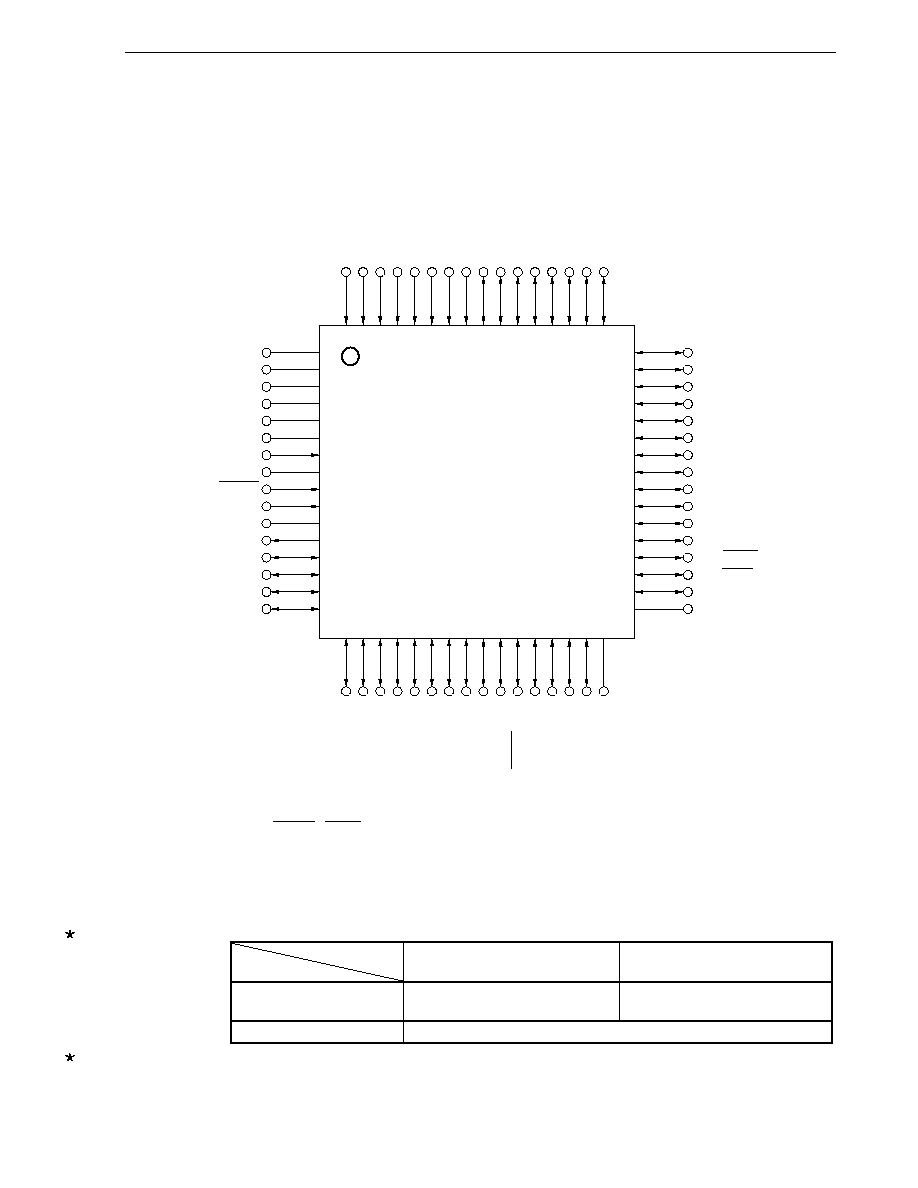
CHAPTER 1 OUTLINE
User's Manual U16228EJ2V0UD
27
1.4 Pin Configuration (Top View)
∑
64-pin plastic LQFP (10
◊
10)
∑
64-pin plastic LQFP (14
◊
14)
∑
64-pin plastic TQFP (12
◊
12)
1
2
3
4
5
6
7
8
9
10
11
12
13
14
15
16
48
47
46
45
44
43
42
41
40
39
38
37
36
35
34
33
P20/ANI0
P21/ANI1
P22/ANI2
P23/ANI3
P24/ANI4
P25/ANI5
P26/ANI6
P27/ANI7
P70/KR0
P71/KR1
P72/KR2
P73/KR3
P74/KR4
P75/KR5
P76/KR6
P77/KR7
P30/INTP1
P140/PCL/INTP6
P141/BUZ/INTP7
P17/TI50/TO50
P16/TOH1/INTP5
P15/TOH0
P14/RxD6
P13/TxD6
P12/SO10
P11/SI10/RxD0
P10/SCK10/TxD0
P60
P61
P62
P63
EV
SS
P40
P41
P42
P43
P50
P51
P52
P53
P00/TI000
P01/TI010/TO00
P02/SO11
Note
P03/SI11
Note
P04/SCK11
Note
P05/SSI11
Note
/TI001
Note
P06/TI011
Note
/TO01
Note
EV
DD
AV
REF
AV
SS
IC (V
PP
)
V
DD
REGC
V
SS
X1
X2
RESET
XT1
XT2
P130
P120/INTP0
P33/TI51/TO51/INTP4
P32/INTP3
P31/INTP2
64 63 62 61 60 59 58 57 56 55 54 53 52 51 50 49
17 18 19 20 21 22 23 24 25 26 27 28 29 30 31 32
Note SO11, SI11, SCK11, SSI11, TI001, TI011, and TO01 are available only in the
µ
PD780133, 780134,
78F0134, 780136, 780138, and 78F0138.
Cautions 1. Connect the IC (Internally Connected) pin directly to V
SS
.
2. Connect the AV
SS
pin to V
SS
.
3. Connect the REGC pin as follows.
Standard Product and (A) Grade
Product
(A1) Grade Product and (A2) Grade
Product
When regulator is used
Connect to V
SS
via a capacitor
(1
µ
F: recommended)
-
(Regulator cannot be used.)
When regulator is not used
Connect directly to V
DD
4. Connect the V
PP
pin to EV
SS
or V
SS
during normal operation.
Remark Figures in parentheses apply to the
µ
PD78F0134 and 78F0138.

CHAPTER 1 OUTLINE
User's Manual U16228EJ2V0UD
28
Pin Identification
ANI0 to ANI7:
Analog input
AV
REF
:
Analog reference voltage
AV
SS
: Analog
ground
BUZ: Buzzer
output
EV
DD
:
Power supply for port
EV
SS
:
Ground for port
IC: Internally
connected
INTP0 to INTP7: External interrupt input
KR0 to KR7:
Key return
P00 to P06:
Port 0
P10 to P17:
Port 1
P20 to P27:
Port 2
P30 to P33:
Port 3
P40 to P43:
Port 4
P50 to P53:
Port 5
P60 to P63:
Port 6
P70 to P77:
Port 7
P120: Port
12
P130: Port
13
P140, P141:
Port 14
PCL:
Programmable clock output
REGC: Regulator
capacitance
RESET: Reset
RxD0, RxD6:
Receive data
SCK10, SCK11
Note
:
Serial clock input/output
SI10, SI11
Note
:
Serial data input
SO10, SO11
Note
:
Serial data output
SSI11
Note
: Serial
interface
chip select input
TI000, TI010,
TI001
Note
, TI011
Note
,
TI50, TI51:
Timer input
TO00, TO01
Note
,
TO50, TO51,
TOH0, TOH1:
Timer output
TxD0, TxD6:
Transmit data
V
DD
: Power
supply
V
PP
: Programming
power
supply
V
SS
: Ground
X1, X2:
Crystal oscillator (X1 input clock)
XT1, XT2:
Crystal oscillator (Subsystem clock)
Note SO11, SI11, SCK11, SSI11, TI001, TI011, and TO01 are available only in the
µ
PD780133, 780134,
78F0134, 780136, 780138, and 78F0138.
CHAPTER 1 OUTLINE
User's Manual U16228EJ2V0UD
29
1.5 K1 Family Lineup
1.5.1 78K0/Kx1 product lineup
PD78F0103
Flash memory: 24 KB, RAM: 768 bytes
Mask ROM: 24 KB, RAM: 768 bytes
Mask ROM: 16 KB, RAM: 768 bytes
Mask ROM: 8 KB, RAM: 512 bytes
PD780103
PD780102
PD780101
78K0/KB1: 30-pin (7.62 mm 0.65 mm pitch)
PD78F0114
Flash memory: 32 KB, RAM: 1 KB
Mask ROM: 32 KB, RAM: 1 KB
Mask ROM: 24 KB, RAM: 1 KB
Mask ROM: 16 KB, RAM: 512 bytes
PD780114
PD780113
PD780112
Mask ROM: 8 KB, RAM: 512 bytes
PD780111
78K0/KC1: 44-pin (10
◊
10 mm 0.8 mm pitch)
PD78F0124
Flash memory: 32 KB, RAM: 1 KB
Mask ROM: 32 KB, RAM: 1 KB
Mask ROM: 24 KB, RAM: 1 KB
Mask ROM: 16 KB, RAM: 512 bytes
PD780124
PD780123
PD780122
Mask ROM: 8 KB, RAM: 512 bytes
PD780121
78K0/KD1: 52-pin (10
◊
10 mm 0.65 mm pitch)
PD78F0148
Flash memory: 60 KB, RAM: 2 KB
Mask ROM: 60 KB, RAM: 2 KB
Mask ROM: 48 KB, RAM: 2 KB
Mask ROM: 32 KB, RAM: 1 KB
PD780148
PD780146
PD780144
Mask ROM: 24 KB, RAM: 1 KB
PD780143
78K0/KF1: 80-pin (12
◊
12 mm 0.5 mm pitch, 14
◊
14 mm 0.65 mm pitch)
PD78F0134
Flash memory: 32 KB, RAM: 1 KB
Mask ROM: 32 KB, RAM: 1 KB
Mask ROM: 24 KB, RAM: 1 KB
Mask ROM: 16 KB, RAM: 512 bytes
PD780134
PD780133
PD780132
Mask ROM: 8 KB, RAM: 512 bytes
PD780131
PD78F0138
Flash memory: 60 KB, RAM: 2 KB
Mask ROM: 60 KB, RAM: 2 KB
Mask ROM: 48 KB, RAM: 2 KB
PD780138
PD780136
78K0/KE1: 64-pin (10
◊
10 mm 0.5 mm pitch, 12
◊
12 mm 0.65 mm pitch, 14
◊
14 mm 0.8 mm pitch)
µ
µ
µ
µ
µ
µ
µ
µ
µ
µ
µ
µ
µ
µ
µ
µ
µ
µ
µ
µ
µ
µ
µ
µ
µ
µ
µ
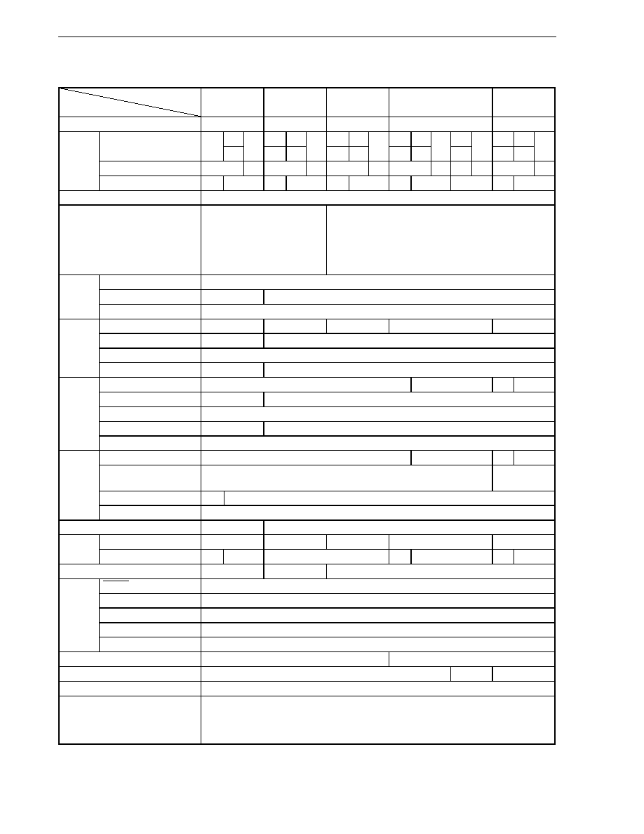
CHAPTER 1 OUTLINE
User's Manual U16228EJ2V0UD
30
The list of functions in the 78K0/Kx1 is shown below.
Part Number
Item
78K0/KB1 78K0/KC1 78K0/KD1
78K0/KE1
78K0/KF1
Package
30 pins
44 pins
52 pins
64 pins
80 pins
16 K
8 K 24 K
8 K 24 K
8 K 24 K
48 K
24 K 48 K
Mask ROM
8 K
24 K
-
16 K 32 K
-
16 K 32 K
-
16 K 32 K
-
60 K
-
32 K 60 K
-
Flash memory
-
24 K
-
32 K
-
32 K
-
32 K
-
60 K
-
60 K
Internal
memory
(bytes)
RAM
512
768
512
1 K
512
1 K
512
1 K
2 K
1 K
2 K
Power supply voltage
V
DD
= 2.7 to 5.5 V
Minimum instruction execution time
0.2
µ
s (when 10 MHz, V
DD
=
4.0 to 5.5 V)
0.24
µ
s (when 8.38 MHz, V
DD
=
3.3 to 5.5 V)
0.4
µ
s (when 5 MHz, V
DD
= 2.7
to 5.5 V)
<Connect REGC pin to V
DD
>
0.2
µ
s (when 10 MHz, V
DD
= 4.0 to 5.5 V)
0.24
µ
s (when 8.38 MHz, V
DD
= 3.3 to 5.5 V)
0.4
µ
s (when 5 MHz, V
DD
= 2.7 to 5.5 V)
X1 input
2 to 10 MHz
Sub
-
32.768 kHz
Clock
Ring-OSC 240
kHz
(TYP.)
CMOS I/O
17
19
26
38
54
CMOS input
4
8
CMOS output
1
Port
N-ch open-drain I/O
-
4
16 bits (TM0)
1 ch
2 ch
1 ch
2 ch
8 bits (TM5)
1 ch
2 ch
8 bits (TMH)
2 ch
For watch
-
1 ch
Timer
WDT 1
ch
3-wire CSI
Note
1 ch
2 ch
1 ch
2 ch
Automatic transmit/
receive 3-wire CSI
-
1 ch
UART
Note
-
1 ch
Serial
interface
UART supporting LIN-bus
1 ch
10-bit A/D converter
4 ch
8 ch
External 6
7
8
9
9
Interrupt
Internal 11
12
15
16
19
17
20
Key return input
-
4 ch
8 ch
RESET pin
Provided
POC 2.85
V
±
0.15 V/3.5 V
±
0.20 V (selectable by mask option)
LVI
3.1 V/3.3 V
±
0.15 V/3.5 V/3.7 V/3.9 V/4.1 V/4.3 V
±
0.2 V (selectable by software)
Clock monitor
Provided
Reset
WDT Provided
Multiplier/divider
-
16 bits
◊
16 bits, 32 bits
˜
16 bits
ROM correction
-
Provided
-
Standby function
HALT/STOP mode
Operating ambient temperature
Standard products, special (A) products:
-
40 to +85
∞
C
Special (A1) products:
-
40 to +110
∞
C (mask ROM version),
-
40 to +105
∞
C (flash memory version)
Special (A2) products:
-
40 to +125
∞
C (mask ROM version)
Note Select either of the functions of these alternate-function pins.
CHAPTER 1 OUTLINE
User's Manual U16228EJ2V0UD
31
1.5.2 V850ES/Kx1 product lineup
144-pin plastic LQFP (fine pitch) (20
◊
20)
PD703217Y
PD703217
Mask ROM: 128 KB, RAM: 6 KB
I
2
C products
PD703216Y
PD703216
Mask ROM: 96 KB, RAM: 6 KB
I
2
C products
V850ES/KJ1
100-pin plastic LQFP (fine pitch) (14
◊
14)
PD703213Y
PD703213
Mask ROM: 96 KB, RAM: 4 KB
I
2
C products
PD703212Y
PD703212
Mask ROM: 64 KB, RAM: 4 KB
I
2
C products
V850ES/KG1
80-pin plastic QFP (14
◊
14)
80-pin plastic TQFP (fine pitch) (12
◊
12)
PD703209Y
PD703209
Mask ROM: 96 KB, RAM: 4 KB
I
2
C products
PD703208Y
PD703208
Mask ROM: 64 KB, RAM: 4 KB
I
2
C products
V850ES/KF1
PD70F3217Y
PD70F3217
Flash memory: 128 KB, RAM: 6 KB
I
2
C products
PD70F3214Y
PD70F3214
Flash memory: 128 KB, RAM: 6 KB
I
2
C products
PD703214Y
PD703214
Mask ROM: 128 KB, RAM: 6 KB
I
2
C products
PD70F3210Y
PD70F3210
Flash memory: 128 KB, RAM: 6 KB
I
2
C products
PD703210Y
PD703210
Mask ROM: 128 KB, RAM: 6 KB
I
2
C products
µ
µ
µ
µ
µ
µ
µ
µ
µ
µ
µ
µ
µ
µ
µ
µ
µ
µ
µ
µ
µ
µ
CHAPTER 1 OUTLINE
User's Manual U16228EJ2V0UD
32
The list of functions in the V850ES/Kx1 is shown below.
Timer Serial
Interface
Function
Part No.
8-Bit 16-Bit TMH Watch WDT
CSI CSIA UART
I
2
C
A/D D/A RTO I/O Other
µ
PD703208
≠
µ
PD703208Y
1 ch
µ
PD703209
≠
µ
PD703209Y
1 ch
µ
PD703210
≠
µ
PD703210Y
1 ch
µ
PD70F3210
≠
V850ES/KF1
µ
PD70F3210Y
2 ch 2 ch 2 ch 1 ch 2 ch
2 ch
1 ch
2 ch
1 ch
8 ch
≠
6 ch
67
≠
µ
PD703212
≠
µ
PD703212Y
1 ch
µ
PD703213
≠
µ
PD703213Y
1 ch
µ
PD703214
≠
µ
PD703214Y
1 ch
µ
PD70F3214
≠
V850ES/KG
1
µ
PD70F3214Y
2 ch 4 ch 2 ch 1 ch 2 ch
2 ch
2 ch
2 ch
1 ch
8 ch
2 ch
6 ch
84
≠
µ
PD703216
≠
µ
PD703216Y
2 ch
µ
PD703217
≠
µ
PD703217Y
2 ch
µ
PD70F3217
≠
V850ES/KJ
1
µ
PD70F3217Y
2 ch 6 ch 2 ch 1 ch 2 ch
3 ch
2 ch
3 ch
2 ch
16 ch
2 ch
12 ch
128
≠
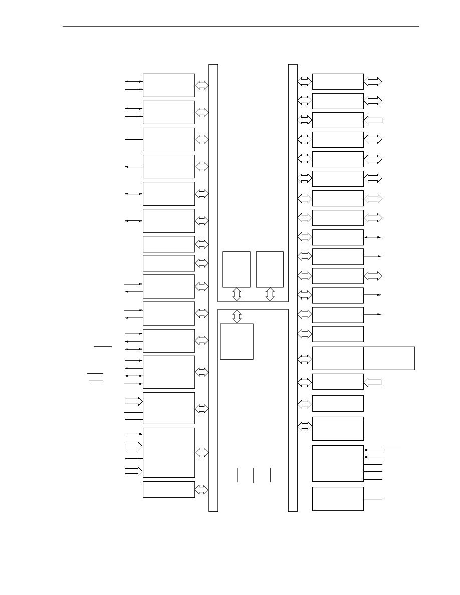
CHAPTER 1 OUTLINE
User's Manual U16228EJ2V0UD
33
1.6 Block Diagram
16-bit timer/
event counter 00
TO00/TI010/P01
TI000/P00
Port 0
P00 to P06
7
Port 1
P10 to P17
Port 2
P20 to P27
8
Port 3
P30 to P33
4
Port 4
Port 5
78K/0
CPU
core
Internal
high-speed
RAM
ROM
(Flash
memory)
V
SS
,
EV
SS
IC
(V
PP
)
V
DD
,
EV
DD
Serial
interface CSI10
SI10/P11
SO10/P12
SCK10/P10
ANI0/P20 to
ANI7/P27
Interrupt control
8-bit timer H0
TOH0/P15
8-bit timer H1
TOH1/P16
TI50/TO50/P17
8-bit timer/
event counter 50
8
A/D converter
RxD0/P11
TxD0/P10
Serial
interface UART0
Watchdog timer
RxD6/P14
TxD6/P13
Serial
interface UART6
AV
REF
AV
SS
INTP1/P30 to
INTP4/P33
4
INTP0/P120
8
System control
RESET
X1
X2
Clock monitor
Power on clear/
low voltage
indicator
Reset control
Port 6
P60 to P63
4
Port 7
P70 to P77
Port 12
P120
Port 13
P130
8
P40 to P43
4
P50 to P53
4
Port 14
P140, P141
2
Ring-OSC
XT1
XT2
16-bit timer/
Note
event counter 01
TO01
Note
/TI011
Note
/P06
TI001
Note
/P05
TI51/TO51/P33
8-bit timer/
event counter 51
Watch timer
Serial
interface CSI11
Note
SI11
Note
/P03
SO11
Note
/P02
SCK11
Note
/P04
SSI11
Note
/P05
INTP5/P16
INTP6/P140,
INTP7/P141
2
Buzzer output
BUZ/P141
Clock output control
PCL/P140
Key return
8
KR0/P70 to
KR7/P77
Multiplier & divider
Voltage regulator
REGC
POC/LVI
control
Note
µ
PD780133, 780134, 78F0134, 780136, 780138, and 78F0138 only.
Remark Items in parentheses are available in the
µ
PD78F0134 and 78F0138.
CHAPTER 1 OUTLINE
User's Manual U16228EJ2V0UD
34
1.7 Outline of Functions
(1/2)
Item
µ
PD780131
µ
PD780132
µ
PD780133
µ
PD780134
µ
PD78F0134
µ
PD780136
µ
PD780138
µ
PD78F0138
Mask ROM
8 K
16 K
24 K
32 K
-
48 K
60 K
-
Flash memory
-
32 K
Note
-
60 K
Note
High-speed RAM
512
1 K
1 K
Note
1 K
1 K
Note
Internal
memory
(bytes)
Expansion RAM
-
1 K
1 K
Note
Memory space
64 KB
X1 input clock (oscillation
frequency)
Ceramic/crystal/external clock oscillation
Standard products,
(A) grade products
REGC pin is connected directly to V
DD
:
10 MHz (V
DD
= 4.0 to 5.5 V), 8.38 MHz (V
DD
= 3.3
to 5.5 V), 5 MHz (V
DD
= 2.7 to 5.5 V)
1
µ
F capacitor is connected to REGC pin: 8.38 MHz (V
DD
= 4.0 to 5.5 V)
(A1) grade products
REGC pin is connected directly to V
DD
:
10 MHz (V
DD
= 4.0 to 5.5 V), 8.38 MHz (V
DD
= 4.0
to 5.5 V), 5 MHz (V
DD
= 3.3 to 5.5 V)
(A2) grade products
REGC pin is connected directly to V
DD
:
8.38 MHz (V
DD
= 4.0 to 5.5 V), 5 MHz (V
DD
= 3.3
to 5.5 V)
Ring-OSC clock
(oscillation frequency)
On-chip Ring oscillation (240 kHz (TYP.))
Subsystem clock
(oscillation frequency)
Crystal/external clock oscillation (32.768 kHz)
General-purpose registers
8 bits
◊
32 registers (8 bits
◊
8 registers
◊
4 banks)
0.2
µ
s/0.4
µ
s/0.8
µ
s/1.6
µ
s/3.2
µ
s (X1 input clock: @ f
XP
= 10 MHz operation)
8.3
µ
s/16.6
µ
s/33.2
µ
s/66.4
µ
s/132.8
µ
s (TYP.) (Ring-OSC clock: @ f
R
= 240 kHz (TYP.)
operation)
Minimum instruction execution
time
122
µ
s (subsystem clock: when operating at f
XT
= 32.768 kHz)
Instruction set
∑ 16-bit operation
∑ Multiply/divide (8 bits
◊
8 bits, 16 bits
˜
8 bits)
∑ Bit manipulate (set, reset, test, and Boolean operation) ∑ BCD adjust, etc.
I/O ports
Total: 51
CMOS I/O
38
CMOS input
8
CMOS output
1
N-ch open-drain I/O
4
Timers
∑ 16-bit timer/event counter: 2 channels (1 channel only in the
µ
PD780131, 780132)
∑ 8-bit timer/event counter: 2 channels
∑ 8-bit timer:
2 channels
∑ Watch timer
1 channel
∑ Watchdog timer:
1 channel
Timer outputs
5 (PWM output: 3)
6 (PWM output: 3)
Clock output
∑ 78.125 kHz, 156.25 kHz, 312.5 kHz, 625 kHz, 1.25 MHz, 2.5 MHz, 5 MHz, 10 MHz
(X1 input clock: 10 MHz)
∑ 32.768 kHz (subsystem clock: 32.768 kHz)
Buzzer output
1.22 kHz, 2.44 kHz, 4.88 kHz, 9.77 kHz (X1 input clock: 10 MHz)
A/D converter
10-bit resolution
◊
8 channels
Note The internal flash memory capacity, internal high-speed RAM capacity, and internal expansion RAM capacity
can be changed using the internal memory size switching register (IMS) and the internal expansion RAM size
switching register (IXS).
CHAPTER 1 OUTLINE
User's Manual U16228EJ2V0UD
35
(2/2)
Item
µ
PD780131
µ
PD780132
µ
PD780133
µ
PD780134
µ
PD78F0134
µ
PD780136
µ
PD780138
µ
PD78F0138
Serial interface
∑ UART mode supporting LIN-bus:
1 channel
∑ 3-wire serial I/O mode:
1 channel (none in the
µ
PD780131, 780132)
∑ 3-wire serial I/O mode/UART mode
Note
: 1 channel
Multiplier/divider
∑ 16 bits
◊
16 bits = 32 bits (multiplication)
∑ 32 bits
˜
16 bits = 32 bits remainder of 16 bits (division)
Internal 16
19
Vectored interrupt
sources
External 9
Key interrupt
Key interrupt (INTKR) occurs by detecting falling edge of key input pins (KR0 to KR7).
Reset
∑ Reset using RESET pin
∑ Internal reset by watchdog timer
∑ Internal reset by clock monitor
∑ Internal reset by power-on-clear
∑ Internal reset by low-voltage detector
ROM correction
-
Provided
Supply voltage
Standard products, (A) grade products: V
DD
= 2.7 to 5.5 V
(A1) grade products, (A2) grade products: V
DD
= 3.3 to 5.5 V
Operating ambient temperature
∑
Standard products, (A) grade products: T
A
=
-
40 to +85
∞
C
∑
(A1) grade products: T
A
=
-
40 to +110
∞
C (mask ROM versions),
-
40 to +105
∞
C (flash memory versions)
∑
(A2) grade products: T
A
=
-
40 to +125
∞
C (mask ROM versions)
Package
∑ 64-pin plastic LQFP (10
◊
10)
∑ 64-pin plastic LQFP (14
◊
14)
∑ 64-pin plastic TQFP (12
◊
12)
Note Select either of the functions of these alternate-function pins.
An outline of the timer is shown below.
16-Bit Timer/
Event Counters 00
and 01
Note 1
8-Bit Timer/
Event Counters
50 and 51
8-Bit Timers H0 and
H1
TM00 TM01
Note 1
TM50 TM51 TMH0 TMH1
Watch
Timer
Watchdog
Timer
Interval timer
1 channel 1 channel 1 channel 1 channel 1 channel 1 channel
Note 2
1 channel 1 channel
Operation
mode
External event counter
1 channel 1 channel 1 channel 1 channel
-
-
-
-
Timer output
1 output
1 output
1 output
1 output
1 output
1 output
-
-
PPG output
1 output
1 output
-
-
-
-
-
-
PWM output
-
-
1 output
1 output
1 output
1 output
-
-
Pulse width measurement
2 inputs
2 inputs
-
-
-
-
-
-
Square-wave output
1 output
1 output
1 output
1 output
1 output
1 output
-
-
Function
Interrupt
source
2 2 1 1 1 1 1
-
Notes 1. 16-bit timer/event counter 01 is available only in the
µ
PD780133, 780134, 78F0134, 780136, 780138, and
78F0138.
2. In the watch timer, the watch timer function and interval timer function can be used simultaneously.
Remark TM51 and TMH1 can be used in combination as a carrier generator mode.
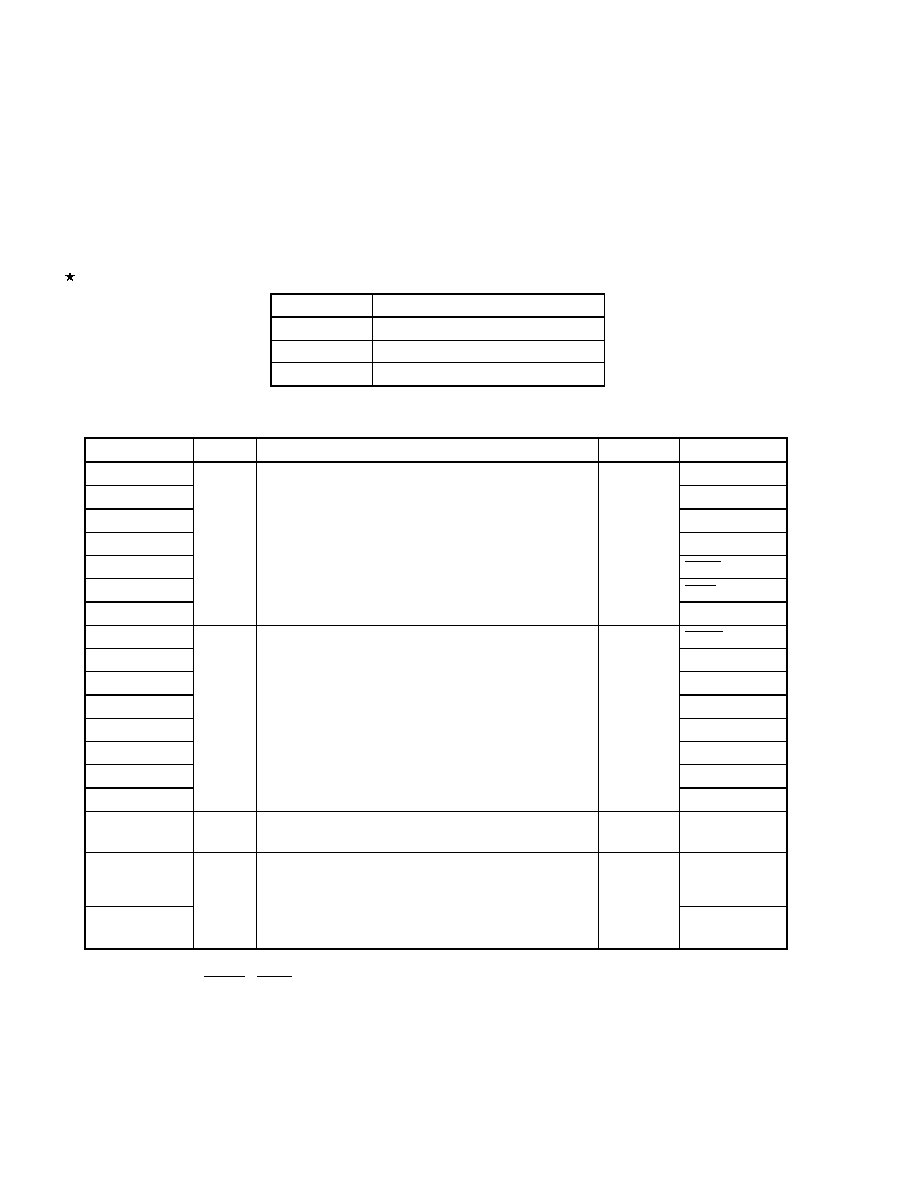
User's Manual U16228EJ2V0UD
36
CHAPTER 2 PIN FUNCTIONS
2.1 Pin Function List
There are three types of pin I/O buffer power supplies: AV
REF
, EV
DD
, and V
DD
. The relationship between these
power supplies and the pins is shown below.
Table 2-1. Pin I/O Buffer Power Supplies
Power Supply
Corresponding Pins
AV
REF
P20 to P27
EV
DD
Port pins other than P20 to P27
V
DD
Pins other than port pins
(1) Port pins (1/2)
Pin Name
I/O
Function
After Reset
Alternate Function
P00
TI000
P01
TI010/TO00
P02
SO11
Note
P03
SI11
Note
P04
SCK11
Note
P05
SSI11
Note
/TI001
Note
P06
I/O
Port 0.
7-bit I/O port.
Input/output can be specified in 1-bit units.
Use of an on-chip pull-up resistor can be specified by a
software setting.
Input
TI011
Note
/TO01
Note
P10
SCK10/TxD0
P11
SI10/RxD0
P12
SO10
P13
TxD6
P14
RxD6
P15
TOH0
P16
TOH1/INTP5
P17
I/O
Port 1.
8-bit I/O port.
Input/output can be specified in 1-bit units.
Use of an on-chip pull-up resistor can be specified by a
software setting.
Input
TI50/TO50
P20 to P27
Input
Port 2.
8-bit input-only port.
Input
ANI0 to ANI7
P30 to P32
INTP1 to INTP3
P33
I/O
Port 3.
4-bit I/O port.
Input/output can be specified in 1-bit units.
Use of an on-chip pull-up resistor can be specified by a
software setting.
Input
INTP4/TI51/TO51
Note SO11, SI11, SCK11, SSI11, TI001, TI011, and TO01 are available only in the
µ
PD780133, 780134, 78F0134,
780136, 780138, and 78F0138.

CHAPTER 2 PIN FUNCTIONS
User's Manual U16228EJ2V0UD
37
(1) Port pins (2/2)
Pin Name
I/O
Function
After Reset
Alternate Function
P40 to P43
I/O
Port 4.
4-bit I/O port.
Input/output can be specified in 1-bit units.
Use of an on-chip pull-up resistor can be specified by a
software setting.
Input
-
P50 to P53
I/O
Port 5.
4-bit I/O port.
Input/output can be specified in 1-bit units.
Use of an on-chip pull-up resistor can be specified by a
software setting.
Input
-
P60 to P63
I/O
Port 6.
4-bit I/O port (N-ch open drain).
Input/output can be specified in 1-bit units.
Use of an on-chip pull-up resistor can be specified by a mask
option only for mask ROM versions.
Input
-
P70 to P77
I/O
Port 7.
8-bit I/O port.
Input/output can be specified in 1-bit units.
Use of an on-chip pull-up resistor can be specified by a
software setting.
Input
KR0 to KR7
P120 I/O
Port 12.
1-bit I/O port.
Use of an on-chip pull-up resistor can be specified by a
software setting.
Input INTP0
P130 Output
Port 13.
1-bit output-only port.
Output
-
P140
PCL/INTP6
P141
I/O
Port 14.
2-bit I/O port.
Input/output can be specified in 1-bit units.
Use of an on-chip pull-up resistor can be specified by a
software setting.
Input
BUZ/INTP7
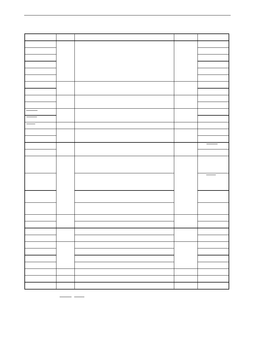
CHAPTER 2 PIN FUNCTIONS
User's Manual U16228EJ2V0UD
38
(2) Non-port
pins
(1/2)
Pin Name
I/O
Function
After Reset
Alternate Function
INTP0
P120
INTP1 to INTP3
P30 to P32
INTP4
P33/TI51/TO51
INTP5
P16/TOH1
INTP6
P140/PCL
INTP7
Input
External interrupt request input for which the valid edge (rising
edge, falling edge, or both rising and falling edges) can be
specified
Input
P141/BUZ
SI10
P11/RxD0
SI11
Note
Input
Serial data input to serial interface
Input
P03
SO10
P12
SO11
Note
Output
Serial data output from serial interface
Input
P02
SCK10
P10/TxD0
SCK11
Note
I/O
Clock input/output for serial interface
Input
P04
SSI11
Note
Input
Serial interface chip select input
Input
P05/TI001
RxD0
P11/SI10
RxD6
Input
Serial data input to asynchronous serial interface
Input
P14
TxD0
P10/SCK10
TxD6
Output
Serial data output from asynchronous serial interface
Input
P13
TI000
External count clock input to 16-bit timer/event counter 00
Capture trigger input to capture registers (CR000, CR010) of
16-bit timer/event counter 00
P00
TI001
Note
External count clock input to 16-bit timer/event counter 01
Capture trigger input to capture registers (CR001, CR011) of
16-bit timer/event counter 01
P05/SSI11
Note
TI010
Capture trigger input to capture register (CR000) of 16-bit
timer/event counter 00
P01/TO00
TI011
Note
Input
Capture trigger input to capture register (CR001) of 16-bit
timer/event counter 01
Input
P06/TO01
Note
TO00
16-bit timer/event counter 00 output
P01/TI010
TO01
Note
Output
16-bit timer/event counter 01 output
Input
P06/TI011
Note
TI50
External count clock input to 8-bit timer/event counter 50
P17/TO50
TI51
Input
External count clock input to 8-bit timer/event counter 51
Input
P33/TO51/INTP4
TO50
8-bit timer/event counter 50 output
P17/TI50
TO51
8-bit timer/event counter 51 output
P33/TI51/INTP4
TOH0
8-bit timer H0 output
P15
TOH1
Output
8-bit timer H1 output
Input
P16/INTP5
PCL
Output
Clock output (for trimming of X1 input clock, subsystem clock)
Input
P140/INTP6
BUZ Output
Buzzer
output
Input
P141/INTP7
ANI0 to ANI7
Input
A/D converter analog input
Input
P20 to P27
Note SO11, SI11, SCK11, SSI11, TI001, TI011, and TO01 are available only in the
µ
PD780133, 780134, 78F0134,
780136, 780138, and 78F0138.

CHAPTER 2 PIN FUNCTIONS
User's Manual U16228EJ2V0UD
39
(2) Non-port
pins
(2/2)
Pin Name
I/O
Function
After Reset
Alternate Function
AV
REF
Input
A/D converter reference voltage input and positive power
supply for port 2
-
-
AV
SS
-
A/D converter ground potential. Make the same potential as
EV
SS
or V
SS
.
-
-
KR0 to KR7
Input
Key interrupt input
Input
P70 to P77
REGC
-
Connecting regulator output stabilization capacitor. When
using the regulator, connect to V
SS
via a capacitor (1
µ
F:
recommended). When the regulator is not used, connect
directly to V
DD
.
-
-
RESET
Input
System reset input
-
-
X1 Input
-
-
X2
-
Connecting resonator for X1 input clock
-
-
XT1 Input
-
-
XT2
-
Connecting resonator for subsystem clock
-
-
V
DD
-
Positive power supply (except for ports)
-
-
EV
DD
-
Positive power supply for ports
-
-
V
SS
-
Ground potential (except for ports)
-
-
EV
SS
-
Ground potential for ports
-
-
IC
-
Internally connected. Connect directly to EV
SS
or V
SS
.
-
-
V
PP
-
Flash memory programming mode setting. High-voltage
application for program write/verify. Connect to EV
SS
or V
SS
in
normal operation mode.
-
-

CHAPTER 2 PIN FUNCTIONS
User's Manual U16228EJ2V0UD
40
2.2 Description of Pin Functions
2.2.1 P00 to P06 (port 0)
P00 to P06 function as a 7-bit I/O port. These pins also function as timer I/O, serial interface data I/O, clock I/O,
and chip select input.
The following operation modes can be specified in 1-bit units.
(1) Port
mode
P00 to P06 function as a 7-bit I/O port. P00 to P06 can be set to input or output in 1-bit units using port mode
register 0 (PM0). Use of an on-chip pull-up resistor can be specified by pull-up resistor option register 0 (PU0).
(2) Control
mode
P00 to P06 function as timer I/O, serial interface data I/O, clock I/O, and chip select input.
(a) TI000,
TI001
Note
These are the pins for inputting an external count clock to 16-bit timer/event counters 00 and 01 and are also
for inputting a capture trigger signal to the capture registers (CR000, CR010 or CR001, CR011) of 16-bit
timer/event counters 00 and 01.
(b) TI010, TI011
Note
These are the pins for inputting a capture trigger signal to the capture register (CR000 or CR001) of 16-bit
timer/event counters 00 and 01.
(c) TO00,
TO01
Note
These are timer output pins.
(d) SI11
Note
This is a serial interface serial data input pin.
(e) SO11
Note
This is a serial interface serial data output pin.
(f) SCK11
Note
This is the serial interface serial clock I/O pin.
(g) SSI11
Note
This is the serial interface chip select input pin.
Note SO11, SI11, SCK11, SSI11, TI001, TI011, and TO01 are available only in the
µ
PD780133, 780134,
78F0134, 780136, 780138, and 78F0138.

CHAPTER 2 PIN FUNCTIONS
User's Manual U16228EJ2V0UD
41
2.2.2 P10 to P17 (port 1)
P10 to P17 function as an 8-bit I/O port. These pins also function as pins for external interrupt request input, serial
interface data I/O, clock I/O, and timer I/O.
The following operation modes can be specified in 1-bit units.
(1) Port
mode
P10 to P17 function as an 8-bit I/O port. P10 to P17 can be set to input or output in 1-bit units using port mode
register 1 (PM1). Use of an on-chip pull-up resistor can be specified by pull-up resistor option register 1 (PU1).
(2) Control
mode
P10 to P17 function as external interrupt request input, serial interface data I/O, clock I/O, and timer I/O.
(a) SI10
This is a serial interface serial data input pin.
(b) SO10
This is a serial interface serial data output pin.
(c) SCK10
This is a serial interface serial clock I/O pin.
(d) RxD0, RxD6
These are the serial data input pins of the asynchronous serial interface.
(e) TxD0,
TxD6
These are the serial data output pins of the asynchronous serial interface.
(f) TI50
This is the pin for inputting an external count clock to 8-bit timer/event counter 50.
(g) TO50, TOH0, and TOH1
These are timer output pins.
(h) INTP5
This is an external interrupt request input pin for which the valid edge (rising edge, falling edge, or both rising
and falling edges) can be specified.
2.2.3 P20 to P27 (port 2)
P20 to P27 function as an 8-bit input-only port. These pins also function as pins for A/D converter analog input.
The following operation modes can be specified in 1-bit units.
(1) Port
mode
P20 to P27 function as an 8-bit input-only port.
(2) Control
mode
P20 to P27 function as A/D converter analog input pins (ANI0 to ANI7). When using these pins as analog input
pins, see (5) ANI0/P20 to ANI7/P27 in 12.6 Cautions for A/D Converter.

CHAPTER 2 PIN FUNCTIONS
User's Manual U16228EJ2V0UD
42
2.2.4 P30 to P33 (port 3)
P30 to P33 function as a 4-bit I/O port. These pins also function as pins for external interrupt request input and
timer I/O.
The following operation modes can be specified in 1-bit units.
(1) Port
mode
P30 to P33 function as a 4-bit I/O port. P30 to P33 can be set to input or output in 1-bit units using port mode
register 3 (PM3). Use of an on-chip pull-up resistor can be specified by pull-up resistor option register 3 (PU3).
(2) Control
mode
P30 to P33 function as external interrupt request input pins and timer I/O pins.
(a) INTP1 to INTP4
These are the external interrupt request input pins for which the valid edge (rising edge, falling edge, or both
rising and falling edges) can be specified.
(b) TI51
This is an external count clock input pin to 8-bit timer/event counter 51.
(c) TO51
This is a timer output pin.
2.2.5 P40 to P43 (port 4)
P40 to P43 function as a 4-bit I/O port. P40 to P43 can be set to input or output in 1-bit units using port mode
register 4 (PM4). Use of an on-chip pull-up resistor can be specified by pull-up resistor option register 4 (PU4).
2.2.6 P50 to P53 (port 5)
P50 to P53 function as a 4-bit I/O port. P50 to P53 can be set to input or output in 1-bit units using port mode
register 5 (PM5). Use of an on-chip pull-up resistor can be specified by pull-up resistor option register 5 (PU5).
2.2.7 P60 to P63 (port 6)
P60 to P63 function as a 4-bit I/O port. P60 to P63 can be set to input port or output port in 1-bit units using port
mode register 6 (PM6).
P60 to P63 are N-ch open-drain pins. Use of an on-chip pull-up resistor can be specified by a mask option only for
mask ROM versions.
2.2.8 P70 to P77 (port 7)
P70 to P77 function as an 8-bit I/O port. These pins also function as key interrupt input pins.
The following operation modes can be specified in 1-bit units.
(1) Port
mode
P70 to P77 function as an 8-bit I/O port. P70 to P77 can be set to input or output in 1-bit units using port mode
register 7 (PM7). Use of an on-chip pull-up resistor can be specified by pull-up resistor option register 7 (PU7).
(2) Control
mode
P70 to P77 function as key interrupt input pins.

CHAPTER 2 PIN FUNCTIONS
User's Manual U16228EJ2V0UD
43
2.2.9 P120 (port 12)
P120 functions as a 1-bit I/O port. This pin also functions as a pin for external interrupt request input.
The following operation modes can be specified.
(1) Port
mode
P120 functions as a 1-bit I/O port. P120 can be set to input or output using port mode register 12 (PM12). Use of
an on-chip pull-up resistor can be specified by pull-up resistor option register 12 (PU12).
(2) Control
mode
P120 functions as an external interrupt request input pin (INTP0) for which the valid edge (rising edge, falling
edge, or both rising and falling edges) can be specified.
2.2.10 P130 (port 13)
P130 functions as a 1-bit output-only port.
2.2.11 P140 and P141 (port 14)
P140 and P141 function as a 2-bit I/O port. These pins also function as external interrupt request input, clock
output, and buzzer output pins.
The following operation modes can be specified in 1-bit units.
(1) Port
mode
P140 and P141 function as a 2-bit I/O port. P140 and P141 can be set to input or output in 1-bit units using port
mode register 14 (PM14). Use of an on-chip pull-up resistor can be specified by pull-up resistor option register 14
(PU14).
(2) Control
mode
P140 and P141 function as external interrupt request input, clock output, and buzzer output pins.
(a) INTP6,
INTP7
These are the external interrupt request input pins for which the valid edge (rising edge, falling edge, or both
rising and falling edges) can be specified.
(b) PCL
This is a clock output pin.
(c) BUZ
This is a buzzer output pin.
2.2.12 AV
REF
This is the A/D converter reference voltage input pin.
When the A/D converter is not used, connect this pin directly to EV
DD
or V
DD
Note
.
Note Connect port 2 directly to EV
DD
when it is used as a digital port.
2.2.13 AV
SS
This is the A/D converter ground potential pin. Even when the A/D converter is not used, always use this pin with
the same potential as the EV
SS
pin or V
SS
pin.

CHAPTER 2 PIN FUNCTIONS
User's Manual U16228EJ2V0UD
44
2.2.14 RESET
This is the active-low system reset input pin.
2.2.15 REGC
This is the pin for connecting the capacitor for the regulator. When using the regulator, connect this pin to V
SS
via a
capacitor (1
µ
F: recommended). When the regulator is not used, connect this pin directly to V
DD
pin.
Caution A regulator cannot be used with (A1) grade products and (A2) grade products. Be sure to
connect the REGC pin of these products directly to V
DD
.
2.2.16 X1 and X2
These are the pins for connecting a resonator for X1 input clock.
When supplying an external clock, input a signal to the X1 pin and input the inverse signal to the X2 pin.
2.2.17 XT1 and XT2
These are the pins for connecting a resonator for subsystem clock.
When supplying an external clock, input a signal to the XT1 pin and input the inverse signal to the XT2 pin.
2.2.18 V
DD
and EV
DD
V
DD
is the positive power supply pin for other than ports.
EV
DD
is the positive power supply pin for ports.
2.2.19 V
SS
and EV
SS
V
SS
is the ground potential pin for other than ports.
EV
SS
is the ground potential pin for ports.
2.2.20 V
PP
(flash memory versions only)
This is a pin for flash memory programming mode setting and high-voltage application for program write/verify.
Connect to EV
SS
or V
SS
in the normal operation mode.
2.2.21 IC (mask ROM versions only)
The IC (Internally Connected) pin is provided to set the test mode to check the 78K0/KE1 at shipment. Connect it
directly to EV
SS
or V
SS
pin with the shortest possible wire in the normal operation mode.
When a potential difference is produced between the IC pin and the EV
SS
or V
SS
pin because the wiring between
these two pins is too long or external noise is input to the IC pin, the user's program may not operate normally.
∑ Connect the IC pin directly to EV
SS
or V
SS
.
As short as possible
IC
EV
SS
or V
SS
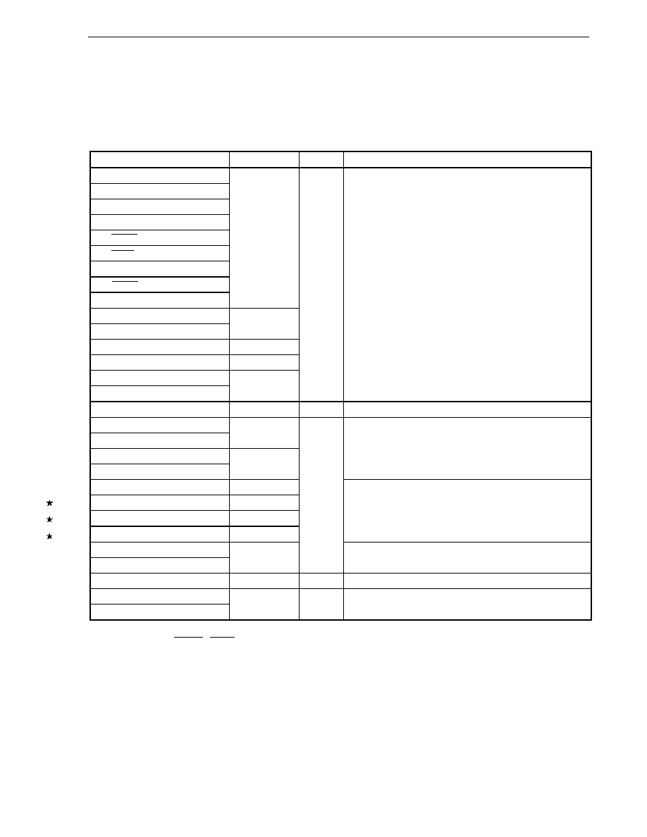
CHAPTER 2 PIN FUNCTIONS
User's Manual U16228EJ2V0UD
45
2.3 Pin I/O Circuits and Recommended Connection of Unused Pins
Table 2-2 shows the types of pin I/O circuits and the recommended connections of unused pins.
Refer to Figure 2-1 for the configuration of the I/O circuit of each type.
Table 2-2. Pin I/O Circuit Types
Pin Name
I/O Circuit Type
I/O
Recommended Connection of Unused Pins
P00/TI000
P01/TI010/TO00
P02/SO11
Note
P03/SI11
Note
P04/SCK11
Note
P05/SSI11
Note
/TI001
Note
P06/TI011
Note
/TO01
Note
P10/SCK10/TxD0
P11/SI10/RxD0
8-A
P12/SO10
P13/TxD6
5-A
P14/RxD6 8-A
P15/TOH0 5-A
P16/TOH1/INTP5
P17/TI50/TO50
8-A
I/O
Input:
Independently connect to EV
DD
or EV
SS
via a resistor.
Output: Leave open.
P20/ANI0 to P27/ANI7
9-C
Input
Connect to EV
DD
or EV
SS
.
P30/INTP1 to P32/INTP3
P33/TI51/TO51/INTP4
8-A
P40 to P43
P50 to P53
5-A
Input:
Independently connect to EV
DD
or EV
SS
via a resistor.
Output: Leave open.
P60, P61 (Mask ROM version)
13-S
P60, P61 (Flash memory version)
13-R
P62, P63 (Mask ROM version)
13-V
P62, P63 (Flash memory version)
13-W
Input:
Connect to EV
SS
.
Output: Leave this pin open at low-level output after clearing
the output latch of the port to 0.
P70/KR0 to P77/KR7
P120/INTP0
8-A
I/O
Input:
Independently connect to EV
DD
or EV
SS
via a resistor.
Output: Leave open.
P130 3-C
Output
Leave
open.
P140/PCL/INTP6
P141/BUZ/INTP7
8-A
I/O
Input:
Independently connect to EV
DD
or EV
SS
via a resistor.
Output: Leave open.
Note SO11, SI11, SCK11, SSI11, TI001, TI011, and TO01 are available only in the
µ
PD780133, 780134, 78F0134,
780136, 780138, and 78F0138.
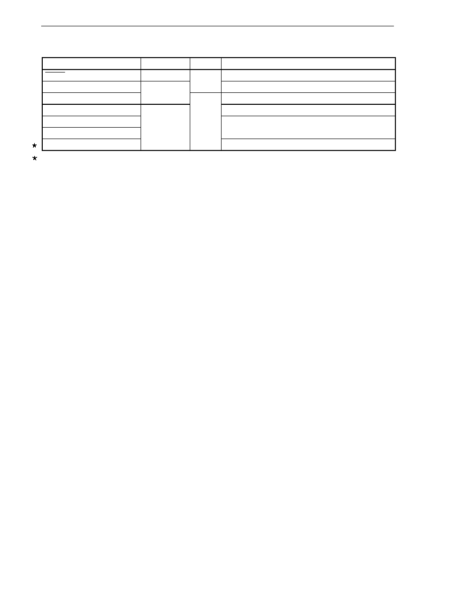
CHAPTER 2 PIN FUNCTIONS
User's Manual U16228EJ2V0UD
46
Table 2-2. Pin I/O Circuit Types (2/2)
Note Connect port 2 directly to EV
DD
when it is used as a digital port.
Pin Name
I/O Circuit Type
I/O
Recommended Connection of Unused Pins
RESET 2
-
XT1
Input
Connect directly to EV
DD
or V
DD
.
XT2
16
Leave open.
AV
REF
Connect directly to EV
DD
or V
DD
Note
.
AV
SS
IC
Connect directly to EV
SS
or V
SS
.
V
PP
-
-
Connect to EV
SS
or V
SS
.
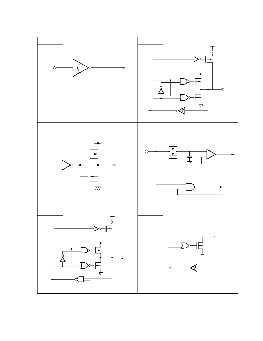
CHAPTER 2 PIN FUNCTIONS
User's Manual U16228EJ2V0UD
47
Figure 2-1. Pin I/O Circuit List (1/2)
Type 3-C
Type 2
Type 8-A
Type 5-A
Type 9-C
Schmitt-triggered input with hysteresis characteristics
IN
Pullup
enable
Data
Output
disable
EV
DD
P-ch
V
DD
P-ch
IN/OUT
N-ch
EV
DD
P-ch
N-ch
Data
OUT
IN
Comparator
V
REF
(threshold voltage)
AV
SS
P-ch
N-ch
Input
enable
+
≠
Pullup
enable
Data
Output
disable
Input
enable
EV
DD
P-ch
V
DD
P-ch
IN/OUT
N-ch
Data
Output disable
IN/OUT
N-ch
Type 13-R
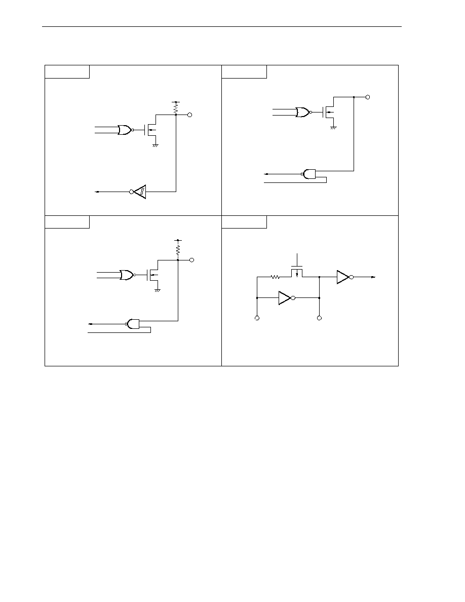
CHAPTER 2 PIN FUNCTIONS
User's Manual U16228EJ2V0UD
48
Figure 2-1. Pin I/O Circuit List (2/2)
Type 13-V
Type 13-S
Type 13-W
Type 16
Data
Output disable
IN/OUT
N-ch
EV
DD
Mask
option
Data
Output disable
IN/OUT
N-ch
Input
enable
Middle-voltage input buffer
Data
Output disable
IN/OUT
N-ch
EV
DD
Mask
option
Input
enable
Middle-voltage input buffer
P-ch
Feedback
cut-off
XT1
XT2

User's Manual U16228EJ2V0UD
49
CHAPTER 3 CPU ARCHITECTURE
3.1 Memory Space
Products in the 78K0/KE1 can each access a 64 KB memory space. Figures 3-1 to 3-8 show the memory maps.
Caution Regardless of the internal memory capacity, the initial values of the internal memory size
switching register (IMS) and internal expansion RAM size switching register (IXS) of all products
in the 78K0/KE1 are fixed (IMS = CFH, IXS = 0CH). Therefore, set the value corresponding to
each product as indicated below.
Table 3-1. Set Values of Internal Memory Size Switching Register (IMS)
and Internal Expansion RAM Size Switching Register (IXS)
IMS
IXS
µ
PD780131 42H
µ
PD780132 44H
µ
PD780133 C6H
µ
PD780134 C8H
0CH
µ
PD78F0134
Note
Value corresponding to mask ROM version
µ
PD780136 CCH
µ
PD780138 CFH
0AH
µ
PD78F0138
Value corresponding to mask ROM version
Note The
µ
PD78F0134 does not support the
µ
PD780136 and 780138.

CHAPTER 3 CPU ARCHITECTURE
User's Manual U16228EJ2V0UD
50
Figure 3-1. Memory Map (
µ
PD780131)
Special function registers
(SFR)
256
◊
8 bits
Internal high-speed RAM
512
◊
8 bits
General-purpose
registers
32
◊
8 bits
Reserved
Internal ROM
8192
◊
8 bits
Program
memory space
Data memory
space
Vector table area
H
CALLT table area
Program area
CALLF entry area
Program area
0
0
0
0
H
F
3
0
0
H
0
4
0
0
H
F
7
0
0
H
0
8
0
0
H
F
F
7
0
H
0
0
8
0
H
F
F
F
0
H
0
0
0
1
H
F
F
F
1
H
0
0
0
0
H
F
F
F
1
H
0
0
0
2
H
F
F
C
F
H
0
0
D
F
H
F
D
E
F
H
0
E
E
F
H
F
F
E
F
H
0
0
F
F
H
F
F
F
F

CHAPTER 3 CPU ARCHITECTURE
User's Manual U16228EJ2V0UD
51
Figure 3-2. Memory Map (
µ
PD780132)
Special function registers
(SFR)
256
◊
8 bits
Internal high-speed RAM
512
◊
8 bits
General-purpose
registers
32
◊
8 bits
Reserved
Internal ROM
16384
◊
8 bits
Program
memory space
Data memory
space
Vector table area
H
CALLT table area
Program area
CALLF entry area
Program area
0
0
0
0
H
F
3
0
0
H
0
4
0
0
H
F
7
0
0
H
0
8
0
0
H
F
F
7
0
H
0
0
8
0
H
F
F
F
0
H
0
0
0
1
H
F
F
F
3
H
0
0
0
0
H
F
F
F
3
H
0
0
0
4
H
F
F
C
F
H
0
0
D
F
H
F
D
E
F
H
0
E
E
F
H
F
F
E
F
H
0
0
F
F
H
F
F
F
F
CHAPTER 3 CPU ARCHITECTURE
User's Manual U16228EJ2V0UD
52
Figure 3-3. Memory Map (
µ
PD780133)
Special function registers
(SFR)
256
◊
8 bits
Internal high-speed RAM
1024
◊
8 bits
General-purpose
registers
32
◊
8 bits
Reserved
Internal ROM
24576
◊
8 bits
Program
memory space
Data memory
space
Vector table area
H
CALLT table area
Program area
CALLF entry area
Program area
0
0
0
0
H
F
3
0
0
H
0
4
0
0
H
F
7
0
0
H
0
8
0
0
H
F
F
7
0
H
0
0
8
0
H
F
F
F
0
H
0
0
0
1
H
F
F
F
5
H
0
0
0
0
H
F
F
F
5
H
0
0
0
6
H
F
F
A
F
H
0
0
B
F
H
F
D
E
F
H
0
E
E
F
H
F
F
E
F
H
0
0
F
F
H
F
F
F
F
CHAPTER 3 CPU ARCHITECTURE
User's Manual U16228EJ2V0UD
53
Figure 3-4. Memory Map (
µ
PD780134)
Special function registers
(SFR)
256
◊
8 bits
Internal high-speed RAM
1024
◊
8 bits
General-purpose
registers
32
◊
8 bits
Reserved
Internal ROM
32768
◊
8 bits
Program
memory space
Data memory
space
Vector table area
H
CALLT table area
Program area
CALLF entry area
Program area
0
0
0
0
H
F
3
0
0
H
0
4
0
0
H
F
7
0
0
H
0
8
0
0
H
F
F
7
0
H
0
0
8
0
H
F
F
F
0
H
0
0
0
1
H
F
F
F
7
H
0
0
0
0
H
F
F
F
7
H
0
0
0
8
H
F
F
A
F
H
0
0
B
F
H
F
D
E
F
H
0
E
E
F
H
F
F
E
F
H
0
0
F
F
H
F
F
F
F

CHAPTER 3 CPU ARCHITECTURE
User's Manual U16228EJ2V0UD
54
Figure 3-5. Memory Map (
µ
PD78F0134)
Special function registers
(SFR)
256
◊
8 bits
Internal high-speed RAM
1024
◊
8 bits
General-purpose
registers
32
◊
8 bits
Reserved
Flash memory
32768
◊
8 bits
Program
memory space
Data memory
space
Vector table area
H
CALLT table area
Program area
CALLF entry area
Program area
0
0
0
0
H
F
3
0
0
H
0
4
0
0
H
F
7
0
0
H
0
8
0
0
H
F
F
7
0
H
0
0
8
0
H
F
F
F
0
H
0
0
0
1
H
F
F
F
7
H
0
0
0
0
H
F
F
F
7
H
0
0
0
8
H
F
F
A
F
H
0
0
B
F
H
F
D
E
F
H
0
E
E
F
H
F
F
E
F
H
0
0
F
F
H
F
F
F
F

CHAPTER 3 CPU ARCHITECTURE
User's Manual U16228EJ2V0UD
55
Figure 3-6. Memory Map (
µ
PD780136)
FFFFH
FF00H
FEFFH
FEE0H
FEDFH
FB00H
FAFFH
F800H
F7FFH
F400H
F3FFH
C000H
BFFFH
0000H
0040H
003FH
0000H
0080H
007FH
0800H
07FFH
1 0 0 0 H
0FFFH
BFFFH
Special function registers
(SFR)
256
◊
8 bits
Internal high-speed RAM
1024
◊
8 bits
General-purpose
registers
32
◊
8 bits
Reserved
Internal ROM
49152
◊
8 bits
Program
memory space
Data memory
space
Vector table area
CALLT table area
Program area
CALLF entry area
Program area
Reserved
Internal expansion RAM
1024
◊
8 bits
CHAPTER 3 CPU ARCHITECTURE
User's Manual U16228EJ2V0UD
56
Figure 3-7. Memory Map (
µ
PD780138)
FFFFH
FF00H
FEFFH
FEE0H
FEDFH
FB00H
FAFFH
F800H
F7FFH
F400H
F3FFH
F000H
EFFFH
0000H
0040H
003FH
0000H
0080H
007FH
0800H
07FFH
1 0 0 0 H
0FFFH
EFFFH
Special function registers
(SFR)
256
◊
8 bits
Internal high-speed RAM
1024
◊
8 bits
General-purpose
registers
32
◊
8 bits
Reserved
Internal ROM
61440
◊
8 bits
Program
memory space
Data memory
space
Vector table area
CALLT table area
Program area
CALLF entry area
Program area
Reserved
Internal expansion RAM
1024
◊
8 bits
CHAPTER 3 CPU ARCHITECTURE
User's Manual U16228EJ2V0UD
57
Figure 3-8. Memory Map (
µ
PD78F0138)
FFFFH
FF00H
FEFFH
FEE0H
FEDFH
FB00H
FAFFH
F800H
F7FFH
F400H
F3FFH
F000H
EFFFH
0000H
0040H
003FH
0000H
0080H
007FH
0800H
07FFH
1 0 0 0 H
0FFFH
EFFFH
Special function registers
(SFR)
256
◊
8 bits
Internal high-speed RAM
1024
◊
8 bits
General-purpose
registers
32
◊
8 bits
Reserved
Flash memory
61440
◊
8 bits
Program
memory space
Data memory
space
Vector table area
CALLT table area
Program area
CALLF entry area
Program area
Reserved
Internal expansion RAM
1024
◊
8 bits
CHAPTER 3 CPU ARCHITECTURE
User's Manual U16228EJ2V0UD
58
3.1.1 Internal program memory space
The internal program memory space stores the program and table data. Normally, it is addressed with the program
counter (PC).
78K0/KE1 products incorporate internal ROM (mask ROM or flash memory), as shown below.
Table 3-2. Internal ROM Capacity
Internal ROM
Part Number
Structure Capacity
µ
PD780131 8192
◊
8 bits (0000H to 1FFFH)
µ
PD780132 16384
◊
8 bits (0000H to 3FFFH)
µ
PD780133 24576
◊
8 bits (0000H to 5FFFH)
µ
PD780134
Mask ROM
µ
PD78F0134 Flash
memory
32768
◊
8 bits (0000H to 7FFFH)
µ
PD780136 49152
◊
8 bits (0000H to BFFFH)
µ
PD780138
Mask ROM
µ
PD78F0138 Flash
memory
61440
◊
8 bits (0000H to EFFFH)
The internal program memory space is divided into the following areas.
(1) Vector table area
The 64-byte area 0000H to 003FH is reserved as a vector table area. The program start addresses for branch
upon reset signal input or generation of each interrupt request are stored in the vector table area.
Of the 16-bit address, the lower 8 bits are stored at even addresses and the higher 8 bits are stored at odd
addresses.
Table 3-3. Vector Table
Vector Table Address
Interrupt Source
Vector Table Address
Interrupt Source
001EH INTTM50
0000H
RESET input, POC, LVI,
clock monitor, WDT
0020H INTTM000
0004H INTLVI
0022H INTTM010
0006H INTP0
0024H INTAD
0008H INTP1
0026H INTSR0
000AH INTP2
0028H INTWTI
000CH INTP3
002AH INTTM51
000EH INTP4
002CH INTKR
0010H INTP5
002EH INTWT
0012H INTSRE6
0030H INTP6
0014H INTSR6
0032H INTP7
0016H INTST6
0034H INTDMU
0018H INTCSI10/INTST0
0036H INTCSI11
Note
001AH INTTMH1
0038H INTTM001
Note
001CH INTTMH0
003AH INTTM011
Note
Note Available only in the
µ
PD780133, 780134, 78F0134, 780136, 780138, and 78F0138.
(2) CALLT instruction table area
The 64-byte area 0040H to 007FH can store the subroutine entry address of a 1-byte call instruction (CALLT).
(3) CALLF instruction entry area
The area 0800H to 0FFFH can perform a direct subroutine call with a 2-byte call instruction (CALLF).

CHAPTER 3 CPU ARCHITECTURE
User's Manual U16228EJ2V0UD
59
3.1.2 Internal data memory space
78K0/KE1 products incorporate the following RAMs.
(1) Internal high-speed RAM
Table 3-4. Internal High-Speed RAM Capacity
Part Number
Internal High-Speed RAM
µ
PD780131
µ
PD780132
512
◊
8 bits (FD00H to FEFFH)
µ
PD780133
µ
PD780134
µ
PD78F0134
µ
PD780136
µ
PD780138
µ
PD78F0138
1024
◊
8 bits (FB00H to FEFFH)
The 32-byte area FEE0H to FEFFH is assigned to four general-purpose register banks consisting of eight 8-bit
registers per one bank.
This area cannot be used as a program area in which instructions are written and executed.
The internal high-speed RAM can also be used as a stack memory.
(2) Internal expansion RAM
Table 3-5. Internal Expansion RAM Capacity
Part Number
Internal Expansion RAM
µ
PD780131
µ
PD780132
µ
PD780133
µ
PD780134
µ
PD78F0134
-
µ
PD780136
µ
PD780138
µ
PD78F0138
1024
◊
8 bits (F400H to F7FFH)
The internal expansion RAM can also be used as a normal data area similar to the internal high-speed RAM, as
well as a program area in which instructions can be written and executed.
3.1.3 Special function register (SFR) area
On-chip peripheral hardware special function registers (SFRs) are allocated in the area FF00H to FFFFH (refer to
Table 3-6 Special Function Register List in 3.2.3 Special Function Registers (SFRs)).
Caution Do not access addresses to which SFRs are not assigned.
CHAPTER 3 CPU ARCHITECTURE
User's Manual U16228EJ2V0UD
60
3.1.4 Data memory addressing
Addressing refers to the method of specifying the address of the instruction to be executed next or the address of
the register or memory relevant to the execution of instructions.
Several addressing modes are provided for addressing the memory relevant to the execution of instructions for the
78K0/KE1, based on operability and other considerations. For areas containing data memory in particular, special
addressing methods designed for the functions of special function registers (SFR) and general-purpose registers are
available for use. Figures 3-9 to 3-16 show correspondence between data memory and addressing. For details of
each addressing mode, refer to 3.4 Operand Address Addressing.
Figure 3-9. Correspondence Between Data Memory and Addressing (
µ
PD780131)
Special function registers (SFR)
256
◊
8 bits
Short direct
addressing
SFR addressing
Internal high-speed RAM
512
◊
8 bits
General-purpose registers
32
◊
8 bits
Reserved
Internal ROM
8192
◊
8 bits
Register addressing
Direct addressing
Register indirect addressing
Based addressing
Based indexed addressing
H
0
0
0
0
H
F
F
F
1
H
0
0
0
2
H
F
F
C
F
H
0
0
D
F
H
F
D
E
F
H
0
E
E
F
H
F
F
E
F
H
0
0
F
F
H
F
F
F
F
H
F
1
E
F
H
0
2
E
F
H
F
1
F
F
H
0
2
F
F
CHAPTER 3 CPU ARCHITECTURE
User's Manual U16228EJ2V0UD
61
Figure 3-10. Correspondence Between Data Memory and Addressing (
µ
PD780132)
Special function registers (SFR)
256
◊
8 bits
Short direct
addressing
SFR addressing
Internal high-speed RAM
512
◊
8 bits
General-purpose registers
32
◊
8 bits
Reserved
Internal ROM
16384
◊
8 bits
Register addressing
Direct addressing
Register indirect addressing
Based addressing
Based indexed addressing
H
0
0
0
0
H
F
F
F
3
H
0
0
0
4
H
F
F
C
F
H
0
0
D
F
H
F
D
E
F
H
0
E
E
F
H
F
F
E
F
H
0
0
F
F
H
F
F
F
F
H
F
1
E
F
H
0
2
E
F
H
F
1
F
F
H
0
2
F
F
CHAPTER 3 CPU ARCHITECTURE
User's Manual U16228EJ2V0UD
62
Figure 3-11. Correspondence Between Data Memory and Addressing (
µ
PD780133)
Special function registers (SFR)
256
◊
8 bits
Short direct
addressing
SFR addressing
Internal high-speed RAM
1024
◊
8 bits
General-purpose registers
32
◊
8 bits
Reserved
Internal ROM
24576
◊
8 bits
Register addressing
Direct addressing
Register indirect addressing
Based addressing
Based indexed addressing
H
0
0
0
0
H
F
F
F
5
H
0
0
0
6
H
F
F
A
F
H
0
0
B
F
H
F
D
E
F
H
0
E
E
F
H
F
F
E
F
H
0
0
F
F
H
F
F
F
F
H
F
1
E
F
H
0
2
E
F
H
F
1
F
F
H
0
2
F
F

CHAPTER 3 CPU ARCHITECTURE
User's Manual U16228EJ2V0UD
63
Figure 3-12. Correspondence Between Data Memory and Addressing (
µ
PD780134)
Special function registers (SFR)
256
◊
8 bits
Short direct
addressing
SFR addressing
Internal high-speed RAM
1024
◊
8 bits
General-purpose registers
32
◊
8 bits
Reserved
Internal ROM
32768
◊
8 bits
Register addressing
Direct addressing
Register indirect addressing
Based addressing
Based indexed addressing
H
0
0
0
0
H
F
F
F
7
H
0
0
0
8
H
F
F
A
F
H
0
0
B
F
H
F
D
E
F
H
0
E
E
F
H
F
F
E
F
H
0
0
F
F
H
F
F
F
F
H
F
1
E
F
H
0
2
E
F
H
F
1
F
F
H
0
2
F
F

CHAPTER 3 CPU ARCHITECTURE
User's Manual U16228EJ2V0UD
64
Figure 3-13. Correspondence Between Data Memory and Addressing (
µ
PD78F0134)
Special function registers (SFR)
256
◊
8 bits
Short direct
addressing
SFR addressing
Internal high-speed RAM
1024
◊
8 bits
General-purpose registers
32
◊
8 bits
Reserved
Flash memory
32768
◊
8 bits
Register addressing
Direct addressing
Register indirect addressing
Based addressing
Based indexed addressing
H
0
0
0
0
H
F
F
F
7
H
0
0
0
8
H
F
F
A
F
H
0
0
B
F
H
F
D
E
F
H
0
E
E
F
H
F
F
E
F
H
0
0
F
F
H
F
F
F
F
H
F
1
E
F
H
0
2
E
F
H
F
1
F
F
H
0
2
F
F
CHAPTER 3 CPU ARCHITECTURE
User's Manual U16228EJ2V0UD
65
Figure 3-14. Correspondence Between Data Memory and Addressing (
µ
PD780136)
FFFFH
FF20H
FF1FH
0 0 0 0 H
FF00H
FEFFH
FEE0H
FEDFH
FE20H
FE1FH
C000H
BFFFH
F 8 0 0 H
F7FFH
F 4 0 0 H
F3FFH
FB00H
FAFFH
Special function registers (SFR)
256
◊
8 bits
Short direct
addressing
SFR addressing
Internal high-speed RAM
1024
◊
8 bits
General-purpose registers
32
◊
8 bits
Reserved
Internal ROM
49152
◊
8 bits
Register addressing
Direct addressing
Register indirect addressing
Based addressing
Based indexed addressing
Reserved
Internal expansion RAM
1024
◊
8 bits
CHAPTER 3 CPU ARCHITECTURE
User's Manual U16228EJ2V0UD
66
Figure 3-15. Correspondence Between Data Memory and Addressing (
µ
PD780138)
FFFFH
FF20H
FF1FH
0 0 0 0 H
FF00H
FEFFH
FEE0H
FEDFH
FE20H
FE1FH
F000H
EFFFH
F 8 0 0 H
F7FFH
F 4 0 0 H
F3FFH
FB00H
FAFFH
Special function registers (SFR)
256
◊
8 bits
Short direct
addressing
SFR addressing
Internal high-speed RAM
1024
◊
8 bits
General-purpose registers
32
◊
8 bits
Reserved
Internal ROM
61440
◊
8 bits
Register addressing
Direct addressing
Register indirect addressing
Based addressing
Based indexed addressing
Reserved
Internal expansion RAM
1024
◊
8 bits

CHAPTER 3 CPU ARCHITECTURE
User's Manual U16228EJ2V0UD
67
Figure 3-16. Correspondence Between Data Memory and Addressing (
µ
PD78F0138)
FFFFH
FF20H
FF1FH
0 0 0 0 H
FF00H
FEFFH
FEE0H
FEDFH
FE20H
FE1FH
F000H
EFFFH
F 8 0 0 H
F7FFH
F 4 0 0 H
F3FFH
FB00H
FAFFH
Special function registers (SFR)
256
◊
8 bits
Short direct
addressing
SFR addressing
Internal high-speed RAM
1024
◊
8 bits
General-purpose registers
32
◊
8 bits
Reserved
Flash memory
61440
◊
8 bits
Register addressing
Direct addressing
Register indirect addressing
Based addressing
Based indexed addressing
Reserved
Internal expansion RAM
1024
◊
8 bits

CHAPTER 3 CPU ARCHITECTURE
User's Manual U16228EJ2V0UD
68
3.2 Processor Registers
The 78K0/KE1 products incorporate the following processor registers.
3.2.1 Control registers
The control registers control the program sequence, statuses and stack memory. The control registers consist of a
program counter (PC), a program status word (PSW) and a stack pointer (SP).
(1) Program counter (PC)
The program counter is a 16-bit register that holds the address information of the next program to be executed.
In normal operation, the PC is automatically incremented according to the number of bytes of the instruction to be
fetched. When a branch instruction is executed, immediate data and register contents are set.
RESET input sets the reset vector table values at addresses 0000H and 0001H to the program counter.
Figure 3-17. Format of Program Counter
15
0
PC
PC15 PC14 PC13 PC12 PC11 PC10 PC9
PC8
PC7
PC6
PC5
PC4
PC3
PC2 PC1 PC0
(2) Program status word (PSW)
The program status word is an 8-bit register consisting of various flags set/reset by instruction execution.
Program status word contents are automatically stacked upon interrupt request generation or PUSH PSW
instruction execution and are restored upon execution of the RETB, RETI and POP PSW instructions.
RESET input sets the PSW to 02H.
Figure 3-18. Format of Program Status Word
7
0
PSW IE Z
RBS1
AC
RBS0
0 ISP
CY
(a) Interrupt enable flag (IE)
This flag controls the interrupt request acknowledge operations of the CPU.
When 0, the IE flag is set to the interrupt disabled (DI) state, and all maskable interrupt requests are
disabled. Other interrupt requests are all disabled.
When 1, the IE flag is set to the interrupt enabled (EI) state and interrupt request acknowledgement is
controlled with an in-service priority flag (ISP), an interrupt mask flag for various interrupt sources, and a
priority specification flag.
The IE flag is reset (0) upon DI instruction execution or interrupt acknowledgement and is set (1) upon EI
instruction execution.

CHAPTER 3 CPU ARCHITECTURE
User's Manual U16228EJ2V0UD
69
(b) Zero flag (Z)
When the operation result is zero, this flag is set (1). It is reset (0) in all other cases.
(c) Register bank select flags (RBS0 and RBS1)
These are 2-bit flags to select one of the four register banks.
In these flags, the 2-bit information that indicates the register bank selected by SEL RBn instruction
execution is stored.
(d) Auxiliary carry flag (AC)
If the operation result has a carry from bit 3 or a borrow at bit 3, this flag is set (1). It is reset (0) in all other
cases.
(e) In-service priority flag (ISP)
This flag manages the priority of acknowledgeable maskable vectored interrupts. When this flag is 0, low-
level vectored interrupt requests specified by a priority specification flag register (PR0L, PR0H, PR1L, PR1H)
(refer to 17.3 (3) Priority specification flag registers (PR0L, PR0H, PR1L, PR1H)) can not be
acknowledged. Actual request acknowledgement is controlled by the interrupt enable flag (IE).
(f) Carry flag (CY)
This flag stores overflow and underflow upon add/subtract instruction execution. It stores the shift-out value
upon rotate instruction execution and functions as a bit accumulator during bit operation instruction
execution.
(3) Stack pointer (SP)
This is a 16-bit register to hold the start address of the memory stack area. Only the internal high-speed RAM
area can be set as the stack area.
Figure 3-19. Format of Stack Pointer
15
0
SP
SP15 SP14 SP13 SP12 SP11 SP10 SP9
SP8
SP7
SP6
SP5
SP4
SP3 SP2 SP1
SP0
The SP is decremented ahead of write (save) to the stack memory and is incremented after read (restored) from
the stack memory.
Each stack operation saves/restores data as shown in Figures 3-20 and 3-21.
Caution Since RESET input makes the SP contents undefined, be sure to initialize the SP before using
the stack.
CHAPTER 3 CPU ARCHITECTURE
User's Manual U16228EJ2V0UD
70
Figure 3-20. Data to Be Saved to Stack Memory
(a) PUSH rp instruction (when SP = FEE0H)
Register pair lower
FEE0H
SP
SP
FEE0H
FEDFH
FEDEH
Register pair higher
FEDEH
(b) CALL, CALLF, CALLT instructions (when SP = FEE0H)
PC15 to PC8
FEE0H
SP
SP
FEE0H
FEDFH
FEDEH
PC7 to PC0
FEDEH
(c) Interrupt, BRK instructions (when SP = FEE0H)
PC15 to PC8
PSW
FEDFH
FEE0H
SP
SP
FEE0H
FEDEH
FEDDH
PC7 to PC0
FEDDH
CHAPTER 3 CPU ARCHITECTURE
User's Manual U16228EJ2V0UD
71
Figure 3-21. Data to Be Restored from Stack Memory
(a) POP rp instruction (when SP = FEDEH)
Register pair lower
FEE0H
SP
SP
FEE0H
FEDFH
FEDEH
Register pair higher
FEDEH
(b) RET instruction (when SP = FEDEH)
PC15 to PC8
FEE0H
SP
SP
FEE0H
FEDFH
FEDEH
PC7 to PC0
FEDEH
(c) RETI, RETB instructions (when SP = FEDDH)
PC15 to PC8
PSW
FEDFH
FEE0H
SP
SP
FEE0H
FEDEH
FEDDH
PC7 to PC0
FEDDH

CHAPTER 3 CPU ARCHITECTURE
User's Manual U16228EJ2V0UD
72
3.2.2 General-purpose registers
General-purpose registers are mapped at particular addresses (FEE0H to FEFFH) of the data memory. The
general-purpose registers consists of 4 banks, each bank consisting of eight 8-bit registers (X, A, C, B, E, D, L, and H).
Each register can be used as an 8-bit register, and two 8-bit registers can also be used in a pair as a 16-bit register
(AX, BC, DE, and HL).
These registers can be described in terms of function names (X, A, C, B, E, D, L, H, AX, BC, DE, and HL) and
absolute names (R0 to R7 and RP0 to RP3).
Register banks to be used for instruction execution are set by the CPU control instruction (SEL RBn). Because of
the 4-register bank configuration, an efficient program can be created by switching between a register for normal
processing and a register for interrupts for each bank.
Figure 3-22. Configuration of General-Purpose Registers
(a) Absolute name
BANK0
BANK1
BANK2
BANK3
FEFFH
FEF8H
FEE0H
RP3
RP2
RP1
RP0
R7
15
0
7
0
R6
R5
R4
R3
R2
R1
R0
16-bit processing
8-bit processing
FEF0H
FEE8H
(b) Function name
BANK0
BANK1
BANK2
BANK3
FEFFH
FEF8H
FEE0H
HL
DE
BC
AX
H
15
0
7
0
L
D
E
B
C
A
X
16-bit processing
8-bit processing
FEF0H
FEE8H

CHAPTER 3 CPU ARCHITECTURE
User's Manual U16228EJ2V0UD
73
3.2.3 Special Function Registers (SFRs)
Unlike a general-purpose register, each special function register has a special function.
SFRs are allocated to the FF00H to FFFFH area.
Special function registers can be manipulated like general-purpose registers, using operation, transfer and bit
manipulation instructions. The manipulatable bit units, 1, 8, and 16, depend on the special function register type.
Each manipulation bit unit can be specified as follows.
∑
1-bit manipulation
Describe the symbol reserved by the assembler for the 1-bit manipulation instruction operand (sfr.bit).
This manipulation can also be specified with an address.
∑
8-bit manipulation
Describe the symbol reserved by the assembler for the 8-bit manipulation instruction operand (sfr).
This manipulation can also be specified with an address.
∑
16-bit manipulation
Describe the symbol reserved by the assembler for the 16-bit manipulation instruction operand (sfrp).
When specifying an address, describe an even address.
Table 3-6 gives a list of the special function registers. The meanings of items in the table are as follows.
∑
Symbol
Symbol indicating the address of a special function register. It is a reserved word in the RA78K0, and is defined
by the header file "sfrbit.h" in the CC78K0. When using the RA78K0, ID78K0-NS, ID78K0, or SM78K0, symbols
can be written as an instruction operand.
∑
R/W
Indicates whether the corresponding special function register can be read or written.
R/W:
Read/write
enable
R: Read
only
W: Write
only
∑
Manipulatable bit units
Indicates the manipulatable bit unit (1, 8, or 16). "
-
" indicates a bit unit for which manipulation is not possible.
∑
After reset
Indicates each register status upon RESET input.
CHAPTER 3 CPU ARCHITECTURE
User's Manual U16228EJ2V0UD
74
Table 3-6. Special Function Register List (1/4)
Manipulatable Bit Unit
Address Special
Function
Register (SFR) Name
Symbol
R/W
1 Bit
8 Bits
16 Bits
After
Reset
FF00H
Port register 0
P0
R/W
-
00H
FF01H
Port register 1
P1
R/W
-
00H
FF02H
Port register 2
P2
R
-
Undefined
FF03H
Port register 3
P3
R/W
-
00H
FF04H
Port register 4
P4
R/W
-
00H
FF05H
Port register 5
P5
R/W
-
00H
FF06H
Port register 6
P6
R/W
-
00H
FF07H
Port register 7
P7
R/W
-
00H
FF08H
FF09H
A/D conversion result register
ADCR
R
-
-
Undefined
FF0AH
Receive buffer register 6
RXB6
R
-
-
FFH
FF0BH
Transmit buffer register 6
TXB6
R/W
-
-
FFH
FF0CH
Port register 12
P12
R/W
-
00H
FF0DH
Port register 13
P13
R/W
-
00H
FF0EH
Port register 14
P14
R/W
-
00H
FF0FH
Serial I/O shift register 10
SIO10
R
-
-
00H
FF10H
FF11H
16-bit timer counter 00
TM00
R
-
-
0000H
FF12H
FF13H
16-bit timer capture/compare register 000
CR000
R/W
-
-
0000H
FF14H
FF15H
16-bit timer capture/compare register 010
CR010
R/W
-
-
0000H
FF16H
8-bit timer counter 50
TM50
R
-
-
00H
FF17H
8-bit timer compare register 50
CR50
R/W
-
-
00H
FF18H
8-bit timer H compare register 00
CMP00
R/W
-
-
00H
FF19H
8-bit timer H compare register 10
CMP10
R/W
-
-
00H
FF1AH
8-bit timer H compare register 01
CMP01
R/W
-
-
00H
FF1BH
8-bit timer H compare register 11
CMP11
R/W
-
-
00H
FF1FH
8-bit timer counter 51
TM51
R
-
-
00H
FF20H
Port mode register 0
PM0
R/W
-
FFH
FF21H
Port mode register 1
PM1
R/W
-
FFH
FF23H
Port mode register 3
PM3
R/W
-
FFH
FF24H
Port mode register 4
PM4
R/W
-
FFH
FF25H
Port mode register 5
PM5
R/W
-
FFH
FF26H
Port mode register 6
PM6
R/W
-
FFH
FF27H
Port mode register 7
PM7
R/W
-
FFH
FF28H
A/D converter mode register
ADM
R/W
-
00H
FF29H
Analog input channel specification register
ADS
R/W
-
00H
FF2AH
Power-fail comparison mode register
PFM
R/W
-
00H
FF2BH
Power-fail comparison threshold register
PFT
R/W
-
-
00H
CHAPTER 3 CPU ARCHITECTURE
User's Manual U16228EJ2V0UD
75
Table 3-6. Special Function Register List (2/4)
Manipulatable Bit Unit
Address Special
Function
Register (SFR) Name
Symbol
R/W
1 Bit
8 Bits
16 Bits
After
Reset
FF2CH
Port mode register 12
PM12
R/W
-
FFH
FF2EH
Port mode register 14
PM14
R/W
-
FFH
FF30H
Pull-up resistor option register 0
PU0
R/W
-
00H
FF31H
Pull-up resistor option register 1
PU1
R/W
-
00H
FF33H
Pull-up resistor option register 3
PU3
R/W
-
00H
FF34H
Pull-up resistor option register 4
PU4
R/W
-
00H
FF35H
Pull-up resistor option register 5
PU5
R/W
-
00H
FF37H
Pull-up resistor option register 7
PU7
R/W
-
00H
FF38H
FF39H
Correction address register 0
Note 1
CORAD0
R/W
-
-
0000H
FF3AH
FF3BH
Correction address register 1
Note 1
CORAD1
R/W
-
-
0000H
FF3CH
Pull-up resistor option register 12
PU12
R/W
-
00H
FF3EH
Pull-up resistor option register 14
PU14
R/W
-
00H
FF40H
Clock output selection register
CKS
R/W
-
00H
FF41H
8-bit timer compare register 51
CR51
R/W
-
-
00H
FF43H
8-bit timer mode control register 51
TMC51
R/W
-
00H
FF48H
External interrupt rising edge enable register
EGP
R/W
-
00H
FF49H
External interrupt falling edge enable register
EGN
R/W
-
00H
FF4AH
Serial I/O shift register 11
Note 2
SIO11
R
-
-
00H
FF4CH
Transmit buffer register 11
Note 2
SOTB11
R/W
-
-
Undefined
FF4FH
Input switch control register
ISC
R/W
-
00H
FF50H
Asynchronous serial interface operation mode
register 6
ASIM6 R/W
-
01H
FF53H
Asynchronous serial interface reception error
status register 6
ASIS6 R
-
-
00H
FF55H
Asynchronous serial interface transmission
status register 6
ASIF6 R
-
-
00H
FF56H
Clock selection register 6
CKSR6
R/W
-
-
00H
FF57H
Baud rate generator control register 6
BRGC6
R/W
-
-
FFH
FF58H
Asynchronous serial interface control register 6
ASICL6
R/W
-
16H
FF60H
SDR0L
-
00H
FF61H
Remainder data register 0
SDR0
SDR0H
R
-
00H
FF62H
MDA0LL
-
00H
FF63H
MDA0L
MDA0LH
R/W
-
00H
FF64H
MDA0HL
-
00H
FF65H
Multiplication/division data register A0
MDA0H
MDA0HH
R/W
-
00H
FF66H
MDB0L
-
00H
FF67H
Multiplication/division data register B0
MDB0
MDB0H
R/W
-
00H
Notes 1.
µ
PD780136, 780138, and 78F0138 only.
2.
µ
PD780133, 780134, 78F0134, 780136, 780138, and 78F0138 only.

CHAPTER 3 CPU ARCHITECTURE
User's Manual U16228EJ2V0UD
76
Table 3-6. Special Function Register List (3/4)
Manipulatable Bit Unit
Address Special
Function
Register (SFR) Name
Symbol
R/W
1 Bit
8 Bits
16 Bits
After
Reset
FF68H
Multiplier/divider control register 0
DMUC0
R/W
-
00H
FF69H
8-bit timer H mode register 0
TMHMD0
R/W
-
00H
FF6AH
Timer clock selection register 50
TCL50
R/W
-
-
00H
FF6BH
8-bit timer mode control register 50
TMC50
R/W
-
00H
FF6CH
8-bit timer H mode register 1
TMHMD1
R/W
-
00H
FF6DH
8-bit timer H carrier control register 1
TMCYC1
R/W
-
00H
FF6EH
Key return mode register
KRM
R/W
-
00H
FF6FH
Watch timer operation mode register
WTM
R/W
-
00H
FF70H
Asynchronous serial interface operation mode
register 0
ASIM0 R/W
-
01H
FF71H
Baud rate generator control register 0
BRGC0
R/W
-
-
1FH
FF72H
Receive buffer register 0
RXB0
R
-
-
FFH
FF73H
Asynchronous serial interface reception error
status register 0
ASIS0 R
-
-
00H
FF74H
Transmit shift register 0
TXS0
W
-
-
FFH
FF80H
Serial operation mode register 10
CSIM10
R/W
-
00H
FF81H
Serial clock selection register 10
CSIC10
R/W
-
00H
FF84H
Transmit buffer register 10
SOTB10
R/W
-
-
Undefined
FF88H
Serial operation mode register 11
Note 1
CSIM11
R/W
-
00H
FF89H
Serial clock selection register 11
Note 1
CSIC11
R/W
-
00H
FF8AH Correction
control
register
Note 1
CORCN
R/W
-
00H
FF8CH
Timer clock selection register 51
TCL51
R/W
-
-
00H
FF98H
Watchdog timer mode register
WDTM
R/W
-
-
67H
FF99H
Watchdog timer enable register
WDTE
R/W
-
-
9AH
FFA0H
Ring-OSC mode register
RCM
R/W
-
00H
FFA1H
Main clock mode register
MCM
R/W
-
00H
FFA2H
Main OSC control register
MOC
R/W
-
00H
FFA3H
Oscillation stabilization time counter status register OSTC
R
-
00H
FFA4H
Oscillation stabilization time select register
OSTS
R/W
-
-
05H
FFA9H
Clock monitor mode register
CLM
R/W
-
00H
FFACH
Reset control flag register
RESF
R
-
-
00H
Note 2
FFB0H
FFB1H
16-bit timer counter 01
Note 1
TM01
R
-
-
0000H
FFB2H
FFB3H
16-bit timer capture/compare register 001
Note 1
CR001
R/W
-
-
0000H
FFB4H
FFB5H
16-bit timer capture/compare register 011
Note 1
CR011
R/W
-
-
0000H
FFB6H
16-bit timer mode control register 01
Note 1
TMC01
R/W
-
00H
Notes 1.
µ
PD780133, 780134, 78F0134, 780136, 780138, and 78F0138 only.
2. This value varies depending on the reset source.

CHAPTER 3 CPU ARCHITECTURE
User's Manual U16228EJ2V0UD
77
Table 3-6. Special Function Register List (4/4)
Manipulatable Bit Unit
Address Special
Function
Register (SFR) Name
Symbol
R/W
1 Bit
8 Bits
16 Bits
After
Reset
FFB7H
Prescaler mode register 01
Note 1
PRM01
R/W
-
00H
FFB8H
Capture/compare control register 01
Note 1
CRC01
R/W
-
00H
FFB9H
16-bit timer output control register 01
Note 1
TOC01
R/W
-
00H
FFBAH
16-bit timer mode control register 00
TMC00
R/W
-
00H
FFBBH
Prescaler mode register 00
PRM00
R/W
-
00H
FFBCH
Capture/compare control register 00
CRC00
R/W
-
00H
FFBDH
16-bit timer output control register 00
TOC00
R/W
-
00H
FFBEH
Low-voltage detection register
LVIM
R/W
-
00H
FFBFH
Low-voltage detection level selection register
LVIS
R/W
-
-
00H
FFE0H
Interrupt request flag register 0L
IF0
IF0L
R/W
00H
FFE1H
Interrupt request flag register 0H
IF0H
R/W
00H
FFE2H
Interrupt request flag register 1L
IF1
IF1L
R/W
00H
FFE3H
Interrupt request flag register 1H
IF1H
R/W
00H
FFE4H
Interrupt mask flag register 0L
MK0
MK0L R/W
FFH
FFE5H
Interrupt mask flag register 0H
MK0H R/W
FFH
FFE6H
Interrupt mask flag register 1L
MK1
MK1L R/W
FFH
FFE7H
Interrupt mask flag register 1H
MK1H R/W
DFH
FFE8H Priority
specification
flag register 0L
PR0
PR0L
R/W
FFH
FFE9H Priority
specification
flag register 0H
PR0H R/W
FFH
FFEAH Priority
specification
flag register 1L
PR1
PR1L
R/W
FFH
FFEBH Priority
specification
flag register 1H
PR1H R/W
FFH
FFF0H
Internal memory size switching register
Note 2
IMS
R/W
-
-
CFH
FFF4H
Internal expansion RAM size switching register
Note 2
IXS R/W
-
-
0CH
FFFBH
Processor clock control register
PCC
R/W
-
00H
Notes 1.
µ
PD780133, 780134, 78F0134, 780136, 780138, and 78F0138 only.
2. The default value of IMS and IXS are fixed (IMS = CFH, IXS = 0CH) in all products in the 78K0/KE1
regardless of the internal memory capacity.
Therefore, set the following value to each product.
IMS
IXS
µ
PD780131 42H
µ
PD780132 44H
µ
PD780133 C6H
µ
PD780134 C8H
0CH
µ
PD78F0134
Note
Value corresponding to mask ROM version
µ
PD780136 CCH
µ
PD780138 CFH
0AH
µ
PD78F0138
Value corresponding to mask ROM version
Note The
µ
PD78F0134 does not support the
µ
PD780136 and 780138.
CHAPTER 3 CPU ARCHITECTURE
User's Manual U16228EJ2V0UD
78
3.3 Instruction Address Addressing
An instruction address is determined by program counter (PC) contents and is normally incremented (+1 for each
byte) automatically according to the number of bytes of an instruction to be fetched each time another instruction is
executed. When a branch instruction is executed, the branch destination information is set to the PC and branched by
the following addressing (for details of instructions, refer to 78K/0 Series Instructions User's Manual (U12326E).
3.3.1 Relative addressing
[Function]
The value obtained by adding 8-bit immediate data (displacement value: jdisp8) of an instruction code to the
start address of the following instruction is transferred to the program counter (PC) and branched. The
displacement value is treated as signed two's complement data (
-
128 to +127) and bit 7 becomes a sign bit.
In other words, relative addressing consists of relative branching from the start address of the following
instruction to the
-
128 to +127 range.
This function is carried out when the BR $addr16 instruction or a conditional branch instruction is executed.
[Illustration]
15
0
PC
+
15
0
8
7
6
S
15
0
PC
jdisp8
When S = 0, all bits of are 0.
When S = 1, all bits of are 1.
PC indicates the start address
of the instruction after the BR instruction.
...
CHAPTER 3 CPU ARCHITECTURE
User's Manual U16228EJ2V0UD
79
3.3.2 Immediate addressing
[Function]
Immediate data in the instruction word is transferred to the program counter (PC) and branched.
This function is carried out when the CALL !addr16 or BR !addr16 or CALLF !addr11 instruction is executed.
CALL !addr16 and BR !addr16 instructions can be branched to the entire memory space. The CALLF !addr11
instruction is branched to the 0800H to 0FFFH area.
[Illustration]
In the case of CALL !addr16 and BR !addr16 instructions
15
0
PC
8 7
7
0
CALL or BR
Low Addr.
High Addr.
In the case of CALLF !addr11 instruction
15
0
PC
8 7
7
0
fa
10≠8
11 10
0
0
0
0
1
6
4
3
CALLF
fa
7≠0
CHAPTER 3 CPU ARCHITECTURE
User's Manual U16228EJ2V0UD
80
3.3.3 Table indirect addressing
[Function]
Table contents (branch destination address) of the particular location to be addressed by bits 1 to 5 of the
immediate data of an operation code are transferred to the program counter (PC) and branched.
This function is carried out when the CALLT [addr5] instruction is executed.
This instruction references the address stored in the memory table from 40H to 7FH, and allows branching to
the entire memory space.
[Illustration]
15
1
15
0
PC
7
0
Low Addr.
High Addr.
Memory (Table)
Effective address+1
Effective address
0
1
0
0
0
0
0
0
0
0
8
7
8
7
6
5
0
0
1
1
1
7
6
5
1
0
ta
4≠0
Operation code
3.3.4 Register addressing
[Function]
Register pair (AX) contents to be specified with an instruction word are transferred to the program counter (PC)
and branched.
This function is carried out when the BR AX instruction is executed.
[Illustration]
7
0
rp
0
7
A
X
15
0
PC
8
7
CHAPTER 3 CPU ARCHITECTURE
User's Manual U16228EJ2V0UD
81
3.4 Operand Address Addressing
The following methods are available to specify the register and memory (addressing) to undergo manipulation
during instruction execution.
3.4.1 Implied addressing
[Function]
The register that functions as an accumulator (A and AX) among the general-purpose registers is automatically
(implicitly) addressed.
Of the 78K0/KE1 instruction words, the following instructions employ implied addressing.
Instruction
Register to Be Specified by Implied Addressing
MULU
A register for multiplicand and AX register for product storage
DIVUW
AX register for dividend and quotient storage
ADJBA/ADJBS
A register for storage of numeric values that become decimal correction targets
ROR4/ROL4
A register for storage of digit data that undergoes digit rotation
[Operand format]
Because implied addressing can be automatically employed with an instruction, no particular operand format is
necessary.
[Description example]
In the case of MULU X
With an 8-bit
◊
8-bit multiply instruction, the product of A register and X register is stored in AX. In this example,
the A and AX registers are specified by implied addressing.
CHAPTER 3 CPU ARCHITECTURE
User's Manual U16228EJ2V0UD
82
3.4.2 Register addressing
[Function]
The general-purpose register to be specified is accessed as an operand with the register bank select flags
(RBS0 to RBS1) and the register specify codes (Rn and RPn) of an operation code.
Register addressing is carried out when an instruction with the following operand format is executed. When an
8-bit register is specified, one of the eight registers is specified with 3 bits in the operation code.
[Operand format]
Identifier Description
r
X, A, C, B, E, D, L, H
rp
AX, BC, DE, HL
`r' and `rp' can be described by absolute names (R0 to R7 and RP0 to RP3) as well as function names (X, A, C,
B, E, D, L, H, AX, BC, DE, and HL).
[Description example]
MOV A, C; when selecting C register as r
Operation code
0
1
1
0
0
0
1
0
Register
specify
code
INCW DE; when selecting DE register pair as rp
Operation code
1
0
0
0
0
1
0
0
Register
specify
code

CHAPTER 3 CPU ARCHITECTURE
User's Manual U16228EJ2V0UD
83
3.4.3 Direct addressing
[Function]
The memory to be manipulated is directly addressed with immediate data in an instruction word becoming an
operand address.
[Operand format]
Identifier Description
addr16
Label or 16-bit immediate data
[Description example]
MOV A, !0FE00H; when setting !addr16 to FE00H
Operation code
1
0
0
0
1
1
1
0
OP code
0
0
0
0
0
0
0
0
00H
1
1
1
1
1
1
1
0
FEH
[Illustration]
Memory
0
7
addr16 (lower)
addr16 (upper)
OP code

CHAPTER 3 CPU ARCHITECTURE
User's Manual U16228EJ2V0UD
84
3.4.4 Short direct addressing
[Function]
The memory to be manipulated in the fixed space is directly addressed with 8-bit data in an instruction word.
This addressing is applied to the 256-byte space FE20H to FF1FH. Internal RAM and special function registers
(SFRs) are mapped at FE20H to FEFFH and FF00H to FF1FH, respectively.
The SFR area (FF00H to FF1FH) where short direct addressing is applied is a part of the overall SFR area.
Ports that are frequently accessed in a program and compare and capture registers of the timer/event counter
are mapped in this area, allowing SFRs to be manipulated with a small number of bytes and clocks.
When 8-bit immediate data is at 20H to FFH, bit 8 of an effective address is set to 0. When it is at 00H to 1FH,
bit 8 is set to 1. Refer to the [Illustration] shown below.
[Operand format]
Identifier Description
saddr
Immediate data that indicate label or FE20H to FF1FH
saddrp
Immediate data that indicate label or FE20H to FF1FH (even address only)
[Description example]
MOV 0FE30H, A; when transferring value of A register to saddr (FE30H)
Operation code
1
1
1
1
0
0
1
0
OP code
0
0
1
1
0
0
0
0
30H
(saddr-offset)
[Illustration]
15
0
Short direct memory
Effective address
1
1
1
1
1
1
1
8 7
0
7
OP code
saddr-offset
When 8-bit immediate data is 20H to FFH,
= 0
When 8-bit immediate data is 00H to 1FH,
= 1
CHAPTER 3 CPU ARCHITECTURE
User's Manual U16228EJ2V0UD
85
3.4.5 Special function register (SFR) addressing
[Function]
A memory-mapped special function register (SFR) is addressed with 8-bit immediate data in an instruction word.
This addressing is applied to the 240-byte spaces FF00H to FFCFH and FFE0H to FFFFH. However, the SFRs
mapped at FF00H to FF1FH can be accessed with short direct addressing.
[Operand format]
Identifier Description
sfr
Special function register name
sfrp
16-bit manipulatable special function register name (even address
only)
[Description example]
MOV PM0, A; when selecting PM0 (FF20H) as sfr
Operation code
1
1
1
1
0
1
1
0
OP code
0
0
1
0
0
0
0
0
20H
(sfr-offset)
[Illustration]
15
0
SFR
Effective address
1
1
1
1
1
1
1
8 7
0
7
OP code
sfr-offset
1
CHAPTER 3 CPU ARCHITECTURE
User's Manual U16228EJ2V0UD
86
3.4.6 Register indirect addressing
[Function]
Register pair contents specified by a register pair specify code in an instruction word and by a register bank
select flag (RBS0 and RBS1) serve as an operand address for addressing the memory. This addressing can be
carried out for all the memory spaces.
[Operand format]
Identifier Description
-
[DE], [HL]
[Description example]
MOV A, [DE]; when selecting [DE] as register pair
Operation code
1
0
0
0
0
1
0
1
[Illustration]
16
0
8
D
7
E
0
7
7 0
A
DE
The contents of the memory
addressed are transferred.
Memory
The memory address
specified with the
register pair DE

CHAPTER 3 CPU ARCHITECTURE
User's Manual U16228EJ2V0UD
87
3.4.7 Based addressing
[Function]
8-bit immediate data is added as offset data to the contents of the base register, that is, the HL register pair in
the register bank specified by the register bank select flag (RBS0 and RBS1), and the sum is used to address
the memory. Addition is performed by expanding the offset data as a positive number to 16 bits. A carry from
the 16th bit is ignored. This addressing can be carried out for all the memory spaces.
[Operand format]
Identifier Description
-
[HL + byte]
[Description example]
MOV A, [HL + 10H]; when setting byte to 10H
Operation code
1
0
1
0
1
1
1
0
0
0
0
1
0
0
0
0
[Illustration]
16
0
8
H
7
L
0
7
7 0
A
HL
The contents of the memory
addressed are transferred.
Memory
+
10
CHAPTER 3 CPU ARCHITECTURE
User's Manual U16228EJ2V0UD
88
3.4.8 Based indexed addressing
[Function]
The B or C register contents specified in an instruction word are added to the contents of the base register, that
is, the HL register pair in the register bank specified by the register bank select flag (RBS0 and RBS1), and the
sum is used to address the memory. Addition is performed by expanding the B or C register contents as a
positive number to 16 bits. A carry from the 16th bit is ignored. This addressing can be carried out for all the
memory spaces.
[Operand format]
Identifier Description
-
[HL + B], [HL + C]
[Description example]
In the case of MOV A, [HL + B] (selecting B register)
Operation code
1
0
1
0
1
0
1
1
[Illustration]
16
0
H
7
8
L
0
7
B
+
0
7
7 0
A
HL
The contents of the memory
addressed are transferred.
Memory
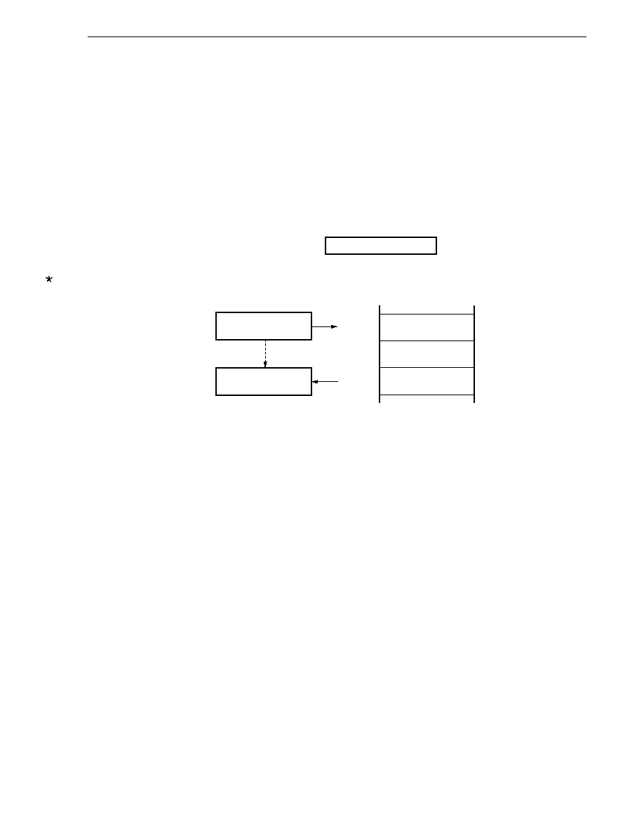
CHAPTER 3 CPU ARCHITECTURE
User's Manual U16228EJ2V0UD
89
3.4.9 Stack addressing
[Function]
The stack area is indirectly addressed with the stack pointer (SP) contents.
This addressing method is automatically employed when the PUSH, POP, subroutine call and return
instructions are executed or the register is saved/reset upon generation of an interrupt request.
With stack addressing, only the internal high-speed RAM area can be accessed.
[Description example]
In the case of PUSH DE (saving DE register)
Operation code
1
0
1
1
0
1
0
1
[Illustration]
E
FEE0H
SP
SP
FEE0H
FEDFH
FEDEH
D
Memory
0
7
FEDEH
User's Manual U16228EJ2V0UD
90
CHAPTER 4 PORT FUNCTIONS
4.1 Port Functions
There are two types of pin I/O buffer power supplies: AV
REF
and EV
DD
. The relationship between these power
supplies and the pins is shown below.
Table 4-1. Pin I/O Buffer Power Supplies
Power Supply
Corresponding Pins
AV
REF
P20 to P27
EV
DD
Port pins other than P20 to P27
78K0/KE1 products are provided with the ports shown in Figure 4-1, which enable variety of control operations.
The functions of each port are shown in Table 4-2.
In addition to the function as digital I/O ports, these ports have several alternate functions. For details of the
alternate functions, refer to CHAPTER 2 PIN FUNCTIONS.
Figure 4-1. Port Types
Port 2
P20
P27
Port 3
P30
P33
Port 5
P50
P53
Port 0
P00
P06
Port 1
P10
P17
Port 4
P40
P43
Port 6
P60
P63
Port 7
P70
P77
P120
Port 12
Port 14
P140
P141
P130
Port 13
CHAPTER 4 PORT FUNCTIONS
User's Manual U16228EJ2V0UD
91
Table 4-2. Port Functions (1/2)
Pin Name
I/O
Function
After Reset
Alternate Function
P00
TI000
P01
TI010/TO00
P02
SO11
Note
P03
SI11
Note
P04
SCK11
Note
P05
SSI11
Note
/TI001
Note
P06
I/O
Port 0.
7-bit I/O port.
Input/output can be specified in 1-bit units.
Use of an on-chip pull-up resistor can be specified by a
software setting.
Input
TI011
Note
/TO01
Note
P10
SCK10/TxD0
P11
SI10/RxD0
P12
SO10
P13
TxD6
P14
RxD6
P15
TOH0
P16
TOH1/INTP5
P17
I/O
Port 1.
8-bit I/O port.
Input/output can be specified in 1-bit units.
Use of an on-chip pull-up resistor can be specified by a
software setting.
Input
TI50/TO50
P20 to P27
Input
Port 2.
8-bit input-only port.
Input
ANI0 to ANI7
P30 to P32
INTP1 to INTP3
P33
I/O
Port 3.
4-bit I/O port.
Input/output can be specified in 1-bit units.
Use of an on-chip pull-up resistor can be specified by a
software setting.
Input
INTP4/TI51/TO51
P40 to P43
I/O
Port 4.
4-bit I/O port.
Input/output can be specified in 1-bit units.
Use of an on-chip pull-up resistor can be specified by a
software setting.
Input
-
P50 to P53
I/O
Port 5.
4-bit I/O port.
Input/output can be specified in 1-bit units.
Use of an on-chip pull-up resistor can be specified by a
software setting.
Input
-
P60 to P63
I/O
Port 6.
4-bit I/O port (N-ch open drain).
Input/output can be specified in 1-bit units.
Use of an on-chip pull-up resistor can be specified by a mask
option only for mask ROM versions.
Input
-
P70 to P77
I/O
Port 7.
8-bit I/O port.
Input/output can be specified in 1-bit units.
Use of an on-chip pull-up resistor can be specified by a
software setting.
Input
KR0 to KR7
Note SO11, SI11, SCK11, SSI11, TI001, TI011, and TO01 are available only in the
µ
PD780133, 780134, 78F0134,
780136, 780138, and 78F0138.
CHAPTER 4 PORT FUNCTIONS
User's Manual U16228EJ2V0UD
92
Table 4-2. Port Functions (2/2)
Pin Name
I/O
Function
After Reset
Alternate Function
P120 I/O
Port 12.
1-bit I/O port.
Use of an on-chip pull-up resistor can be specified by a
software setting.
Input INTP0
P130 Output
Port 13.
1-bit output-only port.
Output
-
P140
PCL/INTP6
P141
I/O
Port 14.
2-bit I/O port.
Input/output can be specified in 1-bit units.
Use of an on-chip pull-up resistor can be specified by a
software setting.
Input
BUZ/INTP7
4.2 Port Configuration
Ports include the following hardware.
Table 4-3. Port Configuration
Item Configuration
Control registers
Port mode register (PM0, PM1, PM3 to PM7, PM12, PM14)
Port register (P0 to P7, P12 to P14)
Pull-up resistor option register (PU0, PU1, PU3 to PU5, PU7, PU12, PU14)
Port
Total: 51 (CMOS I/O: 38, CMOS input: 8, CMOS output: 1, N-ch open drain I/O: 4)
Pull-up resistor
∑
Mask ROM version
Total: 42 (software control: 38, mask option specification: 4)
∑
Flash memory version: Total: 38

CHAPTER 4 PORT FUNCTIONS
User's Manual U16228EJ2V0UD
93
4.2.1 Port 0
Port 0 is a 7-bit I/O port with an output latch. Port 0 can be set to the input mode or output mode in 1-bit units
using port mode register 0 (PM0). When the P00 to P06 pins are used as an input port, use of an on-chip pull-up
resistor can be specified in 1-bit units by pull-up resistor option register 0 (PU0).
This port can also be used for timer I/O, serial interface data I/O, and clock I/O.
RESET input sets port 0 to input mode.
Figures 4-2 to 4-5 show block diagrams of port 0.
Caution When P02/SO11
Note
, P03/SI11
Note
, and P04/SCK11
Note
are used as general-purpose ports, do not
write to serial clock selection register 11 (CSIC11).
Figure 4-2. Block Diagram of P00, P03, and P05
P00/TI000,
P03/SI11
Note
,
P05/SSI11
Note
/TI001
Note
WR
PU
RD
WR
PORT
WR
PM
PU00, PU03, PU05
Alternate function
Output latch
(P00, P03, P05)
PM00, PM03, PM05
EV
DD
P-ch
Selector
Internal bus
PU0
PM0
Note Available only in the
µ
PD780133, 780134, 78F0134, 780136, 780138, and 78F0138.
PU0:
Pull-up resistor option register 0
PM0:
Port mode register 0
RD: Read
signal
WR
◊◊
: Write
signal
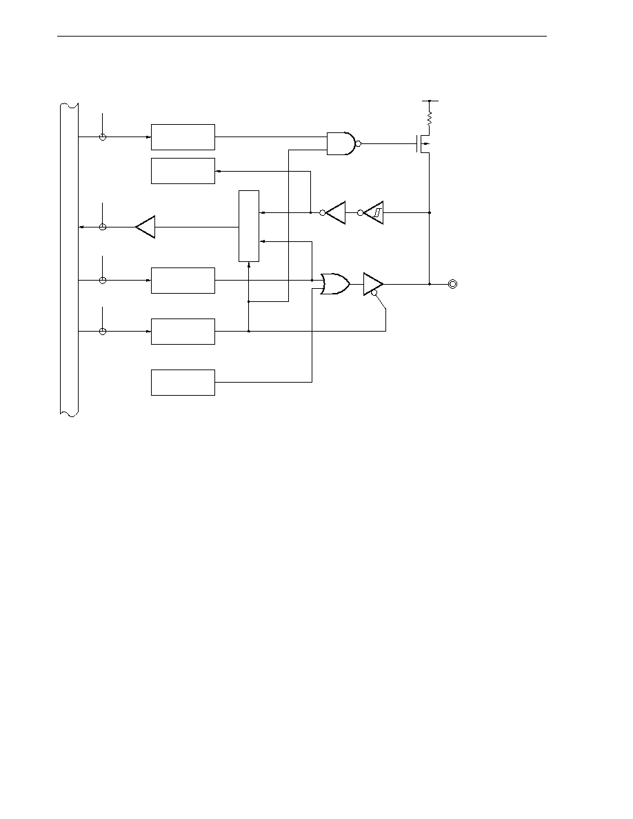
CHAPTER 4 PORT FUNCTIONS
User's Manual U16228EJ2V0UD
94
Figure 4-3. Block Diagram of P01 and P06
P01/TI010/TO00,
P06/TI011
Note
/TO01
Note
WR
PU
RD
WR
PORT
WR
PM
PU01, PU06
Alternate
function
Output latch
(P01, P06)
PM01, PM06
Alternate
function
EV
DD
P-ch
Selector
Internal bus
PU0
PM0
Note Available only in the
µ
PD780133, 780134, 78F0134, 780136, 780138, and 78F0138.
PU0:
Pull-up resistor option register 0
PM0:
Port mode register 0
RD: Read
signal
WR
◊◊
: Write
signal
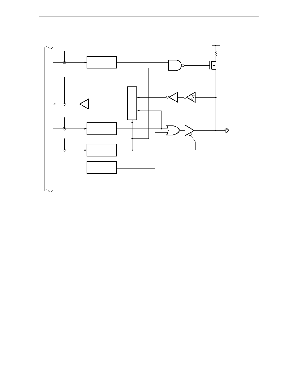
CHAPTER 4 PORT FUNCTIONS
User's Manual U16228EJ2V0UD
95
Figure 4-4. Block Diagram of P02
P02/SO11
Note
WR
PU
RD
WR
PORT
WR
PM
PU02
Output latch
(P02)
PM02
Alternate
function
EV
DD
P-ch
Selector
Internal bus
PU0
PM0
Note Available only in the
µ
PD780133, 780134, 78F0134, 780136, 780138, and 78F0138.
PU0:
Pull-up resistor option register 0
PM0:
Port mode register 0
RD: Read
signal
WR
◊◊
: Write
signal
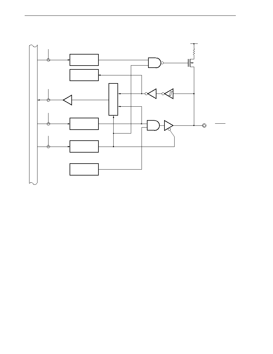
CHAPTER 4 PORT FUNCTIONS
User's Manual U16228EJ2V0UD
96
Figure 4-5. Block Diagram of P04
P04/SCK11
Note
WR
PU
RD
WR
PORT
WR
PM
PU04
Alternate
function
Output latch
(P04)
PM04
Alternate
function
EV
DD
P-ch
Selector
Internal bus
PU0
PM0
Note Available only in the
µ
PD780133, 780134, 78F0134, 780136, 780138, and 78F0138.
PU0:
Pull-up resistor option register 0
PM0:
Port mode register 0
RD: Read
signal
WR
◊◊
: Write
signal
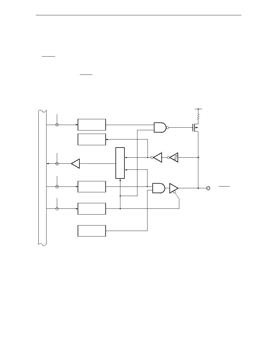
CHAPTER 4 PORT FUNCTIONS
User's Manual U16228EJ2V0UD
97
4.2.2 Port 1
Port 1 is an 8-bit I/O port with an output latch. Port 1 can be set to the input mode or output mode in 1-bit units
using port mode register 1 (PM1). When the P10 to P17 pins are used as an input port, use of an on-chip pull-up
resistor can be specified in 1-bit units by pull-up resistor option register 1 (PU1).
This port can also be used for external interrupt request input, serial interface data I/O, clock I/O, and timer I/O.
RESET input sets port 1 to input mode.
Figures 4-6 to 4-10 show block diagrams of port 1.
Caution When P10/SCK10/TxD0, P11/SI10/RxD0, and P12/SO10 are used as general-purpose ports, do not
write to serial clock selection register 10 (CSIC10).
Figure 4-6. Block Diagram of P10
P10/SCK10/TxD0
WR
PU
RD
WR
PORT
WR
PM
PU10
Alternate
function
Output latch
(P10)
PM10
Alternate
function
EV
DD
P-ch
Selector
Internal bus
PU1
PM1
PU1:
Pull-up resistor option register 1
PM1:
Port mode register 1
RD: Read
signal
WR
◊◊
: Write
signal
CHAPTER 4 PORT FUNCTIONS
User's Manual U16228EJ2V0UD
98
Figure 4-7. Block Diagram of P11 and P14
P11/SI10/RxD0,
P14/RxD6
WR
PU
RD
WR
PORT
WR
PM
PU11, PU14
Alternate
function
Output latch
(P11, P14)
PM11, PM14
EV
DD
P-ch
Selector
Internal bus
PU1
PM1
PU1:
Pull-up resistor option register 1
PM1:
Port mode register 1
RD: Read
signal
WR
◊◊
: Write
signal
CHAPTER 4 PORT FUNCTIONS
User's Manual U16228EJ2V0UD
99
Figure 4-8. Block Diagram of P12 and P15
P12/SO10
P15/TOH0
WR
PU
RD
WR
PORT
WR
PM
PU12, PU15
Output latch
(P12, P15)
PM12, PM15
Alternate
function
EV
DD
P-ch
Selector
Internal bus
PU1
PM1
PU1:
Pull-up resistor option register 1
PM1:
Port mode register 1
RD: Read
signal
WR
◊◊
: Write
signal

CHAPTER 4 PORT FUNCTIONS
User's Manual U16228EJ2V0UD
100
Figure 4-9. Block Diagram of P13
P13/TxD6
WR
PU
RD
WR
PORT
WR
PM
PU13
Output latch
(P13)
PM13
Alternate
function
EV
DD
P-ch
Internal bus
Selector
PU1
PM1
PU1:
Pull-up resistor option register 1
PM1:
Port mode register 1
RD: Read
signal
WR
◊◊
: Write
signal
CHAPTER 4 PORT FUNCTIONS
User's Manual U16228EJ2V0UD
101
Figure 4-10. Block Diagram of P16 and P17
P16/TOH1/INTP5,
P17/TI50/TO50
WR
PU
RD
WR
PORT
WR
PM
PU16, PU17
Alternate
function
Output latch
(P16, P17)
PM16, PM17
Alternate
function
EV
DD
P-ch
Selector
Internal bus
PU1
PM1
PU1:
Pull-up resistor option register 1
PM1:
Port mode register 1
RD: Read
signal
WR
◊◊
: Write
signal
CHAPTER 4 PORT FUNCTIONS
User's Manual U16228EJ2V0UD
102
4.2.3 Port 2
Port 2 is an 8-bit input-only port.
This port can also be used for A/D converter analog input.
Figure 4-11 shows a block diagram of port 2.
Figure 4-11. Block Diagram of P20 to P27
RD
A/D converter
P20/ANI0 to P27/ANI7
Internal bus
RD: Read
signal

CHAPTER 4 PORT FUNCTIONS
User's Manual U16228EJ2V0UD
103
4.2.4 Port 3
Port 3 is a 4-bit I/O port with an output latch. Port 3 can be set to the input mode or output mode in 1-bit units
using port mode register 3 (PM3). When used as an input port, use of an on-chip pull-up resistor can be specified in
1-bit units by pull-up resistor option register 3 (PU3).
This port can also be used for external interrupt request input.
RESET input sets port 3 to input mode.
Figures 4-12 and 4-13 show block diagrams of port 3.
Figure 4-12. Block Diagram of P30 to P32
P30/INTP1 to
P32/INTP3
WR
PU
RD
WR
PORT
WR
PM
PU30 to PU32
Alternate
function
Output latch
(P30 to P32)
PM30 to PM32
EV
DD
P-ch
Selector
Internal bus
PU3
PM3
PU3:
Pull-up resistor option register 3
PM3:
Port mode register 3
RD: Read
signal
WR
◊◊
: Write
signal

CHAPTER 4 PORT FUNCTIONS
User's Manual U16228EJ2V0UD
104
Figure 4-13. Block Diagram of P33
P33/INTP4/TI51/TO51
WR
PU
RD
WR
PORT
WR
PM
PU33
Alternate
function
Output latch
(P33)
PM33
Alternate
function
EV
DD
P-ch
Selector
Internal bus
PU3
PM3
PU3:
Pull-up resistor option register 3
PM3:
Port mode register 3
RD: Read
signal
WR
◊◊
: Write
signal
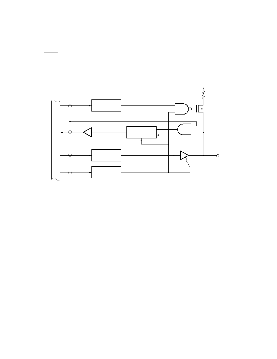
CHAPTER 4 PORT FUNCTIONS
User's Manual U16228EJ2V0UD
105
4.2.5 Port 4
Port 4 is a 4-bit I/O port with an output latch. Port 4 can be set to the input mode or output mode in 1-bit units
using port mode register 4 (PM4). Use of an on-chip pull-up resistor can be specified in 1-bit units with pull-up resistor
option register 4 (PU4).
RESET input sets port 4 to input mode.
Figure 4-14 shows a block diagram of port 4.
Figure 4-14. Block Diagram of P40 to P43
RD
P-ch
WR
PU
WR
PORT
WR
PM
EV
DD
P40 to P43
PU40 to PU43
Output latch
(P40 to P43)
PM40 to PM43
Selector
Internal bus
PU4
PM4
PU4:
Pull-up resistor option register 4
PM4:
Port mode register 4
RD: Read
signal
WR
◊◊
: Write
signal

CHAPTER 4 PORT FUNCTIONS
User's Manual U16228EJ2V0UD
106
4.2.6 Port 5
Port 5 is a 4-bit I/O port with an output latch. Port 5 can be set to the input mode or output mode in 1-bit units
using port mode register 5 (PM5). Use of an on-chip pull-up resistor can be specified in 1-bit units using pull-up
resistor option register 5 (PU5).
RESET input sets port 5 to input mode.
Figure 4-15 shows a block diagram of port 5.
Figure 4-15. Block Diagram of P50 to P53
RD
P-ch
WR
PU
WR
PORT
WR
PM
EV
DD
P50 to P53
PU50 to PU53
Output latch
(P50 to P53)
PM50 to PM53
Selector
Internal bus
PU5
PM5
PU5:
Pull-up resistor option register 5
PM5:
Port mode register 5
RD: Read
signal
WR
◊◊
: Write
signal
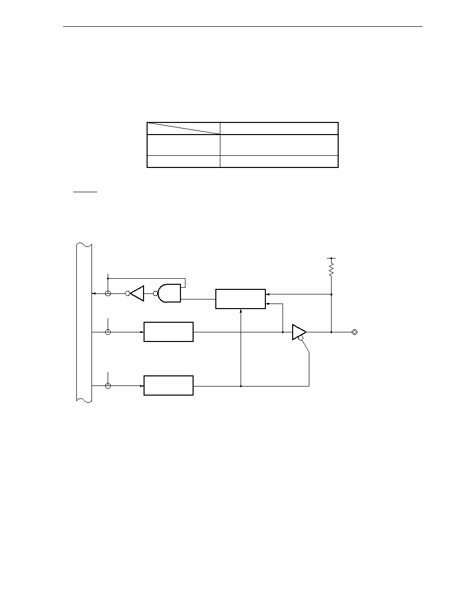
CHAPTER 4 PORT FUNCTIONS
User's Manual U16228EJ2V0UD
107
4.2.7 Port 6
Port 6 is a 4-bit I/O port with an output latch. Port 6 can be set to the input mode or output mode in 1-bit units
using port mode register 6 (PM6).
This port has the following functions for pull-up resistors. These functions differ depending on whether the product
is a mask ROM version or a flash memory version.
Table 4-4. Pull-up Resistor of Port 6
Pins P60 to P63
Mask ROM version
An on-chip pull-up resistor can be
specified in 1-bit units by mask option
Flash memory version
On-chip pull-up resistors are not provided
The P60 to P63 pins are N-ch open-drain pins.
RESET input sets port 6 to input mode.
Figure 4-16 shows a block diagram of port 6.
Figure 4-16. Block Diagram of P60 to P63
RD
P60 to P63
WR
PORT
WR
PM
Output latch
(P60 to P63)
PM60 to PM63
Selector
EV
DD
Mask option resistor
Internal bus
Mask ROM versions only
No pull-up resistor for
flash memory versions
PM6
PM6:
Port mode register 6
RD: Read
signal
WR
◊◊
: Write
signal
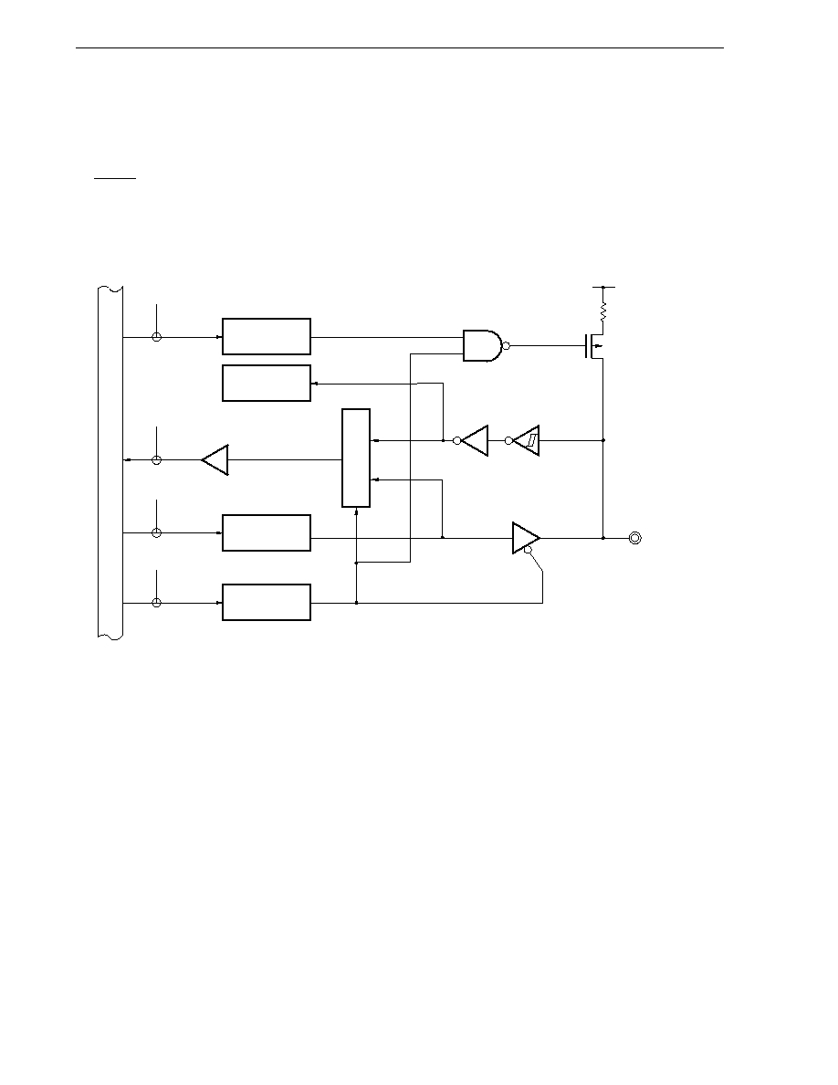
CHAPTER 4 PORT FUNCTIONS
User's Manual U16228EJ2V0UD
108
4.2.8 Port 7
Port 7 is an 8-bit I/O port with an output latch. Port 7 can be set to the input mode or output mode in 1-bit units
using port mode register 7 (PM7). When the P70 to P77 pins are used as an input port, use of an on-chip pull-up
resistor can be specified in 1-bit units by pull-up resistor option register 7 (PU7).
This port can also be used for key return input.
RESET input sets port 7 to input mode.
Figure 4-17 shows a block diagram of port 7.
Figure 4-17. Block Diagram of P70 to P77
P70/KR0 to
P77/KR7
WR
PU
RD
WR
PORT
WR
PM
PU70 to PU77
Alternate function
Output latch
(P70 to P77)
PM70 to PM77
EV
DD
P-ch
Selector
Internal bus
PU7
PM7
PU7:
Pull-up resistor option register 7
PM7:
Port mode register 7
RD: Read
signal
WR
◊◊
: Write
signal

CHAPTER 4 PORT FUNCTIONS
User's Manual U16228EJ2V0UD
109
4.2.9 Port 12
Port 12 is a 1-bit I/O port with an output latch. Port 12 can be set to the input mode or output mode in 1-bit units
using port mode register 12 (PM12). When used as an input port, use of an on-chip pull-up resistor can be specified
by pull-up resistor option register 12 (PU12).
This port can also be used for external interrupt input.
RESET input sets port 12 to input mode.
Figure 4-18 shows a block diagram of port 12.
Figure 4-18. Block Diagram of P120
P120/INTP0
WR
PU
RD
WR
PORT
WR
PM
PU120
Alternate
function
Output latch
(P120)
PM120
EV
DD
P-ch
Selector
Internal bus
PU12
PM12
PU12:
Pull-up resistor option register 12
PM12: Port mode register 12
RD: Read
signal
WR
◊◊
: Write
signal
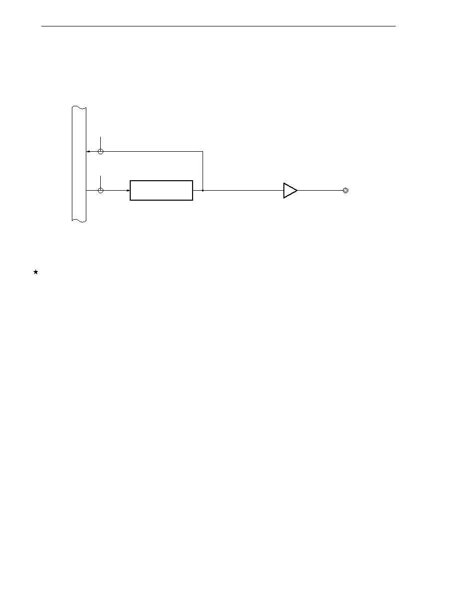
CHAPTER 4 PORT FUNCTIONS
User's Manual U16228EJ2V0UD
110
4.2.10 Port 13
Port 13 is a 1-bit output-only port.
Figure 4-19 shows a block diagram of port 13.
Figure 4-19. Block Diagram of P130
RD
Output latch
(P130)
WR
PORT
P130
Internal bus
RD: Read
signal
WR
◊◊
: Write
signal
Remark When reset is effected, P130 outputs a low level. If P130 is set to output a high level immediately after
reset is released, the output signal of P130 can be dummy-output as the reset signal to the CPU.

CHAPTER 4 PORT FUNCTIONS
User's Manual U16228EJ2V0UD
111
4.2.11 Port 14
Port 14 is a 2-bit I/O port with an output latch. Port 14 can be set to the input mode or output mode in 1-bit units
using port mode register 14 (PM14). When the P140 and P141 pins are used as an input port, use of an on-chip pull-
up resistor can be specified in 1-bit units by pull-up resistor option register 14 (PU14).
This port can also be used for external interrupt request input, buzzer output, and clock output.
RESET input sets port 14 to input mode.
Figure 4-20 shows a block diagram of port 14.
Figure 4-20. Block Diagram of P140 and P141
P140/PCL/INTP6,
P141/BUZ/INTP7
WR
PU
RD
WR
PORT
WR
PM
PU140, PU141
Alternate
function
Output latch
(P140, P141)
PM140, PM141
Alternate
function
EV
DD
P-ch
Selector
Internal bus
PU14
PM14
PU14:
Pull-up resistor option register 14
PM14: Port mode register 14
RD: Read
signal
WR
◊◊
: Write
signal

CHAPTER 4 PORT FUNCTIONS
User's Manual U16228EJ2V0UD
112
4.3 Registers Controlling Port Function
Port functions are controlled by the following three types of registers.
∑
Port mode registers (PM0, PM1, PM3 to PM7, PM12, PM14)
∑
Port registers (P0 to P7, P12 to P14)
∑
Pull-up resistor option registers (PU0, PU1, PU3 to PU5, PU7, PU12, PU14)
(1) Port mode registers (PM0, PM1, PM3 to PM7, PM12, and PM14)
These registers specify input or output mode for the port in 1-bit units.
These registers can be set by a 1-bit or 8-bit memory manipulation instruction.
RESET input sets these registers to FFH.
When port pins are used as alternate-function pins, set the port mode register and output latch as shown in Table
4-4.
Figure 4-21. Format of Port Mode Register
7
1
Symbol
PM0
6
PM06
5
PM05
4
PM04
3
PM03
2
PM02
1
PM01
0
PM00
Address
FF20H
After reset
FFH
R/W
R/W
7
PM17
PM1
6
PM16
5
PM15
4
PM14
3
PM13
2
PM12
1
PM11
0
PM10
FF21H
FFH
R/W
7
1
PM3
6
1
5
1
4
1
3
PM33
2
PM32
1
PM31
0
PM30
FF23H
FFH
R/W
7
1
PM4
6
1
5
1
4
1
3
PM43
2
PM42
1
PM41
0
PM40
FF24H
FFH
R/W
7
1
PM5
6
1
5
1
4
1
3
PM53
2
PM52
1
PM51
0
PM50
FF25H
FFH
R/W
7
1
PM6
6
1
5
1
4
1
3
PM63
2
PM62
1
PM61
0
PM60
FF26H
FFH
R/W
7
PM77
PM7
6
PM76
5
PM75
4
PM74
3
PM73
2
PM72
1
PM71
0
PM70
FF27H
FFH
R/W
7
1
PM12
6
1
5
1
4
1
3
1
2
1
1
1
0
PM120
FF2CH
FFH
R/W
7
1
PM14
6
1
5
1
4
1
3
1
2
1
1
PM141
0
PM140
FF2EH
FFH
R/W
PMmn
Pmn pin I/O mode selection
(m = 0, 1, 3 to 7, 12, 14; n = 0 to 7)
0
Output mode (output buffer on)
1
Input mode (output buffer off)
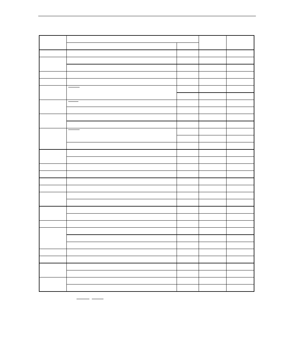
CHAPTER 4 PORT FUNCTIONS
User's Manual U16228EJ2V0UD
113
Table 4-5. Settings of Port Mode Register and Output Latch When Using Alternate Function
Alternate Function
Pin Name
Function Name
I/O
PM
◊◊
P
◊◊
P00 TI000
Input
1
◊
TI010 Input
1
◊
P01
TO00 Output
0
0
P02 SO11
Note
Output
0
0
P03 SI11
Note
Input
1
◊
Input 1
◊
P04 SCK11
Note
Output 0 1
SSI11
Note
Input
1
◊
P05
TI001
Note
Input
1
◊
TI011
Note
Input
1
◊
P06
TO01
Note
Output
0
0
Input 1
◊
SCK10
Output 0 1
P10
TxD0 Output
0
1
SI10 Input
1
◊
P11
RxD0 Input
1
◊
P12 SO10
Output 0
0
P13 TxD6
Output 0
1
P14 RxD6
Input
1
◊
P15 TOH0
Output 0
0
TOH1 Output
0
0
P16
INTP5 Input
1
◊
TI50 Input
1
◊
P17
TO50 Output
0
0
P30 to P32
INTP1 to INTP3
Input
1
◊
INTP4 Input
1
◊
TI51 Input
1
◊
P33
TO51 Output
0
0
P70 to P77
KR0 to KR7
Input
1
◊
P120 INTP0
Input
1
◊
PCL Output
0
0
P140
INTP6 Input
1
◊
BUZ Output
0
0
P141
INTP7 Input
1
◊
Note SO11, SI11, SCK11, SSI11, TI001, TI011, and TO01 are available only in the
µ
PD780133, 780134, 78F0134,
780136, 780138, and 78F0138.
Remark
◊
: Don't
care
PM
◊◊
: Port mode register
P
◊◊
:
Port output latch
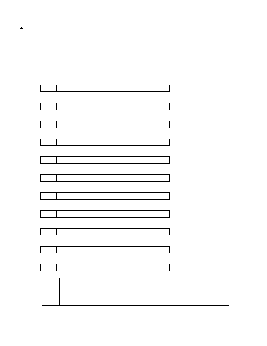
CHAPTER 4 PORT FUNCTIONS
User's Manual U16228EJ2V0UD
114
(2) Port registers (P0 to P7, P12 to P14)
These registers write the data that is output from the chip when data is output from a port.
If the data is read in the input mode, the pin level is read. If it is read in the output mode, the value of the output
latch is read.
These registers can be set by a 1-bit or 8-bit memory manipulation instruction.
RESET input clears these registers to 00H (but P2 is undefined).
Figure 4-22. Format of Port Register
7
0
Symbol
P0
6
P06
5
P05
4
P04
3
P03
2
P02
1
P01
0
P00
Address
FF00H
After reset
00H (output latch)
R/W
R/W
7
P17
P1
6
P16
5
P15
4
P14
3
P13
2
P12
1
P11
0
P10
FF01H
00H (output latch)
R/W
R
7
P27
P2
6
P26
5
P25
4
P24
3
P23
2
P22
1
P21
0
P20
FF02H
Undefined
7
0
P3
6
0
5
0
4
0
3
P33
2
P32
1
P31
0
P30
FF03H
00H (output latch)
R/W
7
0
P4
6
0
5
0
4
0
3
P43
2
P42
1
P41
0
P40
FF04H
00H (output latch)
R/W
7
0
P5
6
0
5
0
4
0
3
P53
2
P52
1
P51
0
P50
FF05H
00H (output latch)
R/W
7
0
P6
6
0
5
0
4
0
3
P63
2
P62
1
P61
0
P60
FF06H
00H (output latch)
R/W
7
P77
P7
6
P76
5
P75
4
P74
3
P73
2
P72
1
P71
0
P70
FF07H
00H (output latch)
R/W
7
0
P12
6
0
5
0
4
0
3
0
2
0
1
0
0
P120
FF0CH
00H (output latch)
R/W
7
0
P13
6
0
5
0
4
0
3
0
2
0
1
0
0
P130
FF0DH
00H (output latch)
R/W
7
0
P14
6
0
5
0
4
0
3
0
2
0
1
P141
0
P140
FF0EH
00H (output latch)
R/W
m = 0 to 7, 12 to 14; n = 0 to 7
Pmn
Output data control (in output mode)
Input data read (in input mode)
0
Output 0
Input low level
1
Output 1
Input high level
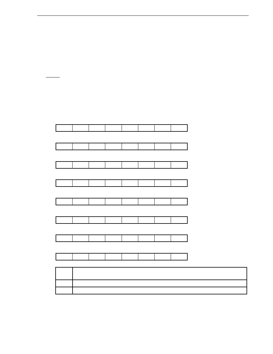
CHAPTER 4 PORT FUNCTIONS
User's Manual U16228EJ2V0UD
115
(3) Pull-up resistor option registers (PU0, PU1, PU3 to PU5, PU7, PU12, and PU14)
These registers specify whether the on-chip pull-up resistors of P00 to P06, P10 to P17, P30 to P33, P40 to P43,
P50 to P53, P70 to P77, P120, or P140 and P141 are to be used or not. On-chip pull-up resistors can be used in
1-bit units only for the bits set to input mode of the pins to which the use of an on-chip pull-up resistor has been
specified in PU0, PU1, PU3 to PU5, PU7, PU12, and PU14. On-chip pull-up resistors cannot be connected to
bits set to output mode and bits used as alternate-function output pins, regardless of the settings of PU0, PU1,
PU3 to PU5, PU7, PU12, and PU14.
These registers can be set by a 1-bit or 8-bit memory manipulation instruction.
RESET input clears these registers to 00H.
Caution Use of a pull-up resistor can be specified for P60 to P63 pins by a mask option only in the mask
ROM versions.
Figure 4-23. Format of Pull-up Resistor Option Register
7
0
Symbol
PU0
6
PU06
5
PU05
4
PU04
3
PU03
2
PU02
1
PU01
0
PU00
Address
FF30H
After reset
00H
R/W
R/W
7
PU17
PU1
6
PU16
5
PU15
4
PU14
3
PU13
2
PU12
1
PU11
0
PU10
FF31H
00H
R/W
7
0
PU3
6
0
5
0
4
0
3
PU33
2
PU32
1
PU31
0
PU30
FF33H
00H
R/W
7
0
PU4
6
0
5
0
4
0
3
PU43
2
PU42
1
PU41
0
PU40
FF34H
00H
R/W
7
0
PU5
6
0
5
0
4
0
3
PU53
2
PU52
1
PU51
0
PU50
FF35H
00H
R/W
7
PU77
PU7
6
PU76
5
PU75
4
PU74
3
PU73
2
PU72
1
PU71
0
PU70
FF37H
00H
R/W
7
0
PU12
6
0
5
0
4
0
3
0
2
0
1
0
0
PU120
FF3CH
00H
R/W
7
0
PU14
6
0
5
0
4
0
3
0
2
0
1
PU141
0
PU140
FF3EH
00H
R/W
PUmn
Pmn pin on-chip pull-up resistor selection
(m = 0, 1, 3 to 5, 7, 12, 14; n = 0 to 7)
0
On-chip pull-up resistor not connected
1
On-chip pull-up resistor connected

CHAPTER 4 PORT FUNCTIONS
User's Manual U16228EJ2V0UD
116
4.4 Port Function Operations
Port operations differ depending on whether the input or output mode is set, as shown below.
Caution In the case of 1-bit memory manipulation instruction, although a single bit is manipulated, the
port is accessed as an 8-bit unit. Therefore, on a port with a mixture of input and output pins, the
output latch contents for pins specified as input are undefined, even for bits other than the
manipulated bit.
4.4.1 Writing to I/O port
(1) Output
mode
A value is written to the output latch by a transfer instruction, and the output latch contents are output from the
pin.
Once data is written to the output latch, it is retained until data is written to the output latch again.
The data of the output latch is cleared by reset.
(2) Input
mode
A value is written to the output latch by a transfer instruction, but since the output buffer is off, the pin status does
not change.
Once data is written to the output latch, it is retained until data is written to the output latch again.
4.4.2 Reading from I/O port
(1) Output
mode
The output latch contents are read by a transfer instruction. The output latch contents do not change.
(2) Input
mode
The pin status is read by a transfer instruction. The output latch contents do not change.
4.4.3 Operations on I/O port
(1) Output
mode
An operation is performed on the output latch contents, and the result is written to the output latch. The output
latch contents are output from the pins.
Once data is written to the output latch, it is retained until data is written to the output latch again.
The data of the output latch is cleared by reset.
(2) Input
mode
The pin level is read and an operation is performed on its contents. The result of the operation is written to the
output latch, but since the output buffer is off, the pin status does not change.

User's Manual U16228EJ2V0UD
117
CHAPTER 5 CLOCK GENERATOR
5.1 Functions of Clock Generator
The clock generator generates the clock to be supplied to the CPU and peripheral hardware.
The following three system clock oscillators are available.
∑
X1
oscillator
The X1 oscillator oscillates a clock of f
XP
= 2.0 to 10.0 MHz. Oscillation can be stopped by executing the STOP
instruction or setting the main OSC control register (MOC) and processor clock control register (PCC).
∑
Ring-OSC
oscillator
The Ring-OSC oscillator oscillates a clock of f
R
= 240 kHz (TYP.). Oscillation can be stopped by setting the
Ring-OSC mode register (RCM) when "Can be stopped by software" is set by a mask option and the X1 input
clock is used as the CPU clock.
∑
Subsystem clock oscillator
The subsystem clock oscillator oscillates a clock of f
XT
= 32.768 kHz. Oscillation cannot be stopped. When
subsystem clock oscillator is not used, setting not to use the on-chip feedback resistor is possible using the
processor clock control register (PCC), and the operating current can be reduced in the STOP mode.
Remarks 1. f
XP
: X1 input clock oscillation frequency
2.
f
R
: Ring-OSC clock oscillation frequency
3.
f
XT
: Subsystem clock oscillation frequency
5.2 Configuration of Clock Generator
The clock generator includes the following hardware.
Table 5-1. Configuration of Clock Generator
Item Configuration
Control registers
Processor clock control register (PCC)
Ring-OSC mode register (RCM)
Main clock mode register (MCM)
Main OSC control register (MOC)
Oscillation stabilization time counter status register (OSTC)
Oscillation stabilization time select register (OSTS)
Oscillators
X1 oscillator
Ring-OSC oscillator
Subsystem clock oscillator
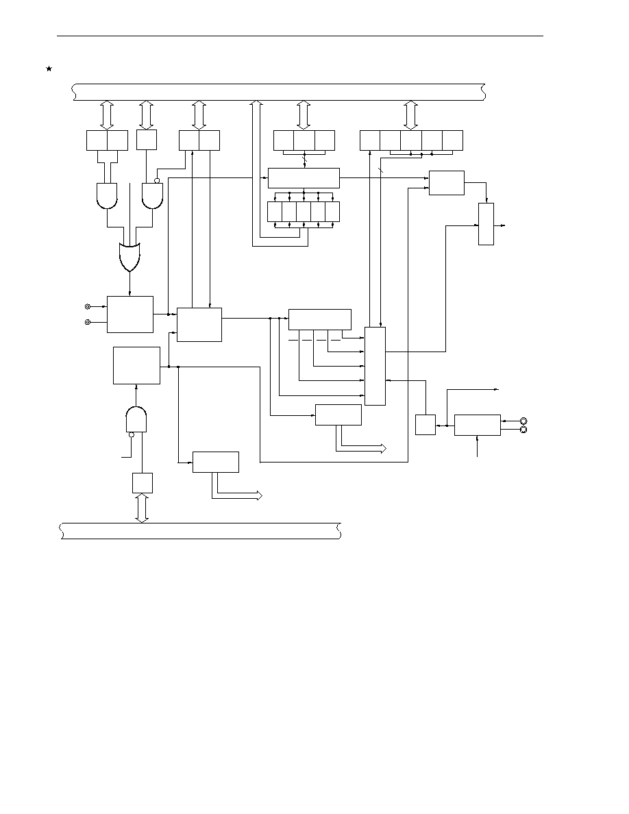
CHAPTER 5 CLOCK GENERATOR
User's Manual U16228EJ2V0UD
118
Figure 5-1. Block Diagram of Clock Generator
X1
X2
f
XP
f
XT
FRC
XT1
XT2
f
X
2
2
STOP
MSTOP
f
X
2
3
f
X
2
4
f
X
2
4
RSTOP
CSS PCC2
CLS
MCM0
MCS
CLS
MCC
OSTS1 OSTS0
OSTS2
1/2
3
MOST
16
MOST
15
MOST
14
MOST
13
MOST
11
C
P
U
f
R
f
X
PCC1 PCC0
X1 oscillator
Internal bus
Ring-OSC mode
register (RCM)
Main OSC
control
register
(MOC)
Internal bus
Ring-OSC
oscillator
Mask option
1: Cannot be stopped
0: Can be stopped
CPU clock
(f
CPU
)
Controller
Processor clock
control register
(PCC)
Main clock
mode register
(MCM)
X1 oscillation
stabilization time counter
Oscillation
stabilization time
select register
(OSTS)
Oscillation
stabilization
time counter
status
register
(OSTC)
Clock to peripheral
hardware
Prescaler
Operation
clock switch
8-bit timer H1,
watchdog timer
Prescaler
Prescaler
Selector
Subsystem
clock oscillator
Watch clock,
clock output
function
f
CPU
Control signal

CHAPTER 5 CLOCK GENERATOR
User's Manual U16228EJ2V0UD
119
5.3 Registers Controlling Clock Generator
The following six registers are used to control the clock generator.
∑
Processor clock control register (PCC)
∑
Ring-OSC mode register (RCM)
∑
Main clock mode register (MCM)
∑
Main OSC control register (MOC)
∑
Oscillation stabilization time counter status register (OSTC)
∑
Oscillation stabilization time select register (OSTS)
(1) Processor clock control register (PCC)
The PCC register is used to select the CPU clock, the division ratio, main system clock oscillator operation/stop
and whether to use the on-chip feedback resistor
Note
of the subsystem clock oscillator.
The PCC is set by a 1-bit or 8-bit memory manipulation instruction.
RESET input clears PCC to 00H.
Note The feedback resistor is required to control the bias point of the oscillation waveform so that the bias point
is in the middle of the power supply voltage.
When the subsystem clock is not used, the operating current in the STOP mode can be reduced by setting
bit 6 (FRC) of PCC to 1 (see Figure 5-11 Subsystem Clock Feedback Resistor).
CHAPTER 5 CLOCK GENERATOR
User's Manual U16228EJ2V0UD
120
Figure 5-2. Format of Processor Clock Control Register (PCC)
Address: FFFBH After reset: 00H R/W
Note 1
Symbol
<7> <6> <5> <4> 3
2
1
0
PCC MCC FRC CLS CSS 0 PCC2
PCC1
PCC0
MCC
Control of X1 oscillator operation
Note 2
0
Oscillation
possible
1
Oscillation
stopped
FRC
Subsystem
clock
feedback resistor selection
0
On-chip feedback resistor used
1
On-chip feedback resistor not used
Note 3
CLS
CPU
clock
status
0
X1 input clock or Ring-OSC clock
1
Subsystem
clock
Notes 1. Bit 5 is read-only.
2. When the CPU is operating on the subsystem clock, MCC should be used to stop the X1 oscillator
operation. When the CPU is operating on the Ring-OSC clock, use bit 7 (MSTOP) of the main OSC
control register (MOC) to stop the X1 oscillator operation (this cannot be set by MCC). A STOP
instruction should not be used.
3. This bit can be set to 1 only when the subsystem clock is not used.
4. Be sure to switch CSS from 1 to 0 when bits 1 (MCS) and 0 (MCM0) of the main clock mode register
(MCM) are 1.
Caution Be sure to clear bit 3 to 0.
CPU clock (f
CPU
) selection
CSS
Note 4
PCC2 PCC1 PCC0
MCM0 = 0
MCM0 = 1
0
0
0
f
X
f
R
f
XP
0
0
1
f
X
/2 f
R
/2 f
XP
/2
0
1
0
f
X
/2
2
f
R
/2
2
f
XP
/2
2
0
1
1
f
X
/2
3
f
R
/2
3
f
XP
/2
3
0
1 0 0
f
X
/2
4
f
R
/2
4
f
XP
/2
4
0
0
0
0
0
1
0
1
0
0
1
1
1
1 0 0
f
XT
/2
Other than above
Setting prohibited
CHAPTER 5 CLOCK GENERATOR
User's Manual U16228EJ2V0UD
121
Remarks 1. MCM0: Bit 0 of the main clock mode register (MCM)
2. f
X
: Main system clock oscillation frequency (X1 input clock oscillation frequency or Ring-OSC clock
oscillation frequency)
3. f
R
: Ring-OSC clock oscillation frequency
4. f
XP
: X1 input clock oscillation frequency
5. f
XT
: Subsystem clock oscillation frequency
The fastest instruction can be executed in 2 clocks of the CPU clock in the 78K0/KE1. Therefore, the relationship
between the CPU clock (f
CPU
) and minimum instruction execution time is as shown in the Table 5-2.
Table 5-2. Relationship Between CPU Clock and Minimum Instruction Execution Time
Minimum Instruction Execution Time: 2/f
CPU
CPU Clock (f
CPU
)
X1 Input Clock
Note
(at 10 MHz Operation)
Ring-OSC Clock
Note
(at 240 kHz (TYP.) Operation)
Subsystem Clock
(at 32.768 kHz Operation)
f
X
0.2
µ
s 8.3
µ
s (TYP.)
-
f
X
/2 0.4
µ
s 16.6
µ
s (TYP.)
-
f
X
/2
2
0.8
µ
s 33.2
µ
s (TYP.)
-
f
X
/2
3
1.6
µ
s 66.4
µ
s (TYP.)
-
f
X
/2
4
3.2
µ
s 132.8
µ
s (TYP.)
-
f
XT
/2
-
-
122.1
µ
s
Note The main clock mode register (MCM) is used to set the CPU clock (X1 input clock/Ring-OSC clock) (see
Figure 5-4).
(2) Ring-OSC mode register (RCM)
This register sets the operation mode of Ring-OSC.
This register is valid when "Can be stopped by software" is set for Ring-OSC by a mask option, and the X1 input
clock or subsystem clock is selected as the CPU clock. If "Cannot be stopped" is selected for Ring-OSC by a
mask option, settings for this register are invalid.
RCM can be set by a 1-bit or 8-bit memory manipulation instruction.
RESET input clears this register to 00H.
Figure 5-3. Format of Ring-OSC Mode Register (RCM)
Address: FFA0H After reset: 00H R/W
Symbol
7 6 5 4 3 2 1
<0>
RCM
0 0 0 0 0 0 0
RSTOP
RSTOP
Ring-OSC
oscillating/stopped
0
Ring-OSC
oscillating
1
Ring-OSC
stopped
Caution Make sure that the bit 1 (MCS) of the main clock mode register (MCM) is 1 before
setting RSTOP.
CHAPTER 5 CLOCK GENERATOR
User's Manual U16228EJ2V0UD
122
(3) Main clock mode register (MCM)
This register sets the CPU clock (X1 input clock/Ring-OSC clock).
MCM can be set by a 1-bit or 8-bit memory manipulation instruction.
RESET input clears this register to 00H.
Figure 5-4. Format of Main Clock Mode Register (MCM)
Address: FFA1H After reset: 00H R/W
Note
Symbol
7 6 5 4 3 2
<1>
<0>
MCM
0 0 0 0 0 0
MCS
MCM0
MCS
CPU
clock
status
0
Operates with Ring-OSC clock
1
Operates with X1 input clock
MCM0
Selection of clock supplied to CPU
0
Ring-OSC
clock
1
X1 input clock
Note Bit 1 is read-only.
Cautions 1. When Ring-OSC clock is selected as the clock to be supplied to the CPU, the
divided clock of the Ring-OSC oscillator output (f
X
) is supplied to the peripheral
hardware (f
X
= 240 kHz (TYP.)).
Operation of the peripheral hardware with Ring-OSC clock cannot be
guaranteed. Therefore, when Ring-OSC clock is selected as the clock supplied
to the CPU, do not use peripheral hardware. In addition, stop the peripheral
hardware before switching the clock supplied to the CPU from the X1 input clock
to the Ring-OSC clock. Note, however, that the following peripheral hardware
can be used when the CPU operates on the Ring-OSC clock.
∑
Watchdog timer
∑
Clock monitor
∑
8-bit timer H1 when f
R
/2
7
is selected as count clock
∑
Peripheral hardware selecting external clock as the clock source
(Except when external count clock of TM0n (n = 0, 1) is selected (TI00n valid
edge))
2. Set MCS = 1 and MCM0 = 1 before switching subsystem clock operation to X1
input clock operation (bit 4 (CSS) of the processor clock control register (PCC)
is changed from 1 to 0).

CHAPTER 5 CLOCK GENERATOR
User's Manual U16228EJ2V0UD
123
(4) Main OSC control register (MOC)
This register selects the operation mode of the X1 input clock.
This register is used to stop the X1 oscillator operation when the CPU is operating with the Ring-OSC clock.
Therefore, this register is valid only when the CPU is operating with the Ring-OSC clock.
MOC can be set by a 1-bit or 8-bit memory manipulation instruction.
RESET input clears this register to 00H.
Figure 5-5. Format of Main OSC Control Register (MOC)
Address: FFA2H After reset: 00H R/W
Symbol
<7>
6 5 4 3 2 1 0
MOC
MSTOP
0 0 0 0 0 0 0
MSTOP
Control of X1 oscillator operation
0
X1 oscillator operating
1
X1 oscillator stopped
Cautions 1. Make sure that bit 1 (MCS) of the main clock mode register (MCM) is 1 before
setting MSTOP.
2. To stop X1 oscillation when the CPU is operating on the subsystem clock, set bit
7 (MCC) of the processor clock control register (PCC) to 1 (setting by MSTOP is
not possible).
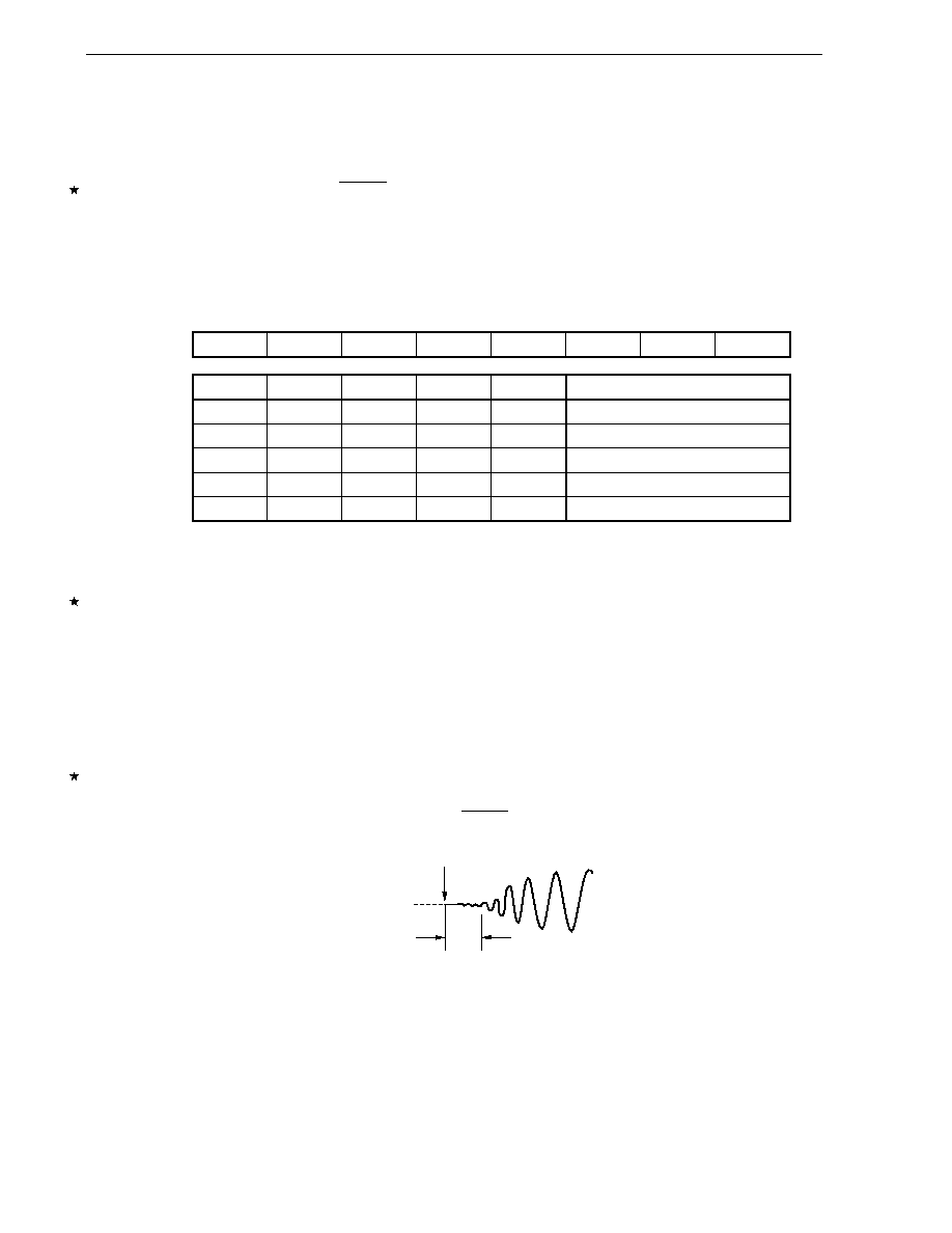
CHAPTER 5 CLOCK GENERATOR
User's Manual U16228EJ2V0UD
124
(5) Oscillation stabilization time counter status register (OSTC)
This is the status register of the X1 input clock oscillation stabilization time counter. If the Ring-OSC clock is used
as the CPU clock, the X1 input clock oscillation stabilization time can be checked.
OSTC can be read by a 1-bit or 8-bit memory manipulation instruction.
When reset is released (reset by RESET input, POC, LVI, clock monitor, and WDT), the STOP instruction,
MSTOP = 1, and MCC = 1 clear OSTC to 00H.
Figure 5-6. Format of Oscillation Stabilization Time Counter Status Register (OSTC)
Address: FFA3H After reset: 00H R
Symbol
7 6 5 4 3 2 1 0
OSTC 0
0
0
MOST11
MOST13 MOST14 MOST15 MOST16
MOST11
MOST13
MOST14
MOST15
MOST16
Oscillation stabilization time status
1 0 0 0 0
2
11
/f
XP
min. (204.8
µ
s min.)
1 1 0 0 0
2
13
/f
XP
min. (819.2
µ
s min.)
1 1 1 0 0
2
14
/f
XP
min. (1.64 ms min.)
1 1 1 1 0
2
15
/f
XP
min. (3.27 ms min.)
1 1 1 1 1
2
16
/f
XP
min. (6.55 ms min.)
Cautions 1. After the above time has elapsed, the bits are set to 1 in order from MOST11 and
remain 1.
2. If the STOP mode is entered and then released while the Ring-OSC is being used
as the CPU clock, set the oscillation stabilization time as follows.
∑
Desired OSTC oscillation stabilization time
Oscillation stabilization time
set by OSTS
The X1 oscillation stabilization time counter counts up to the oscillation
stabilization time set by OSTS. Note, therefore, that only the status up to the
oscillation stabilization time set by OSTS is set to OSTC after STOP mode is
released.
3. The wait time when STOP mode is released does not include the time after STOP
mode release until clock oscillation starts ("a" below) regardless of whether
STOP mode is released by RESET input or interrupt generation.
STOP mode release
X1 pin voltage
waveform
a
Remarks 1. Values in parentheses are reference values for operation with f
XP
= 10 MHz.
2. f
XP
: X1 input clock oscillation frequency

CHAPTER 5 CLOCK GENERATOR
User's Manual U16228EJ2V0UD
125
(6) Oscillation stabilization time select register (OSTS)
This register is used to select the X1 oscillation stabilization wait time when STOP mode is released.
The wait time set by OSTS is valid only after STOP mode is released with the X1 input clock selected as CPU
clock. After STOP mode is released with Ring-OSC selected as CPU clock, the oscillation stabilization time must
be confirmed by OSTC.
OSTS can be set by an 8-bit memory manipulation instruction.
RESET input sets OSTS to 05H.
Figure 5-7. Format of Oscillation Stabilization Time Select Register (OSTS)
Address: FFA4H After reset: 05H R/W
Symbol
7 6 5 4 3 2 1 0
OSTS
0 0 0 0 0
OSTS2
OSTS1
OSTS0
OSTS2
OSTS1
OSTS0
Oscillation stabilization time selection
0 0 1
2
11
/f
XP
(204.8
µ
s)
0 1 0
2
13
/f
XP
(819.2
µ
s)
0 1 1
2
14
/f
XP
(1.64 ms)
1 0 0
2
15
/f
XP
(3.27 ms)
1 0 1
2
16
/f
XP
(6.55 ms)
Other than above
Setting prohibited
Cautions 1. If the STOP mode is entered and then released while the Ring-OSC is being used
as the CPU clock, set the oscillation stabilization time as follows.
∑
Desired OSTC oscillation stabilization time
Oscillation stabilization time
set by OSTS
The X1 oscillation stabilization time counter counts up to the oscillation
stabilization time set by OSTS. Note, therefore, that only the status up to the
oscillation stabilization time set by OSTS is set to OSTC after STOP mode is
released.
2. The wait time when STOP mode is released does not include the time after STOP
mode release until clock oscillation starts ("a" below) regardless of whether
STOP mode is released by RESET input or interrupt generation.
STOP mode release
X1 pin voltage
waveform
a
Remarks 1. Values in parentheses are reference values for operation with f
XP
= 10 MHz.
2. f
XP
: X1 input clock oscillation frequency

CHAPTER 5 CLOCK GENERATOR
User's Manual U16228EJ2V0UD
126
5.4 System Clock Oscillator
5.4.1 X1 oscillator
The X1 oscillator oscillates with a crystal resonator or ceramic resonator (Standard: 8.38 MHz, 10 MHz when
REGC pin is directly connected to V
DD
) connected to the X1 and X2 pins.
An external clock can be input to the X1 oscillator when the REGC pin is directly connected to V
DD
. In this case,
input the clock signal to the X1 pin and input the inverse signal to the X2 pin.
Figure 5-8 shows examples of the external circuit of the X1 oscillator.
Figure 5-8. Examples of External Circuit of X1 Oscillator
(a) Crystal, ceramic oscillation
(b) External clock
V
SS
X1
X2
Crystal resonator or
ceramic resonator
External
clock
X1
X2
5.4.2 Subsystem clock oscillator
The subsystem clock oscillator oscillates with a crystal resonator (Standard: 32.768 kHz) connected to the XT1
and XT2 pins.
External clocks can be input to the subsystem clock oscillator when the REGC pin is directly connected to V
DD
. In
this case, input the clock signal to the XT1 pin and the inverse signal to the XT2 pin.
Figure 5-9 shows examples of an external circuit of the subsystem clock oscillator.
Figure 5-9. Examples of External Circuit of Subsystem Clock Oscillator
(a) Crystal oscillation
(b) External clock
XT2
V
SS
XT1
32.768
kHz
XT1
XT2
External
clock
Cautions are listed on the next page.
CHAPTER 5 CLOCK GENERATOR
User's Manual U16228EJ2V0UD
127
Cautions 1. When using the X1 oscillator and subsystem clock oscillator, wire as follows in the area
enclosed by the broken lines in the Figure 5-10 to avoid an adverse effect from wiring
capacitance.
∑ Keep the wiring length as short as possible.
∑ Do not cross the wiring with the other signal lines.
∑ Do not route the wiring near a signal line through which a high fluctuating current flows.
∑ Always make the ground point of the oscillator capacitor the same potential as V
SS
. Do
not ground the capacitor to a ground pattern through which a high current flows.
∑ Do not fetch signals from the oscillator.
Note that the subsystem clock oscillator is designed as a low-amplitude circuit for reducing
power consumption.
Figure 5-10 shows examples of incorrect resonator connection.
Figure 5-10. Examples of Incorrect Resonator Connection (1/2)
(a) Too long wiring
(b) Crossed signal line
X2
V
SS
X1
X1
V
SS
X2
PORT
Remark When using the subsystem clock, replace X1 and X2 with XT1 and XT2, respectively. Also, insert
resistors in series on the XT2 side.

CHAPTER 5 CLOCK GENERATOR
User's Manual U16228EJ2V0UD
128
Figure 5-10. Examples of Incorrect Resonator Connection (2/2)
(c) Wiring near high alternating current
(d) Current flowing through ground line of oscillator
(potential at points A, B, and C fluctuates)
V
SS
X1
X2
V
SS
X1
X2
A
B
C
Pmn
V
DD
High current
High current
(e) Signals are fetched
V
SS
X1
X2
Remark When using the subsystem clock, replace X1 and X2 with XT1 and XT2, respectively. Also, insert
resistors in series on the XT2 side.
Cautions 2. When X2 and XT1 are wired in parallel, the crosstalk noise of X2 may increase with XT1,
resulting in malfunctioning.
CHAPTER 5 CLOCK GENERATOR
User's Manual U16228EJ2V0UD
129
5.4.3 When subsystem clock is not used
If it is not necessary to use the subsystem clock for low power consumption operations and watch operations,
connect the XT1 and XT2 pins as follows.
XT1: Connect directly to EV
DD
or V
DD
XT2: Leave open
In this state, however, some current may leak via the on-chip feedback resistor of the subsystem clock oscillator
when the X1 input clock and Ring-OSC clock stop. To minimize leakage current, the above on-chip feedback resistor
can be set not to be used via bit 6 (FRC) of the processor clock control register (PCC). In this case also, connect the
XT1 and XT2 pins as described above.
Figure 5-11. Subsystem Clock Feedback Resistor
FRC
P-ch
Feedback resistor
XT1
XT2
Remark The feedback resistor is required to control the bias point of the oscillation waveform so that the bias
point is in the middle of the power supply voltage.
5.4.4 Ring-OSC oscillator
Ring-OSC oscillator is incorporated in the 78K0/KE1.
"Can be stopped by software" or "Cannot be stopped" can be selected by a mask option. The Ring-OSC clock
always oscillates after RESET release (240 kHz (TYP.)).
5.4.5 Prescaler
The prescaler generates various clocks by dividing the X1 oscillator output when the X1 input clock is selected as
the clock to be supplied to the CPU.
Caution When the Ring-OSC clock is selected as the clock supplied to the CPU, the prescaler generates
various clocks by dividing the Ring-OSC oscillator output (f
X
= 240 kHz (TYP.)).

CHAPTER 5 CLOCK GENERATOR
User's Manual U16228EJ2V0UD
130
5.5 Clock Generator Operation
The clock generator generates the following clocks and controls the operation modes of the CPU, such as standby
mode.
∑
X1 input clock f
XP
∑
Ring-OSC clock f
R
∑
Subsystem clock f
XT
∑
CPU clock f
CPU
∑
Clock to peripheral hardware
The CPU starts operation when the on-chip Ring-OSC oscillator starts outputting after reset release in the
78K0/KE1, thus enabling the following.
(1) Enhancement of security function
When the X1 input clock is set as the CPU clock by the default setting, the device cannot operate if the X1 input
clock is damaged or badly connected and therefore does not operate after reset is released. However, the start
clock of the CPU is the on-chip Ring-OSC clock, so the device can be started by the Ring-OSC clock after reset
release by the clock monitor (detection of X1 input clock stop). Consequently, the system can be safely shut
down by performing a minimum operation, such as acknowledging a reset source by software or performing
safety processing when there is a malfunction.
(2) Improvement of performance
Because the CPU can be started without waiting for the X1 input clock oscillation stabilization time, the total
performance can be improved.
A timing diagram of the CPU default start using Ring-OSC is shown in Figure 5-12.
CHAPTER 5 CLOCK GENERATOR
User's Manual U16228EJ2V0UD
131
Figure 5-12. Timing Diagram of CPU Default Start Using Ring-OSC
Ring-OSC clock
(f
R
)
CPU clock
X1 input clock
(f
XP
)
Operation
stopped: 17/f
R
X1 oscillation stabilization time: 2
11
/f
XP
to 2
16
/f
XP
Note
RESET
Ring-OSC clock
X1 input clock
Switched by software
Subsystem clock
(f
XT
)
Note Check using the oscillation stabilization time counter status register (OSTC).
(a) When the RESET signal is generated, bit 0 of the main clock mode register (MCM) is set to 0 and the Ring-
OSC clock is set as the CPU clock. However, a clock is supplied to the CPU after 17 clocks of the Ring-OSC
clock have elapsed after RESET release (or clock supply to the CPU stops for 17 clocks). During the
RESET period, oscillation of the X1 input clock and Ring-OSC clock is stopped.
(b) After RESET release, the CPU clock can be switched from the Ring-OSC clock to the X1 input clock using bit
0 (MCM0) of the main clock mode register (MCM) after the X1 input clock oscillation stabilization time has
elapsed. At this time, check the oscillation stabilization time using the oscillation stabilization time counter
status register (OSTC) before switching the CPU clock. The CPU clock status can be checked using bit 1
(MCS) of MCM.
(c) Ring-OSC can be set to stopped/oscillating using the Ring-OSC mode register (RCM) when "Can be stopped
by software" is selected for the Ring-OSC by a mask option, if the X1 input or subsystem clock is used as the
CPU clock. Make sure that MCS is 1 at this time.
(d) When Ring-OSC is used as the CPU clock, the X1 input clock can be set to stopped/oscillating using the
main OSC control register (MOC). Make sure that MCS is 0 at this time.
When the subsystem clock is used as the CPU clock, whether the X1 input clock stops or oscillates can be
set by the processor clock control register (PCC). In addition, HALT mode can be used during operation with
the subsystem clock, but STOP mode cannot be used (subsystem clock oscillation cannot be stopped by the
STOP instruction).
(e) Select the X1 input clock oscillation stabilization time (2
11
/f
XP
, 2
13
/f
XP
, 2
14
/f
XP
, 2
15
/f
XP
, 2
16
/f
XP
) using the oscillation
stabilization time select register (OSTS) when releasing STOP mode while X1 input clock is being used as
the CPU clock. In addition, when releasing STOP mode while RESET is released and Ring-OSC is being
used as the CPU clock, check the X1 input clock oscillation stabilization time using the oscillation
stabilization time counter status register (OSTC).
CHAPTER 5 CLOCK GENERATOR
User's Manual U16228EJ2V0UD
132
A status transition diagram of this product is shown in Figure 5-13, and the relationship between the operation
clocks in each operation status and between the oscillation control flag and oscillation status of each clock are shown
in Tables 5-3 and 5-4, respectively.
Figure 5-13. Status Transition Diagram (1/4)
(1) When "Ring-OSC can be stopped by software" is selected by mask option
(when subsystem clock is not used)
Status 4
CPU clock: f
XP
f
XP
: Oscillating
f
R
: Oscillation stopped
Status 3
CPU clock: f
XP
f
XP
: Oscillating
f
R
: Oscillating
Status 1
CPU clock: f
R
f
XP
: Oscillation stopped
f
R
: Oscillating
Status 2
CPU clock: f
R
f
XP
: Oscillating
f
R
: Oscillating
HALT
Note 4
Interrupt
Interrupt
Interrupt
Interrupt
Interrupt
Interrupt
Reset release
Interrupt
Interrupt
HALT
instruction
STOP
instruction
STOP
instruction
STOP
instruction
STOP
instruction
RSTOP = 0
RSTOP = 1
Note 1
MCM0 = 0
MCM0 = 1
Note 2
MSTOP = 1
Note 3
MSTOP = 0
HALT
instruction
HALT instruction
HALT
instruction
STOP
Note 4
Reset
Note 5
Notes 1. When shifting from status 3 to status 4, make sure that bit 1 (MCS) of the main clock mode register
(MCM) is 1.
2. Before shifting from status 2 to status 3 after reset and STOP are released, check the X1 input clock
oscillation stabilization time status using the oscillation stabilization time counter status register
(OSTC).
3. When shifting from status 2 to status 1, make sure that MCS is 0.
4. When "Ring-OSC can be stopped by software" is selected by a mask option, the watchdog timer
stops operating in the HALT and STOP modes, regardless of the source clock of the watchdog timer.
However, oscillation of Ring-OSC does not stop even in the HALT and STOP modes if RSTOP = 0.
5. All reset sources (RESET input, POC, LVI, clock monitor, and WDT)
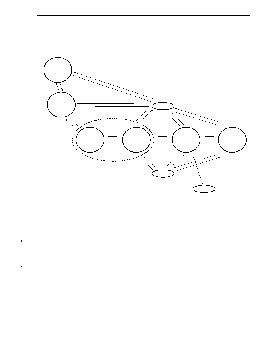
CHAPTER 5 CLOCK GENERATOR
User's Manual U16228EJ2V0UD
133
Figure 5-13. Status Transition Diagram (2/4)
(2) When "Ring-OSC can be stopped by software" is selected by mask option
(when subsystem clock is used)
HALT
Note 4
Interrupt
Interrupt
Interrupt
Interrupt
Interrupt
Interrupt
Interrupt
HALT
instruction
HALT
instruction
STOP
instruction
STOP
instruction
STOP
instruction
RSTOP = 0
RSTOP = 1
Note 1
MCC = 0
CSS = 0
Note 5
MCC = 1
CSS = 1
Note 5
MCM0 = 0
MCM0 = 1
Note 2
MSTOP = 1
Note 3
MSTOP = 0
HALT
instruction
HALT
instruction
STOP
Note 4
Reset
Note 6
Status 4
CPU clock: f
XP
f
XP
: Oscillating
f
R
: Oscillation
stopped
Status 3
CPU clock: f
XP
f
XP
: Oscillating
f
R
: Oscillating
Status 1
CPU clock: f
R
f
XP
: Oscillation
stopped
f
R
: Oscillating
Status 2
CPU clock: f
R
f
XP
: Oscillating
f
R
: Oscillating
Reset release
Interrupt
HALT
instruction
Status 6
CPU clock: f
XT
f
XP
: Oscillation
stopped
f
R
: Oscillating/
oscillation
stopped
Status 5
CPU clock: f
XT
f
XP
: Oscillating
f
R
: Oscillating/
oscillation
stopped
Notes 1. When shifting from status 3 to status 4, make sure that bit 1 (MCS) of the main clock mode register
(MCM) is 1.
2. Before shifting from status 2 to status 3 after reset and STOP are released, check the X1 input clock
oscillation stabilization time status using the oscillation stabilization time counter status register
(OSTC).
3. When shifting from status 2 to status 1, make sure that MCS is 0.
4. When "Ring-OSC can be stopped by software" is selected by a mask option, the clock supply to the
watchdog timer is stopped after the HALT or STOP instruction has been executed, regardless of the
setting of bit 0 (RSTOP) of the Ring-OSC mode register (RCM) and bit 0 (MCM0) of the main clock
mode register (MCM).
5. The operation cannot be shifted between subsystem clock operation and Ring-OSC operation.
6. All reset sources (RESET input, POC, LVI, clock monitor, and WDT)

CHAPTER 5 CLOCK GENERATOR
User's Manual U16228EJ2V0UD
134
Figure 5-13. Status Transition Diagram (3/4)
(3) When "Ring-OSC cannot be stopped" is selected by mask option
(when subsystem clock is not used)
Status 3
CPU clock: f
XP
f
XP
: Oscillating
f
R
: Oscillating
HALT
Interrupt
Interrupt
Interrupt
STOP
instruction
MCM0 = 0
MCM0 = 1
Note 1
HALT
instruction
HALT
instruction
STOP
Note 3
Reset
Note 4
Status 2
CPU clock: f
R
f
XP
: Oscillating
f
R
: Oscillating
Status 1
CPU clock: f
R
f
XP
: Oscillation stopped
f
R
: Oscillating
Interrupt
STOP
instruction
Interrupt
Interrupt
STOP
instruction
MSTOP = 1
Note 2
MSTOP = 0
HALT instruction
Reset release
Notes 1. Before shifting from status 2 to status 3 after reset and STOP are released, check the X1 input clock
oscillation stabilization time status using the oscillation stabilization time counter status register
(OSTC).
2. When shifting from status 2 to status 1, make sure that MCS is 0.
3. The watchdog timer operates using Ring-OSC even in STOP mode if "Ring-OSC cannot be stopped"
is selected by a mask option. Ring-OSC division can be selected as the count source of 8-bit timer
H1 (TMH1), so clear the watchdog timer using the TMH1 interrupt request before watchdog timer
overflow. If this processing is not performed, an internal reset signal is generated at watchdog timer
overflow after STOP instruction execution.
4. All reset sources (RESET input, POC, LVI, clock monitor, and WDT)
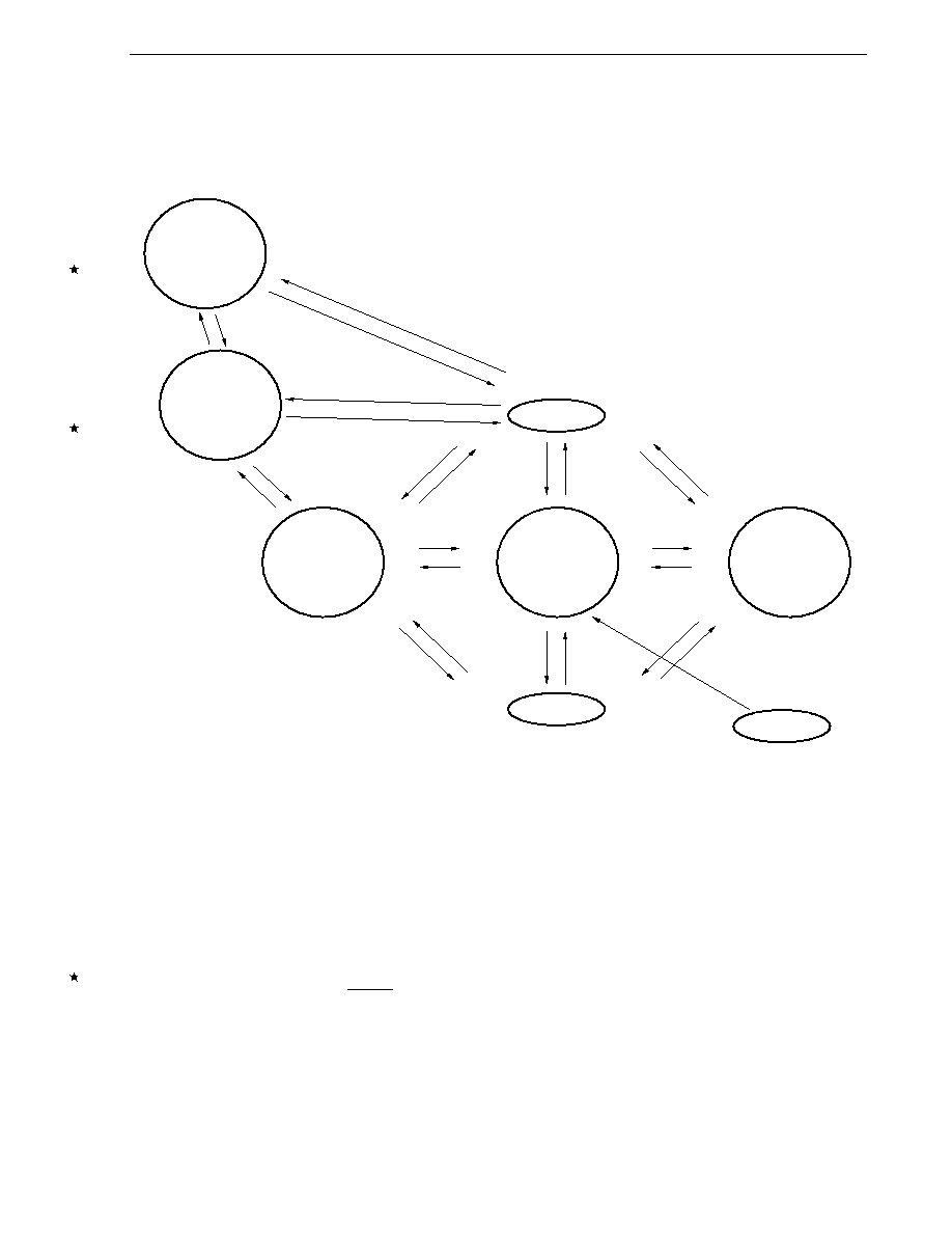
CHAPTER 5 CLOCK GENERATOR
User's Manual U16228EJ2V0UD
135
Figure 5-13. Status Transition Diagram (4/4)
(4) When "Ring-OSC cannot be stopped" is selected by mask option
(when subsystem clock is used)
HALT
Interrupt
Interrupt
Interrupt
STOP
instruction
MCM0 = 0
MCM0 = 1
Note 1
HALT
instruction
HALT
instruction
STOP
Note 3
Reset
Note 5
Interrupt
STOP
instruction
Interrupt
Interrupt
STOP
instruction
MSTOP = 1
Note 2
MSTOP = 0
HALT instruction
Reset release
MCC = 0
CSS = 0
Note 5
MCC = 1
CSS = 1
Note 4
Interrupt
Interrupt
HALT instruction
HALT instruction
Status 3
CPU clock: f
XP
f
XP
: Oscillating
f
R
: Oscillating
Status 2
CPU clock: f
R
f
XP
: Oscillating
f
R
: Oscillating
Status 1
CPU clock: f
R
f
XP
: Oscillation stopped
f
R
: Oscillating
Status 5
CPU clock: f
XT
f
XP
: Oscillation stopped
f
R
: Oscillating
Status 4
CPU clock: f
XT
f
XP
: Oscillating
f
R
: Oscillating
Notes 1. Before shifting from status 2 to status 3 after reset and STOP are released, check the X1 input clock
oscillation stabilization time status using the oscillation stabilization time counter status register
(OSTC).
2. When shifting from status 2 to status 1, make sure that MCS is 0.
3. The watchdog timer operates using Ring-OSC even in STOP mode if "Ring-OSC cannot be stopped"
is selected by a mask option. Ring-OSC division can be selected as the count source of 8-bit timer
H1 (TMH1), so clear the watchdog timer using the TMH1 interrupt request before watchdog timer
overflow. If this processing is not performed, an internal reset signal is generated at watchdog timer
overflow after STOP instruction execution.
4. The operation cannot be shifted between subsystem clock operation and Ring-OSC operation.
5. All reset sources (RESET input, POC, LVI, clock monitor, and WDT)
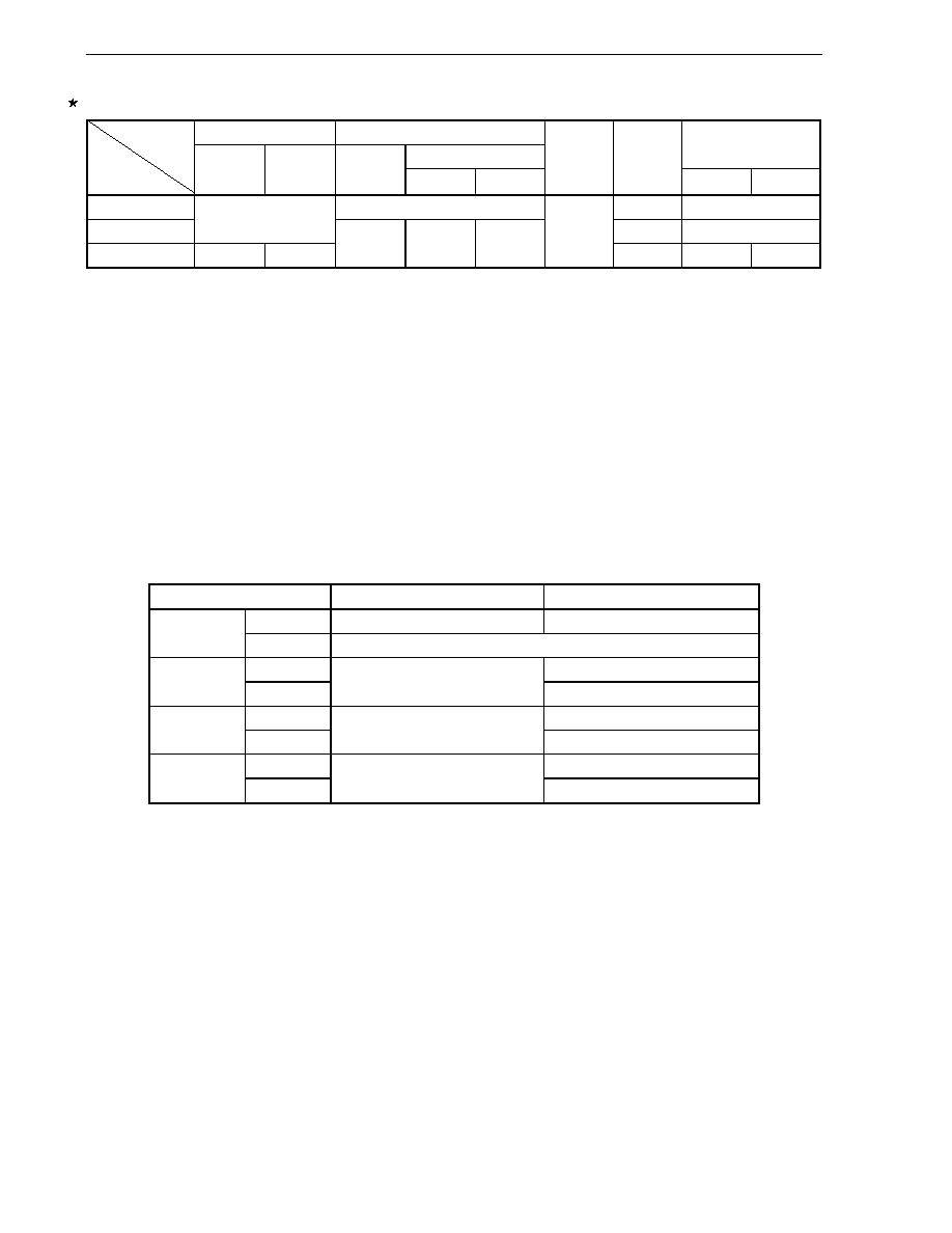
CHAPTER 5 CLOCK GENERATOR
User's Manual U16228EJ2V0UD
136
Table 5-3. Relationship Between Operation Clocks in Each Operation Status
X1 Oscillator
Ring-OSC Oscillator
Note 2
Prescaler Clock
Supplied to Peripherals
Status
Operation
Mode
MSTOP = 0
MCC = 0
MSTOP = 1
MCC = 1
Note 1
RSTOP = 0 RSTOP = 1
Subsystem
Clock
Oscillator
CPU Clock
After
Release
MCM0 = 0 MCM0 = 1
Reset Stopped
Ring-OSC
Stopped
STOP
Stopped
Note 3
Stopped
HALT Oscillating
Stopped
Oscillating
Oscillating
Stopped
Oscillating
Note 4
Ring-OSC X1
Notes 1. When "Cannot be stopped" is selected for Ring-OSC by a mask option.
2. When "Can be stopped by software" is selected for Ring-OSC by a mask option.
3. Operates using the CPU clock at STOP instruction execution.
4. Operates using the CPU clock at HALT instruction execution.
Caution The RSTOP setting is valid only when "Can be stopped by software" is set for Ring-OSC by a mask
option.
Remark MSTOP: Bit 7 of the main OSC control register (MOC)
MCC:
Bit 7 of the processor clock control register (PCC)
RSTOP: Bit 0 of the Ring-OSC mode register (RCM)
MCM0:
Bit 0 of the main clock mode register (MCM)
Table 5-4. Oscillation Control Flags and Clock Oscillation Status
X1
Oscillator
Ring-OSC
Oscillator
RSTOP = 0
Stopped
Oscillating
MSTOP = 1
Note
RSTOP = 1
Setting prohibited
RSTOP = 0
Oscillating
MSTOP = 0
Note
RSTOP = 1
Oscillating
Stopped
RSTOP = 0
Oscillating
MCC = 1
Note
RSTOP = 1
Stopped
Stopped
RSTOP = 0
Oscillating
MCC = 0
Note
RSTOP = 1
Oscillating
Stopped
Note Setting X1 oscillator oscillating/stopped differs depending on the CPU clock used.
∑
When the Ring-OSC clock is used as the CPU clock: Set using the MSTOP bit
∑
When the subsystem clock is used as the CPU clock: Set using the MCC bit
Caution The RSTOP setting is valid only when "Can be stopped by software" is set for Ring-OSC
by a mask option.
Remark MSTOP: Bit 7 of the main OSC control register (MOC)
MCC:
Bit 7 of the processor clock control register (PCC)
RSTOP: Bit 0 of the Ring-OSC mode register (RCM)
CHAPTER 5 CLOCK GENERATOR
User's Manual U16228EJ2V0UD
137
5.6 Time Required to Switch Between Ring-OSC Clock and X1 Input Clock
Bit 0 (MCM0) of the main clock mode register (MCM) is used to switch between the Ring-OSC clock and X1 input
clock.
In the actual switching operation, switching does not occur immediately after MCM0 rewrite; several instructions
are executed using the pre-switch clock after switching MCM0 (see Table 5-5).
Bit 1 (MCS) of MCM is used to judge that operation is performed using either the Ring-OSC clock or X1 input clock.
To stop the original clock after switching the clock, wait for the number of clocks shown in Table 5-5 before
stopping.
Table 5-5. Time Required to Switch Between Ring-OSC Clock and X1 Input Clock
PCC
Time Required for Switching
PCC2 PCC1 PCC0
X1
Ring-OSC Ring-OSC
X1
0 0 0
f
XP
/f
R
+ 1 clock
0 0 1
f
XP
/2f
R
+ 1 clock
0 1 0
f
XP
/4f
R
+ 1 clock
0 1 1
f
XP
/8f
R
+ 1 clock
1 0 0
f
XP
/16f
R
+ 1 clock
2 clocks
Caution To calculate the maximum time, set f
R
= 120 kHz.
Remarks 1. PCC: Processor clock control register
2. f
XP
: X1 input clock oscillation frequency
3. f
R
: Ring-OSC clock oscillation frequency
4. The maximum time is the number of clocks of the CPU clock before switching.

CHAPTER 5 CLOCK GENERATOR
User's Manual U16228EJ2V0UD
138
5.7 Time Required for CPU Clock Switchover
The CPU clock can be switched using bits 0 to 2 (PCC0 to PCC2) and bit 4 (CSS) of the processor clock control
register (PCC).
The actual switchover operation is not performed immediately after rewriting to the PCC; operation continues on
the pre-switchover clock for several instructions (see Table 5-6).
Whether the system is operating on the X1 input clock (or Ring-OSC clock) or the subsystem clock can be
ascertained using bit 5 (CLS) of the PCC register.
Table 5-6. Maximum Time Required for CPU Clock Switchover
Set Value Before
Switchover
Set Value After Switchover
CSS PCC2 PCC1 PCC0 CSS PCC2 PCC1 PCC0 CSS PCC2 PCC1 PCC0 CSS PCC2 PCC1 PCC0 CSS PCC2 PCC1 PCC0 CSS PCC2 PCC1 PCC0
CSS PCC2 PCC1 PCC0
0 0 0 0 0 0 0 1 0 0 1 0 0 0 1 1 0 1 0 0 1
◊
◊
◊
0
0
0
16 clocks
16 clocks
16 clocks
16 clocks
f
XP
/f
XT
clocks
(306 clocks)
0
0
1
8 clocks
8 clocks
8 clocks
8 clocks
f
XP
/2f
XT
clocks
(153 clocks)
0
1
0
4 clocks
4 clocks
4 clocks
4 clocks
f
XP
/4f
XT
clocks
(77 clocks)
0
1
1
2 clocks
2 clocks
2 clocks
2 clocks
f
XP
/8f
XT
clocks
(39 clocks)
0
1
0
0
1 clock
1 clock 1
clock 1
clock
f
XP
/16f
XT
clocks
(20 clocks)
1
◊
◊
◊
1 clock
1 clock
1 clock 1
clock 1
clock
Remarks 1. The maximum time is the number of clocks of the pre-switchover CPU clock.
2. Figures in parentheses apply to operation with f
XP
= 10 MHz and f
XT
= 32.768 kHz.
Caution Selection of the CPU clock cycle division factor (PCC0 to PCC2) and switchover from the X1
input clock to the subsystem clock (changing CSS from 0 to 1) should not be set
simultaneously.
Simultaneous setting is possible, however, for selection of the CPU clock cycle division factor
(PCC0 to PCC2) and switchover from the subsystem clock to the X1 input clock (changing CSS
from 1 to 0).
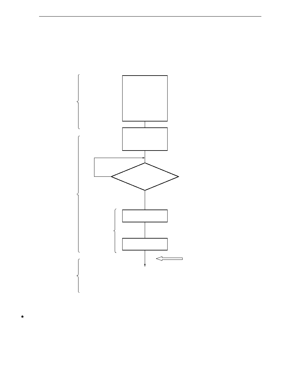
CHAPTER 5 CLOCK GENERATOR
User's Manual U16228EJ2V0UD
139
5.8 Clock Switching Flowchart and Register Setting
5.8.1 Switching from Ring-OSC clock to X1 input clock
Figure 5-14. Switching from Ring-OSC Clock to X1 Input Clock (Flowchart)
; f
CPU
= f
R
; Ring-OSC oscillation
; Ring-OSC clock operation
; X1 oscillation
; Oscillation stabilization time status register
; Oscillation stabilization time f
XP
/2
16
MCM.1 (MCS) is changed from 0 to 1
; X1 oscillation stabilization time status check
X1 oscillation stabilization time has elapsed
X1 oscillation stabilization
time has not elapsed
PCC = 00H
RCM = 00H
MCM = 00H
MOC = 00H
OSTC = 00H
OSTS = 05H
Note
OSTC check
Note
Each processing
After reset
PCC setting
MCM.0
1
X1 input clock operation
Ring-OSC
clock operation
(dividing set PCC)
Register value
after reset
Ring-OSC clock
operation
X1 input clock
Note Check the oscillation stabilization wait time of the X1 oscillator after reset release using the OSTC register
and then switch to the X1 input clock operation after the oscillation stabilization wait time has elapsed. The
OSTS register setting is valid only after STOP mode is released by interrupt during X1 input clock operation.
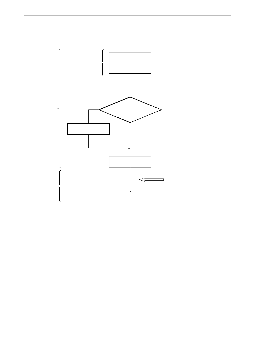
CHAPTER 5 CLOCK GENERATOR
User's Manual U16228EJ2V0UD
140
5.8.2 Switching from X1 input clock to Ring-OSC clock
Figure 5-15. Switching from X1 Input Clock to Ring-OSC Clock (Flowchart)
MCM.1 (MCS) is changed from 1 to 0
; Ring-OSC oscillating
; Ring-OSC oscillating?
Ring-OSC clock operation
; X1 oscillation
; X1 input clock or Ring-OSC clock
; X1 input clock operation
No: RSTOP = 0
Yes: RSTOP = 1
PCC.7 (MCC) = 0
PCC.4 (CSS) = 0
MCM = 03H
RCM.0
Note
(RSTOP) = 1?
RSTOP = 0
MCM0
0
Register setting
in X1 input
clock operation
X1 input
clock operation
Ring-OSC
clock operation
Note Required only when "clock can be stopped by software" is selected for Ring-OSC by a mask option.

CHAPTER 5 CLOCK GENERATOR
User's Manual U16228EJ2V0UD
141
5.8.3 Switching from X1 input clock to subsystem clock
Figure 5-16. Switching from X1 Input Clock to Subsystem Clock (Flowchart)
MCS = 1 not changed.
CLS is changed from 0 to 1.
; Subsystem clock operation
Subsystem clock operation
; X1 oscillation
; X1 input clock or Ring-OSC clock
; X1 input clock operation
PCC.7 (MCC) = 0
PCC.4 (CSS) = 0
MCM = 03H
CSS
1
Note
Register setting
in X1 input
clock operation
X1 input
clock operation
Subsystem
clock
Note Set CSS to 1 after confirming that oscillation of the subsystem clock is stabilized.
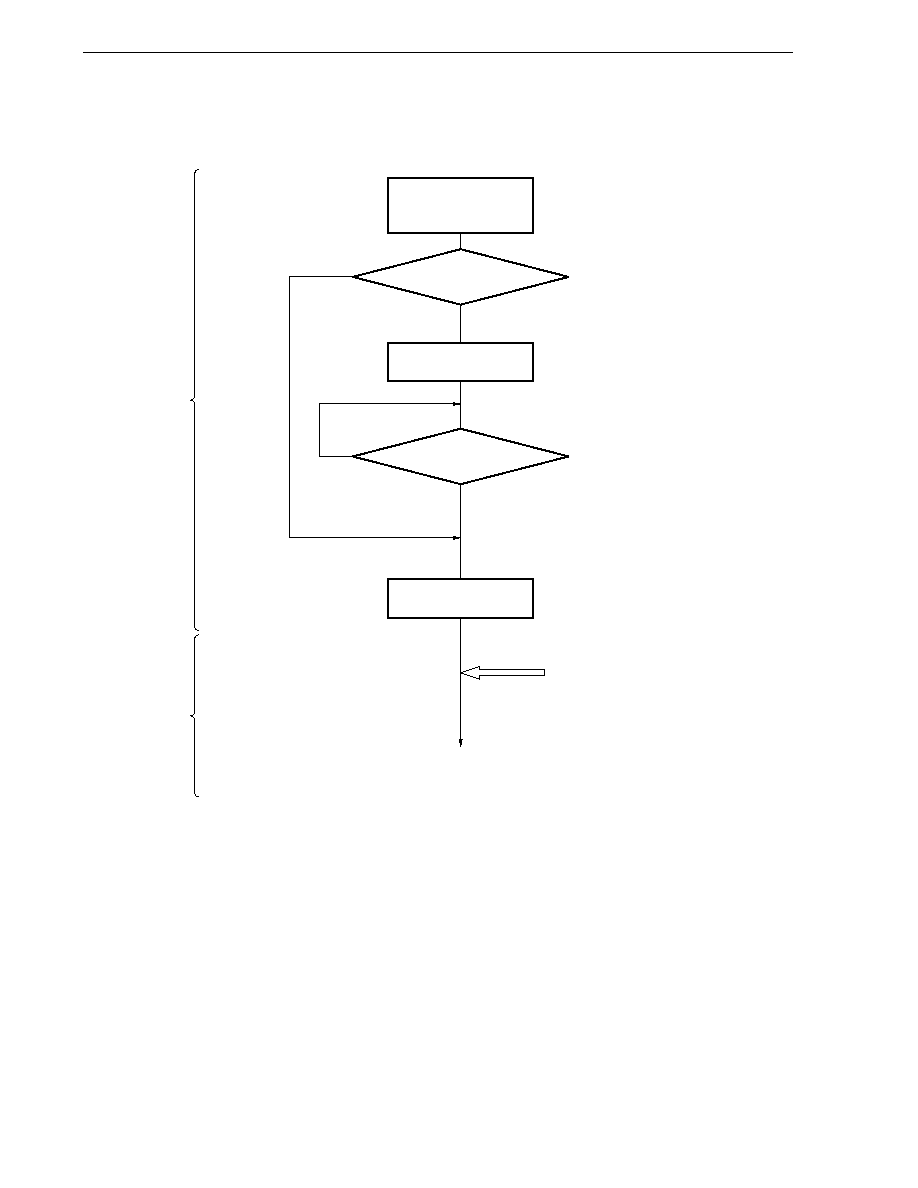
CHAPTER 5 CLOCK GENERATOR
User's Manual U16228EJ2V0UD
142
5.8.4 Switching from subsystem clock to X1 input clock
Figure 5-17. Switching from Subsystem Clock to X1 Input Clock (Flowchart)
; Subsystem clock operation
; X1 oscillating?
; X1 oscillation enabled
; Wait for X1 oscillation stabilization time
; X1 input clock operation
CLS is changed from 1 to 0.
MCS = 1 not changed.
X1 oscillation stabilization time elapsed
X1 oscillation
stabilization time
not elapsed
Yes: X1 oscillation stopped
No: X1 oscillating
MCC
0
PCC.4 (CSS) = 1
MCM = 03H
MCC = 1?
OSTC check
CSS
0
X1 input clock operation
Subsystem
clock operation
X1 input
clock operation
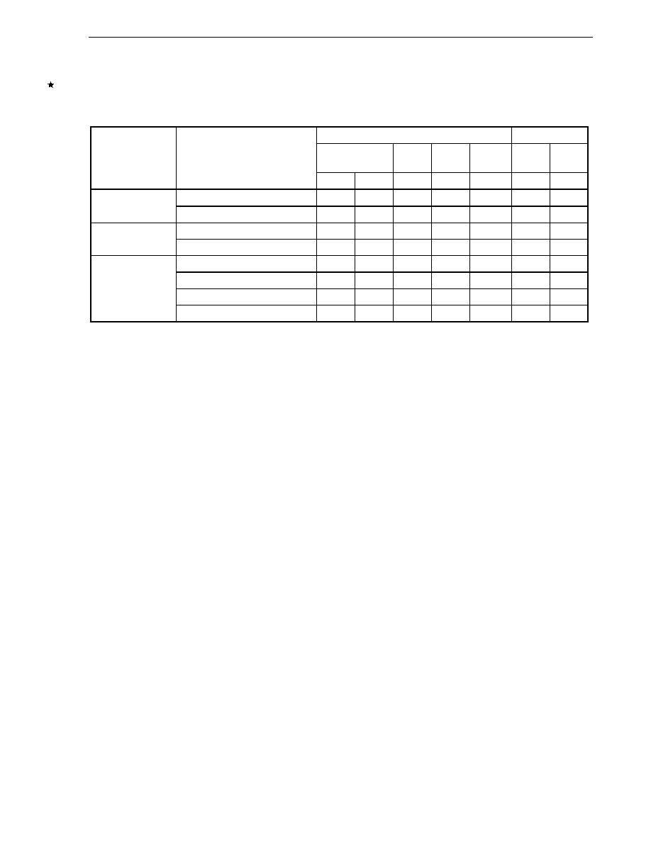
CHAPTER 5 CLOCK GENERATOR
User's Manual U16228EJ2V0UD
143
5.8.5 Register settings
The table below shows the statuses of the setting flags and status flags when each mode is set.
Table 5-7. Clock and Register Setting
Setting Flag
Status Flag
PCC Register
MCM
Register
MOC
Register
RCM
Register
PCC
Register
MCM
Register
f
CPU
Mode
MCC CSS MCM0
MSTOP
RSTOP
Note 1
CLS
MCS
Ring-OSC
oscillating
0 0 1 0 0 0 1
X1 input clock
Note 2
Ring-OSC
stopped
0 0 1 0 1 0 1
X1
oscillating
0 0 0 0 0 0 0
Ring-OSC clock
X1 stopped
0
Note 3
0 0 1 0 0 0
X1 oscillating, Ring-OSC oscillating
0
1
1
Note 5
0
Note 6
0 1 1
X1 stopped, Ring-OSC oscillating
1
1
1
Note 5
0
Note 6
0 1 1
X1 oscillating, Ring-OSC stopped
0
1
1
Note 5
0
Note 6
1 1 1
Subsystem clock
Note 4
X1 stopped, Ring-OSC stopped
1
1
1
Note 5
0
Note 6
1 1 1
Notes 1. Valid only when "clock can be stopped by software" is selected for Ring-OSC by a mask option.
2. Do not set MCC = 1 or MSTOP = 1 during X1 input clock operation (even if MCC = 1 or MSTOP = 1 is set,
the X1 oscillation does not stop).
3. Do not set MCC = 1 during Ring-OSC operation (even if MCC = 1 is set, the X1 oscillation does not stop).
To stop X1 oscillation during Ring-OSC operation, use MSTOP.
4. Shifting to subsystem clock operation mode must be performed from the X1 input clock operation mode.
From subsystem clock operation mode, only X1 input clock operation mode can be shifted to.
5. Do not set MCM0 = 0 (shifting to Ring-OSC) during subsystem clock operation.
6. Do not set MSTOP = 1 during subsystem clock operation (even if MSTOP = 1 is set, X1 oscillation does
not stop). To stop X1 oscillation during subsystem clock operation, use MCC.

User's Manual U16228EJ2V0UD
144
CHAPTER 6 16-BIT TIMER/EVENT COUNTERS 00 AND 01
The
µ
PD780131 and 780132 incorporate 16-bit timer/event counter 00, and the
µ
PD780133, 780134, 78F0134,
780136, 780138, and 78F0138 incorporate 16-bit timer/event counters 00 and 01.
6.1 Functions of 16-Bit Timer/Event Counters 00 and 01
16-bit timer/event counters 00 and 01
Note
have the following functions.
∑
Interval
timer
∑
PPG output
∑
Pulse width measurement
∑
External event counter
∑
Square-wave
output
∑
One-shot pulse output
(1) Interval
timer
16-bit timer/event counters 00 and 01 generate an interrupt request at the preset time interval.
(2) PPG
output
16-bit timer/event counters 00 and 01 can output a rectangular wave whose frequency and output pulse width can
be set freely.
(3) Pulse width measurement
16-bit timer/event counters 00 and 01 can measure the pulse width of an externally input signal.
(4) External event counter
16-bit timer/event counters 00 and 01 can measure the number of pulses of an externally input signal.
(5) Square-wave
output
16-bit timer/event counters 00 and 01 can output a square wave with any selected frequency.
(6) One-shot pulse output
16-bit timer event counters 00 and 01 can output a one-shot pulse whose output pulse width can be set freely.
Note Available only for the
µ
PD780133, 780134, 78F0134, 780136, 780138, and 78F0138.
CHAPTER 6 16-BIT TIMER/EVENT COUNTERS 00 AND 01
User's Manual U16228EJ2V0UD
145
6.2 Configuration of 16-Bit Timer/Event Counters 00 and 01
16-bit timer/event counters 00 and 01 include the following hardware.
Table 6-1. Configuration of 16-Bit Timer/Event Counters 00 and 01
Item Configuration
Timer counter
16 bits (TM0n)
Register
16-bit timer capture/compare register: 16 bits (CR00n, CR01n)
Timer input
TI00n, TI01n
Timer output
TO0n, output controller
Control registers
16-bit timer mode control register 0n (TMC0n)
16-bit timer capture/compare control register 0n (CRC0n)
16-bit timer output control register 0n (TOC0n)
Prescaler mode register 0n (PRM0n)
Port mode register 0 (PM0)
Port register 0 (P0)
Remark n = 0:
µ
PD780131, 780132
n = 0, 1:
µ
PD780133, 780134, 78F0134, 780136, 780138, 78F0138
Figures 6-1 and 6-2 show the block diagrams.
Figure 6-1. Block Diagram of 16-Bit Timer/Event Counter 00
Internal bus
Capture/compare control
register 00 (CRC00)
TI010/TO00/P01
f
X
f
X
/2
2
f
X
/2
8
f
X
TI000/P00
Prescaler mode
register 00 (PRM00)
2
PRM001 PRM000
CRC002
16-bit timer capture/compare
register 010 (CR010)
Match
Match
16-bit timer counter 00
(TM00)
Clear
Noise
elimi-
nator
CRC002 CRC001 CRC000
INTTM000
TO00/TI010/
P01
INTTM010
16-bit timer output
control register 00
(TOC00)
16-bit timer mode
control register 00
(TMC00)
Internal bus
TMC003 TMC002 TMC001 OVF00
TOC004 LVS00 LVR00 TOC001 TOE00
Selector
16-bit timer capture/compare
register 000 (CR000)
Selector
Selector
Selector
Noise
elimi-
nator
Noise
elimi-
nator
Output
controller
OSPE00
OSPT00
Output latch
(P01)
PM01
CHAPTER 6 16-BIT TIMER/EVENT COUNTERS 00 AND 01
User's Manual U16228EJ2V0UD
146
Figure 6-2. Block Diagram of 16-Bit Timer/Event Counter 01
(
µ
PD780133, 780134, 78F0134, 780136, 780138, 78F0138 Only)
Internal bus
Capture/compare control
register 01 (CRC01)
TI011/TO01/P06
f
X
f
X
/2
4
f
X
/2
6
f
X
TI001/P05
Prescaler mode
register 01 (PRM01)
2
PRM011 PRM010
CRC012
16-bit timer capture/compare
register 011 (CR011)
Match
Match
16-bit timer counter 01
(TM01)
Clear
Noise
elimi-
nator
CRC012 CRC011 CRC010
INTTM001
TO01/TI011/
P06
INTTM011
16-bit timer output
control register 01
(TOC01)
16-bit timer mode
control register 01
(TMC01)
Internal bus
TMC013 TMC012 TMC011 OVF01
TOC014 LVS01 LVR01 TOC011 TOE01
Selector
16-bit timer capture/compare
register 001 (CR001)
Selector
Selector
Selector
Noise
elimi-
nator
Noise
elimi-
nator
Output
controller
OSPE01
OSPT01
Output latch
(P06)
PM06
CHAPTER 6 16-BIT TIMER/EVENT COUNTERS 00 AND 01
User's Manual U16228EJ2V0UD
147
(1) 16-bit timer counter 0n (TM0n)
TM0n is a 16-bit read-only register that counts count pulses.
The counter is incremented in synchronization with the rising edge of the input clock.
Figure 6-3. Format of 16-Bit Timer Counter 0n (TM0n)
TM0n
(n = 0, 1)
Symbol
FF11H (TM00)
FFB1H (TM01)
FF10H (TM00)
FFB0H (TM01)
Address: FF10H, FF11H (TM00), FFB0H, FFB1H (TM01) After reset: 0000H R
The count value is reset to 0000H in the following cases.
<1> At RESET input
<2> If TMC0n3 and TMC0n2 are cleared
<3> If the valid edge of TI00n is input in the mode in which clear & start occurs when inputting the valid edge of
TI00n
<4> If TM0n and CR00n match in the mode in which clear & start occurs on a match of TM0n and CR00n
<5> OSPT0n is set in one-shot pulse output mode
(2) 16-bit timer capture/compare register 00n (CR00n)
CR00n is a 16-bit register that has the functions of both a capture register and a compare register. Whether it is
used as a capture register or as a compare register is set by bit 0 (CRC0n0) of capture/compare control register
0n (CRC0n).
CR00n can be set by a 16-bit memory manipulation instruction.
RESET input clears this register to 0000H.
Figure 6-4. Format of 16-Bit Timer Capture/Compare Register 00n (CR00n)
CR00n
(n = 0, 1)
Symbol
FF13H (CR000)
FFB3H (CR001)
FF12H (CR000)
FFB2H (CR001)
Address: FF12H, FF13H (CR000), FFB2H, FFB3H (CR001) After reset: 0000H R/W
∑
When CR00n is used as a compare register
The value set in CR00n is constantly compared with 16-bit timer counter 0n (TM0n) count value, and an
interrupt request (INTTM00n) is generated if they match. The set value is held until CR00n is rewritten.
∑
When CR00n is used as a capture register
It is possible to select the valid edge of the TI00n pin or the TI01n pin as the capture trigger. The TI00n or
TI01n pin valid edge is set using prescaler mode register 0n (PRM0n) (see Table 6-2).

CHAPTER 6 16-BIT TIMER/EVENT COUNTERS 00 AND 01
User's Manual U16228EJ2V0UD
148
Table 6-2. CR00n Capture Trigger and Valid Edges of TI00n and TI01n Pins
(1) TI00n pin valid edge selected as capture trigger (CRC0n1 = 1, CRC0n0 = 1)
TI00n Pin Valid Edge
CR00n Capture Trigger
ES0n1
ES0n0
Falling edge
Rising edge
0
1
Rising edge
Falling edge
0
0
No capture operation
Both rising and falling edges
1
1
(2) TI01n pin valid edge selected as capture trigger (CRC0n1 = 0, CRC0n0 = 1)
TI01n Pin Valid Edge
CR00n Capture Trigger
ES1n1
ES1n0
Falling edge
Falling edge
0
0
Rising edge
Rising edge
0
1
Both rising and falling edges
Both rising and falling edges
1
1
Remarks 1. Setting ES0n1, ES0n0 = 1, 0 and ES1n1, ES1n0 = 1, 0 is prohibited.
2.
ES0n1, ES0n0:
Bits 5 and 4 of prescaler mode register 0n (PRM0n)
ES1n1, ES1n0:
Bits 7 and 6 of prescaler mode register 0n (PRM0n)
CRC0n1, CRC0n0: Bits 1 and 0 of capture/compare control register 0n (CRC0n)
3. n = 0:
µ
PD780131, 780132
n = 0, 1:
µ
PD780133, 780134, 78F0134, 780136, 780138, 78F0138
Cautions 1. Set a value other than 0000H in CR00n in the mode in which clear & start occurs on a match
of TM0n and CR00n. However, in the free-running mode and in the clear mode using the
valid edge of TI00n, if CR00n is cleared to 0000H, an interrupt request (INTTM00n) is
generated when the value of CR00n changes from 0000H to 0001H following overflow
(FFFFH).
2. When P01 or P06 is used as the valid edge input pin of TI01n, it cannot be used as the timer
output (TO0n). Moreover, when P01 or P06 is used as TO0n, it cannot be used as the valid
edge input pin of TI01n.
3. When CR00n is used as a capture register, read data is undefined if the register read time
and capture trigger input conflict (the capture data itself is the correct value).
If count stop input and capture trigger input conflict, the captured data is undefined.
4. Do not rewrite CR00n during TM0n operation.
CHAPTER 6 16-BIT TIMER/EVENT COUNTERS 00 AND 01
User's Manual U16228EJ2V0UD
149
(3) 16-bit timer capture/compare register 01n (CR01n)
CR01n is a 16-bit register that has the functions of both a capture register and a compare register. Whether it is
used as a capture register or a compare register is set by bit 2 (CRC0n2) of capture/compare control register 0n
(CRC0n).
CR01n can be set by a 16-bit memory manipulation instruction.
RESET input clears this register to 0000H.
Figure 6-5. Format of 16-Bit Timer Capture/Compare Register 01n (CR01n)
CR01n
(n = 0, 1)
Symbol
FF15H (CR010)
FFB5H (CR011)
FF14H (CR010)
FFB4H (CR011)
Address: FF14H, FF15H (CR010), FFB4H, FFB5H (CR011) After reset: 0000H R/W
∑
When CR01n is used as a compare register
The value set in the CR01n is constantly compared with 16-bit timer counter 0n (TM0n) count value, and an
interrupt request (INTTM01n) is generated if they match. The set value is held until CR01n is rewritten.
∑
When CR01n is used as a capture register
It is possible to select the valid edge of the TI00n pin as the capture trigger. The TI00n valid edge is set by
prescaler mode register 0n (PRM0n) (see Table 6-3).
Table 6-3. CR01n Capture Trigger and Valid Edge of TI00n Pin (CRC0n2 = 1)
TI00n Pin Valid Edge
CR01n Capture Trigger
ES0n1
ES0n0
Falling edge
Falling edge
0
0
Rising edge
Rising edge
0
1
Both rising and falling edges
Both rising and falling edges
1
1
Remarks 1. Setting ES0n1, ES0n0 = 1, 0 is prohibited.
2.
ES0n1, ES0n0: Bits 5 and 4 of prescaler mode register 0n (PRM0n)
CRC0n2:
Bit 2 of capture/compare control register 0n (CRC0n)
3. n = 0:
µ
PD780131, 780132
n = 0, 1:
µ
PD780133, 780134, 78F0134, 780136, 780138, 78F0138
Cautions 1. If the CR01n register is cleared to 0000H, an interrupt request (INTTM01n) is generated after
the TM0n register overflows, after the timer is cleared and started on a match between the
TM0n register and the CR00n register, or after the timer is cleared by the valid edge of TI00n
or a one-shot trigger.
2. When CR01n is used as a capture register, read data is undefined if the register read time
and capture trigger input conflict (the capture data itself is the correct value).
If count stop input and capture trigger input conflict, the captured data is undefined.
3. CR01n can be rewritten during TM0n operation. For details, see Caution 2 in Figure 6-20.

CHAPTER 6 16-BIT TIMER/EVENT COUNTERS 00 AND 01
User's Manual U16228EJ2V0UD
150
6.3 Registers Controlling 16-Bit Timer/Event Counters 00 and 01
The following six registers are used to control 16-bit timer/event counters 00 and 01.
∑
16-bit timer mode control register 0n (TMC0n)
∑
Capture/compare
control register 0n (CRC0n)
∑
16-bit timer output control register 0n (TOC0n)
∑
Prescaler mode register 0n (PRM0n)
∑
Port mode register 0 (PM0)
∑
Port register 0 (P0)
(1) 16-bit timer mode control register 0n (TMC0n)
This register sets the 16-bit timer operating mode, the 16-bit timer counter 0n (TM0n) clear mode, and output
timing, and detects an overflow.
TMC0n can be set by a 1-bit or 8-bit memory manipulation instruction.
RESET input clears TMC0n to 00H.
Caution 16-bit timer counter 0n (TM0n) starts operation at the moment TMC0n2 and TMC0n3 are set to
values other than 0, 0 (operation stop mode), respectively. Set TMC0n2 and TMC0n3 to 0, 0 to
stop the operation.
Remark n = 0:
µ
PD780131, 780132
n = 0, 1:
µ
PD780133, 780134, 78F0134, 780136, 780138, 78F0138
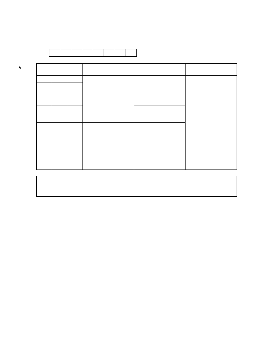
CHAPTER 6 16-BIT TIMER/EVENT COUNTERS 00 AND 01
User's Manual U16228EJ2V0UD
151
Figure 6-6. Format of 16-Bit Timer Mode Control Register 00 (TMC00)
7
0
6
0
5
0
4
0
3
TMC003
2
TMC002
1
TMC001
<0>
OVF00
Symbol
TMC00
Address FFBAH After reset: 00H R/W
TMC003 TMC002 TMC001
Operating mode and clear
mode selection
TO00 inversion timing selection
Interrupt request generation
0 0 0
0 0 1
Operation stop
(TM00 cleared to 0)
No change
Not generated
0 1 0
Free-running
mode
Match between TM00 and
CR000 or match between
TM00 and CR010
0 1 1
Match between TM00 and
CR000, match between TM00
and CR010 or TI000 valid edge
1 0 0
1 0 1
Clear & start occurs on TI000
valid edge
-
1 1 0
Clear & start occurs on match
between TM00 and CR000
Match between TM00 and
CR000 or match between
TM00 and CR010
1 1 1
Match between TM00 and
CR000, match between TM00
and CR010 or TI000 valid edge
Generated on match between
TM00 and CR000, or match
between TM00 and CR010
OVF00
16-bit timer counter 00 (TM00) overflow detection
0 Overflow
not
detected
1 Overflow
detected
Cautions 1. Timer operation must be stopped before writing to bits other than the OVF00 flag.
2. Set the valid edge of the TI000/P00 pin using prescaler mode register 00 (PRM00).
3. If any the following modes: the mode in which clear & start occurs on match between TM00
and CR000, the mode in which clear & start occurs at the TI00 valid edge, or free-running
mode is selected, when the set value of CR000 is FFFFH and the TM00 value changes from
FFFFH to 0000H, the OVF00 flag is set to 1.
Remark TO00: 16-bit
timer/event counter 00 output pin
TI000: 16-bit timer/event counter 00 input pin
TM00: 16-bit timer counter 00
CR000: 16-bit timer capture/compare register 000
CR010: 16-bit timer capture/compare register 010

CHAPTER 6 16-BIT TIMER/EVENT COUNTERS 00 AND 01
User's Manual U16228EJ2V0UD
152
Figure 6-7. Format of 16-Bit Timer Mode Control Register 01 (TMC01)
7
0
6
0
5
0
4
0
3
TMC013
2
TMC012
1
TMC011
<0>
OVF01
Symbol
TMC01
Address FFB6H After reset: 00H R/W
TMC013 TMC012 TMC011
Operating mode and clear
mode selection
TO01 inversion timing selection
Interrupt request generation
0 0 0
0 0 1
Operation stop
(TM01 cleared to 0)
No change
Not generated
0 1 0
Free-running
mode
Match between TM01 and
CR001 or match between
TM01 and CR011
0 1 1
Match between TM01 and
CR001, match between TM01
and CR011 or TI001 valid edge
1 0 0
1 0 1
Clear & start occurs on TI001
valid edge
-
1 1 0
Clear & start occurs on match
between TM01 and CR001
Match between TM01 and
CR001 or match between
TM01 and CR011
1 1 1
Match between TM01 and
CR001, match between TM01
and CR011 or TI001 valid edge
Generated on match between
TM01 and CR001, or match
between TM01 and CR011
OVF01
16-bit timer counter 01 (TM01) overflow detection
0 Overflow
not
detected
1 Overflow
detected
Cautions 1. Timer operation must be stopped before writing to bits other than the OVF01 flag.
2. Set the valid edge of the TI001/P05 pin using prescaler mode register 01 (PRM01).
3. If any the following modes: the mode in which clear & start occurs on match between TM01
and CR001, the mode in which clear & start occurs at the TI01 valid edge, or free-running
mode is selected, when the set value of CR001 is FFFFH and the TM01 value changes from
FFFFH to 0000H, the OVF01 flag is set to 1.
Remark TO01: 16-bit
timer/event counter 01 output pin
TI001: 16-bit timer/event counter 01 input pin
TM01: 16-bit timer counter 01
CR001: 16-bit timer capture/compare register 001
CR011: 16-bit timer capture/compare register 011
CHAPTER 6 16-BIT TIMER/EVENT COUNTERS 00 AND 01
User's Manual U16228EJ2V0UD
153
(2) Capture/compare control register 0n (CRC0n)
This register controls the operation of the 16-bit timer capture/compare registers (CR00n, CR01n).
CRC0n can be set by a 1-bit or 8-bit memory manipulation instruction.
RESET input clears CRC0n to 00H.
Remark n = 0:
µ
PD780131, 780132
n = 0, 1:
µ
PD780133, 780134, 78F0134, 780136, 780138, 78F0138
Figure 6-8. Format of Capture/Compare Control Register 00 (CRC00)
Address: FFBCH After reset: 00H R/W
Symbol
7 6 5 4 3 2 1 0
CRC00 0 0 0 0 0
CRC002
CRC001
CRC000
CRC002
CR010 operating mode selection
0
Operates as compare register
1
Operates as capture register
CRC001
CR000 capture trigger selection
0
Captures on valid edge of TI010
1
Captures on valid edge of TI000 by reverse phase
CRC000
CR000 operating mode selection
0
Operates as compare register
1
Operates as capture register
Cautions 1. Timer operation must be stopped before setting CRC00.
2. When the mode in which clear & start occurs on a match between TM00 and CR000 is
selected with 16-bit timer mode control register 00 (TMC00), CR000 should not be specified
as a capture register.
3. The capture operation is not performed if both the rising and falling edges are specified as
the valid edge of TI000.
4. To ensure that the capture operation is performed properly, the capture trigger requires a
pulse two cycles longer than the count clock selected by prescaler mode register 00
(PRM00).
CHAPTER 6 16-BIT TIMER/EVENT COUNTERS 00 AND 01
User's Manual U16228EJ2V0UD
154
Figure 6-9. Format of Capture/Compare Control Register 01 (CRC01)
Address: FFB8H After reset: 00H R/W
Symbol
7 6 5 4 3 2 1 0
CRC01 0 0 0 0 0
CRC012
CRC011
CRC010
CRC012
CR011 operating mode selection
0
Operates as compare register
1
Operates as capture register
CRC011
CR001 capture trigger selection
0
Captures on valid edge of TI011
1
Captures on valid edge of TI001 by reverse phase
CRC010
CR001 operating mode selection
0
Operates as compare register
1
Operates as capture register
Cautions 1. Timer operation must be stopped before setting CRC01.
2. When the mode in which clear & start occurs on a match between TM01 and CR001 is
selected with 16-bit timer mode control register 01 (TMC01), CR001 should not be specified
as a capture register.
3. The capture operation is not performed if both the rising and falling edges are specified as
the valid edge of TI001.
4. To ensure that the capture operation is performed properly, the capture trigger requires a
pulse two cycles longer than the count clock selected by prescaler mode register 01
(PRM01).
(3) 16-bit timer output control register 0n (TOC0n)
This register controls the operation of the 16-bit timer/event counter 0n output controller. It sets/resets the timer
output F/F (LV0n), enables/disables output inversion and 16-bit timer/event counter 0n timer output,
enables/disables the one-shot pulse output operation, and sets the one-shot pulse output trigger via software.
TOC0n can be set by a 1-bit or 8-bit memory manipulation instruction.
RESET input clears TOC0n to 00H.
Remark n = 0:
µ
PD780131, 780132
n = 0, 1:
µ
PD780133, 780134, 78F0134, 780136, 780138, 78F0138

CHAPTER 6 16-BIT TIMER/EVENT COUNTERS 00 AND 01
User's Manual U16228EJ2V0UD
155
Figure 6-10. Format of 16-Bit Timer Output Control Register 00 (TOC00)
Address: FFBDH After reset: 00H R/W
Symbol 7 <6>
<5> 4 <3>
<2> 1 <0>
TOC00 0
OSPT00
OSPE00
TOC004
LVS00 LVR00 TOC001 TOE00
OSPT00 One-shot
pulse
output
trigger control via software
0
No one-shot pulse trigger
1 One-shot
pulse
trigger
OSPE00
One-shot pulse output operation control
0
Successive pulse output mode
1
One-shot pulse output mode
Note
TOC004
Timer output F/F control using match of CR010 and TM00
0
Disables inversion operation
1
Enables inversion operation
LVS00
LVR00
Timer output F/F status setting
0 0
No
change
0
1
Timer output F/F reset (0)
1
0
Timer output F/F set (1)
1 1
Setting
prohibited
TOC001
Timer output F/F control using match of CR000 and TM00
0
Disables inversion operation
1
Enables inversion operation
TOE00 Timer
output
control
0
Disables output (output fixed to level 0)
1 Enables
output
Note The one-shot pulse output mode operates correctly only in the free-running mode and the mode in which
clear & start occurs at the TI000 valid edge. In the mode in which clear & start occurs on a match between
the TM00 register and CR000 register, one-shot pulse output is not possible because an overflow does not
occur.
Cautions 1. Timer operation must be stopped before setting other than TOC004.
2. If LVS00 and LVR00 are read, 0 is read.
3. OSPT00 is automatically cleared after data is set, so 0 is read.
4. Do not set OSPT00 to 1 other than in one-shot pulse output mode.
5. A write interval of two cycles or more of the count clock selected by prescaler mode register
00 (PRM00) is required to write to OSPT00 successively.
6. Do not set LVS00 to 1 before TOE00, and do not set LVS00 and TOE00 to 1 simultaneously.
CHAPTER 6 16-BIT TIMER/EVENT COUNTERS 00 AND 01
User's Manual U16228EJ2V0UD
156
Figure 6-11. Format of 16-Bit Timer Output Control Register 01 (TOC01)
Address: FFB9H After reset: 00H R/W
Symbol 7 <6>
<5> 4 <3>
<2> 1 <0>
TOC01 0
OSPT01
OSPE01
TOC014
LVS01 LVR01 TOC011 TOE01
OSPT01 One-shot
pulse
output
trigger control via software
0
No one-shot pulse trigger
1 One-shot
pulse
trigger
OSPE01
One-shot pulse output operation control
0
Successive pulse output mode
1
One-shot pulse output mode
Note
TOC014
Timer output F/F control using match of CR011 and TM01
0
Disables inversion operation
1
Enables inversion operation
LVS01
LVR01
Timer output F/F status setting
0 0
No
change
0
1
Timer output F/F reset (0)
1
0
Timer output F/F set (1)
1 1
Setting
prohibited
TOC011
Timer output F/F control using match of CR001 and TM01
0
Disables inversion operation
1
Enables inversion operation
TOE01 Timer
output
control
0
Disables output (output fixed to level 0)
1 Enables
output
Note The one-shot pulse output mode operates correctly only in the free-running mode and the mode in which
clear & start occurs at the TI001 valid edge. In the mode in which clear & start occurs on a match between
the TM01 register and CR001 register, one-shot pulse output is not possible because an overflow does not
occur.
Cautions 1. Timer operation must be stopped before setting other than TOC014.
2. If LVS01 and LVR01 are read, 0 is read.
3. OSPT01 is automatically cleared after data is set, so 0 is read.
4. Do not set OSPT01 to 1 other than in one-shot pulse output mode.
5. A write interval of two cycles or more of the count clock selected by prescaler mode register
01 (PRM01) is required to write to OSPT01 successively.
6. Do not set LVS01 to 1 before TOE01, and do not set LVS01 and TOE01 to 1 simultaneously.
CHAPTER 6 16-BIT TIMER/EVENT COUNTERS 00 AND 01
User's Manual U16228EJ2V0UD
157
(4) Prescaler mode register 0n (PRM0n)
This register is used to set the 16-bit timer counter 0n (TM0n) count clock and TI00n and TI01n input valid edges.
PRM0n can be set by a 1-bit or 8-bit memory manipulation instruction.
RESET input clears PRM0n to 00H.
Remark n = 0:
µ
PD780131, 780132
n = 0, 1:
µ
PD780133, 780134, 78F0134, 780136, 780138, 78F0138
Figure 6-12. Format of Prescaler Mode Register 00 (PRM00)
Address: FFBBH After reset: 00H R/W
Symbol
7 6 5 4 3 2 1 0
PRM00 ES101 ES100 ES001 ES000
0
0 PRM001
PRM000
ES101
ES100
TI010 valid edge selection
0 0
Falling
edge
0 1
Rising
edge
1 0
Setting
prohibited
1
1
Both falling and rising edges
ES001
ES000
TI000 valid edge selection
0 0
Falling
edge
0 1
Rising
edge
1 0
Setting
prohibited
1
1
Both falling and rising edges
PRM001
PRM000
Count clock selection
0 0
f
X
(10 MHz)
0 1
f
X
/2
2
(2.5 MHz)
1 0
f
X
/2
8
(39.06 kHz)
1 1
TI000
valid
edge
Note
Note The external clock requires a pulse two cycles longer than internal count clock (f
X
).
CHAPTER 6 16-BIT TIMER/EVENT COUNTERS 00 AND 01
User's Manual U16228EJ2V0UD
158
Cautions 1. When the Ring-OSC clock is selected as the clock to be supplied to the CPU, the clock of the
Ring-OSC oscillator is divided and supplied as the count clock. If the count clock is the
Ring-OSC clock, the operation of 16-bit timer/event counter 00 is not guaranteed. When an
external clock is used and when the Ring-OSC clock is selected and supplied to the CPU, the
operation of 16-bit timer/event counter 00 is not guaranteed, either, because the Ring-OSC
clock is supplied as the sampling clock to eliminate noise.
2. Always set data to PRM00 after stopping the timer operation.
3. If the valid edge of TI000 is to be set for the count clock, do not set the clear & start mode
using the valid edge of TI000 and the capture trigger.
4. If the TI000 or TI010 pin is high level immediately after system reset, the rising edge is
immediately detected after the rising edge or both the rising and falling edges are set as the
valid edge(s) of the TI000 pin or TI010 pin to enable the operation of 16-bit timer counter 00
(TM00). Care is therefore required when pulling up the TI000 or TI010 pin. However, when re-
enabling operation after the operation has been stopped once, the rising edge is not
detected.
5. When P01 is used as the TI010 valid edge, it cannot be used as the timer output (TO00), and
when used as TO00, it cannot be used as the TI010 valid edge.
Remarks 1. f
X
: X1 input clock oscillation frequency
2. TI000, TI010: 16-bit timer/event counter 00 input pin
3. Figures in parentheses are for operation with f
X
= 10 MHz.
Figure 6-13. Format of Prescaler Mode Register 01 (PRM01)
Address: FFB7H After reset: 00H R/W
Symbol
7 6 5 4 3 2 1 0
PRM01 ES111 ES110 ES011 ES010
0
0 PRM011
PRM010
ES111
ES110
TI011 valid edge selection
0 0
Falling
edge
0 1
Rising
edge
1 0
Setting
prohibited
1
1
Both falling and rising edges
ES011
ES010
TI001 valid edge selection
0 0
Falling
edge
0 1
Rising
edge
1 0
Setting
prohibited
1
1
Both falling and rising edges
PRM011
PRM010
Count clock selection
0 0
f
X
(10 MHz)
0 1
f
X
/2
4
(625 kHz)
1 0
f
X
/2
6
(156.25 kHz)
1 1
TI001
valid
edge
Note
Note The external clock requires a pulse two cycles longer than internal count clock (f
X
).
CHAPTER 6 16-BIT TIMER/EVENT COUNTERS 00 AND 01
User's Manual U16228EJ2V0UD
159
Cautions 1. When the Ring-OSC clock is selected as the clock to be supplied to the CPU, the clock of the
Ring-OSC oscillator is divided and supplied as the count clock. If the count clock is the
Ring-OSC clock, the operation of 16-bit timer/event counter 01 is not guaranteed. When an
external clock is used and when the Ring-OSC clock is selected and supplied to the CPU, the
operation of 16-bit timer/event counter 01 is not guaranteed, either, because the Ring-OSC
clock is supplied as the sampling clock to eliminate noise.
2. Always set data to PRM01 after stopping the timer operation.
3. If the valid edge of TI001 is to be set for the count clock, do not set the clear & start mode
using the valid edge of TI001 and the capture trigger.
4. If the TI001 or TI011 pin is high level immediately after system reset, the rising edge is
immediately detected after the rising edge or both the rising and falling edges are set as the
valid edge(s) of the TI001 pin or TI011 pin to enable the operation of 16-bit timer counter 01
(TM01). Care is therefore required when pulling up the TI001 or TI011 pin. However, when re-
enabling operation after the operation has been stopped once, the rising edge is not
detected.
5. When P06 is used as the TI011 valid edge, it cannot be used as the timer output (TO01), and
when used as TO01, it cannot be used as the TI011 valid edge.
Remarks 1. f
X
: X1 input clock oscillation frequency
2. TI001, TI011: 16-bit timer/event counter 01 input pin
3. Figures in parentheses are for operation with f
X
= 10 MHz.
(5) Port mode register 0 (PM0)
This register sets port 0 input/output in 1-bit units.
When using the P01/TO00/TI010 and P06/TO01
Note
/TI011
Note
pins for timer output, set PM01 and PM06 and the
output latch of P01 and P06 to 0.
When using the P01/TO00/TI010 and P06/TO01
Note
/TI011
Note
pins for timer input, set PM01 and PM06 to 0. At this
time, the output latch of P01 and P06 may be 0 or 1.
PM0 can be set by a 1-bit or 8-bit memory manipulation instruction.
RESET input sets PM0 to FFH.
Figure 6-14. Format of Port Mode Register 0 (PM0)
7
1
6
PM06
5
PM05
4
PM04
3
PM03
2
PM02
1
PM01
0
PM00
Symbol
PM0
Address: FF20H After reset: FFH R/W
PM0n
0
1
P0n pin I/O mode selection (n = 0 to 6)
Output mode (output buffer on)
Input mode (output buffer off)
Note Available only for the
µ
PD780133, 780134, 78F0134, 780136, 780138, and 78F0138.

CHAPTER 6 16-BIT TIMER/EVENT COUNTERS 00 AND 01
User's Manual U16228EJ2V0UD
160
6.4 Operation of 16-Bit Timer/Event Counters 00 and 01
6.4.1 Interval timer operation
Setting 16-bit timer mode control register 0n (TMC0n) and capture/compare control register 0n (CRC0n) as shown
in Figure 6-15 allows operation as an interval timer.
Setting
The basic operation setting procedure is as follows.
<1> Set the CRC0n register (see Figure 6-15 for the set value).
<2> Set any value to the CR00n register.
<3> Set the count clock by using the PRM0n register.
<4> Set the TMC0n register to start the operation (see Figure 6-15 for the set value).
Caution CR00n cannot be rewritten during TM0n operation.
Remark For how to enable the INTTM00n interrupt, see CHAPTER 17 INTERRUPT FUNCTIONS.
Interrupt requests are generated repeatedly using the count value preset in 16-bit timer capture/compare register
00n (CR00n) as the interval.
When the count value of 16-bit timer counter 0n (TM0n) matches the value set in CR00n, counting continues with
the TM0n value cleared to 0 and the interrupt request signal (INTTM00n) is generated.
The count clock of 16-bit timer/event counter 0n can be selected with bits 0 and 1 (PRM0n0, PRM0n1) of prescaler
mode register 0n (PRM0n).
Remark n = 0:
µ
PD780131, 780132
n = 0, 1:
µ
PD780133, 780134, 78F0134, 780136, 780138, 78F0138
CHAPTER 6 16-BIT TIMER/EVENT COUNTERS 00 AND 01
User's Manual U16228EJ2V0UD
161
Figure 6-15. Control Register Settings for Interval Timer Operation
(a) 16-bit timer mode control register 0n (TMC0n)
7
0
6
0
5
0
4
0
TMC0n3
1
TMC0n2
1
TMC0n1
0/1
OVF0n
0
TMC0n
Clears and starts on match between TM0n and CR00n.
(b) Capture/compare control register 0n (CRC0n)
7
0
6
0
5
0
4
0
3
0
CRC0n2
0/1
CRC0n1
0/1
CRC0n0
0
CRC0n
CR00n used as compare register
(c) Prescaler mode register 0n (PRM0n)
ES1n1
0/1
ES1n0
0/1
ES0n1
0/1
ES0n0
0/1
3
0
2
0
PRM0n1
0/1
PRM0n0
0/1
PRM0n
Selects count clock.
Setting invalid (setting "10" is prohibited.)
Setting invalid (setting "10" is prohibited.)
Remarks 1. 0/1: Setting 0 or 1 allows another function to be used simultaneously with the interval timer. See the
description of the respective control registers for details.
2. n = 0:
µ
PD780131, 780132
n = 0, 1:
µ
PD780133, 780134, 78F0134, 780136, 780138, 78F0138
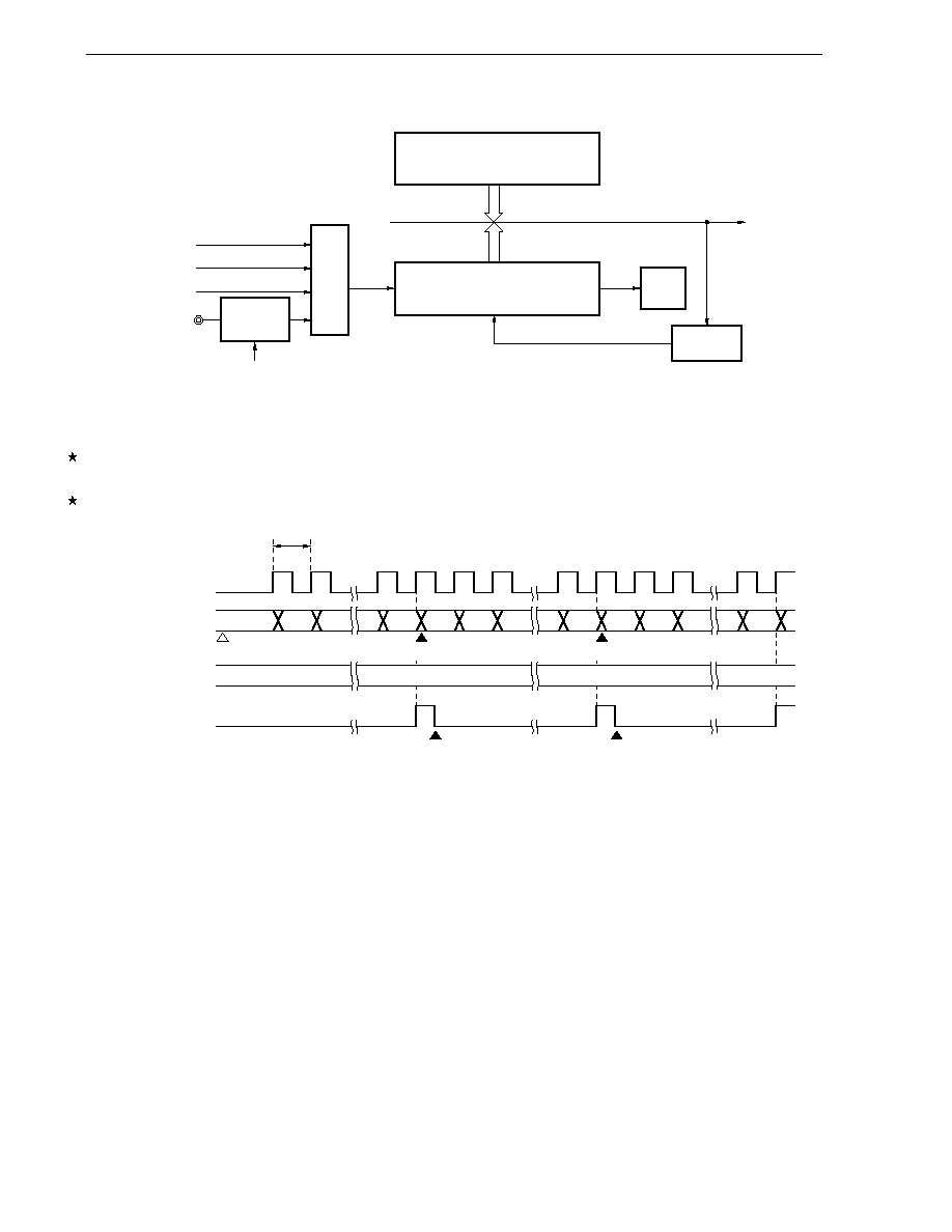
CHAPTER 6 16-BIT TIMER/EVENT COUNTERS 00 AND 01
User's Manual U16228EJ2V0UD
162
Figure 6-16. Interval Timer Configuration Diagram
16-bit timer capture/compare
register 00n (CR00n)
16-bit timer counter 0n
(TM0n)
OVF0n
Clear
circuit
INTTM00n
f
X
(f
X
)
Note 1
f
X
/2
2
(f
X
/2
4
)
Note 1
f
X
/2
8
(f
X
/2
6
)
Note 1
TI000/P00
(TI001/P05)
Note 1
Selector
Noise
eliminator
f
X
Note 2
Notes 1. Frequencies and pin names without parentheses are for 16-bit timer/event counter 00, and those in
parentheses are for 16-bit timer/event counter 01.
2. OVF0n is set to 1 only when 16-bit timer capture/compare register 00n is set to FFFFH.
Figure 6-17. Timing of Interval Timer Operation
Count clock
t
TM0n count value
CR00n
INTTM00n
0000H
0001H
N
0000H 0001H
N
0000H 0001H
N
N
N
N
N
Timer operation enabled
Clear
Clear
Interrupt acknowledged
Interrupt acknowledged
Remark Interval time = (N + 1)
◊
t
N = 0001H to FFFFH
n = 0:
µ
PD780131, 780132
n = 0, 1:
µ
PD780133, 780134, 78F0134, 780136, 780138, 78F0138

CHAPTER 6 16-BIT TIMER/EVENT COUNTERS 00 AND 01
User's Manual U16228EJ2V0UD
163
6.4.2 PPG output operations
Setting 16-bit timer mode control register 0n (TMC0n) and capture/compare control register 0n (CRC0n) as shown
in Figure 6-18 allows operation as PPG (Programmable Pulse Generator) output.
Setting
The basic operation setting procedure is as follows.
<1> Set the CRC0n register (see Figure 6-18 for the set value).
<2> Set any value to the CR00n register as the cycle.
<3> Set any value to the CR01n register as the duty factor.
<4> Set the TOC0n register (see Figure 6-18 for the set value).
<5> Set the count clock by using the PRM0n register.
<6> Set the TMC0n register to start the operation (see Figure 6-18 for the set value).
Caution To change the value of the duty factor (the value of the CR01n register) during operation, see
Caution 2 in Figure 6-20 PPG Output Operation Timing.
Remarks 1. For the setting of the TO0n pin, see 6.3 (5) Port mode register 0 (PM0).
2. For how to enable the INTTM00n interrupt, see CHAPTER 17 INTERRUPT FUNCTIONS.
In the PPG output operation, rectangular waves are output from the TO0n pin with the pulse width and the cycle
that correspond to the count values preset in 16-bit timer capture/compare register 01n (CR01n) and in 16-bit timer
capture/compare register 00n (CR00n), respectively.
Remark n = 0:
µ
PD780131, 780132
n = 0, 1:
µ
PD780133, 780134, 78F0134, 780136, 780138, 78F0138
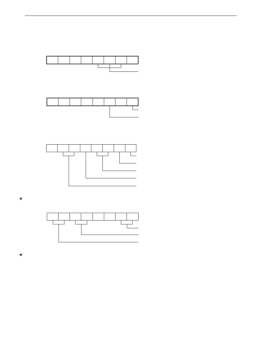
CHAPTER 6 16-BIT TIMER/EVENT COUNTERS 00 AND 01
User's Manual U16228EJ2V0UD
164
Figure 6-18. Control Register Settings for PPG Output Operation
(a) 16-bit timer mode control register 0n (TMC0n)
7
0
6
0
5
0
4
0
TMC0n3
1
TMC0n2
1
TMC0n1
0
OVF0n
0
TMC0n
Clears and starts on match between TM0n and CR00n.
(b) Capture/compare control register 0n (CRC0n)
7
0
6
0
5
0
4
0
3
0
CRC0n2
0
CRC0n1
◊
CRC0n0
0
CRC0n
CR00n used as compare register
CR01n used as compare register
(c) 16-bit timer output control register 0n (TOC0n)
7
0
OSPT0n
0
OSPE0n
0
TOC0n4
1
LVS0n
0/1
LVR0n
0/1
TOC0n1
1
TOE0n
1
TOC0n
Enables TO0n output.
Inverts output on match between TM0n and CR00n.
Specifies initial value of TO0n output F/F (setting "11" is prohibited).
Inverts output on match between TM0n and CR01n.
Disables one-shot pulse output.
(d) Prescaler mode register 0n (PRM0n)
ES1n1
0/1
ES1n0
0/1
ES0n1
0/1
ES0n0
0/1
3
0
2
0
PRM0n1
0/1
PRM0n0
0/1
PRM0n
Selects count clock.
Setting invalid (setting "10" is prohibited.)
Setting invalid (setting "10" is prohibited.)
Cautions 1. Values in the following range should be set in CR00n and CR01n:
0000H
CR01n < CR00n
FFFFH
2. The cycle of the pulse generated through PPG output (CR00n setting value + 1) has a duty of
(CR01n setting value + 1)/(CR00n setting value + 1).
Remark
◊
: Don't care
n = 0:
µ
PD780131, 780132
n = 0, 1:
µ
PD780133, 780134, 78F0134, 780136, 780138, 78F0138
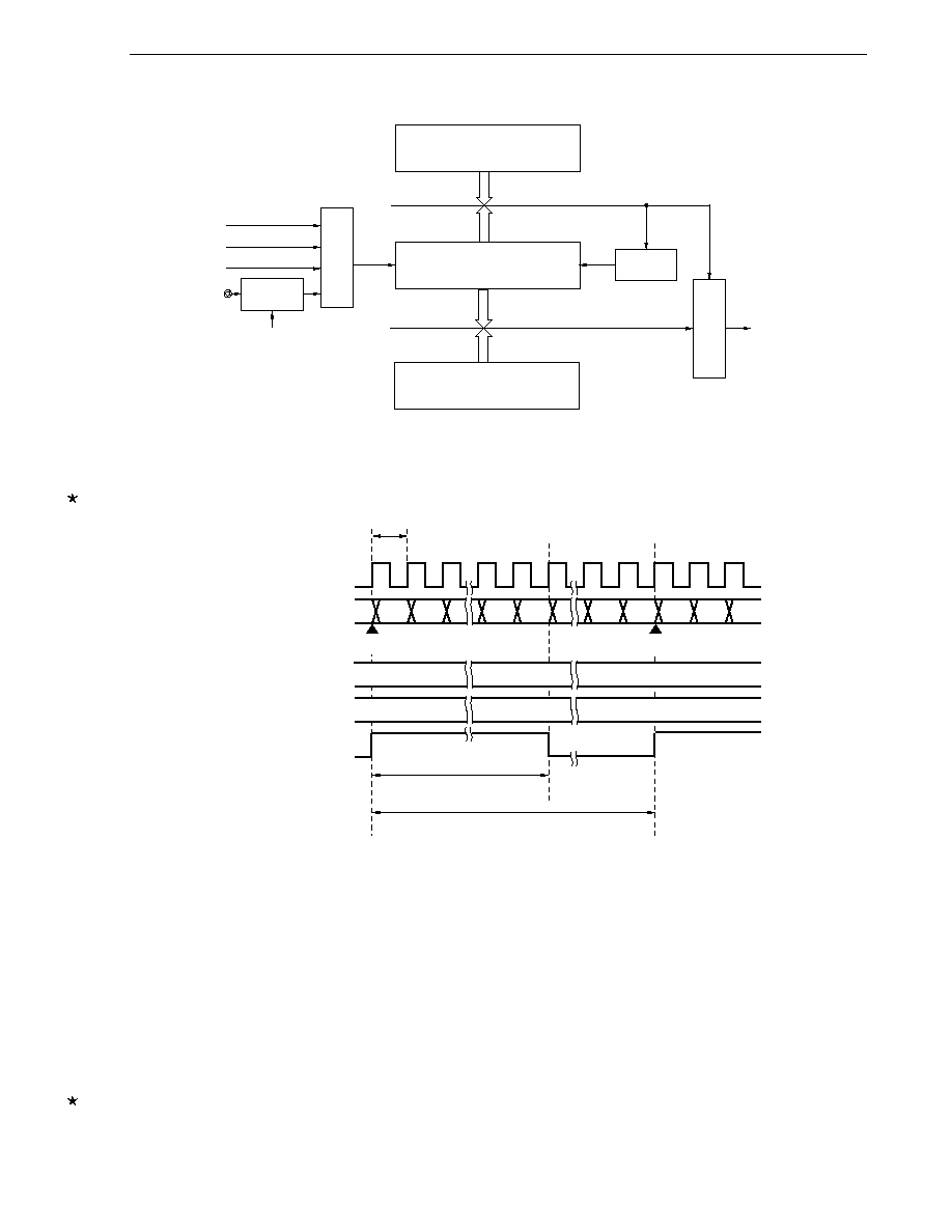
CHAPTER 6 16-BIT TIMER/EVENT COUNTERS 00 AND 01
User's Manual U16228EJ2V0UD
165
Figure 6-19. Configuration Diagram of PPG Output
16-bit timer capture/compare
register 00n (CR00n)
16-bit timer counter 0n
(TM0n)
Clear
circuit
Noise
eliminator
f
X
f
X
(f
X
)
Note
f
X
/2
2
(f
X
/2
4
)
Note
f
X
/2
8
(f
X
/2
6
)
Note
TI000/P00
(TI001/P05)
Note
16-bit timer capture/compare
register 01n (CR01n)
TO00/TI010/P01
( TO01/TI011/P06 )
Selector
Output controller
Note Frequencies and pin names without parentheses are for 16-bit timer/event counter 00, and those in
parentheses are for 16-bit timer/event counter 01.
Figure 6-20. PPG Output Operation Timing
t
0000H
0000H 0001H
0001H
M
-
1
Count clock
TM0n count value
TO0n
Pulse width: (M + 1)
◊
t
1 cycle: (N + 1)
◊
t
N
CR00n capture value
CR01n capture value
M
M
N
-
1
N
N
Clear
Clear
Cautions 1. CR00n cannot be rewritten during TM0n operation.
2. In the PPG output operation, change the pulse width (rewrite CR01n) during TM0n operation
using the following procedure.
<1> Disable the timer output inversion operation by match of TM0n and CR01n (TOC0n4 = 0)
<2> Disable the INTTM01n interrupt (TMMK01n = 1)
<3> Rewrite CR01n
<4> Wait for 1 cycle of the TM0n count clock
<5> Enable the timer output inversion operation by match of TM0n and CR01n (TOC0n4 = 1)
<6> Clear the interrupt request flag of INTTM01n (TMIF01n = 0)
<7> Enable the INTTM01n interrupt (TMMK01n = 0)
Remarks 1. 0000H
M < N
FFFFH
2. n = 0:
µ
PD780131, 780132
n = 0, 1:
µ
PD780133, 780134, 78F0134, 780136, 780138, 78F0138
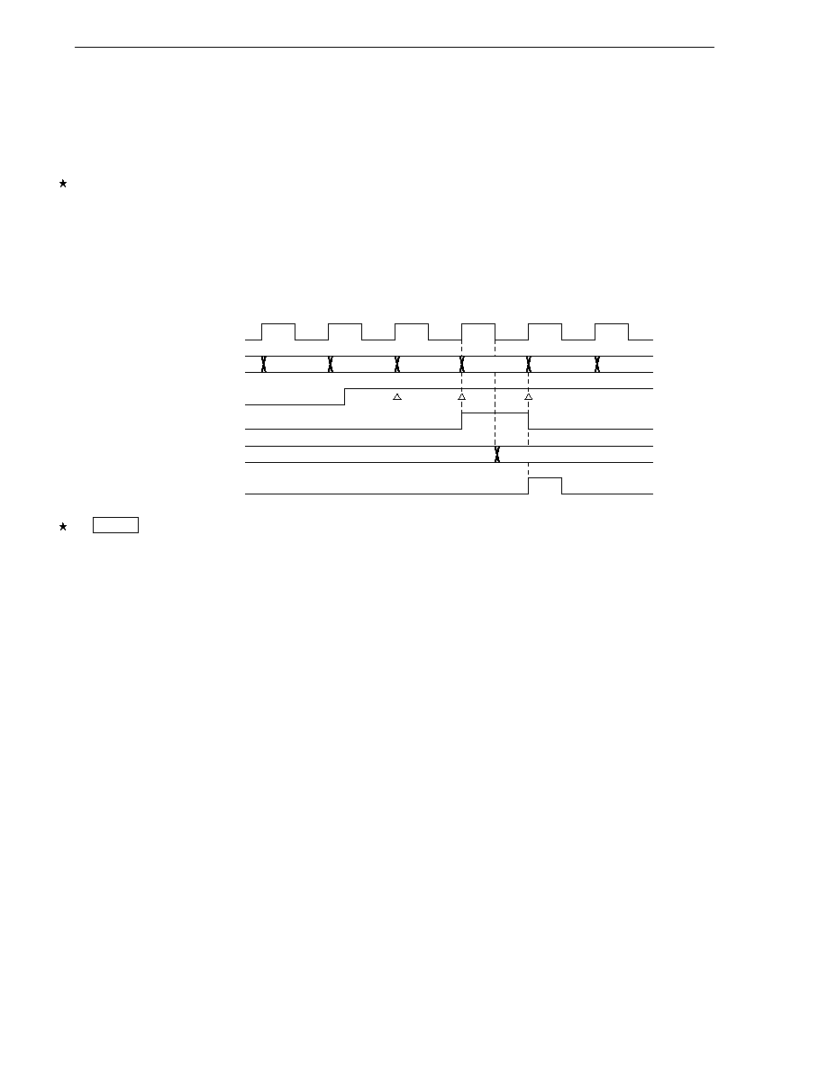
CHAPTER 6 16-BIT TIMER/EVENT COUNTERS 00 AND 01
User's Manual U16228EJ2V0UD
166
6.4.3 Pulse width measurement operations
It is possible to measure the pulse width of the signals input to the TI00n pin and TI01n pin using 16-bit timer
counter 0n (TM0n).
There are two measurement methods: measuring with TM0n used in free-running mode, and measuring by
restarting the timer in synchronization with the edge of the signal input to the TI00n pin.
When an interrupt occurs, read the valid value of the capture register, check the overflow flag, and then calculate
the necessary pulse width. Clear the overflow flag after checking it.
The capture operation is not performed until the signal pulse width is sampled in the count clock cycle selected by
prescaler mode register 0n (PRM0n) and the valid level of the TI00n or TI01n pin is detected twice, thus eliminating
noise with a short pulse width.
Figure 6-21. CR01n Capture Operation with Rising Edge Specified
Count clock
TM0n
TI00n
Rising edge detection
CR01n
INTTM01n
N
-
3
N
-
2
N
-
1
N
N + 1
N
Setting
The basic operation setting procedure is as follows.
<1> Set the CRC0n register (see Figures 6-22, 6-25, 6-27, and 6-29 for the set value).
<2> Set the count clock by using the PRM0n register.
<3> Set the TMC0n register to start the operation (see Figures 6-22, 6-25, 6-27, and 6-29 for the set value).
Caution To use two capture registers, set the TI00n and TI01n pins.
Remarks 1. For the setting of the TI00n (or TI01n) pin, see 6.3 (5) Port mode register 0 (PM0).
2. For how to enable the INTTM00n (or INTTM01n) interrupt, see CHAPTER 17 INTERRUPT
FUNCTIONS.
3. n = 0:
µ
PD780131, 780132
n = 0, 1:
µ
PD780133, 780134, 78F0134, 780136, 780138, 78F0138

CHAPTER 6 16-BIT TIMER/EVENT COUNTERS 00 AND 01
User's Manual U16228EJ2V0UD
167
(1) Pulse width measurement with free-running counter and one capture register
When 16-bit timer counter 0n (TM0n) is operated in free-running mode, and the edge specified by prescaler mode
register 0n (PRM0n) is input to the TI00n pin, the value of TM0n is taken into 16-bit timer capture/compare
register 01n (CR01n) and an external interrupt request signal (INTTM01n) is set.
Specify both the rising and falling edges by using bits 4 and 5 (ES0n0 and ES0n1) of PRM0n.
Sampling is performed using the count clock selected by PRM0n, and a capture operation is only performed
when a valid level of the TI00n pin is detected twice, thus eliminating noise with a short pulse width.
Figure 6-22. Control Register Settings for Pulse Width Measurement with Free-Running Counter
and One Capture Register (When TI00n and CR01n Are Used)
(a) 16-bit timer mode control register 0n (TMC0n)
7
0
6
0
5
0
4
0
TMC0n3
0
TMC0n2
1
TMC0n1
0/1
OVF0n
0
TMC0n
Free-running mode
(b) Capture/compare control register 0n (CRC0n)
7
0
6
0
5
0
4
0
3
0
CRC0n2
1
CRC0n1
0/1
CRC0n0
0
CRC0n
CR00n used as compare register
CR01n used as capture register
(c) Prescaler mode register 0n (PRM0n)
ES1n1
0/1
ES1n0
0/1
ES0n1
1
ES0n0
1
3
0
2
0
PRM0n1
0/1
PRM0n0
0/1
PRM0n
Selects count clock (setting "11" is prohibited).
Specifies both edges for pulse width detection.
Setting invalid (setting "10" is prohibited.)
Remark 0/1: Setting 0 or 1 allows another function to be used simultaneously with pulse width measurement.
See the description of the respective control registers for details.
n = 0:
µ
PD780131, 780132
n = 0, 1:
µ
PD780133, 780134, 78F0134, 780136, 780138, 78F0138
CHAPTER 6 16-BIT TIMER/EVENT COUNTERS 00 AND 01
User's Manual U16228EJ2V0UD
168
Figure 6-23. Configuration Diagram for Pulse Width Measurement with Free-Running Counter
f
X
(f
X
)
Note
f
X
/2
2
(f
X
/2
4
)
Note
f
X
/2
8
(f
X
/2
6
)
Note
TI00n
16-bit timer counter 0n
(TM0n)
OVF0n
16-bit timer capture/compare
register 01n (CR01n)
Internal bus
INTTM01n
Selector
Note Frequencies without parentheses are for 16-bit timer/event counter 00, and those in parentheses are for 16-
bit timer/event counter 01.
Figure 6-24. Timing of Pulse Width Measurement Operation with Free-Running Counter
and One Capture Register (with Both Edges Specified)
t
0000H
0000H
FFFFH
0001H
D0
D0
Count clock
TM0n count value
TI00n pin input
CR01n capture value
INTTM01n
OVF0n
(D1
-
D0)
◊
t
(D3
-
D2)
◊
t
(10000H
-
D1 + D2)
◊
t
D1
D2
D3
D2
D3
D0 + 1
D1
D1 + 1
Note
Note Clear OVF0n by software.
Remark n = 0:
µ
PD780131, 780132
n = 0, 1:
µ
PD780133, 780134, 78F0134, 780136, 780138, 78F0138
CHAPTER 6 16-BIT TIMER/EVENT COUNTERS 00 AND 01
User's Manual U16228EJ2V0UD
169
(2) Measurement of two pulse widths with free-running counter
When 16-bit timer counter 0n (TM0n) is operated in free-running mode, it is possible to simultaneously measure
the pulse widths of the two signals input to the TI00n pin and the TI01n pin.
When the edge specified by bits 4 and 5 (ES0n0 and ES0n1) of prescaler mode register 0n (PRM0n) is input to
the TI00n pin, the value of TM0n is taken into 16-bit timer capture/compare register 01n (CR01n) and an interrupt
request signal (INTTM01n) is set.
Also, when the edge specified by bits 6 and 7 (ES1n0 and ES1n1) of PRM0n is input to the TI01n pin, the value
of TM0n is taken into 16-bit timer capture/compare register 00n (CR00n) and an interrupt request signal
(INTTM00n) is set.
Specify both the rising and falling edges as the edges of the TI00n and TI01n pins, by using bits 4 and 5 (ES0n0
and ES0n1) and bits 6 and 7 (ES1n0 and ES1n1) of PRM0n.
Sampling is performed using the count clock cycle selected by prescaler mode register 0n (PRM0n), and a
capture operation is only performed when a valid level of the TI00n or TI01n pin is detected twice, thus
eliminating noise with a short pulse width.
Figure 6-25. Control Register Settings for Measurement of Two Pulse Widths with Free-Running Counter
(a) 16-bit timer mode control register 0n (TMC0n)
7
0
6
0
5
0
4
0
TMC0n3
0
TMC0n2
1
TMC0n1
0/1
OVF0n
0
TMC0n
Free-running mode
(b) Capture/compare control register 0n (CRC0n)
7
0
6
0
5
0
4
0
3
0
CRC0n2
1
CRC0n1
0
CRC0n0
1
CRC0n
CR00n used as capture register
Captures valid edge of TI01n pin to CR00n.
CR01n used as capture register
(c) Prescaler mode register 0n (PRM0n)
ES1n1
1
ES1n0
1
ES0n1
1
ES0n0
1
3
0
2
0
PRM0n1
0/1
PRM0n0
0/1
PRM0n
Selects count clock (setting "11" is prohibited).
Specifies both edges for pulse width detection.
Specifies both edges for pulse width detection.
Remark 0/1: Setting 0 or 1 allows another function to be used simultaneously with pulse width measurement.
See the description of the respective control registers for details.
n = 0:
µ
PD780131, 780132
n = 0, 1:
µ
PD780133, 780134, 78F0134, 780136, 780138, 78F0138
CHAPTER 6 16-BIT TIMER/EVENT COUNTERS 00 AND 01
User's Manual U16228EJ2V0UD
170
Figure 6-26. Timing of Pulse Width Measurement Operation with Free-Running Counter
(with Both Edges Specified)
t
0000H
0000H
FFFFH
0001H
D0
D0
TI01n pin input
CR00n capture value
INTTM01n
INTTM00n
OVF0n
(D1
-
D0)
◊
t
(D3
-
D2)
◊
t
(10000H
-
D1 + D2)
◊
t
(10000H
-
D1 + (D2 + 1))
◊
t
D1
D2 + 1
D1
D2
D2
D3
D0 + 1
D1
D1 + 1
D2 + 1 D2 + 2
Count clock
TM0n count value
TI00n pin input
CR01n capture value
Note
Note Clear OVF0n by software.
Remark n = 0:
µ
PD780131, 780132
n = 0, 1:
µ
PD780133, 780134, 78F0134, 780136, 780138, 78F0138
CHAPTER 6 16-BIT TIMER/EVENT COUNTERS 00 AND 01
User's Manual U16228EJ2V0UD
171
(3) Pulse width measurement with free-running counter and two capture registers
When 16-bit timer counter 0n (TM0n) is operated in free-running mode, it is possible to measure the pulse width
of the signal input to the TI00n pin.
When the rising or falling edge specified by bits 4 and 5 (ES0n0 and ES0n1) of prescaler mode register 0n
(PRM0n) is input to the TI00n pin, the value of TM0n is taken into 16-bit timer capture/compare register 01n
(CR01n) and an interrupt request signal (INTTM01n) is set.
Also, when the inverse edge to that of the capture operation is input into CR01n, the value of TM0n is taken into
16-bit timer capture/compare register 00n (CR00n).
Sampling is performed using the count clock cycle selected by prescaler mode register 0n (PRM0n), and a
capture operation is only performed when a valid level of the TI00n pin is detected twice, thus eliminating noise
with a short pulse width.
Figure 6-27. Control Register Settings for Pulse Width Measurement with Free-Running Counter and
Two Capture Registers (with Rising Edge Specified)
(a) 16-bit timer mode control register 0n (TMC0n)
7
0
6
0
5
0
4
0
TMC0n3
0
TMC0n2
1
TMC0n1
0/1
OVF0n
0
TMC0n
Free-running mode
(b) Capture/compare control register 0n (CRC0n)
7
0
6
0
5
0
4
0
3
0
CRC0n2
1
CRC0n1
1
CRC0n0
1
CRC0n
CR00n used as capture register
Captures to CR00n at inverse edge
to valid edge of TI00n.
CR01n used as capture register
(c) Prescaler mode register 0n (PRM0n)
ES1n1
0/1
ES1n0
0/1
ES0n1
0
ES0n0
1
3
0
2
0
PRM0n1
0/1
PRM0n0
0/1
PRM0n
Selects count clock (setting "11" is prohibited).
Specifies rising edge for pulse width detection.
Setting invalid (setting "10" is prohibited.)
Remark 0/1: Setting 0 or 1 allows another function to be used simultaneously with pulse width measurement.
See the description of the respective control registers for details.
n = 0:
µ
PD780131, 780132
n = 0, 1:
µ
PD780133, 780134, 78F0134, 780136, 780138, 78F0138
CHAPTER 6 16-BIT TIMER/EVENT COUNTERS 00 AND 01
User's Manual U16228EJ2V0UD
172
Figure 6-28. Timing of Pulse Width Measurement Operation with Free-Running Counter
and Two Capture Registers (with Rising Edge Specified)
t
0000H
0000H
FFFFH
0001H
D0
D0
INTTM01n
OVF0n
D2
D1
D3
D2
D3
D0 + 1
D2 + 1
D1
D1 + 1
CR00n capture value
Count clock
TM0n count value
TI00n pin input
CR01n capture value
(D1
-
D0)
◊
t
(D3
-
D2)
◊
t
(10000H
-
D1 + D2)
◊
t
Note
Note Clear OVF0n by software.
(4) Pulse width measurement by means of restart
When input of a valid edge to the TI00n pin is detected, the count value of 16-bit timer counter 0n (TM0n) is taken
into 16-bit timer capture/compare register 01n (CR01n), and then the pulse width of the signal input to the TI00n
pin is measured by clearing TM0n and restarting the count operation.
Either of two edges
rising or falling
can be selected using bits 4 and 5 (ES0n0 and ES0n1) of prescaler mode
register 0n (PRM0n).
Sampling is performed using the count clock cycle selected by prescaler mode register 0n (PRM0n) and a
capture operation is only performed when a valid level of the TI00n pin is detected twice, thus eliminating noise
with a short pulse width.
Remark n = 0:
µ
PD780131, 780132
n = 0, 1:
µ
PD780133, 780134, 78F0134, 780136, 780138, 78F0138
CHAPTER 6 16-BIT TIMER/EVENT COUNTERS 00 AND 01
User's Manual U16228EJ2V0UD
173
Figure 6-29. Control Register Settings for Pulse Width Measurement by Means of Restart
(with Rising Edge Specified)
(a) 16-bit timer mode control register 0n (TMC0n)
7
0
6
0
5
0
4
0
TMC0n3
1
TMC0n2
0
TMC0n1
0/1
OVF0n
0
TMC0n
Clears and starts at valid edge of TI00n pin.
(b) Capture/compare control register 0n (CRC0n)
7
0
6
0
5
0
4
0
3
0
CRC0n2
1
CRC0n1
1
CRC00n
1
CRC0n
CR00n used as capture register
Captures to CR00n at inverse edge to valid edge of TI00n.
CR01n used as capture register
(c) Prescaler mode register 0n (PRM0n)
ES1n1
0/1
ES1n0
0/1
ES0n1
0
ES0n0
1
3
0
2
0
PRM0n1
0/1
PRM0n0
0/1
PRM0n
Selects count clock (setting "11" is prohibited).
Specifies rising edge for pulse width detection.
Setting invalid (setting "10" is prohibited.)
Figure 6-30. Timing of Pulse Width Measurement Operation by Means of Restart (with Rising Edge Specified)
t
0000H
0001H
0000H
0001H
0000H 0001H
D0
D0
INTTM01n
D1
◊
t
D2
◊
t
D2
D1
D2
D1
CR00n capture value
Count clock
TM0n count value
TI00n pin input
CR01n capture value
Remark n = 0:
µ
PD780131, 780132
n = 0, 1:
µ
PD780133, 780134, 78F0134, 780136, 780138, 78F0138

CHAPTER 6 16-BIT TIMER/EVENT COUNTERS 00 AND 01
User's Manual U16228EJ2V0UD
174
6.4.4 External event counter operation
Setting
The basic operation setting procedure is as follows.
<1> Set the CRC0n register (see Figure 6-31 for the set value).
<2> Set the count clock by using the PRM0n register.
<3> Set any value to the CR00n register (0000H cannot be set).
<4> Set the TMC0n register to start the operation (see Figure 6-31 for the set value).
Remarks 1. For the setting of the TI00n pin, see 6.3 (5) Port mode register 0 (PM0).
2. For how to enable the INTTM00n interrupt, see CHAPTER 17 INTERRUPT FUNCTIONS.
The external event counter counts the number of external clock pulses input to the TI00n pin using 16-bit timer
counter 0n (TM0n).
TM0n is incremented each time the valid edge specified by prescaler mode register 0n (PRM0n) is input.
When the TM0n count value matches the 16-bit timer capture/compare register 00n (CR00n) value, TM0n is
cleared to 0 and the interrupt request signal (INTTM00n) is generated.
Input a value other than 0000H to CR00n (a count operation with 1-bit pulse cannot be carried out).
Any of three edges
rising, falling, or both edges
can be selected using bits 4 and 5 (ES0n0 and ES0n1) of
prescaler mode register 0n (PRM0n).
Sampling is performed using the internal clock (f
X
) and an operation is only performed when a valid level of the
TI00n pin is detected twice, thus eliminating noise with a short pulse width.

CHAPTER 6 16-BIT TIMER/EVENT COUNTERS 00 AND 01
User's Manual U16228EJ2V0UD
175
Figure 6-31. Control Register Settings in External Event Counter Mode (with Rising Edge Specified)
(a) 16-bit timer mode control register 0n (TMC0n)
7
0
6
0
5
0
4
0
TMC0n3
1
TMC0n2
1
TMC0n1
0/1
OVF0n
0
TMC0n
Clears and starts on match between TM0n and CR00n.
(b) Capture/compare control register 0n (CRC0n)
7
0
6
0
5
0
4
0
3
0
CRC0n2
0/1
CRC0n1
0/1
CRC0n0
0
CRC0n
CR00n used as compare register
(c) Prescaler mode register 0n (PRM0n)
ES1n1
0/1
ES1n0
0/1
ES0n1
0
ES0n0
1
3
0
2
0
PRM0n1
1
PRM0n0
1
PRM0n
Selects external clock.
Specifies rising edge for pulse width detection.
Setting invalid (setting "10" is prohibited.)
Remark 0/1: Setting 0 or 1 allows another function to be used simultaneously with the external event counter.
See the description of the respective control registers for details.
n = 0:
µ
PD780131, 780132
n = 0, 1:
µ
PD780133, 780134, 78F0134, 780136, 780138, 78F0138

CHAPTER 6 16-BIT TIMER/EVENT COUNTERS 00 AND 01
User's Manual U16228EJ2V0UD
176
Figure 6-32. Configuration Diagram of External Event Counter
f
X
Internal bus
16-bit timer capture/compare
register 00n (CR00n)
Match
Clear
OVF0n
Note
Noise eliminator
16-bit timer counter 0n (TM0n)
Valid edge of TI00n
INTTM00n
Note OVF0n is set to 1 only when CR00n is set to FFFFH.
Figure 6-33. External Event Counter Operation Timing (with Rising Edge Specified)
TI00n pin input
TM0n count value
CR00n
INTTM00n
0000H 0001H 0002H 0003H 0004H 0005H
N ≠ 1
N
0000H 0001H 0002H 0003H
N
Caution When reading the external event counter count value, TM0n should be read.
Remark n = 0:
µ
PD780131, 780132
n = 0, 1:
µ
PD780133, 780134, 78F0134, 780136, 780138, 78F0138

CHAPTER 6 16-BIT TIMER/EVENT COUNTERS 00 AND 01
User's Manual U16228EJ2V0UD
177
6.4.5 Square-wave output operation
Setting
The basic operation setting procedure is as follows.
<1> Set the count clock by using the PRM0n register.
<2> Set the CRC0n register (see Figure 6-34 for the set value).
<3> Set the TOC0n register (see Figure 6-34 for the set value).
<4> Set any value to the CR00n register (0000H cannot be set).
<5> Set the TMC0n register to start the operation (see Figure 6-34 for the set value).
Caution CR00n cannot be rewritten during TM0n operation.
Remarks 1. For the setting of the TO0n pin, see 6.3 (5) Port mode register 0 (PM0).
2. For how to enable the INTTM00n interrupt, see CHAPTER 17 INTERRUPT FUNCTIONS.
A square wave with any selected frequency can be output at intervals determined by the count value preset to 16-
bit timer capture/compare register 00n (CR00n).
The TO0n pin output status is reversed at intervals determined by the count value preset to CR00n + 1 by setting
bit 0 (TOE0n) and bit 1 (TOC0n1) of 16-bit timer output control register 0n (TOC0n) to 1. This enables a square wave
with any selected frequency to be output.
Figure 6-34. Control Register Settings in Square-Wave Output Mode (1/2)
(a) 16-bit timer mode control register 0n (TMC0n)
7
0
6
0
5
0
4
0
TMC0n3
1
TMC0n2
1
TMC0n1
0
OVF0n
0
TMC0n
Clears and starts on match between TM0n and CR00n.
(b) Capture/compare control register 0n (CRC0n)
7
0
6
0
5
0
4
0
3
0
CRC0n2
0/1
CRC0n1
0/1
CRC0n0
0
CRC0n
CR00n used as compare register
CHAPTER 6 16-BIT TIMER/EVENT COUNTERS 00 AND 01
User's Manual U16228EJ2V0UD
178
Figure 6-34. Control Register Settings in Square-Wave Output Mode (2/2)
(c) 16-bit timer output control register 0n (TOC0n)
7
0
OSPT0n
0
OSPE0n
0
TOC0n4
0
LVS0n
0/1
LVR0n
0/1
TOC0n1
1
TOE0n
1
TOC0n
Enables TO0n output.
Inverts output on match between TM0n and CR00n.
Specifies initial value of TO0n output F/F (setting "11" is prohibited).
Does not invert output on match between TM0n and CR01n.
Disables one-shot pulse output.
(d) Prescaler mode register 0n (PRM0n)
ES1n1
0/1
ES1n0
0/1
ES0n1
0/1
ES0n0
0/1
3
0
2
0
PRM0n1
0/1
PRM0n0
0/1
PRM0n
Selects count clock.
Setting invalid (setting "10" is prohibited.)
Setting invalid (setting "10" is prohibited.)
Remark 0/1: Setting 0 or 1 allows another function to be used simultaneously with square-wave output. See the
description of the respective control registers for details.
n = 0:
µ
PD780131, 780132
n = 0, 1:
µ
PD780133, 780134, 78F0134, 780136, 780138, 78F0138
Figure 6-35. Square-Wave Output Operation Timing
Count clock
TM0n count value
CR00n
INTTM00n
TO0n pin output
0000H 0001H 0002H
N ≠ 1
N
0000H 0001H 0002H
N ≠ 1
N
0000H
N
Remark n = 0:
µ
PD780131, 780132
n = 0, 1:
µ
PD780133, 780134, 78F0134, 780136, 780138, 78F0138

CHAPTER 6 16-BIT TIMER/EVENT COUNTERS 00 AND 01
User's Manual U16228EJ2V0UD
179
6.4.6 One-shot pulse output operation
16-bit timer/event counter 0n can output a one-shot pulse in synchronization with a software trigger or an external
trigger (TI00n pin input).
Setting
The basic operation setting procedure is as follows.
<1> Set the count clock by using the PRM0n register.
<2> Set the CRC0n register (see Figures 6-36 and 6-38 for the set value).
<3> Set the TOC0n register (see Figures 6-36 and 6-38 for the set value).
<4> Set any value to the CR00n and CR01n registers (0000H cannot be set).
<5> Set the TMC0n register to start the operation (see Figures 6-36 and 6-38 for the set value).
Remarks 1. For the setting of the TO0n pin, see 6.3 (5) Port mode register 0 (PM0).
2. For how to enable the INTTM00n (if necessary, INTTM01n) interrupt, see CHAPTER 17
INTERRUPT FUNCTIONS.
(1) One-shot pulse output with software trigger
A one-shot pulse can be output from the TO0n pin by setting 16-bit timer mode control register 0n (TMC0n),
capture/compare control register 0n (CRC0n), and 16-bit timer output control register 0n (TOC0n) as shown in
Figure 6-36, and by setting bit 6 (OSPT0n) of the TOC0n register to 1 by software.
By setting the OSPT0n bit to 1, 16-bit timer/event counter 0n is cleared and started, and its output becomes
active at the count value (N) set in advance to 16-bit timer capture/compare register 01n (CR01n). After that, the
output becomes inactive at the count value (M) set in advance to 16-bit timer capture/compare register 00n
(CR00n)
Note
.
Even after the one-shot pulse has been output, the TM0n register continues its operation. To stop the TM0n
register, the TMC0n3 and TMC0n2 bits of the TMC0n register must be set to 00.
Note The case where N < M is described here. When N > M, the output becomes active with the CR00n register
and inactive with the CR01n register. Do not set N to M.
Cautions 1. Do not set the OSPT0n bit while the one-shot pulse is being output. To output the one-shot
pulse again, wait until the current one-shot pulse output is completed.
2. When using the one-shot pulse output of 16-bit timer/event counter 0n with a software
trigger, do not change the level of the TI00n pin or its alternate-function port pin.
Because the external trigger is valid even in this case, the timer is cleared and started even
at the level of the TI00n pin or its alternate-function port pin, resulting in the output of a
pulse at an undesired timing.
Remark n = 0:
µ
PD780131, 780132
n = 0, 1:
µ
PD780133, 780134, 78F0134, 780136, 780138, 78F0138
CHAPTER 6 16-BIT TIMER/EVENT COUNTERS 00 AND 01
User's Manual U16228EJ2V0UD
180
Figure 6-36. Control Register Settings for One-Shot Pulse Output with Software Trigger
(a) 16-bit timer mode control register 0n (TMC0n)
0
0
0
0
7
6
5
4
0
TMC0n3
TMC0n
TMC0n2 TMC0n1
OVF0n
Free-running mode
1
0
0
(b) Capture/compare control register 0n (CRC0n)
0
0
0
0
0
7
6
5
4
3
CRC0n
CRC0n2 CRC0n1
CRC0n0
CR00n as compare register
CR01n as compare register
0
0/1
0
(c) 16-bit timer output control register 0n (TOC0n)
0
7
0
1
1
0/1
TOC0n
LVR0n
LVS0n
TOC0n4
OSPE0n
OSPT0n
TOC0n1
TOE0n
Enables TO0n output.
Inverts output upon match
between TM0n and CR00n.
Specifies initial value of
TO0n output F/F (setting "11" is prohibited.)
Inverts output upon match
between TM0n and CR01n.
Sets one-shot pulse output mode.
Set to 1 for output.
0/1
1
1
(d) Prescaler mode register 0n (PRM0n)
0/1
0/1
0/1
0/1
0
PRM0n
PRM0n1
PRM0n0
Selects count clock.
Setting invalid
(setting "10" is prohibited.)
0
0/1
0/1
ES1n1
ES1n0
ES0n1
ES0n0
Setting invalid
(setting "10" is prohibited.)
3
2
Caution Do not set 0000H to the CR00n and CR01n registers.
Remark n = 0:
µ
PD780131, 780132
n = 0, 1:
µ
PD780133, 780134, 78F0134, 780136, 780138, 78F0138
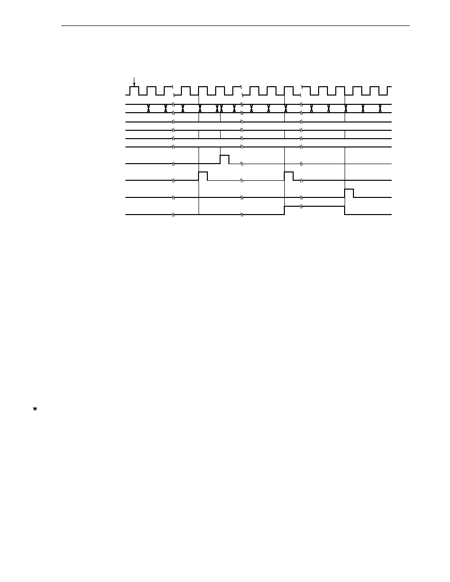
CHAPTER 6 16-BIT TIMER/EVENT COUNTERS 00 AND 01
User's Manual U16228EJ2V0UD
181
Figure 6-37. Timing of One-Shot Pulse Output Operation with Software Trigger
0000H
N
N
N
N
N
M
M
M
M
N
M
N + 1
N ≠ 1
M ≠ 1
0001H
M + 1 M + 2
0000H
Count clock
TM0n count
CR01n set value
CR00n set value
OSPT0n
INTTM01n
INTTM00n
TO0n pin output
Set TMC0n to 0CH
(TM0n count starts)
Caution 16-bit timer counter 0n starts operating as soon as a value other than 00 (operation stop mode) is
set to the TMC0n3 and TMC0n2 bits.
Remark N < M
(2) One-shot pulse output with external trigger
A one-shot pulse can be output from the TO0n pin by setting 16-bit timer mode control register 0n (TMC0n),
capture/compare control register 0n (CRC0n), and 16-bit timer output control register 0n (TOC0n) as shown in
Figure 6-38, and by using the valid edge of the TI00n pin as an external trigger.
The valid edge of the TI00n pin is specified by bits 4 and 5 (ES0n0, ES0n1) of prescaler mode register 0n
(PRM0n). The rising, falling, or both the rising and falling edges can be specified.
When the valid edge of the TI00n pin is detected, the 16-bit timer/event counter is cleared and started, and the
output becomes active at the count value set in advance to 16-bit timer capture/compare register 01n (CR01n).
After that, the output becomes inactive at the count value set in advance to 16-bit timer capture/compare register
00n (CR00n)
Note
.
Note The case where N < M is described here. When N > M, the output becomes active with the CR00n register
and inactive with the CR01n register. Do not set N to M.
Caution Even if the external trigger is generated again while the one-shot pulse is output, it is ignored.
Remark n = 0:
µ
PD780131, 780132
n = 0, 1:
µ
PD780133, 780134, 78F0134, 780136, 780138, 78F0138

CHAPTER 6 16-BIT TIMER/EVENT COUNTERS 00 AND 01
User's Manual U16228EJ2V0UD
182
Figure 6-38. Control Register Settings for One-Shot Pulse Output with External Trigger
(with Rising Edge Specified)
(a) 16-bit timer mode control register 0n (TMC0n)
0
0
0
0
7
6
5
4
1
TMC0n3
TMC0n
TMC0n2 TMC0n1
OVF0n
Clears and starts at
valid edge of TI00n pin.
0
0
0
(b) Capture/compare control register 0n (CRC0n)
0
0
0
0
0
7
6
5
4
3
CRC0n
CRC0n2 CRC0n1
CRC0n0
CR00n used as compare register
CR01n used as compare register
0
0/1
0
(c) 16-bit timer output control register 0n (TOC0n)
0
7
0
1
1
0/1
TOC0n
LVR0n
TOC0n1
TOE0n
OSPE0n
OSPT0n
TOC0n4
LVS0n
Enables TO0n output.
Inverts output upon match
between TM0n and CR00n.
Specifies initial value of
TO0n output F/F (setting "11" is prohibited.)
Inverts output upon match
between TM0n and CR01n.
Sets one-shot pulse output mode.
0/1
1
1
(d) Prescaler mode register 0n (PRM0n)
0/1
0/1
0
1
PRM0n
PRM0n1
PRM0n0
Selects count clock
(setting "11" is prohibited).
Specifies the rising edge
for pulse width detection.
0/1
0/1
ES1n1
ES1n0
ES0n1
ES0n0
Setting invalid
(setting "10" is prohibited.)
0
0
3
2
Caution Do not set the CR00n and CR01n registers to 0000H.
Remark n = 0:
µ
PD780131, 780132
n = 0, 1:
µ
PD780133, 780134, 78F0134, 780136, 780138, 78F0138

CHAPTER 6 16-BIT TIMER/EVENT COUNTERS 00 AND 01
User's Manual U16228EJ2V0UD
183
Figure 6-39. Timing of One-Shot Pulse Output Operation with External Trigger (with Rising Edge Specified)
0000H
N
N
N
N
N
M
M
M
M
M
N + 1 N + 2
M + 1 M + 2
M ≠ 2 M ≠ 1
0001H
0000H
Count clock
TM0n count value
CR01n set value
CR00n set value
TI00n pin input
INTTM01n
INTTM00n
TO0n pin output
When TMC0n is set to 08H
(TM0n count starts)
t
Caution 16-bit timer counter 0n starts operating as soon as a value other than 00 (operation stop mode) is
set to the TMC0n2 and TMC0n3 bits.
Remark N < M
n = 0:
µ
PD780131, 780132
n = 0, 1:
µ
PD780133, 780134, 78F0134, 780136, 780138, 78F0138
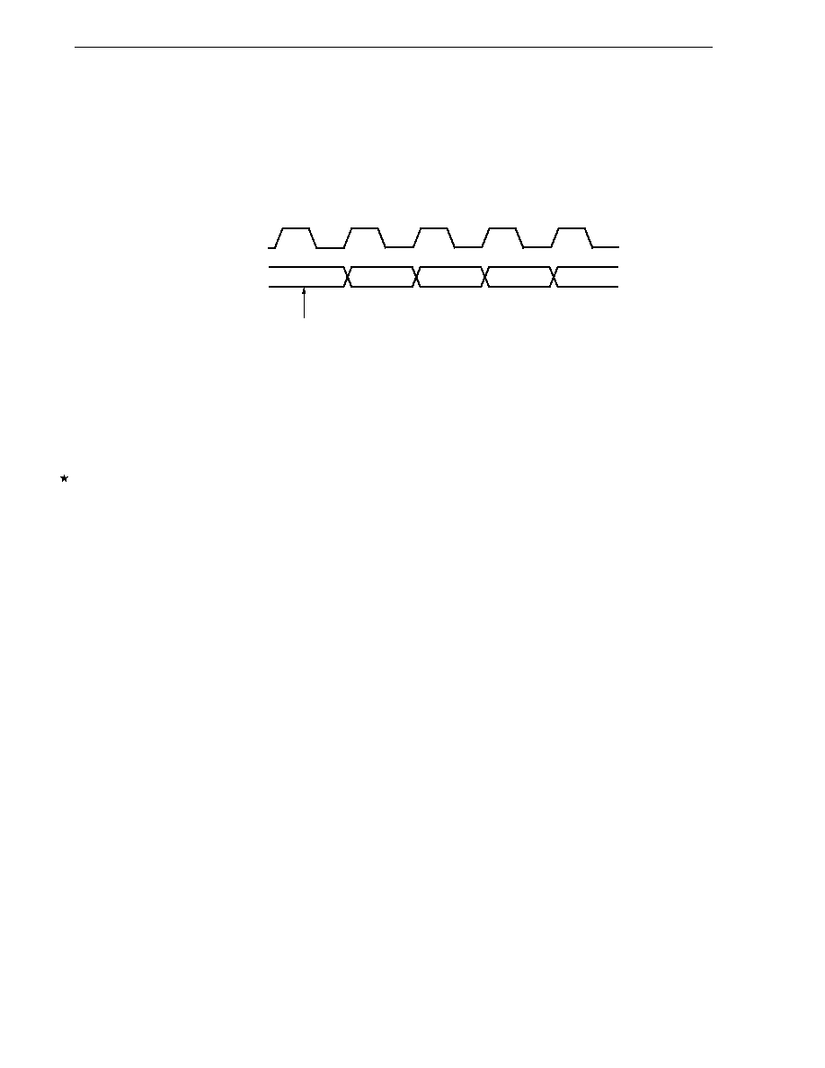
CHAPTER 6 16-BIT TIMER/EVENT COUNTERS 00 AND 01
User's Manual U16228EJ2V0UD
184
6.5 Cautions for 16-Bit Timer/Event Counters 00 and 01
(1) Timer start errors
An error of up to one clock may occur in the time required for a match signal to be generated after timer start.
This is because 16-bit timer counter 0n (TM0n) is started asynchronously to the count clock.
Figure 6-40. Start Timing of 16-Bit Timer Counter 0n (TM0n)
TM0n count value
0000H
0001H
0002H
0004H
Count clock
Timer start
0003H
(2) 16-bit timer capture/compare register setting (in the mode in which clear & start occurs on match
between TM0n and CR00n)
Set 16-bit timer capture/compare registers 00n, 01n (CR00n, CR01n) to other than 0000H. This means a 1-pulse
count operation cannot be performed when 16-bit timer/event counter 0n is used as an event counter.
(3) Capture
register
data retention timing
The values of 16-bit timer capture/compare registers 00n and 01n (CR00n and CR01n) are not guaranteed after
16-bit timer/event counter 0n has been stopped.
(4) Valid edge setting
Set the valid edge of the TI00n pin after setting bits 2 and 3 (TMC0n2 and TMC0n3) of 16-bit timer mode control
register 0n (TMC0n) to 0, 0, respectively, and then stopping timer operation. The valid edge is set using bits 4
and 5 (ES0n0 and ES0n1) of prescaler mode register 0n (PRM0n).
(5) Re-triggering one-shot pulse
(a) One-shot pulse output by software
When a one-shot pulse is output, do not set the OSPT0n bit to 1. Do not output the one-shot pulse again
until INTTM00n, which occurs upon a match with the CR00n register, or INTTM01n, which occurs upon a
match with the CR01n register, occurs.
(b) One-shot pulse output with external trigger
If the external trigger occurs again while a one-shot pulse is output, it is ignored.
(c) One-shot pulse output function
When using the one-shot pulse output of 16-bit timer/event counter 0n with a software trigger, do not change
the level of the TI00n pin or its alternate function port pin.
Because the external trigger is valid even in this case, the timer is cleared and started even at the level of the
TI00n pin or its alternate function port pin, resulting in the output of a pulse at an undesired timing.
Remark n = 0:
µ
PD780131, 780132
n = 0, 1:
µ
PD780133, 780134, 78F0134, 780136, 780138, 78F0138
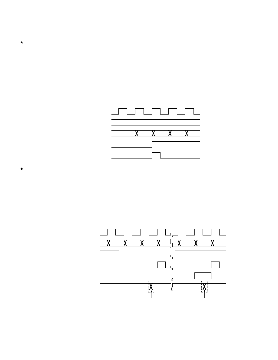
CHAPTER 6 16-BIT TIMER/EVENT COUNTERS 00 AND 01
User's Manual U16228EJ2V0UD
185
(6) Operation of OVF0n flag
<1> The OFV0n flag is also set to 1 in the following case.
When of the following modes: the mode in which clear & start occurs on a match between TM0n and
CR00n, the mode in which clear & start occurs on a TI0n valid edge, or the free-running mode, is selected
CR00n is set to FFFFH
TM0n is counted up from FFFFH to 0000H.
Figure 6-41. Operation Timing of OVF0n Flag
Count clock
CR00n
TM0n
OVF0n
INTTM00n
FFFFH
FFFEH
FFFFH
0000H
0001H
<2> Even if the OVF0n flag is cleared before the next count clock is counted (before TM0n becomes 0001H)
after the occurrence of TM0n overflow, the OVF0n flag is re-set newly and clear is disabled.
(7) Conflicting
operations
Conflict between the read period of the 16-bit timer capture/compare register (CR00n/CR01n) and capture trigger
input (CR00n/CR01n used as capture register)
Capture trigger input has priority. The data read from CR00n/CR01n is undefined.
Figure 6-42. Capture Register Data Retention Timing
Count clock
TM0n count value
Edge input
INTTM01n
Capture read signal
CR01n capture value
N
N + 1
N + 2
M
M + 1
M + 2
X
N + 2
Capture, but
read value is
not guaranteed
Capture
M + 1
Remark n = 0:
µ
PD780131, 780132
n = 0, 1:
µ
PD780133, 780134, 78F0134, 780136, 780138, 78F0138

CHAPTER 6 16-BIT TIMER/EVENT COUNTERS 00 AND 01
User's Manual U16228EJ2V0UD
186
(8) Timer
operation
<1> Even if 16-bit timer counter 0n (TM0n) is read, the value is not captured by 16-bit timer capture/compare
register 01n (CR01n).
<2> Regardless of the CPU's operation mode, when the timer stops, the input signals to the TI00n/TI01n pins
are not acknowledged.
<3> The one-shot pulse output mode operates correctly only in the free-running mode and the mode in which
clear & start occurs at the TI00n valid edge. In the mode in which clear & start occurs on a match between
the TM0n register and CR00n register, one-shot pulse output is not possible because an overflow does not
occur.
(9) Capture
operation
<1> If TI00n valid edge is specified as the count clock, a capture operation by the capture register specified as
the trigger for TI00n is not possible.
<2> To ensure the reliability of the capture operation, the capture trigger requires a pulse two cycles longer than
the count clock selected by prescaler mode register 0n (PRM0n).
<3> The capture operation is performed at the falling edge of the count clock. An interrupt request input
(INTTM00n/INTTM01n), however, is generated at the rise of the next count clock.
(10) Compare operation
A capture operation may not be performed for CR00n/CR01n set in compare mode even if a capture trigger has
been input.
(11) Edge detection
<1> If the TI00n or TI01n pin is high level immediately after system reset and the rising edge or both the rising
and falling edges are specified as the valid edge of the TI00n or TI01n pin to enable the 16-bit timer counter
0n (TM0n) operation, a rising edge is detected immediately after the operation is enabled. Be careful
therefore when pulling up the TI00n or TI01n pin. However, the rising edge is not detected at restart after
the operation has been stopped once.
<2> The sampling clock used to remove noise differs when the TI00n valid edge is used as the count clock and
when it is used as a capture trigger. In the former case, the count clock is f
X
, and in the latter case the
count clock is selected by prescaler mode register 0n (PRM0n). The capture operation is started only after
a valid edge is detected twice by sampling, thus eliminating noise with a short pulse width.
Remark n = 0:
µ
PD780131, 780132
n = 0, 1:
µ
PD780133, 780134, 78F0134, 780136, 780138, 78F0138
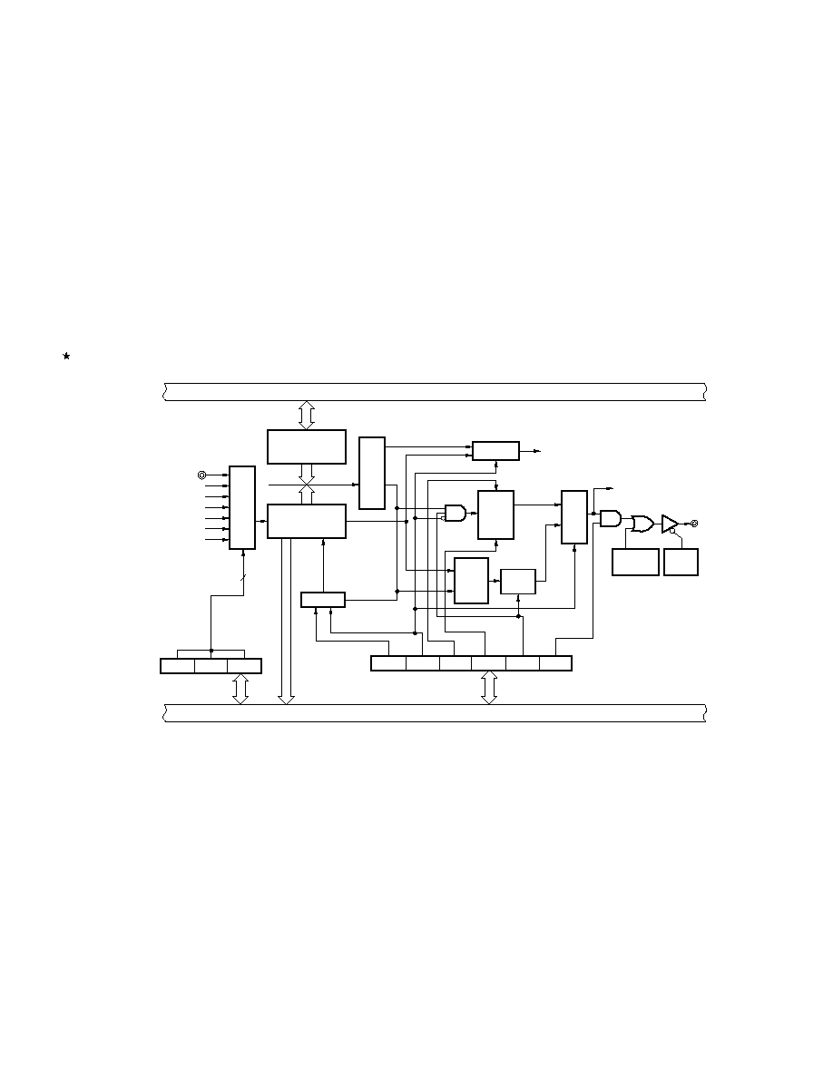
User's Manual U16228EJ2V0UD
187
CHAPTER 7 8-BIT TIMER/EVENT COUNTERS 50 AND 51
7.1 Functions of 8-Bit Timer/Event Counters 50 and 51
8-bit timer/event counters 50 and 51 have the following functions.
∑
Interval
timer
∑
External event counter
∑
Square-wave
output
∑
PWM
output
Figures 7-1 and 7-2 show the block diagrams of 8-bit timer/event counters 50 and 51.
Figure 7-1. Block Diagram of 8-Bit Timer/Event Counter 50
Internal bus
8-bit timer compare
register 50 (CR50)
TI50/TO50/P17
f
X
/2
2
f
X
/2
6
f
X
/2
8
f
X
/2
13
f
X
f
X
/2
Match
Mask circuit
OVF
Clear
3
Selector
TCL502 TCL501 TCL500
Timer clock selection
register 50 (TCL50)
Internal bus
TCE50 TMC506 LVS50 LVR50 TMC501 TOE50
Invert
level
8-bit timer mode control
register 50 (TMC50)
S
R
S
Q
R
INV
Selector
To TMH0
To UART0
To UART6
INTTM50
TO50/
TI50/P17
Note 1
Note 2
Selector
8-bit timer
counter 50 (TM50)
Selector
Output latch
(P17)
PM17
Notes 1. Timer output F/F
2. PWM output F/F
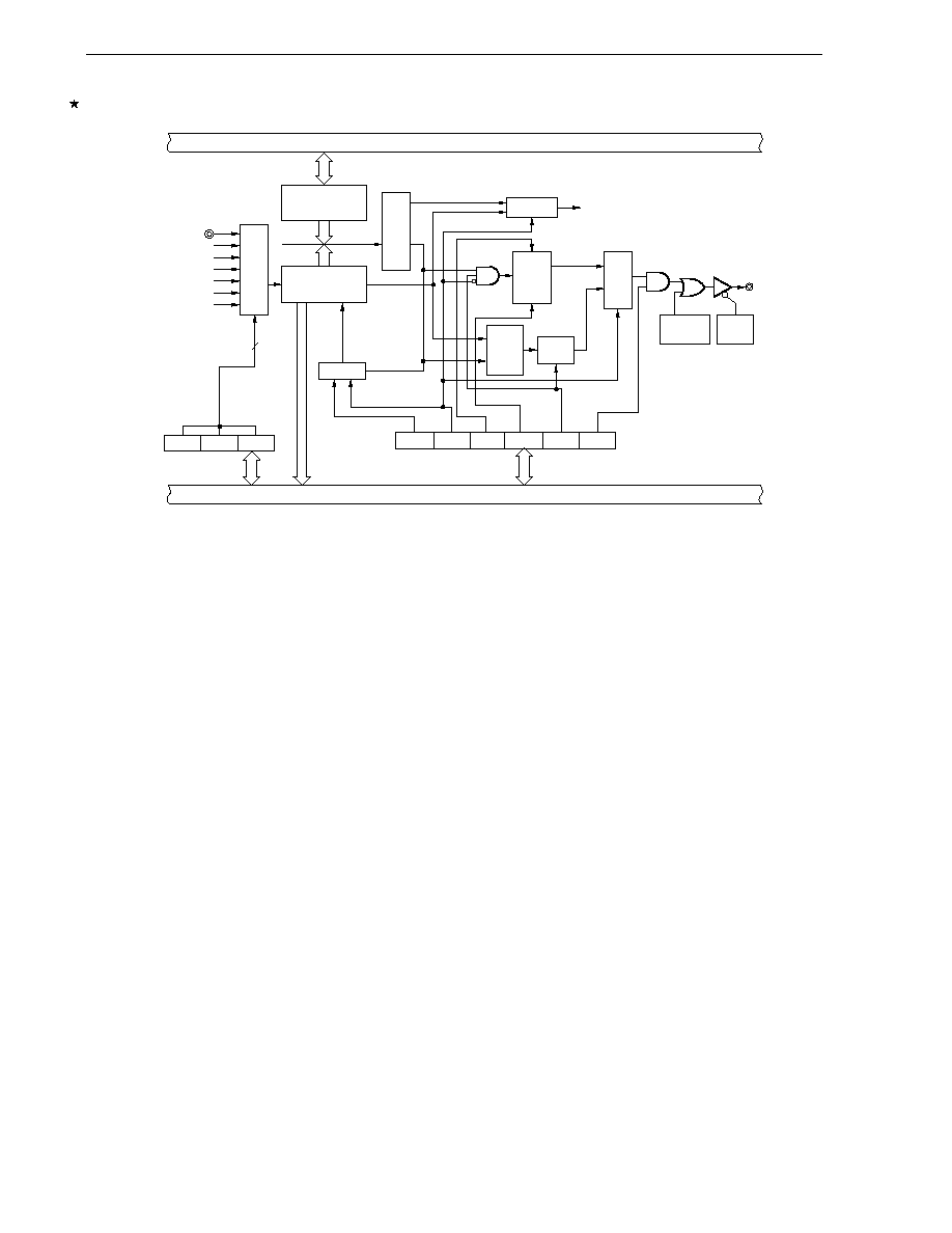
CHAPTER 7 8-BIT TIMER/EVENT COUNTERS 50 AND 51
User's Manual U16228EJ2V0UD
188
Figure 7-2. Block Diagram of 8-Bit Timer/Event Counter 51
Internal bus
8-bit timer compare
register 51 (CR51)
TI51/TO51/P33/INTP4
f
X
/2
8
f
X
/2
12
f
X
f
X
/2
Match
Mask circuit
OVF
Clear
3
Selector
TCL512 TCL511 TCL510
Timer clock selection
register 51 (TCL51)
Internal bus
TCE51 TMC516 LVS51 LVR51 TMC511 TOE51
Invert
level
8-bit timer mode control
register 51 (TMC51)
S
R
S
Q
R
INV
Selector
INTTM51
TO51/TI51/
P33/INTP4
Note 1
Note 2
Selector
8-bit timer
counter 51 (TM51)
Selector
Output latch
(P33)
PM33
f
X
/2
6
f
X
/2
4
Notes 1. Timer output F/F
2. PWM output F/F
CHAPTER 7 8-BIT TIMER/EVENT COUNTERS 50 AND 51
User's Manual U16228EJ2V0UD
189
7.2 Configuration of 8-Bit Timer/Event Counters 50 and 51
8-bit timer/event counters 50 and 51 include the following hardware.
Table 7-1. Configuration of 8-Bit Timer/Event Counters 50 and 51
Item Configuration
Timer register
8-bit timer counter 5n (TM5n)
Register
8-bit timer compare register 5n (CR5n)
Timer input
TI5n
Timer output
TO5n
Control registers
Timer clock selection register 5n (TCL5n)
8-bit timer mode control register 5n (TMC5n)
Port mode register 1 (PM1) or port mode register 3 (PM3)
Port register 1 (P1) or port register 3 (P3)
(1) 8-bit timer counter 5n (TM5n)
TM5n is an 8-bit register that counts the count pulses and is read-only.
The counter is incremented in synchronization with the rising edge of the count clock.
Figure 7-3. Format of 8-Bit Timer Counter 5n (TM5n)
Symbol
TM5n
(n = 0, 1)
Address: FF16H (TM50), FF1FH (TM51) After reset: 00H R
In the following situations, the count value is cleared to 00H.
<1> RESET input
<2> When TCE5n is cleared
<3> When TM5n and CR5n match in the mode in which clear & start occurs upon a match of the TM5n and
CR5n.
CHAPTER 7 8-BIT TIMER/EVENT COUNTERS 50 AND 51
User's Manual U16228EJ2V0UD
190
(2) 8-bit timer compare register 5n (CR5n)
CR5n can be read and written by an 8-bit memory manipulation instruction.
Except in PWM mode, the value set in CR5n is constantly compared with the 8-bit timer counter 5n (TM5n) count
value, and an interrupt request (INTTM5n) is generated if they match.
In PWM mode, when the TO5n pin becomes active due to a TM5n overflow and the values of TM5n and CR5n
match, the TO5n pin becomes inactive.
The value of CR5n can be set within 00H to FFH.
RESET input clears CR5n to 00H.
Figure 7-4. Format of 8-Bit Timer Compare Register 5n (CR5n)
Symbol
CR5n
(n = 0, 1)
Address: FF17H (CR50), FF41H (CR51) After reset: 00H R/W
Cautions 1. In the mode in which clear & start occurs on a match of TM5n and CR5n (TMC5n6 = 0), do
not write other values to CR5n during operation.
2. In PWM mode, make the CR5n rewrite period 3 count clocks of the count clock (clock
selected by TCL5n) or more.
Remark n = 0, 1
CHAPTER 7 8-BIT TIMER/EVENT COUNTERS 50 AND 51
User's Manual U16228EJ2V0UD
191
7.3 Registers Controlling 8-Bit Timer/Event Counters 50 and 51
The following four registers are used to control 8-bit timer/event counters 50 and 51.
∑
Timer clock selection register 5n (TCL5n)
∑
8-bit timer mode control register 5n (TMC5n)
∑
Port mode register 1 (PM1) or port mode register 3 (PM3)
∑
Port register 1 (P1) or port register 3 (P3)
(1) Timer clock selection register 5n (TCL5n)
This register sets the count clock of 8-bit timer/event counter 5n and the valid edge of TI5n input.
TCL5n can be set by an 8-bit memory manipulation instruction.
RESET input clears TCL5n to 00H.
Remark n = 0, 1
Figure 7-5. Format of Timer Clock Selection Register 50 (TCL50)
Address: FF6AH After reset: 00H R/W
Symbol
7 6 5 4 3 2 1 0
TCL50 0 0 0 0 0
TCL502
TCL501
TCL500
TCL502 TCL501 TCL500
Count
clock
selection
0
0
0
TI50 falling edge
0
0
1
TI50 rising edge
0 1 0
f
X
(10 MHz)
0 1 1
f
X
/2 (5 MHz)
1 0 0
f
X
/2
2
(2.5 MHz)
1 0 1
f
X
/2
6
(156.25 kHz)
1 1 0
f
X
/2
8
(39.06 kHz)
1 1 1
f
X
/2
13
(1.22 kHz)
Cautions 1. When the Ring-OSC clock is selected as the clock to be supplied to the CPU, the clock of the
Ring-OSC oscillator is divided and supplied as the count clock. If the count clock is the
Ring-OSC clock, the operation of 8-bit timer/event counter 50 is not guaranteed.
2. When rewriting TCL50 to other data, stop the timer operation beforehand.
3. Be sure to set bits 3 to 7 to 0.
Remarks 1. f
X
: X1 input clock oscillation frequency
2. Figures in parentheses apply to operation at f
X
= 10 MHz.
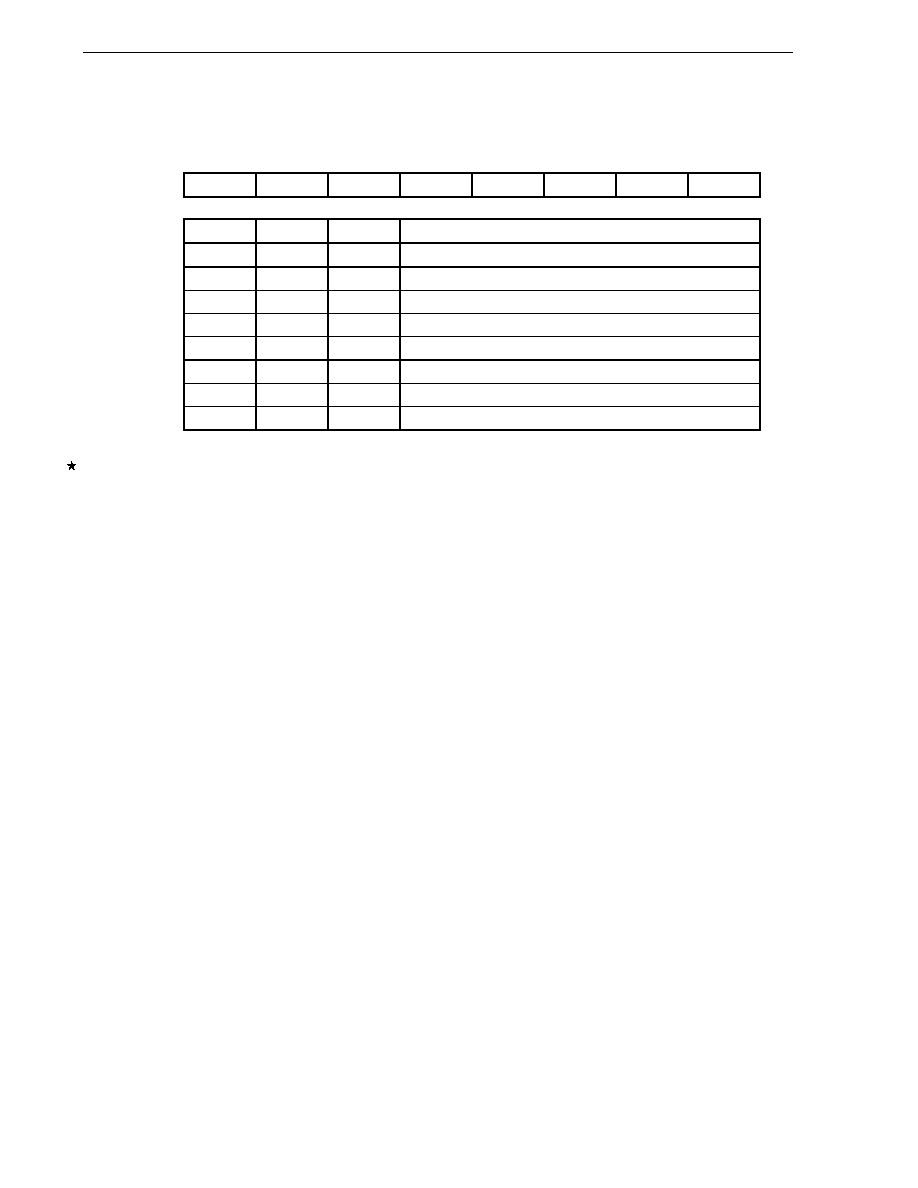
CHAPTER 7 8-BIT TIMER/EVENT COUNTERS 50 AND 51
User's Manual U16228EJ2V0UD
192
Figure 7-6. Format of Timer Clock Selection Register 51 (TCL51)
Address: FF8CH After reset: 00H R/W
Symbol
7 6 5 4 3 2 1 0
TCL51 0 0 0 0 0
TCL512
TCL511
TCL510
TCL512 TCL511 TCL510
Count
clock
selection
0
0
0
TI51 falling edge
0
0
1
TI51 rising edge
0 1 0
f
X
(10 MHz)
0 1 1
f
X
/2 (5 MHz)
1 0 0
f
X
/2
4
(625 kHz)
1 0 1
f
X
/2
6
(156.25 kHz)
1 1 0
f
X
/2
8
(39.06 kHz)
1 1 1
f
X
/2
12
(2.44 kHz)
Cautions 1. When the Ring-OSC clock is selected as the clock to be supplied to the CPU, the clock of the
Ring-OSC oscillator is divided and supplied as the count clock. If the count clock is the Ring-
OSC clock, the operation of 8-bit timer/event counter 51 is not guaranteed.
2. When rewriting TCL51 to other data, stop the timer operation beforehand.
3. Be sure to set bits 3 to 7 to 0.
Remarks 1. f
X
: X1 input clock oscillation frequency
2. Figures in parentheses apply to operation at f
X
= 10 MHz.

CHAPTER 7 8-BIT TIMER/EVENT COUNTERS 50 AND 51
User's Manual U16228EJ2V0UD
193
(2) 8-bit timer mode control register 5n (TMC5n)
TMC5n is a register that performs the following five types of settings.
<1> 8-bit timer counter 5n (TM5n) count operation control
<2> 8-bit timer counter 5n (TM5n) operating mode selection
<3> Timer output F/F (flip flop) status setting
<4> Active level selection in timer F/F control or PWM (free-running) mode.
<5> Timer output control
TMC5n can be set by a 1-bit or 8-bit memory manipulation instruction.
RESET input clears this register to 00H.
Remark n = 0, 1
Figure 7-7. Format of 8-Bit Timer Mode Control Register 50 (TMC50)
Address: FF6BH After reset: 00H R/W
Note
Symbol
<7> 6 5 4 <3>
<2> 1 <0>
TMC50 TCE50
TMC506 0
0 LVS50
LVR50
TMC501
TOE50
TCE50
TM50 count operation control
0
After clearing to 0, count operation disabled (counter stopped)
1 Count
operation
start
TMC506
TM50 operating mode selection
0
Mode in which clear & start occurs on a match between TM50 and CR50
1
PWM (free-running) mode
LVS50
LVR50
Timer output F/F status setting
0 0
No
change
0
1
Timer output F/F reset (0)
1
0
Timer output F/F set (1)
1 1
Setting
prohibited
In other modes (TMC506 = 0)
In PWM mode (TMC506 = 1)
TMC501
Timer F/F control
Active level selection
0
Inversion operation disabled
Active-high
1
Inversion operation enabled
Active-low
TOE50 Timer
output
control
0
Output disabled (TM50 output is low level)
1 Output
enabled
Note Bits 2 and 3 are write-only.
(Refer to Cautions and Remarks on the next page.)
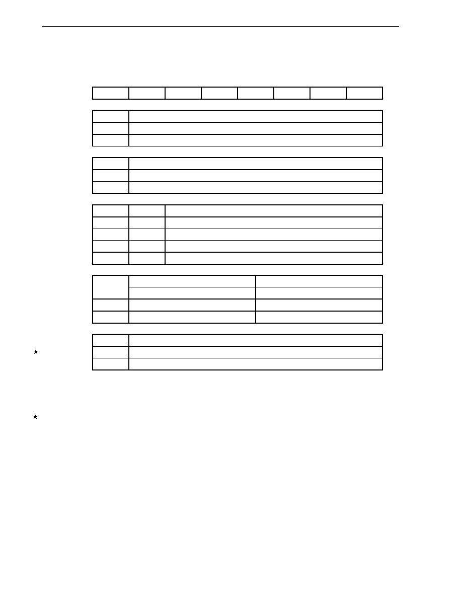
CHAPTER 7 8-BIT TIMER/EVENT COUNTERS 50 AND 51
User's Manual U16228EJ2V0UD
194
Figure 7-8. Format of 8-Bit Timer Mode Control Register 51 (TMC51)
Address: FF43H After reset: 00H R/W
Note
Symbol
<7> 6 5 4 <3>
<2> 1 <0>
TMC51 TCE51
TMC516 0
0 LVS51
LVR51
TMC511
TOE51
TCE51
TM51 count operation control
0
After clearing to 0, count operation disabled (counter stopped)
1 Count
operation
start
TMC516
TM51 operating mode selection
0
Mode in which clear & start occurs on a match between TM51 and CR51
1
PWM (free-running) mode
LVS51
LVR51
Timer output F/F status setting
0 0
No
change
0
1
Timer output F/F reset (0)
1
0
Timer output F/F set (1)
1 1
Setting
prohibited
In other modes (TMC516 = 0)
In PWM mode (TMC516 = 1)
TMC511
Timer F/F control
Active level selection
0
Inversion operation disabled
Active-high
1
Inversion operation enabled
Active-low
TOE51 Timer
output
control
0
Output disabled (TM51 output is low level)
1 Output
enabled
Note Bits 2 and 3 are write-only.
Cautions 1. The settings of LVS5n and LVR5n are valid in other than PWM mode.
2. Do not rewrite following bits simultaneously.
∑
TMC5n1 and TOE5n
∑
TMC5n6 and TOE5n
∑
TMC5n1 and TMC5n6
∑
TMC5n6 and LVS5n, LVR5n
∑
TOE5n and LVS5n, LVR5n
3. Stop operation before rewriting TMC5n6.
Remarks 1. In PWM mode, PWM output is made inactive by clearing TCE5n to 0.
2. If LVS5n and LVR5n are read, the value is 0.
3. The values of the TMC5n6, LVS5n, LVR5n, TMC5n1, and TOE5n bits are reflected at the TO5n pin
regardless of the value of TCE5n.
4. n = 0, 1
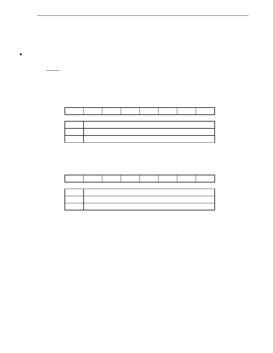
CHAPTER 7 8-BIT TIMER/EVENT COUNTERS 50 AND 51
User's Manual U16228EJ2V0UD
195
(3) Port mode registers 1 and 3 (PM1, PM3)
These registers set port 1 and 3 input/output in 1-bit units.
When using the P17/TO50/TI50 and P33/TO51/TI51/INTP4 pins for timer output, clear PM17 and PM33 and the
output latches of P17 and P33 to 0.
When using the P17/TO50/TI50 and P33/TO51/TI51/INTP4 pins for timer input, set PM17 and PM33 to 1. The
output latches of P17 and P33 at this time may be 0 or 1.
PM1 and PM3 can be set by a 1-bit or 8-bit memory manipulation instruction.
RESET input sets these registers to FFH.
Figure 7-9. Format of Port Mode Register 1 (PM1)
Address: FF21H After reset: FFH R/W
Symbol
7 6 5 4 3 2 1 0
PM1
PM17 PM16 PM15 PM14 PM13 PM12 PM11 PM10
PM1n
P1n pin I/O mode selection (n = 0 to 7)
0
Output mode (output buffer on)
1
Input mode (output buffer off)
Figure 7-10. Format of Port Mode Register 3 (PM3)
Address: FF23H After reset: FFH R/W
Symbol
7 6 5 4 3 2 1 0
PM3 0 0 0 0
PM33
PM32
PM31
PM30
PM3n
P3n pin I/O mode selection (n = 0 to 3)
0
Output mode (output buffer on)
1
Input mode (output buffer off)
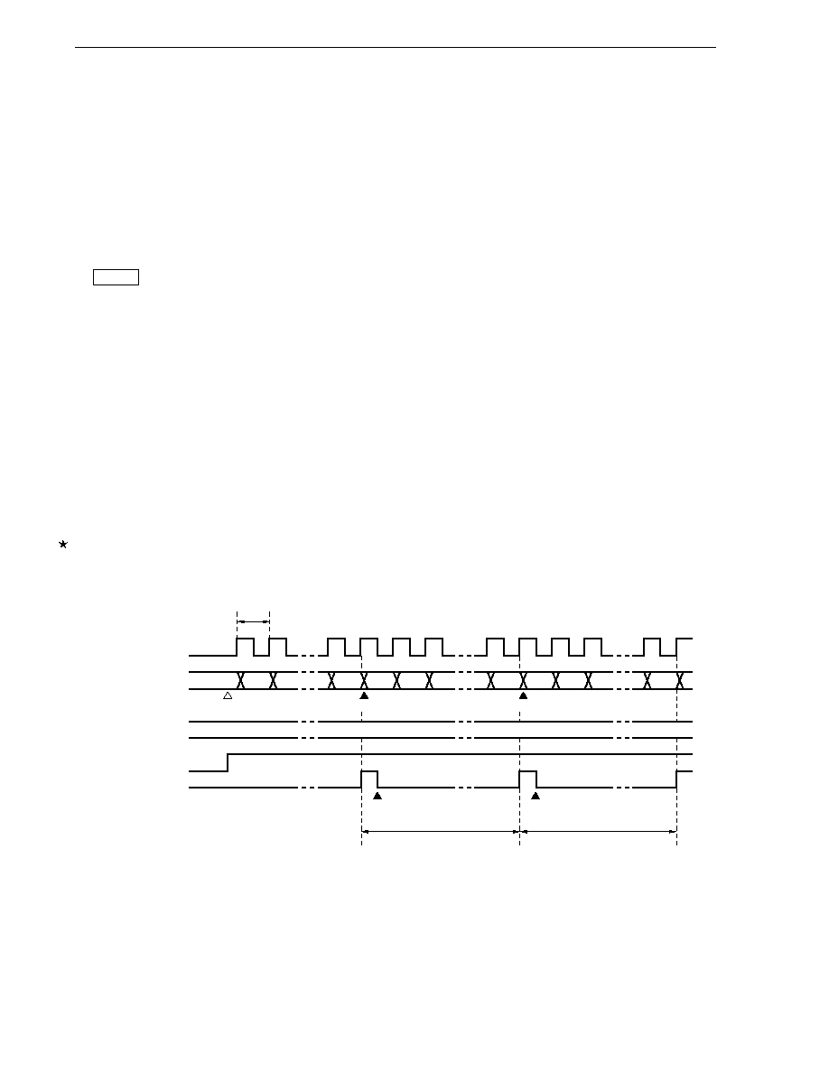
CHAPTER 7 8-BIT TIMER/EVENT COUNTERS 50 AND 51
User's Manual U16228EJ2V0UD
196
7.4 Operations of 8-Bit Timer/Event Counters 50 and 51
7.4.1 Operation as interval timer
8-bit timer/event counter 5n operates as an interval timer that generates interrupt requests repeatedly at intervals
of the count value preset to 8-bit timer compare register 5n (CR5n).
When the count value of 8-bit timer counter 5n (TM5n) matches the value set to CR5n, counting continues with the
TM5n value cleared to 0 and an interrupt request signal (INTTM5n) is generated.
The count clock of TM5n can be selected with bits 0 to 2 (TCL5n0 to TCL5n2) of timer clock selection register 5n
(TCL5n).
Setting
<1> Set the registers.
∑
TCL5n:
Select the count clock.
∑
CR5n:
Compare
value
∑
TMC5n: Stop the count operation, select the mode in which clear & start occurs on a match of TM5n
and
CR5n.
(TMC5n = 0000
◊◊◊
0B
◊
= Don't care)
<2> After TCE5n = 1 is set, the count operation starts.
<3> If the values of TM5n and CR5n match, INTTM5n is generated (TM5n is cleared to 00H).
<4> INTTM5n is generated repeatedly at the same interval.
Set TCE5n to 0 to stop the count operation.
Caution Do not write other values to CR5n during operation.
Figure 7-11. Interval Timer Operation Timing (1/2)
(a) Basic operation
t
Count clock
TM5n count value
CR5n
TCE5n
INTTM5n
Count start
Clear
Clear
00H
01H
N
00H
01H
N
00H
01H
N
N
N
N
N
Interrupt acknowledged
Interrupt acknowledged
Interval time
Interval time
Remark Interval time = (N + 1)
◊
t
N = 00H to FFH
n = 0, 1
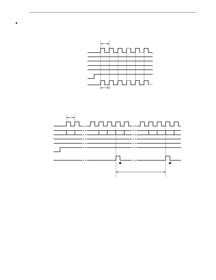
CHAPTER 7 8-BIT TIMER/EVENT COUNTERS 50 AND 51
User's Manual U16228EJ2V0UD
197
Figure 7-11. Interval Timer Operation Timing (2/2)
(b) When CR5n = 00H
t
Interval time
Count clock
TM5n
CR5n
TCE5n
INTTM5n
00H
00H
00H
00H
00H
(c) When CR5n = FFH
t
Count clock
TM5n
CR5n
TCE5n
INTTM5n
01
FE
FF
00
FE
FF
00
FF
FF
FF
Interval time
Interrupt
acknowledged
Interrupt acknowledged
Remark n = 0, 1
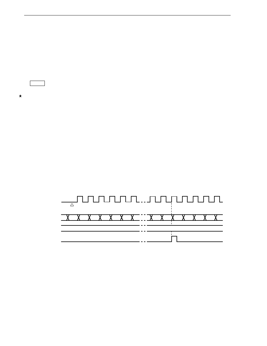
CHAPTER 7 8-BIT TIMER/EVENT COUNTERS 50 AND 51
User's Manual U16228EJ2V0UD
198
7.4.2 Operation as external event counter
The external event counter counts the number of external clock pulses to be input to TI5n by 8-bit timer counter 5n
(TM5n).
TM5n is incremented each time the valid edge specified by timer clock selection register 5n (TCL5n) is input.
Either the rising or falling edge can be selected.
When the TM5n count value matches the value of 8-bit timer compare register 5n (CR5n), TM5n is cleared to 0
and an interrupt request signal (INTTM5n) is generated.
Whenever the TM5n value matches the value of CR5n, INTTM5n is generated.
Setting
<1> Set each register.
∑
Set the port mode register (PM17 or PM33)
Note
to 1.
∑
TCL5n: Select TI5n input edge.
TI5n falling edge
TCL5n = 00H
TI5n rising edge
TCL5n = 01H
∑
CR5n: Compare
value
∑
TMC5n: Stop the count operation, select the mode in which clear & start occurs on match of TM5n and
CR5n, disable the timer F/F inversion operation, disable timer output.
(TMC5n = 0000
◊◊
00B
◊
= Don't care)
<2> When TCE5n = 1 is set, the number of pulses input from TI5n is counted.
<3> When the values of TM5n and CR5n match, INTTM5n is generated (TM5n is cleared to 00H).
<4> After these settings, INTTM5n is generated each time the values of TM5n and CR5n match.
Note 8-bit timer/event counter 50: PM17
8-bit timer/event counter 51: PM33
Figure 7-12. External Event Counter Operation Timing (with Rising Edge Specified)
TI5n
TM5n count value
CR5n
INTTM5n
00
01
02
03
04
05
N ≠ 1
N
00
01
02
03
N
Count start
Remark N = 00H to FFH
n = 0, 1
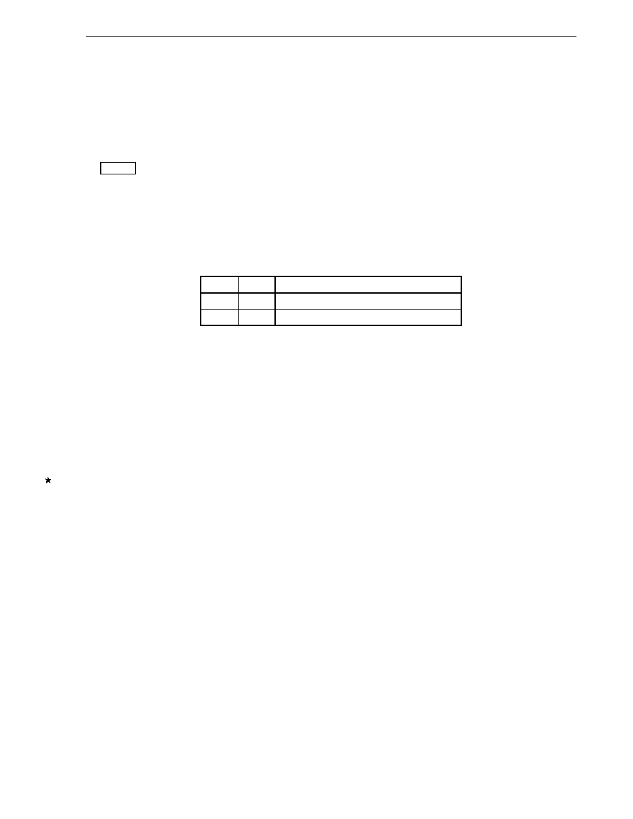
CHAPTER 7 8-BIT TIMER/EVENT COUNTERS 50 AND 51
User's Manual U16228EJ2V0UD
199
7.4.3 Square-wave output operation
A square wave with any selected frequency is output at intervals determined by the value preset to 8-bit timer
compare register 5n (CR5n).
The TO5n pin output status is inverted at intervals determined by the count value preset to CR5n by setting bit 0
(TOE5n) of 8-bit timer mode control register 5n (TMC5n) to 1. This enables a square wave with any selected
frequency to be output (duty = 50%).
Setting
<1> Set each register.
∑
Clear the port output latch (P17 or P33)
Note
and port mode register (PM17 or PM33)
Note
to 0.
∑
TCL5n: Select the count clock.
∑
CR5n: Compare
value
∑
TMC5n: Stop the count operation, select the mode in which clear & start occurs on a match of TM5n and
CR5n.
LVS5n
LVR5n
Timer Output F/F Status Setting
1 0
High-level
output
0 1
Low-level
output
Timer output F/F inversion enabled
Timer output enabled
(TMC5n = 00001011B or 00000111B)
<2> After TCE5n = 1 is set, the count operation starts.
<3> The timer output F/F is inverted by a match of TM5n and CR5n. After INTTM5n is generated, TM5n is
cleared to 00H.
<4> After these settings, the timer output F/F is inverted at the same interval and a square wave is output from
TO5n.
The frequency is as follows.
Frequency = 1/2t (N + 1)
(N: 00H to FFH)
Note 8-bit timer/event counter 50: P17, PM17
8-bit timer/event counter 51: P33, PM33
Caution Do not write other values to CR5n during operation.
Remark n = 0, 1
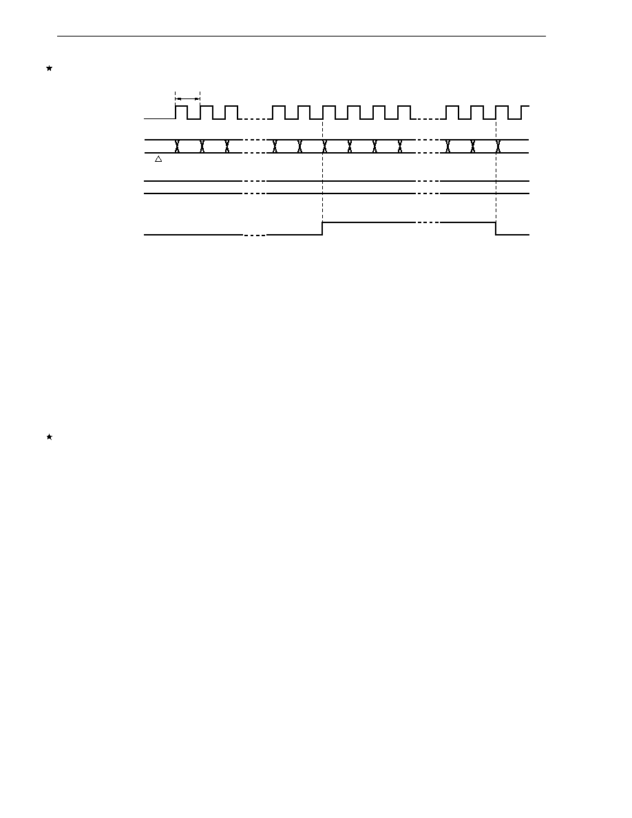
CHAPTER 7 8-BIT TIMER/EVENT COUNTERS 50 AND 51
User's Manual U16228EJ2V0UD
200
Figure 7-13. Square-Wave Output Operation Timing
Count clock
TM5n count value
00H
01H
02H
N
-
1
N
N
00H
N
-
1
N
00H
01H
02H
CR5n
TO5n
Note
t
Count start
Note The initial value of TO5n output can be set by bits 2 and 3 (LVR5n, LVS5n) of 8-bit timer mode control
register 5n (TMC5n).
7.4.4 PWM output operation
8-bit timer/event counter 5n operates as a PWM output when bit 6 (TMC5n6) of 8-bit timer mode control register 5n
(TMC5n) is set to 1.
The duty pulse determined by the value set to 8-bit timer compare register 5n (CR5n) is output from TO5n.
Set the active level width of the PWM pulse to CR5n; the active level can be selected with bit 1 (TMC5n1) of
TMC5n.
The count clock can be selected with bits 0 to 2 (TCL5n0 to TCL5n2) of timer clock selection register 5n (TCL5n).
PWM output can be enabled/disabled with bit 0 (TOE5n) of TMC5n.
Caution In PWM mode, make the CR5n rewrite period 3 count clocks of the count clock (clock selected by
TCL5n) or more.
Remark n = 0, 1
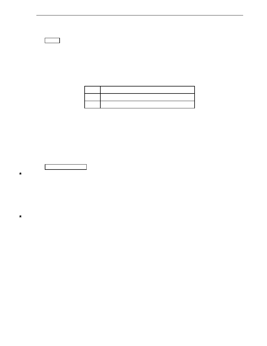
CHAPTER 7 8-BIT TIMER/EVENT COUNTERS 50 AND 51
User's Manual U16228EJ2V0UD
201
(1) PWM output basic operation
Setting
<1> Set each register.
∑
Clear the port output latch (P17 or P33)
Note
and port mode register (PM17 or PM33)
Note
to 0.
∑
TCL5n: Select the count clock.
∑
CR5n: Compare
value
∑
TMC5n: Stop the count operation, select PWM mode.
The timer output F/F is not changed.
TMC5n1
Active Level Selection
0 Active-high
1 Active-low
Timer output enabled
(TMC5n = 01000001B or 01000011B)
<2> The count operation starts when TCE5n = 1.
Clear TCE5n to 0 to stop the count operation.
Note 8-bit timer/event counter 50: P17, PM17
8-bit timer/event counter 51: P33, PM33
PWM output operation
<1> PWM output (output from TO5n) outputs an inactive level until an overflow occurs.
<2> When an overflow occurs, the active level is output. The active level is output until CR5n matches the
count value of 8-bit timer counter 5n (TM5n).
<3> After the CR5n matches the count value, the inactive level is output until an overflow occurs again.
<4> Operations <2> and <3> are repeated until the count operation stops.
<5> When the count operation is stopped with TCE5n = 0, PWM output becomes inactive.
For details of timing, see Figures 7-14 and 7-15.
The cycle, active-level width, and duty are as follows.
∑
Cycle = 2
8
t
∑
Active-level width = Nt
∑
Duty = N/2
8
(N = 00H to FFH)
Remark n = 0, 1
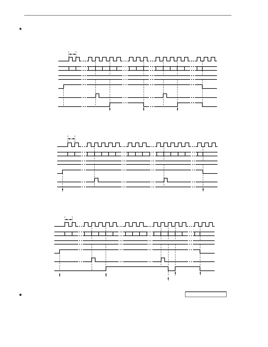
CHAPTER 7 8-BIT TIMER/EVENT COUNTERS 50 AND 51
User's Manual U16228EJ2V0UD
202
Figure 7-14. PWM Output Operation Timing
(a) Basic operation (active level = H)
Count clock
TM5n
CR5n
TCE5n
INTTM5n
TO5n
00H 01H
FFH 00H 01H 02H
N N + 1
FFH 00H 01H 02H
M
00H
N
<2> Active level
<1>
<3> Inactive level
Active level
<5>
t
(b) CR5n = 00H
Count clock
TM5n
CR5n
TCE5n
INTTM5n
TO5n
Inactive level
Inactive level
01H
00H
FFH 00H 01H 02H
N N + 1
FFH 00H 01H 02H
M 00H
00H
N + 2
L
t
(c) CR5n = FFH
TM5n
CR5n
TCE5n
INTTM5n
TO5n
01H
00H
FFH 00H 01H 02H
N N + 1
FFH 00H 01H 02H
M 00H
FFH
N + 2
Inactive level
Active level
Inactive level
Active level
Inactive level
t
Remarks 1. <1> to <3> and <5> in Figure 7-14 (a) correspond to <1> to <3> and <5> in PWM output operation in
7.4.4 (1) PWM output basic operation.
2. n = 0, 1

CHAPTER 7 8-BIT TIMER/EVENT COUNTERS 50 AND 51
User's Manual U16228EJ2V0UD
203
(2) Operation with CR5n changed
Figure 7-15. Timing of Operation with CR5n Changed
(a) CR5n value is changed from N to M before clock rising edge of FFH
Value is transferred to CR5n at overflow immediately after change.
Count clock
TM5n
CR5n
TCE5n
INTTM5n
TO5n
<1> CR5n change (N
M)
N N + 1 N + 2
FFH 00H 01H
M M + 1 M + 2
FFH 00H 01H 02H
M M + 1 M + 2
N
02H
M
H
<2>
t
(b) CR5n value is changed from N to M after clock rising edge of FFH
Value is transferred to CR5n at second overflow.
Count clock
TM5n
CR5n
TCE5n
INTTM5n
TO5n
N
N + 1 N + 2
FFH 00H 01H
N
N + 1 N + 2
FFH 00H 01H 02H
N
02H
N
H
M
M M + 1 M + 2
<1> CR5n change (N
M)
<2>
t
Caution When reading from CR5n between <1> and <2> in Figure 7-15, the value read differs from the
actual value (read value: M, actual value of CR5n: N).

CHAPTER 7 8-BIT TIMER/EVENT COUNTERS 50 AND 51
User's Manual U16228EJ2V0UD
204
7.5 Cautions for 8-Bit Timer/Event Counters 50 and 51
(1) Timer start error
An error of up to one clock may occur in the time required for a match signal to be generated after timer start.
This is because 8-bit timer counters 50 and 51 (TM50, TM51) are started asynchronously to the count clock.
Figure 7-16. 8-Bit Timer Counter 5n Start Timing
Count clock
TM5n count value
00H
01H
02H
03H
04H
Timer start
Remark n = 0, 1

User's Manual U16228EJ2V0UD
205
CHAPTER 8 8-BIT TIMERS H0 AND H1
8.1 Functions of 8-Bit Timers H0 and H1
8-bit timers H0 and H1 have the following functions.
∑
Interval
timer
∑
PWM output mode
∑
Square-wave
output
∑
Carrier generator mode (8-bit timer H1 only)
8.2 Configuration of 8-Bit Timers H0 and H1
8-bit timers H0 and H1 include the following hardware.
Table 8-1. Configuration of 8-Bit Timers H0 and H1
Item Configuration
Timer register
8-bit timer counter Hn
Registers
8-bit timer H compare register 0n (CMP0n)
8-bit timer H compare register 1n (CMP1n)
Timer output
TOHn
Control registers
8-bit timer H mode register n (TMHMDn)
8-bit timer H carrier control register 1 (TMCYC1)
Note
Port mode register 1 (PM1)
Port register 1 (P1)
Note 8-bit timer H1 only
Remark n = 0, 1
Figures 8-1 and 8-2 show the block diagrams.
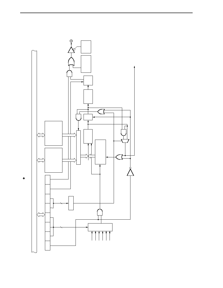
CHAPTER
8 8-
BIT TIME
RS H
0
AND H
1
User's Manual
U1
6228EJ2V0UD
206
Figure 8-1. Block Diagram of 8-Bit Timer H0
TMHE0 CKS02 CKS01 CKS00 TMMD01 TMMD00 TOLEV0 TOEN0
TOH0/P15
INTTMH0
f
X
f
X
/2
f
X
/2
2
f
X
/2
6
f
X
/2
10
1
0
F/F
R
3
2
PM15
Match
Internal bus
8-bit timer H mode control register 0
(TMHMD0)
8-bit timer H
compare register
10 (CMP10)
Decoder
Selector
Interrupt
generator
Output
controller
Level
inversion
PWM mode signal
Timer H enable signal
Clear
8-bit timer H
compare register
00 (CMP00)
Output latch
(P15)
8-bit timer/
event counter 50
output
Selector
8-bit timer
counter H0
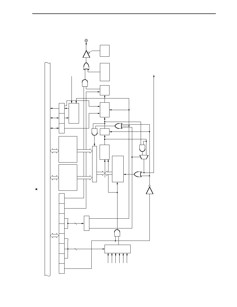
CHAPTER
8 8-
BIT TIME
RS H
0
AND H
1
User's Manual
U1
6228EJ2V0UD
207
Figure 8-2. Block Diagram of 8-Bit Timer H1
Match
Internal bus
TMHE1 CKS12 CKS11 CKS10 TMMD11 TMMD10 TOLEV1 TOEN1
8-bit timer H
compare
register 1 1
( C M P 1 1 )
Decoder
TOH1/
INTP5/
P16
8-bit timer H carrier
control register 1
(TMCYC1)
INTTMH1
INTTM51
Selector
f
X
f
X
/2
2
f
X
/2
4
f
X
/2
6
f
X
/2
12
f
R
/2
7
Interrupt
generator
Output
controller
Level
inversion
PM16
Output latch
(P16)
1
0
F/F
R
PWM mode signal
Carrier generator mode signal
Timer H enable signal
3
2
8-bit timer H
compare
register 0 1
( C M P 0 1 )
8-bit timer
counter H1
Clear
RMC1 NRZB1 NRZ1
Reload/
interrupt control
8-bit timer H mode control
register 1 (TMHMD1)
Selector
CHAPTER 8 8-BIT TIMERS H0 AND H1
User's Manual U16228EJ2V0UD
208
(1) 8-bit timer H compare register 0n (CMP0n)
This register can be read or written by an 8-bit memory manipulation instruction.
RESET input clears this register to 00H.
Figure 8-3. Format of 8-Bit Timer H Compare Register 0n (CMP0n)
Symbol
CMP0n
(n = 0, 1)
Address: FF18H (CMP00), FF1AH (CMP01) After reset: 00H R/W
7
6
5
4
3
2
1
0
Caution CMP0n cannot be rewritten during timer count operation.
(2) 8-bit timer H compare register 1n (CMP1n)
This register can be read or written by an 8-bit memory manipulation instruction.
RESET input clears this register to 00H.
Figure 8-4. Format of 8-Bit Timer H Compare Register 1n (CMP1n)
Symbol
CMP1n
(n = 0, 1)
Address: FF19H (CMP10), FF1BH (CMP11) After reset: 00H R/W
7
6
5
4
3
2
1
0
CMP1n can be rewritten during timer count operation.
An interrupt request signal (INTTMHn) is generated if the values of the timer counter and CMP1n match after
setting CMP1n in carrier generator mode. The timer counter value is cleared at the same time. If the CMP1n value is
rewritten during timer operation, transferring is performed at the timing at which the counter value and CMP1n value
match. If the transfer timing and writing from CPU to CMP1n conflict, transfer is not performed.
Caution In the PWM output mode and carrier generator mode, be sure to set CMP1n when starting the
timer count operation (TMHEn = 1) after the timer count operation was stopped (TMHEn = 0) (be
sure to set again even if setting the same value to CMP1n).
Remark n = 0, 1

CHAPTER 8 8-BIT TIMERS H0 AND H1
User's Manual U16228EJ2V0UD
209
8.3 Registers Controlling 8-Bit Timers H0 and H1
The following four registers are used to control 8-bit timers H0 and H1.
∑
8-bit timer H mode register n (TMHMDn)
∑
8-bit timer H carrier control register 1 (TMCYC1)
Note
∑
Port mode register 1 (PM1)
∑
Port register 1 (P1)
Note 8-bit timer H1 only
(1) 8-bit timer H mode register n (TMHMDn)
This register controls the mode of timer H.
This register can be set by a 1-bit or 8-bit memory manipulation instruction.
RESET input clears this register to 00H.
Remark n = 0, 1
CHAPTER 8 8-BIT TIMERS H0 AND H1
User's Manual U16228EJ2V0UD
210
Figure 8-5. Format of 8-Bit Timer H Mode Register 0 (TMHMD0)
TMHE0
Stops timer count operation (counter is cleared to 0)
Enables timer count operation (count operation started by inputting clock)
TMHE0
0
1
Timer operation enable
TMHMD0
CKS02
CKS01
CKS00
TMMD01 TMMD00 TOLEV0
TOEN0
Address: FF69H After reset: 00H R/W
f
X
f
X
/2
f
X
/2
2
f
X
/2
6
f
X
/2
10
TM50 output
Note
CKS02
0
0
0
0
1
1
CKS01
0
0
1
1
0
0
CKS00
0
1
0
1
0
1
(10 MHz)
(5 MHz)
(2.5 MHz)
(156.25 kHz)
(9.77 kHz)
Count clock (f
CNT
) selection
Setting prohibited
Other than above
Interval timer mode
PWM output mode
Setting prohibited
TMMD01
0
1
TMMD00
0
0
Timer operation mode
Low level
High level
TOLEV0
0
1
Timer output level control (in default mode)
Disables output
Enables output
TOEN0
0
1
Timer output control
Other than above
<7>
6
5
4
3
2
<1>
<0>
Note To select the TM50 output as a count clock, start operation by setting 8-bit timer/event counter 50 in the
PWM output mode (bit 6 (TMC506) of the TMC50 register = 1), and then set CKS02, CKS01, and CKS00 to
1, 0, and 1, respectively. Set the high/low level width of the count clock so that the specifications of the
input width of TI50 are satisfied (see AC Characteristics (1) Basic operation in CHAPTER 29 to
CHAPTER 31). It is not necessary to enable the TO50 pin as a timer output pin (bit 0 (TOE50) of the TMC
register may be 0 or 1).

CHAPTER 8 8-BIT TIMERS H0 AND H1
User's Manual U16228EJ2V0UD
211
Cautions 1. When the Ring-OSC clock is selected as the clock to be supplied to the CPU, the clock of the
Ring-OSC oscillator is divided and supplied as the count clock. If the count clock is the
Ring-OSC clock, the operation of 8-bit timer H0 is not guaranteed.
2. When TMHE0 = 1, setting the other bits of the TMHMD0 register is prohibited.
3. In the PWM output mode, be sure to set 8-bit timer H compare register 10 (CMP10) when
starting the timer count operation (TMHE0 = 1) after the timer count operation was stopped
(TMHE0 = 0) (be sure to set again even if setting the same value to the CMP10 register).
Remarks 1. f
X
: X1 input clock oscillation frequency
2. Figures in parentheses apply to operation at f
X
= 10 MHz
CHAPTER 8 8-BIT TIMERS H0 AND H1
User's Manual U16228EJ2V0UD
212
Figure 8-6. Format of 8-Bit Timer H Mode Register 1 (TMHMD1)
TMHE1
Stops timer count operation (counter is cleared to 0)
Enables timer count operation (count operation started by inputting clock)
TMHE1
0
1
Timer operation enable
TMHMD1
CKS12
CKS11
CKS10
TMMD11 TMMD10 TOLEV1
TOEN1
Address: FF6CH After reset: 00H R/W
f
X
f
X
/2
2
f
X
/2
4
f
X
/2
6
f
X
/2
12
f
R
/2
7
CKS12
0
0
0
0
1
1
CKS11
0
0
1
1
0
0
CKS10
0
1
0
1
0
1
(10 MHz)
(2.5 MHz)
(625 kHz)
(156.25 kHz)
(2.44 kHz)
(1.88 kHz (TYP.))
Count clock (f
CNT
) selection
Setting prohibited
Other than above
Interval timer mode
Carrier generator mode
PWM output mode
Setting prohibited
TMMD11
0
0
1
TMMD10
0
1
0
Timer operation mode
Low level
High level
TOLEV1
0
1
Timer output level control (in default mode)
Disables output
Enables output
TOEN1
0
1
Timer output control
Other than above
<7>
6
5
4
3
2
<1>
<0>
Cautions 1. When the Ring-OSC clock is selected as the clock to be supplied to the CPU, the clock of the
Ring-OSC oscillator is divided and supplied as the count clock. If the count clock is the
Ring-OSC clock, the operation of 8-bit timer H1 is not guaranteed (except when CKS12,
CKS11, CKS10 = 1, 0, 1 (f
R
/2
7
)).
2. When TMHE1 = 1, setting the other bits of the TMHMD1 register is prohibited.
3. In the PWM output mode and carrier generator mode, be sure to set 8-bit timer H compare
register 11 (CMP11) when starting the timer count operation (TMHE1 = 1) after the timer count
operation was stopped (TMHE1 = 0) (be sure to set again even if setting the same value to the
CMP11 register).
4. When the carrier generator mode is used, set so that the count clock frequency of TMH1
becomes more than 6 times the count clock frequency of TM51.
CHAPTER 8 8-BIT TIMERS H0 AND H1
User's Manual U16228EJ2V0UD
213
Remarks 1. f
X
: X1 input clock oscillation frequency
2. f
R
: Ring-OSC clock oscillation frequency
3. Figures in parentheses apply to operation at f
X
= 10 MHz, f
R
= 240 kHz (TYP.).
(2) 8-bit timer H carrier control register 1 (TMCYC1)
This register controls the remote control output and carrier pulse output status of 8-bit timer H1.
This register can be set by a 1-bit or 8-bit memory manipulation instruction.
RESET input clears this register to 00H.
Figure 8-7. Format of 8-Bit Timer H Carrier Control Register 1 (TMCYC1)
0
TMCYC1
0
0
0
0
RMC1
NRZB1
NRZ1
Address: FF6DH After reset: 00H R/W
Note
Low-level output
High-level output
Low-level output
Carrier pulse output
RMC1
0
0
1
1
NRZB1
0
1
0
1
Remote control output
Carrier output disabled status (low-level status)
Carrier output enabled status
(RMC1 = 1: Carrier pulse output, RMC1 = 0: High-level status)
NRZ1
0
1
Carrier pulse output status flag
<0>
Note Bit 0 is read-only.
(3) Port mode register 1 (PM1)
This register sets port 1 input/output in 1-bit units.
When using the P15/TOH0 and P16/TOH1/INTP5 pins for timer output, clear PM15 and PM16 and the output
latches of P15 and P16 to 0.
PM1 can be set by a 1-bit or 8-bit memory manipulation instruction.
RESET input sets this register to FFH.
Figure 8-8. Format of Port Mode Register 1 (PM1)
Address: FF21H After reset: FFH R/W
Symbol
7 6 5 4 3 2 1 0
PM1
PM17 PM16 PM15 PM14 PM13 PM12 PM11 PM10
PM1n
P1n pin I/O mode selection (n = 0 to 7)
0
Output mode (output buffer on)
1
Input mode (output buffer off)
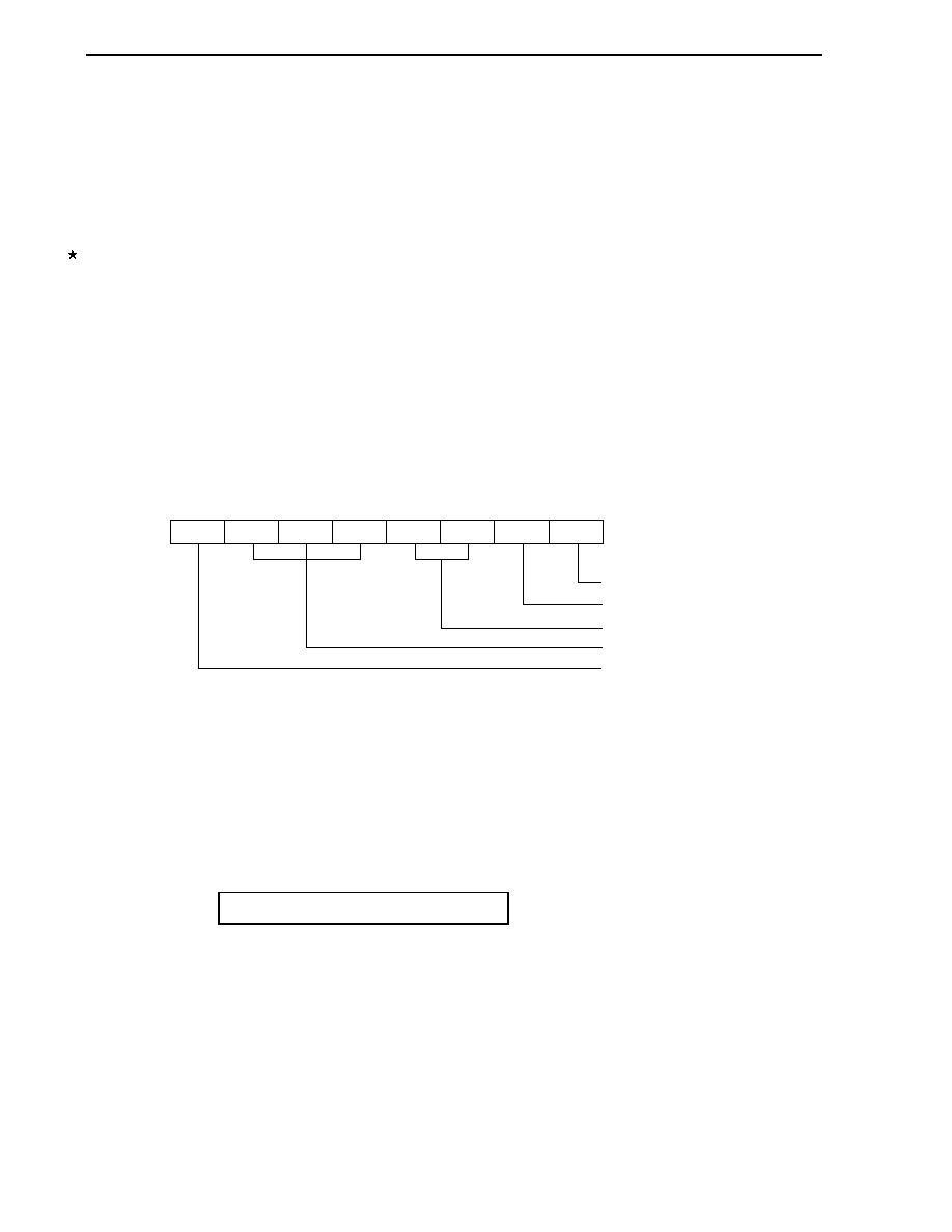
CHAPTER 8 8-BIT TIMERS H0 AND H1
User's Manual U16228EJ2V0UD
214
8.4 Operation of 8-Bit Timers H0 and H1
8.4.1 Operation as interval timer/square-wave output
When 8-bit timer counter Hn and compare register 0n (CMP0n) match, an interrupt request signal (INTTMHn) is
generated and 8-bit timer counter Hn is cleared to 00H.
Compare register 1n (CMP1n) is not used in interval timer mode. Since a match of 8-bit timer counter Hn and the
CMP1n register is not detected even if the CMP1n register is set, timer output is not affected.
By setting bit 0 (TOENn) of timer H mode register n (TMHMDn) to 1, a square wave of any frequency (duty = 50%)
is output from TOHn.
(1) Usage
Generates the INTTMHn signal repeatedly at the same interval.
<1> Set each register.
Figure 8-9. Register Setting During Interval Timer/Square-Wave Output Operation
(i) Setting timer H mode register n (TMHMDn)
0
0/1
0/1
0/1
0
0
0/1
0/1
TMMDn0 TOLEVn
TOENn
CKSn1
CKSn2
TMHEn
TMHMDn
CKSn0
TMMDn1
Timer output setting
Timer output level inversion setting
Interval timer mode setting
Count clock (f
CNT
) selection
Count operation stopped
(ii) CMP0n register setting
∑
Compare value (N)
<2> Count operation starts when TMHEn = 1.
<3> When the values of 8-bit timer counter Hn and the CMP0n register match, the INTTMHn signal is generated
and 8-bit timer counter Hn is cleared to 00H.
Interval time = (N +1)/f
CNT
<4> Subsequently, the INTTMHn signal is generated at the same interval. To stop the count operation, clear
TMHEn to 0.
Remark n = 0, 1

CHAPTER 8 8-BIT TIMERS H0 AND H1
User's Manual U16228EJ2V0UD
215
(2) Timing
chart
The timing of the interval timer/square-wave output operation is shown below.
Figure 8-10. Timing of Interval Timer/Square-Wave Output Operation (1/2)
(a) Basic operation
00H
Count clock
Count start
8-bit timer counter Hn
CMP0n
TMHEn
INTTMHn
TOHn
01H
N
Clear
Interval time
Clear
N
00H
01H
N
00H
01H 00H
<2>
Level inversion,
match interrupt occurrence,
8-bit timer counter Hn clear
<2>
Level inversion,
match interrupt occurrence,
8-bit timer counter Hn clear
<3>
<1>
<1> The count operation is enabled by setting the TMHEn bit to 1. The count clock starts counting no more than
1 clock after the operation is enabled.
<2> When the values of 8-bit timer counter Hn and the CMP0n register match, the value of 8-bit timer counter Hn
is cleared, the TOHn output level is inverted, and the INTTMHn signal is output.
<3> The INTTMHn signal and TOHn output become inactive by clearing the TMHEn bit to 0 during timer Hn
operation. If these are inactive from the first, the level is retained.
Remark n = 0, 1
N = 01H to FEH

CHAPTER 8 8-BIT TIMERS H0 AND H1
User's Manual U16228EJ2V0UD
216
Figure 8-10. Timing of Interval Timer/Square-Wave Output Operation (2/2)
(b) Operation when CMP0n = FFH
00H
Count clock
Count start
8-bit timer counter Hn
CMP0n
TMHEn
INTTMHn
TOHn
01H
FEH
Clear
Clear
FFH
00H
FEH
FFH
00H
FFH
Interval time
(c) Operation when CMP0n = 00H
Count clock
Count start
8-bit timer counter Hn
CMP0n
TMHEn
INTTMHn
TOHn
00H
00H
Interval time
Remark n = 0, 1
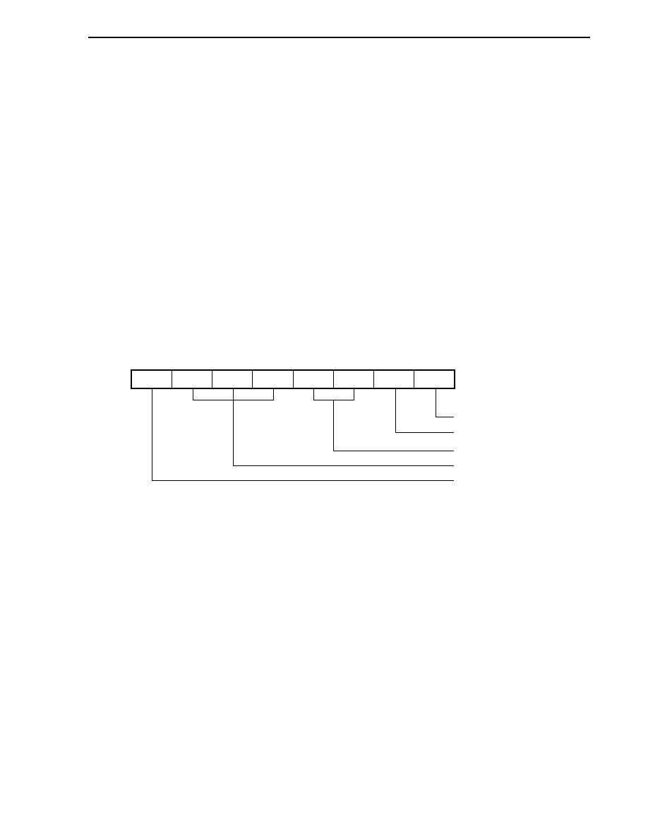
CHAPTER 8 8-BIT TIMERS H0 AND H1
User's Manual U16228EJ2V0UD
217
8.4.2 Operation as PWM output mode
In PWM output mode, a pulse with an arbitrary duty and arbitrary cycle can be output.
8-bit timer compare register 0n (CMP0n) controls the cycle of timer output (TOHn). Rewriting the CMP0n register
during timer operation is prohibited.
8-bit timer compare register 1n (CMP1n) controls the duty of timer output (TOHn). Rewriting the CMP1n register
during timer operation is possible.
The operation in PWM output mode is as follows.
TOHn output becomes active and 8-bit timer counter Hn is cleared to 0 when 8-bit timer counter Hn and the
CMP0n register match after the timer count is started. TOHn output becomes inactive when 8-bit timer counter Hn
and the CMP1n register match.
(1) Usage
In PWM output mode, a pulse for which an arbitrary duty and arbitrary cycle can be set is output.
<1> Set each register.
Figure 8-11. Register Setting in PWM Output Mode
(i) Setting timer H mode register n (TMHMDn)
0
0/1
0/1
0/1
1
0
0/1
1
TMMDn0 TOLEVn
TOENn
CKSn1
CKSn2
TMHEn
TMHMDn
CKSn0
TMMDn1
Timer output enabled
Timer output level inversion setting
PWM output mode selection
Count clock (f
CNT
) selection
Count operation stopped
(ii) Setting CMP0n register
∑
Compare value (N): Cycle setting
(iii) Setting CMP1n register
∑
Compare value (M): Duty setting
Remarks 1. n = 0, 1
2. 00H
CMP1n (M) < CMP0n (N)
FFH
<2> The count operation starts when TMHEn = 1.
<3> The CMP0n register is the compare register that is to be compared first after counter operation is enabled.
When the values of 8-bit timer counter Hn and the CMP0n register match, 8-bit timer counter Hn is cleared,
an interrupt request signal (INTTMHn) is generated, and TOHn output becomes active. At the same time,
the compare register to be compared with 8-bit timer counter Hn is changed from the CMP0n register to the
CMP1n register.

CHAPTER 8 8-BIT TIMERS H0 AND H1
User's Manual U16228EJ2V0UD
218
<4> When 8-bit timer counter Hn and the CMP1n register match, TOHn output becomes inactive and the
compare register to be compared with 8-bit timer counter Hn is changed from the CMP1n register to the
CMP0n register. At this time, 8-bit timer counter Hn is not cleared and the INTTMHn signal is not
generated.
<5> By performing procedures <3> and <4> repeatedly, a pulse with an arbitrary duty can be obtained.
<6> To stop the count operation, set TMHEn = 0.
If the setting value of the CMP0n register is N, the setting value of the CMP1n register is M, and the count clock
frequency is f
CNT
, the PWM pulse output cycle and duty are as follows.
PWM pulse output cycle = (N + 1)/f
CNT
Duty = Active width : Total width of PWM = (M + 1) : (N + 1)
Cautions 1. In PWM output mode, three operation clocks (signal selected using the CKSn2 to CKSn0
bits of the TMHMDn register) are required to transfer the CMP1n register value after
rewriting the register.
2. Be sure to set the CMP1n register when starting the timer count operation (TMHEn = 1) after
the timer count operation was stopped (TMHEn = 0) (be sure to set again even if setting the
same value to the CMP1n register).
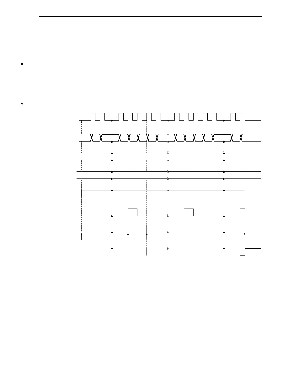
CHAPTER 8 8-BIT TIMERS H0 AND H1
User's Manual U16228EJ2V0UD
219
(2) Timing
chart
The operation timing in PWM output mode is shown below.
Caution Make sure that the CMP1n register setting value (M) and CMP0n register setting value (N) are
within the following range.
00H
CMP1n (M) < CMP0n (N)
FFH
Remark n = 0, 1
Figure 8-12. Operation Timing in PWM Output Mode (1/4)
(a) Basic operation
Count clock
8-bit timer counter Hn
CMP0n
TMHEn
INTTMHn
TOHn
(TOLEVn = 0)
TOHn
(TOLEVn = 1)
00H 01H
A5H 00H 01H 02H
A5H 00H
A5H 00H
01H 02H
CMP1n
A5H
01H
<1>
<2>
<3>
<4>
<1> The count operation is enabled by setting the TMHEn bit to 1. Start 8-bit timer counter Hn by masking one
count clock to count up. At this time, TOHn output remains inactive (when TOLEVn = 0).
<2> When the values of 8-bit timer counter Hn and the CMP0n register match, the TOHn output level is inverted,
the value of 8-bit timer counter Hn is cleared, and the INTTMHn signal is output.
<3> When the values of 8-bit timer counter Hn and the CMP1n register match, the level of the TOHn output is
returned. At this time, the 8-bit timer counter value is not cleared and the INTTMHn signal is not output.
<4> Clearing the TMHEn bit to 0 during timer Hn operation makes the INTTMHn signal and TOHn output inactive.
Remark n = 0, 1
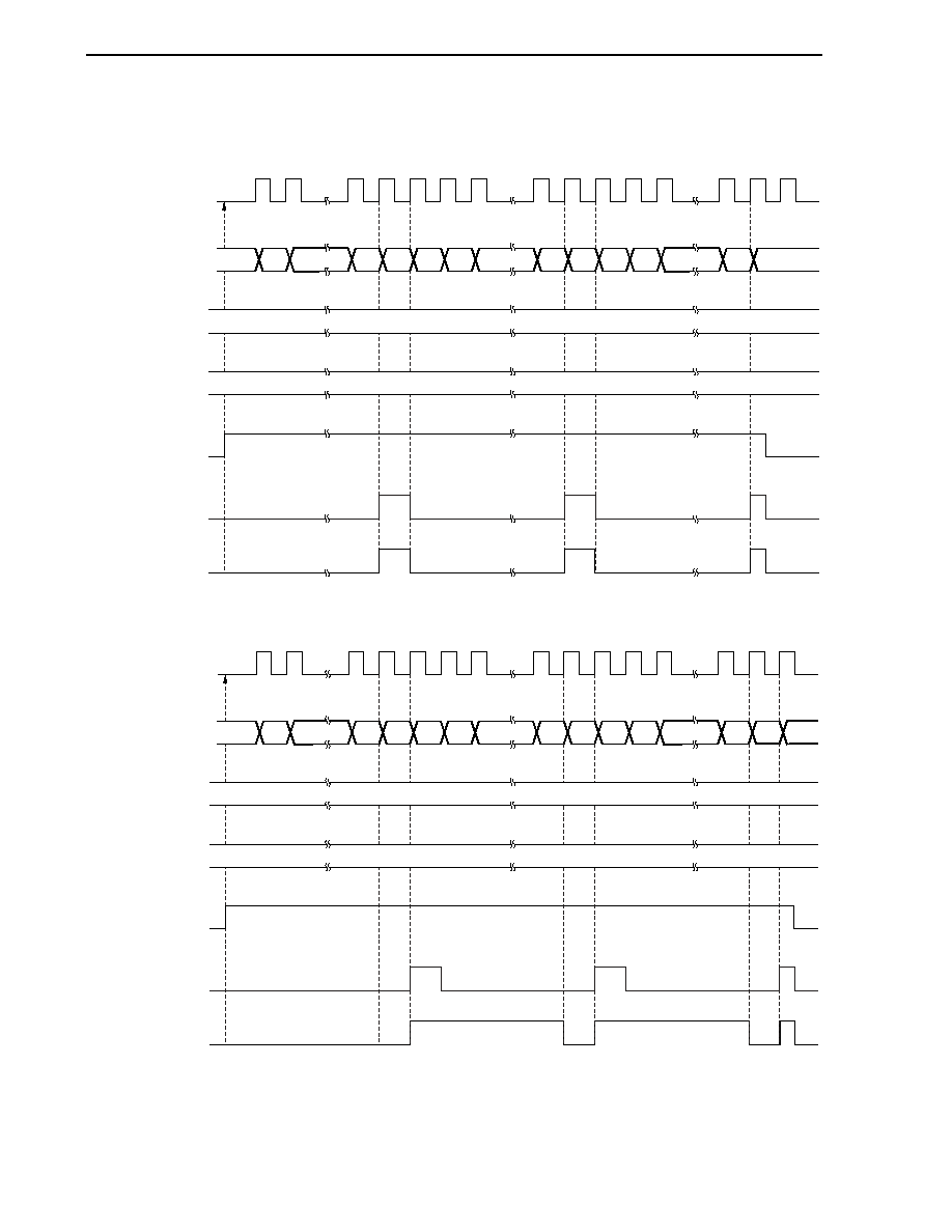
CHAPTER 8 8-BIT TIMERS H0 AND H1
User's Manual U16228EJ2V0UD
220
Figure 8-12. Operation Timing in PWM Output Mode (2/4)
(b) Operation when CMP0n = FFH, CMP1n = 00H
Count clock
8-bit timer counter Hn
CMP0n
TMHEn
INTTMHn
TOHn
(TOLEVn = 0)
00H 01H
FFH 00H 01H 02H
FFH 00H
FFH 00H
01H 02H
CMP1n
FFH
00H
(c) Operation when CMP0n = FFH, CMP1n = FEH
Count clock
8-bit timer counter Hn
CMP0n
TMHEn
INTTMHn
TOHn
(TOLEVn = 0)
00H 01H
FEH FFH 00H 01H
FEH FFH 00H 01H
FEH FFH 00H
CMP1n
FFH
FEH
Remark n = 0, 1
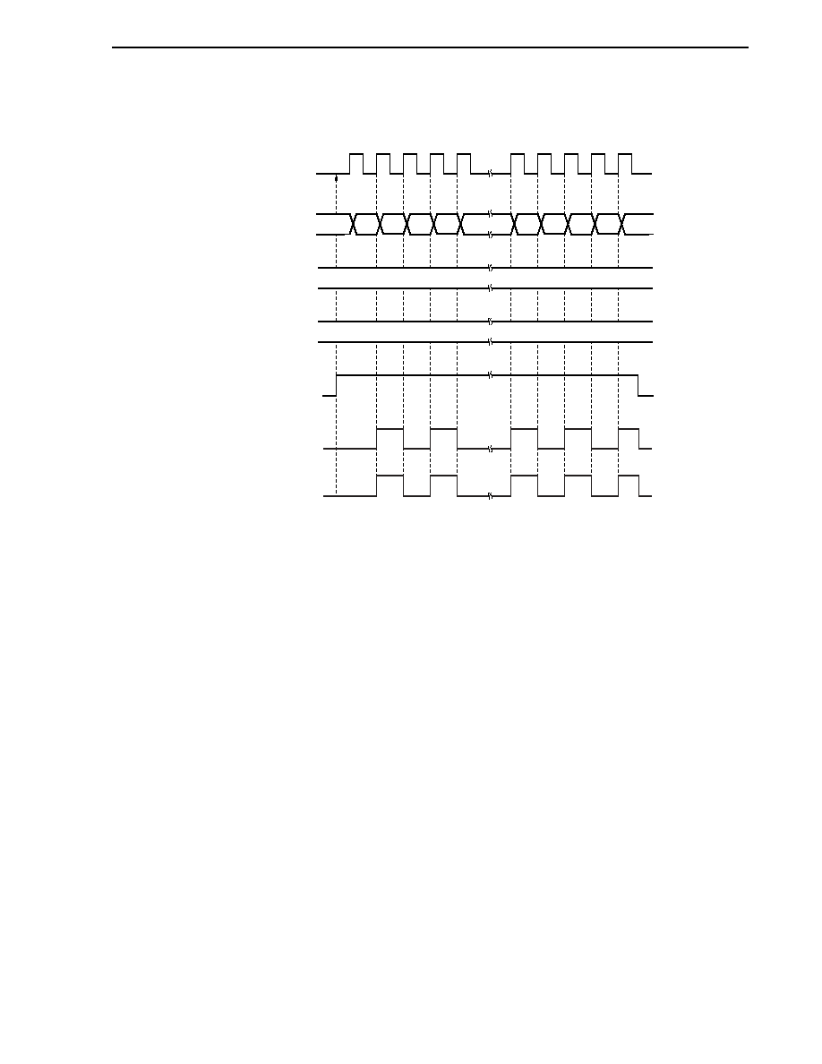
CHAPTER 8 8-BIT TIMERS H0 AND H1
User's Manual U16228EJ2V0UD
221
Figure 8-12. Operation Timing in PWM Output Mode (3/4)
(d) Operation when CMP0n = 01H, CMP1n = 00H
Count clock
8-bit timer counter Hn
CMP0n
TMHEn
INTTMHn
TOHn
(TOLEVn = 0)
01H
00H
01H 00H 01H 00H
00H 01H 00H 01H
CMP1n
00H
Remark n = 0, 1
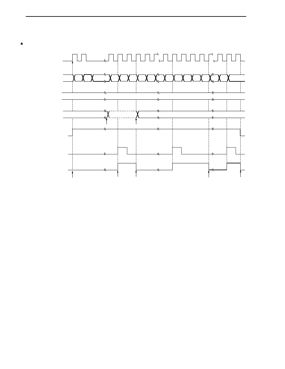
CHAPTER 8 8-BIT TIMERS H0 AND H1
User's Manual U16228EJ2V0UD
222
Figure 8-12. Operation Timing in PWM Output Mode (4/4)
(e) Operation by changing CMP1n (CMP1n = 01H
03H, CMP0n = A5H)
Count clock
8-bit timer counter Hn
CMP0n
TMHEn
INTTMHn
TOHn
(TOLEVn = 0)
00H 01H 02H
A5H 00H 01H 02H 03H
A5H 00H 01H 02H 03H
A5H 00H
CMP1n
01H
A5H
03H
01H (03H)
<1>
<3>
<4>
<2>
<2>'
<5>
<6>
<1> The count operation is enabled by setting TMHEn = 1. Start 8-bit timer counter Hn by masking one count
clock to count up. At this time, the TOHn output remains inactive (when TOLEVn = 0).
<2> The CMP1n register value can be changed during timer counter operation. This operation is asynchronous
to the count clock.
<3> When the values of 8-bit timer counter Hn and the CMP0n register match, the value of 8-bit timer counter Hn
is cleared, the TOHn output becomes active, and the INTTMHn signal is output.
<4> If the CMP1n register value is changed, the value is latched and not transferred to the register. When the
values of 8-bit timer counter Hn and the CMP1n register before the change match, the value is transferred to
the CMP1n register and the CMP1n register value is changed (<2>').
However, three count clocks or more are required from when the CMP1n register value is changed to when
the value is transferred to the register. If a match signal is generated within three count clocks, the changed
value cannot be transferred to the register.
<5> When the values of 8-bit timer counter Hn and the CMP1n register after the change match, the TOHn output
becomes inactive. 8-bit timer counter Hn is not cleared and the INTTMHn signal is not generated.
<6> Clearing the TMHEn bit to 0 during timer Hn operation makes the INTTMHn signal and TOHn output inactive.
Remark n = 0, 1

CHAPTER 8 8-BIT TIMERS H0 AND H1
User's Manual U16228EJ2V0UD
223
8.4.3 Carrier generator mode operation (8-bit timer H1 only)
The carrier clock generated by 8-bit timer H1 is output in the cycle set by 8-bit timer/event counter 51.
In carrier generator mode, the output of the 8-bit timer H1 carrier pulse is controlled by 8-bit timer/event counter 51,
and the carrier pulse is output from the TOH1 output.
(1) Carrier
generation
In carrier generator mode, 8-bit timer H compare register 01 (CMP01) generates a low-level width carrier pulse
waveform and 8-bit timer H compare register 11 (CMP11) generates a high-level width carrier pulse waveform.
Rewriting the CMP11 register during 8-bit timer H1 operation is possible but rewriting the CMP01 register is
prohibited.
(2) Carrier output control
Carrier output is controlled by the interrupt request signal (INTTM51) of 8-bit timer/event counter 51 and the
NRZB1 and RMC1 bits of the 8-bit timer H carrier control register (TMCYC1). The relationship between the
outputs is shown below.
RMC1 Bit
NRZB1 Bit
Output
0 0
Low-level
output
0 1
High-level
output
1 0
Low-level
output
1
1
Carrier pulse output
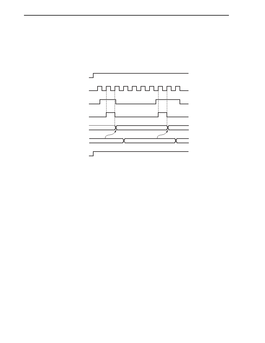
CHAPTER 8 8-BIT TIMERS H0 AND H1
User's Manual U16228EJ2V0UD
224
To control the carrier pulse output during a count operation, the NRZ1 and NRZB1 bits of the TMCYC1 register
have a master and slave bit configuration. The NRZ1 bit is read-only but the NRZB1 bit can be read and written.
The INTTM51 signal is synchronized with the 8-bit timer H1 count clock and output as the INTTM5H1 signal. The
INTTM5H1 signal becomes the data transfer signal of the NRZ1 bit, and the NRZB1 bit value is transferred to the
NRZ1 bit. The timing for transfer from the NRZB1 bit to the NRZ1 bit is as shown below.
Figure 8-13. Transfer Timing
8-bit timer H1
count clock
TMHE1
INTTM51
INTTM5H1
NRZ1
NRZB1
RMC1
1
1
1
0
0
0
<1>
<2>
<1> The INTTM51 signal is synchronized with the count clock of 8-bit timer H1 and is output as the INTTM5H1
signal.
<2> The value of the NRZB1 bit is transferred to the NRZ1 bit at the second clock from the rising edge of the
INTTM5H1 signal.
Cautions 1. Do not rewrite the NRZB1 bit again until at least the second clock after it has been rewritten,
or else the transfer from the NRZB1 bit to the NRZ1 bit is not guaranteed.
2. When 8-bit timer/event counter 51 is used in the carrier generator mode, an interrupt is
generated at the timing of <1>. When 8-bit timer/event counter 51 is used in a mode other
than the carrier generator mode, the timing of the interrupt generation differs.
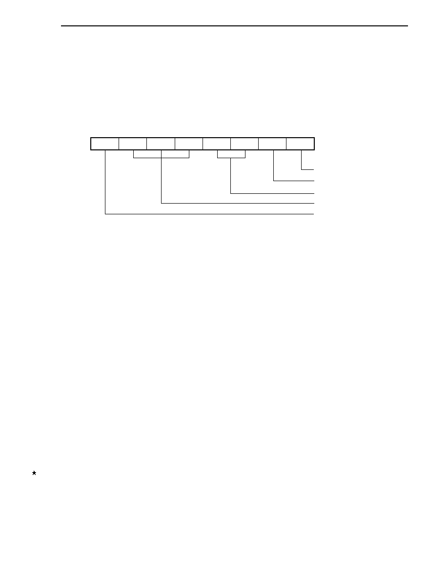
CHAPTER 8 8-BIT TIMERS H0 AND H1
User's Manual U16228EJ2V0UD
225
(3) Usage
Outputs an arbitrary carrier clock from the TOH1 pin.
<1> Set each register.
Figure 8-14. Register Setting in Carrier Generator Mode
(i) Setting 8-bit timer H mode register 1 (TMHMD1)
0
0/1
0/1
0/1
0
Timer output enabled
Timer output level inversion setting
Carrier generator mode selection
Count clock (f
CNT
) selection
Count operation stopped
1
0/1
0/1
TMMD10 TOLEV1
TOEN1
CKS11
CKS12
TMHE1
TMHMD1
CKS10
TMMD11
(ii) CMP01 register setting
∑
Compare value
(iii) CMP11 register setting
∑
Compare value
(iv) TMCYC1 register setting
∑
RMC1 = 1 ... Remote control output enable bit
∑
NRZB1 = 0/1 ... carrier output enable bit
(v) TCL51 and TMC51 register setting
∑
See 7.3 Registers Controlling 8-Bit Timer/Event Counters 50 and 51.
<2> When TMHE1 = 1, 8-bit timer H1 starts counting.
<3> When TCE51 of 8-bit timer mode control register 51 (TMC51) is set to 1, 8-bit timer/event counter 51 starts
counting.
<4> After the count operation is enabled, the first compare register to be compared is the CMP01 register.
When the count value of 8-bit timer counter H1 and the CMP01 register value match, the INTTMH1 signal
is generated, 8-bit timer counter H1 is cleared, and at the same time, the compare register to be compared
with 8-bit timer counter H1 is switched from the CMP01 register to the CMP11 register.
<5> When the count value of 8-bit timer counter H1 and the CMP11 register value match, the INTTMH1 signal
is generated, 8-bit timer counter H1 is cleared, and at the same time, the compare register to be compared
with 8-bit timer counter H1 is switched from the CMP11 register to the CMP01 register.
<6> By performing procedures <4> and <5> repeatedly, a carrier clock is generated.
<7> The INTTM51 signal is synchronized with count clock of 8-bit timer H1 and output as the INTTM5H1 signal.
The INTTM5H1 signal becomes the data transfer signal for the NRZB1 bit, and the NRZB1 bit value is
transferred to the NRZ1 bit.
<8> When the NRZ1 bit is high level, a carrier clock is output from the TOH1 pin.
<9> By performing the procedures above, an arbitrary carrier clock is obtained. To stop the count operation,
clear TMHE1 to 0.

CHAPTER 8 8-BIT TIMERS H0 AND H1
User's Manual U16228EJ2V0UD
226
If the setting value of the CMP01 register is N, the setting value of the CMP11 register is M, and the count clock
frequency is f
CNT
, the carrier clock output cycle and duty are as follows.
Carrier clock output cycle = (N + M + 2)/f
CNT
Duty = High-level width : Carrier clock output width = ( M + 1) : (N + M + 2)
Cautions 1. Be sure to set the CMP11 register when starting the timer count operation (TMHE1 = 1) after
the timer count operation was stopped (TMHE1 = 0) (be sure to set again even if setting the
same value to the CMP11 register).
2. Set so that the count clock frequency of TMH1 becomes more than 6 times the count clock
frequency of TM51.
(4) Timing
chart
The carrier output control timing is shown below.
Cautions 1. Set the values of the CMP01 and CMP11 registers in a range of 01H to FFH.
2. In the carrier generator mode, three operating clocks (signal selected by CKS12 to CKS10
bits of TMHMD1 register) or more are required from when the CMP11 register value is
changed to when the value is transferred to the register.
3. Be sure to set the RMC1 bit before the count operation is started.
CHAPTER 8 8-BIT TIMERS H0 AND H1
User's Manual U16228EJ2V0UD
227
Figure 8-15. Carrier Generator Mode Operation Timing (1/3)
(a) Operation when CMP01 = N, CMP11 = N
00H
N
00H
N
00H
N
00H
N
00H
N
00H
N
N
N
0
0
1
1
0
0
1
1
0
0
00H 01H
L
00H 01H
L
00H 01H
L
00H 01H
00H 01H
L
L
CMPn0
CMPn1
TMHEn
INTTMHn
Carrier clock
8-bit timer 5n
count clock
TM5n count value
CR5n
TCE5n
TOHn
INTTM5n
NRZBn
NRZn
Carrier clock
INTTM5Hn
8-bit timer Hn
count clock
8-bit timer counter
Hn count value
<1> <2>
<3>
<4>
<5>
<6>
<7>
<1> When TMHE1 = 0 and TCE51 = 0, 8-bit timer counter H1 operation is stopped.
<2> When TMHE1 = 1 is set, 8-bit timer counter H1 starts a count operation. At that time, the carrier clock is held
at the inactive level.
<3> When the count value of 8-bit timer counter H1 matches the CMP01 register value, the first INTTMH1 signal
is generated, the carrier clock signal is inverted, and the compare register to be compared with 8-bit timer
counter H1 is switched from the CMP01 register to the CMP11 register. 8-bit timer counter H1 is cleared to
00H.
<4> When the count value of 8-bit timer counter H1 matches the CMP11 register value, the INTTMH1 signal is
generated, the carrier clock signal is inverted, and the compare register to be compared with 8-bit timer
counter H1 is switched from the CMP11 register to the CMP01 register. 8-bit timer counter H1 is cleared to
00H. By performing procedures <3> and <4> repeatedly, a carrier clock with duty fixed to 50% is generated.
<5> When the INTTM51 signal is generated, it is synchronized with 8-bit timer H1 count clock and output as the
INTTM5H1 signal.
<6> The INTTM5H1 signal becomes the data transfer signal for the NRZB1 bit, and the NRZB1 bit value is
transferred to the NRZ1 bit.
<7> When NRZ1 = 0 is set, the TOH1 output becomes low level.
CHAPTER 8 8-BIT TIMERS H0 AND H1
User's Manual U16228EJ2V0UD
228
Figure 8-15. Carrier Generator Mode Operation Timing (2/3)
(b) Operation when CMP01 = N, CMP11 = M
N
L
00H
N
00H 01H
M
00H
N
00H 01H
M
00H
00H
N
M
0
0
1
1
0
0
1
1
0
0
00H 01H
L
00H 01H
L
00H 01H
L
00H 01H
00H 01H
L
CMPn0
CMPn1
TMHEn
INTTMHn
Carrier clock
8-bit timer 5n
count clock
TM5n count value
CR5n
TCE5n
TOHn
INTTM5n
NRZBn
NRZn
Carrier clock
INTTM5Hn
8-bit timer Hn
count clock
8-bit timer counter
Hn count value
<1> <2>
<3>
<4>
<5>
<6>
<7>
<1> When TMHE1 = 0 and TCE51 = 0, 8-bit timer counter H1 operation is stopped.
<2> When TMHE1 = 1 is set, 8-bit timer counter H1 starts a count operation. At that time, the carrier clock is held
at the inactive level.
<3> When the count value of 8-bit timer counter H1 matches the CMP01 register value, the first INTTMH1 signal
is generated, the carrier clock signal is inverted, and the compare register to be compared with 8-bit timer
counter H1 is switched from the CMP01 register to the CMP11 register. 8-bit timer counter H1 is cleared to
00H.
<4> When the count value of 8-bit timer counter H1 matches the CMP11 register value, the INTTMH1 signal is
generated, the carrier clock signal is inverted, and the compare register to be compared with 8-bit timer
counter H1 is switched from the CMP11 register to the CMP01 register. 8-bit timer counter H1 is cleared to
00H. By performing procedures <3> and <4> repeatedly, a carrier clock with duty fixed to other than 50% is
generated.
<5> When the INTTM51 signal is generated, it is synchronized with 8-bit timer H1 count clock and output as the
INTTM5H1 signal.
<6> A carrier signal is output at the first rising edge of the carrier clock if NRZ1 is set to 1.
<7> When NRZ1 = 0, the TOH1 output is held at the high level and is not changed to low level while the carrier
clock is high level (from <6> and <7>, the high-level width of the carrier clock waveform is guaranteed).
CHAPTER 8 8-BIT TIMERS H0 AND H1
User's Manual U16228EJ2V0UD
229
Figure 8-15. Carrier Generator Mode Operation Timing (3/3)
(c) Operation when CMP11 is changed
8-bit timer H1
count clock
CMP01
TMHE1
INTTMH1
Carrier clock
00H 01H
N
00H 01H
01H
M
00H
N
00H
L
00H
<1>
<3>'
<4>
<3>
<2>
CMP11
<5>
M
N
L
M (L)
8-bit timer counter
H1 count value
<1> When TMHE1 = 1 is set, 8-bit timer H1 starts a count operation. At that time, the carrier clock is held at the
inactive level.
<2> When the count value of 8-bit timer counter H1 matches the CMP01 register value, 8-bit timer counter H1 is
cleared and the INTTMH1 signal is output.
<3> The CMP11 register can be rewritten during 8-bit timer H1 operation, however, the changed value (L) is
latched. The CMP11 register is changed when the count value of 8-bit timer counter H1 and the CMP11
register value before the change (M) match (<3>').
<4> When the count value of 8-bit timer counter H1 and the CMP11 register value before the change (M) match,
the INTTMH1 signal is output, the carrier signal is inverted, and 8-bit timer counter H1 is cleared to 00H.
<5> The timing at which the count value of 8-bit timer counter H1 and the CMP11 register value match again is
indicated by the value after the change (L).

User's Manual U16228EJ2V0UD
230
CHAPTER 9 WATCH TIMER
9.1 Functions of Watch Timer
The watch timer has the following functions.
∑
Watch
timer
∑
Interval
timer
The watch timer and the interval timer can be used simultaneously.
Figure 9-1 shows the watch timer block diagram.
Figure 9-1. Block Diagram of Watch Timer
f
X
/2
7
f
W
/2
4
f
W
/2
5
f
W
/2
6
f
W
/2
7
f
W
/2
8
f
W
/2
10
f
W
/2
11
f
W
/2
9
f
XT
INTWT
INTWTI
WTM0
WTM1
WTM2
WTM3
WTM4
WTM5
WTM6
WTM7
f
W
Clear
11-bit prescaler
Clear
5-bit counter
Watch timer operation
mode register (WTM)
Internal bus
Selector
Selector
Selector
Selector
f
WX
/2
4
f
WX
/2
5
f
WX
Remark f
X
: X1 input clock oscillation frequency
f
XT
: Subsystem clock oscillation frequency
f
W
: Watch timer clock frequency
f
WX
: f
W
or f
W
/2
9
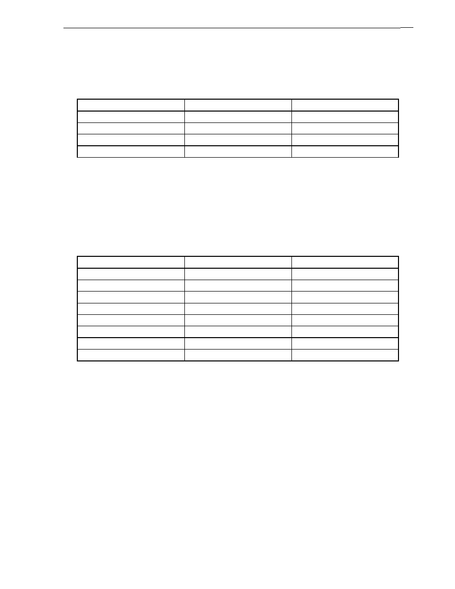
CHAPTER 9 WATCH TIMER
User's Manual U16228EJ2V0UD
231
(1) Watch
timer
When the X1 input clock or subsystem clock is used, interrupt requests (INTWT) are generated at preset
intervals.
Table 9-1. Watch Timer Interrupt Time
Interrupt Time
When Operated at f
XT
= 32.768 kHz
When Operated at f
X
= 10 MHz
2
4
/f
W
488
µ
s 205
µ
s
2
5
/f
W
977
µ
s 410
µ
s
2
13
/f
W
0.25 s
0.105 s
2
14
/f
W
0.5 s
0.210 s
Remark f
X
: X1 input clock oscillation frequency
f
XT
: Subsystem clock oscillation frequency
f
W
: Watch timer clock frequency
(2) Interval
timer
Interrupt requests (INTWTI) are generated at preset time intervals.
Table 9-2. Interval Timer Interval Time
Interval Time
When Operated at f
XT
= 32.768 kHz
When Operated at f
X
= 10 MHz
2
4
/f
W
488
µ
s 205
µ
s
2
5
/f
W
977
µ
s 410
µ
s
2
6
/f
W
1.95
ms
820
µ
s
2
7
/f
W
3.91 ms
1.64 ms
2
8
/f
W
7.81 ms
3.28 ms
2
9
/f
W
15.6 ms
6.55 ms
2
10
/f
W
31.3 ms
13.1 ms
2
11
/f
W
62.5 ms
26.2 ms
Remark f
X
: X1 input clock oscillation frequency
f
XT
: Subsystem clock oscillation frequency
f
W
: Watch timer clock frequency
CHAPTER 9 WATCH TIMER
User's Manual U16228EJ2V0UD
232
9.2 Configuration of Watch Timer
The watch timer includes the following hardware.
Table 9-3. Watch Timer Configuration
Item Configuration
Counter 5
bits
◊
1
Prescaler 11
bits
◊
1
Control register
Watch timer operation mode register (WTM)
9.3 Register Controlling Watch Timer
The watch timer is controlled by the watch timer operation mode register (WTM).
∑
Watch timer operation mode register (WTM)
This register sets the watch timer count clock, enables/disables operation, prescaler interval time, and 5-bit
counter operation control.
WTM is set by a 1-bit or 8-bit memory manipulation instruction.
RESET input clears WTM to 00H.
CHAPTER 9 WATCH TIMER
User's Manual U16228EJ2V0UD
233
Figure 9-2. Format of Watch Timer Operation Mode Register (WTM)
Address: FF6FH After reset: 00H R/W
Symbol
7 6 5 4 3 2
<1>
<0>
WTM
WTM7 WTM6 WTM5 WTM4 WTM3 WTM2 WTM1 WTM0
WTM7
Watch timer count clock selection
0
f
X
/2
7
(78.125 kHz)
1
f
XT
(32.768 kHz)
WTM6
WTM5
WTM4
Prescaler interval time selection
0
0
0
2
4
/f
W
0
0
1
2
5
/f
W
0
1
0
2
6
/f
W
0
1
1
2
7
/f
W
1
0
0
2
8
/f
W
1
0
1
2
9
/f
W
1
1
0
2
10
/f
W
1
1
1
2
11
/f
W
WTM3
WTM2
Interrupt time selection
0
0
2
14
/f
W
0
1
2
13
/f
W
1
0
2
5
/f
W
1
1
2
4
/f
W
WTM1
5-bit counter operation control
0
Clear after operation stop
1
Start
WTM0
Watch timer operation enable
0
Operation stop (clear both prescaler and timer)
1
Operation
enable
Caution Do not change the count clock and interval time (by setting bits 4 to 7 (WTM4 to WTM7) of WTM)
during watch timer operation.
Remarks 1. f
W
: Watch timer clock frequency (f
X
/2
7
or f
XT
)
2. f
X
: X1 input clock oscillation frequency
3. f
XT
: Subsystem clock oscillation frequency
4. Figures in parentheses apply to operation with f
X
= 10 MHz, f
XT
= 32.768 kHz.
CHAPTER 9 WATCH TIMER
User's Manual U16228EJ2V0UD
234
9.4 Watch Timer Operations
9.4.1 Watch timer operation
The watch timer generates an interrupt request (INTWT) at a specific time interval by using the X1 input clock or
subsystem clock.
When bit 0 (WTM0) and bit 1 (WTM1) of the watch timer operation mode register (WTM) are set to 1, the count
operation starts. When these bits are set to 0, the 5-bit counter is cleared and the count operation stops.
When the interval timer is simultaneously operated, zero-second start can be achieved only for the watch timer by
setting WTM1 to 0. In this case, however, the 11-bit prescaler is not cleared. Therefore, an error up to 2
11
◊
1/f
W
seconds occurs in the first overflow (INTWT) after zero-second start.
The interrupt request is generated at the following time intervals.
Table 9-4. Watch Timer Interrupt Time
WTM3
WTM2
Interrupt Time Selection
When Operated at f
XT
= 32.768 kHz
(WTM7 = 1)
When Operated at f
X
= 10 MHz
(WTM7 = 0)
0 0
2
14
/f
W
0.5 s
0.210 s
0 1
2
13
/f
W
0.25 s
0.105 s
1 0
2
5
/f
W
977
µ
s 410
µ
s
1 1
2
4
/f
W
488
µ
s 205
µ
s
Remark f
X
: X1 input clock oscillation frequency
f
XT
: Subsystem clock oscillation frequency
f
W
: Watch timer clock frequency

CHAPTER 9 WATCH TIMER
User's Manual U16228EJ2V0UD
235
9.4.2 Interval timer operation
The watch timer operates as interval timer which generates interrupt requests (INTWTI) repeatedly at an interval of
the preset count value.
The interval time can be selected with bits 4 to 6 (WTM4 to WTM6) of the watch timer operation mode register
(WTM).
When bit 0 (WTM0) of the WTM is set to 1, the count operation starts. When this bit is set to 0, the count operation
stops.
Table 9-5. Interval Timer Interval Time
WTM6 WTM5 WTM4
Interval
Time
When Operated at
f
XT
= 32.768 kHz (WTM7 = 1)
When Operated at
f
X
= 10 MHz (WTM7 = 0)
0 0 0
2
4
/f
W
488
µ
s 205
µ
s
0 0 1
2
5
/f
W
977
µ
s 410
µ
s
0 1 0
2
6
/f
W
1.95
ms
820
µ
s
0 1 1
2
7
/f
W
3.91 ms
1.64 ms
1 0 0
2
8
/f
W
7.81 ms
3.28 ms
1 0 1
2
9
/f
W
15.6 ms
6.55 ms
1 1 0
2
10
/f
W
31.3 ms
13.1 ms
1 1 1
2
11
/f
W
62.5 ms
26.2 ms
Remark f
X
: X1 input clock oscillation frequency
f
XT
: Subsystem clock oscillation frequency
f
W
: Watch timer clock frequency
Figure 9-3. Operation Timing of Watch Timer/Interval Timer
0H
Start
Overflow
Overflow
5-bit counter
Count clock
Watch timer
interrupt INTWT
Interval timer
interrupt INTWTI
Interrupt time of watch timer (0.5 s)
Interval time
(T)
T
Interrupt time of watch timer (0.5 s)
n
◊
T
n
◊
T
Remark f
W
: Watch timer clock frequency
n: The number of times of interval timer operations
Figures in parentheses are for operation with f
W
= 32.768 kHz (WTM7 = 1, WTM3, WTM2 = 0, 0)

CHAPTER 9 WATCH TIMER
User's Manual U16228EJ2V0UD
236
9.5 Cautions for Watch Timer
When operation of the watch timer and 5-bit counter is enabled by the watch timer mode control register (WTM) (by
setting bits 0 (WTM0) and 1 (WTM1) of WTM to 1), the interval until the first interrupt request (INTWT) is generated
after the register is set does not exactly match the specification made with bit 3 (WTM3) of WTM. This is because
there is a delay of one 11-bit prescaler output cycle until the 5-bit counter starts counting. Subsequently, however, the
INTWT signal is generated at the specified intervals.
Figure 9-4. Example of Generation of Watch Timer Interrupt Request (INTWT) (When Interrupt Period = 0.5 s)
It takes 0.515625 seconds for the first INTWT to be generated (2
9
◊
1/32768 = 0.015625 s longer). INTWT is then
generated every 0.5 seconds.
0.5 s
0.5 s
0.515625 s
WTM0, WTM1
INTWT

User's Manual U16228EJ2V0UD
237
CHAPTER 10 WATCHDOG TIMER
10.1 Functions of Watchdog Timer
The watchdog timer is used to detect an inadvertent program loop. If a program loop is detected, an internal reset
signal is generated.
When a reset occurs due to the watchdog timer, bit 4 (WDTRF) of the reset control flag register (RESF) is set to 1.
For details of RESF, refer to CHAPTER 20 RESET FUNCTION.
Table 10-1. Loop Detection Time of Watchdog Timer
Loop Detection Time
During Ring-OSC Clock Operation
During X1 Input Clock Operation
f
R
/2
11
(8.53 ms)
f
XP
/2
13
(819.2
µ
s)
f
R
/2
12
(17.07 ms)
f
XP
/2
14
(1.64 ms)
f
R
/2
13
(34.13 ms)
f
XP
/2
15
(3.28 ms)
f
R
/2
14
(68.27 ms)
f
XP
/2
16
(6.55 ms)
f
R
/2
15
(136.53 ms)
f
XP
/2
17
(13.11 ms)
f
R
/2
16
(273.07 ms)
f
XP
/2
18
(26.21 ms)
f
R
/2
17
(546.13 ms)
f
XP
/2
19
(52.43 ms)
f
R
/2
18
(1.09 s)
f
XP
/2
20
(104.86 ms)
Remarks 1. f
R
: Ring-OSC clock oscillation frequency
2. f
XP
: X1 input clock oscillation frequency
3. Figures in parentheses apply to operation at f
R
= 240 kHz (TYP.), f
XP
= 10 MHz
The operation mode of the watchdog timer (WDT) is switched according to the mask option setting of the on-chip
Ring-OSC as shown in Table 10-2.
CHAPTER 10 WATCHDOG TIMER
User's Manual U16228EJ2V0UD
238
Table 10-2. Mask Option Setting and Watchdog Timer Operation Mode
Mask Option
Ring-OSC Cannot Be Stopped
Ring-OSC Can Be Stopped by Software
Watchdog timer clock
source
Fixed to f
R
Note 1
.
∑
Selectable by software (f
XP
, f
R
or stopped)
∑
When reset is released: f
R
Operation after reset
Operation starts with the maximum interval
(f
R
/2
18
).
Operation starts with maximum interval
(f
R
/2
18
).
Operation mode selection
The interval can be changed only once.
The clock selection/interval can be changed
only once.
Features
The watchdog timer cannot be stopped.
The watchdog timer can be stopped in
standby mode
Note 2
.
Notes 1. As long as power is being supplied, Ring-OSC oscillation cannot be stopped (except in the reset
period).
2. The conditions under which clock supply to the watchdog timer is stopped differ depending on the
clock source of the watchdog timer.
<1> If the clock source is f
XP
, clock supply to the watchdog timer is stopped under the following
conditions.
∑
When f
XP
is stopped
∑
In HALT/STOP mode
∑
During oscillation stabilization time
<2> If the clock source is f
R
, clock supply to the watchdog timer is stopped under the following
conditions.
∑
If the CPU clock is f
XP
and if f
R
is stopped by software before execution of the STOP instruction
∑
In HALT/STOP mode
Remarks 1. f
R
: Ring-OSC clock oscillation frequency
2. f
XP
: X1 input clock oscillation frequency
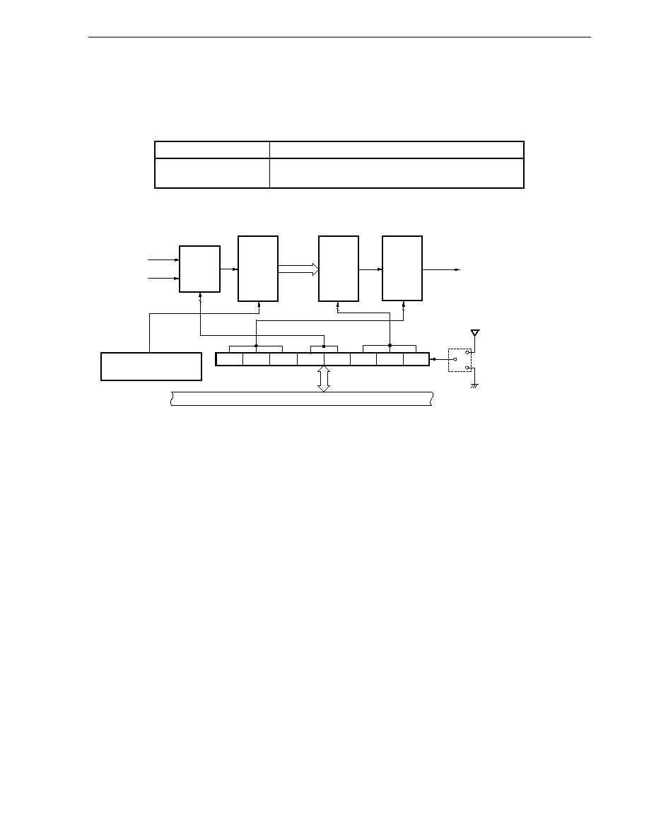
CHAPTER 10 WATCHDOG TIMER
User's Manual U16228EJ2V0UD
239
10.2 Configuration of Watchdog Timer
The watchdog timer includes following hardware.
Table 10-3. Configuration of Watchdog Timer
Item Configuration
Control registers
Watchdog timer mode register (WDTM)
Watchdog timer enable register (WDTE)
Figure 10-1. Block Diagram of Watchdog Timer
f
R
/2
2
Clock
input
controller
Output
controller
Internal reset signal
WDCS2
Internal bus
WDCS1 WDCS0
f
XP
/2
4
WDCS3
WDCS4
0
1
1
Selector
16-bit
counter
or
f
XP
/2
13
to
f
XP
/2
20
f
R
/2
11
to
f
R
/2
18
Watchdog timer enable
register (WDTE)
Watchdog timer mode
register (WDTM)
3
3
2
Clear
Mask option
(to set "Ring-OSC
cannot be stopped" or
"Ring-OSC can be
stopped by software")
CHAPTER 10 WATCHDOG TIMER
User's Manual U16228EJ2V0UD
240
10.3 Registers Controlling Watchdog Timer
The watchdog timer is controlled by the following two registers.
∑
Watchdog timer mode register (WDTM)
∑
Watchdog timer enable register (WDTE)
(1) Watchdog timer mode register (WDTM)
This register sets the overflow time and operation clock of the watchdog timer.
This register can be set by an 8-bit memory manipulation instruction and can be read many times, but can be
written only once after reset is released.
RESET input sets this register to 67H.
Figure 10-2. Format of Watchdog Timer Mode Register (WDTM)
0
WDCS0
1
WDCS1
2
WDCS2
3
WDCS3
4
WDCS4
5
1
6
1
7
0
Symbol
WDTM
Address: FF98H After reset: 67H R/W
WDCS4
Note 1
WDCS3
Note 1
Operation
clock
selection
0
0
Ring-OSC clock (f
R
)
0
1
X1 input clock (f
XP
)
1
◊
Watchdog timer operation stopped
Overflow time setting
WDCS2
Note 2
WDCS1
Note 2
WDCS0
Note 2
During Ring-OSC clock
operation
During X1 input clock operation
0 0 0
f
R
/2
11
(8.53 ms)
f
XP
/2
13
(819.2
µ
s)
0 0 1
f
R
/2
12
(17.07 ms)
f
XP
/2
14
(1.64 ms)
0 1 0
f
R
/2
13
(34.13 ms)
f
XP
/2
15
(3.28 ms)
0 1 1
f
R
/2
14
(68.27 ms)
f
XP
/2
16
(6.55 ms)
1 0 0
f
R
/2
15
(136.53 ms)
f
XP
/2
17
(13.11 ms)
1 0 1
f
R
/2
16
(273.07 ms)
f
XP
/2
18
(26.21 ms)
1 1 0
f
R
/2
17
(546.13 ms)
f
XP
/2
19
(52.43 ms)
1 1 1
f
R
/2
18
(1.09 s)
f
XP
/2
20
(104.86 ms)
Notes 1. If "Ring-OSC cannot be stopped" is specified by a mask option, this cannot be set. The Ring-
OSC clock will be selected no matter what value is written.
2. Reset is released at the maximum cycle (WDCS2, 1, 0 = 1, 1, 1).

CHAPTER 10 WATCHDOG TIMER
User's Manual U16228EJ2V0UD
241
Cautions 1. If data is written to WDTM, a wait cycle is generated. Do not write data to WDTM
when the CPU is operating on the subsystem clock and the X1 input clock is
stopped. For details, see CHAPTER 34 CAUTIONS FOR WAIT.
2. Set bits 7, 6, and 5 to 0, 1, and 1, respectively (when "Ring-OSC cannot be stopped"
is selected by a mask option, other values are ignored).
3. After reset is released, WDTM can be written only once by an 8-bit memory
manipulation instruction. If writing attempted a second time, an internal reset signal
is generated.
4. WDTM cannot be set by a 1-bit memory manipulation instruction.
Remarks 1. f
R
: Ring-OSC clock oscillation frequency
2. f
XP
: X1 input clock oscillation frequency
3.
◊
: Don't care
4. Figures in parentheses apply to operation at f
R
= 240 kHz (TYP.), f
XP
= 10 MHz
(2) Watchdog timer enable register (WDTE)
Writing ACH to WDTE clears the watchdog timer counter and starts counting again.
This register can be set by an 8-bit memory manipulation instruction.
RESET input sets this register to 9AH.
Figure 10-3. Format of Watchdog Timer Enable Register (WDTE)
0
1
2
3
4
5
6
7
Symbol
WDTE
Address: FF99H After reset: 9AH R/W
Cautions 1. If a value other than ACH is written to WDTE, an internal reset signal is generated.
2. If a 1-bit memory manipulation instruction is executed for WDTE, an internal reset
signal is generated.
3. The value read from WDTE is 9AH (this differs from the written value (ACH)).

CHAPTER 10 WATCHDOG TIMER
User's Manual U16228EJ2V0UD
242
10.4 Operation of Watchdog Timer
10.4.1 Watchdog timer operation when "Ring-OSC cannot be stopped" is selected by a mask option
The operation clock of watchdog timer is fixed to the Ring-OSC.
After reset is released, operation is started at the maximum cycle (bits 2, 1, and 0 (WDCS2, WDCS1, WDCS0) of
the watchdog timer mode register (WDTM) = 1, 1, 1). The watchdog timer operation cannot be stopped.
The following shows the watchdog timer operation after reset release.
1. The status after reset release is as follows.
∑
Operation clock: Ring-OSC clock
∑
Cycle: f
R
/2
18
(1.09 seconds: At operation with f
R
= 240 kHz (TYP.))
∑
Counting
starts
2. The following should be set in the watchdog timer mode register (WDTM) by an 8-bit memory manipulation
instruction
Notes 1, 2
.
∑
Cycle: Set using bits 2 to 0 (WDCS2 to WDCS0)
3. After the above procedures are executed, writing ACH to WDTE clears the count to 0, enabling recounting.
Notes 1. The operation clock (Ring-OSC clock) cannot be changed. If any value is written to bits 3 and 4
(WDCS3, WDCS4) of WDTM, it is ignored.
2. As soon as WDTM is written, the counter of the watchdog timer is cleared.
Caution In this mode, operation of the watchdog timer absolutely cannot be stopped even during STOP
instruction execution. For 8-bit timer H1 (TMH1), a division of the Ring-OSC can be selected as
the count source, so clear the watchdog timer using the interrupt request of TMH1 before the
watchdog timer overflows after STOP instruction execution. If this processing is not performed,
an internal reset signal is generated when the watchdog timer overflows after STOP instruction
execution.

CHAPTER 10 WATCHDOG TIMER
User's Manual U16228EJ2V0UD
243
10.4.2 Watchdog timer operation when "Ring-OSC can be stopped by software" is selected by mask option
The operation clock of the watchdog timer can be selected as either the Ring-OSC clock or the X1 input clock.
After reset is released, operation is started at the maximum cycle (bits 2, 1, and 0 (WDCS2, WDCS1, WDCS0) of
the watchdog timer mode register (WDTM) = 1, 1, 1).
The following shows the watchdog timer operation after reset release.
1. The status after reset release is as follows.
∑
Operation clock: Ring-OSC clock oscillation frequency (f
R
)
∑
Cycle: f
R
/2
18
(1.09 seconds: At operation with f
R
= 240 kHz (TYP.))
∑
Counting
starts
2. The following should be set in the watchdog timer mode register (WDTM) by an 8-bit memory manipulation
instruction
Notes 1, 2, 3
.
∑
Operation clock: Any of the following can be selected using bits 3 and 4 (WDCS3 and WDCS4).
Ring-OSC clock (f
R
)
X1 input clock (f
XP
)
Watchdog timer operation stopped
∑
Cycle: Set using bits 2 to 0 (WDCS2 to WDCS0)
3. After the above procedures are executed, writing ACH to WDTE clears the count to 0, enabling recounting.
Notes 1. As soon as WDTM is written, the counter of the watchdog timer is cleared.
2. Set bits 7, 6, and 5 to 0, 1, 1, respectively. Do not set the other values.
3. If the watchdog timer is stopped by setting WDCS4 and WDCS3 to 1 and
◊
, respectively, an internal
reset signal is not generated even if the following processing is performed.
∑
WDTM is written a second time.
∑
A 1-bit memory manipulation instruction is executed to WDTE.
∑
A value other than ACH is written to WDTE.
Caution In this mode, watchdog timer operation is stopped during HALT/STOP instruction execution.
After HALT/STOP mode is released, counting is started again using the operation clock of the
watchdog timer set before HALT/STOP instruction execution by WDTM. At this time, the counter
is not cleared to 0 but holds its value.
For the watchdog timer operation during STOP mode and HALT mode in each status, refer to 10.4.3 Watchdog
timer operation in STOP mode and 10.4.4 Watchdog timer operation in HALT mode.
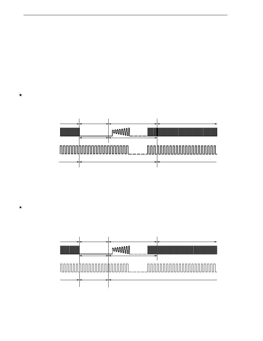
CHAPTER 10 WATCHDOG TIMER
User's Manual U16228EJ2V0UD
244
10.4.3 Watchdog timer operation in STOP mode (when "Ring-OSC can be stopped by software" is selected
by mask option)
The watchdog timer stops counting during STOP instruction execution regardless of whether the X1 input clock or
Ring-OSC clock is being used.
(1) When the CPU clock and the watchdog timer operation clock are the X1 input clock (f
XP
) when the STOP
instruction is executed
When STOP instruction is executed, operation of the watchdog timer is stopped. After STOP mode is released,
counting stops for the oscillation stabilization time set by the oscillation stabilization time select register (OSTS)
and then counting is started again using the operation clock before the operation was stopped. At this time, the
counter is not cleared to 0 but holds its value.
Figure 10-4. Operation in STOP Mode (CPU Clock and WDT Operation Clock: X1 Input Clock)
Watchdog timer
Operating
Operation stopped
Operating
f
R
f
XP
CPU operation
Normal
operation
STOP
Oscillation stabilization time
Normal operation
Oscillation
stopped
Oscillation stabilization time
(set by OSTS register)
(2) When the CPU clock is the X1 input clock (f
XP
) and the watchdog timer operation clock is the Ring-OSC
clock (f
R
) when the STOP instruction is executed
When the STOP instruction is executed, operation of the watchdog timer is stopped. After STOP mode is
released, counting is started again using the operation clock before the operation was stopped. At this time, the
counter is not cleared to 0 but holds its value.
Figure 10-5. Operation in STOP Mode
(CPU Clock: X1 Input Clock, WDT Operation Clock: Ring-OSC Clock)
Watchdog timer
Operating
f
R
f
XP
CPU operation
Normal
operation
STOP
Oscillation stabilization time
Normal operation
Oscillation
stopped
Oscillation stabilization time
(set by OSTS register)
Operating Operation stopped
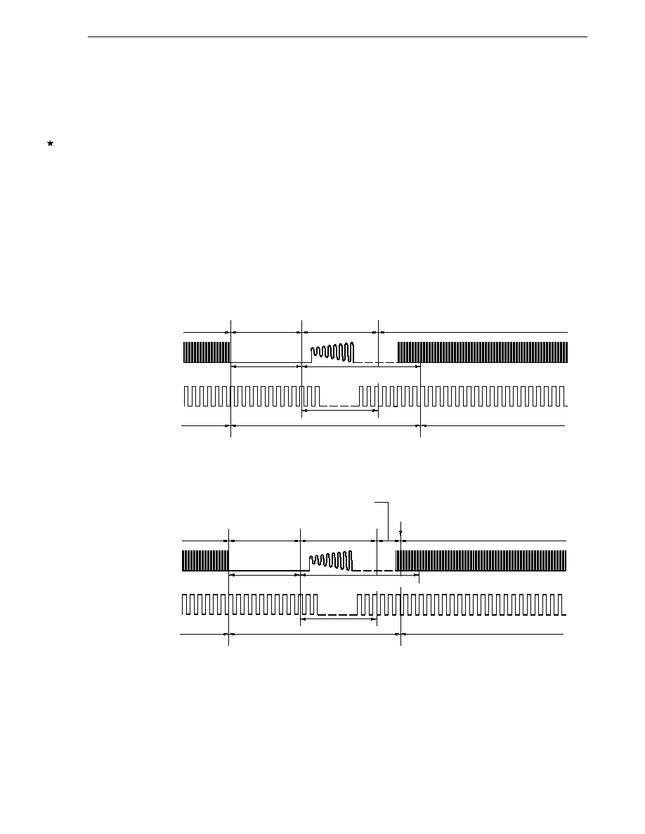
CHAPTER 10 WATCHDOG TIMER
User's Manual U16228EJ2V0UD
245
(3) When the CPU clock is the Ring-OSC clock (f
R
) and the watchdog timer operation clock is the X1 input
clock (f
XP
) when the STOP instruction is executed
When the STOP instruction is executed, operation of the watchdog timer is stopped. After STOP mode is
released, counting is stopped until the timing of <1> or <2>, whichever is earlier, and then counting is started
using the operation clock before the operation was stopped. At this time, the counter is not cleared to 0 but holds
its value.
<1> The oscillation stabilization time set by the oscillation stabilization time select register (OSTS) elapses.
<2> The CPU clock is switched to the X1 input clock (f
XP
).
Figure 10-6. Operation in STOP Mode
(CPU Clock: Ring-OSC Clock, WDT Operation Clock: X1 Input Clock)
<1> Timing when counting is started after the oscillation stabilization time set by the oscillation stabilization time
select register (OSTS) has elapsed
Watchdog timer
Operating
Operation stopped
Operating
f
R
f
XP
CPU operation
17 clocks
Normal operation
(Ring-OSC clock)
Clock supply stopped
Normal operation (Ring-OSC clock)
Oscillation
stopped
STOP
Oscillation stabilization time
(set by OSTS register)
<2> Timing when counting is started after the CPU clock is switched to the X1 input clock (f
XP
)
Operating
Operation stopped
Operating
f
R
f
XP
f
R
f
XP
Note
CPU operation
17 clocks
Normal operation
(Ring-OSC clock)
Clock supply
stopped
Normal operation (Ring-OSC clock)
Normal operation (X1 input clock)
CPU clock
Oscillation
stopped
STOP
Oscillation stabilization time
(set by OSTS register)
Watchdog timer
Note Confirm the oscillation stabilization time of f
XP
using the oscillation stabilization time counter status register
(OSTC).
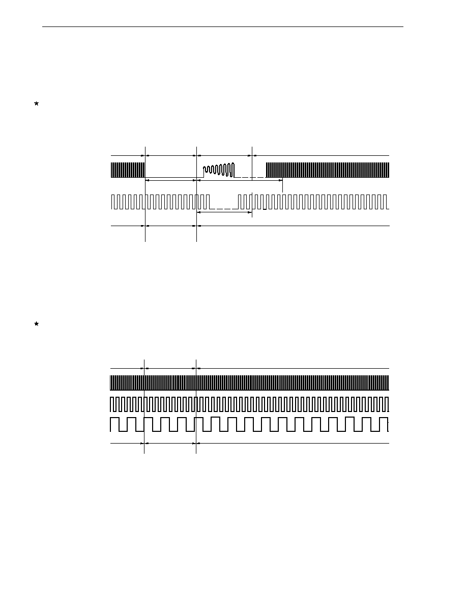
CHAPTER 10 WATCHDOG TIMER
User's Manual U16228EJ2V0UD
246
(4) When CPU clock and watchdog timer operation clock are the Ring-OSC clocks (f
R
) during STOP
instruction execution
When the STOP instruction is executed, operation of the watchdog timer is stopped. After STOP mode is
released, counting is started again using the operation clock before the operation was stopped. At this time, the
counter is not cleared to 0 but holds its value.
Figure 10-7. Operation in STOP Mode (CPU Clock and WDT Operation Clock: Ring-OSC Clock)
Watchdog timer
Operating
f
R
f
XP
CPU operation
17 clocks
Normal operation
(Ring-OSC clock)
Clock supply stopped
Normal operation (Ring-OSC clock)
Oscillation
stopped
STOP
Oscillation stabilization time
(set by OSTS register)
Operating Operation stopped
10.4.4 Watchdog timer operation in HALT mode (when "Ring-OSC can be stopped by software" is selected by
mask option)
The watchdog timer stops counting during HALT instruction execution regardless of whether the CPU clock is the
X1 input clock (f
XP
), Ring-OSC clock (f
R
), or subsystem clock (f
XT
), or whether the operation clock of the watchdog
timer is the X1 input clock (f
XP
) or Ring-OSC clock (f
R
). After HALT mode is released, counting is started again using
the operation clock before the operation was stopped. At this time, the counter is not cleared to 0 but holds its value.
Figure 10-8. Operation in HALT Mode
Watchdog timer
Operating
f
R
f
XP
CPU operation
Normal operation
Operating
HALT
Operation stopped
f
XT
Normal operation

User's Manual U16228EJ2V0UD
247
CHAPTER 11 CLOCK OUTPUT/BUZZER OUTPUT CONTROLLER
11.1 Functions of Clock Output/Buzzer Output Controller
The clock output controller is intended for carrier output during remote controlled transmission and clock output for
supply to peripheral LSIs. The clock selected with the clock output selection register (CKS) is output.
In addition, the buzzer output is intended for square-wave output of buzzer frequency selected with CKS.
Figure 11-1 shows the block diagram of clock output/buzzer output controller.
Figure 11-1. Block Diagram of Clock Output/Buzzer Output Controller
f
X
f
X
/2
10
to f
X
/2
13
f
X
to f
X
/2
7
f
XT
BZOE
BCS1
BCS0
CLOE
CLOE
BZOE
8
4
PCL/INTP6/P140
BUZ/BUSY0/
INTP7/P141
BCS0, BCS1
Clock
controller
Prescaler
Internal bus
CCS3
Clock output selection register (CKS)
CCS2
CCS1
CCS0
Output latch
(P141)
PM141
Output latch
(P140)
PM140
Selector
Selector

CHAPTER 11 CLOCK OUTPUT/BUZZER OUTPUT CONTROLLER
User's Manual U16228EJ2V0UD
248
11.2 Configuration of Clock Output/Buzzer Output Controller
The clock output/buzzer output controller includes the following hardware.
Table 11-1. Clock Output/Buzzer Output Controller Configuration
Item Configuration
Control registers
Clock output selection register (CKS)
Port mode register 14 (PM14)
Port register 14 (P14)
11.3 Register Controlling Clock Output/Buzzer Output Controller
The following two registers are used to control the clock output/buzzer output controller.
∑
Clock output selection register (CKS)
∑
Port mode register 14 (PM14)
(1) Clock output selection register (CKS)
This register sets output enable/disable for clock output (PCL) and for the buzzer frequency output (BUZ), and
sets the output clock.
CKS is set by a 1-bit or 8-bit memory manipulation instruction.
RESET input clears CKS to 00H.
CHAPTER 11 CLOCK OUTPUT/BUZZER OUTPUT CONTROLLER
User's Manual U16228EJ2V0UD
249
Figure 11-2. Format of Clock Output Selection Register (CKS)
Address: FF40H After reset: 00H R/W
Symbol
<7>
6 5
<4>
3 2 1 0
CKS
BZOE BCS1 BCS0 CLOE CCS3 CCS2 CCS1 CCS0
BZOE
BUZ output enable/disable specification
0
Clock division circuit operation stopped. BUZ fixed to low level.
1
Clock division circuit operation enabled. BUZ output enabled.
BCS1
BCS0
BUZ output clock selection
0
0
f
X
/2
10
(9.77 kHz)
0
1
f
X
/2
11
(4.88 kHz)
1
0
f
X
/2
12
(2.44 kHz)
1
1
f
X
/2
13
(1.22 kHz)
CLOE
PCL output enable/disable specification
0
Clock division circuit operation stopped. PCL fixed to low level.
1
Clock division circuit operation enabled. PCL output enabled.
CCS3 CCS2 CCS1 CCS0
PCL
output
clock
selection
0 0 0 0
f
X
(10 MHz)
0 0 0 1
f
X
/2 (5 MHz)
0 0 1 0
f
X
/2
2
(2.5 MHz)
0 0 1 1
f
X
/2
3
(1.25 MHz)
0 1 0 0
f
X
/2
4
(625 kHz)
0 1 0 1
f
X
/2
5
(312.5 kHz)
0 1 1 0
f
X
/2
6
(156.25 kHz)
0 1 1 1
f
X
/2
7
(78.125 kHz)
1 0 0 0
f
XT
(32.768 kHz)
Other than above
Setting prohibited
Remarks 1. f
X
: X1 input clock oscillation frequency
2. f
XT
: Subsystem clock oscillation frequency
3. Figures in parentheses are for operation with f
X
= 10 MHz or f
XT
= 32.768 kHz.
CHAPTER 11 CLOCK OUTPUT/BUZZER OUTPUT CONTROLLER
User's Manual U16228EJ2V0UD
250
(2) Port mode register 14 (PM14)
This register sets port 14 input/output in 1-bit units.
When using the P140/INTP6/PCL pin for clock output and the P141/INTP7/BUZ pin for buzzer output, set
PM140, PM141 and the output latch of P140, P141 to 0.
PM14 is set by a 1-bit or 8-bit memory manipulation instruction.
RESET input sets PM14 to FFH.
Figure 11-3. Format of Port Mode Register 14 (PM14)
Address: FF2EH After reset: FFH R/W
Symbol
7 6 5 4 3 2 1 0
PM14 1 1 1 1 1 1
PM141
PM140
PM14n
P14n pin I/O mode selection (n = 0, 1)
0
Output mode (output buffer ON)
1
Input mode (output buffer OFF)
11.4 Clock Output/Buzzer Output Controller Operations
11.4.1 Clock output operation
The clock pulse is output as the following procedure.
<1> Select the clock pulse output frequency with bits 0 to 3 (CCS0 to CCS3) of the clock output selection register
(CKS) (clock pulse output in disabled status).
<2> Set bit 4 (CLOE) of CKS to 1 to enable clock output.
Remark The clock output controller is designed not to output pulses with a small width during output
enable/disable switching of the clock output. As shown in Figure 11-4, be sure to start output from the
low period of the clock (marked with * in the figure). When stopping output, do so after securing high
level of the clock.
Figure 11-4. Remote Control Output Application Example
CLOE
Clock output
*
*
11.4.2 Operation as buzzer output
The buzzer frequency is output as the following procedure.
<1> Select the buzzer output frequency with bits 5 and 6 (BCS0, BCS1) of the clock output selection register
(CKS) (buzzer output in disabled status).
<2> Set bit 7 (BZOE) of CKS to 1 to enable buzzer output.
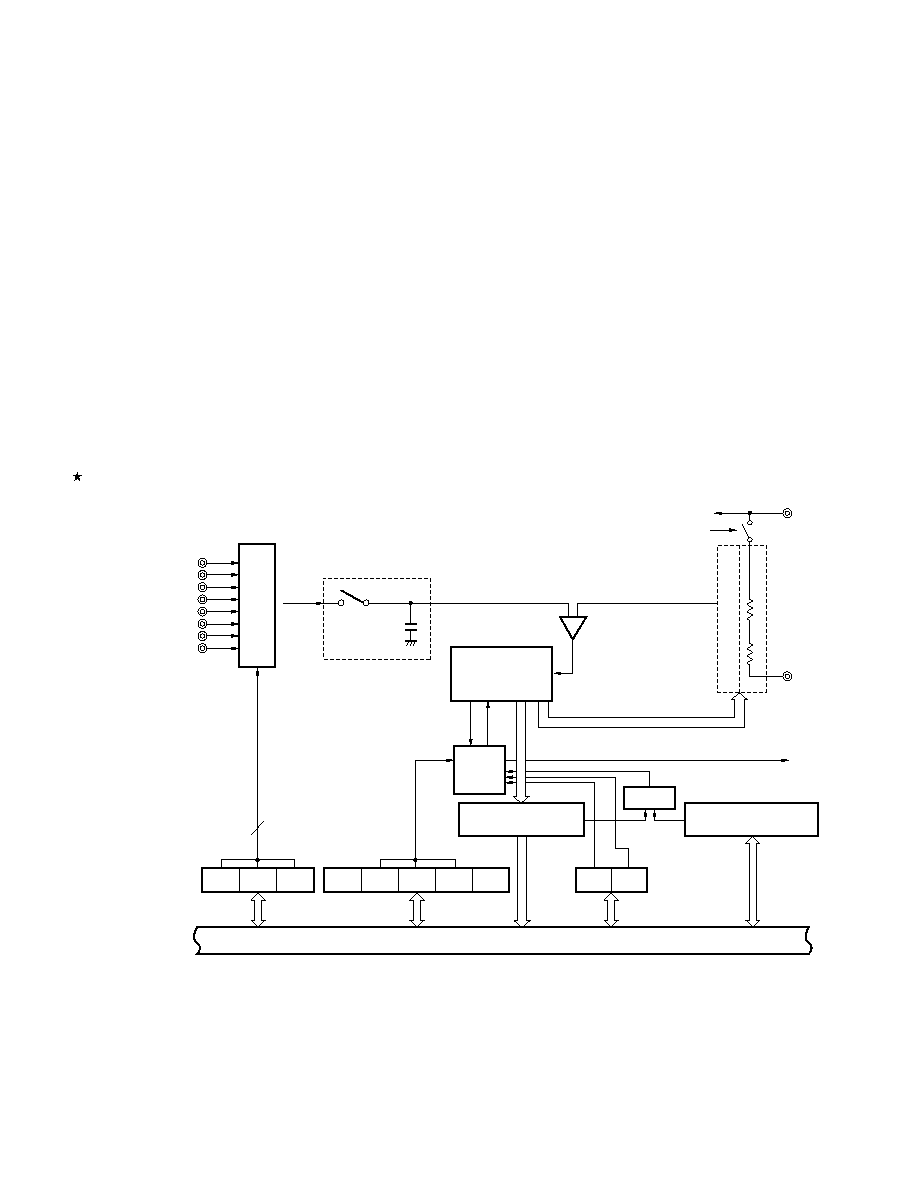
User's Manual U16228EJ2V0UD
251
CHAPTER 12 A/D CONVERTER
12.1 Functions of A/D Converter
The A/D converter converts an analog input signal into a digital value, and consists of up to eight channels (ANI0 to
ANI7) with a resolution of 10 bits.
The A/D converter has the following two functions.
(1) 10-bit resolution A/D conversion
10-bit resolution A/D conversion is carried out repeatedly for one channel selected from analog inputs ANI0 to
ANI7. Each time an A/D conversion operation ends, an interrupt request (INTAD) is generated.
(2) Power-fail detection function
This function is used to detect a voltage drop in a battery. The A/D conversion result (ADCR register value) and
power-fail comparison threshold register (PFT) value are compared. INTAD is generated only when a
comparative condition has been matched.
Figure 12-1. Block Diagram of A/D Converter
AV
REF
AV
SS
INTAD
ADCS bit
3
ADS2
ADS1
ADS0
ADCS
FR2
FR1
ADCE
FR0
Sample & hold circuit
AV
SS
Voltage comparator
Controller
A/D conversion result
register (ADCR)
Power-fail comparison
threshold register (PFT)
Analog input channel
specification register
(ADS)
A/D converter mode
register (ADM)
PFEN
PFCM
Power-fail comparison
mode register (PFM)
Internal bus
Comparator
ANI0/P20
ANI1/P21
ANI2/P22
ANI3/P23
ANI4/P24
ANI5/P25
ANI6/P26
ANI7/P27
Successive
approximation
register (SAR)
Selector
Tap selector

CHAPTER 12 A/D CONVERTER
User's Manual U16228EJ2V0UD
252
12.2 Configuration of A/D Converter
The A/D converter includes the following hardware.
Table 12-1. Registers of A/D Converter Used on Software
Item Configuration
Registers
Successive approximation register (SAR)
A/D conversion result register (ADCR)
A/D converter mode register (ADM)
Analog input channel specification register (ADS)
Power-fail comparison mode register (PFM)
Power-fail comparison threshold register (PFT)
(1) ANI0 to ANI7 pins
These are the analog input pins of the 8-channel A/D converter. They input analog signals to be converted into
digital signals. Pins other than the one selected as the analog input pin by the analog input channel specification
register (ADS) can be used as input port pins.
(2) Sample & hold circuit
The sample & hold circuit samples the input signal of the analog input pin selected by the selector when A/D
conversion is started, and holds the sampled analog input voltage value during A/D conversion.
(3) Series resistor string
The series resistor string is connected between AV
REF
and AV
SS
, and generates a voltage to be compared with
the analog input signal.
(4) Voltage
comparator
The voltage comparator compares the sampled analog input voltage and the output voltage of the series resistor
string.
(5) Successive approximation register (SAR)
This register compares the sampled analog voltage and the voltage of the series resistor string, and converts the
result, starting from the most significant bit (MSB).
When the voltage value is converted into a digital value down to the least significant bit (LSB) (end of A/D
conversion), the contents of the SAR register are transferred to the A/D conversion result register (ADCR).
(6) A/D conversion result register (ADCR)
The result of A/D conversion is loaded from the successive approximation register (SAR) to this register each
time A/D conversion is completed, and the ADCR register holds the result of A/D conversion in its higher 10 bits
(the lower 6 bits are fixed to 0).
(7) Controller
When A/D conversion has been completed or when the power-fail detection function is used, this controller
compares the result of A/D conversion (value of the ADCR register) and the value of the power-fail comparison
threshold register (PFT). It generates the interrupt INTAD only if a specified comparison condition is satisfied as
a result.

CHAPTER 12 A/D CONVERTER
User's Manual U16228EJ2V0UD
253
(8) AV
REF
pin
This pin inputs an analog power/reference voltage to the A/D converter. Always use this pin at the same potential
as that of the V
DD
pin even when the A/D converter is not used.
The signal input to ANI0 to ANI7 is converted into a digital signal, based on the voltage applied across AV
REF
and
AV
SS
.
In the standby mode, the current flowing through the series resistor string can be reduced by lowering the voltage
input to the AV
REF
pin to the AV
SS
level.
(9) AV
SS
pin
This is the ground potential pin of the A/D converter. Always use this pin at the same potential as that of the V
SS
pin even when the A/D converter is not used.
(10) A/D converter mode register (ADM)
This register is used to set the conversion time of the analog input signal to be converted, and to start or stop the
conversion operation.
(11) Analog input channel specification register (ADS)
This register is used to specify the port that inputs the analog voltage to be converted into a digital signal.
(12) Power-fail comparison mode register (PFM)
This register is used to set the power-fail monitor mode.
(13) Power-fail comparison threshold register (PFT)
This register is used to set the threshold value that is to be compared with the value of the A/D conversion result
register (ADCR).
CHAPTER 12 A/D CONVERTER
User's Manual U16228EJ2V0UD
254
12.3 Registers Used in A/D Converter
The A/D converter uses the following five registers.
∑
A/D converter mode register (ADM)
∑
Analog input channel specification register (ADS)
∑
A/D conversion result register (ADCR)
∑
Power-fail comparison mode register (PFM)
∑
Power-fail comparison threshold register (PFT)
(1) A/D converter mode register (ADM)
This register sets the conversion time for analog input to be A/D converted, and starts/stops conversion.
ADM can be set by a 1-bit or 8-bit memory manipulation instruction.
RESET input clears this register to 00H.
Figure 12-2. Format of A/D Converter Mode Register (ADM)
144 s
120 s
96 s
72 s
60 s
48 s
ADCE
0
0
FR0
FR1
FR2
0
ADCS
A/D conversion operation control
Stops conversion operation
Enables conversion operation
ADCS
0
1
Conversion time selection
Note 1
288/f
X
240/f
X
192/f
X
144/f
X
120/f
X
96/f
X
Setting prohibited
FR2
0
0
0
1
1
1
Other than above
FR1
0
0
1
0
0
1
FR0
0
1
0
0
1
0
<0>
1
2
3
4
5
6
<7>
ADM
Address: FF28H After reset: 00H R/W
Symbol
µ
µ
µ
µ
µ
µ
34.3 s
28.6 s
22.9 s
17.2 s
14.3 s
11.5 s
28.8 s
24.0 s
19.2 s
14.4 s
12.0 s
9.6 s
µ
µ
µ
µ
µ
µ
f
X
= 8.38 MHz f
X
= 10 MHz
Boost reference voltage generator operation control
Note 2
Stops operation of reference voltage generator
Enables operation of reference voltage generator
ADCE
0
1
µ
µ
µ
µ
µ
µ
f
X
= 2 MHz
CHAPTER 12 A/D CONVERTER
User's Manual U16228EJ2V0UD
255
Notes 1. Set so that the A/D conversion time is as follows.
∑
Standard products, (A) grade products: 14
µ
s or longer but less than 100
µ
s
∑
(A1) grade products:
14
µ
s or longer but less than 60
µ
s
∑
(A2) grade products:
16
µ
s or longer but less than 48
µ
s
2. A booster circuit is incorporated to realize low-voltage operation. The operation of the circuit that
generates the reference voltage for boosting is controlled by ADCE, and it takes 14
µ
s from operation
start to operation stabilization. Therefore, when ADCS is set to 1 after 14
µ
s or more has elapsed
from the time ADCE is set to 1, the conversion result at that time has priority over the first conversion
result.
Remark f
X
: X1 input clock oscillation frequency
Table 12-2. Settings of ADCS and ADCE
ADCS ADCE
A/D
Conversion Operation
0
0
Stop status (DC power consumption path does not exist)
0
1
Conversion waiting mode (only reference voltage generator consumes power)
1
0
Conversion mode (reference voltage generator operation stopped
Note
)
1
1
Conversion mode (reference voltage generator operates)
Note Data of first conversion cannot be used.
Figure 12-3. Timing Chart When Boost Reference Voltage Generator Is Used
ADCE
Boost reference voltage
ADCS
Conversion
operation
Conversion
operation
Conversion stopped
Conversion
waiting
Boost reference voltage generator: operating
Note
Note The time from the rising of the ADCE bit to the falling of the ADCS bit must be 14
µ
s or longer to stabilize
the reference voltage.
Cautions 1. A/D conversion must be stopped before rewriting bits FR0 to FR2 to values other than the
identical data.
2. For the sampling time of the A/D converter and the A/D conversion start delay time, see (11)
in 12.6 Cautions for A/D Converter.
3. If data is written to ADM, a wait cycle is generated. Do not write data to ADM when the CPU is
operating on the subsystem clock and the X1 input clock is stopped. For details, see
CHAPTER 34 CAUTIONS FOR WAIT.
Remark f
X
: X1 input clock oscillation frequency
CHAPTER 12 A/D CONVERTER
User's Manual U16228EJ2V0UD
256
(2) Analog input channel specification register (ADS)
This register specifies the input port of the analog voltage to be A/D converted.
ADS can be set by a 1-bit or 8-bit memory manipulation instruction.
RESET input clears this register to 00H.
Figure 12-4. Format of Analog Input Channel Specification Register (ADS)
ADS0
ADS1
ADS2
0
0
0
0
0
Analog input channel specification
ANI0
ANI1
ANI2
ANI3
ANI4
ANI5
ANI6
ANI7
ADS0
0
1
0
1
0
1
0
1
ADS1
0
0
1
1
0
0
1
1
ADS2
0
0
0
0
1
1
1
1
0
1
2
3
4
5
6
7
ADS
Address: FF29H After reset: 00H R/W
Symbol
Cautions 1. Be sure to clear bits 3 to 7 of ADS to 0.
2. If data is written to ADS, a wait cycle is generated. Do not write data to ADS when the CPU is
operating on the subsystem clock and the X1 input clock is stopped. For details, see
CHAPTER 34 CAUTIONS FOR WAIT.

CHAPTER 12 A/D CONVERTER
User's Manual U16228EJ2V0UD
257
(3) A/D conversion result register (ADCR)
This register is a 16-bit register that stores the A/D conversion result. The lower six bits are fixed to 0. Each time
A/D conversion ends, the conversion result is loaded from the successive approximation register, and is stored in
ADCR in order starting from the most significant bit (MSB). FF09H indicates the higher 8 bits of the conversion
result, and FF08H indicates the lower 2 bits of the conversion result.
ADCR can be read by a 16-bit memory manipulation instruction.
RESET input makes ADCR undefined.
Figure 12-5. Format of A/D Conversion Result Register (ADCR)
Symbol
Address: FF08H, FF09H After reset: Undefined R
FF09H
FF08H
0
0
0
0
0
0
ADCR
Cautions 1. When writing to the A/D converter mode register (ADM) and analog input channel
specification register (ADS), the contents of ADCR may become undefined. Read the
conversion result following conversion completion before writing to ADM and ADS. Using
timing other than the above may cause an incorrect conversion result to be read.
2. If data is read from ADCR, a wait cycle is generated. Do not read data from ADCR when the
CPU is operating on the subsystem clock and the X1 input clock is stopped. For details, see
CHAPTER 34 CAUTIONS FOR WAIT.
CHAPTER 12 A/D CONVERTER
User's Manual U16228EJ2V0UD
258
(4) Power-fail
comparison
mode register (PFM)
The power-fail comparison mode register (PFM) is used to compare the A/D conversion result (value of the
ADCR register) and the value of the power-fail comparison threshold register (PFT).
PFM can be set by a 1-bit or 8-bit memory manipulation instruction.
RESET input clears this register to 00H.
Figure 12-6. Format of Power-Fail Comparison Mode Register (PFM)
0
0
0
0
0
0
PFCM
PFEN
Power-fail comparison enable
Stops power-fail comparison (used as a normal A/D converter)
Enables power-fail comparison (used for power-fail detection)
PFEN
0
1
Power-fail comparison mode selection
Interrupt request signal (INTAD) generation
No INTAD generation
INTAD generation
No INTAD generation
Higher 8 bits of
ADCR
PFT
Higher 8 bits of
ADCR < PFT
Higher 8 bits of
ADCR
PFT
Higher 8 bits of
ADCR < PFT
PFCM
0
1
0
1
2
3
4
5
<6>
<7>
PFM
Address: FF2AH After reset: 00H R/W
Symbol
Caution If data is written to PFM, a wait cycle is generated. Do not write data to PFM when the CPU is
operating on the subsystem clock and the X1 input clock is stopped. For details, see CHAPTER
34 CAUTIONS FOR WAIT.
(5) Power-fail comparison threshold register (PFT)
The power-fail comparison threshold register (PFT) is a register that sets the threshold value when comparing the
values with the A/D conversion result.
8-bit data in PFT is compared to the higher 8 bits (FF09H) of the 10-bit A/D conversion result.
PFT can be set by an 8-bit memory manipulation instruction.
RESET input clears this register to 00H.
Figure 12-7. Format of Power-Fail Comparison Threshold Register (PFT)
PFT0
PFT1
PFT2
PFT3
PFT4
PFT5
PFT6
PFT7
0
1
2
3
4
5
6
7
PFT
Address: FF2BH After reset: 00H R/W
Symbol
Caution If data is written to PFT, a wait cycle is generated. Do not write data to PFT when the CPU is
operating on the subsystem clock and the X1 input clock is stopped. For details, see CHAPTER
34 CAUTIONS FOR WAIT.

CHAPTER 12 A/D CONVERTER
User's Manual U16228EJ2V0UD
259
12.4 A/D Converter Operations
12.4.1 Basic operations of A/D converter
<1> Select one channel for A/D conversion using the analog input channel specification register (ADS).
<2> Set ADCE to 1 and wait for 14
µ
s or longer.
<3> Set ADCS to 1 and start the conversion operation.
(<4> to <10> are operations performed by hardware.)
<4> The voltage input to the selected analog input channel is sampled by the sample & hold circuit.
<5> When sampling has been done for a certain time, the sample & hold circuit is placed in the hold state and the
input analog voltage is held until the A/D conversion operation has ended.
<6> Bit 9 of the successive approximation register (SAR) is set. The series resistor string voltage tap is set to
(1/2) AV
REF
by the tap selector.
<7> The voltage difference between the series resistor string voltage tap and analog input is compared by the
voltage comparator. If the analog input is greater than (1/2) AV
REF
, the MSB of SAR remains set to 1. If the
analog input is smaller than (1/2) AV
REF
, the MSB is reset to 0.
<8> Next, bit 8 of SAR is automatically set to 1, and the operation proceeds to the next comparison. The series
resistor string voltage tap is selected according to the preset value of bit 9, as described below.
∑
Bit 9 = 1: (3/4) AV
REF
∑
Bit 9 = 0: (1/4) AV
REF
The voltage tap and analog input voltage are compared and bit 8 of SAR is manipulated as follows.
∑
Analog input voltage
Voltage tap: Bit 8 = 1
∑
Analog input voltage < Voltage tap: Bit 8 = 0
<9> Comparison is continued in this way up to bit 0 of SAR.
<10> Upon completion of the comparison of 10 bits, an effective digital result value remains in SAR, and the result
value is transferred to the A/D conversion result register (ADCR) and then latched.
At the same time, the A/D conversion end interrupt request (INTAD) can also be generated.
<11> Repeat steps <4> to <10>, until ADCS is cleared to 0.
To stop the A/D converter, clear ADCS to 0.
To restart A/D conversion from the status of ADCE = 1, start from <3>. To restart A/D conversion from the
status of ADCE = 0, however, start from <2>.

CHAPTER 12 A/D CONVERTER
User's Manual U16228EJ2V0UD
260
Figure 12-8. Basic Operation of A/D Converter
Conversion time
Sampling time
Sampling
A/D conversion
Undefined
Conversion
result
A/D converter
operation
SAR
ADCR
INTAD
Conversion
result
A/D conversion operations are performed continuously until bit 7 (ADCS) of the A/D converter mode register (ADM)
is reset (0) by software.
If a write operation is performed to one of the ADM, analog input channel specification register (ADS), power-fail
comparison mode register (PFM), or power-fail comparison threshold register (PFT) during an A/D conversion
operation, the conversion operation is initialized, and if the ADCS bit is set (1), conversion starts again from the
beginning.
RESET input makes the A/D conversion result register (ADCR) undefined.

CHAPTER 12 A/D CONVERTER
User's Manual U16228EJ2V0UD
261
12.4.2 Input voltage and conversion results
The relationship between the analog input voltage input to the analog input pins (ANI0 to ANI7) and the theoretical
A/D conversion result (stored in the A/D conversion result register (ADCR)) is shown by the following expression.
SAR = INT (
◊
1024 + 0.5)
ADCR = SAR ◊ 64
or
(ADCR
-
0.5)
◊
V
AIN
< (ADCR + 0.5)
◊
where, INT( ): Function which returns integer part of value in parentheses
V
AIN
:
Analog input voltage
AV
REF
: AV
REF
pin voltage
ADCR: A/D conversion result register (ADCR) value
SAR:
Successive approximation register
Figure 12-9 shows the relationship between the analog input voltage and the A/D conversion result.
Figure 12-9. Relationship Between Analog Input Voltage and A/D Conversion Result
1023
1022
1021
3
2
1
0
FFC0H
FF80H
FF40H
00C0H
0080H
0040H
0000H
A/D conversion result
(ADCR)
SAR
ADCR
1
2048
1
1024
3
2048
2
1024
5
2048
Input voltage/AV
REF
3
1024
2043
2048
1022
1024
2045
2048
1023
1024
2047
2048
1
V
AIN
AV
REF
AV
REF
1024
AV
REF
1024
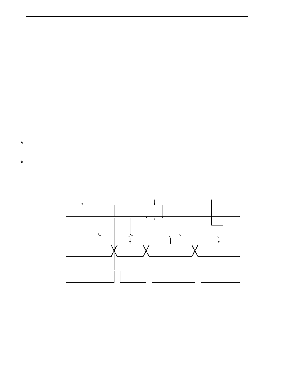
CHAPTER 12 A/D CONVERTER
User's Manual U16228EJ2V0UD
262
12.4.3 A/D converter operation mode
The operation mode of the A/D converter is the select mode. One channel of analog input is selected from ANI0 to
ANI7 by the analog input channel specification register (ADS) and A/D conversion is executed.
In addition, the following two functions can be selected by setting of bit 7 (PFEN) of the power-fail comparison
mode register (PFM).
∑
Normal 10-bit A/D converter (PFEN = 0)
∑
Power-fail detection function (PFEN = 1)
(1) A/D conversion operation (when PFEN = 0)
By setting bit 7 (ADCS) of the A/D converter mode register (ADM) to 1 and bit 7 (PFEN) of the power-fail
comparison mode register (PFM) to 0, the A/D conversion operation of the voltage, which is applied to the analog
input pin specified by the analog input channel specification register (ADS), is started.
When A/D conversion has been completed, the result of the A/D conversion is stored in the A/D conversion result
register (ADCR), and an interrupt request signal (INTAD) is generated. Once the A/D conversion has started and
when one A/D conversion has been completed, the next A/D conversion operation is immediately started. The
A/D conversion operations are repeated until new data is written to ADS.
If ADM, ADS, the power-fail comparison mode register (PFM), and the power-fail comparison threshold register
(PFT) are rewritten during A/D conversion, the A/D conversion operation under execution is stopped and
restarted from the beginning.
If 0 is written to ADCS during A/D conversion, A/D conversion is immediately stopped. At this time, the
conversion result is undefined.
Figure 12-10. A/D Conversion Operation
ANIn
Rewriting ADM
ADCS = 1
Rewriting ADS
ADCS = 0
ANIn
ANIn
ANIn
ANIm
ANIn
ANIm
ANIm
Stopped
A/D conversion
ADCR
INTAD
(PFEN = 0)
Conversion is stopped
Conversion result is not retained
Remarks 1. n = 0 to 7
2. m = 0 to 7

CHAPTER 12 A/D CONVERTER
User's Manual U16228EJ2V0UD
263
(2) Power-fail detection function (when PFEN = 1)
By setting bit 7 (ADCS) of the A/D converter mode register (ADM) to 1 and bit 7 (PFEN) of the power-fail
comparison mode register (PFM) to 1, the A/D conversion operation of the voltage applied to the analog input pin
specified by the analog input channel specification register (ADS) is started.
When the A/D conversion has been completed, the result of the A/D conversion is stored in the A/D conversion
result register (ADCR), the values are compared with power-fail comparison threshold register (PFT), and an
interrupt request signal (INTAD) is generated under the condition specified by bit 6 (PFCM) of PFM.
<1> When PFEN = 1 and PFCM = 0
The higher 8 bits of ADCR and PFT values are compared when A/D conversion ends and INTAD is only
generated when the higher 8 bits of ADCR
PFT.
<2> When PFEN = 1 and PFCM = 1
The higher 8 bits of ADCR and PFT values are compared when A/D conversion ends and INTAD is only
generated when the higher 8 bits of ADCR < PFT.
Figure 12-11. Power-Fail Detection (When PFEN = 1 and PFCM = 0)
A/D conversion
Higher 8 bits
of ADCR
PFT
INTAD
(PFEN = 1)
ANIn
ANIn
80H
80H
Condition match
First conversion
Note
7FH
80H
ANIn
ANIn
Note If the conversion result is not read before the end of the next conversion after INTAD is output, the result is
replaced by the next conversion result.
Remark n = 0 to 7

CHAPTER 12 A/D CONVERTER
User's Manual U16228EJ2V0UD
264
The setting methods are described below.
∑
When used as A/D conversion operation
<1> Set bit 0 (ADCE) of the A/D converter mode register (ADM) to 1.
<2> Select the channel and conversion time using bits 2 to 0 (ADS2 to ADS0) of the analog input channel
specification register (ADS) and bits 5 to 3 (FR2 to FR0) of ADM.
<3> Set bit 7 (ADCS) of ADM to 1.
<4> An interrupt request signal (INTAD) is generated.
<5> Transfer the A/D conversion data to the A/D conversion result register (ADCR).
<Change the channel>
<6> Change the channel using bits 2 to 0 (ADS2 to ADS0) of ADS.
<7> An interrupt request signal (INTAD) is generated.
<8> Transfer the A/D conversion data to the A/D conversion result register (ADCR).
<Complete A/D conversion>
<9> Clear ADCS to 0.
<10> Clear ADCE to 0.
Cautions 1. Make sure the period of <1> to <3> is 14
µ
s or more.
2. It is no problem if the order of <1> and <2> is reversed.
3. <1> can be omitted. However, do not use the first conversion result after <3> in this
case.
4. The period from <4> to <7> differs from the conversion time set using bits 5 to 3 (FR2 to
FR0) of ADM. The period from <6> to <7> is the conversion time set using FR2 to FR0.
∑
When used as power-fail function
<1> Set bit 7 (PFEN) of the power-fail comparison mode register (PFM).
<2> Set power-fail comparison condition using bit 6 (PFCM) of PFM.
<3> Set bit 0 (ADCE) of the A/D converter mode register (ADM) to 1.
<4> Select the channel and conversion time using bits 2 to 0 (ADS2 to ADS0) of the analog input channel
specification register (ADS) and bits 5 to 3 (FR2 to FR0) of ADM.
<5> Set a threshold value to the power-fail comparison threshold register (PFT).
<6> Set bit 7 (ADCS) of ADM to 1.
<7> Transfer the A/D conversion data to the A/D conversion result register (ADCR).
<8> The higher 8 bits of ADCR and PFT are compared and an interrupt request signal (INTAD) is generated
if the conditions match.
<Change the channel>
<9> Change the channel using bits 2 to 0 (ADS2 to ADS0) of ADS.
<10> Transfer the A/D conversion data to the A/D conversion result register (ADCR).
<11> The higher 8 bits of ADCR and the power-fail comparison threshold register (PFT) are compared and an
interrupt request signal (INTAD) is generated if the conditions match.
<Complete A/D conversion>
<12> Clear ADCS to 0.
<13> Clear ADCE to 0.
Cautions 1. Make sure the period of <3> to <6> is 14
µ
s or more.
2. It is no problem if the order of <3>, <4>, and <5> is changed.
3. <3> must not be omitted if the power-fail function is used.
4. The period from <7> to <11> differs from the conversion time set using bits 5 to 3 (FR2 to
FR0) of ADM. The period from <9> to <11> is the conversion time set using FR2 to FR0.
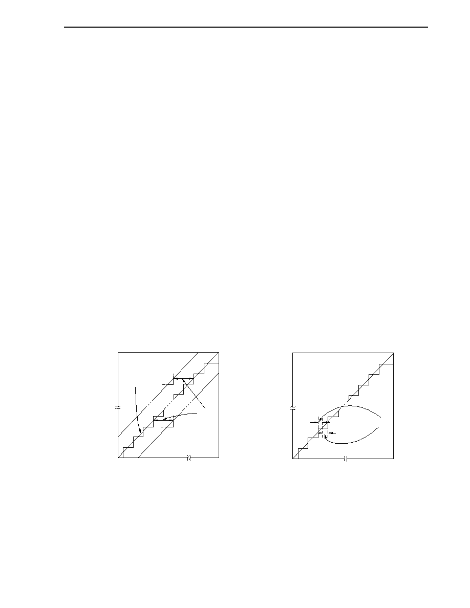
CHAPTER 12 A/D CONVERTER
User's Manual U16228EJ2V0UD
265
12.5 How to Read A/D Converter Characteristics Table
Here, special terms unique to the A/D converter are explained.
(1) Resolution
This is the minimum analog input voltage that can be identified. That is, the percentage of the analog input
voltage per bit of digital output is called 1LSB (Least Significant Bit). The percentage of 1LSB with respect to the
full scale is expressed by %FSR (Full Scale Range).
1LSB is as follows when the resolution is 10 bits.
1LSB = 1/2
10
= 1/1024
= 0.098%FSR
Accuracy has no relation to resolution, but is determined by overall error.
(2) Overall
error
This shows the maximum error value between the actual measured value and the theoretical value.
Zero-scale error, full-scale error, integral linearity error, and differential linearity errors that are combinations of
these express the overall error.
Note that the quantization error is not included in the overall error in the characteristics table.
(3) Quantization
error
When analog values are converted to digital values, a
±
1/2LSB error naturally occurs. In an A/D converter, an
analog input voltage in a range of
±
1/2LSB is converted to the same digital code, so a quantization error cannot
be avoided.
Note that the quantization error is not included in the overall error, zero-scale error, full-scale error, integral
linearity error, and differential linearity error in the characteristics table.
Figure 12-12. Overall Error
Figure 12-13. Quantization Error
Ideal line
0......0
1......1
Digital output
Overall
error
Analog input
AV
REF
0
0......0
1......1
Digital output
Quantization error
1/2LSB
1/2LSB
Analog input
0
AV
REF
(4) Zero-scale
error
This shows the difference between the actual measurement value of the analog input voltage and the theoretical
value (1/2LSB) when the digital output changes from 0......000 to 0......001.
If the actual measurement value is greater than the theoretical value, it shows the difference between the actual
measurement value of the analog input voltage and the theoretical value (3/2LSB) when the digital output
changes from 0......001 to 0......010.
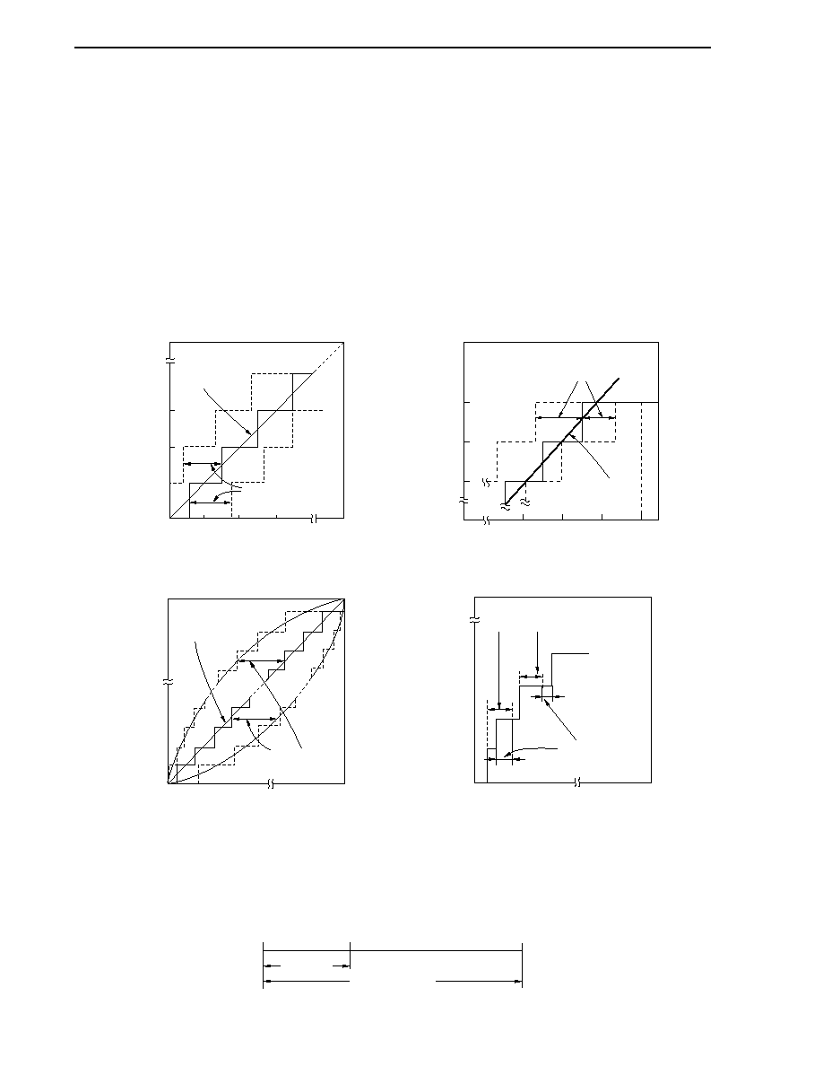
CHAPTER 12 A/D CONVERTER
User's Manual U16228EJ2V0UD
266
(5) Full-scale
error
This shows the difference between the actual measurement value of the analog input voltage and the theoretical
value (Full-scale
-
3/2LSB) when the digital output changes from 1......110 to 1......111.
(6) Integral linearity error
This shows the degree to which the conversion characteristics deviate from the ideal linear relationship. It
expresses the maximum value of the difference between the actual measurement value and the ideal straight line
when the zero-scale error and full-scale error are 0.
(7) Differential linearity error
While the ideal width of code output is 1LSB, this indicates the difference between the actual measurement value
and the ideal value.
Figure 12-14. Zero-Scale Error
Figure 12-15. Full-Scale Error
111
011
010
001
Zero-scale error
Ideal line
000
0
1
2
3
AV
REF
Digital output (Lower 3 bits)
Analog input (LSB)
111
110
101
000
0
AV
REF
-
3
Full-scale error
Ideal line
Analog input (LSB)
Digital output (Lo
w
er 3 bits)
AV
REF
-
2
AV
REF
-
1
AV
REF
Figure 12-16. Integral Linearity Error
Figure 12-17. Differential Linearity Error
0
AV
REF
Digital output
Analog input
Integral linearity
error
Ideal line
1......1
0......0
0
AV
REF
Digital output
Analog input
Differential
linearity error
1......1
0......0
Ideal 1LSB width
(8) Conversion
time
This expresses the time from the start of sampling to when the digital output is obtained.
The sampling time is included in the conversion time in the characteristics table.
(9) Sampling
time
This is the time the analog switch is turned on for the analog voltage to be sampled by the sample & hold circuit.
Sampling
time
Conversion time

CHAPTER 12 A/D CONVERTER
User's Manual U16228EJ2V0UD
267
12.6 Cautions for A/D Converter
(1) Operating current in standby mode
The A/D converter stops operating in the standby mode. At this time, the operating current can be reduced by
clearing bit 7 (ADCS) of the A/D converter mode register (ADM) to 0.
Figure 12-18 shows the circuit configuration of the series resistor string.
Figure 12-18. Circuit Configuration of Series Resistor String
AV
REF
AV
SS
P-ch
Series resistor string
ADCS
(2) Input range of ANI0 to ANI7
Observe the rated range of the ANI0 to ANI7 input voltage. If a voltage of AV
REF
or higher and AV
SS
or lower
(even in the range of absolute maximum ratings) is input to an analog input channel, the converted value of that
channel becomes undefined. In addition, the converted values of the other channels may also be affected.
(3) Conflicting
operations
<1> Conflict between A/D conversion result register (ADCR) write and ADCR read by instruction upon the end
of conversion
ADCR read has priority. After the read operation, the new conversion result is written to ADCR.
<2> Conflict between ADCR write and A/D converter mode register (ADM) write or analog input channel
specification register (ADS) write upon the end of conversion
ADM or ADS write has priority. ADCR write is not performed, nor is the conversion end interrupt signal
(INTAD) generated.
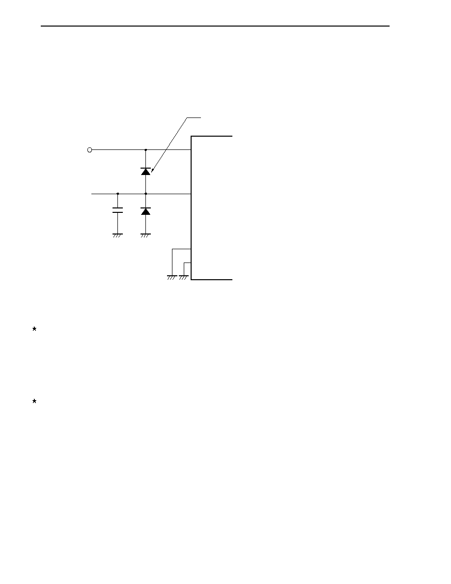
CHAPTER 12 A/D CONVERTER
User's Manual U16228EJ2V0UD
268
(4) Noise
countermeasures
To maintain the 10-bit resolution, attention must be paid to noise input to the AV
REF
pin and pins ANI0 to ANI7.
Because the effect increases in proportion to the output impedance of the analog input source, it is recommended
that a capacitor be connected externally, as shown in Figure 12-19, to reduce noise.
Figure 12-19. Analog Input Pin Connection
Reference
voltage
input
C = 100 to 1,000 pF
If there is a possibility that noise equal to or higher than AV
REF
or
equal to or lower than AV
SS
may enter, clamp with a diode with a
small V
F
value (0.3 V or lower).
AV
REF
AV
SS
V
SS
ANI0 to ANI7
(5) ANI0/P20 to ANI7/P27
<1> The analog input pins (ANI0 to ANI7) are also used as input port pins (P20 to P27).
When A/D conversion is performed with any of ANI0 to ANI7 selected, do not access port 2 while
conversion is in progress; otherwise the conversion resolution may be degraded.
<2> If a digital pulse is applied to the pins adjacent to the pins currently used for A/D conversion, the expected
value of the A/D conversion may not be obtained due to coupling noise. Therefore, do not apply a pulse to
the pins adjacent to the pin undergoing A/D conversion.
(6) Input impedance of ANI0 to ANI7 pins
In this A/D converter, the internal sampling capacitor is charged and sampling is performed for approx. one sixth
of the conversion time.
Since only the leakage current flows other than during sampling and the current for charging the capacitor also
flows during sampling, the input impedance fluctuates and has no meaning.
To perform sufficient sampling, however, it is recommended to make the output impedance of the analog input
source 10 k
or lower, or attach a capacitor of around 100 pF to the ANI0 to ANI7 pins (see Figure 12-19).
(7) AV
REF
pin input impedance
A series resistor string of several tens of 10 k
is connected between the AV
REF
and AV
SS
pins.
Therefore, if the output impedance of the reference voltage source is high, this will result in a series connection to
the series resistor string between the AV
REF
and AV
SS
pins, resulting in a large reference voltage error.
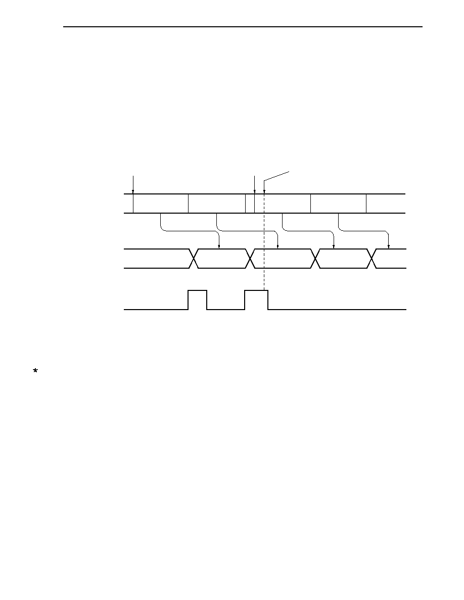
CHAPTER 12 A/D CONVERTER
User's Manual U16228EJ2V0UD
269
(8) Interrupt request flag (ADIF)
The interrupt request flag (ADIF) is not cleared even if the analog input channel specification register (ADS) is
changed.
Therefore, if an analog input pin is changed during A/D conversion, the A/D conversion result and ADIF for the
pre-change analog input may be set just before the ADS rewrite. Caution is therefore required since, at this time,
when ADIF is read immediately after the ADS rewrite, ADIF is set despite the fact A/D conversion for the post-
change analog input has not ended.
When A/D conversion is stopped and then resumed, clear ADIF before the A/D conversion operation is resumed.
Figure 12-20. Timing of A/D Conversion End Interrupt Request Generation
ADS rewrite
(start of ANIn conversion)
A/D conversion
ADCR
ADIF
ANIn
ANIn
ANIm
ANIm
ANIn
ANIn
ANIm
ANIm
ADS rewrite
(start of ANIm conversion)
ADIF is set but ANIm conversion
has not ended.
Remarks 1. n = 0 to 7
2. m = 0 to 7
(9) Conversion results just after A/D conversion start
The first A/D conversion value immediately after A/D conversion starts may not fall within the rating range if the
ADCS bit is set to 1 within 14
µ
s after the ADCE bit was set to 1, or if the ADCS bit is set to 1 with the ADCE bit =
0. Take measures such as polling the A/D conversion end interrupt request (INTAD) and removing the first
conversion result.
(10) A/D conversion result register (ADCR) read operation
When a write operation is performed to the A/D converter mode register (ADM) and analog input channel
specification register (ADS), the contents of ADCR may become undefined. Read the conversion result following
conversion completion before writing to ADM and ADS. Using a timing other than the above may cause an
incorrect conversion result to be read.
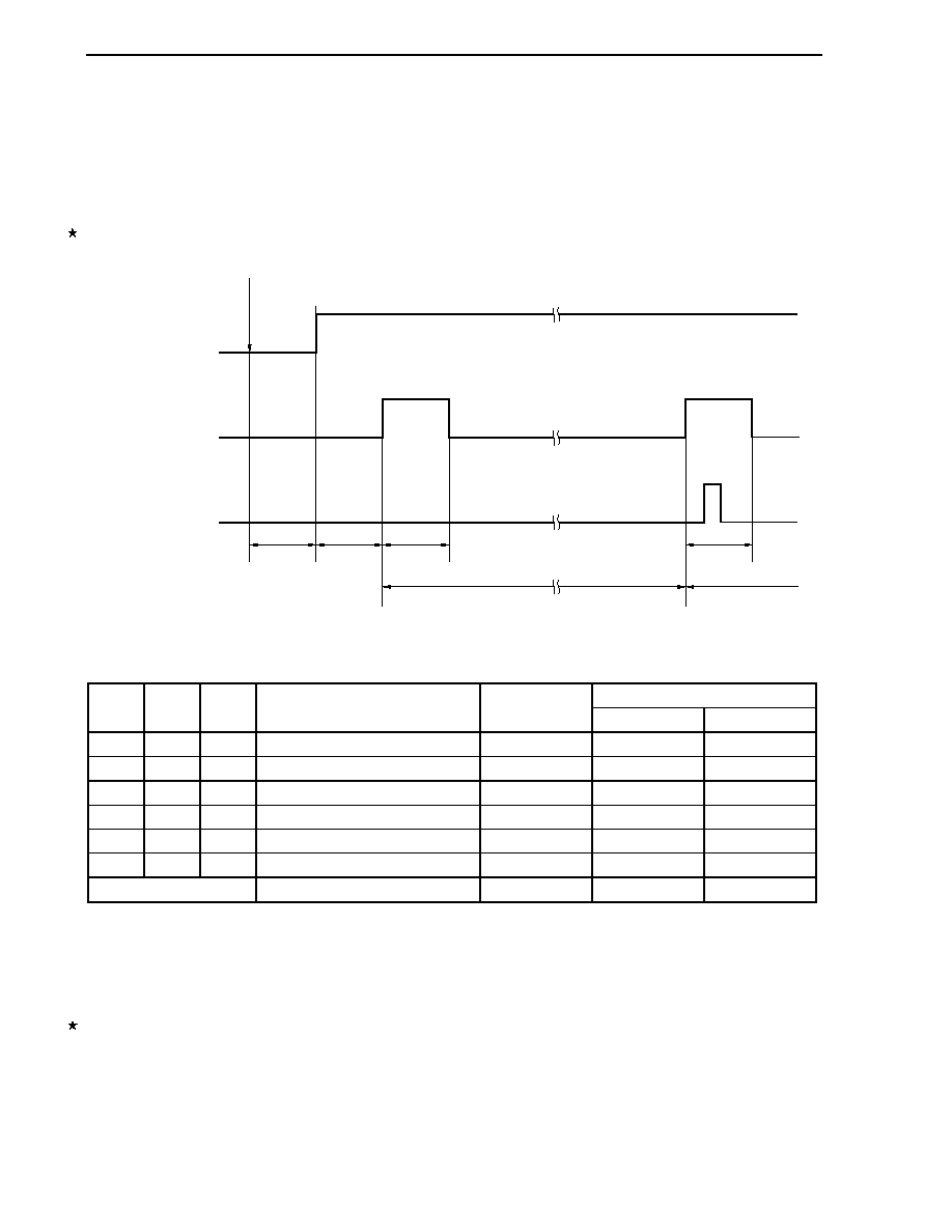
CHAPTER 12 A/D CONVERTER
User's Manual U16228EJ2V0UD
270
(11) A/D converter sampling time and A/D conversion start delay time
The A/D converter sampling time differs depending on the set value of the A/D converter mode register (ADM).
The delay time exists until actual sampling is started after A/D converter operation is enabled.
When using a set in which the A/D conversion time must be strictly observed, care is required for the contents
shown in Figure 12-21 and Table 12-3.
Figure 12-21. Timing of A/D Converter Sampling and A/D Conversion Start Delay
ADCS
Wait
period
Conversion time
Conversion time
A/D
conversion
start delay
time
Sampling
time
Sampling timing
INTAD
ADCS
1 or ADS rewrite
Sampling
time
Table 12-3. A/D Converter Sampling Time and A/D Conversion Start Delay Time (ADM Set Value)
A/D Conversion Start Delay Time
Note
FR2 FR1 FR0
Conversion
Time
Sampling
Time
MIN. MAX.
0 0 0
288/f
X
40/f
X
32/f
X
36/f
X
0 0 1
240/f
X
32/f
X
28/f
X
32/f
X
0 1 0
192/f
X
24/f
X
24/f
X
28/f
X
1 0 0
144/f
X
20/f
X
16/f
X
18/f
X
1 0 1
120/f
X
16/f
X
14/f
X
16/f
X
1 1 0
96/f
X
12/f
X
12/f
X
14/f
X
Other than above
Setting prohibited
-
-
-
Note The A/D conversion start delay time is the time after wait period. For the wait function, see CHAPTER 34
CAUTIONS FOR WAIT.
Remark f
X
: X1 clock oscillation frequency
(12) Register generating wait cycle
Do not read data from the ADCR register and do not write data to the ADM, ADS, PFM, and PFT registers while
the CPU is operating on the subsystem clock and while oscillation of the clock input to X1 is stopped.

CHAPTER 12 A/D CONVERTER
User's Manual U16228EJ2V0UD
271
(13) Internal equivalent circuit
The equivalent circuit of the analog input block is shown below.
Figure 12-22. Internal Equivalent Circuit of ANIn Pin
ANIn
C1
C2
C3
R1
R2
Table 12-4. Resistance and Capacitance Values of Equivalent Circuit (Reference Values)
AV
REF
R1 R2 C1 C2 C3
2.7 V
12 k
8
k
8 pF
3 pF
2 pF
4.5 V
4 k
2.7
k
8 pF
1.4 pF
2 pF
Remarks 1. The resistance and capacitance values shown in Table 12-4 are not guaranteed values.
2. n = 0 to 7

User's Manual U16228EJ2V0UD
272
CHAPTER 13 SERIAL INTERFACE UART0
13.1 Functions of Serial Interface UART0
Serial interface UART0 has the following two modes.
(1) Operation stop mode
This mode is used when serial communication is not executed and can enable a reduction in the power
consumption.
For details, see 13.4.1 Operation stop mode.
(2) Asynchronous serial interface (UART) mode
The functions of this mode are outlined below.
For details, see 13.4.2 Asynchronous serial interface (UART) mode and 13.4.3 Dedicated baud rate
generator.
∑
Two-pin
configuration T
X
D0: Transmit data output pin
R
X
B0: Receive data input pin
∑
Length of communication data can be selected from 7 or 8 bits.
∑
Dedicated on-chip 5-bit baud rate generator allowing any baud rate to be set
∑
Transmission and reception can be performed independently.
∑
Four operating clock inputs selectable
∑
Fixed to LSB-first communication
Cautions 1. If clock supply to serial interface UART0 is not stopped (e.g., in the HALT mode), normal
operation continues. If clock supply to serial interface UART0 is stopped (e.g., in the STOP
mode), each register stops operating, and holds the value immediately before clock supply
was stopped. The T
X
D0 pin also holds the value immediately before clock supply was
stopped and outputs it. However, the operation is not guaranteed after clock supply is
resumed. Therefore, reset the circuit so that POWER0 = 0, RXE0 = 0, and TXE0 = 0.
2. Set POWER0 = 1 and then set TXE0 = 1 (transmission) or RXE0 = 1 (reception) to start
communication.
3. TXE0 and RXE0 are synchronized by the base clock (f
XCLK0
) set by BRGC0. To enable
transmission or reception again, set TXE0 or RXE0 to 1 at least two clocks of base clock
after TXE0 or RXE0 has been cleared to 0. If TXE0 or RXE0 is set within two clocks of base
clock, the transmission circuit or reception circuit may not be initialized.

CHAPTER 13 SERIAL INTERFACE UART0
User's Manual U16228EJ2V0UD
273
13.2 Configuration of Serial Interface UART0
Serial interface UART0 includes the following hardware.
Table 13-1. Configuration of Serial Interface UART0
Item Configuration
Registers
Receive buffer register 0 (RXB0)
Receive shift register 0 (RXS0)
Transmit shift register 0 (TXS0)
Control registers
Asynchronous serial interface operation mode register 0 (ASIM0)
Asynchronous serial interface reception error status register 0 (ASIS0)
Baud rate generator control register 0 (BRGC0)
Port mode register 1 (PM1)
Port register 1 (P1)
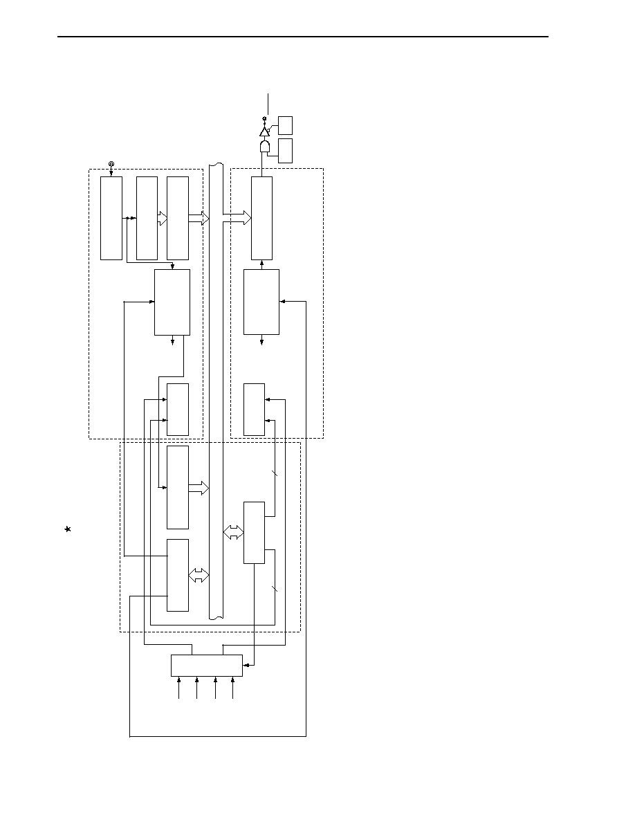
CHAPTER
13
SERIAL IN
TER
F
ACE U
ART0
User's Manual
U1
6228EJ2V0UD
274
Figure 13-1. Block Diagram of Serial Interface UART0
T
x
D0/
SCK10/P10
INTST0
R
x
D0/
SI10/P11
INTSR0
f
X
/2
5
f
X
/2
3
f
X
/2
Transmit shift register 0
(TXS0)
Receive shift register 0
(RXS0)
Receive buffer register 0
(RXB0)
Asynchronous serial
interface reception error
status register 0 (ASIS0)
Asynchronous serial
interface operation mode
register 0 (ASIM0)
Baud rate generator
control register 0
(BRGC0)
8-bit timer/
event counter
50 output
Registers
Selector
Baud rate
generator
Baud rate
generator
Reception unit
Reception control
Filter
Internal bus
Transmission control
Transmission unit
Output latch
(P10)
PM10
7
7

CHAPTER 13 SERIAL INTERFACE UART0
User's Manual U16228EJ2V0UD
275
(1) Receive buffer register 0 (RXB0)
This 8-bit register stores parallel data converted by receive shift register 0 (RXS0).
Each time 1 byte of data has been received, new receive data is transferred to this register from receive shift
register 0 (RXS0).
If the data length is set to 7 bits the receive data is transferred to bits 0 to 6 of RXB0 and the MSB of RXB0 is
always 0.
If an overrun error (OVE0) occurs, the receive data is not transferred to RXB0.
RXB0 can be read by an 8-bit memory manipulation instruction. No data can be written to this register.
RESET input or POWER0 = 0 sets this register to FFH.
(2) Receive shift register 0 (RXS0)
This register converts the serial data input to the R
X
D0 pin into parallel data.
RXS0 cannot be directly manipulated by a program.
(3) Transmit shift register 0 (TXS0)
This register is used to set transmit data. Transmission is started when data is written to TXS0, and serial data is
transmitted from the T
X
D0 pins.
TXS0 can be written by an 8-bit memory manipulation instruction. This register cannot be read.
RESET input, POWER0 = 0, or TXE0 = 0 sets this register to FFH.
Caution Do not write the next transmit data to TXS0 before the transmission completion interrupt signal
(INTST0) is generated.
CHAPTER 13 SERIAL INTERFACE UART0
User's Manual U16228EJ2V0UD
276
13.3 Registers Controlling Serial Interface UART0
Serial interface UART0 is controlled by the following five registers.
∑
Asynchronous serial interface operation mode register 0 (ASIM0)
∑
Asynchronous serial interface reception error status register 0 (ASIS0)
∑
Baud rate generator control register 0 (BRGC0)
∑
Port mode register 1 (PM1)
∑
Port register 1 (P1)
(1) Asynchronous serial interface operation mode register 0 (ASIM0)
This 8-bit register controls the serial communication operations of serial interface UART0.
This register can be set by a 1-bit or 8-bit memory manipulation instruction.
RESET input sets this register to 01H.
Figure 13-2. Format of Asynchronous Serial Interface Operation Mode Register 0 (ASIM0) (1/2)
Address: FF70H After reset: 01H R/W
Symbol
<7>
<6>
<5>
4 3 2 1 0
ASIM0 POWER0 TXE0
RXE0
PS01
PS00
CL0
SL0
1
POWER0
Enables/disables
operation of internal operation clock
0
Note 1
Disables operation of the internal operation clock (fixes the clock to low level) and asynchronously
resets the internal circuit
Note 2
.
1
Enables operation of the internal operation clock.
TXE0
Enables/disables
transmission
0
Disables
transmission
(synchronously resets the transmission circuit).
1
Enables
transmission.
RXE0
Enables/disables
reception
0
Disables
reception
(synchronously resets the reception circuit).
1
Enables
reception.
Notes 1. The input from the R
X
D0 pin is fixed to high level when POWER0 = 0.
2. Asynchronous serial interface reception error status register 0 (ASIS0), transmit shift register 0 (TXS0),
and receive buffer register 0 (RXB0) are reset.
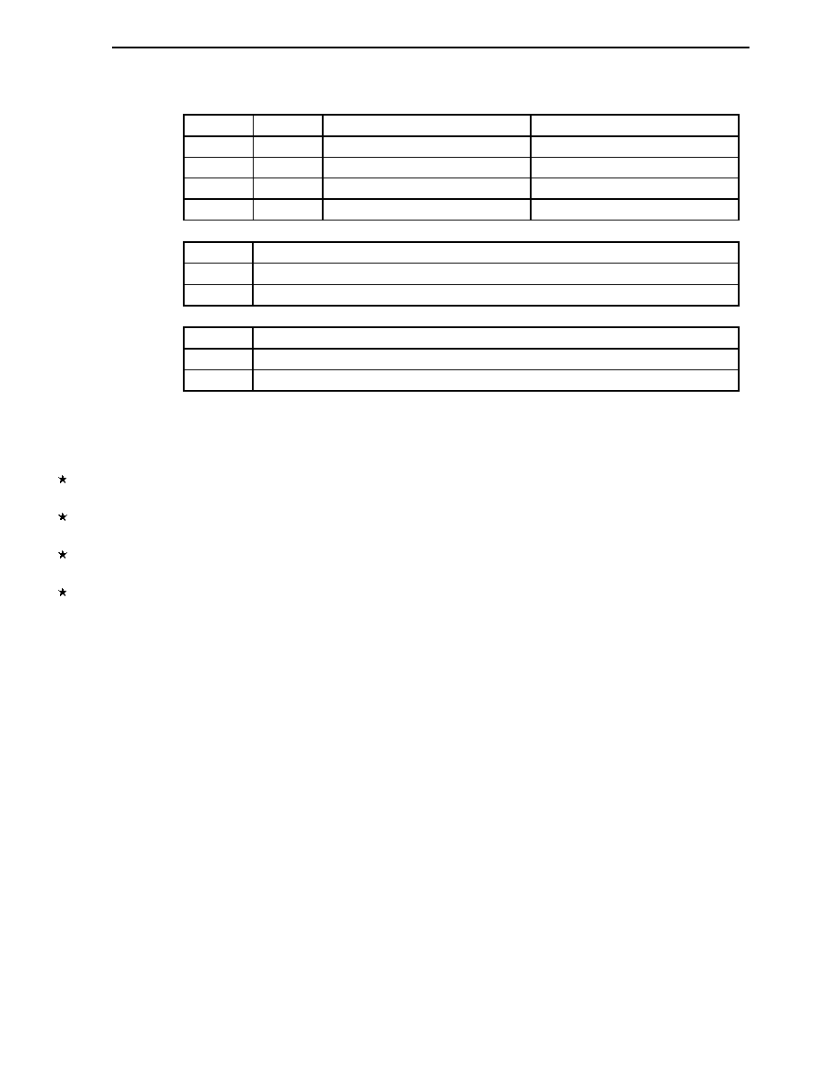
CHAPTER 13 SERIAL INTERFACE UART0
User's Manual U16228EJ2V0UD
277
Figure 13-2. Format of Asynchronous Serial Interface Operation Mode Register 0 (ASIM0) (2/2)
PS01
PS00
Transmission
operation Reception
operation
0
0
Does not output parity bit.
Reception without parity
0
1
Outputs 0 parity.
Reception as 0 parity
Note
1
0
Outputs odd parity.
Judges as odd parity.
1
1
Outputs even parity.
Judges as even parity.
CL0
Specifies character length of transmit/receive data
0
Character length of data = 7 bits
1
Character length of data = 8 bits
SL0
Specifies number of stop bits of transmit data
0
Number of stop bits = 1
1
Number of stop bits = 2
Note If "reception as 0 parity" is selected, the parity is not judged. Therefore, bit 2 (PE0) of asynchronous serial
interface reception error status register 0 (ASIS0) is not set and the error interrupt does not occur.
Cautions 1. At startup, set POWER0 to 1 and then set TXE0 to 1. To stop the operation, clear TXE0 to 0,
and then clear POWER0 to 0.
2. At startup, set POWER0 to 1 and then set RXE0 to 1. To stop the operation, clear RXE0 to 0,
and then clear POWER0 to 0.
3. Set POWER0 to 1 and then set RXE0 to 1 while a high level is input to the RxD0 pin. If
POWER0 is set to 1 and RXE0 is set to 1 while a low level is input, reception is started.
4. TXE0 and RXE0 are synchronized by the base clock (f
XCLK0
) set by BRGC0. To enable
transmission or reception again, set TXE0 or RXE0 to 1 at least two clocks of base clock after
TXE0 or RXE0 has been cleared to 0. If TXE0 or RXE0 is set within two clocks of base clock,
the transmission circuit or reception circuit may not be initialized.
5. Clear the TXE0 and RXE0 bits to 0 before rewriting the PS01, PS00, and CL0 bits.
6. Make sure that TXE0 = 0 when rewriting the SL0 bit. Reception is always performed with
"number of stop bits = 1", and therefore, is not affected by the set value of the SL0 bit.
7. Be sure to set bit 0 to 1.
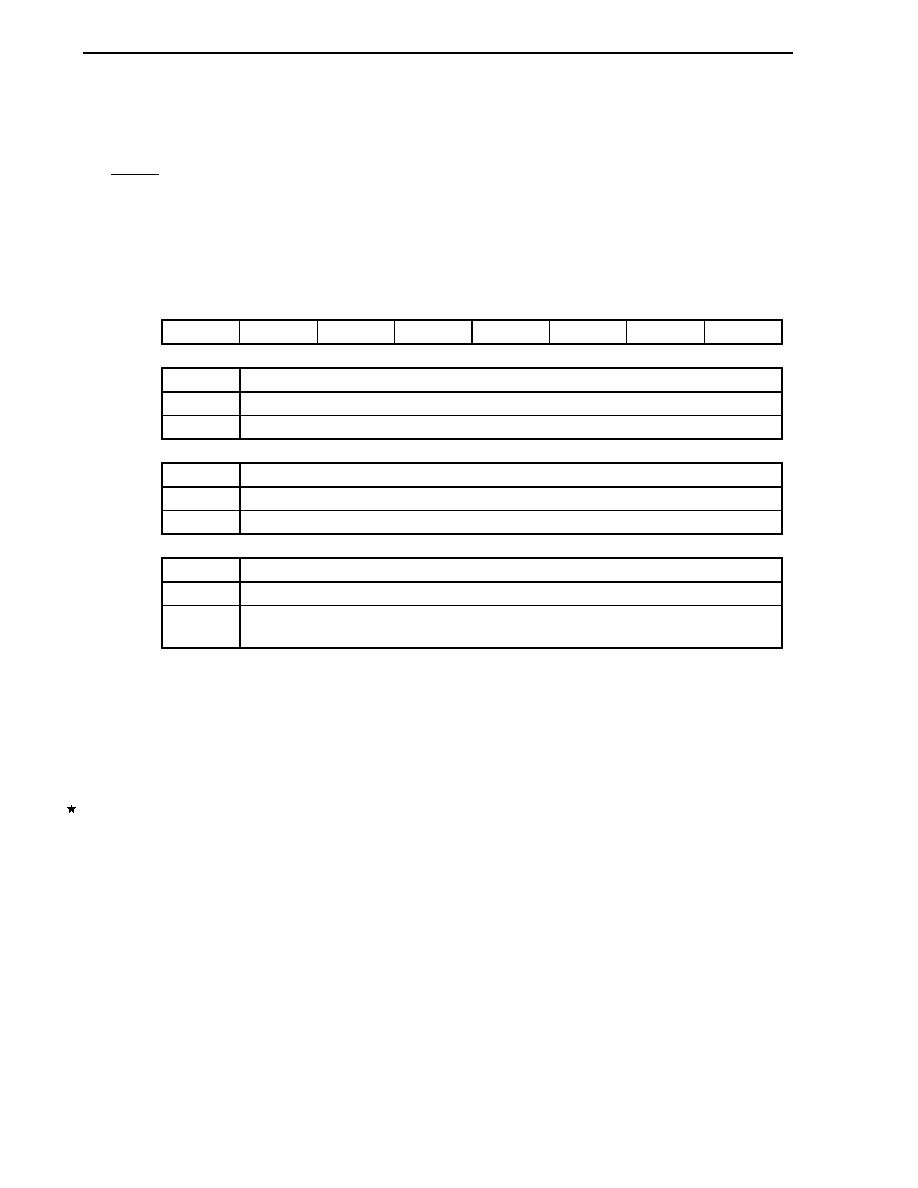
CHAPTER 13 SERIAL INTERFACE UART0
User's Manual U16228EJ2V0UD
278
(2) Asynchronous serial interface reception error status register 0 (ASIS0)
This register indicates an error status on completion of reception by serial interface UART0. It includes three
error flag bits (PE0, FE0, OVE0).
This register is read-only by an 8-bit memory manipulation instruction.
RESET input clears this register to 00H if bit 7 (POWER0) and bit 5 (RXE0) of ASIM0 = 0. 00H is read when this
register is read.
Figure 13-3. Format of Asynchronous Serial Interface Reception Error Status Register 0 (ASIS0)
Address: FF73H After reset: 00H R
Symbol
7 6 5 4 3 2 1 0
ASIS0
0 0 0 0 0
PE0
FE0
OVE0
PE0
Status flag indicating parity error
0
If POWER0 = 0 and RXE0 = 0, or if ASIS0 register is read.
1
If the parity of transmit data does not match the parity bit on completion of reception.
FE0
Status flag indicating framing error
0
If POWER0 = 0 and RXE0 = 0, or if ASIS0 register is read.
1
If the stop bit is not detected on completion of reception.
OVE0
Status flag indicating overrun error
0
If POWER0 = 0 and RXE0 = 0, or if ASIS0 register is read.
1
If receive data is set to the RXB register and the next reception operation is completed before the
data is read.
Cautions 1. The operation of the PE0 bit differs depending on the set values of the PS01 and PS00 bits of
asynchronous serial interface operation mode register 0 (ASIM0).
2. Only the first bit of the receive data is checked as the stop bit, regardless of the number of
stop bits.
3. If an overrun error occurs, the next receive data is not written to receive buffer register 0
(RXB0) but discarded.
4. If data is read from ASIS0, a wait cycle is generated. Do not read data from ASIS0 when the
CPU is operating on the subsystem clock and the X1 input clock is stopped. For details, see
CHAPTER 34 CAUTIONS FOR WAIT.

CHAPTER 13 SERIAL INTERFACE UART0
User's Manual U16228EJ2V0UD
279
(3) Baud rate generator control register 0 (BRGC0)
This register selects the base clock of serial interface UART0 and the division value of the 5-bit counter.
BRGC0 can be set by an 8-bit memory manipulation instruction.
RESET input sets this register to 1FH.
Figure 13-4. Format of Baud Rate Generator Control Register 0 (BRGC0)
Address: FF71H After reset: 1FH R/W
Symbol
7 6 5 4 3 2 1 0
BRGC0 TPS01 TPS00
0
MDL04 MDL03 MDL02 MDL01 MDL00
TPS01
TPS00
Base
clock
(f
XCLK0
) selection
0
0
TM50
output
Note
0
1
f
X
/2 (5 MHz)
1
0
f
X
/2
3
(1.25 MHz)
1
1
f
X
/2
5
(312.5 kHz)
MDL04 MDL03 MDL02 MDL01 MDL00 k Selection of 5-bit counter
output clock
0
0
◊
◊
◊
◊
Setting prohibited
0 1 0 0 0
8
f
XCLK0
/8
0 1 0 0 1
9
f
XCLK0
/9
0 1 0 1 0
10
f
XCLK0
/10
∑
∑
∑
∑
∑
∑
∑
∑
∑
∑
∑
∑
∑
∑
∑
∑
∑
∑
∑
∑
∑
∑
∑
∑
∑
∑
∑
∑
∑
∑
∑
∑
∑
∑
∑
1 1 0 1 0
26
f
XCLK0
/26
1 1 0 1 1
27
f
XCLK0
/27
1 1 1 0 0
28
f
XCLK0
/28
1 1 1 1 0
30
f
XCLK0
/30
1 1 1 1 1
31
f
XCLK0
/31
Note To select the TM50 output as the base clock, start an operation by setting 8-bit timer/event counter 50 so
that the duty is 50% of the output in the PWM mode (bit 6 (TMC506) of the TMC50 register = 1), and then
clear TPS01 and TPS00 to 0. It is not necessary to enable the TO50 pin as a timer output pin (bit 0
(TOE50) of the TMC register may be 0 or 1).
Cautions 1. When the Ring-OSC clock is selected as the clock to be supplied to the CPU, the clock of the
Ring-OSC oscillator is divided and supplied as the count clock. If the base clock is the Ring-
OSC clock, the operation of serial interface UART0 is not guaranteed.
2. Make sure that bit 6 (TXE0) and bit 5 (RXE0) of the ASIM0 register = 0 when rewriting the
MDL04 to MDL00 bits.
3. The baud rate value is the output clock of the 5-bit counter divided by 2.
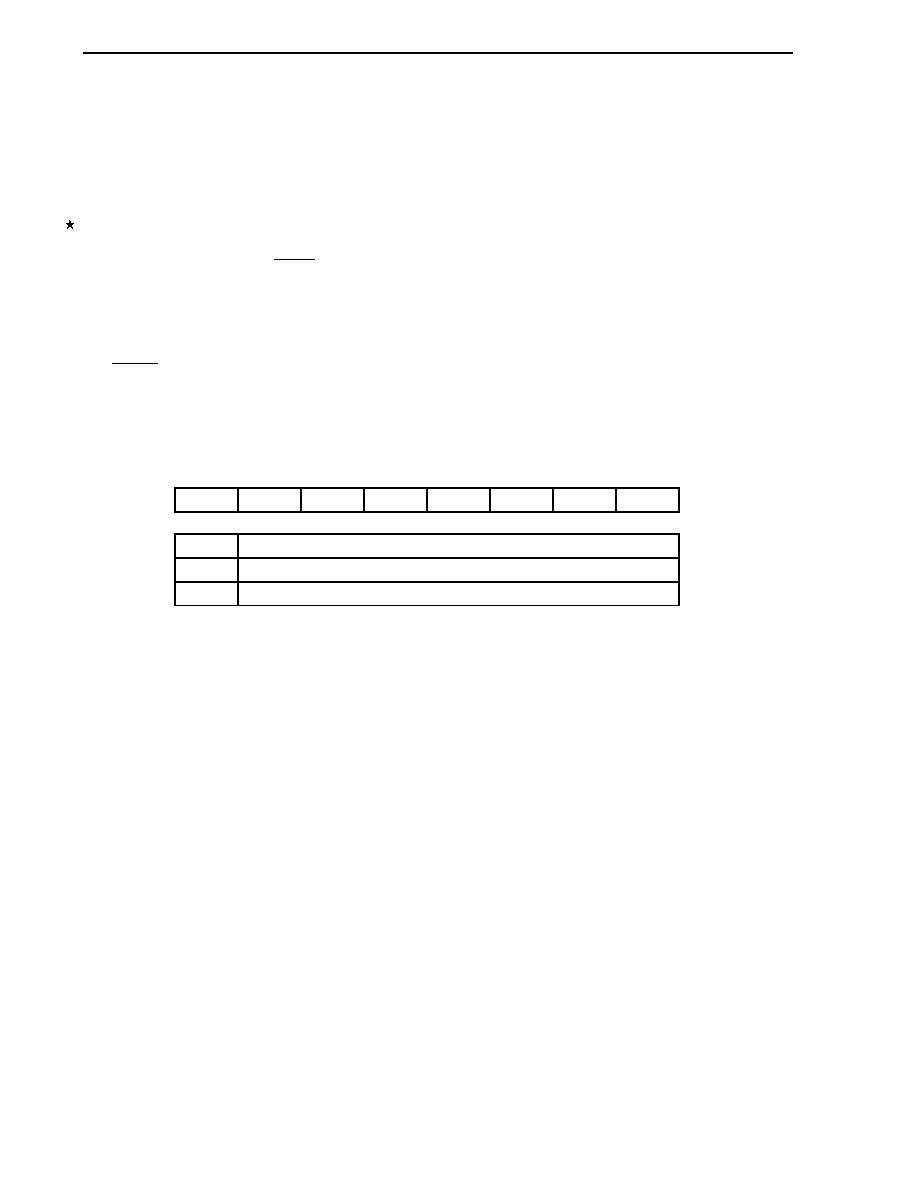
CHAPTER 13 SERIAL INTERFACE UART0
User's Manual U16228EJ2V0UD
280
Remarks 1. f
XCLK0
: Frequency of base clock selected by the TPS01 and TPS00 bits
2. f
X
:
X1 input clock oscillation frequency
3. k:
Value set by the MDL04 to MDL00 bits (k = 8, 9, 10, ..., 31)
4.
◊
: Don't
care
5. Figures in parentheses apply to operation at f
X
= 10 MHz
(4) Port mode register 1 (PM1)
This register sets port 1 input/output in 1-bit units.
When using the P10/TxD0/SCK10 pin for serial interface data output, clear PM10 to 0 and set the output latch of
P10 to 1.
When using the P11/RxD0/SI10 pin for serial interface data input, set PM11 to 1. The output latch of P11 at this
time may be 0 or 1.
PM1 can be set by a 1-bit or 8-bit memory manipulation instruction.
RESET input sets this register to FFH.
Figure 13-5. Format of Port Mode Register 1 (PM1)
Address: FF21H After reset: FFH R/W
Symbol
7 6 5 4 3 2 1 0
PM1
PM17 PM16 PM15 PM14 PM13 PM12 PM11 PM10
PM1n
P1n pin I/O mode selection (n = 0 to 7)
0
Output mode (output buffer on)
1
Input mode (output buffer off)
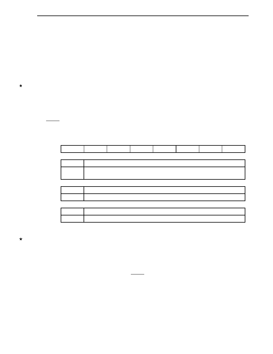
CHAPTER 13 SERIAL INTERFACE UART0
User's Manual U16228EJ2V0UD
281
13.4 Operation of Serial Interface UART0
Serial interface UART0 has the following two modes.
∑
Operation stop mode
∑
Asynchronous serial interface (UART) mode
13.4.1 Operation stop mode
In this mode, serial communication cannot be executed, thus reducing the power consumption. In addition, the
pins can be used as ordinary port pins in this mode. To set the operation stop mode, clear bits 7, 6, and 5 (POWER0,
TXE0, and RXE0) of ASIM0 to 0.
(1) Register
used
The operation stop mode is set by asynchronous serial interface operation mode register 0 (ASIM0).
ASIM0 can be set by a 1-bit or 8-bit memory manipulation instruction.
RESET input sets this register to 01H.
Address: FF70H After reset: 01H R/W
Symbol
<7>
<6>
<5>
4 3 2 1 0
ASIM0 POWER0 TXE0
RXE0
PS01
PS00
CL0
SL0
1
POWER0
Enables/disables
operation of internal operation clock
0
Note 1
Disables operation of the internal operation clock (fixes the clock to low level) and asynchronously
resets the internal circuit
Note 2
.
TXE0
Enables/disables
transmission
0
Disables
transmission
(synchronously resets the transmission circuit).
RXE0
Enables/disables
reception
0
Disables
reception
(synchronously resets the reception circuit).
Notes 1. The input from the R
X
D0 pin is fixed to high level when POWER0 = 0.
2. Asynchronous serial interface reception error status register 0 (ASIS0), transmit shift register 0 (TXS0),
and receive buffer register 0 (RXB0) are reset.
Caution Clear POWER0 to 0 after clearing TXE0 and RXE0 to 0 to set the operation stop mode.
To start the operation, set POWER0 to 1, and then set TXE0 and RXE0 to 1.
Remark To use the RxD0/SI10/P11 and TxD0/SCK10/P10 pins as general-purpose port pins, see CHAPTER 4
PORT FUNCTIONS.
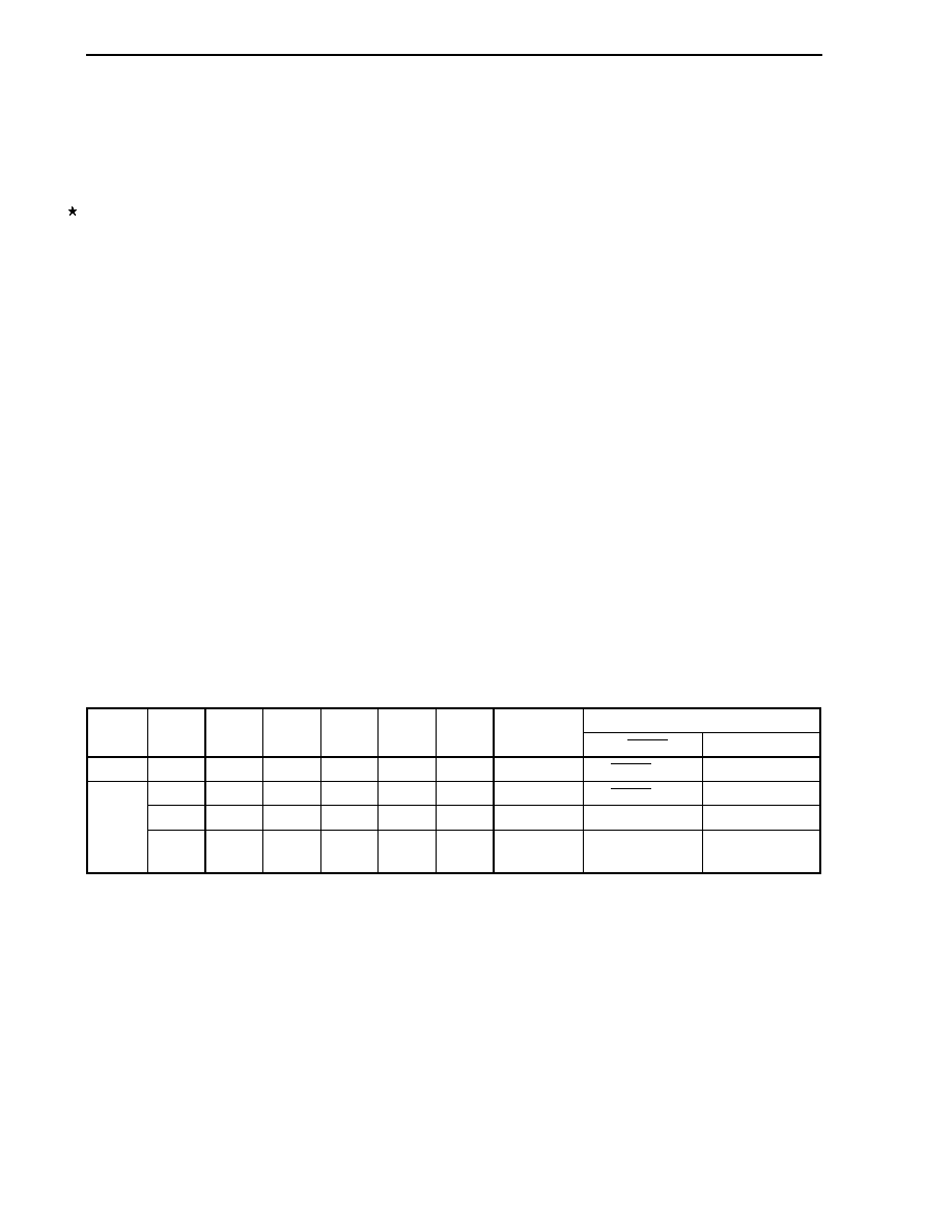
CHAPTER 13 SERIAL INTERFACE UART0
User's Manual U16228EJ2V0UD
282
13.4.2 Asynchronous serial interface (UART) mode
In this mode, 1-byte data is transmitted/received following a start bit, and a full-duplex operation can be performed.
A dedicated UART baud rate generator is incorporated, so that communication can be executed at a wide range of
baud rates.
(1) Registers
used
∑
Asynchronous serial interface operation mode register 0 (ASIM0)
∑
Asynchronous serial interface reception error status register 0 (ASIS0)
∑
Baud rate generator control register 0 (BRGC0)
∑
Port mode register 1 (PM1)
∑
Port register 1 (P1)
The basic procedure of setting an operation in the UART mode is as follows.
<1> Set the BRGC0 register (see Figure 13-4).
<2> Set bits 1 to 4 (SL0, CL0, PS00, and PS01) of the ASIM0 register (see Figure 13-2).
<3> Set bit 7 (POWER0) of the ASIM0 register to 1.
<4> Set bit 6 (TXE0) of the ASIM0 register to 1.
Transmission is enabled.
Set bit 5 (RXE0) of the ASIM0 register to 1.
Reception is enabled.
<5> Write data to the TXS0 register.
Data transmission is started.
Caution Take relationship with the other party of communication when setting the port mode register
and port register.
The relationship between the register settings and pins is shown below.
Table 13-2. Relationship Between Register Settings and Pins
Pin Function
POWER0
TXE0 RXE0 PM10 P10 PM11 P11
UART0
Operation
TxD0/SCK10/P10 RxD0/SI10/P11
0 0 0
◊
Note
◊
Note
◊
Note
◊
Note
Stop SCK10/P10 SI10/P11
0 1
◊
Note
◊
Note
1 ◊ Reception SCK10/P10
RxD0
1 0 0 1
◊
Note
◊
Note
Transmission
TxD0
SI10/P11
1
1 1 0 1 1 ◊
Transmission/
reception
TxD0 RxD0
Note Can be set as port function.
Remark ◊:
don't
care
POWER0: Bit 7 of asynchronous serial interface operation mode register 0 (ASIM0)
TXE0:
Bit 6 of ASIM0
RXE0:
Bit 5 of ASIM0
PM1◊:
Port mode register
P1◊:
Port output latch
CHAPTER 13 SERIAL INTERFACE UART0
User's Manual U16228EJ2V0UD
283
(2) Communication
operation
(a) Format and waveform example of normal transmit/receive data
Figures 13-6 and 13-7 show the format and waveform example of the normal transmit/receive data.
Figure 13-6. Format of Normal UART Transmit/Receive Data
Start
bit
Parity
bit
D0
D1
D2
D3
D4
1 data frame
Character bits
D5
D6
D7
Stop bit
One data frame consists of the following bits.
∑
Start bit ... 1 bit
∑
Character bits ... 7 or 8 bits (LSB first)
∑
Parity bit ... Even parity, odd parity, 0 parity, or no parity
∑
Stop bit ... 1 or 2 bits
The character bit length, parity, and stop bit length in one data frame are specified by asynchronous serial
interface operation mode register 0 (ASIM0).
Figure 13-7. Example of Normal UART Transmit/Receive Data Waveform
1. Data length: 8 bits, Parity: Even parity, Stop bit: 1 bit, Communication data: 55H
1 data frame
Start
D0
D1
D2
D3
D4
D5
D6
D7
Parity
Stop
2. Data length: 7 bits, Parity: Odd parity, Stop bit: 2 bits, Communication data: 36H
1 data frame
Start
D0
D1
D2
D3
D4
D5
D6
Parity
Stop
Stop
3. Data length: 8 bits, Parity: None, Stop bit: 1 bit, Communication data: 87H
1 data frame
Start
D0
D1
D2
D3
D4
D5
D6
D7
Stop

CHAPTER 13 SERIAL INTERFACE UART0
User's Manual U16228EJ2V0UD
284
(b) Parity types and operation
The parity bit is used to detect a bit error in communication data. Usually, the same type of parity bit is used
on both the transmission and reception sides. With even parity and odd parity, a 1-bit (odd number) error
can be detected. With zero parity and no parity, an error cannot be detected.
(i) Even
parity
∑
Transmission
Transmit data, including the parity bit, is controlled so that the number of bits that are "1" is even.
The value of the parity bit is as follows.
If transmit data has an odd number of bits that are "1": 1
If transmit data has an even number of bits that are "1": 0
∑
Reception
The number of bits that are "1" in the receive data, including the parity bit, is counted. If it is odd, a
parity error occurs.
(ii) Odd
parity
∑
Transmission
Unlike even parity, transmit data, including the parity bit, is controlled so that the number of bits that
are "1" is odd.
If transmit data has an odd number of bits that are "1": 0
If transmit data has an even number of bits that are "1": 1
∑
Reception
The number of bits that are "1" in the receive data, including the parity bit, is counted. If it is even, a
parity error occurs.
(iii) 0 parity
The parity bit is cleared to 0 when data is transmitted, regardless of the transmit data.
The parity bit is not detected when the data is received. Therefore, a parity error does not occur
regardless of whether the parity bit is "0" or "1".
(iv) No parity
No parity bit is appended to the transmit data.
Reception is performed assuming that there is no parity bit when data is received. Because there is no
parity bit, a parity error does not occur.
CHAPTER 13 SERIAL INTERFACE UART0
User's Manual U16228EJ2V0UD
285
(c) Transmission
The T
X
D0 pin outputs a high level when bit 7 (POWER0) of asynchronous serial interface operation mode
register 0 (ASIM0) is set to 1. If bit 6 (TXE0) of ASIM0 is then set to 1, transmission is enabled.
Transmission can be started by writing transmit data to transmit shift register 0 (TXS0). The start bit, parity
bit, and stop bit are automatically appended to the data.
When transmission is started, the start bit is output from the T
X
D0 pin, followed by the rest of the data in
order starting from the LSB. When transmission is completed, the parity and stop bits set by ASIM0 are
appended and a transmission completion interrupt request (INTST0) is generated.
Transmission is stopped until the data to be transmitted next is written to TXS0.
Figure 13-8 shows the timing of the transmission completion interrupt request (INTST0). This interrupt
occurs as soon as the last stop bit has been output.
Caution After transmit data is written to TXS0, do not write the next transmit data before the
transmission completion interrupt signal (INTST0) is generated.
Figure 13-8. Transmission Completion Interrupt Request Timing
1. Stop bit length: 1
INTST0
D0
Start
D1
D2
D6
D7
Stop
T
X
D0 (output)
Parity
2. Stop bit length: 2
T
X
D0 (output)
INTST0
D0
Start
D1
D2
D6
D7
Parity
Stop

CHAPTER 13 SERIAL INTERFACE UART0
User's Manual U16228EJ2V0UD
286
(d) Reception
Reception is enabled and the R
X
D0 pin input is sampled when bit 7 (POWER0) of asynchronous serial
interface operation mode register 0 (ASIM0) is set to 1 and then bit 5 (RXE0) of ASIM0 is set to 1.
The 5-bit counter of the baud rate generator starts counting when the falling edge of the R
X
D0 pin input is
detected. When the set value of baud rate generator control register 0 (BRGC0) has been counted, the
R
X
D0 pin input is sampled again ( in Figure 13-9). If the R
X
D0 pin is low level at this time, it is recognized
as a start bit.
When the start bit is detected, reception is started, and serial data is sequentially stored in receive shift
register 0 (RXS0) at the set baud rate. When the stop bit has been received, the reception completion
interrupt (INTSR0) is generated and the data of RXS0 is written to receive buffer register 0 (RXB0). If an
overrun error (OVE0) occurs, however, the receive data is not written to RXB0.
Even if a parity error (PE0) occurs while reception is in progress, reception continues to the reception
position of the stop bit, and an error interrupt (INTSR0) is generated after completion of reception.
Figure 13-9. Reception Completion Interrupt Request Timing
R
X
D0 (input)
INTSR0
Start
D0
D1
D2
D3
D4
D5
D6
D7
Parity
Stop
RXB0
Cautions 1. Be sure to read receive buffer register 0 (RXB0) even if a reception error occurs.
Otherwise, an overrun error will occur when the next data is received, and the reception
error status will persist.
2. Reception is always performed with the "number of stop bits = 1". The second stop bit
is ignored.
3. Be sure to read asynchronous serial interface reception error status register 0 (ASIS0)
before reading RXB0.
CHAPTER 13 SERIAL INTERFACE UART0
User's Manual U16228EJ2V0UD
287
(e) Reception
error
Three types of errors may occur during reception: a parity error, framing error, or overrun error. If the error
flag of asynchronous serial interface reception error status register 0 (ASIS0) is set as a result of data
reception, a reception error interrupt request (INTSR0) is generated.
Which error has occurred during reception can be identified by reading the contents of ASIS0 in the reception
error interrupt servicing (INTSR0) (see Figure 13-3).
The contents of ASIS0 are reset to 0 when ASIS0 is read.
Table 13-3. Cause of Reception Error
Reception Error
Cause
Parity error
The parity specified for transmission does not match the parity of the receive data.
Framing error
Stop bit is not detected.
Overrun error
Reception of the next data is completed before data is read from receive buffer
register 0 (RXB0).
(f) Noise filter of receive data
The R
X
D0 signal is sampled using the base clock output by the prescaler block.
If two sampled values are the same, the output of the match detector changes, and the data is sampled as
input data.
Because the circuit is configured as shown in Figure 13-10, the internal processing of the reception operation
is delayed by two clocks from the external signal status.
Figure 13-10. Noise Filter Circuit
Internal signal B
Internal signal A
Match detector
In
Base clock
R
X
D0/SI10/P11
Q
In
LD_EN
Q
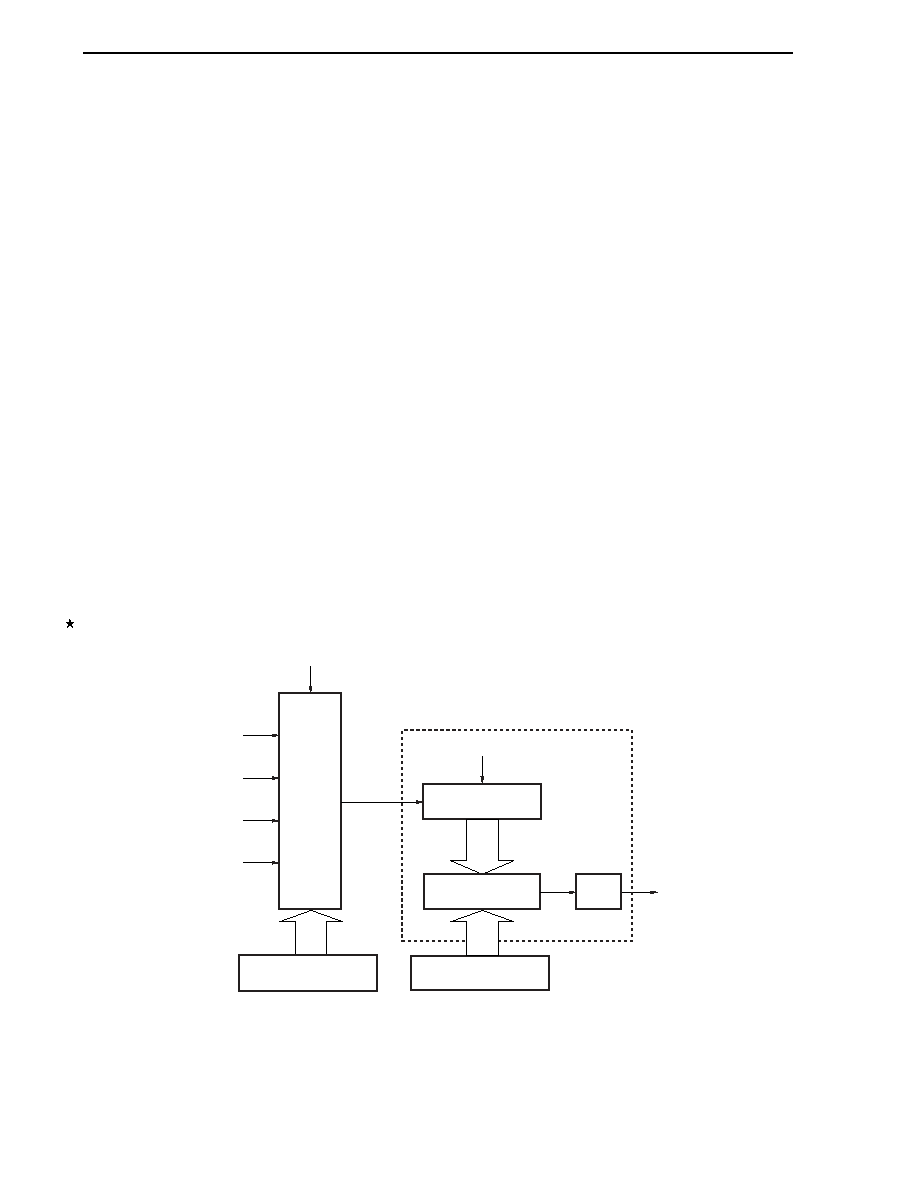
CHAPTER 13 SERIAL INTERFACE UART0
User's Manual U16228EJ2V0UD
288
13.4.3 Dedicated baud rate generator
The dedicated baud rate generator consists of a source clock selector and a 5-bit programmable counter, and
generates a serial clock for transmission/reception of UART0.
Separate 5-bit counters are provided for transmission and reception.
(1) Configuration of baud rate generator
∑
Base
clock
The clock selected by bits 7 and 6 (TPS01 and TPS00) of baud rate generator control register 0 (BRGC0) is
supplied to each module when bit 7 (POWER0) of asynchronous serial interface operation mode register 0
(ASIM0) is 1. This clock is called the base clock and its frequency is called f
XCLK0
. The base clock is fixed
to low level when POWER0 = 0.
∑
Transmission
counter
This counter stops operation, cleared to 0, when bit 7 (POWER0) or bit 6 (TXE0) of asynchronous serial
interface operation mode register 0 (ASIM0) is 0.
It starts counting when POWER0 = 1 and TXE0 = 1.
The counter is cleared to 0 when the first data transmitted is written to transmit shift register 0 (TXS0).
∑
Reception
counter
This counter stops operation, cleared to 0, when bit 7 (POWER0) or bit 5 (RXE0) of asynchronous serial
interface operation mode register 0 (ASIM0) is 0.
It starts counting when the start bit has been detected.
The counter stops operation after one frame has been received, until the next start bit is detected.
Figure 13-11. Configuration of Baud Rate Generator
f
XCLK0
Selector
POWER0
5-bit counter
Match detector
Baud rate
BRGC0: MDL04 to MDL00
1/2
POWER0, TXE0 (or RXE0)
BRGC0: TPS01, TPS00
8-bit timer/
event counter
50 output
f
X
/2
5
f
X
/2
f
X
/2
3
Baud rate generator
Remark POWER0: Bit 7 of asynchronous serial interface operation mode register 0 (ASIM0)
TXE0:
Bit 6 of ASIM0
RXE0:
Bit 5 of ASIM0
BRGC0:
Baud rate generator control register 0

CHAPTER 13 SERIAL INTERFACE UART0
User's Manual U16228EJ2V0UD
289
(2) Generation of serial clock
A serial clock can be generated by using baud rate generator control register 0 (BRGC0).
Select the clock to be input to the 5-bit counter by using bits 7 and 6 (TPS01 and TPS00) of BRGC0.
Bits 4 to 0 (MDL04 to MDL00) of BRGC0 can be used to select the division value of the 5-bit counter.
(a) Baud
rate
The baud rate can be calculated by the following expression.
∑
Baud rate = [bps]
f
XCLK0
: Frequency of base clock selected by the TPS01 and TPS00 bits of the BRGC0 register
k:
Value set by the MDL04 to MDL00 bits of the BRGC0 register (k = 8, 9, 10, ..., 31)
(b) Error of baud rate
The baud rate error can be calculated by the following expression.
∑
Error (%) =
-
1
◊
100 [%]
Cautions 1. Keep the baud rate error during transmission to within the permissible error range at
the reception destination.
2. Make sure that the baud rate error during reception satisfies the range shown in (4)
Permissible baud rate range during reception.
Example: Frequency of base clock = 2.5 MHz = 2,500,000 Hz
Set value of MDL04 to MDL00 bits of BRGC0 register = 10000B (k = 16)
Target baud rate = 76,800 bps
Baud rate = 2.5 M/(2
◊
16)
=
2,500,000/(2
◊
16) = 78,125 [bps]
Error = (78,125/76,800
-
1)
◊
100
= 1.725 [%]
f
XCLK0
2
◊
k
Actual baud rate (baud rate with error)
Desired baud rate (correct baud rate)
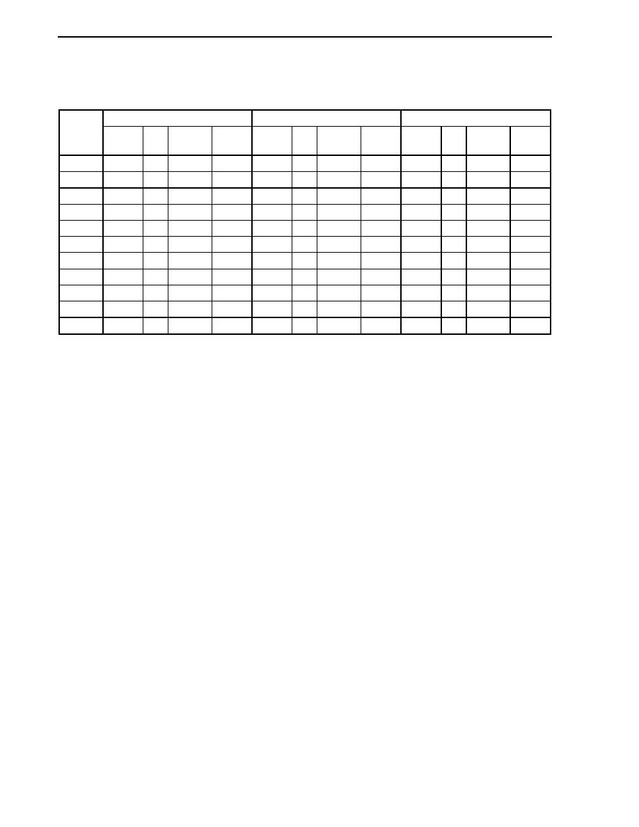
CHAPTER 13 SERIAL INTERFACE UART0
User's Manual U16228EJ2V0UD
290
(3) Example of setting baud rate
Table 13-4. Set Data of Baud Rate Generator
f
X
= 10.0 MHz
f
X
= 8.38 MHz
f
X
= 4.19 MHz
Baud Rate
[bps]
TPS01,
TPS00
k
Calculated
Value
ERR[%]
TPS01,
TPS00
k
Calculated
Value
ERR[%]
TPS01,
TPS00
k
Calculated
Value
ERR[%]
2400
-
-
-
-
-
-
-
-
3 27
2425 1.03
4800
-
-
-
-
3 27
4850 1.03 3 14
4676
-
2.58
9600
3 16 9766 1.73
3 14 9353
-
2.58 2 27
9699 1.03
10400
3 15 10417 0.16
3 13 10072
-
3.15 2 25
10475
0.72
19200 3 8 19531 1.73
2 27
19398 1.03
2 14
18705
-
2.58
31250
2 20 31250
0
2 17 30809
-
1.41
-
-
-
-
38400
2 16 39063 1.73
2 14 38796
-
2.58 2 27
38796
1.03
76800 2 8 78125 1.73
1 27
77593 1.03
1 14
74821
-
2.58
115200 1 22
113636
-
1.36
1 18
116389 1.03
1
9 116389 1.03
153600
1
16 156250 1.73
1
14 149643
-
2.58
-
-
-
-
230400 1 11
227273
-
1.36 1 9
232778
1.03
-
-
-
-
Remark TPS01, TPS00: Bits 7 and 6 of baud rate generator control register 0 (BRGC0) (setting of base clock
(f
XCLK0
))
k:
Value set by the MDL04 to MDL00 bits of BRGC0 (k = 8, 9, 10, ..., 31)
f
X
:
X1 input clock oscillation frequency
ERR:
Baud rate error

CHAPTER 13 SERIAL INTERFACE UART0
User's Manual U16228EJ2V0UD
291
(4) Permissible baud rate range during reception
The permissible error from the baud rate at the transmission destination during reception is shown below.
Caution Make sure that the baud rate error during reception is within the permissible error range, by
using the calculation expression shown below.
Figure 13-12. Permissible Baud Rate Range During Reception
FL
1 data frame (11
◊
FL)
FLmin
FLmax
Data frame length
of UART0
Start bit
Bit 0
Bit 1
Bit 7
Parity bit
Minimum permissible
data frame length
Maximum permissible
data frame length
Stop bit
Start bit
Bit 0
Bit 1
Bit 7
Parity bit
Latch timing
Stop bit
Start bit
Bit 0
Bit 1
Bit 7
Parity bit
Stop bit
As shown in Figure 13-12, the latch timing of the receive data is determined by the counter set by baud rate
generator control register 0 (BRGC0) after the start bit has been detected. If the last data (stop bit) meets this
latch timing, the data can be correctly received.
Assuming that 11-bit data is received, the theoretical values can be calculated as follows.
FL = (Brate)
-
1
Brate: Baud rate of UART0
k:
Set value of BRGC0
FL: 1-bit
data
length
Margin of latch timing: 2 clocks

CHAPTER 13 SERIAL INTERFACE UART0
User's Manual U16228EJ2V0UD
292
Minimum permissible data frame length: FLmin = 11
◊
FL
-
◊
FL = FL
Therefore, the maximum receivable baud rate at the transmission destination is as follows.
BRmax = (FLmin/11)
-
1
= Brate
Similarly, the maximum permissible data frame length can be calculated as follows.
10
k + 2
21k
-
2
11
2
◊
k
2
◊
k
FLmax = FL
◊
11
Therefore, the minimum receivable baud rate at the transmission destination is as follows.
BRmin = (FLmax/11)
-
1
= Brate
The permissible baud rate error between UART0 and the transmission destination can be calculated from the
above minimum and maximum baud rate expressions, as follows.
Table 13-5. Maximum/Minimum Permissible Baud Rate Error
Division Ratio (k)
Maximum Permissible Baud Rate Error
Minimum Permissible Baud Rate Error
8 +3.53%
-
3.61%
16 +4.14%
-
4.19%
24 +4.34%
-
4.38%
31 +4.44%
-
4.47%
Remarks 1. The permissible error of reception depends on the number of bits in one frame, input clock
frequency, and division ratio (k). The higher the input clock frequency and the higher the division
ratio (k), the higher the permissible error.
2. k: Set value of BRGC0
k
-
2
2k
21k + 2
2k
22k
21k + 2
◊
FLmax = 11
◊
FL
-
◊
FL = FL
21k ≠ 2
20k
20k
21k
-
2

User's Manual U16228EJ2V0UD
293
CHAPTER 14 SERIAL INTERFACE UART6
14.1 Functions of Serial Interface UART6
Serial interface UART6 has the following two modes.
(1) Operation stop mode
This mode is used when serial communication is not executed and can enable a reduction in the power
consumption.
For details, see 14.4.1 Operation stop mode.
(2) Asynchronous serial interface (UART) mode
This mode supports the LIN (Local Interconnect Network)-bus. The functions of this mode are outlined below.
For details, see 14.4.2 Asynchronous serial interface (UART) mode and 14.4.3 Dedicated baud rate
generator.
∑
Two-pin
configuration T
X
D6: Transmit data output pin
R
X
B6: Receive data input pin
∑
Data length of communication data can be selected from 7 or 8 bits.
∑
Dedicated internal 8-bit baud rate generator allowing any baud rate to be set
∑
Transmission and reception can be performed independently.
∑
Twelve operating clock inputs selectable
∑
MSB- or LSB-first communication selectable
∑
Inverted transmission operation
∑
Synchronous break field transmission from 13 to 20 bits
∑
More than 11 bits can be identified for synchronous break field reception (SBF reception flag provided).
Cautions 1. The T
X
D6 output inversion function inverts only the transmission side and not the reception
side. To use this function, the reception side must be ready for reception of inverted data.
2. If clock supply to serial interface UART6 is not stopped (e.g., in the HALT mode), normal
operation continues. If clock supply to serial interface UART6 is stopped (e.g., in the STOP
mode), each register stops operating, and holds the value immediately before clock supply
was stopped. The T
X
D6 pin also holds the value immediately before clock supply was
stopped and outputs it. However, the operation is not guaranteed after clock supply is
resumed. Therefore, reset the circuit so that POWER6 = 0, RXE6 = 0, and TXE6 = 0.
3. If data is continuously transmitted, the communication timing from the stop bit to the next
start bit is extended two operating clocks of the macro. However, this does not affect the
result of communication because the reception side initializes the timing when it has
detected a start bit. Do not use the continuous transmission function if the interface is
incorporated in LIN.

CHAPTER 14 SERIAL INTERFACE UART6
User's Manual U16228EJ2V0UD
294
Remark LIN stands for Local Interconnect Network and is a low-speed (1 to 20 kbps) serial communication
protocol intended to aid the cost reduction of an automotive network.
LIN communication is single-master communication, and up to 15 slaves can be connected to one
master.
The LIN slaves are used to control the switches, actuators, and sensors, and these are connected to the
LIN master via the LIN network.
Normally, the LIN master is connected to a network such as CAN (Controller Area Network).
In addition, the LIN bus uses a single-wire method and is connected to the nodes via a transceiver that
complies with ISO9141.
In the LIN protocol, the master transmits a frame with baud rate information and the slave receives it and
corrects the baud rate error. Therefore, communication is possible when the baud rate error in the slave
is
±
15% or less.
Figures 14-1 and 14-2 outline the transmission and reception operations of LIN.
Figure 14-1. LIN Transmission Operation
Sleep
bus
Wakeup
signal frame
8 bits
Note 1
55H
transmission
Data
transmission
Data
transmission
Data
transmission
Data
transmission
13-bit
Note 2
SBF
transmission
Note 3
Synchronous
break field
Synchronous
field
Indent
field
Data field
Data field
Checksum
field
TX6
INTST6
Notes 1. The wakeup signal frame is substituted by 80H transmission in the 8-bit mode.
2. The synchronous break field is output by hardware. The output width is adjusted by baud rate
generator control register 6 (BRGC6) (see 14.4.2 (2) (h) SBF transmission).
3. INTST6 is output on completion of each transmission. It is also output when SBF is transmitted.
Remark The interval between each field is controlled by software.
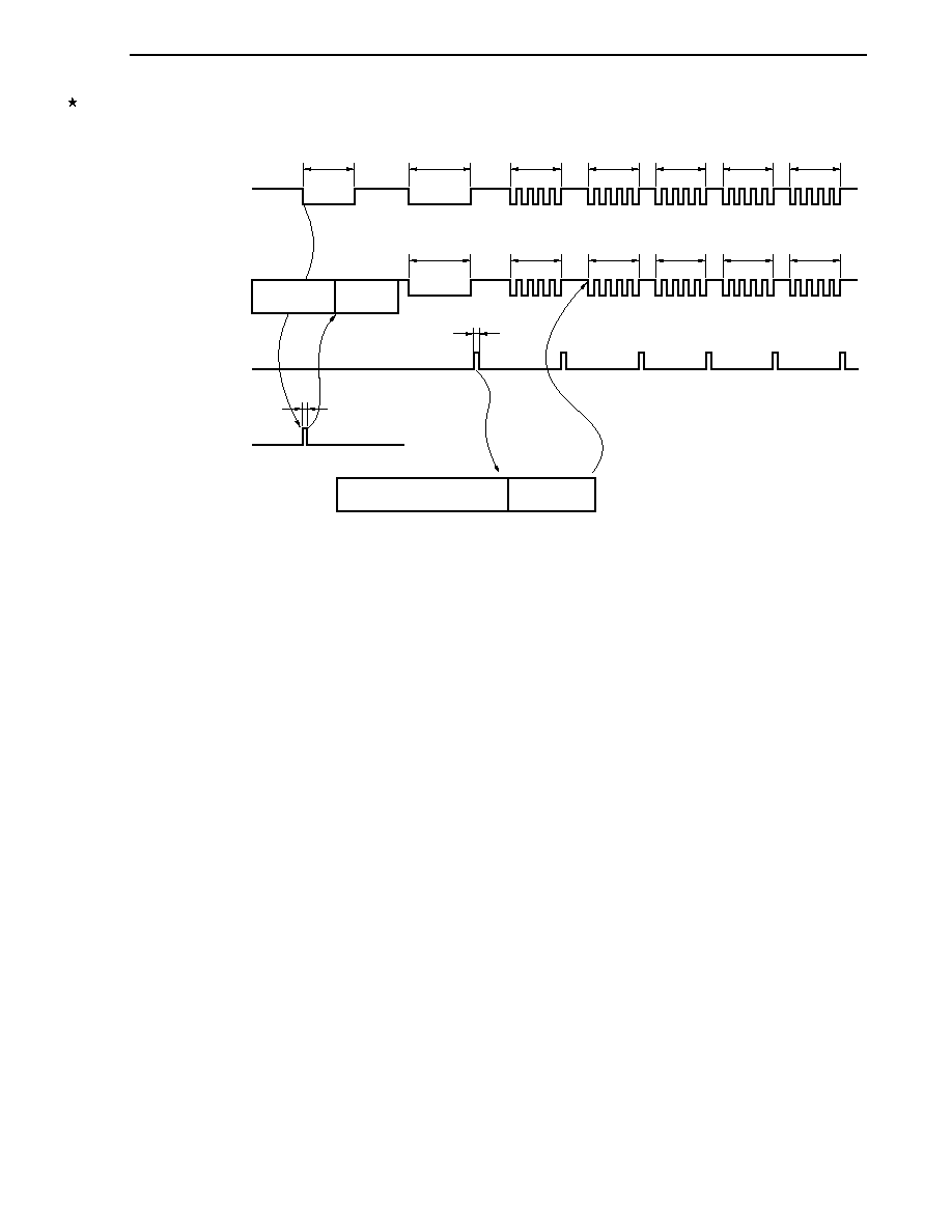
CHAPTER 14 SERIAL INTERFACE UART6
User's Manual U16228EJ2V0UD
295
Figure 14-2. LIN Reception Operation
Sleep
bus
13 bits
Note 2
SF
reception
ID
reception
Data
reception
Data
reception
Data
reception
Note 5
Note 3
Note 1
Note 4
Wakeup
signal frame
Synchronous
break field
Synchronous
field
Indent
field
Data field
Data field
Checksum
field
RX6
SBF
reception
Reception interrupt
(INTSR6)
Edge detection
(INTP0)
Capture timer
Disable
Enable
Disable
Enable
Notes 1. The wakeup signal is detected at the edge of the pin, and enables UART6 and sets the SBF reception
mode.
2. Reception continues until the STOP bit is detected. When an SBF with low-level data of 11 bits or
more has been detected, it is assumed that SBF reception has been completed correctly, and an
interrupt signal is output. If an SBF with low-level data of less than 11 bits has been detected, it is
assumed that an SBF reception error has occurred. The interrupt signal is not output and the SBF
reception mode is restored.
3. If SBF reception has been completed correctly, an interrupt signal is output. This SBF reception
completion interrupt enables the capture timer. Detection of errors OVE6, PE6, and FE6 is
suppressed, and error detection processing of UART communication and data transfer of the shift
register and RXB6 is not performed. The shift register holds the reset value FFH.
4. Calculate the baud rate error from the bit length of the synchronous field, disable UART6 after SF
reception, and then re-set baud rate generator control register 6 (BRGC6).
5. Distinguish the checksum field by software. Also perform processing by software to initialize UART6
after reception of the checksum field and to set the SBF reception mode again.
To perform a LIN receive operation, use a configuration like the one shown in Figure 14-3.
The wakeup signal transmitted from the LIN master is received by detecting the edge of the external interrupt
(INTP0). The length of the synchronous field transmitted from the LIN master can be measured using the external
event capture operation of 16-bit timer/event counter 00, and the baud rate error can be calculated.
The input signal of the reception port input (RxD6) can be input to the external interrupt (INTP0) and 16-bit
timer/event counter 00 by port input switch control (ISC0/ISC1), without connecting RxD6 and INTP0/TI000 externally.
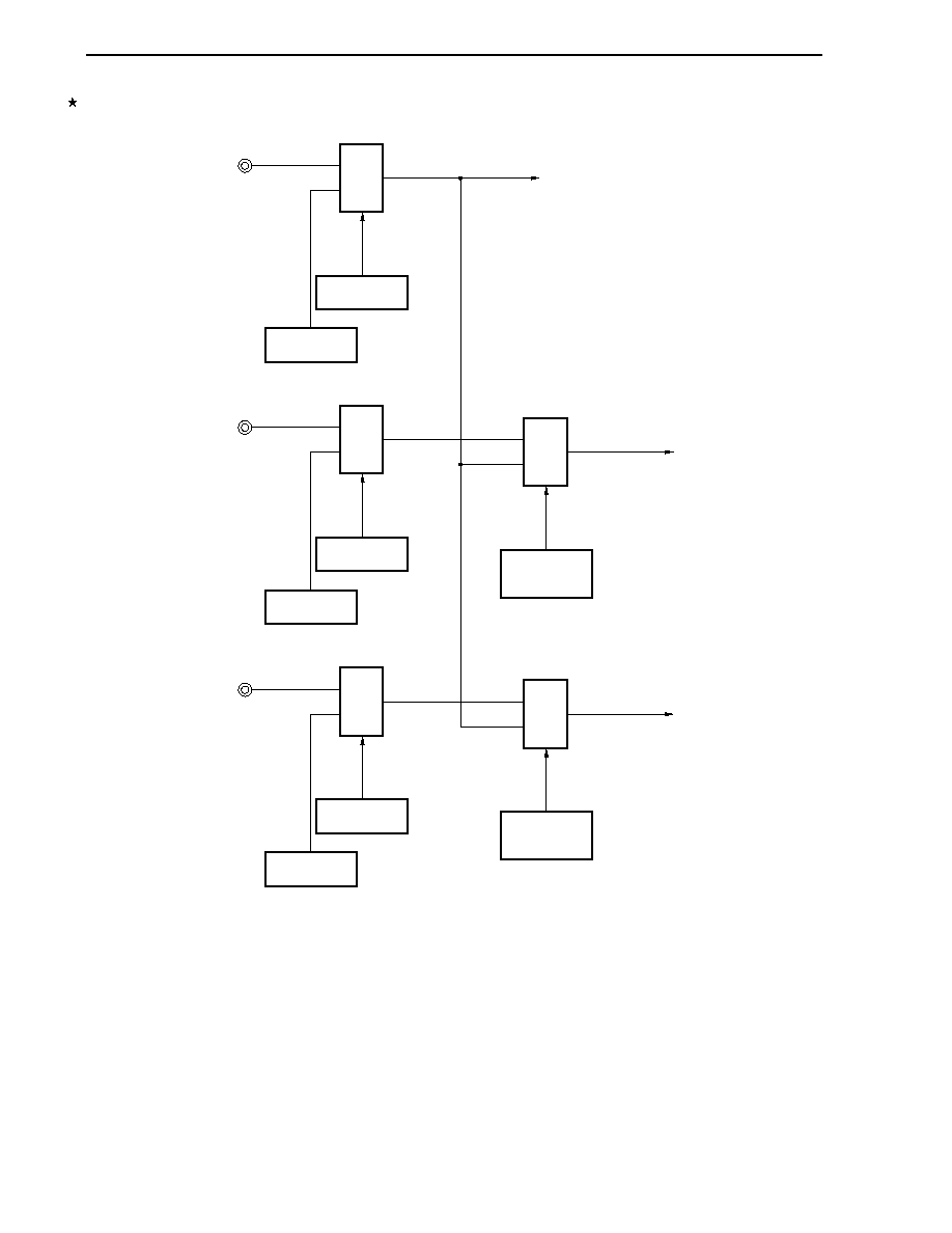
CHAPTER 14 SERIAL INTERFACE UART6
User's Manual U16228EJ2V0UD
296
Figure 14-3. Port Configuration for LIN Reception Operation
RXD6 input
INTP0 input
TI000 input
P14/RxD6
P120/INTP0
P00/TI000
Port input
switch control
(ISC0)
<ISC0>
0: Select INTP0 (P120)
1: Select RxD6 (P14)
Port mode
(PM14)
Output latch
(P14)
Port mode
(PM120)
Output latch
(P120)
Port input
switch control
(ISC1)
<ISC1>
0: Select TI000 (P00)
1: Select RxD6 (P14)
Selector
Selector
Selector
Selector
Selector
Port mode
(PM00)
Output latch
(P00)
Remark ISC0, ISC1: Bits 0 and 1 of the input switch control register (ISC) (see Figure 14-11)
The peripheral functions used in the LIN communication operation are shown below.
<Peripheral functions used>
∑
External interrupt (INTP0); wakeup signal detection
Use: Detects the wakeup signal edges and detects start of communication.
∑
16-bit timer/event counter 00 (TI000); baud rate error detection
Use: Detects the baud rate error (measures the TI000 input edge interval in the capture mode) by detecting the
synchronous break field (SBF) length and divides it by the number of bits.
∑
Serial interface UART6

CHAPTER 14 SERIAL INTERFACE UART6
User's Manual U16228EJ2V0UD
297
14.2 Configuration of Serial Interface UART6
Serial interface UART6 includes the following hardware.
Table 14-1. Configuration of Serial Interface UART6
Item Configuration
Registers
Receive buffer register 6 (RXB6)
Receive shift register 6 (RXS6)
Transmit buffer register 6 (TXB6)
Transmit shift register 6 (TXS6)
Control registers
Asynchronous serial interface operation mode register 6 (ASIM6)
Asynchronous serial interface reception error status register 6 (ASIS6)
Asynchronous serial interface transmission status register 6 (ASIF6)
Clock selection register 6 (CKSR6)
Baud rate generator control register 6 (BRGC6)
Asynchronous serial interface control register 6 (ASICL6)
Input switch control register (ISC)
Port mode register 1 (PM1)
Port register 1 (P1)
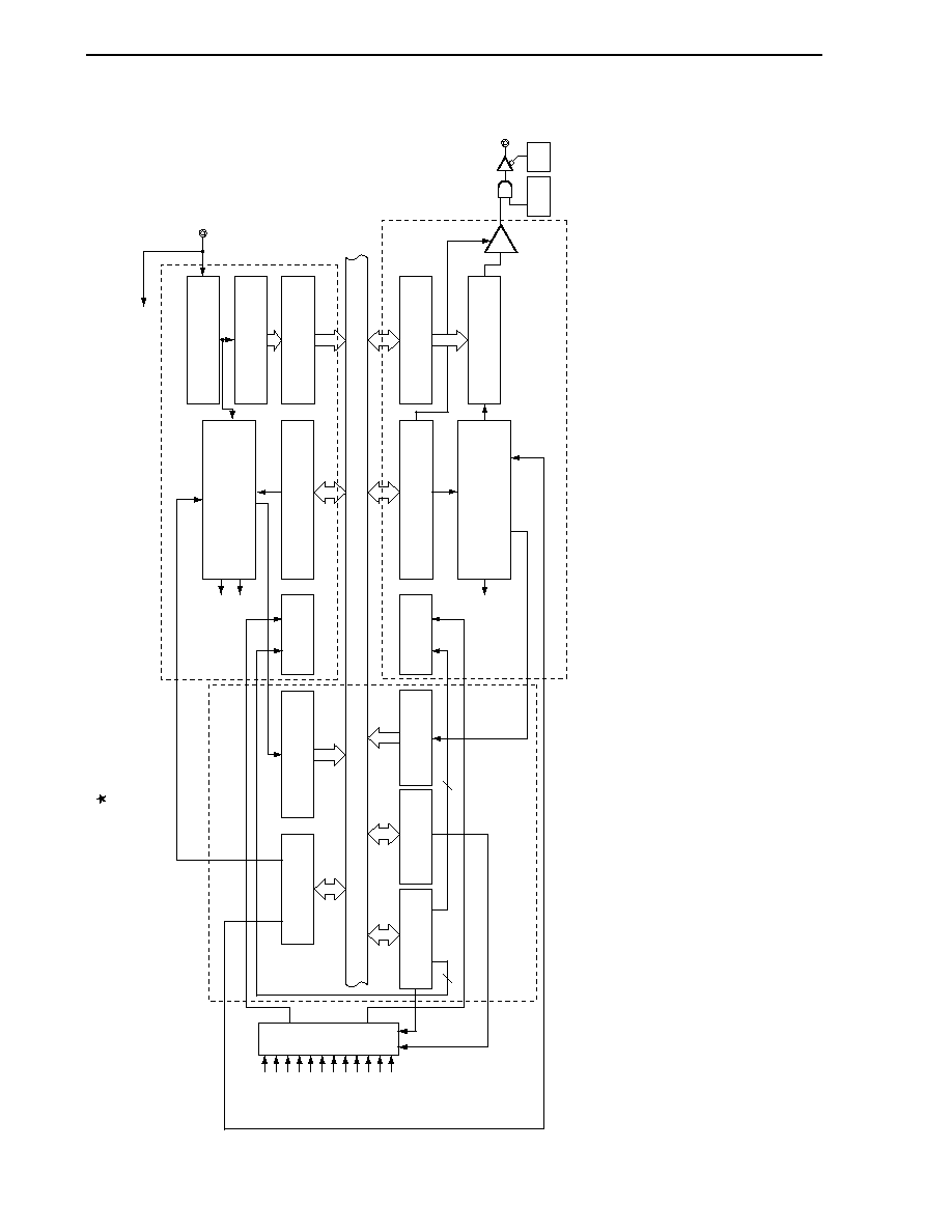
CHAPTER
14
SERIAL IN
TER
F
ACE U
ART6
User's Manual
U1
6228EJ2V0UD
298
Figure 14-4. Block Diagram of Serial Interface UART6
Internal bus
Asynchronous serial interface
control register 6 (ASICL6)
Transmit buffer register 6
(TXB6)
Transmit shift register 6
(TXS6)
T
X
D6/
P13
INTST6
Baud rate
generator
Asynchronous serial interface
control register 6 (ASICL6)
Reception control
Receive shift register 6
(RXS6)
Receive buffer register 6
(RXB6)
R
X
D6/
P14
TI000, INTP0
Note
INTSR6
Baud rate
generator
Filter
INTSRE6
Asynchronous serial
interface reception error
status register 6 (ASIS6)
Asynchronous serial
interface operation mode
register 6 (ASIM6)
Asynchronous serial
interface transmission
status register 6 (ASIF6)
Transmission control
Registers
f
X
f
X
/2
f
X
/2
2
f
X
/2
3
f
X
/2
4
f
X
/2
5
f
X
/2
6
f
X
/2
7
f
X
/2
8
f
X
/2
9
f
X
/2
10
8-bit timer/
event counter
50 output
8
Reception unit
Transmission unit
Clock selection
register 6 (CKSR6)
Baud rate generator
control register 6
(BRGC6)
Output latch
(P13)
PM13
8
Selector
Note Selectable with input switch control register (ISC).

CHAPTER 14 SERIAL INTERFACE UART6
User's Manual U16228EJ2V0UD
299
(1) Receive buffer register 6 (RXB6)
This 8-bit register stores parallel data converted by receive shift register 6 (RXS6).
Each time 1 byte of data has been received, new receive data is transferred to this register from RXS6. If the
data length is set to 7 bits, data is transferred as follows.
∑
In LSB-first reception, the receive data is transferred to bits 0 to 6 of RXB6 and the MSB of RXB6 is always 0.
∑
In MSB-first reception, the receive data is transferred to bits 1 to 7 of RXB6 and the LSB of RXB6 is always 0.
If an overrun error (OVE6) occurs, the receive data is not transferred to RXB6.
RXB6 can be read by an 8-bit memory manipulation instruction. No data can be written to this register.
RESET input sets this register to FFH.
(2) Receive shift register 6 (RXS6)
This register converts the serial data input to the R
X
D6 pin into parallel data.
RXS6 cannot be directly manipulated by a program.
(3) Transmit buffer register 6 (TXB6)
This buffer register is used to set transmit data. Transmission is started when data is written to TXB6.
This register can be read or written by an 8-bit memory manipulation instruction.
RESET input sets this register to FFH.
Cautions 1. Do not write data to TXB6 when bit 1 (TXBF6) of asynchronous serial interface transmission
status register 6 (ASIF6) is 1.
2. Do not refresh (write the same value to) TXB6 by software during a communication
operation (when bit 7 (POWER6) and bit 6 (TXE6) of asynchronous serial interface operation
mode register 6 (ASIM6) are 1 or when bit 7 (POWER6) and bit 5 (RXE6) of ASIM6 are 1).
(4) Transmit shift register 6 (TXS6)
This register transmits the data transferred from TXB6 from the T
X
D6 pin as serial data. Data is transferred from
TXB6 immediately after TXB6 is written for the first transmission, or immediately before INTST6 occurs after one
frame was transmitted for continuous transmission. Data is transferred from TXB6 and transmitted from the T
X
D6
pin at the falling edge of the base clock.
TXS6 cannot be directly manipulated by a program.
CHAPTER 14 SERIAL INTERFACE UART6
User's Manual U16228EJ2V0UD
300
14.3 Registers Controlling Serial Interface UART6
Serial interface UART6 is controlled by the following nine registers.
∑
Asynchronous serial interface operation mode register 6 (ASIM6)
∑
Asynchronous serial interface reception error status register 6 (ASIS6)
∑
Asynchronous serial interface transmission status register 6 (ASIF6)
∑
Clock selection register 6 (CKSR6)
∑
Baud rate generator control register 6 (BRGC6)
∑
Asynchronous serial interface control register 6 (ASICL6)
∑
Input switch control register (ISC)
∑
Port mode register 1 (PM1)
∑
Port register 1 (P1)
(1) Asynchronous serial interface operation mode register 6 (ASIM6)
This 8-bit register controls the serial communication operations of serial interface UART6.
This register can be set by a 1-bit or 8-bit memory manipulation instruction.
RESET input sets this register to 01H.
Remark ASIM6 can be refreshed (the same value is written) by software during a communication operation
(when bit 7 (POWER6) and bit 6 (TXE6) of ASIM6 = 1 or bit 7 (POWER6) and bit 5 (RXE6) of ASIM6
= 1).
Figure 14-5. Format of Asynchronous Serial Interface Operation Mode Register 6 (ASIM6) (1/2)
Address: FF50H After reset: 01H R/W
Symbol
<7>
<6>
<5>
4 3 2 1 0
ASIM6 POWER6 TXE6
RXE6
PS61
PS60
CL6
SL6
ISRM6
POWER6
Enables/disables
operation of internal operation clock
0
Note 1
Disables operation of the internal operation clock (fixes the clock to low level) and asynchronously
resets the internal circuit
Note 2
.
1
Note 3
Enables operation of the internal operation clock
TXE6
Enables/disables
transmission
0
Disables
transmission
(synchronously resets the transmission circuit).
1
Enables
transmission
Notes 1. The output of the T
X
D6 pin goes high and the input from the R
X
D6 pin is fixed to the high level when
POWER6 = 0.
2. Asynchronous serial interface reception error status register 6 (ASIS6), asynchronous serial interface
transmission status register 6 (ASIF6), bit 7 (SBRF6) and bit 6 (SBRT6) of asynchronous serial
interface control register 6 (ASICL6), and receive buffer register 6 (RXB6) are reset.
3. Operation of the 8-bit counter output is enabled at the second base clock after 1 is written to the
POWER6 bit.
CHAPTER 14 SERIAL INTERFACE UART6
User's Manual U16228EJ2V0UD
301
Figure 14-5. Format of Asynchronous Serial Interface Operation Mode Register 6 (ASIM6) (2/2)
RXE6
Enables/disables
reception
0
Disables
reception
(synchronously resets the reception circuit).
1
Enables
reception
PS61
PS60
Transmission
operation Reception
operation
0
0
Does not output parity bit.
Reception without parity
0
1
Outputs 0 parity.
Reception as 0 parity
Note
1
0
Outputs odd parity.
Judges as odd parity.
1
1
Outputs even parity.
Judges as even parity.
CL6
Specifies character length of transmit/receive data
0
Character length of data = 7 bits
1
Character length of data = 8 bits
SL6
Specifies number of stop bits of transmit data
0
Number of stop bits = 1
1
Number of stop bits = 2
ISRM6
Enables/disables
occurrence of reception completion interrupt in case of error
0
"INTSRE6" occurs in case of error (at this time, INTSR6 does not occur).
1
"INTSR6" occurs in case of error (at this time, INTSRE6 does not occur).
Note If "reception as 0 parity" is selected, the parity is not judged. Therefore, bit 2 (PE6) of asynchronous serial
interface reception error status register 6 (ASIS6) is not set and the error interrupt does not occur.
Cautions 1. At startup, set POWER6 to 1 and then set TXE6 to 1. To stop the operation, clear TXE6 to 0,
and then clear POWER6 to 0.
2. At startup, set POWER6 to 1 and then set RXE6 to 1. To stop the operation, clear RXE6 to 0,
and then clear POWER6 to 0.
3. Set POWER6 to 1 and then set RXE6 to 1 while a high level is input to the RxD6 pin. If
POWER6 is set to 1 and RXE6 is set to 1 while a low level is input, reception is started.
4. Clear the TXE6 and RXE6 bits to 0 before rewriting the PS61, PS60, and CL6 bits.
5. Fix the PS61 and PS60 bits to 0 when mounting the device on LIN.
6. Make sure that TXE6 = 0 when rewriting the SL6 bit. Reception is always performed with "the
number of stop bits = 1", and therefore, is not affected by the set value of the SL6 bit.
7. Make sure that RXE6 = 0 when rewriting the ISRM6 bit.

CHAPTER 14 SERIAL INTERFACE UART6
User's Manual U16228EJ2V0UD
302
(2) Asynchronous serial interface reception error status register 6 (ASIS6)
This register indicates an error status on completion of reception by serial interface UART6. It includes three
error flag bits (PE6, FE6, OVE6).
This register is read-only by an 8-bit memory manipulation instruction.
RESET input clears this register to 00H if bit 7 (POWER6) and bit 5 (RXE6) of ASIM6 = 0. 00H is read when this
register is read.
Figure 14-6. Format of Asynchronous Serial Interface Reception Error Status Register 6 (ASIS6)
Address: FF53H After reset: 00H R
Symbol
7 6 5 4 3 2 1 0
ASIS6
0 0 0 0 0
PE6
FE6
OVE6
PE6
Status flag indicating parity error
0
If POWER6 = 0 and RXE6 = 0, or if ASIS6 register is read
1
If the parity of transmit data does not match the parity bit on completion of reception
FE6
Status flag indicating framing error
0
If POWER6 = 0 and RXE6 = 0, or if ASIS6 register is read
1
If the stop bit is not detected on completion of reception
OVE6
Status flag indicating overrun error
0
If POWER6 = 0 and RXE6 = 0, or if ASIS6 register is read
1
If receive data is set to the RXB register and the next reception operation is completed before the
data is read.
Cautions 1. The operation of the PE6 bit differs depending on the set values of the PS61 and PS60 bits of
asynchronous serial interface operation mode register 6 (ASIM6).
2. The first bit of the receive data is checked as the stop bit, regardless of the number of stop
bits.
3. If an overrun error occurs, the next receive data is not written to receive buffer register 6
(RXB6) but discarded.
4. If data is read from ASIS6, a wait cycle is generated. Do not read data from ASIS6 when the
CPU is operating on the subsystem clock and the X1 input clock is stopped. For details, see
CHAPTER 34 CAUTIONS FOR WAIT.
CHAPTER 14 SERIAL INTERFACE UART6
User's Manual U16228EJ2V0UD
303
(3) Asynchronous serial interface transmission status register 6 (ASIF6)
This register indicates the status of transmission by serial interface UART6. It includes two status flag bits
(TXBF6 and TXSF6).
Transmission can be continued without disruption even during an interrupt period, by writing the next data to the
TXB6 register after data has been transferred from the TXB6 register to the TXS6 register.
This register is read-only by an 8-bit memory manipulation instruction.
RESET input clears this register to 00H if bit 7 (POWER6) and bit 6 (TXE6) of ASIM6 = 0.
Figure 14-7. Format of Asynchronous Serial Interface Transmission Status Register 6 (ASIF6)
Address: FF55H After reset: 00H R
Symbol
7 6 5 4 3 2 1 0
ASIF6
0 0 0 0 0 0
TXBF6
TXSF6
TXBF6
Transmit buffer data flag
0
If POWER6 = 0 or TXE6 = 0, or if data is transferred to transmit shift register 6 (TXS6)
1
If data is written to transmit buffer register 6 (TXB6) (if data exists in TXB6)
TXSF6
Transmit shift register data flag
0
If POWER6 = 0 or TXE6 = 0, or if the next data is not transferred from transmit buffer register 6
(TXB6) after completion of transfer
1
If data is transferred from transmit buffer register 6 (TXB6) (if data transmission is in progress)
Cautions 1. To transmit data continuously, write the first transmit data (first byte) to the TXB6 register.
Be sure to check that the TXBF6 flag is "0". If so, write the next transmit data (second byte)
to the TXB6 register. If data is written to the TXB6 register while the TXBF6 flag is "1", the
transmit data cannot be guaranteed.
2. To initialize the transmission unit upon completion of continuous transmission, be sure to
check that the TXSF6 flag is "0" after generation of the transmission completion interrupt,
and then execute initialization. If initialization is executed while the TXSF6 flag is "1", the
transmit data cannot be guaranteed.
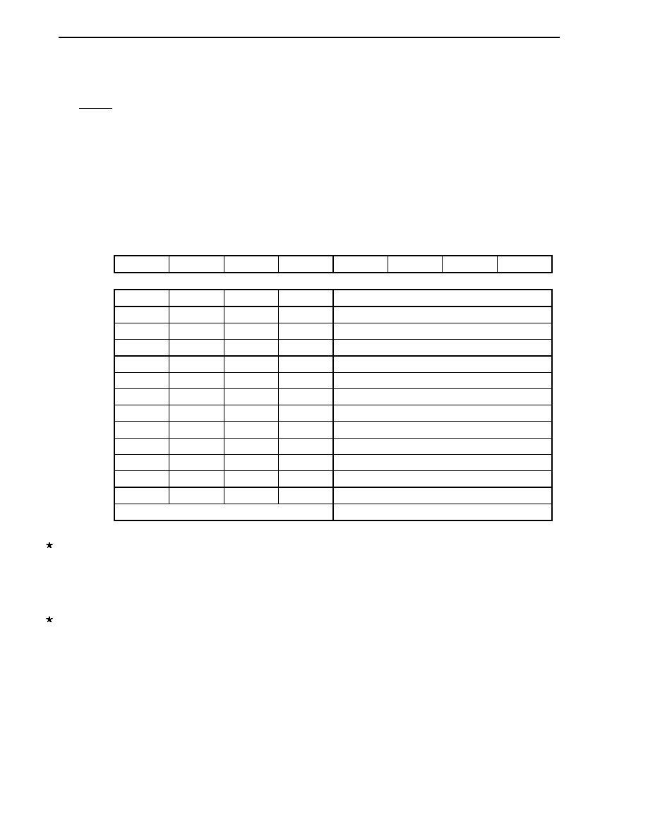
CHAPTER 14 SERIAL INTERFACE UART6
User's Manual U16228EJ2V0UD
304
(4) Clock selection register 6 (CKSR6)
This register selects the base clock of serial interface UART6.
CKSR6 can be set by an 8-bit memory manipulation instruction.
RESET input clears this register to 00H.
Remark CKSR6 can be refreshed (the same value is written) by software during a communication operation
(when bit 7 (POWER6) and bit 6 (TXE6) of ASIM6 = 1 or bit 7 (POWER6) and bit 5 (RXE6) of ASIM6
= 1).
Figure 14-8. Format of Clock Selection Register 6 (CKSR6)
Address: FF56H After reset: 00H R/W
Symbol
7 6 5 4 3 2 1 0
CKSR6
0 0 0 0
TPS63
TPS62
TPS61
TPS60
TPS63 TPS62 TPS61 TPS60
Base
clock
(f
XCLK6
) selection
0 0 0 0
f
X
(10 MHz)
0 0 0 1
f
X
/2 (5 MHz)
0 0 1 0
f
X
/2
2
(2.5 MHz)
0 0 1 1
f
X
/2
3
(1.25 MHz)
0 1 0 0
f
X
/2
4
(625 kHz)
0 1 0 1
f
X
/2
5
(312.5 kHz)
0 1 1 0
f
X
/2
6
(156.25 kHz)
0 1 1 1
f
X
/2
7
(78.13 kHz)
1 0 0 0
f
X
/2
8
(39.06 kHz)
1 0 0 1
f
X
/2
9
(19.53 kHz)
1 0 1 0
f
X
/2
10
(9.77 kHz)
1 0 1 1
TM50
output
Note
Other than above
Setting prohibited
Note To select the output of TM50 as the base clock, start the operation by setting 8-bit timer/event counter 50 so
that the duty is 50% of the output in the PWM mode (bit 6 (TMC506) of the TMC50 register = 1), and then
set TPS63, TPS62, TPS61, and TPS60 to 1, 0, 1, and 1, respectively. It is not necessary to enable the
TO50 pin as a timer output pin (bit 0 (TOE50) of the TMC register may be 0 or 1).
Cautions 1. When the Ring-OSC clock is selected as the clock to be supplied to the CPU, the clock of the
Ring-OSC oscillator is divided and supplied as the count clock. If the base clock is the Ring-
OSC clock, the operation of serial interface UART6 is not guaranteed.
2. Make sure POWER6 = 0 when rewriting TPS63 to TPS60.
Remarks 1. Figures in parentheses are for operation with f
X
= 10 MHz
2. f
X
: X1 input clock oscillation frequency
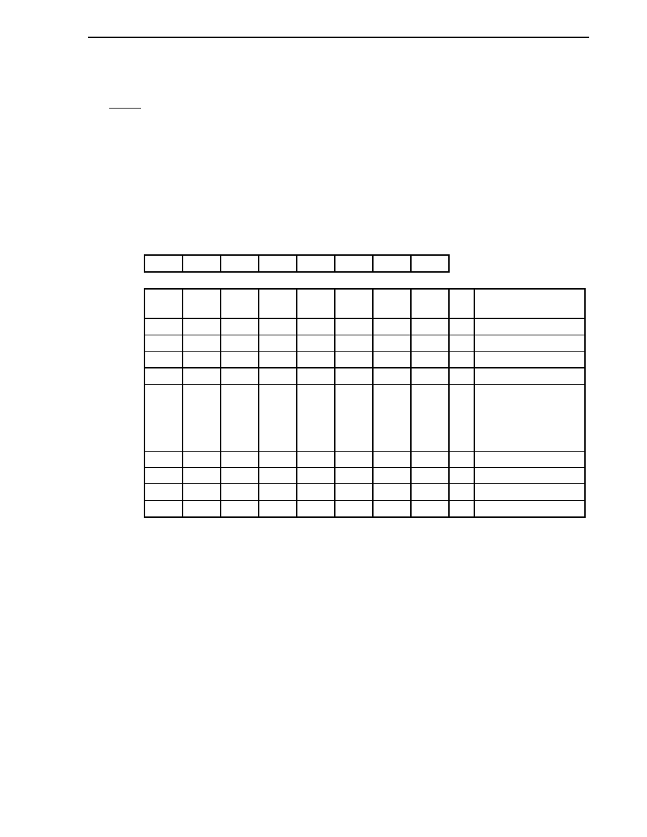
CHAPTER 14 SERIAL INTERFACE UART6
User's Manual U16228EJ2V0UD
305
(5) Baud rate generator control register 6 (BRGC6)
This register sets the division value of the 8-bit counter of serial interface UART6.
BRGC6 can be set by an 8-bit memory manipulation instruction.
RESET input sets this register to FFH.
Remark BRGC6 can be refreshed (the same value is written) by software during a communication operation
(when bit 7 (POWER6) and bit 6 (TXE6) of ASIM6 = 1 or bit 7 (POWER6) and bit 5 (RXE6) of ASIM6
= 1).
Figure 14-9. Format of Baud Rate Generator Control Register 6 (BRGC6)
Address: FF57H After reset: FFH R/W
Symbol 7 6 5 4 3 2 1 0
BRGC6 MDL67 MDL66 MDL65 MDL64 MDL63 MDL62 MDL61 MDL60
MDL67 MDL66 MDL65 MDL64 MDL63 MDL62 MDL61 MDL60 k
Output clock selection of
8-bit counter
0 0 0 0 0
◊
◊
◊
◊
Setting prohibited
0 0 0 0 1 0 0 0
8
f
XCLK6
/8
0 0 0 0 1 0 0 1
9
f
XCLK6
/9
0 0 0 0 1 0 1 0
10
f
XCLK6
/10
∑
∑
∑
∑
∑
∑
∑
∑
∑
∑
∑
∑
∑
∑
∑
∑
∑
∑
∑
∑
∑
∑
∑
∑
∑
∑
∑
∑
∑
∑
∑
∑
∑
∑
∑
∑
∑
∑
∑
∑
∑
∑
∑
∑
∑
∑
∑
∑
∑
∑
1 1 1 1 1 1 0 0
252
f
XCLK6
/252
1 1 1 1 1 1 0 1
253
f
XCLK6
/253
1 1 1 1 1 1 1 0
254
f
XCLK6
/254
1 1 1 1 1 1 1 1
255
f
XCLK6
/255
Cautions 1. Make sure that bit 6 (TXE6) and bit 5 (RXE6) of the ASIM6 register = 0 when rewriting the
MDL67 to MDL60 bits.
2. The baud rate is the output clock of the 8-bit counter divided by 2.
Remarks 1. f
XCLK6
: Frequency of base clock selected by the TPS63 to TPS60 bits of CKSR6 register
2. k: Value set by MDL67 to MDL60 bits (k = 8, 9, 10, ..., 255)
3.
◊
: Don't care
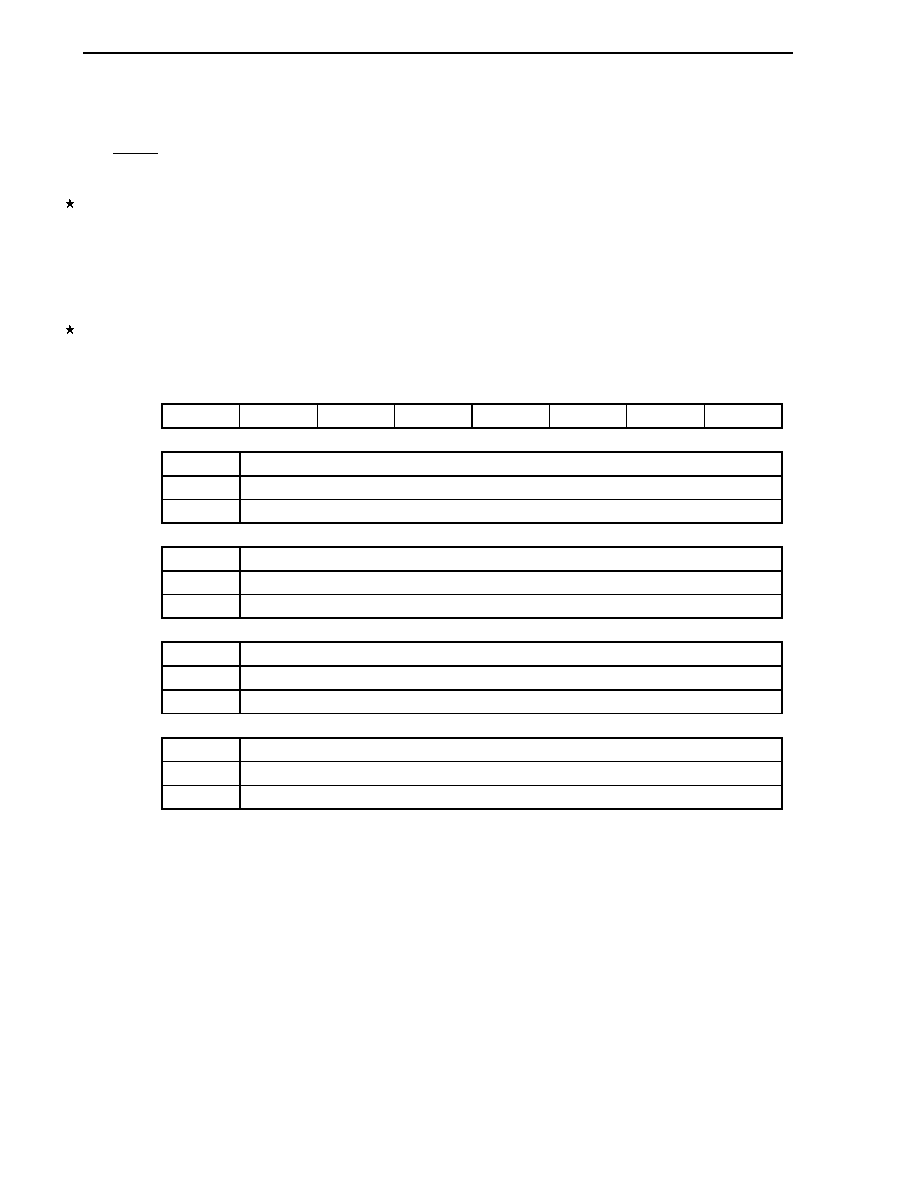
CHAPTER 14 SERIAL INTERFACE UART6
User's Manual U16228EJ2V0UD
306
(6) Asynchronous serial interface control register 6 (ASICL6)
This register controls the serial communication operations of serial interface UART6.
ASICL6 can be set by a 1-bit or 8-bit memory manipulation instruction.
RESET input sets this register to 16H.
Caution ASICL6 can be refreshed (the same value is written) by software during a communication
operation (when bit 7 (POWER6) and bit 6 (TXE6) of ASIM6 = 1 or bit 7 (POWER6) and bit 5
(RXE6) of ASIM6 = 1). Note, however, that communication is started by the refresh operation
because bit 6 (SBRT6) of ASICL6 is cleared to 0 when communication is completed (when an
interrupt signal is generated).
Figure 14-10. Format of Asynchronous Serial Interface Control Register 6 (ASICL6)
Address: FF58H After reset: 16H R/W
Note
Symbol
<7>
<6>
5 4 3 2 1 0
ASICL6
SBRF6
SBRT6
0 1 0 1
DIR6
TXDLV6
SBRF6
SBF reception status flag
0
If POWER6 = 0 and RXE6 = 0 or if SBF reception has been completed correctly
1
SBF reception in progress
SBRT6
SBF reception trigger
0
-
1
SBF reception trigger
DIR6
First
bit
specification
0
MSB
1
LSB
TXDLV6
Enables/disables inverting T
X
D6 output
0
Normal output of T
X
D6
1
Inverted output of T
X
D6
Note Bits 2 to 5 and 7 are read-only.
Cautions 1. In the case of an SBF reception error, return the mode to the SBF reception mode and hold
the status of the SBRF6 flag.
2. Before setting the SBRT6 bit, make sure that bit 7 (POWER6) and bit 5 (RXE6) of ASIM6 = 1.
3. The read value of the SBRT6 bit is always 0. SBRT6 is automatically cleared to 0 after SBF
reception has been correctly completed.
4. Before rewriting the DIR6 and TXDLV6 bits, clear the TXE6 and RXE6 bits to 0.
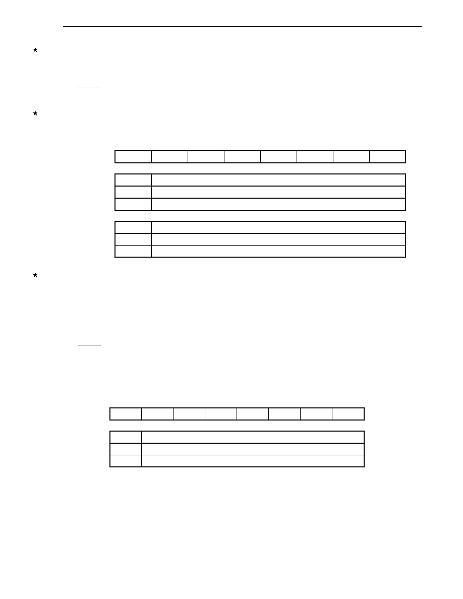
CHAPTER 14 SERIAL INTERFACE UART6
User's Manual U16228EJ2V0UD
307
(7) Input switch control register (ISC)
The input switch control register (ISC) is used to receive a status signal transmitted from the master during LIN
(Local Interconnect Network) reception. The input signal is switched by setting ISC.
This register can be set by a 1-bit or 8-bit memory manipulation instruction.
RESET input clears this register to 00H.
Figure 14-11. Format of Input Switch Control Register (ISC)
Address: FF4FH After reset: 00H R/W
Symbol
7 6 5 4 3 2 1 0
ISC
0 0 0 0 0 0
ISC1
ISC0
ISC1
TI000 input source selection
0
TI000
(P00)
1
RxD6
(P14)
ISC0
INTP0 input source selection
0
INTP0
(P120)
1
RxD6
(P14)
(8) Port mode register 1 (PM1)
This register sets port 1 input/output in 1-bit units.
When using the P13/TxD3 pin for serial interface data output, clear PM13 to 0 and set the output latch of P13 to
1.
When using the P14/RxD6 pin for serial interface data input, set PM14 to 1. The output latch of P14 at this time
may be 0 or 1.
PM1 can be set by a 1-bit or 8-bit memory manipulation instruction.
RESET input sets this register to FFH.
Figure 14-12. Format of Port Mode Register 1 (PM1)
Address: FF21H After reset: FFH R/W
Symbol
7 6 5 4 3 2 1 0
PM1
PM17 PM16 PM15 PM14 PM13 PM12 PM11 PM10
PM1n
P1n pin I/O mode selection (n = 0 to 7)
0
Output mode (output buffer on)
1
Input mode (output buffer off)

CHAPTER 14 SERIAL INTERFACE UART6
User's Manual U16228EJ2V0UD
308
14.4 Operation of Serial Interface UART6
Serial interface UART6 has the following two modes.
∑
Operation stop mode
∑
Asynchronous serial interface (UART) mode
14.4.1 Operation stop mode
In this mode, serial communication cannot be executed; therefore, the power consumption can be reduced. In
addition, the pins can be used as ordinary port pins in this mode. To set the operation stop mode, clear bits 7, 6, and
5 (POWER6, TXE6, and RXE6) of ASIM6 to 0.
(1) Register used
The operation stop mode is set by asynchronous serial interface operation mode register 6 (ASIM6).
ASIM6 can be set by a 1-bit or 8-bit memory manipulation instruction.
RESET input sets this register to 01H.
Address: FF50H After reset: 01H R/W
Symbol
<7>
<6>
<5>
4 3 2 1 0
ASIM6 POWER6 TXE6
RXE6
PS61
PS60
CL6
SL6
ISRM6
POWER6
Enables/disables
operation of internal operation clock
0
Note 1
Disables operation of the internal operation clock (fixes the clock to low level) and asynchronously
resets the internal circuit
Note 2
.
TXE6
Enables/disables
transmission
0
Disables transmission operation (synchronously resets the transmission circuit).
RXE6
Enables/disables
reception
0
Disables
reception
(synchronously resets the reception circuit).
Notes 1. The output of the T
X
D6 pin goes high and the input from the R
X
D6 pin is fixed to high level when
POWER6 = 0.
2. Asynchronous serial interface reception error status register 6 (ASIS6), asynchronous serial interface
transmission status register 6 (ASIF6), bit 7 (SBRF6) and bit 6 (SBRT6) of asynchronous serial
interface control register 6 (ASICL6), and receive buffer register 6 (RXB6) are reset.
Caution Clear POWER6 to 0 after clearing TXE6 and RXE6 to 0 to set the operation stop mode.
To start the operation, set POWER6 to 1, and then set TXE6 and RXE6 to 1.
Remark To use the RxD6/P14 and TxD6/P13 pins as general-purpose port pins, see CHAPTER 4 PORT
FUNCTIONS.

CHAPTER 14 SERIAL INTERFACE UART6
User's Manual U16228EJ2V0UD
309
14.4.2 Asynchronous serial interface (UART) mode
In this mode, data of 1 byte is transmitted/received following a start bit, and a full-duplex operation can be
performed.
A dedicated UART baud rate generator is incorporated, so that communication can be executed at a wide range of
baud rates.
(1) Registers used
∑
Asynchronous serial interface operation mode register 6 (ASIM6)
∑
Asynchronous serial interface reception error status register 6 (ASIS6)
∑
Asynchronous serial interface transmission status register 6 (ASIF6)
∑
Clock selection register 6 (CKSR6)
∑
Baud rate generator control register 6 (BRGC6)
∑
Asynchronous serial interface control register 6 (ASICL6)
∑
Input switch control register (ISC)
∑
Port mode register 1 (PM1)
∑
Port register 1 (P1)
The basic procedure of setting an operation in the UART mode is as follows.
<1> Set the CKSR6 register (see Figure 14-8).
<2> Set the BRGC6 register (see Figure 14-9).
<3> Set bits 0 to 4 (ISRM6, SL6, CL6, PS60, PS61) of the ASIM6 register (see Figure 14-5).
<4> Set bits 0 and 1 (TXDLV6, DIR6) of the ASICL6 register (see Figure 14-10).
<5> Set bit 7 (POWER6) of the ASIM6 register to 1.
<6> Set bit 6 (TXE6) of the ASIM6 register to 1.
Transmission is enabled.
Set bit 5 (RXE6) of the ASIM6 register to 1.
Reception is enabled.
<7> Write data to transmit buffer register 6 (TXB6).
Data transmission is started.
Caution Take relationship with the other party of communication when setting the port mode register
and port register.
CHAPTER 14 SERIAL INTERFACE UART6
User's Manual U16228EJ2V0UD
310
The relationship between the register settings and pins is shown below.
Table 14-2. Relationship Between Register Settings and Pins
Pin Function
POWER6 TXE6 RXE6 PM13
P13
PM14
P14
UART6
Operation
TxD6/P13 RxD6/P14
0 0 0
◊
Note
◊
Note
◊
Note
◊
Note
Stop
P13
P14
0 1
◊
Note
◊
Note
1 ◊ Reception
P13
RxD6
1 0 0 1
◊
Note
◊
Note
Transmission
TxD6
P14
1
1 1 0 1 1 ◊
Transmission/
reception
TxD6 RxD6
Note Can be set as port function.
Remark ◊:
don't
care
POWER6: Bit 7 of asynchronous serial interface operation mode register 6 (ASIM6)
TXE6:
Bit 6 of ASIM6
RXE6:
Bit 5 of ASIM6
PM1◊:
Port mode register
P1◊:
Port output latch
CHAPTER 14 SERIAL INTERFACE UART6
User's Manual U16228EJ2V0UD
311
(2) Communication
operation
(a) Format and waveform example of normal transmit/receive data
Figures 14-13 and 14-14 show the format and waveform example of the normal transmit/receive data.
Figure 14-13. Format of Normal UART Transmit/Receive Data
1. LSB-first transmission/reception
Start
bit
Parity
bit
D0
D1
D2
D3
D4
1 data frame
Character bits
D5
D6
D7
Stop bit
2. MSB-first transmission/reception
Start
bit
Parity
bit
D7
D6
D5
D4
D3
1 data frame
Character bits
D2
D1
D0
Stop bit
One data frame consists of the following bits.
∑
Start bit ... 1 bit
∑
Character bits ... 7 or 8 bits
∑
Parity bit ... Even parity, odd parity, 0 parity, or no parity
∑
Stop bit ... 1 or 2 bits
The character bit length, parity, and stop bit length in one data frame are specified by asynchronous serial
interface operation mode register 6 (ASIM6).
Whether data is communicated with the LSB or MSB first is specified by bit 1 (DIR6) of asynchronous serial
interface control register 6 (ASICL6).
Whether the T
X
D6 pin outputs normal or inverted data is specified by bit 0 (TXDLV6) of ASICL6.
CHAPTER 14 SERIAL INTERFACE UART6
User's Manual U16228EJ2V0UD
312
Figure 14-14. Example of Normal UART Transmit/Receive Data Waveform
1. Data length: 8 bits, LSB first, Parity: Even parity, Stop bit: 1 bit, Communication data: 55H
1 data frame
Start
D0
D1
D2
D3
D4
D5
D6
D7
Parity
Stop
2. Data length: 8 bits, MSB first, Parity: Even parity, Stop bit: 1 bit, Communication data: 55H
1 data frame
Start
D7
D6
D5
D4
D3
D2
D1
D0
Parity
Stop
3. Data length: 8 bits, MSB first, Parity: Even parity, Stop bit: 1 bit, Communication data: 55H, T
X
D6 pin
inverted output
1 data frame
Start
D7
D6
D5
D4
D3
D2
D1
D0
Parity
Stop
4. Data length: 7 bits, LSB first, Parity: Odd parity, Stop bit: 2 bits, Communication data: 36H
1 data frame
Start
D0
D1
D2
D3
D4
D5
D6
Parity
Stop
Stop
5. Data length: 8 bits, LSB first, Parity: None, Stop bit: 1 bit, Communication data: 87H
1 data frame
Start
D0
D1
D2
D3
D4
D5
D6
D7
Stop

CHAPTER 14 SERIAL INTERFACE UART6
User's Manual U16228EJ2V0UD
313
(b) Parity types and operation
The parity bit is used to detect a bit error in communication data. Usually, the same type of parity bit is used
on both the transmission and reception sides. With even parity and odd parity, a 1-bit (odd number) error
can be detected. With zero parity and no parity, an error cannot be detected.
Caution Fix the PS61 and PS60 bits to 0 when the device is incorporated in LIN.
(i) Even
parity
∑
Transmission
Transmit data, including the parity bit, is controlled so that the number of bits that are "1" is even.
The value of the parity bit is as follows.
If transmit data has an odd number of bits that are "1": 1
If transmit data has an even number of bits that are "1": 0
∑
Reception
The number of bits that are "1" in the receive data, including the parity bit, is counted. If it is odd, a
parity error occurs.
(ii) Odd
parity
∑
Transmission
Unlike even parity, transmit data, including the parity bit, is controlled so that the number of bits that
are "1" is odd.
If transmit data has an odd number of bits that are "1": 0
If transmit data has an even number of bits that are "1": 1
∑
Reception
The number of bits that are "1" in the receive data, including the parity bit, is counted. If it is even, a
parity error occurs.
(iii) 0 parity
The parity bit is cleared to 0 when data is transmitted, regardless of the transmit data.
The parity bit is not detected when the data is received. Therefore, a parity error does not occur
regardless of whether the parity bit is "0" or "1".
(iv) No parity
No parity bit is appended to the transmit data.
Reception is performed assuming that there is no parity bit when data is received. Because there is no
parity bit, a parity error does not occur.
CHAPTER 14 SERIAL INTERFACE UART6
User's Manual U16228EJ2V0UD
314
(c) Normal transmission
The T
X
D6 pin outputs a high level when bit 7 (POWER6) of asynchronous serial interface operation mode
register 6 (ASIM6) is set to 1. If bit 6 (TXE6) of ASIM6 is then set to 1, transmission is enabled.
Transmission can be started by writing transmit data to transmit buffer register 6 (TXB6). The start bit, parity
bit, and stop bit are automatically appended to the data.
When transmission is started, the data in TXB6 is transferred to transmit shift register 6 (TXS6). After that,
the data is sequentially output from TXS6 to the T
X
D6 pin. When transmission is completed, the parity and
stop bits set by ASIM6 are appended and a transmission completion interrupt request (INTST6) is generated.
Transmission is stopped until the data to be transmitted next is written to TXB6.
Figure 14-15 shows the timing of the transmission completion interrupt request (INTST6). This interrupt
occurs as soon as the last stop bit has been output.
Figure 14-15. Normal Transmission Completion Interrupt Request Timing
1. Stop bit length: 1
INTST6
D0
Start
D1
D2
D6
D7
Stop
T
X
D6 (output)
Parity
2. Stop bit length: 2
T
X
D6 (output)
INTST6
D0
Start
D1
D2
D6
D7
Parity
Stop

CHAPTER 14 SERIAL INTERFACE UART6
User's Manual U16228EJ2V0UD
315
(d) Continuous transmission
The next transmit data can be written to transmit buffer register 6 (TXB6) as soon as transmit shift register 6
(TXS6) has started its shift operation. Consequently, even while the INTST6 interrupt is being serviced after
transmission of one data frame, data can be continuously transmitted and an efficient communication rate
can be realized. In addition, the TXB6 register can be efficiently written twice (2 bytes) without having to wait
for the transmission time of one data frame, by reading bit 0 (TXSF6) of asynchronous serial interface
transmission status register 6 (ASIF6) when the transmission completion interrupt has occurred.
To transmit data continuously, be sure to reference the ASIF6 register to check the transmission status and
whether the TXB6 register can be written, and then write the data.
Cautions 1. The TXBF6 and TXSF6 flags of the ASIS register change from "10" to "11", and to "01"
during continuous transmission. To check the status, therefore, do not use a
combination of the TXBF6 and TXSF6 flags for judgment. Read only the TXBF6 flag
when executing continuous transmission.
2. When the device is incorporated in a LIN, the continuous transmission function cannot
be used. Make sure that asynchronous serial interface transmission status register 6
(ASIF6) is 00H before writing transmit data to transmit buffer register 6 (TXB6).
TXBF6
Writing to TXB6 Register
0 Writing
enabled
1 Writing
disabled
Caution To transmit data continuously, write the first transmit data (first byte) to the TXB6 register.
Be sure to check that the TXBF6 flag is "0". If so, write the next transmit data (second byte)
to the TXB6 register. If data is written to the TXB6 register while the TXBF6 flag is "1", the
transmit data cannot be guaranteed.
The communication status can be checked using the TXSF6 flag.
TXSF6 Transmission
Status
0 Transmission
is
completed.
1
Transmission is in progress.
Cautions 1. To initialize the transmission unit upon completion of continuous transmission, be sure
to check that the TXSF6 flag is "0" after generation of the transmission completion
interrupt, and then execute initialization. If initialization is executed while the TXSF6
flag is "1", the transmit data cannot be guaranteed.
2. During continuous transmission, an overrun error may occur, which means that the
next transmission was completed before execution of INTST6 interrupt servicing after
transmission of one data frame. An overrun error can be detected by developing a
program that can count the number of transmit data and by referencing the TXSF6 flag.
CHAPTER 14 SERIAL INTERFACE UART6
User's Manual U16228EJ2V0UD
316
Figure 14-16 shows an example of the continuous transmission processing flow.
Figure 14-16. Example of Continuous Transmission Processing Flow
Write TXB6.
Set registers.
Write TXB6.
Transfer
executed necessary
number of times?
Yes
Read
ASIF6
TXBF6 = 0?
No
No
Yes
Transmission
completion interrupt
occurs?
Read
ASIF6
TXSF6 = 0?
No
No
No
Yes
Yes
Yes
Yes
Completion of
transmission processing
Transfer
executed necessary
number of times?
Remark TXB6:
Transmit buffer register 6
ASIF6: Asynchronous serial interface transmission status register 6
TXBF6: Bit 1 of ASIF6 (transmit buffer data flag)
TXSF6: Bit 0 of ASIF6 (transmit shift register data flag)
CHAPTER 14 SERIAL INTERFACE UART6
User's Manual U16228EJ2V0UD
317
Figure 14-17 shows the timing of starting continuous transmission, and Figure 14-18 shows the timing of
ending continuous transmission.
Figure 14-17. Timing of Starting Continuous Transmission
T
X
D6
Start
INTST6
Data (1)
Data (1)
Data (2)
Data (3)
Data (2)
Data (1)
Data (3)
FF
FF
Parity
Stop
Data (2)
Parity
Stop
TXB6
TXS6
TXBF6
TXSF6
Start
Start
Note
Note When ASIF6 is read, there is a period in which TXBF6 and TXSF6 = 1, 1. Therefore, judge whether
writing is enabled using only the TXBF6 bit.
Remark T
X
D6: T
X
D6 pin (output)
INTST6: Interrupt request signal
TXB6:
Transmit buffer register 6
TXS6:
Transmit shift register 6
ASIF6:
Asynchronous serial interface transmission status register 6
TXBF6: Bit 1 of ASIF6
TXSF6: Bit 0 of ASIF6
CHAPTER 14 SERIAL INTERFACE UART6
User's Manual U16228EJ2V0UD
318
Figure 14-18. Timing of Ending Continuous Transmission
T
X
D6
Start
INTST6
Data (n
-
1)
Data (n
-
1)
Data (n)
Data (n)
Data (n
-
1)
FF
Parity
Stop
Stop
Data (n)
Parity
Stop
TXB6
TXS6
TXBF6
TXSF6
POWER6 or TXE6
Start
Remark T
X
D6: T
X
D6 pin (output)
INTST6:
Interrupt request signal
TXB6:
Transmit buffer register 6
TXS6:
Transmit shift register 6
ASIF6:
Asynchronous serial interface transmission status register 6
TXBF6:
Bit 1 of ASIF6
TXSF6:
Bit 0 of ASIF6
POWER6: Bit 7 of asynchronous serial interface operation mode register (ASIM6)
TXE6:
Bit 6 of asynchronous serial interface operation mode register (ASIM6)
CHAPTER 14 SERIAL INTERFACE UART6
User's Manual U16228EJ2V0UD
319
(e) Normal reception
Reception is enabled and the R
X
D6 pin input is sampled when bit 7 (POWER6) of asynchronous serial
interface operation mode register 6 (ASIM6) is set to 1 and then bit 5 (RXE6) of ASIM6 is set to 1.
The 8-bit counter of the baud rate generator starts counting when the falling edge of the R
X
D6 pin input is
detected. When the set value of baud rate generator control register 6 (BRGC6) has been counted, the
R
X
D6 pin input is sampled again ( in Figure 14-19). If the R
X
D6 pin is low level at this time, it is recognized
as a start bit.
When the start bit is detected, reception is started, and serial data is sequentially stored in the receive shift
register (RXS6) at the set baud rate. When the stop bit has been received, the reception completion interrupt
(INTSR6) is generated and the data of RXS6 is written to receive buffer register 6 (RXB6). If an overrun
error (OVE6) occurs, however, the receive data is not written to RXB6.
Even if a parity error (PE6) occurs while reception is in progress, reception continues to the reception
position of the stop bit, and an error interrupt (INTSR6/INTSRE6) is generated on completion of reception.
Figure 14-19. Reception Completion Interrupt Request Timing
R
X
D6 (input)
INTSR6
Start
D0
D1
D2
D3
D4
D5
D6
D7
Parity
RXB6
Stop
Cautions 1. Be sure to read receive buffer register 6 (RXB6) even if a reception error occurs.
Otherwise, an overrun error will occur when the next data is received, and the reception
error status will persist.
2. Reception is always performed with the "number of stop bits = 1". The second stop bit
is ignored.
3. Be sure to read asynchronous serial interface reception error status register 6 (ASIS6)
before reading RXB6.
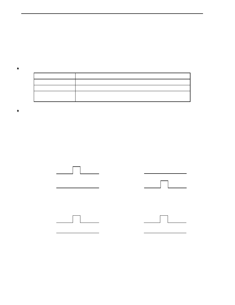
CHAPTER 14 SERIAL INTERFACE UART6
User's Manual U16228EJ2V0UD
320
(f) Reception
error
Three types of errors may occur during reception: a parity error, framing error, or overrun error. If the error
flag of asynchronous serial interface reception error status register 6 (ASIS6) is set as a result of data
reception, a reception error interrupt request (INTSR6/INTSRE6) is generated.
Which error has occurred during reception can be identified by reading the contents of ASIS6 in the reception
error interrupt servicing (INTSR6/INTSRE6) (see Figure 14-6).
The contents of ASIS6 are reset to 0 when ASIS6 is read.
Table 14-3. Cause of Reception Error
Reception Error
Cause
Parity error
The parity specified for transmission does not match the parity of the receive data.
Framing error
Stop bit is not detected.
Overrun error
Reception of the next data is completed before data is read from receive buffer
register 6 (RXB6).
The error interrupt can be separated into reception completion interrupt (INTSR6) and error interrupt
(INTSRE6) by clearing bit 0 (ISRM6) of asynchronous serial interface operation mode register 6 (ASIM6) to
0.
Figure 14-20. Reception Error Interrupt
1. If ISRM6 is cleared to 0 (reception completion interrupt (INTSR6) and error interrupt (INTSRE6) are
separated)
(a) No error during reception
(b) Error during reception
INTSR6
INTSRE6
INTSR6
INTSRE6
2. If ISRM6 is set to 1 (error interrupt is included in INTSR6)
(a) No error during reception
(b) Error during reception
INTSRE6
INTSR6
INTSRE6
INTSR6

CHAPTER 14 SERIAL INTERFACE UART6
User's Manual U16228EJ2V0UD
321
(g) Noise filter of receive data
The RXD6 signal is sampled with the base clock output by the prescaler block.
If two sampled values are the same, the output of the match detector changes, and the data is sampled as
input data.
Because the circuit is configured as shown in Figure 14-21, the internal processing of the reception operation
is delayed by two clocks from the external signal status.
Figure 14-21. Noise Filter Circuit
Internal signal B
Internal signal A
Match detector
In
Base clock
R
X
D6/P14
Q
In
LD_EN
Q
(h) SBF transmission
When the device is incorporated in LIN, the SBF (Synchronous Break Field) transmission control function is
used for transmission. For the transmission operation of LIN, see Figure 14-1 LIN Transmission
Operation.
SBF transmission is used to transmit an SBF length that is a low-level width of 13 bits or more by adjusting
the baud rate value of the ordinary UART transmission function.
[Setting method]
Transmit 00H by setting the number of character bits of the data to 8 bits and the parity bit to 0 parity or even
parity. This enables a low-level transmission of a data frame consisting of 10 bits (1 bit (start bit) + 8 bits
(character bits) + 1 bit (parity bit)).
Adjust the baud rate value to adjust this 10-bit low level to the targeted SBF length.
Example If LIN is to be transmitted under the following conditions
∑
Base clock of UART6 = 5 MHz (set by clock selection register 6 (CKSR6))
∑
Target baud rate value = 19200 bps
To realize the above baud rate value, the length of a 13-bit SBF is as follows if the baud rate generator
control register 6 (BRGC6) is set to 130.
∑
13-bit SBF length = 0.2
µ
s
◊
130
◊
2
◊
13 = 676
µ
s
To realize a 13-bit SBF length in 10 bits, set a value 1.3 times the targeted baud rate to BRGC6. In this
example, set 169 to BRGC6. The transmission length of a 10-bit low level in this case is as follows, and
matches the 13-bit SBF length.
∑
10-bit low-level transmission length = 0.2
µ
s
◊
169
◊
2
◊
10 = 676
µ
s
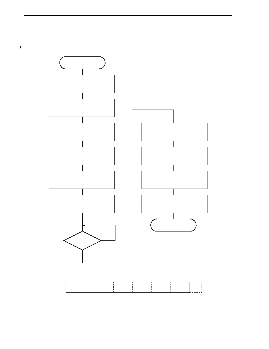
CHAPTER 14 SERIAL INTERFACE UART6
User's Manual U16228EJ2V0UD
322
If the number of bits set by BRGC6 runs short, adjust the number of bits by setting the base clock of
UART6.
Figure 14-22. Example of Setting Procedure of SBF Transmission (Flowchart)
Start
Read BRGC6 register and save current
set value of BRGC6 register to general-
purpose register.
Clear TXE6 and RXE6 bits of ASIM6
register to 0 (to disable transmission/
reception).
Set value to BRGC6 register to realize
desired SBF length.
Set character length of data to 8 bits
and parity to 0 or even using ASIM6
register.
Set TXE6 bit of ASIM6 register to 1 to
enable transmission.
Set TXB6 register to "00H" and start
transmission.
INTST6 occurred?
No
Yes
Clear TXE6 and RXE6 bits of ASIM6
register to 0.
Rewrite saved BRGC6 value to BRGC6
register.
Re-set PS61 bit, PS60 bit, and CL6 bit
of ASIM6 register to desired value.
Set TXE6 bit of ASIM6 register to 1 to
enable transmission.
End
Figure 14-23. SBF Transmission
T
X
D6
INTST6
1
2
3
4
5
6
7
8
9
10
11
12
13
Stop
Remark T
X
D6: T
X
D6 pin (output)
INTST6: Transmission completion interrupt request

CHAPTER 14 SERIAL INTERFACE UART6
User's Manual U16228EJ2V0UD
323
(i) SBF reception
When the device is incorporated in LIN, the SBF (Synchronous Break Field) reception control function is
used for reception. For the reception operation of LIN, see Figure 14-2 LIN Reception Operation.
Reception is enabled when bit 7 (POWER6) of asynchronous serial interface operation mode register 6
(ASIM6) is set to 1 and then bit 5 (RXE6) of ASIM6 is set to 1. SBF reception is enabled when bit 6 (SBRT6)
of asynchronous serial interface control register 6 (ASICL6) is set to 1. In the SBF reception enabled status,
the R
X
D6 pin is sampled and the start bit is detected in the same manner as the normal reception enable
status.
When the start bit has been detected, reception is started, and serial data is sequentially stored in the
receive shift register 6 (RXS6) at the set baud rate. When the stop bit is received and if the width of SBF is
11 bits or more, a reception completion interrupt request (INTSR6) is generated as normal processing. At
this time, the SBRF6 and SBRT6 bits are automatically cleared, and SBF reception ends. Detection of
errors, such as OVE6, PE6, and FE6 (bits 0 to 2 of asynchronous serial interface reception error status
register 6 (ASIS6)) is suppressed, and error detection processing of UART communication is not performed.
In addition, data transfer between receive shift register 6 (RXS6) and receive buffer register 6 (RXB6) is not
performed, and the reset value of FFH is retained. If the width of SBF is 10 bits or less, an interrupt does not
occur as error processing after the stop bit has been received, and the SBF reception mode is restored. In
this case, the SBRF6 and SBRT6 bits are not cleared.
Figure 14-24. SBF Reception
1. Normal SBF reception (stop bit is detected with a width of more than 10.5 bits)
R
X
D6
SBRT6
/SBRF6
INTSR6
1
2
3
4
5
6
7
8
9
10
11
2. SBF reception error (stop bit is detected with a width of 10.5 bits or less)
R
X
D6
SBRT6
/SBRF6
INTSR6
1
2
3
4
5
6
7
8
9
10
"0"
Remark R
X
D6: R
X
D6 pin (input)
SBRT6: Bit 6 of asynchronous serial interface control register 6 (ASICL6)
SBRF6: Bit 7 of ASICL6
INTSR6: Reception completion interrupt request

CHAPTER 14 SERIAL INTERFACE UART6
User's Manual U16228EJ2V0UD
324
14.4.3 Dedicated baud rate generator
The dedicated baud rate generator consists of a source clock selector and an 8-bit programmable counter, and
generates a serial clock for transmission/reception of UART6.
Separate 8-bit counters are provided for transmission and reception.
(1) Configuration of baud rate generator
∑
Base
clock
The clock selected by bits 3 to 0 (TPS63 to TPS60) of clock selection register 6 (CKSR6) is supplied to
each module when bit 7 (POWER6) of asynchronous serial interface operation mode register 6 (ASIM6) is
1. This clock is called the base clock and its frequency is called f
XCLK6
. The base clock is fixed to low level
when POWER6 = 0.
∑
Transmission
counter
This counter stops operation, cleared to 0, when bit 7 (POWER6) or bit 6 (TXE6) of asynchronous serial
interface operation mode register 6 (ASIM6) is 0.
It starts counting when POWER6 = 1 and TXE6 = 1.
The counter is cleared to 0 when the first data transmitted is written to transmit buffer register 6 (TXB6).
If data are continuously transmitted, the counter is cleared to 0 again when one frame of data has been
completely transmitted. If there is no data to be transmitted next, the counter is not cleared to 0 and continues
counting until POWER6 or TXE6 is cleared to 0.
∑
Reception
counter
This counter stops operation, cleared to 0, when bit 7 (POWER6) or bit 5 (RXE6) of asynchronous serial
interface operation mode register 6 (ASIM6) is 0.
It starts counting when the start bit has been detected.
The counter stops operation after one frame has been received, until the next start bit is detected.

CHAPTER 14 SERIAL INTERFACE UART6
User's Manual U16228EJ2V0UD
325
Figure 14-25. Configuration of Baud Rate Generator
Selector
POWER6
8-bit counter
Match detector
Baud rate
Baud rate generator
BRGC6: MDL67 to MDL60
1/2
POWER6, TXE6 (or RXE6)
CKSR6: TPS63 to TPS60
f
X
f
X
/2
f
X
/2
2
f
X
/2
3
f
X
/2
4
f
X
/2
5
f
X
/2
6
f
X
/2
7
f
X
/2
8
f
X
/2
9
f
X
/2
10
8-bit timer/
event counter
50 output
f
XCLK6
Remark POWER6: Bit 7 of asynchronous serial interface operation mode register 6 (ASIM6)
TXE6:
Bit 6 of ASIM6
RXE6:
Bit 5 of ASIM6
CKSR6:
Clock selection register 6
BRGC6:
Baud rate generator control register 6

CHAPTER 14 SERIAL INTERFACE UART6
User's Manual U16228EJ2V0UD
326
(2) Generation of serial clock
A serial clock can be generated by using clock selection register 6 (CKSR6) and baud rate generator control
register 6 (BRGC6).
Select the clock to be input to the 8-bit counter by using bits 3 to 0 (TPS63 to TPS60) of CKSR6.
Bits 7 to 0 (MDL67 to MDL60) of BRGC6 can be used to select the division value of the 8-bit counter.
(a) Baud
rate
The baud rate can be calculated by the following expression.
∑
Baud rate = [bps]
f
XCLK6
: Frequency of base clock selected by TPS63 to TPS60 bits of CKSR6 register
k:
Value set by MDL67 to MDL60 bits of BRGC6 register (k = 8, 9, 10, ..., 255)
(b) Error of baud rate
The baud rate error can be calculated by the following expression.
∑
Error (%) =
-
1
◊
100 [%]
Cautions 1. Keep the baud rate error during transmission to within the permissible error range at
the reception destination.
2. Make sure that the baud rate error during reception satisfies the range shown in (4)
Permissible baud rate range during reception.
Example: Frequency of base clock = 10 MHz = 10,000,000 Hz
Set value of MDL67 to MDL60 bits of BRGC6 register = 00100001B (k = 33)
Target baud rate = 153600 bps
Baud rate = 10 M/(2
◊
33)
=
10000000/(2
◊
33) = 151,515 [bps]
Error = (151515/153600
-
1)
◊
100
=
-
1.357 [%]
Actual baud rate (baud rate with error)
Desired baud rate (correct baud rate)
f
XCLK6
2
◊
k

CHAPTER 14 SERIAL INTERFACE UART6
User's Manual U16228EJ2V0UD
327
(3) Example of setting baud rate
Table 14-4. Set Data of Baud Rate Generator
f
X
= 10.0 MHz
f
X
= 8.38 MHz
f
X
= 4.19 MHz
Baud Rate
[bps]
TPS63 to
TPS60
k
Calculated
Value
ERR[%] TPS63 to
TPS60
k
Calculated
Value
ERR[%] TPS63 to
TPS60
k
Calculated
Value
ERR[%]
600
6H 130 601 0.16 6H 109 601 0.11 5H 109 601 0.11
1200
5H 130 1202 0.16
5H 109 1201 0.11
4H 109 1201 0.11
2400
4H 130 2404 0.16
4H 109 2403 0.11
3H 109 2403 0.11
4800
3H 130 4808 0.16
3H 109 4805 0.11
2H 109 4805 0.11
9600
2H 130 9615 0.16
2H 109 9610 0.11
1H 109 9610 0.11
10400
2H 120 10417 0.16
2H 101 10371 0.28
1H 101 10475
-
0.28
19200
1H 130 19231 0.16
1H 109 19200 0.11
0H 109 19220 0.11
31250 1H 80
31250 0.00 0H 134
31268 0.06 0H 67
31268 0.06
38400 0H 130
38462 0.16 0H 109
38440 0.11 0H 55 38090
-
0.80
76800 0H 65
76923 0.16 0H 55
76182
-
0.80 0H 27
77593 1.03
115200 0H 43 116279 0.94
0H 36 116388 1.03
0H 18 116389 1.03
153600 0H 33
151515
-
1.36
0H 27 155185 1.03
0H 14 149643
-
2.58
230400 0H 22
227272
-
1.36 0H 18
232777 1.03 0H 9 232778 1.03
Remark TPS63 to TPS60: Bits 3 to 0 of clock selection register 6 (CKSR6) (setting of base clock (f
XCLK6
))
k:
Value set by MDL67 to MDL60 bits of baud rate generator control register 6
(BRGC6) (k = 8, 9, 10, ..., 255)
f
X
:
X1 input clock oscillation frequency
ERR:
Baud rate error
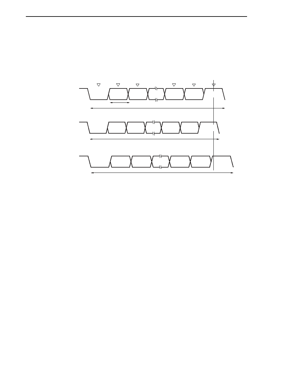
CHAPTER 14 SERIAL INTERFACE UART6
User's Manual U16228EJ2V0UD
328
(4) Permissible baud rate range during reception
The permissible error from the baud rate at the transmission destination during reception is shown below.
Caution Make sure that the baud rate error during reception is within the permissible error range, by
using the calculation expression shown below.
Figure 14-26. Permissible Baud Rate Range During Reception
FL
1 data frame (11
◊
FL)
FLmin
FLmax
Data frame length
of UART6
Start bit
Bit 0
Bit 1
Bit 7
Parity bit
Minimum permissible
data frame length
Maximum permissible
data frame length
Stop bit
Start bit
Bit 0
Bit 1
Bit 7
Parity bit
Latch timing
Stop bit
Start bit
Bit 0
Bit 1
Bit 7
Parity bit
Stop bit
As shown in Figure 14-26, the latch timing of the receive data is determined by the counter set by baud rate
generator control register 6 (BRGC6) after the start bit has been detected. If the last data (stop bit) meets this
latch timing, the data can be correctly received.
Assuming that 11-bit data is received, the theoretical values can be calculated as follows.
FL = (Brate)
-
1
Brate: Baud rate of UART6
k:
Set value of BRGC6
FL: 1-bit
data
length
Margin of latch timing: 2 clocks
CHAPTER 14 SERIAL INTERFACE UART6
User's Manual U16228EJ2V0UD
329
Minimum permissible data frame length: FLmin = 11
◊
FL
-
◊
FL = FL
Therefore, the maximum receivable baud rate at the transmission destination is as follows.
BRmax = (FLmin/11)
-
1
= Brate
Similarly, the maximum permissible data frame length can be calculated as follows.
10
k + 2
21k
-
2
11
2
◊
k
2
◊
k
FLmax = FL
◊
11
Therefore, the minimum receivable baud rate at the transmission destination is as follows.
BRmin = (FLmax/11)
-
1
= Brate
The permissible baud rate error between UART6 and the transmission destination can be calculated from the
above minimum and maximum baud rate expressions, as follows.
Table 14-5. Maximum/Minimum Permissible Baud Rate Error
Division Ratio (k)
Maximum Permissible Baud Rate Error
Minimum Permissible Baud Rate Error
8 +3.53%
-
3.61%
20 +4.26%
-
4.31%
50 +4.56%
-
4.58%
100 +4.66%
-
4.67%
255 +4.72%
-
4.73%
Remarks 1. The permissible error of reception depends on the number of bits in one frame, input clock
frequency, and division ratio (k). The higher the input clock frequency and the higher the division
ratio (k), the higher the permissible error.
2. k: Set value of BRGC6
22k
21k + 2
◊
FLmax = 11
◊
FL
-
◊
FL = FL
21k ≠ 2
20k
20k
21k
-
2
k
-
2
2k
21k + 2
2k
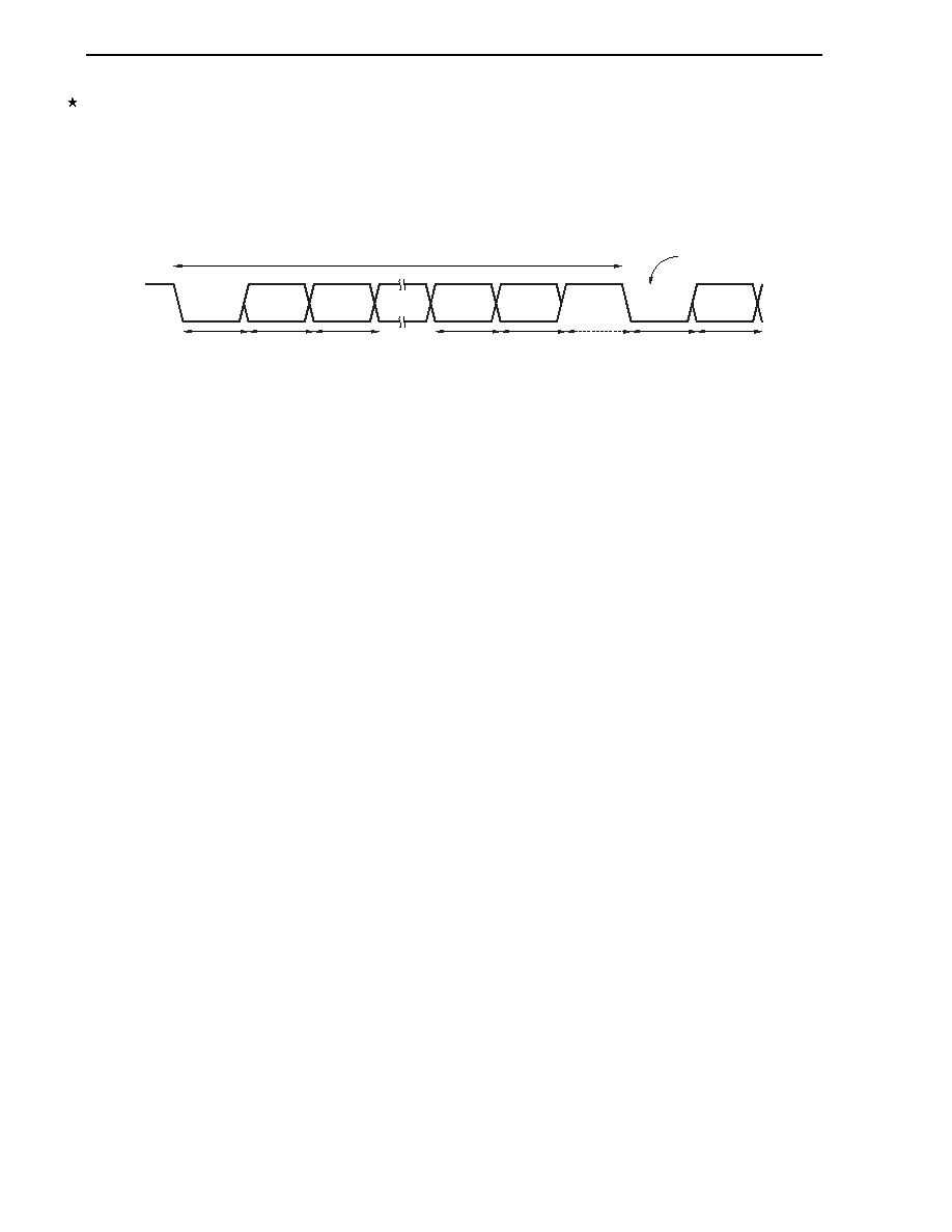
CHAPTER 14 SERIAL INTERFACE UART6
User's Manual U16228EJ2V0UD
330
(5) Data frame length during continuous transmission
When data is continuously transmitted, the data frame length from a stop bit to the next start bit is extended by
two clocks of base clock from the normal value. However, the result of communication is not affected because
the timing is initialized on the reception side when the start bit is detected.
Figure 14-27. Data Frame Length During Continuous Transmission
Start bit
Bit 0
Bit 1
Bit 7
Parity bit
Stop bit
FL
1 data frame
FL
FL
FL
FL
FL
FL
FLstp
Start bit of
second byte
Start bit
Bit 0
Where the 1-bit data length is FL, the stop bit length is FLstp, and base clock frequency is f
XCLK6
, the following
expression is satisfied.
FLstp = FL + 2/f
XCLK6
Therefore, the data frame length during continuous transmission is:
Data frame length = 11
◊
FL + 2/f
XCLK6

User's Manual U16228EJ2V0UD
331
CHAPTER 15 SERIAL INTERFACES CSI10 AND CSI11
The
µ
PD780131 and 780132 incorporate serial interface CSI10, and the
µ
PD780133, 780134, 78F0134, 780136,
780138, and 78F0138 incorporate serial interfaces CSI10 and CSI11.
15.1 Functions of Serial Interfaces CSI10 and CSI11
Serial interfaces CSI10 and CSI11 have the following two modes.
∑
Operation stop mode
∑
3-wire serial I/O mode
(1) Operation stop mode
This mode is used when serial communication is not performed and can enable a reduction in the power
consumption.
For details, see 15.4.1 Operation stop mode.
(2) 3-wire serial I/O mode (MSB/LSB-first selectable)
This mode is used to communicate 8-bit data using three lines: a serial clock line (SCK1n) and two serial data
lines (SI1n and SO1n).
The processing time of data communication can be shortened in the 3-wire serial I/O mode because transmission
and reception can be simultaneously executed.
In addition, whether 8-bit data is communicated with the MSB or LSB first can be specified, so this interface can
be connected to any device.
The 3-wire serial I/O mode is used for connecting peripheral ICs and display controllers with a clocked serial
interface.
For details, see 15.4.2 3-wire serial I/O mode.
CHAPTER 15 SERIAL INTERFACES CSI10 AND CSI11
User's Manual U16228EJ2V0UD
332
15.2 Configuration of Serial Interfaces CSI10 and CSI11
Serial interfaces CSI10 and CSI11 include the following hardware.
Table 15-1. Configuration of Serial Interfaces CSI10 and CSI11
Item Configuration
Registers
Transmit buffer register 1n (SOTB1n)
Serial I/O shift register 1n (SIO1n)
Transmit controller
Clock start/stop controller & clock phase controller
Control registers
Serial operation mode register 1n (CSIM1n)
Serial clock selection register 1n (CSIC1n)
Port mode register 0 (PM0) or port mode register 1 (PM1)
Port register 0 (P0) or port register 1 (P1)
Remark n = 0:
µ
PD780131, 780132
n = 0, 1:
µ
PD780133, 780134, 78F0134, 780136, 780138, 78F0138
Figure 15-1. Block Diagram of Serial Interface CSI10
Internal bus
SI10/P11/R
X
D0
INTCSI10
f
X
/2
f
X
/2
2
f
X
/2
3
f
X
/2
4
f
X
/2
5
f
X
/2
6
f
X
/2
7
SCK10/P10/TxD0
Transmit buffer
register 10 (SOTB10)
Transmit controller
Clock start/stop controller &
clock phase controller
Serial I/O shift
register 10 (SIO10)
Output
selector
SO10/P12
Output latch
8
Transmit data
controller
8
Output latch
(P12)
PM12
Selector
CHAPTER 15 SERIAL INTERFACES CSI10 AND CSI11
User's Manual U16228EJ2V0UD
333
Figure 15-2. Block Diagram of Serial Interface CSI11
(
µ
PD780133, 780134, 78F0134, 780136, 780138, and 78F0138 Only)
8
8
Internal bus
Output
selector
Output latch
Transmit controller
Clock start/stop controller &
clock phase controller
SO11/P02
INTCSI11
Transmit buffer
register 11 (SOTB11)
Transmit data
controller
SI11/P03
Serial I/O shift
register 11 (SIO11)
f
X
/2
f
X
/2
2
f
X
/2
3
f
X
/2
4
f
X
/2
5
f
X
/2
6
f
X
/2
7
SCK11/P04
SSI11
Output latch
(P02)
PM02
Selector
(1) Transmit buffer register 1n (SOTB1n)
This register sets the transmit data.
Transmission/reception is started by writing data to SOTB1n when bit 7 (CSIE1n) and bit 6 (TRMD1n) of serial
operation mode register 1n (CSIM1n) is 1.
The data written to SOTB1n is converted from parallel data into serial data by serial I/O shift register 1n, and
output to the serial output pin (SO1n).
SOTB1n can be written or read by an 8-bit memory manipulation instruction.
RESET input clears this register to 00H.
Cautions 1. Do not access SOTB1n when CSOT1n = 1 (during serial communication).
2. The SSI11 pin can be used in the slave mode. For details of the transmission/reception
operation, see 15.4.2 (2) Communication operation.
(2) Serial I/O shift register 1n (SIO1n)
This is an 8-bit register that converts data from parallel data into serial data and vice versa.
This register can be read by an 8-bit memory manipulation instruction.
Reception is started by reading data from SIO1n if bit 6 (TRMD1n) of serial operation mode register 1n (CSIM1n)
is 0.
During reception, the data is read from the serial input pin (SI1n) to SIO1n.
RESET input clears this register to 00H.
Cautions 1. Do not access SIO1n when CSOT1n = 1 (during serial communication).
2. The SSI11 pin can be used in the slave mode. For details of the reception operation, see
15.4.2 (2) Communication operation.
Remark n = 0:
µ
PD780131, 780132
n = 0, 1:
µ
PD780133, 780134, 78F0134, 780136, 780138, 78F0138
CHAPTER 15 SERIAL INTERFACES CSI10 AND CSI11
User's Manual U16228EJ2V0UD
334
15.3 Registers Controlling Serial Interfaces CSI10 and CSI11
Serial interfaces CSI10 and CSI11 are controlled by the following four registers.
∑
Serial operation mode register 1n (CSIM1n)
∑
Serial clock selection register 1n (CSIC1n)
∑
Port mode register 0 (PM0) or port mode register 1 (PM1)
∑
Port register 0 (P0) or port register 1 (P1)
(1) Serial operation mode register 1n (CSIM1n)
CSIM1n is used to select the operation mode and enable or disable operation.
CSIM1n can be set by a 1-bit or 8-bit memory manipulation instruction.
RESET input clears this register to 00H.
Remark n = 0:
µ
PD780131, 780132
n = 0, 1:
µ
PD780133, 780134, 78F0134, 780136, 780138, 78F0138
Figure 15-3. Format of Serial Operation Mode Register 10 (CSIM10)
Address: FF80H After reset: 00H R/W
Note 1
Symbol
<7>
6 5 4 3 2 1 0
CSIM10
CSIE10
TRMD10
0
DIR10
0 0 0
CSOT10
CSIE10
Operation control in 3-wire serial I/O mode
0
Disables
operation
Note 2
and asynchronously resets the internal circuit
Note 3
.
1
Enables
operation
TRMD10
Note 4
Transmit/receive
mode
control
0
Note 5
Receive mode (transmission disabled).
1
Transmit/receive
mode
DIR10
Note 6
First
bit
specification
0
MSB
1
LSB
CSOT10
Communication
status
flag
0
Communication is stopped.
1
Communication is in progress.
Notes 1. Bit 0 is a read-only bit.
2. When using as a general-purpose port, see Caution 3 of Figure 15-5 and Table 15-2.
3. Bit 0 (CSOT10) of CSIM10 and serial I/O shift register 10 (SIO10) are reset.
4. Do not rewrite TRMD10 when CSOT10 = 1 (during serial communication).
5. The SO10 output is fixed to the low level when TRMD10 is 0. Reception is started when data is read
from SIO10.
6. Do not rewrite DIR10 when CSOT10 = 1 (during serial communication).
Caution Be sure to clear bit 5 to 0.
CHAPTER 15 SERIAL INTERFACES CSI10 AND CSI11
User's Manual U16228EJ2V0UD
335
Figure 15-4. Format of Serial Operation Mode Register 11 (CSIM11)
Address: FF88H After reset: 00H R/W
Note 1
Symbol
<7>
6 5 4 3 2 1 0
CSIM11 CSIE11 TRMD11 SSE11 DIR11
0
0
0
CSOT11
CSIE11
Operation control in 3-wire serial I/O mode
0
Disables
operation
Note 2
and asynchronously resets the internal circuit
Note 3
.
1
Enables
operation
TRMD11
Note 4
Transmit/receive
mode
control
0
Note 5
Receive mode (transmission disabled).
1
Transmit/receive
mode
SSE11
Notes 6, 7
SSI11 pin use selection
0
SSI11 pin is not used
1
SSI11 pin is used
DIR11
Note 8
First
bit
specification
0
MSB
1
LSB
CSOT11
Communication
status
flag
0
Communication is stopped.
1
Communication is in progress.
Notes 1. Bit 0 is a read-only bit.
2. When using as a general-purpose port, see Caution 3 of Figure 15-6 and Table 15-2.
3. Bit 0 (CSOT11) of CSIM11 and serial I/O shift register 11 (SIO11) are reset.
4. Do not rewrite TRMD11 when CSOT11 = 1 (during serial communication).
5. The SO11 output is fixed to the low level when TRMD11 is 0. Reception is started when data is read
from SIO11.
6. Do not rewrite SSE11 when CSOT11 = 1 (during serial communication).
7. Before setting this bit to 1, fix the SSI11 pin input level to 0 or 1.
8. Do not rewrite DIR11 when CSOT11 = 1 (during serial communication).
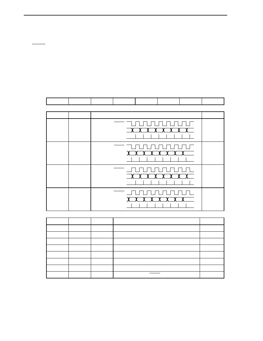
CHAPTER 15 SERIAL INTERFACES CSI10 AND CSI11
User's Manual U16228EJ2V0UD
336
(2) Serial clock selection register 1n (CSIC1n)
This register specifies the timing of the data transmission/reception and sets the serial clock.
CSIC1n can be set by a 1-bit or 8-bit memory manipulation instruction.
RESET input clears this register to 00H.
Remark n = 0:
µ
PD780131, 780132
n = 0, 1:
µ
PD780133, 780134, 78F0134, 780136, 780138, 78F0138
Figure 15-5. Format of Serial Clock Selection Register 10 (CSIC10)
Address: FF81H After reset: 00H R/W
Symbol
7 6 5 4 3 2 1 0
CSIC10 0
0
0 CKP10
DAP10
CKS102
CKS101
CKS100
CKP10
DAP10
Specification of data transmission/reception timing
Type
0
0
D7
D6
D5
D4
D3
D2
D1
D0
SCK10
SO10
SI10 input timing
1
0
1
D7
D6
D5
D4
D3
D2
D1
D0
SCK10
SO10
SI10 input timing
2
1
0
D7
D6
D5
D4
D3
D2
D1
D0
SCK10
SO10
SI10 input timing
3
1
1
D7
D6
D5
D4
D3
D2
D1
D0
SCK10
SO10
SI10 input timing
4
CKS102 CKS101 CKS100
CSI10
serial clock selection
Mode
0 0 0
f
X
/2 (5 MHz)
Master mode
0 0 1
f
X
/2
2
(2.5 MHz)
Master mode
0 1 0
f
X
/2
3
(1.25 MHz)
Master mode
0 1 1
f
X
/2
4
(625 kHz)
Master mode
1 0 0
f
X
/2
5
(312.5 kHz)
Master mode
1 0 1
f
X
/2
6
(156.25 kHz)
Master mode
1 1 0
f
X
/2
7
(78.13 kHz)
Master mode
1
1
1
External clock input to SCK10
Slave mode

CHAPTER 15 SERIAL INTERFACES CSI10 AND CSI11
User's Manual U16228EJ2V0UD
337
Cautions 1. When the Ring-OSC clock is selected as the clock supplied to the CPU, the clock of the Ring-
OSC oscillator is divided and supplied as the serial clock. At this time, the operation of serial
interface CSI10 is not guaranteed.
2. Do not write to CSIC10 while CSIE10 = 1 (operation enabled).
3. Clear CKP10 to 0 to use P10/SCK10/TxD0, P11/SI10/RxD0, and P12/SO10 as general-purpose
port pins.
4. The phase type of the data clock is type 1 after reset.
Remarks 1. Figures in parentheses are for operation with fx = 10 MHz
2. f
X
: X1 input clock oscillation frequency

CHAPTER 15 SERIAL INTERFACES CSI10 AND CSI11
User's Manual U16228EJ2V0UD
338
Figure 15-6. Format of Serial Clock Selection Register 11 (CSIC11)
Address: FF89H After reset: 00H R/W
Symbol
7 6 5 4 3 2 1 0
CSIC11 0
0
0 CKP11
DAP11
CKS112
CKS111
CKS110
CKP11
DAP11
Specification of data transmission/reception timing
Type
0
0
D7
D6
D5
D4
D3
D2
D1
D0
SCK11
SO11
SI11 input timing
1
0
1
D7
D6
D5
D4
D3
D2
D1
D0
SCK11
SO11
SI11 input timing
2
1
0
D7
D6
D5
D4
D3
D2
D1
D0
SCK11
SO11
SI11 input timing
3
1
1
D7
D6
D5
D4
D3
D2
D1
D0
SCK11
SO11
SI11 input timing
4
CKS112 CKS111 CKS110
CSI11
serial clock selection
Mode
0 0 0
f
X
/2 (5 MHz)
Master mode
0 0 1
f
X
/2
2
(2.5 MHz)
Master mode
0 1 0
f
X
/2
3
(1.25 MHz)
Master mode
0 1 1
f
X
/2
4
(625 kHz)
Master mode
1 0 0
f
X
/2
5
(312.5 kHz)
Master mode
1 0 1
f
X
/2
6
(156.25 kHz)
Master mode
1 1 0
f
X
/2
7
(78.13 kHz)
Master mode
1
1
1
External clock input to SCK11
Slave mode
Cautions 1. When the Ring-OSC clock is selected as the clock supplied to the CPU, the clock of the Ring-
OSC oscillator is divided and supplied as the serial clock. At this time, the operation of serial
interface CSI11 is not guaranteed.
2. Do not write to CSIC11 while CSIE11 = 1 (operation enabled).
3. Clear CKP11 to 0 to use P02/SO11, P03/SI11, and P04/SCK11 as general-purpose port pins.
4. The phase type of the data clock is type 1 after reset.
Remarks 1. Figures in parentheses are for operation with fx = 10 MHz
2. f
X
: X1 input clock oscillation frequency

CHAPTER 15 SERIAL INTERFACES CSI10 AND CSI11
User's Manual U16228EJ2V0UD
339
(3) Port mode registers 0 and 1 (PM0, PM1)
These registers set port 0 and 1 input/output in 1-bit units.
When using P10/SCK10 and P04/SCK11
Note
as the clock output pins of the serial interface, and P12/SO10 and
P02/SO11
Note
as the data output pins, clear PM10, PM04, PM12, PM02, and the output latches of P10, P04, P12,
and P02 to 0.
When using P10/SCK10 and P04/SCK11
Note
as the clock input pins of the serial interface, P11/SI10/RxD0 and
P03/SI11
Note
as the data input pins, and P05/SSI11/TI001 as the chip select input pin, set PM10, PM04, PM11,
PM03, and PM05 to 1. At this time, the output latches of P10, P04, P11, P03, and P05 may be 0 or 1.
PM0 and PM1 can be set by a 1-bit or 8-bit memory manipulation instruction.
RESET input sets these registers to FFH.
Note
µ
PD780133, 780134, 78F0134, 780136, 780138, and 78F0138 only.
Figure 15-7. Format of Port Mode Register 0 (PM0)
7
1
6
PM06
5
PM05
4
PM04
3
PM03
2
PM02
1
PM01
0
PM00
Symbol
PM0
Address: FF20H After reset: FFH R/W
PM0n
0
1
P0n pin I/O mode selection (n = 0 to 6)
Output mode (output buffer on)
Input mode (output buffer off)
Figure 15-8. Format of Port Mode Register 1 (PM1)
7
PM17
6
PM16
5
PM15
4
PM14
3
PM13
2
PM12
1
PM11
0
PM10
Symbol
PM1
Address: FF21H After reset: FFH R/W
PM1n
0
1
P1n pin I/O mode selection (n = 0 to 7)
Output mode (output buffer on)
Input mode (output buffer off)
CHAPTER 15 SERIAL INTERFACES CSI10 AND CSI11
User's Manual U16228EJ2V0UD
340
15.4 Operation of Serial Interfaces CSI10 and CSI11
Serial interfaces CSI10 and CSI11 can be used in the following two modes.
∑
Operation stop mode
∑
3-wire serial I/O mode
15.4.1 Operation stop mode
Serial communication is not executed in this mode. Therefore, the power consumption can be reduced. In
addition, the P10/SCK10/T
X
D0, P11/SI10/R
X
D0, P12/SO10, P02/SO11
Note
, P03/SI11
Note
, and P04/SCK11
Note
pins can
be used as ordinary I/O port pins in this mode.
Note
µ
PD780133, 780134, 78F0134, 780136, 780138, and 78F0138 only
(1) Register used
The operation stop mode is set by serial operation mode register 1n (CSIM1n).
To set the operation stop mode, clear bit 7 (CSIE1n) of CSIM1n to 0.
(a) Serial operation mode register 1n (CSIM1n)
CSIM1n can be set by a 1-bit or 8-bit memory manipulation instruction.
RESET input clears CSIM1n to 00H.
Remark n = 0:
µ
PD780131, 780132
n = 0, 1:
µ
PD780133, 780134, 78F0134, 780136, 780138, 78F0138
∑
Serial operation mode register 10 (CSIM10)
Address: FF80H After reset: 00H R/W
Symbol
<7>
6 5 4 3 2 1 0
CSIM10
CSIE10
TRMD10
0
DIR10
0 0 0
CSOT10
CSIE10
Operation control in 3-wire serial I/O mode
0
Disables
operation
Note 1
and asynchronously resets the internal circuit
Note 2
.
Notes 1. To use the SI10/RxD0/P11, SO10/P12, and SCK10/TxD0/P10 pins as general-purpose port pins,
see CHAPTER 4 PORT FUNCTIONS.
2. Bit 0 (CSOT10) of CSIM10 and serial I/O shift register 10 (SIO10) are reset.
∑
Serial operation mode register 11 (CSIM11)
Address: FF88H After reset: 00H R/W
Symbol
<7>
6 5 4 3 2 1 0
CSIM11
CSIE11
TRMD11
SSE11
DIR11
0 0 0
CSOT11
CSIE11
Operation control in 3-wire serial I/O mode
0
Disables
operation
Note 1
and asynchronously resets the internal circuit
Note 2
.
Notes 1. To use the SI11/P03, SO11/P02, SCK11/P04, and SSI11/TI001/P05 pins as general-purpose
port pins, see CHAPTER 4 PORT FUNCTIONS.
2. Bit 0 (CSOT11) of CSIM11 and serial I/O shift register 11 (SIO11) are reset.

CHAPTER 15 SERIAL INTERFACES CSI10 AND CSI11
User's Manual U16228EJ2V0UD
341
15.4.2 3-wire serial I/O mode
The 3-wire serial I/O mode is used for connecting peripheral ICs and display controllers with a clocked serial
interface.
In this mode, communication is executed by using three lines: the serial clock (SCK1n), serial output (SO1n), and
serial input (SI1n) lines.
(1) Registers used
∑
Serial operation mode register 1n (CSIM1n)
∑
Serial clock selection register 1n (CSIC1n)
∑
Port mode register 0 (PM0) or port mode register 1 (PM1)
∑
Port register 0 (P0) or port register 1 (P1)
The basic procedure of setting an operation in the 3-wire serial I/O mode is as follows.
<1> Set the CSIC1n register (see Figures 15-5 and 15-6).
<2> Set bits 0 and 4 to 6 (CSOT1n, DIR1n, SSE11 (serial interface CSI11 only), and TRMD1n) of the CSIM1n
register (see Figures 15-3 and 15-4).
<3> Set bit 7 (CSIE1n) of the CSIM1n register to 1.
Transmission/reception is enabled.
<4> Write data to transmit buffer register 1n (SOTB1n).
Data transmission/reception is started.
Read data from serial I/O shift register 1n (SIO1n).
Data reception is started.
Caution Take relationship with the other party of communication when setting the port mode register
and port register.
Remark n = 0:
µ
PD780131, 780132
n = 0, 1:
µ
PD780133, 780134, 78F0134, 780136, 780138, 78F0138
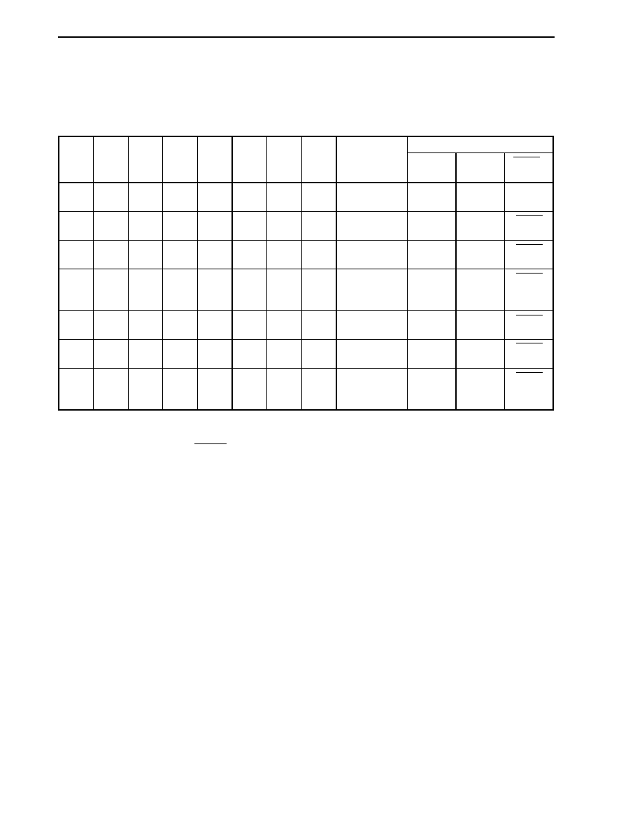
CHAPTER 15 SERIAL INTERFACES CSI10 AND CSI11
User's Manual U16228EJ2V0UD
342
The relationship between the register settings and pins is shown below.
Table 15-2. Relationship Between Register Settings and Pins (1/2)
(a) Serial interface CSI10
Pin Function
CSIE10 TRMD10 PM11
P11
PM12
P12
PM10
P10
CSI10
Operation
SI10/RxD0/
P11
SO10/P12
SCK10/
TxD0/P10
0 ◊
◊
Note 1
◊
Note 1
◊
Note 1
◊
Note 1
◊
Note 1
◊
Note 1
Stop RxD0/P11
P12
TxD0/
P10
Note 2
1 0 1 ◊
◊
Note 1
◊
Note 1
1 ◊
Slave
reception
Note 3
SI10 P12
SCK10
(input)
Note 3
1 1
◊
Note 1
◊
Note 1
0 0 1 ◊
Slave
transmission
Note 3
RxD0/P11 SO10 SCK10
(input)
Note 3
1 1 1 ◊ 0 0 1 ◊
Slave
transmission/
reception
Note 3
SI10 SO10
SCK10
(input)
Note 3
1 0 1 ◊
◊
Note 1
◊
Note 1
0 1
Master
reception
SI10
P12 SCK10
(output)
1 1
◊
Note 1
◊
Note 1
0 0 0 1
Master
transmission
RxD0/P11 SO10 SCK10
(output)
1 1 1 ◊ 0 0 0 1
Master
transmission/
reception
SI10 SO10
SCK10
(output)
Notes 1. Can be set as port function.
2. To use P10/SCK10/TxD0 as port pins, clear CKP10 to 0.
3. To use the slave mode, set CKS102, CKS101, and CKS100 to 1, 1, 1.
Remark ◊:
don't
care
CSIE10:
Bit 7 of serial operation mode register 10 (CSIM10)
TRMD10:
Bit 6 of CSIM10
CKP10:
Bit 4 of serial clock selection register 10 (CSIC10)
CKS102, CKS101, CKS100: Bits 2 to 0 of CSIC10
PM1◊:
Port mode register
P1◊:
Port output latch
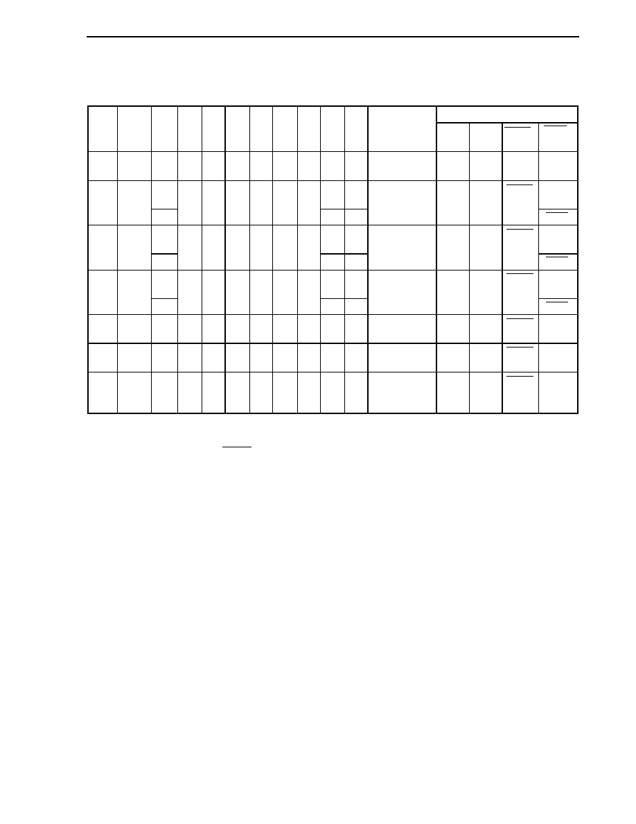
CHAPTER 15 SERIAL INTERFACES CSI10 AND CSI11
User's Manual U16228EJ2V0UD
343
Table 15-2. Relationship Between Register Settings and Pins (2/2)
(b) Serial interface CSI11 (
µ
PD780133, 780134, 78F0134, 780136, 780138, and 78F0138 only)
Pin Function
CSIE11
TRMD11
SSE11
PM03 P03 PM02 P02 PM04 P04 PM05 P05
CSI11
Operation
SI11/
P03
SO11/
P02
SCK11/
P04
SSI11/
TI001/P05
0 ◊ ◊
◊
Note 1
◊
Note 1
◊
Note 1
◊
Note 1
◊
Note 1
◊
Note 1
◊
Note 1
◊
Note 1
Stop P03
P02
P04
Note 2
TI001/
P05
0 ◊
Note 1
◊
Note 1
TI001/
P05
1 0
1
1 ◊
◊
Note 1
◊
Note 1
1 ◊
1 ◊
Slave
reception
Note 3
SI11 P02 SCK11
(input)
Note 3
SSI11
0 ◊
Note 1
◊
Note 1
TI001/
P05
1 1
1
◊
Note 1
◊
Note 1
0 0 1 ◊
1 ◊
Slave
transmission
Note 3
P03 SO11
SCK11
(input)
Note 3
SSI11
0 ◊
Note 1
◊
Note 1
TI001/
P05
1 1
1
1 ◊ 0 0 1 ◊
1 ◊
Slave
transmission/
reception
Note 3
SI11 SO11 SCK11
(input)
Note 3
SSI11
1 0 0
1
◊
◊
Note 1
◊
Note 1
0 1
◊
Note 1
◊
Note 1
Master
reception
SI11 P02 SCK11
(output)
TI001/
P05
1 1 0
◊
Note 1
◊
Note 1
0 0 0 1
◊
Note 1
◊
Note 1
Master
transmission
P03 SO11
SCK11
(output)
TI001/
P05
1
1 0 1 ◊ 0 0 0 1
◊
Note 1
◊
Note 1
Master
transmission/
reception
SI11 SO11 SCK11
(output)
TI001/
P05
Notes 1. Can be set as port function.
2. To use P04/SCK11 as port pins, clear CKP11 to 0.
3. To use the slave mode, set CKS112, CKS111, and CKS110 to 1, 1, 1.
Remark ◊:
don't
care
CSIE11:
Bit 7 of serial operation mode register 11 (CSIM11)
TRMD11:
Bit 6 of CSIM11
CKP11:
Bit 4 of serial clock selection register 11 (CSIC11)
CKS112, CKS111, CKS110: Bits 2 to 0 of CSIC11
PM0◊:
Port mode register
P0◊:
Port output latch

CHAPTER 15 SERIAL INTERFACES CSI10 AND CSI11
User's Manual U16228EJ2V0UD
344
(2) Communication
operation
In the 3-wire serial I/O mode, data is transmitted or received in 8-bit units. Each bit of the data is transmitted or
received in synchronization with the serial clock.
Data can be transmitted or received if bit 6 (TRMD1n) of serial operation mode register 1n (CSIM1n) is 1.
Transmission/reception is started when a value is written to transmit buffer register 1n (SOTB1n). In addition,
data can be received when bit 6 (TRMD1n) of serial operation mode register 1n (CSIM1n) is 0.
Reception is started when data is read from serial I/O shift register 1n (SIO1n).
However, communication is performed as follows if bit 5 (SSE11) of CSIM11 is 1 when serial interface CSI11 is in
the slave mode.
<1> Low level input to the SSI11 pin
Transmission/reception is started when SOTB11 is written, or reception is started when SIO11 is read.
<2> High level input to the SSI11 pin
Transmission/reception or reception is held, therefore, even if SOTB11 is written or SIO11 is read,
transmission/reception or reception will not be started.
<3> Data is written to SOTB11 or data is read from SIO11 while a high level is input to the SSI11 pin, then a low
level is input to the SSI11 pin
Transmission/reception or reception is started.
<4> A high level is input to the SSI11 pin during transmission/reception or reception
Transmission/reception or reception is suspended.
After communication has been started, bit 0 (CSOT1n) of CSIM1n is set to 1. When communication of 8-bit data
has been completed, a communication completion interrupt request flag (CSIIF1n) is set, and CSOT1n is cleared
to 0. Then the next communication is enabled.
Cautions 1. Do not access the control register and data register when CSOT1n = 1 (during serial
communication).
2. When using serial interface CSI11, wait for the duration of at least one clock before the
clock operation is started to change the level of the SSI11 pin in the slave mode; otherwise,
malfunctioning may occur.
Remark n = 0, 1
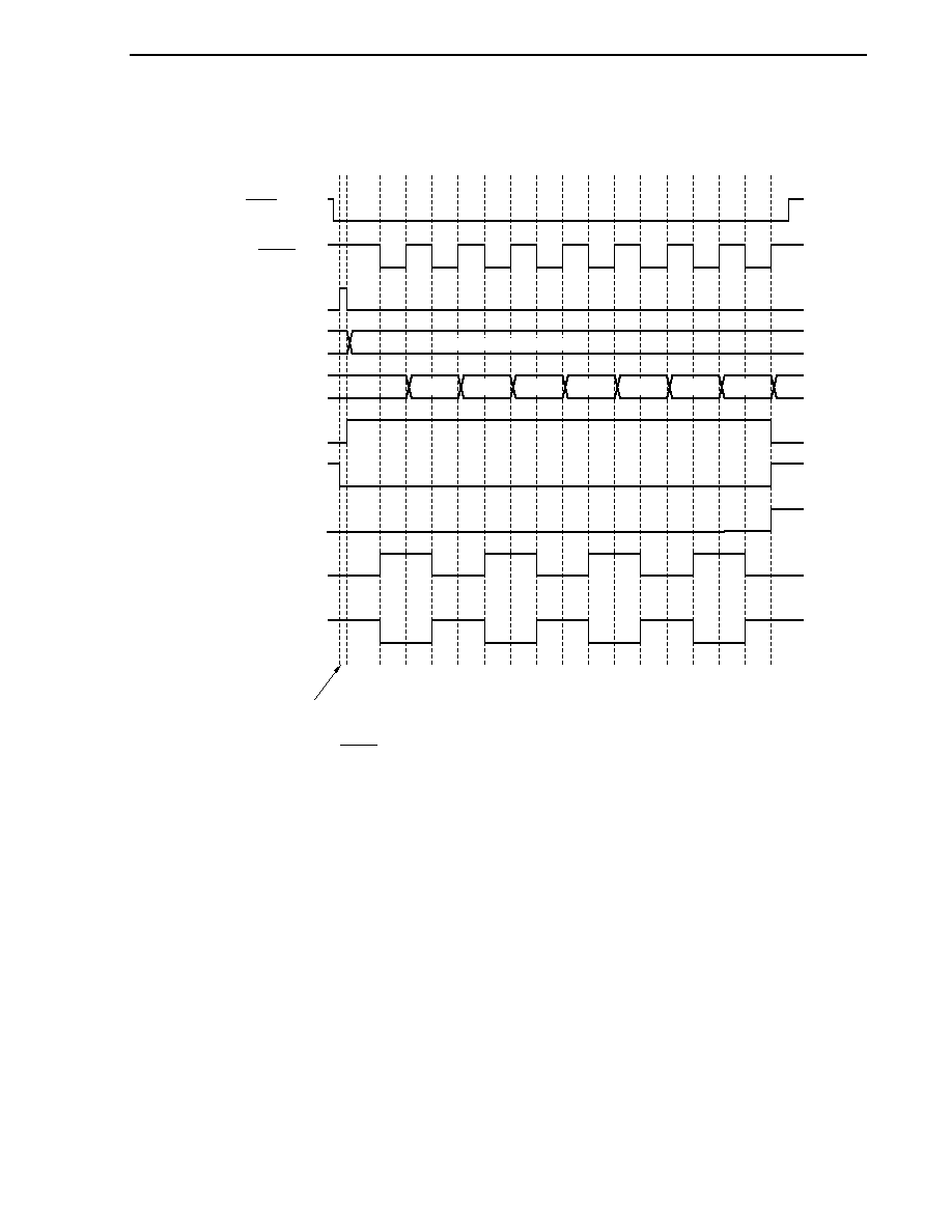
CHAPTER 15 SERIAL INTERFACES CSI10 AND CSI11
User's Manual U16228EJ2V0UD
345
Figure 15-9. Timing in 3-Wire Serial I/O Mode (1/2)
(1) Transmission/reception timing (Type 1; TRMD1n = 1, DIR1n = 0, CKP1n = 0, DAP1n = 0, SSE11 = 1
Note
)
AAH
ABH
56H
ADH
5AH
B5H
6AH
D5H
55H (communication data)
55H is written to SOTB1n.
SCK1n
SOTB1n
SIO1n
CSOT1n
CSIIF1n
SO1n
SI1n (receive AAH)
Read/write trigger
INTCSI1n
SSI11
Note
Note The SSE11 flag and SSI11 pin are available only for serial interface CSI11, and are used in the slave
mode.
Remark n = 0:
µ
PD780131, 780132
n = 0, 1:
µ
PD780133, 780134, 78F0134, 780136, 780138, 78F0138
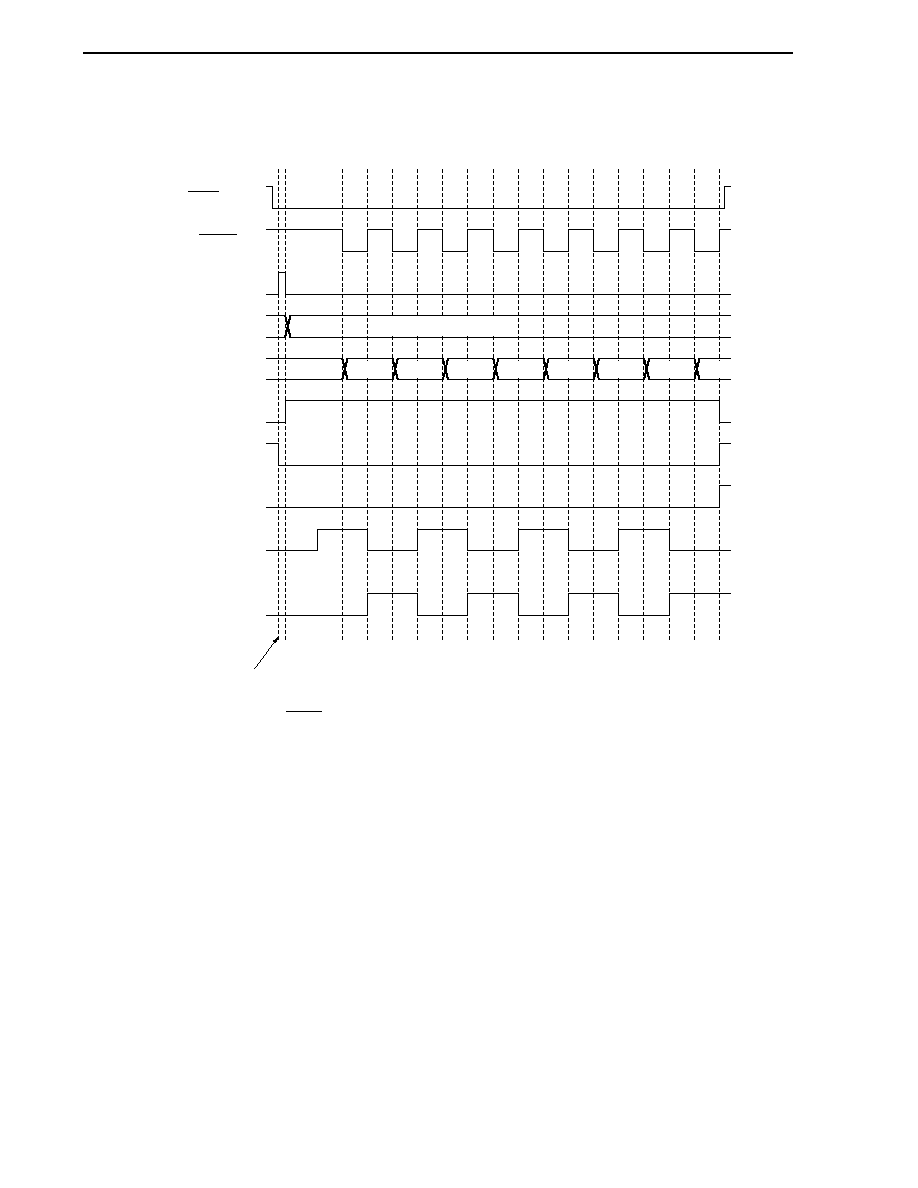
CHAPTER 15 SERIAL INTERFACES CSI10 AND CSI11
User's Manual U16228EJ2V0UD
346
Figure 15-9. Timing in 3-Wire Serial I/O Mode (2/2)
(2) Transmission/reception timing (Type 2; TRMD1n = 1, DIR1n = 0, CKP1n = 0, DAP1n = 1, SSE11 = 1
Note
)
ABH
56H
ADH
5AH
B5H
6AH
D5H
SCK1n
SOTB1n
SIO1n
CSOT1n
CSIIF1n
SO1n
SI1n (input AAH)
AAH
55H (communication data)
55H is written to SOTB1n.
Read/write trigger
INTCSI1n
SSI11
Note
Note The SSE11 flag and SSI11 pin are available only for serial interface CSI11, and are used in the slave
mode.
Remark n = 0:
µ
PD780131, 780132
n = 0, 1:
µ
PD780133, 780134, 78F0134, 780136, 780138, 78F0138
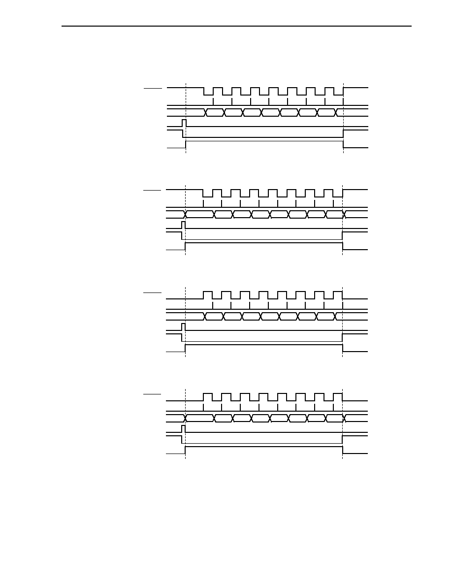
CHAPTER 15 SERIAL INTERFACES CSI10 AND CSI11
User's Manual U16228EJ2V0UD
347
Figure 15-10. Timing of Clock/Data Phase
(a) Type 1; CKP1n = 0, DAP1n = 0
D7
D6
D5
D4
D3
D2
D1
D0
SCK1n
SO1n
Writing to SOTB1n or
reading from SIO1n
SI1n capture
CSIIF1n
CSOT1n
(b) Type 2; CKP1n = 0, DAP1n = 1
D7
D6
D5
D4
D3
D2
D1
D0
SCK1n
SO1n
Writing to SOTB1n or
reading from SIO1n
SI1n capture
CSIIF1n
CSOT1n
(c) Type 3; CKP1n = 1, DAP1n = 0
D7
D6
D5
D4
D3
D2
D1
D0
SCK1n
SO1n
Writing to SOTB1n or
reading from SIO1n
SI1n capture
CSIIF1n
CSOT1n
(d) Type 4; CKP1n = 1, DAP1n = 1
D7
D6
D5
D4
D3
D2
D1
D0
SCK1n
SO1n
Writing to SOTB1n or
reading from SIO1n
SI1n capture
CSIIF1n
CSOT1n
Remark n = 0:
µ
PD780131, 780132
n = 0, 1:
µ
PD780133, 780134, 78F0134, 780136, 780138, 78F0138
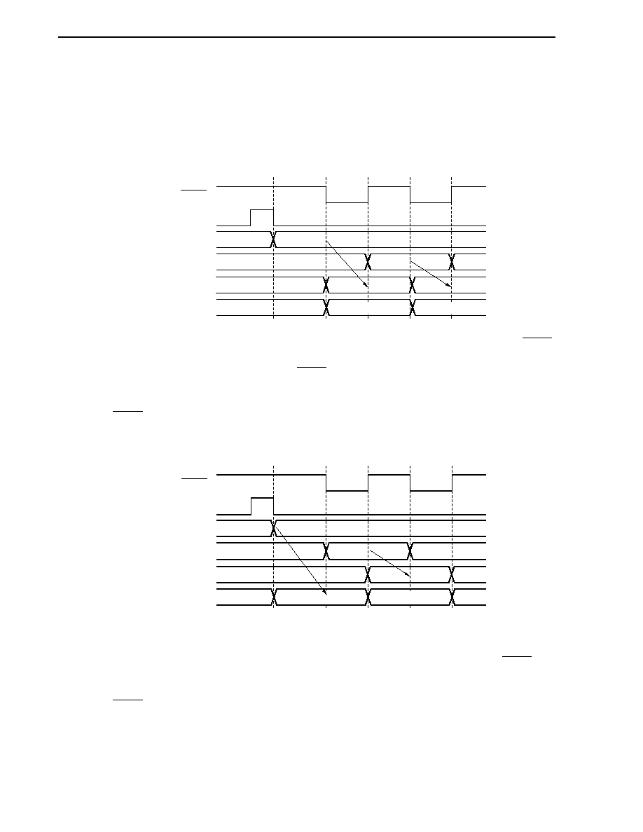
CHAPTER 15 SERIAL INTERFACES CSI10 AND CSI11
User's Manual U16228EJ2V0UD
348
(3) Timing of output to SO1n pin (first bit)
When communication is started, the value of transmit buffer register 1n (SOTB1n) is output from the SO1n pin.
The output operation of the first bit at this time is described below.
Figure 15-11. Output Operation of First Bit
(1) When CKP1n = 0, DAP1n = 0 (or CKP1n = 1, DAP1n = 0)
SCK1n
SOTB1n
SIO1n
SO1n
Writing to SOTB1n or
reading from SIO1n
First bit
2nd bit
Output latch
The first bit is directly latched by the SOTB1n register to the output latch at the falling (or rising) edge of SCK1n,
and output from the SO1n pin via an output selector. Then, the value of the SOTB1n register is transferred to the
SIO1n register at the next rising (or falling) edge of SCK1n, and shifted one bit. At the same time, the first bit of
the receive data is stored in the SIO1n register via the SI1n pin.
The second and subsequent bits are latched by the SIO1n register to the output latch at the next falling (or rising)
edge of SCK1n, and the data is output from the SO1n pin.
(2) When CKP1n = 0, DAP1n = 1 (or CKP1n = 1, DAP1n = 1)
SCK1n
SOTB1n
SIO1n
SO1n
Writing to SOTB1n or
reading from SIO1n
First bit
2nd bit
3rd bit
Output latch
The first bit is directly latched by the SOTB1n register at the falling edge of the write signal of the SOTB1n
register or the read signal of the SIO1n register, and output from the SO1n pin via an output selector. Then, the
value of the SOTB1n register is transferred to the SIO1n register at the next falling (or rising) edge of SCK1n, and
shifted one bit. At the same time, the first bit of the receive data is stored in the SIO1n register via the SI1n pin.
The second and subsequent bits are latched by the SIO1n register to the output latch at the next rising (or falling)
edge of SCK1n, and the data is output from the SO1n pin.
Remark n = 0:
µ
PD780131, 780132
n = 0, 1:
µ
PD780133, 780134, 78F0134, 780136, 780138, 78F0138
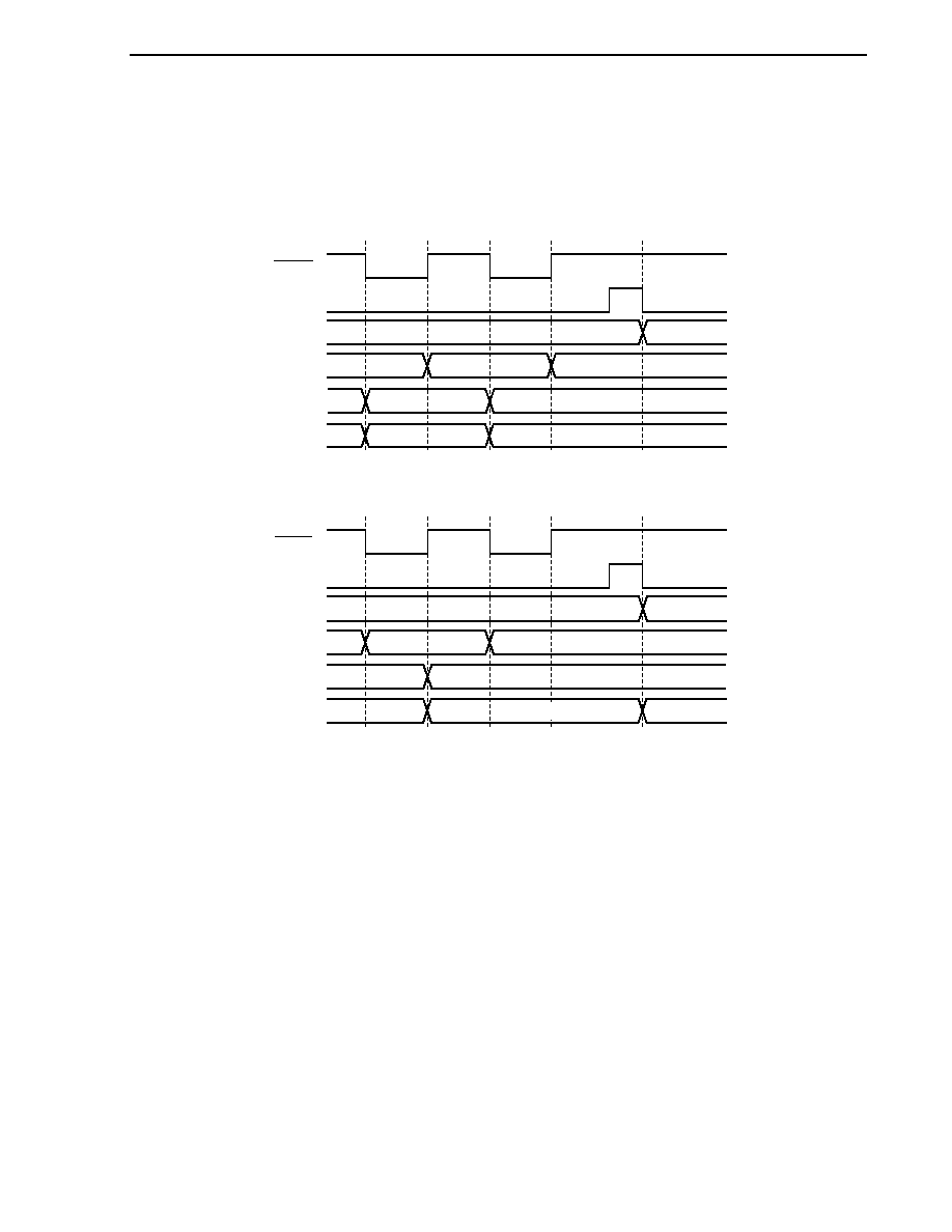
CHAPTER 15 SERIAL INTERFACES CSI10 AND CSI11
User's Manual U16228EJ2V0UD
349
(4) Output value of SO1n pin (last bit)
After communication has been completed, the SO1n pin holds the output value of the last bit.
Figure 15-12. Output Value of SO1n Pin (Last Bit)
(1) Type 1; when CKP1n = 0 and DAP1n = 0 (or CKP1n = 1, DAP1n = 0)
SCK1n
SOTB1n
SIO1n
SO1n
Writing to SOTB1n or
reading from SIO1n
(
Next request is issued.)
Last bit
Output latch
(2) Type 2; when CKP1n = 0 and DAP1n = 1 (or CKP1n = 1, DAP1n = 1)
SCK1n
SOTB1n
SIO1n
SO1n
Last bit
Writing to SOTB1n or
reading from SIO1n
(
Next request is issued.)
Output latch
Remark n = 0:
µ
PD780131, 780132
n = 0, 1:
µ
PD780133, 780134, 78F0134, 780136, 780138, 78F0138
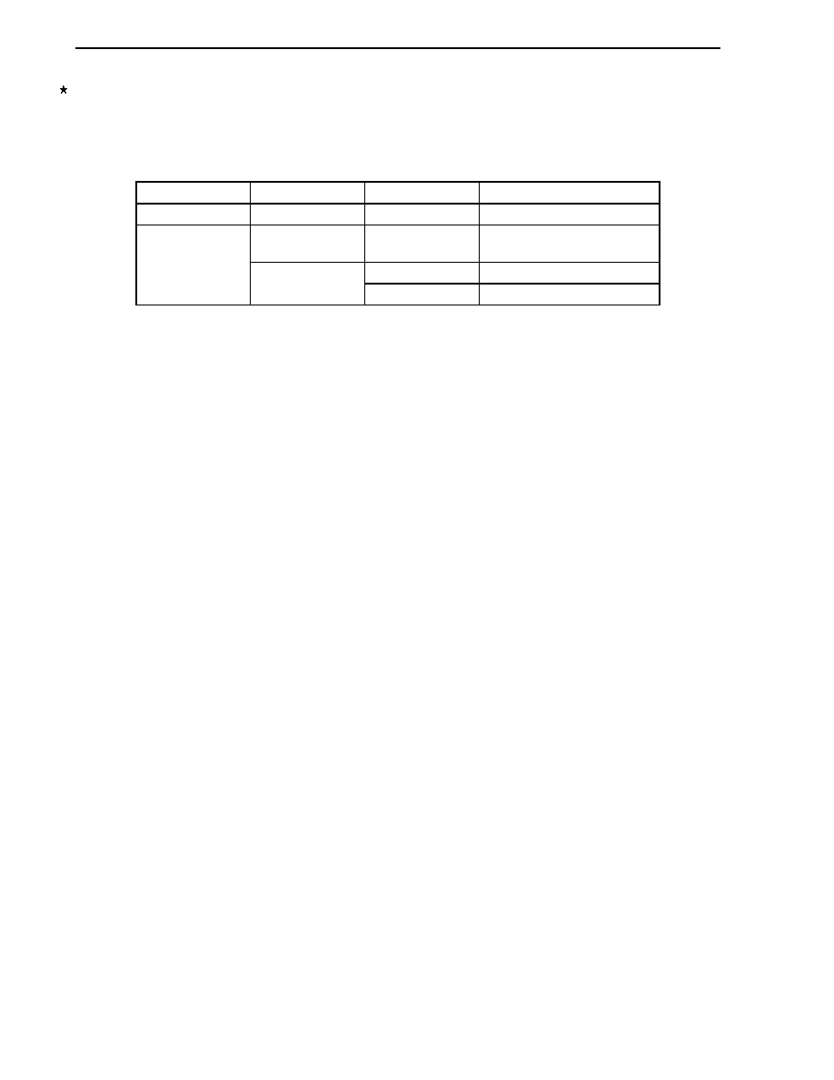
CHAPTER 15 SERIAL INTERFACES CSI10 AND CSI11
User's Manual U16228EJ2V0UD
350
(5) SO1n
output
The status of the SO1n output is as follows if bit 7 (CSIE1n) of serial operation mode register 1n (CSIM1n) is
cleared to 0.
Table 15-3. SO1n Output Status
TRMD1n DAP1n DIR1n
SO1n
Output
TRMD1n = 0
Note
-
-
Outputs low level
Note
.
DAP1n = 0
-
Value of SO1n latch
(low-level output)
DIR1n = 0
Value of bit 7 of SOTB1n
TRMD1n = 1
DAP1n = 1
DIR1n = 1
Value of bit 0 of SOTB1n
Note Status after reset
Caution If a value is written to TRMD1n, DAP1n, and DIR1n, the output value of SO1n changes.
Remark n = 0:
µ
PD780131, 780132
n = 0, 1:
µ
PD780133, 780134, 78F0134, 780136, 780138, 78F0138

User's Manual U16228EJ2V0UD
351
CHAPTER 16 MULTIPLIER/DIVIDER
16.1 Functions of Multiplier/Divider
The multiplier/divider has the following functions.
∑
16 bits
◊
16 bits = 32 bits (multiplication)
∑
32 bits
˜
16 bits = 32 bits, 16-bit remainder (division)
16.2 Configuration of Multiplier/Divider
The multiplier/divider includes the following hardware.
Table 16-1. Configuration of Multiplier/Divider
Item Configuration
Registers
Remainder data register 0 (SDR0)
Multiplication/division data registers A0 (MDA0H, MDA0L)
Multiplication/division data registers B0 (MDB0)
Control register
Multiplier/divider control register 0 (DMUC0)
Figure 16-1 shows the block diagram of the multiplier/divider.
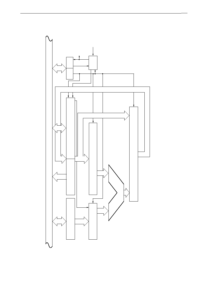
CHAPTER
16
MULTIP
L
IER/DI
VIDER
User's Manual
U1
6228EJ2V0UD
352
Figure 16-1. Block Diagram of Multiplier/Divider
Internal bus
CPU clock
Start
Clear
17-bit
adder
Controller
Multiplication/division data register B0
(MDB0 (MDB0H + MDB0L)
Remainder data register 0
(SDR0 (SDR0H + SDR0L)
6-bit
counter
DMUSEL0
Multiplier/divider control
register 0 (DMUC0)
Controller
Multiplication/division data register A0
(MDA0H (MDA0HH + MDA0HL) + MDA0L (MDA0LH + MDA0LL) )
Controller
DMUE
MDA000
INTDMU
CHAPTER 16 MULTIPLIER/DIVIDER
User's Manual U16228EJ2V0UD
353
(1) Remainder data register 0 (SDR0)
SDR0 is a 16-bit register that stores a remainder. This register stores 0 in the multiplication mode and the
remainder of an operation result in the division mode.
This register can be read by an 8-bit or 16-bit memory manipulation instruction.
RESET input clears this register to 0000H.
Figure 16-2. Format of Remainder Data Register 0 (SDR0)
Address: FF60H, FF61H After reset: 0000H R
Symbol
FF61H (SDR0H)
FF60H (SDR0L)
SDR0
SDR
015
SDR
014
SDR
013
SDR
012
SDR
011
SDR
010
SDR
009
SDR
008
SDR
007
SDR
006
SDR
005
SDR
004
SDR
003
SDR
002
SDR
001
SDR
000
Cautions
1. The value read from SDR0 during operation processing (while bit 7 (DMUE) of
multiplier/divider control register 0 (DMUC0) is 1) is not guaranteed.
2. SDR0 is reset when the operation is started (when DMUE is set to 1).
(2) Multiplication/division data register A0 (MDA0H, MDA0L)
MDA0 is a 32-bit register that sets a 16-bit multiplier A in the multiplication mode and a 32-bit dividend in the
division mode, and stores the 32-bit result of the operation (higher 16 bits: MDA0H, lower 16 bits: MDA0L).
Figure 16-3. Format of Multiplication/Division Data Register A0 (MDA0H, MDA0L)
Address: FF62H, FF63H, FF64H, FF65H After reset: 0000H, 0000H R/W
Symbol
FF65H (MDA0HH)
FF64H (MDA0HL)
MDA0H
MDA
031
MDA
030
MDA
029
MDA
028
MDA
027
MDA
026
MDA
025
MDA
024
MDA
023
MDA
022
MDA
021
MDA
020
MDA
019
MDA
018
MDA
017
MDA
016
Symbol
FF63H (MDA0LH)
FF62H (MDA0LL)
MDA0L
MDA
015
MDA
014
MDA
013
MDA
012
MDA
011
MDA
010
MDA
009
MDA
008
MDA
007
MDA
006
MDA
005
MDA
004
MDA
003
MDA
002
MDA
001
MDA
000
Cautions 1. MDA0H is cleared to 0 when an operation is started in the multiplication mode (when
multiplier/divider control register 0 (DMUC0) is set to 81H).
2. Do not change the value of MDA0 during operation processing (while bit 7 (DMUE) of
multiplier/divider control register 0 (DMUC0) is 1). Even in this case, the operation is
executed, but the result is undefined.
3. The value read from MDA0 during operation processing (while DMUE is 1) is not
guaranteed.
CHAPTER 16 MULTIPLIER/DIVIDER
User's Manual U16228EJ2V0UD
354
The functions of MDA0 when an operation is executed are shown in the table below.
Table 16-2. Functions of MDA0 During Operation Execution
DMUSEL0 Operation
Mode
Setting Operation
Result
0 Division
mode
Dividend
Division result (quotient)
1
Multiplication mode
Higher 16 bits: 0, Lower 16
bits: Multiplier A
Multiplication result
(product)
The register configuration differs between when multiplication is executed and when division is executed, as
follows.
∑
Register configuration during multiplication
<Multiplier A>
<Multiplier B>
<Product>
MDA0 (bits 15 to 0)
◊
MDB0 (bits 15 to 0) = MDA0 (bits 31 to 0)
∑
Register configuration during division
<Dividend>
<Divisor>
<Quotient>
<Remainder>
MDA0 (bits 31 to 0)
˜
MDB0 (bits 15 to 0) = MDA0 (bits 31 to 0) ... SDR0 (bits 15 to 0)
MDA0 fetches the calculation result as soon as the clock is input, when bit 7 (DMUE) of multiplier/divider
control register 0 (DMUC0) is set to 1.
MDA0H and MDA0L can be set by an 8-bit or 16-bit memory manipulation instruction.
RESET input clears this register to 0000H.
(3) Multiplication/division data register B0 (MDB0)
MDB0 is a register that stores a 16-bit multiplier B in the multiplication mode and a 16-bit divisor in the
division mode.
This register can be set by an 8-bit or 16-bit memory manipulation instruction.
RESET input clears this register to 0000H.
Figure 16-4. Format of Multiplication/Division Data Register B0 (MDB0)
Address: FF66H, FF67H After reset: 0000H R/W
Symbol
FF67H (MDB0H)
FF66H (MDB0L)
MDB0
MDB
015
MDB
014
MDB
013
MDB
012
MDB
011
MDB
010
MDB
009
MDB
008
MDB
007
MDB
006
MDB
005
MDB
004
MDB
003
MDB
002
MDB
001
MDB
000
Cautions 1. Do not change the value of MDB0 during operation processing (while bit 7 (DMUE) of
multiplier/divider control register 0 (DMUC0) is 1). Even in this case, the operation is
executed, but the result is undefined.
2. Do not clear MDB0 to 0000H in the division mode. If set, undefined operation results are
stored in MDA0 and SDR0.
CHAPTER 16 MULTIPLIER/DIVIDER
User's Manual U16228EJ2V0UD
355
16.3 Register Controlling Multiplier/Divider
The multiplier/divider is controlled by multiplier/divider control register 0 (DMUC0).
(1) Multiplier/divider control register 0 (DMUC0)
DMUC0 is an 8-bit register that controls the operation of the multiplier/divider.
This register can be read by a 1-bit or 8-bit memory manipulation instruction.
RESET input clears this register to 00H.
Figure 16-5. Format of Multiplier/Divider Control Register 0 (DMUC0)
DMUE
DMUC0
0
0
0
0
0
0
DMUSEL0
Stops operation
Starts operation
DMUE
Note
0
1
Operation start/stop
Division mode
Multiplication mode
DMUSEL0
0
1
Operation mode (multiplication/division) selection
Address: FF68H After reset: 00H R/W
Symbol
4
3
2
1
0
6
<7>
5
Note When DMUE is set to 1, the operation is started. DMUE is automatically cleared to 0 after the operation is
complete.
Cautions 1. If DMUE is cleared to 0 during operation processing (when DMUE is 1), the operation result
is not guaranteed. If the operation is completed while the clearing instruction is being
executed, the operation result is guaranteed, provided that the interrupt flag is set.
2. Do not change the value of DMUSEL0 during operation processing (while DMUE is 1). If it is
changed, undefined operation results are stored in multiplication/division data register A0
(MDA0) and remainder data register 0 (SDR0).
3. If DMUE is cleared to 0 during operation processing (while DMUE is 1), the operation
processing is stopped. To execute the operation again, set multiplication/division data
register A0 (MDA0), multiplication/division data register B0 (MDB0), and multiplier/divider
control register 0 (DMUC0), and start the operation (by clearing DMUE to 1).

CHAPTER 16 MULTIPLIER/DIVIDER
User's Manual U16228EJ2V0UD
356
16.4 Operations of Multiplier/Divider
16.4.1 Multiplication operation
∑
Initial setting
1. Set operation data to multiplication/division data register A0L (MDA0L) and multiplication/division data register
B0 (MDB0).
2. Set bits 0 (DMUSEL0) and 7 (DMUE) of multiplier/divider control register 0 (DMUC0) to 1. Operation will start.
∑
During operation
3. The operation will be completed when 16 internal clocks have been issued after the start of the operation
(intermediate data is stored in the MDA0L and MDA0H registers during operation, and therefore the read
values of these registers are not guaranteed).
∑
End of operation
4. The operation result data is stored in the MDA0L and MDA0H registers.
5. DMUE is cleared to 0 (end of operation).
6. After the operation, an interrupt request signal (INTDMU) is generated.
∑
Next operation
7. To execute multiplication next, start from the initial setting in 16.4.1 Multiplication operation.
8. To execute division next, start from the initial setting in 16.4.2 Division operation.
CHAPTER
16
MULTIP
L
IER/DI
VIDER
User's Manual
U1
6228EJ2V0UD
357
Figure 16-6. Timing Chart of Multiplication Operation (00DAH
◊
0093H)
Operation clock
MDA0
SDR0
MDB0
1
2
3
4
5
6
7
8
9
A
B
C
D
E
F
10
0
0
0000
0000 0000 0000 0000 0000 0000 0000 0000 0000 0000 0000 0000 0000 0000 0000 0000
0000
006D
0000
00DA
XXXX
00DA
XXXX
XXXX
XXXX
0049
8036
0024
C01B
005B
E00D
0077
7006
003B
B803
0067
5C01
007D
2E00
003E
9700
001F
4B80
000F
A5C0
0007
D2E0
0003
E970
0001
F4B8
0000
FA5C
0000
7D2E
0093
XXXX
Internal clock
DMUE
DMUSEL0
Counter
INTDMU

CHAPTER 16 MULTIPLIER/DIVIDER
User's Manual U16228EJ2V0UD
358
16.4.2 Division operation
∑
Initial setting
1. Set operation data to multiplication/division data register A0 (MDA0L and MDA0H) and multiplication/division
data register B0 (MDB0).
2. Set bits 0 (DMUSEL0) and 7 (DMUE) of multiplier/divider control register 0 (DMUC0) to 0 and 1, respectively.
Operation will start.
∑
During operation
3. The operation will be completed when 32 internal clocks have been issued after the start of the operation
(intermediate data is stored in the MDA0L and MDA0H registers and remainder data register 0 (SDR0) during
operation, and therefore the read values of these registers are not guaranteed).
∑
End of operation
4. The result data is stored in the MDA0L, MDA0H, and SDR0 registers.
5. DMUE is cleared to 0 (end of operation).
6. After the operation, an interrupt request signal (INTDMU) is generated.
∑
Next operation
7. To execute multiplication next, start from the initial setting in 16.4.1 Multiplication operation.
8. To execute division next, start from the initial setting in 16.4.2 Division operation.
CHAPTER
16
MULTIP
L
IER/DI
VIDER
User's Manual
U1
6228EJ2V0UD
359
Figure 16-7. Timing Chart of Division Operation (DCBA2586H
˜
0018H)
Operation clock
MDA0
SDR0
MDB0
1
2
3
4
5
6
7
8
19
1A
1B
1C
1D
1E
1F
20
0
0
0000
0001 0003 0006 000D 0003 0007 000E 0004
000B 0016 0014 0010 0008 0011 000B 0016
B974
4B0C
DCBA
2586
XXXX
XXXX
XXXX
72E8
A618
E5D1
2C30
CBA2
6860
A744
BAC1
2E89
6182
6D12
C304
BA25
8609
0C12
64D8
1824
C9B0
3049
9361
6093
26C3
C126
4D87
824C
9B0E
0499
361D
0932
6C3A
0018
XXXX
Internal clock
DMUE
DMUSEL0
Counter
INTDMU
"0"

User's Manual U16228EJ2V0UD
360
CHAPTER 17 INTERRUPT FUNCTIONS
17.1 Interrupt Function Types
The following two types of interrupt functions are used.
(1) Maskable
interrupts
These interrupts undergo mask control. Maskable interrupts can be divided into a high interrupt priority group
and a low interrupt priority group by setting the priority specification flag registers (PR0L, PR0H, PR1L, PR1H).
Multiple interrupt servicing can be applied to low-priority interrupts when high-priority interrupts are generated. If
two or more interrupts with the same priority are generated simultaneously, each interrupt is serviced according to
its predetermined priority (see Table 17-1).
A standby release signal is generated and STOP and HALT modes are released.
Nine external interrupt requests and 19 (16 in the
µ
PD780131 and 780132) internal interrupt requests are
provided as maskable interrupts.
(2) Software
interrupt
This is a vectored interrupt generated by executing the BRK instruction. It is acknowledged even when interrupts
are disabled. The software interrupt does not undergo interrupt priority control.
17.2 Interrupt Sources and Configuration
A total of 29 (26 in the
µ
PD780131 and 780132) interrupt sources exist for maskable and software interrupts (see
Table 17-1).
CHAPTER 17 INTERRUPT FUNCTIONS
User's Manual U16228EJ2V0UD
361
Table 17-1. Interrupt Source List (1/2)
Interrupt Source
Interrupt
Type
Default
Priority
Note 1
Name Trigger
Internal/
External
Vector
Table
Address
Basic
Configuration
Type
Note 2
0 INTLVI Low-voltage
detection
Note 3
Internal
0004H
(A)
1 INTP0
0006H
2 INTP1
0008H
3 INTP2
000AH
4 INTP3
000CH
5 INTP4
000EH
6 INTP5
Pin input edge detection
External
0010H
(B)
7
INTSRE6
UART6 reception error generation
0012H
8
INTSR6
End of UART6 reception
0014H
9
INTST6
End of UART6 transmission
0016H
10
INTCSI10/
INTST0
End of CSI10 communication/end of UART0
transmission
0018H
11 INTTMH1
Match between TMH1 and CRH1
(when compare register is specified)
001AH
12 INTTMH0
Match between TMH0 and CRH0
(when compare register is specified)
001CH
13 INTTM50
Match between TM50 and CR50
(when compare register is specified)
001EH
14 INTTM000
Match between TM00 and CR000
(when compare register is specified),
TI010 pin valid edge detection
(when capture register is specified)
0020H
15 INTTM010
Match between TM00 and CR010
(when compare register is specified),
TI000 pin valid edge detection
(when capture register is specified)
0022H
16
INTAD
End of A/D conversion
0024H
17 INTSR0 End of UART0 reception or reception error
generation
0026H
18 INTWTI Watch
timer
reference time interval signal
0028H
19 INTTM51
Match between TM51 and CR51
(when compare register is specified)
Internal
002AH
(A)
20
INTKR
Key interrupt detection
External
002CH
(C)
21
INTWT
Watch timer overflow
Internal
002EH
(A)
22 INTP6
0030H
Maskable
23 INTP7
Pin input edge detection
External
0032H
(B)
Notes 1. The default priority is the priority applicable when two or more maskable interrupt are generated
simultaneously. 0 is the highest priority, and 27 is the lowest.
2. Basic configuration types (A) to (D) correspond to (A) to (D) in Figure 17-1.
3.
When bit 1 (LVIMD) of the low-voltage detection register (LVIM) is set to 0.
CHAPTER 17 INTERRUPT FUNCTIONS
User's Manual U16228EJ2V0UD
362
Table 17-1. Interrupt Source List (2/2)
Interrupt Source
Interrupt
Type
Default
Priority
Note 1
Name Trigger
Internal/
External
Vector
Table
Address
Basic
Configuration
Type
Note 2
24
INTDMU
End of multiply/divide operation
0034H
25 INTCSI11
Note 3
End of CSI11 communication
0036H
26 INTTM001
Note 3
Match between TM01 and CR001 (when
compare register is specified), TI011 pin valid
edge detection (when capture register is
specified)
0038H
Maskable
27 INTTM011
Note 3
Match between TM01 and CR011 (when
compare register is specified), TI001 pin valid
edge detection (when capture register is
specified)
Internal
003AH
(A)
Software
-
BRK BRK
instruction
execution
-
003EH (D)
RESET Reset
input
POC Power-on
clear
Note 4
LVI Low-voltage
detection
Note 5
Clock monitor X1 oscillation stop detection
Reset
-
WDT WDT
overflow
-
0000H
-
Notes 1. The default priority is the priority applicable when two or more maskable interrupt are generated
simultaneously. 0 is the highest priority, and 27 is the lowest.
2. Basic configuration types (A) to (D) correspond to (A) to (D) in Figure 17-1.
3. The interrupt sources INTCSI11, INTTM001, and INTTM011 are available only in the
µ
PD780133,
780134, 78F0134, 780136, 780138, and 78F0138.
4.
When "POC used" is selected by a mask option.
5.
When bit 1 (LVIMD) of the low-voltage detection register (LVIM) is set to 1.
CHAPTER 17 INTERRUPT FUNCTIONS
User's Manual U16228EJ2V0UD
363
Figure 17-1. Basic Configuration of Interrupt Function (1/2)
(A) Internal maskable interrupt
Internal bus
Interrupt
request
IF
MK
IE
PR
ISP
Priority controller
Vector table
address generator
Standby release signal
(B) External maskable interrupt (INTP0 to INTP7)
Internal bus
Interrupt
request
IF
MK
IE
PR
ISP
Priority controller
Vector table
address generator
Standby release signal
External interrupt edge
enable register
(EGP, EGN)
Edge
detector
IF:
Interrupt request flag
IE:
Interrupt enable flag
ISP:
In-service priority flag
MK:
Interrupt mask flag
PR:
Priority specification flag
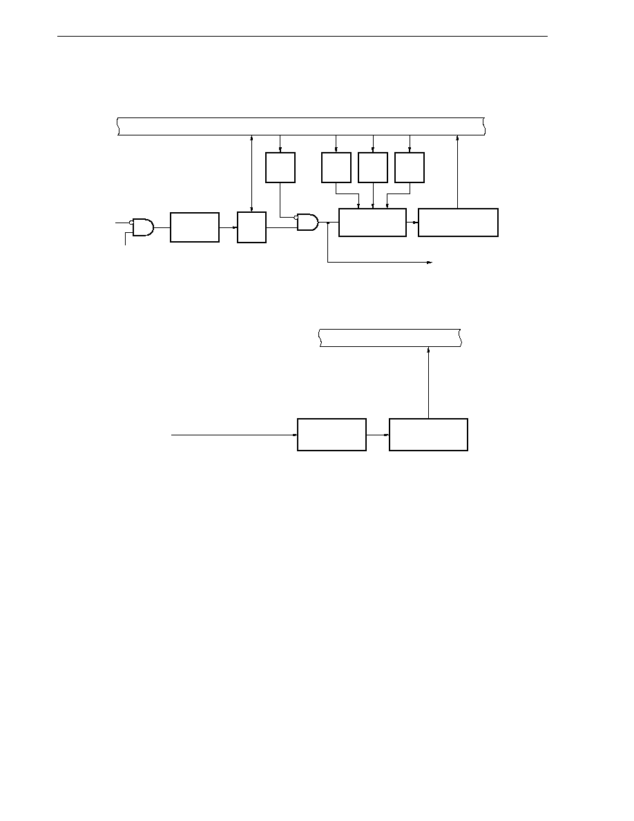
CHAPTER 17 INTERRUPT FUNCTIONS
User's Manual U16228EJ2V0UD
364
Figure 17-1. Basic Configuration of Interrupt Function (2/2)
(C) External maskable interrupt (INTKR)
IF
MK
IE
PR
ISP
Internal bus
Interrupt
request
Priority controller
Vector table
address generator
Standby release signal
Key
interrupt
detector
1 when KRMn = 1 (n = 0 to 7)
(D) Software interrupt
Internal bus
Interrupt
request
Priority controller
Vector table
address generator
IF:
Interrupt request flag
IE:
Interrupt enable flag
ISP:
In-service priority flag
MK:
Interrupt mask flag
PR:
Priority specification flag
KRM: Key return mode register
17.3 Registers Controlling Interrupt Functions
The following 6 types of registers are used to control the interrupt functions.
∑
Interrupt request flag register (IF0L, IF0H, IF1L, IF1H)
∑
Interrupt mask flag register (MK0L, MK0H, MK1L, MK1H)
∑
Priority specification flag register (PR0L, PR0H, PR1L, PR1H)
∑
External interrupt rising edge enable register (EGP)
∑
External interrupt falling edge enable register (EGN)
∑
Program status word (PSW)
Table 17-2 shows a list of interrupt request flags, interrupt mask flags, and priority specification flags corresponding
to interrupt request sources.

CHAPTER 17 INTERRUPT FUNCTIONS
User's Manual U16228EJ2V0UD
365
Table 17-2. Flags Corresponding to Interrupt Request Sources
Interrupt Request Flag
Interrupt Mask Flag
Priority Specification Flag
Interrupt
Request
Register Register Register
INTLVI LVIIF IF0L
LVIMK MK0L LVIPR PR0L
INTP0
PIF0
PMK0
PPR0
INTP1
PIF1
PMK1
PPR1
INTP2
PIF2
PMK2
PPR2
INTP3
PIF3
PMK3
PPR3
INTP4
PIF4
PMK4
PPR4
INTP5
PIF5
PMK5
PPR5
INTSRE6
SREIF6
SREMK6
SREPR6
INTSR6 SRIF6 IF0H
SRMK6 MK0H SRPR6 PR0H
INTST6
STIF6
STMK6
STPR6
INTCSI10 DUALIF0
Note 1
DUALMK0
Note 2
DUALPR0
Note 2
INTST0
INTTMH1
TMIFH1
TMMKH1
TMPRH1
INTTMH0
TMIFH0
TMMKH0
TMPRH0
INTTM50
TMIF50
TMMK50
TMPR50
INTTM000
TMIF000
TMMK000
TMPR000
INTTM010
TMIF010
TMMK010
TMPR010
INTAD ADIF IF1L
ADMK MK1L ADPR PR1L
INTSR0
SRIF0
SRMK0
SRPR0
INTWTI
WTIIF
WTIMK
WTIPR
INTTM51
TMIF51
TMMK51
TMPR51
INTKR
KRIF
KRMK
KRPR
INTWT
WTIF
WTMK
WTPR
INTP6
PIF6
PMK6
PPR6
INTP7
PIF7
PMK7
PPR7
INTDMU DMUIF IF1H
DMUMK MK1H
DMUPR PR1H
INTCSI11
Note 3
CSIIF11
Note 3
CSIMK11
Note 3
CSIPR11
Note 3
INTTM001
Note 3
TMIF001
Note 3
TMMK001
Note 3
TMPR001
Note 3
INTTM011
Note 3
TMIF011
Note 3
TMMK011
Note 3
TMPR011
Note 3
Notes 1. If either of the two types of interrupt sources is generated, these flags are set (1).
2. Both types of interrupt sources are supported.
3.
µ
PD780133, 780134, 78F0134, 780136, 780138, and 78F0138 only.
CHAPTER 17 INTERRUPT FUNCTIONS
User's Manual U16228EJ2V0UD
366
(1) Interrupt request flag registers (IF0L, IF0H, IF1L, IF1H)
The interrupt request flags are set to 1 when the corresponding interrupt request is generated or an instruction is
executed. They are cleared to 0 when an instruction is executed upon acknowledgment of an interrupt request or
upon RESET input.
When an interrupt is acknowledged, the interrupt request flag is automatically cleared and then the interrupt
routine is entered.
IF0L, IF0H, IF1L, and IF1H are set by a 1-bit or 8-bit memory manipulation instruction. When IF0L and IF0H, and
IF1L and IF1H are combined to form 16-bit registers IF0 and IF1, they are read with a 16-bit memory
manipulation instruction.
RESET input clears these registers to 00H.
Figure 17-2. Format of Interrupt Request Flag Registers (IF0L, IF0H, IF1L, IF1H)
Address: FFE0H After reset: 00H R/W
Symbol <7> <6> <5> <4> <3> <2> <1> <0>
IF0L
SREIF6
PIF5 PIF4 PIF3 PIF2 PIF1 PIF0 LVIIF
Address: FFE1H After reset: 00H R/W
Symbol <7> <6> <5> <4> <3> <2> <1> <0>
IF0H TMIF010
TMIF000
TMIF50
TMIFH0
TMIFH1
DUALIF0
STIF6
SRIF6
Address: FFE2H After reset: 00H R/W
Symbol <7> <6> <5> <4> <3> <2> <1> <0>
IF1L PIF7
PIF6
WTIF
KRIF
TMIF51
WTIIF
SRIF0
ADIF
Address: FFE3H After reset: 00H R/W
Symbol 7 6 5 4
<3>
<2>
<1>
<0>
IF1H 0
Note 1
0
Note 1
0
Note 1
0
Note 1
TMIF011
Note 2
TMIF001
Note 2
CSIIF11
Note 2
DMUIF
XXIFX
Interrupt
request
flag
0
No interrupt request signal is generated
1
Interrupt request is generated, interrupt request status
Notes 1. Be sure to set bits 4 to 7 of IF1H to 0.
2.
µ
PD780133, 780134, 78F0134, 780136, 780138, and 78F0138 only. Be sure to set the
µ
PD780131
and 780132 to 0.
Cautions 1. When operating a timer, serial interface, or A/D converter after standby release, operate it
once after clearing the interrupt request flag. An interrupt request flag may be set by noise.
2. If an interrupt request corresponding to a flag of the interrupt request flag register is
generated while the interrupt request flag register is being manipulated (including by 1-bit
memory manipulation), the flag corresponding to the interrupt request may not be set to 1.
CHAPTER 17 INTERRUPT FUNCTIONS
User's Manual U16228EJ2V0UD
367
(2) Interrupt mask flag registers (MK0L, MK0H, MK1L, MK1H)
The interrupt mask flags are used to enable/disable the corresponding maskable interrupt servicing.
MK0L, MK0H, MK1L, and MK1H are set by a 1-bit or 8-bit memory manipulation instruction. When MK0L and
MK0H, and MK1L and MK1H are combined to form 16-bit registers MK0 and MK1, they are set with a 16-bit
memory manipulation instruction.
RESET input sets MK0L, MK0H, and MK1L to FFH and sets MK1H to DFH.
Figure 17-3. Format of Interrupt Mask Flag Registers (MK0L, MK0H, MK1L, MK1H)
Address: FFE4H After reset: FFH R/W
Symbol <7> <6> <5> <4> <3> <2> <1> <0>
MK0L
SREMK6
PMK5 PMK4 PMK3 PMK2 PMK1 PMK0 LVIMK
Address: FFE5H After reset: FFH R/W
Symbol <7> <6> <5> <4> <3> <2> <1> <0>
MK0H TMMK010
TMMK000
TMMK50
TMMKH0
TMMKH1
DUALMK0
STMK6
SRMK6
Address: FFE6H After reset: FFH R/W
Symbol <7> <6> <5> <4> <3> <2> <1> <0>
MK1L PMK7
PMK6
WTMK
KRMK
TMMK51
WTIMK
SRMK0
ADMK
Address: FFE7H After reset: DFH R/W
Symbol 7 6 5 4
<3>
<2>
<1>
<0>
MK1H 1
Note 1
1
Note 1
0
Note 1
1
Note 1
TMMK011
Note 2
TMMK001
Note 2
CSIMK11
Note 2
DMUMK
XXMKX
Interrupt servicing control
0
Interrupt servicing enabled
1
Interrupt servicing disabled
Notes 1. Be sure to set bits 4, 6, and 7 of MK1H to 1. Be sure to clear bit 5 of MK1H to 0.
2.
µ
PD780133, 780134, 78F0134, 780136, 780138, and 78F0138 only. Be sure to set the
µ
PD780131
and 780132 to 1.
CHAPTER 17 INTERRUPT FUNCTIONS
User's Manual U16228EJ2V0UD
368
(3) Priority specification flag registers (PR0L, PR0H, PR1L, PR1H)
The priority specification flag registers are used to set the corresponding maskable interrupt priority order.
PR0L, PR0H, PR1L, and PR1H are set by a 1-bit or 8-bit memory manipulation instruction. If PR0L and PR0H,
and PR1L and PR1H are combined to form 16-bit registers PR0 and PR1, they are set with a 16-bit memory
manipulation instruction.
RESET input sets these registers to FFH.
Figure 17-4. Format of Priority Specification Flag Registers (PR0L, PR0H, PR1L, PR1H)
Address: FFE8H After reset: FFH R/W
Symbol <7> <6> <5> <4> <3> <2> <1> <0>
PR0L
SREPR6
PPR5 PPR4 PPR3 PPR2 PPR1 PPR0 LVIPR
Address: FFE9H After reset: FFH R/W
Symbol <7> <6> <5> <4> <3> <2> <1> <0>
PR0H
TMPR010
TMPR000 TMPR50 TMPRH0 TMPRH1 DUALPRO STPR6 SRPR6
Address: FFEAH After reset: FFH R/W
Symbol <7> <6> <5> <4> <3> <2> <1> <0>
PR1L PPR7
PPR6
WTPR
KRPR
TMPR51
WTIPR
SRPR0
ADPR
Address: FFEBH After reset: FFH R/W
Symbol 7 6 5 4
<3>
<2>
<1>
<0>
PR1H 1
Note 1
1
Note 1
1
Note 1
1
Note 1
TMPR011
Note 2
TMPR001
Note 2
CSIPR11
Note 2
DMUPR
XXPRX
Priority
level
selection
0
High priority level
1
Low priority level
Notes 1. Be sure to set bits 4 to 7 of PR1H to 1.
2.
µ
PD780133, 780134, 78F0134, 780136, 780138, and 78F0138 only. Be sure to set the
µ
PD780131
and 780132 to 1.
CHAPTER 17 INTERRUPT FUNCTIONS
User's Manual U16228EJ2V0UD
369
(4) External interrupt rising edge enable register (EGP), external interrupt falling edge enable register (EGN)
These registers specify the valid edge for INTP0 to INTP7.
EGP and EGN are set by a 1-bit or 8-bit memory manipulation instruction.
RESET input clears these registers to 00H.
Figure 17-5. Format of External Interrupt Rising Edge Enable Register (EGP)
and External Interrupt Falling Edge Enable Register (EGN)
Address: FF48H After reset: 00H R/W
Symbol 7 6 5 4 3 2 1 0
EGP
EGP7 EPG6 EGP5 EGP4 EGP3 EGP2 EGP1 EGP0
Address: FF49H After reset: 00H R/W
Symbol 7 6 5 4 3 2 1 0
EGN
EGN7 EGN6 EGN5 EGN4 EGN3 EGN2 EGN1 EGN0
EGPn
EGNn
INTPn pin valid edge selection (n = 0 to 7)
0
0
Edge detection disabled
0
1
Falling
edge
1
0
Rising
edge
1
1
Both rising and falling edges
Table 17-3 shows the ports corresponding to EGPn and EGNn.
Table 17-3. Ports Corresponding to EGPn and EGNn
Detection Enable Register
Edge Detection Port
External Request Signal
EGP0 EGN0
P120
INTP0
EGP1 EGN1
P30
INTP1
EGP2 EGN2
P31
INTP2
EGP3 EGN3
P32
INTP3
EGP4 EGN4
P33
INTP4
EGP5 EGN5
P16
INTP5
EGP6 EGN6
P140
INTP6
EGP7 EGN7
P141
INTP7
Caution Select the port mode by clearing EGPn and EGNn to 0 because an edge may be
detected when the external interrupt function is switched to the port function.
Remark n = 0 to 7
CHAPTER 17 INTERRUPT FUNCTIONS
User's Manual U16228EJ2V0UD
370
(5) Program status word (PSW)
The program status word is a register used to hold the instruction execution result and the current status for an
interrupt request. The IE flag that sets maskable interrupt enable/disable and the ISP flag that controls multiple
interrupt servicing are mapped to the PSW.
Besides 8-bit read/write, this register can carry out operations using bit manipulation instructions and dedicated
instructions (EI and DI). When a vectored interrupt request is acknowledged, if the BRK instruction is executed,
the contents of the PSW are automatically saved into a stack and the IE flag is reset to 0. If a maskable interrupt
request is acknowledged, the contents of the priority specification flag of the acknowledged interrupt are
transferred to the ISP flag. The PSW contents are also saved into the stack with the PUSH PSW instruction.
They are restored from the stack with the RETI, RETB, and POP PSW instructions.
RESET input sets PSW to 02H.
Figure 17-6. Format of Program Status Word
<7>
IE
<6>
Z
<5>
RBS1
<4>
AC
<3>
RBS0
2
0
<1>
ISP
0
CY
PSW
After reset
02H
ISP
High-priority interrupt servicing (low-priority
interrupt disabled)
IE
0
1
Disabled
Priority of interrupt currently being serviced
Interrupt request acknowledgment enable/disable
Used when normal instruction is executed
Enabled
Interrupt request not acknowledged, or low-
priority interrupt servicing (all maskable
interrupts enabled)
0
1
CHAPTER 17 INTERRUPT FUNCTIONS
User's Manual U16228EJ2V0UD
371
17.4 Interrupt Servicing Operations
17.4.1 Maskable interrupt acknowledgement
A maskable interrupt becomes acknowledgeable when the interrupt request flag is set to 1 and the mask (MK) flag
corresponding to that interrupt request is cleared to 0. A vectored interrupt request is acknowledged if interrupts are
in the interrupt enabled state (when the IE flag is set to 1). However, a low-priority interrupt request is not
acknowledged during servicing of a higher priority interrupt request (when the ISP flag is reset to 0). The times from
generation of a maskable interrupt request until interrupt servicing is performed are listed in Table 17-4 below.
For the interrupt request acknowledgement timing, see Figures 17-8 and 17-9.
Table 17-4. Time from Generation of Maskable Interrupt Until Servicing
Minimum Time
Maximum Time
Note
When
◊◊
PR = 0
7 clocks
32 clocks
When
◊◊
PR = 1
8 clocks
33 clocks
Note If an interrupt request is generated just before a divide instruction, the wait time becomes longer.
Remark 1 clock: 1/f
CPU
(f
CPU
: CPU clock)
If two or more maskable interrupt requests are generated simultaneously, the request with a higher priority level
specified in the priority specification flag is acknowledged first. If two or more interrupts requests have the same
priority level, the request with the highest default priority is acknowledged first.
An interrupt request that is held pending is acknowledged when it becomes acknowledgeable.
Figure 17-7 shows the interrupt request acknowledgement algorithm.
If a maskable interrupt request is acknowledged, the contents are saved into the stacks in the order of PSW, then
PC, the IE flag is reset (0), and the contents of the priority specification flag corresponding to the acknowledged
interrupt are transferred to the ISP flag. The vector table data determined for each interrupt request is the loaded into
the PC and branched.
Restoring from an interrupt is possible by using the RETI instruction.
CHAPTER 17 INTERRUPT FUNCTIONS
User's Manual U16228EJ2V0UD
372
Figure 17-7. Interrupt Request Acknowledgement Processing Algorithm
Start
◊◊
IF = 1?
◊◊
MK = 0?
◊◊
PR = 0?
IE = 1?
ISP = 1?
Interrupt request held pending
Yes
Yes
No
No
Yes (interrupt request generation)
Yes
No (Low priority)
No
No
Yes
Yes
No
IE = 1?
No
Any high-priority
interrupt request among those
simultaneously generated
with
◊◊
PR = 0?
Yes (High priority)
No
Yes
Yes
No
Vectored interrupt servicing
Interrupt request held pending
Interrupt request held pending
Interrupt request held pending
Interrupt request held pending
Interrupt request held pending
Interrupt request held pending
Vectored interrupt servicing
Any high-priority
interrupt request among
those simultaneously
generated?
Any high-priority
interrupt request among
those simultaneously generated
with
◊◊
PR = 0?
◊◊
IF: Interrupt request flag
◊◊
MK: Interrupt mask flag
◊◊
PR: Priority specification flag
IE:
Flag that controls acknowledgement of maskable interrupt request (1 = Enable, 0 = Disable)
ISP:
Flag that indicates the priority level of the interrupt currently being serviced (0 = high-priority interrupt
servicing, 1 = No interrupt request acknowledged, or low-priority interrupt servicing)
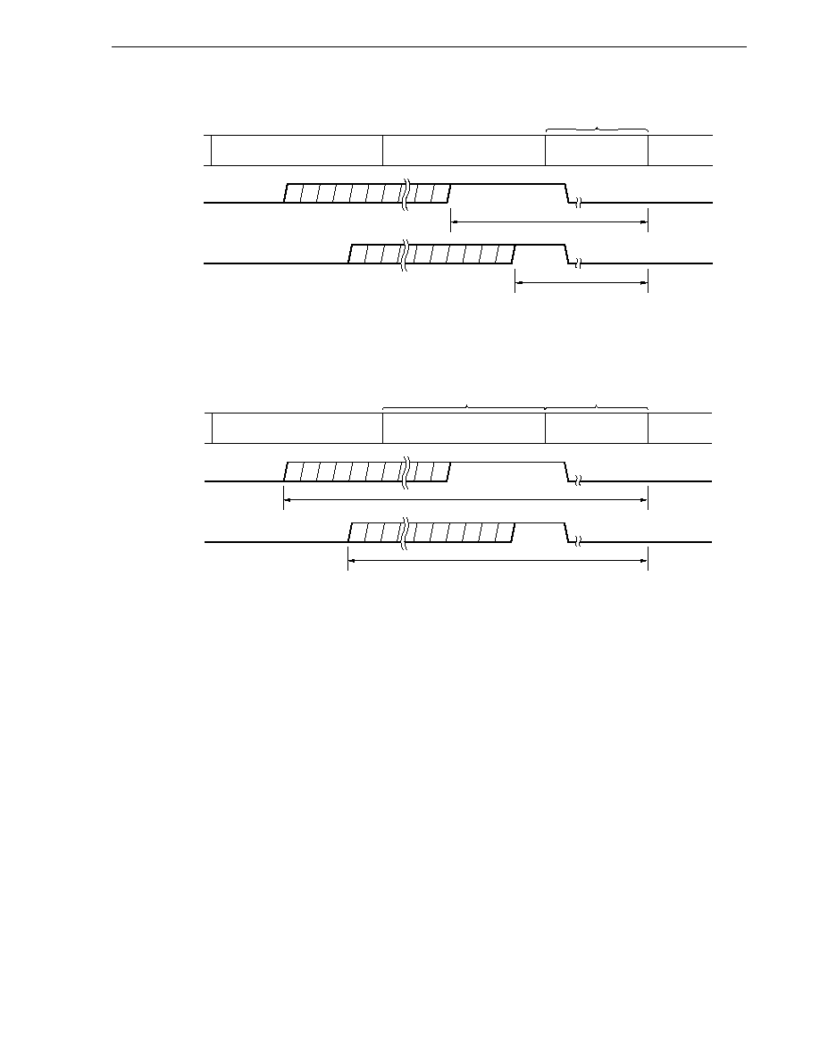
CHAPTER 17 INTERRUPT FUNCTIONS
User's Manual U16228EJ2V0UD
373
Figure 17-8. Interrupt Request Acknowledgement Timing (Minimum Time)
8 clocks
7 clocks
Instruction
Instruction
PSW and PC saved,
jump to interrupt
servicing
Interrupt servicing
program
CPU processing
◊◊
IF
(
◊◊
PR = 1)
◊◊
IF
(
◊◊
PR = 0)
6 clocks
Remark 1 clock: 1/f
CPU
(f
CPU
: CPU clock)
Figure 17-9. Interrupt Request Acknowledgement Timing (Maximum Time)
33 clocks
32 clocks
Instruction
Divide instruction
PSW and PC saved,
jump to interrupt
servicing
Interrupt servicing
program
CPU processing
◊◊
IF
(
◊◊
PR = 1)
◊◊
IF
(
◊◊
PR = 0)
6 clocks
25 clocks
Remark 1 clock: 1/f
CPU
(f
CPU
: CPU clock)
17.4.2 Software interrupt request acknowledgement
A software interrupt acknowledge is acknowledged by BRK instruction execution. Software interrupts cannot be
disabled.
If a software interrupt request is acknowledged, the contents are saved into the stacks in the order of the program
status word (PSW), then program counter (PC), the IE flag is reset (0), and the contents of the vector table (003EH,
003FH) are loaded into the PC and branched.
Restoring from a software interrupt is possible by using the RETB instruction.
Caution Do not use the RETI instruction for restoring from the software interrupt.
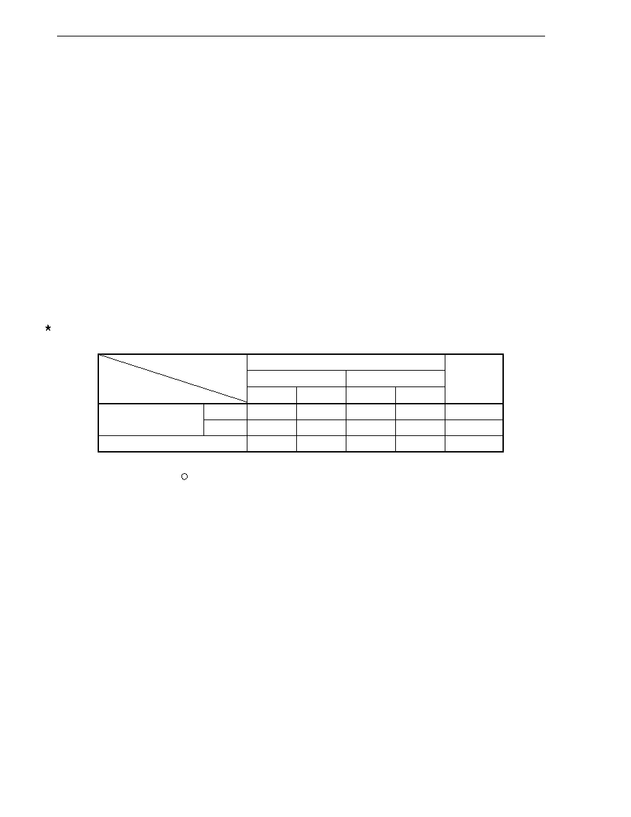
CHAPTER 17 INTERRUPT FUNCTIONS
User's Manual U16228EJ2V0UD
374
17.4.3 Multiple interrupt servicing
Multiple interrupt servicing occurs when another interrupt request is acknowledged during execution of an interrupt.
Multiple interrupt servicing does not occur unless the interrupt request acknowledgement enabled state is selected
(IE = 1). When an interrupt request is acknowledged, interrupt request acknowledgement becomes disabled (IE = 0).
Therefore, to enable multiple interrupt servicing, it is necessary to set (1) the IE flag with the EI instruction during
interrupt servicing to enable interrupt acknowledgement.
Moreover, even if interrupts are enabled, multiple interrupt servicing may not be enabled, this being subject to
interrupt priority control. Two types of priority control are available: default priority control and programmable priority
control. Programmable priority control is used for multiple interrupt servicing.
In the interrupt enabled state, if an interrupt request with a priority equal to or higher than that of the interrupt
currently being serviced is generated, it is acknowledged for multiple interrupt servicing. If an interrupt with a priority
lower than that of the interrupt currently being serviced is generated during interrupt servicing, it is not acknowledged
for multiple interrupt servicing. Interrupt requests that are not enabled because interrupts are in the interrupt disabled
state or because they have a lower priority are held pending. When servicing of the current interrupt ends, the
pending interrupt request is acknowledged following execution of at least one main processing instruction execution.
Table 17-5 shows relationship between interrupt requests enabled for multiple interrupt servicing and Figure 17-10
shows multiple interrupt servicing examples.
Table 17-5. Relationship Between Interrupt Requests Enabled for Multiple Interrupt Servicing
During Interrupt Servicing
Maskable Interrupt Request
PR = 0
PR = 1
Multiple Interrupt Request
Interrupt Being Serviced
IE = 1
IE = 0
IE = 1
IE = 0
Software
Interrupt
Request
ISP = 0
◊
◊
◊
Maskable interrupt
ISP = 1
◊
◊
Software interrupt
◊
◊
Remarks 1. : Multiple interrupt servicing enabled
2.
◊
: Multiple interrupt servicing disabled
3. ISP and IE are flags contained in the PSW.
ISP = 0: An interrupt with higher priority is being serviced.
ISP = 1: No interrupt request has been acknowledged, or an interrupt with a lower
priority is being serviced.
IE = 0:
Interrupt request acknowledgement is disabled.
IE = 1:
Interrupt request acknowledgement is enabled.
4. PR is a flag contained in PR0L, PR0H, PR1L, and PR1H.
PR = 0: Higher priority level
PR = 1: Lower priority level
CHAPTER 17 INTERRUPT FUNCTIONS
User's Manual U16228EJ2V0UD
375
Figure 17-10. Examples of Multiple Interrupt Servicing (1/2)
Example 1. Multiple interrupt servicing occurs twice
Main processing
INTxx servicing
INTyy servicing
INTzz servicing
EI
EI
EI
RETI
RETI
RETI
INTxx
(PR = 1)
INTyy
(PR = 0)
INTzz
(PR = 0)
IE = 0
IE = 0
IE = 0
IE = 1
IE = 1
IE = 1
During servicing of interrupt INTxx, two interrupt requests, INTyy and INTzz, are acknowledged, and multiple
interrupt servicing takes place. Before each interrupt request is acknowledged, the EI instruction must always be
issued to enable interrupt request acknowledgment.
Example 2. Multiple interrupt servicing does not occur due to priority control
Main processing
INTxx servicing
INTyy servicing
INTxx
(PR = 0)
INTyy
(PR = 1)
EI
RETI
IE = 0
IE = 0
EI
1 instruction execution
RETI
IE = 1
IE = 1
Interrupt request INTyy issued during servicing of interrupt INTxx is not acknowledged because its priority is lower
than that of INTxx, and multiple interrupt servicing does not take place. The INTyy interrupt request is held pending,
and is acknowledged following execution of one main processing instruction.
PR = 0: Higher priority level
PR = 1: Lower priority level
IE = 0: Interrupt request acknowledgment disabled
CHAPTER 17 INTERRUPT FUNCTIONS
User's Manual U16228EJ2V0UD
376
Figure 17-10. Examples of Multiple Interrupt Servicing (2/2)
Example 3. Multiple interrupt servicing does not occur because interrupts are not enabled
Main processing
INTxx servicing INTyy servicing
EI
1 instruction execution
RETI
RETI
INTxx
(PR = 0)
INTyy
(PR = 0)
IE = 0
IE = 0
IE = 1
IE = 1
Interrupts are not enabled during servicing of interrupt INTxx (EI instruction is not issued), therefore, interrupt
request INTyy is not acknowledged and multiple interrupt servicing does not take place. The INTyy interrupt request
is held pending, and is acknowledged following execution of one main processing instruction.
PR = 0: Higher priority level
IE = 0: Interrupt request acknowledgement disabled

CHAPTER 17 INTERRUPT FUNCTIONS
User's Manual U16228EJ2V0UD
377
17.4.4 Interrupt request hold
There are instructions where, even if an interrupt request is issued for them while another instruction is being
executed, request acknowledgement is held pending until the end of execution of the next instruction. These
instructions (interrupt request hold instructions) are listed below.
∑
MOV PSW, #byte
∑
MOV A, PSW
∑
MOV PSW, A
∑
MOV1 PSW. bit, CY
∑
MOV1 CY, PSW. bit
∑
AND1 CY, PSW. bit
∑
OR1 CY, PSW. bit
∑
XOR1 CY, PSW. bit
∑
SET1 PSW. bit
∑
CLR1 PSW. bit
∑
RETB
∑
RETI
∑
PUSH
PSW
∑
POP
PSW
∑
BT PSW. bit, $addr16
∑
BF PSW. bit, $addr16
∑
BTCLR PSW. bit, $addr16
∑
EI
∑
DI
∑
Manipulation instructions for the IF0L, IF0H, IF1L, IF1H, MK0L, MK0H, MK1L, MK1H, PR0L, PR0H, PR1L, and
PR1H registers.
Caution The BRK instruction is not one of the above-listed interrupt request hold instructions. However,
the software interrupt activated by executing the BRK instruction causes the IE flag to be
cleared. Therefore, even if a maskable interrupt request is generated during execution of the
BRK instruction, the interrupt request is not acknowledged.
Figure 17-11 shows the timing at which interrupt requests are held pending.
Figure 17-11. Interrupt Request Hold
Instruction N
Instruction M
PSW and PC saved, jump
to interrupt servicing
Interrupt servicing
program
CPU processing
◊◊
IF
Remarks 1. Instruction N: Interrupt request hold instruction
2. Instruction M: Instruction other than interrupt request hold instruction
3. The
◊◊
PR (priority level) values do not affect the operation of
◊◊
IF (instruction request).
User's Manual U16228EJ2V0UD
378
CHAPTER 18 KEY INTERRUPT FUNCTION
18.1 Functions of Key Interrupt
A key interrupt (INTKR) can be generated by setting the key return mode register (KRM) and inputting a rising
edge to the key interrupt input pins (KR0 to KR7).
Table 18-1. Assignment of Key Interrupt Detection Pins
Flag Description
KRM0
Controls KR0 signal in 1-bit units.
KRM1
Controls KR1 signal in 1-bit units.
KRM2
Controls KR2 signal in 1-bit units.
KRM3
Controls KR3 signal in 1-bit units.
KRM4
Controls KR4 signal in 1-bit units.
KRM5
Controls KR5 signal in 1-bit units.
KRM6
Controls KR6 signal in 1-bit units.
KRM7
Controls KR7 signal in 1-bit units.
18.2 Configuration of Key Interrupt
The key interrupt includes the following hardware.
Table 18-2. Configuration of Key Interrupt
Item Configuration
Control register
Key return mode register (KRM)
Figure 18-1. Block Diagram of Key Interrupt
INTKR
Key return mode register (KRM)
KRM7 KRM6 KRM5 KRM4 KRM3 KRM2 KRM1 KRM0
KR7
KR6
KR5
KR4
KR3
KR2
KR1
KR0
Edge detector
CHAPTER 18 KEY INTERRUPT FUNCTION
User's Manual U16228EJ2V0UD
379
18.3 Register Controlling Key Interrupt
(1) Key return mode register (KRM)
This register controls the KRM0 to KRM7 bits using the KR0 to KR7 signals, respectively.
This register is set by a 1-bit or 8-bit memory manipulation instruction.
RESET input clears this register to 00H.
Figure 18-2. Format of Key Return Mode Register (KRM)
KRM7
Does not detect key interrupt signal
Detects key interrupt signal
KRMn
0
1
Key interrupt mode control
KRM
KRM6
KRM5
KRM4
KRM3
KRM2
KRM1
KRM0
Address: FF6EH After reset: 00H R/W
Symbol
7
6
5
4
3
2
0
Cautions 1. If any of the KRM0 to KRM7 bits used is set to 1, set bits 0 to 7 (PU70 to PU77) of the
corresponding pull-up resistor register 7 (PU7) to 1.
2. If KRM is changed, the interrupt request flag may be set. Therefore, disable interrupts and
then change the KRM register. Clear the interrupt request flag and enable interrupts.
3. The bits not used in the key interrupt mode can be used as normal ports.

User's Manual U16228EJ2V0UD
380
CHAPTER 19 STANDBY FUNCTION
19.1 Standby Function and Configuration
19.1.1 Standby function
Table 19-1. Relationship Between Operation Clocks in Each Operation Status
X1 Oscillator
Ring-OSC Oscillator
Prescaler Clock
Supplied to Peripherals
Note 2
Status
Operation
Mode
MSTOP = 0
MCC = 0
MSTOP = 1
MCC = 1
Note 1
RSTOP = 0 RSTOP = 1
Subsystem
Clock
Oscillator
CPU Clock
After
Release
MCM0 = 0 MCM0 = 1
Reset Stopped
Ring-OSC
Stopped
STOP
Stopped
Note 3
Stopped
HALT Oscillating
Stopped
Oscillating Oscillating Stopped
Oscillating
Note 4
Ring-OSC X1
Notes 1. When "Cannot be stopped" is selected for Ring-OSC by a mask option.
2. When "Can be stopped by software" is selected for Ring-OSC by a mask option.
3. Operates using the CPU clock at STOP instruction execution.
4. Operates using the CPU clock at HALT instruction execution.
Caution The RSTOP setting is valid only when "Can be stopped by software" is set for Ring-OSC by a mask
option.
Remark MSTOP: Bit 7 of the main OSC control register (MOC)
MCC:
Bit 7 of the processor clock control register (PCC)
RSTOP: Bit 0 of the Ring-OSC mode register (RCM)
MCM0:
Bit 0 of the main clock mode register (MCM)
The standby function is designed to reduce the operating current of the system. The following two modes are
available.
(1) HALT
mode
HALT instruction execution sets the HALT mode. In the HALT mode, the CPU operation clock is stopped. If the
X1 oscillator, Ring-OSC oscillator, or subsystem clock oscillator is operating before the HALT mode is set,
oscillation of each clock continues. In this mode, the operating current is not decreased as much as in the STOP
mode, but the HALT mode is effective for restarting operation immediately upon interrupt request generation and
carrying out intermittent operations.

CHAPTER 19 STANDBY FUNCTION
User's Manual U16228EJ2V0UD
381
(2) STOP
mode
STOP instruction execution sets the STOP mode. In the STOP mode, the X1 oscillator stops, stopping the whole
system, thereby considerably reducing the CPU operating current.
Because this mode can be cleared by an interrupt request, it enables intermittent operations to be carried out.
However, because a wait time is required to secure the oscillation stabilization time after the STOP mode is
released, select the HALT mode if it is necessary to start processing immediately upon interrupt request
generation.
In either of these two modes, all the contents of registers, flags and data memory just before the standby mode is
set are held. The I/O port output latches and output buffer statuses are also held.
Cautions 1. STOP mode can be used only when CPU is operating on the X1 input clock or Ring-OSC
clock. HALT mode can be used when CPU is operating on the X1 input clock, Ring-OSC
clock, or subsystem clock. However, when the STOP instruction is executed during Ring-
OSC clock operation, the X1 oscillator stops, but Ring-OSC oscillator does not stop.
2. When shifting to the STOP mode, be sure to stop the peripheral hardware operation before
executing STOP instruction.
3. The following sequence is recommended for operating current reduction of the A/D converter
when the standby function is used: First clear bit 7 (ADCS) of the A/D converter mode
register (ADM) to 0 to stop the A/D conversion operation, and then execute the HALT or STOP
instruction.
4. If the Ring-OSC oscillator is operating before the STOP mode is set, oscillation of the Ring-
OSC clock cannot be stopped in the STOP mode. However, when the Ring-OSC clock is used
as the CPU clock, the CPU operation is stopped for 17/f
R
(s) after STOP mode is released.

CHAPTER 19 STANDBY FUNCTION
User's Manual U16228EJ2V0UD
382
19.1.2 Registers controlling standby function
The standby function is controlled by the following two registers.
∑
Oscillation stabilization time counter status register (OSTC)
∑
Oscillation stabilization time select register (OSTS)
Remark For the registers that start, stop, or select the clock, see CHAPTER 5 CLOCK GENERATOR.
(1) Oscillation stabilization time counter status register (OSTC)
This is the status register of the X1 input clock oscillation stabilization time counter. If the Ring-OSC clock is used
as the CPU clock, the X1 input clock oscillation stabilization time can be checked.
OSTC can be read by a 1-bit or 8-bit memory manipulation instruction.
Reset release (reset by RESET input, POC, LVI, clock monitor, and WDT), the STOP instruction, MSTOP (bit 7 of
MOC register) = 1, and MCC (bit 7 of PCC register) = 1 clear OSTC to 00H.
Figure 19-1. Format of Oscillation Stabilization Time Counter Status Register (OSTC)
Address: FFA3H After reset: 00H R
Symbol
7 6 5 4 3 2 1 0
OSTC 0
0
0
MOST11
MOST13 MOST14 MOST15 MOST16
MOST11
MOST13
MOST14
MOST15
MOST16
Oscillation stabilization time status
1 0 0 0 0
2
11
/f
X
min. (204.8
µ
s min.)
1 1 0 0 0
2
13
/f
X
min. (819.2
µ
s min.)
1 1 1 0 0
2
14
/f
X
min. (1.64 ms min.)
1 1 1 1 0
2
15
/f
X
min. (3.27 ms min.)
1 1 1 1 1
2
16
/f
X
min. (6.55 ms min.)
Cautions 1. After the above time has elapsed, the bits are set to 1 in order from MOST11 and
remain 1.
2. If the STOP mode is entered and then released while the Ring-OSC clock is
being used as the CPU clock, set the oscillation stabilization time as follows.
∑
Desired OSTC oscillation stabilization time
Oscillation stabilization time
set by OSTS
The X1 oscillation stabilization time counter counts only during the oscillation
stabilization time set by OSTS. Therefore, note that only the statuses during the
oscillation stabilization time set by OSTS are set to OSTC after STOP mode has
been released.
3. The wait time when STOP mode is released does not include the time after
STOP mode release until clock oscillation starts ("a" below) regardless of
whether STOP mode is released by RESET input or interrupt generation.
a
STOP mode release
X1 pin voltage
waveform
Remarks 1. Values in parentheses are reference value for operation with f
X
= 10 MHz.
2. f
X
: X1 input clock oscillation frequency
CHAPTER 19 STANDBY FUNCTION
User's Manual U16228EJ2V0UD
383
(2) Oscillation stabilization time select register (OSTS)
This register is used to select the X1 oscillation stabilization wait time when STOP mode is released. The wait
time set by OSTS is valid only after STOP mode is released when the X1 input clock is selected as the CPU
clock. After STOP mode is released when the Ring-OSC clock is selected, check the oscillation stabilization time
using OSTC.
OSTS can be set by an 8-bit memory manipulation instruction.
RESET input sets OSTS to 05H.
Figure 19-2. Format of Oscillation Stabilization Time Select Register (OSTS)
Address: FFA4H After reset: 05H R/W
Symbol
7 6 5 4 3 2 1 0
OSTS
0 0 0 0 0
OSTS2
OSTS1
OSTS0
OSTS2
OSTS1
OSTS0
Oscillation stabilization time selection
0 0 1
2
11
/f
X
(204.8
µ
s)
0 1 0
2
13
/f
X
(819.2
µ
s)
0 1 1
2
14
/f
X
(1.64 ms)
1 0 0
2
15
/f
X
(3.27 ms)
1 0 1
2
16
/f
X
(6.55 ms)
Other than above
Setting prohibited
Cautions 1. If the STOP mode is entered and then released while the Ring-OSC clock is
being used as the CPU clock, set the oscillation stabilization time as follows.
∑
Desired OSTC oscillation stabilization time
Oscillation stabilization time
set by OSTS
The X1 oscillation stabilization time counter counts only during the oscillation
stabilization time set by OSTS. Therefore, note that only the statuses during the
oscillation stabilization time set by OSTS are set to OSTC after STOP mode has
been released.
2. The wait time when STOP mode is released does not include the time after
STOP mode release until clock oscillation starts ("a" below) regardless of
whether STOP mode is released by RESET input or interrupt generation.
a
STOP mode release
X1 pin voltage
waveform
Remarks 1. Values in parentheses are reference value for operation with f
X
= 10 MHz.
2. f
X
: X1 input clock oscillation frequency
CHAPTER 19 STANDBY FUNCTION
User's Manual U16228EJ2V0UD
384
19.2 Standby Function Operation
19.2.1 HALT mode
(1) HALT
mode
The HALT mode is set by executing the HALT instruction. HALT mode can be set regardless of whether the CPU
clock before the setting was the X1 input clock, Ring-OSC clock, or subsystem clock.
The operating statuses in the HALT mode are shown below.
Table 19-2. Operating Statuses in HALT Mode (1/2)
When HALT Instruction Is Executed While CPU Is
Operating on X1 Input Clock
When HALT Instruction Is Executed While CPU Is
Operating on Ring-OSC Clock
When Ring-OSC
Oscillation Continues
When Ring-OSC
Oscillation Stopped
Note 1
When X1 Input Clock
Oscillation Continues
When X1 Input Clock
Oscillation Stopped
HALT Mode Setting
Item
When
Subsystem
Clock Used
When
Subsystem
Clock Not
Used
When
Subsystem
Clock Used
When
Subsystem
Clock Not
Used
When
Subsystem
Clock Used
When
Subsystem
Clock Not
Used
When
Subsystem
Clock Used
When
Subsystem
Clock Not
Used
System clock
Clock supply to the CPU is stopped.
CPU Operation
stopped
Port (latch)
Status before HALT mode was set is retained
16-bit timer/event counter 00
Operable Operation
not
guaranteed
16-bit timer/event counter 01
Note 2
Operable Operation
not
guaranteed
8-bit timer/event counter 50
Operable
Operation not guaranteed when count clock other than
TI50 is selected
8-bit timer/event counter 51
Operable
Operation not guaranteed when count clock other than
TI51 is selected
8-bit timer H0
Operable
Operation not guaranteed when count clock other than
TM50 output is selected during 8-bit timer/event counter
50 operation
8-bit timer H1
Operable
Operation not guaranteed when count clock other than
f
R
/2
7
is selected
Watch timer
Operable
Operable
Note 3
Operable
Operable
Note 3
Operable
Note 4
Operation not
guaranteed
Operable
Note 4
Operation not
guaranteed
Ring-OSC cannot
be stopped
Note 5
Operable
-
Operable
Watchdog
timer
Ring-OSC can be
stopped
Note 5
Operation stopped
A/D converter
Operable
Operation not guaranteed
UART0 Operable
UART6 Operable
Operation not guaranteed when serial clock other than
TM50 output is selected during TM50 operation
CSI10 Operable
Operation
not
guaranteed when serial clock other than
external SCK10 is selected
Serial
interface
CSI11
Note 2
Operable
Operation not guaranteed when serial clock other than
external SCK11 is selected
Clock monitor
Operable
Operation stopped
Operable
Operation stopped
Multiplier/divider Operable
Operation
not
guaranteed
Power-on-clear function
Note 6
Operable
Low-voltage detection function
Operable
External interrupt
Operable
Notes 1. When "Stopped by software" is selected for Ring-OSC by a mask option and Ring-OSC is stopped by
software (for mask options, see CHAPTER 25 MASK OPTIONS).
2.
µ
PD780133, 780134, 78F0134, 780136, 780138, and 78F0138 only.
3. Operable when the X1 input clock is selected.
4. Operation not guaranteed when other than subsystem clock is selected.
5. "Ring-OSC cannot be stopped" or "Ring-OSC can be stopped by software" can be selected by a mask
option.
6. When "POC used" is selected by a mask option.
CHAPTER 19 STANDBY FUNCTION
User's Manual U16228EJ2V0UD
385
Table 19-2. Operating Statuses in HALT Mode (2/2)
When HALT Instruction Is Executed While CPU Is Operating on Subsystem Clock
When X1 Input Clock Oscillation Continues
When X1 Input Clock Oscillation Stopped
HALT Mode Setting
Item
When Ring-OSC
Oscillation Continues
When Ring-OSC
Oscillation Stopped
Note 1
When Ring-OSC
Oscillation Continues
When Ring-OSC
Oscillation Stopped
Note 1
System clock
Clock supply to the CPU is stopped.
CPU Operation
stopped
Port (latch)
Status before HALT mode was set is retained
16-bit timer/event counter 00
Operable
Operation stopped
16-bit timer/event counter 01
Note 2
Operable Operation
stopped
8-bit timer/event counter 50
Operable
Operable only when TI50 is selected as the count clock
8-bit timer/event counter 51
Operable
Operable only when TI51 is selected as the count clock
8-bit timer H0
Operable
Operable only when TM50 output is selected as the
count clock during 8-bit timer/event counter 50
operation
8-bit timer H1
Operable
Operable only when the
X1 input clock is selected
as the count clock
Operable only when f
R
/2
7
is selected as the count
clock
Operation stopped
Watch timer
Operable
Operable only when subsystem clock is selected
Ring-OSC cannot
be stopped
Note 3
Operable
-
Operable
-
Watchdog
timer
Ring-OSC can be
stopped
Note 3
Operation stopped
A/D converter
Operable
Not operable
UART0 Operable
UART6 Operable
Operable only when TM50 output is selected as the
serial clock during TM50 operation
CSI10
Operable
Operable only when external clock is selected as the
serial clock
Serial
interface
CSI11
Note 2
Operable
Operable only when external clock is selected as the
serial clock
Clock monitor
Operable
Operation stopped
Multiplier/divider Operable
Operation
stopped
Power-on-clear function
Note 4
Operable
Low-voltage detection function
Operable
External interrupt
Operable
Notes 1. When "Stopped by software" is selected for Ring-OSC by a mask option and Ring-OSC is stopped by
software (for mask options, see CHAPTER 25 MASK OPTIONS).
2.
µ
PD780133, 780134, 78F0134, 780136, 780138, and 78F0138 only.
3. "Ring-OSC cannot be stopped" or "Ring-OSC can be stopped by software" can be selected by a mask
option.
4. When "POC used" is selected by a mask option.
CHAPTER 19 STANDBY FUNCTION
User's Manual U16228EJ2V0UD
386
(2) HALT mode release
The HALT mode can be released by the following two sources.
(a) Release by unmasked interrupt request
When an unmasked interrupt request is generated, the HALT mode is released. If interrupt
acknowledgement is enabled, vectored interrupt servicing is carried out. If interrupt acknowledgement is
disabled, the next address instruction is executed.
Figure 19-3. HALT Mode Release by Interrupt Request Generation
HALT
instruction
Wait
Wait
Operating mode
HALT mode
Operating mode
Oscillation
X1 input clock,
Ring-OSC clock,
or subsystem clock
Status of CPU
Standby
release signal
Interrupt
request
Remarks 1. The broken lines indicate the case when the interrupt request which has released the standby
mode is acknowledged.
2. The wait time is as follows:
∑ When vectored interrupt servicing is carried out:
8 or 9 clocks
∑ When vectored interrupt servicing is not carried out: 2 or 3 clocks
CHAPTER 19 STANDBY FUNCTION
User's Manual U16228EJ2V0UD
387
(b) Release by RESET input
When the RESET signal is input, HALT mode is released, and then, as in the case with a normal reset
operation, the program is executed after branching to the reset vector address.
Figure 19-4. HALT Mode Release by RESET Input (1/2)
(1) When X1 input clock is used as CPU clock
HALT
instruction
RESET signal
X1 input clock
Operating mode
HALT mode
Reset
period
Operation
stopped
Operating mode
Oscillates
Oscillation
stopped
Oscillates
Status of CPU
(X1 input clock)
Oscillation stabilization time
(2
11
/f
XP
to 2
16
/f
XP
)
(Ring-OSC clock)
(17/f
R
)
(2) When Ring-OSC clock is used as CPU clock
HALT
instruction
RESET signal
Ring-OSC clock
Operating mode
HALT mode
Reset
period
Operation
stopped
Operating mode
Oscillates
Oscillation
stopped
Oscillates
Status of CPU
(Ring-OSC clock)
(17/f
R
)
(Ring-OSC clock)
Remarks 1. f
XP
: X1 input clock oscillation frequency
2. f
R
: Ring-OSC clock oscillation frequency

CHAPTER 19 STANDBY FUNCTION
User's Manual U16228EJ2V0UD
388
Figure 19-4. HALT Mode Release by RESET Input (2/2)
(3) When subsystem clock is used as CPU clock
HALT instruction
RESET signal
Subsystem clock
Operating
mode
HALT mode
Reset
period
Operation
stopped
Operating mode
Oscillates
Status of CPU
(Ring-OSC clock)
(17/f
R
)
Subsystem
clock
Remark f
R
: Ring-OSC clock oscillation frequency
Table 19-3. Operation in Response to Interrupt Request in HALT Mode
Release Source
MK
◊◊
PR
◊◊
IE ISP
Operation
0 0 0
◊
Next address
instruction execution
0 0 1
◊
Interrupt servicing
execution
0 1 0 1
0 1
◊
0
Next address
instruction execution
0 1 1 1
Interrupt servicing
execution
Maskable interrupt
request
1
◊
◊
◊
HALT mode held
RESET input
-
-
◊
◊
Reset processing
◊
: don't care

CHAPTER 19 STANDBY FUNCTION
User's Manual U16228EJ2V0UD
389
19.2.2 STOP mode
(1) STOP mode setting and operating statuses
The STOP mode is set by executing the STOP instruction, and it can be set when the CPU clock before the
setting was the X1 input clock or Ring-OSC clock.
Caution Because the interrupt request signal is used to clear the standby mode, if there is an interrupt
source with the interrupt request flag set and the interrupt mask flag reset, the standby mode is
immediately cleared if set. Thus, the STOP mode is reset to the HALT mode immediately after
execution of the STOP instruction and the system returns to the operating mode as soon as the
wait time set using the oscillation stabilization time select register (OSTS) has elapsed.
The operating statuses in the STOP mode are shown below.
Table 19-4. Operating Statuses in STOP Mode
When STOP Instruction Is Executed While CPU Is Operating on X1 Input Clock
When Ring-OSC Oscillation
Continues
When Ring-OSC Oscillation
Stopped
Note 1
When STOP Instruction Is Executed
While CPU Is Operating on Ring-
OSC Clock
STOP Mode Setting
Item
When Subsystem
Clock Used
When Subsystem
Clock Not Used
When Subsystem
Clock Used
When Subsystem
Clock Not Used
When Subsystem
Clock Used
When Subsystem
Clock Not Used
System clock
Only X1 oscillator oscillation is stopped. Clock supply to the CPU is stopped.
CPU Operation
stopped
Port (latch)
Status before STOP mode was set is retained
16-bit timer/event counter 00
Operation stopped
16-bit timer/event counter 01
Note 2
Operation stopped
8-bit timer/event counter 50
Operable only when TI50 is selected as the count clock
8-bit timer/event counter 51
Operable only when TI51 is selected as the count clock
8-bit timer H0
Operable only when TM50 output is selected as the count clock during 8-bit timer/event counter 50 operation
8-bit timer H1
Operable
Note 3
Operation stopped
Operable
Note 3
Watch timer
Operable
Note 4
Operation stopped Operable
Note 4
Operation stopped Operable
Note 4
Operation stopped
Ring-OSC cannot
be stopped
Note 5
Operable
-
Operable
Watchdog
timer
Ring-OSC can be
stopped
Note 5
Operation stopped
A/D converter
Operation stopped
UART0
UART6
Operable only when TM50 output is selected as the serial clock during TM50 operation
CSI10
Operable only when external SCK10 is selected as the serial clock
Serial interface
CSI11
Note 2
Operable only when external SCK11 is selected as the serial clock
Clock monitor
Operation stopped
Multiplier/divider Operation
stopped
Power-on-clear function
Note 6
Operable
Low-voltage detection function
Operable
External interrupt
Operable
Notes 1. When "Stopped by software" is selected for Ring-OSC by a mask option and Ring-OSC is stopped by
software (for mask options, see CHAPTER 25 MASK OPTIONS).
2.
µ
PD780133, 780134, 78F0134, 780136, 780138, and 78F0138 only.
3.
Operable only when f
R
/2
7
is selected as the count clock.
4.
Operable when the subsystem clock is selected.
5. "Ring-OSC cannot be stopped" or "Ring-OSC can be stopped by software" can be selected by a mask
option.
6.
When "POC used" is selected by a mask option.

CHAPTER 19 STANDBY FUNCTION
User's Manual U16228EJ2V0UD
390
(2) STOP mode release
Figure 19-5. Operation Timing When STOP Mode Is Released
Ring-OSC clock is
selected as CPU clock
when STOP instruction
is executed
Ring-OSC clock
X1 input clock
X1 input clock is
selected as CPU clock
when STOP instruction
is executed
STOP mode release
STOP mode
Operation stopped
(17/f
R
)
Clock switched
by software
Ring-OSC clock
X1 input clock
HALT status
(oscillation stabilization time set by OSTS)
X1 input clock
The STOP mode can be released by the following two sources.
CHAPTER 19 STANDBY FUNCTION
User's Manual U16228EJ2V0UD
391
(a) Release by unmasked interrupt request
When an unmasked interrupt request is generated, the STOP mode is released. After the oscillation
stabilization time has elapsed, if interrupt acknowledgment is enabled, vectored interrupt servicing is carried
out. If interrupt acknowledgment is disabled, the next address instruction is executed.
Figure 19-6. STOP Mode Release by Interrupt Request Generation
(1) When X1 input clock is used as CPU clock
Operating mode
Operating mode
Oscillates
Oscillates
STOP
instruction
STOP mode
Wait
(set by OSTS)
Standby release signal
Oscillation stabilization wait
(HALT mode status)
Oscillation stopped
X1 input clock
Status of CPU
Oscillation stabilization time (set by OSTS)
(X1 input clock)
(X1 input clock)
(2) When Ring-OSC clock is used as CPU clock
Operating mode
Operating mode
Oscillates
STOP
instruction
STOP mode
Standby release signal
Ring-OSC clock
Status of CPU
(Ring-OSC clock)
Operation
stopped
(17/f
R
)
(Ring-OSC clock)
Remarks 1. The broken lines indicate the case when the interrupt request that has released the standby
mode is acknowledged.
2. f
R
: Ring-OSC clock oscillation frequency
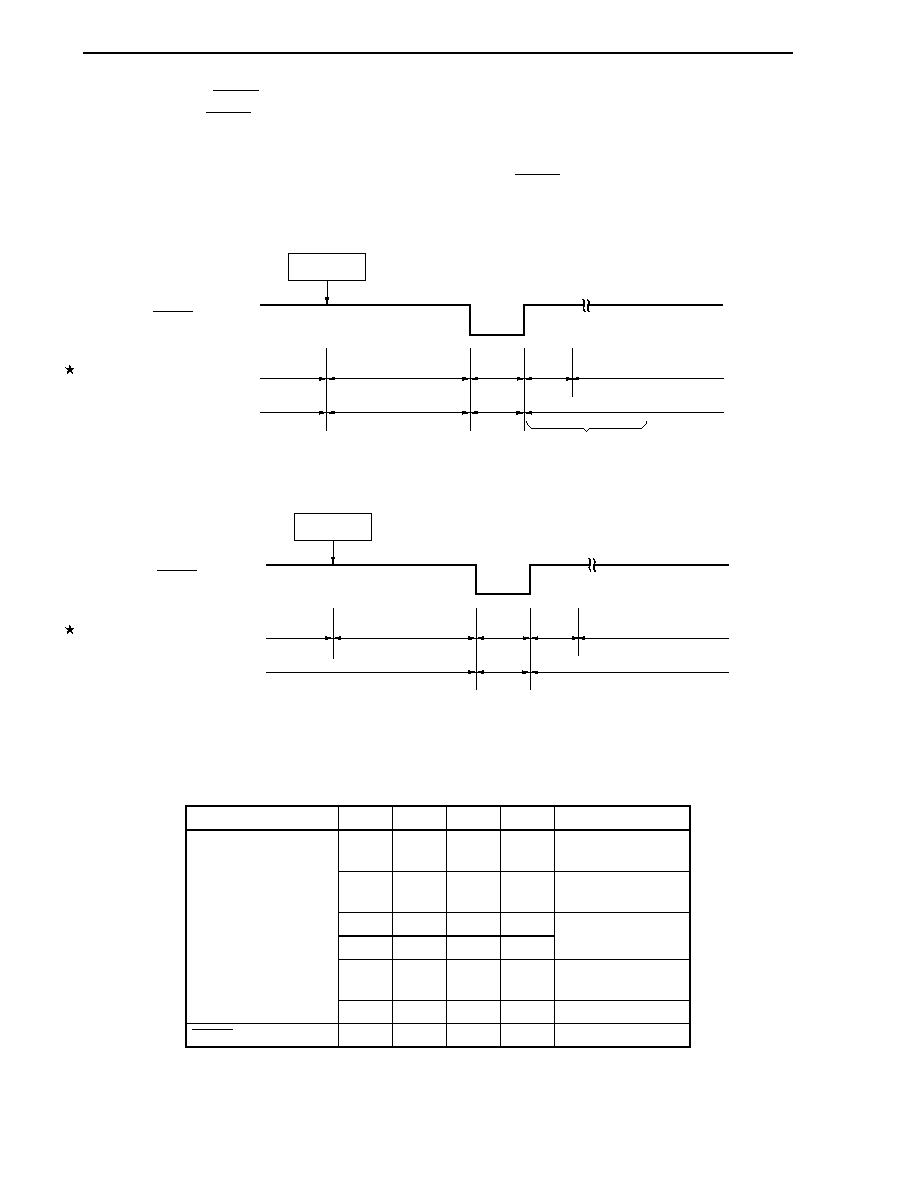
CHAPTER 19 STANDBY FUNCTION
User's Manual U16228EJ2V0UD
392
(b) Release by RESET input
When the RESET signal is input, STOP mode is released and a reset operation is performed after the
oscillation stabilization time has elapsed.
Figure 19-7. STOP Mode Release by RESET Input
(1) When X1 input clock is used as CPU clock
STOP
instruction
RESET signal
X1 input clock
Operating mode
STOP mode
Reset
period
Operation
stopped
Operating mode
Oscillates
Oscillation
stopped
Oscillates
Status of CPU
(X1 input clock)
Oscillation stabilization time (2
11
/f
XP
to 2
16
/f
XP
)
(Ring-OSC clock)
(17/f
R
)
Oscillation stopped
(2) When Ring-OSC clock is used as CPU clock
STOP
instruction
RESET signal
Ring-OSC clock
Operating mode
STOP mode
Reset
period
Operation
stopped
Operating mode
Oscillates
Oscillation
stopped
Oscillates
Status of CPU
(Ring-OSC clock)
(17/f
R
)
(Ring-OSC clock)
Remarks 1. f
XP
: X1 input clock oscillation frequency
2. f
R
: Ring-OSC clock oscillation frequency
Table 19-5. Operation in Response to Interrupt Request in STOP Mode
Release Source
MK
◊◊
PR
◊◊
IE ISP
Operation
0 0 0
◊
Next address
instruction execution
0 0 1
◊
Interrupt servicing
execution
0 1 0 1
0 1
◊
0
Next address
instruction execution
0 1 1 1
Interrupt servicing
execution
Maskable interrupt
request
1
◊
◊
◊
STOP mode held
RESET input
-
-
◊
◊
Reset processing
◊
: don't care

User's Manual U16228EJ2V0UD
393
CHAPTER 20 RESET FUNCTION
The following five operations are available to generate a reset signal.
(1) External reset input via RESET pin
(2) Internal reset by watchdog timer program loop detection
(3) Internal reset by clock monitor X1 clock oscillation stop detection
(4) Internal reset by comparison of supply voltage and detection voltage of power-on-clear (POC) circuit
(5) Internal reset by comparison of supply voltage and detection voltage of low-power-supply detector (LVI)
External and internal resets have no functional differences. In both cases, program execution starts at the address
at 0000H and 0001H when the reset signal is input.
A reset is applied when a low level is input to the RESET pin, the watchdog timer overflows, X1 clock oscillation
stop is detected by the clock monitor, or by POC and LVI circuit voltage detection, and each item of hardware is set to
the status shown in Table 20-1. Each pin is high impedance during reset input or during the oscillation stabilization
time just after reset release, except for P130, which is low-level output.
When a high level is input to the RESET pin, the reset is released and program execution starts using the Ring-
OSC clock after the CPU clock operation has stopped for 17/f
R
(s). A reset generated by the watchdog timer and
clock monitor sources is automatically released after the reset, and program execution starts using the Ring-OSC
clock after the CPU clock operation has stopped for 17/f
R
(s) (see Figures 20-2 to 20-4). Reset by POC and LVI
circuit power supply detection is automatically released when V
DD
> V
POC
or V
DD
> V
LVI
after the reset, and program
execution starts using the Ring-OSC clock after the CPU clock operation has stopped for 17/f
R
(s) (see CHAPTER 22
POWER-ON-CLEAR CIRCUIT and CHAPTER 23 LOW-VOLTAGE DETECTOR).
Cautions 1. For an external reset, input a low level for 10
µ
s or more to the RESET pin.
2. During reset input, the X1 input clock and Ring-OSC clock stop oscillating.
3. When the STOP mode is released by a reset, the STOP mode contents are held during reset
input. However, the port pins become high-impedance, except for P130, which is set to low-
level output.
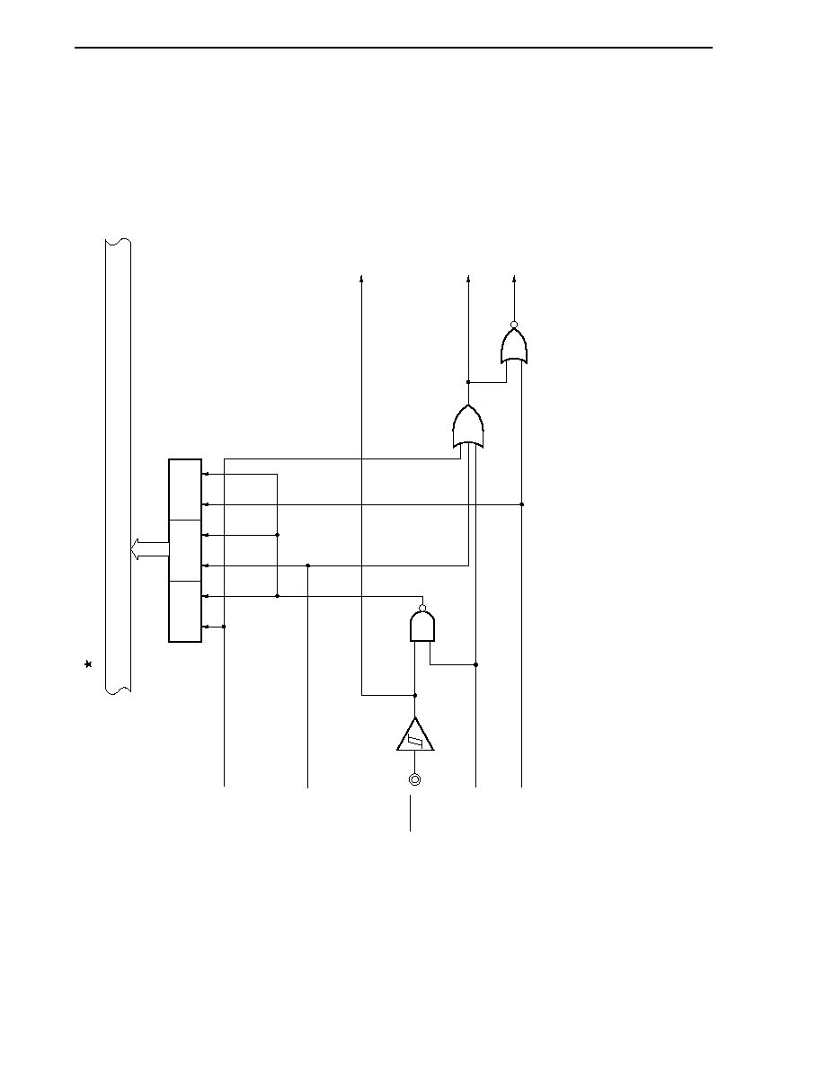
CHAPTER
20
RESET FU
NCTI
O
N
User's Manual
U1
6228EJ2V0UD
394
Figure 20-1. Block Diagram of Reset Function
CLMRF
LVIRF
WDTRF
Reset control flag
register (RESF)
Internal bus
Watchdog timer reset signal
Clock monitor reset signal
RESET
Power-on-clear circuit reset signal
Low-voltage detector reset signal
Reset signal
Reset signal
Reset signal to LVIM/LVIS register
Clear
Set
Set
Clear
Clear
Set
Caution An LVI circuit internal reset does not reset the LVI circuit.
Remarks 1. LVIM: Low-voltage detection register
2. LVIS: Low-voltage detection level selection register
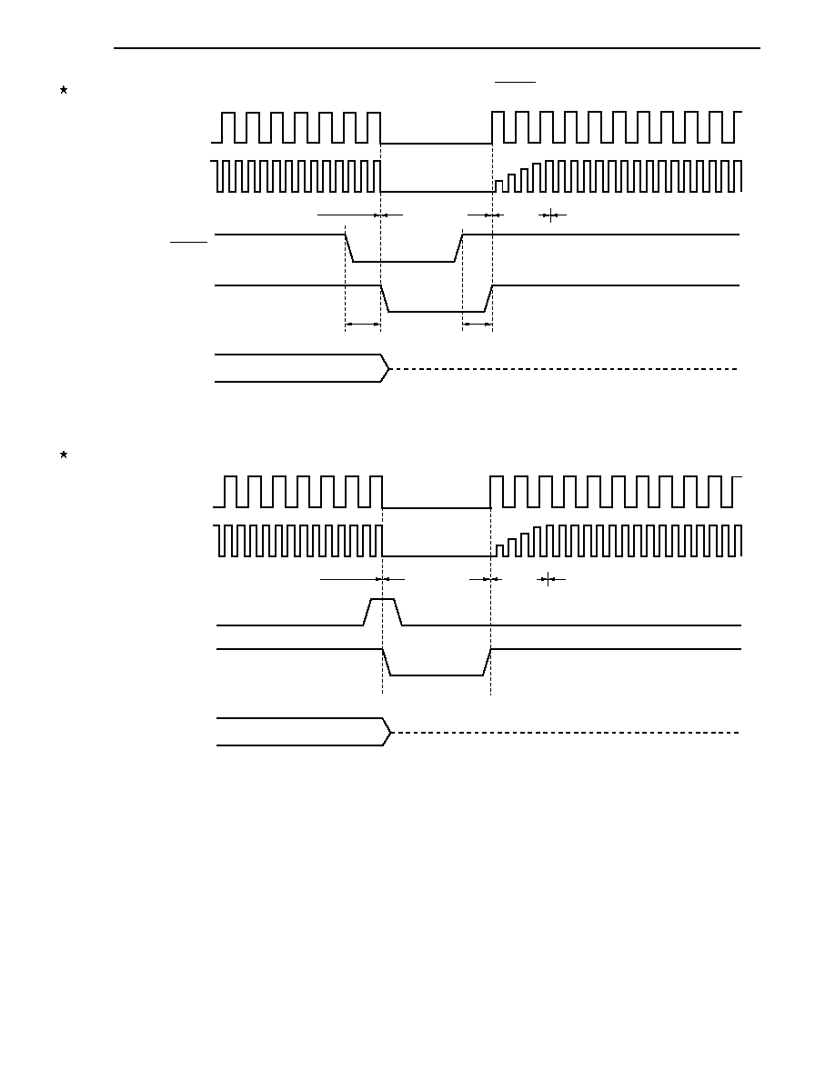
CHAPTER 20 RESET FUNCTION
User's Manual U16228EJ2V0UD
395
Figure 20-2. Timing of Reset by RESET Input
Delay
Delay
Hi-Z
Note
Normal operation
CPU clock
Reset period
(Oscillation stop)
Operation stop
(17/f
R
)
Normal operation
(Reset processing, Ring-OSC clock)
RESET
Internal
reset signal
Port pin
X1 input clock
Ring-OSC clock
Note The port pins become high impedance, except for P130, which is set to low-level output.
Figure 20-3. Timing of Reset Due to Watchdog Timer Overflow
Hi-Z
Note
Normal operation
Reset period
(Oscillation stop)
CPU clock
Watchdog timer
overflow
Internal
reset signal
Port pin
Operation stop
(17/f
R
)
Normal operation
(Reset processing, Ring-OSC clock)
X1 input clock
Ring-OSC clock
Note The port pins become high impedance, except for P130, which is set to low-level output.
Caution A watchdog timer internal reset resets the watchdog timer.
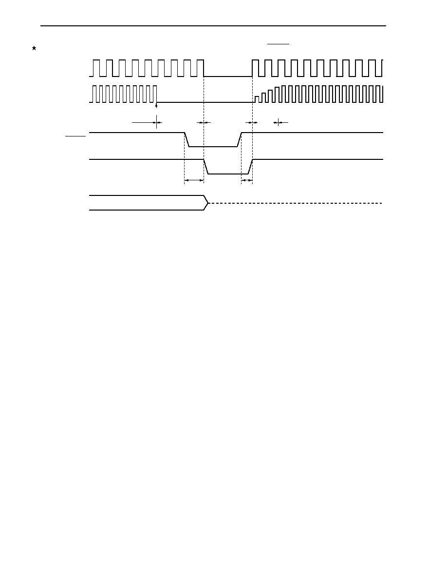
CHAPTER 20 RESET FUNCTION
User's Manual U16228EJ2V0UD
396
Figure 20-4. Timing of Reset in STOP Mode by RESET Input
Delay
Delay
Hi-Z
Note
Normal
operation
CPU clock
Reset period
(Oscillation stop)
RESET
Internal
reset signal
Port pin
STOP instruction execution
Stop status
(Oscillation stop)
Operation stop
(17/f
R
)
Normal operation
(Reset processing, Ring-OSC clock)
X1 input clock
Ring-OSC clock
Note The port pins become high impedance, except for P130, which is set to low-level output.
Remark For the reset timing of the power-on-clear circuit and low-voltage detector, see CHAPTER 22 POWER-
ON-CLEAR CIRCUIT and CHAPTER 23 LOW-VOLTAGE DETECTOR.

CHAPTER 20 RESET FUNCTION
User's Manual U16228EJ2V0UD
397
Table 20-1. Hardware Statuses After Reset Acknowledgment (1/3)
Hardware
Status After Reset
Acknowledgment
Note 1
Program counter (PC)
The contents of the
reset vector table
(0000H, 0001H) are
set.
Stack pointer (SP)
Undefined
Program status word (PSW)
02H
Data memory
Undefined
Note 2
RAM
General-purpose registers
Undefined
Note 2
Port registers (P0 to P7, P12 to P14) (output latches)
00H (undefined only
for P2)
Port mode registers (PM0, PM1, PM3 to PM7, PM12, PM14)
FFH
Pull-up resistor option registers (PU0, PU1, PU3 to PU5, PU7, PU12, PU14)
00H
Input switch control register (ISC)
00H
Internal memory size switching register (IMS)
CFH
Internal expansion RAM size switching register (IXS)
0CH
Processor clock control register (PCC)
00H
Ring-OSC mode register (RCM)
00H
Main clock mode register (MCM)
00H
Main OSC control register (MOC)
00H
Oscillation stabilization time select register (OSTS)
05H
Oscillation stabilization time counter status register (OSTC)
00H
Timer counters 00, 01 (TM00, TM01)
0000H
Capture/compare registers 000, 010, 001, 011 (CR000, CR010, CR001, CR011)
0000H
Mode control registers 00, 01 (TMC00, TMC01)
00H
Prescaler mode registers 00, 01 (PRM00, PRM01)
00H
Capture/compare control registers 00, 01 (CRC00, CRC01)
00H
16-bit timer/event
counters 00, 01
Note 3
Timer output control registers 00, 01 (TOC00, TOC01)
00H
Timer counters 50, 51 (TM50, TM51)
00H
Compare registers 50, 51 (CR50, CR51)
00H
Timer clock selection registers 50, 51 (TCL50, TCL51)
00H
8-bit timer/event
counters 50, 51
Mode control registers 50, 51 (TMC50, TMC51)
00H
Compare registers 00, 10, 01, 11 (CMP00, CMP10, CMP01, CMP11)
00H
Mode registers (TMHMD0, TMHMD1)
00H
8-bit timers H0, H1
Carrier control register 1 (TMCYC1)
Note 4
00H
Watch timer
Operation mode register (WTM)
00H
Clock output/buzzer
output controller
Clock output selection register (CKS)
00H
Notes 1. During reset input or oscillation stabilization time wait, only the PC contents among the hardware statuses
become undefined. All other hardware statuses remain unchanged after reset.
2. When a reset is executed in the standby mode, the pre-reset status is held even after reset.
3. 16-bit timer/event counter 01 is available only for the
µ
PD780133, 780134, 78F0134, 780136, 780138,
and 78F0138.
4. 8-bit timer H1 only.

CHAPTER 20 RESET FUNCTION
User's Manual U16228EJ2V0UD
398
Table 20-1. Hardware Statuses After Reset Acknowledgment (2/3)
Hardware
Status After Reset
Acknowledgment
Mode register (WDTM)
67H
Watchdog timer
Enable register (WDTE)
9AH
Conversion result register (ADCR)
Undefined
Mode register (ADM)
00H
Analog input channel specification register (ADS)
00H
Power-fail comparison mode register (PFM)
00H
A/D converter
Power-fail comparison threshold register (PFT)
00H
Receive buffer register 0 (RXB0)
FFH
Transmit shift register 0 (TXS0)
FFH
Asynchronous serial interface operation mode register 0 (ASIM0)
01H
Serial interface UART0
Baud rate generator control register 0 (BRGC0)
1FH
Receive buffer register 6 (RXB6)
FFH
Transmit buffer register 6 (TXB6)
FFH
Asynchronous serial interface operation mode register 6 (ASIM6)
01H
Asynchronous serial interface reception error status register 6 (ASIS6)
00H
Asynchronous serial interface transmission status register 6 (ASIF6)
00H
Clock selection register 6 (CKSR6)
00H
Baud rate generator control register 6 (BRGC6)
FFH
Serial interface UART6
Asynchronous serial interface control register 6 (ASICL6)
16H
Transmit buffer registers 10, 11 (SOTB10, SOTB11)
Undefined
Serial I/O shift registers 10, 11 (SIO10, SIO11)
Undefined
Serial operation mode registers 10, 11 (CSIM10, CSIM11)
00H
Serial interfaces CSI10,
CSI11
Note
Serial clock selection registers 10, 11 (CSIC10, CSIC11)
00H
Remainder data register 0 (SDR0)
0000H
Multiplication/division data register A0 (MDA0H, MDA0L)
0000H
Multiplication/division data register B0 (MDB0)
0000H
Multiplier/divider
Multiplier/divider control register 0 (DMUC0)
00H
Key interrupt
Key return mode register (KRM)
00H
Clock monitor
Mode register (CLM)
00H
Note Serial interface CSI11 is available only for the
µ
PD780146, 780148, and 78F0148.

CHAPTER 20 RESET FUNCTION
User's Manual U16228EJ2V0UD
399
Table 20-1. Hardware Statuses After Reset Acknowledgment (3/3)
Hardware
Status After Reset
Acknowledgment
Reset function
Reset control flag register (RESF)
00H
Note
Low-voltage detection register (LVIM)
00H
Note
Low-voltage detector
Low-voltage detection level selection register (LVIS)
00H
Note
Request flag registers 0L, 0H, 1L, 1H (IF0L, IF0H, IF1L, IF1H)
00H
Mask flag registers 0L, 0H, 1L (MK0L, MK0H, MK1L)
FFH
Mask flag register 1H (MK1H)
DFH
Priority specification flag registers 0L, 0H, 1L, 1H (PR0L, PR0H, PR1L,
PR1H)
FFH
External interrupt rising edge enable register (EGP)
00H
Interrupt
External interrupt falling edge enable register (EGN)
00H
Note These values vary depending on the reset source.
Reset Source
Register
RESET Input
Reset by POC
Reset by WDT
Reset by CLM
Reset by LVI
RESF See
Table 20-2.
LVIM
LVIS
Cleared (00H)
Cleared (00H)
Cleared (00H)
Cleared (00H)
Held

CHAPTER 20 RESET FUNCTION
User's Manual U16228EJ2V0UD
400
20.1 Register for Confirming Reset Source
Many internal reset generation sources exist in the 78K0/KE1. The reset control flag register (RESF) is used to
store which source has generated the reset request.
RESF can be read by an 8-bit memory manipulation instruction.
RESET input, reset input by power-on-clear (POC) circuit, and reading RESF clear RESF to 00H.
Figure 20-5. Format of Reset Control Flag Register (RESF)
Address: FFACH After reset: 00H
Note
R
Symbol
7 6 5 4 3 2 1 0
RESF 0
0
0 WDTRF 0
0 CLMRF
LVIRF
WDTRF
Internal reset request by watchdog timer (WDT)
0
Internal reset request is not generated, or RESF is cleared.
1
Internal reset request is generated.
CLMRF
Internal
reset
request by clock monitor (CLM)
0
Internal reset request is not generated, or RESF is cleared.
1
Internal reset request is generated.
LVIRF
Internal reset request by low-voltage detector (LVI)
0
Internal reset request is not generated, or RESF is cleared.
1
Internal reset request is generated.
Note The value after reset varies depending on the reset source.
Caution Do not read data by a 1-bit memory manipulation instruction.
The status of RESF when a reset request is generated is shown in Table 20-2.
Table 20-2. RESF Status When Reset Request Is Generated
Reset Source
Flag
RESET Input
Reset by POC
Reset by WDT
Reset by CLM
Reset by LVI
WDTRF Set
(1)
Held
Held
CLMRF Held
Set
(1)
Held
LVIRF
Cleared (0)
Cleared (0)
Held Held Set
(1)
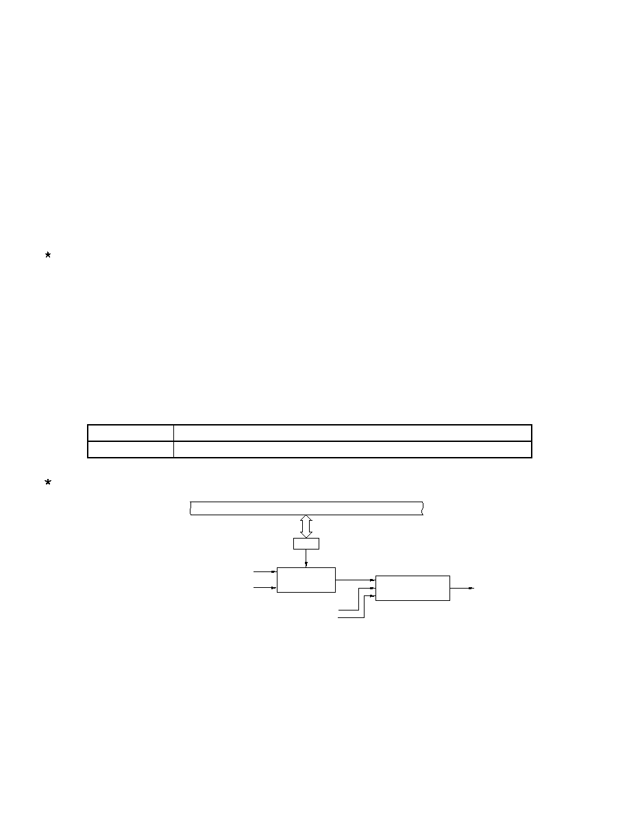
User's Manual U16228EJ2V0UD
401
CHAPTER 21 CLOCK MONITOR
21.1 Functions of Clock Monitor
The clock monitor samples the X1 input clock using the on-chip Ring-OSC, and generates an internal reset signal
when the X1 input clock is stopped.
When a reset signal is generated by the clock monitor, bit 1 (CLMRF) of the reset control flag register (RESF) is set
to 1. For details of RESF, see CHAPTER 20 RESET FUNCTION.
The clock monitor automatically stops under the following conditions.
∑
Reset is released and during the oscillation stabilization time
∑
In STOP mode and during the oscillation stabilization time
∑
When the X1 input clock is stopped by software (MSTOP = 1 or MCC = 1) and during the oscillation stabilization
time
∑
When the Ring-OSC clock is stopped
Remark MSTOP: Bit 7 of the main OSC control register (MOC)
MCC:
Bit 7 of the processor clock control register (PCC)
21.2 Configuration of Clock Monitor
The clock monitor includes the following hardware.
Table 21-1. Configuration of Clock Monitor
Item Configuration
Control register
Clock monitor mode register (CLM)
Figure 21-1. Block Diagram of Clock Monitor
Operation mode
controller
X1 input clock
Ring-OSC clock
CLME
Clock monitor
mode register (CLM)
Internal bus
X1 oscillation
monitor circuit
Internal reset
signal
X1 oscillation control signal
(MCC, MSTOP)
X1 oscillation stabilization status
(OSTC overflow)
Remark MCC:
Bit 7 of the processor clock control register (PCC)
MSTOP: Bit 7 of the main OSC control register (MOC)
OSTC: Oscillation stabilization time counter status register (OSTC)
CHAPTER 21 CLOCK MONITOR
User's Manual U16228EJ2V0UD
402
21.3 Registers Controlling Clock Monitor
The clock monitor is controlled by the clock monitor mode register (CLM).
(1) Clock monitor mode register (CLM)
This register sets the operation mode of the clock monitor.
This register can be set by a 1-bit or 8-bit memory manipulation instruction.
RESET input clears this register to 00H.
Figure 21-2. Format of Clock Monitor Mode Register (CLM)
7
0
CLME
0
1
Symbol
CLM
Address: FFA9H After reset: 00H R/W
6
0
Disables clock monitor operation
Enables clock monitor operation
5
0
4
0
3
0
Enables/disables clock monitor operation
2
0
1
0
<0>
CLME
Cautions 1. Once bit 0 (CLME) is set to 1, it cannot be cleared to 0 except by RESET input or the internal
reset signal.
2. If the reset signal is generated by the clock monitor, CLME is cleared to 0 and bit 1 (CLMRF)
of the reset control flag register (RESF) is set to 1.
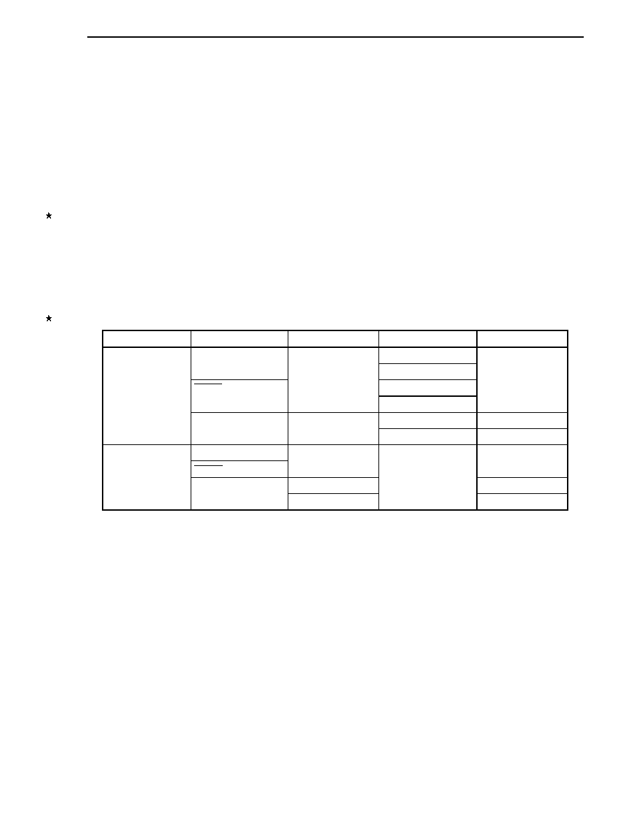
CHAPTER 21 CLOCK MONITOR
User's Manual U16228EJ2V0UD
403
21.4 Operation of Clock Monitor
This section explains the functions of the clock monitor. The monitor start and stop conditions are as follows.
<Monitor start condition>
When bit 0 (CLME) of the clock monitor mode register (CLM) is set to operation enabled (1).
<Monitor stop condition>
∑
Reset is released and during the oscillation stabilization time
∑
In STOP mode and during the oscillation stabilization time
∑
When the X1 input clock is stopped by software (MSTOP = 1 or MCC = 1) and during the oscillation
stabilization time
∑
When the Ring-OSC clock is stopped
Remark MSTOP: Bit 7 of the main OSC control register (MOC)
MCC:
Bit 7 of the processor clock control register (PCC)
Table 21-2. Operation Status of Clock Monitor (When CLME = 1)
CPU Operation Clock
Operation Mode
X1 Input Clock Status
Ring-OSC Clock Status
Clock Monitor Status
Oscillating
STOP mode
Stopped
Stopped
Note
Oscillating
RESET input
Stopped
Note
Stopped
Oscillating Operating
X1 input clock
Normal operation mode
HALT mode
Oscillating
Stopped
Note
Stopped
STOP mode
RESET input
Stopped Oscillating Stopped
Oscillating
Operating
Ring-OSC clock
Normal operation mode
HALT mode
Stopped
Stopped
Note The Ring-OSC clock is stopped only when the "Ring-OSC can be stopped by software" is selected by a
mask option. If "Ring-OSC cannot be stopped" is selected, the Ring-OSC clock cannot be stopped.
The clock monitor timing is as shown in Figure 21-3.
CHAPTER 21 CLOCK MONITOR
User's Manual U16228EJ2V0UD
404
Figure 21-3. Timing of Clock Monitor (1/4)
(1) When internal reset is executed by oscillation stop of X1 input clock
4 clocks of Ring-OSC clock
X1 input clock
Ring-OSC clock
Internal reset signal
CLME
CLMRF
(2) Clock monitor status after RESET input
(CLME = 1 is set after RESET input and during X1 input clock oscillation stabilization time)
CPU operation
Clock monitor status
CLME
Ring-OSC clock
X1 input clock
Reset
Oscillation
stopped
Oscillation stabilization time
Normal
operation
Clock supply
stopped
Normal operation (Ring-OSC clock)
Monitoring
Monitoring stopped
Monitoring
Waiting for end
of oscillation
stabilization time
Oscillation
stopped
17 clocks
Set to 1 by software
RESET
RESET input clears bit 0 (CLME) of the clock monitor mode register (CLM) to 0 and stops the clock monitor
operation. Even if CLME is set to 1 by software during the oscillation stabilization time (reset value of OSTS register
is 05H (2
16
/f
XP
)) of the X1 input clock, monitoring is not performed until the oscillation stabilization time of the X1 input
clock ends. Monitoring is automatically started at the end of the oscillation stabilization time.
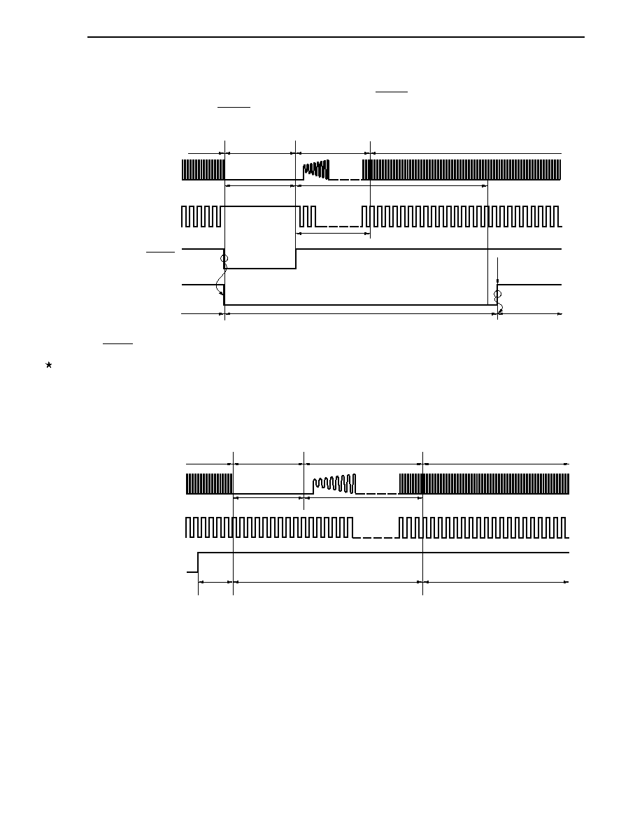
CHAPTER 21 CLOCK MONITOR
User's Manual U16228EJ2V0UD
405
Figure 21-3. Timing of Clock Monitor (2/4)
(3) Clock monitor status after RESET input
(CLME = 1 is set after RESET input and at the end of X1 input clock oscillation stabilization time)
CPU operation
Clock monitor status
CLME
RESET
Ring-OSC clock
X1 input clock
Reset
Oscillation stabilization time
Normal
operation
Clock supply
stopped
Normal operation (Ring-OSC clock)
Monitoring
Monitoring stopped
Monitoring
17 clocks
Set to 1 by software
RESET input clears bit 0 (CLME) of the clock monitor mode register (CLM) to 0 and stops the clock monitor
operation. When CLME is set to 1 by software at the end of the oscillation stabilization time (reset value of OSTS
register is 05H (2
16
/f
XP
)) of the X1 input clock, monitoring is started.
(4) Clock monitor status after STOP mode is released
(CLME = 1 is set when CPU clock operates on X1 input clock and before entering STOP mode)
Clock monitor status
Monitoring
Monitoring stopped
Monitoring
CLME
Ring-OSC clock
X1 input clock
(CPU clock)
CPU operation
Normal
operation
STOP
Oscillation stabilization time
Normal operation
Oscillation
stopped
Oscillation stabilization time
(time set by OSTS register)
When bit 0 (CLME) of the clock monitor mode register (CLM) is set to 1 before entering STOP mode, monitoring
automatically starts at the end of the X1 input clock oscillation stabilization time. Monitoring is stopped in STOP mode
and during the oscillation stabilization time.

CHAPTER 21 CLOCK MONITOR
User's Manual U16228EJ2V0UD
406
Figure 21-3. Timing of Clock Monitor (3/4)
(5) Clock monitor status after STOP mode is released
(CLME = 1 is set when CPU clock operates on Ring-OSC clock and before entering STOP mode)
Clock monitor status
Monitoring
Monitoring
stopped
Monitoring stopped
Monitoring
CLME
Ring-OSC clock
(CPU clock)
X1 input clock
CPU operation
Normal
operation
17 clocks
Clock supply
stopped
Normal operation
Oscillation
stopped
Oscillation stabilization time
(time set by OSTS register)
STOP
When bit 0 (CLME) of the clock monitor mode register (CLM) is set to 1 before entering STOP mode, monitoring
automatically starts at the end of the X1 input clock oscillation stabilization time. Monitoring is stopped in STOP mode
and during the oscillation stabilization time.
(6) Clock monitor status after X1 input clock oscillation is stopped by software
Clock monitor status
CLME
MSTOP or
MCC
Note
Ring-OSC clock
X1 input clock
Oscillation stabilization time
(time set by OSTS register)
Normal operation (Ring-OSC clock or subsystem clock
Note
)
Monitoring
Monitoring
stopped
Monitoring
CPU operation
Monitoring stopped
Oscillation
stopped
When bit 0 (CLME) of the clock monitor mode register (CLM) is set to 1 before or while oscillation of the X1 input
clock is stopped, monitoring automatically starts at the end of the X1 input clock oscillation stabilization time.
Monitoring is stopped when oscillation of the X1 input clock is stopped and during the oscillation stabilization time.
Note The register that controls oscillation of the X1 input clock differs depending on the type of the clock supplied
to the CPU.
∑
When CPU operates on Ring-OSC clock: Controlled by bit 7 (MSTOP) of the main OSC control
register (MOC)
∑
When CPU operates on subsystem clock: Controlled by bit 7 (MCC) of the processor clock control
register (PCC)
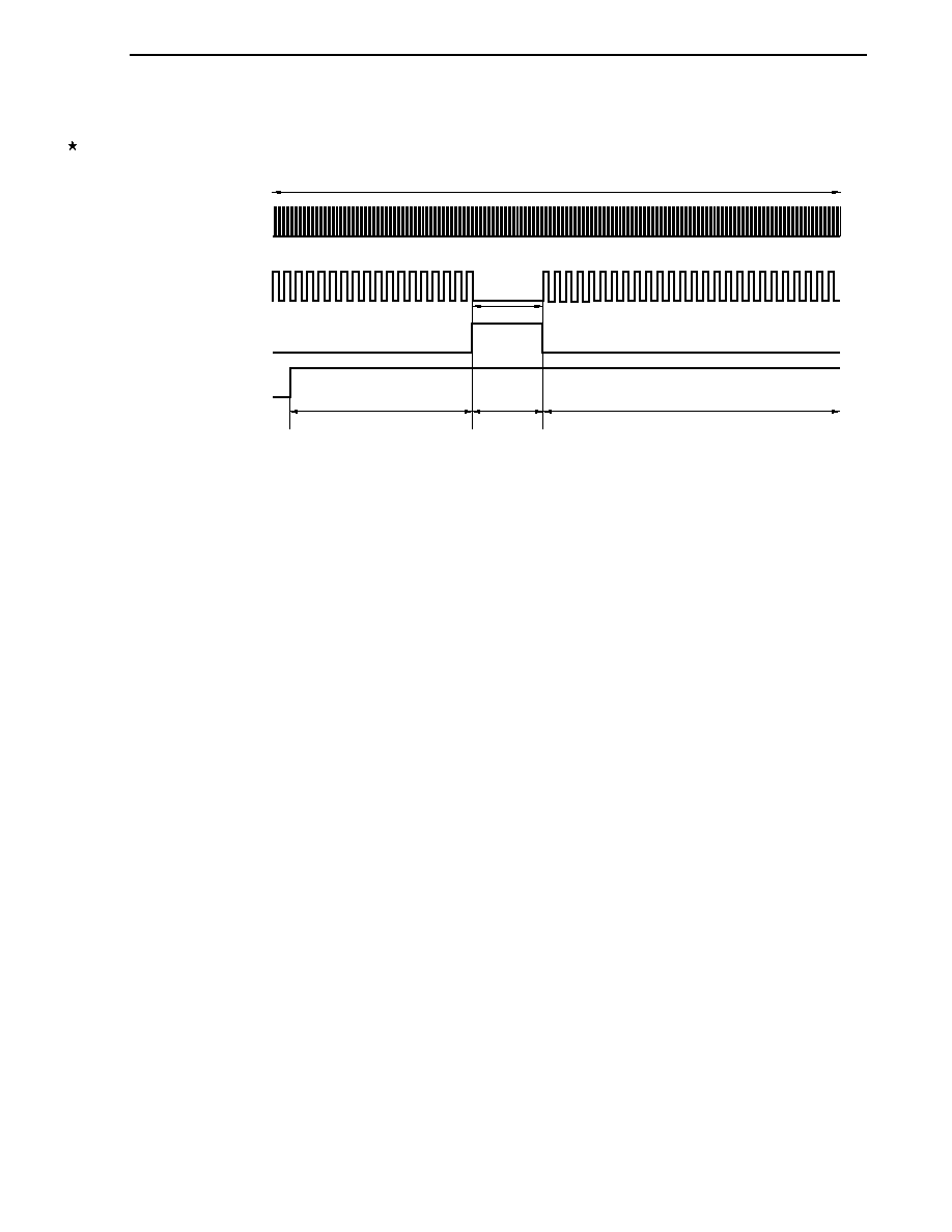
CHAPTER 21 CLOCK MONITOR
User's Manual U16228EJ2V0UD
407
Figure 21-3. Timing of Clock Monitor (4/4)
(7) Clock monitor status after Ring-OSC clock oscillation is stopped by software
Ring-OSC clock
X1 input clock
CPU operation
Normal operation (X1 input clock or subsystem clock)
Oscillation stopped
RSTOP
Note
Clock monitor status
Monitoring
Monitoring
stopped
Monitoring
CLME
When bit 0 (CLME) of the clock monitor mode register (CLM) is set to 1 before or while oscillation of the Ring-OSC
clock is stopped, monitoring automatically starts after the Ring-OSC clock is stopped. Monitoring is stopped when
oscillation of the Ring-OSC clock is stopped.
Note If it is specified by a mask option that Ring-OSC cannot be stopped, the setting of bit 0 (RSTOP) of the
Ring-OSC mode register (RCM) is invalid. To set RSTOP, be sure to confirm that bit 1 (MCS) of the main
clock mode register (MCM) is 1.

User's Manual U16228EJ2V0UD
408
CHAPTER 22 POWER-ON-CLEAR CIRCUIT
22.1 Functions of Power-on-Clear Circuit
The power-on-clear circuit (POC) has the following functions.
∑
Generates internal reset signal at power on.
∑
Compares supply voltage (V
DD
) and detection voltage (V
POC
), and generates internal reset signal when V
DD
<
V
POC
.
∑
The following can be selected by a mask option.
∑
POC disabled
∑
POC used (detection voltage: V
POC
= 2.85 V
±
0.15 V)
Note
∑
POC used (detection voltage: V
POC
= 3.5 V
±
0.2 V)
Note This option cannot be selected in (A1) and (A2) grade products because the supply voltage V
DD
is 3.3 to
5.5 V.
Caution If an internal reset signal is generated in the POC circuit, the reset control flag register (RESF) is
cleared to 00H.
Remark This product incorporates multiple hardware functions that generate an internal reset signal. A flag that
indicates the reset cause is located in the reset control flag register (RESF) for when an internal reset
signal is generated by the watchdog timer (WDT), low-voltage-detection (LVI) circuit, or clock monitor.
RESF is not cleared to 00H and the flag is set to 1 when an internal reset signal is generated by WDT,
LVI, or the clock monitor.
For details of the RESF, refer to CHAPTER 20 RESET FUNCTION.
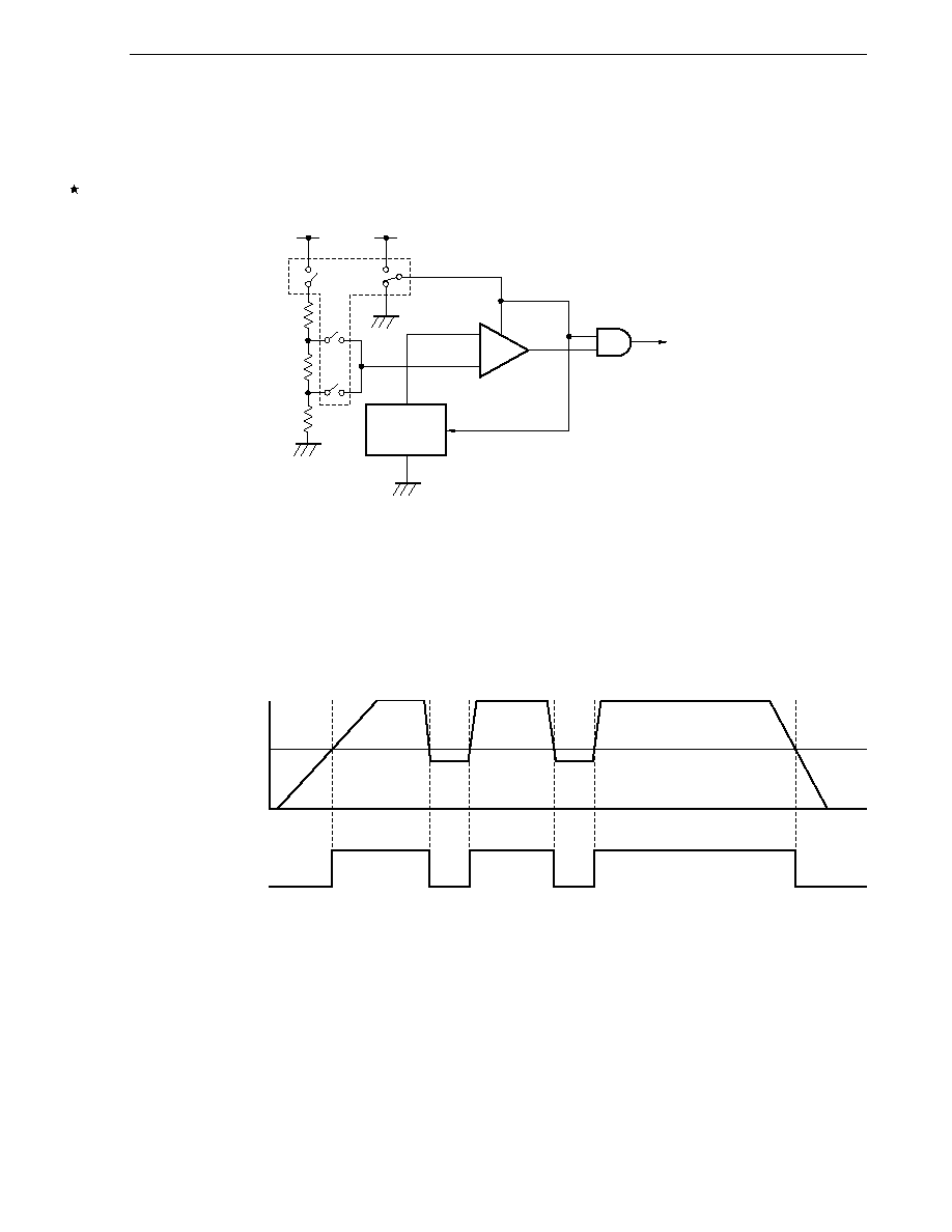
CHAPTER 22 POWER-ON-CLEAR CIRCUIT
User's Manual U16228EJ2V0UD
409
22.2 Configuration of Power-on-Clear Circuit
The block diagram of the power-on-clear circuit is shown in Figure 22-1.
Figure 22-1. Block Diagram of Power-on-Clear Circuit
-
+
Detection
voltage source
(V
POC
)
Internal reset signal
V
DD
V
DD
Mask option
22.3 Operation of Power-on-Clear Circuit
In the power-on-clear circuit, the supply voltage (V
DD
) and detection voltage (V
POC
) are compared, and when V
DD
<
V
POC
, an internal reset signal is generated.
Figure 22-2. Timing of Internal Reset Signal Generation in Power-on-Clear Circuit
Time
Supply voltage (V
DD
)
POC detection voltage
(V
POC
)
2.7 V
Internal reset signal

CHAPTER 22 POWER-ON-CLEAR CIRCUIT
User's Manual U16228EJ2V0UD
410
22.4 Cautions for Power-on-Clear Circuit
In a system where the supply voltage (V
DD
) fluctuates for a certain period in the vicinity of the POC detection
voltage (V
POC
), the system may be repeatedly reset and released from the reset status. In this case, the time from
release of reset to the start of the operation of the microcontroller can be arbitrarily set by taking the following action.
<Action>
After releasing the reset signal, wait for the supply voltage fluctuation period of each system by means of a
software counter that uses a timer, and then initialize the ports.
Figure 22-3. Example of Software Processing After Release of Reset (1/2)
∑
If supply voltage fluctuation is 50 ms or less in vicinity of POC detection voltage
Yes
Power-on-clear
; The
Ring-OSC clock is set as the CPU clock when the reset signal is generated
;
The cause of reset (power-on-clear, WDT, LVI, or clock monitor)
can be identified by the RESF register.
;
Change the CPU clock from the Ring-OSC clock to the X1 input clock.
;
Check the stabilization of oscillation of the X1 input clock by using the
OSTC register.
;
TMIFH1 = 1: Interrupt request is generated.
;
Initialization of ports
;
8-bit timer H1 can operate with the Ring-OSC clock.
Source: f
R
(480 kHz (MAX.))/2
7
◊
compare value 200 = 53 ms
(f
R
: Ring-OSC clock oscillation frequency)
No
Note 1
Reset
Checking cause
of reset
Note 2
Check stabilization
of oscillation
Change CPU clock
50 ms has passed?
(TMIFH1 = 1?)
Initialization
processing
Start timer
(set to 50 ms)
Notes 1. If reset is generated again during this period, initialization processing is not started.
2. A flowchart is shown on the next page.

CHAPTER 22 POWER-ON-CLEAR CIRCUIT
User's Manual U16228EJ2V0UD
411
Figure 22-3. Example of Software Processing After Release of Reset (2/2)
∑
Checking reset cause
Yes
No
Check reset cause
Power-on-clear/external
reset generated
Reset processing by
watchdog timer
Reset processing by
clock monitor
Reset processing by
low-voltage detector
No
No
WDTRF of RESF
register = 1?
CLMRF of RESF
register = 1?
LVIRF of RESF
register = 1?
Yes
Yes

User's Manual U16228EJ2V0UD
412
CHAPTER 23 LOW-VOLTAGE DETECTOR
23.1 Functions of Low-Voltage Detector
The low-voltage detector (LVI) has following functions.
∑
Compares supply voltage (V
DD
) and detection voltage (V
LVI
), and generates an internal interrupt signal or
internal reset signal when V
DD
< V
LVI
.
∑
Detection levels (seven levels)
Note
of supply voltage can be changed by software.
∑
Interrupt or reset function can be selected by software.
∑
Operable in STOP mode.
Note Five levels in the case of (A1) grade products and (A2) grade products.
When the low-voltage detector is used to reset, bit 0 (LVIRF) of the reset control flag register (RESF) is set to 1 if
reset occurs. For details of RESF, refer to CHAPTER 20 RESET FUNCTION.
23.2 Configuration of Low-Voltage Detector
The block diagram of the low-voltage detector is shown below.
Figure 23-1. Block Diagram of Low-Voltage Detector
LVIS1 LVIS0
LVION
LVIE
-
+
Detection
voltage source
(V
LVI
)
V
DD
Internal bus
N-ch
Low-voltage detection level
selection register (LVIS)
Low-voltage detection register
(LVIM)
LVIS2
LVIMD
LVIF
INTLVI
Internal reset signal
3
V
DD
Low-voltage detection level selector
Selector

CHAPTER 23 LOW-VOLTAGE DETECTOR
User's Manual U16228EJ2V0UD
413
23.3 Registers Controlling Low-Voltage Detector
The low-voltage detector is controlled by the following registers.
∑
Low-voltage detection register (LVIM)
∑
Low-voltage detection level selection register (LVIS)
CHAPTER 23 LOW-VOLTAGE DETECTOR
User's Manual U16228EJ2V0UD
414
(1) Low-voltage detection register (LVIM)
This register sets low-voltage detection and the operation mode.
This register can be set by a 1-bit or 8-bit memory manipulation instruction.
RESET input clears LVIM to 00H.
Figure 23-2. Format of Low-Voltage Detection Register (LVIM)
<0>
LVIF
<1>
LVIMD
2
0
3
0
<4>
LVIE
5
0
6
0
<7>
LVION
Symbol
LVIM
Address: FFBEH After reset: 00H R/W
Note 1
LVION
Notes 2, 3
Enables low-voltage detection operation
0 Disables
operation
1 Enables
operation
LVIE
Notes 2, 4, 5
Specifies reference voltage generator
0 Disables
operation
1 Enables
operation
LVIMD
Note 2
Low-voltage detection operation mode selection
0
Generates interrupt signal when supply voltage (V
DD
) < detection voltage (V
LVI
)
1
Generates internal reset signal when supply voltage (V
DD
) < detection voltage (V
LVI
)
LVIF
Note 6
Low-voltage detection flag
0
Supply voltage (V
DD
) > detection voltage (V
LVI
), or when operation is disabled
1
Supply voltage (V
DD
) < detection voltage (V
LVI
)
Notes 1. Bit 0 is read-only.
2. LVION, LVIE, and LVIMD are cleared to 0 at a reset other than an LVI reset. These are not
cleared to 0 at an LVI reset.
3. When LVION is set to 1, operation of the comparator in the LVI circuit is started. Use
software to instigate a wait of at least 0.2 ms from when LVION is set to 1 until the voltage is
confirmed at LVIF.
4. If "POC cannot be used" is selected by a mask option, wait for 2 ms or more by software from
when LVIE is set to 1 until LVION is set to 1.
5. If "POC used" is selected by a mask option, setting of LVIE is invalid because the reference
voltage generator in the LVI circuit always operates.
6. The value of LVIF is output as the interrupt request signal INTLVI when LVION = 1 and
LVIMD = 0.
Caution To stop LVI, follow either of the procedures below.
∑
When using 8-bit manipulation instruction: Write 00H to LVIM.
∑
When using 1-bit memory manipulation instruction: Clear LVION to 0 first and then
clear LVIE to 0.
CHAPTER 23 LOW-VOLTAGE DETECTOR
User's Manual U16228EJ2V0UD
415
(2) Low-voltage
detection
level selection register (LVIS)
This register selects the low-voltage detection level.
This register can be set by an 8-bit memory manipulation instruction.
RESET input clears LVIS to 00H.
Figure 23-3. Format of Low-Voltage Detection Level Selection Register (LVIS)
0
LVIS0
1
LVIS1
2
LVIS2
3
0
4
0
5
0
6
0
7
0
Symbol
LVIS
Address: FFBFH After reset: 00H R/W
LVIS2 LVIS1 LVIS0
Detection
level
0 0 0
V
LVI0
(4.3 V
±
0.2 V)
0 0 1
V
LVI1
(4.1 V
±
0.2 V)
0 1 0
V
LVI2
(3.9 V
±
0.2 V)
0 1 1
V
LVI3
(3.7 V
±
0.2 V)
1 0 0
V
LVI4
(3.5 V
±
0.2 V)
Note 1
1 0 1
V
LVI5
(3.3 V
±
0.15 V)
Notes 1, 2
1 1 0
V
LVI6
(3.1 V
±
0.15 V)
Notes 1, 2
1 1 1
Setting
prohibited
Notes 1. When the detection voltage of the POC circuit is specified as V
POC
= 3.5 V
±
0.2 V by a mask
option, do not select V
LVI4
to V
LVI6
as the LVI detection voltage. Even if V
LVI4
to V
LVI6
are
selected, the POC circuit has priority.
2. This setting is prohibited in (A1) grade products and (A2) grade products.
Caution Be sure to clear bits 3 to 7 to 0.

CHAPTER 23 LOW-VOLTAGE DETECTOR
User's Manual U16228EJ2V0UD
416
23.4 Operation of Low-Voltage Detector
The low-voltage detector can be used in the following two modes.
∑
Used as reset
Compares the supply voltage (V
DD
) and detection voltage (V
LVI
), and generates an internal reset signal when
V
DD
< V
LVI
.
∑
Used as interrupt
Compares the supply voltage (V
DD
) and detection voltage (V
LVI
), and generates an interrupt signal (INTLVI)
when V
DD
< V
LVI
.
The operation is set as follows.
(1) When used as reset
∑
When
starting
operation
<1> Mask the LVI interrupt (LVIMK = 1).
<2> Set the detection voltage using bits 2 to 0 (LVIS2 to LVIS0) of the low-voltage detection level selection
register (LVIS).
<3> Set bit 4 (LVIE) of the low-voltage detection register (LVIM) to 1 (enables reference voltage generator
operation).
<4> Use software to instigate a wait of at least 2 ms.
<5> Set bit 7 (LVION) of LVIM to 1 (enables LVI operation).
<6> Use software to instigate a wait of at least 0.2 ms.
<7> Wait until it is checked that (supply voltage (V
DD
) > detection voltage (V
LVI
)) by bit 0 (LVIF) of LVIM.
<8> Set bit 1 (LVIMD) of LVIM to 1 (generates internal reset signal when supply voltage (V
DD
) < detection
voltage (V
LVI
)).
Figure 23-4 shows the timing of the internal reset signal generated by the low-voltage detector. The numbers
in this timing chart correspond to <1> to <8> above.
Cautions 1. <1> must always be executed. When LVIMK = 0, an interrupt may occur immediately
after the processing in <5>.
2. If "POC used" is selected by a mask option, procedures <3> and <4> are not required.
3. If supply voltage (V
DD
) > detection voltage (V
LVI
) when LVIM is set to 1, an internal reset
signal is not generated.
∑
When stopping operation
Either of the following procedures must be executed.
∑
When using 8-bit memory manipulation instruction:
Write 00H to LVIM.
∑
When using 1-bit memory manipulation instruction:
Clear LVIMD to 0, LVION to 0, and LVIE to 0 in that order.

CHAPTER 23 LOW-VOLTAGE DETECTOR
User's Manual U16228EJ2V0UD
417
Figure 23-4. Timing of Low-Voltage Detector Internal Reset Signal Generation
Supply voltage (V
DD
)
LVI detection voltage
(V
LVI
)
POC detection voltage
(V
POC
)
2.7 V
LVIF flag
LVIRF flag
Note 3
Note 2
LVI reset signal
POC reset signal
Internal reset signal
Cleared by
software
Not cleared
Not cleared
Not cleared
Not cleared
Not cleared
Not cleared
Cleared by
software
<2>
<1>
Note 1
<5>
<7>
<8>
Time
Clear
Clear
Clear
Clear
<3>
<4> 2 ms or longer
<6> 0.2 ms or longer
LVIMK flag
(set by software)
LVIE flag
(set by software)
LVION flag
(set by software)
LVIMD flag
(set by software)
Notes 1. The LVIMK flag is set to "1" by RESET input.
2. The LVIF flag may be set (1).
3. LVIRF is bit 0 of the reset control flag register (RESF). For details of RESF, see CHAPTER 20
RESET FUNCTION.
Remark <1> to <8> in Figure 23-4 above correspond to <1> to <8> in the description of "when starting operation"
in 23.4 (1) When used as reset.

CHAPTER 23 LOW-VOLTAGE DETECTOR
User's Manual U16228EJ2V0UD
418
(2) When used as interrupt
∑
When
starting
operation
<1> Mask the LVI interrupt (LVIMK = 1).
<2> Set the detection voltage using bits 2 to 0 (LVIS2 to LVIS0) of the low-voltage detection level selection
register (LVIS).
<3> Set bit 4 (LVIE) of the low-voltage detection register (LVIM) to 1 (enables reference voltage generator
operation).
<4> Use software to instigate a wait of at least 2 ms.
<5> Set bit 7 (LVION) of LVIM to 1 (enables LVI operation).
<6> Use software to instigate a wait of at least 0.2 ms.
<7> Confirm that "supply voltage (V
DD
) > detection voltage (V
LVI
)" at bit 0 (LVIF) of LVIM.
<8> Clear the interrupt request flag of LVI (LVIIF) to 0.
<9> Release the interrupt mask flag of LVI (LVIMK).
<10> Execute the EI instruction (when vector interrupts are used).
Figure 23-5 shows the timing of the internal reset signal generated by the low-voltage detector. The numbers in
this timing chart correspond to <1> to <9> above.
Caution If "use POC" is selected by a mask option, procedures <3> and <4> are not required.
∑
When stopping operation
Either of the following procedures must be executed.
∑
When using 8-bit memory manipulation instruction:
Write 00H to LVIM.
∑
When using 1-bit memory manipulation instruction:
Clear LVION to 0 first, and then clear LVIE to 0.
CHAPTER 23 LOW-VOLTAGE DETECTOR
User's Manual U16228EJ2V0UD
419
Figure 23-5. Timing of Low-Voltage Detector Interrupt Signal Generation
Supply voltage (V
DD
)
LVI detection voltage
(V
LVI
)
POC detection voltage
(V
POC
)
2.7 V
Time
LVIF flag
INTLVI
LVIIF flag
Internal reset signal
<2>
<1>
Note 1
<5>
<7>
<8>
Cleared by software
<3>
<4> 2 ms or longer
<9> Cleared by software
<6> 0.2 ms or longer
LVIMK flag
(set by software)
LVIE flag
(set by software)
LVION flag
(set by software)
Note 2
Note 2
Notes 1. The LVIMK flag is set to "1" by RESET input.
2. The LVIF and LVIIF flags may be set (1).
Remark <1> to <9> in Figure 23-5 above correspond to <1> to <9> in the description of "when starting operation"
in 23.4 (2) When used as interrupt.

CHAPTER 23 LOW-VOLTAGE DETECTOR
User's Manual U16228EJ2V0UD
420
23.5 Cautions for Low-Voltage Detector
In a system where the supply voltage (V
DD
) fluctuates for a certain period in the vicinity of the LVI detection voltage
(V
LVI
), the operation is as follows depending on how the low-voltage detector is used.
(1) When used as reset
The system may be repeatedly reset and released from the reset status.
In this case, the time from release of reset to the start of the operation of the microcontroller can be arbitrarily set
by taking action (1) below.
(2) When used as interrupt
Interrupt requests may be frequently generated. Take action (2) below.
In this system, take the following actions.
<Action>
(1) When used as reset
After releasing the reset signal, wait for the supply voltage fluctuation period of each system by means of a
software counter that uses a timer, and then initialize the ports.
CHAPTER 23 LOW-VOLTAGE DETECTOR
User's Manual U16228EJ2V0UD
421
Figure 23-6. Example of Software Processing After Release of Reset (1/2)
∑
If supply voltage fluctuation is 50 ms or less in vicinity of LVI detection voltage
Yes
LVI
; The
Ring-OSC clock is set as the CPU clock when the reset signal is generated
;
The cause of reset (power-on-clear, WDT, LVI, or clock monitor)
can be identified by the RESF register.
;
Change the CPU clock from the Ring-OSC clock to the X1 input clock.
;
Check the stabilization of oscillation of the X1 input clock by using the
OSTC register.
;
TMIFH1 = 1: Interrupt request is generated.
;
Initialization of ports
;
8-bit timer H1 can operate with the Ring-OSC clock.
Source: f
R
(480 kHz (MAX.))/2
7
◊
compare value 200 = 53 ms
(f
R
: Ring-OSC clock oscillation frequency)
No
Note 1
Reset
Checking cause
of reset
Note 2
Check stabilization
of oscillation
Change CPU clock
50 ms has passed?
(TMIFH1 = 1?)
Initialization
processing
Start timer
(set to 50 ms)
Notes 1. If reset is generated again during this period, initialization processing is not started.
2. A flowchart is shown on the next page.
CHAPTER 23 LOW-VOLTAGE DETECTOR
User's Manual U16228EJ2V0UD
422
Figure 23-6. Example of Software Processing After Release of Reset (2/2)
∑
Checking reset cause
Yes
No
Check reset cause
Power-on-clear/external
reset generated
Reset processing by
watchdog timer
Reset processing by
clock monitor
Reset processing by
low-voltage detector
No
Yes
WDTRF of RESF
register = 1?
CLMRF of RESF
register = 1?
LVIRF of RESF
register = 1?
Yes
No
(2) When used as interrupt
Check that "supply voltage (V
DD
) > detection voltage (V
LVI
)" in the servicing routine of the LVI interrupt by using bit
0 (LVIF) of the low-voltage detection register (LVIM). Clear bit 0 (LVIIF) of interrupt request flag register 0L (IF0L)
to 0 and enable interrupts (EI).
In a system where the supply voltage fluctuation period is long in the vicinity of the LVI detection voltage, wait for
the supply voltage fluctuation period, check that "supply voltage (V
DD
) > detection voltage (V
LVI
)" using the LVIF
flag, and then enable interrupts (EI).

User's Manual U16228EJ2V0UD
423
CHAPTER 24 REGULATOR
24.1 Outline of Regulator
The 78K0/KE1 includes a circuit to realize constant-voltage operation inside the device. To stabilize the regulator
output voltage, connect the REGC pin to V
SS
via a capacitor (1
µ
F: recommended). The output voltage of the
regulator is 3.5 V (TYP.).
The supply voltage and oscillation frequency at which the regulator can be used are as follows.
∑
Power supply voltage: V
DD
= 4.0 to 5.5 V
∑
Oscillation frequency: f
X
= 2.0 to 8.38 MHz
The regulator of the 78K0/KE1 stops operating in the following cases.
∑
During the reset period
∑
In STOP mode
∑
In HALT mode when the CPU is operating on the subsystem clock and when X1 oscillation is stopped
Figure 24-1 shows the block diagram of the periphery of the regulator.
Figure 24-1. Block Diagram of Regulator Periphery
EV
DD
system I/O buffer
Internal digital circuits
Bidirectional
level shifter
A/D converter
Flash memory
( PD78F0134,
78F0138 only)
Regulator
X1, Ring,
sub
oscillator
V
DD
REGC
V
PP
1 F
AV
REF
EV
DD
µ
µ
Cautions 1. Directly connect the REGC pin of standard products and (A) grade products to V
DD
when the
regulator is not used.
2. The regulator cannot be used with (A1) and (A2) grade products. Be sure to connect the
REGC pin of these products directly to V
DD
.
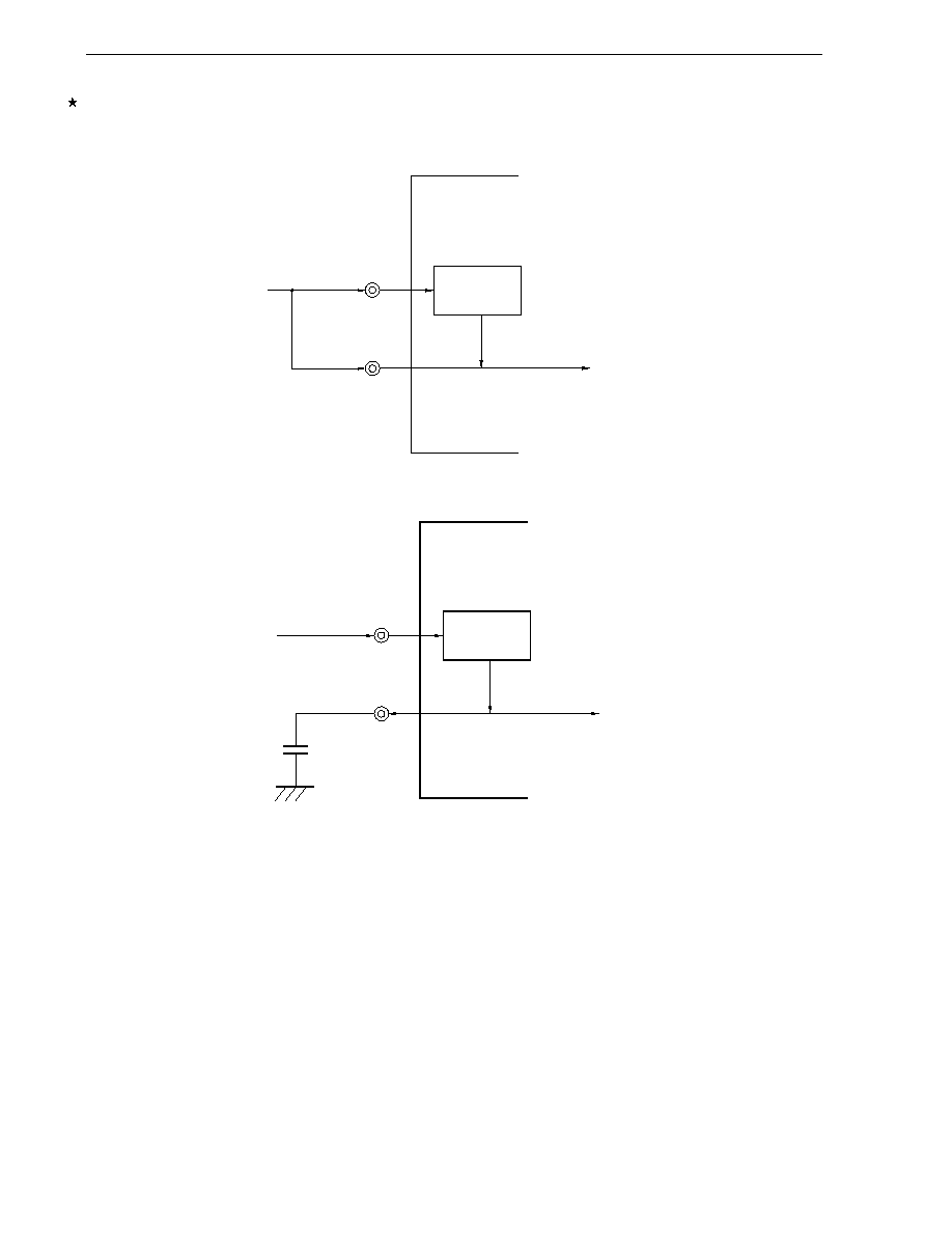
CHAPTER 24 REGULATOR
User's Manual U16228EJ2V0UD
424
Figure 24-2. REGC Pin Connection
(a) When REGC = V
DD
REG
Input voltage = 2.7 to 5.5 V
Voltage supply to oscillator/internal logic = 2.7 to 5.5 V
V
DD
REGC
(b) When connecting REGC pin to V
SS
via a capacitor
REG
Input voltage = 4.0 to 5.5 V
Voltage supply to oscillator/internal logic = 3.5 V
V
DD
REGC
1 F
(recommended)
µ

User's Manual U16228EJ2V0UD
425
CHAPTER 25 MASK OPTIONS
Mask ROM versions are provided with the following mask options.
1. Power-on-clear (POC) circuit
∑
POC cannot be used
∑
POC used (detection voltage: V
POC
= 2.85 V
±
0.15 V)
Note
∑
POC used (detection voltage: V
POC
= 3.5 V
±
0.2 V)
2. Ring-OSC
∑
Cannot be stopped
∑
Can be stopped by software
3. Pull-up resistor of P60 to P63 pins
∑
Pull-up resistor can be incorporated in 1-bit units
(Pull-up resistors are not available for the flash memory versions.)
Note This option cannot be selected in (A1) and (A2) grade products because the supply voltage V
DD
is 3.3 to
5.5 V.
Flash memory versions that support the mask options of the mask ROM versions are as follows.
Table 25-1. Flash Memory Versions Supporting Mask Options of Mask ROM Versions
Mask Option
POC Circuit
Ring-OSC
Flash Memory Version
Cannot be stopped
µ
PD78F0134M1, 78F0138M1, 78F0134M1(A),
78F0138M1(A), 78F0134M1(A1), 78F0138M1(A1)
POC cannot be used
Can be stopped by software
µ
PD78F0134M2, 78F0138M2, 78F0134M2(A),
78F0138M2(A), 78F0134M2(A1), 78F0138M2(A1)
Cannot be stopped
µ
PD78F0134M3, 78F0138M3, 78F0134M3(A),
78F0138M3(A)
POC used
(V
POC
= 2.85 V
±
0.15 V)
Can be stopped by software
µ
PD78F0134M4, 78F0138M4, 78F0134M4(A),
78F0138M4(A)
Cannot be stopped
µ
PD78F0134M5, 78F0138M5, 78F0134M5(A),
78F0138M5(A), 78F0134M5(A1), 78F0138M5(A1)
POC used
(V
POC
= 3.5 V
±
0.2 V)
Can be stopped by software
µ
PD78F0134M6, 78F0138M6, 78F0134M6(A),
78F0138M6(A), 78F0134M6(A1), 78F0138M6(A1)

User's Manual U16228EJ2V0UD
426
CHAPTER 26 ROM CORRECTION
26.1 Functions of ROM Correction
The
µ
PD780136, 780138, and 78F0138 can replace part of a program in the mask ROM or flash memory with a
program in the internal expansion RAM.
Program bugs found in the mask ROM or flash memory can be avoided, and program flow can be changed by
using the ROM correction.
The ROM correction can correct two places (max.) of the internal ROM or internal flash memory (program).
Caution The ROM correction cannot be emulated by the in-circuit emulator.
26.2 Configuration of ROM Correction
The ROM correction includes the following hardware.
Table 26-1. Configuration of ROM Correction
Item Configuration
Registers Correction
address registers 0 and 1 (CORAD0, CORAD1)
Control register
Correction control register (CORCN)
Figure 26-1 shows a block diagram of the ROM correction.
Figure 26-1. Block Diagram of ROM Correction
Match
CORENn CORSTn
Program counter (PC)
Comparator
Correction address
register n (CORADn)
Internal bus
Correction control register
Correction branch request
signal (BR !F7FDH)
Branch instruction
generator
Remark n = 0, 1

CHAPTER 26 ROM CORRECTION
User's Manual U16228EJ2V0UD
427
(1) Correction address registers 0 and 1 (CORAD0, CORAD1)
These registers set the start address (correction address) of the instruction(s) to be corrected in the mask
ROM or flash memory.
The ROM correction corrects two places (max.) of the program. Addresses are set to two registers, CORAD0
and CORAD1. If only one place needs to be corrected, set the address to either of the registers.
CORAD0 and CORAD1 are set by a 16-bit memory manipulation instruction.
RESET input clears CORAD0 and CORAD1 to 0000H.
Figure 26-2. Format of Correction Address Registers 0 and 1
FF3AH/FF3BH
0000H
Symbol
15
CORAD0
0
Address
FF38H/FF39H
After reset
0000H
R/W
R/W
CORAD1
R/W
Cautions 1. Set the CORAD0 and CORAD1 when bit 1 (COREN0) and bit 3 (COREN1) of the correction
control register (CORCN: see Figure 26-3) are 0.
2. Only addresses where operation codes are stored can be set in CORAD0 and CORAD1.
3. Do not set the following addresses to CORAD0 and CORAD1.
∑
Address value in table area of table reference instruction (CALLT instruction): 0040H to
007FH
∑
Address value in vector table area: 0000H to 003FH
(2) Comparator
The comparator always compares the correction address value set in correction address registers 0 and 1
(CORAD0, CORAD1) with the fetch address value. When bit 1 (COREN0) or bit 3 (COREN1) of the correction
control register (CORCN) is 1 and the correction address matches the fetch address value, the correction
branch request signal (BR !F7FDH) is generated from the ROM correction circuit.
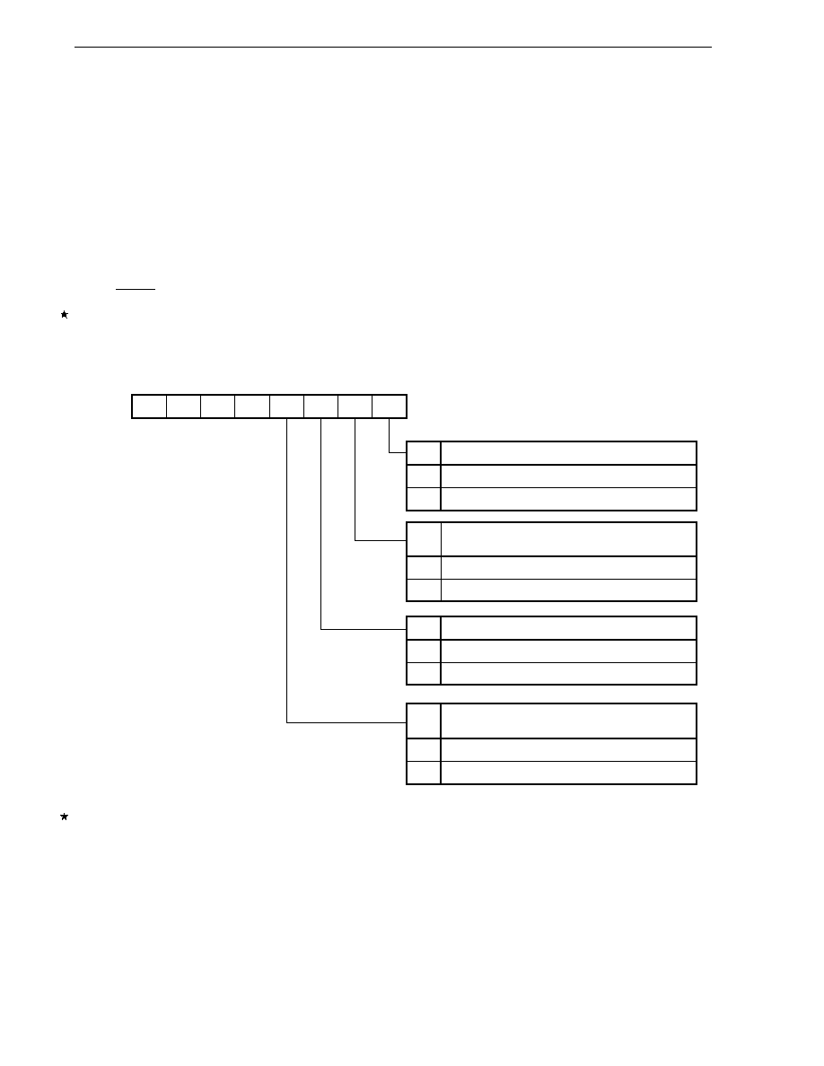
CHAPTER 26 ROM CORRECTION
User's Manual U16228EJ2V0UD
428
26.3 Register Controlling ROM Correction
The ROM correction is controlled by the correction control register (CORCN).
(1) Correction control register (CORCN)
This register controls whether or not the correction branch request signal is generated when the fetch address
matches the correction address set in correction address registers 0 and 1. The correction control register
consists of correction enable flags (COREN0, COREN1) and correction status flags (CORST0, CORST1). The
correction enable flags enable or disable the comparator match detection signal, and correction status flags
show the values are matched.
CORCN is set by a 1-bit or 8-bit memory manipulation instruction.
RESET input clears CORCN to 00H.
Clear CORST0 and CORST1 using software.
Figure 26-3. Format of Correction Control Register
7
0
6
0
5
0
4
0
COREN1 CORST1 COREN0 CORST0
Symbol
CORCN
Address
FF8AH
After reset
COREN0
0
1
CORST0
0
1
COREN1
0
1
CORST1
0
1
R/W
R/W
Note
00H
Correction Address Register 0 and Fetch Address Match Detection
Not detected
Detected
Correction Address Register 0 and Fetch Address
Match Detection Control
Disabled
Enabled
Correction Address Register 1 and Fetch Address Match Detection
Not detected
Detected
Correction Address Register 1 and Fetch Address
Match Detection Control
Disabled
Enabled
<3>
<2>
<1>
<0>
Note Do not set bits 0 and 2 to 1.
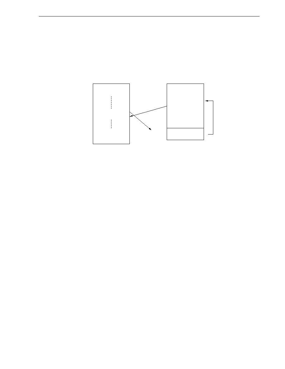
CHAPTER 26 ROM CORRECTION
User's Manual U16228EJ2V0UD
429
26.4 ROM Correction Usage Example
The example of ROM correction when the instruction at address 1000H "ADD A, #1" is changed to "ADD A, #2" is
as follows.
Figure 26-4. ROM Correction Usage Example
ADD A, #2
BR
!1002H
BR
!F702H
ADD A, #1
MOV B, A
0000H
0080H
Program start
1000H
1002H
Internal ROM or
internal flash memory
Internal expansion RAM
F400H
F702H
F7FDH
F7FFH
(1)
(2)
(3)
EFFFH
(1) Branches to address F7FDH when the preset value 1000H in the correction address register matches the fetch
address value after the main program is started.
(2) Branches to any address (address F702H in this example) by setting the entire-space branch instruction (BR
!addr16) to address F7FDH with the main program.
(3) Returns to the internal ROM (internal flash memory) program after executing the substitute instruction ADD A,
#2.
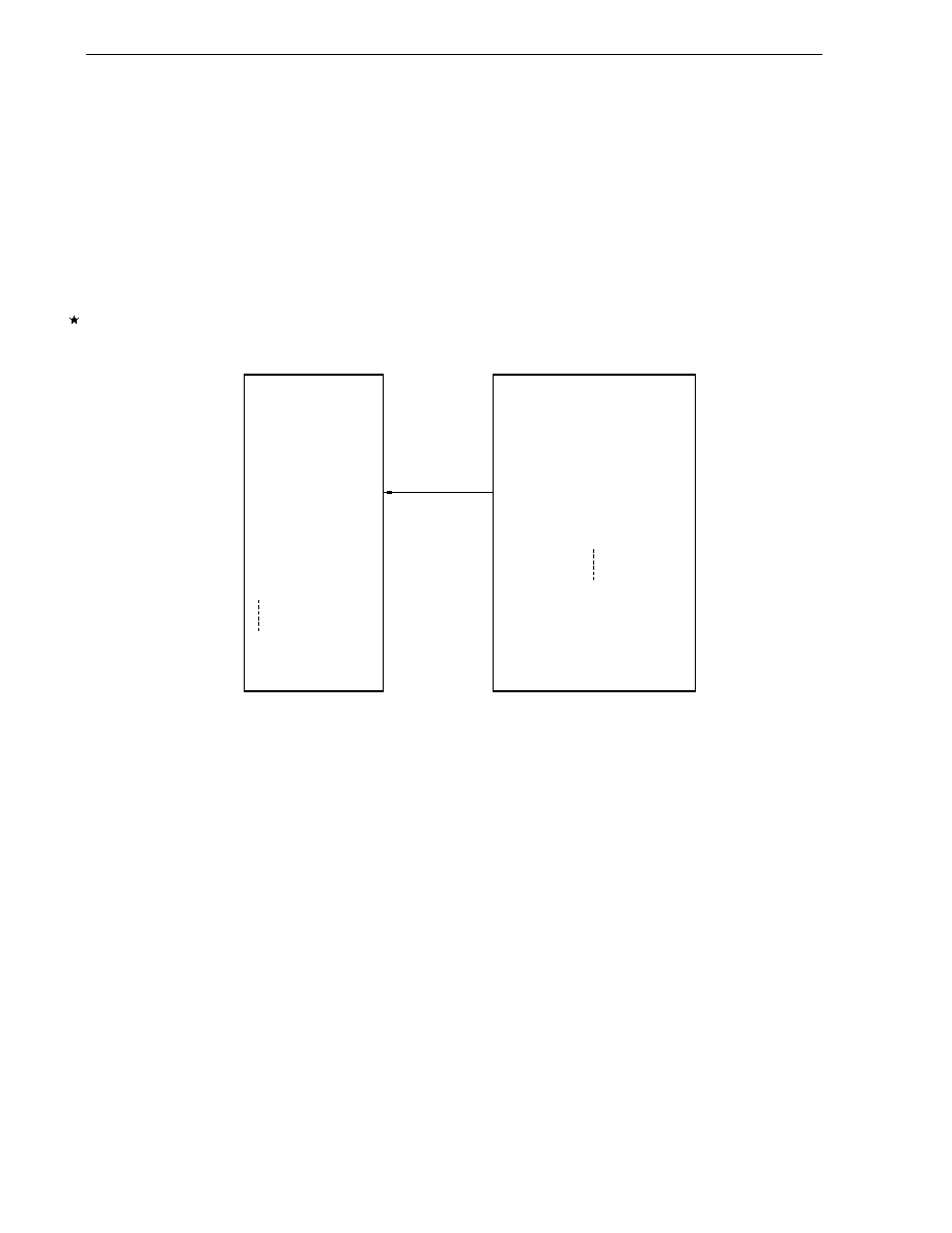
CHAPTER 26 ROM CORRECTION
User's Manual U16228EJ2V0UD
430
26.5 ROM Correction Application
How to apply the example shown in 26.4 is described below.
(1) Store the correction address and instruction after correction (patch program) to nonvolatile memory (such as
EEPROM
TM
) outside the microcontroller.
When two places should be corrected, store the branch destination judgment program as well. The branch
destination judgment program checks which one of the addresses set to correction address registers 0 and 1
(CORAD0 or CORAD1) generates the correction branch.
Figure 26-5. Example of Storing to EEPROM (When One Place Is Corrected)
RA78K/0
EEPROM
Source Program
00
10
0D
02
9B
02
10
00H
01H
02H
FFH
CSEG AT 0000H
DW #1000H
ADD A, #2
BR !1002H
CHAPTER 26 ROM CORRECTION
User's Manual U16228EJ2V0UD
431
(2) Assemble in advance the initial setting routine as shown in Figure 26-6 to correct the program.
Figure 26-6. Initial Setting Routine
No
Yes
Initial setting
Load the contents of external nonvolatile memory
into internal expansion RAM
Correction address register setting
ROM correction operation enabled
Is ROM
correction used ?
Note
ROM correction
Main program
Note Whether the ROM correction is used or not should be judged by the port input level. For example, when the
P20 input level is high, the ROM correction is used, otherwise, it is not used.
(3) After reset, store the corrected address and program that have been previously stored in the external
nonvolatile memory with initial setting routine for ROM correction of the user to internal expansion RAM (see
Figure 26-6).
Set the start address of the instruction to be corrected to CORAD0 and CORAD1, and set bits 1 and 3
(COREN0, COREN1) of the correction control register (CORCN) to 1.
(4) Set the main program so that the program branches from the specified address of the internal expansion RAM
(F7FDH) to the internal expansion RAM address where the corrected program is stored using the entire space
branch instruction (BR !addr16).
(5) After the main program is started, the fetch address value and the values set in CORAD0 and CORAD1 are
always compared by the comparator in the ROM correction circuit. When these values match, the correction
branch request signal is generated. Simultaneously the corresponding correction status flag (CORST0 or
CORST1) is set to 1.
(6) Branch to the address F7FDH by the correction branch request signal.
(7) Branch to the internal expansion RAM address set in (4) by the entire-space branch instruction of the address
F7FDH.
(8) When one place is corrected, the correction program is executed. When two places are corrected, the
correction status flag is checked with the branch destination judgment program, and branches to the correction
program.
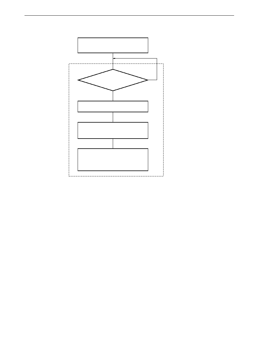
CHAPTER 26 ROM CORRECTION
User's Manual U16228EJ2V0UD
432
Figure 26-7. ROM Correction Operation
No
Yes
Internal ROM (internal flash memory)
program start
Does fetch address
match with correction
address?
Set correction status flag
Correction branch
(branch to address F7FDH)
Correction program execution
ROM correction

CHAPTER 26 ROM CORRECTION
User's Manual U16228EJ2V0UD
433
26.6 Program Execution Flow
Figures 26-8 and 26-9 show the program transition diagrams when the ROM correction is used.
Figure 26-8. Program Transition Diagram (When One Place Is Corrected)
Correction place
Internal ROM
Internal ROM
(Internal flash memory)
JUMP
FFFFH
F7FFH
F7FDH
xxxxH
0000H
(1)
(2)
(3)
BR !JUMP
Correction program
(1) Branches to address F7FDH when fetch address matches correction address
(2) Branches to correction program
(3) Returns to internal ROM (internal flash memory) program
Remark Area filled with diagonal lines: Internal expansion RAM
JUMP: Correction program start address
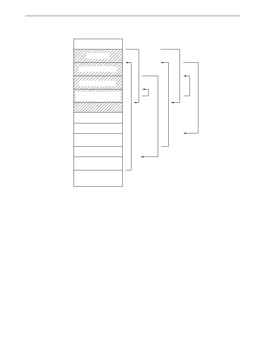
CHAPTER 26 ROM CORRECTION
User's Manual U16228EJ2V0UD
434
Figure 26-9. Program Transition Diagram (When Two Places Are Corrected)
Internal ROM
(Internal flash memory)
Correction place 1
Internal ROM
(Internal flash memory)
JUMP
Internal ROM
(Internal flash memory)
(1)
(2)
(3)
(4)
(5)
(6)
(7)
(8)
FFFFH
F7FFH
F7FDH
yyyyH
xxxxH
0000H
BR !JUMP
Branch destination
judgment program
Correction program 2
Correction program 1
Correction place 2
(1) Branches to address F7FDH when fetch address matches correction address
(2) Branches to branch destination judgment program
(3) Branches to correction program 1 by branch destination judgment program (BTCLR !CORST0, $xxxxH)
(4) Returns to internal ROM (internal flash memory) program
(5) Branches to address F7FDH when fetch address matches correction address
(6) Branches to branch destination judgment program
(7) Branches to correction program 2 by branch destination judgment program (BTCLR !CORST1, $yyyyH)
(8) Returns to internal ROM (internal flash memory) program
Remark Area filled with diagonal lines: Internal expansion RAM
JUMP: Branch destination judgment program start address

CHAPTER 26 ROM CORRECTION
User's Manual U16228EJ2V0UD
435
26.7 Cautions for ROM Correction
(1) Address values set in correction address registers 0 and 1 (CORAD0, CORAD1) must be addresses where
instruction codes are stored.
(2) Correction address registers 0 and 1 (CORAD0, CORAD1) should be set when the correction enable flag
(COREN0, COREN1) is 0 (when the correction branch is in disabled state). If address is set to CORAD0 or
CORAD1 when COREN0 or COREN1 is 1 (when the correction branch is in enabled state), the correction
branch may start with the different address from the set address value.
(3) Do not set the address value of instruction immediately after the instruction that sets the correction enable flag
(COREN0, COREN1) to 1, to correction address register 0 or 1 (CORAD0, CORAD1); the correction branch
may not start.
(4) Do not set the address value in table area of table reference instruction (CALLT instruction) (0040H to 007FH),
and the address value in vector table area (0000H to 003FH) to correction address registers 0 and 1
(CORAD0, CORAD1).
(5) Do not set two addresses immediately after the instructions shown below to correction address registers 0 and
1 (CORAD0, CORAD1). (that is, when the mapped terminal address of these instructions is N, do not set the
address values of N + 1 and N + 2.)
∑
RET
∑
RETI
∑
RETB
∑
BR $addr16
∑
STOP
∑
HALT

User's Manual U16228EJ2V0UD
436
CHAPTER 27
µ
PD78F0134, 78F0138
The
µ
PD78F0134 and 78F0138 are provided as the flash memory version of the 78K0/KE1.
The
µ
PD78F0134 and 78F0138 replace the internal mask ROM of the
µ
PD780134 and 780138 respectively with
flash memory to which a program can be written, erased, and overwritten while mounted on the board. Table 27-1
lists the differences between the
µ
PD78F0134, 78F0138 and the mask ROM versions.
Table 27-1. Differences Between
µ
PD78F0134, 78F0138 and Mask ROM Versions
Item
µ
PD78F0134, 78F0138
Mask ROM Versions
Internal ROM configuration
Flash memory
Mask ROM
Internal ROM capacity
µ
PD78F0134
Note 1
: 32 KB
Note 2
µ
PD78F0138:
60 KB
Note 2
µ
PD780131: 8 KB
µ
PD780132: 16 KB
µ
PD780133: 24 KB
µ
PD780134: 32 KB
µ
PD780136: 48 KB
µ
PD780138: 60 KB
Internal high-speed RAM capacity
µ
PD78F0134
Note 1
: 1024 bytes
Note 2
µ
PD78F0138:
1024 bytes
Note 2
µ
PD780131: 512 bytes
µ
PD780132: 512 bytes
µ
PD780133: 1024 bytes
µ
PD780134: 1024 bytes
µ
PD780136: 1024 bytes
µ
PD780138: 1024 bytes
Internal expansion RAM capacity
µ
PD78F0134
Note 1
: None
µ
PD78F0138:
1024 bytes
Note 2
µ
PD780131: None
µ
PD780132: None
µ
PD780133: None
µ
PD780134: None
µ
PD780136: 1024 bytes
µ
PD780138: 1024 bytes
IC pin
None
Available
V
PP
pin
Available
None
Electrical specifications,
recommended soldering conditions
Refer to the description of electrical specifications and recommended soldering
conditions.
Notes 1. The
µ
PD78F0134 does not support the
µ
PD780136 and 780138.
2. The same capacity as the mask ROM versions can be specified by means of the internal memory size
switching register (IMS) and the internal expansion RAM size switching register (IXS).
Caution There are differences in noise immunity and noise radiation between the flash memory and
mask ROM versions. When pre-producing an application set with the flash memory version and
then mass-producing it with the mask ROM version, be sure to conduct sufficient evaluations
for the commercial samples (not engineering samples) of the mask ROM versions.
CHAPTER 27
µ
PD78F0134, 78F0138
User's Manual U16228EJ2V0UD
437
27.1 Internal Memory Size Switching Register
The
µ
PD78F0134 and 78F0138 allow users to select the internal memory capacity using the internal memory size
switching register (IMS) so that the same memory map as that of the mask ROM versions with a different internal
memory capacity can be achieved.
IMS is set by an 8-bit memory manipulation instruction.
RESET input sets IMS to CFH.
Cautions 1. Be sure to set the value of the relevant mask ROM version at initialization.
2.
The
µ
PD78F0134 does not support the
µ
PD780136 and 780138.
Figure 27-1. Format of Internal Memory Size Switching Register (IMS)
Address: FFF0H After reset: CFH R/W
Symbol 7 6 5 4 3 2 1 0
IMS
RAM2 RAM1 RAM0
0
ROM3 ROM2 ROM1 ROM0
RAM2
RAM1
RAM0
Internal
high-speed RAM capacity selection
0
1
0
512
bytes
1
1
0
1024
bytes
Other than above
Setting prohibited
ROM3
ROM2
ROM1
ROM0
Internal ROM capacity selection
0
0
1
0
8
KB
0
1
0
0
16
KB
0
1
1
0
24
KB
1
0
0
0
32
KB
1
1
0
0
48
KB
1
1
1
1
60
KB
Other than above
Setting prohibited
The IMS settings required to obtain the same memory map as mask ROM versions are shown in Table 27-2.
Table 27-2. Internal Memory Size Switching Register Settings
Target Mask ROM Versions
IMS Setting
µ
PD780131 42H
µ
PD780132 44H
µ
PD780133 C6H
µ
PD780134 C8H
µ
PD780136 CCH
µ
PD780138
CFH
Cautions 1. When using a mask ROM version, be sure to set the value indicated in Table 27-2 to IMS.
2.
The
µ
PD78F0134 does not support the
µ
PD780136 and 780138.
CHAPTER 27
µ
PD78F0134, 78F0138
User's Manual U16228EJ2V0UD
438
27.2 Internal Expansion RAM Size Switching Register
This register is used to set the internal expansion RAM capacity via software.
This register is set by an 8-bit memory manipulation instruction.
RESET input sets IXS to 0CH.
Cautions 1. Be sure to set the value of the relevant mask ROM version at initialization.
2.
The
µ
PD78F0134 does not support the
µ
PD780136 and 780138.
Figure 27-2. Format of Internal Expansion RAM Size Switching Register (IXS)
Address: FFF4H After reset: 0CH R/W
Symbol 7 6 5 4 3 2 1 0
IXS
0
0
0
IXRAM4 IXRAM3 IXRAM2 IXRAM1 IXRAM0
IXRAM4
IXRAM3
IXRAM2
IXRAM1
IXRAM0
Internal expansion RAM capacity selection
0 1 1 0 0
0
bytes
0 1 0 1 0
1024
bytes
Other than above
Setting prohibited
The IXS settings required to obtain the same memory map as mask ROM versions are shown in Table 27-3.
Table 27-3. Internal Expansion RAM Size Switching Register Settings
Target Mask ROM Versions
IXS Setting
µ
PD780131 0CH
µ
PD780132 0CH
µ
PD780133 0CH
µ
PD780134 0CH
µ
PD780136 0AH
µ
PD780138
0AH
Cautions 1. When using a mask ROM version, be sure to set the value indicated in Table 27-3 to IXS.
2.
The
µ
PD78F0134 does not support the
µ
PD780136 and 780138.
CHAPTER 27
µ
PD78F0134, 78F0138
User's Manual U16228EJ2V0UD
439
27.3 Writing with Flash Programmer
Data can be written to the flash memory on-board or off-board, by using a dedicated flash programmer.
(1) On-board
programming
The contents of the flash memory can be rewritten after the
µ
PD78F0134 or 78F0138 has been mounted on the
target system. The connectors that connect the dedicated flash programmer must be mounted on the target
system.
(2) Off-board
programming
Data can be written to the flash memory with a dedicated program adapter (FA series) before the
µ
PD78F0134 or
78F0138 is mounted on the target system.
Remark The FA series is a product of Naito Densei Machida Mfg. Co., Ltd.
Table 27-4. Wiring Between
µ
PD78F0134 or 78F0138 and Dedicated Flash Programmer (1/2)
(1) 3-wire serial I/O (CSI10)
Pin Configuration of Dedicated Flash Programmer
With CSI10
With CSI10 + HS
Signal Name
I/O
Pin Function
Pin Name
Pin No.
Pin Name
Pin No.
SI/RxD Input
Receive
signal
SO10/P12
25 SO10/P12
25
SO/TxD Output
Transmit
signal
SI10/RxD0/P11
26 SI10/RxD0/P11
26
SCK Output
Transfer
clock
SCK10/TxD0/P10 27
SCK10/TxD0/P10 27
X1 7
X1 7
CLK Output
Clock
to
µ
PD78F0134 or 78F0138
X2
Note 1
8
X2
Note 1
8
/RESET Output
Reset
signal
RESET
9 RESET
9
V
PP
Output
Write
voltage
V
PP
3
V
PP
3
H/S
Input
Handshake signal
Not needed
Not needed
HS/P15/TOH0
22
V
DD
4
V
DD
4
EV
DD
33
EV
DD
33
V
DD
I/O
V
DD
voltage generation/voltage
monitor
Note 2
AV
REF
1
AV
REF
1
V
SS
6
V
SS
6
EV
SS
32
EV
SS
32
GND
-
Ground
AV
SS
2
AV
SS
2
Notes 1. When using the clock out of the flash programmer, connect CLK of the programmer to X1, and connect
its inverse signal to X2.
2. Flashpro III only
Cautions 1. Be sure to connect the REGC pin in either of the following ways.
∑
To GND via a 1
µ
F capacitor
∑
Directly to V
DD
2. When connecting the REGC pin to GND via a 1
µ
F capacitor, the clock cannot be supplied
from the CLK pin of the flash programmer.
Create an oscillator on the board to supply a clock.
CHAPTER 27
µ
PD78F0134, 78F0138
User's Manual U16228EJ2V0UD
440
Table 27-4. Wiring Between
µ
PD78F0134 or 78F0138 and Dedicated Flash Programmer (2/2)
(2) UART (UART0, UART6)
Pin Configuration of Dedicated Flash Programmer
With UART0
With UART0 + HS
With UART6
Signal Name
I/O
Pin Function
Pin Name
Pin No.
Pin Name
Pin No.
Pin Name
Pin No.
SI/RxD Input
Receive
signal
TxD0/
SCK10/P10
27
TxD0/
SCK10/P10
27 TxD6/P13
27
SO/TxD Output
Transmit
signal
RxD0/SI10/
P11
26
RxD0/SI10/
P11
26 RxD6/P14
26
SCK Output
Transfer
clock
Not
needed
Not
needed
Not needed
Not
needed
Not needed
Not
needed
X1 7
X1 7
X1 7
CLK Output
Clock to
µ
PD78F0134 or
78F0138
X2
Note 1
8
X2
Note 1
8
X2
Note 1
8
/RESET Output
Reset
signal
RESET
9 RESET
9 RESET
9
V
PP
Output
Write
voltage
V
PP
3
V
PP
3
V
PP
3
H/S Input
Handshake
signal
Not
needed
Not
needed
HS/P15/TOH0
22 Not
needed
Not
needed
V
DD
4
V
DD
4
V
DD
4
EV
DD
33
EV
DD
33
EV
DD
33
V
DD
I/O
V
DD
voltage generation/voltage
monitor
Note 2
AV
REF
1
AV
REF
1
AV
REF
1
V
SS
6
V
SS
6
V
SS
6
EV
SS
32
EV
SS
32
EV
SS
32
GND
-
Ground
AV
SS
2
AV
SS
2
AV
SS
2
Notes 1. When using the clock out of the flash programmer, connect CLK of the programmer to X1, and connect
its inverse signal to X2.
2. Flashpro III only
Cautions 1. Be sure to connect the REGC pin in either of the following ways.
∑
To GND via a 1
µ
F capacitor
∑
Directly to V
DD
2. When connecting the REGC pin to GND via a 1
µ
F capacitor, the clock cannot be supplied
from the CLK pin of the flash programmer.
Create an oscillator on the board to supply a clock.
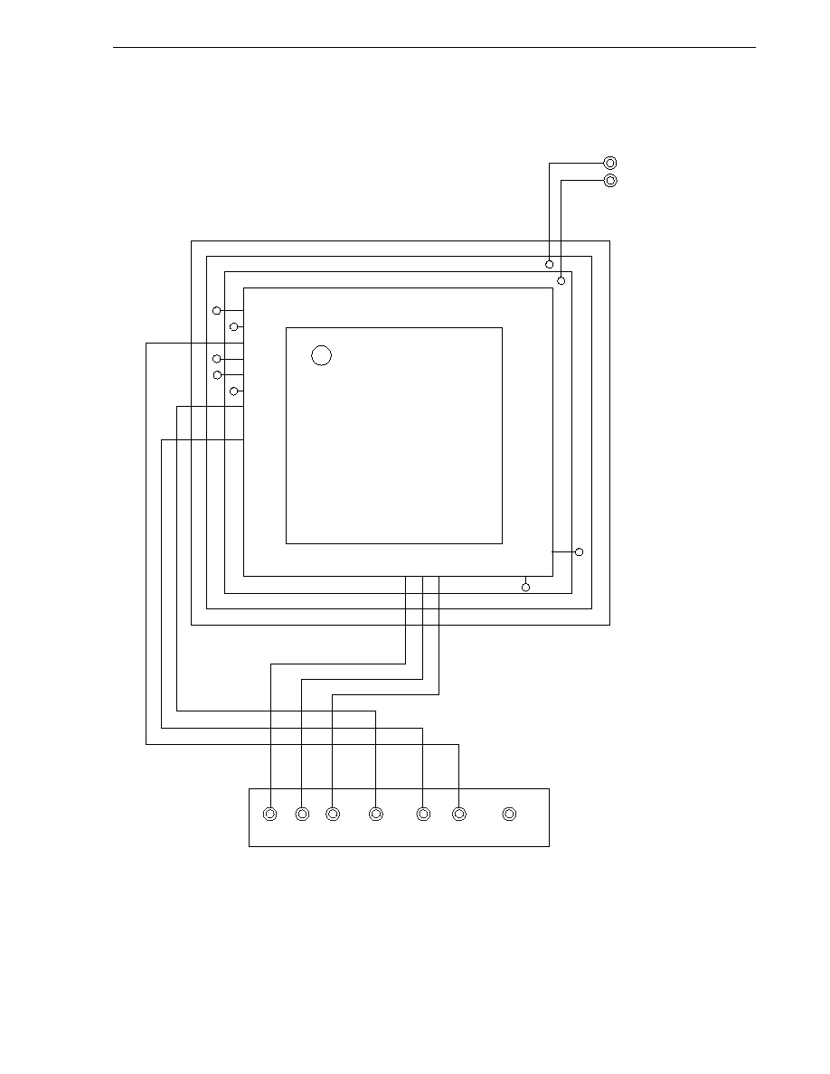
CHAPTER 27
µ
PD78F0134, 78F0138
User's Manual U16228EJ2V0UD
441
Examples of the recommended connection when using the adapter for flash memory writing are shown below.
Figure 27-3. Example of Wiring Adapter for Flash Memory Writing in 3-Wire Serial I/O (CSI10) Mode
GND
VDD
VDD2 (LVDD)
SI SO SCK CLK /RESET V
PP
RESERVE/HS
WRITER INTERFACE
V
DD
(2.7 to 5.5 V)
Note 1
GND
1
2
3
4
6
7
8
9
10
11
12
13
14
15
16
48
47
46
45
44
43
42
41
40
39
38
37
36
35
34
33
64 63 62 61 60 59 58 57 56 55 54 53 52 51 50 49
17 18 19 20 21 22 23 24 25 26 27 28 29 30 31 32
5
Note 2
Notes 1.
µ
PD78F0134, 78F0138, 78F0134(A), 78F0138(A): 2.7 to 5.5 V
µ
PD78F0134(A1), 78F0138(A1):
3.3 to 5.5 V
2.
Connect the REGC pin as follows.
µ
PD78F0134, 78F0138, 78F0134(A), 78F0138(A):
Connect directly to V
DD
or connect to GND via a 1
µ
F capacitor
µ
PD78F0134(A1), 78F0138(A1): Connect directly to V
DD

CHAPTER 27
µ
PD78F0134, 78F0138
User's Manual U16228EJ2V0UD
442
Figure 27-4. Example of Wiring Adapter for Flash Memory Writing in 3-Wire Serial I/O (CSI10 + HS) Mode
GND
VDD
SI SO SCK CLK /RESET V
PP
RESERVE/HS
WRITER INTERFACE
V
DD
(2.7 to 5.5 V)
Note 1
GND
1
2
3
4
6
7
8
9
10
11
12
13
14
15
16
48
47
46
45
44
43
42
41
40
39
38
37
36
35
34
33
64 63 62 61 60 59 58 57 56 55 54 53 52 51 50 49
17 18 19 20 21 22 23 24 25 26 27 28 29 30 31 32
VDD2 (LVDD)
5
Note 2
Notes 1.
µ
PD78F0134, 78F0138, 78F0134(A), 78F0138(A): 2.7 to 5.5 V
µ
PD78F0134(A1), 78F0138(A1):
3.3 to 5.5 V
2.
Connect the REGC pin as follows.
µ
PD78F0134, 78F0138, 78F0134(A), 78F0138(A):
Connect directly to V
DD
or connect to GND via a 1
µ
F capacitor
µ
PD78F0134(A1), 78F0138(A1): Connect directly to V
DD
CHAPTER 27
µ
PD78F0134, 78F0138
User's Manual U16228EJ2V0UD
443
Figure 27-5. Example of Wiring Adapter for Flash Memory Writing in UART (UART0) Mode
GND
VDD
SI SO SCK CLK /RESET V
PP
RESERVE/HS
WRITER INTERFACE
V
DD
(2.7 to 5.5 V)
Note 1
GND
1
2
3
4
6
7
8
9
10
11
12
13
14
15
16
48
47
46
45
44
43
42
41
40
39
38
37
36
35
34
33
64 63 62 61 60 59 58 57 56 55 54 53 52 51 50 49
17 18 19 20 21 22 23 24 25 26 27 28 29 30 31 32
VDD2 (LVDD)
5
Note 2
Notes 1.
µ
PD78F0134, 78F0138, 78F0134(A), 78F0138(A): 2.7 to 5.5 V
µ
PD78F0134(A1), 78F0138(A1):
3.3 to 5.5 V
2.
Connect the REGC pin as follows.
µ
PD78F0134, 78F0138, 78F0134(A), 78F0138(A):
Connect directly to V
DD
or connect to GND via a 1
µ
F capacitor
µ
PD78F0134(A1), 78F0138(A1): Connect directly to V
DD
CHAPTER 27
µ
PD78F0134, 78F0138
User's Manual U16228EJ2V0UD
444
Figure 27-6. Example of Wiring Adapter for Flash Memory Writing in UART (UART0 + HS) Mode
GND
VDD
SI SO SCK CLK /RESET V
PP
RESERVE/HS
WRITER INTERFACE
V
DD
(2.7 to 5.5 V)
Note 1
GND
1
2
3
4
6
7
8
9
10
11
12
13
14
15
16
48
47
46
45
44
43
42
41
40
39
38
37
36
35
34
33
64 63 62 61 60 59 58 57 56 55 54 53 52 51 50 49
17 18 19 20 21 22 23 24 25 26 27 28 29 30 31 32
VDD2 (LVDD)
5
Note 2
Notes 1.
µ
PD78F0134, 78F0138, 78F0134(A), 78F0138(A): 2.7 to 5.5 V
µ
PD78F0134(A1), 78F0138(A1):
3.3 to 5.5 V
2.
Connect the REGC pin as follows.
µ
PD78F0134, 78F0138, 78F0134(A), 78F0138(A):
Connect directly to V
DD
or connect to GND via a 1
µ
F capacitor
µ
PD78F0134(A1), 78F0138(A1): Connect directly to V
DD
CHAPTER 27
µ
PD78F0134, 78F0138
User's Manual U16228EJ2V0UD
445
Figure 27-7. Example of Wiring Adapter for Flash Memory Writing in UART (UART6) Mode
GND
VDD
SI SO SCK CLK /RESET V
PP
RESERVE/HS
WRITER INTERFACE
V
DD
(2.7 to 5.5 V)
Note 1
GND
1
2
3
4
6
7
8
9
10
11
12
13
14
15
16
48
47
46
45
44
43
42
41
40
39
38
37
36
35
34
33
64 63 62 61 60 59 58 57 56 55 54 53 52 51 50 49
17 18 19 20 21 22 23 24 25 26 27 28 29 30 31 32
VDD2 (LVDD)
5
Note 2
Notes 1.
µ
PD78F0134, 78F0138, 78F0134(A), 78F0138(A): 2.7 to 5.5 V
µ
PD78F0134(A1), 78F0138(A1):
3.3 to 5.5 V
2.
Connect the REGC pin as follows.
µ
PD78F0134, 78F0138, 78F0134(A), 78F0138(A):
Connect directly to V
DD
or connect to GND via a 1
µ
F capacitor
µ
PD78F0134(A1), 78F0138(A1): Connect directly to V
DD
CHAPTER 27
µ
PD78F0134, 78F0138
User's Manual U16228EJ2V0UD
446
27.4 Programming Environment
The environment required for writing a program to the flash memory of the
µ
PD78F0134 and 78F0138 is illustrated
below.
Figure 27-8. Environment for Writing Program to Flash Memory
RS-232C
Host machine
PD78F0134, 78F0138
V
PP
V
DD
V
SS
RESET
CSI10/UART0/UART6
Dedicated flash
programmer
USB
Note
PG-FP4
(Flash Pro4)
Cxxxxxx
Bxxxxx
Axxxx
XXX YYY
XXXXX
XXXXXX
XXXX
XXXX YYYY
STATVE
µ
Note Flashpro IV only
A host machine that controls the dedicated flash programmer is necessary.
To interface between the dedicated flash programmer and the
µ
PD78F0134 or 78F0138, CSI10, UART0, or
UART6 is used for manipulation such as writing and erasing. To write the flash memory off-board, a dedicated
program adapter (FA series) is necessary.
27.5 Communication Mode
Communication between the dedicated flash programmer and the
µ
PD78F0134 or 78F0138 is established by
serial communication via CSI10, UART0, or UART6 of the
µ
PD78F0134 or 78F0138.
(1) CSI10
Transfer rate: 200 kHz to 2 MHz
Figure 27-9. Communication with Dedicated Flash Programmer (CSI10)
PD78F0134, 78F0138
V
PP
V
DD
/EV
DD
/AV
REF
V
SS
/EV
SS
/AV
SS
RESET
SO10
SI10
SCK10
V
PP
V
DD
GND
/RESET
SI/RxD
SO/TxD
X1
CLK
X2
SCK
Dedicated flash
programmer
PG-FP4
(Flash Pro4)
Cxxxxxx
Bxxxxx
Axxxx
XXX YYY
XX
XXX
XXXXXX
XXXX
XXXX YYYY
STATVE
µ

CHAPTER 27
µ
PD78F0134, 78F0138
User's Manual U16228EJ2V0UD
447
(2) CSI communication mode supporting handshake
Transfer rate: 200 kHz to 2 MHz
Figure 27-10. Communication with Dedicated Flash Programmer (CSI10 + HS)
PD78F0134, 78F0138
V
PP
RESET
SO10
SI10
SCK10
HS
V
PP
V
DD
GND
/RESET
SI/RxD
SO/TxD
SCK
X1
CLK
X2
H/S
Dedicated flash
programmer
PG-FP4
(Flash Pro4)
Cxxxxxx
Bxxxxx
Axxxx
X
X
X
Y
Y
Y
XXXXX
XXXXXX
XXXX
X
X
X
X Y
Y
Y
Y
STATVE
V
DD
/EV
DD
/AV
REF
V
SS
/EV
SS
/AV
SS
µ
(3) UART0
Transfer rate: 4800 to 38400 bps
Figure 27-11. Communication with Dedicated Flash Programmer (UART0)
PD78F0134, 78F0138
V
PP
RESET
TxD0
X1
V
PP
V
DD
GND
/RESET
SI/RxD
RxD0
SO/TxD
CLK
X2
Dedicated flash
programmer
PG-FP4
(Flash Pro4)
Cxxxxxx
Bxxxxx
Axxxx
XXX YYY
XXXXX
XXXXXX
XXXX
XXXX YYYY
STATVE
V
DD
/EV
DD
/AV
REF
V
SS
/EV
SS
/AV
SS
µ
(4) UART communication mode supporting handshake
Transfer rate: 4800 to 38400 bps
Figure 27-12. Communication with Dedicated Flash Programmer (UART0 + HS)
PD78F0134, 78F0138
V
PP
RESET
TxD0
RxD0
HS
V
PP
V
DD
GND
/RESET
SI/RxD
SO/TxD
X1
CLK
X2
H/S
Dedicated flash
programmer
PG-FP4
(Flash Pro4)
Cxxxxxx
Bxxxxx
Axxxx
XXX YYY
XXXXX
XXXXXX
XXXX
XXXX YYYY
STATVE
V
DD
/EV
DD
/AV
REF
V
SS
/EV
SS
/AV
SS
µ
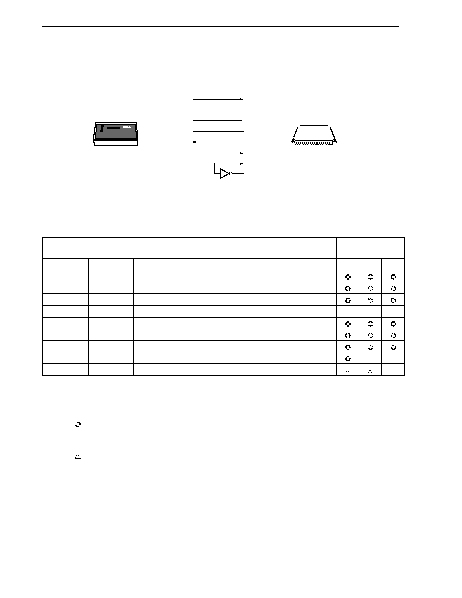
CHAPTER 27
µ
PD78F0134, 78F0138
User's Manual U16228EJ2V0UD
448
(5) UART6
Transfer rate: 4800 to 76800 bps
Figure 27-13. Communication with Dedicated Flash Programmer (UART6)
PD78F0134, 78F0138
V
PP
V
DD
V
SS
RESET
TxD6
RxD6
V
PP
V
DD
GND
/RESET
SI/RxD
SO/TxD
X1
CLK
X2
Dedicated flash
programmer
PG-FP4
(Flash Pro4)
Cxxxxxx
Bxxxxx
Axxxx
X
XX
Y
YY
XXXXX
XXXXXX
XXXX
X
X
X
X Y
Y
Y
Y
STATVE
µ
If Flashpro III/Flashpro IV is used as the dedicated flash programmer, Flashpro III/Flashpro IV generates the
following signal for the
µ
PD78F0134 or 78F0138. For details, refer to the Flashpro III/Flashpro IV Manual.
Table 27-5. Pin Connection
Flashpro III/Flashpro IV
µ
PD78F0134,
78F0138
Connection
Signal Name
I/O
Pin Function
Pin Name
CSI00 UART0 UART6
V
PP
Output
Write
voltage
V
PP
V
DD
I/O V
DD
voltage generation/voltage monitor
Note 1
V
DD
, EV
DD
, AV
REF
GND
-
Ground V
SS
, EV
SS
, AV
SS
CLK Output
Clock
output
to
µ
PD78F0134/78F0138 X1,
X2
Note 2
/RESET Output Reset
signal
RESET
SI/RxD Input
Receive
signal
SO10/TxD0/TxD6
SO/TxD Output Transmit
signal
SI10/RxD0/RxD6
SCK Output
Transfer
clock
SCK10
◊
◊
H/S Input
Handshake
signal
HS
◊
Notes 1. Flashpro III only
2. For off-board writing only: connect the clock output of the flash programmer to X1 and its inverse signal to
X2.
Remark
: Be sure to connect the pin.
: The pin does not have to be connected if the signal is generated on the target board.
◊
: The pin does not have to be connected.
: In handshake mode
CHAPTER 27
µ
PD78F0134, 78F0138
User's Manual U16228EJ2V0UD
449
27.6
Handling of Pins on Board
To write the flash memory on-board, connectors that connect the dedicated flash programmer must be provided on
the target system. First provide a function that selects the normal operation mode or flash memory programming
mode on the board.
When the flash memory programming mode is set, all the pins not used for programming the flash memory are in
the same status as immediately after reset. Therefore, if the external device does not recognize the state immediately
after reset, the pins must be handled as described below.
27.6.1 V
PP
pin
In the normal operation mode, the V
PP
pin is connected to V
SS
. In addition, a write voltage of 10.0 V (TYP.) is
supplied to the V
PP
pin in the flash memory programming mode. Perform the following pin handling.
(1) Connect pull-down resistor R
VPP
= 10 k
to the V
PP
pin.
(2) Switch the input of the V
PP
pin to the programmer side by using a jumper on the board or to GND directly.
Figure 27-14. Example of Connection of V
PP
Pin
PD78F0134, 78F0138
V
PP
Dedicated flash programmer connection pin
Pull-down resistor (R
VPP
)
µ
27.6.2 Serial interface pins
The pins used by each serial interface are listed below.
Table 27-6. Pins Used by Each Serial Interface
Serial Interface
Pins Used
CSI10
SO10, SI10, SCK10
CSI10 + HS
SO10, SI10, SCK10, HS/P15
UART0 TxD0,
RxD0
UART0 + HS
TxD0, RxD0, HS/P15
UART6 TxD6,
RxD6
To connect the dedicated flash programmer to the pins of a serial interface that is connected to another device on
the board, care must be exercised so that signals do not collide or that the other device does not malfunction.
CHAPTER 27
µ
PD78F0134, 78F0138
User's Manual U16228EJ2V0UD
450
(1) Signal
collision
If the dedicated flash programmer (output) is connected to a pin (input) of a serial interface connected to another
device (output), signal collision takes place. To avoid this collision, either isolate the connection with the other
device, or make the other device go into an output high-impedance state.
Figure 27-15. Signal Collision (Input Pin of Serial Interface)
Input pin
Signal collision
Dedicated flash programmer
connection pin
Other device
Output pin
In the flash memory programming mode, the signal output by the device
collides with the signal sent from the dedicated flash programmer.
Therefore, isolate the signal of the other device.
PD78F0134, 78F0138
µ
(2) Malfunction of other device
If the dedicated flash programmer (output or input) is connected to a pin (input or output) of a serial interface
connected to another device (input), a signal may be output to the other device, causing the device to
malfunction. To avoid this malfunction, isolate the connection with the other device.
Figure 27-16. Malfunction of Other Device
Pin
Dedicated flash programmer
connection pin
Other device
Input pin
If the signal output by the
PD78F0134 or 78F0138 in the flash memory
programming mode affects the other device, isolate the signal of the other
device.
Pin
Dedicated flash programmer
connection pin
Other device
Input pin
If the signal output by the dedicated flash programmer in the flash memory
programming mode affects the other device, isolate the signal of the other
device.
PD78F0134, 78F0138
µ
µ
PD78F0134, 78F0138
µ
CHAPTER 27
µ
PD78F0134, 78F0138
User's Manual U16228EJ2V0UD
451
27.6.3 RESET pin
If the reset signal of the dedicated flash programmer is connected to the RESET pin that is connected to the reset
signal generator on the board, signal collision takes place. To prevent this collision, isolate the connection with the
reset signal generator.
If the reset signal is input from the user system while the flash memory programming mode is set, the flash
memory will not be correctly programmed. Do not input any signal other than the reset signal of the dedicated flash
programmer.
Figure 27-17. Signal Collision (RESET Pin)
RESET
Dedicated flash programmer
connection signal
Reset signal generator
Signal collision
Output pin
In the flash memory programming mode, the signal output by the reset
signal generator collides with the signal output by the dedicated flash
programmer. Therefore, isolate the signal of the reset signal generator.
PD78F0134, 78F0138
µ
27.6.4 Port pins
When the flash memory programming mode is set, all the pins not used for flash memory programming enter the
same status as that immediately after reset. If external devices connected to the ports do not recognize the port
status immediately after reset, the port pin must be connected to V
DD
or V
SS
via a resistor.
27.6.5 REGC pin
Handle the REGC pin in the same manner as during normal operation.
∑
µ
PD78F0134, 78F0138, 78F0134(A), 78F0138(A):
Connect directly to V
DD
or connect to GND via a 1
µ
F capacitor
∑
µ
PD78F0134(A1), 78F0138(A1):
Connect directly to V
DD
27.6.6 Other signal pins
Connect X1 and X2 in the same status as in the normal operation mode when using the on-board clock.
To input the operating clock from the programmer, however, connect the clock out of the programmer to X1, and its
inverse signal to X2.
27.6.7 Power supply
To use the supply voltage output of the flash programmer, connect the V
DD
pin to V
DD
of the flash programmer, and
the V
SS
pin to V
SS
of the flash programmer.
To use the on-board supply voltage, connect in compliance with the normal operation mode.
Supply the same other power supplies (EV
DD
, EV
SS
, AV
REF
, and AV
SS
) as those in the normal operation mode.
Caution In the dedicated flash programmer PG-FP3 or FL-PR3, V
DD
has a power monitor function. Be
sure to connect V
DD
and V
SS
to V
DD
and GND of the dedicated flash programmer.

CHAPTER 27
µ
PD78F0134, 78F0138
User's Manual U16228EJ2V0UD
452
27.7 Programming Method
27.7.1 Controlling flash memory
The following figure illustrates the procedure to manipulate the flash memory.
Figure 27-18. Flash Memory Manipulation Procedure
Start
Selecting communication mode
Manipulate flash memory
End?
Yes
V
PP
pulse supply
No
End
Flash memory programming
mode is set
27.7.2 Flash memory programming mode
To rewrite the contents of the flash memory by using the dedicated flash programmer, set the
µ
PD78F0134 or
78F0138 in the flash memory programming mode. To set the mode, set the V
PP
pin and clear the reset signal.
Change the mode by using a jumper when writing the flash memory on-board.
Figure 27-19. Flash Memory Programming Mode
10.0 V
V
SS
RESET
V
PP
V
DD
V
PP
pulse
Flash memory programming mode
1
2
n
∑ ∑ ∑
V
PP
Operation
mode
V
SS
Normal operation mode
10.0 V
Flash memory programming mode
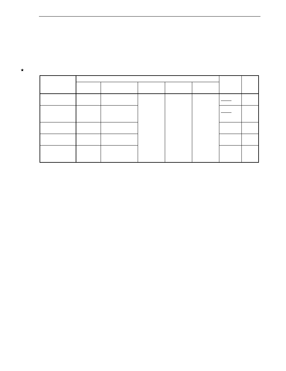
CHAPTER 27
µ
PD78F0134, 78F0138
User's Manual U16228EJ2V0UD
453
27.7.3 Selecting communication mode
In the
µ
PD78F0134 and 78F0138, a communication mode is selected by inputting pulses (up to 11 pulses) to the
V
PP
pin after the dedicated flash memory programming mode is entered. These V
PP
pulses are generated by the flash
programmer.
The following table shows the relationship between the number of pulses and communication modes.
Table 27-7. Communication Modes
Standard (TYPE) Setting
Note 1
Communication Mode
Port
(COMM PORT)
Speed
(SIO CLOCK)
On Target
(CPU CLOCK)
Frequency
(Flashpro Clock)
Multiply Rate
(Multiple Rate)
Pins Used
Number
of V
PP
Pulses
3-wire serial I/O
(CSI10)
SIO-ch0
(SIO ch-0)
200 k to 2 MHz
Note 2
SO10, SI10,
SCK10
0
3-wire serial I/O with
handshake supported
(CSI10 + HS)
SIO-H/S
(SIO ch-3
+ handshake)
200 k to 2 MHz
Note 2
SO10, SI10,
SCK10,
HS/P15
3
UART
(UART0)
UART-ch0
(UART ch-0)
4800 to 38400 bps
Notes 2, 3
TxD0, RxD0
8
UART
(UART6)
UART-ch1
(UART ch-1)
4800 to 76800 bps
Notes 2, 3
TxD6, RxD6
9
UART with
handshake supported
(UART0 + HS)
UART-ch3
(UART ch-3)
4800 to 38400 bps
Notes 2, 3
Optional
2 M to 10 MHz
1.0
TxD0, RxD0,
HS/P15
11
Notes 1. Selection items for Standard settings on Flashpro IV (TYPE settings on Flashpro III).
2. The possible setting range differs depending on the voltage. For details, refer to the chapters of electrical
specifications.
3. Because factors other than the baud rate error, such as the signal waveform slew, also affect UART
communication, thoroughly evaluate the slew as well as the baud rate error.
Caution When UART0 or UART6 is selected, the receive clock is calculated based on the reset command
sent from the dedicated flash programmer after the V
PP
pulse has been received.
Remark Items enclosed in parentheses in the setting item column are the set value and set item when they differ
from those of Flashpro IV.
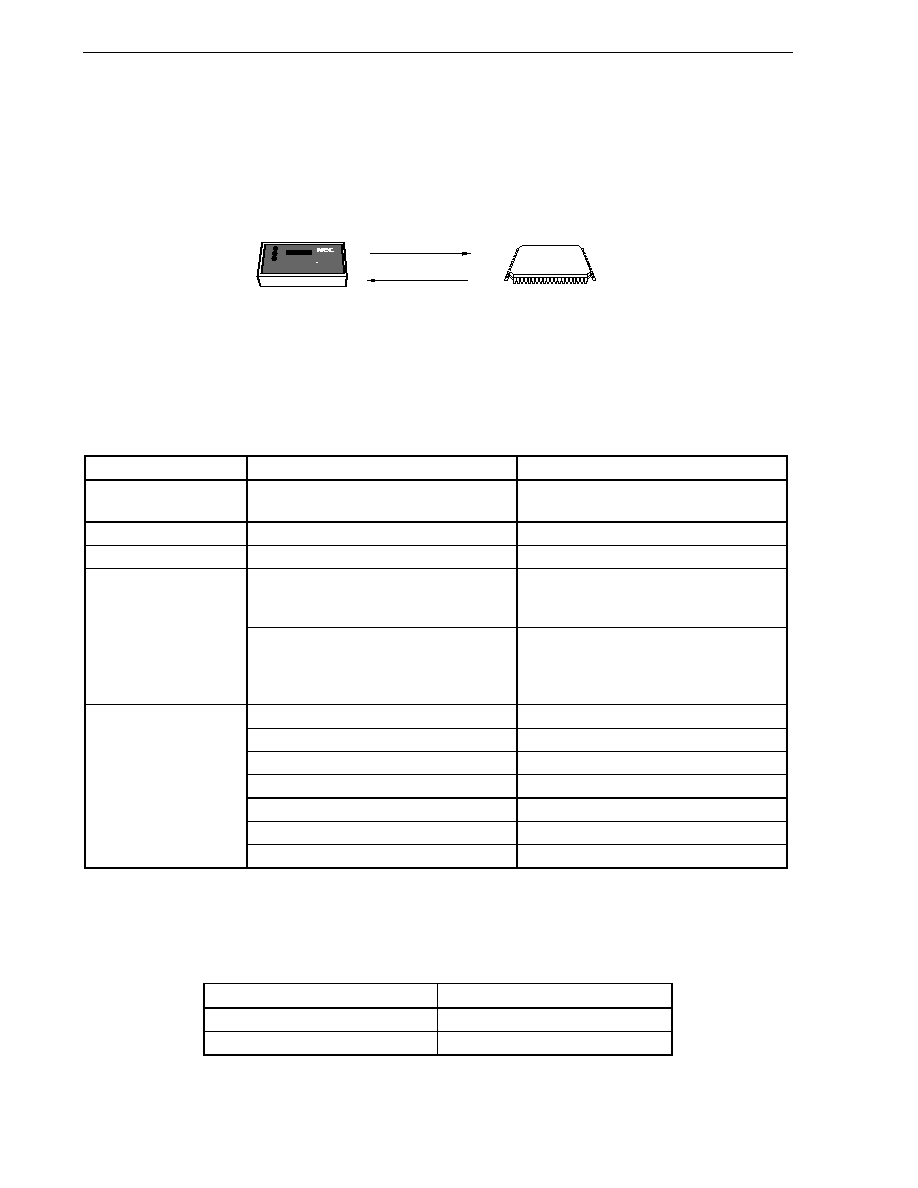
CHAPTER 27
µ
PD78F0134, 78F0138
User's Manual U16228EJ2V0UD
454
27.7.4 Communication commands
The
µ
PD78F0134 and 78F0138 communicate with the dedicated flash programmer by using commands. The
signals sent from the flash programmer to the
µ
PD78F0134 or 78F0138 are called commands, and the commands
sent from the
µ
PD78F0134 or 78F0138 to the dedicated flash programmer are called response commands.
Figure 27-20. Communication Commands
PD78F0134, 78F0138
Command
Response command
Dedicated flash
programmer
PG-FP4
(Flash Pro4)
Cxxxxxx
Bxxxxx
Axxxx
XXX YYY
XXXXX
XXXXXX
XXXX
XXXX YYYY
STATVE
µ
The flash memory control commands of the
µ
PD78F0134 and 78F0138 are listed in the table below. All these
commands are issued from the programmer and the
µ
PD78F0134 and 78F0138 perform processing corresponding to
the respective commands.
Table 27-8. Flash Memory Control Commands
Classification Command
Name
Function
Verify Batch
verify
command
Compares the contents of the entire memory
with the input data.
Erase
Batch erase command
Erases the contents of the entire memory.
Blank check
Batch blank check command
Checks the erasure status of the entire memory.
High-speed write command
Writes data by specifying the write address and
number of bytes to be written, and executes a
verify check.
Data write
Successive write command
Writes data from the address following that of
the high-speed write command executed
immediately before, and executes a verify
check.
Status read command
Obtains the operation status
Oscillation frequency setting command
Sets the oscillation frequency
Erase time setting command
Sets the erase time for batch erase
Write time setting command
Sets the write time for writing data
Baud rate setting command
Sets the baud rate when UART is used
Silicon signature command
Reads the silicon signature information
System setting, control
Reset command
Escapes from each status
The
µ
PD78F0134 and 78F0138 return a response command for the command issued by the dedicated flash
programmer. The response commands sent from the
µ
PD78F0134 and 78F0138 are listed below.
Table 27-9. Response Commands
Command Name
Function
ACK Acknowledges
command/data.
NAK
Acknowledges illegal command/data.

User's Manual U16228EJ2V0UD
455
CHAPTER 28 INSTRUCTION SET
This chapter lists each instruction set of the 78K0/KE1 in table form. For details of each operation and operation
code, refer to the separate document 78K/0 Series Instruction User's Manual (U12326E).
28.1 Conventions Used in Operation List
28.1.1 Operand identifiers and specification methods
Operands are written in the "Operand" column of each instruction in accordance with the specification method of
the instruction operand identifier (refer to the assembler specifications for details). When there are two or more
methods, select one of them. Upper case letters and the symbols #, !, $ and [ ] are keywords and must be written as
they are. Each symbol has the following meaning.
∑
#: Immediate data specification
∑
!: Absolute address specification
∑
$: Relative address specification
∑
[ ]: Indirect address specification
In the case of immediate data, describe an appropriate numeric value or a label. When using a label, be sure to
write the #, !, $, and [ ] symbols.
For operand register identifiers r and rp, either function names (X, A, C, etc.) or absolute names (names in
parentheses in the table below, R0, R1, R2, etc.) can be used for specification.
Table 28-1. Operand Identifiers and Specification Methods
Identifier Specification
Method
r
rp
sfr
sfrp
X (R0), A (R1), C (R2), B (R3), E (R4), D (R5), L (R6), H (R7),
AX (RP0), BC (RP1), DE (RP2), HL (RP3)
Special function register symbol
Note
Special function register symbol (16-bit manipulatable register even addresses only)
Note
saddr
saddrp
FE20H to FF1FH Immediate data or labels
FE20H to FF1FH Immediate data or labels (even address only)
addr16
addr11
addr5
0000H to FFFFH Immediate data or labels
(Only even addresses for 16-bit data transfer instructions)
0800H to 0FFFH Immediate data or labels
0040H to 007FH Immediate data or labels (even address only)
word
byte
bit
16-bit immediate data or label
8-bit immediate data or label
3-bit immediate data or label
RBn
RB0 to RB3
Note Addresses from FFD0H to FFDFH cannot be accessed with these operands.
Remark For special function register symbols, refer to Table 3-6 Special Function Register List.

CHAPTER 28 INSTRUCTION SET
User's Manual U16228EJ2V0UD
456
28.1.2 Description of operation column
A:
A register; 8-bit accumulator
X: X
register
B: B
register
C: C
register
D: D
register
E: E
register
H: H
register
L: L
register
AX:
AX register pair; 16-bit accumulator
BC:
BC register pair
DE:
DE register pair
HL:
HL register pair
PC: Program
counter
SP: Stack
pointer
PSW:
Program status word
CY: Carry
flag
AC:
Auxiliary carry flag
Z: Zero
flag
RBS:
Register bank select flag
IE:
Interrupt request enable flag
NMIS:
Non-maskable interrupt servicing flag
( ):
Memory contents indicated by address or register contents in parentheses
X
H
, X
L
: Higher 8 bits and lower 8 bits of 16-bit register
:
Logical product (AND)
:
Logical sum (OR)
:
Exclusive logical sum (exclusive OR)
: Inverted
data
addr16: 16-bit immediate data or label
jdisp8: Signed 8-bit data (displacement value)
28.1.3 Description of flag operation column
(Blank): Not affected
0:
Cleared to 0
1:
Set to 1
◊
:
Set/cleared according to the result
R:
Previously saved value is restored

CHAPTER 28 INSTRUCTION SET
User's Manual U16228EJ2V0UD
457
28.2 Operation List
Clocks Flag
Instruction
Group
Mnemonic Operands Bytes
Note 1
Note 2
Operation
Z AC CY
r, #byte
2
4
-
r
byte
saddr, #byte
3
6
7
(saddr)
byte
sfr, #byte
3
-
7 sfr
byte
A, r
Note 3
1 2
-
A
r
r, A
Note 3
1 2
-
r
A
A, saddr
2
4
5
A
(saddr)
saddr, A
2
4
5
(saddr)
A
A, sfr
2
-
5 A
sfr
sfr, A
2
-
5 sfr
A
A, !addr16
3
8
9 + n
A
(addr16)
!addr16, A
3
8
9 + m
(addr16)
A
PSW, #byte
3
-
7 PSW
byte
◊ ◊ ◊
A, PSW
2
-
5 A
PSW
PSW, A
2
-
5 PSW
A
◊ ◊ ◊
A, [DE]
1
4
5 + n
A
(DE)
[DE], A
1
4
5 + m
(DE)
A
A, [HL]
1
4
5 + n
A
(HL)
[HL], A
1
4
5 + m
(HL)
A
A, [HL + byte]
2
8
9 + n
A
(HL + byte)
[HL + byte], A
2
8
9 + m
(HL + byte)
A
A, [HL + B]
1
6
7 + n
A
(HL + B)
[HL + B], A
1
6
7 + m
(HL + B)
A
A, [HL + C]
1
6
7 + n
A
(HL + C)
MOV
[HL + C], A
1
6
7 + m
(HL + C)
A
A, r
Note 3
1 2
-
A
r
A, saddr
2
4
6
A
(saddr)
A, sfr
2
-
6 A
(sfr)
A, !addr16
3
8
10 + n + m A
(addr16)
A, [DE]
1
4
6 + n + m A
(DE)
A, [HL]
1
4
6 + n + m A
(HL)
A, [HL + byte]
2
8
10 + n + m A
(HL + byte)
A, [HL + B]
2
8
10 + n + m A
(HL + B)
8-bit data
transfer
XCH
A, [HL + C]
2
8
10 + n + m A
(HL + C)
Notes 1. When the internal high-speed RAM area is accessed or for an instruction with no data access
2. When an area except the internal high-speed RAM area is accessed
3. Except "r = A"
Remarks 1. One instruction clock cycle is one cycle of the CPU clock (f
CPU
) selected by the processor clock
control register (PCC).
2. This clock cycle applies to the internal ROM program.
3. n is the number of waits when the external memory expansion area is read.
4. m is the number of waits when the external memory expansion area is written.

CHAPTER 28 INSTRUCTION SET
User's Manual U16228EJ2V0UD
458
Clocks Flag
Instruction
Group
Mnemonic Operands Bytes
Note 1
Note 2
Operation
Z AC CY
rp, #word
3
6
-
rp
word
saddrp, #word
4
8
10
(saddrp)
word
sfrp, #word
4
-
10 sfrp
word
AX, saddrp
2
6
8
AX
(saddrp)
saddrp, AX
2
6
8
(saddrp)
AX
AX, sfrp
2
-
8 AX
sfrp
sfrp, AX
2
-
8 sfrp
AX
AX, rp
Note 3
1 4
-
AX
rp
rp, AX
Note 3
1 4
-
rp
AX
AX, !addr16
3
10
12 + 2n AX
(addr16)
MOVW
!addr16, AX
3
10
12 + 2m (addr16)
AX
16-bit data
transfer
XCHW
AX, rp
Note 3
1 4
-
AX
rp
A, #byte
2
4
-
A, CY
A + byte
◊ ◊ ◊
saddr, #byte
3
6
8
(saddr), CY
(saddr) + byte
◊ ◊ ◊
A, r
Note 4
2 4
-
A, CY
A + r
◊ ◊ ◊
r, A
2
4
-
r, CY
r + A
◊ ◊ ◊
A, saddr
2
4
5
A, CY
A + (saddr)
◊ ◊ ◊
A, !addr16
3
8
9 + n
A, CY
A + (addr16)
◊ ◊ ◊
A, [HL]
1
4
5 + n
A, CY
A + (HL)
◊ ◊ ◊
A, [HL + byte]
2
8
9 + n
A, CY
A + (HL + byte)
◊ ◊ ◊
A, [HL + B]
2
8
9 + n
A, CY
A + (HL + B)
◊ ◊ ◊
ADD
A, [HL + C]
2
8
9 + n
A, CY
A + (HL + C)
◊ ◊ ◊
A, #byte
2
4
-
A, CY
A + byte + CY
◊ ◊ ◊
saddr, #byte
3
6
8
(saddr), CY
(saddr) + byte + CY
◊ ◊ ◊
A, r
Note 4
2 4
-
A, CY
A + r + CY
◊ ◊ ◊
r, A
2
4
-
r, CY
r + A + CY
◊ ◊ ◊
A, saddr
2
4
5
A, CY
A + (saddr) + CY
◊ ◊ ◊
A, !addr16
3
8
9 + n
A, CY
A + (addr16) + C
◊ ◊ ◊
A, [HL]
1
4
5 + n
A, CY
A + (HL) + CY
◊ ◊ ◊
A, [HL + byte]
2
8
9 + n
A, CY
A + (HL + byte) + CY
◊ ◊ ◊
A, [HL + B]
2
8
9 + n
A, CY
A + (HL + B) + CY
◊ ◊ ◊
8-bit
operation
ADDC
A, [HL + C]
2
8
9 + n
A, CY
A + (HL + C) + CY
◊ ◊ ◊
Notes 1. When the internal high-speed RAM area is accessed or for an instruction with no data access
2. When an area except the internal high-speed RAM area is accessed
3. Only when rp = BC, DE or HL
4. Except "r = A"
Remarks 1. One instruction clock cycle is one cycle of the CPU clock (f
CPU
) selected by the processor clock
control register (PCC).
2. This clock cycle applies to the internal ROM program.
3. n is the number of waits when the external memory expansion area is read.
4. m is the number of waits when the external memory expansion area is written.
CHAPTER 28 INSTRUCTION SET
User's Manual U16228EJ2V0UD
459
Clocks Flag
Instruction
Group
Mnemonic Operands Bytes
Note 1
Note 2
Operation
Z AC CY
A, #byte
2
4
-
A, CY
A
-
byte
◊ ◊ ◊
saddr, #byte
3
6
8
(saddr), CY
(saddr)
-
byte
◊ ◊ ◊
A, r
Note 3
2 4
-
A, CY
A
-
r
◊ ◊ ◊
r, A
2
4
-
r, CY
r
-
A
◊ ◊ ◊
A, saddr
2
4
5
A, CY
A
-
(saddr)
◊ ◊ ◊
A, !addr16
3
8
9 + n
A, CY
A
-
(addr16)
◊ ◊ ◊
A, [HL]
1
4
5 + n
A, CY
A
-
(HL)
◊ ◊ ◊
A, [HL + byte]
2
8
9 + n
A, CY
A
-
(HL + byte)
◊ ◊ ◊
A, [HL + B]
2
8
9 + n
A, CY
A
-
(HL + B)
◊ ◊ ◊
SUB
A, [HL + C]
2
8
9 + n
A, CY
A
-
(HL + C)
◊ ◊ ◊
A, #byte
2
4
-
A, CY
A
-
byte
-
CY
◊ ◊ ◊
saddr, #byte
3
6
8
(saddr), CY
(saddr)
-
byte
-
CY
◊ ◊ ◊
A, r
Note 3
2 4
-
A, CY
A
-
r
-
CY
◊ ◊ ◊
r, A
2
4
-
r, CY
r
-
A
-
CY
◊ ◊ ◊
A, saddr
2
4
5
A, CY
A
-
(saddr)
-
CY
◊ ◊ ◊
A, !addr16
3
8
9 + n
A, CY
A
-
(addr16)
-
CY
◊ ◊ ◊
A, [HL]
1
4
5 + n
A, CY
A
-
(HL)
-
CY
◊ ◊ ◊
A, [HL + byte]
2
8
9 + n
A, CY
A
-
(HL + byte)
-
CY
◊ ◊ ◊
A, [HL + B]
2
8
9 + n
A, CY
A
-
(HL + B)
-
CY
◊ ◊ ◊
SUBC
A, [HL + C]
2
8
9 + n
A, CY
A
-
(HL + C)
-
CY
◊ ◊ ◊
A, #byte
2
4
-
A
A
byte
◊
saddr, #byte
3
6
8
(saddr)
(saddr)
byte
◊
A, r
Note 3
2 4
-
A
A
r
◊
r, A
2
4
-
r
r
A
◊
A, saddr
2
4
5
A
A
(saddr)
◊
A, !addr16
3
8
9 + n
A
A
(addr16)
◊
A, [HL]
1
4
5 + n
A
A
[HL]
◊
A, [HL + byte]
2
8
9 + n
A
A
[HL + byte]
◊
A, [HL + B]
2
8
9 + n
A
A
[HL + B]
◊
8-bit
operation
AND
A, [HL + C]
2
8
9 + n
A
A
[HL + C]
◊
Notes 1. When the internal high-speed RAM area is accessed or for an instruction with no data access
2. When an area except the internal high-speed RAM area is accessed
3. Except "r = A"
Remarks 1. One instruction clock cycle is one cycle of the CPU clock (f
CPU
) selected by the processor clock
control register (PCC).
2. This clock cycle applies to the internal ROM program.
3. n is the number of waits when the external memory expansion area is read.

CHAPTER 28 INSTRUCTION SET
User's Manual U16228EJ2V0UD
460
Clocks Flag
Instruction
Group
Mnemonic Operands Bytes
Note 1
Note 2
Operation
Z AC CY
A, #byte
2
4
-
A
A
byte
◊
saddr, #byte
3
6
8
(saddr)
(saddr)
byte
◊
A, r
Note 3
2 4
-
A
A
r
◊
r, A
2
4
-
r
r
A
◊
A, saddr
2
4
5
A
A
(saddr)
◊
A, !addr16
3
8
9 + n
A
A
(addr16)
◊
A, [HL]
1
4
5 + n
A
A
(HL)
◊
A, [HL + byte]
2
8
9 + n
A
A
(HL + byte)
◊
A, [HL + B]
2
8
9 + n
A
A
(HL + B)
◊
OR
A, [HL + C]
2
8
9 + n
A
A
(HL + C)
◊
A, #byte
2
4
-
A
A
byte
◊
saddr, #byte
3
6
8
(saddr)
(saddr)
byte
◊
A, r
Note 3
2 4
-
A
A
r
◊
r, A
2
4
-
r
r
A
◊
A, saddr
2
4
5
A
A
(saddr)
◊
A, !addr16
3
8
9 + n
A
A
(addr16)
◊
A, [HL]
1
4
5 + n
A
A
(HL)
◊
A, [HL + byte]
2
8
9 + n
A
A
(HL + byte)
◊
A, [HL + B]
2
8
9 + n
A
A
(HL + B)
◊
XOR
A, [HL + C]
2
8
9 + n
A
A
(HL + C)
◊
A, #byte
2
4
-
A
-
byte
◊ ◊ ◊
saddr, #byte
3
6
8
(saddr)
-
byte
◊ ◊ ◊
A, r
Note 3
2 4
-
A
-
r
◊ ◊ ◊
r, A
2
4
-
r
-
A
◊ ◊ ◊
A, saddr
2
4
5
A
-
(saddr)
◊ ◊ ◊
A, !addr16
3
8
9 + n
A
-
(addr16)
◊ ◊ ◊
A, [HL]
1
4
5 + n
A
-
(HL)
◊ ◊ ◊
A, [HL + byte]
2
8
9 + n
A
-
(HL + byte)
◊ ◊ ◊
A, [HL + B]
2
8
9 + n
A
-
(HL + B)
◊ ◊ ◊
8-bit
operation
CMP
A, [HL + C]
2
8
9 + n
A
-
(HL + C)
◊ ◊ ◊
Notes 1. When the internal high-speed RAM area is accessed or for an instruction with no data access
2. When an area except the internal high-speed RAM area is accessed
3. Except "r = A"
Remarks 1. One instruction clock cycle is one cycle of the CPU clock (f
CPU
) selected by the processor clock
control register (PCC).
2. This clock cycle applies to the internal ROM program.
3. n is the number of waits when the external memory expansion area is read.
CHAPTER 28 INSTRUCTION SET
User's Manual U16228EJ2V0UD
461
Clocks Flag
Instruction
Group
Mnemonic Operands Bytes
Note 1
Note 2
Operation
Z AC CY
ADDW
AX, #word
3
6
-
AX, CY
AX + word
◊ ◊ ◊
SUBW
AX, #word
3
6
-
AX, CY
AX
-
word
◊ ◊ ◊
16-bit
operation
CMPW
AX, #word
3
6
-
AX
-
word
◊ ◊ ◊
MULU
X 2
16
-
AX
A
◊
X
Multiply/
divide
DIVUW
C 2
25
-
AX (Quotient), C (Remainder)
AX
˜
C
r 1
2
-
r
r + 1
◊ ◊
INC
saddr 2
4
6
(saddr)
(saddr) + 1
◊ ◊
r 1
2
-
r
r
-
1
◊ ◊
DEC
saddr 2
4
6
(saddr)
(saddr)
-
1
◊ ◊
INCW
rp 1
4
-
rp
rp + 1
Increment/
decrement
DECW
rp 1
4
-
rp
rp
-
1
ROR
A, 1
1
2
-
(CY, A
7
A
0
, A
m
-
1
A
m
)
◊
1 time
◊
ROL
A, 1
1
2
-
(CY, A
0
A
7
, A
m + 1
A
m
)
◊
1 time
◊
RORC
A, 1
1
2
-
(CY
A
0
, A
7
CY, A
m
-
1
A
m
)
◊
1 time
◊
ROLC
A, 1
1
2
-
(CY
A
7
, A
0
CY, A
m + 1
A
m
)
◊
1 time
◊
ROR4
[HL]
2
10 12 + n + m A
3
-
0
(HL)
3
-
0
, (HL)
7
-
4
A
3
-
0
,
(HL)
3
-
0
(HL)
7
-
4
Rotate
ROL4
[HL]
2
10 12 + n + m A
3
-
0
(HL)
7
-
4
, (HL)
3
-
0
A
3
-
0
,
(HL)
7
-
4
(HL)
3
-
0
ADJBA
2
4
-
Decimal Adjust Accumulator after Addition
◊ ◊ ◊
BCD
adjustment ADJBS
2
4
-
Decimal Adjust Accumulator after Subtract
◊ ◊ ◊
CY, saddr.bit
3
6
7
CY
(saddr.bit)
◊
CY, sfr.bit
3
-
7 CY
sfr.bit
◊
CY, A.bit
2
4
-
CY
A.bit
◊
CY, PSW.bit
3
-
7 CY
PSW.bit
◊
CY, [HL].bit
2
6
7 + n
CY
(HL).bit
◊
saddr.bit, CY
3
6
8
(saddr.bit)
CY
sfr.bit, CY
3
-
8 sfr.bit
CY
A.bit, CY
2
4
-
A.bit
CY
PSW.bit, CY
3
-
8 PSW.bit
CY
◊ ◊
Bit
manipulate
MOV1
[HL].bit, CY
2
6
8 + n + m (HL).bit
CY
Notes 1. When the internal high-speed RAM area is accessed or for an instruction with no data access
2. When an area except the internal high-speed RAM area is accessed
Remarks 1. One instruction clock cycle is one cycle of the CPU clock (f
CPU
) selected by the processor clock
control register (PCC).
2. This clock cycle applies to the internal ROM program.
3. n is the number of waits when the external memory expansion area is read.
4. m is the number of waits when the external memory expansion area is written.
CHAPTER 28 INSTRUCTION SET
User's Manual U16228EJ2V0UD
462
Clocks Flag
Instruction
Group
Mnemonic Operands Bytes
Note 1
Note 2
Operation
Z AC CY
CY, saddr.bit
3
6
7
CY
CY
saddr.bit)
◊
CY, sfr.bit
3
-
7 CY
CY
sfr.bit
◊
CY, A.bit
2
4
-
CY
CY
A.bit
◊
CY, PSW.bit
3
-
7 CY
CY
PSW.bit
◊
AND1
CY, [HL].bit
2
6
7 + n
CY
CY
(HL).bit
◊
CY, saddr.bit
3
6
7
CY
CY
(saddr.bit)
◊
CY, sfr.bit
3
-
7 CY
CY
sfr.bit
◊
CY, A.bit
2
4
-
CY
CY
A.bit
◊
CY, PSW.bit
3
-
7 CY
CY
PSW.bit
◊
OR1
CY, [HL].bit
2
6
7 + n
CY
CY
(HL).bit
◊
CY, saddr.bit
3
6
7
CY
CY
(saddr.bit)
◊
CY, sfr.bit
3
-
7 CY
CY
sfr.bit
◊
CY, A.bit
2
4
-
CY
CY
A.bit
◊
CY, PSW. bit
3
-
7 CY
CY
PSW.bit
◊
XOR1
CY, [HL].bit
2
6
7 + n
CY
CY
(HL).bit
◊
saddr.bit 2
4
6
(saddr.bit)
1
sfr.bit 3
-
8 sfr.bit
1
A.bit 2
4
-
A.bit
1
PSW.bit 2
-
6 PSW.bit
1
◊ ◊ ◊
SET1
[HL].bit
2
6
8 + n + m (HL).bit
1
saddr.bit 2
4
6
(saddr.bit)
0
sfr.bit 3
-
8 sfr.bit
0
A.bit 2
4
-
A.bit
0
PSW.bit 2
-
6 PSW.bit
0
◊ ◊ ◊
CLR1
[HL].bit
2
6
8 + n + m (HL).bit
0
SET1
CY 1
2
-
CY
1
1
CLR1
CY 1
2
-
CY
0
0
Bit
manipulate
NOT1
CY 1
2
-
CY
CY
◊
Notes 1. When the internal high-speed RAM area is accessed or for an instruction with no data access
2. When an area except the internal high-speed RAM area is accessed
Remarks 1. One instruction clock cycle is one cycle of the CPU clock (f
CPU
) selected by the processor clock
control register (PCC).
2. This clock cycle applies to the internal ROM program.
3. n is the number of waits when the external memory expansion area is read.
4. m is the number of waits when the external memory expansion area is written.
CHAPTER 28 INSTRUCTION SET
User's Manual U16228EJ2V0UD
463
Clocks Flag
Instruction
Group
Mnemonic Operands Bytes
Note 1
Note 2
Operation
Z AC CY
CALL
!addr16 3
7
-
(SP
-
1)
(PC + 3)
H
, (SP
-
2)
(PC + 3)
L
,
PC
addr16, SP
SP
-
2
CALLF
!addr11 2
5
-
(SP
-
1)
(PC + 2)
H
, (SP
-
2)
(PC + 2)
L
,
PC
15
-
11
00001, PC
10
-
0
addr11,
SP
SP
-
2
CALLT
[addr5] 1
6
-
(SP
-
1)
(PC + 1)
H
, (SP
-
2)
(PC + 1)
L
,
PC
H
(00000000, addr5 + 1),
PC
L
(00000000, addr5),
SP
SP
-
2
BRK
1
6
-
(SP
-
1)
PSW, (SP
-
2)
(PC + 1)
H
,
(SP
-
3)
(PC + 1)
L
, PC
H
(003FH),
PC
L
(003EH), SP
SP
-
3, IE
0
RET
1
6
-
PC
H
(SP + 1), PC
L
(SP),
SP
SP + 2
RETI
1
6
-
PC
H
(SP + 1), PC
L
(SP),
PSW
(SP + 2), SP
SP + 3
R
R R
Call/return
RETB
1
6
-
PC
H
(SP + 1), PC
L
(SP),
PSW
(SP + 2), SP
SP + 3
R
R R
PSW 1
2
-
(SP
-
1)
PSW, SP
SP
-
1
PUSH
rp 1
4
-
(SP
-
1)
rp
H
, (SP
-
2)
rp
L
,
SP
SP
-
2
PSW 1
2
-
PSW
(SP), SP
SP + 1
R
R R
POP
rp 1
4
-
rp
H
(SP + 1), rp
L
(SP),
SP
SP + 2
SP, #word
4
-
10 SP
word
SP, AX
2
-
8 SP
AX
Stack
manipulate
MOVW
AX, SP
2
-
8 AX
SP
!addr16 3
6
-
PC
addr16
$addr16 2
6
-
PC
PC + 2 + jdisp8
Unconditional
branch
BR
AX 2
8
-
PCH
A, PC
L
X
BC
$addr16 2
6
-
PC
PC + 2 + jdisp8 if CY = 1
BNC
$addr16 2
6
-
PC
PC + 2 + jdisp8 if CY = 0
BZ
$addr16 2
6
-
PC
PC + 2 + jdisp8 if Z = 1
Conditional
branch
BNZ
$addr16 2
6
-
PC
PC + 2 + jdisp8 if Z = 0
Notes 1. When the internal high-speed RAM area is accessed or for an instruction with no data access
2. When an area except the internal high-speed RAM area is accessed
Remarks 1. One instruction clock cycle is one cycle of the CPU clock (f
CPU
) selected by the processor clock
control register (PCC).
2. This clock cycle applies to the internal ROM program.
CHAPTER 28 INSTRUCTION SET
User's Manual U16228EJ2V0UD
464
Clocks Flag
Instruction
Group
Mnemonic Operands Bytes
Note 1
Note 2
Operation
Z AC CY
saddr.bit, $addr16
3
8
9
PC
PC + 3 + jdisp8 if(saddr.bit) = 1
sfr.bit, $addr16
4
-
11 PC
PC + 4 + jdisp8 if sfr.bit = 1
A.bit, $addr16
3
8
-
PC
PC + 3 + jdisp8 if A.bit = 1
PSW.bit, $addr16
3
-
9 PC
PC + 3 + jdisp8 if PSW.bit = 1
BT
[HL].bit, $addr16
3
10
11 + n PC
PC + 3 + jdisp8 if (HL).bit = 1
saddr.bit, $addr16
4
10
11
PC
PC + 4 + jdisp8 if(saddr.bit) = 0
sfr.bit, $addr16
4
-
11 PC
PC + 4 + jdisp8 if sfr.bit = 0
A.bit, $addr16
3
8
-
PC
PC + 3 + jdisp8 if A.bit = 0
PSW.bit, $addr16
4
-
11 PC
PC + 4 + jdisp8 if PSW. bit = 0
BF
[HL].bit, $addr16
3
10
11 + n PC
PC + 3 + jdisp8 if (HL).bit = 0
saddr.bit, $addr16
4
10
12
PC
PC + 4 + jdisp8
if(saddr.bit) = 1
then reset(saddr.bit)
sfr.bit, $addr16
4
-
12 PC
PC + 4 + jdisp8 if sfr.bit = 1
then reset sfr.bit
A.bit, $addr16
3
8
-
PC
PC + 3 + jdisp8 if A.bit = 1
then reset A.bit
PSW.bit, $addr16
4
-
12 PC
PC + 4 + jdisp8 if PSW.bit = 1
then reset PSW.bit
◊ ◊ ◊
BTCLR
[HL].bit, $addr16
3
10 12 + n + m PC
PC + 3 + jdisp8 if (HL).bit = 1
then reset (HL).bit
B, $addr16
2
6
-
B
B
-
1, then
PC
PC + 2 + jdisp8 if B
0
C, $addr16
2
6
-
C
C
-
1, then
PC
PC + 2 + jdisp8 if C
0
Conditional
branch
DBNZ
Saddr, $addr16
3
8
10
(saddr)
(saddr)
-
1, then
PC
PC + 3 + jdisp8 if(saddr)
0
SEL
RBn 2
4
-
RBS1, 0
n
NOP
1
2
-
No Operation
EI
2
-
6 IE
1(Enable Interrupt)
DI
2
-
6 IE
0(Disable Interrupt)
HALT
2
6
-
Set HALT Mode
CPU
control
STOP
2
6
-
Set STOP Mode
Notes 1. When the internal high-speed RAM area is accessed or for an instruction with no data access
2. When an area except the internal high-speed RAM area is accessed
Remarks 1. One instruction clock cycle is one cycle of the CPU clock (f
CPU
) selected by the processor clock
control register (PCC).
2. This clock cycle applies to the internal ROM program.
3. n is the number of waits when the external memory expansion area is read.
4. m is the number of waits when the external memory expansion area is written.

CHAPTER 28 INSTRUCTION SET
User's Manual U16228EJ2V0UD
465
28.3 Instructions Listed by Addressing Type
(1) 8-bit
instructions
MOV, XCH, ADD, ADDC, SUB, SUBC, AND, OR, XOR, CMP, MULU, DIVUW, INC, DEC, ROR, ROL, RORC,
ROLC, ROR4, ROL4, PUSH, POP, DBNZ
Second Operand
First Operand
#byte A r
Note
sfr saddr
!addr16
PSW [DE] [HL]
[HL + byte]
[HL + B]
[HL + C]
$addr16 1 None
A
ADD
ADDC
SUB
SUBC
AND
OR
XOR
CMP
MOV
XCH
ADD
ADDC
SUB
SUBC
AND
OR
XOR
CMP
MOV
XCH
MOV
XCH
ADD
ADDC
SUB
SUBC
AND
OR
XOR
CMP
MOV
XCH
ADD
ADDC
SUB
SUBC
AND
OR
XOR
CMP
MOV
MOV
XCH
MOV
XCH
ADD
ADDC
SUB
SUBC
AND
OR
XOR
CMP
MOV
XCH
ADD
ADDC
SUB
SUBC
AND
OR
XOR
CMP
ROR
ROL
RORC
ROLC
r
MOV
MOV
ADD
ADDC
SUB
SUBC
AND
OR
XOR
CMP
INC
DEC
B, C
DBNZ
sfr
MOV
MOV
saddr
MOV
ADD
ADDC
SUB
SUBC
AND
OR
XOR
CMP
MOV
DBNZ
INC
DEC
!addr16
MOV
PSW
MOV
MOV
PUSH
POP
[DE]
MOV
[HL]
MOV
ROR4
ROL4
[HL + byte]
[HL + B]
[HL + C]
MOV
X
MULU
C
DIVUW
Note Except "r = A"
CHAPTER 28 INSTRUCTION SET
User's Manual U16228EJ2V0UD
466
(2) 16-bit instructions
MOVW, XCHW, ADDW, SUBW, CMPW, PUSH, POP, INCW, DECW
Second Operand
First Operand
#word AX rp
Note
sfrp saddrp
!addr16 SP None
AX
ADDW
SUBW
CMPW
MOVW
XCHW
MOVW MOVW MOVW MOVW
rp MOVW
MOVW
Note
INCW
DECW
PUSH
POP
sfrp
MOVW
MOVW
saddrp
MOVW
MOVW
!addr16
MOVW
SP
MOVW
MOVW
Note Only when rp = BC, DE, HL
(3) Bit manipulation instructions
MOV1, AND1, OR1, XOR1, SET1, CLR1, NOT1, BT, BF, BTCLR
Second Operand
First Operand
A.bit sfr.bit
saddr.bit
PSW.bit
[HL].bit CY $addr16
None
A.bit
MOV1
BT
BF
BTCLR
SET1
CLR1
sfr.bit
MOV1
BT
BF
BTCLR
SET1
CLR1
saddr.bit MOV1
BT
BF
BTCLR
SET1
CLR1
PSW.bit
MOV1
BT
BF
BTCLR
SET1
CLR1
[HL].bit
MOV1
BT
BF
BTCLR
SET1
CLR1
CY
MOV1
AND1
OR1
XOR1
MOV1
AND1
OR1
XOR1
MOV1
AND1
OR1
XOR1
MOV1
AND1
OR1
XOR1
MOV1
AND1
OR1
XOR1
SET1
CLR1
NOT1

CHAPTER 28 INSTRUCTION SET
User's Manual U16228EJ2V0UD
467
(4) Call instructions/branch instructions
CALL, CALLF, CALLT, BR, BC, BNC, BZ, BNZ, BT, BF, BTCLR, DBNZ
Second Operand
First Operand
AX !addr16
!addr11
[addr5]
$addr16
Basic instruction
BR
CALL
BR
CALLF CALLT BR
BC
BNC
BZ
BNZ
Compound
instruction
BT
BF
BTCLR
DBNZ
(5) Other instructions
ADJBA, ADJBS, BRK, RET, RETI, RETB, SEL, NOP, EI, DI, HALT, STOP
User's Manual U16228EJ2V0UD
468
CHAPTER 29 ELECTRICAL SPECIFICATIONS
(STANDARD PRODUCTS, (A) GRADE PRODUCTS)
Target products:
µ
PD780131, 780132, 780133, 780134, 780136, 780138, 78F0134, 78F0138, 780131(A),
780132(A), 780133(A), 780134(A), 780136(A), 780138(A), 78F0134(A), 78F0138(A)
Absolute Maximum Ratings (T
A
= 25
∞
C) (1/2)
Parameter Symbol
Conditions
Ratings
Unit
V
DD
-
0.3 to +6.5
V
EV
DD
-
0.3 to +6.5
V
REGC
-
0.3 to +6.5
V
V
SS
-
0.3 to +0.3
V
EV
SS
-
0.3 to +0.3
V
AV
REF
-
0.3 to V
DD
+ 0.3
Note 1
V
AV
SS
-
0.3 to +0.3
V
Supply voltage
V
PP
Flash memory version only, Note 2
-
0.3 to +10.5
V
V
I1
P00 to P06, P10 to P17, P20 to P27, P30
to P33, P40 to P43, P50 to P53, P60,
P61, P70 to P77, P120, P130, P140,
P141, X1, X2, XT1, XT2, RESET
-
0.3 to V
DD
+ 0.3
Note 1
V
N-ch open drain
-
0.3 to + 13
V
V
I2
P62,
P63
On-chip pull-up resistor
-
0.3 to V
DD
+ 0.3
Note 1
V
Input voltage
V
I3
V
PP
in flash programming mode
(flash memory version only)
-
0.3 to +10.5
V
Output voltage
V
O
-
0.3 to V
DD
+ 0.3
Note 1
V
Analog input voltage
V
AN
AV
SS
-
0.3 to AV
REF
+ 0.3
Note 1
and
-
0.3 to V
DD
+ 0.3
Note 1
V
Per pin
-
10 mA
P00 to P06, P40 to P43, P50 to
P53, P70 to P77
-
30 mA
Output current, high
I
OH
Total of
all pins
-
60 mA P10 to P17, P30 to P33, P120,
P130, P140, P141
-
30 mA
(Refer to Notes on the next page.)
Caution Product quality may suffer if the absolute maximum rating is exceeded even momentarily for any
parameter. That is, the absolute maximum ratings are rated values at which the product is on the
verge of suffering physical damage, and therefore the product must be used under conditions that
ensure that the absolute maximum ratings are not exceeded.
Remark Unless specified otherwise, the characteristics of alternate-function pins are the same as those of port pins.
CHAPTER 29 ELECTRICAL SPECIFICATIONS (STANDARD PRODUCTS, (A) GRADE PRODUCTS)
User's Manual U16228EJ2V0UD
469
Absolute Maximum Ratings (T
A
= 25
∞
C) (2/2)
Parameter Symbol
Conditions
Ratings
Unit
P00 to P06, P10 to P17, P30 to
P33, P40 to P43, P50 to P53,
P70 to P77, P120, P130, P140,
P141
20 mA
Per pin
P60 to P63
30
mA
P00 to P06, P40 to P43, P50 to
P53, P70 to P77
35 mA
Output current, low
I
OL
Total of
all pins
70 mA
P10 to P17, P30 to P33, P60 to
P63, P120, P130, P140, P141
35 mA
In normal operation mode
-
40 to +85
Operating ambient
temperature
T
A
In flash memory programming mode
-
10 to +85
∞
C
Mask ROM version
-
65 to +150
Storage temperature
T
stg
Flash memory version
-
40 to +125
∞
C
Notes 1. Must be 6.5 V or lower.
2.
Make sure that the following conditions of the V
PP
voltage application timing are satisfied when the flash
memory is written.
∑
When supply voltage rises
V
PP
must exceed V
DD
10
µ
s or more after V
DD
has reached the lower-limit value (2.7 V) of the operating
voltage range (15
µ
s if the supply voltage is dropped by the regulator) (see a in the figure below).
∑
When supply voltage drops
Raise
V
DD
10
µ
s or more after V
PP
falls below the lower-limit value (2.7 V) of the operating voltage range
of V
DD
(see b in the figure below).
2.7 V
V
DD
0 V
0 V
V
PP
2.7 V
a
b
Caution Product quality may suffer if the absolute maximum rating is exceeded even momentarily for any
parameter. That is, the absolute maximum ratings are rated values at which the product is on the
verge of suffering physical damage, and therefore the product must be used under conditions that
ensure that the absolute maximum ratings are not exceeded.
Remark Unless specified otherwise, the characteristics of alternate-function pins are the same as those of port pins.
CHAPTER 29 ELECTRICAL SPECIFICATIONS (STANDARD PRODUCTS, (A) GRADE PRODUCTS)
User's Manual U16228EJ2V0UD
470
X1 Oscillator Characteristics
(T
A
=
-
40 to +85
∞
C, 2.7 V
V
DD
= EV
DD
5.5 V, 2.7 V
AV
REF
V
DD
, V
SS
= EV
SS
= AV
SS
= 0 V)
Resonator Recommended
Circuit
Parameter
Conditions
MIN. TYP. MAX. Unit
When a capacitor
is connected to
the REGC pin
Note 2
4.0 V
V
DD
5.5 V
2.0
8.38
MHz
4.0 V
V
DD
5.5 V
2.0
10
3.3 V
V
DD
< 4.0 V
2.0
8.38
Ceramic
resonator
C1
X2
X1
V
SS
C2
Oscillation
frequency (f
XP
)
Note 1
When the REGC
pin is directly
connected to V
DD
2.7 V
V
DD
< 3.3 V
2.0
5.0
MHz
When a capacitor
is connected to
the REGC pin
Note 2
4.0 V
V
DD
5.5 V
2.0
8.38
MHz
4.0 V
V
DD
5.5 V
2.0
10
3.3 V
V
DD
< 4.0 V
2.0
8.38
Crystal
resonator
C1
X2
X1
V
SS
C2
Oscillation
frequency (f
XP
)
Note 1
When the REGC
pin is directly
connected to V
DD
2.7 V
V
DD
< 3.3 V
2.0
5.0
MHz
4.0 V
V
DD
5.5 V
2.0
10
3.3 V
V
DD
< 4.0 V
2.0
8.38
X1 input
frequency (f
XP
)
Note 1
2.7 V
V
DD
< 3.3 V
2.0
5.0
MHz
4.0 V
V
DD
5.5 V
46
500
3.3 V
V
DD
< 4.0 V
56
500
External
clock
Note 3
X2
X1
X1 input high-
/low-level width
(t
XPH
, t
XPL
)
2.7 V
V
DD
< 3.3 V
96
500
ns
Notes 1. Indicates
only
oscillator
characteristics. Refer to AC Characteristics for instruction execution time.
2. When the REGC pin is connected to V
SS
via a capacitor (1
µ
F: recommended).
3. Connect the REGC pin directly to V
DD
.
Cautions 1. When using the X1 oscillator, wire as follows in the area enclosed by the broken lines in the
above figures to avoid an adverse effect from wiring capacitance.
∑ Keep the wiring length as short as possible.
∑ Do not cross the wiring with the other signal lines.
∑ Do not route the wiring near a signal line through which a high fluctuating current flows.
∑ Always make the ground point of the oscillator capacitor the same potential as V
SS
.
∑ Do not ground the capacitor to a ground pattern through which a high current flows.
∑ Do not fetch signals from the oscillator.
2. Since the CPU is started by the Ring-OSC after reset, check the oscillation stabilization time of
the X1 input clock using the oscillation stabilization time status register (OSTC). Determine the
oscillation stabilization time of the OSTC register and oscillation stabilization time select
register (OSTS) after sufficiently evaluating the oscillation stabilization time with the resonator
to be used.

CHAPTER 29 ELECTRICAL SPECIFICATIONS (STANDARD PRODUCTS, (A) GRADE PRODUCTS)
User's Manual U16228EJ2V0UD
471
Ring-OSC Oscillator Characteristics
(T
A
=
-
40 to +85
∞
C, 2.7 V
V
DD
= EV
DD
5.5 V, 2.7 V
AV
REF
V
DD
, V
SS
= EV
SS
= AV
SS
= 0 V)
Resonator Parameter
Conditions
MIN.
TYP.
MAX.
Unit
On-chip Ring-OSC oscillator
Oscillation frequency (f
R
)
120 240 480 kHz
Subsystem Clock Oscillator Characteristics
(T
A
=
-
40 to +85
∞
C, 2.7 V
V
DD
= EV
DD
5.5 V, 2.7 V
AV
REF
V
DD
, V
SS
= EV
SS
= AV
SS
= 0 V)
Resonator Recommended
Circuit
Parameter
Conditions
MIN.
TYP.
MAX.
Unit
Crystal
resonator
XT1
V
SS
XT2
C4
C3
Rd
Oscillation frequency
(f
XT
)
Note
32
32.768
35
kHz
XT1 input frequency
(f
XT
)
Note
32
38.5
kHz
External clock
XT1
XT2
XT1 input high-/low-level
width (t
XTH
, t
XTL
)
12 15
µ
s
Note Indicates
only
oscillator
characteristics. Refer to AC Characteristics for instruction execution time.
Cautions 1. When using the subsystem clock oscillator, wire as follows in the area enclosed by the broken
lines in the above figures to avoid an adverse effect from wiring capacitance.
∑
Keep the wiring length as short as possible.
∑
Do not cross the wiring with the other signal lines.
∑
Do not route the wiring near a signal line through which a high fluctuating current flows.
∑
Always make the ground point of the oscillator capacitor the same potential as V
SS
.
∑
Do not ground the capacitor to a ground pattern through which a high current flows.
∑
Do not fetch signals from the oscillator.
2. The subsystem clock oscillator is designed as a low-amplitude circuit for reducing power
consumption, and is more prone to malfunction due to noise than the X1 oscillator. Particular
care is therefore required with the wiring method when the subsystem clock is used.
Remark For the resonator selection and oscillator constant, customers are requested to either evaluate the
oscillation themselves or apply to the resonator manufacturer for evaluation.

CHAPTER 29 ELECTRICAL SPECIFICATIONS (STANDARD PRODUCTS, (A) GRADE PRODUCTS)
User's Manual U16228EJ2V0UD
472
Recommended Oscillator Constants
Caution For the resonator selection of the
µ
PD780131(A), 780132(A), 780133(A), 780134(A), 780136(A),
780138(A), 78F0134(A), and 78F0138(A) and oscillator constants, users are required to either
evaluate the oscillation themselves or apply to the resonator manufacturer for evaluation.
X1 oscillation: Ceramic resonator (T
A
=
-
40 to +85
∞
C)
(
µ
PD780131, 780132, 780133, 780134, 780136, 780138, 78F0134, and 78F0138)
Recommended
Circuit Constants
Oscillation Voltage Range
When Capacitor
Is Connected to
REGC Pin
Note
REGC Pin Is
Connected
Directly to V
DD
Manufacturer Part
Number SMD/
Lead
Frequency
(MHz)
C1
(pF)
C2
(pF)
MIN.
(V)
MAX.
(V)
MIN.
(V)
MAX.
(V)
CSTCC2M00G56-R0 SMD
2.00
Internal
(47)
Internal
(47)
CSTCR4M00G55-R0
CSTCR4M00G55U-R0
SMD Internal
(39)
Internal
(39)
CSTLS4M00G56-B0
CSTLS4M00G56U-B0
Lead
4.00
Internal
(47)
Internal
(47)
CSTCR4M19G55-R0
CSTCR4M19G55U-R0
SMD Internal
(39)
Internal
(39)
CSTLS4M19G56-B0
CSTLS4M19G56U-B0
Lead
4.194
Internal
(47)
Internal
(47)
CSTCR4M91G53-R0
CSTCR4M91G53U-R0
SMD Internal
(15)
Internal
(15)
CSTLS4M91G53-B0
CSTLS4M91G53U-B0
Lead
4.915
Internal
(15)
Internal
(15)
CSTCR5M00G53-R0
CSTCR5M00G53U-R0
SMD Internal
(15)
Internal
(15)
CSTLS5M00G53-B0
CSTLS5M00G53U-B0
Lead
5.00
Internal
(15)
Internal
(15)
2.7
CSTCR6M00G53-R0
CSTCR6M00G53U-R0
SMD Internal
(15)
Internal
(15)
CSTLS6M00G53-B0
CSTLS6M00G53U-B0
Lead
6.00
Internal
(15)
Internal
(15)
2.95
CSTCE8M00G52-R0 SMD
Internal
(10)
Internal
(10)
CSTLS8M00G53-B0
CSTLS8M00G53U-B0
Lead
8.00
Internal
(15)
Internal
(15)
4.0 5.5
3.25
CSTCE10M0G52-R0 SMD
Internal
(10)
Internal
(10)
CSTLS10M0G53-B0
Murata Mfg.
CSTLS10M0G53U-B0
Lead
10.0
Internal
(15)
Internal
(15)
-
-
4.0
5.5
Note When the REGC pin is connected to V
SS
via a capacitor (1
µ
F: recommended).
Caution The oscillator constants shown above are reference values based on evaluation in a specific
environment by the resonator manufacturer. If it is necessary to optimize the oscillator
characteristics in the actual application, apply to the resonator manufacturer for evaluation on
the implementation circuit. The oscillation voltage and oscillation frequency only indicate the
oscillator characteristic. Use the 78K0/KE1 so that the internal operation conditions are within
the specifications of the DC and AC characteristics.
CHAPTER 29 ELECTRICAL SPECIFICATIONS (STANDARD PRODUCTS, (A) GRADE PRODUCTS)
User's Manual U16228EJ2V0UD
473
DC Characteristics (1/4)
(T
A
=
-
40 to +85
∞
C, 2.7 V
V
DD
= EV
DD
5.5 V, 2.7 V
AV
REF
V
DD
, V
SS
= EV
SS
= AV
SS
= 0 V)
Parameter Symbol
Conditions
MIN.
TYP.
MAX.
Unit
Per pin
4.0 V
V
DD
5.5 V
-
5 mA
Total of P10 to P17, P30 to
P33, P120, P130, P140,
P141
4.0 V
V
DD
5.5 V
-
25 mA
Total of P00 to P06, P40 to
P43, P50 to P53, P70 to
P77
4.0 V
V
DD
5.5 V
-
25 mA
Output current, high
I
OH
All pins
2.7 V
V
DD
< 4.0 V
-
10 mA
Per pin for P00 to P06, P10
to P17, P30 to P33, P40 to
P43, P50 to P53, P70 to
P77, P120, P130, P140,
P141
4.0 V
V
DD
5.5 V
10
mA
Per pin for P60 to P63
4.0 V
V
DD
5.5 V
15
mA
Total of P10 to P17, P30 to
P33, P60 to P63, P120,
P130, P140, P141
4.0 V
V
DD
5.5 V
30
mA
Total of P00 to P06, P40 to
P43, P50 to P53, P70 to
P77
4.0 V
V
DD
5.5 V
30
mA
Output current, low
I
OL
All pins
2.7 V
V
DD
< 4.0 V
10
mA
V
IH1
P12, P13, P15, P40 to P43, P50 to P53
0.7V
DD
V
DD
V
V
IH2
P00 to P06, P10, P11, P14, P16, P17, P30 to
P33, P70 to P77, P120, P140, P141, RESET
0.8V
DD
V
DD
V
V
IH3
P20 to P27
Note
0.7AV
REF
AV
REF
V
V
IH4
P60,
P61
0.7V
DD
V
DD
V
N-ch open drain
0.7V
DD
12 V
V
IH5
P62,
P63
On-chip pull-up resistor
(mask ROM version only)
0.7V
DD
V
DD
V
Input voltage, high
V
IH6
X1, X2, XT1, XT2
V
DD
-
0.5
V
DD
V
V
IL1
P12, P13, P15, P40 to P43, P50 to P53
0
0.3V
DD
V
V
IL2
P00 to P06, P10, P11, P14, P16, P17, P30 to
P33, P70 to P77, P120, P140, P141, RESET
0
0.2V
DD
V
V
IL3
P20 to P27
Note
0
0.3AV
REF
V
V
IL4
P60,
P61
0
0.3V
DD
V
V
IL5
P62,
P63
0
0.3V
DD
V
Input voltage, low
V
IL6
X1, X2, XT1, XT2
0
0.4
V
Note When used as digital input ports, set AV
REF
= V
DD
.
Remark Unless specified otherwise, the characteristics of alternate-function pins are the same as those of port pins.
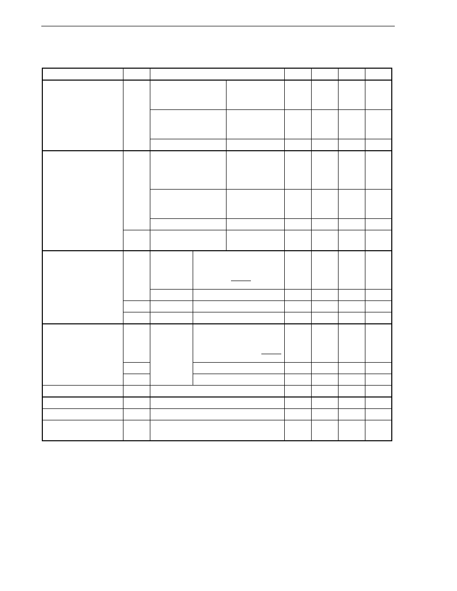
CHAPTER 29 ELECTRICAL SPECIFICATIONS (STANDARD PRODUCTS, (A) GRADE PRODUCTS)
User's Manual U16228EJ2V0UD
474
DC Characteristics (2/4)
(T
A
=
-
40 to +85
∞
C, 2.7 V
V
DD
= EV
DD
5.5 V, 2.7 V
AV
REF
V
DD
, V
SS
= EV
SS
= AV
SS
= 0 V)
Parameter Symbol
Conditions
MIN.
TYP.
MAX.
Unit
P10 to P17, P30 to P33,
P120, P130, P140, P141
Total I
OH
=
-
25 mA
4.0 V
V
DD
5.5 V,
I
OH
=
-
5 mA
V
DD
-
1.0
V
P00 to P06, P40 to P43,
P50 to P53, P70 to P77
Total I
OH
=
-
25 mA
4.0 V
V
DD
5.5 V,
I
OH
=
-
5 mA
V
DD
-
1.0
V
Output voltage, high
V
OH
I
OH
=
-
100
µ
A 2.7
V
V
DD
< 4.0 V V
DD
-
0.5
V
P10 to P17, P30 to P33,
P60 to P63, P120, P130,
P140, P141
Total I
OL
= 30 mA
4.0 V
V
DD
5.5 V,
I
OL
= 10 mA
1.3
V
P00 to P06, P40 to P43,
P50 to P53, P70 to P77
Total I
OL
= 30 mA
4.0 V
V
DD
5.5 V,
I
OL
= 10 mA
1.3
V
V
OL1
I
OL
= 400
µ
A 2.7
V
V
DD
< 4.0 V
0.4
V
Output voltage, low
V
OL2
P60 to P63
4.0 V
V
DD
5.5 V,
I
OL
= 15 mA
2.0
V
V
I
= V
DD
P00 to P06, P10 to P17, P30 to
P33, P40 to P43, P50 to P53,
P60, P61, P70 to P77, P120,
P140, P141, RESET
3
µ
A
I
LIH1
V
I
= AV
REF
P20 to P27
3
µ
A
I
LIH2
V
I
= V
DD
X1,
X2
Note 1
, XT1, XT2
Note 1
20
µ
A
Input leakage current, high
I
LIH3
V
I
= 12 V
P62, P63 (N-ch open drain)
3
µ
A
I
LIL1
P00 to P06, P10 to P17, P20 to
P27, P30 to P33, P40 to P43,
P50 to P53, P60, P61, P70 to
P77, P120, P140, P141, RESET
-
3
µ
A
I
LIL2
X1,
X2
Note 1
, XT1, XT2
Note 1
-
20
µ
A
Input leakage current, low
I
LIL3
V
I
= 0 V
P62, P63 (N-ch open drain)
-
3
Note 2
µ
A
Output leakage current, high I
LOH
V
O
= V
DD
3
µ
A
Output leakage current, low
I
LOL
V
O
= 0 V
-
3
µ
A
Pull-up resistor
R
L
V
I
= 0 V
10
30
100
k
V
PP
supply voltage (flash
memory version only)
V
PP1
In normal operation mode
0
0.2V
DD
V
Notes 1. When the inverse level of X1 is input to X2 and the inverse level of XT1 is input to XT2.
2. If there is no on-chip pull-up resistor for P62 and P63 (specified by a mask option) and if port 6 has been
set to input mode when a read instruction is executed to read from port 6, a low-level input leakage
current of up to
-
45
µ
A flows during only one cycle. At all other times, the maximum leakage current is
-
3
µ
A.
Remark Unless specified otherwise, the characteristics of alternate-function pins are the same as those of port pins.
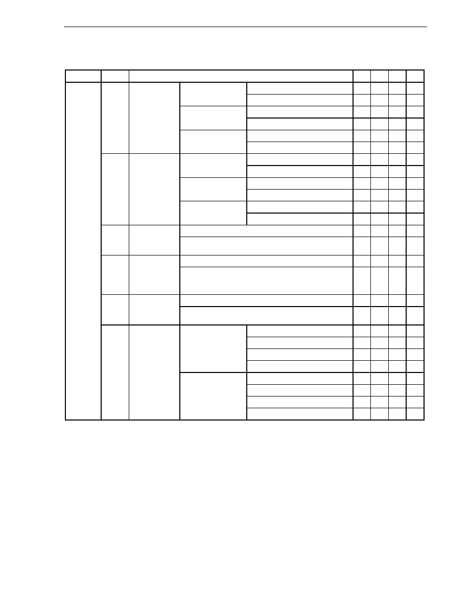
CHAPTER 29 ELECTRICAL SPECIFICATIONS (STANDARD PRODUCTS, (A) GRADE PRODUCTS)
User's Manual U16228EJ2V0UD
475
DC Characteristics (3/4): Flash memory version
(T
A
=
-
40 to +85
∞
C, 2.7 V
V
DD
= EV
DD
5.5 V, 2.7 V
AV
REF
V
DD
, V
SS
= EV
SS
= AV
SS
= 0 V)
Parameter Symbol
Conditions
MIN.
TYP. MAX. Unit
When A/D converter is stopped
13.8
25.2
mA
f
XP
= 10 MHz
V
DD
= 5.0 V
±
10%
Notes 3, 7
When A/D converter is operating
Note 9
14.6
27.2
mA
When A/D converter is stopped
8
14.6
mA
f
XP
= 8.38 MHz
V
DD
= 5.0 V
±
10%
Notes 3, 8
When A/D converter is operating
Note 9
9
16.6
mA
When A/D converter is stopped
4.5
7.8
mA
I
DD1
X1 crystal
oscillation
operating
mode
Note 2
f
XP
= 5 MHz
V
DD
= 3.0 V
±
10%
Note 3
When A/D converter is operating
Note 9
5.1 9 mA
When peripheral functions are stopped
1.8
3.6
mA
f
XP
= 10 MHz
V
DD
= 5.0 V
±
10%
Note 7
When peripheral functions are operating
8.9
mA
When peripheral functions are stopped
0.9
1.8
mA
f
XP
= 8.38 MHz
V
DD
= 5.0 V
±
10%
Note 8
When peripheral functions are operating
6
mA
When peripheral functions are stopped
0.41
0.82
mA
I
DD2
X1 crystal
oscillation HALT
mode
f
XP
= 5 MHz
V
DD
= 3.0 V
±
10%
When peripheral functions are operating
2.3
mA
V
DD
= 5.0 V
±
10%
0.48
1.92
mA
I
DD3
Ring-OSC
operating
mode
Note 4
V
DD
= 3.0 V
±
10%
0.37
1.48
mA
V
DD
= 5.0 V
±
10%
120
240
µ
A
I
DD4
32.768 kHz
crystal oscillation
operating
mode
Notes 4, 6
V
DD
= 3.0 V
±
10%
91
182
µ
A
V
DD
= 5.0 V
±
10%
20
40
µ
A
I
DD5
32.768 kHz
crystal oscillation
HALT mode
Notes 4, 6
V
DD
= 3.0 V
±
10%
6
12
µ
A
POC: OFF, RING: OFF
0.1
30
µ
A
POC: OFF, RING: ON
14
58
µ
A
POC: ON
Note 5
, RING: OFF
3.5
35.5
µ
A
V
DD
= 5.0 V
±
10%
POC: ON
Note 5
, RING: ON
17.5
63.5
µ
A
POC: OFF, RING: OFF
0.05
10
µ
A
POC: OFF, RING: ON
7.5
25
µ
A
POC: ON
Note 5
, RING: OFF
3.5
15.5
µ
A
Supply
current
Note 1
I
DD6
STOP
mode
V
DD
= 3.0 V
±
10%
POC: ON
Note 5
, RING: ON
11
30.5
µ
A
Notes 1. Total current flowing through the internal power supply (V
DD
). Peripheral operation current is included
(however, the current that flows through the pull-up resistors of ports is not included).
2. I
DD1
includes peripheral operation current.
3. When PCC = 00H.
4. When X1 oscillator is stopped.
5.
Including when LVIE (bit 4 of LVIM) = 1 in the
µ
PD78F0134M1, 78F0134M2, 78F0138M1, 78F0138M2,
78F0134M1(A), 78F0134M2(A), 78F0138M1(A), and 78F0138M2 (A).
6.
When the
µ
PD78F0134M1, 78F0134M2, 78F0138M1, 78F0138M2, 78F0134M1(A), 78F0134M2(A),
78F0138M1(A), and 78F0138M2(A) (including LVIE = 0) are selected and Ring-OSC oscillation is
stopped.
7. When the REGC pin is directly connected to V
DD
.
8. When the REGC pin is connected to V
SS
via a capacitor (1
µ
F: recommended).
9. Including the current that flows through the AV
REF
pin.

CHAPTER 29 ELECTRICAL SPECIFICATIONS (STANDARD PRODUCTS, (A) GRADE PRODUCTS)
User's Manual U16228EJ2V0UD
476
DC Characteristics (4/4): Mask ROM version
(T
A
=
-
40 to +85
∞
C, 2.7 V
V
DD
= EV
DD
5.5 V, 2.7 V
AV
REF
V
DD
, V
SS
= EV
SS
= AV
SS
= 0 V)
Parameter Symbol
Conditions
MIN. TYP.
MAX. Unit
When A/D converter is stopped
7.6
15.2
mA
f
XP
= 10 MHz
V
DD
= 5.0 V
±
10%
Notes 3, 7
When A/D converter is operating
Note 9
8.6
17.2
mA
When A/D converter is stopped
4
8.5
mA
f
XP
= 8.38 MHz
V
DD
= 5.0 V
±
10%
Notes 3, 8
When A/D converter is operating
Note 9
5
10.5
mA
When A/D converter is stopped
2.1
4.2
mA
I
DD1
X1 crystal
oscillation
operating
mode
Note 2
f
XP
= 5 MHz
V
DD
= 3.0 V
±
10%
Note 3
When A/D converter is operating
Note 9
2.7
5.4
mA
When peripheral functions are stopped
1.6
3.2
mA
f
XP
= 10 MHz
V
DD
= 5.0 V
±
10%
Notes 7
When peripheral functions are operating
7.5
mA
When peripheral functions are stopped
0.8
1.6
mA
f
XP
= 8.38 MHz
V
DD
= 5.0 V
±
10%
Notes 8
When peripheral functions are operating
5
mA
When peripheral functions are stopped
0.31
0.62
mA
I
DD2
X1 crystal
oscillation HALT
mode
f
XP
= 5 MHz
V
DD
= 3.0 V
±
10%
When peripheral functions are operating
1.8
mA
V
DD
= 5.0 V
±
10%
0.25
1
mA
I
DD3
Ring-OSC
operating
mode
Note 4
V
DD
= 3.0 V
±
10%
0.15
0.6
mA
V
DD
= 5.0 V
±
10%
35
70
µ
A
I
DD4
32.768 kHz
crystal oscillation
operating
mode
Notes 4, 6
V
DD
= 3.0 V
±
10%
15
30
µ
A
V
DD
= 5.0 V
±
10%
20
40
µ
A
I
DD5
32.768 kHz
crystal oscillation
HALT mode
Notes 4, 6
V
DD
= 3.0 V
±
10%
6
12
µ
A
POC: OFF, RING: OFF
0.1
30
µ
A
POC: OFF, RING: ON
14
58
µ
A
POC: ON
Note 5
, RING: OFF
3.5
35.5
µ
A
V
DD
= 5.0 V
±
10%
POC: ON
Note 5
, RING: ON
17.5 63.5
µ
A
POC: OFF, RING: OFF
0.05
10
µ
A
POC: OFF, RING: ON
7.5
25
µ
A
POC: ON
Note 5
, RING: OFF
3.5
15.5
µ
A
Supply
current
Note 1
I
DD6
STOP
mode
V
DD
= 3.0 V
±
10%
POC: ON
Note 5
, RING: ON
11
30.5
µ
A
Notes 1. Total current flowing through the internal power supply (V
DD
). Peripheral operation current is included
(however, the current that flows through the pull-up resistors of ports is not included).
2. I
DD1
includes peripheral operation current.
3. When PCC = 00H.
4. When X1 oscillator is stopped.
5. Including when LVIE (bit 4 of LVIM) = 1 with POC-OFF selected by a mask option.
6. When POC-OFF (including LVIE = 0) is selected by a mask option and Ring-OSC oscillation is stopped.
7. When the REGC pin is directly connected to V
DD
.
8.
When the REGC pin is connected to V
SS
via a capacitor (1
µ
F: recommended).
9.
Including the current that flows through the AV
REF
pin.
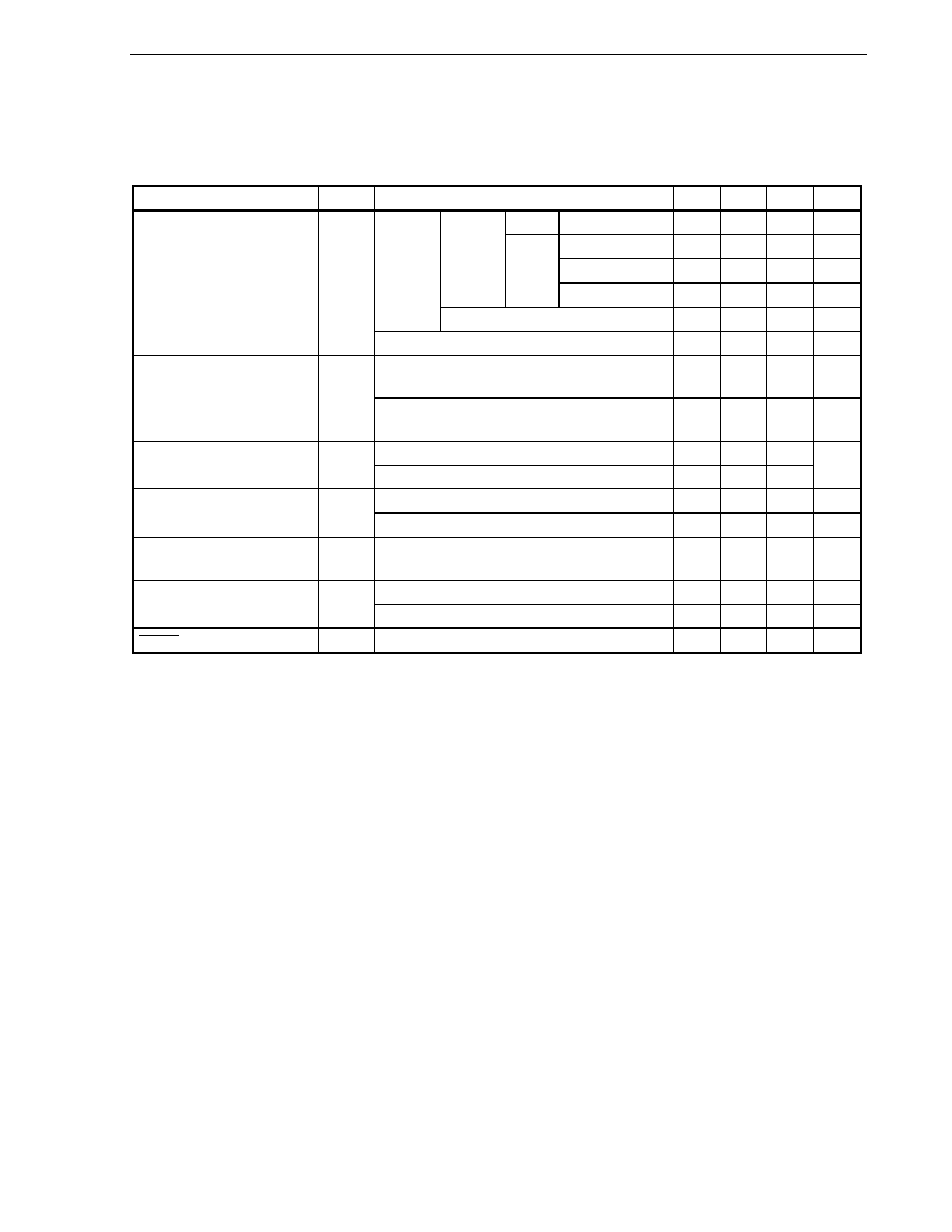
CHAPTER 29 ELECTRICAL SPECIFICATIONS (STANDARD PRODUCTS, (A) GRADE PRODUCTS)
User's Manual U16228EJ2V0UD
477
AC Characteristics
(1) Basic
operation
(T
A
=
-
40 to +85
∞
C, 2.7 V
V
DD
= EV
DD
5.5 V, 2.7 V
AV
REF
V
DD
, V
SS
= EV
SS
= AV
SS
= 0 V)
Parameter Symbol
Conditions
MIN.
TYP.
MAX.
Unit
Note 1
4.0 V
V
DD
5.5 V 0.238
16
µ
s
4.0 V
V
DD
5.5 V
0.2
16
µ
s
3.3 V
V
DD
< 4.0 V 0.238
16
µ
s
X1 input
clock
Note 2
2.7 V
V
DD
< 3.3 V
0.4
16
µ
s
Main
system
clock
operation
Ring-OSC clock
4.17
8.33
16.67
µ
s
Instruction cycle (minimum
instruction execution time)
T
CY
Subsystem
clock
operation
114 122 125
µ
s
4.0 V
V
DD
5.5 V
2/f
sam
+
0.1
Note 4
µ
s
TI000, TI010, TI001
Note 3
,
TI011
Note 3
input high-level width,
low-level width
t
TIH0
,
t
TIL0
2.7 V
V
DD
< 4.0 V
2/f
sam
+
0.2
Note 4
µ
s
4.0 V
V
DD
5.5 V
10
TI50, TI51 input frequency
f
TI5
2.7 V
V
DD
< 4.0 V
5
MHz
4.0 V
V
DD
5.5 V
50
ns
TI50, TI51 input high-level width,
low-level width
t
TIH5
,
t
TIL5
2.7 V
V
DD
< 4.0 V
100
ns
Interrupt input high-level width,
low-level width
t
INTH
,
t
INTL
1
µ
s
4.0 V
V
DD
5.5 V
50
ns
Key return input low-level width t
KR
2.7 V
V
DD
< 4.0 V
100
ns
RESET low-level width
t
RSL
10
µ
s
Notes 1. When the REGC pin is connected to V
SS
via a capacitor (1
µ
F: recommended).
2. When the REGC pin is directly connected to V
DD
.
3.
µ
PD780133, 780134, 78F0134, 780136, 780138, 78F0138, 780133(A), 780134(A), 78F0134(A),
780136(A), 780138(A), and 78F0138(A) only.
4. Selection
of
f
sam
= f
XP
, f
XP
/4, f
XP
/256, or f
XP
, f
XP
/16, f
XP
/64 is possible using bits 0 and 1 (PRM000, PRM001
or PRM010, PRM011) of prescaler mode registers 00 and 01 (PRM00, PRM01). Note that when selecting
the TI000 or TI001 valid edge as the count clock, f
sam
= f
XP.
CHAPTER 29 ELECTRICAL SPECIFICATIONS (STANDARD PRODUCTS, (A) GRADE PRODUCTS)
User's Manual U16228EJ2V0UD
478
T
CY
vs. V
DD
(X1 Input Clock Operation)
(a) When REGC pin is connected to V
SS
via capacitor (1
µ
F: recommended)
5.0
1.0
2.0
0.4
0.2
0.1
0
10.0
1.0
2.0
3.0
4.0
5.0
6.0
5.5
Guaranteed
operation
range
20.0
16.0
0.238
Supply voltage V
DD
[V]
Cycle time T
CY
[ s]
µ
(b) When REGC pin is connected directly to V
DD
5.0
1.0
2.0
0.4
0.2
0.1
Supply voltage V
DD
[V]
Cycle time T
CY
[ s]
0
10.0
1.0
2.0
3.0
4.0
5.0
6.0
5.5
2.7
3.3
Guaranteed
operation range
20.0
16.0
0.238
µ
CHAPTER 29 ELECTRICAL SPECIFICATIONS (STANDARD PRODUCTS, (A) GRADE PRODUCTS)
User's Manual U16228EJ2V0UD
479
(2) Serial
interface
(T
A
=
-
40 to +85
∞
C, 2.7 V
V
DD
= EV
DD
5.5 V, 2.7 V
AV
REF
V
DD
, V
SS
= EV
SS
= AV
SS
= 0 V)
(a) UART mode (UART6, dedicated baud rate generator output)
Parameter Symbol
Conditions
MIN.
TYP.
MAX.
Unit
Transfer rate
312.5
kbps
(b) UART mode (UART0, dedicated baud rate generator output)
Parameter Symbol
Conditions
MIN.
TYP.
MAX.
Unit
Transfer rate
312.5
kbps
(c) 3-wire serial I/O mode (master mode, SCK1n... internal clock output)
Parameter Symbol
Conditions
MIN.
TYP.
MAX.
Unit
4.0 V
V
DD
5.5 V
200
ns
3.3 V
V
DD
< 4.0 V
240
ns
SCK1n cycle time
t
KCY1
2.7 V
V
DD
< 3.3 V
400
ns
SCK1n high-/low-level width
t
KH1
,
t
KL1
t
KCY1
/2
-
10
ns
SI1n setup time (to SCK1n
) t
SIK1
30 ns
SI1n hold time (from SCK1n
) t
KSI1
30 ns
Delay time from SCK1n
to
SO1n output
t
KSO1
C = 100 pF
Note
30
ns
Note C is the load capacitance of the SCK1n and SO1n output lines.
(d) 3-wire serial I/O mode (slave mode, SCK1n... external clock input)
Parameter Symbol
Conditions
MIN.
TYP.
MAX.
Unit
SCK1n cycle time
t
KCY2
400
ns
SCK1n high-/low-level width
t
KH2
,
t
KL2
t
KCY2
/2
ns
SI1n setup time (to SCK1n
) t
SIK2
80 ns
SI1n hold time (from SCK1n
) t
KSI2
50 ns
Delay time from SCK1n
to
SO1n output
t
KSO2
C = 100 pF
Note
120
ns
Note C is the load capacitance of the SO1n output line.
Remark n = 0:
µ
PD780131, 780132, 780131(A1), 780132(A)
n = 0, 1:
µ
PD780133, 780134, 78F0134, 780136, 780138, 78F0138, 780133(A), 780134(A), 78F0134(A),
780136(A), 780138(A), 78F0138(A)
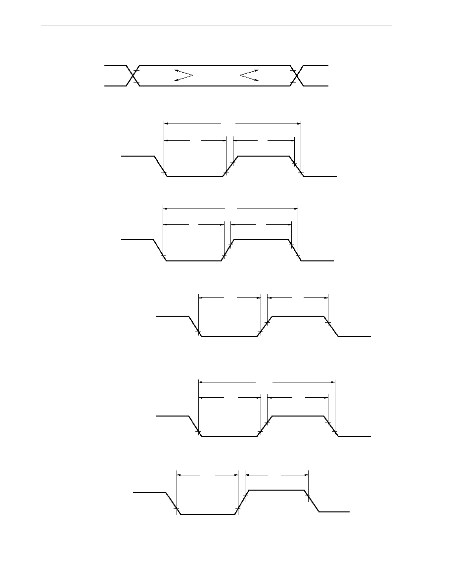
CHAPTER 29 ELECTRICAL SPECIFICATIONS (STANDARD PRODUCTS, (A) GRADE PRODUCTS)
User's Manual U16228EJ2V0UD
480
AC Timing Test Points (Excluding X1 Input)
0.8V
DD
0.2V
DD
Test points
0.8V
DD
0.2V
DD
Clock Timing
X1 input
V
IH6
(MIN.)
V
IL6
(MAX.)
1/f
XP
t
XPL
t
XPH
1/f
XT
t
XTL
t
XTH
XT1 input
V
IH6
(MIN.)
V
IL6
(MAX.)
TI Timing
TI00, TI010, TI001
Note
, TI011
Note
t
TIL0
t
TIH0
TI50, TI51
1/f
TI5
t
TIL5
t
TIH5
Interrupt Request Input Timing
INTP0 to INTP7
t
INTL
t
INTH
Note
µ
PD780133, 780134, 78F0134, 780136, 780138, 78F0138, 780133(A), 780134(A), 78F0134(A), 780136(A),
780138(A), and 78F0138(A) only.

CHAPTER 29 ELECTRICAL SPECIFICATIONS (STANDARD PRODUCTS, (A) GRADE PRODUCTS)
User's Manual U16228EJ2V0UD
481
RESET Input Timing
RESET
t
RSL
Serial Transfer Timing
3-wire serial I/O mode:
SI1n
SO1n
t
KCYm
t
KLm
t
KHm
t
SIKm
t
KSIm
Input data
t
KSOm
Output data
SCK1n
Remark m = 1, 2
n = 0:
µ
PD780131, 780132, 780131(A), 780132(A)
n = 0, 1:
µ
PD780133, 780134, 78F0134, 780136, 780138, 78F0138, 780133(A), 780134(A),
78F0134(A), 780136(A), 780138(A), 78F0138(A)
CHAPTER 29 ELECTRICAL SPECIFICATIONS (STANDARD PRODUCTS, (A) GRADE PRODUCTS)
User's Manual U16228EJ2V0UD
482
A/D Converter Characteristics
(T
A
=
-
40 to +85
∞
C, 2.7 V
V
DD
= EV
DD
5.5 V, 2.7 V
AV
REF
V
DD
, V
SS
= EV
SS
= AV
SS
= 0 V)
Parameter Symbol
Conditions
MIN.
TYP.
MAX.
Unit
Resolution
10 10 10 bit
4.0 V
AV
REF
5.5 V
±
0.2
±
0.4 %FSR
Overall error
Notes 1, 2
2.7 V
AV
REF
< 4.0 V
±
0.3
±
0.6 %FSR
4.0 V
AV
REF
5.5 V
14
100
µ
s
Conversion time
t
CONV
2.7 V
AV
REF
< 4.0 V
17
100
µ
s
4.0 V
AV
REF
5.5 V
±
0.4 %FSR
Zero-scale error
Notes 1, 2
2.7 V
AV
REF
< 4.0 V
±
0.6 %FSR
4.0 V
AV
REF
5.5 V
±
0.4 %FSR
Full-scale error
Notes 1, 2
2.7 V
AV
REF
< 4.0 V
±
0.6 %FSR
4.0 V
AV
REF
5.5 V
±
2.5 LSB
Integral non-linearity error
Note 1
2.7 V
AV
REF
< 4.0 V
±
4.5 LSB
4.0 V
AV
REF
5.5 V
±
1.5 LSB
Differential non-linearity error
Note 1
2.7 V
AV
REF
< 4.0 V
±
2.0 LSB
Analog input voltage
V
IAN
AV
SS
AV
REF
V
Notes 1.
Excludes quantization error (
±
1/2 LSB).
2. This value is indicated as a ratio (%FSR) to the full-scale value.
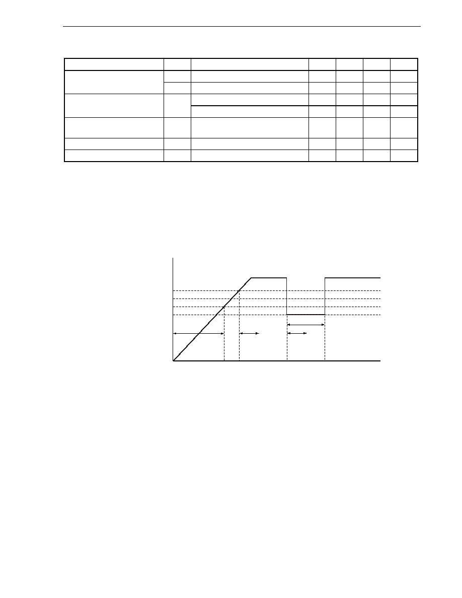
CHAPTER 29 ELECTRICAL SPECIFICATIONS (STANDARD PRODUCTS, (A) GRADE PRODUCTS)
User's Manual U16228EJ2V0UD
483
POC Circuit Characteristics (T
A
=
-
40 to +85
∞
C)
Parameter Symbol
Conditions
MIN.
TYP.
MAX.
Unit
V
POC0
Mask option = 3.5 V
Note 1
3.3 3.5 3.7 V
Detection voltage
V
POC1
Mask option = 2.85 V
Note 2
2.7 2.85 3.0 V
V
DD
: 0 V
2.7 V
0.0015
ms
Power supply rise time
t
PTH
V
DD
: 0 V
3.3 V
0.002
ms
Response delay time 1
Note 3
t
PTHD
When power supply rises, after reaching
detection voltage (MAX.)
3.0
ms
Response delay time 2
Note 3
t
PD
When
V
DD
falls
1.0
ms
Minimum pulse width
t
PW
0.2
ms
Notes 1. When flash memory version
µ
PD78F0134M5, 78F0134M6, 78F0138M5, 78F0138M6, 78F0134M5(A),
78F0134M6(A), 78F0138M5(A), or 78F0138M6(A) is used
2.
When flash memory version
µ
PD78F0134M3, 78F0134M4, 78F0138M3, 78F0138M4, 78F0134M3(A),
78F0134M4(A), 78F0138M3(A), or 78F0138M4(A) is used
3. Time required from voltage detection to reset release.
POC Circuit Timing
Supply voltage
(V
DD
)
Time
Detection voltage (MIN.)
Detection voltage (TYP.)
Detection voltage (MAX.)
t
PTH
t
PTHD
t
PW
t
PD
CHAPTER 29 ELECTRICAL SPECIFICATIONS (STANDARD PRODUCTS, (A) GRADE PRODUCTS)
User's Manual U16228EJ2V0UD
484
LVI Circuit Characteristics (T
A
=
-
40 to +85
∞
C)
Parameter Symbol
Conditions
MIN.
TYP.
MAX.
Unit
V
LVI0
4.1 4.3 4.5 V
V
LVI1
3.9 4.1 4.3 V
V
LVI2
3.7 3.9 4.1 V
V
LVI3
3.5 3.7 3.9 V
V
LVI4
3.3 3.5 3.7 V
V
LVI5
3.15 3.3 3.45 V
Detection voltage
V
LVI6
2.95 3.1 3.25 V
Response time
Note 1
t
LD
0.2 2.0 ms
Minimum pulse width
t
LW
0.2
ms
Reference voltage stabilization wait
time
Note 2
t
LWAIT0
0.5
2.0
ms
Operation stabilization wait time
Note 3
t
LWAIT1
0.1
0.2
ms
Notes 1. Time required from voltage detection to interrupt output or internal reset output.
2. Time required from setting LVIE to 1 to reference voltage stabilization when POC-OFF is selected by the
POC mask option (when flash memory version
µ
PD78F0134M1, 78F0134M2, 78F0138M1, 78F0138M2,
78F0134M1(A), 78F0134M2(A), 78F0138M1(A), or 78F0138M2(A) is used).
3. Time required from setting LVION to 1 to operation stabilization.
Remarks 1. V
LVI0
> V
LVI1
> V
LVI2
> V
LVI3
> V
LVI4
> V
LVI5
> V
LVI6
2. V
POCn
< V
LVIm
(n = 0 or 1, m = 0 to 6)
LVI Circuit Timing
Supply voltage
(V
DD
)
Time
Detection voltage (MIN.)
Detection voltage (TYP.)
Detection voltage (MAX.)
t
WAIT0
t
LW
t
LD
t
WAIT1
LVIE
1 LVION
1
Data Memory STOP Mode Low Supply Voltage Data Retention Characteristics (T
A
=
-
40 to +85
∞
C)
Parameter Symbol
Conditions
MIN.
TYP.
MAX.
Unit
Data retention supply voltage
V
DDDR
When POC-OFF is selected by mask
option
Note
1.6 5.5 V
Release signal set time
t
SREL
0
µ
s
Note When flash memory version
µ
PD78F0134M1, 78F0134M2, 78F0138M1, 78F0138M2, 78F0134M1(A),
78F0134M2(A), 78F0138M1(A), or 78F0138M2(A) is used
CHAPTER 29 ELECTRICAL SPECIFICATIONS (STANDARD PRODUCTS, (A) GRADE PRODUCTS)
User's Manual U16228EJ2V0UD
485
Flash Memory Programming Characteristics: Flash memory version
(T
A
= +10 to +60
∞
C, 2.7 V
V
DD
= EV
DD
5.5 V, 2.7 V
AV
REF
V
DD
, V
SS
= EV
SS
= AV
SS
= 0 V)
(1) Write erase characteristics
Parameter Symbol
Conditions
MIN.
TYP.
MAX.
Unit
V
PP
supply voltage
V
PP2
During flash memory programming
9.7
10.0
10.3
V
V
DD
supply current
I
DD
When
V
PP
= V
PP2
, f
XP
= 10 MHz, V
DD
= 5.5 V
37
mA
V
PP
supply current
I
PP
V
PP
= V
PP2
100
mA
Step erase time
Note 1
T
er
0.199 0.2 0.201 s
Overall erase time
Note 2
T
era
When step erase time = 0.2 s
20
s/chip
Writeback time
Note 3
T
wb
49.4 50 50.6 ms
Number of writebacks per 1
writeback command
Note 4
C
wb
When writeback time = 50 ms
60
Times
Number of erases/writebacks
C
erwb
16 Times
Step write time
Note 5
T
wr
48 50 52
µ
s
Overall write time per word
Note 6
T
wrw
When step write time = 50
µ
s (1 word = 1
byte)
48 520
µ
s
Number of rewrites per chip
Note 7
C
erwr
1 erase + 1 write after erase = 1 rewrite
20
Times/
area
Notes 1. The recommended setting value of the step erase time is 0.2 s.
2.
The prewrite time before erasure and the erase verify time (writeback time) are not included.
3.
The recommended setting value of the writeback time is 50 ms.
4.
Writeback is executed once by the issuance of the writeback command. Therefore, the number of retries
must be the maximum value minus the number of commands issued.
5.
The recommended setting value of the step write time is 50
µ
s.
6. The actual write time per word is 100
µ
s longer. The internal verify time during or after a write is not
included.
7. When a product is first written after shipment, "erase
write" and "write only" are both taken as one
rewrite.
Example: P: Write, E: Erase
Shipped
product
P
E
P
E
P: 3 rewrites
Shipped
product
E
P
E
P
E
P: 3 rewrites
Remark The range of the operating clock during flash memory programming is the same as the range during normal
operation.
CHAPTER 29 ELECTRICAL SPECIFICATIONS (STANDARD PRODUCTS, (A) GRADE PRODUCTS)
User's Manual U16228EJ2V0UD
486
(2) Serial write operation characteristics
Parameter Symbol
Conditions
MIN.
TYP.
MAX.
Unit
Set time from V
DD
to V
PP
t
DP
10
µ
s
Release time from V
PP
to RESET
t
PR
10
µ
s
V
PP
pulse input start time from
RESET
t
RP
2
ms
V
PP
pulse high-/low-level width
t
PW
8
µ
s
V
PP
pulse input end time from
RESET
t
RPE
14 ms
V
PP
pulse low-level input voltage
V
PPL
0.8V
DD
1.2V
DD
V
V
PP
pulse high-level input voltage
V
PPH
9.7 10.0 10.3 V
Flash Write Mode Setting Timing
V
DD
V
DD
0 V
V
DD
RESET (input)
0 V
V
PPH
0 V
V
PP
V
PPL
t
RP
t
PR
t
DP
t
PW
t
PW
t
RPE

User's Manual U16228EJ2V0UD
487
CHAPTER 30 ELECTRICAL SPECIFICATIONS ((A1) GRADE PRODUCTS)
Target products:
µ
PD780131(A1), 780132(A1), 780133(A1), 780134(A1), 780136(A1), 780138(A1), 78F0134(A1),
78F0138(A1)
Caution Be sure to connect the REGC pin of (A1) grade products directly to V
DD
.
Absolute Maximum Ratings (T
A
= 25
∞
C) (1/2)
Parameter Symbol
Conditions
Ratings
Unit
V
DD
-
0.3 to +6.5
V
EV
DD
-
0.3 to +6.5
V
REGC
-
0.3 to +6.5
V
V
SS
-
0.3 to +0.3
V
EV
SS
-
0.3 to +0.3
V
AV
REF
-
0.3 to V
DD
+ 0.3
Note 1
V
AV
SS
-
0.3 to +0.3
V
Supply voltage
V
PP
Flash memory version only, Note 2
-
0.3 to +10.5
V
V
I1
P00 to P06, P10 to P17, P20 to P27, P30
to P33, P40 to P43, P50 to P53, P60,
P61, P70 to P77, P120, P130, P140,
P141, X1, X2, XT1, XT2, RESET
-
0.3 to V
DD
+ 0.3
Note 1
V
N-ch open drain
-
0.3 to +13
V
V
I2
P62,
P63
On-chip pull-up resistor
-
0.3 to V
DD
+ 0.3
Note 1
V
Input voltage
V
I3
V
PP
in flash programming mode
(flash memory version only)
-
0.3 to +10.5
V
Output voltage
V
O
-
0.3 to V
DD
+ 0.3
Note 1
V
Analog input voltage
V
AN
AV
SS
-
0.3 to AV
REF
+ 0.3
Note 1
and
-
0.3 to V
DD
+ 0.3
Note 1
V
Per pin
-
8 mA
P00 to P06, P40 to P43, P50 to
P53, P70 to P77
-
24 mA
Output current, high
I
OH
Total of
all pins
-
48 mA
P10 to P17, P30 to P33, P120,
P130, P140, P141
-
24 mA
(Refer to Note on the next page.)
Caution Product quality may suffer if the absolute maximum rating is exceeded even momentarily for any
parameter. That is, the absolute maximum ratings are rated values at which the product is on the
verge of suffering physical damage, and therefore the product must be used under conditions that
ensure that the absolute maximum ratings are not exceeded.
Remark Unless specified otherwise, the characteristics of alternate-function pins are the same as those of port pins.
CHAPTER 30 ELECTRICAL SPECIFICATIONS ((A1) GRADE PRODUCTS)
User's Manual U16228EJ2V0UD
488
Absolute Maximum Ratings (T
A
= 25
∞
C) (2/2)
Parameter Symbol
Conditions
Ratings
Unit
P00 to P06, P10 to P17, P30 to
P33, P40 to P43, P50 to P53,
P70 to P77, P120, P130, P140,
P141
16 mA
Per pin
P60 to P63
24
mA
P00 to P06, P40 to P43, P50 to
P53, P70 to P77
28 mA
Output current, low
I
OL
Total of
all pins
56 mA
P10 to P17, P30 to P33, P60 to
P63, P120, P130, P140, P141
28 mA
Mask ROM version
-
40 to +110
In normal operation mode
-
40 to +105
Operating ambient
temperature
T
A
Flash
memory
version
In flash memory programming
mode
-
40 to +85
∞
C
Mask ROM version
-
65 to +150
Storage temperature
T
stg
Flash memory version
-
40 to +125
∞
C
Notes 1. Must be 6.5 V or lower.
2.
Make sure that the following conditions of the V
PP
voltage application timing are satisfied when the flash
memory is written.
∑
When supply voltage rises
V
PP
must exceed V
DD
10
µ
s or more after V
DD
has reached the lower-limit value (3.3 V) of the operating
voltage range (see a in the figure below).
∑
When supply voltage drops
Raise
V
DD
10
µ
s or more after V
PP
falls below the lower-limit value (3.3 V) of the operating voltage range
of V
DD
(see b in the figure below).
3.3 V
V
DD
0 V
0 V
V
PP
3.3 V
a
b
Caution Product quality may suffer if the absolute maximum rating is exceeded even momentarily for any
parameter. That is, the absolute maximum ratings are rated values at which the product is on the
verge of suffering physical damage, and therefore the product must be used under conditions that
ensure that the absolute maximum ratings are not exceeded.
Remark Unless specified otherwise, the characteristics of alternate-function pins are the same as those of port pins.
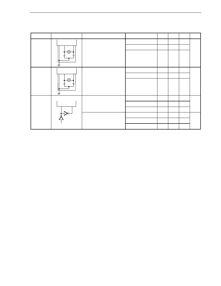
CHAPTER 30 ELECTRICAL SPECIFICATIONS ((A1) GRADE PRODUCTS)
User's Manual U16228EJ2V0UD
489
X1 Oscillator Characteristics
(T
A
=
-
40 to +110
∞
C
Note 1
, 3.3 V
V
DD
= EV
DD
5.5 V, 3.3 V
AV
REF
V
DD
, V
SS
= EV
SS
= AV
SS
= 0 V)
Resonator Recommended
Circuit
Parameter
Conditions
MIN. TYP. MAX. Unit
4.5 V
V
DD
5.5 V
2.0
10
4.0 V
V
DD
< 4.5 V
2.0
8.38
Ceramic
resonator
Note 2
C1
X2
X1
V
SS
C2
Oscillation frequency (f
XP
)
Note 3
3.3 V
V
DD
< 4.0 V
2.0
5.0
MHz
4.5 V
V
DD
5.5 V
2.0
10
4.0 V
V
DD
< 4.5 V
2.0
8.38
Crystal
resonator
Note 2
C1
X2
X1
V
SS
C2
Oscillation frequency (f
XP
)
Note 3
3.3 V
V
DD
< 4.0 V
2.0
5.0
MHz
4.5 V
V
DD
5.5 V
2.0
10
4.0 V
V
DD
< 4.5 V
2.0
8.38
X1 input frequency (f
XP
)
Note 3
3.3 V
V
DD
< 4.0 V
2.0
5.0
MHz
4.5 V
V
DD
5.5 V
46
500
4.0 V
V
DD
< 4.5 V
56
500
External
clock
Note 2
X2
X1
X1 input high-/low-level width
(t
XPH
, t
XPL
)
3.3 V
V
DD
< 4.0 V
96
500
ns
Notes 1. T
A
=
-
40 to +110
∞
C:
µ
PD780131(A1), 780132(A1), 780133(A1), 780134(A1), 780136(A1), 780138(A1)
T
A
=
-
40 to +105
∞
C:
µ
PD78F0134(A1), 78F0138(A1)
2. Connect the REGC pin directly to V
DD
.
3. Indicates
only
oscillator
characteristics. Refer to AC Characteristics for instruction execution time.
Cautions 1. When using the X1 oscillator, wire as follows in the area enclosed by the broken lines in the
above figures to avoid an adverse effect from wiring capacitance.
∑ Keep the wiring length as short as possible.
∑ Do not cross the wiring with the other signal lines.
∑ Do not route the wiring near a signal line through which a high fluctuating current flows.
∑ Always make the ground point of the oscillator capacitor the same potential as V
SS
.
∑ Do not ground the capacitor to a ground pattern through which a high current flows.
∑ Do not fetch signals from the oscillator.
2. Since the CPU is started by the Ring-OSC after reset is released, check the oscillation
stabilization time of the X1 input clock using the oscillation stabilization time status register
(OSTC). Determine the oscillation stabilization time of the OSTC register and oscillation
stabilization time select register (OSTS) after sufficiently evaluating the oscillation stabilization
time with the resonator to be used.
Remark For the resonator selection and oscillator constant, users are required to either evaluate the oscillation
themselves or apply to the resonator manufacturer for evaluation.
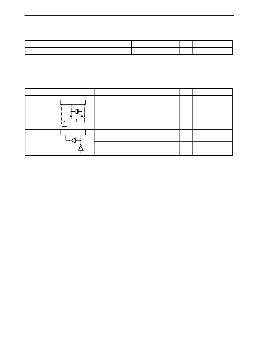
CHAPTER 30 ELECTRICAL SPECIFICATIONS ((A1) GRADE PRODUCTS)
User's Manual U16228EJ2V0UD
490
Ring-OSC Oscillator Characteristics
(T
A
=
-
40 to +110
∞
C
Note
, 3.3 V
V
DD
= EV
DD
5.5 V, 3.3 V
AV
REF
V
DD
, V
SS
= EV
SS
= AV
SS
= 0 V)
Resonator Parameter
Conditions
MIN.
TYP.
MAX.
Unit
On-chip Ring-OSC oscillator
Oscillation frequency (f
R
)
120 240 490 kHz
Note T
A
=
-
40 to +110
∞
C:
µ
PD780131(A1), 780132(A1), 780133(A1), 780134(A1), 780136(A1), 780138(A1)
T
A
=
-
40 to +105
∞
C:
µ
PD78F0134(A1), 78F0138(A1)
Subsystem Clock Oscillator Characteristics
(T
A
=
-
40 to +110
∞
C
Note 1
, 3.3 V
V
DD
= EV
DD
5.5 V, 3.3 V
AV
REF
V
DD
, V
SS
= EV
SS
= AV
SS
= 0 V)
Resonator Recommended
Circuit
Parameter
Conditions
MIN.
TYP.
MAX.
Unit
Crystal
resonator
XT1
V
SS
XT2
C4
C3
Rd
Oscillation frequency
(f
XT
)
Note 2
32
32.768
35
kHz
XT1 input frequency
(f
XT
)
Note 2
32
38.5
kHz
External clock
XT1
XT2
XT1 input high-/low-level
width (t
XTH
, t
XTL
)
12 15
µ
s
Notes 1. T
A
=
-
40 to +110
∞
C:
µ
PD780131(A1), 780132(A1), 780133(A1), 780134(A1), 780136(A1), 780138(A1)
T
A
=
-
40 to +105
∞
C:
µ
PD78F0134(A1), 78F0138(A1)
2. Indicates
only
oscillator
characteristics. Refer to AC Characteristics for instruction execution time.
Cautions 1. When using the subsystem clock oscillator, wire as follows in the area enclosed by the broken
lines in the above figures to avoid an adverse effect from wiring capacitance.
∑
Keep the wiring length as short as possible.
∑
Do not cross the wiring with the other signal lines.
∑
Do not route the wiring near a signal line through which a high fluctuating current flows.
∑
Always make the ground point of the oscillator capacitor the same potential as V
SS
.
∑
Do not ground the capacitor to a ground pattern through which a high current flows.
∑
Do not fetch signals from the oscillator.
2. The subsystem clock oscillator is designed as a low-amplitude circuit for reducing power
consumption, and is more prone to malfunction due to noise than the X1 oscillator. Particular
care is therefore required with the wiring method when the subsystem clock is used.
Remark For the resonator selection and oscillator constant, customers are requested to either evaluate the
oscillation themselves or apply to the resonator manufacturer for evaluation.
CHAPTER 30 ELECTRICAL SPECIFICATIONS ((A1) GRADE PRODUCTS)
User's Manual U16228EJ2V0UD
491
DC Characteristics (1/6): Flash memory version
(T
A
=
-
40 to +105
∞
C, 3.3 V
V
DD
= EV
DD
5.5 V, 3.3 V
AV
REF
V
DD
, V
SS
= EV
SS
= AV
SS
= 0 V)
Parameter Symbol
Conditions
MIN.
TYP.
MAX.
Unit
Per pin
4.0 V
V
DD
5.5 V
-
4 mA
Total of P10 to P17, P30 to
P33, P120, P130, P140,
P141
4.0 V
V
DD
5.5 V
-
20 mA
Total of P00 to P06, P40 to
P43, P50 to P53, P70 to
P77
4.0 V
V
DD
5.5 V
-
20 mA
4.0 V
V
DD
5.5 V
-
25 mA
Output current, high
I
OH
All pins
3.3 V
V
DD
< 4.0 V
-
8 mA
Per pin for P00 to P06, P10
to P17, P30 to P33, P40 to
P43, P50 to P53, P70 to
P77, P120, P130, P140,
P141
4.0 V
V
DD
5.5 V
8
mA
Per pin for P60 to P63
4.0 V
V
DD
5.5 V
12
mA
Total of P10 to P17, P30 to
P33, P60 to P63, P120,
P130, P140, P141
4.0 V
V
DD
5.5 V
24
mA
Total of P00 to P06, P40 to
P43, P50 to P53, P70 to
P77
4.0 V
V
DD
5.5 V
24
mA
4.0 V
V
DD
5.5 V
30
mA
Output current, low
I
OL
All pins
3.3 V
V
DD
< 4.0 V
8
mA
V
IH1
P12, P13, P15, P40 to P43, P50 to P53
0.7V
DD
V
DD
V
V
IH2
P00 to P06, P10, P11, P14, P16, P17, P30 to
P33, P70 to P77, P120, P140, P141, RESET
0.8V
DD
V
DD
V
V
IH3
P20 to P27
Note
0.7AV
REF
AV
REF
V
V
IH4
P60,
P61
0.7V
DD
V
DD
V
V
IH5
P62, P63
N-ch open drain
0.7V
DD
12 V
Input voltage, high
V
IH6
X1, X2, XT1, XT2
V
DD
-
0.5
V
DD
V
V
IL1
P12, P13, P15, P40 to P43, P50 to P53
0
0.3V
DD
V
V
IL2
P00 to P06, P10, P11, P14, P16, P17, P30 to
P33, P70 to P77, P120, P140, P141, RESET
0
0.2V
DD
V
V
IL3
P20 to P27
Note
0
0.3AV
REF
V
V
IL4
P60,
P61
0
0.3V
DD
V
V
IL5
P62,
P63
0
0.3V
DD
V
Input voltage, low
V
IL6
X1, X2, XT1, XT2
0
0.4
V
Note When used as digital input ports, set AV
REF
= V
DD
.
Remark Unless specified otherwise, the characteristics of alternate-function pins are the same as those of port pins.
CHAPTER 30 ELECTRICAL SPECIFICATIONS ((A1) GRADE PRODUCTS)
User's Manual U16228EJ2V0UD
492
DC Characteristics (2/6): Flash memory version
(T
A
=
-
40 to +105
∞
C, 3.3 V
V
DD
= EV
DD
5.5 V, 3.3 V
AV
REF
V
DD
, V
SS
= EV
SS
= AV
SS
= 0 V)
Parameter Symbol
Conditions
MIN.
TYP.
MAX.
Unit
P10 to P17, P30 to P33,
P120, P130, P140, P141
Total I
OH
=
-
20 mA
4.0 V
V
DD
5.5 V,
I
OH
=
-
4 mA
V
DD
-
1.0
V
P00 to P06, P40 to P43,
P50 to P53, P70 to P77
Total I
OH
=
-
20 mA
4.0 V
V
DD
5.5 V,
I
OH
=
-
4 mA
V
DD
-
1.0
V
Output voltage, high
V
OH
I
OH
=
-
100
µ
A 3.3
V
V
DD
< 4.0 V V
DD
-
0.5
V
P10 to P17, P30 to P33,
P60 to P63, P120, P130,
P140, P141
Total I
OL
= 24 mA
4.0 V
V
DD
5.5 V,
I
OL
= 8 mA
1.3
V
P00 to P06, P40 to P43,
P50 to P53, P70 to P77
Total I
OL
= 24 mA
4.0 V
V
DD
5.5 V,
I
OL
= 8 mA
1.3
V
V
OL1
I
OL
= 400
µ
A 3.3
V
V
DD
< 4.0 V
0.4
V
Output voltage, low
V
OL2
P60 to P63
I
OL
= 12 mA
2.0
V
V
I
= V
DD
P00 to P06, P10 to P17, P30 to
P33, P40 to P43, P50 to P53,
P60, P61, P70 to P77, P120,
P140, P141, RESET
10
µ
A
I
LIH1
V
I
= AV
REF
P20 to P27
10
µ
A
I
LIH2
V
I
= V
DD
X1,
X2
Note 1
, XT1, XT2
Note 1
20
µ
A
Input leakage current, high
I
LIH3
V
I
= 12 V
P62, P63 (N-ch open drain)
20
µ
A
I
LIL1
P00 to P06, P10 to P17, P20 to
P27, P30 to P33, P40 to P43,
P50 to P53, P60, P61, P70 to
P77, P120, P140, P141, RESET
-
10
µ
A
I
LIL2
X1,
X2
Note 1
, XT1, XT2
Note 1
-
20
µ
A
Input leakage current, low
I
LIL3
V
I
= 0 V
P62, P63 (N-ch open drain)
-
10
Note 2
µ
A
Output leakage current, high I
LOH
V
O
= V
DD
10
µ
A
Output leakage current, low
I
LOL
V
O
= 0 V
-
10
µ
A
Pull-up resistor
R
L
V
I
= 0 V
10
30
120
k
V
PP
supply voltage
V
PP1
In normal operation mode
0
0.2V
DD
V
Notes 1. When the inverse level of X1 is input to X2 and the inverse level of XT1 is input to XT2.
2. If port 6 has been set to input mode when a read instruction is executed to read from port 6, a low-level
input leakage current of up to
-
55
µ
A flows during only one cycle. At all other times, the maximum
leakage current is
-
10
µ
A.
Remark Unless specified otherwise, the characteristics of alternate-function pins are the same as those of port pins.

CHAPTER 30 ELECTRICAL SPECIFICATIONS ((A1) GRADE PRODUCTS)
User's Manual U16228EJ2V0UD
493
DC Characteristics (3/6): Flash memory version
(T
A
=
-
40 to +105
∞
C, 3.3 V
V
DD
= EV
DD
5.5 V, 3.3 V
AV
REF
V
DD
, V
SS
= EV
SS
= AV
SS
= 0 V)
Parameter Symbol
Conditions
MIN.
TYP. MAX. Unit
When A/D converter is stopped
13.8
26.6
mA
I
DD1
X1 crystal
oscillation
operating
mode
Note 2
f
XP
= 10 MHz
V
DD
= 5.0 V
±
10%
Note 3
When A/D converter is
operating
Note 7
14.6
28.6
mA
When peripheral functions are
stopped
1.8
5.0
mA
I
DD2
X1 crystal
oscillation HALT
mode
f
XP
= 10 MHz
V
DD
= 5.0 V
±
10%
When peripheral functions are
operating
10.3
mA
I
DD3
Ring-OSC
operating
mode
Note 4
V
DD
= 5.0 V
±
10%
0.48
3.32
mA
I
DD4
32.768 kHz
crystal oscillation
operating
mode
Notes 4, 6
V
DD
= 5.0 V
±
10%
120
1600
µ
A
I
DD5
32.768 kHz
crystal oscillation
HALT mode
Notes 4, 6
V
DD
= 5.0 V
±
10%
20
1400
µ
A
POC: OFF, RING: OFF
0.1 1400
µ
A
POC: OFF, RING: ON
14
1500
µ
A
POC: ON
Note 5
, RING: OFF
3.5 1400
µ
A
Supply
current
Note 1
I
DD6
STOP
mode V
DD
= 5.0 V
±
10%
POC: ON
Note 5
, RING: ON
17.5 1500
µ
A
Notes 1. Total current flowing through the internal power supply (V
DD
). Peripheral operation current is included
(however, the current that flows through the pull-up resistors of ports is not included).
2. I
DD1
includes peripheral operation current.
3. When PCC = 00H.
4. When X1 oscillator is stopped.
5. Including when LVIE (bit 4 of LVIM) = 1 in the
µ
PD78F0134M1(A1), 78F0134M2(A1), 78F0138M1(A1),
and 78F0138M2(A1).
6. When
the
µ
PD78F0134M1(A1), 78F0134M2(A1), 78F0138M1(A1), and 78F0138M2(A1) (including LVIE =
0) are selected and Ring-OSC oscillation is stopped.
7. Including the current that flows through the AV
REF
pin.

CHAPTER 30 ELECTRICAL SPECIFICATIONS ((A1) GRADE PRODUCTS)
User's Manual U16228EJ2V0UD
494
DC Characteristics (4/6): Mask ROM version
(T
A
=
-
40 to +110
∞
C, 3.3 V
V
DD
= EV
DD
5.5 V, 3.3 V
AV
REF
V
DD
, V
SS
= EV
SS
= AV
SS
= 0 V)
Parameter Symbol
Conditions
MIN.
TYP.
MAX.
Unit
Per pin
4.0 V
V
DD
5.5 V
-
4 mA
Total of P10 to P17, P30 to
P33, P120, P130, P140,
P141
4.0 V
V
DD
5.5 V
-
20 mA
Total of P00 to P06, P40 to
P43, P50 to P53, P70 to
P77
4.0 V
V
DD
5.5 V
-
20 mA
Output current, high
I
OH
All pins
3.3 V
V
DD
< 4.0 V
-
8 mA
Per pin for P00 to P06, P10
to P17, P30 to P33, P40 to
P43, P50 to P53, P70 to
P77, P120, P130, P140,
P141
4.0 V
V
DD
5.5 V
8
mA
Per pin for P60 to P63
4.0 V
V
DD
5.5 V
12
mA
Total of P10 to P17, P30 to
P33, P60 to P63, P120,
P130, P140, P141
4.0 V
V
DD
5.5 V
24
mA
Total of P00 to P06, P40 to
P43, P50 to P53, P70 to
P77
4.0 V
V
DD
5.5 V
24
mA
Output current, low
I
OL
All pins
3.3 V
V
DD
< 4.0 V
8
mA
V
IH1
P12, P13, P15, P40 to P43, P50 to P53
0.7V
DD
V
DD
V
V
IH2
P00 to P06, P10, P11, P14, P16, P17, P30 to
P33, P70 to P77, P120, P140, P141, RESET
0.8V
DD
V
DD
V
V
IH3
P20 to P27
Note
0.7AV
REF
AV
REF
V
V
IH4
P60,
P61
0.7V
DD
V
DD
V
N-ch open drain
0.7V
DD
12 V
V
IH5
P62,
P63
On-chip pull-up resistor
0.7V
DD
V
DD
V
Input voltage, high
V
IH6
X1, X2, XT1, XT2
V
DD
-
0.5
V
DD
V
V
IL1
P12, P13, P15, P40 to P43, P50 to P53
0
0.3V
DD
V
V
IL2
P00 to P06, P10, P11, P14, P16, P17, P30 to
P33, P70 to P77, P120, P140, P141, RESET
0
0.2V
DD
V
V
IL3
P20 to P27
Note
0
0.3AV
REF
V
V
IL4
P60,
P61
0
0.3V
DD
V
V
IL5
P62,
P63
0
0.3V
DD
V
Input voltage, low
V
IL6
X1, X2, XT1, XT2
0
0.4
V
Note When used as digital input ports, set AV
REF
= V
DD
.
Remark Unless specified otherwise, the characteristics of alternate-function pins are the same as those of port pins.
CHAPTER 30 ELECTRICAL SPECIFICATIONS ((A1) GRADE PRODUCTS)
User's Manual U16228EJ2V0UD
495
DC Characteristics (5/6): Mask ROM version
(T
A
=
-
40 to +110
∞
C, 3.3 V
V
DD
= EV
DD
5.5 V, 3.3 V
AV
REF
V
DD
, V
SS
= EV
SS
= AV
SS
= 0 V)
Parameter Symbol
Conditions
MIN.
TYP.
MAX.
Unit
P10 to P17, P30 to P33,
P120, P130, P140, P141
Total I
OH
=
-
20 mA
4.0 V
V
DD
5.5 V,
I
OH
=
-
4 mA
V
DD
-
1.0
V
P00 to P06, P40 to P43,
P50 to P53, P70 to P77
Total I
OH
=
-
20 mA
4.0 V
V
DD
5.5 V,
I
OH
=
-
4 mA
V
DD
-
1.0
V
Output voltage, high
V
OH
I
OH
=
-
100
µ
A 3.3
V
V
DD
< 4.0 V V
DD
-
0.5
V
P10 to P17, P30 to P33,
P60 to P63, P120, P130,
P140, P141
Total I
OL
= 24 mA
4.0 V
V
DD
5.5 V,
I
OL
= 8 mA
1.3
V
P00 to P06, P40 to P43,
P50 to P53, P70 to P77
Total I
OL
= 24 mA
4.0 V
V
DD
5.5 V,
I
OL
= 8 mA
1.3
V
V
OL1
I
OL
= 400
µ
A 3.3
V
V
DD
< 4.0 V
0.4
V
Output voltage, low
V
OL2
P60 to P63
4.0 V
V
DD
5.5 V,
I
OL
= 12 mA
2.0
V
V
I
= V
DD
P00 to P06, P10 to P17, P30 to
P33, P40 to P43, P50 to P53,
P60, P61, P70 to P77, P120,
P140, P141, RESET
10
µ
A
I
LIH1
V
I
= AV
REF
P20 to P27
10
µ
A
I
LIH2
V
I
= V
DD
X1,
X2
Note 1
, XT1, XT2
Note 1
20
µ
A
Input leakage current, high
I
LIH3
V
I
= 12 V
P62, P63 (N-ch open drain)
20
µ
A
I
LIL1
P00 to P06, P10 to P17, P20 to
P27, P30 to P33, P40 to P43,
P50 to P53, P60, P61, P70 to
P77, P120, P140, P141, RESET
-
10
µ
A
I
LIL2
X1,
X2
Note 1
, XT1, XT2
Note 1
-
20
µ
A
Input leakage current, low
I
LIL3
V
I
= 0 V
P62, P63 (N-ch open drain)
-
10
Note 2
µ
A
Output leakage current, high I
LOH
V
O
= V
DD
10
µ
A
Output leakage current, low
I
LOL
V
O
= 0 V
-
10
µ
A
Pull-up resistor
R
L
V
I
= 0 V
10
30
120
k
Notes 1. When the inverse level of X1 is input to X2 and the inverse level of XT1 is input to XT2.
2. If there is no on-chip pull-up resistor for P62 and P63 (specified by a mask option) and if port 6 has been
set to input mode when a read instruction is executed to read from port 6, a low-level input leakage
current of up to
-
55
µ
A flows during only one cycle. At all other times, the maximum leakage current is
-
10
µ
A.
Remark Unless specified otherwise, the characteristics of alternate-function pins are the same as those of port pins.

CHAPTER 30 ELECTRICAL SPECIFICATIONS ((A1) GRADE PRODUCTS)
User's Manual U16228EJ2V0UD
496
DC Characteristics (6/6): Mask ROM version
(T
A
=
-
40 to +110
∞
C, 3.3 V
V
DD
= EV
DD
5.5 V, 3.3 V
AV
REF
V
DD
, V
SS
= EV
SS
= AV
SS
= 0 V)
Parameter Symbol
Conditions
MIN.
TYP.
MAX. Unit
When A/D converter is stopped
7.6
16.3
mA
I
DD1
X1 crystal
oscillation
operating
mode
Note 2
f
XP
= 10 MHz
V
DD
= 5.0 V
±
10%
Note 3
When A/D converter is
operating
Note 7
8.6
18.3
mA
When peripheral functions are
stopped
1.6
4.3
mA
I
DD2
X1 crystal
oscillation HALT
mode
f
XP
= 10 MHz
V
DD
= 5.0 V
±
10%
When peripheral functions are
operating
8.6
mA
I
DD3
Ring-OSC
operating
mode
Note 4
V
DD
= 5.0 V
±
10%
0.25
2.1
mA
I
DD4
32.768 kHz
crystal oscillation
operating
mode
Notes 4, 6
V
DD
= 5.0 V
±
10%
35
1200
µ
A
I
DD5
32.768 kHz
crystal oscillation
HALT mode
Notes 4, 6
V
DD
= 5.0 V
±
10%
20
1100
µ
A
POC: OFF, RING: OFF
0.1 1100
µ
A
POC: OFF, RING: ON
14
1200
µ
A
POC: ON
Note 5
, RING: OFF
3.5 1100
µ
A
Supply
current
Note 1
I
DD6
STOP
mode V
DD
= 5.0 V
±
10%
POC: ON
Note 5
, RING: ON
17.5 1200
µ
A
Notes 1. Total current flowing through the internal power supply (V
DD
). Peripheral operation current is included
(however, the current that flows through the pull-up resistors of ports is not included).
2. I
DD1
includes peripheral operation current.
3. When PCC = 00H.
4. When X1 oscillator is stopped.
5. Including when LVIE (bit 4 of LVIM) = 1 with POC-OFF selected by a mask option.
6. When POC-OFF (including LVIE = 0) is selected by a mask option and Ring-OSC oscillation is stopped.
7. Including the current that flows through the AV
REF
pin.

CHAPTER 30 ELECTRICAL SPECIFICATIONS ((A1) GRADE PRODUCTS)
User's Manual U16228EJ2V0UD
497
AC Characteristics
(1) Basic operation
(T
A
=
-
40 to +110
∞
C
Note 1
, 3.3 V
V
DD
= EV
DD
5.5 V, 3.3 V
AV
REF
V
DD
, V
SS
= EV
SS
= AV
SS
= 0 V)
Parameter Symbol
Conditions
MIN.
TYP.
MAX.
Unit
4.5 V
V
DD
5.5 V
0.2
16
µ
s
4.0 V
V
DD
< 4.5 V
0.238
16
µ
s
X1 input
clock
3.3 V
V
DD
< 4.0 V
0.4
16
µ
s
Main
system
clock
operation
Ring-OSC clock
4.09
8.33
16.67
µ
s
Instruction cycle (minimum
instruction execution time)
T
CY
Subsystem
clock
operation
114 122 125
µ
s
4.0 V
V
DD
5.5 V
2/f
sam
+
0.1
Note 3
µ
s
TI000, TI010, TI001
Note 2
,
TI011
Note 2
input high-level width,
low-level width
t
TIH0
,
t
TIL0
3.3 V
V
DD
< 4.0 V
2/f
sam
+
0.2
Note 3
µ
s
4.0 V
V
DD
5.5 V
10
MHz
TI50, TI51 input frequency
f
TI5
3.3 V
V
DD
< 4.0 V
5
MHz
4.0 V
V
DD
5.5 V
50
ns
TI50, TI51 input high-level width,
low-level width
t
TIH5
,
t
TIL5
3.3 V
V
DD
< 4.0 V
100
ns
Interrupt input high-level width,
low-level width
t
INTH
,
t
INTL
1
µ
s
4.0 V
V
DD
5.5 V
50
ns
Key return input low-level width t
KR
3.3 V
V
DD
< 4.0 V
100
ns
RESET low-level width
t
RSL
10
µ
s
Notes 1. T
A
=
-
40 to +110
∞
C:
µ
PD780131(A1), 780132(A1), 780133(A1), 780134(A1), 780136(A1), 780138(A1)
T
A
=
-
40 to +105
∞
C:
µ
PD78F0134(A1), 78F0138(A1)
2.
µ
PD780133(A1), 780134(A1), 78F0134(A1), 780136(A1), 780138(A1), and 78F0138(A1) only.
3. Selection
of
f
sam
= f
XP
, f
XP
/4, f
XP
/256, or f
XP
, f
XP
/16, f
XP
/64 is possible using bits 0 and 1 (PRM000, PRM001
or PRM010, PRM011) of prescaler mode registers 00 and 01 (PRM00, PRM01). Note that when selecting
the TI000 or TI001 valid edge as the count clock, f
sam
= f
XP.

CHAPTER 30 ELECTRICAL SPECIFICATIONS ((A1) GRADE PRODUCTS)
User's Manual U16228EJ2V0UD
498
T
CY
vs. V
DD
(X1 Input Clock Operation)
5.0
1.0
2.0
0.4
0.2
0.1
Supply voltage V
DD
[V]
Cycle time
T
CY
[ s]
0
10.0
1.0
2.0
3.0
4.0
5.0
6.0
5.5
3.3
4.5
Guaranteed
operation range
20.0
16.0
0.238
µ

CHAPTER 30 ELECTRICAL SPECIFICATIONS ((A1) GRADE PRODUCTS)
User's Manual U16228EJ2V0UD
499
(2) Serial
interface
(T
A
=
-
40 to +110
∞
C
Note
, 3.3 V
V
DD
= EV
DD
5.5 V, 3.3 V
AV
REF
V
DD
, V
SS
= EV
SS
= AV
SS
= 0 V)
Note T
A
=
-
40 to +110
∞
C:
µ
PD780131(A1), 780132(A1), 780133(A1), 780134(A1), 780136(A1), 780138(A1)
T
A
=
-
40 to +105
∞
C:
µ
PD78F0134(A1), 78F0138(A1)
(a) UART mode (UART6, dedicated baud rate generator output)
Parameter Symbol
Conditions
MIN.
TYP.
MAX.
Unit
Transfer rate
312.5
kbps
(b) UART mode (UART0, dedicated baud rate generator output)
Parameter Symbol
Conditions
MIN.
TYP.
MAX.
Unit
Transfer rate
312.5
kbps
(c) 3-wire serial I/O mode (master mode, SCK1n... internal clock output)
Parameter Symbol
Conditions
MIN.
TYP.
MAX.
Unit
4.5 V
V
DD
5.5 V
200
ns
4.0 V
V
DD
< 4.5 V
240
ns
SCK1n cycle time
t
KCY1
3.3 V
V
DD
< 4.0 V
400
ns
SCK1n high-/low-level width
t
KH1
,
t
KL1
t
KCY1
/2
-
10
ns
SI1n setup time (to SCK1n
) t
SIK1
30 ns
SI1n hold time (from SCK1n
) t
KSI1
30 ns
Delay time from SCK1n
to
SO1n output
t
KSO1
C = 100 pF
Note
30
ns
Note C is the load capacitance of the SCK1n and SO1n output lines.
(d) 3-wire serial I/O mode (slave mode, SCK1n... external clock input)
Parameter Symbol
Conditions
MIN.
TYP.
MAX.
Unit
SCK1n cycle time
t
KCY2
400
ns
SCK1n high-/low-level width
t
KH2
,
t
KL2
t
KCY2
/2
ns
SI1n setup time (to SCK1n
) t
SIK2
80 ns
SI1n hold time (from SCK1n
) t
KSI2
50 ns
Delay time from SCK1n
to
SO1n output
t
KSO2
C = 100 pF
Note
120
ns
Note C is the load capacitance of the SO1n output line.
Remark n = 0:
µ
PD780131(A1), 780132(A1)
n = 0, 1:
µ
PD780133(A1), 780134(A1), 78F0134(A1), 780136(A1), 780138(A1), 78F0138(A1)

CHAPTER 30 ELECTRICAL SPECIFICATIONS ((A1) GRADE PRODUCTS)
User's Manual U16228EJ2V0UD
500
AC Timing Test Points (Excluding X1 Input)
0.8V
DD
0.2V
DD
Test points
0.8V
DD
0.2V
DD
Clock Timing
X1 input
V
IH6
(MIN.)
V
IL6
(MAX.)
1/f
XP
t
XPL
t
XPH
1/f
XT
t
XTL
t
XTH
XT1 input
V
IH6
(MIN.)
V
IL6
(MAX.)
TI Timing
TI00, TI010, TI001
Note
, TI011
Note
t
TIL0
t
TIH0
TI50, TI51
1/f
TI5
t
TIL5
t
TIH5
Interrupt Request Input Timing
INTP0 to INTP7
t
INTL
t
INTH
Note
µ
PD780133(A1), 780134(A1), 78F0134(A1), 780136(A1), 780138(A1), and 78F0138(A1) only.
CHAPTER 30 ELECTRICAL SPECIFICATIONS ((A1) GRADE PRODUCTS)
User's Manual U16228EJ2V0UD
501
RESET Input Timing
RESET
t
RSL
Serial Transfer Timing
3-wire serial I/O mode:
SI1n
SO1n
t
KCYm
t
KLm
t
KHm
t
SIKm
t
KSIm
Input data
t
KSOm
Output data
SCK1n
Remark m = 1, 2
n = 0:
µ
PD780131(A1), 780132(A1)
n = 0, 1:
µ
PD780133(A1), 780134(A1), 78F0134(A1), 780136(A1), 780138(A1), 78F0138(A1)
CHAPTER 30 ELECTRICAL SPECIFICATIONS ((A1) GRADE PRODUCTS)
User's Manual U16228EJ2V0UD
502
A/D Converter Characteristics
(T
A
=
-
40 to +110
∞
C
Note 1
, 3.3 V
V
DD
= EV
DD
5.5 V, 3.3 V
AV
REF
V
DD
, V
SS
= EV
SS
= AV
SS
= 0 V)
Parameter Symbol
Conditions
MIN.
TYP.
MAX.
Unit
Resolution
10 10 10 bit
4.0 V
AV
REF
5.5 V
±
0.2
±
0.6 %FSR
Overall error
Notes 2, 3
3.3 V
AV
REF
< 4.0 V
±
0.3
±
0.8 %FSR
4.0 V
AV
REF
5.5
V
14 60
µ
s
Conversion time
t
CONV
3.3 V
AV
REF
< 4.0 V
19
60
µ
s
4.0 V
AV
REF
5.5 V
±
0.6 %FSR
Zero-scale error
Notes 2, 3
3.3 V
AV
REF
< 4.0 V
±
0.8 %FSR
4.0 V
AV
REF
5.5 V
±
0.6 %FSR
Full-scale error
Notes 2, 3
3.3 V
AV
REF
< 4.0 V
±
0.8 %FSR
4.0 V
AV
REF
5.5 V
±
4.5 LSB
Integral non-linearity error
Note 2
3.3 V
AV
REF
< 4.0 V
±
6.5 LSB
4.0 V
AV
REF
5.5 V
±
2.0 LSB
Differential non-linearity error
Note 2
3.3 V
AV
REF
< 4.0 V
±
2.5 LSB
Analog input voltage
V
AIN
AV
SS
AV
REF
V
Notes 1. T
A
=
-
40 to +110
∞
C:
µ
PD780131(A1), 780132(A1), 780133(A1), 780134(A1), 780136(A1), 780138(A1)
T
A
=
-
40 to +105
∞
C:
µ
PD78F0134(A1), 78F0138(A1)
2. Excludes quantization error (
±
1/2 LSB).
3. This value is indicated as a ratio (%FSR) to the full-scale value.
POC Circuit Characteristics (T
A
=
-
40 to +110
∞
C
Note 1
)
Parameter Symbol
Conditions
MIN.
TYP.
MAX.
Unit
Detection voltage
V
POC0
Mask option = 3.5 V
Note 2
3.3
3.5
3.72
V
Power supply rise time
t
PTH
V
DD
: 0 V
3.3 V
0.002
ms
Response delay time 1
Note 3
t
PTHD
When power supply rises, after reaching
detection voltage (MAX.)
3.0
ms
Response delay time 2
Note 3
t
PD
When
V
DD
falls
1.0
ms
Minimum pulse width
t
PW
0.2
ms
Notes 1. T
A
=
-
40 to +110
∞
C:
µ
PD780131(A1), 780132(A1), 780133(A1), 780134(A1), 780136(A1), 780138(A1)
T
A
=
-
40 to +105
∞
C:
µ
PD78F0134(A1), 78F0138(A1)
2. When flash memory version
µ
PD78F0134M5(A1), 78F0134M6(A1), 78F0138M5(A1), or 78F0138M6(A1)
is used
3. Time required from voltage detection to reset release.
POC Circuit Timing
Supply voltage
(V
DD
)
Time
Detection voltage (MIN.)
Detection voltage (TYP.)
Detection voltage (MAX.)
t
PTH
t
PTHD
t
PW
t
PD
CHAPTER 30 ELECTRICAL SPECIFICATIONS ((A1) GRADE PRODUCTS)
User's Manual U16228EJ2V0UD
503
LVI Circuit Characteristics (T
A
=
-
40 to +110
∞
C
Note 1
)
Parameter Symbol
Conditions
MIN.
TYP.
MAX.
Unit
V
LVI0
4.1 4.3 4.52 V
V
LVI1
3.9 4.1 4.32 V
V
LVI2
3.7 3.9 4.12 V
V
LVI3
3.5 3.7 3.92 V
Detection voltage
V
LVI4
3.3 3.5 3.72 V
Response time
Note 2
t
LD
0.2 2.0 ms
Minimum pulse width
t
LW
0.2
ms
Reference voltage stabilization wait
time
Note 3
t
LWAIT0
0.5
2.0
ms
Operation stabilization wait time
Note 4
t
LWAIT1
0.1
0.2
ms
Notes 1. T
A
=
-
40 to +110
∞
C:
µ
PD780131(A1), 780132(A1), 780133(A1), 780134(A1), 780136(A1), 780138(A1)
T
A
=
-
40 to +105
∞
C:
µ
PD78F0134(A1), 78F0138(A1)
2. Time required from voltage detection to interrupt output or internal reset output.
3. Time required from setting LVIE to 1 to reference voltage stabilization when POC-OFF is selected by
mask option (when flash memory version
µ
PD78F0134M1(A1), 78F0134M2(A1), 78F0138M1(A1), or
78F0138M2(A1) is used).
4. Time required from setting LVION to 1 to operation stabilization.
Remarks 1. V
LVI0
> V
LVI1
> V
LVI2
> V
LVI3
> V
LVI4
2. V
POCn
< V
LVIm
(n = 0 or 1, m = 0 to 4)
LVI Circuit Timing
Supply voltage
(V
DD
)
Time
Detection voltage (MIN.)
Detection voltage (TYP.)
Detection voltage (MAX.)
t
WAIT0
t
LW
t
LD
t
WAIT1
LVIE
1 LVION
1
Data Memory STOP Mode Low Supply Voltage Data Retention Characteristics (T
A
=
-
40 to +110
∞
C
Note 1
)
Parameter Symbol
Conditions
MIN.
TYP.
MAX.
Unit
Data retention supply voltage
V
DDDR
When POC-OFF is selected by mask
option
Note 2
2.0 5.5 V
Release signal set time
t
SREL
0
µ
s
Notes 1. T
A
=
-
40 to +110
∞
C:
µ
PD780131(A1), 780132(A1), 780133(A1), 780134(A1), 780136(A1), 780138(A1)
T
A
=
-
40 to +105
∞
C:
µ
PD78F0134(A1), 78F0138(A1)
2. When flash memory version
µ
PD78F0134M1(A1), 78F0134M2(A1), 78F0138M1(A1), or 78F0138M2(A1)
is used
CHAPTER 30 ELECTRICAL SPECIFICATIONS ((A1) GRADE PRODUCTS)
User's Manual U16228EJ2V0UD
504
Flash Memory Programming Characteristics: Flash memory version
(T
A
= +10 to +60
∞
C, 3.3 V
V
DD
= EV
DD
5.5 V, 3.3 V
AV
REF
V
DD
, V
SS
= EV
SS
= AV
SS
= 0 V)
(1) Write erase characteristics
Parameter Symbol
Conditions
MIN.
TYP.
MAX.
Unit
V
PP
supply voltage
V
PP2
During flash memory programming
9.7
10.0
10.3
V
V
DD
supply current
I
DD
When
V
PP
= V
PP2
, f
XP
= 10 MHz, V
DD
= 5.5 V
37
mA
V
PP
supply current
I
PP
V
PP
= V
PP2
100
mA
Step erase time
Note 1
T
er
0.199 0.2 0.201 s
Overall erase time
Note 2
T
era
When step erase time = 0.2 s
20
s/chip
Writeback time
Note 3
T
wb
49.4 50 50.6 ms
Number of writebacks per 1
writeback command
Note 4
C
wb
When writeback time = 50 ms
60
Times
Number of erases/writebacks
C
erwb
16 Times
Step write time
Note 5
T
wr
48 50 52
µ
s
Overall write time per word
Note 6
T
wrw
When step write time = 50
µ
s (1 word = 1
byte)
48 520
µ
s
Number of rewrites per chip
Note 7
C
erwr
1 erase + 1 write after erase = 1 rewrite
20
Times/
area
Notes 1. The recommended setting value of the step erase time is 0.2 s.
2.
The prewrite time before erasure and the erase verify time (writeback time) are not included.
3.
The recommended setting value of the writeback time is 50 ms.
4.
Writeback is executed once by the issuance of the writeback command. Therefore, the number of retries
must be the maximum value minus the number of commands issued.
5.
The recommended setting value of the step write time is 50
µ
s.
6. The actual write time per word is 100
µ
s longer. The internal verify time during or after a write is not
included.
7. When a product is first written after shipment, "erase
write" and "write only" are both taken as one
rewrite.
Example: P: Write, E: Erase
Shipped
product
P
E
P
E
P: 3 rewrites
Shipped
product
E
P
E
P
E
P: 3 rewrites
Remark The range of the operating clock during flash memory programming is the same as the range during normal
operation.

CHAPTER 30 ELECTRICAL SPECIFICATIONS ((A1) GRADE PRODUCTS)
User's Manual U16228EJ2V0UD
505
(2) Serial write operation characteristics
Parameter Symbol
Conditions
MIN.
TYP.
MAX.
Unit
Set time from V
DD
to V
PP
t
DP
10
µ
s
Release time from V
PP
to RESET
t
PR
10
µ
s
V
PP
pulse input start time from
RESET
t
RP
2
ms
V
PP
pulse high-/low-level width
t
PW
8
µ
s
V
PP
pulse input end time from
RESET
t
RPE
14 ms
V
PP
pulse low-level input voltage
V
PPL
0.8V
DD
1.2V
DD
V
V
PP
pulse high-level input voltage
V
PPH
9.7 10.0 10.3 V
Flash Write Mode Setting Timing
V
DD
V
DD
0 V
V
DD
RESET (input)
0 V
V
PPH
0 V
V
PP
V
PPL
t
RP
t
PR
t
DP
t
PW
t
PW
t
RPE
User's Manual U16228EJ2V0UD
506
CHAPTER 31 ELECTRICAL SPECIFICATIONS ((A2) GRADE PRODUCTS)
Target products:
µ
PD780131(A2), 780132(A2), 780133(A2), 780134(A2), 780136(A2), 780138(A2)
Caution Be sure to connect the REGC pin of (A2) grade products directly to V
DD
.
Absolute Maximum Ratings (T
A
= 25
∞
C) (1/2)
Parameter Symbol
Conditions
Ratings
Unit
V
DD
-
0.3 to +6.5
V
EV
DD
-
0.3 to +6.5
V
REGC
-
0.3 to +6.5
V
V
SS
-
0.3 to +0.3
V
EV
SS
-
0.3 to +0.3
V
AV
REF
-
0.3 to V
DD
+ 0.3
Note
V
Supply voltage
AV
SS
-
0.3 to +0.3
V
V
I1
P00 to P06, P10 to P17, P20 to P27, P30
to P33, P40 to P43, P50 to P53, P60,
P61, P70 to P77, P120, P130, P140,
P141, X1, X2, XT1, XT2, RESET
-
0.3 to V
DD
+ 0.3
Note
V
N-ch open drain
-
0.3 to + 13
V
Input voltage
V
I2
P62,
P63
On-chip pull-up resistor
-
0.3 to V
DD
+ 0.3
Note
V
Output voltage
V
O
-
0.3 to V
DD
+ 0.3
Note
V
Analog input voltage
V
AN
AV
SS
-
0.3 to AV
REF
+ 0.3
Note
and
-
0.3 to V
DD
+ 0.3
Note
V
Per pin
-
7 mA
P00 to P06, P40 to P43, P50 to
P53, P70 to P77
-
21 mA
Output current, high
I
OH
Total of
all pins
-
42 mA P10 to P17, P30 to P33, P120,
P130, P140, P141
-
21 mA
Note Must be 6.5 V or lower.
Caution Product quality may suffer if the absolute maximum rating is exceeded even momentarily for any
parameter. That is, the absolute maximum ratings are rated values at which the product is on the
verge of suffering physical damage, and therefore the product must be used under conditions that
ensure that the absolute maximum ratings are not exceeded.
Remark Unless specified otherwise, the characteristics of alternate-function pins are the same as those of port pins.

CHAPTER 31 ELECTRICAL SPECIFICATIONS ((A2) GRADE PRODUCTS)
User's Manual U16228EJ2V0UD
507
Absolute Maximum Ratings (T
A
= 25
∞
C) (2/2)
Parameter Symbol
Conditions
Ratings
Unit
P00 to P06, P10 to P17, P30 to
P33, P40 to P43, P50 to P53,
P70 to P77, P120, P130, P140,
P141
14 mA
Per pin
P60 to P63
21
mA
P00 to P06, P40 to P43, P50 to
P53, P70 to P77
24.5 mA
Output current, low
I
OL
Total of
all pins
49 mA
P10 to P17, P30 to P33, P60 to
P63, P120, P130, P140, P141
24.5 mA
Operating ambient
temperature
T
A
In normal operation mode
-
40 to +125
∞
C
Storage temperature
T
stg
-
65 to +150
∞
C
Caution Product quality may suffer if the absolute maximum rating is exceeded even momentarily for any
parameter. That is, the absolute maximum ratings are rated values at which the product is on the
verge of suffering physical damage, and therefore the product must be used under conditions that
ensure that the absolute maximum ratings are not exceeded.
Remark Unless specified otherwise, the characteristics of alternate-function pins are the same as those of port pins.
CHAPTER 31 ELECTRICAL SPECIFICATIONS ((A2) GRADE PRODUCTS)
User's Manual U16228EJ2V0UD
508
X1 Oscillator Characteristics
(T
A
=
-
40 to +125
∞
C, 3.3 V
V
DD
= EV
DD
5.5 V, 3.3 V
AV
REF
V
DD
, V
SS
= EV
SS
= AV
SS
= 0 V)
Resonator Recommended
Circuit
Parameter
Conditions
MIN. TYP.
MAX. Unit
4.0 V
V
DD
< 5.5 V
2.0
8.38
Ceramic
resonator
Note 2
C1
X2
X1
V
SS
C2
Oscillation frequency
(f
XP
)
Note 1
3.3 V
V
DD
< 4.0 V
2.0
5.0
MHz
4.0 V
V
DD
< 5.5 V
2.0
8.38
Crystal
resonator
Note 2
C1
X2
X1
V
SS
C2
Oscillation frequency
(f
XP
)
Note 1
3.3 V
V
DD
< 4.0 V
2.0
5.0
MHz
4.0 V
V
DD
< 5.5 V
2.0
8.38
X1 input frequency
(f
XP
)
Note 1
3.3 V
V
DD
< 4.0 V
2.0
5.0
MHz
4.0 V
V
DD
< 5.5 V
56
500
External
clock
Note 2
X2
X1
X1 input high-/low-
level width (t
XPH
, t
XPL
)
3.3 V
V
DD
< 4.0 V
96
500
ns
Notes 1. Indicates
only
oscillator
characteristics. Refer to AC Characteristics for instruction execution time.
2. Connect the REGC pin directly to V
DD
.
Cautions 1. When using the X1 oscillator, wire as follows in the area enclosed by the broken lines in the
above figures to avoid an adverse effect from wiring capacitance.
∑ Keep the wiring length as short as possible.
∑ Do not cross the wiring with the other signal lines.
∑ Do not route the wiring near a signal line through which a high fluctuating current flows.
∑ Always make the ground point of the oscillator capacitor the same potential as V
SS
.
∑ Do not ground the capacitor to a ground pattern through which a high current flows.
∑ Do not fetch signals from the oscillator.
2. Since the CPU is started by the Ring-OSC after reset is released, check the oscillation
stabilization time of the X1 input clock using the oscillation stabilization time status register
(OSTC). Determine the oscillation stabilization time of the OSTC register and oscillation
stabilization time select register (OSTS) after sufficiently evaluating the oscillation stabilization
time with the resonator to be used.
Remark For the resonator selection and oscillator constant, users are required to either evaluate the oscillation
themselves or apply to the resonator manufacturer for evaluation.
CHAPTER 31 ELECTRICAL SPECIFICATIONS ((A2) GRADE PRODUCTS)
User's Manual U16228EJ2V0UD
509
Ring-OSC Oscillator Characteristics
(T
A
=
-
40 to +125
∞
C, 3.3 V
V
DD
= EV
DD
5.5 V, 3.3 V
AV
REF
V
DD
, V
SS
= EV
SS
= AV
SS
= 0 V)
Resonator Parameter
Conditions
MIN.
TYP.
MAX.
Unit
On-chip Ring-OSC oscillator
Oscillation frequency (f
R
)
120 240 495 kHz
Subsystem Clock Oscillator Characteristics
(T
A
=
-
40 to +125
∞
C, 3.3 V
V
DD
= EV
DD
5.5 V, 3.3 V
AV
REF
V
DD
, V
SS
= EV
SS
= AV
SS
= 0 V)
Resonator Recommended
Circuit
Parameter
Conditions
MIN.
TYP.
MAX.
Unit
Crystal
resonator
XT1
V
SS
XT2
C4
C3
Rd
Oscillation frequency
(f
XT
)
Note
32
32.768
35
kHz
XT1 input frequency
(f
XT
)
Note
32
38.5
kHz
External clock
XT1
XT2
XT1 input high-/low-level
width (t
XTH
, t
XTL
)
12 15
µ
s
Note Indicates
only
oscillator
characteristics. Refer to AC Characteristics for instruction execution time.
Cautions 1. When using the subsystem clock oscillator, wire as follows in the area enclosed by the broken
lines in the above figures to avoid an adverse effect from wiring capacitance.
∑
Keep the wiring length as short as possible.
∑
Do not cross the wiring with the other signal lines.
∑
Do not route the wiring near a signal line through which a high fluctuating current flows.
∑
Always make the ground point of the oscillator capacitor the same potential as V
SS
.
∑
Do not ground the capacitor to a ground pattern through which a high current flows.
∑
Do not fetch signals from the oscillator.
2. The subsystem clock oscillator is designed as a low-amplitude circuit for reducing power
consumption, and is more prone to malfunction due to noise than the X1 oscillator. Particular
care is therefore required with the wiring method when the subsystem clock is used.
Remark For the resonator selection and oscillator constant, customers are requested to either evaluate the
oscillation themselves or apply to the resonator manufacturer for evaluation.
CHAPTER 31 ELECTRICAL SPECIFICATIONS ((A2) GRADE PRODUCTS)
User's Manual U16228EJ2V0UD
510
DC Characteristics (1/3)
(T
A
=
-
40 to +125
∞
C, 3.3 V
V
DD
= EV
DD
5.5 V, 3.3 V
AV
REF
V
DD
, V
SS
= EV
SS
= AV
SS
= 0 V)
Parameter Symbol
Conditions
MIN.
TYP.
MAX.
Unit
Per pin
4.0 V
V
DD
5.5 V
-
3.5 mA
Total of P10 to P17, P30 to
P33, P120, P130, P140,
P141
4.0 V
V
DD
5.5 V
-
17.5 mA
Total of P00 to P06, P40 to
P43, P50 to P53, P70 to
P77
4.0 V
V
DD
5.5 V
-
17.5 mA
Output current, high
I
OH
All pins
3.3 V
V
DD
< 4.0 V
-
7 mA
Per pin for P00 to P06, P10
to P17, P30 to P33, P40 to
P43, P50 to P53, P70 to
P77, P120, P130, P140,
P141
4.0 V
V
DD
5.5 V
7
mA
Per pin for P60 to P63
4.0 V
V
DD
5.5 V
10.5
mA
Total of P10 to P17, P30 to
P33, P60 to P63, P120,
P130, P140, P141
4.0 V
V
DD
5.5 V
21
mA
Total of P00 to P06, P40 to
P43, P50 to P53, P70 to
P77
4.0 V
V
DD
5.5 V
21
mA
Output current, low
I
OL
All pins
3.3 V
V
DD
< 4.0 V
7
mA
V
IH1
P12, P13, P15, P40 to P43, P50 to P53
0.7V
DD
V
DD
V
V
IH2
P00 to P06, P10, P11, P14, P16, P17, P30 to
P33, P70 to P77, P120, P140, P141, RESET
0.8V
DD
V
DD
V
V
IH3
P20 to P27
Note
0.7AV
REF
AV
REF
V
V
IH4
P60,
P61
0.75V
DD
V
DD
V
N-ch open drain
0.7V
DD
12 V
V
IH5
P62,
P63
On-chip pull-up resistor
0.7V
DD
V
DD
V
Input voltage, high
V
IH6
X1, X2, XT1, XT2
V
DD
-
0.5
V
DD
V
V
IL1
P12, P13, P15, P40 to P43, P50 to P53
0
0.3V
DD
V
V
IL2
P00 to P06, P10, P11, P14, P16, P17, P30 to
P33, P70 to P77, P120, P140, P141, RESET
0
0.2V
DD
V
V
IL3
P20 to P27
Note
0
0.3AV
REF
V
V
IL4
P60,
P61
0
0.25V
DD
V
V
IL5
P62,
P63
0
0.3V
DD
V
Input voltage, low
V
IL6
X1, X2, XT1, XT2
0
0.4
V
Note When used as digital input ports, set AV
REF
= V
DD
.
Remark Unless specified otherwise, the characteristics of alternate-function pins are the same as those of port pins.

CHAPTER 31 ELECTRICAL SPECIFICATIONS ((A2) GRADE PRODUCTS)
User's Manual U16228EJ2V0UD
511
DC Characteristics (2/3)
(T
A
=
-
40 to +125
∞
C, 3.3 V
V
DD
= EV
DD
5.5 V, 3.3 V
AV
REF
V
DD
, V
SS
= EV
SS
= AV
SS
= 0 V)
Parameter Symbol
Conditions
MIN.
TYP.
MAX.
Unit
P10 to P17, P30 to P33,
P120, P130, P140, P141
Total I
OH
=
-
17.5 mA
4.0 V
V
DD
5.5 V,
I
OH
=
-
3.5 mA
V
DD
-
1.0
V
P00 to P06, P40 to P43,
P50 to P53, P70 to P77
Total I
OH
=
-
17.5 mA
4.0 V
V
DD
5.5 V,
I
OH
=
-
3.5 mA
V
DD
-
1.0
V
Output voltage, high
V
OH
I
OH
=
-
100
µ
A 3.3
V
V
DD
< 4.0 V V
DD
-
0.5
V
P10 to P17, P30 to P33,
P60 to P63, P120, P130,
P140, P141
Total I
OL
= 21 mA
4.0 V
V
DD
5.5 V,
I
OL
= 7 mA
1.3
V
P00 to P06, P40 to P43,
P50 to P53, P70 to P77
Total I
OL
= 21 mA
4.0 V
V
DD
5.5 V,
I
OL
= 7 mA
1.3
V
V
OL1
I
OL
= 400
µ
A 3.3
V
V
DD
< 4.0 V
0.4
V
Output voltage, low
V
OL2
P60 to P63
I
OL
= 10.5 mA
2.0
V
V
I
= V
DD
P00 to P06, P10 to P17, P30 to
P33, P40 to P43, P50 to P53,
P60, P61, P70 to P77, P120,
P140, P141, RESET
10
µ
A
I
LIH1
V
I
= AV
REF
P20 to P27
10
µ
A
I
LIH2
V
I
= V
DD
X1,
X2
Note 1
, XT1, XT2
Note 1
20
µ
A
Input leakage current, high
I
LIH3
V
I
= 12 V
P62, P63 (N-ch open drain)
40
µ
A
I
LIL1
P00 to P06, P10 to P17, P20 to
P27, P30 to P33, P40 to P43,
P50 to P53, P60, P61, P70 to
P77, P120, P140, P141, RESET
-
10
µ
A
I
LIL2
X1,
X2
Note 1
, XT1, XT2
Note 1
-
20
µ
A
Input leakage current, low
I
LIL3
V
I
= 0 V
P62, P63 (N-ch open drain)
-
10
Note 2
µ
A
Output leakage current, high I
LOH
V
O
= V
DD
10
µ
A
Output leakage current, low
I
LOL
V
O
= 0 V
-
10
µ
A
Pull-up resistor
R
L
V
I
= 0 V
10
30
120
k
Notes 1. When the inverse level of X1 is input to X2 and the inverse level of XT1 is input to XT2.
2. If there is no on-chip pull-up resistor for P62 and P63 (specified by a mask option) and if port 6 has been
set to input mode when a read instruction is executed to read from port 6, a low-level input leakage
current of up to
-
55
µ
A flows during only one cycle. At all other times, the maximum leakage current is
-
10
µ
A.
Remark Unless specified otherwise, the characteristics of alternate-function pins are the same as those of port pins.

CHAPTER 31 ELECTRICAL SPECIFICATIONS ((A2) GRADE PRODUCTS)
User's Manual U16228EJ2V0UD
512
DC Characteristics (3/3)
(T
A
=
-
40 to +125
∞
C, 3.3 V
V
DD
= EV
DD
5.5 V, 3.3 V
AV
REF
V
DD
, V
SS
= EV
SS
= AV
SS
= 0 V)
Parameter Symbol
Conditions
MIN.
TYP.
MAX. Unit
When A/D converter is stopped
6.6
14.8
mA
I
DD1
X1 crystal
oscillation
operating
mode
Note 2
f
XP
= 8.38 MHz
V
DD
= 5.0 V
±
10%
Note 3
When A/D converter is
operating
Note 7
7.6
16.8
mA
When peripheral functions are
stopped
1.4
4.5
mA
I
DD2
X1 crystal
oscillation HALT
mode
f
XP
= 8.38 MHz
V
DD
= 5.0 V
±
10%
Note 3
When peripheral functions are
operating
8.2
mA
I
DD3
Ring-OSC
operating
mode
Note 4
V
DD
= 5.0 V
±
10%
0.25
2.7
mA
I
DD4
32.768 kHz
crystal oscillation
operating
mode
Notes 4, 6
V
DD
= 5.0 V
±
10%
35
1800
µ
A
I
DD5
32.768 kHz
crystal oscillation
HALT mode
Notes 4, 6
V
DD
= 5.0 V
±
10%
20
1700
µ
A
POC: OFF, RING: OFF
0.1 1700
µ
A
POC: OFF, RING: ON
14
1800
µ
A
POC: ON
Note 5
, RING: OFF
3.5 1700
µ
A
Supply
current
Note 1
I
DD6
STOP
mode V
DD
= 5.0 V
±
10%
POC: ON
Note 5
, RING: ON
17.5 1800
µ
A
Notes 1. Total current flowing through the internal power supply (V
DD
). Peripheral operation current is included
(however, the current that flows through the pull-up resistors of ports is not included).
2. I
DD1
includes peripheral operation current.
3. When PCC = 00H.
4. When X1 oscillator is stopped.
5. Including when LVIE (bit 4 of LVIM) = 1 with POC-OFF selected by a mask option.
6. When POC-OFF (including LVIE = 0) is selected by a mask option and Ring-OSC oscillation is stopped.
7. Including the current that flows through the AV
REF
pin.
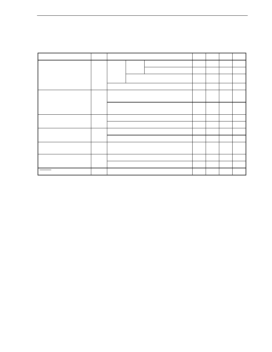
CHAPTER 31 ELECTRICAL SPECIFICATIONS ((A2) GRADE PRODUCTS)
User's Manual U16228EJ2V0UD
513
AC Characteristics
(1) Basic operation
(T
A
=
-
40 to +125
∞
C, 3.3 V
V
DD
= EV
DD
5.5 V, 3.3 V
AV
REF
V
DD
, V
SS
= EV
SS
= AV
SS
= 0 V)
Parameter Symbol
Conditions
MIN.
TYP.
MAX.
Unit
4.0 V
V
DD
5.5 V
0.238
16
µ
s
X1 input
clock
3.3 V
V
DD
< 4.0 V
0.4
16
µ
s
Main
system
clock
operation
Ring-OSC clock
4.04
8.33
16.67
µ
s
Instruction cycle (minimum
instruction execution time)
T
CY
Subsystem
clock
operation
114 122 125
µ
s
4.0 V
V
DD
5.5 V
2/f
sam
+
0.1
Note 2
µ
s
TI000, TI010, TI001
Note 1
,
TI011
Note 1
input high-level width,
low-level width
t
TIH0
,
t
TIL0
3.3 V
V
DD
< 4.0 V
2/f
sam
+
0.2
Note 2
µ
s
4.0 V
V
DD
5.5 V
8.38
MHz
TI50, TI51 input frequency
f
TI5
3.3 V
V
DD
< 4.0 V
5
MHz
4.0 V
V
DD
5.5 V
59.6
ns
TI50, TI51 input high-level width,
low-level width
t
TIH5
,
t
TIL5
3.3 V
V
DD
< 4.0 V
100
ns
Interrupt input high-level width,
low-level width
t
INTH
,
t
INTL
1
µ
s
4.0 V
V
DD
5.5 V
59.6
ns
Key return input low-level width t
KR
3.3 V
V
DD
< 4.0 V
100
ns
RESET low-level width
t
RSL
10
µ
s
Notes 1.
µ
PD780133(A2), 780134(A2), 780136(A2), and 780138(A2) only.
2. Selection
of
f
sam
= f
XP
, f
XP
/4, f
XP
/256, or f
XP
, f
XP
/16, f
XP
/64 is possible using bits 0 and 1 (PRM000, PRM001
or PRM010, PRM011) of prescaler mode registers 00 and 01 (PRM00, PRM01). Note that when selecting
the TI000 or TI001 valid edge as the count clock, f
sam
= f
XP.
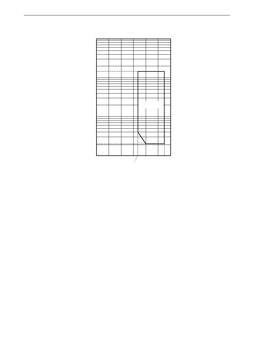
CHAPTER 31 ELECTRICAL SPECIFICATIONS ((A2) GRADE PRODUCTS)
User's Manual U16228EJ2V0UD
514
T
CY
vs. V
DD
(X1 Input Clock Operation)
5.0
1.0
2.0
0.4
0.2
0.1
Supply voltage V
DD
[V]
Cycle time
T
CY
[ s]
0
10.0
1.0
2.0
3.0
4.0
5.0
6.0
5.5
3.3
Guaranteed
operation range
20.0
16.0
0.238
µ

CHAPTER 31 ELECTRICAL SPECIFICATIONS ((A2) GRADE PRODUCTS)
User's Manual U16228EJ2V0UD
515
(2) Serial
interface
(T
A
=
-
40 to +125
∞
C, 3.3 V
V
DD
= EV
DD
5.5 V, 3.3 V
AV
REF
V
DD
, V
SS
= EV
SS
= AV
SS
= 0 V)
(a) UART mode (UART6, dedicated baud rate generator output)
Parameter Symbol
Conditions
MIN.
TYP.
MAX.
Unit
Transfer rate
261.9
kbps
(b) UART mode (UART0, dedicated baud rate generator output)
Parameter Symbol
Conditions
MIN.
TYP.
MAX.
Unit
Transfer rate
261.9
kbps
(c) 3-wire serial I/O mode (master mode, SCK1n... internal clock output)
Parameter Symbol
Conditions
MIN.
TYP.
MAX.
Unit
4.0 V
V
DD
5.5 V
240
ns
SCK1n cycle time
t
KCY1
3.3 V
V
DD
< 4.0 V
400
ns
SCK1n high-/low-level width
t
KH1
,
t
KL1
t
KCY1
/2
-
10
ns
SI1n setup time (to SCK1n
) t
SIK1
30 ns
SI1n hold time (from SCK1n
) t
KSI1
30 ns
Delay time from SCK1n
to
SO1n output
t
KSO1
C = 100 pF
Note
30
ns
Note C is the load capacitance of the SCK1n and SO1n output lines.
(d) 3-wire serial I/O mode (slave mode, SCK1n... external clock input)
Parameter Symbol
Conditions
MIN.
TYP.
MAX.
Unit
SCK1n cycle time
t
KCY2
400
ns
SCK1n high-/low-level width
t
KH2
,
t
KL2
t
KCY2
/2
ns
SI1n setup time (to SCK1n
) t
SIK2
80 ns
SI1n hold time (from SCK1n
) t
KSI2
50 ns
Delay time from SCK1n
to
SO1n output
t
KSO2
C = 100 pF
Note
120
ns
Note C is the load capacitance of the SO1n output line.
Remark n = 0:
µ
PD780131(A2), 780132(A2)
n = 0, 1:
µ
PD780133(A2), 780134(A2), 780136(A2), 780138(A2)

CHAPTER 31 ELECTRICAL SPECIFICATIONS ((A2) GRADE PRODUCTS)
User's Manual U16228EJ2V0UD
516
AC Timing Test Points (Excluding X1 Input)
0.8V
DD
0.2V
DD
Test points
0.8V
DD
0.2V
DD
Clock Timing
X1 input
V
IH6
(MIN.)
V
IL6
(MAX.)
1/f
XP
t
XPL
t
XPH
1/f
XT
t
XTL
t
XTH
XT1 input
V
IH6
(MIN.)
V
IL6
(MAX.)
TI Timing
TI00, TI010, TI001
Note
, TI011
Note
t
TIL0
t
TIH0
TI50, TI51
1/f
TI5
t
TIL5
t
TIH5
Interrupt Request Input Timing
INTP0 to INTP7
t
INTL
t
INTH
Note
µ
PD780133(A2), 780134(A2), 780136(A2), and 780138(A2) only.

CHAPTER 31 ELECTRICAL SPECIFICATIONS ((A2) GRADE PRODUCTS)
User's Manual U16228EJ2V0UD
517
RESET Input Timing
RESET
t
RSL
Serial Transfer Timing
3-wire serial I/O mode:
SI1n
SO1n
t
KCYm
t
KLm
t
KHm
t
SIKm
t
KSIm
Input data
t
KSOm
Output data
SCK1n
Remark m = 1, 2
n = 0:
µ
PD780131(A2), 780132(A2)
n = 0, 1:
µ
PD780133(A2), 780134(A2), 780136(A2), and 780138(A2)
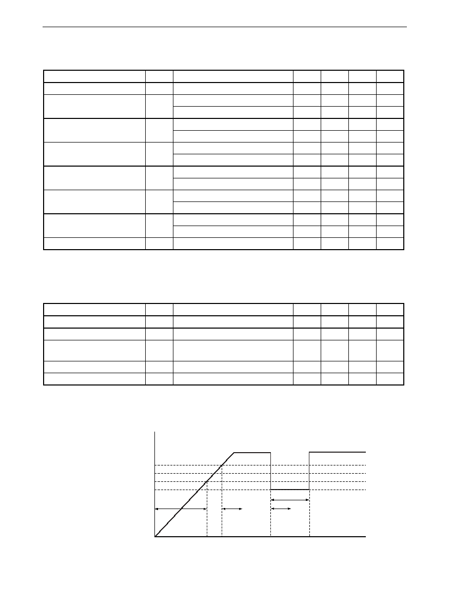
CHAPTER 31 ELECTRICAL SPECIFICATIONS ((A2) GRADE PRODUCTS)
User's Manual U16228EJ2V0UD
518
A/D Converter Characteristics
(T
A
=
-
40 to +125
∞
C, 3.3 V
V
DD
= EV
DD
5.5 V, 3.3 V
AV
REF
V
DD
, V
SS
= EV
SS
= AV
SS
= 0 V)
Parameter Symbol
Conditions
MIN.
TYP.
MAX.
Unit
Resolution
10 10 10 bit
4.0 V
AV
REF
5.5 V
±
0.2
±
0.7 %FSR
Overall error
Notes 1, 2
3.3 V
AV
REF
< 4.0 V
±
0.3
±
0.9 %FSR
4.0 V
AV
REF
5.5
V
16 48
µ
s
Conversion time
t
CONV
3.3 V
AV
REF
< 4.0 V
19
48
µ
s
4.0 V
AV
REF
5.5 V
±
0.7 %FSR
Zero-scale error
Notes 1, 2
3.3 V
AV
REF
< 4.0 V
±
0.9 %FSR
4.0 V
AV
REF
5.5 V
±
0.7 %FSR
Full-scale error
Notes 1, 2
3.3 V
AV
REF
< 4.0 V
±
0.9 %FSR
4.0 V
AV
REF
5.5 V
±
5.5 LSB
Integral non-linearity error
Note 1
3.3 V
AV
REF
< 4.0 V
±
7.5 LSB
4.0 V
AV
REF
5.5 V
±
2.5 LSB
Differential non-linearity error
Note 1
3.3 V
AV
REF
< 4.0 V
±
3.0 LSB
Analog input voltage
V
IAN
AV
SS
AV
REF
V
Notes 1. Excludes quantization error (
±
1/2 LSB).
2. This value is indicated as a ratio (%FSR) to the full-scale value.
POC Circuit Characteristics (T
A
=
-
40 to +125
∞
C)
Parameter Symbol
Conditions
MIN.
TYP.
MAX.
Unit
Detection voltage
V
POC0
Mask option = 3.5 V
3.3
3.5
3.76
V
Power supply rise time
t
PTH
V
DD
: 0 V
3.3 V
0.002
ms
Response delay time 1
Note
t
PTHD
When power supply rises, after reaching
detection voltage (MAX.)
3.0
ms
Response delay time 2
Note
t
PD
When
V
DD
falls
1.0
ms
Minimum pulse width
t
PW
0.2
ms
Note Time required from voltage detection to reset release.
POC Circuit Timing
Supply voltage
(V
DD
)
Time
Detection voltage (MIN.)
Detection voltage (TYP.)
Detection voltage (MAX.)
t
PTH
t
PTHD
t
PW
t
PD
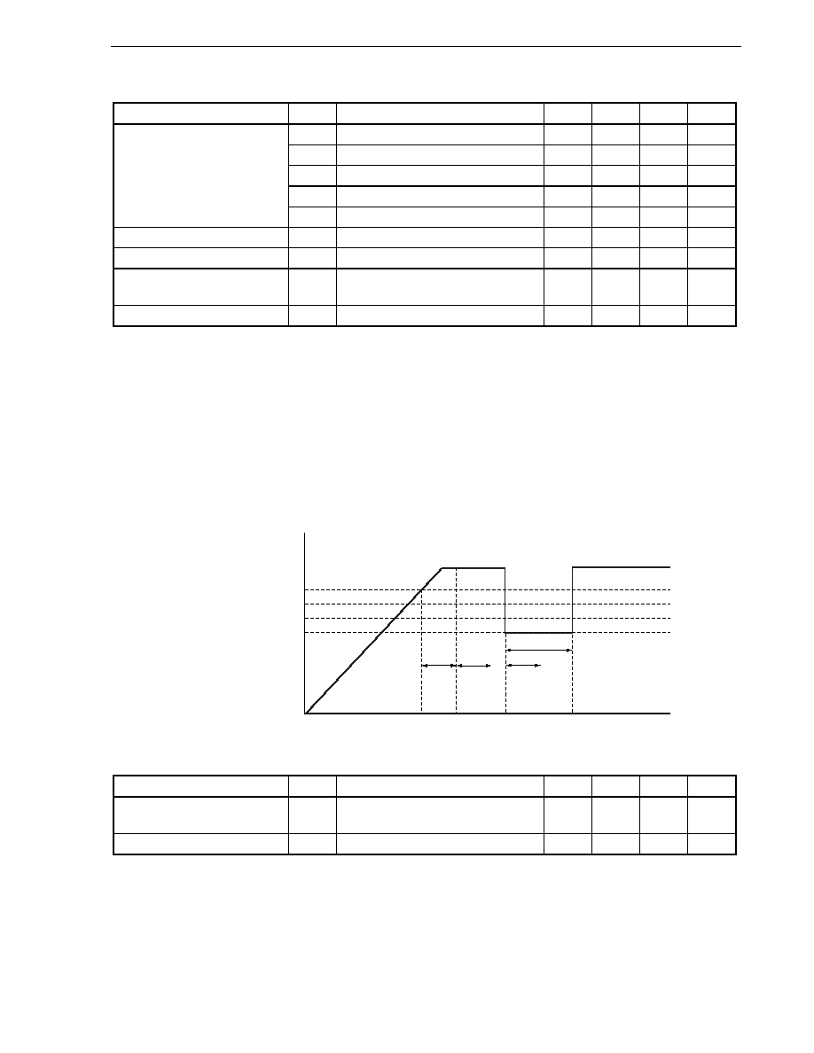
CHAPTER 31 ELECTRICAL SPECIFICATIONS ((A2) GRADE PRODUCTS)
User's Manual U16228EJ2V0UD
519
LVI Circuit Characteristics (T
A
=
-
40 to +125
∞
C)
Parameter Symbol
Conditions
MIN.
TYP.
MAX.
Unit
V
LVI0
4.1 4.3 4.56 V
V
LVI1
3.9 4.1 4.36 V
V
LVI2
3.7 3.9 4.16 V
V
LVI3
3.5 3.7 3.96 V
Detection voltage
V
LVI4
3.3 3.5 3.76 V
Response time
Note 1
t
LD
0.2 2.0 ms
Minimum pulse width
t
LW
0.2
ms
Reference voltage stabilization wait
time
Note 2
t
LWAIT0
0.5
2.0
ms
Operation stabilization wait time
Note 3
t
LWAIT1
0.1
0.2
ms
Notes 1. Time required from voltage detection to interrupt output or internal reset output.
2. Time required from setting LVIE to 1 to reference voltage stabilization when POC-OFF is selected by the
mask option.
3. Time required from setting LVION to 1 to operation stabilization.
Remarks 1. V
LVI0
> V
LVI1
> V
LVI2
> V
LVI3
> V
LVI4
2. V
POCn
< V
LVIm
(n = 0 or 1, m = 0 to 4)
LVI Circuit Timing
Supply voltage
(V
DD
)
Time
Detection voltage (MIN.)
Detection voltage (TYP.)
Detection voltage (MAX.)
t
WAIT0
t
LW
t
LD
t
WAIT1
LVIE
1 LVION
1
Data Memory STOP Mode Low Supply Voltage Data Retention Characteristics (T
A
=
-
40 to +125
∞
C)
Parameter Symbol
Conditions
MIN.
TYP.
MAX.
Unit
Data retention supply voltage
V
DDDR
When POC-OFF is selected by mask
option
2.0 5.5 V
Release signal set time
t
SREL
0
µ
s
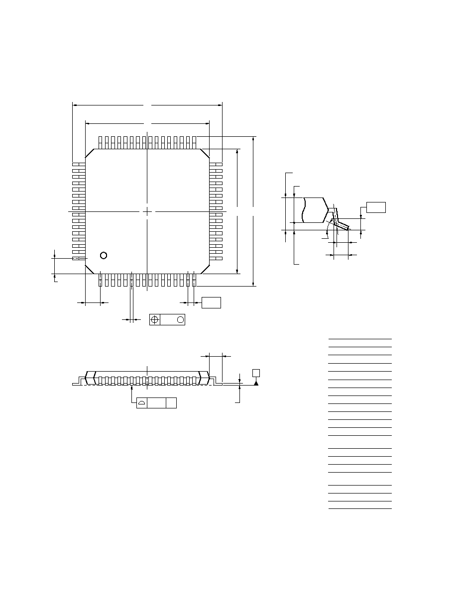
User's Manual U16228EJ2V0UD
520
CHAPTER 32 PACKAGE DRAWINGS
M
48
32
33
64
1
17
16
49
S
N
S
J
detail of lead end
R
K
M
I
S
L
T
P
Q
G
F
H
64-PIN PLASTIC LQFP (10x10)
ITEM
MILLIMETERS
A
B
D
G
12.0
±
0.2
10.0
±
0.2
1.25
12.0
±
0.2
H
0.22
±
0.05
C
10.0
±
0.2
F
1.25
I
J
K
0.08
0.5 (T.P.)
1.0
±
0.2
L
0.5
P
1.4
Q
0.1
±
0.05
T
0.25
S
1.5
±
0.10
U
0.6
±
0.15
S64GB-50-8EU-2
R
3
∞+
4
∞
-
3
∞
N
0.08
M
0.17
+
0.03
-
0.07
A
B
C
D
U
NOTE
Each lead centerline is located within 0.08 mm of
its true position (T.P.) at maximum material condition.

CHAPTER 32 PACKAGE DRAWINGS
User's Manual U16228EJ2V0UD
521
64-PIN PLASTIC LQFP (14x14)
NOTE
Each lead centerline is located within 0.20 mm of
its true position (T.P.) at maximum material condition.
ITEM
MILLIMETERS
A
B
D
G
17.2
±
0.2
14.0
±
0.2
0.8 (T.P.)
1.0
J
17.2
±
0.2
K
C
14.0
±
0.2
I
0.20
1.6
±
0.2
L
0.8
F
1.0
N
P
Q
0.10
1.4
±
0.1
0.127
±
0.075
U
0.886
±
0.15
R
S
3
∞
1.7 MAX.
T
0.25
P64GC-80-8BS
H
0.37
+
0.08
-
0.07
M
0.17
+
0.03
-
0.06
S
N
J
T
detail of lead end
C
D
A
B
K
M
I
S
P
R
L
U
Q
G
F
M
H
+
4
∞
-
3
∞
1
64
49
17
32
16
48
33
S
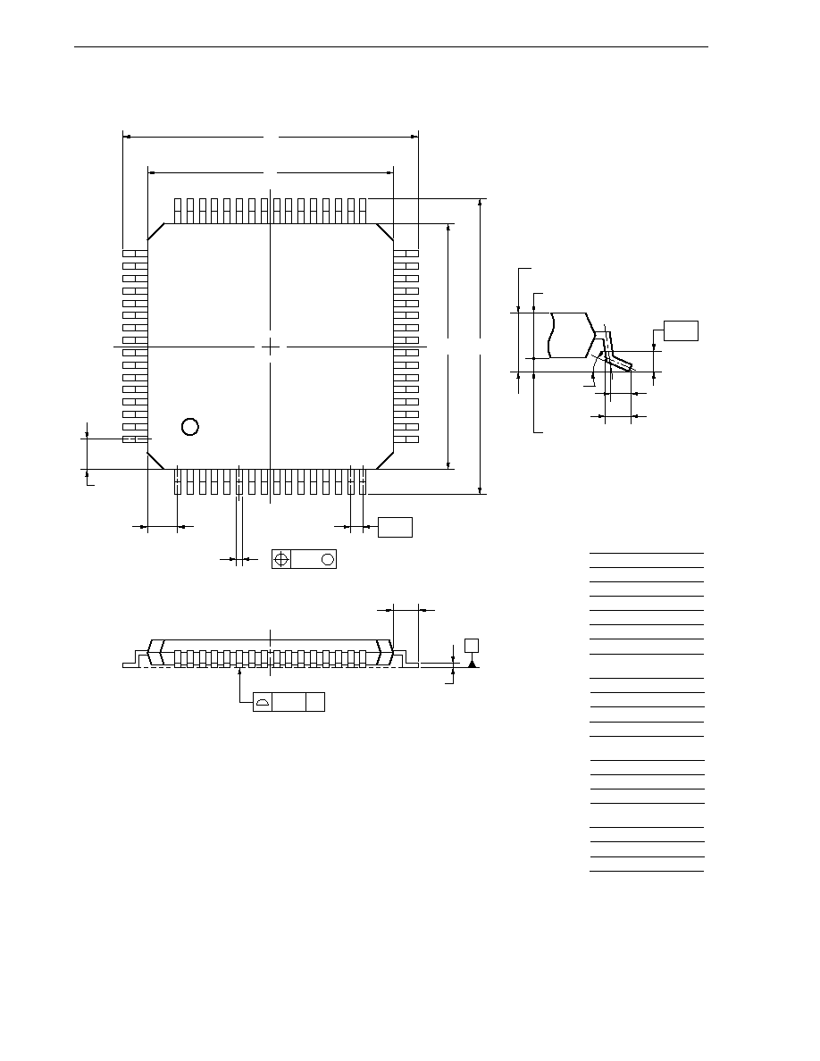
CHAPTER 32 PACKAGE DRAWINGS
User's Manual U16228EJ2V0UD
522
48
32
33
64
1
17
16
49
S
S
64-PIN PLASTIC TQFP (12x12)
ITEM
MILLIMETERS
G
1.125
A
14.0
±
0.2
C
12.0
±
0.2
D
F
1.125
14.0
±
0.2
B
12.0
±
0.2
N
0.10
P
Q
0.1
±
0.05
1.0
S
R
3
∞+
4
∞
-
3
∞
R
H
K
J
Q
G
I
S
P
detail of lead end
NOTE
Each lead centerline is located within 0.13 mm of
its true position (T.P.) at maximum material condition.
M
H
0.32
+
0.06
-
0.10
I
0.13
J
K
1.0
±
0.2
0.65 (T.P.)
L
0.5
M
0.17
+
0.03
-
0.07
P64GK-65-9ET-3
T
U
0.6
±
0.15
0.25
F
M
A
B
C
D
N
T
L
U
1.1
±
0.1

User's Manual U16228EJ2V0UD
523
CHAPTER 33 RECOMMENDED SOLDERING CONDITIONS
These products should be soldered and mounted under the following recommended conditions.
For soldering methods and conditions other than those recommended below, please contact an NEC Electronics
sales representative.
For technical information, see the following website.
Semiconductor Device Mount Manual (http://www.necel.com/pkg/en/mount/index.html)
Table 33-1. Surface Mounting Type Soldering Conditions (1/6)
(1) Mask ROM version (GB-8EU type)
64-pin plastic LQFP (10
◊
10)
µ
PD780131GB-
◊◊◊
-8EU, 780132GB-
◊◊◊
-8EU, 780133GB-
◊◊◊
-8EU,
µ
PD780134GB-
◊◊◊
-8EU, 780136GB-
◊◊◊
-8EU, 780138GB-
◊◊◊
-8EU,
µ
PD780131GB(A)-
◊◊◊
-8EU, 780132GB(A)-
◊◊◊
-8EU, 780133GB(A)-
◊◊◊
-8EU,
µ
PD780134GB(A)-
◊◊◊
-8EU, 780136GB(A)-
◊◊◊
-8EU, 780138GB(A)-
◊◊◊
-8EU,
µ
PD780131GB(A1)-
◊◊◊
-8EU, 780132GB(A1)-
◊◊◊
-8EU, 780133GB(A1)-
◊◊◊
-8EU,
µ
PD780134GB(A1)-
◊◊◊
-8EU, 780136GB(A1)-
◊◊◊
-8EU, 780138GB(A1)-
◊◊◊
-8EU,
µ
PD780131GB(A2)-
◊◊◊
-8EU, 780132GB(A2)-
◊◊◊
-8EU, 780133GB(A2)-
◊◊◊
-8EU,
µ
PD780134GB(A2)-
◊◊◊
-8EU, 780136GB(A2)-
◊◊◊
-8EU, 780138GB(A2)-
◊◊◊
-8EU
Soldering Method
Soldering Conditions
Recommended
Condition Symbol
Infrared reflow
Package peak temperature: 235
∞
C, Time: 30 seconds max. (at 210
∞
C or higher),
Count: Twice or less, Exposure limit: 7 days
Note
(after that, prebake at 125
∞
C for 10
hours)
IR35-107-2
VPS
Package peak temperature: 215
∞
C, Time: 40 seconds max. (at 200
∞
C or higher),
Count: Twice or less, Exposure limit: 7 days
Note
(after that, prebake at 125
∞
C for 10
hours)
VP15-107-2
Partial heating
Pin temperature: 300
∞
C max., Time: 3 seconds max. (per pin row)
-
Note After opening the dry pack, store it at 25
∞
C or less and 65% RH or less for the allowable storage period.
Caution Do not use different soldering methods together (except for partial heating).

CHAPTER 33 RECOMMENDED SOLDERING CONDITIONS
User's Manual U16228EJ2V0UD
524
Table 33-1. Surface Mounting Type Soldering Conditions (2/6)
(2) Mask ROM version (GC-8BS type)
64-pin plastic LQFP (14
◊
14)
µ
PD780131GC-
◊◊◊
-8BS, 780132GC-
◊◊◊
-8BS, 780133GC-
◊◊◊
-8BS,
µ
PD780134GC-
◊◊◊
-8BS, 780136GC-
◊◊◊
-8BS, 780138GC-
◊◊◊
-8BS,
µ
PD780131GC(A)-
◊◊◊
-8BS, 780132GC(A)-
◊◊◊
-8BS, 780133GC(A)-
◊◊◊
-8BS,
µ
PD780134GC(A)-
◊◊◊
-8BS, 780136GC(A)-
◊◊◊
-8BS, 780138GC(A)-
◊◊◊
-8BS,
µ
PD780131GC(A1)-
◊◊◊
-8BS, 780132GC(A1)-
◊◊◊
-8BS, 780133GC(A1)-
◊◊◊
-8BS,
µ
PD780134GC(A1)-
◊◊◊
-8BS, 780136GC(A1)-
◊◊◊
-8BS, 780138GC(A1)-
◊◊◊
-8BS,
µ
PD780131GC(A2)-
◊◊◊
-8BS, 780132GC(A2)-
◊◊◊
-8BS, 780133GC(A2)-
◊◊◊
-8BS,
µ
PD780134GC(A2)-
◊◊◊
-8BS, 780136GC(A2)-
◊◊◊
-8BS, 780138GC(A2)-
◊◊◊
-8BS
Soldering Method
Soldering Conditions
Recommended
Condition Symbol
Infrared reflow
Package peak temperature: 235
∞
C, Time: 30 seconds max. (at 210
∞
C or higher),
Count: Twice or less, Exposure limit: 3 days
Note
(after that, prebake at 125
∞
C for 10
hours)
IR35-103-2
VPS
Package peak temperature: 215
∞
C, Time: 40 seconds max. (at 200
∞
C or higher),
Count: Twice or less, Exposure limit: 3 days
Note
(after that, prebake at 125
∞
C for 10
hours)
VP15-103-2
Wave soldering
Solder bath temperature: 260
∞
C max., Time: 10 seconds max., Count: Once,
Preheating temperature: 120
∞
C max. (package surface temperature), Exposure
limit: 3 days
Note
(after that, prebake at 125
∞
C for 10 hours)
WS60-103-1
Partial heating
Pin temperature: 300
∞
C max., Time: 3 seconds max. (per pin row)
-
Note After opening the dry pack, store it at 25
∞
C or less and 65% RH or less for the allowable storage period.
Caution Do not use different soldering methods together (except for partial heating).

CHAPTER 33 RECOMMENDED SOLDERING CONDITIONS
User's Manual U16228EJ2V0UD
525
Table 33-1. Surface Mounting Type Soldering Conditions (3/6)
(3) Mask ROM version (GK-9ET type)
64-pin plastic TQFP (12
◊
12)
µ
PD780131GK-
◊◊◊
-9ET, 780132GK-
◊◊◊
-9ET, 780133GK-
◊◊◊
-9ET,
µ
PD780134GK-
◊◊◊
-9ET, 780136GK-
◊◊◊
-9ET, 780138GK-
◊◊◊
-9ET,
µ
PD780131GK(A)-
◊◊◊
-9ET, 780132GK(A)-
◊◊◊
-9ET, 780133GK(A)-
◊◊◊
-9ET,
µ
PD780134GK(A)-
◊◊◊
-9ET, 780136GK(A)-
◊◊◊
-9ET, 780138GK(A)-
◊◊◊
-9ET,
µ
PD780131GK(A1)-
◊◊◊
-9ET, 780132GK(A1)-
◊◊◊
-9ET, 780133GK(A1)-
◊◊◊
-9ET,
µ
PD780134GK(A1)-
◊◊◊
-9ET, 780136GK(A1)-
◊◊◊
-9ET, 780138GK(A1)-
◊◊◊
-9ET,
µ
PD780131GK(A2)-
◊◊◊
-9ET, 780132GK(A2)-
◊◊◊
-9ET, 780133GK(A2)-
◊◊◊
-9ET,
µ
PD780134GK(A2)-
◊◊◊
-9ET, 780136GK(A2)-
◊◊◊
-9ET, 780138GK(A2)-
◊◊◊
-9ET
Soldering Method
Soldering Conditions
Recommended
Condition Symbol
Infrared reflow
Package peak temperature: 235
∞
C, Time: 30 seconds max. (at 210
∞
C or higher),
Count: Twice or less, Exposure limit: 7 days
Note
(after that, prebake at 125
∞
C for 10
hours)
IR35-107-2
VPS
Package peak temperature: 215
∞
C, Time: 40 seconds max. (at 200
∞
C or higher),
Count: Twice or less, Exposure limit: 7 days
Note
(after that, prebake at 125
∞
C for 10
hours)
VP15-107-2
Wave soldering
Solder bath temperature: 260
∞
C max., Time: 10 seconds max., Count: Once,
Preheating temperature: 120
∞
C max. (package surface temperature), Exposure
limit: 7 days
Note
(after that, prebake at 125
∞
C for 10 hours)
WS60-107-1
Partial heating
Pin temperature: 300
∞
C max., Time: 3 seconds max. (per pin row)
-
Note After opening the dry pack, store it at 25
∞
C or less and 65% RH or less for the allowable storage period.
Caution Do not use different soldering methods together (except for partial heating).

CHAPTER 33 RECOMMENDED SOLDERING CONDITIONS
User's Manual U16228EJ2V0UD
526
Table 33-1. Surface Mounting Type Soldering Conditions (4/6)
(4) Flash memory version (GB-8EU type)
64-pin plastic LQFP (10
◊
10)
µ
PD78F0134M1GB-8EU, 78F0134M2GB-8EU, 78F0134M3GB-8EU,
µ
PD78F0134M4GB-8EU, 78F0134M5GB-8EU, 78F0134M6GB-8EU,
µ
PD78F0134M1GB(A)-8EU, 78F0134M2GB(A)-8EU, 78F0134M3GB(A)-8EU,
µ
PD78F0134M4GB(A)-8EU, 78F0134M5GB(A)-8EU, 78F0134M6GB(A)-8EU,
µ
PD8F0134M1GB(A1)-8EU, 78F0134M2GB(A1)-8EU, 78F0134M5GB(A1)-8EU, 78F0134M6GB(A1)-8EU,
µ
PD78F0138M1GB-8EU, 78F0138M2GB-8EU, 78F0138M3GB-8EU,
µ
PD78F0138M4GB-8EU, 78F0138M5GB-8EU, 78F0138M6GB-8EU,
µ
PD78F0138M1GB(A)-8EU, 78F0138M2GB(A)-8EU, 78F0138M3GB(A)-8EU,
µ
PD78F0138M4GB(A)-8EU, 78F0138M5GB(A)-8EU, 78F0138M6GB(A)-8EU,
µ
PD78F0138M1GB(A1)-8EU, 78F0138M2GB(A1)-8EU, 78F0138M5GB(A1)-8EU, 78F0138M6GB(A1)-8EU
Soldering Method
Soldering Conditions
Recommended
Condition Symbol
Infrared reflow
Package peak temperature: 235
∞
C, Time: 30 seconds max. (at 210
∞
C or higher),
Count: Twice or less, Exposure limit: 3 days
Note
(after that, prebake at 125
∞
C for 10
hours)
IR35-103-2
VPS
Package peak temperature: 215
∞
C, Time: 40 seconds max. (at 200
∞
C or higher),
Count: Twice or less, Exposure limit: 3 days
Note
(after that, prebake at 125
∞
C for 10
hours)
VP15-103-2
Partial heating
Pin temperature: 300
∞
C max., Time: 3 seconds max. (per pin row)
-
Note After opening the dry pack, store it at 25
∞
C or less and 65% RH or less for the allowable storage period.
Caution Do not use different soldering methods together (except for partial heating).

CHAPTER 33 RECOMMENDED SOLDERING CONDITIONS
User's Manual U16228EJ2V0UD
527
Table 33-1. Surface Mounting Type Soldering Conditions (5/6)
(5) Flash memory version (GC-8BS type)
64-pin plastic LQFP (14
◊
14)
µ
PD78F0134M1GC-8BS, 78F0134M2GC-8BS, 78F0134M3GC-8BS,
µ
PD78F0134M4GC-8BS, 78F0134M5GC-8BS, 78F0134M6GC-8BS,
µ
PD78F0134M1GC(A)-8BS, 78F0134M2GC(A)-8BS, 78F0134M3GC(A)-8BS,
µ
PD78F0134M4GC(A)-8BS, 78F0134M5GC(A)-8BS, 78F0134M6GC(A)-8BS,
µ
PD78F0134M1GC(A1)-8BS, 78F0134M2GC(A1)-8BS, 78F0134M5GC(A1)-8BS, 78F0134M6GC(A1)-8BS,
µ
PD78F0138M1GC-8BS, 78F0138M2GC-8BS, 78F0138M3GC-8BS,
µ
PD78F0138M4GC-8BS, 78F0138M5GC-8BS, 78F0138M6GC-8BS,
µ
PD78F0138M1GC(A)-8BS, 78F0138M2GC(A)-8BS, 78F0138M3GC(A)-8BS,
µ
PD78F0138M4GC(A)-8BS, 78F0138M5GC(A)-8BS, 78F0138M6GC(A)-8BS,
µ
PD78F0138M1GC(A1)-8BS, 78F0138M2GC(A1)-8BS, 78F0138M5GC(A1)-8BS, 78F0138M6GC(A1)-8BS
Soldering Method
Soldering Conditions
Recommended
Condition Symbol
Infrared reflow
Package peak temperature: 235
∞
C, Time: 30 seconds max. (at 210
∞
C or higher),
Count: Twice or less, Exposure limit: 3 days
Note
(after that, prebake at 125
∞
C for 10
hours)
IR35-103-2
VPS
Package peak temperature: 215
∞
C, Time: 40 seconds max. (at 200
∞
C or higher),
Count: Twice or less, Exposure limit: 3 days
Note
(after that, prebake at 125
∞
C for 10
hours)
VP15-103-2
Wave soldering
Solder bath temperature: 260
∞
C max., Time: 10 seconds max., Count: Once,
Preheating temperature: 120
∞
C max. (package surface temperature), Exposure
limit: 3 days
Note
(after that, prebake at 125
∞
C for 10 hours)
WS60-103-1
Partial heating
Pin temperature: 300
∞
C max., Time: 3 seconds max. (per pin row)
-
Note After opening the dry pack, store it at 25
∞
C or less and 65% RH or less for the allowable storage period.
Caution Do not use different soldering methods together (except for partial heating).

CHAPTER 33 RECOMMENDED SOLDERING CONDITIONS
User's Manual U16228EJ2V0UD
528
Table 33-1. Surface Mounting Type Soldering Conditions (6/6)
(6) Flash memory version (GK-9ET type)
64-pin plastic TQFP (12
◊
12)
µ
PD78F0134M1GK-9ET, 78F0134M2GK-9ET, 78F0134M3GK-9ET,
µ
PD78F0134M4GK-9ET, 78F0134M5GK-9ET, 78F0134M6GK-9ET,
µ
PD78F0134M1GK(A)-9ET, 78F0134M2GK(A)-9ET, 78F0134M3GK(A)-9ET,
µ
PD78F0134M4GK(A)-9ET, 78F0134M5GK(A)-9ET, 78F0134M6GK(A)-9ET,
µ
PD78F0134M1GK(A1)-9ET, 78F0134M2GK(A1)-9ET, 78F0134M5GK(A1)-9ET, 78F0134M6GK(A1)-9ET,
µ
PD78F0138M1GK-9ET, 78F0138M2GK-9ET, 78F0138M3GK-9ET,
µ
PD78F0138M4GK-9ET, 78F0138M5GK-9ET, 78F0138M6GK-9ET,
µ
PD78F0138M1GK(A)-9ET, 78F0138M2GK(A)-9ET, 78F0138M3GK(A)-9ET,
µ
PD78F0138M4GK(A)-9ET, 78F0138M5GK(A)-9ET, 78F0138M6GK(A)-9ET,
µ
PD78F0138M1GK(A1)-9ET, 78F0138M2GK(A1)-9ET, 78F0138M5GK(A1)-9ET, 78F0138M6GK(A1)-9ET
Soldering Method
Soldering Conditions
Recommended
Condition Symbol
Infrared reflow
Package peak temperature: 235
∞
C, Time: 30 seconds max. (at 210
∞
C or higher),
Count: Twice or less, Exposure limit: 3 days
Note
(after that, prebake at 125
∞
C for 10
hours)
IR35-103-2
VPS
Package peak temperature: 215
∞
C, Time: 40 seconds max. (at 200
∞
C or higher),
Count: Twice or less, Exposure limit: 3 days
Note
(after that, prebake at 125
∞
C for 10
hours)
VP15-103-2
Wave soldering
Solder bath temperature: 260
∞
C max., Time: 10 seconds max., Count: Once,
Preheating temperature: 120
∞
C max. (package surface temperature), Exposure
limit: 3 days
Note
(after that, prebake at 125
∞
C for 10 hours)
WS60-103-1
Partial heating
Pin temperature: 300
∞
C max., Time: 3 seconds max. (per pin row)
-
Note After opening the dry pack, store it at 25
∞
C or less and 65% RH or less for the allowable storage period.
Caution Do not use different soldering methods together (except for partial heating).

User's Manual U16228EJ2V0UD
529
CHAPTER 34 CAUTIONS FOR WAIT
34.1 Cautions for Wait
This product has two internal system buses.
One is a CPU bus and the other is a peripheral bus that interfaces with the low-speed peripheral hardware.
Because the clock of the CPU bus and the clock of the peripheral bus are asynchronous, unexpected illegal data
may be passed if an access to the CPU conflicts with an access to the peripheral hardware.
When accessing the peripheral hardware that may cause a conflict, therefore, the CPU repeatedly executes
processing, until the correct data is passed.
As a result, the CPU does not start the next instruction processing but waits. If this happens, the number of
execution clocks of an instruction increases by the number of wait clocks (for the number of wait clocks, refer to Table
34-1). This must be noted when real-time processing is performed.
CHAPTER 34 CAUTIONS FOR WAIT
User's Manual U16228EJ2V0UD
530
34.2 Peripheral Hardware That Generates Wait
Table 34-1 lists the registers that issue a wait request when accessed by the CPU, and the number of CPU wait
clocks.
Table 34-1. Registers That Generate Wait and Number of CPU Wait Clocks
Peripheral Hardware
Register
Access
Number of Wait Clocks
Watchdog timer
WDTM
Write
3 clocks (fixed)
Serial interface UART0
ASIS0
Read
1 clock (fixed)
Serial interface UART6
ASIS6
Read
1 clock (fixed)
ADM Write
ADS Write
PFM Write
PFT Write
2 to 5 clocks
Note
(when ADM.5 flag = "1")
2 to 9 clocks
Note
(when ADM.5 flag = "0")
ADCR Read 1 to 5 clocks
(when ADM.5 flag = "1")
1 to 9 clocks
(when ADM.5 flag = "0")
A/D converter
<Calculating maximum number of wait clocks>
{(1/f
MACRO
)
◊
2/(1/f
CPU
)} + 1
*The result after the decimal point is truncated if it is less than t
CPUL
after it has been multiplied by
(1/f
CPU
), and is rounded up if it exceeds t
CPUL
.
f
MACRO
:
Macro operating frequency
(When bit 5 (FR2) of ADM = "1": f
X
/2, when bit 5 (FR2) of ADM = "0": f
X
/2
2
)
f
CPU
:
CPU clock frequency
t
CPUL
:
Low-level width of CPU clock
Note No wait cycle is generated for the CPU if the number of wait clocks calculated by the above expression is 1.
Caution When the CPU is operating on the subsystem clock and the X1 input clock is stopped (MCC = 1), do
not access the registers listed above using an access method in which a wait request is issued.
Remark The clock is the CPU clock (f
CPU
).

CHAPTER 34 CAUTIONS FOR WAIT
User's Manual U16228EJ2V0UD
531
34.3 Example of Wait Occurrence
<1> Watchdog timer
<On execution of MOV WDTM, A>
Number of execution clocks: 8
(5 clocks when data is written to a register that does not issue a wait (MOV sfr, A).)
<On execution of MOV WDTM, #byte>
Number of execution clocks: 10
(7 clocks when data is written to a register that does not issue a wait (MOV sfr, #byte).)
<2> Serial interface UART6
<On execution of MOV A, ASIS6>
Number of execution clocks: 6
(5 clocks when data is read from a register that does not issue a wait (MOV A, sfr).)
<3> A/D converter
Table 34-2. Number of Wait Clocks and Number of Execution Clocks on Occurrence of Wait (A/D Converter)
<On execution of MOV ADM, A; MOV ADS, A; or MOV A, ADCR>
∑
When f
X
= 10 MHz, t
CPUL
= 50 ns
Value of Bit 5 (FR2)
of ADM Register
f
CPU
Number of Wait Clocks
Number of Execution Clocks
f
X
9 clocks
14 clocks
f
X
/2
5 clocks
10 clocks
f
X
/2
2
3 clocks
8 clocks
f
X
/2
3
2 clocks
7 clocks
0
f
X
/2
4
0 clocks (1 clock
Note
)
5 clocks (6 clocks
Note
)
f
X
5 clocks
10 clocks
f
X
/2
3 clocks
8 clocks
f
X
/2
2
2 clocks
7 clocks
f
X
/2
3
0 clocks (1 clock
Note
)
5 clocks (6 clocks
Note
)
1
f
X
/2
4
0 clocks (1 clock
Note
)
5 clocks (6 clocks
Note
)
Note On execution of MOV A, ADCR
Remark The clock is the CPU clock (f
CPU
).
f
X
:
X1 input clock frequency
t
CPUL
: Low-level width of CPU clock

User's Manual U16228EJ2V0UD
532
APPENDIX A DEVELOPMENT TOOLS
The following development tools are available for the development of systems that employ the 78K0/KE1.
Figure A-1 shows the development tool configuration.
∑
Support for PC98-NX series
Unless otherwise specified, products supported by IBM PC/AT
TM
compatibles are compatible with PC98-NX
series computers. When using PC98-NX series computers, refer to the explanation for IBM PC/AT compatibles.
∑
Windows
Unless otherwise specified, "Windows" means the following OSs.
∑
Windows
3.1
∑
Windows 95, 98, 2000
∑
Windows
NT
TM
Ver 4.0
APPENDIX A DEVELOPMENT TOOLS
User's Manual U16228EJ2V0UD
533
Figure A-1. Development Tool Configuration (1/2)
(1) When using the in-circuit emulators IE-78K0-NS, IE-78K0-NS-A
Language processing software
∑ Assembler package
∑ C compiler package
∑ Device file
∑ C library source file
Note 1
Debugging software
∑ Integrated debugger
∑ System simulator
Host machine (PC or EWS)
Interface adapter,
PC card interface, etc.
In-circuit emulator
Note 3
Emulation board
Emulation probe
Conversion socket or
conversion adapter
Target system
Flash programmer
Flash memory
write adapter
Flash memory
∑ Software package
∑ Project manager
(Windows only)
Note 2
Software package
Flash memory
write environment
Control software
Embedded software
∑ Real-time OS
Performance board
Power supply unit
Notes 1. The C library source file is not included in the software package.
2. The project manager is included in the assembler package.
The project manager is only used for Windows.
3. Products other than in-circuit emulators IE-78K0-NS and IE-78K0-NS-A are all sold separately.

APPENDIX A DEVELOPMENT TOOLS
User's Manual U16228EJ2V0UD
534
Figure A-1. Development Tool Configuration (2/2)
(2) When using the in-circuit emulator IE-78K0K1-ET
Language processing software
∑ Assembler package
∑ C compiler package
∑ Device file
∑ C library source file
Note 1
Debugging software
∑ Integrated debugger
∑ System simulator
Host machine (PC or EWS)
Interface adapter,
PC card interface, etc.
In-circuit emulator
Note 3
Emulation probe
Conversion socket or
conversion adapter
Target system
Flash programmer
Flash memory
write adapter
Flash memory
∑ Software package
∑ Project manager
(Windows only)
Note 2
Software package
Flash memory
write environment
Control software
Embedded software
∑ Real-time OS
Power supply unit
Notes 1. The C library source file is not included in the software package.
2. The project manager is included in the assembler package.
The project manager is only used for Windows.
3. In-circuit emulator IE-78K0K1-ET is supplied with integrated debugger ID78K0-NS, a device file, power
supply unit, and PCI bus interface adapter IE-70000-PCI-IF-A. Any other products are sold separately.

APPENDIX A DEVELOPMENT TOOLS
User's Manual U16228EJ2V0UD
535
A.1 Software Package
Development tools (software) common to the 78K/0 Series are combined in this package.
SP78K0
78K/0 Series software package
Part number:
µ
S
◊◊◊◊
SP78K0
Remark
◊◊◊◊
in the part number differs depending on the host machine and OS used.
µ
S
◊◊◊◊
SP78K0
◊◊◊◊
Host Machine
OS
Supply Medium
AB17 Windows
(Japanese
version)
BB17
PC-9800 series,
IBM PC/AT compatibles
Windows (English version)
CD-ROM
A.2 Language Processing Software
This assembler converts programs written in mnemonics into object codes executable
with a microcontroller.
This assembler is also provided with functions capable of automatically creating symbol
tables and branch instruction optimization.
This assembler should be used in combination with a device file (DF780138) (sold
separately).
<Precaution when using RA78K0 in PC environment>
This assembler package is a DOS-based application. It can also be used in Windows,
however, by using the Project Manager (included in assembler package) on Windows.
RA78K0
Assembler package
Part number:
µ
S
◊◊◊◊
RA78K0
This compiler converts programs written in C language into object codes executable with
a microcontroller.
This compiler should be used in combination with an assembler package and device file
(both sold separately).
<Precaution when using CC78K0 in PC environment>
This C compiler package is a DOS-based application. It can also be used in Windows,
however, by using the Project Manager (included in assembler package) on Windows.
CC78K0
C compiler package
Part number:
µ
S
◊◊◊◊
CC78K0
This file contains information peculiar to the device.
This device file should be used in combination with a tool (RA78K0, CC78K0, SM78K0,
ID78K0-NS, and ID78K0) (all sold separately).
The corresponding OS and host machine differ depending on the tool to be used (all sold
separately).
DF780138
Note 1
Device file
Part number:
µ
S
◊◊◊◊
DF780138
This is a source file of the functions that configure the object library included in the C
compiler package (CC78K0).
This file is required to match the object library included in the C compiler package to the
user's specifications.
CC78K/0-L
Note 2
C library source file
Part number:
µ
S
◊◊◊◊
CC78K0-L
Notes 1. The DF780138 can be used in common with the RA78K0, CC78K0, SM78K0, ID78K0-NS, and
ID78K0.
2. The CC78K0-L is not included in the software package (SP78K0).

APPENDIX A DEVELOPMENT TOOLS
User's Manual U16228EJ2V0UD
536
Remark
◊◊◊◊
in the part number differs depending on the host machine and OS used.
µ
S
◊◊◊◊
RA78K0
µ
S
◊◊◊◊
CC78K0
◊◊◊◊
Host Machine
OS
Supply Medium
AB13 Windows
(Japanese
version)
BB13
Windows (English version)
3.5-inch 2HD FD
AB17 Windows
(Japanese
version)
BB17
PC-9800 series,
IBM PC/AT compatibles
Windows (English version)
3P17 HP9000
series
700
TM
HP-UX
TM
(Rel. 10.10)
3K17 SPARCstation
TM
SunOS
TM
(Rel. 4.1.4)
Solaris
TM
(Rel. 2.5.1)
CD-ROM
µ
S
◊◊◊◊
DF780138
µ
S
◊◊◊◊
CC78K0-L
◊◊◊◊
Host Machine
OS
Supply Medium
AB13 Windows
(Japanese
version)
BB13
PC-9800 series,
IBM PC/AT compatibles
Windows (English version)
3.5-inch 2HD FD
3P16
HP9000 series 700
HP-UX (Rel. 10.10)
DAT
3K13
3.5-inch 2HD FD
3K15
SPARCstation
SunOS (Rel. 4.1.4)
Solaris (Rel. 2.5.1)
1/4-inch CGMT
A.3 Control Software
Project manager
This is control software designed to enable efficient user program development in the
Windows environment. All operations used in development of a user program, such as
starting the editor, building, and starting the debugger, can be performed from the project
manager.
<Caution>
The project manager is included in the assembler package (RA78K0).
It can only be used in Windows.
A.4 Flash Memory Writing Tools
Flashpro III
(part number: FL-PR3, PG-FP3)
Flashpro IV
(part number: FL-PR4, PG-FP4)
Flash programmer
Flash programmer dedicated to microcontrollers with on-chip flash memory.
FA-64GB-8EU
FA-64GC-8BS
FA-64GK-9ET
Flash memory writing adapter
Flash memory writing adapter used connected to the Flashpro III/Flashpro IV.
∑
FA-64GB-8EU: For 64-pin plastic LQFP (GB-8EU type)
∑
FA-64GC-8BS: For 64-pin plastic LQFP (GC-8BS type)
∑
FA-64GK-9ET: For 64-pin plastic TQFP (GK-9ET type)
Remark FL-PR3, FL-PR4, FA-64GB-8EU, FA-64GC-8BS, and FA-64GK-9ET are products of Naito Densei
Machida Mfg. Co., Ltd.
TEL: +81-45-475-4191 Naito Densei Machida Mfg. Co., Ltd.
APPENDIX A DEVELOPMENT TOOLS
User's Manual U16228EJ2V0UD
537
A.5 Debugging Tools (Hardware)
A.5.1 When using in-circuit emulators IE-78K0-NS and IE-78K0-NS-A
IE-78K0-NS
In-circuit emulator
The in-circuit emulator serves to debug hardware and software when developing
application systems using a 78K/0 Series product. It corresponds to the integrated
debugger (ID78K0-NS). This emulator should be used in combination with a power
supply unit, emulation probe, and the interface adapter required to connect this emulator
to the host machine.
IE-78K0-NS-PA
Performance board
This board is connected to the IE-78K0-NS to expand its functions. Adding this board
adds a coverage function and enhances debugging functions such as tracer and timer
functions.
IE-78K0-NS-A
In-circuit emulator
Product that combines the IE-78K0-NS and IE-78K0-NS-PA
IE-70000-MC-PS-B
Power supply unit
This adapter is used for supplying power from a 100 V to 240 V AC outlet.
IE-70000-98-IF-C
Interface adapter
This adapter is required when using a PC-9800 series computer (except notebook type)
as the host machine (C bus compatible).
IE-70000-CD-IF-A
PC card interface
This is PC card and interface cable required when using a notebook-type computer as
the host machine (PCMCIA socket compatible).
IE-70000-PC-IF-C
Interface adapter
This adapter is required when using an IBM PC compatible computer as the host
machine (ISA bus compatible).
IE-70000-PCI-IF-A
Interface adapter
This adapter is required when using a computer with a PCI bus as the host machine.
IE-780148-NS-EM1
Emulation board
This board emulates the operations of the peripheral hardware peculiar to a device. It
should be used in combination with an in-circuit emulator.
NP-64GB-TQ
NP-H64GB-TQ
Emulation probe
This emulation probe is used to connect the in-circuit emulator and target system, and is
designed for a 64-pin plastic LQFP (GB-8EU type).
TGB-064SDP
Conversion adapter
This conversion adapter is used to connect the NP-64GB-TQ or NP-H64GB-TQ and
target system board to which a 64-pin plastic LQFP (GB-8EU type) can be connected.
NP-64GC-TQ
NP-H64GC-TQ
Emulation probe
This emulation probe is used to connect the in-circuit emulator and target system, and is
designed for a 64-pin plastic LQFP (GC-8BS type).
TGC-064SAP
Conversion adapter
This conversion adapter is used to connect the NP-64GC-TQ or NP-H64GC-TQ and
target system board to which a 64-pin plastic LQFP (GC-8BS type) can be connected.
NP-64GK
NP-H64GK-TQ
Emulation probe
This emulation probe is used to connect the in-circuit emulator and target system, and is
designed for a 64-pin plastic TQFP (GK-9ET type).
TGK-064SBW
Conversion adapter
This conversion adapter is used to connect the NP-64GK or NP-H64GK-TQ and target
system board to which a 64-pin plastic TQFP (GK-9ET type) can be connected.
Remarks 1. NP-64GB-TQ, NP-H64GB-TQ, NP-64GC-TQ, NP-H64GC-TQ, NP-64GK, and NP-H64GK-TQ are
products of Naito Densei Machida Mfg. Co., Ltd.
TEL: +81-45-475-4191 Naito Densei Machida Mfg. Co., Ltd.
2. TGB-064SDP, TGC-064-SAP, and TGK-064SBW are products made by TOKYO ELETECH
CORPORATION.
For further information, contact: Daimaru Kogyo, Ltd.
Tokyo Electronics Department (TEL +81-3-3820-7112)
Osaka Electronics Department (TEL +81-6-6244-6672)

APPENDIX A DEVELOPMENT TOOLS
User's Manual U16228EJ2V0UD
538
A.5.2 When using in-circuit emulator IE-78K0K1-ET
IE-78K0K1-ET
Notes 1, 2
In-circuit emulator
The in-circuit emulator serves to debug hardware and software when developing
application systems using a 78K0/Kx1 product. It corresponds to the integrated
debugger (ID78K0-NS). This emulator should be used in combination with a power
supply unit, emulation probe, and the interface adapter required to connect this emulator
to the host machine.
IE-70000-98-IF-C
Interface adapter
This adapter is required when using a PC-9800 series computer (except notebook type)
as the host machine (C bus compatible).
IE-70000-CD-IF-A
PC card interface
This is PC card and interface cable required when using a notebook-type computer as
the host machine (PCMCIA socket compatible).
IE-70000-PC-IF-C
Interface adapter
This adapter is required when using an IBM PC/AT compatible computer as the host
machine (ISA bus compatible).
IE-70000-PCI-IF-A
Interface adapter
This adapter is required when using a computer with a PCI bus as the host machine.
This is supplied with IE-78K0K1-ET.
NP-64GB-TQ
NP-H64GB-TQ
Emulation probe
This emulation probe is used to connect the in-circuit emulator and target system, and is
designed for a 64-pin plastic LQFP (GB-8EU type).
TGB-064SDP
Conversion adapter
This conversion adapter is used to connect the NP-64GB-TQ or NP-H64GB-TQ and
target system board to which a 64-pin plastic LQFP (GB-8EU type) can be connected.
NP-64GC-TQ
NP-H64GC-TQ
Emulation probe
This emulation probe is used to connect the in-circuit emulator and target system, and is
designed for a 64-pin plastic LQFP (GC-8BS type).
TGC-064SAP
Conversion adapter
This conversion adapter is used to connect the NP-64GC-TQ or NP-H64GC-TQ and
target system board to which a 64-pin plastic LQFP (GC-8BS type) can be connected.
NP-64GK
NP-H64GK-TQ
Emulation probe
This emulation probe is used to connect the in-circuit emulator and target system, and is
designed for a 64-pin plastic TQFP (GK-9ET type).
TGK-064SBW
Conversion adapter
This conversion adapter is used to connect the NP-64GK or NP-H64GK-TQ and target
system board to which a 64-pin plastic TQFP (GK-9ET type) can be connected.
Notes 1. IE-78K0K1-ET is supplied with a power supply unit and PCI bus interface adapter IE-70000-PCI-IF-A.
It is also supplied with integrated debugger ID78K0-NS and a device file as control software.
2. Under
development
Remarks 1. NP-64GB-TQ, NP-H64GB-TQ, NP-64GC-TQ, NP-H64GC-TQ, NP-64GK, and NP-H64GK-TQ are
products of Naito Densei Machida Mfg. Co., Ltd.
TEL: +81-45-475-4191 Naito Densei Machida Mfg. Co., Ltd.
2. TGB-064SDP, TGC-064-SAP, and TGK-064SBW are products made by TOKYO ELETECH
CORPORATION.
For further information, contact: Daimaru Kogyo, Ltd.
Tokyo Electronics Department (TEL +81-3-3820-7112)
Osaka Electronics Department (TEL +81-6-6244-6672)
APPENDIX A DEVELOPMENT TOOLS
User's Manual U16228EJ2V0UD
539
A.6 Debugging Tools (Software)
This is a system simulator for the 78K/0 Series. The SM78K0 is Windows-based
software.
It is used to perform debugging at the C source level or assembler level while simulating
the operation of the target system on a host machine.
Use of the SM78K0 allows the execution of application logical testing and performance
testing on an independent basis from hardware development, thereby providing higher
development efficiency and software quality.
The SM78K0 should be used in combination with the device file (DF780138) (sold
separately).
SM78K0
System simulator
Part number:
µ
S
◊◊◊◊
SM78K0
This debugger supports the in-circuit emulators for the 78K/0 Series. The ID78K0-NS is
Windows-based software.
It has improved C-compatible debugging functions and can display the results of tracing
with the source program using an integrating window function that associates the source
program, disassemble display, and memory display with the trace result. It should be
used in combination with the device file (sold separately).
ID78K0-NS
Integrated debugger
(supporting in-circuit emulators
IE-78K0-NS, IE-78K0-NS-A, and
IE-78K0K1-ET)
Part number:
µ
S
◊◊◊◊
ID78K0-NS
Remark
◊◊◊◊
in the part number differs depending on the host machine and OS used.
µ
S
◊◊◊◊
SM78K0
µ
S
◊◊◊◊
ID78K0-NS
◊◊◊◊
Host Machine
OS
Supply Medium
AB13 Windows
(Japanese
version)
BB13
Windows (English version)
3.5-inch 2HD FD
AB17 Windows
(Japanese
version)
BB17
PC-9800 series,
IBM PC/AT compatibles
Windows (English version)
CD-ROM
APPENDIX A DEVELOPMENT TOOLS
User's Manual U16228EJ2V0UD
540
A.7 Embedded Software
The RX78K0 is a real-time OS conforming to the
µ
ITRON specifications.
A tool (configurator) for generating the nucleus of the RX78K0 and multiple information
tables is supplied.
Used in combination with an assembler package (RA78K0) and device file (DF780138)
(both sold separately).
<Precaution when using RX78K0 in PC environment>
The real-time OS is a DOS-based application. It should be used in the DOS prompt when
using it in Windows.
RX78K0
Real-time OS
Part number:
µ
S
◊◊◊◊
RX78013-
Caution To purchase the RX78K0, first fill in the purchase application form and sign the user agreement.
Remark
◊◊◊◊
and
in the part number differ depending on the host machine and OS used.
µ
S
◊◊◊◊
RX78013-
Product Outline
Maximum Number for Use in Mass Production
001
Evaluation object
Do not use for mass-produced product.
100K
0.1 million units
001M
1 million units
010M
Mass-production object
10 million units
S01
Source program
Object source program for mass production
◊◊◊◊
Host Machine
OS
Supply Medium
AA13
PC-9800 series
Windows (Japanese version)
AB13 Windows
(Japanese
version)
BB13
IBM PC/AT compatibles
Windows (English version)
3.5-inch 2HD FD
User's Manual U16228EJ2V0UD
541
APPENDIX B NOTES ON TARGET SYSTEM DESIGN
The following shows a diagram of the connection conditions between the emulation probe and conversion adapter.
Design your system making allowances for conditions such as the shape of parts mounted on the target system, as
shown below.
Table B-1. Distance Between IE System and Conversion Adapter
Emulation Probe
Conversion Adapter
Distance Between IE System
and Conversion Adapter
NP-64GB-TQ 155
mm
NP-H64GB-TQ
TGB-064SDP
355 mm
NP-64GC-TQ 155
mm
NP-H64GC-TQ
TGC-064SAP
355 mm
NP-64GK
155 mm
NP-H64GK-TQ
TGK-064SBW
355 mm
Figure B-1. Distance Between In-Circuit Emulator and Conversion Adapter
155 mm
Note
In-circuit emulator
IE-78K0-NS, IE-78K0-NS-A,
or IE-78K0K1-ET
Emulation board
IE-780148-NS-EM1
Conversion adapter
TGB-064SDP,
TGC-064SAP,
TGK-064SBW
Target system
CN1
78013X PROBE Board
Emulation probe
NP-64GB-TQ, NP-H64GB-TQ,
NP-64GC-TQ, NP-H64GC-TQ,
NP-64GK, NP-H64GK-TQ
Note Distance when using NP-64GB-TQ, NP-64GC-TQ, or NP-64GK. This is 355 mm when using NP-H64GB-
TQ, NP-H64GC-TQ, or NP-H64GK-TQ.
Remark The NP-64GB-TQ, NP-H64GB-TQ, NP-64GC-TQ, NP-H64GC-TQ, NP-64GK, and NP-H64GK-TQ are
products of Naito Densei Machida Mfg. Co., Ltd.
The TGB-064SDP, TGC-064SAP, and TGK-064SBW are products of TOKYO ELETECH CORPORATION.
APPENDIX B NOTES ON TARGET SYSTEM DESIGN
User's Manual U16228EJ2V0UD
542
Figure B-2. Connection Conditions of Target System (When Using NP-64GB-TQ)
Emulation probe
NP-64GB-TQ
Emulation board
IE-780148-NS-EM1
22 mm
40 mm
34 mm
Target system
Conversion adapter
TGB-064SDP
16 mm
Pin 1
11 mm
16 mm
APPENDIX B NOTES ON TARGET SYSTEM DESIGN
User's Manual U16228EJ2V0UD
543
Figure B-3. Connection Conditions of Target System (When Using NP-H64GB-TQ)
Emulation probe
NP-H64GB-TQ
Emulation board
IE-780148-NS-EM1
21.4 mm
42.6 mm
45 mm
16 mm
Target system
Conversion adapter
TGB-064SDP
16 mm
Pin 1
11 mm

APPENDIX B NOTES ON TARGET SYSTEM DESIGN
User's Manual U16228EJ2V0UD
544
Figure B-4. Connection Conditions of Target System (When Using NP-64GC-TQ)
Emulation probe
NP-64GC-TQ
Emulation board
IE-780148-NS-EM1
23 mm
25 mm
40 mm
34 mm
Target system
Conversion adapter
TGC-064SAP
20.65 mm
Pin 1
11 mm
20.65 mm
APPENDIX B NOTES ON TARGET SYSTEM DESIGN
User's Manual U16228EJ2V0UD
545
Figure B-5. Connection Conditions of Target System (When Using NP-H64GC-TQ)
Emulation probe
NP-H64GC-TQ
Emulation board
IE-780148-NS-EM1
23 mm
23 mm
42 mm
45 mm
Target system
Conversion adapter:
TGC-064SAP
20.65 mm
Pin 1
11 mm
20.65 mm

APPENDIX B NOTES ON TARGET SYSTEM DESIGN
User's Manual U16228EJ2V0UD
546
Figure B-6. Connection Conditions of Target System (When Using NP-64GK)
Emulation probe
NP-64GK
Emulation board
IE-780148-NS-EM1
21.95 mm
40 mm
34 mm
Target system
Conversion adapter
TGK-064SBW
18.4 mm
Pin 1
11 mm
25 mm
18.4 mm
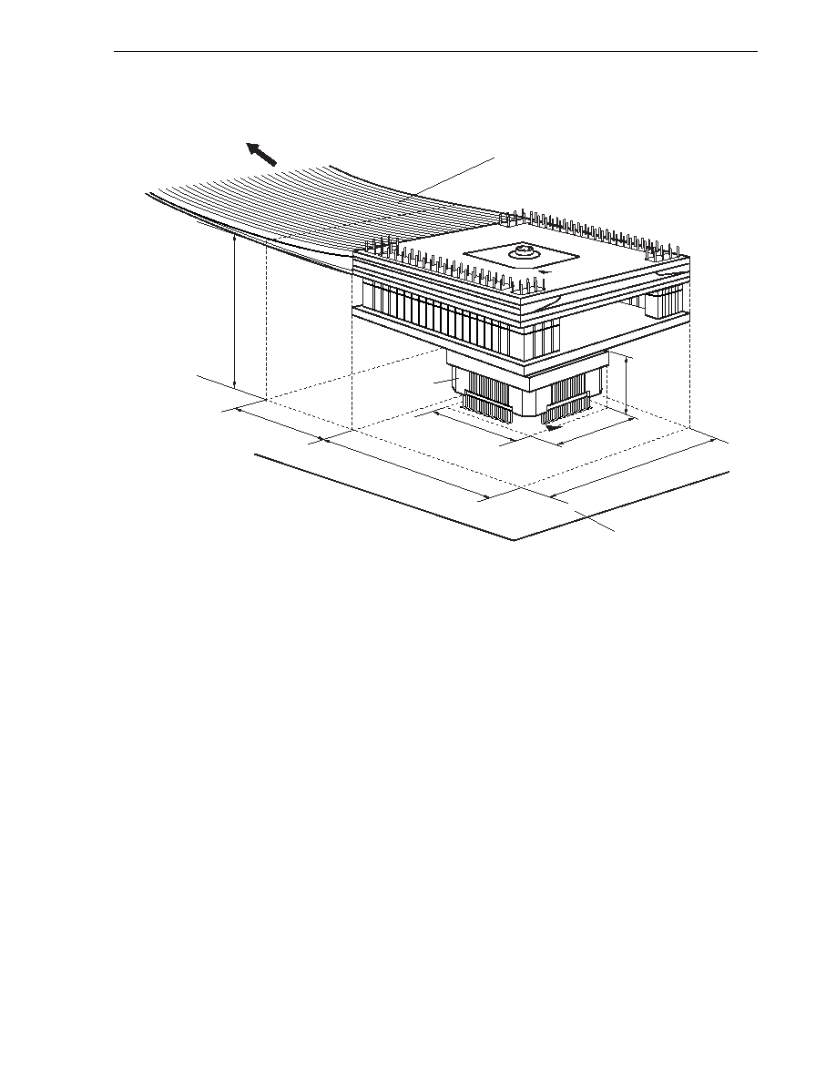
APPENDIX B NOTES ON TARGET SYSTEM DESIGN
User's Manual U16228EJ2V0UD
547
Figure B-7. Connection Conditions of Target System (When Using NP-H64GK-TQ)
Emulation probe
NP-H64GK-TQ
Emulation board
IE-780148-NS-EM1
42 mm
45 mm
18.4 mm
11 mm
Target system
Conversion adapter
TGK-064SBW
18.4 mm
Pin 1
21.95 mm
23 mm

User's Manual U16228EJ2V0UD
548
APPENDIX C REGISTER INDEX
C.1 Register Index (In Alphabetical Order with Respect to Register Names)
[A]
A/D conversion result register (ADCR)........................................................................................................................257
A/D converter mode register (ADM) ............................................................................................................................254
Analog input channel specification register (ADS) ......................................................................................................256
Asynchronous serial interface control register 6 (ASICL6) ..........................................................................................306
Asynchronous serial interface operation mode register 0 (ASIM0) .............................................................................276
Asynchronous serial interface operation mode register 6 (ASIM6) .............................................................................300
Asynchronous serial interface reception error status register 0 (ASIS0) .....................................................................278
Asynchronous serial interface reception error status register 6 (ASIS6) .....................................................................302
Asynchronous serial interface transmission status register 6 (ASIF6) ........................................................................303
[B]
Baud rate generator control register 0 (BRGC0) .........................................................................................................279
Baud rate generator control register 6 (BRGC6) .........................................................................................................305
[C]
Capture/compare control register 00 (CRC00)............................................................................................................153
Capture/compare control register 01 (CRC01)............................................................................................................154
Clock monitor mode register (CLM) ............................................................................................................................402
Clock output selection register (CKS) .........................................................................................................................248
Clock selection register 6 (CKSR6).............................................................................................................................304
Correction address register 0 (CORAD0)....................................................................................................................427
Correction address register 1 (CORAD1)....................................................................................................................427
Correction control register (CORCN) ..........................................................................................................................428
[E]
8-bit timer compare register 50 (CR50) .......................................................................................................................190
8-bit timer compare register 51 (CR51) .......................................................................................................................190
8-bit timer counter 50 (TM50)......................................................................................................................................189
8-bit timer counter 51 (TM51)......................................................................................................................................189
8-bit timer H carrier control register 1 (TMCYC1)........................................................................................................213
8-bit timer H compare register 00 (CMP00).................................................................................................................208
8-bit timer H compare register 01 (CMP01).................................................................................................................208
8-bit timer H compare register 10 (CMP10).................................................................................................................208
8-bit timer H compare register 11 (CMP11).................................................................................................................208
8-bit timer H mode register 0 (TMHMD0) ....................................................................................................................209
8-bit timer H mode register 1 (TMHMD1) ....................................................................................................................209
8-bit timer mode control register 50 (TMC50)..............................................................................................................193
8-bit timer mode control register 51 (TMC51)..............................................................................................................194
External interrupt falling edge enable register (EGN)..................................................................................................369
External interrupt rising edge enable register (EGP)...................................................................................................369

APPENDIX C REGISTER INDEX
User's Manual U16228EJ2V0UD
549
[I]
Input switch control register (ISC) ...............................................................................................................................307
Internal expansion RAM size switching register (IXS).................................................................................................438
Internal memory size switching register (IMS) ............................................................................................................437
Interrupt mask flag register 0H (MK0H) ......................................................................................................................367
Interrupt mask flag register 0L (MK0L)........................................................................................................................367
Interrupt mask flag register 1H (MK1H) ......................................................................................................................367
Interrupt mask flag register 1L (MK1L)........................................................................................................................367
Interrupt request flag register 0H (IF0H) .....................................................................................................................366
Interrupt request flag register 0L (IF0L) ......................................................................................................................366
Interrupt request flag register 1H (IF1H) .....................................................................................................................366
Interrupt request flag register 1L (IF1L) ......................................................................................................................366
[K]
Key return mode register (KRM) .................................................................................................................................379
[L]
Low-voltage detection level selection register (LVIS)..................................................................................................415
Low-voltage detection register (LVIM) ........................................................................................................................414
[M]
Main clock mode register (MCM) ................................................................................................................................122
Main OSC control register (MOC) ...............................................................................................................................123
Multiplication/division data register A0 (MDA0H, MDA0L) ..........................................................................................353
Multiplication/division data register B0 (MDB0)...........................................................................................................354
Multiplier/divider control register 0 (DMUC0) ..............................................................................................................355
[O]
Oscillation stabilization time counter status register (OSTC) ..............................................................................124, 382
Oscillation stabilization time select register (OSTS)............................................................................................125, 383
[P]
Port mode register 0 (PM0)......................................................................................................................... 112, 159, 339
Port mode register 1 (PM1)................................................................................................. 112, 195, 213, 280, 307, 339
Port mode register 12 (PM12).....................................................................................................................................112
Port mode register 14 (PM14).............................................................................................................................112, 250
Port mode register 3 (PM3).................................................................................................................................112, 195
Port mode register 4 (PM4).........................................................................................................................................112
Port mode register 5 (PM5).........................................................................................................................................112
Port mode register 6 (PM6).........................................................................................................................................112
Port mode register 7 (PM7).........................................................................................................................................112
Port register 0 (P0)......................................................................................................................................................114
Port register 1 (P1)......................................................................................................................................................114
Port register 12 (P12)..................................................................................................................................................114
Port register 13 (P13)..................................................................................................................................................114
Port register 14 (P14)..................................................................................................................................................114
Port register 2 (P2)......................................................................................................................................................114
Port register 3 (P3)......................................................................................................................................................114

APPENDIX C REGISTER INDEX
User's Manual U16228EJ2V0UD
550
Port register 4 (P4)......................................................................................................................................................114
Port register 5 (P5)......................................................................................................................................................114
Port register 6 (P6)......................................................................................................................................................114
Port register 7 (P7)......................................................................................................................................................114
Power-fail comparison mode register (PFM) ...............................................................................................................258
Power-fail comparison threshold register (PFT) ..........................................................................................................258
Prescaler mode register 00 (PRM00) ..........................................................................................................................157
Prescaler mode register 01 (PRM01) ..........................................................................................................................157
Priority specification flag register 0H (PR0H) ..............................................................................................................368
Priority specification flag register 0L (PR0L) ...............................................................................................................368
Priority specification flag register 1H (PR1H) ..............................................................................................................368
Priority specification flag register 1L (PR1L) ...............................................................................................................368
Processor clock control register (PCC) .......................................................................................................................119
Pull-up resistor option register 0 (PU0) .......................................................................................................................115
Pull-up resistor option register 1 (PU1) .......................................................................................................................115
Pull-up resistor option register 12 (PU12) ...................................................................................................................115
Pull-up resistor option register 14 (PU14) ...................................................................................................................115
Pull-up resistor option register 3 (PU3) .......................................................................................................................115
Pull-up resistor option register 4 (PU4) .......................................................................................................................115
Pull-up resistor option register 5 (PU5) .......................................................................................................................115
Pull-up resistor option register 7 (PU7) .......................................................................................................................115
[R]
Receive buffer register 0 (RXB0) ................................................................................................................................275
Receive buffer register 6 (RXB6) ................................................................................................................................299
Remainder data register 0 (SDR0)..............................................................................................................................353
Reset control flag register (RESF) ..............................................................................................................................400
Ring-OSC mode register (RCM) .................................................................................................................................121
[S]
Serial clock selection register 10 (CSIC10) .................................................................................................................336
Serial clock selection register 11 (CSIC11) .................................................................................................................336
Serial I/O shift register 10 (SIO10) ..............................................................................................................................333
Serial I/O shift register 11 (SIO11) ..............................................................................................................................333
Serial operation mode register 10 (CSIM10) ...............................................................................................................334
Serial operation mode register 11 (CSIM11) ...............................................................................................................334
16-bit timer capture/compare register 000 (CR000) ....................................................................................................147
16-bit timer capture/compare register 001 (CR001) ....................................................................................................147
16-bit timer capture/compare register 010 (CR010) ....................................................................................................149
16-bit timer capture/compare register 011 (CR011) ....................................................................................................149
16-bit timer counter 00 (TM00)....................................................................................................................................147
16-bit timer counter 01 (TM01)....................................................................................................................................147
16-bit timer mode control register 00 (TMC00)............................................................................................................150
16-bit timer mode control register 01 (TMC01)............................................................................................................150
16-bit timer output control register 00 (TOC00)...........................................................................................................154
16-bit timer output control register 01 (TOC01)...........................................................................................................154

APPENDIX C REGISTER INDEX
User's Manual U16228EJ2V0UD
551
[T]
Timer clock selection register 50 (TCL50) ..................................................................................................................191
Timer clock selection register 51 (TCL51) ..................................................................................................................191
Transmit buffer register 10 (SOTB10).........................................................................................................................333
Transmit buffer register 11 (SOTB11).........................................................................................................................333
Transmit buffer register 6 (TXB6)................................................................................................................................299
Transmit shift register 0 (TXS0) ..................................................................................................................................275
[W]
Watch timer operation mode register (WTM) ..............................................................................................................232
Watchdog timer enable register (WDTE) ....................................................................................................................241
Watchdog timer mode register (WDTM) .....................................................................................................................240

APPENDIX C REGISTER INDEX
User's Manual U16228EJ2V0UD
552
C.2 Register Index (In Alphabetical Order with Respect to Register Symbol)
[A]
ADCR: A/D
conversion result register .................................................................................................................257
ADM: A/D
converter mode register....................................................................................................................254
ADS: Analog
input
channel specification register .............................................................................................256
ASICL6: Asynchronous
serial
interface control register 6 ......................................................................................306
ASIF6: Asynchronous
serial
interface
transmission status register 6 ..................................................................303
ASIM0: Asynchronous
serial
interface operation mode register 0........................................................................276
ASIM6: Asynchronous
serial
interface operation mode register 6........................................................................300
ASIS0:
Asynchronous serial interface reception error status register 0...............................................................278
ASIS6:
Asynchronous serial interface reception error status register 6...............................................................302
[B]
BRGC0:
Baud rate generator control register 0 .....................................................................................................279
BRGC6:
Baud rate generator control register 6 .....................................................................................................305
[C]
CKS:
Clock output selection register ................................................................................................................248
CKSR6: Clock
selection register 6 ........................................................................................................................304
CLM: Clock
monitor mode register....................................................................................................................402
CMP00:
8-bit timer H compare register 00 ............................................................................................................208
CMP01:
8-bit timer H compare register 01 ............................................................................................................208
CMP10:
8-bit timer H compare register 10 ............................................................................................................208
CMP11:
8-bit timer H compare register 11 ............................................................................................................208
CORAD0: Correction
address register 0 ..................................................................................................................427
CORAD1: Correction
address register 1 ..................................................................................................................427
CORCN: Correction
control register .......................................................................................................................428
CR000:
16-bit timer capture/compare register 000...............................................................................................147
CR001:
16-bit timer capture/compare register 001...............................................................................................147
CR010:
16-bit timer capture/compare register 010...............................................................................................149
CR011:
16-bit timer capture/compare register 011...............................................................................................149
CR50:
8-bit timer compare register 50................................................................................................................190
CR51:
8-bit timer compare register 51................................................................................................................190
CRC00: Capture/compare
control register 00 .......................................................................................................153
CRC01: Capture/compare
control register 01 .......................................................................................................154
CSIC10:
Serial clock selection register 10 .............................................................................................................336
CSIC11:
Serial clock selection register 11 .............................................................................................................336
CSIM10: Serial
operation mode register 10............................................................................................................334
CSIM11: Serial
operation mode register 11............................................................................................................334
[D]
DMUC0: Multiplier/divider control register 0 ...........................................................................................................355
[E]
EGN: External
interrupt
falling edge enable register .........................................................................................369
EGP: External
interrupt
rising edge enable register ..........................................................................................369

APPENDIX C REGISTER INDEX
User's Manual U16228EJ2V0UD
553
[I]
IF0H: Interrupt
request flag register 0H.............................................................................................................366
IF0L: Interrupt
request flag register 0L .............................................................................................................366
IF1H: Interrupt
request flag register 1H.............................................................................................................366
IF1L: Interrupt
request flag register 1L .............................................................................................................366
IMS:
Internal memory size switching register ..................................................................................................437
ISC: Input
switch
control register.....................................................................................................................307
IXS:
Internal expansion RAM size switching register ......................................................................................438
[K]
KRM: Key
return mode register.........................................................................................................................379
[L]
LVIM: Low-voltage
detection register ................................................................................................................414
LVIS: Low-voltage
detection
level selection register .........................................................................................415
[M]
MCM: Main
clock mode register ........................................................................................................................122
MDA0H: Multiplication/division data register A0 ....................................................................................................353
MDA0L: Multiplication/division data register A0 ....................................................................................................353
MDB0: Multiplication/division data register B0 ....................................................................................................354
MK0H: Interrupt
mask
flag register 0H ................................................................................................................367
MK0L: Interrupt
mask
flag register 0L.................................................................................................................367
MK1H: Interrupt
mask
flag register 1H ................................................................................................................367
MK1L: Interrupt
mask
flag register 1L.................................................................................................................367
MOC:
Main OSC control register .......................................................................................................................123
[O]
OSTC:
Oscillation stabilization time counter status register ........................................................................124, 382
OSTS: Oscillation
stabilization time select register .....................................................................................125, 383
[P]
P0: Port
register 0..........................................................................................................................................114
P1: Port
register 1..........................................................................................................................................114
P12: Port
register 12........................................................................................................................................114
P13: Port
register 13........................................................................................................................................114
P14: Port
register 14........................................................................................................................................114
P2: Port
register 2..........................................................................................................................................114
P3: Port
register 3..........................................................................................................................................114
P4: Port
register 4..........................................................................................................................................114
P5: Port
register 5..........................................................................................................................................114
P6: Port
register 6..........................................................................................................................................114
P7: Port
register 7..........................................................................................................................................114
PCC: Processor
clock control register ..............................................................................................................119
PFM: Power-fail
comparison mode register ......................................................................................................258
PFT: Power-fail
comparison threshold register ................................................................................................258
PM0: Port
mode
register 0................................................................................................................ 112, 159, 339
PM1:
Port mode register 1........................................................................................ 112, 195, 213, 280, 307, 339

APPENDIX C REGISTER INDEX
User's Manual U16228EJ2V0UD
554
PM12: Port
mode
register 12 ..............................................................................................................................112
PM14: Port
mode
register 14 ......................................................................................................................112, 250
PM3: Port
mode
register 3 ........................................................................................................................112, 195
PM4: Port
mode
register 4 ................................................................................................................................112
PM5: Port
mode
register 5 ................................................................................................................................112
PM6: Port
mode
register 6 ................................................................................................................................112
PM7: Port
mode
register 7 ................................................................................................................................112
PR0H: Priority
specification flag register 0H .......................................................................................................368
PR0L: Priority
specification flag register 0L ........................................................................................................368
PR1H: Priority
specification flag register 1H .......................................................................................................368
PR1L: Priority
specification flag register 1L ........................................................................................................368
PRM00: Prescaler
mode register 00 .....................................................................................................................157
PRM01: Prescaler
mode register 01 .....................................................................................................................157
PU0: Pull-up
resistor option register 0 ..............................................................................................................115
PU1: Pull-up
resistor option register 1 ..............................................................................................................115
PU12: Pull-up
resistor option register 12 ............................................................................................................115
PU14: Pull-up
resistor option register 14 ............................................................................................................115
PU3: Pull-up
resistor option register 3 ..............................................................................................................115
PU4: Pull-up
resistor option register 4 ..............................................................................................................115
PU5: Pull-up
resistor option register 5 ..............................................................................................................115
PU7: Pull-up
resistor option register 7 ..............................................................................................................115
[R]
RCM: Ring-OSC
mode register .........................................................................................................................121
RESF: Reset
control flag register........................................................................................................................400
RXB0: Receive
buffer register 0 .........................................................................................................................275
RXB6: Receive
buffer register 6 .........................................................................................................................299
[S]
SDR0: Remainder
data register 0 .......................................................................................................................353
SIO10:
Serial I/O shift register 10 ........................................................................................................................333
SIO11:
Serial I/O shift register 11 ........................................................................................................................333
SOTB10: Transmit
buffer register 10 ......................................................................................................................333
SOTB11: Transmit
buffer register 11 ......................................................................................................................333
[T]
TCL50:
Timer clock selection register 50 .............................................................................................................191
TCL51:
Timer clock selection register 51 .............................................................................................................191
TM00: 16-bit
timer counter 00.............................................................................................................................147
TM01: 16-bit
timer counter 01.............................................................................................................................147
TM50: 8-bit
timer counter 50...............................................................................................................................189
TM51: 8-bit
timer counter 51...............................................................................................................................189
TMC00:
16-bit timer mode control register 00 .......................................................................................................150
TMC01:
16-bit timer mode control register 01 .......................................................................................................150
TMC50:
8-bit timer mode control register 50 .........................................................................................................193
TMC51:
8-bit timer mode control register 51 .........................................................................................................194
TMCYC1: 8-bit timer H carrier control register 1 ......................................................................................................213

APPENDIX C REGISTER INDEX
User's Manual U16228EJ2V0UD
555
TMHMD0: 8-bit
timer
H mode register 0...................................................................................................................209
TMHMD1: 8-bit
timer
H mode register 1...................................................................................................................209
TOC00:
16-bit timer output control register 00......................................................................................................154
TOC01:
16-bit timer output control register 01......................................................................................................154
TXB6: Transmit
buffer register 6 ........................................................................................................................299
TXS0: Transmit
shift register 0...........................................................................................................................275
[W]
WDTE: Watchdog
timer
enable register ..............................................................................................................241
WDTM: Watchdog
timer mode register ................................................................................................................240
WTM:
Watch timer operation mode register ......................................................................................................232

User's Manual U16228EJ2V0UD
556
APPENDIX D REVISION HISTORY
D.1 Major Revisions in This Edition
(1/3)
Page Description
Addition of products
µ
PD78F0134(A1), 78F0138(A1), 780131(A2), 780132(A2), 780133(A2), 780134(A2), 780136(A2),
780138(A2)
Under development
Under mass production
µ
PD780131, 780132, 780133, 780134, 780136, 780138, 78F0134, 78F0138,
780131(A), 780132(A), 780133(A), 780134(A), 780136(A), 780138(A), 78F0134(A),
78F0138(A), 780131(A1), 780132(A1), 780133(A1), 780134(A1), 780136(A1), 780138(A1)
Throughout
Modification of names of the following special function registers (SFRs)
∑
Ports 0 to 7, and 12 to 14
Port registers 0 to 7, and 12 to 14
p. 27
Addition of Cautions 3 and 4 to 1.4 Pin Configuration (Top View)
p. 29
Modification of 1.5 K1 Family Lineup
p. 41
Modification of outline of timer in and addition of Remark to 1.7 Outline of Functions
p. 36
Addition of Table 2-1 Pin I/O Buffer Power Supplies
pp. 43, 44
Modification of descriptions in 2.2.12 AV
REF
, 2.2.15 REGC, and 2.2.20 V
PP
(flash memory versions only)
pp. 45, 46
Modification of the following contents in Table 2-2 Pin I/O Circuit Types
∑
Modification of recommended connection when P60 to P63 are not used
∑
Modification of I/O circuit type of P62 and P63
∑
Addition of Note to AV
REF
∑
Modification of recommended connection when V
PP
is not used
p. 70
Modification of Figure 3-20 Data to Be Saved to Stack Memory
p. 71
Modification of Figure 3-21 Data to Be Restored from Stack Memory
p. 84
Modification of [Description example] in 3.4.4 Short direct addressing
pp. 87 to 89
Addition of [Illustration] to 3.4.7 Based addressing, 3.4.8 Based indexed addressing, and 3.4.9 Stack
addressing
p. 90
Addition of Table 4-1 Pin I/O Buffer Power Supplies
p. 92
Modification of Table 4-3 Port Configuration
p. 102
Modification of Figure 4-11 Block Diagram of P20 to P27
p. 110
Addition of Remark to Figure 4-19 Block Diagram of P130
p. 112
Deletion of input switch control register (ISC) from and addition of port registers (P0 to P7, P12 to P14) to 4.3
Registers Controlling Port Function
p. 116
Partial modification of descriptions in 4.4.1 (1) Output mode, 4.4.3 (1) Output mode, and (2) Input mode
p. 118
Modification of Figure 5-1 Block Diagram of Clock Generator
p. 119
Addition of Note to 5.3 (1) Processor clock control register (PCC)
p. 124
Addition of Cautions 2 and 3 to Figure 5-6 Format of Oscillation Stabilization Time Counter Status
Register (OSTC)
pp. 126 to 128
Modification of Figure 5-8 Examples of External Circuit of X1 Oscillator, Figure 5-9 Examples of
External Circuit of Subsystem Clock Oscillator, and Figure 5-10 Examples of Incorrect Resonator
Connection

APPENDIX D REVISION HISTORY
User's Manual U16228EJ2V0UD
557
(2/3)
Page Description
p. 133
Modification of Notes 4 and 5 in Figure 5-13 Status Transition Diagram (2)
p. 135
Modification of Note 4 and illustration in Figure 5-13 Status Transition Diagram (4)
p. 136
Modification of Table 5-3 Relationship Between Operation Clocks in Each Operation Status
p. 139
Modification of Note in Figure 5-14 Switching from Ring-OSC Clock to X1 Input Clock (Flowchart)
p. 141
Addition of Note to Figure 5-16 Switching from X1 Input Clock to Subsystem Clock (Flowchart)
p. 144
Revision of CHAPTER 6 16-BIT TIMER/EVENT COUNTERS 00 AND 01
p. 187
Revision of CHAPTER 7 8-BIT TIMER/EVENT COUNTERS 50 AND 51
p. 205
Revision of CHAPTER 8 8-BIT TIMERS H0 AND H1
p. 230
Modification of Figure 9-1 Block Diagram of Watch Timer
p. 236
Addition of Figure 9-4 Example of Generation of Watch Timer Interrupt Request (INTWT) (When
Interrupt Period = 0.5 s)
p. 247
Modification of Figure 11-1 Block Diagram of Clock Output/Buzzer Output Controller
p. 251
Revision of CHAPTER 12 A/D CONVERTER
p. 272
Revision of CHAPTER 13 SERIAL INTERFACE UART0
p. 293
Revision of CHAPTER 14 SERIAL INTERFACE UART6
p. 331
Revision of CHAPTER 15 SERIAL INTERFACES CSI10 AND CSI11
p. 351
Revision of CHAPTER 16 MULTIPLIER/DIVIDER
pp. 361, 362
Addition of Note to INTVLI, POC, and LVI in Table 17-1 Interrupt Source List
p. 365
Addition of Note 2 to Table 17-2 Flags Corresponding to Interrupt Request Sources
p. 366
Addition of Caution 2 to Figure 17-2 Format of Interrupt Request Flag Registers (IF0L, IF0H, IF1L, IF1H)
p. 369
Addition of Caution to Table 17-3 Ports Corresponding to EGPn and EGNn
p. 374
Addition of software interrupt request item to Table 17-5 Relationship Between Interrupt Requests
Enabled for Multiple Interrupt Servicing During Interrupt Servicing
p. 378
Modification of Figure 18-1 Block Diagram of Key Interrupt
p. 380
Modification of Table 19-1 Relationship Between HALT Mode, STOP Mode, and Clock in old edition to
Table 19-1 Relationship Between Operation Clocks in Each Operation Status
p. 384
Addition of Cautions 2 and 3 to Figure 19-1 Format of Oscillation Stabilization Time Counter Status
Register (OSTC)
p. 385
Modification of Table 19-2 Operating Statuses in HALT Mode
p. 388
Addition of (3) When subsystem clock is used as CPU clock to Figure 19-4 HALT Mode Release by
RESET Input
p. 389
Modification of the following items in Table 19-4 Operating Statuses in STOP Mode
∑
8-bit timer H0
∑
Serial interfaces UART0 and UART6
pp. 394 to 396
Modification of Figure 20-1 Block Diagram of Reset Function to Figure 20-4 Timing of Reset in STOP
Mode by RESET Input
p. 401
Modification of Figure 21-1 Block Diagram of Clock Monitor
p. 403
Addition of normal operation mode to Table 21-2 Operation Status of Clock Monitor (When CLME = 1)
pp. 406, 407
Addition of (6) Clock monitor status after X1 input clock oscillation is stopped by software and (7)
Clock monitor status after Ring-OSC clock oscillation is stopped by software to Figure 21-3 Timing of
Clock Monitor

APPENDIX D REVISION HISTORY
User's Manual U16228EJ2V0UD
558
(3/3)
Page Description
p. 408
Addition of Note to description in 22.1 Functions of Power-on-Clear Circuit
p. 409
Modification of Figure 22-1 Block Diagram of Power-on-Clear Circuit
p. 412
Addition of Note to description in 23.1 Functions of Low-Voltage Detector
p. 412
Modification of Figure 23-1 Block Diagram of Low-Voltage Detector
p. 414
Modification of Note 5 in Figure 23-2 Format of Low-Voltage Detection Register (LVIM)
p. 415
Addition of Note 2 and Caution to Figure 23-3 Format of Low-Voltage Detection Level Selection
Register (LVIS)
pp. 417, 419
Modification of Figure 23-4 Timing of Low-Voltage Detector Internal Reset Signal Generation and
Figure 23-5 Timing of Low-Voltage Detector Interrupt Signal Generation
p. 422
Partial modification of description of (2) When used as interrupt under <Action> in 23.5 Cautions for
Low-Voltage Detector
p. 423
Revision of CHAPTER 24 REGULATOR
p. 425
Addition of Note to CHAPTER 25 MASK OPTIONS
p. 426
Modification of Figure 26-1 Block Diagram of ROM Correction
p. 428
Modification of Note in Figure 26-3 Format Correction Control Register
p. 430
Modification of Figure 26-5 Example of Storing to EEPROM (When One Place Is Corrected)
p. 436
Revision of CHAPTER 27
µ
PD78F0134, 78F0138 (no modification of 27.1 Internal Memory Size
Switching Register and 27.2 Internal Expansion RAM Size Switching Register)
p. 463
Partial modification of operation of "RETI" in 28.2 Operation List
p. 468
Revision of CHAPTER 29 ELECTRICAL SPECIFICATIONS (STANDARD PRODUCTS, (A) GRADE
PRODUCTS)
p. 487
Addition of CHAPTER 30 ELECTRICAL SPECIFICATIONS ((A1) GRADE PRODUCTS)
p. 506
Addition of CHAPTER 31 ELECTRICAL SPECIFICATIONS ((A2) GRADE PRODUCTS)
p. 523
Addition of CHAPTER 33 RECOMMENDED SOLDERING CONDITIONS
p. 536
Addition of A.3 Control Software
p. 538
Addition of in-circuit emulator "IE-78K0K1-ET" to A.5 Debugging Tools (Hardware)
p. 540
Modification of part number of RX78K0 in A.7 Embedded Software
p. 541
Addition of APPENDIX B NOTES ON TARGET SYSTEM DESIGN
p. 556
Addition of APPENDIX D REVISION HISTORY