Document Outline
- COVER
- DESCRIPTION
- FEATURES
- APPLICATIONS
- ORDERING INFORMATION
- 78K/IV SERIES LINEUP
- OVERVIEW OF FUNCTIONS
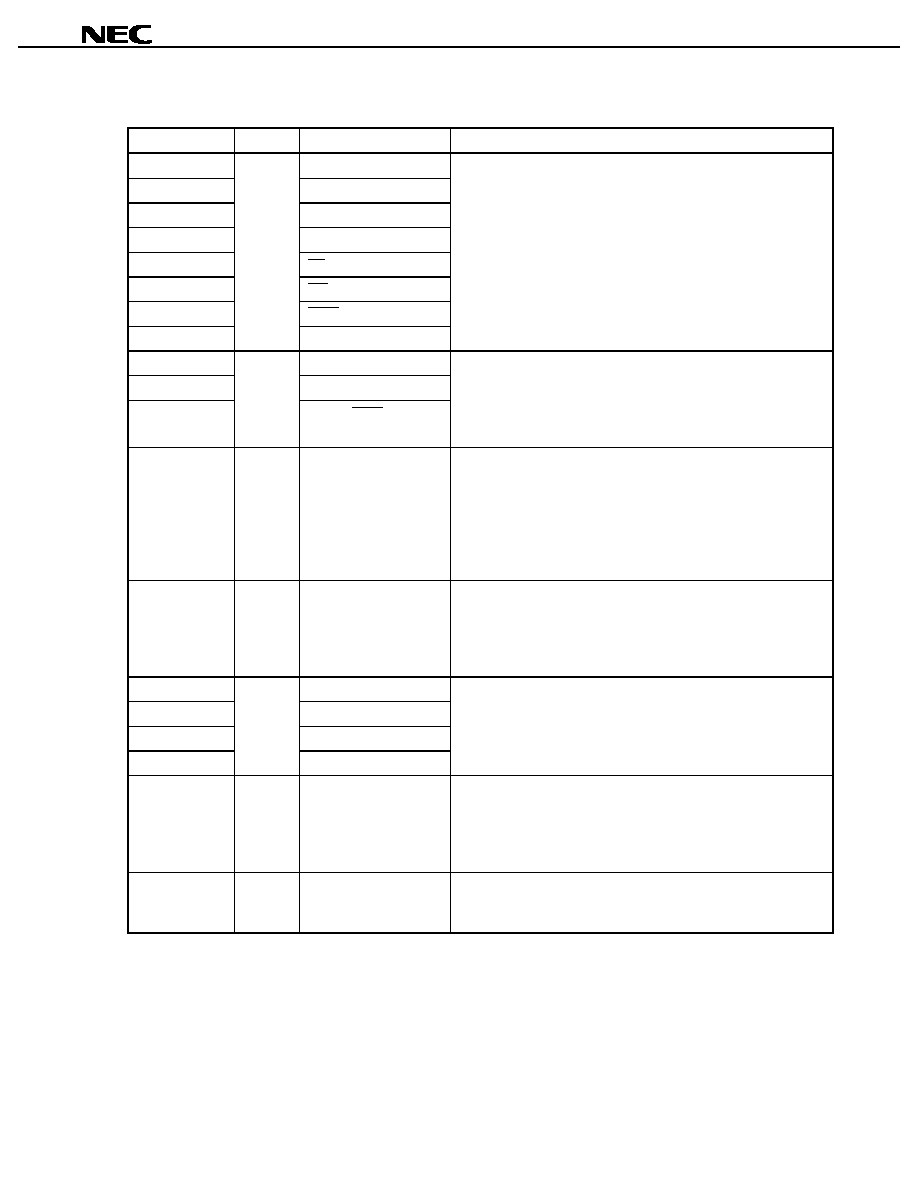
- 1. DIFFERENCES AMONG MODELS IN uPD784216A/784216AY, 784218A/784218AY SUBSERIES
- 2. PIN CONFIGURATION (TOP VIEW)
- 3. BLOCK DIAGRAM
- 4. PIN FUNCTIONS
- 4.1 Port Pins
- 4.2 Non-Port Pins
- 4.3 Pin I/O Circuits and Recommended Connections of Unused Pins
- 5. INTERNAL MEMORY SIZE SWITCHING REGISTER (IMS)
- 6. PROGRAMMING FLASH MEMORY
- 6.1 Selecting Communication Mode
- 6.2 Flash Memory Programming Function
- 6.3 Connecting Flashpro II and Flashpro III
- 7. ELECTRICAL SPECIFICATIONS
- 8. PACKAGE DRAWINGS
- 9. RECOMMENDED SOLDERING CONDITIONS
- APPENDIX A. DEVELOPMENT TOOLS
- APPENDIX B. RELATED DOCUMENTS

MOS INTEGRATED CIRCUIT
µ
µ
µ
µ
PD78F4216A, 78F4218A, 78F4216AY, 78F4218AY
16-BIT SINGLE-CHIP MICROCONTROLLERS
Document No. U14125EJ1V0DS00 (1st edition)
Date Published November 2000 N CP(K)
Printed in Japan
DATA SHEET
DESCRIPTION
The
µ
PD78F4216A/78F4218A and 78F4216AY/78F4218AY are products of
µ
PD784216A/784218A,
784216AY/784218AY Subseries in the 78K/IV Series.
The
µ
PD78F4216A/78F4218A have flash memory in place of the internal ROM of the
µ
PD784216A/784218A. The
incorporation of flash memory allows a program to be written or erased while mounted on the target board.
The
µ
PD78F4216AY/78F4218AY are based on the
µ
PD78F4216A/78F4218A Subseries with the addition of a
multimaster-supporting I
2
C bus interface.
Detailed function descriptions are provided in the following user's manuals. Be sure to read them before
designing.
µ
µ
µ
µ
PD784216A, 784216AY Subseries User's Manual Hardware: U13570E
µ
µ
µ
µ
PD784218A, 784218AY Subseries User's Manual Hardware: U12970E
78K/IV Series User's Manual Instructions:
U10905E
FEATURES
∑
Pin compatible with the mask ROM products
∑
Flash memory: 128 KB (
µ
PD78F4216A/78F4216AY)
256 KB (
µ
PD78F4218A/78F4218AY)
∑
Internal RAM: 8,192 bytes (
µ
PD78F4216A/78F4216AY)
12,800 bytes (
µ
PD78F4218A/78F4218AY)
∑
Supply voltage: V
DD
= 1.9 to 5.5 V
APPLICATIONS
Cellular phones, PHS, cordless telephones, CD-ROM, AV equipment
Unless otherwise specified, references in this document to the
µ
µ
µ
µ
PD78F4218AY refer to the
µ
µ
µ
µ
PD78F4216A,
78F4218A, 78F4216AY, and 78F4218AY.
2000
The information in this document is subject to change without notice. Before using this document, please
confirm that this is the latest version.
Not all devices/types available in every country. Please check with local NEC representative for
availability and additional information.

Data Sheet U14125EJ1V0DS00
2
µ
µ
µ
µ
PD78F4216A, 78F4218A, 78F4216AY, 78F4218AY
ORDERING INFORMATION
Part Number
Package
Internal ROM (Bytes)
Internal RAM (Bytes)
µ
PD78F4216AGC-8EU
100-pin plastic LQFP
(fine pitch) (14
◊
14)
128 K
8,192
µ
PD78F4216AGF-3BA
100-pin plastic QFP
(14
◊
20)
128 K
8,192
µ
PD78F4218AGC-8EU
100-pin plastic LQFP
(fine pitch) (14
◊
14)
256 K
12,800
µ
PD78F4218AGF-3BA
100-pin plastic QFP
(14
◊
20)
256 K
12,800
µ
PD78F4216AYGC-8EU
100-pin plastic LQFP
(fine pitch) (14
◊
14)
128 K
8,192
µ
PD78F4216AYGF-3BA
100-pin plastic QFP
(14
◊
20)
128 K
8,192
µ
PD78F4218AYGC-8EU
100-pin plastic LQFP
(fine pitch) (14
◊
14)
256 K
12,800
µ
PD78F4218AYGF-3BA
100-pin plastic QFP
(14
◊
20)
256 K
12,800
Data Sheet U14125EJ1V0DS00
3
µ
µ
µ
µ
PD78F4216A, 78F4218A, 78F4216AY, 78F4218AY
78K/IV SERIES LINEUP
PD784026
PD784956A
PD784908
PD784915
PD784928
PD784928Y
PD784046
PD784054
PD784216A
PD784216AY
PD784038
PD784038Y
PD784225Y
PD784225
PD784218AY
PD784218A
Enhanced
A/D converter,
16-bit timer, and
power management
Enhanced internal memory capacity
Pin-compatible with the PD784026
Supports I
2
C bus
Supports multimaster I
2
C bus
80-pin, ROM correction added
Supports multimaster I
2
C bus
Enhanced internal memory
capacity, ROM correction added
100-pin, enhanced I/O and
internal memory capacity
On-chip 10-bit A/D converter
For DC inverter control
On-chip IEBus
TM
controller
Software servo control
On-chip analog circuit for VCRs
Enhanced timer
Supports multimaster I
2
C bus
Enhanced functions
of the PD784915
Standard models
ASSP models
Supports multimaster I
2
C bus
: Products in mass-production
: Products under development
µ
µ
PD784976
On-chip VFD controller/driver
µ
µ
µ
µ
µ
µ
µ
µ
µ
µ
µ
µ
µ
µ
µ
µ
µ
PD784938A
Enhanced functions of the
PD784908, enhanced
internal memory capacity,
ROM correction added.
µ
µ
PD784967
µ
Enhanced functions of the
PD784938A, enhanced
I/O and internal memory
capacity.
µ
Data Sheet U14125EJ1V0DS00
4
µ
µ
µ
µ
PD78F4216A, 78F4218A, 78F4216AY, 78F4218AY
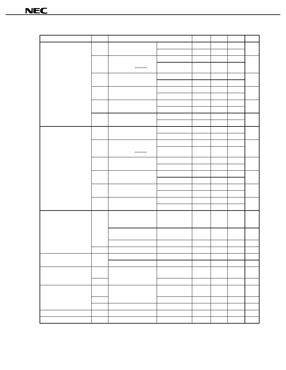
OVERVIEW OF FUNCTIONS (1/2)
Part Number
Item
µ
PD78F4216A,
µ
PD78F4216AY
µ
PD78F4218A,
µ
PD78F4218AY
Number of basic instructions (mnemonics)
113
General-purpose registers
8 bits
◊
16 registers
◊
8 banks, or 16 bits
◊
8 registers
◊
8 banks (memory
mapping)
Minimum instruction execution time
∑
160 ns/320 ns/640 ns/1,280 ns/2,560 ns (@f
XX
= 12.5 MHz operation with
main system clock)
∑
61
µ
s (@f
XT
= 32.768 kHz operation with subsystem clock)
Flash memory
128 KB
256 KB
Internal
memory
RAM
8,192 bytes
12,800 bytes
Memory space
1 MB with program and data spaces combined
Total
86
CMOS input
8
CMOS I/O
72
I/O ports
N-ch open-drain I/O
6
Pins with pull-up resistor
70
LED direct drive output
22
Pins with
additional
functions
Note 1
Middle-voltage pin
6
Real-time output port
4 bits
◊
2 or 8 bits
◊
1
Timer/event counter:
Timer counter
◊
1
Pulse output
(16-bit)
Capture/compare register
◊
2
∑
PPG output
∑
Square wave output
∑
One-shot pulse output
Timer/event counter 1: Timer counter
◊
1
Pulse output
(8-bit) Compare
register
◊
1
∑
PWM output
∑
Square wave output
Timer/event counter 2: Timer counter
◊
1
Pulse output
(8-bit) Compare
register
◊
1
∑
PWM output
∑
Square wave output
Timer/event counter 5: Timer counter
◊
1
Pulse output
(8-bit) Compare
register
◊
1
∑
PWM output
∑
Square wave output
Timer/event counter 6: Timer counter
◊
1
Pulse output
(8-bit) Compare
register
◊
1
∑
PWM output
∑
Square wave output
Timer/event counter 7: Timer counter
◊
1
Pulse output
(8-bit) Compare
register
◊
1
∑
PWM output
∑
Square wave output
Timer/event counter
Timer/event counter 8: Timer counter
◊
1
Pulse output
(8-bit) Compare
register
◊
1
∑
PWM output
∑
Square wave output
Serial interface
∑
UART/IOE (3-wire serial I/O): 2 channels (on-chip baud rate generator)
∑
CSI (3-wire serial I/O, multimaster supporting I
2
C bus
Note 2
): 1 channel
A/D converter
8-bit resolution
◊
8 channels
D/A converter
8-bit resolution
◊
2 channels
Notes 1. Pins with additional functions are included with the I/O pins.
2.
µ
PD78F4216AY, 78F4218AY only
Data Sheet U14125EJ1V0DS00
5
µ
µ
µ
µ
PD78F4216A, 78F4218A, 78F4216AY, 78F4218AY
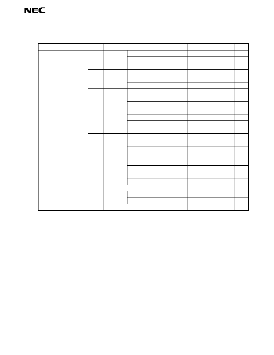
OVERVIEW OF FUNCTIONS (2/2)
Part Number
Item
µ
PD78F4216A,
µ
PD78F4216AY
µ
PD78F4218A,
µ
PD78F4218AY
Clock output
Selectable from f
XX
, f
XX
/2, f
XX
/2
2
, f
XX
/2
3
, f
XX
/2
4
, f
XX
/2
5
, f
XX
/2
6
, f
XX
/2
7
, f
XT
Buzzer output
Selectable from f
XX
/2
10
, f
XX
/2
11
, f
XX
/2
12
, f
XX
/2
13
Watch timer
1 channel
Watchdog timer
1 channel
Standby
∑
HALT/STOP/IDLE modes
∑
In low power consumption mode (with subsystem clock): HALT/IDLE modes
Hardware sources
29 (internal: 20, external: 9)
Software sources
BRK instruction, BRKCS instruction, operand error
Non-maskable
Internal: 1, external: 1
Interrupt
Maskable
Internal: 19, external: 8
∑
4 programmable priority levels
∑
3 service modes: Vectored interrupt/macro service/context switching
Supply voltage
V
DD
= 1.9 to 5.5 V
Package
100-pin plastic LQFP (fine pitch) (14
◊
14)
100-pin plastic QFP (14
◊
20)

Data Sheet U14125EJ1V0DS00
6
µ
µ
µ
µ
PD78F4216A, 78F4218A, 78F4216AY, 78F4218AY
CONTENTS
1. DIFFERENCES AMONG MODELS IN
µ
µ
µ
µ
PD784216A/784216AY, 784218A/784218AY
SUBSERIES ............................................................................................................................................. 7
2. PIN CONFIGURATION (TOP VIEW) ................................................................................................... 8
3. BLOCK DIAGRAM ............................................................................................................................... 11
4. PIN FUNCTIONS .................................................................................................................................. 12
4.1 Port Pins ..................................................................................................................................... 12
4.2 Non-Port Pins ............................................................................................................................. 14
4.3 Pin I/O Circuits and Recommended Connections of Unused Pins ....................................... 16
5. INTERNAL MEMORY SIZE SWITCHING REGISTER (IMS) ................................................................ 20
6. PROGRAMMING FLASH MEMORY..................................................................................................... 22
6.1 Selecting Communication Mode .............................................................................................. 22
6.2 Flash Memory Programming Function .................................................................................... 23
6.3 Connecting Flashpro ll and Flashpro lll ................................................................................... 24
7. ELECTRICAL SPECIFICATIONS ........................................................................................................ 25
8. PACKAGE DRAWINGS ....................................................................................................................... 47
9. RECOMMENDED SOLDERING CONDITIONS .................................................................................. 49
APPENDIX A. DEVELOPMENT TOOLS ................................................................................................ 50
APPENDIX B. RELATED DOCUMENTS ................................................................................................ 53
Data Sheet U14125EJ1V0DS00
7
µ
µ
µ
µ
PD78F4216A, 78F4218A, 78F4216AY, 78F4218AY
1. DIFFERENCES AMONG MODELS IN
µ
µ
µ
µ
PD784216A/784216AY, 784218A/784218AY SUBSERIES
The only difference among the
µ
PD784214A, 784215A, 784216A, 784217A, and 784218A lies in the internal
memory capacity.
The
µ
PD784214AY, 784215AY, 784216AY, 784217AY, and 784218AY are models with the addition of an I
2
C bus
control function.
The
µ
PD78F4216A, 78F4216AY, 78F4218A, and 78F4218AY are provided with a 128 KB/256 KB flash memory
instead of the mask ROM of the above models.
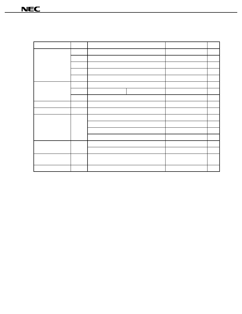
These differences are summarized in Table 1-1.
Table 1-1. Differences Among Models in
µ
µ
µ
µ
PD784216A/784216AY, 784218A/784218AY Subseries
Part Number
Item
µ
PD784214A,
µ
PD784214AY
µ
PD784215A,
µ
PD784215AY
µ
PD784216A,
µ
PD784216AY
µ
PD784217A,
µ
PD784217AY
µ
PD784218A,
µ
PD784218AY
µ
PD78F4216A,
µ
PD78F4216AY
µ
PD78F4218A,
µ
PD78F4218AY
Internal ROM
96 KB
(Mask
ROM)
128 KB (Mask ROM)
192 KB
(Mask
ROM)
256 KB
(Mask
ROM)
128 KB
(Flash
memory)
256 KB
(Flash
memory)
Internal RAM
3,584 bytes
5,120 bytes
8,192 bytes
12,800 bytes
8,192
bytes
12,800
bytes
Internal memory size
switching register
(IMS)
Not provided
Provided
Note
ROM correction
Not provided
Provided
Not
provided
Provided
External access status
function
Not provided
Provided
Not
provided
Provided
Supply voltage
V
DD
= 1.8 to 5.5 V
V
DD
= 1.9 to 5.5 V
Electrical
specifications
Recommended
soldering conditions
Refer to the data sheet for each device.
EXA pin
Not provided
Provided
Not
provided
Provided
TEST pin
Provided
Not provided
V
PP
pin
Not provided
Provided
Note The internal flash memory capacity and internal RAM capacity can be changed using the internal memory
size switching register (IMS).
Caution There are differences in noise immunity and noise radiation between the flash memory and mask
ROM versions. When pre-producing an application set with the flash memory version and then
mass-producing it with the mask ROM version, be sure to conduct sufficient evaluations on the
commercial samples (not engineering samples) of the mask ROM version.
Data Sheet U14125EJ1V0DS00
8
µ
µ
µ
µ
PD78F4216A, 78F4218A, 78F4216AY, 78F4218AY
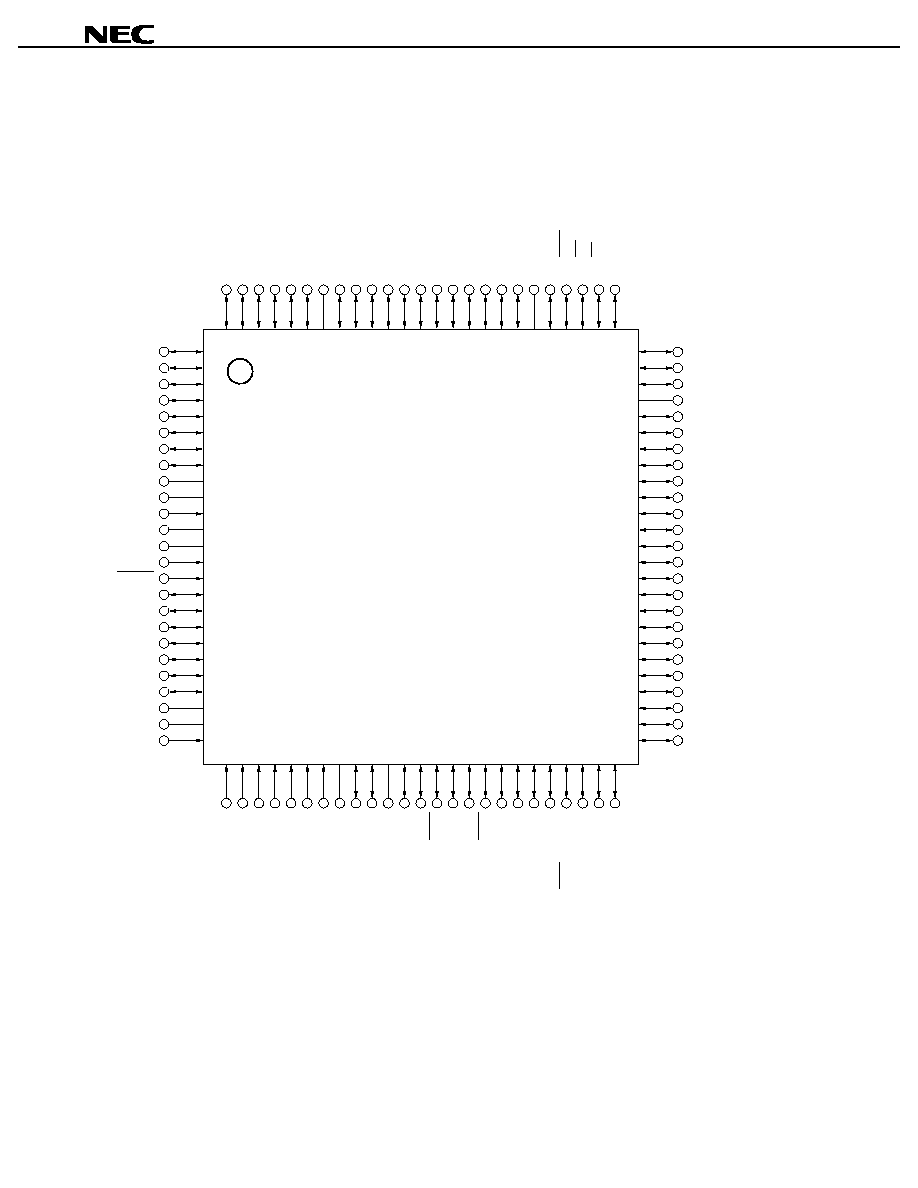
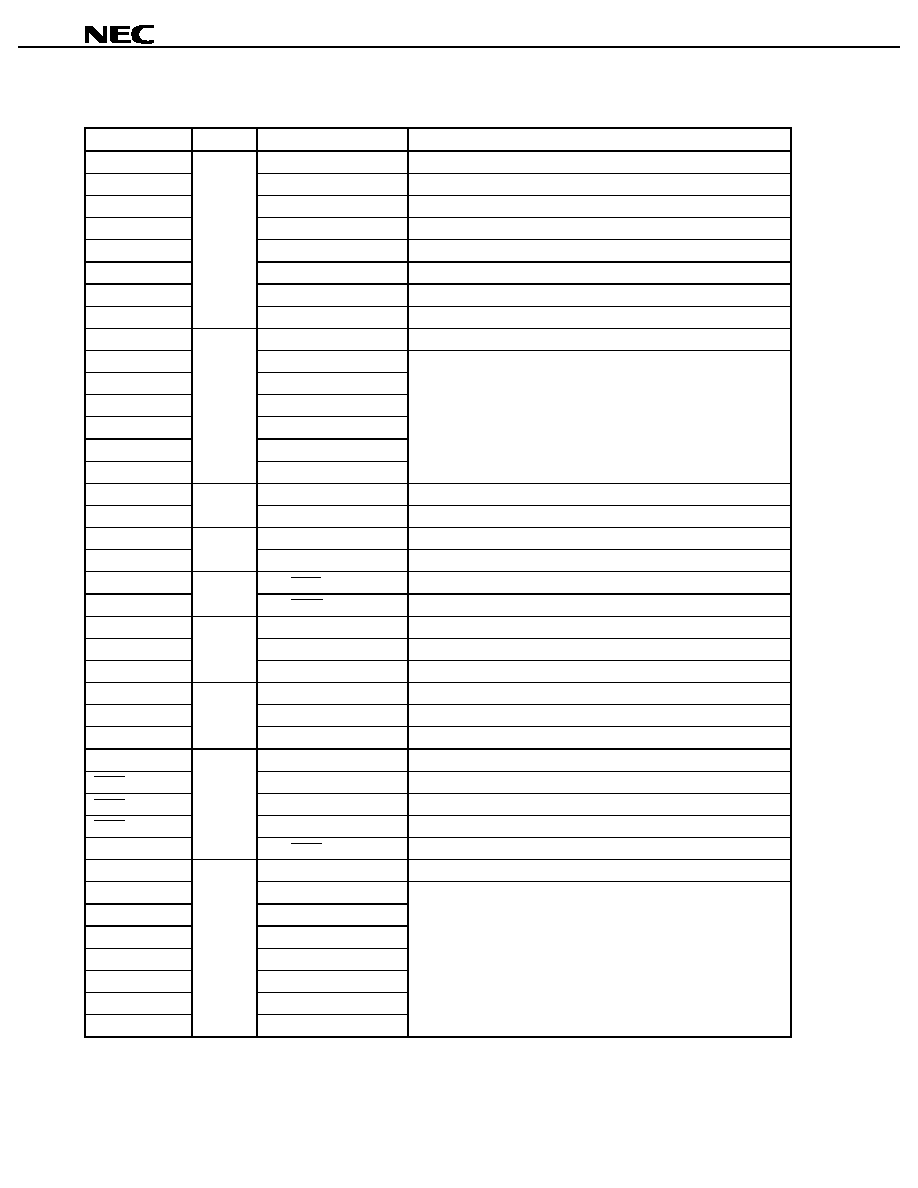
2. PIN CONFIGURATION (TOP VIEW)
∑
∑
∑
∑
100-pin plastic LQFP (fine pitch) (14
◊
◊
◊
◊
14)
µ
µ
µ
µ
PD78F4216AGC-8EU,
µ
µ
µ
µ
PD78F4218AGC-8EU,
µ
µ
µ
µ
PD78F4216AYGC-8EU,
µ
µ
µ
µ
PD78F4218AYGC-8EU
Notes 1. Connect the V
PP
pin to V
SS
directly or via a pull-down resistor in normal operation mode. Connect the
V
PP
pin to V
SS
via a pull-down resistor in a system in which the on-chip flash memory is written while
mounted on the target board. For the pull-down connection, it is recommended to use a resistor with a
resistance ranging from 470
to 10 k
.
2. Connect the AV
DD
pin to V
DD
.
3. Connect the AV
SS
pin to V
SS
.
4. The SCL0 and SDA0 pins are available in the
µ
PD78F4216AY, 78F4218AY only.
5. The EXA pin is available in the
µ
PD78F4218A, 78F4218AY only.
1
2
3
4
5
6
7
8
9
10
11
12
13
14
15
16
17
18
19
20
21
22
23
24
25
75
74
73
72
71
70
69
68
67
66
65
64
63
62
61
60
59
58
57
56
55
54
53
52
51
100
76
P120/RTP0
P121/RTP1
P122/RTP2
P123/RTP3
P124/RTP4
P125/RTP5
P126/RTP6
P127/RTP7
V
DD
X2
X1
V
SS
XT2
XT1
RESET
P00/INTP0
P01/INTP1
P02/INTP2/NMI
P03/INTP3
P04/INTP4
P05/INTP5
P06/INTP6
AV
DD
Note 2
AV
REF0
P10/ANI0
P62/A18
P61/A17
P60/A16
V
SS
P57/A15
P56/A14
P55/A13
P54/A12
P53/A11
P52/A10
P51/A9
P50/A8
P47/AD7
P46/AD6
P45/AD5
P44/AD4
P43/AD3
P42/AD2
P41/AD1
P40/AD0
P87/A7
P86/A6
P85/A5
P84/A4
P83/A3
P95
P94
P93
P92
P91
P90
V
PP
Note 1
P37/EXA
Note 5
P36/TI01
P35/TI00
P34/TI2
P33/TI1
P32/TO2
P31/TO1
P30/TO0
P103/TI8/TO8
P102/TI7/TO7
P101/TI6/TO6
P100/TI5/TO5
V
DD
P67/ASTB
P66/WAIT
P65/WR
P64/RD
P63/A19
P11/ANI1
P12/ANI2
P13/ANI3
P14/ANI4
P15/ANI5
P16/ANI6
P17/ANI7
AV
SS
Note 3
P130/ANO0
P131/ANO1
AV
REF1
P70/RxD2/SI2
P71/TxD2/SO2
P72/ASCK2/SCK2
P20/RxD1/SI1
P21/TxD1/SO1
P22/ASCK1/SCK1
P23/PCL
P24/BUZ
P25/SI0/SDA0
Note 4
P26/SO0
P27/SCK0/SCL0
Note 4
P80/A0
P81/A1
P82/A2
77
78
79
80
81
82
83
84
85
86
87
88
89
90
91
92
93
94
95
96
97
98
99
26
50
49
48
47
46
45
44
43
42
41
40
39
38
37
36
35
34
33
32
31
30
29
28
27
Data Sheet U14125EJ1V0DS00
9
µ
µ
µ
µ
PD78F4216A, 78F4218A, 78F4216AY, 78F4218AY
∑
∑
∑
∑
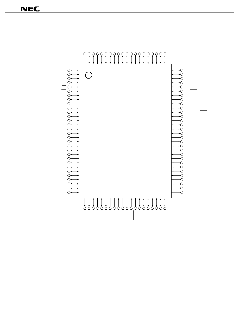
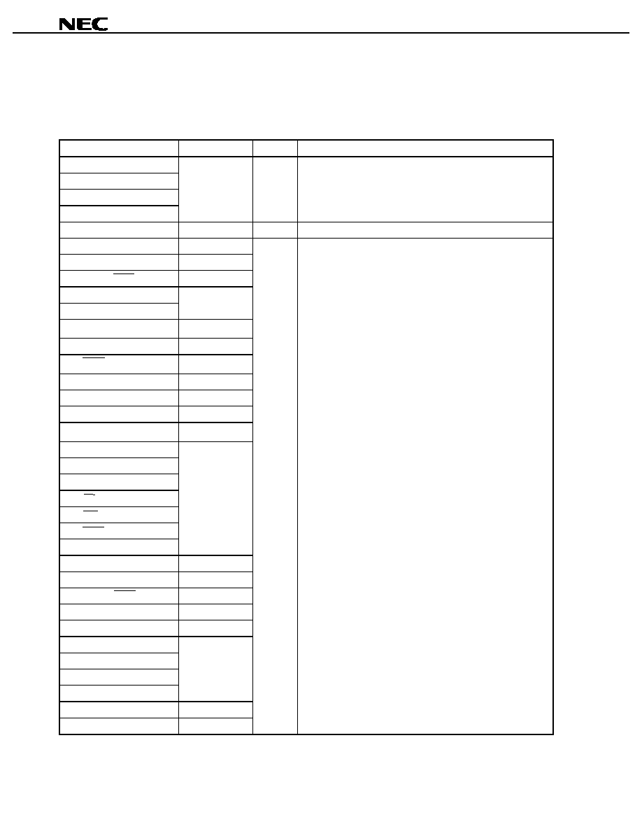
100-pin plastic QFP (14
◊
◊
◊
◊
20)
µ
µ
µ
µ
PD78F4216AGF-3BA,
µ
µ
µ
µ
PD78F4218AGF-3BA,
µ
µ
µ
µ
PD78F4216AYGF-3BA,
µ
µ
µ
µ
PD78F4218AYGF-3BA
Notes 1. Connect the V
PP
pin to V
SS
directly or via a pull-down resistor in normal operation mode. Connect the
V
PP
pin to V
SS
via a pull-down resistor in a system in which the on-chip flash memory is written while
mounted on the target board. For the pull-down connection, it is recommended to use a resistor with a
resistance ranging from 470
to 10 k
.
2. Connect the AV
DD
pin to V
DD
.
3. Connect the AV
SS
pin to V
SS
.
4. The SCL0 and SDA0 pins are available in the
µ
PD78F4216AY, 78F4218AY only.
5. The EXA pin is available in the
µ
PD78F4218A, 78F4218AY only.
100
V
SS
P57/A15
P56/A14
P55/A13
P54/A12
P53/A11
P52/A10
P51/A9
P50/A8
P47/AD7
P46/AD6
P45/AD5
P44/AD4
P43/AD3
P42/AD2
P41/AD1
P40/AD0
P87/A7
P86/A6
P85/A5
81
82
83
84
85
86
87
88
89
90
91
92
93
94
95
96
97
98
99
80
79
78
77
76
75
74
73
72
71
70
69
68
67
66
65
64
63
62
61
60
59
58
57
56
55
54
53
52
51
P84/A4
P83/A3
P82/A2
P81/A1
P80/A0
P27/SCK0/SCL0
Note 4
P26/SO0
P25/SI0/SDA0
Note 4
P24/BUZ
P23/PCL
P22/ASCK1/SCK1
P21/TxD1/SO1
P20/RxD1/SI1
P72/ASCK2/SCK2
P71/TxD2/SO2
P70/RxD2/SI2
AV
REF1
P131/ANO1
P130/ANO0
AV
SS
Note 3
P17/ANI7
P16/ANI6
P15/ANI5
P14/ANI4
P13/ANI3
P12/ANI2
P11/ANI1
P10/ANI0
AV
REF0
AV
DD
Note 2
1
2
3
4
5
6
7
8
9
10
11
12
13
14
15
16
17
18
19
20
21
22
23
24
25
26
27
28
29
30
P60/A16
P61/A17
P62/A18
P63/A19
P64/RD
P65/WR
P66/WAIT
P67/ASTB
V
DD
P100/TI5/TO5
P101/TI6/TO6
P102/TI7/TO7
P103/TI8/TO8
P30/TO0
P31/TO1
P32/TO2
P33/TI1
P34/TI2
P35/TI00
P36/TI01
P37/EXA
Note 5
V
PP
Note 1
P90
P91
P92
P93
P94
P95
P120/RTP0
P121/RTP1
P122/RTP2
P123/RTP3
P124/RTP4
P125/RTP5
P126/RTP6
P127/RTP7
V
DD
X2
X1
V
SS
XT2
XT1
RESET
P00/INTP0
P01/INTP1
P02/INTP2/NMI
P03/INTP3
P04/INTP4
P05/INTP5
P06/INTP6
31
50
49
48
47
46
45
44
43
42
41
40
39
38
37
36
35
34
33
32

Data Sheet U14125EJ1V0DS00
10
µ
µ
µ
µ
PD78F4216A, 78F4218A, 78F4216AY, 78F4218AY
A0 to A19:
Address Bus
P120 to P127:
Port 12
AD0 to AD7:
Address/Data Bus
P130, P131:
Port 13
ANI0 to ANI7:
Analog Input
PCL:
Programmable Clock
ANO0, ANO1:
Analog Output
RD:
Read Strobe
ASCK1, ASCK2:
Asynchronous Serial Clock
RESET:
Reset
ASTB:
Address Strobe
RTP0 to RTP7:
Real-time Output Port
AV
DD
:
Analog Power Supply
RxD1, RxD2:
Receive Data
AV
REF0
, AV
REF1
:
Analog Reference Voltage
SCK0 to SCK2:
Serial Clock
AV
SS
:
Analog Ground
SCL0
Note 1
:
Serial Clock
BUZ:
Buzzer Clock
SDA0
Note 1
:
Serial Data
EXA
Note 2
:
External Access Status Output
SI0 to SI2:
Serial Input
INTP0 to INTP6:
Interrupt from Peripherals
SO0 to SO2:
Serial Output
NMI:
Non-maskable Interrupt
TI00, TI01,
P00 to P06:
Port 0
TI1, TI2, TI5 to TI8:
Timer Input
P10 to P17:
Port 1
TO0 to TO2, TO5 to TO8: Timer Output
P20 to P27:
Port 2
TxD1, TxD2:
Transmit Data
P30 to P37:
Port 3
V
DD
:
Power Supply
P40 to P47:
Port 4
V
PP
:
Programming Power Supply
P50 to P57:
Port 5
V
SS
:
Ground
P60 to P67:
Port 6
WAIT:
Wait
P70 to P72:
Port 7
WR:
Write Strobe
P80 to P87:
Port 8
X1, X2:
Crystal (Main System Clock)
P90 to P95:
Port 9
XT1, XT2:
Crystal (Subsystem Clock)
P100 to P103:
Port 10
Notes 1. The SCL0 and SDA0 pins are available in the
µ
PD78F4216AY, 78F4218AY only.
2. The EXA pin is available in the
µ
PD78F4218A, 78F4218AY only.
Data Sheet U14125EJ1V0DS00
11
µ
µ
µ
µ
PD78F4216A, 78F4218A, 78F4216AY, 78F4218AY
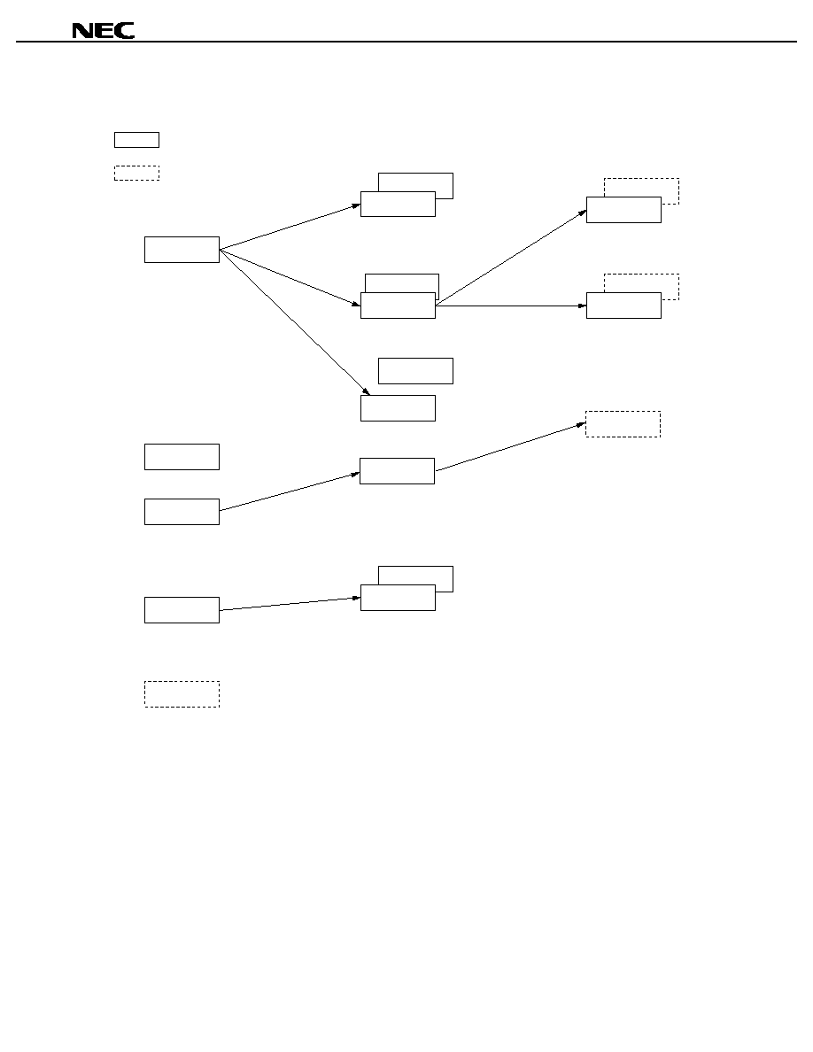
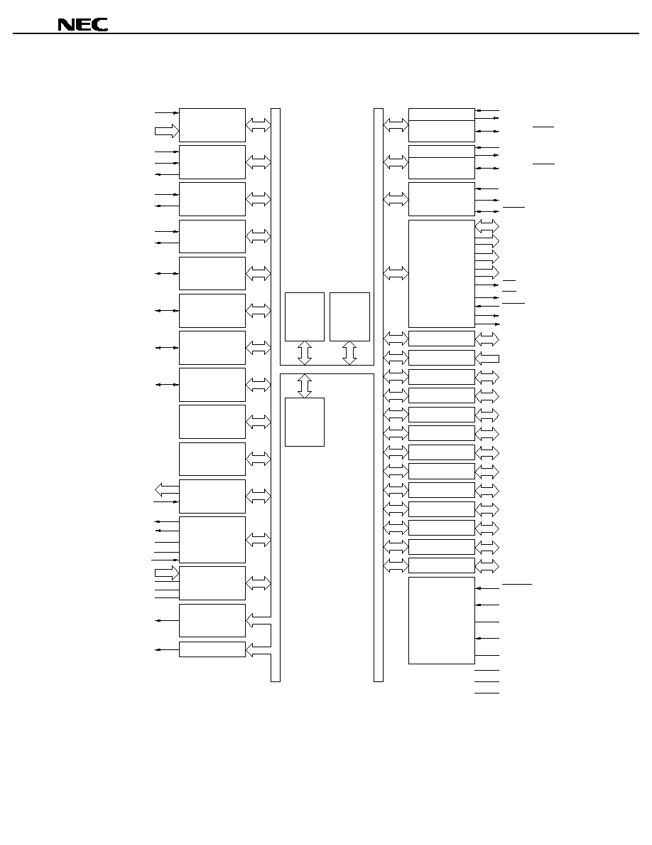
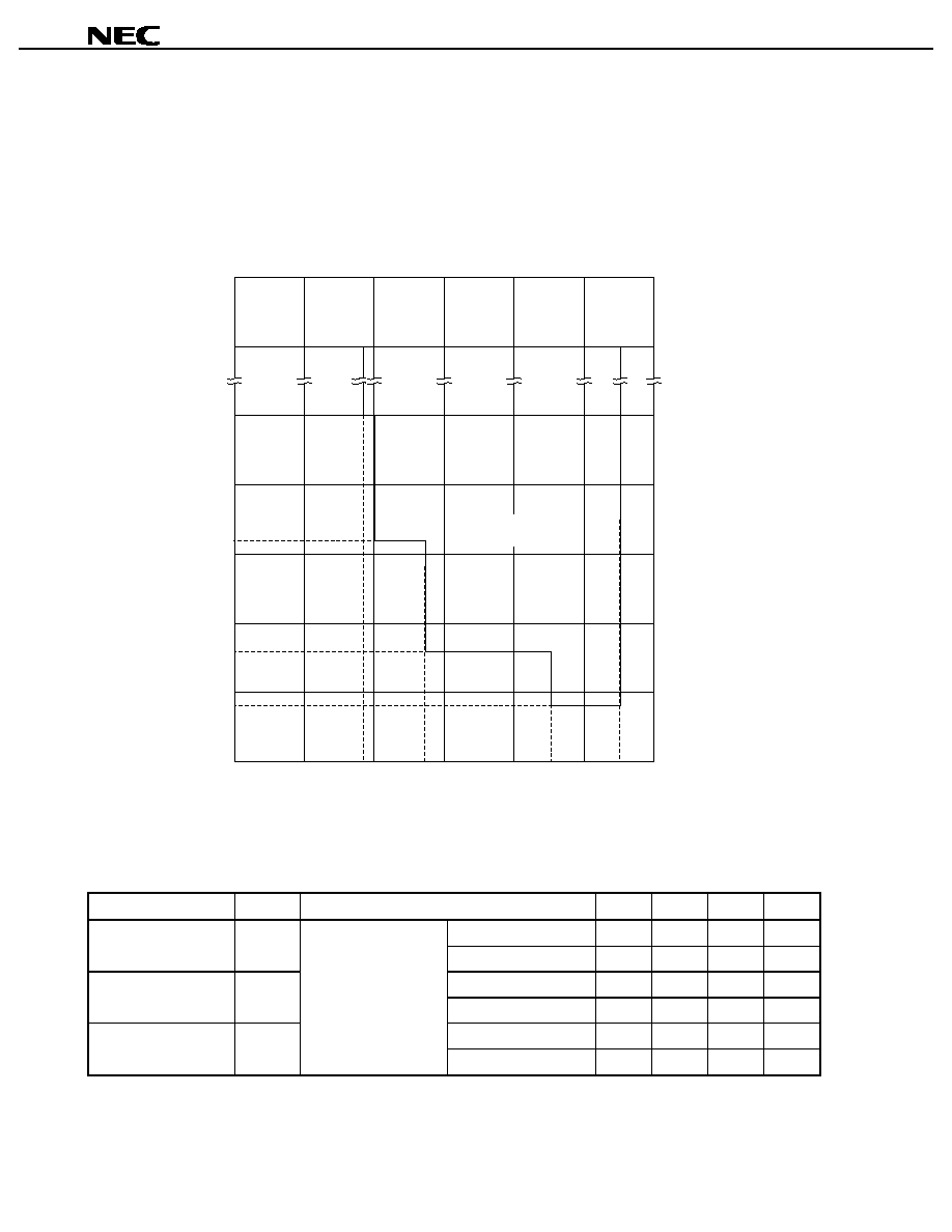
3. BLOCK DIAGRAM
Notes 1. This function supports the I
2
C bus interface and is available in the
µ
PD78F4216AY, 78F4218AY only.
2. The EXA pin is available in the
µ
PD78F4218A, 78F4218AY only.
INTP2/NMI
INTP0, INTP1,
INTP3 to INTP6
Programmable
interrupt
controller
Real-time
output port
Timer/event
counter 7
(8 bits)
Timer/event
counter 6
(8 bits)
Timer/event
counter 5
(8 bits)
Timer/event
counter 2
(8 bits)
Timer/event
counter 1
(8 bits)
Timer/event
counter
(16 bits)
Watch timer
Timer/event
counter 8
(8 bits)
Watchdog timer
TI00
TI01
TO0
TI1
TO1
TI2
TO2
TI5/TO5
TI6/TO6
TI7/TO7
TI8/TO8
NMI/INTP2
RTP0 to RTP7
Clock output
control
A/D
converter
AV
DD
AV
SS
PCL
BUZ
AV
REF0
ANI0 to ANI7
D/A
converter
ANO0
AV
SS
P03/INTP3
AV
REF1
ANO1
78K/IV
CPU core
Flash
memory
RAM
Baud-rate
generator
RxD1/SI1
TxD1/SO1
ASCK1/SCK1
RxD2/SI2
TxD2/SO2
ASCK2/SCK2
SI0/SDA0
Note 1
SO0
SCK0/SCL0
Note 1
Bus I/F
UART/IOE1
RD
ASTB
WR
WAIT
A0 to A7
AD0 to AD7
A8 to A15
A16 to A19
Port 1
P10 to P17
Port 0
P00 to P06
Port 2
P20 to P27
Port 3
P30 to P37
Port 4
P40 to P47
Port 5
P50 to P57
Port 6
P60 to P67
Port 7
P70 to P72
Port 8
P80 to P87
Port 9
P90 to P95
Port 10
P100 to P103
Port 12
P120 to P127
Port 13
P130, P131
Buzzer output
System control
RESET
XT2
X1
XT1
X2
V
SS
V
DD
V
PP
Clocked
serial
interface
Baud-rate
generator
UART/IOE2
EXA
Note 2
Data Sheet U14125EJ1V0DS00
12
µ
µ
µ
µ
PD78F4216A, 78F4218A, 78F4216AY, 78F4218AY
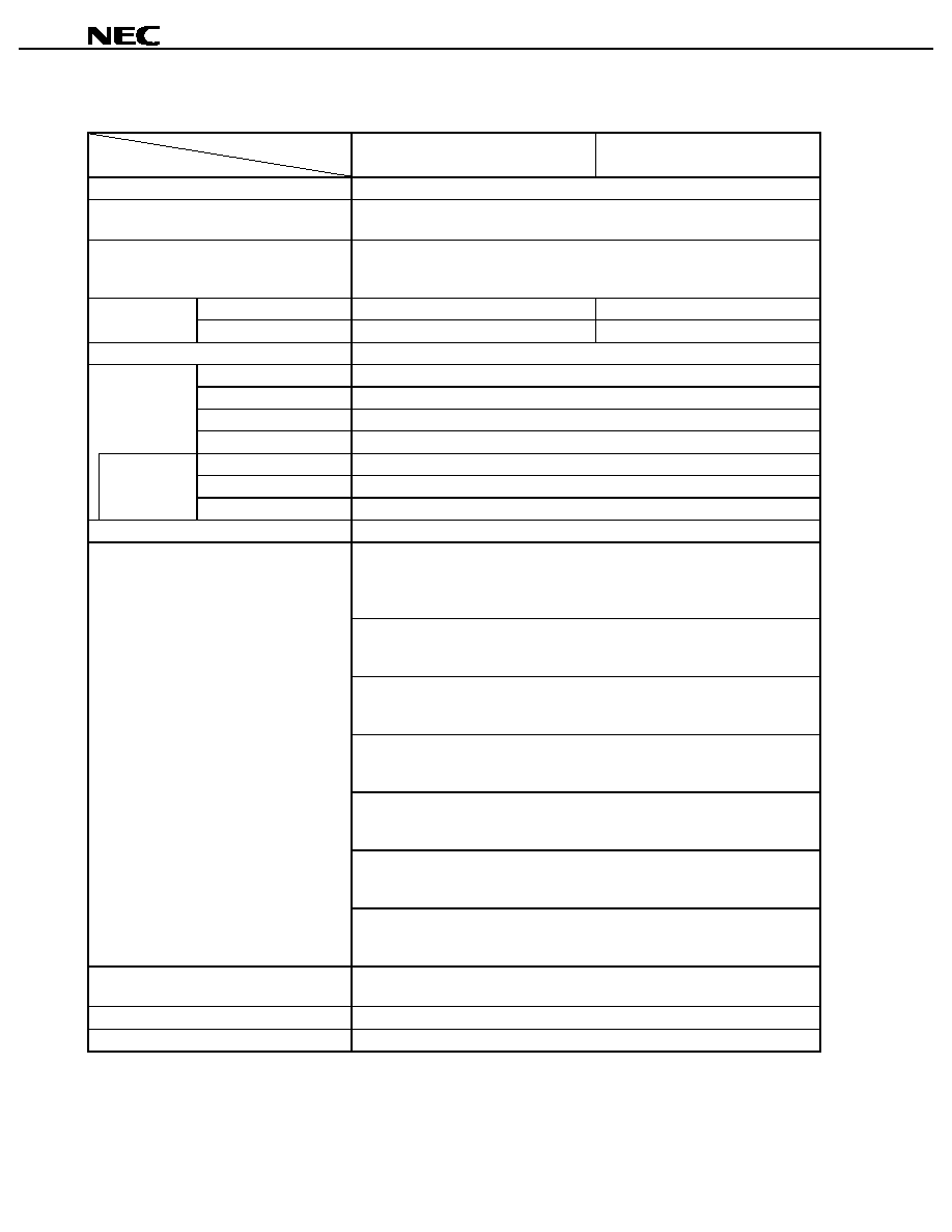
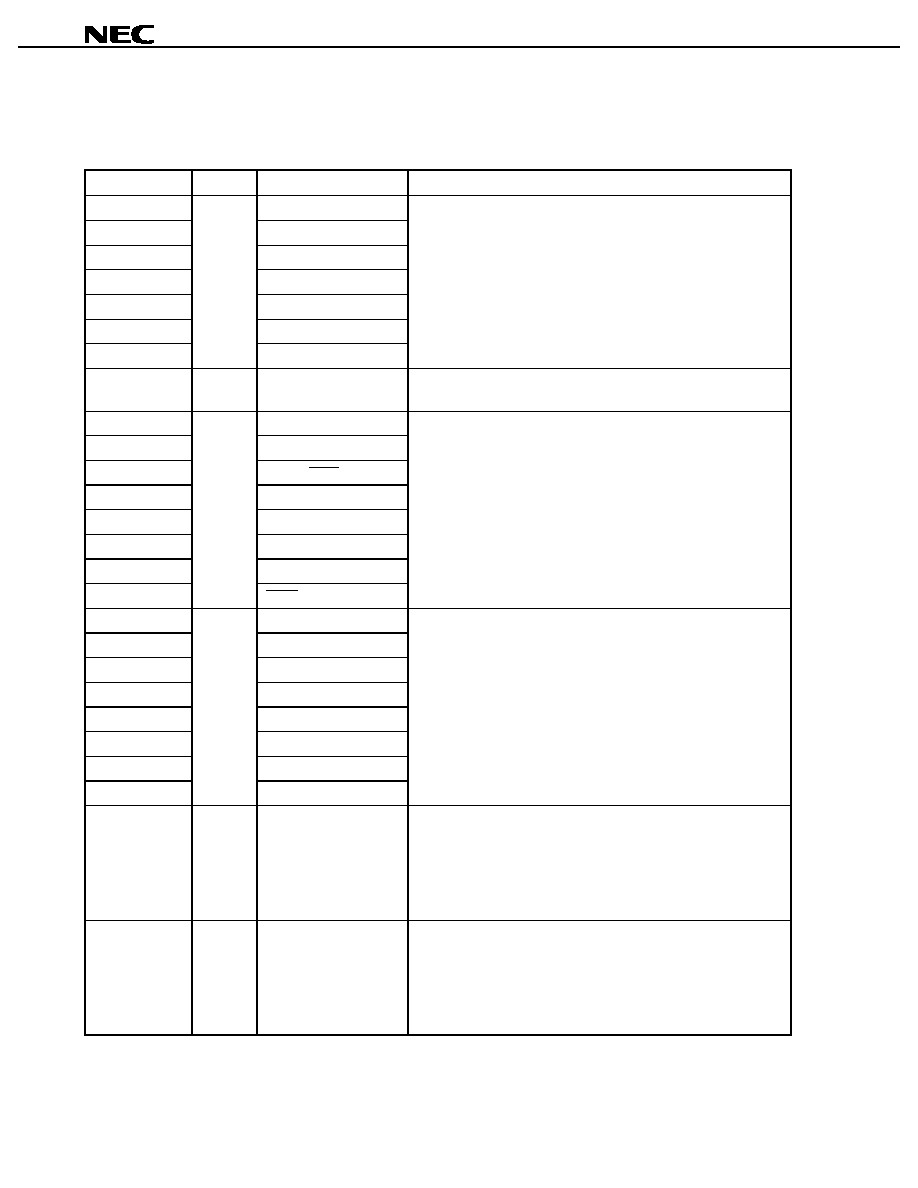
4. PIN FUNCTIONS
4.1 Port Pins (1/2)
Pin Name
I/O
Alternate Function
Function
P00
INTP0
P01
INTP1
P02
INTP2/NMI
P03
INTP3
P04
INTP4
P05
INTP5
P06
I/O
INTP6
Port 0 (P0):
∑
7-bit I/O port
∑
Input/output can be specified in 1-bit units.
∑
Whether specifying input mode or output mode, an on-chip pull-up
resistor can be specified in 1-bit units by means of software.
P10 to P17
Input
ANI0 to ANI7
Port 1 (P1):
∑
8-bit input only port
P20
RxD1/SI1
P21
TxD1/SO1
P22
ASCK1/SCK1
P23
PCL
P24
BUZ
P25
SI0/SDA0
Note 1
P26
SO0
P27
I/O
SCK0/SCL0
Note 1
Port 2 (P2):
∑
8-bit I/O port
∑
Input/output can be specified in 1-bit units.
∑
Whether specifying input mode or output mode, an on-chip pull-up
resistor can be specified in 1-bit units by means of software.
P30
TO0
P31
TO1
P32
TO2
P33
TI1
P34
TI2
P35
TI00
P36
TI01
P37
I/O
EXA
Note 2
Port 3 (P3):
∑
8-bit I/O port
∑
Input/output can be specified in 1-bit units.
∑
Whether specifying input mode or output mode, an on-chip pull-up
resistor can be specified in 1-bit units by means of software.
P40 to P47
I/O
AD0 to AD7
Port 4 (P4):
∑
8-bit I/O port
∑
Input/output can be specified in 1-bit units.
∑
When used as an input port, an on-chip pull-up resistor can be
specified by means of software.
∑
LEDs can be driven directly.
P50 to P57
I/O
A8 to A15
Port 5 (P5):
∑
8-bit I/O port
∑
Input/output can be specified in 1-bit units.
∑
When used as an input port, an on-chip pull-up resistor can be
specified by means of software.
∑
LEDs can be driven directly.
Notes 1. This SDA0 and SCL0 are available in the
µ
PD78F4216AY, 78F4218AY only.
2. This function is available in the
µ
PD78F4218A, 784218AY only.
Data Sheet U14125EJ1V0DS00
13
µ
µ
µ
µ
PD78F4216A, 78F4218A, 78F4216AY, 78F4218AY
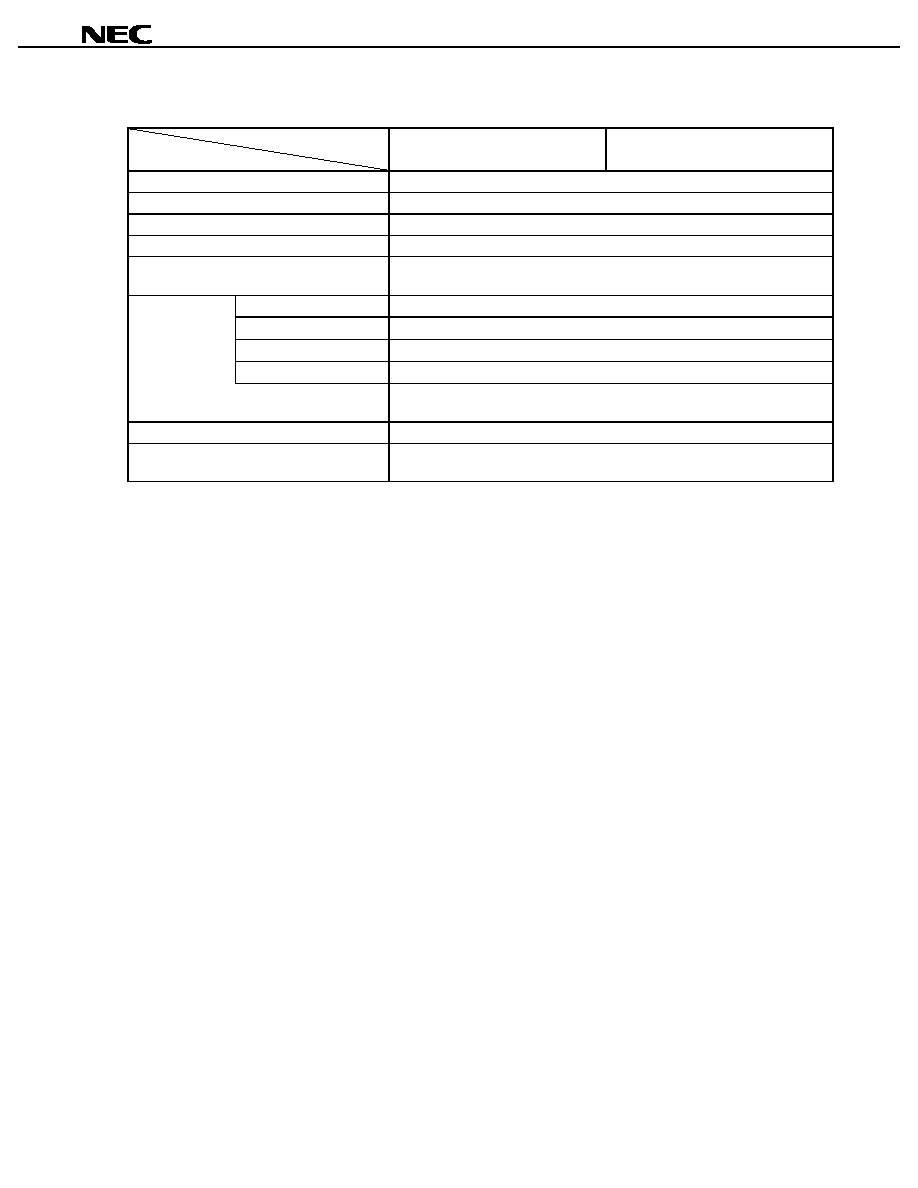
4.1 Port Pins (2/2)
Pin Name
I/O
Alternate Function
Function
P60
A16
P61
A17
P62
A18
P63
A19
P64
RD
P65
WR
P66
WAIT
P67
I/O
ASTB
Port 6 (P6):
∑
8-bit I/O port
∑
Input/output can be specified in 1-bit units.
∑
When used as an input port, an on-chip pull-up resistor can be
specified by means of software.
P70
RxD2/SI2
P71
TxD2/SO2
P72
I/O
ASCK2/SCK2
Port 7 (P7):
∑
3-bit I/O port
∑
Input/output can be specified in 1-bit units.
∑
Whether specifying input mode or output mode, an on-chip pull-up
resistor can be specified in 1-bit units by means of software.
P80 to P87
I/O
A0 to A7
Port 8 (P8):
∑
8-bit I/O port
∑
Input/output can be specified in 1-bit units.
∑
Whether specifying input mode or output mode, an on-chip pull-up
resistor can be specified in 1-bit units by means of software.
∑
The interrupt control flag (KRIF) is set to 1 when a falling edge is
detected at a pin of this port.
P90 to P95
I/O
-
Port 9 (P9):
∑
N-ch open-drain middle-voltage I/O port
∑
6-bit I/O port
∑
Input/output can be specified in 1-bit units.
∑
LEDs can be driven directly.
P100
TI5/TO5
P101
TI6/TO6
P102
TI7/TO7
P103
I/O
TI8/TO8
Port 10 (P10):
∑
4-bit I/O port
∑
Input/output can be specified in 1-bit units.
∑
Whether specifying input mode or output mode, an on-chip pull-up
resistor can be specified in 1-bit units by means of software.
P120 to P127
I/O
RTP0 to RTP7
Port 12 (P12):
∑
8-bit I/O port
∑
Input/output can be specified in 1-bit units.
∑
Whether specifying input mode or output mode, an on-chip pull-up
resistor can be specified in 1-bit units by means of software.
P130, P131
I/O
ANO0, ANO1
Port 13 (P13):
∑
2-bit I/O port
∑
Input/output can be specified in 1-bit units.
Data Sheet U14125EJ1V0DS00
14
µ
µ
µ
µ
PD78F4216A, 78F4218A, 78F4216AY, 78F4218AY
4.2
Non-Port Pins (1/2)
Pin Name
I/O
Alternate Function
Function
TI00
P35
External count clock input to 16-bit timer counter
TI01
P36
Capture trigger signal input to capture/compare register 00
TI1
P33
External count clock input to 8-bit timer counter 1
TI2
P34
External count clock input to 8-bit timer counter 2
TI5
P100/TO5
External count clock input to 8-bit timer counter 5
TI6
P101/TO6
External count clock input to 8-bit timer counter 6
TI7
P102/TO7
External count clock input to 8-bit timer counter 7
TI8
Input
P103/TO8
External count clock input to 8-bit timer counter 8
TO0
P30
16-bit timer output (shared by 14-bit PWM output)
TO1
P31
TO2
P32
TO5
P100/TI5
TO6
P101/TI6
TO7
P102/TI7
TO8
Output
P103/TI8
8-bit timer output (shared by 8-bit PWM output)
RxD1
P20/SI1
Serial data input (UART1)
RxD2
Input
P70/SI2
Serial data input (UART2)
TxD1
P21/SO1
Serial data output (UART1)
TxD2
Output
P71/SO2
Serial data output (UART2)
ASCK1
P22/SCK1
Baud rate clock input (UART1)
ASCK2
Input
P72/SCK2
Baud rate clock input (UART2)
SI0
P25/SDA0
Note
Serial data input (3-wire serial I/O 0)
SI1
P20/RxD1
Serial data input (3-wire serial I/O 1)
SI2
Input
P70/RxD2
Serial data input (3-wire serial I/O 2)
SO0
P26
Serial data output (3-wire serial I/O 0)
SO1
P21/TxD1
Serial data output (3-wire serial I/O 1)
SO2
Output
P71/TxD2
Serial data output (3-wire serial I/O 2)
SDA0
Note
P25/SI0
Serial data input/output (I
2
C bus)
SCK0
P27/SCL0
Note
Serial clock input/output (3-wire serial I/O 0)
SCK1
P22/ASCK1
Serial clock input/output (3-wire serial I/O 1)
SCK2
P72/ASCK2
Serial clock input/output (3-wire serial I/O 2)
SCL0
Note
I/O
P27/SCK0
Serial clock input/output (I
2
C bus)
NMI
P02/INTP2
Non-maskable interrupt request input
INTP0
P00
INTP1
P01
INTP2
P02/NMI
INTP3
P03
INTP4
P04
INTP5
P05
INTP6
Input
P06
External interrupt request input
Note This function is available in the
µ
PD78F4216AY, 78F4218AY only.

Data Sheet U14125EJ1V0DS00
15
µ
µ
µ
µ
PD78F4216A, 78F4218A, 78F4216AY, 78F4218AY
4.2 Non-Port Pins (2/2)
Pin Name
I/O
Alternate Function
Function
PCL
Output
P23
Clock output (for trimming main system clock and subsystem clock)
BUZ
Output
P24
Buzzer output
RTP0 to RTP7
Output
P120 to P127
Real-time output port that outputs data in synchronization with
trigger
AD0 to AD7
I/O
P40 to P47
Lower address/data bus for expanding memory externally
A0 to A7
P80 to P87
Lower address bus for expanding memory externally
A8 to A15
P50 to P57
Middle address bus for expanding memory externally
A16 to A19
Output
P60 to P63
Higher address bus for expanding memory externally
RD
P64
Strobe signal output for reading from external memory
WR
Output
P65
Strobe signal output for writing to external memory
WAIT
Input
P66
Wait insertion at external memory access
ASTB
Output
P67
Strobe output that externally latches address information output to
ports 4 through 6 and 8 to access external memory
EXA
Note
Output
P37
Status signal output at external memory access
RESET
Input
-
System reset input
X1
Input
X2
-
-
Connecting crystal resonator for main system clock oscillation
XT1
Input
XT2
-
-
Connecting crystal resonator for subsystem clock oscillation
ANI0 to ANI7
Input
P10 to P17
A/D converter analog input
ANO0, ANO1
Output
P130, P131
D/A converter analog output
AV
REF0
A/D converter reference voltage input
AV
REF1
D/A converter reference voltage input
AV
DD
A/D converter positive power supply. Connect to V
DD
.
AV
SS
GND for A/D converter and D/A converter. Connect to V
SS
.
V
DD
Positive power supply
V
SS
GND
V
PP
-
-
Flash memory programming mode setting.
Applying high-voltage for program write/verify. Connect this pin to
V
SS
directly or via a pull-down resistor in normal operation mode.
Connect the V
PP
pin to V
SS
via a pull-down resistor in a system in
which the on-chip flash memory is written while mounted on the
target board. For the pull-down connection, it is recommended to
use a resistor with a resistance ranging from 470
to 10 k
.
Note The EXA pin is available in the
µ
PD78F4218A, 78F4218AY only.
Data Sheet U14125EJ1V0DS00
16
µ
µ
µ
µ
PD78F4216A, 78F4218A, 78F4216AY, 78F4218AY
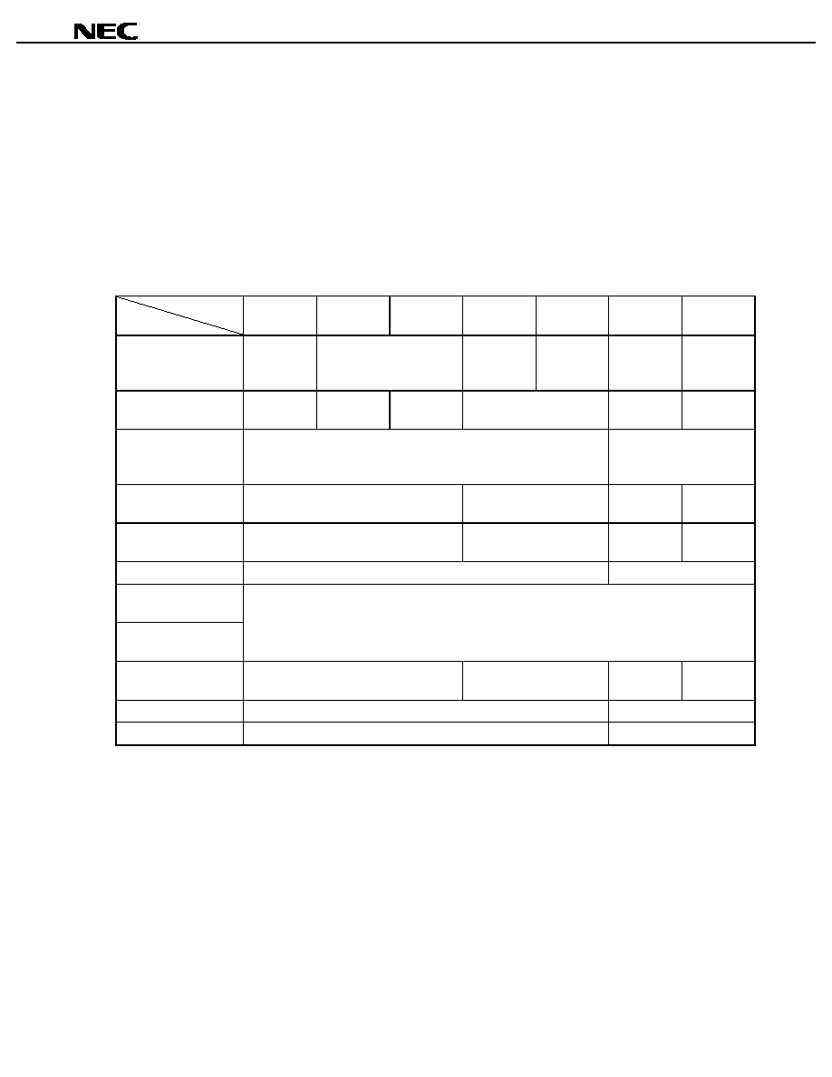
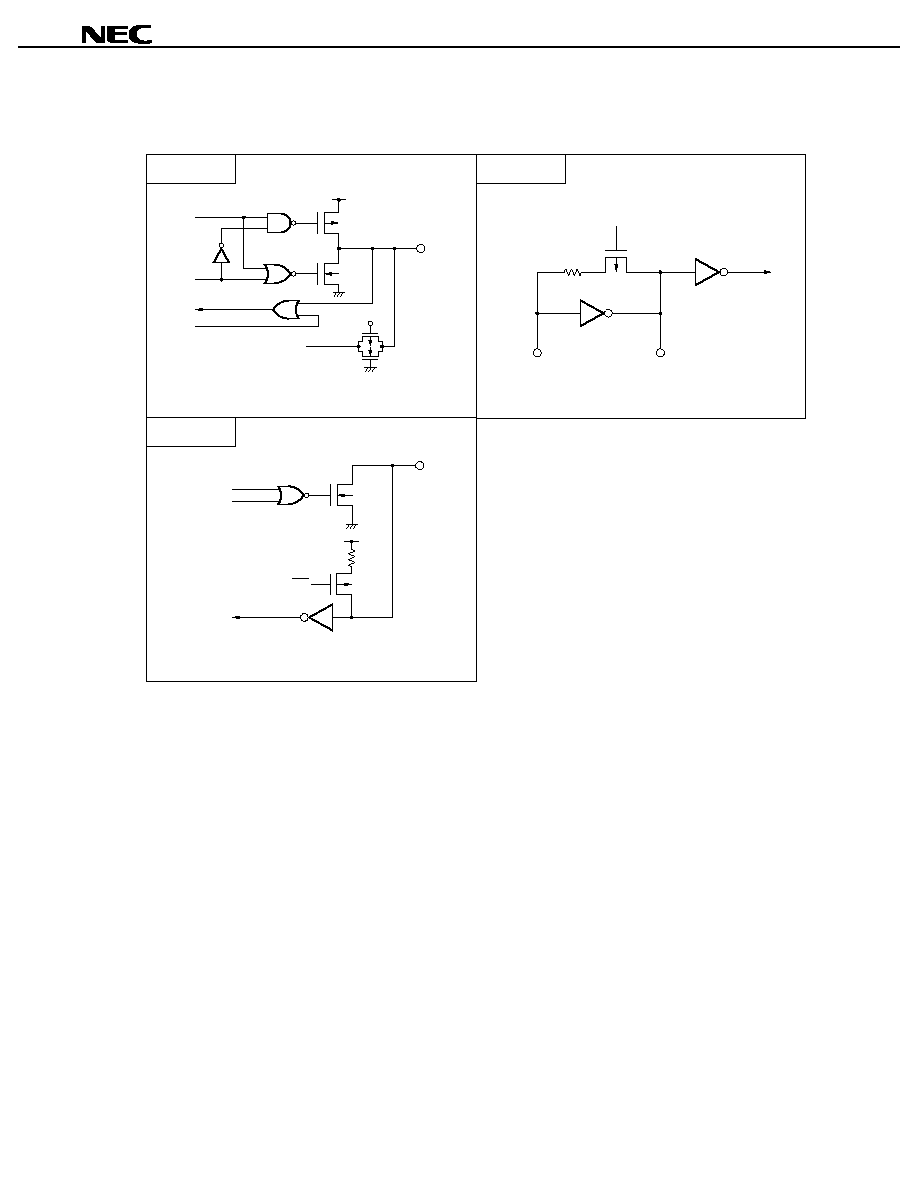
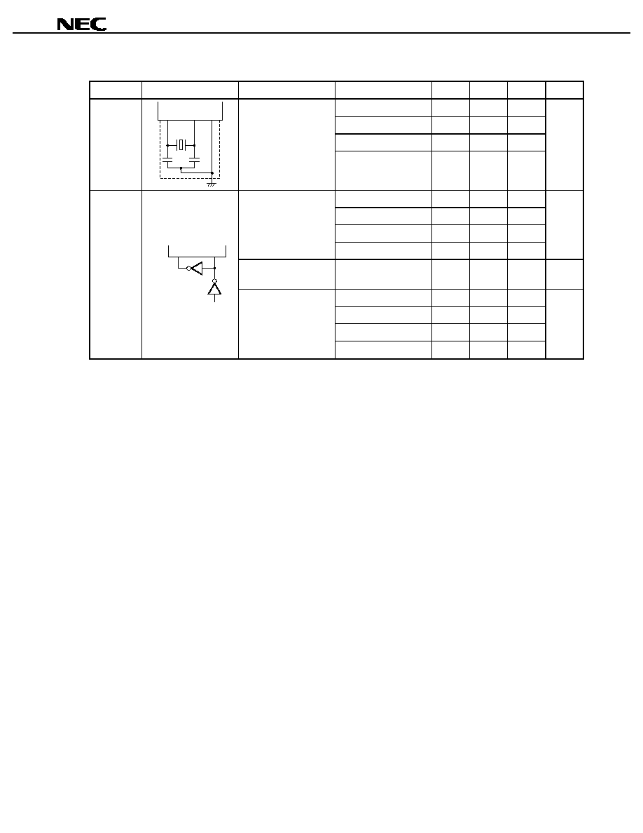
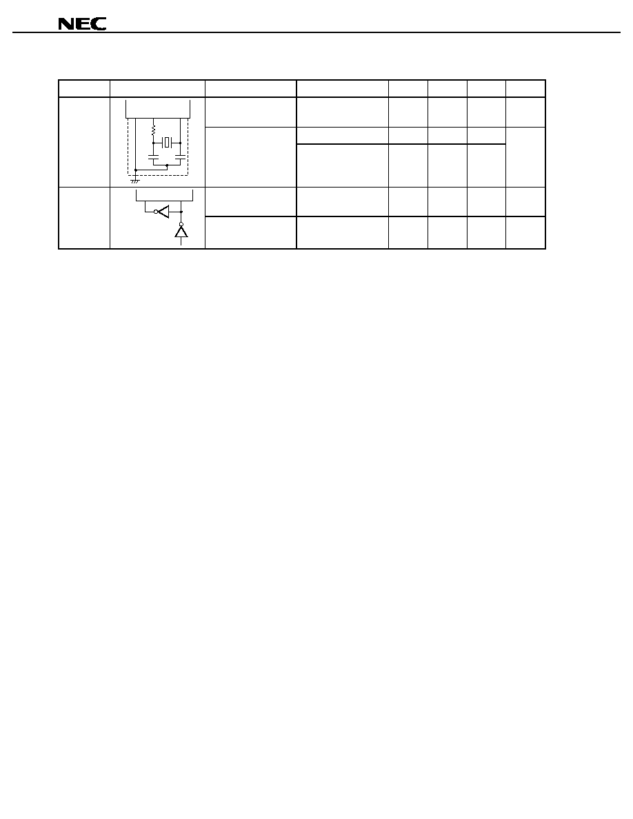
4.3 Pin I/O Circuits and Recommended Connections of Unused Pins
The I/O circuit type of each pin and recommended connections of unused pins are shown in Table 4-1.
For each type of input/output circuit, refer to Figure 4-1.
Table 4-1. Types of Pin I/O Circuits and Recommended Connection of Unused Pins (1/2)
Pin Name
I/O Circuit Type
I/O
Recommended Connection of Unused Pins
P00/INTP0
P01/INTP1
P02/INTP2/NMI
P03/INTP3 to P06/INTP6
8-N
I/O
Input:
Independently connect to V
SS
via a resistor
Output: Leave open
P10/ANI0 to P17/ANI7
9
Input
Connect to V
SS
or V
DD
P20/RxD1/SI1
10-K
P21/TxD1/SO1
10-L
P22/ASCK1/SCK1
10-K
P23/PCL
P24/BUZ
10-L
P25/SI0/SDA0
Note 1
10-K
P26/SO0
10-L
P27/SCK0/SCL0
Note 1
10-K
P30/TO0 to P32/TO2
12-E
P33/TI1, P34/TI2
8-N
P35/TI00, P36/TI01
10-M
P37/EXA
Note 2
12-E
P40/AD0 to P47/AD7
P50/A8 to P57/A15
P60/A16 to P63/A19
P64/RD
P65/WR
P66/WAIT
P67/ASTB
5-A
P70/RxD2/SI2
8-N
P71/TxD2/SO2
10-M
P72/ASCK2/SCK2
8-N
P80/A0 to P87/A7
12-E
P90 to P95
13-D
P100/TI5/TO5
P101/TI6/TO6
P102/TI7/TO7
P103/TI8/TO8
8-N
P120/RTP0 to P127/RTP7
12-E
P130/ANO0, P131/ANO1
12-F
I/O
Input:
Independently connect to V
SS
via a resistor
Output: Leave open
Notes 1. The SDA0 and SCL0 pins are available in the
µ
PD78F4216AY, 78F4218AY only.
2. The EXA pin is available in the
µ
PD78F4218A, 78F4218AY only.
Data Sheet U14125EJ1V0DS00
17
µ
µ
µ
µ
PD78F4216A, 78F4218A, 78F4216AY, 78F4218AY
Table 4-1. Types of Pin I/O Circuits and Recommended Connection of Unused Pins (2/2)
Pin Name
I/O Circuit Type
I/O
Recommended Connection of Unused Pins
RESET
2-G
-
XT1
Input
Connect to V
SS
XT2
16
Leave open
AV
REF0
Connect to V
SS
AV
REF1
AV
DD
Connect to V
DD
AV
SS
Connect to V
SS
V
PP
-
-
Connect this pin to V
SS
directly or via a pull-down resist in normal
operation mode. Connect the V
PP
pin to V
SS
via a pull-down
resistor in a system in which the on-chip flash memory is written
while mounted on the target board.
For the pull-down connection, it is recommended to use a resistor
with a resistance ranging from 470
to 10 k
.
Remark Because the circuit type numbers are standardized among the 78K Series products, they are not
sequential in some models (i.e., some circuits are not provided).

Data Sheet U14125EJ1V0DS00
18
µ
µ
µ
µ
PD78F4216A, 78F4218A, 78F4216AY, 78F4218AY
Figure 4-1. Types of Pin I/O Circuits (1/2)
IN
Pullup
enable
Data
Output
disable
Input
enable
V
DD
P-ch
V
DD
P-ch
IN/OUT
N-ch
Pullup
enable
Data
Output
disable
V
DD
P-ch
V
DD
P-ch
IN/OUT
N-ch
Pullup
enable
Data
Open drain
Output disable
V
DD
P-ch
V
DD
P-ch
IN/OUT
N-ch
Pullup
enable
Data
Open drain
Output disable
Output disable
V
DD
P-ch
V
DD
V
SS
P-ch
IN/OUT
N-ch
Pullup
enable
Data
V
DD
P-ch
V
DD
V
SS
P-ch
IN/OUT
N-ch
Pullup
enable
Data
Output
disable
Input
enable
V
DD
P-ch
V
DD
P-ch
IN/OUT
N-ch
P-ch
N-ch
IN
Comparator
+
≠
P-ch
N-ch
Input
enable
Type 2-G
Type 5-A
Type 8-N
Type 9
(Threshold voltage)
Analog output
voltage
Type 12-E
Type 10-M
Type 10-L
Type 10-K
Schmitt-triggered input with hysteresis characteristics
V
REF
Data Sheet U14125EJ1V0DS00
19
µ
µ
µ
µ
PD78F4216A, 78F4218A, 78F4216AY, 78F4218AY
Figure 4-1. Types of Pin I/O Circuits (2/2)
Data
Output disable
Middle-voltage input buffer
IN/OUT
N-ch
P-ch
V
DD
RD
Data
Analog output
voltage
Type 12-F
Type 13-D
Type 16
Output
disable
P-ch
IN/OUT
V
DD
V
SS
V
SS
N-ch
Input
enable
P-ch
N-ch
P-ch
Feedback
cut-off
XT1
XT2
Data Sheet U14125EJ1V0DS00
20
µ
µ
µ
µ
PD78F4216A, 78F4218A, 78F4216AY, 78F4218AY
5. INTERNAL MEMORY SIZE SWITCHING REGISTER (IMS)
IMS is a register that is set by software and is used to specify a part of the internal memory that is not to be used.
By setting this register, the internal memory of the
µ
PD78F4218AY can be mapped identically to that of a mask ROM
version with a different internal memory (ROM and RAM) capacity.
IMS is set with an 8-bit memory manipulation instruction.
RESET input sets IMS to FFH.
(1)
µ
µ
µ
µ
PD78F4216A, 78F4216AY
Figure 5-1. Internal Memory Size Switching Register (IMS) Format
Address: 0FFFCH
After reset: FFH W
7
6
5
4
3
2
1
0
IMS
1
1
ROM1
ROM0
1
1
RAM1
RAM0
ROM1
ROM0
Internal ROM Capacity Selection
0
0
48 KB
0
1
64 KB
1
0
96 KB
1
1
128 KB
RAM1
RAM0
Peripheral RAM Capacity Selection
0
0
3,072 bytes
0
1
4,608 bytes
1
0
6,114 bytes
1
1
7,680 bytes
Caution IMS is not provided on the mask ROM versions (
µ
µ
µ
µ
PD784214A, 784215A, 784216A,
µ
µ
µ
µ
PD784214AY,
784215AY, and 784216AY).
Table 5-1 shows the IMS setting values to make the memory mapping the same as that of the mask ROM
versions.
Table 5-1. Setting Value of Internal Memory Size Switching Register (IMS)
Target Mask ROM Version
IMS Setting Value
µ
PD784214A, 784214AY
ECH
µ
PD784215A, 784215AY
FDH
µ
PD784216A, 784216AY
FFH
Data Sheet U14125EJ1V0DS00
21
µ
µ
µ
µ
PD78F4216A, 78F4218A, 78F4216AY, 78F4218AY
(2)
µ
µ
µ
µ
PD78F4218A, 78F4218AY
Figure 5-2. Internal Memory Size Switching Register (IMS) Format
Address: 0FFFCH
After reset: FFH W
7
6
5
4
3
2
1
0
IMS
1
1
ROM1
ROM0
1
1
RAM1
RAM0
ROM1
ROM0
Internal ROM Capacity Selection
0
0
64 KB
0
1
128 KB
1
0
192 KB
1
1
256 KB
RAM1
RAM0
Peripheral RAM Capacity Selection
0
0
3,072 bytes
0
1
6,656 bytes
1
0
7,168 bytes
1
1
12,288 bytes
Caution IMS is not provided on the mask ROM versions (
µ
µ
µ
µ
PD784217A, 784218A, 784217AY, and
784218AY).
Table 5-2 shows the IMS setting values to make the memory mapping the same as that of the mask ROM
versions.
Table 5-2. Setting Value of Internal Memory Size Switching Register (IMS)
Target Mask ROM Version
IMS Setting Value
µ
PD784217A, 784217AY
EFH
µ
PD784218A, 784218AY
FFH

Data Sheet U14125EJ1V0DS00
22
µ
µ
µ
µ
PD78F4216A, 78F4218A, 78F4216AY, 78F4218AY
6. PROGRAMMING FLASH MEMORY
The flash memory can be written with the
µ
PD78F4218AY mounted on the target board (on-board). To do so,
connect a dedicated flash programmer (Flashpro II (part number: FL-PR2), Flashpro III (part number: FL-PR3, PG-
FP3) to the host machine and target system.
Writing to flash memory can also be performed using flash memory writing adapter connected to Flashpro II or
Flashpro III.
Remark FL-PR2 and FL-PR3 are products of Naito Densei Machida Mfg. Co., Ltd.
6.1 Selecting Communication Mode
To write the flash memory, use Flashpro II and Flashpro III by serial communication. Select a serial
communication mode from those listed in Table 6-1 in the format shown in Figure 6-1. Each communication mode is
selected by the number of V
PP
pulses shown in Table 6-1.
Table 6-1. Communication Modes
Communication
Mode
Number of
Channels
Pins Used
Number of
V
PP
Pulses
SCK0/P27/SCL0
Note 1
SO0/P26
SI0/P25/SDA0
Note 1
0
SCK1/ASCK1/P22
SO1/TxD1/P21
SI1/RxD1/P20
1
3-wire serial I/O
3
SCK2/ASCK2/P72
SO2/TxD2/P71
SI2/RxD2/P70
2
Handshake
Note 2
1
SCK0/P27/SCL0
Note 1
SO0/P26
SI0/P25/SDA0
Note 1
P24/BUZ
3
TxD1/SO1/P21
RxD1/SI1/P20
8
UART
2
TxD2/SO2/P71
RxD2/SI2/P70
9
Notes 1. The SCL0 and SDA0 pins are available in the
µ
PD78F4216AY, 78F4218AY only.
2. This made is available in the
µ
PD78F4216A, 78F4216AY (other than I, K, E standard)
This made is available in the
µ
PD78F4218A, 78F4218AY (other than I standard)
Caution Be sure to select a communication mode with the number of V
PP
pulses shown in Table 6-1.

Data Sheet U14125EJ1V0DS00
23
µ
µ
µ
µ
PD78F4216A, 78F4218A, 78F4216AY, 78F4218AY
Figure 6-1. Communication Mode Selecting Format
6.2 Flash Memory Programming Function
The flash memory is written by transferring or receiving commands and data in a selected communication mode.
The major functions of flash memory programming are listed in Table 6-2.
Table 6-2. Major Functions of Flash Memory Programming
Function
Description
Batch erasure
Erases all contents of memory.
Block erasure
Erases contents of specified memory block with one memory block
consisting of 16 KB.
Batch blank check
Checks erased status of entire memory.
Block blank check
Checks erased status of specified block.
Data write
Writes flash memory based on write start address and number of
data to be written (in bytes).
Batch verify
Compares all contents of memory with input data.
Block verify
Compares contents of specified memory block with input data.
10 V
V
DD
V
SS
V
DD
V
PP
RESET
V
SS
1
2
n
V
PP
pulses
Flash programming mode
Data Sheet U14125EJ1V0DS00
24
µ
µ
µ
µ
PD78F4216A, 78F4218A, 78F4216AY, 78F4218AY
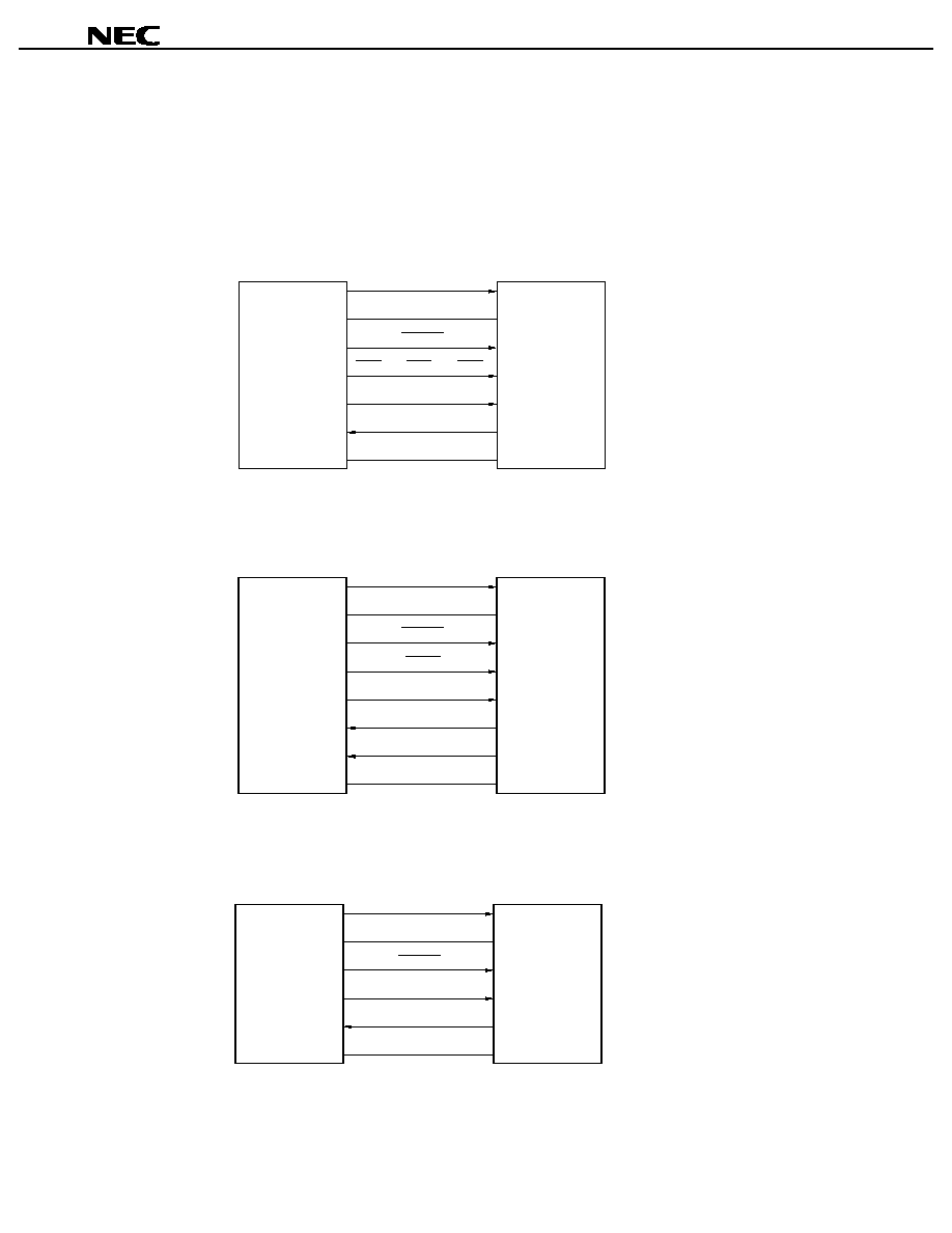
6.3 Connecting Flashpro II and Flashpro III
The Flashpro II, Flashpro III and
µ
PD78F4218AY are connected differently depending on the selected
communication mode (3-wire serial I/O or UART). Figures 6-2 to 6-4 show the connections in the respective
communication modes.
Figure 6-2. Connection of Flashpro II and Flashpro III in 3-Wire Serial I/O Mode
Figure 6-3. Connection of Flashpro III in Handshake Mode
Figure 6-4. Connection of Flashpro II and Flashpro III in UART Mode
V
PP
V
DD
RESET
SCK0 or SCK1 or SCK2
SI0 or SI1 or SI2
SO0 or SO1 or SO2
V
SS
Flashpro ll,
Flashpro lll
PD78F4218AY
µ
V
PP
V
DD
RESET
SCK0
SI0
SO0
P24
V
SS
Flashpro lll
PD78F4218AY
µ
V
PP
V
DD
RESET
RxD1 or RxD2
TxD1 or TxD2
V
SS
Flashpro ll,
Flashpro lll
PD78F4218AY
µ
Data Sheet U14125EJ1V0DS00
25
µ
µ
µ
µ
PD78F4216A, 78F4218A, 78F4216AY, 78F4218AY
7. ELECTRICAL SPECIFICATIONS
Absolute Maximum Ratings (T
A
= 25
∞
∞
∞
∞
C)
Parameter
Symbol
Conditions
Ratings
Unit
V
DD
-
0.3 to +6.5
V
AV
DD
-
0.3 to V
DD
+ 0.3
V
AV
SS
-
0.3 to V
SS
+ 0.3
V
AV
REF0
A/D converter reference voltage input
-
0.3 to V
DD
+ 0.3
V
Supply voltage
AV
REF1
D/A converter reference voltage input
-
0.3 to V
DD
+ 0.3
V
V
I1
Other than P90 to P95
-
0.3 to V
DD
+ 0.3
V
V
I2
P90 to P95
N-ch open drain
-
0.3 to +12
V
Input voltage
V
I3
V
PP
pin for programming
-
0.3 to +10.5
V
Analog input voltage
V
AN
Analog input pin
AV
SS
-
0.3 to AV
REF0
+ 0.3
V
Output voltage
V
O
-
0.3 to V
DD
+ 0.3
V
Per pin
15
mA
Total of P2, P4 to P8
75
mA
Total of P0, P3, P9, P10, P12, P13
75
mA
Output current, low
I
OL
Total of all pins
100
mA
Per pin
-
10
mA
Output current, high
I
OH
Total of all pins
-
50
mA
Operating ambient
temperature
T
A
-
40 to +85
∞
C
Storage temperature
T
stg
-
65 to +125
∞
C
Caution
Product quality may suffer if the absolute maximum rating is exceeded even momentarily for
any parameter. That is, the absolute maximum ratings are rated values at which the product is
on the verge of suffering physical damage, and therefore the product must be used under
conditions that ensure that the absolute maximum ratings are not exceeded.
Data Sheet U14125EJ1V0DS00
26
µ
µ
µ
µ
PD78F4216A, 78F4218A, 78F4216AY, 78F4218AY
Operating Conditions
∑
Operating ambient temperature (T
A
):
-
40 to +85
∞
C
∑
Supply voltage and clock cycle time: See Figure 7-1
∑
Operating voltage with subsystem clock operation: V
DD
= 1.9 to 5.5 V
Figure 7-1. Supply Voltage and Clock Cycle Time (CPU Clock Frequency: f
CPU
)
Capacitance (T
A
= 25
∞
∞
∞
∞
C, V
DD
= V
SS
= 0 V)
Parameter
Symbol
Conditions
MIN.
TYP.
MAX.
Unit
Other than Port 9
15
pF
Input capacitance
C
I
Port 9
20
pF
Other than Port 9
15
pF
Output capacitance
C
O
Port 9
20
pF
Other than Port 9
15
pF
I/O capacitance
C
IO
f = 1 MHz
Unmeasured pins
returned to 0 V.
Port 9
20
pF
8,000
10,000
500
400
300
320
160
80
200
100
0
0
1
2
3
1.9
2.7
4.5
5.5
Supply voltage [V]
4
5
6
Clock cycle time t
CYK
[ns]
Guaranteed
operating range
Data Sheet U14125EJ1V0DS00
27
µ
µ
µ
µ
PD78F4216A, 78F4218A, 78F4216AY, 78F4218AY
Main System Clock Oscillator Characteristics (T
A
=
-
-
-
-
40 to +85
∞
∞
∞
∞
C)
Resonator
Recommended Circuit
Parameter
Conditions
MIN.
TYP.
MAX.
Unit
4.5 V
V
DD
5.5 V
2
12.5
2.7 V
V
DD
< 4.5 V
2
6.25
2.0 V
V
DD
< 2.7 V
2
3.125
Ceramic
resonator
or crystal
resonator
X2
X1 V
SS
Oscillation frequency
(f
X
)
1.9 V
V
DD
< 2.0 V
2
2
MHz
4.5 V
V
DD
5.5 V
2
12.5
2.7 V
V
DD
< 4.5 V
2
6.25
2.0 V
V
DD
< 2.7 V
2
3.125
X1 input frequency (f
X
)
1.9 V
V
DD
< 2.0 V
2
2
MHz
X1 input high-/low-
level width (t
WXH
, t
WXL
)
15
250
ns
4.5 V
V
DD
5.5 V
0
5
2.7 V
V
DD
< 4.5 V
0
10
2.0 V
V
DD
< 2.7 V
0
20
External
clock
X2
X1
PD74HCU04
µ
X1 input rising/falling
time (t
XR
, t
XF
)
1.9 V
V
DD
< 2.0 V
0
30
ns
Cautions 1. When using the main system clock oscillator, wire as follows in the area enclosed by the
broken lines in the above figures to avoid an adverse effect from wiring capacitance.
∑
∑
∑
∑
Keep the wiring length as short as possible.
∑
∑
∑
∑
Do not cross the wiring with other signal lines.
∑
∑
∑
∑
Do not route the wiring near a signal line through which a high fluctuating current flows.
∑
∑
∑
∑
Always make the ground point of the oscillator capacitor the same potential as V
SS
.
∑
∑
∑
∑
Do not ground the capacitor to a ground pattern through which a high current flows.
∑
∑
∑
∑
Do not fetch signals from the oscillator.
2. When the main system clock is stopped and the system is operated by the subsystem clock,
the subsystem clock should be switched back to the main system clock after the oscillation
stabilization time is secured by the program.
Remark For the resonator selection and oscillator constant, users are required to either evaluate the oscillation
themselves or apply to the resonator manufacturer for evaluation.
Data Sheet U14125EJ1V0DS00
28
µ
µ
µ
µ
PD78F4216A, 78F4218A, 78F4216AY, 78F4218AY
Subsystem Clock Oscillator Characteristics (T
A
=
-
-
-
-
40 to +85
∞
∞
∞
∞
C)
Resonator
Recommended Circuit
Parameter
Conditions
MIN.
TYP.
MAX.
Unit
Oscillation frequency
(f
XT
)
32
32.768
35
kHz
4.5 V
V
DD
5.5 V
1.2
2
Crystal
resonator
V
SS
XT2
XT1
Oscillation
stabilization time
Note
1.9 V
V
DD
< 4.5 V
10
s
XT1 input frequency
(f
XT
)
32
35
kHz
External
clock
XT2
XT1
PD74HCU04
µ
XT1 input high-/low-
level width (t
XTH
, t
XTL
)
14.3
15.6
µ
s
Note Time required to stabilize oscillation after applying supply voltage (V
DD
).
Cautions 1. When using the subsystem clock oscillator, wire as follows in the area enclosed by the
broken lines in the above figures to avoid an adverse effect from wiring capacitance.
∑
∑
∑
∑
Keep the wiring length as short as possible.
∑
∑
∑
∑
Do not cross the wiring with other signal lines.
∑
∑
∑
∑
Do not route the wiring near a signal line through which a high fluctuating current flows.
∑
∑
∑
∑
Always make the ground point of the oscillator capacitor the same potential as V
SS
.
∑
∑
∑
∑
Do not ground the capacitor to a ground pattern through which a high current flows.
∑
∑
∑
∑
Do not fetch signals from the oscillator.
2. When the main system clock is stopped and the device is operating on the subsystem clock,
wait until the oscillation stabilization time has been secured by the program before switching
back to the main system clock.
Remark For the resonator selection and oscillator constant, users are required to either evaluate the oscillation
themselves or apply to the resonator manufacturer for evaluation.
Data Sheet U14125EJ1V0DS00
29
µ
µ
µ
µ
PD78F4216A, 78F4218A, 78F4216AY, 78F4218AY
DC Characteristics (T
A
=
-
-
-
-
40 to +85
∞
∞
∞
∞
C, V
DD
= AV
DD
= 1.9 to 5.5 V, V
SS
= AV
SS
= 0 V) (1/3)
Parameter
Symbol
Conditions
MIN.
TYP.
MAX.
Unit
2.2 V
V
DD
5.5 V
0
0.3V
DD
V
IL1
Note 1
1.9 V
V
DD
< 2.2 V
0
0.2V
DD
V
2.2 V
V
DD
5.5 V
0
0.2V
DD
V
IL2
P00 to P06, P20, P22, P33,
P34, P70, P72,
P100 to P103, RESET
1.9 V
V
DD
< 2.2 V
0
0.15V
DD
V
2.2 V
V
DD
5.5 V
0
0.3V
DD
V
IL3
P90 to P95
(N-ch open drain)
1.9 V
V
DD
< 2.2 V
0
0.2V
DD
V
2.2 V
V
DD
5.5 V
0
0.3V
DD
V
IL4
P10 to P17, P130, P131
1.9 V
V
DD
< 2.2 V
0
0.2V
DD
V
2.2 V
V
DD
5.5 V
0
0.2V
DD
V
IL5
X1, X2, XT1, XT2
1.9 V
V
DD
< 2.2 V
0
0.1V
DD
V
2.2 V
V
DD
5.5 V
0
0.3V
DD
Input voltage, low
V
IL6
P25, P27
1.9 V
V
DD
< 2.2 V
0
0.2V
DD
V
2.2 V
V
DD
5.5 V
0.7V
DD
V
DD
V
IH1
Note 1
1.9 V
V
DD
< 2.2 V
0.8V
DD
V
DD
V
2.2 V
V
DD
5.5 V
0.8V
DD
V
DD
V
IH2
P00 to P06, P20, P22, P33,
P34, P70, P72,
P100 to P103, RESET
1.9 V
V
DD
< 2.2 V
0.85V
DD
V
DD
V
2.2 V
V
DD
5.5 V
0.7V
DD
12
V
IH3
P90 to P95
(N-ch open drain)
1.9 V
V
DD
< 2.2 V
0.8V
DD
V
DD
V
2.2 V
V
DD
5.5 V
0.7V
DD
V
DD
V
IH4
P10 to P17, P130, P131
1.9 V
V
DD
< 2.2 V
0.8V
DD
V
DD
V
2.2 V
V
DD
5.5 V
0.8V
DD
V
DD
V
IH5
X1, X2, XT1, XT2
1.9 V
V
DD
< 2.2 V
0.85V
DD
V
DD
V
2.2 V
V
DD
5.5 V
0.7V
DD
V
DD
Input voltage, high
V
IH6
P25, P27
1.9 V
V
DD
< 2.2 V
0.8V
DD
V
DD
V
For pins other than
P40 to P47, P50 to P57,
P90 to P95 I
OL
= 1.6 mA
Note 1
4.5 V
V
DD
5.5 V
0.4
V
P40 to P47, P50 to P57
I
OL
= 8 mA
Note 2
4.5 V
V
DD
5.5 V
1.0
V
V
OL1
P90 to P95 I
OL
= 15 mA
Note 2
4.5 V
V
DD
5.5 V
0.8
2.0
V
Output voltage, low
V
OL2
I
OL
= 400
µ
A
Note 2
0.5
V
I
OH
=
-
1 mA
Note 2
4.5 V
V
DD
5.5 V
V
DD
-
1.0
V
Output voltage, high
V
OH1
I
OL
=
-
100
µ
A
Note 2
V
DD
-
0.5
V
I
LIL1
Except X1, X2, XT1,
XT2
-
3
µ
A
Input leakage current, low
I
LIL2
V
IN
= 0 V
X1, X2, XT1, XT2
-
20
µ
A
I
LIH1
Except X1, X2, XT1,
XT2
3
µ
A
I
LIH2
V
IN
= V
DD
X1, X2, XT1, XT2
20
µ
A
Input leakage current, high
I
LIH3
V
IN
= 12 V (N-ch open drain) P90 to P95
20
µ
A
Output leakage current, low
I
LOL1
V
OUT
= 0 V
-
3
µ
A
Output leakage current, high
I
LOH1
V
OUT
= V
DD
3
µ
A
Notes 1. P21, P23, P24, P26, P30 to P32, P35 to P37, P40 to P47, P50 to P57, P60 to P67, P71, P80 to P87,
P120 to P127
2. Per pin

Data Sheet U14125EJ1V0DS00
30
µ
µ
µ
µ
PD78F4216A, 78F4218A, 78F4216AY, 78F4218AY
DC Characteristics (T
A
=
-
-
-
-
40 to +85
∞
∞
∞
∞
C, V
DD
= AV
DD
= 1.9 to 5.5 V, V
SS
= AV
SS
= 0 V) (2/3)
(1)
µ
µ
µ
µ
PD78F4216A, 78F4216AY
Parameter
Symbol
Conditions
MIN.
TYP.
MAX.
Unit
f
XX
= 12.5 MHz, V
DD
= 5.0 V
±
10%
17
40
mA
f
XX
= 6 MHz, V
DD
= 3.0 V
±
10%
5
17
mA
I
DD1
Operation
mode
f
XX
= 2 MHz, V
DD
= 2.0 V
±
5%
2
10
mA
f
XX
= 12.5 MHz, V
DD
= 5.0 V
±
10%
6
20
mA
f
XX
= 6 MHz, V
DD
= 3.0 V
±
10%
2
10
mA
I
DD2
HALT mode
f
XX
= 2 MHz, V
DD
= 2.0 V
±
5%
0.4
7
mA
f
XX
= 12.5 MHz, V
DD
= 5.0 V
±
10%
1
3
mA
f
XX
= 6 MHz, V
DD
= 3.0 V
±
10%
0.5
1.3
mA
I
DD3
IDLE mode
f
XX
= 2 MHz, V
DD
= 2.0 V
±
5%
0.3
0.9
mA
f
XX
= 32 kHz, V
DD
= 5.0 V
±
10%
130
500
µ
A
f
XX
= 32 kHz, V
DD
= 3.0 V
±
10%
90
350
µ
A
f
XX
= 32 kHz, 2.0 V
V
DD
2.7 V
80
300
µ
A
I
DD4
Operation
mode
Note
f
XX
= 32 kHz, 1.9 V
V
DD
<
2.0 V
70
250
µ
A
f
XX
= 32 kHz, V
DD
= 5.0 V
±
10%
60
200
µ
A
f
XX
= 32 kHz, V
DD
= 3.0 V
±
10%
20
160
µ
A
f
XX
= 32 kHz, 2.0 V
V
DD
2.7 V
15
120
µ
A
I
DD5
HALT
mode
Note
f
XX
= 32 kHz, 1.9 V
V
DD
<
2.0 V
10
100
µ
A
f
XX
= 32 kHz, V
DD
= 5.0 V
±
10%
50
190
µ
A
f
XX
= 32 kHz, V
DD
= 3.0 V
±
10%
15
150
µ
A
f
XX
= 32 kHz, 2.0 V
V
DD
2.7 V
12
110
µ
A
Supply voltage
I
DD6
IDLE
mode
Note
f
XX
= 32 kHz, 1.9 V
V
DD
<
2.0 V
7
90
µ
A
Data retention voltage
V
DDDR
HALT, IDLE modes
1.9
5.5
V
V
DD
= 2.0 V
±
5%
2
10
µ
A
Data retention current
I
DDDR
STOP mode
V
DD
= 5.0 V
±
10%
10
50
µ
A
Pull-up resistor
R
L
V
IN
= 0 V
10
30
100
k
Note When main system clock is stopped and subsystem clock is operating.
Remark Unless otherwise specified, the characteristics of alternate-function pins are the same as those of port
pins.
Data Sheet U14125EJ1V0DS00
31
µ
µ
µ
µ
PD78F4216A, 78F4218A, 78F4216AY, 78F4218AY
DC Characteristics (T
A
=
-
-
-
-
40 to +85
∞
∞
∞
∞
C, V
DD
= AV
DD
= 1.9 to 5.5 V, V
SS
= AV
SS
= 0 V) (3/3)
(2)
µ
µ
µ
µ
PD78F4218A, 78F4218AY
Parameter
Symbol
Conditions
MIN.
TYP.
MAX.
Unit
f
XX
= 12.5 MHz, V
DD
= 5.0 V
±
10%
19
40
mA
f
XX
= 6 MHz, V
DD
= 3.0 V
±
10%
6
17
mA
I
DD1
Operation
mode
f
XX
= 3 MHz, V
DD
= 2.0 V
±
5%
2
10
mA
f
XX
= 12.5 MHz, V
DD
= 5.0 V
±
10%
7
20
mA
f
XX
= 6 MHz, V
DD
= 3.0 V
±
10%
2
10
mA
I
DD2
HALT mode
f
XX
= 3 MHz, V
DD
= 2.0 V
±
5%
0.5
7
mA
f
XX
= 12.5 MHz, V
DD
= 5.0 V
±
10%
1
3
mA
f
XX
= 6 MHz, V
DD
= 3.0 V
±
10%
0.5
1.3
mA
I
DD3
IDLE mode
f
XX
= 3 MHz, V
DD
= 2.0 V
±
5%
0.3
0.9
mA
f
XX
= 32 kHz, V
DD
= 5.0 V
±
10%
140
500
µ
A
f
XX
= 32 kHz, V
DD
= 3.0 V
±
10%
100
350
µ
A
f
XX
= 32 kHz, 2.0 V
V
DD
2.7 V
90
300
µ
A
I
DD4
Operation
mode
Note
f
XX
= 32 kHz, 1.9 V
V
DD
<
2.0 V
80
250
µ
A
f
XX
= 32 kHz, V
DD
= 5.0 V
±
10%
60
200
µ
A
f
XX
= 32 kHz, V
DD
= 3.0 V
±
10%
20
160
µ
A
f
XX
= 32 kHz, 2.0 V
V
DD
2.7 V
15
120
µ
A
I
DD5
HALT
mode
Note
f
XX
= 32 kHz, 1.9 V
V
DD
<
2.0 V
10
100
µ
A
f
XX
= 32 kHz, V
DD
= 5.0 V
±
10%
50
190
µ
A
f
XX
= 32 kHz, V
DD
= 3.0 V
±
10%
15
150
µ
A
f
XX
= 32 kHz, 2.0 V
V
DD
2.7 V
12
110
µ
A
Supply voltage
I
DD6
IDLE
mode
Note
f
XX
= 32 kHz, 1.9 V
V
DD
<
2.0 V
7
90
µ
A
Data retention voltage
V
DDDR
HALT, IDLE modes
1.9
5.5
V
V
DD
= 2.0 V
±
5%
2
10
µ
A
Data retention current
I
DDDR
STOP mode
V
DD
= 5.0 V
±
10%
10
50
µ
A
Pull-up resistor
R
L
V
IN
= 0 V
10
30
100
k
Note When main system clock is stopped and subsystem clock is operating.
Remark Unless otherwise specified, the characteristics of alternate-function pins are the same as those of port
pins.

Data Sheet U14125EJ1V0DS00
32
µ
µ
µ
µ
PD78F4216A, 78F4218A, 78F4216AY, 78F4218AY
AC Characteristics (T
A
=
-
-
-
-
40 to +85
∞
∞
∞
∞
C, V
DD
= AV
DD
= 1.9 to 5.5 V, V
SS
= AV
SS
= 0 V)
(1) Read/write operation (1/2)
Parameter
Symbol
Conditions
MIN.
TYP.
MAX.
Unit
4.5 V
V
DD
5.5 V
80
ns
2.7 V
V
DD
<
4.5 V
160
ns
2.0 V
V
DD
<
2.7 V
320
ns
Cycle time
t
CYK
1.9 V
V
DD
<
2.0 V
500
ns
V
DD
= 5.0 V
±
10%
(0.5
+
a)T
-
20
ns
V
DD
= 3.0 V
±
10%
(0.5
+
a)T
-
40
ns
Address setup time (to ASTB
)
t
SAST
V
DD
= 2.0 V
±
5%
(0.5
+
a)T
-
80
ns
V
DD
= 5.0 V
±
10%
0.5T
-
19
ns
V
DD
= 3.0 V
±
10%
0.5T
-
24
ns
Address hold time (from ASTB
) t
HSTLA
V
DD
= 2.0 V
±
5%
0.5T
-
34
ns
V
DD
= 5.0 V
±
10%
(0.5
+
a)T
-
17
ns
V
DD
= 3.0 V
±
10%
(0.5
+
a)T
-
40
ns
ASTB high-level width
t
WSTH
V
DD
= 2.0 V
±
5%
(0.5
+
a)T
-
110
ns
V
DD
= 5.0 V
±
10%
0.5T
-
14
ns
V
DD
= 3.0 V
±
10%
0.5T
-
14
ns
Address hold time (from RD
)
t
HRA
V
DD
= 2.0 V
±
5%
0.5T
-
14
ns
V
DD
= 5.0 V
±
10%
(1
+
a)T
-
24
ns
V
DD
= 3.0 V
±
10%
(1
+
a)T
-
35
ns
Delay time from address to RD
t
DAR
V
DD
= 2.0 V
±
5%
(1
+
a)T
-
80
ns
V
DD
= 5.0 V
±
10%
0
ns
V
DD
= 3.0 V
±
10%
0
ns
Address float time (from RD
)
t
FAR
V
DD
= 2.0 V
±
5%
0
ns
V
DD
= 5.0 V
±
10%
(2.5
+
a
+
n)T
-
37
ns
V
DD
= 3.0 V
±
10%
(2.5
+
a
+
n)T
-
52
ns
Data input time from address
t
DAID
V
DD
= 2.0 V
±
5%
(2.5
+
a
+
n)T
-
120
ns
V
DD
= 5.0 V
±
10%
(2
+
n)T
-
35
ns
V
DD
= 3.0 V
±
10%
(2
+
n)T
-
50
ns
Data input time from ASTB
t
DSTID
V
DD
= 2.0 V
±
5%
(2
+
n)T
-
80
ns
V
DD
= 5.0 V
±
10%
(1.5
+
n)T
-
40
ns
V
DD
= 3.0 V
±
10%
(1.5
+
n)T
-
50
ns
Data input time from RD
t
DRID
V
DD
= 2.0 V
±
5%
(1.5
+
n)T
-
90
ns
V
DD
= 5.0 V
±
10%
0.5T
-
9
ns
V
DD
= 3.0 V
±
10%
0.5T
-
9
ns
Delay time from ASTB
to RD
t
DSTR
V
DD
= 2.0 V
±
5%
0.5T
-
20
ns
V
DD
= 5.0 V
±
10%
0
ns
V
DD
= 3.0 V
±
10%
0
ns
Data hold time (from RD
)
t
HRID
V
DD
= 2.0 V
±
5%
0
ns
Remark T: t
CYK
= 1/f
XX
(f
XX
: main system clock frequency)
a: 1 (during address wait), otherwise, 0
n: Number of waits (n
0)
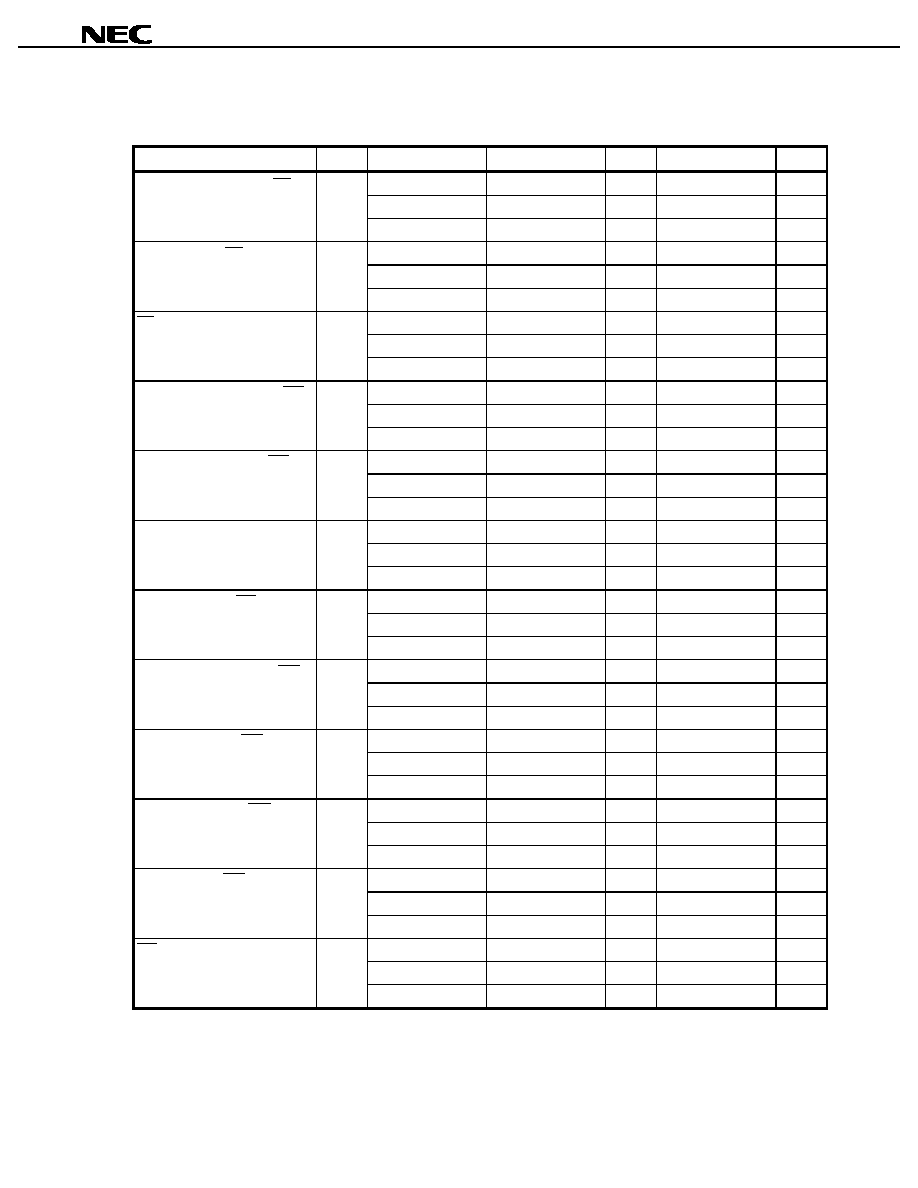
Data Sheet U14125EJ1V0DS00
33
µ
µ
µ
µ
PD78F4216A, 78F4218A, 78F4216AY, 78F4218AY
AC Characteristics
(1) Read/write operation (2/2)
Parameter
Symbol
Conditions
MIN.
TYP.
MAX.
Unit
V
DD
= 5.0 V
±
10%
0.5T
-
2
ns
V
DD
= 3.0 V
±
10%
0.5T
-
12
ns
Address active time from RD
t
DRA
V
DD
= 2.0 V
±
5%
0.5T
-
35
ns
V
DD
= 5.0 V
±
10%
0.5T
-
9
ns
V
DD
= 3.0 V
±
10%
0.5T
-
9
ns
Delay time from RD
to ASTB
t
DRST
V
DD
= 2.0 V
±
5%
0.5T
-
40
ns
V
DD
= 5.0 V
±
10%
(1.5
+
n)T
-
25
ns
V
DD
= 3.0 V
±
10%
(1.5
+
n)T
-
30
ns
RD low-level width
t
WRL
V
DD
= 2.0 V
±
5%
(1.5
+
n)T
-
25
ns
V
DD
= 5.0 V
±
10%
(1
+
a)T
-
24
ns
V
DD
= 3.0 V
±
10%
(1
+
a)T
-
34
ns
Delay time from address to WR
t
DAW
V
DD
= 2.0 V
±
5%
(1
+
a)T
-
70
ns
V
DD
= 5.0 V
±
10%
0.5T
-
14
ns
V
DD
= 3.0 V
±
10%
0.5T
-
14
ns
Address hold time (from WR
)
t
HRD
V
DD
= 2.0 V
±
5%
0.5T
-
14
ns
V
DD
= 5.0 V
±
10%
0.5T
+
15
ns
V
DD
= 3.0 V
±
10%
0.5T
+
30
ns
Delay time from ASTB
to data
output
t
DSTOD
V
DD
= 2.0 V
±
5%
0.5T
+
240
ns
V
DD
= 5.0 V
±
10%
0.5T
-
30
ns
V
DD
= 3.0 V
±
10%
0.5T
-
30
ns
Delay time from WR
to data
output
t
DWOD
V
DD
= 2.0 V
±
5%
0.5T
-
30
ns
V
DD
= 5.0 V
±
10%
0.5T
-
9
ns
V
DD
= 3.0 V
±
10%
0.5T
-
9
ns
Delay time from ASTB
to WR
t
DSTW
V
DD
= 2.0 V
±
5%
0.5T
-
20
ns
V
DD
= 5.0 V
±
10%
(1.5
+
n)T
-
20
ns
V
DD
= 3.0 V
±
10%
(1.5
+
n)T
-
25
ns
Data setup time (to WR
)
t
SODWR
V
DD
= 2.0 V
±
5%
(1.5
+
n)T
-
70
ns
V
DD
= 5.0 V
±
10%
0.5T
-
14
ns
V
DD
= 3.0 V
±
10%
0.5T
-
14
ns
Data hold time (from WR
)
t
HWOD
V
DD
= 2.0 V
±
5%
0.5T
-
50
ns
V
DD
= 5.0 V
±
10%
0.5T
-
9
ns
V
DD
= 3.0 V
±
10%
0.5T
-
9
ns
Delay time from WR
to ASTB
t
DWST
V
DD
= 2.0 V
±
5%
0.5T
-
30
ns
V
DD
= 5.0 V
±
10%
(1.5
+
n)T
-
25
ns
V
DD
= 3.0 V
±
10%
(1.5
+
n)T
-
30
ns
WR low-level width
t
WWL
V
DD
= 2.0 V
±
5%
(1.5
+
n)T
-
30
ns
Remark T: t
CYK
= 1/f
XX
(f
XX
: main system clock frequency)
a: 1 (during address wait), otherwise, 0
n: Number of wait states (n
0)
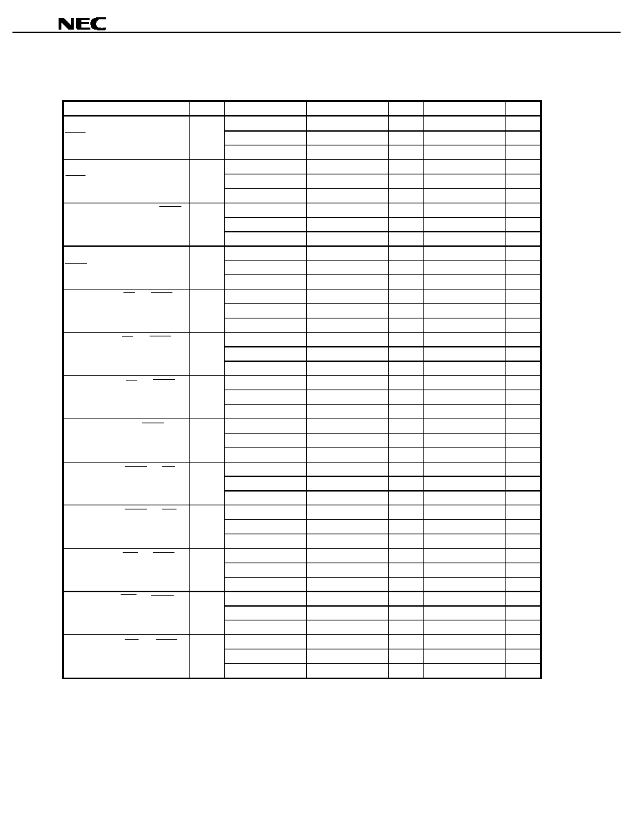
Data Sheet U14125EJ1V0DS00
34
µ
µ
µ
µ
PD78F4216A, 78F4218A, 78F4216AY, 78F4218AY
AC Characteristics
(2) External wait timing
Parameter
Symbol
Conditions
MIN.
TYP.
MAX.
Unit
V
DD
= 5.0 V
±
10%
(2
+
a)T
-
40
ns
V
DD
= 3.0 V
±
10%
(2
+
a)T
-
60
ns
Input time from address to
WAIT
t
DAWT
V
DD
= 2.0 V
±
5%
(2
+
a)T
-
300
ns
V
DD
= 5.0 V
±
10%
1.5T
-
40
ns
V
DD
= 3.0 V
±
10%
1.5T
-
60
ns
Input time from ASTB
to
WAIT
t
DSTWT
V
DD
= 2.0 V
±
5%
1.5T
-
260
ns
V
DD
= 5.0 V
±
10%
(0.5
+
n)T
+
5
ns
V
DD
= 3.0 V
±
10%
(0.5
+
n)T
+
10
ns
Hold time from ASTB
to WAIT
t
HSTWT
V
DD
= 2.0 V
±
5%
(0.5
+
n)T
+
30
ns
V
DD
= 5.0 V
±
10%
(1.5
+
n)T
-
40
ns
V
DD
= 3.0 V
±
10%
(1.5
+
n)T
-
60
ns
Delay time from ASTB
to
WAIT
t
DSTWTH
V
DD
= 2.0 V
±
5%
(1.5
+
n)T
-
90
ns
V
DD
= 5.0 V
±
10%
T
-
40
ns
V
DD
= 3.0 V
±
10%
T
-
60
ns
Input time from RD
to WAIT
t
DRWTL
V
DD
= 2.0 V
±
5%
T
-
70
ns
V
DD
= 5.0 V
±
10%
nT
+
5
ns
V
DD
= 3.0 V
±
10%
nT
+
10
ns
Hold time from RD
to WAIT
t
HRWT
V
DD
= 2.0 V
±
5%
nT
+
30
ns
V
DD
= 5.0 V
±
10%
(1
+
n)T
-
40
ns
V
DD
= 3.0 V
±
10%
(1
+
n)T
-
60
ns
Delay time from RD
to WAIT
t
DRWTH
V
DD
= 2.0 V
±
5%
(1
+
n)T
-
90
ns
V
DD
= 5.0 V
±
10%
0.5T
-
5
ns
V
DD
= 3.0 V
±
10%
0.5T
-
10
ns
Data input time from WAIT
t
DWTID
V
DD
= 2.0 V
±
5%
0.5T
-
30
ns
V
DD
= 5.0 V
±
10%
0.5T
ns
V
DD
= 3.0 V
±
10%
0.5T
ns
Delay time from WAIT
to RD
t
DWTR
V
DD
= 2.0 V
±
5%
0.5T
+
5
ns
V
DD
= 5.0 V
±
10%
0.5T
ns
V
DD
= 3.0 V
±
10%
0.5T
ns
Delay time from WAIT
to WR
t
DWTW
V
DD
= 2.0 V
±
5%
0.5T
+
5
ns
V
DD
= 5.0 V
±
10%
T
-
40
ns
V
DD
= 3.0 V
±
10%
T
-
60
ns
Input time from WR
to WAIT
t
DWWTL
V
DD
= 2.0 V
±
5%
T
-
90
ns
V
DD
= 5.0 V
±
10%
nT
+
5
ns
V
DD
= 3.0 V
±
10%
nT
+
10
ns
Hold time from WR
to WAIT
t
HWWT
V
DD
= 2.0 V
±
5%
nT
+
30
ns
V
DD
= 5.0 V
±
10%
(1
+
n)T
-
40
ns
V
DD
= 3.0 V
±
10%
(1
+
n)T
-
60
ns
Delay time from WR
to WAIT
t
DWWTH
V
DD
= 2.0 V
±
5%
(1
+
n)T
-
90
ns
Remark T: t
CYK
= 1/f
XX
(f
XX
: main system clock frequency)
a: 1 (during address wait), otherwise, 0
n: Number of wait states (n
0)
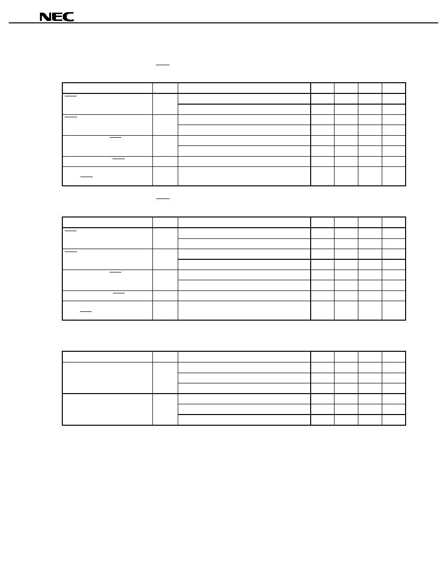
Data Sheet U14125EJ1V0DS00
35
µ
µ
µ
µ
PD78F4216A, 78F4218A, 78F4216AY, 78F4218AY
Serial Operation (T
A
=
-
-
-
-
40 to +85
∞
∞
∞
∞
C, V
DD
= AV
DD
= 1.9 to 5.5 V, V
SS
= AV
SS
= 0 V)
(a) 3-wire serial I/O mode (SCK: Internal clock output)
Parameter
Symbol
Conditions
MIN.
TYP.
MAX.
Unit
2.7 V
V
DD
5.5 V
800
ns
SCK cycle time
t
KCY1
3,200
ns
2.7 V
V
DD
5.5 V
350
ns
SCK high-/low-level width
t
KH1
,
t
KL1
1,500
ns
2.7 V
V
DD
5.5 V
10
ns
SI setup time (to SCK
)
t
SIK1
30
ns
SI hold time (from SCK
)
t
KSI1
40
ns
SO output delay time
(from SCK
)
t
KSO1
30
ns
(b) 3-wire serial I/O mode (SCK: External clock input)
Parameter
Symbol
Conditions
MIN.
TYP.
MAX.
Unit
2.7 V
V
DD
5.5 V
800
ns
SCK cycle time
t
KCY2
3,200
ns
2.7 V
V
DD
5.5 V
400
ns
SCK high-/low-level width
t
KH2
t
KL2
1,600
ns
2.7 V
V
DD
5.5 V
10
ns
SI setup time (to SCK
)
t
SIK2
30
ns
SI hold time (from SCK
)
t
KSI2
40
ns
SO output delay time
(from SCK
)
t
KSO2
30
ns
(c) UART mode
Parameter
Symbol
Conditions
MIN.
TYP.
MAX.
Unit
4.5 V
V
DD
5.5 V
417
ns
2.7 V
V
DD
< 4.5 V
833
ns
ASCK cycle time
t
KCY3
1,667
ns
4.5 V
V
DD
5.5 V
208
ns
2.7 V
V
DD
< 4.5 V
416
ns
ASCK high-/low-level width
t
KH3
t
KL3
833
ns
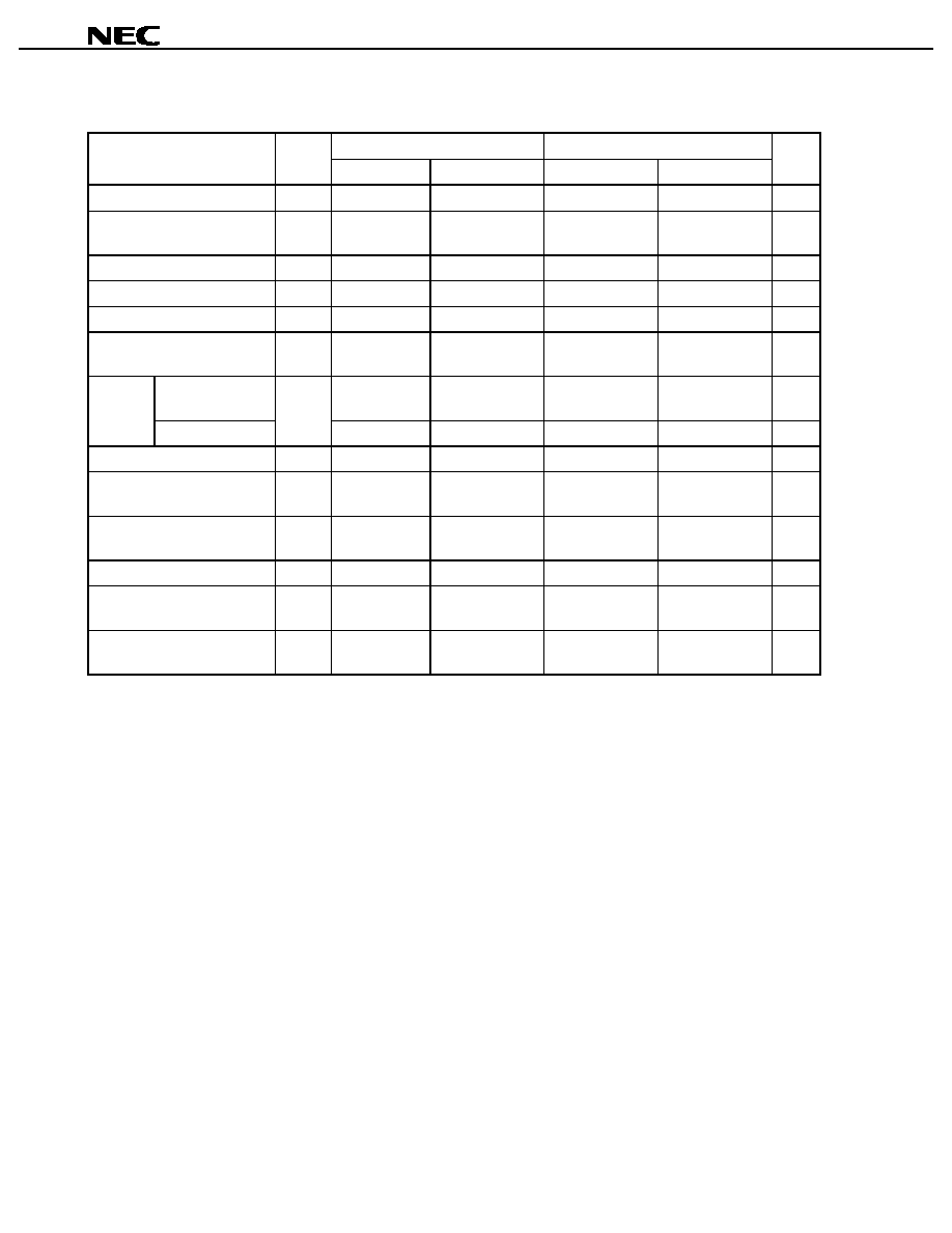
Data Sheet U14125EJ1V0DS00
36
µ
µ
µ
µ
PD78F4216A, 78F4218A, 78F4216AY, 78F4218AY
(d) I
2
C bus mode
Standard Mode
High-Speed Mode
Parameter
Symbol
MIN.
MAX.
MIN.
MAX.
Unit
SCL0 clock frequency
f
CLK
0
100
0
400
kHz
Bus free time (between stop
and start conditions)
t
BUF
4.7
-
1.3
-
µ
s
Hold time
Note1
t
HD : STA
4.0
-
0.6
-
µ
s
Low-level width of SCL0 clock
t
LOW
4.7
-
1.3
-
µ
s
High-level width of SCL0 clock
t
HIGH
4.0
-
0.6
-
µ
s
Setup time of start/restart
conditions
t
SU : STA
4.7
-
0.6
-
µ
s
When using CBUS-
compatible master
5.0
-
-
-
µ
s
Data hold
time
When using I
2
C bus
t
HD : DAT
0
Note 2
-
0
Note 2
0.9
Note 3
µ
s
Data setup time
t
SU : DAT
250
-
100
Note 4
-
ns
Rise time of SDA0 and SCL0
signals
t
R
-
1,000
20 + 0.1Cb
Note 5
300
ns
Fall time of SDA0 and SCL0
signals
t
F
-
300
20 + 0.1Cb
Note 5
300
ns
Setup time of stop condition
t
SU : STO
4.0
-
0.6
-
µ
s
Pulse width of spike restricted
by input filter
t
SP
-
-
0
50
ns
Load capacitance of each bus
line
Cb
-
400
-
400
pF
Notes 1. For the start condition, the first clock pulse is generated after the hold time.
2. To fill the undefined area of the SCL0 falling edge, it is necessary for the device to provide an internal
SDA0 signal (on V
IHmin.
) with at least 300 ns of hold time.
3. If the device does not extend the SCL0 signal low-level hold time (t
LOW
), only the maximum data hold
time t
HD : DAT
needs to be satisfied.
4. The high-speed mode I
2
C bus can be used in a standard mode I
2
C bus system. In this case, the
conditions described below must be satisfied.
∑
If the device does not extend the SCL0 signal low-level hold time
t
SU : DAT
250 ns
∑
If the device extends the SCL0 signal low-level hold time
Be sure to transmit the data bit to the SDA0 line before the SCL0 line is released (t
Rmax.
+ t
SU :
DAT
= 1,000 + 250 = 1,250 ns by standard mode I
2
C bus specification)
5. Cb: Total capacitance per bus line (unit: pF)
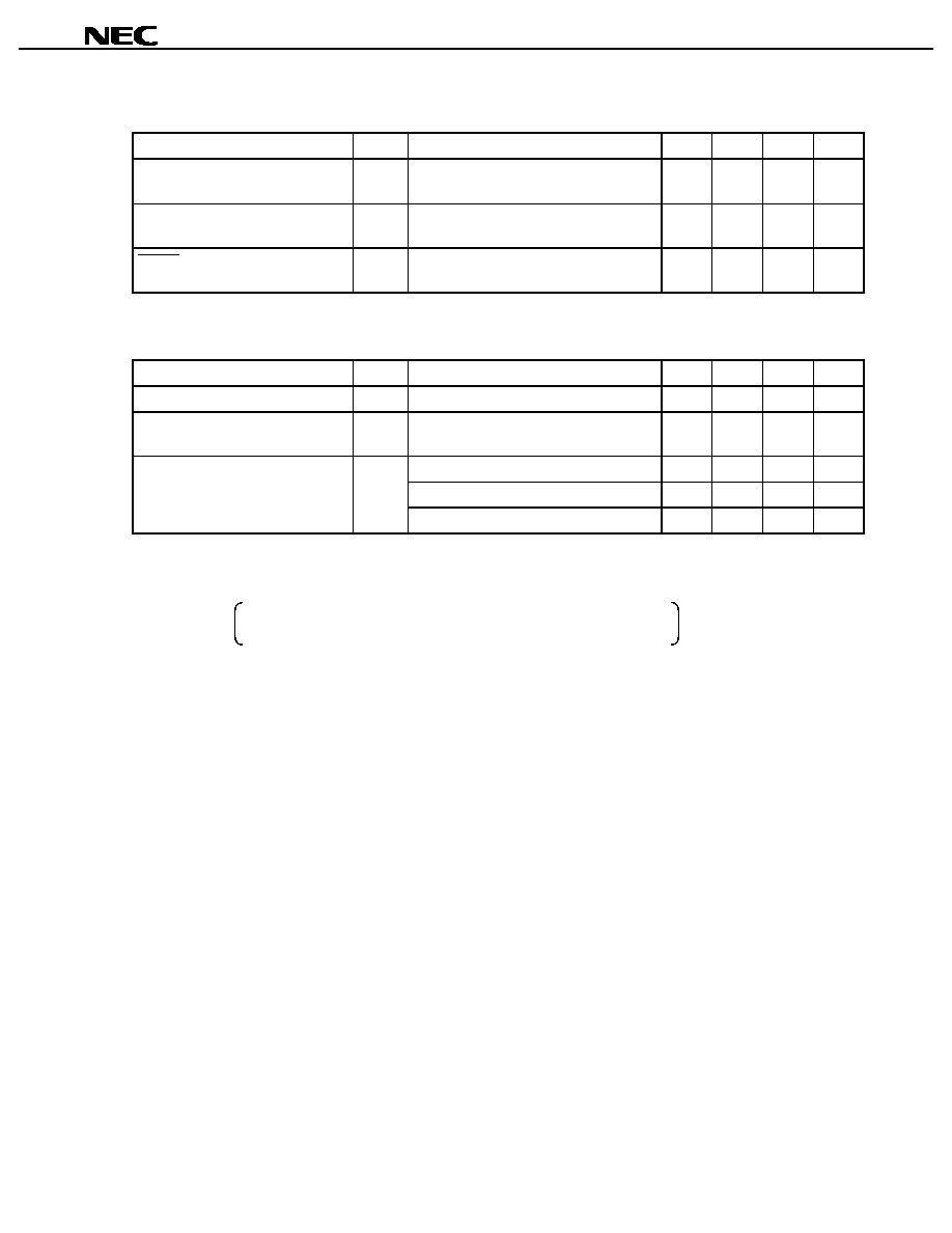
Data Sheet U14125EJ1V0DS00
37
µ
µ
µ
µ
PD78F4216A, 78F4218A, 78F4216AY, 78F4218AY
Other Operations (T
A
=
-
-
-
-
40 to +85
∞
∞
∞
∞
C, V
DD
= AV
DD
= 1.9 to 5.5 V, V
SS
= AV
SS
= 0 V)
Parameter
Symbol
Conditions
MIN.
TYP.
MAX.
Unit
NMI high-/low-level width
t
WNIL
t
WNIH
10
µ
s
Interrupt input high-/low-level width
t
WITL
t
WITH
INTP0 to INTP6
100
ns
RESET high-/low-level width
t
WRSL
t
WRSH
10
µ
s
Clock Output Operation (T
A
=
-
-
-
-
40 to +85
∞
∞
∞
∞
C, V
DD
= AV
DD
= 1.9 to 5.5 V, V
SS
= AV
SS
= 0 V)
Parameter
Symbol
Conditions
MIN.
TYP.
MAX.
Unit
PCL cycle time
t
CYCL
4.5 V
V
DD
5.5 V, nT
80
31,250
ns
PCL high-/low-level width
t
CLL
t
CLH
4.5 V
V
DD
5.5 V, 0.5T
-
10
30
15,615
ns
4.5 V
V
DD
5.5 V
5
ns
2.7 V
V
DD
< 4.5 V
10
ns
PCL rise/fall time
t
CLR
t
CLF
1.9 V
V
DD
< 2.7 V
20
ns
Remark T: t
CYK
= 1/f
XX
(f
XX
: Main system clock frequency)
n: Divided frequency ratio set by software in the CPU
∑
When using the main system clock: n = 1, 2, 4, 8, 16, 32, 64, 128
∑
When using the subsystem clock: n = 1
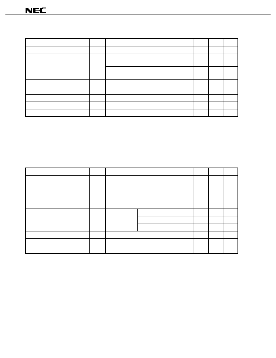
Data Sheet U14125EJ1V0DS00
38
µ
µ
µ
µ
PD78F4216A, 78F4218A, 78F4216AY, 78F4218AY
A/D Converter Characteristics (T
A
=
-
-
-
-
40 to +85
∞
∞
∞
∞
C, V
DD
= AV
DD
= 1.9 to 5.5 V, V
SS
= AV
SS
= 0 V)
Parameter
Symbol
Conditions
MIN.
TYP.
MAX.
Unit
Resolution
8
8
8
bits
2.7 V
V
DD
5.5 V
2.2 V
AV
REF0
V
DD
±
1.2
%FSR
Overall error
Notes 1, 2
1.9 V
V
DD
< 2.7 V
1.9 V
AV
REF0
V
DD
±
1.6
%FSR
Conversion time
t
CONV
14
144
µ
s
Sampling time
t
SAMP
24/f
XX
µ
s
Analog input voltage
V
IAN
AV
SS
AV
REF0
V
Reference voltage
AV
REF0
1.9
AV
DD
V
Resistance between AV
REF0
and AV
SS
R
AVREF0
When not A/D converting
40
k
Notes 1. Quantization error (
±
1/2 LSB) is not included.
2. Overall error is indicated as a ratio to the full-scale value.
Remark f
XX
: Main system clock frequency
D/A Converter Characteristics (T
A
=
-
-
-
-
40 to +85
∞
∞
∞
∞
C, V
DD
= AV
DD
= 1.9 to 5.5 V, V
SS
= AV
SS
= 0 V)
Parameter
Symbol
Conditions
MIN.
TYP.
MAX.
Unit
Resolution
8
8
8
Bits
R = 10 M
, 2.0 V
AV
REF1
V
DD
,
2.0 V
V
DD
5.5 V
±
0.6
%FSR
Overall error
Notes 1, 2
R = 10 M
, 1.9 V
AV
REF1
V
DD
,
1.9 V
V
DD
2.0 V
±
1.2
%FSR
4.5 V
AV
REF1
5.5 V
10
µ
s
2.7 V
AV
REF1
< 4.5 V
15
µ
s
Settling time
Load conditions:
C = 30 pF
1.9 V
AV
REF1
< 2.7 V
20
µ
s
Output resistance
R
O
DACS0, 1 = 55H
8
k
Reference voltage
AV
REF1
1.9
V
DD
V
AV
REF1
current
AI
REF1
For only 1 channel
2.5
mA
Notes 1. Quantization error (
±
1/2 LSB) is not included.
2. Overall error is indicated as a ratio to the full-scale value.
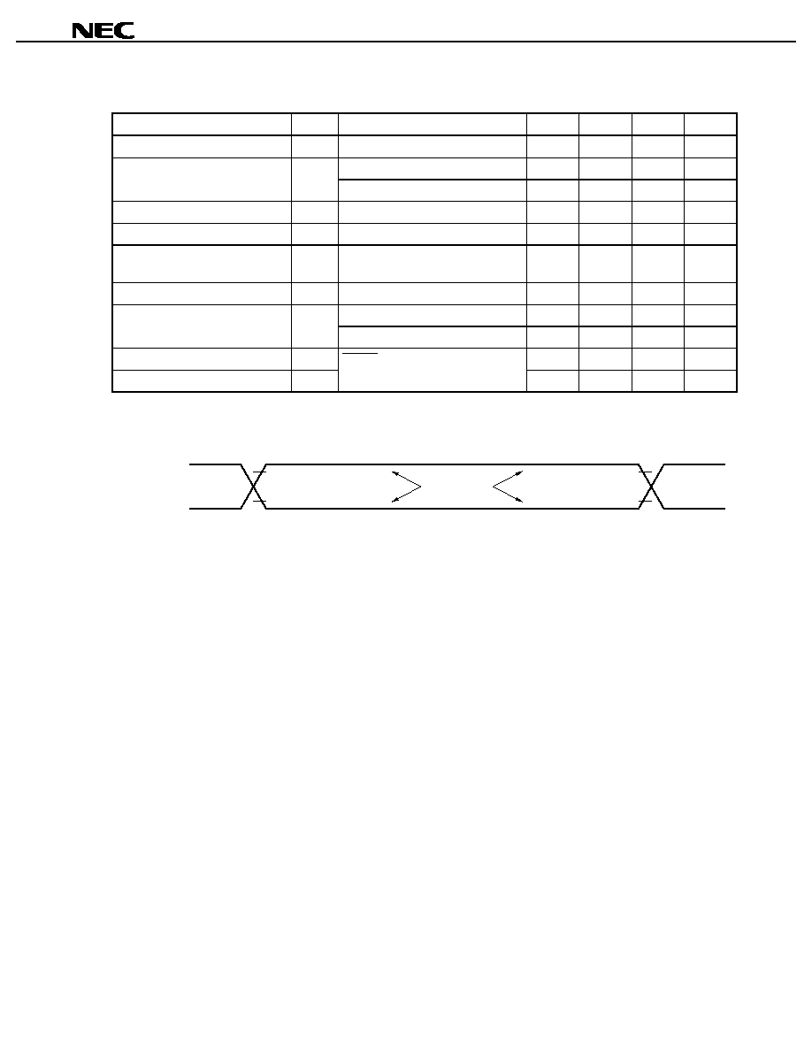
Data Sheet U14125EJ1V0DS00
39
µ
µ
µ
µ
PD78F4216A, 78F4218A, 78F4216AY, 78F4218AY
Data Retention Characteristics (T
A
=
-
-
-
-
40 to +85
∞
∞
∞
∞
C, V
DD
= AV
DD
= 1.9 to 5.5 V, V
SS
= AV
SS
= 0 V)
Parameter
Symbol
Conditions
MIN.
TYP.
MAX.
Unit
Data retention voltage
V
DDDR
STOP mode
1.9
5.5
V
V
DDDR
= 5.0 V
±
10%
10
50
µ
A
Data retention current
I
DDDR
V
DDDR
= 2.0 V
±
5%
2
10
µ
A
V
DD
rise time
t
RVD
200
µ
s
V
DD
fall time
t
FVD
200
µ
s
V
DD
hold time
(from STOP mode setting)
t
HVD
0
ms
STOP release signal input time
t
DREL
0
ms
Crystal resonator
30
ms
Oscillation stabilization wait time
t
WAIT
Ceramic resonator
5
ms
Low-level input voltage
V
IL
0
0.1V
DDDR
V
High-level input voltage
V
IH
RESET, P00/INTP0 to P06/INTP6
0.9V
DDDR
V
DDDR
V
AC Timing Test Points
0.8V
DD
or 1.9 V
0.8 V
0.8V
DD
or 1.9 V
0.8 V
Test points
V
DD
-
1 V
0.45 V
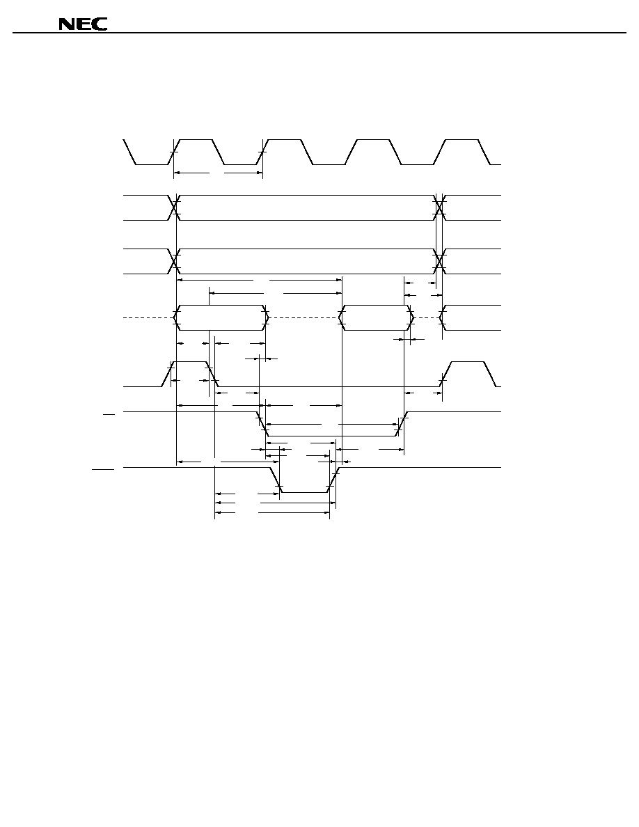
Data Sheet U14125EJ1V0DS00
40
µ
µ
µ
µ
PD78F4216A, 78F4218A, 78F4216AY, 78F4218AY
Timing Waveforms
(1) Read operations
Remark The signal is output from pins A0 to A7 when P80 to P87 are unused.
(CLK)
A8 to A19
(Output)
ASTB
(Output)
RD
(Output)
WAIT
(Input)
AD0 to AD7
(I/O)
t
CYK
Higher address
Hi-Z
Hi-Z
Hi-Z
Higher address
A0 to A7
(Output)
Lower address
Lower address
Data (Input)
Lower address
(Output)
Lower address
(Output)
t
DAID
t
HRA
t
SAST
t
WSTH
t
DSTR
t
DRST
t
DAR
t
DRID
t
WRL
t
DRWTH
t
DSTWT
t
DSTWTH
t
HSTWT
t
HRWT
t
DAWT
t
DWTR
t
HSTLA
t
FAR
t
DWTID
t
DRWTL
t
HRID
t
DRA
t
DSTID
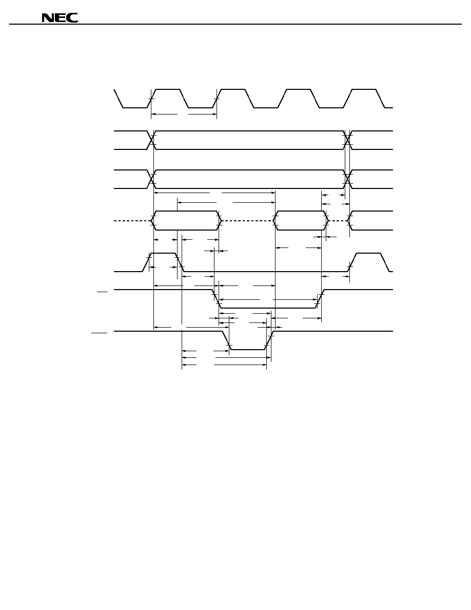
Data Sheet U14125EJ1V0DS00
41
µ
µ
µ
µ
PD78F4216A, 78F4218A, 78F4216AY, 78F4218AY
(2) Write operation
Remark The signal is output from pins A0 to A7 when P80 to P87 are unused.
(CLK)
A8 to A19
(Output)
ASTB
(Output)
WAIT
(Input)
AD0 to AD7
(Output)
t
CYK
t
DAID
t
HWA
t
SAST
t
WSTH
t
DSTW
t
DWST
t
DAW
t
DWOD
t
WWL
t
DWWTH
t
DSTWT
t
DSTWTH
t
HSTWT
t
HWWT
t
DAWT
t
DWTW
t
HSTLA
t
FAR
t
DWTID
t
DWWTL
t
HWOD
t
DAW
t
DSTOD
t
SODWR
Hi-Z
Hi-Z
Hi-Z
WR
(Output)
Higher address
Higher address
A0 to A7
(Output)
Lower address
Lower address
Data (Output)
Lower address
(Output)
Lower address
(Output)
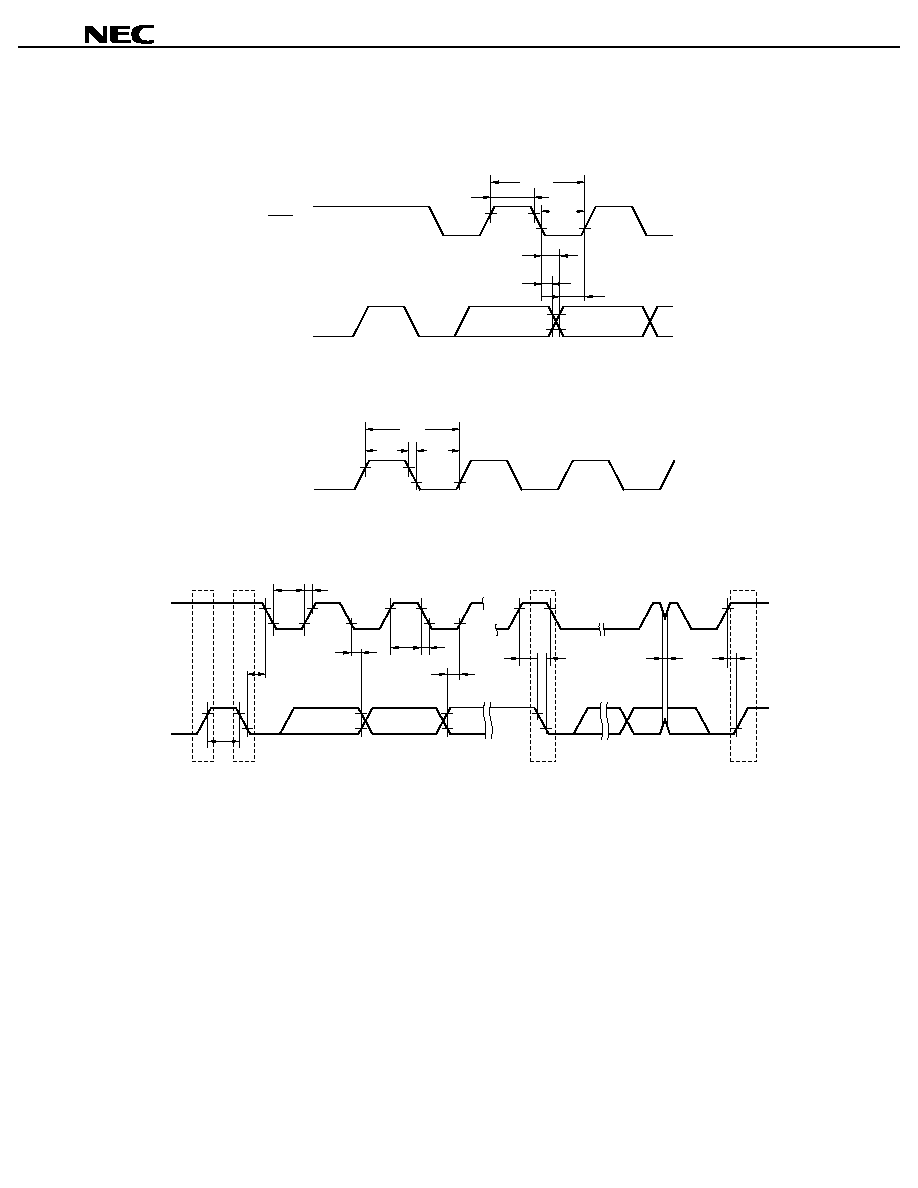
Data Sheet U14125EJ1V0DS00
42
µ
µ
µ
µ
PD78F4216A, 78F4218A, 78F4216AY, 78F4218AY
Serial Operation
(1) 3-wire serial I/O mode
(2) UART mode
(3) I
2
C bus mode (
µ
µ
µ
µ
PD78F4216AY, 78F4218AY only)
SCK
SI/SO
t
KCY1, 2
t
KL1, 2
t
KH1, 2
t
KSO1, 2
t
SIK1, 2
t
KSI1, 2
ASCK
t
KCY3
t
KH3
t
KL3
SCL0
SDA0
t
R
t
HD : DAT
t
HD : STA
t
BUF
t
HIGH
t
SU : DAT
t
F
t
SU : STA
t
HD : STA
t
SP
t
SU : STO
Stop
condition
Start
condition
Restart
condition
Stop
condition
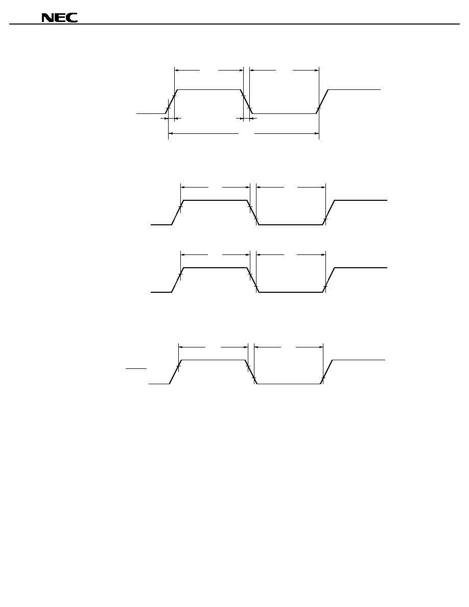
Data Sheet U14125EJ1V0DS00
43
µ
µ
µ
µ
PD78F4216A, 78F4218A, 78F4216AY, 78F4218AY
Clock Output Timing
Interrupt Input Timing
Reset Input Timing
CLKOUT
t
CLH
t
CLL
t
CYCL
t
CLF
t
CLR
NMI
INTP0 to INTP6
t
WNIH
t
WNIL
t
WITH
t
WITL
RESET
t
WRSH
t
WRSL
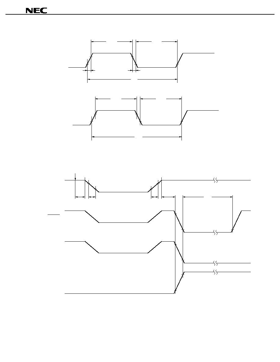
Data Sheet U14125EJ1V0DS00
44
µ
µ
µ
µ
PD78F4216A, 78F4218A, 78F4216AY, 78F4218AY
Clock Timing
Data Retention Characteristics
X1
t
WXH
t
WXL
1/f
X
t
XF
t
XR
XT1
t
XTH
t
XTL
1/f
XT
V
DD
RESET
NMI
(Cleared by falling edge)
NMI
(Cleared by rising edge)
t
HVD
t
FVD
t
RVD
t
DREL
V
DDDR
STOP mode setting
t
WAIT
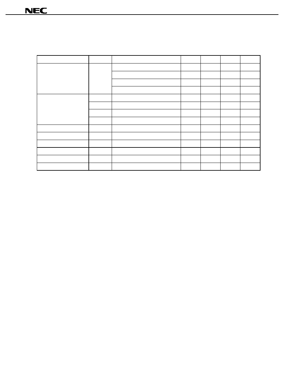
Data Sheet U14125EJ1V0DS00
45
µ
µ
µ
µ
PD78F4216A, 78F4218A, 78F4216AY, 78F4218AY
Flash Memory Programming Characteristics (V
DD
= AV
DD
= 1.9 to 5.5 V, V
SS
= AV
SS
= 0 V, V
PP
= 9.7
to 10.3 V)
(1) Basic characteristics
Parameter
Symbol
Conditions
MIN.
TYP.
MAX.
Unit
4.5 V
V
DD
5.5 V
2
12.5
MHz
2.7 V
V
DD
< 4.5 V
2
6.25
MHz
2.0 V
V
DD
< 2.7 V
2
3.125
MHz
Operating frequency
f
X
1.9 V
V
DD
< 2.0 V
2
2
2
MHz
V
DD
1.9
5.5
V
V
PPL
Upon V
PP
low-level detection
0
0.2V
DD
V
V
PP
Upon V
PP
high-level detection
0.9V
DD
V
DD
1.1V
DD
V
Supply voltage
Note 1
V
PPH
Upon V
PP
high-voltage detection
9.7
10
10.3
V
V
DD
supply current
I
DD
40
mA
V
PP
supply current
I
PP
V
PP
= 10 V
100
mA
Write count
C
WRT
20
Note2
Times
Operating temperature
Note 3
T
A
-
40
85
∞
C
Storage temperature
Note 4
T
stg
-
65
125
∞
C
Programming temperature
T
PRG
10
40
∞
C
Notes 1.
µ
PD78F4216A, 78F4216AY
K standard: 2.7 V
V
DD
<
5.5 V, V
PP
= 10.3
±
0.3 V
E standard: 2.7 V
V
DD
<
5.5 V, V
PP
= 10.0
±
0.3 V
2. Operation cannot be guaranteed when the number of writes exceeds 20 times. In the case of the
µ
PD78F4216A and 78F4216AY with K standard, operation cannot be guaranteed when the number of
writes exceeds 5 times.
3.
µ
PD78F4216A, 78F4216AY K standard: T
A
=
-
10 to +60
∞
C
4.
µ
PD78F4216A, 78F4216AY K standard: T
A
=
-
10 to +80
∞
C
Cautions 1. If writing is not successful in write operation, execute the program command again, and
execute the verify command to confirm the normal completion of the write operation.
(
µ
µ
µ
µ
PD78F4216A, 78F4216AY: I, K, E, P standard)
2. Handshake mode is supported by the following products.
µ
µ
µ
µ
PD78F4216A, 78F4216AY: Other than I, K, E standard
µ
µ
µ
µ
PD78F4218A, 78F4218AY: Other than I standard
Remark The fifth alphabetic character from the left in the lot number indicates the standard of the product. After
executing the program command, execute the verify command to confirm the normal completion of the
write operation.
Handshake mode is the CSI write mode that uses P24.
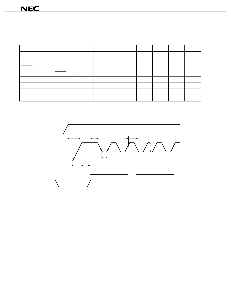
Data Sheet U14125EJ1V0DS00
46
µ
µ
µ
µ
PD78F4216A, 78F4218A, 78F4216AY, 78F4218AY
Flash Memory Programming Characteristics (V
DD
= AV
DD
= 1.9 to 5.5 V, V
SS
= AV
SS
= 0 V, V
PP
= 9.7
to 10.3 V)
(2) Serial write operation characteristics
Parameter
Symbol
Conditions
MIN.
TYP.
MAX.
Unit
V
PP
setup time
t
PSRON
V
PP
high voltage
1.0
µ
s
V
PP
setup time to V
DD
t
DRPSR
V
PP
high voltage
10
µ
s
RESET
set up time to V
PP
t
PSRRF
V
PP
high voltage
1.0
µ
s
V
PP
count start time from RESET
t
RFCF
1.0
µ
s
Count execution time
t
COUNT
1.0
ms
V
PP
counter high-level width
t
CH
8.0
µ
s
V
PP
counter low-level width
t
CL
8.0
µ
s
V
PP
counter noise elimination width
t
NFW
40
ns
Flash Memory Write Mode Setting Timing
V
DD
V
DD
0 V
V
DD
RESET (input)
0 V
V
PPH
V
PPL
V
PP
V
PP
t
RFCF
t
PSRON
t
PSRRF
t
DRPSR
t
CH
t
CL
t
COUNT
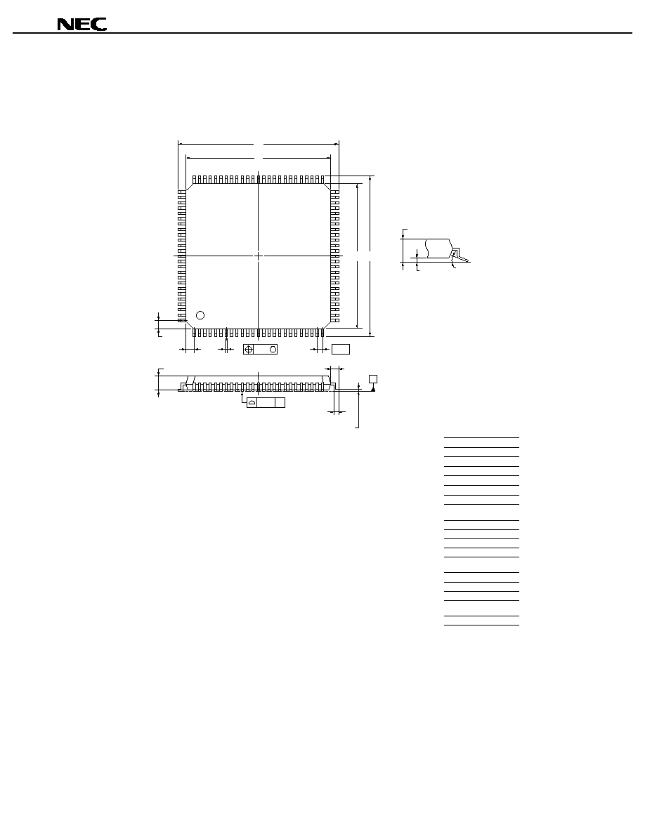
Data Sheet U14125EJ1V0DS00
47
µ
µ
µ
µ
PD78F4216A, 78F4218A, 78F4216AY, 78F4218AY
8. PACKAGE DRAWINGS
Remark The external dimensions and material of the ES version are the same as those of the mass-produced
version.
100-PIN PLASTIC LQFP (FINE PITCH) (14x14)
NOTE
Each lead centerline is located within 0.08 mm of
its true position (T.P.) at maximum material condition.
ITEM
MILLIMETERS
A
B
D
G
16.00
±
0.20
14.00
±
0.20
0.50 (T.P.)
1.00
J
16.00
±
0.20
K
C
14.00
±
0.20
I
0.08
1.00
±
0.20
L
0.50
±
0.20
F
1.00
N
P
Q
0.08
1.40
±
0.05
0.10
±
0.05
S100GC-50-8EU, 8EA-2
S
1.60 MAX.
H
0.22
+
0.05
-
0.04
M
0.17
+
0.03
-
0.07
R
3
∞+
7
∞
-
3
∞
1
25
26
50
100
76
75
51
S
S
N
J
detail of lead end
C
D
A
B
R
K
M
L
P
I
S
Q
G
F
M
H
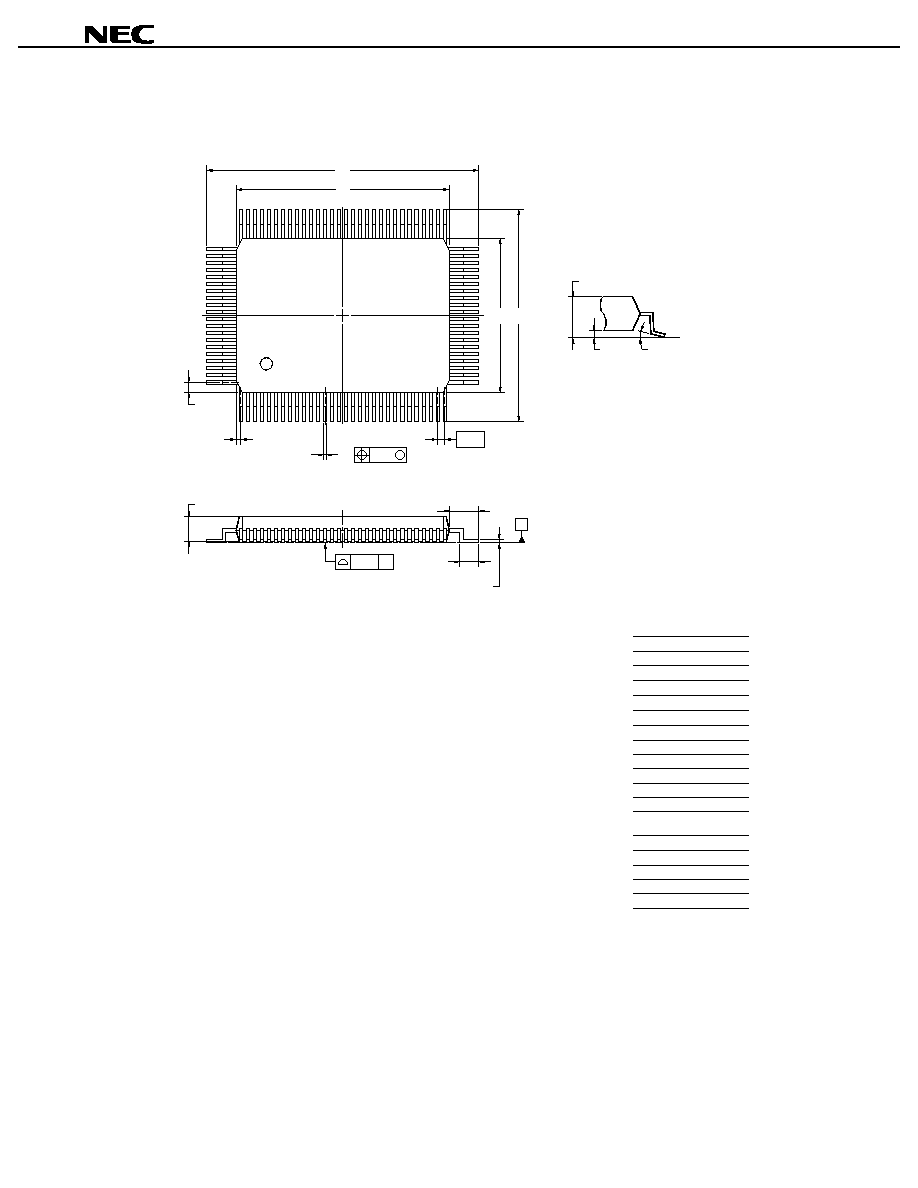
Data Sheet U14125EJ1V0DS00
48
µ
µ
µ
µ
PD78F4216A, 78F4218A, 78F4216AY, 78F4218AY
Remark The external dimensions and material of the ES version are the same as those of the mass-produced
version.
80
81
50
100
1
31
30
51
100-PIN PLASTIC QFP (14x20)
H
I
J
detail of lead end
M
Q
R
K
M
L
P
S
S
N
G
F
NOTE
Each lead centerline is located within 0.15 mm of
its true position (T.P.) at maximum material condition.
ITEM
MILLIMETERS
A
B
D
G
23.6
±
0.4
20.0
±
0.2
0.30
±
0.10
0.6
H
17.6
±
0.4
I
C
14.0
±
0.2
0.15
J
0.65 (T.P.)
K
1.8
±
0.2
L
0.8
±
0.2
F
0.8
P100GF-65-3BA1-4
N
P
Q
0.10
2.7
±
0.1
0.1
±
0.1
R
5
∞±
5
∞
S
3.0 MAX.
M
0.15
+
0.10
-
0.05
C D
A
B
S
Data Sheet U14125EJ1V0DS00
49
µ
µ
µ
µ
PD78F4216A, 78F4218A, 78F4216AY, 78F4218AY
9. RECOMMENDED SOLDERING CONDITIONS
The
µ
PD78F4218AY should be soldered and mounted under the following recommended conditions. For the
details of the recommended soldering conditions, refer to the document Semiconductor Device Mounting
Technology Manual (C10535E).
For soldering methods and conditions other than those recommended below, contact your NEC sales
representative.
Table 9-1. Surface Mounting Type Soldering Conditions
(1)
µ
µ
µ
µ
PD78F4216AGC-8EU:100-pin plastic LQFP (fine pitch) (14
◊
◊
◊
◊
14)
µ
µ
µ
µ
PD78F4218AGC-8EU:100-pin plastic LQFP (fine pitch) (14
◊
◊
◊
◊
14)
µ
µ
µ
µ
PD78F4216AYGC-8EU:100-pin plastic LQFP (fine pitch) (14
◊
◊
◊
◊
14)
µ
µ
µ
µ
PD78F4218AYGC-8EU: 100-pin plastic LQFP (fine pitch) (14
◊
◊
◊
◊
14)
Soldering Method
Soldering Conditions
Recommended
Condition Symbol
Infrared reflow
Package peak temperature: 235
∞
C, Time: 30 seconds max. (at 210
∞
C or higher),
Count: Two times or less, Exposure limit: 7 days
Note
(after that, prebake at 125
∞
C
for 10 hours)
IR35-107-2
VPS
Package peak temperature: 215
∞
C, Time: 40 seconds max. (at 200
∞
C or higher),
Count: Two times or less, Exposure limit: 7 days
Note
(after that, prebake at 125
∞
C
for 10 hours)
VP15-107-2
Partial heating
Pin temperature: 300
∞
C max., Time: 3 seconds max. (per pin row)
-
Note After opening the dry pack, store it at 25
∞
C or less and 65% RH or less for the allowable storage period.
Caution Do not use different soldering methods together (except for partial heating).
(2)
µ
µ
µ
µ
PD78F4216AGF-3BA:100-pin plastic QFP (14
◊
◊
◊
◊
20)
µ
µ
µ
µ
PD78F4218AGF-3BA:100-pin plastic QFP (14
◊
◊
◊
◊
20)
µ
µ
µ
µ
PD78F4216AYGF-3BA:100-pin plastic QFP (14
◊
◊
◊
◊
20)
µ
µ
µ
µ
PD78F4218AYGF-3BA: 100-pin plastic QFP (14
◊
◊
◊
◊
20)
Soldering Method
Soldering Conditions
Recommended
Condition Symbol
Infrared reflow
Package peak temperature: 235
∞
C, Time: 30 seconds max. (at 210
∞
C or higher),
Count: Two times or less
IR35-00-2
VPS
Package peak temperature: 215
∞
C, Time: 40 seconds max. (at 200
∞
C or higher),
Count: Two times or less
VP15-00-2
Wave soldering
Solder bath temperature: 260
∞
C max., Time: 10 seconds max., Count: Once,
Preheating temperature: 120
∞
C max. (package surface temperature)
WS60-00-1
Partial heating
Pin temperature: 300
∞
C max., Time: 3 seconds max. (per pin row)
-
Caution Do not use different soldering methods together (except for partial heating).
Data Sheet U14125EJ1V0DS00
50
µ
µ
µ
µ
PD78F4216A, 78F4218A, 78F4216AY, 78F4218AY
APPENDIX A. DEVELOPMENT TOOLS
The following development tools are available for system development using the
µ
PD78F4218AY. Also refer to
(5) Cautions on using development tools.
(1) Language processing software
RA78K4
Assembler package common to 78K/IV Series
CC78K4
C compiler package common to 78K/IV Series
DF784218
Device file common to
µ
PD784216A, 784216AY, 784218A, 784218AY Subseries
CC78K4-L
C compiler library source file common to 78K/IV Series
(2) Flash memory writing tools
Flashpro II
(Part number: FL-PR2),
Flashpro III
(Part number: FL-PR3, PG-FP3)
Dedicated flash programmer for microcontroller incorporating flash memory
FA-100GF
Adapter for writing 100-pin plastic QFP (GF-3BA type) flash memory. Connection must be
performed in accordance with the target product.
FA-100GC
Adapter for writing 100-pin plastic LQFP (GC-8EU type) flash memory. Connection must be
performed in accordance with the target product.
(3) Debugging tools
∑
∑
∑
∑
When IE-78K4-NS in-circuit emulator is used
IE-78K4-NS
In-circuit emulator common to 78K/IV Series
IE-70000-MC-PS-B
Power supply unit for IE-78K4-NS
IE-70000-98-IF-C
Interface adapter required when PC-9800 series PC (except notebook type) is used as host
machine (C bus supported)
IE-70000-CD-IF-A
PC card and cable when PC-9800 series notebook PC is used as host machine (PCMCIA
socket supported)
IE-70000-PC-IF-C
Interface adapter required when using IBM PC/AT
TM
compatibles as host machine (ISA bus
supported)
IE-70000-PCI-IF
Interface adapter required when using PC that incorporates PCI bus as host machine
IE-784225-NS-EM1
Emulation board to emulate
µ
PD784216A, 784216AY, 784218A, 784218AY Subseries
NP-100GF
Emulation probe for 100-pin plastic QFP (GF-3BA type)
NP-100GC
Emulation probe for 100-pin plastic LQFP (GC-8EU type)
EV-9200GF-100
Socket to be mounted on a target system board made for 100-pin plastic QFP (GF-3BA type)
TGC-100SDW
Conversion adapter to connect the NP-100GC and a target system board on which a 100-pin
plastic LQFP (GC-8EU type) can be mounted
ID78K4-NS
Integrated debugger for IE-78K4-NS
SM78K4
System simulator common to 78K/IV Series
DF784218
Device file common to
µ
PD784216A, 784216AY, 784218A, 784218AY Subseries
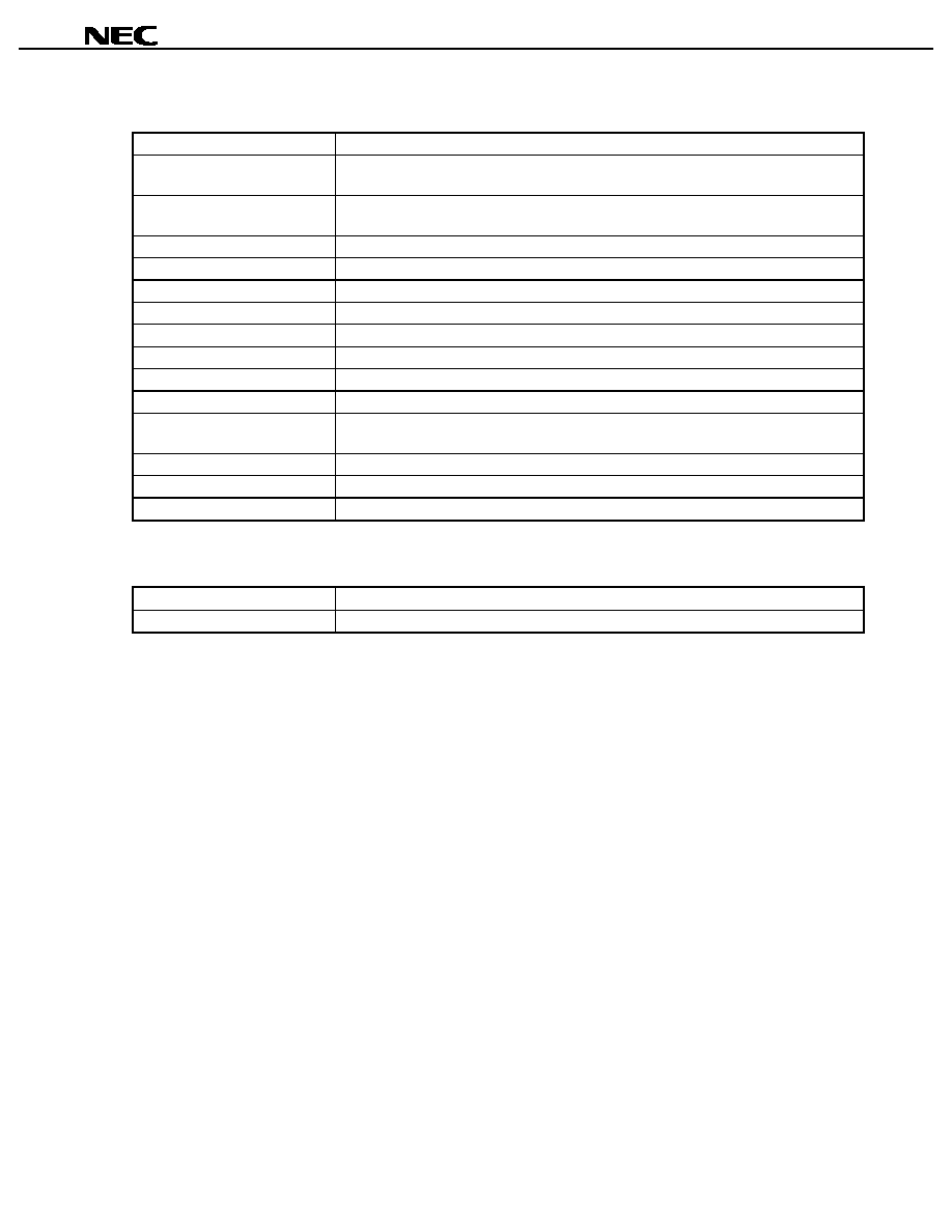
Data Sheet U14125EJ1V0DS00
51
µ
µ
µ
µ
PD78F4216A, 78F4218A, 78F4216AY, 78F4218AY
∑
∑
∑
∑
When IE-784000-R in-circuit emulator is used
IE-784000-R
In-circuit emulator common to 78K/IV Series
IE-70000-98-IF-C
Interface adapter required when PC-9800 series PC (except notebook type) is used as host
machine (C bus supported)
IE-70000-PC-IF-C
Interface adapter required when using IBM PC/AT and compatibles as host machine (ISA bus
supported)
IE-70000-PCI-IF
Interface adapter required when using PC that incorporates PCI bus as host machine
IE-78000-R-SV3
Interface adapter and cable required when EWS is used as host machine
IE-784225-NS-EM1
Emulation board to emulate
µ
PD784216A, 784216AY, 784218A, 784218AY Subseries
IE-784000-R-EM
Emulation board common to 78K/IV Series
IE-78K4-R-EX3
Emulation probe conversion board required when using IE-784225-NS-EM1 on IE-784000-R.
EP-784218GF-R
Emulation probe for 100-pin plastic QFP (GF-3BA type)
EP-78064GC-R
Emulation probe for 100-pin plastic LQFP (GC-8EU type)
EV-9200GF-100
Socket to be mounted on a target system board made for 100-pin plastic QFP (GF-3BA type)
TGC-100SDW
Conversion adapter to connect the EP-78064GC-R and a target system board on which a
100-pin plastic LQFP (GC-8EU type) can be mounted
ID78K4
Integrated debugger for IE-784000-R
SM78K4
System simulator common to 78K/IV Series
DF784218
Device file common to
µ
PD784216A, 784216AY, 784218A, 784218AY Subseries
(4) Real-time OS
RX78K/IV
Real-time OS for 78K/IV Series
MX78K4
OS for 78K/IV Series
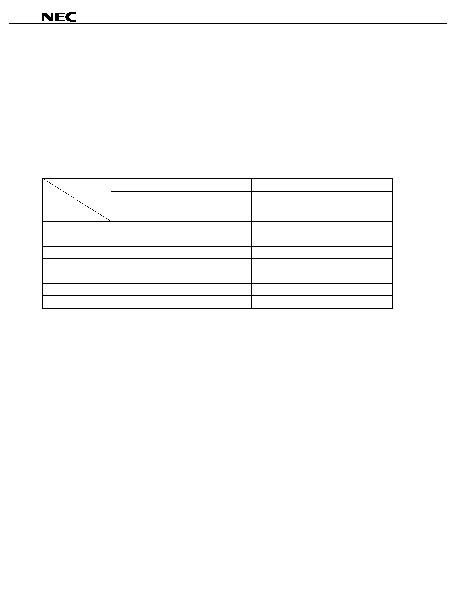
Data Sheet U14125EJ1V0DS00
52
µ
µ
µ
µ
PD78F4216A, 78F4218A, 78F4216AY, 78F4218AY
(5) Cautions on using development tools
∑
The ID78K4-NS, ID78K4, and SM78K4 are used in combination with the DF784218.
∑
The CC78K4 and RX78K/IV are used in combination with the RA78K4 and DF784218.
∑
The FL-PR2, FL-PR3, FA-100GF, FA-100GC, NP-100GF, and NP-100GC are products made by Naito
Densei Machida Mfg. Co., Ltd. (TEL: +81-44-822-3813).
∑
The TGC-100SDW is a product made by TOKYO ELETECH CORPORATION.
For further information, contact Daimaru Kogyo, Ltd.
Tokyo Electronic Division (TEL: +81-3-3820-7112)
Osaka Electronic Division (TEL: +81-6-6244-6672)
∑
For third party development tools, see the Single-Chip Microcontroller Development Tool Selection
Guide (U11069E).
∑
The host machine and OS suitable for each software are as follows:
PC
EWS
Host Machine
[OS]
Software
PC-9800 series [Windows]
IBM PC/AT and compatibles
[Japanese/English Windows]
HP9000 Series 700
TM
[HP-UX
TM
]
SPARCstation
TM
[SunOS
TM
, Solaris
TM
]
NEWS
TM
(RISC) [NEWS-OS
TM
]
RA78K4
Note
CC78K4
Note
ID78K4-NS
-
ID78K4
SM78K4
-
RX78K/IV
Note
MX78K4
Note
Note DOS-based software
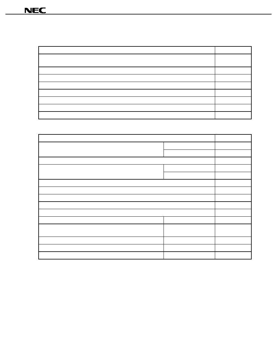
Data Sheet U14125EJ1V0DS00
53
µ
µ
µ
µ
PD78F4216A, 78F4218A, 78F4216AY, 78F4218AY
APPENDIX B. RELATED DOCUMENTS
Documents related to devices
Document Name
Document No.
µ
PD784214A, 784215A, 784216A, 784217A, 784218A, 784214AY, 784215AY, 784216AY, 784217AY,
784218AY Data Sheet
U14121E
µ
PD78F4216A, 78F4216AY, 78F4218A, 78F4218AY Data Sheet
This document
µ
PD784216A, 784216AY Subseries User's Manual Hardware
U13570E
µ
PD784218A, 784218AY Subseries User's Manual Hardware
U12970E
78K/IV Series User's Manual Instructions
U10905E
78K/IV Series Instruction Table
-
78K/IV Series Instruction Set
-
78K/IV Series Application Note Software Basics
-
Documents related to development tools (user's manuals)
Document Name
Document No.
Language
U11162E
RA78K4 Assembler Package
Operation
U11334E
RA78K Structured Assembler Preprocessor
U11743E
Language
U11571E
CC78K4 C Compiler
Operation
U11572E
IE-78K4-NS
U13356E
IE-784000-R
U12903E
IE-784218-R-EM1
U12155E
IE-784225-NS-EM1
U13742E
EP-78064
EEU-1469
SM78K4 System Simulator Windows Based
Reference
U10093E
SM78K Series System Simulator
External Part User Open
Interface Specifications
U10092E
ID78K4-NS Integrated Debugger PC Based
Reference
U12796E
ID78K4 Integrated Debugger Windows Based
Reference
U10440E
ID78K4 Integrated Debugger HP-UX, SunOS, NEWS-OS Based
Reference
U11960E
Caution
The related documents listed above are subject to change without notice. Be sure to use the
latest version of each document for designing.
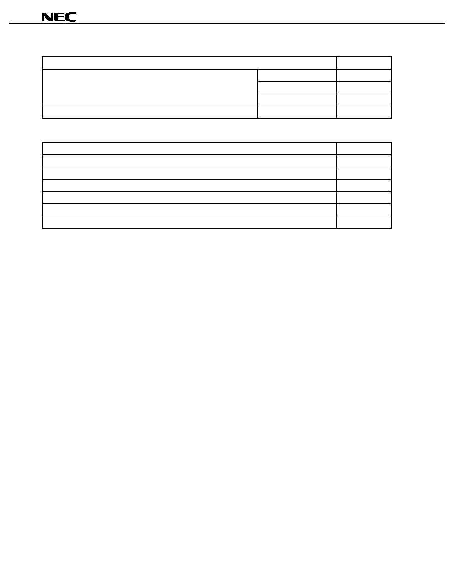
Data Sheet U14125EJ1V0DS00
54
µ
µ
µ
µ
PD78F4216A, 78F4218A, 78F4216AY, 78F4218AY
Documents related to embedded software (user's manuals)
Document Name
Document No.
Fundamental
U10603E
Installation
U10604E
78K/IV Series Real-Time OS
Debugger
-
78K/IV Series OS MX78K4
Fundamental
-
Other documents
Document Name
Document No.
SEMICONDUCTOR SELECTION GUIDE Products & Packages (CD-ROM)
X13769X
Semiconductor Device Mounting Technology Manual
C10535E
Quality Grades on NEC Semiconductor Devices
C11531E
NEC Semiconductor Device Reliability/Quality Control System
C10983E
Guide to Prevent Damage for Semiconductor Devices by Electrostatic Discharge (ESD)
C11892E
Guide to Microcomputer-Related Products by Third Party
-
Caution
The related documents listed above are subject to change without notice. Be sure to use the
latest version of each document for designing.

Data Sheet U14125EJ1V0DS00
55
µ
µ
µ
µ
PD78F4216A, 78F4218A, 78F4216AY, 78F4218AY
[MEMO]

Data Sheet U14125EJ1V0DS00
56
µ
µ
µ
µ
PD78F4216A, 78F4218A, 78F4216AY, 78F4218AY
[MEMO]

Data Sheet U14125EJ1V0DS00
57
µ
µ
µ
µ
PD78F4216A, 78F4218A, 78F4216AY, 78F4218AY
[MEMO]
Data Sheet U14125EJ1V0DS00
58
µ
µ
µ
µ
PD78F4216A, 78F4218A, 78F4216AY, 78F4218AY
NOTES FOR CMOS DEVICES
1
PRECAUTION AGAINST ESD FOR SEMICONDUCTORS
Note:
Strong electric field, when exposed to a MOS device, can cause destruction of the gate oxide and
ultimately degrade the device operation. Steps must be taken to stop generation of static electricity
as much as possible, and quickly dissipate it once, when it has occurred. Environmental control
must be adequate. When it is dry, humidifier should be used. It is recommended to avoid using
insulators that easily build static electricity. Semiconductor devices must be stored and transported
in an anti-static container, static shielding bag or conductive material. All test and measurement
tools including work bench and floor should be grounded. The operator should be grounded using
wrist strap. Semiconductor devices must not be touched with bare hands. Similar precautions need
to be taken for PW boards with semiconductor devices on it.
2
HANDLING OF UNUSED INPUT PINS FOR CMOS
Note:
No connection for CMOS device inputs can be cause of malfunction. If no connection is provided
to the input pins, it is possible that an internal input level may be generated due to noise, etc., hence
causing malfunction. CMOS devices behave differently than Bipolar or NMOS devices. Input levels
of CMOS devices must be fixed high or low by using a pull-up or pull-down circuitry. Each unused
pin should be connected to V
DD
or GND with a resistor, if it is considered to have a possibility of
being an output pin. All handling related to the unused pins must be judged device by device and
related specifications governing the devices.
3
STATUS BEFORE INITIALIZATION OF MOS DEVICES
Note:
Power-on does not necessarily define initial status of MOS device. Production process of MOS
does not define the initial operation status of the device. Immediately after the power source is
turned ON, the devices with reset function have not yet been initialized. Hence, power-on does
not guarantee out-pin levels, I/O settings or contents of registers. Device is not initialized until the
reset signal is received. Reset operation must be executed immediately after power-on for devices
having reset function.
IEBus is a trademark of NEC Corporation.
Windows is either a registered trademark or a trademark of Microsoft Corporation in the United States and/or
other countries.
PC/AT is a trademark of International Business Machines Corporation.
HP9000 series 700 and HP-UX are trademarks of Hewlett-Packard Company.
SPARCstation is a trademark of SPARC International, Inc.
Solaris and SunOS are trademarks of Sun Microsystems, Inc.
NEWS and NEWS-OS are trademarks of Sony Corporation.

Data Sheet U14125EJ1V0DS00
59
µ
µ
µ
µ
PD78F4216A, 78F4218A, 78F4216AY, 78F4218AY
Regional Information
Some information contained in this document may vary from country to country. Before using any NEC
product in your application, pIease contact the NEC office in your country to obtain a list of authorized
representatives and distributors. They will verify:
∑
Device availability
∑
Ordering information
∑
Product release schedule
∑
Availability of related technical literature
∑
Development environment specifications (for example, specifications for third-party tools and
components, host computers, power plugs, AC supply voltages, and so forth)
∑
Network requirements
In addition, trademarks, registered trademarks, export restrictions, and other legal issues may also vary
from country to country.
NEC Electronics Inc. (U.S.)
Santa Clara, California
Tel: 408-588-6000
800-366-9782
Fax: 408-588-6130
800-729-9288
NEC Electronics (Germany) GmbH
Duesseldorf, Germany
Tel: 0211-65 03 02
Fax: 0211-65 03 490
NEC Electronics (UK) Ltd.
Milton Keynes, UK
Tel: 01908-691-133
Fax: 01908-670-290
NEC Electronics Italiana s.r.l.
Milano, Italy
Tel: 02-66 75 41
Fax: 02-66 75 42 99
NEC Electronics (Germany) GmbH
Benelux Office
Eindhoven, The Netherlands
Tel: 040-2445845
Fax: 040-2444580
NEC Electronics (France) S.A.
Velizy-Villacoublay, France
Tel: 01-30-67 58 00
Fax: 01-30-67 58 99
NEC Electronics (France) S.A.
Madrid Office
Madrid, Spain
Tel: 91-504-2787
Fax: 91-504-2860
NEC Electronics (Germany) GmbH
Scandinavia Office
Taeby, Sweden
Tel: 08-63 80 820
Fax: 08-63 80 388
NEC Electronics Hong Kong Ltd.
Hong Kong
Tel: 2886-9318
Fax: 2886-9022/9044
NEC Electronics Hong Kong Ltd.
Seoul Branch
Seoul, Korea
Tel: 02-528-0303
Fax: 02-528-4411
NEC Electronics Singapore Pte. Ltd.
United Square, Singapore
Tel: 65-253-8311
Fax: 65-250-3583
NEC Electronics Taiwan Ltd.
Taipei, Taiwan
Tel: 02-2719-2377
Fax: 02-2719-5951
NEC do Brasil S.A.
Electron Devices Division
Guarulhos-SP Brasil
Tel: 55-11-6462-6810
Fax: 55-11-6462-6829
J00.7
µ
µ
µ
µ
PD78F4216A, 78F4218A, 78F4216AY, 78F4218AY
The related documents indicated in this publication may include preliminary versions. However, preliminary
versions are not marked as such.
Purchase of NEC I
2
C components conveys a license under the Philips I
2
C Patent Rights to use these components
in an I
2
C system, provided that the system conforms to the I
2
C Standard Specification as defined by Philips.
M8E 00. 4
The information in this document is current as of August, 2000. The information is subject to
change without notice. For actual design-in, refer to the latest publications of NEC's data sheets or
data books, etc., for the most up-to-date specifications of NEC semiconductor products. Not all
products and/or types are available in every country. Please check with an NEC sales representative
for availability and additional information.
No part of this document may be copied or reproduced in any form or by any means without prior
written consent of NEC. NEC assumes no responsibility for any errors that may appear in this document.
NEC does not assume any liability for infringement of patents, copyrights or other intellectual property rights of
third parties by or arising from the use of NEC semiconductor products listed in this document or any other
liability arising from the use of such products. No license, express, implied or otherwise, is granted under any
patents, copyrights or other intellectual property rights of NEC or others.
Descriptions of circuits, software and other related information in this document are provided for illustrative
purposes in semiconductor product operation and application examples. The incorporation of these
circuits, software and information in the design of customer's equipment shall be done under the full
responsibility of customer. NEC assumes no responsibility for any losses incurred by customers or third
parties arising from the use of these circuits, software and information.
While NEC endeavours to enhance the quality, reliability and safety of NEC semiconductor products, customers
agree and acknowledge that the possibility of defects thereof cannot be eliminated entirely. To minimize
risks of damage to property or injury (including death) to persons arising from defects in NEC
semiconductor products, customers must incorporate sufficient safety measures in their design, such as
redundancy, fire-containment, and anti-failure features.
NEC semiconductor products are classified into the following three quality grades:
"Standard", "Special" and "Specific". The "Specific" quality grade applies only to semiconductor products
developed based on a customer-designated "quality assurance program" for a specific application. The
recommended applications of a semiconductor product depend on its quality grade, as indicated below.
Customers must check the quality grade of each semiconductor product before using it in a particular
application.
"Standard": Computers, office equipment, communications equipment, test and measurement equipment, audio
and visual equipment, home electronic appliances, machine tools, personal electronic equipment
and industrial robots
"Special":
Transportation equipment (automobiles, trains, ships, etc.), traffic control systems, anti-disaster
systems, anti-crime systems, safety equipment and medical equipment (not specifically designed
for life support)
"Specific": Aircraft, aerospace equipment, submersible repeaters, nuclear reactor control systems, life
support systems and medical equipment for life support, etc.
The quality grade of NEC semiconductor products is "Standard" unless otherwise expressly specified in NEC's
data sheets or data books, etc. If customers wish to use NEC semiconductor products in applications not
intended by NEC, they must contact an NEC sales representative in advance to determine NEC's willingness
to support a given application.
(Note)
(1) "NEC" as used in this statement means NEC Corporation and also includes its majority-owned subsidiaries.
(2) "NEC semiconductor products" means any semiconductor product developed or manufactured by or for
NEC (as defined above).
∑
∑
∑
∑
∑
∑