Document Outline
- COVER
- DESCRIPTION
- FEATURES
- ORDERING INFORMATION
- 78K/IV SERIES PRODUCT DEVELOPMENT
- FUNCTIONS
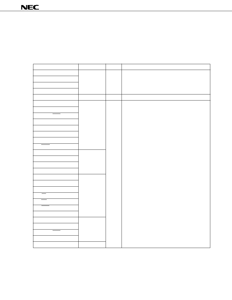
- 1. DIFFERENCES AMONG MODELS IN uPD784225 SUBSERIES
- 2. PIN CONFIGURATION (Top View)
- 3. BLOCK DIAGRAM
- 4. PIN FUNCTION
- 4.1 Port Pins
- 4.2 Pins Other Than Port Pins
- 4.3 I/O Circuit Type of Respective Pins and Recommended Connections of Unused Pins
- 5. INTERNAL MEMORY SIZE SELECT REGISTER (IMS)
- 6. PROGRAMMING FLASH MEMORY
- 6.1 Selecting Communication Mode
- 6.2 Flash Memory Programming Function
- 6.3 Connecting Flashpro II
- 7. PACKAGE DRAWINGS
- APPENDIX A. DEVELOPMENT TOOLS
- APPENDIX B. RELATED DOCUMENTS

MOS INTEGRATED CIRCUIT
µ
PD78F4225
16/8-BIT SINGLE-CHIP MICROCONTROLLERS
DESCRIPTION
The
µ
PD78F4225 is a product in the
µ
PD784225 subseries in the 78K/IV series.
The
µ
PD78F4225 has a flash memory in the place of the internal ROM of the
µ
PD784225. Data can be written
to or erased from the flash memory of the
µ
PD78F4225 with the microcontroller mounted on a printed wiring board.
The functions are explained in detail in the following user's manuals. Be sure to read this manual when
designing your system.
µ
PD784225, 784225Y Subseries User's Manual - Hardware : Planned
78K/IV Series User's Manual - Instruction
: U10905E
FEATURES
∑
Pin-compatible with mask ROM model (except V
PP
pin)
∑
Flash memory: 128K bytes
∑
Internal RAM : 4352 bytes
∑
Same operating voltage as mask ROM model: V
DD
= 1.8 to 5.5 V
ORDERING INFORMATION
Part Number
Package
µ
PD78F4225GC-8BT
80-pin plastic QFP (14
◊
14 mm)
µ
PD78F4225GK-BE9
80-pin plastic TQFP (fine pitch) (12
◊
12 mm)
Document No. U12499EJ1V0PM00 (1st edition)
Date Published June 1997 N
Printed in Japan
The information contained in this document is being issued in advance of the production cycle for the
device. The parameters for the device may change before final production or NEC Corporation, at its own
discretion, may withdraw the device prior to its production.
©
1997
PRELIMINARY PRODUCT INFORMATION
2
µ
PD78F4225
78K/IV SERIES PRODUCT DEVELOPMENT
: Under mass production
: Under development
Standard Models
PD784026
µ
ASSP Models
PD784038Y
µ
PD784038
µ
Enhanced A/D,
16-bit timer, power
management
Enhanced internal memory
capacity, pin-compatible with
PD784026
I
2
C bus compatible model
PD784225Y
µ
PD784225
µ
80 pins,
ROM correction added
Multi-master I
2
C bus
compatible model
PD784216Y
µ
PD784216
µ
100 pins, enhanced I/O and
internal memory capacity
Multi-master I
2
C bus
compatible model
µ
PD784218Y
µ
PD784218
µ
Enhanced internal memory capacity,
ROM correction added
Multi-master I
2
C bus
compatible model
PD784054
µ
PD784046
µ
With 10-bit A/D
PD784908
µ
With IEBus
TM
controller
PD78F4943
µ
For CD-ROM,
Flash memory: 56K bytes
PD784915
µ
With software servo control,
analog circuit for VCRs,
enhanced timer
PD784928Y
µ
PD784928
µ
Multi-master I
2
C bus
compatible model
Enhanced function of
PD784915
µ
3
µ
PD78F4225
FUNCTIONS
Item
Function
Number of basic instructions
113
(mnemonics)
General-purpose register
8 bits
◊
16 registers
◊
8 banks, or 16 bits
◊
8 registers
◊
8 banks (memory mapping)
Minimum instruction execution
∑ 160 ns/320 ns/640 ns/1280 ns/2560 ns (main system clock: f
XX
= 12.5 MHz)
time
∑ 61
µ
s (subsystem clock: f
XT
= 32.768 KHz)
Internal
Flash memory
128 KB
memory
RAM
4352 bytes
Memory space
1 MB with program and data spaces combined
I/O port
Total
67
CMOS Input
8
CMOS I/O
59
Pins with pull-up
57
resistor
LEDs direct
16
drive output
Real-time output port
4 bits
◊
2, or 8 bits
◊
1
Timer/counter
16-bit timer/counter : timer register
◊
1
Pulse output
Capture/compare register
◊
2
∑ PWM/PPG output
∑ Square wave output
∑ One-shot pulse output
8-bit timer/counter 1 : timer register
◊
1
Pulse output
Compare register
◊
1
∑ PWM output
∑ Square wave output
8-bit timer/counter 2 : timer register
◊
1
Pulse output
Compare register
◊
1
∑ PWM output
∑ Square wave output
8-bit timer/counter 5 : timer register
◊
1
Compare register
◊
1
8-bit timer/counter 6 : timer register
◊
1
Compare register
◊
1
Serial interface
UART/IOE (3-wire serial I/O): 2 channels (on-chip baud rate generator)
CSI (3-wire serial I/O): 1 channel
A/D converter
8-bit resolution
◊
8 channels
D/A converter
8-bit resolution
◊
2 channels
Clock output
Selectable from f
XX
, f
XX
/2, f
XX
/2
2
, f
XX
/2
3
, f
XX
/2
4
, f
XX
/2
5
, f
XX
/2
6
, f
XX
/2
7
, f
XT
Buzzer output
Selectable from f
XX
/2
10
, f
XX
/2
11
, f
XX
/2
12
, f
XX
/2
13
Watch timer
1 channel
Watchdog timer
1 channel
Standby
∑ HALT/STOP/IDLE mode
∑ In power-saving mode (with subsystem clock): HALT/IDLE mode
Interrupt
Hardware
25 (internal: 18, external: 7)
Software
BRK instruction, BRKCS instruction, operand error
Non-maskable
Internal: 1, external: 1
Maskable
Internal: 17, external: 6
∑ 4 programmable priority levels
∑ 3 service modes: vectored interrupt/macro service/context switching
Supply voltage
V
DD
= 1.8 to 5.5 V
Package
∑ 80-pin plastic QFP (14
◊
14 mm)
∑ 80-pin plastic TQFP (fine pitch) (12
◊
12 mm)
Note The pins with ancillary functions are included in the I/O pins.
Pins with
ancillary
functions
Note

4
µ
PD78F4225
CONTENTS
1.
DIFFERENCES AMONG MODELS IN
µ
PD784225 SUBSERIES ............................................... 5
2.
PIN CONFIGURATION (Top View) ............................................................................................... 6
3.
BLOCK DIAGRAM ......................................................................................................................... 8
4.
PIN FUNCTION ............................................................................................................................... 9
4.1
Port Pins ................................................................................................................................................
9
4.2
Pins Other Than Port Pins .................................................................................................................. 11
4.3
I/O Circuit Type of Respective Pins and Recommended Connections of Unused Pins ........... 13
5.
INTERNAL MEMORY SIZE SELECT REGISTER (IMS) .............................................................. 16
6.
PROGRAMMING FLASH MEMORY ............................................................................................. 17
6.1
Selecting Communication Mode ........................................................................................................ 17
6.2
Flash Memory Programming Function ............................................................................................. 18
6.3
Connecting Flashpro II ........................................................................................................................ 18
7.
PACKAGE DRAWINGS ................................................................................................................. 20
APPENDIX A. DEVELOPMENT TOOLS ............................................................................................. 22
APPENDIX B. RELATED DOCUMENTS ............................................................................................ 24
5
µ
PD78F4225
1. DIFFERENCES AMONG MODELS IN
µ
PD784225 SUBSERIES
The only difference among the
µ
PD784224 and 784225 lies in the internal memory capacity.
The
µ
PD78F4225 is provided with a 128-KB flash memory instead of the mask ROM of the above models. These
differences are summarized in Table 1-1.
Table 1-1. Differences among Models in
µ
PD784225 Subseries
Part Number
µ
PD784224
µ
PD784225
µ
PD78F4225
Item
Internal ROM
96 KBytes
128 KBytes
128 KBytes
(mask ROM)
(mask ROM)
(flash memory)
Internal RAM
3584 Bytes
4352 Bytes
Internal memory size
None
Provided
switching register (IMS)
V
PP
pin
None
Provided
6
µ
PD78F4225
2. PIN CONFIGURATION (Top View)
∑ 80-pin plastic QFP (14
◊
14 mm)
µ
PD78F4225GC-8BT
∑ 80-pin plastic TQFP (fine pitch) (12
◊
12 mm)
µ
PD78F4225GK-BE9
Notes 1. Directly connect the TEST/V
PP
pin to V
SS0
in normal operation mode.
2. Connect the AV
SS
pin to V
SS0
.
Remark When using in applications where noise from inside the microcomputer has to be reduced, it is
recommended to take countermeasures against noise such as supplying power to V
DD0
and V
DD1
independently, and connecting V
SS0
and V
SS1
to different ground lines.
1
2
3
4
5
6
7
8
9
10
11
12
13
14
15
16
17
18
19
20
P15/ANI5
P16/ANI6
P17/ANI7
AV
SS
P130/ANO0
P131/ANO1
AV
REF1
P70/SI2/RxD2
P71/SO2/TxD2
P72/SCK2/ASCK2
P20/SI1/RxD1
P21/SO1/TxD1
P22/SCK1/ASCK1
P23/PCL
P24/BUZ
P25/SI0
P26/SO0
P27/SCK0
P40/AD0
P41/AD1
60
59
58
57
56
55
54
53
52
51
50
49
48
47
46
45
44
43
42
41
RESET
P127/RTP7
P126/RTP6
P125/RTP5
P124/RTP4
P123/RTP3
P122/RTP2
P121/RTP1
P120/RTP0
P37/EXA
P36/TI01
P35/TI00
P34/TI2
P33/TI1
P32/TO2
P31/TO1
P30/TO0
P67/ASTB
P66/WAIT
P65/WR
P42/AD2
P43/AD3
P44/AD4
P45/AD5
P46/AD6
P47/AD7
P50/A8
P51/A9
P52/A10
P53/A11
P54/A12
P55/A13
V
SS1
P56/A14
P57/A15
P60/A16
P61/A17
P62/A18
P63/A19
P64/RD
21 22 23 24 25 26 27 28 29 30 31 32 33 34 35 36 37 38 39 40
P14/ANI4
P13/ANI3
P12/ANI2
P11/ANI1
P10/ANI0
AV
DD
V
DD0
XT1
XT2
TEST/V
PP
X1
X2
V
DD1
V
SS0
P05/INTP5
P04/INTP4
P03/INTP3
P02/INTP2/NMI
P01/INTP1
P00/INTP0
80 79 78 77 76 75 74 73 72 71 70 69 68 67 66 65 64 63 62 61

7
µ
PD78F4225
A8-A19
: Address Bus
AD0-AD7
: Address/Data Bus
ANI0-ANI7
: Analog Input
ANO0, ANO1
: Analog Output
ASCK1, ASCK2
: Asynchronous Serial Clock
ASTB
: Address Strobe
AV
DD
: Analog Power Supply
AV
REF1
: Analog Reference Voltage
AV
SS
: Analog Ground
BUZ
: Buzzer Clock
EXA
: External Access Status Output
INTP0-INTP5
: Interrupt from Peripherals
NMI
: Non-maskable Interrupt
P00-P05
: Port0
P10-P17
: Port1
P20-P27
: Port2
P30-P37
: Port3
P40-P47
: Port4
P50-P57
: Port5
P60-P67
: Port6
P70-P72
: Port7
P120-P127
: Port12
P130, P131
: Port13
PCL
: Programmable Clock
RD
: Read Strobe
RESET
: Reset
RTP0-RTP7
: Real-time Output Port
RxD1, RxD2
: Receive Data
SCK0-SCK2
: Serial Clock
SI0-SI2
: Serial Input
SO0-SO2
: Serial Output
TEST
: Test
TI00, TI01, TI1-TI2 : Timer Input
TO0-TO2
: Timer Output
TxD1, TxD2
: Transmit Data
V
DD0
, V
DD1
: Power Supply
V
PP
: Programming Power Supply
V
SS0
, V
SS1
: Ground
WAIT
: Wait
WR
: Write Strobe
X1, X2
: Crystal (Main System Clock)
XT1, XT2
: Crystal (Subsystem Clock)
8
µ
PD78F4225
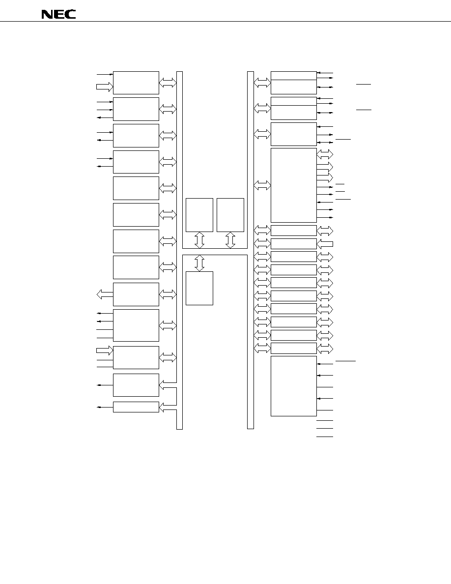
3. BLOCK DIAGRAM
INTP2/NMI
INTP0, INTP1,
INTP3-INTP6
PROGRAMMABLE
INTERRUPT
CONTROLLER
REAL-TIME
OUTPUT PORT
TIMER/COUNTER6
(8 BITS)
TIMER/COUNTER5
(8 BITS)
TIMER/COUNTER2
(8 BITS)
TIMER/COUNTER1
(8 BITS)
TIMER/COUNTER
(16 BITS)
WATCH TIMER
WATCHDOG TIMER
TI00
TI01
TO0
TI1
TO1
TI2
TO2
RTP0-RTP7
CLOCK OUTPUT
CONTROL
A/D
CONVERTER
AV
DD
AV
SS
PCL
BUZ
ANI0-ANI7
D/A
CONVERTER
ANO0
AV
SS
AV
REF1
ANO1
78K/IV
CPU CORE
FLASH
MEMORY
RAM
BAUD-RATE
GENERATOR
RxD1/SI1
TxD1/SO1
ASCK1/SCK1
RxD2/SI2
TxD2/SO2
ASCK2/SCK2
SI0
SO0
SCK0
BUS I/F
UART/IOE1
RD
ASTB
WR
WAIT
AD0-AD7
A8-A15
A16-A19
PORT1
P10-P17
PORT0
P00-P05
PORT2
P20-P27
PORT3
P30-P37
PORT4
P40-P47
PORT5
P50-P57
PORT6
P60-P67
PORT7
P70-P72
PORT12
P120-P127
PORT13
P130,P131
BUZZER OUTPUT
SYSTEM CONTROL
RESET
XT2
XT1
X2
X1
V
SS0
, V
SS1
V
DD0
, V
DD1
TEST/V
PP
CLOCKED
SERIAL
INTERFACE
BAUD-RATE
GENERATOR
UART/IOE2
EXA
9
µ
PD78F4225
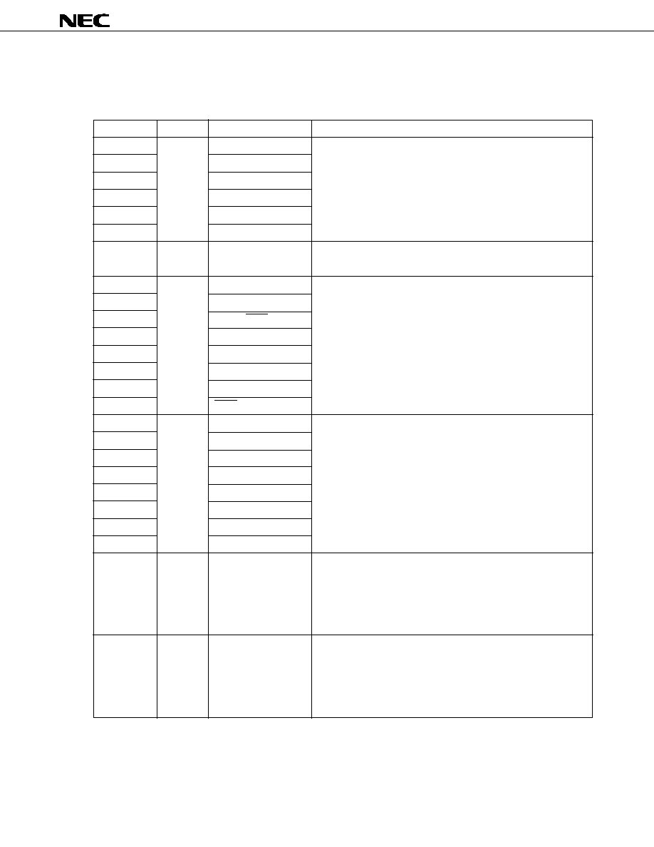
4. PIN FUNCTION
4.1 Port Pins (1/2)
Pin Name
I/O
Alternate Function
Function
P00
I/O
INTP0
P01
INTP1
P02
INTP2/NMI
P03
INTP3
P04
INTP4
P05
INTP5
P10-P17
Input
ANI0-ANI7
P20
I/O
RxD1/SI1
P21
TxD1/SO1
P22
ASCK1/SCK1
P23
PCL
P24
BUZ
P25
SI0
P26
SO0
P27
SCK0
P30
I/O
TO0
P31
TO1
P32
TO2
P33
TI1
P34
TI2
P35
TI00
P36
TI01
P37
EXA
P40-P47
I/O
AD0-AD7
Port 4 (P4):
∑ 8-bit I/O port
∑ Can be set in input or output mode bit-wise.
∑ All pins set in input mode can be connected to internal pull-up
resistors in software.
∑ Can drive LEDs.
P50-P57
I/O
A8-A15
Port 5 (P5):
∑ 8-bit I/O port
∑ Can be set in input or output mode bit-wise.
∑ All pins set in input mode can be connected to internal pull-up
resistors in software.
∑ Can drive LEDs.
Port 1 (P1):
∑ 8-bit input port
Port 0 (P0):
∑ 6-bit I/O port
∑ Can be set in input or output mode bit-wise.
∑ Pins set in input mode can be connected to internal pull-up
resistors in software bit-wise.
Port 2 (P2):
∑ 8-bit I/O port
∑ Can be set in input or output mode bit-wise.
∑ Pins set in input mode can be connected to internal pull-up
resistors in software bit-wise.
Port 3 (P3):
∑ 8-bit I/O port
∑ Can be set in input or output mode bit-wise.
∑ Pins set in input mode can be connected to internal pull-up
resistors in software bit-wise.
10
µ
PD78F4225
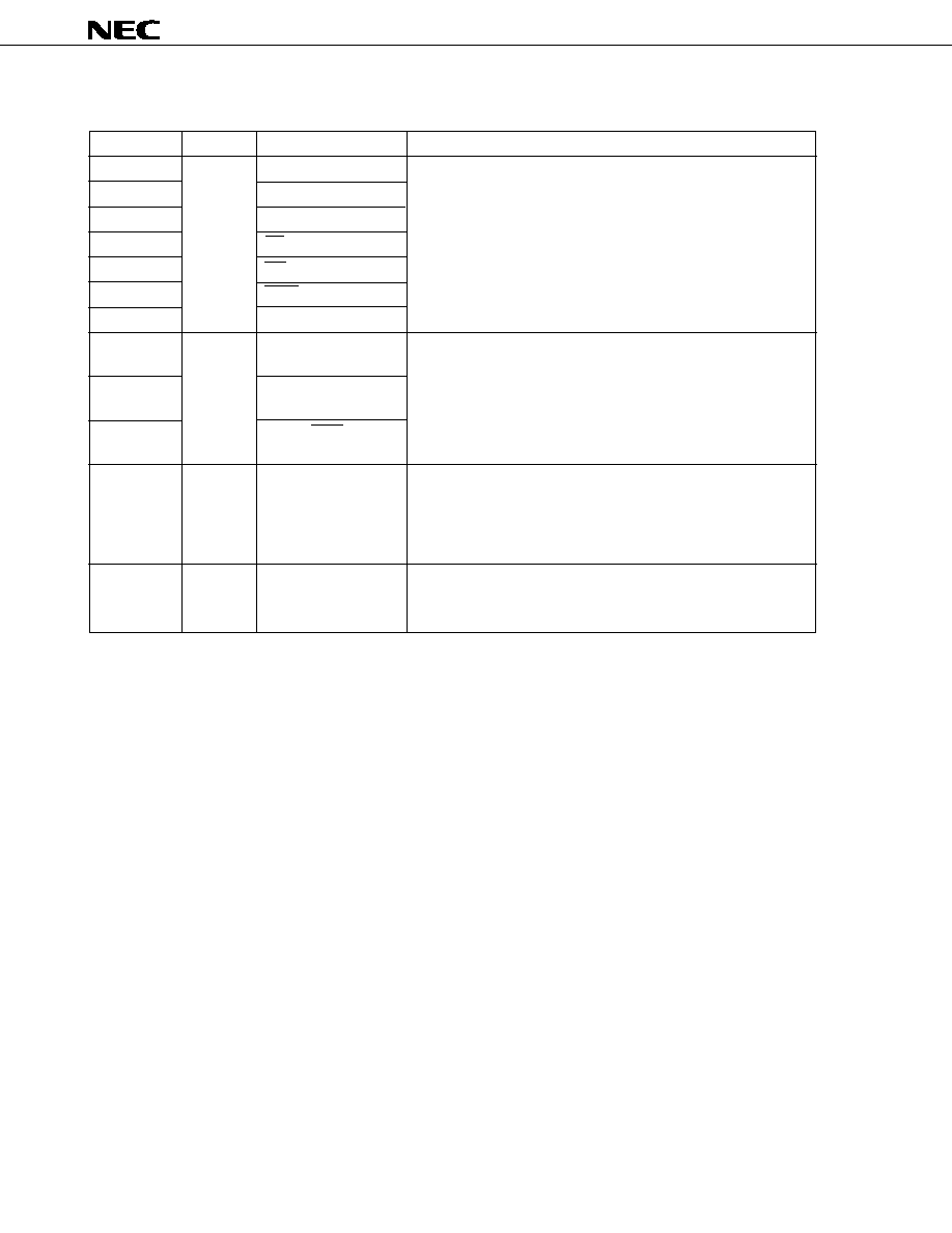
4.1 Port Pins (2/2)
Pin Name
I/O
Alternate Function
Function
P60
I/O
A16
P61
A17
P62
A18
P64
RD
P65
WR
P66
WAIT
P67
ASTB
P70
I/O
RxD2/SI2
P71
TxD2/SO2
P72
ASCK2/SCK2
P120-P127
I/O
RTP0-RTP7
Port 12 (P12):
∑ 8-bit I/O port
∑ Can be set in input or output mode bit-wise.
∑ Pins set in input mode can be connected to internal pull-up resistor
in software bit-wise.
P130, P131
I/O
ANO0, ANO1
Port 13 (P13):
∑ 2-bit I/O port
∑ Can be set in input or output mode bit-wise.
Port 6 (P6):
∑ 8-bit I/O port
∑ Can be set in input or output mode bit-wise.
∑ All pins set in input mode can be connected to internal pull-up
resistors in software.
Port 7 (P7):
∑ 3-bit I/O port
∑ Can be set in input or output mode bit-wise.
∑ Pins set in input mode can be connected to internal pull-up resistor
in software bit-wise.
11
µ
PD78F4225
4.2 Pins Other Than Port Pins (1/2)
Pin Name
I/O
Alternate Function
Function
TI00
Input
P35
External count clock input to 16-bit timer register
TI01
P36
Capture trigger signal input to capture/compare register 00
TI1
P33
External count clock input to 8-bit timer register 1
TI2
P34
External count clock input to 8-bit timer register 2
TO0
Output
P30
16-bit timer output (shared by 14-bit PWM output)
TO1
P31
8-bit timer output (shared by 8-bit PWM output)
TO2
P32
RxD1
Input
P20/SI1
Serial data input (UART1)
RxD2
P70/SI2
Serial data input (UART2)
TxD1
Output
P21/SO1
Serial data output (UART1)
TxD2
P71/SO2
Serial data output (UART2)
ASCK1
Intput
P22/SCK1
Baud rate clock input (UART1)
ASCK2
P72/SCK2
Baud rate clock input (UART2)
SI0
Input
P25
Serial data input (3-wire serial clock I/O0)
SI1
P20/RxD1
Serial data input (3-wire serial clock I/O1)
SI2
P70/RxD2
Serial data input (3-wire serial clock I/O2)
SO0
Output
P26
Serial data output (3-wire serial I/O0)
SO1
P21/TxD1
Serial data output (3-wire serial I/O1)
SO2
P71/TxD2
Serial data output (3-wire serial I/O2)
SCK0
I/O
P27
Serial clock input/output (3-wire serial I/O0)
SCK1
P22/ASCK1
Serial clock input/output (3-wire serial I/O1)
SCK2
P72/ASCK2
Serial clock input/output (3-wire serial I/O2)
NMI
Input
P02/INTP2
Non-maskable interrupt request input
INTP0
P00
External interrupt request input
INTP1
P01
INTP2
P02/NMI
INTP3
P03
INTP4
P04
INTP5
P05
PCL
Output
P23
Clock output (for trimming main system clock and subsystem clock)
BUZ
Output
P24
Buzzer output
RTP0-RTP7
Output
P120-P127
Real-time output port that outputs data in synchronization with
trigger
AD0-AD7
I/O
P40-P47
Low-order address/data bus when external memory is connected
A8-A15
Output
P50-P57
Middle-order address bus when external memory is connected
A16-A19
P60-P63
High-order address bus when external memory is connected
RD
Output
P64
Strobe signal output for read operation of external memory
WR
P65
Strobe signal output for write operation of external memory
WAIT
Input
P66
To insert wait state(s) when external memory is accessed

12
µ
PD78F4225
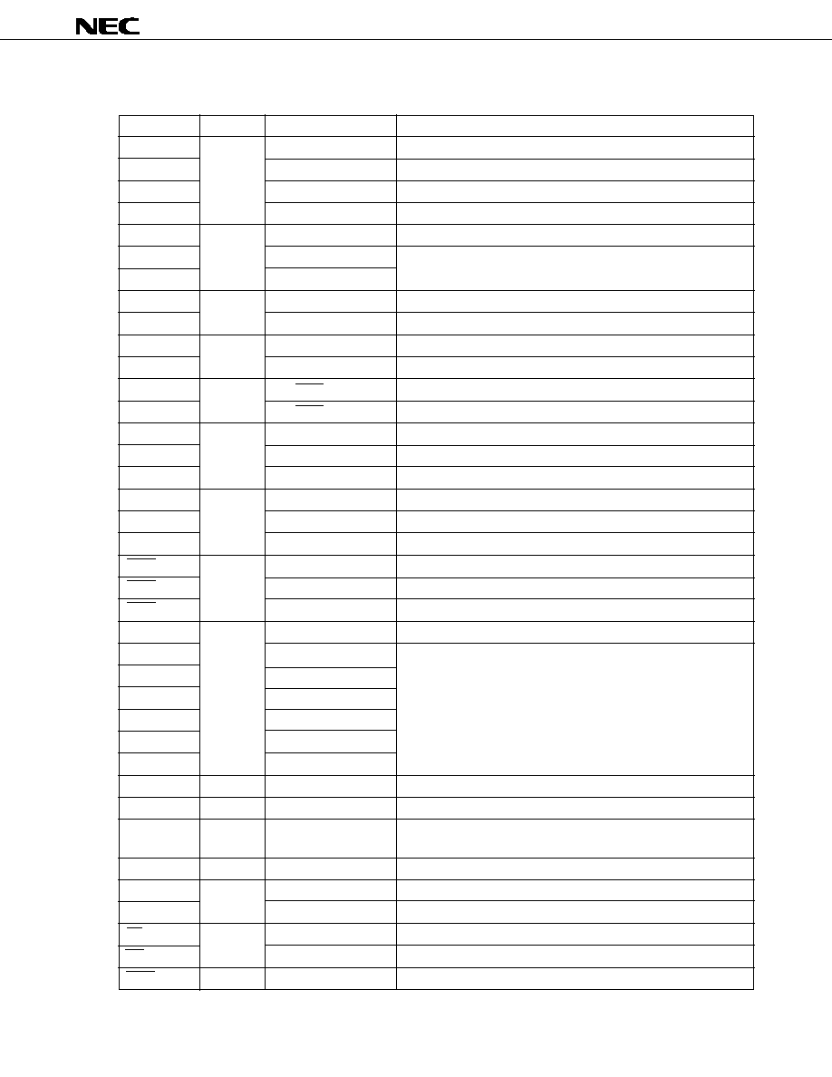
4.2 Pins Other Than Port Pins (2/2)
Pin Name
I/O
Alternate Function
Function
ASTB
Output
P67
Strobe output to externally latch address information output to ports
4 through 6 to access external memory
EXA
Output
P37
External access status output
RESET
Input
--
System reset input
X1
Input
--
To connect main system clock oscillation crystal
X2
--
XT1
Input
--
To connect subsystem clock oscillation crystal
XT2
--
ANI0-ANI7
Input
P10-P17
Analog voltage input for A/D converter
ANO0, ANO1
Output
P130, P131
Analog voltage output for D/A converter
AV
REF1
--
--
To apply reference voltage for D/A converter
AV
DD
Positive power supply for A/D converter. Connected to V
DD0
.
AV
SS
GND for A/D converter and D/A converter. Connected to V
SS0
.
V
DD0
Positive power supply for port block
V
SS0
GND potential for port block
V
DD1
Positive power supply (except port block)
V
SS1
GND potential (except port block)
TEST
V
PP
Directly connect this pin to V
SS
(this pin is for IC test).
V
PP
TEST
Sets flash memory programming mode.
To apply a high voltage when program is written or verified.
13
µ
PD78F4225
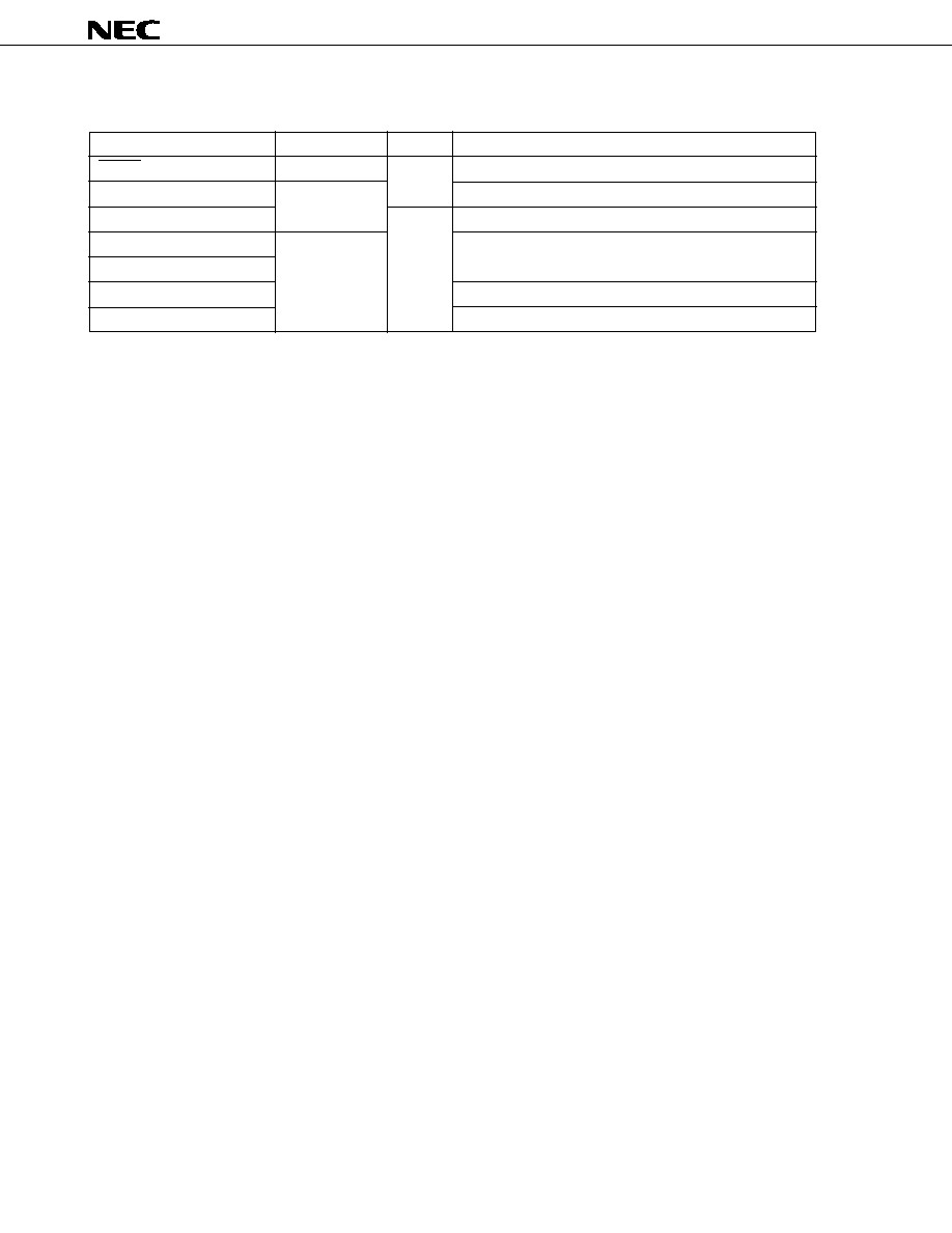
4.3 I/O Circuit Type of Respective Pins and Recommended Connections of Unused Pins
Table 4-1 shows symbols indicating the I/O circuit types of the respective pins and the recommended connection
of unused pins.
For the circuit diagram of each type of I/O circuit, refer to Figure 4-1.
Table 4-1. I/O Circuit Type of Respective Pins and Recommended Connections of Unused Pins (1/2)
Pin Name
I/O Circuit Type
I/O
Recommended Connections of Unused Pins
P00/INTP0
8-C
I/O
Input : Individually connected to V
SS0
via resistor
P01/INTP1
Output: Open
P02/INTP2/NMI
P03/INTP3-P05/INTP5
P10/ANI0-P17/ANI7
9
Input
Connected to V
SS0
or V
DD0
P20/RxD1/SI1
10-B
I/O
Input : Individually connected to V
SS0
via resistor
P21/TxD1/SO1
Output: Open
P22/ASCK1/SCK1
P23/PCL
P24/BUZ
P25/SI0
P26/SO0
P27/SCK0
P30/TO0-P32/TO2
8-C
P33/TI1, P34/TI2
P35/TI00, P36/TI01
P37/EXA
P40/AD0-P47/AD7
5-H
P50/A8-P57/A15
P60/A16-P63/A19
P64/RD
P65/WR
P66/WAIT
P67/ASTB
P70/RxD2/SI2
8-C
P71/TxD2/SO2
P72/ASCK2/SCK2
P120/RTP0-P127/RTP7
P130/ANO0, P131/ANO1
12-C
14
µ
PD78F4225
Table 4-1. I/O Circuit Type of Respective Pins and Recommended Connections of Unused Pins (2/2)
Pin Name
I/O Circuit Type
I/O
Recommended Connections of Unused Pins
RESET
2
Input
--
XT1
16
Connected to V
SS0
XT2
--
Open
AV
REF1
--
Connected to V
DD0
AV
DD
AV
SS
Connected to V
SS0
TEST/V
PP
Directly connected to V
SS0
Remark Because the circuit type numbers are standardized among the 78K series products, they are not
sequential in some models (i.e., some circuits are not provided).
15
µ
PD78F4225
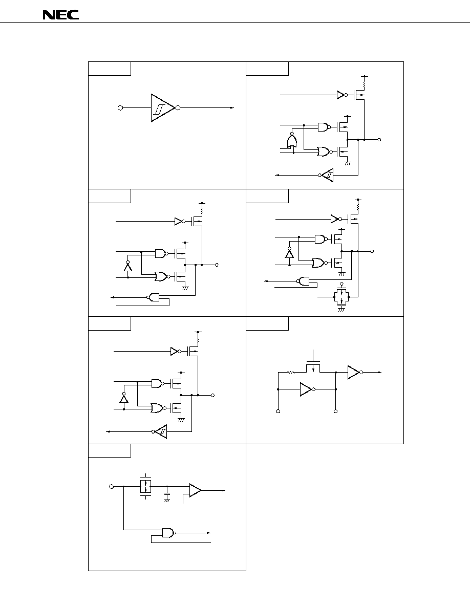
Figure 4-1. Types of Pin I/O Circuits
Type 2
IN
Schmitt trigger input with hysteresis characteristics
Type 5-H
pull-up
enable
data
output
disable
input
enable
V
DD0
P-ch
V
DD0
P-ch
IN/OUT
N-ch
Type 8-C
pull-up
enable
data
output
disable
V
DD0
P-ch
V
DD0
P-ch
IN/OUT
N-ch
Type 9
pull-up
enable
data
open drain
output disable
V
DD0
P-ch
V
DD0
P-ch
IN/OUT
N-ch
Type 10-B
Type 12-C
pull-up
enable
data
output
disable
input
enable
Analog output
voltage
V
DD0
P-ch
V
DD0
P-ch
IN/OUT
N-ch
P-ch
N-ch
Type 16
feedback
cut-off
P-ch
XT1
XT2
IN
Comparator
+
±
V
REF
(threshold voltage)
P-ch
N-ch
input
enable
V
SS0
V
SS0
V
SS0
V
SS0
V
SS0
16
µ
PD78F4225
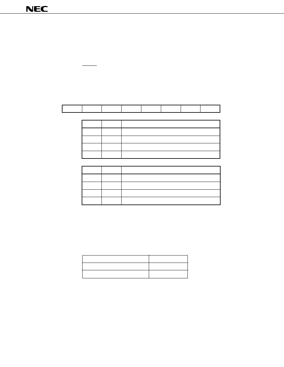
5. INTERNAL MEMORY SIZE SELECT REGISTER (IMS)
The IMS is a register that prevents in software a part of the internal memory from being used. By using this
register, the memory of the
µ
PD78F4225 can be mapped in the same manner as a mask ROM model with different
internal memory (ROM and RAM) capacity.
This register is set by using an 8-bit memory manipulation instruction.
Its value is set to FFH by RESET input.
Figure 5-1. Format of Internal Memory Size Select Register (IMS)
Caution
IMS is not provided on the mask ROM models (
µ
PD784224 and 784225).
The value to be set to the IMS to map the memory of the
µ
PD78F4225 in the same manner as the mask ROM
model is shown in Table 5-1.
Table 5-1. Set Value of Internal Memory Size Select Register (IMS)
Mask ROM Model
Set Value of IMS
µ
PD784225
EEH
µ
PD784226
FFH
1
1
ROM1
ROM0
1
1
RAM1
RAM0
7
6
5
4
3
2
1
0
ROM1
0
0
1
1
ROM0
0
1
0
1
Selects internal ROM capacity
48K bytes
64K bytes
96K bytes
128K bytes
RAM1
0
0
1
1
RAM0
0
1
0
1
Selects peripheral RAM capacity
1536 bytes
2304 bytes
3072 bytes
3840 bytes
Address: 0FFFCH
IMS
At reset: FFH
W

17
µ
PD78F4225
6. PROGRAMMING FLASH MEMORY
The flash memory can be written with the
µ
PD78F4225 mounted on the target board (on-board). To do so,
connect a dedicated flash writer (Flashpro II) to the host machine and target system.
Remark Flashpro II is a product of Naito Densei Machida Mfg. Co., Ltd.
6.1 Selecting Communication Mode
To write the flash memory, use Flashpro II and serial communication. Select a serial communication mode from
those listed in Table 6-1 in the format shown in Figure 6-1. Each communication mode is selected by the number
of V
PP
pulses shown in Table 6-1.
Table 6-1. Communication Modes
Communication Mode
Number of Channels
Pins Used
Number of V
PP
Pulses
3-wire serial I/O
3
SCK0/P27
0
SO0/P26
SI0/P25
SCK1/ASCK1/P22
1
SO1/TxD1/P21
SI1/RxD1/P20
SCK2/ASCK2/P72
2
SO2/TxD2/P71
SI2/RxD2/P70
UART
2
TxD1/SO1/P21
8
RxD1/SI1/P20
TxD2/SO2/P71
9
RxD2/SI2/P70
Psendo-3-wire serial
1
P32/TO2
12
I/O
Note
(serial clock I/O)
P31/TO1
(serial data output)
P30/TO0
(serial data output)
Note Performs serial transfer by controlling port by software.
Caution
Be sure to select a communication mode with the number of V
PP
pulses shown in Table 6-1.
Figure 6-1. Communication Mode Selecting Format
1
2
n
10 V
V
DD
V
SS
V
PP
V
DD
V
SS
RESET
18
µ
PD78F4225
6.2 Flash Memory Programming Function
The flash memory is written by transferring or receiving commands and data in a selected communication mode.
The major functions of flush memory programming are listed in Table 6-2.
Table 6-2. Major Functions of Flash Memory Programming
Function
Description
Batch erasure
Erases all contents of memory.
Block erasure
Erases contents of specified memory block.
Batch blank check
Checks erased status of entire memory.
Block blank check
Checks erased status of specified block
Data write
Writes flash memory based on write start address and number of data to be
written (in bytes).
Batch verify
Compares all contents of memory with input data.
Block verify
Compares contents of specified memory block with input data.
6.3 Connecting Flashpro II
The Flashpro II and
µ
PD78F4225 are connected differently depending on the selected communication mode.
Figures 6-2 through 6-5 show the connections in the respective communication modes.
Figure 6-2. Connection of Flashpro II in 3-Wire Serial I/O Mode (When Using 3-Wire Serial I/O 0)
Flashpro II
PD78F4225
µ
V
PP
n
Note
V
DD
V
SS
RESET
SCK
SO
SI
V
PP
V
DD0
, V
DD1
V
SS0
, V
SS1
RESET
SCK0
SI0
SO0
Note n = 1, 2
19
µ
PD78F4225
Figure 6-3. Connection of Flashpro II in UART Mode (When Using UART1)
Figure 6-4. Connection of Flashpro II in Pseudo-3-Wire Serial I/O Mode
Flashpro II
PD78F4225
µ
V
PP
n
Note
V
DD
V
SS
RESET
SO
SI
V
PP
V
DD0
, V
DD1
V
SS0
, V
SS1
RESET
R
X
D1
Note n = 1, 2
T
X
D1
Flashpro II
PD78F4225
µ
V
PP
n
Note
V
DD
V
SS
RESET
SCK
SO
SI
V
PP
V
DD0
, V
DD1
V
SS0
, V
SS1
RESET
P32 (serial clock)
P30 (serial input)
P31 (serial output)
Note n = 1, 2
20
µ
PD78F4225
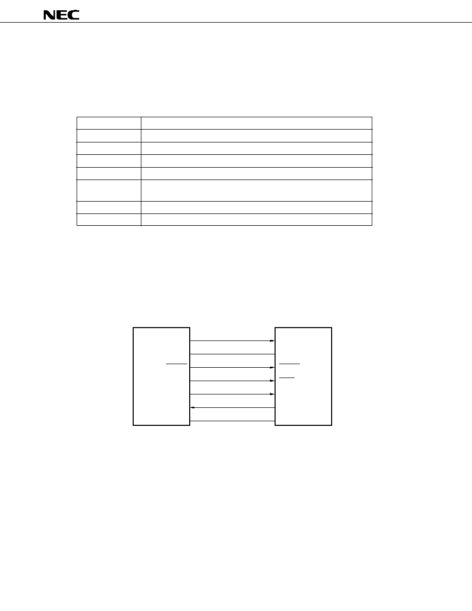
7. PACKAGE DRAWINGS
80 PIN PLASTIC QFP (14
◊
14)
ITEM
MILLIMETERS
INCHES
NOTE
Each lead centerline is located within 0.13 mm (0.005 inch) of
its true position (T.P.) at maximum material condition.
P80GC-65-8BT
F
0.825
0.032
B
14.00±0.20
0.551+0.009
≠0.008
S
1.70 MAX.
0.067 MAX.
M
0.17
0.007+0.001
≠0.003
+0.03
≠0.07
+0.009
≠0.008
C
14.00±0.20
0.551+0.009
≠0.008
A
17.20±0.20
0.677±0.008
G
0.825
0.032
H
0.32±0.06
0.013+0.002
≠0.003
I
0.13
0.005
J
0.65 (T.P.)
0.026 (T.P.)
K
1.60±0.20
0.063±0.008
L
0.80±0.20
0.031+0.009
≠0.008
N
0.10
0.004
P
1.40±0.10
0.055±0.004
Q
0.125±0.075
0.005±0.003
R
3
∞
3
∞
+7
∞
≠3
∞
+7
∞
≠3
∞
D
17.20±0.20
0.677±0.008
41
60
40
61
21
80
20
1
M
S
Q
R
K
M
L
A
B
C
D
J
H
I
F
G
P
N
detail of lead end
21
µ
PD78F4225
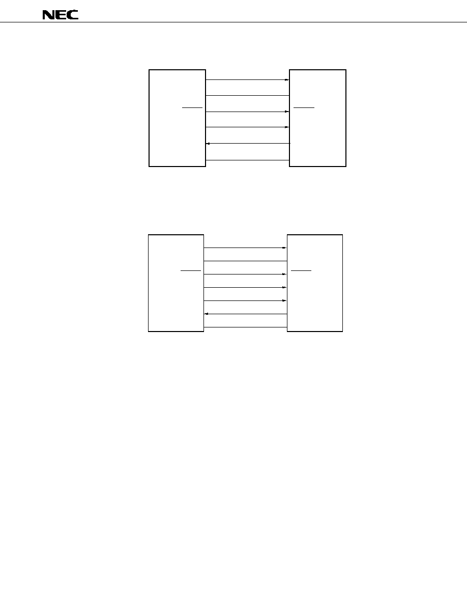
80 PIN PLASTIC TQFP (FINE PITCH) ( 12)
ITEM
MILLIMETERS
INCHES
I
J
0.5 (T.P.)
0.10
0.004
0.020 (T.P.)
A
NOTE
Each lead centerline is located within 0.10 mm (0.004 inch) of
its true position (T.P.) at maximum material condition.
S
A
14.0±0.2
0.551+0.009
≠0.008
B
12.0±0.2
0.472+0.009
≠0.008
C
12.0±0.2
0.472+0.009
≠0.008
D
14.0±0.2
0.551+0.009
≠0.008
F
G
1.25
1.25
0.049
0.049
H
0.22
0.009±0.002
P80GK-50-BE9-4
S
1.27 MAX.
0.050 MAX.
K
1.0±0.2
0.039+0.009
≠0.008
L
0.5±0.2
0.020+0.008
≠0.009
M
0.145
0.006±0.002
N
0.10
0.004
P
1.05
0.041
Q
0.05±0.05
0.002±0.002
R
5∞±5∞
5∞±5∞
+0.05
≠0.04
+0.055
≠0.045
B
C
D
J
H
I
G
F
P
N
L
K
M
Q
R
detail of lead end
M
61
60
41
40
21
20
1
80
22
µ
PD78F4225
APPENDIX A. DEVELOPMENT TOOLS
The following development tools are available for supporting development of a system using the
µ
PD78F4225.
Language processor software
RA78K4
Note 1
Assembler package common to 78K/IV series
CC78K4
Note 1
C compiler package common to 78K/IV series
CC78K4-L
Note 1
C compiler library source file common to 78K/IV series
Flash memory writing tool
Flashpro II
Dedicated flash writer.
Flashpro is the product of Naito Densei Machida Mfg. Co., Ltd.
Product name pending
Adapter for flash memory writing.
Debugging tool
IE-784000-R
In-circuit emulator common to 78K/IV series
IE-784000-R-BK
Break board common to 78K/IV series
IE-784218-R-EM1
Emulation board for evaluation of
µ
PD784225 subseries
IE-784000-R-EM
IE-70000-98-IF-B
Interface adapter when PC-9800 series (except notebook type) is used as host machine
IE-70000-98N-IF
Interface adapter and cable when notebook type PC-9800 series is used as host machine
IE-70000-PC-IF-B
Interface adapter when IBM PC/AT
TM
is used as host machine
IE-78000-R-SV3
Interface adapter and cable when EWS is used as host machine
Product name pending
Emulation probe common to
µ
PD784225 subseries
SM78K4
Note 2
System simulator common to 78K/IV series
ID78K4
Note 2
Integrated debugger for IE-784000-R
DF784225 (Pending)
Note 3
Device file for
µ
PD784225 subseries
Real-time OS
RX78K/IV
Note 3
Real-time OS for 78K/IV series
MX78K4
Note 4
OS for 78K/IV series
Remark RA78K4, CC78K4, SM78K4, and ID78K4 are used in combination with DF784225.

23
µ
PD78F4225
Notes 1. ∑ PC-9800 series (MS-DOS
TM
) based
∑ IBM PC/AT and compatible machine (PC DOS
TM
, Windows
TM
, MS-DOS, IBM DOS
TM
) based
∑ HP9000 series 700
TM
(HP-UX
TM
) based
∑ SPARCstation
TM
(SunOS
TM
) based
∑ NEWS
TM
(NEWS-OS
TM
) based
2. ∑ PC-9800 series (MS-DOS+Windows) based
∑ IBM PC/AT and compatible machine (PC DOS, Windows, MS-DOS, IBM DOS) based
∑ HP9000 series 700 (HP-UX) based
∑ SPARCstation (SunOS) based
3. ∑ PC-9800 series (MS-DOS) based
∑ IBM PC/AT and compatible machine (PC DOS, Windows, MS-DOS, IBM DOS) based
∑ HP9000 series 700 (HP-UX) based
∑ SPARCstation (SunOS) based
4. ∑ PC-9800 series (MS-DOS) based
∑ IMB PC/AT and compatible machine (PC DOS, Windows, MS-DOS, IBM DOS) based
24
µ
PD78F4225
APPENDIX B. RELATED DOCUMENTS
Documents Related to Device
Document Name
Document No.
Japanese
English
µ
PD784224, 784225 Preliminary Product Information
U12498J
Planned
µ
PD78F4225 Preliminary Product Information
U12499J
This document
µ
PD784225, 784225Y Subseries User's Manual - Hardware
Planned
Planned
µ
PD784225 Subseries Special Function Register Table
Planned
≠
78K/IV Series User's Manual - Instruction
U10905J
U10905E
78K/IV Series Instruction Table
U10594J
≠
78K/IV Series Instruction Set
U10595J
≠
78K/IV Series Application Note - Software Basics
U10095J
≠
Documents Related to Development Tools (User's Manuals)
Document Name
Document No.
Japanese
English
RA78K4 Assembler Package
Operation
U11334J
U11334E
Language
U11162J
≠
RA78K Series Structured Assembler Preprocessor
EEU-817
EEU-1402
CC78K4 Series
Operation
EEU-960
≠
Language
EEU-961
≠
CC78K Series Library Source File
U12322J
≠
IE-784000-R
EEU-5004
EEU-1534
IE-784218-R-EM1
U12155J
U12155E
SM78K4 System Simulator - Windows Based
Reference
U10093J
U10093E
SM78K Series System Simulator
External component
U10092J
U10092E
user open interface
specification
ID78K4 Integrated Debugger - Windows Based
Reference
U10440J
U10440E
ID78K4 Integrated Debugger - HP9000 Series
Reference
U11960J
Planned
(HP-UX Based)
Caution
The contents of the above related documents are subject to change without notice. Be sure to
use the latest edition of a document for designing.
25
µ
PD78F4225
Documents Related to Embedded Software (User's Manual)
Document Name
Document No.
Japanese
English
78K/IV Series Real-Time OS
Fundamental
U10603J
U10603E
Installation
U10604J
U10604E
Debugger
U10364J
≠
78K/IV Series OS MX78K4
Fundamental
U11779J
≠
Other Documents
Document Name
Document No.
Japanese
English
IC Package Manual
C10943X
Semiconductor Device Mounting Technology Manual
C10535J
C10535E
Quality Grades on NEC Semiconductor Devices
C11531J
C11531E
NEC Semiconductor Device Reliability/Quality Control System
C10983J
C10983E
Electrostatic Discharge (ESD) Test
MEM-539
≠
Guide to Quality Assurance for Semiconductor Devices
C11893J
MEI-1202
Guide to Microcomputer-Related Products by Third Parties
U11416J
≠
Caution
The contents of the above related documents are subject to change without notice. Be sure to
use the latest edition of a document for designing.
26
µ
PD78F4225
NOTES FOR CMOS DEVICES
1
PRECAUTION AGAINST ESD FOR SEMICONDUCTORS
Note: Strong electric field, when exposed to a MOS device, can cause destruction
of the gate oxide and ultimately degrade the device operation. Steps must
be taken to stop generation of static electricity as much as possible, and
quickly dissipate it once, when it has occurred. Environmental control must
be adequate. When it is dry, humidifier should be used. It is recommended
to avoid using insulators that easily build static electricity. Semiconductor
devices must be stored and transported in an anti-static container, static
shielding bag or conductive material. All test and measurement tools
including work bench and floor should be grounded. The operator should
be grounded using wrist strap. Semiconductor devices must not be touched
with bare hands. Similar precautions need to be taken for PW boards with
semiconductor devices on it.
2
HANDLING OF UNUSED INPUT PINS FOR CMOS
Note: No connection for CMOS device inputs can be cause of malfunction. If no
connection is provided to the input pins, it is possible that an internal input
level may be generated due to noise, etc., hence causing malfunction. CMOS
device behave differently than Bipolar or NMOS devices. Input levels of
CMOS devices must be fixed high or low by using a pull-up or pull-down
circuitry. Each unused pin should be connected to V
DD
or GND with a
resistor, if it is considered to have a possibility of being an output pin. All
handling related to the unused pins must be judged device by device and
related specifications governing the devices.
3
STATUS BEFORE INITIALIZATION OF MOS DEVICES
Note: Power-on does not necessarily define initial status of MOS device. Produc-
tion process of MOS does not define the initial operation status of the device.
Immediately after the power source is turned ON, the devices with reset
function have not yet been initialized. Hence, power-on does not guarantee
out-pin levels, I/O settings or contents of registers. Device is not initialized
until the reset signal is received. Reset operation must be executed imme-
diately after power-on for devices having reset function.

27
µ
PD78F4225
NEC Electronics Inc. (U.S.)
Santa Clara, California
Tel: 800-366-9782
Fax: 800-729-9288
NEC Electronics (Germany) GmbH
Duesseldorf, Germany
Tel: 0211-65 03 02
Fax: 0211-65 03 490
NEC Electronics (UK) Ltd.
Milton Keynes, UK
Tel: 01908-691-133
Fax: 01908-670-290
NEC Electronics Italiana s.r.1.
Milano, Italy
Tel: 02-66 75 41
Fax: 02-66 75 42 99
NEC Electronics Hong Kong Ltd.
Hong Kong
Tel: 2886-9318
Fax: 2886-9022/9044
NEC Electronics Hong Kong Ltd.
Seoul Branch
Seoul, Korea
Tel: 02-528-0303
Fax: 02-528-4411
NEC Electronics Singapore Pte. Ltd.
United Square, Singapore 1130
Tel: 253-8311
Fax: 250-3583
NEC Electronics Taiwan Ltd.
Taipei, Taiwan
Tel: 02-719-2377
Fax: 02-719-5951
NEC do Brasil S.A.
Sao Paulo-SP, Brasil
Tel: 011-889-1680
Fax: 011-889-1689
NEC Electronics (Germany) GmbH
Benelux Office
Eindhoven, The Netherlands
Tel: 040-2445845
Fax: 040-2444580
NEC Electronics (France) S.A.
Velizy-Villacoublay, France
Tel: 01-30-67 58 00
Fax: 01-30-67 58 99
NEC Electronics (France) S.A.
Spain Office
Madrid, Spain
Tel: 01-504-2787
Fax: 01-504-2860
NEC Electronics (Germany) GmbH
Scandinavia Office
Taeby, Sweden
Tel: 08-63 80 820
Fax: 08-63 80 388
Regional Information
Some information contained in this document may vary from country to country. Before using any NEC
product in your application, please contact the NEC office in your country to obtain a list of authorized
representatives and distributors. They will verify:
∑ Device availability
∑ Ordering information
∑ Product release schedule
∑ Availability of related technical literature
∑ Development environment specifications (for example, specifications for third-party tools and
components, host computers, power plugs, AC supply voltages, and so forth)
∑ Network requirements
In addition, trademarks, registered trademarks, export restrictions, and other legal issues may also vary
from country to country.
J96. 8

µ
PD78F4225
The related documents indicated in this publication may include preliminary versions. However, preliminary
versions are not marked as such.
No part of this document may be copied or reproduced in any form or by any means without the prior written
consent of NEC Corporation. NEC Corporation assumes no responsibility for any errors which may appear in
this document.
NEC Corporation does not assume any liability for infringement of patents, copyrights or other intellectual property
rights of third parties by or arising from use of a device described herein or any other liability arising from use
of such device. No license, either express, implied or otherwise, is granted under any patents, copyrights or other
intellectual property rights of NEC Corporation or others.
While NEC Corporation has been making continuous effort to enhance the reliability of its semiconductor devices,
the possibility of defects cannot be eliminated entirely. To minimize risks of damage or injury to persons or
property arising from a defect in an NEC semiconductor device, customers must incorporate sufficient safety
measures in its design, such as redundancy, fire-containment, and anti-failure features.
NEC devices are classified into the following three quality grades:
"Standard", "Special", and "Specific". The Specific quality grade applies only to devices developed based on a
customer designated "quality assurance program" for a specific application. The recommended applications of
a device depend on its quality grade, as indicated below. Customers must check the quality grade of each device
before using it in a particular application.
Standard: Computers, office equipment, communications equipment, test and measurement equipment,
audio and visual equipment, home electronic appliances, machine tools, personal electronic
equipment and industrial robots
Special:
Transportation equipment (automobiles, trains, ships, etc.), traffic control systems, anti-disaster
systems, anti-crime systems, safety equipment and medical equipment (not specifically designed
for life support)
Specific:
Aircrafts, aerospace equipment, submersible repeaters, nuclear reactor control systems, life
support systems or medical equipment for life support, etc.
The quality grade of NEC devices is "Standard" unless otherwise specified in NEC's Data Sheets or Data Books.
If customers intend to use NEC devices for applications other than those specified for Standard quality grade,
they should contact an NEC sales representative in advance.
Anti-radioactive design is not implemented in this product.
M4 96.5
IEBus is a trademark of NEC Corp.
MS-DOS and Windows are either registered trademarks or trademarks of Microsoft Corporation in the
United States and/or other countries.
IBM DOS, PC/AT, and PC DOS are trademarks of IBM Corp.
HP9000 series 700 and HP-UX are trademarks of Hewlett-Packard Co.
SPARCstation is a trademark of SPARC International, Inc.
SunOS is a trademark of Sun Microsystems, Inc.
NEWS and NEWS-OS are trademarks of Sony Corp.