Document Outline
- Cover
- INTRODUCTION
- CHAPTER 1 GENERAL
- 1.1 Features
- 1.2 Ordering Information
- 1.3 Pin Configuration (Top View)
- 1.3.1 Normal operation mode
- 1.4 Application System Configuration Example (Car Audio (Tuner, Deck))
- 1.5 Block Diagram
- 1.6 List of Functions
- 1.7 Differences among Products in uPD784938 Subseries
- 1.8 Main Differences with uPD784908 Subseries
- CHAPTER 2 PIN FUNCTIONS
- 2.1 Pin Function Lists
- 2.1.1 Normal operation mode
- 2.2 Pin Functions
- 2.2.1 Normal operation mode
- 2.3 Input/Output Circuits and Connection of Unused Pins
- 2.4 Cautions
- CHAPTER 3 CPU ARCHITECTURE
- 3.1 Memory Space
- 3.2 Internal ROM Area
- 3.3 Base Area
- 3.3.1 Vector table area
- 3.3.2 CALLT instruction table area
- 3.3.3 CALLF instruction entry area
- 3.4 Internal Data Area
- 3.4.1 Internal RAM area
- 3.4.2 Special function register (SFR) area
- 3.4.3 External SFR area
- 3.5 External Memory Space
- 3.6 uPD78F4938 Memory Mapping
- 3.7 Control Registers
- 3.7.1 Program counter (PC)
- 3.7.2 Program status word (PSW)
- 3.7.3 Use of RSS bit
- 3.7.4 Stack pointer (SP)
- 3.8 General-Purpose Registers
- 3.8.1 Configuration
- 3.8.2 Functions
- 3.9 Special Function Registers (SFR)
- 3.10 Cautions
- CHAPTER 4 CLOCK GENERATOR
- 4.1 Configuration and Function
- 4.2 Control Registers
- 4.2.1 Standby control register (STBC)
- 4.2.2 Oscillation stabilization time specification register (OSTS)
- 4.3 Clock Generator Operation
- 4.3.1 Clock oscillator
- 4.3.2 Divider
- 4.4 Cautions
- 4.4.1 When an external clock is input
- 4.4.2 When crystal/ceramic oscillation is used
- CHAPTER 5 REGULATOR
- CHAPTER 6 PORT FUNCTIONS
- 6.1 Digital Input/Output Ports
- 6.2 Port 0
- 6.2.1 Hardware configuration
- 6.2.2 I/O mode/control mode setting
- 6.2.3 Operating status
- 6.2.4 On-chip pull-up resistors
- 6.2.5 Transistor drive
- 6.3 Port 1
- 6.3.1 Hardware configuration
- 6.3.2 I/O mode/control mode setting
- 6.3.3 Operating status
- 6.3.4 On-chip pull-up resistors
- 6.3.5 Direct LED drive
- 6.4 Port 2
- 6.4.1 Hardware configuration
- 6.4.2 Input mode/control mode setting
- 6.4.3 Operating status
- 6.4.4 On-chip pull-up resistors
- 6.5 Port 3
- 6.5.1 Hardware configuration
- 6.5.2 I/O mode/control mode setting
- 6.5.3 Operating status
- 6.5.4 On-chip pull-up resistors
- 6.6 Port 4
- 6.6.1 Hardware configuration
- 6.6.2 I/O mode/control mode setting
- 6.6.3 Operating status
- 6.6.4 On-chip pull-up resistors
- 6.6.5 Direct LED drive
- 6.7 Port 5
- 6.7.1 Hardware configuration
- 6.7.2 I/O mode/control mode setting
- 6.7.3 Operating status
- 6.7.4 On-chip pull-up resistors
- 6.7.5 Direct LED drive
- 6.8 Port 6
- 6.8.1 Hardware configuration
- 6.8.2 I/O mode/control mode setting
- 6.8.3 Operating status
- 6.8.4 On-chip pul-up resistors
- 6.9 Port 7
- 6.9.1 Hardware configuration
- 6.9.2 I/O mode/control mode setting
- 6.9.3 Operating status
- 6.9.4 On-chip pull-up resistors
- 6.9.5 Caution
- 6.10 Port 9
- 6.10.1 Hardware configuration
- 6.10.2 I/O mode/control mode setting
- 6.10.3 Operating status
- 6.10.4 On-chip pull-up resistors
- 6.11 Port 10
- 6.11.1 Hardware configuration
- 6.11.2 I/O mode/control mode setting
- 6.11.3 Operating status
- 6.11.4 On-chip pull-up resistors
- 6.12 Port Output Check Function
- 6.13 Cautions
- CHAPTER 7 REAL-TIME OUTPUT FUNCTION
- 7.1 Configuration and Function
- 7.2 Real-time Output Port Control Register (RTPC)
- 7.3 Real-time Output Port Accesses
- 7.4 Operation
- 7.5 Example of Use
- 7.6 Cautions
- CHAPTER 8 OUTLINE OF TIMER
- CHAPTER 9 TIMER/EVENT COUNTER 0
- 9.1 Functions
- 9.2 Configuration
- 9.3 Timer/Event Counter 0 Control Registers
- 9.4 Timer Counter 0 (TM0) Operation
- 9.4.1 Basic operation
- 9.4.2 Clear operation
- 9.5 External Event Counter Function
- 9.6 Compare Register and Capture Register Operation
- 9.6.1 Compare operations
- 9.6.2 Capture operations
- 9.7 Basic Operation of Output Control Circuit
- 9.7.1 Basic operation
- 9.7.2 Toggle output
- 9.7.3 PWM output
- 9.7.4 PPG output
- 9.7.5 Software triggered one-shot pulse output
- 9.8 Examples of Use
- 9.8.1 Operation as interval timer (1)
- 9.8.2 Operation as interval timer (2)
- 9.8.3 Pulse width measurement operation
- 9.8.4 Operation as PWM output
- 9.8.5 Operation as PPG output
- 9.8.6 Example of software triggered one-shot pulse output
- 9.9 Cautions
- CHAPTER 10 TIMER/EVENT COUNTER 1
- 10.1 Functions
- 10.2 Configuration
- 10.3 Timer/Event Counter 1 Control Registers
- 10.4 Timer Counter 1 (TM1) Operation
- 10.4.1 Basic operation
- 10.4.2 Clear operation
- 10.5 External Event Counter Function
- 10.6 Compare Register and Capture/Compare Register Operation
- 10.6.1 Compare operations
- 10.6.2 Capture operations
- 10.7 Examples of Use
- 10.7.1 Operation as interval timer (1)
- 10.7.2 Operation as interval timer (2)
- 10.7.3 Pulse width measurement operation
- 10.8 Cautions
- CHAPTER 11 TIMER/EVENT COUNTER 2
- 11.1 Functions
- 11.2 Configuration
- 11.3 Timer/Event Counter 2 Control Registers
- 11.4 Timer Counter 2 (TM2) Operation
- 11.4.1 Basic operation
- 11.4.2 Clear operation
- 11.5 External Event Counter Function
- 11.6 One-Shot Timer Function
- 11.7 Compare Register, Capture/Compare Register, and Capture Register Operation
- 11.7.1 Compare operations
- 11.7.2 Capture operations
- 11.8 Basic Operation of Output Control Circuit
- 11.8.1 Basic operation
- 11.8.2 Toggle output
- 11.8.3 PWM output
- 11.8.4 PPG output
- 11.9 Examples of Use
- 11.9.1 Operation as interval timer (1)
- 11.9.2 Operation as interval timer (2)
- 11.9.3 Pulse width measurement operation
- 11.9.4 Operation as PWM output
- 11.9.5 Operation as PPG output
- 11.9.6 Operation as external event counter
- 11.9.7 Operation as one-shot timer
- 11.10 Cautions
- CHAPTER 12 TIMER 3
- 12.1 Function
- 12.2 Configuration
- 12.3 Timer 3 Control Registers
- 12.4 Timer Counter 3 (TM3) Operation
- 12.4.1 Basic operation
- 12.4.2 Clear operation
- 12.5 Compare Register Operation
- 12.6 Example of Use
- 12.7 Cautions
- CHAPTER 13 WATCHDOG TIMER
- 13.1 Configuration
- 13.2 Watchdog Timer Mode Register (WDM)
- 13.3 Operation
- 13.3.1 Count operation
- 13.3.2 Interrupt priorities
- 13.4 Cautions
- 13.4.1 General cautions on use of watchdog timer
- 13.4.2 Cautions on uPD784938 Subseries watchdog timer
- CHAPTER 14 WATCH TIMER
- CHAPTER 15 PWM OUTPUT UNIT
- 15.1 PWM Output Unit Configuration
- 15.2 PWM Output Unit Control Registers
- 15.2.1 PWM control register (PWMC)
- 15.2.2 PWM prescaler register (PWPR)
- 15.2.3 PWM modulo registers (PWM0, PWM1)
- 15.3 PWM Output Unit Operation
- 15.3.1 Basic PWM output operation
- 15.3.2 PWM pulse output enabling/disabling
- 15.3.3 PWM pulse active level specification
- 15.3.4 PWM pulse width rewrite cycle specification
- 15.4 Caution
- CHAPTER 16 A/D CONVERTER
- 16.1 Configuration
- 16.2 A/D Converter Mode Register (ADM)
- 16.3 A/D Current Cut Select Register (IEAD)
- 16.4 Operation
- 16.4.1 Basic A/D converter operation
- 16.4.2 Select mode
- 16.4.3 Scan mode
- 16.4.4 A/D conversion operation start by software
- 16.4.5 A/D conversion operation start by hardware
- 16.5 External Circuit of A/D Converter
- 16.6 Cautions
- CHAPTER 17 OUTLINE OF SERIAL INTERFACE
- CHAPTER 18 ASYNCHRONOUS SERIAL INTERFACE/3-WIRE SERIAL I/O
- 18.1 Switching between Asynchronous Serial Interface Mode and 3-Wire Serial I/O Mode
- 18.2 Asynchronous Serial Interface Mode
- 18.2.1 Configuration in asynchronous serial interface mode
- 18.2.2 Asynchronous serial interface control registers
- 18.2.3 Data format
- 18.2.4 Parity types and operations
- 18.2.5 Transmission
- 18.2.6 Reception
- 18.2.7 Receive errors
- 18.3 3-Wire Serial I/O Mode
- 18.3.1 Configuration in 3-wire serial I/O mode
- 18.3.2 Clocked serial interface mode registers (CSIM1, CSIM2)
- 18.3.3 Basic operation timing
- 18.3.4 Operation when transmission only is enabled
- 18.3.5 Operation when reception only is enabled
- 18.3.6 Operation when transmission/reception is enabled
- 18.3.7 Corrective action in case of slippage of serial clock and shift operations
- 18.4 Baud Rate Generator
- 18.4.1 Baud rate generator configuration
- 18.4.2 Baud rate generator control register (BRGC, BRGC2)
- 18.4.3 Baud rate generator operation
- 18.4.4 Baud rate setting in asynchronous serial interface mode
- 18.5 Cautions
- CHAPTER 19 3-WIRE SERIAL I/O MODE
- 19.1 Function
- 19.2 Configuration
- 19.3 Control Registers
- 19.3.1 Clocked serial interface mode register (CSIM, CSIM3)
- 19.4 3-Wire Serial I/O Mode
- 19.4.1 Basic operation timing
- 19.4.2 Operation when transmission only is enabled
- 19.4.3 Operation when reception only is enabled
- 19.4.4 Operation when transmission/reception is enabled
- 19.4.5 Corrective action in case of slippage of serial clock and shift operations
- CHAPTER 20 IEBus CONTROLLER
- 20.1 IEBus Controller Function
- 20.1.1 Communication protocol of IEBus
- 20.1.2 Determination of bus mastership (arbitration)
- 20.1.3 Communication mode
- 20.1.4 Communication address
- 20.1.5 Broadcasting communication
- 20.1.6 Transmission format of IEBus
- 20.1.7 Transmit data
- 20.1.8 Bit format
- 20.2 Simple IEBus Controller
- 20.3 IEBus Controller Configuration
- 20.4 Internal Registers of IEBus Controller
- 20.4.1 Internal register list
- 20.4.2 Description of internal registers
- 20.5 Interrupt Operations of IEBus Controller
- 20.5.1 Interrupt control block
- 20.5.2 Interrupt source list
- 20.6 Interrupt Generation Timing and Main CPU Processing
- 20.6.1 Master transmission
- 20.6.2 Master reception
- 20.6.3 Slave transmission
- 20.6.4 Slave reception
- 20.6.5 Interval of occurrence of interrupt for IEBus control
- 20.7 Cautions when Using IEBus Controller
- CHAPTER 21 CLOCK OUTPUT FUNCTION
- 21.1 Configuration
- 21.2 Clock Output Mode Register (CLOM)
- 21.3 Operation
- 21.3.1 Clock output
- 21.3.2 1-bit output port
- 21.3.3 Operation in standby mode
- 21.4 Cautions
- CHAPTER 22 EDGE DETECTION FUNCTION
- 22.1 Edge Detection Function Control Registers
- 22.1.1 External interrupt mode registers (INTM0, INTM1)
- 22.1.2 Sampling clock selection register (SCS0)
- 22.2 Edge Detection for Pins P20, P25, and P26
- 22.3 P21 Pin Edge Detection
- 22.4 Pin Edge Detection for Pins P22 to P24
- 22.5 Cautions
- CHAPTER 23 INTERRUPT FUNCTIONS
- 23.1 Interrupt Request Sources
- 23.1.1 Software interrupts
- 23.1.2 Operand error interrupts
- 23.1.3 Non-maskable interrupts
- 23.1.4 Maskable interrupts
- 23.2 Interrupt Service Modes
- 23.2.1 Vectored interrupt service
- 23.2.2 Macro service
- 23.2.3 Context switching
- 23.3 Interrupt Service Control Registers
- 23.3.1 Interrupt control registers
- 23.3.2 Interrupt mask registers (MK0/MK1)
- 23.3.3 In-service priority register (ISPR)
- 23.3.4 Interrupt mode control register (IMC)
- 23.3.5 Watchdog timer mode register (WDM)
- 23.3.6 Program status word (PSW)
- 23.4 Software Interrupt Acknowledgment Operations
- 23.4.1 BRK instruction software interrupt acknowledgment operation
- 23.4.2 BRKCS instruction software interrupt (software context switching) acknowledgment operation
- 23.5 Operand Error Interrupt Acknowledgment Operation
- 23.6 Non-Maskable Interrupt Acknowledgment Operation
- 23.7 Maskable Interrupt Acknowledgment Operation
- 23.7.1 Vectored interrupt
- 23.7.2 Context switching
- 23.7.3 Maskable interrupt priority levels
- 23.8 Macro Service Function
- 23.8.1 Outline of macro service function
- 23.8.2 Types of macro service
- 23.8.3 Basic macro service operation
- 23.8.4 Operation at end of macro service
- 23.8.5 Macro service control registers
- 23.8.6 Macro service type A
- 23.8.7 Macro service type B
- 23.8.8 Macro service type C
- 23.8.9 Counter mode
- 23.9 When Interrupt Requests and Macro Service are Temporarily Held Pending
- 23.10 Instructions whose Execution is Temporarily Suspended by an Interrupt or Macro Service
- 23.11 Interrupt and Macro Service Operation Timing
- 23.11.1 Interrupt acknowledge processing time
- 23.11.2 Processing time of macro service
- 23.12 Restoring Interrupt Function to Initial State
- 23.13 Cautions
- CHAPTER 24 LOCAL BUS INTERFACE FUNCTION
- 24.1 Memory Expansion Function
- 24.1.1 Memory expansion mode register (MM)
- 24.1.2 Memory map with external memory expansion
- 24.1.3 Basic operation of local bus interface
- 24.2 Wait Function
- 24.2.1 Wait function control registers
- 24.2.2 Address waits
- 24.2.3 Access waits
- 24.3 Pseudo-Static RAM Refresh Function
- 24.3.1 Control registers
- 24.3.2 Operations
- 24.4 Bus Hold Function
- 24.4.1 Hold mode register (HLDM)
- 24.4.2 Operation
- 24.5 Cautions
- CHAPTER 25 STANDBY FUNCTION
- 25.1 Configuration and Function
- 25.2 Control Registers
- 25.2.1 Standby control register (STBC)
- 25.2.2 Oscillation stabilization time specification register (OSTS)
- 25.3 HALT Mode
- 25.3.1 HALT mode setting and operating status
- 25.3.2 HALT mode release
- 25.4 STOP Mode
- 25.4.1 STOP mode setting and operating status
- 25.4.2 STOP mode release
- 25.5 IDLE Mode
- 25.5.1 IDLE mode setting and operating status
- 25.5.2 IDLE mode release
- 25.6 Check Items when STOP Mode/IDLE Mode is Used
- 25.7 Cautions
- CHAPTER 26 RESET FUNCTION
26.1 Reset Function
- 26.1 Reset Function
- 26.2 Caution
- CHAPTER 27 ROM CORRECTION
- 27.1 ROM Correction Functions
- 27.2 ROM Correction Configuration
- 27.3 Control Register for ROM Correction
- 27.4 Use of ROM Correction
- 27.5 Conditions for Executing ROM Correction
- CHAPTER 28 uPD78F4938 PROGRAMMING
- 28.1 Internal Memory Size Switching Register (IMS)
- 28.2 Flash Memory Programming Using Flashpro II and Flashpro III
- 28.2.1 Selecting communication mode
- 28.2.2 Flash memory programming functions
- 28.2.3 Connecting Flashpro II or Flashpro III
- CHAPTER 29 INSTRUCTION OPERATIONS
- 29.1 Conventions
- 29.2 List of Operations
- 29.3 Instructions Listed by Type of Addressing
- APPENDIX A DEVELOPMENT TOOLS
- A.1 Language Processing Software
- A.2 Flash Memory Programming Tools
- A.3 Debugging Tools
- A.3.1 Hardware (1/2)
- A.3.2 Software (1/2)
- A.4 Drawings of Conversion Socket (EV-9200GF-100) and Recommended Board Mounting Pattern
D
C
- A.5 Check Sheet for uPD784938 Subseries Development Tools
- APPENDIX B EMBEDDED SOFTWARE
- APPENDIX C REGISTER INDEX
- C.1 Register Name Index
- C.2 Register Symbol Index

�
PD784938 Subseries
16-Bit Single-Chip Microcontrollers
Hardware
�
PD784935
�
PD784936
�
PD784937
�
PD784938
�
PD78F4938
Document No. U13987EJ1V0UM00 (1st edition)
Date Published September 1999 N CP(K)
Preliminary User's Manual
Printed in Japan
�
1999

2
Preliminary User's Manual U13987EJ1V0UM00
[MEMO]

3
Preliminary User's Manual U13987EJ1V0UM00
NOTES FOR CMOS DEVICES
1
PRECAUTION AGAINST ESD FOR SEMICONDUCTORS
Note:
Strong electric field, when exposed to a MOS device, can cause destruction of the gate oxide and
ultimately degrade the device operation. Steps must be taken to stop generation of static electricity
as much as possible, and quickly dissipate it once, when it has occurred. Environmental control
must be adequate. When it is dry, humidifier should be used. It is recommended to avoid using
insulators that easily build static electricity. Semiconductor devices must be stored and transported
in an anti-static container, static shielding bag or conductive material. All test and measurement
tools including work bench and floor should be grounded. The operator should be grounded using
wrist strap. Semiconductor devices must not be touched with bare hands. Similar precautions need
to be taken for PW boards with semiconductor devices on it.
2
HANDLING OF UNUSED INPUT PINS FOR CMOS
Note:
No connection for CMOS device inputs can be cause of malfunction. If no connection is provided
to the input pins, it is possible that an internal input level may be generated due to noise, etc., hence
causing malfunction. CMOS devices behave differently than Bipolar or NMOS devices. Input levels
of CMOS devices must be fixed high or low by using a pull-up or pull-down circuitry. Each unused
pin should be connected to V
DD
or GND with a resistor, if it is considered to have a possibility of
being an output pin. All handling related to the unused pins must be judged device by device and
related specifications governing the devices.
3
STATUS BEFORE INITIALIZATION OF MOS DEVICES
Note:
Power-on does not necessarily define initial status of MOS device. Production process of MOS
does not define the initial operation status of the device. Immediately after the power source is
turned ON, the devices with reset function have not yet been initialized. Hence, power-on does
not guarantee out-pin levels, I/O settings or contents of registers. Device is not initialized until the
reset signal is received. Reset operation must be executed immediately after power-on for devices
having reset function.

4
Preliminary User's Manual U13987EJ1V0UM00
FIP, IEBus, Inter Equipment Bus, and EEPROM are trademarks of NEC Corporation.
MS-DOS, Windows, and Windows NT are either trademarks or registered trademarks of Microsoft Corporation
in the United States and/or other countries.
PC/AT is a trademark of International Business Machines Corporation.
SPARCstation is a trademark of SPARC International, Inc.
Solaris and SunOS are trademarks of Sun Microsystems, Inc.
HP9000 Series 700 and HP-UX are trademarks of Hewlett-Packard Company.
NEWS and NEWS-OS are trademarks of Sony Corporation.
Ethernet is a trademark of Xerox Corporation.
OSF/Motif is a trademark of Open Software Foundation, Inc.
TRON is an abbreviation of The Realtime Operating system Nucleus.
ITRON is an abbreviation of Industrial TRON.

5
Preliminary User's Manual U13987EJ1V0UM00
The application circuits and their parameters are for reference only and are not intended for use in actual design-ins.
�
The information contained in this document is being issued in advance of the production cycle for the
device. The parameters for the device may change before final production or NEC Corporation, at its own
discretion, may withdraw the device prior to its production.
�
Not all devices/types available in every country. Please check with local NEC representative for availability
and additional information.
�
No part of this document may be copied or reproduced in any form or by any means without the prior written
consent of NEC Corporation. NEC Corporation assumes no responsibility for any errors which may appear in
this document.
�
NEC Corporation does not assume any liability for infringement of patents, copyrights or other intellectual property
rights of third parties by or arising from use of a device described herein or any other liability arising from use
of such device. No license, either express, implied or otherwise, is granted under any patents, copyrights or other
intellectual property rights of NEC Corporation or others.
�
Descriptions of circuits, software, and other related information in this document are provided for illustrative
purposes in semiconductor product operation and application examples. The incorporation of these circuits,
software, and information in the design of the customer's equipment shall be done under the full responsibility
of the customer. NEC Corporation assumes no responsibility for any losses incurred by the customer or third
parties arising from the use of these circuits, software, and information.
�
While NEC Corporation has been making continuous effort to enhance the reliability of its semiconductor devices,
the possibility of defects cannot be eliminated entirely. To minimize risks of damage or injury to persons or
property arising from a defect in an NEC semiconductor device, customers must incorporate sufficient safety
measures in its design, such as redundancy, fire-containment, and anti-failure features.
�
NEC devices are classified into the following three quality grades:
"Standard", "Special", and "Specific". The Specific quality grade applies only to devices developed based on a
customer designated "quality assurance program" for a specific application. The recommended applications of
a device depend on its quality grade, as indicated below. Customers must check the quality grade of each device
before using it in a particular application.
Standard: Computers, office equipment, communications equipment, test and measurement equipment,
audio and visual equipment, home electronic appliances, machine tools, personal electronic
equipment and industrial robots
Special: Transportation equipment (automobiles, trains, ships, etc.), traffic control systems, anti-disaster
systems, anti-crime systems, safety equipment and medical equipment (not specifically designed
for life support)
Specific: Aircraft, aerospace equipment, submersible repeaters, nuclear reactor control systems, life
support systems or medical equipment for life support, etc.
The quality grade of NEC devices is "Standard" unless otherwise specified in NEC's Data Sheets or Data Books.
If customers intend to use NEC devices for applications other than those specified for Standard quality grade,
they should contact an NEC sales representative in advance.
M5D 98. 12
License not needed:
�
PD78F4938
The customer must judge the need for license:
�
PD784935, 784936, 784937, 784938
The export of these products from Japan is regulated by the Japanese government. The export of some or all of these
products may be prohibited without governmental license. To export or re-export some or all of these products from a
country other than Japan may also be prohibited without a license from that country. Please call an NEC sales
representative.

6
Preliminary User's Manual U13987EJ1V0UM00
Regional Information
Some information contained in this document may vary from country to country. Before using any NEC
product in your application, pIease contact the NEC office in your country to obtain a list of authorized
representatives and distributors. They will verify:
�
Device availability
�
Ordering information
�
Product release schedule
�
Availability of related technical literature
�
Development environment specifications (for example, specifications for third-party tools and
components, host computers, power plugs, AC supply voltages, and so forth)
�
Network requirements
In addition, trademarks, registered trademarks, export restrictions, and other legal issues may also vary
from country to country.
NEC Electronics Inc. (U.S.)
Santa Clara, California
Tel: 408-588-6000
800-366-9782
Fax: 408-588-6130
800-729-9288
NEC Electronics (Germany) GmbH
Duesseldorf, Germany
Tel: 0211-65 03 02
Fax: 0211-65 03 490
NEC Electronics (UK) Ltd.
Milton Keynes, UK
Tel: 01908-691-133
Fax: 01908-670-290
NEC Electronics Italiana s.r.l.
Milano, Italy
Tel: 02-66 75 41
Fax: 02-66 75 42 99
NEC Electronics (Germany) GmbH
Benelux Office
Eindhoven, The Netherlands
Tel: 040-2445845
Fax: 040-2444580
NEC Electronics (France) S.A.
Velizy-Villacoublay, France
Tel: 01-30-67 58 00
Fax: 01-30-67 58 99
NEC Electronics (France) S.A.
Spain Office
Madrid, Spain
Tel: 91-504-2787
Fax: 91-504-2860
NEC Electronics (Germany) GmbH
Scandinavia Office
Taeby, Sweden
Tel: 08-63 80 820
Fax: 08-63 80 388
NEC Electronics Hong Kong Ltd.
Hong Kong
Tel: 2886-9318
Fax: 2886-9022/9044
NEC Electronics Hong Kong Ltd.
Seoul Branch
Seoul, Korea
Tel: 02-528-0303
Fax: 02-528-4411
NEC Electronics Singapore Pte. Ltd.
United Square, Singapore 1130
Tel: 65-253-8311
Fax: 65-250-3583
NEC Electronics Taiwan Ltd.
Taipei, Taiwan
Tel: 02-2719-2377
Fax: 02-2719-5951
NEC do Brasil S.A.
Electron Devices Division
Rodovia Presidente Dutra, Km 214
07210-902-Guarulhos-SP Brasil
Tel: 55-11-6465-6810
Fax: 55-11-6465-6829
J99.1

7
Preliminary User's Manual U13987EJ1V0UM00
INTRODUCTION
Target Readers
This manual is intended for users who understand the functions of the
�
PD784938 Subseries to
design application systems.
Purpose
The purpose of this manual is to give users an understanding of the various hardware functions of
the
�
PD784938 Subseries.
Organization
The
�
PD784938 Subseries user's manual is divided into two volumes � hardware (this manual) and
instruction.
Hardware
Instruction
Pin functions
CPU functions
Internal block functions
Addressing
Interrupts
Instruction set
Other internal peripheral functions
Certain operating precautions apply to these products.
These precautions are stated at the relevant points in the text of each chapter, and are
also summarized at the end of each chapter. Be sure to read them.

8
Preliminary User's Manual U13987EJ1V0UM00
How to Read This Manual
Readers are required to have a general knowledge of electric engineering, logic circuits and
microcomputers.
� Unless otherwise specified
The
�
PD784938 is treated as the representative model. If using the
�
PD784935, 784936,
784937, and 78F4938, take the
�
PD784938 for the
�
PD784935, 784936, 784937, and
78F4938.
To understand overall functions of the
�
PD784938 Subseries:
Read this manual in the order of the CONTENTS.
To learn about differences from the
�
PD784908 Subseries:
See 1.8 Main Differences with
�
PD784908 Subseries.
If the device operates strangely after debugging:
Cautions are summarized at the end of each chapter, so refer to the cautions for the
relevant function.
To learn the detailed functions of a register whose register name is known:
Use APPENDIX C REGISTER INDEX.
To learn the details of the instruction functions:
Refer to 78K/IV Series User's Manual-Instruction (U10905E) separately available.
To learn about the electrical characteristics:
Refer to Data Sheets.
To learn about application examples of each function:
Refer to Application Note separately available.
Conventions
Data significance:
Higher digits on the left and lower digits on the right
Active low representation:
� � �
(Overscore over pin or signal name)
Note:
Footnote for item marked with Note in the text
Caution:
Information requiring particular attention
Remark:
Supplementary information
Numerical representation: Binary .........................
� � � �
B or
� � � �
Decimal ......................
� � � �
Hexadecimal ...............
� � � �
H
9
Preliminary User's Manual U13987EJ1V0UM00
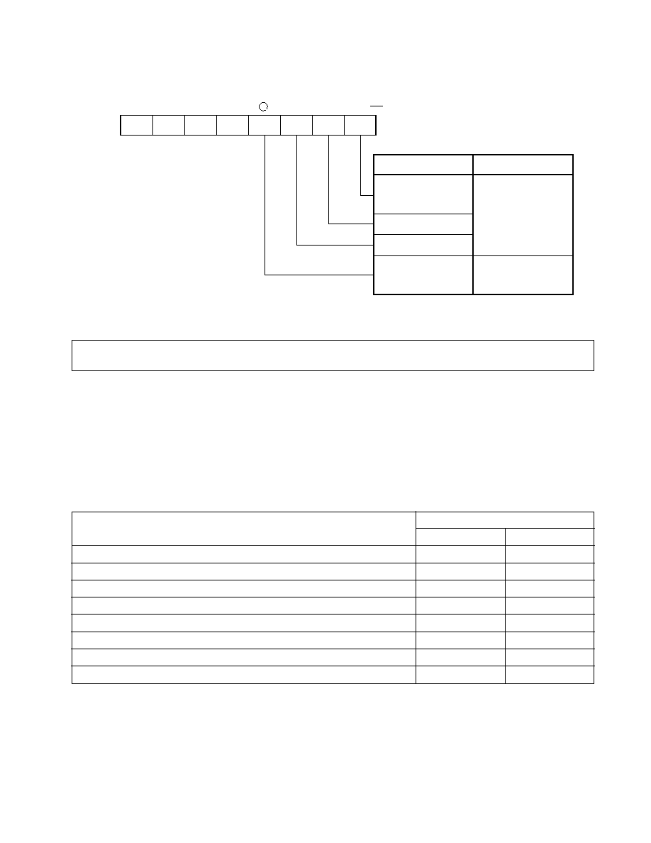
Register Notation
7
B
EDC
6
1
5
0
4
�
3
A
2
1
1
0
0
�
Write Operation
Read Operation
0 or 1 is written. The
operation is not affected
by either value.
0 must be written
1 must be written
A value is written
according to the
function to be used.
A value is read
according to the
operating status.
0 or 1 is read.
Where the bit number is marked with a circle, the
bit name is reserved for NEC's assembler and is
defined as an sfr variable by the #pragma sfr
directive for C compiler.
Code combinations marked "Setting prohibited" in the register notations in the text must not be written.
Easily confused characters : 0 (Zero), O (Letter O)
: 1 (One), l (Lowercase letter L), I (Uppercase letter I)
Related Documents
The related documents indicated in this publication may include preliminary versions. However,
preliminary versions are not marked as such.
Device related documents
Document Name
Document No.
Japanese
English
�
PD784935, 784936, 784937, 784938 Data Sheet
U13572J
U13572E
�
PD78F4938 Preliminary Product Information
U13573J
U13573E
�
PD784938 Subseries Special Function Register Table
To be prepared
--
�
PD784938 Subseries User's Manual - Hardware
U13987J
This manual
78K/IV Series Application Note - Software Basics
U10095J
U10095E
78K/IV Series User's Manual - Instruction
U10905J
U10905E
78K/IV Series Instruction Table
U10594J
--
78K/IV Series Instruction Set
U10595J
--
10
Preliminary User's Manual U13987EJ1V0UM00
Documents for development tools (User's Manuals)
Document Name
Document No.
Japanese
English
RA78K4 Assembler Package
Operation
U11334J
U11334E
Language
U11162J
U11162E
RA78K4 Structured Assembler Preprocessor
U11743J
U11743E
CC78K4 C Compiler
Operation
U11517J
U11517E
Language
U11518J
U11518E
IE-78K4-NS
U13356J
U13356E
IE-784000-R
U12903J
EEU-1534
IE-784937-NS-EM1
To be prepared
To be prepared
IE-784937-R-EM1
To be prepared
--
EP-78064
EEU-934
EEU-1469
SM78K4 System Simulator Windows
TM
Based
Reference
U10093J
U10093E
SM78K Series System Simulator
External component user
U10092J
U10092E
open interface specification
ID-78K4-NS Integrated Debugger
Reference
U12796J
U12796E
ID78K4 Integrated Debugger Windows Based
Reference
U10440J
U10440E
ID78K4 Integrated Debugger HP-UX
TM
, SunOS
TM
,
Reference
U11960J
U11960E
NEWS-OS
TM
Based
Documents for embedded software (User's Manuals)
Document Name
Document No.
Japanese
English
78K/IV Series Real-Time OS
Fundamental
U10603J
U10603E
Installation
U10604J
U10604E
Debugger
U10364J
--
78K/IV Series OS MX78K4
Basics
U11779J
--
Caution
The related documents listed above are subject to change without notice. Be sure to use the latest version
of each document for designing.

11
Preliminary User's Manual U13987EJ1V0UM00
Other documents
Document Name
Document No.
Japanese
English
SEMICONDUCTORS SELECTION GUIDE Products & Packages (CD-ROM)
X13769X
Semiconductor Device Mounting Technology Manual
C10535J
C10535E
Quality Grades on NEC Semiconductor Device
C11531J
C11531E
NEC Semiconductor Device Reliability/Quality Control System
C10983J
C10983E
Guide to Prevent Damage for Semiconductor Devices by Electrostatic Discharge (ESD)
C11892J
C11892E
Guide to Microcomputer-Related Products by Third Party
U11416J
--
Caution
The related documents listed above are subject to change without notice. Be sure to use the latest version
of each document for designing.

12
Preliminary User's Manual U13987EJ1V0UM00
[MEMO]

13
Preliminary User's Manual U13987EJ1V0UM00
CONTENTS
CHAPTER 1 GENERAL ...........................................................................................................................
39
1.1
Features ....................................................................................................................................
41
1.2
Ordering Information ...............................................................................................................
42
1.3
Pin Configuration (Top View) .................................................................................................
43
1.3.1
Normal operation mode ...............................................................................................................
43
1.4
Application System Configuration Example (Car Audio (Tuner, Deck)) ..........................
45
1.5
Block Diagram ..........................................................................................................................
46
1.6
List of Functions ......................................................................................................................
47
1.7
Differences among Products in
�
PD784938 Subseries .....................................................
50
1.8
Main Differences with
�
PD784908 Subseries ......................................................................
50
CHAPTER 2 PIN FUNCTIONS ...............................................................................................................
51
2.1
Pin Function Lists ....................................................................................................................
51
2.1.1
Normal operation mode ...............................................................................................................
51
2.2
Pin Functions ...........................................................................................................................
55
2.2.1
Normal operation mode ...............................................................................................................
55
2.3
Input/Output Circuits and Connection of Unused Pins .....................................................
62
2.4
Cautions ....................................................................................................................................
65
CHAPTER 3 CPU ARCHITECTURE ......................................................................................................
67
3.1
Memory Space ..........................................................................................................................
67
3.2
Internal ROM Area ....................................................................................................................
73
3.3
Base Area ..................................................................................................................................
74
3.3.1
Vector table area ..........................................................................................................................
75
3.3.2
CALLT instruction table area .......................................................................................................
76
3.3.3
CALLF instruction entry area ......................................................................................................
76
3.4
Internal Data Area ....................................................................................................................
77
3.4.1
Internal RAM area ........................................................................................................................
78
3.4.2
Special function register (SFR) area ...........................................................................................
81
3.4.3
External SFR area .......................................................................................................................
81
3.5
External Memory Space ..........................................................................................................
81
3.6
�
PD78F4938 Memory Mapping ...............................................................................................
82
3.7
Control Registers .....................................................................................................................
83
3.7.1
Program counter (PC) ..................................................................................................................
83
3.7.2
Program status word (PSW) ........................................................................................................
83
3.7.3
Use of RSS bit .............................................................................................................................
86
3.7.4
Stack pointer (SP) ........................................................................................................................
88
3.8
General-Purpose Registers ....................................................................................................
92
3.8.1
Configuration ................................................................................................................................
92
3.8.2
Functions ......................................................................................................................................
94
3.9
Special Function Registers (SFR) .........................................................................................
97
3.10
Cautions ....................................................................................................................................
103
CHAPTER 4 CLOCK GENERATOR ......................................................................................................
105
4.1
Configuration and Function ...................................................................................................
105

14
Preliminary User's Manual U13987EJ1V0UM00
4.2
Control Registers .....................................................................................................................
107
4.2.1
Standby control register (STBC) .................................................................................................
107
4.2.2
Oscillation stabilization time specification register (OSTS) .......................................................
109
4.3
Clock Generator Operation ....................................................................................................
110
4.3.1
Clock oscillator .............................................................................................................................
110
4.3.2
Divider ..........................................................................................................................................
110
4.4
Cautions ....................................................................................................................................
111
4.4.1
When an external clock is input ..................................................................................................
111
4.4.2
When crystal/ceramic oscillation is used ....................................................................................
112
CHAPTER 5 REGULATOR ......................................................................................................................
115
5.1
Outline of Regulator ................................................................................................................
115
CHAPTER 6 PORT FUNCTIONS ...........................................................................................................
117
6.1
Digital Input/Output Ports .......................................................................................................
117
6.2
Port 0 .........................................................................................................................................
119
6.2.1
Hardware configuration ................................................................................................................
119
6.2.2
I/O mode/control mode setting ....................................................................................................
120
6.2.3
Operating status ...........................................................................................................................
121
6.2.4
On-chip pull-up resistors ..............................................................................................................
123
6.2.5
Transistor drive ............................................................................................................................
125
6.3
Port 1 .........................................................................................................................................
126
6.3.1
Hardware configuration ................................................................................................................
127
6.3.2
I/O mode/control mode setting ....................................................................................................
131
6.3.3
Operating status ...........................................................................................................................
132
6.3.4
On-chip pull-up resistors ..............................................................................................................
135
6.3.5
Direct LED drive ...........................................................................................................................
136
6.4
Port 2 .........................................................................................................................................
137
6.4.1
Hardware configuration ................................................................................................................
139
6.4.2
Input mode/control mode setting .................................................................................................
141
6.4.3
Operating status ...........................................................................................................................
141
6.4.4
On-chip pull-up resistors ..............................................................................................................
141
6.5
Port 3 .........................................................................................................................................
143
6.5.1
Hardware configuration ................................................................................................................
144
6.5.2
I/O mode/control mode setting ....................................................................................................
148
6.5.3
Operating status ...........................................................................................................................
150
6.5.4
On-chip pull-up resistors ..............................................................................................................
153
6.6
Port 4 .........................................................................................................................................
155
6.6.1
Hardware configuration ................................................................................................................
155
6.6.2
I/O mode/control mode setting ....................................................................................................
156
6.6.3
Operating status ...........................................................................................................................
157
6.6.4
On-chip pull-up resistors ..............................................................................................................
159
6.6.5
Direct LED drive ...........................................................................................................................
161
6.7
Port 5 .........................................................................................................................................
162
6.7.1
Hardware configuration ................................................................................................................
162
6.7.2
I/O mode/control mode setting ....................................................................................................
163
6.7.3
Operating status ...........................................................................................................................
164
6.7.4
On-chip pull-up resistors ..............................................................................................................
166

15
Preliminary User's Manual U13987EJ1V0UM00
6.7.5
Direct LED drive ...........................................................................................................................
168
6.8
Port 6 .........................................................................................................................................
169
6.8.1
Hardware configuration ................................................................................................................
170
6.8.2
I/O mode/control mode setting ....................................................................................................
174
6.8.3
Operating status ...........................................................................................................................
176
6.8.4
On-chip pull-up resistors ..............................................................................................................
178
6.9
Port 7 .........................................................................................................................................
179
6.9.1
Hardware configuration ................................................................................................................
179
6.9.2
I/O mode/control mode setting ....................................................................................................
180
6.9.3
Operating status ...........................................................................................................................
181
6.9.4
On-chip pull-up resistors ..............................................................................................................
182
6.9.5
Caution .........................................................................................................................................
182
6.10
Port 9 .........................................................................................................................................
183
6.10.1
Hardware configuration ................................................................................................................
183
6.10.2
I/O mode/control mode setting ....................................................................................................
184
6.10.3
Operating status ...........................................................................................................................
185
6.10.4
On-chip pull-up resistors ..............................................................................................................
187
6.11
Port 10 ....................................................................................................................................... 188
6.11.1
Hardware configuration ................................................................................................................
189
6.11.2
I/O mode/control mode setting ....................................................................................................
193
6.11.3
Operating status ...........................................................................................................................
194
6.11.4
On-chip pull-up resistors ..............................................................................................................
197
6.12
Port Output Check Function ..................................................................................................
198
6.13
Cautions ....................................................................................................................................
199
CHAPTER 7 REAL-TIME OUTPUT FUNCTION ..................................................................................
201
7.1
Configuration and Function ...................................................................................................
201
7.2
Real-time Output Port Control Register (RTPC)..................................................................
203
7.3
Real-time Output Port Accesses ...........................................................................................
204
7.4
Operation .................................................................................................................................. 206
7.5
Example of Use ........................................................................................................................
209
7.6
Cautions ....................................................................................................................................
211
CHAPTER 8 OUTLINE OF TIMER .......................................................................................................
213
CHAPTER 9 TIMER/EVENT COUNTER 0 ...........................................................................................
215
9.1
Functions .................................................................................................................................. 215
9.2
Configuration ............................................................................................................................
218
9.3
Timer/Event Counter 0 Control Registers.........................................................................
221
9.4
Timer Counter 0 (TM0) Operation ..........................................................................................
226
9.4.1
Basic operation ............................................................................................................................
226
9.4.2
Clear operation .............................................................................................................................
228
9.5
External Event Counter Function ..........................................................................................
230
9.6
Compare Register and Capture Register Operation ...........................................................
233
9.6.1
Compare operations ....................................................................................................................
233
9.6.2
Capture operations ......................................................................................................................
235
9.7
Basic Operation of Output Control Circuit ..........................................................................
236
9.7.1
Basic operation ............................................................................................................................
238

16
Preliminary User's Manual U13987EJ1V0UM00
9.7.2
Toggle output ................................................................................................................................
238
9.7.3
PWM output ..................................................................................................................................
240
9.7.4
PPG output ...................................................................................................................................
245
9.7.5
Software triggered one-shot pulse output ...................................................................................
251
9.8
Examples of Use ......................................................................................................................
252
9.8.1
Operation as interval timer (1) ....................................................................................................
252
9.8.2
Operation as interval timer (2) ....................................................................................................
254
9.8.3
Pulse width measurement operation ...........................................................................................
256
9.8.4
Operation as PWM output ...........................................................................................................
259
9.8.5
Operation as PPG output ............................................................................................................
262
9.8.6
Example of software triggered one-shot pulse output ...............................................................
265
9.9
Cautions ....................................................................................................................................
268
CHAPTER 10 TIMER/EVENT COUNTER 1 .........................................................................................
271
10.1
Functions ..................................................................................................................................
271
10.2
Configuration ............................................................................................................................
273
10.3
Timer/Event Counter 1 Control Registers ............................................................................
277
10.4
Timer Counter 1 (TM1) Operation ..........................................................................................
280
10.4.1
Basic operation ............................................................................................................................
280
10.4.2
Clear operation .............................................................................................................................
283
10.5
External Event Counter Function ..........................................................................................
285
10.6
Compare Register and Capture/Compare Register Operation ..........................................
288
10.6.1
Compare operations ....................................................................................................................
288
10.6.2
Capture operations ......................................................................................................................
290
10.7
Examples of Use ......................................................................................................................
293
10.7.1
Operation as interval timer (1) ....................................................................................................
293
10.7.2
Operation as interval timer (2) ....................................................................................................
296
10.7.3
Pulse width measurement operation ...........................................................................................
298
10.8
Cautions ....................................................................................................................................
301
CHAPTER 11 TIMER/EVENT COUNTER 2 .........................................................................................
305
11.1
Functions ..................................................................................................................................
305
11.2
Configuration ............................................................................................................................
308
11.3
Timer/Event Counter 2 Control Registers ............................................................................
312
11.4
Timer Counter 2 (TM2) Operation ..........................................................................................
316
11.4.1
Basic operation ............................................................................................................................
316
11.4.2
Clear operation .............................................................................................................................
319
11.5
External Event Counter Function ..........................................................................................
321
11.6
One-Shot Timer Function .......................................................................................................
324
11.7
Compare Register, Capture/Compare Register, and Capture Register Operation .........
325
11.7.1
Compare operations ....................................................................................................................
325
11.7.2
Capture operations ......................................................................................................................
327
11.8
Basic Operation of Output Control Circuit ..........................................................................
330
11.8.1
Basic operation ............................................................................................................................
332
11.8.2
Toggle output ................................................................................................................................
332
11.8.3
PWM output ..................................................................................................................................
334
11.8.4
PPG output ...................................................................................................................................
340
11.9
Examples of Use ......................................................................................................................
347

17
Preliminary User's Manual U13987EJ1V0UM00
11.9.1
Operation as interval timer (1) ....................................................................................................
347
11.9.2
Operation as interval timer (2) ....................................................................................................
350
11.9.3
Pulse width measurement operation ...........................................................................................
353
11.9.4
Operation as PWM output ...........................................................................................................
356
11.9.5
Operation as PPG output ............................................................................................................
360
11.9.6
Operation as external event counter ...........................................................................................
364
11.9.7
Operation as one-shot timer ........................................................................................................
366
11.10 Cautions ....................................................................................................................................
369
CHAPTER 12 TIMER 3 ........................................................................................................................... 373
12.1
Function ....................................................................................................................................
373
12.2
Configuration ............................................................................................................................
374
12.3
Timer 3 Control Registers ......................................................................................................
376
12.4
Timer Counter 3 (TM3) Operation ..........................................................................................
378
12.4.1
Basic operation ............................................................................................................................
378
12.4.2
Clear operation .............................................................................................................................
380
12.5
Compare Register Operation ................................................................................................. 382
12.6
Example of Use ........................................................................................................................
383
12.7
Cautions ....................................................................................................................................
385
CHAPTER 13 WATCHDOG TIMER .......................................................................................................
387
13.1
Configuration ............................................................................................................................
387
13.2
Watchdog Timer Mode Register (WDM) ................................................................................
388
13.3
Operation .................................................................................................................................. 390
13.3.1
Count operation ............................................................................................................................
390
13.3.2
Interrupt priorities .........................................................................................................................
390
13.4
Cautions ....................................................................................................................................
391
13.4.1
General cautions on use of watchdog timer ...............................................................................
391
13.4.2
Cautions on
�
PD784938 Subseries watchdog timer ..................................................................
392
CHAPTER 14 WATCH TIMER ................................................................................................................
393
CHAPTER 15 PWM OUTPUT UNIT .....................................................................................................
395
15.1
PWM Output Unit Configuration ............................................................................................
395
15.2
PWM Output Unit Control Registers .....................................................................................
397
15.2.1
PWM control register (PWMC) ....................................................................................................
397
15.2.2
PWM prescaler register (PWPR) ................................................................................................
398
15.2.3
PWM modulo registers (PWM0, PWM1) .....................................................................................
398
15.3
PWM Output Unit Operation ...................................................................................................
399
15.3.1
Basic PWM output operation .......................................................................................................
399
15.3.2
PWM pulse output enabling/disabling .........................................................................................
400
15.3.3
PWM pulse active level specification ..........................................................................................
400
15.3.4
PWM pulse width rewrite cycle specification ..............................................................................
401
15.4
Caution ......................................................................................................................................
402
CHAPTER 16 A/D CONVERTER ...........................................................................................................
403
16.1
Configuration ............................................................................................................................
403
16.2
A/D Converter Mode Register (ADM) ....................................................................................
407

18
Preliminary User's Manual U13987EJ1V0UM00
16.3
A/D Current Cut Select Register (IEAD) ...............................................................................
410
16.4
Operation ..................................................................................................................................
411
16.4.1
Basic A/D converter operation .....................................................................................................
411
16.4.2
Select mode .................................................................................................................................
415
16.4.3
Scan mode ...................................................................................................................................
416
16.4.4
A/D conversion operation start by software ................................................................................
418
16.4.5
A/D conversion operation start by hardware ..............................................................................
420
16.5
External Circuit of A/D Converter ..........................................................................................
423
16.6
Cautions ....................................................................................................................................
423
CHAPTER 17 OUTLINE OF SERIAL INTERFACE ............................................................................
425
CHAPTER 18 ASYNCHRONOUS SERIAL INTERFACE/3-WIRE SERIAL I/O ...............................
427
18.1
Switching between Asynchronous Serial Interface Mode and 3-Wire Serial I/O Mode .
428
18.2
Asynchronous Serial Interface Mode ...................................................................................
429
18.2.1
Configuration in asynchronous serial interface mode ................................................................
429
18.2.2
Asynchronous serial interface control registers .........................................................................
432
18.2.3
Data format ...................................................................................................................................
435
18.2.4
Parity types and operations .........................................................................................................
436
18.2.5
Transmission ................................................................................................................................
437
18.2.6
Reception .....................................................................................................................................
438
18.2.7
Receive errors ..............................................................................................................................
439
18.3
3-Wire Serial I/O Mode ............................................................................................................
440
18.3.1
Configuration in 3-wire serial I/O mode ......................................................................................
440
18.3.2
Clocked serial interface mode registers (CSIM1, CSIM2) .........................................................
443
18.3.3
Basic operation timing .................................................................................................................
444
18.3.4
Operation when transmission only is enabled ............................................................................
446
18.3.5
Operation when reception only is enabled .................................................................................
446
18.3.6
Operation when transmission/reception is enabled ...................................................................
447
18.3.7
Corrective action in case of slippage of serial clock and shift operations ................................
447
18.4
Baud Rate Generator ...............................................................................................................
448
18.4.1
Baud rate generator configuration ..............................................................................................
448
18.4.2
Baud rate generator control register (BRGC, BRGC2) ..............................................................
450
18.4.3
Baud rate generator operation ....................................................................................................
452
18.4.4
Baud rate setting in asynchronous serial interface mode ..........................................................
454
18.5
Cautions ....................................................................................................................................
456
CHAPTER 19 3-WIRE SERIAL I/O MODE .........................................................................................
457
19.1
Function ....................................................................................................................................
457
19.2
Configuration ............................................................................................................................
458
19.3
Control Registers .....................................................................................................................
459
19.3.1
Clocked serial interface mode register (CSIM, CSIM3) .............................................................
459
19.4
3-Wire Serial I/O Mode ............................................................................................................
461
19.4.1
Basic operation timing .................................................................................................................
462
19.4.2
Operation when transmission only is enabled ............................................................................
464
19.4.3
Operation when reception only is enabled .................................................................................
465
19.4.4
Operation when transmission/reception is enabled ...................................................................
465
19.4.5
Corrective action in case of slippage of serial clock and shift operations ................................
465

19
Preliminary User's Manual U13987EJ1V0UM00
CHAPTER 20 IEBus CONTROLLER .....................................................................................................
467
20.1
IEBus Controller Function ......................................................................................................
467
20.1.1
Communication protocol of IEBus ...............................................................................................
467
20.1.2
Determination of bus mastership (arbitration) ............................................................................
468
20.1.3
Communication mode ..................................................................................................................
468
20.1.4
Communication address ..............................................................................................................
468
20.1.5
Broadcasting communication ......................................................................................................
469
20.1.6
Transmission format of IEBus .....................................................................................................
469
20.1.7
Transmit data ...............................................................................................................................
477
20.1.8
Bit format ......................................................................................................................................
479
20.2
Simple IEBus Controller .........................................................................................................
480
20.3
IEBus Controller Configuration .............................................................................................
481
20.4
Internal Registers of IEBus Controller .................................................................................
483
20.4.1
Internal register list ......................................................................................................................
483
20.4.2
Description of internal registers ..................................................................................................
484
20.5
Interrupt Operations of IEBus Controller .............................................................................
500
20.5.1
Interrupt control block ..................................................................................................................
500
20.5.2
Interrupt source list ......................................................................................................................
501
20.6
Interrupt Generation Timing and Main CPU Processing ....................................................
502
20.6.1
Master transmission .....................................................................................................................
502
20.6.2
Master reception ..........................................................................................................................
504
20.6.3
Slave transmission .......................................................................................................................
505
20.6.4
Slave reception ............................................................................................................................
506
20.6.5
Interval of occurrence of interrupt for IEBus control ..................................................................
507
20.7
Cautions when Using IEBus Controller ................................................................................
510
CHAPTER 21 CLOCK OUTPUT FUNCTION .......................................................................................
511
21.1
Configuration ............................................................................................................................
511
21.2
Clock Output Mode Register (CLOM) ...................................................................................
513
21.3
Operation .................................................................................................................................. 514
21.3.1
Clock output .................................................................................................................................
514
21.3.2
1-bit output port ............................................................................................................................
515
21.3.3
Operation in standby mode .........................................................................................................
515
21.4
Cautions ....................................................................................................................................
515
CHAPTER 22 EDGE DETECTION FUNCTION ...................................................................................
517
22.1
Edge Detection Function Control Registers ........................................................................
517
22.1.1
External interrupt mode registers (INTM0, INTM1) ....................................................................
517
22.1.2
Sampling clock selection register (SCS0) ..................................................................................
520
22.2
Edge Detection for Pins P20, P25, and P26 .........................................................................
521
22.3
P21 Pin Edge Detection ..........................................................................................................
522
22.4
Pin Edge Detection for Pins P22 to P24 ...............................................................................
523
22.5
Cautions ....................................................................................................................................
524
CHAPTER 23 INTERRUPT FUNCTIONS ..............................................................................................
525
23.1
Interrupt Request Sources .....................................................................................................
526
23.1.1
Software interrupts .......................................................................................................................
528
23.1.2
Operand error interrupts ..............................................................................................................
528

20
Preliminary User's Manual U13987EJ1V0UM00
23.1.3
Non-maskable interrupts ..............................................................................................................
528
23.1.4
Maskable interrupts ......................................................................................................................
528
23.2
Interrupt Service Modes .........................................................................................................
529
23.2.1
Vectored interrupt service ............................................................................................................
529
23.2.2
Macro service ...............................................................................................................................
529
23.2.3
Context switching .........................................................................................................................
529
23.3
Interrupt Service Control Registers ......................................................................................
530
23.3.1
Interrupt control registers ............................................................................................................
533
23.3.2
Interrupt mask registers (MK0/MK1) ...........................................................................................
538
23.3.3
In-service priority register (ISPR) ................................................................................................
540
23.3.4
Interrupt mode control register (IMC) ..........................................................................................
541
23.3.5
Watchdog timer mode register (WDM) .......................................................................................
542
23.3.6
Program status word (PSW) ........................................................................................................
543
23.4
Software Interrupt Acknowledgment Operations ................................................................
544
23.4.1
BRK instruction software interrupt acknowledgment operation .................................................
544
23.4.2
BRKCS instruction software interrupt (software context switching)
acknowledgment operation ..........................................................................................................
544
23.5
Operand Error Interrupt Acknowledgment Operation ........................................................
546
23.6
Non-Maskable Interrupt Acknowledgment Operation ........................................................
546
23.7
Maskable Interrupt Acknowledgment Operation .................................................................
550
23.7.1
Vectored interrupt .........................................................................................................................
552
23.7.2
Context switching .........................................................................................................................
552
23.7.3
Maskable interrupt priority levels ................................................................................................
554
23.8
Macro Service Function ..........................................................................................................
560
23.8.1
Outline of macro service function ................................................................................................
560
23.8.2
Types of macro service ................................................................................................................
560
23.8.3
Basic macro service operation ....................................................................................................
563
23.8.4
Operation at end of macro service ..............................................................................................
564
23.8.5
Macro service control registers ...................................................................................................
566
23.8.6
Macro service type A ...................................................................................................................
569
23.8.7
Macro service type B ...................................................................................................................
574
23.8.8
Macro service type C ...................................................................................................................
579
23.8.9
Counter mode ...............................................................................................................................
592
23.9
When Interrupt Requests and Macro Service are Temporarily Held Pending ................
594
23.10 Instructions whose Execution is Temporarily Suspended by an Interrupt or
Macro Service ...........................................................................................................................
596
23.11 Interrupt and Macro Service Operation Timing ...................................................................
596
23.11.1 Interrupt acknowledge processing time ......................................................................................
597
23.11.2 Processing time of macro service ...............................................................................................
598
23.12 Restoring Interrupt Function to Initial State ........................................................................
599
23.13 Cautions ....................................................................................................................................
600
CHAPTER 24 LOCAL BUS INTERFACE FUNCTION ........................................................................
603
24.1
Memory Expansion Function .................................................................................................
603
24.1.1
Memory expansion mode register (MM) .....................................................................................
603
24.1.2
Memory map with external memory expansion ..........................................................................
605
24.1.3
Basic operation of local bus interface .........................................................................................
614
24.2
Wait Function ...........................................................................................................................
615

21
Preliminary User's Manual U13987EJ1V0UM00
24.2.1
Wait function control registers .....................................................................................................
615
24.2.2
Address waits ...............................................................................................................................
618
24.2.3
Access waits .................................................................................................................................
621
24.3
Pseudo-Static RAM Refresh Function ..................................................................................
628
24.3.1
Control registers ...........................................................................................................................
629
24.3.2
Operations ....................................................................................................................................
630
24.4
Bus Hold Function ...................................................................................................................
634
24.4.1
Hold mode register (HLDM) ........................................................................................................
634
24.4.2
Operation ......................................................................................................................................
635
24.5
Cautions ....................................................................................................................................
636
CHAPTER 25 STANDBY FUNCTION ....................................................................................................
637
25.1
Configuration and Function ...................................................................................................
637
25.2
Control Registers .....................................................................................................................
639
25.2.1
Standby control register (STBC) .................................................................................................
639
25.2.2
Oscillation stabilization time specification register (OSTS) .......................................................
641
25.3
HALT Mode ................................................................................................................................
642
25.3.1
HALT mode setting and operating status ....................................................................................
642
25.3.2
HALT mode release .....................................................................................................................
642
25.4
STOP Mode ............................................................................................................................... 646
25.4.1
STOP mode setting and operating status ...................................................................................
646
25.4.2
STOP mode release ....................................................................................................................
647
25.5
IDLE Mode .................................................................................................................................
650
25.5.1
IDLE mode setting and operating status ....................................................................................
650
25.5.2
IDLE mode release ......................................................................................................................
651
25.6
Check Items when STOP Mode/IDLE Mode is Used ...........................................................
653
25.7
Cautions ....................................................................................................................................
655
CHAPTER 26 RESET FUNCTION .........................................................................................................
657
26.1
Reset Function .........................................................................................................................
657
26.2
Caution ...................................................................................................................................... 662
CHAPTER 27 ROM CORRECTION .......................................................................................................
663
27.1
ROM Correction Functions .....................................................................................................
663
27.2
ROM Correction Configuration ..............................................................................................
665
27.3
Control Register for ROM Correction ...................................................................................
667
27.4
Use of ROM Correction ...........................................................................................................
669
27.5
Conditions for Executing ROM Correction ..........................................................................
670
CHAPTER 28
�
PD78F4938 PROGRAMMING ......................................................................................
671
28.1
Internal Memory Size Switching Register (IMS) ..................................................................
672
28.2
Flash Memory Programming Using Flashpro II and Flashpro III ......................................
673
28.2.1
Selecting communication mode ..................................................................................................
673
28.2.2
Flash memory programming functions ........................................................................................
674
28.2.3
Connecting Flashpro II or Flashpro III ........................................................................................
675
CHAPTER 29 INSTRUCTION OPERATIONS .......................................................................................
677
29.1
Conventions .............................................................................................................................
677

22
Preliminary User's Manual U13987EJ1V0UM00
29.2
List of Operations ....................................................................................................................
681
29.3
Instructions Listed by Type of Addressing ..........................................................................
705
APPENDIX A DEVELOPMENT TOOLS ................................................................................................
709
A.1
Language Processing Software .............................................................................................
712
A.2
Flash Memory Programming Tools .......................................................................................
713
A.3
Debugging Tools ......................................................................................................................
714
A.3.1
Hardware ......................................................................................................................................
714
A.3.2
Software .......................................................................................................................................
716
A.4
Drawings of Conversion Socket (EV-9200GF-100) and
Recommended Board Mounting Pattern ..............................................................................
718
A.5
Check Sheet for
�
PD784938 Subseries Development Tools .............................................
720
APPENDIX B EMBEDDED SOFTWARE ................................................................................................
723
APPENDIX C REGISTER INDEX ...........................................................................................................
725
C.1
Register Name Index ...............................................................................................................
725
C.2
Register Symbol Index ............................................................................................................
728

23
Preliminary User's Manual U13987EJ1V0UM00
2-1
Pin Input/Output Circuits .............................................................................................................................
64
3-1
�
PD784935 Memory Map ............................................................................................................................
69
3-2
�
PD784936 Memory Map ............................................................................................................................
70
3-3
�
PD784937 Memory Map ............................................................................................................................
71
3-4
�
PD784938, 78F4938 Memory Map ...........................................................................................................
72
3-5
Internal RAM Memory Map .........................................................................................................................
79
3-6
Internal Memory Size Switching Register (IMS) .........................................................................................
82
3-7
Program Counter (PC) Format ....................................................................................................................
83
3-8
Program Status Word (PSW) Format .........................................................................................................
83
3-9
Stack Pointer (SP) Format ..........................................................................................................................
88
3-10
Data Saved to Stack Area ...........................................................................................................................
89
3-11
Data Restored from Stack Area ..................................................................................................................
90
3-12
General-Purpose Register Format ..............................................................................................................
92
3-13
General-Purpose Register Addresses ........................................................................................................
93
4-1
Clock Generator Block Diagram ..................................................................................................................
105
4-2
Clock Oscillator External Circuitry ..............................................................................................................
106
4-3
Standby Control Register (STBC) Format ..................................................................................................
108
4-4
Oscillation Stabilization Time Specification Register (OSTS) Format .......................................................
109
4-5
Signal Extraction with External Clock Input ................................................................................................
111
4-6
Cautions on Resonator Connection ............................................................................................................
112
4-7
Incorrect Example of Resonator Connection ..............................................................................................
113
5-1
Regulator Peripherals Block Diagram .........................................................................................................
115
6-1
Port Configuration ........................................................................................................................................
117
6-2
Port 0 Block Diagram ...................................................................................................................................
119
6-3
Port 0 Mode Register (PM0) Format ...........................................................................................................
120
6-4
Port Specified as Output Port .....................................................................................................................
121
6-5
Port Specified as Input Port ........................................................................................................................
122
6-6
Pull-Up Resistor Option Register L (PUOL) Format ..................................................................................
123
6-7
Pull-Up Resistor Specification (Port 0) .......................................................................................................
124
6-8
Example of Transistor Drive ........................................................................................................................
125
6-9
P12 (Port 1) Block Diagram ........................................................................................................................
127
6-10
P13 (Port 1) Block Diagram ........................................................................................................................
128
6-11
P14 (Port 1) Block Diagram ........................................................................................................................
129
6-12
Block Diagram of P10, P11, and P15 to P17 (Port 1) ................................................................................
130
6-13
Port 1 Mode Register (PM1) Format ...........................................................................................................
131
6-14
Port 1 Mode Control Register (PMC1) Format ...........................................................................................
131
6-15
Port Specified as Output Port .....................................................................................................................
132
LIST OF FIGURES (1/12)
Figure No.
Title
Page

24
Preliminary User's Manual U13987EJ1V0UM00
6-16
Port Specified as Input Port ........................................................................................................................
133
6-17
Control Specification ....................................................................................................................................
134
6-18
Pull-Up Resistor Option Register L (PUOL) Format ..................................................................................
135
6-19
Pull-Up Resistor Specification (Port 1) .......................................................................................................
136
6-20
Example of Direct LED Drive ......................................................................................................................
136
6-21
Block Diagram of P20 to P24, P26, and P27 (Port 2) ...............................................................................
139
6-22
P25 (Port 2) Block Diagram ........................................................................................................................
140
6-23
Port Specified as Input Port ........................................................................................................................
141
6-24
Pull-Up Resistor Option Register L (PUOL) Format ..................................................................................
141
6-25
Pull-Up Specification (Port 2) ......................................................................................................................
142
6-26
P30 (Port 3) Block Diagram ........................................................................................................................
144
6-27
Block Diagram of P31 and P34 to P37 (Port 3) .........................................................................................
145
6-28
P32 (Port 3) Block Diagram ........................................................................................................................
146
6-29
P33 (Port 3) Block Diagram ........................................................................................................................
147
6-30
Port 3 Mode Register (PM3) Format ...........................................................................................................
148
6-31
Port 3 Mode Control Register (PMC3) Format ...........................................................................................
149
6-32
Port Specified as Output Port .....................................................................................................................
150
6-33
Port Specified as Input Port ........................................................................................................................
151
6-34
Control Specification ....................................................................................................................................
152
6-35
Pull-Up Resistor Option Register L (PUOL) Format ..................................................................................
153
6-36
Pull-Up Specification (Port 3) ......................................................................................................................
154
6-37
Port 4 Block Diagram ...................................................................................................................................
155
6-38
Port 4 Mode Register (PM4) Format ...........................................................................................................
156
6-39
Port Specified as Output Port .....................................................................................................................
157
6-40
Port Specified as Input Port ........................................................................................................................
158
6-41
Pull-Up Resistor Option Register L (PUOL) Format ..................................................................................
159
6-42
Pull-Up Specification (Port 4) ......................................................................................................................
160
6-43
Example of Direct LED Drive ......................................................................................................................
161
6-44
Port 5 Block Diagram ...................................................................................................................................
162
6-45
Port 5 Mode Register (PM5) Format ...........................................................................................................
163
6-46
Port Specified as Output Port .....................................................................................................................
164
6-47
Port Specified as Input Port ........................................................................................................................
165
6-48
Pull-Up Resistor Option Register L (PUOL) Format ..................................................................................
166
6-49
Pull-Up Specification (Port 5) ......................................................................................................................
167
6-50
Example of Direct LED Drive ......................................................................................................................
168
6-51
P60 to P63 (Port 6) Block Diagram ............................................................................................................
170
6-52
P64 and P65 (Port 6) Block Diagram .........................................................................................................
171
6-53
P66 (Port 6) Block Diagram ........................................................................................................................
172
6-54
P67 (Port 6) Block Diagram ........................................................................................................................
173
6-55
Port 6 Mode Register (PM6) Format ...........................................................................................................
175
6-56
Port Specified as Output Port .....................................................................................................................
176
LIST OF FIGURES (2/12)
Figure No.
Title
Page

25
Preliminary User's Manual U13987EJ1V0UM00
6-57
Port Specified as Input Port ........................................................................................................................
177
6-58
Pull-Up Resistor Option Register L (PUOL) Format ..................................................................................
178
6-59
Pull-Up Specification (Port 6) ......................................................................................................................
178
6-60
Port 7 Block Diagram ...................................................................................................................................
179
6-61
Port 7 Mode Register (PM7) Format ...........................................................................................................
180
6-62
Port Specified as Output Port .....................................................................................................................
181
6-63
Port Specified as Input Port ........................................................................................................................
182
6-64
Port 9 Block Diagram ...................................................................................................................................
183
6-65
Port 9 Mode Register (PM9) Format ...........................................................................................................
184
6-66
Port Specified as Output Port .....................................................................................................................
185
6-67
Port Specified as Input Port ........................................................................................................................
186
6-68
Pull-Up Resistor Option Register H (PUOH) Format .................................................................................
187
6-69
Pull-Up Specification (Port 9) ......................................................................................................................
187
6-70
P100 to P104 (Port 10) Block Diagram ......................................................................................................
189
6-71
P105 (Port 10) Block Diagram ....................................................................................................................
190
6-72
P106 (Port 10) Block Diagram ....................................................................................................................
191
6-73
P107 (Port 10) Block Diagram ....................................................................................................................
192
6-74
Port 10 Mode Register (PM10) Format ......................................................................................................
193
6-75
Port 10 Mode Control Register (PMC10) Format .......................................................................................
193
6-76
Port Specified as Output Port .....................................................................................................................
194
6-77
Port Specified as Input Port ........................................................................................................................
195
6-78
Control Specification ....................................................................................................................................
196
6-79
Pull-Up Resistor Option Register H (PUOH) Format .................................................................................
197
6-80
Pull-Up Specification (Port 10) ....................................................................................................................
197
7-1
Real-Time Output Port Block Diagram ........................................................................................................
202
7-2
Real-Time Output Port Control Register (RTPC) Format ..........................................................................
203
7-3
Port 0 Buffer Register (P0H, P0L) Configuration .......................................................................................
204
7-4
Real-Time Output Port Operation Timing ...................................................................................................
207
7-5
Real-Time Output Port Operation Timing (2-channel independent control example) ...............................
208
7-6
Real-Time Output Port Operation Timing ...................................................................................................
209
7-7
Real-Time Output Function Control Register Settings ...............................................................................
210
7-8
Real-Time Output Function Setting Procedure ...........................................................................................
210
7-9
Interrupt Request Servicing when Real-Time Output Function is Used ....................................................
211
8-1
Timer Block Diagram ...................................................................................................................................
214
9-1
Timer/Event Counter 0 Block Diagram .......................................................................................................
219
9-2
Timer Control Register 0 (TMC0) Format ...................................................................................................
221
9-3
Prescaler Mode Register 0 (PRM0) Format ...............................................................................................
222
9-4
Capture/Compare Control Register 0 (CRC0) Format ...............................................................................
223
LIST OF FIGURES (3/12)
Figure No.
Title
Page

26
Preliminary User's Manual U13987EJ1V0UM00
9-5
Timer Output Control Register (TOC) Format ............................................................................................
224
9-6
One-Shot Pulse Output Control Register (OSPC) Format .........................................................................
225
9-7
Basic Operation of Timer Counter 0 (TM0) ................................................................................................
227
9-8
TM0 Clearance by Match with Compare Register (CR01) ........................................................................
228
9-9
Clear Operation when CE0 Bit is Cleared (0) ............................................................................................
229
9-10
Timer/Event Counter 0 External Event Count Timing ................................................................................
230
9-11
Example of the Case where the External Event Counter does Not Distinguish between
One Valid Edge Input and No Valid Edge Input .........................................................................................
231
9-12
To Distinguish whether One or No Valid Edge has been Input with External Event Counter ..................
232
9-13
Compare Operation .....................................................................................................................................
233
9-14
TM0 Clearance After Match Detection ........................................................................................................
234
9-15
Capture Operation .......................................................................................................................................
235
9-16
Toggle Output Operation .............................................................................................................................
238
9-17
PWM Pulse Output ......................................................................................................................................
240
9-18
Example of PWM Output Using TM0 ..........................................................................................................
241
9-19
Example of PWM Output when CR00 = FFFFH ........................................................................................
241
9-20
Example of Compare Register (CR00) Rewrite .........................................................................................
242
9-21
Example of 100% Duty with PWM Output ..................................................................................................
243
9-22
When Timer/Event Counter 0 is Stopped During PWM Signal Output .....................................................
244
9-23
Example of PPG Output Using TM0 ...........................................................................................................
245
9-24
Example of PPG Output when CR00 = CR01 ............................................................................................
246
9-25
Example of Compare Register (CR00) Rewrite .........................................................................................
247
9-26
Example of 100% Duty with PPG Output ...................................................................................................
248
9-27
Example of Extended PPG Output Cycle ...................................................................................................
249
9-28
When Timer/Event Counter 0 is Stopped During PPG Signal Output .......................................................
250
9-29
Example of Software Triggered One-Shot Pulse Output ...........................................................................
251
9-30
Interval Timer Operation (1) Timing ............................................................................................................
252
9-31
Control Register Settings for Interval Timer Operation (1) ........................................................................
253
9-32
Interval Timer Operation (1) Setting Procedure .........................................................................................
253
9-33
Interval Timer Operation (1) Interrupt Request Servicing ..........................................................................
253
9-34
Interval Timer Operation (2) Timing ............................................................................................................
254
9-35
Control Register Settings for Interval Timer Operation (2) ........................................................................
255
9-36
Interval Timer Operation (2) Setting Procedure .........................................................................................
255
9-37
Pulse Width Measurement Timing ..............................................................................................................
256
9-38
Control Register Settings for Pulse Width Measurement ..........................................................................
257
9-39
Pulse Width Measurement Setting Procedure ...........................................................................................
257
9-40
Interrupt Request Servicing that Calculates Pulse Width ..........................................................................
258
9-41
Example of Timer/Event Counter 0 PWM Signal Output ...........................................................................
259
9-42
Control Register Settings for PWM Output Operation ...............................................................................
259
9-43
PWM Output Setting Procedure ..................................................................................................................
260
9-44
Changing PWM Output Duty .......................................................................................................................
261
LIST OF FIGURES (4/12)
Figure No.
Title
Page

27
Preliminary User's Manual U13987EJ1V0UM00
9-45
Example of Timer/Event Counter 0 PPG Signal Output ............................................................................
262
9-46
Control Register Settings for PPG Output Operation ................................................................................
262
9-47
PPG Output Setting Procedure ...................................................................................................................
263
9-48
Changing PPG Output Duty ........................................................................................................................
264
9-49
Example of Timer/Event Counter 0 One-Shot Pulse Output .....................................................................
265
9-50
Control Register Settings for One-Shot Pulse Output ...............................................................................
266
9-51
One-Shot Pulse Output Setting Procedure .................................................................................................
267
9-52
Operation when Counting is Started ...........................................................................................................
268
9-53
Example of the Case where the External Event Counter does Not Distinguish between
One Valid Edge Input and No Valid Edge Input .........................................................................................
269
9-54
To Distinguish whether One or No Valid Edge has been Input with External Event Counter ..................
270
10-1
Timer/Event Counter 1 Block Diagram .......................................................................................................
274
10-2
Timer Control Register 1 (TMC1) Format ...................................................................................................
277
10-3
Prescaler Mode Register 1 (PRM1) Format ...............................................................................................
278
10-4
Capture/Compare Control Register 1 (CRC1) Format ...............................................................................
279
10-5
Basic Operation in 8-Bit Operation Mode (BW1 = 0) .................................................................................
281
10-6
Basic Operation in 16-Bit Operation Mode (BW1 = 1) ...............................................................................
282
10-7
TM1 Clearance by Match with Compare Register (CR10, CR11) .............................................................
283
10-8
TM1 Clearance after Capture Operation ....................................................................................................
283
10-9
Clear Operation when CE1 Bit is Cleared (to 0) ........................................................................................
284
10-10
Timer/Event Counter 1 External Event Count Timing ................................................................................
285
10-11
Example of the Case where the External Event Counter does Not Distinguish between
One Valid Edge Input and No Valid Edge Input .........................................................................................
286
10-12
To Distinguish whether One or No Valid Edge has been Input with External Event Counter ..................
287
10-13
Compare Operation in 8-Bit Operation Mode .............................................................................................
288
10-14
Compare Operation in 16-Bit Operation Mode ...........................................................................................
289
10-15
TM1 Clearance after Match Detection ........................................................................................................
289
10-16
Capture Operation in 8-Bit Operation Mode ...............................................................................................
290
10-17
Capture Operation in 16-Bit Operation Mode .............................................................................................
291
10-18
TM1 Clearance after Capture Operation ....................................................................................................
292
10-19
Interval Timer Operation (1) Timing ............................................................................................................
293
10-20
Control Register Settings for Interval Timer Operation (1) ........................................................................
294
10-21
Interval Timer Operation (1) Setting Procedure .........................................................................................
295
10-22
Interval Timer Operation (1) Interrupt Request Servicing ..........................................................................
295
10-23
Interval Timer Operation (2) Timing (when CR11 is used as Compare Register) ....................................
296
10-24
Control Register Settings for Interval Timer Operation (2) ........................................................................
297
10-25
Interval Timer Operation (2) Setting Procedure .........................................................................................
297
10-26
Pulse Width Measurement Timing (when CR11 is used as Capture Register) ........................................
298
10-27
Control Register Settings for Pulse Width Measurement ..........................................................................
299
10-28
Pulse Width Measurement Setting Procedure ...........................................................................................
300
LIST OF FIGURES (5/12)
Figure No.
Title
Page

28
Preliminary User's Manual U13987EJ1V0UM00
10-29
Interrupt Request Servicing that Calculates Pulse Width ..........................................................................
300
10-30
Operation when Counting is Started ...........................................................................................................
301
10-31
Example of the Case where the External Event Counter does Not Distinguish between
One Valid Edge Input and No Valid Edge Input .........................................................................................
302
10-32
To Distinguish whether One or No Valid Edge has been Input with External Event Counter ..................
303
11-1
Timer/Event Counter 2 Block Diagram .......................................................................................................
309
11-2
Timer Control Register 1 (TMC1) Format ...................................................................................................
312
11-3
Prescaler Mode Register 1 (PRM1) Format ...............................................................................................
313
11-4
Capture/Compare Control Register 2 (CRC2) Format ...............................................................................
314
11-5
Timer Output Control Register (TOC) Format ............................................................................................
315
11-6
Basic Operation in 8-Bit Operation Mode (BW2 = 0) .................................................................................
317
11-7
Basic Operation in 16-Bit Operation Mode (BW2 = 1) ...............................................................................
318
11-8
TM2 Clearance by Match with Compare Register (CR20/CR21) ..............................................................
319
11-9
TM2 Clearance after Capture Operation ....................................................................................................
319
11-10
Clear Operation when CE2 Bit is Cleared (0) ............................................................................................
320
11-11
Timer/Event Counter 2 External Event Count Timing ................................................................................
321
11-12
Example of the Case where the External Event Counter does Not Distinguish between
One Valid Edge Input and No Valid Edge Input .........................................................................................
322
11-13
To Distinguish whether One or No Valid Edge has been Input with External Event Counter ..................
323
11-14
One-Shot Timer Operation ..........................................................................................................................
324
11-15
Compare Operation in 8-Bit Operation Mode .............................................................................................
325
11-16
Compare Operation in 16-Bit Operation Mode ...........................................................................................
326
11-17
TM2 Clearance after Match Detection ........................................................................................................
327
11-18
Capture Operation in 8-Bit Operation Mode ...............................................................................................
328
11-19
Capture Operation in 16-Bit Operation Mode .............................................................................................
329
11-20
TM2 Clearance after Capture Operation ....................................................................................................
330
11-21
Toggle Output Operation .............................................................................................................................
332
11-22
PWM Pulse Output (BW2 = 0) ....................................................................................................................
335
11-23
PWM Pulse Output (BW2 = 1) ....................................................................................................................
336
11-24
Example of PWM Output Using TM2W .......................................................................................................
337
11-25
Example of PWM Output when CR20W = FFFFH .....................................................................................
337
11-26
Example of Compare Register (CR20W) Rewrite ......................................................................................
338
11-27
Example of 100% Duty with PWM Output ..................................................................................................
338
11-28
When Timer/Event Counter 2 is Stopped During PWM Signal Output .....................................................
339
11-29
Example of PPG Output Using TM2 ...........................................................................................................
341
11-30
Example of PPG Output when CR20 = CR21 ............................................................................................
342
11-31
Example of Compare Register Rewrite ......................................................................................................
343
11-32
Example of 100% Duty with PPG Output ...................................................................................................
344
11-33
Example of Extended PPG Output Cycle ...................................................................................................
345
11-34
When Timer/Event Counter 2 is Stopped During PPG Signal Output .......................................................
346
LIST OF FIGURES (6/12)
Figure No.
Title
Page

29
Preliminary User's Manual U13987EJ1V0UM00
11-35
Interval Timer Operation (1) Timing ............................................................................................................
347
11-36
Control Register Settings for Interval Timer Operation (1) ........................................................................
348
11-37
Interval Timer Operation (1) Setting Procedure .........................................................................................
349
11-38
Interval Timer Operation (1) Interrupt Request Servicing ..........................................................................
349
11-39
Interval Timer Operation (2) Timing ............................................................................................................
350
11-40
Control Register Settings for Interval Timer Operation (2) ........................................................................
351
11-41
Interval Timer Operation (2) Setting Procedure .........................................................................................
352
11-42
Pulse Width Measurement Timing ..............................................................................................................
353
11-43
Control Register Settings for Pulse Width Measurement ..........................................................................
354
11-44
Pulse Width Measurement Setting Procedure ...........................................................................................
355
11-45
Interrupt Request Servicing that Calculates Pulse Width ..........................................................................
355
11-46
Example of Timer/Event Counter 2 PWM Signal Output ...........................................................................
356
11-47
Control Register Settings for PWM Output Operation ...............................................................................
357
11-48
PWM Output Setting Procedure ..................................................................................................................
358
11-49
Changing PWM Output Duty .......................................................................................................................
359
11-50
Example of Timer/Event Counter 2 PPG Signal Output ............................................................................
360
11-51
Control Register Settings for PPG Output Operation ................................................................................
361
11-52
PPG Output Setting Procedure ...................................................................................................................
362
11-53
Changing PPG Output Duty ........................................................................................................................
363
11-54
External Event Counter Operation (single edge) .......................................................................................
364
11-55
Control Register Settings for External Event Counter Operation ..............................................................
365
11-56
External Event Counter Operation Setting Procedure ...............................................................................
365
11-57
One-Shot Timer Operation ..........................................................................................................................
366
11-58
Control Register Settings for One-Shot Timer Operation ..........................................................................
367
11-59
One-Shot Timer Operation Setting Procedure ...........................................................................................
368
11-60
One-Shot Timer Operation Start Procedure from Second Time Onward ..................................................
368
11-61
Operation when Counting is Started ...........................................................................................................
369
11-62
Example of the Case where External Event Counter does Not Distinguish between
One Valid Edge Input and No Valid Edge Input .........................................................................................
370
11-63
To Distinguish whether One or No Valid Edge has been Input with External Event Counter ..................
371
12-1
Timer 3 Block Diagram ................................................................................................................................
374
12-2
Timer Control Register 0 (TMC0) Format ...................................................................................................
376
12-3
Prescaler Mode Register 0 (PRM0) Format ...............................................................................................
377
12-4
Basic Operation in 8-Bit Operation Mode (BW3 = 0) .................................................................................
378
12-5
Basic Operation in 16-Bit Operation Mode (BW3 = 1) ...............................................................................
379
12-6
TM3 Clearance by Match with Compare Register (CR30) ........................................................................
380
12-7
Clear Operation when CE3 Bit is Cleared (0) ............................................................................................
381
12-8
Compare Operation .....................................................................................................................................
382
12-9
Interval Timer Operation Timing ..................................................................................................................
383
12-10
Control Register Settings for Interval Timer Operation ..............................................................................
384
LIST OF FIGURES (7/12)
Figure No.
Title
Page

30
Preliminary User's Manual U13987EJ1V0UM00
12-11
Interval Timer Operation Setting Procedure ...............................................................................................
384
12-12
Operation when Counting is Started ...........................................................................................................
385
13-1
Watchdog Timer Block Diagram ..................................................................................................................
387
13-2
Watchdog Timer Mode Register (WDM) Format ........................................................................................
389
14-1
Watch Timer Mode Register (WM) Format .................................................................................................
393
14-2
Block Diagram of Watch Timer ....................................................................................................................
394
15-1
PWM Output Unit Configuration ..................................................................................................................
395
15-2
PWM Control Register (PWMC) Format .....................................................................................................
397
15-3
PWM Prescaler Register (PWPR) Format ..................................................................................................
398
15-4
Basic PWM Output Operation .....................................................................................................................
399
15-5
PWM Output Active Level Setting ...............................................................................................................
400
15-6
PWM Output Timing Example 1 (PWM pulse width rewrite cycle = 2
12
/f
PWMC
) .........................................
401
15-7
PWM Output Timing Example 2 (PWM pulse width rewrite cycle = 2
8
/f
PWMC
) ..........................................
402
16-1
A/D Converter Block Diagram .....................................................................................................................
404
16-2
Example of Capacitor Connection on A/D Converter Pins ........................................................................
405
16-3
A/D Converter Mode Register (ADM) Format ............................................................................................
408
16-4
A/D Current Cut Select Register (IEAD) Format ........................................................................................
410
16-5
A/D Current Cut Select Register Function ..................................................................................................
410
16-6
Basic A/D Converter Operation ...................................................................................................................
412
16-7
Relationship between Analog Input Voltage and A/D Conversion Result .................................................
413
16-8
Select Mode Operation Timing ....................................................................................................................
415
16-9
Scan Mode 0 Operation Timing ...................................................................................................................
416
16-10
Scan Mode 1 Operation Timing ...................................................................................................................
417
16-11
Software Start Select Mode A/D Conversion Operation ............................................................................
418
16-12
Software Start Scan Mode A/D Conversion Operation ..............................................................................
419
16-13
Hardware Start Select Mode A/D Conversion Operation ...........................................................................
421
16-14
Hardware Start Scan Mode A/D Conversion Operation .............................................................................
422
16-15
Example of Capacitor Connection on A/D Converter Pins ........................................................................
424
17-1
Example of Serial Interface .........................................................................................................................
425
18-1
Switching between Asynchronous Serial Interface Mode and 3-Wire Serial I/O Mode ............................
428
18-2
Asynchronous Serial Interface Block Diagram ...........................................................................................
430
18-3
Format of Asynchronous Serial Interface Mode Register (ASIM) and
Asynchronous Serial Interface Mode Register 2 (ASIM2) .........................................................................
433
18-4
Format of Asynchronous Serial Interface Status Register (ASIS) and
Asynchronous Serial Interface Status Register 2 (ASIS2) ........................................................................
434
18-5
Asynchronous Serial Interface Transmit/Receive Data Format .................................................................
435
LIST OF FIGURES (8/12)
Figure No.
Title
Page

31
Preliminary User's Manual U13987EJ1V0UM00
18-6
Asynchronous Serial Interface Transmission Completion Interrupt Timing ..............................................
437
18-7
Asynchronous Serial Interface Reception Completion Interrupt Timing ....................................................
438
18-8
Receive Error Timing ...................................................................................................................................
439
18-9
Example of 3-Wire Serial I/O System Configuration ..................................................................................
440
18-10
3-Wire Serial I/O Mode Block Diagram .......................................................................................................
441
18-11
Format of Clocked Serial Interface Mode Register 1 (CSIM1) and
Clocked Serial Interface Mode Register 2 (CSIM2) ...................................................................................
443
18-12
3-Wire Serial I/O Mode Timing ....................................................................................................................
444
18-13
Example of Connection to 2-Wire Serial I/O ..............................................................................................
445
18-14
Baud Rate Generator Block Diagram .........................................................................................................
449
18-15
Format of Baud Rate Generator Control Register (BRGC) and
Baud Rate Generator Control Register 2 (BRGC2) ...................................................................................
451
19-1
Clocked Serial Interface Block Diagram .....................................................................................................
458
19-2
Format of Clocked Serial Interface Mode Register (CSIM) and
Clocked Serial Interface Mode Register 3 (CSIM3) ...................................................................................
459
19-3
Example of 3-Wire Serial I/O System Configuration ..................................................................................
461
19-4
3-Wire Serial I/O Mode Timing ....................................................................................................................
462
19-5
Operation when Reception is Disabled .......................................................................................................
464
20-1
IEBus Transmission Signal Format .............................................................................................................
469
20-2
Master Address Field ...................................................................................................................................
470
20-3
Slave Address Field .....................................................................................................................................
471
20-4
Control Field .................................................................................................................................................
473
20-5
Telegraph Length Field ................................................................................................................................
473
20-6
Data Field .....................................................................................................................................................
474
20-7
Bit Configuration of Slave Status ................................................................................................................
477
20-8
Configuration of Lock Address ....................................................................................................................
478
20-9
Bit Format of IEBus .....................................................................................................................................
479
20-10
IEBus Controller Block Diagram ..................................................................................................................
481
20-11
Bus Control Register (BCR) Format ...........................................................................................................
484
20-12
Unit Address Register (UAR) Format ..........................................................................................................
486
20-13
Slave Address Register (SAR) Format .......................................................................................................
486
20-14
Partner Address Register (PAR) Format .....................................................................................................
486
20-15
Control Data Register (CDR) Format ..........................................................................................................
487
20-16
Interrupt Generation Timing (in case of <1>, <3>, <4>) ............................................................................
488
20-17
Interrupt Generation Timing (in case of <2>, <5>) .....................................................................................
488
20-18
INTIE2 Interrupt Generation Timing in Locked Status (in case of <4>, <5>) ...........................................
489
20-19
INTIE2 Interrupt Generation Timing in Locked Status (in case of <3>) ....................................................
489
20-20
Telegraph Length Register (DLR) Format ..................................................................................................
490
20-21
Data Register (DR) Format .........................................................................................................................
491
LIST OF FIGURES (9/12)
Figure No.
Title
Page

32
Preliminary User's Manual U13987EJ1V0UM00
20-22
Unit Status Register (USR) Format ............................................................................................................
492
20-23
Broadcasting Communication Flag Operation Example ............................................................................
493
20-24
Interrupt Status Register (ISR) Format .......................................................................................................
494
20-25
Slave Status Register (SSR) Format ..........................................................................................................
498
20-26
Success Count Register (SCR) Format ......................................................................................................
499
20-27
Communication Count Register (CCR) Format ..........................................................................................
499
20-28
Configuration of Interrupt Control Block .....................................................................................................
500
21-1
Clock Output Function Configuration ..........................................................................................................
511
21-2
Clock Output Mode Register (CLOM) Format ............................................................................................
513
21-3
Clock Output Operation Timing ...................................................................................................................
514
21-4
One-Bit Output Port Operation ....................................................................................................................
515
22-1
External Interrupt Mode Register 0 (INTM0) Format .................................................................................
518
22-2
External Interrupt Mode Register 1 (INTM1) Format .................................................................................
519
22-3
Sampling Clock Selection Register (SCS0) Format ...................................................................................
520
22-4
Edge Detection for Pins P20, P25, and P26 ..............................................................................................
521
22-5
P21 Pin Edge Detection ..............................................................................................................................
522
22-6
Edge Detection for Pins P22 to P24 ...........................................................................................................
523
23-1
Interrupt Control Registers (
��
ICn) .............................................................................................................
534
23-2
Interrupt Mask Register (MK0, MK1) Format .............................................................................................
538
23-3
In-Service Priority Register (ISPR) Format ................................................................................................
540
23-4
Interrupt Mode Control Register (IMC) Format ..........................................................................................
541
23-5
Watchdog Timer Mode Register (WDM) Format ........................................................................................
542
23-6
Program Status Word (PSWL) Format .......................................................................................................
543
23-7
Context Switching Operation by Execution of a BRKCS Instruction .........................................................
544
23-8
Return from BRKCS Instruction Software Interrupt (RETCSB instruction operation) ..............................
545
23-9
Non-Maskable Interrupt Request Acknowledgment Operations ................................................................
547
23-10
Interrupt Acknowledgment Processing Algorithm .......................................................................................
551
23-11
Context Switching Operation by Generation of an Interrupt Request .......................................................
552
23-12
Return from Interrupt that Uses Context Switching by Means of RETCS Instruction ..............................
553
23-13
Examples of Servicing when Another Interrupt Request is Generated During Interrupt Service ............
555
23-14
Examples of Servicing of Simultaneously Generated Interrupts ...............................................................
558
23-15
Differences in Level 3 Interrupt Acknowledgment According to IMC Register Setting .............................
559
23-16
Differences between Vectored Interrupt and Macro Service Processing ..................................................
560
23-17
Macro Service Processing Sequence .........................................................................................................
563
23-18
Operation at End of Macro Service when VCIE = 0 ..................................................................................
564
23-19
Operation at End of Macro Service when VCIE = 1 ..................................................................................
565
23-20
Macro Service Control Word Format ..........................................................................................................
566
23-21
Macro Service Mode Register Format ........................................................................................................
567
LIST OF FIGURES (10/12)
Figure No.
Title
Page

33
Preliminary User's Manual U13987EJ1V0UM00
23-22
Macro Service Data Transfer Processing Flow (Type A) ...........................................................................
570
23-23
Type A Macro Service Channel ...................................................................................................................
572
23-24
Asynchronous Serial Reception ..................................................................................................................
573
23-25
Macro Service Data Transfer Processing Flow (Type B) ...........................................................................
575
23-26
Type B Macro Service Channel ...................................................................................................................
576
23-27
Parallel Data Input Synchronized with External Interrupts ........................................................................
577
23-28
Parallel Data Input Timing ...........................................................................................................................
578
23-29
Macro Service Data Transfer Processing Flow (Type C) ...........................................................................
580
23-30
Type C Macro Service Channel ..................................................................................................................
582
23-31
Stepping Motor Open Loop Control by Real-Time Output Port .................................................................
584
23-32
Data Transfer Control Timing ......................................................................................................................
585
23-33
Single-Phase Excitation of 4-Phase Stepping Motor .................................................................................
587
23-34
1-2-Phase Excitation of 4-Phase Stepping Motor ......................................................................................
587
23-35
Automatic Addition Control + Ring Control Block Diagram 1
(when output timing varies with 1-2-phase excitation) ...............................................................................
588
23-36
Automatic Addition Control + Ring Control Timing Diagram 1
(when output timing varies with 1-2-phase excitation) ...............................................................................
589
23-37
Automatic Addition Control + Ring Control Block Diagram 2
(1-2-phase excitation constant-velocity operation) .....................................................................................
590
23-38
Automatic Addition Control + Ring Control Timing Diagram 2
(1-2-phase excitation constant-velocity operation) .....................................................................................
591
23-39
Macro Service Data Transfer Processing Flow (counter mode) ................................................................
592
23-40
Counter Mode ..............................................................................................................................................
593
23-41
Counting Number of Edges .........................................................................................................................
593
23-42
Interrupt Request Generation and Acknowledgment (unit: clocks) ...........................................................
596
24-1
Memory Expansion Mode Register (MM) Format ......................................................................................
604
24-2
�
PD784935 Memory Map ............................................................................................................................
606
24-3
�
PD784936 Memory Map ............................................................................................................................
608
24-4
�
PD784937 Memory Map ............................................................................................................................
610
24-5
�
PD784938 Memory Map ............................................................................................................................
612
24-6
Read Timing .................................................................................................................................................
614
24-7
Write Timing .................................................................................................................................................
614
24-8
Memory Expansion Mode Register (MM) Format ......................................................................................
615
24-9
Programmable Wait Control Register (PWC1/PWC2) Format ...................................................................
616
24-10
Address Wait Function Read/Write Timing .................................................................................................
618
24-11
Wait Control Spaces ....................................................................................................................................
622
24-12
Access Wait Function Read Timing ............................................................................................................
623
24-13
Access Wait Function Write Timing ............................................................................................................
625
24-14
Timing with External Wait Signal .................................................................................................................
627
24-15
Refresh Mode Register (RFM) Format .......................................................................................................
629
LIST OF FIGURES (11/12)
Figure No.
Title
Page

34
Preliminary User's Manual U13987EJ1V0UM00
24-16
Refresh Area Specification Register (RFA) Format ...................................................................................
630
24-17
Pulse Refresh Operation in Internal Memory Access ................................................................................
631
24-18
Refresh Pulse Output Operation .................................................................................................................
632
24-19
Timing for Return from Self-Refresh Operation ..........................................................................................
633
24-20
Hold Mode Register (HLDM) Format ..........................................................................................................
634
24-21
Hold Mode Timing ........................................................................................................................................
635
25-1
Standby Mode Transition Diagram ..............................................................................................................
637
25-2
Standby Function Block Diagram ................................................................................................................
638
25-3
Standby Control Register (STBC) Format ..................................................................................................
640
25-4
Oscillation Stabilization Time Specification Register (OSTS) Format .......................................................
641
25-5
STOP Mode Release by NMI Input .............................................................................................................
648
25-6
STOP Mode Release by INTP4/INTP5 Input .............................................................................................
649
25-7
Example of Address/Data Bus Processing .................................................................................................
654
26-1
Reset Signal Acknowledgment ....................................................................................................................
657
26-2
Power-On Reset Operation .........................................................................................................................
658
26-3
Reset Input Timing .......................................................................................................................................
661
27-1
ROM Correction Block Diagram ..................................................................................................................
665
27-2
Memory Mapping Example (
�
PD784938) ...................................................................................................
666
27-3
ROM Correction Address Register (CORAH, CORAL) Format .................................................................
667
27-4
ROM Correction Control Register (CORC) Format ....................................................................................
668
28-1
Internal Memory Size Switching Register (IMS) Format ............................................................................
672
28-2
Communication Mode Selection Format .....................................................................................................
673
28-3
Flashpro II and Flashpro III Connection in 3-Wire Serial I/O Mode ..........................................................
675
28-4
Flashpro II and Flashpro III Connection in UART Mode ............................................................................
675
A-1
Development Tool Configuration .................................................................................................................
710
A-2
Package Drawing of EV-9200GF-100 (reference) (unit: mm) ....................................................................
718
A-3
Recommended Board Mounting Pattern of EV-9200GF-100 (reference) (unit: mm) ...............................
719
LIST OF FIGURES (12/12)
Figure No.
Title
Page

35
Preliminary User's Manual U13987EJ1V0UM00
2-1
Port 1 Operation Modes ..............................................................................................................................
55
2-2
Port 2 Operation Modes ..............................................................................................................................
56
2-3
Port 3 Operation Modes ..............................................................................................................................
57
2-4
Port 6 Operation Modes ..............................................................................................................................
58
2-5
Pin Input/Output Circuit Types and Recommended Connection of Unused Pins .....................................
62
3-1
Vector Table ..................................................................................................................................................
75
3-2
Internal RAM Area .......................................................................................................................................
78
3-3
Internal Memory Size Switching Register (IMS) Setting Value ..................................................................
82
3-4
Register Bank Selection ..............................................................................................................................
85
3-5
Correspondence between Function Names and Absolute Names ............................................................
96
3-6
List of Special Function Registers (SFRs) ..................................................................................................
98
4-1
Time Required to Change Division Ratio ...................................................................................................
110
6-1
Port Functions ..............................................................................................................................................
118
6-2
Number of Input/Output Ports .....................................................................................................................
118
6-3
Port 1 Operation Modes ..............................................................................................................................
126
6-4
Port 2 Operation Modes ..............................................................................................................................
137
6-5
Port 3 Operation Modes ..............................................................................................................................
143
6-6
Port 4 Operation Modes ..............................................................................................................................
156
6-7
Port 5 Operation Modes ..............................................................................................................................
163
6-8
Port 6 Operation Modes ..............................................................................................................................
169
6-9
Port 6 Control Pin Function .........................................................................................................................
174
6-10
P60 to P65 Control Pin Specification ..........................................................................................................
174
6-11
Port 10 Operation Modes ............................................................................................................................
188
7-1
Operations when Port 0 and Port 0 Buffer Registers (P0H, P0L) are Manipulated .................................
204
7-2
Real-Time Output Port Output Triggers (when P0MH = P0ML = 1) ..........................................................
206
8-1
Operations of Timer .....................................................................................................................................
213
9-1
Timer/Event Counter 0 Interval Time ..........................................................................................................
215
9-2
Timer/Event Counter 0 Programmable Square-Wave Output Setting Range ...........................................
216
9-3
Timer/Event Counter 0 Pulse Width Measurement Range ........................................................................
217
9-4
Timer/Event Counter 0 Pulse Width Measurement Time ...........................................................................
218
9-5
Timer Output (TO0/TO1) Operations ..........................................................................................................
237
9-6
TO0, TO1 Toggle Output (f
XX
= 12.58 MHz) ...............................................................................................
239
9-7
TO0, TO1 PWM Cycle (f
XX
= 12.58 MHz) ...................................................................................................
240
9-8
TO0 PPG Output (f
XX
= 12.58 MHz) ...........................................................................................................
246
LIST OF TABLES (1/3)
Table No.
Title
Page

36
Preliminary User's Manual U13987EJ1V0UM00
LIST OF TABLES (2/3)
Table No.
Title
Page
10-1
Timer/Event Counter 1 Intervals .................................................................................................................
271
10-2
Timer/Event Counter 1 Pulse Width Measurement Range ........................................................................
272
10-3
Timer/Event Counter 1 Pulse Width Measurement Time ...........................................................................
273
10-4
Maximum Input Frequency and Minimum Input Pulse Width that can be Counted as Events ................
285
11-1
Timer/Event Counter 2 Intervals .................................................................................................................
305
11-2
Timer/Event Counter 2 Programmable Square-Wave Output Setting Range ...........................................
306
11-3
Timer/Event Counter 2 Pulse Width Measurement Range ........................................................................
307
11-4
Clocks Enabled to be Input to Timer/Event Counter 2 ...............................................................................
307
11-5
Timer Output (TO2/TO3) Operations ..........................................................................................................
331
11-6
TO2/TO3 Toggle Output (f
XX
= 12.58 MHz) ................................................................................................
333
11-7
TO2/TO3 PWM Cycle (f
XX
= 12.58 MHz, BW2 = 0) ...................................................................................
335
11-8
TO2/TO3 PWM Cycle (f
XX
= 12.58 MHz, BW2 = 1) ...................................................................................
336
11-9
TO2 PPG Output (f
XX
= 12.58 MHz) ...........................................................................................................
341
12-1
Timer 3 Intervals ..........................................................................................................................................
373
14-1
Relation between Count Clock and Watch Timer Operation .....................................................................
394
16-1
A/D Conversion Time ...................................................................................................................................
414
18-1
Differences between UART/IOE1 and UART2/IOE2 Names .....................................................................
427
18-2
Receive Error Causes ..................................................................................................................................
439
18-3
Baud Rate Setting Methods ........................................................................................................................
454
18-4
Examples of BRGC Settings when Baud Rate Generator is Used ...........................................................
454
18-5
Examples of Settings when External Baud Rate Input (ASCK) is Used ...................................................
455
19-1
Differences in Name between IOE0 and IOE3 ...........................................................................................
457
20-1
Transfer Rate and Maximum Number of Transmit Bytes in Communication Mode 1 ..............................
468
20-2
Contents of Control Bits ..............................................................................................................................
472
20-3
Control Field for Locked Slave Unit ............................................................................................................
473
20-4
Control Field for Unlocked Slave Unit .........................................................................................................
473
20-5
Contents of Telegraph Length Bit ................................................................................................................
473
20-6
Meaning of Slave Status .............................................................................................................................
477
20-7
Comparison between Existing and Simple IEBus Interface Functions .....................................................
480
20-8
Internal Registers of IEBus Controller ........................................................................................................
483
20-9
Interrupt Source List ....................................................................................................................................
501
20-10
IEBus Controller Operation (Slave Status Request) of
�
PD784938 Subseries .......................................
510
22-1
Pins P20 to P26 and Use of Detected Edge ..............................................................................................
517

37
Preliminary User's Manual U13987EJ1V0UM00
23-1
Interrupt Request Service Modes ...............................................................................................................
525
23-2
Interrupt Request Sources ..........................................................................................................................
526
23-3
Control Registers .........................................................................................................................................
530
23-4
Interrupt Control Register Flags Corresponding to Interrupt Request ......................................................
531
23-5
Multiple Interrupt Servicing ..........................................................................................................................
554
23-6
Interrupts for which Macro Service can be Used .......................................................................................
561
23-7
Interrupt Acknowledge Processing Time .....................................................................................................
597
23-8
Macro Service Processing Time ..................................................................................................................
598
24-1
System Clock Frequency and Refresh Pulse Output Cycle when Pseudo-Static RAM is Used .............
630
25-1
Operating States in HALT Mode .................................................................................................................
642
25-2
HALT Mode Release and Operations after Release ..................................................................................
643
25-3
HALT Mode Release by Maskable Interrupt Request ................................................................................
645
25-4
Operating States in STOP Mode .................................................................................................................
646
25-5
STOP Mode Release and Operations after Release .................................................................................
647
25-6
Operating States in IDLE Mode ..................................................................................................................
650
25-7
IDLE Mode Release and Operations after Release ...................................................................................
651
26-1
Pin Statuses During Reset Input and After Reset Release .......................................................................
658
26-2
Hardware Status After Reset .......................................................................................................................
659
27-1
Differences between 78K/IV ROM Correction and 78K/0 ROM Correction ..............................................
664
27-2
ROM Correction Configuration ....................................................................................................................
665
28-1
Differences between the
�
PD78F4938 Mask ROM Versions ....................................................................
671
28-2
Internal Memory Size Switching Register (IMS) Settings ..........................................................................
672
28-3
Communication Mode ..................................................................................................................................
673
28-4
Flash Memory Programming Functions ......................................................................................................
674
29-1
List of Instructions by 8-Bit Addressing ......................................................................................................
705
29-2
List of Instructions by 16-Bit Addressing ....................................................................................................
706
29-3
List of Instructions by 24-Bit Addressing ....................................................................................................
707
29-4
List of Instructions by Bit Manipulation Instruction Addressing .................................................................
707
29-5
List of Instructions by Call/Return Instruction/Branch Instruction Addressing ..........................................
708
LIST OF TABLES (3/3)
Table No.
Title
Page

38
Preliminary User's Manual U13987EJ1V0UM00
[MEMO]
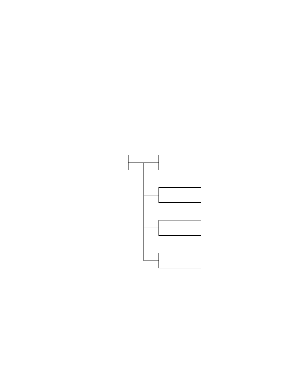
39
Preliminary User's Manual U13987EJ1V0UM00
CHAPTER 1 GENERAL
The
�
PD784938 Subseries consists of 78K/IV Series products that combine a 78K/IV Series CPU core enabling mounting
large-capacity memory and a IEBus
TM
(Inter Equipment Bus
TM
) controller. The 78K/IV Series consists of 16-bit single-chip
microcontrollers, and comes with a high-performance CPU that has various functions including a function to access 1-Mbyte
memory spaces.
The
�
PD784938 Subseries is based on the
�
PD784908 Subseries. It features expanded internal ROM and RAM capacities
and the addition of a ROM correction function.
The
�
PD784938 has a 256-Kbyte mask ROM and 10,240-byte RAM on chip. Besides an IEBus controller, it features among
other things a high-performance timer counter, an 8-bit A/D converter, a PWM output function, a 2-channel independent serial
interface, and a watch timer.
The
�
PD784937 replaces the mask ROM of the
�
PD784938 with a 192-Kbyte mask ROM.
The
�
PD784936 replaces the mask ROM and RAM of the
�
PD784938 with a 128-Kbyte mask ROM and a 6,656-byte RAM.
The
�
PD784935 replaces the mask ROM and RAM of the
�
PD784938 with a 96-Kbyte mask ROM and a 5,120-byte RAM.
The
�
PD78F4938 replaces the mask ROM of the
�
PD784938 with flash memory.
The
�
PD784938 Subseries product lineup is as follows.
These models can be used in the following fields:
� Car audio, etc.
PD784936
PD78F4938
Flash memory
RAM
256 Kbytes
10,240 bytes
Flash memory models
PD784938
ROM
RAM
256 Kbytes
10,240 bytes
Mask ROM models
PD784937
ROM
RAM
192 Kbytes
8,192 bytes
ROM
RAM
128 Kbytes
6,656 bytes
PD784935
ROM
RAM
96 Kbytes
5,120 bytes
�
�
�
�
�
CHAPTER 1 GENERAL
40
Preliminary User's Manual U13987EJ1V0UM00
78K/IV Series Product Lineup
PD784026
PD784038Y
I
2
C bus supported
PD784038
Enhanced internal memory
capacity, pin compatible with
the PD784026
PD784225Y
Multi-master I
2
C bus supported
PD784225
80 pins, added ROM correction
PD784218Y
Multi-master I
2
C bus supported
Multi-master I
2
C bus supported
PD784218
Enhanced internal memory capacity,
added ROM correction
PD784928Y
Multi-master I
2
C bus supported
PD784928
Enhanced function of
the PD784915
PD784216Y/
784216AY
PD784054
PD784216/
784216A
PD784046
PD784908
On-chip 10-bit A/D
100 pins, enhanced I/O and
internal memory capacity
Enhanced A/D,
16-bit timer, and
power management
PD784915
For software servo control,
on-chip analog circuit
for VCR, enhanced timer
Enhanced function of the PD784908,
enhanced internal memory capacity,
added ROM correction
On-chip IEBus
controller
PD784955
For DC inverter control
PD784938
Standard models
ASSP models
: In mass production
: Under development
�
�
�
�
�
�
�
�
�
�
�
�
�
�
�
�
�
�
�
�

CHAPTER 1 GENERAL
41
Preliminary User's Manual U13987EJ1V0UM00
1.1 Features
�
78K/IV Series
�
High-speed instruction execution
� Minimum instruction execution time: 320 ns (@ 6.29-MHz operation)
160 ns (@ 12.58-MHz operation)
�
Instruction set suitable for control applications
�
Data memory expansion function (1-Mbyte memory space: 2 bank specification pointers)
�
Interrupt controller (4-level priority system)
� Vectored interrupt service/macro service/context switching
�
Standby functions: HALT/STOP/IDLE modes
�
Internal memory: � ROM
Mask ROM:
256 Kbytes (
�
PD784938)
192 Kbytes (
�
PD784937)
128 Kbytes (
�
PD784936)
96 Kbytes (
�
PD784935)
Flash memory: 256 Kbytes (
�
PD78F4938)
� RAM:
10,240 bytes (
�
PD784938, 78F4938)
8,192 bytes (
�
PD784937)
6,656 bytes (
�
PD784936)
5,120 bytes (
�
PD784935)
�
I/O pins: 80
� Software programmable pull-up: 70 inputs
� Direct LED drive capability:
24 outputs
� Direct transistor drive capability: 8 outputs
� N-ch open-drain:
4 outputs
�
Serial interface
� UART/IOE (3-wire serial I/O): 2 channels (with on-chip baud rate generator)
� CSI (3-wire serial I/O): 2 channels
�
Real-time output ports (combination with timer/counter allows independent control of 2-system stepping motors)
�
A/D converter (8-bit resolution
�
8 channels)
�
PWM outputs (12-bit resolution
�
2 channels)
�
On-chip simple model with IEBus controller
�
Watch timer (operation with main clock possible in the IDLE mode)
�
Power-saving regulator
�
High-performance timer/counter
� Timer/event counter (16 bits)
�
3 units
� Timer (16 bits)
�
1 unit
�
Watchdog timer: 1 channel
�
Clock output function: f
CLK
, f
CLK
/2, f
CLK
/4, f
CLK
/8, f
CLK
/16 can be selected
�
On-chip ROM correction function

CHAPTER 1 GENERAL
42
Preliminary User's Manual U13987EJ1V0UM00
1.2 Ordering Information
Part Number
Package
Internal ROM
�
PD784935GF-
���
-3BA
100-pin plastic QFP (14
�
20 mm)
Mask ROM
�
PD784936GF-
���
-3BA
100-pin plastic QFP (14
�
20 mm)
Mask ROM
�
PD784937GF-
���
-3BA
100-pin plastic QFP (14
�
20 mm)
Mask ROM
�
PD784938GF-
���
-3BA
100-pin plastic QFP (14
�
20 mm)
Mask ROM
�
PD78F4938GF-3BA
100-pin plastic QFP (14
�
20 mm)
Flash memory
Remark
���
indicates ROM code suffix.

CHAPTER 1 GENERAL
43
Preliminary User's Manual U13987EJ1V0UM00
1.3 Pin Configuration (Top View)
1.3.1 Normal operation mode
� 100-pin plastic QFP (14
�
20 mm)
�
PD784935GF-
���
-3BA, 784936GF-
���
-3BA, 784937GF-
���
-3BA, 784938GF-
���
-3BA, 78F4938GF-3BA
Notes
1. Connect the IC (Internally Connected)/V
PP
pin directly to V
SS
.
2. Connect the AV
DD
pin directly to V
DD
.
3. Connect the AV
SS
pin directly to V
SS
.
4. The V
PP
pin is used only in the
�
PD78F4938.
1
2
3
4
5
6
7
8
9
10
11
12
13
14
15
16
17
18
19
20
21
22
23
24
25
26
27
28
29
30
P36/T02
P37/T03
P100
P101
P102
P103
P104
P105/SCK3
P106/SI3
P107/SO3
RESET
XT2
XT1
V
SS
X2
X1
REGOFF
REGC
V
DD
P00
P01
P02
P03
P04
P05
P06
P07
P67/REFRQ/HLDAK
P66/WAIT/HLDRQ
P65/WR
P76/ANI6
P75/ANI5
P74/ANI4
P73/ANI3
P72/ANI2
P71/ANI1
P70/ANI0
IC/V
PP
Notes 1, 4
PWM1
PWM0
P17
P16
P15
P14/TxD2/SO2
P13/RxD2/SI2
P12/ASCK2/SCK2
P11
P10
ASTB/CLKOUT
P90
P91
P92
P93
P94
P95
P96
P97
P40/AD0
P41/AD1
P42/AD2
80
79
78
77
76
75
74
73
72
71
70
69
68
67
66
65
64
63
62
61
60
59
58
57
56
55
54
53
52
51
100 99 98 97 96 95 94 93 92 91 90 89 88 87 86 85 84 83 82 81
31 32 33 34 35 36 37 38 39 40 41 42 43 44 45 46 47 48 49 50
P35/TO1
P34/TO0
P33/SO0
P32/SCK0
P31/TxD/SO1
P30/RxD/SI1
P27/SI0
P26/INTP5
P25/INTP4/ASCK/SCK1
P24/INTP3
P23/INTP2/CI
P22/INTP1
P21/INTP0
P20/NMI
TX
RX
AV
SS
Note 3
AV
REF1
AV
DD
Note 2
P77/ANI7
P64/RD
P63/A19
P62/A18
P61/A17
P60/A16
P57/A15
P56/A14
P55/A13
P54/A12
V
SS
V
DD
P53/A11
P52/A10
P51/A9
P50/A8
P47/AD7
P46/AD6
P45/AD5
P44/AD4
P43/AD3

CHAPTER 1 GENERAL
44
Preliminary User's Manual U13987EJ1V0UM00
A8 to A19:
Address Bus
AD0 to AD7:
Address/Data Bus
ANI0 to ANI7:
Analog Input
ASCK, ASCK2:
Asynchronous Serial Clock
ASTB:
Address Strobe
AV
DD
:
Analog Power Supply
AV
REF1
:
Analog Reference Voltage
AV
SS
:
Analog Ground
CI:
Clock Input
CLKOUT:
Clock Output
HLDAK:
Hold Acknowledge
HLDRQ:
Hold Request
INTP0 to INTP5: Interrupt from Peripherals
NMI:
Non-maskable Interrupt
P00 to P07:
Port0
P10 to P17:
Port1
P20 to P27:
Port2
P30 to P37:
Port3
P40 to P47:
Port4
P50 to P57:
Port5
P60 to P67:
Port6
P70 to P77:
Port7
P90 to P97:
Port9
P100 to P107:
Port10
PWM0, PWM1:
Pulse Width Modulation 0, 1
RD:
Read Strobe
REFRQ:
Refresh Request
REGC:
Regulator Capacitance
REGOFF:
Regulator Off
RESET:
Reset
RX:
IEBus Receive Data
RxD, RxD2:
Receive Data
SCK0 to SCK3:
Serial Clock
SI0 to SI3:
Serial Input
SO0 to SO3:
Serial Output
TEST:
Test
TO0 to TO3:
Timer Output
TxD, TxD2:
Transmit Data
TX:
IEBus Transmit Data
V
DD
:
Power Supply
V
PP
Note
:
Programming Power Supply
V
SS
:
Ground
WAIT:
Wait
WR:
Write Strobe
X1, X2:
Crystal (Main System Clock)
XT1, XT2:
Crystal (Watch)
Note
The V
PP
pin is used only in the
�
PD78F4938.

CHAPTER 1 GENERAL
45
Preliminary User's Manual U13987EJ1V0UM00
1.4 Application System Configuration Example (Car Audio (Tuner, Deck))
Remote controller
signal receiver circuit
FIP
TM
LED
FIP
controller/driver
Key matrix
Audio system
control circuit
Electronic
volume
EEPROM
TM
PD16312, etc.
PC2800A, etc.
Front panel
PD784938
Interrupt input
General-purpose
port
3-wire
serial I/O
IEBus
controller
SIO with automatic
transmit/receive
function
3-wire serial I/O
Cassette deck
unit
Tuner pack
IEBus
driver/
receiver
IEBus
CD unit
(changer,
single CD, etc.)
DSP unit
TV unit
�
�
�
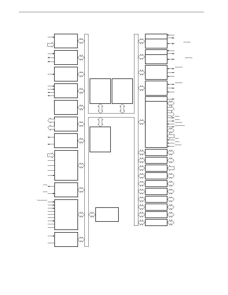
CHAPTER 1 GENERAL
46
Preliminary User's Manual U13987EJ1V0UM00
1.5 Block Diagram
Note
�
PD78F4938 only
Remark The capacities of the internal ROM and RAM varies depending on the product.
PROGRAMMABLE
INTERRUPT
CONTROLLER
TIMER/EVENT
COUNTER0
(16 BITS)
TIMER/EVENT
COUNTER1
(16 BITS)
TIMER/EVENT
COUNTER2
(16 BITS)
TIMER3
(16 BITS)
REAL-TIME
OUTPUT PORT
A/D
CONVERTER
PWM
78 K/IV
CPU CORE
ROM
RAM
UART/IOE2
UART/IOE1
BAUD-RATE
GENERATOR
BAUD-RATE
GENERATOR
CLOCKED
SERIAL
INTERFACE
CLOCK OUTPUT
BUS I/F
PORT0
PORT1
PORT2
PORT3
PORT4
PORT5
PORT6
PORT7
NMI
INTP3
TO0
TO1
INTP0
INTP1
INTP2/CI
TO2
TO3
P00 to P03
P04 to P07
PWM0
PWM1
AV
DD
AV
REF1
AV
SS
INTP5
ANI0 to ANI7
INTP0 to INTP5
RxD/SI1
TxD/SO1
ASCK/SCK1
RxD2/SI2
ASCK2/SCK2
TxD2/SO2
SCK0
SO0
SI0
ASTB/CLKOUT
AD0 to AD7
A8 to A15
A16 to A19
RD
WR
WAIT/HLDRQ
REFRQ/HLDAK
D0 to D7
Note
CE
Note
A0 to A16
Note
OE
Note
PGM
Note
P00 to P07
P10 to P17
P30 to P37
P40 to P47
P50 to P57
P20 to P27
P60 to P67
P70 to P77
CLOCKED
SERIAL
INTERFACE3
SCK3
SO3
SI3
PORT9
PORT10
P90 to P97
P100 to P107
TX
RX
RESET
TEST
X1
X2
REGC
REGOFF
V
PP
Note
V
DD
V
SS
XT1
XT2
SYSTEM
CONTROL
(REGULATOR)
IEBus
CONTROLLER
WATCH
TIMER
WATCHDOG
TIMER
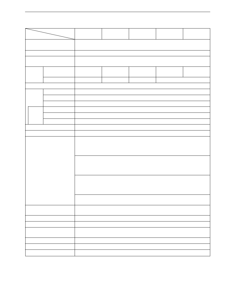
CHAPTER 1 GENERAL
47
Preliminary User's Manual U13987EJ1V0UM00
1.6 List of Functions
Part Number
�
PD784935
�
PD784936
�
PD784937
�
PD784938
�
PD78F4938
Item
Number of basic instructions
113
(mnemonics)
General-purpose register
8 bits
�
32 registers
�
8 banks, or 16 bits
�
8 registers
�
8 banks (memory mapping)
Minimum instruction execution time
320 ns/636 ns/1.27
�
s/2.54
�
s (@6.29-MHz operation)
160 ns/320 ns/636 ns/1.27
�
s (@12.58-MHz operation)
Internal
ROM
96 Kbytes
128 Kbytes
192 Kbytes
256 Kbytes
256 Kbytes
memory
(mask ROM)
(mask ROM)
(mask ROM)
(mask ROM)
(flash memory)
RAM
5,120 bytes
6,656 bytes
8,192 bytes
10,240 bytes
Memory space
1 Mbyte with program and data memories combined
I/O port
Total
80
Input
8
I/O
72
Pins with
LED direct drive output
24
ancillary
Transistor direct drive
8
functions
Note
N-ch open-drain
4
Real-time output port
4 bits
�
2, or 8 bits
�
1
IEBus controller
Internal (simple version)
Timer/counter
Timer/event counter 0 (16 bits): Timer counter
�
1
Pulse output
Capture register
�
1
� Toggle output
Compare register
�
2
� PWM/PPG output
� One-shot pulse output
Timer/event counter 1 (16 bits): Timer counter
�
1
Real-time output port
Capture register
�
1
Capture/compare register
�
1
Compare register
�
1
Timer/event counter 2:
Timer counter
�
1
Pulse output
Capture register
�
1
� Toggle output
Capture/compare register
�
1
� PWM/PPG output
Compare register
�
1
Timer 3:
Timer counter
�
1
Compare register
�
1
Watch timer
Generates interrupt request at intervals of 0.5 second (internal watch clock oscillator)
Main clock (12.58 MHz (MAX.)) or watch clock (32.7 kHz) selectable as input clock
Clock output
Selectable from f
CLK
, f
CLK
/2, f
CLK
/4, f
CLK
/8, and f
CLK
/16 (can also be used as 1-bit output port)
PWM output
12-bit resolution
�
2 channels
Serial interface
UART/IOE (3-wire serial I/O): 2 channels (with baud rate generator)
CSI (3-wire serial I/O):
2 channels
A/D converter
8-bit resolution
�
8 channels
Watchdog timer
1 channel
Standby
HALT/STOP/IDLE mode
Note
The pins with ancillary functions are included in the I/O pins.

CHAPTER 1 GENERAL
48
Preliminary User's Manual U13987EJ1V0UM00
Part Number
�
PD784935
�
PD784936
�
PD784937
�
PD784938
�
PD78F4938
Item
Interrupt
Hardware source
27 (Internal: 20, External: 7 (sampling clock variable input: 1))
Software source
BRK instruction, BRKCS instruction, operand error
Non-maskable
Internal: 1, External: 1
Maskable
Internal: 19, External: 6
4 levels of programmable priority
3 processing type: Vectored interrupt/macro service/context switching
Supply voltage
�
V
DD
= 4.0 to 5.5 V
�
V
DD
= 4.5 to 5.5 V
(Main clock: @ f
XX
= 12.58-MHz operation,
(Main clock:
Internal system clock = @ f
XX
, f
CYK
= 79 ns)
@ f
XX
= 12.58-
�
V
DD
= 3.5 to 5.5 V
MHz operation,
(Other than above, f
CYK
= 159 ns)
Internal system
clock = @ f
XX
,
f
CYK
= 79 ns)
�
V
DD
= 4.0 to 5.5 V
(Other than
above,
f
CYK
= 159 ns)
Package
100-pin plastic QFP (14
�
20 mm)
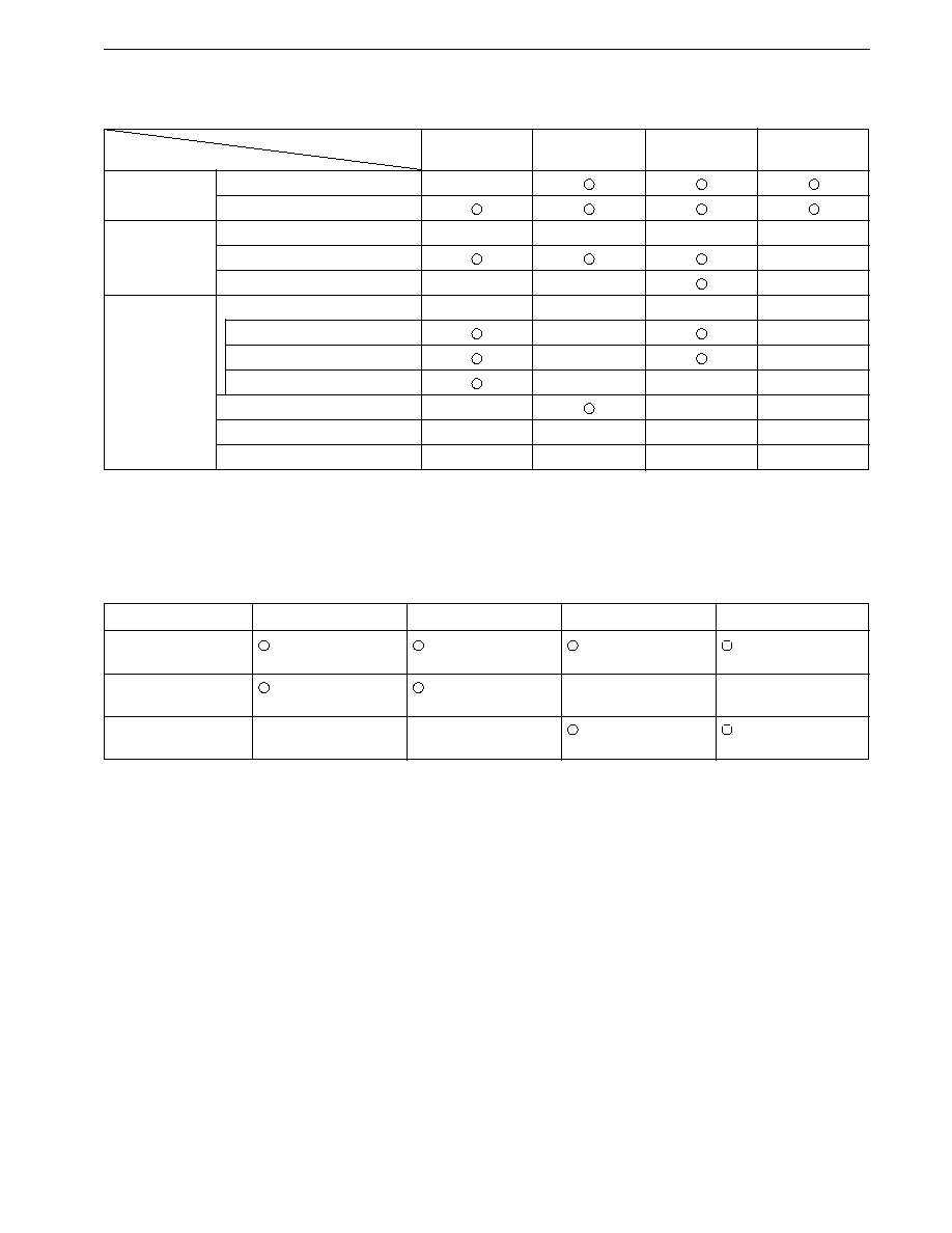
CHAPTER 1 GENERAL
49
Preliminary User's Manual U13987EJ1V0UM00
The outline of the timer is as follows (for details, refer to CHAPTER 8 OUTLINE OF TIMER)
Name
Timer/Event
Timer/Event
Timer/Event
Timer 3
Item
Counter 0
Counter 1
Counter 2
Count width
8 bits
--
16 bits
Operation mode
Interval timer
2ch
2ch
2ch
1ch
External event counter
--
One-shot timer
--
--
--
Function
Timer output
2ch
--
2ch
--
Toggle output
--
--
PWM/PPG output
--
--
One-shot pulse output
Note
--
--
--
Real-time output
--
--
--
Pulse width measurement
1 input
1 input
2 inputs
--
Number of interrupt requests
2
2
2
1
Note
The one-shot pulse output function is used to make a pulse output level active by software and inactive by hardware
(interrupt request signal).
This function is different from the one-shot timer function of timer/event counter 2 in nature.
The outline of the serial interface is as follows (for details, refer to CHAPTER 17 OUTLINE OF SERIAL INTERFACE).
Function
UART/IOE1
UART/IOE2
IOE0
IOE3
3-wire serial I/O mode
(MSB first/LSB first
(MSB first/LSB first
(MSB first/LSB first
(MSB first/LSB first
switchable)
switchable)
switchable)
switchable)
Asynchronous serial
(On-chip dedicated
(On-chip dedicated
--
--
I/O mode
baud rate generator )
baud rate generator )
SBI mode
--
--
(MSB first/LSB first
(MSB first/LSB first
switchable)
switchable)

CHAPTER 1 GENERAL
50
Preliminary User's Manual U13987EJ1V0UM00
1.7 Differences among Products in
�
PD784938 Subseries
Part Number
�
PD784935
�
PD784936
�
PD784937
�
PD784938
�
PD78F4938
Item
Internal memory
ROM
96 Kbytes
128 Kbytes
192 Kbytes
256 Kbytes
256 Kbytes
(mask ROM)
(mask ROM)
(mask ROM)
(mask ROM)
(flash memory)
RAM
5,120 bytes
6,656 bytes
8,192 bytes
10,240 bytes
1.8 Main Differences with
�
PD784908 Subseries
The
�
PD784938 Subseries replaces the PROM of PROM products in the
�
PD784908 Subseries with flash memory and
added a ROM correction function.
51
Preliminary User's Manual U13987EJ1V0UM00
CHAPTER 2 PIN FUNCTIONS
2.1 Pin Function Lists
2.1.1 Normal operation mode
(1) Port pins (1/2)
Pin Name
Input/Output
Alternate Function
Function
P00 to P07
Input/output
--
Port 0 (P0):
� 8-bit input/output port
� Can be used as real-time output ports (4 bits
�
2)
� Input/output can be specified in 1-bit units
� For input mode pins, on-chip pull-up resistor connection can be
specified at once by means of software
� Transistor drive capability
P10
Input/output
--
P11
--
P12
ASCK2/SCK2
P13
RxD2/SI2
P14
TxD2/SO2
P15 to P17
--
P20
Input
NMI
P21
INTP0
P22
INTP1
P23
INTP2/CI
P24
INTP3
P25
INTP4/ASCK/SCK1
P26
INTP5
P27
SI0
P30
Input/output
RxD/SI1
P31
TxD/SO1
P32
SCK0
P33
SO0
P34 to P37
TO0 to TO3
Port 1 (P1):
� 8-bit input/output port
� Input/output can be specified in 1-bit units
� For input mode pins, on-chip pull-up resistor connection can be
specified at once by means of software
� LED drive capability
Port 2 (P2):
� 8-bit input/output port
� P20 cannot be used as a general-purpose port (non-maskable
interrupt). Input level can be confirmed in the interrupt routine.
� For P22 to P27, on-chip pull-up resistor connection can be specified
by means of software in 6-bit units
� The P25/INTP4/ASCK/SCK1 pin operates as the SCK1 output pin
in accordance with the CSIM1 register specification
Port 3 (P3):
� 8-bit input/output port
� Input/output can be specified in 1-bit units
� For input mode pins, on-chip pull-up resistor connection can be
specified at once by means of software
� P32 and P33 can be set in N-ch open-drain mode
CHAPTER 2 PIN FUNCTIONS
52
Preliminary User's Manual U13987EJ1V0UM00
(1) Port pins (2/2)
Pin Name
Input/Output
Alternate Function
Function
P40 to P47
Input/output
AD0 to AD7
Port 4 (P4):
� 8-bit input/output port
� Input/output can be specified in 1-bit units
� For input mode pins, on-chip pull-up resistor connection can be
specified at once by means of software
� LED drive capability
P50 to P57
Input/output
A8 to A15
Port 5 (P5):
� 8-bit input/output port
� Input/output can be specified in 1-bit units
� For input mode pins, on-chip pull-up resistor connection can be
specified at once by means of software
� LED drive capability
P60 to P63
Input/output
A16 to A19
P64
RD
P65
WR
P66
WAIT/HLDRQ
P67
REFRQ/HLDAK
P70 to P77
Input/output
ANI0 to ANI7
Port 7 (P7):
� 8-bit input/output port
� Input/output can be specified in 1-bit units
P90 to P97
Input/output
--
Port 9 (P9):
� 8-bit input/output port
� Input/output can be specified in 1-bit units
� For input mode pins, on-chip pull-up resistor connection can be
specified at once by means of software
P100 to P104
Input/output
--
P105
SCK3
P106
SI3
P107
SO3
Port 6 (P6):
� 8-bit input/output port
� Input/output can be specified in 1-bit units
� For input mode pins, on-chip pull-up resistor connection can be
specified at once by means of software
Port 10 (P10):
� 8-bit input/output port
� Input/output can be specified in 1-bit units
� For input mode pins, on-chip pull-up resistor connection can be
specified at once by means of software
� P105 and P107 can be set in N-ch open-drain mode
CHAPTER 2 PIN FUNCTIONS
53
Preliminary User's Manual U13987EJ1V0UM00
(2) Non-port pins (1/2)
Pin Name
Input/Output
Alternate Function
Function
TO0/TO3
Output
P34 to P37
Timer output
CI
Input
P23/INTP2
Count clock input to timer/event counter 2
RxD
Input
P30/SI1
Serial data input (UART0)
RxD2
P13/SI2
Serial data input (UART2)
TxD
Output
P31/SO1
Serial data output (UART0)
TxD2
P14/SO2
Serial data output (UART2)
ASCK
Input
P25/INTP4/SCK1
Baud rate clock input (UART0)
ASCK2
P12/SCK2
Baud rate clock input (UART2)
SI0
Input
P27
Serial data input (3-wire serial I/O0)
SI1
P30/RxD
Serial data input (3-wire serial I/O1)
SI2
P13/RxD2
Serial data input (3-wire serial I/O2)
SI3
P106
Serial data input (3-wire serial I/O3)
SO0
Output
P33
Serial data output (3-wire serial I/O0)
SO1
P31/TxD
Serial data output (3-wire serial I/O1)
SO2
P14/TxD2
Serial data output (3-wire serial I/O2)
SO3
P107
Serial data output (3-wire serial I/O3)
SCK0
Input/output
P32
Serial clock input/output (3-wire serial I/O0)
SCK1
P25/INTP4/ASCK
Serial clock input/output (3-wire serial I/O1)
SCK2
P12/ASCK2
Serial clock input/output (3-wire serial I/O2)
SCK3
P105
Serial clock input/output (3-wire serial I/O3)
NMI
Input
P20
External interrupt requests
--
INTP0
P21
� Count clock input to timer/event counter 1
� CR11 or CR12 capture trigger signal
INTP1
P22
� Count clock input to timer/event counter 2
� CR22 capture trigger signal
INTP2
P23/CI
� Count clock input to timer/event counter 2
� CR21 capture trigger signal
INTP3
P24
� Count clock input to timer/event counter 0
� CR02 capture trigger signal
INTP4
P25/ASCK0/SCK1
--
INTP5
P26
A/D converter conversion start trigger input
AD0 to AD7
Input/output
P40 to P47
Time division address/data bus (external memory connection)
A8 to A15
Output
P50 to P57
Upper address bus (external memory connection)
A16 to A19
Output
P60 to P63
Upper address with address extension (external memory connection)
RD
Output
P64
External memory read strobe
WR
Output
P65
External memory write strobe
WAIT
Input
P66/HLDRQ
Wait insertion
REFRQ
Output
P67/HLDAK
External pseudo-static memory refresh pulse output
HLDRQ
Input
P66/WAIT
Bus hold request input
HLDAK
Output
P67/REFRQ
Bus hold response output

CHAPTER 2 PIN FUNCTIONS
54
Preliminary User's Manual U13987EJ1V0UM00
(2) Non-port pins (2/2)
Pin Name
Input/Output
Alternate Function
Function
ASTB
Output
CLKOUT
Time division address (A0 to A7) latch timing output (during external memory access)
CLKOUT
Output
ASTB
Clock output
PWM0
Output
--
PWM output 0
PWM1
Output
--
PWM output 1
RX
Input
--
Data input (IEBus)
TX
Output
--
Data output (IEBus)
REGC
--
--
Connection of capacitor for regulator output stabilization/power supply when
regulator stops
REGOFF
--
--
Regulator operation specification signal
RESET
Input
--
Chip reset
X1
Input
--
System clock oscillation crystal connections
X2
--
(clock can also be input to X1)
XT1
Input
--
Watch clock connection
XT2
--
--
ANI0 to ANI7
Input
P70 to P77
A/D converter analog voltage inputs
AV
REF1
--
--
A/D converter reference voltage application
AV
DD
A/D converter positive power supply
AV
SS
A/D converter GND
V
DD
Positive power supply
V
SS
GND
IC
Input
V
PP
Internally connected. Connect directly to V
SS
(IC test pin).
V
PP
IC
Flash memory programming mode setting.
High voltage application during program write/verify.
Connect directly to V
SS
in normal operating mode.
CHAPTER 2 PIN FUNCTIONS
55
Preliminary User's Manual U13987EJ1V0UM00
2.2 Pin Functions
2.2.1 Normal operation mode
(1) P00 to P07 (Port 0) ... 3-state input/output
Port 0 is an 8-bit input/output port with an output latch, and has direct transistor drive capability. Input/output can be specified
in 1-bit units by setting the port 0 mode register (PM0). Each pin incorporates a software programmable pull-up resistor.
P00 to P03 and P04 to P07 can output the port 0 buffer register (P0L, P0H) contents at any time interval as 4-bit or 8-bit
real-time output port. The real-time output port control register (RTPC) is used to select whether this port is used as a normal
output port or a real-time output port.
When RESET is input, port 0 is set as an input port (output high-impedance state), and the output latch contents become
undefined.
(2) P10 to P17 (Port 1) ... 3-state input/output
Port 1 is an 8-bit input/output port with an output latch. Input/output can be specified in 1-bit units by setting the port 1 mode
register (PM1). Each pin incorporates a software programmable pull-up resistor. This port has direct LED drive capability.
Pins P12 to P14 can also be made to function as serial input/output pins by setting the port 1 mode control register (PMC1).
When RESET is input, port 1 is set as an input port (output high-impedance state), and the output latch contents are
undefined.
Table 2-1. Port 1 Operation Modes
Pin Name
Port Mode
Control Signal Input/Output Mode
Operation to Operate as Control Pin
P10
Input/output port
--
--
P11
--
--
P12
ASCK2/SCK2 input/output
Set (to 1) PMC12 bit of PMC1
P13
RxD2/SI2 input
Set (to 1) PMC13 bit of PMC1
P14
TxD2/SO2 output
Set (to 1) PMC14 bit of PMC1
P15 to P17
--
--
(a) Port mode
P12 to P14 operate as port mode pins when the relevant bits of the port 1 mode control (PMC1) register are cleared
(0), and P10 and P11 and P15 to P17 always operate as port mode pins. Input/output can be specified in 1-bit units
by setting the port 1 mode register (PM1).
(b) Control signal input/output mode
P12 to P14 can be set as control pins in 1-bit units by setting the port 1 mode control (PMC1) register.
(i)
ASCK2/SCK2
ASCK2 is the asynchronous serial interface baud rate clock input pin.
SCK2 is the serial clock input/output pin (in 3-wire serial I/O2 mode).
(ii)
RxD2/SI2
RxD2 is the asynchronous serial interface serial data input pin.
SI2 is the serial data input pin (in 3-wire serial I/O2 mode).
(iii) TxD2/SO2
TxD2 is the asynchronous serial interface serial data output pin.
SO2 is the serial data output pin (in 3-wire serial I/O2 mode).

CHAPTER 2 PIN FUNCTIONS
56
Preliminary User's Manual U13987EJ1V0UM00
(3) P20 to P27 (Port 2) ... Input
Port 2 is an 8-bit input-only port. P22 to P27 incorporate a software programmable pull-up resistor. As well as operating
as an input port, port 2 pins also operate as control signal input pins, such as external interrupt signal pins (see Table
2-2). All 8 pins are Schmitt-triggered inputs to prevent misoperation due to noise.
Also, pin P25 can also be made to function as a serial clock output pin by selecting the external clock as "serial operation
enabled" with the clocked serial interface mode register 1 (CSIM1).
Table 2-2. Port 2 Operation Modes
Port
Function
P20
Input port/NMI input
Note
P21
Input port/INTP0 input/CR11 capture trigger input/
timer/event counter 1 count clock/real-time output port trigger signal
P22
Input port/INTP1 input/CR22 capture trigger input
P23
Input port/INTP2 input/CI input
P24
Input port/INTP3 input/CR02 capture trigger input/
timer/event counter 0 count clock
P25
Input port/INTP4 input/ASCK input/SCK1 input/output
P26
Input port/INTP5 input/A/D converter external trigger input
P27
Input port/SI0 input
Note NMI input is acknowledged regardless of whether interrupts are enabled or disabled.
(a) Function as port pins
The pin level can always be read or tested regardless of the alternate function pin operation.
(b) Functions as control signal input pins
(i)
NMI (Non-maskable Interrupt)
The external non-maskable interrupt request input pin. Rising edge detection or falling edge
detection can be specified by setting the external interrupt mode register 0 (INTM0).
(ii)
INTP0 to INTP5 (Interrupt from Peripherals)
External interrupt request input pins. When the valid edge specified by the external interrupt mode register 0,
1 (INTM0/INTM1) is detected by pins INTP0 to INTP5, an interrupt is generated (see CHAPTER 22 EDGE
DETECTION FUNCTION).
In addition, pins INTP0 to INTP3 and INTP5 are also used as external trigger input pins with the various functions
shown below.
� INTP0 ....... Timer/event counter 1 capture trigger input pin
Timer/event counter 1 external count clock input pin
Real-time output port trigger input pin
� INTP1 ....... Timer/event counter 2 capture trigger input pin to capture register (CR22)
� INTP2 ....... Timer/event counter 2 external count clock input pin
Capture trigger input pin to capture/compare register (CR21)
� INTP3 ....... Timer/event counter 0 capture trigger input pin
Timer/event counter 0 external count clock input pin
� INTP5 ....... A/D converter external trigger input pin

CHAPTER 2 PIN FUNCTIONS
57
Preliminary User's Manual U13987EJ1V0UM00
(iii) CI (Clock Input)
The timer/event counter 2 external clock input pin.
(iv) ASCK (Asynchronous Serial Clock)
The external baud rate clock input pin.
(v) SCK1 (Serial Clock)
The serial clock input/output pin (in 3-wire serial I/O1 mode).
(vi) SI0 (Serial Input 0)
The serial data input pin (in 3-wire serial I/O0 mode).
(4) P30 to P37 (Port 3) ... 3-state input/output
Port 3 is an 8-bit input/output port with an output latch. Input/output can be specified bit-wise by setting the port 3 mode
register (PM3). Each pin incorporates a software programmable pull-up resistor. P32 and P33 can be set in the N-ch open-
drain mode.
In addition to its function as an input/output port, port 3 also has various control signal pin alternate functions.
The operation mode can be specified in 1-bit units by setting the port 3 mode control register (PMC3), as shown in
Table 2-3. The pin level of any pin can always be read or tested regardless of the alternate-function operation.
When RESET is input, port 3 is set as an input port (output high-impedance state), and the output latch contents are
undefined.
Table 2-3. Port 3 Operation Modes (n = 0 to 7)
Mode
Port Mode
Control Signal Input/Output Mode
Setting Condition
PMC3n = 0
PMC3n = 1
P30
Input/output port
RxD input / SI1 input
P31
TxD output / SO1 output
P32
SCK0 input/output
P33
SO0 output
P34
TO0 output
P35
TO1 output
P36
TO2 output
P37
TO3 output
(a) Port mode
Each port specified as port mode by the port 3 mode control register (PMC3) can be specified as input/output in 1-
bit units by setting the port 3 mode register (PM3).
(b) Control signal input/output mode
Pins can be set as control pins in 1-bit units by setting the port 3 mode control register (PMC3).
(i)
RxD (Receive Data) /SI1 (Serial Input 1)
RxD is the asynchronous serial interface serial data input pin.
SI1 is the serial data input pin (in 3-wire serial I/O1 mode).
CHAPTER 2 PIN FUNCTIONS
58
Preliminary User's Manual U13987EJ1V0UM00
(ii)
TxD (Transmit Data) /SO1 (Serial Output 1)
TxD is the asynchronous serial interface serial data output pin.
SO1 is the serial data output pin (in 3-wire serial I/O1 mode).
(iii) SCK0 (Serial Clock 0)
SCK0 is the clocked serial interface serial clock input/output pin (in 3-wire serial I/O 0 mode).
(iv) SO0 (Serial Output 0)
SO0 is the serial data output pin (in 3-wire serial I/O 0 mode).
(v)
TO0 to TO3 (Timer Output)
The timer output pins.
(5) P40 to P47 (Port 4) ... 3-state input/output
Port 4 is an 8-bit input/output port with an output latch. Input/output can be specified in 1-bit units by setting the port 4 mode
register (PM4). Each pin incorporates a software programmable pull-up resistor. This port has direct LED drive capability.
Port 4 also functions as the time division address/data bus (AD0 to AD7) by the memory expansion mode register (MM)
when external memory or I/Os are expanded.
When RESET is input, port 4 is set as an input port (output high-impedance state), and the output latch contents are
undefined.
(6) P50 to P57 (Port 5) ... 3-state input/output
Port 5 is an 8-bit input/output port with an output latch. Input/output can be specified in 1-bit units by setting the port 5 mode
register (PM5). Each pin incorporates a software programmable pull-up resistor. This port has direct LED drive capability.
In addition, P50 to P57 can be selected by means of the memory expansion mode register (MM) in 2-bit units as pins that
function as the address bus (A8 to A15) when external memory or I/Os are expanded.
When RESET is input, port 5 is set as an input port (output high-impedance state), and the output latch contents are
undefined.
(7) P60 to P67 (Port 6) ... 3-state input/output
Port 6 is an 8-bit input/output port with an output latch. P60 to P67 incorporate a software programmable pull-up resistor.
In addition to its function as a port, port 6 also has various alternate-function control signal pin functions, as shown in Table
2-4. Operations as control pins are performed by the respective function operations.
When RESET is input, P60 to P67 are set as input port pins (output high-impedance state), and the output latch contents
are undefined.
Table 2-4. Port 6 Operation Modes
Pin Name
Port Mode
Control Signal Input/Output Mode
Operation to Operate as Control Pin
P60 to P63
Input/output ports
A16 to A19 output
Specified in 2-bit units by bits MM3 to MM0 of the MM
P64
RD output
External memory expansion mode is specified by bits MM3
P65
WR output
to MM0 of the MM
P66
WAIT input
Specified by setting bits PWn1 & PWn0 (n = 0 to 7) of the
PWC1 & PWC2 and P66 to input mode
HLDRQ input
Bus hold enabled by the HLDE bit of the HLDM
P67
HLDAK output
REFRQ output
Set (to 1) the RFEN bit of the RFM

CHAPTER 2 PIN FUNCTIONS
59
Preliminary User's Manual U13987EJ1V0UM00
(a) Port mode
Each port not set in the control mode can be set in the input or output mode in 1-bit units by using the port 6 mode
register (PM6).
(b) Control signal input/output mode
(i)
A16 to A19 (Address Bus)
Upper address bus output pins in case of external memory space expansion (10000H to FFFFFH).
These pins operate in accordance with the memory expansion mode register (MM).
(ii)
RD (Read Strobe)
Pin that outputs the strobe signal for an external memory read operation.
Operates in accordance with the memory expansion mode register (MM).
(iii) WR (Write Strobe)
Pin that outputs the strobe signal for an external memory write operation.
Operates in accordance with the memory expansion mode register (MM).
(iv) WAIT (Wait)
Wait signal input pin. Operates in accordance with the programmable wait control registers (PWC1, PWC2).
(v)
REFRQ (Refresh Request)
This pin outputs refresh pulses to pseudo-static memory when this memory is connected
externally. Operates in accordance with the refresh mode register (RFM).
(vi) HLDRQ (Hold Request)
External bus hold request signal input pin. Operates in accordance with the hold mode register
(HLDM).
(vii) HLDAK (Hold Acknowledge)
Bus hold acknowledge signal output pin. Operates in accordance with the hold mode register
(HLDM).
(8) P70 to P77 (Port 7) ... 3-state input/output
Port 7 is an 8-bit input/output port. In addition to operating as an input/output port, it also operates as the A/D converter
analog input pins (ANI0 to ANI7).
Input/output can be specified in 1-bit units by setting the port 7 mode register (PM7).
The levels of these pins can always be read or tested, regardless of the alternate-function operation.
When RESET is input, port 7 is set as an input port (output high-impedance state), and the output latch contents are
undefined.
(9) P90 to P97 (Port 9) ... 3-state input/output
Port 9 is an 8-bit input/output port with an output latch. Input/output can be specified in 1-bit units by setting the port 9 mode
register (PM9). Each pin incorporates a software programmable pull-up resistor.
When RESET is input, port 9 is set as an input port (output high-impedance state), and the output latch contents are
undefined.

CHAPTER 2 PIN FUNCTIONS
60
Preliminary User's Manual U13987EJ1V0UM00
(10) P100 to P107 (Port 10) ... 3-state input/output
Port 10 is an 8-bit input/output port with an output latch. Input/output can be specified in 1-bit units by setting the port 10
mode register (PM10). Each pin incorporates a software programmable pull-up resistor. P105 and P107 can be set in
the N-ch open-drain mode.
P105 to P107 pins also function as the serial input/output pin by the port 10 mode control register (PMC10).
When RESET is input, port 10 is set as an input port (output high-impedance state), and the output latch contents are
undefined.
(11) ASTB (Address Strobe)/CLKOUT (Clock Output) ... Output
This pin outputs the timing signal that latches address information externally in order to access an external address. It
also operates as the pin that supplies the clock to an external device.
(12) X1, X2 (Crystal)
The internal clock oscillation crystal connection pins. When the clock is supplied externally, it is input to the X1 pin. Usually
signal with the inverse phase of the X1 pin signal phase is input to the X2 pin (Refer to 4.3.1 Clock oscillator).
(13) RESET (Reset) ... Input
Active-low reset input
(14) AV
REF1
A/D converter reference voltage input pin
(15) AV
DD
A/D converter power supply pin. This should be made at the same potential as the V
DD
pin.
(16) AV
SS
A/D converter GND pin. This should be made at the same potential as the V
SS
pin.
(17) V
DD
Positive power supply pins. All V
DD
pins should be connected to the positive power supply.
(18) V
SS
GND potential pins. All V
SS
pins should be connected to the ground.
(19) XT1 and XT2
These pins connect a crystal for watch clock oscillation.
(20) PWM0 and PWM1
These pins function as PWM output pins when so specified by the PWM control register (PWMC).
(21) RX
IEBus data input pin
(22) TX
IEBus data output pin
(23) REGC
This pin connects a capacitor for stabilizing the regulator output. Supply a voltage same as V
DD
to this pin when the
regulator is stopped (refer to Figure 5-1. Regulator Peripherals Block Diagram).

CHAPTER 2 PIN FUNCTIONS
61
Preliminary User's Manual U13987EJ1V0UM00
(24) REGOFF
This pin controls the regulator operation by operating or stopping the regulator.
(25) V
PP
(
�
PD78F4938) only
High-voltage apply pin for flash memory programming mode setting and program write/verify
(26) IC
IC test pin. Connect directly to V
SS
.
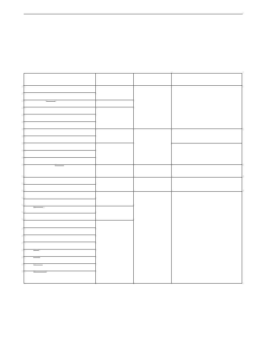
CHAPTER 2 PIN FUNCTIONS
62
Preliminary User's Manual U13987EJ1V0UM00
2.3 Input/Output Circuits and Connection of Unused Pins
Table 2-5 shows the input/output circuit types of the pins that have functions, and the connection method when that function
is not used.
Each input/output circuit type is shown in Figure 2-1.
Table 2-5. Pin Input/Output Circuit Types and Recommended Connection of Unused Pins (1/2)
Pin Name
Input/Output
Input/Output
Recommended Connection
Circuit Type
of Unused Pins
P00 to P07
5-A
Input/output
Input:
Connect to V
DD
P10, P11
Output: Leave open
P12/ASCK2/SCK2
8-A
P13/RxD2/SI2
5-A
P14/TxD2/SO2
P15 to P17
P20/NMI
2
Input
Connect to V
DD
or V
SS
P21/INTP0
P22/INTP1
2-A
Connect to V
DD
P23/INTP2/CI
P24/INTP3
P25/INTP4/ASCK/SCK1
8-A
Input/output
Input:
Connect to V
DD
Output: Leave open
P26/INTP5
2-A
Input
Connect to V
DD
P27/SI0
P30/RxD/SI1
5-A
Input/output
Input:
Connect to V
DD
P31/TxD/SO1
Output: Leave open
P32/SCK0
10-A
P33/SO0
P34/TO0 to P37/TO3
5-A
P40/AD0 to P47/AD7
P50/A8 to P57/A15
P60/A16 to P63/A19
P64/RD
P65/WR
P66/WAIT/HLDRQ
P67/REFRQ/HLDAK

CHAPTER 2 PIN FUNCTIONS
63
Preliminary User's Manual U13987EJ1V0UM00
Table 2-5. Pin Input/Output Circuit Types and Recommended Connection of Unused Pins (2/2)
Pin Name
Input/Output
Input/Output
Recommended Connection
Circuit Type
of Unused Pins
P70/ANI0 to P77/ANI7
20
Input/output
Input:
Connect to V
DD
or V
SS
P90 to P97
5-A
Output: Leave open
P100 to P104
P105/SCK3
10-A
P106/SI3
8-A
P107/SO3
10-A
ASTB/CLKOUT
4
Output
Leave open
RESET
2
Input
--
IC/V
PP
Note
1
Directly connect to V
SS
XT2
--
--
Leave open
XT1
--
Input
Connect to V
SS
REGOFF
1
Connect to V
DD
REGC
--
--
PWM0, PWM1
3
Output
Leave open
RX
2
Input
Connect to V
DD
or V
SS
TX
3
Output
Leave open
AV
REF1
--
Input
Connect to V
SS
AV
SS
AV
DD
Connect to V
DD
Note
The V
PP
pin is used only in the
�
PD78F4938.
Caution
If the input/output mode is undefined for an input/output alternate-function pin, it should be connected
to V
DD
via a resistor of several tens of k
(especially when the reset input pin goes to the low-level input
voltage or over upon powering on, and when input/output is switched by software.)
Remark
The type numbers are standard for the 78K Series, and therefore are not necessarily serial numbers within each
product (there are non-incorporated circuits).
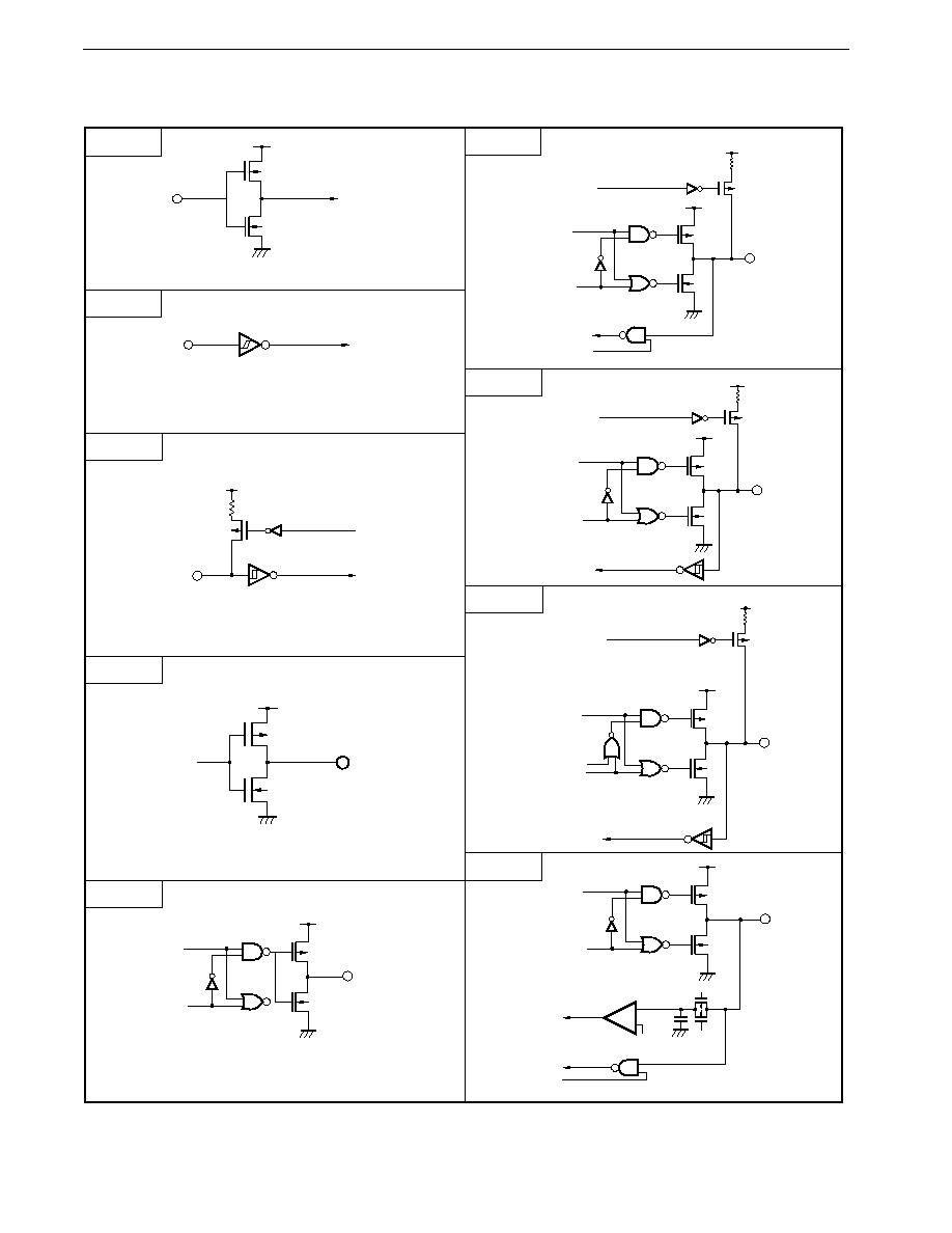
CHAPTER 2 PIN FUNCTIONS
64
Preliminary User's Manual U13987EJ1V0UM00
Figure 2-1. Pin Input/Output Circuits
P
N
IN
Type 1
V
DD
Type 2
Type 4
Type 8-A
Type 10-A
Type 2-A
Type 5-A
Type 20
IN
Schmitt-triggered input with hysteresis characteristics.
Schmitt-triggered input with hysteresis characteristics.
Push-pull output allowing output to be set to high impedance
(P-ch & N-ch both off).
P
N
Data
Output
Disable
OUT
V
DD
P
N
Data
Output
disable
IN/OUT
IN/OUT
V
DD
P
Pullup
enable
V
DD
P
N
Data
Output
disable
IN/OUT
P
Pullup
enable
Open
drain
V
DD
V
DD
P
IN
Pullup
enable
V
DD
P
N
Data
Output
disable
IN/OUT
P
Pullup
enable
V
DD
V
DD
Input
enable
P
N
Data
Output
disable
V
DD
Input
enable
Comparator
P
N
V
REF
(Threshold voltage)
+
-
Type 3
V
DD
P-ch
N-ch
OUT
data

CHAPTER 2 PIN FUNCTIONS
65
Preliminary User's Manual U13987EJ1V0UM00
2.4 Cautions
When connecting unused pins, if the input/output mode is undefined for an input/output alternate function, it should
be connected to V
DD
with a resistor of several tens of k
(especially when the reset input pin becomes the low-level
input voltage or over upon powering on, and when input/output is switched by software.)

66
Preliminary User's Manual U13987EJ1V0UM00
[MEMO]

67
Preliminary User's Manual U13987EJ1V0UM00
CHAPTER 3 CPU ARCHITECTURE
3.1 Memory Space
The
�
PD784938 can access a 1-Mbyte memory space. The mapping of the internal data area (special function registers and
internal RAM) depends on the LOCATION instruction. A LOCATION instruction must be executed after reset release, and can
only be used once.
The program after reset release must be as follows:
RSTVCT
CSEG
AT 0
DW
RSTSTRT
to
INITSEG
CSEG
BASE
RSTSTRT: LOCATION 0H; or LOCATION 0FH
MOVG
SP, #STKBGN

68
CHAPTER 3 CPU ARCHITECTURE
Preliminary User's Manual U13987EJ1V0UM00
(1) When LOCATION 0 instruction is executed
� Internal memory
The internal data area and internal ROM area are follows:
Part Number
Internal Data Area
Internal ROM Area
�
PD784935
0EB00H to 0FFFFH
00000H to 0EAFFH
10000H to 17FFFH
�
PD784936
0E500H to 0FFFFH
00000H to 0E4FFH
10000H to 1FFFFH
�
PD784937
0DF00H to 0FFFFH
00000H to 0DEFFH
10000H to 2FFFFH
�
PD784938
0D600H to 0FFFFH
00000H to 0D5FFH
�
PD78F4938
10000H to 3FFFFH
Caution
The following areas of the internal ROM that overlap the internal data area cannot be used when the
LOCATION 0 instruction is executed.
Part Number
Area That Cannot Be Used
�
PD784935
0EB00H to 0FFFFH (5,376 bytes)
�
PD784936
0E500H to 0FFFFH (6,192 bytes)
�
PD784937
0DF00H to 0FFFFH (8,448 bytes)
�
PD784938
0D600H to 0FFFFH (10,752 bytes)
�
PD78F4938
� External memory
The external memory is accessed in the external memory expansion mode.
(2) When LOCATION 0FH instruction is executed
� Internal memory
The internal data area and internal ROM area are follows:
Part Number
Internal Data Area
Internal ROM Area
�
PD784935
FEB00H to FFFFFH
00000H to 17FFFH
�
PD784936
FE500H to FFFFFH
00000H to 1FFFFH
�
PD784937
FDF00H to FFFFFH
00000H to 2FFFFH
�
PD784938
FD600H to FFFFFH
00000H to 3FFFFH
�
PD78F4938
� External memory
The external memory is accessed in the external memory expansion mode.
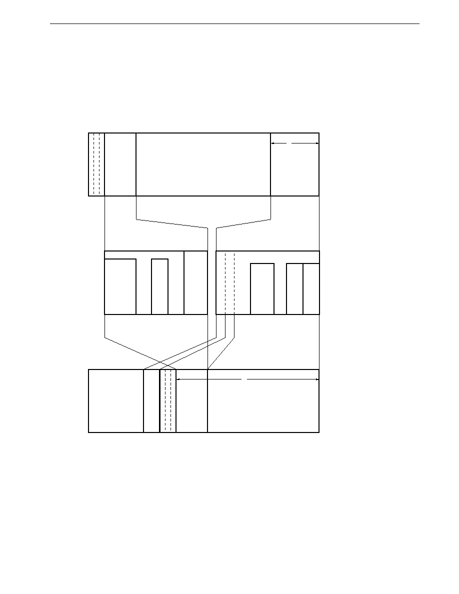
69
CHAPTER 3 CPU ARCHITECTURE
Preliminary User's Manual U13987EJ1V0UM00
Figure 3-1.
�
PD784935 Memory Map
Notes 1. Accessed in external memory expansion mode.
2. The 5,376 bytes of this area can be used as internal ROM only when the LOCATION 0FH instruction is executed.
3. 92,928 bytes when the LOCATION 0 instruction is executed, and 98,304 bytes when the LOCATION 0FH instruction is
executed.
4. Base area, reset or interrupt entry area, excluding internal RAM in the case of reset.
Internal ROM
(32,768 bytes)
(256 bytes)
Special function registers (SFRs)
Internal ROM
(60,160 bytes)
Internal RAM
(5,120 bytes)
External memory
Note 1
(928 Kbytes)
Note 1
Note 2
Internal ROM
(96 Kbytes)
When location 0 instruction is executed
General-purpose
registers
(128 bytes)
Data area (512 bytes)
Program/data area
(4,608 bytes)
Macro service control
word area (42 bytes)
CALLF entry area
(2 Kbytes)
Program/data area
Note 3
CALLT table area
(64 bytes)
Vector table area
(64 bytes)
Internal RAM
(5,120 bytes)
External memory
Note 1
(944,896 bytes)
(256 bytes)
Special function registers (SFRs)
When location 0FH instruction is executed
Note 1
1 8 0 0 0 H
1 7 F F F H
0 E B 0 0 H
0 E A F F H
0 F F D F H
0 F F D 0 H
0 F F 0 0 H
0 F E F F H
F F F F F H
0 0 8 0 0 H
0 0 7 F F H
0 F E F F H
F F E F F H
0 F E 8 0 H
0 F E 7 F H
0 F E 3 9 H
0 F E 0 6 H
0 F D 0 0 H
0 F C F F H
0 E B 0 0 H
0 1 0 0 0 H
0 0 F F F H
0 0 0 8 0 H
0 0 0 7 F H
0 0 0 4 0 H
0 0 0 3 F H
0 0 0 0 0 H
F F E 8 0 H
F F E 7 F H
F F E 2 F H
F F E 0 6 H
F F D 0 0 H
F F C F F H
F E B 0 0 H
F F F F F H
F F F D F H
F F F D 0 H
F F F 0 0 H
F F E F F H
F E B 0 0 H
F E A F F H
0 0 0 0 0 H
0 0 0 0 0 H
0 E A F F H
1 8 0 0 0 H
1 7 F F F H
1 7 F F F H
1 0 0 0 0 H
0 F F F F H
1 7 F F F H
1 0 0 0 0 H
Note 4
Note 4
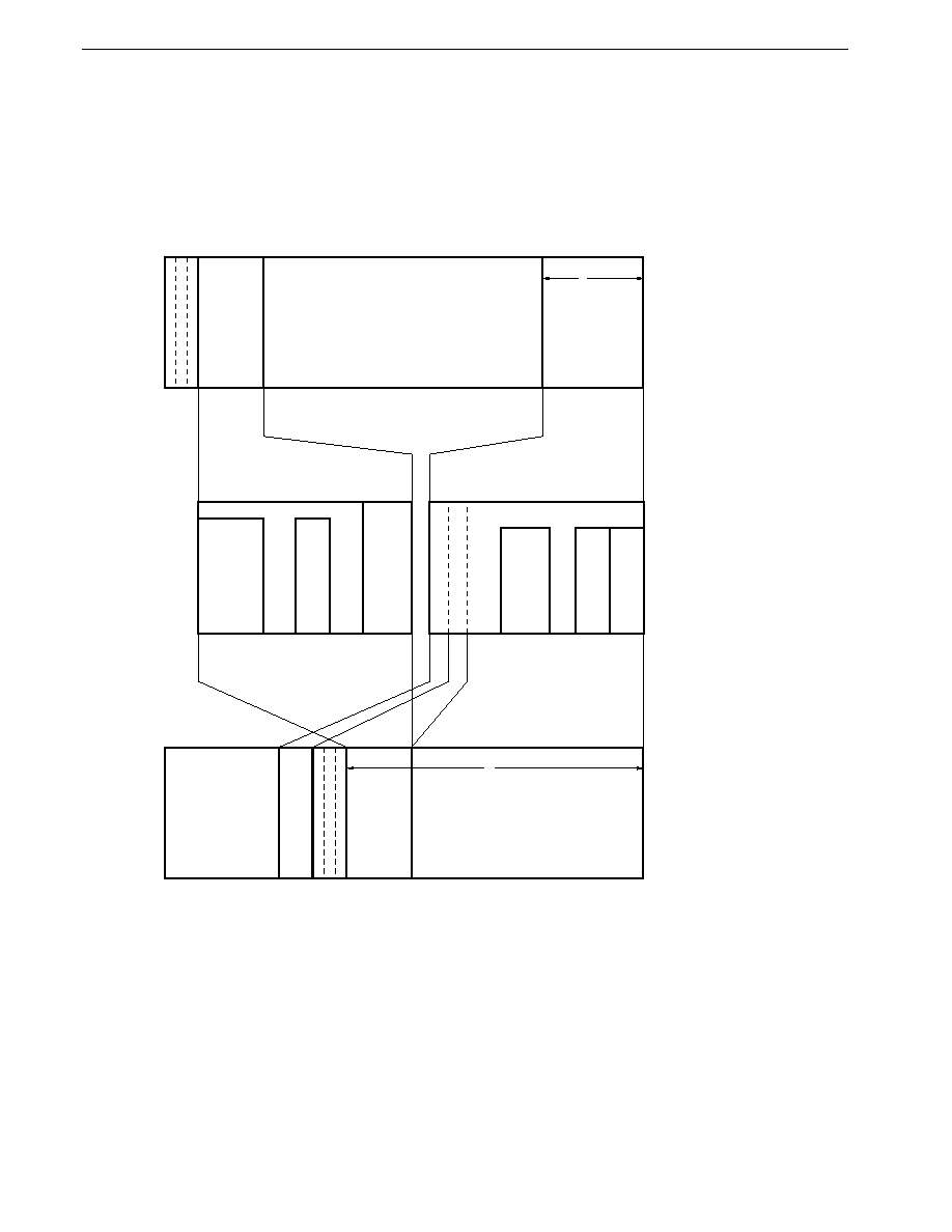
70
CHAPTER 3 CPU ARCHITECTURE
Preliminary User's Manual U13987EJ1V0UM00
Figure 3-2.
�
PD784936 Memory Map
Notes 1. Accessed in external memory expansion mode.
2. The 6,912 bytes of this area can be used as internal ROM only when the LOCATION 0FH instruction is executed.
3. 124,160 bytes when the LOCATION 0 instruction is executed, and 131,072 bytes when the LOCATION 0FH instruction is
executed.
4. Base area, reset or interrupt entry area, excluding internal RAM in the case of reset.
Internal ROM
(65,536 bytes)
(256 bytes)
Special function registers (SFRs)
Internal ROM
(58,624 bytes)
Internal RAM
(6,656 bytes)
External memory
Note 1
Note 1
(896 Kbytes)
Note 1
Note 2
Internal ROM
(128 Kbytes)
When location 0 instruction is executed
General-purpose
registers
(128 bytes)
Data area (512 bytes)
Program/data area
(6,144 bytes)
Macro service control
word area (42 bytes)
CALLF entry area
(2 Kbytes)
Program/data area
Note 3
CALLT table area
(64 bytes)
Vector table area
(64 bytes)
Internal RAM
(6,656 bytes)
External memory
Note 1
(910,720 bytes)
(256 bytes)
Special function registers (SFRs)
When location 0FH instruction is executed
2 0 0 0 0 H
1 F F F F H
0 E 5 0 0 H
0 E 4 F F H
0 F F D F H
0 F F D 0 H
0 F F 0 0 H
0 F E F F H
F F F F F H
0 0 8 0 0 H
0 0 7 F F H
0 F E F F H
F F E F F H
0 F E 8 0 H
0 F E 7 F H
0 F E 3 9 H
0 F E 0 6 H
0 F D 0 0 H
0 F C F F H
0 E 5 0 0 H
0 1 0 0 0 H
0 0 F F F H
0 0 0 8 0 H
0 0 0 7 F H
0 0 0 4 0 H
0 0 0 3 F H
0 0 0 0 0 H
F F E 8 0 H
F F E 7 F H
F F E 2 F H
F F E 0 6 H
F F D 0 0 H
F F C F F H
F E 5 0 0 H
F F F F F H
F F F D F H
F F F D 0 H
F F F 0 0 H
F F E F F H
F E 5 0 0 H
F E 4 F F H
0 0 0 0 0 H
0 0 0 0 0 H
0 E 4 F F H
2 0 0 0 0 H
1 F F F F H
1 F F F F H
1 0 0 0 0 H
0 F F F F H
1 F F F F H
1 0 0 0 0 H
Note 4
Note 4

71
CHAPTER 3 CPU ARCHITECTURE
Preliminary User's Manual U13987EJ1V0UM00
Figure 3-3.
�
PD784937 Memory Map
Notes 1. Accessed in external memory expansion mode.
2. The 8,488 bytes of this area can be used as internal ROM only when the LOCATION 0FH instruction is executed.
3. 188,160 bytes when the LOCATION 0 instruction is executed, and 196,608 bytes when the LOCATION 0FH instruction is
executed.
4. Base area, reset or interrupt entry area, excluding internal RAM in the case of reset.
(256 bytes)
Special function registers (SFRs)
Internal ROM
(57,088 bytes)
Internal RAM
(8,192 bytes)
External memory
(832 Kbytes)
Note 1
General-purpose
registers
(128 bytes)
Data area (512 bytes)
Program/data area
(7,680 bytes)
Note 2
CALLF entry area
(2 Kbytes)
Program/data area
Note 3
CALLT table area
(64 bytes)
Vector table area
(64 bytes)
Internal RAM
(8,192 bytes)
External memory
Note 1
(843,520 bytes)
(256 bytes)
Special function registers (SFR)
Internal ROM
(192 Kbytes)
Note 4
Note 4
When location 0 instruction is executed
F D F 0 0 H
F D E F F H
3 0 0 0 0 H
2 F F F F H
0 0 0 0 0 H
0 F E F F H
0 F E 8 0 H
0 F E 7 F H
0 0 8 0 0 H
0 0 7 F F H
0 0 0 0 0 H
0 F E 3 9 H
0 F E 0 6 H
0 F D 0 0 H
0 F C F F H
0 D F 0 0 H
2 F F F F H
0 1 0 0 0 H
0 0 F F F H
0 0 0 8 0 H
0 0 0 7 F H
0 0 0 4 0 H
0 0 0 3 F H
0 D F 0 0 H
0 D E F F H
0 0 0 0 0 H
F F E F F H
F F E 8 0 H
F F E 7 F H
F F E 2 F H
F F E 0 6 H
F F D 0 0 H
F F C F F H
F D F 0 0 H
Note 1
When location 0FH instruction is executed
F F F F F H
2 F F F F H
Internal ROM
(131,072 bytes)
3 0 0 0 0 H
2 F F F F H
1 0 0 0 0 H
0 D E F F H
Macro service control
word area (42 bytes)
1 0 0 0 0 H
0 F F F F H
0 F F D F H
0 F F D 0 H
0 F F 0 0 H
0 F E F F H
F F F F F H
F F F D F H
F F F D 0 H
F F F 0 0 H
F F E F F H
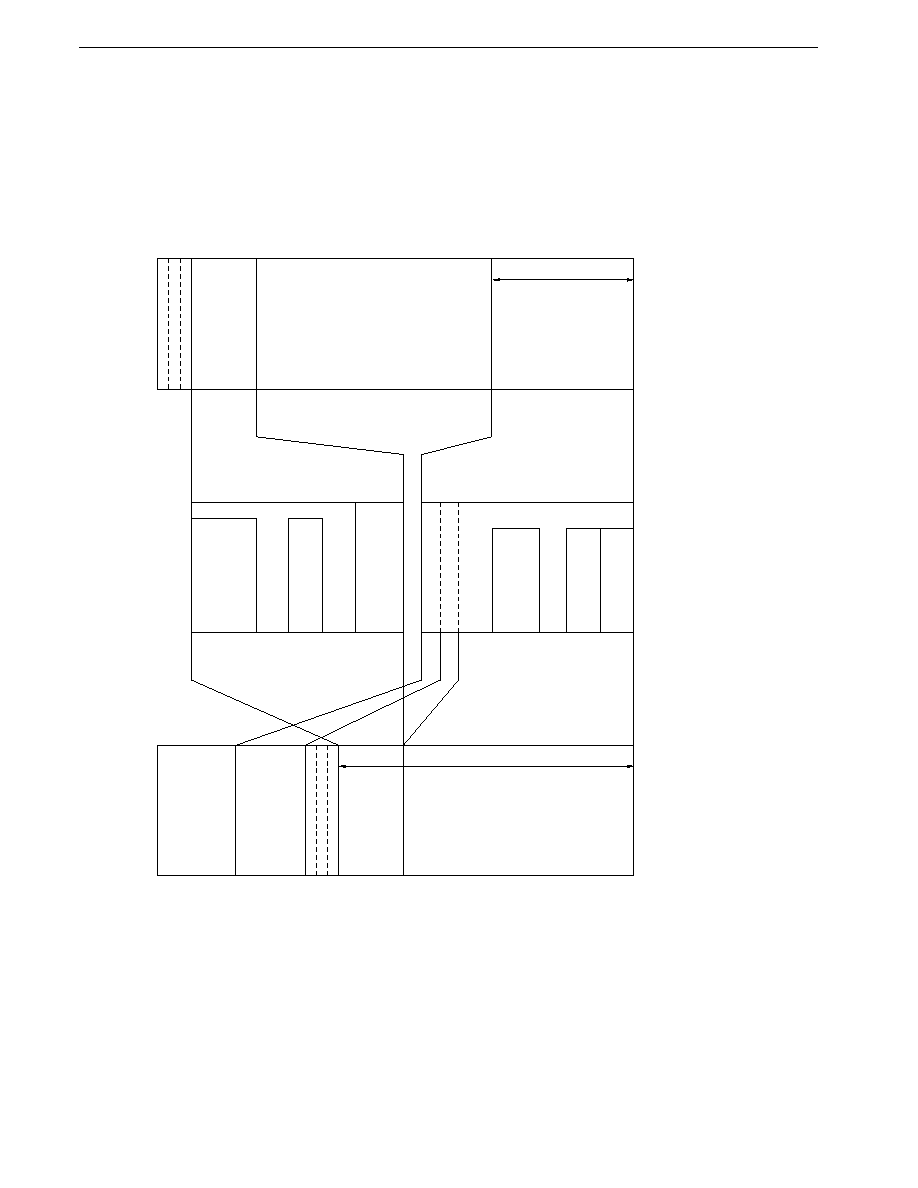
72
CHAPTER 3 CPU ARCHITECTURE
Preliminary User's Manual U13987EJ1V0UM00
Figure 3-4.
�
PD784938, 78F4938 Memory Map
Notes 1. Accessed in external memory expansion mode.
2. The 10,496 bytes of this area can be used as internal ROM only when the LOCATION 0FH instruction is executed.
3. 251,647 bytes when the LOCATION 0 instruction is executed, and 262,143 bytes when the LOCATION 0FH instruction is
executed.
4. Base area, reset or interrupt entry area, excluding internal RAM in the case of reset.
5. In the case of
�
PD78F4938: Flash memory
Note
4
Note
4
F F F F F H
F F F D F H
F F F D 0 H
F F F 0 0 H
F F E F F H
F D 6 0 0 H
F D 5 F F H
4 0 0 0 0 H
3 F F F F H
0 0 0 0 0 H
0 F E F F H
0 F E 8 0 H
0 F E 7 F H
0 0 8 0 0 H
0 0 7 F F H
0 0 0 0 0 H
0 F E 3 9 H
0 F E 0 6 H
0 F D 0 0 H
0 F C F F H
0 D 6 0 0 H
3 F F F F H
0 1 0 0 0 H
0 0 F F F H
0 0 0 8 0 H
0 0 0 7 F H
0 0 0 4 0 H
0 0 0 3 F H
0 D 6 0 0 H
0 D 5 F F H
00000H
F F E F F H
F F E 8 0 H
F F E 7 F H
F F E 3 9 H
F F E 0 6 H
F F D 0 0 H
F F C F F H
F D 6 0 0 H
F F F F F H
1 0 0 0 0 H
0 F F F F H
0 F F D F H
0 F F D 0 H
0 F F 0 0 H
0 F E F F H
3 F F F F H
4 0 0 0 0 H
3 F F F F H
1 0 0 0 0 H
0 D E F F H
(256 bytes)
Special function registers (SFRs)
Internal ROM
(54,768 bytes)
Internal RAM
(10,240 bytes
)
External memory
Note 1
(832 Kbytes)
Note 1
General-purpose
register
(128 bytes)
Macro service control
word area (42 bytes)
Data area (512 bytes)
Program/data area
(9,728 bytes)
Note 2
CALLF entry area
(2 Kbytes)
Program/data area
Note 3
CALLT table area
(64 bytes)
Vector table area
(64 bytes)
Internal RAM
(10,240 bytes)
External memory
Note 1
(843,520 bytes)
(256 bytes)
Special function registers (SFRs)
Internal ROM
(256 Kbytes)
When LOCATION 0 instruction is executed
Note 1
When LOCATION 0FH instruction is executed
Internal ROM
(196,608 bytes)

73
CHAPTER 3 CPU ARCHITECTURE
Preliminary User's Manual U13987EJ1V0UM00
3.2 Internal ROM Area
The
�
PD784938 Subseries products shown below incorporate ROM which is used to store programs, table data, etc.
If the internal ROM area and internal data area overlap when the LOCATION 0 instruction is executed, the internal data area
is accessed, and the overlapping part of the internal ROM area cannot be accessed.
Part Number
Internal ROM
Address Space
LOCATION 0 Instruction LOCATION 0FH Instruction
�
PD784935
96 Kbytes
�
8 bits
00000H to 0EAFFH
00000H to 17FFFH
10000H to 17FFFH
�
PD784936
128 Kbytes
�
8 bits
00000H to 0E4FFH
00000H to 1FFFFH
10000H to 1FFFFH
�
PD784937
192 Kbytes
�
8 bits
00000H to 0DEFFH
00000H to 2FFFFH
10000H to 2FFFFH
�
PD784938
256 Kbytes
�
8 bits
00000H to 0D5FFH
00000H to 3FFFFH
�
PD78F4938
10000H to 3FFFFH
The internal ROM can be accessed at high speed. Normally, fetches are performed at the same speed as external ROM,
but if the IFCH bit of the memory expansion mode register (MM) is set (to 1), the high-speed fetch function is used and internal
ROM fetches are performed at high speed (2-byte fetch performed in 2 system clocks).
When the instruction execution cycle equal to an external ROM fetch is selected, wait insertion is performed by the wait
function, but when high-speed fetches are used, wait insertion is not performed for internal ROM.
RESET input sets the instruction execution cycle equal to the external ROM fetch cycle.

74
CHAPTER 3 CPU ARCHITECTURE
Preliminary User's Manual U13987EJ1V0UM00
3.3 Base Area
The space from 0 to FFFFH comprises the base area. The base area is the object for the following uses:
� Reset entry address
� Interrupt entry address
� CALLT instruction entry address
� 16-bit immediate addressing mode (with instruction address addressing)
� 16-bit direct addressing mode
� 16-bit register addressing mode (with instruction address addressing)
� 16-bit register indirect addressing mode
� Short direct 16-bit memory indirect addressing mode
The vector table area, CALLT instruction table area and CALLF instruction entry area are allocated to the base area.
When the LOCATION 0 instruction is executed, the internal data area is located in the base area. Note that, in the internal
data area, program fetches cannot be performed from the internal high-speed RAM area or special function register (SFR) area.
Also, internal RAM area data should only be used after initialization has been performed.

75
CHAPTER 3 CPU ARCHITECTURE
Preliminary User's Manual U13987EJ1V0UM00
3.3.1 Vector table area
The 64-byte area from 00000H to 0003FH is reserved as the vector table area. The vector table area stores the program
start addresses used when a branch is made as the result of RESET input or generation of an interrupt request. When context
switching is used by an interrupt, the number of the register bank to be switched to is stored here.
Any portion not used as the vector table can be used as program memory or data memory.
16-bit values can be written to the vector table. Therefore, branches can only be made within the base area.
Table 3-1. Vector Table
Vector Table Address
Interrupt Source
0003CH
Operand error
0003EH
BRK
00000H
Reset (RESET input)
00002H
NMI
00004H
WDT
00006H
INTP0
00008H
INTP1
0000AH
INTP2
0000CH
INTP3
0000EH
INTC00
00010H
INTC01
00012H
INTC10
00014H
INTC11
00016H
INTC20
00018H
INTC21
0001AH
INTC30
0001CH
INTP4
0001EH
INTP5
00020H
INTAD
00022H
INTSER1
00024H
INTSR1/INTCSI1
00026H
INTST1
00028H
INTCSI
0002AH
INTSER2
0002CH
INTSR2/INTCSI2
0002EH
INTST2
00032H
INTIE1
00034H
INTIE2
00036H
INTW
00038H
INTCSI3

76
CHAPTER 3 CPU ARCHITECTURE
Preliminary User's Manual U13987EJ1V0UM00
3.3.2 CALLT instruction table area
The 1-byte call instruction (CALLT) subroutine entry addresses can be stored in the 64-byte area from 00040H to 0007FH.
The CALLT instruction references this table, and branches to a base area address written in the table as a subroutine. As
the CALLT instruction is one byte in length, use of the CALLT instruction for subroutine calls written frequently throughout the
program enables the program object size to be reduced. The table can contain up to 32 subroutine entry addresses, and
therefore it is recommended that they be recorded in order of frequency.
If this area is not used as the CALLT instruction table, it can be used as ordinary program memory or data memory.
3.3.3 CALLF instruction entry area
A subroutine call can be made directly to the area from 00800H to 00FFFH with the 2-byte call instruction (CALLF).
As the CALLF instruction is a two-byte call instruction, it enables the object size to be reduced compared with use of the direct
subroutine call CALL instruction (3 or 4 bytes).
Writing subroutines directly in this area is an effective means of exploiting the high-speed capability of the device.
If you wish to reduce the object size, writing an unconditional branch (BR) instruction in this area and locating the subroutine
itself outside this area will result in a reduced object size for subroutines that are called from five or more points. In this case,
only the 4 bytes of the BR instruction are occupied in the CALLF entry area, enabling the object size to be reduced in a large
number of subroutines.

77
CHAPTER 3 CPU ARCHITECTURE
Preliminary User's Manual U13987EJ1V0UM00
3.4 Internal Data Area
The internal data area consists of the internal RAM area and special function register area (see Figures 3-1, 3-2, and 3-3).
The final address of the internal data area can be specified by means of the LOCATION instruction as either 0FFFFH (when
a LOCATION 0 instruction is executed) or FFFFFH (when a LOCATION 0FH instruction is executed). Selection of the addresses
of the internal data area by means of the LOCATION instruction must be executed once immediately after reset release, and
once the selection is made, it cannot be changed. The program after reset release must be as shown in the example below.
If the internal data area and another area are allocated to the same addresses, the internal data area is accessed and the other
area cannot be accessed.
Example
RSTVCT
CSEG
AT 0
DW
RSTSTRT
to
INITSEG
CSEG
BASE
RSTSTRT: LOCATION 0H; or LOCATION 0FH
MOVG
SP, #STKBGN
Caution
When the LOCATION 0 instruction is executed, it is necessary to ensure that the program after reset
release does not overlap the internal data area. It is also necessary to make sure that the entry addresses
of the service routines for non-maskable interrupts such as NMI do not overlap the internal data area.
Also, initialization must be performed for maskable interrupt entry areas, etc., before the internal data area
is referenced.
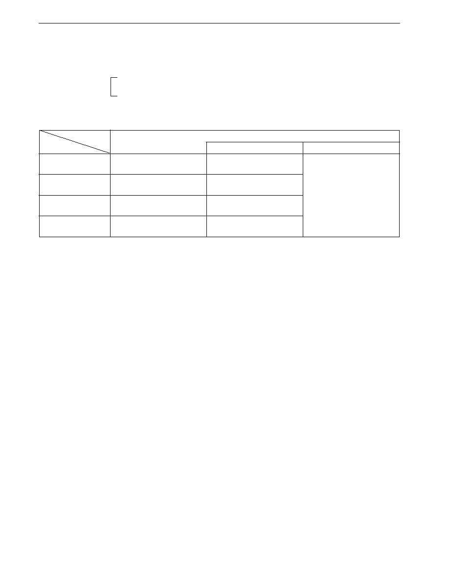
78
CHAPTER 3 CPU ARCHITECTURE
Preliminary User's Manual U13987EJ1V0UM00
3.4.1 Internal RAM area
The
�
PD784938 incorporates general-purpose static RAM.
This area is configured as follows:
Peripheral RAM (PRAM)
Internal RAM area
Internal high-speed RAM (IRAM)
Table 3-2. Internal RAM Area
Internal RAM
Internal RAM Area
Part Number
Peripheral RAM: PRAM
Internal High-Speed RAM: IRAM
�
PD784935
5,120 bytes
4,608 bytes
512 bytes
(0EB00H to 0FEFFH)
(0EB00H to 0FCFFH)
(0FD00H to 0FEFFH)
�
PD784936
6,656 bytes
6,144 bytes
(0E500H to 0FEFFH)
(0E500H to 0FCFFH)
�
PD784937
8,192 bytes
7,680 bytes
(0DF00H to 0FEFFH)
(0DF00H to 0FCFFH)
�
PD784938
10,240 bytes
9,728 bytes
�
PD78F4938
(0D600H to 0FEFFH)
(0D600H to 0FCFFH)
Remark
The addresses in the table are the values that apply when the LOCATION 0 instruction is executed. When the
LOCATION 0FH instruction is executed, 0F0000H should be added to the values shown above.

79
CHAPTER 3 CPU ARCHITECTURE
Preliminary User's Manual U13987EJ1V0UM00
The internal RAM memory map is shown in Figure 3-5.
Figure 3-5. Internal RAM Memory Map
Note
�
PD784935:
00EB00H
�
PD784936:
00E500H
�
PD784937:
00DF00H
�
PD784938, 78F4938: 00D600H
Remark
The addresses in the figure are the values that apply when the LOCATION 0 instruction is executed. When the
LOCATION 0FH instruction is executed, 0F0000H should be added to the values shown above.
00FEFFH
00FE80H
00FE39H
00FE06H
00FE00H
00FDFFH
Peripheral RAM
Internal high-speed RAM
Macro service
control word area
General-purpose
register area
Short direct addressing 1
permissible range
Short direct addressing 2
permissible range
00FD20H
00FD1FH
00FD00H
00FCFFH
Differs depending on product
Note

80
CHAPTER 3 CPU ARCHITECTURE
Preliminary User's Manual U13987EJ1V0UM00
(1) Internal high-speed RAM (IRAM)
The internal high-speed RAM (IRAM) allows high-speed accesses to be made. The short direct addressing mode for high-
speed accesses can be used on FD20H to FEFFH in this area. There are two kinds of short direct addressing mode, short
direct addressing 1 and short direct addressing 2, according to the target address. The function is the same in both of these
addressing modes. With some instructions, the word length is shorter with short direct addressing 2 than with short direct
addressing 1. See the 78K/IV Series User's Manual Instructions for details.
A program fetch cannot be performed from IRAM. If a program fetch is performed from an address onto which IRAM is
mapped, CPU inadvertent loop will result.
The following areas are reserved in IRAM.
� General-purpose register area:
FE80H to FEFFH
� Macro service control word area: FE06H to FE39H (excluding 0FE22H, 0FE23H, 0FE2AH, 0FE2BH, 0FE30H, 0FE31H)
� Macro service channel area:
FE00H to FEFFH (the address is specified by the macro service control word)
If the reserved function is not used in these areas, they can be used as ordinary data memory.
Remark
The addresses in this text are those that apply when the LOCATION 0 instruction is executed. When the
LOCATION 0FH instruction is executed, 0F0000H should be added to the values shown in the text.
(2) Peripheral RAM (PRAM)
The peripheral RAM (PRAM) is used as ordinary program memory or data memory. When used as program memory, the
program must be written to the peripheral RAM beforehand by a program.
Program fetches from peripheral RAM are fast, with a 2-byte fetch being executed in 2 clocks.

81
CHAPTER 3 CPU ARCHITECTURE
Preliminary User's Manual U13987EJ1V0UM00
3.4.2 Special function register (SFR) area
The on-chip peripheral hardware special function registers (SFRs) are mapped onto the area from 0FF00H to 0FFFFH (see
Figures 3-1, 3-2, 3-3, and 3-4).
The area from 0FFD0H to 0FFDFH is mapped as an external SFR area, and allows externally connected peripheral I/Os,
etc., to be accessed in external memory expansion mode (specified by the memory expansion mode register (MM)) by the ROM-
less product or on-chip ROM products.
Caution
Addresses onto which SFRs are not mapped should not be accessed in this area. If such an address is
accessed by mistake, the CPU may become deadlocked. A deadlock can only be released by reset input.
Remark
The addresses in this text are those that apply when the LOCATION 0 instruction is executed. When the
LOCATION 0FH instruction is executed, 0F0000H should be added to the values shown in the text.
3.4.3 External SFR area
In
�
PD784938 Subseries products, the 16-byte area from 0FFD0H to 0FFDFH in the SFR area (when the LOCATION 0 is
executed; 0FFFD0H to 0FFFDFH when the LOCATION 0FH instruction is executed) is mapped as an external SFR area. When
the external memory expansion mode is set in a ROM-less product or on-chip ROM product, externally connected peripheral
I/Os, etc., can be accessed using the address bus or address/data bus, etc.
As the external SFR area can be accessed by SFR addressing, peripheral I/O and similar operations can be performed easily,
the object size can be reduced, and macro service can be used.
Bus operations for accesses to the external SFR area are performed in the same way as for ordinary memory accesses.
3.5 External Memory Space
The external memory space is a memory space that can be accessed in accordance with the setting of the memory expansion
mode register (MM). It can store programs, table data, etc., and can have peripheral I/O devices allocated to it.

82
CHAPTER 3 CPU ARCHITECTURE
Preliminary User's Manual U13987EJ1V0UM00
3.6
�
PD78F4938 Memory Mapping
The memory size switching register (IMS) specifies the internal memory size. With the
�
PD78F4938, users are able to select
the internal memory capacity using the IMS so that the same memory map as that of mask ROM versions with a different internal
memory capacity can be achieved.
The IMS is set with an 8-bit memory manipulation instruction.
RESET input sets IMS to FFH.
Figure 3-6. Internal Memory Size Switching Register (IMS)
Caution
The IMS is not contained in mask ROM products (
�
PD784935, 784936, 784937, 784938).
The IMS setting to obtain the same memory map as mask ROM products are shown in Table 3-3.
Table 3-3. Internal Memory Size Switching Register (IMS) Setting Value
Mask ROM Product
IMS Setting Value
�
PD784935
DDH
�
PD784936
EEH
�
PD784937
FFH
�
PD784938
CCH
7
1
Address: 0FFFCCH
After reset: FFH W/R
6
1
5
ROM1
4
ROM0
3
1
2
1
1
RAM1
0
RAM0
IMS
Internal ROM Capacity Selection
ROM1
ROM0
Internal RAM Capacity Selection
RAM1
RAM0
0
0
1
1
0
1
0
1
10,240 bytes
5,120 bytes
6,656 bytes
8,192 bytes
0
0
1
1
0
1
0
1
256 Kbytes
96 Kbytes
128 Kbytes
192 Kbytes

83
CHAPTER 3 CPU ARCHITECTURE
Preliminary User's Manual U13987EJ1V0UM00
3.7 Control Registers
Control registers consist of the program counter (PC), program status word (PSW), and stack pointer (SP).
3.7.1 Program counter (PC)
This is a 20-bit binary counter that holds address information on the next program to be executed (see Figure 3-7).
Normally, the PC is incremented automatically by the number of bytes in the fetched instruction. When an instruction
associated with a branch is executed, the immediate data or register contents are set in the PC.
Upon RESET input, the 16-bit data in address 0 and 1 is set in the low-order 16 bits, and 0000 in the high-order 4 bits of the
PC.
Figure 3-7. Program Counter (PC) Format
19
PC
0
3.7.2 Program status word (PSW)
The program status word (PSW) is a 16-bit register comprising various flags that are set or reset according to the result of
instruction execution.
Read accesses and write accesses are performed in high-order 8-bit (PSWH) and low-order 8-bit (PSWL) units. Individual
flags can be manipulated by bit-manipulation instructions.
The contents of the PSW are automatically saved to the stack when a vectored interrupt request is acknowledged or a BRK
instruction is executed, and automatically restored when an RETI or RETB instruction is executed. When context switching is
used, the contents are automatically saved in RP3, and automatically restored when an RETCS or RETCSB instruction is
executed.
RESET input resets (to 0) all bits.
"0" must always be written to the bits written as "0" in Figure 3-8. The contents of bits written as "-" are undefined when read.
Figure 3-8. Program Status Word (PSW) Format
7
UF
PSWH
Symbol
6
RBS2
5
RBS1
4
RBS0
3
�
2
�
1
�
0
�
7
S
PSWL
6
Z
5
RSS
4
AC
3
IE
2
P/V
1
0
0
CY
The flags are described below.
(1) Carry flag (CY)
The carry flag records a carry or borrow resulting from an operation.
This flag also records the shifted-out value when a shift/rotate instruction is executed, and functions as a bit accumulator
when a bit-manipulation instruction is executed.
The status of the CY flag can be tested with a conditional branch instruction.

84
CHAPTER 3 CPU ARCHITECTURE
Preliminary User's Manual U13987EJ1V0UM00
(2) Parity/overflow flag (P/V)
The P/V flag performs the following two kinds of operation associated with execution of an operation instruction.
The status of the P/V flag can be tested with a conditional branch instruction.
� Parity flag operation
Set (to 1) when the number of bits set (to 1) as the result of execution of a logical operation instruction, shift/rotate
instruction, or a CHKL or CHKLA instruction is even, and reset (to 0) if odd. When a 16-bit shift instruction is executed,
however, only the low-order 8 bits of the operation result are valid for the parity flag.
� Overflow flag operation
Set (1) only when the numeric range expressed as a two's complement is exceeded as the result of execution of a
arithmetic operation instruction, and reset (to 0) otherwise. More specifically, the value of this flag is the exclusive OR
of the carry into the MSB and the carry out of the MSB. For example, the two's complement range in an 8-bit arithmetic
operation is 80H (�128) to 7FH (+127), and the flag is set (to 1) if the operation result is outside this range, and reset (to
0) if within this range.
Example The operation of the overflow flag when an 8-bit addition instruction is executed is shown below.
When the addition of 78H (+120) and 69H (+105) is performed, the operation result is E1H (+225), and the two's
complement limit is exceeded, with the result that the P/V flag is set (to 1). Expressed as a two's complement,
E1H is -31.
78H (+120)
=
0111
1000
+)
69H (+105)
= +)
0110
1001
0
1110
0001
=
�31
P/V = 1
CY
When the following two negative numbers are added together, the operation result is within the two's
complement range, and therefore the P/V flag is reset (to 0).
FBH (�5)
=
1111
1011
+)
F0H (�16)
= +)
1111
0000
1
1110
1011
=
�21
P/V = 0
CY
(3) Interrupt request enable flag (IE)
This flag controls CPU interrupt request acknowledgment operations.
When "0", interrupts are disabled, and only non-maskable interrupts and unmasked macro service can be acknowledged.
All other interrupts are disabled.
When "1", the interrupt enabled state is set, and enabling of interrupt request acknowledgment is controlled by the interrupt
mask flags corresponding to the individual interrupt requests and the priority of the individual interrupts.
The IE flag is set (to 1) by execution of an EI instruction, and reset (to 0) by execution of a DI instruction or acknowledgment
of an interrupt.

85
CHAPTER 3 CPU ARCHITECTURE
Preliminary User's Manual U13987EJ1V0UM00
(4) Auxiliary carry flag (AC)
The AC flag is set (to 1) when there is a carry out of bit 3 or a borrow into bit 3 as the result of an operation, and reset (to
0) otherwise.
This flag is used when the ADJBA or ADJBS instruction is executed.
(5) Register set selection flag (RSS)
The RSS flag specifies the general-purpose registers that function as X, A, C, and B, and the general-purpose register pairs
(16-bit) that function as AX and BC.
This flag is provided to maintain compatibility with the 78K/III Series, and must be set to 0 except when using a 78K/III Series
program.
(6) Zero flag (Z)
The Z flag records the fact that the result of an operation is "0".
It is set (to 1) when the result of an operation is "0", and reset (to 0) otherwise. The status of the Z flag can be tested with
a conditional branch instruction.
(7) Sign flag (S)
The S flag records the fact that the MSB is "1" as the result of an operation.
It is set (to 1) when the MSB is "1" as the result of an operation, and reset (to 0) otherwise. The status of the S flag can be
tested with a conditional branch instruction.
(8) Register bank selection flag (RBS0 to RBS2)
This is a 3-bit flag used to select one of the 8 register banks (register bank 0 to register bank 7) (see Table 3-4).
It stores 3-bit information which indicates the register bank selected by execution of a SEL RBn instruction, etc.
Table 3-4. Register Bank Selection
RBS2
RBS1
RBS0
Specified Register Bank
0
0
0
Register bank 0
0
0
1
Register bank 1
0
1
0
Register bank 2
0
1
1
Register bank 3
1
0
0
Register bank 4
1
0
1
Register bank 5
1
1
0
Register bank 6
1
1
1
Register bank 7
(9) User flag (UF)
This flag can be set and reset in the user program, and used for program control.

86
CHAPTER 3 CPU ARCHITECTURE
Preliminary User's Manual U13987EJ1V0UM00
3.7.3 Use of RSS bit
Basically, the RSS bit should be fixed at 0 at all times.
The following explanation refers to the case where a 78K/III Series program is used, and the program used sets the RSS bit
to 1. This explanation can be skipped if the RSS bit is fixed at 0.
The RSS bit is provided to allow the functions of A (R1), X (R0), B (R3), C (R2), AX (RP0), and BC (RP1) to be used by registers
R4 to R7 (RP2, RP3) as well. Effective use of this bit enables efficient programs to be written in terms of program size and
program execution.
However, careless use can result in unforeseen problems. Therefore, the RSS bit should always be set to 0. The RSS bit
should only be set to 1 when a 78K/III Series program is used.
Use of the RSS bit set to 0 in all programs will improve programming and debugging efficiency.
Even when using a program in which the RSS bit set to 1 is used, it is recommended that the program be amended if possible
so that it does not set the RSS bit to 1.
(1) RSS bit specification
� Registers used by instructions for which the A, X, B, C, and AX registers are directly entered in the operand column of
the operation list (see 28.2)
� Registers specified as implied by instructions that use the A, AX, B, and C registers by means of implied addressing
� Registers used in addressing by instructions that use the A, B, and C registers in indexed addressing and based indexed
addressing
The registers used in these cases are switched as follows according to the RSS bit.
�
When RSS = 0
A
R1, X
R0, B
R3, C
R2, AX
RP0, BC
RP1
�
When RSS = 1
A
R5, X
R4, B
R7, C
R6, AX
RP2, BC
RP3
Registers used other than those mentioned above are always the same irrespective of the value of the RSS bit. With the
NEC assembler (RA78K4), the register operation code generated when the A, X, B, C, AX, and BC registers are described by
those names is determined by the assembler RSS pseudo-instruction.
When the RSS bit is set or reset, an RSS pseudo-instruction must be written immediately before (or immediately after) the
relevant instruction (see example below).
<Program example>
� When RSS is set to 0
RSS
0
; RSS pseudo-instruction
CLR1 PSWL. 5
MOV B, A
; This description is equivalent to "MOV R3, R1".
� When RSS is set to 1
RSS
1
; RSS pseudo-instruction
SET1 PSWL. 5
MOV B, A
; This description is equivalent to "MOV R7, R5".

87
CHAPTER 3 CPU ARCHITECTURE
Preliminary User's Manual U13987EJ1V0UM00
(2) Operation code generation method with RA78K4
� With RA78K4, if there is an instruction with the same function as an instruction for which A or AX is directly entered in
the operand column of the instruction operation list, the operation code for which A or AX is directly entered in the operand
column is generated first.
Example The function is the same when B is used as r in a MOV A,r instruction, and when A is used as r and B is used
as r' in a MOVr,r' instruction, and the same description (MOV,A,B) is used in the assembler source program.
In this case, RA78K4 generates code equivalent to the MOV A, r instruction.
� If A, X, B, C, AX, or BC is written in an instruction for which r, r', rp, and rp' are specified in the operand column, the A,
X, B, C, AX, and BC instructions generate an operation code that specifies the following registers according to the
operand of the RA78K4 RSS pseudo-instruction.
Register
RSS = 0
RSS = 1
A
R1
R5
X
R0
R4
B
R3
R7
C
R2
R6
AX
RP0
RP2
BC
RP1
RP3
� If R0 to R7 or RP0 to RP4 is written as r, r', rp, or rp' in the operand column, an operation code in accordance with that
specification is output (an operation code for which A or AX is directly entered in the operand column is not output.)
� Descriptions R1, R3, R2 or R5, R7, R6 cannot be used for registers A, B, and C used in indexed addressing and based
indexed addressing.
(3) Operating precautions
Switching the RSS bit has the same effect as having two register sets. However, when writing a program, care must be
taken to ensure that the static program description and dynamic RSS bit changes at the time of program execution always
coincide.
Also, a program that sets RSS to 1 cannot be used by a program that uses the context switching function, and therefore
program usability is poor. Moreover, since different registers are used with the same name, program readability is poor and
debugging is difficult. Therefore, if it is necessary to set RSS to 1, these disadvantages must be fully taken into consideration
when writing a program.
A register not specified by the RSS bit can be accessed by writing its absolute name.

88
CHAPTER 3 CPU ARCHITECTURE
Preliminary User's Manual U13987EJ1V0UM00
3.7.4 Stack pointer (SP)
The stack pointer is a 24-bit register that holds the start address of the stack area (LIFO type: 00000H to FFFFFFH) (see
Figure 3-9). It is used to address the stack area when subroutine processing or interrupt servicing is performed. Be sure to
write "0" in the high-order 4 bits.
The contents of the SP are decremented before a write to the stack area and incremented after a read from the stack area
(see Figures 3-10 and 3-11).
The SP is accessed by dedicated instructions.
The SP contents are undefined after RESET input, and therefore the SP must always be initialized by an initialization program
directly after reset release (before a subroutine call or interrupt acknowledgment).
Example SP initialization
MOVG SP, #0FEE0H;SP
0FEE0H (when used from FEDFH)
Figure 3-9. Stack Pointer (SP) Format
23
SP
0
89
CHAPTER 3 CPU ARCHITECTURE
Preliminary User's Manual U13987EJ1V0UM00
Figure 3-10. Data Saved to Stack Area
PUSH sfr instruction
stack
PUSH sfrp instruction
stack
Upper byte
Lower byte
Upper byte
Undefined
Undefined
PC15 to PC8
PC7 to PC0
PC15 to PC8
PC7 to PC0
PC19 to
PC16
PC19 to
PC16
PSWH
7
to
PSWH
4
PSWH
7
to
PSWH
4
PSWL
PSWL
R7
R6
R5
R4
RP3
RP2
AX
A
X
Middle byte
Lower byte
PUSH rg instruction
stack
PUSH PSW instruction
stack
CALL, CALLF, CALLT instruction
stack
Vectored interrupt
stack
PUSH post, PUSHU post instruction
(in case of PUSH AX, RP2, RP3)
stack
SP
SP� 1
SP
SP� 1
SP
SP� 1
SP� 2
SP
SP� 2
SP
SP� 1
SP� 2
SP
SP� 2
SP
SP� 1
SP� 2
SP� 3
SP
SP� 3
SP
SP� 1
SP� 2
SP� 3
SP
SP� 3
SP
SP� 1
SP� 2
SP� 3
SP� 4
SP
SP� 4
SP
SP� 1
SP� 2
SP� 3
SP� 4
SP� 5
SP� 6
SP
SP� 6
90
CHAPTER 3 CPU ARCHITECTURE
Preliminary User's Manual U13987EJ1V0UM00
Figure 3-11. Data Restored from Stack Area
Note
This 4-bit data is ignored.
POP sfr instruction
stack
POP sfrp instruction
stack
Upper byte
Lower byte
Upper byte
�
Note
PC15 to PC8
PC7 to PC0
PC15 to PC8
PC7 to PC0
PC19 to
PC16
PC19 to
PC16
PSWH
7
to
PSWH
4
PSWH
7
to
PSWH
4
PSWL
PSWL
R7
R6
R5
R4
RP3
RP2
AX
A
X
Middle byte
Lower byte
POP rg instruction
stack
POP PSW instruction
stack
RET instruction
stack
RETI, RETB instruction
stack
POP post, POPU post instruction
(In case of POP AX, RP2, RP3)
stack
SP
SP+1
SP+1
SP
SP
SP+2
SP+1
SP
SP
SP+3
SP+2
SP+1
SP
SP
SP+3
SP+2
SP+1
SP
SP
SP+4
SP+3
SP+2
SP+1
SP
SP
SP+6
SP+5
SP+4
SP+3
SP+2
SP+1
SP
SP
SP+2
SP+1
SP
�
Note

91
CHAPTER 3 CPU ARCHITECTURE
Preliminary User's Manual U13987EJ1V0UM00
Cautions 1. With stack addressing, the entire 1-Mbyte space can be accessed but a stack area cannot be reserved
in the SFR area or internal ROM area.
2. The stack pointer (SP) is undefined after RESET input. Moreover, non-maskable interrupts can still
be acknowledged when the SP is in an undefined state. An unanticipated operation may therefore be
performed if a non-maskable interrupt request is generated when the SP is in the undefined state
directly after reset release. To avoid this risk, the program after reset release must be written as
follows.
RSTVCT
CSEG
AT
0
DW
RSTSTRT
to
INITSEG
CSEG
BASE
RSTSTRT : LOCATION 0H ; or LOCATION 0FH
MOVG
SP, #STKBGN
92
CHAPTER 3 CPU ARCHITECTURE
Preliminary User's Manual U13987EJ1V0UM00
3.8 General- Purpose Registers
3.8.1 Configuration
There are sixteen 8-bit general-purpose registers, and two 8-bit general-purpose registers can be used together as a 16-bit
general-purpose register. In addition, four of the 16-bit general-purpose registers can be combined with an 8-bit register for
address extension, and used as 24-bit address specification registers.
General-purpose registers other than the V, U, T, and W registers for address extension are mapped onto internal RAM.
These register sets are provided in 8 banks, and can be switched by means of software or the context switching function.
Upon RESET input, register bank 0 is selected. The register bank used during program execution can be checked by reading
the register bank selection flag (RBS0, RBS1, RBS2) in the PSW.
Figure 3-12. General-Purpose Register Format
7
0 7
0
A (R1)
X (R0)
AX (RP0)
B (R3)
C (R2)
BC (RP1)
R5
R4
RP2
R7
R6
RP3
R9
R8
VP (RP4)
V
VVP (RG4)
R11
R10
UP (RP5)
U
UUP (RG5)
D (R13)
E (R12)
DE (RP6)
T
TDE (RG6)
H (R15)
L (R14)
HL (RP7)
W
WHL (RG7)
0
23
15
8 banks
Remark
Absolute names are shown in parentheses.
93
CHAPTER 3 CPU ARCHITECTURE
Preliminary User's Manual U13987EJ1V0UM00
Figure 3-13. General-Purpose Register Addresses
RBNK0
FEFFH
Note
FE80H
Note
RBNK1
RBNK2
RBNK3
RBNK4
RBNK5
RBNK6
RBNK7
H (R15)
(FH)
8-bit processing
16-bit processing
D (R13)
(DH)
R11
(BH)
R9
(9H)
R7
(7H)
R5
(5H)
B (R3)
(3H)
A (R1)
(1H)
7
7
0
0
15
0
L (R14)
(EH)
E (R12)
(CH)
R10
(AH)
R8
(8H)
R6
(6H)
R4
(4H)
C (R2)
(2H)
X (R0)
(0H)
HL (RP7)
(EH)
DE (RP6)
(CH)
UP (RP5)
(AH)
VP (RP4)
(8H)
RP3
(6H)
RP2
(4H)
BC (RP1)
(2H)
AX (RP0)
(0H)
Note
When the LOCATION 0 instruction is executed. When the LOCATION 0FH instruction is executed, 0F0000H should
be added to the address values shown above.
Caution
R4, R5, R6, R7, RP2, and RP3 can be used as the X, A, C, B, AX, and BC registers respectively by setting
the RSS bit of the PSW to 1, but this function should only be used when using a 78K/III Series program.
Remark
When the register bank is changed, and it is necessary to return to the original register bank, an SEL RBn
instruction should be executed after saving the PSW to the stack with a PUSH PSW instruction. When returning
to the original register bank, if the stack location does not change the POP PSW instruction should be used.
When the register bank is changed by a vectored interrupt service program, etc., the PSW is automatically saved
to the stack when an interrupt is acknowledged and restored by an RETI or RETB instruction, so that, if only one
register bank is used in the interrupt service routine, only an SEL RBn instruction needs be executed, and
execution of a PUSH PSW and POP PSW instruction is not necessary.
Example When register bank 2 is specified
PUSH PSW
SEL RB2
Operations in register bank 2
POP PSW
Operations in original register bank
......
......
......

94
CHAPTER 3 CPU ARCHITECTURE
Preliminary User's Manual U13987EJ1V0UM00
3.8.2 Functions
In addition to being manipulated in 8-bit units, the general-purpose registers can also be manipulated in 16-bit units by pairing
two 8-bit registers. Also, four of the 16-bit registers can be combined with an 8-bit register for address extension and manipulated
in 24-bit units.
Each register can be used in a general-purpose way for temporary storage of an operation result and as the operand of an
inter-register operation instruction.
The area from 0FE80H to 0FEFFH (when the LOCATION 0 instruction is executed; 0FFE80H to 0FFEFFH when the
LOCATION 0FH instruction is executed) can be given an address specification and accessed as ordinary data memory
irrespective of whether or not it is used as the general-purpose register area.
As 8 register banks are provided in the 78K/IV Series, efficient programs can be written by using different register banks for
normal processing and processing in the event of an interrupt.
The registers have the following specific functions.
A (R1):
� Register mainly used for 8-bit data transfers and operation processing. Can be used in combination with all addressing
modes for 8-bit data.
� Can also be used for bit data storage.
� Can be used as the register that stores the offset value in indexed addressing and based indexed addressing.
X (R0):
� Can be used for bit data storage.
AX (RP0):
� Register mainly used for 16-bit data transfers and operation processing. Can be used in combination with all
addressing modes for 16-bit data.
AXDE:
� Used for 32-bit data storage when a DIVUX, MACW, or MACSW instruction is executed.
B (R3):
� Has a loop counter function, and can be used by the DBNZ instruction.
� Can be used as the register that stores the offset value in indexed addressing and based indexed addressing.
� Used as the MACW and MACSW instruction data pointer.
C (R2):
� Has a loop counter function, and can be used by the DBNZ instruction.
� Can be used as the register that stores the offset value in based indexed addressing.
� Used as the counter in a string instruction and the SACW instruction.
� Used as the MACW and MACSW instruction data pointer.
RP2:
� Used to save the low-order 16 bits of the program counter (PC) when context switching is used.
RP3:
� Used to save the high-order 4 bits of the program counter (PC) and the program status word (PSW) (excluding bits
0 to 3 of PSWH) when context switching is used.

95
CHAPTER 3 CPU ARCHITECTURE
Preliminary User's Manual U13987EJ1V0UM00
VVP (RG4):
� Has a pointer function, and operates as the register that specifies the base address in register indirect addressing,
based addressing and based indexed addressing.
UUP (RG5):
� Has a user stack pointer function, and enables a stack separate from the system stack to be implemented by means
of the PUSHU and POPU instructions.
� Has a pointer function, and operates as the register that specifies the base address in register indirect addressing and
based addressing.
DE (RP6), HL (RP7):
� Operate as the registers that store the offset value in indexed addressing and based indexed addressing.
TDE (RG6):
� Has a pointer function, and operates as the register that specifies the base address in register indirect addressing and
based addressing.
� Used as the pointer in a string instruction and the SACW instruction.
WHL (RG7):
� Register used mainly for 24-bit data transfers and operation processing.
� Has a pointer function, and operates as the register that specifies the base address in register indirect addressing and
based addressing.
� Used as the pointer in a string instruction and the SACW instruction.

96
CHAPTER 3 CPU ARCHITECTURE
Preliminary User's Manual U13987EJ1V0UM00
In addition to the function name that emphasizes the specific function of the register (X, A, C, B, E, D, L, H, AX, BC, VP, UP,
DE, HL, VVP, UUP, TDE, WHL), each register can also be described by its absolute name (R0 to R15, RP0 to RP7, RG4 to RG7).
The correspondence between these names is shown in Table 3-5.
Table 3-5. Correspondence between Function Names and Absolute Names
Note RSS should only be set to 1 when a 78K/III Series program is used.
Remark
R8 to R11 have no function name.
(b) 16-bit registers
Absolute Name
Function Name
RSS = 0
RSS = 1
Note
RP0
AX
RP1
BC
RP2
AX
RP3
BC
RP4
VP
VP
RP5
UP
UP
RP6
DE
DE
RP7
HL
HL
(c) 24-bit registers
Absolute Name
Function Name
RG4
VVP
RG5
UUP
RG6
TDE
RG7
WHL
(a) 8-bit registers
Absolute Name
Function Name
RSS = 0
RSS = 1
Note
R0
X
R1
A
R2
C
R3
B
R4
X
R5
A
R6
C
R7
B
R8
R9
R10
R11
R12
E
E
R13
D
D
R14
L
L
R15
H
H

97
CHAPTER 3 CPU ARCHITECTURE
Preliminary User's Manual U13987EJ1V0UM00
3.9 Special Function Registers (SFR)
These are registers to which a special function is assigned, such as on-chip peripheral hardware mode registers, control
registers, etc. They are mapped onto the 256-byte space from 0FF00H to 0FFFFH
Note
.
Note
When the LOCATION 0 instruction is executed. When the LOCATION 0FH instruction is executed, the area is
FFF00H to FFFFFH.
Caution
Addresses onto which SFRs are not assigned should not be accessed in this area. If such an address is
as accessed by mistake, the
�
PD784938 may become deadlocked. A deadlock can only be released by
reset input.
A list of special function registers (SFRs) is given in Table 3-6. The meaning of the items in the table is as explained below.
� Symbol ............................... Symbol that indicates the incorporated SFR. This is a reserved word in the NEC assembler
(RA78K4). With the C compiler (CC78K4), this symbol can be used as an sfr variable by
means of a #pragma sfr command.
� R/W .................................... Indicates whether the corresponding SFR is read/write enabled.
R/W: Read/write enabled
R:
Read-only
W:
Write-only
� Manipulable Bit Units ......... Indicates the applicable manipulation bit units when the corresponding SFR is manipulated.
A 16-bit-manipulable SFR can be written in the operand "sfrp", and when specified by an
address, an even address is specified.
A bit-manipulable SFR can be written in a bit manipulation instruction.
� After Reset ......................... Indicates the status of the register after RESET input.

98
CHAPTER 3 CPU ARCHITECTURE
Preliminary User's Manual U13987EJ1V0UM00
Table 3-6. List of Special Function Registers (SFRs) (1/5)
Address
Note
Special Function Register (SFR) Name
Symbol
R/W
Manipulable Bit Units
After Reset
1 Bit
8 Bits 16 Bits
0FF00H
Port 0
P0
R/W
--
Undefined
0FF01H
Port 1
P1
--
0FF02H
Port 2
P2
R
--
0FF03H
Port 3
P3
R/W
--
0FF04H
Port 4
P4
--
0FF05H
Port 5
P5
--
0FF06H
Port 6
P6
--
00H
0FF07H
Port 7
P7
--
Undefined
0FF09H
Port 9
P9
--
0FF0AH
Port 10
P10
--
0FF0EH
Port 0 buffer register
P0L
--
0FF0FH
Port 0 buffer register H
P0H
--
0FF10H
Compare register (timer/event counter 0)
CR00
--
--
0FF12H
Capture/compare register (timer/event counter 0)
CR01
--
--
0FF14H
Compare register L (timer/event counter 1)
CR10
CR10W
--
0FF15H
Compare register H (timer/event counter 1)
--
--
--
0FF16H
Capture/compare register L (timer/event counter 1)
CR11
CR11W
--
0FF17H
Capture/compare register H (timer/event counter 1)
--
--
--
0FF18H
Compare register L (timer/event counter 2)
CR20
CR20W
--
0FF19H
Compare register H (timer/event counter 2)
--
--
--
0FF1AH
Capture/compare register L (timer/event counter 2)
CR21
CR21W
--
0FF1BH
Capture/compare register H (timer/event counter 2)
--
--
--
0FF1CH
Compare register L (timer 3)
CR30
CR30W
--
0FF1DH
Compare register H (timer 3)
--
--
--
0FF20H
Port 0 mode register
PM0
--
FFH
0FF21H
Port 1 mode register
PM1
--
0FF23H
Port 3 mode register
PM3
--
0FF24H
Port 4 mode register
PM4
--
0FF25H
Port 5 mode register
PM5
--
0FF26H
Port 6 mode register
PM6
--
0FF27H
Port 7 mode register
PM7
--
0FF29H
Port 9 mode register
PM9
--
0FF2AH
Port 10 mode register
PM10
--
0FF2EH
Real-time output port control register
RTPC
--
00H
0FF30H
Capture/compare control register 0
CRC0
--
--
10H
Note
When the LOCATION 0 instruction is executed. When the LOCATION 0FH instruction is executed, "F0000H" should
be added to the value shown.
99
CHAPTER 3 CPU ARCHITECTURE
Preliminary User's Manual U13987EJ1V0UM00
Table 3-6. List of Special Function Registers (SFRs) (2/5)
Address
Note
Special Function Register (SFR) Name
Symbol
R/W
Manipulable Bit Units
After Reset
1 Bit
8 Bits 16 Bits
0FF31H
Timer output control register
TOC
R/W
--
00H
0FF32H
Capture/compare control register 1
CRC1
--
--
0FF33H
Capture/compare control register 2
CRC2
--
--
10H
0FF36H
Capture register (timer/event counter 0)
CR02
R
--
--
0000H
0FF38H
Capture register L (timer/event counter 1)
CR12
CR12W
--
0FF39H
Capture register H (timer/event counter 1)
--
--
--
0FF3AH
Capture register L (timer/event counter 2)
CR22
CR22W
--
0FF3BH
Capture register H (timer/event counter 2)
--
--
--
0FF41H
Port 1 mode control register
PMC1
R/W
--
00H
0FF43H
Port 3 mode control register
PMC3
--
0FF4AH
Port 10 mode control register
PMC10
--
0FF4EH
Pull-up resistor option register L
PUOL
--
0FF4FH
Pull-up resistor option register H
PUOH
--
0FF50H
Timer counter 0
TM0
R
--
--
0000H
0FF51H
--
--
0FF52H
Timer counter 1
TM1
TM1W
--
0FF53H
--
--
--
0FF54H
Timer counter 2
TM2
TM2W
--
0FF55H
--
--
--
0FF56H
Timer counter 3
TM3
TM3W
--
0FF57H
--
--
--
0FF5CH
Prescaler mode register 0
PRM0
R/W
--
--
11H
0FF5DH
Timer control register 0
TMC0
--
00H
0FF5EH
Prescaler mode register 1
PRM1W
--
--
11H
0FF5FH
Timer control register 1
TMC1
--
00H
0FF68H
A/D converter mode register
ADM
--
0FF6AH
A/D conversion result register
ADCR
R
--
--
Undefined
0FF6CH
A/D current cut select register
IEAD
R/W
--
00H
0FF6FH
Watch timer mode register
WM
--
0FF70H
PWM control register
PWMC
--
05H
0FF71H
PWM prescaler register
PWPR
--
--
00H
0FF72H
PWM modulo register 0
PWM0
--
--
Undefined
0FF74H
PWM modulo register 1
PWM1
--
--
0FF78H
ROM correction control register
CORC
--
00H
0FF79H
ROM correction address register H
CORAH
--
--
0FF7AH
ROM correction address register L
CORAL
--
--
0000H
Note
When the LOCATION 0 instruction is executed. When the LOCATION 0FH instruction is executed, "F0000H" should
be added to the value shown.

100
CHAPTER 3 CPU ARCHITECTURE
Preliminary User's Manual U13987EJ1V0UM00
Table 3-6. List of Special Function Registers (SFRs) (3/5)
Address
Note
Special Function Register (SFR) Name
Symbol
R/W
Manipulable Bit Units
After Reset
1 Bit
8 Bits 16 Bits
0FF7DH
One-shot pulse output control register
OSPC
R/W
--
00H
0FF80H
Clocked serial interface mode register 3
CSIM3
--
0FF82H
Clocked serial interface mode register
CSIM
--
0FF84H
Clocked serial interface mode register 1
CSIM1
--
0FF85H
Clocked serial interface mode register 2
CSIM2
--
0FF86H
Serial shift register
SIO
--
--
Undefined
0FF88H
Asynchronous serial interface mode register
ASIM
--
00H
0FF89H
Asynchronous serial interface mode register 2
ASIM2
--
0FF8AH
Asynchronous serial interface status register
ASIS
R
--
0FF8BH
Asynchronous serial interface status register 2
ASIS2
--
0FF8CH
Serial receive buffer: UART0
RXB
--
--
Undefined
Serial transmit shift register: UART0
TXS
W
--
--
Serial shift register: IOE1
SIO1
R/W
--
--
0FF8DH
Serial receive buffer: UART2
RXB2
R
--
--
Serial transmit shift register: UART2
TXS2
W
--
--
Serial shift register: IOE2
SIO2
R/W
--
--
0FF8EH
Serial shift register: IOE3
SIO3
--
--
0FF90H
Baud rate generator control register
BRGC
--
--
00H
0FF91H
Baud rate generator control register 2
BRGC2
--
--
0FFA0H
External interrupt mode register 0
INTM0
--
0FFA1H
External interrupt mode register 1
INTM1
--
0FFA4H
Sampling clock selection register
SCS0
--
--
0FFA8H
In-service priority register
ISPR
R
--
0FFAAH
Interrupt mode control register
IMC
R/W
--
80H
0FFACH
Interrupt mask register 0L
MK0L
MK0
FFFFH
0FFADH
Interrupt mask register 0H
MK0H
0FFAEH
Interrupt mask register 1L
MK1L
MK1
0FFAFH
Interrupt mask register 1H
MK1H
0FFB0H
Bus control register
BCR
--
00H
0FFB2H
Unit address register
UAR
--
--
0000H
0FFB4H
Slave address register
SAR
--
--
0FFB6H
Partner address register
PAR
R
--
--
0FFB8H
Control data register
CDR
R/W
--
--
01H
0FFB9H
Telegraph length register
DLR
--
--
0FFBAH
Data register
DR
--
--
00H
0FFBBH
Unit status register
USR
R
--
0FFBCH
Interrupt status register
ISR
R/W
--
Note
When the LOCATION 0 instruction is executed. When the LOCATION 0FH instruction is executed, "F0000H" should
be added to the value shown.

101
CHAPTER 3 CPU ARCHITECTURE
Preliminary User's Manual U13987EJ1V0UM00
Table 3-6. List of Special Function Registers (SFRs) (4/5)
Address
Note 1
Special Function Register (SFR) Name
Symbol
R/W
Manipulable Bit Units
After Reset
1 Bit
8 Bits 16 Bits
0FFBDH
Slave status register
SSR
R
--
41H
0FFBEH
Success count register
SCR
--
--
01H
0FFBFH
Communication count register
CCR
--
--
20H
0FFC0H
Standby control register
STBC
R/W
--
Note 2
--
30H
0FFC2H
Watchdog timer mode register
WDM
--
Note 2
--
00H
0FFC4H
Memory expansion mode register
MM
--
20H
0FFC5H
Hold mode register
HLDM
--
00H
0FFC6H
Clock output mode register
CLOM
--
0FFC7H
Programmable wait control register 1
PWC1
--
--
AAH
0FFC8H
Programmable wait control register 2
PWC2
--
--
AAAAH
0FFCCH
Refresh mode register
RFM
--
00H
0FFCDH
Refresh area specification register
RFA
--
0FFCFH
Oscillation stabilization time specification register
OSTS
--
--
0FFD0H to External SFR area
--
--
--
0FFDFH
0FFE0H
Interrupt control register (INTP0)
PIC0
--
43H
0FFE1H
Interrupt control register (INTP1)
PIC1
--
0FFE2H
Interrupt control register (INTP2)
PIC2
--
0FFE3H
Interrupt control register (INTP3)
PIC3
--
0FFE4H
Interrupt control register (INTC00)
CIC00
--
0FFE5H
Interrupt control register (INTC01)
CIC01
--
0FFE6H
Interrupt control register (INTC10)
CIC10
--
0FFE7H
Interrupt control register (INTC11)
CIC11
--
0FFE8H
Interrupt control register (INTC20)
CIC20
--
0FFE9H
Interrupt control register (INTC21)
CIC21
--
0FFEAH
Interrupt control register (INTC30)
CIC30
--
0FFEBH
Interrupt control register (INTP4)
PIC4
--
0FFECH
Interrupt control register (INTP5)
PIC5
--
0FFEDH
Interrupt control register (INTAD)
ADIC
--
0FFEEH
Interrupt control register (INTSER)
SERIC
--
0FFEFH
Interrupt control register (INTSR)
SRIC
--
Interrupt control register (INTCSI1)
CSIIC1
--
0FFF0H
Interrupt control register (INTST)
STIC
--
0FFF1H
Interrupt control register (INTCSI)
CSIIC
--
0FFF2H
Interrupt control register (INTSER2)
SERIC2
--
Notes 1. When the LOCATION 0 instruction is executed. When the LOCATION 0FH instruction is executed, "F0000H"
should be added to the value shown.
2. The write operation is possible by using the dedicated instruction "MOV STBC, #byte" or "MOV WDM, #byte" only.
Instructions other than these cannot perform the write operation.
102
CHAPTER 3 CPU ARCHITECTURE
Preliminary User's Manual U13987EJ1V0UM00
Table 3-6. List of Special Function Registers (SFRs) (5/5)
Address
Note 1
Special Function Register (SFR) Name
Symbol
R/W
Manipulable Bit Units
After Reset
1 Bit
8 Bits 16 Bits
0FFF3H
Interrupt control register (INTSR2)
SRIC2
R/W
--
43H
Interrupt control register (INTCSI2)
CSIIC2
--
0FFF4H
Interrupt control register (INTST2)
STIC2
--
0FFF6H
Interrupt control register (INTIE1)
IEIC1
--
0FFF7H
Interrupt control register (INTIE2)
IEIC2
--
0FFF8H
Interrupt control register (INTW)
WIC
--
0FFF9H
Interrupt control register (INTCSI3)
CSIIC3
--
0FFFCH
Internal memory size switching register
Note 2
IMS
--
--
FFH
Notes 1. When the LOCATION 0 instruction is executed. When the LOCATION 0FH instruction is executed, "F0000H"
should be added to the value shown.
2. Writes to this register are only meaningful in the case of the
�
PD78F4938.

103
CHAPTER 3 CPU ARCHITECTURE
Preliminary User's Manual U13987EJ1V0UM00
3.10 Cautions
(1) Program fetches cannot be performed from the internal high-speed RAM area (0FD00H to 0FEFFH when the LOCATION
0 instruction is executed; FFD00H to FFEFFH when the LOCATION 0FH instruction is executed).
(2) Special function registers (SFRs)
Addresses onto which SFRs are not assigned should not be accessed in the area 0FF00H to 0FFFFH
Note
. If such an address
is accessed by mistake, the
�
PD784938 may become deadlocked. A deadlock can only be released by reset input.
Note
When the LOCATION 0 instruction is executed; FFF00H to FFFFFH when the LOCATION 0FH instruction is
executed.
(3) Stack pointer (SP) operation
With stack addressing, the entire 1-Mbyte space can be accessed, but a stack area cannot be reserved in the SFR area
or internal ROM area.
(4) Stack pointer (SP) initialization
The SP is undefined after RESET input, while non-maskable interrupts can be acknowledged directly after reset release.
Therefore, an unforeseen operation may be performed if a non-maskable interrupt request is generated while the SP is in
the undefined state directly after reset release. To minimize this risk, the following program should be coded without fail
after reset release.
RSTVCT
CSEG
AT
0
DW
RSTSTRT
to
INITSEG
CSEG
BASE
RSTSTRT :
LOCATION 0H ; or LOCATION 0FH
MOVG
SP, #STKBGN

104
Preliminary User's Manual U13987EJ1V0UM00
[MEMO]
105
Preliminary User's Manual U13987EJ1V0UM00
CHAPTER 4 CLOCK GENERATOR
4.1 Configuration and Function
The clock generator generates and controls the internal clock and internal system clock supplied to the CPU and on-chip
hardware. The clock generator block diagram is shown in Figure 4-1.
Figure 4-1. Clock Generator Block Diagram
Remark
f
XX
: Crystal/ceramic oscillation frequency or internal clock frequency
f
CLK
: Internal system clock frequency
The clock oscillator oscillates by means of a crystal resonator/ceramic resonator connected to the X1 and X2 pins. When
standby mode (STOP) is set, oscillation stops (see CHAPTER 25 STANDBY FUNCTION).
It is also possible to input an external clock. In this case, the clock signal is input to the X1 pin, and the inverse phase signal
to the X2 pin.
The frequency divider generates an internal system clock by 1/1, 1/2, 1/4, or 1/8 scaling of the clock oscillator output (f
XX
)
according to the setting of the standby control register (STBC).
X1
Internal bus
f
XX
SELOSC
CK1
CK0
STP
Clock oscillator
X2
f
XX
/2
f
CLK
f
XX
/8
Selector
Frequency divider
f
XX
f
XX
/4
OSTS
EXTC
OSTS1 OSTS0
RESET
OSTS2
f
XX
Internal system clock
(CPU, watchdog timer, noise
elimination circuit, A/D, PWM,
interrupts, local bus interface)
Internal clock
(UART/IOE, CSI, noise elimination
circuit, timer/counters, oscillation
stabilization timer)
IEBus
SELOSC = 1
STBC
HLT
RESET
Selector
1/2 divider
Clock supplied to watch
timer when the main clock
selected (WM6 = 0)
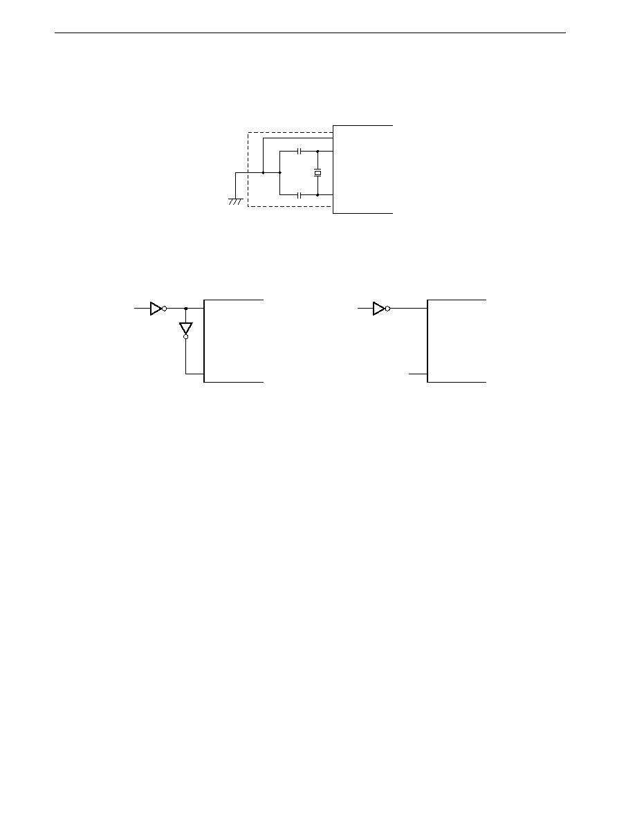
106
CHAPTER 4 CLOCK GENERATOR
Preliminary User's Manual U13987EJ1V0UM00
Figure 4-2. Clock Oscillator External Circuitry
(a) Crystal/ceramic oscillation
V
SS
X2
�
PD784938
X1
(b) External clock
EXTC bit of OSTS = 1 EXTC bit of OSTS = 0
Open
X1
X2
PD74HC04, etc.
�
PD784938
�
X1
X2
PD784938
�
Cautions 1. The oscillator should be as close as possible to the X1 and X2 pins.
2. No other signal lines should pass through the area enclosed by the dotted line.
Remark
Differences between crystal resonator and ceramic resonator
Generally speaking, the oscillation frequency of a crystal resonator is extremely stable. It is therefore ideal for
performing high-precision time management (in clocks, frequency meters, etc.).
A ceramic resonator is inferior to a crystal resonator in terms of oscillation frequency stability, but it has three
advantages: a fast oscillation start-up time, small size, and low price. It is therefore suitable for general use (when
high-precision time management is not required). In addition, there are products with a built-in capacitor, etc.,
which enable the number of parts and mounting area to be reduced.

107
CHAPTER 4 CLOCK GENERATOR
Preliminary User's Manual U13987EJ1V0UM00
4.2 Control Registers
4.2.1 Standby control register (STBC)
STBC is a register used to set the standby mode and select the internal system clock. See CHAPTER 25 STANDBY
FUNCTION for details of the standby modes.
To prevent erroneous entry into standby mode due to an inadvertent program loop, the STBC register can only be written
to by a dedicated instruction. This instruction is the MOV STBC, #byte instruction, and has a special code configuration (4 bytes).
A write is only performed if the 3rd and 4th bytes of the op code are mutual complements. If the 3rd and 4th bytes of the op code
are not mutual complements, a write is not performed, and an operand error interrupt is generated. In this case, the return
address saved in the stack area is the address of the instruction which is the source of the error. The error source address can
thus be found from the return address saved on the stack area.
An endless loop will result if restore from an operand error is simply performed with an RETB instruction.
Because the operand error interrupt occurs only when the program hangs up (only the correct dedicated instruction is
generated with the NEC's assembler RA78K4 when MOV STBC, #byte is described), make sure that the operand error interrupt
processing program initializes the system.
Other write instructions ("MOV STBC, A", "AND STBC, #byte", "SET1 STBC.7", etc.) are ignored, and no operation is
performed. That is, a write is not performed on the STBC, and an interrupt such as an operand error interrupt is not generated.
STBC can be read at any time with a data transfer instruction.
RESET input sets STBC to 30H.
The format of STBC is shown in Figure 4-3.
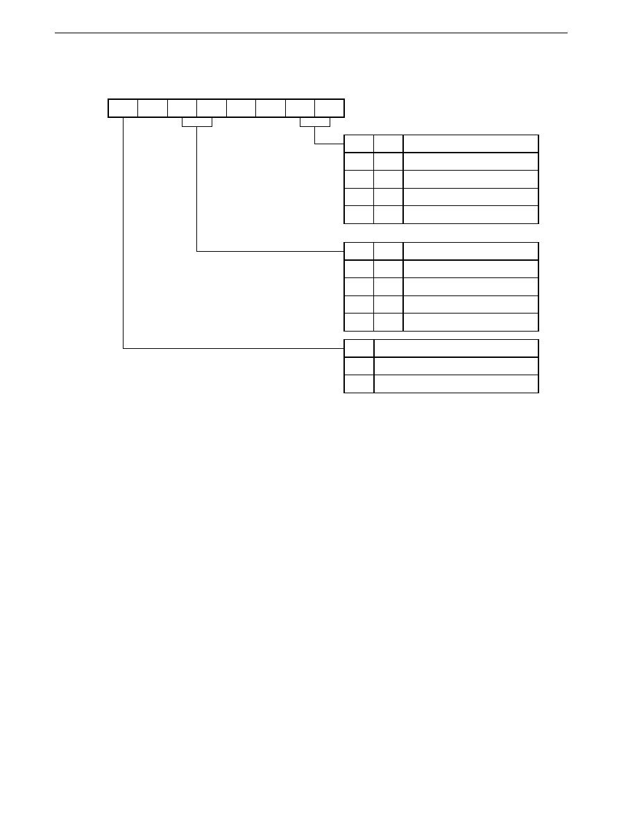
108
CHAPTER 4 CLOCK GENERATOR
Preliminary User's Manual U13987EJ1V0UM00
Figure 4-3. Standby Control Register (STBC) Format
SELOSC
0
CK1
CK0
�
0
STP
HLT
7
6
5
4
3
2
1
0
STBC
0FFC0H
Address
30H
After reset
R/W
R/W
STP
0
0
1
1
Operating Mode
Normal mode
HALT mode
STOP mode
IDLE mode
HLT
0
1
0
1
CK1
0
0
1
1
Internal System Clock Selection
f
XX
(12.58 MHz)
f
XX
/2 (6.29 MHz)
f
XX
/4 (3.15 MHz)
f
XX
/8 (1.57 kHz)
CK0
0
1
0
1
(f
XX
= 12.58 MHz)
SELOSC
0
1
Oscillation Frequency Control
6.29 MHz
12.58 MHz
Cautions 1. Overwrite the SELOSC bit after performing the following settings.
�
Stop the IEBus (Set bit 7 of the bus control register (BCR) to "0").
�
If the watch Timer is operated with the main clock selected, stop the watch timer (Set bit 3 of the
watch timer mode register (WM) to "0").
2. If the above settings are not performed, the IEBus and watch timer may perform incorrectly.

109
CHAPTER 4 CLOCK GENERATOR
Preliminary User's Manual U13987EJ1V0UM00
4.2.2 Oscillation stabilization time specification register (OSTS)
OSTS is a register used to select the oscillation stabilization time.
OSTS can be written to only by an 8-bit transfer instruction.
RESET input clears OSTS to 00H.
The format of OSTS is shown in Figure 4-4.
Figure 4-4. Oscillation Stabilization Time Specification Register (OSTS) Format
7
0
OSTS
6
0
5
0
4
0
3
0
2
OSTS2
1
OSTS1
0
OSTS0
Oscillation stabilization time selection
(see Figure 25-4 for details)
Address
After reset
R/W
R/W
00H
0FFCFH
Caution
When using the regulator (refer to CHAPTER 5 REGULATOR), set a value of at least 10.4 ms, taking in
consideration the regulator output stabilization time.

110
CHAPTER 4 CLOCK GENERATOR
Preliminary User's Manual U13987EJ1V0UM00
4.3 Clock Generator Operation
4.3.1 Clock oscillator
(1) When using crystal/ceramic oscillation
The clock oscillator starts oscillating when the RESET signal is input, and stops oscillation when the STOP mode is set by
the standby control register (STBC). Oscillation is resumed when the STOP mode is released.
(2) When using external clock
The clock oscillator supplies the clock input from the X1 pin to the internal circuitry when the RESET signal is input.
4.3.2 Divider
The divider performs 1/1, 1/2, 1/4, or 1/8 scaling of the clock oscillator output, and supplies the resulting clock to the CPU,
watchdog timer, noise elimination circuit, clocked serial interface (CSI), A/D converter, PWM, interrupt control circuit, and local
bus interface. The division ratio is specified by the CK0 and CK1 bits of the standby control register (STBC).
Controlling the division ratio to match the speed required by the CPU enables the overall power consumption to be reduced.
Also, the operating speed can be selected to match the supply voltage.
When RESET is input, the lowest speed (1/8) is selected.
If the division ratio of the divider circuit is changed, the maximum time shown in Table 4-1 is required to change the division
ratio, depending on the clock selected before change.
Instruction execution continues even while the division ratio is changed, and the clock is supplied with the previous division
ratio until the division ratio has been completely changed.
Table 4-1. Time Required to Change Division Ratio
Previous Division Ratio
Maximum Time Required for Change
None
11/f
XX
1/2
12/f
XX
1/4
8/f
XX
1/8
8/f
XX
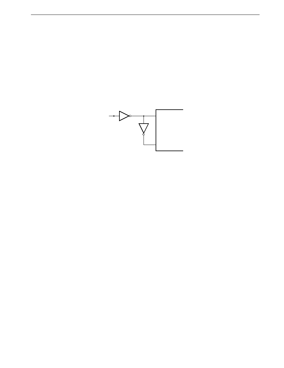
111
CHAPTER 4 CLOCK GENERATOR
Preliminary User's Manual U13987EJ1V0UM00
4.4 Cautions
The following cautions apply to the clock generator.
4.4.1 When an external clock is input
(1) When an external clock is input, this should be performed with a HCMOS device, or a device with the equivalent drive
capability.
(2) A signal should not be extracted from the X1 and X2 pins. If a signal is extracted, it should be extracted from point a in Figure
4-5.
Figure 4-5. Signal Extraction with External Clock Input
X1
�
PD74HC04, etc.
�
PD784938
X2
a
(3) The wiring connecting the X1 pin to the X2 pin via an inverter, in particular, should be made as short as possible.
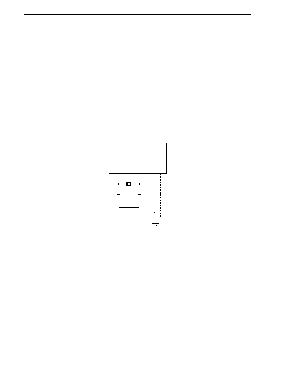
112
CHAPTER 4 CLOCK GENERATOR
Preliminary User's Manual U13987EJ1V0UM00
4.4.2 When crystal/ceramic oscillation is used
(1) As the oscillator is a high-frequency analog circuit, considerable care is required.
The following points, in particular, require attention.
� Keep the wiring length as short as possible.
� Do not cross the wiring with the other signal lines.
� Do not route the wiring near a signal line through which a high fluctuating current flows.
� Always make the ground point of the oscillator capacitor the same potential as V
SS
. Do not ground the capacitor
to a ground pattern through which a high current flows.
� Do not fetch signals from the oscillator.
If oscillation is not performed normally and stably, the microcontroller will not be able to operate normally and
stably, either. Also, if a high-precision oscillation frequency is required, consultation with the oscillator manufacturer
is recommended.
Figure 4-6. Cautions on Resonator Connection
V
SS
X2
X1
�
PD784938
Cautions 1. The oscillator should be as close as possible to the X1 and X2 pins.
2. No other signal lines should pass through the area enclosed by the broken lines.
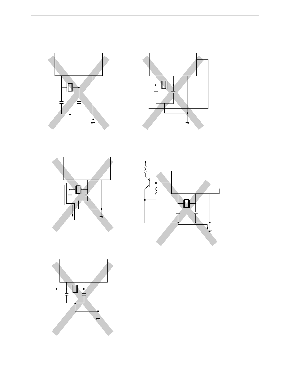
113
CHAPTER 4 CLOCK GENERATOR
Preliminary User's Manual U13987EJ1V0UM00
Figure 4-7. Incorrect Example of Resonator Connection
(a) Wiring of connected circuits is too long
(b) Crossed signal lines
PD784938
�
X1
X2
V
SS
PD784938
�
X1
Pnm
X2
V
SS
(c) Wiring near high fluctuating current
(d) Current flowing through ground line of
oscillator
(Potentials at points A, B, and C fluctuate)
(e) Signal extracted
PD784938
�
X1
X2
V
SS
PD784938
�
X1
X2
V
SS
High
fluctuating
current
PD784938
�
X1
X2
V
SS
B
A
C
V
DD
Pnm
High current

114
CHAPTER 4 CLOCK GENERATOR
Preliminary User's Manual U13987EJ1V0UM00
(2) When the device is powered on, and when restoring from the STOP mode, sufficient time must be allowed for the oscillation
to stabilize. Generally speaking, the time required for oscillation stabilization is several milliseconds when a crystal
resonator is used, and several hundred microseconds when a ceramic resonator is used.
An adequate oscillation stabilization period should be secured by the following means:
<1>
When powered-on: RESET input (reset period)
<2>
When returning from STOP mode:
(i) RESET input (reset period)
(ii) Time of the oscillation stabilization timer that automatically starts at the valid edge of NMI, INTP4, or INTP5
signal
Note
(set by the oscillation stabilization time specification register (OSTS))
Note For INTP4 and INTP5, when masking is released and macro service is disabled.
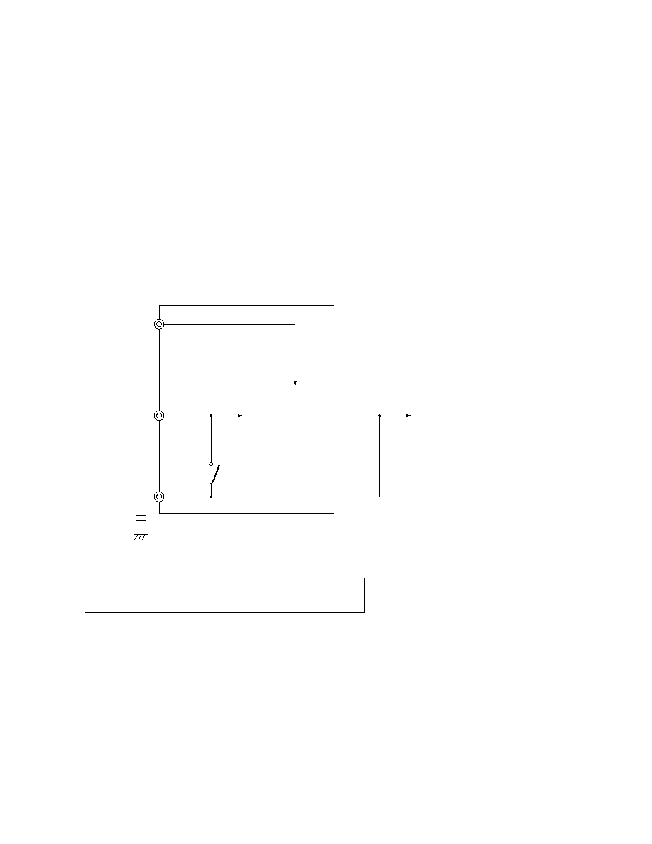
115
Preliminary User's Manual U13987EJ1V0UM00
CHAPTER 5 REGULATOR
5.1 Outline of Regulator
The
�
PD784938 has a regulator that reduces the power consumption of the device (a circuit for low voltage
operation). The operation of this regulator is controlled by the input level of the REGOFF pin. When the REGOFF
pin is made high, the regulator is turned OFF; when it is made low, the regulator is turned ON.
When the regulator is turned ON, it enables to reduce the power consumption.
To stabilize the output voltage of the regulator, connect a capacitor for stabilizing the regulator (approximately 1
�
F) to the REGC pin.
Apply the same level as V
DD
to the REGC pin when the regulator is stopped. Figure 5-1 shows the block diagram
of the peripherals of the regulator.
Figure 5-1. Regulator Peripherals Block Diagram
� Processing of REGC pin
Regulator ON
Connects capacitance for regulator stabilization
Regulator OFF
Supplies power supply voltage
Caution
For the oscillation stabilization time when the stop mode is released, set a value of at least 10.4 ms with
the oscillation stabilization time specification register (OSTS), taking in consideration the regulator
output oscillation stabilization time. (refer to CHAPTER 25 STANDBY FUNCTION.)
REGOFF
V
DD
REGC
1 F
Regulator
Low level: Regulator ON
High level: Regulator OFF
Internal supply voltage
(Supplied to CPU and each peripheral circuit)
�

116
Preliminary User's Manual U13987EJ1V0UM00
[MEMO]
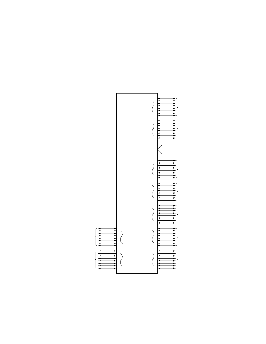
117
Preliminary User's Manual U13987EJ1V0UM00
CHAPTER 6 PORT FUNCTIONS
6.1 Digital Input/Output Ports
The
�
PD784938 is provided with the ports shown in Figure 6-1, enabling various kinds of control to be performed. The function
of each port is shown in Table 6-1. For ports 0 to 6, port 9, and port 10, use of an on-chip pull-up resistor can be specified by
software when used as input ports.
Figure 6-1. Port Configuration
Port 0
Port 1
Port 3
Port 4
Port 5
Port 6
Port 7
8
Port 2
P00
P07
P10
P17
P30
P37
P40
P47
P50
P57
P60
P67
P70
P77
P20 to P27
Port 9
Port 10
P90
P97
P100
P107
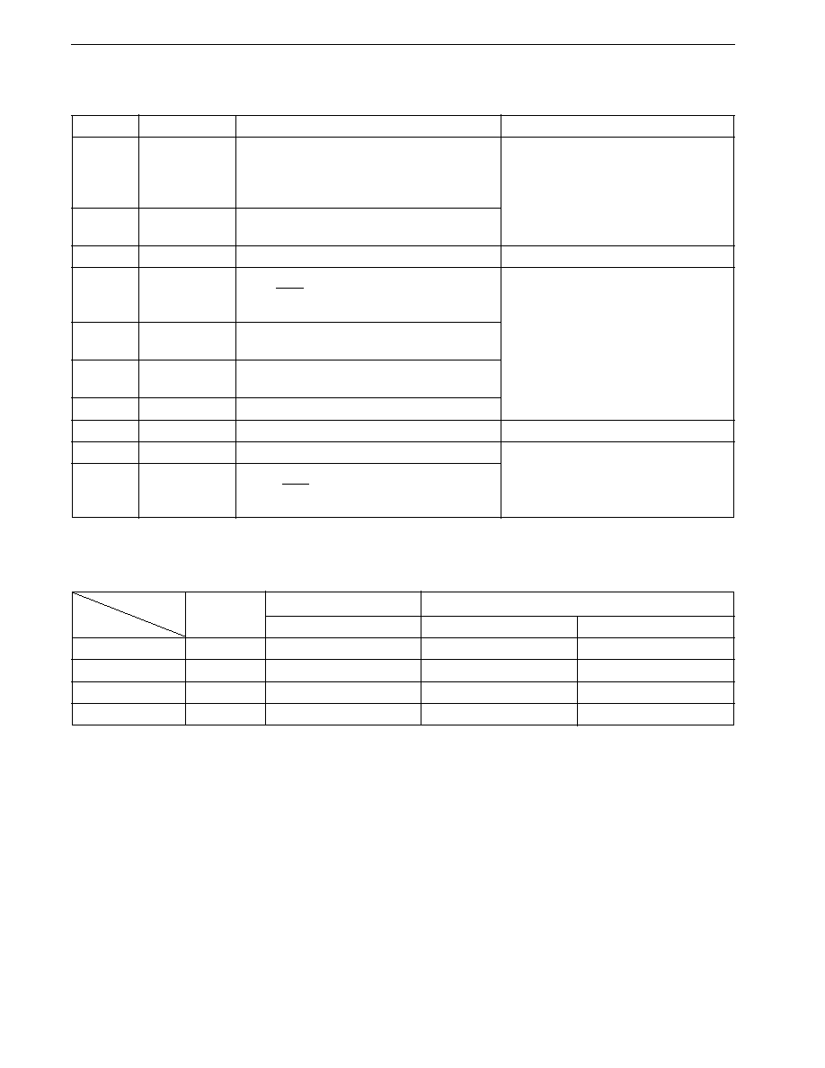
CHAPTER 6 PORT FUNCTIONS
118
Preliminary User's Manual U13987EJ1V0UM00
Table 6-1. Port Functions
Port Name
Pin Names
Functions
Software Pull-Up Specification
Port 0
P00 to P07
� Input/output can be specified in 1-bit units.
Input mode pins specified at once
� Can also operate as 4-bit real-time output ports
(P00 to P03, P04 to P07).
� Can drive a transistor.
Port 1
P10 to P17
� Input/output can be specified in 1-bit units.
� LED drive capability.
Port 2
P20 to P27
� Input port
6-bit unit (P22 to P27)
Port 3
P30 to P37
� Input/output can be specified in 1-bit units.
Input mode pins specified at once
� P32/SCK0 pin and P33/SO0 pin can be set in
N-ch open-drain mode.
Port 4
P40 to P47
� Input/output can be specified in 1-bit units.
� Can drive an LED.
Port 5
P50 to P57
� Input/output can be specified in 1-bit units.
� LED drive capability.
Port 6
P60 to P67
� Input/output can be specified in 1-bit units.
Port 7
P70 to P77
� Input/output can be specified in 1-bit units.
--
Port 9
P90 to P97
� Input/output can be specified in 1-bit units.
Input mode pin specified at once
Port 10
P100 to P107
� Input/output can be specified in 1-bit units.
� P105/SCK3 pin and P107/SO3 pin can be set in
N-ch open-drain mode.
Table 6-2. Number of Input/Output Ports
Input/Output
Total
Input Mode
Output Mode
Ports
Software Pull-Up Resistor
Direct LED Drive
Direct Transistor Drive
Input ports
8
6
--
--
Input/output ports
72
64
24
0
Output ports
0
--
0
8
Total
80
70
24
8
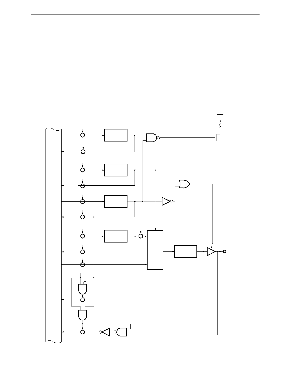
119
CHAPTER 6 PORT FUNCTIONS
Preliminary User's Manual U13987EJ1V0UM00
6.2 Port 0
Port 0 is an 8-bit input/output port with an output latch, and has direct transistor drive capability. Input/output can be specified
in 1-bit units by means of the port 0 mode register (PM0). Each pin incorporates a software programmable pull-up resistor.
P00 to P03 and P04 to P07 can output the buffer register (P0L, P0H) contents at any time interval as 4-bit real-time output
ports or one 8-bit real-time output port. The real-time output port control register (RTPC) is used to select whether this port is
used as a normal output port or a real-time output port.
When RESET is input, port 0 is set as an input port (output high-impedance state), and the output latch contents are undefined.
6.2.1 Hardware configuration
The port 0 hardware configuration is shown in Figure 6-2.
Figure 6-2. Port 0 Block Diagram
WR
PUOL
Pull-up resistor option register L
PUOL0
WR
RTPC
Real-time output port control register
P0LM
(P0HM)
WR
PM0
Port 0 mode register
RD
RTPC
WR
P0L
Buffer register
PM0n
(PM0m)
RD
P0L
WR
OUT
RD
P0
P0Ln
(P0Hm)
P0n
(P0m)
P 0 n
( P 0 m )
n = 0 , 1 , 2 , 3
m = 4 , 5 , 6 , 7
Trigger
Output latch
RD
PM0
V
DD
Selector
Internal
bus
RD
PUOL
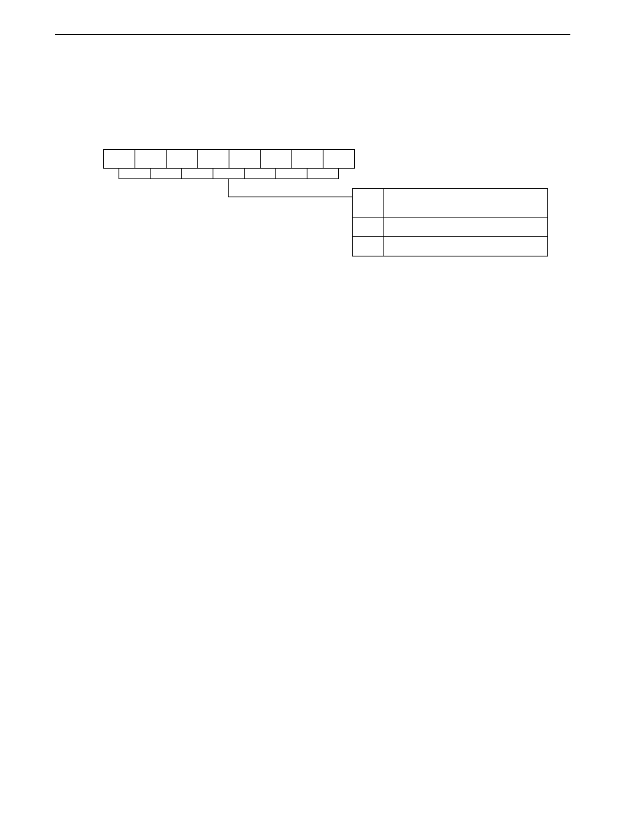
CHAPTER 6 PORT FUNCTIONS
120
Preliminary User's Manual U13987EJ1V0UM00
6.2.2 I/O mode/control mode setting
The port 0 input/output mode is set by means of the port 0 mode register (PM0) as shown in Figure 6-3.
Figure 6-3. Port 0 Mode Register (PM0) Format
7
PM07
PM0
6
PM06
5
PM05
4
PM04
3
PM03
2
PM02
1
PM01
0
PM00
Address
After reset
R/W
R/W
FFH
0FF20H
PM0n
P0n Pin Input/Output Mode Specification
(n = 0 to 7)
Output mode (output buffer on)
Input mode (output buffer off)
1
0
When port 0 is used as a real-time output port, the P0LM and P0HM bits of the real-time output port control register (RTPC)
should be set (to 1).
When P0LM and P0HM are set, the respective pin output buffer is turned on and the output latch contents are output to the
pin irrespective of the contents of PM0.
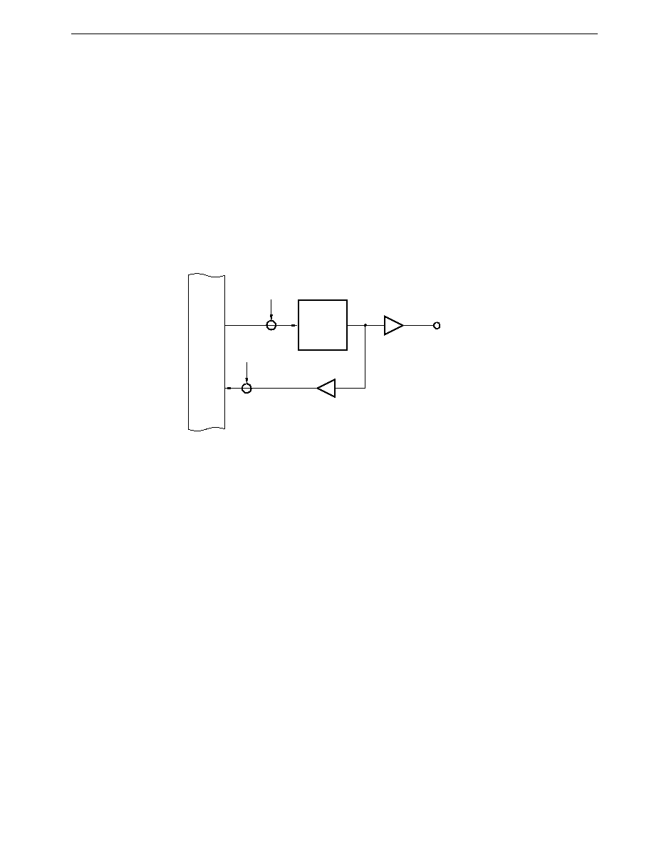
121
CHAPTER 6 PORT FUNCTIONS
Preliminary User's Manual U13987EJ1V0UM00
6.2.3 Operating status
Port 0 is an input/output port.
(1) When set as an output port
The output latch is enabled, and data transfers between the output latch and accumulator are performed by means of
transfer instructions. The output latch contents can be freely set by means of logical operation instructions. Once data has
been written to the output latch, it is retained until data is next written to the output latch
Note
.
Writes cannot be performed to the output latch of a port specified as a real-time output port. However, the output latch
contents can be read even if it is set to the real-time output port mode.
Note Including the case where another bit of the same port is manipulated by a bit manipulation instruction.
Figure 6-4. Port Specified as Output Port
P0n
n = 0 to 7
RD
OUT
WR
PORT
Internal
bus
Output
latch

CHAPTER 6 PORT FUNCTIONS
122
Preliminary User's Manual U13987EJ1V0UM00
(2) When set as an input port
The port pin level can be loaded into an accumulator by means of a transfer instruction, etc. In this case, too, writes can
be performed to the output latch, and data transferred from the accumulator by a transfer instruction, etc., is stored in all
output latches irrespective of the port input/output specification. However, since the output buffer of a bit specified as an
input port is high-impedance, the data is not output to the port pin (when a bit specified as input is switched to an output
port, the output latch contents are output to the port pin). Also, the contents of the output latch of a bit specified as an input
port cannot be loaded into an accumulator.
Figure 6-5. Port Specified as Input Port
Output
latch
P0n
n = 0 to 7
RD
IN
WR
PORT
Internal
bus
Caution
A bit manipulation instruction manipulates one bit as the result, but accesses the port in 8-bit units.
Therefore, if a bit manipulation instruction is used on a port with a mixture of input and output pins, the
contents of the output latch of pins specified as inputs will be undefined (excluding bits manipulated with
a SET1 or CLR1 instruction, etc.). Particular care is required when there are bits which are switched
between input and output.
Caution is also required when manipulating the port with other 8-bit arithmetic instructions.

123
CHAPTER 6 PORT FUNCTIONS
Preliminary User's Manual U13987EJ1V0UM00
6.2.4 On-chip pull-up resistors
Port 0 incorporates pull-up resistors. Use of these internal resistors when pull-up is necessary enables the number of parts
and the mounting area to be reduced.
Whether or not an on-chip pull-up resistor is to be used can be specified for each pin by means of the PUOL0 bit of the pull-
up resistor option register L (PUOL) and the port 0 mode register (PM0). When PUOL0 is 1, the on-chip pull-up resistors of the
pins for which input is specified by PM0 are enabled (PM0n = 1, n = 0 to 7).
Figure 6-6. Pull-Up Resistor Option Register L (PUOL) Format
7
0
PUOL
6
PUOL6
5
PUOL5
4
PUOL4
3
PUOL3
2
PUOL2
1
PUOL1
0
PUOL0
Address
After reset
R/W
R/W
00H
0FF4EH
PUOL0
Port 0 Pull-Up Resistor Specification
Not used in port 0
Used in port 0
1
0
Remark
When STOP mode is entered, setting PUOL to 00H is effective for reducing the current consumption.

CHAPTER 6 PORT FUNCTIONS
124
Preliminary User's Manual U13987EJ1V0UM00
Figure 6-7. Pull-Up Resistor Specification (Port 0)
P06
Input
buffer
P07
P05
P01
P00
V
DD
Port 0 mode register
(PM0)
PUOL0
(PUOL)
Internal
bus
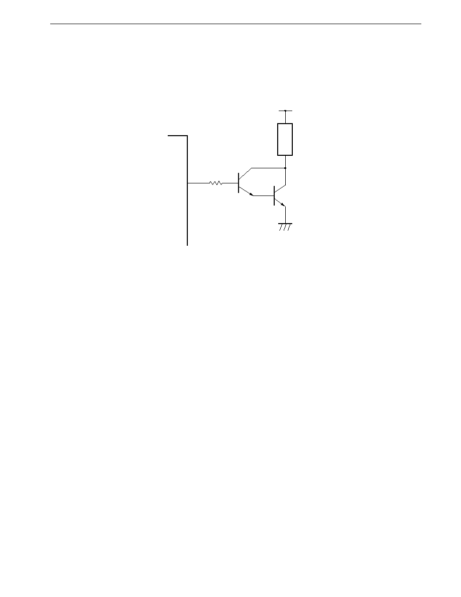
125
CHAPTER 6 PORT FUNCTIONS
Preliminary User's Manual U13987EJ1V0UM00
6.2.5 Transistor drive
In port 0, the output buffer high-level side drive capability has been increased, allowing active-high direct transistor drive.
An example of the connection is shown in Figure 6-8.
Figure 6-8. Example of Transistor Drive
P0n
V
DD
Load
CHAPTER 6 PORT FUNCTIONS
126
Preliminary User's Manual U13987EJ1V0UM00
6.3 Port 1
Port 1 is an 8-bit input/output port with an output latch. Input/output can be specified in 1-bit units by setting the port 1 mode
register (PM1). Each pin incorporates a programmable pull-up resistor. This port has direct LED drive capability.
In addition to their input/output port function, P10 to P14 also have an alternate function as serial interface pins. The operation
mode can be specified bit-wise by setting the port 1 mode control register (PMC1), as shown in Table 6-3. The level of any pin
can be read and tested at any time irrespective of the alternate-function operation.
When RESET is input, port 1 is set as an input port (output high-impedance state), and the output latch contents are undefined.
Table 6-3. Port 1 Operation Modes
Pin Name
Port Mode
Control Signal I/O Mode
Operation to Operate Control Pin
P10, P11
I/O port
--
--
P12
ASCK2 I/O/SCK2 I/O
Setting PMC12 bit of PMC1 to 1
P13
RxD2 input/SI2 input
Setting PMC13 bit of PMC1 to 1
P14
TxD2 output/SO2 output
Setting PMC14 bit of PMC1 to 1
P15 to P17
--
--
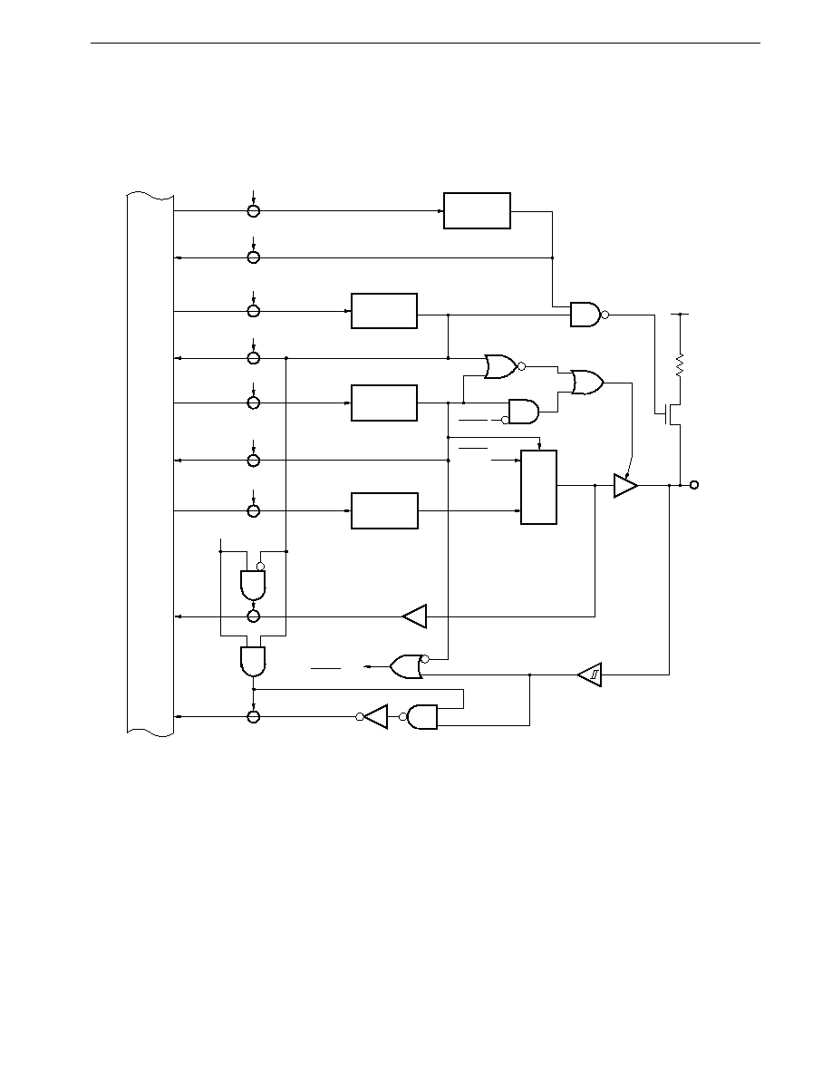
127
CHAPTER 6 PORT FUNCTIONS
Preliminary User's Manual U13987EJ1V0UM00
6.3.1 Hardware configuration
The port 1 hardware configuration is shown in Figures 6-9 to 6-12.
Figure 6-9. P12 (Port 1) Block Diagram
P12
WR
PUOL
V
DD
RD
PUOL
WR
PMC1
WR
P1
ASCK2,
SCK2 input
RD
PMC1
External
SCK2
WR
PM1
SCK2
output
PUOL1
PMC12
P12
PM12
RD
PM1
RD
P1
Pull-up resistor option register L
Port 1 mode register
Output latch
Selector
Internal
bus
Port 1 mode control register
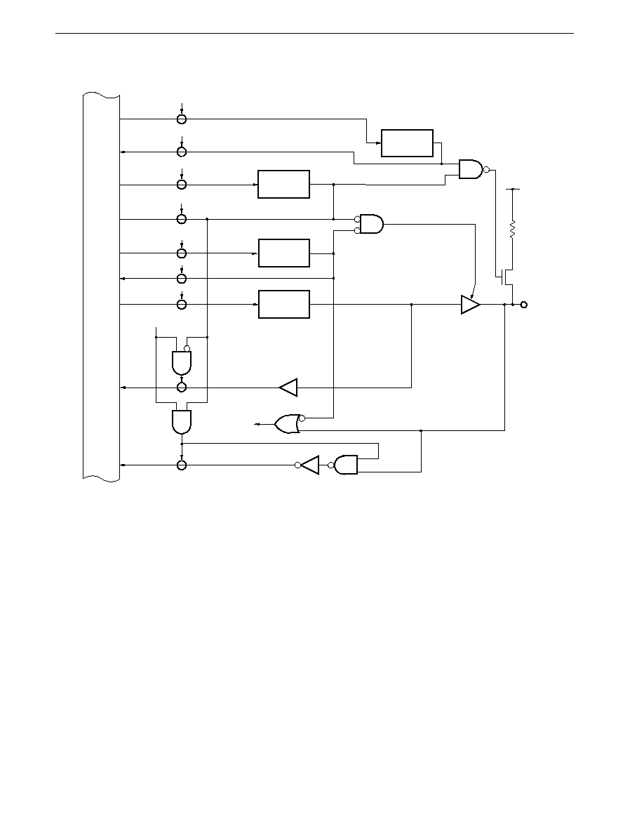
CHAPTER 6 PORT FUNCTIONS
128
Preliminary User's Manual U13987EJ1V0UM00
Figure 6-10. P13 (Port 1) Block Diagram
P13
V
DD
WR
PUOL
WR
P1
SI2, RxD2 input
RD
PUOL
WR
PM1
WR
PMC1
RD
PMC1
PUOL1
PM13
P13
PMC13
RD
PM1
RD
P1
Pull-up resistor option register L
Port 1 mode register
Output latch
Internal
bus
Port 1 mode control register
129
CHAPTER 6 PORT FUNCTIONS
Preliminary User's Manual U13987EJ1V0UM00
Figure 6-11. P14 (Port 1) Block Diagram
WR
PUOL
RD
PUOL
WR
PMC1
WR
P1
RD
PMC1
TxD2/SO2 output
PUOL1
PMC14
P14
PM14
WR
PM1
P14
V
DD
RD
PM1
RD
P1
Pull-up resistor option register L
Port 1 mode register
Output latch
Internal
bus
Port 1 mode control register
Selector

CHAPTER 6 PORT FUNCTIONS
130
Preliminary User's Manual U13987EJ1V0UM00
Figure 6-12. Block Diagram of P10, P11, and P15 to P17 (Port 1)
P1n
n = 0, 1, 5 to 7
WR
PUOL
PUOL1
V
DD
RD
PUOL
WR
PM1
PM1n
WR
P1
P1n
RD
PM1
RD
P1
Pull-up resistor option register L
Port 1 mode register
Output latch
Internal
bus
131
CHAPTER 6 PORT FUNCTIONS
Preliminary User's Manual U13987EJ1V0UM00
6.3.2 I/O mode/control mode setting
The port 1 input/output mode is set for each pin by means of the port 1 mode register (PM1) as shown in Figure 6-13.
In addition to their input/output port function, P12 to P14 also have an alternate function as serial interface pins, and the
control mode is specified by setting the port 1 mode control register (PMC1) as shown in Figure 6-14.
Figure 6-13. Port 1 Mode Register (PM1) Format
7
PM17
PM1
6
PM16
5
PM15
4
PM14
3
PM13
2
PM12
1
PM11
0
PM10
Address
After reset
R/W
R/W
FFH
0FF21H
PM1n
P1n Pin Input/Output Mode Specification
(n = 0 to 7)
Output mode (output buffer on)
Intput mode (output buffer off)
1
0
Figure 6-14. Port 1 Mode Control Register (PMC1) Format
7
0
PMC1
6
0
5
0
4
PMC14
3
PMC13
2
PMC12
1
0
0
0
Address
After reset
R/W
R/W
00H
0FF41H
PMC12
P12 Pin Control Mode Specification
Input/output port mode
ASCK2/SCK2 input/output mode
1
0
PMC13
P13 Pin Control Mode Specification
Input/output port mode
RxD2/SI2 input mode
1
0
PMC14
P14 Pin Control Mode Specification
Input/output port mode
TxD2/SO2 output mode
1
0
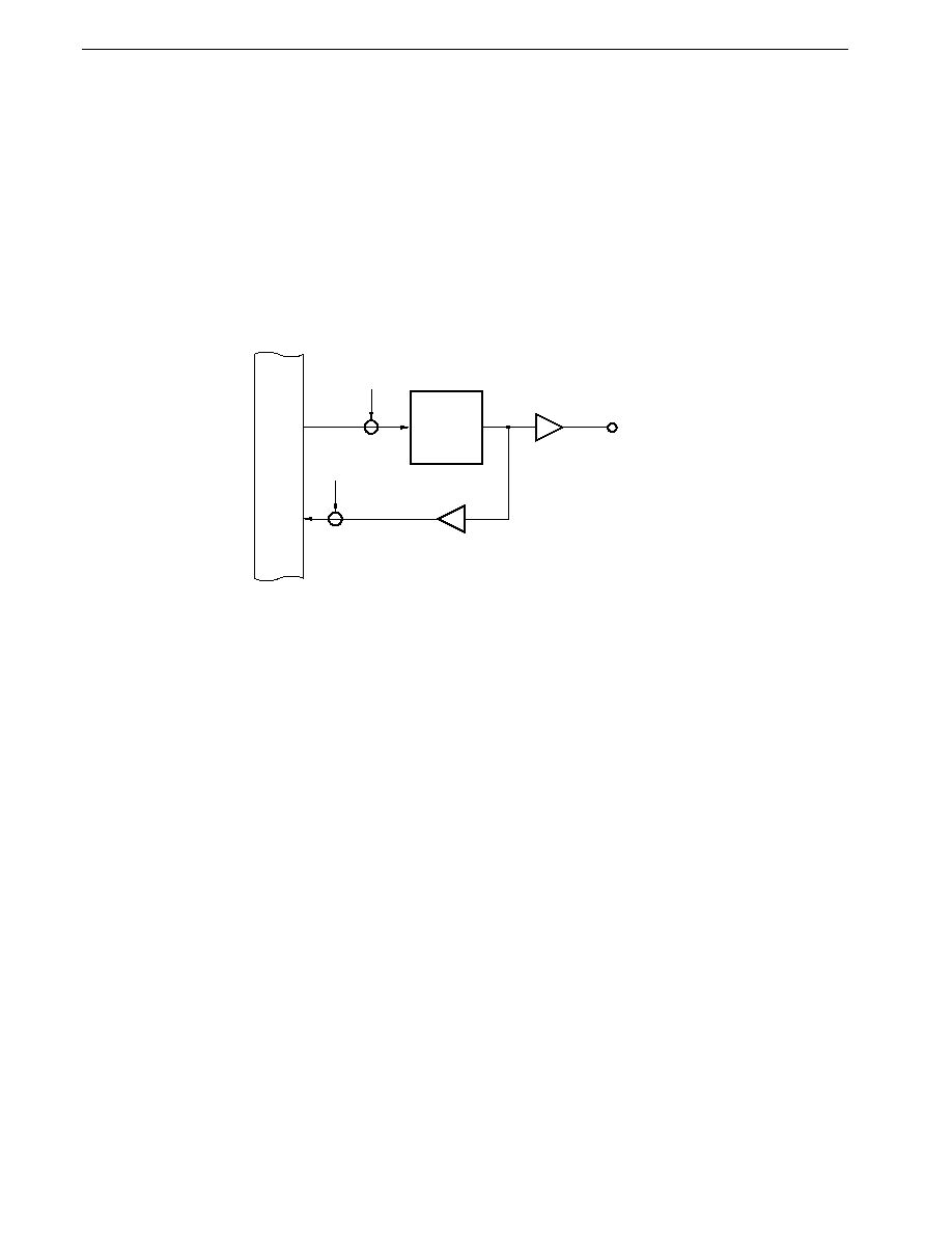
CHAPTER 6 PORT FUNCTIONS
132
Preliminary User's Manual U13987EJ1V0UM00
6.3.3 Operating status
Port 1 is an input/output port. Pins P12 to P14 have an alternate function as serial interface pins.
(1) When set as an output port
The output latch is enabled, and data transfers between the output latch and accumulator are performed by means of
transfer instructions. The output latch contents can be freely set by means of logical operation instructions. Once data has
been written to the output latch, it is retained until data is next written to the output latch
Note
.
Note Including the case where another bit of the same port is manipulated by a bit manipulation instruction.
Figure 6-15. Port Specified as Output Port
Internal
bus
Output
latch
P1n
n = 0 to 7
RD
OUT
WR
PORT

133
CHAPTER 6 PORT FUNCTIONS
Preliminary User's Manual U13987EJ1V0UM00
(2) When set as an input port
The port pin level can be loaded into an accumulator by means of a transfer instruction, etc. In this case, too, writes can
be performed to the output latch, and data transferred from the accumulator by a transfer instruction, etc., is stored in all
output latches irrespective of the port input/output specification. However, since the output buffer of a bit specified as an
input port is high-impedance, the data is not output to the port pin (when a bit specified as input is switched to an output
port, the output latch contents are output to the port pin). Also, the contents of the output latch of a bit specified as an input
port cannot be loaded into an accumulator.
Figure 6-16. Port Specified as Input Port
Output
latch
P1n
n = 0 to 7
RD
IN
WR
PORT
Internal
bus
Caution
A bit manipulation instruction manipulates one bit as the result, but accesses the port in 8-bit units.
Therefore, if a bit manipulation instruction is used on a port that has the I/O mode or port mode and control
mode, the contents of the output latch of the pin set in the input mode or control mode become undefined
(excluding bits manipulated with a SET1 or CLR1 instruction, etc.). Particular care is required when there
are bits which are switched between input and output.
Caution is also required when manipulating the port with other 8-bit arithmetic instructions.
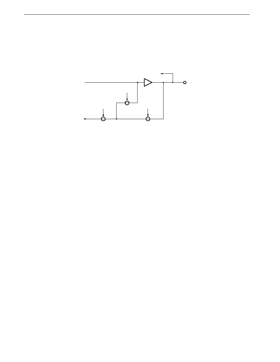
CHAPTER 6 PORT FUNCTIONS
134
Preliminary User's Manual U13987EJ1V0UM00
(3) When specified as control signal input/output
P12 to P14 (by setting (to 1) bits of the port 1 mode control register (PMC1)) can be used as control signal inputs or outputs
bit-wise irrespective of the setting of the port 1 mode register (PM1). When a pin is used as a control signal, the control
signal status can be seen by executing a port read instruction.
Figure 6-17. Control Specification
P1n
n = 2 to 4
PM1n = 0
PM1n = 1
RD
Control
(output)
Internal
bus
Control (input)
(a) When port is control signal output
When the port 1 mode register (PM1) is set (to 1), the control signal pin level can be read by executing a port read
instruction.
When PM1 is reset (to 0), the
�
PD784938 internal control signal status can be read by executing a port read instruction.
(b) When port is control signal input
When the port 1 mode register (PM1) is set (to 1), control signal pin level can be read by executing a port read
instruction.
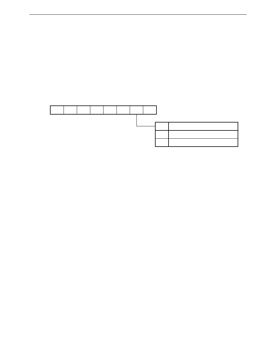
135
CHAPTER 6 PORT FUNCTIONS
Preliminary User's Manual U13987EJ1V0UM00
6.3.4 On-chip pull-up resistors
Port 1 incorporates pull-up resistors. Use of these internal resistors when pull-up is necessary enables the number of parts
and the mounting area to be reduced.
Whether or not an on-chip pull-up resistor is to be used can be specified for each pin by means of the PUOL1 bit of the pull-
up resistor option register L (PUOL) and the port 1 mode register (PM1). When PUOL1 is 1, the on-chip pull-up resistors of the
pins for which input is specified by PM1 are enabled (PM1n = 1, n = 0 to 7).
Also, the specification for use of the pull-up resistor is also valid for pins specified as control signal output pins (pull-up
resistors are also connected to pins that function as control signal output pins). Therefore, if you do not want to connect the pull-
up resistors with the control signal output pin, the contents of the corresponding bits of PM1 should be set to 0 (output mode).
Figure 6-18. Pull-Up Resistor Option Register L (PUOL) Format
7
0
PUOL
6
PUOL6
5
PUOL5
4
PUOL4
3
PUOL3
2
PUOL2
1
PUOL1
0
PUOL0
Address
After reset
R/W
R/W
00H
0FF4EH
PUOL1
Port 1 Pull-Up Resistor Specification
Not used in port 1
Used in port 1
1
0
Remark
When STOP mode is entered, setting PUOL to 00H is effective for reducing the current consumption.
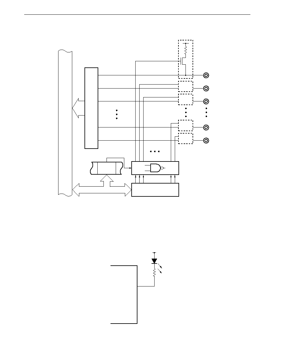
CHAPTER 6 PORT FUNCTIONS
136
Preliminary User's Manual U13987EJ1V0UM00
Figure 6-19. Pull-Up Resistor Specification (Port 1)
P16
Input
buffer
P17
P15
P11
P10
V
DD
Port 1 mode register
(PM1)
PUOL1
(PUOL)
Internal
bus
6.3.5 Direct LED drive
In port 1, the output buffer low-level side drive capability has been reinforced allowing active-low direct LED drive. An example
of such use is shown in Figure 6-20.
Figure 6-20. Example of Direct LED Drive
�
PD784938
P1n
(n = 0 to 7)
V
DD

137
CHAPTER 6 PORT FUNCTIONS
Preliminary User's Manual U13987EJ1V0UM00
6.4 Port 2
Port 2 is an 8-bit input-only port. P22 to P27 incorporate a software programmable pull-up resistor. As well as operating as
input ports, port 2 pins also operate as control signal input pins, such as external interrupt signal pins (see Table 6-4). All 8 pins
are Schmitt-triggered inputs to prevent misoperation due to noise.
Table 6-4. Port 2 Operation Modes
Port Name
Function
P20
Input port/NMI input
Note
P21
Input port/INTP0 input/CR11 capture trigger input/
timer/event counter 1 count clock/real-time output port trigger signal
P22
Input port/INTP1 input/CR22 capture trigger input
P23
Input port/INTP2 input/CI input
P24
Input port/INTP3 input/CR02 capture trigger input/
timer/event counter 0 count clock
P25
Input port/INTP4 input/ASCK input/SCK1 input/output
P26
Input port/INTP5 input/A/D converter external trigger input
P27
Input port/SI0 input
Note NMI input is acknowledged regardless of whether interrupts are enabled or disabled.
(a) Function as port pins
The pin level can always be read or tested regardless of the alternate-function operation.
(b) Functions as control signal input pins
(i)
NMI (Non-maskable Interrupt)
The external non-maskable interrupt request input pin. Rising edge detection or falling edge detection can be
specified by setting the external interrupt mode register 0 (INTM0).
(ii) INTP0 to INTP5 (Interrupt from Peripherals)
External interrupt request input pins. When the valid edge specified by the external interrupt mode registers 0,
1 (INTM0/INTM1) is detected an interrupt is generated (see CHAPTER 22 EDGE DETECTION FUNCTION).
In addition, pins INTP0 to INTP3 and INTP5 are also used as external trigger input pins with the various functions
shown below.
� INTP0 ....... Timer/event counter 1 capture trigger input pin
External count clock input pin
Real-time output port trigger input pin
� INTP1 ....... Timer/event counter 2 capture register (CR22) capture trigger input pin
� INTP2 ....... Timer/event counter 2 external count clock input pin
Capture/compare register (CR21) capture trigger input pin
� INTP3 ....... Timer/event counter 0 capture trigger input pin
Timer/event counter 0 external count clock input pin
� INTP5 ....... A/D converter external trigger input pin

CHAPTER 6 PORT FUNCTIONS
138
Preliminary User's Manual U13987EJ1V0UM00
(iii) CI (Clock Input)
The timer/event counter 2 external clock input pin
(iv) ASCK (Asynchronous Serial Clock)
The external baud rate clock input pin
(v) SCK1 (Serial Clock 1)
The serial clock input/output pin (in 3-wire serial I/O 1 mode)
(vi) SI0 (Serial Input 0)
The serial data input pin (in 3-wire serial I/O 0 mode)
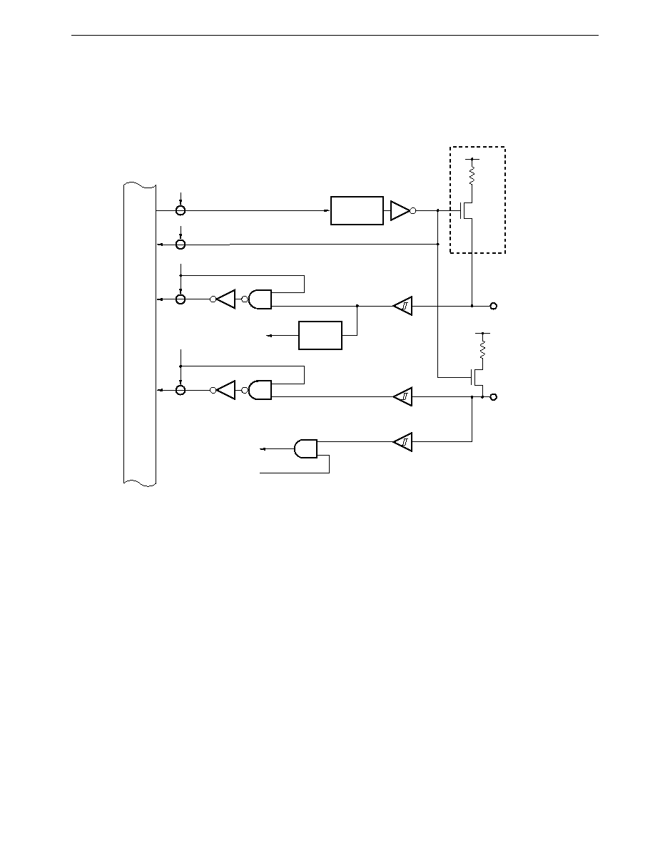
139
CHAPTER 6 PORT FUNCTIONS
Preliminary User's Manual U13987EJ1V0UM00
6.4.1 Hardware configuration
The port 2 hardware configuration is shown in Figure 6-21.
Figure 6-21. Block Diagram of P20 to P24, P26 and P27 (Port 2)
Internal
bus
RD
P2
RD
PUOL
WR
PUOL
SI0 input
Various interrupt
control signals
V
DD
P27
RD
P2
3-wire serial
I/O mode 0
P2n
n = 0 to 4, 6
PUOL2
Edge
detection
circuit
Note
Pull-up resistor option register L
V
DD
Note P20 and P21 do not have the circuitry enclosed by the broken lines.
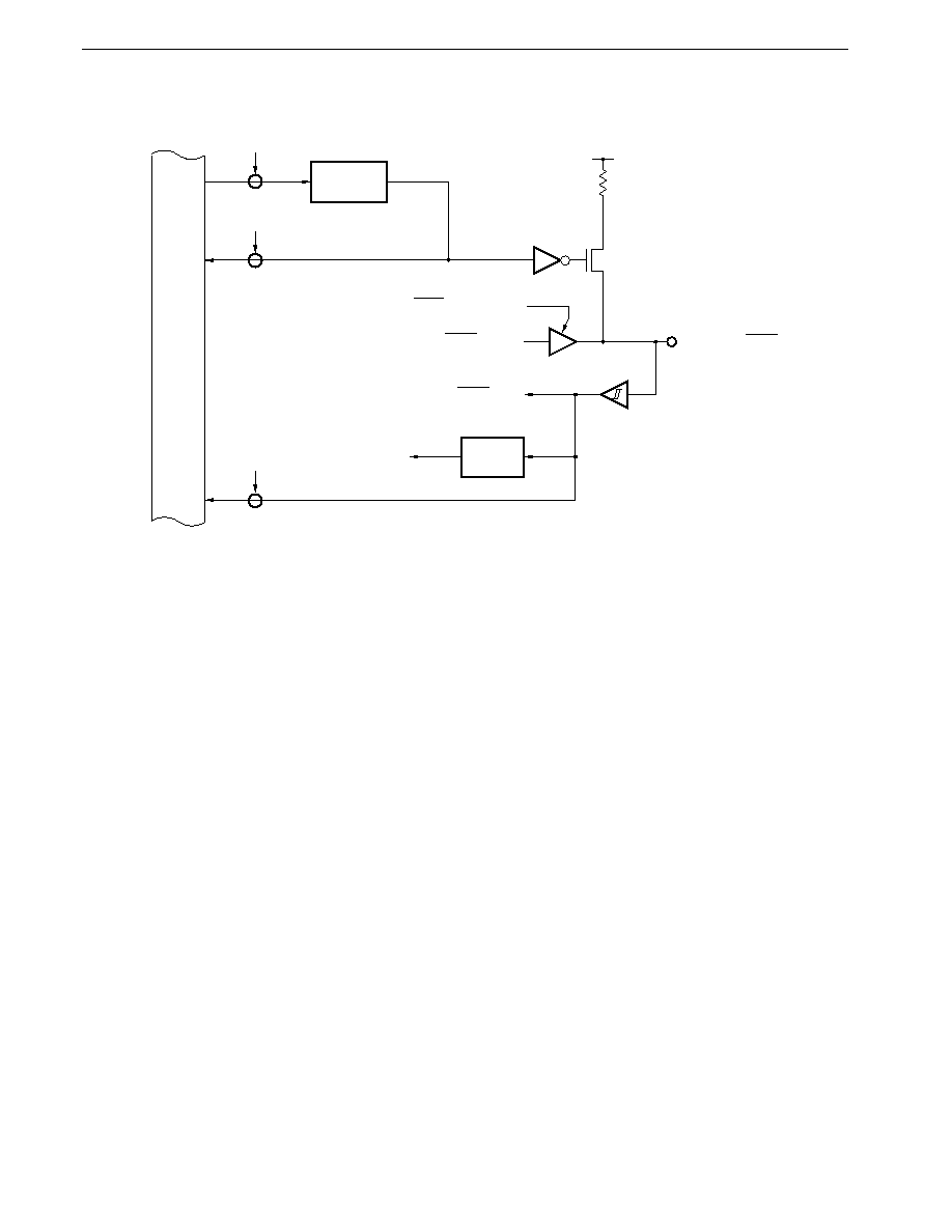
CHAPTER 6 PORT FUNCTIONS
140
Preliminary User's Manual U13987EJ1V0UM00
Figure 6-22. P25 (Port 2) Block Diagram
RD
P2
V
DD
RD
PUOL
WR
PUOL
PUOL2
INTP4 input
SCK1 output mode
SCK1 output
ASCK/SCK1 input
P25/ASCK/SCK1
Internal
bus
Edge
detection
circuit
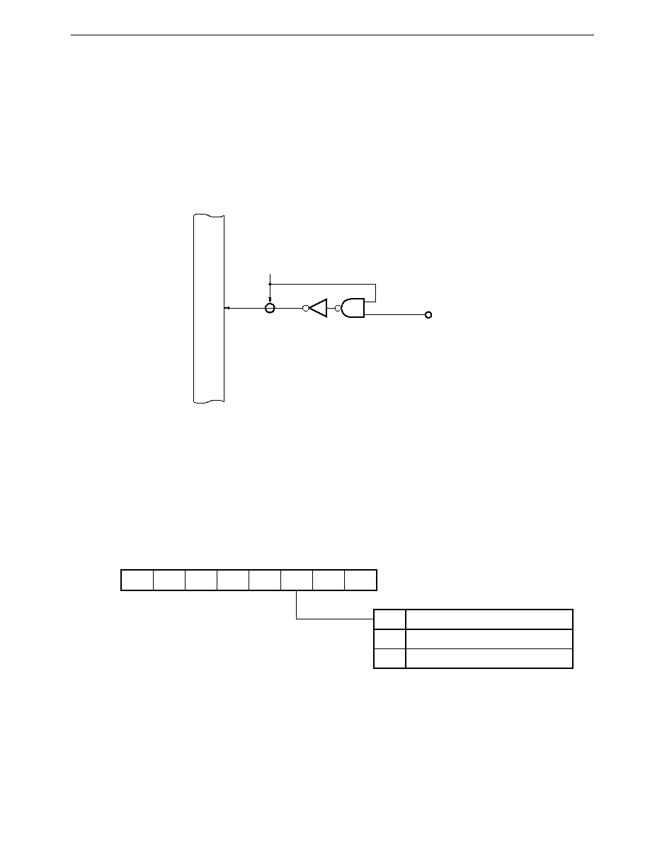
141
CHAPTER 6 PORT FUNCTIONS
Preliminary User's Manual U13987EJ1V0UM00
6.4.2 Input mode/control mode setting
Port 2 is an input-only port, and there is no register for setting the input mode.
Also, control signal input is always possible, and therefore the signal to be used is determined by the control registers for
individual on-chip hardware items.
6.4.3 Operating status
Port 2 is an input-only port, and pin levels can always be read or tested.
Figure 6-23. Port Specified as Input Port
Internal
bus
P2n
n = 0 to 7
RD
IN
6.4.4 On-chip pull-up resistors
P22 to P27 incorporate pull-up resistors. Use of these internal resistors when pull-up is necessary enables the number of
parts and the mounting area to be reduced.
Whether or not an on-chip pull-up resistor is to be used can be specified for all six pins, P22 to P27, together by means of
the PUOL2 bit of the pull-up resistor option register L (PUOL) (bit-wise specification is not possible).
P20 and P21 do not incorporate a pull-up resistor.
Figure 6-24. Pull-Up Resistor Option Register L (PUOL) Format
7
0
PUOL
6
PUOL6
5
PUOL5
4
PUOL4
3
PUOL3
2
PUOL2
1
PUOL1
0
PUOL0
Address
After reset
R/W
R/W
00H
0FF4EH
PUOL2
Port 2 Pull-Up Resistor Specification
Not used in port 2
Used in pins P22 to P27
1
0
Remark
When STOP mode is entered, setting PUOL to 00H is effective for reducing the current consumption.
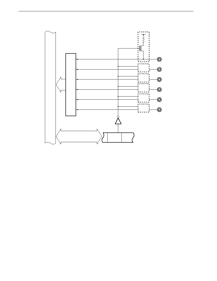
CHAPTER 6 PORT FUNCTIONS
142
Preliminary User's Manual U13987EJ1V0UM00
Figure 6-25. Pull-Up Specification (Port 2)
P23
V
DD
Pull-up resistor option register L (PUOL)
PUOL2
Input
buffer
Internal
bus
P22
P24
P25
P26
P27
Caution
As P22 to P26 are not pulled up immediately after a reset, an interrupt request flag may be set depending
on the function of the alternate function (INTP1 to INTP5). Therefore, the interrupt request flags should
be cleared after specifying pull-up in the initialization routine.

143
CHAPTER 6 PORT FUNCTIONS
Preliminary User's Manual U13987EJ1V0UM00
6.5 Port 3
Port 3 is an 8-bit input/output port with an output latch. Input/output can be specified in 1-bit units by setting the port 3 mode
register (PM3). Each pin incorporates a software programmable pull-up resistor. P32 and P33 can be set in the N-ch open-
drain mode.
In addition to its function as an input/output port, port 3 also has various alternate-function control signal pin functions.
The operation mode can be specified in 1-bit units by setting the port 3 mode control register (PMC3), as shown in
Table 6-5. The pin level of all pins can always be read or tested regardless of the alternate-function pin operation.
When RESET is input, port 3 is set as an input port (output high-impedance state), and the output latch contents are undefined.
Table 6-5. Port 3 Operation Modes
(n = 0 to 7)
Mode
Port Mode
Control Signal Input/Output Mode
Setting Condition
PMC3n = 0
PMC3n = 1
P30
Input/output port
RxD input/SI1 input
P31
TxD output/SO1 output
P32
SCK0 input/output
P33
SO0 output
P34
TO0 output
P35
TO1 output
P36
TO2 output
P37
TO3 output
(a) Port mode
Each port specified as port mode by the port 3 mode control register (PMC3) can be specified as input/output bit-wise
by setting the port 3 mode register (PM3).
(b) Control signal input/output mode
Pins can be set as control pins in 1-bit units by setting the port 3 mode control register (PMC3).
(i)
RxD (Receive Data) /SI1 (Serial Input 1)
RxD is the asynchronous serial interface serial data input pin. SI1 is the serial data input pin (in 3-wire serial
I/O 1 mode).
(ii) TxD (Transmit Data) /SO1 (Serial Output 1)
TxD is the asynchronous serial interface serial data output pin. SO1 is the serial data output pin (in 3-wire serial
I/O 1 mode).
(iii) SCK0 (Serial Clock 0)
SCK0 is the clocked serial interface serial clock input/output pin (in 3-wire serial I/O 0 mode).
(iv) SO0 (Serial Output 0)
SO0 is the serial data output pin (in 3-wire serial I/O 0 mode).
(v) TO0 to TO3 (Timer Output)
Timer output pins
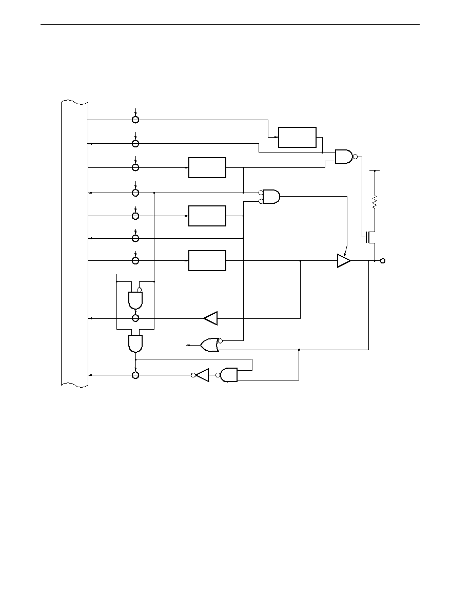
CHAPTER 6 PORT FUNCTIONS
144
Preliminary User's Manual U13987EJ1V0UM00
6.5.1 Hardware configuration
The port 3 hardware configuration is shown in Figures 6-26 to 6-29.
Figure 6-26. P30 (Port 3) Block Diagram
P30
V
DD
WR
PUOL
WR
P3
SI1, RxD input
RD
PUOL
WR
PM3
WR
PMC3
RD
PMC3
PUOL3
PM30
P30
PMC30
RD
PM3
RD
P3
Pull-up resistor option register L
Port 3 mode register
Output latch
Internal
bus
Port 3 mode control register
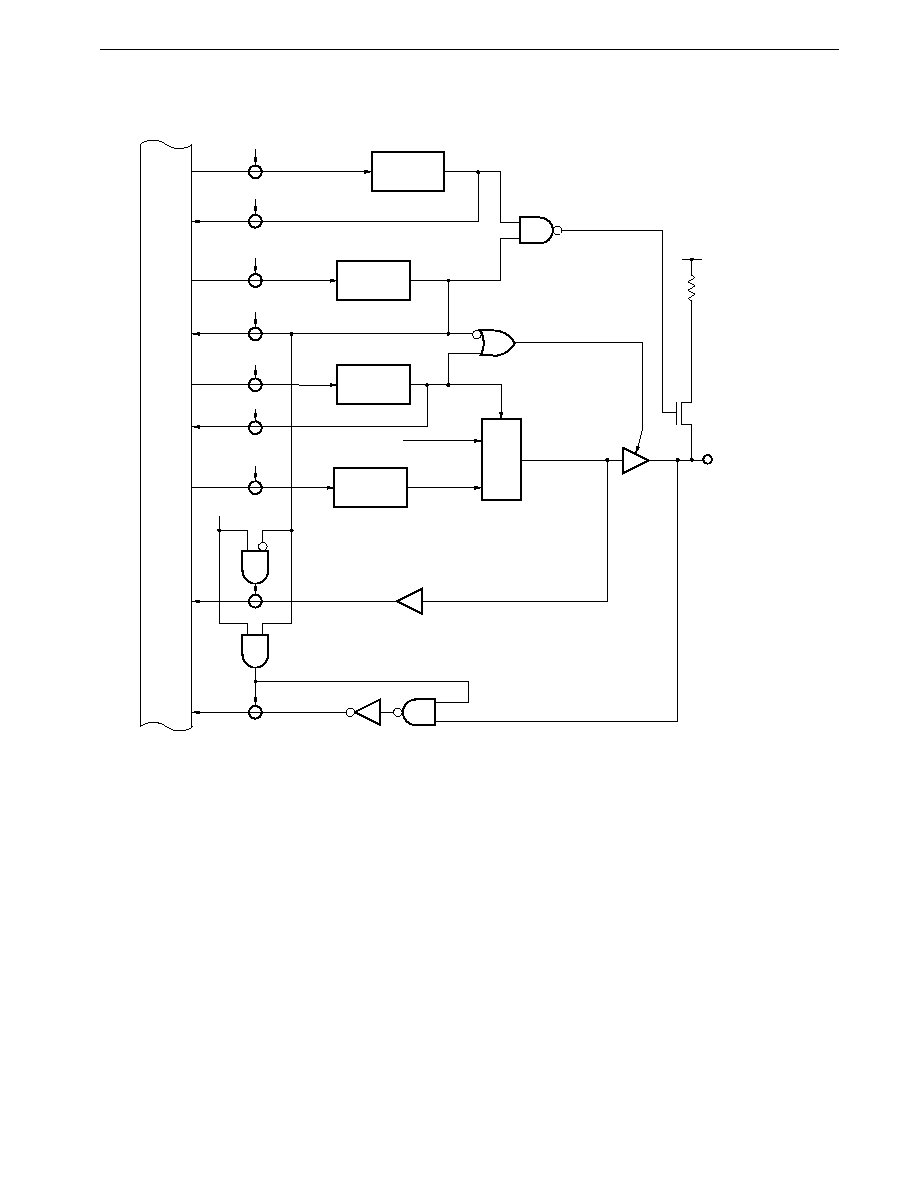
145
CHAPTER 6 PORT FUNCTIONS
Preliminary User's Manual U13987EJ1V0UM00
Figure 6-27. Block Diagram of P31 and P34 to P37 (Port 3)
WR
PUOL
RD
PUOL
WR
PMC3
WR
P3
RD
PMC3
TO, SO1, TxD output
PUOL3
PMC3n
P3n
PM3n
WR
PM3
P3n
n = 1, 4, 5, 6, 7
V
DD
RD
PM3
RD
P3
Pull-up resistor option register L
Port 3 mode register
Output latch
Internal
bus
Port 3 mode control register
Selector
CHAPTER 6 PORT FUNCTIONS
146
Preliminary User's Manual U13987EJ1V0UM00
Figure 6-28. P32 (Port 3) Block Diagram
WR
PUOL
RD
PUOL
WR
PM3
RD
PM3
WR
PMC3
RD
PMC3
RD
P3
RD
P3
PUOL3
PM32
PMC32
P32
SCK0 output
SCK0 input
V
DD
V
DD
P32
Pull-up resistor option register L
Port 3 mode register
Output latch
Internal
bus
Port 3 mode control register
Selector
SCK0 input
N-ch open-drain
specification
(CSIM MOD bit)
147
CHAPTER 6 PORT FUNCTIONS
Preliminary User's Manual U13987EJ1V0UM00
Figure 6-29. P33 (Port 3) Block Diagram
WR
PUOL
RD
PUOL
WR
PM3
RD
PM3
WR
PMC3
RD
PMC3
WR
P3
RD
P3
PUOL3
PM33
PMC33
P33
SO0 output
V
DD
V
DD
P33
N-ch open-drain specification
(CSIM MOD bit)
Pull-up resistor option register L
Port 3 mode register
Output latch
Internal
bus
Port 3 mode control register
Selector
CHAPTER 6 PORT FUNCTIONS
148
Preliminary User's Manual U13987EJ1V0UM00
6.5.2 I/O mode/control mode setting
The port 3 input/output mode is set for each pin by means of the port 3 mode register (PM3) as shown in Figure 6-30.
In addition to their input/output port function, port 3 pins also have an alternate function as various control signal pins, and
the control mode is specified by setting the port 3 mode control register (PMC3) as shown in Figure 6-31.
Figure 6-30. Port 3 Mode Register (PM3) Format
7
PM37
PM3
6
PM36
5
PM35
4
PM34
3
PM33
2
PM32
1
PM31
0
PM30
Address
After reset
R/W
R/W
FFH
0FF23H
PM3n
P3n Pin Input/Output Mode Specification
(n = 0 to 7)
Output mode (output buffer on)
Intput mode (output buffer off)
1
0
149
CHAPTER 6 PORT FUNCTIONS
Preliminary User's Manual U13987EJ1V0UM00
Figure 6-31. Port 3 Mode Control Register (PMC3) Format
7
PMC37
PMC3
6
PMC36
5
PMC35
4
PMC34
3
PMC33
2
PMC32
1
PMC31
0
PMC30
Address
After reset
R/W
R/W
00H
0FF43H
PMC30
P30 Pin Control Mode Specification
Input/output port mode
RxD/SI1 input mode
1
0
PMC31
P31 Pin Control Mode Specification
Input/output port mode
TxD/SO1 output mode
1
0
PMC32
P32 Pin Control Mode Specification
Input/output port mode
SCK0 Input/output mode
1
0
PMC33
P33 Pin Control Mode Specification
Input/output port mode
SO0 output mode
1
0
PMC3n
P3n Pin Control Mode Specification
(n = 4 to 7)
Input/output port mode
TOn output mode (n = 0 to 3)
1
0

CHAPTER 6 PORT FUNCTIONS
150
Preliminary User's Manual U13987EJ1V0UM00
6.5.3 Operating status
Port 3 is an input/output port, with an alternate function as various control pins.
(1) When set as an output port
The output latch is enabled, and data transfers between the output latch and accumulator are performed by means of
transfer instructions. The output latch contents can be freely set by means of logical operation instructions. Once data has
been written to the output latch, it is retained until data is next written to the output latch
Note
.
Note Including the case where another bit of the same port is manipulated by a bit manipulation instruction.
Figure 6-32. Port Specified as Output Port
Internal
bus
Output
latch
P3n
n = 0 to 7
RD
OUT
WR
PORT

151
CHAPTER 6 PORT FUNCTIONS
Preliminary User's Manual U13987EJ1V0UM00
(2) When set as an input port
The port pin level can be loaded into an accumulator by means of a transfer instruction. In this case, too, writes can be
performed to the output latch, and data transferred from the accumulator by a transfer instruction, etc., is stored in all output
latches irrespective of the port input/output specification. However, since the output buffer of a bit specified as an input port
is high impedance, the data is not output to the port pin (when a bit specified as input is switched to an output port, the output
latch contents are output to the port pin). Also, the contents of the output latch of a bit specified as an input port cannot be
loaded into an accumulator.
Figure 6-33. Port Specified as Input Port
Output
latch
P3n
n = 0 to 7
RD
IN
WR
PORT
Internal
bus
Caution
A bit manipulation instruction manipulates one bit as the result, but accesses the port in 8-bit units.
Therefore, if a bit manipulation instruction is used on a port with a mixture of input and output pins
or port mode and control mode, the contents of the output latch of pins specified as inputs and pins
specified as control mode will be undefined (excluding bits manipulated with a SET1 or CLR1
instruction, etc.). Particular care is required when there are bits which are switched between input
and output.
Caution is also required when manipulating the port with other 8-bit arithmetic instructions.
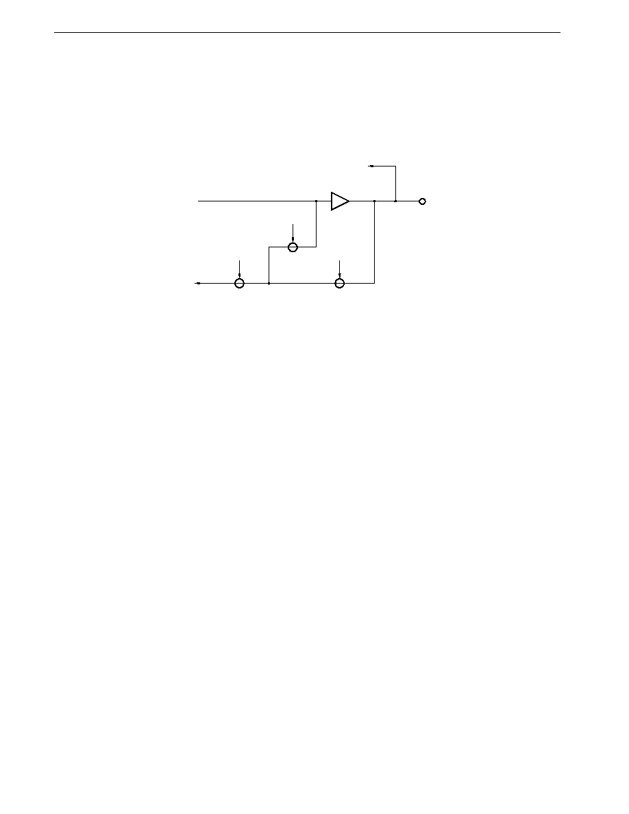
CHAPTER 6 PORT FUNCTIONS
152
Preliminary User's Manual U13987EJ1V0UM00
(3) When specified as control signal input/output
By setting (to 1) bits of the port 3 mode control register (PMC3), port 3 can be used as control signal input or output bit-wise
irrespective of the setting of the port 3 mode register (PM3). When a pin is used as a control signal, the control signal status
can be seen by executing a port read instruction.
Figure 6-34. Control Specification
P3n
n = 0 to 7
PM3n = 0
PM3n = 1
RD
Control
(output)
Internal bus
Control (input)
(a) When port is control signal output
When the port 3 mode register (PM3) is set (to 1), the control signal pin level can be read by executing a port read
instruction.
When PM3 is reset (to 0), the
�
PD784938 internal control signal status can be read by executing a port read instruction.
(b) When port is control signal input
Only the port 3 mode register (PM3) is set (to 1), control signal pin levels can be read by executing a port read instruction.
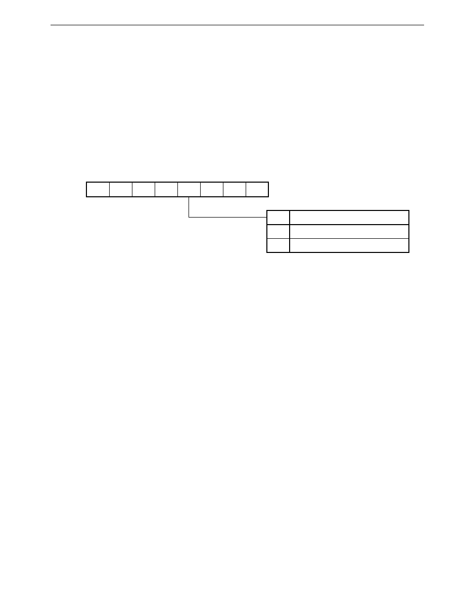
153
CHAPTER 6 PORT FUNCTIONS
Preliminary User's Manual U13987EJ1V0UM00
6.5.4 On-chip pull-up resistors
Port 3 incorporates pull-up resistors. Use of these internal resistors when pull-up is necessary enables the number of parts
and the mounting area to be reduced.
Whether or not an on-chip pull-up resistor is to be used can be specified for each pin by setting the PUOL3 bit of the pull-
up resistor option register L (PUOL) and the port 3 mode register (PM3). When PUOL3 is 1, the on-chip pull-up resistors of the
pins for which input is specified by PM3 (PM3n = 1, n = 0 to 7) are enabled.
Also, the specification for use of the pull-up resistor is also valid for pins specified as control mode pins (pull-up resistors are
also connected to pins that function as output pins in the control mode). Therefore, if you do not want to connect the pull-up
resistors in the control mode, the contents of the corresponding bits of PM3 should be set to 0 (output mode).
Figure 6-35. Pull-Up Resistor Option Register L (PUOL) Format
7
0
PUOL
6
PUOL6
5
PUOL5
4
PUOL4
3
PUOL3
2
PUOL2
1
PUOL1
0
PUOL0
Address
After reset
R/W
R/W
00H
0FF4EH
PUOL3
Port 3 Pull-Up Resistor Specification
Not used in port 3
Used in port 3
1
0
Remark
When STOP mode is entered, setting PUOL to 00H is effective for reducing the current consumption.
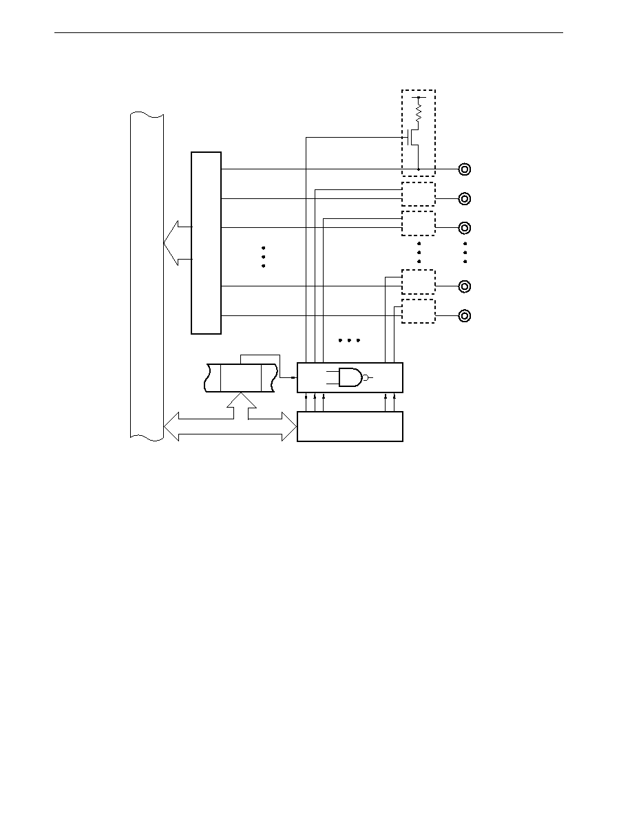
CHAPTER 6 PORT FUNCTIONS
154
Preliminary User's Manual U13987EJ1V0UM00
Figure 6-36. Pull-Up Specification (Port 3)
P31
Input
buffer
P30
P32
P36
P37
V
DD
Port 3 mode register
(PM3)
PUOL3
(PUOL)
Internal
bus

CHAPTER 6 PORT FUNCTIONS
155
Preliminary User's Manual U13987EJ1V0UM00
6.6 Port 4
Port 4 is an 8-bit input/output port with an output latch. Input/output can be specified in 1-bit units by setting the port 4 mode
register (PM4). Each pin incorporates a software programmable pull-up resistor. This port has direct LED drive capability.
Port 4 also functions as the time division address/data bus (AD0 to AD7) by the memory expansion mode register (MM) when
external memory or I/Os are expanded.
When RESET is input, port 4 is set as an input port (output high-impedance state), and the output latch contents are undefined.
6.6.1 Hardware configuration
The port 4 hardware configuration is shown in Figure 6-37.
Figure 6-37. Port 4 Block Diagram
RD
PUOL
WR
PUOL
PUOL4
V
DD
P4n
n = 0 to 7
WR
PM4
PM4n
WR
P4
P4n
MM0 to MM3
RD
PM4
RD
P4
Pull-up resistor option register L
Port 4 mode register
Output latch
Internal
data
bus
Internal
address
bus
Input/
output
control
circuit
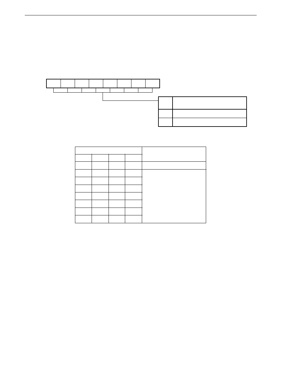
CHAPTER 6 PORT FUNCTIONS
156
Preliminary User's Manual U13987EJ1V0UM00
6.6.2 I/O mode/control mode setting
The port 4 input/output mode is set for each pin by means of the port 4 mode register (PM4) as shown in Figure 6-38.
When port 4 is used as the address/data bus, it is set by means of the memory expansion mode register (MM: See Figure
24-1) as shown in Table 6-6.
Figure 6-38. Port 4 Mode Register (PM4) Format
7
PM47
PM4
6
PM46
5
PM45
4
PM44
3
PM43
2
PM42
1
PM41
0
PM40
Address
After reset
R/W
R/W
FFH
0FF24H
P4n
P4n Pin Input/Output Mode Specification
(n = 0 to 7)
Output mode (output buffer on)
Intput mode (output buffer off)
1
0
Table 6-6. Port 4 Operation Modes
MM Bits
Operation Mode
MM3
MM2
MM1
MM0
0
0
0
0
Port
0
0
1
1
Address/data bus (AD0 to AD7)
0
1
0
0
0
1
0
1
0
1
1
0
0
1
1
1
1
0
0
0
1
0
0
1

CHAPTER 6 PORT FUNCTIONS
157
Preliminary User's Manual U13987EJ1V0UM00
6.6.3 Operating status
Port 4 is an input/output port, with an alternate function as the address/data bus (AD0 to AD7).
(1) When set as an output port
The output latch is enabled, and data transfers between the output latch and accumulator are performed by means of
transfer instructions. The output latch contents can be freely set by means of logical operation instructions. Once data has
been written to the output latch, it is retained until data is next written to the output latch
Note
.
Note Including the case where another bit of the same port is manipulated by a bit manipulation instruction.
Figure 6-39. Port Specified as Output Port
Internal
bus
Output
latch
P4n
n = 0 to 7
RD
OUT
WR
PORT
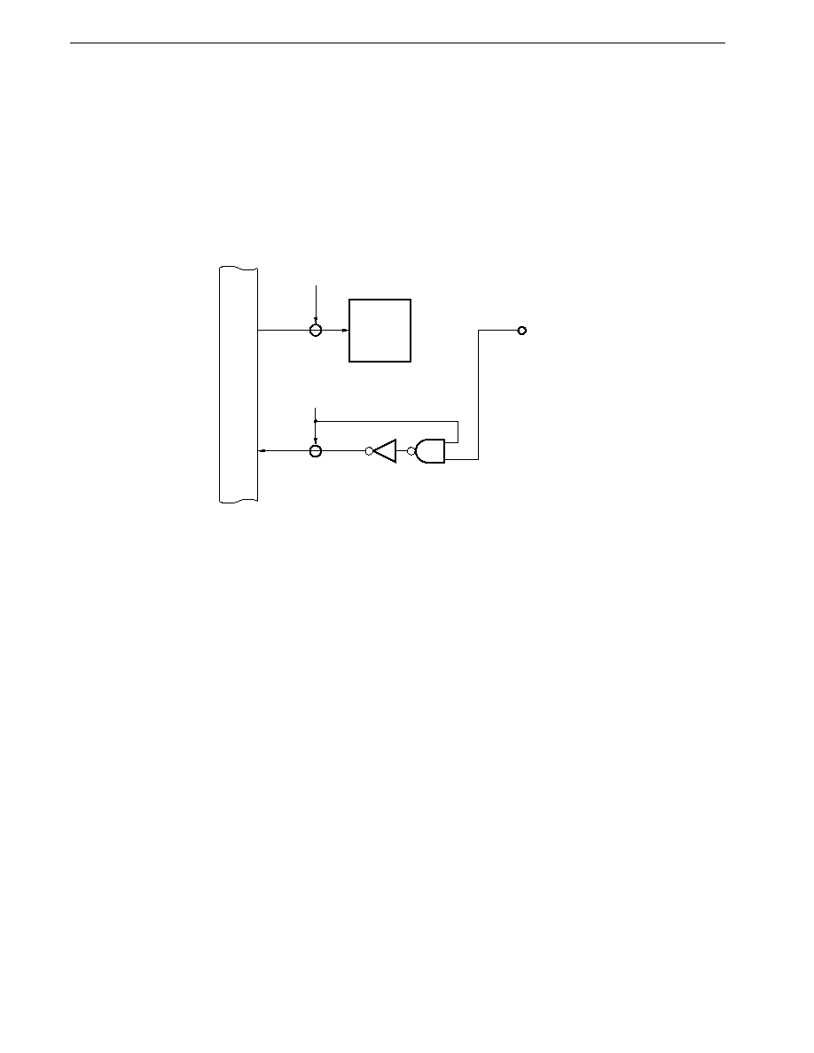
CHAPTER 6 PORT FUNCTIONS
158
Preliminary User's Manual U13987EJ1V0UM00
(2) When set as an input port
The port pin level can be loaded into an accumulator by means of a transfer instruction. In this case, too, writes can be
performed to the output latch, and data transferred from the accumulator by a transfer instruction, etc., is stored in all output
latches irrespective of the port input/output specification. However, since the output buffer of a bit specified as an input port
is high-impedance, the data is not output to the port pin (when a port specified as input is switched to an output port, the
output latch contents are output to the port pin). Also, when specified as an input port, the output latch contents cannot be
loaded into an accumulator.
Figure 6-40. Port Specified as Input Port
Output
latch
P4n
n = 0 to 7
RD
IN
WR
PORT
Internal
bus
Caution
A bit manipulation instruction manipulates one bit as the result, but accesses the port in 8-bit units.
Therefore, if a bit manipulation instruction is used on a port with a mixture of input and output pins,
the contents of the output latch of pins specified as inputs will be undefined (excluding bits
manipulated with a SET1 or CLR1 instruction, etc.). Particular care is required when there are bits
which are switched between input and output.
Caution is also required when manipulating the port with other 8-bit arithmetic instructions.
(3) When used as address/data bus (AD0 to AD7)
Used automatically when an external access is performed.
Input/output instructions should not be executed on port 4.

CHAPTER 6 PORT FUNCTIONS
159
Preliminary User's Manual U13987EJ1V0UM00
6.6.4 On-chip pull-up resistors
Port 4 incorporates pull-up resistors. Use of these internal resistors when pull-up is necessary enables the number of parts
and the mounting area to be reduced.
Whether or not an on-chip pull-up resistor is to be used can be specified for each pin by setting the PUOL4 bit of the pull-
up resistor option register L (PUOL) and the port 4 mode register (PM4).
When PUOL4 is 1, the on-chip pull-up resistors of the pins for which input is specified by the PM4 for port 4 (PM4n = 1,
n = 0 to 7) are enabled .
Figure 6-41. Pull-Up Resistor Option Register L (PUOL) Format
7
0
PUOL
6
PUOL6
5
PUOL5
4
PUOL4
3
PUOL3
2
PUOL2
1
PUOL1
0
PUOL0
Address
After reset
R/W
R/W
00H
0FF4EH
PUOL4
Port 4 Pull-Up Resistor Specification
Not used in port 4
Used in port 4
1
0
Caution
When using the port 4 of the
�
PD784938 as an address/data bus pin, be sure to clear PUOL4 to 0 to
disconnect the on-chip pull-up resistor.
Remark
When STOP mode is entered, setting PUOL to 00H is effective for reducing the current consumption.
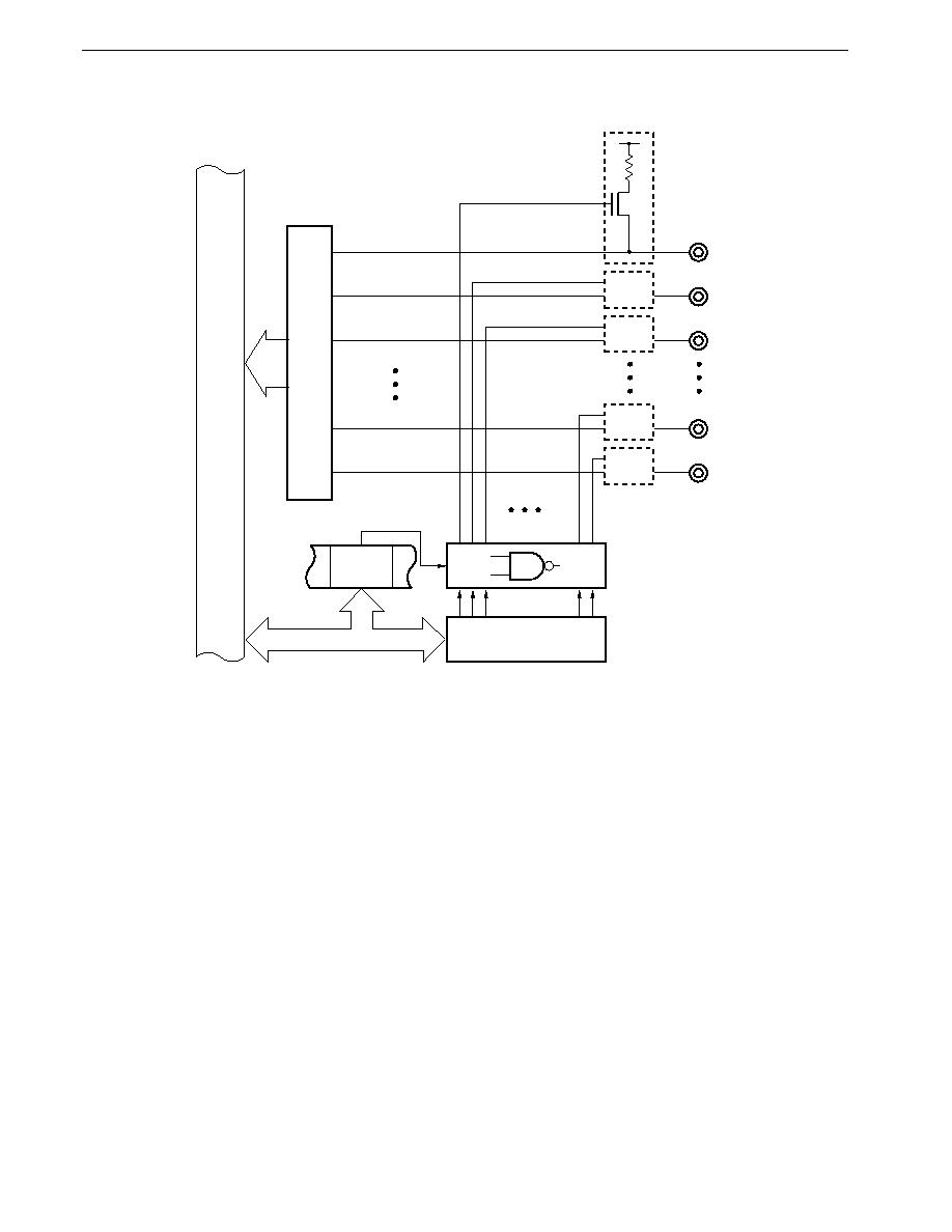
CHAPTER 6 PORT FUNCTIONS
160
Preliminary User's Manual U13987EJ1V0UM00
Figure 6-42. Pull-Up Specification (Port 4)
P41
Input
buffer
P40
P42
P46
P47
V
DD
Port 4 mode register
(PM4)
PUOL4
(PUOL)
Internal
bus
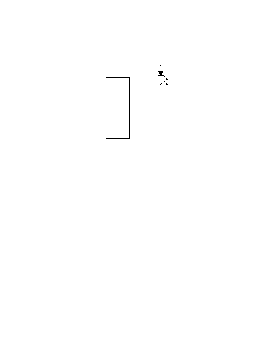
CHAPTER 6 PORT FUNCTIONS
161
Preliminary User's Manual U13987EJ1V0UM00
6.6.5 Direct LED drive
In port 4, the output buffer low-level side drive capability has been reinforced, allowing active-low direct LED drive. An
example of such use is shown in Figure 6-43.
Figure 6-43. Example of Direct LED Drive
�
PD784938
P4n
(n = 0 to 7)
V
DD
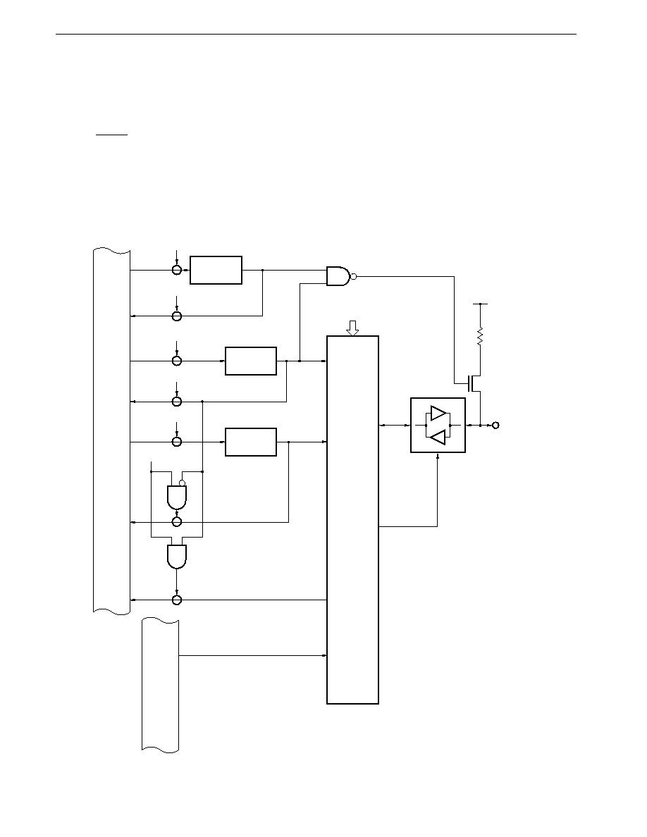
CHAPTER 6 PORT FUNCTIONS
162
Preliminary User's Manual U13987EJ1V0UM00
6.7 Port 5
Port 5 is an 8-bit input/output port with an output latch. Input/output can be specified in 1-bit units by setting the port 5 mode
register (PM5). Each pin incorporates a software programmable pull-up resistor. This port has direct LED drive capability.
In addition, P50 to P57 function as the address bus (A8 to A15) when external memory or I/Os are expanded.
When RESET is input, port 5 is set as an input port (output high-impedance state), and the output latch contents are undefined.
6.7.1 Hardware configuration
The port 5 hardware configuration is shown in Figure 6-44.
Figure 6-44. Port 5 Block Diagram
V
DD
P5n
n = 0 to 7
MM0 to MM3
RD
PUOL
WR
PUOL
PUOL5
WR
PM5
PM5n
WR
P5
P5n
RD
PM5
RD
P5
Pull-up resistor option register L
Port 5 mode register
Output latch
Internal
data
bus
Internal
address
bus
Input/
output
control
circuit
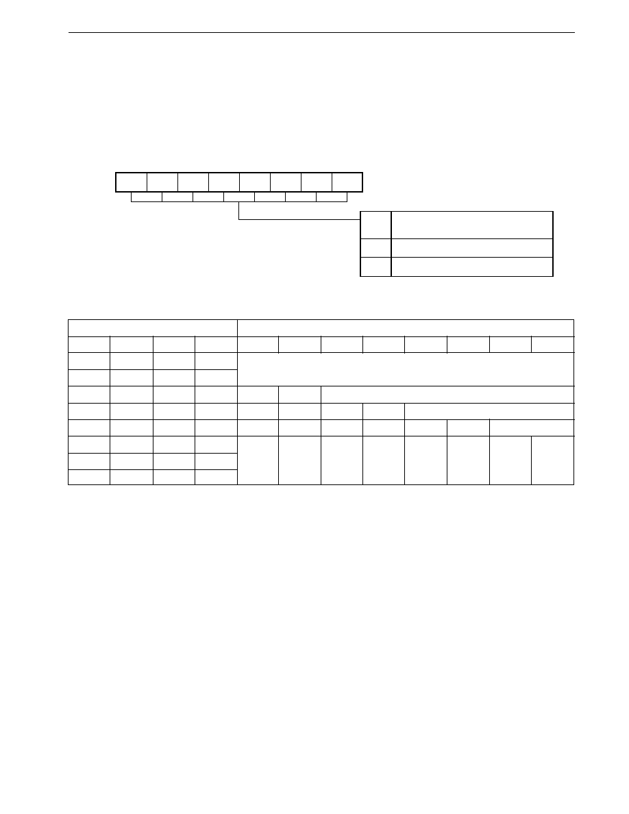
CHAPTER 6 PORT FUNCTIONS
163
Preliminary User's Manual U13987EJ1V0UM00
6.7.2 I/O mode/control mode setting
The port 5 input/output mode is set for each pin by setting the port 5 mode register (PM5) as shown in Figure 6-45.
When port 5 pins can be used as port or address pins in 2-bit units, the setting is performed by means of the memory expansion
mode register (MM: See Figure 24-1) as shown in Table 6-7.
Figure 6-45. Port 5 Mode Register (PM5) Format
7
PM57
PM5
6
PM56
5
PM55
4
PM54
3
PM53
2
PM52
1
PM51
0
PM50
Address
After reset
R/W
R/W
FFH
0FF25H
PM5n
P5n Pin Input/Output Mode Specification
(n = 0 to 7)
Output mode (output buffer on)
Input mode (output buffer off)
1
0
Table 6-7. Port 5 Operation Modes
MM Bits
Operation Mode
MM3
MM2
MM1
MM0
P50
P51
P52
P53
P54
P55
P56
P57
0
0
0
0
Port (P50 to P57)
0
0
1
1
0
1
0
0
A8
A9
Port
0
1
0
1
A8
A9
A10
A11
Port
0
1
1
0
A8
A9
A10
A11
A12
A13
Port
0
1
1
1
A8
A9
A10
A11
A12
A13
A14
A15
1
0
0
0
1
0
0
1
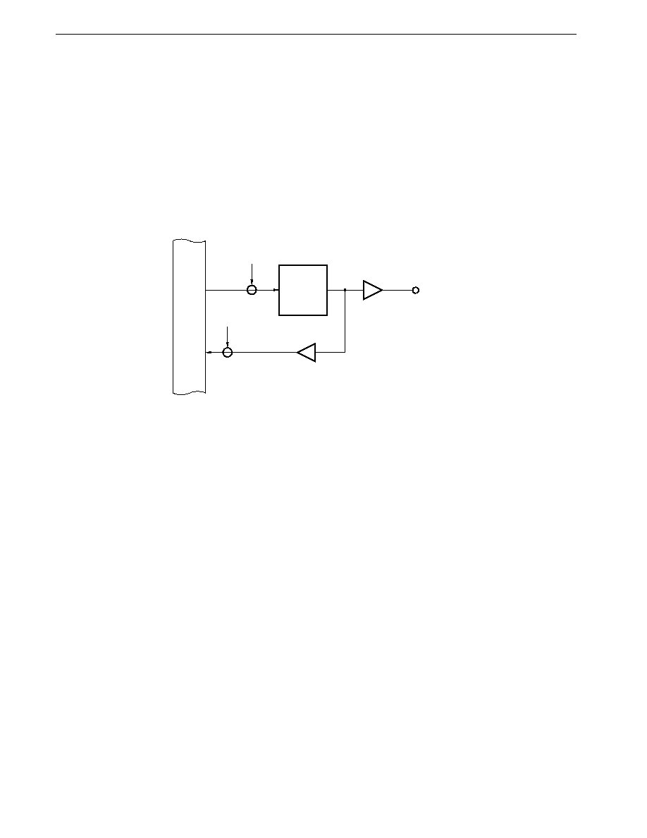
CHAPTER 6 PORT FUNCTIONS
164
Preliminary User's Manual U13987EJ1V0UM00
6.7.3 Operating status
Port 5 is an input/output port, with an alternate function as the address bus (A8 to A15).
(1) When set as an output port
The output latch is enabled, and data transfers between the output latch and accumulator are performed by means of
transfer instructions. The output latch contents can be freely set by means of logical operation instructions. Once data has
been written to the output latch, it is retained until data is next written to the output latch
Note
.
Note Including the case where another bit of the same port is manipulated by a bit manipulation instruction.
Figure 6-46. Port Specified as Output Port
Internal
bus
Output
latch
P5n
n = 0 to 7
RD
OUT
WR
PORT

CHAPTER 6 PORT FUNCTIONS
165
Preliminary User's Manual U13987EJ1V0UM00
(2) When set as an input port
The port pin level can be loaded into an accumulator by means of a transfer instruction. In this case, too, writes can be
performed to the output latch, and data transferred from the accumulator by a transfer instruction, etc., is stored in all output
latches irrespective of the port input/output specification. However, since the output buffer of a bit specified as an input port
is high-impedance, the data is not output to the port pin (when a bit specified as input is switched to an output port, the output
latch contents are output to the port pin). Also, the contents of the output latch of a bit specified as an input port cannot be
loaded into an accumulator.
Figure 6-47. Port Specified as Input Port
Output
latch
P5n
n = 0 to 7
RD
IN
WR
PORT
Internal
bus
Caution
A bit manipulation instruction manipulates one bit as the result, but accesses the port in 8-bit units.
Therefore, if a bit manipulation instruction is used on a port with a mixture of input and output, the
contents of the output latch of pins specified as inputs will be undefined (excluding bits manipulated
with a SET1 or CLR1 instruction, etc.). Particular care is required when there are bits which are
switched between input and output.
Caution is also required when manipulating the port with other 8-bit arithmetic instructions.
(3) When used as address bus (A8 to A15)
Used automatically when an external address is accessed.
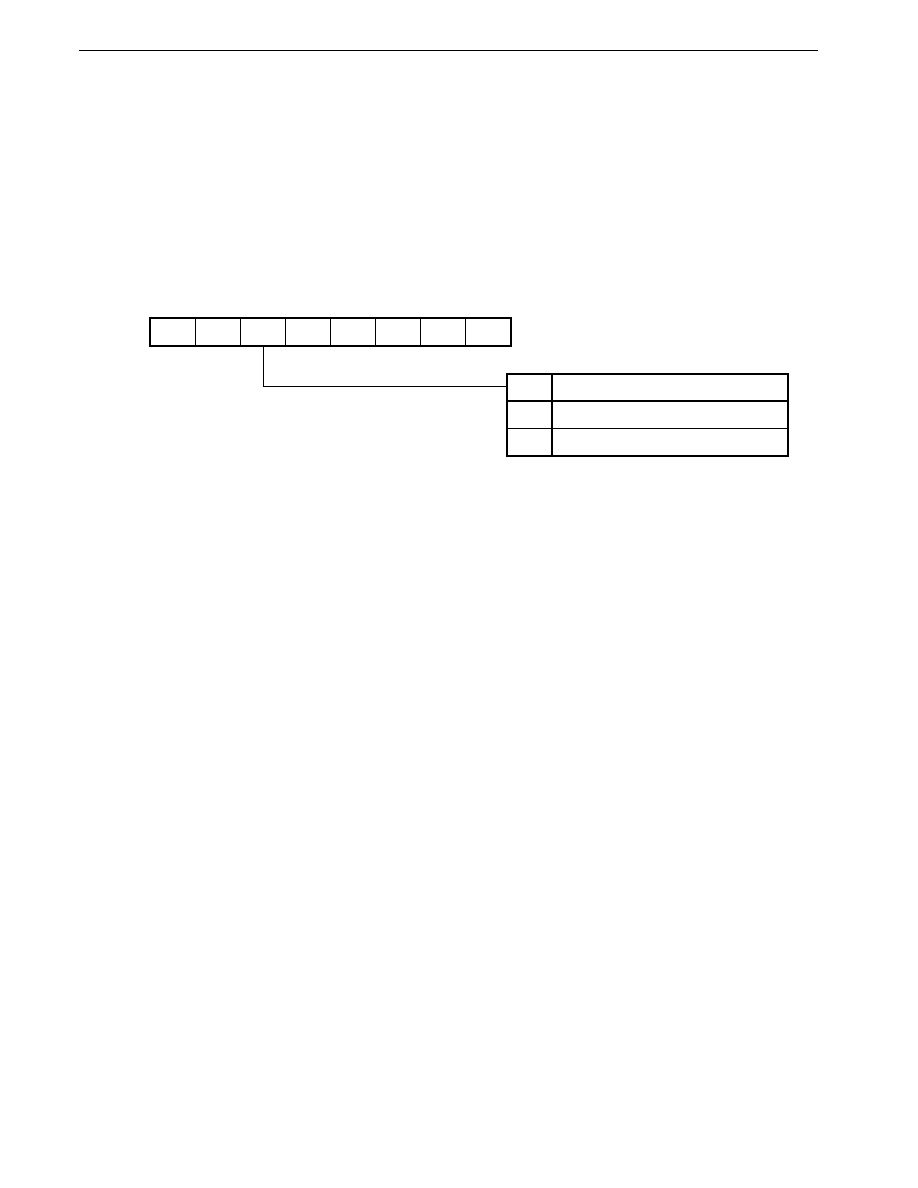
CHAPTER 6 PORT FUNCTIONS
166
Preliminary User's Manual U13987EJ1V0UM00
6.7.4 On-chip pull-up resistors
Port 5 incorporates pull-up resistors. Use of these internal resistors when pull-up is necessary enables the number of parts
and the mounting area to be reduced.
Whether or not an on-chip pull-up resistor is to be used can be specified for each pin by setting the PUOL5 bit of the pull-
up resistor option register L (PUOL) and the port 5 mode register (PM5).
When PUOL5 is 1, the on-chip pull-up resistors of the pins for which input is specified by the PM5 for port 5 (PM5n = 1, n =
0 to 7) are enabled .
Figure 6-48. Pull-Up Resistor Option Register L (PUOL) Format
7
0
PUOL
6
PUOL6
5
PUOL5
4
PUOL4
3
PUOL3
2
PUOL2
1
PUOL1
0
PUOL0
Address
After reset
R/W
R/W
00H
0FF4EH
PUOL5
Port 5 Pull-Up Resistor Specification
Not used in port 5
Used in port 5
1
0
Caution
When using the port 5 of the
�
PD784938 as an address bus, be sure to clear PUOL5 to 0 to disconnect the
on-chip pull-up resistor.
Remark
When STOP mode is entered, setting PUOL to 00H is effective for reducing the current consumption.

CHAPTER 6 PORT FUNCTIONS
167
Preliminary User's Manual U13987EJ1V0UM00
Figure 6-49. Pull-Up Specification (Port 5)
P51
Input
buffer
P50
P52
P56
P57
V
DD
Port 5 mode register
(PM5)
PUOL5
(PUOL)
Internal
bus
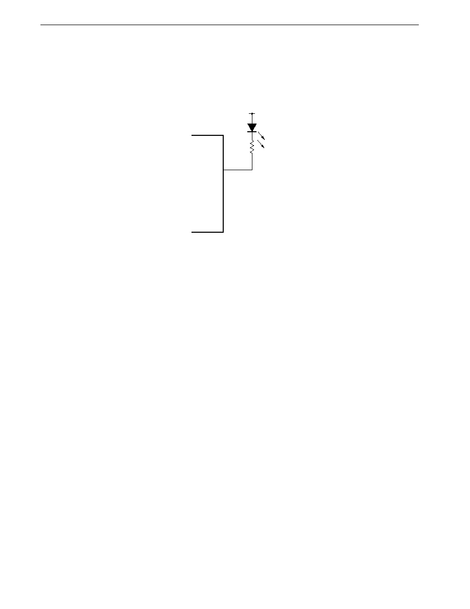
CHAPTER 6 PORT FUNCTIONS
168
Preliminary User's Manual U13987EJ1V0UM00
6.7.5 Direct LED drive
In port 5, the output buffer low-level side drive capability has been reinforced, allowing active-low direct LED drive. An
example of such use is shown in Figure 6-50.
Figure 6-50. Example of Direct LED Drive
�
PD784938
P5n
(n = 0 to 7)
V
DD
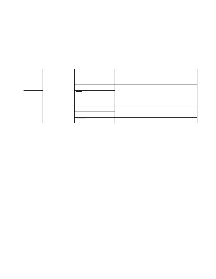
CHAPTER 6 PORT FUNCTIONS
169
Preliminary User's Manual U13987EJ1V0UM00
6.8 Port 6
Port 6 is an 8-bit input/output port with an output latch. P60 to P67 incorporate a software programmable pull-up resistor.
In addition to its function as a port, port 6 also has various alternate-function control signal pin functions as shown in Table
6-8. Operations as control pins are performed by the respective function operations.
When RESET is input, P60 to P67 are set as input port pins (output high-impedance state), and the output latch contents
are undefined.
Table 6-8. Port 6 Operation Modes
Pin Name
Port Mode
Control Signal Input/
Operation to Operate as Control Pins
Output Mode
P60 to P63
Input/output ports
A16 to A19 outputs
Specified by bits MM3 to MM0 of the MM in 2-bit units
P64
RD output
P65
WR output
P66
WAIT input
Specified by bits PWn1 & PWn0 (n = 0 to 7) of the PWC1 &
PWC2 or setting P66 in the input mode
HLDRQ input
Bus hold enabled by the HLDE bit of the HLDM
P67
HLDAK output
REFRQ output
Set (to 1) the RFEN bit of the RFM
External memory expansion mode is specified by bits MM3 to
MM0 of the MM
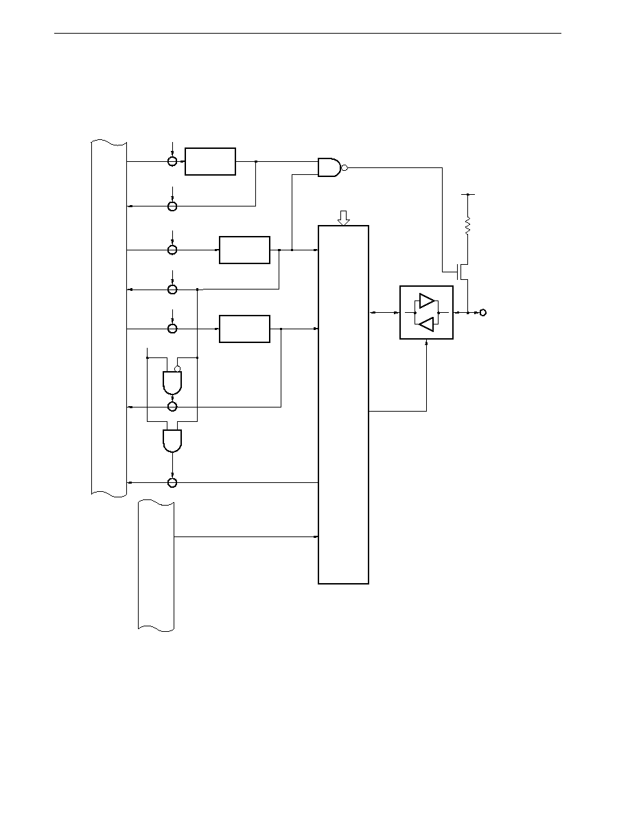
CHAPTER 6 PORT FUNCTIONS
170
Preliminary User's Manual U13987EJ1V0UM00
6.8.1 Hardware configuration
The port 6 hardware configuration is shown in Figures 6-51 to 6-54.
Figure 6-51. P60 to P63 (Port 6) Block Diagram
V
DD
P6n
n = 0 to 3
MM0 to MM3
RD
PUOL
WR
PUOL
PUOL6
WR
PM6
PM6n
WR
P6
P6n
RD
PM6
RD
P6
Pull-up resistor option register L
Port 6 mode register
Output latch
Internal
data
bus
Internal
address
bus
Input/
output
control
circuit
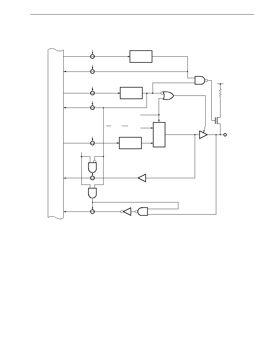
CHAPTER 6 PORT FUNCTIONS
171
Preliminary User's Manual U13987EJ1V0UM00
Figure 6-52. P64 and P65 (Port 6) Block Diagram
WR
PUOL
RD
PUOL
WR
P6
PUOL6
P64
(P65)
WR
PM6
P64
(P65)
V
DD
External expansion mode
PM64
(PM65)
RD signal (WR signal)
RD
PM6
RD
P6
Pull-up resistor option register L
Port 6 mode register
Output latch
Internal
bus
Selector
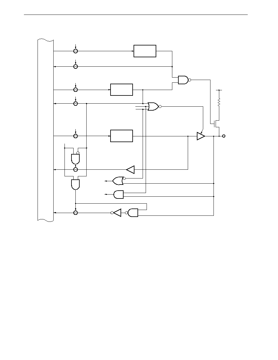
CHAPTER 6 PORT FUNCTIONS
172
Preliminary User's Manual U13987EJ1V0UM00
Figure 6-53. P66 (Port 6) Block Diagram
P66
WR
PUOL
PUOL6
V
DD
RD
PUOL
WR
PM6
PM66
WR
P6
P66
Hold enabled mode
External wait specification
Wait input
Hold request
input
RD
P6
RD
PM6
Pull-up resistor option register L
Port 6 mode register
Output latch
Internal
bus
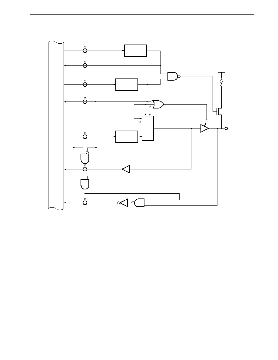
CHAPTER 6 PORT FUNCTIONS
173
Preliminary User's Manual U13987EJ1V0UM00
Figure 6-54. P67 (Port 6) Block Diagram
PM67
WR
PUOL
RD
PUOL
WR
P6
PUOL6
P67
WR
PM6
P67
V
DD
RD
PM6
RD
P6
Hold enabled mode
Refresh mode
Pull-up resistor option register L
Port 6 mode register
Output latch
Internal
bus
Refresh signal
Hold acknowledge signal
Selector
CHAPTER 6 PORT FUNCTIONS
174
Preliminary User's Manual U13987EJ1V0UM00
6.8.2 I/O mode/control mode setting
The port 6 input/output mode is set by setting the port 6 mode register (PM6) as shown in Figure 6-55.
Operations for operating port 6 as control pins are shown in Table 6-9.
Table 6-9. Port 6 Control Pin Function
Pin Name
Control Signal I/O Mode
Port Mode
Operation to Operate as Control Pins
P60
A16
Input/output port
P61
A17
P62
A18
P63
A19
P64
RD
Output port
P65
WR
P66
WAIT
Input/output port
External wait input is specified by bits
PWn1 & PWn0 (n = 0 to 7) of the PWC1 & PWC2
HLDRQ
Bus hold enabled by the HLDE bit of the HLDM
P67
HLDAK
Output port
REFRQ
Set (to 1) the RFEN bit of the RFM
Table 6-10. P60 to P65 Control Pin Specification
MM Bits
Operation Mode
MM3
MM2
MM1
MM0
P60
P61
P62
P63
P64
P65
0
0
0
0
Port (P60 to P65)
0
0
1
1
0
1
0
0
Port (P60 to P63)
RD
WR
0
1
0
1
0
1
1
0
0
1
1
1
1
0
0
0
A16
A17
Port
1
0
0
1
A16
A17
A18
A19
(a) Port mode
Each port not specified as in control mode can be specified as input/output in 1-bit units by setting the port 6 mode
register (PM6).
(b) Control signal input/output mode
(i)
A16 to A19 (Address Bus)
Upper address bus output pins when the external memory space is expanded (10000H to FFFFFH).
These pins operate in accordance with the memory expansion mode register (MM).
External memory expansion mode specified by bits MM3 to MM0 of
the MM (see Table 6-10)
External memory expansion mode specified by bits MM3 to MM0 of
the MM (see Table 6-10)
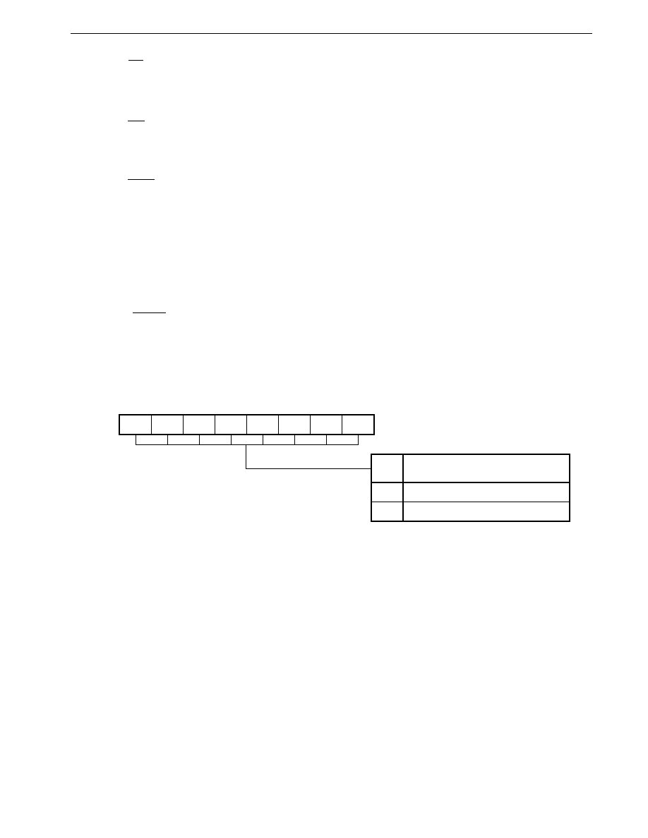
CHAPTER 6 PORT FUNCTIONS
175
Preliminary User's Manual U13987EJ1V0UM00
(ii) RD (Read Strobe)
The strobe signal for an external memory read operation. The operation of this pin is controlled by the memory
expansion mode register (MM).
(iii) WR (Write Strobe)
Pin that outputs the strobe signal for an external memory write operation. The operation of this pin is controlled
by the memory expansion mode register (MM).
(iv) WAIT (Wait)
Wait signal input pin. Operates in accordance with the programmable wait control registers (PWC1, PWC2).
(v) HLDRQ (Hold Request)
External bus hold request signal input pin. Operates in accordance with the hold mode register (HLDM).
(vi) HLDAK (Hold Acknowledge)
Bus hold acknowledge signal output pin. Operates in accordance with the hold mode register (HLDM).
(vii) REFRQ (Refresh Request)
This pin outputs refresh pulses to pseudo-static memory when this memory is connected to it externally. Operates
in accordance with the refresh mode register (RFM).
Figure 6-55. Port 6 Mode Register (PM6) Format
7
PM67
PM6
6
PM66
5
PM65
4
PM64
3
PM63
2
PM62
1
PM61
0
PM60
Address
After reset
R/W
R/W
FFH
0FF26H
PM6n
P6n Pin Input/Output Mode Specification
(n = 0 to 7)
Output mode (output buffer on)
Intput mode (output buffer off)
1
0
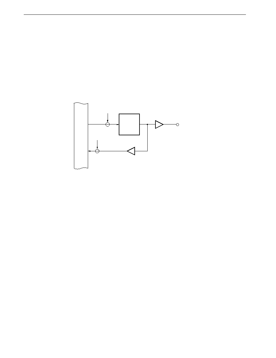
CHAPTER 6 PORT FUNCTIONS
176
Preliminary User's Manual U13987EJ1V0UM00
6.8.3 Operating status
Port 6 is an input/output port, with an alternate function as various control pins.
(1) When set as an output port
The output latch is enabled, and data transfers between the output latch and accumulator are performed by means of
transfer instructions. The output latch contents can be freely set by means of logical operation instructions. Once data has
been written to the output latch, it is retained until data is next written to the output latch
Note
.
Note Including the case where another bit of the same port is manipulated by a bit manipulation instruction.
Figure 6-56. Port Specified as Output Port
Internal
bus
Output
latch
P6n
n = 0 to 7
RD
OUT
WR
PORT
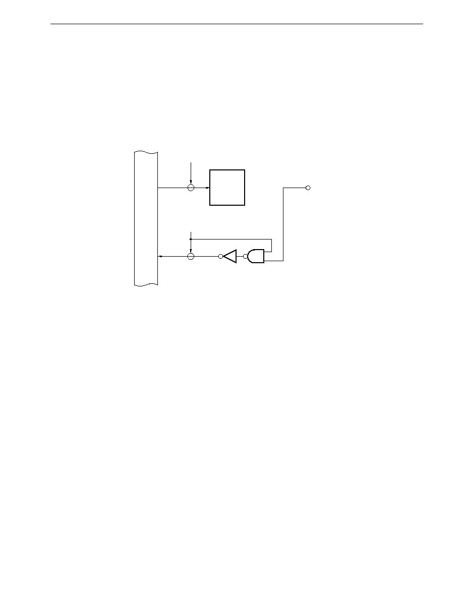
CHAPTER 6 PORT FUNCTIONS
177
Preliminary User's Manual U13987EJ1V0UM00
(2) When set as an input port
The port pin level can be loaded into an accumulator by means of a transfer instruction. In this case, too, writes can be
performed to the output latch, and data transferred from the accumulator by a transfer instruction, etc., is stored in all output
latches irrespective of the port input/output specification. However, since the output buffer of a bit specified as an input port
is high-impedance, the data is not output to the port pin (when a bit specified as input is switched to an output port, the output
latch contents are output to the port pin). Also, the contents of the output latch of a bit specified as an input port cannot be
loaded into an accumulator.
Figure 6-57. Port Specified as Input Port
Output
latch
P6n
n = 4 to 7
RD
IN
WR
PORT
Internal
bus
Caution
A bit manipulation instruction manipulates one bit as the result, but accesses the port in 8-bit units.
Therefore, if a bit manipulation instruction is used on a port with a mixture of input and output pins,
or port mode and control mode, the contents of the output latch of pins specified as inputs or pins
specified as in the control mode will be undefined (excluding bits manipulated with a SET1 or CLR1
instruction, etc.). Particular care is required when there are bits which are switched between input
and output.
Caution is also required when manipulating the port with other 8-bit arithmetic instructions.
(3) When used as control pins
Cannot be manipulated or tested by software.

CHAPTER 6 PORT FUNCTIONS
178
Preliminary User's Manual U13987EJ1V0UM00
6.8.4 On-chip pull-up resistors
P60 to P67 incorporate pull-up resistors. Use of these internal resistors when pull-up is necessary enables the number of
parts and the mounting area to be reduced.
Whether or not an on-chip pull-up resistor is to be used can be specified for each pin by setting the PUOL6 bit of the pull-
up resistor option register L (PUOL) and the port 6 mode register (PM6).
When PUOL6 is 1, the on-chip pull-up resistors of the pins for which input is specified by the PM6 (PM6n = 1, n = 0 to 7) are
enabled .
Figure 6-58. Pull-Up Resistor Option Register L (PUOL) Format
Remark
When STOP mode is entered, setting PUOL to 00H is effective for reducing the current consumption.
Figure 6-59. Pull-Up Specification (Port 6)
P66
Input
buffer
P67
P65
P61
P60
V
DD
Port 6 mode register
(PM6)
PUOL6
(PUOL)
Internal
bus
7
0
PUOL
6
PUOL6
5
PUOL5
4
PUOL4
3
PUOL3
2
PUOL2
1
PUOL1
0
PUOL0
Address
After reset
R/W
R/W
00H
0FF4EH
PUOL6
Port 6 Pull-Up Resistor Specification
Not used in port 6
Used in port 6
1
0

CHAPTER 6 PORT FUNCTIONS
179
Preliminary User's Manual U13987EJ1V0UM00
6.9 Port 7
Port 7 is an 8-bit input/output port. In addition to operating as an input/output port, it also operates as the A/D converter analog
input pins (ANI0 to ANI7).
Input/output can be specified in 1-bit units by setting the port 7 mode register (PM7).
Pin levels can be read or tested at any time irrespective of alternate-function operations.
When RESET is input, port 7 is set as an input port (output high-impedance state), and the output latch contents are undefined.
6.9.1 Hardware configuration
The port 7 hardware configuration is shown in Figure 6-60.
Figure 6-60. Port 7 Block Diagram
P7n
(n = 0 to 7)
WR
P7
P7n
RD
PM7
PM7n
WR
PM7
A/D converter
RD
P7
Port 7 mode register
Output latch
Internal
bus
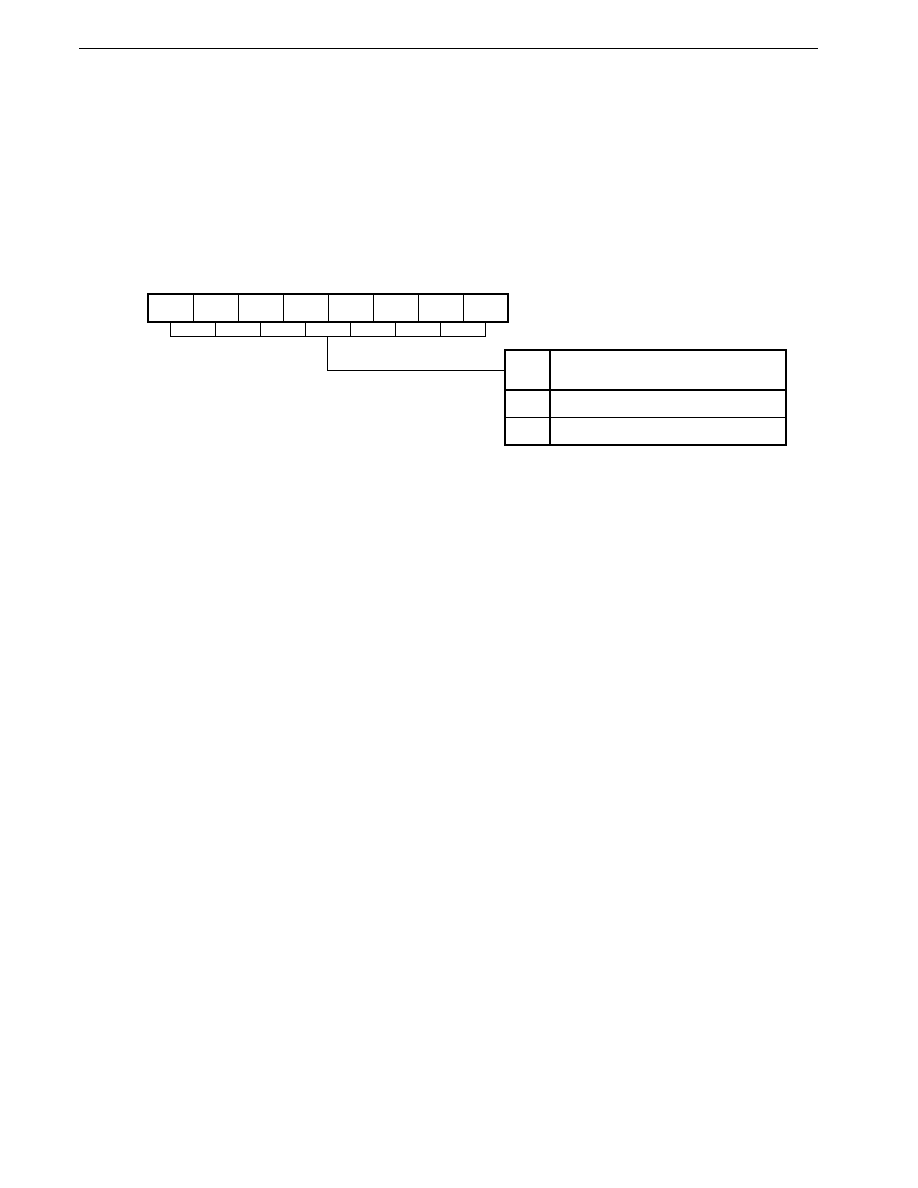
CHAPTER 6 PORT FUNCTIONS
180
Preliminary User's Manual U13987EJ1V0UM00
6.9.2 I/O mode/control mode setting
The port 7 input/output mode is set for each pin by setting the port 7 mode register (PM7) as shown in Figure 6-61.
In addition to the operation of port 7 as an input/output port, analog signal input can be performed at any time. Mode setting
is not necessary.
Specification of the A/D conversion operation is performed by ADM of the A/D converter (see CHAPTER 16 A/D
CONVERTER for details).
Figure 6-61. Port 7 Mode Register (PM7) Format
7
PM77
PM7
6
PM76
5
PM75
4
PM74
3
PM73
2
PM72
1
PM71
0
PM70
Address
After reset
R/W
R/W
FFH
0FF27H
PM7n
P7n Pin Input/Output Mode Specification
(n = 0 to 7)
Output mode (output buffer on)
Intput mode (output buffer off)
1
0
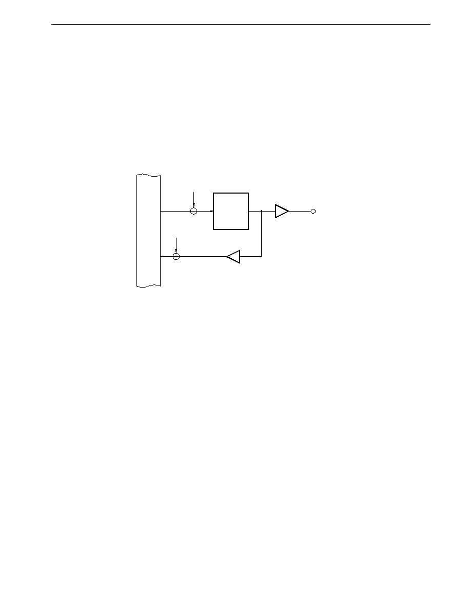
CHAPTER 6 PORT FUNCTIONS
181
Preliminary User's Manual U13987EJ1V0UM00
6.9.3 Operating status
Port 7 is an input/output port, with an alternate function as the A/D converter analog input pins (ANI0 to ANI7).
(1) When set as an output port
The output latch is enabled, and data transfers between the output latch and accumulator are performed by means of
transfer instructions. The output latch contents can be freely set by means of logical operation instructions. Once data has
been written to the output latch, it is retained until data is next written to the output latch
Note
.
Note Including the case where another bit of the same port is manipulated by a bit manipulation instruction.
Figure 6-62. Port Specified as Output Port
Internal
bus
Output
latch
P7n
n = 0 to 7
RD
OUT
WR
PORT
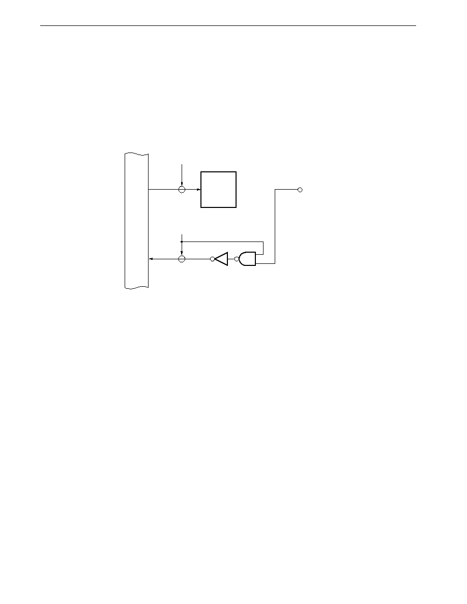
CHAPTER 6 PORT FUNCTIONS
182
Preliminary User's Manual U13987EJ1V0UM00
(2) When set as an input port
The port pin level can be loaded into an accumulator by means of a transfer instruction. In this case, too, writes can be
performed to the output latch, and data transferred from the accumulator by a transfer instruction, etc., is stored in all output
latches-irrespective of the port input/output specification. However, since the output buffer of a bit specified as an input port
is high-impedance, the data is not output to the port pin (when a bit specified as input is switched to an output port, the output
latch contents are output to the port pin). Also, the contents of the output latch of a bit specified as an input port cannot be
loaded into an accumulator.
Figure 6-63. Port Specified as Input Port
Output
latch
P7n
n = 0 to 7
RD
IN
WR
PORT
Internal
bus
Caution
A bit manipulation instruction manipulates one bit as the result, but accesses the port in 8-bit units.
Therefore, if a bit manipulation instruction is used on a port with a mixture of input and output pins, the
contents of the output latch of pins specified as inputs will be undefined (excluding bits manipulated with
a SET1 or CLR1 instruction, etc.). Particular care is required when there are bits which are switched
between input and output.
Caution is also required when manipulating the port with other 8-bit arithmetic instructions.
6.9.4 On-chip pull-up resistors
Port 7 does not incorporate pull-up resistors.
6.9.5 Caution
A voltage outside the range AV
SS
to AV
REF
must not be applied to pins for which P70 to P77 are used as ANI0 to AN17.
See 16.6 Cautions in CHAPTER 16 A/D CONVERTER for details.

CHAPTER 6 PORT FUNCTIONS
183
Preliminary User's Manual U13987EJ1V0UM00
6.10 Port 9
Port 9 is an 8-bit input/output port with an output latch. Input/output can be specified in 1-bit units by setting the port 9 mode
register (PM9). Each pin incorporates a software programmable pull-up resistor.
When RESET is input, port 9 is set as an input port (output high-impedance state), and the output latch contents are undefined.
6.10.1 Hardware configuration
The port 9 hardware configuration is shown in Figure 6-64.
Figure 6-64. Port 9 Block Diagram
WR
PUOH
RD
PUOH
WR
P9
PUOH9
P9n
PM9n
WR
PM9
P9n
n = 0 to 7
V
DD
RD
PM9
RD
P9
Pull-up resistor option register H
Port 9 mode register
Output latch
Internal
bus
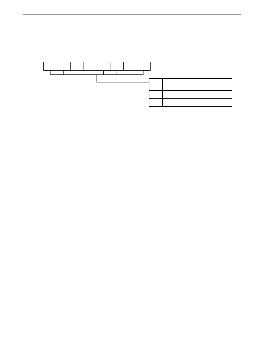
CHAPTER 6 PORT FUNCTIONS
184
Preliminary User's Manual U13987EJ1V0UM00
6.10.2 I/O mode/control mode setting
The port 9 input/output mode is set for each pin by setting the port 9 mode register (PM9) as shown in Figure 6-65.
Figure 6-65. Port 9 Mode Register (PM9) Format
7
PM97
PM9
6
PM96
5
PM95
4
PM94
3
PM93
2
PM92
1
PM91
0
PM90
Address
After reset
R/W
R/W
FFH
0FF29H
PM9n
P9n Pin Input/Output Mode Specification
(n = 0 to 7)
Output mode (output buffer on)
Input mode (output buffer off)
1
0

CHAPTER 6 PORT FUNCTIONS
185
Preliminary User's Manual U13987EJ1V0UM00
6.10.3 Operating status
Port 9 is an input/output port.
(1) When set as an output port
The output latch is enabled, and data transfers between the output latch and accumulator are performed by means of
transfer instructions. The output latch contents can be freely set by means of logical operation instructions. Once data has
been written to the output latch, it is retained until data is next written to the output latch
Note
.
Note Including the case where another bit of the same port is manipulated by a bit manipulation instruction.
Figure 6-66. Port Specified as Output Port
Internal
bus
Output
latch
P9n
n = 0 to 7
RD
OUT
WR
PORT

CHAPTER 6 PORT FUNCTIONS
186
Preliminary User's Manual U13987EJ1V0UM00
(2) When set as an input port
The port pin level can be loaded into an accumulator by means of a transfer instruction. In this case, too, writes can be
performed to the output latch, and data transferred from the accumulator by a transfer instruction, etc., is stored in all output
latches irrespective of the port input/output specification. However, since the output buffer of a bit specified as an input port
is high-impedance, the data is not output to the port pin (when a bit specified as input is switched to an output port, the output
latch contents are output to the port pin). Also, the contents of the output latch of a bit specified as an input port cannot be
loaded into an accumulator.
Figure 6-67. Port Specified as Input Port
Output
latch
P9n
n = 0 to 7
RD
IN
WR
PORT
Internal
bus
Caution
A bit manipulation instruction manipulates one bit as the result, but accesses the port in 8-bit units.
Therefore, if a bit manipulation instruction is used on a port with a mixture of input and output, the
contents of the output latch of pins specified as inputs will be undefined (excluding bits manipulated
with a SET1 or CLR1 instruction, etc.). Particular care is required when there are bits which are
switched between input and output.
Caution is also required when manipulating the port with other 8-bit arithmetic instructions.
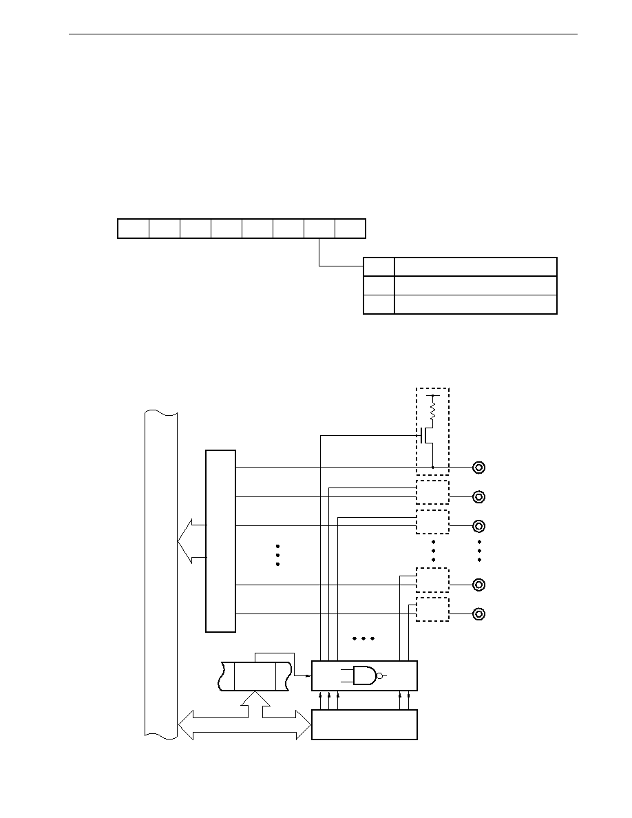
CHAPTER 6 PORT FUNCTIONS
187
Preliminary User's Manual U13987EJ1V0UM00
6.10.4 On-chip pull-up resistors
Port 9 incorporates pull-up resistors. Use of these internal resistors when pull-up is necessary enables the number of parts
and the mounting area to be reduced.
Whether or not an on-chip pull-up resistor is to be used can be specified for each pin by setting the PUOH9 bit of the pull-
up resistor option register H (PUOH) and the port 9 mode register (PM9).
When PUOH9 is 1, the on-chip pull-up resistors of the pins for which input is specified by the PM9 for port 9 (PM9n = 1, n
= 0 to 7) are enabled .
Figure 6-68. Pull-Up Resistor Option Register H (PUOH) Format
7
0
PUOH
6
0
5
0
4
0
3
0
2
PUOH10
1
PUOH9
0
0
Address
After reset
R/W
R/W
00H
0FF4FH
PUOH9
Port 9 Pull-Up Resistor Specification
Not used in port 9
Used in port 9
1
0
Remark
When STOP mode is entered, setting PUOH to 00H is effective for reducing the current consumption.
Figure 6-69. Pull-Up Specification (Port 9)
P96
Input
buffer
P97
P95
P91
P90
V
DD
Port 9 mode register
(PM9)
PUOH9
(PUOH)
Internal
bus

CHAPTER 6 PORT FUNCTIONS
188
Preliminary User's Manual U13987EJ1V0UM00
6.11 Port 10
Port 10 is an 8-bit input/output port with an output latch. Input/output can be specified in 1-bit units by setting the port 10 mode
register (PM10). Each pin incorporates a software programmable pull-up resistor. P105 and P107 can be set in the N-ch open-
drain mode.
In addition to its function as an input/output port, port 10 also has an alternate function as serial interface pin.
The operation mode can be specified bit-wise by setting the port 10 mode control register (PMC10), as shown in
Table 6-11. The pin level of all pins can always be read or tested regardless of the alternate-function pin operation.
When RESET is input, port 10 is set as an input port (output high-impedance state), and the output latch contents are
undefined.
Table 6-11. Port 10 Operation Modes
(n = 0 to 7)
Mode
Port Mode
Control Signal Input/Output Mode
Setting Condition
PMC10n = 0
PMC10n = 1
P100 to P104
Input/output port
--
P105
SCK3 input/output
P106
SI3 input
P107
SO3 output
(a) Port mode
Each port specified as port mode by the port 10 mode control register (PMC10) can be specified as input/output in 1-
bit units by setting the port 10 mode register (PM10).
(b) Control signal input/output mode
Pins can be set as control pins in 1-bit units by setting the port 10 mode control register (PMC10).
(i)
SCK3 (Serial Clock 3)
SCK3 is the clocked serial interface serial clock input/output pin (in 3-wire serial I/O 3 mode).
(ii) SI3 (Serial Input 3)
SI3 is the serial data input pin (in 3-wire serial I/O 3 mode).
(iii) SO3 (Serial Output 3)
SO3 is the serial data output pin (in 3-wire serial I/O 3 mode).
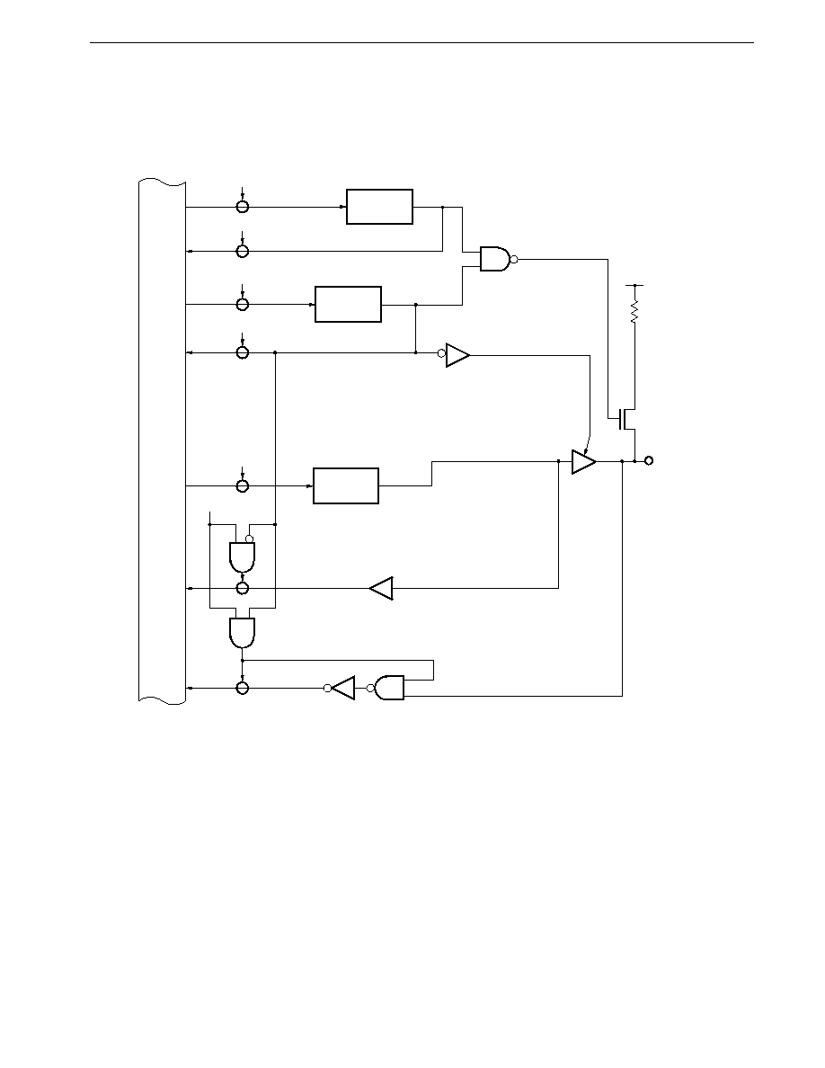
CHAPTER 6 PORT FUNCTIONS
189
Preliminary User's Manual U13987EJ1V0UM00
6.11.1 Hardware configuration
The port 10 hardware configuration is shown in Figures 6-70 to 6-73.
Figure 6-70. P100 to P104 (Port 10) Block Diagram
WR
PUOH
RD
PUOH
WR
P10
PUOH10
P10n
PM10n
WR
PM10
P10n
n = 0 to 4
V
DD
RD
PM10
RD
P10
Pull-up resistor option register H
Port 10 mode register
Output latch
Internal
bus
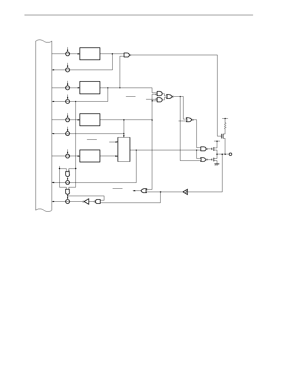
CHAPTER 6 PORT FUNCTIONS
190
Preliminary User's Manual U13987EJ1V0UM00
Figure 6-71. P105 (Port 10) Block Diagram
WR
PUOH
RD
PUOH
WR
PM10
RD
PM10
WR
PMC10
RD
PMC10
RD
P10
RD
P10
PUOH10
PM105
PMC105
P105
SCK3 output
SCK3 input
V
DD
V
DD
P105
Pull-up resistor option register H
Port 10 mode register
Output latch
Internal
bus
Port 10 mode control register
Selector
SCK3 Input
N-ch open-drain
specification
(CSIM3 MOD3 bit)
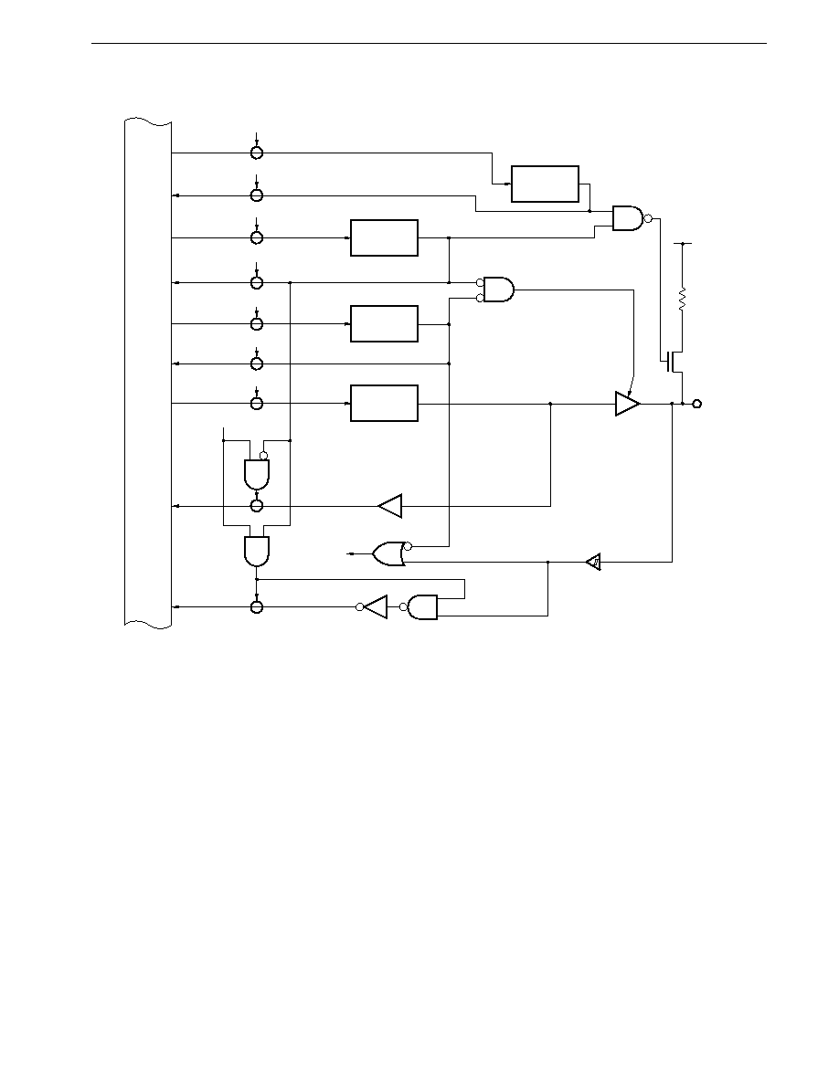
CHAPTER 6 PORT FUNCTIONS
191
Preliminary User's Manual U13987EJ1V0UM00
Figure 6-72. P106 (Port 10) Block Diagram
P106
V
DD
WR
PUOH
WR
P10
SI3 input
RD
PUOH
WR
PM10
WR
PMC10
RD
PMC10
PUOH10
PM10n
P106
PMC106
RD
PM10
RD
P10
Pull-up resistor option register H
Port 10 mode register
Output latch
Internal
bus
Port 10 mode control register
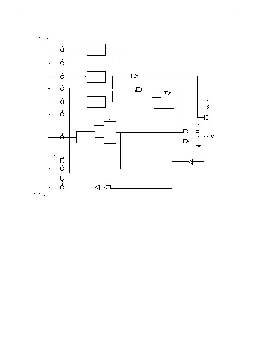
CHAPTER 6 PORT FUNCTIONS
192
Preliminary User's Manual U13987EJ1V0UM00
Figure 6-73. P107 (Port 10) Block Diagram
WR
PUOH
RD
PUOH
WR
PM10
RD
PM10
WR
PMC10
RD
PMC10
WR
P10
RD
P10
PUOH10
PM107
PMC107
P107
SO3 output
V
DD
V
DD
P107
N-ch open-drain specification
(SCIM3 MOD3 bit)
Pull-up resistor option register H
Port 10 mode register
Output latch
Internal
bus
Port 10 mode control register
Selector
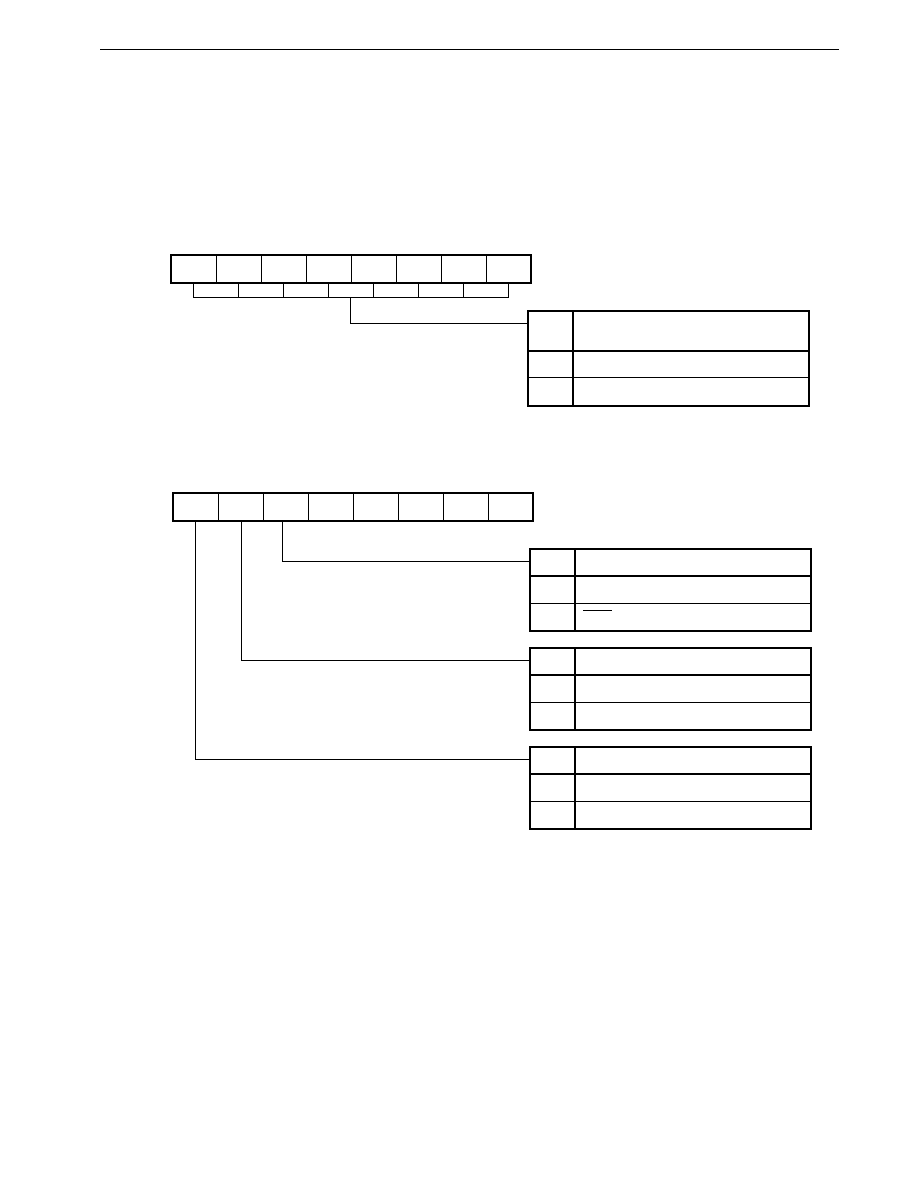
CHAPTER 6 PORT FUNCTIONS
193
Preliminary User's Manual U13987EJ1V0UM00
6.11.2 I/O mode/control mode setting
The port 10 input/output mode is set for each pin by means of the port 10 mode register (PM10) as shown in Figure 6-74.
In addition to their input/output port function, port 10 also have an alternate function as serial interface pin, and the control
mode is specified by setting the port 10 mode control register (PMC10) as shown in Figure 6-75.
Figure 6-74. Port 10 Mode Register (PM10) Format
7
PM107
PM10
6
PM106
5
PM105
4
PM104
3
PM103
2
PM102
1
PM101
0
PM100
Address
After reset
R/W
R/W
FFH
0FF2AH
PM10n P10n Pin Input/Output Mode Specification
(n = 0 to 7)
Output mode (output buffer on)
Intput mode (output buffer off)
1
0
Figure 6-75. Port 10 Mode Control Register (PMC10) Format
7
PMC107
PMC10
6
PMC106
5
PMC105
4
0
3
0
2
0
1
0
0
0
Address
After reset
R/W
R/W
00H
0FF4AH
PMC105
P105 Pin Control Mode Specification
Input/output port mode
SCK3 input/output mode
1
0
PMC106
P106 Pin Control Mode Specification
Input/output port mode
SI3 input mode
1
0
PMC107
P107 Pin Control Mode Specification
Input/output port mode
SO3 output mode
1
0
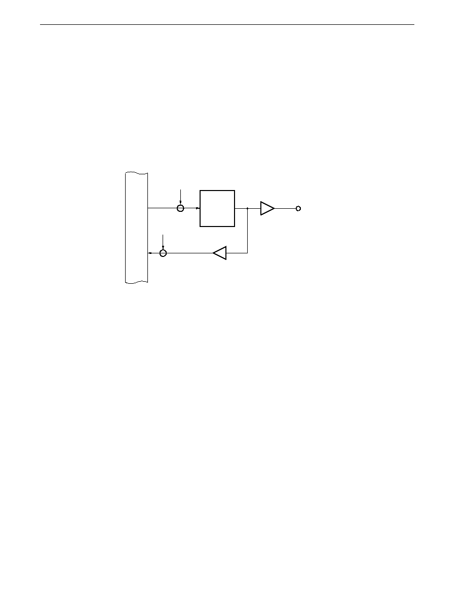
CHAPTER 6 PORT FUNCTIONS
194
Preliminary User's Manual U13987EJ1V0UM00
6.11.3 Operating status
Port 10 is an input/output port, with an alternate function as various control pins.
(1) When set as an output port
The output latch is enabled, and data transfers between the output latch and accumulator are performed by means of
transfer instructions. The output latch contents can be freely set by means of logical operation instructions. Once data has
been written to the output latch, it is retained until data is next written to the output latch
Note
.
Note Including the case where another bit of the same port is manipulated by a bit manipulation instruction.
Figure 6-76. Port Specified as Output Port
Internal
bus
Output
latch
P10n
n = 0 to 7
RD
OUT
WR
PORT

CHAPTER 6 PORT FUNCTIONS
195
Preliminary User's Manual U13987EJ1V0UM00
(2) When set as an input port
The port pin level can be loaded into an accumulator by means of a transfer instruction. In this case, too, writes can be
performed to the output latch, and data transferred from the accumulator by a transfer instruction, etc., is stored in all output
latches irrespective of the port input/output specification. However, since the output buffer of a bit specified as an input port
is high impedance, the data is not output to the port pin (when a bit specified as input is switched to an output port, the output
latch contents are output to the port pin). Also, the contents of the output latch of a bit specified as an input port cannot be
loaded into an accumulator.
Figure 6-77. Port Specified as Input Port
Output
latch
P10n
n = 0 to 7
RD
IN
WR
PORT
Internal
bus
Caution
A bit manipulation instruction manipulates one bit as the result, but accesses the port in 8-bit units.
Therefore, if a bit manipulation instruction is used on a port with a mixture of input and output pins
or port mode and control mode, the contents of the output latch of pins specified as inputs and pins
specified as control mode will be undefined (excluding bits manipulated with a SET1 or CLR1
instruction, etc.). Particular care is required when there are bits which are switched between input
and output.
Caution is also required when manipulating the port with other 8-bit arithmetic instructions.
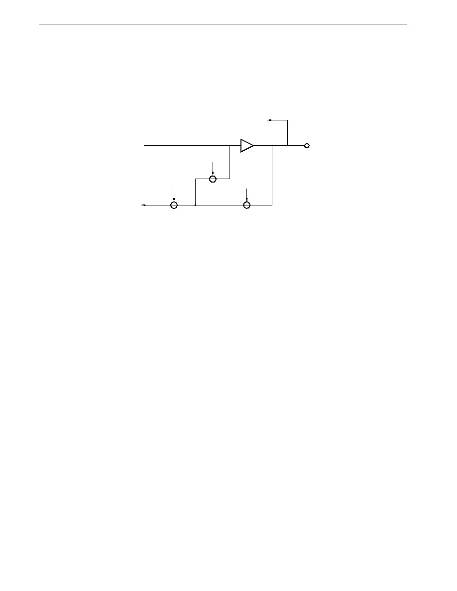
CHAPTER 6 PORT FUNCTIONS
196
Preliminary User's Manual U13987EJ1V0UM00
(3) When specified as control signal input/output
By setting (to 1) bits of the port 10 mode control register (PMC10), port 10 can be used as control signal input or output in
1-bit units irrespective of the setting of the port 10 mode register (PM10). When a pin is used as a control signal, the control
signal status can be seen by executing a port read instruction.
Figure 6-78. Control Specification
P10n
n = 0 to 7
PM10n = 0
PM10n = 1
RD
Control
(output)
Internal bus
Control (input)
(a) When port is control signal output
When the port 10 mode register (PM10) is set (to 1), the control signal pin level can be read by executing a port read
instruction.
When PM10 is reset (to 0), the
�
PD784938 internal control signal status can be read by executing a port read
instruction.
(b) When port is control signal input
Only the port 10 mode register (PM10) is set (to 1), control signal pin levels can be read by executing a port read
instruction.
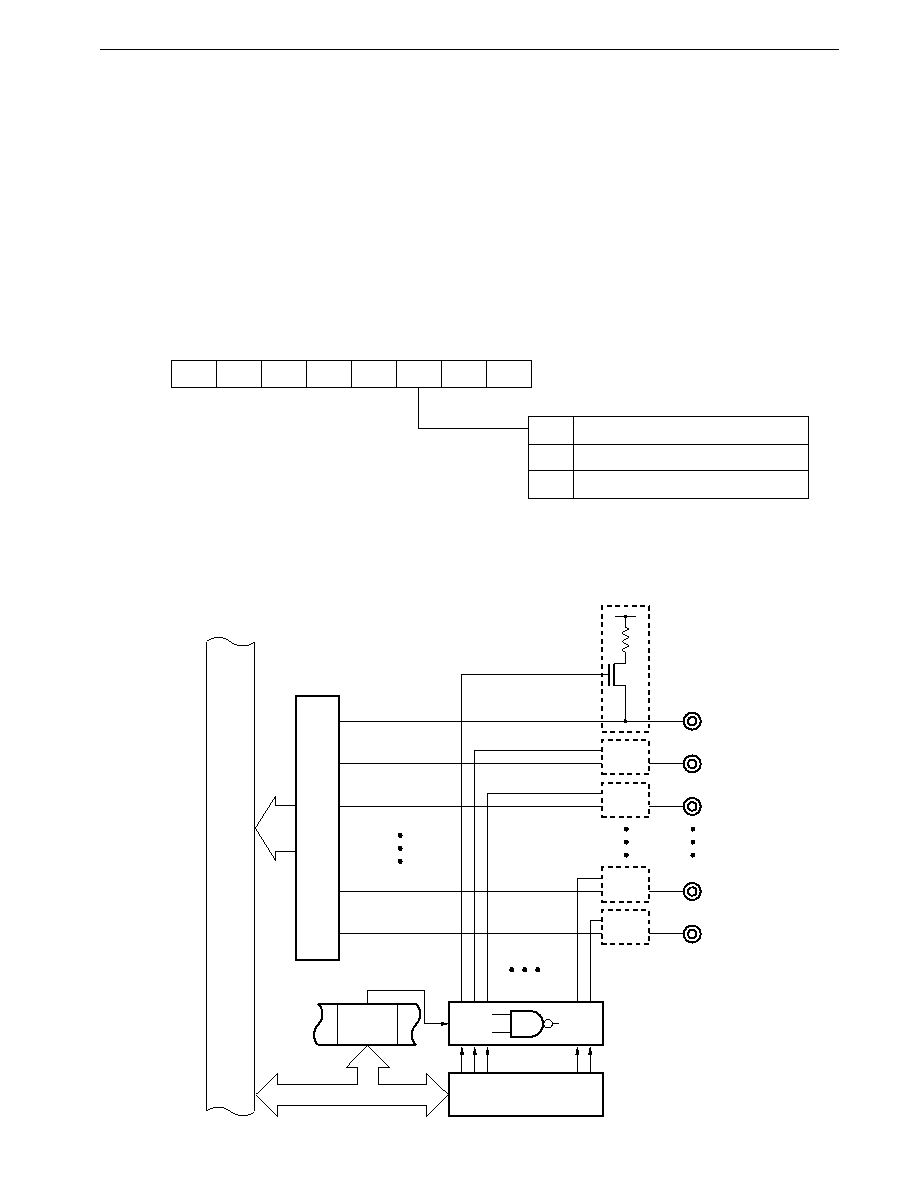
CHAPTER 6 PORT FUNCTIONS
197
Preliminary User's Manual U13987EJ1V0UM00
6.11.4 On-chip pull-up resistors
Port 10 incorporates pull-up resistors. Use of these internal resistors when pull-up is necessary enables the number of parts
and the mounting area to be reduced.
Whether or not an on-chip pull-up resistor is to be used can be specified for each pin by setting the PUOH10 bit of the pull-
up resistor option register H (PUOH) and the port 10 mode register (PM10). When PUOH10 is 1, the on-chip pull-up resistors
of the pins for which input is specified by PM10 (PM10n = 1, n = 0 to 7) are enabled.
Also, the specification for use of the pull-up resistor is also valid for pins specified as control mode pins (pull-up resistors are
also connected to pins that function as output pins in the control mode). Therefore, if you do not want to connect the pull-up
resistors in the control mode, the contents of the corresponding bits of PM10 should be set to 0 (output mode).
Figure 6-79. Pull-Up Resistor Option Register H (PUOH) Format
7
0
PUOH
6
0
5
0
4
0
3
0
2
PUOH10
1
PUOH9
0
0
Address
After reset
R/W
R/W
00H
0FF4FH
PUOH10
Port 10 Pull-Up Resistor Specification
Not used in port 10
Used in port 10
1
0
Remark
When STOP mode is entered, setting PUOH to 00H is effective for reducing the current consumption.
Figure 6-80. Pull-Up Specification (Port 10)
P106
Input
buffer
P107
P105
P101
P100
V
DD
Port 10 mode register
(PM10)
PUOH10
(PUOH)
Internal
bus

CHAPTER 6 PORT FUNCTIONS
198
Preliminary User's Manual U13987EJ1V0UM00
6.12 Port Output Check Function
The
�
PD784938 has a function for reading and testing output port pin levels in order to improve the reliability of application
systems. It is therefore possible to check the output data and the actual pin status as required. If there is a mismatch, appropriate
action can be taken, such as replacement with another system.
Special instructions, CHKL and CHKLA, are provided to check the port status. These instructions perform a comparison by
taking the exclusive OR of the pin status and the output latch contents (in port mode), or the pin status and the internal control
output signal level (in control mode).
Example An example of a program that checks the pin status and output latch contents using the CHKL instruction and
CHKLA instruction is as follows.
TEST :
SET1
P0.3
; Set bit 3 of port 0
CHKL
P0
; Check port 0
BNE
$ ERR1
; Branch to error processing (ERR1) in case of mismatch with output
latch contents
.
.
.
ERR1 :
CHKLA
P0
; Faulty bit check
BT
A.7, $BIT07
; Bit 7?
BT
A.6, $BIT06
; Bit 6?
.
.
.
BT
A.1, $BIT01
; Bit 1?
BR
$BIT00
; If none of the bits, bit 0 is faulty
Cautions 1. If each port is set to input mode, a comparison of the pin status with the output latch contents (or
control output level) using the CHKL or CHKLA instruction will always show a match whether the
individual pins of the port are port pins or control pins.
Therefore, executing these instructions on a port set to input mode is actually ineffective.
2. If the output levels of a port in which control outputs and port outputs are mixed in a single port are
checked with the CHKL or CHKLA instruction, the input/output mode of control output pins should
be set to input mode before executing these instructions (as the output levels of control outputs vary
asynchronously, the output level cannot be checked with the CHKL or CHKLA instruction).
3. As port 2 is an input-only port, a comparison of the pin status with the output latch contents using
the CHKL or CHKLA instruction will always show a match. Therefore, executing these instructions
on port 2 is actually ineffective.

CHAPTER 6 PORT FUNCTIONS
199
Preliminary User's Manual U13987EJ1V0UM00
6.13 Cautions
(1)
All port pins become high-impedance after RESET signal input (on-chip pull-up resistors are disconnected from the
pins).
If there is a problem with pins becoming high-impedance during RESET input, this should be handled with external
circuitry.
(2)
Bit 7 of the pull-up resistor option register (PUO) that sets the on-chip pull-up resistor connection is fixed at 0, but if "1"
is written to bit 7 of the PUO in the in-circuit emulator, "1" will be read.
(3)
Output latch contents are not initialized by RESET input. When a port is used as an output port, the output latch must
be initialized without fail before turning on the output buffer. If the output latch is not initialized before turning on the output
buffer, unexpected data will be output to the output port.
Similarly, for pins used as control pins, internal peripheral hardware initialization must be performed before performing
the control pin specification.
(4)
As P22 to P26 are not pulled up immediately after a reset, an interrupt request flag may be set depending on the function
of the alternate-function pins (INTP1 to INTP5). Therefore, the interrupt request flags should be cleared after specifying
pull-up in the initialization routine.
(5)
When P40 to P47 and P50 to P57 are used as the address/data bus and address bus respectively in the
�
PD784938,
bits PUO4 and PUO5 of the pull-up resistor option register (PUO) must be set to "0" so that on-chip pull-up resistor
connection is not performed.
(6)
A voltage outside the range AV
SS
to AV
REF
must not be applied to pins for which P70 to P77 are used as ANI0 to ANI7.
See 16.6 Cautions in CHAPTER 16 A/D CONVERTER for details.
(7)
A bit manipulation instruction manipulates one bit as the result, but accesses the port in 8-bit units. Therefore, if a bit
manipulation instruction is used on a port with a mixture of input and output pins or port mode and control mode, the
contents of the output latch of pins specified as inputs or pins specified as in control mode will be undefined (excluding
bits manipulated with a SET1 or CLR1 instruction, etc.). Particular care is required when there are bits which are
switched between input and output.
Caution is also required when manipulating the port with other 8-bit arithmetic instructions.
(8)
If each port is set to input mode, a comparison of the pin status with the output latch contents (or control output level)
using the CHKL or CHKLA instruction will always show a match whether the individual pins of the port are port pins or
control pins. Therefore, executing these instructions on a port set to input mode is actually ineffective.
(9)
If the output levels of a port in which control outputs and port outputs are mixed in a single port are checked with the
CHKL or CHKLA instruction, the input/output mode of control output pins should be set to input mode before executing
these instructions (as the output levels of control outputs vary asynchronously, the output level cannot be checked with
the CHKL or CHKLA instruction).
(10) As port 2 is an input-only port, a comparison of the pin status with the output latch contents using the CHKL or CHKLA
instruction will always show a match. Therefore, executing these instructions on port 2 is actually ineffective.

200
Preliminary User's Manual U13987EJ1V0UM00
[MEMO]

201
Preliminary User's Manual U13987EJ1V0UM00
CHAPTER 7 REAL-TIME OUTPUT FUNCTION
7.1 Configuration and Function
The real-time output function is implemented by hardware, including primarily port 0 and the port 0 buffer registers (P0H, P0L),
shown in Figure 7-1.
The real-time output function refers to the transfer to the output latch by hardware of data prepared in the P0H and P0L
beforehand, simultaneously with the generation of an interrupt from timer/event counter 1 or external interrupt, and its output
off-chip. The pins that output the data off-chip are called real-time output ports.
The following two kinds of real-time output data are handled:
� 4 bits
�
2 channels
� 8 bits
�
1 channel
By combining the real-time output function with the macro service function described later, the functions of a pattern generator
with programmable timing are implemented without software intermediation.
This is ideally suited to stepping motor control, for example.
Figure 7-1 shows the block diagram of the real-time output port.
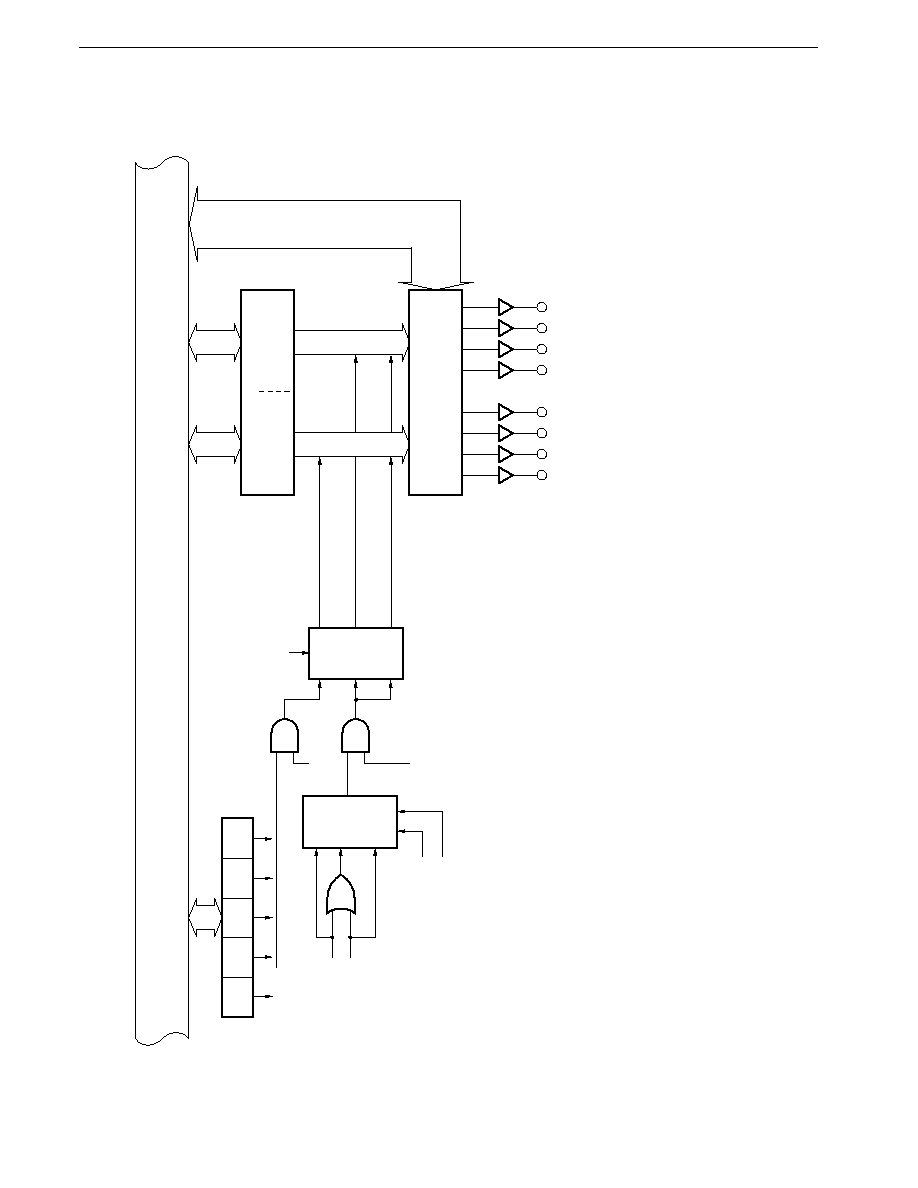
202
CHAPTER 7 REAL-TIME OUTPUT FUNCTION
Preliminary User's Manual U13987EJ1V0UM00
Figure 7-1. Real-Time Output Port Block Diagram
Internal bus
Selector
RTPC BYTE P0MH EXTR
P0ML
INTC11
INTP0
INTC10
EXTR
TRGP0
TRGP0
P0ML
P0MH
BYTE
4-bit real-time output (P0H)
4-bit real-time output (P0L)
8-bit real-time output (P0)
4
4
Output latch
P0
P0H
P0L
Port 0 buffer registers
P07
P05
P06
P04
P03 P02 P01 P00
8
4
4
Selector
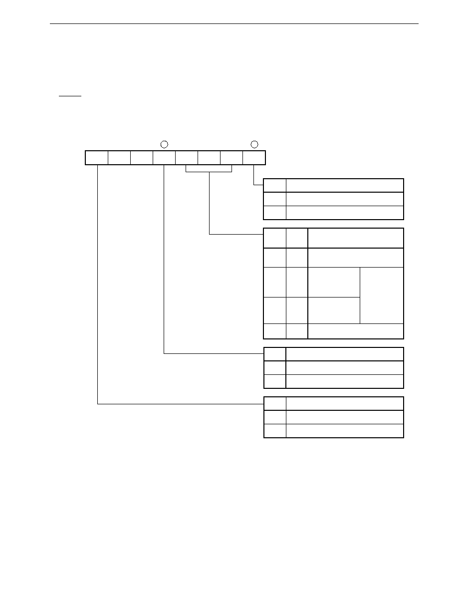
203
CHAPTER 7 REAL-TIME OUTPUT FUNCTION
Preliminary User's Manual U13987EJ1V0UM00
7.2 Real-time Output Port Control Register (RTPC)
RTPC is an 8-bit register that specifies the function of port 0.
RTPC can be read or written to with an 8-bit manipulation instruction or bit manipulation instruction. Figure 7-2 shows the
format of RTPC.
RESET input clears RTPC to 00H.
Figure 7-2. Real-Time Output Port Control Register (RTPC) Format
Caution
When P0ML and P0MH bits are set (to 1), the corresponding port output buffer is turned on and the port
0 output latch contents are output irrespective of the contents of the port 0 mode register (PM0). The
output latch contents should therefore be initialized before making a real-time output port specification.
7
BYTE
RTPC
6
0
5
0
4
P0MH
3
EXTR
2
0
1
TRGP0
0
P0ML
Address
After reset
R/W
R/W
00H
0FF2EH
P0ML
P00 to P03 Function Specification
Port mode
Real-time output port mode
1
0
EXTR TRGP0
Enabling of Data Transfer to Output
Latch from P0H, P0L by INTP0
Not enabled
(data transfer by INTC10 only)
Transfer by either
INTP0 or INTC10
Transfer by
INTP0 only
Setting prohibited
Enabled
� BYTE = 0:
P0L only
transferred
� BYTE = 1:
P0L/P0H
transferred
1
1
0
0
1
0
1
0
P0MH
P04 to P07 Function Specification
Port mode
Real-time output port mode
1
0
BYTE
Real-Time Output Port Operating Mode
4-bit separate real-time output port
8-bit real-time output port
1
0
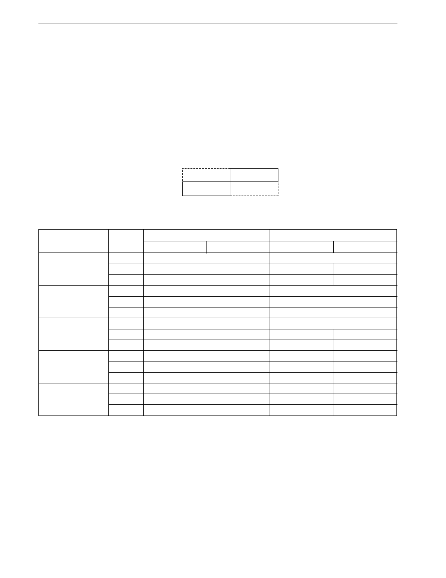
204
CHAPTER 7 REAL-TIME OUTPUT FUNCTION
Preliminary User's Manual U13987EJ1V0UM00
7.3 Real-time Output Port Accesses
The port 0 buffer registers (P0H, P0L) are mapped onto mutually independent addresses in the SFR area as shown in Figure
7-3.
When the 4-bit
�
2-channel real-time output function is specified, data can be set in the P0H, P0L independently of each other.
When the 8-bit
�
1-channel real-time output function is specified, data can be set in P0H and P0L by writing 8-bit data to either
one of the P0H or P0L.
Table 7-1 shows the operations when port 0, the P0H and P0L are manipulated.
Figure 7-3. Port 0 Buffer Register (P0H, P0L) Configuration
High-order 4 bits
P0H
Low-order 4 bits
P0L
0FF0EH
0FF0FH
Table 7-1. Operations when Port 0 and Port 0 Buffer Registers (P0H, P0L) are Manipulated
Operation Mode
Register
Read Operation
Write Operation
High-Order 4 Bits
Low-Order 4 Bits
High-Order 4 Bits
Low-Order 4 Bits
8-bit port mode
P0
Output latch
Output latch
P0L
Buffer register
Note
--
Buffer register
P0H
Buffer register
Note
Buffer register
--
8-bit real-time output
P0
Output latch
--
port mode
P0L
Buffer register
Buffer register
P0H
Buffer register
Buffer register
4-bit separate real-time
P0
Output latch
--
output port mode
P0L
Buffer register
Note
--
Buffer register
P0H
Buffer register
Note
Buffer register
--
P00 to P03: Ports
P0
Output latch
--
Output latch
P04 to P07: Real-time
P0L
Buffer register
Note
--
Buffer register
output port mode
P0H
Buffer register
Note
Buffer register
--
P00 to P03: Real-time
P0
Output latch
Output latch
--
output port mode
P0L
Buffer register
Note
--
Buffer register
P04 to P07: Ports
P0H
Buffer register
Note
Buffer register
--
Note The contents of P0H are read from the high-order 4 bits, and the contents of P0L from the low-order 4 bits.
Remark
-- : The output latch and port 0 buffer registers are not affected.

205
CHAPTER 7 REAL-TIME OUTPUT FUNCTION
Preliminary User's Manual U13987EJ1V0UM00
<Examples of setting data in port 0 buffer registers>
� 4-bit
�
2-channel operation
MOV P0L,
#05H
; Sets 0101B in P0L
MOV P0H, #0C0H
; Sets 1100B in P0H
� 8-bit
�
1-channel operation
MOV P0L,
#0C5H
; Sets 0101B in P0L and 1100B in P0H
or
MOV P0H, #0C5H
The timing for transfer to the output latch can be determined by the following three sources:
� Interrupt from timer/event counter 1 (INTC10 or INTC11)
� INTP0 external interrupt

206
CHAPTER 7 REAL-TIME OUTPUT FUNCTION
Preliminary User's Manual U13987EJ1V0UM00
7.4 Operation
When the port 0 function is specified as the real-time output port, the port 0 buffer register (P0H, P0L) contents are fetched
into the output latch and output to the port 0 pins in synchronization with the generation of one of the trigger conditions shown
in Table 7-2.
For example, the timer/event counter 1 timer counter 1 (TM1) and compare register (CR10, CR11) match signal (INTC10,
INTC11) can be selected as the output trigger generation source. In this case, the port 0 pin output data can be changed to the
P0H and P0L values using the value set in the CR10, CR11 beforehand as the timing interval. Combining this real-time output
port function with the macro service function enables the port 0 output pin output data to be changed sequentially at any interval
time (see 23.8 Macro Service Function).
If the INTP0 external interrupt pin is selected as the output trigger source, port 0 output can be obtained in synchronization
with an external event.
Table 7-2. Real-Time Output Port Output Triggers (when P0MH = P0ML = 1)
RTPC
Output Mode
P0H
P0L
BYTE
EXTR
TRGP0
0
0
0
4-bit real-time output
INTC11
INTC10
0
1
0
INTC11
INTC10 or INTP0
0
1
1
INTC11
INTP0
1
0
0
8-bit real-time output
INTC10
1
1
0
INTC10 or INTP0
1
1
1
INTP0
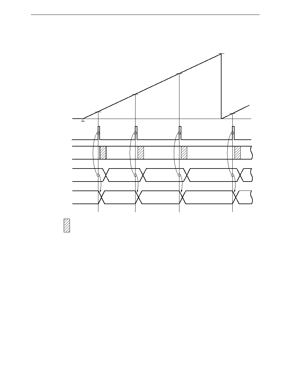
207
CHAPTER 7 REAL-TIME OUTPUT FUNCTION
Preliminary User's Manual U13987EJ1V0UM00
Figure 7-4. Real-Time Output Port Operation Timing
INTC11
interrupt request
CPU operation
Timer/event counter 1
0H
FFH
Output latches
P07 to P04
Timer start
Port 0 buffer register
P0H
D01
CR11
CR11
CR11
CR11
D01
D02
D00
Port 0 buffer register and compare register overwrite by software servicing or macro
service (see 23.8 MACRO SERVICE FUNCTION)
D03
D04
D02
D03
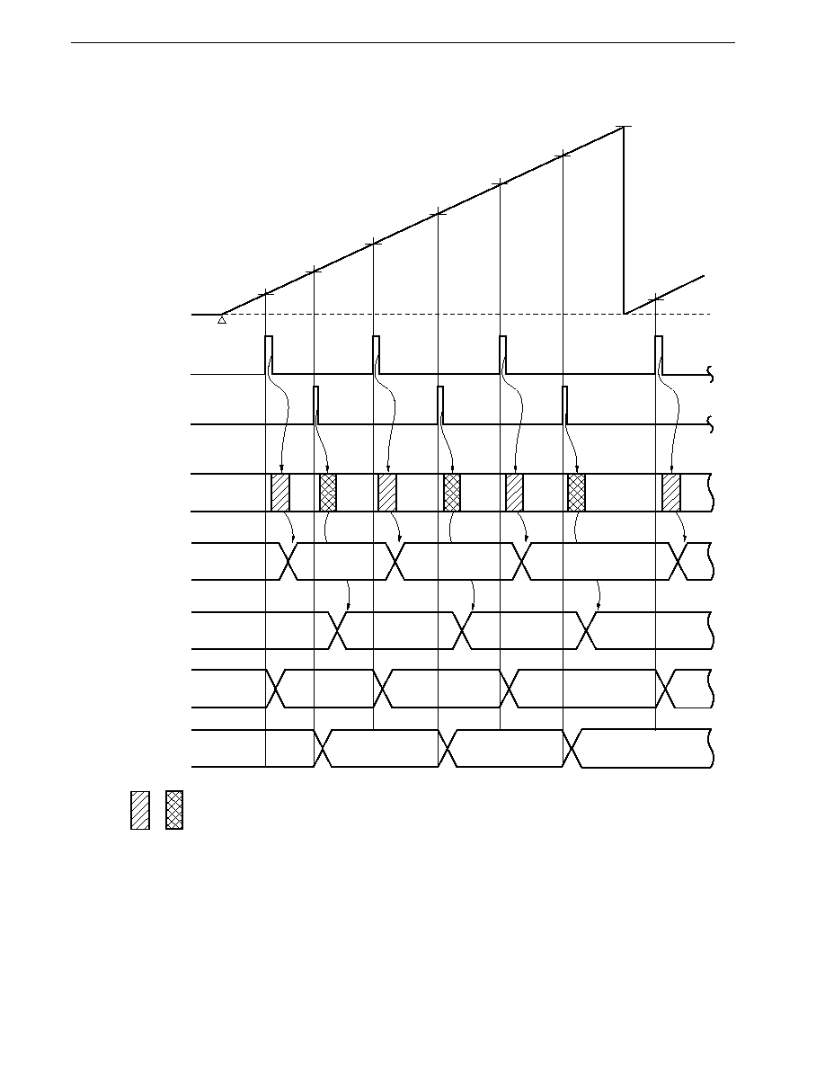
208
CHAPTER 7 REAL-TIME OUTPUT FUNCTION
Preliminary User's Manual U13987EJ1V0UM00
Figure 7-5. Real-Time Output Port Operation Timing (2-channel independent control example)
INTC11
interrupt request
CPU operation
Timer/event counter 1
0H
FFH
Timer start
Output latches
P07 to P04
D00
Port 0 buffer register
P0H
D01
CR11
CR11
CR11
CR11
CR10
CR10
CR10
INTC10
interrupt request
P0L
D11
P03 to P00
D02
D03
D04
D14
D12
D13
D01
D02
D13
D11
D12
D10
D03
Port 0 buffer register and compare register overwrite by software servicing or macro
service (see 23.8 MACRO SERVICE FUNCTION)
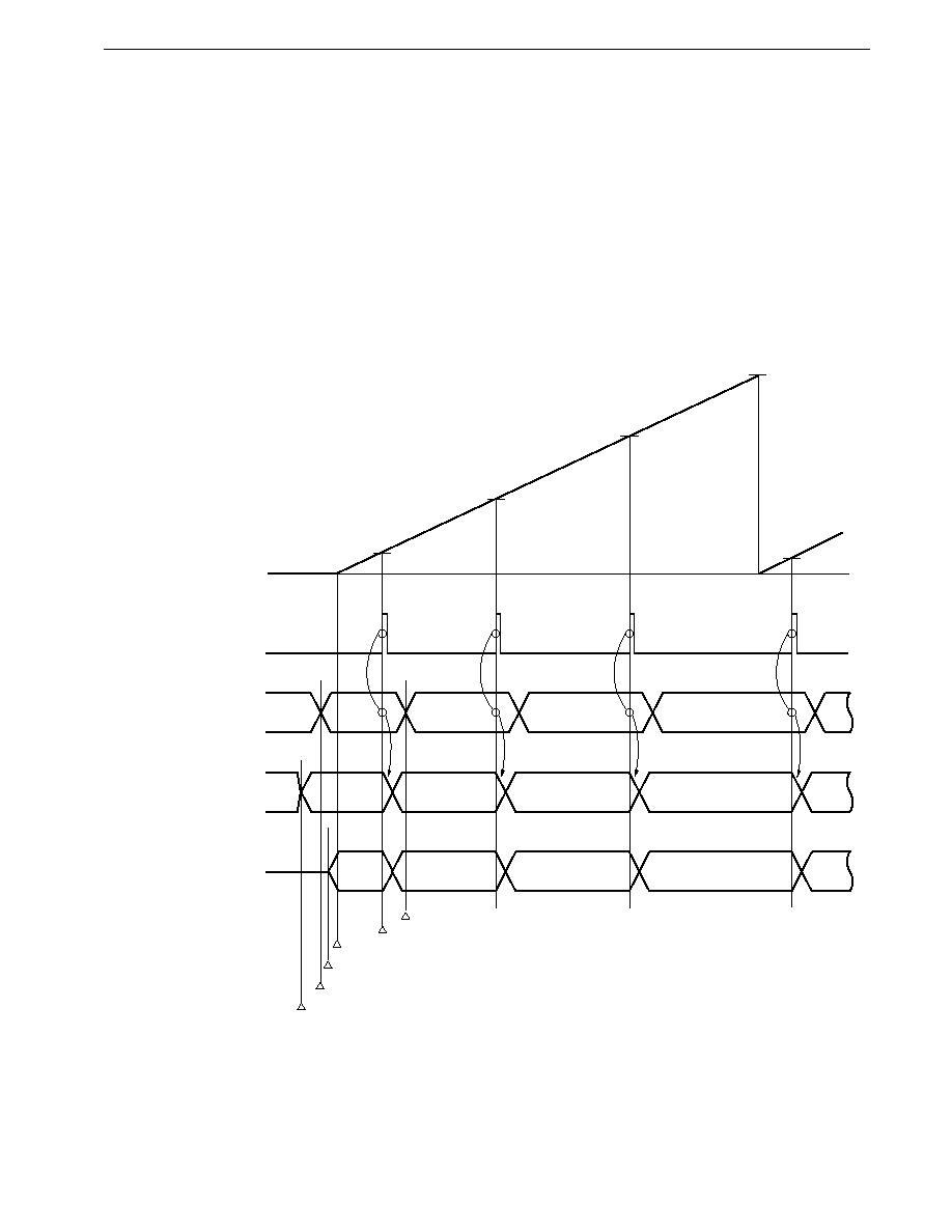
209
CHAPTER 7 REAL-TIME OUTPUT FUNCTION
Preliminary User's Manual U13987EJ1V0UM00
7.5 Example of Use
The case in which P00 to P03 are used as a 4-bit real-time output port is shown here.
Each time the contents of timer/event counter 1 timer counter 1 (TM1) and compare register (CR10) match, the contents of
port 0 buffer register (P0L) are output to P00 to P03. At this time, the next data to be output and the timing at which the output
is to be changed next are set in the service routine for the simultaneously generated interrupt (see Figure 7-6).
See CHAPTER 10 TIMER/EVENT COUNTER 1 for the method of using timer/event counter 1.
The control register settings are shown in Figure 7-7, the setting procedure in Figure 7-8, and the processing in the interrupt
service routine in Figure 7-9.
Figure 7-6. Real-Time Output Port Operation Timing
INTC10
interrupt request
Timer/event counter 1
0H
FFH
Output pins
P00 to P03
D01
D02
Port 0 buffer register
P0L
D02
D03
CR10
CR10
CR10
CR10
Output latches
P00 to P03
D01
D02
D03
D04
D03
D01
D00
D00
P0L and CR10 overwritten by INTC10 interrput
P0L contents transferred to output latch on match of TM1 and CR10
Timer start
Output buffer turned on
Next data to be output is set in P0L
Initial output data is set in output latches P00 to P03
Hi-Z

210
CHAPTER 7 REAL-TIME OUTPUT FUNCTION
Preliminary User's Manual U13987EJ1V0UM00
Figure 7-7. Real-Time Output Function Control Register Settings
7
0
RTPC
6
0
5
0
4
0
3
0
2
0
1
0
0
0
P00 to P03 used as real-time output port
P04 to P07 used as normal output port
4-bit separate real-time output ports selected
Data transfer to output latch from P0L
by INTP0 disabled
Figure 7-8. Real-Time Output Function Setting Procedure
Real-time output port
Set initial value in P0
output latch
Set next value to be output
in P0L
Set real-time output port
control register (RTPC)
Set timer/event counter 1
INTC10 interrupt
Timer start

211
CHAPTER 7 REAL-TIME OUTPUT FUNCTION
Preliminary User's Manual U13987EJ1V0UM00
Figure 7-9. Interrupt Request Servicing when Real-Time Output Function is Used
Timer interrupt
Interval time setting
Set next value to be output
in P0L
Return
7.6 Cautions
(1) When P0ML and P0MH bits are set (to 1), the corresponding port output buffer is turned on and the port 0 output latch
contents are output irrespective of the contents of the port 0 mode register (PM0). The output latch contents should
therefore be initialized before making a real-time output port specification.
(2) When the port is specified as a real-time output port, values cannot be directly written to the output latch by software.
Therefore, the initial value of the output latch must be set by software before specifying use as a real-time output port.
Also, if the need arises to forcibly set the output data to a fixed value while the port is being used as a real-time output
port, you should change the port to a normal output port by manipulating the real-time output port control register (RTPC),
then write the value to be output to the output latch.

212
Preliminary User's Manual U13987EJ1V0UM00
[MEMO]

213
Preliminary User's Manual U13987EJ1V0UM00
CHAPTER 8 OUTLINE OF TIMER
The
�
PD784938 incorporates three timer/event counter units and one timer unit.
These timer/event counter and timer units can be used as seven units of timer/event counters because the
�
PD784938
supports seven interrupt requests.
Table 8-1. Operations of Timer
Name
Timer/Event
Timer/Event
Timer/Event
Timer 3
Item
Counter 0
Counter 1
Counter 2
Count
8 bits
--
width
16 bits
Operation
Interval timer
2 ch
2 ch
2 ch
1 ch
mode
External event counter
--
One-shot timer
--
--
--
Function
Timer output
2 ch
--
2 ch
--
Toggle output
--
--
PWM/PPG output
--
--
One-shot pulse output
Note
--
--
--
Real-time output
--
--
--
Pulse width measurement
1 input
1 input
2 inputs
--
Number of interrupt requests
2
2
2
1
Note
In the one-shot pulse output function, the pulse output level activated by software and inactivated by hardware (an
interrupt request signal).
This function is different in nature from the one-shot timer function of timer/event counter 2.

214
CHAPTER 8 OUTLINE OF TIMER
Preliminary User's Manual U13987EJ1V0UM00
Figure 8-1. Timer Block Diagram
Timer/Event Counter 0
Timer/Event Counter 2
Clear control
INTC00
Compare register
(CR00)
Pulse
output
control
OVF
INTC01
TO0
TO1
Timer counter 0
(TM0)
Prescaler
Edge detection
Selector
Match
Match
INTP3
f
XX
/4
INTP3
Software trigger
Compare register
(CR01)
Capture register
(CR02)
Timer/Event Counter 1
Edge
detection
INTP0
INTP0
Clear control
Compare register
(CR10/CR10W)
Capture/compare register
(CR11/CR11W)
Capture register
(CR12/CR12W)
OVF
Timer counter 1
(TM1/TM1W)
Prescaler
Selector
Match
f
XX
/4
Event input
To real-time
output port
INTC11
INTC10
Match
Clear control
INTC20
Compare register
(CR20/CR20W)
Capture/compare register
(CR21/CR21W)
Capture register
(CR22/CR22W)
Pulse
output
control
OVF
INTC21
TO2
TO3
Timer counter 2
(TM2/TM2W)
Prescaler
Edge
detection
Selector
Match
Match
INTP1
f
XX
/4
INTP2/CI
INTP1
INTP2
Edge
detection
Timer 3
Remark
OVF: Overflow flag
Compare register
(CR30/CR30W)
Timer counter 3
(TM3/TM3W)
Prescaler
Match
f
XX
/4
Match
UART, CSI
INTC30

215
Preliminary User's Manual U13987EJ1V0UM00
CHAPTER 9 TIMER/EVENT COUNTER 0
9.1 Functions
Timer/event counter 0 is a 16-bit timer/event counter.
In addition to its basic functions of interval timer, programmable square-wave output, pulse width measurement and event
counter, timer/event counter 0 can be used for the following functions.
� PWM output
� Cycle measurement
� Soft triggered one-shot pulse output
(1) Interval timer
Generates internal interrupts at preset intervals.
Table 9-1. Timer/Event Counter 0 Interval Time
Minimum Interval Time
Maximum Interval Time
Resolution
4/f
XX
2
16
�
4/f
XX
4/f
XX
(0.32
�
s)
(20.8 ms)
(0.32
�
s)
8/f
XX
2
16
�
8/f
XX
8/f
XX
(0.64
�
s)
(41.7 ms)
(0.64
�
s)
16/f
XX
2
16
�
16/f
XX
16/f
XX
(1.27
�
s)
(83.4 ms)
(1.27
�
s)
32/f
XX
2
16
�
32/f
XX
32/f
XX
(2.54
�
s)
(167 ms)
(2.54
�
s)
64/f
XX
2
16
�
64/f
XX
64/f
XX
(5.09
�
s)
(333 ms)
(5.09
�
s)
128/f
XX
2
16
�
128/f
XX
128/f
XX
(10.17
�
s)
(667 ms)
(10.17
�
s)
256/f
XX
2
16
�
256/f
XX
256/f
XX
(20.35
�
s)
(1.33 s)
(20.35
�
s)
512/f
XX
2
16
�
512/f
XX
512/f
XX
(40.70
�
s)
(2.67 s)
(40.20
�
s)
1,024/f
XX
2
16
�
1,024/f
XX
1,024/f
XX
(81.40
�
s)
(5.33 s)
(81.40
�
s)
( ): When f
XX
= 12.58 MHz

216
CHAPTER 9 TIMER/EVENT COUNTER 0
Preliminary User's Manual U13987EJ1V0UM00
(2) Programmable square-wave output
Outputs square waves independently to the timer output pins (TO0, TO1).
Table 9-2. Timer/Event Counter 0 Programmable Square-Wave Output Setting Range
Minimum Pulse Width
Maximum Pulse Width
4/f
XX
2
16
�
4/f
XX
(0.32
�
s)
(20.8 ms)
8/f
XX
2
16
�
8/f
XX
(0.64
�
s)
(41.7 ms)
16/f
XX
2
16
�
16/f
XX
(1.27
�
s)
(83.4 ms)
32/f
XX
2
16
�
32/f
XX
(2.54
�
s)
(167 ms)
64/f
XX
2
16
�
64/f
XX
(5.09
�
s)
(333 ms)
128/f
XX
2
16
�
128/f
XX
(10.17
�
s)
(667 ms)
256/f
XX
2
16
�
256/f
XX
(20.35
�
s)
(1.33 s)
512/f
XX
2
16
�
512/f
XX
(40.70
�
s)
(2.67 s)
1,024/f
XX
2
16
�
1,024/f
XX
(81.40
�
s)
(5.33 s)
( ): When f
XX
= 12.58 MHz

217
CHAPTER 9 TIMER/EVENT COUNTER 0
Preliminary User's Manual U13987EJ1V0UM00
(3) Pulse width measurement
Detects the pulse width of the signal input to the external interrupt request input pin (INTP3).
Table 9-3. Timer/Event Counter 0 Pulse Width Measurement Range
Measurable Pulse Width
Note
Resolution
4/f
XX
to
2
16
�
4/f
XX
4/f
XX
(0.32
�
s)
(20.8 ms)
(0.32
�
s)
8/f
XX
to
2
16
�
8/f
XX
8/f
XX
(0.64
�
s)
(41.7 ms)
(0.64
�
s)
16/f
XX
to
2
16
�
16/f
XX
16/f
XX
(1.27
�
s)
(83.4 ms)
(1.27
�
s)
32/f
XX
to
2
16
�
32/f
XX
32/f
XX
(2.54
�
s)
(167 ms)
(2.54
�
s)
64/f
XX
to
2
16
�
64/f
XX
64/f
XX
(5.09
�
s)
(333 ms)
(5.09
�
s)
128/f
XX
to
2
16
�
128/f
XX
128/f
XX
(10.17
�
s)
(667 ms)
(10.17
�
s)
256/f
XX
to
2
16
�
256/f
XX
256/f
XX
(20.35
�
s)
(1.33 s)
(20.35
�
s)
512/f
XX
to
2
16
�
512/f
XX
512/f
XX
(40.70
�
s)
(2.67 s)
(40.70
�
s)
1,024/f
XX
to 2
16
�
1,024/f
XX
1,024/f
XX
(81.40
�
s)
(5.33 s)
(81.40
�
s)
( ): When f
XX
= 12.58 MHz
Note
The minimum pulse width that can be measured differs depending on the selected value of f
CLK
.
The minimum pulse width that can be measured is the value of 3/f
CLK
or the value in the above table, whichever is
greater.
(4) Software triggered one-shot pulse output
This is a one-shot pulse output function in which the pulse output level is activated by software and inactivated by hardware
(an interrupt request signal). Control can be performed for the timer output pins (TO0, TO1) independently.
Caution
The software triggered one-shot pulse output function is different in nature from the one-shot timer
function of timer/event counter 2.

218
CHAPTER 9 TIMER/EVENT COUNTER 0
Preliminary User's Manual U13987EJ1V0UM00
(5) External event counter
Counts the clock pulses input from the external interrupt request input pin (INTP3).
The clocks that can be input to timer/event counter 0 are shown in Table 9-4.
Table 9-4. Timer/Event Counter 0 Pulse Width Measurement Time
When Counting One Edge
When Counting Both Edges
Maximum frequency
f
CLK
/6 (2.10 MHz)
f
CLK
/6 (2.10 MHz)
Minimum pulse width
3/f
CLK
(0.24
�
s)
3/f
CLK
(0.24
�
s)
(High and low levels)
( ): When f
CLK
= 12.58 MHz
9.2 Configuration
Timer/event counter 0 consists of the following registers:
� Timer counter (TM0)
�
1
� Compare register (CR00, CR01)
�
2
� Capture register (CR02)
�
1
The block diagram of timer/event counter 0 is shown in Figure 9-1.
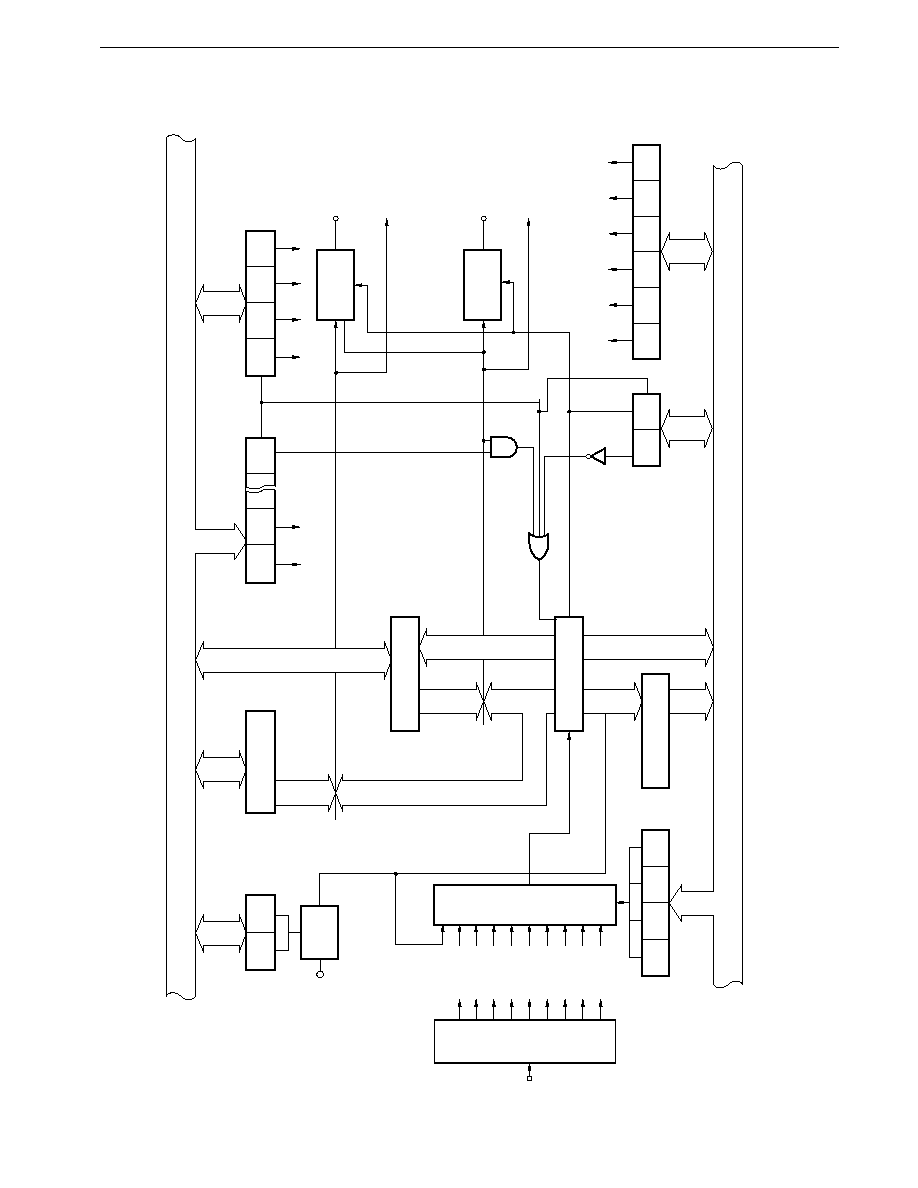
219
CHAPTER 9 TIMER/EVENT COUNTER 0
Preliminary User's Manual U13987EJ1V0UM00
Figure 9-1. Timer/Event Counter 0 Block Diagram
Internal bus
1/8
8/16
8
1/8
External interrupt
mode register 1
(INTM1)
ES31 ES30
P24/INTP3
Edge
detection
circuit
Compare register
(CR00)
16
16
16
MOD1 MOD0
CLR01
PWM/PPG
output control
Capture/compare control
register 0 (CRC0)
ENT01 ALV1 ENT00 ALV0
Timer output
control register
(TOC)
Match
P34/TO0
INTC00
P35/TO1
INTC01
RESET
Clear
Overflow
Compare register
(CR01)
16
16
16
16
16
16
8
Selector
Prescaler
f
XX
/1,024
f
XX
/512
f
XX
/256
f
XX
/128
f
XX
/64
f
XX
f
XX
/32
f
XX
/16
f
XX
/8
f
XX
/4
Prescaler mode
register 0
(PRM0)
PRS03 PRS02 PRS01 PRS00
Capture register
(CR02)
Timer counter 0
(TM0)
Timer control
register 0
(TMC0)
OVF0
CE0
ST1
RT1
OS1
ST0
RT0
OS0
One-shot pulse
control register
(OSPC)
1/8
1/8
Internal bus
Capture trigger
Output
control
circuit
Output
control
circuit

220
CHAPTER 9 TIMER/EVENT COUNTER 0
Preliminary User's Manual U13987EJ1V0UM00
(1) Timer counter 0 (TM0)
TM0 is a timer counter that counts up using the count clock specified by the low-order 4 bits of prescaler mode register 0
(PRM0).
The count operation is stopped or enabled by means of timer control register 0 (TMC0).
TM0 can be read only with a 16-bit manipulation instruction. When RESET is input, TM0 is cleared to 0000H and the count
is stopped.
(2) Compare registers (CR00/CR01)
CR00 and CR01 are 16-bit registers that hold the values that determine the interval timer frequency.
If the CR00/CR01 contents match the contents of TM0, an interrupt request (INTC00/INTC01) and timer output control
signal are generated. Also, the count value can be cleared by a content match (CR01).
CR00 and CR01 can be read or written with a 16-bit manipulation instruction. The contents of these registers are undefined
after RESET input.
(3) Capture register (CR02)
CR02 is a 16-bit register that captures the contents of TM0.
The capture operation is synchronized with the input of a valid edge (capture trigger) on the external interrupt request input
pin (INTP3). The contents of the CR02 are retained until the next capture trigger is generated.
CR02 can be read only with a 16-bit manipulation instruction. The contents of this register are undefined after RESET input.
(4) Edge detection circuit
The edge detection circuit detects an external input valid edge.
When the valid edge set by external interrupt mode register 1 (INTM1) is detected in the INTP3 pin input, the external
interrupt request (INTP3), a capture trigger, and a external event count clock are generated (see Figure 22-2 for details
of the INTM1).
(5) Output control circuit
It is possible to invert the timer output when the compare register (CR00, CR01) register contents and the contents of the
timer counter (TM0) match. A square wave can be output from the timer output pins (TO0/TO1) in accordance with the
setting of the low-order 4 bits of the timer output control register (TOC). At this time, PWM output or PPG output can be
performed according to the specification of capture/compare control register 0 (CRC0).
In addition, one-shot pulse output can also be performed by means of a software trigger.
Timer output can be disabled/enabled by means of the TOC. When timer output is disabled, a fixed level is output to the
TO0 and TO1 pins (the output level is set by the TOC).
(6) Prescaler
The prescaler generates the count clock from the internal system clock. The clock generated by this prescaler is selected
by the selector, and is used as the count clock by the timer counter 0 (TM0) to perform count operations.
(7) Selector
The selector selects a signal resulting from dividing the internal clock or the edge detected by the edge detection circuit as
the count clock of timer counter 0 (TM0).
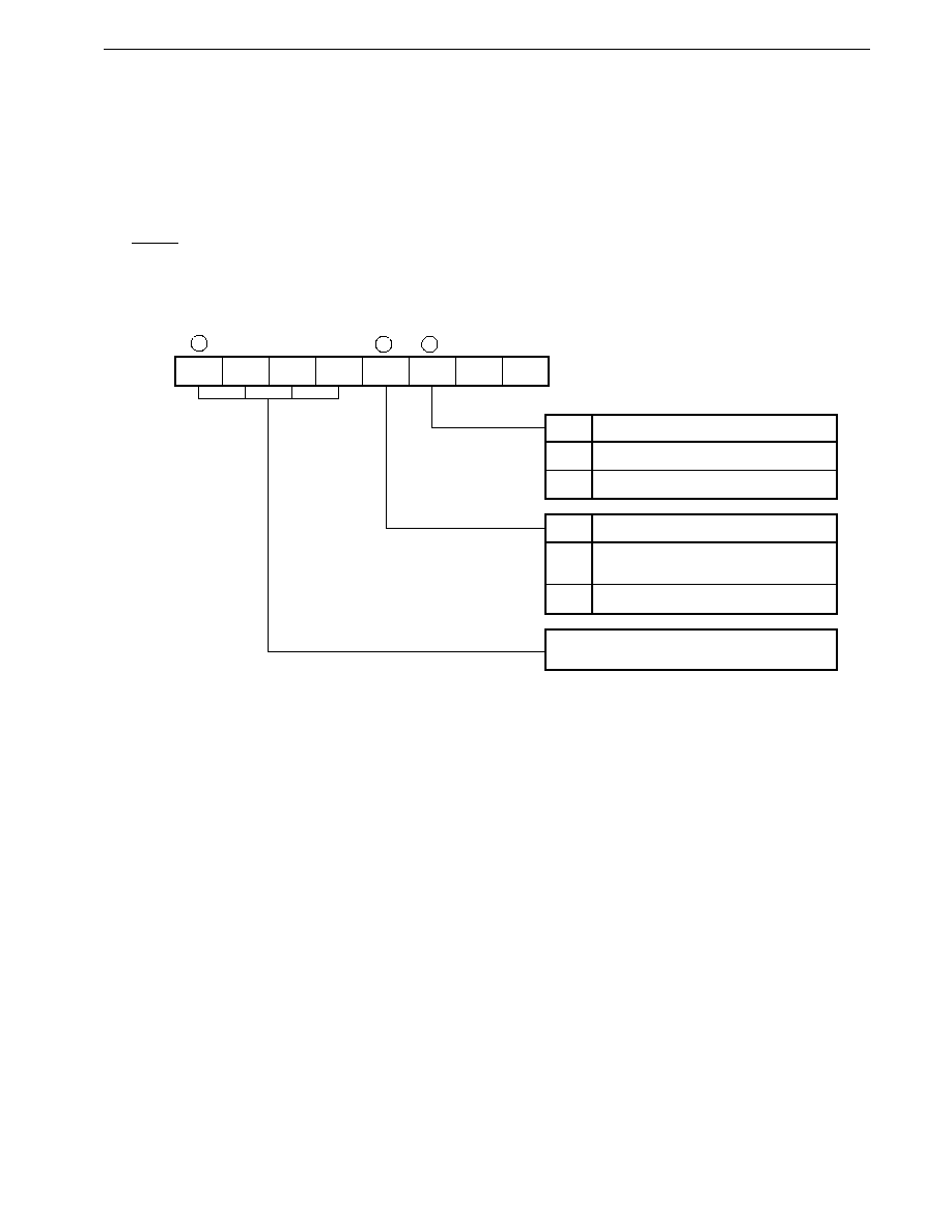
221
CHAPTER 9 TIMER/EVENT COUNTER 0
Preliminary User's Manual U13987EJ1V0UM00
9.3 Timer/Event Counter 0 Control Registers
(1) Timer control register 0 (TMC0)
The timer/event counter 0 TM0 count operation is controlled by the low-order 4 bits in the TMC0 (the high-order 4 bits control
the count operation of the TM3/TM3W of the timer 3).
TMC0 can be read or written to with an 8-bit manipulation instruction or bit manipulation instruction. The format of TMC0
is shown in Figure 9-2.
RESET input clears TMC0 to 00H.
Figure 9-2. Timer Control Register 0 (TMC0) Format
7
CE3
TMC0
6
0
5
0
4
BW3
3
CE0
2
OVF0
1
0
0
0
Address
After reset
R/W
R/W
00H
0FF5DH
OVF0
TM0 Overflow Flag
No overflow
Overflow (count up from FFFFH to 0000H)
1
0
CE0
TM0 Count Operation Control
Count operation stopped with count
cleared
Count operation enabled
1
0
Countrols count operation of the TM3/TM3W of the
timer 3 (see Figure 12-2).
Remark
The OVF0 bit is reset by software only.
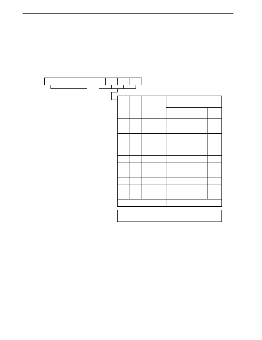
222
CHAPTER 9 TIMER/EVENT COUNTER 0
Preliminary User's Manual U13987EJ1V0UM00
(2) Prescaler mode register 0 (PRM0)
The count clock of the timer/event counter 0 TM0 is specified by the low-order 4 bits of PRM0 (the high-order 4 bits specify
the count clock of the timer 3, TM3/TM3W).
PRM0 can be read/written with an 8-bit manipulation instruction. The format of PRM0 is shown in Figure 9-3.
RESET input sets PRM0 to 11H.
Figure 9-3. Prescaler Mode Register 0 (PRM0) Format
PRS3
PRS2
PRS1
PRS0 PRS03 PRS02 PRS01 PRS00
7
6
5
4
3
2
1
0
PRM0
0FF5CH
Address
11H
After reset
R/W
R/W
PRS03
0
0
0
0
0
0
0
0
1
1
1
Specifies count clock of the TM3/TM3W of the timer 3
(see Figure 12-3).
PRS02
0
0
0
0
1
1
1
1
0
0
1
PRS01
0
0
1
1
0
0
1
1
0
0
1
PRS00
0
1
0
1
0
1
0
1
0
1
1
Timer/Event Counter 0 TM0 Count
Clock Specification
Count Clock [Hz]
Specification
Setting prohibited
f
XX
/4
f
XX
/8
f
XX
/16
f
XX
/32
f
XX
/64
f
XX
/128
f
XX
/256
f
XX
/512
f
XX
/1,024
External clock (INTP3)
Setting prohibited
�
0.32
0.64
1.27
2.54
5.09
10.17
20.35
40.70
81.40
�
(f
XX
= 12.58 MHz)
Other than the above
Resolution
[ s]
�
Remark
f
XX
: X1 input frequency or oscillation frequency
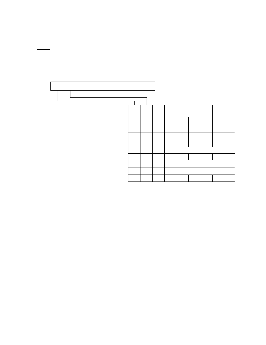
223
CHAPTER 9 TIMER/EVENT COUNTER 0
Preliminary User's Manual U13987EJ1V0UM00
(3) Capture/compare control register 0 (CRC0)
CRC0 specifies the enabling conditions for the TM0 clear operation by a match signal between the contents of the compare
register (CR01) and the timer counter 0 (TM0) counter value, and the timer outputs (TO0/TO1) mode.
CRC0 can be read/written with an 8-bit manipulation instruction. The format of CRC0 is shown in Figure 9-4.
RESET input sets CRC0 to 10H.
Figure 9-4. Capture/Compare Control Register 0 (CRC0) Format
7
MOD1
CRC0
6
MOD0
5
0
4
1
3
CLR01
2
0
1
0
0
0
Address
After reset
R/W
R/W
10H
0FF30H
MOD1 MOD0 CLR01
Timer Output
Mode Specification
TM0 Clear
Opration
when
TM0 = CR01
Toggle output
Toggle output
PWM output
Toggle output
Toggle output
Toggle output
PWM output
PWM output
Disabled
TO0
TO1
Setting prohibited
Setting prohibited
Setting prohibited
Disabled
Enabled
Disabled
0
0
0
0
1
1
1
1
0
0
1
1
0
0
1
1
0
1
0
1
0
1
0
1
PPG output
Toggle output
Enabled
224
CHAPTER 9 TIMER/EVENT COUNTER 0
Preliminary User's Manual U13987EJ1V0UM00
(4) Timer output control register (TOC)
TOC is an 8-bit register that controls the active level of timer output and output enabling/disabling.
The operation of the timer output pins (TO0/TO1) by the timer/event counter 0 is controlled by the low-order 4 bits (the high-
order 4 bits control the operation of the timer output pins (TO2/TO3) by the timer/event counter 2).
TOC can be written to or read with an 8-bit manipulation instruction or bit manipulation instruction. The format of TOC is
shown in Figure 9-5.
RESET input clears TOC to 00H.
Figure 9-5. Timer Output Control Register (TOC) Format
7
ENTO3
TOC
6
ALV3
5
ENTO2
4
ALV2
3
ENTO1
2
ALV1
1
ENTO0
0
ALV0
Address
After reset
R/W
R/W
00H
0FF31H
ALV0
TO0 Pin Active Level
Toggle output specifica-
tion or one-shot pulse
output specificaton
PWM/PPG
output
specification
Low level
High level
High level
Low level
1
0
ENTO0
TO0 Pin Operation Specification
ALV0 output
Pulse output enabled
1
0
ENTO1
TO1 Pin Operation Specification
ALV1 output
Pulse output enabled
1
0
Countrol timer output pins (TO2/TO3) by timer/
event counter 2 (see Figure 11-5).
ALV1
TO1 Pin Active Level
Toggle output specifica-
tion or one-shot pulse
output specificaton
PWM/PPG
output
specification
Low level
High level
High level
Low level
1
0
225
CHAPTER 9 TIMER/EVENT COUNTER 0
Preliminary User's Manual U13987EJ1V0UM00
(5) One-shot pulse output control register (OSPC)
OSPC is an 8-bit register that specifies enabling/disabling of one-shot pulse output by a software trigger and the output
level, etc.
OSPC can be read or written to with an 8-bit manipulation instruction or bit manipulation instruction.
The format of OSPC is shown in Figure 9-6.
RESET input clears OSPC to 00H.
Figure 9-6. One-Shot Pulse Output Control Register (OSPC) Format
Remarks 1. The RT0, ST0, RT1, and ST1 bits are write-only, and show a value of "0" if read.
2. Pin pulse output disabling/enabling and active level setting are performed by means of the timer output control
register (TOC).
7
ST1
OSPC
6
RT1
5
0
4
OS1
3
ST0
2
RT0
1
0
0
OS0
Address
After reset
R/W
R/W
00H
0FF7DH
OS0
TO0 Pulse Output Type Selection
Toggle output/PWM output/PPG output
selectable
Software triggerd one-shot pulse selectable
1
0
ST0
TO0 Output Control
Output not changed
Inactive level output to TO0
0
0
RT0
1
0
Active level output to TO0
Setting prohibited
1
1
1
0
OS1
TO1 Pulse Output Type Selection
Toggle output/PWM output/PPG output
selectable
Software triggerd one-shot pulse output
1
0
ST1
TO1 Output Control
Output not changed
Inactive level output to TO1
0
0
RT1
1
0
Active level output to TO1
Setting prohibited
1
1
1
0

226
CHAPTER 9 TIMER/EVENT COUNTER 0
Preliminary User's Manual U13987EJ1V0UM00
9.4 Timer Counter 0 (TM0) Operation
9.4.1 Basic operation
In the timer/event counter 0 count operation, an count-up is performed using the count clock specified by the low-order 4 bits
of prescaler mode register 0 (PRM0).
Count operation enabling/disabling is controlled by bit 3 (CE0) of timer control register 0 (TMC0). When the CE0 bit is set
(to 1) by software, the contents of TM0 are cleared to 0000H on the first count clock, and then the count-up operation is performed.
When the CE0 bit is cleared (to 0), TM0 becomes 0000H immediately, and capture operations and match signal generation
are stopped.
If the CE0 bit is set (to 1) again when it is already set (1), TM0 continues the count operation without being cleared.
If the count clock is input when TM0 is FFFFH, TM0 becomes 0000H. In this case, OVF0 bit is set (to 1) and an overflow
signal is sent to the output control circuit. OVF0 bit is cleared by software only. The count operation is continued.
When RESET is input, TM0 is cleared to 0000H, and the count operation is stopped.
227
CHAPTER 9 TIMER/EVENT COUNTER 0
Preliminary User's Manual U13987EJ1V0UM00
Figure 9-7. Basic Operation of Timer Counter 0 (TM0)
(a) Count started
count stopped
count started
(b) When "1" is written to the CE0 bit again after the count starts
(c) Operation when TM0 = FFFFH
TM0
CE0
0H
0H
1H
2H
FFH
100H
101H
0H
1H
0H
Count started
CE0
1
Count stopped
CE0
0
Count started
CE0
1
Count clock
f
CLK
/8
TM0
CE0
0H
0H
1H
2H
3H
4H
5H
6H
Count started
CE0
1
Rewrite
CE0
1
Count clock
f
CLK
/8
TM0
OVF0
FFFEH FFFFH
0H
Cleared by software
OVF0
0
Count clock
f
CLK
/8
1H
228
CHAPTER 9 TIMER/EVENT COUNTER 0
Preliminary User's Manual U13987EJ1V0UM00
9.4.2 Clear operation
(1) Clear operation after a match with the compare register
The timer counter 0 (TM0) can be cleared automatically after a match with the compare register (CR01). When a clearance
source arises, TM0 is cleared to 0000H on the next count clock. Therefore, even if a clearance source arises, the value
at the point at which the clearance source arose is retained until the next count clock arrives.
Figure 9-8. TM0 Clearance by Match with Compare Register (CR01)
(2) Clear operation by the CE0 bit of the timer control register 0 (TMC0)
The timer counter 0 (TM0) is also cleared when the CE0 bit of TMC0 is cleared (to 0) by software. The clear operation is
performed immediately after clearance (to 0) of the CE0 bit.
TM0
Compare register
(CR01)
n
Cleared here
Count clock
0
1
n-1
n
TM0 and CR01 match
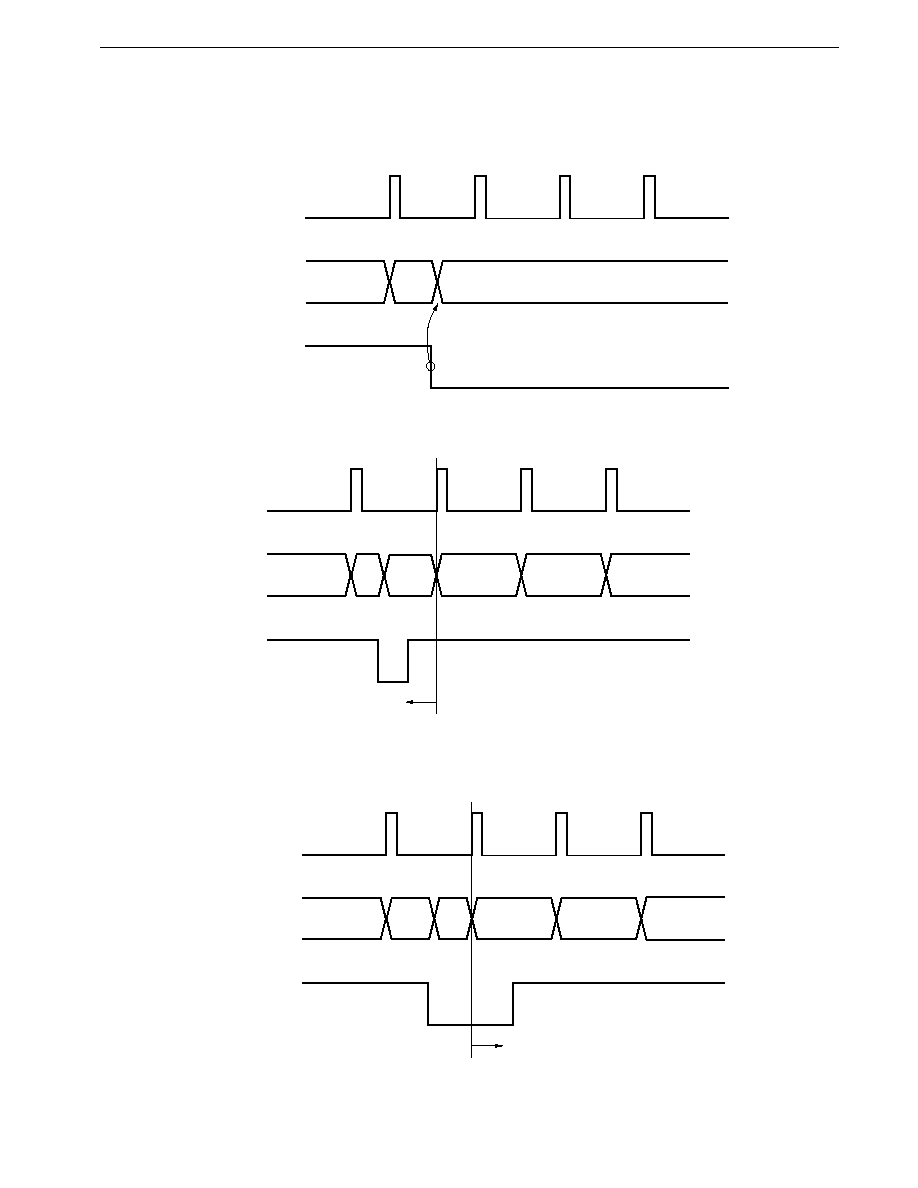
229
CHAPTER 9 TIMER/EVENT COUNTER 0
Preliminary User's Manual U13987EJ1V0UM00
Figure 9-9. Clear Operation when CE0 Bit is Cleared (0)
(a) Basic operation
(b) Restart before count clock input after clearance
(c) Restart after count clock input after clearance
TM0
CE0
n
Count clock
n-1
0
TM0
CE0
n
0
Count clock
n-1
0
1
2
If the CE0 bit is set (to 1) before this count clock, the count starts from 0 on the count clock.
TM0
CE0
n
Count clock
n-1
0
0
0
1
If the CE0 bit is set (to 1) from this count clock onward, the count starts from 0
on the count clock after the CE0 bit is set (to 1).
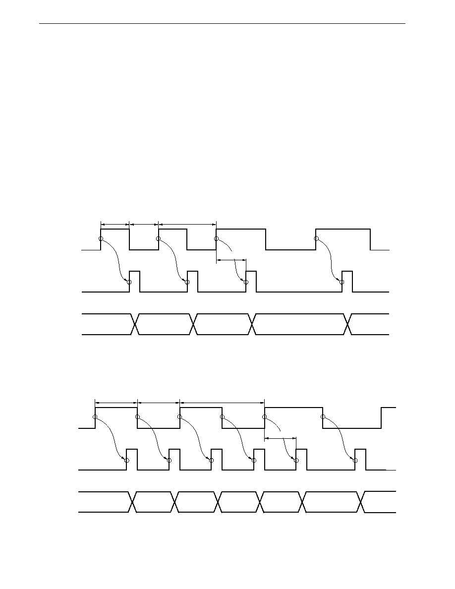
230
CHAPTER 9 TIMER/EVENT COUNTER 0
Preliminary User's Manual U13987EJ1V0UM00
9.5 External Event Counter Function
The timer/event counter 0 can count clock pulses input from the external interrupt request input pin (INTP3).
No special selection method is needed for the external event counter operation mode. When the timer counter 0 (TM0) count
clock is specified as external clock input by the setting of the low-order 4 bits of prescaler mode register 0 (PRM0), TM0 operates
as an external event counter.
The maximum frequency of external clock pulses that can be counted by TM0 as the external event counter is 2.10 MHz (f
CLK
= 12.58 MHz) irrespective of whether only one edge or both edges are counted on INTP3 input.
The pulse width of the INTP3 input must be at least 3 system clocks (0.24
�
s: f
CLK
= 12.58 MHz) for both the high level and
low level. If the pulse width is shorter than this, the pulse may not be counted.
The timer/event counter 0 external event counter timing is shown in Figure 9-10.
Figure 9-10. Timer/Event Counter 0 External Event Count Timing
(1) Counting one edge (maximum frequency = f
CLK
/6)
Remark
ICI: INTP3 input signal after passing through edge detection circuit
(2) Counting both edges (maximum frequency = f
CLK
/6)
Remark
ICI: INTP3 input signal after passing through edge detection circuit
ICI
TM0
INTP3
Dn
3/f
CLK
(MIN.) 3/f
CLK
(MIN.)
6/f
CLK
(MIN.)
Dn+1
Dn+2
Dn+3
2-3/f
CLK
ICI
TM0
INTP3
Dn+1
Dn
Dn+2
Dn+3
Dn+4
Dn+5
3/f
CLK
(MIN.)
3/f
CLK
(MIN.)
6/f
CLK
(MIN.)
2-3/f
CLK

231
CHAPTER 9 TIMER/EVENT COUNTER 0
Preliminary User's Manual U13987EJ1V0UM00
The TM0 count operation is controlled by the CE0 bit of the timer control register 0 (TMC0) in the same way as with basic
operation.
When the CE0 bit is set (to 1) by software, the contents of TM0 are set to 0000H and the count-up is started on the initial count
clock.
When the CE0 bit is cleared (to 0) by software during a TM0 count operation, the contents of TM0 are set to 0000H immediately
and the stopped state is entered. The TM0 count operation is not affected if the CE0 bit is set (to 1) by software again when
it is already set (to 1).
Caution
When timer/event counter 0 is used as an external event counter, it is not possible to distinguish between
the case where there is no valid edge input at all and the case where there is a single valid edge input, using
the timer counter 0 (TM0) alone (see Figure 9-11), since the contents of TM0 are 0 in both cases. If it is
necessary to make this distinction, the INTP3 interrupt request flag should be used. An example is shown
in Figure 9-12.
Figure 9-11. Example of the Case where the External Event Counter does Not Distinguish between One
Valid Edge Input and No Valid Edge Input
TM0
0
INTP3
1
2
0
Count start
No distinction made
232
CHAPTER 9 TIMER/EVENT COUNTER 0
Preliminary User's Manual U13987EJ1V0UM00
Figure 9-12. To Distinguish whether One or No Valid Edge has been Input with External Event Counter
(a) Processing when count is started
Clear INTP3 interrupt
request flag
PIF3
0
; Clear PIF3 to 0
End
Start count
Start count
CE0
1
; Set CE0 to 1
(b) Processing when count value is read
Read TM0 contents
AX
TM0
AX
AX+1
; Check PIF3 contents
If 1, there is a valid
edge
; Number of input valid edges is set in AX register
; Check TM0 value
If 0, check interrupt
request flag
End
PIF3 = 1?
YES
YES
NO
NO
Count value read
AX = 0?
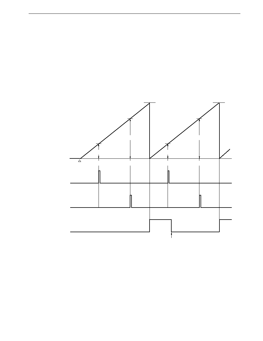
233
CHAPTER 9 TIMER/EVENT COUNTER 0
Preliminary User's Manual U13987EJ1V0UM00
9.6 Compare Register and Capture Register Operation
9.6.1 Compare operations
Timer/event counter 0 performs compare operations in which the value set in compare registers (CR00, CR01) are compared
with the timer counter 0 (TM0) count value.
If the count value of TM0 matches the preset CR0n (n = 0, 1) value as the result of the count operation, a match signal is sent
to the output control circuit, and at the same time an interrupt request (INTC00/INTC01) is generated.
After a match with the CR01 value, the TM0 count value can be cleared, and the timer functions as an interval timer that
repeatedly counts up to the value set in the CR01.
Figure 9-13. Compare Operation
INTC00
interrupt request
TM0
Count value
0H
FFFFH
Count start
CE0
1
CR00 value
CR01 value
FFFFH
CR00 value
CR01 value
INTC01
interrupt request
OVF0
Match
Match
Match
Match
Cleared by software
Remark
CLR01 = 0
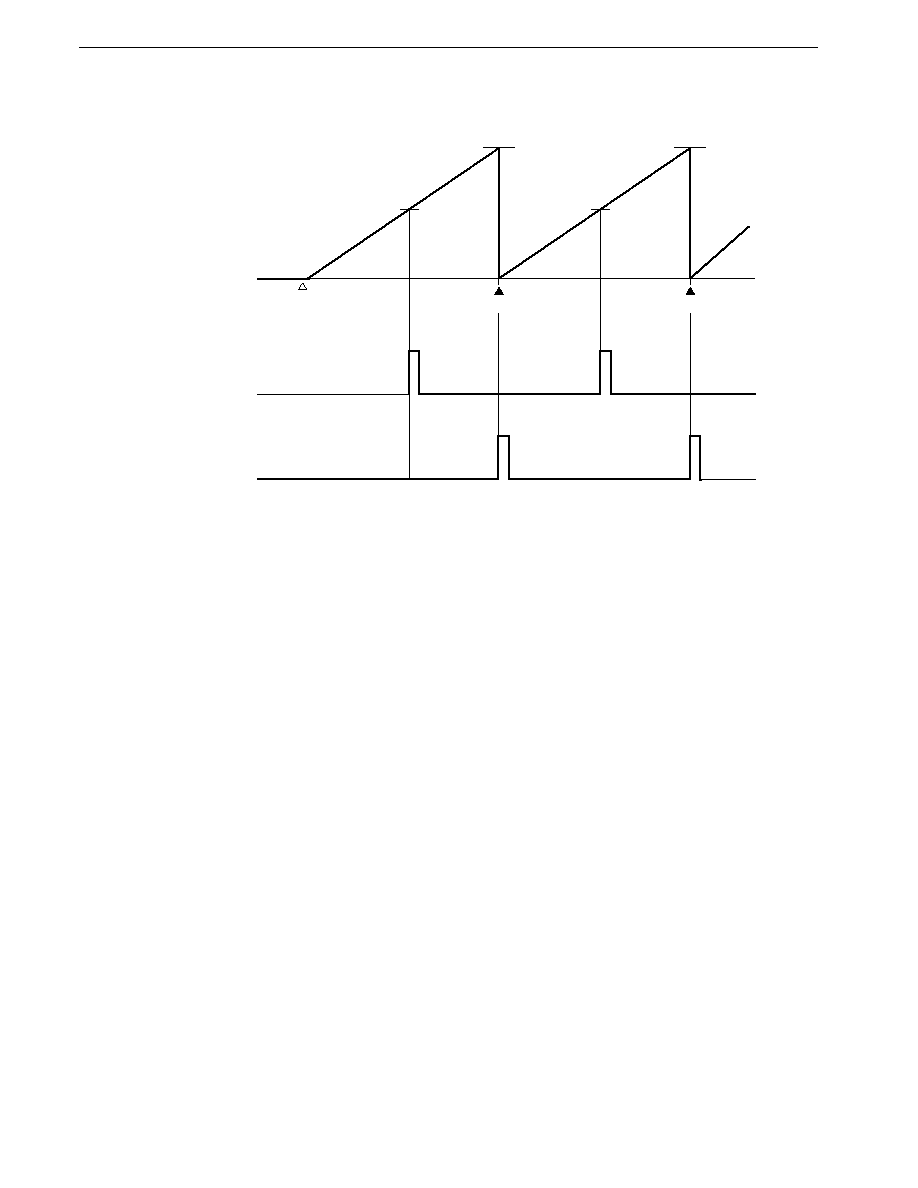
234
CHAPTER 9 TIMER/EVENT COUNTER 0
Preliminary User's Manual U13987EJ1V0UM00
Figure 9-14. TM0 Clearance After Match Detection
Remark
CLR01 = 0
INTC00
interrupt request
TM0
Count value
0H
CR01
Count start
CE0
1
INTC01
interrupt request
CR00
Clear
Clear
CR01
CR00
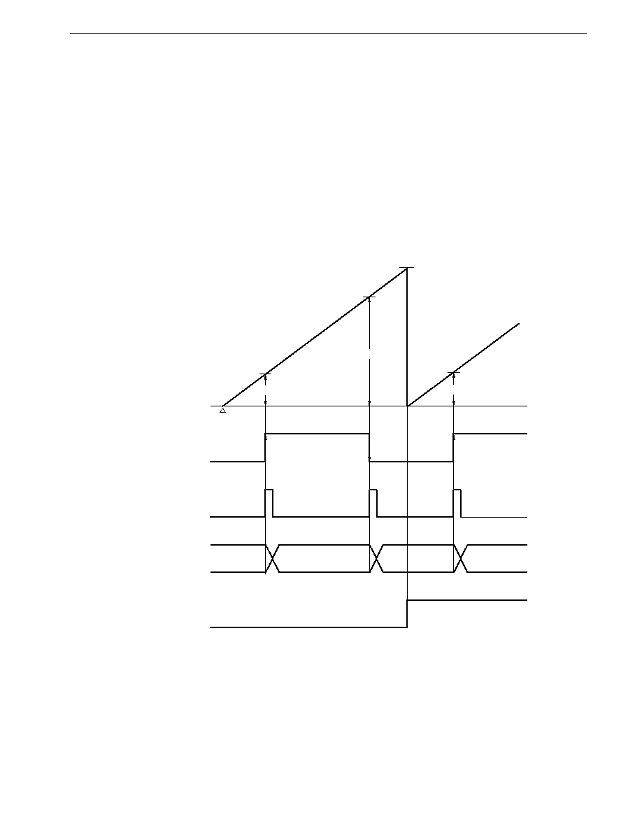
235
CHAPTER 9 TIMER/EVENT COUNTER 0
Preliminary User's Manual U13987EJ1V0UM00
9.6.2 Capture operations
Timer/event counter 0 performs capture operations in which the timer counter 0 (TM0) count value is fetched into the capture
register in synchronization with an external trigger, and retained there.
A valid edge detected from the input of the external interrupt request input pin (INTP3) is used as the external trigger (capture
trigger). The count value of TM0 in the process of being counted is fetched into the capture register (CR02) in synchronization
with the capture trigger, and is retained there. The contents of the CR02 are retained until the next capture trigger is generated.
The capture trigger valid edge is set by means of external interrupt mode register 1 (INTM1). If both rising and falling edges
are set as capture triggers, the width of pulses input from off-chip can be measured. Also, if a capture trigger is generated by
a single edge, the input pulse cycle can be measured.
See Figure 22-2 for details of the INTM1.
Figure 9-15. Capture Operation
Remark
Dn: TM0 count value (n = 0, 1, 2, ...)
CLR01 = 0
INTP3
pin input
INTP3
interrupt request
TM0
count value
0H
FFFFH
OVF0
D0
D1
D2
Count start
CE0
1
D0
D1
D2
Capture register
(CR02)

236
CHAPTER 9 TIMER/EVENT COUNTER 0
Preliminary User's Manual U13987EJ1V0UM00
9.7 Basic Operation of Output Control Circuit
The output control circuit controls the timer output pin (TO0/TO1) levels by means of overflow signals or match signals from
the compare registers (CR00, CR01). The operation of the output control circuit is determined by the timer output control register
(TOC), capture/compare control register 0 (CRC0), and the one-shot pulse output control register (OSPC) (see Table 9-5).
When TO0, TO1 signals are output to a pin, the relevant pin must be in control mode in the port 3 mode register (PMC3).

237
CHAPTER 9 TIMER/EVENT COUNTER 0
Preliminary User's Manual U13987EJ1V0UM00
Table 9-5. Timer Output (TO0/TO1) Operations
TOC
OSPC
CRC0
TO1
TO0
ENTO1
ALV1
ENTO0
ALV0
OS1
OS0
MOD1
MOD0
CLR01
0
0/1
0
0/1
�
�
�
�
�
High/low level fixed
High/low level fixed
0
0/1
1
0/1
�
0
0
0
�
High/low level fixed
Toggle output (active-low/high)
0
0/1
1
0/1
�
0
0
1
0
High/low level fixed
PWM output (active-high/low)
0
0/1
1
0/1
�
0
1
0
0
High/low level fixed
PWM output (active-high/low)
0
0/1
1
0/1
�
0
1
1
1
High/low level fixed
PPG output (active-high/low)
0
0/1
1
0/1
�
1
�
�
�
High/low level fixed
One-shot pulse output (active-low/high)
1
0/1
0
0/1
0
�
0
�
�
Toggle output (active-low/high)
High/low level fixed
1
0/1
0
0/1
0
�
1
0
0
PWM output (active-high/low)
High/low level fixed
1
0/1
0
0/1
0
�
1
1
�
Toggle output (active-low/high)
High/low level fixed
1
0/1
0
0/1
1
�
�
�
�
One-shot pulse output (active-low/high)
High/low level fixed
1
0/1
1
0/1
0
0
0
0
�
Toggle output (active-low/high)
Toggle output (active-low/high)
1
0/1
1
0/1
0
0
0
1
0
Toggle output (active-low/high)
PWM output (active-high/low)
1
0/1
1
0/1
0
0
1
0
0
PWM output (active-high/low)
PWM output (active-high/low)
1
0/1
1
0/1
0
0
1
1
1
Toggle output (active-low/high)
PPG output (active-high/low)
1
0/1
1
0/1
0
1
0
�
�
Toggle output (active-low/high)
One-shot pulse output (active-low/high)
1
0/1
1
0/1
0
1
1
0
0
PWM output (active-high/low)
One-shot pulse output (active-low/high)
1
0/1
1
0/1
0
1
1
1
1
Toggle output (active-low/high)
One-shot pulse output (active-low/high)
1
0/1
1
0/1
1
0
0
0
�
One-shot pulse output (active-low/high)
Toggle output (active-low/high)
1
0/1
1
0/1
1
0
0
1
0
One-shot pulse output (active-low/high)
PWM output (active-high/low)
1
0/1
1
0/1
1
0
1
0
0
One-shot pulse output (active-low/high)
PWM output (active-high/low)
1
0/1
1
0/1
1
0
1
1
1
One-shot pulse output (active-low/high)
PPG output (active-high/low)
1
0/1
1
0/1
1
1
�
�
�
One-shot pulse output (active-low/high)
One-shot pulse output (active-low/high)
Remarks 1. In the ALVn (n = 0, 1) columns, the figures on the left and right of the slash ("/") correspond to the items on the left and right of the slash in the TOn
(n = 0, 1) columns.
2. The "
�
" mark indicates that the operation is the same for either 0 or 1, but some prohibited combinations are included (see Figure 9-4).
3. Use with combinations not shown in this table is prohibited.
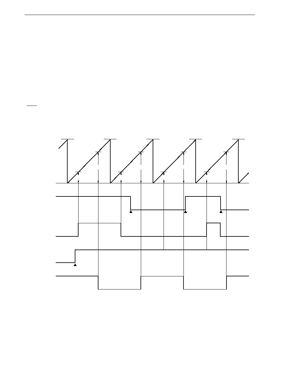
238
CHAPTER 9 TIMER/EVENT COUNTER 0
Preliminary User's Manual U13987EJ1V0UM00
9.7.1 Basic operation
Setting (to 1) the ENTOn (n = 0, 1) bit of the timer output control register (TOC) enables timer output (TOn: n = 0, 1) to be
varied at a timing in accordance with the settings of MOD0, MOD1, and CLR01 bits of capture/compare control register 0 (CRC0)
and the one-shot pulse output control register (OSPC).
Clearing (to 0) ENTOn sets the TOn to a fixed level. The fixed level is determined by the ALVn (n = 0, 1) bit of the TOC. The
level is high when ALVn is 0, and low when 1.
9.7.2 Toggle output
Toggle output is an operation mode in which the output level is inverted each time the compare register (CR00/CR01) value
coincides with the timer counter 0 (TM0) value. The output level of timer output (TO0) is inverted by a match between CR00
and TM0, and the output level of TO1 is inverted by a match between CR01 and TM0.
When timer/event counter 0 is stopped by clearing (to 0) the CE0 bit of the timer control register 0 (TMC0), the inactive level
(ALVn: n = 0, 1) is output.
Figure 9-16. Toggle Output Operation
ENTO0
TM0
count value
0H
FFFFH
CR00 value
CR01 value
FFFFH
CR00 value
CR01 value
FFFFH
CR00 value
CR01 value
FFFFH
CR00 value
CR01 value
FFFFH
TO0 output
(ALV0 = 1)
ENTO1
Instruction
execution
Instruction
execution
Instruction
execution
Instruction
execution
TO1 output
(ALV1 = 0)

239
CHAPTER 9 TIMER/EVENT COUNTER 0
Preliminary User's Manual U13987EJ1V0UM00
Table 9-6. TO0, TO1 Toggle Output (f
XX
= 12.58 MHz)
Count Clock
Minimum Pulse Width
Maximum Interval Time
f
XX
/4
0.32
�
s
0.02 s
f
XX
/8
0.64
�
s
0.04 s
f
XX
/16
1.27
�
s
0.08 s
f
XX
/32
2.54
�
s
0.17 s
f
XX
/64
5.09
�
s
0.33 s
f
XX
/128
10.17
�
s
0.67 s
f
XX
/256
20.35
�
s
1.33 s
f
XX
/512
40.70
�
s
2.67 s
f
XX
/1,024
81.40
�
s
5.33 s
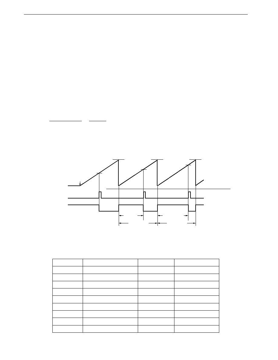
240
CHAPTER 9 TIMER/EVENT COUNTER 0
Preliminary User's Manual U13987EJ1V0UM00
9.7.3 PWM output
(1) Basic operation of PWM output
In this mode, a PWM signal with the period in which timer counter 0 (TM0) reaches a full count used as one cycle is output.
The timer output (TO0) pulse width is determined by the value of compare register (CR00), and the timer output (TO1) pulse
width is determined by the value of compare register (CR01). When this function is used, the CLR01 bit of capture/compare
control register 0 (CRC0) must be set to 0.
The pulse cycle and pulse width are as shown below.
� PWM cycle = 65,536
�
x/f
XX
� PWM pulse width = CR0n
�
x/f
XX
Note
; x = 4, 8, 16, 32, 64, 128, 256, 512, 1,024
Note 0 cannot be set in the CR0n.
� Duty =
PWM pulse width
=
CR0n
PWM cycle
65,536
Remark n = 0, 1
Figure 9-17. PWM Pulse Output
Remark ALV0 = 0
Table 9-7. TO0, TO1 PWM Cycle (f
XX
= 12.58 MHz)
Count Clock
Minimum Pulse Width [
�
s]
PWM Cycle [s]
PWM Frequency [Hz]
f
XX
/4
0.32
0.02
47.6
f
XX
/8
0.64
0.04
23.8
f
XX
/16
1.27
0.08
12.0
f
XX
/32
2.54
0.17
6.0
f
XX
/64
5.09
0.33
3.0
f
XX
/128
10.17
0.67
1.5
f
XX
/256
20.35
1.33
0.7
f
XX
/512
40.70
2.67
0.4
f
XX
/1,024
81.40
5.33
0.2
CR00
Interrupt
Timer count
0H
FFFFH
Count start
CR00
FFFFH
FFFFH
Pulse
width
Pulse cycle
TO0
CR00
Pulse width
Pulse cycle
241
CHAPTER 9 TIMER/EVENT COUNTER 0
Preliminary User's Manual U13987EJ1V0UM00
Figure 9-18 shows an example of 2-channel PWM output, and Figure 9-19 shows the operation of the case where FFFFH
is set in the CR00.
Figure 9-18. Example of PWM Output Using TM0
Remark
ALV0 = 0, ALV1 = 0
Figure 9-19. Example of PWM Output when CR00 = FFFFH
Remarks 1.
ALV0 = 0
2.
T = x/f
XX
(x = 4, 8, 16, 32, 64, 128, 256, 512, 1,024)
TM0
count value
0H
CR00
FFFFH
INTC00
CR01
CR00
FFFFH
CR01
CR00
FFFFH
INTC01
TO0
TO1
TM0
count value
FFFFH
INTC00
0
1
2
FFFEH
FFFFH
0
1
2
FFFEH
Count clock cycle T
FFFFH
0
Pulse width
T
Duty =
�
100 = 99.998 (%)
.
.
65,535
65,536
Pulse cycle = 65,536T
TO0
OVF flag
242
CHAPTER 9 TIMER/EVENT COUNTER 0
Preliminary User's Manual U13987EJ1V0UM00
(2) Rewriting compare registers (CR00, CR01)
The output level of the timer output (TOn: n = 0, 1) does not change even if the CR0n (n = 0, 1) value matches the timer
counter 0 (TM0) value more than once during one PWM output cycle.
Figure 9-20. Example of Compare Register (CR00) Rewrite
CR00
TO0
TM0
count value
0H
T1
T2
T1
T2
T1
T2
CR00 and TM0 values match, but TO0 does not change here.
CR00
rewrite
FFFFH
T1
FFFFH
243
CHAPTER 9 TIMER/EVENT COUNTER 0
Preliminary User's Manual U13987EJ1V0UM00
If a value smaller than that of the TM0 is set as the CR0n value, a 100% duty PWM signal will be output. CR0n rewriting should
be performed by the interrupt due to a match between TM0 and the CR0n on which the rewrite is performed.
Figure 9-21. Example of 100% Duty with PWM Output
Remark
ALV0 = 0
CR00
TO0
TM0
count value
0H
n1
n2
n3
n1
When value n2 which is smaller than the TM0 value n3 is
written to CR00, the duty of this period will be 100%.
FFFFH
FFFFH
FFFFH
FFFFH
n2
n2
n2
n1

244
CHAPTER 9 TIMER/EVENT COUNTER 0
Preliminary User's Manual U13987EJ1V0UM00
(3) Stopping PWM output
If timer/event counter 0 is stopped by clearing (to 0) the CE0 bit of the timer control register 0 (TMC0) during PWM signal
output, the active level is output.
Figure 9-22. When Timer/Event Counter 0 is Stopped During PWM Signal Output
Remark
ALV0 = 1
Caution
The output level of the TOn (n = 0, 1) pin when timer output is disabled (ENTOn = 0: n = 0, 1) is the inverse
of the value set in ALVn (n = 0, 1) bit. Caution is therefore required as the active level is output when timer
output is disabled when the PWM output function has been selected.
TO0
TM0
count value
0H
CR00
FFFFH
FFFFH
CR00
245
CHAPTER 9 TIMER/EVENT COUNTER 0
Preliminary User's Manual U13987EJ1V0UM00
9.7.4 PPG output
(1) Basic operation of PPG output
This function outputs a square-wave with the time determined by compare register CR01 value as one cycle, and the time
determined by compare register CR00 value as the pulse width. The PWM cycle output by the PWM is made variable. This
signal can only be output from the timer output (TO0).
When this function is used, the CLR01 bit of capture/compare control register 0 (CRC0) must be set to 1.
The pulse cycle and pulse width are as shown below.
� PPG cycle = (CR01 + 1)
�
x/f
XX
; x = 4, 8, 16, 32, 64, 128, 256, 512, 1,024
� PPG pulse width = CR00
�
x/f
XX
where 1
CR00
CR01
� Duty =
PPG pulse width
=
CR00
PPG cycle
CR01 + 1
Figure 9-23 shows an example of PPG output using timer counter 0 (TM0), Figure 9-24 shows an example of the case where
CR00 = CR01.
Figure 9-23. Example of PPG Output Using TM0
Remark
ALV0 = 0, ALV1 = 0
INTC01
TM0
count value
0H
CR00
CR00
CR00
CR01
CR01
CR01
INTC00
TO0
(PPG output)
Pulse
width
Count start
Pulse cycle
TO1
(timer output)
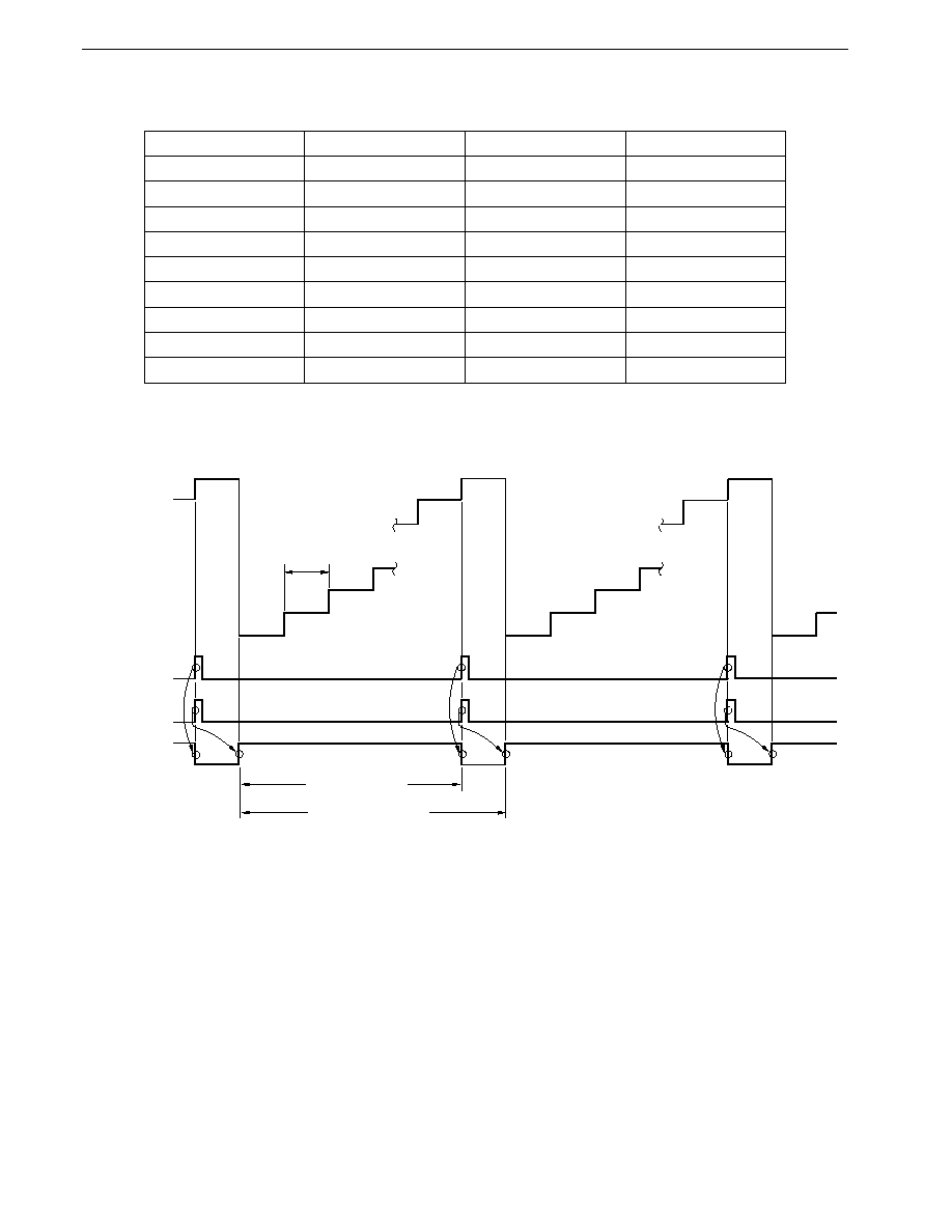
246
CHAPTER 9 TIMER/EVENT COUNTER 0
Preliminary User's Manual U13987EJ1V0UM00
Table 9-8. TO0 PPG Output (f
XX
= 12.58 MHz)
Count Clock
Minimum Pulse Width [
�
s]
PPG Cycle
PPG Frequency
f
XX
/4
0.32
0.64
�
s to 20.84 ms
1572 kHz to 48.0 Hz
f
XX
/8
0.64
1.27
�
s to 41.68 ms
786 kHz to 24.0 Hz
f
XX
/16
1.27
2.54
�
s to 83.35 ms
393 kHz to 12.0 Hz
f
XX
/32
2.54
5.09
�
s to 166.71 ms
197 kHz to 6.0 Hz
f
XX
/64
5.09
10.17
�
s to 333.41 ms
98.3 kHz to 3.0 Hz
f
XX
/128
10.17
20.35
�
s to 666.82 ms
49.1 kHz to 1.5 Hz
f
XX
/256
20.35
40.70
�
s to 1.33 s
24.6 kHz to 0.7 Hz
f
XX
/512
40.70
81.40
�
s to 2.67 s
12.3 kHz to 0.4 Hz
f
XX
/1,024
81.40
162.80
�
s to 5.33 s
6.1 kHz to 0.2 Hz
Figure 9-24. Example of PPG Output when CR00 = CR01
Remark
ALV0 = 0
T = x/f
XX
(x = 4, 8, 16, 32, 64, 128, 256, 512, 1,024)
TM0
count value
n
INTC00
0
1
2
n-1
n
0
1
2
n-1
Count cycle T
n
0
Pulse width = nT
Pulse cycle = (n+1) T
INTC01
TO0
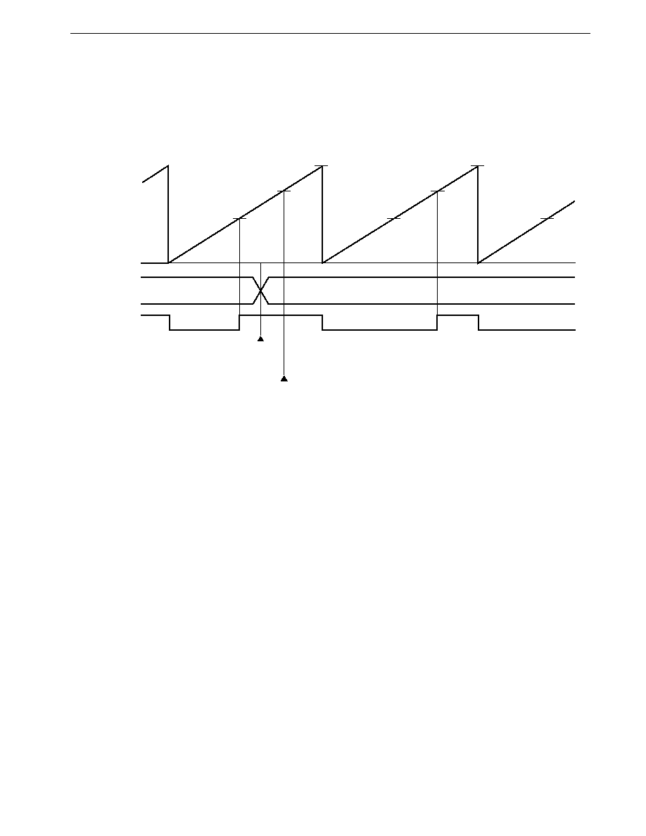
247
CHAPTER 9 TIMER/EVENT COUNTER 0
Preliminary User's Manual U13987EJ1V0UM00
(2) Rewriting compare register (CR00)
The output level of the timer output (TO0) does not change even if the CR00 value matches the timer counter 0 (TM0) value
more than once during one PPG output cycle.
Figure 9-25. Example of Compare Register (CR00) Rewrite
Remark
ALV0 = 1
CR00
TO0
TM0
count value
0H
T1
T2
T1
T2
CR00 and TM0 values match, but TO0 does not change here.
CR00
rewrite
CR01
T1
CR01
T1
T2
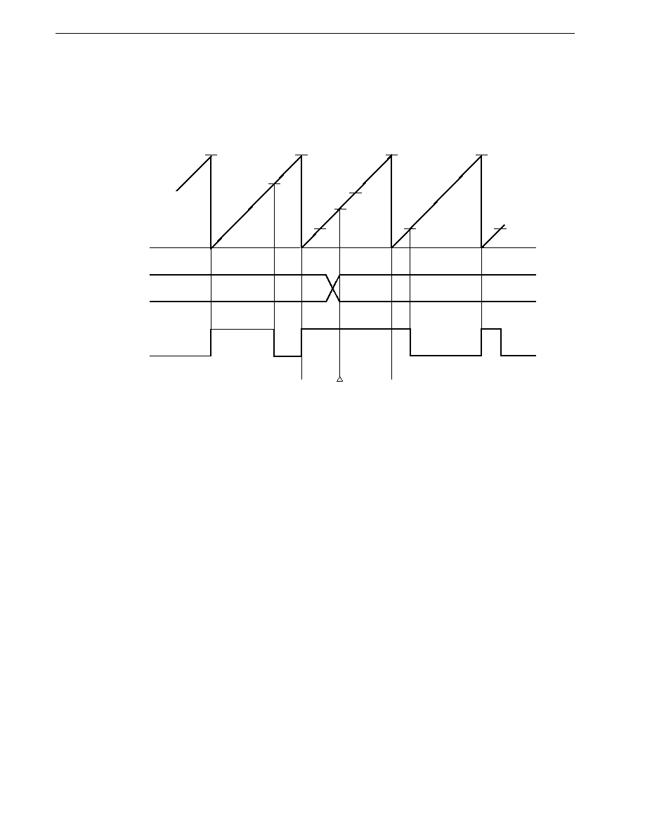
248
CHAPTER 9 TIMER/EVENT COUNTER 0
Preliminary User's Manual U13987EJ1V0UM00
If a value equal to or less than the TM0 value is written to CR00 before the compare register (CR00) and timer counter 0
(TM0) match, the duty of the PPG cycle will be 100%. CR00 rewriting should be performed by the interrupt due to a match
between TM0 and CR00.
Figure 9-26. Example of 100% Duty with PPG Output
Remark
ALV0 = 0
Caution
If the PPG cycle is extremely short as compared with the time required to acknowledge an interrupt, the
value of CR00 cannot be rewritten by interrupt processing that is performed on coincidence between TM0
and CR00. Use another method (for example, to poll the interrupt request flags by software with all the
interrupts masked).
CR00
TO0
TM0
count value
0H
n1
n2
n3
n1
When value n2 which is smaller than the TM0 value n3
is written to CR00 here, the duty of this period will be 100%.
CR01
CR01
CR01
CR01
n2
n2
n2
n1
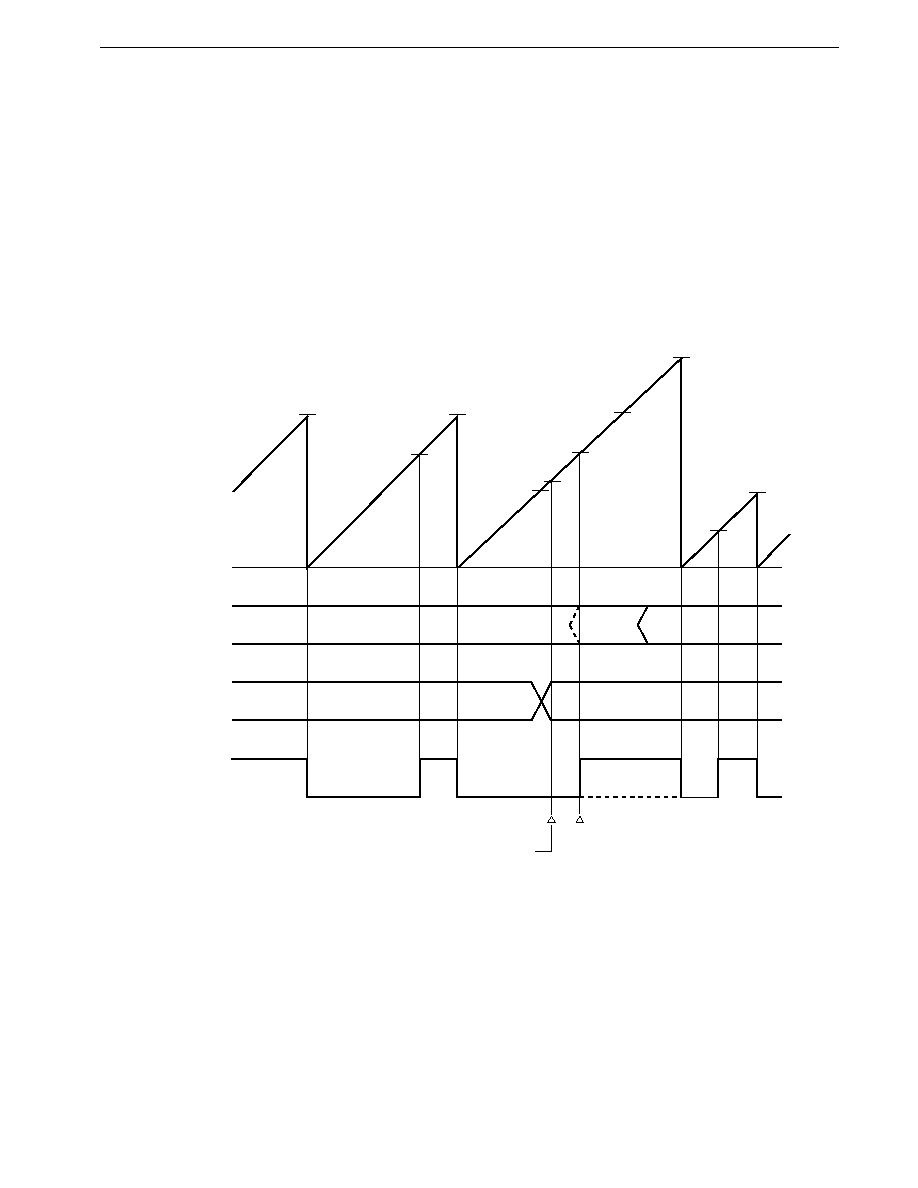
249
CHAPTER 9 TIMER/EVENT COUNTER 0
Preliminary User's Manual U13987EJ1V0UM00
(3) Rewriting compare register (CR01)
If the current value of the CR01 is changed to a smaller value, and the CR01 value is made smaller than the timer counter
0 (TM0) value, the PPG cycle at that time will be extended to the time equivalent to a full-count by TM0. If CR01 is rewritten
after the compare register (CR00) and TM0 match, the output level at this time will be the inactive level until TM0 overflows
and becomes 0, and will then return to normal PPG output.
If CR01 is rewritten before CR00 and TM0 match, the active level will be output until CR00 and TM0 match. If CR00 and
TM0 match before TM0 overflows and becomes 0, the inactive level is output at that point. When TM0 overflows and
becomes 0, the active level will be output, and normal PPG output will be restored. CR01 rewriting should be performed
by the interrupt due to a match between TM0 and CR01, etc.
Figure 9-27. Example of Extended PPG Output Cycle
Remark
ALV0 = 1
Caution
If the PPG cycle is extremely short as compared with the time required to acknowledge an interrupt, the
value of CR01 cannot be rewritten by interrupt processing that is performed on coincidence between the
timer counter 0 (TM0) and compare register (CR01). Use another method (for example, to poll the interrupt
request flags by software with all the interrupts masked).
CR00
TO0
TM0
count value
0H
n3
n4
n2
If CR00 and TM0 match, TO0 enters
the inactive level. Otherwise, it
remains at the active level.
Full count value
n4
n2
n3
n1
n2
CR01
n5
n3
n1
n1
n1
When value n2 which is smaller than the
TM0 value n5 is written to CR01 here,
the PPG cycle is extended.
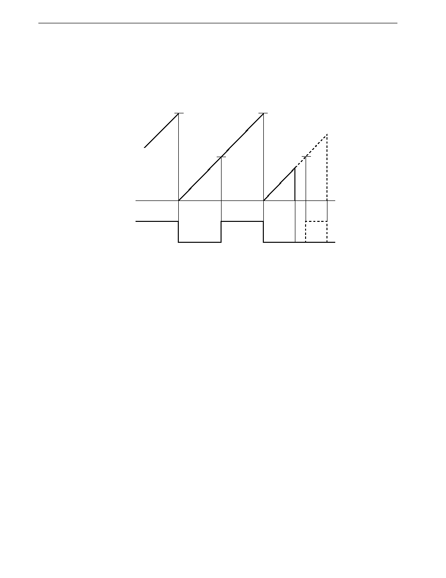
250
CHAPTER 9 TIMER/EVENT COUNTER 0
Preliminary User's Manual U13987EJ1V0UM00
(4) Stopping PPG output
If timer/event counter 0 is stopped by clearing (to 0) the CE0 bit of the timer control register 0 (TMC0) during PPG signal
output, the active level is output irrespective of the output level at the time it was stopped.
Figure 9-28. When Timer/Event Counter 0 is Stopped During PPG Signal Output
Caution
The output level of the TOn (n = 0, 1) pin when timer output is disabled (ENTOn = 0: n = 0, 1) is the inverse
of the value set in ALVn (n = 0, 1) bit. Caution is therefore required as the active level is output when timer
output is disabled when the PPG output function has been selected.
TO0
TM0
count value
0H
CR00
CR01
CR01
CR00

251
CHAPTER 9 TIMER/EVENT COUNTER 0
Preliminary User's Manual U13987EJ1V0UM00
9.7.5 Software triggered one-shot pulse output
In the software triggered one-shot pulse output mode, a one-shot pulse is output by software.
When the STn (n = 0, 1) bit of the one-shot pulse output control register (OSPC) is set (1), timer output pin (TOn: n = 0, 1)
is set to the active level. TOn then remains at the active level until the timer counter 0 (TM0) value and the compare register
(CR0n: n = 0, 1) value match, at which point TOn changes to the inactive level. TOn then remains at the inactive level until the
STn bit is set again. TOn can also be set to the inactive level by setting (to 1) the RTn bit (n = 0, 1), and in the same way, TOn
remains at the inactive level until the STn bit is set again.
TO0 and TO1 can be controlled independently.
An example of software triggered one-shot pulse output is shown in Figure 9-29.
When timer/event counter 0 is stopped by clearing (to 0) the CE0 bit of the TMC0, the level at the time was stopped is retained.
Figure 9-29. Example of Software Triggered One-Shot Pulse Output
Caution
"1" should not be written to STn and RTn simultaneously.
0H
FFFFH
Count start
Software trigger
ST0
INTC00
ALV0
TO0
Active period
"1"
Inactive level output

252
CHAPTER 9 TIMER/EVENT COUNTER 0
Preliminary User's Manual U13987EJ1V0UM00
9.8 Examples of Use
9.8.1 Operation as interval timer (1)
When timer counter 0 (TM0) is made free-running and a fixed value is added to the compare register (CR0n: n = 0, 1) in the
interrupt service routine, TM0 operates as an interval timer with the added fixed value as the cycle (see Figure 9-30).
This interval timer can count within the range shown in Table 9-1 (internal system clock f
XX
= 32 MHz).
Since TM0 has two compare registers, two interval timers with different cycles can be constructed.
The control register settings are shown in Figure 9-31, the setting procedure in Figure 9-32, and the processing in the interrupt
service routine in Figure 9-33.
Figure 9-30. Interval Timer Operation (1) Timing
Remark
Interval = n
�
4/f
XX
, 1
n
FFFFH
MOD (2n)
INTC00
interrupt request
TM0
count value
0H
FFFFH
Compare register
(CR00)
n
Timer start
MOD (3n)
MOD (4n)
FFFFH
n
MOD (2n)
MOD (3n)
Interval
Interval
Interval
Rewritten by
interrupt program
Rewritten by
interrupt program
Rewritten by
interrupt program
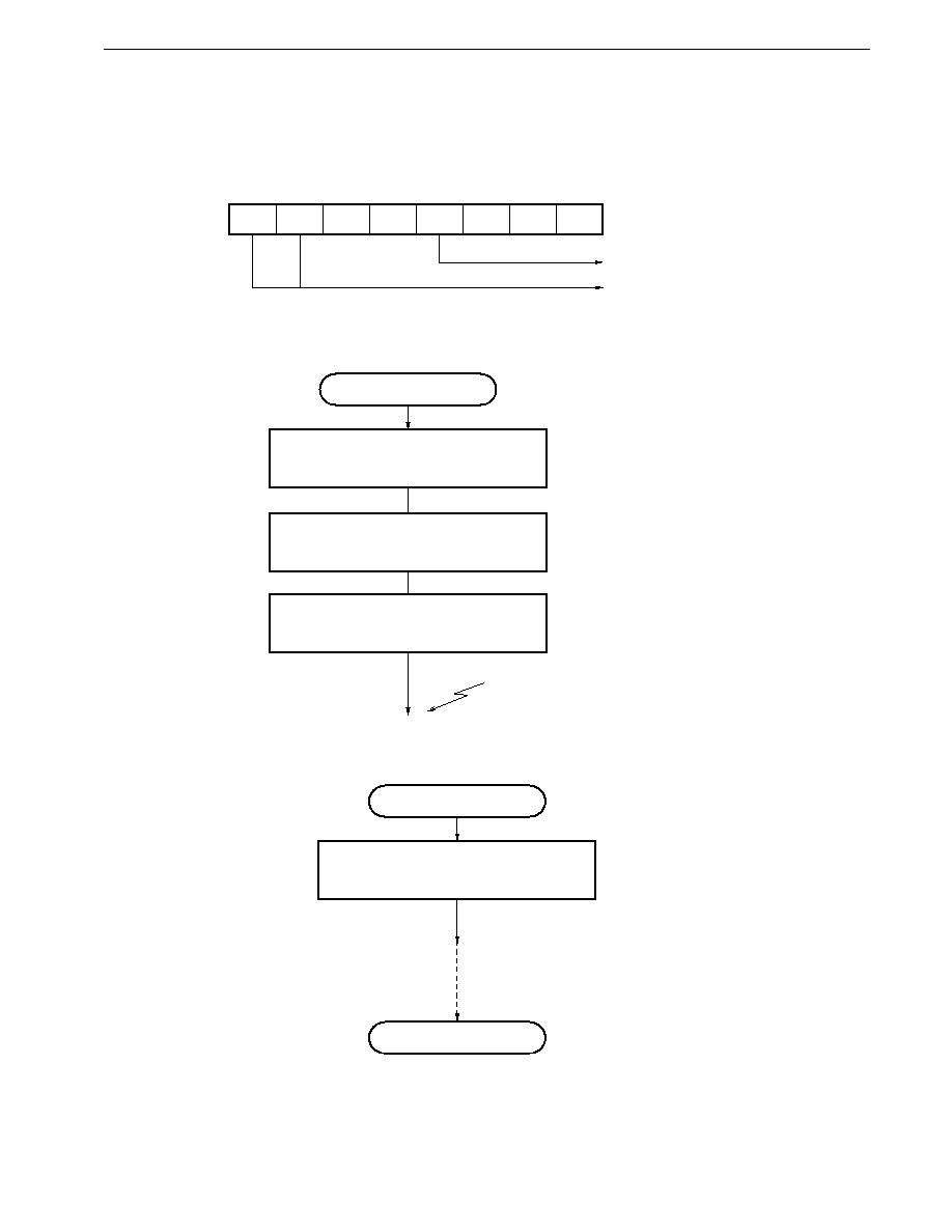
253
CHAPTER 9 TIMER/EVENT COUNTER 0
Preliminary User's Manual U13987EJ1V0UM00
Figure 9-31. Control Register Settings for Interval Timer Operation (1)
Capture/compare control register 0 (CRC0)
Figure 9-32. Interval Timer Operation (1) Setting Procedure
Figure 9-33. Interval Timer Operation (1) Interrupt Request Servicing
7
0
CRC0
6
0
5
0
4
1
3
0
2
0
1
0
0
0
TM0 clearing disabled
TO0 & TO1 both toggle outputs
Interval timer (1)
Set count value in CR00
CR00
n
INTC00 interrupt
; Set 1 in bit 3 of TMC0
Set CRC0
CRC0
10H
Start count
CE0
1
INTC00 interrupt
Calculate timer value that will
generate next interrupt
CR00
CR00+n
Other interrupt service program
RETI
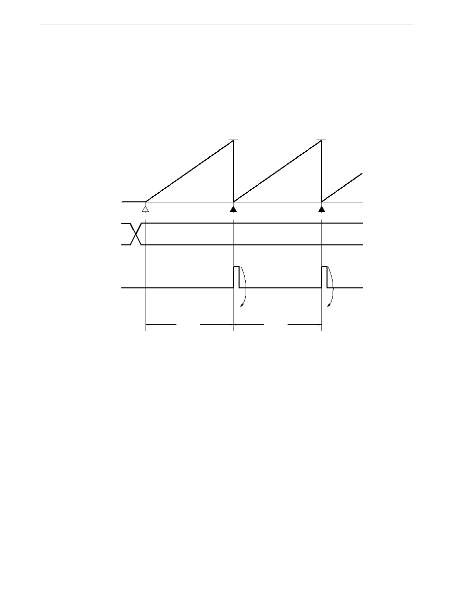
254
CHAPTER 9 TIMER/EVENT COUNTER 0
Preliminary User's Manual U13987EJ1V0UM00
9.8.2 Operation as interval timer (2)
TM0 operates as an interval timer that generates interrupts repeatedly with the preset count time as the interval (see Figure
9-34).
This interval timer can count within the range shown in Table 9-1 (internal system clock f
XX
= 32 MHz).
The control register settings are shown in Figure 9-35, and the setting procedure in Figure 9-36.
Figure 9-34. Interval Timer Operation (2) Timing
Remark
Interval = (n + 1)
�
4/f
XX
, 0
n
FFFFH
n
Compare register
(CR01)
INTC01
interrupt request
TM0
count value
0H
n
n
Count start
Clear
Clear
Interrupt acknowledged
Interrupt acknowledged
Interval
Interval
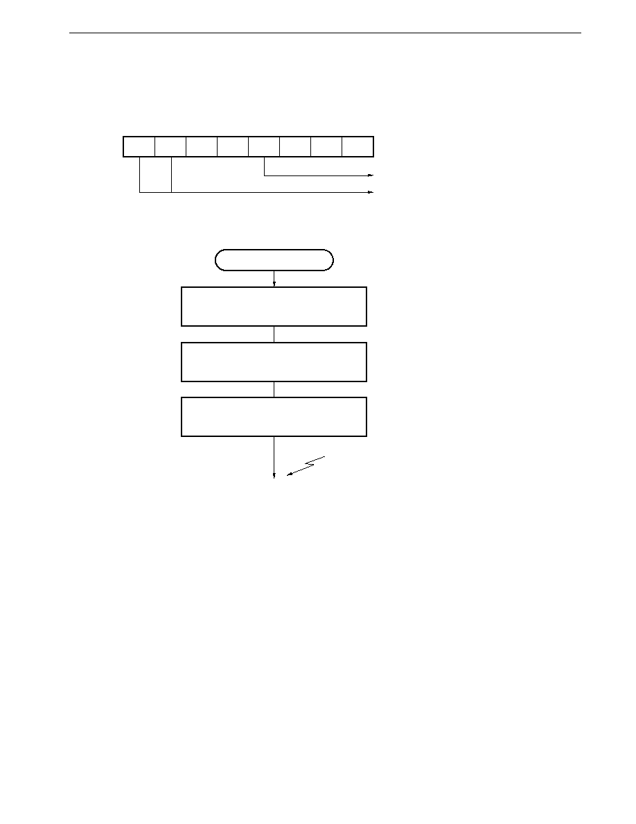
255
CHAPTER 9 TIMER/EVENT COUNTER 0
Preliminary User's Manual U13987EJ1V0UM00
Figure 9-35. Control Register Settings for Interval Timer Operation (2)
Capture/compare control register 0 (CRC0)
Figure 9-36. Interval Timer Operation (2) Setting Procedure
7
0
CRC0
6
0
5
0
4
1
3
1
2
0
1
0
0
0
TM0 cleared by match of CR01 & TM0 contents
TO0 & TO1 both toggle outputs
Interval timer (2)
Set count value in CR01
CR01
n
INTC01 interrupt
; Set 1 in bit 3 of TMC0
Set CRC0
CRC0
18H
Start count
CE0
1
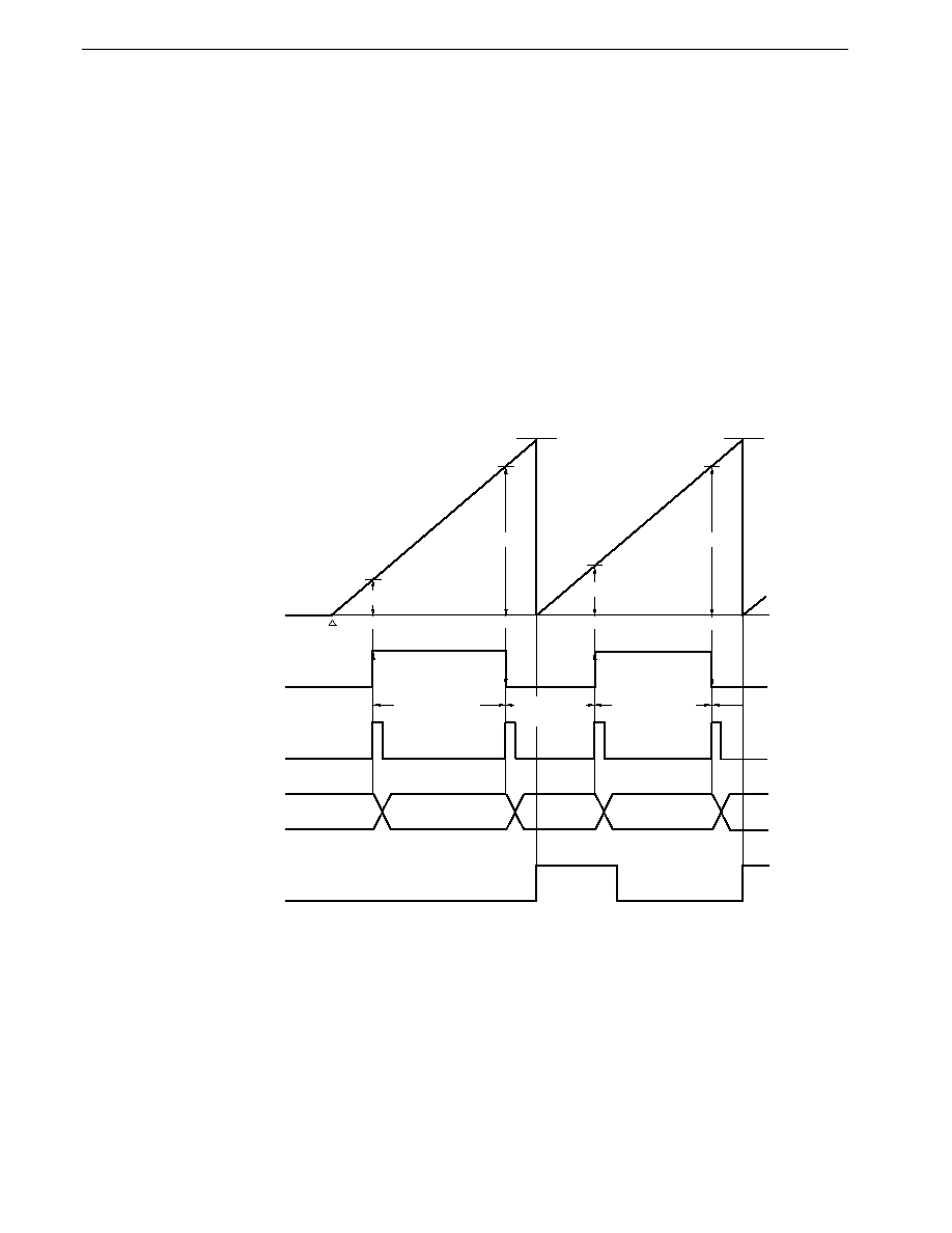
256
CHAPTER 9 TIMER/EVENT COUNTER 0
Preliminary User's Manual U13987EJ1V0UM00
9.8.3 Pulse width measurement operation
In pulse width measurement, the high-level or low-level width of external pulses input to the external interrupt request input
pin (INTP3) is measured.
Both the high-level and low-level widths of pulses input to the INTP3 pin must be at least 3 system clocks (0.24
�
s: f
CLK
= 12.58 MHz); if shorter than this, the valid edge will not be detected and a capture operation will not be performed.
This pulse width measurement can be performed within the range shown in Table 9-3 (f
CLK
= 12.58 MHz).
As shown in Figure 9-37, the timer counter 0 (TM0) value being counted is fetched into the capture register (CR02) in
synchronization with a valid edge (specified as both rising and falling edges) in the INTP3 pin input, and held there. The pulse
width is obtained from the product of the difference between the TM0 count value (Dn) fetched into and held in the CR02 on
detection of the nth valid edge and the count value (D
n-1
) fetched and held on detection of valid edge n-1, and the number of
count clocks (x/f
XX
; x = 4, 8, 16, 32, 64, 128, 256, 512, 1,024).
The control register settings are shown in Figure 9-38, and the setting procedure in Figure 9-39.
Figure 9-37. Pulse Width Measurement Timing
Remark
Dn: TM0 count value (n = 0, 1, 2, ...)
x = 4, 8, 16, 32, 64, 128, 256, 512, 1,024
D1
INTP3
external input signal
INTP3
interrupt request
TM0
count value
0H
FFFFH
Capture register
(CR02)
OVF0
D0
D0
D1
Count start
FFFFH
D2
D2
D3
Capture
Capture
Capture
Capture
(D1-D0)
�
8/f
XX
(10000H-D1+
D2)
�
8/f
XX
(D3-D2)
�
8/f
XX
D3
Cleared by software
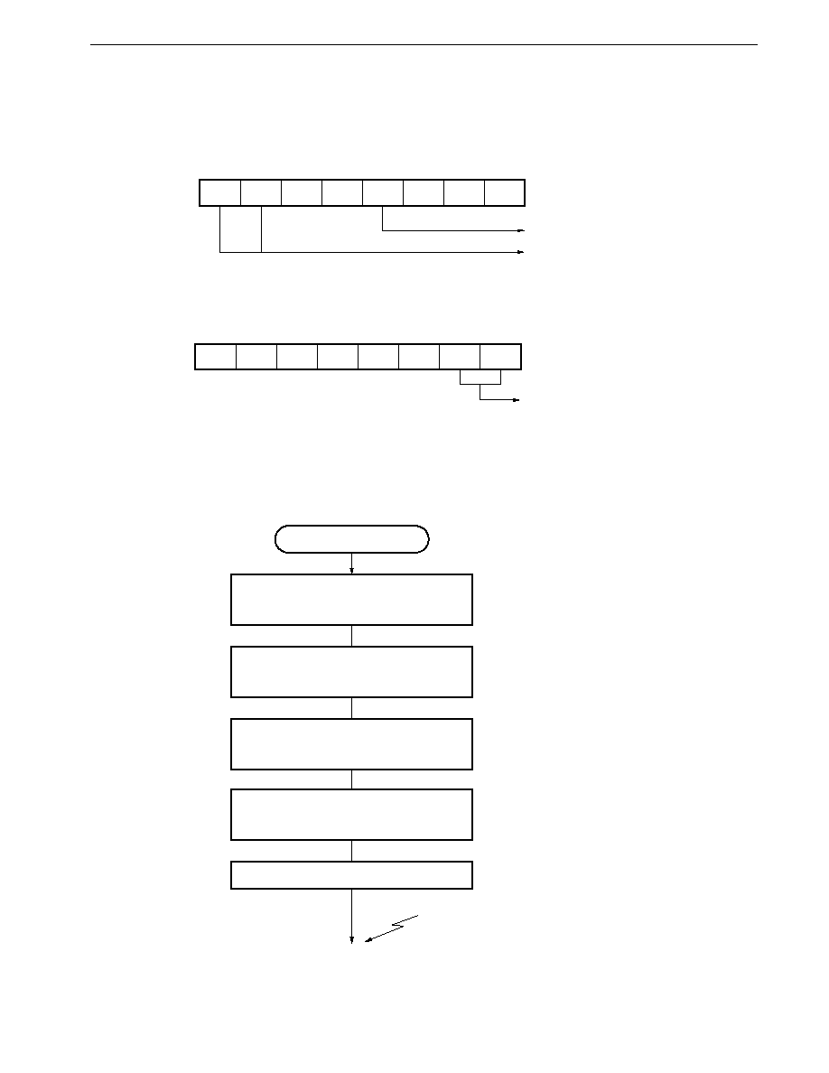
257
CHAPTER 9 TIMER/EVENT COUNTER 0
Preliminary User's Manual U13987EJ1V0UM00
Figure 9-38. Control Register Settings for Pulse Width Measurement
(a) Capture/compare control register 0 (CRC0)
(b) External interrupt mode register 1 (INTM1)
Figure 9-39. Pulse Width Measurement Setting Procedure
7
0
CRC0
6
0
5
0
4
1
3
0
2
0
1
0
0
0
TM0 clearing disabled
TO0 & TO1 both toggle outputs
Pulse width measurement
Set CRC0
CRC0
10H
Set INTM1,
Set MK0L
Initialize capture value buffer memory
X
0
0
Start count
CE0
1
Enable interrupt
; Specify both edges as
INTP3 input valid edges,
release interrupt masking
INTP3 interrupt
; Set 1 in bit 3 of TMC0
7
0
INTM1
6
0
5
�
4
�
3
�
2
�
�
: don't care
1
1
0
1
Both rising & falling edges
specified as INTP3 input valid edges
258
CHAPTER 9 TIMER/EVENT COUNTER 0
Preliminary User's Manual U13987EJ1V0UM00
Figure 9-40. Interrupt Request Servicing that Calculates Pulse Width
INTP3 interrupt
Calculate pulse width
Y
n
= CR02 � X
n
Store capture value in memory
X
n+1
CR02
RETI
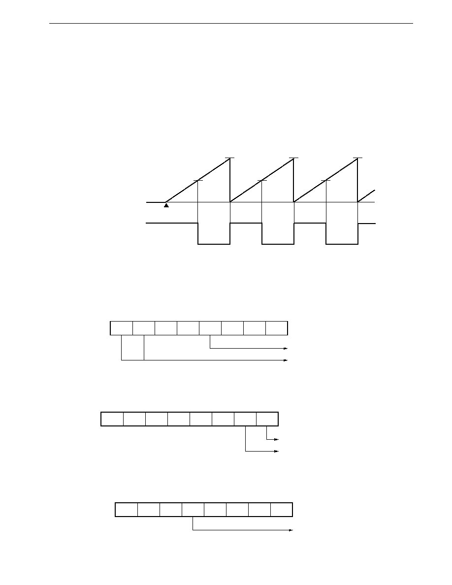
259
CHAPTER 9 TIMER/EVENT COUNTER 0
Preliminary User's Manual U13987EJ1V0UM00
9.8.4 Operation as PWM output
In PWM output, pulses with the duty ratio determined by the value set in the compare register (CR0n: n = 0, 1) are output
(see Figure 9-41).
This PWM output duty ratio can be varied in the range 1/65,536 to 65,535/65,536 in 1/65,536 units.
Since timer counter 0 (TM0) has two compare registers, two different PWM signals can be output.
The control register settings are shown in Figure 9-42, the setting procedure in Figure 9-43, and the procedure for varying
the duty in Figure 9-44.
Figure 9-41. Example of Timer/Event Counter 0 PWM Signal Output
Figure 9-42. Control Register Settings for PWM Output Operation
(a) Capture/compare control register 0 (CRC0)
(b) Timer output control register (TOC)
(c) Port 3 mode control register (PMC3)
TO0
(When active-low)
TM0
count value
0H
Timer start
FFFFH
CR00
FFFFH
CR00
FFFFH
CR00
7
1
CRC0
6
0
5
0
4
1
3
0
2
0
1
0
0
0
TM0 clearing disabled
TO0 & TO1 both PWM outputs
7
�
TOC
6
�
5
�
4
�
3
�
2
�
1
1
0
1
TO0 = active-low PWM signal output
TO0 PWM output enabled
7
�
PMC3
6
�
5
�
4
1
3
�
2
�
1
�
0
�
P34 pin set as TO0 output
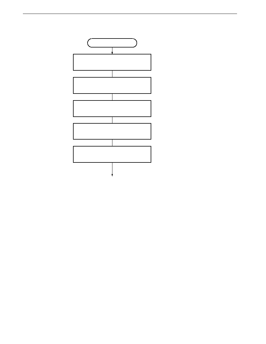
260
CHAPTER 9 TIMER/EVENT COUNTER 0
Preliminary User's Manual U13987EJ1V0UM00
Figure 9-43. PWM Output Setting Procedure
PWM output
Set CRC0
CRC0
90H
Set TOC
Set P34 pin to control mode
PMC3.4
1
Set initial value in CR00, CR01
; Set bit 3 of TMC0
Start count
CE0
1
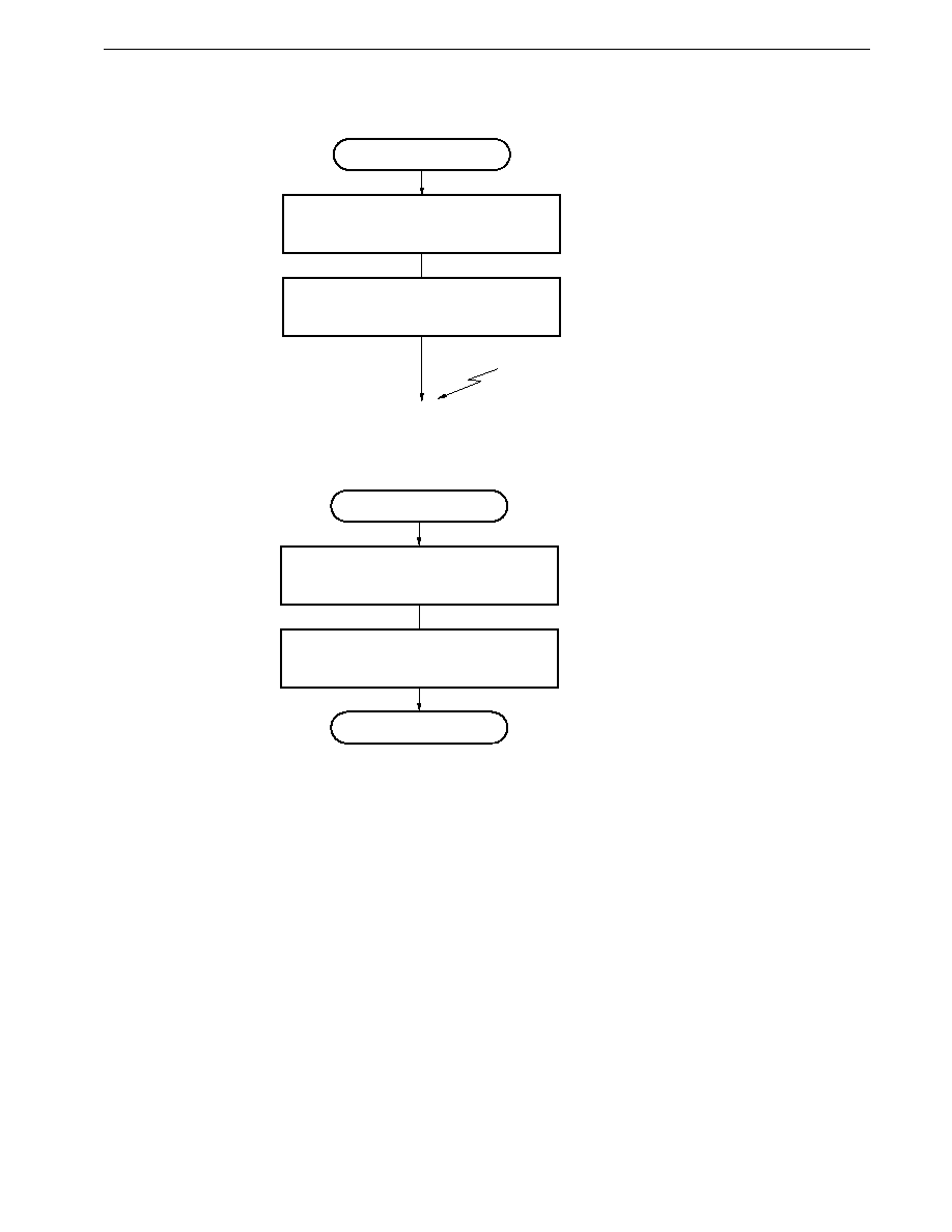
261
CHAPTER 9 TIMER/EVENT COUNTER 0
Preliminary User's Manual U13987EJ1V0UM00
Figure 9-44. Changing PWM Output Duty
Duty change processing
Set duty value in CR00
Disable INTC00 interrupts
CMK00
1
RETI
; Set bit 4 of MK0L
Duty change preprocessing
Clear INTC00 interrupt request flag
CIF00
0
Enable INTC00 interrupts
CMK00
0
INTC00 interrupt
; Clear bit 4 of IF0L
; Clear bit 4 of MK0L
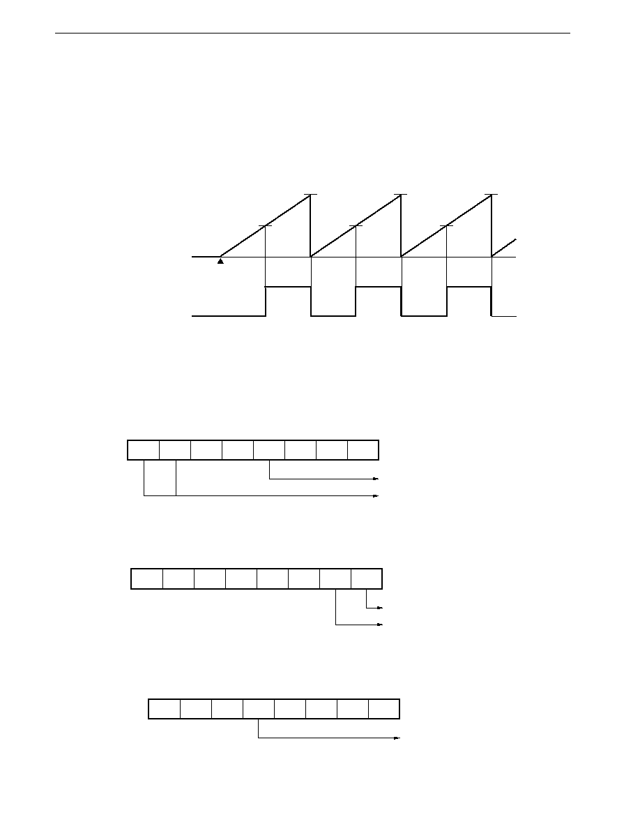
262
CHAPTER 9 TIMER/EVENT COUNTER 0
Preliminary User's Manual U13987EJ1V0UM00
9.8.5 Operation as PPG output
In PPG output, pulses with the cycle and duty ratio determined by the values set in the compare registers (CR0n: n = 0, 1)
are output (see Figure 9-45).
The control register settings are shown in Figure 9-46, the setting procedure in Figure 9-47, and the procedure for varying
the duty in Figure 9-48.
Figure 9-45. Example of Timer/Event Counter 0 PPG Signal Output
Figure 9-46. Control Register Settings for PPG Output Operation
(a) Capture/compare control register 0 (CRC0)
(b) Timer output control register (TOC)
(c) Port 3 mode control register (PMC3)
TO0
(when active-low)
TM0
count value
0H
Timer start
CR01
CR00
CR01
CR00
CR01
CR00
7
1
CRC0
6
1
5
0
4
1
3
1
2
0
1
0
0
0
TM0 cleared by match of TM0 & CR01
TO0 = PPG output
7
�
TOC
6
�
5
�
4
�
3
�
2
�
1
1
0
1
TO0 = active-low PPG signal output
TO0 PPG output enabled
7
�
PMC3
6
�
5
�
4
1
3
�
2
�
1
�
0
�
P34 pin set as TO0 output
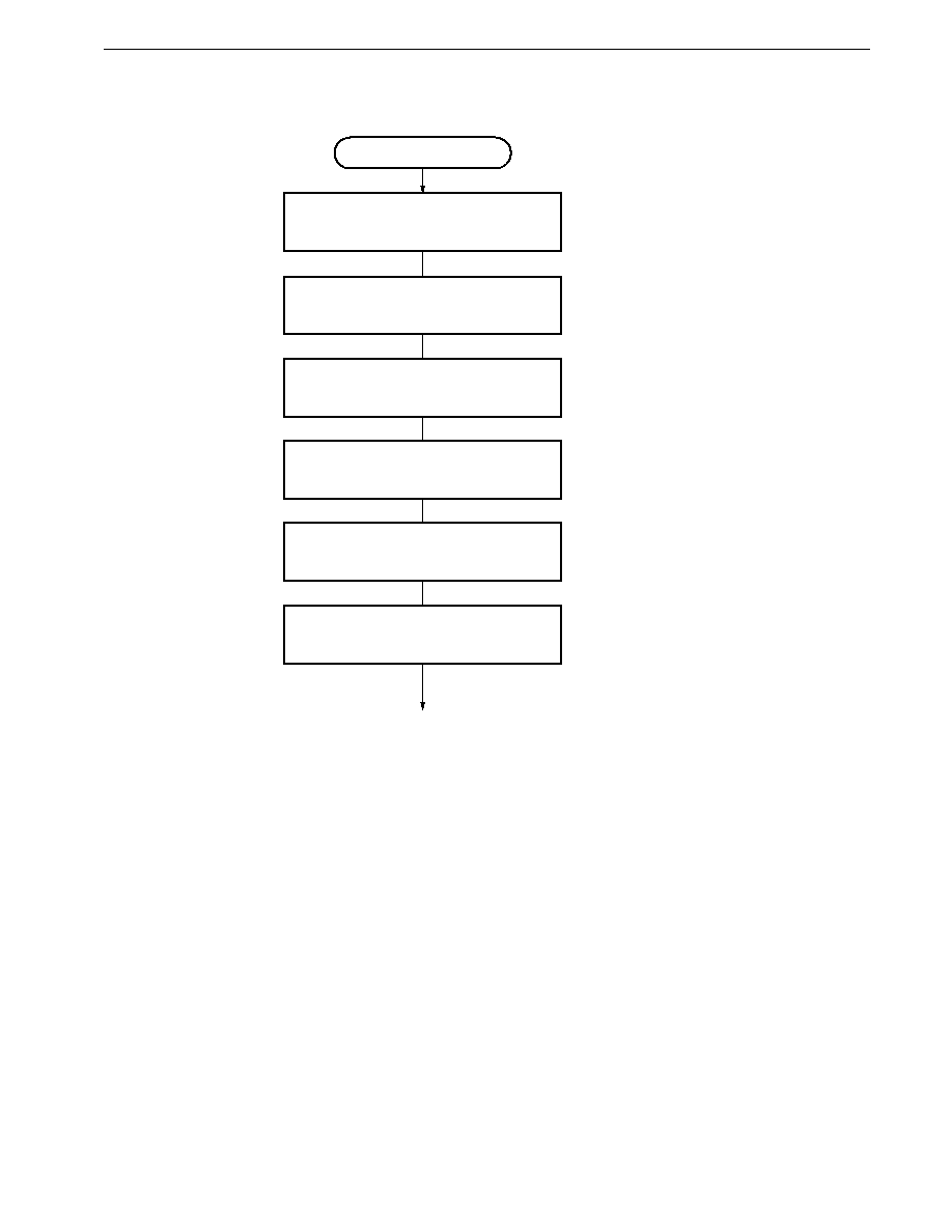
263
CHAPTER 9 TIMER/EVENT COUNTER 0
Preliminary User's Manual U13987EJ1V0UM00
Figure 9-47. PPG Output Setting Procedure
PPG output
Set CRC0
CRC0
D8H
Set TOC
Set P34 pin to control mode
PMC3.4
1
Set cycle in CR01
Set duty in CR00
; Set bit 3 of TMC0
Start count
CE0
1

264
CHAPTER 9 TIMER/EVENT COUNTER 0
Preliminary User's Manual U13987EJ1V0UM00
Figure 9-48. Changing PPG Output Duty
Duty change preprocessing
Clear INTC00 interrupt request flag
CIF00
0
Duty change processing
Set duty value in CR00
Disable INTC00 interrupts
CMK00
1
RETI
INTC00 interrupt
; Clear bit 4 of IF0L
; Clear bit 4 of MK0L
; Set bit 4 of MK0L
Enable INTC00 interrupts
CMK00
0
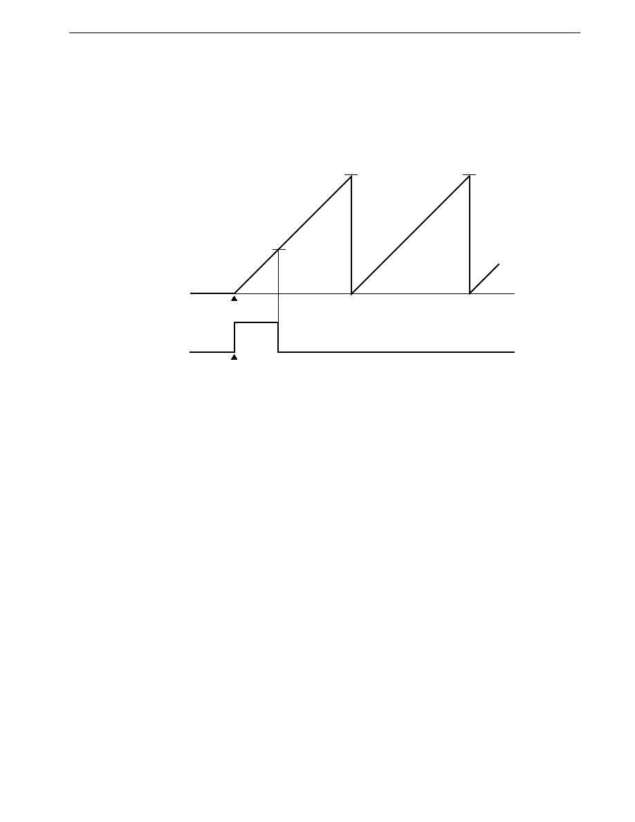
265
CHAPTER 9 TIMER/EVENT COUNTER 0
Preliminary User's Manual U13987EJ1V0UM00
9.8.6 Example of software triggered one-shot pulse output
In the software triggered one-shot pulse output mode, a one-shot pulse is output in response to a trigger activated by software
(see Figure 9-49).
The control register settings are shown in Figure 9-50, and the setting procedure in Figure 9-51.
Figure 9-49. Example of Timer/Event Counter 0 One-Shot Pulse Output
TO0
TM0
count value
0H
FFFFH
Count start
CR00
FFFFH
Set trigger
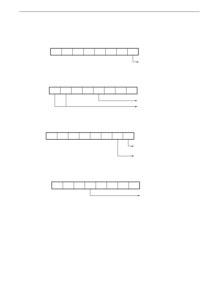
266
CHAPTER 9 TIMER/EVENT COUNTER 0
Preliminary User's Manual U13987EJ1V0UM00
Figure 9-50. Control Register Settings for One-Shot Pulse Output
(a) One-shot pulse output control register (OSPC)
(b) Capture/compare control register 0 (CRC0)
(c) Timer output control register (TOC)
(d) Port 3 mode control register (PMC3)
7
0
OSPC
6
0
5
0
4
�
3
0
2
0
1
0
0
1
TO0 = one-shot pulse output
7
0
CRC0
6
0
5
0
4
1
3
0
2
0
1
0
0
0
TM0 clearing disabled
TO0 & TO1 both toggle outputs
7
�
TOC
6
�
5
�
4
�
3
�
2
�
1
1
0
1
TO0 = active-high one-shot pulse
signal output
TO0 one-shot pulse output enabled
7
�
PMC3
6
�
5
�
4
1
3
�
2
�
1
�
0
�
P34 pin set as TO0 output
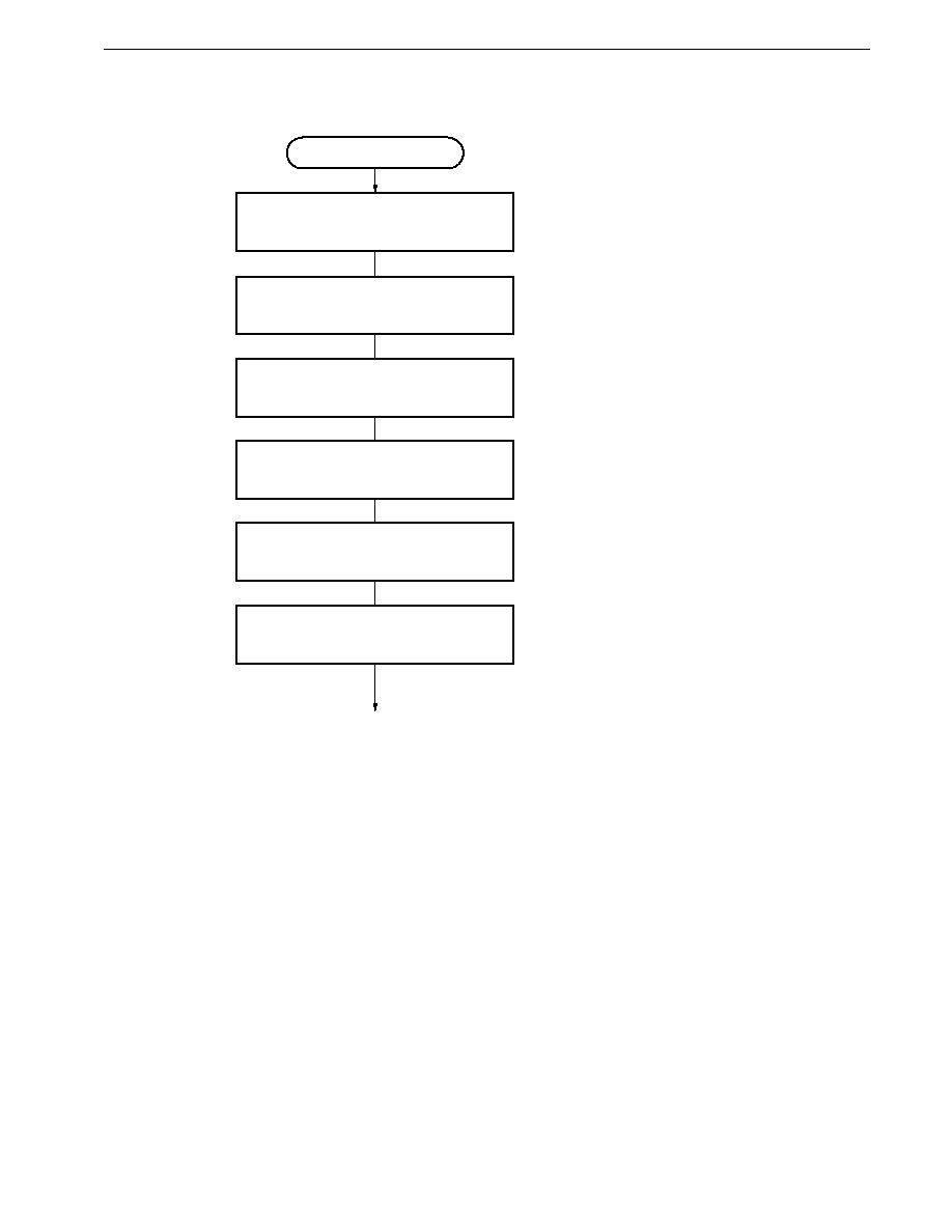
267
CHAPTER 9 TIMER/EVENT COUNTER 0
Preliminary User's Manual U13987EJ1V0UM00
Figure 9-51. One-Shot Pulse Output Setting Procedure
One-shot pulse output
Set OSPC
OS0
1
; Set bit 3 of TMC0
; Set to one-shot pulse output mode
Set CRC0
CRC0
10H
Set P34 pin to control mode
PMC 3.4
1
Start count
CE0
1
One-shot pulse output
ST0
1
Set pulse width in CR00
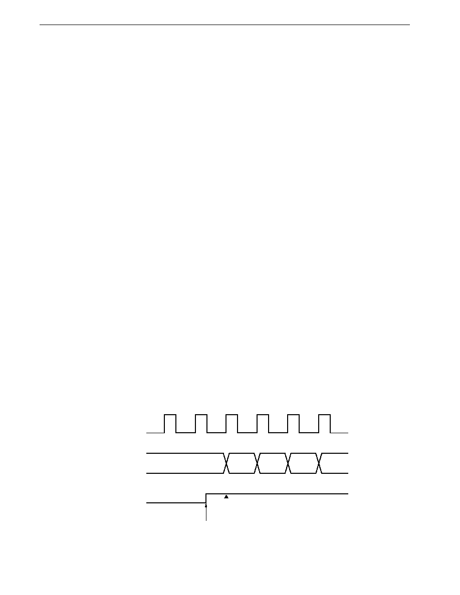
268
CHAPTER 9 TIMER/EVENT COUNTER 0
Preliminary User's Manual U13987EJ1V0UM00
9.9 Cautions
(1) While timer/event counter 0 is operating (while the CE0 bit of the timer control register 0 (TMC0) is set), malfunctioning may
occur if the contents of the following registers are rewritten. This is because it is undefined which takes precedence in a
contention the change in the hardware functions due to rewriting the register, or the change in the status because of the
function before rewriting.
Therefore, be sure to stop the counter operation for the sake of safety before rewriting the contents of the following registers.
� Prescaler mode register 0 (PRM0)
� Capture/compare control register 0 (CRC0)
� Timer output control register (TOC)
(2) If the contents of the compare register (CR0n: n = 0, 1) coincide with those of TM0 operation when an instruction that stops
timer counter 0 (TM0) operation is executed, the counting operation of TM0 stops, but an interrupt request is generated.
In order not to generate the interrupt when stopping the operation of TM0, mask the interrupt in advance by using the
interrupt mask register before stopping TM0.
Example
Program that may generate interrupt request
Program that does not generate interrupt request
CLR1
CE0
OR
MK0L, #30H
OR
MK0L, #30H
CLR1
CE0
CLR1
CIF00
CLR1
CIF01
(3) Up to 1 count clock is required after an operation to start timer/event counter 0 (CE0
1) has been performed before timer/
event counter 0 actually starts (refer to Figure 9-52).
For example, when using timer/event counter 0 as an interval timer, the first interval time is delayed by up to 1 clock. The
second and those that follow are at the specified interval.
Figure 9-52. Operation when Counting is Started
���
���
Interrupt request from
timer/event counter 0
occurs between these
instructions
Disables interrupt from
timer/event counter 0
Clears interrupt request flag
for timer/event counter 0
���
���
Count clock
TM0
CE0
Timing to start actual counting
Count start command (CE0
1) by software
0
0
1
2
3
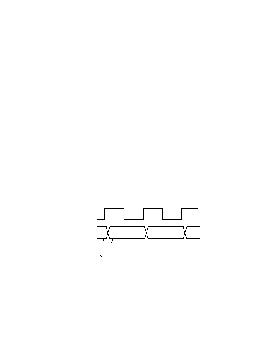
269
CHAPTER 9 TIMER/EVENT COUNTER 0
Preliminary User's Manual U13987EJ1V0UM00
(4) While an instruction that writes data to the compare register (CR0n: n = 0, 1) is executed, coincidence between CR0n, to
which the data is to be written, and timer counter 0 (TM0) is not detected. For example, if the contents of CR0n do not change
before and after the writing, the interrupt request is not generated even if the value of TM0 coincides with the value of CR0n,
nor does the timer output (TOn: n = 0, 1) change.
Write data to CR0n when timer/event counter 0 is executing counting operation, in the timing that the contents of TM0 do
not coincide with the value of CR0n before and after writing (e.g., immediately after an interrupt request has been generated
because TM0 and CR0n have coincided).
(5) Coincidence between TM0 and compare register (CR0n: n = 0, 1) is detected only when TM0 is incremented. Therefore,
the interrupt request is not generated even if the same value as TM0 is written to CR0n, and the timer output (TOn: n = 0,
1) does not change.
(6) If the PPG cycle is extremely short as compared with the time required to acknowledge an interrupt, the value of the CR0n
cannot be rewritten by interrupt processing that is performed on coincidence between TM0 and the compare register (CR0n:
n = 0, 1). Use another method (for example, to poll the interrupt request flags by software with all the interrupts masked).
(7) The output level of the TOn (n = 0, 1) when the timer output is disabled (ENTOn = 0: n = 0, 1) is the reverse value of the
value set to the ALVn (n = 0, 1) bit. Note, therefore, that an active level is output when the timer output is disabled with the
PWM output function or PPG output function selected.
(8) When timer/event counter 0 is used as an external event counter, it is not possible to distinguish between the case where
there is no valid edge input at all and the case where there is a single valid edge input, using the timer counter 0 (TM0)
alone (refer to Figure 9-53), since the contents of TM0 are 0 in both cases. If it is necessary to make this distinction, the
INTP3 interrupt request flag should be used. To make a distinction, use the interrupt request flag of INTP3, as shown in
Figure 9-54.
Figure 9-53. Example of the Case where the External Event Counter does Not Distinguish
between One Valid Edge Input and No Valid Edge Input
INTP3
TM0
0
1
2
0
Cannot be
distinguished
Count start
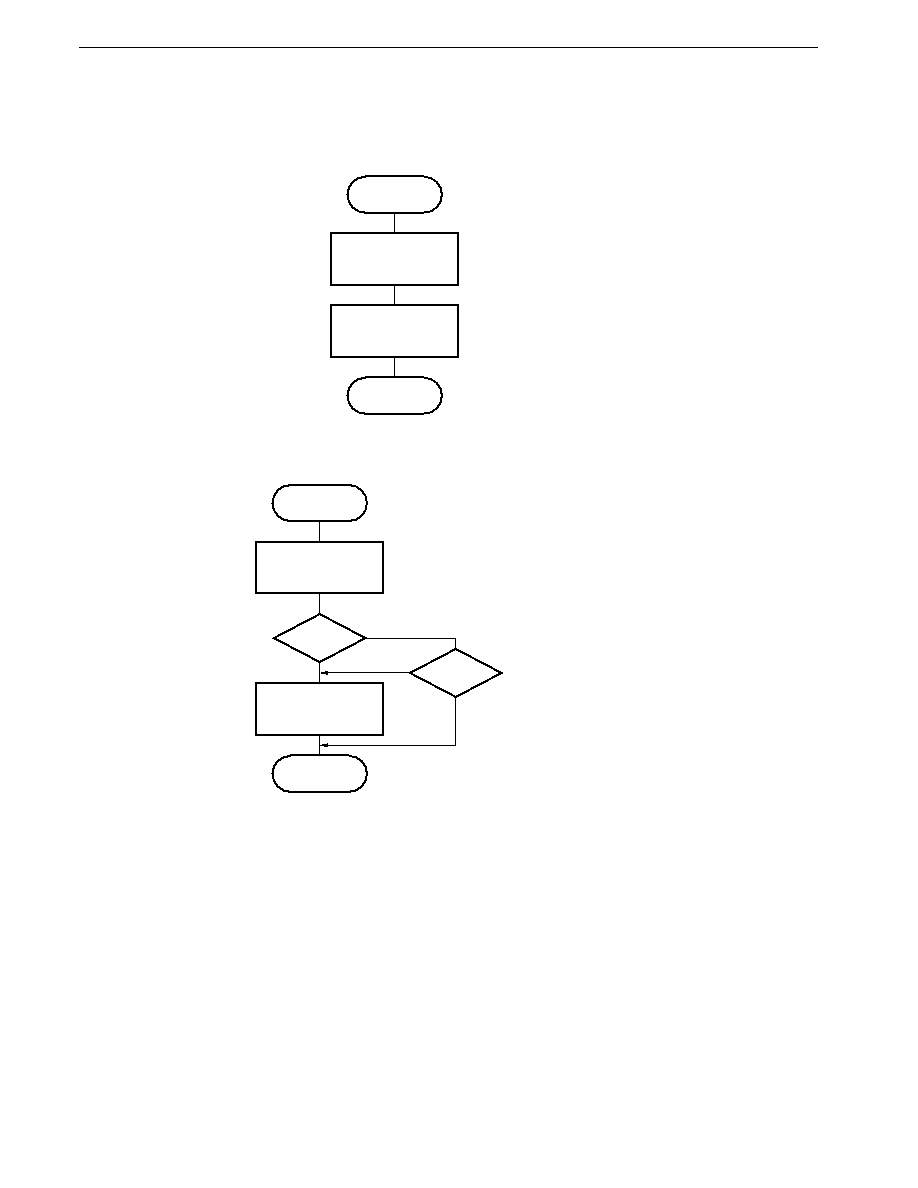
270
CHAPTER 9 TIMER/EVENT COUNTER 0
Preliminary User's Manual U13987EJ1V0UM00
Figure 9-54. To Distinguish whether One or No Valid Edge has been Input with External Event Counter
(a) Processing on starting counting
(b) Processing on reading count value
; Set CE3 to 1
; Clear PIF3 to 0
Clear INTP3
interrupt request flag
PIF3
0
Start count
CE3
1
Start count
End
Number of input valid edges is set to AX register
Count value
read
Read TM0 contents
AX
TM0
AX
AX+1
End
AX = 0?
PIF3 = 1?
;
;
Check TM0 value.
If 0, check interrupt
request flag.
Check PIF3 contents.
If 1, valid edge is input.
YES
NO
YES
NO

271
Preliminary User's Manual U13987EJ1V0UM00
CHAPTER 10 TIMER/EVENT COUNTER 1
10.1 Functions
Timer/event counter 1 is 16-bit or 8-bit timer/event counter.
In addition to its basic functions of interval timer, pulse width measurement, and event counter, timer/event counter 1 can
be used as a real-time output port output trigger generation timer.
(1) Interval timer
Generates internal interrupts at preset intervals.
Table 10-1. Timer/Event Counter 1 Intervals
Minimum Interval
Maximum Interval
Resolution
4/f
XX
2
16
�
4/f
XX
4/f
XX
(0.32
�
s)
(20.8 ms)
(0.32
�
s)
8/f
XX
2
16
�
8/f
XX
8/f
XX
(0.64
�
s)
(41.7 ms)
(0.64
�
s)
16/f
XX
2
16
�
16/f
XX
16/f
XX
(1.27
�
s)
(83.4 ms)
(1.27
�
s)
32/f
XX
2
16
�
32/f
XX
32/f
XX
(2.54
�
s)
(167 ms)
(2.54
�
s)
64/f
XX
2
16
�
64/f
XX
64/f
XX
(5.09
�
s)
(333 ms)
(5.09
�
s)
128/f
XX
2
16
�
128/f
XX
128/f
XX
(10.17
�
s)
(667 ms)
(10.17
�
s)
256/f
XX
2
16
�
256/f
XX
256/f
XX
(20.35
�
s)
(1.33 s)
(20.35
�
s)
512/f
XX
2
16
�
512/f
XX
512/f
XX
(40.70
�
s)
(2.67 s)
(40.70
�
s)
1,024/f
XX
2
16
�
1,024/f
XX
1,024/f
XX
(81.40
�
s)
(5.33 s)
(81.40
�
s)
( ): When f
XX
= 12.58 MHz

272
CHAPTER 10 TIMER/EVENT COUNTER 1
Preliminary User's Manual U13987EJ1V0UM00
(2) Pulse width measurement
Detects the pulse width of the signal input to the external interrupt request input pin INTP0.
Table 10-2. Timer/Event Counter 1 Pulse Width Measurement Range
Measurable Pulse Width
Note
Resolution
4/f
XX
to
2
16
�
4/f
XX
4/f
XX
(0.32
�
s)
(20.8 ms)
(0.32
�
s)
8/f
XX
to
2
16
�
8/f
XX
8/f
XX
(0.64
�
s)
(41.7 ms)
(0.64
�
s)
16/f
XX
to
2
16
�
16/f
XX
16/f
XX
(1.27
�
s)
(83.4 ms)
(1.27
�
s)
32/f
XX
to
2
16
�
32/f
XX
32/f
XX
(2.54
�
s)
(167 ms)
(2.54
�
s)
64/f
XX
to
2
16
�
64/f
XX
64/f
XX
(5.09
�
s)
(333 ms)
(5.09
�
s)
128/f
XX
to 2
16
�
128/f
XX
128/f
XX
(10.17
�
s)
(667 ms)
(10.17
�
s)
256/f
XX
to 2
16
�
256/f
XX
256/f
XX
(20.35
�
s)
(1.33 s)
(20.35
�
s)
512/f
XX
to 2
16
�
512/f
XX
512/f
XX
(40.70
�
s)
(2.67 s)
(40.70
�
s)
1,024/f
XX
to 2
16
�
1,024/f
XX
1,024/f
XX
(81.40
�
s)
(5.33 s)
(81.40
�
s)
( ): When f
XX
= 12.58 MHz
Note
The minimum pulse width that can be measured changes depending on the sampling clock selected by the sampling
clock select register (SCS0). The minimum pulse width that can be measured is the value in the table below or above,
whichever is greater.
at f
XX
= 12.58 MHz operation
Sampling Clock
Minimum Pulse Width
f
CLK
f
CLK
= f
XX
3/f
CLK
= 3/f
XX
(0.24
�
s)
f
CLK
= f
XX
/2
3/f
CLK
= 6/f
XX
(0.48
�
s)
f
CLK
= f
XX
/4
3/f
CLK
= 12/f
XX
(0.95
�
s)
f
CLK
= f
XX
/8
3/f
CLK
= 24/f
XX
(1.19
�
s)
f
XX
/32
96/f
XX
(7.63
�
s)
f
XX
/64
192/f
XX
(15.26
�
s)
f
XX
/128
384/f
XX
(30.52
�
s)

273
CHAPTER 10 TIMER/EVENT COUNTER 1
Preliminary User's Manual U13987EJ1V0UM00
(3) External event counter
Counts the clock pulses input from the external interrupt request input pin (INTP0).
The clocks that can be input to timer/event counter 1 are shown in Table 10-3.
Table 10-3. Timer/Event Counter 1 Pulse Width Measurement Time
( ): When f
CLK
= 12.58 MHz and f
XX
= 12.58 MHz
Sampling Clock
Note
When Counting One Edge
When Counting Both Edges
f
CLK
Maximum frequency
f
CLK
/6 (2.10 MHz)
f
CLK
/6 (2.10 MHz)
Minimum pulse width
3/f
CLK
(0.24
�
s)
3/f
CLK
(0.24
�
s)
(High and low levels)
f
XX
/32
Maximum frequency
f
XX
/192 (65.52 kHz)
f
XX
/192 (65.52 kHz)
Minimum pulse width
96/f
XX
(7.63
�
s)
96/f
XX
(7.63
�
s)
(High and low levels)
f
XX
/64
Maximum frequency
f
XX
/384 (32.76 kHz)
f
XX
/384 (32.76 kHz)
Minimum pulse width
192/f
XX
(15.26
�
s)
192/f
XX
(15.26
�
s)
(High and low levels)
f
XX
/128
Maximum frequency
f
XX
/768 (16.38 kHz)
f
XX
/768 (16.38 kHz)
Minimum pulse width
384/f
XX
(30.52
�
s)
384/f
XX
(30.52
�
s)
(High and low levels)
Note Selected by means of the sampling clock selection register (SCS0)
10.2 Configuration
Timer/event counter 1 consists of the following registers:
� Timer counter (TM1/TM1W)
�
1
� Compare register (CR10/CR10W)
�
1
� Capture/Compare register (CR11/CR11W)
�
1
� Capture register (CR12/CR12W)
�
1
The block diagram of timer/event counter 1 is shown in Figure 10-1.

274
CHAPTER 10 TIMER/EVENT COUNTER 1
Preliminary User's Manual U13987EJ1V0UM00
Figure 10-1. Timer/Event Counter 1 Block Diagram
Internal bus
1/8
8/16
8
External interrupt
mode register 0
(INTM0)
ES31 ES30
P21/INTP0
Edge
detection
circuit
16
16
8/16
Capture/compare
register
(CR11/CR11W)
16
8/16
16
16
16
8/16
8
Selector
Prescaler
f
XX
/1,024
f
XX
/512
f
XX
/256
f
XX
/128
f
XX
f
XX
/64
f
XX
/32
f
XX
/16
f
XX
/8
Prescaler
mode register 1
(PRM1)
PRS23 PRS22 PRS21 PRS20
Capture register
(CR12/CR12W)
Timer counter 1
(TM1/TM1W)
Timer control
register 1 (TMC1)
OVF1
CE1
1/8
Internal bus
BW1
Overflow
CM
Selector
8
8
8
8
INTP0
Match
Match
Match
Match
RESET
CLR11
CM CLR10
Capture/compare
control register 1 (CRC1)
INTC10
Real-time output port
INTC11
Compare register
(CR10/CR10W)
Selector
Capture trigger
Capture trigger
Clear
f
XX
/4

275
CHAPTER 10 TIMER/EVENT COUNTER 1
Preliminary User's Manual U13987EJ1V0UM00
(1) Timer counter 1 (TM1/TM1W)
TM1/TM1W is a timer counter that counts up using the count clock specified by the low-order 4 bits of prescaler mode register
1 (PRM1).
The count operation can be specified to stop or enable, and an 8-bit operation mode (TM1)/16-bit operation mode (TM1W)
can be selected, by means of timer control register 1 (TMC1).
TM1/TM1W can be read only with an 8/16-bit manipulation instruction. When RESET is input, TM1/TM1W is cleared to
00H and the count is stopped.
(2) Compare register (CR10/CR10W)
CR10/CR10W is an 8/16-bit register that holds the value that determines the interval timer operation cycle.
If the contents of the CR10/CR10W match the values of TM1/TM1W, an interrupt request (INTC10) is generated. This match
signal is also a real-time output port trigger signal. Also, the count value can be cleared by a match.
This compare register operates as CR10 in the 8-bit operation mode, and CR10W in the 16-bit operation mode.
CR10/CR10W can be read or written to with an 8/16-bit manipulation instruction. The contents of this register are undefined
after RESET input.
(3) Capture/compare register (CR11/CR11W)
CR11/CR11W is an 8/16-bit register that can be specified as a compare register for detecting a match with the TM1/TM1W
count value or a capture register for capturing the TM1/TM1W count value according to the setting of capture/compare
control register 1 (CRC1).
This capture/compare register operates as CR11 in the 8-bit operation mode, and CR11W in the 16-bit operation mode.
CR11/CR11W can be read or written to with an 8/16-bit manipulation instruction. The contents of this register are undefined
after RESET input.
(a) When specified as compare register
CR11/CR11W functions as an 8/16-bit register that holds the value that determines the interval timer operation cycle.
An interrupt request (INTC11) is generated by a match between the contents of CR11/CR11W and the contents of
TM1/TM1W.
Also, the count value can be cleared by a match. This match signal is also a real-time output port trigger signal.
(b) When specified as capture register
CR11/CR11W functions as an 8/16-bit register that captures the contents of TM1/TM1W in synchronization with the
input of a valid edge (capture trigger) on the external interrupt request input pin (INTP0).
The contents of the CR11/CR11W are retained until the next capture trigger is generated. TM1/TM1W can be cleared
after a capture operation.
(4) Capture register (CR12/CR12W)
CR12/CR12W is an 8/16-bit register that captures the contents of TM1/TM1W.
The capture operation is synchronized with the input of a valid edge (capture trigger) on the external interrupt request input
pin (INTP0). The contents of the CR12/CR12W are retained until the next capture trigger is generated.
This capture/compare register operates as CR12 in the 8-bit operation mode, and CR12W in the 16-bit operation mode.
CR12/CR12W can be read only with an 8/16-bit manipulation instruction. The contents of this register are undefined after
RESET input.

276
CHAPTER 10 TIMER/EVENT COUNTER 1
Preliminary User's Manual U13987EJ1V0UM00
(5) Edge detection circuit
The edge detection circuit detects an external input valid edge.
When the valid edge set by external interrupt mode register 0 (INTM0) is detected in the INTP0 pin input, the external
interrupt request (INTP0), a capture trigger and a count clock of the external event are generated (see Figure 22-1 for details
of the INTM0).
(6) Prescaler
The prescaler generates the count clock from the internal system clock. The clock generated by this prescaler is selected
by the selector, and is used as the count clock by the timer counter 1 (TM1/TM1W) to perform count operations.
(7) Selector
The selector selects a signal resulting from dividing the internal clock or the edge detected by the edge detection circuit as
the count clock of timer counter 1 (TM1/TM1W).
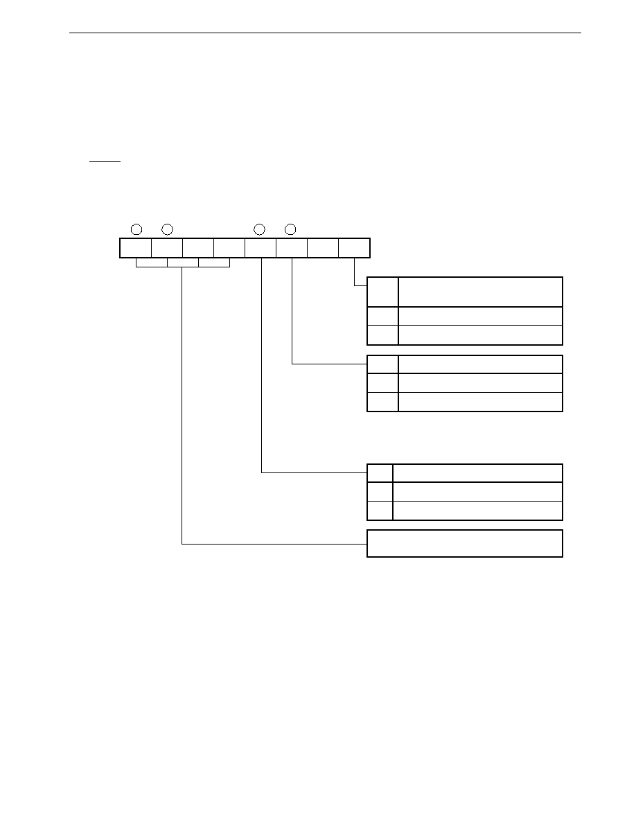
277
CHAPTER 10 TIMER/EVENT COUNTER 1
Preliminary User's Manual U13987EJ1V0UM00
10.3 Timer/Event Counter 1 Control Registers
(1) Timer control register 1 (TMC1)
TMC1 controls the timer/event counter 1, TM1/TM1W, count operation by the low-order 4 bits (the high-order 4 bits control
the count operation of timer/event counter 2 TM2/TM2W).
TMC1 can be read or written to with an 8-bit manipulation instruction or bit manipulation instruction. The format of TMC1
is shown in Figure 10-2.
RESET input clears TMC1 to 00H.
Figure 10-2. Timer Control Register 1 (TMC1) Format
Remark
The OVF1 bit is reset by software only.
7
CE2
TMC1
6
OVF2
5
CMD2
4
BW2
3
CE1
2
OVF1
1
0
0
BW1
Address
After reset
R/W
R/W
00H
0FF5FH
BW1
Timer/Event Counter 1 Bit Length
Specification
8-bit operating mode
16-bit operating mode
1
0
OVF1
TM1/TM1W Overflow Flag
No overflow
Overflow
Note
1
0
CE1
TM1/TM1W Count Operation Control
Count operation stopped with count cleared
Count operation enabled
1
0
Countrols count operation of timer/event counter 2
(TM2/TM2W) (see Figure 11-2).
Note In 8-bit operating mode:
count up from FFH to 00H
In 16-bit operating mode:
count up from FFFFH to 0000H
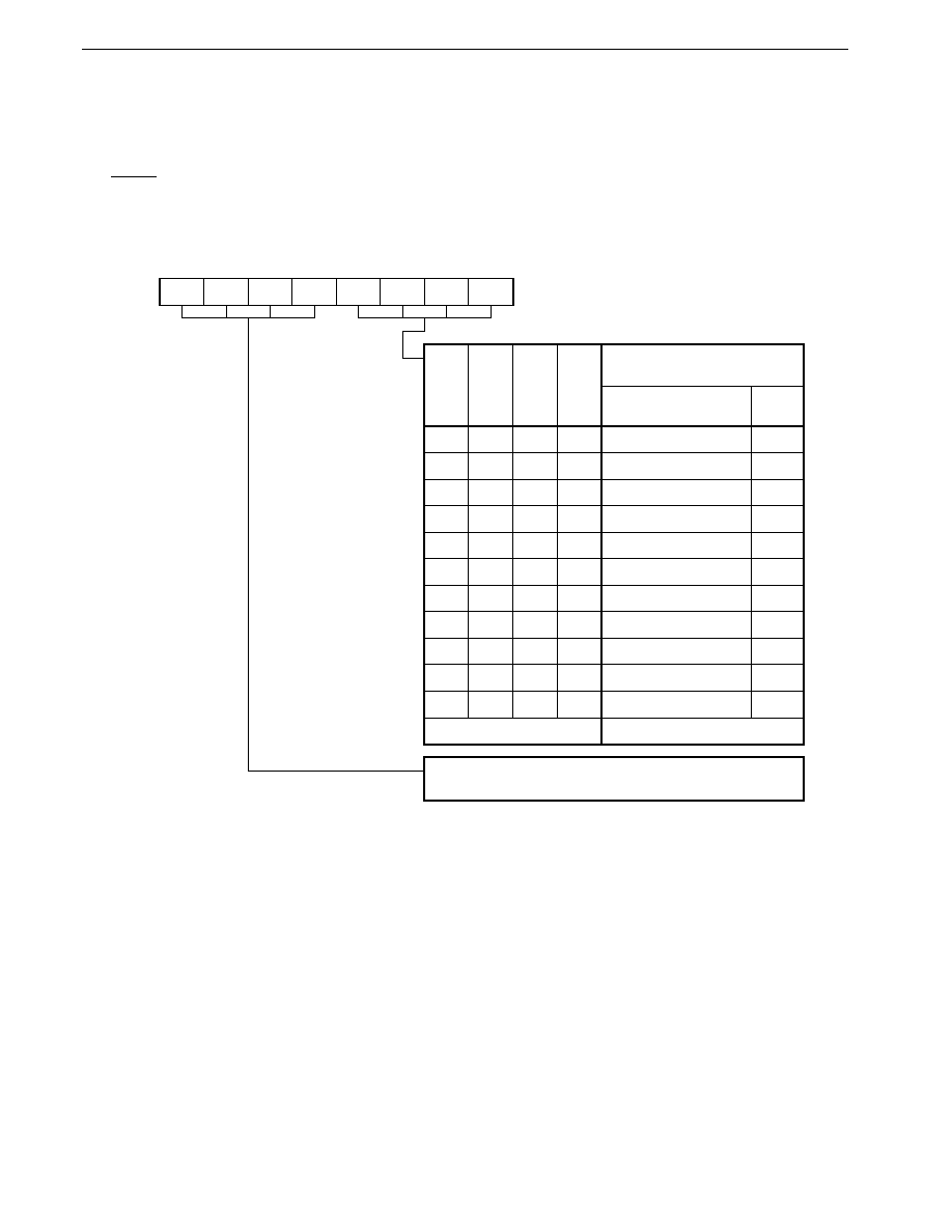
278
CHAPTER 10 TIMER/EVENT COUNTER 1
Preliminary User's Manual U13987EJ1V0UM00
(2) Prescaler mode register 1 (PRM1)
In PRM1, the count clock to timer/event counter 1 TM1/TM1W is specified by the low-order 4 bits (the high-order 4 bits
specify the count clock to timer/event counter 2 TM2/TM2W).
PRM1 can be read or written to with an 8-bit manipulation instruction. The format of PRM1 is shown in Figure 10-3.
RESET input sets PRM1 to 11H.
Figure 10-3. Prescaler Mode Register 1 (PRM1) Format
Remark
f
XX
: X1 input frequency or oscillation frequency
PRS23 PRS22 PRS21 PRS20 PRS13 PRS12 PRS11 PRS10
7
6
5
4
3
2
1
0
PRM1
0FF5EH
Address
11H
After reset
R/W
R/W
PRS13
0
0
0
0
0
0
0
0
1
1
1
Specifies count clock to TM2/TM2W of timer/event counter 2
(see Figure 11-3).
PRS12
0
0
0
0
1
1
1
1
0
0
1
PRS11
0
0
1
1
0
0
1
1
0
0
1
PRS10
0
1
0
1
0
1
0
1
0
1
1
Timer/Event Counter 1 (TM1/
TM1W) Count Clock Specification
Count Clock [Hz]
Specification
Setting prohibited
f
XX
/4
f
XX
/8
f
XX
/16
f
XX
/32
f
XX
/64
f
XX
/128
f
XX
/256
f
XX
/512
f
XX
/1,024
External clock (INTP0)
Setting prohibited
�
0.64
1.27
2.54
5.09
10.17
20.35
40.70
81.40
162.80
�
Other than the above
(f
XX
= 12.58 MHz)
Resolution
[ s]
�
279
CHAPTER 10 TIMER/EVENT COUNTER 1
Preliminary User's Manual U13987EJ1V0UM00
(3) Capture/compare control register 1 (CRC1)
CRC1 specifies the operation of the capture/compare register (CR11/CR11W) and the enabling condition for a timer counter
1 (TM1/TM1W) clear operation.
CRC1 can be read or written to with an 8-bit manipulation instruction. The format of CRC1 is shown in Figure 10-4.
RESET input clears CRC1 to 00H.
Figure 10-4. Capture/Compare Control Register 1 (CRC1) Format
7
0
CRC1
6
0
5
0
4
0
3
CLR11
2
CM
1
CLR10
0
0
Address
After reset
R/W
R/W
00H
0FF32H
CLR10
TM1 Clear Operation when TM1 = CR10
TM1W Clear Operation when TM1W = CR10W
Disabled
Enabled
1
0
CLR11
CM
Compare
operation
CR11/CR11W
Operation
Specificaton
TM1/TM1W
Clearance
Operation
Disabled
Enabled (when
TM1 & CR11 or
TM1W & CR11W
contents match)
1
0
0
0
Capture
operation
Disabled
Enabled (when
TM1 contents
are captured in
CR11 or when
TM1W contents
are captured in
CR11W)
1
0
1
1

280
CHAPTER 10 TIMER/EVENT COUNTER 1
Preliminary User's Manual U13987EJ1V0UM00
10.4 Timer Counter 1 (TM1) Operation
10.4.1 Basic operation
8-bit operation mode/16-bit operation mode control can be performed for timer/event counter 1 by means of bit 0 (BW1) of
timer control register 1 (TMC1)
Note
.
In the timer/event counter 1 count operation, the count-up is performed using the count clock specified by the low-order 4
bits of prescaler mode register 1 (PRM1).
Count operation enabling/disabling is controlled by bit 3 (CE1) of TMC1 (timer/event counter 1 operation control is performed
by the low-order 4 bits of the TMC1). When the CE1 bit is set (to 1) by software, the contents of TM1 are cleared to 0H on the
first count clock, and then the count-up operation is performed.
When the CE1 bit is cleared (to 0), TM1 becomes 0H immediately, and capture operations and match signal generation are
stopped.
If the CE1 bit is set (to 1) again when it is already set (to 1), TM1 continues the count operation without being cleared.
If the count clock is input when TM1 is FFH in 8-bit operation mode and when TM1W is FFFFH in 16-bit operation mode, TM1/
TM1W becomes 0H. In this case, OVF1 bit is set. OVF1 bit is cleared by software only. The count operation is continued.
When RESET is input, TM1 is cleared to 0H, and the count operation is stopped.
Note
Unless otherwise specified, the functions of timer counter 1 in the 8-bit operation mode are described hereafter. In
the 16-bit operation mode, TM1, CR10, and CR11 operate as TM1W, CR10W, and CR11W respectively.
281
CHAPTER 10 TIMER/EVENT COUNTER 1
Preliminary User's Manual U13987EJ1V0UM00
Figure 10-5. Basic Operation in 8-Bit Operation Mode (BW1 = 0)
(a) Count started
count disabled
count started
(b) When "1" is written to the CE1 bit again after the count starts
(c) Operation when TM1 = FFH
TM1
CE1
0H
0H
1H
2H
0FH
10H
11H
0H
1H
0H
Count started
CE1
1
Count stopped
CE1
0
Count started
CE1
1
Count clock
TM1
CE1
Count started
CE1
1
Rewrite
CE1
1
Count clock
0H
0H
1H
2H
3H
4H
5H
6H
TM1
OVF1
FEH
FFH
0H
Cleared by software
OVF1
0
Count clock
1H
282
CHAPTER 10 TIMER/EVENT COUNTER 1
Preliminary User's Manual U13987EJ1V0UM00
Figure 10-6. Basic Operation in 16-Bit Operation Mode (BW1 = 1)
(a) Count started
count disabled
count started
(b) When "1" is written to the CE1 bit again after the count starts
(c) Operation when TM1W = FFFFH
TM1W
CE1
0H
0H
1H
2H
FFH 100H
101H
0H
1H
0H
Count started
CE1
1
Count stopped
CE1
0
Count started
CE1
1
Count clock
TM1W
CE1
Count started
CE1
1
Rewrite
CE1
1
Count clock
0H
0H
1H
2H
3H
4H
5H
6H
TM1W
OVF1
FFFEH FFFFH
0H
Cleared by software
OVF1
0
Count clock
1H
283
CHAPTER 10 TIMER/EVENT COUNTER 1
Preliminary User's Manual U13987EJ1V0UM00
10.4.2 Clear operation
(1) Clear operation after match with compare register and after capture operation
Timer counter 1 (TM1) can be cleared automatically after a match with the compare register (CR1n: n = 0, 1) and a capture
operation. When a clearance source arises, TM1 is cleared to 0H on the next count clock. Therefore, even if a clearance
source arises, the value at the point at which the clearance source arose is retained until the next count clock arrives.
Figure 10-7. TM1 Clearance by Match with Compare Register (CR10, CR11)
Figure 10-8. TM1 Clearance after Capture Operation
(2) Clear operation by CE1 bit of timer control register 1 (TMC1)
Timer counter 1 (TM1) is also cleared when the CE1 bit of TMC1 is cleared (to 0) by software. The clear operation is
performed immediately after the clearance (to 0) of the CE1 bit.
TM1
Compare register
(CR1n)
Cleared here
Count clock
n
TM1 and CR1n match
n
0
1
n-1
TM1
INTP0
TM1 is captured
in CR11 here
Cleared here
Count clock
n
0
1
2
n-1
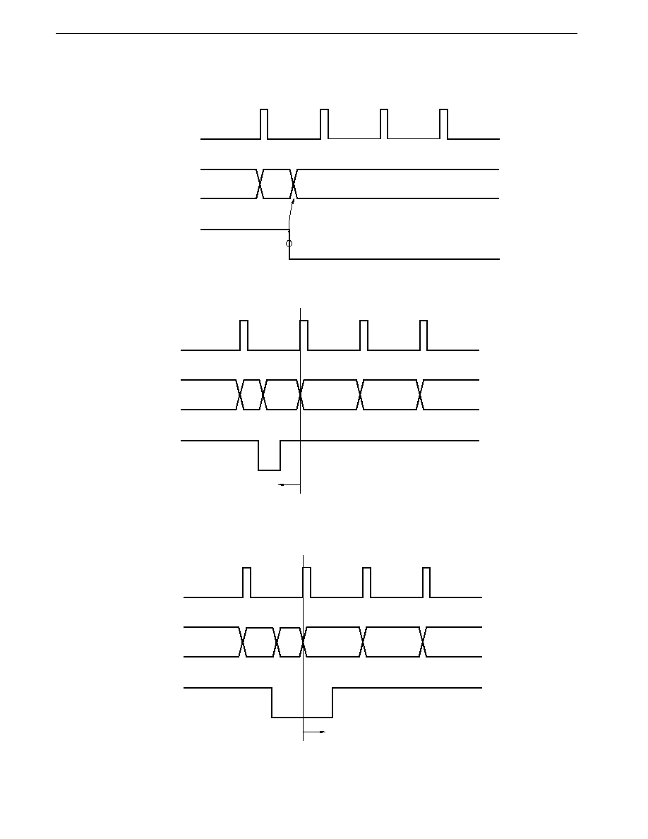
284
CHAPTER 10 TIMER/EVENT COUNTER 1
Preliminary User's Manual U13987EJ1V0UM00
Figure 10-9. Clear Operation when CE1 Bit is Cleared (to 0)
(a) Basic operation
(b) Restart before count clock is input after clearance
(c) Restart after count clock is input after clearance
TM1
CE1
n
Count clock
n-1
0
TM1
CE1
n
Count clock
n-1
0
0
1
2
If the CE1 bit is set (to 1) before this count clock, this count clock starts counting from 0.
TM1
CE1
n
0
Count clock
n-1
0
0
1
If the CE1 bit is set (to 1) from this count clock onward, the count clock starts counting
from 0 after the CE1 bit is set (to 1).
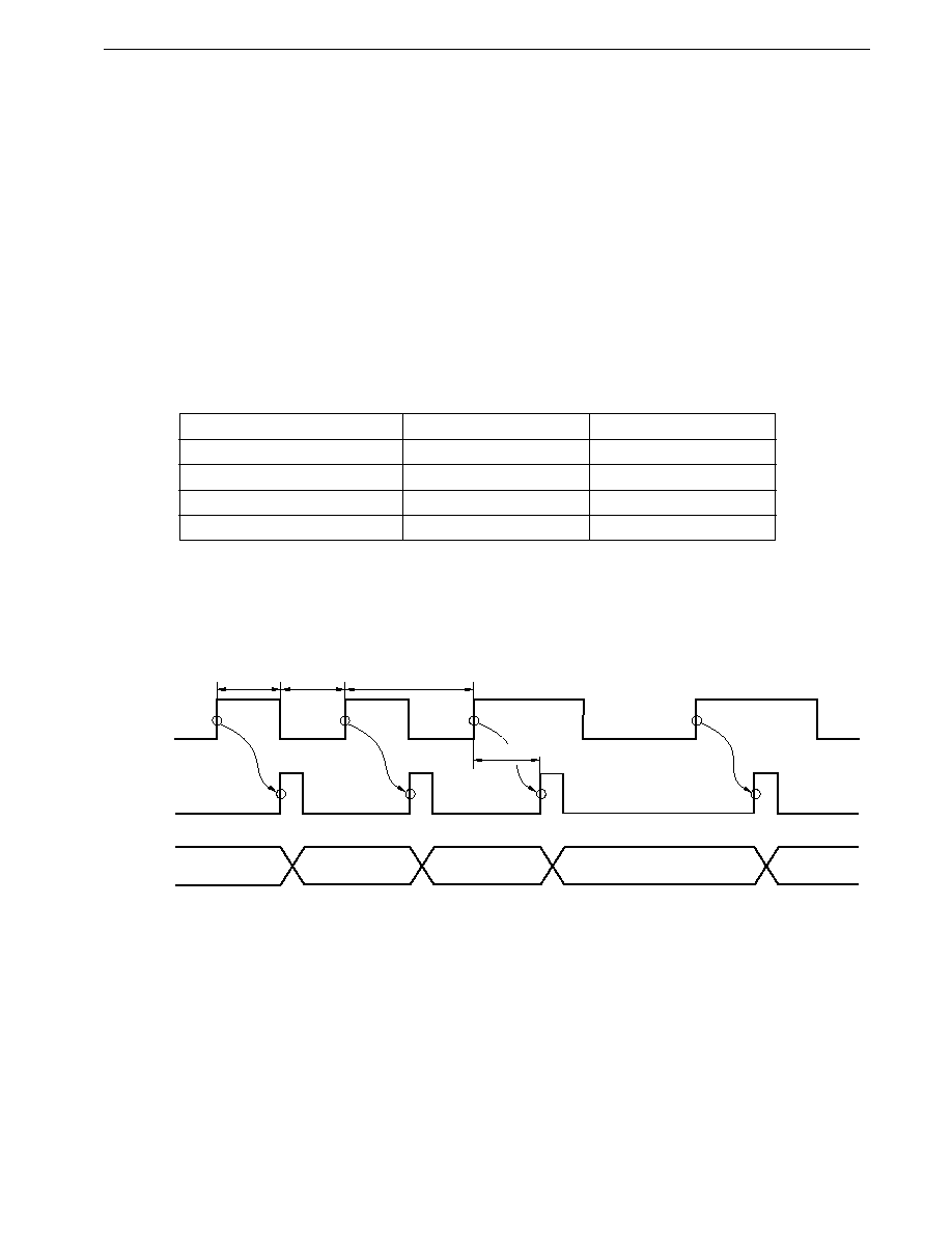
285
CHAPTER 10 TIMER/EVENT COUNTER 1
Preliminary User's Manual U13987EJ1V0UM00
10.5 External Event Counter Function
Timer/event counter 1 can count clock pulses input from the external interrupt request input pin (INTP0) pin.
No special selection method is needed for the external event counter operation mode. When the timer counter 1 (TM1) count
clock is specified as external clock input by the setting of the low-order 4 bits of prescaler mode register 1 (PRM1), TM1 operates
as an external event counter.
The maximum frequency of the external clock pulse that can be counted by the external event counter is determined by the
sampling clock select register (SCS0) as shown in Table 10-4.
The maximum frequency is the same when both the edges of the INTP0 input are counted and when only one edge is counted.
The pulse width of the INTP0 input must be three or more sampling clocks selected by SCS0, regardless of whether the level
is high or low. If the width is shorter than this, the pulse may not be counted.
Figure 10-10 shows the timing of the external event count by timer/event counter 1.
Table 10-4. Maximum Input Frequency and Minimum Input Pulse Width that can be Counted as Events
( ): f
XX
= 12.58 MHz, f
CLK
= 12.58 MHz
Sampling Clock Selected by SCS0
Maximum Input Frequency
Minimum Pulse Width
f
CLK
f
CLK
/6 (2.10 MHz)
3/f
CLK
(0.24
�
s)
f
XX
/32
f
XX
/192 (65.52 kHz)
96/f
XX
(7.63
�
s)
f
XX
/64
f
XX
/384 (32.76 kHz)
192/f
XX
(15.26
�
s)
f
XX
/128
f
XX
/768 (16.38 kHz)
384/f
XX
(30.52
�
s)
Figure 10-10. Timer/Event Counter 1 External Event Count Timing (1/2)
(1) Counting one edge (maximum frequency = f
CLK
/6)
Remarks 1. ICI: INTP0 input signal after passing through edge detection circuit
2. f
SMP
is selected by the sampling clock selection register (SCS0).
ICI
TM1
INTP0
Dn
Dn+1
Dn+2
Dn+3
3/f
SMP
(MIN.) 3/f
SMP
(MIN.)
6/f
SMP
(MIN.)
2-3/f
SMP
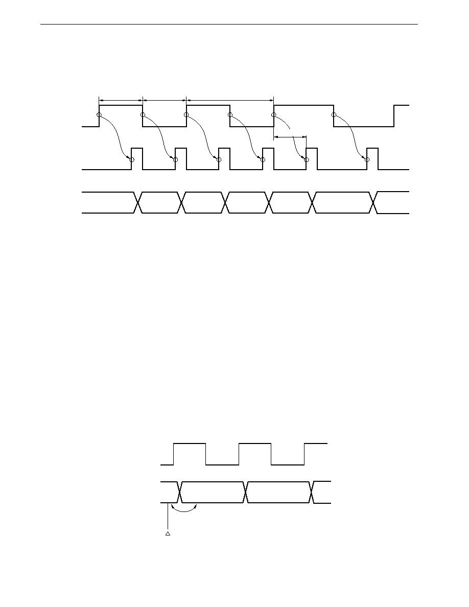
286
CHAPTER 10 TIMER/EVENT COUNTER 1
Preliminary User's Manual U13987EJ1V0UM00
Figure 10-10. Timer/Event Counter 1 External Event Count Timing (2/2)
(2) Counting both edges (maximum frequency = f
CLK
/6)
Remarks 1. ICI: INTP0 input signal after passing through edge detection circuit
2. f
SMP
is selected by the sampling clock selection register (SCS0).
The TM1 count operation is controlled by the CE1 bit of the timer control register 1 (TMC1) in the same way as with the basic
operation.
When the CE1 bit is set (to 1) by software, the contents of TM1 are set to 0H and the count-up operation is started on the
initial count clock.
When the CE1 bit is cleared (to 0) by software during a TM1 count operation, the contents of TM1 are set to 0H immediately
and the stopped state is entered. The TM1 count operation is not affected if the CE1 bit is set (to 1) by software again when
it is already set (to 1).
Caution
When timer/event counter 1 is used as an external event counter, it is not possible to distinguish between
the case where there is no valid edge input at all and the case where there is a single valid edge input using
the timer counter 1 (TM1) alone (see Figure 10-11), since the contents of TM1 are 0 in both cases. If it is
necessary to make this distinction, the INTP0 interrupt request flag should be used. An example is shown
in Figure 10-12.
Figure 10-11. Example of the Case where the External Event Counter does Not Distinguish between One
Valid Edge Input and No Valid Edge Input
ICI
TM1
INTP0
Dn+1
Dn
Dn+2
Dn+3
Dn+4
Dn+5
3/f
SMP
(MIN.)
3/f
SMP
(MIN.)
6/f
SMP
(MIN.)
2-3/f
SMP
TM1
0
INTP0
1
2
0
Count start
No distinction made
287
CHAPTER 10 TIMER/EVENT COUNTER 1
Preliminary User's Manual U13987EJ1V0UM00
Figure 10-12. To distinguish whether One or No Valid Edge has been Input with External Event Counter
(a) Processing when count is started
(b) Processing when count value is read
Clear INTP0 interrupt
request flag
PIF0
0
; Clear PIF0 to 0
End
Start count
; Set CE1 to 1
Start count
CE1
1
Read TM1 contents
A
TM1
; Check PIF0 contents
If 1, there is a valid edge
; Number of input valid edges is set in A register
; Check TM1 value
If 0, check interrupt
request flag
End
PIF0 = 1?
YES
YES
NO
NO
Count value read
A = 0?
A
A+1
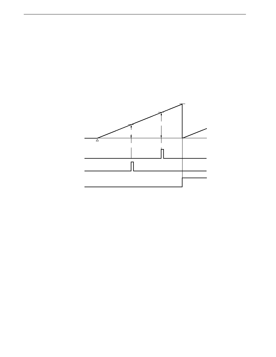
288
CHAPTER 10 TIMER/EVENT COUNTER 1
Preliminary User's Manual U13987EJ1V0UM00
10.6 Compare Register and Capture/Compare Register Operation
10.6.1 Compare operations
Timer/event counter 1 performs compare operations in which the value set in a compare register (CR10), capture/compare
register (CR11), specified for compare operation is compared with the timer counter 1 (TM1) count value.
If the count value of TM1 matches the preset value of the CR10, or the CR11 as the result of the count operation, an
interrupt request signal (INTC10 or INTC11) is generated.
After a match with the CR10 or CR11 value, the TM1 contents can be cleared, and the timer functions as an interval timer
that repeatedly counts up to the value set in the CR10 or CR11.
Figure 10-13. Compare Operation in 8-Bit Operation Mode
Remark
CLR10 = 0, CLR11 = 0, CM = 0, BW1 = 0
INTC10
interrupt request
TM1
count value
0H
Count start
CE1
1
CR10 value
OVF1
INTC11
interrupt request
FFH
CR11 value
Match
Match
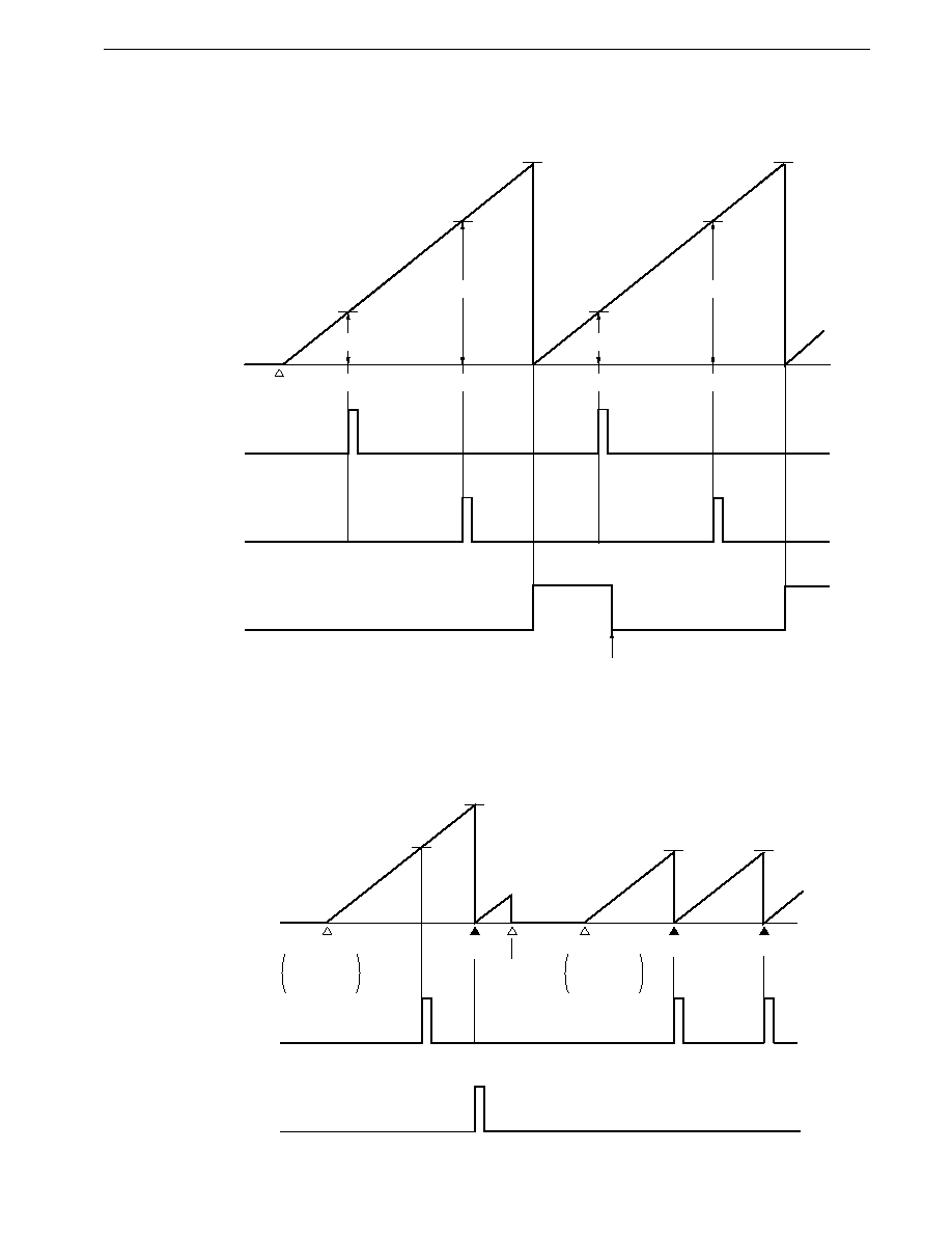
289
CHAPTER 10 TIMER/EVENT COUNTER 1
Preliminary User's Manual U13987EJ1V0UM00
Figure 10-14. Compare Operation in 16-Bit Operation Mode
Remark
CLR10 = 0, CLR11 = 0, BW1 = 1
Figure 10-15. TM1 Clearance after Match Detection
INTC10
interrupt request
TM1W
count value
0H
FFFFH
Count start
CE1
1
CR10W value
CR11W value
FFFFH
CR10W value
CR11W value
INTC11
interrupt request
OVF1
Cleared by software
Match
Match
Match
Match
INTC10
interrupt request
TM1
count value
0H
CR11
Count start
CE
1
CLR10
0
CLR11
1
CE1
0
CLR10
1
CLR11
0
INTC11
interrupt request
CR10
CR10
CR10
Count disabled
CE1
0
Count start
Clear
Clear
Clear
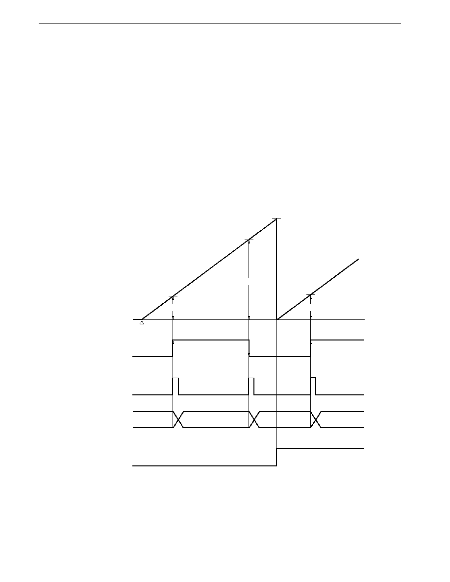
290
CHAPTER 10 TIMER/EVENT COUNTER 1
Preliminary User's Manual U13987EJ1V0UM00
10.6.2 Capture operations
Timer/event counter 1 performs capture operations in which the timer counter 1 (TM1) count value is fetched into the capture
register in synchronization with an external trigger, and retained there.
A valid edge detected from the input of the external interrupt request input pin (INTP0) is used as the external trigger (capture
trigger). The count value of TM1 in the process of being counted is fetched into the capture register (CR12), or the capture/
compare register (CR11) when a capture operation is specified, in synchronization with the capture trigger, and is retained there.
The contents of the CR11 and CR12 are retained until the next capture trigger is generated.
The capture trigger valid edge is set by means of external interrupt mode register 0 (INTM0). If both rising and falling edges
are set as capture triggers, the width of pulses input from off-chip can be measured, and if a capture trigger is generated by a
single edge, the input pulse cycle can be measured.
See Figure 22-1 for details of the INTM0 format.
When CR11 is used as a capture register, TM1 can be cleared as soon as the contents of TM1 have been captured to CR11
by capture trigger.
Figure 10-16. Capture Operation in 8-Bit Operation Mode
Remark
Dn: TM1 count value (n = 0, 1, 2, ...)
CLR10 = 0, CLR11 = 0, CM = 1, BW1 = 0
INTP0
pin input
INTP0
interrupt request
TM1
count value
0H
FFH
Capture/compare
register (CR11)
OVF1
Count start
D0
D1
D2
D0
D1
D2

291
CHAPTER 10 TIMER/EVENT COUNTER 1
Preliminary User's Manual U13987EJ1V0UM00
Figure 10-17. Capture Operation in 16-Bit Operation Mode
Remark
Dn: TM1W count value (n = 0, 1, 2, ...)
CLR10 = 0, CLR11 = 0, CM = 1, BW1 = 1
INTP0
pin input
INTP0
interrupt request
TM1W
count value
0H
FFFFH
Capture register
(CR12W)
OVF1
Count start
CE1
1
D0
D1
D2
D0
D1
D2
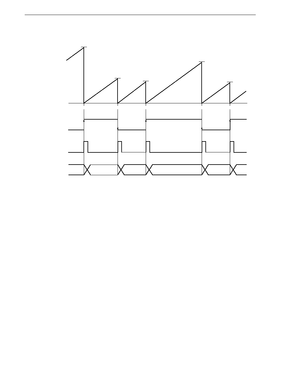
292
CHAPTER 10 TIMER/EVENT COUNTER 1
Preliminary User's Manual U13987EJ1V0UM00
Figure 10-18. TM1 Clearance after Capture Operation
Remark
NI: TM1 count value (n = 0, 1, 2, ...)
CLR10 = 0, CLR11 = 1, CM = 1
INTP0
pin input
INTP0
interrupt request
TM1
count value
0H
Capture/compare
register (CR11)
N1
Capture
Capture
Capture
Capture
Capture
N2
N3
N4
N5
N3
N2
N4
N1
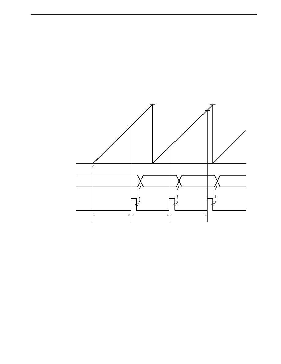
293
CHAPTER 10 TIMER/EVENT COUNTER 1
Preliminary User's Manual U13987EJ1V0UM00
10.7 Examples of Use
10.7.1 Operation as interval timer (1)
When timer counter 1 (TM1) is made free-running and a fixed value is added to the compare register (CR1n: n = 0, 1) in the
interrupt service routine, TM1 operates as an interval timer with the added fixed value as the cycle (see Figure 10-19).
Since TM1 has two compare registers, two interval timers with different intervals can be constructed.
The control register settings are shown in Figure 10-20, the setting procedure in Figure 10-21, and the processing in the
interrupt service routine in Figure 10-22.
Figure 10-19. Interval Timer Operation (1) Timing
Remark
Interval = n
�
x/f
XX
, 1
n
FFH
x = 4, 8, 16, 32, 64, 128, 256, 512, 1,024
MOD (2n)
INTC10
interrupt request
TM1
count value
0H
FFH
Compare register
(CR10)
n
Timer start
MOD (3n)
MOD (4n)
FFH
n
MOD (2n)
MOD (3n)
Interval
Interval
Interval
Rewritten by
interrupt program
Rewritten by
interrupt program
Rewritten by
interrupt program
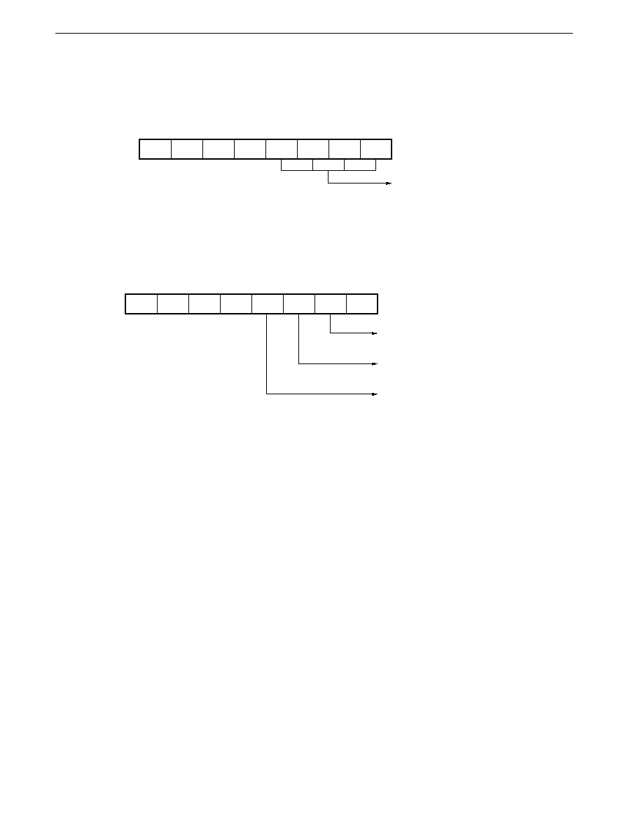
294
CHAPTER 10 TIMER/EVENT COUNTER 1
Preliminary User's Manual U13987EJ1V0UM00
Figure 10-20. Control Register Settings for Interval Timer Operation (1)
(a) Prescaler mode register 1 (PRM1)
(b) Capture/compare control register 1 (CRC1)
7
�
PRM1
6
�
5
�
4
�
3
PRS13
2
PRS12
1
PRS11
0
PRS10
Count clock specification
(x/f
XX
; x = 4, 8, 16, 32, 64, 128,
256, 512, 1,024)
7
0
CRC1
6
0
5
0
4
0
3
0
2
0
1
0
0
0
TM1 clearing by match of CR10 & TM1
contents disabled
CR11 specified as compare register
TM1 clearing by match of CR11 & TM1
contents disabled
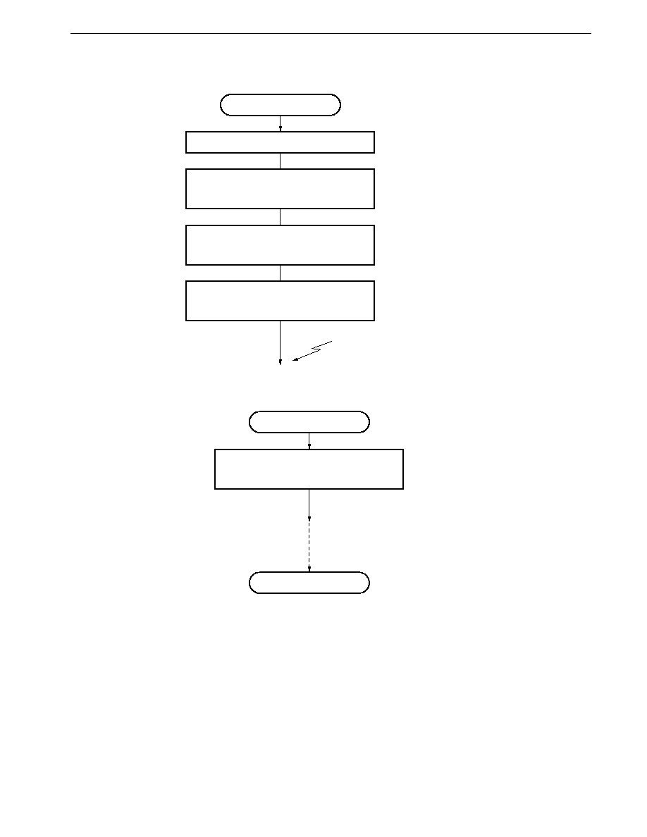
295
CHAPTER 10 TIMER/EVENT COUNTER 1
Preliminary User's Manual U13987EJ1V0UM00
Figure 10-21. Interval Timer Operation (1) Setting Procedure
Figure 10-22. Interval Timer Operation (1) Interrupt Request Servicing
Interval timer (1)
Set count value in CR10
CR10
n
Start count
CE1
1
INTC10 interrupt
; Set 1 in bit 3 of TMC1
Set PRM1
Set CRC1
CRC1
00H
INTC10 interrupt
Calculate timer value that will
generate next interrupt
CR10
CR10+n
Other interrupt service program
RETI

296
CHAPTER 10 TIMER/EVENT COUNTER 1
Preliminary User's Manual U13987EJ1V0UM00
10.7.2 Operation as interval timer (2)
TM1 operates as an interval timer that generates interrupts repeatedly with the preset count time as the interval (see Figure
10-23).
The control register settings are shown in Figure 10-24, and the setting procedure in Figure 10-25.
Figure 10-23. Interval Timer Operation (2) Timing (when CR11 is used as Compare Register)
Remark
Interval = (n+1)
�
x/f
XX
0
n
FFH
x = 4, 8, 16, 32, 64, 128, 256, 512, 1,024
Compare register
(CR11)
INTC11
interrupt request
TM1
count value
0H
n
n
n
Count start
Clear
Clear
Interval
Match
Match
Interrupt acknowledge
Interrupt acknowledge
Interval
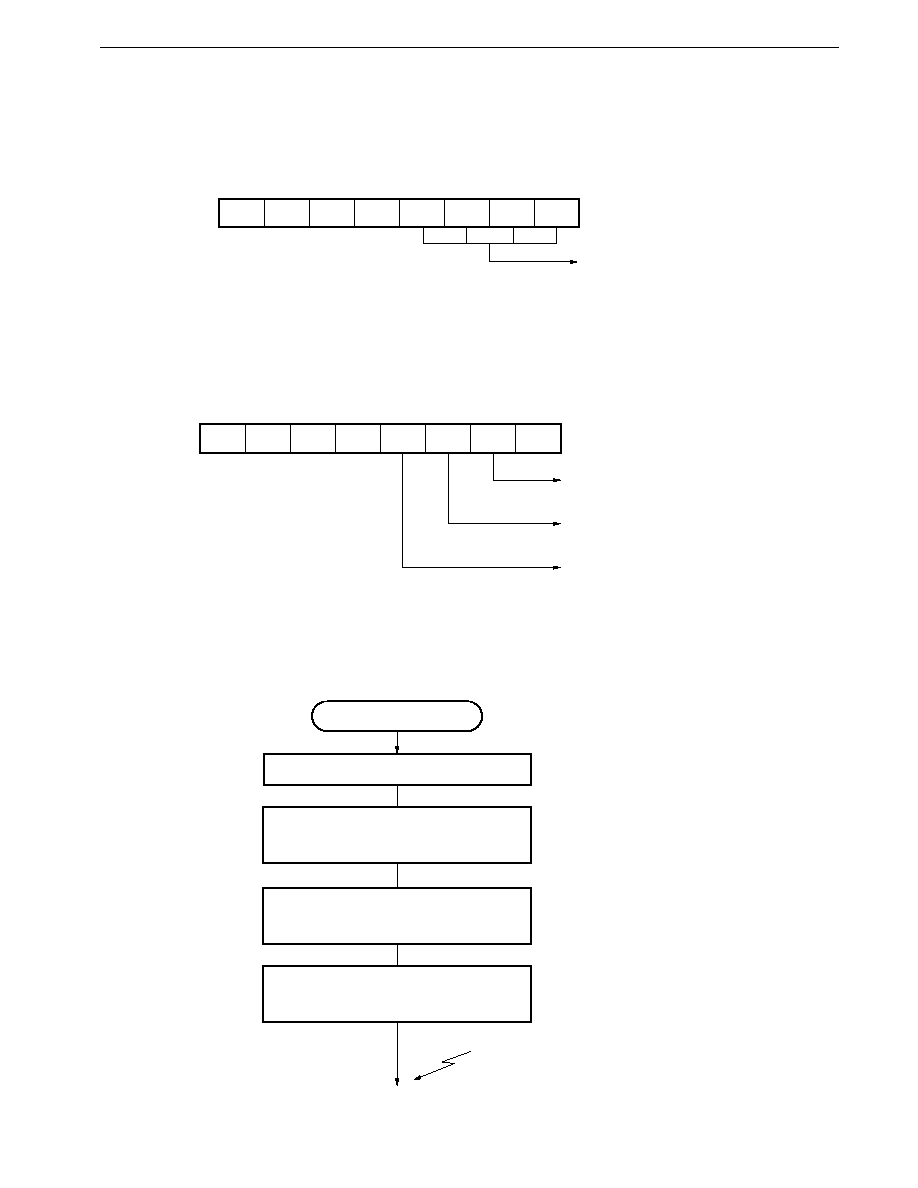
297
CHAPTER 10 TIMER/EVENT COUNTER 1
Preliminary User's Manual U13987EJ1V0UM00
Figure 10-24. Control Register Settings for Interval Timer Operation (2)
(a) Prescaler mode register 1 (PRM1)
(b) Capture/compare control register 1 (CRC1)
Figure 10-25. Interval Timer Operation (2) Setting Procedure
7
�
PRM1
6
�
5
�
4
�
3
PRS13
2
PRS12
1
PRS11
0
PRS10
Count clock specification
(x/f
XX
; x = 4, 8, 16, 32, 64, 128,
256, 512, 1,024)
7
0
CRC1
6
0
5
0
4
0
3
1
2
0
1
0
0
0
TM1 clearing by match of CR10 & TM1
contents disabled
CR11 specified as compare operation
TM1 clearing by match of CR11 & TM1
contents enabled
Interval timer (2)
Set count value in CR11
CR11
n
INTC11 interrupt
; Set 1 in bit 3 of TMC1
Set PRM1
Set CRC1
CRC1
08H
Start count
CE1
1
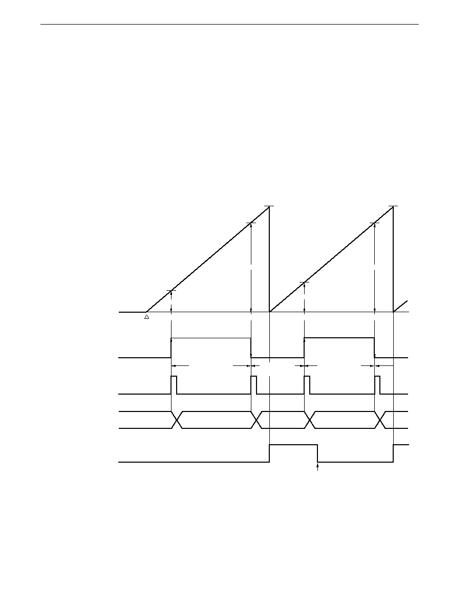
298
CHAPTER 10 TIMER/EVENT COUNTER 1
Preliminary User's Manual U13987EJ1V0UM00
10.7.3 Pulse width measurement operation
In pulse width measurement, the high-level or low-level width of external pulses input to the external interrupt request input
pin (INTP0) is measured.
Both the high-level and low-level widths of pulses input to the INTP0 pin must be at least 3 sampling clocks selected by
SCS0; if shorter than this, the valid edge will not be detected and a capture operation will not be performed.
As shown in Figure 10-26, the timer counter 1 (TM1) value being counted is fetched into the capture/compare register (CR11)
set as a capture register in synchronization with a valid edge (set as both rising and falling edges) in the INTP0 pin input, and
held there. The pulse width is obtained from the product of the difference between the TM1 count value (D
n
) fetched into and
held in the CR11 on detection of the nth valid edge and the count value (D
n-1
) fetched and held on detection of valid edge n-1,
and the number of count clocks (x/f
XX
; x = 4, 8, 16, 32, 64, 128, 256, 512, 1,024).
The control register settings are shown in Figure 10-27, and the setting procedure in Figure 10-28.
Figure 10-26. Pulse Width Measurement Timing (when CR11 is used as Capture Register)
Remark
Dn: TM1 count value (n = 0, 1, 2, ...)
x = 4, 8, 16, 32, 64, 128, 256, 512, 1,024
INTP0
external input signal
INTP0
interrupt request
TM1
count value
0H
FFH
Capture/compare
register (CR11)
OVF1
D0
D1
Count start
CE1
1
FFH
D2
D3
(D1-D0)
�
x /f
XX
(D3-D2)
�
x /f
XX
Cleard by software
D1
D0
D2
D3
(100H-D1+
D2)
�
x /f
XX
Capture
Capture
Capture
Capture
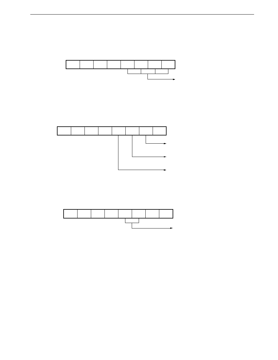
299
CHAPTER 10 TIMER/EVENT COUNTER 1
Preliminary User's Manual U13987EJ1V0UM00
Figure 10-27. Control Register Settings for Pulse Width Measurement
(a) Prescaler mode register 1 (PRM1)
(b) Capture/compare control register 1 (CRC1)
7
�
PRM1
6
�
5
�
4
�
3
PRS13
2
PRS12
1
PRS11
0
PRS10
Count clock specification
(x/f
XX
; x = 4, 8, 16, 32, 64, 128,
256, 512, 1,024)
(c) External interrupt mode register 0 (INTM0)
7
0
CRC1
6
0
5
0
4
0
3
0
2
1
1
0
0
0
TM1 clearing by match of TM1 & CR10
contents disabled
CR11 specified as capture
operation
TM1 clearing upon capture of CR11 in TM1
disabled
7
�
INTM0
6
�
5
�
4
�
3
1
2
1
1
0
0
�
Both rising & falling edges
specified as INTP0 input valid edges
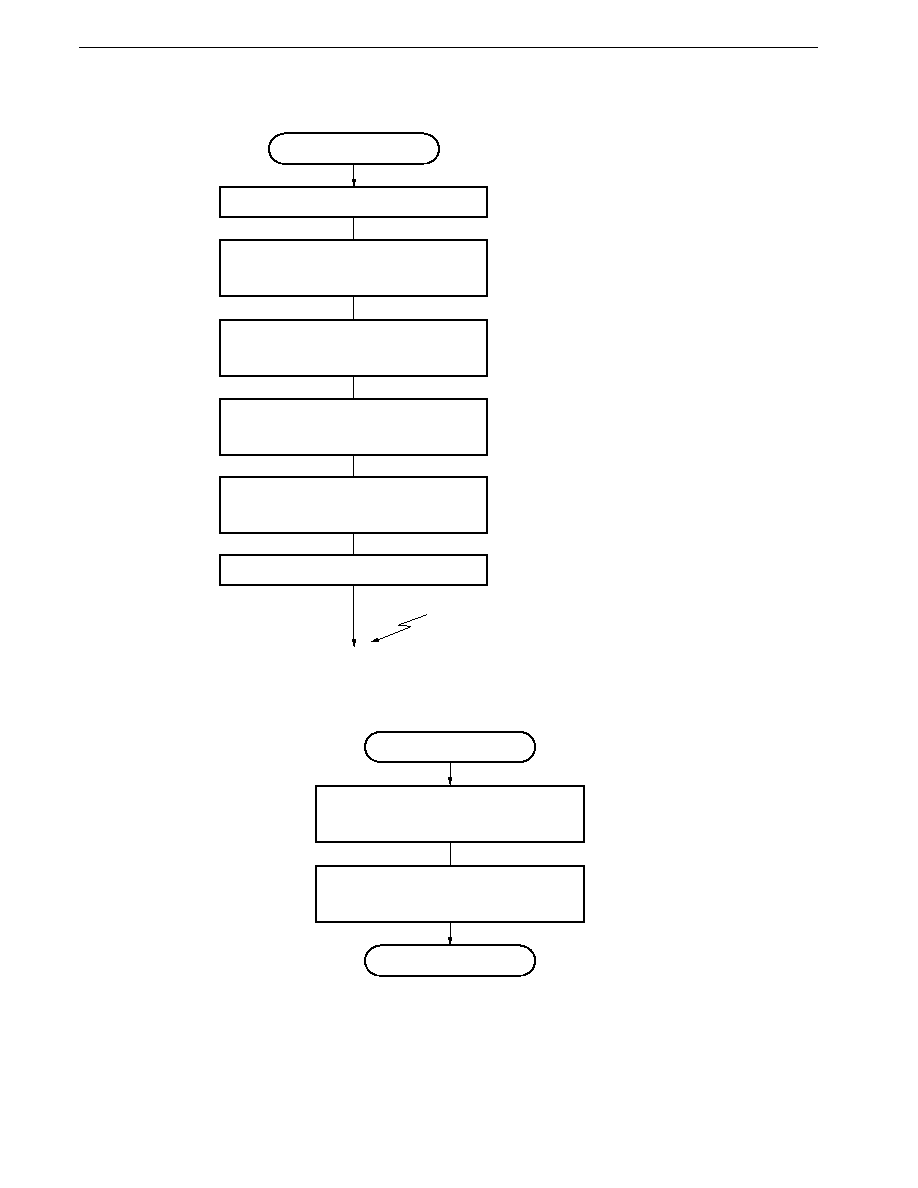
300
CHAPTER 10 TIMER/EVENT COUNTER 1
Preliminary User's Manual U13987EJ1V0UM00
Figure 10-28. Pulse Width Measurement Setting Procedure
Figure 10-29. Interrupt Request Servicing that Calculates Pulse Width
Pulse width measurement
Initialize capture value buffer memory
X
0
0
INTP0 interrupt
; Set 1 in bit 3 of TMC1
Set PRM1
Set INTM0
Set MK0L
Set CRC1
CRC1
04H
Enable interrupts
Start count
CE1
1
; Specify both edges as INTP0
input valid edges, release
interrupt masking
INTP0 interrupt
Calculate pulse width
Y
n
= CR11 � X
n
Store capture value in memory
X
n+1
CR11
RETI

301
CHAPTER 10 TIMER/EVENT COUNTER 1
Preliminary User's Manual U13987EJ1V0UM00
10.8 Cautions
(1) While timer/event counter 1 is operating (while the CE1 bit of the timer control register 1 (TMC1) is set), malfunctioning
may occur if the contents of the following registers are rewritten. This is because it is undefined which takes precedence
in a contention, the change in the hardware functions due to rewriting the register, or the change in the status because
of the function before rewriting.
Therefore, be sure to stop the counter operation for the sake of safety before rewriting the contents of the following registers.
� Prescaler mode register 1 (PRM1)
� Capture/compare control register 1 (CRC1)
� CMD2 bit of timer control register 1 (TMC1)
(2) If the contents of the compare register (CR1n: n = 0 or 1) coincide with those of TM1 when an instruction that stops timer
counter 1 (TM1) operation is executed, the counting operation of TM1 stops, but an interrupt request is generated.
In order not to generate the interrupt when stopping the operation of TM1, mask the interrupt in advance by using the interrupt
mask register before stopping TM1.
Example
Program that may generate interrupt request Program that does not generate interrupt request
CLR1
CE1
OR
MK0L, #C0H
OR
MK0L, #C0H
CLR1
CE1
CLR1
CIF10
CLR1
CIF11
(3) Up to 1 count clock is required after an operation to start timer/event counter 1 (CE1
1) has been performed before timer/
event counter 1 actually starts (refer to Figure 10-30).
For example, when using timer/event counter 1 as an interval timer, the first interval time is delayed by up to 1 clock. The
second and those that follow are at the specified interval.
Figure 10-30. Operation when Counting is Started
.
.
.
.
.
.
Disables interrupt from timer/
event counter 1
Clears interrupt request flag
from timer/event counter 1
Interrupt request from
timer/event counter 1
occurs between these
instructions
Count clock
TM1
CE1
Timing to start actual counting
Count start command (CE1
1)
by software
0
0
1
2
3
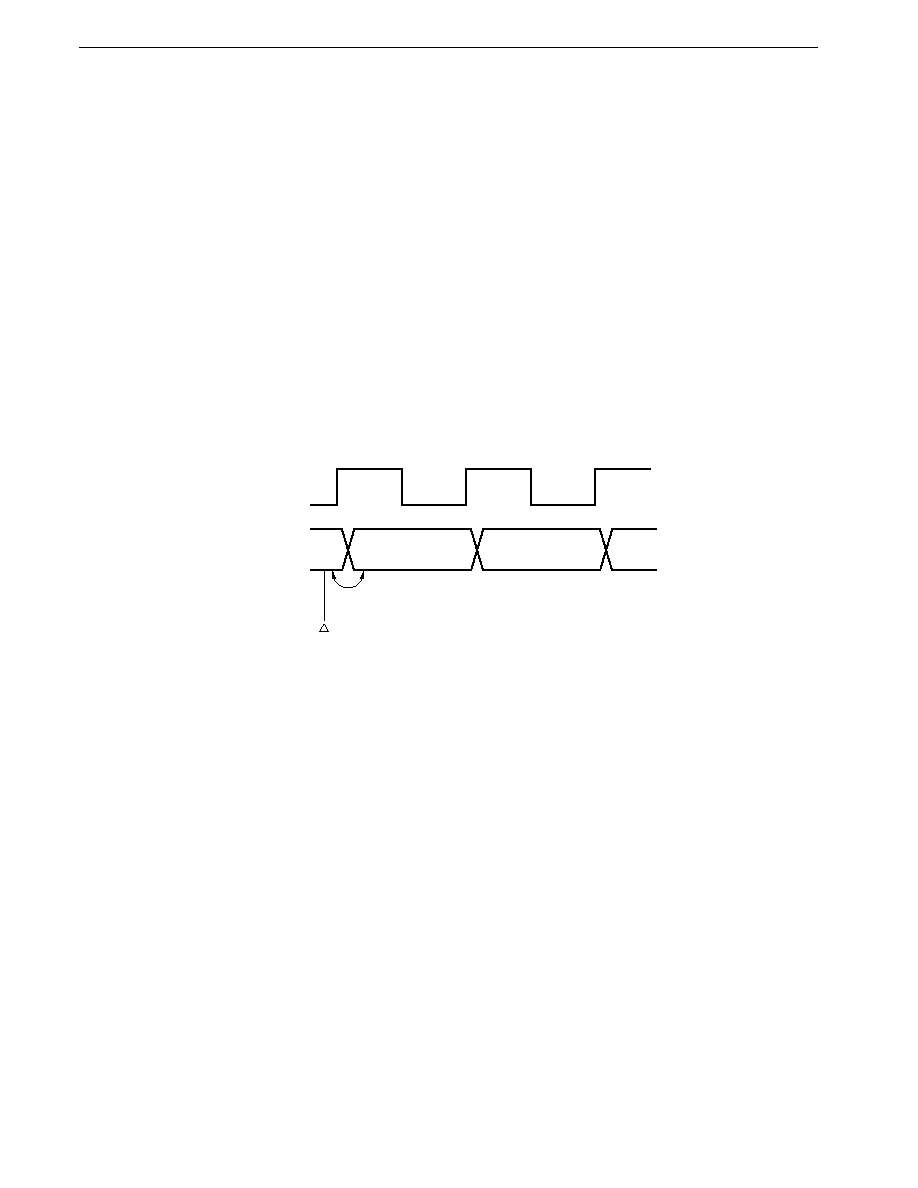
302
CHAPTER 10 TIMER/EVENT COUNTER 1
Preliminary User's Manual U13987EJ1V0UM00
(4) While an instruction that writes data to the compare register (CR1n: n = 0, 1) is executed, coincidence between CR1n, to
which the data is to be written, and timer counter 1 (TM1) is not detected.
Write data to CR1n when timer/event counter 1 is executing counting operation in the timing that the contents of TM1 do
not coincide with the value of CR1n before and after writing (e.g., immediately after an interrupt request has been generated
because TM1 and CR1n have coincided).
(5) Coincidence between TM1 and compare register (CR1n: n = 0, 1) is detected only when TM1 is incremented. Therefore,
the interrupt request is not generated even if the same value as TM1 is written to CR1n.
(6) When timer/event counter 1 is used as an external event counter, it is not possible to distinguish between the case where
there is no valid edge input at all and the case where there is a single valid edge input, using the timer counter 1 (TM1)
alone (refer to Figure 10-31), since the contents of TM1 are 0 in both cases. If it is necessary to make this distinction, the
INTP3 interrupt request flag should be used. To make a distinction, use the interrupt request flag of INTP0, as shown in
Figure 10-32.
Figure 10-31. Example of the Case where the External Event Counter does Not Distinguish
between One Valid Edge Input and No Valid Edge Input
INTP0
TM1
0
1
2
0
Cannot be
distinguished
Count start
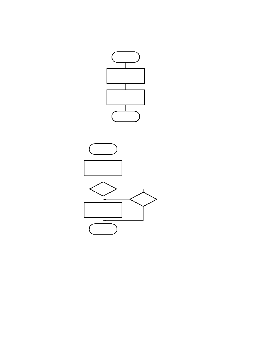
303
CHAPTER 10 TIMER/EVENT COUNTER 1
Preliminary User's Manual U13987EJ1V0UM00
Figure 10-32. To Distinguish whether One or No Valid Edge has been Input with External Event Counter
(a) Processing when count is started
(b) Processing when count value is read
; Set CE1 to 1
; Clear PIF0 to 0
Clear INTP0
interrupt request flag
PIF0
0
Start count
CE1
1
Start count
End
; Number of input valid edges is set to A register
Count value
read
Read TM1 contents
A
TM1
A
A+1
End
A = 0?
PIF0 = 1?
; Check TM1 value.
If 0, check interrupt
request flag.
; Check PIF0 contents.
If 1, valid edge is input.
YES
NO
YES
NO

304
Preliminary User's Manual U13987EJ1V0UM00
[MEMO]

305
Preliminary User's Manual U13987EJ1V0UM00
CHAPTER 11 TIMER/EVENT COUNTER 2
11.1 Functions
Timer/event counter 2 is 16-bit or 8-bit timer/event counter, and has the following function which the other three timer/
counters do not have:
�
One-shot timer
Note
Note
The one-shot timer function is a count operation of timer/event counter 2 (TM2/TM2W), and is thus different in
nature from the one-shot pulse output function of timer/event counter 0.
In this section, the following four basic functions are described in order:
�
Interval timer
�
Programmable square-wave output
�
Pulse width measurement
�
External event counter
(1) Interval timer
Generates internal interrupts at preset intervals.
Table 11-1. Timer/Event Counter 2 Intervals
Minimum Interval
Maximum Interval
Resolution
4/f
XX
2
16
�
4/f
XX
4/f
XX
(0.32
�
s)
(20.8 ms)
(0.32
�
s)
8/f
XX
2
16
�
8/f
XX
8/f
XX
(0.64
�
s)
(41.7 ms)
(0.64
�
s)
16/f
XX
2
16
�
16/f
XX
16/f
XX
(1.27
�
s)
(83.4 ms)
(1.27
�
s)
32/f
XX
2
16
�
32/f
XX
32/f
XX
(2.54
�
s)
(167 ms)
(2.54
�
s)
64/f
XX
2
16
�
64/f
XX
64/f
XX
(5.09
�
s)
(333 ms)
(5.09
�
s)
128/f
XX
2
16
�
128/f
XX
128/f
XX
(10.17
�
s)
(667 ms)
(10.17
�
s)
256/f
XX
2
16
�
256/f
XX
256/f
XX
(20.35
�
s)
(1.33 s)
(20.35
�
s)
512/f
XX
2
16
�
512/f
XX
512/f
XX
(40.70
�
s)
(2.67 s)
(40.70
�
s)
1,024/f
XX
2
16
�
1,024/f
XX
1,024/f
XX
(81.40
�
s)
(5.33 s)
(81.40
�
s)
( ): When f
XX
= 12.58 MHz

306
CHAPTER 11 TIMER/EVENT COUNTER 2
Preliminary User's Manual U13987EJ1V0UM00
(2) Programmable square-wave output
Outputs square waves independently to the timer output pins (TO2 and TO3).
Table 11-2. Timer/Event Counter 2 Programmable Square-Wave Output Setting Range
Minimum Pulse Width
Maximum Pulse Width
4/f
XX
2
16
�
4/f
XX
(0.32
�
s)
(20.8 ms)
8/f
XX
2
16
�
8/f
XX
(0.64
�
s)
(41.7 ms)
16/f
XX
2
16
�
16/f
XX
(1.27
�
s)
(83.4 ms)
32/f
XX
2
16
�
32/f
XX
(2.54
�
s)
(167 ms)
64/f
XX
2
16
�
64/f
XX
(5.09
�
s)
(333 ms)
128/f
XX
2
16
�
128/f
XX
(10.17
�
s)
(667 ms)
256/f
XX
2
16
�
256/f
XX
(20.35
�
s)
(1.33 s)
512/f
XX
2
16
�
512/f
XX
(40.70
�
s)
(2.67 s)
1,024/f
XX
2
16
�
1,024/f
XX
(81.40
�
s)
(5.33 s)
( ): When f
XX
= 12.58 MHz
Caution The above table is applicable to use of an internal clock.
307
CHAPTER 11 TIMER/EVENT COUNTER 2
Preliminary User's Manual U13987EJ1V0UM00
(3) Pulse width measurement
Detects the pulse width of the signal input to an external interrupt request input pins (INTP1 and INTP2).
Table 11-3. Timer/Event Counter 2 Pulse Width Measurement Range
Measurable Pulse Width
Note
Resolution
4/f
XX
to
2
16
�
4/f
XX
4/f
XX
(0.32
�
s)
(20.8 ms)
(0.32
�
s)
8/f
XX
to
2
16
�
8/f
XX
8/f
XX
(0.64
�
s)
(41.7 ms)
(0.64
�
s)
16/f
XX
to
2
16
�
16/f
XX
16/f
XX
(1.27
�
s)
(83.4 ms)
(1.27
�
s)
32/f
XX
to
2
16
�
32/f
XX
32/f
XX
(2.54
�
s)
(167 ms)
(2.54
�
s)
64/f
XX
to
2
16
�
64/f
XX
64/f
XX
(5.09
�
s)
(333 ms)
(5.09
�
s)
128/f
XX
to
2
16
�
128/f
XX
128/f
XX
(10.17
�
s)
(667 ms)
(10.17
�
s)
256/f
XX
to
2
16
�
256/f
XX
256/f
XX
(20.35
�
s)
(1.33 s)
(20.35
�
s)
512/f
XX
to
2
16
�
512/f
XX
512/f
XX
(40.70
�
s)
(2.67 s)
(40.70
�
s)
1,024/f
XX
to 2
16
�
1,024/f
XX
1,024/f
XX
(81.40
�
s)
(5.33 s)
(81.40
�
s)
( ): When f
XX
= 12.58 MHz
Note
The minimum pulse width that can be measured differs depending on the selected value of f
CLK
.
The minimum pulse width that can be measured is the value of 3/f
CLK
or the value in the above table, whichever
greater.
(4) External event counter
Counts the clock pulses input from the external interrupt request input pin (INTP2) (CI pin input pulses). The clocks
that can be input to timer/event counter 2 are shown in Table 11-4.
Table 11-4. Clocks Enabled to be Input to Timer/Event Counter 2
When Counting One Edge
When Counting Both Edges
Maximum frequency
f
CLK
/6 (2.10 MHz)
f
CLK
/6 (2.10 MHz)
Minimum pulse width
3/f
CLK
(0.24
�
s)
3/f
CLK
(0.24
�
s)
(High and low levels)
( ): When f
CLK
= 12.58 MHz and f
XX
= 12.58 MHz

308
CHAPTER 11 TIMER/EVENT COUNTER 2
Preliminary User's Manual U13987EJ1V0UM00
11.2 Configuration
Timer/event counter 2 consists of the following registers.
�
Timer counter (TM2/TM2W)
�
1
�
Compare register (CR20/CR20W)
�
1
�
Capture/compare register (CR21/CR21W)
�
1
�
Capture register (CR22/CR22W)
�
1
The block diagram of timer/event counter 2 is shown in Figure 11-1.
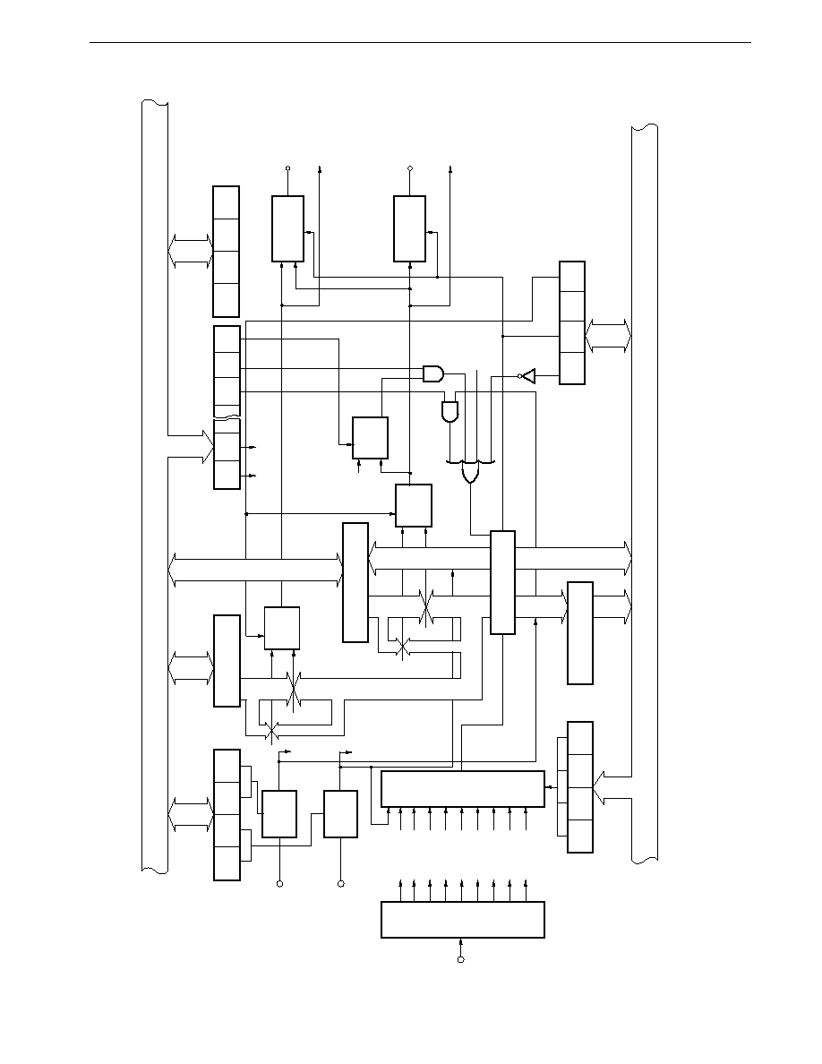
309
CHAPTER 11 TIMER/EVENT COUNTER 2
Preliminary User's Manual U13987EJ1V0UM00
Figure 11-1. Timer/Event Counter 2 Block Diagram
Internal bus
1/8
8/16
8
External interrupt
mode register 0
(INTM0)
ES21
ES11
Compare register
(CR20/CR20W)
16
16
8/16
Capture/compare
register (CR21/CR21W)
16
8/16
16
16
16
8/16
8
Selector
f
XX
/512
f
XX
/256
f
XX
/128
f
XX
/64
f
XX
f
XX
/32
f
XX
/16
f
XX
/8
f
XX
/4
Prescaler
mode register 1
(PRM1)
PRS23 PRS22 PRS21 PRS20
Capture register
(CR22/CR22W)
Timer counter 2
(TM2/TM2W)
Timer control
register 1 (TMC1)
OVF2
CE2
1/8
Internal bus
P22/INTP1
Edge
detection
circuit
Edge
detection
circuit
CMD2
Overflow
Selector
8
8
8
8
INTP2
Match
Match
Match
Match
RESET
Capture/compare
control register 2 (CRC2)
P23/INTP2/CI
INTP1
P36/TO2
ES20
ES10
f
XX
/1,024
Prescaler
Capture trigger
Capture trigger
MOD1 MOD0
CLR22 CLR21 CM21
ENT03 ALV3 ENT02 ALV2
Timer output
control register
(TOC)
Output control
circuit
Output control
circuit
INTC20
P37/TO3
INTC21
BW2
INTP2
8
PWM/PPG
output control
Selector
Selector

310
CHAPTER 11 TIMER/EVENT COUNTER 2
Preliminary User's Manual U13987EJ1V0UM00
(1) Timer counter 2 (TM2/TM2W)
TM2/TM2W is a timer counter that counts up the count clock specified by the high-order 4 bits of prescaler mode register
1 (PRM1). An internal clock or external clock can be selected as the count clock.
The count operation can be stopped or enabled by means of timer control register 1 (TMC1). The timer counter can
select to operate in an 8-bit (TM2) or 16-bit (TM2W) mode. TM2/TM2W can be read only with an 8/16-bit manipulation
instruction.
When RESET is input, TM2/TM2W is cleared to 00H and the count is stopped.
(2) Compare register (CR20/CR20W)
CR20/CR20W is an 8/16-bit register that holds the value that determines the interval timer operation cycle.
If the contents of the CR20/CR20W register match the contents of TM2/TM2W, an interrupt request (INTC20) and a
timer output control signal are generated. This compare register operates as CR20 in the 8-bit mode, and CR20W
in the 16-bit mode.
CR20/CR20W can be read or written to with an 8/16-bit manipulation instruction. The contents of this register are
undefined after RESET input.
(3) Capture/compare register (CR21/CR21W)
CR21/CR21W is an 8/16-bit register that can be specified as a compare register for detecting a match with the TM2/
TM2W count value or a capture register for capturing the TM2/TM2W count value according to the setting of the capture/
compare control register 2 (CRC2).
This capture/compare register operates as CR21 in the 8-bit mode, and CR21W in the 16-bit mode.
CR21/CR21W can be read or written to with an 8/16-bit manipulation instruction.
The contents of this register are undefined after RESET input.
(a) When specified as compare register
CR21/CR21W functions as an 8/16-bit register that holds the value that determines the interval timer operation
cycle.
An interrupt request (INTC21) and a timer output control signal are generated by a match between the contents
of the CR21/CR21W register and the contents of TM2/TM2W.
Also, the count value can be cleared by a match of the contents.
(b) When specified as capture register
CR21/CR21W functions as an 8/16-bit register that captures the contents of TM2/TM2W in synchronization with
the input of a valid edge on the external interrupt input pin (INTP2) (capture trigger).
The contents of the CR21/CR21W register are retained until the next capture trigger is generated.
(4) Capture register (CR22/CR22W)
CR22/CR22W is an 8/16-bit register that captures the contents of TM2/TM2W.
The capture operation is synchronized with the input of a valid edge to the external interrupt request input pin (INTP1)
(capture trigger). The contents of the CR22/CR22W register are retained until the next capture trigger is generated.
Also, TM2/TM2W can be cleared after a capture operation.
This capture register operates as CR22 in the 8-bit mode, and CR22W in the 16-bit mode.
CR22/CR22W can be read only with an 8/16-bit manipulation instruction. The contents of this register are undefined
after RESET input.

311
CHAPTER 11 TIMER/EVENT COUNTER 2
Preliminary User's Manual U13987EJ1V0UM00
(5) Edge detection circuit
The edge detection circuit detects an external input valid edge.
This circuit generates an external interrupt request (INTP1) and capture trigger by detecting the valid edge of the INTP1
pin input specified by the external interrupt mode register 0 (INTM0). It also generates a capture trigger, the count
clock of an external event, and external interrupt request (INTP2) by detecting the valid edge from an external interrupt
request input pin (INTP2).
(6) Output control circuit
It is possible to invert the timer output when the CR20/CR21 register contents and the contents of TM2 match or the
CR20W/CR21W contents and the contents of TM2W match.
A square wave can be output from the timer output pins (TO2/TO3) in accordance with the setting of the high-order
4 bits of the timer output control register (TOC). At this time, PWM output or PPG output can be performed according
to the specification of the capture/compare control register 2 (CRC2).
Timer output can be disabled/enabled by means of the TOC register. When timer output is disabled, a fixed level is
output to the TO2 and TO3 pins (the output level is set by the TOC register).
(7) Prescaler
The prescaler generates the count clock from the internal system clock. The clock generated by the prescaler is selected
by the selector, and is used as the count clock by the timer counter 2 (TM2/TM2W) to perform count operations.
(8) Selector
The selector selects a signal resulting from dividing the internal clock or the edge detected by the edge detection circuit
as the count clock of timer counter 2 (TM2/TM2W).
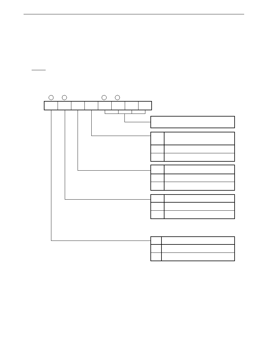
312
CHAPTER 11 TIMER/EVENT COUNTER 2
Preliminary User's Manual U13987EJ1V0UM00
11.3 Timer/Event Counter 2 Control Registers
(1) Timer control register 1 (TMC1)
In TMC1 the timer/event counter 2 TM2/TM2W count operation is controlled by the high-order 4 bits (the low-order 4
bits control the count operation of timer/event counter 1, TM1/TM1W).
TMC1 can be read or written to with an 8-bit manipulation instruction or bit manipulation instruction. The format of
TMC1 is shown in Figure 11-2.
RESET input clears TMC1 to 00H.
Figure 11-2. Timer Control Register 1 (TMC1) Format
Remark
The OVF2 bit is reset by software only.
7
CE2
TMC1
6
OVF2
5
CMD2
4
BW2
3
CE1
2
OVF1
1
0
0
BW1
Address
After reset
R/W
R/W
00H
0FF5FH
BW2
Timer/Event Counter 2 Bit Length
Specification
8-bit operation mode
16-bit operation mode
1
0
CMD2
TM2/TM2W Operation Mode Specificaton
Normal mode
One-shot mode
1
0
OVF2
TM2/TM2W Overflow Flag
No overflow
Overflow
Note
1
0
CE2
TM2/TM2W Count Operation Control
Count operation stopped with count cleared
Count operation enabled
1
0
Controls count operation of timer/event counter 1
TM1/TM1W (see Figure 10-2).
Note 8-bit operating mode:
count up from FFH to 00H
In 16-bit operating mode:
count up from FFFFH to 0000H
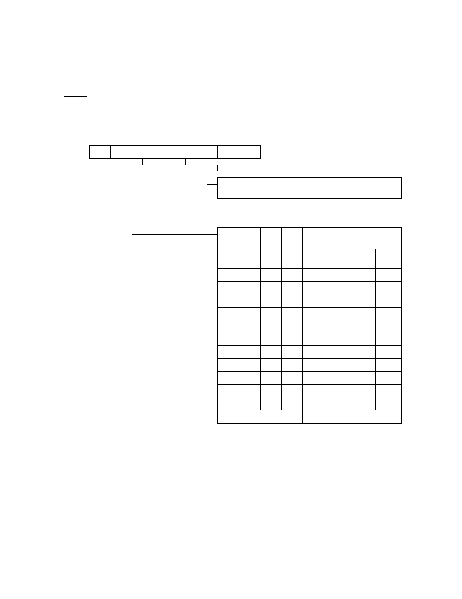
313
CHAPTER 11 TIMER/EVENT COUNTER 2
Preliminary User's Manual U13987EJ1V0UM00
(2) Prescaler mode register 1 (PRM1)
In PRM1, the count clock to timer/event counter 2 TM2/TM2W is specified by the high-order 4 bits (the low-order 4
bits specify the count clock to timer/event counter 1 TM1/TM1W).
PRM1 can be read or written with an 8-bit manipulation instruction. The format of PRM1 is shown in
Figure 11-3.
RESET input sets PRM1 to 11H.
Figure 11-3. Prescaler Mode Register 1 (PRM1) Format
Remark
f
XX
: X1 input frequency or oscillation frequency
PRS23 PRS22 PRS21 PRS20 PRS13 PRS12 PRS11 PRS10
7
6
5
4
3
2
1
0
PRM1
0FF5EH
Address
11H
After reset
R/W
R/W
PRS23
0
0
0
0
0
0
0
0
1
1
1
Specifies count clock to timer/event counter 1 (TM1/TM1W)
(see Figure 10-3).
PRS22
0
0
0
0
1
1
1
1
0
0
1
PRS21
0
0
1
1
0
0
1
1
0
0
1
PRS20
0
1
0
1
0
1
0
1
0
1
1
Timer/Event Counter 2 TM2/
TM2W Count Clock Specification
Count Clock [Hz]
Specification
Resolution
[ s]
Setting prohibited
f
XX
/4
f
XX
/8
f
XX
/16
f
XX
/32
f
XX
/64
f
XX
/128
f
XX
/256
f
XX
/512
f
XX
/1,024
External clock (CI/INTP2)
Setting prohibited
�
0.32
0.64
1.27
2.54
5.09
10.17
20.35
40.70
81.40
�
Other than the above
(f
XX
= 12.58 MHz)
�
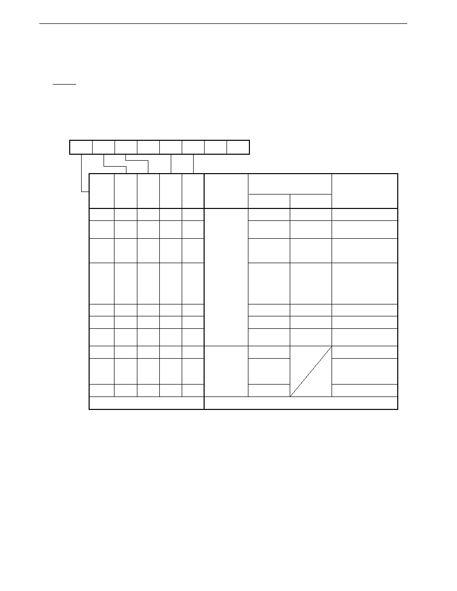
314
CHAPTER 11 TIMER/EVENT COUNTER 2
Preliminary User's Manual U13987EJ1V0UM00
(3) Capture/compare control register 2 (CRC2)
CRC2 specifies the enabling condition for a timer counter 2 (TM2/TM2W) clear operation by the capture/compare
register (CR21/CR21W) or the capture register (CR22/CR22W) and the timer output (TO2/TO3) mode.
CRC2 can be read or written with an 8-bit manipulation instruction. The format of CRC2 is shown in Figure 11-4.
RESET input sets CRC2 to 10H.
Figure 11-4. Capture/Compare Control Register 2 (CRC2) Format
Remark
The register names in the 8-bit operation mode are shown in this figure. In the 16-bit operation mode, the
register names TM2, CR20, CR21, and CR22 are TM2W, CR20W, CR21W, and CR22W, respectively.
7
MOD1
CRC2
6
MOD0
5
CLR22
4
1
3
CLR21
2
CM21
1
0
0
0
Address
After reset
R/W
R/W
10H
0FF33H
MOD1 MOD0 CLR22 CLR21
Timer Output
Mode Specification
Compare
operations
Capture
operations
CR21
Operation
Specification
TM2 Clear Operation
Toggle output Toggle output
Toggle output
Toggle output
Toggle output
TO2
TO3
Setting prohibited
Other than the above
Not cleared
PWM output
Toggle output Not cleared
PWM output
PPG output
PWM output
Toggle output
Not cleared
Not cleared
PWM output
Not cleared
0
0
0
0
CM21
0
0
0
0
1
0
Toggle output
Toggle output
Toggle output
0
0
1
0
0
Toggle output
Toggle output
0
0
1
1
0
0
1
0
0
0
1
0
0
0
0
1
1
0
1
0
0
0
0
0
1
0
0
0
1
1
0
1
0
0
1
Cleared if TM2 and
CR21 match
Cleared if TM2 and
CR21 match
Cleared after TM2
contents are captured
in CR22 by INTP1
Cleared after TM2
contents are captured
in CR21 by INTP2
Cleared by match of
TM2 and CR21 or after
TM2 contents are
captured in CR22 by
INTP1
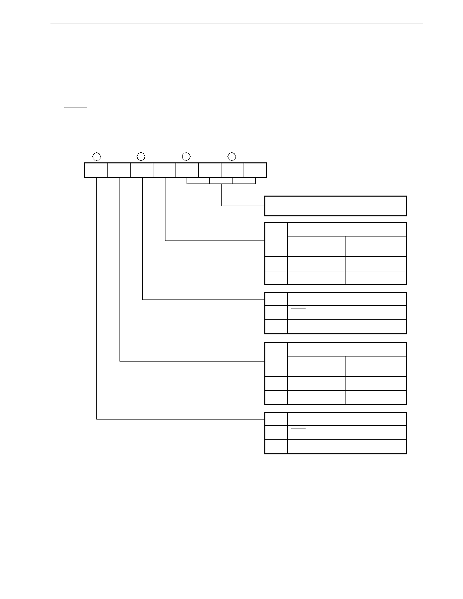
315
CHAPTER 11 TIMER/EVENT COUNTER 2
Preliminary User's Manual U13987EJ1V0UM00
(4) Timer output control register (TOC)
TOC is an 8-bit register that controls output enabling/disabling of the active level of timer output.
The operation of the timer output pins (TO2/TO3) by timer/event counter 2 is controlled by the high-order 4 bits (the
low-order 4 bits control the operation of the timer output pins (TO0/TO1) by timer/event counter 0).
TOC can be read or written with an 8-bit manipulation instruction or bit manipulation instruction. The format of TOC
is shown in Figure 11-5.
RESET input clears TOC to 00H.
Figure 11-5. Timer Output Control Register (TOC) Format
7
ENTO3
TOC
6
ALV3
5
ENTO2
4
ALV2
3
ENTO1
2
ALV1
1
ENTO0
0
ALV0
Address
After reset
R/W
R/W
0000H
0FF31H
ENTO2
TO2 Pin Operation Specification
ALV2 output
Pulse output enabled
1
0
Control operation of timer output pins (TO0 & TO1)
by timer/event counter 0 (see Figure 9-5).
ALV2
TO2 Pin Active Level
Toggle Output
Specification
PWM/PPG
Output Specification
Low level
High level
High level
Low level
1
0
ENTO3
TO3 Pin Operation Specification
ALV3 output
Pulse output enabled
1
0
ALV3
TO3 Pin Active Level
Toggle Output
Specification
PWM/PPG
Output Specification
Low level
High level
High level
Low level
1
0

316
CHAPTER 11 TIMER/EVENT COUNTER 2
Preliminary User's Manual U13987EJ1V0UM00
11.4 Timer Counter 2 (TM2) Operation
11.4.1 Basic operation
8-bit operation mode/16-bit operation mode control can be performed for timer/event counter 2 by means of bit 0 (BW2)
of timer control register 2 (TMC2)
Note
.
In the timer/event counter 2 count operation, a count-up is performed using the count clock specified by the high-order
4 bits of prescaler mode register 1 (PRM1).
Count operation enabling/disabling is controlled by bit 3 (CE2) of TMC2 (timer/event counter 2 operation control is
performed by the high-order 4 bits of the timer control register 1 (TMC1). When the CE2 bit is set (to 1) by software, the
contents of TM2 are cleared to 0H on the first count clock, and then the count-up operation is performed.
When the CE2 bit is cleared (to 0) by software, TM2 becomes 0H immediately, and capture operations and match signal
generation are stopped.
If the CE2 bit is set (to 1) again when it is already set (to 1), the TM2 count operation is not affected (see Figure 11-
6 (b)).
TM2/TM2W is cleared to 0H when the count clock is input while the value of TM2 is FFH in the 8-bit operation mode
or while the value of TM2W is FFFFH in the 16-bit operation mode. At this time, OVF2 bit is set and the overflow signal
is sent to the output control circuit. OVF2 bit is cleared by software only. The count operation is continued.
When RESET is input, TM2 is cleared to 0H, and the count operation is stopped.
Note
Unless otherwise specified, the functions of timer counter 2 in the 8-bit operation mode are described hereafter.
In the 16-bit operation mode, TM2, CR20, CR21, and CR22 operate as TM2W, CR20W, CR21W, and CR22W,
respectively.
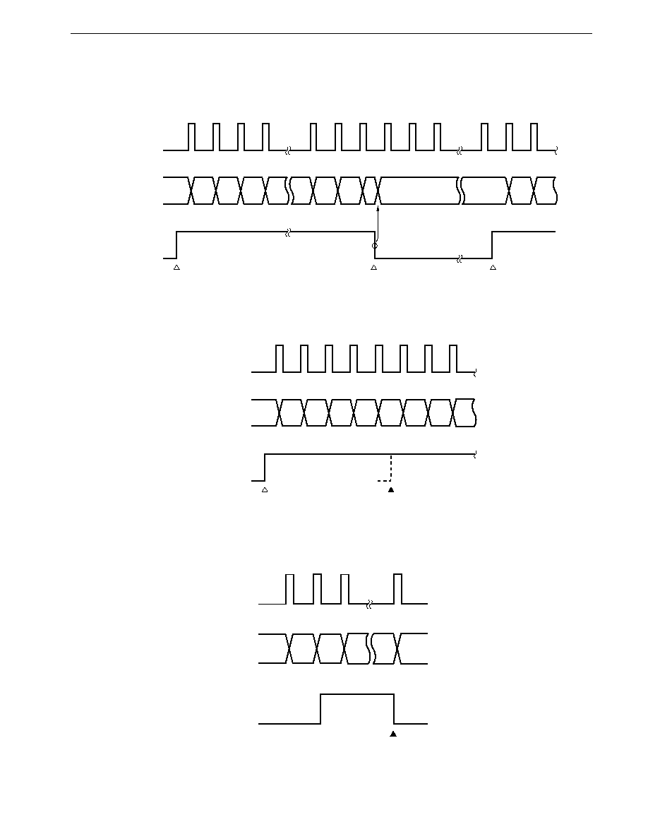
317
CHAPTER 11 TIMER/EVENT COUNTER 2
Preliminary User's Manual U13987EJ1V0UM00
Figure 11-6. Basic Operation in 8-Bit Operation Mode (BW2 = 0)
(a) Count started
count disabled
count started
(b) When "1" is written to the CE2 bit again after the count starts
TM2
OVF2
FEH
FFH
0H
Cleared by software
OVF2
0
Count clock
f
CLK
/8
1H
TM2
CE2
0H
0H
1H
2H
3H
4H
5H
6H
Count started
CE2
1
Rewrite
CE2
1
Count clock
(c) Operation when TM2 = FFH
TM2
CE2
0H
0H
1H
2H
0FH
10H 11H
0H
1H
0H
Count started
CE2
1
Count stopped
CE2
0
Count started
CE2
1
Count clock
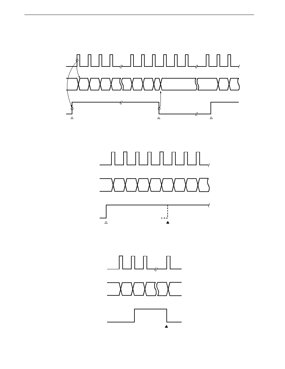
318
CHAPTER 11 TIMER/EVENT COUNTER 2
Preliminary User's Manual U13987EJ1V0UM00
Figure 11-7. Basic Operation in 16-Bit Operation Mode (BW2 = 1)
(a) Count started
count disabled
count started
(b) When "1" is written to the CE2 bit again after the count starts
(c) Operation when TM2W = FFFFH
TM2W
CE2
0H
0H
1H
2H
FFH 100H 101H
0H
1H
0H
Count started
CE2
1
Count started
CE2
1
Count stopped
CE2
0
Count clock
TM2W
CE2
0H
0H
1H
2H
3H
4H
5H
6H
Count started
CE2
1
Rewrite
CE2
1
Count clock
TM2W
OVF2
FFFEH
FFFFH
0H
Cleared by software
OVF2
0
Count clock
f
CLK
/8
1H
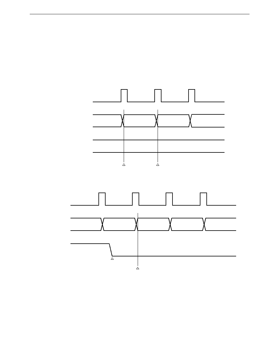
319
CHAPTER 11 TIMER/EVENT COUNTER 2
Preliminary User's Manual U13987EJ1V0UM00
11.4.2 Clear operation
(1) Clear operation after match with compare register and capture operation
Timer counter 2 (TM2) can be cleared automatically after a match with the compare register (CR2n: n = 0, 1) and a
capture operation. When a clearance source arises, TM2 is cleared to 0H on the next count clock. Therefore, even
if a clearance source arises, the value at the point at which the clearance source arose is retained until the next count
clock arrives.
Figure 11-8. TM2 Clearance by Match with Compare Register (CR20/CR21)
Figure 11-9. TM2 Clearance after Capture Operation
(2) Clear operation by CE2 bit of timer control register 1 (TMC1)
TM2 is also cleared when the CE2 bit of the TMC1 is cleared (to 0) by software. The clear operation is performed
immediately after clearance (to 0) of the CE2 bit.
TM2
Compare register
(CR2n)
n
Cleared here
Count clock
0
1
n-1
n
TM2 and CR2n match
TM2
INTP1
n
TM2 is captured
in CR22 here
Cleared here
Count clock
0
1
2
n-1

320
CHAPTER 11 TIMER/EVENT COUNTER 2
Preliminary User's Manual U13987EJ1V0UM00
Figure 11-10. Clear Operation when CE2 Bit is Cleared (0)
(a) Basic operation
(b) Restart before count clock is input after clearance
(c) Restart after count clock is input after clearance
TM2
CE2
n
Count clock
n-1
0
TM2
CE2
n
0
Count clock
n-1
0
1
2
If the CE2 bit is set (to 1) before this count clock, this count clock starts
counting from 0.
TM2
CE2
n
0
Count clock
n-1
0
0
1
If the CE2 bit is set (to 1) from this count clock onward, the count starts
from 0 on the count clock after the CE2 bit is set (to 1).

321
CHAPTER 11 TIMER/EVENT COUNTER 2
Preliminary User's Manual U13987EJ1V0UM00
11.5 External Event Counter Function
Timer/event counter 2 can count clock pulses input from external interrupt request input pin (INTP2/CI).
No special selection method is needed for the external event counter operation mode. When the timer counter 2 (TM2)
count clock is specified as external clock input by the setting of the high-order 4 bits of prescaler mode register 1 (PRM1),
TM2 operates as an external event counter.
The maximum frequency of external clock pulses that can be counted by TM2 as the external event counter is 2.10 MHz
(f
CLK
= 12.58 MHz) irrespective of whether only one edge or both edges are counted on INTP2/CI input.
The pulse width of INTP2/CI input must be at least 3 system clocks (0.24
�
s: f
CLK
= 12.58 MHz) for both the high level
and low level. If the pulse width is shorter than this, the pulse may not be counted.
The timer/event counter 2 external event count timing is shown in Figure 11-11.
Figure 11-11. Timer/Event Counter 2 External Event Count Timing
(1) Counting one edge (maximum frequency = f
CLK
/6)
Remark ICI: CI input signal after passing through edge detection circuit
ICI
TM2
CI
3/f
CLK
(MIN.) 3/f
CLK
(MIN.) 6/f
CLK
(MIN.)
Dn+1
Dn
Dn+2
Dn+3
2-3/f
CLK
Remark ICI: CI input signal after passing through edge detection circuit
(2) Counting both edges (maximum frequency = f
CLK
/6)
ICI
TM2
CI
3/f
CLK
(MIN.) 3/f
CLK
(MIN.)
6/f
CLK
(MIN.)
Dn+1
Dn
Dn+2
Dn+3
Dn+4
Dn+5
2-3/f
CLK
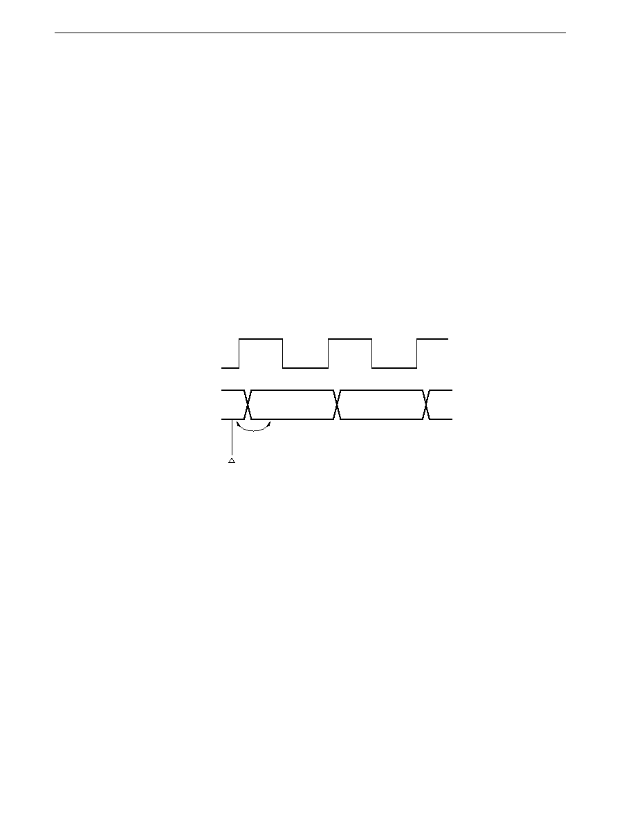
322
CHAPTER 11 TIMER/EVENT COUNTER 2
Preliminary User's Manual U13987EJ1V0UM00
The TM2 count operation is controlled by the CE2 bit of the timer control register 1 (TMC1) in the same way as with
the basic operation.
When the CE2 bit is set (to 1) by software, the contents of TM2 are set to 0H and the count-up operation is started on
the initial count clock.
When the CE2 bit is cleared (to 0) by software during a TM2 count operation, the contents of TM2 are set to 0H immediately
and the stopped state is entered. The TM2 count operation is not affected if the CE2 bit is set (to 1) by software again
when it is already set (to 1).
Caution When timer/event counter 2 is used as an external event counter, it is not possible to distinguish
between the case where there is no valid edge input at all and the case where there is a single valid
edge input using timer counter 2 (TM2) alone (see Figure 11-12), since the contents of TM2 are 0 in
both cases. If it is necessary to make this distinction, the INTP2 interrupt request flag should be used
(the INTP2 pin and CI pin have a dual function, and both functions can be used at the same time). An
example is shown in Figure 11-13.
Figure 11-12. Example of the Case where the External Event Counter does Not Distinguish between One
Valid Edge Input and No Valid Edge Input
TM2
0
INTP2/CI
1
2
0
Count start
No distinction made
323
CHAPTER 11 TIMER/EVENT COUNTER 2
Preliminary User's Manual U13987EJ1V0UM00
Figure 11-13. To Distinguish whether One or No Valid Edge has been Input with External Event Counter
(a) Processing when count is started
(b) Processing when count value is read
Clear INTP2 interrupt
request flag
PIF2
0
; Clear PIF2 to 0
End
Start count
Start count
CE2
1
; Set CE2 to 1
Read TM2 contents
A
TM2
A
A+1
; Check PIF2 contents
If 1, there is a valid edge
; Number of input valid edges is set in A register
; Check TM2 value
If 0, check interrupt
request flag
End
PIF2 = 1?
YES
YES
NO
NO
Count value read
A = 0?
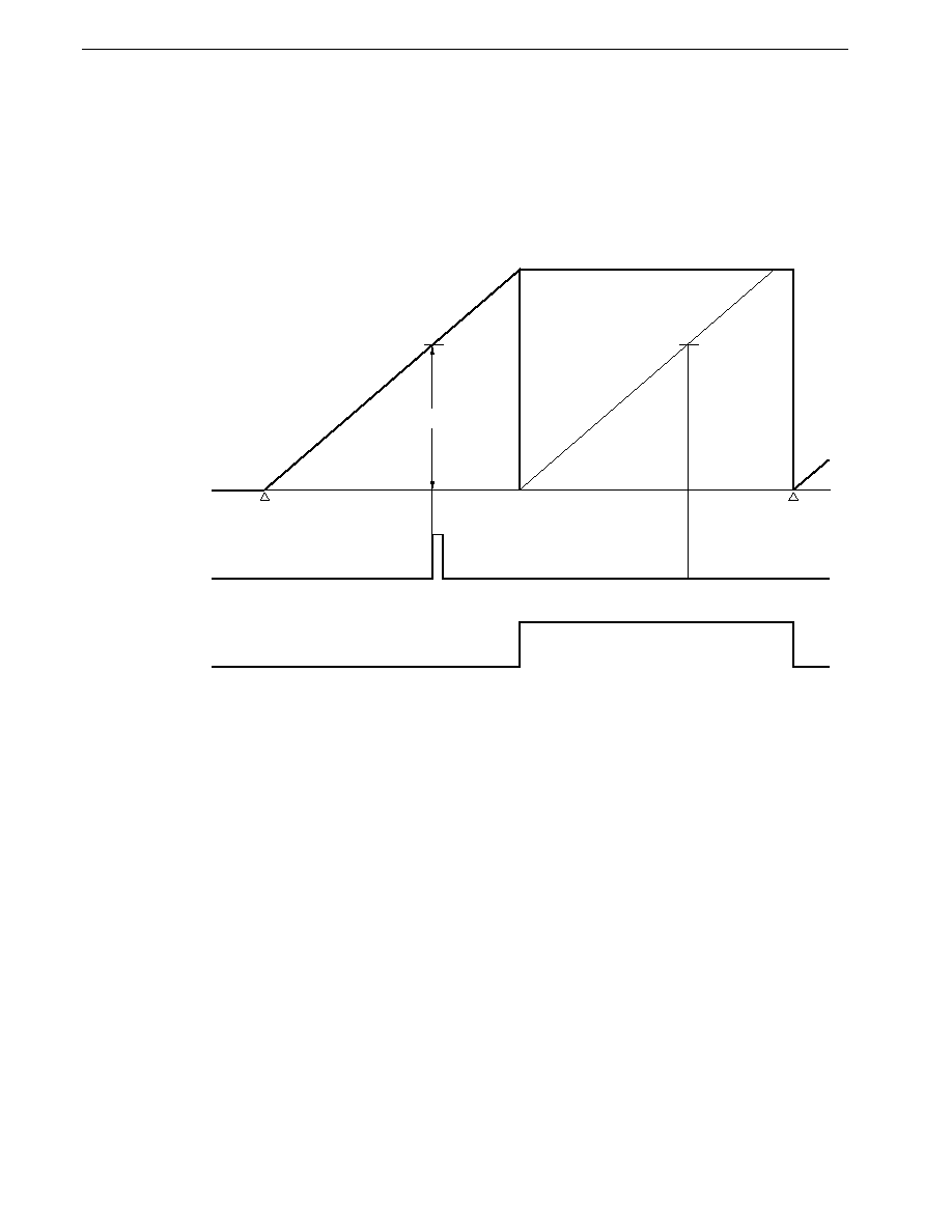
324
CHAPTER 11 TIMER/EVENT COUNTER 2
Preliminary User's Manual U13987EJ1V0UM00
11.6 One-Shot Timer Function
Timer/event counter 2 has an operation mode in which it stops automatically when a full count value is reached (FFH/
FFFFH) as a result of counting by timer counter 2 (TM2/TM2W).
Figure 11-14. One-Shot Timer Operation
As shown in Figure 11-14, the respective one-shot interrupt is generated when the value (0H to FFH/FFFFH) set
beforehand in the CR20, CR21/CR21W, or CR21W and TM2/TM2W value match.
The one-shot timer operation mode is specified by setting (to 1) bit 5 (CMD2) of timer control register 1 (TMC1) by
software.
The TM2/TM2W count operation is controlled by the CE2 bit of the TMC1 as with the basic operation.
When the CE2 bit is set (to 1) by software, the contents of TM2/TM2W are set to 0H and the count-up operation is started
on the initial count clock.
When the contents of TM2/TM2W reach FFH/FFFFH (full count) as a result of the count-up operation, bit 6 (OVF2) of
the TMC1 are set (to 1), and TM2/TM2W stops with the count at FFH/FFFFH.
The one-shot timer operation is started again from the count-stopped state by clearing (to 0) the OVF2 bit by software.
When the OVF2 bit is cleared (to 0), the contents of TM2/TM2W become 0H and the count-up operation is restarted on
the next count clock.
If the CE2 bit is cleared (to 0) by software during a TM2/TM2W count operation, the contents of TM2/TM2W are set to
0H immediately and the stopped state is entered. The TM2/TM2W count operation is not affected if the CE2 bit is set (to
1) by software again when it is already set (to 1).
INTC21
interrupt request
TM2/TM2W
count value
0H
FFH or FFFFH
Count start
CE2
1
CR21/CR21W value
OVF2
Clear
OVF2
0
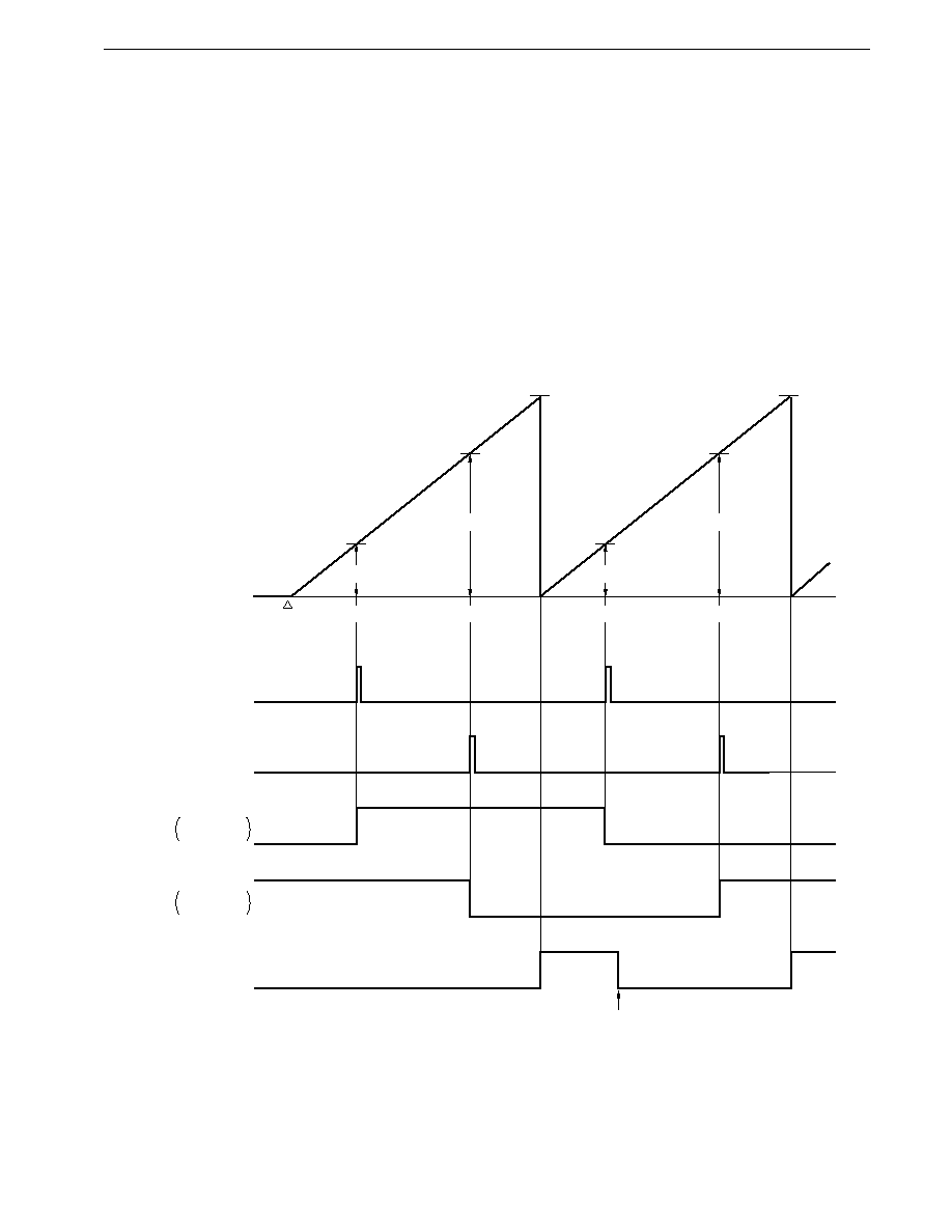
325
CHAPTER 11 TIMER/EVENT COUNTER 2
Preliminary User's Manual U13987EJ1V0UM00
11.7 Compare Register, Capture/Compare Register, and Capture Register Operation
11.7.1 Compare operations
Timer/event counter 2 performs compare operations in which the value set in the compare register (CR20) and the
capture/compare register (CR21) specified for compare operation is compared with the timer counter 2 (TM2) count value.
If the count value of TM2 matches the preset value of the CR20, and CR21 when a compare operation is performed,
as the result of the count operation, a match signal is sent to the output control circuit, and an interrupt request signal
(INTC20/INTC21) is generated at the same time.
After a match with the CR20 or CR21 value, the TM2 contents can be cleared, and the timer functions as an interval
timer that repeatedly counts up to the value set in the CR20 or CR21.
Figure 11-15. Compare Operation in 8-Bit Operation Mode
Remark CLR21 = 0, CLR22 = 0, BW2 = 0
INTC20
interrupt request
TM2
count value
0H
FFH
Count start
CE2
1
CR20 value
CR21 value
FFH
CR20 value
CR21 value
INTC21
interrupt request
TO2 pin output
ENTO2 = 1
ALV2 = 1
OVF2
Match
Match
Match
Match
TO3 pin output
ENTO2 = 1
ALV3 = 0
Cleared by software
Inactive level
Inactive level
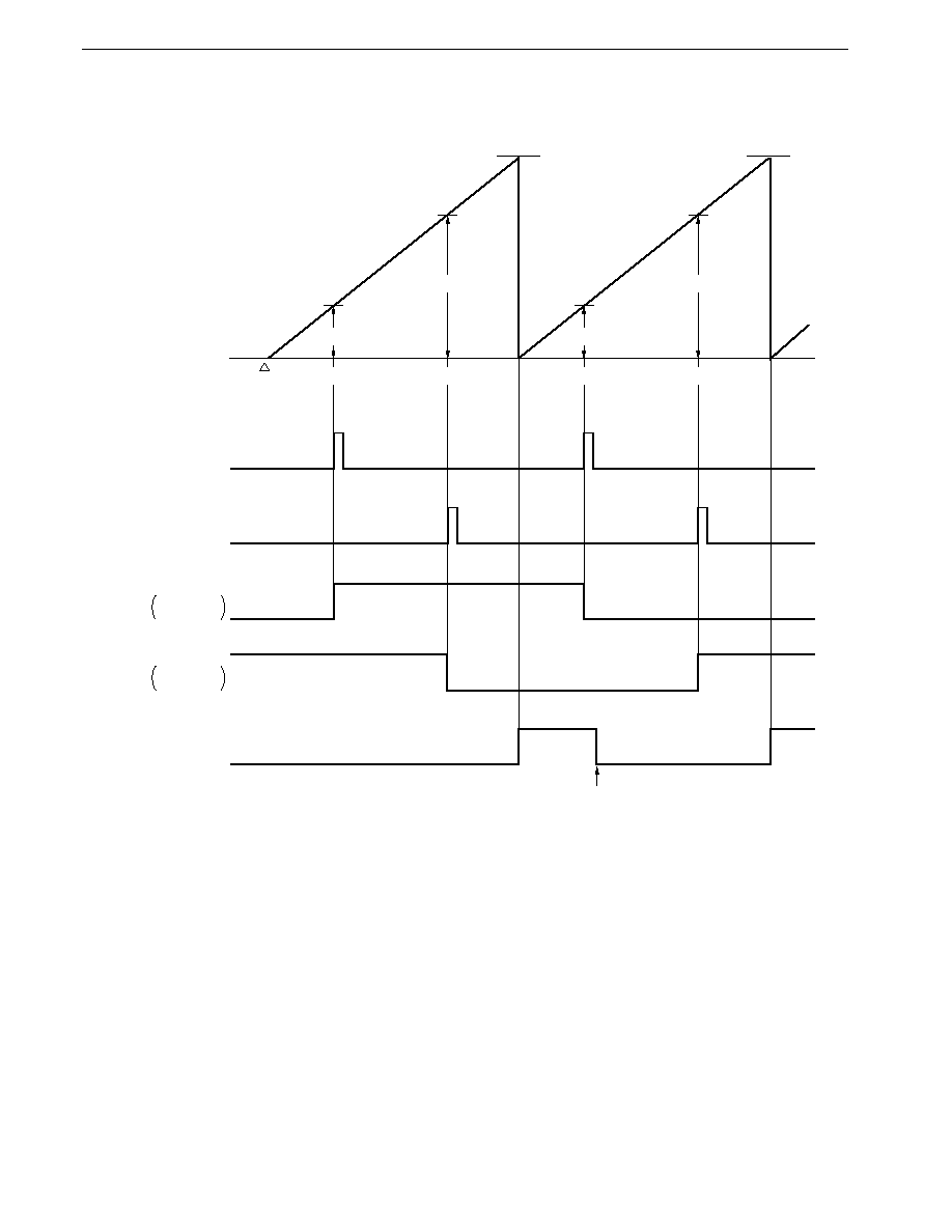
326
CHAPTER 11 TIMER/EVENT COUNTER 2
Preliminary User's Manual U13987EJ1V0UM00
Figure 11-16. Compare Operation in 16-Bit Operation Mode
Remark
CLR21 = 0, CLR22 = 0, BW2 = 1
INTC20
interrupt request
TM2W
count value
0H
FFFFH
Count start
CE2
1
CR20W value
CR21W value
FFFFH
CR20W value
CR21W value
INTC21
interrupt request
TO2 pin output
ENTO2 = 1
ALV2 = 1
OVF2
Match
Match
Match
Match
TO3 pin output
ENTO2 = 1
ALV3 = 0
Cleared by software
Inactive level
Inactive level
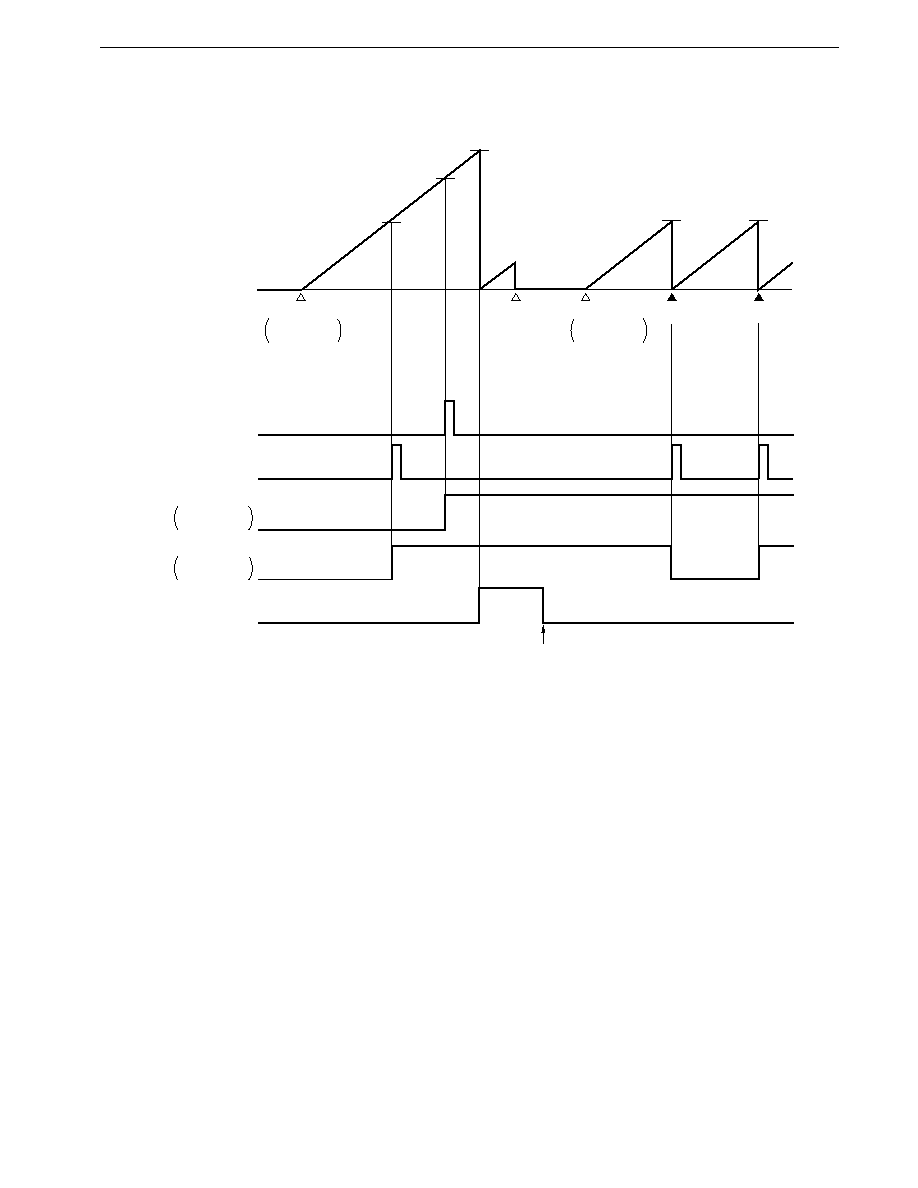
327
CHAPTER 11 TIMER/EVENT COUNTER 2
Preliminary User's Manual U13987EJ1V0UM00
Figure 11-17. TM2 Clearance after Match Detection
Remark CLR22 = 0
11.7.2 Capture operations
Timer/event counter 2 performs capture operations in which the timer counter 2 (TM2) count value is fetched into the
capture register in synchronization with an external trigger, and retained there.
A valid edge detected from the input of the external interrupt request input pins (INTP1/INTP2) is used as the external
trigger (capture trigger). The count value of TM2 in the process of being counted in synchronization with the capture trigger
is fetched into the capture register (CR22) in synchronization with INTP1, or into the capture/compare register (CR21) when
a capture operation is specified in synchronization with INTP2, and is retained there.
The contents of CR21 and CR22 are retained until the next capture triggers corresponding to CR21 and CR22 are
generated.
The capture trigger valid edge is set by means of external interrupt mode register 0 (INTM0). If both rising and falling
edges are set as capture triggers, the width of pulses input from off-chip can be measured, and if a capture trigger is
generated by a single edge, the input pulse cycle can be measured.
See Figure 22-1 for details of the INTM0 format.
When CR21 is used as a capture register, TM2 can be cleared as soon as the contents of TM2 have been captured
by capture trigger to CR21 or CR22.
INTC20
interrupt request
TM2
count value
0H
FFH
Count start
CE2
1
CLR21
0
INTC21
interrupt request
TO2 pin output
ENTO2
1
ALV2
1
OVF2
TO3 pin output
ENTO3
1
ALV3
1
Cleared by software
CR20
CR21
CR21
CR21
Inactive level
Inactive level
Count start
CE2
1
CLR21
1
Count disabled
CE2
0
Clear
Clear
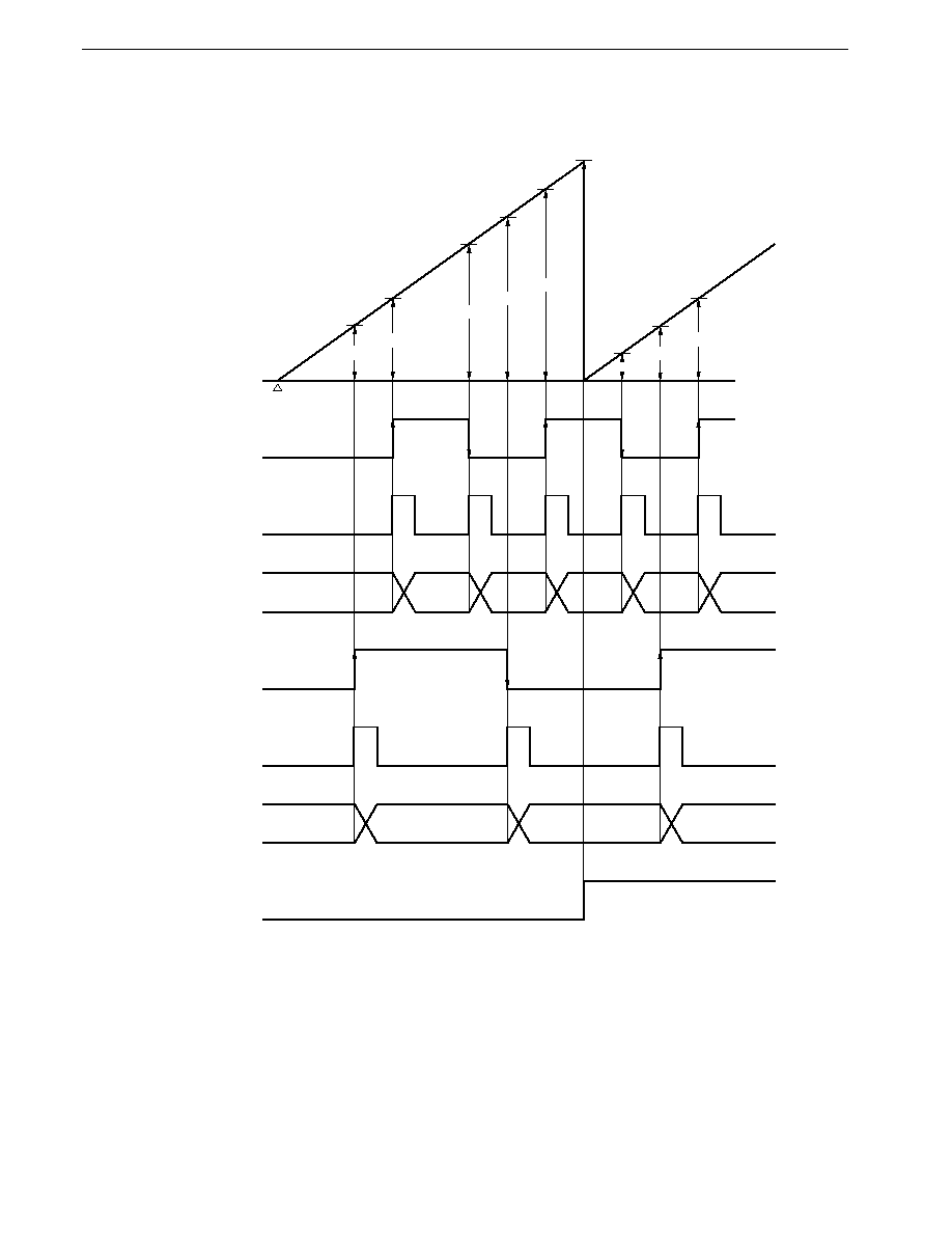
328
CHAPTER 11 TIMER/EVENT COUNTER 2
Preliminary User's Manual U13987EJ1V0UM00
Figure 11-18. Capture Operation in 8-Bit Operation Mode
Remark
Dn: TM2 count value (n = 0, 1, 2, ...)
CM21 = 1, CLR21 = 0, CLR22 = 0, BW2 = 0
TM2
count value
Count start
CE
1
0H
INTP2
pin input
INTP2
interrupt request
Capture register
(CR21)
INTP1
pin input
INTP1
interrupt request
Capture register
(CR22)
OVF2
D0
D3
D6
D1
D2
D4
D5
D7
D0
D1
D2
D3
D4
D6
D7
D5
FFH
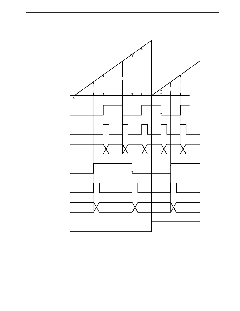
329
CHAPTER 11 TIMER/EVENT COUNTER 2
Preliminary User's Manual U13987EJ1V0UM00
Figure 11-19. Capture Operation in 16-Bit Operation Mode
Remark
Dn: TM2W count value (n = 0, 1, 2, ...)
CM21 = 1, CLR21 = 0, CLR22 = 0, BW2 = 0
TM2W
count value
Count start
CE
1
0H
INTP2
pin input
INTP2
interrupt request
Capture register
(CR21W)
INTP1
pin input
INTP1
interrupt request
Capture register
(CR22W)
OVF2
D0
D3
D6
D1
D2
D4
D5
D7
D0
D1
D2
D3
D4
D6
D7
D5
FFFFH

330
CHAPTER 11 TIMER/EVENT COUNTER 2
Preliminary User's Manual U13987EJ1V0UM00
Figure 11-20. TM2 Clearance after Capture Operation
Remark
CLR21 = 0, CLR22 = 1
11.8 Basic Operation of Output Control Circuit
The output control circuit controls the timer output pins (TO2/TO3) level by means of match signals from the compare
register (CR22). The operation of the output control circuit is determined by the timer output control register (TOC) and
capture/compare control register 2 (CRC2) (see Table 11-5). When TO2/TO3 signal is output to a pin, the relevant pin
must be in control mode in the port 3 mode register (PMC3).
N3
INTP1
pin input
INTP1
interrupt request
TM2
count value
0H
Capture/compare
register (CR22)
N2
N1
N4
Capture
Capture
Capture
Capture
Capture
N1
N2
N3
N4
N5

331
CHAPTER 11 TIMER/EVENT COUNTER 2
Preliminary User's Manual U13987EJ1V0UM00
Table 11-5. Timer Output (TO2/TO3) Operations
TOC
CRC2
TMC1
TO3
TO2
ENTO3
ALV3
ENTO2
ALV2
MOD1
MOD0
CLR22
CLR21
CMD2
0
0/1
0
0/1
�
�
�
�
�
High/low level fixed
High/low level fixed
0
0/1
1
0/1
0
0
�
Note
�
�
High/low level fixed
Toggle output (active-low/high)
1
0/1
0
0/1
0
0
�
Note
�
�
Toggle output (active-low/high)
High/low level fixed
1
0/1
1
0/1
0
0
�
Note
�
�
Toggle output (active-low/high)
Toggle output (active-low/high)
0
0/1
1
0/1
0
1
0
0
0
High/low level fixed
PWM output (active-high/low)
1
0/1
0
0/1
0
1
0
0
0
Toggle output (active-low/high)
High/low level fixed
1
0/1
1
0/1
0
1
0
0
0
Toggle output (active-low/high)
PWM output (active-high/low)
0
0/1
1
0/1
1
0
0
0
0
High/low level fixed
PWM output (active-high/low)
1
0/1
0
0/1
1
0
0
0
0
PWM output (active-high/low)
High/low level fixed
1
0/1
1
0/1
1
0
0
0
0
PWM output (active-high/low)
PWM output (active-high/low)
0
0/1
1
0/1
1
1
0
1
0
High/low level fixed
PPG output (active-high/low)
1
0/1
0
0/1
1
1
0
1
0
Toggle output (active-low/high)
High/low level fixed
1
0/1
1
0/1
1
1
0
1
0
Toggle output (active-low/high)
PPG output (active-high/low)
Note CLR22 is normally set to 0 in this case.
Remarks 1. 0/1 in the ALVn (n = 2, 3) columns correspond to the items on the left and right of the slash ("/") in the TOn (n = 2, 3) columns respectively.
2. "
�
" indicates 0 or 1.
3. Combinations not shown in this table are prohibited to use in that combination.
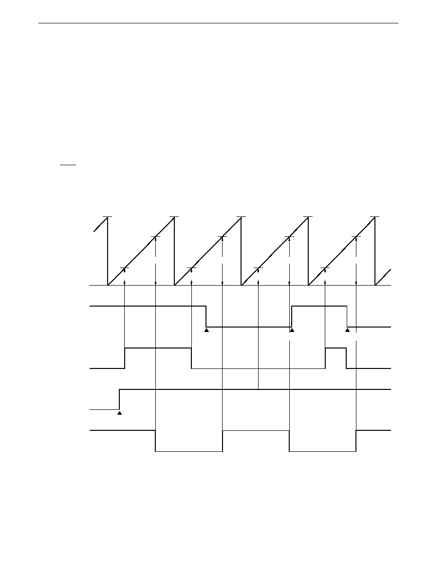
332
CHAPTER 11 TIMER/EVENT COUNTER 2
Preliminary User's Manual U13987EJ1V0UM00
11.8.1 Basic operation
Setting (to 1) the ENTOn (n = 2, 3) bit of the timer output control register (TOC) enables timer output (TOn: n = 2, 3)
to be varied at a timing in accordance with the settings of MOD0, MOD1, and CLR21 bits of capture/compare control register
2 (CRC2).
Clearing (to 0) ENTOn sets the TOn to a fixed level. The fixed level is determined by the ALVn (n = 2, 3) bit of the TOC.
The level is high when ALVn is 0, and low when 1.
11.8.2 Toggle output
Toggle output is an operation mode in which the output level is inverted each time the compare register (CR20/CR21)
value coincides with the timer counter 2 (TM2) value. The output level of timer output (TO2) is inverted by a match between
CR20 and TM2, and the output level of timer output (TO3) is inverted by a match between CR21 and TM2.
When timer/event counter 2 is stopped by clearing (to 0) the CE2 bit of the timer control register 1 (TMC1), the inactive
level (ALVn: n = 0, 1) is output.
Figure 11-21. Toggle Output Operation
ENTO0
TM2
count value
0H
FFH
Instruction
execution
CR20 value
CR21 value
FFH
CR20 value
CR21 value
FFH
CR20 value
CR21 value
FFH
CR20 value
CR21 value
FFH
TO2 output
(ALV2 = 1)
ENTO3
TO3 output
(ALV3 = 0)
Instruction execution
Instruction execution
Instruction execution

333
CHAPTER 11 TIMER/EVENT COUNTER 2
Preliminary User's Manual U13987EJ1V0UM00
Table 11-6. TO2/TO3 Toggle Output (f
XX
= 12.58 MHz)
Count Clock
Minimum Pulse Width
Maximum Pulse Width
f
XX
/4
4/f
XX
2
16
�
4/f
XX
(0.32
�
s)
(0.32
�
s)
(20.8 ms)
f
XX
/8
8/f
XX
2
16
�
8/f
XX
(0.64
�
s)
(0.64
�
s)
(41.7 ms)
f
XX
/16
16/f
XX
2
16
�
16/f
XX
(1.27
�
s)
(1.27
�
s)
(83.4 ms)
f
XX
/32
32/f
XX
2
16
�
32/f
XX
(2.54
�
s)
(2.54
�
s)
(167 ms)
f
XX
/64
64/f
XX
2
16
�
64/f
XX
(5.09
�
s)
(5.09
�
s)
(333 ms)
f
XX
/128
128/f
XX
2
16
�
128/f
XX
(10.17
�
s)
(10.17
�
s)
(667 ms)
f
XX
/256
256/f
XX
2
16
�
256/f
XX
(20.35
�
s)
(20.35
�
s)
(1.33 s)
f
XX
/512
512/f
XX
2
16
�
512/f
XX
(40.70
�
s)
(40.70
�
s)
(2.67 s)
f
XX
/1,024
1,024/f
XX
2
16
�
1,024/f
XX
(81.40
�
s)
(81.40
�
s)
(5.33 s)

334
CHAPTER 11 TIMER/EVENT COUNTER 2
Preliminary User's Manual U13987EJ1V0UM00
11.8.3 PWM output
(1) Basic operation of PWM output
In this mode, a PWM signal with the period in which timer counter 2 (TM2) reaches a full count used as one cycle is
output. The timer output (TO2) pulse width is determined by the value of compare register (CR20), and the timer output
(TO3) pulse width is determined by the value of compare register (CR21). When this function is used, the CLR21 bit
and CLR22 bit of capture/compare control register 2 (CRC2) and the CMD2 bit of timer control register 1 (TMC1) must
be set to 0.
The pulse cycle and pulse width are as shown below.
(a) BW2 = 0
�
PWM cycle = 256
�
x/f
XX
�
PWM pulse width = CR2n
�
x/f
XX
Note
; x = 4, 8, 16, 32, 64, 128, 256, 512, 1,024
Note
0 cannot be set in the CR2n.
�
Duty =
PWM pulse width
=
CR2n
PWM
256
(b) BW2 = 1
�
PWM cycle = 65,536
�
x/f
XX
�
PWM pulse width = CR2n
�
x/f
XX
Note
; x = 4, 8, 16, 32, 64, 128, 256, 512, 1,024
Note
0 cannot be set in the CR2n.
�
Duty =
PWM pulse width
=
CR2n
PWM cycle
65,536
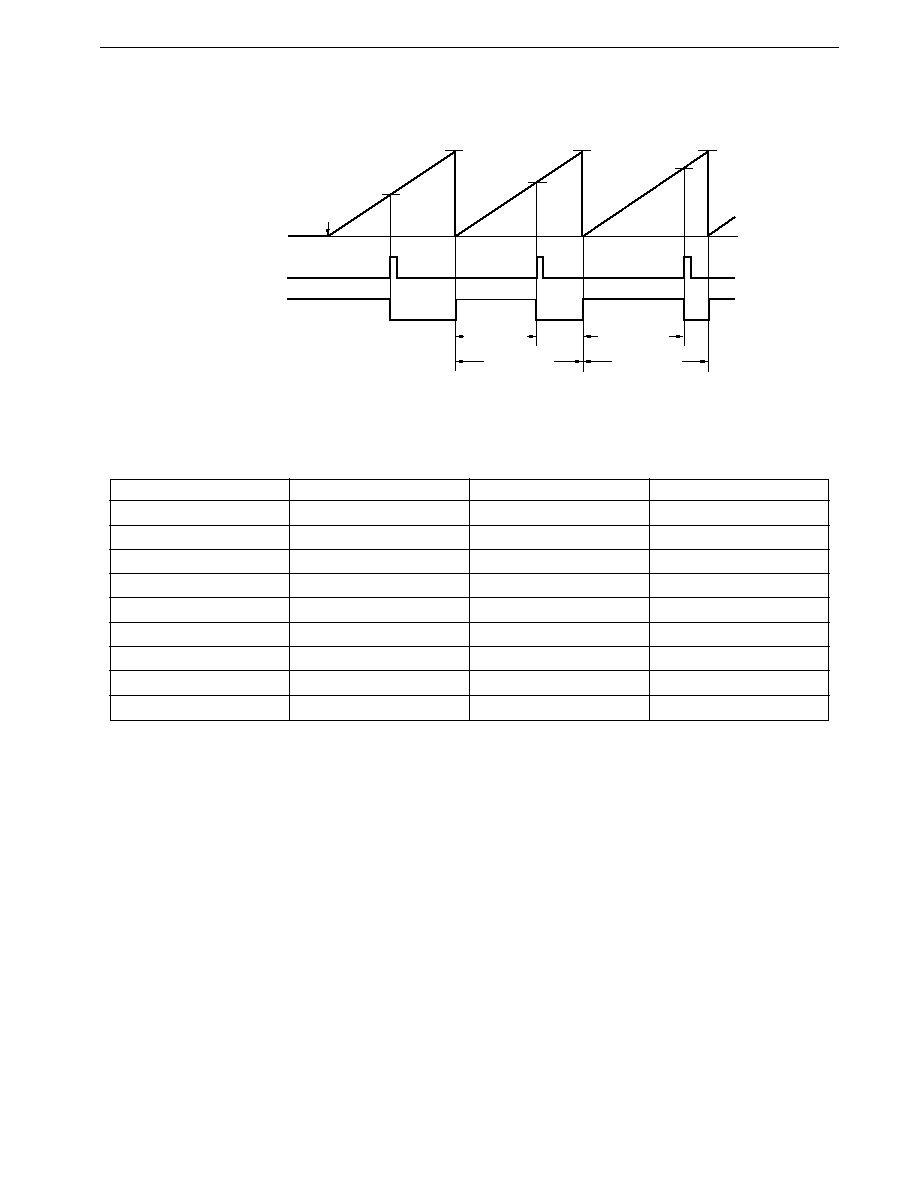
335
CHAPTER 11 TIMER/EVENT COUNTER 2
Preliminary User's Manual U13987EJ1V0UM00
Figure 11-22. PWM Pulse Output (BW2 = 0)
Remark ALV2 = 0
Table 11-7. TO2/TO3 PWM Cycle (f
XX
= 12.58 MHz, BW2 = 0)
Count Clock
Minimum Pulse Width [
�
s]
PWM Cycle [ms]
PWM Frequency [Hz]
f
XX
/4
0.32
0.08
12,286
f
XX
/8
0.64
0.16
6,143
f
XX
/16
1.27
0.33
3,071
f
XX
/32
2.54
0.65
1,536
f
XX
/64
5.09
1.30
768
f
XX
/128
10.17
2.60
384
f
XX
/256
20.35
5.21
192
f
XX
/512
40.70
10.42
96
f
XX
/1,024
81.40
20.84
48
CR20
Interrupt
TM2
count value
0H
FFH
Count start
CR20
FFH
FFH
Pulse width
Pulse cycle
Pulse width
TO2
CR20
Pulse cycle
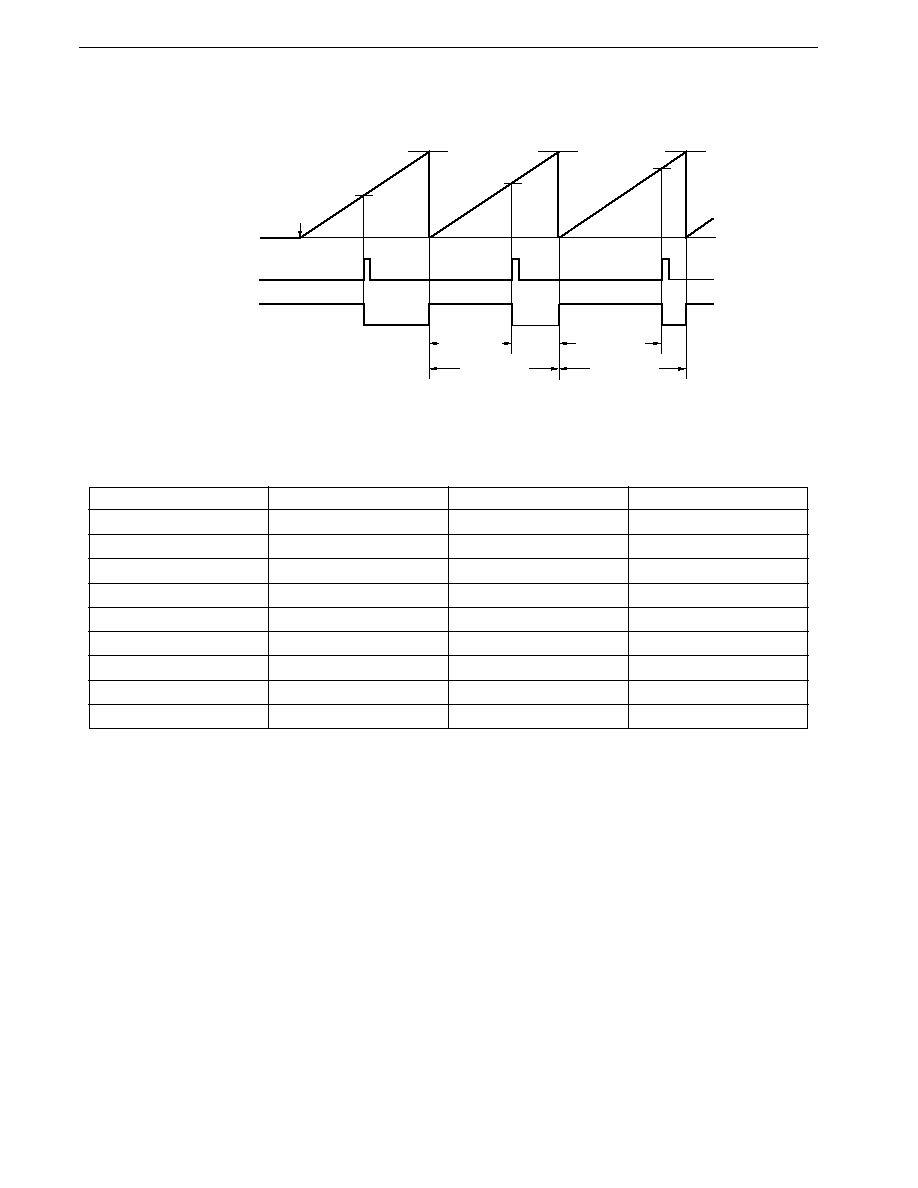
336
CHAPTER 11 TIMER/EVENT COUNTER 2
Preliminary User's Manual U13987EJ1V0UM00
Figure 11-23. PWM Pulse Output (BW2 = 1)
Remark
ALV2 = 0
Table 11-8. TO2/TO3 PWM Cycle (f
XX
= 12.58 MHz, BW2 = 1)
Count Clock
Minimum Pulse Width [
�
s]
PWM Cycle [s]
PWM Frequency [Hz]
f
XX
/4
0.32
0.02
47.6
f
XX
/8
0.64
0.04
23.8
f
XX
/16
1.27
0.08
12.0
f
XX
/32
2.54
0.17
6.0
f
XX
/64
5.09
0.33
3.0
f
XX
/128
10.17
0.67
1.5
f
XX
/256
20.35
1.33
0.7
f
XX
/512
40.70
2.67
0.4
f
XX
/1,024
81.40
5.33
0.2
CR20
Interrupt
TM2
count value
0H
FFFFH
Count start
CR20
FFFFH
FFFFH
Pulse width
Pulse cycle
TO2
CR20
Pulse width
Pulse cycle
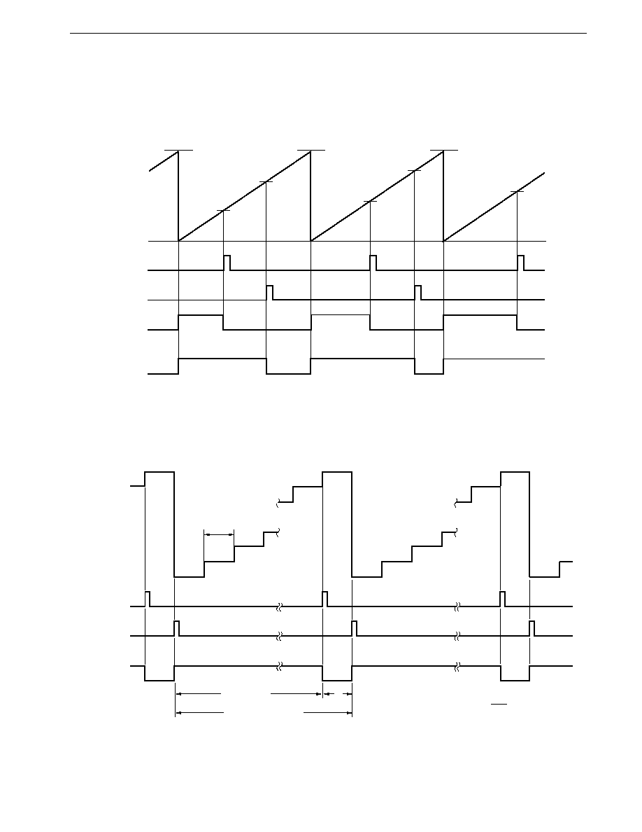
337
CHAPTER 11 TIMER/EVENT COUNTER 2
Preliminary User's Manual U13987EJ1V0UM00
Figure 11-24 shows an example of 2-channel PWM output, and Figure 11-25 shows the case where FFFFH is set in
the CR20W.
Figure 11-24. Example of PWM Output Using TM2W
Remark ALV2 = 0, ALV3 = 0
Figure 11-25. Example of PWM Output when CR20W = FFFFH
Remarks 1.
ALV2 = 0
2. T = x/f
XX
(x = 4, 8, 16, 32, 64, 128, 256, 512, 1,024)
TM2W
count value
0H
CR20W
FFFFH
INTC20
CR21W
CR20W
FFFFH
CR21W
CR20W
FFFFH
INTC21
TO2
TO3
TM2W
count value
FFFFH
INTC20
0
1
2
FFFEH
FFFFH
0
1
2
FFFEH
Count clock cycle T
FFFFH
0
Pulse width
T
Duty =
�
100 = 99.6 (%)
.
.
255
256
Pulse cycle = 256T
OVF2
TO2
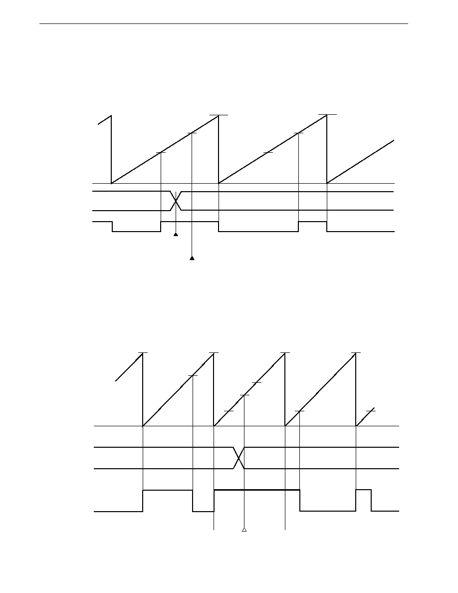
338
CHAPTER 11 TIMER/EVENT COUNTER 2
Preliminary User's Manual U13987EJ1V0UM00
(2) Rewriting compare registers (CR20, CR21)
The output level of the timer output (TOn + 2: n + 2 = 2, 3) is not inverted even if the CR2n (n = 0, 1) value matches
the timer counter 2 (TM2) value more than once during one PWM output cycle.
Figure 11-26. Example of Compare Register (CR20W) Rewrite
Remark
ALV2 = 1
If a value smaller than that of the TM2 is set as the CR2n value, a 100% duty PWM signal will be output. CR2n rewriting
should be performed by the interrupt due to a match between TM2 and the CR2n on which the rewrite is performed.
Figure 11-27. Example of 100% Duty with PWM Output
CR20W
TO2
TM2W
count value
0H
T1
T1
T2
T1
T2
FFFFH
CR20W and TM2W values match, but TO2 does not change here.
CR20W
rewrite
FFFFH
T2
Remark
ALV2 = 0
CR20
TO2
TM2
count value
0H
n1
n2
n3
n1
When value n2 which is smaller than the TM2 value n3 is
written to CR20 here, the duty of this period will be 100%.
FFH
FFH
FFH
FFH
n2
n2
n2
n1
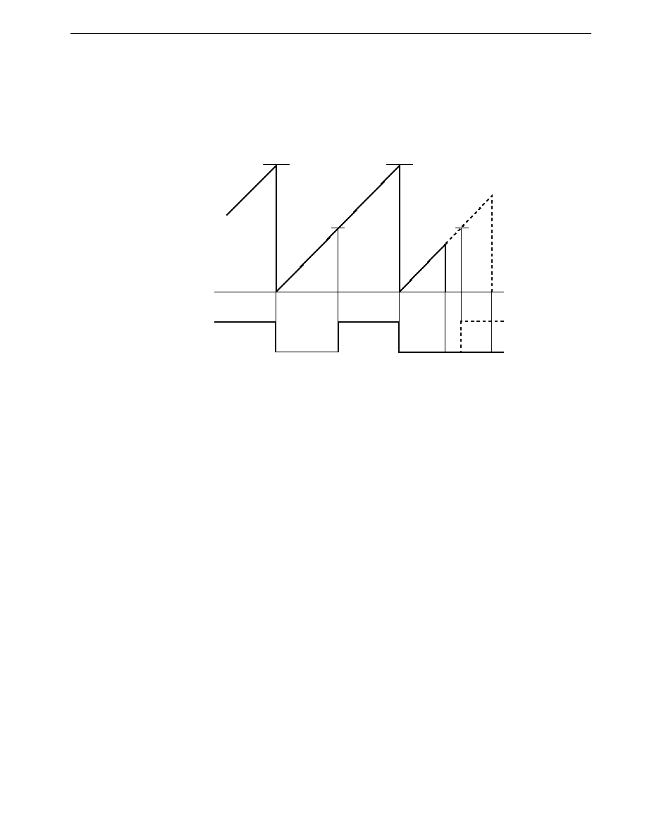
339
CHAPTER 11 TIMER/EVENT COUNTER 2
Preliminary User's Manual U13987EJ1V0UM00
(3) Stopping PWM output
If timer/event counter 2 is stopped by clearing (to 0) the CE2 bit of the timer control register 1 (TMC1) during PWM
signal output, the active level is output.
Figure 11-28. When Timer/Event Counter 2 is Stopped During PWM Signal Output
Remark ALV2 = 1
Caution The output level of the TOn (n = 2, 3) pin when timer output is disabled (ENTOn = 0: n = 2, 3) is
the inverse of the value set in ALVn (n = 2, 3) bits. Caution is therefore required as the active level
is output when timer output is disabled when the PWM output function has been selected.
TO2
TM2W
count value
0H
CR20W
CR20W
FFFFH
FFFFH

340
CHAPTER 11 TIMER/EVENT COUNTER 2
Preliminary User's Manual U13987EJ1V0UM00
11.8.4 PPG output
(1) Basic operation of PPG output
This function outputs a square-wave with the time determined by compare register CR21 value as one cycle, and the
time determined by compare register CR20 value as the pulse width. The PWM output PWM cycle is made variable.
This signal can only be output from timer output (TO2).
When this function is used, it is necessary to set the CLR21 bit of capture/compare control register 2 (CRC2) to 1 and
the CLR22 bit to 0, and to set the CMD2 bit of timer control register 1 (TMC1) to 0.
The pulse cycle and pulse width are as shown below.
�
PPG cycle = (CR21 + 1)
�
x/f
XX
; x = 4, 8, 16, 32, 64, 128, 256, 512, 1,024
�
PPG pulse width = CR20
�
x/f
XX
where 1
CR20
CR21
�
Duty =
PPG pluse width
PPG cycle
=
CR
CR
20
21
1
+
Figure 11-29 shows an example of PPG output using timer counter 2 (TM2), Figure 11-30 shows an example of the case
where CR20 = CR21.
341
CHAPTER 11 TIMER/EVENT COUNTER 2
Preliminary User's Manual U13987EJ1V0UM00
Figure 11-29. Example of PPG Output Using TM2
Remark ALV2 = 0, ALV3 = 0
Table 11-9. TO2 PPG Output (f
XX
= 12.58 MHz)
Count Clock
Minimum Pulse Width [
�
s]
PPG Cycle [s]
PPG Frequency [Hz]
f
XX
/4
0.32
0.64
�
s to 20.84 ms
1,572 kHz to 48.0 Hz
f
XX
/8
0.64
1.27
�
s to 41.68 ms
786 kHz to 24.0 Hz
f
XX
/16
1.27
2.54
�
s to 83.35 ms
393 kHz to 12.0 Hz
f
XX
/32
2.54
5.09
�
s to 166.71 ms
197 kHz to 6.0 Hz
f
XX
/64
5.09
10.17
�
s to 333.41 ms
98.3 kHz to 3.0 Hz
f
XX
/128
10.17
20.35
�
s to 666.82 ms
49.1 kHz to 1.5 Hz
f
XX
/256
20.35
40.70
�
s to 1.33 s
24.6 kHz to 0.7 Hz
f
XX
/512
40.70
81.40
�
s to 2.67 s
12.3 kHz to 0.4 Hz
f
XX
/1,024
81.40
162.80
�
s to 5.38 s
6.1 kHz to 0.2 Hz
INTC21
TM2
count value
0H
CR20
Pulse cycle
CR20
CR20
CR21
CR21
CR21
INTC20
TO2
(PPG output)
TO3
(timer output)
Pulse width
Count start

342
CHAPTER 11 TIMER/EVENT COUNTER 2
Preliminary User's Manual U13987EJ1V0UM00
Figure 11-30. Example of PPG Output when CR20 = CR21
Remark ALV2 = 0
T = x/f
XX
(x = 4, 8, 16, 32, 64, 128, 256, 512, 1,024)
TM2
count value
n
INTC20
0
1
2
n-1
n
0
1
2
n-1
Count cycle T
n
0
Pulse width = nT
Pulse cycle = (n+1) T
INTC21
TO2
343
CHAPTER 11 TIMER/EVENT COUNTER 2
Preliminary User's Manual U13987EJ1V0UM00
(2) Rewriting compare register (CR20)
The output level of the timer output (TO2) is not changed even if the CR20 value matches the timer counter 2 (TM2)
value more than once during one PPG output cycle.
Figure 11-31. Example of Compare Register Rewrite
Remark ALV2 = 1
CR20
TO2
TM2
count value
0H
T1
T2
T1
T2
T1
T2
CR20 and TM2 values match, but TO2 does not change here.
CR20
rewrite
CR21
CR21
T1
CR21
CR21
344
CHAPTER 11 TIMER/EVENT COUNTER 2
Preliminary User's Manual U13987EJ1V0UM00
If a value equal to or less than the TM2 value is written to CR20 before the CR20 and TM2 match, the duty of that
PPG cycle will be 100%. CR20 rewriting should be performed by the interrupt due to a match between TM2 and CR20.
Figure 11-32. Example of 100% Duty with PPG Output
Remark
ALV2 = 0
Caution If the PPG cycle is extremely short as compared with the time required to acknowledge an interrupt,
the value of CR20 cannot be rewritten by interrupt processing that is performed on match between
TM2 and CR20. Use another method (for example, to poll the interrupt request flags by software
with all the interrupts masked).
CR20
TO2
TM2
count value
0H
n1
n2
n3
n1
When value n2 which is smaller than the TM2 value n3 is
written to CR20 here, the duty of this period will be 100%.
CR21
CR21
CR21
CR21
n2
n2
n2
n1
345
CHAPTER 11 TIMER/EVENT COUNTER 2
Preliminary User's Manual U13987EJ1V0UM00
(3) Rewriting compare register (CR21)
If the current value of the CR21 is changed to a smaller value, and the CR21 value is made smaller than the timer counter
2 (TM2) value, the PPG cycle at that time will be extended to the time equivalent to a full-count by TM2. If CR21 is
rewritten after the compare register (CR20) and TM2 match, the output level at this time will be the inactive level until
TM2 overflows and becomes 0, and will then return to normal PPG output.
If CR21 is rewritten before CR20 and TM2 match, the active level will be output until CR20 and TM2 match. If CR20
and TM2 match before TM2 overflows and becomes 0, the inactive level is output at that point. When TM2 overflows
and becomes 0, the active level will be output, and normal PPG output will be restored.
CR21 rewriting should be performed by the interrupt due to a match between TM2 and CR21, etc.
Figure 11-33. Example of Extended PPG Output Cycle
Remark ALV2 = 1
Caution If the PPG cycle is extremely short as compared with the time required to acknowledge an interrupt,
the value of CR2n cannot be rewritten by interrupt processing that is performed on match between
timer counter 2 (TM2) and compare register (CR2n: n = 0, 1). Use another method (for example, to
poll the interrupt request flags by software with all the interrupts masked).
CR20
TO2
TM2
count value
0H
n3
n4
n2
TO2 becomes inactive level when
CR20 and TM2 match, otherwise
it remains at the active level.
Full count value
n4
n2
n3
n1
n2
CR21
n5
n3
n1
n1
n1
When value n2 smaller than the TM2
value n5 is written to CR21 here, the
PPG cycle is extended.
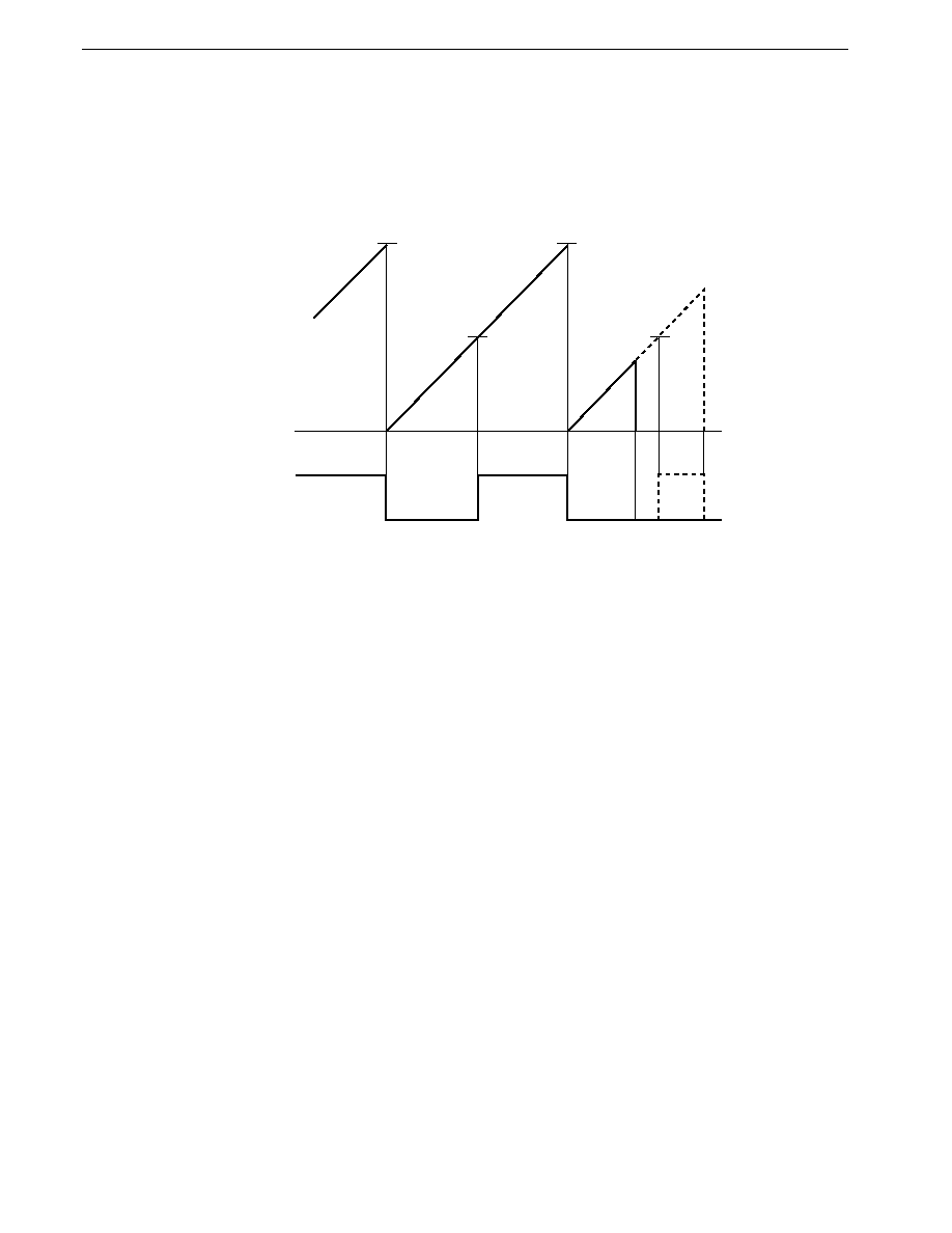
346
CHAPTER 11 TIMER/EVENT COUNTER 2
Preliminary User's Manual U13987EJ1V0UM00
(4) Stopping PPG output
If timer/event counter 2 is stopped by clearing (to 0) the CE2 bit of the timer control register 1 (TMC1) during PPG signal
output, the active level is output irrespective of the output level at the time timer/event counter 2 was stopped.
Figure 11-34. When Timer/Event Counter 2 is Stopped During PPG Signal Output
Caution The output level of the TOn (n = 2, 3) pin when timer output is disabled (ENTOn = 0: n = 2, 3) is the
inverse value of the value set in ALVn (n = 2, 3) bits. Caution is therefore required as the active level
is output when timer output is disabled when the PPG output function has been selected.
TO2
TM2
count value
0H
CR20
CR21
CR21
CR20
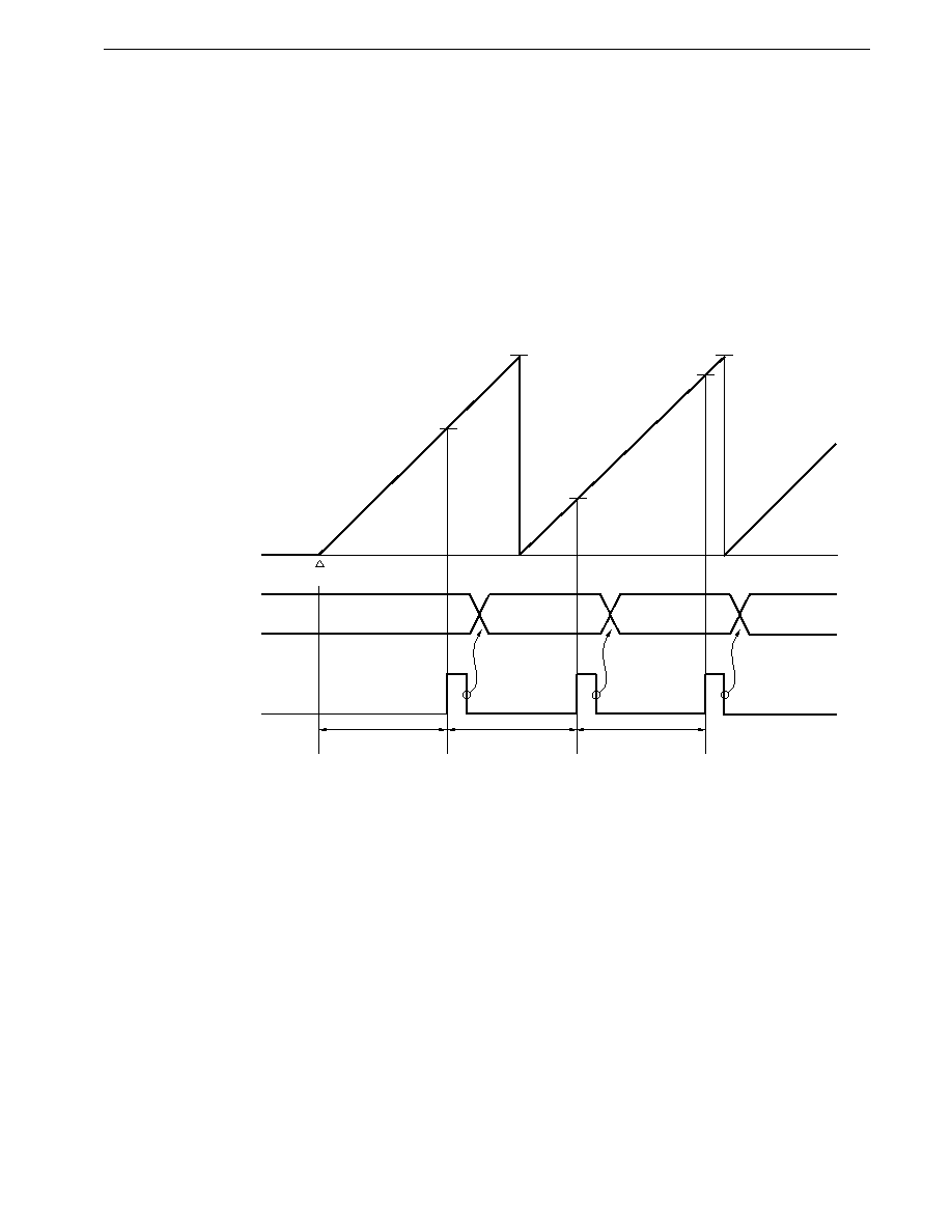
347
CHAPTER 11 TIMER/EVENT COUNTER 2
Preliminary User's Manual U13987EJ1V0UM00
11.9 Examples of Use
11.9.1 Operation as interval timer (1)
When timer counter 2 (TM2) is made free-running and a fixed value is added to the compare register (CR2n: n = 0,
1) in the interrupt service routine, TM2 operates as an interval timer with the added fixed value as the cycle (see Figure
11-35).
The control register settings are shown in Figure 11-36, the setting procedure in Figure 11-37, and the processing in
the interrupt service routine in Figure 11-38.
Figure 11-35. Interval Timer Operation (1) Timing
Remark Interval = n
�
x/f
XX
1
n
FFH, x = 4, 8, 16, 32, 64, 128, 256, 512, 1,024
MOD (2n)
INTC20
interrupt request
TM2
count value
0H
FFH
FFH
Compare register
(CR20)
n
Timer start
MOD (3n)
MOD (4n)
n
MOD (2n)
MOD (3n)
Interval
Interval
Interval
Rewritten by
interrupt program
Rewritten by
interrupt program
Rewritten by
interrupt program

348
CHAPTER 11 TIMER/EVENT COUNTER 2
Preliminary User's Manual U13987EJ1V0UM00
Figure 11-36. Control Register Settings for Interval Timer Operation (1)
(a) Prescaler mode register 1 (PRM1)
(b) Capture/compare control register 2 (CRC2)
7
PRS23
PRM1
6
PRS22
5
PRS21
4
PRS20
3
0
2
�
1
�
0
�
Count clock specification
(x/f
XX
; x = 4, 8, 16, 32, 64, 128, 256,
512, 1,024, or external clock)
(c) Timer control register 1 (TMC1)
7
0
CRC2
6
0
5
0
4
1
3
0
2
0
1
0
0
0
TM2 clearing disabled
TO2 & TO3 both toggle outputs
7
1
TMC1
6
0
5
0
4
0
3
�
2
�
1
0
0
0
Normal mode
Overflow flag
Count operation enabled
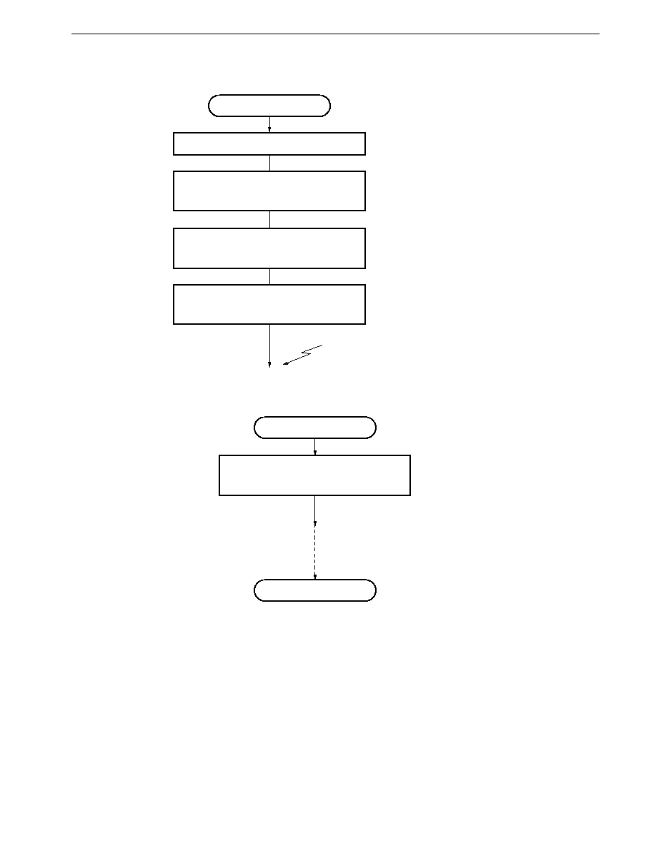
349
CHAPTER 11 TIMER/EVENT COUNTER 2
Preliminary User's Manual U13987EJ1V0UM00
Figure 11-37. Interval Timer Operation (1) Setting Procedure
Figure 11-38. Interval Timer Operation (1) Interrupt Request Servicing
Interval timer (1)
INTC20 interrupt
; Set 1 in bit 7 of TMC1
Set normal mode (CMD2 = 0)
Set PRM1
Set count value in CR20
CR20
n
Set CRC2
CRC2
10H
Set TMC1
CE2
1
CMD2
0
INTC20 interrupt
Calculate timer value that will
generate next interrupt
CR20
CR20+n
Other interrupt service program
RETI

350
CHAPTER 11 TIMER/EVENT COUNTER 2
Preliminary User's Manual U13987EJ1V0UM00
11.9.2 Operation as interval timer (2)
TM2 operates as an interval timer that generates interrupts repeatedly with the preset count time as the interval (see
Figure 11-39).
The control register settings are shown in Figure 11-40, and the setting procedure in Figure 11-41.
Figure 11-39. Interval Timer Operation (2) Timing
Remark
Interval = (n+1)
�
x/f
XX
0
n
FFH, x = 4, 8, 16, 32, 64, 128, 256, 512, 1,024
Compare register
(CR21)
INTC21
interrupt request
TM2
count value
0H
n
n
n
Count start
Clear
Clear
Interval
Interrupt acknowledged
Interrupt acknowledged
Interval
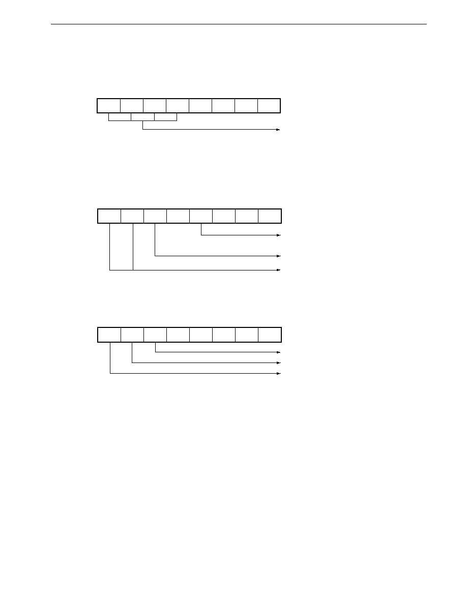
351
CHAPTER 11 TIMER/EVENT COUNTER 2
Preliminary User's Manual U13987EJ1V0UM00
Figure 11-40. Control Register Settings for Interval Timer Operation (2)
(a) Prescaler mode register 1 (PRM1)
(b) Capture/compare control register 2 (CRC2)
7
PRS23
PRM1
6
PRS22
5
PRS21
4
PRS20
3
0
2
�
1
�
0
�
Count clock specification
(x/f
XX
; x = 4, 8, 16, 32, 64, 128, 256,
512, 1,024, or external clock)
(c) Timer control register 1 (TMC1)
7
0
CRC2
6
0
5
0
4
1
3
1
2
0
1
0
0
0
TM2 clearing by match of CR21 & TM2
contents enabled
TM2 clearing by capture operation disabled
TO2 & TO3 both toggle outputs
7
1
TMC1
6
0
5
0
4
0
3
�
2
�
1
0
0
0
Normal mode
Overflow flag
Count operation enabled
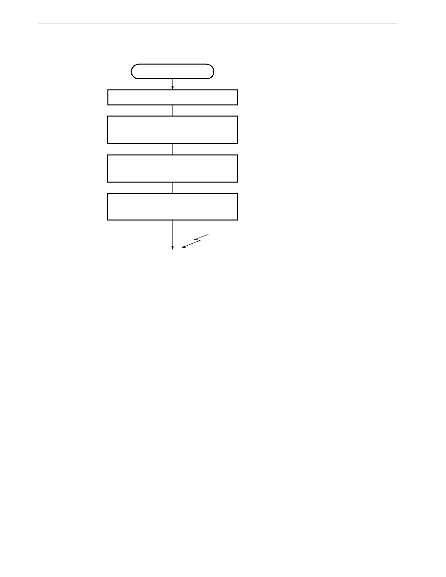
352
CHAPTER 11 TIMER/EVENT COUNTER 2
Preliminary User's Manual U13987EJ1V0UM00
Figure 11-41. Interval Timer Operation (2) Setting Procedure
Interval timer
Set count value in CR21
CR21
n
INTC21 interrupt
; Set 1 in bit 7 of TMC1
Set normal mode (CMD2 = 0)
Set PRM1
Set CRC2
CRC2
18H
Set TMC1
CE2
1
CMD2
0
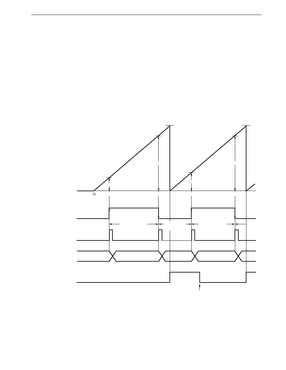
353
CHAPTER 11 TIMER/EVENT COUNTER 2
Preliminary User's Manual U13987EJ1V0UM00
11.9.3 Pulse width measurement operation
In pulse width measurement, the high-level or low-level width of external pulses input to the external interrupt request
input pin (INTP1) are measured.
Both the high-level and low-level widths of pulses input to the INTP1 pin must be at least 3 system clocks (0.24
�
s: f
CLK
= 12.58 MHz); if shorter than this, the valid edge will not be detected and a capture operation will not be performed.
As shown in Figure 11-42, the timer counter 2 (TM2) value being counted is fetched into the capture register (CR22)
in synchronization with a valid edge (specified as both rising and falling edges) in the INTP1 pin input, and held there. The
pulse width is obtained from the product of the difference value between the TM2 count value (D
n
) fetched into and held
in the CR22 on detection of the nth valid edge and the count value (D
n-1
) fetched and held on detection of n-1th valid edge,
and the number of n-1th count clocks (x/f
XX
; x = 4, 8, 16, 32, 64, 128, 256, 512, 1,024).
The control register settings are shown in Figure 11-43, and the setting procedure in Figure 11-44.
Figure 11-42. Pulse Width Measurement Timing
Remark Dn: TM2 count value (n = 0, 1, 2, ...)
x = 4, 8, 16, 32, 64, 128, 256, 512, 1,024
INTP1
external input signal
INTP1
interrupt request
TM2
count value
0H
FFH
FFH
Capture register
(CR22)
OVF2
D0
D1
Count start
D2
D3
Capture
(D1-D0)
�
x/f
XX
(100H-D1+
D2)
�
x/f
XX
(D3-D2)
�
x/f
XX
Cleared by software
D1
D0
D2
D3
Capture
Capture
Capture
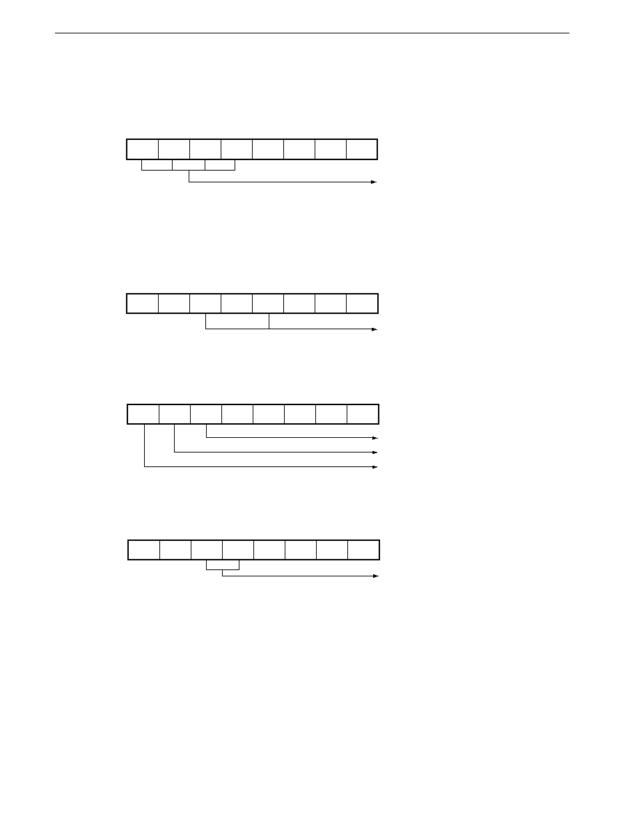
354
CHAPTER 11 TIMER/EVENT COUNTER 2
Preliminary User's Manual U13987EJ1V0UM00
Figure 11-43. Control Register Settings for Pulse Width Measurement
(a) Prescaler mode register 1 (PRM1)
(b) Capture/compare control register 2 (CRC2)
7
PRS23
PRM1
6
PRS22
5
PRS21
4
PRS20
3
0
2
�
1
�
0
�
Count clock specification
(x/f
XX
; x = 4, 8, 16, 32, 64, 128, 256,
512, 1,024, or external clock)
(c) Timer control register 1 (TMC1)
7
0
CRC2
6
0
5
0
4
1
3
0
2
0
1
0
0
0
TM2 clearing disabled
(d) External interrupt mode register 0 (INTM0)
7
1
TMC1
6
0
5
0
4
0
3
�
2
�
1
0
0
0
Normal mode
Overflow flag
Count operation enabled
7
�
INTM0
6
�
5
1
4
1
3
�
2
�
1
0
0
�
Both rising and falling edges
specified as INTP1 input valid edges
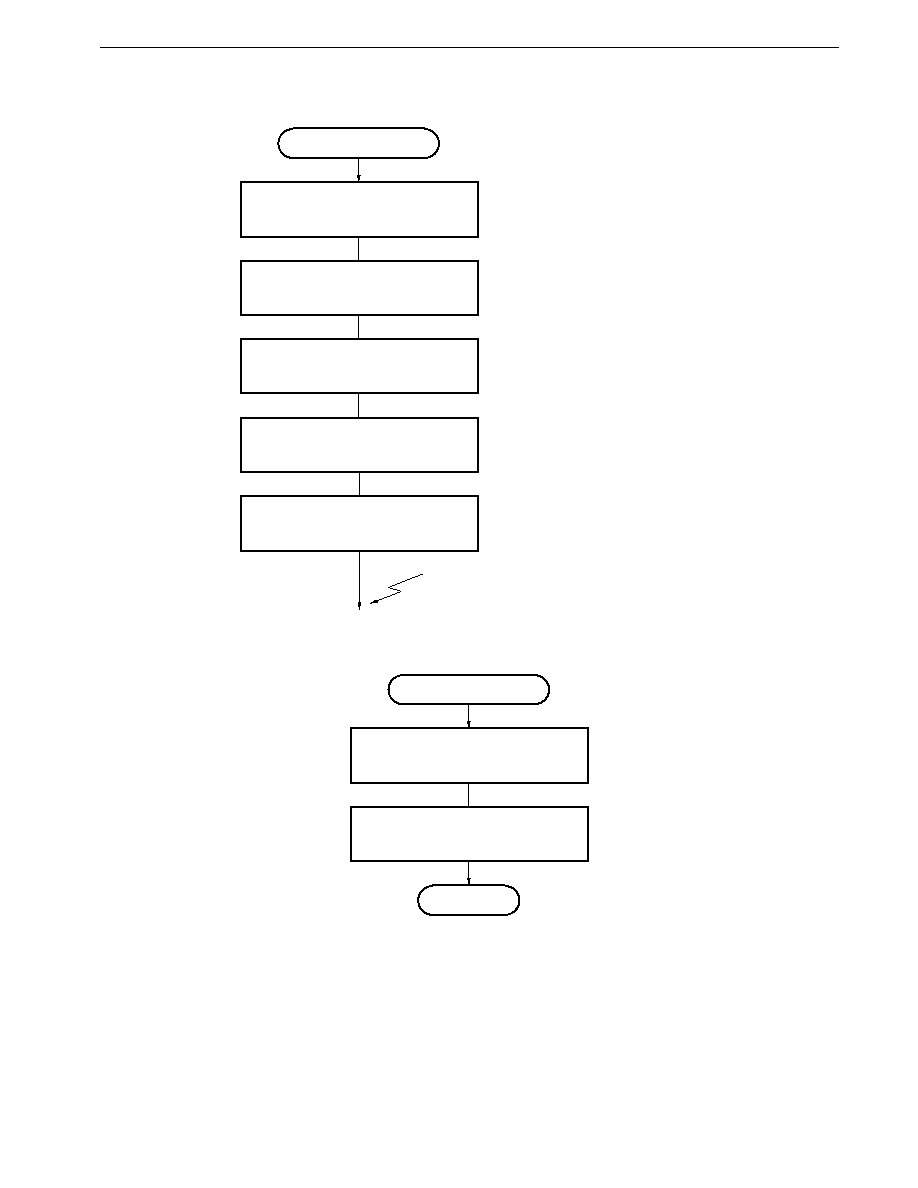
355
CHAPTER 11 TIMER/EVENT COUNTER 2
Preliminary User's Manual U13987EJ1V0UM00
Figure 11-44. Pulse Width Measurement Setting Procedure
Enable interrupts
Pulse width measurement
; Specify both edges as INTP1 input
valid edges, release interrupt masking
Set CRC2
CRC2
10H
Set TMC1
CE2
1
CMD2
0
Initialize capture value buffer memory
X0
0
; Set 1 in bit 7 of TMC1
Set normal mode (CMD2 = 0)
INTP1 interrupt
Set INTM0
Set MK0L
Figure 11-45. Interrupt Request Servicing that Calculates Pulse Width
INTP1 interrupt
Store capture value in memory
X
n+1
CR22
Calculate pulse width
Yn = X
n+1
� Xn
RETI
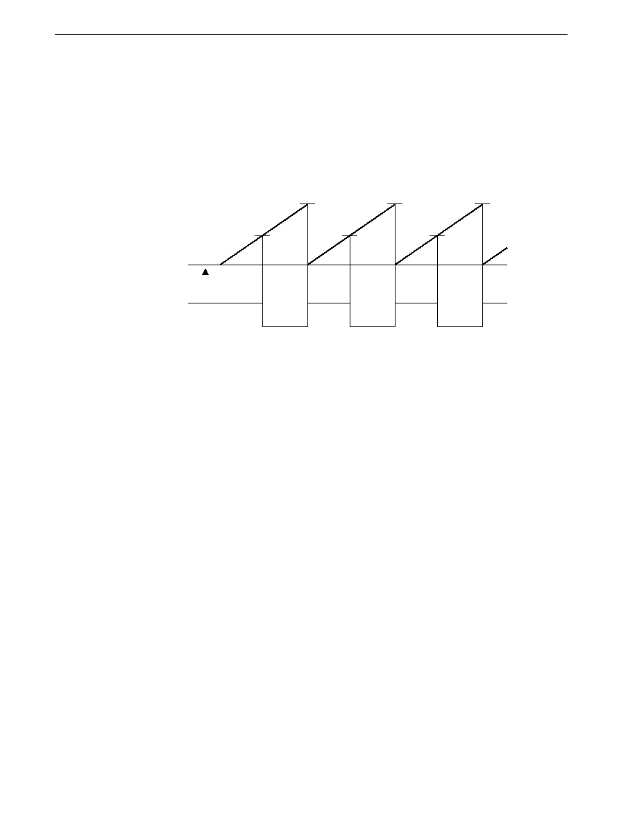
356
CHAPTER 11 TIMER/EVENT COUNTER 2
Preliminary User's Manual U13987EJ1V0UM00
11.9.4 Operation as PWM output
In PWM output, pulses with the duty ratio determined by the value set in the compare register (CR2n: n = 0, 1) are output
(see Figure 11-46).
This PWM output duty ratio can be varied in the range 1/256 to 255/256 in 1/256 units.
The control register settings are shown in Figure 11-47, the setting procedure in Figure 11-48, and the procedure for
varying the duty in Figure 11-49.
Figure 11-46. Example of Timer/Event Counter 2 PWM Signal Output
FFH or FFFFH
FFH or FFFFH
FFH or FFFFH
TM2
count value
0H
TO3
(when active-high)
Timer start
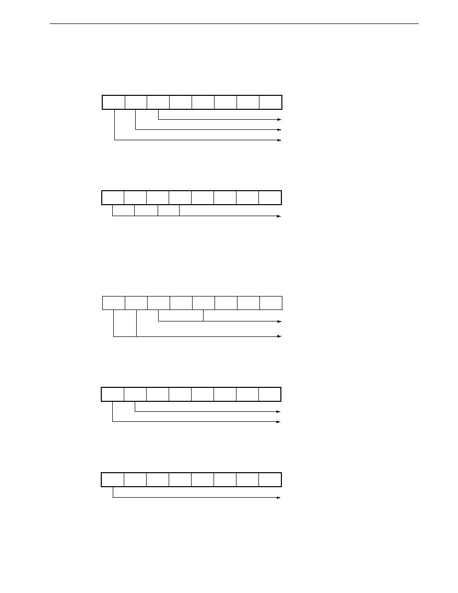
357
CHAPTER 11 TIMER/EVENT COUNTER 2
Preliminary User's Manual U13987EJ1V0UM00
Figure 11-47. Control Register Settings for PWM Output Operation
(a) Timer control register 1 (TMC1)
(b) Prescaler mode register 1 (PRM1)
(c) Capture/compare control register 2 (CRC2)
(d) Timer output control register (TOC)
(e) Port 3 mode control register (PMC3)
7
1
TMC1
6
0
5
0
4
0
3
�
2
�
1
0
0
0
Normal mode
Overflow flag
TM2 count enabled
7
1
CRC2
6
0
5
0
4
1
3
0
2
0
1
0
0
0
TM2 clearing disabled
TO2 & TO3 both PWM outputs
7
1
TOC
6
0
5
�
4
�
3
�
2
�
1
�
�
0
TO3 = active-high PMW signal output
TO3 PMW output enabled
7
1
PMC3
6
�
5
�
4
�
3
�
2
�
1
�
�
0
P37 pin set as TO3 output
7
PRS23
PRM1
6
PRS22
5
PRS21
4
PRS20
3
�
2
�
1
�
0
�
Count clock specification
(x/f
XX
; x = 4, 8, 16, 32, 64, 128, 256,
512, 1,024)

358
CHAPTER 11 TIMER/EVENT COUNTER 2
Preliminary User's Manual U13987EJ1V0UM00
Figure 11-48. PWM Output Setting Procedure
PWM output
Set CRC2
CRC2
90H
Set TOC
Set P34 pin to control mode
PMC3.4
1
Start count
CE2
1
; Set bit 7 of TMC1
Set count clock in PRM1
Set initial value in CR20

359
CHAPTER 11 TIMER/EVENT COUNTER 2
Preliminary User's Manual U13987EJ1V0UM00
Figure 11-49. Changing PWM Output Duty
Duty change preprocessing
Clear INTC21 interrupt request flag
CIF21
0
Enable INTC21 interrupts
CMK21
0
; Clear bit 0 of IF0H
; Clear bit 0 of MK0H
INTC21 interrupt
Duty change processing
Set duty value in CR21
Disable INTC21 interrupts
CMK21
1
; Set bit 0 of MK0H
RETI
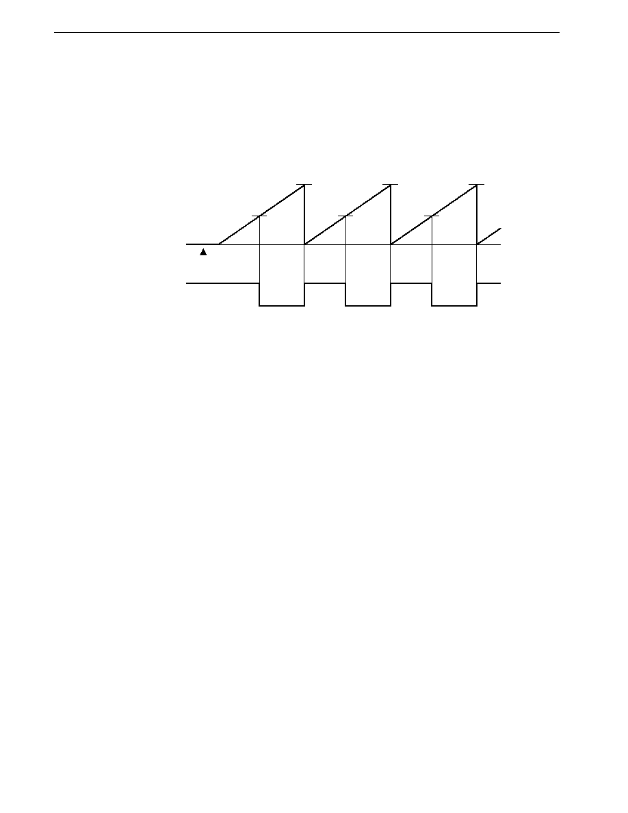
360
CHAPTER 11 TIMER/EVENT COUNTER 2
Preliminary User's Manual U13987EJ1V0UM00
11.9.5 Operation as PPG output
In PPG output, pulses with the cycle and duty ratio determined by the value set in the compare register (CR2n: n = 0,
1) are output (see Figure 11-50).
The control register settings are shown in Figure 11-51, the setting procedure in Figure 11-52, and the procedure for
varying the duty in Figure 11-53.
Figure 11-50. Example of Timer/Event Counter 2 PPG Signal Output
CR21
CR20
CR21
CR20
CR21
CR20
TM2
count value
0H
TO2
(when active-high)
Timer start
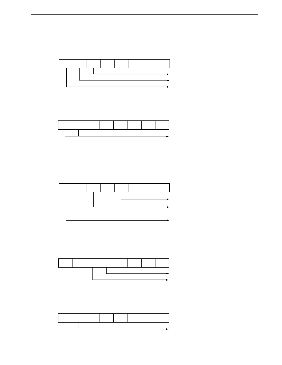
361
CHAPTER 11 TIMER/EVENT COUNTER 2
Preliminary User's Manual U13987EJ1V0UM00
Figure 11-51. Control Register Settings for PPG Output Operation
(a) Timer control register 1 (TMC1)
(b) Prescaler mode register 1 (PRM1)
(c) Capture/compare control register 2 (CRC2)
(d) Timer output control register (TOC)
(e) Port 3 mode control register (PMC3)
7
1
TMC1
6
0
5
0
4
0
3
�
2
�
1
0
0
0
Normal mode
Overflow flag
TM2 count enabled
7
PRS23
PRM1
6
PRS22
5
PRS21
4
PRS20
3
�
2
�
1
�
0
�
Count clock specification
(x/f
XX
; x = 4, 8, 16, 32, 64, 128, 256,
512, 1,024)
7
1
CRC2
6
1
5
0
4
1
3
1
2
0
1
0
0
0
Cleared by match of TM2 & CR21
Clearing when TM2 is captured in CR22
disabled
TO2 = PPG output
7
�
TOC
6
�
5
1
4
0
3
�
2
�
1
�
�
0
TO2 = active-high PPG signal output
TO2 PPG output enabled
7
�
PMC3
6
1
5
�
4
�
3
�
2
�
1
�
�
0
P36 pin set as TO2 output

362
CHAPTER 11 TIMER/EVENT COUNTER 2
Preliminary User's Manual U13987EJ1V0UM00
Figure 11-52. PPG Output Setting Procedure
PPG output
Set CRC2
CRC2
D8H
Set P34 pin to control mode
PMC3.6
1
Start count
CE2
1
Set TOC
; Set bit 7 of TMC1
Set count clock in PRM1
Set cycle in CR21
Set duty in CR21
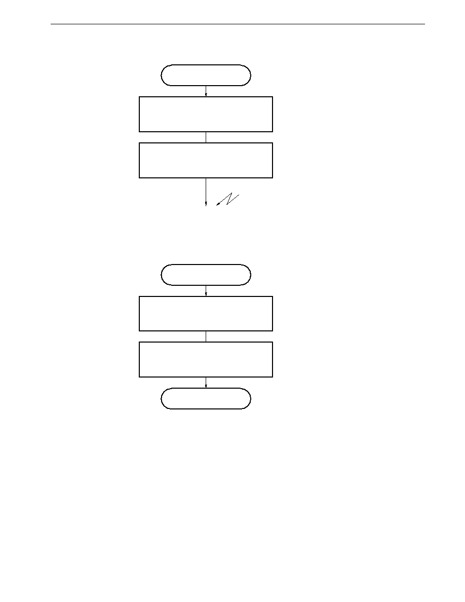
363
CHAPTER 11 TIMER/EVENT COUNTER 2
Preliminary User's Manual U13987EJ1V0UM00
Figure 11-53. Changing PPG Output Duty
Duty change preprocessing
Clear INTC20 interrupt request flag
CIF20
0
; Clear bit 3 of IF0H
Enable INTC20 interrupts
CMK20
0
; Clear bit 3 of MK0H
INTC20 interrupt
Duty change processing
Set duty value in CR20
Disable INTC20 interrupts
CMK20
1
; Set bit 3 of MK0H
RETI
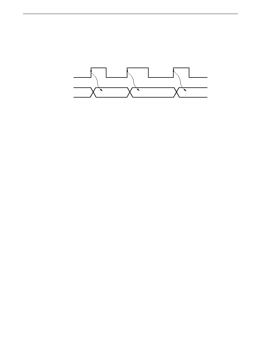
364
CHAPTER 11 TIMER/EVENT COUNTER 2
Preliminary User's Manual U13987EJ1V0UM00
11.9.6 Operation as external event counter
An external event counter counts clock pulses (CI pin input pulses) input from off-chip.
As shown in Figure 11-54, the value of timer counter 2 (TM2) is incremented in synchronization with a CI pin input valid
edge (specified as rising edge only).
Figure 11-54. External Event Counter Operation (single edge)
CI pin input
TM2
n+1
n+2
n
Remark
The TM2 value is one less than the number of input clock pulses.
The control register settings when TM2 operates as an external event counter are shown in Figure 11-55, and the setting
procedure in Figure 11-56.
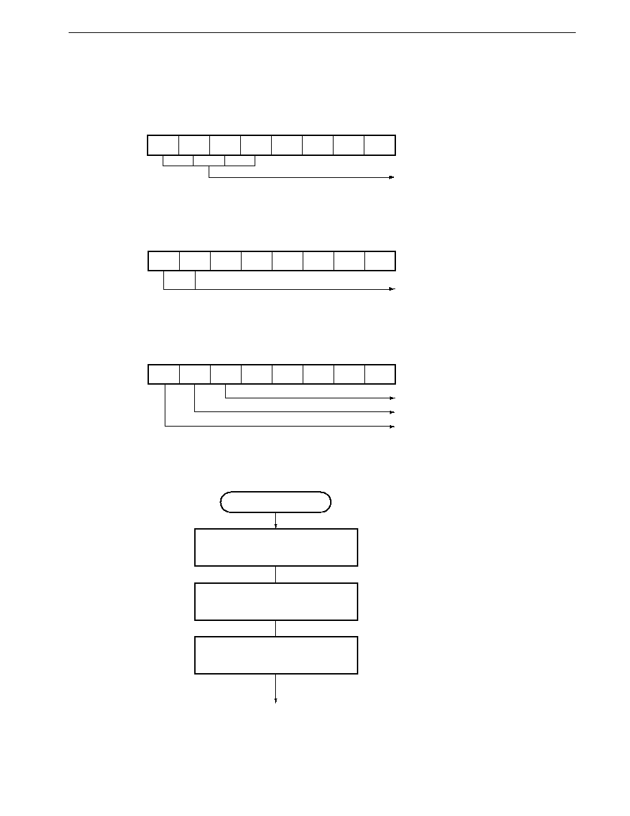
365
CHAPTER 11 TIMER/EVENT COUNTER 2
Preliminary User's Manual U13987EJ1V0UM00
Figure 11-55. Control Register Settings for External Event Counter Operation
(a) Prescaler mode register 1 (PRM1)
(b) External interrupt mode register 0 (INTM0)
(c) Timer control register 1 (TMC1)
Figure 11-56. External Event Counter Operation Setting Procedure
Event counter
; Set 1 in bit 7 of TMC1
Set PRM1
PRM1
0F
�
H
Start count
CE2
1
Specify CI pin input valid edge
7
1
PRM1
6
1
5
1
4
1
3
0
2
�
1
�
0
�
External clock input (C1) specified
7
0
INTM0
6
1
5
�
4
�
3
�
2
�
1
�
0
�
Rising edge specified as CI input
valid edge
7
1
TMC1
6
0
5
0
4
0
3
�
2
�
1
0
0
0
Normal mode
Overflow flag
Count operation enabled
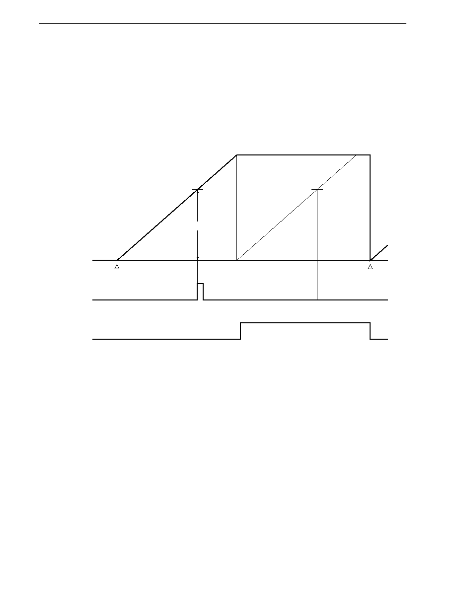
366
CHAPTER 11 TIMER/EVENT COUNTER 2
Preliminary User's Manual U13987EJ1V0UM00
11.9.7 Operation as one-shot timer
After timer counter 2 (TM2) is started, it operates as a one-shot pulse that generates a single interrupt after the preset
count time (see Figure 11-57).
The second and subsequent one-shot timer operations can be started by clearing the OVF2 bit of timer control register
1 (TMC1).
The control register settings are shown in Figure 11-58, the setting procedure in Figure 11-59, and the procedure for
starting the one-shot timer from the second time onward in Figure 11-60.
Figure 11-57. One-Shot Timer Operation
FFH or FFFFH
CR21 value
Count start
CE2
1
Clear
OVF2
0
TM2
count value
0H
INTC21
OVF2
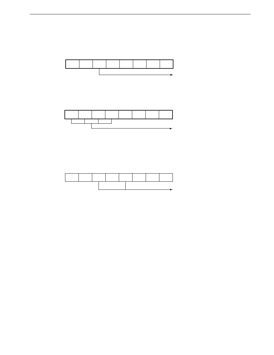
367
CHAPTER 11 TIMER/EVENT COUNTER 2
Preliminary User's Manual U13987EJ1V0UM00
Figure 11-58. Control Register Settings for One-Shot Timer Operation
(a) Timer control register 1 (TMC1)
(b) Prescaler mode register 1 (PRM1)
(c) Capture/compare control register 2 (CRC2)
7
CE2
TMC1
6
OVF2
5
1
4
0
3
�
2
�
1
�
�
0
One-shot timer mode
7
PRS23
PRM1
6
PRS22
5
PRS21
4
PRS20
3
0
2
�
1
�
0
�
Count clock specification
(x/f
XX
; x = 4, 8, 16, 32, 64, 128, 256,
512, 1,024, or external clock)
7
0
CRC2
6
0
5
0
4
1
3
0
2
0
1
0
0
0
TM2 clearing disabled
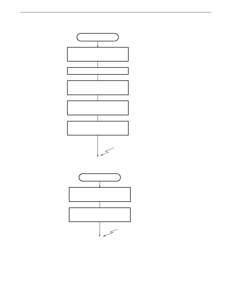
368
CHAPTER 11 TIMER/EVENT COUNTER 2
Preliminary User's Manual U13987EJ1V0UM00
Figure 11-59. One-Shot Timer Operation Setting Procedure
One-shot timer
Set one-shot timer mode
CMD2
1
; Set 1 in bit 7 of TMC1
Set PRM1
Set count value in CR21
CR21
n
Set CRC2
CRC2
10H
Start count
CE2
1
INTC21 interrupt
; Set 1 in bit 5 of TMC1
Figure 11-60. One-Shot Timer Operation Start Procedure from Second Time Onward
One-shot timer restart
Set count value in CR21
CR21
n
Restart count
OVF2
0
INTC21 interrupt
; Clear bit 6 of TMC1

369
CHAPTER 11 TIMER/EVENT COUNTER 2
Preliminary User's Manual U13987EJ1V0UM00
11.10 Cautions
(1) While timer/event counter 2 is operating (while the CE2 bit of the timer control register 1 (TMC1) is set), malfunctioning
may occur if the contents of the following registers are rewritten. This is because it is undefined which takes precedence,
change in the hardware functions due to rewriting the register, or the change in the status because of the function before
rewriting.
Therefore, be sure to stop the counter operation for the sake of safety before rewriting the contents of the following
registers.
�
Prescaler mode register 1 (PRM1)
�
Capture/compare control register 2 (CRC2)
�
Timer output control register (TOC)
�
CMD2 bit of timer control register 1 (TMC1)
(2) If the contents of the compare register (CR2n: n = 0, 1) match with those of TM2 when an instruction that stops timer
counter 2 (TM2) operation is executed, the counting operation of TM2 stops, but an interrupt request is generated.
In order not to generate the interrupt when stopping the operation of TM2, mask the interrupt in advance by using the
interrupt mask register before stopping TM2.
Example
Program that may generate interrupt request
Program that does not generate interrupt request
CLR1 CE2
OR
MK0H, #03H
OR
MK0H, #03H
CLR1 CE2
CLR1 CIF20
CLR1 CIF21
(3) Up to 1 count clock is required after an operation to start timer/event counter 2 (CE2
1) has been performed before
timer/event counter 2 actually starts (refer to Figure 11-61).
For example, when using timer/event counter 2 as an interval timer, the first interval time is delayed by up to 1 clock.
The second and those that follow are at the specified interval.
Figure 11-61. Operation when Counting is Started
Count clock
TM2
CE2
Timing to start actual counting
Count start command (CE2
1)
by software
0
0
1
2
3
Disables interrupt from timer/event
counter 2
Clears interrupt request flag for timer/
event counter 2
Interrupt request from
timer/event counter 2
occurs between these
instructions
...
...
...
...
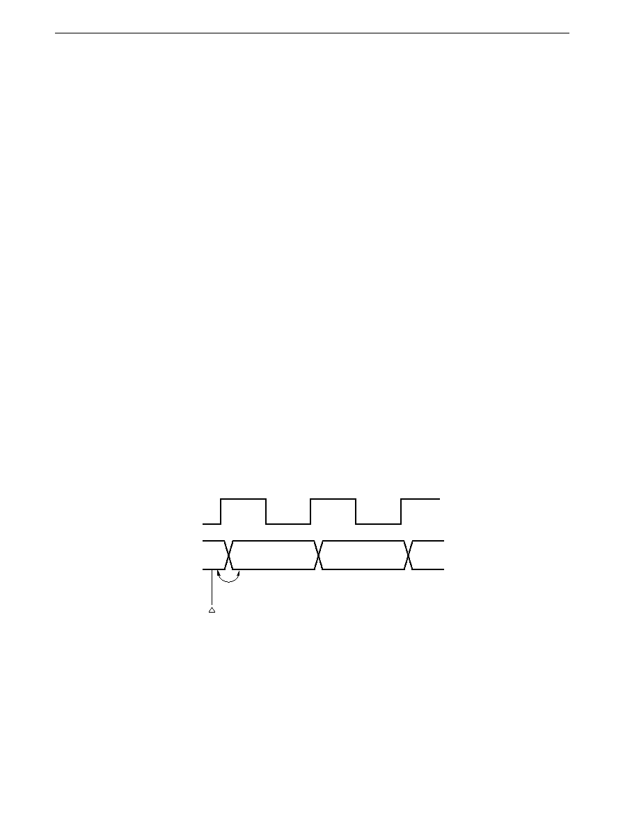
370
CHAPTER 11 TIMER/EVENT COUNTER 2
Preliminary User's Manual U13987EJ1V0UM00
(4) While an instruction that writes data to the compare register (CR2n: n = 0, 1) is executed, coincidence between CR2n,
to which the data is to be written, and timer counter 2 (TM2) is not detected. For example, if the contents of CR2n
do not change before and after the writing, the interrupt request is not generated even if the value of TM2 coincides
with the value of CR2n, nor does the timer output (TOn + 2: n + 2 = 2, 3) change.
Write data to CR2n when timer/event counter 2 is executing count operation in the manner that the contents of TM2
do not match the value of CR2n before and after writing (e.g., immediately after an interrupt request has been generated
because TM2 and CR2n have matched).
(5) Match between TM2 and compare register (CR2n: n = 0, 1) is detected only when TM2 is incremented. Therefore,
the interrupt request is not generated and timer output (TOn + 2 : n + 2 = 2, 3) does not change even if the same value
as TM2 is written to CR2n.
(6) During PPG output, if the PPG cycle is extremely short as compared with the time required to acknowledge an interrupt,
the value of the compare register (CR2n: n = 0, 1) cannot be rewritten by interrupt processing that is performed on
match between timer counter 2 (TM2) and compare register (CR2n). Use another method (for example, to poll the
interrupt request flags by software with all the interrupts masked).
(7) The output level of the TOn (n = 2, 3) when the timer output is disabled (ENTOn = 0: n = 2, 3) is the inverse value
of the value set to the ALVn (n = 2, 3) bits. Note, therefore, that an active level is output when the timer output is disabled
with the PWM output function or PPG output function selected.
(8) When using timer/event counter 2 as an external event counter, the status where no valid edge is input cannot be
distinguished from the status where only one valid edge has been input, by using TM2 alone (refer to Figure 11-62),
because the contents of TM2 are 0 in both the cases. To make a distinction, use the interrupt request flag of INTP2,
as shown in Figure 11-63 (the INTP2 pin is multiplexed with the CI pin and both the functions can be used at the same
time).
Figure 11-62. Example of the Case where External Event Counter does Not Distinguish between One Valid
Edge Input and No Valid Edge Input
CI
TM2
0
1
2
0
Cannot be
distinguished
Count start

371
CHAPTER 11 TIMER/EVENT COUNTER 2
Preliminary User's Manual U13987EJ1V0UM00
Figure 11-63. To Distinguish whether One or No Valid Edge has been Input with External Event Counter
(a) Processing when count is started
; Set CE2 to 1
; Clear PIF2 to 0
Clear INTP2
interrupt request flag
PIF2
0
Start count
CE2
1
Start count
End
(b) Processing when count value is read
; Number of input valid edges is set to A register
Count value
read
Read TM2 contents
A
TM2
A
A+1
End
A = 0?
PIF2 = 1?
; Check TM2 value.
If 0, check interrupt
request flag.
; Check PIF2 contents.
If 1, valid edge is input.
YES
NO
YES
NO

372
Preliminary User's Manual U13987EJ1V0UM00
[MEMO]

373
Preliminary User's Manual U13987EJ1V0UM00
CHAPTER 12 TIMER 3
12.1 Function
Timer 3 is a 16- or 8-bit timer.
In addition to its function as an interval timer, it can be used as a counter for clocked serial interface (CSI) clock generation.
The interval timer generates internal interrupts at preset intervals. The interval setting range is shown in Table 12-1.
Table 12-1. Timer 3 Intervals
Minimum Interval
Maximum Interval
Resolution
4/f
XX
2
16
�
4/f
XX
4/f
XX
(0.32
�
s)
(20.8 ms)
(0.32
�
s)
8/f
XX
2
16
�
8/f
XX
8/f
XX
(0.64
�
s)
(41.7 ms)
(0.64
�
s)
16/f
XX
2
16
�
16/f
XX
16/f
XX
(1.27
�
s)
(83.4 ms)
(1.27
�
s)
32/f
XX
2
16
�
32/f
XX
32/f
XX
(2.54
�
s)
(167 ms)
(2.54
�
s)
64/f
XX
2
16
�
64/f
XX
64/f
XX
(5.09
�
s)
(333 ms)
(5.09
�
s)
128/f
XX
2
16
�
128/f
XX
128/f
XX
(10.17
�
s)
(667 ms)
(10.17
�
s)
256/f
XX
2
16
�
256/f
XX
256/f
XX
(20.35
�
s)
(1.33 s)
(20.35
�
s)
512/f
XX
2
16
�
512/f
XX
512/f
XX
(40.70
�
s)
(2.67 s)
(40.70
�
s)
1,024/f
XX
2
16
�
1,024/f
XX
1,024/f
XX
(81.40
�
s)
(5.33 s)
(81.40
�
s)
( ): When f
XX
= 12.58 MHz
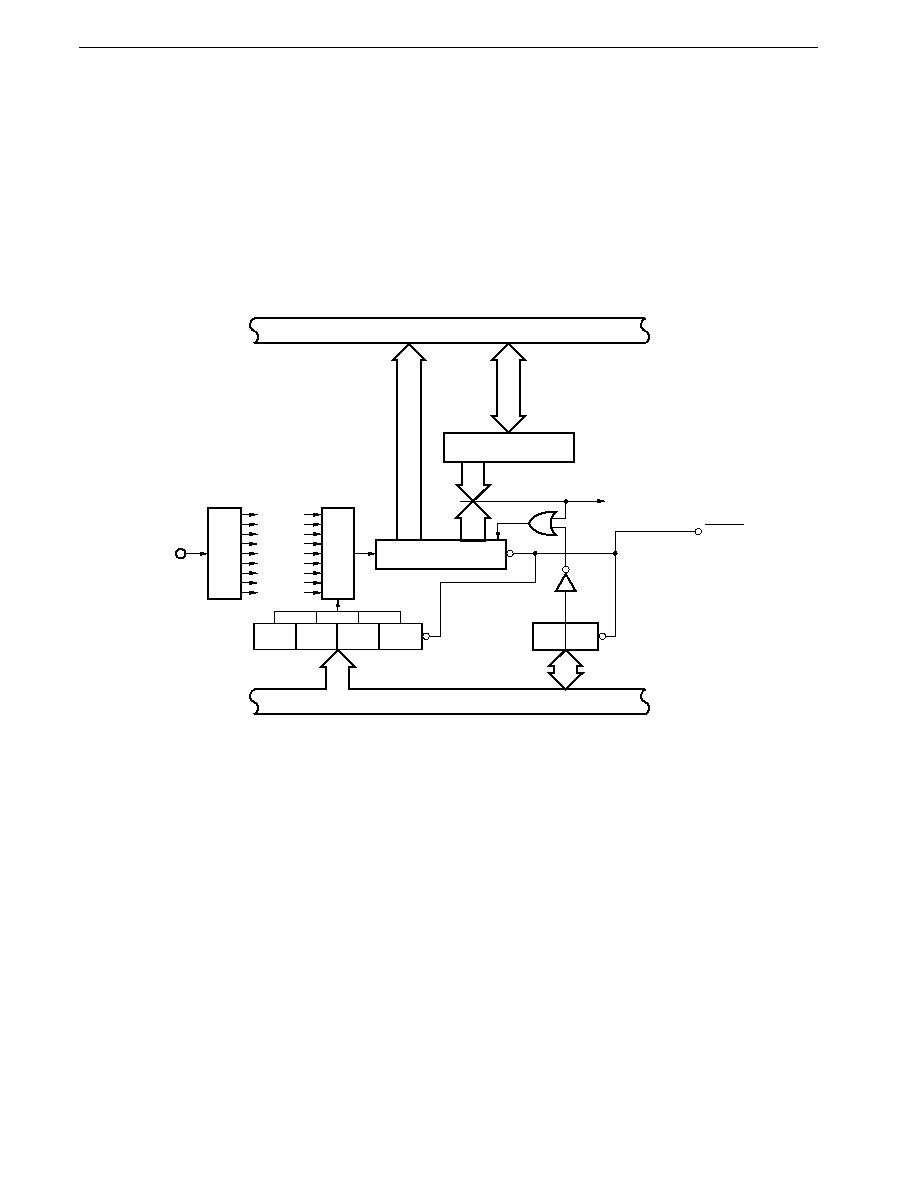
CHAPTER 12 TIMER 3
374
Preliminary User's Manual U13987EJ1V0UM00
12.2 Configuration
Timer 3 consists of the following registers:
�
Timer counter (TM3/TM3W)
�
1
�
Compare register (CR30/CR30W)
�
1
The block diagram of timer 3 is shown in Figure 12-1.
Figure 12-1. Timer 3 Block Diagram
f
XX
/1,024
f
XX
/512
f
XX
/256
f
XX
/128
f
XX
/64
f
XX
/32
f
XX
/16
f
XX
/8
f
XX
/4
f
XX
PRS3 PRS2 PRS1 PRS0
CE3
1/8
BW3
8
Timer control
register 0 (TMC0)
Internal bus
Internal bus
Compare register
(CR30/CR30W)
16
16
Timer counter 3
(TM3/TM3W)
Prescaler
Selector
8/16
8/16
RESET
Match
Clear
INTC30
Serial interface
Prescaler mode
register 0 (PRM0)

375
CHAPTER 12 TIMER 3
Preliminary User's Manual U13987EJ1V0UM00
(1) Timer counter 3 (TM3/TM3W)
TM3/TM3W is a timer counter that count up using the count clock specified by the high-order 4 bits of prescaler mode
register 0 (PRM0).
The count operation is stopped or enabled by the timer control register 0 (TMC0). In addition, an 8-bit mode (TM3)
or 16-bit mode (TM3W) can be selected.
TM3 can be read only with an 8/16-bit manipulation instruction.
When RESET is input, TM3 is cleared to 00H and the count is stopped.
(2) Compare register (CR30/CR30W)
CR30/CR30W is an 8/16-bit register that hold the value that determines the interval timer frequency.
If the CR30/CR30W contents match the contents of TM3/TM3W, the contents of TM3/TM3W is cleared automatically
and an interrupt request (INTC30) is generated.
This compare register operates as CR30 in the 8-bit mode and CR30W in the 16-bit mode.
CR30 can be read or written to with an 8/16-bit manipulation instruction. The contents of CR30 are undefined after
RESET input.
(3) Prescaler
The prescaler generates the count clock from the internal system clock. The clock generated by the prescaler is selected
by the selector, and is used as the count clock by TM3/TN3W to perform count operations.
(4) Selector
The selector selects a signal resulting from dividing the internal clock or the edge detected by the edge detection circuit
as the count clock of TM3/TM3W.

CHAPTER 12 TIMER 3
376
Preliminary User's Manual U13987EJ1V0UM00
12.3 Timer 3 Control Registers
(1) Timer control register 0 (TMC0)
TMC0 controls the timer 3 timer counter 3 (TM3/TM3W) count operation by the high-order 4 bits (the low-order 4 bits
control the count operation of timer/event counter 0 TM0).
TMC0 can be read or written to with an 8-bit manipulation instruction. The format of TMC0 is shown in
Figure 12-2.
RESET input clears TMC0 to 00H.
Figure 12-2. Timer Control Register 0 (TMC0) Format
7
CE3
TMC0
6
0
5
0
4
BW3
3
CE0
2
OVF0
1
0
0
0
CE3
TM3/TM3W Count Operation Control
Count operation stopped with count
cleared
Count operation enabled
1
0
BW3
Timer 3 Bit Length Specification
8-bit operating mode
16-bit operating mode
1
0
Countrols count operation of timer/event counter 0
TM0 (see Figure 9-2).
Address
After reset
R/W
R/W
00H
0FF5DH
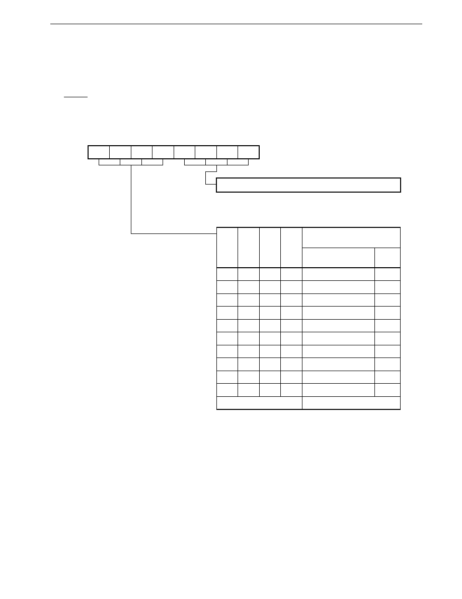
377
CHAPTER 12 TIMER 3
Preliminary User's Manual U13987EJ1V0UM00
(2) Prescaler mode register 0 (PRM0)
PRM0 specifies the count clock to timer 3 timer counter 3 (TM3/TM3W) by the high-order 4 bits (the low-order 4 bits
specify the count clock to timer/event counter 0 TM0).
PRM0 can be read and written with an 8-bit manipulation instruction. The format of the PRM0 is shown in
Figure 12-3.
RESET input sets PRM0 to 11H.
Figure 12-3. Prescaler Mode Register 0 (PRM0) Format
PRS3
PRS2
PRS1
PRS0 PRS03 PRS02 PRS01 PRS00
7
6
5
4
3
2
1
0
PRM0
0FF5CH
Address
11H
After reset
R/W
R/W
PRS3
0
0
0
0
0
0
0
0
1
1
Specifies count clock to timer/event counter 0 TM0 (see Figure 9-3).
PRS2
0
0
0
0
1
1
1
1
0
0
PRS1
0
0
1
1
0
0
1
1
0
0
PRS0
0
1
0
1
0
1
0
1
0
1
Timer 3 TM3/TM3W Count
Clock Specification
Count Clock [Hz]
Specification
Resolution
[ s]
Setting prohibited
f
XX
/4
f
XX
/8
f
XX
/16
f
XX
/32
f
XX
/64
f
XX
/128
f
XX
/256
f
XX
/512
f
XX
/1,024
Setting prohibited
�
0.32
0.64
1.27
2.54
5.09
10.17
20.35
40.70
81.40
(f
XX
= 12.58 MHz)
Other than the above
�
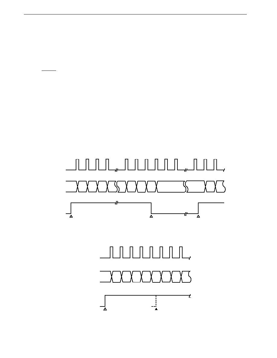
CHAPTER 12 TIMER 3
378
Preliminary User's Manual U13987EJ1V0UM00
12.4 Timer Counter 3 (TM3) Operation
12.4.1 Basic operation
Timer 3 can operate in an 8-bit or 16-bit mode. These operation modes are selected by bit 4 (BW3) of timer control
register 0 (TMC0)
Note
.
In the timer 3 count operation, the count-up is performed using the count clock specified by the high-order 4 bits of
prescaler mode register 0 (PRM0).
When RESET is input, timer counter 3 (TM3) is cleared to 0000H, and the count operation is stopped.
Count operation enabling/disabling is controlled by bit 7 (CE3) of timer control register 0 (TMC0) (the high-order 4 bits
of TMC0 control timer 3 operation). When the CE3 bit is set (to 1) by software, the contents of TM3 are immediately cleared
on the first count clock, and then the count-up operation is performed. When the CE3 bit is cleared (to 0), TM3 becomes
0H immediately, and match signal generation is stopped. If the CE3 bit is set (to 1) again when it is already set (to 1), TM3
continues the count operation without being cleared.
Note
Unless there functional differences are found, the register names in the 8-bit mode are used. In the 16-bit mode,
the register names TM3 and CR30 are TM3W and CR30W, respectively.
Figure 12-4. Basic Operation in 8-Bit Operation Mode (BW3 = 0)
(a) Count started
count stopped
count started
0H
0H
1H
2H
0FH 10H 11H
0H
0H
1H
Count started
CE3
1
Count clock
Count started
CE3
1
TM3
CE3
Count stopped
CE3
0
(b) When "1" is written to the CE3 bit again after the count starts
Count started
CE3
1
Rewrite
CE3
1
Count clock
TM3
CE3
0H
0H
1H
2H
3H
4H
5H
6H
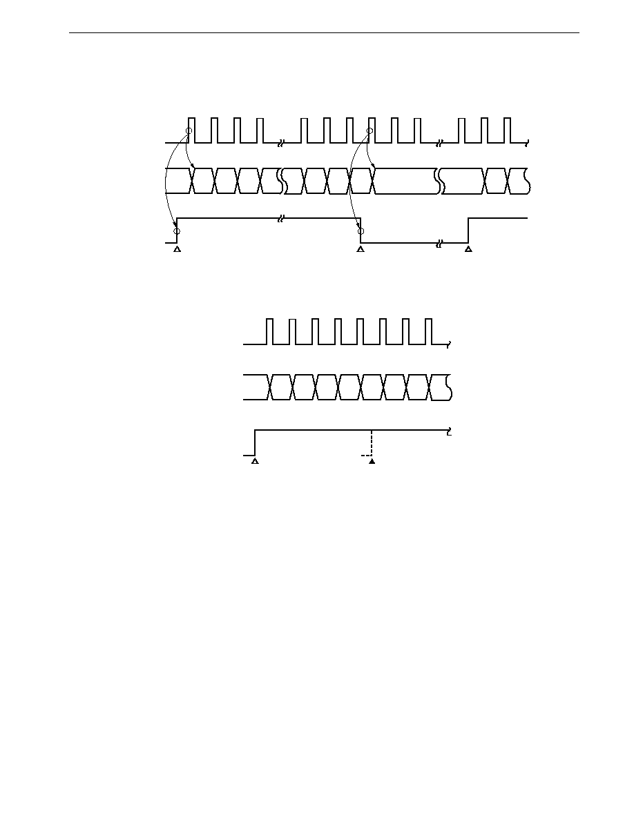
379
CHAPTER 12 TIMER 3
Preliminary User's Manual U13987EJ1V0UM00
Figure 12-5. Basic Operation in 16-Bit Operation Mode (BW3 = 1)
(a) Count started
count stopped
count started
0H
0H
1H
2H
FFH 100H 101H
0H
0H
1H
Count started
CE3
1
Count clock
Count started
CE3
1
TM3W
CE3
Count stopped
CE3
0
(b) When "1" is written to the CE3 bit again after the count starts
Count started
CE3
1
Rewrite
CE3
1
Count clock
TM3W
CE3
0H
0H
1H
2H
3H
4H
5H
6H
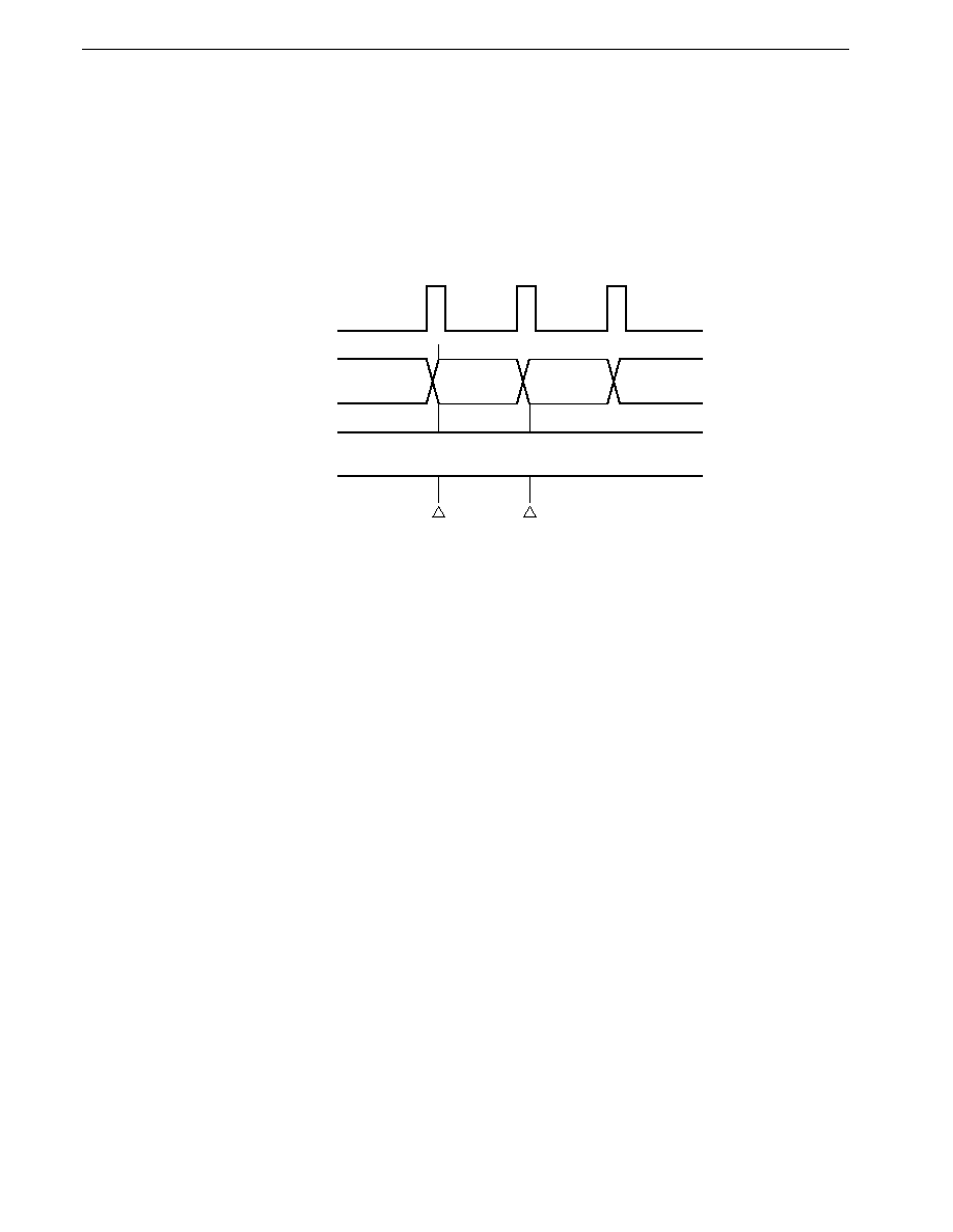
CHAPTER 12 TIMER 3
380
Preliminary User's Manual U13987EJ1V0UM00
12.4.2 Clear operation
(1) Clear operation by match with compare register (CR30)
Timer counter 3 (TM3) is cleared automatically after a match with the compare register (CR30). When a clearance
source arises, TM3 is cleared to 0H on the next count clock. Therefore, even if a clearance source arises, the value
at the point at which the clearance source arose is retained until the next count clock arrives.
Figure 12-6. TM3 Clearance by Match with Compare Register (CR30)
Count clock
TM3
n
0
1
n-1
Compare register
(CR30)
n
TM3 and CR30 match
Cleared here
(2) Clear operation by CE3 bit of timer control register 0 (TMC0)
TM3 is also cleared when the CE3 bit of TMC0 is cleared (to 0) by software. The clear operation is performed following
clearance (to 0) of the CE3 bit in the same way.
381
CHAPTER 12 TIMER 3
Preliminary User's Manual U13987EJ1V0UM00
Figure 12-7. Clear Operation when CE3 Bit is Cleared (0)
(a) Basic operation
Count clock
TM3
n
0
n-1
CE3
(b) Restart before count clock is input after clearance
Count clock
TM3
n
n-1
CE3
0
1
2
If the CE3 bit is set (to 1) before this count clock, the count starts from 0 on
this count clock
0
(c) Restart when count clock is input after clearance
Count clock
TM3
n
0
n-1
CE3
0
0
1
If the CE3 bit is set (to 1) from this count clock onward, the count starts from 0
on the count clock after the CE3 bit is set (to 1).
CHAPTER 12 TIMER 3
382
Preliminary User's Manual U13987EJ1V0UM00
12.5 Compare Register Operation
Timer 3 performs compare operations in which the value set in the compare register (CR30) is compared with the timer
counter 3 (TM3) count value.
If the count value of TM3 matches the preset CR30 value as the result of the count operation, an interrupt request
(INTC30) is generated.
After a match, the TM3 contents are cleared automatically, and therefore TM3 functions as an interval timer that
repeatedly counts up to the value set in the CR30.
Figure 12-8. Compare Operation
CR30
TM3
count value
0H
INTC30
interrupt request
Count start
CE
1
Clear
(match)
Clear
(match)
CR30
383
CHAPTER 12 TIMER 3
Preliminary User's Manual U13987EJ1V0UM00
12.6 Example of Use
Operation as interval timer:
TM3 operates as an interval timer that generates interrupts repeatedly with the preset count time as the interval (see
Figure 12-9). TM3 can also be used for baud rate generation.
This interval timer can count up to a maximum of 20.85 ms at the minimum resolution of 0.32
�
s, and up to 5.33 s at
the maximum resolution of 81.40
�
s (internal system clock f
XX
= 12.58 MHz).
The control register settings are shown in Figure 12-10, and the setting procedure in Figure 12-11.
Figure 12-9. Interval Timer Operation Timing
n
Count start
Clear
Clear
n
Interrupt acknowledgment
Interrupt acknowledgment
Interval
Interval
TM3
count value
0H
INTC30
interrupt request
Compare register
(CR30)
n
Remark
Interval = (n+1)
�
x/f
XX
0
n
FFH, x = 4, 8, 16, 32, 64, 128, 256, 512, 1,024
CHAPTER 12 TIMER 3
384
Preliminary User's Manual U13987EJ1V0UM00
Figure 12-10. Control Register Settings for Interval Timer Operation
Prescaler mode register 0 (PRM0)
7
PRS3
PRM0
6
PRS2
5
PRS1
4
PRS0
3
0
2
0
1
0
0
0
Count clock specification
(x/f
XX
; x = 4, 8, 16, 32, 64, 128, 256,
512, 1,024)
Figure 12-11. Interval Timer Operation Setting Procedure
Interval timer
; Set 1 in bit 7 of TMC0
Set PRM0
Set count value in CR30
CR30
n
Start count
CE
1
INTC30 interrupt

385
CHAPTER 12 TIMER 3
Preliminary User's Manual U13987EJ1V0UM00
Disables interrupts from timer 3
Clears timer 3 interrupt request flag
Interrupt request generated
by timer 3 here
12.7 Cautions
(1) There is a possibility of malfunction if the next register contents are rewritten while the timer 3 is operating (when the
CE3 bit of the timer control register 0 (TMC0) is set). The malfunction occurs as there is no defined order of priority
in the event of contention between the timings at which the hardware function changes due to a register rewrite and
the status changes in the function prior to the rewrite.
When the contents of the following register are rewritten, counter operations must be stopped first to ensure stability.
�
Prescaler mode register 0 (PRM0)
(2) If the compare register (CR30) and timer counter 3 (TM3) contents match when an instruction that stops TM3 operation
is executed, the TM3 count operation stops, but an interrupt request is generated.
If you do not want an interrupt to be generated when TM3 operation is stopped, interrupts should be masked by means
of interrupt the mask register before stopping the TM3.
Example
Program in which an interrupt request may be
Program in which an interrupt request is not generated
generated
CLR1 CE3
SET1 CMK30
SET1 CMK30
CLR1 CE3
CLR1 CIF30
(3) There is a delay of up to one count clock between the operation that starts a timer 3 (CE3
1) and the actual start
of the timer 3 (see Figure 12-12).
For example, if a timer 3 is used as an interval timer, the first interval will be extended by up to one clock. The second
and subsequent intervals will be as specified.
Figure 12-12. Operation when Counting is Started
...
...
...
...
Count clock
TM3
0
CE3
0
3
1
2
Timing at which count actually starts
Software count start command (CE3
1)

CHAPTER 12 TIMER 3
386
Preliminary User's Manual U13987EJ1V0UM00
(4) While an instruction that writes data to the compare register (CR30) is executed, match between CR30, to which the
data is to be written, and timer counter 3 (TM3) is not detected.
Write data to CR30 when timer 3 is executing count operation so that the contents of TM3 do not match the value of
CR30 before and after writing (e.g., immediately after an interrupt request has been generated because TM3 and CR30
have matched).
(5) Match between TM3 and compare register (CR30) is detected only when TM3 is incremented. Therefore, the interrupt
request is not generated even if the same value as TM3 is written to CR30.
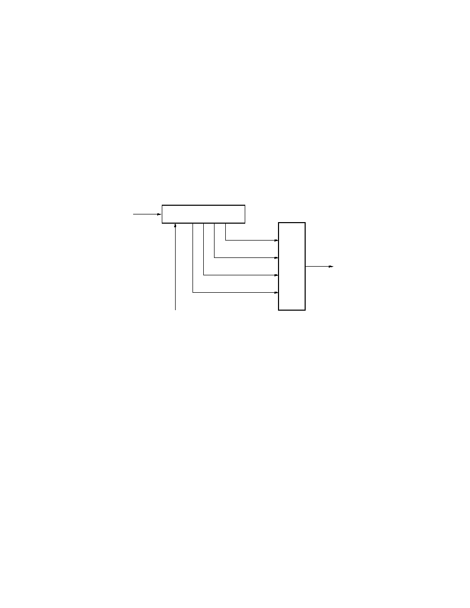
387
Preliminary User's Manual U13987EJ1V0UM00
CHAPTER 13 WATCHDOG TIMER
The watchdog timer is a timer that detects inadvertent program loops.
Watchdog timer interrupts are used to detect system or program errors. For this purpose, instructions that clear the
watchdog timer (start the count) within a given period are inserted at various places in a program.
If an instruction that clears the watchdog timer is not executed within the set time and the watchdog timer overflows,
a watchdog timer interrupt (INTWDT) is generated and a program error is reported.
13.1 Configuration
The watchdog timer block diagram is shown in Figure 13-1.
Figure 13-1. Watchdog Timer Block Diagram
Watchdog timer
Clear signal
f
CLK
/2
17
f
CLK
/2
19
f
CLK
/2
20
f
CLK
/2
21
INTWDT
Selector
f
CLK

388
CHAPTER 13 WATCHDOG TIMER
Preliminary User's Manual U13987EJ1V0UM00
13.2 Watchdog Timer Mode Register (WDM)
WDM is an 8-bit register that controls the watchdog timer operation.
To prevent erroneous clearing of the watchdog timer by an inadvertent program loop, writing can only be performed by
a dedicated instruction. This dedicated instruction, MOV WDM, #byte, has a special code configuration (4 bytes), and a
write is not performed unless the 3rd and 4th bytes of the operation code are mutual complements of 1.
If the 3rd and 4th bytes of the operation code are not mutual complements of 1, a write is not performed and an operand
error interrupt is generated. In this case, the return address saved in the stack area is the address of the instruction that
was the source of the error, and thus the address that was the source of the error can be identified from the return address
saved in the stack area.
If recovery from an operand error is simply performed by means of an RETB instruction, an endless loop will result.
As an operand error interrupt is only generated in the event of an inadvertent program loop (with the NEC assembler,
RA78K4, only the correct dedicated instruction is generated when MOV WDM, #byte is written), system initialization should
be performed by the program.
Other write instructions (MOV WDM, A, AND WDM, #byte, SET1 WDM.7, etc.) are ignored and do not perform any
operation. That is, a write is not performed to the WDM, and an interrupt such as an operand error interrupt is not generated.
After a system reset (RESET input), once the watchdog timer has been started (by setting (to 1) the RUN bit), the WDM
contents cannot be changed. The watchdog timer can only be stopped by a reset, but can be cleared at any time with a
dedicated instruction.
WDM can be read at any time by a data transfer instruction.
RESET input clears WDM to 00H.
The WDM format is shown in Figure 13-2.
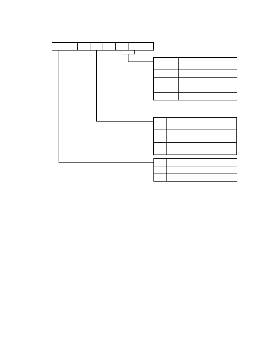
389
CHAPTER 13 WATCHDOG TIMER
Preliminary User's Manual U13987EJ1V0UM00
Figure 13-2. Watchdog Timer Mode Register (WDM) Format
RUN
0
0
PRC
0
WDI2
WDI1
0
7
6
5
4
3
2
1
0
WDM
FFC2H
Address
00H
After reset
R/W
R/W
WDI2
0
0
1
1
Overflow Time [ms]
f
CLK
= 12.58 MHz
2
17
/f
CLK
(10.4)
2
19
/f
CLK
(41.7)
2
20
/f
CLK
(83.4)
2
21
/f
CLK
(166.7)
WDI1
0
1
0
1
Remark f
CLK
: Internal System Clock Frequency
PRC
0
1
Watchdog Timer Interrupt Request Priority
Specification
Watchdog timer interrupt request <
NMI pin input interrupt request
RUN
0
1
Watchdog Timer Operation Specification
Watchdog timer stopped
Clear watchdog timer and start count
Watchdog timer interrupt request >
NMI pin input interrupt request
Cautions 1. The watchdog timer mode register (WDM) can only be written to with a dedicated instruction (MOV
WDM, #byte).
2. The same value should be written each time in writes to the WDM to set (to 1) the RUN bit. The
contents written at the first time cannot be changed even if a different value is written.
3. Once the RUN bit has been set (to 1), it cannot be reset (to 0) by software.

390
CHAPTER 13 WATCHDOG TIMER
Preliminary User's Manual U13987EJ1V0UM00
13.3 Operation
13.3.1 Count operation
The watchdog timer is cleared, and the count started, by setting (to 1) the RUN bit of the watchdog timer mode register
(WDM). When overflow time specified by the WDM2 and WDM1 bits of WDM has elapsed after the RUN bit has been set
(to 1), a non-maskable interrupt (INTWDT) is generated.
If the RUN bit is set (to 1) again before the overflow time elapses, the watchdog timer is cleared and the count operation
is started again.
13.3.2 Interrupt priorities
The watchdog timer interrupt (INTWDT) is a non-maskable interrupt. Other non-maskable interrupts are interrupts from
the NMI pin (NMI). The order of acknowledgment when an INTWDT interrupt and NMI interrupt are generated simultaneously
can be specified by the setting of bit 4 of the watchdog timer mode register (WDM).
Even if INTWDT is generated while the NMI processing program is executed when NMI acknowledgement is specified
to take precedence, INTWDT is not acknowledged until completion of execution of the NMI processing program.

391
CHAPTER 13 WATCHDOG TIMER
Preliminary User's Manual U13987EJ1V0UM00
13.4 Cautions
13.4.1 General cautions on use of watchdog timer
(1) The watchdog timer is one means of detecting inadvertent program loops, but it cannot detect all inadvertent program
loops. Therefore, in equipment that requires a high level of reliability, you should not rely on the on-chip watchdog
timer alone, but should use external circuitry for early detection of inadvertent program loops, to enable processing
to be performed that will restore the normal state or establish a stable state and then stop the operation.
(2) The watchdog timer cannot detect inadvertent program loops in the following cases.
<1> If watchdog timer clearance is performed in the timer interrupt service program
<2> If cases where an interrupt request or macro service is held pending (see 23.9) occur consecutively
<3> If the watchdog timer is cleared periodically when inadvertent program looping is due to an error in the program
logic (if each module of the program functions normally but the overall program does not)
<4> If the watchdog timer is periodically cleared by a group of instructions executed when an inadvertent program
loop occurs
<5> If the STOP mode or IDLE mode is entered as the result of an inadvertent program loop
<6> If watchdog timer inadvertent program loop also occurs in the event of CPU inadvertent program loop due to
external noise
In cases <1>, <2>, and <3> the program can be amended to allow detection to be performed.
In case <4>, the watchdog timer can only be cleared by a 4-byte dedicated instruction. Similarly, in case <5>, the STOP
mode or IDLE mode cannot be set unless a 4-byte dedicated instruction is used. For state <2> to be entered as the
result of an inadvertent program loop, 3 or more consecutive bytes of data must comprise a specific pattern (e.g. BT
PSWL.bit, $$, etc.). Therefore, the establishment of state <2> as the result of <4>, <5> or an inadvertent program
loop is likely to be extremely rare.

392
CHAPTER 13 WATCHDOG TIMER
Preliminary User's Manual U13987EJ1V0UM00
13.4.2 Cautions on
�
PD784938 Subseries watchdog timer
(1) The watchdog timer mode register (WDM) can only be written to with a dedicated instruction (MOV WDM, #byte).
(2) The same value should be written each time in writes to the watchdog timer mode register (WDM) to set (to 1) the RUN
bit. The contents written at the first time cannot be changed even if a different value is written.
(3) Once the RUN bit has been set (to 1), it cannot be reset (to 0) by software.
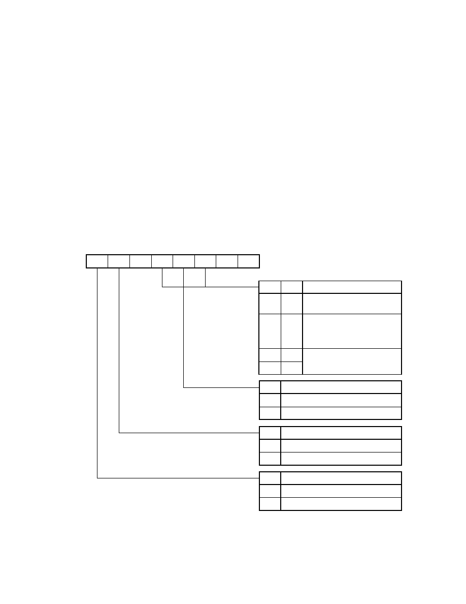
393
Preliminary User's Manual U13987EJ1V0UM00
CHAPTER 14 WATCH TIMER
Two types of count clocks can be input to the watch timer: main clock (12.58 MHz (MAX.)) and watch clock (32.768 kHz).
These count clocks can be selected by the control register. The watch clock is input only to the watch timer, and not to
the CPU and other peripheral circuits. Therefore, the operating speed of the CPU cannot be slowed down by using the
watch clock.
The watch timer generates an interrupt signal with a 0.5-second interval (INTW) by dividing the count clock. At the same
time, it also sets an interrupt request flag (WIF: bit 7 of interrupt control register (WIC)).
The INTW generation interval can be changed to about 1 ms by changing the mode (fast forward mode: 512 times faster
than the normal mode). Also, the INTW generation interval can be set to 15.6 ms.
When the main clock is selected as the count clock, the watch timer stops at standby in STOP mode. However, it continues
operating in the IDLE and HALT modes. When the watch clock is selected as the count clock, the watch timer can continue
operating in any standby mode (it means any of STOP, IDLE, and HALT modes). The operation of the watch clock oscillator
is controlled by the watch timer mode register (WM).
Figure 14-1 shows the format of WM.
Figure 14-1. Watch Timer Mode Register (WM) Format
WM7
WM6
0
WM4
WM3
WM2
0
0
7
6
5
4
3
2
1
0
WM
0FF6FH
Address
00H
After reset
R/W
R/W
WM3
0
1
Watch Timer Operation Control
Clears division counter and stops counting
Starts operation of division counter
WM6
0
1
Watch Timer Operation Clock Specification
Main clock
Watch clock
WM7
0
1
Watch Clock Oscillator Operation Control
Stops watch clock oscillator
Operation watch clock oscillator
WM4
0
1
0
1
Watch Timer Operation Mode
Normal watch mode (generates
INTW at 0.5 s intervals)
Medium-fast forward mode (32
times faster than normal mode,
generates INTW at 15.6 ms
intervals)
Fast forward mode (512 times
faster than normal mode, generates
INTW at 0.98 ms intervals)
WM2
0
0
1
1
Caution The time from when the watch timer is started up until the first INTW occurs is less than 0.5 seconds.
This time becomes 0.5 seconds from the second and subsequent INTW occurrences.
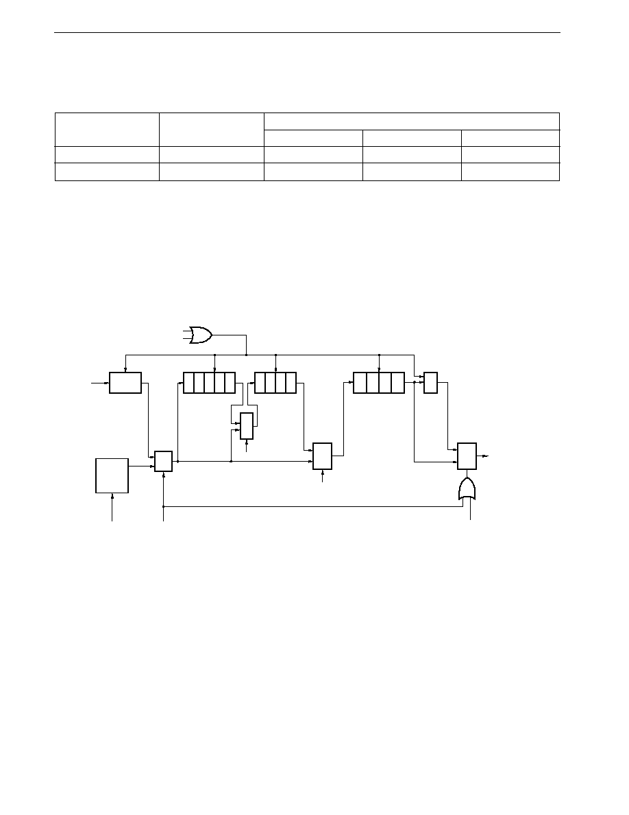
394
CHAPTER 14 WATCH TIMER
Preliminary User's Manual U13987EJ1V0UM00
The watch timer of the
�
PD784938 does not have a buzzer output function.
Table 14-1. Relation between Count Clock and Watch Timer Operation
Count Clock Selection
Normal Operation Mode
Type of Standby Mode
HALT mode
STOP mode
IDLE mode
Main clock
Operable
Operable
Stopped
Operable
Note
Watch clock
Operable
Operable
Operable
Operable
Note When bit 3 (WM3) of the watch timer mode register (WM) is set to "1" and bit 6 (WM6) of the same register is
set to "0", main clock operation in the IDLE mode is enabled.
The watch timer consists of a divider circuit that divides the count clock by three, and a counter that divides the output
signal of the divider circuit by 2
14
. As the count clock, select the signal obtained by dividing the internal system clock by
128, or the signal from the watch clock oscillator.
Figure 14-2. Block Diagram of Watch Timer
1 2 3 4
10 11 12 13
14
5
6 7 8 9
Counter
Counter
Counter
1/3
divider
SEL
SEL
S
E
L
SEL
WM.3
reset
Watch
clock
oscillator
ON/OFF
WM.7
WM.6
WM.2
WM.4
(Set by instruction when main clock is 12.58 MHz)
STBC.7
INTW
1
0
0
1
0
0
1
Main clock
f
XX
/128
Caution The interval until the first INTW is generated is not 0.5 second after the operation has been enabled.
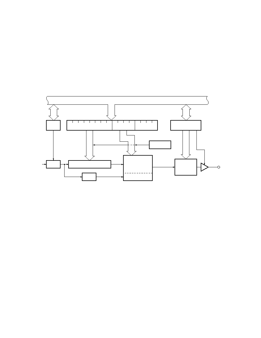
395
Preliminary User's Manual U13987EJ1V0UM00
CHAPTER 15 PWM OUTPUT UNIT
The
�
PD784938 incorporates two 12-bit resolution PWM (pulse width modulation) output circuit channels. The active
level of the PWM output pulses can be selected as high or low. The PWM output ports consist of dedicated pins.
15.1 PWM Output Unit Configuration
The PWM output unit configuration is shown in Figure 15-1.
Figure 15-1. PWM Output Unit Configuration
Internal bus
16
15
8
7
4
3
0
PWMn
8
PWPR
Prescaler
f
CLK
8
8-bit down counter
f
PWMC
1/256
4-bit counter
PWM pulse
generator
4
Reload control
Reload
Reload
8
PWMC
Output control
circuit
PWMn
Remark
n = 0, 1

CHAPTER 15 PWM OUTPUT UNIT
396
Preliminary User's Manual U13987EJ1V0UM00
(1) 8-bit down counter
Generates the basic PWM signal timing.
(2) PWM pulse generator (including 4-bit counter)
Controls addition of extra pulses and generates the PWM pulses to be output.
(3) Reload control
Controls 8-bit down counter and 4-bit count modulo value reloading.
(4) Output control circuit
Controls the active level of the PWM signal.
(5) Prescaler
Scales f
CLK
, and generates the reference clock.
397
CHAPTER 15 PWM OUTPUT UNIT
Preliminary User's Manual U13987EJ1V0UM00
15.2 PWM Output Unit Control Registers
15.2.1 PWM control register (PWMC)
PWMC is an 8-bit register that controls the operating status of the PWM output pins (PWMn: n = 0, 1).
PWMC can be read or written to with an 8-bit manipulation instruction or bit manipulation instruction. Its format is shown
in Figure 15-2.
When RESET is input, PWMC is set to 05H, the PWMn pin is disabled from outputting signals.
Figure 15-2. PWM Control Register (PWMC) Format
7
SYN1
PWMC
6
0
5
SYN0
4
0
3
EN1
2
ALV1
1
EN0
0
ALV0
Address
After reset
R/W
R/W
05H
0FF70H
ALVn
PWMn Pin PWM Active Level Specification
(n = 0, 1)
Active-low
Active-high
1
0
ENn
PWMn Pin PWM Output Control
Output disabled
PWM output enabled
SYNn
PWM Pulse Width Rewrite Cycle
Specification
Rewritten every 16 PWM cycles (2
12
/f
PWMC
)
Rewritten every PWM cycle (2
8
/f
PWMC
)
1
0
1
0
CHAPTER 15 PWM OUTPUT UNIT
398
Preliminary User's Manual U13987EJ1V0UM00
15.2.2 PWM prescaler register (PWPR)
PWPR is an 8-bit register that selects the PWM output circuit operating clock (f
PWMC
).
PWPR can be read or written to with an 8-bit manipulation instruction. Its format is shown in Figure 15-3.
When RESET is input, PWPR is cleared to 00H, and f
CLK
is selected as f
PWMC
for both channels.
Figure 15-3. PWM Prescaler Register (PWPR) Format
0
PWP12 PWP11 PWP10
0
PWP02 PWP01 PWP00
7
6
5
4
3
2
1
0
PWPR
0FF71H
Address
00H
After reset
R/W
R/W
PWPn2
0
0
0
0
1
PWMn Operating
Clock (f
PWMC
)
f
CLK
f
CLK
/2
f
CLK
/3
f
CLK
/4
Setting prohibited
PWPn1
0
0
1
1
0
PWPn0
0
1
0
1
0
PWMn Repetition Frequency
(f
CLK
= 12.58 MHz)
Other than the above
f
CLK
/256 (49.14 kHz)
f
CLK
/512 (24.58 kHz)
f
CLK
/768 (16.38 kHz)
f
CLK
/1,028 (12.28 kHz)
(n = 0, 1)
15.2.3 PWM modulo registers (PWM0, PWM1)
The PWM modulo register (PWMn: n = 0, 1) is a 16-bit register that determines the PWM pulse width. Reads/writes
by a 16-bit manipulation instruction are possible for data setting.
The contents of bits 4 to 15 of the PWMn determines the 12-bit PWM pulse width (12-bit resolution). Bits 3 to 0 have
no meaning, and PWM output is not affected whether 1 or 0 is written to these bits.
When RESET is input, the PWMn content are undefined, and therefore data must be set by the program before PWM
output is enabled.
Caution A value between 0000H and 00FFH should not be set in the PWM modulo registers (PWMn: n = 0, 1).
A value between 0100H and FFFFH should be set in the PWMn registers. The PWM signal duty values
that can be output are 17/4,096 to 4,096/4,096.
399
CHAPTER 15 PWM OUTPUT UNIT
Preliminary User's Manual U13987EJ1V0UM00
15.3 PWM Output Unit Operation
15.3.1 Basic PWM output operation
The PWM pulse output duty is determined by the value set in bits 4 to 15 of the PWM modulo register (PWMn: n = 0,
1) as shown below.
PWM pulse output duty =
(Value of PWMn bits 4 to 15)
Note
+ 1
4,096
Note 16
(Value of PWMn bits 4 to 15)
4095
The PWM pulse output repetition frequency is the frequency obtained by division-by-256 of the PWM clock f
CLK
/1 to
f
CLK
/4 set by the PWM prescaler register (PWPR) (=f
PWMC
/256), and the minimum pulse width is 1/f
PWMC
.
In PWM pulse output, 12-bit resolution is achieved by repeating output of a f
PWMC
/256 repetition frequency 8-bit resolution
PWM signal 16 times.
The addition of extra pulses (1/f
PWMC
) to the 8-bit resolution PWM pulses determined by bits 8 to 15 of the PWMn every
cycle is controlled in accordance with the value of bits 4 to 7 of the PWMn to implement a PWM pulse signal once every
16 cycles.
Figure 15-4. Basic PWM Output Operation
PWM signal
Note
One 12-bit PWM signal cycle
Note 8-bit resolution per PWM pulse cycle

CHAPTER 15 PWM OUTPUT UNIT
400
Preliminary User's Manual U13987EJ1V0UM00
15.3.2 PWM pulse output enabling/disabling
When PWM pulses are output, the ENn (n = 0, 1) bits of the PMC register are set (to 1) after data is set in the PWM
prescaler register (PWPR) and PWM modulo register (PWMn: n = 0, 1). As a result, PWM pulses with the active level
specified by ALVn (n = 0, 1) bit of the PWM control register (PWMC) are output from the PWM output pin.
When the ENn bits of the PWMC are cleared (to 0), the PWM output unit immediately stops the PWM output operation.
15.3.3 PWM pulse active level specification
The ALVn (n = 0, 1) bit of the PWM control register (PWMC) specify the active level of PWM pulses output from the
PWM output pins.
When ALVn bit is set (to 1), active-high level pulses are output, and when cleared (to 0), active-low level pulses are output.
When ALVn bit is rewritten, the PWM active level changes immediately. PWM output active level setting and pin states
are shown in Figure 15-5.
Figure 15-5 shows the case where ALVn bit is switched when the ENn (n = 0, 1) bit of the PWMC is set (to 1) and PWM
output is enabled.
The pin state does not change if ALVn is rewritten when ENn bit is in the cleared (to 0) state.
Figure 15-5. PWM Output Active Level Setting
ALVn
PWMn
(Active-high)
(Active-low)
(ALVn bit rewrite)
Remark
ENn = 1 (n = 0, 1)
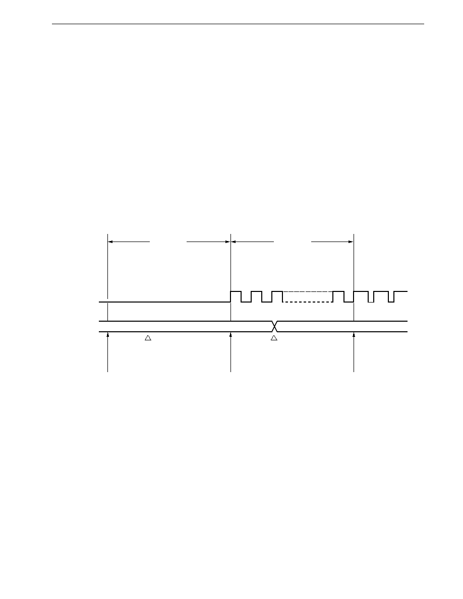
401
CHAPTER 15 PWM OUTPUT UNIT
Preliminary User's Manual U13987EJ1V0UM00
15.3.4 PWM pulse width rewrite cycle specification
The start of PWM output and pulse width changes are performed in synchronization either with every 16 PWM pulse
cycles (2
12
/f
PWMC
) or with every PWM pulse cycle (2
8
/f
PWMC
). This PWM pulse width rewrite cycle specification is performed
by means of the SYNn bits of the PWM control register (PWMC).
When the SYNn bit is cleared (to 0), a pulse width change is performed every 16 PWM pulse cycles (2
12
/f
PWMC
). It therefore
takes a maximum of 2
12
clocks (326
�
s when f
PWMC
= 12.58 MHz) until a pulse of a width corresponding to the data written
in the PWM modulo register (PWMn: n = 0, 1) is output. An example of the PWM output timing at this time is shown in
Figure 15-6.
When the SYNn bit is set (to 1), on the other hand, a pulse width change is performed every PWM pulse cycle (2
8
/f
PWMC
).
In this case, it takes a maximum of 2
8
clocks (20.4
�
s when f
PWMC
= 12.58 MHz) until a pulse of a width corresponding to
the data written in the PWMn is output.
However, caution is required since, if the PWM pulse rewrite cycle is specified as every 2
8
/f
PWMC
, (if the SYNn bit is set
(to 1)), the obtained PWM pulse precision is between 8 bits and 12 bits, and is lower than when the PWM pulse rewrite
cycle is specified as 2
12
/f
PWMC
.
An example of the PWM output timing when the rewrite timing is 2
8
/f
PWMC
is shown in Figure 15-7.
Figure 15-6. PWM Output Timing Example 1 (PWM pulse width rewrite cycle = 2
12
/f
PWMC
)
PWM
output pin
PWMn
contents
PWM
output
enabled
PWM pulse width
switching timing
PWM pulse width
switching timing
PWM pulse width
switching timing
PWMn
rewrite
n
m
16 PWM
pulse cycles
16 PWM
pulse cycles
Cautions 1. Pulse width rewriting is performed every PWM pulse cycle.
2. The PWM pulse precision is 12 bits.
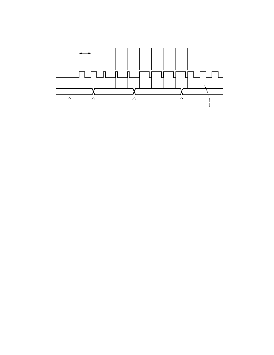
CHAPTER 15 PWM OUTPUT UNIT
402
Preliminary User's Manual U13987EJ1V0UM00
Figure 15-7. PWM Output Timing Example 2 (PWM pulse width rewrite cycle = 2
8
/f
PWMC
)
1 PWM
pulse cycle
PWM
output pin
PWMn
contents
PWM
output
enabled
PWMn
rewrite
PWMn
rewrite
PWMn
rewrite
PWM pulse width
switching timing
n
I
m
n
Cautions 1.
Pulse width rewriting is performed every PWM pulse cycle.
2.
The PWM pulse precision is between 8 and 12 bits.
Remark
l, m, and n mean the PWMn contents.
15.4 Caution
A value between 0000H and 00FFH should not be set in the PWM modulo registers (PWMn: n = 0, 1). A value between
0100H and FFFFH should be set in the PWMn. The PWM signal duty values that can be output are 17/4,096 to 4,096/
4,096.

403
Preliminary User's Manual U13987EJ1V0UM00
CHAPTER 16 A/D CONVERTER
The
�
PD784938 incorporates an analog/digital (A/D) converter with 8 multiplexed analog inputs (ANI0 to ANI7).
The successive approximation conversion method is used, and the conversion result is held in the 8-bit A/D conversion
result register (ADCR). This allows fast, high-precision conversion to be performed.
There are two modes for starting A/D conversion, as follows:
�
Hardware start: Conversion started by trigger input (INTP5).
�
Software start:
Conversion started in accordance with A/D converter mode register (ADM) bit setting.
After start-up, there are two operation modes, as follows:
�
Scan mode:
Multiple analog inputs are selected in order, and conversion data is obtained from all pins.
�
Select mode: One pin is used as the analog input, and conversion values are obtained in succession.
Stoppage of all the above modes and conversion operations is specified by the ADM register.
When the conversion result is transferred to the ADCR, an INTAD interrupt request is generated. This allows conversion
values to be transferred to memory in succession by means of macro service.
Cautions 1. Apply a voltage same as the supply voltage (AV
DD
) to the reference voltage input pin (AV
REF1
) of
this product.
2. When port 7 is used for both output port and A/D input, do not write to output port during A/D
conversion operations.
16.1 Configuration
The A/D converter configuration is shown in Figure 16-1.
404
CHAPTER 16 A/D CONVERTER
Preliminary User's Manual U13987EJ1V0UM00
Figure 16-1. A/D Converter Block Diagram
Internal bus
8
8
A/D converter mode
register (ADM)
RESET
8
Successive approximation
register (SAR)
Edge detection
circuit
INTP5
ANI7
ANI6
ANI5
ANI4
ANI3
ANI2
ANI1
ANI0
Sample & hold circuit
Tap
selector
AV
REF1
R/2
R
R/2
Voltage comparator
INTAD
Control circuit
Conversion trigger
Trigger enable
AV
SS
A/D conversion result
register (ADCR)
Series resistor string
Input
selector
A/D current cut select
register (IEAD)
Connection
control
AV
DD
405
CHAPTER 16 A/D CONVERTER
Preliminary User's Manual U13987EJ1V0UM00
Cautions 1. A capacitor should be connected between the analog input pins (ANI0 to ANI7) and AV
SS
, and
between the reference voltage input pin (AV
REF1
) and AV
SS
to prevent malfunction due to noise.
Be sure to connect the capacitor as closely to ANI0 through ANI7 and AV
REF1
as possible.
Figure 16-2. Example of Capacitor Connection on A/D Converter Pins
Analog
input
Reference
voltage input
100 to
500 pF
ANI0 to ANI7
AV
REF1
AV
SS
�
PD784938
2. A voltage outside the range AV
SS
to AV
REF1
should not be applied to pins used as A/D converter
input pins. See 16.6 Cautions for details.
(1) Input circuit
The input circuit selects the analog input in accordance with the specification of the A/D converter mode register (ADM),
and sends the analog input to the sample & hold circuit according to the operation mode,
(2) Sample & hold circuit
The sample & hold circuit samples the analog inputs arriving sequentially one by one and holds the analog input in
the process of A/D conversion.
(3) Voltage comparator
The voltage comparator determines the voltage difference between the analog input and the series resistor string value
tap.
(4) Series resistor string
The series resistor string is used to generate voltages that match the analog inputs.
The series resistor string is connected between the A/D converter reference voltage pin (AV
REF1
) and the A/D converter
GND pin (AV
SS
). To provide 256 equal voltage steps between the two pins, it is made up of 255 equal resistors and
two resistors with half that resistance value.
The series resistor string voltage tap is selected by a tap selector controlled by the SAR successive approximation
register.

406
CHAPTER 16 A/D CONVERTER
Preliminary User's Manual U13987EJ1V0UM00
(5) SAR: Successive Approximation Register
SAR is an 8-bit register in which the data for which the series resistor string voltage tap value matches the analog input
voltage value is set bit by bit starting from the most significant bit (MSB).
When data has been set up to the least significant bit (LSB) of the SAR (when A/D conversion is completed), the SAR
contents (conversion result) are stored in the A/D conversion result register (ADCR).
(6) ADCR: A/D Conversion Result Register
ADCR is an 8-bit register that holds the A/D conversion result. The conversion result is loaded into this register from
the successive approximation register (SAR) each time A/D conversion finishes.
The contents of this register approximation are undefined when RESET is input.
(7) Edge detection circuit
The edge detection circuit detects a valid edge from the interrupt request input pin (INTP5) input, and generates an
external interrupt request signal (INTP5) and A/D conversion operation external trigger.
The INTP5 pin input valid edge is specified by external interrupt mode register 1 (INTM1) (see Figure 22-2). External
trigger enabling/disabling is set by means of the A/D converter mode register (ADM) (see 16.2 A/D Converter Mode
Register (ADM)).

407
CHAPTER 16 A/D CONVERTER
Preliminary User's Manual U13987EJ1V0UM00
16.2 A/D Converter Mode Register (ADM)
ADM is an 8-bit register that controls A/D converter operations.
ADM register can be read or written to with an 8-bit manipulation instruction or bit manipulation instruction. Its format
is shown in Figure 16-3.
Bit 0 (MS) controls the operation mode.
Bits 1, 2, and 3 (ANI0, 1, 2) select the analog inputs for A/D conversion.
Bit 5 (SCMD) controls the A/D conversion operation in scan mode.
Bit 6 (TRG) enables external synchronization of the A/D conversion operation. If the TRG bit is set (to 1) when the CS
bit is set (to 1), the conversion operation is initialized with each input of a valid edge as an external trigger to the INTP5
pin. When the TRG bit is cleared (to 0), the conversion operation is performed without regard to the INTP5 pin.
Bit 7 (CS) controls the A/D conversion operation. When the CS bit is set (to 1) the conversion operation is started, and
when cleared (to 0), all conversion operations are stopped even if conversion is in progress. In this case, the A/D conversion
result register (ADCR) is not updated and an INTAD interrupt request is not generated. Also, the power supply to the voltage
comparator is stopped, and the A/D converter consumption current is reduced.
RESET input clears ADM to 00H.
Caution When the STOP mode or IDLE mode is used, the consumption current should be reduced by clearing
(to 0) the CS bit before entering the STOP or IDLE mode. If the CS bit remains set (to 1), the conversion
operation will be stopped by entering the STOP or IDLE mode, but the power supply to the voltage
comparator will not be stopped, and therefore the A/D converter consumption current will not be
reduced.
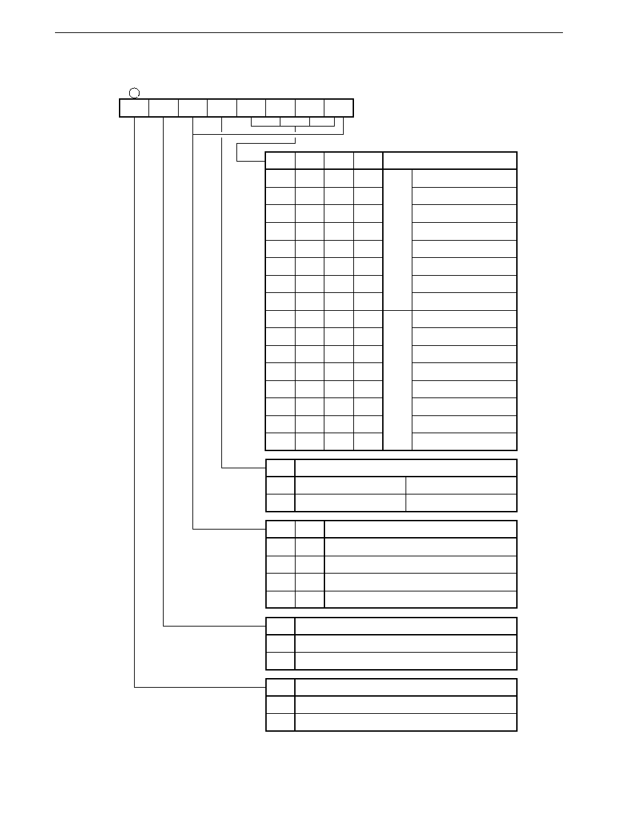
408
CHAPTER 16 A/D CONVERTER
Preliminary User's Manual U13987EJ1V0UM00
Figure 16-3. A/D Converter Mode Register (ADM) Format
CS
TRG
SCMD
FR
ANIS2 ANIS1 ANIS0
MS
7
6
5
4
3
2
1
0
ADM
0FF68H
Address
00H
After reset
R/W
R/W
ANIS2
0
0
0
0
1
1
1
1
0
0
0
0
1
1
1
1
A/D Conversion Operating Mode Setting
Scan
mode
(0/1)
ANIS1
0
0
1
1
0
0
1
1
0
0
1
1
0
0
1
1
ANIS0
0
1
0
1
0
1
0
1
0
1
0
1
0
1
0
1
MS
0
0
0
0
0
0
0
0
1
1
1
1
1
1
1
1
ANI0 input scanned
Input ANI0 & ANI1 scanned
Input ANI0 to ANI2 scanned
Input ANI0 to ANI3 scanned
Input ANI0 to ANI4 scanned
Input ANI0 to ANI5 scanned
Input ANI0 to ANI6 scanned
Input ANI0 to ANI7 scanned
ANI0 input selected
ANI1 input selected
ANI2 input selected
ANI3 input selected
ANI4 input selected
ANI5 input selected
ANI6 input selected
ANI7 input selected
FR
0
1
Conversion Speed Control (f
CLK
= 12.58 MHz)
180/f
CLK
(19.1 s)
120/f
CLK
(9.6 s)
Low-speed conversion
High-speed conversion
SCMD
0
1
0
1
Scan Mode Selection
Scan mode 0 (no delay control)
Scan mode 1 (delay control)
Select mode
Setting prohibited
MS
0
0
1
1
TRG
0
1
External Trigger Control
External trigger disabled
External trigger enabled
CS
0
1
A/D Conversion Operation Control
Stop A/D conversion operation
Start A/D conversion operation
�
�
Select
mode

409
CHAPTER 16 A/D CONVERTER
Preliminary User's Manual U13987EJ1V0UM00
Caution Once the A/D converter starts operating, conversion operations are performed repeatedly until the CS
bit of the A/D converter mode register (ADM) is cleared (to 0). Therefore, a superfluous interrupt may
be generated if ADM setting is performed after interrupt-related registers, etc., when A/D converter
mode conversion, etc., is performed. The result of this superfluous interrupt is that the conversion
result storage address appears to have been shifted when the scan mode is used. Also, when the select
mode is used, the first conversion result appears to have been an abnormal value, such as the
conversion result for the other channel. It is therefore recommended that A/D converter mode
conversion be carried out using the following procedure.
<1> Write to the ADM (CS bit must be set (to 1))
<2> Interrupt request flag (ADIF) clearance (to 0)
<3> Interrupt mask flag or interrupt service mode flag setting
Operations <1> to <3> should not be divided by an interrupt or macro service. When scan mode 0 (no
delay control) is used, in particular, you should ensure that the time between <1> and <2> is less than
the time taken by one A/D conversion operation.
Alternatively, the following procedure is recommended.
<1> Stop the A/D conversion operation by clearing (to 0) the CS bit of the ADM.
<2> Interrupt request flag (ADIF) clearance (to 0).
<3> Interrupt mask flag or interrupt service mode flag setting
<4> Write to the ADM
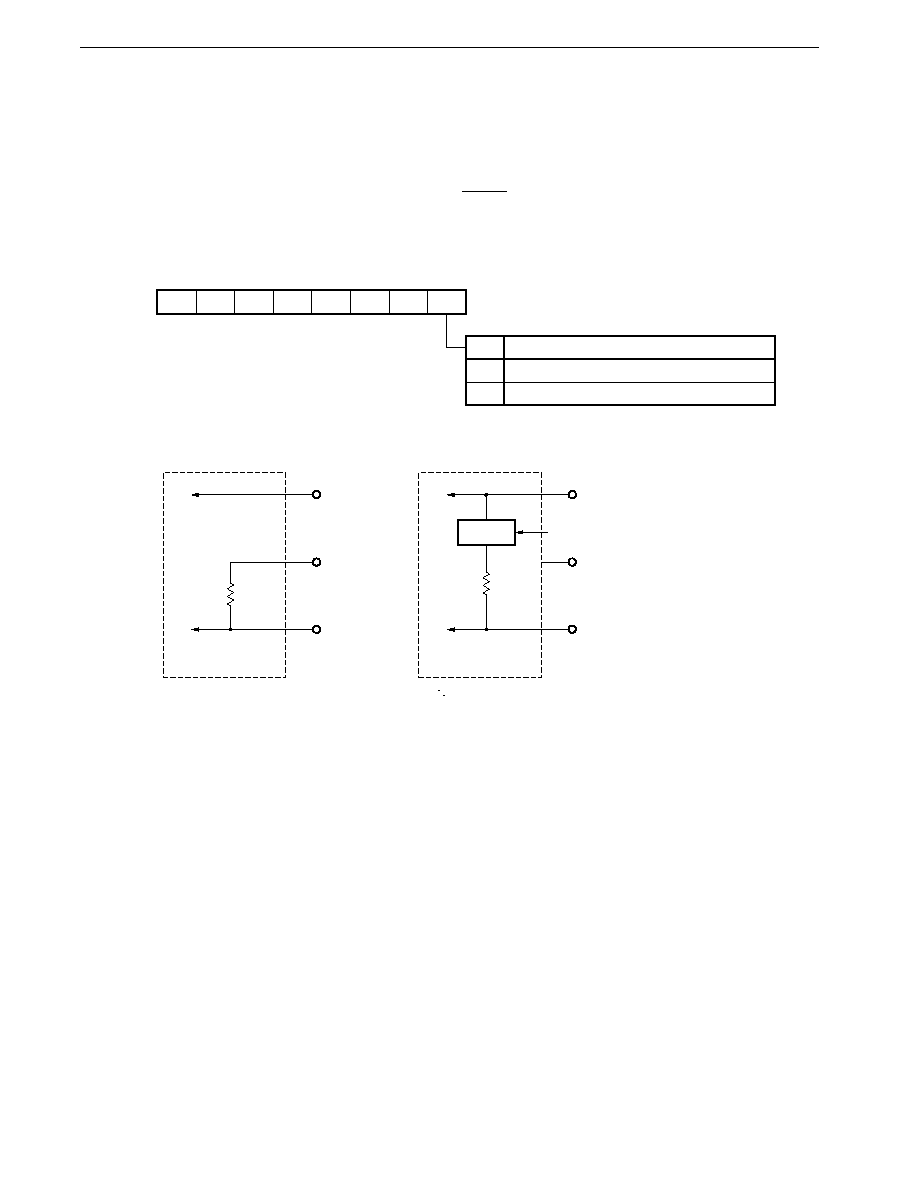
410
CHAPTER 16 A/D CONVERTER
Preliminary User's Manual U13987EJ1V0UM00
16.3 A/D Current Cut Select Register (IEAD)
IEAD is a register that selects whether AV
DD
and AV
REF1
are connected.
In a system where AV
DD
= AV
REF1
and a high accuracy is not required, open the AV
REF1
pin. In the normal mode, connect
AV
DD
and AV
REF1
. In the standby mode, the connection between these pins is disconnected to lower the power consumption.
IEAD is set with an 8-bit or 1-bit manipulation instruction. RESET input clears IEAD to 00H.
Figure 16-4. A/D Current Cut Select Register (IEAD) Format
7
0
6
0
5
0
4
0
3
0
2
0
1
0
0
IEAD0
Address
0FF6CH
After reset
00H
R/W
R/W
IEAD0
0
Controls Connection between AV
DD
and AV
REF1
Disconnects AV
DD
and AV
REF1
1
Connects AV
DD
and AV
REF1
IEAD
Symbol
Figure 16-5. A/D Current Cut Select Register Function
AV
DD
AV
REF1
AV
SS
Connection
control
Power consumption can be lowered by
controlling connection between AV
DD
and
AV
REF1
with IEAD0.
AV
DD
AV
REF1
(open)
AV
SS
AV
DD
AV
REF1
or when high
accuracy is required
AV
DD
=
AV
REF1
and when high
accuracy is not required
.
.

411
CHAPTER 16 A/D CONVERTER
Preliminary User's Manual U13987EJ1V0UM00
16.4 Operation
16.4.1 Basic A/D converter operation
(1) A/D conversion operation procedure
A/D conversion is performed by means of the following procedure:
(a) Analog pin selection and operation mode specification are set with the A/D converter mode register (ADM).
(b) Bit 7 (CS) of the ADM is set (to 1), and A/D conversion is started.
(c) When conversion starts, the MSB (bit 7) of the successive approximation register (SAR) is set (to 1) automatically.
(d) When bit 7 of the SAR is set (to 1), the tap selector sets the series resistor string voltage tap to
225
512
AV
REF1
(= 1/2 AV
REF1
).
(e) The voltage difference between the series resistor string voltage tap and the analog input is determined by the
voltage comparator. If the analog input is greater than (1/2) AV
REF1
, the MSB of the SAR remains set (to 1), and
if it is less than (1/2) AV
REF1
, the MSB is cleared (to 0).
(f)
Next, bit 6 of the SAR is set (to 1) automatically, and the next comparison is performed. Here, the series resistor
string voltage tap is selected according to the value of bit 7 for which the result has already been set, as shown
below.
�
Bit 7 = 1 ........
383
512
AV
REF1
=
3
4
AV
REF1
�
Bit 7 = 0 ........
127
512
AV
REF1
=
1
4
AV
REF1
This voltage tap is compared with the analog input voltage, and bit 6 of the SAR is manipulated as follows according
to the result:
�
Analog input voltage
voltage tap: Bit 6 = 1
�
Analog input voltage < voltage tap: Bit 6 = 0
(g) The same kind of comparison is continued up to the LSB (bit 0) of the SAR (binary search method).
.
.
.
.
.
.
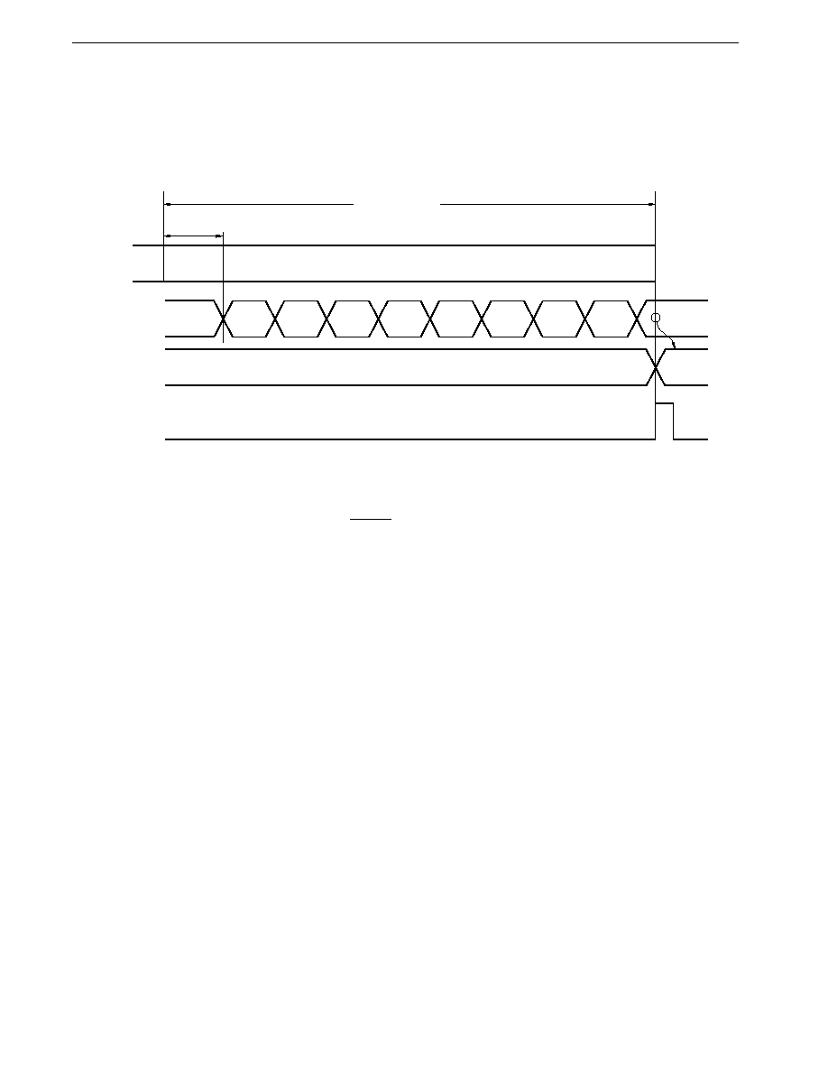
412
CHAPTER 16 A/D CONVERTER
Preliminary User's Manual U13987EJ1V0UM00
(h) When comparison of the 8 bits is completed, a valid digital result is left in the SAR, and that value is transferred
to the A/D conversion result register (ADCR) and latched.
An A/D conversion operation end interrupt request (INTAD) can be generated at the same time.
Figure 16-6. Basic A/D Converter Operation
80H
C0H
or
40H
Conversion
result
Conversion
result
Undefined
Conversion time
Sampling time
A/D converter
operation
SAR
ADCR
INTAD
A/D conversion
Sampling
A/D conversion operations are performed successively until the CS bit is cleared (to 0) by software. If a write operation
is performed on the ADM during an A/D conversion operation, the conversion operation is initialized, and if the CS bit is
set (to 1), conversion will be started from the beginning.
The contents of the ADCR are undefined after RESET input.

413
CHAPTER 16 A/D CONVERTER
Preliminary User's Manual U13987EJ1V0UM00
(2) Input voltage and conversion result
The relationship between the analog input voltage input to an analog input pin (ANI0 to ANI7) and the A/D conversion
result (value stored in ADCR) is shown by the following expression:
ADCR = INT(
V
AV
IN
REF1
�
256 + 0.5)
or
(ADCR � 0.5)
�
AV
REF1
256
V
IN
< (ADCR + 0.5)
�
AV
REF1
256
Remark
INT( ):
Function that returns the integer part of the value in ( )
V
IN
:
Analog input voltage
AV
REF1
: AV
REF1
pin voltage
ADCR:
ADCR value
Figure 16-7 shows the relationship between the analog input voltage and the A/D conversion result in graphic form.
Figure 16-7. Relationship between Analog Input Voltage and A/D Conversion Result
255
254
253
3
2
1
0
Input voltage/AV
REF1
1
512
1
256
3
512
2
256
5
512
3
256
507
512
254
256
509
512
255
256
511
512
1
A/D conversion
result (ADCR)

414
CHAPTER 16 A/D CONVERTER
Preliminary User's Manual U13987EJ1V0UM00
(3) A/D conversion time
The A/D conversion time is determined by the system clock frequency (f
CLK
) and the FR bit of the A/D converter mode
register (ADM).
The A/D conversion time includes the entire time required for one A/D conversion operation, and the sampling time
is also included in the A/D conversion time.
These values are shown in Table 16-1.
Table 16-1. A/D Conversion Time
System Clock (f
CLK
) Range
FR Bit
Conversion Time
Sampling Time
2 MHz
f
CLK
16 MHz
0
180/f
CLK
36/f
CLK
(11.3
�
s to 90
�
s)
(2.3
�
s to 18
�
s)
2 MHz
f
CLK
16 MHz
1
120/f
CLK
24/f
CLK
(7.5
�
s to 60
�
s)
(1.5
�
s to 12
�
s)
(4) A/D converter operation modes
There are two A/D converter operation modes, scan mode and select mode. These modes are selected according
to the setting of bit 0 (MS) of the A/D converter mode register (ADM). In addition, scan mode 0 or 1 can be selected
by bit 5 (SCMD) of the ADM.
Operation in either mode continues until the ADM is rewritten.
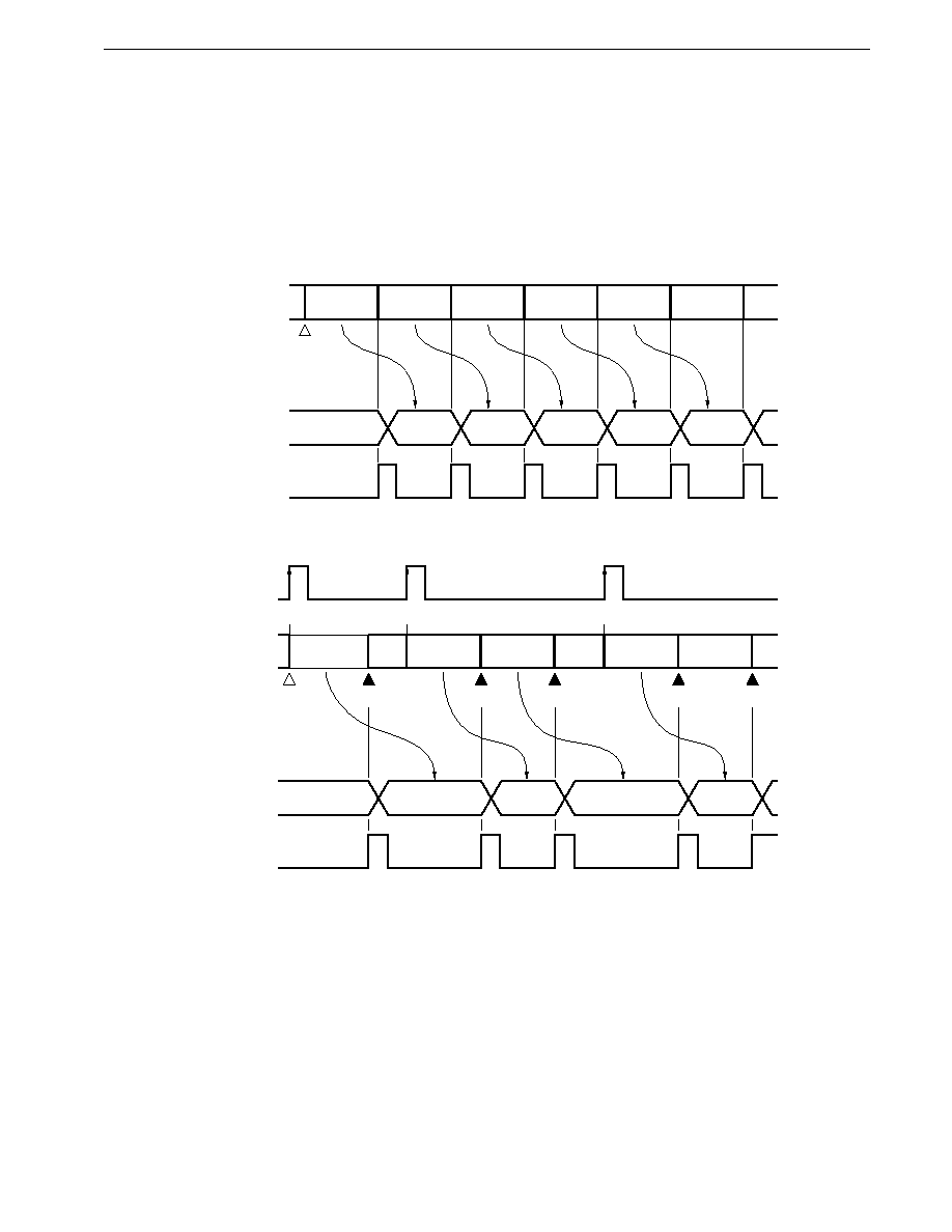
415
CHAPTER 16 A/D CONVERTER
Preliminary User's Manual U13987EJ1V0UM00
16.4.2 Select mode
One analog input is specified by bits 1 to 3 (ANIS0 to ANIS2) of the A/D converter mode register (ADM), and A/D
conversion of the specified analog input pin is started. The conversion result is stored in the A/D conversion result register
(ADCR). An A/D conversion end interrupt request (INTAD) is generated at the end of each conversion operation.
Figure 16-8. Select Mode Operation Timing
(a) TRG bit
0
ANI3
ANI3
ANI3
ANI3
ANI3
ANI3
ANI3
ANI3
ANI3
ANI3
ANI3
Conversion start
(
ADCR
A/D conversion
INTAD
(
CS
1
MS
1
ANIS2 to ANIS0
011
(b) TRG bit
1
Conversion end
Conversion end
Conversion end
Conversion end
Conversion end
(
(
ANI0
A/D conversion
ANI0
ANI0
Initialization
Initialization
Initialization
INTP5
ANI0
ANI0
ANI0
ANI0
ANI0
ANI0
ANI0
ANI0
ADCR
INTAD
Conversion start
CS
1
MS
1
ANIS2 to ANIS0
000
416
CHAPTER 16 A/D CONVERTER
Preliminary User's Manual U13987EJ1V0UM00
16.4.3 Scan mode
Two scan modes, 1 and 0, are available. In scan mode 0, delay control that takes delay in reading the A/D conversion
result by the CPU into consideration can be performed. In scan mode 1, no delay control is performed but the A/D conversion
interval is fixed.
Generally, use of scan mode 1 is recommended.
(1) Scan mode 0 (bit 5 (SCMD) of A/D converter mode register (ADM) = 0)
Input from the analog input pins specified by bits 1 to 3 (ANIS0 to ANIS2) of the ADM is selected and converted in
order.
For example, if ANIS2 to ANIS0 of the ADM = 001, ANI0 and ANI1 will be scanned repeatedly (ANI0
ANI1
ANI0
ANI1
...). In the scan mode, at the end of the conversion operation for each input the conversion value is stored
in the A/D conversion result register (ADCR) and an A/D conversion end interrupt request (INTAD) is generated.
Figure 16-9. Scan Mode 0 Operation Timing
(a) TRG bit
0
ANI0
ANI0
ANI1
ANI0
ANI1
ANI0
ANI1
Conversion end Conversion end
Conversion end
Conversion end
Conversion end
Conversion end
ANI1
ANI0
ANI1
ANI0
Conversion start
(
ADCR
A/D conversion
INTAD
(
CS
1
MS
0
ANIS2 to ANIS0
001
(b) TRG bit
1
ANI0
ANI1
ANI0
A/D conversion
ANI2
ANI0
ANI1
ANI0
Initialization
Initialization Initialization
Initialization
ANI0
ANI1
ADCR
ANI0
Conversion end Conversion end
Conversion end
Conversion end
Conversion start
(
(
INTAD
INTP5
CS
1
MS
1
ANIS2 to ANIS0
010
417
CHAPTER 16 A/D CONVERTER
Preliminary User's Manual U13987EJ1V0UM00
(2) Scan mode 1 (bit 5 (SCMD) of A/D converter mode register (ADM) = 1)
When bit 5 of the ADM is set (to 1), the analog input pins specified by bits 1 to 3 (ANIS0 to ANIS2) are selected, and
subjected to conversion, in order. If an A/D conversion result register (ADCR) read is not performed by the CPU by
the end of the next A/D conversion after A/D conversion end (INTAD) generation, conversion is restarted without
performing INTAD generation, ADCR updating or channel updating (see Figure 16-10).
If an ADCR read is performed by the CPU before the end of the next A/D conversion, the same operation as in scan
mode 0 is performed.
Figure 16-10. Scan Mode 1 Operation Timing
ANI1
A/D conversion
ANI2
ANI2
ANI3
ANI0
ANI0
ANI0
ADCR
ANI1
ANI2
ANI3
INTAD
ADCR read
Channel updating disabled
ADCR updating disabled
Interrupt generation disabled
418
CHAPTER 16 A/D CONVERTER
Preliminary User's Manual U13987EJ1V0UM00
16.4.4 A/D conversion operation start by software
An A/D conversion operation start by software is performed by writing a value to the A/D converter mode register (ADM)
that sets the TRG bit of the ADM register to 0 and the CS bit to 1.
If a value is written to the ADM during an A/D conversion operation (CS bit = 1) such that the TRG bit is set to 0 and
the CS bit to 1 again, the A/D conversion operation being performed at that time is suspended, and A/D conversion is started
immediately in accordance with the written value.
Once A/D conversion operation is started, as soon as one A/D conversion operation ends the next A/D conversion
operation is started in accordance with the operation mode set by the ADM, and conversion operations continue repeatedly
until an instruction that writes to the ADM is executed.
When A/D conversion operation is started by software (TRG bit = 0), INTP5 pin (P26 pin) input does not affect the A/D
conversion operation.
(1) Select mode A/D conversion operation
An A/D conversion operation is started on the analog input pin set by the A/D converter mode register (ADM). As soon
as the A/D conversion operation ends, another A/D conversion operation is performed on the same analog input pin.
An A/D conversion end interrupt request (INTAD) is generated at the end of each A/D conversion operation.
Figure 16-11. Software Start Select Mode A/D Conversion Operation
ANIn
A/D conversion
ANIn
ANIm
ANIm
ANIm
ANIn
ANIn
ANIn
ANIm
ANIm
ADM rewrite
CS
1, TRG
0
Conversion start
CS
1, TRG
0
ADCR
INTAD
Remark
n = 0, 1, ..., 7
m = 0, 1, ..., 7
419
CHAPTER 16 A/D CONVERTER
Preliminary User's Manual U13987EJ1V0UM00
(2) Scan mode A/D conversion operation
When conversion operation is started, an A/D conversion operation is started on the ANI0 pin input. When the A/D
conversion operation ends, an A/D conversion operation is started on the next analog input pin. An A/D conversion
end interrupt request (INTAD) is generated at the end of each A/D conversion operation.
Figure 16-12. Software Start Scan Mode A/D Conversion Operation
ADM rewrite
CS
1
TRG
0
Interrupt request
acknowledgment
ANI0
ANI1
ANI2
ANI0
ANI1
ANI2
ANI0
ANI1
ANI0
ANI0
ANI1
ANI2
ANI0
ANI1
ANI2
ANI0
Conversion start
CS
1
TRG
0
A/D conversion
(ANI0 to ANI2
scanned)
ADCR
INTAD

420
CHAPTER 16 A/D CONVERTER
Preliminary User's Manual U13987EJ1V0UM00
16.4.5 A/D conversion operation start by hardware
An A/D conversion operation start by hardware is made possible by setting both the TRG bit and the CS bit of the
A/D converter mode register (ADM) to 1. When the TRG bit and the CS bit of the ADM are both set to 1, external signals
are placed in the standby state, and an A/D conversion operation is started when a valid edge is input to the INTP5 pin
(P26 pin).
If another valid edge is input to the INTP5 pin after the A/D conversion operation has been started by a valid edge input
to the INTP5 pin, the A/D conversion operation being performed at that time is suspended, and A/D conversion is performed
from the beginning in accordance with the contents set in the ADM.
If a value is written to the ADM during an A/D conversion operation (CS bit = 1) such that the TRG bit and CS bit are
both set to 1 again, the A/D conversion operation being performed at that time is suspended (the standby state is also
suspended), and a standby state is entered in which the A/D converter waits for input of a valid edge to the INTP5 pin in
the A/D conversion operation mode in accordance with the written value, and a conversion operation is started when a valid
edge is input.
Use of this function allows A/D conversion operations to be synchronized with external signals. Once A/D conversion
operation is started, as soon as one A/D conversion operation ends the next A/D conversion operation is started in
accordance with the operation mode set by the ADM (the A/D converter does not wait for INTP5 pin input), and conversion
operations continue repeatedly until an instruction that writes to the ADM is executed, or a valid edge is input to the INTP5
pin.
Caution Approximately 10
�
s is required from the time a valid edge is input to the INTP5 pin until the A/D
conversion operation is actually started. This delay must be taken into account in the design stage.
See CHAPTER 22 EDGE DETECTION FUNCTION for details of the edge detection function.
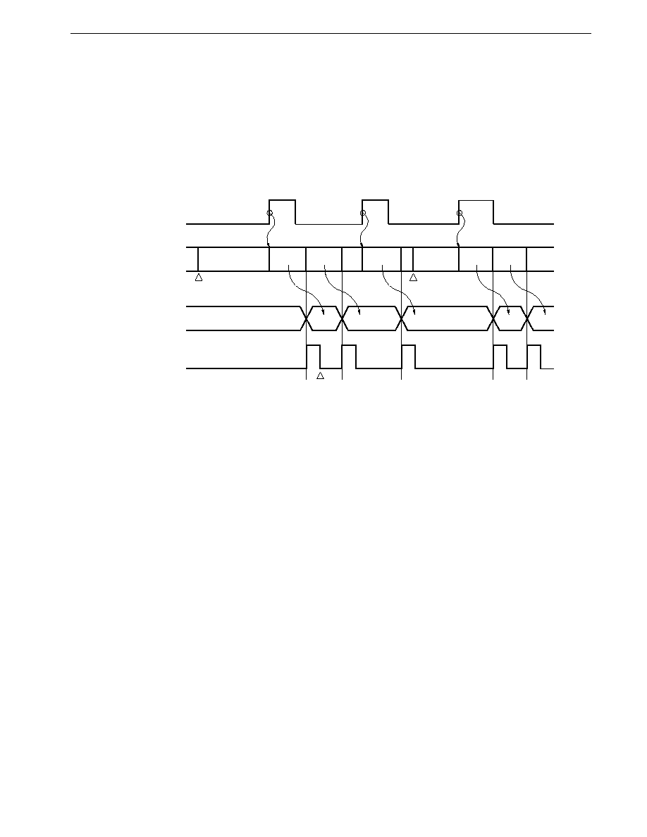
421
CHAPTER 16 A/D CONVERTER
Preliminary User's Manual U13987EJ1V0UM00
(1) Select mode A/D conversion operation
An A/D conversion operation is started on the analog input pin set by the A/D converter mode register (ADM). As soon
as the A/D conversion operation ends, another A/D conversion operation is performed on the same analog input pin.
An A/D conversion end interrupt request (INTAD) is generated at the end of each A/D conversion operation.
If a valid edge is input to the INTP5 pin during an A/D conversion operation, the A/D conversion operation being
performed at that time is suspended, and a new A/D conversion operation is started.
Figure 16-13. Hardware Start Select Mode A/D Conversion Operation
Standby state
ANIn
ANIn
ANIn
ANIn
ANIn
ANIm
ANIm
Standby state
ANIn
ANIn
ANIn
ANIm
ADM rewrite
CS
1, TRG
1
ADM rewrite
CS
1, TRG
1
INTAD acknowledgment
ADCR
INTAD
A/D conversion
INTP5 pin input
(rising edge valid)
Remark
n = 0, 1, ..., 7
m = 0, 1, ..., 7
(2) Scan mode A/D conversion operation
When conversion operation is started, an A/D conversion operation is started on the ANI0 pin input. When the A/D
conversion operation ends, an A/D conversion operation is started on the next analog input pin. An A/D conversion
end interrupt request (INTAD) is generated at the end of each A/D conversion operation.
If a valid edge is input to the INTP5 pin during an A/D conversion operation, the A/D conversion operation being
performed at that time is suspended, and a new A/D conversion operation is started on the ANI0 pin input.
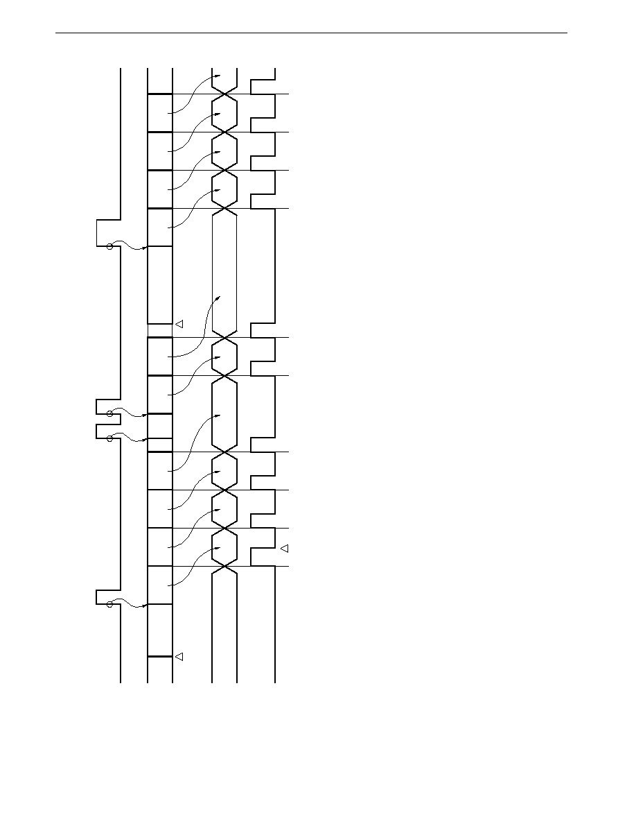
422
CHAPTER 16 A/D CONVERTER
Preliminary User's Manual U13987EJ1V0UM00
Figure 16-14. Hardware Start Scan Mode A/D Conversion Operation
Standby state
ANI0
ANI1
ANI2
ANI0
ANI0
ANI0
ANI1
ANI2
Standby state
ANI0
ANI1
ANI2
ANI0
ANI1
ANI0
ANI1
ANI2
ANI0
ANI0
ANI1
ANI0
ANI1
ANI2
ADM rewrite
CS
1, TRG
1
ADM rewrite
CS
1, TRG
1
A/D conversion
(ANI0 to ANII2
scanned)
ADCR
INTAD
INTP5 pin input
(rising edge valid)
INTAD aknowledgment

423
CHAPTER 16 A/D CONVERTER
Preliminary User's Manual U13987EJ1V0UM00
16.5 External Circuit of A/D Converter
The A/D converter is provided with a sample & hold circuit to stabilize its conversion operation. This sample & hold circuit
outputs sampling noise during sampling immediately after an A/D conversion channel has been changed.
To absorb this sampling noise, an external capacitor must be connected. If the impedance of the signal source is high,
an error may occur in the conversion result due to the sampling noise. Especially when the scan mode is used, the
impedance of the signal source must be kept low because the channel whose signal is to be converted changes one after
another.
One way to absorb the sampling noise is to increase the capacitance of the capacitor. However, if the capacitance is
increased too much, the sampling noise is accumulated. Therefore, the most effective way is to reduce the resistance
component.
16.6 Cautions
(1) Range of voltages applied to analog input pins
The following must be noted concerning A/D converter analog input pins ANI0 to ANI7 (P70 to P77).
�
A voltage outside the range AV
SS
to AV
REF1
should not be applied to pins subject to A/D conversion during an A/D
conversion operation.
If this restriction is not observed, the
�
PD784938 may be damaged.
(2) Hardware start A/D conversion
Approximately 10
�
s is required from the time a valid edge is input to the INTP5 pin until the A/D conversion operation
is actually started. This delay must be taken into account in the design stage. See CHAPTER 22 EDGE DETECTION
FUNCTION for details of the edge detection function.
(3) Connecting capacitor to analog input pins
A capacitor should be connected between the analog input pins (ANI0 to ANI7) and AV
SS
and between the reference
voltage input pin (AV
REF1
) and AV
SS
to prevent misoperation due to noise.
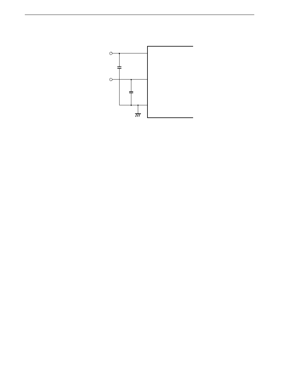
424
CHAPTER 16 A/D CONVERTER
Preliminary User's Manual U13987EJ1V0UM00
Figure 16-15. Example of Capacitor Connection on A/D Converter Pins
Analog
input
Reference
voltage input
100 to
500 pF
ANI0 to ANI7
AV
REF1
AV
SS
�
PD784938
(4) When the STOP mode or IDLE mode is used, the consumption current should be reduced by clearing (to 0) the CS
bit before entering the STOP or IDLE mode. If the CS bit remains set (to 1), the conversion operation will be stopped
by entering the STOP or IDLE mode, but the power supply to the voltage comparator will not be stopped, and therefore
the A/D converter consumption current will not be reduced.
(5) Once the A/D converter starts operating, conversion operations are performed repeatedly until the CS bit of the A/D
converter mode (ADM) is cleared (to 0). Therefore, a superfluous interrupt may be generated if ADM setting is performed
after interrupt-related registers, etc., are set when A/D converter mode conversion, etc., is performed. The result of
this superfluous interrupt is that the conversion result storage address appears to have been shifted when the scan
mode is used. Also, when the select mode is used, the first conversion result appears to have been an abnormal value,
such as the conversion result for the other channel. It is therefore recommended that A/D converter mode conversion
be carried out using the following procedure.
<1> Write to the ADM (CS bit must be set (to 1))
<2> Interrupt request flag (ADIF) clearance (to 0)
<3> Interrupt mask flag or interrupt service mode flag setting
Operations <1> to <3> should not be divided by an interrupt or macro service. When scan mode 0 (no delay control)
is used, in particular, you should ensure that the time between <1> and <2> is less than the time taken by one A/D
conversion operation.
Alternatively, the following procedure is recommended.
<1> Stop the A/D conversion operation by clearing (to 0) the CS bit of the ADM.
<2> Interrupt request flag (ADIF) clearance (to 0).
<3> Interrupt mask flag or interrupt service mode flag setting
<4> Write to the ADM
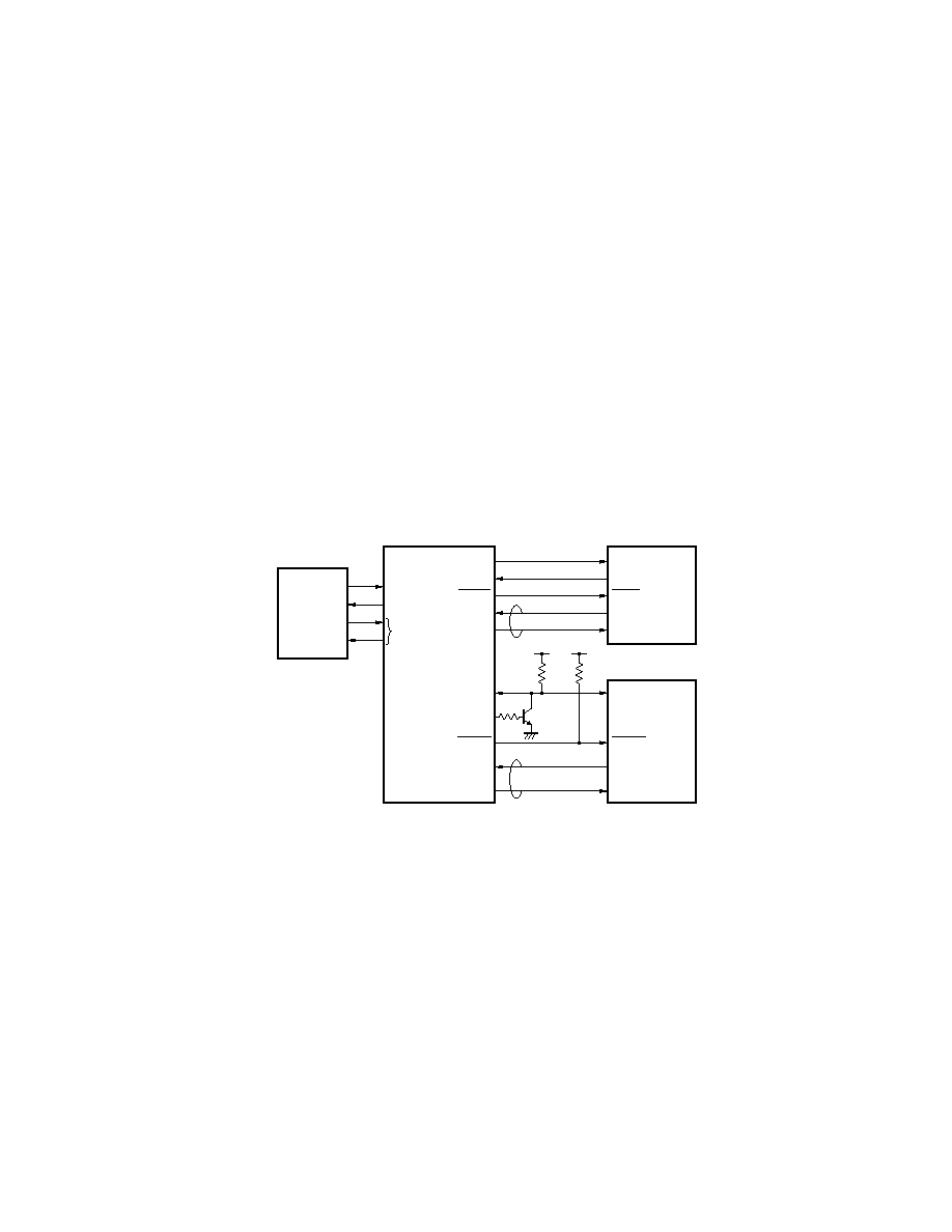
425
Preliminary User's Manual U13987EJ1V0UM00
CHAPTER 17 OUTLINE OF SERIAL INTERFACE
The
�
PD784938 Subseries is provided with four independent serial interface channels. Therefore, communication with
an external system and local communication within the system can be simultaneously executed by using these four
channels.
�
Asynchronous serial interface (UART)/3-wire serial I/O (IOE)
�
2 channels
Refer to CHAPTER 18.
�
Clocked serial interface (CSI)
�
2 channels
�
3-wire serial I/O mode (MSB/LSB first)
Refer to CHAPTER 19.
Figure 17-1 shows an example of the serial interface.
Figure 17-1. Example of Serial Interface
UART + 3-wire serial I/O + 2-wire serial I/O
RS-232-C
driver/
receiver
PD4711A
[UART]
RxD
TxD
Port
SO1
SI1
SCK1
INTPm
Port
SI0
SO0
SCK0
INTPn
PD784938 (master)
Note
V
DD
V
DD
[2-wire serial I/O]
SI
SO
SCK
Port
INT
SB0
Port
INT
SCK0
Slave
Slave
[3-wire serial I/O]
Port
Note
�
�
Note Handshake line

426
Preliminary User's Manual U13987EJ1V0UM00
[MEMO]

427
Preliminary User's Manual U13987EJ1V0UM00
CHAPTER 18 ASYNCHRONOUS SERIAL INTERFACE/3-WIRE SERIAL I/O
The
�
PD784938 incorporates two serial interface channels for which asynchronous serial interface (UART) mode or
3-wire serial I/O (IOE) mode can be selected.
The two UART/IOE channels have completely identical functions. In this chapter, therefore, unless stated otherwise,
UART/IOE1 will be described as representative of both UART/IOEs. When used as UART2/IOE2, the UART/IOE1 register
names, bit names and pin names should be read as their UART2/IOE2 equivalents as shown in Table 18-1.
Table 18-1. Differences between UART/IOE1 and UART2/IOE2 Names
Item
UART/IOE1
UART2/IOE2
Pin names
P25/ASCK/SCK1, P30/RxD/SI1,
P12/ASCK2/SCK2, P13/RxD2/SI2,
P31/TxD/SO2
P14/TxD2/SO2
Asynchronous serial interface mode register
ASIM
ASIM2
Asynchronous serial interface mode register bit names
TXE, RXE, PS1, PS0, CL, SL,
TXE2, RXE2, PS21, PS20, CL2,
ISRM, SCK
SL2, ISRM2, SCK2
Asynchronous serial interface status register
ASIS
ASIS2
Asynchronous serial interface status register bit names
PE, FE, OVE
PE2, FE2, OVE2
Clocked serial interface mode register
CSIM1
CSIM2
Clocked serial interface mode register bit names
CTXE1, CRXE1, DIR1, CSCK1
CTXE2, CRXE2, DIR2, CSCK2
Baud rate generator control register
BRGC
BRGC2
Baud rate generator control register bit names
TPS0 to TPS3, MDL0 to MDL3
TPS20 to TPS23, MDL20 to MDL23
Interrupt request names
INTSR/ITCSI1, INTSER, INTST
INTSR2/INTCSI2, INTSER2,
INTST2
Interrupt control registers and bit names used in this
SRIC, CSIIC1, SERIC, STIC,
SRIC2, CSIIC2, SERIC2, STIC2,
chapter
SRIF, CSIIF1, SERIF, STIF
SRIF2, SCIIF2, SERIF2, STIF2
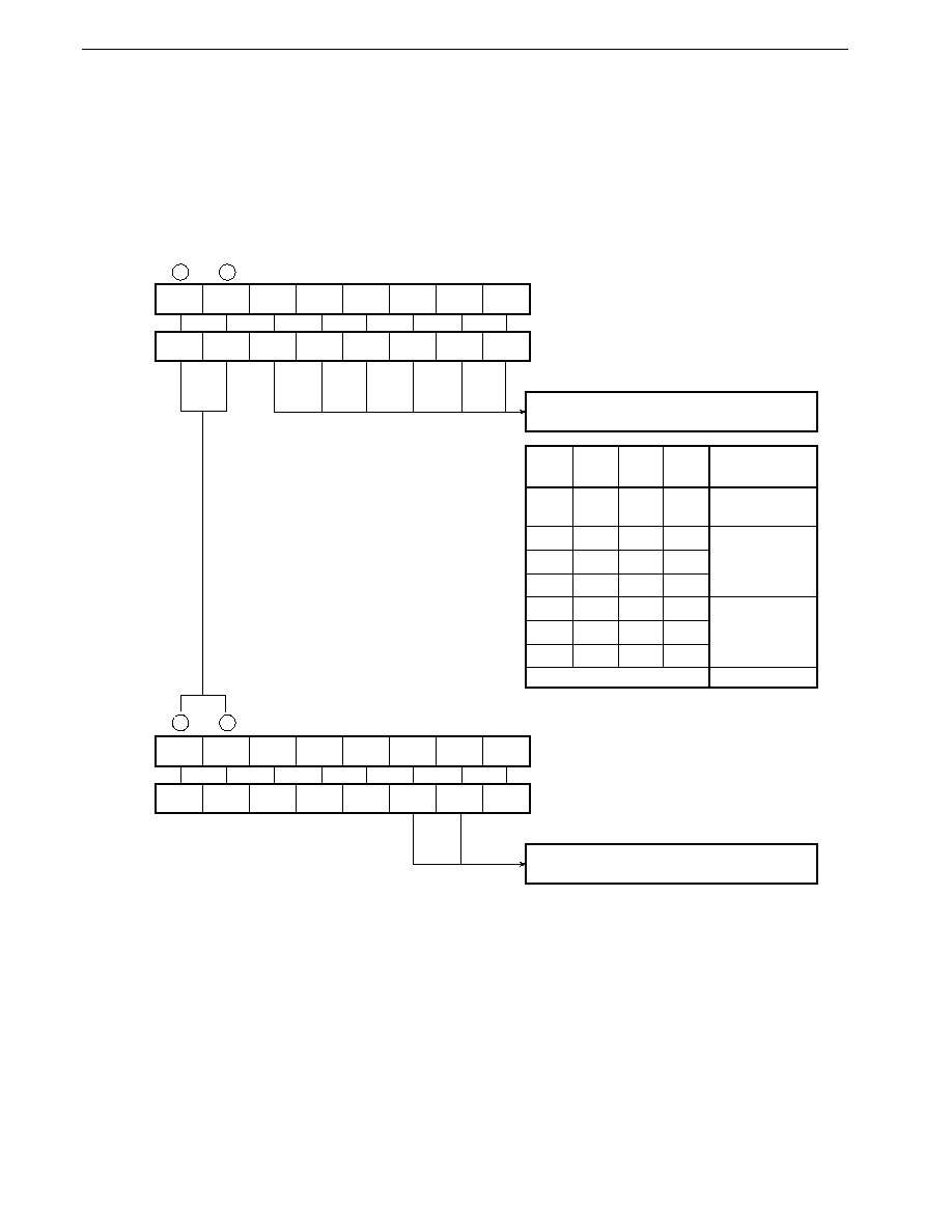
428
CHAPTER 18 ASYNCHRONOUS SERIAL INTERFACE/3-WIRE SERIAL I/O
Preliminary User's Manual U13987EJ1V0UM00
18.1 Switching between Asynchronous Serial Interface Mode and 3-Wire Serial I/O Mode
The asynchronous serial interface mode and 3-wire serial I/O mode cannot be used simultaneously. Switching between
these modes is performed in accordance with the settings of the asynchronous serial interface mode register (ASIM/ASIM2)
and the clocked serial interface mode register (CSIM1/CSIM2) as shown in Figure 18-1.
Figure 18-1. Switching between Asynchronous Serial Interface Mode and 3-Wire Serial I/O Mode
7
TXE
ASIM
6
RXE
5
PS1
4
PS0
3
CL
2
SL
1
ISRM
0
SCK
TXE2
RXE2
PS21
PS20
CL2
SL2
ISRM2 SCK2
Asynchronous serial interface mode operation
specification (see Figure 18-3)
After reset
Address
Address
R/W
R/W
00H
0FF88H
ASIM2
R/W
00H
0FF89H
TXE
TXE2
RXE
RXE2
CTXE1
CTXE2
CRXE1
CRXE2
Operation Mode
Setting prohibited
Other than the above
Operation-stopped
mode
3-wire serial
I/O mode
Asynchronous
serial interface
mode
0
0
0
0
0
0
0
0
0
0
1
1
1
0
0
1
0
1
1
0
1
1
0
0
0
0
0
0
7
CTXE1
CSIM1
6
CRXE1
5
0
4
0
3
0
2
DIR1
1
CSCK1
0
0
CTXE2 CRXE2
0
0
0
DIR2
CSCK2
0
After reset
R/W
R/W
00H
0FF84H
CSIM2
R/W
00H
0FF85H
3-wire serial I/O mode operation specification
(see Figure 18-11)

429
CHAPTER 18 ASYNCHRONOUS SERIAL INTERFACE/3-WIRE SERIAL I/O
Preliminary User's Manual U13987EJ1V0UM00
18.2 Asynchronous Serial Interface Mode
A UART (Universal Asynchronous Receiver Transmitter) is incorporated as the asynchronous serial interface. With this
method, one byte of data is transmitted following a start bit, and full-duplex operation is possible.
A baud rate generator is incorporated, enabling communication to be performed at any of a wide range of baud rates.
Also, the baud rate can be defined by scaling the clock input to the ASCK pin.
18.2.1 Configuration in asynchronous serial interface mode
The block diagram of the asynchronous serial interface is described in Figure 18-2.
See 18.4 Baud Rate Generator for details of the baud rate generator.

430
CHAPTER 18 ASYNCHRONOUS SERIAL INTERFACE/3-WIRE SERIAL I/O
Preliminary User's Manual U13987EJ1V0UM00
Figure 18-2. Asynchronous Serial Interface Block Diagram
Internal bus
1/8
1/8
Serial receive
buffer
Shift register
Reception
control
parity check
FE
FE2
PE
PE2
OVE
OVE2
RESET
ASIS, ASIS2
TXE
TXE2
RXE
RXE2 PS21
PS0
PS20
CL
CL2
SL
SL2
ISRM
ISRM2
SCK
SCK2
RXB, RXB2
P30/R
X
D,
P13/R
X
D2
P31/T
X
D,
P14/T
X
D2
Serial transmit
shift register
Transmission
control parity
addition
INTSER,
INTSER2
INTST,
TXS,
TXS2
INTST2
1
m
INTSR, INTSR2
1
m
1
2
n
Selector
P25/ASCK,
P12/ASCK2
f
XX
Baud rate generator
RESET
ASIM, ASIM2
1/8
PS1

431
CHAPTER 18 ASYNCHRONOUS SERIAL INTERFACE/3-WIRE SERIAL I/O
Preliminary User's Manual U13987EJ1V0UM00
(1) Serial receive buffer (RXB/RXB2)
This is the register that holds the receive data. Each time one byte of data is received, the receive data is transferred
from the shift register.
If a 7-bit data length is specified, receive data is transferred to bits 0 to 6 of RXB/RXB2, and the MSB of RXB/RXB2
is always "0".
RXB/RXB2 can be read only by an 8-bit manipulation instruction. The contents of RXB/RXB2 are undefined after RESET
input.
(2) Serial transmit shift register (TXS/TXS2)
This is the register in which the data to be transmitted is set. Data written to the TXS/TXS2 is transmitted as serial
data.
If a 7-bit data length is specified, bits 0 to 6 of the data written in the TXS/TXS2 are treated as transmit data. A transmit
operation starts when a write to the TXS/TXS2 is performed. The TXS/TXS2 cannot be written to during a transmit
operation.
TXS/TXS2 can be written to only with an 8-bit manipulation instruction. The contents of TXS/TXS2 are undefined after
RESET input.
(3) Shift register
This is the shift register that converts the serial data input to the RxD pin to parallel data. When one byte of data is
received, the receive data is transferred to the receive buffer.
The shift register cannot be manipulated directly by the CPU.
(4) Reception control parity check
Receive operations are controlled in accordance with the contents set in the asynchronous serial interface mode register
(ASIM/ASIM2). In addition, parity error and other error checks are performed during receive operations, and if an error
is detected, a value is set in the asynchronous serial interface status register (ASIS/ASIS2) according to the type of
error.
(5) Transmission control parity addition
Transmission operation is controlled by appending a start bit, parity bit, and stop bit to the data written to the serial
transmit shift registers (TXS/TXS2) in accordance with the contents set to the asynchronous serial interface mode
registers (ASIM/ASIM2).
(6) Selector
Selects the baud rate clock source.

432
CHAPTER 18 ASYNCHRONOUS SERIAL INTERFACE/3-WIRE SERIAL I/O
Preliminary User's Manual U13987EJ1V0UM00
18.2.2 Asynchronous serial interface control registers
(1) Asynchronous serial interface mode register (ASIM), Asynchronous serial interface mode register 2 (ASIM2)
ASIM and ASIM2 are 8-bit registers that specify the UART mode operation.
These registers can be read or written to with an 8-bit manipulation instruction or bit manipulation instruction. The format
of ASIM and ASIM is shown in Figure 18-3.
RESET input clears these registers to 00H.
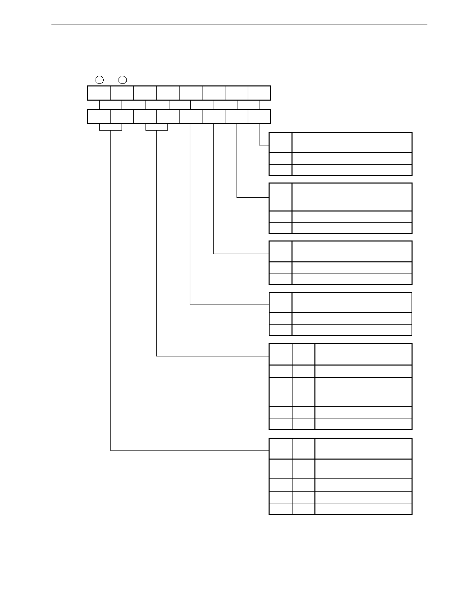
433
CHAPTER 18 ASYNCHRONOUS SERIAL INTERFACE/3-WIRE SERIAL I/O
Preliminary User's Manual U13987EJ1V0UM00
Figure 18-3. Format of Asynchronous Serial Interface Mode Register (ASIM) and Asynchronous Serial
Interface Mode Register 2 (ASIM2)
7
TXE
ASIM
6
RXE
5
PS1
4
PS0
3
CL
2
SL
1
ISRM
0
SCK
TXE2
RXE2
PS21
PS20
CL2
SL2
ISRM2 SCK2
After reset
Address
R/W
R/W
00H
0FF88H
ASIM2
R/W
00H
0FF89H
SCK
SCK2
Specification of Input Clock to Baud Rate
Generator
External clock input (ASCK, ASCK2)
0
Internal clock (fxx)
1
CL
CL2
Data Character Length Specification
7 bits
8 bits
SL
SL2
Stop Bit Length Specification
(Transmission Only)
1 bit
0
2 bits
1
0
1
PS0
PS20
Parity Bit Specification
No parity
Transmission = 0 parity addition
Reception = Parity error not
generated
Odd parity
0
1
PS1
PS21
0
0
1
0
Even parity
1
1
ISRM
ISRM2
Specification of Enabling/Disabling of
Reception Completion Interrupt
Generation in Case of Receive Error
Enabled
0
Disabled
1
TXE
TXE2
Transmit/Receive Operation
Transmission/reception disabled,
or 3-wire serial I/O mode
Transmission enabled
Reception enabled
0
1
RXE
RXE2
0
0
1
0
Transmission/reception enabled
1
1
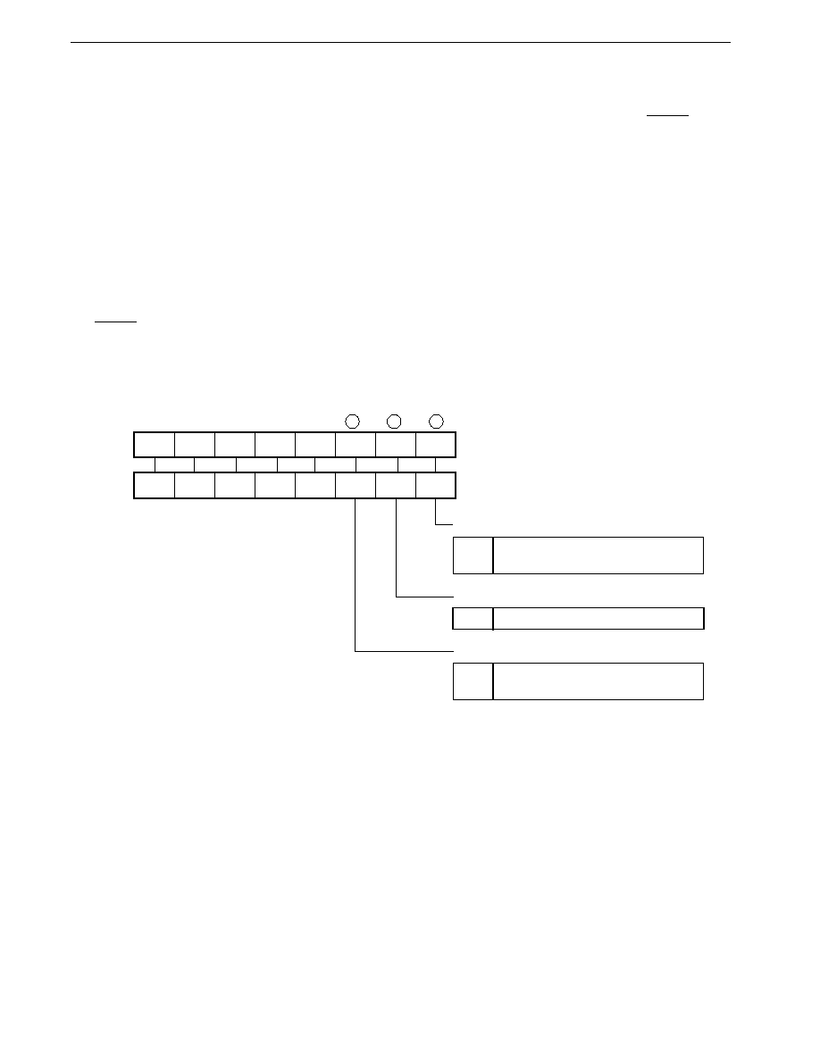
434
CHAPTER 18 ASYNCHRONOUS SERIAL INTERFACE/3-WIRE SERIAL I/O
Preliminary User's Manual U13987EJ1V0UM00
Caution An asynchronous serial interface mode register (ASIM/ASIM2) rewrite should not be performed during
a transmit operation. If an ASIM/ASIM2 register rewrite is performed during a transmit operation,
subsequent transmit operations may not be possible (normal operation is restored by RESET input).
Software can determine whether transmission is in progress by using a transmission completion
interrupt (INTST/INTST2) or the interrupt request flag (STIF/STIF2) set by INTST/INTST2.
(2) Asynchronous serial interface status register (ASIS), Asynchronous serial interface status register 2 (ASIS2)
ASIS and ASIS2 contain flags that indicate the error contents when a receive error occurs. Flags are set (to 1) when
a receive error occurs, and cleared (to 0) when data is read from the serial receive buffer (RXB/RXB2). If the next
data is received before RXB/RXB2 is read, the overrun error flag (OVE/OVE2) is set (to 1), and the other error flags
are cleared (to 0) (if there is an error in the next data, the corresponding error flag is set (to 1)).
These registers can be read only with an 8-bit manipulation instruction or bit manipulation instruction. The format of
ASIS and ASIS2 is shown in Figure 18-4.
RESET input clears these registers to 00H.
Figure 18-4. Format of Asynchronous Serial Interface Status Register (ASIS) and Asynchronous Serial
Interface Status Register 2 (ASIS2)
7
0
ASIS
6
0
5
0
4
0
3
0
2
PE
1
FE
0
OVE
0
0
0
0
0
PE2
FE2
OVE2
After reset
Address
R/W
R
00H
0FF8AH
ASIS2
R
Overrun error flag
00H
0FF8BH
Next receive completed before data is
read from receive buffer
1
Parity error flag
Transmit data parity specification and
receive data parity do not match
1
Framing error flag
Stop bit not detected
1
Caution The serial receive buffer (RXB/RXB2) must be read even if there is a receive error. If RXB/RXB2 is not
read, an overrun error will occur when the next data is received, and the receive error state will continue
indefinitely.
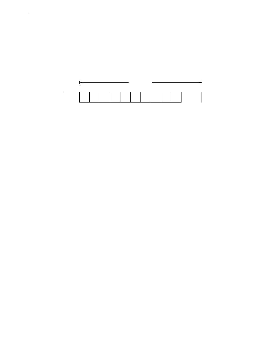
435
CHAPTER 18 ASYNCHRONOUS SERIAL INTERFACE/3-WIRE SERIAL I/O
Preliminary User's Manual U13987EJ1V0UM00
18.2.3 Data format
Serial data transmission/reception is performed in full-duplex asynchronous mode.
The transmit/receive data format is shown in Figure 18-5. One data frame is made up of a start bit, character bits, parity
bit, and stop bit(s).
Character bit length specification, parity selection and stop bit length specification for one data frame are performed by
means of the asynchronous serial interface mode register (ASIM).
Figure 18-5. Asynchronous Serial Interface Transmit/Receive Data Format
1 data frame
Start
bit
D0
D1
D2
D3
D4
D5
D6
D7
Parity
bit
Stop
bit(s)
�
Start bit ������������������������ 1 bit
�
Character bits ������������� 7 bits/8 bits
�
Parity bits �������������������� Even parity/odd parity/0 parity/no parity
�
Stop bits ���������������������� 1 bit/2 bits
The serial transfer rate is selected in accordance with the asynchronous serial interface mode register and baud rate
generator settings. If a serial data receive error occurs, the nature of the receive error can be determined by reading the
asynchronous serial interface status register (ASIS) status.

436
CHAPTER 18 ASYNCHRONOUS SERIAL INTERFACE/3-WIRE SERIAL I/O
Preliminary User's Manual U13987EJ1V0UM00
18.2.4 Parity types and operations
The parity bit is used to detect a bit error in the communication data. Normally, the same kind of parity bit is used on
the transmission side and the reception side. With even parity and odd parity, 1 bit (odd number) errors can be detected.
With 0 parity and no parity, errors cannot be detected.
�
Even parity
If the number of bits with a value of "1" in the transmit data is odd, the parity bit is set to "1", and if the number of
"1" bits is even, the parity bit is set to "0". Control is thus performed to make the number of "1" bits in the transmit
data plus the parity bit an even number. In reception, the number of "1" bits in the receive data plus the parity bit
is counted, and if this number is odd, a parity error is generated.
�
Odd parity
Conversely to the case of even parity, control is performed to make the number of "1" bits in the transmit data plus
the parity bit an odd number.
In reception, a parity error is generated if the number of "1" bits in the receive data plus the parity bit is even.
�
0 parity
In transmission, the parity bit is set to "0" irrespective of the receive data.
In reception, parity bit detection is not performed. Therefore, no parity error is generated irrespective of whether the
parity bit is "0" or "1".
�
No parity
In transmission, a parity bit is not added.
In reception, reception is performed on the assumption that there is no parity bit. Since there is no parity bit, no parity
error is generated.
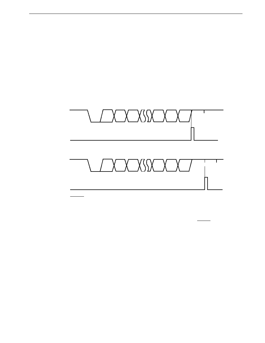
437
CHAPTER 18 ASYNCHRONOUS SERIAL INTERFACE/3-WIRE SERIAL I/O
Preliminary User's Manual U13987EJ1V0UM00
18.2.5 Transmission
The
�
PD784938's asynchronous serial interface is set to the transmission enabled state when the TXE bit of the
asynchronous serial interface mode register (ASIM) is set (to 1). A transmit operation is started by writing transmit data
to the serial transmit shift register (TXS) when transmission is enabled. The start bit, parity bit and stop bit(s) are added
automatically.
When a transmit operation is started, the data in the TXS is shifted out, and a transmission completion interrupt (INTST)
is generated when the TXS is empty.
If no more data is written to the TXS, the transmit operation is discontinued.
If the TXE bit is cleared (to 0) during a transmit operation, the transmit operation is discontinued immediately.
Figure 18-6. Asynchronous Serial Interface Transmission Completion Interrupt Timing
(a) Stop bit length: 1
STOP
Parity
D0
START
TxD (output)
INTST
D1
D2
D6
D7
(b) Stop bit length: 2
Parity
D0
START
TxD (output)
INTST
D1
D2
D6
D7
STOP
Cautions 1. After RESET input the serial transmit shift register (TXS) is emptied but a transmission completion
interrupt is not generated. A transmit operation can be started by writing transmit data to the TXS.
2. An asynchronous serial interface mode register (ASIM) rewrite should not be performed during
a transmit operation. If an ASIM rewrite is performed during a transmit operation, subsequent
transmit operations may not be possible (normal operation is restored by RESET input). Software
can determine whether transmission is in progress by using a transmission completion interrupt
(INTST) or the interrupt request flag (STIF) set by INTST.
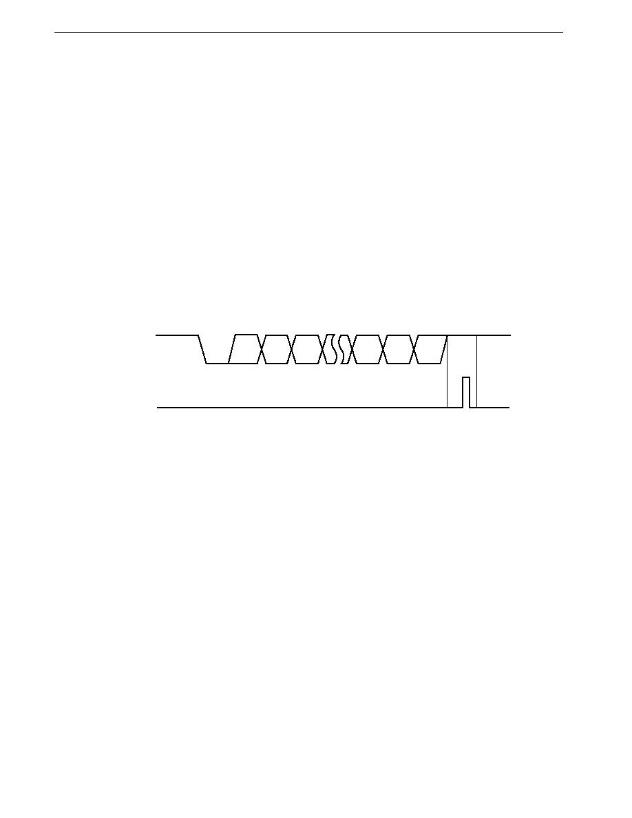
438
CHAPTER 18 ASYNCHRONOUS SERIAL INTERFACE/3-WIRE SERIAL I/O
Preliminary User's Manual U13987EJ1V0UM00
18.2.6 Reception
When the RXE bit of the asynchronous serial interface mode register (ASIM) is set (to 1), receive operations are enabled
and sampling of the RxD input pin is performed.
RxD input pin sampling is performed using the serial clock (divide-by-m counter input clock) specified by ASIM and band
rate generator control register (BRGC).
When the RxD pin input is driven low, the divide-by-m counter starts counting and a data sampling start timing signal
is output on the m'th count. If the RxD pin input is low when sampled again by this start timing signal, the input is recognized
as a start bit, the divide-by-m counter is initialized and the count is started, and data sampling is performed. When the
character data, parity bit and stop bit are detected following the start bit, reception of one data frame ends.
When reception of one data frame ends, the receive data in the shift register is transferred to the serial receive buffer,
RXB, and a reception completion interrupt (INTSR) is generated.
If an error occurs, the receive data in which the error occurred is still transferred to RXB. If bit 1 (ISRM) of the ASIM
was cleared (to 0) when the error occurred,
INTSR is generated. If the ISRM was set (to 1), INTSR is not generated.
If the RXE bit is cleared (to 0) during a receive operation, the receive operation is stopped immediately. In this case
the contents of RXB and ASIS are not changed, and no INTSR or INTSER interrupt is generated.
Figure 18-7. Asynchronous Serial Interface Reception Completion Interrupt Timing
STOP
Parity
D0
START
RxD (input)
INTSR
D1
D2
D6
D7
Caution The serial receive buffer (RXB) must be read even if there is a receive error. If RXB is not read, an
overrun error will occur when the next data is received, and the receive error state will continue
indefinitely.

439
CHAPTER 18 ASYNCHRONOUS SERIAL INTERFACE/3-WIRE SERIAL I/O
Preliminary User's Manual U13987EJ1V0UM00
18.2.7 Receive errors
Three kinds of errors can occur in a receive operation: parity errors, framing errors, and overrun errors. As the result
of data reception, an error flag is raised in the asynchronous serial interface status register (ASIS) and a receive error
interrupt (INTSER) is generated. Receive error causes are shown in Table 18-2.
It is possible to detect the occurrence of any of the above errors during reception by reading the contents of the ASIS
(see Figures 18-4 and 18-8).
The contents of the ASIS register are cleared (to 0) by reading the serial receive buffer (RXB) or by reception of the
next data (if there is an error in the next data, the corresponding error flag is set).
Table 18-2. Receive Error Causes
Receive Error
Cause
Parity error
Transmit data parity specification and receive data parity do not match
Framing error
Stop bit not detected
Overrun error
Reception of next data completed before data is read from receive buffer
Figure 18-8. Receive Error Timing
STOP
Parity
D0
START
RxD (input)
INTSR
Note
D1
D2
D6
D7
INTSER
Note If a receive error occurs while the ISRM bit is set (to 1), INTSR is not generated.
Remark
In the
�
PD784938, a break signal cannot be detected by hardware. As a break signal is a low-level signal
of two characters or more, a break signal may be judged to have been input if software detects the occurrence
of two consecutive framing errors in which the receive data was 00H. The chance occurrence of two
consecutive framing errors can be distinguished from a break signal by having the RxD pin level read by
software (confirmation is possible by setting "1" in bit 0 of the port 3 mode register (PM3) and reading port
3 (P3)) and confirming that it is "0".
Cautions 1. The contents of the asynchronous serial interface status register (ASIS) are cleared (to 0) by
reading the serial receive buffer (RXB) or by reception of the next data. If you want to find the details
of an error, therefore, ASIS must be read before reading RXB.
2. The RXB must be read even if there is a receive error. If RXB is not read, an overrun error will
occur when the next data is received, and the receive error state will continue indefinitely.
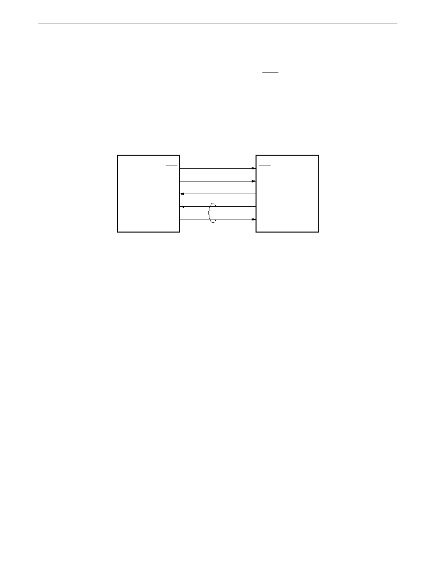
440
CHAPTER 18 ASYNCHRONOUS SERIAL INTERFACE/3-WIRE SERIAL I/O
Preliminary User's Manual U13987EJ1V0UM00
18.3 3-Wire Serial I/O Mode
The 3-wire serial I/O mode is used to communicate with devices that incorporate a conventional clocked serial interface.
Basically, communication is performed using three lines: the serial clock (SCK), serial data output (SO), and serial data
input (SI). Generally, a handshake line is necessary for checking the communication status.
Figure 18-9. Example of 3-Wire Serial I/O System Configuration
3-wire serial I/O
3-wire serial I/O
SCK
SO
SI
Port (interrupt)
Port
SCK
SI
SO
Port
Interrupt (port)
Master CPU
Note
Slave CPU
Note Handshake lines
18.3.1 Configuration in 3-wire serial I/O mode
The block diagram in the 3-wire serial I/O mode is shown in Figure 18-10.

441
CHAPTER 18 ASYNCHRONOUS SERIAL INTERFACE/3-WIRE SERIAL I/O
Preliminary User's Manual U13987EJ1V0UM00
Figure 18-10. 3-Wire Serial I/O Mode Block Diagram
Internal bus
RESET
8
D
Q
Shift register
Direction control circuit
8
Serial clock counter
Interrupt signal
generator
INTCSI1, INTCSI2
P27/SCK1,
P12/SCK2
Serial clock control circuit
Selector
Baud rate generator
P30/SI1,
P13/SI2
P31/SO1,
P14/SO2
CSCK1, CSCK2
CSCK1, CSCK2
SO latch
8
CSCK2
DIR2
CRXE2
CTXE2
CSCK1
DIR1
CRXE1
CTXE1
N-ch open-drain output enable

442
CHAPTER 18 ASYNCHRONOUS SERIAL INTERFACE/3-WIRE SERIAL I/O
Preliminary User's Manual U13987EJ1V0UM00
(1) Serial shift register (SIO1/SIO2)
SIO1 and SIO2 convert 8-bit serial data to 8-bit parallel data, and vice versa. SIO1/SIO2 is used for both transmission
and reception.
Actual transmit/receive operations are controlled by writing to/reading from SIO1/SIO2.
These registers can be read or written with an 8-bit manipulation instruction.
The contents of SIO1/SIO2 are undefined after RESET input.
(2) SO latch
The SO latch holds the SO1/SO2 pin output level.
(3) Serial clock selector (1/2n)
Generates and selects the serial clock to be used.
(4) Serial clock counter
Counts the serial clocks output or input in a transmit/receive operation, and checks that 8-bit data transmission/reception
has been performed.
(5) Interrupt signal generator
Generates an interrupt request when 8 serial clocks have been counted by the serial clock counter.
(6) Selector
Selects whether data is input to the serial shift registers 1 and 2 (SIO1 and SIO2) from the SI1 and SI2 pins or output
latches.
(7) Direction control circuit
Switches between MSB-first and LSB-first modes.
443
CHAPTER 18 ASYNCHRONOUS SERIAL INTERFACE/3-WIRE SERIAL I/O
Preliminary User's Manual U13987EJ1V0UM00
18.3.2 Clocked serial interface mode registers (CSIM1, CSIM2)
CSIM1 and CSIM2 are 8-bit registers that specify operations in the 3-wire serial I/O mode.
These registers can be read or written to with an 8-bit manipulation instruction or bit manipulation instruction. The CSIM1
and CSIM2 format is shown in Figure 18-11.
RESET input clears these registers to 00H.
Figure 18-11. Format of Clocked Serial Interface Mode Register 1 (CSIM1) and Clocked Serial Interface
Mode Register 2 (CSIM2)
7
CTXE1
CSIM1
6
CRXE1
5
0
4
0
3
0
2
DIR1
1
CSCK1
0
0
CTXE2 CRXE2
0
0
0
DIR2
CSCK2
0
After reset
Address
R/W
R/W
00H
0FF84H
CSIM2
R/W
(n = 1, 2)
00H
0FF85H
CSCKn
Serial Clock Selection Bit
Source Clock
In case of SCKn
(CTXEn, CRXEn = 1)
External input
clock to SCKn pin
Input
CMOS output
0
Baud rate
generator output
1
DIRn
Operation Mode Specification
(Transfer Bit Order)
MSB-first
LSB-first
0
1
CTXEn
Transmit/Receive Operation
Transmission/reception disabled,
or asynchronous serial interface
mode
Transmission enabled
Reception enabled
0
1
CRXEn
0
0
1
0
Transmission/reception enabled
1
1

444
CHAPTER 18 ASYNCHRONOUS SERIAL INTERFACE/3-WIRE SERIAL I/O
Preliminary User's Manual U13987EJ1V0UM00
18.3.3 Basic operation timing
In the 3-wire serial I/O mode, data transmission/reception is performed in 8-bit units. Data is transmitted/received bit
by bit in MSB-first or LSB-first order in synchronization with the serial clock.
MSB/LSB switching is specified by the DIR1 bit of the clock serial interface mode register (CSIM1).
Transmit data is output in synchronization with the fall of SCK1, and receive data is sampled on the rise of SCK1.
An interrupt request (INTCSI1) is generated on the 8th rise of SCK1.
When the internal clock is used as SCK1, SCK1 output is stopped on the 8th rise of SCK1 and SCK1 remains high until
the next data transmit or receive operation is started.
3-wire serial I/O mode timing is shown in Figure 18-12.
Figure 18-12. 3-Wire Serial I/O Mode Timing (1/2)
(a) MSB-first
INTCSI1
DI7
DI6
DI5
DI4
DI3
DI2
DI1
DI0
SCK1
Note
SI1 (input)
SO1 (output)
1
2
3
4
5
6
7
8
DO7
DO6
DO5
DO4 DO3 DO2
DO1
DO0
Transfer end
interrupt generation
Start of transfer synchronized with fall of SCK1
Note Master CPU:
Slave CPU:
Execution of instruction that writes to SIO1, etc.
Output
Input
445
CHAPTER 18 ASYNCHRONOUS SERIAL INTERFACE/3-WIRE SERIAL I/O
Preliminary User's Manual U13987EJ1V0UM00
Figure 18-12. 3-Wire Serial I/O Mode Timing (2/2)
(b) LSB-first
INTCSI1
DI0
DI1
DI2
DI3
DI4
DI5
DI6
DI7
SCK1
Note
SI1 (input)
SO1 (output)
1
2
3
4
5
6
7
8
DO0
DO1
DO2
DO3 DO4 DO5
DO6
DO7
Transfer end
interrupt generation
Start of transfer synchronized with fall of SCK1
Note Master CPU:
Slave CPU:
Execution of instruction that writes to SIO1, etc.
Output
Input
Remark
If the
�
PD784938 is connected to a 2-wire serial I/O device, a buffer should be connected to the SO1 pin as
shown in Figure 18-13. In the example shown in Figure 18-13, the output level is inverted by the buffer, and
therefore the inverse of the data to be output should be written to SIO1.
In addition, non-connection of the on-chip pull-up resistor should be specified for the P31/SO1 pin.
Figure 18-13. Example of Connection to 2-Wire Serial I/O
�
PD784938
SCK1
SI1
SO1
2-wire serial I/O device
SIO
SCK
(Serial clock line)
(Serial data line)

446
CHAPTER 18 ASYNCHRONOUS SERIAL INTERFACE/3-WIRE SERIAL I/O
Preliminary User's Manual U13987EJ1V0UM00
18.3.4 Operation when transmission only is enabled
A transmit operation is performed when the CTXE1 bit of clocked serial interface mode register (CSIM1) is set (to 1).
The transmit operation starts when a write to the serial shift register (SIO1) is performed while the CTXE1 bit is set (to 1).
When the CTXE1 bit is cleared (to 0), the SO1 pin is in the output high level.
(1) When the internal clock is selected as the serial clock
When transmission starts, the serial clock is output from the SCK1 pin and data is output in sequence from SIO1 to
the SO1 pin in synchronization with the fall of the serial clock, and SI1 pin signals are shifted into SIO1 in synchronization
with the rise of the serial clock.
There is a delay of up to one SCK1 clock cycle between the start of transmission and the first fall of SCK1.
If transmission is disabled during the transmit operation (by clearing (to 0) the CTXE1 bit), SCK1 clock output is stopped
and the transmit operation is discontinued on the next rise of SCK1. In this case an interrupt request (INTCSI1) is
not generated, and the SO1 pin becomes output high level.
(2) When an external clock is selected as the serial clock
When transmission starts, data is output in sequence from SIO1 to the SO1 pin in synchronization with the fall of the
serial clock input to the SCK1 pin after the start of transmission, and SI1 pin signals are shifted into SIO1 in
synchronization with the rise of the SCK1 pin input. If transmission has not started, shift operations are not performed
and the SO1 pin output level does not change even if the serial clock is input to the SCK1 pin.
If transmission is disabled during the transmit operation (by clearing (to 0) the CTXE1 bit), the transmit operation is
discontinued and subsequent SCK1 input is ignored. In this case an interrupt request (INTCSI1) is not generated, and
the SO1 pin becomes output high level.
18.3.5 Operation when reception only is enabled
A receive operation is performed when the CRXE1 bit of the clocked serial interface mode register (CSIM1) is set (to
1). The receive operation starts when the CRXE1 changes from "0" to "1", or when a read from serial shift register (SIO1)
is performed.
(1) When the internal clock is selected as the serial clock
When reception starts, the serial clock is output from the SCK1 pin and the SI1 pin data is fetched in sequence into
serial shift register (SIO1) in synchronization with the rise of the serial clock.
There is a delay of up to one SCK1 clock cycle between the start of reception and the first fall of SCK1.
If reception is disabled during the receive operation (by clearing (to 0) the CRXE1 bit), SCK1 clock output is stopped
and the receive operation is discontinued on the next rise of SCK1. In this case an interrupt request (INTCSI1) is not
generated, and the contents of the SIO1 are undefined.
(2) When an external clock is selected as the serial clock
When reception starts, the SI1 pin data is fetched into serial shift register (SIO1) in synchronization with the rise of
the serial clock input to the SCK1 pin after the start of reception. If reception has not started, shift operations are not
performed even if the serial clock is input to the SCK1 pin.
If reception is disabled during the receive operation (by clearing (to 0) the CRXE1 bit), the receive operation is
discontinued and subsequent SCK1 input is ignored. In this case an interrupt request (INTCSI1) is not generated.

447
CHAPTER 18 ASYNCHRONOUS SERIAL INTERFACE/3-WIRE SERIAL I/O
Preliminary User's Manual U13987EJ1V0UM00
18.3.6 Operation when transmission/reception is enabled
When the CTXE1 bit and CRXE1 bit of the clocked serial interface mode register (CSIM1) register are both set (1), a
transmit operation and receive operation can be performed simultaneously (transmit/receive operation). The transmit/
receive operation is started when the CRXE1 bit is changed from "0" to "1", or by performing a write to serial shift register
(SIO1).
When a transmit/receive operation is started for the first time, the CRXE1 bit always changes from "0" to "1", and there
is thus a possibility that the transmit/receive operation will start immediately, and undefined data will be output. The first
transmit data should therefore be written to SIO1 beforehand when both transmission and reception are disabled (when
the CTXE1 bit and CRXE1 bit are both cleared (to 0)), before enabling transmission/reception. However, specify whether
data is transferred with MSB or LSB first before writing the SIO1. Even if the specification is made after writing the SIO1,
the byte order of the data already stored in the SIO1 cannot be changed.
When transmission/reception is disabled (CTXE1 = CRXE1 = 0), the SO1 pin is in the output high level.
(1) When the internal clock is selected as the serial clock
When transmission/reception starts, the serial clock is output from the SCK1 pin, data is output in sequence from serial
shift register (SIO1) to the (SO1) pin in synchronization with the fall of the serial clock, and SI1 pin data is shifted in
order into SIO1 in synchronization with the rise of the serial clock.
There is a delay of up to one SCK1 clock cycle between the start of transmission and the first fall of SCK1.
If either transmission or reception is disabled during the transmit/receive operation, only the disabled operation is
discontinued. If transmission only is disabled, the SO1 pin becomes output high level. If reception only is disabled,
the contents of the SIO1 will be undefined.
If transmission and reception are disabled simultaneously, SCK1 clock output is stopped and the transmit and receive
operations are discontinued on the next rise of SCK1. When transmission and reception are disabled simultaneously,
the contents of SIO1 are undefined, an interrupt request (INTCSI1) is not generated, and the SO1 pin becomes output
high level.
(2) When an external clock is selected as the serial clock
When transmission/reception starts, data is output in sequence from serial shift register (SIO1) to the SO1 pin in
synchronization with the fall of the serial clock input to the SCK1 pin after the start of transmission/reception, and SI1
pin data is shifted in order into SIO1 in synchronization with the rise of the serial clock. If transmission/reception has
not started, the SIO1 shift operations are not performed and the SO1 pin output level does not change even if the serial
clock is input to the SCK1 pin.
If either transmission or reception is disabled during the transmit/receive operation, only the disabled operation is
discontinued. If transmission only is disabled, the SO1 pin becomes output high level. If reception only is disabled,
the contents of the SIO1 will be undefined.
If transmission and reception are disabled simultaneously, the transmit and receive operations are discontinued and
subsequent SCK1 input is ignored. When transmission and reception are disabled simultaneously, the contents of
SIO1 are undefined, an interrupt request (INTCSI1) is not generated, and the SO1 pin becomes output high level.
18.3.7 Corrective action in case of slippage of serial clock and shift operations
When an external clock is selected as the serial clock, there may be slippage between the number of serial clocks and
shift operations due to noise, etc. In this case, since the serial clock counter is initialized by disabling both transmit operations
and receive operations (by clearing (to 0) the CTXE1 bit and CRXE1 bit), synchronization of the shift operations and the
serial clock can be restored by using the first serial clock input after reception or transmission is next enabled as the first
clock.

448
CHAPTER 18 ASYNCHRONOUS SERIAL INTERFACE/3-WIRE SERIAL I/O
Preliminary User's Manual U13987EJ1V0UM00
18.4 Baud Rate Generator
The baud rate generator is the circuit that generates the UART/IOE serial clock. Two independent circuits are
incorporated, one for each serial interface.
18.4.1 Baud rate generator configuration
The baud rate generator block diagram is shown in Figure 18-14.

449
CHAPTER 18 ASYNCHRONOUS SERIAL INTERFACE/3-WIRE SERIAL I/O
Preliminary User's Manual U13987EJ1V0UM00
Figure 18-14. Baud Rate Generator Block Diagram
Internal bus
8
Baud rate generator
control register
BRGC, BRGC2
RESET
Asynchronous serial
interface mode
registers 1 & 2
ASIM1, ASIM2
1/8
SCK
Clocked serial
interface mode
registers 1 & 2
CSIM1, CSIM2
1/8
CSCK1
5-bit counter
5-bit counter
RESET
Start bit detection
1/2
UART reception
shift clock
Clear
Match
Match
1/2
Selector
Selector
Selector
Shift clock
for UART
transmission
& IOE
Frequency
divider
Selector
f
PRS
f
XX
P25/ASCK/SCK1,
P12/ASCK2/SCK2
BRGC write
CSCK1
Start bit detection
sampling clock
RESET

450
CHAPTER 18 ASYNCHRONOUS SERIAL INTERFACE/3-WIRE SERIAL I/O
Preliminary User's Manual U13987EJ1V0UM00
(1) 5-bit counter
Counter that counts the clock (f
PRS
) by which the output from the frequency divider is selected. Generates a signal
with the frequency selected by the low-order 4 bits of the baud rate generator control registers (BRGC/BRGC2).
(2) Frequency divider
Scales the internal clock (f
XX
) or, in asynchronous serial interface mode, a clock that is twice the external baud rate
input (ASCK/ASCK2), and selects f
PRS
with the next-stage selector.
(3) Both-edge detection circuit
Detects both edges of the ASCK/ASCK2 pin input signal and generates a signal with a frequency twice that of the ASCK/
ASCK2 input clock.
18.4.2 Baud rate generator control register (BRGC, BRGC2)
BRGC and BRGC2 are 8-bit registers that set the baud rate clock in asynchronous serial interface mode or the shift clock
in 3-wire serial I/O mode.
These registers can be written to only with an 8-bit manipulation instruction. The BRGC and BRGC2 format is shown
in Figure 18-15.
RESET input clears BRGC to 00H.
Caution When a baud rate generator control register (BRGC, BRGC2) write instruction is executed, the 5-bit
counter and 1/2 frequency divider operations are reset. Consequently, if a write to the BRGC and
BRGC2 is performed during communication, the generated baud rate clock may be disrupted,
preventing normal communication from continuing. The BRGC and BRGC2 should therefore not be
written to during communication.
451
CHAPTER 18 ASYNCHRONOUS SERIAL INTERFACE/3-WIRE SERIAL I/O
Preliminary User's Manual U13987EJ1V0UM00
Figure 18-15. Format of Baud Rate Generator Control Register (BRGC) and
Baud Rate Generator Control Register 2 (BRGC2)
7
TPS3
BRGC
6
TPS2
5
TPS1
4
TPS0
3
MDL3
2
MDL2
1
MDL1
0
MDL0
TPS23 TPS22 TPS21 TPS20 MDL23 MDL22 MDL21 MDL20
0
0
0
0
0
0
0
0
1
1
1
1
1
1
1
1
0
0
0
0
1
1
1
1
0
0
0
0
1
1
1
1
0
0
1
1
0
0
1
1
0
0
1
1
0
0
1
1
0
1
0
1
0
1
0
1
0
1
0
1
0
1
0
1
0
1
2
3
4
5
6
7
8
9
10
11
12
13
14
15
f
PRS
/16
f
PRS
/17
f
PRS
/18
f
PRS
/19
f
PRS
/20
f
PRS
/21
f
PRS
/22
f
PRS
/23
f
PRS
/24
f
PRS
/25
f
PRS
/26
f
PRS
/27
f
PRS
/28
f
PRS
/29
f
PRS
/30
f
PRS
Note 2
After reset
Address
R/W
R/W
00H
0FF90H
BRGC2
R/W
k
Baud Rate Generator Input
Clock
Note 1
f
PRS
: Prescaler output selection clock
00H
0FF91H
MDL3
MDL2
MDL1
MDL0
MDL23 MDL22 MDL21 MDL20
0
0
0
0
0
0
0
0
1
1
1
1
0
0
0
0
1
1
1
1
0
0
0
0
0
0
1
1
0
0
1
1
0
0
1
1
0
1
0
1
0
1
0
1
0
1
0
1
0
1
2
3
4
5
6
7
8
9
10
11
f
XX
/2
f
XX
/4
f
XX
/8
f
XX
/16
f
XX
/32
f
XX
/64
f
XX
/128
f
XX
/256
f
XX
/512
f
XX
/1,024
f
XX
/2,048
f
XX
/4,096
f
ASCK
/2
Note
f
ASCK
/4
f
ASCK
/8
f
ASCK
/16
f
ASCK
/32
f
ASCK
/64
f
ASCK
/128
f
ASCK
/256
f
ASCK
/512
f
ASCK
/1,024
f
ASCK
/2,048
f
ASCK
/4,096
n
12-Bit Prescaler Tap
Selection (f
PRS
)
Other than the above
Setting prohibited
f
XX
: Oscillator frequency or external clock input
TPS3 TPS2
TPS1 TPS0
TPS23 TPS22 TPS21 TPS20
Notes 1. Only f
PRS
/16 can be selected when ASCK/ASCK2 input is used.
2. Can only be used in 3-wire serial I/O mode.
Note Can not be selected when the value set in bits MDL3 to MDL0,
k = 15.

452
CHAPTER 18 ASYNCHRONOUS SERIAL INTERFACE/3-WIRE SERIAL I/O
Preliminary User's Manual U13987EJ1V0UM00
18.4.3 Baud rate generator operation
The baud rate generator only operates when UART/IOE transmit/receive operations are enabled. The generated baud
rate clock is a signal scaled from the internal clock (f
XX
) or a signal scaled from the clock input from the external baud rate
input (ASCK) pin.
Caution If a write to the baud rate generator control register (BRGC) is performed during communication, the
generated baud rate clock may be disrupted, preventing normal communication from continuing. The
BRGC should therefore not be written to during communication.
(1) Baud rate clock generation in UART mode
(a) Using internal clock (f
XX
)
This function is selected by setting (to 1) bit 0 (SCK) of the asynchronous serial interface mode register (ASIM).
The internal clock (f
XX
) is scaled by the frequency divider, this signal (f
PRS
) is scaled by the 5-bit counter, and the
signal further divided by 2 is used as the baud rate. The baud rate is given by the following expression:
(Baud rate) =
f
XX
(k + 16)
�
2
n+2
f
XX
: Oscillator frequency or external clock input frequency
k:
Value set in bits MDL3 to MDL0 of BRGC (k = 0 to 14)
n:
Value set in bits TPS3 to TPS0 of BRGC (n = 0 to 11)
(b) Using external baud rate input
This function is selected by clearing (to 0) bit 0 (SCK) of the asynchronous serial interface mode register (ASIM).
When this function is used, bits MDL3 to MDL0 of the baud rate generator control register (BRGC) must all be
cleared (to 0) (k = 0).
When this function is used with UART2, it is necessary to set (to 1) bit 2 of the port 1 mode control register (PMC1)
and set the P12 pin to control mode.
The ASCK pin input clock is scaled by the frequency divider, and the signal obtained by dividing this signal by
32 (f
PRS
) (division by 16 and division by 2) is used as the baud rate. The baud rate is given by the following
expression:
(Baud rate) =
f
ASCK
2
n+6
f
ASCK
: ASCK pin input clock frequency
n:
Value set in bits TPS3 to TPS0 of BRGC (n = 0 to 11)
When this function is used, a number of baud rates can be generated by one external input clock.

453
CHAPTER 18 ASYNCHRONOUS SERIAL INTERFACE/3-WIRE SERIAL I/O
Preliminary User's Manual U13987EJ1V0UM00
(2) Serial clock generation in 3-wire serial I/O mode
Selected when the CSCK1 bit of the clocked serial interface mode register (CSIM1) is set (to 1) and SCK1 is output.
(a) Normal mode
The internal clock (f
XX
) is scaled by the frequency divider, this signal (f
PRS
) is scaled by the 5-bit counter, and the
signal further divided by 2 is used as the serial clock. The serial clock is given by the following expression:
(Serial clock) =
f
XX
(k + 16)
�
2
n+2
f
XX
: Oscillator frequency or external clock input frequency
k:
Value set in bits MDL3 to MDL0 of BRGC (k = 0 to 14)
n:
Value set in bits TPS3 to TPS0 of BRGC (n = 0 to 11)
(b) High-speed mode
When this function is used, bits MDL3 to MDL0 of the baud rate generator control register (BRGC) are all set (1)
(k= 15).
The internal clock (f
XX
) is scaled by the frequency divider, and this signal (f
PRS
) divided by 2 is used as the serial
clock. The serial clock is given by the following expression:
(Serial clock) =
f
XX
2
n+2
f
XX
: Oscillator frequency or external clock input frequency
n:
Value set in bits TPS3 to TPS0 of BRGC (n = 1 to 11)

454
CHAPTER 18 ASYNCHRONOUS SERIAL INTERFACE/3-WIRE SERIAL I/O
Preliminary User's Manual U13987EJ1V0UM00
18.4.4 Baud rate setting in asynchronous serial interface mode
There are two methods of setting the baud rate, as shown in Table 18-3.
This table shows the range of baud rates that can be generated, the baud rate calculation expression and selection
method for each case.
Table 18-3. Baud Rate Setting Methods
Baud Rate Clock Source
Selection Method
Baud Rate Calculation
Baud Rate Range
Expression
Baud rate generator
Internal system clock
SCK in ASIM = 1
f
XX
f
XX
to
f
XX
(k + 16) � 2
n+2
245,760
64
ASCK input
SCK in ASIM = 0
f
ASCK
f
ASCK
to
f
ASCK
Note
2
n+6
131,072
64
Note Including f
ASCK
input range: (0 to f
XX
/256)
Remarks f
XX
:
Oscillator frequency or external clock input frequency
k:
Value set in bits MDL3 to MDL0 of BRGC (k = 0 to 14; see Figure 18-15)
n:
Value set in bits TPS3 to TPS0 of BRGC (n = 0 to 11; see Figure 18-15)
f
ASCK
: ASCK input clock frequency (0 to f
XX
/4)
(1) Examples of settings when baud rate generator is used
Examples of baud rate generator control register (BRGC) settings when the baud rate generator is used are shown
below.
When the baud rate generator is used, the SCK bit of the asynchronous serial interface mode register (ASIM) should
be set (to 1).
Table 18-4. Examples of BRGC Settings when Baud Rate Generator is Used
Oscillator Frequency (f
XX
)
12.0 MHz
11.0592 MHz
or External Clock (f
X
)
Baud Rate
BRGC Value
Error
BRGC Value
Error
[bps]
(%)
(%)
75
A4H
2.34
A2H
0.00
110
9BH
1.36
99H
1.82
150
94H
2.34
92H
0.00
300
84H
2.34
82H
0.00
600
74H
2.34
72H
0.00
1,200
64H
2.34
62H
0.00
2,400
54H
2.34
52H
0.00
4,800
44H
2.34
42H
0.00
9,600
34H
2.34
32H
0.00
19,200
24H
2.34
22H
0.00
31,250
19H
0.00
16H
0.54
38,400
14H
2.34
12H
0.00
76,800
04H
2.34
02H
0.00

455
CHAPTER 18 ASYNCHRONOUS SERIAL INTERFACE/3-WIRE SERIAL I/O
Preliminary User's Manual U13987EJ1V0UM00
(2) Examples of settings when external baud rate input (ASCK) is used
Table 18-5 shows an example of setting when external baud rate input (ASCK) is used. When using the ASCK input,
clear the SCK bit of the asynchronous serial interface mode register (ASIM) to 0, and set the corresponding pin in the
control mode by using PMC3 or PMC1.
Table 18-5. Examples of Settings when External Baud Rate Input (ASCK) is Used
f
ASCK
153.6 kHz
4.9152 MHz
(ASCK Input Frequency)
Baud Rate [bps]
BRGC Value
BRGC Value
75
50H
A0H
150
40H
90H
300
30H
80H
600
20H
70H
1,200
10H
60H
2,400
00H
50H
4,800
--
40H
9,600
--
30H
19,200
--
20H
38,400
--
10H
76,800
--
00H

456
CHAPTER 18 ASYNCHRONOUS SERIAL INTERFACE/3-WIRE SERIAL I/O
Preliminary User's Manual U13987EJ1V0UM00
18.5 Cautions
(1) An asynchronous serial interface mode register (ASIM) rewrite should not be performed during a transmit operation.
If an ASIM rewrite is performed during a transmit operation, subsequent transmit operations may not be possible (normal
operation is restored by RESET input).
Software can determine whether transmission is in progress by using a transmission completion interrupt (INTST) or
the interrupt request flag (STIF) set by INTST.
(2) After RESET input the serial transmit shift register (TXS) is emptied but a transmission completion interrupt is not
generated. A transmit operation can be started by writing transmit data to the TXS.
(3) The serial receive buffer (RXB) must be read even if there is a receive error. If RXB is not read, an overrun error will
occur when the next data is received, and the receive error state will continue indefinitely.
(4) The contents of the asynchronous serial interface status register (ASIS) are cleared (to 0) by reading the serial receive
buffer (RXB) or by reception of the next data. If you want to find the details of an error, therefore, ASIS must be read
before reading RXB.
(5) The baud rate generator control register (BRGC) should not be written to during communication. If a write instruction
is executed, the 5-bit counter and 1/2 frequency divider operations will be reset, and the generated baud rate clock
may be disrupted, preventing normal communication from continuing.
(6) To specify the transfer bit order with CSIM1 and CSIM2 (bit 2 manipulation), do not set the CTXE and CRXE bits at
the same time. If these bits are specified at the same time, the bit transfer order may not be as specified.
457
Preliminary User's Manual U13987EJ1V0UM00
CHAPTER 19 3-WIRE SERIAL I/O MODE
The
�
PD784938 has two channels of serial interfaces in 3-wire serial I/O mode (IOE0/IOE3).
The two channels of IOE have identical functions. Unless otherwise specified, therefore, IOE0 is explained in this chapter.
To use IOE3, refer to Table 19-1 for the register name, bit name, and pin name of IOE3.
Table 19-1. Differences in Name between IOE0 and IOE3
Item
IOE0
IOE3
Pin name
P32/SCK0
P105/SCK3
P27/SI0
P106/SI3
P33/SO0
P107/SO3
Clocked serial interface mode register
CSIM
CSIM3
Clocked serial interface mode register bit names
ENCSI, DIR, CRXE, MOD,
ENCSI3, DIR3, CRXE3, MOD3,
SELCL2 to SELCL0
SELCL32 to SELCL30
Serial shift register
SIO
SIO3
Interrupt request name
INTCSI
INTCSI3
19.1 Function
In the 3-wire serial I/O mode (MSB/LSB first), basically, three lines are used for communication: serial clock (SCK0),
serial data output (SO0), and serial data input (SI0). Generally, a handshake line is necessary for checking the
communication status.
458
CHAPTER 19 3-WIRE SERIAL I/O MODE
Preliminary User's Manual U13987EJ1V0UM00
19.2 Configuration
Figure 19-1 shows the block diagram of the clocked serial interface in the 3-wire serial I/O mode (note that the functions
of both channels are identical).
Figure 19-1. Clocked Serial Interface Block Diagram
(1) Serial shift register (SIO)
The SIO converts 8-bit serial data to 8-bit parallel data, and vice versa. SIO is used for both transmission and reception.
Data is received or transmitted starting from the MSB (or LSB). Actual transmit/receive operations are controlled by
writing to/reading from SIO.
SIO can be read or written to with an 8-bit manipulation instruction. The contents of SIO are undefined after RESET
input.
(2) Serial clock counter
Counts the serial clocks output or input in a transmit/receive operation, and checks that 8-bit data transmission/reception
has been performed.
(3) Interrupt signal generator
A interrupt request is generated when 8 serial clocks have been counted by the serial clock counter.
P27/SI0
To P33/SO0 port block
To P32/SCK0 port block
SIO
Shift
LSB/MSB
CSIM
EN
CSI
CRX
E
DIR
SEL
ST
MO
D
SEL
CL2
SEL
CL1
SEL
CL0
N-ch open-drain
specification
Q
S
R
Write to SIO
Read to SIO
INTCSI
Interrupt signal
generation
circuit
Eighth clock
Serial clock counter
SELCL. 0 to 2
External clock selection
f
XX
/8
f
XX
/16
f
XX
/32
f
XX
/64
f
XX
/128
Selector
0
1
459
CHAPTER 19 3-WIRE SERIAL I/O MODE
Preliminary User's Manual U13987EJ1V0UM00
19.3 Control Registers
19.3.1 Clocked serial interface mode register (CSIM, CSIM3)
CSIM and CSIM3 are 8-bit registers that specify the serial interface operation mode (enable/disable), serial clock, etc.
These registers can be read or written to with an 8-bit manipulation instruction or bit manipulation instruction. The CSIM
and CSIM3 format is shown in Figure 19-1.
RESET input clears these registers to 00H.
Figure 19-2. Format of Clocked Serial Interface Mode Register (CSIM) and
Clocked Serial Interface Mode Register 3 (CSIM3)
ENCSI3 SELST3 DIR3 CRXE3 MOD3 SELCL32 SELCL31 SELCL30
CSIM3
0FF80H
00H
R/W
Serial Clock Specification
External clock
Note 1
f
XX
/128
f
XX
/64
f
XX
/32
f
XX
/16
f
XX
/8
Note 2
Setting prohibited
ENCSI SELST
DIR
CRXE
MOD SELCL2 SELCL1 SELCL0
7
6
5
4
3
2
1
0
CSIM
0FF82H
Address
00H
After reset
R/W
R/W
SELCL
n2
0
0
0
0
1
1
SELCL
n1
0
0
1
1
0
0
SELCL
n0
0
1
0
1
0
1
(n = 3 with CSIM3 only)
Other than the above
N-ch Open-Drain Specification (P32, P33, or P105, P107)
Not N-ch open drain
N-ch open drain
MODn
0
1
Enables/Disables Serial Interface Receive Operation
Reception disabled
Reception enabled
CRXEn
0
1
Serial Interface Bit Transfer Order Selection
MSB first
LSB first
DIRn
0
1
Transmit Activation Condition Selection
Start with a write operation to SIO (serial shift register)
Start with a read operation from SIO
SELSTn
0
1
Enables/Disables Serial Interface Operation
Disabled
Enabled
ENCSIn
0
1

460
CHAPTER 19 3-WIRE SERIAL I/O MODE
Preliminary User's Manual U13987EJ1V0UM00
Notes 1. When the external clock is selected, the usable serial clock is MIN f
XX
/8 in the case of f
CLK
= f
XX
/1; otherwise,
it is MIN f
CLK
/4.
2. Setting is prohibited when the system clock (f
CLK
= f
XX
/8) is selected.
Caution When bit 3 is set, the P-ch of the output buffer is forcibly turned OFF. This channel is not affected
by PM3 and PMC3, or PM10 and PMC10. Therefore, if the input or output mode is changed by using
the PM register with bit 3 set in the port mode, the content of the port latch can be output and the pin
level can be read in the N-ch open-drain mode.
461
CHAPTER 19 3-WIRE SERIAL I/O MODE
Preliminary User's Manual U13987EJ1V0UM00
19.4 3-Wire Serial I/O Mode
The 3-wire serial I/O mode is used to communicate with devices that incorporate a conventional clocked serial interface.
Basically, communication is performed using three lines: the serial clock (SCK0), serial data output (SO0), and serial
data input (SI0). Generally, a handshake line is necessary for checking the communication status.
Figure 19-3. Example of 3-Wire Serial I/O System Configuration
SCK0
SO0
SI0
Port (interrupt)
Port
SCK
SI
SO
Port
Interrupt (port)
Master CPU
Note
Slave CPU
PD784938
�
Note Handshake lines
462
CHAPTER 19 3-WIRE SERIAL I/O MODE
Preliminary User's Manual U13987EJ1V0UM00
19.4.1 Basic operation timing
In the 3-wire serial I/O mode, data transmission/reception is performed in 8-bit units. Data is transmitted/received bit
by bit in MSB-first or LSB-first order in synchronization with the serial clock.
MSB first/LSB first switching is specified by the DIR bit of the clocked serial interface mode register (CSIM).
Transmit data is output in synchronization with the fall of SCK0, and receive data is sampled on the rise of SCK0.
An interrupt request (INTCSI) is generated on the 8th rise of SCK0.
When the internal clock is used as SCK0, SCK0 output is stopped on the 8th rise of SCK0 and SCK0 remains high until
the next data transmit or receive operation is started.
3-wire serial I/O mode timing is shown in Figure 19-4.
Figure 19-4. 3-Wire Serial I/O Mode Timing (1/2)
(a) MSB-first
INTCSI
DI7
DI6
DI5
DI4
DI3
DI2
DI1
DI0
SCK0
Note
SI0 (input)
SO0 (output)
1
2
3
4
5
6
7
8
DO7
DO6
DO5
DO4 DO3 DO2
DO1
DO0
Transfer end
interrupt generation
Start of transfer synchronized with fall of SCK0
Note Master CPU:
Slave CPU:
Execution of instruction that writes to SIO, etc.
Output
Input
Cautions 1.
If data is written to SIO during transfer operation after the transfer was started by writing SIO,
malfunctioning may occur. Therefore, do not rewrite SIO during the transfer operation.
2.
The operation is immediately stopped even during transfer operation if the ENCSI bit is cleared
(to 0).
463
CHAPTER 19 3-WIRE SERIAL I/O MODE
Preliminary User's Manual U13987EJ1V0UM00
Figure 19-4. 3-Wire Serial I/O Mode Timing (2/2)
(b) LSB-first
INTCSI
DI0
DI1
DI2
DI3
DI4
DI5
DI6
DI7
SCK0
Note
SI0 (input)
SO0 (output)
1
2
3
4
5
6
7
8
DO0
DO1
DO2
DO3 DO4 DO5
DO6
DO7
Transfer end
interrupt generation
Start of transfer synchronized with fall of SCK0
Note Master CPU:
Slave CPU:
Execution of instruction that writes to SIO, etc.
Output
Input
In the 3-wire serial I/O mode, the SO0 pin functions as a CMOS push-pull output.

464
CHAPTER 19 3-WIRE SERIAL I/O MODE
Preliminary User's Manual U13987EJ1V0UM00
19.4.2 Operation when transmission only is enabled
When the CRXE bit of the clocked serial interface mode register (CSIM) is cleared (to 0), data is only transmitted and
reception is disabled. Transmission is started when data is written to the serial shift register (SIO) with the ENCSI bit set
(to 1).
Transmit data is input to SIO instead of the data received from the SI0 pin. If reception is disabled, therefore, the transmit
data can be saved without being lost.
If an instruction that writes data to SI0 is executed when ENCSI = 1 and CRXE = 0, the data is transmitted in 1-bit units
in synchronization with the serial clock. The data of the first bit is output from the SO0 pin, and at the same time, input
to the last bit of SI0. When the transmission is completed by repeating this operation eight times, an interrupt request is
generated.
Figure 19-5. Operation when Reception is Disabled
SIO
Serial I/O shift register
SI0 pin
(a) When the internal clock is selected as the serial clock
When transmission starts, the serial clock is output from the SCK0 pin and data is output in sequence from SIO to the
SO0 pin in synchronization with the fall of the serial clock, and SI0 pin signals are shifted into SIO in synchronization
with the rise of the serial clock.
There is a delay of up to one SCK0 clock cycle between the start of transmission and the first fall of SCK0.
(b) When an external clock is selected as the serial clock
When transmission starts, data is output in sequence from SIO to the SO0 pin in synchronization with the fall of the
serial clock input to the SCK0 pin after the start of transmission, and SI0 pin signals are shifted into SIO in
synchronization with the rise of the SCK0 pin input. If transmission has not started, shift operations are not performed
and the SO0 pin output level does not change even if the serial clock is input to the SCK0 pin.
If transmission is disabled during the transmit operation (by clearing (to 0) the ENCSI), the transmit operation is
discontinued and subsequent SCK0 input is ignored. In this case an interrupt request (INTCSI) is not generated.
Even if the serial clock is input to SCK0 while the CTXE bit is cleared (to 0), shift operations are not performed and
the SO0 pin output level does not change.
Caution When the external clock is selected, do not input the serial clock to the SCK0 pin before setting
transmit data to SIO after transmission has been started. Otherwise, undefined data may be output.
Similarly, do not use the macro service when the external clock is selected.

465
CHAPTER 19 3-WIRE SERIAL I/O MODE
Preliminary User's Manual U13987EJ1V0UM00
19.4.3 Operation when reception only is enabled
To enable only reception, set (to 1) the ENCSI and CRXE bits of the clocked serial interface mode register (CSIM). Also
set the P33/SO0 pin in the port mode by using the port 3 mode control register (PMC3) (if this pin is not set in the port mode,
it outputs data). Reception can be started by reading the serial shift register (SIO).
19.4.4 Operation when transmission/reception is enabled
When the ENCSI bit and CRXE bit of the clocked serial interface mode register (CSIM) are both set (to 1), a transmit
operation and receive operation can be performed simultaneously (transmit/receive operation). Both transmission and
reception can be started by writing data to SIO when both the ENCSI and CRXE bits are set (to 1).
(a) When the internal clock is selected as the serial clock
When transmission/reception starts, the serial clock is output from the SCK0 pin, data is output in sequence from serial
shift register (SIO) to the SO0 pin in synchronization with the fall of the serial clock, and SI0 pin data is shifted in order
into SIO in synchronization with the rise of the serial clock.
There is a delay of up to one SCK0 clock cycle between the start of transmission and the first fall of SCK0.
(b) When an external clock is selected as the serial clock
When transmission/reception starts, data is output in sequence from serial shift register (SIO) to the SO0 pin in
synchronization with the fall of the serial clock input to the SCK0 pin after the start of transmission/reception, and SI0
pin data is shifted in order into SIO in synchronization with the rise of the serial clock. If transmission/reception has
not started, shift operations are not performed and the SO0 pin output level does not change even if the serial clock
is input to the SCK0 pin.
Caution When the external clock is selected, do not input the serial clock to the SCK0 pin before setting
transmit data to SIO after transmission has been started. Otherwise, undefined data may be output.
Similarly, do not use the macro service when the external clock is selected.
19.4.5 Corrective action in case of slippage of serial clock and shift operations
When an external clock is selected as the serial clock, there may be slippage between the number of serial clocks and
shift operations due to noise, etc. In this case, since the serial clock counter is initialized by disabling both transmit operations
and receive operations (by clearing (to 0) the ENCSI bit), synchronization of the shift operations and the serial clock can
be restored by using the first serial clock input after reception or transmission is next enabled as the first clock.

466
Preliminary User's Manual U13987EJ1V0UM00
[MEMO]

467
Preliminary User's Manual U13987EJ1V0UM00
CHAPTER 20 IEBus CONTROLLER
20.1 IEBus Controller Function
IEBus (Inter Equipment Bus) is a small-scale digital data transmission system that transmits data between units. To
implement IEBus with the
�
PD784938 Subseries, external IEBus driver and receiver are necessary because they are not
provided.
The internal IEBus controller of the
�
PD784938 Subseries is of negative logic.
20.1.1 Communication protocol of IEBus
The communication protocol of the IEBus is as follows:
(1) Multi-master mode
All the units connected to the IEBus can transmit data to the other units.
(2) Broadcasting communication function
Communication between one unit and plural units can be performed as follows:
�
Group-unit broadcasting communication: Broadcasting communication to group units
�
All-unit broadcasting communication: Broadcasting communication to all units.
(3) Effective transfer rate
The effective transfer rate is in mode 1 (the
�
PD784938 does not support modes 0 and 2 of effective transfer rate).
�
Mode 1: Approx. 17 kbps
Caution Different modes must not be mixed on one IEBus.
(4) Communication mode
Data transfer is executed in half-duplex asynchronous communication mode.
(5) Access control: CSMA/CD (Carrier Sense Multiple Access with Collision Detection)
The priority of the IEBus is as follows:
<1> Broadcasting communication takes precedence over individual communication (communication from one unit to
another).
<2> The lower master address takes precedence.
(6) Communication scale
The communication scale of IEBus is as follows:
�
Number of units: 50 MAX.
�
Cable length:
150 m MAX. (when twisted pair cable is used)
Caution The communication scale in an actual system differs depending on the characteristics of the cables,
etc., constituting the IEBus driver/receiver and IEBus.

468
CHAPTER 20 IEBus CONTROLLER
Preliminary User's Manual U13987EJ1V0UM00
20.1.2 Determination of bus mastership (arbitration)
An operation to occupy the bus is performed when a unit connected to the IEBus controls the other units. This operation
is called arbitration.
When two or more units simultaneously start transmission, arbitration is to grant one of the units the permission to occupy
the bus.
Because only one unit is granted the bus mastership as a result of arbitration, the priority condition of the bus is
predetermined as follows:
Caution The bus mastership is released if communication is aborted.
(1) Priority by communication type
Broadcasting communication (communication from one unit to plural units) takes precedence over normal communi-
cation (communication from one unit to another).
(2) Priority by master address
If the communication type is the same, communication with the lower master address takes precedence.
A master address consists of 12 bits, with unit 000H having the highest priority and unit FFFH having the lowest priority.
20.1.3 Communication mode
Although the IEBus has three communication modes each having a different transfer rate, the
�
PD784938 Subseries
supports only communication mode 1. The transfer rate and the maximum number of transmit bytes in one communication
frame in communication mode 1 are as shown in Table 20-1.
Table 20-1. Transfer Rate and Maximum Number of Transmit Bytes in Communication Mode 1
Communication Mode
Maximum Number of Transmit Bytes (bytes/frame)
Effective Transfer Rate (kbps)
Note
1
32
Approx. 17
Note The effective transfer rate when the maximum number of transmit bytes is transmitted.
Select the communication mode (mode 1) for each unit connected to the IEBus before starting communication. If the
communication mode of the master unit and that of the mating unit (slave unit) are not the same, communication is not
correctly executed.
20.1.4 Communication address
With the IEBus, each unit is assigned a specific 12-bit address. This communication address consists of the following
identification numbers:
High-order 4 bits: Group number (number to identify the group to which each unit belongs)
Low-order 8 bits:
Unit number (number to identify each unit in a group)

469
CHAPTER 20 IEBus CONTROLLER
Preliminary User's Manual U13987EJ1V0UM00
20.1.5 Broadcasting communication
Normally, transmission or reception is performed between the master unit and its mating slave unit on a one-to-one basis.
During broadcasting communication, however, two or more slave units exist and the master unit executes transmission
to these slave units. Because plural slave units exist, the slave units do not return an acknowledge signal during
communication.
Whether broadcasting communication or normal communication is to be executed is selected by broadcasting bit (for
this bit, refer to 20.1.6 (2) Broadcasting request bit).
Broadcasting communication can be classified into the following two types:
(1) Group-unit broadcasting communication
Broadcasting communication is performed to the units in a group identified by the group number indicated by the high-
order 4 bits of the communication address.
(2) All-unit broadcasting communication
Broadcasting communication is performed to all the units, regardless of the value of the group number.
Group-unit broadcasting and all-unit broadcasting are identified by the value of the slave address (for the slave address,
refer to 20.1.6 (4) Slave address field).
20.1.6 Transmission format of IEBus
Figure 20-1 shows the transmission signal format of the IEBus.
Figure 20-1. IEBus Transmission Signal Format
Header
Master
address
field
Slave
address
field
Control field
Telegraph
length
field
Data field
Start
bit
Broad-
casting
bit
Master
address
bit
P
Frame format
Slave
address
bit
P A
Control
bit
P A
Tele-
graph
length
bit
P A
Data
bit
P A
Data
bit
P A
Remarks 1. P: Parity bit, A: ACK/NACK bit
2. The master station ignores the acknowledge bit during broadcasting communication.
(1) Start bit
The start bit is a signal that informs the other units of the start of data transmission. The unit that is to start data
transmission outputs a high-level signal (start bit) from the TX pin for a specific time, and then starts outputting the
broadcasting bit.
If another unit has already output its start bit when one unit is to output the start bit, this unit does not output the start
bit but waits for completion of output of the start bit by the other unit. When the output of the start bit by the other unit
has completed, the unit starts outputting the broadcasting bit in synchronization with the completion of the start bit output
by the other unit.
The units other than the one that has started communication detect this start bit, and enter the reception status.

470
CHAPTER 20 IEBus CONTROLLER
Preliminary User's Manual U13987EJ1V0UM00
(2) Broadcasting bit
This bit indicates whether the master selects one slave (individual communication) or plural slaves (broadcasting
communication) as the other party of communication.
When the broadcasting request bit is 0, it indicates broadcasting communication; when it is 1, individual communication
is indicated. Broadcasting communication is classified into two types: group-unit communication and all-unit
communication. These communication types are identified by the value of the slave address (for the slave address,
refer to (4) Slave address field).
Because two or more slave units exist in the case of broadcasting communication, the acknowledge bit in each field
subsequent to the master address field is not returned.
If two or more units start transmitting a communication frame at the same time, broadcasting communication takes
precedence over individual communication, and wins in arbitration.
If one station occupies the bus as the master, the value set to the broadcasting request bit (ALLRQ) of the bus control
register (BCR) is output.
(3) Master address field
The master address field is output by the master to inform a slave of the master's address.
The configuration of the master address field is as shown in Figure 20-2.
If two or more units start transmitting the broadcasting bit at the same time, the master address field makes a judgment
of arbitration.
The master address field compares the data it outputs with the data on the bus each time it has output one bit. If the
master address output by the master address field is found to be different from the data on the bus as a result of
comparison, it is assumed that the master has lost in arbitration. As a result, the master stops transmission and enters
the reception status.
Because the IEBus is configured of wired AND, the unit having the minimum master address of the units participating
in arbitration (arbitration masters) wins in arbitration.
After a 12-bit master address has been output, only one unit remains in the transmission status as one master unit.
Next, this master unit outputs a parity bit, determines the master address of other unit, and starts outputting a slave
address field.
If one unit occupies the bus as the master, the address set by the unit address register (UAR) is output.
Figure 20-2. Master Address Field
Master address field
Master address (12 bits)
MSB
LSB
Parity
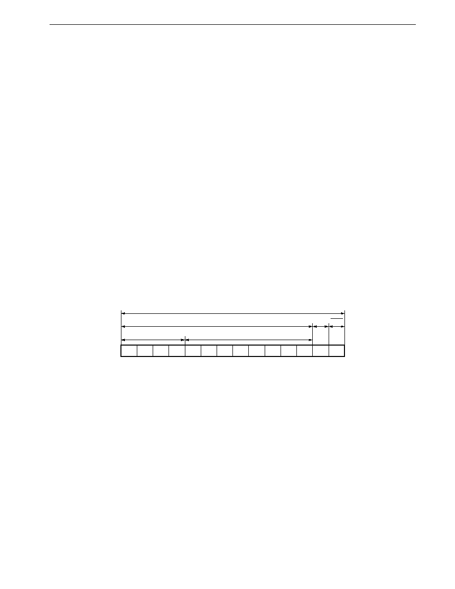
471
CHAPTER 20 IEBus CONTROLLER
Preliminary User's Manual U13987EJ1V0UM00
(4) Slave address field
The master outputs the address of the unit with which it is to communicate.
Figure 20-3 shows the configuration of the slave address field.
A parity bit is output after a 12-bit slave address has been transmitted in order to prevent a wrong slave address from
being received by mistake. Next, the master unit detects an acknowledge signal from the slave unit to confirm that
the slave unit exists on the bus. When the master has detected the acknowledge signal, it starts outputting the control
field. During broadcasting communication, however, the master does not detect the acknowledge bit but starts
outputting the control field.
The slave unit outputs the acknowledge signal if its slave address coincides and if the slave detects that the parities
of both the master address and slave address are even. The slave unit judges that the master address or slave address
has not been correctly received and does not output the acknowledge signal if the parities are odd. At this time, the
master unit is in the standby (monitor) status, and communication ends.
During broadcasting communication, the slave address is used to identify group-unit broadcasting or all-unit
broadcasting, as follows:
If slave address is FFFH:
All-unit broadcasting communication
If slave address is other than FFFH:
Group-unit broadcasting communication
Remark
The group No. during group-unit broadcasting communication is the value of the high-order 4 bits of the slave
address.
If one unit occupies the bus as the master, the address set by the slave address register (SAR) is output.
Figure 20-3. Slave Address Field
Slave address field
Unit No.
MSB
LSB
ACK
Parity
Slave address (12 bits)
Group No.
(5) Control field
The master outputs the operation it requires the slave to perform, by using this field.
The configuration of the control field is as shown in Figure 20-4.
If the parity following the control bit is even and if the slave unit can execute the function required by the master unit,
the slave unit outputs an acknowledge signal and starts outputting the telegraph length field. If the slave unit cannot
execute the function required by the master unit even if the parity is even, or if the parity is odd, the slave unit does
not output the acknowledge signal, and returns to the standby (monitor) status.
The master unit starts outputting the telegraph field after confirming the acknowledge signal.
If the master cannot confirm the acknowledge signal, the master unit enters the standby status, and communication
ends. During broadcasting communication, however, the master unit does not confirm the acknowledge signal, and
starts outputting the telegraph length field.
Table 20-2 shows the contents of the control bits.
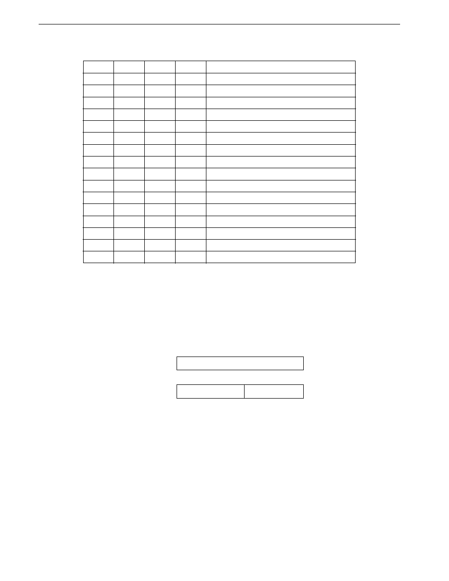
472
CHAPTER 20 IEBus CONTROLLER
Preliminary User's Manual U13987EJ1V0UM00
Table 20-2. Contents of Control Bits
Bit 3
Note 1
Bit 2
Bit 1
Bit 0
Function
0
0
0
0
Reads slave status
0
0
0
1
Undefined
0
0
1
0
Undefined
0
0
1
1
Reads data and locks
Note 2
0
1
0
0
Reads lock address (low-order 8 bits)
Note 3
0
1
0
1
Reads lock address (high-order 4 bits)
Note 3
0
1
1
0
Reads slave status and unlocks
Note 2
0
1
1
1
Reads data
1
0
0
0
Undefined
1
0
0
1
Undefined
1
0
1
0
Writes command and locks
Note 2
1
0
1
1
Writes data and locks
Note 2
1
1
0
0
Undefined
1
1
0
1
Undefined
1
1
1
0
Writes command
1
1
1
1
Writes data
Notes 1. The telegraph length bit of the telegraph length field and data transfer direction of the data field change as
follows depending on the value of bit 3 (MSB).
If bit 3 is `1': Transfer from master unit to slave unit
If bit 3 is `0': Transfer from slave unit to master unit
2. This is a control bit that specifies locking or unlocking (refer to 20.1.7 (4) Locking and unlocking).
3. The lock address is transmitted in 1-byte (8-bit) units and is configured as follows:
MSB
Low-order 8 bits
Undefined
High-order 4 bits
Control bit: 4H
Control bit: 5H
LSB
If the control bit received from the master unit is not as shown in Table 20-3, the unit locked by the master
unit rejects accepting the control bit, and does not output the acknowledge bit.
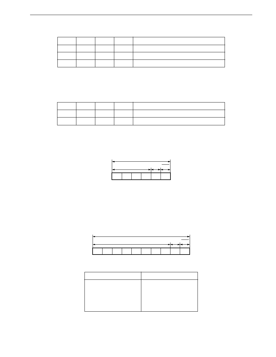
473
CHAPTER 20 IEBus CONTROLLER
Preliminary User's Manual U13987EJ1V0UM00
Table 20-3. Control Field for Locked Slave Unit
Bit 3
Bit 2
Bit 1
Bit 0
Function
0
0
0
0
Reads slave status
0
1
0
0
Reads lock address (low-order 8 bits)
0
0
0
1
Reads lock address (high-order 4 bits)
If the unlocked unit receives the control data shown in Table 20-4, the unit rejects accepting the control data
and does not output the acknowledge bit.
Table 20-4. Control Field for Unlocked Slave Unit
Bit 3
Bit 2
Bit 1
Bit 0
Function
0
1
0
0
Interrupts lock address (low-order 8 bits)
0
1
0
1
Interrupts lock address (high-order 4 bits)
If one unit occupies the bus as the master, the value set to the control data register (CDR) is output.
Figure 20-4. Control Field
MSB
LSB
ACK
Parity
Control bit (4 bits)
Control field
(6) Telegraph length field
This field is output by the transmission side to inform the reception side of the number of bytes of the transmit data.
The configuration of the telegraph length field is as shown in Figure 20-5.
Table 20-5 shows the relation between the telegraph length bit and the number of transmit data.
Figure 20-5. Telegraph Length Field
MSB
LSB
Telegraph length field
Telegraph length bit (8 bits)
Parity ACK
Table 20-5. Contents of Telegraph Length Bit
Telegraph Length Bit (Hex)
Number of Transmit Data Bytes
01H
1 byte
02H
2 bytes
|
|
FFH
255 bytes
00H
256 bytes
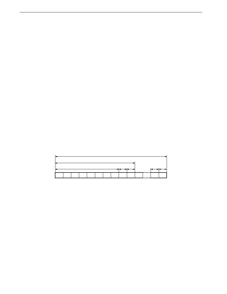
474
CHAPTER 20 IEBus CONTROLLER
Preliminary User's Manual U13987EJ1V0UM00
The operation of the telegraph length field differs depending on whether the master transmits (when control bit 3 is
1) or receives (when control bit 3 is 0) data.
<1> When master transmits data
The telegraph length bit and parity bit are output by the master unit. When the slave unit detects that the parity
is even, it outputs the acknowledge signal, and starts outputting the data field. During broadcasting
communication, however, the slave unit does not output the acknowledge signal.
If the parity is odd, the slave unit judges that the telegraph length bit has not been correctly received, does not
output the acknowledge signal, and returns to the standby (monitor) status. At this time, the master unit also
returns to the standby status, and communication ends.
<2> When master receives data
The telegraph length bit and parity bit are output by the slave unit. If the master unit detects that the parity bit
is even, it outputs the acknowledge signal.
If the parity bit is odd, the master unit judges that the telegraph length bit has not been correctly received, does
not output the acknowledge signal, and returns to the standby status. At this time, the slave unit also returns
to the standby status, and communication ends.
(7) Data field
This is data output by the transmission side.
The master unit transmits or receives data to or from a slave unit by using the data field.
The configuration of the data field is as shown in Figure 20-6.
Figure 20-6. Data Field
Data field (number specified by telegraph length field)
MSB
LSB
One data
ACK
Parity
Control bit (8 bits)
ACK
Parity
Following the data bit, the parity bit and acknowledge bit are respectively output by the master unit and slave unit.
Broadcasting communication is used only when the master unit transmits data. At this time, the acknowledge bit is
ignored.

475
CHAPTER 20 IEBus CONTROLLER
Preliminary User's Manual U13987EJ1V0UM00
The operation differs as follows depending on whether the master transmits or receives data.
<1> When master transmits data
When the master units writes data to a slave unit, the master unit transmits the data bit and parity bit to the slave
unit. If the parity is even and receive data is not stored in the data register (DR) when the slave unit receives
the data bit and parity bit, the slave unit outputs an acknowledge signal. If the parity is odd or if receive data
is stored in the DR, the slave unit rejects receiving the data, and does not output the acknowledge signal.
If the slave unit does not output the acknowledge signal, the master unit transmits the same data again. This
operation continues until the master detects the acknowledge signal from the slave unit, or the data exceeds the
maximum number of transmit bytes.
If the data is continuous and the maximum number of transmit bytes is not exceeded when the parity is even
and when the slave unit outputs the acknowledge signal, the master unit transmits the next data.
During broadcast communication, the slave unit does not output the acknowledge signal, and the master unit
transfers 1 byte of data at a time. During broadcast communication, the slave unit receives the data and parity
bits, and if the parity is odd or receive data is stored in the DR, reception is considered not to have been performed
correctly and is stopped.
<2> When master receives data
When the master unit reads data from a slave unit, the master unit outputs a sync signal corresponding to all
the read bits.
The slave unit outputs the contents of the data and parity bits to the bus in response to the sync signal from the
master unit.
The master unit reads the data and parity bits output by the slave unit, and checks the parity.
If the parity is odd or the DR is receiving data, the master unit refuses to acknowledge this data and does not
output the acknowledge signal. If the maximum number of transmit bytes is a value within the range that can
be transmitted in one communication frame, the master unit repeats reading the same data.
If the parity is even and the DR is not receiving data, the master unit accepts the data and returns the acknowledge
signal. If the maximum number of transmit bytes is within the value that can be transmitted in one frame, the
master unit reads the next data.
(8) Parity bit
The parity bit is used to confirm that the transmit data has no error.
The parity bit is appended to each data of the master address, slave address, control, telegraph length, and data bits.
The parity is an even parity. If the number of bits in the data that are `1' is odd, the parity bit is `1'. If the number of
bits in the data that are `1' is even, the parity bit is `0'.
(9) Acknowledge bit
During normal communication (communication from one unit to another), an acknowledge bit is appended to the
following locations to confirm that the data has been correctly received.
�
End of slave address field
�
End of control field
�
End of telegraph length field
�
End of data field
The definition of the acknowledge bit is as follows:
�
`0': Indicates that the transmit data is recognized (ACK).
�
`1': Indicates that the transmit data is not recognized (NACK).

476
CHAPTER 20 IEBus CONTROLLER
Preliminary User's Manual U13987EJ1V0UM00
During broadcast communication, however, the content of the acknowledge bit is ignored.
<1> Last acknowledge bit of slave address field
The last acknowledge bit of the slave address field serves as NACK in any of the following cases, and transmission
is stopped.
�
If the parity of the master address bit or slave address bit is incorrect
�
If a timing error (error in bit format) occurs
�
If a slave unit does not exist
<2> Last acknowledge bit of control field
The last acknowledge bit of the control field serves as NACK in any of the following cases, and transmission is
stopped.
�
If the parity of the control bit is incorrect
�
When control bit 3 is "1" (write operation) when the slave receive enable flag (ENSLVRX)
Note
is not set
�
When control bits for which ENSLVRX
Note
is not set are data read (3H, 7H)
�
If control bits 3H, 6H, 7H, AH, BH, EH, or FH are requested from a unit other than one for which lock has been
set
�
If the control bit indicates reading of a lock address (4H or 5H) even when locking is not set
�
If a timing error occurs
�
If the control bit is undefined
Note Bit 3 of the bus control register (BCR)
Cautions 1. When the slave status request control data is received even if the slave transmit enable
flag (ENSLVTX) is not set, ACK is always returned.
2. When data/command write control data is received even when the slave receive enable
flag (ENSLVRX) is not set, the control field acknowledge bit returns NACK.
Prohibiting receive operations (stopping communication) using ENSLVRX is limited to
individual sommunication. In the case of broadcast communication, communication
continues until a data request interrupt (INTIE1) or end interrupt (INTIE2) is generated.
<3> Last acknowledge bit of telegraph length field
The last acknowledge bit of the telegraph length field serves as NACK in any of the following cases, and
transmission is stopped.
�
If the parity of the telegraph length bit is incorrect
�
If a timing error occurs
<4> Last acknowledge bit of data field
The last acknowledge bit of the data field serves as NACK in any of the following cases, and transmission is
stopped.
�
If the parity of the data bit is incorrect
Note
�
If a timing error occurs after the preceding acknowledge bit has been transmitted
�
When receive data is stored in the data register (DR), and no more data can be accepted
Note
.
Note In this case, for the individual communication, if the maximum number of transmission bytes is a value
within the range that can be transmitted in one frame, the transmission side performs transmission of
that data field again. In the case of broadcast communication, the transmission side does not perform
transmission of that data field again, and a transmission error occurs on the receiving side and reception
is stopped.

477
CHAPTER 20 IEBus CONTROLLER
Preliminary User's Manual U13987EJ1V0UM00
20.1.7 Transmit data
(1) Slave status
The master unit can learn why the slave unit did not return the acknowledge bit (ACK), by reading the slave status.
The slave status is determined depending on the result of the last communication the slave unit has executed.
All the slave units can supply information on the slave status.
Table 20-6 shows the meaning of the slave status.
Figure 20-7. Bit Configuration of Slave Status
MSB
LSB
Bit 7
Bit 6
Bit 5
Bit 4
Bit 3
Bit 2
Bit 1
Bit 0
Table 20-6. Meaning of Slave Status
Bit
Value
Meaning
Bit 0
Note 1
0
Transmit data is not written to data register (DR)
1
Transmit data is written to DR
Bit 1
Note 2
0
Receive data is not saved to DR
1
Receive data is saved to DR
Bit 2
0
Unit is not locked
1
Unit is locked
Bit 3
0
Fixed to `0'
Bit 4
Note 3
0
Slave transmission is stopped
1
Slave transmission is ready
Bit 5
0
Fixed to `0'
Bit 7
00
Mode 0
Indicates highest mode supported by unit
Note 4
Bit 6
01
Mode 1
10
Mode 2
11
Not used
Notes 1. The value of this buffer of the
�
PD784938 Subseries is initialized to 1 at reset.
2. The receive buffer of the
�
PD784938 Subseries has a capacity of 1 byte.
3. When the
�
PD784938 Subseries serves as a slave unit, this bit corresponds to the status indicated by bit
4 (ENSLVTX) of the bus control register (BCR).
4. When the
�
PD784938 Subseries serves as a slave unit, bits 7 and 6 are fixed to `0' and `1' (mode 1),
respectively.

478
CHAPTER 20 IEBus CONTROLLER
Preliminary User's Manual U13987EJ1V0UM00
(2) Lock address
When the lock address is read (control bit: 4H or 5H), the address (12 bits) of the master unit that has issued the lock
instruction is configured in 1-byte units as shown below and read.
Figure 20-8. Configuration of Lock Address
MSB
Low-order 8 bits
Undefined
High-order 4 bits
Control bit: 4H
Control bit: 5H
LSB
(3) Data
If the control bit indicates reading of data (3H or 7H), the data in the data buffer of the slave unit is read by the master
unit.
If the control bit indicates writing of data (BH or FH), the data received by the slave unit is processed according to the
operation rule of that slave unit.
(4) Locking and unlocking
The lock function is used when a message is transferred in two or more communication frames.
The unit that is locked does not receive data from units other than the one that has locked the unit.
A unit is locked or unlocked as follows:
<1> Locking
If the communication frame is completed without succeeding in transmission or reception of the data of the number
of bytes specified by the telegraph length bit after the acknowledge bit `0' of the telegraph length field has been
transmitted or received by the control bit that specifies locking (3H, AH, or BH), the slave unit is locked by the
master unit. At this time, the bit (bit 2) in the byte indicating the slave status is set to `1'.
<2> Unlocking
After transmitting or receiving data of the number of data bytes specified by the telegraph length bit in one
communication frame by the control bit that has specified locking (3H, AH, or BH), or the control bit that has
specified unlocking (6H), the slave unit is unlocked by the master unit. At this time, the bit related to locking (bit
2) in the byte indicating the slave status is reset to `0'.
Locking or unlocking is not performed during broadcasting communication.

479
CHAPTER 20 IEBus CONTROLLER
Preliminary User's Manual U13987EJ1V0UM00
20.1.8 Bit format
Figure 20-9 shows the format of the bits constituting the communication frame of the IEBus.
Figure 20-9. Bit Format of IEBus
Logic "1"
Logic "0"
Preparation
period
Synchronization
period
Data period
Stop period
Preparation period:
First low-level (logic "1") period
Synchronization period: Next high-level (logic "0") period
Data period:
Period indicating value of bit
Stop period:
Last low-level (logic "1") period
The synchronization period and data period are almost equal to each other in length.
The IEBus synchronizes each 1 bit. The specifications on the time of the entire bit and the time related to the period
allocated to that bit differ depending on the type of the transmit bit, or whether the unit is the master unit or a slave unit.

480
CHAPTER 20 IEBus CONTROLLER
Preliminary User's Manual U13987EJ1V0UM00
20.2 Simple IEBus Controller
The
�
PD784938 has a newly developed IEBus controller. The functions of this IEBus controller are limited as compared
with the IEBus interface functions of the existing models (provided to the 78K/0 Series).
Table 20-7 compares the IEBus interface functions of the existing models with the simple IEBus interface functions of
the
�
PD784938 Subseries.
Table 20-7. Comparison between Existing and Simple IEBus Interface Functions
Item
Existing Function (IEBus of 78K/0)
Simple IEBus
Communication mode
Modes 0, 1, and 2
Fixed to mode 1
Internal system clock
6.0 (6.29) MHz
Internal buffer size
Transmit buffer: 33 bytes (FIFO)
Transmit/receive data register
Receive buffer: 40 bytes (FIFO)
Up to 4 frames can be received.
CPU processing
Hardware processing
Communication start preprocessing (data setting)
Setting and management of each communication
status
1-byte data write processing
1-byte data read processing
Management of transmission such as slave status
Management of plural frames, master request
reprocessing
Bit processing (modulation/demodulation, error
detection)
Field processing (generation/management)
Arbitration result detection
Parity processing (generation/error detection)
Automatic return of ACK/NACK
Automatic data transmission re-processing
Communication start preprocessing (data setting)
Setting and management of each communication
status
Writing data to transmit buffer
Reading data from receive buffer
Bit processing (modulation/demodulation, error
detection)
Field processing (generation/management)
Arbitration result detection
Parity processing (generation/error detection)
Automatic return of ACK/NACK
Automatic data re-processing
Automatic master re-processing
Note
Transmission processing such as automatic slave
status transmission
Plural-frame reception processing
Note Automatic master re-processing: After generating the master request, if the master request is cancelled by
arbitration, etc., the bus is released and automatically re-issue the master
request.
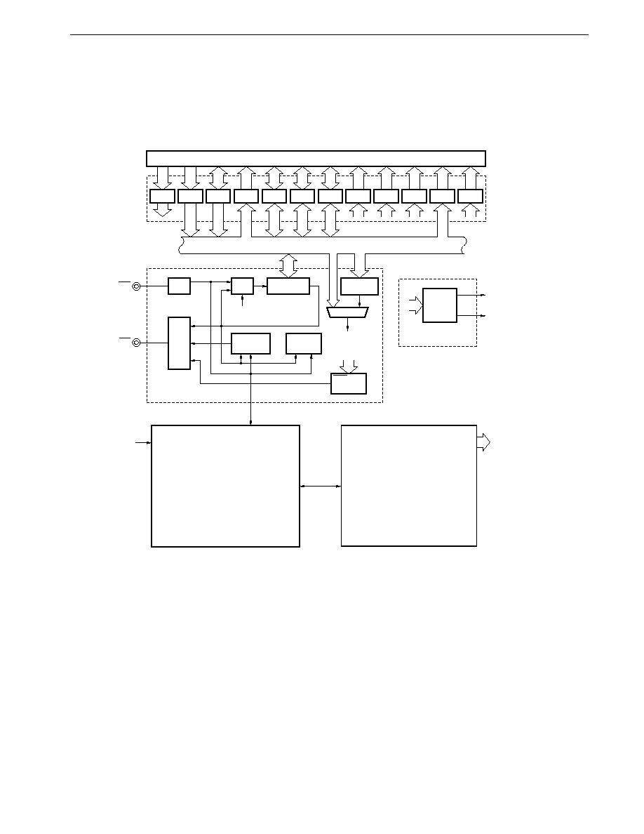
481
CHAPTER 20 IEBus CONTROLLER
Preliminary User's Manual U13987EJ1V0UM00
20.3 IEBus Controller Configuration
Figure 20-10 shows the block diagram of the IEBus controller.
Figure 20-10. IEBus Controller Block Diagram
BCR (8)
UAR (12)
SAR (12)
PAR (12)
CDR (8)
DLR (8)
DR (8)
USR (8)
ISR (8)
SSR (8) SCR (8) CCR (8)
8
12
12
8
8
8
8
12
8
8
8
8
8
8
8
8
8
8
8
8
NF
RX
TX
MPX
MPX
12-bit latch
Comparator
Contention
detection
ACK
generation
Parity generation
error detection
TX/RX
Interrupt
control
circuit
Interrupt control block
INT request
CPU interface block
Internal
registers
(vector, macro
service)
IEBus interface block
CLK
Bit processing block
Field processing block
Internal bus R/W
PSR (8 bits)
8
5
8
12
12
12
Internal bus
8
12

482
CHAPTER 20 IEBus CONTROLLER
Preliminary User's Manual U13987EJ1V0UM00
�
Hardware configuration and function
The IEBus mainly consists of the following six internal blocks.
�
CPU interface block
�
Interrupt control block
�
Internal registers
�
Bit processing block
�
Field processing block
�
IEBus interface block
<CPU interface block>
This is a control block that interfaces between the CPU (78K/IV) and IEBus.
<Interrupt control block>
This control block transfers interrupt request signals from the IEBus to the CPU.
<Internal registers>
These registers set data to the control registers and fields that control the IEBus (for the internal registers, refer to
20.4 Internal Registers of IEBus Controller).
<Bit processing block>
This block generates and disassembles bit timing, and mainly consists of a bit sequence ROM, 8-bit preset timer,
and comparator.
<Field processing block>
This block generates each field in the communication frame, and mainly consists of a field sequence ROM, 4-bit down
counter, and comparator.
<IEBus interface block>
This is the interface block for an external driver/receiver, and mainly consists of a noise filter, shift register, collision
detector, parity detector, parity generation circuit, and ACK/NACK generation circuit.

483
CHAPTER 20 IEBus CONTROLLER
Preliminary User's Manual U13987EJ1V0UM00
20.4 Internal Registers of IEBus Controller
The IEBus controller consists of the following registers:
20.4.1 Internal register list
Table 20-8 lists the internal registers of the IEBus controller.
Table 20-8. Internal Registers of IEBus Controller
Address
IEBus Register Name
Symbol
R/W
Bit Units for Manipulation
Initial Value
1 bit
8 bits
16 bits
0FFB0H
Bus control register
BCR
R/W
--
00H
0FFB2H
Unit address register
UAR
--
--
0000H
0FFB4H
Slave address register
SAR
--
--
0FFB6H
Partner address register
PAR
R
--
--
0FFB8H
Control data register
CDR
R/W
--
--
01H
0FFB9H
Telegraph length register
DLR
--
--
0FFBAH
Data register
DR
--
--
00H
0FFBBH
Unit status register
USR
R
--
0FFBCH
Interrupt status register
ISR
R/W
--
0FFBDH
Slave status register
SSR
R
--
41H
0FFBEH
Communication success counter
SCR
--
--
01H
0FFBFH
Transmit counter
CCR
--
--
20H
Cautions 1. The above registers are mapped to the SFR space.
2. Registers UAR, SAR, and PAR must be manipulated in word units.
3. Instructions in Read Modify Write mode (such as XCH and ROL4) cannot be used for DR, CDR,
DLR, and ISR.
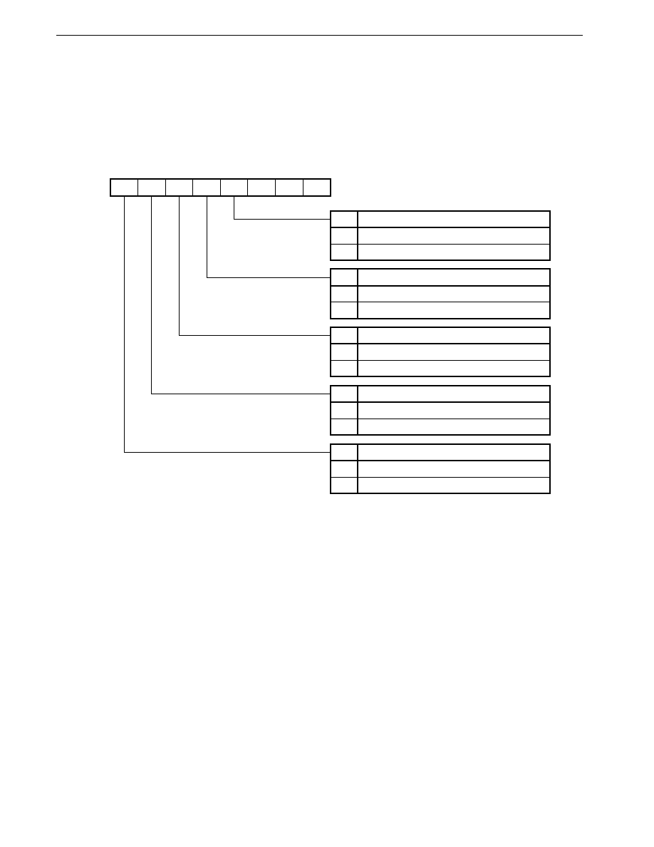
484
CHAPTER 20 IEBus CONTROLLER
Preliminary User's Manual U13987EJ1V0UM00
20.4.2 Description of internal registers
Each internal register of the IEBus controller is explained below.
(1) Bus control register (BCR)
Figure 20-11. Bus Control Register (BCR) Format
7
ENIEBUS
6
MSTRQ
5
ALLRQ
4
ENSLVTX
3
ENSLVRX
2
0
1
0
0
0
Address
0FFB0H
After reset
00H
R/W
R/W
ENSLVRX
0
1
Slave Reception Enable Flag
Slave reception disabled
Slave reception enabled
ENSLVTX
0
Slave Transmission Enable Flag
Slave transmission disabled
1
Slave transmission enabled
ALLRQ
0
Broadcasting Request Flag
Requests individual communication
1
Requests broadcasting communication
MSTRQ
0
Master Request Flag
Does not request IEBus unit as master
1
Requests IEBus unit as master
BCR
ENIEBUS
0
Communication Enable Flag
Stops IEBus unit
1
Makes IEBus unit active

485
CHAPTER 20 IEBus CONTROLLER
Preliminary User's Manual U13987EJ1V0UM00
�
Communication enable flag (ENIEBUS) ... Bit 7
[Set/reset condition]
Set:
Through software manipulation
Reset: Through software manipulation
Caution Before setting this flag, the following registers for communication must be set.
During master transmission
UAR
During master reception
During slave transmission
During slave reception
�
Master request flag (MSTRQ) ... Bit 6
[Set/reset condition]
Set:
Through software manipulation
Reset: Through hardware at the end of the arbitration period
Caution Make a remaster request through software processing in case the unit loses in contention.
�
Broadcasting request flag (ALLRQ) ... Bit 5
[Set/reset condition]
Set:
Through software manipulation
Reset: Through software manipulation
Caution Be sure to set this flag to request broadcasting communication, and set bit 6.
�
Slave transmission enable flag (ENSLVTX) ... Bit 4
[Set/reset condition]
Set:
Through software manipulation
Reset: Through software manipulation
Cautions 1. Clear this flag before setting the master request flag during master request. If a slave
transmission request is made by the master with this flag not set during slave, or if the
disabled status is to be returned to the enabled status, the next new frame and those that
follow become valid.
2. When ENSLVTX is not set, upon reception of data/command write control data "3H, 7H",
the acknowledge bit of the control field returns NACK.
3. Even if ENSLVTX has been reset, when slave status request control data is returned, a status
interrupt (INTIE2) is generated and communication is continued.
�
Slave reception enable flag (ENSLVRX) ... Bit 3
[Set/reset condition]
Set:
Through software manipulation
Reset: Through software manipulation
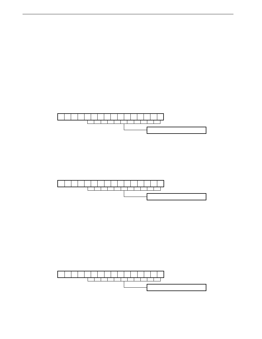
486
CHAPTER 20 IEBus CONTROLLER
Preliminary User's Manual U13987EJ1V0UM00
Caution When the CPU is busy with other processing, slave reception can be disabled by resetting this
flag and returning NACK with the acknowledge bit of the control field. Therefore, when this flag
is reset, individual communication can be disabled, but broadcasting communication cannot.
Furthermore, during individual communication, start interrupt (INTIE2) is generated. When CPU
processing is prioritized (in case neither reception nor transmission are to be performed), reset
ENIEBUS (communication enable flag) and stop the IEBus unit. Also, when returning to the
enabled status from the disabled status, the operation becomes effective from the next new
frame.
(2) Unit address register (UAR)
This register sets the unit address of an IEBus unit. This register must be always set before starting communication.
Figure 20-12. Unit Address Register (UAR) Format
15
0
14
0
13
0
12
0
UAR
11 10
9
8
7
6
5
4
3
2
1
0
Address
0FFB2H
After reset
0000H
R/W
R/W
Sets unit address (12 bits)
(3) Slave address register (SAR)
During master request, the value of this register is reflected on the value of the transmit data in the slave address field.
This register must be always set before starting communication.
Figure 20-13. Slave Address Register (SAR) Format
15
0
14
0
13
0
12
0
SAR
11 10
9
8
7
6
5
4
3
2
1
0
Address
0FFB4H
After reset
0000H
R/W
R/W
Sets slave address (12 bits)
(4) Partner address register (PAR)
[During slave unit]
The value of the receive data in the master address field (address of the master unit) is written to this register.
If a request "4H" to read the lock address (low-order 8 bits) is received from the master, the CPU must read the
value of this register, and write the data of the low-order 8 bits to the data register (DR).
If a request "5H" to read the lock address (high-order 4 bits) is received from the master, the CPU must read the
value of this register and write the data of the high-order 4 bits to DR.
Figure 20-14. Partner Address Register (PAR) Format
15
0
14
0
13
0
12
0
PAR
11 10
9
8
7
6
5
4
3
2
1
0
Address
0FFB6H
After reset
0000H
R/W
R
Sets partner address (12 bits)
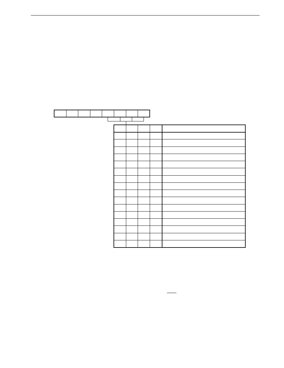
487
CHAPTER 20 IEBus CONTROLLER
Preliminary User's Manual U13987EJ1V0UM00
(5) Control data register (CDR)
[During master unit]
The data of the low-order 4 bits is reflected on the data transmitted in the control field. During master request, this
register must be set in advance before starting communication.
[During slave unit]
The data received in the control field is written to the low-order 4 bits.
When the status transmission flag (STATUS) is set, an interrupt (INTIE2) is issued, and each processing should
be performed by software, according to the value of the low-order 4 bits of this register.
Figure 20-15. Control Data Register (CDR) Format
7
6
5
4
3
2
1
0
Address After reset R/W
SELCL2
Function
0
0
0
0
1
1
1
1
0
0
0
0
1
1
1
1
Reads slave status
Undefined
Undefined
Reads data and locks
Reads lock address (low-order 8 bits)
Reads lock address (low-order 4 bits)
Reads slave status and unlocks
Reads data
Undefined
Undefined
Writes command and locks
Writes data and locks
Undefined
Undefined
Writes command
Writes data
SELCL1
0
0
1
1
0
0
1
1
0
0
1
1
0
0
1
1
SELCL0
0
1
0
1
0
1
0
1
0
1
0
1
0
1
0
1
0
0
0
0
MOD SELCL2 SELCL1 SELCL0 0FFB8H
01H
R/W
CDR
MOD
0
0
0
0
0
0
0
0
1
1
1
1
1
1
1
1
Cautions 1. Because the slave unit must judge whether the received data is a "command" or "data", it must
read the value of this register after completing communication.
2. The Read Modify Write instruction (such as XCH and ROL4) cannot be used for CDR.
3. If the master unit sets an undefined value, NACK is returned from the slave unit, and
communication is aborted. During broadcasting communication, however, the master unit
continues communication without recognizing ACK/NACK; therefore, make sure not to set an
undefined value to this register during broadcasting communication.
4. In the case of defeat in a bus conflict and a slave status request is received from the unit that
won, telegraph length register (DLR) is fixed to "01H". Therefore, in a re-request of the master
follows, the appointed telegraph length must be set to DLR.
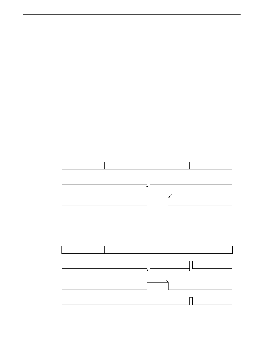
488
CHAPTER 20 IEBus CONTROLLER
Preliminary User's Manual U13987EJ1V0UM00
[Slave status response operation]
The ACK response operation of the control field differs depending on the status of slave side when a slave status
request (control data: "0H, 6H") and a lock address request "4H, 5H" are received.
<1> In unlocked status, when "0H, 6H" control data is received
Return ACK
<2> In unlocked status, when "4H, 5H" control data is received
Don't return ACK
<3> In locked status, when "0H, 4H, 5H, 6H" control data is
Return ACK
received from the request unit
<4> In locked status, when "0H, 4H, 5H" control data is received
from an address other than the request unit
Return ACK
<5> In locked status, when "6H" control data is received from an
address other than the request unit
Return ACK
In all cases from <1> to <5>, the status transmission flag (bit 4 of the interrupt status register (ISR)) is set upon
reception of the slave status and lock address request, and the status interrupt request (INTIE2) is generated. The
generation timing is the end of the control field parity bit (start of the ACK bit).
However, if ACK communication is not performed, an NACK error occurs at the end of the ACK bit and communication
is stopped.
Figure 20-16. Interrupt Generation Timing (in case of <1>, <3>, <4>)
Control bits (4 bits)
<Control field>
IEBus
sequence
INTIE2
Status
transmission flag
Internal
NACK flag
Parity bit (1 bit)
ACK bit (1 bit)
End with communication error
Flag is set upon reception
of "0H, 4H, 5H, 6H"
Flag is reset with CPU processing
Figure 20-17. Interrupt Generation Timing (in case of <2>, <5>)
Control bits (4 bits)
<Control field>
IEBus
sequence
INTIE2
Status
transmission flag
Internal
NACK flag
Parity bit (1 bit)
ACK bit (1 bit)
End with communication error
Flag is set upon reception
of "0H, 4H, 5H, 6H"
Error is set upon
NACK detection
Flag is reset with
CPU processing

489
CHAPTER 20 IEBus CONTROLLER
Preliminary User's Manual U13987EJ1V0UM00
In the case of <4> and <5>, communication is performed from other than lock request in the locked status, so that
even if the unit address is the target of the communication, no start interrupt or communication end interrupt (INTIE2)
is generated. However, if a slave status, lock address request is received, the status transmission flag (bit 4 of
interrupt status register (ISR)) is set, and a status interrupt request (INTIE2) is generated. In this way, even if the
same control data is received in the locked status, the INTIE2 generation timing differs depending on whether the
master side is the lock request address (<3>) or it is a different address.
Figure 20-18. INTIE2 Interrupt Generation Timing in Locked Status (in case of <4>, <5>)
<Control field>
IEBus
sequence
Start
Broad-
casting
Master address
(12 + A)
Slave address
(12 + P + A)
Control
(4 + P + A)
Telegraph
length
(8 + P + A)
Data
(8 + P + A)
INTIE2
Status interrupt
Figure 20-19. INTIE2 Interrupt Generation Timing in Locked Status (in case of <3>)
Status
interrupt
INTIE2
Start interrupt
Communication
end interrupt
<Control field>
IEBus
sequence
Start
Broad-
casting
Master address
(12 + P)
Slave address
(12 + P + A)
Control
(4 + P + A)
Telegraph
length
(8 + P + A)
Data
(8 + P + A)
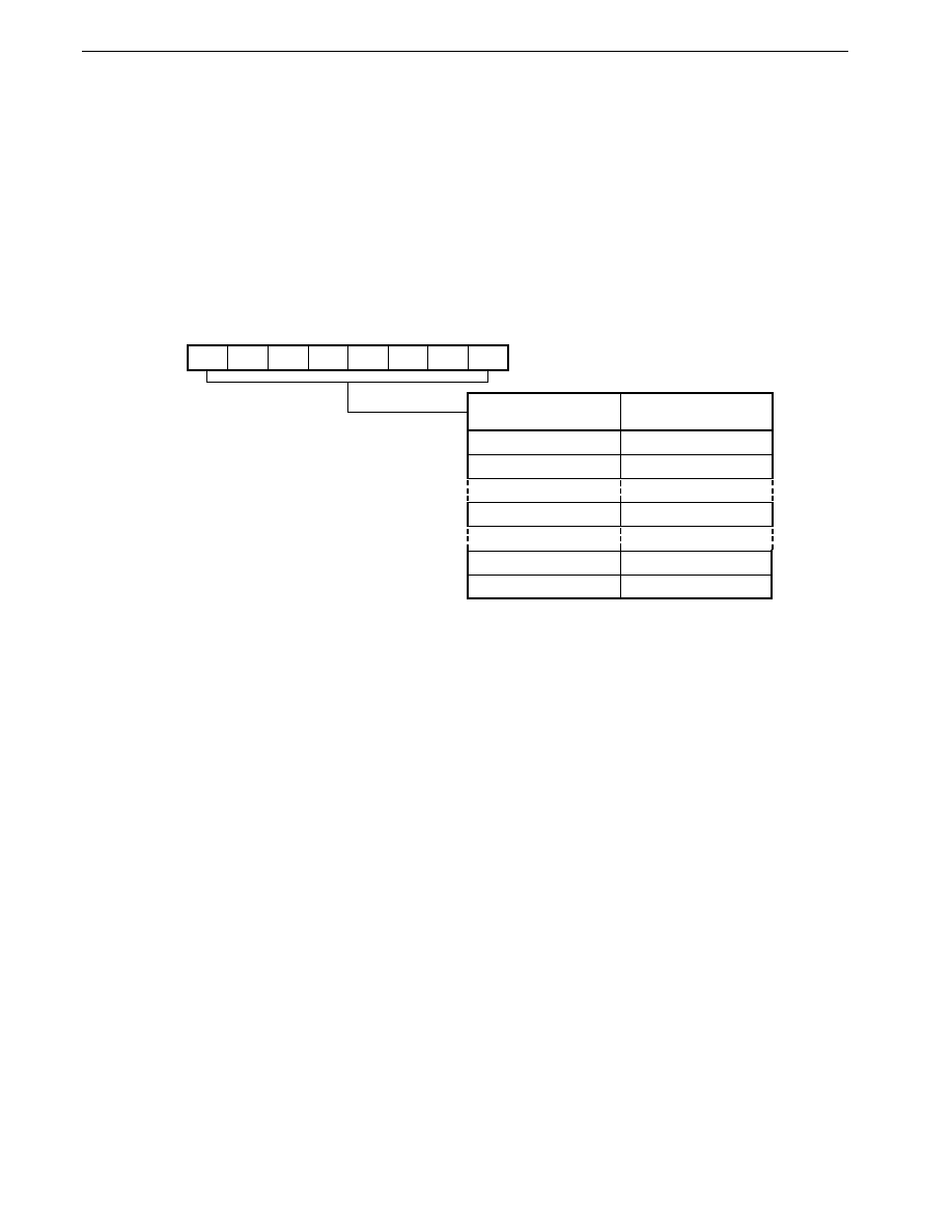
490
CHAPTER 20 IEBus CONTROLLER
Preliminary User's Manual U13987EJ1V0UM00
(6) Telegraph length register (DLR)
[During transmission unit] ... Master transmission, slave transmission
The data of this register is reflected on the data transmitted in the telegraph length field and indicates the number
of bytes of the transmit data.
This register must be set in advance before transmission.
[During reception unit] ... Master reception, slave reception
The receive data in the telegraph length field transmitted from the transmission unit is written to this register.
Figure 20-20. Telegraph Length Register (DLR) Format
7
6
5
4
3
2
1
0
Address After reset R/W
Remaining Number of
Communication Data Bytes
1 byte
2 bytes
32 bytes
255 bytes
256 bytes
0
0
0
0
0
0
0
0
0FFB9H
01H
R/W
DLR
01H
02H
20H
FFH
00H
Cautions 1. If the master issues a request "0H, 4H, 5H, or 6H" to transmit a slave status and lock address
(high-order 4 bits, low-order 8 bits), the contents of this register are set to "01H" by hardware;
therefore, the CPU does not have to set this register.
An instruction of Read Modify Write mode (such as XCH and ROL4) cannot be used for DLR.
2. In the case of defeat in a bus conflict and a slave status request is received from the unit that
won, DLR is fixed to "01H". Therefore, if a re-request of the master follows, the appointed
telegraph length must be set to DLR.
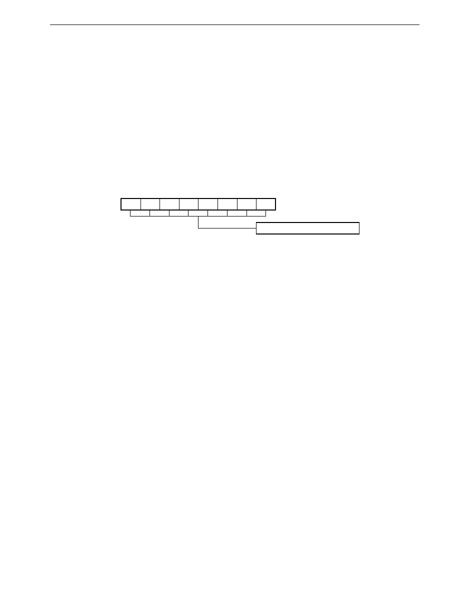
491
CHAPTER 20 IEBus CONTROLLER
Preliminary User's Manual U13987EJ1V0UM00
(7) Data register (DR)
[During transmission unit]
The data (1 byte) written to the data register (DR) is stored to the internal shift register of the IEBus. It is then output
from the most significant bit, and an interrupt (INTIE1) is issued to the CPU each time 1 byte has been transmitted.
INTIE is generated at the timing of the data register (DR) value stored in the internal shift register of the IEBus.
However, INTIE1 is not generated when the last byte and the 32nd byte (last byte of one communication frame)
is delivered to the internal register.
[During reception unit]
One byte of the data received by the internal shift register of the IEBus is stored to this register.
Each time 1 byte has been correctly received, an interrupt (INTIE1) is issued.
Figure 20-21. Data Register (DR) Format
7
6
5
4
3
2
1
0
Address After reset R/W
0FFBAH
00H
R/W
DR
Sets communication data (8 bits)
Caution If the next data is not in time while the transmission unit is set, an underrun occurs, and a
communication error interrupt (INTIE2) occurs.
An instruction of Read Modify Write mode (such as XCH and ROL4) cannot be used for DR.
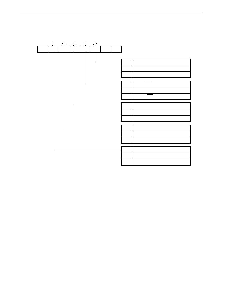
492
CHAPTER 20 IEBus CONTROLLER
Preliminary User's Manual U13987EJ1V0UM00
(8) Unit status register (USR)
Figure 20-22. Unit Status Register (USR) Format
0
SLVRQ ARBIT ALLTRNS
ACK
LOCK
0
0
7
6
5
4
3
2
1
0
USR
0FFBBH
Address
00H
After reset
R
R/W
LOCK
0
1
Lock Status Flag
Non-lock status
Lock status
ACK
0
1
ACK Transmission Flag
Transmits NACK
Transmits ACK
ALLTRNS
0
1
Broadcasting Communication Flag
Individual communication status
Broadcasting communication status
ARBIT
0
1
Contention Flag
Wins in contention
Loses in contention
SLVRQ
0
1
Slave Request Flag
No slave request
Slave request

493
CHAPTER 20 IEBus CONTROLLER
Preliminary User's Manual U13987EJ1V0UM00
�
Slave request flag (SLVRQ) ... Bit 6
This flag indicates whether the master has issued a slave request.
�
Contention flag (ARBIT) ... Bit 5
This flag indicates the result of contention.
[Set/reset condition]
Set:
Set if the data output by a unit does not coincide with the data on the bus line during the arbitration period
after the master request has been made.
Reset:
Cleared at start bit timing
�
Broadcasting communication flag (ALLTRANS)... Bit 4
This flag indicates if the unit is performing broadcasting communication. The contents of the flag are initialized upon
detection of the start bit of each frame, and updated to the broadcasting field.
The set/bit conditions change depending on the broadcasting field bit reception data at all times except initialization
(reset) through system reset.
[Set/reset condition]
Set:
Upon reception of "broadcasting" in broadcasting field
Reset:
Upon reception of "individual" in broadcasting field, or upon input of system reset.
Caution Update of the broadcasting communication flag is performed regardless of whether or not the
communication target is the unit address.
Figure 20-23. Broadcasting Communication Flag Operation Example
Broad-
casting
IEBus
sequence
No reset with start bit
INTIE2
Set
Reset
M10
M11
M10
M11
Broad-
casting
Start
Start
�
ACK transmission flag (ACK) ... Bit 3
This flag indicates whether ACK is transmitted during the ACK period of each field while the unit serves as a reception
unit. The content of the flag is updated during the ACK period of each frame.
If the internal circuit is initialized due to the occurrence of a parity error, the content of the flag cannot be updated
during the ACK period of the field.
�
Lock status flag (LOCK) ... Bit 2
This flag indicates whether the unit is locked.
[Set/reset condition]
Set:
Set if lock specifications "3H, 6H, AH, and BH" are received in the control field, and if the communication
end flag is "L" and frame end flag is "H".
Reset:
If the communication enable flag is cleared.
If unlocking commands "3H, 6H, AH, and BH" are received by the control field and the communication
end flag is set.
Caution Locking or unlocking is not performed during broadcasting communication.
494
CHAPTER 20 IEBus CONTROLLER
Preliminary User's Manual U13987EJ1V0UM00
(9) Interrupt status register (ISR)
This status register indicates the status when an interrupt of the IEBus is issued. User must read this register and
perform the subsequent processing each time an interrupt has been generated.
Clear the contents of the following communication error flag (IEERR), start interrupt flag (START), and status
transmission flag (STATUS) through software manipulation in vector interrupt processing. Also be sure to check and
clear the contents of the communication end flag (ENDTRANS) and frame end flag (ENDFRAM) through software
manipulation.
Figure 20-24. Interrupt Status Register (ISR) Format
0
IEERR START STATUS ENDTRNS ENDFRAM
0
0
7
6
5
4
3
2
1
0
ISR
0FFBCH
Address
00H
After reset
R/W
R/W
ENDFRAM
0
1
Frame End Flag
Frame does not end
Frame ends
ENDTRNS
0
1
Communication End Flag
Communication does not end
Communication ends
STATUS
0
1
Status Transmission Flag
No status transmission request
Status transmission request
START
0
1
Start Interrupt Flag
Interrupt after ACK period of slave address
field
Interrupt during ACK period of slave
address field
IEERR
0
1
Communication Error Flag
No communication error
Communication error occurs
Remark
Reset of IEER, STARTF, and STATUSF flags is performed by writing a byte in to the interrupt status register
(ISR).

495
CHAPTER 20 IEBus CONTROLLER
Preliminary User's Manual U13987EJ1V0UM00
�
Communication error flag (IEERR) ... Bit 6
This flag detects an error during communication.
[Set/reset condition]
Set:
Set if a timing error, parity error (except the data field), NACK reception (except the data field), or
underrun occurs
Reset:
Through software manipulation
�
Start interrupt flag (START) ... Bit 5
This flag indicates the interrupt during the ACK period of the slave address field.
[Set/reset condition]
Set:
Set in the slave address field during the master request.
Set if there was a slave request from the master. (In the case of lock status, only if there was a slave
request from the lock request unit.)
Reset:
Through software manipulation
�
Status transmission flag (STATUS) ... Bit 4
This flag indicates that the master transmits a slave status or lock address (high-order 4 bits, low-order 8 bits) while
the unit serves as a slave.
[Set/reset condition]
Set:
Set when "0H, 4H, 5H, or 6H" is received from the master in the control field while the unit serves as
a slave.
Reset:
Through software manipulation
�
Communication end flag (ENDTRNS) ... Bit 3
This flag indicates whether communication has been completed by the number of transmit bytes set by the telegraph
length field.
[Set/reset condition]
Set:
When the count value of the SCR counter has reached 0.
Reset:
When any of the master request flag, slave transmission enable flag, or slave reception enable flag is
set.
�
Frame end flag (ENDFRAM) ... Bit 2
This flag indicates whether communication of the maximum number of transmit bytes (32 bytes) specified by each
communication mode is completed.
[Set/reset condition]
Set:
When the count value of the CCR has reached 0.
Reset:
When any of the master request fag, slave transmission enable flag, or slave reception enable flag is
set

496
CHAPTER 20 IEBus CONTROLLER
Preliminary User's Manual U13987EJ1V0UM00
[Description of communication error source]
<Timing error>
Condition of occurrence:
If the high-/low-level width of the communication bit exceeds or falls below a rated
value.
Remark:
Each rated value is set by the bit processing block and is monitored by the internal
8-bit timer. If a timing error occurs, an interrupt is issued.
<Parity error>
Condition of occurrence:
If the generated parity and received parity do not coincide in each field while the unit
serves as a receive unit.
Remark:
During individual communication, if a parity error occurs in other than the data field,
an interrupt is issued.
During broadcasting communication, even if a parity error occurs in the data field, an
interrupt is issued.
Limitations:
If a broadcasting communication request is performed and a slave request
defeated in contention occurs, no interrupt is generated even if a parity error
occurs in the data field.
<NACK reception>
Condition of occurrence:
If NACK is received during the ACK period in the slave address, control, or telegraph
length field while the unit serves as a receive transmit unit.
Remark:
If NACK is received (transmitted) in other than the data field, an interrupt is issued.
<Underrun>
Condition of occurrence:
If the data that is to be transmitted next to the data register (DR) until ACK is received
is not written in time during data transmission.
Remark:
If underrun occurs, an interrupt is issued.
<Overrun>
Condition of occurrence:
When the unit is used as a receive unit, a data interrupt request (INTIE1), which stores
data one byte at a time in the data register (DR), is generated, and the CPU performs
DR read processing. If this read processing is late and the next data receive timing
starts, an overrun error occurs.
Remark:
When the unit is used for individual communication reception, no acknowledge is
returned during the ACK period of the next data. Through this, the transmission unit
performs retransmission of the data. Therefore, the communication count register
(CCR) is decremented, but the success count register (SCR) is not decremented.
When the unit is used for broadcast communication reception, a communication error
interrupt request (INTIE2) occurs, and reception is stopped. At this time, DR is not
updated. Moreover, no INTIE1 is generated, and the DR reception status flag (bit
1 of the timer mode control register (SSR)) is set (to 1) and maintained. The overrun
status is canceled using the data reception timing following DR read.

497
CHAPTER 20 IEBus CONTROLLER
Preliminary User's Manual U13987EJ1V0UM00
[Supplementary explanation of overrun error]
(1) If overrun occurs during individual communication reception, resulting in frame end
If DR read is not performed following the overrun status and data retransmission reaches the maximum number
of data transfer bytes (32 bytes), a frame end interrupt (INTIE2) occurs. The overrun status is maintained until
DR read is performed even after frame end.
(2) If the next reception starts in the case of (1) above, or if the next transmission starts without DR read
being performed, following reception of the last data, regardless of whether it is broadcasting or
individual communication
Even if communication is started to one's own address in the overrun status, an overrun caused NACK return
does not occur during the ACK period in each of the slave address, control, and telegraph length fields. However,
when DR read is not performed until data reception completion in the data field, no acknowledge is returned
and reception is not performed (DR update is not performed). If the next communication is not directed to one's
own address, DR is not updated until DR read is performed. Since the communication is not directed at one's
own address, data interrupt (INTIE1) or communication error interrupt (INTIE2) is not generated.
498
CHAPTER 20 IEBus CONTROLLER
Preliminary User's Manual U13987EJ1V0UM00
(10) Slave status register (SSR)
This register indicates the communication status of the slave unit. After receiving a slave status transmission request
from the master, the CPU reads this register, and writes a slave status to the data register (DR) to transmit the slave
status. At this time, the telegraph length is automatically set to "01H" that setting of telegraph length register (DLR)
is not required (because it is preset by hardware).
Figure 20-25. Slave Status Register (SSR) Format
0
1
0
STATSLV
0
STATLOCK STATRX STATTX
7
6
5
4
3
2
1
0
SSR
0FFBDH
Address
41H
After reset
R
R/W
STATTX
0
1
DR Transmit Status
Transmission data not stored in DR
Transmission data stored in DR
STATRX
0
1
DR Receive Status
Receiving data not stored in DR
Receiving data stored in DR
STATLOCK
0
1
Lock Status Flag
Unlock status
Lock status
STATSLV
0
1
Slave Transmission Enable Flag
Slave transmission stops
Slave transmission enabled
�
Slave transmission status flag (STATSLV) ... Bit 4
Reflects the content of the slave transmission enable flag.
�
Lock status flag (STATLOCK) ... Bit 2
Reflects the content of the lock status flag.
�
DR receive status (STATRX) ... Bit 1
The flag that indicates the receive status of the DR.
�
DR transmit status (STATTX) ... Bit 0
The flag that indicates the transmit status of the DR.
Bits 6 and 7 indicate the highest mode supported by the unit, and are fixed to "01H" (mode 1).
499
CHAPTER 20 IEBus CONTROLLER
Preliminary User's Manual U13987EJ1V0UM00
(11) Success count register (SCR)
This register reads the count value of the counter that decrements the value set by the telegraph length register by
ACK in the data field. When the count value has reached "00H", the communication end flag (ENDTRNS) is set.
Figure 20-26. Success Count Register (SCR) Format
7
6
5
4
3
2
1
0
SCR
0FFBEH
Address
01H
After Reset
R
R/W
Remaining Number of Communication Data Bytes
01H
02H
20H
FFH
00H
1 byte
2 bytes
32 bytes
255 bytes
0 byte (end of communication) or 256 bytes
Note
Note The bit length of the actual hard counter consists of 9 bits. When "00H" is read, it cannot be judged whether
the remaining number of communication data bytes is 0 (end of communication) or 256. Therefore, either the
communication end flag is used, or if "00H" is read when the first interrupt occurs at the beginning of
communication, the remaining number of communication data bytes is judged to be 256.
(12) Communication count register (CCR)
This register reads the count value of the counter that is preset to the maximum number of transmitted bytes (32 bytes)
per frame specified in mode 1 and is decremented during the ACK period of the data field regardless of ACK/NACK.
When the count value has reached "00H", the frame end flag (ENDFRAM) is set.
Figure 20-27. Communication Count Register (CCR) Format
7
6
5
4
3
2
1
0
Address After reset R/W
0FFBFH
20H
R
CCR
Number of transmitted bytes
�
Preset value in mode 1 and maximum number of transmitted bytes per frame ... 20H (32 bytes)
500
CHAPTER 20 IEBus CONTROLLER
Preliminary User's Manual U13987EJ1V0UM00
20.5 Interrupt Operations of IEBus Controller
20.5.1 Interrupt control block
<Interrupt request signal>
1.
Communication error
(IEERR)
2.
Start interrupt
(START)
3.
Status communication
(STATUS)
4.
End of communication
(ENDTRANS)
5.
End of frame
(ENDFRAM)
6.
Transmit data write request
(STATTX)
7.
Receive data read request
(STATRX)
1 through 5 of the above interrupt requests 1 are assigned to the interrupt status register (ISR). For details, refer to
Table 20-9 Interrupt Requests.
The configuration of the interrupt control block is illustrated below.
Figure 20-28. Configuration of Interrupt Control Block
Cautions 1.
With regard to ORed output of STATTX, STATRX, faster processing is aimed for by using a macro
service.
2.
With regard to ORed output of IEERR, START, STATUS, ENDTRANS, ENDFRAM, check the
interrupt generation source using vector interrupt processing.
IEERR
START
STATUS
ENDTRANS
ENDFRAM
STATTX
STATRX
IEBus macro
Interrupt control block
78K/IV CPU
INTIE1
INTIE2

501
CHAPTER 20 IEBus CONTROLLER
Preliminary User's Manual U13987EJ1V0UM00
20.5.2 Interrupt source list
The interrupt request signals of the internal IEBus controller in the 78K/IV Series can be classified into vector interrupts
and macro service interrupts. These interrupt processing can be specified through software manipulation.
The interrupt sources are listed below.
Table 20-9. Interrupt Source List
Interrupt Source
Condition of Generation
CPU Processing after
Remark
Unit
Field
Generation of Interrupt
Communication error
Undo communication processing
Communication error is OR output
(Timing error)
Master/slave
All fields
of timing error, parity error, NACK
(Parity error)
Reception
Other than data
reception, underrun error, and
(individual)
overrun error.
All fields
(broadcasting)
(NACK reception)
Transmission
Other than data
(individual)
(Underrun error)
Transmission
Data
(Overrun error)
Reception
Data
(broadcasting)
Start interrupt
Master
Slave/address
Slave request judgment
Interrupt always occurs if loses in
Contention judgment
contention during master request.
(If loses, remaster processing)
Communication preparation
processing
Slave
Slave/address
Slave request judgment
Generated only during slave
Communication preparation
request
processing
Status transmission
Slave
Control
Refer to transmission processing
Generated regardless of the
example such as slave status.
slave transmission enable flag.
Invalid if flag is disabled.
End of communication
Transmission
Data
Macro service end processing
Set if SCR is cleared to 0
Reception
Data
Macro service end processing
Set if CCR is cleared to 0
Receive data processing
End of frame
Transmission
Data
Retransmission preparation
Set if CCR is cleared to 0
processing
Reception
Data
Re-reception preparation
Set if CCR is cleared to 0
processing
Transmit data write
Transmission
Data
None (processed by macro
Set after transfering of transmit
service)
data to internal shift register
Receive data read
Reception
Data
None (processed by macro
Set after normal data reception
service)
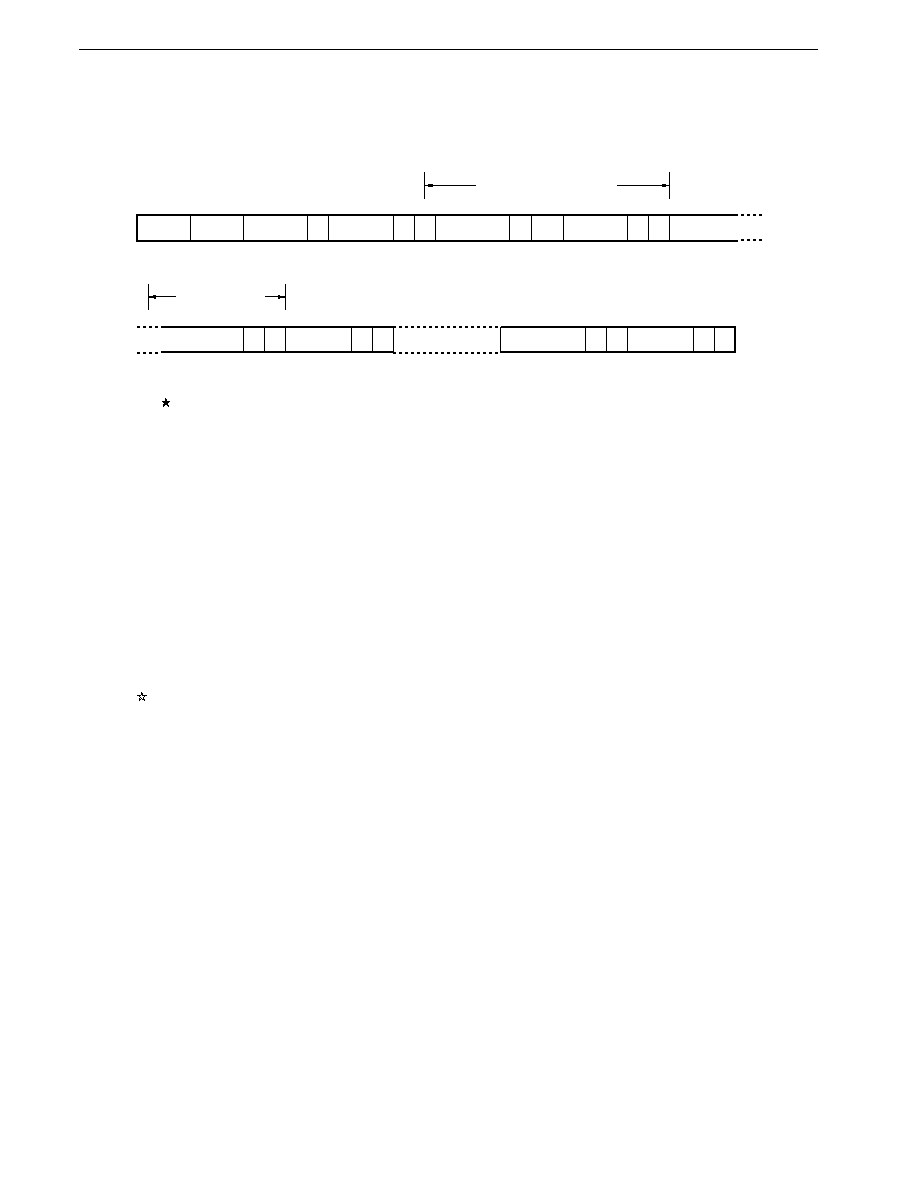
502
CHAPTER 20 IEBus CONTROLLER
Preliminary User's Manual U13987EJ1V0UM00
20.6 Interrupt Generation Timing and Main CPU Processing
20.6.1 Master transmission
Start
Broad-
casting
M address P
S address
P
A
Control
P
A
Telegraph
length
P
A
Data 1
P
A
Data 1
Data 2
P
A
Data n�1
P
A
Data n
P
A
<1>
6
<2>
5
6
6
6
Approx. 624 s (mode 1)
Approx. 390 s
(mode 1)
n = Final number of data bytes
�
�
Caution
indicates that an interrupt (INTIE1) does not occur.
Initial preparation processing
Sets a unit address, slave address, control data, telegraph length, and the first byte of the transmit data.
Communication start processing
Sets the bus control register (enables communication, master request, and slave reception).
<1> Interrupt (INTIE2) occurrence
Judgment of occurrence of error
Error processing
Judgment of slave request
Slave reception processing
Note 1
Judgment of contention result
Remaster request processing
Interrupt (INTIE1) occurrence
Note 2
The transmit data of the second byte and those that follow are written to the data register (DR) by macro service.
At this time, the data transfer direction is RAM (memory)
SFR (peripheral)
<2> Interrupt (INTIE2) occurrence
Judgment of occurrence of error
Error processing
Judgment of end of communication
End of communication processing
Judgment of end of frame
Re-communication processing
Note 3

503
CHAPTER 20 IEBus CONTROLLER
Preliminary User's Manual U13987EJ1V0UM00
Notes 1. If a slave reception request is confirmed during vector interrupt processing, the data transfer direction
of macro service must change from RAM (memory)
SFR (peripheral) to SFR (peripheral)
RAM
(memory) until the first data is received. The maximum pending period of this data transfer direction
changing processing is about 1,040
�
s in communication mode 1.
2. If NACK is received from the slave in the data field, an interrupt (INTIE1) is not issued to the CPU, but
the same data is retransmitted by hardware.
If the transmit data is not written during the period while the next data is being written, a communication
error interrupt occurs due to the occurrence of an underrun, and communication is ended midway
through.
3. The vector interrupt processing in <2> judges whether the data has been correctly transmitted within
one frame. If the data has not been correctly transmitted (if the number of data to be transmitted in
one frame could not be transmitted), the data must be retransmitted in the next frame, or the remainder
of the data must be transmitted.
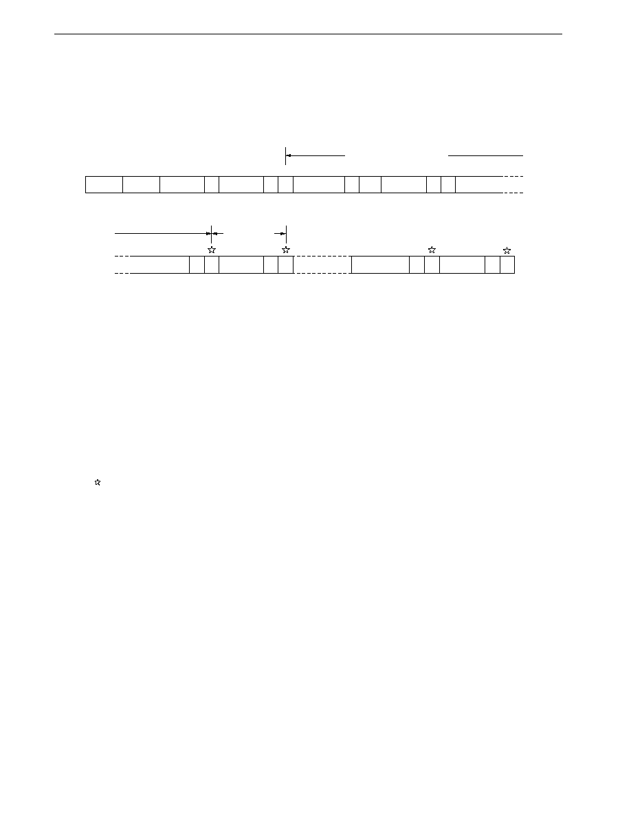
504
CHAPTER 20 IEBus CONTROLLER
Preliminary User's Manual U13987EJ1V0UM00
20.6.2 Master reception
If master reception is performed, it is necessary to give prior notice of "Slave transmission" to the unit set as slave.
Therefore, master reception requires at least two communication frames.
The slave unit prepares the transmission data, sets ENSLVTX (slave request transmission flag (bit 4 of the bus control
register (BCR)), and then waits.
Approx. 1,014 s (mode 1)
�
Start
Broad-
casting
M address
P
S address
P
A
Control
A
P
Telegraph
length
A
P
Data 1
Approx. 390 s
(mode 1)
�
Data 1
P
A
Data 2
P
A
Data n�1
P
A
Data n
P
A
< 2 >
n = Final number of data bytes
< 1 >
Initial preparation processing
Sets a unit address, slave address, and control data.
Communication start processing
Sets the bus control register (enables communication and master request).
<1> Interrupt (INTIE2) occurrence
Judgment of occurrence of error
Error processing
Judgment of slave request
Slave processing
Judgment of collision result
Remaster request processing
Interrupt (INTIE1) occurrence
Note 1
The receive data stored to the data register (DR) is read by macro service.
At this time, the data transfer direction is SFR (peripheral)
RAM (memory).
<2> Interrupt (INTIE2) occurrence
Judgment of occurrence of error
Error processing
Judgment of end of communication
End of communication processing
Judgment of end of frame
Re-communication processing
Note 2
Notes 1. If NACK is transmitted (hardware processing) in the data field, an interrupt (INTIE1) is not issued to
the CPU, but the same data is retransmitted from the slave.
If the receive data is not read in time until the next data is received, the hardware automatically transmits
NACK.
2. The vector interrupt processing in <2> judges whether the data has been correctly received within one
frame. If the data has not been correctly received (if the number of data to be received in one frame
could not be received), a request to retransmit the data must be made to the slave in the next
communication frame.
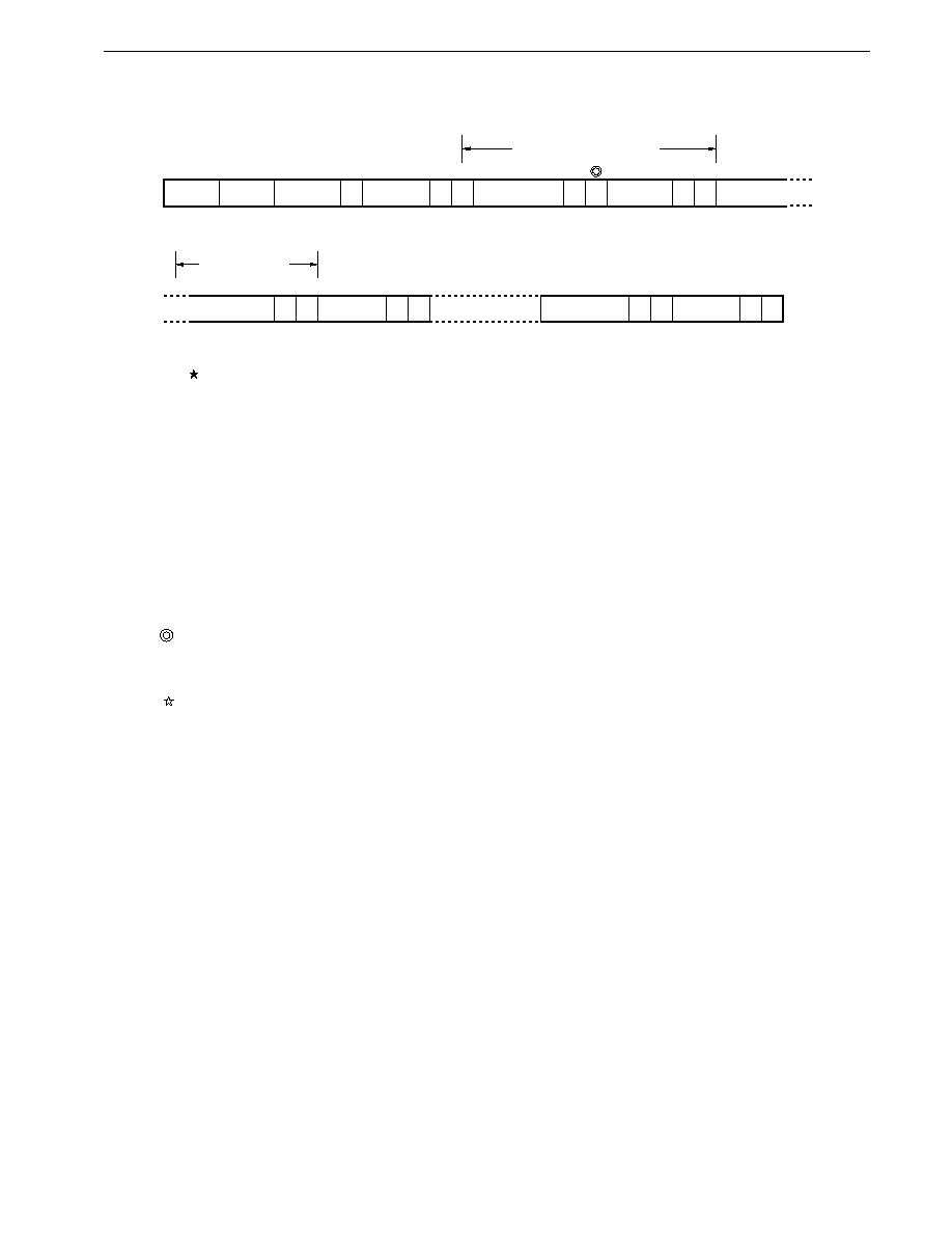
505
CHAPTER 20 IEBus CONTROLLER
Preliminary User's Manual U13987EJ1V0UM00
20.6.3 Slave transmission
Start
M address P
S address
P
A
Control
P
A
Data 1
P
A
Data 1
Data 2
P
A
Data n�1
P
A
Data n
P
A
<1>
6
<2>
5
6
6
6
n = Final number of data bytes
P
A
Approx. 390 s
(mode 1)
Approx. 624 s (mode 1)
�
�
Broad-
casting
Telegraph
length
Caution
indicates that an interrupt (INTIE1) does not occur.
Initial preparation processing
Sets a unit address, telegraph length, and the first byte of the transmit data.
Communication start processing
Sets the bus control register (enables communication, slave transmission, and slave reception).
<1> Interrupt (INTIE2) occurrence
Judgment of occurrence of error
Error processing
Judgment of slave request
Interrupt (INTIE2) occurrence
An interrupt occurs only when 0H, 4H, 5H, or 6H is received in the control field in the slave status.
Interrupt (INTIE1) occurrence
Note 1
The transmit data of the second byte and those that follow are written to the data register (DR) by macro service.
At this time, the data transfer direction is RAM (memory)
SFR (peripheral).
<2> Interrupt (INTIE2) occurrence
Judgment of occurrence of error
Error processing
Judgment of end of communication
End of communication processing
Judgment of end of frame
Re-communication processing
Note 2
Notes 1. If NACK is received from the master in the data field, an interrupt (INTIE1) is not issued to the CPU,
but the same data is retransmitted by hardware.
If the transmit data is not written in time during the period of writing the next data, a communication
error interrupt occurs due to occurrence of underrun, and communication is abnormally ended.
2. The vector interrupt processing in <2> judges whether the data has been correctly transmitted within
one frame. If the data has not been correctly transmitted (if the number of data to be transmitted in
one frame could not be transmitted), the data must be retransmitted in the next frame, or the continuation
of the data must be transmitted.
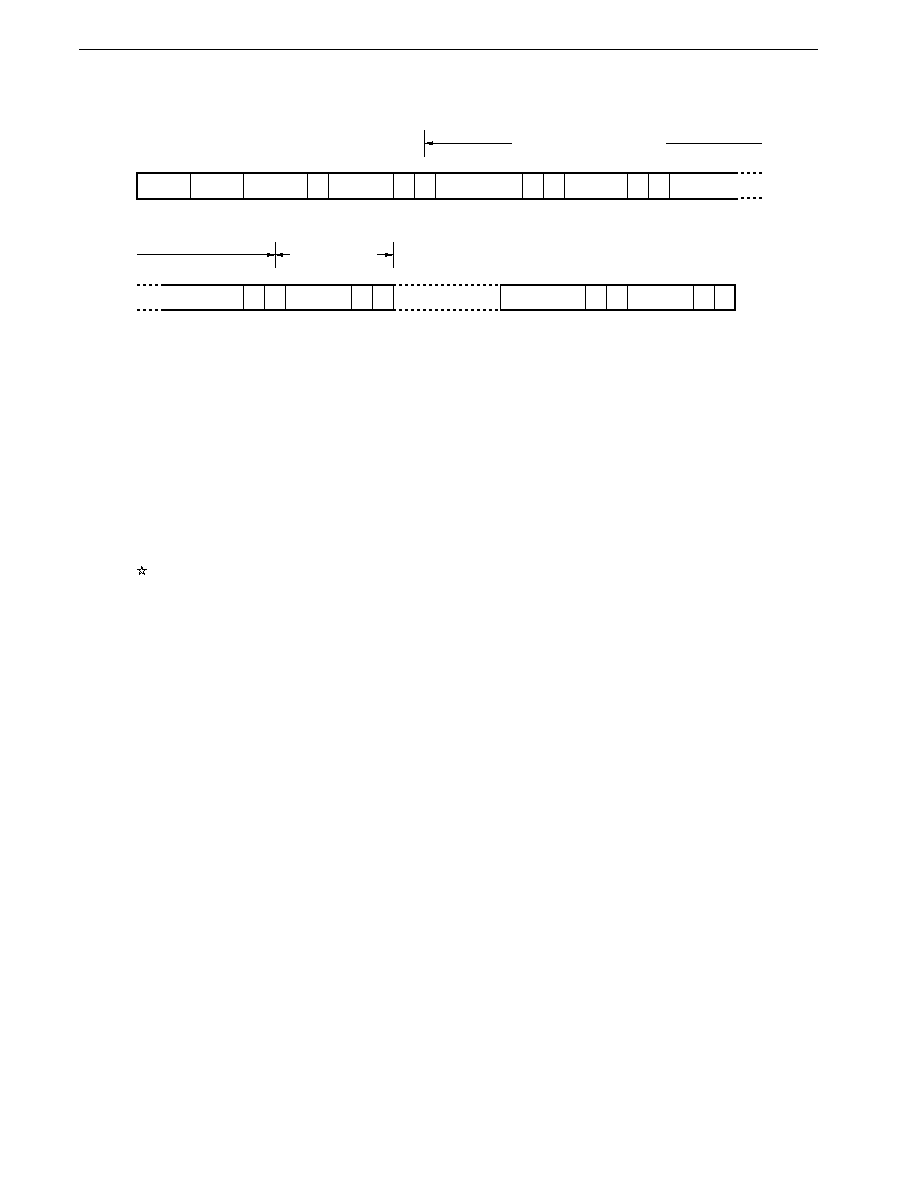
506
CHAPTER 20 IEBus CONTROLLER
Preliminary User's Manual U13987EJ1V0UM00
20.6.4 Slave reception
Start
M address P
S address
P
A
Control
P
A
Data 1
P
A
Data 1
Data 2
P
A
Data n�1
P
A
Data n
P
A
<1>
6
6
6
n = Final number of data bytes
P
A
6
<2>
Approx. 390 s
(mode 1)
Approx. 1,014 s (mode 1)
�
�
Broad-
casting
Telegraph
length
Initial preparation processing
Sets a unit address.
Communication start processing
Sets the bus control register (enables communication, disables slave transmission, and enables slave reception).
<1> Interrupt (INTIE2) occurrence
Judgment of occurrence of error
Error processing
Judgment of slave request
Slave processing
Note 1
Interrupt (INTIE1) occurrence
Note 1
The receive data stored to the data register (DR) is read by macro service.
At this time, the data transfer direction is SFR (peripheral)
RAM (memory).
<2> Interrupt (INTIE2) occurrence
Judgment of occurrence of error
Error processing
Judgment of end of communication
End of communication processing
Judgment of end of frame
End of frame processing
Note 2
Notes 1. If NACK is transmitted in the data field, an interrupt (INTIE1) is not issued to the CPU, but the same
data is retransmitted from the master.
If the receive data is not read in time until the next data is received, NACK is automatically transmitted.
2. The vector interrupt processing in <2> judges whether the data has been correctly received within one
frame.
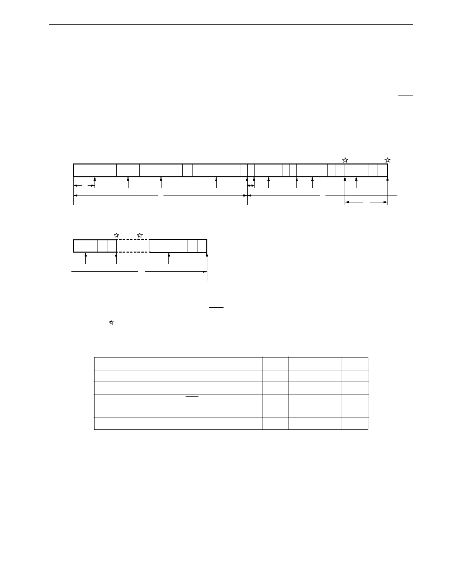
507
CHAPTER 20 IEBus CONTROLLER
Preliminary User's Manual U13987EJ1V0UM00
20.6.5 Interval of occurrence of interrupt for IEBus control
Each control interrupt must occur at each point of communication and perform the necessary processing until the next
interrupt occurs. Therefore, the CPU must control the IEBus control block, taking the shortest time of this interrupt into
consideration.
The locations at which the following interrupts may occur are indicated by
in the field where it may occur.
does not
mean that the interrupt occurs at each of the points indicated by
. If an error interrupt (timing error, parity error, or ACK
error) occurs, the IEBus internal circuit is initialized. As a result, the following interrupt does not occur in that communication
frame.
(1) Master transmission
Start bit
T
t1
T
Broad-
casting
Master address
T
t2
P
Slave address
T
P A
A
T
t3
Control
P A
A
t4
P
T
A
T
Telegraph
lengh
P A
Data
P
A
Communication
starts
Communication
starts
P
A
Data
Data
A
P
Data
T
T
t4
End of communication
End of frame
U
U
t5
Remarks 1. T: timing error, P: parity error, A: ACK error, U: underrun error
: data set interrupt (INTIE1)
2. End of frame occurs at the end of 32-byte data.
(IEBus: @ 6-MHz operation)
Item
Symbol
MIN.
Unit
Communication starts � timing error
t1
Approx. 97
�
s
Communication starts � communication start interrupt
t2
Approx. 1,380
�
s
Communication start interrupt � ACK error
t3
Approx. 16
�
s
Communication start interrupt � end of communication
t4
Approx. 1,014
�
s
Data transmission � underrun error
t5
Approx. 390
�
s
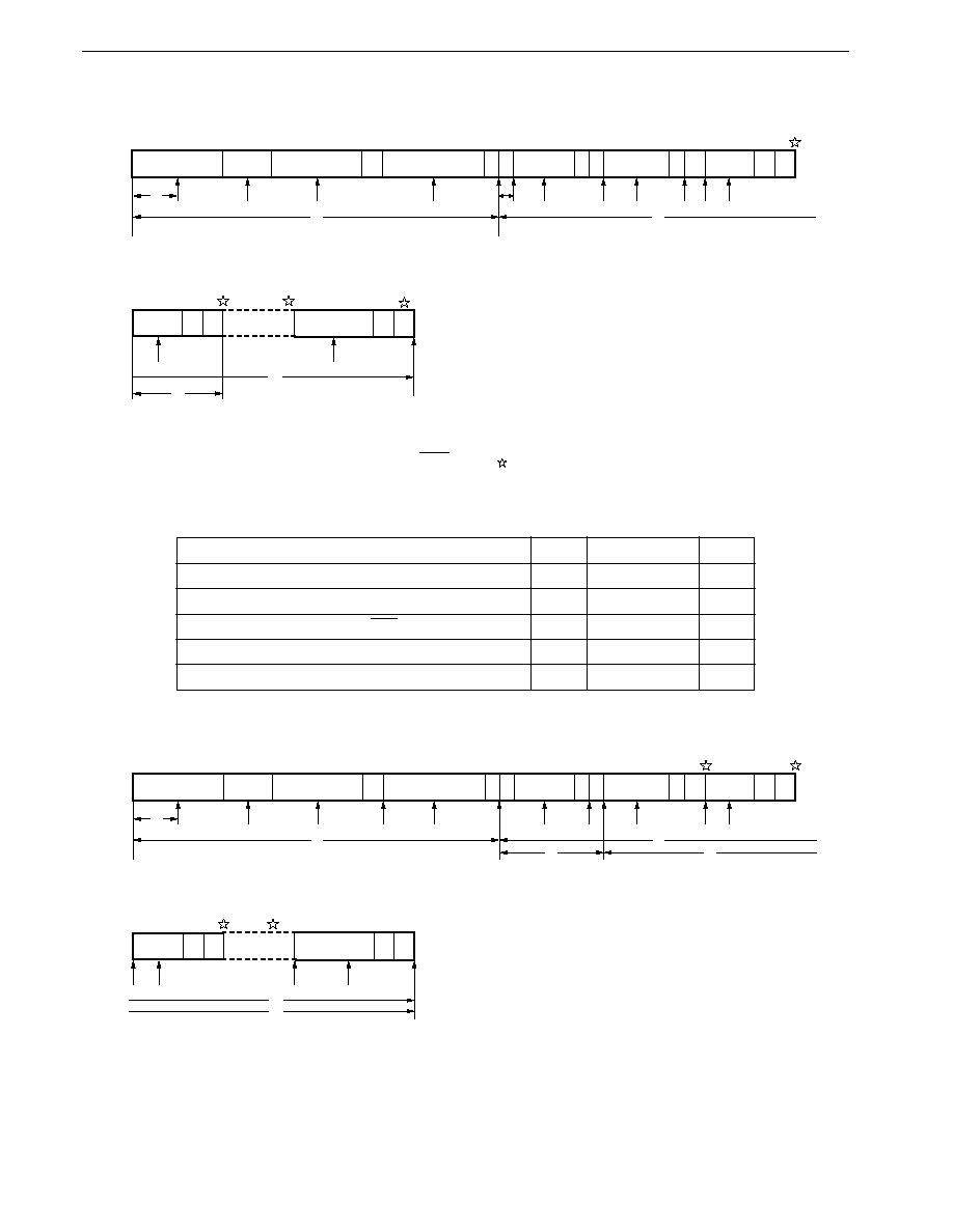
508
CHAPTER 20 IEBus CONTROLLER
Preliminary User's Manual U13987EJ1V0UM00
(2) Master reception
Start bit
T
t1
T
Broad-
casting
Master address
T
t2
P
Slave address
T
P A
A
T
t3
Control
P A
A
t4
P
T
A
T
Telegraph
lengh
P A
Data
P
A
Communication
starts
Communication
starts
P
A
Data
Data
A
P
Data
T
T
t4
End of communication
End of frame
P
t5
Remarks 1. T: timing error, P: parity error, A: ACK error,
: data set interrupt (INTIE1)
2. End of frame occurs at the end of 32-byte data.
(IEBus: @ 6-MHz operation)
Item
Symbol
MIN.
Unit
Communication starts � timing error
t1
Approx. 97
�
s
Communication starts � communication start interrupt
t2
Approx. 1,380
�
s
Communication start interrupt � ACK error
t3
Approx. 16
�
s
Communication start interrupt � end of communication
t4
Approx. 1,014
�
s
Receive data read interval
t5
Approx. 390
�
s
(3) Slave transmission
Start bit
T
t1
T
Broad-
casting
Master address
T
t2
P
Slave address
T
P A
T
Control
P A
A
t4
T
A
T
Telegraph
lengh
P A
Data
P
A
Communication
starts
Communication
starts
P
A
Data
Data
A
P
Data
T
T
t4
End of communication
End of frame
U
t5
U
P
P
P
t5
t3
Status
request

509
CHAPTER 20 IEBus CONTROLLER
Preliminary User's Manual U13987EJ1V0UM00
Remarks 1. T: timing error, P: parity error, A: ACK error, U: underrun error,
: data set interrupt (INTIE1)
2. End of frame occurs at the end of 32-byte data.
(IEBus: @ 6-MHz operation)
Item
Symbol
MIN.
Unit
Communication starts � timing error
t1
Approx. 97
�
s
Communication starts � communication start interrupt
t2
Approx. 1,380
�
s
Communication start interrupt � status request
t3
Approx. 234
�
s
Communication start interrupt � end of communication
t4
Approx. 1,014
�
s
Status request � end of communication
t5
Approx. 780
�
s
(4) Slave reception
Start bit
T
t1
T
Broad-
casting
Master address
T
t2
P
P
Slave address
T
P A
A
T
t3
Control
P A
P A
t4
P
T
P
T
Telegraph
lengh
P A
Data
P
A
Communication
starts
Communication
starts
P
A
Data
Data
A
P
Data
T
T
t4
t5
End of communication
End of frame
Remarks 1. T: timing error, P: parity error, A: ACK error,
: data set interrupt (INTIE1)
2. End of frame occurs at the end of 32-byte data.
(IEBus: @ 6-MHz operation)
Item
Symbol
MIN.
Unit
Communication starts - timing error
t1
Approx. 97
�
s
Communication starts - communication start interrupt
t2
Approx. 1,380
�
s
Communication start interrupt - ACK error
t3
Approx. 16
�
s
Communication start interrupt - end of communication
t4
Approx. 1,014
�
s
Receive data read interval
t5
Approx. 390
�
s

510
CHAPTER 20 IEBus CONTROLLER
Preliminary User's Manual U13987EJ1V0UM00
20.7 Cautions when Using IEBus Controller
(1) Receiving slave status request
The
�
PD784938 Subseries operates differently from the
�
PD784908 Subseries when receiving the slave status
request. The differences are as follows.
Table 20-10 shows the operation (slave status request) of IEBus controller of the
�
PD784938 Subseries.
Table 20-10. IEBus Controller Operation (Slave Status Request) of
�
PD784938 Subseries
State of
�
PD784938
Slave Status
Received Control
Operation During Reception
Subseries
Request
Data
Unlocked state
All units
0H, 4H, 5H, 6H
� ACK return at ACK period of the control field.
Locked state
Units that have
� Sets status transmission flag and generates INTIE2.
lock requested
Except units
that have lock
requested
(2) Data register (DR) read operation
When receiving a unit, after the reception of each byte is completed, a macro-service activated signal (INTIE1) is
generated, and the CPU needs to perform data register (DR) read processing. When this DR read processing is delayed
and the next data reception is completed, DR will be updated. Therefore, DR read processing should be completed
in the period between INTIE1 generation and the next data reception. The maximum holding time from INTIE1
generation to DR read is approximately 390
�
s.
The
�
PD784908 Subseries has 40 bytes of reception buffer. When receiving data when there is no space in the
reception buffer, NACK is returned and a request for data to be retransmitted to the transmission unit is automatically
generated.
Because, in the case of the
�
PD784938 Subseries (simple IEBus controller), INTIE1 is generated for every 1 byte
reception, that DR needs to be read by interrupt processing (macro service recommendation).
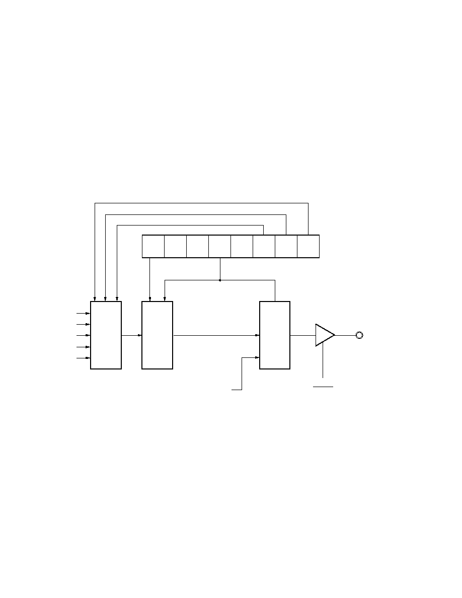
511
Preliminary User's Manual U13987EJ1V0UM00
CHAPTER 21 CLOCK OUTPUT FUNCTION
The
�
PD784938 has a clock function that outputs a signal scaled from the system clock.
The clock output function can output the system clock directly, or a 1/2, 1/4, 1/8, or 1/16 system clock signal. In addition,
it can be used as a 1-bit output port. The output pin has a alternate function as the ASTB pin.
Caution This function cannot be used when the external memory expansion mode is used.
21.1 Configuration
The clock output function configuration is shown in Figure 21-1.
Figure 21-1. Clock Output Function Configuration
f
CLK
f
CLK
/2
f
CLK
/4
f
CLK
/8
f
CLK
/16
Selector 2
Output
control
Selector 1
Address latch signal
RESET
ASTB/CLOCKOUT
Clock output mode
register (CLOM)
LV
0 0
CLE
0
FS2
FS1
FS0

512
CHAPTER 21 CLOCK OUTPUT FUNCTION
Preliminary User's Manual U13987EJ1V0UM00
(1) Clock output mode register (CLOM)
Register that controls the operation of the clock output function.
(2) Selector 1
Selector that selects the frequency of the clock to be output.
(3) Output control
Controls the output signal in accordance with the contents of the clock output mode register (CLOM).
(4) Selector 2
Selects either the ASTB signal or the CLOCKOUT signal as the signal to be output to the ASTB/CLOCKOUT pin.
(5) ASTB/CLOCKOUT pin
Pin that outputs the signal selected by selector 2. While the RESET input is low, the ASTB/CLOCKOUT pin is in the
Hi-Z state, and when the RESET input becomes high, it outputs a low-level signal, and then outputs a signal according
to the set function.
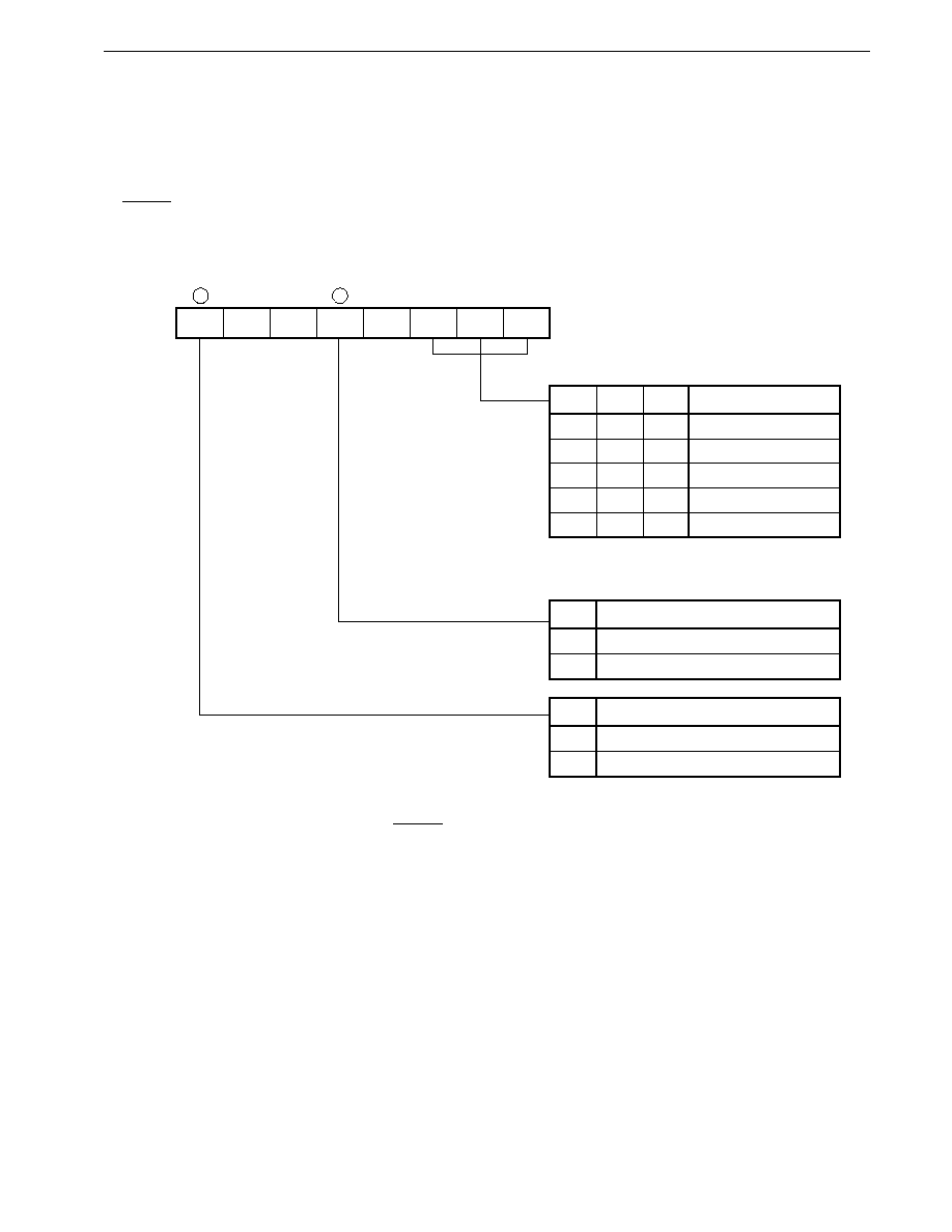
513
CHAPTER 21 CLOCK OUTPUT FUNCTION
Preliminary User's Manual U13987EJ1V0UM00
21.2 Clock Output Mode Register (CLOM)
The CLOM controls the clock output function.
CLOM can be read or written to with an 8-bit manipulation instruction or bit manipulation instruction.
The CLOM format is shown in Figure 21-2.
RESET input clears CLOM to 00H.
Figure 21-2. Clock Output Mode Register (CLOM) Format
7
LV
CLOM
6
0
5
0
4
CLE
3
0
2
FS2
1
FS1
0
FS0
Frequency Selection
f
CLK
Note
f
CLK
/2
f
CLK
/4
f
CLK
/8
f
CLK
/16
FS2
0
0
FS1
0
0
FS0
1
0
0
1
0
0
1
1
1
0
0
Outputs LV bit contents
Outputs clock selected by bits FS2 to FS0
Clock Output Control
CLE
1
0
Outputs low level
Outputs high level
Output Level Control
LV
1
0
Address
After reset
R/W
R/W
00H
0FFC6H
Note Outputs the system clock
Duty
50 %
Cautions 1. When the external memory expansion mode is used, the clock output mode register (CLOM) should
be set to 00H (value after RESET release).
2. The other bits (FS0 to FS2 and LV) must not be changed while the CLE bit is set (to 1).
3. The other bits (FS0 to FS2 and LV) must not be changed at the same time when the CLE bit is
changed.
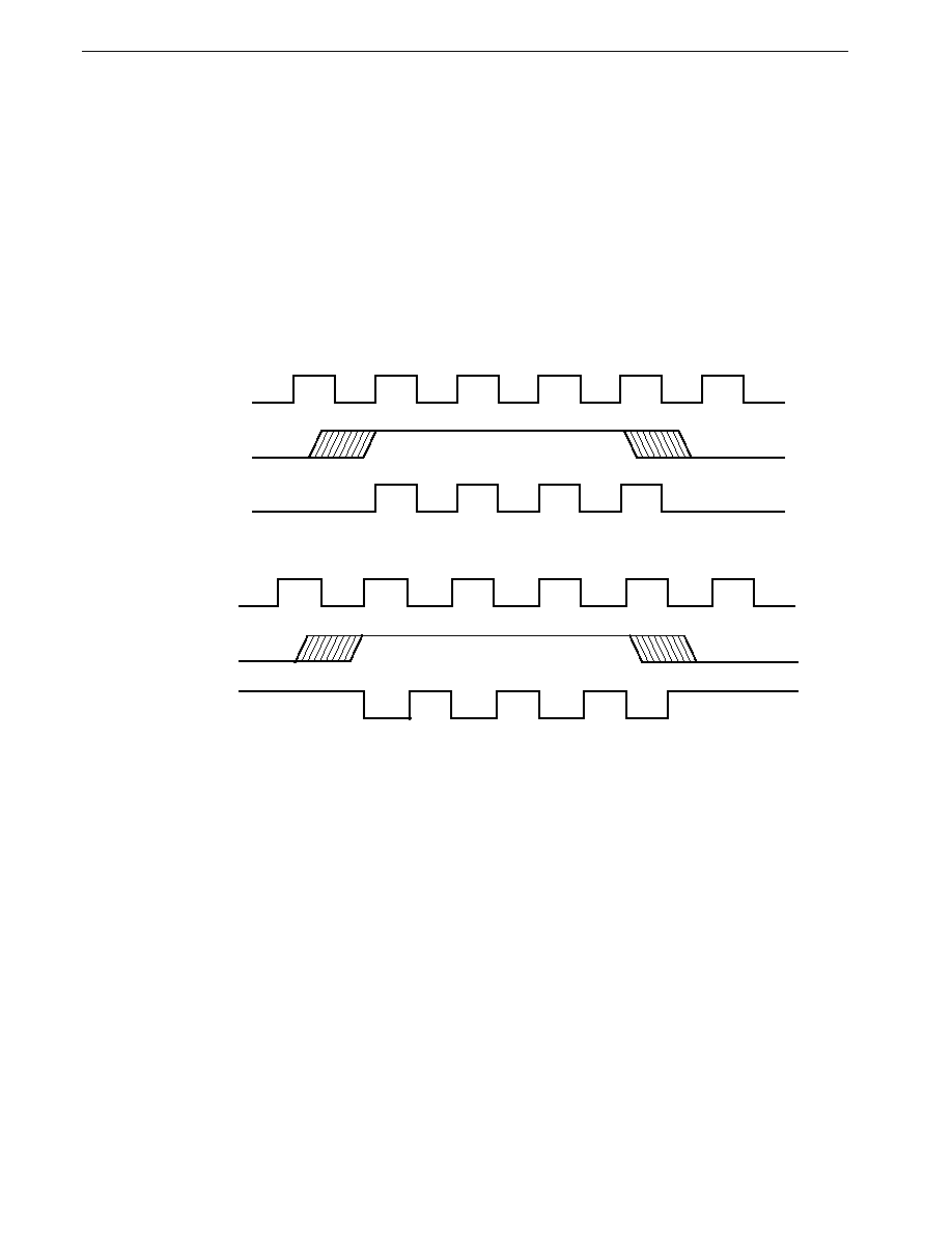
514
CHAPTER 21 CLOCK OUTPUT FUNCTION
Preliminary User's Manual U13987EJ1V0UM00
21.3 Operation
21.3.1 Clock output
A signal with the clock output frequency selected by bits FS0 to FS2 is selected by selector 1 and output.
The output signal has the same level as the LV bit when the CLE bit is cleared (to 0), and is output from the clock signal
immediately after the CLE bit is set (to 1).
When the CLE bit is cleared (to 0), the contents of the LV bit are output in synchronization with the clock signal, and
further output operations are stopped.
Figure 21-3. Clock Output Operation Timing
(a) LV = 0
f
CLK
/n
(n = 1, 2, 4, 8, 16)
CLOCKOUT
CLE
(b) LV = 1
f
CLK
/n
(n = 1, 2, 4, 8, 16)
CLE
CLOCKOUT
Setting of bits FS0 to FS2 and the LV bit should only be performed when CLE = 0 (bits FS0 to FS2 and the LV bit should
not be changed within the same instruction that changes the CLE bit contents).
<Operation Example>
MOV CLOM, #82H; CLOCKOUT pin: high level, clock output: f
CLK
/4
SET1 CLE;
Starts clock output
CLR1 CLE;
Stops clock output, CLOCKOUT pin: high level
... ...

515
CHAPTER 21 CLOCK OUTPUT FUNCTION
Preliminary User's Manual U13987EJ1V0UM00
21.3.2 1-bit output port
When the CLE bit is cleared (to 0), the contents of the LV bit are output from the CLOCKOUT pin. The CLOCKOUT
pin changes as soon as the contents of the LV bit change.
Figure 21-4. 1-Bit Output Port Operation
CLOCKOUT
SET1 LV instruction executed
CLR1 LV instruction executed
LV
21.3.3 Operation in standby mode
(1) HALT mode
The state prior to setting of the HALT mode is maintained. That is, if, during clock output, clock output has been
performed continuously, and clock output has been disabled, the LV bit contents set before the HALT mode setting
are output unchanged.
(2) STOP mode and IDLE mode
Clock output must be disabled before setting the STOP mode or IDLE mode (this must be done by software). The
CLOCKOUT pin level output is the level before the STOP mode or IDLE mode was set (the contents of the LV bit).
21.4 Cautions
(1) This function cannot be used when the external memory expansion mode is used.
(2) When the external memory expansion mode is used, the clock output mode register (CLOM) should be set to 00H (value
after RESET release).
(3) The other bits (FS0 to FS2 and LV) must not be changed while the CLE bit is set (to 1).
(4) The other bits (FS0 to FS2 and LV) must not be changed at the same time when the CLE bit is changed.

516
Preliminary User's Manual U13987EJ1V0UM00
[MEMO]

517
Preliminary User's Manual U13987EJ1V0UM00
CHAPTER 22 EDGE DETECTION FUNCTION
P20 to P26 have an edge detection function that allows a rising edge/falling edge to be set programmable, and the
detected edge is sent to internal hardware. The relation between pins P20 to P26 and the use of the detected edge is shown
in Table 22-1.
Table 22-1. Pins P20 to P26 and Use of Detected Edge
Pin
Use
Detected Edge Specification Register
P20
NMI, standby circuit control
INTM0
P21
INTP0, timer/event counter 1 capture signal
timer/event counter 1 count clock signal
Real-time output port trigger signal
P22
INTP1, timer/event counter 2 CR22 capture signal
P23
INTP2, CI (timer/event counter 2 count clock signal),
timer/event counter 2 CR21 capture signal
P24
INTP3, timer/event counter 0 capture signal
INTM1
timer/event counter 0 count clock signal
P25
INTP4, standby circuit control
P26
INTP5, A/D converter conversion start signal, standby circuit control
The edge detection function operates at all times except in STOP mode and IDLE mode (although the edge detection
function for pins P20, P25, and P26 also operates in STOP mode and IDLE mode).
For the P21/INTP0 pin, the noise elimination time when edge detection is performed can be selected by software.
22.1 Edge Detection Function Control Registers
22.1.1 External interrupt mode registers (INTM0, INTM1)
The INTMn (n = 0, 1) specify the valid edge to be detected on pins P20 to P26. The INTM0 specifies the valid edge
for pins P20 to P23, and the INTM1 specifies the valid edge for pins P24 to P26.
The INTMn can be read or written to with an 8-bit manipulation instruction or bit manipulation instruction. The format
of INTM0 and INTM1 are shown in Figures 22-1 and 22-2 respectively.
RESET input clears these registers to 00H.
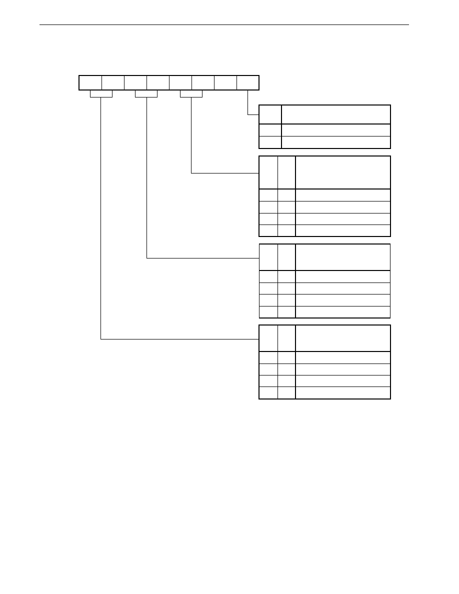
518
CHAPTER 22 EDGE DETECTION FUNCTION
Preliminary User's Manual U13987EJ1V0UM00
Figure 22-1. External Interrupt Mode Register 0 (INTM0) Format
7
ES21
INTM0
6
ES20
5
ES11
4
ES10
3
ES01
2
ES00
1
0
0
ESNM1
Falling edge
Rising edge
P20 (NMI) Pin Input Detected Edge
Specification
ESNM1
1
0
Falling edge
Rising edge
P21 (INTP0, CR11/CR11W Capture
Trigger, TM1/TM1W Count Clock,
Real-Time Output Port Output Trigger)
Pin Input Detected Edge Specification
ES01
0
0
Setting prohibited
1
Both falling & rising edges
1
ES00
1
0
0
1
Falling edge
Rising edge
P22 (INTP1, CR22/CR22W Capture
Trigger) Pin Input Detected Edge
Specification
ES11
0
0
Setting prohibited
1
Both falling & rising edges
1
ES10
1
0
0
1
Falling edge
Rising edge
P23 (INTP2, CR21/CR21W Capture
Trigger, CI) Pin Input Detected Edge
Specification
ES21
0
0
Setting prohibited
1
Both falling & rising edges
1
ES20
1
0
0
1
Address
After reset
R/W
R/W
00H
0FFA0H
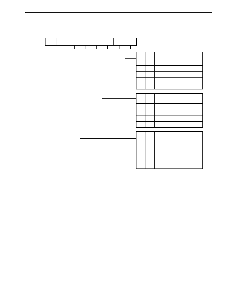
519
CHAPTER 22 EDGE DETECTION FUNCTION
Preliminary User's Manual U13987EJ1V0UM00
Figure 22-2. External Interrupt Mode Register 1 (INTM1) Format
7
0
INTM1
6
0
5
ES51
4
ES50
3
ES41
2
ES40
1
ES31
0
ES30
Falling edge
Rising edge
P24 (INTP3, CR02 Capture Trigger,
TM0 Count Clock) Pin Input
Detected Edge Specification
ES31
0
0
Setting prohibited
1
Both falling & rising edges
1
ES30
1
0
0
1
Falling edge
Rising edge
P25 (INTP4) Pin Input Detected
Edge Specification
ES41
0
0
Setting prohibited
1
Both falling & rising edges
1
ES40
1
0
0
1
Falling edge
Rising edge
P26 (INTP5, A/D Conversion Start
Signal) Pin Input Detected Edge
Specification
ES51
0
0
Setting prohibited
1
Both falling & rising edges
1
ES50
1
0
0
1
Address
After reset
R/W
R/W
00H
0FFA1H
Caution Valid edge detection cannot be performed when the valid edge is changed by a write to the external
interrupt mode register (INTMn: n = 0, 1). Also, if an edge is input during a change of the valid edge,
that edge may or may not be judged to be a valid edge.
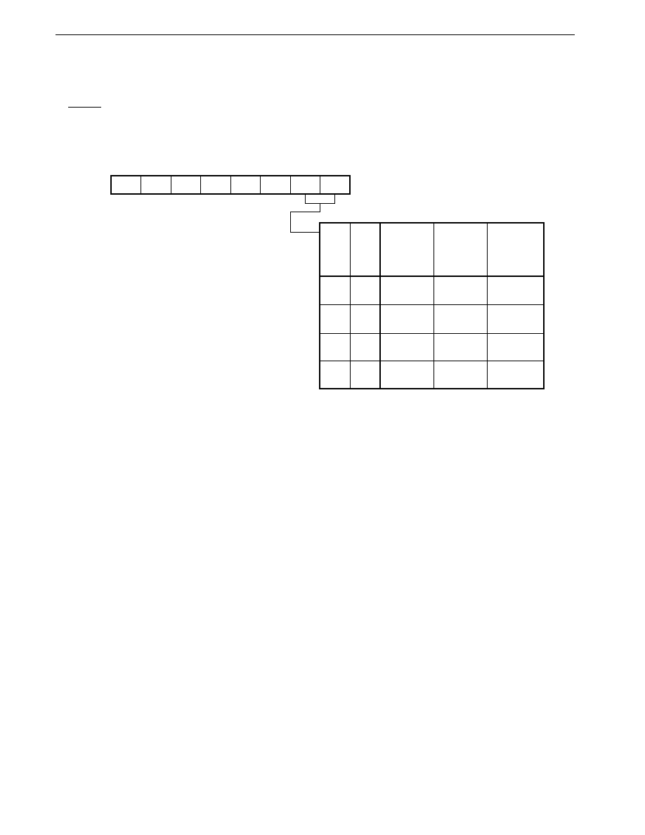
520
CHAPTER 22 EDGE DETECTION FUNCTION
Preliminary User's Manual U13987EJ1V0UM00
22.1.2 Sampling clock selection register (SCS0)
SCS0 specifies the sampling clock (f
SMP
) for digital noise elimination performed on pin P21.
SCS0 can be read or written to with an 8-bit manipulation instruction. The format of SCS0 is shown in Figure 22-3.
RESET input clears SCS0 to 00H.
Figure 22-3. Sampling Clock Selection Register (SCS0) Format
0
0
0
0
0
0
SCS01 SCS00
7
6
5
4
3
2
1
0
SCS0
0FFA4H
Address
00H
After reset
R/W
R/W
SCS01
Sampling
Clock (f
SMP
)
f
CLK
f
XX
/32
f
XX
/64
f
XX
/128
SCS00
0
0
1
1
0
1
0
1
Pulse Width
Eliminated
as Noise
Minimum
Pulse Width
Recognized
as Signal
3/f
CLK
(239 ns)
96/f
XX
(7.7 s)
192/f
XX
(15.3 s)
384/f
XX
(30.5 s)
2/f
CLK
(159 ns)
64/f
XX
(5.1 s)
128/f
XX
(10.2 s)
256/f
XX
(20.3 s)
f
XX
= 12.58 MHz
f
CLK
= 12.58 MHz
�
�
�
�
�
�
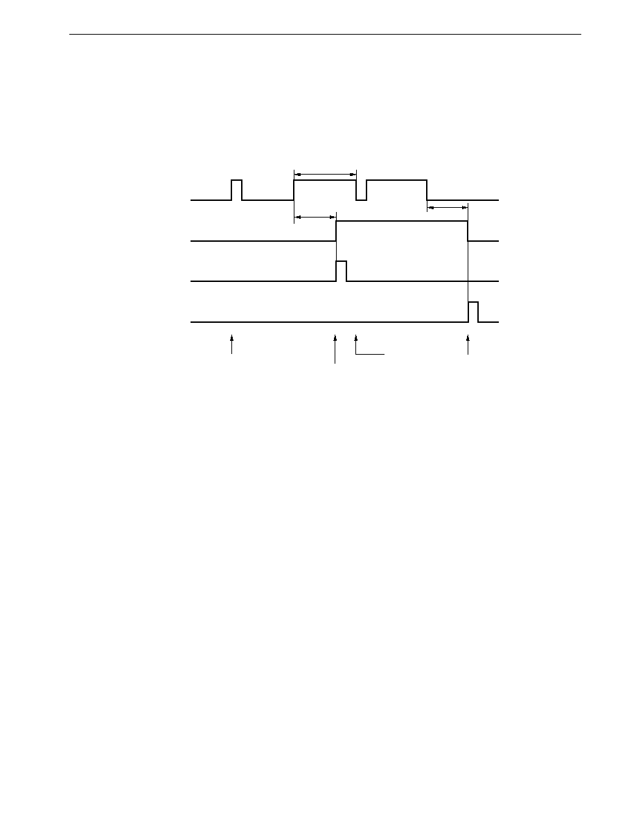
521
CHAPTER 22 EDGE DETECTION FUNCTION
Preliminary User's Manual U13987EJ1V0UM00
22.2 Edge Detection for Pins P20, P25, and P26
On pins P20, P25, and P26, noise elimination is performed by means of analog delay before edge detection. Therefore,
an edge cannot be detected unless the pulse width is a given time (10
�
s) or longer.
Figure 22-4. Edge Detection for Pins P20, P25, and P26
P20/P25/P26 input
P20/P25/P26 input signal
after noise elimination
Falling edge
Rising edge
Eliminated as noise
since pulse is short Falling edge detected since
pulse is sufficiently wide
Eliminated as noise
since pulse is short
Rising edge detected since
pulse is suficiently wide
10 s (MIN.)
�
10 s
(MAX.)
�
10 s
(MAX.)
�
Caution Since analog delay noise elimination is performed on pins P20, P25, and P26, an edge is detected up
to 10
�
s after it is actually input. Also, unlike pins P21 to P24, the delay before an edge is detected
is not a specific value, because of differences in the characteristics of various devices.
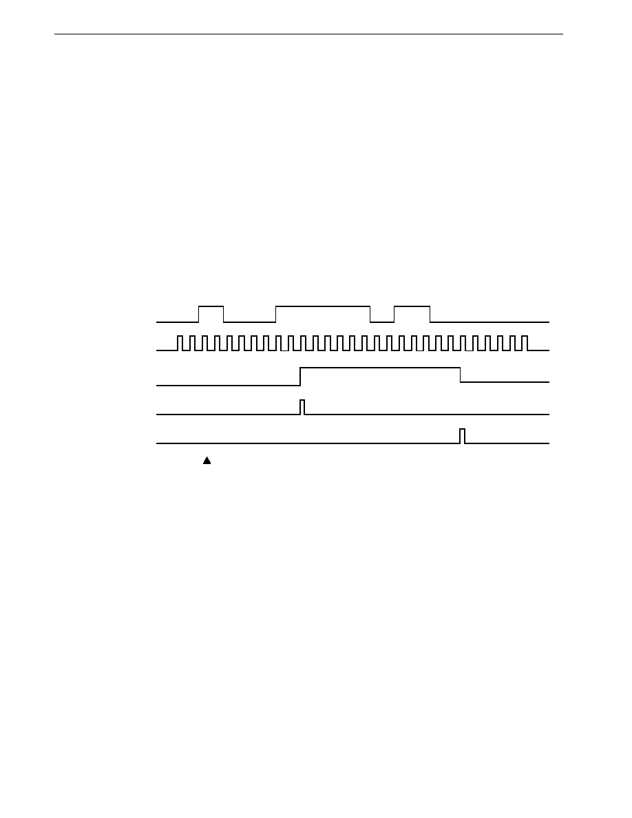
522
CHAPTER 22 EDGE DETECTION FUNCTION
Preliminary User's Manual U13987EJ1V0UM00
22.3 P21 Pin Edge Detection
In P21 edge detection, digital noise elimination is performed using the clock (f
SMP
) specified by the sampling clock
selection register (SCS0). In digital noise elimination, input is sampled using the f
SMP
clock, and if the input level is not
the same at least three times in succession (if it is the same only two or fewer times in succession), it is eliminated as noise.
Therefore, the level must be maintained for at least 3 f
SMP
clock cycles in order to be recognized as a valid edge.
Remark
When the pulse width of a signal with a comparatively long pulse width and a lot of noise, such as a reception
signal infrared remote controller, is measured, or when a signal is input in which oscillation occurs when an
edge occurs, as with switch input chattering, for instance, it is better to set the sampling clock to low speed
with the sampling clock selection register (SCS0). If the sampling clock is high-speed, there will be a reaction
to the short-pulse noise components as well, and the program will frequently have to judge whether the input
is noise or a signal. However, by slowing down the sampling clock, reaction to short pulse width noise is
eliminated and thus the program does not have to make judgments so frequently, and can thus be simplified.
Figure 22-5. P21 Pin Edge Detection
P21 input
f
SMP
P21 input signal after
noise elimination
Rising edge
Falling edge
Digital noise
elimination by f
SMP
clock
Cautions 1.
Since digital noise elimination is performed with the f
SMP
clock, there is a delay of 2 to 3 f
SMP
clocks
between input of an edge to the pin and the point at which the edge is actually detected.
2.
If the input pulse width is 2 to 3 f
SMP
clocks, it is uncertain whether a valid edge will be detected.
Therefore, to ensure reliable operation, the level should be held for at least 3 clocks.
3.
If noise input to the pin is synchronized with the f
SMP
clock in the
�
PD784938, it may not be
recognized as noise. If there is a possibility of such noise being input, noise should be eliminated
by adding a filter to the input pin.
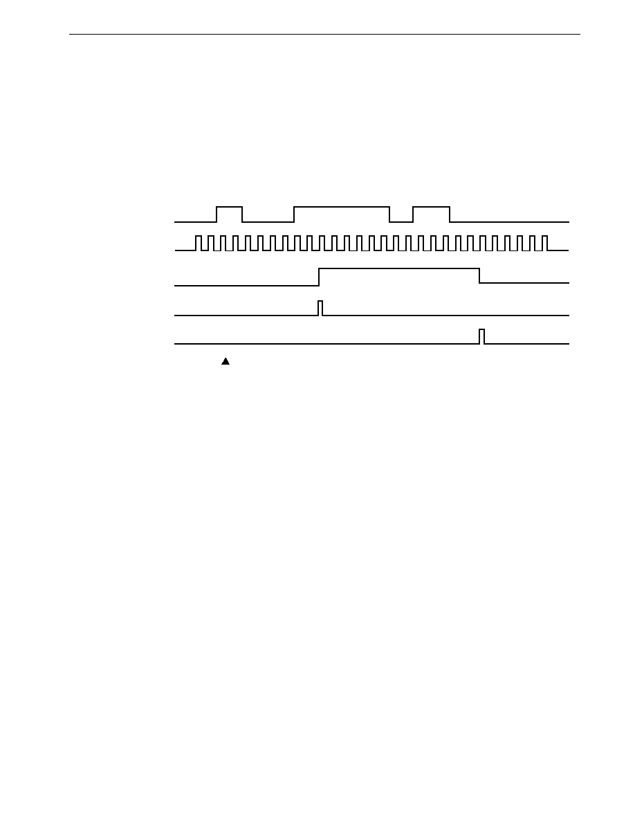
523
CHAPTER 22 EDGE DETECTION FUNCTION
Preliminary User's Manual U13987EJ1V0UM00
22.4 Pin Edge Detection for Pins P22 to P24
Edge detection for pins P22 to P24 is performed after digital noise elimination by means of clock sampling. Unlike the
P21 pin, f
CLK
is used as the sampling clock.
In digital noise elimination, input is sampled using the f
CLK
clock, and if the input level is not the same at least three times
in succession (if it is the same only two or fewer times in succession), it is eliminated as noise. Therefore, the level must
be maintained for at least 3 f
CLK
clock cycles (0.24
�
s: f
CLK
= 12.58 MHz) in order to be recognized as a valid edge.
Figure 22-6. Edge Detection for Pins P22 to P24
P22 to P24 input
f
CLK
P22 to P24 input signal
after noise elimination
Rising edge
Falling edge
Digital noise elimination
with f
CLK
clock
Cautions 1. Since digital noise elimination is performed with the f
CLK
clock, there is a delay of 2 to 3 f
CLK
clocks
between input of an edge to the pin and the point at which the edge is actually detected.
2. If the input pulse width is 2 to 3 f
CLK
clocks, it is uncertain whether a valid edge will be detected.
Therefore, to ensure reliable operation, the level should be held for at least 3 clocks.
3. If noise input to a pin is synchronized with the f
CLK
clock in the
�
PD784938, it may not be recognized
as noise. If there is a possibility of such noise being input, noise should be eliminated by adding
a filter to the input pins.

524
CHAPTER 22 EDGE DETECTION FUNCTION
Preliminary User's Manual U13987EJ1V0UM00
22.5 Cautions
(1) Valid edge detection cannot be performed when the valid edge is changed by a write to the external interrupt mode
register (INTMn: n = 0, 1). Also, if an edge is input during a change of the valid edge, that edge may or may not be
judged to be a valid edge.
(2) Since analog delay noise elimination is performed on pins P20, P25, and P26, an edge is detected up to 10
�
s after
it is actually input. Also, unlike pins P21 to P24, the delay before an edge is detected is not a specific value, because
of differences in the characteristics of various devices.
(3) Since digital noise elimination is performed on the P21 pin with the f
SMP
clock, there is a delay of 2 to 3 f
SMP
clocks
between input of an edge to the pin and the point at which the edge is actually detected.
(4) If the input pulse width on the P21 pin is 2 to 3 f
SMP
clocks, it is uncertain whether a valid edge will be detected. Therefore,
to ensure reliable operation, the level should be held for at least 3 clocks.
(5) If noise input of the P21 pin is synchronized with the f
SMP
clock in the
�
PD784938, it may not be recognized as noise.
If there is a possibility of such noise being input, noise should be eliminated by adding a filter to the input pins.
(6) Since digital noise elimination is performed on pins P22 to P24 with the f
CLK
clock, there is a delay of 2 to 3 f
CLK
clocks
between input of an edge to the pin and the point at which the edge is actually detected.
(7) If the input pulse width on pins P22 to P24 is 2 to 3 f
CLK
clocks, it is uncertain whether a valid edge will be detected.
Therefore, to ensure reliable operation, the level should be held for at least 3 clocks.
(8) If noise input to pins P22 to P24 is synchronized with the f
CLK
clock in the
�
PD784938, it may not be recognized as
noise. If there is a possibility of such noise being input, noise should be eliminated by adding a filter to the input pins.

525
Preliminary User's Manual U13987EJ1V0UM00
CHAPTER 23 INTERRUPT FUNCTIONS
The
�
PD784938 is provided with three interrupt request service modes (see Table 23-1). These three service modes
can be set as required in the program. However interrupt service by macro service can only be selected for interrupt request
sources provided with the macro service processing mode shown in Table 23-2. Context switching cannot be selected for
non-maskable interrupts or operand error interrupts.
Multiple-interrupt control using 4 priority levels can easily be performed for maskable vectored interrupts.
Table 23-1. Interrupt Request Service Modes
Interrupt Request
Servicing Performed
PC & PSW Contents
Service
Service Mode
Vectored interrupts
Software
Saving to & restoration
Executed by branching to service program at
from stack
address
Note
specified by vector table
Context switching
Saving to & restoration
Executed by automatic switching to register
from fixed area in
bank specified by vector table and branching
register bank
to service program at address
Note
specified by
fixed area in register bank
Macro service
Hardware
Retained
Execution of pre-set service such as data
(firmware)
transfers between memory and I/O
Note The start addresses of all interrupt service programs must be in the base area. If the body of a service program
cannot be located in the base area, a branch instruction to the service program should be written in the base area.

526
CHAPTER 23 INTERRUPT FUNCTIONS
Preliminary User's Manual U13987EJ1V0UM00
23.1 Interrupt Request Sources
The
�
PD784938 has the 29 interrupt request sources shown in Table 23-2, with a vector table allocated to each.
Table 23-2. Interrupt Request Sources (1/2)
Type of
Default
Interrupt Request
Generating
Interrupt
Context
Macro
Macro
Vector
Interrupt
Priority
Generating Source
Unit
Control
Switching
Service
Service
Table
Request
Register
Control
Address
Name
Word
Address
Software
None
BRK instruction execution
--
--
Not
Not
--
3EH
possible
possible
BRKCS instruction execution
--
--
Possible
Not
--
--
Operand
None
Invalid operand in MOV STBC,
--
--
Not
Not
--
3CH
error
#byte instruction or MOV WDM,
possible
possible
#byte instruction, and LOCATION
instruction
Non-
None
NMI (pin input edge detection)
Edge
--
Not
Not
--
2H
maskable
detection
possible
possible
INTWDT (watchdog timer
Watchdog
--
Not
Not
--
4H
overflow)
timer
possible
possible

527
CHAPTER 23 INTERRUPT FUNCTIONS
Preliminary User's Manual U13987EJ1V0UM00
Table 23-2. Interrupt Request Sources (2/2)
Type of
Default
Interrupt Request
Generating
Interrupt
Context
Macro
Macro
Vector
Interrupt
Priority
Generating Source
Unit
Control
Switching
Service
Service
Table
Request
Register
Control
Address
Name
Word
Address
Maskable
0
INTP0 (pin input edge detection)
Edge
PIC0
Possible
Possible
0FE06H
6H
1
INTP1 (pin input edge detection)
detection
PIC1
0FE08H
8H
2
INTP2 (pin input edge detection)
PIC2
0FE0AH
0AH
3
INTP3 (pin input edge detection)
PIC3
0FE0CH
0CH
4
INTC00 (TM0-CR00 match signal
Timer/event
CIC00
0FE0EH
0EH
generation)
counter 0
5
INTC01 (TM0-CR01 match signal
CIC01
0FE10H
10H
generation)
6
INTC10 (TM1-CR10 or TM1W-
Timer/event
CIC10
0FE12H
12H
CR10W match signal generation)
counter 1
7
INTC11 (TM1-CR11 or TM1W-
CIC11
0FE14H
14H
CR11W match signal generation)
8
INTC20 (TM2-CR20 or TM2W-
Timer/event
CIC20
0FE16H
16H
CR20W match signal generation)
counter 2
9
INTC21 (TM2-CR21 or TM2W-
CIC21
0FE18H
18H
CR21W match signal generation)
10
INTC30 (TM3-CR30 or TM3W-
Timer 3
CIC30
0FE1AH
1AH
CR30W match signal generation)
11
INTP4 (pin input edge detection)
Edge
PIC4
0FE1CH
1CH
12
INTP5 (pin input edge detection)
detection
PIC5
0FE1EH
1EH
13
INTAD (A/D conversion end)
A/D
ADIC
0FE20H
20H
converter
14
INTSER (asynchronous serial
Asynchro-
SERIC
Not
0FE22H
22H
interface receive error)
nous
possible
15
INTSR (asynchronous serial
serial
SRIC
Possible
0FE24H
24H
interface reception end)
interface/
INTCSI1 (clocked serial interface
clocked
CSIIC1
transfer end)
serial
16
INTST (asynchronous serial
interface 1
STIC
0FE26H
26H
interface transmission end)
17
INTCSI (clocked serial interface
Clocked
CSIIC
0FE28H
28H
transfer end)
serial
interface
18
INTSER2 (asynchronous serial
Asynchro-
SERIC2
Not
0FE2AH
2AH
interface 2 receive error)
nous
possible
19
INTSR2 (asynchronous serial
serial
SRIC2
Possible
0FE2CH
2CH
interface 2 reception end)
interface 2/
INTCSI2 (clocked serial interface 2
clocked
CSIIC2
transfer end)
serial
20
INTST2 (asynchronous serial
interface 2
STIC2
0FE2EH
2EH
interface 2 transmission end)
21
INTIE1 (IEBus data access request)
IEBus
IEIC1
0FE32H
32H
22
INTIE2 (IEBus communication
controller
IEIC2
0FE34H
34H
error and communication end)
23
INTW (watch timer output)
Watch
WIC
0FE36H
36H
timer
24
INTCSI3 (clocked serial interface 3
Clocked
CSIIC3
0FE38H
38H
transfer end)
serial
interface 3

528
CHAPTER 23 INTERRUPT FUNCTIONS
Preliminary User's Manual U13987EJ1V0UM00
Remarks 1.
The default priority is a fixed number. This indicates the order of priority when interrupt requests specified
as having the same priority are generated simultaneously,
2.
The INTSR and INTCSI1 interrupts are generated by the same hardware (they cannot both be used
simultaneously). Therefore, although the same hardware is used for the interrupts, two names are
provided, for use in each of the two modes. The same applies to INTSR2 and INTCSI2.
23.1.1 Software interrupts
Interrupts by software consist of the BRK instruction which generates a vectored interrupt and the BRKCS instruction
which performs context switching.
Software interrupts are acknowledged even in the interrupt disabled state, and are not subject to priority control.
23.1.2 Operand error interrupts
These interrupts are generated if there is an illegal operand in an MOV STBC, #byte instruction or MOV WDMC, #byte
instruction, and LOCATION instruction.
Operand error interrupts are acknowledged even in the interrupt disabled state, and are not subject to priority control.
23.1.3 Non-maskable interrupts
A non-maskable interrupt is generated by NMI pin input or the watchdog timer.
Non-maskable interrupts are acknowledged unconditionally
Note
, even in the interrupt disabled state. They are not subject
to interrupt priority control, and are of higher priority that any other interrupt.
Note Except during execution of the service program for the same non-maskable interrupt, and during execution of the
service program for a higher-priority non-maskable interrupt
23.1.4 Maskable interrupts
A maskable interrupt is one subject to masking control according to the setting of an interrupt mask flag. In addition,
acknowledgment enabling/disabling can be specified for all maskable interrupts by means of the IE flag in the program status
word (PSW).
In addition to normal vectored interruption, maskable interrupts can be acknowledged by context switching and macro
service (though some interrupts cannot use macro service: see Table 23-2).
The priority order for maskable interrupt requests when interrupt requests of the same priority are generated
simultaneously is predetermined (default priority) as shown in Table 23-2. Also, multiprocessing control can be performed
with interrupt priorities divided into 4 levels. However, macro service requests are acknowledged without regard to priority
control or the IE flag.

529
CHAPTER 23 INTERRUPT FUNCTIONS
Preliminary User's Manual U13987EJ1V0UM00
23.2 Interrupt Service Modes
There are three
�
PD784938 interrupt service modes, as follows:
�
Vectored interrupt service
�
Macro service
�
Context switching
23.2.1 Vectored interrupt service
When an interrupt is acknowledged, the program counter (PC) and program status word (PSW) are automatically saved
to the stack, a branch is made to the address indicated by the data stored in the vector table, and the interrupt service routine
is executed.
23.2.2 Macro service
When an interrupt is acknowledged, CPU execution is temporarily suspended and a data transfer is performed by
hardware. Since macro service is performed without the intermediation of the CPU, it is not necessary to save or restore
CPU statuses such as the program counter (PC) and program status word (PSW) contents. This is therefore very effective
in improving the CPU service time (See 23.8 Macro Service Function).
23.2.3 Context switching
When an interrupt is acknowledged, the prescribed register bank is selected by hardware, a branch is made to a pre-
set vector address in the register bank, and at the same time the current program counter (PC) and program status word
(PSW) are saved in the register bank (see 23.4.2 BRKCS instruction software interrupt (software context switching)
acknowledgment operation and 23.7.2 Context switching).
Remark
"Context" refers to the CPU registers that can be accessed by a program while that program is being executed.
These registers include general registers, the program counter (PC), program status word (PSW), and stack
pointer (SP).

530
CHAPTER 23 INTERRUPT FUNCTIONS
Preliminary User's Manual U13987EJ1V0UM00
23.3 Interrupt Service Control Registers
�
PD784938 interrupt service is controlled for each interrupt request by various control registers that perform interrupt
service specification. The interrupt control registers are listed in Table 23-3.
Table 23-3. Control Registers
Register Name
Symbol
Function
Interrupt control registers
PIC0
Registers that perform each interrupt request generation recording, mask
PIC1
control, vectored interrupt service or macro service specification, context
PIC2
switching function enabling/disabling, and priority specification.
PIC3
CIC00
CIC01
CIC10
CIC11
CIC20
CIC21
CIC30
PIC4
PIC5
ADIC
SERIC
SRIC
CSIIC1
STIC
CSIIC
SERIC2
SRIC2
CSIIC2
STIC2
IEIC1
IEIC2
WIC
CSIIC3
Interrupt mask registers
MK0
Maskable interrupt request mask control
MK1
Linked to mask control flags in interrupt control registers
Word accesses or byte accesses possible
In-service priority register
ISPR
Records priority of interrupt request currently being acknowledged
Interrupt mode control register
IMC
Controls nesting of maskable interrupts for which lowest priority level
(level 3) is specified
Watchdog timer mode register
WDM
Specifies priority of interrupts due to NMI pin input and interrupts due to
watchdog timer overflow
Program status word
PSW
Specifies enabling/disabling of maskable interrupt acknowledgment
An interrupt control register is allocated to each interrupt source. The flags of each register perform control of the contents
corresponding to the relevant bit position in the register. The interrupt control register flag names corresponding to each
interrupt request signal are shown in Table 23-4.

531
CHAPTER 23 INTERRUPT FUNCTIONS
Preliminary User's Manual U13987EJ1V0UM00
Table 23-4. Interrupt Control Register Flags Corresponding to Interrupt Request (1/2)
Default
Interrupt
Interrupt Control Registers
Priority
Request
Interrupt
Interrupt
Macro Service
Priority Speci-
Context Switching
Signal
Request Flag
Mask Flag
Enable Flag
fication Flag
Enable Flag
0
INTP0
PIC0
PIF0
PMK0
PISM0
PPR00
PCSE0
PPR01
1
INTP1
PIC1
PIF1
PMK1
PISM1
PPR10
PCSE1
PPR11
2
INTP2
PIC2
PIF2
PMK2
PISM2
PPR20
PCSE2
PPR21
3
INTP3
PIC3
PIF3
PMK3
PISM3
PPR30
PCSE3
PPR31
4
INTC00
CIC00
CIF00
CMK00
CISM00
CPR000
CCSE00
CPR001
5
INTC01
CIC01
CIF01
CMK01
CISM01
CPR010
CCSE01
CPR011
6
INTC10
CIC10
CIF10
CMK10
CISM10
CPR100
CCSE10
CPR101
7
INTC11
CIC11
CIF11
CMK11
CISM11
CPR110
CCSE11
CPR111
8
INTC20
CIC20
CIF20
CMK20
CISM20
CPR200
CCSE20
CPR201
9
INTC21
CIC21
CIF21
CMK21
CISM21
CPR210
CCSE21
CPR211
10
INTC30
CIC30
CIF30
CMK30
CISM30
CPR300
CCSE30
CPR301
11
INTP4
PIC4
PIF4
PMK4
PISM4
PPR40
PCSE4
PPR41
12
INTP5
PIC5
PIF5
PMK5
PISM5
PPR50
PCSE5
PPR51
13
INTAD
ADIC
ADIF
ADMK
ADISM
ADPR0
ADCSE
ADPR1
14
INTSER
SERIC
SERIF
SERMK
--
SERPR0
SERCSE
SERPR1
15
INTSR
SRIC
SRIF
SRMK
SRISM
SRPR0
SRCSE
SRPR1
INTCSI1
CSIIC1
CSIIF1
CSIMK1
CSIISM1
CSIPR10
CSICSE1
CSIPR11
16
INTST
STIC
STIF
STMK
STISM
STPR0
STCSE
STPR1
17
INTCSI
CSIIC
CSIIF
CSIMK
CSIISM
CSIPR0
CSICSE
CSIPR1
18
INTSER2
SERIC2
SERIF2
SERMK2
--
SERPR20
SERCSE2
SERPR21
19
INTSR2
SRIC2
SRIF2
SRMK2
SRISM2
SRPR20
SRCSE2
SRPR21
INTCSI2
CSIIC2
CSIIF2
CSIMK2
CSIISM2
CSIPR20
CSICSE2
CSIPR21

532
CHAPTER 23 INTERRUPT FUNCTIONS
Preliminary User's Manual U13987EJ1V0UM00
Table 23-4. Interrupt Control Register Flags Corresponding to Interrupt Request (2/2)
Default
Interrupt
Interrupt Control Registers
Priority
Request
Interrupt
Interrupt
Macro Service
Priority Speci-
Context Switching
Signal
Request Flag
Mask Flag
Enable Flag
fication Flag
Enable Flag
20
INTST2
STIC2
STIF2
STMK2
STISM2
STPR20
STCSE2
SERPR21
21
INTIE1
IEIC1
IEIF1
IEMK1
IEISM1
IEPR10
IECSE1
IEPR11
22
INTIE2
IEIC2
IEIF2
IEMK2
IEISM2
IEPR20
IECSE2
IEPR21
23
INTW
WIC
WIF
WMK
WISM
WRP0
WCSE
WRP1
24
INTCSI3
CSIIC3
CSIIF3
CSIMK3
CSIISM3
CSIPR30
CSICSE3
CSIPR31

533
CHAPTER 23 INTERRUPT FUNCTIONS
Preliminary User's Manual U13987EJ1V0UM00
23.3.1 Interrupt control registers
An interrupt control register is allocated to each interrupt source, and performs priority control, mask control, etc. for
the corresponding interrupt request. The interrupt control register format is shown in Figure 23-1.
(1) Priority specification flags (
��
PR1/
��
PR0)
The priority specification flags specify the priority on an individual interrupt source basis for the 25 maskable interrupts.
Up to 4 priority levels can be specified, and a number of interrupt sources can be specified at the same level. Among
maskable interrupt sources, level 0 is the highest priority.
If multiple interrupt requests are generated simultaneously among interrupt source of the same priority level, they are
acknowledged in default priority order.
These flags can be manipulated bit-wise by software.
RESET input sets all bits to "1".
(2) Context switching enable flag (
��
CSE)
The context switching enable flag specifies that a maskable interrupt request is to be serviced by context switching.
In context switching, the register bank specified beforehand is selected by hardware, a branch is made to a vector
address stored beforehand in the register bank, and at the same time the current contents of the program counter (PC)
and program status word (PSW) are saved in the register bank.
Context switching is suitable for real-time processing, since execution of interrupt servicing can be started faster than
with normal vectored interrupt servicing.
This flag can be manipulated bit-wise by software.
(3) Macro service enable flag (
��
ISM)
The macro service enable flag specifies whether an interrupt request corresponding to that flag is to be handled by
vectored interruption or context switching, or by macro service.
When macro service processing is selected, at the end of the macro service (when the macro service counter reaches
0) the macro service enable flag is automatically cleared (to 0) by hardware (vectored interrupt service/context switching
service).
This flag can be manipulated bit-wise by software.
RESET input sets all bits to "0".
(4) Interrupt mask flag (
��
MK)
An interrupt mask flag specifies enabling/disabling of vectored interrupt servicing and macro service processing for
the interrupt request corresponding to that flag.
The interrupt mask contents are not changed by the start of interrupt service, etc., and are the same as the interrupt
mask register contents (see 23.3.2 Interrupt Mask Registers (MK0/MK1)).
Macro service processing requests are also subject to mask control, and macro service requests can also be masked
with this flag.
This flag can be manipulated by software.
RESET input sets all bits to "1".
(5) Interrupt request flag (
��
IF)
An interrupt request flag is set (to 1) by generation of the interrupt request that corresponds to that flag. When the
interrupt is acknowledged, the flag is automatically cleared (to 0) by hardware.
This flag can be manipulated by software.
RESET input sets all bits to "0".
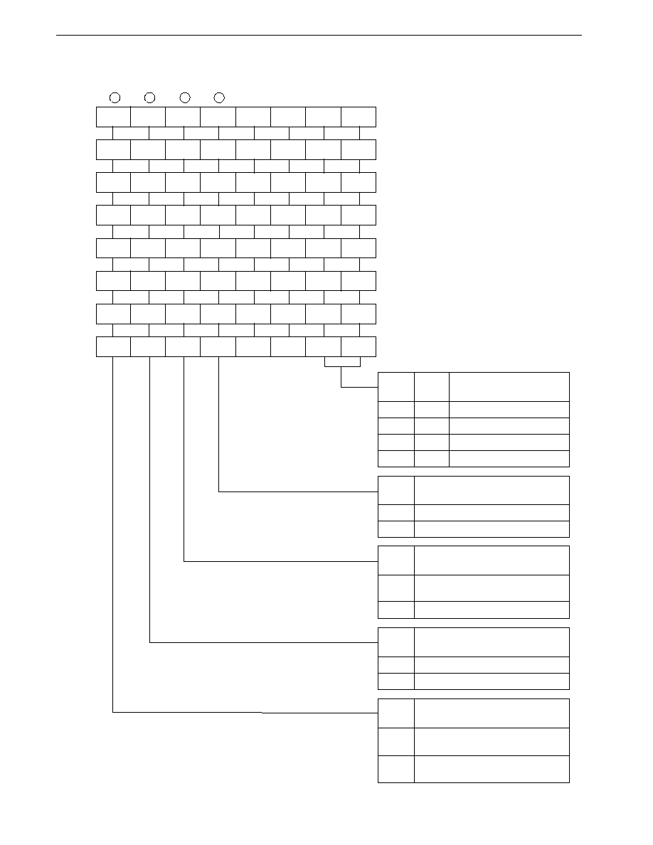
534
CHAPTER 23 INTERRUPT FUNCTIONS
Preliminary User's Manual U13987EJ1V0UM00
Figure 23-1. Interrupt Control Registers (
��
ICn) (1/4)
7
PIF0
PIC0
6
PMK0
5
PISM0
4
PCSE0
3
0
2
0
1
PPR01
0
PPR00
Interrupt Request Priority
Specification
Priority 0 (highest priority)
Priority 1
Priority 2
Priority 3
��
PRn1
(Bit 1)
0
0
��
PRn0
(Bit 0)
1
0
1
0
1
1
Context Switching Service
Specification
Serviced by vectored interrupt
Serviced by context switching
��
CSEn
(Bit 4)
0
1
Interrupt Service Mode Specification
Vectored interrupt service/
context switching service
Macro service
��
ISMn
(Bit 5)
0
1
Interrupt Service Enabling/Disabling
Interrupt service enabled
Interrupt service disabled
��
MKn
(Bit 6)
0
1
Interrupt Request Generation
Presence/Absence
No interrupt request
(interrupt signal not being generated)
Interrupt request state
(interrupt signal being generated)
��
IFn
(Bit 7)
0
1
Address
After reset
R/W
R/W
43H
0FFE0H
PIF1
PIC1
PMK1
PISM1
PCSE1
0
0
PPR11
PPR10
R/W
43H
0FFE1H
PIF2
PIC2
PMK2
PISM2
PCSE2
0
0
PPR21
PPR20
R/W
43H
0FFE2H
PIF3
PIC3
PMK3
PISM3
PCSE3
0
0
PPR31
PPR30
R/W
43H
0FFE3H
CIF00
CIC00
CMK00
CISM00 CCSE00
0
0
CPR001 CPR000
CIF01
CMK01
CISM01 CCSE01
0
0
CPR011 CPR010
CIF10
CMK10
CISM10 CCSE10
0
0
CPR101 CPR100
CIF11
CMK11
CISM11 CCSE11
0
0
CPR111 CPR110
R/W
43H
0FFE4H
CIC01
R/W
43H
0FFE5H
CIC10
R/W
43H
0FFE6H
CIC11
R/W
43H
0FFE7H
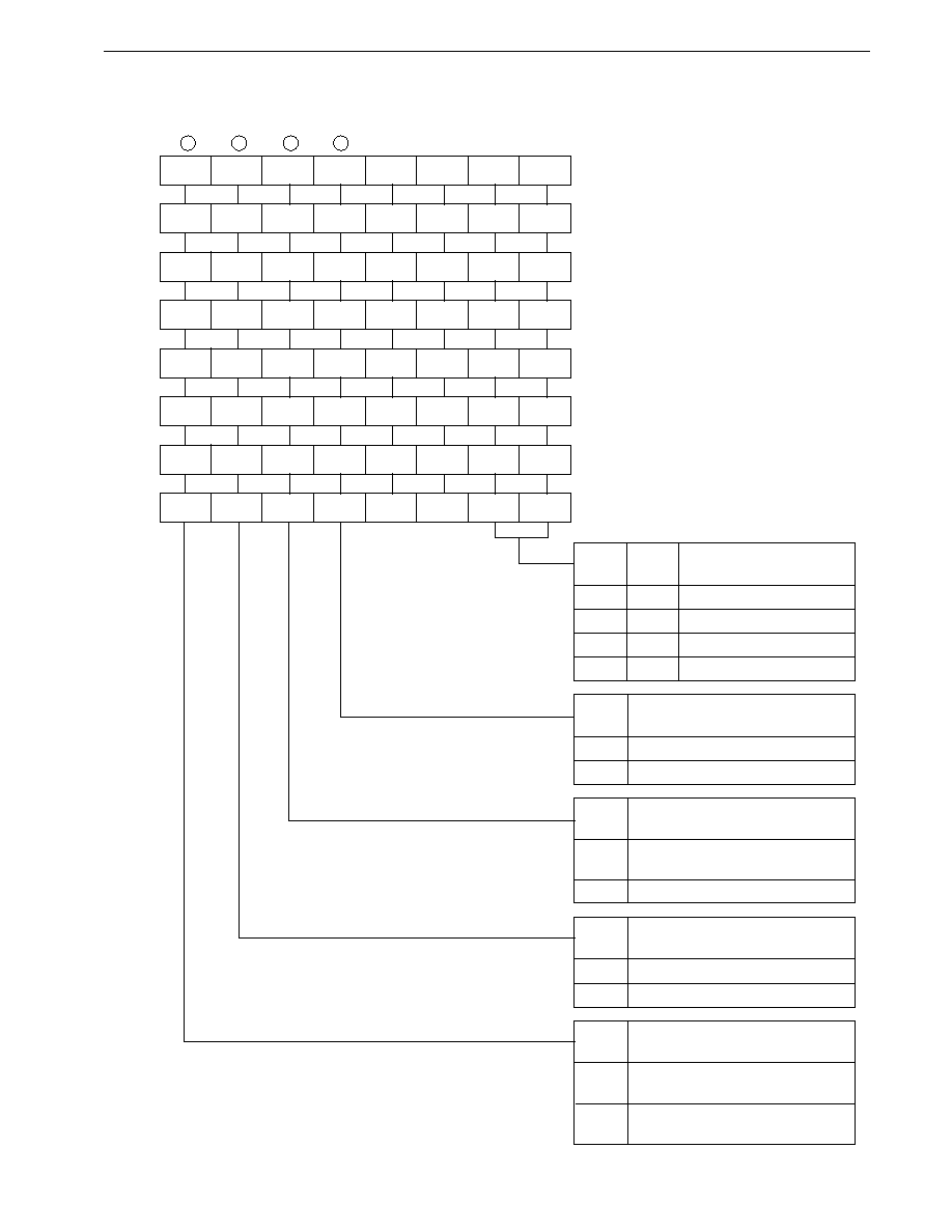
535
CHAPTER 23 INTERRUPT FUNCTIONS
Preliminary User's Manual U13987EJ1V0UM00
Figure 23-1. Interrupt Control Registers (
��
ICn) (2/4)
7
CIF20
CIC20
6
CMK20
5
CISM20
4
CCSE20
3
0
2
0
1
CPR201
0
CPR200
Interrupt Request Priority
Specification
Priority 0 (highest priority)
Priority 1
Priority 2
Priority 3
��
PRn1
(Bit 1)
0
0
��
PRn0
(Bit 0)
1
0
1
0
1
1
Context Switching Service
Specification
Serviced by vectored interrupt
Serviced by context switching
��
CSEn
(Bit 4)
0
1
Interrupt Service Mode Specification
Vectored interrupt service/
context switching service
Macro service
��
ISMn
(Bit 5)
0
1
Interrupt Service Enabling/Disabling
Interrupt service enabled
Interrupt service disabled
��
MKn
(Bit 6)
0
1
Interrupt Request Generation
Presence/Absence
No interrupt request
(interrupt signal not being generated)
Interrupt request state
(interrupt signal being generated)
��
IFn
(Bit 7)
0
1
Address
After reset
R/W
R/W
43H
0FFE8H
CIF21
CIC21
CMK21
CISM21 CCSE21
0
0
CPR211 CPR210
R/W
43H
0FFE9H
CIF30
CIC30
CMK30
CISM30 CCSE30
0
0
CPR301 CPR300
R/W
43H
0FFEAH
PIF4
PIC4
PMK4
PISM4
PCSE4
0
0
PPR41
PPR40
R/W
43H
0FFEBH
PIF5
PIC5
PMK5
PISM5
PCSE5
0
0
PPR51
PPR50
R/W
43H
0FFECH
ADIF
ADIC
ADMK
ADISM
ADCSE
0
0
ADPR1
ADPR0
R/W
43H
0FFEDH
SERIF
SERIC
SERMK
0
SERCSE 0
0
SERPR1 SERPR0
R/W
43H
0FFEEH
SRIF
SRIC
SRMK
SRISM
SRCSE
0
0
SRPR1
SRPR0
R/W
43H
0FFEFH

536
CHAPTER 23 INTERRUPT FUNCTIONS
Preliminary User's Manual U13987EJ1V0UM00
Figure 23-1. Interrupt Control Registers (
��
ICn) (3/4)
7
CSIIF1
CSIIC1
6
CSIMK1
5
CSIISM1
4
CSICSE1
3
0
2
0
1
CSIPR11
0
CSIPR10
Interrupt Request Priority
Specification
Priority 0 (highest priority)
Priority 1
Priority 2
Priority 3
��
PRn1
(Bit 1)
0
0
��
PRn0
(Bit 0)
1
0
1
0
1
1
Context Switching Service
Specification
Serviced by vectored interrupt
Serviced by context switching
��
CSEn
(Bit 4)
0
1
Interrupt Service Mode Specification
Vectored interrupt service/
context switching service
Macro service
��
ISMn
(Bit 5)
0
1
Interrupt Service Enabling/Disabling
Interrupt service enabled
Interrupt service disabled
��
MKn
(Bit 6)
0
1
Interrupt Request Generation
Presence/Absence
No interrupt request
(interrupt signal not being generated)
Interrupt request state
(interrupt signal being generated)
��
IFn
(Bit 7)
0
1
Address
After reset
R/W
R/W
43H
0FFEFH
STIF
STIC
STMK
STISM
STCSE
0
0
STPR1
STPR0
R/W
43H
0FFF0H
CSIIF
CSIIC
CSIMK
CSIISM CSICSE
0
0
CSIPR1 CSIPR0
R/W
43H
0FFF1H
SERIF2
SERIC2
SERMK2
0
SERCSE2
0
0
SERPR21 SERPR20
R/W
43H
0FFF2H
SRIF2
SRIC2
SRMK2
SRISM2 SRCSE2
0
0
SRPR21 SRPR20
CSIIF2
CSIMK2 CSIISM2 CSICSE2
0
0
CSIPR21 CSIPR20
STIF2
STMK2
STISM2 STCSE2
0
0
STPR21 STPR20
R/W
43H
0FFF3H
CSIIC2
R/W
43H
0FFF3H
STIC2
R/W
43H
0FFF4H

537
CHAPTER 23 INTERRUPT FUNCTIONS
Preliminary User's Manual U13987EJ1V0UM00
Figure 23-1. Interrupt Control Registers (
��
ICn) (4/4)
7
IEIF1
IEIC1
6
IEMK1
5
IEISM1
4
IECSE1
3
0
2
0
1
IEPR11
0
IEPR10
Interrupt Request Priority
Specification
Priority 0 (highest priority)
Priority 1
Priority 2
Priority 3
��
PRn1
(Bit 1)
0
0
��
PRn0
(Bit 0)
1
0
1
0
1
1
Context Switching Service
Specification
Serviced by vectored interrupt
Serviced by context switching
��
CSEn
(Bit 4)
0
1
Interrupt Service Mode Specification
Vectored interrupt service/
context switching service
Macro service
��
ISMn
(Bit 5)
0
1
Interrupt Service Enabling/Disabling
Interrupt service enabled
Interrupt service disabled
��
MKn
(Bit 6)
0
1
Interrupt Request Generation
Presence/Absence
No interrupt request
(interrupt signal not being generated)
Interrupt request state
(interrupt signal being generated)
��
IFn
(Bit 7)
0
1
Address
After reset
R/W
R/W
43H
0FFF6H
IEIF2
IEMK2
IEISM2 IECSE2
0
0
IEPR21
IEPR20
WIF
WMK
WISM
WCSE
0
0
WPR1
WPR0
CSIIF3
CSIMK3 CSIISM3 CSICSE3
0
0
CSIPR31 CSIPR30
IEIC2
R/W
43H
0FFF7H
WIC
R/W
43H
0FFF8H
CSIIC3
R/W
43H
0FFF9H
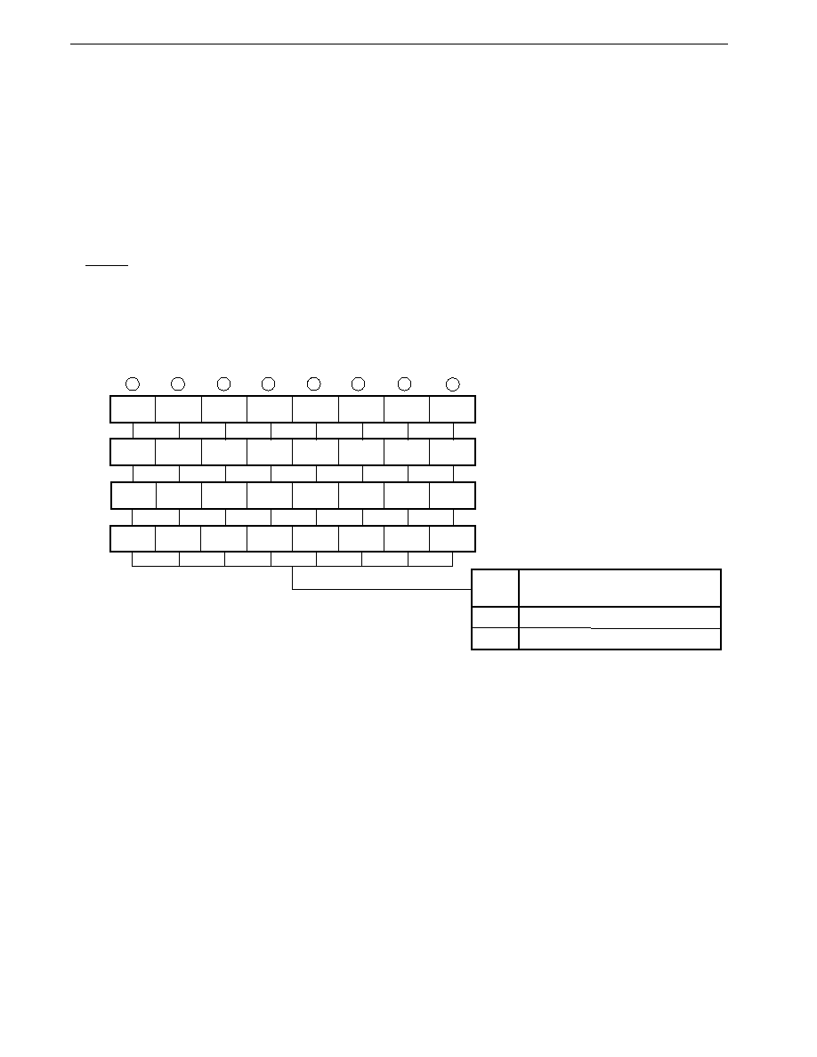
538
CHAPTER 23 INTERRUPT FUNCTIONS
Preliminary User's Manual U13987EJ1V0UM00
23.3.2 Interrupt mask registers (MK0/MK1)
MK0 and MK1 are composed of interrupt mask flags. MK0 and MK1 are 16-bit register which can be manipulated as
8-bit units, MK0L, MK0H, MK1L, and MK1H, as well as being manipulated as a 16-bit unit.
In addition, each bit of MK0 and MK1 can be manipulated individually with a bit manipulation instruction. Each interrupt
mask flag controls enabling/disabling of the corresponding interrupt request.
When an interrupt mask flag is set (to 1), acknowledgment of the corresponding interrupt request is disabled.
When an interrupt mask flag is cleared (to 0), the corresponding interrupt request can be acknowledged as a vectored
interrupt or macro service request.
Each interrupt mask flag in MK0 and MK1 is the same flag as the interrupt mask flag in the interrupt control register.
MK0 and MK1 are provided for en bloc control of interrupt masking.
RESET input sets MK0 and MK1 to FFFFH, and all maskable interrupts are disabled.
Figure 23-2. Interrupt Mask Register (MK0, MK1) Format (1/2)
(1) Byte Accesses
CMK11
MK0L
CMK10
CMK01
CMK00
PMK3
PMK2
PMK1
PMK0
Address
After reset
R/W
R/W
FFH
0FFACH
CSIMK1
SRMK
CSIMK2
SRMK2
MK0H
SERMK
ADMK
PMK5
PMK4
CMK30
CMK21
CMK20
R/W
FFH
0FFADH
IEMK2
MK1L
IEMK1
1
STMK2
SERMK2 CSIMK
STMK
R/W
FFH
0FFAEH
Interrupt Request Enabling/Disabling
Specification
Interrupt service enabled
Interrupt service disabled
MK
0
1
7
6
5
4
3
2
1
0
1
MK1H
1
1
1
1
1
CSIMK3
WMK
R/W
FFH
0FFAFH
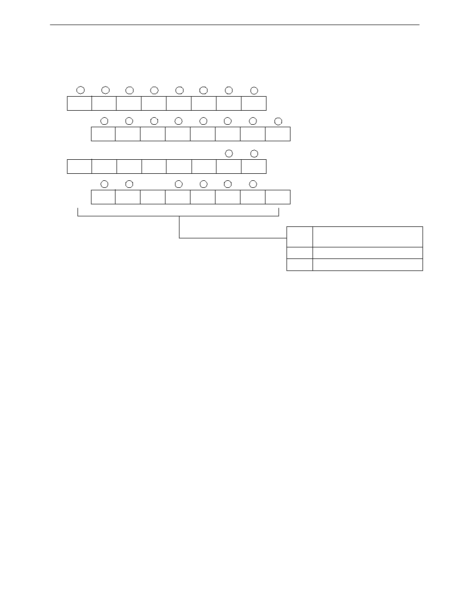
539
CHAPTER 23 INTERRUPT FUNCTIONS
Preliminary User's Manual U13987EJ1V0UM00
Figure 23-2. Interrupt Mask Register (MK0, MK1) Format (2/2)
(2) Word Accesses
7
CMK11
MK0
6
CMK10
5
CMK01
4
CMK00
3
PMK3
2
PMK2
1
PMK1
0
PMK0
Interrupt Request Enabling/Disabling
Specification
Interrupt service enabled
Interrupt service disabled
MK
0
1
15
14
13
12
11
10
9
8
Address
After reset
R/W
R/W
FFFFH
0FFACH
CSIMK1
SRMK
SERMK
ADMK
PMK5
PMK4
CMK30
CMK21
CMK20
7
IEMK2
MK1
6
IEMK1
5
1
4
STMK2
3
CSIMK2
SRMK2
2
SERMK2
1
CSIMK
0
STMK
15
14
13
12
11
10
9
8
1
1
1
1
1
1
CSIMK3
WMK
Address
After reset
R/W
R/W
FFFFH
0FFAEH
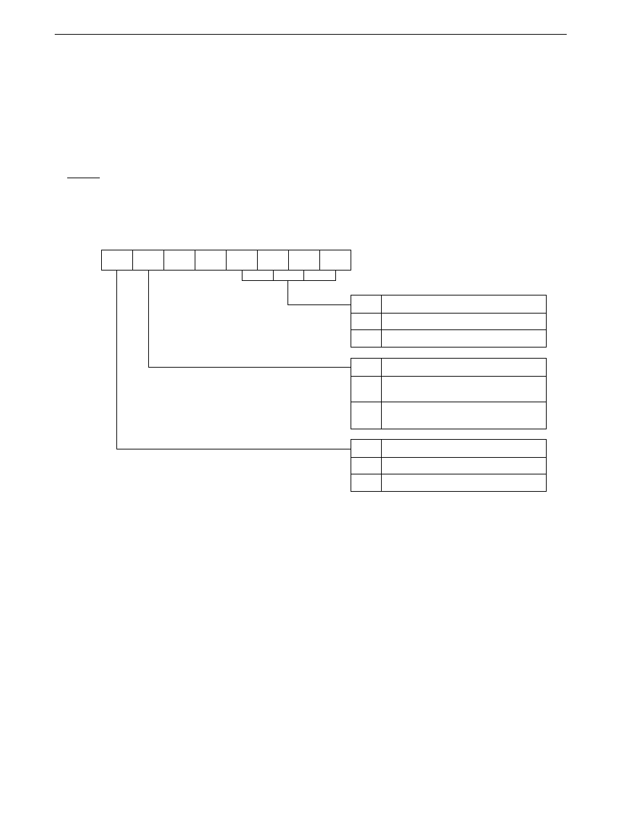
540
CHAPTER 23 INTERRUPT FUNCTIONS
Preliminary User's Manual U13987EJ1V0UM00
23.3.3 In-service priority register (ISPR)
ISPR shows the priority level of the maskable interrupt currently being serviced and the non-maskable interrupt being
serviced. When a maskable interrupt request is acknowledged, the bit corresponding to the priority of that interrupt request
is set (to 1), and remains set until the service program ends. When a non-maskable interrupt is acknowledged, the bit
corresponding to the priority of that non-maskable interrupt is set (to 1), and remains set until the service program ends.
When an RETI instruction or RETCS instruction is executed, the bit, among those set (to 1) in the ISPR, that corresponds
to the highest-priority interrupt request is automatically cleared (to 0) by hardware.
The contents of ISPR are not changed by execution of an RETB or RETCSB instruction.
RESET input clears ISPR to 00H.
Figure 23-3. In-Service Priority Register (ISPR) Format
7
NMIS
ISPR
6
WDTS
5
0
4
0
3
ISPR3
2
ISPR2
1
ISPR1
0
ISPR0
Priority n interrupt not being acknowledged
Priority n interrupt being acknowledged
(n = 0 to 3)
ISPRn
1
0
NMI interrupt not being acknowledged
NMI interrupt being acknowledged
NMIS
1
0
Watchdog timer interrupt not being
acknowledged
Watchdog timer interrupt being
acknowledged
WDTS
1
0
Address
After reset
R/W
R
00H
0FFA8H
Priority Level
Watchdog Timer Interrupt Service State
NMI Service State
Caution In-service priority register (ISPR) is a read-only register. There is a risk of misoperation if a write is
performed on this register.
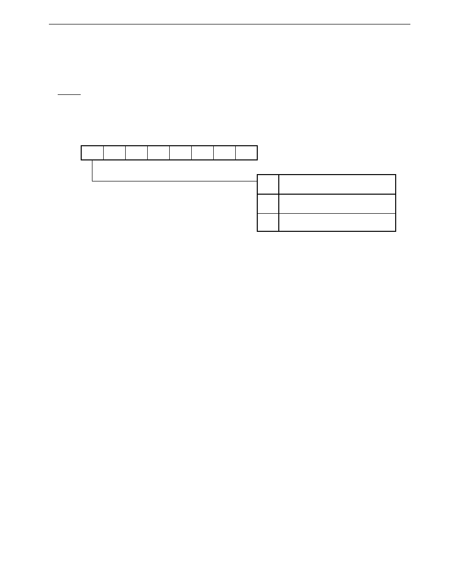
541
CHAPTER 23 INTERRUPT FUNCTIONS
Preliminary User's Manual U13987EJ1V0UM00
23.3.4 Interrupt mode control register (IMC)
IMC contains the PRSL flag. The PRSL flag specifies enabling/disabling of nesting of maskable interrupts for which
the lowest priority level (level 3) is specified.
When IMC is manipulated, the interrupt disabled state (DI state) should be set first to prevent misoperation.
IMC can be read or written to with an 8-bit manipulation instruction or bit manipulation instruction.
RESET input sets IMC to 80H.
Figure 23-4. Interrupt Mode Control Register (IMC) Format
7
PRSL
IMC
6
0
5
0
4
0
3
0
2
0
1
0
0
0
Control of Nesting Operations for
Maskable Interrupts (Lowest Level)
Nesting between interrupts set as level 3
(lowest level) enabled
Nesting between interrupts set as level 3
(lowest level) disabled
PRSL
1
0
Address
After reset
R/W
R/W
80H
0FFAAH
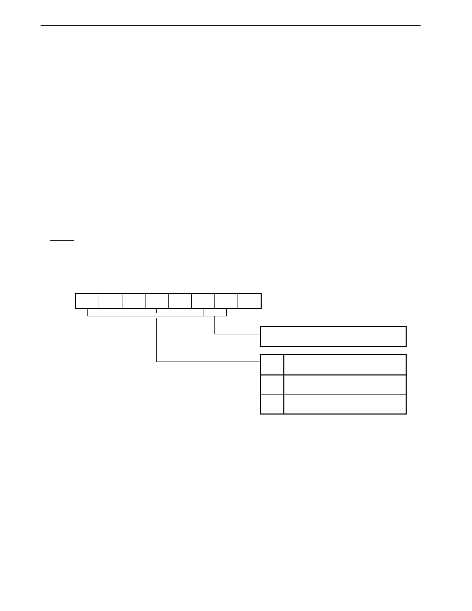
542
CHAPTER 23 INTERRUPT FUNCTIONS
Preliminary User's Manual U13987EJ1V0UM00
23.3.5 Watchdog timer mode register (WDM)
The PRC bit of WDM specifies the priority of NMI pin input non-maskable interrupts and watchdog timer overflow non-
maskable interrupts.
WDM can be written to only by a dedicated instruction. This dedicated instruction, MOV WDM, #byte, has a special
code configuration (4 bytes), and a write is not performed unless the 3rd and 4th bytes of the operation code are mutual
complements of 1.
If the 3rd and 4th bytes of the operation code are not complements of 1, a write is not performed and an operand error
interrupt is generated. In this case, the return address saved in the stack area is the address of the instruction that was
the source of the error, and thus the address that was the source of the error can be identified from the return address saved
in the stack area.
If recovery from an operand error is simply performed by means of an RETB instruction, an endless loop will result.
As an operand error interrupt is only generated in the event of an inadvertent program loop (with the NEC assembler,
RA78K4, only the correct dedicated instruction is generated when MOV WDM, #byte is written), system initialization should
be performed by the program.
Other write instructions (MOV WDM, A, AND WDM, #byte instruction, SET1 WDM.7, etc.) are ignored and do not perform
any operation. That is, a write is not performed to the WDM, and an interrupt such as an operand error interrupt is not
generated.
WDM can be read at any time by a data transfer instruction.
RESET input clears WDM to 00H.
Figure 23-5. Watchdog Timer Mode Register (WDM) Format
7
RUN
WDM
6
0
5
0
4
PRC
3
0
2
WDI2
1
WDI1
0
0
Watchdog Timer Interrupt Request Priority
Specification
Watchdog timer interrupt request <
NMI pin input interrupt request
Watchdog timer interrupt request >
NMI pin input interrupt request
PRC
1
0
Address
After reset
R/W
R/W
00H
0FFC2H
See Figure 13-2 in CHAPTER 13 WATCHDOG
TIMER FUNCTION for details.
Caution The watchdog timer mode register (WDM) can only be written to with a dedicated instruction (MOV
WDM, #byte).
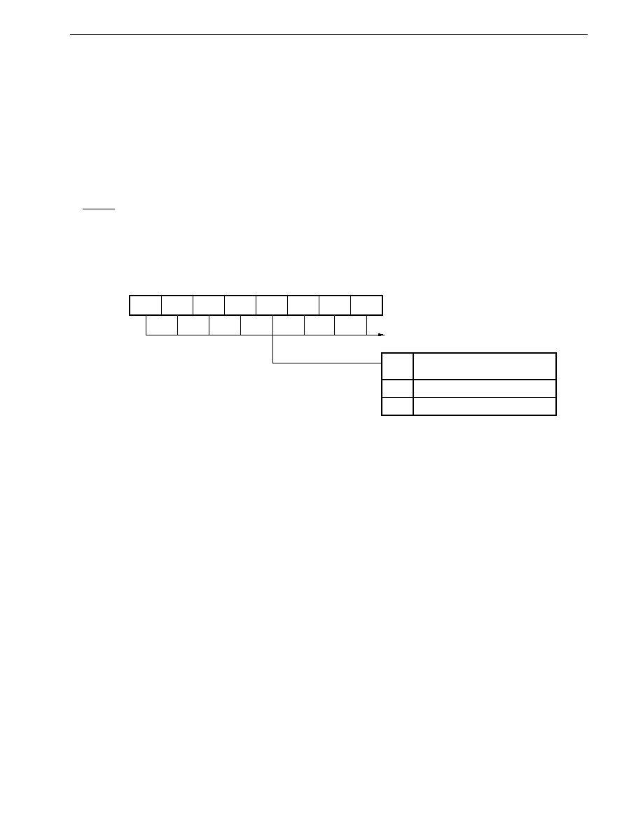
543
CHAPTER 23 INTERRUPT FUNCTIONS
Preliminary User's Manual U13987EJ1V0UM00
23.3.6 Program status word (PSW)
PSW is a register that holds the current status regarding instruction execution results and interrupt requests. The IE
flag that sets enabling/disabling of maskable interrupts is mapped in the low-order 8 bits of the PSW (PSWL).
PSWL can be read or written to with an 8-bit manipulation instruction, and can also be manipulated with a bit manipulation
instruction or dedicated instruction (EI/DI).
When a vectored interrupt is acknowledged or a BRK instruction is executed, PSWL is saved to the stack and the IE
flag is cleared (to 0). PSWL is also saved to the stack by the PUSH PSW instruction, and is restored from the stack by
the RETI, RETB and POP PSW instructions.
When context switching or a BRKCS instruction is executed, PSWL is saved to a fixed area in the register bank, and
the IE flag is cleared (to 0). PSWL is restored from the fixed area in the register bank by an RETCSI or RETCSB instruction.
RESET input clears PSWL to 00H.
Figure 23-6. Program Status Word (PSWL) Format
7
S
PSWL
6
Z
5
RSS
4
AC
3
IE
2
P/V
1
0
0
CY
After reset
00H
IE
Interrupt Acknowledgment
Enabling/Disabling
Disabled
Enabled
1
0
Used in normal instruction execution
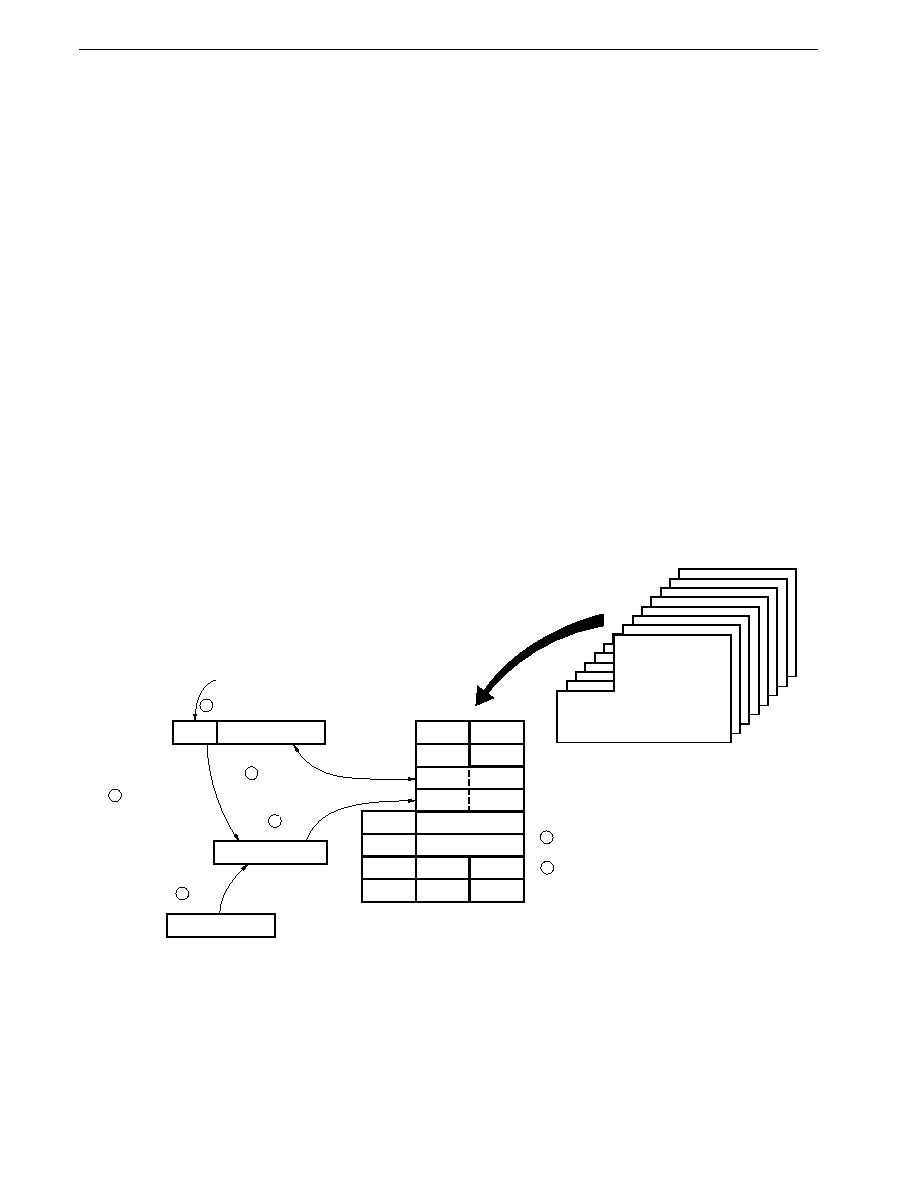
544
CHAPTER 23 INTERRUPT FUNCTIONS
Preliminary User's Manual U13987EJ1V0UM00
23.4 Software Interrupt Acknowledgment Operations
A software interrupt is acknowledged in response to execution of a BRK or BRKCS instruction. Software interrupts cannot
be disabled.
23.4.1 BRK instruction software interrupt acknowledgment operation
When a BRK instruction is executed, the program status word (PSW), program counter (PC) are saved in that order to
the stack, the IE flag is cleared (to 0), the vector table (003EH/003FH) contents are loaded into the low-order 16 bits of
the PC, and 0000B into the high-order 4 bits, and a branch is performed (the start of the service program must be in the
base area).
The RETB instruction must be used to return from a BRK instruction software interrupt.
Caution The RETI instruction must not be used to return from a BRK instruction software interrupt.
23.4.2 BRKCS instruction software interrupt (software context switching) acknowledgment operation
The context switching function can be initiated by executing a BRKCS instruction.
The register bank to be used after context switching is specified by the BRKCS instruction operand.
When a BRKCS instruction is executed, the program branches to the start address of the interrupt service program (which
must be in the base area) stored beforehand in the specified register bank, and the contents of the program status word
(PSW) and program counter (PC) are saved in the register bank.
Figure 23-7. Context Switching Operation by Execution of a BRKCS Instruction
The RETCSB instruction is used to return from a software interrupt due to a BRKCS instruction. The RETCSB instruction
must specify the start address of the interrupt service program for the next time context switching is performed by a BRKCS
instruction. This interrupt service program start address must be in the base area.
Caution The RETCS instruction must not be used to return from a BRKCS instruction software interrupt.
Register bank
(0 to 7)
A
B
R5
R7
X
C
R4
R6
D
H
VP
UP
E
L
V
U
T
W
Register bank n (n = 0 to 7)
7 Transfer
3 Register bank switching
(RBS0 to RBS2
n)
4 RSS
0
(
IE
0
)
1 Save
2 Save
(bits 8 to 11 of
temporary register)
6 Exchange
5 Save
PC
15 to 0
PC
19 to16
0000B
Temporary register
PSW
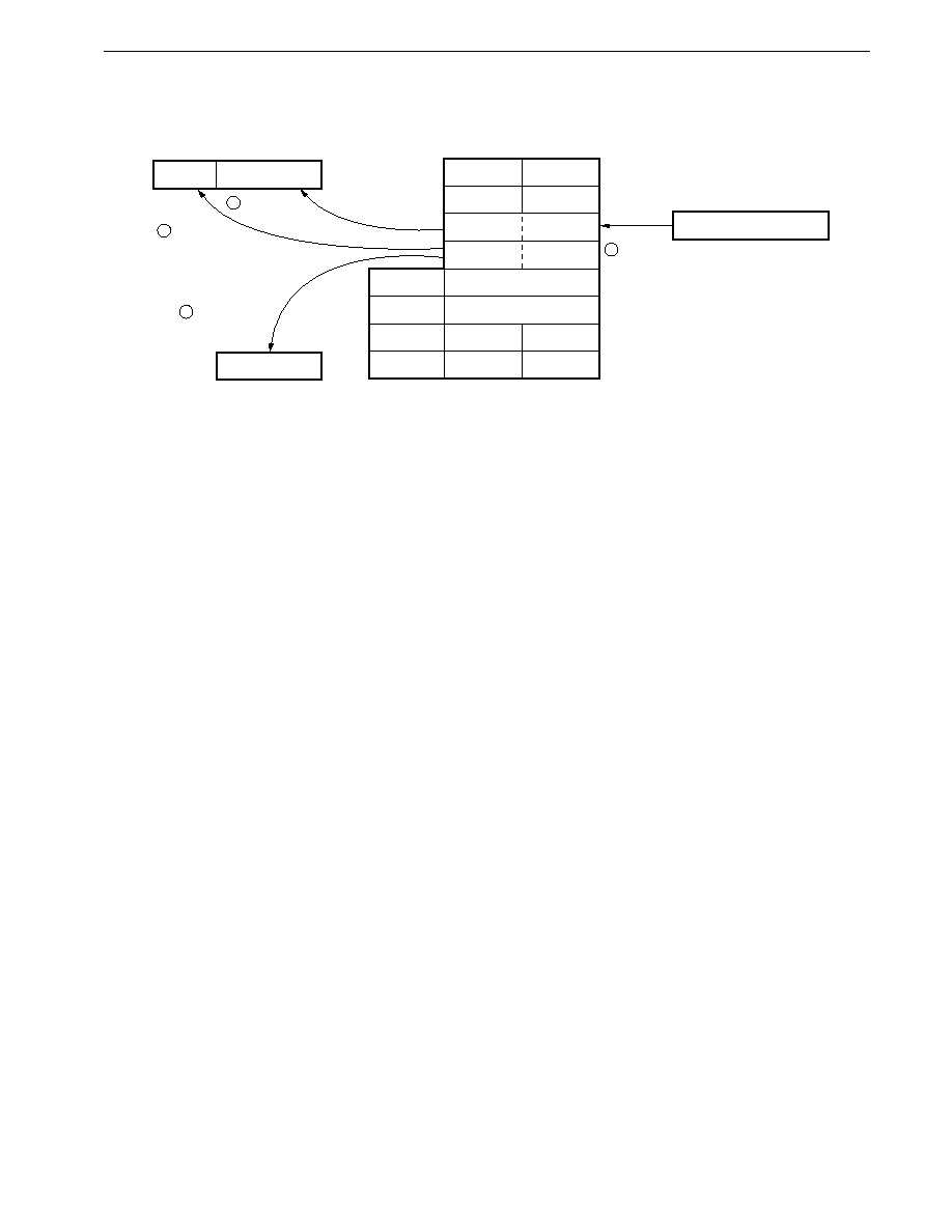
545
CHAPTER 23 INTERRUPT FUNCTIONS
Preliminary User's Manual U13987EJ1V0UM00
Figure 23-8. Return from BRKCS Instruction Software Interrupt (RETCSB instruction operation)
PC
19 to 16
PC
15 to 0
1 Restoration
3 Transfer
4 Restoration
(to original
register bank)
2 Restoration
PSW
V
VP
U
UP
T
E
W
L
RETCSB instruction operand
Register bank n (n = 0 to 7)
A
R5
R7
D
H
B
X
R4
R6
C

546
CHAPTER 23 INTERRUPT FUNCTIONS
Preliminary User's Manual U13987EJ1V0UM00
23.5 Operand Error Interrupt Acknowledgment Operation
An operand error interrupt is generated when the data obtained by inverting all the bits of the 3rd byte of the operand
of a "MOV STBC, #byte instruction "," LOCATION instruction" or a "MOV WDM, #byte instruction" does not match the 4th
byte of the operand. Operand error interrupts cannot be disabled.
When an operand error interrupt is generated, the program status word (PSW) and the start address of the instruction
that caused the error are saved to the stack, the IE flag is cleared (to 0), the vector table value is loaded into the program
counter (PC), and a branch is performed (within the base area only).
As the address saved to the stack is the start address of the instruction in which the error occurred, simply writing an
RETB instruction at the end of the operand error interrupt service program will result in generation of another operand error
interrupt. You should therefore either process the address in the stack or initialize the program by referring to 23.12
Restoring Interrupt Function to Initial State.
23.6 Non-Maskable Interrupt Acknowledgment Operation
Non-maskable interrupts are acknowledged even in the interrupt disabled state. Non-maskable interrupts can be
acknowledged at all times except during execution of the service program for an identical non-maskable interrupt or a non-
maskable interrupt of higher priority.
The relative priorities of non-maskable interrupts are set by the PRC bit of the watchdog timer mode register (WDM)
(see 23.3.5 Watchdog timer mode register (WDM)).
Except in the cases described in 23.9 When Interrupt Requests and Macro Service are Temporarily Held Pending,
a non-maskable interrupt request is acknowledged immediately. When a non-maskable interrupt request is acknowledged,
the program status word (PSW) and program counter (PC) are saved in that order to the stack, the IE flag is cleared (to
0), the in-service priority register (ISPR) bit corresponding to the acknowledged non-maskable interrupt is set (to 1), the
vector table contents are loaded into the PC, and a branch is performed. The ISPR bit that is set (to 1) is the NMIS bit
in the case of a non-maskable interrupt due to edge input to the NMI pin, and the WDTS bit in the case of watchdog timer
overflow.
When the non-maskable interrupt service program is executed, non-maskable interrupt requests of the same priority
as the non-maskable interrupt currently being executed and non-maskable interrupts of lower priority than the non-maskable
interrupt currently being executed are held pending. A pending non-maskable interrupt is acknowledge after completion
of the non-maskable interrupt service program currently being executed (after execution of the RETI instruction). However,
even if the same non-maskable interrupt request is generated more than once during execution of the non-maskable
interrupt service program, only one non-maskable interrupt is acknowledged after completion of the non-maskable interrupt
service program.
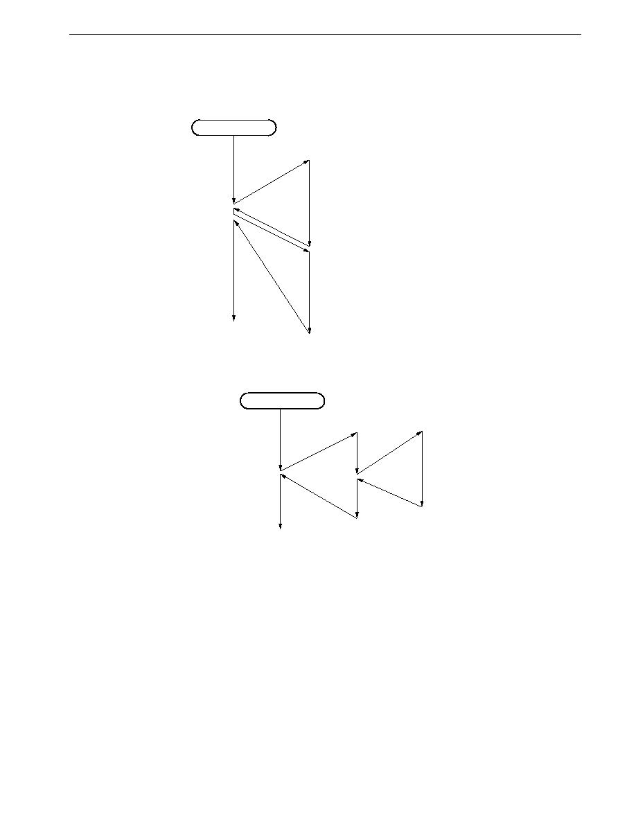
547
CHAPTER 23 INTERRUPT FUNCTIONS
Preliminary User's Manual U13987EJ1V0UM00
Figure 23-9. Non-Maskable Interrupt Request Acknowledgment Operations (1/2)
(a) When a new NMI request is generated during NMI service program execution
Main routine
NMI request
NMI request
(NMIS = 1)
NMI request held pending since NMIS = 1
Pending NMI request is processed
(b) When a watchdog timer interrupt request is generated during NMI service program execution (when the
watchdog timer interrupt priority is higher (when PRC in the WDM = 1))
Main routine
NMI request
Watchdog
timer interrupt
request
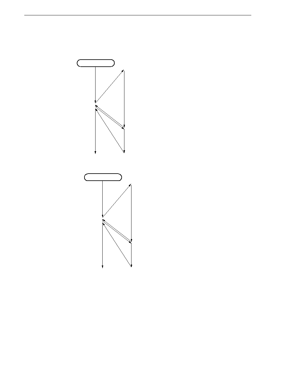
548
CHAPTER 23 INTERRUPT FUNCTIONS
Preliminary User's Manual U13987EJ1V0UM00
Figure 23-9. Non-Maskable Interrupt Request Acknowledgment Operations (2/2)
(c) When a watchdog timer interrupt request is generated during NMI service program execution (when the
NMI interrupt priority is higher (when PRC in the WDM = 0))
Main routine
NMI request
Watchdog
timer
interrupt
request
Pending watchdog timer interrupt is processed
Watchdog timer interrupt held
pending since PRC = 0
(d) When an NMI request is generated twice during NMI service program execution
Main routine
NMI request
NMI
request
Held pending since NMI service
program is being executed
NMI
request
Held pending since NMI service
program is being executed
NMI request was generated more than
once, but is only acknowledged once

549
CHAPTER 23 INTERRUPT FUNCTIONS
Preliminary User's Manual U13987EJ1V0UM00
Cautions 1. Macro service requests are acknowledged and serviced even during execution of a non-maskable
interrupt service program. If you do not want macro service processing to be performed during
a non-maskable interrupt service program, you should manipulate the interrupt mask register in
the non-maskable interrupt service program to prevent macro service generation.
2. The RETI instruction must be used to return from a non-maskable interrupt. Subsequent interrupt
acknowledgment will not be performed normally if a different instruction is used.
3. Non-maskable interrupts are always acknowledged, except during non-maskable interrupt service
program execution (except when a high non-maskable interrupt request is generated during
execution of a low-priority non-maskable interrupt service program) and for a certain period after
execution of the special instructions shown in 23.9 When Interrupt Requests and Macro Service
are Temporarily Held Pending. Therefore, a non-maskable interrupt will be acknowledged even
when the stack pointer (SP) value is undefined, in particular after reset release, etc. In this case,
depending on the value of the SP, it may happen that the program counter (PC) and program status
word (PSW) are written to the address of a write-inhibited special function register (SFR) (see Table
3-5 in 3.9 Special Function Registers (SFR)), and the CPU becomes deadlocked, or an unexpected
signal is output from a pin, or the PC and PSW are written to an address in which RAM is not
mounted, with the result that the return from the non-maskable interrupt service program to the
main routine is not performed normally and an inadvertent program routine occurs.
Therefore, the program following RESET release must be as shown below.
CSEG AT 0
DW
STRT
CSEG BASE
STRT:
LOCATION 0FH; or LOCATION 0
MOVG SP, #imm24

550
CHAPTER 23 INTERRUPT FUNCTIONS
Preliminary User's Manual U13987EJ1V0UM00
23.7 Maskable Interrupt Acknowledgment Operation
A maskable interrupt can be acknowledged when the interrupt request flag is set (to 1) and the mask flag for that interrupt
is cleared (to 0). When servicing is performed by macro service, the interrupt is acknowledged and serviced by macro service
immediately. In the case of vectored interruption and context switching, an interrupt is acknowledged in the interrupt enabled
state (when the IE flag is set (to 1)) if the priority of that interrupt is one for which acknowledgment is permitted.
If maskable interrupt requests are generated simultaneously, the interrupt for which the highest priority is specified by
the priority specification flag is acknowledged. If the interrupts have the same priority specified, they are acknowledged
in accordance with their default priorities.
A pending interrupt is acknowledged when a state in which it can be acknowledged is established.
The interrupt acknowledgment algorithm is shown in Figure 23-10.
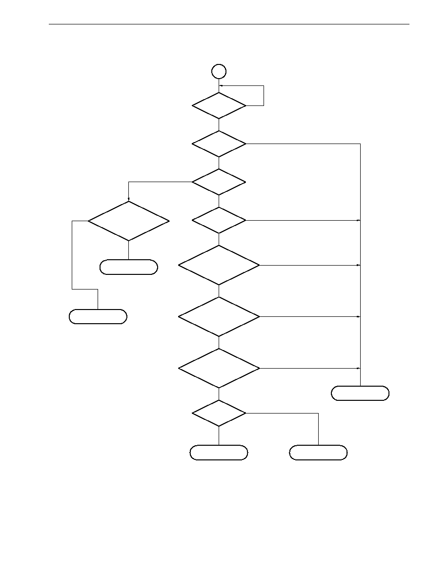
551
CHAPTER 23 INTERRUPT FUNCTIONS
Preliminary User's Manual U13987EJ1V0UM00
Figure 23-10. Interrupt Acknowledgment Processing Algorithm
No
��
IF = 1
��
MK = 0
��
ISM = 1
��
CSE = 1
IE = 1
Higher priority
than interrupt currently
being serviced?
Higher priority
than other existing interrupt
requests?
Highest default
priority among interrupt
requests of same
priority?
Vectored interrupt
generation
Interrupt request?
Yes
No
Interrupt mask released?
Yes
No
Yes
Yes
Yes
Yes
No
No
Interrupt enabled state?
Macro service?
No
No
No
Interrupt request
held pending
Yes
Context switching?
Context switching
generation
Yes
Highest
default priority among
macro service
requests?
Macro service
processing execution
Interrupt request
held pending
No
Yes

552
CHAPTER 23 INTERRUPT FUNCTIONS
Preliminary User's Manual U13987EJ1V0UM00
23.7.1 Vectored interrupt
When a vectored interrupt maskable interrupt request is acknowledged, the program status word (PSW) and program
counter (PC) are saved in that order to the stack, the IE flag is cleared (to 0) (the interrupt disabled state is set), and the
in-service priority register (ISPR) bit corresponding to the priority of the acknowledged interrupt is set (to 1). Also, data
in the vector table predetermined for each interrupt request is loaded into the PC, and a branch is performed. The return
from a vectored interrupt is performed by means of the RETI instruction.
Caution When a maskable interrupt is acknowledged by vectored interrupt, the RETI instruction must be used
to return from the interrupt. Subsequent interrupt acknowledgment will not be performed normally
if a different instruction is used.
23.7.2 Context switching
Initiation of the context switching function is enabled by setting (to 1) the context switching enable flag of the interrupt
control register.
When an interrupt request for which the context switching function is enabled is acknowledged, the register bank specified
by 3 bits of the lower address (even address) of the corresponding vector table address is selected.
The vector address stored beforehand in the selected register bank is transferred to the program counter (PC), and at
the same time the contents of the PC and program status word (PSW) up to that time are saved in the register bank and
a branch is made to the interrupt service program.
Figure 23-11. Context Switching Operation by Generation of an Interrupt Request
Register bank
(0 to 7)
A
B
R5
R7
X
C
R4
R6
D
H
VP
UP
E
L
V
U
T
W
Register bank n (n = 0 to 7)
7 Transfer
6 Exchange
4
2 Save
(temporary
register
bits 8 to 11)
5 Save
1 Save
PC
15 to 0
PC
19 to 16
0000B
Temporary register
PSW
n
3 Register bank switching
(RBS0 to RBS2
n)
Vector table
RSS
0
(
IE
0
)
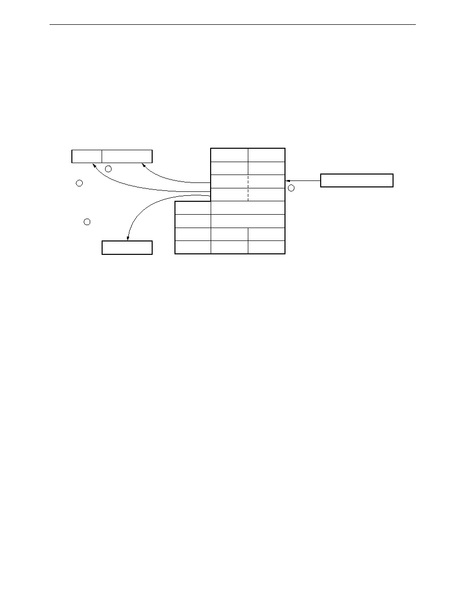
553
CHAPTER 23 INTERRUPT FUNCTIONS
Preliminary User's Manual U13987EJ1V0UM00
The RETCS instruction is used to return from an interrupt that uses the context switching function. The RETCS instruction
must specify the start address of the interrupt service program to be executed when that interrupt is acknowledged next.
This interrupt service program start address must be in the base area.
Caution The RETCS instruction must be used to return from an interrupt serviced by context switching.
Subsequent interrupt acknowledgment will not be performed normally if a different instruction is used.
Figure 23-12. Return from Interrupt that Uses Context Switching by Means of RETCS Instruction
PC
19 to 16
PC
15 to 0
2 Restoration
4 Restoration
(to original
register bank)
PSW
RETCS instruction operand
3 Transfer
Register bank n (n = 0 to 7)
V
VP
U
UP
T
D
E
W
H
L
A
X
R5
R4
R7
R6
B
C
1 Restoration

554
CHAPTER 23 INTERRUPT FUNCTIONS
Preliminary User's Manual U13987EJ1V0UM00
23.7.3 Maskable interrupt priority levels
The
�
PD784938 performs multiple interrupt servicing in which an interrupt is acknowledged during servicing of another
interrupt. Multiple interrupts can be controlled by priority levels.
There are two kinds of priority control, control by default priority and programmable priority control in accordance with
the setting of the priority specification flag. In priority control by means of default priority, interrupt service is performed
in accordance with the priority preassigned to each interrupt request (default priority) (see Table 23-2). In programmable
priority control, interrupt requests are divided into four levels according to the setting of the priority specification flag. Interrupt
requests for which multiple interruption is permitted are shown in Table 23-5.
Since the IE flag is cleared (to 0) automatically when an interrupt is acknowledged, when multiple interruption is used,
the IE flag should be set (to 1) to enable interrupts by executing an EI instruction in the interrupt service program, etc.
Table 23-5. Multiple Interrupt Servicing
Priority of Interrupt Currently
ISPR Value
IE Flag in PSW
PRSL Flag in
Acknowledgeable Maskable Interrupts
Being Acknowledged
IMC
No interrupt being
00000000
0
�
�
All macro service only
acknowledged
1
�
�
All maskable interrupts
3
00001000
0
�
�
All macro service only
1
0
�
All maskable interrupts
1
1
�
All macro service
�
Maskable interrupts specified as
priority 0/1/2
2
0000
�
100
0
�
�
All macro service only
1
�
�
All macro service
�
Maskable interrupts specified as
priority 0/1
1
0000
��
10
0
�
�
All macro service only
1
�
�
All macro service
�
Maskable interrupts specified as
priority 0
0
0000
���
1
�
�
�
All macro service only
Non-maskable interrupts
1000
����
�
�
�
All macro service only
0100
����
1100
����
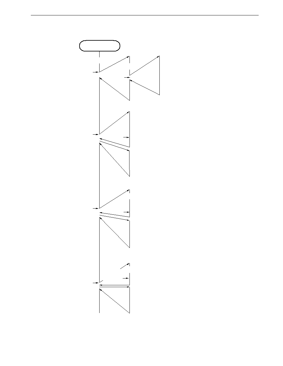
555
CHAPTER 23 INTERRUPT FUNCTIONS
Preliminary User's Manual U13987EJ1V0UM00
Figure 23-13. Examples of Servicing when Another Interrupt Request is Generated During Interrupt Service (1/3)
Main routine
EI
EI
EI
Interrupt request a
(level 3)
Interrupt
request b
(level 2)
Interrupt
request d
(level 2)
Interrupt request e
(level 2)
Interrupt
request f
(level 3)
Interrupt request g
(level 1)
a servicing
b servicing
c servicing
d servicing
e servicing
f servicing
g servicing
h servicing
Since interrupt request b has a higher
priority than interrupt request a, and
interrupts are enabled, interrupt
request b is acknowledged.
The priority of interrupt request d is
higher than that of interrupt request c,
but since interrupts are disabled,
interrupt request d is held pending.
Although interrupts are enabled,
interrupt request f is held pending
since it has a lower priority than
interrupt request e.
Although interrupts are enabled,
interrupt request h is held pending
since it has the same priority as
interrupt request g.
Interrupt
request h
(level 1)
EI
Interrupt request c
(level 3)
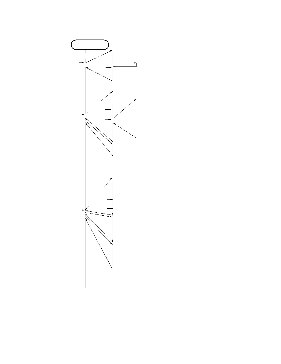
556
CHAPTER 23 INTERRUPT FUNCTIONS
Preliminary User's Manual U13987EJ1V0UM00
Figure 23-13. Examples of Servicing when Another Interrupt Request is Generated During Interrupt Service (2/3)
Main routine
EI
EI
Interrupt request i
(level 1)
Interrupt request k
(level 2)
Interrupt request n
(level 2)
Macro service
request j
(level 2)
i servicing
j macro service
k servicing
l servicing
m servicing
n servicing
o servicing
p servicing
The macro service request is
serviced irrespective of interrupt
enabling/disabling and priority.
The interrupt request is held
peding since it has a lower
priority than interrupt request k.
Interrupt request m generated
after interrupt request l has a
higher priority, and is therefore
acknowledged first.
Since servicing of interrupt
request n performed in the
interrupt disabled state,
interrupt requests o and p
are held pending.
After interrupt request n
servicing, the pending interrupt
requests are acknowledged.
Although interrupt request o
was generated first, interrupt
request p has a higher priority
and is therefore acknowledged
first.
Interrupt
request l
(level 3)
Interrupt
request m
(level 1)
Interrupt
request o
(level 3)
Interrupt
request p
(level 1)

557
CHAPTER 23 INTERRUPT FUNCTIONS
Preliminary User's Manual U13987EJ1V0UM00
Figure 23-13. Examples of Servicing when Another Interrupt Request is Generated During Interrupt Service (3/3)
Main routine
EI
EI
EI
EI
EI
EI
Interrupt request q
(level 3)
Interrupt
request s
(level 1)
Interrupt request u
(level 0)
Interrupt
request v
(level 0)
w macro service
q servicing
r servicing
s servicing
t servicing
u servicing
v servicing
x servicing
y servicing
z servicing
Interrupt request x
(level 1)
Interrupt
request r
(level 2)
Interrupt
request t
(level 0)
Interrupt
request y
Note
(level 2)
Interrupt
request w
(level 3)
Multiple acknowledgment of levels 3 to 0. If
the PRSL bit of the IMC register is set (to 1),
only macro service requests and non-
maskable interrupts generate nesting
beyond this.
If the PRSL bit of the IMC register is
cleared (to 0), level 3 interrupts can also be
nested during level 3 interrupt servicing
(see Figure 23-15).
Even though the interrupt enabled state is
set during servicing of level 0 interrupt
request u, the interrupt request is not
acknowledged but held pending even
though its priority is 0. However, the macro
service request is acknowledged and
serviced irrespective of its level and even
though there is a peding interrupt with a
higher priority level.
Pending interrupt requests y and z are
acknowledged after servicing of interrupt
request x. As interrupt requests y and z
have the same priority level, interrupt
request z which has the higher default
priority is acknowledged first, irrespective
of the order in which the interrupt requests
were generated.
Interrupt
request z
Note
(level 2)
Notes 1. Low default priority
2. High default priority
Remarks 1. "a" to "z" in the figure are arbitrary names used to differentiate between the interrupt requests and macro
service requests.
2. High/low default priorities in the figure indicate the relative priority levels of the two interrupt requests.

558
CHAPTER 23 INTERRUPT FUNCTIONS
Preliminary User's Manual U13987EJ1V0UM00
Figure 23-14. Examples of Servicing of Simultaneously Generated Interrupts
Main routine
EI
Interrupt request a (level 2)
Macro service request b (level 3)
Macro service request c (level 1)
Interrupt request d (level 1)
Interrupt request e (level 1)
Macro service request f (level 1)
Default priority order
a > b > c > d > e > f
Macro service request b servicing
Macro service request c servicing
Macro service request f servicing
Interrupt request d servicing
Interrupt request e servicing
Interrupt request a servicing
�
When requests are generated
simultaneously, they are
acknowledged in the order starting
with macro service.
�
Macro service requests are
acknowledged in default priority
order (b/c/f) (not dependent
upon the programmable priority
order).
�
As interrupt requests are
acknowledged in high-to-low
priority level order, d and e are
acknowledged first.
�
As d and e have the same
prority level, the interrupt
request with the higher default
priority, d, is acknowledged
first.
Remark
"a" to "f" in the figure are arbitrary names used to differentiate between the interrupt requests and macro service
requests.
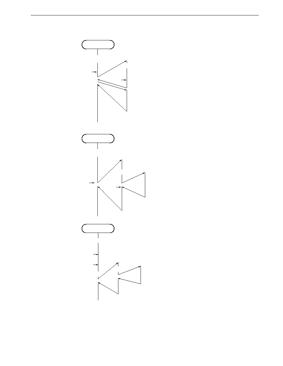
559
CHAPTER 23 INTERRUPT FUNCTIONS
Preliminary User's Manual U13987EJ1V0UM00
Figure 23-15. Differences in Level 3 Interrupt Acknowledgment According to IMC Register Setting
Main routine
EI
EI
Interrupt request a
(level 3)
Interrupt
request b
(level 3)
a servicing
b servicing
Interrupt request c
(level 3)
Interrupt
request d
(level 3)
c servicing
d servicing
Interrupt request e
Note1
(level 3)
Interrupt request f
Note2
(level 3)
f servicing
e servicing
IMC
80H
EI
Main routine
IMC
00H
EI
Main routine
EI
EI
The PRSL bit of the IMC is set to 1, and
nesting between level 3 interrupts is
disabled.
Even though interrupts are enabled, interrupt
request b is held pending since it has the
same priority as interrupt request a.
The PRSL bit of the IMC is set to 0, so that a
level 3 interrupt is acknowledged even during
level 3 interrupt servicing (nesting is
possible).
Since level 3 interrupt request c is being
serviced in the interrupt enabled state and
PRSL = 0, interrupt request d, which is also
level 3, is acknowledged.
As interrupt requests e and f are the
same level, the one with the higher default
priority, f, is acknowledged first.
When the interrupt enabled state is set
during servicing of interrupt request f,
pending interrupt request e is acknowledged
since PRSL = 0.
IMC
00H
Notes 1. Low default priority
2. High default priority
Remarks 1. "a" to "f" in the figure are arbitrary names used to differentiate between the interrupt requests and macro
service requests.
2. High or low in default priorities in the figure indicate the relative priority levels of the two interrupt requests.
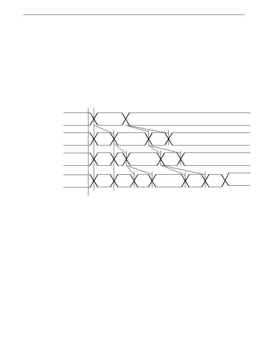
560
CHAPTER 23 INTERRUPT FUNCTIONS
Preliminary User's Manual U13987EJ1V0UM00
23.8 Macro Service Function
23.8.1 Outline of macro service function
Macro service is one of the method of interrupts servicing. In the normal interrupt, the start address in the interrupt service
program is loaded into the program counter (PC) by saving the PC or program status word (PSW), in the macro service,
however, another processing (mainly data transfers) is performed instead of these processing. This processing enables
a quick response to interrupt requests. Moreover, processing time can be reduced because the higher transfer speed can
be obtained.
In addition, there is another advantage in simplifying the vectored interrupt program since the vectored interrupt is
generated after the specified number of processing.
Figure 23-16. Differences between Vectored Interrupt and Macro Service Processing
Macro service
Context switching
Note 1
Vectored interrupt
Note 1
Vectored interrupt
Interrupt request generation
Main routine
Main routine
Main routine
Main routine
Macro service
processing
Main routine
Note 2
Note 4
Note 4
Note 3
Interrupt
servicing
Main routine
SEL
RBn
Interrupt
servicing
Restore
PC, PSW
Save
general
registers
Initialize
general
registers
Interrupt
servicing
Restore
general
registers
Main routine
Restore
PC & PSW
Main routine
Notes 1. When register bank switching is used, and an initial value has been set in the register beforehand
2. Register bank switching by context switching, saving of PC and PSW
3. Register bank, PC and PSW restoration by context switching
4. PC and PSW saved to the stack, vector address loaded into PC
23.8.2 Types of macro service
Macro service can be used with the 23 kinds of interrupt shown in Table 23-6. There are four kinds of operation, which
can be used to suit the application.

561
CHAPTER 23 INTERRUPT FUNCTIONS
Preliminary User's Manual U13987EJ1V0UM00
Table 23-6. Interrupts for which Macro Service can be Used
Default
Interrupt Request Generation Source
Generating Unit
Macro Service Control
Priority
Word Address
0
INTP0 (pin input edge detection)
Edge detection
0FE06H
1
INTP1 (pin input edge detection)
0FE08H
2
INTP2 (pin input edge detection)
0FE0AH
3
INTP3 (pin input edge detection)
0FE0CH
4
INTC00 (TM0-CR00 match signal generation)
Timer/event counter 0
0FE0EH
5
INTC01 (TM0-CR01 match signal generation)
0FE10H
6
INTC10 (TM1-CR10 or TM1W-CR10W match signal generation)
Timer/event counter 1
0FE12H
7
INTC11 (TM1-CR11 or TM1W-CR11W match signal generation)
0FE14H
8
INTC20 (TM2-CR20 or TM2W-CR20W match signal generation)
Timer/event counter 2
0FE16H
9
INTC21 (TM2-CR21 or TM2W-CR21W match signal generation)
0FE18H
10
INTC30 (TM3-CR30 or TM3W-CR30W match signal generation)
Timer 3
0FE1AH
11
INTP4 (pin input edge detection)
Edge detection
0FE1CH
12
INTP5 (pin input edge detection)
0FE1EH
13
INTAD (A/D conversion end)
A/D converter
0FE20H
14
INTSR (asynchronous serial interface reception end)
Asynchronous
0FE24H
INTCSI1 (clocked serial interface transfer end)
serial interface/
15
INTST (asynchronous serial interface transmission end)
clocked serial
0FE26H
interface 1
16
INTCSI (clocked serial interface transfer end)
Clocked serial
0FE28H
interface
17
INTSR2 (asynchronous serial interface 2 reception end)
Asynchronous
0FE2CH
INTCSI2 (clocked serial interface 2 transfer end)
serial interface 2/
18
INTST2 (asynchronous serial interface 2 transmission end)
clocked serial
0FE2EH
interface 2
19
INTIE1 (IEBus data access request)
IEBus controller
0FE32H
20
INTIE2 (IEBus communication error and communication end)
0FE34H
21
INTW (watch timer output)
Watch timer
0FE36H
22
INTCSI3 (clocked serial interface 3 transfer end)
Clocked serial
0FE38H
interface 3
Remarks 1. The default priority is a fixed number. This indicates the order of priority when macro service requests
are generated simultaneously,
2. The INTSR and INTCSI1 interrupts are generated by the same hardware (they cannot both be used
simultaneously). Therefore, although the same hardware is used for the interrupts, two names are
provided, for use in each of the two modes. The same applies to INTSR2 and INTCSI2.

562
CHAPTER 23 INTERRUPT FUNCTIONS
Preliminary User's Manual U13987EJ1V0UM00
There are four kinds of macro service, as shown below.
(1) Type A
One byte or one word of data is transferred between a special function register (SFR) and memory each time an interrupt
request is generated, and a vectored interrupt request is generated when the specified number of transfers have been
performed.
Memory that can be used in the transfers is limited to internal RAM addresses 0FE00H to 0FEFFH when the LOCATION
0 instruction is executed, and addresses 0FFE00H to 0FFEFFH when the LOCATION 0FH instruction is executed.
The specification method is simple and is suitable for low-volume, high-speed data transfers.
(2) Type B
As with type A, one byte or one word of data is transferred between a special function register (SFR) and memory each
time an interrupt request is generated, and a vectored interrupt request is generated when the specified number of
transfers have been performed.
The SFR and memory to be used in the transfers is specified by the macro service channel (the entire 1-Mbyte memory
space can be used).
This is a general version of type A, suitable for large volumes of transfer data.
(3) Type C
Data is transferred from memory to two special function registers (SFR) each time an interrupt request is generated,
and a vectored interrupt request is generated when the specified number of transfers have been performed.
With type C macro service, not only are data transfers performed to two locations in response to a single interrupt
request, but it is also possible to add output data ring control and a function that automatically adds data to a compare
register. The entire 1-Mbyte memory space can be used.
Type C is mainly used with the INTC10 and INTC11 interrupts, and is used for stepping motor control, etc., by macro
service, with P0L or P0H and CR10, CR10W, CR11, and CR11W used as the SFRs to which data is transferred.
(4) Counter mode
This mode is to decrement the macro service counter (MSC) when an interrupt occurs and is used to count the division
operation of an interrupt and interrupt generation circuit.
When MSC is 0, a vector interrupt can be generated.
To restart the macro service, MSC must be set again.
MSC is fixed to 16 bits and cannot be used as an 8-bit counter.
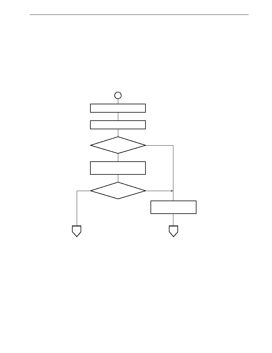
563
CHAPTER 23 INTERRUPT FUNCTIONS
Preliminary User's Manual U13987EJ1V0UM00
23.8.3 Basic macro service operation
Interrupt requests for which the macro service processing generated by the algorithm shown in Figure 23-10 can be
specified are basically serviced in the sequence shown in Figure 23-17.
Interrupt requests for which macro service processing can be specified are not affected by the status of the IE flag, but
are disabled by setting (to 1) an interrupt mask flag in the interrupt mask register (MK0). Macro service processing can
be executed in the interrupt disabled state and during execution of an interrupt service program.
Figure 23-17. Macro Service Processing Sequence
The macro service type and transfer direction are determined by the value set in the macro service control word mode
register. Transfer processing is then performed using the macro service channel specified by the channel pointer according
to the macro service type.
The macro service channel is memory which contains the macro service counter which records the number of transfers,
the transfer destination and transfer source pointers, and data buffers, and can be located at any address in the range FE00H
to FEFFH when the LOCATION 0 instruction is executed, or FFE00H to FFEFFH when the LOCATION 0FH instruction is
executed.
No
MSC = 0?
VCIE = 1?
MSC
MSC-1
Interrupt service mode bit
0
Interrupt request flag
0
Yes
No
Yes
Macro service processing execution
; Data transfer, real-time output port control
; Decrement macro service counter (MSC)
Interrupt request generation
Execute next instruction
Generation of interrupt request for which
macro service processing can be specified

564
CHAPTER 23 INTERRUPT FUNCTIONS
Preliminary User's Manual U13987EJ1V0UM00
23.8.4 Operation at end of macro service
In macro service, processing is performed the number of times specified during execution of another program. Macro
service ends when the processing has been performed the specified number of times (when the macro service counter
(MSC) reaches 0). Either of two operations may be performed at this point, as specified by the VCIE bit (bit 7) of the macro
service mode register for each macro service.
(1) When VCIE bit is 0
In this mode, an interrupt is generated as soon as the macro service ends. Figure 23-18 shows an example of macro
service and interrupt acknowledgment operations when the VCIE bit is 0.
This mode is used when a series of operations end with the last macro service processing performed, for instance.
It is mainly used in the following cases:
�
Asynchronous serial interface receive data buffering (INTSR/INTSR2)
�
A/D conversion result fetch (INTAD)
�
Compare register update as the result of a match between a timer register and the compare register (INTC00/
INTC01/INTC10/INTC11/INTC20/INTC21/INTC30)
�
Timer/counter capture register read due to edge input to the INTPn pin (INTP0/INTP1/INTP2/INTP3)
Figure 23-18. Operation at End of Macro Service when VCIE = 0
Main routine
EI
Main routine
EI
Macro service request
Last macro service request
Macro service processing
Macro service processing
Servicing of interrupt request
due to end of macro service
Other interrupt request
Last macro
service request
Servicing of other interrupt
Macro service processing
Servicing of interrupt request
due to end of macro service
At the end of macro service
(MSC = 0), an interrupt
request is generated and
acknowledged.
If the last macro service is
performed when the
interrupt due to the end of
macro service cannot be
acknowledged while other
interrupt servicing is being
executed, tec., that interrupt
is held pending until it can
be acknowledged.

565
CHAPTER 23 INTERRUPT FUNCTIONS
Preliminary User's Manual U13987EJ1V0UM00
(2) When VCIE bit is 1
In this mode, an interrupt is not generated after macro service ends. Figure 23-19 shows an example of macro service
and interrupt acknowledgment operations when the VCIE bit is 1.
This mode is used when the final operation is to be started by the last macro service processing performed, for instance.
It is mainly used in the following cases:
�
Clocked serial interface receive data transfers (INTCSI/INTCSI1/INTCSI2)
�
Asynchronous serial interface data transfers (INTST/INTST2)
�
To stop a stepping motor in the case (INTC10/INTC11) of stepping motor control by means of macro service type
C using the real-time output port and timer/counter.
Figure 23-19. Operation at End of Macro Service when VCIE = 1
Main routine
EI
Macro service request
Last macro service request
Interrupt request due to the end of
the hardware operation started by
the last macro service processing
Macro service processing
Processing of last macro service
Interrupt servicing

566
CHAPTER 23 INTERRUPT FUNCTIONS
Preliminary User's Manual U13987EJ1V0UM00
23.8.5 Macro service control registers
(1) Macro service control word
The
�
PD784938's macro service function is controlled by the macro service control mode register and macro service
channel pointer. The macro service processing mode is set by means of the macro service mode register, and the
macro service channel address is indicated by the macro service channel pointer.
The macro service mode register and macro service channel pointer are mapped onto the part of the internal RAM
shown in Figure 23-20 for each macro service as the macro service control word.
When macro service processing is performed, the macro service mode register and channel pointer values
corresponding to the interrupt requests for which macro service processing can be specified must be set beforehand.
Figure 23-20. Macro Service Control Word Format
Reserved word
Channel pointer
Mode register
0FE39H
0FE38H
0FE37H
0FE36H
0FE35H
0FE34H
0FE33H
0FE32H
0FE2FH
0FE2EH
0FE2DH
0FE2CH
CSICHP3
CSIMMD3
WCHP
WMMD
IECHP2
IEMMD2
IECHP1
IEMMD1
STCHP2
STMMD2
SRCHP2/CSICHP2
SRMMD2/CSIMMD2
0FE29H
0FE28H
0FE27H
0FE26H
0FE25H
0FE24H
CSICHP
CSIMMD
STCHP
STMMD
SRCHP/CSICHP1
SRMMD/CSIMMD1
0FE21H
0FE20H
0FE1FH
0FE1EH
0FE1DH
0FE1CH
0FE1BH
0FE1AH
0FE19H
0FE18H
0FE17H
0FE16H
0FE15H
0FE14H
0FE13H
0FE12H
0FE11H
0FE10H
0FE0FH
0FE0EH
0FE0DH
0FE0CH
0FE0BH
0FE0AH
0FE09H
0FE08H
0FE07H
0FE06H
ADCHP
ADMMD
PCHP5
PMMD5
PCHP4
PMMD4
CCHP30
CMMD30
CCHP21
CMMD21
CCHP20
CMMD20
CCHP11
CMMD11
CCHP10
CMMD10
CCHP01
CMMD01
CCHP00
CMMD00
PCHP3
PMMD3
PCHP2
PMMD2
PCHP1
PMMD1
PCHP0
PMMD0
INTST2
Channel pointer
Mode register
Channel pointer
Mode register
Channel pointer
Mode register
Channel pointer
Mode register
Channel pointer
Mode register
Channel pointer
Mode register
Channel pointer
Mode register
Channel pointer
Mode register
Channel pointer
Mode register
Channel pointer
Mode register
Channel pointer
Mode register
Channel pointer
Mode register
Channel pointer
Mode register
Channel pointer
Mode register
Channel pointer
Mode register
Channel pointer
Mode register
Channel pointer
Mode register
Channel pointer
Mode register
INTSR2/INTCSI2
INTCSI
INTST
INTAD
INTP5
INTP4
INTC30
INTC21
INTC20
INTC11
INTC10
INTC01
INTC00
INTP3
INTP2
INTP1
INTP0
INTSR/INTCSI1
Source
Address
Channel pointer
Mode register
INTCSI3
Channel pointer
Mode register
Channel pointer
Mode register
Channel pointer
Mode register
INTW
INTIE2
INTIE1
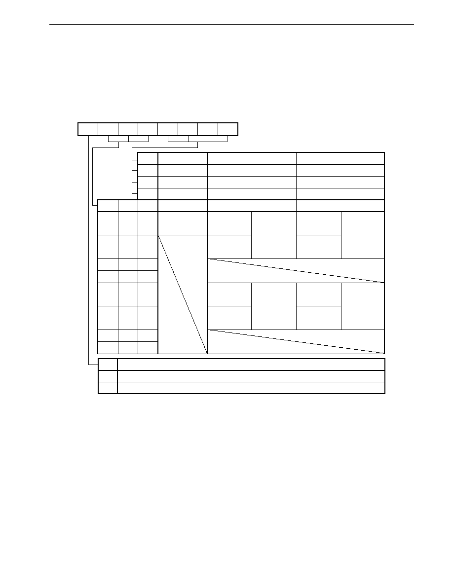
567
CHAPTER 23 INTERRUPT FUNCTIONS
Preliminary User's Manual U13987EJ1V0UM00
(2) Macro service mode register
The macro service mode register is an 8-bit register that specifies the macro service operation. This register is written
in internal RAM as part of the macro service control word (see Figure 23-20).
The format of the macro service mode register is shown in Figure 23-21.
Figure 23-21. Macro Service Mode Register Format (1/2)
7
VCIE
6
MOD2
5
MOD1
4
MOD0
3
CHT3
2
CHT2
1
CHT1
0
CHT0
CHT0
0
1
0
CHT1
0
0
0
CHT2
0
0
0
CHT3
1
0
0
MOD2 MOD1 MOD0
0
0
0
0
0
1
0
1
0
0
1
1
1
0
0
1
0
1
1
1
0
1
1
1
VCIE
0
1
Type A
Counter Mode
Counter
decrement
Data transfer
direction
Memory
SFR
Data size:
1 byte
Data transfer
direction
SFR
memory
Data transfer
direction
Memory
SFR
Data size:
1 byte
Data transfer
direction
SFR
memory
Data transfer
direction
Memory
SFR
Data size:
2 bytes
Data transfer
direction
SFR
memory
Data transfer
direction
Memory
SFR
Data size:
2 bytes
Data transfer
direction
SFR
memory
Not generated (next interrupt processing is vectored interrupt)
Generated
Interrupt Request when MSC = 0
Type B
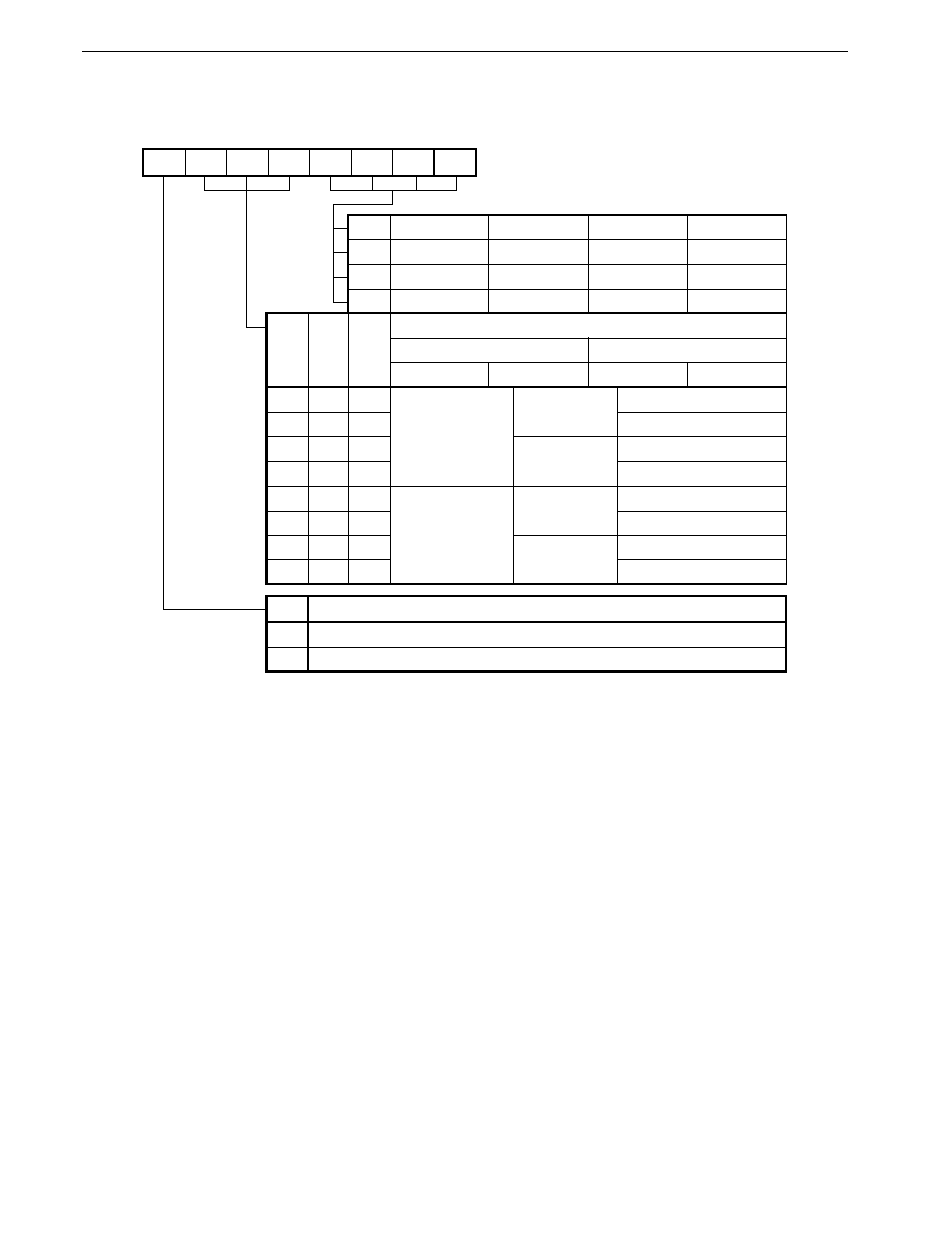
568
CHAPTER 23 INTERRUPT FUNCTIONS
Preliminary User's Manual U13987EJ1V0UM00
Figure 23-21. Macro Service Mode Register Format (2/2)
7
VCIE
6
MOD2
5
MOD1
4
MOD0
3
CHT3
2
CHT2
1
CHT1
0
CHT0
CHT0
1
1
0
CHT1
1
0
0
CHT2
1
1
1
CHT3
1
1
1
0
1
1
1
MOD2 MOD1 MOD0
0
0
0
0
0
1
0
1
0
0
1
1
1
0
0
1
0
1
1
1
0
1
1
1
Type C
Decrements MPD
Increments MPD
Retains MPT
Decrements MPT Retains MPT
Increments MPT
Data size for timer
specified
by MPT: 1 byte
No automatic
addition
No ring control
Ring control
Automatic
addition
No ring control
Ring control
No ring control
Ring control
No ring control
Ring control
Data size for timer
specified
by MPT: 2 bytes
No automatic
addition
Automatic
addition
VCIE
0
1
Generated
Not generated (next interrupt processing is vectored interrupt)
Interrupt Request when MSC = 0
(3) Macro service channel pointer
The macro service channel pointer specifies the macro service channel address. The macro service channel can be
located in the 256-byte space from FE00H to FEFFH when the LOCATION 0 instruction is executed, or FFE00H to
FFEFFH when the LOCATION 0FH instruction is executed, and the high-order 16 bits of the address are fixed.
Therefore, the low-order 8 bits of the data stored to the highest address of the macro service channel are set in the
macro service channel pointer.

569
CHAPTER 23 INTERRUPT FUNCTIONS
Preliminary User's Manual U13987EJ1V0UM00
23.8.6 Macro service type A
(1) Operation
Data transfers are performed between buffer memory in the macro service channel and an SFR specified in the macro
service channel.
With type A, the data transfer direction can be selected as memory-to-SFR or SFR-to-memory.
Data transfers are performed the number of times set beforehand in the macro service counter. One macro service
processing transfers 8-bit or 16-bit data.
Type A macro service is useful when the amount of data to be transferred is small, as transfers can be performed at
high speed.
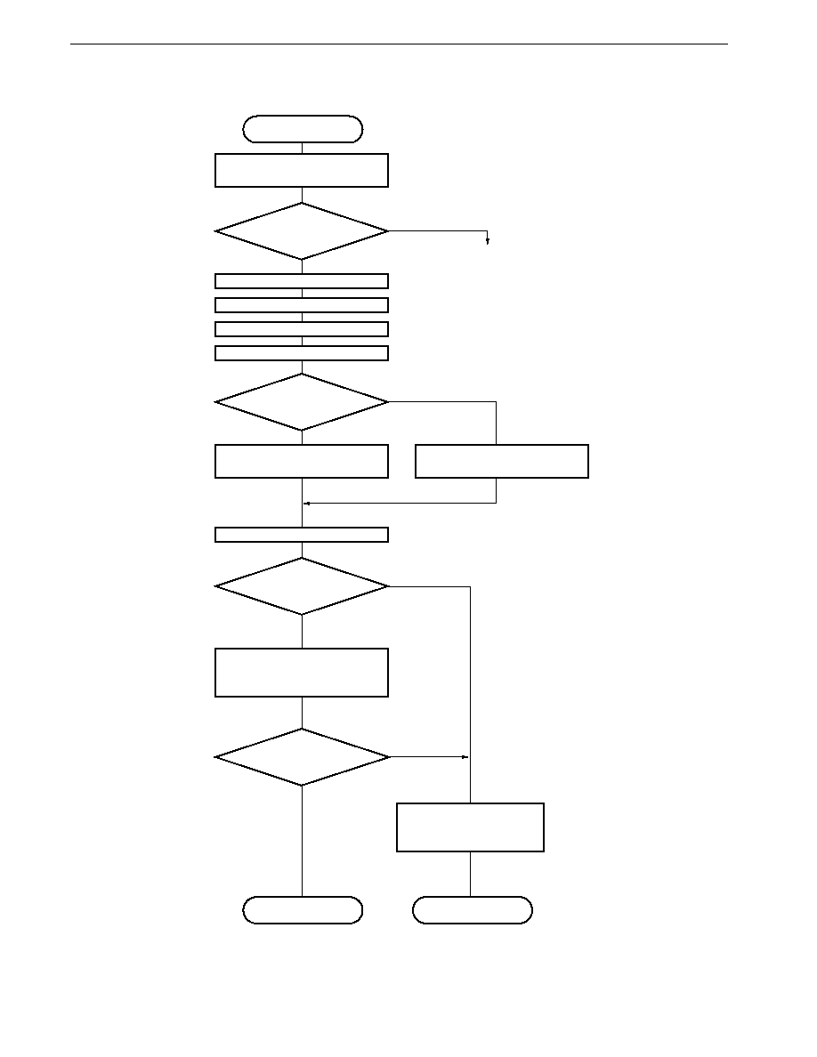
570
CHAPTER 23 INTERRUPT FUNCTIONS
Preliminary User's Manual U13987EJ1V0UM00
Figure 23-22. Macro Service Data Transfer Processing Flow (Type A)
Read contents of macro
service mode register
Determine channel type
Read channel pointer contents (m)
Other
To other macro service processing
Read MSC contents (n)
Calculate buffer address
Note
Read SFR pointer contents
Determine transfer direction
SFR
Memory
Memory
SFR
Read buffer contents, then transfer
read data to specified SFR
Specified SFR contents, then
transfer read data to buffer
MSC
MSC-1
MSC = 0?
No
Yes
Clear (to 0) interrupt service mode
bit (ISM)
VCIE = 1?
(Vectored interrupt request generation)
TYPE A
Yes
No
1-byte transfer: m-n-1
2-byte transfer: m-n
�
2-1
Note
Macro service request
acknowledgment
Clear (to 0) interrupt request
flag (IF)
End
End

571
CHAPTER 23 INTERRUPT FUNCTIONS
Preliminary User's Manual U13987EJ1V0UM00
(2) Macro service channel configuration
The channel pointer and 8-bit macro service counter (MSC) indicate the buffer address in internal RAM (FE00H to
FEFFH when the LOCATION 0 instruction is executed, or FFE00H to FFEFFH when the LOCATION 0FH instruction
is executed) which is the transfer source or transfer destination (see Figure 23-23). In the channel pointer, the low-
order 8 bits of the address are written to the macro service counter in the macro service channel.
The SFR involved with the access is specified by the SFR pointer (SFRP). The low-order 8 bits of the SFR address
are written to the SFRP.
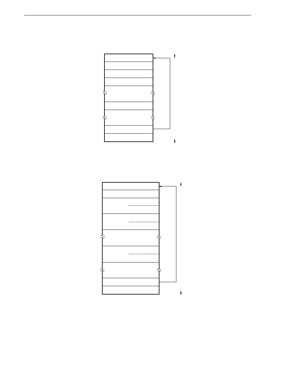
572
CHAPTER 23 INTERRUPT FUNCTIONS
Preliminary User's Manual U13987EJ1V0UM00
Figure 23-23. Type A Macro Service Channel
(a) 1-byte transfers
(b) 2-byte transfers
7
0
Macro service counter (MSC)
SFR pointer (SFRP)
Macro service buffer 1
Macro service buffer 2
Macro service buffer n
Channel pointer
Mode register
Macro service
control word
Macro service
channel
High-order addresses
Low-order addresses
Macro service buffer address = (channel pointer) � (macro service counter) � 1
MCS = 1
MCS = 2
MCS = n
7
0
Macro service counter (MSC)
SFR pointer (SFRP)
Macro service
buffer 1
Macro service
buffer 2
Macro service
buffer n
Channel pointer
Mode register
Macro service
control word
Macro service
channel
High-order addresses
Low-order addresses
Macro service buffer address = (channel pointer) � (macro service counter)
�
2 � 1
MCS = 1
MCS = 2
MCS = n
(high-order byte)
(low-order byte)
(high-order byte)
(low-order byte)
(high-order byte)
(low-order byte)
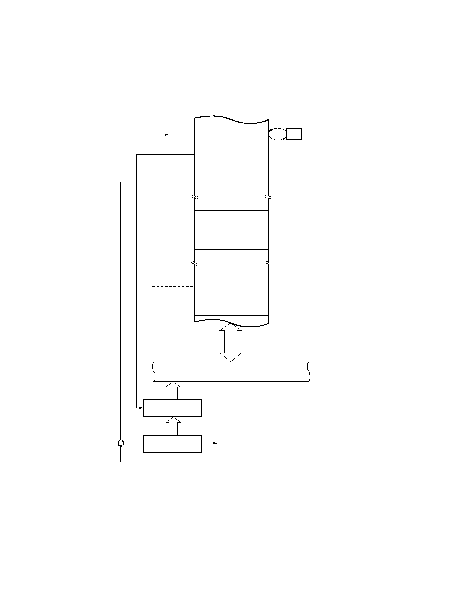
573
CHAPTER 23 INTERRUPT FUNCTIONS
Preliminary User's Manual U13987EJ1V0UM00
(3) Example of use of type A
An example is shown below in which data received via the asynchronous serial interface is transferred to a buffer area
in on-chip RAM.
Figure 23-24. Asynchronous Serial Reception
(Internal RAM)
0FE7FH
Channel pointer 7FH
Mode register 11H
Note Low-order 8 bits of RXB address
Type A, SFR
memory, 8-bit transfer,
interrupt request generation when
MSC = 0
�1
Internal bus
MSC 0EH
SFRP 8CH
Note
0FE70H
R
X
D/P30
INTSR macro service request
Receive buffer
(RXB)
Shift register
Remark
Addresses in the figure are the values when the LOCATION 0 instruction is executed.
When the LOCATION 0FH instruction is executed, 0F0000H should be added to the values in the figure.

574
CHAPTER 23 INTERRUPT FUNCTIONS
Preliminary User's Manual U13987EJ1V0UM00
23.8.7 Macro service type B
(1) Operation
Data transfers are performed between a data area in memory and an SFR specified by the macro service channel.
With type B, the data transfer direction can be selected as memory-to-SFR or SFR-to-memory.
Data transfers are performed the number of times set beforehand in the macro service counter. One macro service
processing transfers 8-bit or 16-bit data.
This type of macro service is macro service type A for general purposes and is ideal for processing a large amount
of data because up to 64 Kbytes of data buffer area when 8-bit data is transferred or 1 Mbyte of data buffer area when
16-bit data is transferred can be set in any address space.
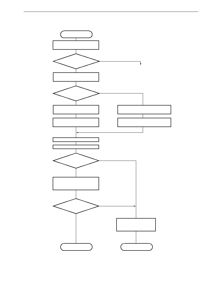
575
CHAPTER 23 INTERRUPT FUNCTIONS
Preliminary User's Manual U13987EJ1V0UM00
Figure 23-25. Macro Service Data Transfer Processing Flow (Type B)
Read contents of macro service
mode register
Determine channel type
Other
To other macro service processing
1-byte transfer: +1
2-byte transfer: +2
Determine transfer direction
SFR
Memory
Memory
SFR
MSC
MSC�1
MSC = 0?
No
Yes
Clear (to 0) interrupt service
mode bit (ISM)
VCIE = 1?
(Vectored interrupt request generation)
TYPE B
Yes
No
Increment MP
Note
Read data from SFR, and write to
memory addressed by MP
Read data from memory, and write to
SFR specified by SFR pointer
Select transfer source memory with
macro service pointer (MS)
Note
Select transfer source SFR with
SFR pointer
End
End
Macro service request
acknowledgment
Read channel pointer contents (m)
Clear (to 0) interrupt request
flag (IF)

576
CHAPTER 23 INTERRUPT FUNCTIONS
Preliminary User's Manual U13987EJ1V0UM00
(2) Macro service channel configuration
The macro service pointer (MP) indicates the data buffer area in the 1-Mbyte memory space that is the transfer
destination or transfer source.
The low-order 8 bits of the SFR that is the transfer destination or transfer source is written to the SFR pointer (SFRP).
The macro service counter (MSC) is a 16-bit counter that specifies the number of data transfers.
The macro service channel that stores the MP, SFRP and MSC is located in internal RAM space addresses 0FE00H
to 0FEFFH when the LOCATION 0 instruction is executed, or 0FFE00H to 0FFEFFH when the LOCATION 0FH
instruction is executed.
The macro service channel is indicated by the channel pointer as shown in Figure 23-26. In the channel pointer, the
low-order 8 bits of the address are written to the macro service counter in the macro service channel.
Figure 23-26. Type B Macro Service Channel
Note Bits 20 to 23 must be set to 0.
Macro service
counter (MSC)
SFR pointer (SFRP)
(bits 8 to 15)
(bits 0 to 7)
(bits 16 to 23)
Note
(bits 8 to 15)
(bits 0 to 7)
Channel pointer
Mode register
Macro service
pointer (MP)
Macro service
control word
Low-order addresses
Macro service
channel
High-order addresses
SFR
Buffer area
Macro service buffer address = macro service pointer
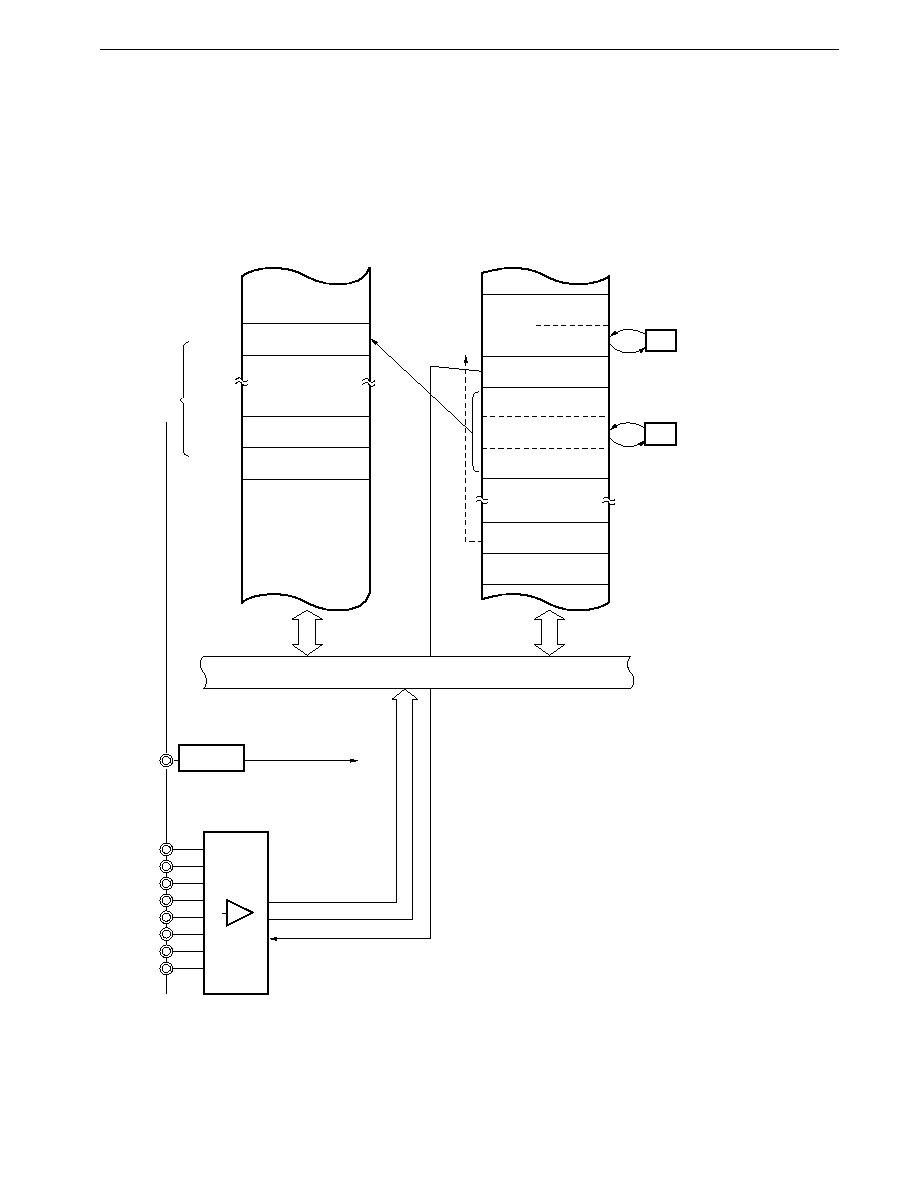
577
CHAPTER 23 INTERRUPT FUNCTIONS
Preliminary User's Manual U13987EJ1V0UM00
(3) Example of use of type B
An example is shown below in which parallel data is input from port 3 in synchronization with an external signal. The
INTP4 external interrupt pin is used for synchronization with the external signal.
Figure 23-27. Parallel Data Input Synchronized with External Interrupts
64 K memory space
Macro service control word,
Macro service channel
(internal RAM)
0FE6EH
Buffer Area
Note Low-order 8 bits of port 3 address
-
1
+1
Internal bus
Port 3
P37
P36
P35
P34
P33
P32
P31
P30
INTP4
Edge
detection
Macro service request
INTP4
MSC
00H
20H
03H
MP
00H
A0H
00H
SFRP
Type B, SFR
memory, 8-bit transfer,
interrupt request generation when
MSC = 0
Channel pointer 6EH
Mode register 18H
0A01FH
0A000H
Note
Remark
Macro service channel addresses in the figure are the values when the LOCATION 0 instruction is executed.
When the LOCATION 0FH instruction is executed, 0F0000H should be added to the values in the figure.
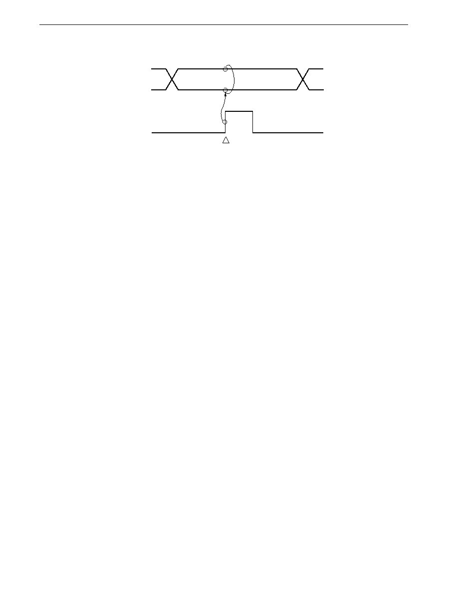
578
CHAPTER 23 INTERRUPT FUNCTIONS
Preliminary User's Manual U13987EJ1V0UM00
Figure 23-28. Parallel Data Input Timing
INTP4
Port 3
Data fetch (macro service)

579
CHAPTER 23 INTERRUPT FUNCTIONS
Preliminary User's Manual U13987EJ1V0UM00
23.8.8 Macro service type C
(1) Operation
In type C macro service, data in the memory specified by the macro service channel is transferred to two SFRs, for
timer use and data use, specified by the macro service channel in response to a single interrupt request (the SFRs
can be freely selected). An 8-bit or 16-bit timer SFR can be selected.
In addition to the basic data transfers described above, type C macro service, the following functions can be added
to type C macro service to reduce the size of the buffer area and alleviate the burden on software.
These specifications are made by using the mode register of the macro service control word.
(a) Updating of timer macro service pointer
It is possible to choose whether the timer macro service pointer (MPT) is to be kept as it is or incremented/
decremented. The MPT is incremented or decremented in the same direction as the macro service pointer (MPD)
for data.
(b) Updating of data macro service pointer
It is possible to choose whether the data macro service pointer (MPD) is to be incremented or decremented.
(c) Automatic addition
The current compare register value is added to the data addressed by the timer macro service pointer (MPT), and
the result is transferred to the compare register. If automatic addition is not specified, the data addressed by the
MPT is simply transferred to the compare register.
(d) Ring control
An output data pattern of the length specified beforehand is automatically output repeatedly.

580
CHAPTER 23 INTERRUPT FUNCTIONS
Preliminary User's Manual U13987EJ1V0UM00
Figure 23-29. Macro Service Data Transfer Processing Flow (Type C) (1/2)
Read contents of macro service
mode register
Determine channel type
Read channel pointer contents (m)
Other
To other macro service processing
Note
Transfer data to compare register
Automatic addition specified?
No
Increment MPT?
No
Increment MPD?
TYPE C
Yes
Read memory addressed by MPT
Retain MPT?
No
Increment MPD (+1)
No
Yes
Yes
Yes
Increment MPT
Note
1
1-byte transfer: +1
2-byte transfer: +2
Add data to compare register
Decrement MPD (�1)
Decrement MPT
Transfer data to buffer register
Read memory addressed by MPD
Macro service request
acknowledgment
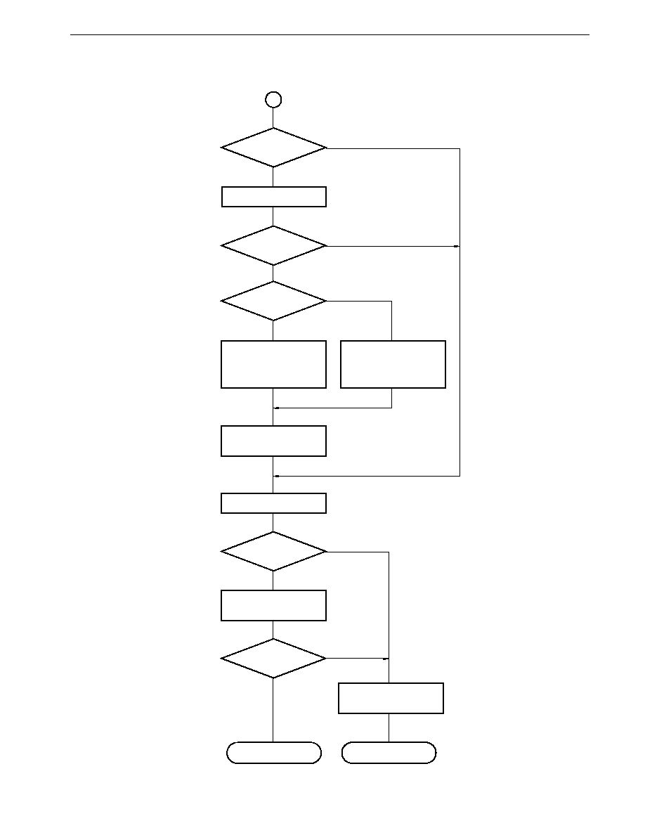
581
CHAPTER 23 INTERRUPT FUNCTIONS
Preliminary User's Manual U13987EJ1V0UM00
Figure 23-29. Macro Service Data Transfer Processing Flow (Type C) (2/2)
No
No
Yes
No
No
Yes
Yes
Yes
No
Yes
1
End
Ring control?
Ring counter = 0?
Increment MPD?
MSC = 0?
VCIE = 1?
Subtract modulo register
contents from data macro
service pointer (MPD), and
return pointer to start address
Add modulo register contents
to data macro service pointer
(MPD), and return pointer to
start address
MSC
MSC�1
Clear (to 0) interrupt
service mode bit (ISM)
Clear (to 0) interrupt
request flag (IF)
Load modulo register
contents into ring counter
End
Decrement ring counter
(Vectored interrupt request generation)
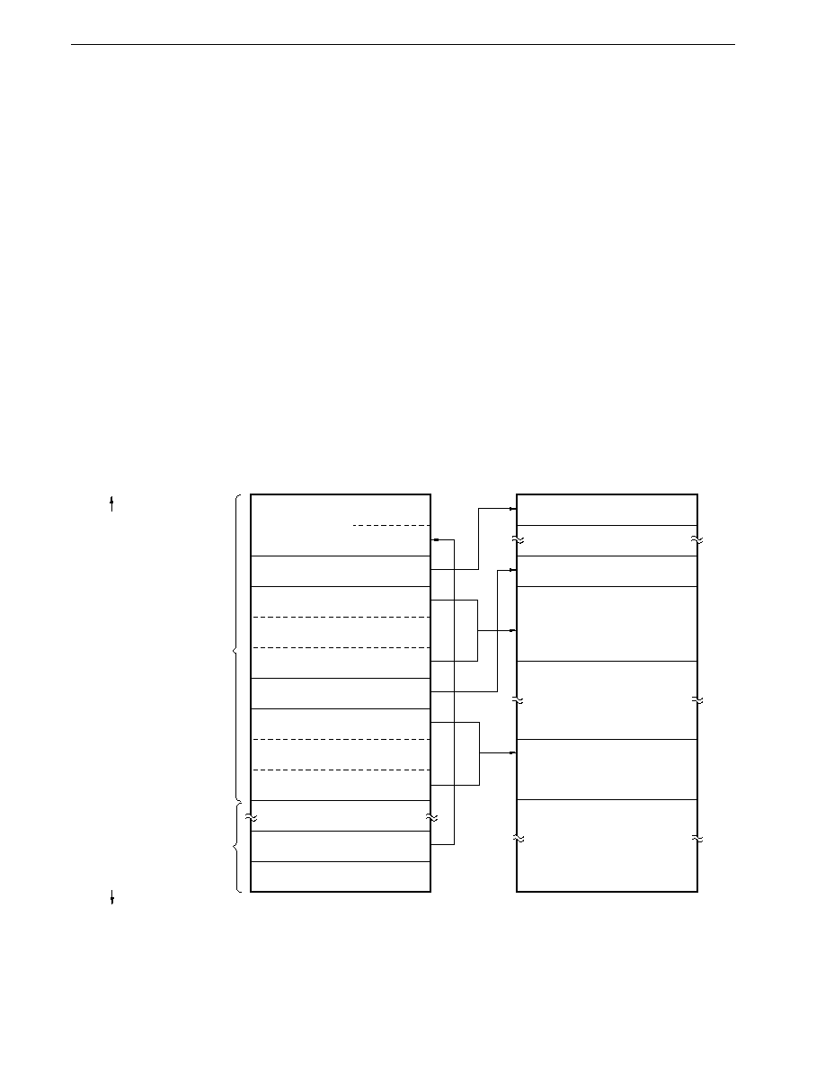
582
CHAPTER 23 INTERRUPT FUNCTIONS
Preliminary User's Manual U13987EJ1V0UM00
(2) Macro service channel configuration
There are two kinds of type C macro service channel, as shown in Figure 23-30.
The timer macro service pointer (MPT) mainly indicates the data buffer area in the 1-Mbyte memory space to be
transferred or added to the timer/event counter compare register.
The data macro service pointer (MPD) indicates the data buffer area in the 1-Mbyte memory space to be transferred
to the real-time output port.
The modulo register (MR) specifies the number of repeat patterns when ring control is used.
The ring counter (RC) holds the step in the pattern when ring control is used. When initialization is performed, the
same value as in the MR is normally set in this counter.
The macro service counter (MSC) is a 16-bit counter that specifies the number of data transfers.
The low-order 8 bits of the SFR that is the transfer destination is written to the timer SFR pointer (TSFRP) and data
SFR pointer (DSFRP).
The macro service channel that stores these pointers and counters is located in internal RAM space addresses 0FE00H
to 0FEFFH when the LOCATION 0 instruction is executed, or 0FFE00H to 0FFEFFH when the LOCATION 0FH
instruction is executed. The macro service channel is indicated by the channel pointer as shown in Figure 23-30. In
the channel pointer, the low-order 8 bits of the address are written to the macro service counter in the macro service
channel.
Figure 23-30. Type C Macro Service Channel (1/2)
(a) No ring control
Note Bits 20 to 23 must be set to 0.
Macro service
counter (MSC)
Timer SFR pointer (TSFRP)
(bits 8 to 15)
(bits 0 to 7)
(bits 8 to 15)
(bits 8 to 15)
(bits 0 to 7)
(bits 0 to 7)
(bits 16 to 23)
Note
(bits 16 to 23)
Note
Channel pointer
Mode register
Timer macro service
pointer (MPT)
Data macro service
pointer (MPD)
Data SFR pointer (DSFRP)
Macro service
control word
Low-order addresses
Macro service
channel
High-order addresses
TSFR
DSFR
Timer buffer area
Data buffer area
Macro service buffer address = macro service pointer
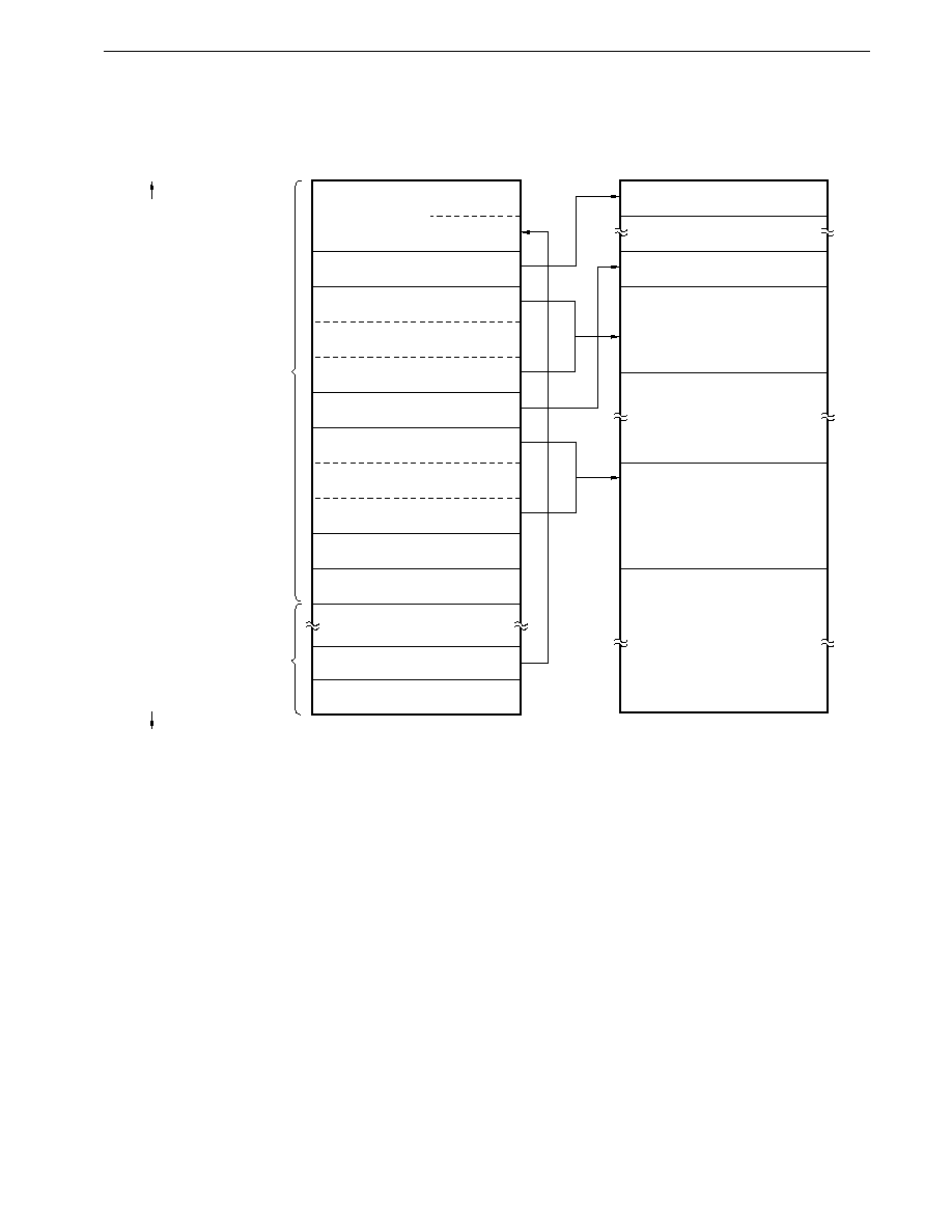
583
CHAPTER 23 INTERRUPT FUNCTIONS
Preliminary User's Manual U13987EJ1V0UM00
Figure 23-30. Type C Macro Service Channel (2/2)
(b) With ring control
Note Bits 20 to 23 must be set to 0.
(3) Examples of use of type C
(a) Basic operation
An example is shown below in which the output pattern to the real-time output port and the output interval are directly
controlled.
Update data is transferred from the two data storage areas set in the 1-Mbyte space beforehand to the real-time
output function buffer register (P0L) and the compare register (CR10).
Macro service
counter (MSC)
Timer SFR pointer (TSFRP)
(bits 8 to 15)
(bits 8 to 15)
(bits 8 to 15)
(bits 0 to 7)
(bits 0 to 7)
(bits 0 to 7)
(bits 16 to 23)
Note
(bits 16 to 23)
Note
Ring counter (RC)
Channel pointer
Mode register
Timer macro service
pointer (MPT)
Data SFR pointer (DSFRP)
Data macro service
pointer (MPD)
Modulo register (MR)
Macro service
control word
Low-order addresses
Macro service
channel
High-order addresses
TSFR
DSFR
Timer buffer area
Data buffer area
Macro service buffer address = macro service pointer
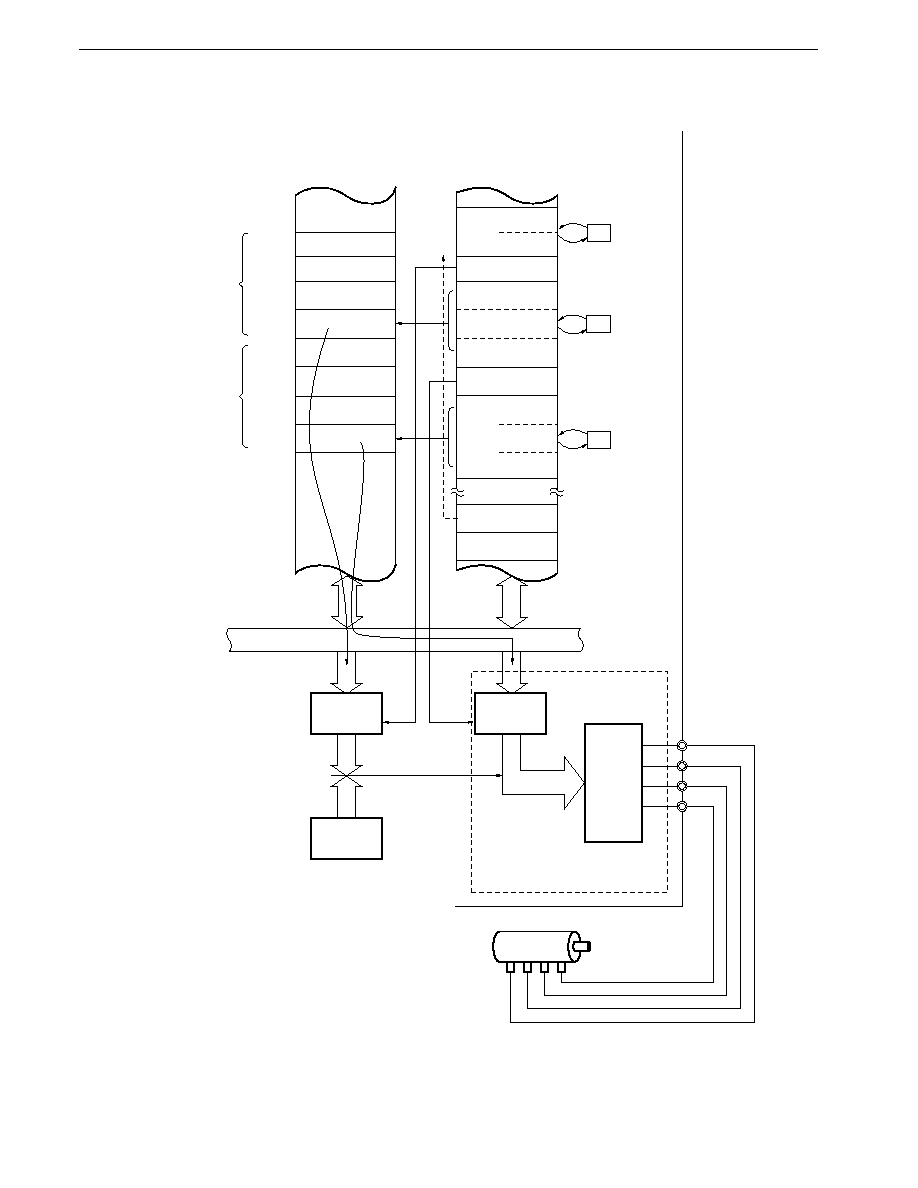
584
CHAPTER 23 INTERRUPT FUNCTIONS
Preliminary User's Manual U13987EJ1V0UM00
Figure 23-31. Stepping Motor Open Loop Control by Real-Time Output Port
1 M memory space
Macro service control word,
macro service channel
(internal RAM)
Timer
counter 1
TM1
Output
latch P0
0FE5EH
123408H
123400H
Output data area
Low-order 8 bits
of CR10 address
Type C, MPT/MPD
incremented, 1-byte
timer data, no
automatic addition,
no ring control,
interrupt request
generation at
MSC = 0
Low-order 8 bits
of P0L address
INTC10
Match
Real-time
output trigger/
macro service start
�1
+1
123411H
123409H
Output timing
data area
T9
...
T2
T1
D9
D2
D1
...
MSC
00H
04H
14H
MPT
12H
34H
DSFRP
09H
0EH
12H
MPD
Channel
pointer
34H
00H
5EH
TSFRP
Mode
register
0FH
Stepping motor
Internal bus
Compare
register CR10
Buffer
register P0L
P00
P01
P02
P03
+1
P0
Remark
Internal RAM addresses in the figure are the values when the LOCATION 0 instruction is executed.
When the LOCATION 0FH instruction is executed, 0F0000H should be added to the values in the figure.
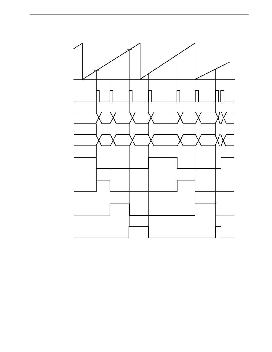
585
CHAPTER 23 INTERRUPT FUNCTIONS
Preliminary User's Manual U13987EJ1V0UM00
Figure 23-32. Data Transfer Control Timing
TM1
count value
0H
Compare register
(CR10)
T1
Buffer register
P0L
INTC10
timer interrupt
P00
P02
P03
P01
T1
T7
T8
T9
D1
D2
D3
D4
D5
D6
D7
D9
T2
T3
T4
T5
T6
T8
T7
T3
T2
T4
T5
T6
D8

586
CHAPTER 23 INTERRUPT FUNCTIONS
Preliminary User's Manual U13987EJ1V0UM00
(b) Examples of use of automatic addition control and ring control
(i)
Automatic addition control
The output timing data (
t) specified by the macro service pointer (MPT) is added to the contents of the compare
register, and the result is written back to the compare register.
Use of this automatic addition control eliminates the need to calculate the compare register setting value in
the program each time.
(ii) Ring control
With ring control, the predetermined output patterns is prepared for one cycle only, and the one-cycle data
patterns are output repeatedly in order in ring form.
When ring control is used, only the output patterns for one cycle need be prepared, allowing the size of the
data ROM area to be reduced.
The macro service counter (MSC) is decremented each time a data transfer is performed.
With ring control, too, an interrupt request is generated when MSC = 0.
When controlling a stepping motor, for example, the output patterns will vary depending on the configuration
of the stepping motor concerned, and the phase excitation method (single-phase excitation, two-phase
excitation, etc.), but repeat patterns are used in all cases. Examples of single-phase excitation and 1-2-phase
excitation of a 4-phase stepping motor are shown in Figures 23-33 and 23-34.

587
CHAPTER 23 INTERRUPT FUNCTIONS
Preliminary User's Manual U13987EJ1V0UM00
Figure 23-33. Single-Phase Excitation of 4-Phase Stepping Motor
Phase A
Phase B
Phase C
Phase D
1 cycle
(4 patterns)
1
2
3
4
1
2
3
Figure 23-34. 1-2-Phase Excitation of 4-Phase Stepping Motor
Phase A
Phase B
Phase C
Phase D
1 cycle
(8 patterns)
1
2
3
4
5
6
7
8
1
2
3
4
8
5
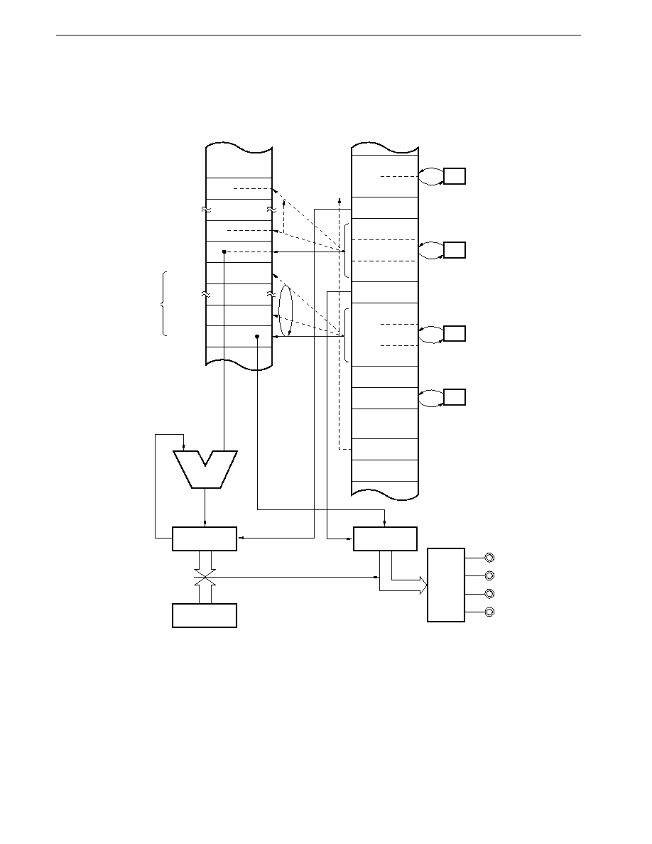
588
CHAPTER 23 INTERRUPT FUNCTIONS
Preliminary User's Manual U13987EJ1V0UM00
Figure 23-35. Automatic Addition Control + Ring Control Block Diagram 1
(when output timing varies with 1-2-phase excitation)
.
.
.
D1
1 M memory space
Macro service control word,
macro service channel
(internal RAM)
Compare register
CR10W
Timer counter 1
TM1W
Addition
Buffer register
P0L
Output
latch P0
P00
P02
P01
P03
0FE5AH
1237FEH
123007H
Output timing: 123400H
123000H
Output data (8 items)
D7
D0
MSC
02H
00H
14H
MPT
12H
34H
DSFRP
00H
0EH
12H
MPD
30H
MR
00H
RC
08H
08H
Channel
pointer
5AH
TSFRP
Mode
register
7FH
Low-order 8 bits of CR10 address
Type C, MPT/MPD incremented,
2-byte timer data, automatic addition,
ring control, interrupt request
generation at MSC = 0
Low-order 8 bits of P0L address
To stepping
motor
INTC10
Match
t512
�1
+2
+1
�1
t2
t1
.
.
.
Remark
Internal RAM addresses in the figure are the values when the LOCATION 0 instruction is executed.
When the LOCATION 0FH instruction is executed, 0F0000H should be added to the values in the figure.
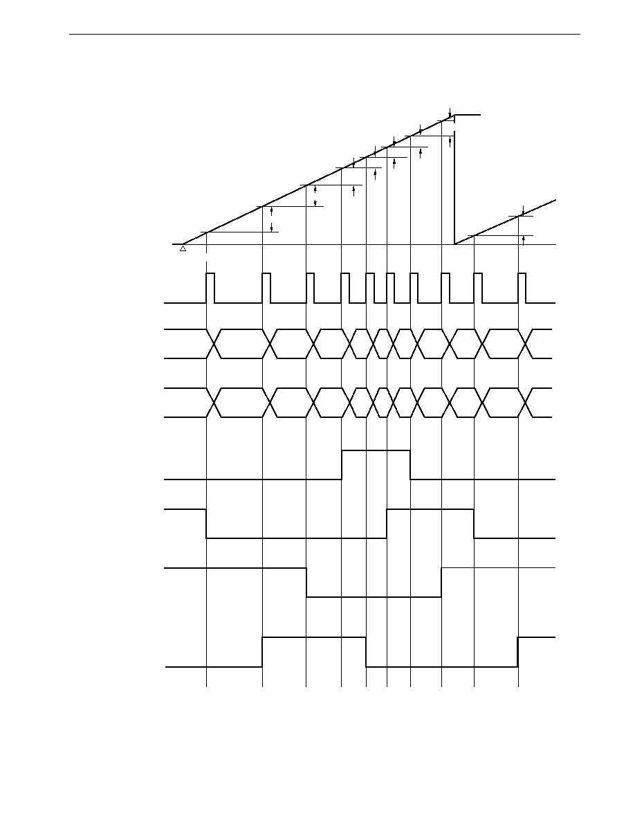
589
CHAPTER 23 INTERRUPT FUNCTIONS
Preliminary User's Manual U13987EJ1V0UM00
Figure 23-36. Automatic Addition Control + Ring Control Timing Diagram 1
(when output timing varies with 1-2-phase excitation)
TM1W
count value
0H
FFFFH
Compare register
(CR10W)
T0
Buffer register
P0L
INTC10
t1
P00
P02
P03
P01
T2
T1+
t2
T3
T2+
t3
T7
T6+
t7
T9
T8+
t9
T4
T3+
t4
T6
T5+
t6
T5
T4+
t5
T1
T0+
t1
t3
t4
t5
t6
t9
T0
t7
t8
D1
D2
D3
D4
D5
D6
D7
D0
D0
D7
Count start
t2
T8
T7+
t8

590
CHAPTER 23 INTERRUPT FUNCTIONS
Preliminary User's Manual U13987EJ1V0UM00
Figure 23-37. Automatic Addition Control + Ring Control Block Diagram 2
(1-2-phase excitation constant-velocity operation)
Remark
Internal RAM addresses in the figure are the values when the LOCATION 0 instruction is executed.
When the LOCATION 0FH instruction is executed, 0F0000H should be added to the values in the figure.
1 M memory space
Macro service control word,
macro service channel
(internal RAM)
Compare register
CR10
Timer counter 1
TM1
Addition
Buffer register
P0L
Output
latch P0
P00
P02
P01
P03
0FE7AH
123007H
Output timing: 1233FFH
123000H
Output data (8 Items)
D7
D6
D0
.
.
.
MSC
FFH
FFH
14H
MPT
12H
33H
DSFRP
FFH
0EH
12H
MPD
30H
MR
07H
RC
08H
08H
Channel
pointer
7AH
TSFRP
Mode
register
3CH
Low-order 8 bits of CR10 address
Type C, MPT retained, MPD
decremented, 1-byte timer data,
automatic addition, ring control,
interrupt request generation
at MSC = 0
Low-order 8 bits of P0L address
To stepping
motor
INTC10
Match
t
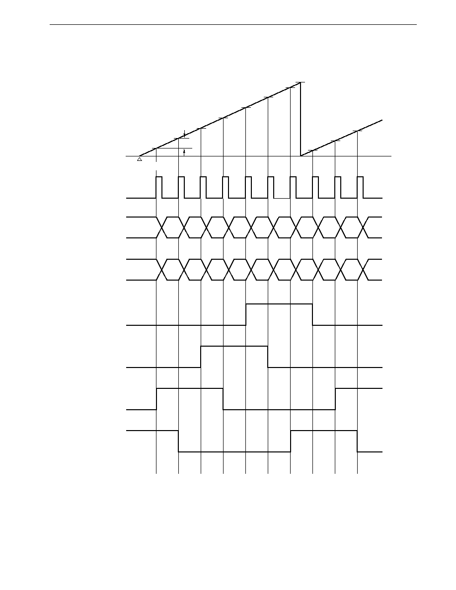
591
CHAPTER 23 INTERRUPT FUNCTIONS
Preliminary User's Manual U13987EJ1V0UM00
Figure 23-38. Automatic Addition Control + Ring Control Timing Diagram 2
(1-2-phase excitation constant-velocity operation)
TM1
count value
0H
FFFFH
Compare register
(CR10)
T0
Buffer register
P0L
D6
D5
D4
D3
D2
D1
D0
D7
D6
D7
D0
INTC10
t
P00
P02
P03
P01
Count start
T1
T0+
t
T2
T1+
t
T3
T2+
t
T4
T3+
t
T5
T4+
t
T6
T5+
t
T7
T6+
t
T8
T7+
t
T9
T8+
t
T10
T9+
t
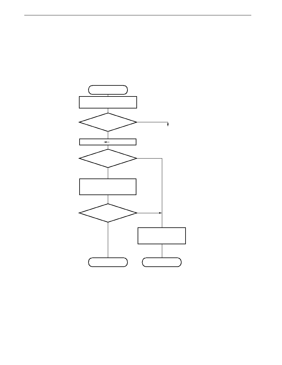
592
CHAPTER 23 INTERRUPT FUNCTIONS
Preliminary User's Manual U13987EJ1V0UM00
23.8.9 Counter mode
(1) Operation
MSC is decremented the number of times set in advance to the macro service counter (MSC).
Because the number of times an interrupt occurs can be counted, this function can be used as an event counter where
the interrupt generation cycle is long.
Figure 23-39. Macro Service Data Transfer Processing Flow (counter mode)
Macro service request
acknowledged
Reads contents of macro service
mode register
Identifies channel type
MSC MSC-1
Others
To other macro service processing
MSC is 16 bits wide
Counter mode
MSC = 0?
No
Yes
VCIE = 1?
No
Yes
Clears interrupt processing type
bit (ISM) to 0
Clears interrupt request flag
(IF) to 0
End
End
(Vectored interrupt request is generated)
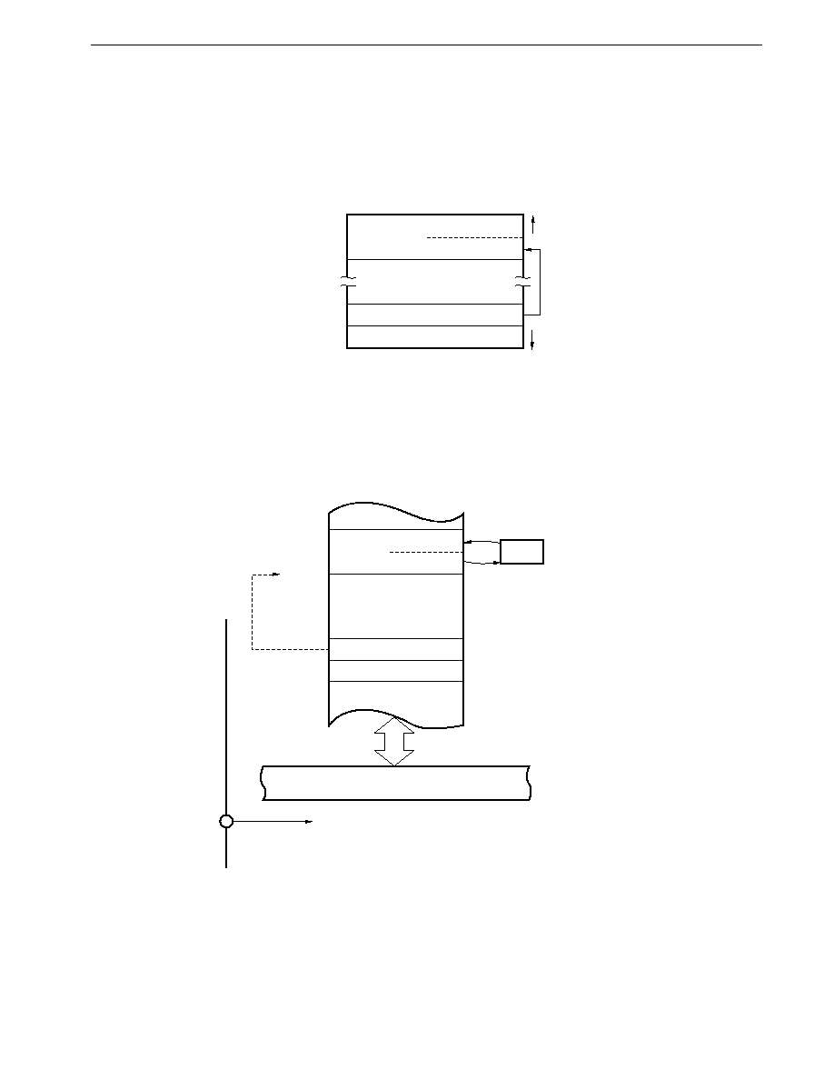
593
CHAPTER 23 INTERRUPT FUNCTIONS
Preliminary User's Manual U13987EJ1V0UM00
(2) Configuration of macro service channel
The macro service channel consists of only a 16-bit macro service counter. The low-order 8 bits of the address of the
MSC are written to the channel pointer.
Figure 23-40. Counter Mode
(3) Example of using counter mode
Here is an example of counting the number of edges input to external interrupt pin INTP5.
Figure 23-41. Counting Number of Edges
(Internal RAM)
INTP5 macro service request
MSC 0EH
High-order 8 bytes
Low-order 8 bytes
Channel pointer 7EH
Mode register 00H
Counter mode
Interrupt request is generated when MSC = 0.
Internal bus
OFE7EH
�1
INTP5/P26
Remark
The internal RAM address in the figure above is the value when the LOCATION 0 instruction is executed.
When the LOCATION 0FH instruction is executed, add 0F0000H to this value.
Macro service channel
Macro service
counter (MSC)
High-order 8 bytes
Low-order 8 bytes
High-order addresses
Low-order addresses
Channel pointer
Mode register
7
0

594
CHAPTER 23 INTERRUPT FUNCTIONS
Preliminary User's Manual U13987EJ1V0UM00
23.9 When Interrupt Requests and Macro Service are Temporarily Held Pending
When the following instructions are executed, interrupt acknowledgment and macro service processing is deferred for
8 system clock cycles. However, software interrupts are not deferred.
EI
DI
BRK
BRKCS RBn
RETI
RETB
RETCS
RETCSB
!addr16
POP PSW
LOCATION 0H or LOCATION 0FH
POPU POST
MOV PSWL, A
MOV PSWL, #byte
MOVG SP, #imm24
Write instruction and bit manipulation instruction to an interrupt control register
Note
, or the MK0, MK1, IMC or ISPR register
(except BT and BF instructions)
PSWL bit manipulation instruction
(Excluding the BT PSWL. bit, $addr16, BF PSWL. bit, $addr16, SET1 CY, NOT1 CY, and CLR1 CY instructions)
Note Interrupt control registers: PIC0, PIC1, PIC2, PIC3, PIC4, PIC5, CIC00, CIC01, CIC10, CIC11, CIC20, CIC21,
CIC30, ADIC, SERIC, SRIC, CSIIC1, STIC, CSIIC, SERIC2, SRIC2, CSIIC2, STIC2,
IEIC1, IEIC2, WIC, CSIIC3

595
CHAPTER 23 INTERRUPT FUNCTIONS
Preliminary User's Manual U13987EJ1V0UM00
Cautions 1. When an interrupt related register is polled using a BF instruction, etc., the branch destination
of that BR instruction, etc., should not be that instruction. If a program is written in which a branch
is made to that instruction itself, all interrupts and macro service requests will be held pending
until a condition whereby a branch is not made by that instruction arises.
Bad Example
LOOP : BF PIC0.7, $LOOP
All interrupts and macro service requests are held pending until
PIC0.7 is 1.
� � �
Interrupts and macro service requests are not serviced until
after execution of the instruction following the BF instruction.
Good Example (1)
LOOP : NOP
BF PIC0.7, $LOOP
Interrupts and macro service requests are serviced after execution
of the NOP instruction, so that interrupts are never held
pending for a long period.
Good Example (2)
LOOP : BT PIC0.7, $NEXT
Using a BTCLR instruction instead of a BT instruction has the
advantage that the flag is cleared (to 0) automatically.
BR $LOOP
Interrupts and macro service requests are serviced after
NEXT :
execution of the BR instruction, so that interrupts are never held
pending for a long period.
2. For a similar reason, if problems are caused by a long pending period for interrupts and macro
service when instructions to which the above applies are used in succession, a time at which
interrupts and macro service requests can be acknowledged should be provided by inserting an
NOP instruction, etc., in the series of instructions.
......
...
......
...
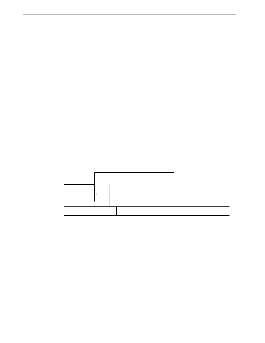
596
CHAPTER 23 INTERRUPT FUNCTIONS
Preliminary User's Manual U13987EJ1V0UM00
23.10
Instructions whose Execution is Temporarily Suspended by an Interrupt or Macro Service
Execution of the following instructions is temporarily suspended by an acknowledgeable interrupt request or macro
service request, and the interrupt or macro service request is acknowledged. The suspended instruction is resumed after
completion of the interrupt service program or macro service processing.
Temporarily suspended instructions:
MOVM, XCHM, MOVBK, XCHBK
CMPME, CMPMNE, CMPMC, CMPMNC
CMPBKE, CMPBKNE, CMPBKC, CMPBKNC
SACW
23.11 Interrupt and Macro Service Operation Timing
Interrupt requests are generated by hardware. The generated interrupt request sets (to 1) an interrupt request flag.
When the interrupt request flag is set (to 1), a time of 8 clocks (0.64
�
s: f
CLK
= 12.58 MHz) is taken to determine the
priority, etc.
Following this, if acknowledgment of that interrupt or macro service is enabled, interrupt request acknowledgment
processing is performed when the instruction being executed ends. If the instruction being executed is one which temporarily
defers interrupts and macro service, the interrupt request is acknowledged after the following instruction (see 23.9 When
Interrupt Requests and Macro Service are Temporarily Held Pending for deferred instructions).
Figure 23-42. Interrupt Request Generation and Acknowledgment (unit: clocks)
Interrupt request flag
8 clocks
Instruction
Interrupt request acknowledgment processing/macro service processing

597
CHAPTER 23 INTERRUPT FUNCTIONS
Preliminary User's Manual U13987EJ1V0UM00
23.11.1 Interrupt acknowledge processing time
The time shown in Table 23-7 is required to acknowledge an interrupt request. After the time shown in this table has
elapsed, execution of the interrupt processing program is started.
Table 23-7. Interrupt Acknowledge Processing Time
(Unit: Clock = 1/f
CLK
)
Vector Table
IROM
EMEM
Branch
IROM, PRAM
EMEM
PRAM
EMEM
Destination
Stack
IRAM
PRAM
EMEM
IRAM
PRAM
EMEM
IRAM
PRAM
EMEM
IRAM
PRAM
EMEM
Vectored
26
29
37 + 4n
27
30
38 + 4n
30
33
41 + 4n
31
34
42 + 4n
Interrupts
Context
22
�
�
23
�
�
22
�
�
23
�
�
Switching
Remarks 1. IROM: internal ROM (with high-speed fetch specified)
PRAM: peripheral RAM of internal RAM (only when LOCATION 0 instruction is executed in the case of
branch destination)
IRAM: internal high-speed RAM
EMEM: internal ROM when external memory and high-speed fetch are not specified
2. n is the number of wait states per byte necessary for writing data to the stack (the number of wait states
is the sum of the number of address wait states and the number of access wait states).
3. It the vector table is EMEM, and if wait states are inserted in reading the vector table, add 2 m to the value
of the vectored interrupt in the above table, and add m to the value of context switching, where m is the
number of wait states per byte necessary for reading the vector table.
4. It the branch destination is EMEM and if wait states are inserted in reading the instruction at the branch
destination, add that number of wait states.
5. If the stack is occupied by PRAM and if the value of the stack pointer (SP) is odd, add 4 to the value in
the above table.
6. The number of wait states is the sum of the number of address wait states and the number of access wait
states.

598
CHAPTER 23 INTERRUPT FUNCTIONS
Preliminary User's Manual U13987EJ1V0UM00
23.11.2 Processing time of macro service
Macro service processing time differs depending on the type of the macro service, as shown in Table 23-8.
Table 23-8. Macro Service Processing Time
(Units: Clock = 1/f
CLK
)
Processing Type of Macro Service
Data Area
IRAM
Others
Type A
SFR
memory
1 byte
24
�
2 bytes
25
�
Memory
SFR
1 byte
24
�
2 bytes
26
�
Type B
SFR
memory
33
35
Memory
SFR
34
36
Type C
49
53
Counter mode
MSC
0
17
�
MSC = 0
25
�
Remarks 1.
IRAM: internal high-speed RAM
2.
In the following cases in the other data areas, add the number of clocks specified below.
�
If the data size is 2 bytes with IROM or IRAM, and the data is located at an odd address: 4 clocks
�
If the data size is 1 byte with EMEM: number of wait states for data access
�
If the data size is 2 bytes with EMEM: 4 + 2n (where n is the number of wait states per byte)
3.
If MSC = 0 with type A, B, or C, add 1 clock.
4.
With type C, add the following value depending on the function to be used and the status at that time.
�
Ring control: 4 clocks. Adds 7 more clocks if the ring counter is 0 during ring control.

599
CHAPTER 23 INTERRUPT FUNCTIONS
Preliminary User's Manual U13987EJ1V0UM00
23.12 Restoring Interrupt Function to Initial State
If an inadvertent program loop or system error is detected by means of an operand error interrupt, the watchdog timer,
NMI pin input, etc., the entire system must be restored to its initial state. In the
�
PD784938, interrupt acknowledgment
related priority control is performed by hardware. This interrupt acknowledgment related hardware must also be restored
to its initial state, otherwise subsequent interrupt acknowledgment control may not be performed normally.
A method of initializing interrupt acknowledgment related hardware in the program is shown below. The only way of
performing initialization by hardware is by RESET input.
Example
MOVW MK0, #0FFFFH;
Mask all maskable interrupts
MOV
MK1L, #0FFH
IRESL:
CMP
ISPR, #0;
No interrupt service programs running?
BZ
$NEXT
MOVG SP, #RETVAL;
Forcibly change SP location
RETI;
Forcibly terminate running interrupt service program, return
address = IRESL
RETVAL:
DW
LOWW (IRESL);
Stack data to return to IRESL with RETI instruction
DB
0
DB
HIGHW (IRESL); LOWW & HIGHW are assembler operators for calculating low-order
16 bits & high-order 16 bits respectively of symbol NEXT
NEXT:
� It is necessary to ensure that a non-maskable interrupt request is not generated via the NMI pin
during execution of this program.
� After this, on-chip peripheral hardware initialization and interrupt control register initialization are
performed.
� When interrupt control register initialization is performed, the interrupt request flags must be
cleared (to 0).

600
CHAPTER 23 INTERRUPT FUNCTIONS
Preliminary User's Manual U13987EJ1V0UM00
23.13 Cautions
(1) The in-service priority register (ISPR) is read-only. Writing to this register may result in misoperation.
(2) The watchdog timer mode register (WDM) can only be written to with a dedicated instruction (MOV WDM/#byte).
(3) The RETI instruction must not be used to return from a software interrupt caused by a BRK instruction.
(4) The RETCS instruction must not be used to return from a software interrupt caused by a BRKCS instruction.
(5) When a maskable interrupt is acknowledged by vectored interruption, the RETI instruction must be used to return from
the interrupt. Subsequent interrupt related operations will not be performed normally if a different instruction is used.
(6) The RETCS instruction must be used to return from a context switching interrupt. Subsequent interrupt related
operations will not be performed normally if a different instruction is used.
(7) Macro service requests are acknowledged and serviced even during execution of a non-maskable interrupt service
program. If you do not want macro service processing to be performed during a non-maskable interrupt service program,
you should manipulate the interrupt mask register in the non-maskable interrupt service program to prevent macro
service generation.
(8) The RETI instruction must be used to return from a non-maskable interrupt. Subsequent interrupt acknowledgment
will not be performed normally if a different instruction is used.
(9) Non-maskable interrupts are always acknowledged, except during non-maskable interrupt service program execution
(except when a high non-maskable interrupt request is generated during execution of a low-priority non-maskable
interrupt service program) and for a certain period after execution of the special instructions shown in 23.9. Therefore,
a non-maskable interrupt will be acknowledged even when the stack pointer (SP) value is undefined, in particular after
reset release, etc. In this case, depending on the value of the SP, it may happen that the program counter (PC) and
program status word (PSW) are written to the address of a write-inhibited special function register (SFR) (see Table
3-6 in 3.9 Special Function Registers (SFR)), and the CPU becomes deadlocked, or the PC and PSW are written
to an unexpected signal is output from a pin, or an address is which RAM is not mounted, with the result that the return
from the non-maskable interrupt service program is not performed normally and a software upsets occurs.
Therefore, the program following RESET release must be as follows.
CSEG AT
0
DW
STRT
CSEG BASE
STRT:
LOCATION 0FH; or LOCATION 0
MOVG SP, #imm24

601
CHAPTER 23 INTERRUPT FUNCTIONS
Preliminary User's Manual U13987EJ1V0UM00
(10) When an interrupt related register is polled using a BF instruction, etc., the branch destination of that BR instruction,
etc., should not be that instruction. If a program is written in which a branch is made to that instruction itself, all
interrupts and macro service requests will be held pending until a condition whereby a branch is not made by that
instruction arises.
Bad Example
LOOP:
BF PIC0.7, $LOOP
All interrupts and macro service requests are held pending until PIC0.7 is 1.
� � �
Interrupts and macro service requests are not serviced until after execution
of the instruction following the BF instruction.
Good Example (1)
LOOP:
NOP
BF PIC0.7, $LOOP
Interrupts and macro service requests are serviced after execution of the
NOP instruction, so that interrupts are never held pending for a long period.
Good Example (2)
LOOP:
BT PIC0.7, $NEXT
Using a BTCLR instruction instead of a BT instruction has the advantage
that the flag is cleared (to 0) automatically.
BR $LOOP
Interrupts and macro service requests are serviced after execution of the
NEXT:
BR instruction, so that interrupts are never held pending for a long period.
(11) For a similar reason to that given in (10), if problems are caused by a long pending period for interrupts and macro
service when instructions to which the above applies are used in succession, a time at which interrupts and macro
service requests can be acknowledged should be provided by inserting an NOP instruction, etc., in the series of
instructions.
...
...
......
...
...

602
Preliminary User's Manual U13987EJ1V0UM00
[MEMO]

603
Preliminary User's Manual U13987EJ1V0UM00
CHAPTER 24 LOCAL BUS INTERFACE FUNCTION
The local bus interface function is provided for the connection of external memory (ROM and RAM) and I/Os.
External memory (ROM and RAM) and I/Os are accessed using the RD, WR, and ASTB pin signals, with pins AD0 to
AD7 used as the multiplexed address/data bus and pins A8 to A19 as the address bus.
The basic bus interface timing is shown in Figures 24-6 and 24-7.
Also provided are a wait function for interfacing with low-speed memory, a refresh signal output function for refreshing
pseudo-static RAM, and a bus hold function for connecting devices that have a bus master function, such as a DMA
controller.
24.1 Memory Expansion Function
With the
�
PD784938, external memory and I/O expansion can be performed by setting the memory expansion mode
register (MM).
24.1.1 Memory expansion mode register (MM)
MM is an 8-bit register that performs external expansion memory control, address wait number specification, and internal
fetch cycle control.
MM can be read or written to with an 8-bit manipulation instruction or bit manipulation instruction. The MM format is
shown in Figure 24-1.
RESET input sets MM to 20H.
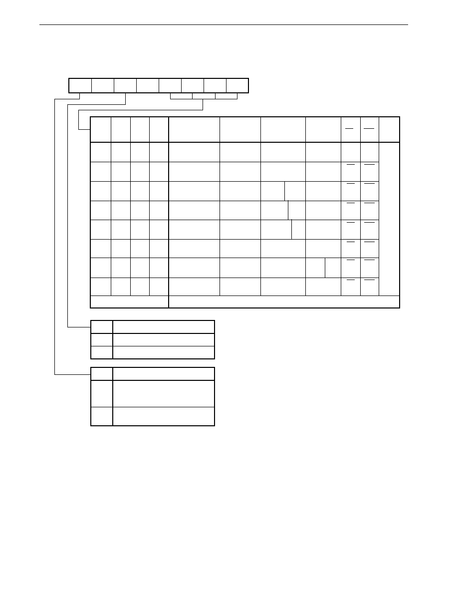
604
CHAPTER 24 LOCAL BUS INTERFACE FUNCTION
Preliminary User's Manual U13987EJ1V0UM00
Figure 24-1. Memory Expansion Mode Register (MM) Format
7
IFCH
MM
6
0
MM3
0
0
0
0
0
0
1
1
0
0
1
1
1
1
0
0
0
1
0
0
1
1
0
0
0
1
0
1
0
1
0
1
ASTB
/CLK
OUT
5
AW
4
0
3
MM3
2
MM2
1
MM1
0
MM0
Address
After reset
R/W
R/W
20H
0FFC4H
MM2
MM1
MM0
Mode Port
4 Port 5
Single-chip
mode
256-byte
expansion mode
1-Kbyte
expansion mode
4-Kbyte
expansion mode
16-Kbyte
expansion mode
64-Kbyte
expansion mode
256-Kbyte
expansion mode
1-Mbyte
expansion mode
Setting prohibited
Port
Port
Port
Port
Port
Port
RD
WR
Port
Port
Port
Port
Port
Port
A8, A9
Port
A8 to A11
A8 to A13
A8 to A15
A8 to A15
A8 to A15
A16 to A19
P60 to P63
P64/
RD
P65/
WR
AD0 to AD7
AD0 to AD7
AD0 to AD7
AD0 to AD7
AD0 to AD7
AD0 to AD7
AD0 to AD7
Port
A16,
A17
Port
RD
WR
RD
WR
ASTB
RD
WR
RD
WR
RD
WR
RD
WR
Other than the above
AW
Address Wait Specification
Disabled
Enabled
1
0
IFCH
Internal ROM Fetches
Fetch performed at same speed as
external memory
All wait control settings valid
High-speed fetches performed
Wait control specification invalid
1
0

605
CHAPTER 24 LOCAL BUS INTERFACE FUNCTION
Preliminary User's Manual U13987EJ1V0UM00
24.1.2 Memory map with external memory expansion
The memory map when memory expansion is used is shown in Figures 24-2 and 24-3. External devices at the same
addresses as the internal ROM area, internal RAM area and SFR area (excluding the external SFR area (0FFD0H to
0FFDFH)) cannot be accessed. If an access is made to these addresses, the memory or SFR in the
�
PD784938 has access
priority and no ASTB signal, RD signal, or WR signal is output (these pins remain at the inactive level). The address bus
output level remains at the level output prior to this, and the address/data bus output becomes high-impedance.
Except in 1-Mbyte expansion mode, the address output externally is output with the upper part of the address specified
by the program masked.
Example 1:
In 256-byte expansion mode, when address 54321H is accessed by the program, the output address is 21H.
Example 2:
In 256-byte expansion mode, when address 67821H is accessed by the program, the output address is 21H.

606
CHAPTER 24 LOCAL BUS INTERFACE FUNCTION
Preliminary User's Manual U13987EJ1V0UM00
Figure 24-2.
�
PD784935 Memory Map (1/2)
(a) When LOCATION 0 instruction is executed
Notes 1. Any expansion size area in unshaded part
2. External SFR area
SFR
SFR
SFR
SFR
SFR
Note 2
SFR
Internal RAM
Internal ROM
Internal ROM
Internal ROM
Internal RAM
Internal RAM
Internal ROM
Single-chip mode
1-Mbyte expansion mode
256-byte to 256-Kbyte
expansion modes
Internal ROM
Internal ROM
External memory
External memory
Note 1
External memory
Note 2
FFFFFH
0FFFFH
10000H
17FFFH
0FFE0H
0FFCFH
0EB00H
00000H
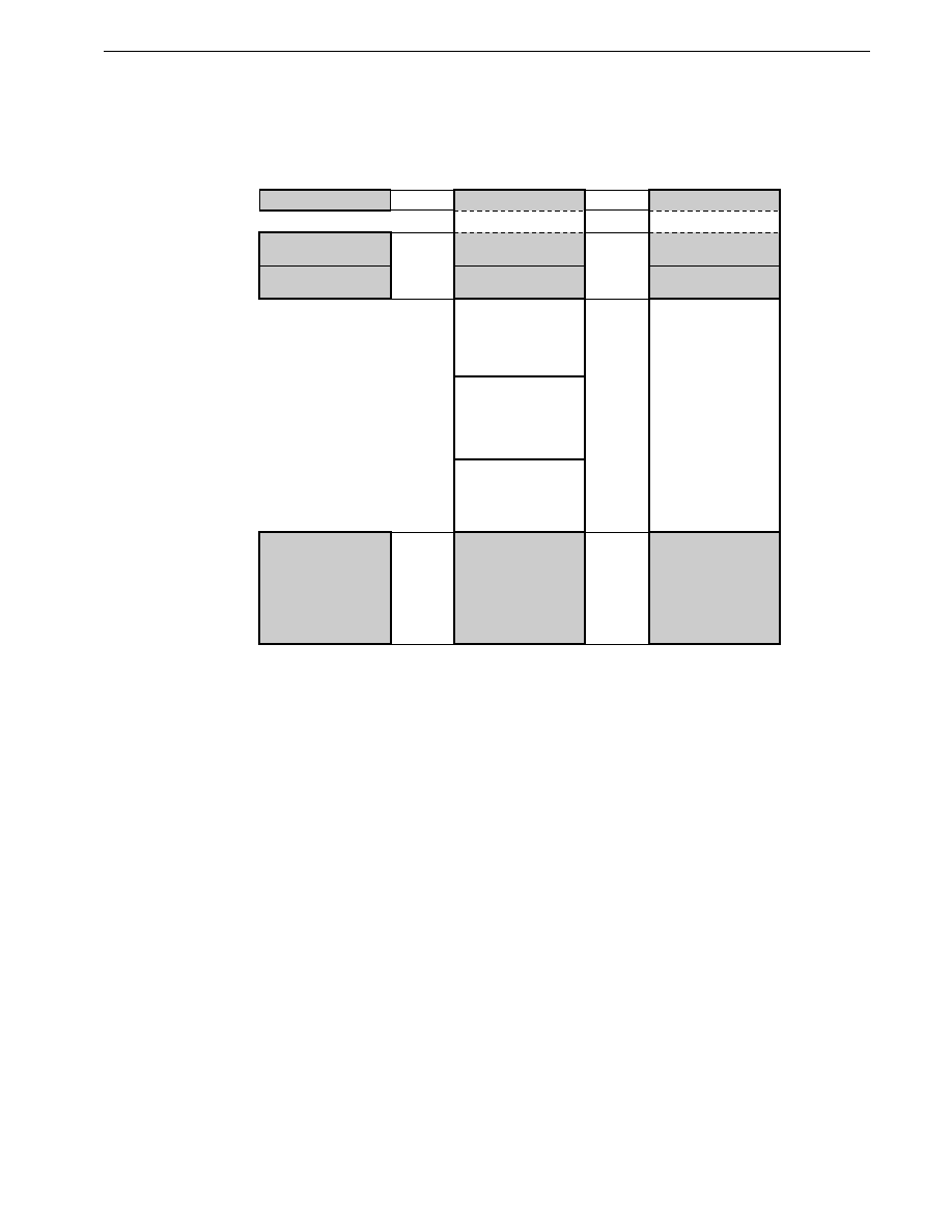
607
CHAPTER 24 LOCAL BUS INTERFACE FUNCTION
Preliminary User's Manual U13987EJ1V0UM00
Figure 24-2.
�
PD784935 Memory Map (2/2)
(b) When LOCATION 0FH instruction is executed
Notes 1. Any expansion size area in unshaded part
2. External SFR area
SFR
SFR
SFR
SFR
SFR
Note 2
SFR
Internal RAM
Internal RAM
Internal RAM
Internal ROM
Single-chip mode
1-Mbyte expansion mode
256-byte to 256-Kbyte
expansion mode
Internal ROM
Internal ROM
External memory
Note 2
FFFFFH
FFFE0H
FFFCFH
FEB00H
17FFFH
00000H
External memory
External memory
Note 1
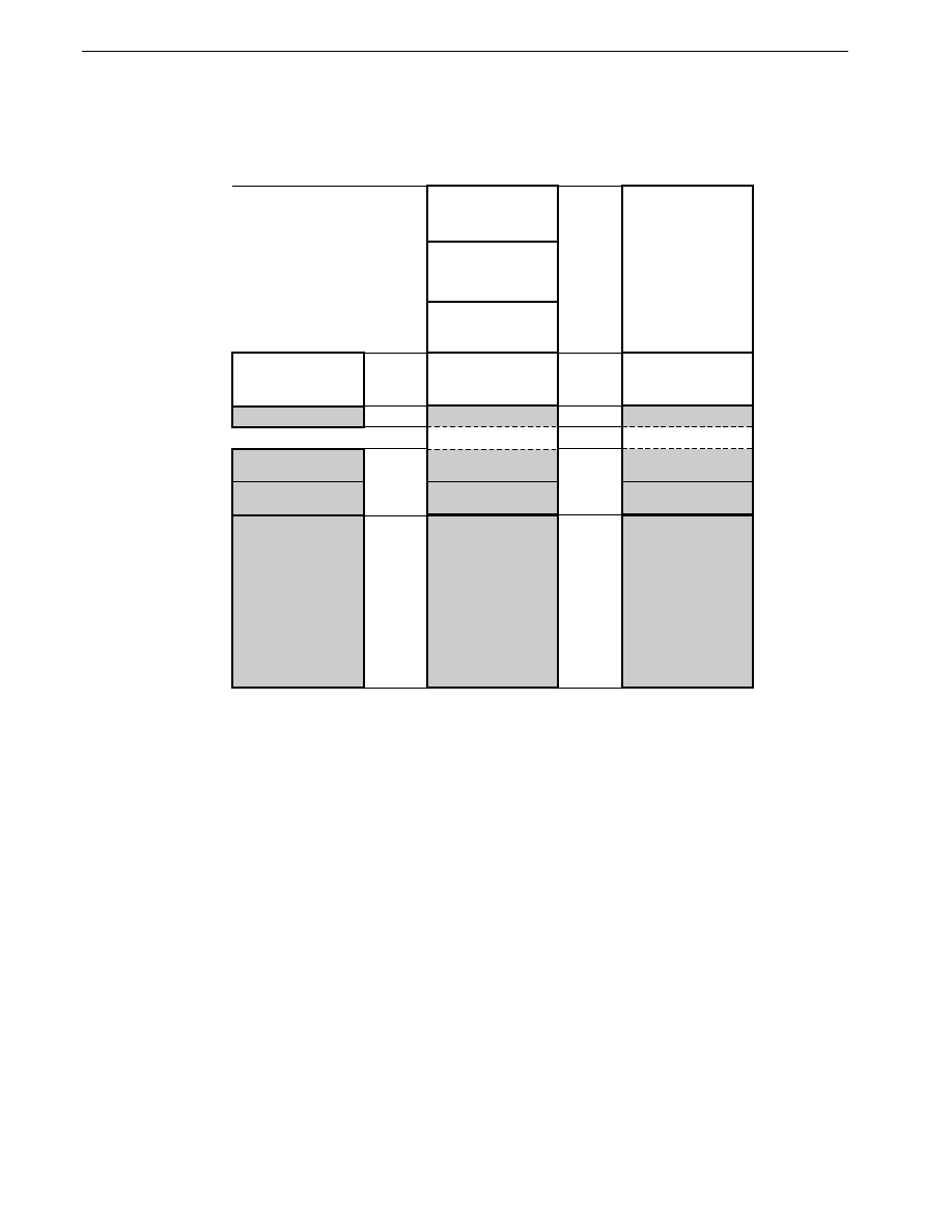
608
CHAPTER 24 LOCAL BUS INTERFACE FUNCTION
Preliminary User's Manual U13987EJ1V0UM00
Figure 24-3.
�
PD784936 Memory Map (1/2)
(a) When LOCATION 0 instruction is executed
Notes 1. Any expansion size area in unshaded part
2. External SFR area
SFR
SFR
SFR
SFR
SFR
Note 2
SFR
Internal RAM
Internal ROM
Internal ROM
Internal ROM
Internal RAM
Internal RAM
Internal ROM
Single-chip mode
1-Mbyte expansion mode
256-byte to 256-Kbyte
expansion modes
Internal ROM
Internal ROM
External memory
External memory
Note 1
External memory
Note 2
FFFFFH
0FFFFH
10000H
1FFFFH
0FFE0H
0FFCFH
0E500H
00000H
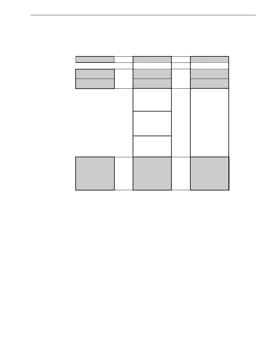
609
CHAPTER 24 LOCAL BUS INTERFACE FUNCTION
Preliminary User's Manual U13987EJ1V0UM00
Figure 24-3.
�
PD784936 Memory Map (2/2)
(b) When LOCATION 0FH instruction is executed
Notes 1. Any expansion size area in unshaded part
2. External SFR area
SFR
SFR
SFR
SFR
SFR
Note 2
SFR
Internal RAM
Internal RAM
Internal RAM
Internal ROM
Single-chip mode
1-Mbyte expansion mode
256-byte to 256-Kbyte
expansion mode
Internal ROM
Internal ROM
External memory
Note 2
FFFFFH
FFFE0H
FFFCFH
FE500H
1FFFFH
00000H
External memory
External memory
Note 1

610
CHAPTER 24 LOCAL BUS INTERFACE FUNCTION
Preliminary User's Manual U13987EJ1V0UM00
Figure 24-4.
�
PD784937 Memory Map (1/2)
(a) When LOCATION 0 instruction is executed
Notes 1. Any expansion size area in unshaded part
2. External SFR area
SFR
SFR
SFR
SFR
SFR
Note 2
SFR
Internal RAM
Internal ROM
Internal ROM
Internal ROM
Internal RAM
Internal RAM
Internal ROM
Single-chip mode
1-Mbyte expansion mode
256-byte to 256-Kbyte
expansion modes
Internal ROM
Internal ROM
External memory
External memory
Note 1
External memory
Note 2
FFFFFH
0FFFFH
10000H
2FFFFH
0FFE0H
0FFCFH
0DF00H
00000H

611
CHAPTER 24 LOCAL BUS INTERFACE FUNCTION
Preliminary User's Manual U13987EJ1V0UM00
Figure 24-4.
�
PD784937 Memory Map (2/2)
(b) When LOCATION 0FH instruction is executed
Notes 1. Any expansion size area in unshaded part
2. External SFR area
SFR
SFR
SFR
SFR
SFR
Note 2
SFR
Internal RAM
Internal RAM
Internal RAM
Internal ROM
Single-chip mode
1-Mbyte expansion mode
256-byte to 256-Kbyte
expansion mode
Internal ROM
Internal ROM
External memory
Note 2
FFFFFH
FFFE0H
FFFCFH
FDF00H
1FFFFH
00000H
External memory
External memory
Note 1

612
CHAPTER 24 LOCAL BUS INTERFACE FUNCTION
Preliminary User's Manual U13987EJ1V0UM00
Figure 24-5.
�
PD784938 Memory Map (1/2)
(a) When LOCATION 0 instruction is executed
Notes 1. Any expansion size area in unshaded part
2. External SFR area
SFR
SFR
SFR
SFR
SFR
Note 2
SFR
Internal RAM
Internal ROM
Internal ROM
Internal ROM
Internal RAM
Internal RAM
Internal ROM
Single-chip mode
1-Mbyte expansion mode
256-byte to 256-Kbyte
expansion modes
Internal ROM
Internal ROM
External memory
External memory
Note 1
External memory
Note 2
FFFFFH
0FFFFH
10000H
3FFFFH
0FFE0H
0FFCFH
0D600H
00000H

613
CHAPTER 24 LOCAL BUS INTERFACE FUNCTION
Preliminary User's Manual U13987EJ1V0UM00
Figure 24-5.
�
PD784938 Memory Map (2/2)
(b) When LOCATION 0FH instruction is executed
Notes 1. Any expansion size area in unshaded part
2. External SFR area
SFR
SFR
SFR
SFR
SFR
Note 2
SFR
Internal RAM
Internal RAM
Internal RAM
Internal ROM
Single-chip mode
1-Mbyte expansion mode
256-byte to 256-Kbyte
expansion mode
Internal ROM
Internal ROM
External memory
Note 2
FFFFFH
FFFE0H
FFFCFH
FD600H
1FFFFH
00000H
External memory
External memory
Note 1
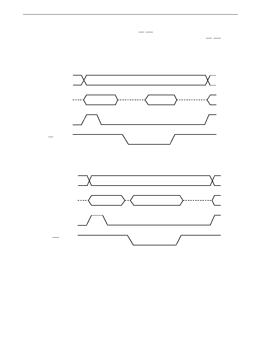
614
CHAPTER 24 LOCAL BUS INTERFACE FUNCTION
Preliminary User's Manual U13987EJ1V0UM00
24.1.3 Basic operation of local bus interface
The local bus interface accesses external memory using ASTB, RD, WR, an address/data bus (AD0 to AD7), and address
bus (A8 to A19). When the local bus interface is used, P64, P65, and port 4 automatically operate as RD, WR and AD0
to AD7. On the address bus, only the pins that correspond to the expansion memory size operate as address bus pins.
An outline of the memory access timing is shown in Figures 24-6 and 24-7.
Figure 24-6. Read Timing
High address
Data (input)
ASTB (output)
RD (output)
AD0 to AD7
A8 to A19
Note
(output)
Hi-Z
Hi-Z
Hi-Z
Low address
(output)
Note The number of address bus pins used depends on the expansion mode size.
Figure 24-7. Write Timing
High address
ASTB (output)
AD0 to AD7 (output)
A8 to A19
Note
(output)
Hi-Z
Hi-Z
Hi-Z
WR (output)
Data
Low address
Note The number of address bus pins used depends on the expansion mode size.
615
CHAPTER 24 LOCAL BUS INTERFACE FUNCTION
Preliminary User's Manual U13987EJ1V0UM00
24.2 Wait Function
When a low-speed memory or I/O is connected externally to the
�
PD784938, waits can be inserted in the external memory
access cycle.
There are two kinds of wait cycle, an address wait for securing the address decoding time, and an access wait for securing
the access time.
24.2.1 Wait function control registers
(1) Memory expansion mode register (MM)
The IFCH bit of MM performs wait control setting for internal ROM accesses, and the AW bit performs address wait
setting.
MM can be read or written to with an 8-bit manipulation instruction. The MM format is shown in Figure 24-8.
When RESET is input, MM is set to 20H, the same cycle as for external memory is used for internal ROM accesses,
and the address wait function is validated.
Figure 24-8. Memory Expansion Mode Register (MM) Format
(2) Programmable wait control registers (PWC1/PWC2)
PWC1 and PWC2 specify the number of waits.
PWC1 is an 8-bit register that divides the space from 0 to FFFFH into four, and specifies wait control for each of these
four spaces. PWC2 is a 16-bit register that divides the space from 10000H to FFFFH into four, and specifies wait control
for each of these four spaces.
PWC1 can be read or written to with an 8-bit manipulation instruction, and PWC2 with a 16-bit manipulation instruction.
The PWC1 and PWC2 formats are shown in Figure 24-9.
The high-order 8 bits of PWC2 are fixed at AAH, and therefore ensure that the high-order 8 bits are set to AAH.
When RESET is input, PWC1 is set to AAH, and PWC2 to AAAAH, and 2-wait insertion is performed on the entire space.
3
2
1
0
Address
After reset
R/W
0FFC4H
R/W
20H
IFCH
0
AW
0
MM2
MM1
MM0
MM
7
6
5
4
MM3
AW
0
1
Address Wait Specification
Disabled
Enabled
IFCH
0
1
Internal ROM Fetches
Fetch performed at same speed as
external memory
All wait control settings valid
High-speed fetches performed
Wait control specification invalid
Memory expansion mode settings (see 24.1
Memory Extension Function)
616
CHAPTER 24 LOCAL BUS INTERFACE FUNCTION
Preliminary User's Manual U13987EJ1V0UM00
Figure 24-9. Programmable Wait Control Register (PWC1/PWC2) Format
(a) Programmable wait control register 1 (PWC1)
7
PW31
PWC1
6
PW30
5
PW21
4
PW20
3
PW11
2
PW10
1
PW01
0
PW00
Address
After reset
R/W
R/W
AAH
0FFC7H
000000H to
003FFFH
PW01
Address
Subject to Wait
PW00
0
0
1
1
0
1
0
1
Wait Cycle Insertion
Access wait cycle inserted only for
WAIT pin low-level input period
0
1
2
004000H to
007FFFH
PW11
Address
Subject to Wait
PW10
0
0
1
1
0
1
0
1
Wait Cycle Insertion
Access wait cycle inserted only for
WAIT pin low-level input period
0
1
2
008000H to
00BFFFH
PW21
Address
Subject to Wait
PW20
0
0
1
1
0
1
0
1
Wait Cycle Insertion
Access wait cycle inserted only for
WAIT pin low-level input period
0
1
2
00C000H to
00FFFFH
Note
PW31
Address
Subject to Wait
PW30
0
0
1
1
0
1
0
1
Wait Cycle Insertion
Access wait cycle inserted only for
WAIT pin low-level input period
0
1
2
Note Except part overlapping internal data area
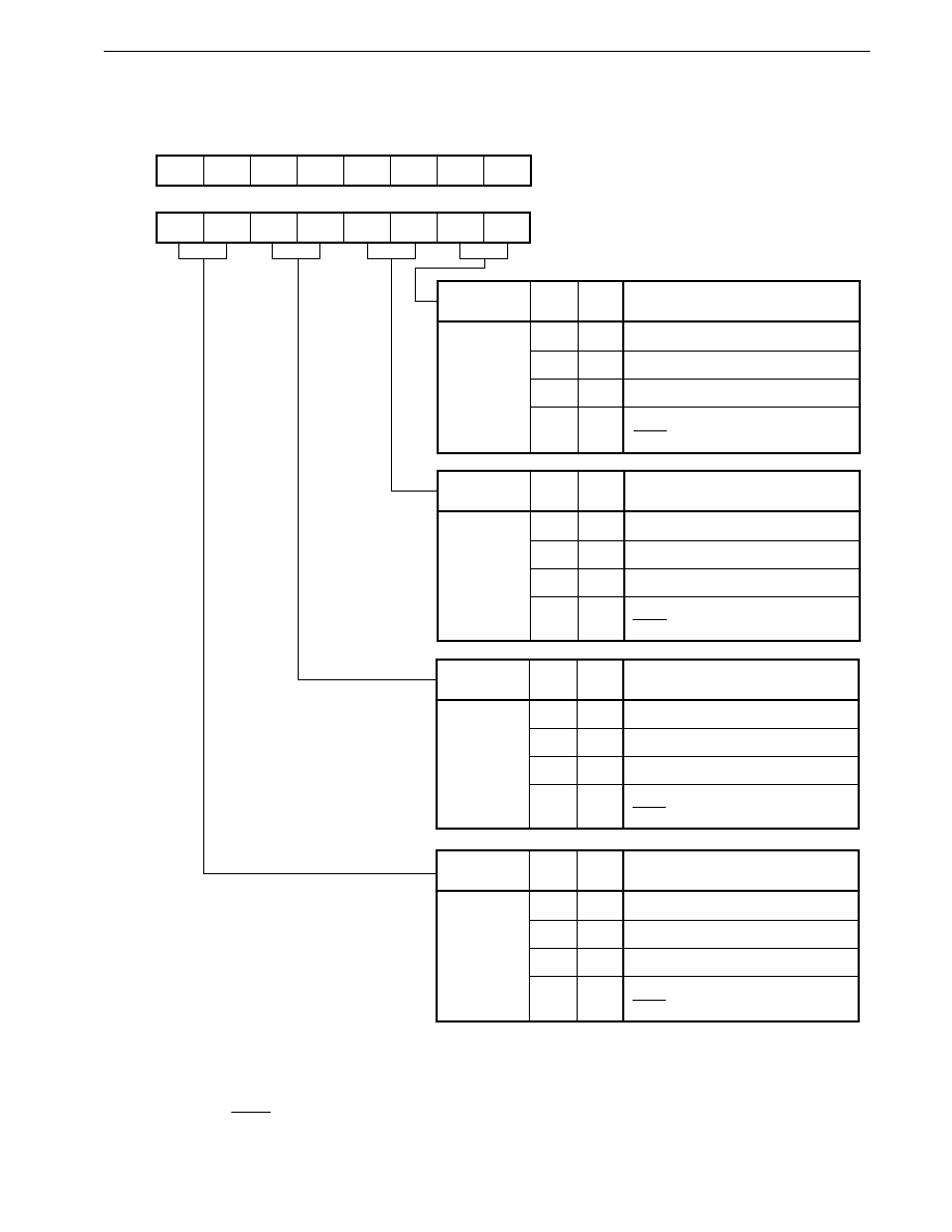
617
CHAPTER 24 LOCAL BUS INTERFACE FUNCTION
Preliminary User's Manual U13987EJ1V0UM00
(b) Programmable wait control register 2 (PWC2)
7
PW71
6
PW70
5
PW61
4
PW60
3
PW51
2
PW50
1
PW41
0
PW40
Address
After reset
R/W
R/W
AAAAH
0FFC8H
15
1
PWC2
14
0
13
1
12
0
11
1
10
0
9
1
8
0
010000H to
01FFFFH
PW41
Address
Subject to Wait
PW40
0
0
1
1
0
1
0
1
Wait Cycle Insertion
Access wait cycle inserted only for
WAIT pin low-level input period
0
1
2
020000H to
03FFFFH
PW51
Address
Subject to Wait
PW50
0
0
1
1
0
1
0
1
Wait Cycle Insertion
Access wait cycle inserted only for
WAIT pin low-level input period
0
1
2
040000H to
07FFFFH
PW61
Address
Subject to Wait
PW60
0
0
1
1
0
1
0
1
Wait Cycle Insertion
Access wait cycle inserted only for
WAIT pin low-level input period
0
1
2
080000H to
0FFFFFH
Note
PW71
Address
Subject to Wait
PW70
0
0
1
1
0
1
0
1
Wait Cycle Insertion
Access wait cycle inserted only for
WAIT pin low-level input period
0
1
2
Note Except part overlapping internal data area
Caution When the bus hold function is used, access wait control cannot be performed by means of the
WAIT pin, and 0, 1, or 2 waits must be selected for the entire space.
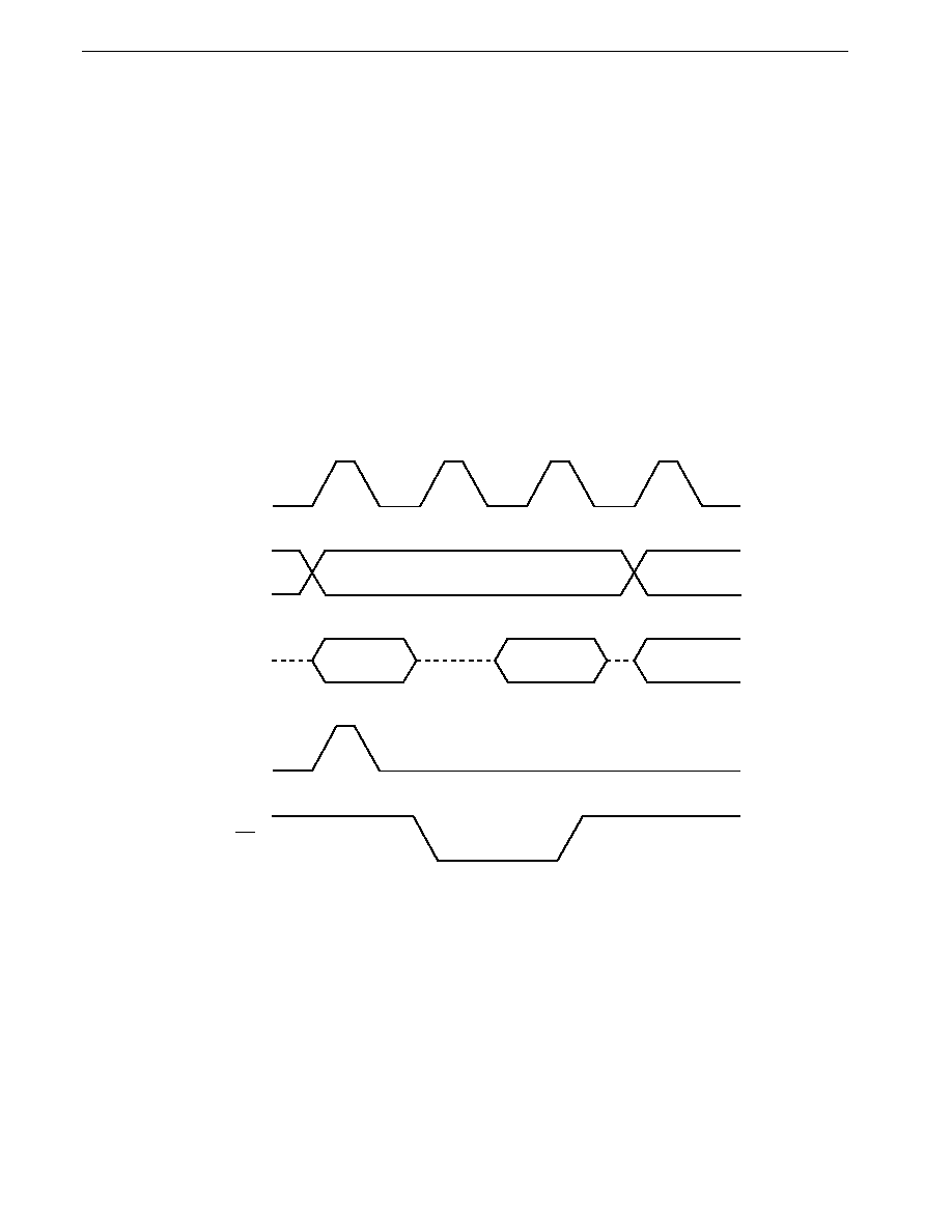
618
CHAPTER 24 LOCAL BUS INTERFACE FUNCTION
Preliminary User's Manual U13987EJ1V0UM00
24.2.2 Address waits
Address waits are used to secure the address decoding time. If the AW bit of the memory expansion mode register
(MM) is set (to 1), waits are inserted in every memory access
Note
. When an address wait is inserted, the high-level period
of the ASTB signal is extended by one system clock cycle (80 ns: f
CLK
= 12.58 MHz).
Note Except for the internal RAM, internal SFRs, and internal ROM during high-speed fetch.
If it is specified that the internal ROM is accessed in the same cycle as the external ROM, an address wait state
is inserted even when the internal ROM is accessed.
Caution If the pseudo-static RAM refresh function is used when the address wait function is used, the refresh
pulse is output and, at the same time, the memory is accessed. Therefore, do not use the pseudo-static
RAM refresh function when using the address wait function.
Figure 24-10. Address Wait Function Read/Write Timing (1/3)
(a) Read timing with no address wait insertion
f
CLK
Note
High address
ASTB
AD0 to AD7
A8 to A19
Hi-Z
Hi-Z
RD
Input data
Low address
Hi-Z
Note f
CLK
: Internal system clock frequency. This signal is present inside the
�
PD784938 only.
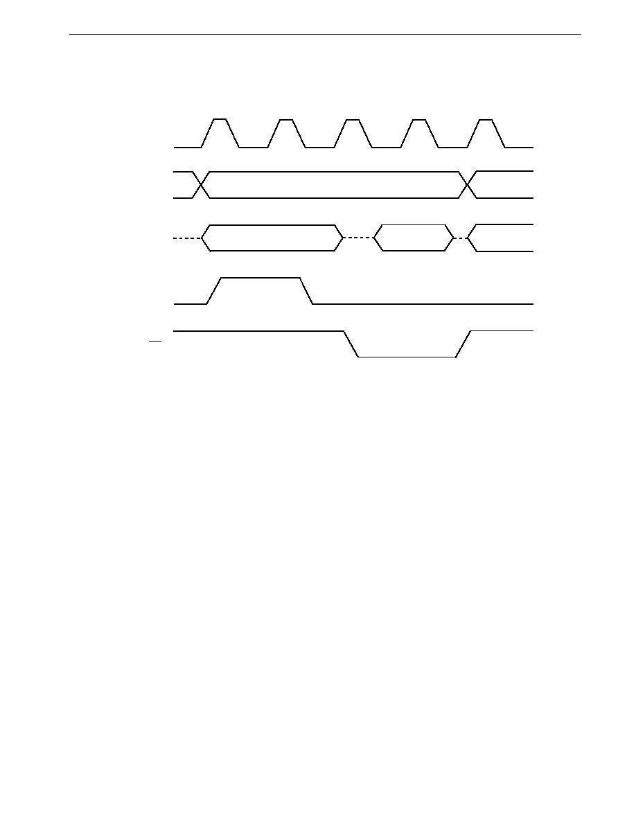
619
CHAPTER 24 LOCAL BUS INTERFACE FUNCTION
Preliminary User's Manual U13987EJ1V0UM00
Figure 24-10. Address Wait Function Read/Write Timing (2/3)
(b) Read timing with address wait insertion
f
CLK
Note
ASTB
AD0 to AD7
A8 to A19
Hi-Z
Hi-Z
RD
Hi-Z
Low address
Input data
High address
Note f
CLK
: Internal system clock frequency. This signal is present inside the
�
PD784938 only.
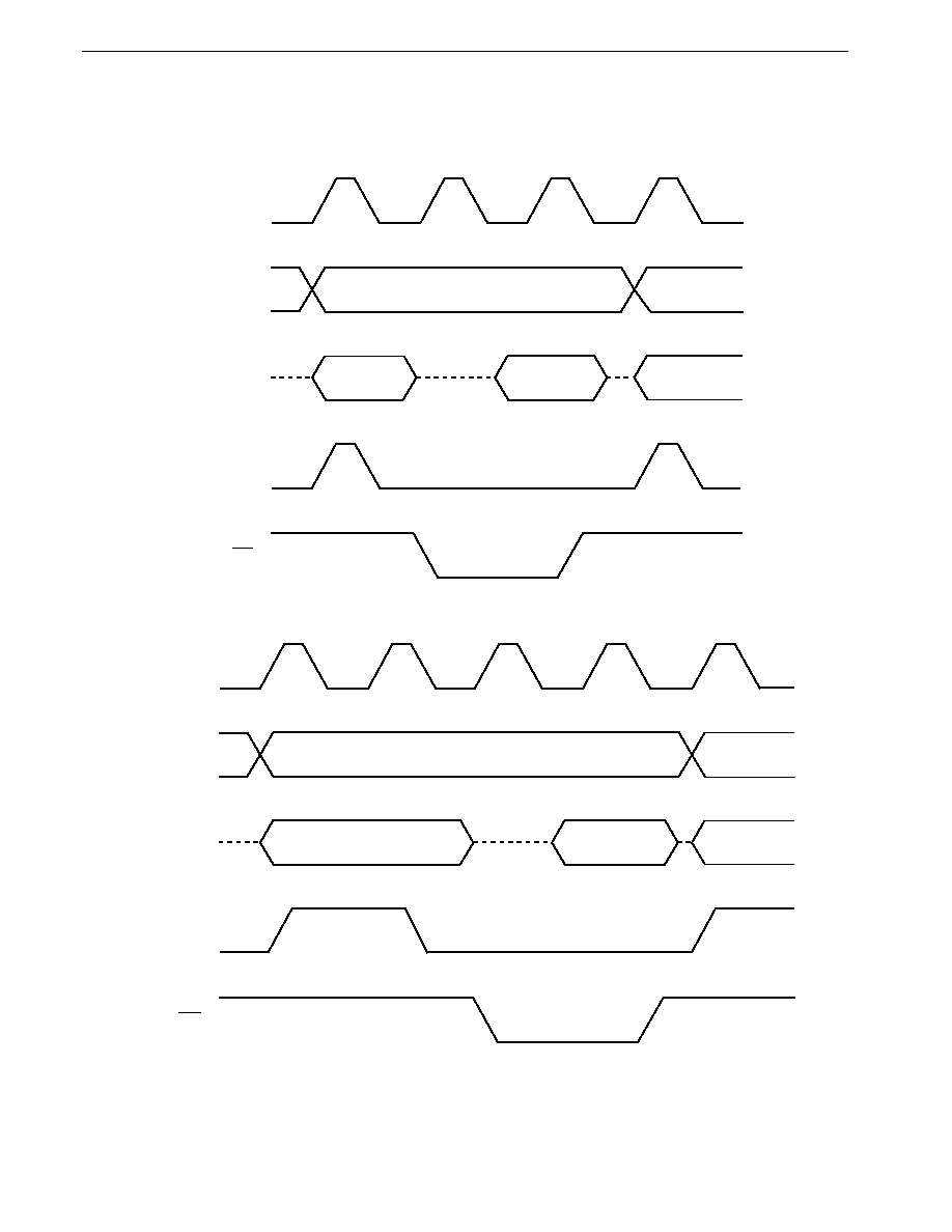
620
CHAPTER 24 LOCAL BUS INTERFACE FUNCTION
Preliminary User's Manual U13987EJ1V0UM00
Figure 24-10. Address Wait Function Read/Write Timing (3/3)
(c) Write timing with no address wait insertion
f
CLK
Note
High address
ASTB
AD0 to AD7
A8 to A19
Hi-Z
Hi-Z
WR
Output data
Low address
Hi-Z
(d) Write timing with address wait insertion
f
CLK
Note
High address
ASTB
AD0 to AD7
A8 to A19
Hi-Z
Hi-Z
WR
Output data
Low address
Hi-Z
Note f
CLK
: Internal system clock frequency. This signal is present inside the
�
PD784938 only.

621
CHAPTER 24 LOCAL BUS INTERFACE FUNCTION
Preliminary User's Manual U13987EJ1V0UM00
24.2.3 Access waits
Access waits are inserted in the RD or WR signal low-level period, and extend the low-level period by 1/f
CLK
(80 ns: f
CLK
= 12.58 MHz) per cycle.
There are two wait insertion methods, using either the programmable wait function that automatically inserts the preset
number of cycles, or the external wait function controlled by a wait signal from outside.
For wait cycle insertion control, the 1-Mbyte memory space is divided into eight as shown in Figure 24-11, and control
is specified for each space by means of the programmable wait control registers (PWC1/PWC2). Waits are not inserted
in accesses to internal ROM or internal RAM using high-speed fetches. In accesses to internal SFRs, waits are inserted
at the necessary times regardless of this specification.
If access operations are specified as being performed in the same number of cycles as for external ROM, waits are
inserted also in internal ROM accesses in accordance with the PWC1 settings.
If there is a space for which control by a wait signal from outside has been selected by means of the PWC1/PWC2, the
P66 pin operates as the WAIT signal input pin. After RESET input, the P66 pin operates as a general-purpose input/output
port.
Bus timing in the case of access wait insertion is shown in Figures 24-12 to 24-14.
Caution The external wait function cannot be used when the bus hold function is used.

622
CHAPTER 24 LOCAL BUS INTERFACE FUNCTION
Preliminary User's Manual U13987EJ1V0UM00
Figure 24-11. Wait Control Spaces
512 Kbytes
256 Kbytes
128 Kbytes
64 Kbytes
16 Kbytes
16 Kbytes
16 Kbytes
16 Kbytes
FFFFFH
80000H
03FFFH
7FFFFH
Controlled by bits
PW70 & PW71
Controlled by bits
PW60 & PW61
Controlled by PWC2
Controlled by PWC1
Controlled by bits
PW50 & PW51
Controlled by bits
PW40 & PW41
Controlled by bits
PW30 & PW31
Controlled by bits
PW20 & PW21
Controlled by bits
PW10 & PW11
Controlled by bits
PW00 & PW01
20000H
1FFFFH
10000H
0FFFFH
0C000H
0BFFFH
08000H
07FFFH
40000H
3FFFFH
04000H
00000H
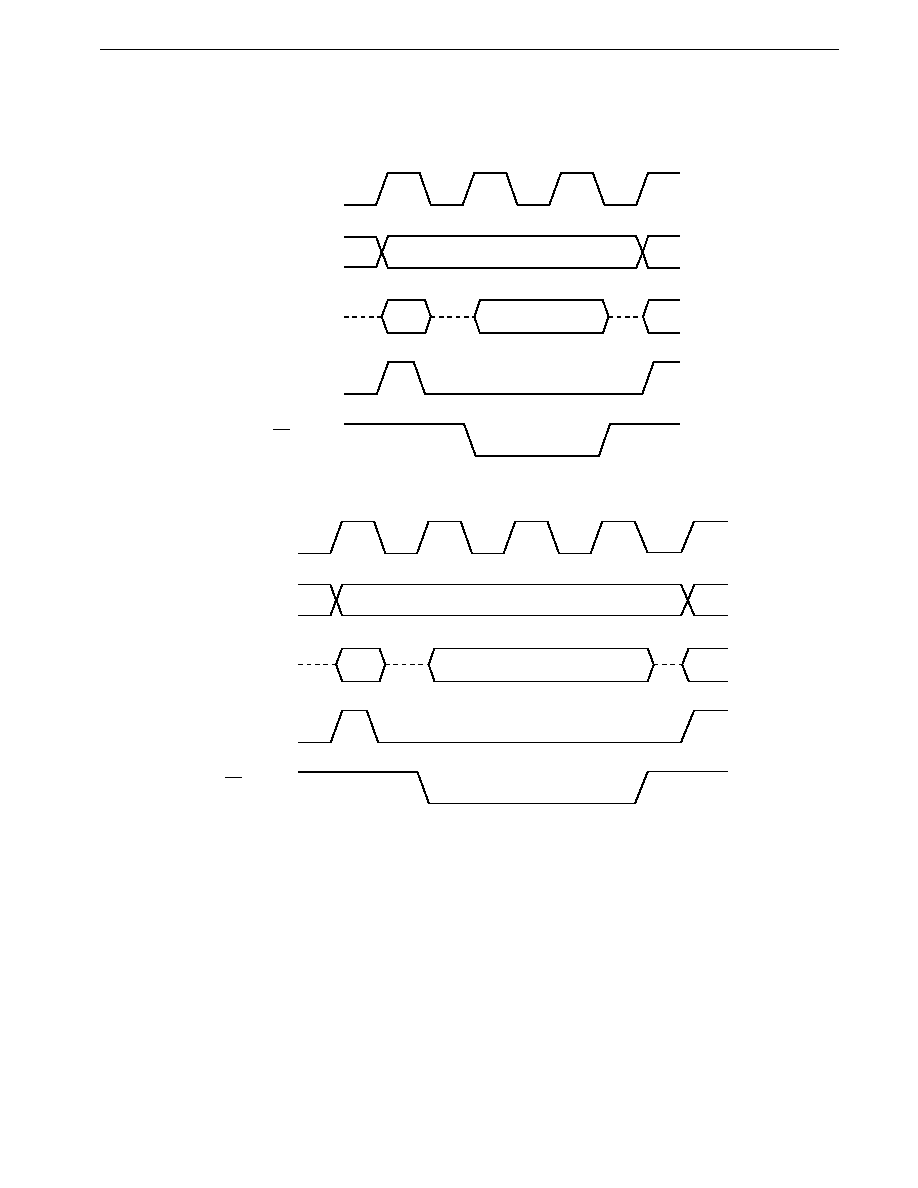
623
CHAPTER 24 LOCAL BUS INTERFACE FUNCTION
Preliminary User's Manual U13987EJ1V0UM00
Figure 24-12. Access Wait Function Read Timing (1/2)
(a) 0 wait cycles set
f
CLK
Note
High address
ASTB (output)
AD0 to AD7
A8 to A15
(output)
Hi-Z
Hi-Z
RD (output)
Data (input)
Low
address
Hi-Z
(b) 1 wait cycle set
f
CLK
Note
High address
ASTB (output)
AD0 to AD7
A8 to A15
(output)
Hi-Z
Hi-Z
RD (output)
Data (input)
Low
address
Hi-Z
Note f
CLK
: Internal system clock frequency. This signal is only present inside the
�
PD784938.
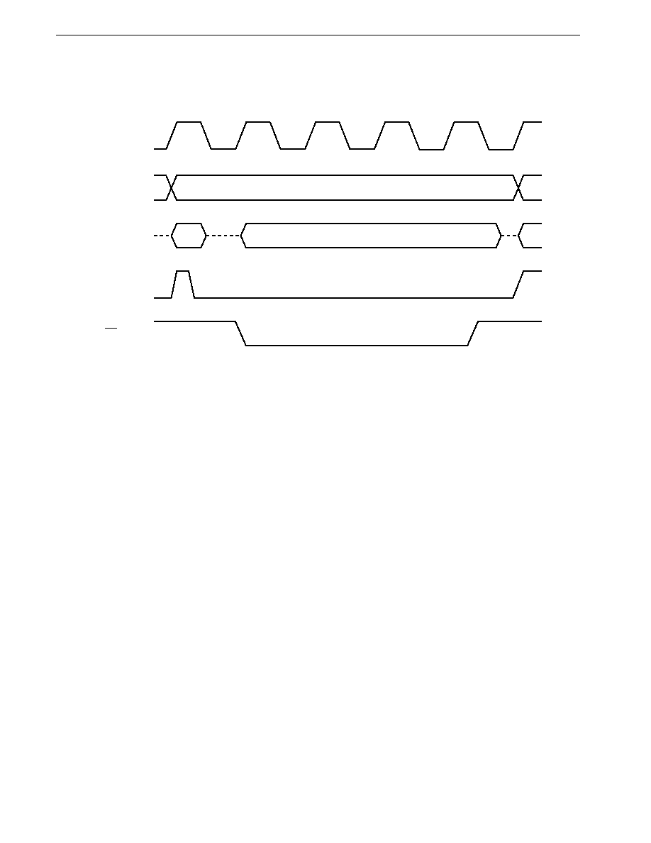
624
CHAPTER 24 LOCAL BUS INTERFACE FUNCTION
Preliminary User's Manual U13987EJ1V0UM00
Figure 24-12. Access Wait Function Read Timing (2/2)
(c) 2 wait cycles set
High address
ASTB (output)
AD0 to AD7
A8 to A15
(output)
Hi-Z
RD (output)
Data (input)
Low
address
Hi-Z
f
CLK
Note
Note f
CLK
: Internal system clock frequency. This signal is only present inside the
�
PD784938.

625
CHAPTER 24 LOCAL BUS INTERFACE FUNCTION
Preliminary User's Manual U13987EJ1V0UM00
Figure 24-13. Access Wait Function Write Timing (1/2)
(a) 0 wait cycles set
f
CLK
Note
High address
ASTB (output)
AD0 to AD7
(output)
A8 to A15
(output)
Hi-Z
Hi-Z
WR (output)
Data
Low
address
Hi-Z
(b) 1 wait cycle set
f
CLK
Note
High address
ASTB (output)
AD0 to AD7
(output)
A8 to A15
(output)
Hi-Z
Hi-Z
WR (output)
Data
Low
address
Hi-Z
Note f
CLK
: Internal system clock frequency. This signal is only present inside the
�
PD784938.
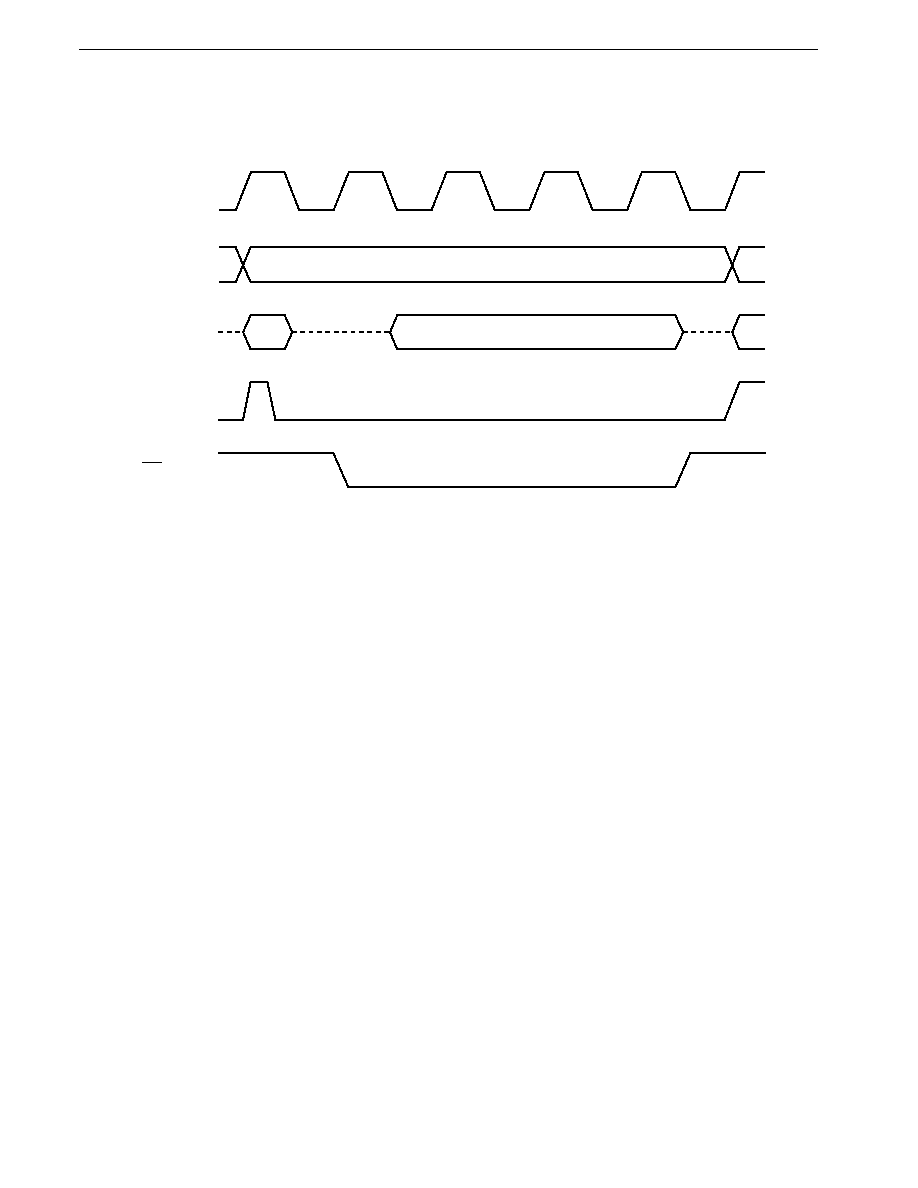
626
CHAPTER 24 LOCAL BUS INTERFACE FUNCTION
Preliminary User's Manual U13987EJ1V0UM00
Figure 24-13. Access Wait Function Write Timing (2/2)
(c) 2 wait cycles set
High address
ASTB (output)
AD0 to AD7
(output)
A8 to A15
(output)
Hi-Z
WR (output)
Data
Low
address
Hi-Z
f
CLK
Note
Hi-Z
Note f
CLK
: Internal system clock frequency. This signal is only present inside the
�
PD784938.
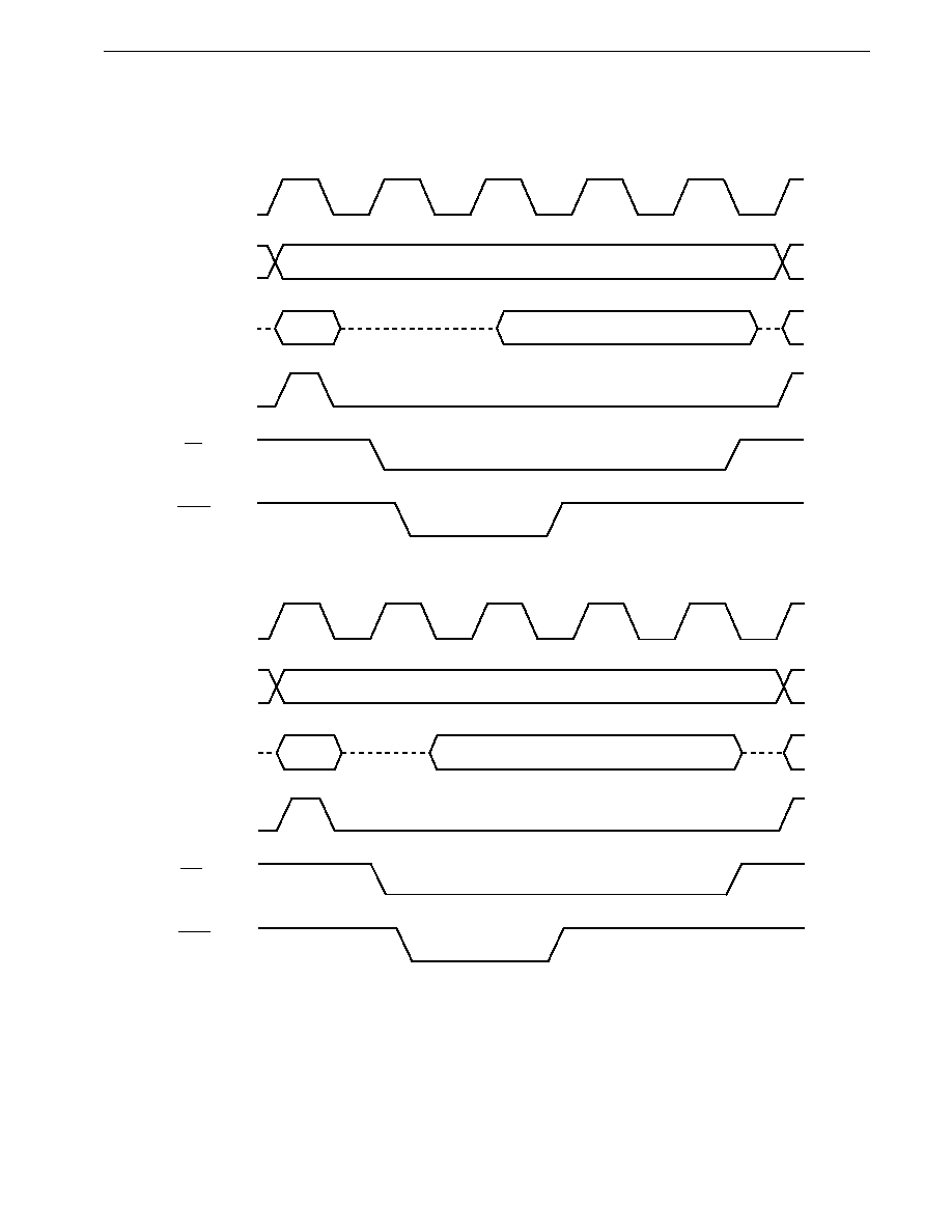
627
CHAPTER 24 LOCAL BUS INTERFACE FUNCTION
Preliminary User's Manual U13987EJ1V0UM00
Figure 24-14. Timing with External Wait Signal
(a) Read timing
High address
ASTB (output)
AD0 to AD7
A8 to A15
(output)
Hi-Z
RD (output)
Data (input)
Low
address
Hi-Z
f
CLK
Note
WAIT (input)
(b) Write timing
High address
ASTB (output)
AD0 to AD7
(output)
A8 to A15
(output)
Hi-Z
WR (output)
Data
Low
address
Hi-Z
f
CLK
Note
WAIT (input)
Note f
CLK
: Internal system clock frequency. This signal is only present inside the
�
PD784938.

628
CHAPTER 24 LOCAL BUS INTERFACE FUNCTION
Preliminary User's Manual U13987EJ1V0UM00
24.3 Pseudo-Static RAM Refresh Function
The
�
PD784938 incorporates a pseudo-static RAM refresh function for direct connection of pseudo-static RAM.
The pseudo-static RAM refresh function outputs refresh pulses at any desired intervals. The refresh pulse output interval
is specified by the refresh mode register (RFM) setting.
The refresh area specification register (RFA) specifies the addresses on which refresh operations can be performed at
the same time as memory access operations. This enables bus cycle insertions for refresh operations to be greatly
decreased, thus minimizing the reduction in performance due to refresh operations.
The
�
PD784938 is provided with a function for supporting self-refresh operations that offers low power consumption
by a pseudo-static RAM application system.
Cautions 1.
The refresh function cannot be used when the bus hold function is used.
2.
If the pseudo-static RAM refresh function is used when the address wait function is used, the
refresh pulse is output and, at the same time, the memory is accessed. Therefore, do not use the
pseudo-static RAM refresh function when using the address wait function.
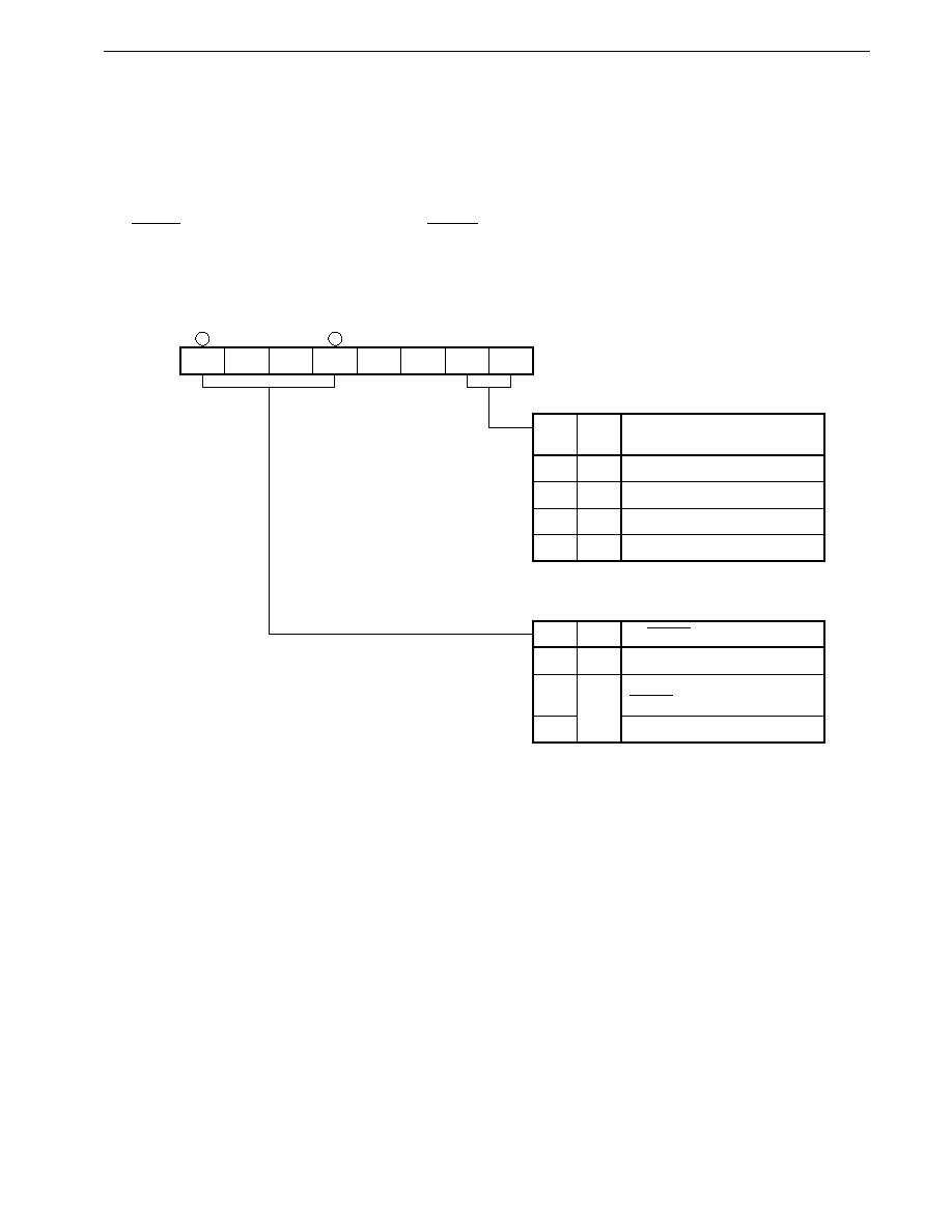
629
CHAPTER 24 LOCAL BUS INTERFACE FUNCTION
Preliminary User's Manual U13987EJ1V0UM00
24.3.1 Control registers
(1) Refresh mode register (RFM)
RFM is an 8-bit register that controls the pseudo-static RAM refresh cycle and switching to self-refresh operations.
RFM can be read or written to with an 8-bit manipulation instruction or bit manipulation instruction. The RFM format
is shown in Figure 24-15.
RESET input clears RFM to 00H and sets the REFRQ pin to port mode, so that it operates as the alternate-function
P67 pin.
Figure 24-15. Refresh Mode Register (RFM) Format
RFLV
0
0
RFEN
0
0
RFT1
RFT0
7
6
5
4
3
2
1
0
RFM
0FFCCH
Address
00H
After reset
R/W
R/W
RFT1
0
0
1
1
Refresh Pulse Output Cycle
Specification
32/f
CLK
Note
(2.5 s)
64/f
CLK
(5.1 s)
128/f
CLK
(10.2 s)
256/f
CLK
(20.3 s)
RFT0
0
1
0
1
f
CLK
= 12.58 MHz
RFLV
�
0
1
REFRQ Pin Output Control
Port mode
Self-refresh operation
(REFRQ low level)
Refresh pulse output enabled
RFEN
0
1
Remark
�
: 0 or 1
Note f
CLK
: Internal system clock frequency
�
�
�
�
Caution The refresh function cannot be used when the bus hold function is used. In this case, ensure that
refreshing is specified as disabled.
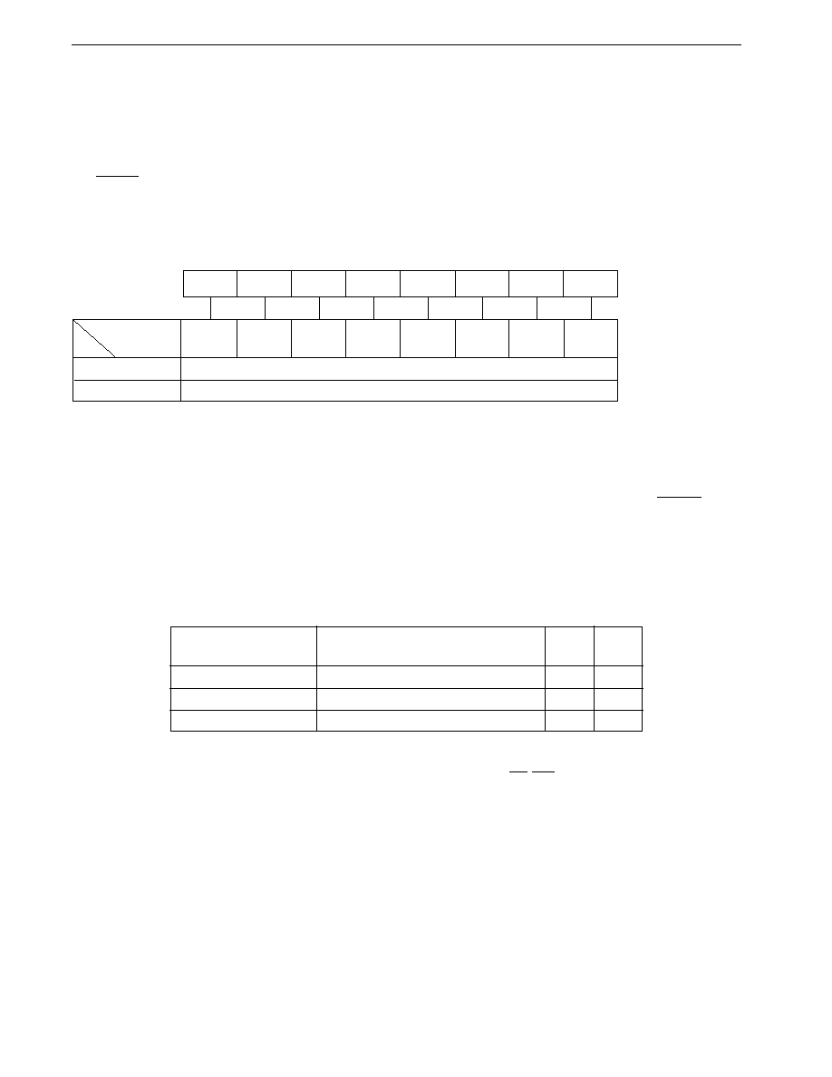
630
CHAPTER 24 LOCAL BUS INTERFACE FUNCTION
Preliminary User's Manual U13987EJ1V0UM00
(2) Refresh area specification register (RFA)
RFA is an 8-bit register that specifies the areas on which refresh operations can be performed at the same time as
memory access operations.
RFA can be read or written to with an 8-bit manipulation instruction and bit manipulation instruction. The RFA format
is shown in Figure 24-16.
RESET input clears RFA to 00H.
Figure 24-16. Refresh Area Specification Register (RFA) Format
RFA7
RFA
RFA6
RFA5
RFA4
RFA3
RFA2
RFA1
RFA0
Address After reset R/W
R/W
00H
0FFCDH
Refresh
Specification
Area
0
1
7
6
5
4
3
2
1
0
080000H to
0FFFFFH
040000H to
07FFFFH
020000H to
03FFFFH
010000H to
01FFFFH
00C000H to
00FFFFH
008000H to
00BFFFH
004000H to
007FFFH
000000H to
003FFFH
Refreshing performed at same time as memory access operations in corresponding block
Refreshing performed exclusively from memory access operations in corresponding block
(n = 0 to 7)
RFAn
24.3.2 Operations
(1) Pulse refresh operation
To support the pulse refresh cycles of pseudo-static RAM, refresh pulses are output from the REFRQ pin in
synchronization with bus cycles.
The system clock frequency and bits 1 and 0 (RFT1/RFT0) of the refresh mode register (RFM) are adjusted so that
512 or more refresh pulses are generated in an 8 ms period.
Table 24-1. System Clock Frequency and Refresh Pulse Output Cycle when Pseudo-Static RAM is Used
System Clock Frequency
Refresh Pulse Output Cycle Specification
RFT1
RFT0
(f
CLK
) MHz
8.192 < f
CLK
16
128/f
CLK
1
0
4.096 < f
CLK
8.192
64/f
CLK
0
1
2.048 < f
CLK
4.096
32/f
CLK
0
0
These pulse refresh operations are performed so that they do not overlap external memory access operations. During
a refresh cycle, an external memory access cycle is held pending (ASTB, RD, WR, etc. are inactive), and during an
external memory access cycle, a refresh cycle is held pending.
If there is no overlapping with an external memory access operation, the refresh cycle is performed without affecting
CPU instruction execution.
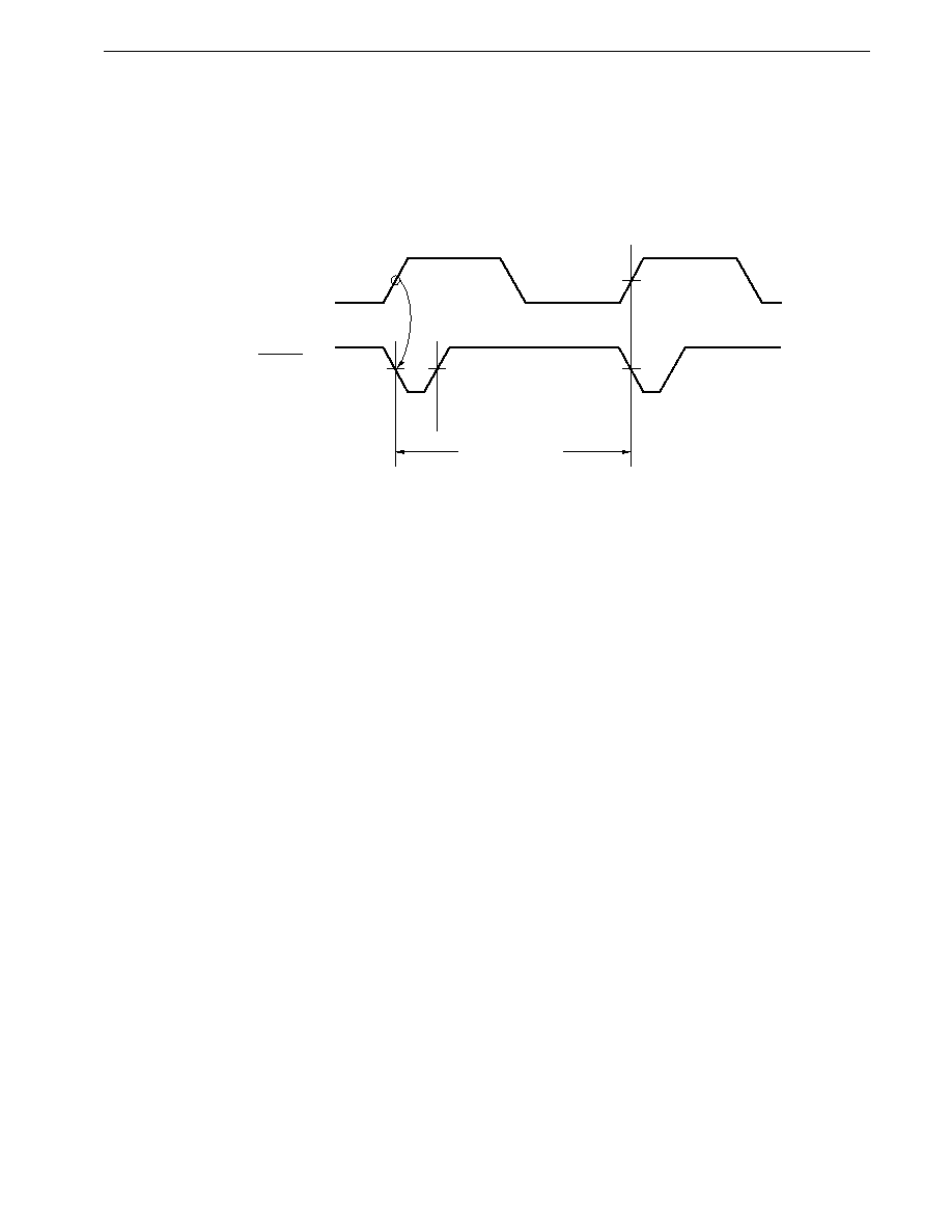
631
CHAPTER 24 LOCAL BUS INTERFACE FUNCTION
Preliminary User's Manual U13987EJ1V0UM00
(a) Internal memory accesses
In the case of internal memory accesses in which the external pseudo-static RAM is not accessed, also, refresh
bus cycles are output at the intervals specified by the refresh mode register (RFM) so that the data stored in the
pseudo-static RAM is retained. In this case, CPU instruction execution is not affected.
Figure 24-17. Pulse Refresh Operation in Internal Memory Access
REFRQ
pin output
Refresh cycle
Note
Refresh timing counter
Note Cycle specified by the RFT1 and RFT0 bits of the RFM
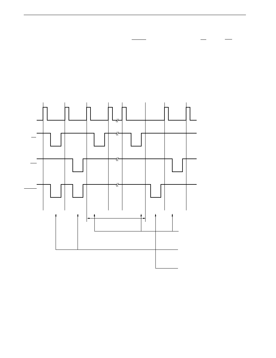
632
CHAPTER 24 LOCAL BUS INTERFACE FUNCTION
Preliminary User's Manual U13987EJ1V0UM00
(b) External memory accesses
When an access is made to an address corresponding to a cleared (to 0) bit in the refresh area specification register
(RFA), a refresh pulse is always output from the REFRQ pin at the same time as the RD signal or WR signal,
irrespective of the cycle specified by the refresh mode register (RFM).
After refresh pulse output, accesses to internal memory or accesses to addresses corresponding to a set (to 1)
bit in the RFA continue, and after the time specified by the RFT0 and RFT1 bits of the RFM has elapsed, a refresh
bus cycle is generated so as not to overlap a memory access cycle, and a refresh pulse is output.
In this way, refreshing can be performed while memory that does not need refreshing, such as PROM, is being
accessed, refresh bus cycle insertions can be reduced, and instruction execution can be performed efficiently.
Figure 24-18. Refresh Pulse Output Operation
ASTB
Read cycle
Write cycle
Read cycle
Read cycle
Refresh
bus cycle
Write cycle
Time specified by RFT0 &
RFT1 bits of RFM
In case of access to area in which
memory access operations and refresh
operations are performed simultaneously
Time specified by RFT0 & RFT1 bits of
REM.
As refresh pulse has not been output,
refresh bus cycle is inserted
In case of access to area in which
memory access operations and refresh
operations are performed exclusively
REFRQ
RD
WR
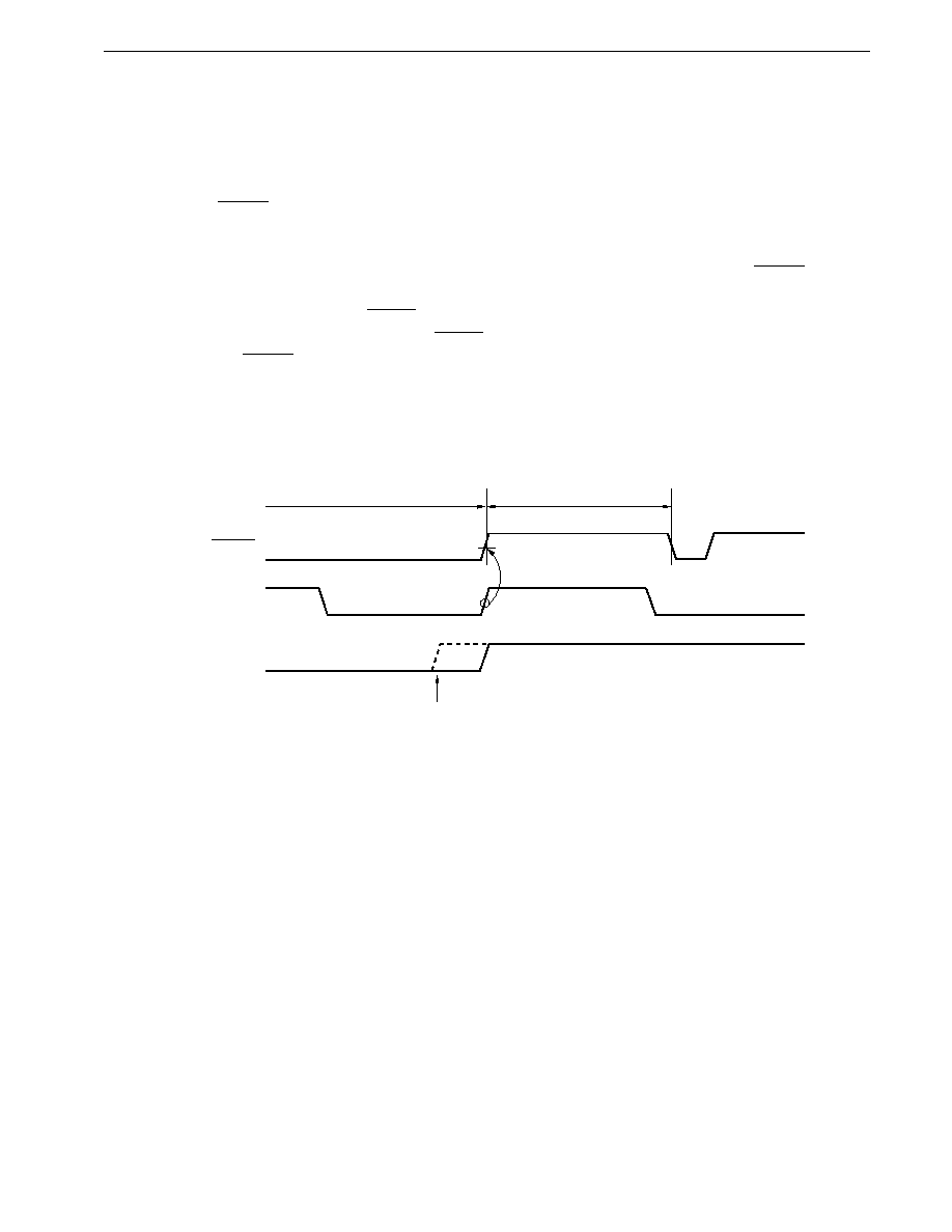
633
CHAPTER 24 LOCAL BUS INTERFACE FUNCTION
Preliminary User's Manual U13987EJ1V0UM00
(2) Self-refresh operation
This mode is used to retain the contents of pseudo-static RAM in standby mode.
(a) Self-refresh operation mode setting
When bit 4 (RFEN) of the refresh mode (RFM) register is set to "1", and bit 7 (RFLV) to "0", a low level is output
from the REFRQ pin, and the self-refresh operation mode is specified for the pseudo-static RAM.
(b) Return from self-refresh operation
Refresh pulse output to the pseudo-static RAM is disabled approximately 200 ns
Note
after the REFRQ pin output
level changes from low to high. Therefore, the
�
PD784938 arranges for refresh pulses not to be output during
the disabled time by raising the REFRQ pin in synchronization with the refresh timing counter.
To enable this low-to-high transition of the REFRQ pin level to be recognized, the RFLV bit read level is set (to
1) when the REFRQ pin level changes from low to high.
Note This time varies according to the speed rank, etc. of the pseudo-static RAM.
Figure 24-19. Timing for Return from Self-Refresh Operation
Approximately min. 200 ns
Note
REFRQ
RFLV bit
Software set operation execution
Self refresh mode
Refresh timing
counter output
Note Refreshing disabled time
634
CHAPTER 24 LOCAL BUS INTERFACE FUNCTION
Preliminary User's Manual U13987EJ1V0UM00
24.4 Bus Hold Function
The bus hold function is provided for the connection of a device that functions as the bus master, such as a DMA controller.
In response to a request from the bus master device, all local bus interface pins are set to high impedance (except HLDAK),
and local bus interface mastership is passed to that device.
The bus hold function cannot be used when the external wait function or refresh function is used.
24.4.1 Hold mode register (HLDM)
HLDM is an 8-bit register that specifies enabling/disabling of the bus hold function. HLDM format is shown in Figure
24-20.
When RESET is input, HLDM is cleared to 00H, so that the bus hold function is disabled. The HLDRQ and HLDAK pins
are set to port mode and operate as the P66 and P67 pins.
Figure 24-20. Hold Mode Register (HLDM) Format
7
HLDE
HLDM
6
0
5
0
4
0
3
0
2
0
1
0
0
0
Disabled
Port
Enabled
HLDE
P66
P67
HLDRQ
HLDAK
1
0
Address
After reset
R/W
R/W
00H
0FFC5H
Bus Hold Enabling/Disabling
Caution The bus hold function must be disabled when the external wait function or refresh function is used.
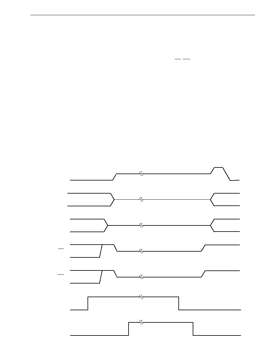
635
CHAPTER 24 LOCAL BUS INTERFACE FUNCTION
Preliminary User's Manual U13987EJ1V0UM00
24.4.2 Operation
When the HLDE bit of the hold mode register (HLDM) is set (to 1), the bus hold function is enabled. When the bus hold
function is enabled, pins P66 and P67 operate as the HLDRQ and HLDAK pins respectively. The HLDRQ pin becomes
high-impedance, and the HLDAK pin outputs a low-level signal.
If a high-level signal is input to the HLDRQ pin when the bus hold function is enabled, at the end of the access operation
being executed the address bus (A8 to A19), address/data bus (AD0 to AD7), RD, WR, and ASTB pins are all set to high-
impedance, the HLDAK pin output level is driven high, and the hold mode is established.
While the HLDAK pin is high (in the hold mode) the
�
PD784938 does not use the local bus interface, and therefore an
external DMA controller, etc. is free to access the memory.
When the HLDRQ pin input level changes from high to low, the hold mode is released, the HLDAK pin level changes
from high to low, and then the
�
PD784938 resumes use of the local bus.
A transition to the hold mode is performed between bus cycles, and the instruction being executed may be suspended.
Also, if a transition to the hold mode is made during execution of an instruction that does not use the local bus interface
when a program is fetched from the external memory, the
�
PD784938 continues execution of prefetched instructions until
it comes to an instruction that uses the local bus interface, and suspends instruction execution when there are no more
prefetched instructions. When the hold mode is released, execution of the suspended instruction is resumed from the point
at which it was suspended.
When a program is fetched from the internal ROM or RAM, execution of instructions until it comes to an instruction that
uses the local bus interface continues.
Figure 24-21. Hold Mode Timing
Hi-Z
Hi-Z
Hi-Z
Hi-Z
Hi-Z
Hi-Z
A8 to A19
ASTB
AD0 to AD7
RD
HLDRQ
HLDAK
WR

636
CHAPTER 24 LOCAL BUS INTERFACE FUNCTION
Preliminary User's Manual U13987EJ1V0UM00
24.5 Cautions
(1) When the bus hold function is used, the external wait function cannot be used (access wait control by means of the
WAIT pin), and 0, 1, or 2 waits must be selected for the entire space.
(2) The refresh function cannot be used when the bus hold function is used. In this case, ensure that refreshing is specified
as disabled.
(3) Do not set external wait to the internal ROM area. Otherwise, the CPU may be in the deadlock status which can be
cleared only by reset input.
(4) If the pseudo-static RAM refresh function is used when the address wait function is used, the refresh pulse is output
and, at the same time, the memory is accessed. Therefore, do not use the pseudo-static RAM refresh function when
using the address wait function.
Conversely do not use the address wait function when the pseudo-static RAM refresh function is used.

637
Preliminary User's Manual U13987EJ1V0UM00
CHAPTER 25 STANDBY FUNCTION
25.1 Configuration and Function
The
�
PD784938 has a standby function that enables the system power consumption to be reduced. The standby function
includes three modes as follows:
�
HALT mode........ In this mode the CPU operating clock is stopped. Intermittent operation in combination with the
normal operation mode enables the total system power consumption to be reduced.
�
IDLE mode......... In this mode the oscillator continues operating while the entire remainder of the system is stopped.
Normal program operation can be restored at a low power consumption close to that of the STOP
mode and in a time equal to that of the HALT mode.
�
STOP mode........In this mode the oscillator is stopped and the entire system is stopped.
Ultra-low power consumption can be achieved, consisting of leakage current only.
These modes are set by software. The standby mode (STOP/IDLE/HALT mode) transition diagram is shown in Figure
25-1, and the standby function block diagram in Figure 25-2.
Figure 25-1. Standby Mode Transition Diagram
Wait of
oscillation
stabilization
Program
operation
Macro
service
Macro service request
End of 1st service
End of macro service
Macro service request
End of 1st service
STOP setting
RESET input
INTW
Notes 1, 3
,
NMI, INTP4, INTP5 input
Note 1
IDLE setting
RESET input
INTW
Notes 1, 3
, NMI, INTP4, INTP5 input
Note 1
Interrupt request
Note 2
RESET input
HALT setting
Masked interrupt
request
HALT
(standby)
IDLE
(standby)
STOP
(standby)
End of oscillation stabilization time
Notes 1. When INTW, INTP4, and INTP5 are not masked
2. Unmasked interrupt request only
3. At subclock operation
Remark
Only external input is valid as NMI. The watchdog timer must not be used to release the standby mode (STOP,
IDLE, or HALT mode)
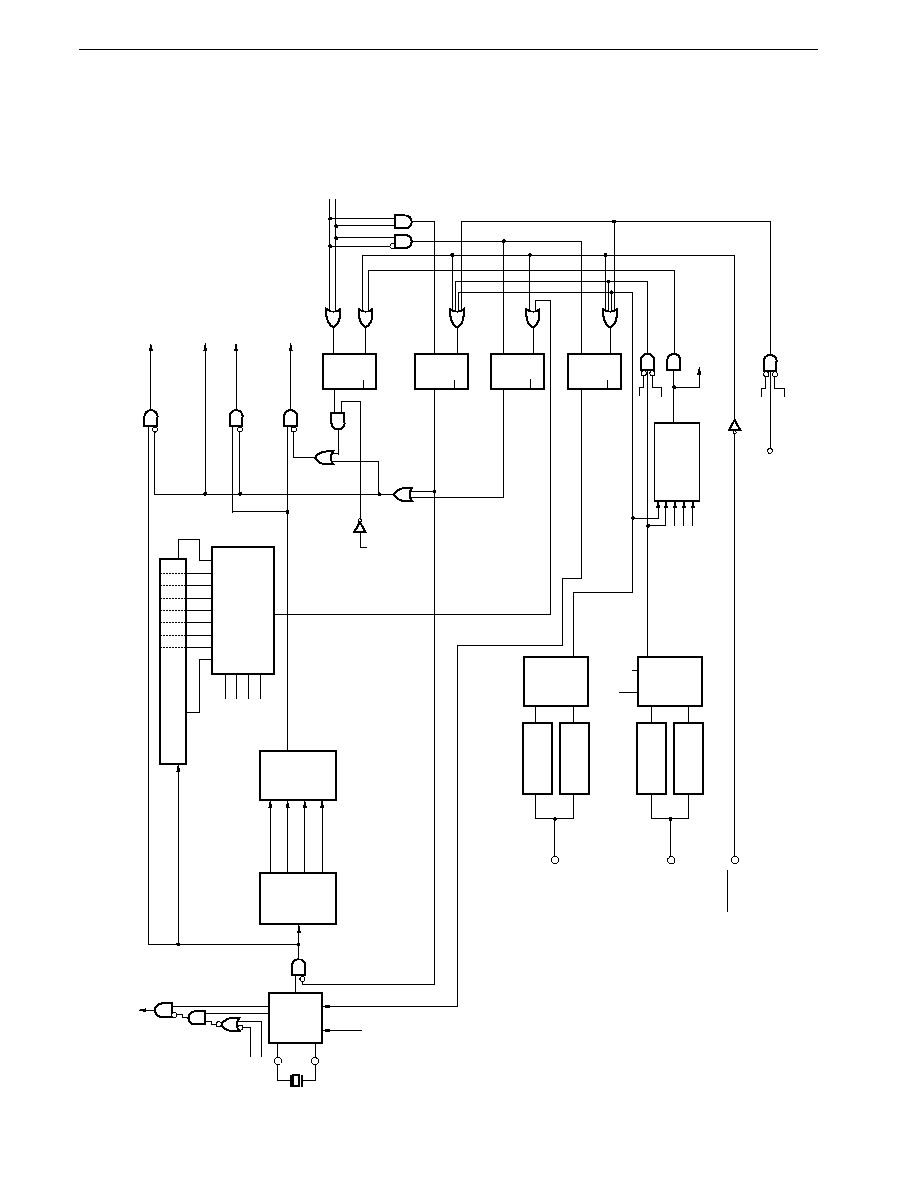
638
CHAPTER 25 STANDBY FUNCTION
Preliminary User's Manual U13987EJ1V0UM00
Figure 25-2. Standby Function Block Diagram
EXTC
System
cock
oscillator
fxx
fxx/2
fxx/4
fxx/8
Frequency
divider
Oscillation stabilization
timer (19)
OSTS0
OSTS1
OSTS2
EXTC
NMI
INTP4, INTP5
RESET
Rising edge
detection
Rising edge
detection
Falling edge
detection
Falling edge
detection
Selector
Selector
Selector
ESNMI
ES40, ES50
ES41, ES51
Interrupt
INTC
MK
ISM
Macro service
request
Selector
To peripheral circuit
RAM PROTECT
To peripheral circuit
CPU CLK
HLT F/F
IDLE F/F
STP F/F2
STP F/F1
Macro service
request
HALT bit setting
STOP bit setting
Q
S
R
Q
Q
S
R
Q
Q
S
R
Q
Q
S
R
Q
Valid edge
fxx
MK
ISM
INTW
WM3
To watch timer
after division by 128
WM6

639
CHAPTER 25 STANDBY FUNCTION
Preliminary User's Manual U13987EJ1V0UM00
25.2 Control Registers
25.2.1 Standby control register (STBC)
STBC is used to select the STOP mode setting and the internal system clock.
To prevent entry into standby mode due to an inadvertent program loop, STBC can only be written to with a dedicated
instruction. This dedicated instruction, MOV STBC, #byte, has a special code configuration (4 bytes), and a write is only
performed if the 3rd and 4th bytes of the operation code are mutual complements of 1.
If the 3rd and 4th bytes of the operation code are not mutual complements of 1, a write is not performed and an operand
error interrupt is generated. In this case, the return address saved in the stack area is the address of the instruction that
was the source of the error, and thus the address that was the source of the error can be identified from the return address
saved in the stack area.
If recovery from an operand error is simply performed by means of an RETB instruction, an endless loop will result.
As an operand error interrupt is only generated in the event of an inadvertent program loop (with the NEC assembler,
RA78K4, only the correct dedicated instruction is generated when MOV STBC, #byte is written), system initialization should
be performed by the program.
Other write instructions (MOV STBC, A, AND STBC, #byte, SET1 STBC.7, etc.) are ignored and do not perform any
operation. That is, a write is not performed to STBC, and an interrupt such as an operand error interrupt is not generated.
STBC can be read at any time by a data transfer instruction.
RESET input sets STBC to 30H.
The format of STBC is shown in Figure 25-3.
Caution Be sure to use a program that executes a NOP instruction three times to set the standby mode.
Example
MOV STBC, #byte; Sets standby mode
NOP
NOP
NOP
.
.
.
.
.
.

640
CHAPTER 25 STANDBY FUNCTION
Preliminary User's Manual U13987EJ1V0UM00
Figure 25-3. Standby Control Register (STBC) Format
SELOSC
0
CK1
CK0
�
0
STP
HLT
7
6
5
4
3
2
1
0
STBC
0FFC0H
Address
30H
After reset
R/W
R/W
STP
0
0
1
1
Operation Mode
Normal operation mode
HALT mode
STOP mode
IDLE mode
HLT
0
1
0
1
CK1
0
0
1
1
Internal System Clock Selection
f
XX
(12.58 MHz)
f
XX
/2 (6.29 MHz)
f
XX
/4 (3.15 MHz)
f
XX
/8 (1.57 MHz)
CK0
0
1
0
1
(f
XX
= 12.58 MHz)
SELOSC
0
1
Oscillation Frequency Control
6.29 MHz
12.58 MHz
Cautions 1.
The SELOSC bit must be overwritten after performing the next setting.
� Stop the IEBus (Set bit 7 (ENIEBUS) of the bus control register (BCR) to "0".)
� If the watch timer is operated with the main clock selected, stop the watch timer (Set bit 3 (WM3)
of the watch timer mode register (WM) to "0".)
2.
If the above settings are not performed, the IEBus and watch timer may perform incorrectly.
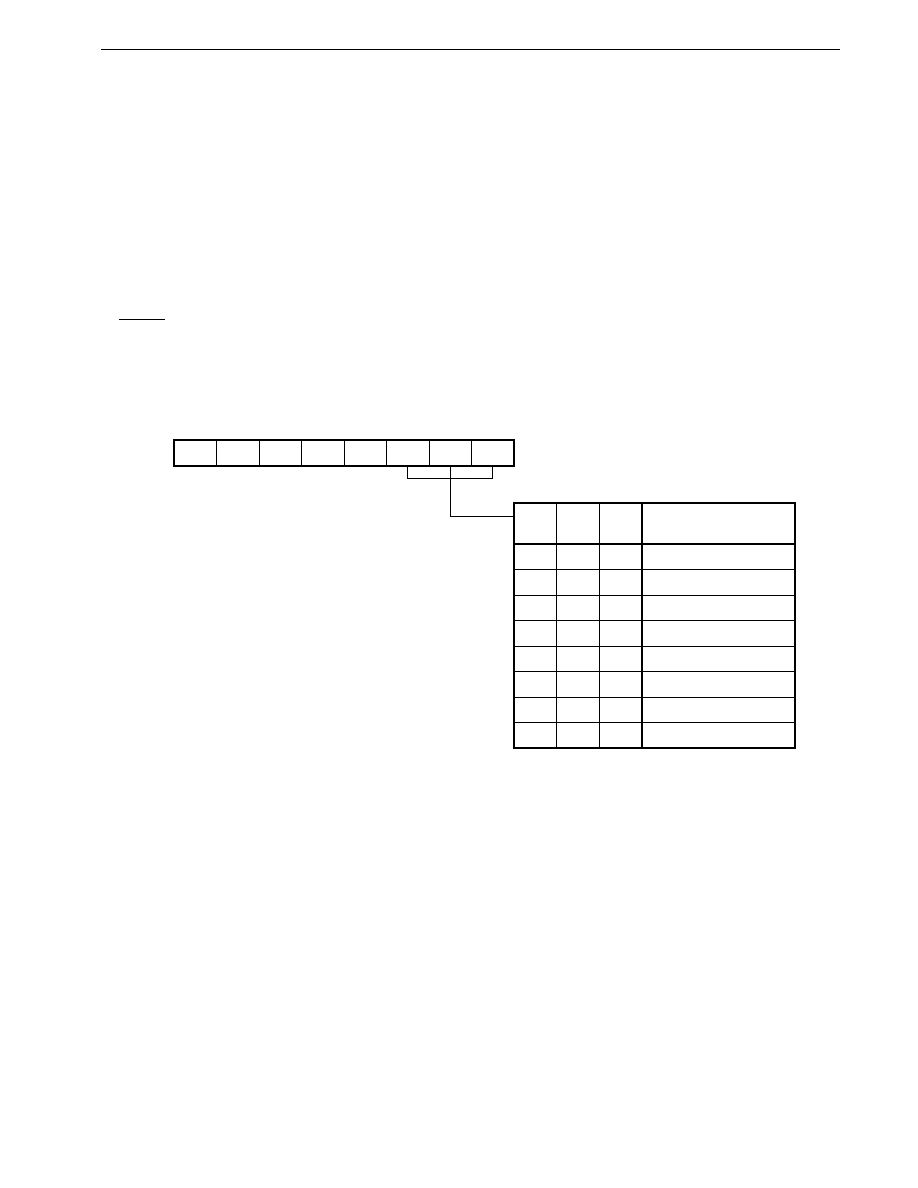
641
CHAPTER 25 STANDBY FUNCTION
Preliminary User's Manual U13987EJ1V0UM00
25.2.2 Oscillation stabilization time specification register (OSTS)
OSTS specifies the oscillator operation and the oscillation stabilization time when STOP mode is released. The EXTC
bit of OSTS specifies whether crystal/ceramic oscillation or an external clock is used. STOP mode can be set when external
clock input is used only when the EXTC bit is set (to 1).
Bits OSTS0 to OSTS2 of OSTS select the oscillation stabilization time when STOP mode is released. In general, an
oscillation stabilization time of at least 40 ms should be selected when a crystal resonator is used, and at least 4 ms when
a ceramic oscillator is used.
The time taken for oscillation stabilization is affected by the crystal resonator or ceramic resonator used, and the
capacitance of the connected capacitor. Therefore, if you want to set a short oscillation stabilization time, you should consult
the crystal resonator or ceramic resonator manufacturer.
OSTS can be written to only with an 8-bit transfer instruction.
RESET input clears OSTS to 00H.
The format of OSTS is shown in Figure 25-4.
Figure 25-4. Oscillation Stabilization Time Specification Register (OSTS) Format
0
0
0
0
0
OSTS2 OSTS1 OSTS0
7
6
5
4
3
2
1
0
OSTS
0FFCFH
Address
00H
After reset
R/W
R/W
2
19
/f
XX
(41.7 ms)
2
18
/f
XX
(20.8 ms)
2
17
/f
XX
(10.4 ms)
2
16
/f
XX
(5.2 ms)
2
15
/f
XX
(2.6 ms)
2
14
/f
XX
(1.3 ms)
2
13
/f
XX
(0.7 ms)
Setting prohibited
OSTS2
0
0
0
0
1
1
1
1
OSTS1
0
0
1
1
0
0
1
1
OSTS0
0
1
0
1
0
1
0
1
Oscillation Stabilization
Time Selection Bits
(f
XX
= 12.58 MHz)
Caution When using the regulator (Refer to CHAPTER 5 REGULATOR), set a value of at least 10.4 ms, taking
in consideration the regulator output stabilization time.
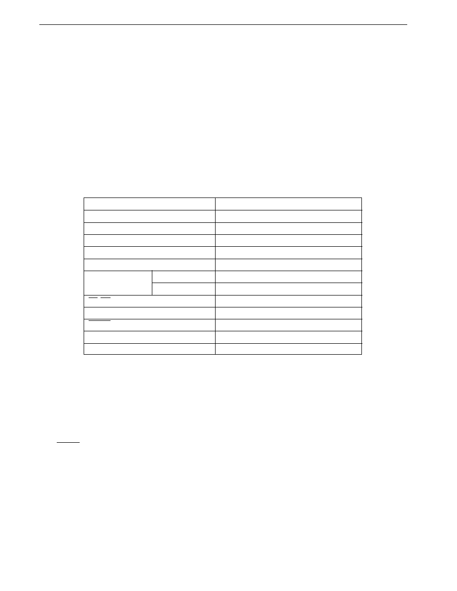
642
CHAPTER 25 STANDBY FUNCTION
Preliminary User's Manual U13987EJ1V0UM00
25.3 HALT Mode
25.3.1 HALT mode setting and operating status
The HALT mode is selected by setting (to 1) the HLT bit of the standby control (STBC) register.
The only writes that can be performed on STBC are 8-bit data writes by means of a dedicated instruction. HALT mode
setting is therefore performed by means of the "MOV STBC, #byte" instruction.
Caution If HALT mode setting is performed when a condition that releases HALT mode is in effect, HALT mode
is not entered, and execution of the next instruction, or a branch to a vectored interrupt service
program, is performed. To ensure that a definite HALT mode setting is made, interrupt requests should
be cleared (to 0), etc. before entering HALT mode.
Table 25-1. Operating Status in HALT Mode
Clock oscillator
Operating
Internal system clock
Operating
CPU
Operation stopped
Note
I/O lines
Retain status prior to HALT mode setting
Peripheral functions
Continue operating
Internal RAM
Retained
Bus lines
AD0 to AD7
High-impedance
A8 to A19
Retained
RD, WR output
High level
ASTB output
Low level
REFRQ output
Continue operating
HLDRQ input
Continue operating (input)
HLDAK output
Continue operating
Note Macro service processing is executed.
25.3.2 HALT mode release
HALT mode can be released by the following three sources.
�
Non-maskable interrupt request
�
Maskable interrupt request (vectored interrupt/context switching/macro service)
�
RESET input
Release sources and an outline of operations after release are shown in Table 25-2.

643
CHAPTER 25 STANDBY FUNCTION
Preliminary User's Manual U13987EJ1V0UM00
Table 25-2. HALT Mode Release and Operations after Release
Release Source
MK
Note 1
IE
Note 2
State on Release
Operation after Release
RESET input
�
�
--
Normal reset operation
Non-maskable
�
�
� Non-maskable interrupt service program
Interrupt request acknowledgment
interrupt request
not being executed
(NMI pin input/
� Low-priority non-maskable interrupt
watchdog timer)
service program being executed
� Service program for same request being
Execution of instruction after MOV STBC,
executed
#byte instruction (interrupt request that
� High-priority non-maskable interrupt
released HALT mode is held pending
Note 3
)
service program being executed
Maskable
0
1
� Interrupt service program not being
Interrupt request acknowledgment
interrupt request
executed
(excluding macro
� Low-priority maskable interrupt service
service request)
program being executed
� PRSL bit
Note 4
cleared (to 0) during execution
of priority level 3 interrupt service program
� Same-priority maskable interrupt service
Execution of instruction after MOV STBC,
program being executed
#byte instruction (interrupt request that
(If PRSL bit
Note 4
is cleared (to 0), excluding
released HALT mode is held pending
Note 3
)
execution of priority level 3 interrupt
service program)
� High-priority interrupt service program
being executed
0
0
--
1
�
--
HALT mode maintained
Macro service
0
�
--
Macro service processing execution
request
End condition not established
HALT
mode again
End condition established
If VCIE
Note 5
= 1: HALT mode again
If VCIE
Note 5
= 0: Same as release
by maskable interrupt request
1
�
--
HALT mode maintained
Notes 1. Interrupt mask bit in individual interrupt request source
2. Interrupt enable flag in program status word (PSW)
3. Pending interrupt requests are acknowledged when acknowledgment becomes possible.
4. Bit in interrupt mode control register (IMC)
5. Bit in macro service mode register of macro service control word in individual macro service request source

644
CHAPTER 25 STANDBY FUNCTION
Preliminary User's Manual U13987EJ1V0UM00
(1) Release by non-maskable interrupt
When a non-maskable interrupt is generate, the
�
PD784938 is released from HALT mode irrespective of whether the
interrupt acknowledgment enabled state (EI) or disabled state (DI) is in effect.
When the
�
PD784938 is released from HALT mode, if the non-maskable interrupt that released HALT mode can be
acknowledged, acknowledgment of that non-maskable interrupt is performed and a branch is made to the service
program. If the interrupt cannot be acknowledged, the instruction following the instruction that set the HALT mode (the
MOV STBC, #byte instruction) is executed, and the non-maskable interrupt that released the HALT mode is
acknowledged when acknowledgment becomes possible. See 23.6 Non-maskable Interrupt Acknowledgment
Operation for details of non-maskable interrupt acknowledgment.
(2) Release by maskable interrupt request
HALT mode release by a maskable interrupt request can only be performed by an interrupt for which the interrupt mask
flag is 0.
When HALT mode is released, if an interrupt can be acknowledged when the interrupt request enable flag (IE) is set
(to 1), a branch is made to the interrupt service program. If the interrupt cannot be acknowledged and if the IE flag
is cleared (to 0), execution is resumed from the instruction following the instruction that set the HALT mode. See 23.7
Maskable Interrupt Acknowledgment Operation for details of interrupt acknowledgment.
With macro service, HALT mode is released temporarily, service is performed once, then HALT mode is restored. When
macro service has been performed the specified number of times, HALT mode is released if the VCIC bit in the macro
service mode register of the macro service control word is cleared (to 0). The operation after release in this case is
the same as for release by a maskable interrupt described earlier. If the VCIE bit is set (to 1), the HALT mode is entered
again and is released by the next interrupt request.

645
CHAPTER 25 STANDBY FUNCTION
Preliminary User's Manual U13987EJ1V0UM00
Table 25-3. HALT Mode Release by Maskable Interrupt Request
Release Source
MK
Note 1
IE
Note 2
State on Release
Operation after Release
Maskable
0
1
� Interrupt service program not being
Interrupt request acknowledgment
interrupt request
executed
(excluding macro
� Low-priority maskable interrupt service
service request)
program being executed
� PRSL bit
Note 4
cleared (to 0) during execution
of priority level 3 interrupt service program
� Same-priority maskable interrupt service
Execution of instruction after MOV STBC,
program being executed
#byte instruction (interrupt request that
(If PRSL bit
Note 4
is cleared (to 0), excluding
released HALT mode is held pending
Note 3
)
execution of priority level 3 interrupt
service program)
� High-priority interrupt service program
being executed
0
0
--
1
�
--
HALT mode maintained
Macro service
0
�
--
Macro service processing execution
request
End condition not established
HALT
mode again
End condition established
If VCIE
Note 5
= 1: HALT mode again
If VCIE
Note 5
= 0: Same as release
by maskable interrupt request
1
�
--
HALT mode maintained
Notes 1. Interrupt mask bit in individual interrupt request source
2. Interrupt enable flag in program status word (PSW)
3. Pending interrupt requests are acknowledged when acknowledgment becomes possible.
4. Bit in interrupt mode control register (IMC)
5. Bit in macro service mode register of macro service control word in individual macro service request source
(3) Release by RESET input
The program is executed after branching to the reset vector address, as in a normal reset operation. However, internal
RAM contents retain their value directly before HALT mode was set.

646
CHAPTER 25 STANDBY FUNCTION
Preliminary User's Manual U13987EJ1V0UM00
25.4 STOP Mode
25.4.1 STOP mode setting and operating status
The STOP mode is selected by setting (to 1) the STP bit of the standby control register (STBC) register.
The only writes that can be performed on STBC are 8-bit data writes by means of a dedicated instruction. STOP mode
setting is therefore performed by means of the "MOV STBC, #byte" instruction.
Caution If the STOP mode is set when the condition to release the HALT mode is satisfied (refer to 25.3.2 HALT
mode release), the STOP mode is not set, but the next instruction is executed or execution branches
to a vectored interrupt service program. To accurately set the STOP mode, clear the interrupt request
before setting the STOP mode.
Table 25-4. Operating Status in STOP Mode
Clock oscillator
Oscillation stopped
Internal system clock
Stopped
CPU
Operation stopped
I/O lines
Retain state prior to STOP mode setting
Peripheral functions
All operation stopped
Note
Internal RAM
Retained
Bus lines
AD0 to AD7
High-impedance
A8 to A19
High-impedance
RD, WR output
High-impedance
ASTB output
High-impedance
REFRQ output
Retained
HLDRQ input
High-impedance
HLDAK output
Low level
Note A/D converter operation is stopped, but if the CS bit of the A/D converter mode register (ADM) is set (to 1), the
current consumption does not decrease.
Cautions 1.
If the STOP mode is set when the EXTC bit of the oscillation stabilization time specification (OSTS)
register is cleared (to 0), the X1 pin is shorted internally to V
SS
(GND potential) to suppress clock
generator leakage. Therefore, when the STOP mode is used in a system that uses an external clock,
the EXTC bit of OSTS must be set (to 1). If STOP mode setting is performed in a system to which
an external clock is input when the EXTC bit of OSTS is cleared (to 0), the
�
PD784938 may suffer
damage or reduced reliability.
When setting the EXTC bit of OSTS to 1, be sure to input a clock in phase reverse to that of the
clock input to the X1 pin, to the X2 pin (refer to 4.3.1 Clock oscillator).
2.
The CS bit of the A/D converter mode (ADM) register should be cleared (to 0).

647
CHAPTER 25 STANDBY FUNCTION
Preliminary User's Manual U13987EJ1V0UM00
25.4.2 STOP mode release
STOP mode is released by NMI input, INTP4 input, INTP5 input, INTW input, and RESET input.
Table 25-5. STOP Mode Release and Operations after Release
Release Source MK
Note 1
ISM
Note 2
IE
Note 3
State after Release
Operation after Release
RESET input
�
�
�
--
Normal reset operation
NMI pin input
�
�
�
� Non-maskable interrupt service
Interrupt request acknowledgment
program not being executed
� Low-priority non-maskable interrupt
service program being executed
� NMI pin input service program being
Execution of instruction after MOV
executed
STBC, #byte instruction (interrupt
� High-priority non-maskable interrupt
request that released STOP mode is
service program being executed
held pending
Note 4
)
INTP4/INTP5
0
0
1
� Interrupt service program not being
Interrupt request acknowledgment
pin input,
executed
INTW input
� Low-priority maskable interrupt service
program being executed
� PRSL bit
Note 5
cleared (to 0) during
execution of priority level 3 interrupt
service program
� Same-priority maskable interrupt
Execution of instruction after MOV
service program being executed
STBC, #byte instruction (interrupt
(If PRSL bit
Note 5
is cleared (to 0),
request that released STOP mode is
excluding execution of priority level 3
held pending
Note 4
)
interrupt service program)
� High-priority interrupt service program
being executed
0
0
0
--
1
0
�
--
STOP mode maintained
�
1
�
Notes 1. Interrupt mask bit in individual interrupt request source
2. Macro service enable flag in individual interrupt request source
3. Interrupt enable flag in program status word (PSW)
4. Pending interrupt requests are acknowledged when acknowledgment becomes possible.
5. Bit in interrupt mode control register (IMC)
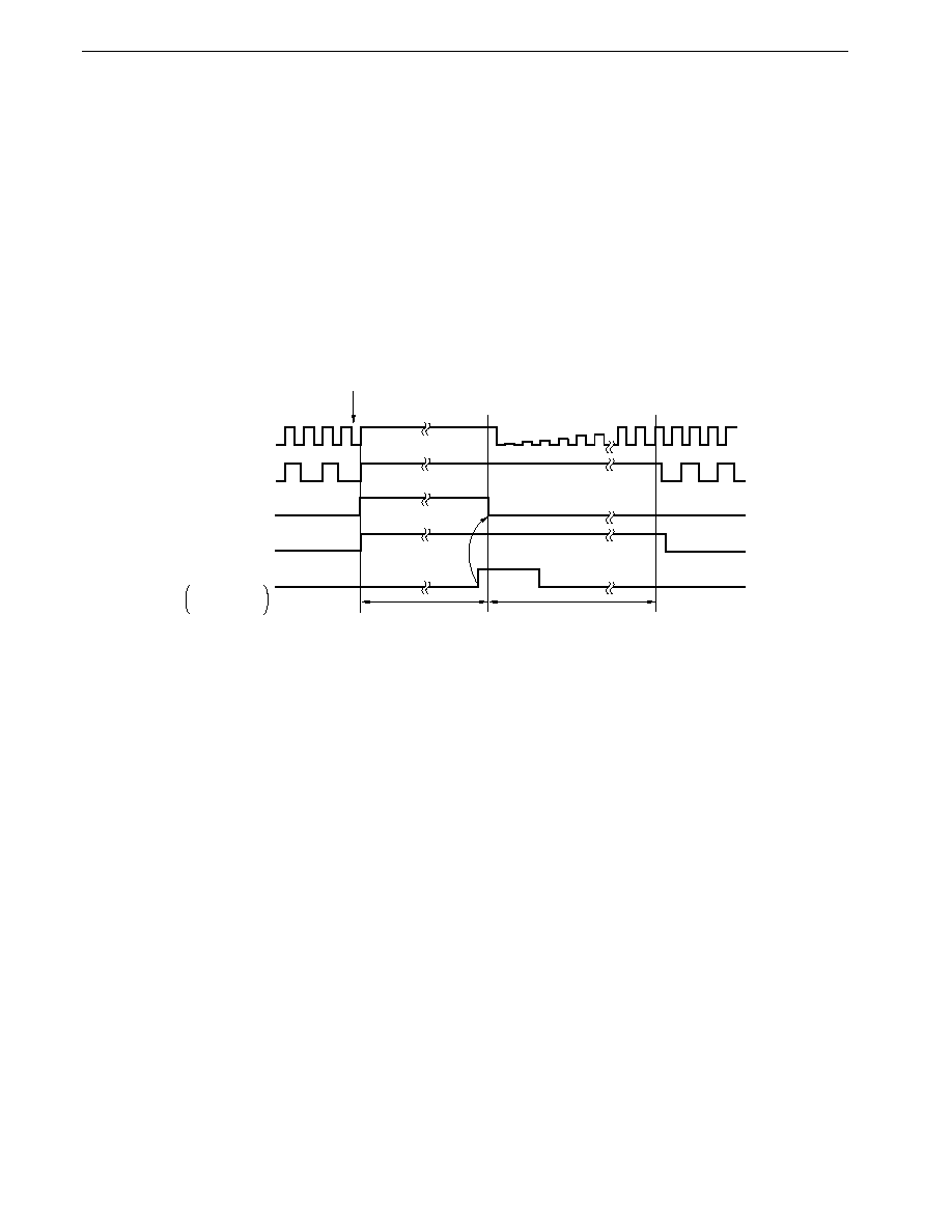
648
CHAPTER 25 STANDBY FUNCTION
Preliminary User's Manual U13987EJ1V0UM00
(1) STOP mode release by NMI input
The oscillator resumes oscillation when the valid edge specified by external interrupt mode register 0 (INTM0) is input
to the NMI input. STOP mode is released after the oscillation stabilization time specified by the oscillation stabilization
time specification register (OSTS).
When the
�
PD784938 is released from STOP mode, if a non-maskable interrupt by NMI pin input can be acknowledged,
a branch is made to the NMI interrupt service program. If the interrupt cannot be acknowledged (if the STOP mode
is set in an NMI interrupt service program, etc.), execution is resumed from the instruction following the instruction that
set the STOP mode, and a branch is made to the NMI interrupt service program when acknowledgment becomes
possible (by execution of an RETI instruction, etc.).
See 23.6 Non-maskable Interrupt Acknowledgment Operation for details of NMI interrupt acknowledgment.
Figure 25-5. STOP Mode Release by NMI Input
Oscillator
f
XX
/2
STP F/F1
NMI input
Rising edge
specified
STP F/F2
Oscillator stopped
STOP
Oscillation stabilization
count time
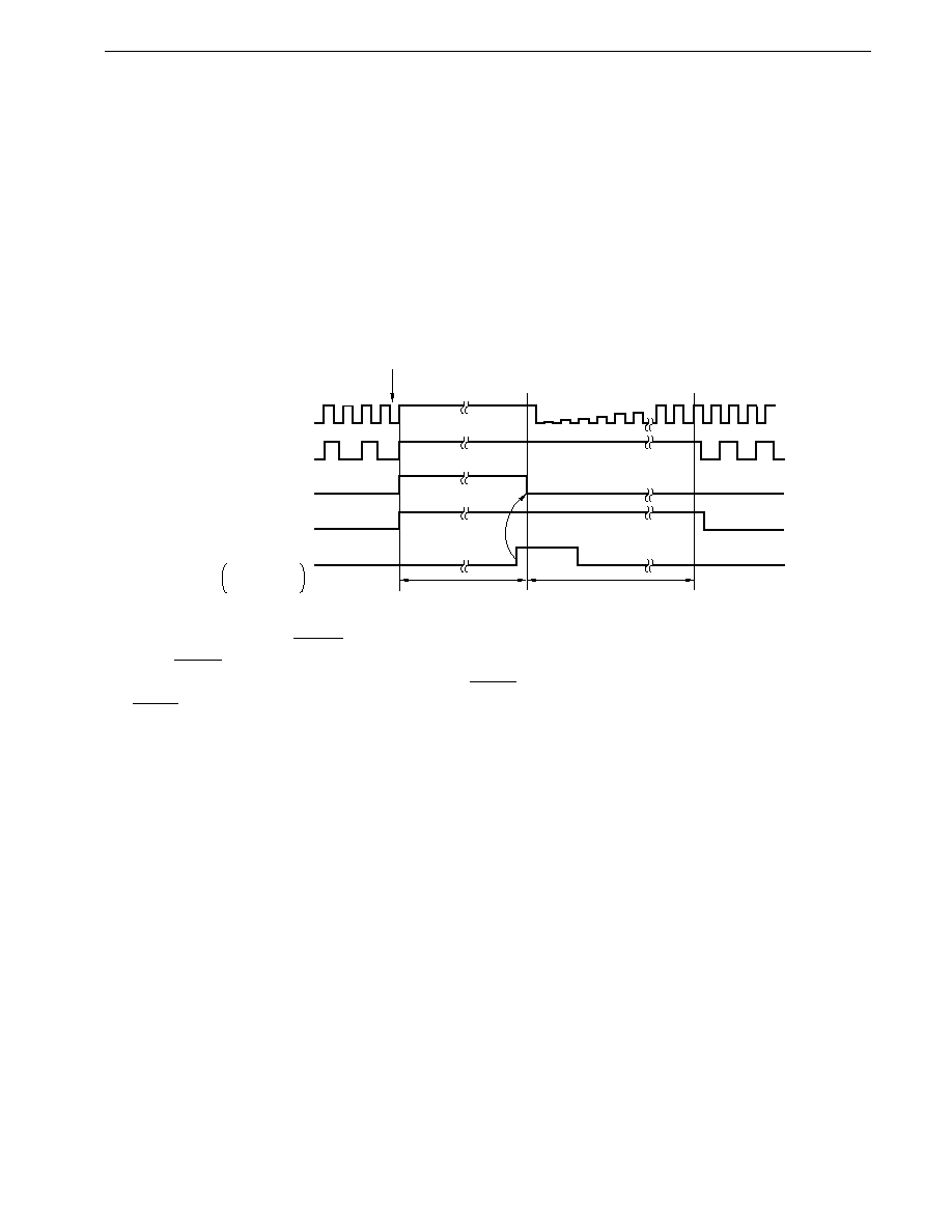
649
CHAPTER 25 STANDBY FUNCTION
Preliminary User's Manual U13987EJ1V0UM00
(2) STOP mode release by INTP4 or INTP5 input
When masking of interrupts by INTP4 and INTP5 input is released and macro service is disabled, the oscillator resumes
oscillation when the valid edge specified by external interrupt mode register 1 (INTM1) is input to the INTP4 or INTP5
input. Following this, STOP mode is released after the oscillation stabilization time specified by the oscillation
stabilization time specification register (OSTS) elapses.
When the
�
PD784938 is released from STOP mode, if an interrupt can be acknowledged when the interrupt enable
flag (IE) is set (to 1), a branch is made to the interrupt service program. If the interrupt cannot be acknowledged and
if the IE flag is cleared (to 0), execution is resumed from the instruction following the instruction that set the STOP mode.
See 23.7 Maskable Interrupt Acknowledgment Operation for details of interrupt acknowledgment.
Figure 25-6. STOP Mode Release by INTP4/INTP5 Input
INTP4, INTP5 input
Rising edge
specified
Oscillator
f
XX
/2
STP F/F1
STP F/F2
Oscillation stopped
STOP
Oscillation stabilization
count time
(3) STOP mode release by RESET input
When RESET input falls from high to low and the reset state is established, the oscillator resumes oscillation. The
oscillation stabilization time should be secured while RESET is active. Thereafter, normal operation is started when
RESET rises.
Unlike an ordinary reset operation, data memory retains its contents prior to STOP mode setting.
650
CHAPTER 25 STANDBY FUNCTION
Preliminary User's Manual U13987EJ1V0UM00
25.5 IDLE Mode
25.5.1 IDLE mode setting and operating status
The IDLE mode is selected by setting (to 1) both the STP bit and the HLT bit of the standby control (STBC) register.
The only writes that can be performed on the STBC are 8-bit data writes by means of a dedicated instruction. IDLE
mode setting is therefore performed by means of the "MOV STBC, #byte" instruction.
Caution If the IDLE mode is set when the condition to release the HALT mode is satisfied (refer to 25.3.2 HALT
mode release), the IDLE mode is not set, but the next instruction is executed or execution branches
to a vectored interrupt service program. To accurately set the IDLE mode, clear the interrupt request
before setting the IDLE mode.
Table 25-6. Operating States in IDLE Mode
Clock oscillator
Oscillation continued
Internal system clock
Stopped
CPU
Operation stopped
I/O lines
Retain state prior to IDLE mode setting
Peripheral functions
All operation excluding watch timer (WM3 = 1,
WM6 = 0) stopped
Note
Internal RAM
Retained
Bus lines
AD0 to AD7
High-impedance
A8 to A19
High-impedance
RD, WR output
High-impedance
ASTB output
High-impedance
REFRQ output
Retained
HLDRQ input
High-impedance
HLDAK output
Low level
Note A/D converter operation is stopped, but if the CS bit of the A/D converter mode register (ADM) is set, the current
consumption does not decrease.
Caution The CS bit of the A/D converter mode (ADM) register should be reset.

651
CHAPTER 25 STANDBY FUNCTION
Preliminary User's Manual U13987EJ1V0UM00
25.5.2 IDLE mode release
IDLE mode is released by NMI input, INTP4 input, INTP5 input, INTW input, or RESET input.
Table 25-7. IDLE Mode Release and Operations after Release
Release Source MK
Note 1
ISM
Note 2
IE
Note 3
State after Release
Operation after Release
RESET input
�
�
�
--
Normal reset operation
NMI pin input
�
�
�
� Non-maskable interrupt service
Interrupt request acknowledgment
program not being executed
� Low-priority non-maskable interrupt
service program being executed
� NMI pin input service program being
Execution of instruction after MOV
executed
STBC, #byte instruction (interrupt
� High-priority non-maskable interrupt
request that released IDLE mode is
service program being executed
held pending
Note 4
)
INTP4/INTP5
0
0
1
� Interrupt service program not being
Interrupt request acknowledgment
pin input,
executed
INTW input
� Low-priority maskable interrupt service
program being executed
� PRSL bit
Note 5
cleared (to 0) during
execution of priority level 3 interrupt
service program
� Same-priority maskable interrupt
Execution of instruction after MOV
service program being executed
STBC, #byte instruction (interrupt
(If PRSL bit
Note 5
is cleared (to 0),
request that released IDLE mode is
excluding execution of priority level 3
held pending
Note 4
)
interrupt service program)
� High-priority interrupt service program
being executed
0
0
0
--
1
0
�
--
IDLE mode maintained
�
1
�
Notes 1. Interrupt mask bit in individual interrupt request source
2. Macro service enable flag in individual interrupt request source
3. Interrupt enable flag in program status word (PSW)
4. Pending interrupt requests are acknowledged when acknowledgment becomes possible.
5. Bit in interrupt mode control register (IMC)

652
CHAPTER 25 STANDBY FUNCTION
Preliminary User's Manual U13987EJ1V0UM00
(1) IDLE mode release by NMI input
IDLE mode is released when the valid edge specified by external interrupt mode register 0 (INTM0) is input to the NMI
input.
When the
�
PD784938 is released from IDLE mode, if a non-maskable interrupt by NMI pin input can be acknowledged,
a branch is made to the NMI interrupt service program. If the interrupt cannot be acknowledged (if the IDLE mode
is set in an NMI interrupt service program, etc.), execution is resumed from the instruction following the instruction that
set the IDLE mode, and a branch is made to the NMI interrupt service program when acknowledgment becomes possible
(by execution of an RETI instruction, etc.).
See 23.6 Non-maskable Interrupt Acknowledgment Operation for details of NMI interrupt acknowledgment.
(2) IDLE mode release by INTP4 or INTP5 input
When masking of interrupts by INTP4 and INTP5 input is released and macro service is disabled, IDLE mode is released
when the valid edge specified by external interrupt mode register 1 (INTM1) is input to the INTP4 or INTP5 input.
When the
�
PD784938 is released from IDLE mode, if an interrupt can be acknowledged when the interrupt enable flag
(IE) is set (to 1), a branch is made to the interrupt service program. If the interrupt cannot be acknowledged and if
the IE flag is cleared (to 0), execution is resumed from the instruction following the instruction that set the IDLE mode.
See 23.7 Maskable Interrupt Acknowledgment Operation for details of interrupt acknowledgment.
(3) IDLE mode release by RESET input
When RESET input falls from high to low and the reset state is established, the oscillator resumes oscillation. The
oscillation stabilization time should be secured while RESET is active. Thereafter, normal operation is started when
RESET rises.
Unlike an ordinary reset operation, data memory retains its contents prior to IDLE mode setting.

653
CHAPTER 25 STANDBY FUNCTION
Preliminary User's Manual U13987EJ1V0UM00
25.6 Check Items when STOP Mode/IDLE Mode is Used
Check items required to reduce the current consumption when STOP mode/IDLE mode is used are shown below.
(1) Is the output level of each output pin appropriate?
The appropriate output level for each pin varies according to the next-stage circuit. You should select the output level
that minimizes the current consumption.
�
If high level is output when the input impedance of the next-stage circuit is low, a current will flow from the power
supply to the port, resulting in an increased current consumption. This applies when the next-stage circuit is a CMOS
IC, etc. When the power supply is off, the input impedance of a CMOS IC is low. In order to suppress the current
consumption, or to prevent an adverse effect on the reliability of the CMOS IC, low level should be output. If a high
level is output, latchup may result when power is turned on again.
�
Depending on the next-stage circuit, inputting low level may increase the current consumption. In this case, high-
level or high-impedance output should be used to reduce the current consumption.
�
If the next-stage circuit is a CMOS IC, the current consumption of the CMOS IC may increase if the output is made
high-impedance when power is supplied to it (the CMOS IC may also be overheated and damaged). In this case
you should output an appropriate level, or pull the output high or low with a resistor.
The method of setting the output level depends on the port mode.
�
When a port is in control mode, the output level is determined by the status of the on-chip hardware, and therefore
the on-chip hardware status must be taken into consideration when setting the output level.
�
In port mode, the output level can be set by writing to the port output latch and port mode register by software.
When a port is in control mode, its output level can be set easily by changing to port mode.
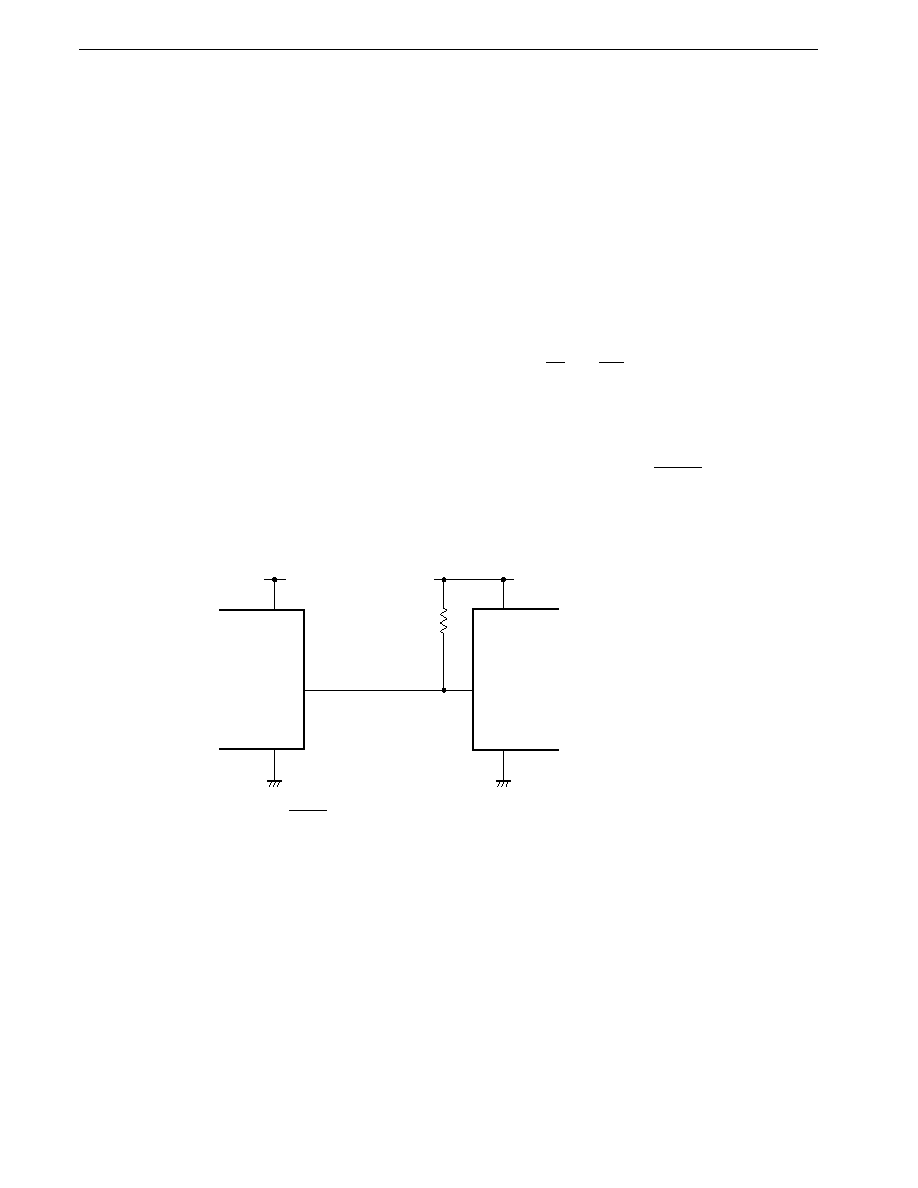
654
CHAPTER 25 STANDBY FUNCTION
Preliminary User's Manual U13987EJ1V0UM00
(2) Is the input pin level appropriate?
The voltage level input to each pin should be in the range between V
SS
potential and V
DD
potential. If a voltage outside
this range is applied, the current consumption will increase and the reliability of the
�
PD784938 may be adversely
affected.
Also ensure that an intermediate potential is not applied.
(3) Are pull-up resistors necessary?
An unnecessary pull-up resistor will increase the current consumption and cause a latchup of other devices. A mode
should be specified in which pull-up resistors are used only for parts that require them.
If there is a mixture of parts that do and do not require pull-up resistors, for parts that do, you should connect a pull-
up resistor externally and specify a mode in which the on-chip pull-up resistor is not used.
(4) Is processing of the address bus, address/data bus, etc., appropriate?
In STOP mode and IDLE mode, the address bus, address/data bus, RD and WR pins become high-impedance.
Normally, these pins are pulled high with a pull-up resistor. If this pull-up resistor is connected to the backed-up power
supply, then if the input impedance of circuitry connected to the non-backed-up power supply is low, a current will flow
through the pull-up resistor, and the current consumption will increase. Therefore, the pull-up resistor should be
connected to the non-backed-up power supply side as shown in Figure 25-7.
Also, in STOP mode and IDLE mode the ASTB pin also becomes high impedance, and the REFRQ/HLDAK pin adopts
a fixed level. Countermeasures should be taken with reference to the points noted in (to 1).
Figure 25-7. Example of Address/Data Bus Processing
V
DD
V
DD
IN/OUT
CMOS IC, etc.
V
SS
V
SS
Non-backed-up power supply
ADn
(n = 0 to 7)
�
PD784938
Backed-up power supply
The voltage level input to the WAIT/HLDRQ pin should be in the range between V
SS
potential and V
DD
potential. If
a voltage outside this range is applied, the current consumption will increase and the reliability of the
�
PD784938 may
be adversely affected.
(5) A/D converter
The current flowing to the AV
DD
, AV
REF1
pins can be reduced by clearing (0) the CS bit (bit 7) of the A/D converter mode
register (ADM). The current can be further reduced, if required, by cutting the current supply to the AV
DD
, AV
REF1
pins
with external circuitry.
Make sure that the AV
DD
pin is not at the same potential as the V
DD
pin. Unless power is supplied to the AV
DD
pin in
the STOP mode, not only does the current consumption increase, but the reliability is also affected.

655
CHAPTER 25 STANDBY FUNCTION
Preliminary User's Manual U13987EJ1V0UM00
25.7 Cautions
(1) If HALT/STOP/IDLE mode (standby mode hereafter) setting is performed when a condition that release HALT mode
(refer to 25.3.2 HALT mode release) is satisfied, standby mode is not entered, and execution of the next instruction,
or a branch to a vectored interrupt service program, is performed. To ensure that a definite standby mode setting is
made, interrupt requests should be cleared, etc. before entering standby mode.
(2) When crystal/ceramic oscillation is used, the EXTC bit must be cleared (to 0) before use. If the EXTC bit is set (to
1), oscillation will stop.
(3) If the STOP mode is set when the EXTC bit of the oscillation stabilization time specification (OSTS) register is cleared
(to 0), the X1 pin is shorted internally to V
SS
(GND potential) to suppress clock generator leakage. Therefore, when
the STOP mode is used in a system that uses an external clock, the EXTC bit of OSTS must be set (to 1). If STOP
mode setting is performed in a system to which an external clock is input when the EXTC bit of the OSTS is cleared
(to 0), the
�
PD784938 may suffer damage or reduced reliability.
When setting the EXTC bit of OSTS to 1, be sure to input a clock in phase reverse to that of the clock input to the X1
pin, to the X2 pin (refer to 4.3.1 Clock oscillator).
(4) In STOP mode and IDLE mode, the CS bit of the A/D converter mode ADM register should be cleared (to 0).

656
Preliminary User's Manual U13987EJ1V0UM00
[MEMO]
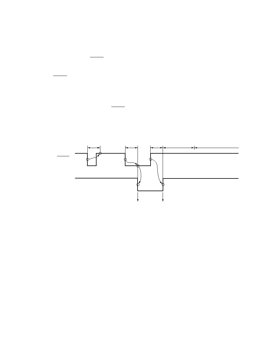
657
Preliminary User's Manual U13987EJ1V0UM00
CHAPTER 26 RESET FUNCTION
26.1 Reset Function
When low level is input to the RESET input pin, a system reset is affected, the various hardware units are set to the
states shown in Table 26-2, and all pins except the power supply pins and the X1 and X2 pins are placed in the high-
impedance state. Table 26-1 shows the pin statuses on reset and after reset release.
When the RESET input changes from low to high level, the reset state is released, the contents of address 00000H of
the reset vector table are set in bits 0 to 7 of the program counter (PC), the contents of address 00001H in bits 8 to 15,
and 0000B in bits 16 to 19, a branch is made, and program execution is started at the branch destination address. A reset
start can therefore be performed from any address in the base area.
The contents of the various registers should be initialized as required in the program in the base area.
To prevent misoperation due to noise, the RESET input pin incorporates an analog delay noise elimination circuit (see
Figure 26-1).
Figure 26-1. Reset Signal Acknowledgment
Delay PC initialization, etc.
Execution of instruction
at reset start address
Reset start
Delay
Delay
Reset end
Internal reset signal
RESET
(input)
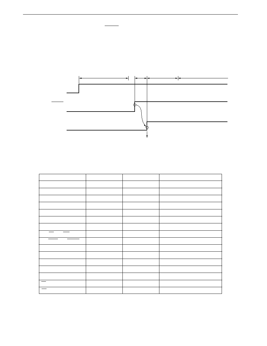
CHAPTER 26 RESET FUNCTION
658
Preliminary User's Manual U13987EJ1V0UM00
In a reset operation upon powering on, the RESET signal must be kept active until the oscillation stabilization time has
elapsed.
As the time taken for oscillation stabilization is influenced by the crystal oscillator/ceramic resonator used and the
capacitance of capacitor connected, please contact the manufacturer of the crystal oscillator/ceramic resonator for details.
Figure 26-2. Power-On Reset Operation
Oscillation stabilization time
V
DD
Delay PC initialization, etc.
Execution of instruction at
reset start address
Internal reset signal
Reset end
RESET
(input)
Remark
f
CLK
: Internal system clock frequency
Table 26-1. Pin Statuses During Reset Input and After Reset Release
Pin Name
Input/Output
On Reset
Directly After Reset Release
P00 to P07
Input/output
Hi-Z
Hi-Z (input port mode)
P10 to P17
Input/output
Hi-Z
Hi-Z (input port mode)
P20/NMI to P27/SI
Input
Hi-Z
Hi-Z (input port)
P30/RxD/SI1 to P37/TO3
Input/output
Hi-Z
Hi-Z (input port mode)
P40/AD0 to P47/AD7
Input/output
Hi-Z
Hi-Z (input port mode)
P50/A8 to P57/A15
Input/output
Hi-Z
Hi-Z (input port mode)
P60/A16 to P63/A19
Input/output
Hi-Z
Hi-Z (input port mode)
P64/RD, P65/WR
Input/output
Hi-Z
Hi-Z (input port mode)
P66/WAIT, P67/REFRQ
Input/output
Hi-Z
Hi-Z (input port mode)
P70/ANI0 to P77/ANI7
Input/output
Hi-Z
Hi-Z (input port mode)
P90 to P97
Input/output
Hi-Z
Hi-Z (input port mode)
P100 to P107/SO3
Input/output
Hi-Z
Hi-Z (input port mode)
ASTB/CLKOUT
Output
Hi-Z
0
PWM0, PWM1
Output
Hi-Z
Low level output
TX
Output
Hi-Z
Low level output
RX
Input
Hi-Z
Hi-Z (input port)

659
CHAPTER 26 RESET FUNCTION
Preliminary User's Manual U13987EJ1V0UM00
Table 26-2. Hardware Status After Reset (1/2)
Hardware
State After Reset
Program counter (PC)
Set with contents of reset
vector table (0000H/0001H).
Stack pointer (SP)
Undefined
Note
Program status word (PSW)
02H
On-chip RAM
Data memory
Undefined
Note
General-purpose registers
Ports
Ports 0, 1, 2, 3, 4, 5, 6, 7, 9, 10
Undefined (high impedance)
Port mode registers
PM0, 1, 3, 4, 5, 6, 7, 9, 10
FFH
Port mode control registers (PMC1, PMC3, PMC10)
00H
Pull-up resistor option register (PUOL, PUOH)
00H
Real-time output port control register (RTPC)
00H
Timer/counter
Timer counters (TM0, TM1W, TM2W, TM3W)
0000H
Compare registers (CR00, CR01, CR10LW, CR20W, CR30W)
Undefined
Capture registers (CR02, CR12W, CR22W)
Capture/compare registers (CR11W, CR21W)
Timer control registers (TMC0, TMC1)
00H
Timer output control register (TOC)
Capture/compare control registers
CRC0
10H
CRC1, CRC2
00H
Prescaler mode registers (PRM0, PRM1)
00H
One-shot pulse output control register (OSPC)
00H
PWM
PWM control register (PWMC)
05H
PWM prescaler register (PWPR)
00H
PWM modulo registers (PWM0, PWM1)
Undefined
A/D converter
A/D converter mode register (ADM)
00H
A/D conversion result register (ADCR)
Undefined
A/D current cut select register (IEAD)
00H
ROM correction
ROM correction address register H (CORAH)
00H
ROM correction address register L (CORAL)
0000H
ROM correction control register (CORC)
00H
Serial interface
Clocked serial interface mode registers (CSIM, CSIM1, CSIM2, CSIM3)
00H
Serial shift registers (SIO, SIO1, SIO2, SIO3)
Undefined
Asynchronous serial interface mode registers (ASIM, ASIM2)
00H
Asynchronous serial interface status registers (ASIS, ASIS2)
00H
Serial receive buffers (RXB, RXB2)
Undefined
Serial transmit shift registers (TXS, TXS2)
Undefined
Baud rate generator control registers (BRGC, BRGC2)
00H
Note When HALT mode, STOP mode, or IDLE mode is released by RESET input, the value before that mode was set
is retained.

CHAPTER 26 RESET FUNCTION
660
Preliminary User's Manual U13987EJ1V0UM00
Table 26-2. Hardware Status After Reset (2/2)
Hardware
State After Reset
Clock output function (CLOM)
00H
Watch timer mode register (WM)
00H
Memory extension mode register (MM)
20H
Programmable wait control registers
PWC1
AAH
PWC2
AAAAH
Refresh function
Refresh mode register (RFM)
00H
Refresh area specification register (RFA)
00H
Hold mode register (HLDM)
00H
Interrupts
Interrupt control registers (PIC0, PIC1, PIC2, PIC3, PIC4, PIC5, CIC00,
43H
CIC01, CIC10, CIC11, CIC20, CIC21, CIC30, ADIC, SERIC, SRIC,
STIC, SERIC2, SRIC2, STIC2, CSIIC, CSIIC1, CSIIC2, IEIC1, IEIC2,
WIC, CSIIC3)
Interrupt mask registers
MK0
FFFFH
MK1
FFH
In-service priority register (ISPR)
00H
Interrupt mode control register (IMC)
00H
External interrupt mode registers (INTM0, INTM1)
00H
Sampling clock selection register (SCS0)
00H
Standby control register (STBC)
30H
Oscillation stabilization time specification register (OSTS)
00H
Internal memory size switching register (IMS)
FFH
IEBus controller
Bus control register (BCR)
00H
Unit address register (UAR)
0000H
Slave address register (SAR)
Partner address register (PAR)
Control data register (CDR)
01H
Telegraph-length register (DLR)
Data register (DR)
00H
Unit status register (USR)
Interrupt status register (ISR)
Slave status register (SSR)
41H
Success count register (SCR)
01H
Communication count register (CCR)
20H
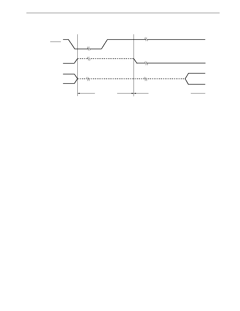
661
CHAPTER 26 RESET FUNCTION
Preliminary User's Manual U13987EJ1V0UM00
Figure 26-3. Reset Input Timing
Hi-Z
Other I/O ports
RESET
(input)
Hi-Z
ASTB (output)
Reset period
Reset release � instruction
execution period

CHAPTER 26 RESET FUNCTION
662
Preliminary User's Manual U13987EJ1V0UM00
26.2 Caution
Reset input when powering on must remain at the low level until oscillation stabilizes after the supply voltage has reached
the prescribed voltage.

663
Preliminary User's Manual U13987EJ1V0UM00
CHAPTER 27 ROM CORRECTION
27.1 ROM Correction Functions
�
PD784938 converts part of the program within the mask ROM into the program within the internal expansion ROM.
The use of ROM correction enables command bugs discovered in the mask ROM to be repaired, and change the flow
of the program.
ROM correction can be used in a maximum of four locations within the internal ROM (program).
Caution Note that ROM correction cannot perform emulation in the in-circuit emulator (IE-784000-R, IE-784000-
R-EM).
In more detail, the command addresses that require repair from the inactive memory connected to an external
microcontroller by a user program and the repair command codes are loaded into the peripheral RAM.
The above addresses and the internal ROM access addresses are compared by the comparator built into the
microcontroller during execution of internal ROM programs (during command fetch), and internal ROM's output data is then
converted to call command (CALLT) codes and output when a match is determined.
When the CALLT command codes are changed to valid commands by the CPU and executed, the CALLT table is
referenced, and the process routine and other peripheral RAM are branched. At this point, a CALLT table is prepared for
each repair address for referencing purposes. Four repair address can be set for the
�
PD784938.
Matches with address pointer 0:
CALLT table (0078H)
Conversion command code: FCH
Matches with address pointer 1:
CALLT table (007AH)
Conversion command code: FDH
Matches with address pointer 2:
CALLT table (007CH)
Conversion command code: FEH
Matches with address pointer 3:
CALLT table (007EH)
Conversion command code: FFH
Cautions 1. As it is necessary to reserve four locations for the CALLT tables when the ROM correction function
is used (0078H, 007AH, 007CH, 007EH), ensure that these are not used for other applications.
However, the CALLT tables can be used if the ROM correction function is not being used.
2. If there are two or more channels for which the correction operation is enabled, do not set the same
correction address.
3. Be sure to set the address where the start command code is stored as the correction address.
The differences between 78K/IV ROM correction and 78K/0 ROM correction are shown in Table 27-1.

664
CHAPTER 27 ROM CORRECTION
Preliminary User's Manual U13987EJ1V0UM00
Table 27-1. Differences between 78K/IV ROM Correction and 78K/0 ROM Correction
Difference
78K/IV
78K/0
Generated command codes
CALLT instruction
Peripheral RAM
(1-byte instruction:
FCH, FDH, FEH, FFH)
Address comparison conditions
Instruction fetch only
Instruction fetch only
Correction status flag
None
Yes
As there is a possibility that the
addresses match owing to an invalid
fetch, the status is not necessary
Jump destination address during correction
CALLT Table
Fixed address on the peripheral RAM
0078H, 007AH, 007CH, 007EH
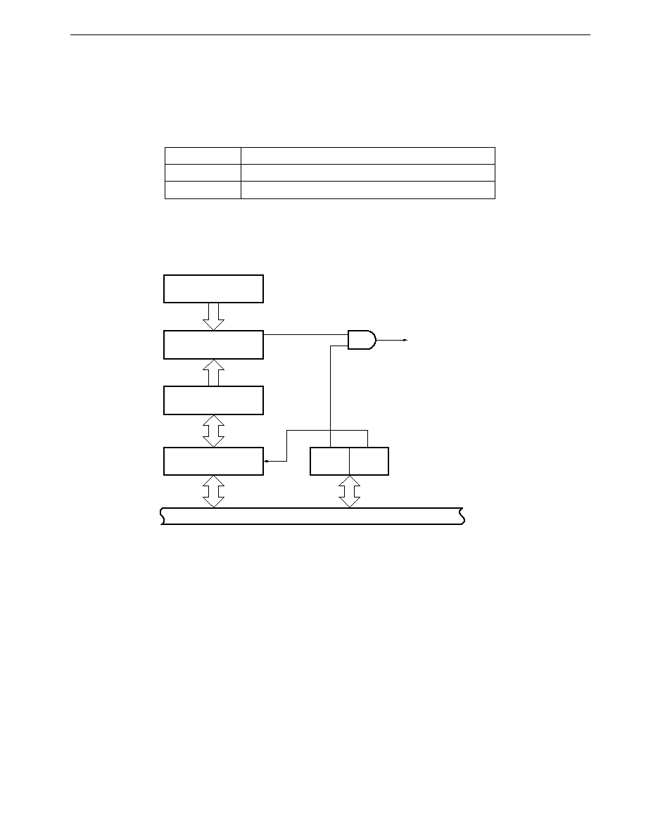
665
CHAPTER 27 ROM CORRECTION
Preliminary User's Manual U13987EJ1V0UM00
27.2 ROM Correction Configuration
ROM correction is composed of the following hardware.
Table 27-2. ROM Correction Configuration
Item
Configuration
Register
ROM correction address register H, L (CORAH, CORAL)
Control register
ROM correction control register (CORC)
A ROM correction block diagram is shown in Figure 27-1, and Figure 27-2 shows an example of memory mapping.
Figure 27-1. ROM Correction Block Diagram
Internal bus
Program counter (PC)
Comparator
Correction address
pointer n
ROM correction address
register (CORAH, CORAL)
Match
Correction branch
process request signal
(CALLT command)
ROM correction control register
(CORC)
CORENn CORCHm
Remark
n = 0 to 3, m = 0, 1

666
CHAPTER 27 ROM CORRECTION
Preliminary User's Manual U13987EJ1V0UM00
Figure 27-2. Memory Mapping Example (
�
PD784938)
Vector table area
Internal ROM
High-speed internal RAM
Peripheral RAM
(correction program)
SFR
Internal RAM
Internal ROM
(Reference table 3)
(Reference table 2)
(Reference table 1)
(Reference table 0)
CALLT
Table area
03FFFFH
00FFFFH
00FF00H
00FEFFH
00D600H
00D5FFH
000000H
000000H
00003FH
000040H
00007FH
00D600H
00FD00H
00FEFFH
00FCFFH

667
CHAPTER 27 ROM CORRECTION
Preliminary User's Manual U13987EJ1V0UM00
(1) ROM correction address register (CORAH, CORAL)
The register that sets the header address (correction address) of the command within the mask ROM that needs to
be repaired. A maximum of four program locations can be repaired with ROM correction. First of all, the channel is
selected with bit 0 (CORCH0) and bit 1 (CORCH1) of the ROM correction control register (CORC), and the address
is then set in the specified channel's address pointer when the address is written in CORAH and CORAL.
Figure 27-3. ROM Correction Address Register (CORAH, CORAL) Format
7
0
0
15
CORAL
CORAH
FF79H
Address
00H
After reset
R/W
R/W
FF7AH
Address
0000H
After reset
R/W
R/W
(2) Comparator
The ROM correction address registers H and L (CORAH, CORAL) normally compare the corrected address value with
the fetch register value. If any of the ROM correction control register (CORC) bits between bit 4 to bit 7 (COREN0
to 3) are 1 and the correct address matches the fetch address value, a table reference instruction (CALLT) is issued
from the ROM correction circuit.
27.3 Control Register for ROM Correction
ROM correction is controlled by the ROM correction control register (CORC).
(1) ROM correction control register (CORC)
The register that controls the issuance of the table reference instruction (CALLT) when the correct address set in ROM
correction address registers H and L (CORAH, CORAL) match the value of the fetch address.
This is composed of a correction enable flag (COREN0 to 3) that enables or disables match detection with the
comparator, and four channel correction pointers.
CORC is set with a 1-bit or 8-bit memory manipulation instruction.
RESET input sets CORC to 00H.

668
CHAPTER 27 ROM CORRECTION
Preliminary User's Manual U13987EJ1V0UM00
Figure 27-4. ROM Correction Control Register (CORC) Format
CORC
COREN3
7
6
5
4
3
2
1
COREN2
COREN1
COREN0
0
0
CORCH1
0
CORCH0
Address 0FF88H
R/W
After reset 00H
Symbol
CORENn
0
1
Controls the Match Detection for the ROM Correction
Address Register and the Fetch Address.
Disabled
Enabled
CORCH1
CORCH0
0
0
Address pointer channel 0
Address pointer channel 1
Address pointer channel 2
Address pointer channel 3
0
1
1
0
1
1
Channel Selection
Remark
n = 0 to 3
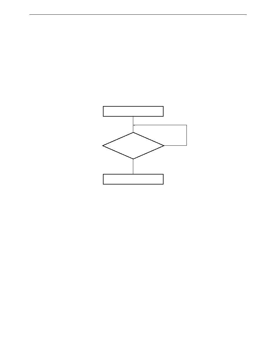
669
CHAPTER 27 ROM CORRECTION
Preliminary User's Manual U13987EJ1V0UM00
27.4 Use of ROM Correction
<1> The correct address and post-correction instruction (correction program) are stored in the microcontroller external
non-volatile memory (EEPROM).
<2> A substitute instruction is read from the non-volatile memory with the use of a serial interface when the initialization
program is running after being reset, and this is stored in the peripheral RAM and external memory. The correction
channel is then selected, the address for the command that requires correction is read and set in the ROM correction
address registers (CORAH, CORAL), and the correction enable flag (COREN0 to 3) is set at 1. A maximum of four
locations can be set.
<3> Execute the CALLT instruction during execution of the corrected address.
CALLT execution
Program execution (internal ROM)
Correct address executed?
No
Yes
<4> CALLT routine branch
When matched with address pointer 0: CALLT table (0078H)
When matched with address pointer 1: CALLT table (007AH)
When matched with address pointer 2: CALLT table (007CH)
When matched with address pointer 3: CALLT table (007EH)
<5> Execute substitute instruction
<6> Add +3 to the stack pointer (SP)
<7> Restore to any addresses with the branch instruction (BR)

670
CHAPTER 27 ROM CORRECTION
Preliminary User's Manual U13987EJ1V0UM00
27.5 Conditions for Executing ROM Correction
In order to use the ROM correction function, it is necessary for the external environment and program to satisfy the
following conditions.
(1) External environment
Must be connected externally to an non-volatile memory, and be configured to read that data.
(2) Target program
The data setting instruction for CORC, CORAH and CORAL will be previously annotated in the target program (program
stored in the ROM).
The set-up data (the items written in lower-case in the set-up example below) must be read from the external non-volatile
memory, and the correct number of required correction pointers must be set.
Example of four pointer settings
MOV
CORC,
#00H;
Specified channel 0
MOVW
CORAL, #ch0 datal;
Sets the channel 0 matching address
MOV
CORAH, #ch0 datah;
Sets the channel 0 matching address
MOV
CORC,
#01H;
Specified channel 1
MOVW
CORAL, #ch1 datal;
Sets the channel 1 matching address
MOV
CORAH, #ch1 datah;
Sets the channel 1 matching address
MOV
CORC,
#02H;
Specified channel 2
MOVW
CORAL, #ch2 datal;
Sets the channel 2 matching address
MOV
CORAH, #ch2 datah;
Sets the channel 2 matching address
MOV
CORC,
#chH;
Specified channel 3
MOV
CORAL, #ch3 datah;
Sets the channel 3 matching address
MOV
CORAH, #ch3 datal;
Sets the channel 3 matching address
MOV
CORC,
#romcor en
; Sets 00H when correction is disabled
; Sets F0H when correction is operated
BR
$NORMAL
BR
! ! COR ADDR;
Specifies the address of the correction program
;
NOMAL instruction ; next instruction
(3) Setting the branch instruction in the CALLT table.
In the case of the above program, the header address for the BR!!COR_ADDR instruction is specified. (COR ADDR
indicates the address where the correction program is located.)
The reason for this being branched into the CALLT instruction and BR instruction is owing to the fact that only the base
area can be branched with CALLT. There is no necessity to branch into two levels when it is to be attached to the RAM
base area with the LOCATION instruction.

671
Preliminary User's Manual U13987EJ1V0UM00
CHAPTER 28
�
PD78F4938 PROGRAMMING
The
�
PD78F4938 is a flash memory version of the
�
PD784938 Subseries.
The
�
PD78F4938 has on-chip flash memory that allows write, erase, and rewrite of programs in the state in which it
is mounted on the substrate. Table 28-1 shows the differences between the flash memory version (
�
PD78F4938) and the
mask ROM versions (
�
PD784935, 784936, 784937, and 784938).
Table 28-1. Differences between the
�
PD78F4938 Mask ROM Versions
Item
�
PD78F4938
Mask ROM Versions
Internal ROM type
Flash memory
Mask ROM
Internal ROM capacity
256 Kbytes
�
PD784935: 96 Kbytes
�
PD784936: 128 Kbytes
�
PD784937: 192 Kbytes
�
PD784938: 256 Kbytes
Internal RAM capacity
10,240 bytes
�
PD784935: 5,120 bytes
�
PD784936: 6,656 bytes
�
PD784937: 8,192 bytes
�
PD784938: 10,240 bytes
Internal memory size switching register (IMS)
Available
Not available
IC pin
Not available
Available
V
PP
pin
Available
Not available
Caution There are differences in noise immunity and noise radiation between the flash memory and mask ROM
versions. When pre-producing an application set with the flash memory version and then mass-
producing it with the mask ROM version, be sure to conduct sufficient evaluations for the commercial
samples (not engineering samples) of the mask ROM version.
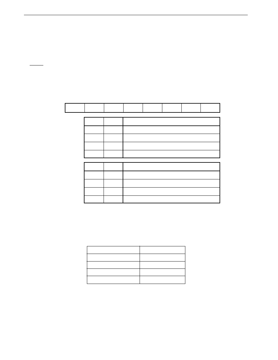
672
CHAPTER 28
�
PD78F4938 PROGRAMMING
Preliminary User's Manual U13987EJ1V0UM00
28.1 Internal Memory Size Switching Register (IMS)
IMS is a register to prevent a certain part of the internal memory from being used by software. By setting the IMS, it
is possible to establish a memory map that is the same as that of mask ROM version with a different internal memory (ROM,
RAM) with capacity.
IMS is set with an 8-bit memory manipulation instruction.
RESET input sets IMS to FFH.
Figure 28-1. Internal Memory Size Switching Register (IMS) Format
IMS
1
7
6
5
4
3
2
1
1
ROM1
ROM0
1
1
RAM1
0
RAM0
Address 0FFFCH
W
After reset FFH
Symbol
ROM1
ROM0
0
0
256 Kbytes
96 Kbytes
128 Kbytes
192 Kbytes
0
1
1
0
1
1
Internal ROM Capacity Selection
RAM1
RAM0
0
0
10,240 bytes
5,120 bytes
8,192 bytes
6,656 bytes
0
1
1
0
1
1
Internal RAM Capacity Selection
Caution IMS is not available for mask ROM versions (
�
PD784935, 784936, 784937, and 784938).
The IMS settings to create the same memory map as mask ROM versions are shown in Table 28-2.
Table 28-2. Internal Memory Size Switching Register (IMS) Settings
Relevant Mask ROM Version
IMS Setting
�
PD784935
DDH
�
PD784936
EEH
�
PD784937
FFH
�
PD784938
CCH
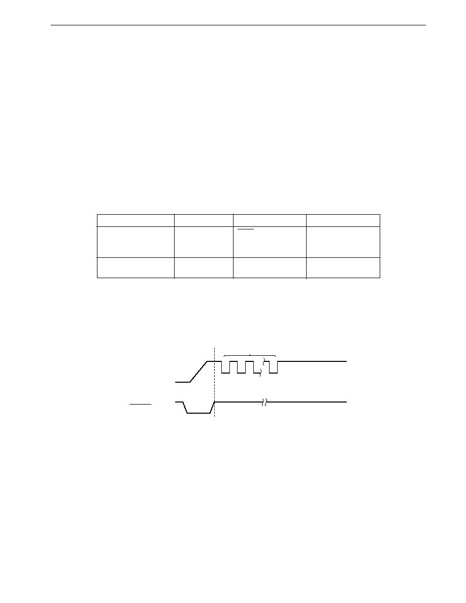
673
CHAPTER 28
�
PD78F4938 PROGRAMMING
Preliminary User's Manual U13987EJ1V0UM00
28.2 Flash Memory Programming Using Flashpro II and Flashpro III
Flash memory can be written while mounted on the target system (on-board writing). Connect the dedicated flash
programmer (Flashpro II (part number FL-PR2), Flashpro III (part number FL-PR3 and FG-FP3)) to the host computer and
target system for programming. Moreover, writing to flash memory can also be performed using a flash memory writing
adapter connected to Flashpro II or Flashpro III.
Remark
FL-PR2 and FL-PR3 are products of Naito Densei Machida Mfg. Co., Ltd.
28.2.1 Selecting communication mode
The Flashpro II or III is used to write data into a flash memory by serial communications. Select the communication
mode for writing from Table 28-3. Figure 28-2 shows the format used to select the communication mode. Each
communication mode is selected with the number of V
PP
pulses shown in Table 28-3.
Table 28-3. Communication Mode
Communication Mode Number of Channels
Pins Used
Number of V
PP
Pulses
3-wire serial I/O 1
SCK3/P105
1
SI3/P106
SO3/P107
UART 1
RxD/P30
8
TxD/P31
Caution Always select the communication mode using the number of V
PP
pulses shown in Table 28-3.
Figure 28-2. Communication Mode Selection Format
10 V
V
DD
V
SS
V
DD
V
SS
V
PP
RESET
1
2
n
V
PP
pulses
Flash memory write mode

674
CHAPTER 28
�
PD78F4938 PROGRAMMING
Preliminary User's Manual U13987EJ1V0UM00
28.2.2 Flash memory programming functions
By transmitting and receiving various commands and data by the selected communication mode, operations such as
writing to the flash memory are performed. Table 28-4 shows the major functions.
Table 28-4. Flash Memory Programming Functions
Function
Description
Batch erase
Erase the entire memory contents.
Block erase
Erase the contents of the specified memory block where one memory block is 16 Kbytes.
Batch blank check
Checks the erase state of the entire memory.
Block blank check
Checks the erase state of the specified block.
Data write
Writes to the flash memory based on the start write address and the number of data written (number of
bytes).
Batch verify
Compares the data input to the contents of the entire memory.
Block verify
Compares the data input to the contents of the specified memory block.
Verification for the flash memory entails supplying the data to be verified from an external source via a serial interface,
and then outputting the existence of unmatched data to the external source after referencing the blocks or all of the data.
Consequently, the flash memory is not equipped with a read function, and it is not possible for third parties to read the
contents of the flash memory with the use of the verification function.
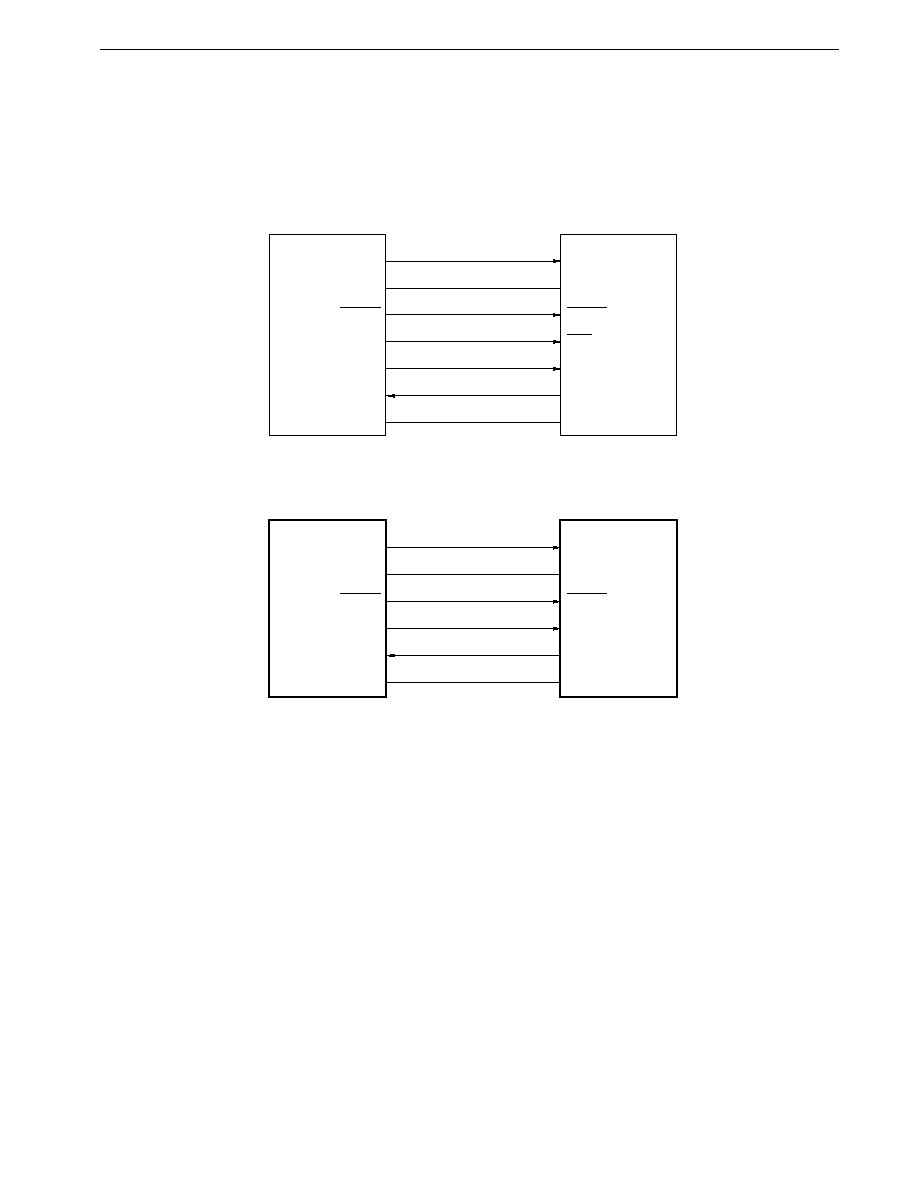
675
CHAPTER 28
�
PD78F4938 PROGRAMMING
Preliminary User's Manual U13987EJ1V0UM00
28.2.3 Connecting Flashpro II or Flashpro III
The connection between the Flashpro II or Flashpro III and the
�
PD78F4938 differs with the communication mode (3-
wire serial I/O or UART). Figures 28-3 and 28-4 are the connection diagrams in each case.
Figure 28-3. Flashpro II and Flashpro III Connection in 3-Wire Serial I/O Mode
V
PP
V
DD
RESET
SCK
SO
SI
V
SS
V
PP
V
DD
RESET
SCK
SI
SO
V
SS
Flashpro II or Flashpro III
PD78F4938
�
Figure 28-4. Flashpro II and Flashpro III Connection in UART Mode
V
PP
V
DD
RESET
SO
SI
V
SS
V
PP
V
DD
RESET
RxD
TxD
V
SS
Flashpro II or Flashpro III
PD78F4938
�

676
Preliminary User's Manual U13987EJ1V0UM00
[MEMO]

677
Preliminary User's Manual U13987EJ1V0UM00
CHAPTER 29 INSTRUCTION OPERATIONS
29.1 Conventions
(1) Operand identifiers and descriptions (1/2)
Identifier
Description
r, r'
Note 1
X (R0), A (R1), C (R2), B (R3), R4, R5, R6, R7, R8, R9, R10, R11, E (R12), D (R13), L (R14), H (R15)
r1
Note 1
X (R0), A (R1), C (R2), B (R3), R4, R5, R6, R7
r2
R8, R9, R10, R11, E (R12), D (R13), L (R14), H (R15)
r3
V, U, T, W
rp, rp'
Note 2
AX (RP0), BC (RP1), RP2, RP3, VP (RP4), UP (RP5), DE (RP6), HL (RP7)
rp1
Note 2
AX (RP0), BC (RP1), RP2, RP3
rp2
VP (RP4), UP (RP5), DE (RP6), HL (RP7)
rg, rg'
VVP (RG4), UUP (RG5), TDE (RG6), WHL (RG7)
sfr
Special function register symbol (see Special Function Register Application Table)
sfrp
Special function register symbol (register for which 16-bit operation is possible: see Special Function
Register Application Table)
post
Note 2
AX (RP0), BC (RP1), RP2, RP3, VP (RP4), UP (RP5)/PSW, DE (RP6), HL (RP7)
Multiple descriptions are permissible. However, UP is only used with PUSH/POP instructions, and PSW
with PUSHU/POPU instructions.
mem
[TDE], [WHL], [TDE+], [WHL+], [TDE�], [WHL�], [VVP], [UUP]: Register indirect addressing
[TDE+byte], [WHL+byte], [SP+byte], [UUP+byte], [VVP+byte]: Based addressing
imm24 [A], imm24 [B], imm24 [DE], imm24 [HL]: Indexed addressing
[TDE+A], [TDE+B], [TDE+C], [WHL+A], [WHL+B], [WHL+C],
[VVP+DE], [VVP+HL]: Based indexed addressing
mem1
All mem except [WHL+] and [WHL�]
mem2
[TDE], [WHL]
mem3
[AX], [BC], [RP2], [RP3], [VVP], [UUP], [TDE], [WHL]
Notes 1. Setting the RSS bit to 1 enables R4 to R7 to be used as X, A, C, and B, but this function should only be used
when using a 78K/III Series program.
2. Setting the RSS bit to 1 enables RP2 and RP3 to be used as AX and BC, but this function should only be
used when using a 78K/III Series program.

678
CHAPTER 29 INSTRUCTION OPERATIONS
Preliminary User's Manual U13987EJ1V0UM00
(1) Operand identifiers and descriptions (2/2)
Identifier
Description
Note
saddr, saddr'
FD20H to FF1FH immediate data or label
saddr1
FE00H to FEFFH immediate data or label
saddr2
FD20H to FDFFH, FF00H to FF1FH immediate data or label
saddrp
FD20H to FF1EH immediate data or label (16-bit operation)
saddrp1
FE00H to FEFFH immediate data or label (16-bit operation)
saddrp2
FD20H to FDFFH, FF00H to FF1EH immediate data or label (16-bit operation)
saddrg
FD20H to FEFDH immediate data or label (24-bit operation)
saddrg1
FE00H to FEFDH immediate data or label (24-bit operation)
saddrg2
FD20H to FDFFH immediate data or label (24-bit operation)
addr24
0H to FFFFFFH immediate data or label
addr20
0H to FFFFFH immediate data or label
addr16
0H to FFFFH immediate data or label
addr11
800H to FFFH immediate data or label
addr8
0FE00H to 0FEFFH
Note
immediate data or label
addr5
40H to 7EH immediate data or label
imm24
24-bit immediate data or label
word
16-bit immediate data or label
byte
8-bit immediate data or label
bit
3-bit immediate data or label
n
3-bit immediate data
locaddr
00H or 0FH
Note The addresses shown here apply when 00H is specified by the LOCATION instruction.
When 0FH is specified by the LOCATION instruction, F0000H should be added to the address values shown.

679
CHAPTER 29 INSTRUCTION OPERATIONS
Preliminary User's Manual U13987EJ1V0UM00
(2) Operand column symbols
Symbol
Description
+
Auto-increment
�
Auto-decrement
#
Immediate data
!
16-bit absolute address
!!
24-bit/20-bit absolute address
$
8-bit relative address
$!
16-bit relative address
/
Bit inversion
[ ]
Indirect addressing
[%]
24-bit indirect addressing
(3) Flag column symbols
Symbol
Description
(Blank)
No change
0
Cleared to 0
1
Set to 1
�
Set or cleared depending on result
P
P/V flag operates as parity flag
V
P/V flag operates as overflow flag
R
Previously saved value is restored
(4) Operation column symbols
Symbol
Description
jdisp8
Signed two's complement data (8 bits) indicating relative address distance between start address of
next instruction and branch address
jdisp16
Signed two's complement data (16 bits) indicating relative address distance between start address of
next instruction and branch address
PC
HW
PC bits 16 to 19
PC
LW
PC bits 0 to 15

680
CHAPTER 29 INSTRUCTION OPERATIONS
Preliminary User's Manual U13987EJ1V0UM00
(5) Number of bytes of instruction that includes mem in operands
mem Mode
Register Indirect Addressing
Based
Indexed
Based Indexed
Addressing
Addressing
Addressing
Number of bytes
1
2
Note
3
5
2
Note One-byte instruction only when [TDE], [WHL], [TDE+], [TDE�], [WHL+], or [WHL�] is written as mem in an MOV
instruction.
(6) Number of bytes of instruction that includes saddr, saddrp, r, or rp in operands
For some instructions that include saddr, saddrp, r, or rp in their operands, two "Bytes" entries are given, separated
by a slash ("/"). The entry that applies is shown in the table below.
Identifier
Left-Hand "Bytes" Figure
Right-Hand "Bytes" Figure
saddr
saddr2
saddr1
saddrp
saddrp2
saddrp1
r
r1
r2
rp
rp1
rp2
(7) Description of instructions that include mem in operands and string instructions
Operands TDE, WHL, VVP, and UUP (24-bit registers) can also be written as DE, HL, VP, and UP respectively.
However, they are still treated as TDE, WHL, VVP, and UUP (24-bit registers) when written as DE, HL, VP, and UP.

681
CHAPTER 29 INSTRUCTION OPERATIONS
Preliminary User's Manual U13987EJ1V0UM00
29.2 List of Operations
(1) 8-bit data transfer instruction: MOV
Mnemonic
Operands
Bytes
Operation
Flags
S
Z
AC P/V CY
MOV
r, #byte
2/3
r
byte
saddr, #byte
3/4
(saddr)
byte
sfr, #byte
3
sfr
byte
!addr16, #byte
5
(saddr16)
byte
!!addr24, #byte
6
(addr24)
byte
r, r'
2/3
r
r'
A, r
1/2
A
r
A, saddr2
2
A
(saddr2)
r, saddr
3
r
(saddr)
saddr2, A
2
(saddr2)
A
saddr, r
3
(saddr)
r
A, sfr
2
A
sfr
r, sfr
3
r
sfr
sfr, A
2
sfr
A
sfr, r
3
sfr
r
saddr, saddr'
4
(saddr)
(saddr')
r, !addr16
4
r
(addr16)
!addr16, r
4
(addr16)
r
r, !!addr24
5
r
(addr24)
!!addr24, r
5
(addr24)
r
A, [saddrp]
2/3
A
((saddrp))
A, [%saddrg]
3/4
A
((saddrg))
A, mem
1 to 5
A
(mem)
[saddrp], A
2/3
((saddrp))
A
[%saddrg], A
3/4
((saddrg))
A
mem, A
1 to 5
(mem)
A
PSWL, #byte
3
PSW
L
byte
�
�
�
�
�
PSWH, #byte
3
PSW
H
byte
PSWL, A
2
PSW
L
A
�
�
�
�
�
PSWH, A
2
PSW
H
A
A, PSWL
2
A
PSW
L
A, PSWH
2
A
PSW
H
r3, #byte
3
r3
byte
A, r3
2
A
r3
r3, A
2
r3
A

682
CHAPTER 29 INSTRUCTION OPERATIONS
Preliminary User's Manual U13987EJ1V0UM00
(2) 16-bit data transfer instruction: MOVW
Mnemonic
Operands
Bytes
Operation
Flags
S
Z
AC P/V CY
MOVW
rp, #word
3
rp
word
saddrp, #word
4/5
(saddrp)
word
sfrp, #word
4
sfrp
word
!addr16, #word
6
(addr16)
word
!!addr24, #word
7
(addr24)
word
rp, rp'
2
rp
rp'
AX, saddrp2
2
AX
(saddrp2)
rp, saddrp
3
rp
(saddrp)
saddrp2, AX
2
(saddrp2)
AX
saddrp, rp
3
(saddrp)
rp
AX, sfrp
2
AX
sfrp
rp, sfrp
3
rp
sfrp
sfrp, AX
2
sfrp
AX
sfrp, rp
3
sfrp
rp
saddrp, saddrp'
4
(saddrp)
(saddrp')
rp, !addr16
4
rp
(addr16)
!addr16, rp
4
(addr16)
rp
rp, !!addr24
5
rp
(addr24)
!!addr24, rp
5
(addr24)
rp
AX, [saddrp]
3/4
AX
((saddrp))
AX, [%saddrg]
3/4
AX
((saddrg))
AX, mem
2 to 5
AX
(mem)
[saddrp], AX
3/4
((saddrp))
AX
[%saddrg], AX
3/4
((saddrg))
AX
mem, AX
2 to 5
(mem)
AX
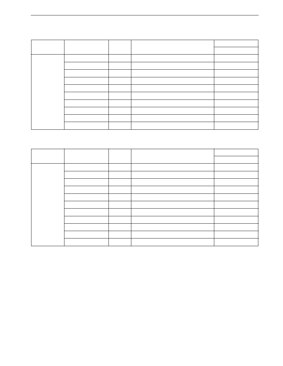
683
CHAPTER 29 INSTRUCTION OPERATIONS
Preliminary User's Manual U13987EJ1V0UM00
(3) 24-bit data transfer instruction: MOVG
Mnemonic
Operands
Bytes
Operation
Flags
S
Z
AC P/V CY
MOVG
rg, #imm24
5
rg
imm24
rg, rg'
2
rg
rg'
rg, !!addr24
5
rg
(addr24)
!!addr24, rg
5
(addr24)
rg
rg, saddrg
3
rg
(saddrg)
saddrg, rg
3
(saddrg)
rg
WHL, [%saddrg]
3/4
WHL
((saddrg))
[%saddrg], WHL
3/4
((saddrg))
WHL
WHL, mem1
2 to 5
WHL
(mem1)
mem1, WHL
2 to 5
(mem1)
WHL
(4) 8-bit data exchange instruction: XCH
Mnemonic
Operands
Bytes
Operation
Flags
S
Z
AC P/V CY
XCH
r, r'
2/3
r
r'
A, r
1/2
A
r
A, saddr2
2
A
(saddr2)
r, saddr
3
r
(saddr)
r, sfr
3
r
sfr
saddr, saddr'
4
(saddr)
(saddr')
r, !addr16
4
r
(addr16)
r, !!addr24
5
r
(addr24)
A, [saddrp]
2/3
A
((saddrp))
A, [%saddrg]
3/4
A
((saddrg))
A, mem
2 to 5
A
(mem)

684
CHAPTER 29 INSTRUCTION OPERATIONS
Preliminary User's Manual U13987EJ1V0UM00
(5) 16-bit data exchange instruction: XCHW
Mnemonic
Operands
Bytes
Operation
Flags
S
Z
AC P/V CY
XCHW
rp, rp'
2
rp
rp'
AX, saddrp2
2
AX
(saddrp2)
rp, saddrp
3
rp
(saddrp)
rp, sfrp
3
rp
sfrp
AX, [saddrp]
3/4
AX
((saddrp))
AX, [%saddrg]
3/4
AX
((saddrg))
AX, !addr16
4
AX
(addr16)
AX, !!addr24
5
AX
(addr24)
saddrp, saddrp'
4
(saddrp)
(saddrp')
AX, mem
2 to 5
AX
(mem)
(6) 8-bit operation instructions: ADD, ADDC, SUB, SUBC, CMP, AND, OR, XOR
Mnemonic
Operands
Bytes
Operation
Flags
S
Z
AC P/V CY
ADD
A, #byte
2
A, CY
A + byte
�
�
�
V
�
r, #byte
3
r, CY
r + byte
�
�
�
V
�
saddr, #byte
3/4
(saddr), CY
(saddr) + byte
�
�
�
V
�
sfr, #byte
4
sfr, CY
sfr + byte
�
�
�
V
�
r, r'
2/3
r, CY
r + r'
�
�
�
V
�
A, saddr2
2
A, CY
A + (saddr2)
�
�
�
V
�
r, saddr
3
r, CY
r + (saddr)
�
�
�
V
�
saddr, r
3
(saddr), CY
(saddr) + r
�
�
�
V
�
r, sfr
3
r, CY
r + sfr
�
�
�
V
�
sfr, r
3
sfr, CY
sfr + r
�
�
�
V
�
saddr, saddr'
4
(saddr), CY
(saddr) + (saddr')
�
�
�
V
�
A, [saddrp]
3/4
A, CY
A + ((saddrp))
�
�
�
V
�
A, [%saddrg]
3/4
A, CY
A + ((saddrg))
�
�
�
V
�
[saddrp], A
3/4
((saddrp)), CY
((saddrp)) + A
�
�
�
V
�
[%saddrg], A
3/4
((saddrg)), CY
((saddrg)) + A
�
�
�
V
�
A, !addr16
4
A, CY
A + (addr16)
�
�
�
V
�
A, !!addr24
5
A, CY
A + (addr24)
�
�
�
V
�
!addr16, A
4
(addr16), CY
(addr16) + A
�
�
�
V
�
!!addr24, A
5
(addr24), CY
(addr24) + A
�
�
�
V
�
A, mem
2 to 5
A, CY
A + (mem)
�
�
�
V
�
mem, A
2 to 5
(mem), CY
(mem) + A
�
�
�
V
�

685
CHAPTER 29 INSTRUCTION OPERATIONS
Preliminary User's Manual U13987EJ1V0UM00
Mnemonic
Operands
Bytes
Operation
Flags
S
Z
AC P/V CY
ADDC
A, #byte
2
A, CY
A + byte + CY
�
�
�
V
�
r, #byte
3
r, CY
r + byte + CY
�
�
�
V
�
saddr, #byte
3/4
(saddr), CY
(saddr) + byte + CY
�
�
�
V
�
sfr, #byte
4
sfr, CY
sfr + byte + CY
�
�
�
V
�
r, r'
2/3
r, CY
r + r' + CY
�
�
�
V
�
A, saddr2
2
A, CY
A + (saddr2) + CY
�
�
�
V
�
r, saddr
3
r, CY
r + (saddr) + CY
�
�
�
V
�
saddr, r
3
(saddr), CY
(saddr) + r + CY
�
�
�
V
�
r, sfr
3
r, CY
r + sfr + CY
�
�
�
V
�
sfr, r
3
sfr, CY
sfr + r + CY
�
�
�
V
�
saddr, saddr'
4
(saddr), CY
(saddr) + (saddr') + CY
�
�
�
V
�
A, [saddrp]
3/4
A, CY
A + ((saddrp)) + CY
�
�
�
V
�
A, [%saddrg]
3/4
A, CY
A + ((saddrg)) + CY
�
�
�
V
�
[saddrp], A
3/4
((saddrp)), CY
((saddrp)) + A + CY
�
�
�
V
�
[%saddrg], A
3/4
((saddrg)), CY
((saddrg)) + A + CY
�
�
�
V
�
A, !addr16
4
A, CY
A + (addr16) + CY
�
�
�
V
�
A, !!addr24
5
A, CY
A + (addr24) + CY
�
�
�
V
�
!addr16, A
4
(addr16), CY
(addr16) + A + CY
�
�
�
V
�
!!addr24, A
5
(addr24), CY
(addr24) + A + CY
�
�
�
V
�
A, mem
2 to 5
A, CY
A + (mem) + CY
�
�
�
V
�
mem, A
2 to 5
(mem), CY
(mem) + A + CY
�
�
�
V
�

686
CHAPTER 29 INSTRUCTION OPERATIONS
Preliminary User's Manual U13987EJ1V0UM00
Mnemonic
Operands
Bytes
Operation
Flags
S
Z
AC P/V CY
SUB
A, #byte
2
A, CY
A � byte
�
�
�
V
�
r, #byte
3
r, CY
r � byte
�
�
�
V
�
saddr, #byte
3/4
(saddr), CY
(saddr) � byte
�
�
�
V
�
sfr, #byte
4
sfr, CY
sfr � byte
�
�
�
V
�
r, r'
2/3
r, CY
r � r'
�
�
�
V
�
A, saddr2
2
A, CY
A � (saddr2)
�
�
�
V
�
r, saddr
3
r, CY
r � (saddr)
�
�
�
V
�
saddr, r
3
(saddr), CY
(saddr) � r
�
�
�
V
�
r, sfr
3
r, CY
r � sfr
�
�
�
V
�
sfr, r
3
sfr, CY
sfr � r
�
�
�
V
�
saddr, saddr'
4
(saddr), CY
(saddr) � (saddr')
�
�
�
V
�
A, [saddrp]
3/4
A, CY
A � ((saddrp))
�
�
�
V
�
A, [%saddrg]
3/4
A, CY
A � ((saddrg))
�
�
�
V
�
[saddrp], A
3/4
((saddrp)), CY
((saddrp)) � A
�
�
�
V
�
[%saddrg], A
3/4
((saddrg)), CY
((saddrg)) � A
�
�
�
V
�
A, !addr16
4
A, CY
A � (addr16)
�
�
�
V
�
A, !!addr24
5
A, CY
A � (addr24)
�
�
�
V
�
!addr16, A
4
(addr16), CY
(addr16) � A
�
�
�
V
�
!!addr24, A
5
(addr24), CY
(addr24) � A
�
�
�
V
�
A, mem
2 to 5
A, CY
A � (mem)
�
�
�
V
�
mem, A
2 to 5
(mem), CY
(mem) � A
�
�
�
V
�

687
CHAPTER 29 INSTRUCTION OPERATIONS
Preliminary User's Manual U13987EJ1V0UM00
Mnemonic
Operands
Bytes
Operation
Flags
S
Z
AC P/V CY
SUBC
A, #byte
2
A, CY
A � byte � CY
�
�
�
V
�
r, #byte
3
r, CY
r � byte � CY
�
�
�
V
�
saddr, #byte
3/4
(saddr), CY
(saddr) � byte � CY
�
�
�
V
�
sfr, #byte
4
sfr, CY
sfr � byte � CY
�
�
�
V
�
r, r'
2/3
r, CY
r � r' � CY
�
�
�
V
�
A, saddr2
2
A, CY
A � (saddr2) � CY
�
�
�
V
�
r, saddr
3
r, CY
r � (saddr) � CY
�
�
�
V
�
saddr, r
3
(saddr), CY
(saddr) � r � CY
�
�
�
V
�
r, sfr
3
r, CY
r � sfr � CY
�
�
�
V
�
sfr, r
3
sfr, CY
sfr � r � CY
�
�
�
V
�
saddr, saddr'
4
(saddr), CY
(saddr) � (saddr') � CY
�
�
�
V
�
A, [saddrp]
3/4
A, CY
A � ((saddrp)) � CY
�
�
�
V
�
A, [%saddrg]
3/4
A, CY
A � ((saddrg)) � CY
�
�
�
V
�
[saddrp], A
3/4
((saddrp)), CY
((saddrp)) � A � CY
�
�
�
V
�
[%saddrg], A
3/4
((saddrg)), CY
((saddrg)) � A � CY
�
�
�
V
�
A, !addr16
4
A, CY
A � (addr16) � CY
�
�
�
V
�
A, !!addr24
5
A, CY
A � (addr24) � CY
�
�
�
V
�
!addr16, A
4
(addr16), CY
(addr16) � A � CY
�
�
�
V
�
!!addr24, A
5
(addr24), CY
(addr24) � A � CY
�
�
�
V
�
A, mem
2 to 5
A, CY
A � (mem) � CY
�
�
�
V
�
mem, A
2 to 5
(mem), CY
(mem) � A � CY
�
�
�
V
�

688
CHAPTER 29 INSTRUCTION OPERATIONS
Preliminary User's Manual U13987EJ1V0UM00
Mnemonic
Operands
Bytes
Operation
Flags
S
Z
AC P/V CY
CMP
A, #byte
2
A � byte
�
�
�
V
�
r, #byte
3
r � byte
�
�
�
V
�
saddr, #byte
3/4
(saddr) � byte
�
�
�
V
�
sfr, #byte
4
sfr � byte
�
�
�
V
�
r, r'
2/3
r � r'
�
�
�
V
�
A, saddr2
2
A � (saddr2)
�
�
�
V
�
r, saddr
3
r � (saddr)
�
�
�
V
�
saddr, r
3
(saddr) � r
�
�
�
V
�
r, sfr
3
r � sfr
�
�
�
V
�
sfr, r
3
sfr � r
�
�
�
V
�
saddr, saddr'
4
(saddr) � (saddr')
�
�
�
V
�
A, [saddrp]
3/4
A � ((saddrp))
�
�
�
V
�
A, [%saddrg]
3/4
A � ((saddrg))
�
�
�
V
�
[saddrp], A
3/4
((saddrp)) � A
�
�
�
V
�
[%saddrg], A
3/4
((saddrg)) � A
�
�
�
V
�
A, !addr16
4
A � (addr16)
�
�
�
V
�
A, !!addr24
5
A � (addr24)
�
�
�
V
�
!addr16, A
4
(addr16) � A
�
�
�
V
�
!!addr24, A
5
(addr24) � A
�
�
�
V
�
A, mem
2 to 5
A � (mem)
�
�
�
V
�
mem, A
2 to 5
(mem) � A
�
�
�
V
�

689
CHAPTER 29 INSTRUCTION OPERATIONS
Preliminary User's Manual U13987EJ1V0UM00
Mnemonic
Operands
Bytes
Operation
Flags
S
Z
AC P/V CY
AND
A, #byte
2
A
A
byte
�
�
P
r, #byte
3
r
r
byte
�
�
P
saddr, #byte
3/4
(saddr)
(saddr)
byte
�
�
P
sfr, #byte
4
sfr
sfr
byte
�
�
P
r, r'
2/3
r
r
r'
�
�
P
A, saddr2
2
A
A
(saddr2)
�
�
P
r, saddr
3
r
r
(saddr)
�
�
P
saddr, r
3
(saddr)
(saddr)
r
�
�
P
r, sfr
3
r
r
sfr
�
�
P
sfr, r
3
sfr
sfr
r
�
�
P
saddr, saddr'
4
(saddr)
(saddr)
(saddr')
�
�
P
A, [saddrp]
3/4
A
A
((saddrp))
�
�
P
A, [%saddrg]
3/4
A
A
((saddrg))
�
�
P
[saddrp], A
3/4
((saddrp))
((saddrp))
A
�
�
P
[%saddrg], A
3/4
((saddrg))
((saddrg))
A
�
�
P
A, !addr16
4
A
A
(addr16)
�
�
P
A, !!addr24
5
A
A
(addr24)
�
�
P
!addr16, A
4
(addr16)
(addr16)
A
�
�
P
!!addr24, A
5
(addr24)
(addr24)
A
�
�
P
A, mem
2 to 5
A
A
(mem)
�
�
P
mem, A
2 to 5
(mem)
(mem)
A
�
�
P

690
CHAPTER 29 INSTRUCTION OPERATIONS
Preliminary User's Manual U13987EJ1V0UM00
Mnemonic
Operands
Bytes
Operation
Flags
S
Z
AC P/V CY
OR
A, #byte
2
A
A
byte
�
�
P
r, #byte
3
r
r
byte
�
�
P
saddr, #byte
3/4
(saddr)
(saddr)
byte
�
�
P
sfr, #byte
4
sfr
sfr
byte
�
�
P
r, r'
2/3
r
r
r'
�
�
P
A, saddr2
2
A
A
(saddr2)
�
�
P
r, saddr
3
r
r
(saddr)
�
�
P
saddr, r
3
(saddr)
(saddr)
r
�
�
P
r, sfr
3
r
r
sfr
�
�
P
sfr, r
3
sfr
sfr
r
�
�
P
saddr, saddr'
4
(saddr)
(saddr)
(saddr')
�
�
P
A, [saddrp]
3/4
A
A
((saddrp))
�
�
P
A, [%saddrg]
3/4
A
A
((saddrg))
�
�
P
[saddrp], A
3/4
((saddrp))
((saddrp))
A
�
�
P
[%saddrg], A
3/4
((saddrg))
((saddrg))
A
�
�
P
A, !addr16
4
A
A
(addr16)
�
�
P
A, !!addr24
5
A
A
(addr24)
�
�
P
!addr16, A
4
(addr16)
(addr16)
A
�
�
P
!!addr24, A
5
(addr24)
(addr24)
A
�
�
P
A, mem
2 to 5
A
A
(mem)
�
�
P
mem, A
2 to 5
(mem)
(mem)
A
�
�
P
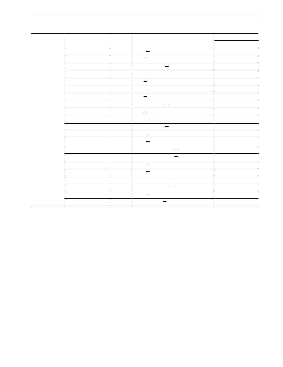
691
CHAPTER 29 INSTRUCTION OPERATIONS
Preliminary User's Manual U13987EJ1V0UM00
Mnemonic
Operands
Bytes
Operation
Flags
S
Z
AC P/V CY
XOR
A, #byte
2
A
A
byte
�
�
P
r, #byte
3
r
r
byte
�
�
P
saddr, #byte
3/4
(saddr)
(saddr)
byte
�
�
P
sfr, #byte
4
sfr
sfr
byte
�
�
P
r, r'
2/3
r
r
r'
�
�
P
A, saddr2
2
A
A
(saddr2)
�
�
P
r, saddr
3
r
r
(saddr)
�
�
P
saddr, r
3
(saddr)
(saddr)
r
�
�
P
r, sfr
3
r
r
sfr
�
�
P
sfr, r
3
sfr
sfr
r
�
�
P
saddr, saddr'
4
(saddr)
(saddr)
(saddr')
�
�
P
A, [saddrp]
3/4
A
A
((saddrp))
�
�
P
A, [%saddrg]
3/4
A
A
((saddrg))
�
�
P
[saddrp], A
3/4
((saddrp))
((saddrp))
A
�
�
P
[%saddrg], A
3/4
((saddrg))
((saddrg))
A
�
�
P
A, !addr16
4
A
A
(addr16)
�
�
P
A, !!addr24
5
A
A
(addr24)
�
�
P
!addr16, A
4
(addr16)
(addr16)
A
�
�
P
!!addr24, A
5
(addr24)
(addr24)
A
�
�
P
A, mem
2 to 5
A
A
(mem)
�
�
P
mem, A
2 to 5
(mem)
(mem)
A
�
�
P

692
CHAPTER 29 INSTRUCTION OPERATIONS
Preliminary User's Manual U13987EJ1V0UM00
(7) 16-bit operation instructions: ADDW, SUBW, CMPW
Mnemonic
Operands
Bytes
Operation
Flags
S
Z
AC P/V CY
ADDW
AX, #word
3
AX, CY
AX + word
�
�
�
V
�
rp, #word
4
rp, CY
rp + word
�
�
�
V
�
rp, rp'
2
rp, CY
rp + rp'
�
�
�
V
�
AX, saddrp2
2
AX, CY
AX + (saddrp2)
�
�
�
V
�
rp, saddrp
3
rp, CY
rp + (saddrp)
�
�
�
V
�
saddrp, rp
3
(saddrp), CY
(saddrp) + rp
�
�
�
V
�
rp, sfrp
3
rp, CY
rp + sfrp
�
�
�
V
�
sfrp, rp
3
sfrp, CY
sfrp + rp
�
�
�
V
�
saddrp, #word
4/5
(saddrp), CY
(saddrp) + word
�
�
�
V
�
sfrp, #word
5
sfrp, CY
sfrp + word
�
�
�
V
�
saddrp, saddrp'
4
(saddrp), CY
(saddrp) + (saddrp')
�
�
�
V
�
SUBW
AX, #word
3
AX, CY
AX � word
�
�
�
V
�
rp, #word
4
rp, CY
rp � word
�
�
�
V
�
rp, rp'
2
rp, CY
rp � rp'
�
�
�
V
�
AX, saddrp2
2
AX, CY
AX � (saddrp2)
�
�
�
V
�
rp, saddrp
3
rp, CY
rp � (saddrp)
�
�
�
V
�
saddrp, rp
3
(saddrp), CY
(saddrp) � rp
�
�
�
V
�
rp, sfrp
3
rp, CY
rp � sfrp
�
�
�
V
�
sfrp, rp
3
sfrp, CY
sfrp � rp
�
�
�
V
�
saddrp, #word
4/5
(saddrp), CY
(saddrp) � word
�
�
�
V
�
sfrp, #word
5
sfrp, CY
sfrp � word
�
�
�
V
�
saddrp, saddrp'
4
(saddrp), CY
(saddrp) � (saddrp')
�
�
�
V
�
CMPW
AX, #word
3
AX � word
�
�
�
V
�
rp, #word
4
rp � word
�
�
�
V
�
rp, rp'
2
rp � rp'
�
�
�
V
�
AX, saddrp2
2
AX � (saddrp2)
�
�
�
V
�
rp, saddrp
3
rp � (saddrp)
�
�
�
V
�
saddrp, rp
3
(saddrp) � rp
�
�
�
V
�
rp, sfrp
3
rp � sfrp
�
�
�
V
�
sfrp, rp
3
sfrp � rp
�
�
�
V
�
saddrp, #word
4/5
(saddrp) � word
�
�
�
V
�
sfrp, #word
5
sfrp � word
�
�
�
V
�
saddrp, saddrp'
4
(saddrp) � (saddrp')
�
�
�
V
�
693
CHAPTER 29 INSTRUCTION OPERATIONS
Preliminary User's Manual U13987EJ1V0UM00
(8) 24-bit operation instructions: ADDG, SUBG
Mnemonic
Operands
Bytes
Operation
Flags
S
Z
AC P/V CY
ADDG
rg, rg'
2
rg, CY
rg + rg'
�
�
�
V
�
rg, #imm24
5
rg, CY
rg + #imm24
�
�
�
V
�
WHL, saddrg
3
WHL, CY
WHL + (saddrg)
�
�
�
V
�
SUBG
rg, rg'
2
rg, CY
rg � rg'
�
�
�
V
�
rg, #imm24
5
rg, CY
rg � imm24
�
�
�
V
�
WHL, saddrg
3
WHL, CY
WHL � (saddrg)
�
�
�
V
�
(9) Multiplication instructions: MULU, MULUW, MULW, DIVUW, DIVUX
Mnemonic
Operands
Bytes
Operation
Flags
S
Z
AC P/V CY
MULU
r
2/3
AX
A
�
r
MULUW
rp
2
AX (upper half), rp (lower half)
AX
�
rp
MULW
rp
2
AX (upper half), rp (lower half)
AX
�
rp
DIVUW
r
2/3
AX (quotient), r (remainder)
AX
�
r
Note 1
DIVUX
rp
2
AXDE (quotient), rp (remainder)
AXDE
�
rp
Note 2
Notes 1. When r = 0, r
X, AX
FFFFH
2. When rp = 0, pr
DE, AXDE
FFFFFFFFH
(10) Special operation instructions: MACW, MACSW, SACW
Mnemonic
Operands
Bytes
Operation
Flags
S
Z
AC P/V CY
MACW
byte
3
AXDE
(B)
�
(C) + AXDE, B
B + 2,
�
�
�
V
�
C
C + 2, byte
byte � 1
End if(byte = 0 or P/V = 1)
MACSW
byte
3
AXDE
(B)
�
(C) + AXDE, B
B + 2,
�
�
�
V
�
C
C + 2, byte
byte � 1
if byte = 0 then End
if P/V = 1 then
if overflow AXDE
7FFFFFFFH, End
if underflow AXDE
80000000H, End
SACW
[TDE+], [WHL+]
4
AX
|(TDE) � (WHL)| + AX,
�
�
�
V
�
TDE
TDE + 2, WHL
WHL + 2
C
C � 1 End if(C = 0 or CY = 1)

694
CHAPTER 29 INSTRUCTION OPERATIONS
Preliminary User's Manual U13987EJ1V0UM00
(11) Increment/decrement instructions: INC, DEC, INCW, DECW, INCG, DECG
Mnemonic
Operands
Bytes
Operation
Flags
S
Z
AC P/V CY
INC
r
1/2
r
r + 1
�
�
�
V
saddr
2/3
(saddr)
(saddr) + 1
�
�
�
V
DEC
r
1/2
r
r �1
�
�
�
V
saddr
2/3
(saddr)
(saddr) � 1
�
�
�
V
INCW
rp
2/1
rp
rp + 1
saddrp
3/4
(saddrp)
(saddrp) + 1
DECW
rp
2/1
rp
rp � 1
saddrp
3/4
(saddrp)
(saddrp) � 1
INCG
rg
2
rg
rg + 1
DECG
rg
2
rg
rg � 1
(12) Adjustment instructions: ADJBA, ADJBS, CVTBW
Mnemonic
Operands
Bytes
Operation
Flags
S
Z
AC P/V CY
ADJBA
2
Decimal Adjust Accumulator after Addition
�
�
�
P
�
ADJBS
2
Decimal Adjust Accumulator after Subtract
�
�
�
P
�
CVTBW
1
X
A, A
00H if A
7
= 0
X
A, A
FFH if A
7
= 1
695
CHAPTER 29 INSTRUCTION OPERATIONS
Preliminary User's Manual U13987EJ1V0UM00
(13) Shift/rotate instructions: ROR, ROL, RORC, ROLC, SHR, SHL, SHRW, SHLW, ROR4, ROL4
Mnemonic
Operands
Bytes
Operation
Flags
S
Z
AC P/V CY
ROR
r, n
2/3
(CY,
r7
r0
,
rm � 1
rm
)
�
n times n = 0 � 7
P
�
ROL
r, n
2/3
(CY,
r0
r7
,
rm + 1
rm
)
�
n times n = 0 � 7
P
�
RORC
r, n
2/3
(CY
r0
,
r7
CY,
rm � 1
rm
)
�
n times n = 0 � 7
P
�
ROLC
r, n
2/3
(CY
r7
,
r0
CY,
rm
+ 1
rm
)
�
n times n = 0 � 7
P
�
SHR
r, n
2/3
(CY
r0
,
r7
0,
rm � 1
rm
)
�
n times n = 0 � 7
�
�
0
P
�
SHL
r, n
2/3
(CY
r7
,
r0
0,
rm + 1
rm
)
�
n times n = 0 � 7
�
�
0
P
�
SHRW
rp, n
2
(CY
rp0
,
rp15
0,
rpm � 1
rpm)
�
n times
�
�
0
P
�
n = 0 � 7
SHLW
rp, n
2
(CY
rp15
,
rp0
0,
rpm + 1
rpm)
�
n times
�
�
0
P
�
n = 0 � 7
ROR4
mem3
2
A
3 � 0
(mem3)
3 � 0
, (mem3)
7 � 4
A
3 � 0
,
(mem3)
3 � 0
(mem3)
7 � 4
ROL4
mem3
2
A
3 � 0
(mem3)
7 � 4
, (mem3)
3 � 0
A
3 � 0
,
(mem3)
7 � 4
(mem3)
3 � 0
(14) Bit manipulation instructions: MOV1, AND1, OR1, XOR1, NOT1, SET1, CLR1
Mnemonic
Operands
Bytes
Operation
Flags
S
Z
AC P/V CY
MOV1
CY, saddr.bit
3/4
CY
(saddr.bit)
�
CY, sfr.bit
3
CY
sfr.bit
�
CY, X.bit
2
CY
X.bit
�
CY, A.bit
2
CY
A.bit
�
CY, PSWL.bit
2
CY
PSWL.bit
�
CY, PSWH.bit
2
CY
PSWH.bit
�
CY, !addr16.bit
5
CY
!addr16.bit
�
CY, !!addr24.bit
2
CY
!!addr24.bit
�
CY, mem2.bit
2
CY
mem2.bit
�
saddr.bit, CY
3/4
(saddr.bit)
CY
sfr.bit, CY
3
sfr.bit
CY
X.bit, CY
2
X.bit
CY
A.bit, CY
2
A.bit
CY
PSWL.bit, CY
2
PSW
L
.bit
CY
�
�
�
�
�
PSWH.bit, CY
2
PSW
H
.bit
CY
!addr16.bit, CY
5
!addr16.bit
CY
!!addr24.bit, CY
6
!!addr24.bit
CY
mem2.bit, CY
2
mem2.bit
CY

696
CHAPTER 29 INSTRUCTION OPERATIONS
Preliminary User's Manual U13987EJ1V0UM00
Mnemonic
Operands
Bytes
Operation
Flags
S
Z
AC P/V CY
AND1
CY, saddr.bit
3/4
CY
CY
(saddr.bit)
�
CY, /saddr.bit
3/4
CY
CY
(saddr.bit)
�
CY, sfr.bit
3
CY
CY
sfr.bit
�
CY, /sfr.bit
3
CY
CY
sfr.bit
�
CY, X.bit
2
CY
CY
X.bit
�
CY, /X.bit
2
CY
CY
X.bit
�
CY, A.bit
2
CY
CY
A.bit
�
CY, /A.bit
2
CY
CY
A.bit
�
CY, PSWL.bit
2
CY
CY
PSW
L
.bit
�
CY, /PSWL.bit
2
CY
CY
PSW
L
.bit
�
CY, PSWH.bit
2
CY
CY
PSW
H
.bit
�
CY, /PSWH.bit
2
CY
CY
PSW
H
.bit
�
CY, !addr16.bit
5
CY
CY
!addr16.bit
�
CY, /!addr16.bit
5
CY
CY
!addr16.bit
�
CY, !!addr24.bit
2
CY
CY
!!addr24.bit
�
CY, /!!addr24.bit
6
CY
CY
!!addr24.bit
�
CY, mem2.bit
2
CY
CY
mem2.bit
�
CY, /mem2.bit
2
CY
CY
mem2.bit
�
OR1
CY, saddr.bit
3/4
CY
CY
(saddr.bit)
�
CY, /saddr.bit
3/4
CY
CY
(saddr.bit)
�
CY, sfr.bit
3
CY
CY
sfr.bit
�
CY, /sfr.bit
3
CY
CY
sfr.bit
�
CY, X.bit
2
CY
CY
X.bit
�
CY, /X.bit
2
CY
CY
X.bit
�
CY, A.bit
2
CY
CY
A.bit
�
CY, /A.bit
2
CY
CY
A.bit
�
CY, PSWL.bit
2
CY
CY
PSW
L
.bit
�
CY, /PSWL.bit
2
CY
CY
PSW
L
.bit
�
CY, PSWH.bit
2
CY
CY
PSW
H
.bit
�
CY, /PSWH.bit
2
CY
CY
PSW
H
.bit
�
CY, !addr16.bit
5
CY
CY
!addr16.bit
�
CY, /!addr16.bit
5
CY
CY
!addr16.bit
�
CY, !!addr24.bit
2
CY
CY
!!addr24.bit
�
CY, /!!addr24.bit
6
CY
CY
!!addr24.bit
�
CY, mem2.bit
2
CY
CY
mem2.bit
�
CY, /mem2.bit
2
CY
CY
mem2.bit
�
697
CHAPTER 29 INSTRUCTION OPERATIONS
Preliminary User's Manual U13987EJ1V0UM00
Mnemonic
Operands
Bytes
Operation
Flags
S
Z
AC P/V CY
XOR1
CY, saddr.bit
3/4
CY
CY
(saddr.bit)
�
CY, sfr.bit
3
CY
CY
sfr.bit
�
CY, X.bit
2
CY
CY
X.bit
�
CY, A.bit
2
CY
CY
A.bit
�
CY, PSWL.bit
2
CY
CY
PSWL.bit
�
CY, PSWH.bit
2
CY
CY
PSWH.bit
�
CY, !addr16.bit
5
CY
CY
!addr16.bit
�
CY, !!addr24.bit
2
CY
CY
!!addr24.bit
�
CY, mem2.bit
2
CY
CY
mem2.bit
�
NOT1
saddr.bit
3/4
(saddr.bit)
(saddr.bit)
sfr.bit
3
sfr.bit
sfr.bit
X.bit
2
X.bit
X.bit
A.bit
2
A.bit
A.bit
PSWL.bit
2
PSWL.bit
PSW
L
.bit
�
�
�
�
�
PSWH.bit
2
PSWH.bit
PSW
H
.bit
!addr16.bit
5
!addr16.bit
!addr16.bit
!!addr24.bit
2
!!addr24.bit
!!addr24.bit
mem2.bit
2
mem2.bit
mem2.bit
CY
1
CY
CY
�
SET1
saddr.bit
2/3
(saddr.bit)
1
sfr.bit
3
sfr.bit
1
X.bit
2
X.bit
1
A.bit
2
A.bit
1
PSWL.bit
2
PSWL.bit
1
�
�
�
�
�
PSWH.bit
2
PSWH.bit
1
!addr16.bit
5
!addr16.bit
1
!!addr24.bit
2
!!addr24.bit
1
mem2.bit
2
mem2.bit
1
CY
1
CY
1
1
CLR1
saddr.bit
2/3
(saddr.bit)
0
sfr.bit
3
sfr.bit
0
X.bit
2
X.bit
0
A.bit
2
A.bit
0
PSWL.bit
2
PSWL.bit
0
�
�
�
�
�
PSWH.bit
2
PSWH.bit
0
!addr16.bit
5
!addr16.bit
0
!!addr24.bit
2
!!addr24.bit
0
mem2.bit
2
mem2.bit
0
CY
1
CY
0
0

698
CHAPTER 29 INSTRUCTION OPERATIONS
Preliminary User's Manual U13987EJ1V0UM00
(15) Stack manipulation instructions: PUSH, PUSHU, POP, POPU, MOVG, ADDWG, SUBWG, INCG, DECG
Mnemonic
Operands
Bytes
Operation
Flags
S
Z
AC P/V CY
PUSH
PSW
1
(SP � 2)
PSW, SP
SP � 2
sfrp
3
(SP � 2)
sfrp, SP
SP � 2
sfr
3
(SP � 1)
sfr, SP
SP � 1
post
2
{(SP � 2)
post, SP
SP � 2}
�
m times
Note
rg
2
(SP � 3)
rg, SP
SP � 3
PUSHU
post
2
{(UUP � 2)
post, UUP
UUP � 2}
�
m times
Note
POP
PSW
1
PSW
(SP), SP
SP + 2
R
R
R
R
R
sfrp
3
sfrp
(SP), SP
SP + 2
sfr
3
sfr
(SP), SP
SP + 1
post
2
{post
(SP), SP
SP + 2}
�
m times
Note
rg
2
rg
(SP), SP
SP + 3
POPU
post
2
{post
(UUP), UUP
UUP + 2}
�
m times
Note
MOVG
SP, #imm24
5
SP
imm24
SP, WHL
2
SP
WHL
WHL, SP
2
WHL
SP
ADDWG
SP, #word
4
SP
SP + word
SUBWG
SP, #word
4
SP
SP � word
INCG
SP
2
SP
SP + 1
DECG
SP
2
SP
SP � 1
Note m = number of registers specified by "post"

699
CHAPTER 29 INSTRUCTION OPERATIONS
Preliminary User's Manual U13987EJ1V0UM00
(16) Call/return instructions: CALL, CALLF, CALLT, BRK, BRKCS, RET, RETI, RETB, RETCS, RETCSB
Mnemonic
Operands
Bytes
Operation
Flags
S
Z
AC P/V CY
CALL
!addr16
3
(SP � 3)
(PC + 3), SP
SP � 3,
PC
HW
0, PC
LW
addr16
!!addr20
4
(SP � 3)
(PC + 4), SP
SP � 3,
PC
addr20
rp
2
(SP � 3)
(PC + 2), SP
SP � 3,
PC
HW
0, PC
LW
rp
rg
2
(SP � 3)
(PC + 2), SP
SP � 3,
PC
rg
[rp]
2
(SP � 3)
(PC + 2), SP
SP � 3,
PC
HW
0, PC
LW
(rp)
[rg]
2
(SP � 3)
(PC + 2), SP
SP � 3,
PC
(rg)
$!addr20
3
(SP � 3)
(PC + 3), SP
SP � 3,
PC
PC + 3 + jdisp16
CALLF
!addr11
2
(SP � 3)
(PC + 2), SP
SP � 3,
PC
19 � 12
0, PC11
1, PC
10 � 0
addr11
CALLT
[addr5]
1
(SP � 3)
(PC + 1), SP
SP � 3,
PC
HW
0, PC
LW
(addr5)
BRK
1
(SP � 2)
PSW, (SP � 1)
0 � 3
(PC + 1)
HW
,
(SP � 4)
(PC + 1)
LW
,
SP
SP � 4
PC
HW
0, PC
LW
(003EH)
BRKCS
RBn
2
PC
LW
RP2, RP3
PSW, RBS2 � 0
n,
RSS
0, IE
0, RP3
8 � 11
PC
HW
, PC
HW
0
RET
1
PC
(SP), SP
SP + 3
RET1
1
PC
LW
(SP), PC
HW
(SP + 3)
0 � 3
,
R
R
R
R
R
PSW
(SP + 2), SP
SP + 4
Clears to 0 flag with highest priority of flags
of ISPR that are set (1)
RETB
1
PC
LW
(SP), PC
HW
(SP + 3)
0 � 3
,
R
R
R
R
R
PSW
(SP + 2), SP
SP + 4
RETCS
!addr16
3
PSW
RP3, PC
LW
RP2, RP2
addr16,
R
R
R
R
R
PC
HW
RP3
8 � 11
Clears to 0 flag with highest priority of flags
of ISPR that are set (1)
RETCSB
!addr16
4
PSW
RP3, PC
LW
RP2, RP2
addr16,
R
R
R
R
R
PC
HW
RP3
8 � 11

700
CHAPTER 29 INSTRUCTION OPERATIONS
Preliminary User's Manual U13987EJ1V0UM00
(17) Unconditional branch instruction: BR
Mnemonic
Operands
Bytes
Operation
Flags
S
Z
AC P/V CY
BR
!addr16
3
PC
HW
0, PC
LW
addr16
!!addr20
4
PC
addr20
rp
2
PC
HW
0, PC
LW
rp
rg
2
PC
rg
[rp]
2
PC
HW
0, PC
LW
(rp)
[rg]
2
PC
(rg)
$addr20
2
PC
PC + 2 + jdisp8
$!addr20
3
PC
PC + 3 + jdisp16

701
CHAPTER 29 INSTRUCTION OPERATIONS
Preliminary User's Manual U13987EJ1V0UM00
(18) Conditional branch instructions: BNZ, BNE, BZ, BE, BNC, BNL, BC, BL, BNV, BPO, BV, BPE, BP, BN, BLT,
BGE, BLE, BGT, BNH, BH, BF, BT, BTCLR, BFSET, DBNZ
Mnemonic
Operands
Bytes
Operation
Flags
S
Z
AC P/V CY
BNZ
$addr20
2
PC
PC + 2 + jdisp8 if Z = 0
BNE
BZ
$addr20
2
PC
PC + 2 + jdisp8 if Z = 1
BE
BNC
$addr20
2
PC
PC + 2 + jdisp8 if CY = 0
BNL
BC
$addr20
2
PC
PC + 2 + jdisp8 if CY = 1
BL
BNV
$addr20
2
PC
PC + 2 + jdisp8 if P/V = 0
BPO
BV
$addr20
2
PC
PC + 2 + jdisp8 if P/V = 1
BPE
BP
$addr20
2
PC
PC + 2 + jdisp8 if S = 0
BN
$addr20
2
PC
PC + 2 + jdisp8 if S = 1
BLT
$addr20
3
PC
PC + 3 + jdisp8 if P/V
S = 1
BGE
$addr20
3
PC
PC + 3 + jdisp8 if P/V
S = 0
BLE
$addr20
3
PC
PC + 3 + jdisp8 if (P/V
S)
Z = 1
BGT
$addr20
3
PC
PC + 3 + jdisp8 if (P/V
S)
Z = 0
BNH
$addr20
3
PC
PC + 3 + jdisp8 if Z
CY = 1
BH
$addr20
3
PC
PC + 3 + jdisp8 if Z
CY = 0
BF
saddr.bit, $addr20
4/5
PC
PC + 4
Note
+ jdisp8 if (saddr.bit) = 0
sfr.bit, $addr20
4
PC
PC + 4 + jdisp8 if sfr.bit = 0
X.bit, $addr20
3
PC
PC + 3 + jdisp8 if X.bit = 0
A.bit, $addr20
3
PC
PC + 3 + jdisp8 if A.bit = 0
PSWL.bit, $addr20
3
PC
PC + 3 + jdisp8 if PSWL.bit = 0
PSWH.bit, $addr20
3
PC
PC + 3 + jdisp8 if PSWH.bit = 0
!addr16.bit, $addr20
6
PC
PC + 3 + jdisp8 if !addr16.bit = 0
!!addr24.bit, $addr20
3
PC
PC + 3 + jdisp8 if !!addr24.bit = 0
mem2.bit, $addr20
3
PC
PC + 3 + jdisp8 if mem2.bit = 0
Note When the number of bytes is 4. When 5, the operation is: PC
PC + 5 + jdisp8.

702
CHAPTER 29 INSTRUCTION OPERATIONS
Preliminary User's Manual U13987EJ1V0UM00
Mnemonic
Operands
Bytes
Operation
Flags
S
Z
AC P/V CY
BT
saddr.bit, $addr20
3/4
PC
PC + 3
Note 1
+ jdisp8 if (saddr.bit) = 1
sfr.bit, $addr20
4
PC
PC + 4 + jdisp8 if sfr.bit = 1
X.bit, $addr20
3
PC
PC + 3 + jdisp8 if X.bit = 1
A.bit, $addr20
3
PC
PC + 3 + jdisp8 if A.bit = 1
PSWL.bit, $addr20
3
PC
PC + 3 + jdisp8 if PSW
L
.bit = 1
PSWH.bit, $addr20
3
PC
PC + 3 + jdisp8 if PSW
H
.bit = 1
!addr16.bit, $addr20
6
PC
PC + 3 + jdisp8 if !addr16.bit = 1
!!addr24.bit, $addr20
3
PC
PC + 3 + jdisp8 if !!addr24.bit = 1
mem2.bit, $addr20
3
PC
PC + 3 + jdisp8 if mem2.bit = 1
BTCLR
saddr.bit, $addr20
4/5
{PC
PC + 4
Note 2
+ jdisp8, (saddr.bit)
0}
if (saddr.bit) = 1
sfr.bit, $addr20
4
{PC
PC + 4 + jdisp8, sfr.bit
0} if sfr.bit = 1
X.bit, $addr20
3
{PC
PC + 3 + jdisp8, X.bit
0} if X.bit = 1
A.bit, $addr20
3
{PC
PC + 3 + jdisp8, A.bit
0} if A.bit = 1
PSWL.bit, $addr20
3
{PC
PC + 3 + jdisp8, PSW
L
.bit
0}
�
�
�
�
�
if PSW
L
.bit = 1
PSWH.bit, $addr20
3
{PC
PC + 3 + jdisp8, PSW
H
.bit
0}
if PSW
H
.bit = 1
!addr16.bit, $addr20
6
{PC
PC + 3 + jdisp8, !addr16.bit
0}
if !addr16.bit = 1
!!addr24.bit, $addr20
3
{PC
PC + 3 + jdisp8, !!addr24.bit
0}
if !!addr24.bit = 1
mem2.bit, $addr20
3
{PC
PC + 3 + jdisp8, mem2.bit
0}
if mem2.bit = 1
Notes 1. When the number of bytes is 3. When 4, the operation is: PC
PC + 4 + jdisp8.
2. When the number of bytes is 4. When 5, the operation is: PC
PC + 5 + jdisp8.
703
CHAPTER 29 INSTRUCTION OPERATIONS
Preliminary User's Manual U13987EJ1V0UM00
Mnemonic
Operands
Bytes
Operation
Flags
S
Z
AC P/V CY
BFSET
saddr.bit, $addr20
4/5
{PC
PC + 4
Note 2
+ jdisp8, (saddr.bit)
1}
if (saddr.bit) = 0
sfr.bit, $addr20
4
{PC
PC + 4 + jdisp8, sfr.bit
1} if sfr.bit = 0
X.bit, $addr20
3
{PC
PC + 3 + jdisp8, X.bit
1} if X.bit = 0
A.bit, $addr20
3
{PC
PC + 3 + jdisp8, A.bit
1} if A.bit = 0
PSWL.bit, $addr20
3
{PC
PC + 3 + jdisp8, PSW
L
.bit
1}
�
�
�
�
�
if PSW
L
.bit = 0
PSWH.bit, $addr20
3
{PC
PC + 3 + jdisp8, PSW
H
.bit
1}
if PSW
H
.bit = 0
!addr16.bit, $addr20
6
{PC
PC + 3 + jdisp8, !addr16.bit
1}
if !addr16.bit = 0
!!addr24.bit, $addr20
3
{PC
PC + 3 + jdisp8, !!addr24.bit
1}
if !!addr24.bit = 0
mem2.bit, $addr20
3
{PC
PC + 3 + jdisp8, mem2.bit
1}
if mem2.bit = 0
DBNZ
B, $addr20
2
B
B � 1, PC
PC + 2 + jdisp8 if B
0
C, $addr20
2
C
C � 1, PC
PC + 2 + jdisp8 if C
0
$addr, $addr20
3/4
(saddr)
(saddr) � 1,
PC
PC + 3
Note 1
= jdisp8 if (saddr)
0
Notes 1. When the number of bytes is 3. When 4, the operation is: PC
PC + 4 + jdisp8.
2. When the number of bytes is 4. When 5, the operation is: PC
PC + 5 + jdisp8.
(19) CPU control instructions: MOV, LOCATION, SEL, SWRS, NOP, EI, DI
Mnemonic
Operands
Bytes
Operation
Flags
S
Z
AC P/V CY
MOV
STBC, #byte
4
STBC
byte
WDM, #byte
4
WDM
byte
LOCATION
locaddr
4
SFR, internal data area location address
upper word specification
SEL
RBn
2
RSS
0, RBS2 � 0
n
RBn, ALT
2
RSS
1, RBS2 � 0
n
SWRS
2
RSS
RSS
NOP
1
No Operaton
EI
1
IE
1 (Enable interrupt)
DI
1
IE
0 (Disable interrupt)

704
CHAPTER 29 INSTRUCTION OPERATIONS
Preliminary User's Manual U13987EJ1V0UM00
(20) String instructions: MOVTBLW, MOVM, XCHM, MOVBK, XCHBK, CMPME, CMPMNE, CMPMC, CMPMNC,
CMPBKE, CMPBKNE, CMPBKC, CMPBKNC
Mnemonic
Operands
Bytes
Operation
Flags
S
Z
AC P/V CY
MOVTBLW
!addr8, byte
4
(addr8 + 2)
(addr8), byte
byte � 1,
addr8
addr8 � 2 End if byte = 0
MOVW
[TDE+], A
2
(TDE)
A, TDE
TDE + 1, C
C � 1 End if C = 0
[TDE�], A
2
(TDE)
A, TDE
TDE � 1, C
C � 1 End if C = 0
XCHM
[TDE+], A
2
(TDE)
A, TDE
TDE + 1, C
C � 1 End if C = 0
[TDE�], A
2
(TDE)
A, TDE
TDE � 1, C
C � 1 End if C = 0
MOVBK
[TDE+], [WHL+]
2
(TDE)
(WHL), TDE
TDE + 1,
WHL
WHL + 1, C
C � 1 End if C = 0
[TDE�], [WHL�]
2
(TDE)
(WHL), TDE
TDE � 1,
WHL
WHL � 1, C
C � 1 End if C = 0
XCHBK
[TDE+], [WHL+]
2
(TDE)
(WHL), TDE
TDE +1,
WHL
WHL + 1, C
C � 1 End if C = 0
[TDE�], [WHL�]
2
(TDE)
(WHL), TDE
TDE � 1,
WHL
WHL � 1, C
C � 1 End if C = 0
CMPME
[TDE+], A
2
(TDE) � A, TDE
TDE + 1, C
C � 1 End if C = 0 or Z = 0
�
�
�
V
�
[TDE�], A
2
(TDE) � A, TDE
TDE � 1, C
C � 1 End if C = 0 or Z = 0
�
�
�
V
�
CMPMNE
[TDE+], A
2
(TDE) � A, TDE
TDE + 1, C
C � 1 End if C = 0 or Z = 1
�
�
�
V
�
[TDE�], A
2
(TDE) � A, TDE
TDE � 1, C
C � 1 End if C = 0 or Z = 1
�
�
�
V
�
CMPMC
[TDE+], A
2
(TDE) � A, TDE
TDE + 1, C
C � 1 End if C = 0 or CY = 0
�
�
�
V
�
[TDE�], A
2
(TDE) � A, TDE
TDE � 1, C
C � 1 End if C = 0 or CY = 0
�
�
�
V
�
CMPMNC
[TDE+], A
2
(TDE) � A, TDE
TDE + 1, C
C � 1 End if C = 0 or CY = 1
�
�
�
V
�
[TDE�], A
2
(TDE) � A, TDE
TDE � 1, C
C � 1 End if C = 0 or CY = 1
�
�
�
V
�
CMPBKE
[TDE+], [WHL+]
2
(TDE)
(WHL), TDE
TDE + 1,
�
�
�
V
�
WHL
WHL + 1, C
C � 1 End if C = 0 or Z = 0
[TDE�], [WHL�]
2
(TDE)
(WHL), TDE
TDE � 1,
�
�
�
V
�
WHL
WHL � 1, C
C � 1 End if C = 0 or Z = 0
CMPBKNE
[TDE+], [WHL+]
2
(TDE) � (WHL), TDE
TDE + 1,
�
�
�
V
�
WHL
WHL + 1, C
C � 1 End if C = 0 or Z = 1
[TDE�], [WHL�]
2
(TDE) � (WHL), TDE
TDE � 1,
�
�
�
V
�
WHL
WHL � 1, C
C � 1 End if C = 0 or Z = 1
CMPBKC
[TDE+], [WHL+]
2
(TDE) � (WHL), TDE
TDE + 1,
�
�
�
V
�
WHL
WHL + 1, C
C � 1 End if C = 0 or CY = 0
[TDE�], [WHL�]
2
(TDE) � (WHL), TDE
TDE � 1,
�
�
�
V
�
WHL
WHL � 1, C
C � 1 End if C = 0 or CY = 0
CMPBKNC
[TDE+], [WHL+]
2
(TDE) � (WHL), TDE
TDE + 1,
�
�
�
V
�
WHL
WHL + 1, C
C � 1 End if C = 0 or CY = 1
[TDE�], [WHL�]
2
(TDE) � (WHL), TDE
TDE � 1,
�
�
�
V
�
WHL
WHL � 1, C
C � 1 End if C = 0 or CY = 1

705
CHAPTER 29 INSTRUCTION OPERATIONS
Preliminary User's Manual U13987EJ1V0UM00
29.3 Instructions Listed by Type of Addressing
(1) 8-bit instructions (combinations expressed by writing A for r are shown in parentheses)
MOV, XCH, ADD, ADDC, SUB, SUBC, AND OR XOR, CMP, MULU, DIVUW, INC, DEC, ROR, ROL, RORC, ROLC,
SHR, SHL, ROR4, ROL4, DBNZ, PUSH, POP, MOVM, XCHM, CMPME, CMPMNE, CMPMNC, CMPMC, MOVBK,
XCHBK, CMPBKE, CMPBKNE, CMPBKNC, CMPBKC
Table 29-1. List of Instructions by 8-Bit Addressing
2nd Operand
#byte
A
r
saddr
sfr
!addr16
mem
r3
[WHL+]
n
None
Note 2
r'
saddr'
!!addr24
[saddrp]
PSWL
[WHL�]
1st Operand
[%saddrg]
PSWH
A
(MOV)
(MOV)
MOV
(MOV)
Note 6
MOV
(MOV)
MOV
MOV
(MOV)
ADD
Note 1
(XCH)
XCH
(XCH)
Note 6
(XCH)
(XCH)
XCH
(XCH)
(ADD)
Note 1
(ADD)
Note 1
(ADD)
Notes 1, 6
(ADD)
Note 1
ADD
Note 1
ADD
Note 1
(ADD)
Note 1
r
MOV
(MOV)
MOV
MOV
MOV
MOV
ROR
Note 3
MULU
ADD
Note 1
(XCH)
XCH
XCH
XCH
XCH
DIVUW
(ADD)
Note 1
ADD
Note 1
ADD
Note 1
ADD
Note 1
INC
DEC
saddr
MOV
(MOV)
Note 6
MOV
MOV
INC
ADD
Note 1
(ADD)
Note 1
ADD
Note 1
XCH
DEC
ADD
Note 1
DBNZ
sfr
MOV
MOV
MOV
PUSH
ADD
Note 1
(ADD)
Note 1
ADD
Note 1
POP
!addr16
MOV
(MOV)
MOV
!!addr24
ADD
Note 1
mem
MOV
[saddrp]
ADD
Note 1
[%saddrg]
mem3
ROR4
ROL4
r3
MOV
MOV
PSWL
PSWH
B, C
DBNZ
STBC, WDM
MOV
[TDE+]
(MOV)
MOVBK
Note 5
[TDE�]
(ADD)
Note 1
MOVM
Note 4
Notes 1. ADDC, SUB, SUBC, AND, OR, XOR, and CMP are the same as ADD.
2. There is no 2nd operand, or the 2nd operand is not an operand address.
3. ROL, RORC, ROLC, SHR, and SHL are the same as ROR.
4. XCHM, CMPME, CMPMNE, CMPMNC, and CMPMC are the same as MOVM.
5. XCHBK, CMPBKE, CMPBKNE, CMPBKNC, and CMPBKC are the same as MOVBK.
6. If saddr is saddr2 in this combination, there is a short code length instruction.

706
CHAPTER 29 INSTRUCTION OPERATIONS
Preliminary User's Manual U13987EJ1V0UM00
(2) 16-bit instructions (combinations expressed by writing AX for rp are shown in parentheses)
MOVM, XCHW, ADDW, SUBW, CMPW, MULUW, MULW, DIVUX, INCW, DECW, SHRW, SHLW, PUSH, POP,
ADDWG, SUBWG, PUSHU, POPU, MOVTBLW, MACW, MACSW, SACW
Table 29-2. List of Instructions by 16-Bit Addressing
2nd Operand
#word
AX
rp
saddrp
sfrp
!addr16
mem
[WHL+]
byte
n
None
Note 2
rp'
saddrp'
!!addr24
[saddrp]
1st Operand
[%saddrg]
AX
(MOVW)
(MOVW)
(MOVW)
(MOVW)
Note 3
MOVW
(MOVW)
MOVW
(MOVW)
ADDW
Note 1
(XCHW)
(XCHW)
(XCHW)
Note 3
(XCHW)
XCHW
XCHW
(XCHW)
(ADD)
Note 1
(ADDW)
Note 1
(ADDW)
Notes 1,3
(ADDW)
Note 1
rp
MOVW
(MOVW)
MOVW
MOVW
MOVW
MOVW
SHRW
MULW
Note 4
ADDW
Note 1
(XCHW)
XCHW
XCHW
XCHW
SHLW
INCW
(ADDW)
Note 1
ADDW
Note 1
ADDW
Note 1
ADDW
Note 1
DECW
saddrp
MOVW
(MOVW)
Note 3
MOVW
MOVW
INCW
ADDW
Note 1
(ADDW)
Note 1
ADDW
Note 1
XCHW
DECW
ADDW
Note 1
sfrp
MOVW
MOVW
MOVW
PUSH
ADDW
Note 1
(ADDW)
Note 1
ADDW
Note 1
POP
!addr16
MOVW
(MOVW)
MOVW
MOVTBLW
!!addr24
mem
MOVW
[saddrp]
[%saddrg]
PSW
PUSH
POP
SP
ADDWG
SUBWG
post
PUSH
POP
PUSHU
POPU
[TDE+]
(MOVW)
SACW
byte
MACW
MACSW
Notes 1. SUBW and CMPW are the same as ADDW.
2. There is no 2nd operand, or the 2nd operand is not an operand address.
3. If saddrp is saddrp2 in this combination, there is a short code length instruction.
4. MULUW and DIVUX are the same as MULW.

707
CHAPTER 29 INSTRUCTION OPERATIONS
Preliminary User's Manual U13987EJ1V0UM00
(3) 24-bit instructions (combinations expressed by writing WHL for rg are shown in parentheses)
MOVG, ADDG, SUBG, INCG, DECG, PUSH, POP
Table 29-3. List of Instructions by 24-Bit Addressing
2nd Operand
#imm24
WHL
rg
saddrg
!!addr24
mem1
[%saddrg]
SP
None
Note
rg'
1st Operand
WHL
(MOVG)
(MOVG)
(MOVG)
(MOVG)
(MOVG)
MOVG
MOVG
MOVG
(ADDG)
(ADDG)
(ADDG)
ADDG
(SUBG)
(SUBG)
(SUBG)
SUBG
rg
MOVG
(MOVG)
MOVG
MOVG
MOVG
INCG
ADDG
(ADDG)
ADDG
DECG
SUBG
(SUBG)
SUBG
PUSH
POP
saddrg
(MOVG)
MOVG
!!addr24
(MOVG)
MOVG
mem1
MOVG
[%saddrg]
MOVG
SP
MOVG
MOVG
INCG
DECG
Note There is no 2nd operand, or the 2nd operand is not an operand address.
(4) Bit manipulation instructions
MOV1, AND1, OR1, XOR1, SET1, CLR1, NOT1, BT, BF, BTCLR, BFSET
Table 29-4. List of Instructions by Bit Manipulation Instruction Addressing
2nd Operand
CY
saddr.bit sfr.bit
/saddr.bit /sfr.bit
None
Note
A.bit X.bit
/A.bit /X.bit
PSWL.bit PSWH.bit
/PSWL.bit /PSWH.bit
mem2.bit
/mem2.bit
!addr16.bit
/!addr16.bit
1st Operand
!!addr24.bit
/!!addr24.bit
CY
MOV1
AND1
NOT1
AND1
SET1
SET1
OR1
CLR1
XOR1
saddr.bit
MOV1
NOT1
sfr.bit
SET1
A.bit
CLR1
X.bit
BF
PSWL.bit
BT
PSWH.bit
BTCLR
mem2.bit
BFSET
!addr16.bit
!!addr24.bit
Note There is no 2nd operand, or the 2nd operand is not an operand address.

708
CHAPTER 29 INSTRUCTION OPERATIONS
Preliminary User's Manual U13987EJ1V0UM00
(5) Call/return instructions/branch instructions
CALL, CALLF, CALLT, BRK, RET, RETI, RETB, RETCS, RETCSB, BRKCS, BR, BNZ, BNE, BZ, BE, BNC, BNL, BC,
BL, BNV, BPO, BV, BPE, BP, BN, BLT, BGE, BLE, BGT, BNH, BH, BF, BT, BTCLR, BFSET, DBNZ
Table 29-5. List of Instructions by Call/Return Instruction/Branch Instruction Addressing
Instruction
$addr20 $!addr20
!addr16
!!addr20
rp
rg
[rp]
[rg]
!addr11
[addr5]
RBn
None
Address
Operand
Basic
BC
Note
CALL
CALL
CALL
CALL
CALL
CALL
CALL
CALLF
CALLT
BRKCS
BRK
instructions
BR
BR
BR
BR
BR
BR
BR
BR
RET
RETCS
RETI
RETCSB
RETB
Compound
BF
instructions
BT
BTCLR
BFSET
DBNZ
Note BNZ, BNE, BZ, BE, BNC, BNL, BL, BNV, BPO, BV, BPE, BP, BN, BLT, BGE, BLE, BGT, BNH, and BH are the
same as BC.
(6) Other instructions
ADJBA, ADJBS, CVTBW, LOCATION, SEL, NOT, EI, DI, SWRS

709
Preliminary User's Manual U13987EJ1V0UM00
APPENDIX A DEVELOPMENT TOOLS
The following development tools are available for the development of systems that employ the
�
PD784938 Subseries.
Figure A-1 shows the development tool configuration.
� Support of PC98-NX Series
Unless otherwise specified, products that operate in IBM PC/AT
TM
or compatibles can operate in the PC98-NX Series.
When using PC98-NX Series, refer to the descriptions for IBM PC/AT or compatibles.
� Windows
Unless otherwise specified, "Windows" refers the following OSs.
� Windows 3.1
� Windows 95
� Windows NT Ver.4.0
710
APPENDIX A DEVELOPMENT TOOLS
Preliminary User's Manual U13987EJ1V0UM00
Figure A-1. Development Tool Configuration (1/2)
(1) When using in-circuit emulator IE-78K4-NS
� Assembler package
� C compiler package
� C library source file
� Device file
Language processing Software
� System simulator
� Integrated debugger
� Device file
� Real-time OS
� OS
Software for embedding
Flash memory
writing adapter
In-circuit emulator
Emulation probe
Conversion socket
Target system
Host machine (PC)
Emulation board
On-chip flash
memory version
Flash memory programming
environment
Flash programmer
Debugging tools
Interface adapter, PC card
interface, etc.
Power supply unit

711
APPENDIX A DEVELOPMENT TOOLS
Preliminary User's Manual U13987EJ1V0UM00
Figure A-1. Development Tool Configuration (2/2)
(2) When using in-circuit emulator IE-784000-R
� Assembler package
� C compiler package
� C library source file
� Device file
Language processing software
� System simulator
� Integrated debugger
� Device file
� Real-time OS
� OS
Software for embedding
Flash memory
writing adapter
In-circuit emulator
Emulation probe
Conversion socket
Target system
Host machine (PC or EWS)
Interface adapter
I/O emulation board
Probe board
Emulation probe conversion board
Emulation board
On-chip flash
memory version
Flash memory programming
environment
Flash programmer
Debugging tools
Interface board
Remark
Items in broken line boxes differ according to the development environment. Refer to A.3.1 Hardware.

712
APPENDIX A DEVELOPMENT TOOLS
Preliminary User's Manual U13987EJ1V0UM00
A.1 Language Processing Software
RA78K4
Assembler package
CC78K4
C compiler package
DF784937
Note
CC78K4-L
C library source file
Note The DF784937 can be used in common with the RA78K4, CC78K4, SM78K4, ID78K4-NS, and ID78K4.
This assembler converts programs written in mnemonics into an object codes executable
with a microcontroller.
Further, this assembler is provided with functions capable of automatically creating symbol
tables and branch instruction optimization.
This assembler should be used in combination with an optional device file (DF784937).
<Precaution when using RA78K4 in PC environment>
This assembler package is a DOS-based application. It can also be used in Windows,
however, by using the Project Manager (included in assembler package) on Windows.
Part Number:
�
S
����
RA78K4
This compiler converts programs written in C language into object codes executable with a
microcontroller.
This compiler should be used in combination with an optional assembler package
(RA78K4) and device file (DF784937).
<Precaution when using RA78K4 in PC environment>
This C compiler package is a DOS-based application. It can also be used in Windows,
however, by using the Project Manager (included in assembler package) on Windows.
Part Number:
�
S
����
CC78K4
This file contains information peculiar to the device.
This device file should be used in combination with an optional tool (RA78K4, CC78K4,
SM78K4, ID78K4-NS, and ID78K4).
Corresponding OS and host machine differ depending on the tool to be used with.
Part Number:
�
S
����
784937
This is a source file of functions configuring the object library included in the C compiler
package.
This file is required to match the object library included in C compiler package to the
customer's specifications.
Operating environment for the source file is not dependent on the OS.
Part Number:
�
S
����
CC78K4-L
713
APPENDIX A DEVELOPMENT TOOLS
Preliminary User's Manual U13987EJ1V0UM00
Remark
����
in the part number differs depending on the host machine and OS used.
�
S
����
RA78K4
�
S
����
CC78K4
�
S
����
DF784937
�
S
����
CC78K4-L
����
Host Machine
OS
Supply Medium
AA13
PC-9800 Series
Windows (Japanese version)
Note
3.5-inch 2HD FD
AB13
IBM PC/AT or compatibles
Windows (Japanese version)
Note
3.5-inch 2HC FD
BB13
Windows (English version)
Note
3P16
HP9000 Series 700
TM
HP-UX
(Rel. 10.10)
DAT (DDS) HP-UX
3K13
SPARCstation
TM
SunOS
(Rel. 4.1.4)
3.5-inch 2HC FD
3K15
Solaris (Rel. 2.5.1)
1/4-inch CGMT
3R13
NEWS
TM
(RISC)
NEWS-OS (Rel. 6.1)
3.5-inch 2HC FD
Note Can be operated in DOS environment.
A.2 Flash Memory Programming Tools
Flashpro II (part number FL-PR2)
Flash programmer dedicated to microcontrollers with on-chip flash memory.
Flashpro III (part number FL-PR3, PG-FP3)
Flash programmer
FA-100GF
Note
Flash memory writing adapter used connected to the Flashpro II, Flashpro III.
Flash memory writing adapter
� FA-100GF: For 100-pin plastic QFP (GF-3BA type)
Note Under development
Remark
FL-PR2, FL-PR3, and FA-100GF are products of Naito Densei Machida Mfg. Co., Ltd.
Phone: +81-44-822-3813 Naito Densei Machida Mfg. Co., Ltd.

714
APPENDIX A DEVELOPMENT TOOLS
Preliminary User's Manual U13987EJ1V0UM00
A.3 Debugging Tools
A.3.1 Hardware (1/2)
(1) When using the in-circuit emulator IE-78K4-NS
IE-78K4-NS
In-circuit emulator
IE-70000-MC-PS-B
Power supply unit
IE-70000-98-IF-C
Interface adapter
IE-70000-CD-IF-C
PC card interface
IE-70000-PC-IF-C
Interface adapter
IE-70000-PCI-IF
Interface adapter
IE-784937-NS-EM1
Note
Emulation board
NP-100GF
Emulation probe
EV-9200GF-100
Conversion socket
(Refer to Figures
A-2 and A-3)
Note Under development
Remarks 1.
NP-100GF is a product of Naito Densei Machida Mfg. Co., Ltd.
Phone: +81-44-822-3813 Naito Densei Machida Mfg. Co., Ltd.
2.
EV-9200GF-100 is sold in units of five.
The in-circuit emulator serves to debug hardware and software when developing
application systems using a 78K/IV Series product. It corresponds to integrated debugger
(ID78K4-NS). This emulator should be used in combination with power supply unit,
emulation probe, and interface adapter which is required to connect this emulator to the
host machine.
This adapter is used for supplying power from a receptacle of 100-V to 200-V AC.
This adapter is required when using the PC-9800 Series computer (except notebook type)
as the IE-78K4-NS host machine (C bus supported).
This is PC card and interface cable required when using the PC-9800 Series notebook-
type computer as the IE-78K4-NS host machine (PCMCIA socket supported).
This adapter is required when using the IBM PC/AT or compatibles as the IE-78K4-NS
host machine (ISA bus supported).
This adapter is required when connecting a personal computer that includes a PCI bus as
the IE-78K4-NS host machine.
This board is used to emulate the operations of the peripheral hardware peculiar to a
device. It should be used in combination with an in-circuit emulator.
This probe is used to connect the in-circuit emulator to the target system and is designed
for 100-pin plastic QFP (GF-3BA type).
This conversion socket connects the NP-100GF to the target system board designed to
mount a 100-pin plastic QFP (GF-3BA type).

715
APPENDIX A DEVELOPMENT TOOLS
Preliminary User's Manual U13987EJ1V0UM00
A.3.1 Hardware (2/2)
(2) When using the in-circuit emulator IE-784000-R
IE-784000-R
In-circuit emulator
IE-70000-98-IF-C
Interface adapter
IE-70000-PC-IF-C
Interface adapter
IE-78000-R-SV3
Interface adapter
IE-784000-R-EM
Emulation board
IE-784937-NS-EM1
Note
or
IE-784937-SL-EM1
Emulation board
IE-78K4-R-EX3
Note
Emulation probe
conversion board
EP-78064GF-R
Emulation probe
EV-9200GF-100
Conversion socket
(Refer to Figures
A-2 and A-3)
Note Under development
Remark
EV-9200GF-100 is sold in units of five.
The IE-784000-R is an in-circuit emulator that can be used in all members of the 78K/IV
Series.
Use in combination with the separately purchased IE-784000-R-EM and IE-784937-NS-
EM1. For debugging, connect to the host machine. Using in combination with the
mandatory, separately purchased, integrated debugger (ID78K4) and device file, allows
debugging on the source program level in C language and structured assembly language.
The C0 coverage function provides efficient debugging and program inspection.
Connecting with the host machine by either EthernetTM or a dedicated bus requires a
separately purchased interface adapter.
This adapter is required when using the PC-9800 Series computer (except notebook type)
as the IE-784000-R host machine (C bus supported).
This adapter is required when using the IBM PC/AT or compatibles as the IE-784000-R
host machine (ISA bus supported).
This is adapter and cable required when using an EWS computer as the IE-784000-R host
machine, and is used connected to the board in the IE-784000-R.
10Base-5 is supported for Ethernet, but a commercially available conversion adapter is
required for other formats.
The emulation board that is used with all units in the 78K/IV Series.
Board for emulating peripheral hardware that is inherent to a device.
100-pin conversion board required when using the IE-784937-NS-EM1 on the IE-784000-R.
This probe is used to connect the in-circuit emulator to the target system and is designed
for 100-pin plastic QFP (GF-3BA type).
This conversion socket connects the EP-78064GF-R to the target system board designed
to mount a 100-pin plastic QFP (GF-3BA type).
716
APPENDIX A DEVELOPMENT TOOLS
Preliminary User's Manual U13987EJ1V0UM00
A.3.2 Software (1/2)
SM78K4
This system simulator is used to perform debugging at C source level or assembler level
System simulator
while simulating the operation of the target system on a host machine.
This simulator runs on Windows.
Use of the SM78K4 allows the execution of application logical testing and performance
testing on an independent basis from hardware development without having to use an
in-circuit emulator, thereby providing higher development efficiency and software quality.
The SM78K4 should be used in combination with the optional device file (DF784937).
Part Number:
�
S
����
SM78K4
Remark
����
in the part number differs depending on the host machine and OS used.
�
S
����
SM78K4
����
Host Machine
OS
Supply Medium
AA13
PC-9800 Series
Windows (Japanese version)
3.5-inch 2HD FD
AB13
IBM PC/AT or compatibles
Windows (Japanese version)
3.5-inch 2HC FD
BB13
Windows (English version)
717
APPENDIX A DEVELOPMENT TOOLS
Preliminary User's Manual U13987EJ1V0UM00
A.3.2 Software (2/2)
ID78K4-NS
Note
Integrated debugger
(supporting in-circuit emulator
IE-78K4-NS)
ID78K4
Integrated debugger
(supporting in-circuit emulator
IE-784000-R)
Note Under development
Remark
����
in the part number differs depending on the host machine and OS used.
�
S
����
ID78K4-NS
����
Host Machine
OS
Supply Medium
AA13
PC-9800 Series
Windows (Japanese version)
3.5-inch 2HD FD
AB13
IBM PC/AT or compatibles
Windows (Japanese version)
3.5-inch 2HC FD
BB13
Windows (English version)
�
S
����
ID78K4
����
Host Machine
OS
Supply Medium
AA13
PC-9800 Series
Windows (Japanese version)
3.5-inch 2HD FD
AB13
IBM PC/AT or compatibles
Windows (Japanese version)
3.5-inch 2HC FD
BB13
Windows (English version)
3P16
HP9000 Series 700
HP-UX (Rel. 10.10)
DAT (DDS)
3K13
SPARCstation
SunOS (Rel. 4.1.4)
3.5-inch 2HC FD
3K15
Solaris (Rel. 2.5.1)
1/4 inch CGMT
3R13
NEWS (RISC)
NEWS-OS (Rel. 6.1)
3.5-inch 2HC FD
This debugger is a control program to debug 78K/IV Series microcontrollers.
It adopts a graphical user interface, which is equivalent visually and operationally to
Windows or OSF/MotifTM. It also has an enhanced debugging function for C language
programs, and thus trace results can be displayed on screen in C-language level by using
the windows integration function which links a trace result with its source program, disas-
sembled display, and memory display. In addition, by incorporating function modules such
as task debugger and system performance analyzer, the efficiency of debugging programs,
which run on real-time OSs can be improved.
It should be used in combination with the optional device file (DF784937).
Part Number:
�
S
����
ID78K4-NS,
�
S
����
ID78K4
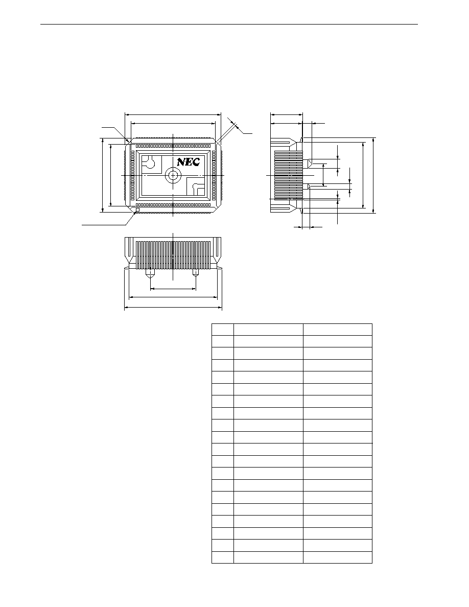
718
APPENDIX A DEVELOPMENT TOOLS
Preliminary User's Manual U13987EJ1V0UM00
A.4 Drawings of Conversion Socket (EV-9200GF-100) and Recommended Board Mounting Pattern
Mount the EP-78064GF-R in combination on the board.
Figure A-2. Package Drawing of EV-9200GF-100 (reference) (unit: mm)
EV-9200GF-100
A
D
E
B
F
1
No.1 pin index
M
N
O
L
K
S
R
Q
I
H
G
P
C
J
EV-9200GF-100-G0E
ITEM
MILLIMETERS
INCHES
A
B
C
D
E
F
G
H
I
J
K
L
M
N
O
P
Q
R
S
24.6
21
15
18.6
4-C 2
0.8
12.0
22.6
25.3
6.0
16.6
19.3
8.2
8.0
2.5
2.0
0.35
2.3
1.5
0.969
0.827
0.591
0.732
4-C 0.079
0.031
0.472
0.89
0.996
0.236
0.654
0.76
0.323
0.315
0.098
0.079
0.014
0.091
0.059

719
APPENDIX A DEVELOPMENT TOOLS
Preliminary User's Manual U13987EJ1V0UM00
Figure A-3. Recommended Board Mounting Pattern of EV-9200GF-100 (reference) (unit: mm)
F
H
E
D
A
B
C
I
J
K
L
0.026
�
1.142=0.742
0.026
�
0.748=0.486
EV-9200GF-100-P1E
ITEM
MILLIMETERS
INCHES
A
B
C
D
E
F
G
H
I
J
K
L
26.3
21.6
15.6
20.3
12
�
0.05
6
�
0.05
0.35
�
0.02
2.36
�
0.03
2.3
1.57
�
0.03
1.035
0.85
0.614
0.799
0.472
0.236
0.014
0.093
0.091
0.062
0.65
�
0.02
�
29=18.85
�
0.05
0.65
�
0.02
�
19=12.35
�
0.05
+0.001
�0.002
+0.002
�0.002
+0.001
�0.002
+0.003
�0.002
+0.003
�0.002
+0.003
�0.002
+0.001
�0.001
+0.001
�0.002
+0.001
�0.002
G
Dimensions of mount pad for EV-9200 and that for
target device (QFP) may be different in some parts.
For the recommended mount pad dimensions for
QFP, refer to "SEMICONDUCTOR DEVICE
MOUNTING TECHNOLOGY MANUAL" (C10535E).
Caution

720
APPENDIX A DEVELOPMENT TOOLS
Preliminary User's Manual U13987EJ1V0UM00
A.5 Check Sheet for
�
PD784938 Subseries Development Tools
The following development tools are necessary for using the
�
PD784938 Subseries products. Check if the necessary
tools are at hand (the dotted line in the table below indicates either of the tools above or below the line should be selected).
�
Host machine: PC-9800 Series
Order Code
Check
Remark
IE-784000-R
IE-784000-R-EM
IE-784937-R-EM1
IE-784937-NS-EM1
IE-70000-98-IF-B (other than notebook type personal computer),
IE-70000-98-IF-C
IE-70000-98N-IF (for notebook type personal computer)
IE-78000R-SV3
IE-78K4-R-EX3
EP-78064GF-R
EV-9200GF-100
FA-100GF (necessary for using flash memory version)
�
SAA13ID78K4 (3.5")
�
S5A13DF784937 (3.5")
�
S5A10DF784937 (5")
�
S5A13RA78K4 (3.5")
�
S5A10RA78K4 (5")
�
S5A13CC78K4 (3.5")
Note 1
�
S5A10CC78K4 (5")
Note 1
�
S5A13CC78K4-L (3.5")
Note 2
�
S5A10CC78K4-L (5")
Note 2
Notes 1. Necessary for using the C compiler.
2. Necessary for remodelling the library of the C compiler.

721
APPENDIX A DEVELOPMENT TOOLS
Preliminary User's Manual U13987EJ1V0UM00
�
Host machine: IBM PC/AT
Order Code
Check
Remark
IE-784000-R
IE-784000-R-EM
IE-784937-R-EM1
IE-784937-NS-EM1
IE-70000-PC-IF-B, IE-70000-PC-IF-C
IE-78000R-SV3
IE-78K4-R-EX3
EP-78064GF-R
EV-9200GF-100
FA-100GF (necessary for using flash memory version)
�
SBB13ID78K4 (3.5") (English version)
�
SAB13ID78K4 (3.5") (Japanese version)
�
S5A13DF784937 (3.5")
�
S5A10DF784937 (5")
�
S5A13RA78K4 (3.5")
�
S5A10RA78K4 (5")
�
S5A13CC78K4 (3.5")
Note 1
�
S5A10CC78K4 (5")
Note 1
�
S5A13CC78K4-L (3.5")
Note 2
�
S5A10CC78K4-L (5")
Note 2
Notes 1. Necessary for using the C compiler.
2. Necessary for remodelling the library of the C compiler.

722
Preliminary User's Manual U13987EJ1V0UM00
[MEMO]
723
Preliminary User's Manual U13987EJ1V0UM00
APPENDIX B EMBEDDED SOFTWARE
The following embedded software products are available for efficient program development and maintenance of the
�
PD784938 Subseries.
Real-Time OS (1/2)
RX78K/IV
RX78K/IV is a real-time OS conforming to the
�
ITRON specifications.
Real-time OS
Tool (configurator) for generating nucleus of RX78K/IV and plural information tables is
supplied.
Used in combination with an optional assembler package (RA78K4) and device file
(DF784937).
<Precaution when using RX78K/IV in PC environment>
The real-time OS is a DOS-based application. It should be used in the DOS Prompt when
using in Windows.
Part number:
�
S
����
RX78K4
Caution When purchasing the RX78K/IV, fill in the purchase application form in advance and sign the User
Agreement.
Remark
����
and
in the part number differ depending on the host machine and OS used.
�
S
����
RX78K4-
Product Outline
Maximum Number for Use in Mass Production
001
Evaluation object
Do not use for mass-produced product.
100K
Mass-production object
0.1 million units
001M
1 million units
010M
10 million units
S01
Source program
Source program for mass-produced object
����
Host Machine
OS
Supply Medium
AA13
PC-9800 Series
Windows (Japanese version)
Note
3.5-inch 2HD FD
AB13
IBM PC/AT or compatibles
Windows (Japanese version)
Note
3.5-inch 2HC FD
BB13
Windows (English version)
Note
3P16
HP9000 Series 700
HP-UX (Rel. 10.10)
DAT (DDS)
3K13
SPARCstation
SunOS (Rel. 4.1.4)
3.5-inch 2HC FD
3K15
Solaris (Rel. 2.5.1)
1/4-inch CGMT
3R13
NEWS (RISC)
NEWS-OS (Rel. 6.1)
3.5-inch 2HC FD
Note
Can also be operated in DOS environment.
724
APPENDIX B EMBEDDED SOFTWARE
Preliminary User's Manual U13987EJ1V0UM00
Real-Time OS (2/2)
MX78K4
MX78K4 is an OS for
�
ITRON specification subsets. A nucleus for the MX78K4 is also
OS
included as a companion product.
This manages tasks, events, and time. In the task management, determining the task
execution order and switching from task to the next task are performed.
<Precaution when using MX78K4 in PC environment>
The MX78K4 is a DOS-based application. It should be used in the DOS Prompt when
using in Windows.
Part number:
�
S
����
MX78K4-
Remark
����
and
in the part number differ depending on the host machine and OS used.
�
S
����
MX78K4-
Product Outline
Maximum Number for Use in Mass Production
001
Evaluation object
Use in preproduction stages.
��
Mass-production object
Use in mass production stages.
S01
Source program
Only the users who purchased mass-production
objects are allowed to purchase this program.
����
Host Machine
OS
Supply Medium
AA13
PC-9800 Series
Windows (Japanese version)
Note
3.5-inch 2HD FD
AB13
IBM PC/AT or compatibles
Windows (Japanese version)
Note
3.5-inch 2HC FD
BB13
Windows (English version)
Note
3P16
HP9000 Series 700
HP-UX (Rel. 10.10)
DAT (DDS)
3K13
SPARCstation
SunOS (Rel. 4.1.4)
3.5-inch 2HC FD
3K15
Solaris (Rel. 2.5.1)
1/4-inch CGMT
3R13
NEWS (RISC)
NEWS-OS (Rel. 6.1)
3.5-inch 2HC FD
Note
Can also be operated in DOS environment.

725
Preliminary User's Manual U13987EJ1V0UM00
APPENDIX C REGISTER INDEX
C.1 Register Name Index
[A]
A/D conversion result register (ADCR) ... 406
A/D converter mode register (ADM) ... 407
A/D current cut select register (IEAD) ... 410
Asynchronous serial interface mode register (ASIM) ... 428, 433
Asynchronous serial interface mode register 2 (ASIM2) ... 428, 433
Asynchronous serial interface status register (ASIS) ... 434
Asynchronous serial interface status register 2 (ASIS2) ... 434
[B]
Baud rate generator control register (BRGC) ... 451
Baud rate generator control register 2 (BRGC2) ... 451
Bus control register (BCR) ... 484
[C]
Capture/compare control register 0 (CRC0) ... 223
Capture/compare control register 1 (CRC1) ... 279
Capture/compare control register 2 (CRC2) ... 314
Capture/compare register (CR11/CR11W, CR21/CR21W) ... 275, 310
Capture register (CR02, CR12/CR12W, CR22/CR22W) ... 220, 275, 310
Clock output mode register (CLOM) ... 513
Clocked serial interface mode register (CSIM) ... 459
Clocked serial interface mode register 1 (CSIM1) ... 428, 443
Clocked serial interface mode register 2 (CSIM2) ... 428, 443
Clocked serial interface mode register 3 (CSIM3) ... 459
Communication count register (CCR) ... 499
Compare register (CR00, CR01, CR10/CR10W, CR20/CR20W, CR30/CR30W) ... 220, 275, 310, 375
Control data register (CDR) ... 487
[D]
Data register (DR) ... 491
[E]
External interrupt mode register 0 (INTM0) ... 518
External interrupt mode register 1 (INTM1) ... 519
[H]
Hold mode register (HLDM) ... 634
[I]
In-service priority register (ISPR) ... 540
Internal memory size switching register (IMS) ... 82
Interrupt control register ... 533

726
APPENDIX C REGISTER INDEX
Preliminary User's Manual U13987EJ1V0UM00
Interrupt mask register (MK0H, MK0L, MK1H, MK1L) ... 538
Interrupt mode control register (IMC) ... 541
Interrupt status register (ISR) ... 494
[M]
Macro service mode register ... 567
Memory expansion mode register (MM) ... 603, 615
[O]
One-shot pulse output control register (OSPC) ... 225
Oscillation stabilization time specification register (OSTS) ... 109, 641
[P]
Partner address register (PAR) ... 486
Port 0 (P0) ... 119
Port 0 buffer register (P0L, P0H) ... 204
Port 0 mode register (PM0) ... 120
Port 1 (P1) ... 126
Port 1 mode control register (PMC1) ... 131
Port 1 mode register (PM1) ... 131
Port 2 (P2) ... 137
Port 3 (P3) ... 143
Port 3 mode control register (PMC3) ... 149
Port 3 mode register (PM3) ... 148
Port 4 (P4) ... 155
Port 4 mode register (PM4) ... 156
Port 5 (P5) ... 162
Port 5 mode register (PM5) ... 163
Port 6 (P6) ... 169
Port 6 mode register (PM6) ... 175
Port 7 (P7) ... 179
Port 7 mode register (PM7) ... 180
Port 9 (P9) ... 183
Port 9 mode register (PM9) ... 184
Port 10 (P10) ... 188
Port 10 mode control register (PMC10) ... 193
Port 10 mode register (PM10) ... 193
Prescaler mode register 0 (PRM0) ... 222, 377
Prescaler mode register 1 (PRM1) ... 278, 313
Program status word (PSWL) ... 543
Programmable wait control register 1 (PWC1) ... 616
Programmable wait control register 2 (PWC2) ... 617
Pull-up resistor option register H (PUOH) ... 187, 197
Pull-up resistor option register L (PUOL) ... 123, 135, 141, 153, 159, 166, 178
PWM control register (PWMC) ... 397
PWM modulo register 0 (PWM0) ... 398
PWM modulo register 1 (PWM1) ... 398
PWM prescaler register (PWPR) ... 398

727
APPENDIX C REGISTER INDEX
Preliminary User's Manual U13987EJ1V0UM00
[R]
Real-time output port control register (RTPC) ... 203
Refresh area specification register (RFA) ... 630
Refresh mode register (RFM) ... 629
ROM correction adress register H (CORAH) ... 667
ROM correction adress register L (CORAL) ... 667
ROM correction control register (CORC) ... 667
[S]
Sampling clock selection register (SCS0) ... 520
Serial receive buffer (RXB) ... 431
Serial receive buffer 2 (RXB2) ... 431
Serial shift register (SIO) ... 458
Serial shift register 1 (SIO1) ... 442
Serial shift register 2 (SIO2) ... 442
Serial shift register 3 (SIO3) ... 457
Serial transmit shift register (TXS) ... 431
Serial transmit shift register 2 (TXS2) ... 431
Slave address register (SAR) ... 486
Slave status register (SSR) ... 498
Standby control register (STBC) ... 108, 639
Success count register (SCR) ... 499
[T]
Telegraph length register (DLR) ... 490
Timer control register 0 (TMC0) ... 221, 376
Timer control register 1 (TMC1) ... 277, 312
Timer output control register (TOC) ... 224, 315
Timer counter 0 (TM0) ... 220
Timer counter 1 (TM1/TM1W) ... 275
Timer counter 2 (TM2/TM2W) ... 310
Timer counter 3 (TM3/TM3W) ... 375
[U]
Unit address register (UAR) ... 486
Unit status register (USR) ... 492
[W]
Watch timer mode register (WM) ... 393
Watchdog timer mode register (WDM) ... 389, 542

728
APPENDIX C REGISTER INDEX
Preliminary User's Manual U13987EJ1V0UM00
C.2 Register Symbol Index
[A]
ADCR
: A/D Conversion Result Register ... 406
ADIC
: Interrupt Control Register ... 535
ADM
: A/D Converter Mode Register ... 407
ASIM
: Asynchronous Serial Interface Mode Register ... 428, 433
ASIM2
: Asynchronous Serial Interface Mode Register 2 ... 428, 433
ASIS
: Asynchronous Serial Interface Status Register ... 434
ASIS2
: Asynchronous Serial Interface Status Register 2 ... 434
[B]
BCR
: Bus Control Register ... 484
BRGC
: Baud Rate Generator Control Register ... 451
BRGC2
: Baud Rate Generator Control Register 2 ... 451
[C]
CCR
: Communication Count Register ... 499
CDR
: Control Data Register ... 486
CIC00
: Interrupt Control Register ... 534
CIC01
: Interrupt Control Register ... 534
CIC10
: Interrupt Control Register ... 534
CIC11
: Interrupt Control Register ... 534
CIC20
: Interrupt Control Register ... 535
CIC21
: Interrupt Control Register ... 535
CIC30
: Interrupt Control Register ... 535
CLOM
: Clock Output Mode Register ... 513
CORAH
: ROM Correction Address Register H ... 667
CORAL
: ROM Correction Address Register L ... 667
CORC
: ROM Correction Control Register ... 667
CR00
: Compare Register ... 220
CR01
: Compare Register ... 220
CR02
: Capture Register ... 220
CR10/CR10W
: Compare Register ... 275
CR11/CR11W
: Capture/Compare Register ... 275
CR12/CR12W
: Capture Register ... 275
CR20/CR20W
: Compare Register ... 310
CR21/CR21W
: Capture/Compare Register ... 310
CR22/CR22W
: Capture Register ... 310
CR30/CR30W
: Compare Register ... 375
CRC0
: Capture/Compare Control Register 0 ... 223
CRC1
: Capture/Compare Control Register 1 ... 279
CRC2
: Capture/Compare Control Register 2 ... 314
CSIIC
: Interrupt Control Register ... 536
CSIIC1
: Interrupt Control Register ... 536
CSIIC2
: Interrupt Control Register ... 536
CSIIC3
: Interrupt Control Register ... 537
CSIM
: Clocked Serial Interface Mode Register ... 459

729
APPENDIX C REGISTER INDEX
Preliminary User's Manual U13987EJ1V0UM00
CSIM1
: Clocked Serial Interface Mode Register 1 ... 428, 443
CSIM2
: Clocked Serial Interface Mode Register 2 ... 428, 443
CSIM3
: Clocked Serial Interface Mode Register 3 ... 459
[D]
DLR
: Telegraph Length Register ... 490
DR
: Data Register ... 491
[H]
HLDM
: Hold Mode Register ... 634
[I]
IEAD
: A/D Current Cut Select Register ... 410
IEIC1
: Interrupt Control Register ... 537
IEIC2
: Interrupt Control Register ... 537
IMC
: Interrupt Mode Control Register ... 541
IMS
: Internal Memory Size Switching Register ... 82
INTM0
: External Interrupt Mode Register 0 ... 518
INTM1
: External Interrupt Mode Register 1 ... 519
ISPR
: In-Service Priority Register ... 540
ISR
: Interrupt Status Register ... 494
[M]
MK0H
: Interrupt Mask Register H ... 538
MK0L
: Interrupt Mask Register L ... 538
MK1H
: Interrupt Mask Register 1H ... 538
MK1L
: Interrupt Mask Register 1L ... 538
MM
: Memory Expansion Mode Register ... 603, 615
[O]
OSPC
: One-Shot Pulse Output Control Register ... 225
OSTS
: Oscillation Stabilization Time Specification Register ... 109, 641
[P]
P0
: Port 0 ... 119
P0H
: Port 0 Buffer Register H ... 204
P0L
: Port 0 Buffer Register L ... 204
P1
: Port 1 ... 126
P2
: Port 2 ... 137
P3
: Port 3 ... 143
P4
: Port 4 ... 155
P5
: Port 5 ... 162
P6
: Port 6 ... 169
P7
: Port 7 ... 179
P9
: Port 9 ... 183
P10
: Port 10 ... 188
PAR
: Partner Address Register ... 486
PIC0
: Interrupt Control Register ... 534

730
APPENDIX C REGISTER INDEX
Preliminary User's Manual U13987EJ1V0UM00
PIC1
: Interrupt Control Register ... 534
PIC2
: Interrupt Control Register ... 534
PIC3
: Interrupt Control Register ... 534
PIC4
: Interrupt Control Register ... 535
PIC5
: Interrupt Control Register ... 535
PM0
: Port 0 Mode Register ... 120
PM1
: Port 1 Mode Register ... 131
PM3
: Port 3 Mode Register ... 148
PM4
: Port 4 Mode Register ... 156
PM5
: Port 5 Mode Register ... 163
PM6
: Port 6 Mode Register ... 175
PM7
: Port 7 Mode Register ... 180
PM9
: Port 9 Mode Register ... 184
PM10
: Port 10 Mode Register ... 193
PMC1
: Port 1 Mode Control Register ... 131
PMC3
: Port 3 Mode Control Register ... 149
PMC10
: Port 10 Mode Control Register ... 193
PRM0
: Prescaler Mode Register 0 ... 222, 377
PRM1
: Prescaler Mode Register 1 ... 278, 313
PSWL
: Program Status Word ... 543
PUOH
: Pull-Up Resistor Option Register H ... 187, 197
PUOL
: Pull-Up Resistor Option Register L ... 123, 135, 141, 153, 159, 166, 178
PWC1
: Programmable Wait Control Register 1 ... 616
PWC2
: Programmable Wait Control Register 2 ... 617
PWM0
: PWM Modulo Register 0 ... 398
PWM1
: PWM Modulo Register 1 ... 398
PWMC
: PWM Control Register ... 397
PWPR
: PWM Prescaler Register ... 398
[R]
RFA
: Refresh Area Specification Register ... 630
RFM
: Refresh Mode Register ... 629
RTPC
: Real-Time Output Port Control Register ... 203
RXB
: Serial Receive Buffer ... 431
RXB2
: Serial Receive Buffer 2 ... 431
[S]
SAR
: Slave Address Register ... 486
SCR
: Success Count Register ... 499
SCS0
: Sampling Clock Selection Register ... 520
SERIC
: Interrupt Control Register ... 535
SERIC2
: Interrupt Control Register ... 536
SIO
: Serial Shift Register ... 458
SIO1
: Serial Shift Register 1 ... 442
SIO2
: Serial Shift Register 2 ... 442
SIO3
: Serial Shift Register 3 ... 457
SRIC
: Interrupt Control Register ... 535
SRIC2
: Interrupt Control Register ... 536

731
APPENDIX C REGISTER INDEX
Preliminary User's Manual U13987EJ1V0UM00
SSR
: Slave Status Register ... 498
STBC
: Standby Control Register ... 108, 639
STIC
: Interrupt Control Register ... 536
STIC2
: Interrupt Control Register ... 536
[T]
TM0
: Timer Counter 0 ... 220
TM1/TM1W
: Timer Counter 1 ... 275
TM2/TM2W
: Timer Counter 2 ... 310
TM3/TM3W
: Timer Counter 3 ... 375
TMC0
: Timer Control Register 0 ... 221, 376
TMC1
: Timer Control Register 1 ... 277, 312
TOC
: Timer Output Control Register ... 224, 315
TXS
: Serial Transmit Shift Register ... 431
TXS2
: Serial Transmit Shift Register 2 ... 431
[U]
UAR
: Unit Address Register ... 486
USR
: Unit Status Register ... 492
[W]
WDM
: Watchdog Timer Mode Register ... 389, 542
WIC
: Interrupt Control Register ... 537
WM
: Watch Timer Mode Register ... 393

732
Preliminary User's Manual U13987EJ1V0UM00
[MEMO]
Although NEC has taken all possible steps
to ensure that the documentation supplied
to our customers is complete, bug free
and up-to-date, we readily accept that
errors may occur. Despite all the care and
precautions we've taken, you may
encounter problems in the documentation.
Please complete this form whenever
you'd like to report errors or suggest
improvements to us.
Hong Kong, Philippines, Oceania
NEC Electronics Hong Kong Ltd.
Fax: +852-2886-9022/9044
Korea
NEC Electronics Hong Kong Ltd.
Seoul Branch
Fax: 02-528-4411
Taiwan
NEC Electronics Taiwan Ltd.
Fax: 02-2719-5951
Address
North America
NEC Electronics Inc.
Corporate Communications Dept.
Fax: 1-800-729-9288
1-408-588-6130
Europe
NEC Electronics (Europe) GmbH
Technical Documentation Dept.
Fax: +49-211-6503-274
South America
NEC do Brasil S.A.
Fax: +55-11-6465-6829
Asian Nations except Philippines
NEC Electronics Singapore Pte. Ltd.
Fax: +65-250-3583
Japan
NEC Semiconductor Technical Hotline
Fax: 044-548-7900
I would like to report the following error/make the following suggestion:
Document title:
Document number:
Page number:
Thank you for your kind support.
If possible, please fax the referenced page or drawing.
Excellent
Good
Acceptable
Poor
Document Rating
Clarity
Technical Accuracy
Organization
CS 99.1
Name
Company
From:
Tel.
FAX
Facsimile
Message