Document Outline
- COVER
- FEATURES
- APPLICATIONS
- ORDERING INFORMATION
- 78K/0S SERIES DEVELOPMENT
- OVERVIEW OF FUNCTIONS
- 1. PIN CONFIGURATION (TOP VIEW)
- 2. BLOCK DIAGRAM
- 3. PIN FUNCTIONS
- 3.1 Port Pins
- 3.2 Non-Port Pins
- 3.3 Pin I/O Circuits and Recommended Connection of Unused Pins
- 4. CPU ARCHITECTURE
- 5. FLASH MEMORY PROGRAMMING
- 5.1 Selecting Communication Mode
- 5.2 Function of Flash Memory Programming
- 5.3 Flashpro III Connection Example
- 5.4 Example of Settings for Flashpro III (PG-FP3)
- 6. INSTRUCTION SET OVERVIEW
- 6.1 Conventions
- 6.2 Operations
- 7. ELECTRICAL SPECIFICATIONS
- 8. CHARACTERISTICS CURVES
- 9. PACKAGE DRAWING
- 10. RECOMMENDED SOLDERING CONDITIONS
- APPENDIX A. DIFFERENCES BETWEEN uPD78F9177, 78F9177Y, AND MASK ROM VERSIONS
- APPENDIX B. DEVELOPMENT TOOLS
- APPENDIX C. RELATED DOCUMENTS

The information in this document is subject to change without notice. Before using this document, please
confirm that this is the latest version.
Not all devices/types available in every country. Please check with local NEC representative for
availability and additional information.
Document No. U14022EJ1V0DS00 (1st edition)
Date Published August 2000 NS CP(K)
Printed in Japan
8-BIT SINGLE-CHIP MICROCONTROLLER
DATA SHEET
MOS INTEGRATED CIRCUIT
µ
µ
µ
µ
PD78F9177, 78F9177Y
The mark
shows major revised
The
µ
PD78F9177 and
µ
PD78F9177Y are
µ
PD789177, 789177Y Subseries (small, general-purpose) in the 78K/0S
Series.
The
µ
PD78F9177 replaces the internal ROM of the
µ
PD789176 and
µ
PD789177 with flash memory, while the
µ
PD78F9177Y replaces the ROM of the
µ
PD789176Y and
µ
PD789177Y with flash memory.
Because flash memory allows the program to be written and erased electrically with the device mounted on the
board, this product is ideal for the evolution stages of system development, small-scale production and rapid
development of new products.
Detailed function descriptions are provided in the following user's manuals. Be sure to read them before
designing.
µ
PD789167, 789177, 789167Y, 789177Y Subseries User's Manual: U14186E
78K/0S Series User's Manual Instruction: U11047E
FEATURES
∑ Pin compatible with mask ROM version (except V
PP
pin)
∑ Flash memory: 24 Kbytes
∑ High-speed RAM: 512 bytes
∑ Minimum instruction execution time can be changed from high-speed (0.4
µ
s: @5.0-MHz operation with main
system clock) to ultra-low-speed (122
µ
s: @ 32.768-kHz operation with subsystem clock)
∑ 10-bit resolution A/D converter: 8 channels
∑ I/O ports: 31
∑ Serial interface: 2 channels
∑
3-wire serial I/O mode / UART mode: 1 channel
∑
SMB (
µ
PD78F9177Y only): 1 channel
∑ Timers: 6 channels
∑
16-bit timer: 1 channel
∑
8-bit timer/event counter: 2 channels
∑
8-bit timer: 1 channel
∑
Watch timer: 1 channel
∑
Watchdog timer: 1 channel
∑ On-chip 16-bit multiplier
∑ Power supply voltage: V
DD
= 1.8 to 5.5 V
©
2000

2
µ
µ
µ
µ
PD78F9177, 78F9177Y
Data Sheet U14022EJ1V0DS00
APPLICATIONS
Power windows, battery management unit, side air bags, etc
ORDERING INFORMATION
(1)
µ
µ
µ
µ
PD78F9177
Part Number
Package
µ
PD78F9177GB-8ES
44-pin plastic QFP (10
◊
10)
(2)
µ
µ
µ
µ
PD78F9177Y
Part Number
Package
µ
PD78F9177YGB-8ES
44-pin plastic LQFP (10 X 10)
µ
PD78F9177YGA-9EU
48-pin plastic TQFP (fine pitch) (7 X 7)

3
µ
µ
µ
µ
PD78F9177, 78F9177Y
Data Sheet U14022EJ1V0DS00
78K/0S SERIES DEVELOPMENT
The products in the 78K/0S Series are listed below. The names enclosed in boxes are subseries names.
78K/0S
series
Small, general-purpose
Small, general-purpose + A/D
For inverter control
For driving LCD
For ASSP
44 pins
44 pins
42/44 pins
28 pins
44 pins
30 pins
30 pins
30 pins
30 pins
30 pins
30 pins
44 pins
Products under mass production
Products under development
Y subseries supports SMB.
PD789014
80 pins
80 pins
64 pins
64 pins
64 pins
64 pins
64 pins
64 pins
44 pins
44 pins
20 pins
20 pins
µ
PD789026
µ
PD789046
PD789026 with subsystem clock added
PD789014 with timer reinforced and ROM and RAM expanded
UART. Low-voltage (1.8-V) operation
PD789167 with improved A/D
PD789104A with improved timer
PD789146 with improved A/D
PD789104A with EEPROM added
PD789124A with improved A/D
RC oscillation model of PD789104A
PD789104A with improved A/D
PD789026 with A/D and multiplier added
PD789407A with improved A/D
PD789456 with improved I/O
PD789446 with improved A/D
PD789426 with improved display output
PD789426 with improved A/D
PD789306 with A/D added
RC oscillation model of PD789306
Basic subseries for driving LCD
For PC keyboard. Internal USB function
For key pad. Internal POC
RC oscillation model of PD789860
For keyless entry. Internal POC and key return circuit
Internal inverter control circuit and UART
µ
PD789104A
µ
PD789114A
µ
PD789842
µ
PD789124A
µ
PD789134A
µ
PD789146
µ
PD789156
µ
PD789167
µ
PD789177
µ
PD789306
µ
PD789316
µ
PD789426
µ
PD789436
µ
PD789860
µ
PD789861
µ
PD789840
µ
PD789800
µ
PD789446
µ
PD789456
µ
PD789167Y
µ
PD789177Y
µ
µ
µ
µ
µ
µ
µ
µ
µ
µ
µ
µ
µ
µ
µ
µ
µ
µ
µ
PD789407A
µ
PD789417A
µ
88 pins
Segment: 40 pins, common: 16 pins
PD789830
µ
144 pins
Segment/common output: 96 pins
PD789835
µ
For driving Dot LCD
52 pins
52 pins
For remote controller. Internal LCD controller/driver
PD789327
µ
PD789467
µ
PD789327 with A/D added
µ
4
µ
µ
µ
µ
PD78F9177, 78F9177Y
Data Sheet U14022EJ1V0DS00
The major differences between subseries are shown below.
Timer
ROM
Capacity
8-bit
16-bit
Watch
WDT
8-bit
A/D
10-bit
A/D
Serial Interface
I/O
V
DD
MIN
Value
Remark
µ
PD789046 16 K
1 ch
µ
PD789026 4 K-16 K
1 ch
1 ch
34 pins
Small,
general-
purpose
µ
PD789014 2 K-4 K
2 ch
-
-
1 ch
-
-
1 ch (UART:1 ch)
22 pins
1.8 V
-
µ
PD789177
-
8 ch
µ
PD789167
16 K-24 K
3 ch
1 ch
8 ch
-
31 pins
-
µ
PD789156
-
4 ch
µ
PD789146
8 K-16 K
4 ch
-
Internal
EEPROM
µ
PD789134A
4 ch
µ
PD789124A
4 ch
-
RC oscillation
version
µ
PD789114A
-
4 ch
Small,
general-
purpose
+ A/D
µ
PD789104A
2 K-8 K
1 ch
1 ch
-
1 ch
4 ch
-
1 ch (UART: 1 ch)
20 pins
1.8 V
-
For
inverter
control
µ
PD789842 8 K-16 K
3 ch
Note
1 ch
1 ch
8 ch
-
1 ch (UART: 1 ch) 30 pins
4.0 V
-
µ
PD789417A
7 ch
µ
PD789407A
12 K-24 K
3 ch
7 ch
-
43 pins
µ
PD789456
-
6 ch
µ
PD789446
6 ch
-
30 pins
µ
PD789436
-
6 ch
µ
PD789426
12 K-16 K
6 ch
1 ch (UART: 1 ch)
40 pins
-
µ
PD789316
RC oscillation
version
For LCD
driving
µ
PD789306
8 K to
16K
2 ch
1 ch
1 ch
1 ch
-
-
2 ch (UART: 1 ch) 23 pins
1.8 V
-
µ
PD789835 24 K-60 K
6 ch
-
3 ch
28 pins
1.8 V
For Dot
LCD
driving
µ
PD789830 24 K
1 ch
1 ch
1 ch
1 ch
-
-
1 ch
30 pins
2.7 V
-
µ
PD789467
1 ch
-
18 pins
µ
PD789327
4 K-24 K
2 ch
-
1 ch
1 ch
-
1 ch
21 pins
1.8 V
Internal
LCD
µ
PD789800
-
2 ch (USB: 1 ch)
31 pins
4.0 V
µ
PD789840
8 K
1 ch
4 ch
1 ch
29 pins
2.8 V
-
µ
PD789861
RC oscillation
version,
Internal
EEPROM
ASSP
µ
PD789860
4 K
2 ch
-
-
1 ch
-
-
-
14 pins
1.8 V
Internal
EEPROM
Note 10-bit timer: 1 channel
Function
Subseries Name

5
µ
µ
µ
µ
PD78F9177, 78F9177Y
Data Sheet U14022EJ1V0DS00
OVERVIEW OF FUNCTIONS
Item
µ
PD78F9177
µ
PD78F9177Y
Flash memory
24 Kbytes
Internal memory
High-speed RAM
512 bytes
Minimum instruction execution time
∑ 0.4/1.6
µ
s (@5.0-MHz operation with main system clock)
∑ 122
µ
s (@ 32.768-kHz operation with subsystem clock)
General-purpose registers
8 bits
◊
8 registers
Instruction set
∑ 16-bit operations
∑ Bit manipulations (set, reset, test)
Multiplier
8 bits
◊
8 bits = 16 bits
I/O ports
Total:
31
∑ CMOS input:
8
∑ CMOS I/O:
17
∑ N-ch open drain:
6
A/D converters
10-bit resolution
◊
8 channels
Serial interfaces
3-wire serial I/O/UART : 1 channel
∑
3-wire serial I/O / UART: 1 channel
∑
SMB: 1 channel
Timers
∑ 16-bit timer:1 channel
∑ 8-bit timer/event counter:2 channels
∑ 8-bit timer:1 channel
∑ Watch timer:1 channel
∑ Watchdog timer:1 channel
Timer output
4 output
Buzzer output
1
Internal: 10, External: 4
(µ
PD78F9177)
Maskable
Internal: 12, External: 4
(µ
PD78F9177Y)
Vectored interrupt
sources
Non-maskable
Internal: 1
Power supply voltage
V
DD
= 1.8 to 5.5 V
Operating ambient temperature
T
A
=
-
40∞C to
+
85∞C
Package
44-pin plastic LQFP (10
◊
10)
∑
44-pin plastic LQFP (10 X10)
∑
48-pin plastic TQFP (fine pitch) (7 x 7)

6
µ
µ
µ
µ
PD78F9177, 78F9177Y
Data Sheet U14022EJ1V0DS00
CONTENTS
1.
PIN CONFIGURATION (TOP VIEW) .................................................................................................
7
2.
BLOCK DIAGRAM.............................................................................................................................
10
3.
PIN FUNCTIONS................................................................................................................................
11
3.1
Port Pins ..................................................................................................................................................
11
3.2
Non-Port Pins..........................................................................................................................................
12
3.3
Pin I/O Circuits and Recommended Connection of Unused Pins ......................................................
13
4.
CPU ARCHITECTURE.......................................................................................................................
15
5.
FLASH MEMORY PROGRAMMING ................................................................................................
16
5.1
Selecting Communication Mode ..........................................................................................................
16
5.2
Function of Flash Memory Programming ............................................................................................
17
5.3
Flashpro III Connection Example .........................................................................................................
17
5.4
Example of Settings for Flashpro III (PG-FP3) ....................................................................................
19
6.
INSTRUCTION SET OVERVIEW ......................................................................................................
20
6.1
Conventions ...........................................................................................................................................
20
6.2
Operations ..............................................................................................................................................
22
7.
ELECTRICAL SPECIFICATIONS......................................................................................................
27
8.
CHARACTERISTICS CURVES ........................................................................................................
45
9.
PACKAGE DRAWING ......................................................................................................................
46
10. RECOMMENDED SOLDERING CONDITIONS ...............................................................................
48
APPENDIX A. DIFFERENCES BETWEEN
µ
µ
µ
µ
PD78F9177, 78F9177Y, AND MASK ROM VERSIONS ......
49
APPENDIX B. DEVELOPMENT TOOLS ...............................................................................................
50
APPENDIX C. RELATED DOCUMENTS ...............................................................................................
52

7
µ
µ
µ
µ
PD78F9177, 78F9177Y
Data Sheet U14022EJ1V0DS00
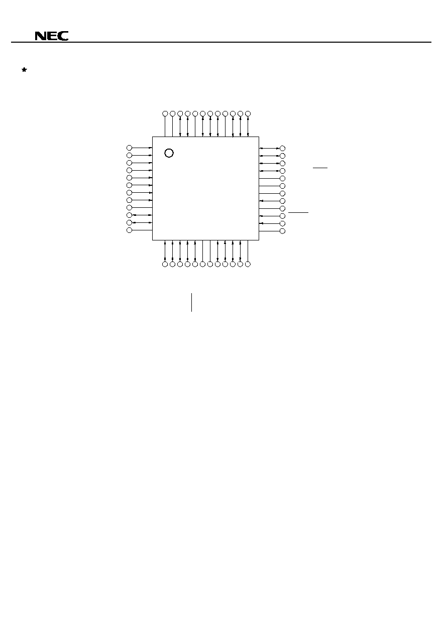
1. PIN CONFIGURATION (TOP VIEW)
∑ 44-pin plastic LQFP (10
◊
◊
◊
◊
10)
µ
PD78F9177GB-8ES
µ
PD78F9177YGB-8ES
P60/ANI0
P61/ANI1
P62/ANI2
P63/ANI3
P64/ANI4
P65/ANI5
P66/ANI6
P67/ANI7
AV
SS
P10
P11
33
32
31
30
29
28
27
26
25
24
23
P01
P00
P26/TO80
P25/TI80/SS20
V
DD0
V
SS0
X1
X2
RESET
XT1
XT2
1
2
3
4
5
6
7
8
9
10
11
44 43 42 41 40 39 38 37 36 35 34
12 13 14 15 16 17 18 19 20 21 22
AV
REF
AV
DD
P53
P52
P51
P50
P05
V
SS1
P04
P03
P02
P30/INTP0/TI81/CPT90
P31/INTP1/TO81
P32/INTP2/TO90
P33/INTP3/TO82/BZO90
P20/SCK20/ASCK20
V
DD1
P21/SO20/T
X
D20
P22/SI20/R
X
D20
P23/SCL0
Note
P24/SDA0
Note
V
PP
Note
The SCL0 and SDA0 pins are available in
µ
PD78F9177Y product only.
Cautions 1. Connect the V
PP
pin directly to V
SS0
or V
SS1
.
2. Connect the AV
DD
pin to V
DD0
.
3. Connect the AV
SS
pin to V
SS0
.
8
µ
µ
µ
µ
PD78F9177, 78F9177Y
Data Sheet U14022EJ1V0DS00
∑ 44-pin plastic QFP (fine pitch) (7
◊
◊
◊
◊
7)
µ
PD78F9177YGA-9EU
P60/ANI0
P61/ANI1
P62/ANI2
P63/ANI3
P64/ANI4
P65/ANI5
P66/ANI6
P67/ANI7
AV
SS
P10
P11
IC2
1
2
3
4
5
6
7
8
9
10
11
12
48 47 46 45 44 43 42 41 40 39 38 37
13 14 15 16 17 18 19 20 21 22 23 24
36
35
34
33
32
31
30
29
28
27
26
25
P01
P00
P26/TO80
P25/Tl80/SS20
V
DD0
IC2
V
SS0
X1
X2
RESET
XT1
XT2
P30/INTP0/Tl81/CPT90
P31/INTP1/TO81
P32/INTP2/TO90
P33/INTP3/TO82/BZO90
P20/SCK20/ASCK20
V
DD1
IC2
P21/SO20/TxD20
P22/Sl20/RxD20
P23/SCL0
P24/SDA0
V
PP
AV
REF
AV
DD
P53
P52
IC0
P51
P50
P05
V
SS1
P04
P03
P02
Cautions 1. Connect the V
PP
pin directly to the V
SS0
or V
SS1
pin in normal operation mode.
2. Connect the IC0 (Internally Connected) pin directly to V
SS0
or V
SS1
.
3. Leave the IC2 pin open.
4. Connect the AV
DD
pin to V
DD0
.
5.
Connect the AV
SS
pin to V
SS0
.

9
µ
µ
µ
µ
PD78F9177, 78F9177Y
Data Sheet U14022EJ1V0DS00
ANI0 to ANI7:
Analog Input
RESET:
Reset
ASCK20:
Asynchronous Serial Input
RxD20:
Receive Data
AV
DD
:
Analog Power Supply
SCK20:
Serial Clock (for SIO20)
AV
REF
:
Analog Reference Voltage
SCL0
Note2
:
Serial Clock (for SMB0)
AV
SS
:
Analog Ground
SDA0
Note2
:
Serial Data
BZO90:
Buzzer Output
SI20:
Serial Input
CPT90:
Capture Trigger Input
SO20:
Serial Output
IC0
Note1
,IC2
Note2
:
Internally Connected
SS20:
Chip Select Input
INTP0 to INTP3: Interrupt from Peripherals
TI80, TI81:
Timer Input
P00 to P05:
Port 0
TO80 to TO82, TO90: Timer Output
P10, P11:
Port 1
TxD20:
Transmit Data
P20 to P26:
Port 2
V
DD0
, V
DD1
:
Power Supply
P30 to P33:
Port 3
V
PP
:
Programming Power Supply
P50 to P53:
Port 5
V
SS0
, V
SS1
:
Ground
P60 to P67:
Port 6
X1, X2:
Crystal (Main System Clock)
XT1, XT2:
Crystal (Subsystem Clock)
Notes 1. The IC0 pin is available in 48-pin plastic TQFP (fine pitch) only.
2. The IC2, SCL0, and SDA0 pins are available in
µ
PD78F9177Y product only.
10
µ
µ
µ
µ
PD78F9177, 78F9177Y
Data Sheet U14022EJ1V0DS00
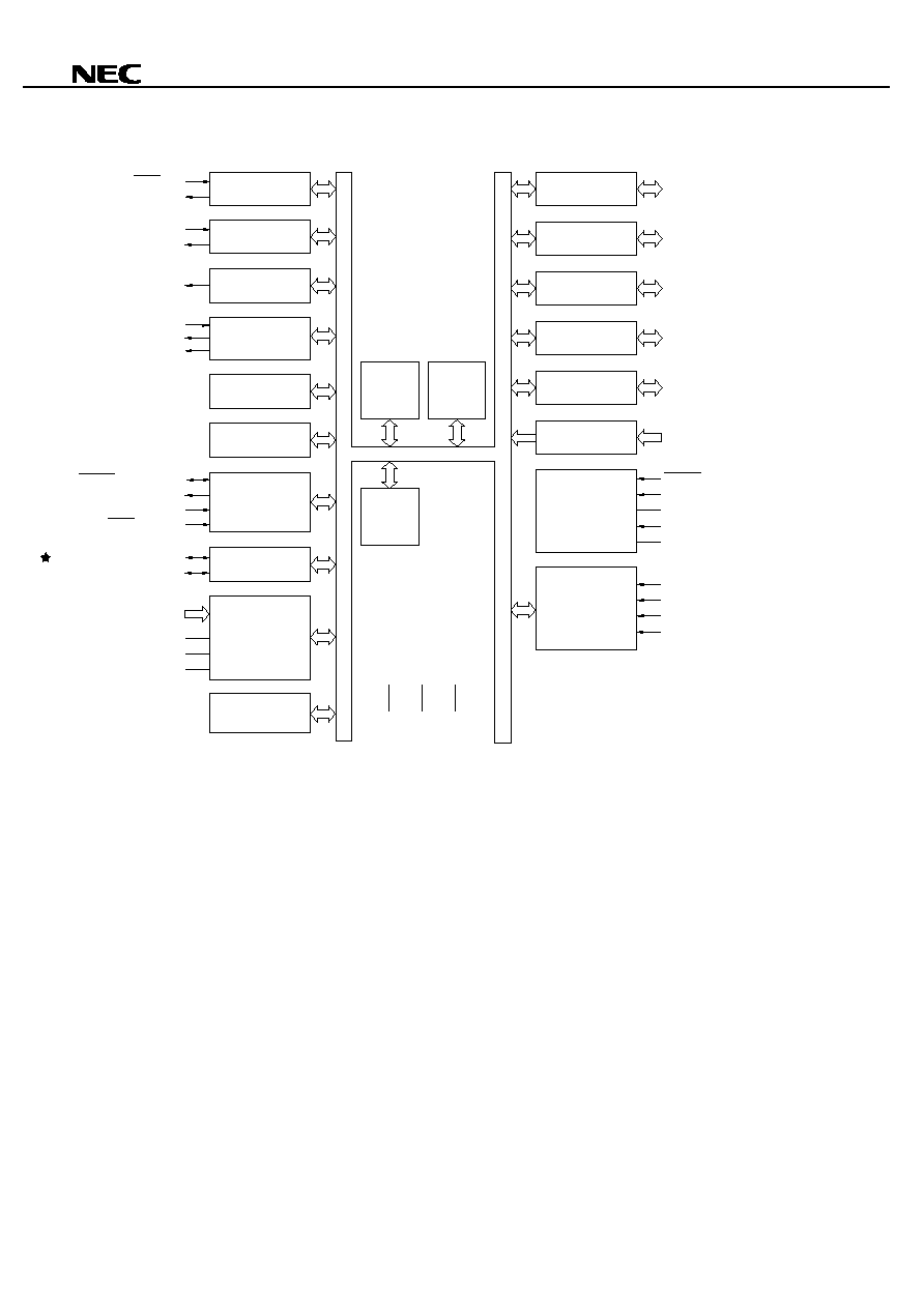
2. BLOCK DIAGRAM
RAM
V
DD0
V
DD1
V
SS0
V
SS1
V
PP
IC0
IC2
Note3
78K/0S
CPU CORE
ROM
TI80/SS20/P25
8-BIT TIMER/
EVENT COUNTER80
P00-P05
PORT0
P10, P11
PORT1
P20-P26
PORT2
P30-P33
PORT3
P50-P53
PORT5
P60-P67
PORT6
SYSTEM
CONTROL
8-BIT TIMER82
16-BIT TIMER90
WATCH TIMER
WATCHDOG TIMER
SIO20
TO80/P26
8-BIT TIMER/
EVENT COUNTER81
TI81/INTP0/CPT90/P30
TO81/INTP1/P31
CPT90/INTP0/TI81/P30
TO90/INTP2/P32
BZO90/INTP3/TO82/P33
TO82/INTP3/BZO90/P33
SCK20/ASCK20/P20
SI20/R
X
D20/P22
SO20/T
X
D20/P21
SS20/TI80/P25
MULTIPLIER
ANI0/P60-
ANI7/P67
AV
DD
AV
SS
AV
REF
A/D
CONVERTER
RESET
X1
X2
XT1
XT2
INTERRUPT
CONTROL
INTP0/TI81/CPT90/P30
INTP1/TO81/P31
INTP2/TO90/P32
INTP3/TO82/BZO90/P33
SMB
Note1
SCL0/P23
SDA0/P24
Notes 1. SMB is available in
µ
PD78F9177Y product only.
2. The IC0 pin is available in 48-pin plastic TQFP (fine pitch) only.
3. The IC2 pin is available in
µ
PD78F9177Y product only.
Note2
11
µ
µ
µ
µ
PD78F9177, 78F9177Y
Data Sheet U14022EJ1V0DS00
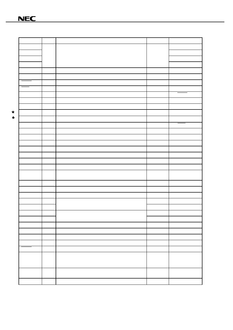
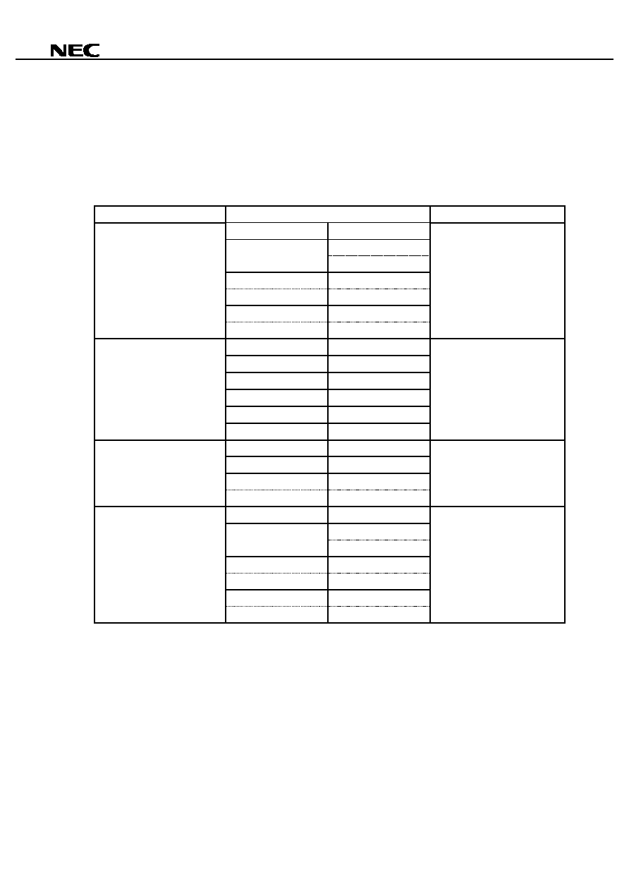
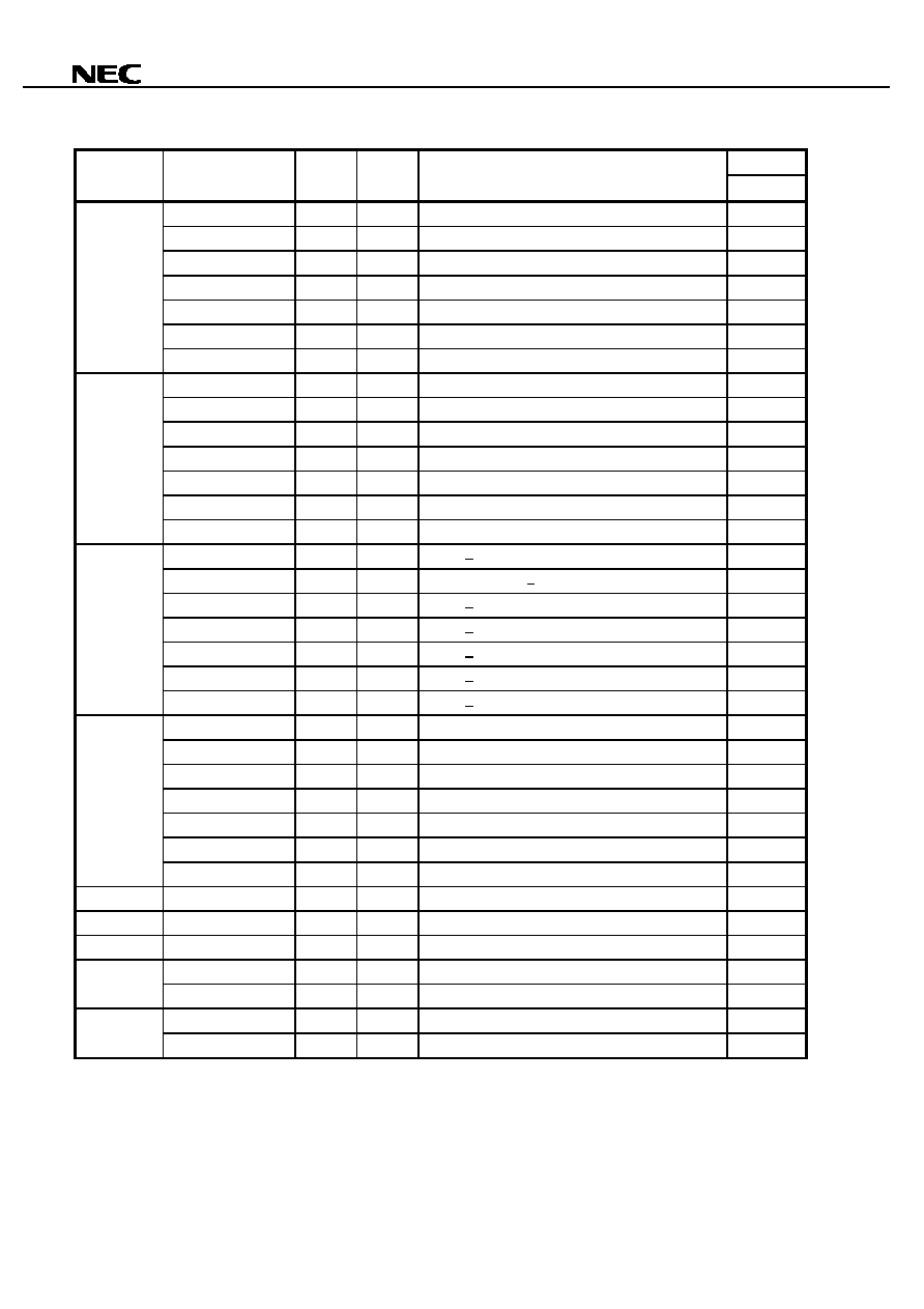
3. PIN FUNCTIONS
3.1
Port Pins
Pin Name
I/O
Function
After Reset
Alternate Function
P00 to P05
I/O
Port 0
6-bit input/output port
Input/output mode can be specified in 1-bit units
When used as an input port, an on-chip pull-up resistor can be
specified by software.
Input
-
P10, P11
I/O
Port 1
2-bit input/output port
Input/output mode can be specified in 1-bit units
When used as an input port, an on-chip pull-up resistor can be
specified by software.
Input
-
P20
SCK20/ASCK20
P21
SO20/TxD20
P22
SI20/RxD20
P23
SCL0
Note
P24
SDA0
Note
P25
TI80/SS20
P26
I/O
Port 2
7-bit input/output port
Input/output mode can be specified in 1-bit units
For P20 to P22, P25, and P26, an on-chip pull-up resistor can be
specified by software.
Only P23 and P24 can be used as N-ch open-drain
input/output port pins.
Input
TO80
P30
INTP0/TI81/CPT90
P31
INTP1/TO81
P32
INTP2/TO90
P33
I/O
Port 3
4-bit input/output port
Input/output mode can be specified in 1-bit units
On-chip pull-up resistor can be specified by software.
Input
INTP3/TO82/BZO90
P50 to P53
I/O
Port 5
4-bit N-ch open-drain input/output port
Input/output mode can be specified in 1-bit units
Input
-
P60 to P67
Input
Port 6
8-bit input-only port
Input
ANI0 to ANI7
Note
µ
PD78F9177Y only
12
µ
µ
µ
µ
PD78F9177, 78F9177Y
Data Sheet U14022EJ1V0DS00
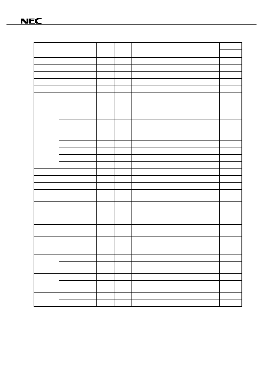
3.2
Non-Port Pins
Pin Name
I/O
Function
After Reset
Alternate Function
INTP0
P30/TI81/CPT90
INTP1
P31/TO81
INTP2
P32/TO90
INTP3
Input
External interrupt input for which the valid edge (rising edge,
falling edge, or both rising and falling edges) can be specified
Input
P33/TO82/BZO90
SI20
Input
Serial data input to serial interface
Input
P22/RxD20
SO20
Output
Serial data output from serial interface
Input
P21/TxD20
SCK20
I/O
Serial clock input/output for serial interface
Input
P20/ASCK20
SS20
Input
Chip select input to serial interface
Input
P25/TI80
ASCK20
Input
Serial clock input for asynchronous serial interface
Input
P20/SCK20
RxD20
Input
Serial data input for asynchronous serial interface
Input
P22/SI20
TxD20
Output
Serial data output for asynchronous serial interface
Input
P21/SO20
SCL0
Note1
I/O
SMB0 clock input/output
Input
P23
SDA0
Note1
I/O
SMB0 data input/output
Input
P24
TI80
Input
External count clock input to 8-bit timer/event counter (TM80)
Input
P25/SS20
TI81
Input
External count clock input to 8-bit timer/event counter (TM81)
Input
P30/INTP0/CPT90
TO80
Output
8-bit timer/event counter (TM80) output
Input
P26
TO81
Output
8-bit timer/event counter (TM81) output
Input
P31/INTP1
TO82
Output
8-bit timer (TM82) output
Input
P33/INTP3/BZO90
TO90
Output
16-bit timer (TM90) output
Input
P32/INTP2
BZO90
Output
16-bit timer (TM90) Buzzer output
Input
P33/INTP3/TO82
CPT90
Input
Capture edge input
Input
P30/INTP0/TI81
ANI0 to
ANI7
Input
A/D converter analog input
Input
P60 to P67
AV
REF
-
A/D converter reference voltage
-
-
AV
SS
-
A/D converter ground potential
-
-
AV
DD
-
A/D converter analog power supply
-
-
X1
Input
-
-
X2
-
Connecting crystal resonator for main system clock
oscillation
-
-
XT1
Input
-
-
XT2
-
Connecting crystal resonator for subsystem clock oscillation
-
-
V
DD0
-
Positive power supply
-
-
V
DD1
-
Positive power supply (other than ports)
-
-
V
SS0
-
Ground potential
-
-
V
SS1
-
Ground potential (other than ports)
-
-
RESET
Input
System reset input
Input
-
V
PP
-
Sets flash memory programming mode. Applies high voltage
when a program is written or verified. Connect directly to V
SS0
or V
SS1
in normal operation mode.
-
-
IC0
Note2
-
Internally connected. Connect this pin directly to the V
SS0
or
V
SS1
pin.
-
-
IC2
Note1
-
Internally connected. Leave this pin open.
-
-
Notes 1.
µ
PD78F9177Y only.
2. 48-pin plastic TQFP (fine pitch) only.
13
µ
µ
µ
µ
PD78F9177, 78F9177Y
Data Sheet U14022EJ1V0DS00
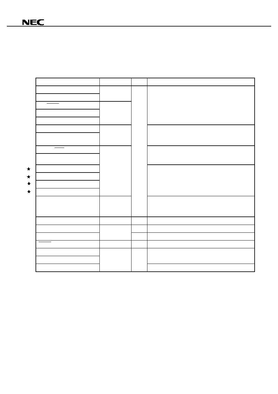
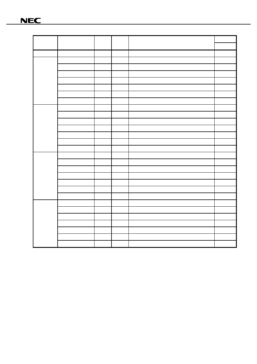
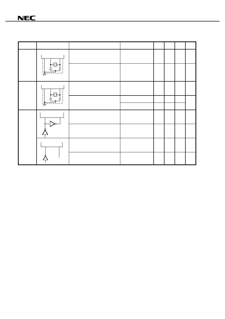
3.3
Pin I/O Circuits and Recommended Connection of Unused Pins
The input/output circuit type of each pin and recommended connection of unused pins is shown in Table 3-1.
For the input/output circuit configuration of each type, refer to Figure 3-1.
Table 3-1. Type of I/O Circuit for Each Pin and Connection of Unused Pins
Pin Name
I/O Circuit Type
I/O
Recommended Connection of Unused Pins
P00 to P05
P10, P11
5-H
P20/SCK20/ASCK20
P21/SO20/TxD20
P22/SI20/RxD20
8-C
Input:
Independently connects to V
DD0
, V
DD1
or V
SS0
, V
SS1
via a resistor.
Output: Leave open.
P23/SCL0
Note1
P24/SDA0
Note1
13-X
Input:
Independently connects to V
DD0
or V
DD1
via a
resistor.
Output: Leave open.
P25/TI80/SS20
P26/TO80
Input:
Independently connects to V
DD0
, V
DD1
or V
SS0
, V
SS1
via a resistor.
Output: Leave open.
P30/INTP0/TI81/CPT90
P31/INTP1/TO81
P32/INTP2/TO90
P33/INTP3/TO82/BZO90
8-C
Input:
Independently connects to V
SS0
or V
SS1
via a
resistor.
Output: Leave open.
P50 to P53
13-T
I/O
Input:
Independently connects to V
DD0
or V
DD1
via a
resistor.
Output: Leave open.
P60/ANI0 to P67/ANI7
9-C
Input
Connect directly to V
DD0
, V
DD1
or V
SS0
, V
SS1
.
XT1
Input
Connect to V
SS0
or V
SS1
.
XT2
-
-
Leave open.
RESET
2
Input
-
V
PP
IC0
Note2
Connect directly to V
SS0
or V
SS1
.
IC2
Note1
-
-
Leave open.
Notes 1. The IC2, SCL0, and SDA0 pins are available in
µ
PD78F9177Y product only.
2. 48-pin plastic TQFP (fine pitch) only.
14
µ
µ
µ
µ
PD78F9177, 78F9177Y
Data Sheet U14022EJ1V0DS00
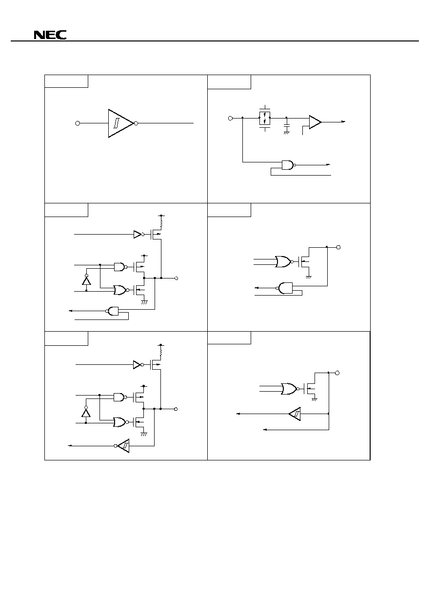
Figure 3-1. Pin Input/Output Circuits
Schmitt-triggered input with hysteresis characteristics
Type 2
IN
Type 5-H
Pull-up
enable
Data
Output
disable
Input
enable
V
DD0
P-ch
V
DD0
P-ch
IN/OUT
N-ch
Type 13-T
V
SS0
V
SS0
Type 8-C
Pull-up
enable
Data
Output
disable
V
DD0
P-ch
V
DD0
P-ch
IN/OUT
N-ch
V
SS0
Type 9-C
Type 13-X
Output data
Output disable
IN/OUT
N-ch
Input buffer with intermediate withstand voltage
Input enable
V
SS0
Output data
Output disable
IN/OUT
Input buffer with 5-V
withstand voltage
Comparator
N-ch
IN
Comparator
+
-
V
REF
(Threshold voltage)
AV
SS
P-ch
N-ch
Input
enable

15
µ
µ
µ
µ
PD78F9177, 78F9177Y
Data Sheet U14022EJ1V0DS00
4. CPU ARCHITECTURE
Products in the
µ
PD78F9177 and
µ
PD78F9177Y can access up to 64 Kbytes of memory space.
Figure 4-1 shows the memory map.
Figure 4-1. Memory Map
Special function registers
256
◊
8 bits
Internal high-speed RAM
512
◊
8 bits
Program memory
space
Data memory space
Program area
Program area
CALLT table area
Reserved
Vector table area
Internal flash memory
24576 x 8 bits
F F F F H
F F 0 0 H
F E F F H
F D 0 0 H
F C F F H
5 F F F H
0 0 8 0 H
0 0 7 F H
0 0 4 0 H
0 0 3 F H
0 0 2 4 H
0 0 2 3 H
0 0 0 0 H
0 0 0 0 H
5 F F F H
6 0 0 0 H
16
µ
µ
µ
µ
PD78F9177, 78F9177Y
Data Sheet U14022EJ1V0DS00
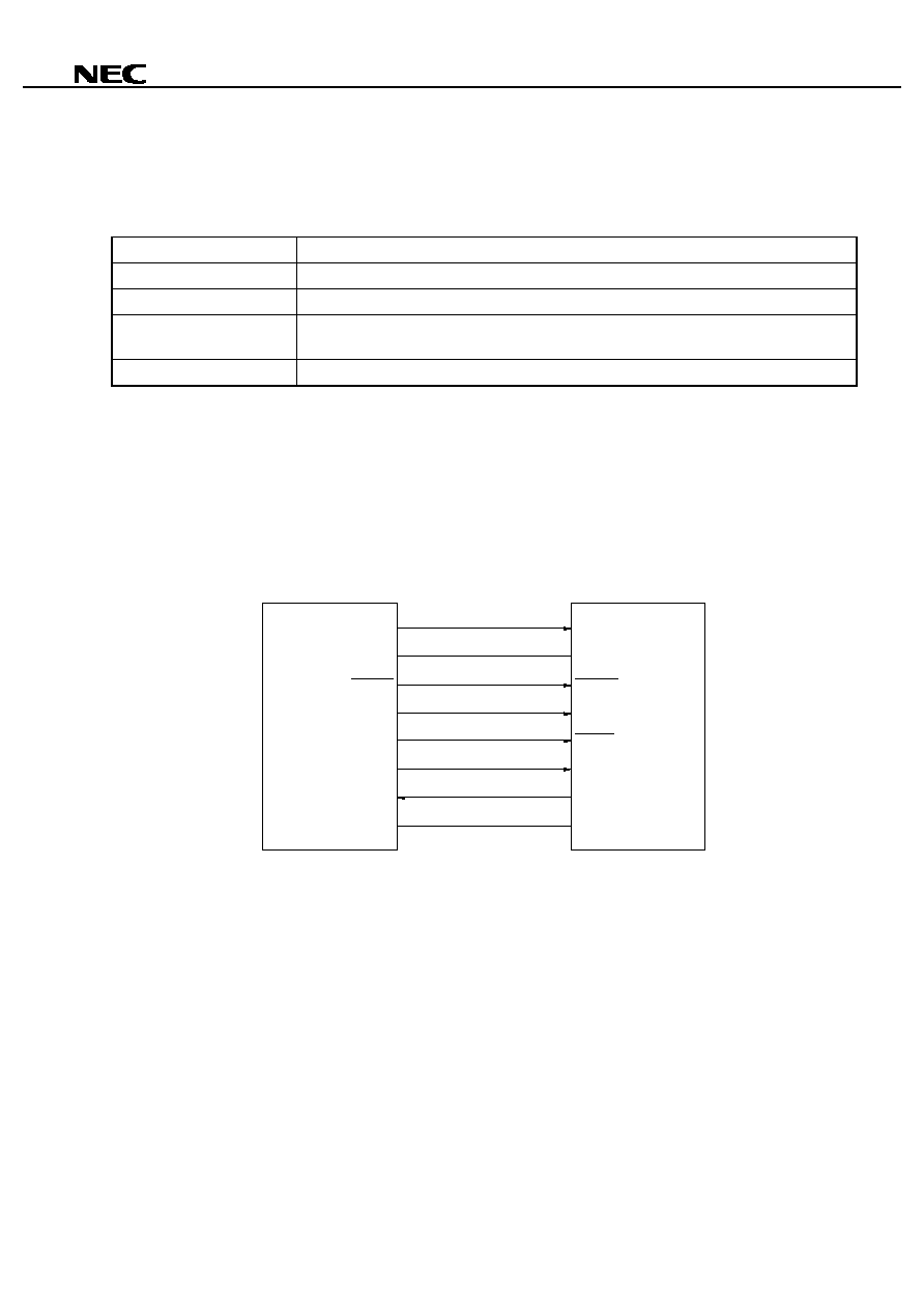
5. FLASH MEMORY PROGRAMMING
The on-chip program memory in the
µ
PD78F9177 and
µ
PD78F9177Y is flash memory.
The flash memory can be written with the
µ
PD78F9177 and
µ
PD78F9177Y mounted on the target system (on-
board). Connect the dedicated flash programmer (Flashpro III (part number: FL-PR3, PG-FP3)) to the host machine
and target system to write the flash memory.
Remark FL-PR3 is made by Naito Densei Machida Mfg. Co., Ltd.
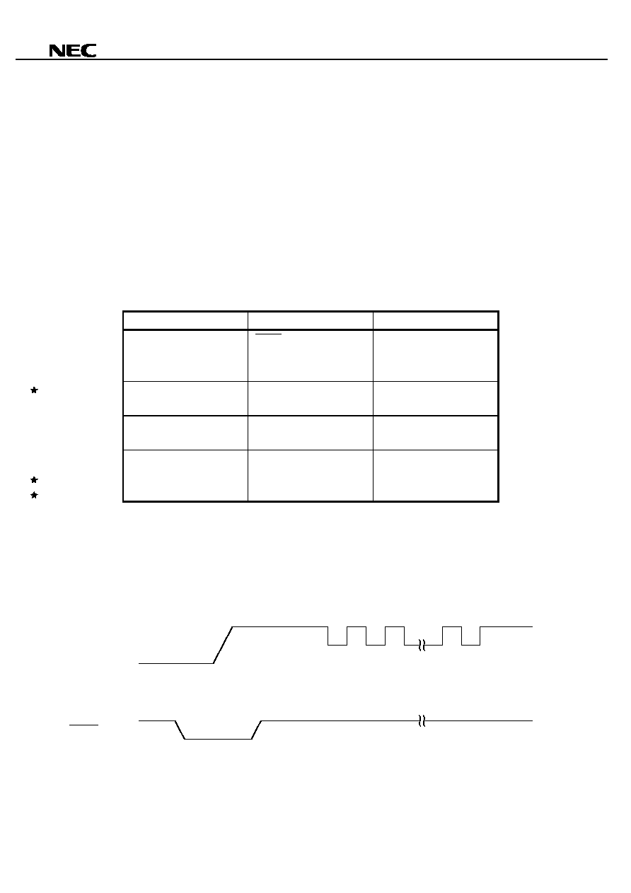
5.1
Selecting Communication Mode
The flash memory is written by using Flashpro III and by means of serial communication. Select a communication
mode from those listed in Table 5-1. To select a communication mode, the format shown in Figure 5-1 is used. Each
communication mode is selected by the number of V
PP
pulses shown in Table 5-1.
Table 5-1. Communication Mode
Communication Mode
Pins Used
Number of V
PP
Pulses
3-wire serial I/O
SCK20/ASCK20/P20
SO20/TxD20/P21
SI20/RxD20/P22
0
SMB
Note1
SCL0/P23
SDA0/P24
4
UART
TxD20/SO20/P21
RxD20/SI20/P22
8
Pseudo 3-wire mode
Note2
P00 (Serial clock input)
P01 (Serial data output)
P02 (Serial data input)
12
Notes 1.
µ
PD78F9177Y only
2. Serial transfer is performed by controlling a port by software.
Caution
Be sure to select a communication mode based on the V
PP
pulse number shown in Table 5-1.
Figure 5-1. Communication Mode Selection Format
10 V
V
SS
V
DD
V
PP
V
DD
V
SS
RESET
1
2
n
17
µ
µ
µ
µ
PD78F9177, 78F9177Y
Data Sheet U14022EJ1V0DS00
5.2
Function of Flash Memory Programming
By transmitting/receiving commands and data in the selected communication mode, operations such as writing to
the flash memory are performed. Table 5-2 shows the major functions of flash memory programming.
Table 5-2. Functions of Flash Memory Programming
Function
Description
Batch erase
Erases all contents of memory
Batch blank check
Checks erased state of entire memory
Data write
Write to flash memory based on write start address and number of data written
(number of bytes)
Batch verify
Compares all contents of memory with input data
5.3
Flashpro III Connection Example
How the Flashpro III is connected to the
µ
PD78F9177 and
µ
PD78F9177Y differs depending on the communication
mode (3-wired serial I/O, SMB, UART, or pseudo 3-wire mode). Figures 5-2 to 5-5 show the connection in the
respective mode.
Figure 5-2. Flashpro III Connection in 3-wired Serial I/O Mode
V
PP
n
Note
V
DD
RESET
SCK
SO
SI
GND
V
PP
V
DD0
, V
DD1
, AV
DD
RESET
CLK
X1
SCK20
SI20
SO20
V
SS0
, V
SS1
, A
VSS
Flashpro III
PD78F9177, 78F9177Y
µ
Note n = 1, 2
18
µ
µ
µ
µ
PD78F9177, 78F9177Y
Data Sheet U14022EJ1V0DS00
Figure 5-3. Flashpro III Connection in SMB Mode
V
PP
n
Note
V
DD
RESET
SO
SI
GND
V
PP
V
DD0
, V
DD1
, AV
DD
RESET
CLK
X1
SCL0
SDA0
V
SS0
, V
SS1
, AV
SS
Flashpro III
PD78F9177Y
µ
Note n = 1, 2
Figure 5-4. Flashpro III Connection in UART Mode
V
PP
n
Note
V
DD
RESET
SO
SI
GND
V
PP
V
DD0
, V
DD1
, AV
DD
RESET
CLK
X1
RxD20
TxD20
V
SS0
, V
SS1
, AV
SS
Flashpro III
PD78F9177, 78F9177Y
µ
Note n = 1, 2
Figure 5-5. Flashpro III Connection in Pseudo Serial I/O Mode (When Port 0 is Used)
V
PP
n
Note
V
DD
SCK
SO
SI
GND
RESET
V
PP
V
DD0
, V
DD1
, AV
DD
RESET
CLK
X1
P00 (Serial clock)
P02 (Serial input)
P01 (Serial output)
V
SS0
, V
SS1
, AV
SS
Flashpro III
PD78F9177, 78F9177Y
µ
Note n = 1, 2
19
µ
µ
µ
µ
PD78F9177, 78F9177Y
Data Sheet U14022EJ1V0DS00
5.4
Example of Settings for Flashpro III (PG-FP3)
Set as follows when writing to flash memory using the Flashpro III (PG-FP3).
<1> Download the parameter file.
<2> Select the serial mode and the serial clock using the type command.
<3> The following is a setting example using the PG-FP3.
Table 5-3. Example Using PG-FP3
Communication mode
Setting example using PG-FP3
Number of V
PP
pulses
Note1
COMM PORT
SIO ch-0
On target board
CPU CLK
In Flashpro
On target board
4.1943 MHz
SIO CLK
1.0 MHz
In Flashpro
4.0 MHz
3-wired serial I/O mode
SIO CLK
1.0 MHz
0
COMM PORT
IIC-ch0
SLAVE ADDRESS
10H
IIC CLOCK
100 kHz
CPU CLOCK
In Flashpro
Flashpro Clock
4.0 MHz
Note3
SMB
Note2
Multiple Rate
01.00
4
COMM PORT
UART-ch0
CPU CLK
On target board
On target board
4.1943 MHz
UART
UART BPS
9600 bps
Note4
8
COMM PORT
Port A
On target board
CPU CLK
In Flashpro
On target board
4.1943 MHz
SIO CLK
1.0 MHz
In Flashpro
4.0 MHz
Pseudo 3-wire mode
SIO CLK
1.0 MHz
12
Notes 1. The number of V
PP
pulses supplied from the Flashpro III during serial communication initialization.
The pins to be used in communication are determined by this number of pulses.
2.
µ
PD78F9177Y only.
3. Select one of 4.0 MHz or 3.125 MHz.
4. Select one of 9600 bps, 19200 bps, 38400 bps, or 76800 bps.
Remark
COMM PORT : Selection of serial port
SIO CLK
: Selection of serial clock frequency
CPU CLK
: Selection of CPU clock source to be input

20
µ
µ
µ
µ
PD78F9177, 78F9177Y
Data Sheet U14022EJ1V0DS00
6. INSTRUCTION SET OVERVIEW
This section lists the
µ
PD78F9177 and
µ
PD78F9177Y instruction set.
6.1 Conventions
6.1.1 Operand identifiers and description methods
Operands are described in the "Operand" column of each instruction in accordance with the description method of
the instruction operand identifier (refer to the assembler specifications for detail). When there are two or more
description methods, select one of them. Alphabetic letters in capitals and the symbols, #, !, $, and [ ], are keywords
and must be described as they are. Each symbol has the following meaning.
∑
#:
Immediate data specification
∑
$:
Relative address specification
∑
!:
Absolute address specification
∑
[ ]:
Indirect address specification
In the case of immediate data, describe an appropriate numeric value or a label. When using a label, be sure to
describe the #,!, $, or [ ] symbols.
For operand register identifiers, r and rp, either function names (X, A, C, etc.) or absolute names (names in
parentheses in the table below, R0, R1, R2, etc.) can be used for description.
Table 6-1. Operand Identifiers and Description Methods
Identifier
Description Method
r
rp
sfr
X (R0), A (R1), C (R2), B (R3), E (R4), D (R5), L (R6), H (R7),
AX (RP0), BC (RP1), DE (RP2), HL (RP3)
Special function register symbol
saddr
saddrp
FE20H to FF1FH immediate data or label
FE20H to FF1FH immediate data or label (even address only)
addr16
addr5
0000H to FFFFH immediate data or label
(Only even addresses for 16-bit data transfer instructions)
0040H to 007FH immediate data or label (even address only)
word
byte
bit
16-bit immediate data or label
8-bit immediate data or label
3-bit immediate data or label

21
µ
µ
µ
µ
PD78F9177, 78F9177Y
Data Sheet U14022EJ1V0DS00
6.1.2 Descriptions of the operation field
A:
A register; 8-bit accumulator
X:
X register
B:
B register
C:
C register
D:
D register
E:
E register
H:
H register
L:
L register
AX:
AX register pair; 16-bit accumulator
BC:
BC register pair
DE:
DE register pair
HL:
HL register pair
PC:
Program counter
SP:
Stack pointer
PSW:
Program status word
CY:
Carry flag
AC:
Auxiliary carry flag
Z:
Zero flag
IE:
Interrupt request enable flag
NMIS:
Non-maskable interrupt servicing flag
( ):
Memory contents indicated by address or register contents in parentheses
X
H
, X
L
:
Higher 8 bits and lower 8 bits of 16-bit register
:
Logical product (AND)
:
Logical sum (OR)
:
Exclusive OR
:
Inverted data
addr16:
16-bit immediate data or label
jdisp8:
Signed 8-bit data (displacement value)
6.1.3 Description of the flag operation field
(Blank):
Not affected
0:
Cleared to 0
1:
Set to 1
◊
:
Set/cleared according to the result
R:
Previously saved value is restored

22
µ
µ
µ
µ
PD78F9177, 78F9177Y
Data Sheet U14022EJ1V0DS00
6.2 Operations
Flags
Mnemonic
Operand
Bytes
Clock
Operation
Z
AC CY
MOV
r. #byte
3
6
r
byte
saddr, #byte
3
6
(saddr)
byte
sfr, #byte
3
6
sfr
byte
A, r
Note 1
2
4
A
r
r, A
Note 1
2
4
r
A
A, saddr
2
4
A
(saddr)
saddr, A
2
4
(saddr)
A
A, sfr
2
4
A
sfr
sfr, A
2
4
sfr
A
A, !addr16
3
8
A
(addr16)
!addr16, A
3
8
(addr16)
A
PSW, #byte
3
6
PSW
byte
◊
◊
◊
A, PSW
2
4
A
PSW
PSW, A
2
4
PSW
A
◊
◊
◊
A, [DE]
1
6
A
(DE)
[DE], A
1
6
(DE)
A
A, [HL]
1
6
A
(HL)
[HL], A
1
6
(HL)
A
A, [HL + byte]
2
6
A
(HL + byte)
[HL + byte], A
2
6
(HL + byte)
A
XCH
A, X
1
4
A
X
A, r
Note 2
2
6
A
r
A, saddr
2
6
A
(saddr)
A, sfr
2
6
A
(sfr)
A, [DE]
1
8
A
(DE)
A, [HL]
1
8
A
(HL)
A, [HL + byte]
2
8
A
(HL+byte)
MOVW
rp, #word
3
6
rp
word
AX, saddrp
2
6
AX
(saddrp)
saddrp, AX
2
8
(saddrp)
AX
AX, rp
Note 3
1
4
AX
rp
rp, AX
Note 3
1
4
rp
AX
Notes 1. Except r = A
2. Except r = A, X
3. Only when rp = BC, DE, HL
Remark
One clock of an instruction is one clock of the CPU clock (f
CPU
) selected using the processor clock
control register (PCC).
23
µ
µ
µ
µ
PD78F9177, 78F9177Y
Data Sheet U14022EJ1V0DS00
Flags
Mnemonic
Operand
Bytes
Clock
Operation
Z
AC CY
XCHW
AX, rp
Note
1
8
AX
rp
ADD
A, #byte
2
4
A, CY
A + byte
◊
◊
◊
saddr, #byte
3
6
(saddr), CY
(saddr) + byte
◊
◊
◊
A, r
2
4
A, CY
A + r
◊
◊
◊
A, saddr
2
4
A, CY
A + (saddr)
◊
◊
◊
A, !addr16
3
8
A, CY
A + (addr16)
◊
◊
◊
A, [HL]
1
6
A, CY
A + (HL)
◊
◊
◊
A, [HL + byte]
2
6
A, CY
A + (HL + byte)
◊
◊
◊
ADDC
A, #byte
2
4
A, CY
A + byte + CY
◊
◊
◊
saddr, #byte
3
6
(saddr), CY
(saddr) + byte + CY
◊
◊
◊
A, r
2
4
A, CY
A + r + CY
◊
◊
◊
A, saddr
2
4
A, CY
A+ (saddr) + CY
◊
◊
◊
A, !addr16
3
8
A, CY
A+ (addr16) +CY
◊
◊
◊
A, [HL]
1
6
A, CY
A + (HL) + CY
◊
◊
◊
A, [HL + byte]
2
6
A, CY
A+ (HL + byte) + CY
◊
◊
◊
SUB
A, #byte
2
4
A, CY
A ≠ byte
◊
◊
◊
saddr, #byte
3
6
(saddr), CY
(saddr) ≠ byte
◊
◊
◊
A, r
2
4
A, CY
A ≠ r
◊
◊
◊
A, saddr
2
4
A, CY
A ≠ (saddr)
◊
◊
◊
A, !addr16
3
8
A, CY
A ≠ (addr16)
◊
◊
◊
A, [HL]
1
6
A, CY
A ≠ (HL)
◊
◊
◊
A, [HL + byte]
2
6
A, CY
A ≠ (HL + byte)
◊
◊
◊
SUBC
A, #byte
2
4
A, CY
A ≠ byte ≠ CY
◊
◊
◊
saddr, #byte
3
6
(saddr), CY
(saddr) ≠ byte ≠ CY
◊
◊
◊
A, r
2
4
A, CY
A ≠ r ≠ CY
◊
◊
◊
A, saddr
2
4
A, CY
A ≠ (saddr) ≠ CY
◊
◊
◊
A, !addr16
3
8
A, CY
A ≠ (addr16) ≠ CY
◊
◊
◊
A, [HL]
1
6
A, CY
A ≠ (HL) ≠ CY
◊
◊
◊
A, [HL + byte]
2
6
A, CY
A ≠ (HL + byte) ≠ CY
◊
◊
◊
Note Only when rp = BC, DE, HL
Remark
One clock of an instruction is one clock of the CPU clock (f
CPU
) selected using the processor clock
control register (PCC).
24
µ
µ
µ
µ
PD78F9177, 78F9177Y
Data Sheet U14022EJ1V0DS00
Flags
Mnemonic
Operand
Bytes
Clock
Operation
Z
AC CY
AND
A, #byte
2
4
A
A
byte
◊
saddr, #byte
3
6
(saddr)
(saddr)
byte
◊
A, r
2
4
A
A
r
◊
A, saddr
2
4
A
A
(saddr)
◊
A, !addr16
3
8
A
A
(addr16)
◊
A, [HL]
1
6
A
A
(HL)
◊
A, [HL + byte]
2
6
A
A
(HL + byte)
◊
OR
A, #byte
2
4
A
A
byte
◊
saddr, #byte
3
6
(saddr)
(saddr)
byte
◊
A, r
2
4
A
A
r
◊
A, saddr
2
4
A
A
(saddr)
◊
A, !addr16
3
8
A
A
(addr16)
◊
A, [HL]
1
6
A
A
(HL)
◊
A, [HL + byte]
2
6
A
A
(HL + byte)
◊
XOR
A, #byte
2
4
A
A
byte
◊
saddr, #byte
3
6
(saddr)
(saddr)
byte
◊
A, r
2
4
A
A
r
◊
A, saddr
2
4
A
A
(saddr)
◊
A, !addr16
3
8
A
A
(addr16)
◊
A, [HL]
1
6
A
A
(HL)
◊
A, [HL + byte]
2
6
A
A
(HL + byte)
◊
CMP
A, #byte
2
4
A ≠ byte
◊
◊
◊
saddr, #byte
3
6
(saddr) ≠ byte
◊
◊
◊
A, r
2
4
A ≠ r
◊
◊
◊
A, saddr
2
4
A ≠ (saddr)
◊
◊
◊
A, !addr16
3
8
A ≠ (addr16)
◊
◊
◊
A, [HL]
1
6
A ≠ (HL)
◊
◊
◊
A, [HL + byte]
2
6
A ≠ (HL + byte)
◊
◊
◊
ADDW
AX, #word
3
6
AX, CY
AX + word
◊
◊
◊
SUBW
AX, #word
3
6
AX, CY
AX ≠ word
◊
◊
◊
CMPW
AX, #word
3
6
AX ≠ word
◊
◊
◊
INC
r
2
4
r
r + 1
◊
◊
saddr
2
4
(saddr)
(saddr) + 1
◊
◊
DEC
r
2
4
r
r≠ 1
◊
◊
saddr
2
4
(saddr)
(saddr) ≠ 1
◊
◊
Remark
One clock of an instruction is one clock of the CPU clock (f
CPU
) selected using the processor clock
control register (PCC).
25
µ
µ
µ
µ
PD78F9177, 78F9177Y
Data Sheet U14022EJ1V0DS00
Flags
Mnemonic
Operand
Bytes
Clock
Operation
Z
AC CY
INCW
rp
1
4
rp
rp + 1
DECW
rp
1
4
rp
rp ≠ 1
ROR
A, 1
1
2
(CY, A
7
A
0
, A
m-1
A
m
)
◊
1
◊
ROL
A, 1
1
2
(CY, A
0
A
7
, A
m+1
A
m
)
◊
1
◊
RORC
A, 1
1
2
(CY
A
0
, A
7
CY, A
m-1
A
m
)
◊
1
◊
ROLC
A, 1
1
2
(CY
A
7
, A
0
CY, A
m+1
A
m
)
◊
1
◊
SET1
saddr.bit
3
6
(saddr.bit)
1
sfr.bit
3
6
sfr.bit
1
A.bit
2
4
A.bit
1
PSW.bit
3
6
PSW.bit
1
◊
◊
◊
[HL].bit
2
10
(HL).bit
1
CLR1
saddr.bit
3
6
(saddr.bit)
0
sfr.bit
3
6
sfr.bit
0
A.bit
2
4
A.bit
0
PSW.bit
3
6
PSW.bit
0
◊
◊
◊
[HL].bit
2
10
(HL).bit
0
SET1
CY
1
2
CY
1
1
CLR1
CY
1
2
CY
0
0
NOT1
CY
1
2
CY
CY
◊
CALL
!addr16
3
6
(SP ≠ 1)
(PC + 3)
H
, (SP ≠ 2)
(PC + 3)
L
,
PC
addr16, SP
SP ≠ 2
CALLT
[addr5]
1
8
(SP ≠ 1)
(PC + 1)
H
, (SP ≠ 2)
(PC + 1)
L
,
PC
H
(00000000, addr5 + 1)
PC
L
(00000000, addr5)
SP
SP ≠ 2
RET
1
6
PC
H
(SP + 1), PC
L
(SP),
SP
SP + 2
RETI
1
8
PC
H
(SP + 1), PC
L
(SP),
PSW
(SP + 2), SP
SP + 3,
NMIS
0
R
R
R
PUSH
PSW
1
2
(SP ≠ 1)
PSW, SP
SP ≠ 1
rp
1
4
(SP ≠ 1)
rp
H
, (SP ≠ 2)
rp
L
,
SP
SP -≠ 2
POP
PSW
1
4
PSW
(SP), SP
SP + 1
R
R
R
rp
1
6
rp
H
(SP + 1), rp
L
(SP),
SP
SP + 2
MOVW
SP, AX
2
8
SP
AX
AX, SP
2
6
AX
SP
Remark
One clock of an instruction is one clock of the CPU clock (f
CPU
) selected using the processor clock
control register (PCC).

26
µ
µ
µ
µ
PD78F9177, 78F9177Y
Data Sheet U14022EJ1V0DS00
Flags
Mnemonic
Operand
Bytes
Clock
Operation
Z
AC CY
BR
!addr16
3
6
PC
addr16
$addr16
2
6
PC
PC + 2 + jdisp8
AX
1
6
PC
H
A, PC
L
X
BC
$addr16
2
6
PC
PC + 2 + jdisp8 if CY = 1
BNC
$addr16
2
6
PC
PC + 2 + jdisp8 if CY = 0
BZ
$addr16
2
6
PC
PC + 2 + jdisp8 if Z = 1
BNZ
$addr16
2
6
PC
PC + 2 + jdisp8 if Z = 0
BT
saddr.bit, $saddr16
4
10
PC
PC + 4 + jdisp8
if (saddr. bit) = 1
sfr.bit, $addr16
4
10
PC
PC + 4 + jdisp8 if sfr. bit = 1
A.bit, $saddr16
3
8
PC
PC + 3 + jdisp8 if A. bit = 1
PSW.bit $addr16
4
10
PC
PC + 4 + jdisp8 if PSW. bit = 1
BF
saddr.bit, $addr16
4
10
PC
PC + 4 + jdisp8
if (saddr. bit) = 0
sfr.bit, $addr16
4
10
PC
PC + 4 + jdisp8 if sfr. bit = 0
A.bit, $addr16
3
8
PC
PC + 3 + jdisp8 if A. bit = 0
PSW.bit, $addr16
4
10
PC
PC + 4 + jdisp8 if PSW. bit = 0
DBNZ
B, $addr16
2
6
B
B ≠ 1, then
PC
PC + 2 + jdisp8 if B
0
C, $addr16
2
6
C
C ≠ 1, then
PC
PC + 2 + jdisp8 if C
0
saddr, $addr16
3
8
(saddr)
(saddr) ≠ 1, then
PC
PC + 3 + jdisp8 if (saddr)
0
NOP
1
2
No Operation
EI
3
6
IE
1 (Enable Interrupt)
DI
3
6
IE
0 (Disable Interrupt)
HALT
1
2
Set HALT Mode
STOP
1
2
Set Stop Mode
Remark
One clock of an instruction is one clock of the CPU clock (f
CPU
) selected using the processor clock
control register (PCC).

27
µ
µ
µ
µ
PD78F9177, 78F9177Y
Data Sheet U14022EJ1V0DS00
7. ELECTRICAL SPECIFICATIONS
Absolute Maximum Ratings (T
A
= 25
∞
∞
∞
∞
C)
Parameter
Symbol
Conditions
Ratings
Unit
V
DD
V
AV
DD
V
AV
REF
AV
DD
-
0.3 V
V
DD
AV
DD
+ 0.3 V
AV
REF
AV
DD
+ 0.3 V
AV
REF
V
DD
+ 0.3 V
-
0.3 to +6.5
V
Supply voltage
V
PP
-
0.3 to +10.5
V
V
I1
Pins other than P50 to P53, P23, P24
-
0.3 to V
DD
+ 0.3
V
V
I2
P23, P24
-
0.3 to +5.5
V
Input voltage
V
I3
P50 to P53
-
0.3 to +13
V
Output voltage
V
O
-
0.3 to V
DD
+ 0.3
V
Per pin
-
10
mA
Output current, high
I
OH
Total for all pins
-
30
mA
Per pin
30
mA
Output current, low
I
OL
Total for all pins
160
mA
In normal operation mode
-
40 to +85
∞
C
Operating ambient temperature
T
A
During flash memory programming
+10 to +40
∞
C
Storage temperature
T
stg
-
40 to +125
∞
C
Caution
Product quality may suffer if the absolute maximum rating is exceeded even momentarily for
any parameter. That is, the absolute maximum ratings are rated values at which the product is
on the verge of suffering physical damage, and therefore the product must be used under
conditions that ensure that the absolute maximum ratings are not exceeded.
Remark
Unless otherwise specified, the characteristics of alternate-function pins are the same as those of port
pins.
28
µ
µ
µ
µ
PD78F9177, 78F9177Y
Data Sheet U14022EJ1V0DS00
Main System Clock Oscillator Characteristics (T
A
=
-
-
-
-
40 to +85
∞
∞
∞
∞
C, V
DD
= 1.8 to 5.5 V)
Resonator
Recommended Circuit
Parameter
Conditions
MIN.
TYP.
MAX.
Unit
Oscillation frequency (f
X
)
Note 1
V
DD
= oscillation
voltage range
1.0
5.0
MHz
Ceramic
resonator
X2
X1
V
PP
C2
C1
Oscillation stabilization time
Note 2
After V
DD
reaches
oscillation voltage
range MIN.
4
ms
Oscillation frequency (f
X
)
Note 1
1.0
5.0
MHz
V
DD
= 4.5 to 5.5 V
10
Crystal
resonator
X2
X1
V
PP
C2
C1
Oscillation stabilization time
Note 2
30
ms
X1 input frequency (f
X
)
Note 1
1.0
5.0
MHz
X1 input high-/low-level width
(t
XH
, t
XL
)
85
500
ns
X1 input frequency (f
X
)
Note 1
V
DD
= 2.7 to 5.5 V
1.0
5.0
MHz
External
clock
X1 input high-/low-level width
(t
XH
, t
XL
)
V
DD
= 2.7 to 5.5 V
85
500
ns
Notes 1. Indicates only oscillator characteristics. Refer to AC Characteristics for instruction execution time.
2. Time required to stabilize oscillation after reset or STOP mode release. Use a resonator that stabilizes
oscillation within the oscillation wait time.
Cautions 1. When using the main system clock oscillator, wire as follows in the area enclosed by the
broken lines in the above figures to avoid an adverse effect from wiring capacitance.
∑
∑
∑
∑
Keep the wiring length as short as possible.
∑
Do not cross the wiring with the other signal lines.
∑
Do not route the wiring near a signal line through which a high fluctuating current flows.
∑
Always make the ground point of the oscillator capacitor the same potential as V
SS0
.
∑
Do not ground the capacitor to a ground pattern through which a high current flows.
∑
Do not fetch signals from the oscillator.
2. When the main system clock is stopped and the device is operating on the subsystem clock,
wait until the oscillation stabilization time has been secured by the program before
switching back to the main system clock.
Remark
For the resonator selection and oscillator constant, customers are requested to either evaluate the
oscillation themselves or apply to the resonator manufacturer for evaluation.
X1
X2
X1
X2
OPEN

29
µ
µ
µ
µ
PD78F9177, 78F9177Y
Data Sheet U14022EJ1V0DS00
Subsystem Clock Oscillator Characteristics (T
A
=
-
-
-
-
40 to +85
∞
∞
∞
∞
C, V
DD
= 1.8 to 5.5 V)
Resonator
Recommended Circuit
Parameter
Conditions
MIN.
TYP.
MAX.
Unit
Oscillation frequency (f
XT
)
Note 1
32
32.768
35
kHz
V
DD
= 4.5 to 5.5 V
1.2
2
s
Crystal
resonator
XT2
XT1
V
PP
C4
C3
R
Oscillation stabilization time
Note 2
10
s
XT1 input frequency (f
XT
)
Note 1
32
35
kHz
External
clock
XT1 input high-/low-level width
(t
XTH
, t
XTL
)
14.3
15.6
µ
s
Notes 1. Indicates only oscillator characteristics. Refer AC Characteristics for instruction execution time.
2. Time required to stabilize oscillation after reset or STOP mode release.
Cautions 1. When using the subsystem clock oscillator, wire as follows in the area enclosed by the
broken lines in the above figures to avoid an adverse effect from wiring capacitance.
∑
∑
∑
∑
Keep the wiring length as short as possible.
∑
Do not cross the wiring with the other signal lines.
∑
Do not route the wiring near a signal line through which a high fluctuating current flows.
∑
Always make the ground point of the oscillator capacitor the same potential as V
SS0
.
∑
Do not ground the capacitor to a ground pattern through which a high current flows.
∑
Do not fetch signals from the oscillator.
2. The subsystem clock oscillator is designed as a low-amplitude circuit for reducing current
consumption, and is more prone to malfunction due to noise than the main system clock
oscillator. Particular care is therefore required with the wiring method when the subsystem
clock is used.
Remark
For the resonator selection and oscillator constant, customers are requested to either evaluate the
oscillation themselves or apply to the resonator manufacturer for evaluation.
XT1
XT2

30
µ
µ
µ
µ
PD78F9177, 78F9177Y
Data Sheet U14022EJ1V0DS00
DC Characteristics (T
A
=
-
-
-
-
40 to +85
∞
∞
∞
∞
C, V
DD
= 1.8 to 5.5 V)
Parameter
Symbol
Conditions
MIN.
TYP.
MAX.
Unit
Per pin
-
1
mA
Output current
,
high
I
OH
Total for all pins
-
15
mA
Per pin
10
mA
Output current, low
I
OL
Total for all pins
80
mA
V
DD
= 2.7 to 5.5 V
0.7 V
DD
V
DD
V
V
IH1
P00 to P05, P10,
P11,P60 to P67
0.9 V
DD
V
DD
V
V
DD
= 2.7 to 5.5 V
0.7 V
DD
12
V
V
IH2
P50 to P53
V
DD
= 1.8 to 5.5 V,
T
A
= 25 to +85
∞
C
0.9 V
DD
12
V
V
DD
= 2.7 to 5.5 V
0.8 V
DD
V
DD
V
V
IH3
RESET,
P20 to P26, P30
to P33
0.9 V
DD
V
DD
V
V
DD
= 4.5 to 5.5 V
V
DD
-
0.5
V
DD
V
Input voltage, high
V
IH4
X1, X2, XT1, XT2
V
DD
-
0.1
V
DD
V
V
DD
= 2.7 to 5.5 V
0
0.3 V
DD
V
V
IL1
P00 to P05, P10,
P11, P60 to P67
0
0.1 V
DD
V
V
DD
= 2.7 to 5.5 V
0
0.3 V
DD
V
V
IL2
P50 to P53
0
0.1 V
DD
V
V
DD
= 2.7 to 5.5 V
0
0.2 V
DD
V
V
IL3
RESET,P20 to
P26, P30 to P33
0
0.1 V
DD
V
V
DD
= 4.5 to 5.5 V
0
0.4
V
Input voltage, low
V
IL4
X1, X2, XT1, XT2
0
0.1
V
V
DD
= 4.5 to 5.5 V, I
OH
=
-
1 mA
V
DD
-
1.0
V
Output voltage,
high
V
OH
Pins other than
P23, P24, P50 to
P53
V
DD
= 1.8 to 5.5 V, I
OH
=
-
100
µ
A
V
DD
-
0.5
V
V
DD
= 4.5 to 5.5 V, I
OL
= 10 mA
1.0
V
V
OL1
Pins other than
P50 to P53
V
DD
= 1.8 to 5.5 V, I
OL
= 400
µ
A
0.5
V
V
DD
= 4.5 to 5.5 V, I
OL
= 10 mA
1.0
V
Output voltage,
low
V
OL2
P50 to P53
V
DD
= 1.8 to 5.5 V, I
OL
= 1.6 mA
0.4
V
I
LIH1
Pins other than P50 to P53 (N-ch
open-drain) X1, X2, XT1, and
XT2
3
µ
A
I
LIH2
V
I
= V
DD
X1, X2, XT1, XT2
20
µ
A
Input leakage
current, high
I
LIH3
V
I
= 12 V
P50 to P53 (N-ch open drain)
20
µ
A
I
LIL1
Pins other than P50 to P53 (N-ch
open-drain) X1, X2, XT1, and
XT2
-
3
µ
A
I
LIL2
X1, X2, XT1, XT2
-
20
µ
A
Input leakage
current, low
I
LIL3
V
I
= 0 V
P50 to P53 (N-ch open drain)
-
3
Note
µ
A
Output leakage
current, high
I
LOH
V
O
= V
DD
3
µ
A
Output leakage
current, low
I
LOL
V
O
= 0 V
-
3
µ
A
Software
pull-up
resistor
R
1
V
I
= 0 V, for pins other than P23, P24, and P50 to
P53
50
100
200
k
Note A low-level input leakage current of -60
µ
A(MAX.) flows only during the 1-cycle time after a read instruction
is executed to P50 to P53 and P50 to P53 are set to input mode. At times other than this, -3
µ
A (MAX.)
current flows.
Remark
Unless otherwise specified, the characteristics of alternate-function pins are the same as those of port
pins.

31
µ
µ
µ
µ
PD78F9177, 78F9177Y
Data Sheet U14022EJ1V0DS00
DC Characteristics (T
A
=
-
-
-
-
40 to +85
∞
∞
∞
∞
C, V
DD
= 1.8 to 5.5 V)
Parameter
Symbol
Conditions
MIN.
TYP.
MAX.
Unit
V
DD
= 5.0 V
±
10%
Note 4
5.0
15.0
mA
V
DD
= 3.0 V
±
10%
Note 5
2.0
5.0
mA
I
DD1
Note 1
5.0-MHz crystal oscillation
operating mode
(C1 = C2 = 22pF)
V
DD
= 2.0 V
±
10%
Note 5
1.5
3.0
mA
V
DD
= 5.0 V
±
10%
Note 4
2.0
6.0
mA
V
DD
= 3.0 V
±
10%
Note 5
1.0
2.5
mA
I
DD2
Note 1
5.0-MHz crystal oscillation
HALT mode
(C1 = C2 = 22pF)
V
DD
= 2.0 V
±
10%
Note 5
0.75
1.5
mA
V
DD
= 5.0 V
±
10%
250
750
µ
A
V
DD
= 3.0 V
±
10%
200
600
µ
A
I
DD3
Note 1
32.768-kHz crystal
oscillation operating
mode
Note 3
(C3 = C4 = 22pF,
R = 220k
)
V
DD
= 2.0 V
±
10%
150
450
µ
A
V
DD
= 5.0 V
±
10%
50
150
µ
A
V
DD
= 3.0 V
±
10%
30
90
µ
A
I
DD4
Note 1
32.768-kHz crystal
oscillation HALT mode
Note 3
(C3 = C4 = 22pF,
R = 220k
)
V
DD
= 2.0 V
±
10%
20
60
µ
A
V
DD
= 5.0 V
±
10%
0.1
30
µ
A
V
DD
= 3.0 V
±
10%
0.05
10
µ
A
I
DD5
Note 1
32.768-kHz crystal stop
STOP mode
V
DD
= 2.0 V
±
10%
0.05
10
µ
A
V
DD
= 5.0 V
±
10%
Note 4
6.0
17.0
mA
V
DD
= 3.0 V
±
10%
Note 5
3.0
7.0
mA
Power supply
current
I
DD6
Note 2
5.0-MHz crystal oscillation
A/D operating mode
(C1 = C2 = 22pF)
V
DD
= 2.0 V
±
10%
Note 5
2.5
5.0
mA
Notes 1. The AV
REF
ON (ADCS0 (bit 7 of ADM0; A/D converter mode register 0) = 1), AV
DD
, and the port current
(including the current flowing through the internal pull-up resistors) are not included.
2. The AV
REF
On (ADCS0 =1) and port current (including the current flowing through the internal pull-up
resistors) are not included. Refer to the A/D converter characteristics for the current flowing through
AV
REF
.
3. When the main system clock is stopped.
4. During high-speed mode operation (when the processor clock control register (PCC) is set to 00H.)
5. During low-speed mode operation (when PCC is set to 02H)
Remark
Unless otherwise specified, the characteristics of alternate-function pins are the same as those of port
pins.

32
µ
µ
µ
µ
PD78F9177, 78F9177Y
Data Sheet U14022EJ1V0DS00
AC Characteristics
(1) Basic operation (T
A
=
-
-
-
-
40 to +85
∞
∞
∞
∞
C, V
DD
= 1.8 to 5.5 V)
Parameter
Symbol
Conditions
MIN.
TYP.
MAX.
Unit
V
DD
= 2.7 to 5.5 V
0.4
8
µ
s
Operation based on the
main system clock
1.6
8
µ
s
Cycle time
(minimum instruction
execution time)
T
CY
Operation based on the subsystem clock
114
122
125
µ
s
V
DD
= 2.7 to 5.5 V
0
4
MHz
TI80 and TI81 input
frequency
f
TI
0
275
kHz
V
DD
= 2.7 to 5.5 V
0.1
µ
s
TI80 and TI81 input
high-/low-level width
t
TIH
, t
TIL
1.8
µ
s
Interrupt input high-
/low-level width
t
INTH
, t
INTL
INTP0 to INTP3
10
µ
s
RESET input low-
level width
t
RSL
10
µ
s
CPT90 input high-
/low-level width
t
CPH
,
t
CPL
10
µ
s
T
CY
vs V
DD
(main system clock)
Supply voltage V
DD
[V]
1
2
3
4
5
6
0.1
0.4
0.5
1.0
2.0
10
60
Cycle time T
CY
[ s]
Guaranteed
operation range
µ

33
µ
µ
µ
µ
PD78F9177, 78F9177Y
Data Sheet U14022EJ1V0DS00
(2) Serial interface (T
A
=
-
-
-
-
40 to +85
∞
∞
∞
∞
C, V
DD
= 1.8 to 5.5 V)
(a) 3-wire serial I/O mode (SCK20...Internal clock)
Parameter
Symbol
Conditions
MIN.
TYP.
MAX.
Unit
V
DD
= 2.7 to 5.5 V
800
ns
SCK20 cycle time
t
KCY1
3200
ns
V
DD
= 2.7 to 5.5 V
t
KCY1
/2
-
50
ns
SCK20 high-/low-
level width
t
KH1
, t
KL1
t
KCY1
/2
-
150
ns
V
DD
= 2.7 to 5.5 V
150
ns
SI20 setup time
(to SCK20
)
t
SIK1
500
ns
V
DD
= 2.7 to 5.5 V
400
ns
SI20 hold time
(from SCK20
)
t
KSI1
600
ns
V
DD
= 2.7 to 5.5 V
0
250
ns
SO20 output
delay
time from SCK20
t
KSO1
R = 1 k
,
C = 100 pF
Note
0
1000
ns
Note R and C are the load resistance and load capacitance of the SO20 output line.
(b) 3-wire serial I/O mode (SCK20...External clock)
Parameter
Symbol
Conditions
MIN.
TYP.
MAX.
Unit
V
DD
= 2.7 to 5.5 V
900
ns
SCK20 cycle time
t
KCY2
3500
ns
V
DD
= 2.7 to 5.5 V
400
ns
SCK20 high-/low-
level width
t
KH2
, t
KL2
1600
ns
V
DD
= 2.7 to 5.5 V
100
ns
SI20 setup time
(to SCK20
)
t
SIK2
150
ns
V
DD
= 2.7 to 5.5 V
400
ns
SI20 hold time
(from SCK20
)
t
KSI2
600
ns
V
DD
= 2.7 to 5.5 V
0
300
ns
SO20 output delay
time
from SCK20
t
KSO2
R = 1 k
,
C = 100 pF
Note
0
1000
ns
V
DD
= 2.7 to 5.5 V
120
ns
SO20 setup time
(when using SS20,
to SS20
)
t
KAS2
400
ns
V
DD
= 2.7 to 5.5 V
240
ns
SO20 disable time
(when using SS20,
from SS20
)
t
KDS2
800
ns
Note R and C are the load resistance and load capacitance of the SO20 output line.
(c) UART mode (dedicated baud rate generator output)
Parameter
Symbol
Conditions
MIN.
TYP.
MAX.
Unit
V
DD
= 2.7 to 5.5 V
78125
bps
Transfer rate
19531
bps

34
µ
µ
µ
µ
PD78F9177, 78F9177Y
Data Sheet U14022EJ1V0DS00
(d) UART mode (external clock input)
Parameter
Symbol
Conditions
MIN.
TYP.
MAX.
Unit
V
DD
= 2.7 to 5.5 V
900
ns
ASCK20 cycle
time
t
KCY3
3500
ns
V
DD
= 2.7 to 5.5 V
400
ns
ASCK20 high-/low-
level width
t
KH3
, t
KL3
1600
ns
V
DD
= 2.7 to 5.5 V
39063
bps
Transfer rate
9766
bps
ASCK20 rise time,
fall time
t
R
, t
F
1
µ
s

35
µ
µ
µ
µ
PD78F9177, 78F9177Y
Data Sheet U14022EJ1V0DS00
(3) Serial interface SMB0 (T
A
=
-
-
-
-
40 to +85
∞
∞
∞
∞
C, V
DD
= 1.8 to 5.5 V) (
µ
µ
µ
µ
PD78F9177Y only)
(a) DC Characteristics
Parameter
Symbol
Conditions
MIN.
TYP.
MAX.
Unit
Input voltage, high
V
IH
SCL0, SDA0 (at hysteresis)
0.8 V
DD
V
DD
V
Input voltage, low
V
IL
SCL0, SDA0 (at hysteresis)
0
0.2 V
DD
V
V
DD
= 4.5 to 5.5 V, I
OL
= 10 mA
1.0
V
Output voltage,
high
V
OL
SCL0, SDA0
V
DD
= 1.8 to 5.5 V, I
OL
= 400
µ
A
0.5
V
Input leakage
current, high
I
LIH
SCL0, SDA0
V
I
= V
DD
3
µ
A
Input leakage
current, low
I
LIL
SCL0, SDA0
V
I
= 0 V
-
3
µ
A
(b) DC Characteristics (When using comparator)
Parameter
Symbol
Conditions
MIN.
TYP.
MAX.
Unit
Input range
V
SDA
,
V
SCL
V
DD
= 1.8 to 5.5 V
0
5.5
V
4.5
V
DD
5.5 V
0.72 V
ISMB
V
ISMB
1.28 V
ISMB
V
3.3
V
DD
< 4.5 V
0.78 V
ISMB
V
ISMB
1.22 V
ISMB
V
2.7
V
DD
< 3.3 V
0.75 V
ISMB
V
ISMB
1.25 V
ISMB
V
Transfer level
V
ISDA
,
V
ISCL
1.8
V
DD
< 2.7 V
0.90 V
ISMB
V
ISMB
1.45 V
ISMB
V
LVL01, LVL00 = 0, 1
0.25
◊
V
DD
V
LVL01, LVL00 = 1, 0
0.375
◊
V
DD
V
Input level
threshold value
V
ISMB
LVL01, LVL00 = 1, 1
0.5
◊
V
DD
V
Note V
ISMB
is an input level threshold value selected by bits LVL00 and LVL01 (bits 0 and 1 of SMB input level
setting register 0 (SMBVI0)).
According to the SMB standard (V1.1), the maximum value of low-level input voltage is 0.8 V, and the
minimum value of high-level input voltage, 2.1 V. To satisfy these conditions, set LVL01 and LVL00 as
follows;
∑
When V
DD
= 1.8 to 3.3 V: LVL01, LVL00 = 1, 1 (0.5
◊
V
DD
)
∑
When V
DD
= 3.3 to 4.5 V: LVL01, LVL00 = 1, 0 (0.375
◊
V
DD
)
∑
When V
DD
= 4.5 to 5.5 V: LVL01, LVL00 = 0, 1 (0.25
◊
V
DD
)
"LVL01, LVL00 = 0, 0" is not available since this setting does not satisfy the SMB standard (V1.1).

36
µ
µ
µ
µ
PD78F9177, 78F9177Y
Data Sheet U14022EJ1V0DS00
(c) AC Characteristics
SMB Mode
Standard Mode I
2
C
Bus
High-speed Mode I
2
C
Bus
Parameter
Symbol
MIN.
MAX.
MIN.
MAX.
MIN.
MAX.
Unit
SCL0 clock frequency
f
CLK
10
100
0
100
0
400
kHz
Bus free time
(between stop and start condition)
t
BUF
4.7
-
4.7
-
1.3
-
µ
s
Hold time
Note1
t
HD:STA
4.0
-
4.0
-
0.6
-
µ
s
Start/restart condition setup time
t
SU:STA
4.7
-
4.7
-
0.6
-
µ
s
Stop condition setup time
t
SU:STO
4.0
-
4.0
-
0.6
-
µ
s
When using CBUS-
compatible master
-
-
5
-
-
-
µ
s
Data hold
time
When using SMB/IIC
bus
t
HD:DAT
300
-
-
-
0
Note2
900
Note3
ns
Data setup time
t
SU:DAT
250
-
250
-
100
Note4
-
ns
SCL0 clock low-level width
t
LOW
4.7
-
4.7
-
1.3
-
µ
s
SCL0 clock high-level width
t
HIGH
4.0
50
4.0
-
0.6
-
µ
s
SCL0 and SDA0 signal fall time
t
F
-
300
-
300
-
300
ns
SCL0 and SDA0 signal rise time
t
R
-
1000
-
1000
-
300
ns
Spike pulse width controlled by
input filter
t
SP
-
-
-
-
0
50
ns
Timeout
t
TIMEOUT
25
35
-
-
-
-
ms
Total extended time of SCL0 clock
low-level period (slave)
t
LOW:SEXT
-
25
-
-
-
-
ms
Total extended time of cumulative
clock low-level period (master)
t
LOW:MEXT
-
10
-
-
-
-
ms
Capacitive load per each bus line
Cb
-
-
-
400
-
400
pF
Notes 1. In the start condition, the first clock pulse is generated after this hold time.
2. To fill in the underfined area of the SCL0 falling edge, it is necessary for the device to internally
provide at least 300 ns of hold time for the SDA0 signal (which is V
IHmin
. of the SCL0 signal).
3. If the device does not extend the SCL0 signal low hold time (t
LOW
), only maximum data hold time
t
HD:DAT
needs to be fulfilled.
4. The high-speed mode I
2
C bus is available in the SMB mode and the standard mode I
2
C bus system.
At this time, the conditions described below must be satisfied.
If the device extends the SCL0 signal low state hold time
t
SU:DAT
250 ns
If the device extends the SCL0 signal low state hold time
Be sure to transmit the next data bit to the SDA0 line before the SCL0 line is released (t
Rmax.
+
t
SU:DAT
= 1000 + 250 = 1250 ns by the SMB mode or the standard mode I
2
C bus specification).

37
µ
µ
µ
µ
PD78F9177, 78F9177Y
Data Sheet U14022EJ1V0DS00
AC Timing Measurement Points (excluding the X1 and XT1 inputs)
Clock Timing
TI Timing
0.8 V
DD
0.2 V
DD
Point of
measurement
0.8 V
DD
0.2 V
DD
1/f
X
t
XL
t
XH
X1 input
V
IH4
(MIN.)
V
IL4
(MAX.)
1/f
XT
t
XTL
t
XTH
XT1 input
V
IH4
(MIN.)
V
IL4
(MAX.)
1/f
TI
t
TIL
t
TIH
TI80, TI81

38
µ
µ
µ
µ
PD78F9177, 78F9177Y
Data Sheet U14022EJ1V0DS00
Interrupt Input Timing
INTP0-INTP3
t
INTL
t
INTH
RESET Input Timing
RESET
t
RSL
CPT90 Input Timing
CPT90
t
CPL
t
CPH

39
µ
µ
µ
µ
PD78F9177, 78F9177Y
Data Sheet U14022EJ1V0DS00
Serial Transfer Timing
3-wire serial I/O mode:
Remark
m = 1, 2
3-wire serial I/O mode (when using SS20):
UART mode (external clock input):
SCK20
t
KLm
t
KCYm
t
KHm
SI20
Input data
t
KSIm
t
SIKm
Output data
t
KSOm
SO20
ASCK20
t
R
t
F
t
KL3
t
KCY3
t
KH3
t
KAS2
SO20
SS20
Output data
t
KDS2

40
µ
µ
µ
µ
PD78F9177, 78F9177Y
Data Sheet U14022EJ1V0DS00
SMB mode:
t
R
t
LOW
t
F
t
HIGH
t
HD:STA
Stop condition
Start condition
Restart condition
Stop condition
t
BUF
t
SU:DAT
t
SU:STA
t
HD:STA
t
SP
t
SU:STO
t
HD:DAT
SCL0
SDA0
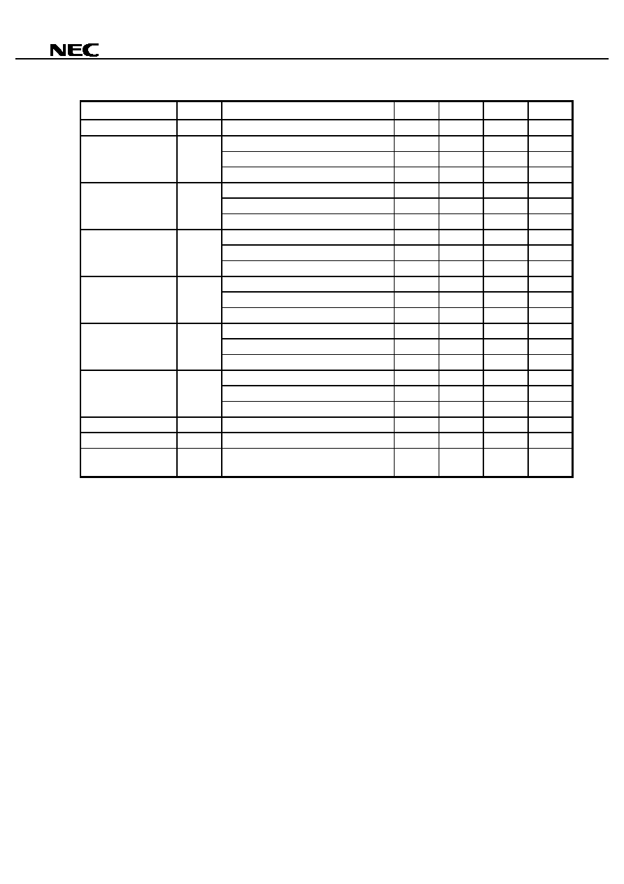
41
µ
µ
µ
µ
PD78F9177, 78F9177Y
Data Sheet U14022EJ1V0DS00
10-Bit A/D Converter Characteristics (T
A
=
-
-
-
-
40 to +85
∞
∞
∞
∞
C, 1.8
AV
REF
AV
DD
= V
DD
5.5 V, AV
SS
= V
SS
= 0 V)
Parameter
Symbol
Conditions
MIN.
TYP.
MAX.
Unit
Resolution
10
10
10
bit
4.5 V
AV
REF
AV
DD
5.5 V
±
0.2
±
0.4
%FSR
2.7 V
AV
REF
AV
DD
5.5 V
±
0.4
±
0.6
%FSR
Overall error
Note
1.8 V
AV
REF
AV
DD
5.5 V
±
0.8
±
1.2
%FSR
4.5 V
AV
REF
AV
DD
5.5 V
14
100
µ
s
2.7 V
AV
REF
AV
DD
5.5 V
14
100
µ
s
Conversion time
t
CONV
1.8 V
AV
REF
AV
DD
5.5 V
28
100
µ
s
4.5 V
AV
REF
AV
DD
5.5 V
±
0.4
%FSR
2.7 V
AV
REF
AV
DD
5.5 V
±
0.6
%FSR
Zero-scale error
Note
1.8 V
AV
REF
AV
DD
5.5 V
±
1.2
%FSR
4.5 V
AV
REF
AV
DD
5.5 V
±
0.4
%FSR
2.7 V
AV
REF
AV
DD
5.5 V
±
0.6
%FSR
Full-scale error
Note
1.8 V
AV
REF
AV
DD
5.5 V
±
1.2
%FSR
4.5 V
AV
REF
AV
DD
5.5 V
±
2.5
LSB
2.7 V
AV
REF
AV
DD
5.5 V
±
4.5
LSB
Integral linearity
error
Note
INL
1.8 V
AV
REF
AV
DD
5.5 V
±
8.5
LSB
4.5 V
AV
REF
AV
DD
5.5 V
±
1.5
LSB
2.7 V
AV
REF
AV
DD
5.5 V
±
2.0
LSB
Differential linearity
error
Note
DNL
1.8 V
AV
REF
AV
DD
5.5 V
±
3.5
LSB
Analog input voltage
V
IAN
0
AV
REF
V
Reference voltage
AV
REF
1.8
AV
DD
V
Resistance between
AV
REF
and AV
SS
R
AIREF
20
40
k
Note Excludes quantization error (
±
0.05%FSR).
Remark
FSR: Full scale range

42
µ
µ
µ
µ
PD78F9177, 78F9177Y
Data Sheet U14022EJ1V0DS00
FLASH MEMORY WRITE/DELETE CHARACTERISTICS (T
A
= 10 to 40
∞
∞
∞
∞
C, V
DD
= 1.8 to 5.5 V)
Parameter
Symbol
Conditions
MIN.
TYP.
MAX.
Unit
Write current
(V
DD
pin)
Note
I
DDW
When V
PP
supply voltage = V
PP1
(5.0-MHz crystal oscillation operation mode)
18
mA
Write current
(V
PP
pin)
Note
I
PPW
When V
PP
supply voltage = V
PP1
7.5
mA
Delete current
(V
DD
pin)
Note
I
DDE
When V
PP
supply voltage = V
PP1
(5.0-MHz crystal oscillation operation mode)
18
mA
Delete current
(V
PP
pin)
Note
I
PPE
When V
PP
supply voltage = V
PP1
100
mA
Unit delete time
t
er
0.5
1
1
s
Total delete time
t
era
20
s
Write count
Delete/write are regarded as 1 cycle
20
Times
V
PP0
In normal operation
0
0.2V
DD
V
V
PP
supply voltage
V
PP1
During flash memory programming
9.7
10.0
10.3
V
Note The current flowing to the ports (including the current flowing through an on-chip pull-up resistor) and AV
DD
current are not included.
Data Memory Stop Mode Low Power Supply Voltage Data Retention Characteristics (T
A
=
-
-
-
-
40 to +85
∞
∞
∞
∞
C)
Parameter
Symbol
Conditions
MIN.
TYP.
MAX.
Unit
Data retention power
supply voltage
V
DDDR
1.8
5.5
V
Release signal set time
t
SREL
0
µ
s
Release by RESET
2
15
/f
X
s
Oscillation stabilization
wait time
Note 1
t
WAIT
Release by interrupt request
Note 2
s
Notes 1.
The oscillation stabilization time is the time the CPU operation is stopped to prevent unstable
operation when oscillation starts.
2.
By using bits 0 to 2 (OSTS0 to OSTS2) of the oscillation stabilization time selection register (OSTS),
2
12
/f
X
, 2
15
/f
X
, or 2
17
/f
X
can be selected.
Remark
f
X
: Main system clock oscillation frequency

43
µ
µ
µ
µ
PD78F9177, 78F9177Y
Data Sheet U14022EJ1V0DS00
Data Retention Timing (STOP Mode Release by RESET)
V
DD
Data retention mode
STOP mode
HALT mode
Internal reset operation
Operating mode
t
SREL
t
WAIT
STOP instruction execution
V
DDDR
RESET
Data Retention Timing (Standby Release Signal: STOP Mode Release by Interrupt Signal)
V
DD
Data retention mode
STOP mode
HALT mode
Operating mode
t
SREL
t
WAIT
STOP instruction execution
V
DDDR
Standby release signal
(interrupt request)

44
µ
µ
µ
µ
PD78F9177, 78F9177Y
Data Sheet U14022EJ1V0DS00
8. CHARACTERISTICS CURVES
10.0
1.0
0.5
0.1
0.05
0.01
0.005
0.001
0
1
2
3
4
Supply voltage V
DD
(V)
5
6
7
8
X1
X2
22 pF
XT1
XT2
33 pF
220 k
V
SS
22 pF
33 pF
V
SS
Supply current I
DD
(mA)
Crystal
resonator
5.0 MHz
Crystal
resonator
32.768 kHz
Subsystem clock operation
HALT mode (CSS0 = 1,
MCC = 1)
Subsystem clock operating
mode (CSS0 = 1, MCC = 1)
Main system clock operation
HALT mode (PCC1 = 1, CSS0 = 0)
Main system clock operation
HALT mode (PCC1 = 1,
CSS0 = 0)
Main system clock operating
mode (PCC1 = 1, CSS0 = 0)
Main system clock operating
mode (PCC1 = 0, CSS0 = 0)
(T
A
= 25 ∞C)
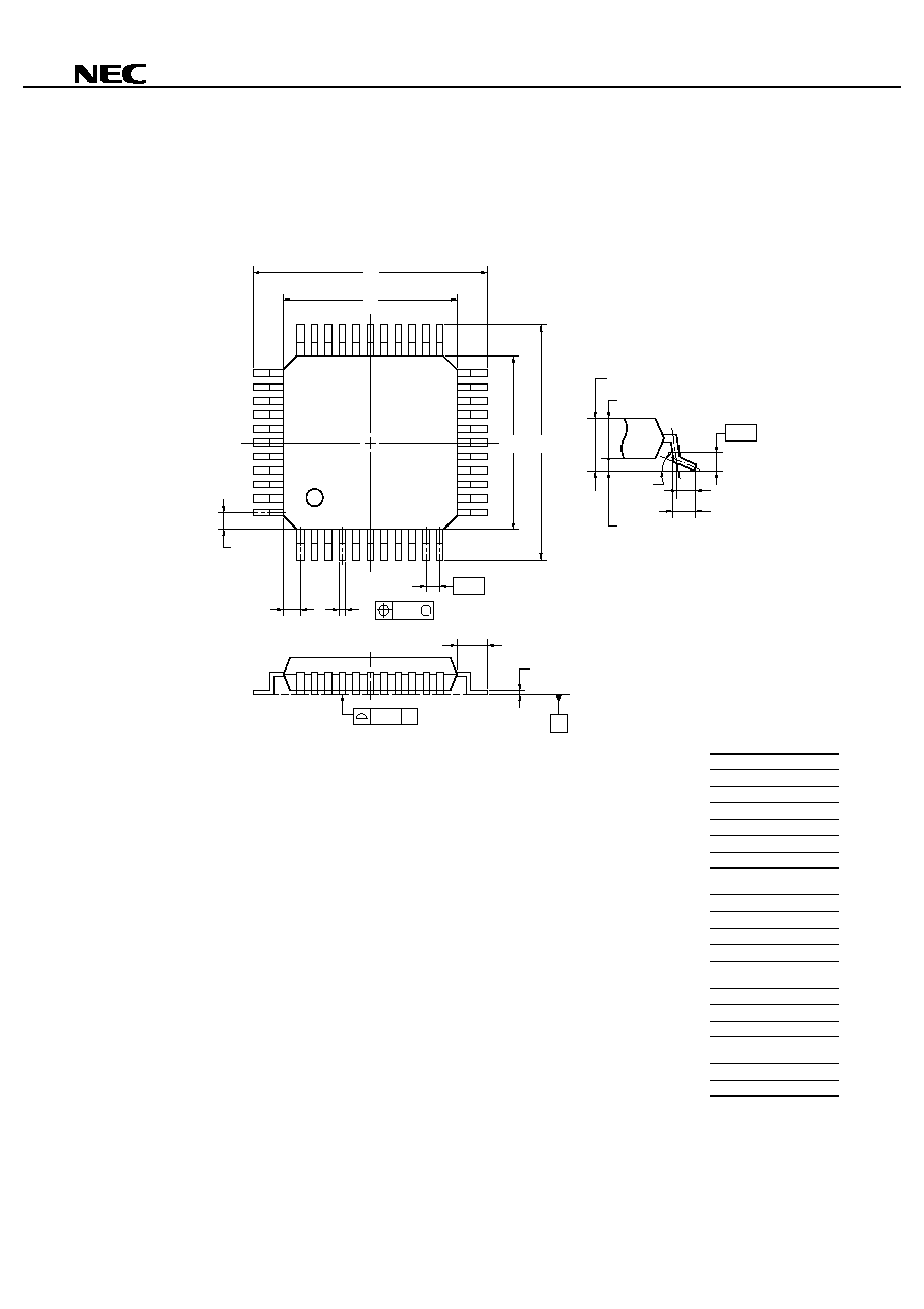
45
µ
µ
µ
µ
PD78F9177, 78F9177Y
Data Sheet U14022EJ1V0DS00
9. PACKAGE DRAWING
33
34
22
44
1
12
11
23
44 PIN PLASTIC QFP (10x10)
ITEM
MILLIMETERS
N
Q
0.1
±
0.05
0.10
U
0.6
±
0.15
S44GB-80-8ES-1
J
I
H
N
A
12.0
±
0.2
B
10.0
±
0.2
C
10.0
±
0.2
D
12.0
±
0.2
F
G
H
1.0
0.37
1.0
I
J
K
0.8 (T.P.)
1.0
±
0.2
0.2
L
0.5
M
0.17
S
1.6 MAX.
R
3
∞
+
0.08
-
0.07
+
0.03
-
0.06
+
4
∞
-
3
∞
detail of lead end
F
G
K
M
M
P
1.4
±
0.05
NOTE
Each lead centerline is located within 0.16 mm of
its true position (T.P.) at maximum material condition.
S
S
A
B
C
D
U
R
S
P
Q
L
T
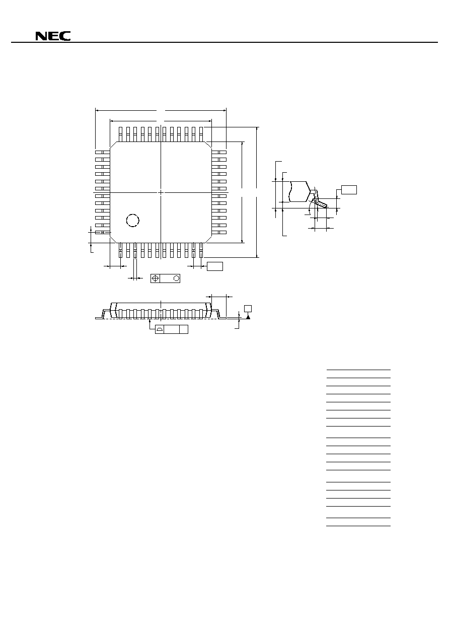
46
µ
µ
µ
µ
PD78F9177, 78F9177Y
Data Sheet U14022EJ1V0DS00
NOTE
Each lead centerline is located within 0.10 mm of
its true position (T.P.) at maximum material condition.
A
S
P
B
C
D
M
G
H
K
I
J
R
detail of lead end
F
48-PIN PLASTIC TQFP (FINE PITCH) (7x7)
ITEM
MILLIMETERS
A
9.0
±
0.2
B
7.0
±
0.2
F
0.75
G
H
0.75
C
7.0
±
0.2
D
9.0
±
0.2
P48GA-50-9EU
I
0.10
L
0.5
±
0.2
J
0.5 (T.P.)
K
1.0
±
0.2
M
36
37
24
48
1
13
12
25
S
N
S
Q
L
T
U
0.22
+
0.05
-
0.04
M
N
0.08
P
1.0
±
0.1
Q
0.1
±
0.05
0.17
+
0.03
-
0.07
R
S
1.27 MAX.
3
∞+
4
∞
-
3
∞
47
µ
µ
µ
µ
PD78F9177, 78F9177Y
Data Sheet U14022EJ1V0DS00
10. RECOMMENDED SOLDERING CONDITIONS
The
µ
PD78F9177 and
µ
PD789177Y should be soldered and mounted under the following recommended
conditions.
For the details of the recommended soldering conditions, refer to the document Semiconductor Device
Mounting Technology Manual (C10535E).
For soldering methods and conditions other than those recommended below, contact your NEC sales
representative.
Table 10-1. Surface Mounting Type Soldering Conditions (1/2)
µ
µ
µ
µ
PD78F9177GB-8ES: 44-pin plastic LQFP (10
◊
◊
◊
◊
10)
µ
µ
µ
µ
PD78F9177YGB-8ES: 44-pin plastic LQFP (10
◊
◊
◊
◊
10)
Soldering Method
Soldering Conditions
Recommended Condition
Symbol
Infrared reflow
Package peak temperature: 235
∞
C, Time: 30 seconds max.
(at 210
∞
C or higher), Count: Twice or less
IR35-00-2
VPS
Package peak temperature: 215
∞
C, Time: 40 seconds max.
(at 200
∞
C or higher), Count: Twice or less
VP15-00-2
Wave soldering
Solder bath temperature: 260
∞
C max., Time: 10 seconds max., Count:
Once, Preheating temperature: 120
∞
C max. (package surface
temperature)
WS60-00-1
Partial heating
Pin temperature: 300
∞
C max., Time: 3 seconds max. (per pin row)
-
Caution
Do not use different soldering methods together (except for partial heating).
Table 10-1. Surface Mounting Type Soldering Conditions (2/2)
µ
µ
µ
µ
PD78F9177YGA-9EU: 48-pin plastic TQFP (7
◊
◊
◊
◊
7)
Soldering Method
Soldering Conditions
Recommended Condition
Symbol
Infrared reflow
Package peak temperature: 235
∞
C, Time: 30 seconds max.
(at 210
∞
C or higher), Count: Twice or less, Number of days:3
Note
(After
that, prebaking sis necessary at 125
∞
C for 10 hours)
IR35-103-2
VPS
Package peak temperature: 215
∞
C, Time: 40 seconds max.
(at 200
∞
C or higher), Count: Twice or less, Number of days:3
Note
(After
that, prebaking sis necessary at 125
∞
C for 10 hours)
VP15-103-2
Partial heating
Pin temperature: 300
∞
C max., Time: 3 seconds max. (per pin row)
-
Note The number of days for storage at 25
∞
C, 65% RH MAX after the dry pack has been opened.
Caution
Do not use different soldering methods together (except for partial heating).

48
µ
µ
µ
µ
PD78F9177, 78F9177Y
Data Sheet U14022EJ1V0DS00
APPENDIX A. DIFFERENCES BETWEEN
µ
PD78F9177, 78F9177Y, AND MASK ROM VERSIONS
The
µ
PD78F9177 and
µ
PD78F9177Y are flash memory version of the Mask ROM version. The differences
between the
µ
PD78F9177, 78F9177Y and the Mask ROM versions are shown in Table A-1.
Table A-1. Differences between
µ
µ
µ
µ
PD78F9177, 78F9177Y and Mask ROM Versions
Flash Memory Version
Mask ROM Version
Product Name
Item
µ
PD78F9177, 78F9177Y
µ
PD789166, 789166Y
789176, 789176Y
µ
PD789167, 789167Y
789177, 789177Y
ROM
24 KB
16 KB
24 KB
Internal
memory
High-speed RAM
512 bytes
V
PP
pin
Provided
Not provided
Pull-up resistor
17 (Software control)
21 (Software control: 17, mask option specification: 4)
A/D resolution
10 bits
8 bits (
µ
PD789166, 789167, 789166Y, 789167Y)
10 bits (
µ
PD789176, 789177, 789176Y, 789177Y)
Electrical specifications
See the relevant data sheet
Cautions 1. There are differences in the amount of noise immunity and noise radiation between the
flash memory and mask ROM versions. When pre-producing an application set with the
flash memory version and then mass producing it with the mask ROM versions, be sure
to conduct sufficient evaluations on the commercial samples (CS) (not engineering
sample, ES) of the mask ROM version.
2. When the
µ
µ
µ
µ
PD78F9177, a flash memory counterpart of the
µ
µ
µ
µ
PD789166 or
µ
µ
µ
µ
PD789167, is
used, however, ADCR0 can be manipulated with an 8-bit memory manipulation
instruction. In this case, use an object file assembled with the
µ
µ
µ
µ
PD789166 or
µ
µ
µ
µ
PD789167.
The same is also true for the
µ
µ
µ
µ
PD78F9177Y, a flash memory counterpart of the
µ
µ
µ
µ
PD789166Y or
µ
µ
µ
µ
PD789167Y. When the
µ
µ
µ
µ
PD78F9177Y is used, ADCR0 can be
manipulated with an 8-bit memory manipulation instruction. In this case, use an object
file assembled with the
µ
µ
µ
µ
PD789166Y or
µ
µ
µ
µ
PD789167Y.
49
µ
µ
µ
µ
PD78F9177, 78F9177Y
Data Sheet U14022EJ1V0DS00
APPENDIX B. DEVELOPMENT TOOLS
The following development tools are available for developing systems using the
µ
PD78F9177 and
µ
PD78F9177Y.
Language Processing Software
RA78K0S
Notes 1, 2, 3
Assembler package common to 78K/0S Series
CC78K0S
Notes 1, 2, 3
C compiler package common to 78K/0S Series
DF789177
Notes 1, 2, 3
Device file for
µ
PD789167, 789177, 789167Y, and 789177Y Subseries
CC78K0S-L
Notes 1, 2, 3
C compiler library source file common to 78K/0S Series
Flash Memory Writing Tools
Flashpro lIl
(Part No. FL-PR3
Note 4
, PG-FP3)
Flash programmer dedicated for on-chip flash memory microcontrollers
FA-44GB-8ES
Note 4
Flash memory programming adapter for 44-pin plastic LQFP (GB-8ES type)
FA-48GA
Flash memory programming adapter for 48-pin plastic TQFP (fine pitch) (GA-9EU
type)
Debugging Tools(1/2)
IE-78K0S-NS
In-circuit emulator
In-circuit emulator used to debug hardware or software when application systems
which use the 78K/0S Series are developed. The IE-78K0S-NS supports an integrated
debugger (ID78K0S-NS). The IE-78K0S-NS is used in combination with an interface
adapter for connection to an AC adapter, emulation probe, or host machine.
IE-70000-MC-PS-B
AC adapter
Adapter used to supply power from a 100- to 240-V AC outlet
IE-70000-98-IF-C
Interface adapter
Adapter required when using the PC-9800 series (excluding notebook PCs) as the host
machine for the IE-78K0S-NS (C bus supported)
IE-70000-CD-IF-A
PC card/interface
PC card and interface cable required when using a notebook PC as the host machine
for the IE-78K0S-NS (PCMCIA socket supported)
IE-70000-PC-IF-C
Interface adapter
Adapter required when using an IBM PC/AT
TM
or compatible as the host machine for
the IE-78K0S-NS (ISA bus supported)
IE-70000-PCI-IF
Interface adapter
Adapter required when using a PC equipped with a PCI bus as the host machine for
the IE-78K0S-NS
IE-789177-NS-EM1
Emulation board
Emulation board used to emulate the peripheral hardware specific to the device. This
is used in combination with the in-circuit emulator.
Board to connect an in-circuit emulator to the target system. This is used in
combination with the EV-9200G-44
NP-44GB
Note 4
Emulation probe
EV-9200G-44
conversion socket
Conversion socket to connect the target system board on which a 44-pin plastic LQFP
can be mounted and the NP-44GB
Board to connect an in-circuit emulator to the target system. This is used in
combination with the TGB-044SAP.
NP-44GB-TQ
Note 4
Emulation probe
TGB-044SAP
Note 5
conversion socket
Conversion socket to connect the target system board on which a 44-pin plastic LQFP
can be mounted and the NP-44GB-TQ

50
µ
µ
µ
µ
PD78F9177, 78F9177Y
Data Sheet U14022EJ1V0DS00
Debugging Tools(2/2)
Board to connect an in-circuit emulator to the target system. This is used in
combination with the TGA-048SDP.
NP-48GA
Note 4
Emulation probe
TGA-048SDP
Note 5
conversion socket
Conversion socket to connect the target system board on which a 48-pin plastic TQFP
(fine pitch) can be mounted and the NP-48GA
SM78K0S
Notes 1, 2
System simulator common to 78K/0S Series
ID78K0S-NS
Notes 1, 2
Integrated debugger common to 78K/0S Series
DF789177
Notes 1, 2
Device file for
µ
PD789167, 789177, 789167, and 789177Y Subseries
Real-Time OS
MX78K0S
Notes 1, 2
OS for 78K/0S Series
Notes 1. Based on the PC-9800 series (Japanese Windows
TM
)
2. Based on IBM PC/AT and compatibles (Japanese Windows/English Windows)
3. Based on the HP9000 series 700
TM
(HP-UX
TM
), SPARCstation
TM
(SunOS
TM
, Soraris
TM
), and NEWS
TM
(NEWS-OS
TM
)
4. Product made by and available from Naito Densei Machida Mfg. Co., Ltd. (+81-44-822-3813).
5. Product made by TOKYO ELETECH CORPORATION.
Refer to: Daimaru Kogyo, Ltd.
Tokyo Electronic Division (+81-3-3820-7112)
Osaka Electronic Division (+81-6-6244-6672)
Remark
The RA78K0S, CC78K0S, and SM78K0S can be used in combination with the DF789177.

51
µ
µ
µ
µ
PD78F9177, 78F9177Y
Data Sheet U14022EJ1V0DS00
APPENDIX C. RELATED DOCUMENTS
Documents Related to Devices
Document No.
Document Name
Japanese
English
µ
PD789166, 167, 176, 177, 166Y, 167Y, 176Y, 177Y, 166(A), 167(A), 176(A), 177(A),
166Y(A), 167Y(A), 176Y(A), 177Y(A) Data Sheet
U14017J
U14017E
µ
PD78F9177, 78F9177Y Data Sheet
U14022J
This manual
µ
PD789167, 789177, 789167Y, 789177Y Subseries User's Manual
U14186J
U14186E
78K/0S Series Instruction User's Manual
U11047J
U11047E
Document Related to Development Tools (User's Manuals)
Document No.
Document Name
Japanese
English
Operation
U11622J
U11622E
Assembly Language
U11599J
U11599E
RA78K0S Assembler Package
Structured Assembly
Language
U11623J
U11623E
Operation
U11816J
U11816E
CC78K0S C Compiler
Language
U11817J
U11817E
SM78K0S System Simulator Windows based
Reference
U11489J
U11489E
SM78K Series System Simulator
External Parts User
Open Interface
Specifications
U10092J
U10092E
ID78K0S-NS Windows based
Reference
U12901J
U12901E
IE-78K0S-NS In-circuit Emulator
U13549J
U13549E
IE-789177-NS-EM1 Emulation Board
U14621J
U14621E
Documents Related to Embedded Software (User's Manuals)
Document No.
Document Name
Japanese
English
OS for 78K/0S Series MX78K0S
Fundamental
U12938J
U12938E
Caution
The related documents listed above are subject to change without notice. Be sure to use the
latest version of each document for designing.

52
µ
µ
µ
µ
PD78F9177, 78F9177Y
Data Sheet U14022EJ1V0DS00
Other Documents
Document No.
Document Name
Japanese
English
SEMICONDUCTOR SELECTION GUIDE Products & Packages (CD-ROM)
X13769X
Semiconductor Device Mounting Technology Manual
C10535J
C10535E
Quality Grades on NEC Semiconductor Device
C11531J
C11531E
NEC Semiconductor Device Reliability/Quality Control System
C10983J
C10983E
Guide to Prevent Damage for Semiconductor Devices by Electrostatic Discharge (ESD)
C11892J
C11892E
Guide to Microcomputer-Related Products by Third Party
U11416J
-
Caution
The related documents listed above are subject to change without notice. Be sure to use the
latest version of each document for designing.
The related document indicated in this publication may include preliminary versions. However, preliminary versions
are not marked as such.

53
µ
µ
µ
µ
PD78F9177, 78F9177Y
Data Sheet U14022EJ1V0DS00
[MEMO]
54
µ
µ
µ
µ
PD78F9177, 78F9177Y
Data Sheet U14022EJ1V0DS00
EEPROM is a trademark of NEC Corporation.
Windows is either a registered trademark or a trademark of Microsoft Corporation in the United States and/or
other countries.
PC/AT is a trademark of International Business Machines Corporation.
HP9000 series 700 and HP-UX are trademarks of Hewlett-Packard Company.
SPARCstation is a trademark of SPARC International, Inc.
Solaris and SunOS are trademarks of Sun Microsystems, Inc.
NEWS and NEWS-OS are trademarks of SONY Corporation.
NOTES FOR CMOS DEVICES
1
PRECAUTION AGAINST ESD FOR SEMICONDUCTORS
Note:
Strong electric field, when exposed to a MOS device, can cause destruction of the gate oxide and
ultimately degrade the device operation. Steps must be taken to stop generation of static electricity
as much as possible, and quickly dissipate it once, when it has occurred. Environmental control
must be adequate. When it is dry, humidifier should be used. It is recommended to avoid using
insulators that easily build static electricity. Semiconductor devices must be stored and transported
in an anti-static container, static shielding bag or conductive material. All test and measurement
tools including work bench and floor should be grounded. The operator should be grounded using
wrist strap. Semiconductor devices must not be touched with bare hands. Similar precautions need
to be taken for PW boards with semiconductor devices on it.
2
HANDLING OF UNUSED INPUT PINS FOR CMOS
Note:
No connection for CMOS device inputs can be cause of malfunction. If no connection is provided
to the input pins, it is possible that an internal input level may be generated due to noise, etc., hence
causing malfunction. CMOS devices behave differently than Bipolar or NMOS devices. Input levels
of CMOS devices must be fixed high or low by using a pull-up or pull-down circuitry. Each unused
pin should be connected to V
DD
or GND with a resistor, if it is considered to have a possibility of
being an output pin. All handling related to the unused pins must be judged device by device and
related specifications governing the devices.
3
STATUS BEFORE INITIALIZATION OF MOS DEVICES
Note:
Power-on does not necessarily define initial status of MOS device. Production process of MOS
does not define the initial operation status of the device. Immediately after the power source is
turned ON, the devices with reset function have not yet been initialized. Hence, power-on does
not guarantee out-pin levels, I/O settings or contents of registers. Device is not initialized until the
reset signal is received. Reset operation must be executed immediately after power-on for devices
having reset function.

55
µ
µ
µ
µ
PD78F9177, 78F9177Y
Data Sheet U14022EJ1V0DS00
Regional Information
Some information contained in this document may vary from country to country. Before using any NEC
product in your application, pIease contact the NEC office in your country to obtain a list of authorized
representatives and distributors. They will verify:
∑
Device availability
∑
Ordering information
∑
Product release schedule
∑
Availability of related technical literature
∑
Development environment specifications (for example, specifications for third-party tools and
components, host computers, power plugs, AC supply voltages, and so forth)
∑
Network requirements
In addition, trademarks, registered trademarks, export restrictions, and other legal issues may also vary
from country to country.
NEC Electronics Inc. (U.S.)
Santa Clara, California
Tel: 408-588-6000
800-366-9782
Fax: 408-588-6130
800-729-9288
NEC Electronics (Germany) GmbH
Duesseldorf, Germany
Tel: 0211-65 03 02
Fax: 0211-65 03 490
NEC Electronics (UK) Ltd.
Milton Keynes, UK
Tel: 01908-691-133
Fax: 01908-670-290
NEC Electronics Italiana s.r.l.
Milano, Italy
Tel: 02-66 75 41
Fax: 02-66 75 42 99
NEC Electronics (Germany) GmbH
Benelux Office
Eindhoven, The Netherlands
Tel: 040-2445845
Fax: 040-2444580
NEC Electronics (France) S.A.
Velizy-Villacoublay, France
Tel: 01-30-67 58 00
Fax: 01-30-67 58 99
NEC Electronics (France) S.A.
Madrid Office
Madrid, Spain
Tel: 91-504-2787
Fax: 91-504-2860
NEC Electronics (Germany) GmbH
Scandinavia Office
Taeby, Sweden
Tel: 08-63 80 820
Fax: 08-63 80 388
NEC Electronics Hong Kong Ltd.
Hong Kong
Tel: 2886-9318
Fax: 2886-9022/9044
NEC Electronics Hong Kong Ltd.
Seoul Branch
Seoul, Korea
Tel: 02-528-0303
Fax: 02-528-4411
NEC Electronics Singapore Pte. Ltd.
United Square, Singapore
Tel: 65-253-8311
Fax: 65-250-3583
NEC Electronics Taiwan Ltd.
Taipei, Taiwan
Tel: 02-2719-2377
Fax: 02-2719-5951
NEC do Brasil S.A.
Electron Devices Division
Guarulhos-SP Brasil
Tel: 55-11-6462-6810
Fax: 55-11-6462-6829
J00.7

µ
µ
µ
µ
PD78F9177, 78F9177Y
M8E 00. 4
The information in this document is current as of August, 2000. The information is subject to
change without notice. For actual design-in, refer to the latest publications of NEC's data sheets or
data books, etc., for the most up-to-date specifications of NEC semiconductor products. Not all
products and/or types are available in every country. Please check with an NEC sales representative
for availability and additional information.
No part of this document may be copied or reproduced in any form or by any means without prior
written consent of NEC. NEC assumes no responsibility for any errors that may appear in this document.
NEC does not assume any liability for infringement of patents, copyrights or other intellectual property rights of
third parties by or arising from the use of NEC semiconductor products listed in this document or any other
liability arising from the use of such products. No license, express, implied or otherwise, is granted under any
patents, copyrights or other intellectual property rights of NEC or others.
Descriptions of circuits, software and other related information in this document are provided for illustrative
purposes in semiconductor product operation and application examples. The incorporation of these
circuits, software and information in the design of customer's equipment shall be done under the full
responsibility of customer. NEC assumes no responsibility for any losses incurred by customers or third
parties arising from the use of these circuits, software and information.
While NEC endeavours to enhance the quality, reliability and safety of NEC semiconductor products, customers
agree and acknowledge that the possibility of defects thereof cannot be eliminated entirely. To minimize
risks of damage to property or injury (including death) to persons arising from defects in NEC
semiconductor products, customers must incorporate sufficient safety measures in their design, such as
redundancy, fire-containment, and anti-failure features.
NEC semiconductor products are classified into the following three quality grades:
"Standard", "Special" and "Specific". The "Specific" quality grade applies only to semiconductor products
developed based on a customer-designated "quality assurance program" for a specific application. The
recommended applications of a semiconductor product depend on its quality grade, as indicated below.
Customers must check the quality grade of each semiconductor product before using it in a particular
application.
"Standard": Computers, office equipment, communications equipment, test and measurement equipment, audio
and visual equipment, home electronic appliances, machine tools, personal electronic equipment
and industrial robots
"Special":
Transportation equipment (automobiles, trains, ships, etc.), traffic control systems, anti-disaster
systems, anti-crime systems, safety equipment and medical equipment (not specifically designed
for life support)
"Specific": Aircraft, aerospace equipment, submersible repeaters, nuclear reactor control systems, life
support systems and medical equipment for life support, etc.
The quality grade of NEC semiconductor products is "Standard" unless otherwise expressly specified in NEC's
data sheets or data books, etc. If customers wish to use NEC semiconductor products in applications not
intended by NEC, they must contact an NEC sales representative in advance to determine NEC's willingness
to support a given application.
(Note)
(1) "NEC" as used in this statement means NEC Corporation and also includes its majority-owned subsidiaries.
(2) "NEC semiconductor products" means any semiconductor product developed or manufactured by or for
NEC (as defined above).
∑
∑
∑
∑
∑
∑