Document Outline
- Cover
- FEATURES
- APPLICATIONS
- ORDERING INFORMATION
- 78K/0S SERIES DEVELOPMENT
- FUNCTIONS
- CONTENTS
- 1. PIN CONFIGURATION (TOP VIEW)
- 2. BLOCK DIAGRAM
- 3. DIFFERENCES BETWEEN uPD78F9801 AND MASKED ROM VERSION
- 4. PIN FUNCTIONS
- 4.1 Port Pins
- 4.2 Non-Port Pins
- 4.3 Pin Input/Output Circuits and Handling of Unused Pins
- 5. MEMORY SPACE
- 6. FLASH MEMORY PROGRAMMING
- 6.1 Selecting Communication Mode
- 6.2 Function of Flash Memory Programming
- 6.3 Flashpro III Connection
- 6.4 Example of Settings for Flashpro III (PG-FP3)
- 7. INSTRUCTION SET OVERVIEW
- 7.1 Legend
- 7.1.1 Operand formats and descriptions
- 7.1.2 Descriptions of the operation field
- 7.1.3 Description of the flag operation field
- 7.2 Operations
- 8. ELECTRICAL CHARACTERISTICS
- 9. PACKAGE DRAWINGS
- 10. RECOMMENDED SOLDERING CONDITIONS
- APPENDIX A DEVELOPMENT TOOLS
- APPENDIX B RELATED DOCUMENTS
The information in this document is subject to change without notice. Before using this document, please
confirm that this is the latest version.
Not all devices/types available in every country. Please check with local NEC representative for
availability and additional information.
Document No. U12626EJ1V0DSJ1 (1st edition)
Date Published October 2000 J CP(K)
Printed in Japan
8-BIT SINGLE-CHIP MICROCONTROLLER
DATA SHEET
MOS INTEGRATED CIRCUIT
µ
µ
µ
µ
PD78F9801
The mark
shows major revised points.
©
1997, 1999
The
µPD78F9801 is a µPD789800 sub-series product (for a USB keyboard) of the 78K/0S series.
The
µPD78F9801 replaces the internal masked ROM of the µPD789800 with flash memory, which enables the
writing/erasing of a program while the device is mounted on the board.
Because the device can be programmed by the user, it is ideally suited to the evaluation stages of system
development, the manufacture of small batches of multiple products, and the rapid development of new products.
The functions of this microcontroller are described in the following user's manuals. Refer to these
manuals when designing a system based on this microcontroller.
µ
µ
µ
µPD789800 Sub-Series User's Manual
:
U12978E
78K/0S Series User's Manual - Instruction :
U11047E
FEATURES
∑ Pin-compatible with masked ROM version (excluding V
PP
pin)
∑ Flash memory: 16K bytes
∑ Internal high-speed RAM: 256 bytes
∑ Operable on the same supply voltage as masked ROM version (V
DD
= 4.0 to 5.5 V)
Remark The differences between the flash memory and masked ROM versions are summarized in Chapter 3.
APPLICATIONS
USB keyboards
ORDERING INFORMATION
Part number
Package
µPD78F9801GB-3BS-MTX
44-pin plastic QFP (10
◊ 10 mm, 2.7-mm resin thickness)
µPD78F9801GB-8ES
44-pin plastic LQFP (10
◊ 10 mm, 1.4-mm resin thickness)
Data Sheet U12626EJ1V0DS00
2
µ
µ
µ
µ
PD78F9801
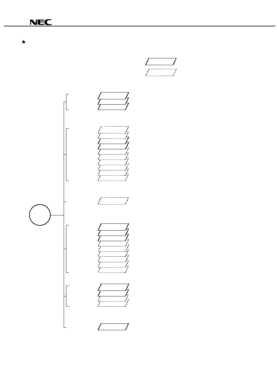
78K/0S SERIES DEVELOPMENT
The 78K/0S series products are shown below. The sub-series names are indicated in frames.
Products under development
Products in mass-production
PD789014
42/44-pin
PD789014 with enhanced timer function and expanded ROM and RAM
Small-scale package, general-purpose applications
PD789146
PD789156
44-pin
RC oscillation version of the PD789197AY
PD789177 with internal EEPROM
TM
and SMB
78K/0S
Series
44/48-pin
44/48-pin
Small-scale package, general-purpose applications and A/D function
28-pin
44-pin
PD789167 with enhanced A/D converter
PD789104A with enhanced timer
PD789124A with enhanced A/D converter
RC oscillation version of the PD789104A
PD789104A with enhanced A/D converter
PD789026 with A/D converter and multiplier
On-chip UART and capable of low-voltage (1.8 V) operation
PD789026
44-pin
PD789046
PD789026 with internal subsystem clock
28/30-pin
28/30-pin
28/30-pin
28/30-pin
PD789124A
PD789134A
PD789217AY
PD789197AY
PD789177
PD789167
30-pin
30-pin
PD789104A
PD789114A
PD789104A with EEPROM
PD789146 with enhanced A/D converter
PD789427 with enhanced A/D converter
On-chip UART and dot LCD
80-pin
80-pin
For LCD drive
88-pin
PD789447 with enhanced A/D converter
For Inverter control
44-pin
PD789842
On-chip inverter control circuit and UART
On-chip EEPROM and security circuit
5-pin
PD789810
For IC card
For keyless entry, on-chip key return circuit
20-pin
PD789860
PD789840
For key pad, on-chip POC
44-pin
For ASSP
For PC keyboard, on-chip USB function
42/44-pin
PD789800
20-pin
PD789861
RC oscillation version of the PD789860
PD789457 with enhanced I/O
RC oscillation version of the PD789427
PD789447
PD789457
PD789437
PD789407A with enhanced A/D converter
PD789417A
PD789830
PD789407A
PD789427
PD789306
PD789316
PD789306 with A/D converter
RC oscillation version of the PD789306
Basic subseries for LCD drive
64-pin
64-pin
64-pin
64-pin
64-pin
64-pin
µ
µ
µ
µ
µ
µ
µ
µ
µ
µ
µ
µ
µ
µ
µ
µ
µ
µ
µ
µ
µ
µ
µ
µ
µ
µ
µ
µ
µ
µ
µ
µ
µ
µ
µ
µ
µ
µ
µ
µ
µ
µ
µ
µ
µ
µ
µ
µ
Data Sheet U12626EJ1V0DS00
3
µ
µ
µ
µ
PD78F9801
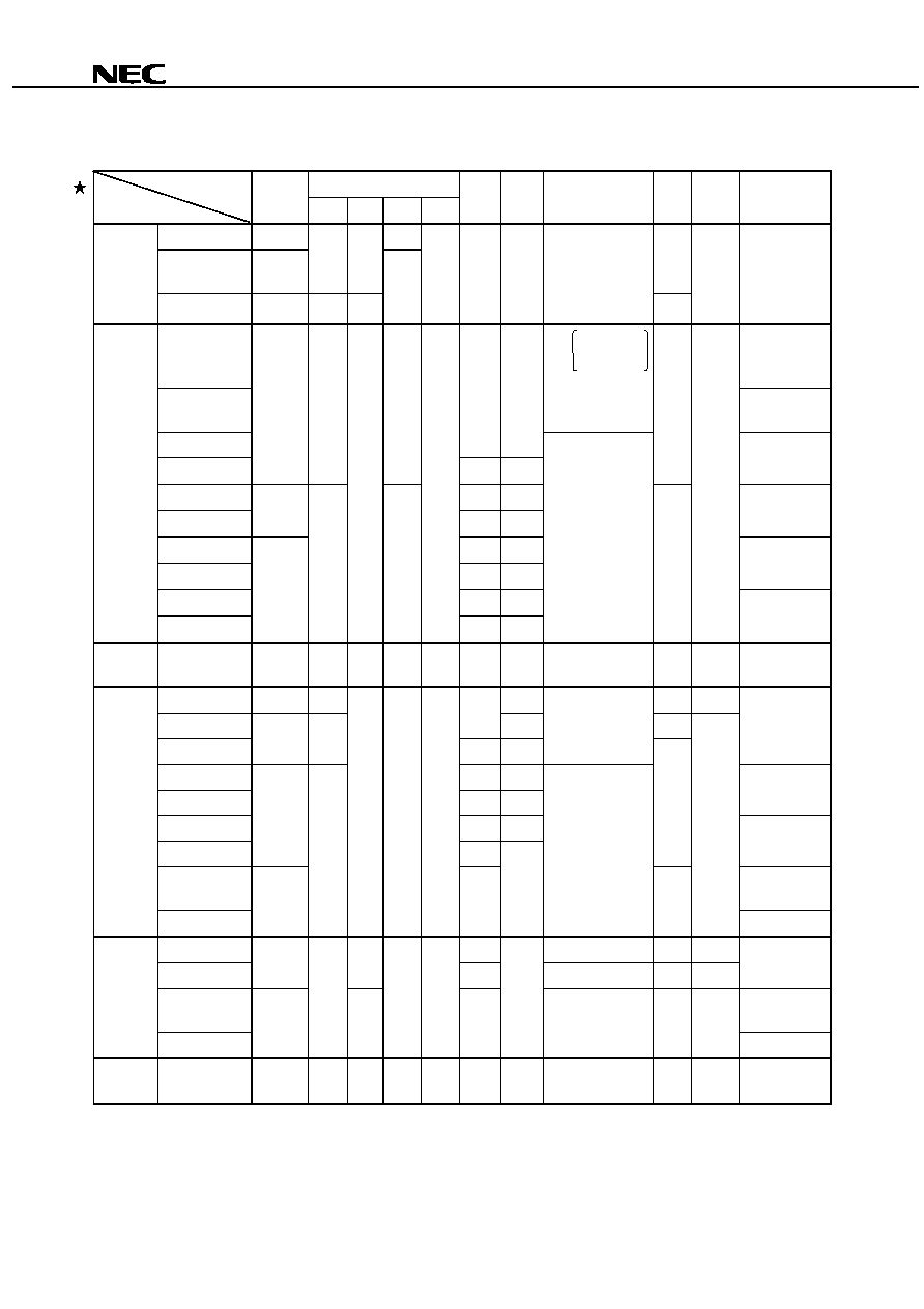
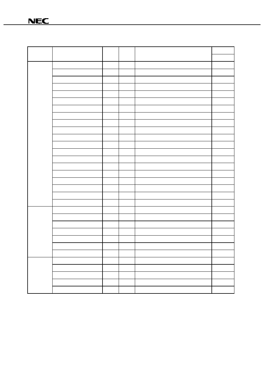
The major functional differences among the subseries are listed below.
Timer
Function
Subseries name
ROM
capacity
8-bit 16-bit Watch WDT
8-bit
A/D
10-bit
A/D
Serial interface
I/O
V
DD
MIN.
value
Remark
µ
PD789046
16 K
1ch
µ
PD789026
4 K to
16 K
1ch
1ch
34
Small-scale
package,
general-
purpose
applications
µ
PD789014
2 K to 4 K 2 ch
≠
≠
1ch
≠
≠
1ch (UART: 1ch)
22
1.8 V
≠
µ
PD789217AY
RC oscillation
version, on-
chip EEPROM
µ
PD789197AY
2ch UART: 1ch
SMB: 1ch
On-chip
EEPROM
µ
PD789177
≠
8 ch
µ
PD789167
16 K to
24 K
3 ch
1 ch
8 ch
≠
31
≠
µ
PD789156
≠
4 ch
µ
PD789146
8 K to
16 K
4 ch
≠
On-chip
EEPROM
µ
PD789134A
≠
4 ch
µ
PD789124A
4 ch
≠
RC oscillation
version
µ
PD789114A
≠
4 ch
Small-scale
package,
general-
purpose
applications
+ A/D
converter
µ
PD789104A
2 K to 8 K
1 ch
1 ch
≠
1 ch
4 ch
≠
1 ch (UART: 1 ch)
20
1.8 V
≠
Inverter
control
µ
PD789842
8 K to
16 K
3 ch
Note 1 ch
1 ch
8 ch
≠
1 ch (UART: 1 ch)
30
4.0 V
≠
µ
PD789830
24 K
1 ch
≠
30
2.7 V
µ
PD789417A
≠
7 ch
43
µ
PD789407A
12 K to
24 K
3 ch
7 ch
≠
1 ch (UART: 1 ch)
≠
µ
PD789457
≠
4 ch
µ
PD789447
4 ch
≠
RC oscillation
version
µ
PD789437
≠
4 ch
µ
PD789427
16 K to
24 K
4 ch
25
≠
µ
PD789316
RC oscillation
version
LCD drive
µ
PD789306
8 K to
16 K
2 ch
1 ch
1 ch
1 ch
≠
≠
2 ch (UART: 1 ch)
23
1.8 V
≠
µ
PD789800
≠
2 ch (USB: 1 ch)
31
4.0 V
µ
PD789840
8 K
1 ch
4 ch
1 ch
29
2.8 V
≠
µ
PD789861
RC oscillation
version
ASSP
µ
PD789860
4 K
2 ch
≠
≠
1 ch
≠
≠
≠
14
1.8 V
≠
IC card
µ
PD789810
6 K
≠
≠
≠
1 ch
≠
≠
≠
1
2.7 V
On-chip
EEPROM
Note
10-bit timer: 1 channel
Data Sheet U12626EJ1V0DS00
4
µ
µ
µ
µ
PD78F9801
FUNCTIONS
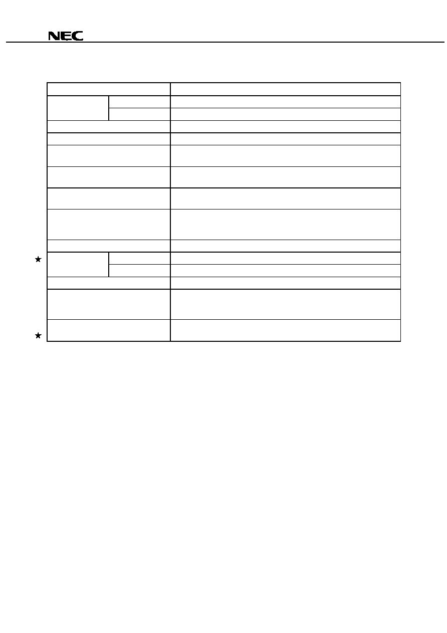
Item
Function
Flash memory
16K bytes
Internal memory
High-speed RAM
256 bytes
Minimum instruction execution time
0.33
µ
s/1.33
µ
s (when the system clock operates at 6.0 MHz)
General-purpose register
8 bits
◊
8 registers
Instruction set
∑ 16-bit operation
∑ Bit manipulation (set, reset, and test) etc.
I/O ports
CMOS I/O: 31 pins (Of these, 18 pins can be switched to N-ch open-drain I/O
pins.)
Serial interface
∑ USB (Universal Serial Bus) function : 1 channel
∑ Three-wire serial I/O mode
: 1 channel
Timer
∑ 8-bit timer 00
: 1 channel
∑ 8-bit timer/event counter 01 : 1 channel
∑ Watchdog timer
: 1 channel
Regulator
Incorporated (V
REG
= 3.3
±
0.3 V)
Maskable
Internal: 9, external: 2
Vector interrupt
source
Nonmaskable
Internal: 1
Power supply voltage
V
DD
= 4.0 to 5.5 V
Operating ambient temperature
∑ T
A
= -40∞C to
+
85∞C (when the USB is not operating)
∑ T
A
= 0∞C to
+
70∞C (when the USB is operating)
∑ T
A
= 10∞C to 40∞C (when a flash memory is written)
Package
∑ 44-pin plastic QFP (10
◊
10 mm, 2.7-mm resin thickness)
∑ 44-pin plastic LQFP (10
◊
10 mm, 1.4-mm resin thickness)

Data Sheet U12626EJ1V0DS00
5
µ
µ
µ
µ
PD78F9801
CONTENTS
1.
PIN CONFIGURATION (TOP VIEW) ................................................................................................6
2.
BLOCK DIAGRAM ............................................................................................................................7
3.
DIFFERENCES BETWEEN
µ
µ
µ
µ
PD78F9801 AND MASKED ROM VERSION ....................................8
4.
PIN FUNCTIONS ...............................................................................................................................9
4.1
Port Pins ................................................................................................................................................. 9
4.2
Non-Port Pins........................................................................................................................................ 10
4.3
Pin Input/Output Circuits and Handling of Unused Pins .................................................................. 11
5.
MEMORY SPACE ............................................................................................................................13
6.
FLASH MEMORY PROGRAMMING................................................................................................14
6.1
Selecting Communication Mode ......................................................................................................... 14
6.2
Function of Flash Memory Programming........................................................................................... 15
6.3
Flashpro III Connection........................................................................................................................ 15
6.4
Example of Settings for Flashpro III (PG-FP3) ................................................................................... 17
7.
INSTRUCTION SET OVERVIEW .....................................................................................................18
7.1
Legend................................................................................................................................................... 18
7.2
Operations............................................................................................................................................. 20
8.
ELECTRICAL CHARACTERISTICS................................................................................................25
9.
PACKAGE DRAWINGS ...................................................................................................................34
10. RECOMMENDED SOLDERING CONDITIONS...............................................................................36
APPENDIX A DEVELOPMENT TOOLS...............................................................................................37
APPENDIX B RELATED DOCUMENTS ..............................................................................................39
Data Sheet U12626EJ1V0DS00
6
µ
µ
µ
µ
PD78F9801
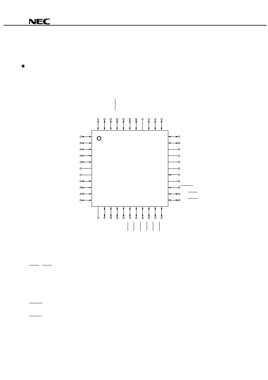
1. PIN CONFIGURATION (TOP VIEW)
∑
44-pin plastic QFP (10
◊
10 mm, 2.7-mm resin thickness)
µ
PD78F9801GB-3BS-MTX
∑
44-pin plastic LQFP (10
◊
10 mm, 1.4-mm resin thickness)
µ
PD78F9801GB-8ES
P04
P03
P02
P01
P00
V
DD1
V
SS1
P17
P16
P15
P14
NC
P13
P12
P11
P10
USBDP
USBDM
V
PP
REGC
V
DD0
V
SS0
X1
X2
RESET
P40/KR00
P41/KR01
P05
P06
P07
P20/SCK10
P21/SO10
P22/SI10
P23
NC
P24
P25
P26/TI01/TO01/INTP0
44 43 42 41 40 39 38 37 36 35 34
12 13 14 15 16 17 18 19 20 21 22
1
2
3
4
5
6
7
8
9
10
11
33
32
31
30
29
28
27
26
25
24
23
P47/KR07
P46/KR06
P45/KR05
P44/KR04
P43/KR03
P42/KR02
Caution
In normal operation mode, connect the V
PP
pin directly to the V
SS0
or V
SS1
pin.
INTP0
: Interrupt from peripherals
SI10
: Serial data input
KR00 - KR07 : Key return
SO10
: Serial data output
NC
: No connection
TI01
: Timer input
P00-P07
: Port 0
TO01
: Timer output
P10-P17
: Port 1
USBDM, USBDP : Universal serial bus data
P20-P26
: Port 2
V
DD0
, V
DD1
: Power supply
P40-P47
: Port 4
V
PP
: Programming power supply
RESET
: Reset
V
SS0
, V
SS1
: Ground
REGC
: Voltage regulator for USB function
X1, X2
: Crystal
SCK10
: Serial clock input/output
Data Sheet U12626EJ1V0DS00
7
µ
µ
µ
µ
PD78F9801
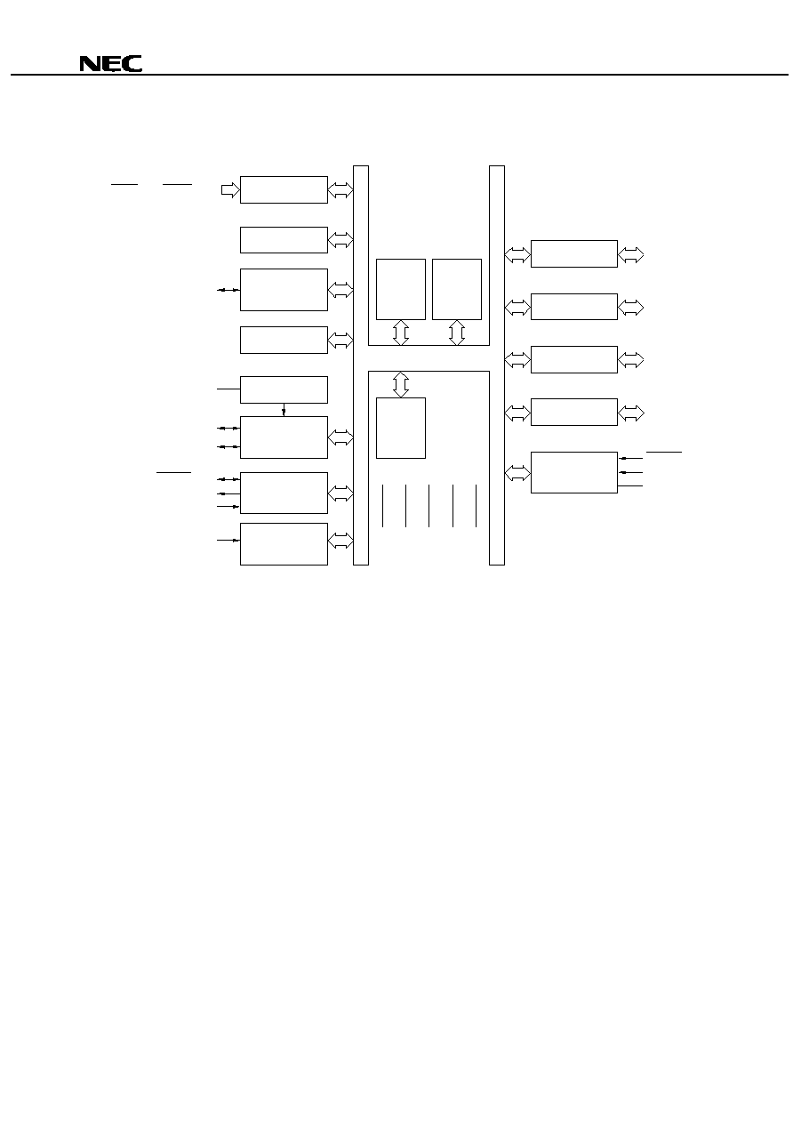
2. BLOCK DIAGRAM
KEY RETURN0
8-bit TIMER00
8-bit TIMER/
EVENT COUNTER01
WATCHDOG TIMER
REGULATOR
USB
FUNCTION0
SERIAL
INTERFACE10
INTERRUPT
CONTROL
PORT 0
PORT 1
PORT 2
PORT 4
SYSTEM
CONTROL
78K/0S
CPU CORE
FLASH
MEMORY
RAM
P00-P07
P10-P17
P20-P26
P40-P47
RESET
X1
X2
KR00/P40-KR07/P47
TI01/TO01/P26/INTP0
REGC
USBDM
USBDP
INTP0/P26/TI01/TO01
SCK10/P20
SO10/P21
SI10/P22
V
DD0
V
DD1
V
SS0
V
SS1
V
PP
V
REG
Data Sheet U12626EJ1V0DS00
8
µ
µ
µ
µ
PD78F9801
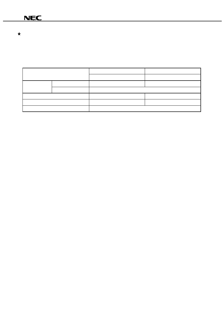
3. DIFFERENCES BETWEEN
µ
µ
µ
µ
PD78F9801 AND MASKED ROM VERSION
The
µ
PD78F9801 is a product that substitutes flash memory for the internal ROM of the masked ROM version
(
µ
PD789800). The differences between the
µ
PD78F9801 and the masked ROM versions are shown in Table 3-1.
Table 3-1. Differences between
µ
µ
µ
µ
PD78F9801 and Masked ROM Version
Flash memory version
Masked ROM version
Item
µ
PD78F9801
µ
PD789800
ROM
16 Kbytes (Flash memory)
8 Kbytes
Internal memory
High-speed RAM
256 bytes
IC pin
Not provided
Provided
V
PP
pin
Provided
Not provided
Electric characteristics
See the relevant data sheet
Caution
There are differences in the amount of noise tolerance and noise radiation between flash
memory versions and masked ROM versions. When considering changing from a flash
memory version to a masked ROM version during process from experimental manufacturing to
mass production, make sure to sufficiently evaluate the masked ROM versions using
commercial samples (CS) (not engineering samples (ES)).
Data Sheet U12626EJ1V0DS00
9
µ
µ
µ
µ
PD78F9801
4. PIN FUNCTIONS
4.1
Port Pins
Pin name
I/O
Function
When reset
Also used as
P00-P07
I/O
Port 0
8-bit input/output port
Input or output is specifiable bit by bit.
When used as an input port, the use of on-chip pull-up resistors can
be specified by software.
CMOS output or N-ch open-drain output is specifiable in 8-bit units.
Input
-
P10-P17
I/O
Port 1
8-bit input/output port
Input or output is specifiable bit by bit.
When used as an input port, the use of on-chip pull-up resistors can
be specified by software.
CMOS output or N-ch open-drain output is specifiable in 8-bit units.
Input
-
P20
SCK10
P21
SO10
P22
SI10
P23-P25
-
P26
I/O
Port 2
7-bit input/output port
Input or output is specifiable bit by bit.
When used as an input port, the use of on-chip pull-up resistors can
be specified by software.
Only for P25 and P26, CMOS output or N-ch open-drain output is
specifiable bit by bit.
Input
INTP0/TI01/TO01
P40-P47
I/O
Port 4
8-bit input/output port
Input or output is specifiable bit by bit.
When used as an input port, the use of on-chip pull-up resistors can
be specified by software.
Input
KR00
-
KR07
Data Sheet U12626EJ1V0DS00
10
µ
µ
µ
µ
PD78F9801
4.2
Non-Port Pins
Pin name
I/O
Function
When reset
Also used as
INTP0
Input
External interrupt request input for which effective edges
(rising and/or falling edges) can be specified
Input
P26/TI01/TO01
KR00
-
KR07
Input
Input for detecting key return signals
Input
P40-P47
REGC
-
Internally generated power supply for driving USB
driver/receiver. Connect this pin to V
SS
through a 220-
resistor and a 0.1-
µ
F capacitor.
-
-
RESET
Input
System reset input
Input
-
SCK10
I/O
Serial clock input/output for serial interface
Input
P20
SI10
Input
Serial data input for serial interface
Input
P22
SO10
Output
Serial data output for serial interface
Input
P21
TI01
Input
External count clock input to 8-bit timer/event counter 01
Input
P26/INTP0/TO01
TO01
Output
Timer output from 8-bit timer/event counter 01
Input
P26/INTP0/TI01
USBDM
I/O
Serial data input/output (negative side) for USB function. The
pull-up resistor (1.5 k
) for the USBDM pin must be
connected to the REGC pin.
Input
-
USBDP
I/O
Serial data input/output (positive side) for USB function
Input
-
X1
Input
Input
X2
-
Connected to crystal for system clock oscillator
-
-
V
DD0
-
Positive supply voltage for ports
-
-
V
DD1
-
Positive supply voltage for circuits other than ports
-
-
V
SS0
-
Ground potential for ports
-
-
V
SS1
-
Ground potential for circuits other than ports
-
-
V
PP
-
Flash memory programming mode setting. High-voltage
application for program write/verify. Connect directly to V
SS0
or V
SS1
in normal operation mode.
-
-
NC
-
Not internally connected. Leave this pin open.
-
-
Data Sheet U12626EJ1V0DS00
11
µ
µ
µ
µ
PD78F9801
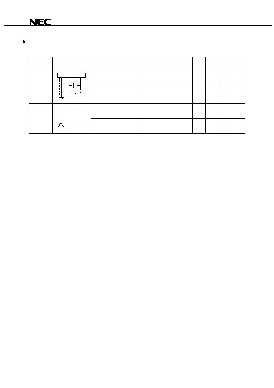
4.3
Pin Input/Output Circuits and Handling of Unused Pins
Table 4-1 lists the types of input/output circuits for each pin and explains how unused pins are handled.
Figure 4-1 shows the configuration of each type of input/output circuit.
Table 4-1. Type of Input/Output Circuit for Each Pin
Pin name
I/O circuit type
I/O
Recommended connection of unused pins
P00-P07
P10-P17
5-R
P20/
SCK10
P21/SO10
P22/SI10
P23, P24
8-C
P25
P26/INTP0/TI01/TO01
8-F
P40/
KR00
-P47/
KR07
8-C
Input
: Connect these pins separately to V
DD0
, V
DD1
, V
SS0
, or V
SS1
via
respective resistors.
Output : Leave these pins open.
USBDM
Connect this pin to the REGC pin.
USBDP
24-A
I/O
Connect this pin to V
SS0
or V
SS1
via resistors.
RESET
2
Input
-
V
PP
-
-
Connect this pin directly to V
SS0
or V
SS1
.
NC
-
-
Leave this pin open.
REGC
-
-
Connect this pin to the USBDM pin.
Data Sheet U12626EJ1V0DS00
12
µ
µ
µ
µ
PD78F9801
Figure 4-1. Pin Input/Output Circuits
Type 2
Type 5-R
Type 8-F
Type 24-A
Type 8-C
IN
Schmitt trigger input with hysteresis
Pull-up
enable
P-ch
cut
Output
data
Output
disable
V
DD0
V
DD0
P-ch
N-ch
IN/OUT
P-ch
Input
enable
V
SS0
V
DD0
P-ch
IN/OUT
P-ch
V
DD0
Pull-up
enable
Output
disable
Output
data
N-ch
V
SS0
Pull-up
enable
P-ch
cut
Output
data
Output
disable
V
DD0
V
DD0
P-ch
N-ch
IN/OUT
P-ch
V
SS0
V
SS0
TXDXP
RXDX
TXDXN
V
REG
P-ch
N-ch
IN/OUT
Data Sheet U12626EJ1V0DS00
13
µ
µ
µ
µ
PD78F9801
5. MEMORY SPACE
Figure 5-1 shows the memory map of the
µ
PD78F9801.
Figure 5-1. Memory Map
Special function register
256
◊
8 bits
Internal high-speed RAM
256
◊
8 bits
Unusable
Program area
CALLT table area
Program area
Vector table area
Flash memory
16,384
◊
8 bits
Data memory
space
Program memory
space
F F F F H
F F 0 0 H
F E F F H
F E 0 0 H
F D F F H
4 0 0 0 H
3 F F F H
0 0 0 0 H
0 0 0 0 H
0 0 1 A H
0 0 1 9 H
0 0 4 0 H
0 0 3 F H
3 F F F H
0 0 7 F H
0 0 8 0 H
Data Sheet U12626EJ1V0DS00
14
µ
µ
µ
µ
PD78F9801
6. FLASH MEMORY PROGRAMMING
The on-chip program memory in the
µ
PD78F9801 is a flash memory.
The flash memory can be written with the
µ
PD78F9801 mounted on the target system (on-board). Connect the
dedicated flash programmer (Flashpro III (model number: FL-PR3, PG-FP3)) to the host machine and target system
to write the flash memory.
Remark
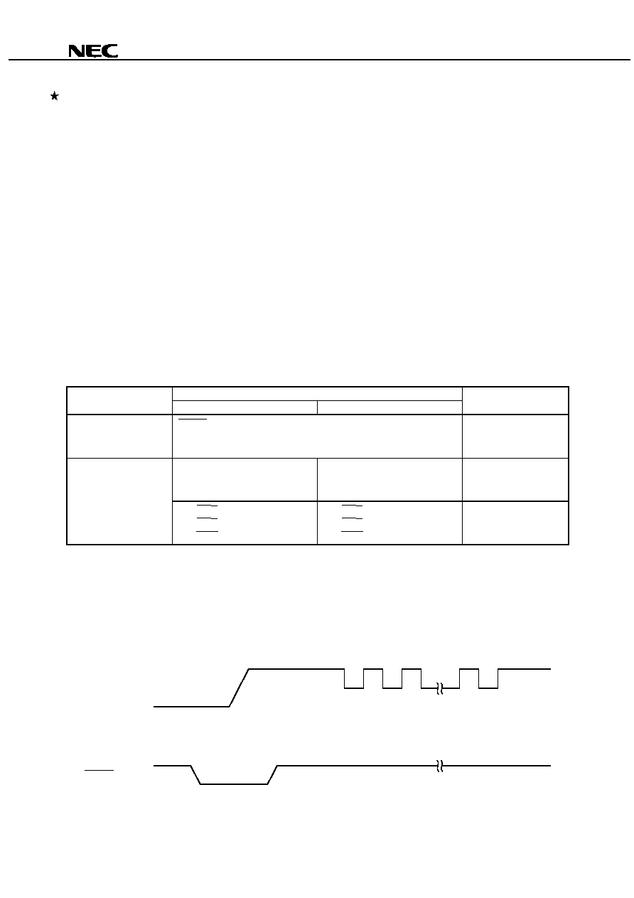
FL-PR3 is made by Naito Densei Machida Mfg. Co., Ltd..
6.1
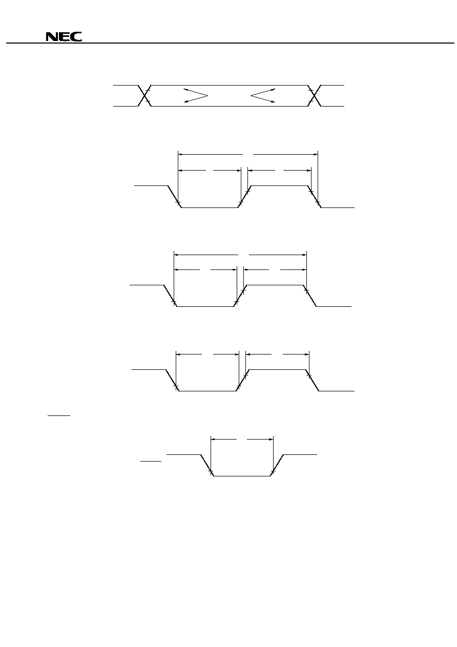
Selecting Communication Mode
The flash memory is written by using Flashpro III and by means of serial communication. Select a communication
mode from those listed in Table 6-1. To select a communication mode, the format shown in Figure 6-1 is used. Each
communication mode is selected by the number of V
PP
pulses shown in Table 6-1.
Caution
When the pseudo 3-wire mode is selected as the communication mode, pins to be used differ
depending on the version of the
µ
µ
µ
µ
PD78F9801. Be sure to check the marking of the version if
writing to flash memory when the pseudo 3-wire mode is selected.
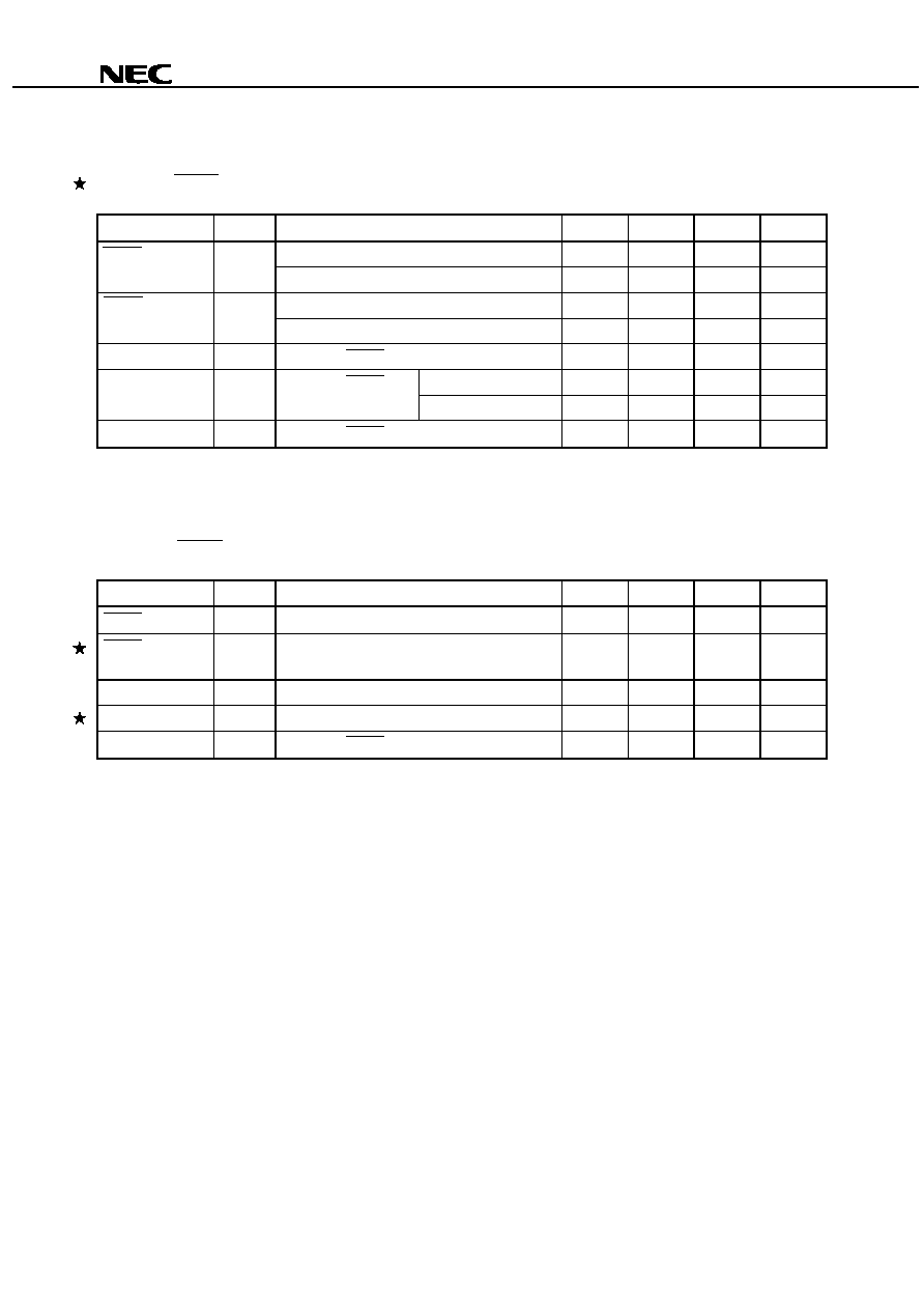
Table 6-1. Communication Mode List
Pins used
Communication mode
Ver. 2.3 or earlier
Ver. 3.0 or later, or without marking
Number of V
PP
pulses
3-wired serial I/O mode
SCK10/P20
SO10/P21
SI10/P22
0
P15 (Serial clock input)
P16 (Serial data output)
P17 (Serial data input)
P10 (Serial clock input)
P11 (Serial data output)
P12 (Serial data input)
12
Pseudo 3-wire mode
Note
P45/KR05 (Serial clock input)
P46/KR06 (Serial data output)
P47/KR07 (Serial data input)
P40/KR00 (Serial clock input)
P41/KR01 (Serial data output)
P42/KR02 (Serial data input)
13
Note
Serial transfer is performed by controlling a port by software.
Caution
Be sure to select a communication mode depending on the V
PP
pulse number shown in Table
6-1.
Figure 6-1. Communication Mode Selection Format
10 V
V
SS
V
DD
V
PP
V
DD
V
SS
RESET
1
2
n
Data Sheet U12626EJ1V0DS00
15
µ
µ
µ
µ
PD78F9801
6.2
Function of Flash Memory Programming
By transmitting/receiving commands and data in the selected communication mode, operations such as writing to
the flash memory are performed. Table 6-2 shows the major functions of flash memory programming.
Table 6-2. Functions of Flash Memory Programming
Function
Description
Batch erase
Erases all contents of memory
Batch blank check
Checks erased state of entire memory
Data write
Write to flash memory based on write start address and number of data written (number of bytes)
Batch verify
Compares all contents of memory with input data
6.3
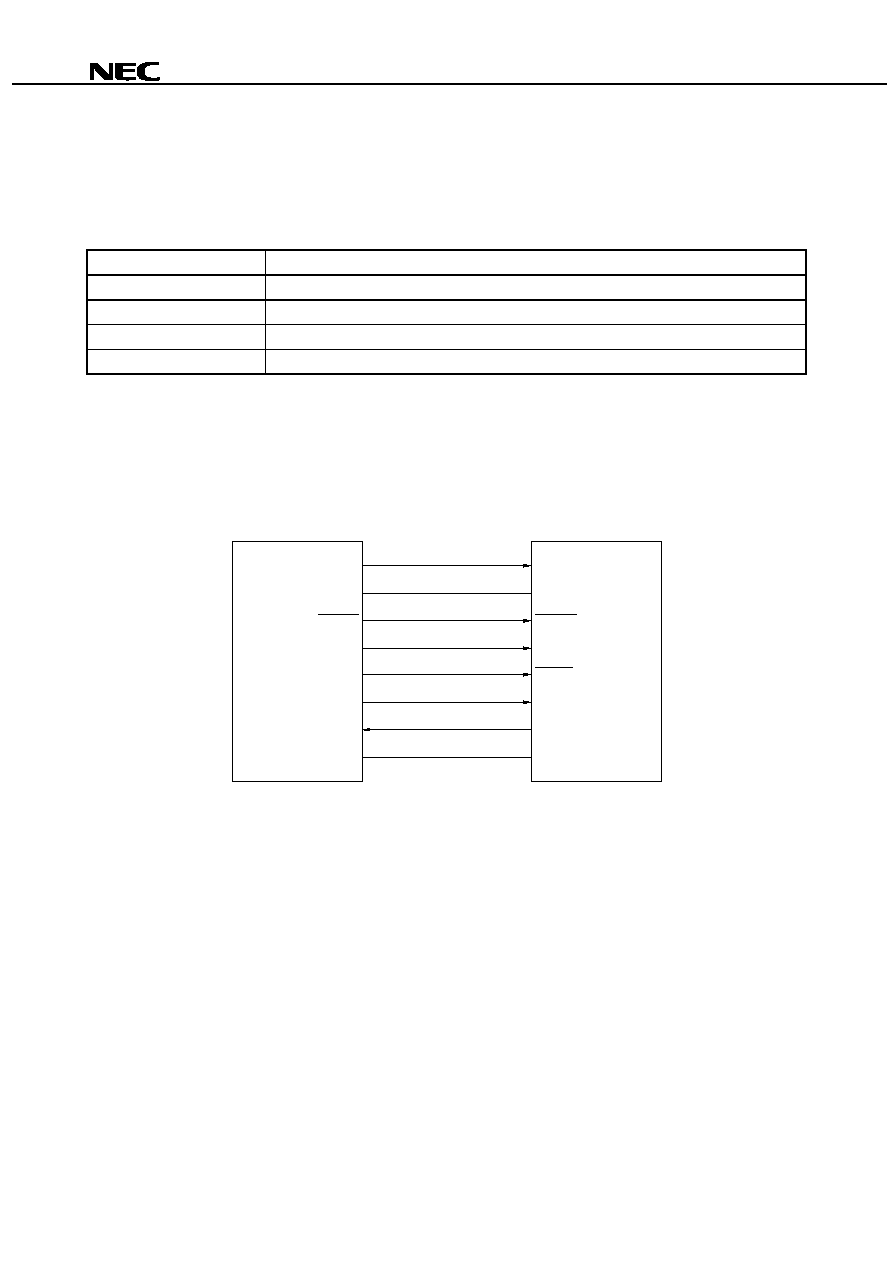
Flashpro III Connection
How the Flashpro III is connected to the
µ
PD78F9801 differs depending on the communication mode (3-wired
serial I/O or pseudo 3-wire mode). Figures 6-2 to 6-4 show the connection in the respective mode.
Figure 6-2. Flashpro III Connection in 3-wired Serial I/O Mode
V
PP
n
Note
V
DD
RESET
SCK
SO
SI
GND
V
PP
V
DD
RESET
CLK
X1
SCK10
SI10
SO10
V
SS
Flashpro III
PD78F9801
µ
Note
n = 1, 2
Data Sheet U12626EJ1V0DS00
16
µ
µ
µ
µ
PD78F9801
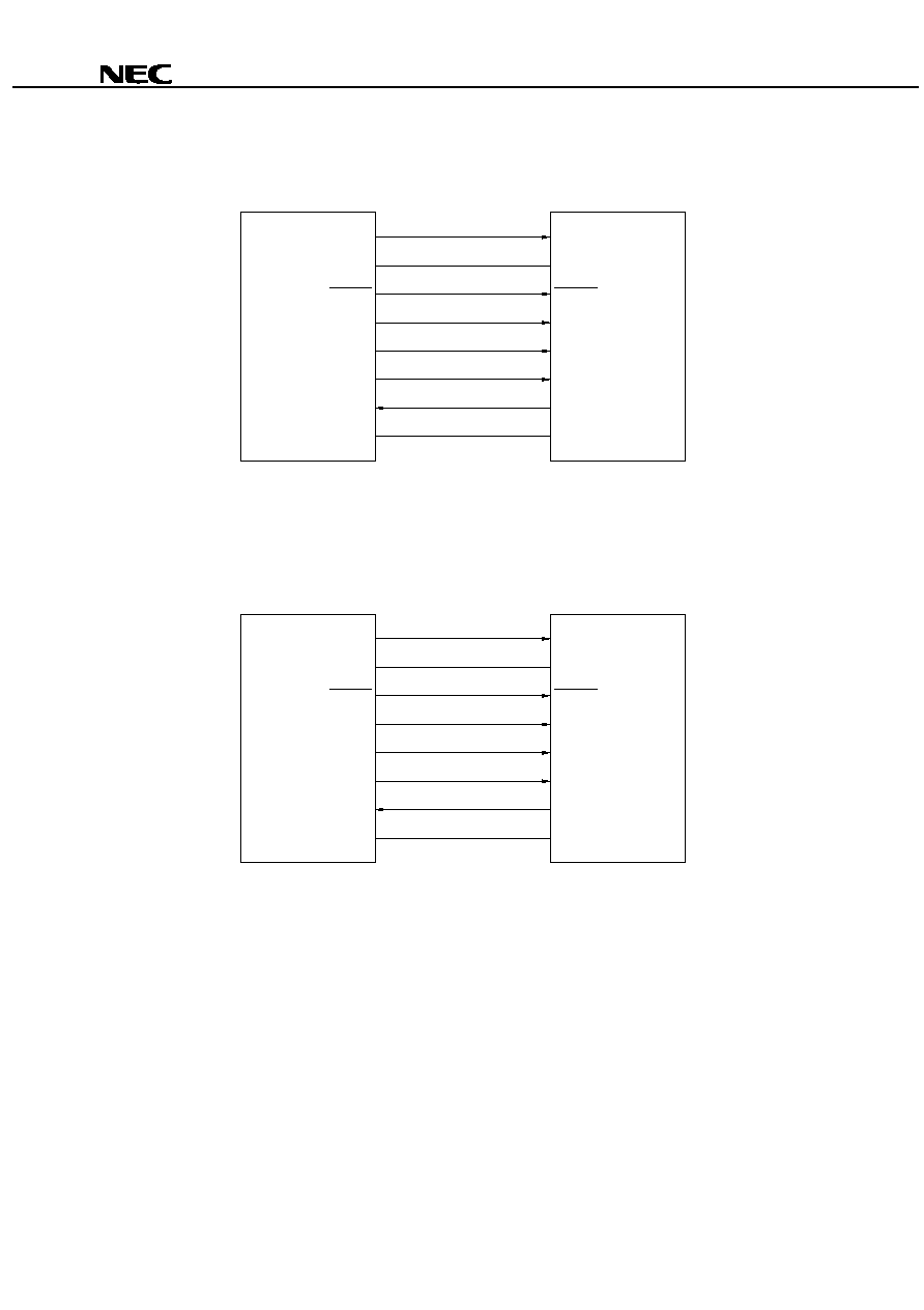
Figure 6-3. Flashpro III Connection in Pseudo 3-Wire Mode (When Port 1 is Used)
(Ver.3.0 or later, or without marking)
V
PP
n
Note
V
DD
RESET
SCK
SO
SI
GND
V
PP
V
DD
RESET
CLK
X1
P15 (Serial clock)
P17 (Serial input)
P16 (Serial output)
V
SS
Flashpro III
PD78F9801
µ
Note
n= 1, 2
Figure 6-4. Flashpro III Connection in Pseudo 3-Wire Mode (When Port 4 is Used)
(Ver.3.0 or later, or without marking)
V
PP
n
Note
V
DD
RESET
SCK
SO
SI
GND
V
PP
V
DD
RESET
CLK
X1
P10 (Serial clock)
P12 (Serial input)
P11 (Serial output)
V
SS
Flashpro III
PD78F9801
µ
Note
n= 1, 2
Data Sheet U12626EJ1V0DS00
17
µ
µ
µ
µ
PD78F9801
6.4
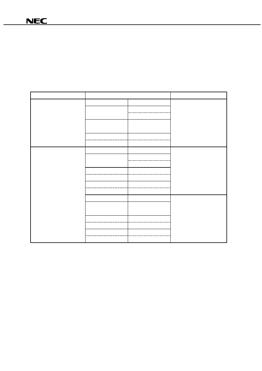
Example of Settings for Flashpro III (PG-FP3)
Set as follows when writing to flash memory using the Flashpro III (PG-FP3).
<1> Download the parameter file.
<2> Select the serial mode and the serial clock using the type command.
<3> The following is a setting example using the PG-FP3.
Table 6-3. Example Using PG-FP3
Communication mode
Setting example using PG-FP3
Number of V
PP
pulses
Note
COMM PORT
SIO ch-0
On target board
CPU CLK
In Flashpro
On target board
6.0 MHz
SIO CLK
1.0 MHz
In Flashpro
6.0 MHz
3-wired serial I/O mode
SIO CLK
1.0 MHz
0
COMM PORT
Port A
On target board
CPU CLK
In Flashpro
On target board
6.0 MHz
SIO CLK
1 kHz
In Flashpro
6.0 MHz
SIO CLK
1 kHz
12
COMM PORT
Port B
On target board
CPU CLK
In Flashpro
On target board
6.0 MHz
SIO CLK
1 kHz
In Flashpro
6.0 MHz
Pseudo 3-wire mode
SIO CLK
1 kHz
13
Note
The number of V
PP
pulses supplied from the Flashpro III during serial communication initialization. The
pins to be used in communication are determined by this number of pulses.
Remark
COMM PORT: Selection of serial port
SIO CLK
: Selection of serial clock frequency
CPU CLK
: Selection of CPU clock source to be input

Data Sheet U12626EJ1V0DS00
18
µ
µ
µ
µ
PD78F9801
7. INSTRUCTION SET OVERVIEW
The instruction set for the
µ
PD78F9801 is listed later.
7.1
Legend
7.1.1 Operand formats and descriptions
The description made in the operand field of each instruction conforms to the operand format for the instructions
listed below (the details conform with the assembly specification). If more than one operand format is listed for an
instruction, one is selected. Uppercase letters, #, !, $, and a pair of [ and ] are used to specify keywords, which must
be written exactly as they appear. The meanings of these special characters are as follows:
∑ #: Immediate data specification
∑ $: Relative address specification
∑ !: Absolute address specification
∑ [ and ]: Indirect address specification
Immediate data should be described using appropriate values or labels. The specification of values and labels
must be accompanied by #, !, $, or a pair of [ and ].
Operand registers, expressed as r or rp in the formats, can be described using both functional names (X, A, C,
etc.) and absolute names (R0, R1, R2, and other names listed in Table 7-1).
Table 7-1. Operand Formats and Descriptions
Format
Description
r
rp
sfr
X (R0), A (R1), C (R2), B (R3), E (R4), D (R5), L (R6), H (R7)
AX (RP0), BC (RP1), DE (RP2), HL (RP3)
Special function register symbol
saddr
saddrp
FE20H to FF1FH: Immediate data or label
FE20H to FF1FH: Immediate data or label (even addresses only)
addr16
addr5
0000H to FFFFH: Immediate data or label
(only even address for 16-bit data transfer instructions)
0040H to 007FH: Immediate data or label (even addresses only)
word
byte
bit
16-bit immediate data or label
8-bit immediate data or label
3-bit immediate data or label

Data Sheet U12626EJ1V0DS00
19
µ
µ
µ
µ
PD78F9801
7.1.2 Descriptions of the operation field
A
: A register (8-bit accumulator)
X
: X register
B
: B register
C
: C register
D
: D register
E
: E register
H
: H register
L
: L register
AX
: AX register pair (16-bit accumulator)
BC
: BC register pair
DE
: DE register pair
HL
: HL register pair
PC
: Program counter
SP
: Stack pointer
PSW
: Program status word
CY
: Carry flag
AC
: Auxiliary carry flag
Z
: Zero flag
IE
: Interrupt request enable flag
NMIS
: Flag to indicate that a nonmaskable interrupt is being handled
()
: Contents of a memory location indicated by a parenthesized address or register name
X
H
, X
L
: Upper and lower 8 bits of a 16-bit register
: Logical product (AND)
: Logical sum (OR)
: Exclusive OR
: Inverted data
addr16 : 16-bit immediate data or label
jdisp8 : Signed 8-bit data (displacement value)
7.1.3 Description of the flag operation field
(blank) : No change
0
: To be cleared to 0
1
: To be set to 1
◊
: To be set or cleared according to the result
R
: To be restored to the previous value
Data Sheet U12626EJ1V0DS00
20
µ
µ
µ
µ
PD78F9801
7.2
Operations
Flag
Mnemonic
Operand
Byte
Clock
Operation
Z
AC CY
MOV
r, #byte
3
6
r
byte
saddr, #byte
3
6
(saddr)
byte
sfr, #byte
3
6
sfr
byte
A, r
Note 1
2
4
A
r
r, A
Note 1
2
4
r
A
A, saddr
2
4
A
(saddr)
saddr, A
2
4
(saddr)
A
A, sfr
2
4
A
sfr
sfr, A
2
4
sfr
A
A, !addr16
3
8
A
(addr16)
!addr16, A
3
8
(addr16)
A
PSW, #byte
3
6
PSW
byte
◊
◊
◊
A, PSW
2
4
A
PSW
PSW, A
2
4
PSW
A
◊
◊
◊
A, [DE]
1
6
A
(DE)
[DE], A
1
6
(DE)
A
A, [HL]
1
6
A
(HL)
[HL], A
1
6
(HL)
A
A, [HL + byte]
2
6
A
(HL + byte)
[HL + byte], A
2
6
(HL + byte)
A
XCH
A, X
1
4
A
X
A, r
Note 2
2
6
A
r
A, saddr
2
6
A
(saddr)
A, sfr
2
6
A
(sfr)
A, [DE]
1
8
A
(DE)
A, [HL]
1
8
A
(HL)
A, [HL + byte]
2
8
A
(HL + byte)
MOVW
rp, #word
3
6
rp
word
AX, saddrp
2
6
AX
(saddrp)
saddrp, AX
2
8
(saddrp)
AX
AX, rp
Note 3
1
4
AX
rp
rp, AX
Note 3
1
4
rp
AX
Notes 1. Except when r = A.
2. Except when r = A or X.
3. Only when rp = BC, DE, or HL.
Remark The instruction clock cycle is based on the CPU clock (f
CPU
), specified in the processor clock control
register (PCC).
Data Sheet U12626EJ1V0DS00
21
µ
µ
µ
µ
PD78F9801
Flag
Mnemonic
Operand
Byte
Clock
Operation
Z
AC CY
XCHW
AX, rp
Note
1
8
AX
rp
ADD
A, #byte
2
4
A, CY
A + byte
◊
◊
◊
saddr, #byte
3
6
(saddr), CY
(saddr) + byte
◊
◊
◊
A, r
2
4
A, CY
A + r
◊
◊
◊
A, saddr
2
4
A, CY
A + (saddr)
◊
◊
◊
A, !addr16
3
8
A, CY
A + (addr16)
◊
◊
◊
A, [HL]
1
6
A, CY
A + (HL)
◊
◊
◊
A, [HL + byte]
2
6
A, CY
A + (HL + byte)
◊
◊
◊
ADDC
A, #byte
2
4
A, CY
A + byte + CY
◊
◊
◊
saddr, #byte
3
6
(saddr), CY
(saddr) + byte + CY
◊
◊
◊
A, r
2
4
A, CY
A + r + CY
◊
◊
◊
A, saddr
2
4
A, CY
A + (saddr) + CY
◊
◊
◊
A, !addr16
3
8
A, CY
A + (addr16) + CY
◊
◊
◊
A, [HL]
1
6
A, CY
A + (HL) + CY
◊
◊
◊
A, [HL + byte]
2
6
A, CY
A + (HL + byte) + CY
◊
◊
◊
SUB
A, #byte
2
4
A, CY
A
-
byte
◊
◊
◊
saddr, #byte
3
6
(saddr), CY
(saddr)
-
byte
◊
◊
◊
A, r
2
4
A, CY
A
-
r
◊
◊
◊
A, saddr
2
4
A, CY
A
-
(saddr)
◊
◊
◊
A, !addr16
3
8
A, CY
A
-
(addr16)
◊
◊
◊
A, [HL]
1
6
A, CY
A
-
(HL)
◊
◊
◊
A, [HL + byte]
2
6
A, CY
A
-
(HL + byte)
◊
◊
◊
SUBC
A, #byte
2
4
A, CY
A
-
byte
-
CY
◊
◊
◊
saddr, #byte
3
6
(saddr), CY
(saddr)
-
byte
-
CY
◊
◊
◊
A, r
2
4
A, CY
A
-
r
-
CY
◊
◊
◊
A, saddr
2
4
A, CY
A
-
(saddr)
-
CY
◊
◊
◊
A, !addr16
3
8
A, CY
A
-
(addr16)
-
CY
◊
◊
◊
A, [HL]
1
6
A, CY
A
-
(HL)
-
CY
◊
◊
◊
A, [HL + byte]
2
6
A, CY
A
-
(HL + byte)
-
CY
◊
◊
◊
AND
A, #byte
2
4
A
A
byte
◊
saddr, #byte
3
6
(saddr)
(saddr)
byte
◊
A, r
2
4
A
A
r
◊
A, saddr
2
4
A
A
(saddr)
◊
A, !addr16
3
8
A
A
(addr16)
◊
A, [HL]
1
6
A
A
(HL)
◊
A, [HL + byte]
2
6
A
A
(HL + byte)
◊
Note
Only when rp = BC, DE, or HL.
Remark The instruction clock cycle is based on the CPU clock (f
CPU
), specified in the processor clock control
register (PCC).

Data Sheet U12626EJ1V0DS00
22
µ
µ
µ
µ
PD78F9801
Flag
Mnemonic
Operand
Byte
Clock
Operation
Z
AC CY
OR
A, #byte
2
4
A
A
byte
◊
saddr, #byte
3
6
(saddr)
(saddr)
byte
◊
A, r
2
4
A
A
r
◊
A, saddr
2
4
A
A
(saddr)
◊
A, !addr16
3
8
A
A
(addr16)
◊
A, [HL]
1
6
A
A
(HL)
◊
A, [HL + byte]
2
6
A
A
(HL + byte)
◊
XOR
A, #byte
2
4
A
A byte
◊
saddr, #byte
3
6
(saddr)
(saddr) byte
◊
A, r
2
4
A
A r
◊
A, saddr
2
4
A
A (saddr)
◊
A, !addr16
3
8
A
A (addr16)
◊
A, [HL]
1
6
A
A (HL)
◊
A, [HL + byte]
2
6
A
A (HL + byte)
◊
CMP
A, #byte
2
4
A
-
byte
◊
◊
◊
saddr, #byte
3
6
(saddr)
-
byte
◊
◊
◊
A, r
2
4
A
-
r
◊
◊
◊
A, saddr
2
4
A
-
(saddr)
◊
◊
◊
A, !addr16
3
8
A
-
(addr16)
◊
◊
◊
A, [HL]
1
6
A
-
(HL)
◊
◊
◊
A, [HL + byte]
2
6
A
-
(HL + byte)
◊
◊
◊
ADDW
AX, #word
3
6
AX, CY
AX + word
◊
◊
◊
SUBW
AX, #word
3
6
AX, CY
AX
-
word
◊
◊
◊
CMPW
AX, #word
3
6
AX
-
word
◊
◊
◊
INC
r
2
4
r
r + 1
◊
◊
saddr
2
4
(saddr)
(saddr) + 1
◊
◊
DEC
r
2
4
r
r
-
1
◊
◊
saddr
2
4
(saddr)
(saddr)
-
1
◊
◊
INCW
rp
1
4
rp
rp + 1
DECW
rp
1
4
rp
rp
-
1
ROR
A, 1
1
2
(CY, A
7
A
0
, A
m
-
1
A
m
)
◊
1
◊
ROL
A, 1
1
2
(CY, A
0
A
7
, A
m+1
A
m
)
◊
1
◊
RORC
A, 1
1
2
(CY
A
0
, A
7
CY, A
m
-
1
A
m
)
◊
1
◊
ROLC
A, 1
1
2
(CY
A
7
, A
0
CY, A
m+1
A
m
)
◊
1
◊
Remark The instruction clock cycle is based on the CPU clock (f
CPU
), specified in the processor clock control
register (PCC).

Data Sheet U12626EJ1V0DS00
23
µ
µ
µ
µ
PD78F9801
Flag
Mnemonic
Operand
Byte
Clock
Operation
Z
AC CY
SET1
saddr. bit
3
6
(saddr. bit)
1
sfr. bit
3
6
sfr. bit
1
A. bit
2
4
A. bit
1
PSW. bit
3
6
PSW. bit
1
◊
◊
◊
[HL]. bit
2
10
(HL). bit
1
CLR1
saddr. bit
3
6
(saddr. bit)
0
sfr. bit
3
6
sfr. bit
0
A. bit
2
4
A. bit
0
PSW. bit
3
6
PSW. bit
0
◊
◊
◊
[HL]. bit
2
10
(HL). bit
0
SET1
CY
1
2
CY
1
1
CLR1
CY
1
2
CY
0
0
NOT1
CY
1
2
CY
CY
◊
CALL
!addr16
3
6
(SP
-
1)
(PC + 3)
H
, (SP
-
2)
(PC + 3)
L
,
PC
addr16, SP
SP
-
2
CALLT
[addr5]
1
8
(SP
-
1)
(PC + 1)
H
, (SP
-
2)
(PC + 1)
L
,
PC
H
(00000000, addr5 + 1),
PC
L
(00000000, addr5),
SP
SP
-
2
RET
1
6
PC
H
(SP + 1), PC
L
(SP),
SP
SP + 2
RETI
1
8
PC
H
(SP + 1), PC
L
(SP),
PSW
(SP + 2), SP
SP + 3,
NMIS
0
R
R
R
PUSH
PSW
1
2
(SP
-
1)
PSW, SP
SP
-
1
rp
1
4
(SP
-
1)
rp
H
, (SP
-
2)
rp
L
,
SP
SP
-
2
POP
PSW
1
4
PSW
(SP), SP
SP + 1
R
R
R
rp
1
6
rp
H
(SP + 1), rp
L
(SP),
SP
SP + 2
MOVW
SP, AX
2
8
SP
AX
AX, SP
2
6
AX
SP
BR
!addr16
3
6
PC
addr16
$addr16
2
6
PC
PC + 2 + jdisp8
AX
1
6
PC
H
A, PC
L
X
Remark The instruction clock cycle is based on the CPU clock (f
CPU
), specified in the processor clock control
register (PCC).
Data Sheet U12626EJ1V0DS00
24
µ
µ
µ
µ
PD78F9801
Flag
Mnemonic
Operand
Byte
Clock
Operation
Z
AC CY
BC
$addr16
2
6
PC
PC + 2 + jdisp8 if CY = 1
BNC
$addr16
2
6
PC
PC + 2 + jdisp8 if CY = 0
BZ
$addr16
2
6
PC
PC + 2 + jdisp8 if Z = 1
BNZ
$addr16
2
6
PC
PC + 2 + jdisp8 if Z = 0
BT
saddr. bit, $addr16
4
10
PC
PC + 4 + jdisp8
if (saddr. bit) = 1
sfr. bit, $addr16
4
10
PC
PC + 4 + jdisp8 if sfr. bit = 1
A. bit, $addr16
3
8
PC
PC + 3 + jdisp8 if A. bit = 1
PSW. bit, $addr16
4
10
PC
PC + 4 + jdisp8 if PSW. bit = 1
BF
saddr. bit, $addr16
4
10
PC
PC + 4 + jdisp8
if (saddr. bit) = 0
sfr. bit, $addr16
4
10
PC
PC + 4 + jdisp8 if sfr. bit = 0
A. bit, $addr16
3
8
PC
PC + 3 + jdisp8 if A. bit = 0
PSW. bit, $addr16
4
10
PC
PC + 4 + jdisp8 if PSW. bit = 0
DBNZ
B, $addr16
2
6
B
B
-
1, then
PC
PC + 2 + jdisp8 if B
0
C, $addr16
2
6
C
C
-
1, then
PC
PC + 2 + jdisp8 if C
0
saddr, $addr16
3
8
(saddr)
(saddr)
-
1, then
PC
PC + 3 + jdisp8 if (saddr)
0
NOP
1
2
No Operation
EI
3
6
IE
1 (Enable Interrupt)
DI
3
6
IE
0 (Disable Interrupt)
HALT
1
2
Set HALT Mode
STOP
1
2
Set STOP Mode
Remark The instruction clock cycle is based on the CPU clock (f
CPU
), specified in the processor clock control
register (PCC).
Data Sheet U12626EJ1V0DS00
25
µ
µ
µ
µ
PD78F9801
8. ELECTRICAL CHARACTERISTICS
ABSOLUTE MAXIMUM RATINGS (T
A
= 25
∞
∞
∞
∞
C)
Parameter
Symbol
Conditions
Rated value
Unit
Supply voltage
V
DD
-0.3 to +6.5
V
Input voltage
V
I
-0.3 to V
DD
+ 0.3
V
Output voltage
V
O
-0.3 to V
DD
+ 0.3
V
Each pin
-10
mA
Output high current
I
OH
Total for all pins
-30
mA
Each pin
30
mA
Output low current
I
OL
Total for all pins
160
mA
In normal operation mode
-40 to +85
∞
C
Operating ambient temperature
T
A
During flash memory programming
10 to 40
∞
C
Storage temperature
T
stg
-40 to +125
∞
C
Caution
Absolute maximum ratings are rated values beyond which physical damage will be caused to
the product; if the rated value of any of the parameters in the above table is exceeded, even
momentarily, the quality of the product may deteriorate. Always use the product within its rated
values.
Remark The characteristics of a dual-function pin do not differ between the port function and the secondary
function, unless otherwise stated.
Data Sheet U12626EJ1V0DS00
26
µ
µ
µ
µ
PD78F9801
CHARACTERISTICS OF THE SYSTEM CLOCK OSCILLATION CIRCUIT
(T
A
= -40
∞
∞
∞
∞
C to +85
∞
∞
∞
∞
C, V
DD
= 4.0 to 5.5 V)
Resonator
Recommended
circuit
Parameter
Conditions
MIN.
TYP.
MAX.
Unit
Oscillator frequency (f
X
)
Note 1
6.0
6.0
6.0
MHz
Crystal
X2
X1
V
PP
C2
C1
Oscillation settling time
Note 2
10
ms
X1 input frequency (f
X
)
Note 1
6.0
6.0
6.0
MHz
External
clock
X1 input high/low level
width (t
XH
, t
XL
)
71
83
ns
Notes 1. Only the characteristics of the oscillation circuit are indicated. See the description of the AC
characteristics for the instruction execution time.
2. Time required for oscillation to settle once a reset sequence ends or STOP mode is deselected. Use a
resonator that can settle oscillation before the oscillation settling time expires.
Caution
When using the system clock oscillation circuit, observe the following conditions for the wiring
of that section enclosed in dotted lines in the above diagrams, so as to avoid the influence of
the wiring capacitance.
∑
Keep the wiring as short as possible.
∑
∑
∑
∑
Do not allow signal wires to cross one another.
∑
∑
∑
∑
Keep the wiring away from wires that carry a high, non-stable current.
∑
∑
∑
∑
Keep the grounding point of the capacitors at the same level as V
SS0
.
∑
∑
∑
∑
Do not connect the grounding point to a grounding wire that carries a high current.
∑
∑
∑
∑
Do not extract a signal from the oscillation circuit.
X1
X2
OPEN
Data Sheet U12626EJ1V0DS00
27
µ
µ
µ
µ
PD78F9801
FLASH MEMORY WRITE/DELETE CHARACTERISTICS (T
A
= 10
∞
∞
∞
∞
C to 40
∞
∞
∞
∞
C, V
DD
= 4.0 to 5.5 V)
Parameter
Symbol
Conditions
MIN.
TYP.
MAX.
Unit
Write current
(V
DD
pin)
I
DDW
When V
PP
supply voltage = V
PP1
(in 6.0-MHz operation mode)
18
Note
mA
Write current
(V
PP
pin)
I
PPW
When V
PP
supply voltage = V
PP1
7.5
mA
Delete current
(V
DD
pin)
I
DDE
When V
PP
supply voltage = V
PP1
(in 6.0-MHz operation mode)
18
Note
mA
Delete current
(V
PP
pin)
I
PPE
When V
PP
supply voltage = V
PP1
100
mA
Unit delete time
t
er
1
1
1
s
Total delete time
t
era
20
s
Write count
Delete/write are regarded as 1 cycle
1
Times
V
PP0
In normal operation
0
0.2V
DD
V
V
PP
supply voltage
V
PP1
During flash memory programming
9.7
10.0
10.3
V
Note The current flowing to the ports (including the current flowing through the on-chip pull-up resistors) is not
included.
Data Sheet U12626EJ1V0DS00
28
µ
µ
µ
µ
PD78F9801
DC CHARACTERISTICS (T
A
= -40
∞
∞
∞
∞
C to +85
∞
∞
∞
∞
C, V
DD
= 4.0 to 5.5 V)
Parameter
Symbol
Conditions
MIN.
TYP.
MAX.
Unit
Each pin
-1
mA
Output high
current
I
OH
Total for all pins
-15
mA
Each pin
10
mA
Output low current
I
OL
Total for all pins
80
mA
V
IH1
P00-P07, P10-P17
0.7V
DD
V
DD
V
V
IH2
RESET, P20-P26, P40-P47
0.8V
DD
V
DD
V
V
IH3
X1
V
DD
≠ 0.1
V
DD
V
Input high voltage
V
IH4
USBDM, USBDP T
A
= 0
∞
C to +70
∞
C
2.0
3.6
V
V
IL1
P00-P07, P10-P17
0
0.3V
DD
V
V
IL2
RESET, P20, P22, P40-P47
0
0.2V
DD
V
V
IL3
X1
0
0.1
V
Input low voltage
V
IL4
USBDM, USBDP T
A
= 0
∞
C to +70
∞
C
0
0.8
V
V
OH1
Pins other than USBDM and
USBDP
I
O
= -1 mA
V
DD
≠ 1.0
V
Output high
voltage
V
OH2
USBDM, USBDP T
A
= 0
∞
C to +70
∞
C,
RL = 15 k
(connected to V
SS
)
Note 1
2.8
V
V
OL1
Pins other than USBDM and
USBDP
I
O
= -10 mA
1.0
V
Output low voltage
V
OL2
USBDM, USBDP T
A
= 0
∞
C to +70
∞
C,
RL = 15 k
(connected to V
DD
)
Note 1
0.3
V
I
LIH1
Pins other than X1, X2,
USBDM, and USBDP
V
I
= V
DD
3
µ
A
I
LIH2
X1, X2
V
I
= V
DD
20
µ
A
High-level input
leakage current
I
LIH3
USBDM, USBDP
T
A
= 0
∞
C to +70
∞
C
0 V
V
IN
V
REG
10
µ
A
I
LIL1
Pins other than X1, X2,
USBDM, and USBDP
V
I
= 0 V
-3
µ
A
I
LIL2
X1, X2
V
I
= 0 V
-20
µ
A
Low-level input
leakage current
I
LIL3
USBDM, USBDP
T
A
= 0
∞
C to +70
∞
C
0 V
V
IN
V
REG
-10
µ
A
High-level output
leakage current
I
LOH
V
OUT
= 0 V
3
µ
A
Low-level output
leakage current
I
LOL
V
OUT
= 0 V
-3
µ
A
Software pull-up
resistor
R
V
I
= 0 V
50
100
200
k
Regulator output
voltage
V
REG
I
O
= 0 to -3 mA
3.0
3.3
3.6
V
I
DD1
6.0-MHz crystal oscillation (operating mode)
Note 3
5.0
10
mA
I
DD2
6.0-MHz crystal oscillation (HALT mode)
Note 3
1.5
3.5
mA
When the USB
function is disabled
10
30
µ
A
Supply current
Note 2
I
DD3
STOP mode
When the USB
function is enabled
(T
A
= 0
∞
C to +70
∞
C)
50
100
µ
A
Notes 1. RL is a resistor connected to a bus line.
2. The power supply current does not include the current flowing through the on-chip pull-up resistor.
3. During high-speed mode operation (when the processor clock control register (PCC) is cleared to 00H)
Remark
The characteristics of a dual-function pin do not differ between the port function and the secondary
function, unless otherwise stated.
Data Sheet U12626EJ1V0DS00
29
µ
µ
µ
µ
PD78F9801
AC CHARACTERISTICS
(1) Basic operations (T
A
= -40
∞
∞
∞
∞
C to +85
∞
∞
∞
∞
C, V
DD
= 4.0 to 5.5 V)
Parameter
Symbol
Conditions
MIN.
TYP.
MAX.
Unit
When PCC = 00H (f
X
= 6.0 MHz)
0.333
0.333
0.333
µ
s
Cycle time (minimum
instruction execution
time)
T
CY
When PCC = 02H (f
X
= 6.0 MHz)
1.333
1.333
1.333
µ
s
TI01 input
frequency
f
TI
0
4.0
MHz
TI01 input high/low
level width
t
TIH
, t
TIL
0.1
µ
s
Interrupt input
high/low level
width
t
INTH
, t
INTL
INTP0
10
µ
s
RESET
input low
level width
t
RSL
10
µ
s
(2) Serial interface
(a) USB function (T
A
= 0
∞
∞
∞
∞
C to +70
∞
∞
∞
∞
C, V
DD
= 4.0 to 5.5 V)
Parameter
Symbol
Conditions
MIN.
TYP.
MAX.
Unit
CL = 50 pF
Note
75
ns
USBDM and
USBDP rise time
t
R
CL = 350 pF
Note
300
ns
CL = 50 pF
Note
75
ns
USBDM and
USBDP fall time
t
F
CL = 350 pF
Note
300
ns
t
R
and t
F
matching
t
RFM
t
R
/t
F
80
120
%
Differential output
signal cross-over
point
V
CRS
1.3
2.0
V
Data transfer rate
t
DRATE
When the microcontroller operates at the system
clock (f
X
) of 6.0 MHz
1.5
1.5
1.5
Mbps
t
UDJ1
Upon transferring the next bit
-95
0
95
ns
Transmission
differential signal
jitter
t
UDJ2
Upon transferring the bit following the next bit
-150
0
150
ns
Transmission EOP
width
t
EOPT1
1.25
1.33
1.50
µ
s
t
EOPR1
EOP width to be eliminated
300
µ
s
Reception EOP
width
t
EOPR2
EOP width to be detected
675
µ
s
t
URES1
USB reset width to be eliminated
2.5
µ
s
Reception USB
reset width
t
URES2
USB reset width to be detected
5.5
µ
s
Note
CL is the capacitance of the USBDM and USBDP output lines.
Data Sheet U12626EJ1V0DS00
30
µ
µ
µ
µ
PD78F9801
(b) Three-wire serial I/O mode (T
A
= -40
∞
∞
∞
∞
C to +85
∞
∞
∞
∞
C, V
DD
= 4.0 to 5.5 V)
(i) SCK10 ...Internal clock output (when f
X
= 6.0 MHz)
Parameter
Symbol
Conditions
MIN.
TYP.
MAX.
Unit
When TPS100
Note 1
= 0
667
667
667
ns
SCK10
cycle time
t
KCY1
When TPS100
Note 1
= 1
1,333
1,333
1,333
ns
When TPS100
Note 1
= 0
283
333
ns
SCK10
high/low
level width
t
KH1
,
t
KL1
When TPS100
Note 1
= 1
617
667
ns
SI10 setup time
t
SIK1
Relative to
SCK10
150
ns
When TPS100
Note 1
= 0
333
ns
SI10 hold time
t
KSI1
Relative to
SCK10
When TPS100
Note 1
= 1
667
ns
SO10 output dalay
t
KSO1
Relative to
SCK10
, CL = 100 pF
Note 2
0
200
ns
Notes 1. Bit 4 of serial operation mode register 10 (CSIM10)
2. CL is the capacitance of the SO output line.
(ii) SCK10 ...External clock output
Parameter
Symbol
Conditions
MIN.
TYP.
MAX.
Unit
SCK10
cycle time
t
KCY2
667
ns
SCK10
high/low
level width
t
KH2
,
t
KL2
283
ns
SI10 setup time
t
SIK2
100
ns
SI10 hold time
t
KSI2
333
ns
SO10 output delay
t
KSO2
Relative to
SCK10
, CL = 100 pF
Note
0
250
ns
Note
CL is the capacitance of the SO output line.
Data Sheet U12626EJ1V0DS00
31
µ
µ
µ
µ
PD78F9801
AC TIMING MEASUREMENT POINTS (except the X1 input and USB function)
0.8V
DD
0.2V
DD
0.8V
DD
0.2V
DD
Measurement
points
CLOCK TIMING
1/f
X
t
XL
t
XH
X1 input
V
IH3
(MIN.)
V
IL3
(MAX.)
TI TIMING
TI01
t
TIL
t
TIH
1/f
TI
INTERRUPT INPUT TIMING
INTP0
t
INTL
t
INTH
RESET INPUT TIMING
RESET
t
RSL
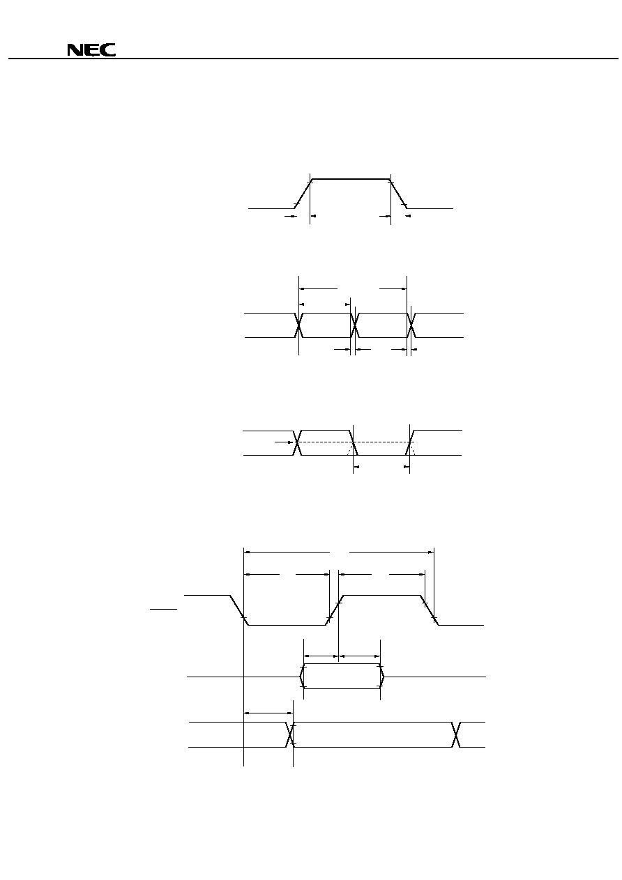
Data Sheet U12626EJ1V0DS00
32
µ
µ
µ
µ
PD78F9801
SERIAL TRANSFER TIMING
USB Function:
USBDM and USBDP rise/fall time
USBDM, USBDP
t
R
0.1V
DD
0.9V
DD
t
F
Transmission different signal jitter
Next bit
Bit following
the next bit
667 ns
1,333 ns
t
UDJ1
t
UDJ2
USBDM, USBDP
Differential output signal cross-over point, transmission EOP width, reception EOP width, and reception
USB reset width
t
EOPT1
, t
EOPRm
,
t
URESm
USBDM, USBDP
V
CRS
m = 1, 2
Three-Wire Serial I/O Mode:
t
KCYm
t
KLm
t
KHm
SCK10
0.8V
DD
0.2V
DD
t
SIKm
t
KSIm
t
KSOm
Input data
Output data
SI10
SO10
m = 1, 2
Data Sheet U12626EJ1V0DS00
33
µ
µ
µ
µ
PD78F9801
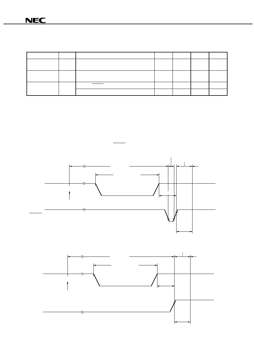
DATA HOLD CHARACTERISTICS OF DATA MEMORY AT LOW VOLTAGE IN STOP MODE
(T
A
= -40
∞
∞
∞
∞
C to +85
∞
∞
∞
∞
C)
Item
Symbol
Conditions
MIN.
TYP.
MAX.
Unit
Data hold supply
voltage
V
DDDR
4.0
5.5
V
Release signal set
time
t
SREL
0
µ
s
Reset by
RESET
2
15
/f
X
ms
Oscillation settling
time
Note 1
t
WAIT
Reset by interrupt request
Note 2
ms
Notes 1.
During the oscillation settling time, CPU operations are disabled to prevent them from becoming
unstable upon the start of oscillation.
2.
2
12
/f
X
, 2
15
/f
X
, or 2
17
/f
X
can be selected according to the setting of bits 0 to 2 (OSTS0 to OSTS2) of the
oscillation settling time selection register.
Remark f
X
: System clock oscillation frequency
DATA HOLD TIMING (STOP mode release by RESET )
V
DD
Data hold mode
STOP mode
HALT mode
Internal reset operation
Operating mode
t
SREL
t
WAIT
STOP instruction execution
V
DDDR
RESET
DATA HOLD TIMING (standby release signal: STOP mode release by interrupt signal)
V
DD
Data hold mode
STOP mode
HALT mode
Operating mode
t
SREL
t
WAIT
STOP instruction execution
V
DDDR
Standby release signal
(interrupt request)
Data Sheet U12626EJ1V0DS00
34
µ
µ
µ
µ
PD78F9801
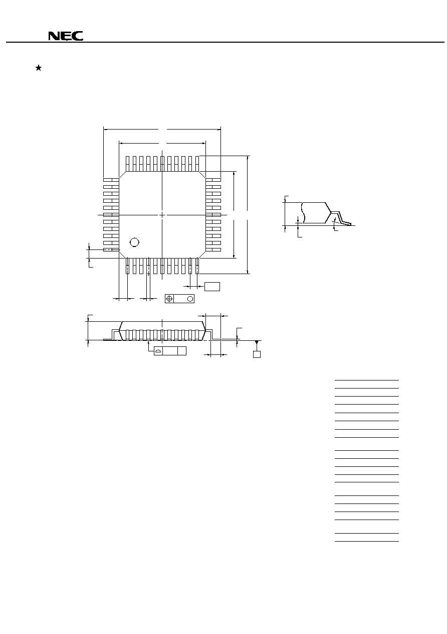
9. PACKAGE DRAWINGS
44-PIN PLASTIC QFP (10
◊
10 mm, 2.7-mm resin thickness)
ITEM
MILLIMETERS
A
B
D
G
13.2
±
0.2
10.0
±
0.2
0.8 (T.P.)
1.0
J
13.2
±
0.2
K
S44GB-80-3BS-2
C
10.0
±
0.2
I
0.16
1.6
±
0.2
L
0.8
±
0.2
F
1.0
N
P
Q
S
0.10
2.7
±
0.1
0.125
±
0.075
3.0 MAX.
M
0.17
+
0.06
-
0.05
H
0.37
+
0.08
-
0.07
R
3
∞+
7
∞
-
3
∞
NOTE
Each lead centerline is located within 0.16 mm of
its true position (T.P.) at maximum material condition.
33
34
22
44
1
12
11
23
S
S
N
J
detail of lead end
C
D
A
B
R
K
M
L
P
I
S
Q
G
F
M
H
Data Sheet U12626EJ1V0DS00
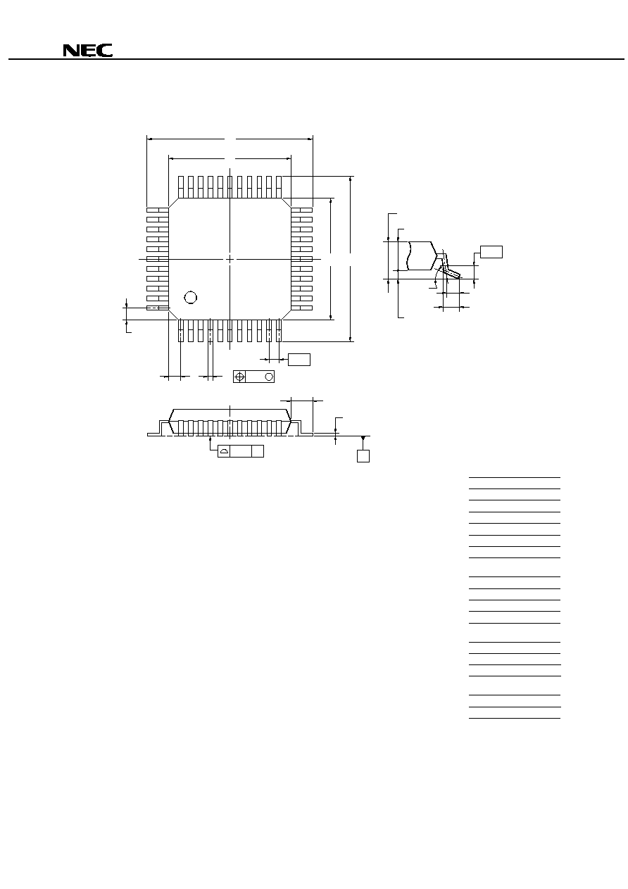
35
µ
µ
µ
µ
PD78F9801
33
34
22
44
1
12
11
23
44 PIN PLASTIC LQFP (10
◊
10 mm, 1.4-mm resin thickness)
ITEM
MILLIMETERS
N
Q
0.1
±
0.05
0.10
U
0.6
±
0.15
S44GB-80-8ES-1
J
I
H
N
A
12.0
±
0.2
B
10.0
±
0.2
C
10.0
±
0.2
D
12.0
±
0.2
F
G
H
1.0
0.37
1.0
I
J
K
0.8 (T.P.)
1.0
±
0.2
0.2
L
0.5
M
0.17
S
1.6 MAX.
R
3
∞
+
0.08
-
0.07
+
0.03
-
0.06
+
4
∞
-
3
∞
detail of lead end
F
G
K
M
M
P
1.4
±
0.05
NOTE
Each lead centerline is located within 0.16 mm of
its true position (T.P.) at maximum material condition.
S
S
A
B
C
D
U
R
S
P
Q
L
T
Data Sheet U12626EJ1V0DS00
36
µ
µ
µ
µ
PD78F9801
10. RECOMMENDED SOLDERING CONDITIONS
The
µ
PD78F9801 should be soldered and mounted under the conditions recommended in the table below.
For detail of recommended soldering conditions, refer to the information document Semiconductor Device
Mounting Technology Manual (C10535E).
For soldering methods and conditions other than those recommended below, contact our sales representatives.
Table 10-1. Surface Mounting Type Soldering Conditions
µ
µ
µ
µ
PD78F9801GB-3BS-MTX: 44-pin plastic QFP (10
◊
◊
◊
◊
10 mm, 2.7-mm resin thickness)
Soldering method
Soldering conditions
Symbol
Infrared reflow
Package peak temperature: 235∞C
Duration: 30 sec. max. (at 210∞C or above)
Maximum allowable number of reflow processes: 3
IR35-00-3
VPS
Package peak temperature: 215∞C
Duration: 40 sec. max. (at 200∞C or above)
Maximum allowable number of reflow processes: 3
VP15-00-3
Wave soldering
Solder bath temperature: 260∞C max.
Duration: 10 sec. max.
Number of times: Once
Preliminary heat temperature: 120∞C max. (Package surface temperature)
WS60-00-1
Partial heating
method
Terminal temperature: 300∞C max. Duration: 3 sec. max. (per device side)
-
Caution
Use of more than one soldering method should be avoided (except for partial heating method).
µ
µ
µ
µ
PD78F9801GB-8ES: 44-pin plastic LQFP (10
◊
◊
◊
◊
10 mm, 1.4-mm resin thickness)
Soldering method
Soldering conditions
Symbol
Infrared reflow
Package peak temperature: 235∞C
Duration: 30 sec. max. (at 210∞C or above)
Maximum allowable number of reflow processes: 2
IR35-00-2
VPS
Package peak temperature: 215∞C
Duration: 40 sec. max. (at 200∞C or above)
Maximum allowable number of reflow processes: 2
VP15-00-2
Wave soldering
Solder bath temperature: 260∞C max.
Duration: 10 sec. max.
Number of times: Once
Preliminary heat temperature: 120∞C max. (Package surface temperature)
WS60-00-1
Partial heating
method
Terminal temperature: 300∞C max. Duration: 3 sec. max. (per device side)
-
Caution
Use of more than one soldering method should be avoided (except for partial heating method).
Data Sheet U12626EJ1V0DS00
37
µ
µ
µ
µ
PD78F9801
APPENDIX A DEVELOPMENT TOOLS
The following development tools are available for developing systems using the
µ
PD78F9801.
LANGUAGE PROCESSING SOFTWARE
RA78K0S
Notes 1, 2, 3
Assembler package common to the 78K/0S series
CC78K0S
Notes 1, 2, 3
C compiler package common to the 78K/0S series
DF789801
Notes 1, 2, 3
Device file for the
µ
PD789800 sub-series
CC78K0S-L
Notes 1, 2, 3
C compiler library source file common to the 78K/0S series
FLASH MEMORY WRITE TOOLS
Flashpro Ill
Dedicated flash writer
FA-44GB
Note 4
Flash memory write adapter (GB-3BS type)
FA-44GB-8ES
Note 4
Flash memory write adapter (GB-8ES type)
DEBUGGING TOOLS (1/2)
IE-78K0S-NS
In-circuit emulator
In-circuit emulator for debugging hardware and software of application system using 78K/0S
Series. Supports integrated debugger (ID78K0S-NS). Used in combination with AC adapter,
emulation probe, and interface adapter for connecting the host machine.
IE-70000-MC-PS-B
AC adapter
This is the adapter for supplying power from outlet of 100 to 240 VAC.
IE-70000-98-IF-C
Interface adapter
This adapter is needed when PC-9800 series (excluding notebook models) is used as a host
machine of IE-78K0S-NS. (Compatible with C bus)
IE-70000-CD-IF-A
PC card interface
This PC card and interface cable are needed when a notebook-type personal computer is
used as a host machine of IE-78K0S-NS. (Compatible with a PCMCIA socket)
IE-70000-PC-IF-C
Interface adapter
This adapter is needed when IBM PC/AT
TM
and compatibles are used as a host machine of
IE-78K0S-NS. (Compatible with ISA bus)
IE-70000-PCI-IF
Interface adapter
This adapter is needed when a personal computer with a built-in PCI bus is used as a host
machine of IE-78K0S-NS.
IE-789801-NS-EM1
Emulation board
Emulation board for emulating the peripheral hardware inherent to the device.
Used in combination with in-circuit emulator.
Notes 1. Based on the PC-9800 series (Japanese Windows
TM
)
2. Based on the IBM PC/AT and compatibles (Japanese/English Windows)
3. Based on the HP9000 series 700
TM
(HP-UX
TM
), SPARCstation
TM
(SunOS
TM
, Solaris
TM
), and NEWS
TM
(NEWS-OS
TM
)
4. Product manufactured by Naito Densei Machida Mfg. Co., Ltd. (044-822-3813). Contact an NEC sales
representative for purchase.
Remark The RA78K0S and CC78K0S can be used in combination with the DF789801.
Data Sheet U12626EJ1V0DS00
38
µ
µ
µ
µ
PD78F9801
DEBUGGING TOOLS (2/2)
NP-44GB
Notes 1, 2
Emulation prove
This probe is used to connect the in-circuit emulator to the target system and is designed for
44-pin plastic QFP. It should be used in combination with EV-9200G-44.
EV-9200G-44
Conversion socket
This conversion socket connects the NP-44GB to the target system board designed to mount
a 44-pin plastic QFP (GB-3BS, GB-8ES type).
NP-44GB-TQ
Notes 1, 2
Emulation prove
This probe is used to connect the in-circuit emulator to the target system and is designed for
44-pin plastic QFP. It should be used in combination with TGB-044SAP.
TGB-044SAP
Note 3
Conversion socket
This conversion socket connects the NP-44GB-TQ to the target system board designed to
mount a 44-pin plastic QFP (GB-3BS, GB-8ES type).
SM78K0S
Notes 4, 5
System simulator common to the 78K/0S series
ID78K0S-NS
Notes 4, 5
Integrated debugger common to the 78K/0S series
DF789801
Notes 4, 5
Device file for the
µ
PD789800 sub-series
REAL-TIME OS
MX78K0S
Notes 4, 5
OS for the 78K/0S series
Notes 1. Product manufactured by Naito Densei Machida Mfg. Co., Ltd. (044-822-3813). Contact an NEC sales
representative for purchase.
2. Either probe and socket combination can be selected for use.
3. Product manufactured by TOKYO ELETEC Corporation
For further information, consult:
Tokyo Electronic Div. (TEL (03) 3820-7112), or
Osaka Electronic Div. (TEL (06) 6244-6672)
Daimaru Kogyo Corporation.
4. Based on the PC-9800 series (Japanese Windows)
5. Based on the IBM PC/AT and compatibles (Japanese/English Windows)
Remark The SM78K0S can be used in combination with the DF789801.
Data Sheet U12626EJ1V0DS00
39
µ
µ
µ
µ
PD78F9801
APPENDIX B RELATED DOCUMENTS
DOCUMENTS RELATED TO DEVICES
Document No.
Document name
Japanese
English
µ
PD789800 Data Sheet
U12627J
U12627E
µ
PD78F9801 Data Sheet
U12626J
This manual
µ
PD789800 Sub-Series User's Manual
U12978J
U12978E
78K/0S Series User's Manual, Instruction
U11047J
U11047E
DOCUMENTS RELATED TO DEVELOPMENT TOOLS (USER'S MANUAL)
Document No.
Document name
Japanese
English
Operation
U11622J
U11622E
Assembly Language
U11599J
U11599E
RA78K0S Assembler Package
Structured Assembly
Language
U11623J
U11623E
Operation
U11816J
U11816E
CC78K0S C Compiler
Language
U11817J
U11817E
SM78K0S System Simulator for IBM PC/AT (Windows)
Reference
U11489J
U11489E
SM78K Series System Simulator
External Parts User Open
Interface Specifications
U10092J
U10092E
ID78K0S-NS Integrated Debugger Windows-Based
Reference
U12901J
U12901E
IE-78K0S-NS In-circuit Emulator
U13549J
U13549E
IE-789801-NS-EM1 Emulation Board
U13390J
U13390E
DOCUMENTS RELATED TO SOFTWARE TO BE INCORPORATED INTO THE PRODUCT
(USER'S MANUAL)
Document No.
Document name
Japanese
English
OS for 78K/0S Series MX78K0S
Basic
U12938J
U12938E
OTHER DOCUMENTS
Document No.
Document name
Japanese
English
SEMICONDUCTORS SELECTION GUIDE Products & Packages (CD-ROM)
X13769X
Semiconductor Device Mounting Technology Manual
C10535J
C10535E
Quality Grades on NEC Semiconductor Device
C11531J
C11531E
NEC Semiconductor Device Reliability/Quality Control System
C10983J
C10983E
Guide to Prevent Damage for Semiconductor Devices by Electrostatic Discharge (ESD)
C11892J
C11892E
Semiconductor Device Quality Control/Reliability Handbook
C12769J
-
Guide for Products Related to Micro-Computer: Other Companies
U11416J
-
Caution
The above documents may be revised without notice. Use the latest versions when you design
application systems.
Data Sheet U12626EJ1V0DS00
40
µ
µ
µ
µ
PD78F9801
NOTES FOR CMOS DEVICES
1
PRECAUTION AGAINST ESD FOR SEMICONDUCTORS
Note:
Strong electric field, when exposed to a MOS device, can cause destruction of the gate oxide and
ultimately degrade the device operation. Steps must be taken to stop generation of static electricity
as much as possible, and quickly dissipate it once, when it has occurred. Environmental control
must be adequate. When it is dry, humidifier should be used. It is recommended to avoid using
insulators that easily build static electricity. Semiconductor devices must be stored and transported
in an anti-static container, static shielding bag or conductive material. All test and measurement
tools including work bench and floor should be grounded. The operator should be grounded using
wrist strap. Semiconductor devices must not be touched with bare hands. Similar precautions need
to be taken for PW boards with semiconductor devices on it.
2
HANDLING OF UNUSED INPUT PINS FOR CMOS
Note:
No connection for CMOS device inputs can be cause of malfunction. If no connection is provided
to the input pins, it is possible that an internal input level may be generated due to noise, etc., hence
causing malfunction. CMOS devices behave differently than Bipolar or NMOS devices. Input levels
of CMOS devices must be fixed high or low by using a pull-up or pull-down circuitry. Each unused
pin should be connected to V
DD
or GND with a resistor, if it is considered to have a possibility of
being an output pin. All handling related to the unused pins must be judged device by device and
related specifications governing the devices.
3
STATUS BEFORE INITIALIZATION OF MOS DEVICES
Note:
Power-on does not necessarily define initial status of MOS device. Production process of MOS
does not define the initial operation status of the device. Immediately after the power source is
turned ON, the devices with reset function have not yet been initialized. Hence, power-on does
not guarantee out-pin levels, I/O settings or contents of registers. Device is not initialized until the
reset signal is received. Reset operation must be executed immediately after power-on for devices
having reset function.
EEPROM is a trademark of NEC Corporation.
Windows is a registered trademark or a trademark of Microsoft Corporation in the United States and/or other
countries.
PC/AT is a trademark of IBM Corporation.
HP9000 series 700 and HP-UX are trademarks of Hewlett-Packard Company.
SPARCstation is a trademark of SPARC International, Inc.
Solaris and SunOS are trademarks of Sun Microsystems, Inc.
NEWS and NEWS-OS are trademarks of SONY Corporation.

Data Sheet U12626EJ1V0DS00
41
µ
µ
µ
µ
PD78F9801
[MEMO]

Data Sheet U12626EJ1V0DS00
42
µ
µ
µ
µ
PD78F9801
[MEMO]

Data Sheet U12626EJ1V0DS00
43
µ
µ
µ
µ
PD78F9801
Regional Information
Some information contained in this document may vary from country to country. Before using any NEC
product in your application, pIease contact the NEC office in your country to obtain a list of authorized
representatives and distributors. They will verify:
∑
Device availability
∑
Ordering information
∑
Product release schedule
∑
Availability of related technical literature
∑
Development environment specifications (for example, specifications for third-party tools and
components, host computers, power plugs, AC supply voltages, and so forth)
∑
Network requirements
In addition, trademarks, registered trademarks, export restrictions, and other legal issues may also vary
from country to country.
NEC Electronics Inc. (U.S.)
Santa Clara, California
Tel: 408-588-6000
800-366-9782
Fax: 408-588-6130
800-729-9288
NEC Electronics (Germany) GmbH
Duesseldorf, Germany
Tel: 0211-65 03 02
Fax: 0211-65 03 490
NEC Electronics (UK) Ltd.
Milton Keynes, UK
Tel: 01908-691-133
Fax: 01908-670-290
NEC Electronics Italiana s.r.l.
Milano, Italy
Tel: 02-66 75 41
Fax: 02-66 75 42 99
NEC Electronics (Germany) GmbH
Benelux Office
Eindhoven, The Netherlands
Tel: 040-2445845
Fax: 040-2444580
NEC Electronics (France) S.A.
Velizy-Villacoublay, France
Tel: 01-30-67 58 00
Fax: 01-30-67 58 99
NEC Electronics (France) S.A.
Madrid Office
Madrid, Spain
Tel: 91-504-2787
Fax: 91-504-2860
NEC Electronics (Germany) GmbH
Scandinavia Office
Taeby, Sweden
Tel: 08-63 80 820
Fax: 08-63 80 388
NEC Electronics Hong Kong Ltd.
Hong Kong
Tel: 2886-9318
Fax: 2886-9022/9044
NEC Electronics Hong Kong Ltd.
Seoul Branch
Seoul, Korea
Tel: 02-528-0303
Fax: 02-528-4411
NEC Electronics Singapore Pte. Ltd.
United Square, Singapore
Tel: 65-253-8311
Fax: 65-250-3583
NEC Electronics Taiwan Ltd.
Taipei, Taiwan
Tel: 02-2719-2377
Fax: 02-2719-5951
NEC do Brasil S.A.
Electron Devices Division
Guarulhos-SP Brasil
Tel: 55-11-6462-6810
Fax: 55-11-6462-6829
J00.7

µ
µ
µ
µ
PD78F9801
Some related documents may be preliminary versions. Note, however, that whether a related document is
preliminary is not indicated in this document.
M8E 00. 4
The information in this document is current as of November, 1999. The information is subject to
change without notice. For actual design-in, refer to the latest publications of NEC's data sheets or
data books, etc., for the most up-to-date specifications of NEC semiconductor products. Not all
products and/or types are available in every country. Please check with an NEC sales representative
for availability and additional information.
No part of this document may be copied or reproduced in any form or by any means without prior
written consent of NEC. NEC assumes no responsibility for any errors that may appear in this document.
NEC does not assume any liability for infringement of patents, copyrights or other intellectual property rights of
third parties by or arising from the use of NEC semiconductor products listed in this document or any other
liability arising from the use of such products. No license, express, implied or otherwise, is granted under any
patents, copyrights or other intellectual property rights of NEC or others.
Descriptions of circuits, software and other related information in this document are provided for illustrative
purposes in semiconductor product operation and application examples. The incorporation of these
circuits, software and information in the design of customer's equipment shall be done under the full
responsibility of customer. NEC assumes no responsibility for any losses incurred by customers or third
parties arising from the use of these circuits, software and information.
While NEC endeavours to enhance the quality, reliability and safety of NEC semiconductor products, customers
agree and acknowledge that the possibility of defects thereof cannot be eliminated entirely. To minimize
risks of damage to property or injury (including death) to persons arising from defects in NEC
semiconductor products, customers must incorporate sufficient safety measures in their design, such as
redundancy, fire-containment, and anti-failure features.
NEC semiconductor products are classified into the following three quality grades:
"Standard", "Special" and "Specific". The "Specific" quality grade applies only to semiconductor products
developed based on a customer-designated "quality assurance program" for a specific application. The
recommended applications of a semiconductor product depend on its quality grade, as indicated below.
Customers must check the quality grade of each semiconductor product before using it in a particular
application.
"Standard": Computers, office equipment, communications equipment, test and measurement equipment, audio
and visual equipment, home electronic appliances, machine tools, personal electronic equipment
and industrial robots
"Special":
Transportation equipment (automobiles, trains, ships, etc.), traffic control systems, anti-disaster
systems, anti-crime systems, safety equipment and medical equipment (not specifically designed
for life support)
"Specific": Aircraft, aerospace equipment, submersible repeaters, nuclear reactor control systems, life
support systems and medical equipment for life support, etc.
The quality grade of NEC semiconductor products is "Standard" unless otherwise expressly specified in NEC's
data sheets or data books, etc. If customers wish to use NEC semiconductor products in applications not
intended by NEC, they must contact an NEC sales representative in advance to determine NEC's willingness
to support a given application.
(Note)
(1) "NEC" as used in this statement means NEC Corporation and also includes its majority-owned subsidiaries.
(2) "NEC semiconductor products" means any semiconductor product developed or manufactured by or for
NEC (as defined above).
∑
∑
∑
∑
∑
∑