Document Outline
- COVER
- FEATURES
- ORDERING INFORMATION
- PIN CONFIGURATIONS (Top View)
- BLOCK DIAGRAM
- 1. PIN FUNCTIONS
- 1.1 Normal Operating Mode
- 1.2 PROM Programming Mode (RESET# = H, AVDD = L)
- 1.3 Pin Input/Output Circuits and Recommended Connection of Unused Pins
- 2. DIFFERENCES BETWEEN uPD78P322 and uPD78322
- 3. PROM PROGRAMMING
- 3.1 Operation Mode
- 3.2 PROM Write Procedure
- 3.3 PROM Read Procedure
- 4. ERASURE CHARACTERISTICS (FOR uPD78P322K/KC/KD ONLY)
- 5. OPAQUE FILM ON ERASURE WINDOW (FOR uPD78P322K/KC/KD ONLY)
- 6. ONE-TIME PROM VERSION SCREENING
- 7. ELECTRICAL SPECIFICATIONS
- 8. PACKAGE DRAWINGS
- 9. RECOMMENDED SOLDERING CONDITIONS
- APPENDIX A. DRAWINGS OF CONVERSION SOCKETS AND RECOMMENDED FOOTPRINTS
- APPENDIX B. TOOLS
- B.1 Development Tools
- B.2 Evaluation Tools
- B.3 Embedded Software
MOS Integrated Circuit
µ
PD78P322
16/8-BIT SINGLE-CHIP MICROCONTROLLER
Document No.
U10435EJ5V0DS00 (5th edition)
(Previous No.
IC-2485)
Date Published
December 1995 P
Printed in Japan
The
µ
PD78P322 is a version provided by replacing the
µ
PD75322's internal mask ROM with one-time PROM
or EPROM.
Because the one-time PROM version is programmable only once by users, it is ideally suited for small-scale
production of many different products, and rapid development and time-to-market of application sets.
The EPROM version is reprogrammable, and suited for the evaluation of systems.
The
µ
PD78P322K, which is the EPROM version, does not maintain planned reliability when
used in mass-produced products. Please use only experimentally or for evaluating functions
during trial manufacture.
Functions are described in detail in the following user's manual. Be sure to read it for designing.
µ
PD78322 User's Manual: IEU-1248
FEATURES
∑
µ
PD78322 compatible
∑ For mass-production, the
µ
PD78P322 can be replaced with the
µ
PD78322 which incorporates mask
ROM
∑
Internal PROM: 16,384
◊
8 bits
∑ Programmable once only (one-time PROM version without window)
∑ Erasable with ultraviolet rays and electrically programmable (EPROM version with window)
∑
PROM programming characteristics:
µ
PD27C256A compatible
∑
The
µ
PD78P328 is a QTOP
TM
microcontroller
Remark
QTOP microcontroller is a general term for microcontrollers which incorporate one-time PROM, and
are totally supported by NEC's programming service (from programming to marking, screening, and
verification).
ORDERING INFORMATION
Part Number
Package
Internal ROM
Quality Grade
µ
PD78P322GF-3B9
80-pin plastic QFP (14
◊
20 mm)
One-time PROM
Standard
µ
PD78P322GJ-5BJ
74-pin plastic QFP (20
◊
20 mm)
One-time PROM
Standard
µ
PD78P322L
68-pin plastic QFJ (950
◊
950 mils)
One-time PROM
Standard
µ
PD78P322K
80-pin ceramic WQFN
EPROM
Not applicable
µ
PD78P322KC
68-pin ceramic WQFN
EPROM
Standard
µ
PD78P322KD
74-pin ceramic WQFN
EPROM
Standard
Please refer to "Quality grade on NEC Semiconductor Devices" (Document number IEI-1209) published by NEC Corporation to know the
specification of quality grade on the devices and its recommended applications.
Functions common to the one-time PROM and EPROM versions are referred to as PROM functions throughout this document.
The information in this document is subject to change without notice.
The mark
*
shows revised points.
©
1994
DATA SHEET
©
1991
µ
PD78P322
2
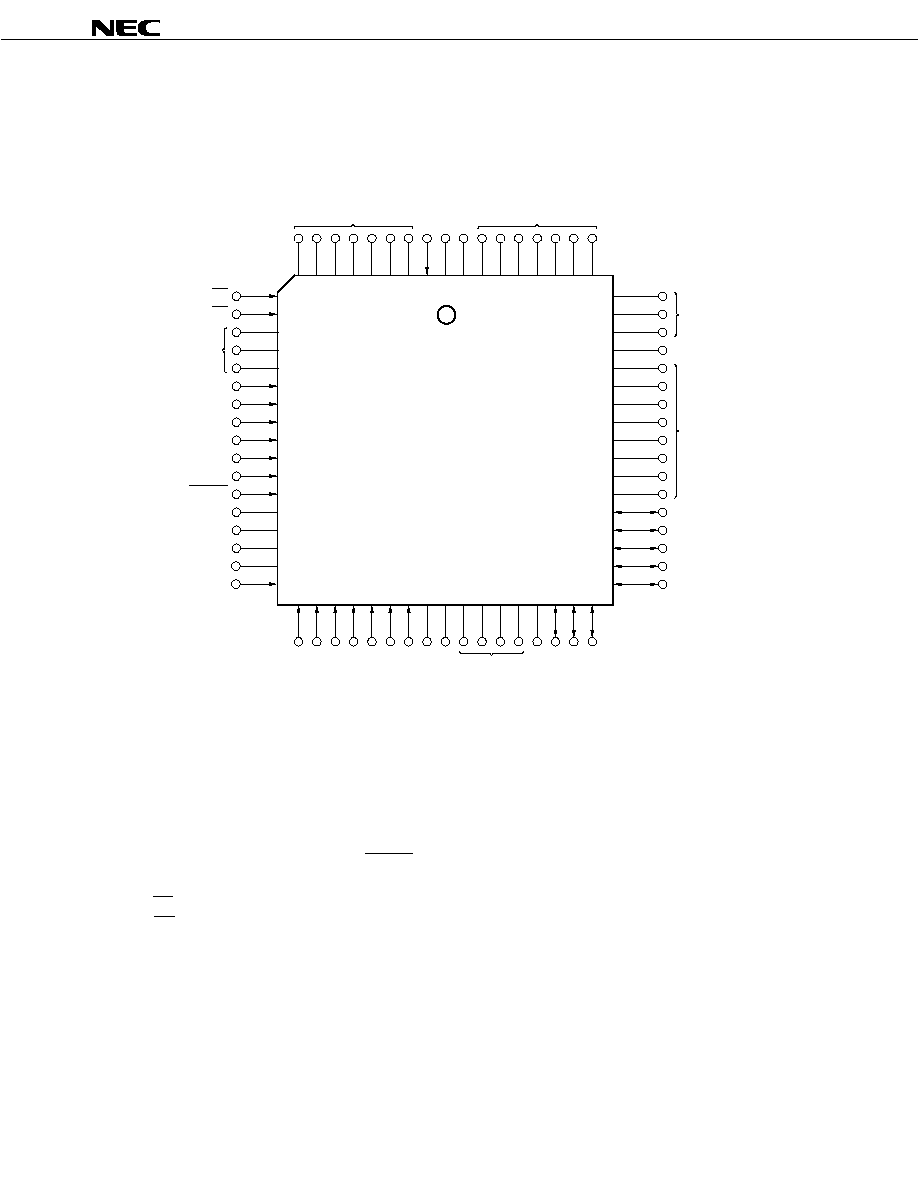
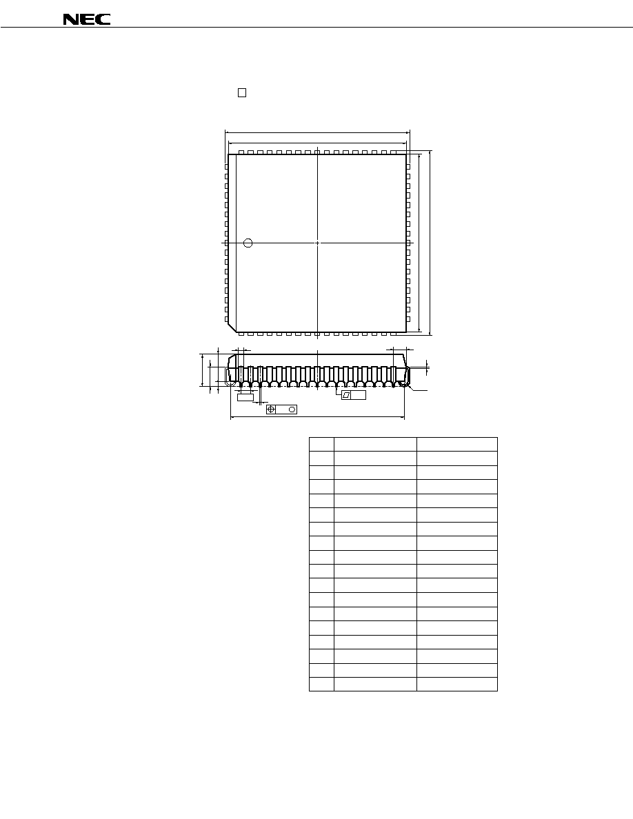
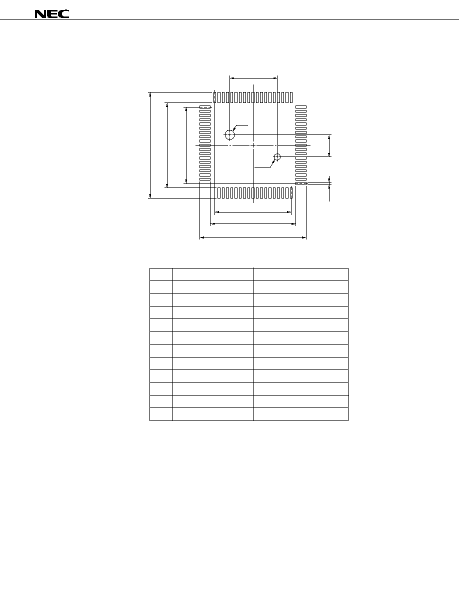
PIN CONFIGURATIONS (Top View)
(1)
Normal operating mode
∑ 80-pin plastic QFP (14
◊
20 mm)
µ
PD78P322GF-3B9
∑ 80-pin ceramic WQFN
µ
PD78P322K
1
2
3
4
5
6
7
8
9
10
11
12
13
14
15
16
62
61
60
59
58
57
56
55
54
53
52
51
50
49
48
47
X2
X1
RTP2/P02
RTP3/P03
RTP4/P04
RTP6/P06
RTP7/P07
EA
V
SS
V
SS
P93/
TMD
P92/
TAS
P91/
WR
P90/RD
17
18
V
SS
19
WDTO
20
RTP0/P00
21
NC
22
TRP1/P01
23
NC
24
25 26 27 28 29 30 31 32 33 34 35 36 37
ASTB
38
P40/AD0
39
P41/AD1
40
P27/INTP6/ TI
NC
NC
P30/ TxD
P31/RxD
P32/SO/SB0
P33/S1/SB1
P34/SCK
P80/ TO00
P81/ TO01
P82/ TO02
P83/ TO03
P84/ TO10
NC
P85/ TO11
RESET
NC
P71/ANI1
P70/ANI0
AV
SS
V
DD
P57/A15
P56/A14
P55/A13
P54/A12
P53/A11
P52/A10
P51/A9
P50/A8
P47/AD7
P46/AD6
P45/AD5
46
P44/AD4
45
P43/AD3
44
NC
43
NC
42
NC
41
P42/AD2
64
63
80
NC
79
P26/INTP5
78
P25/INTP4
77
P24/INTP3
RTP5/P05
76
P23/INTP2
75
P22/INTP1
74
P21/INTP0
73
P20/NMI
72
V
DD
71
AV
DD
70
AV
REF
67
P75/ANI5
68
P76/AN6
69
P77/AN7
65
P73/AN3
66
P74/AN4
P72/ANI2
NC
Caution Connect NC pins to V
SS
as a measure against noise (can leave open).
Remark
These pins are compatible with the
µ
PD78322GF pins.
The
µ
PD78P322K does not maintain planned reliability when used in mass-produced products. Please use only
experimentally or for evaluating functions during trial manufacture.
µ
PD78P322
3
∑ 74-pin plastic QFP (20
◊
20 mm)
µ
PD78P322GJ-5BJ
∑ 74-pin ceramic WQFN
µ
PD78P322KD
Caution Connect NC pins to V
SS
for measures against noise (can leave open).
Remark
These pins are compatible with the
µ
PD78322GJ pins.
1
2
3
4
5
6
7
8
9
10
11
12
13
14
15
16
53
52
51
50
49
48
47
46
45
44
43
42
41
40
39
38
P70/AN0
P71/AN1
NC
P73/AN3
P74/AN4
P76/AN6
P77/AN7
AV
REF
AV
DD
V
DD
P20/NMI
P21/INTP0
P22/INTP1
P23/INTP2
17
18
19
P72/AN2
20 21 22 23 24 25 26 27 28 29 30 31 32
P24/INTP3
33
P25/INTP4
34
P26/INTP5
35
P27/INTP6
36
NC
37
P43/AD3
P44/AD4
P45/AD5
P46/AD6
P47/AD7
P50/A8
P51/A9
P52/A10
P53/A11
P54/A12
P55/A13
NC
P56/A14
P57/A15
V
DD
AV
SS
NC
X1
X2
RESET
P85/TO11
P84/TO10
P83/TO03
P82/TO02
P81/TO01
P80/TO00
NC
P34/SCK
P33/SI/SBI
P32/SO/SB0
P31/RxD
P30/TxD
74 73 72 71 70 69 68 67 66 65 64 63 62
57
56
55
54
P42/AD2
P41/AD1
P40/AD0
ASTB
P75/AN5
P90/RD
P91/WR
P92/
TAS
P93/
TMD
V
SS
EA
P07/RTP7
P06/RTP6
P05/RTP5
61
P04/RTP4
60
P03/RTP3
59
P02/RTP2
58
P01/RTP1
NC
P00/RTP0
WDTO
V
SS

µ
PD78P322
4
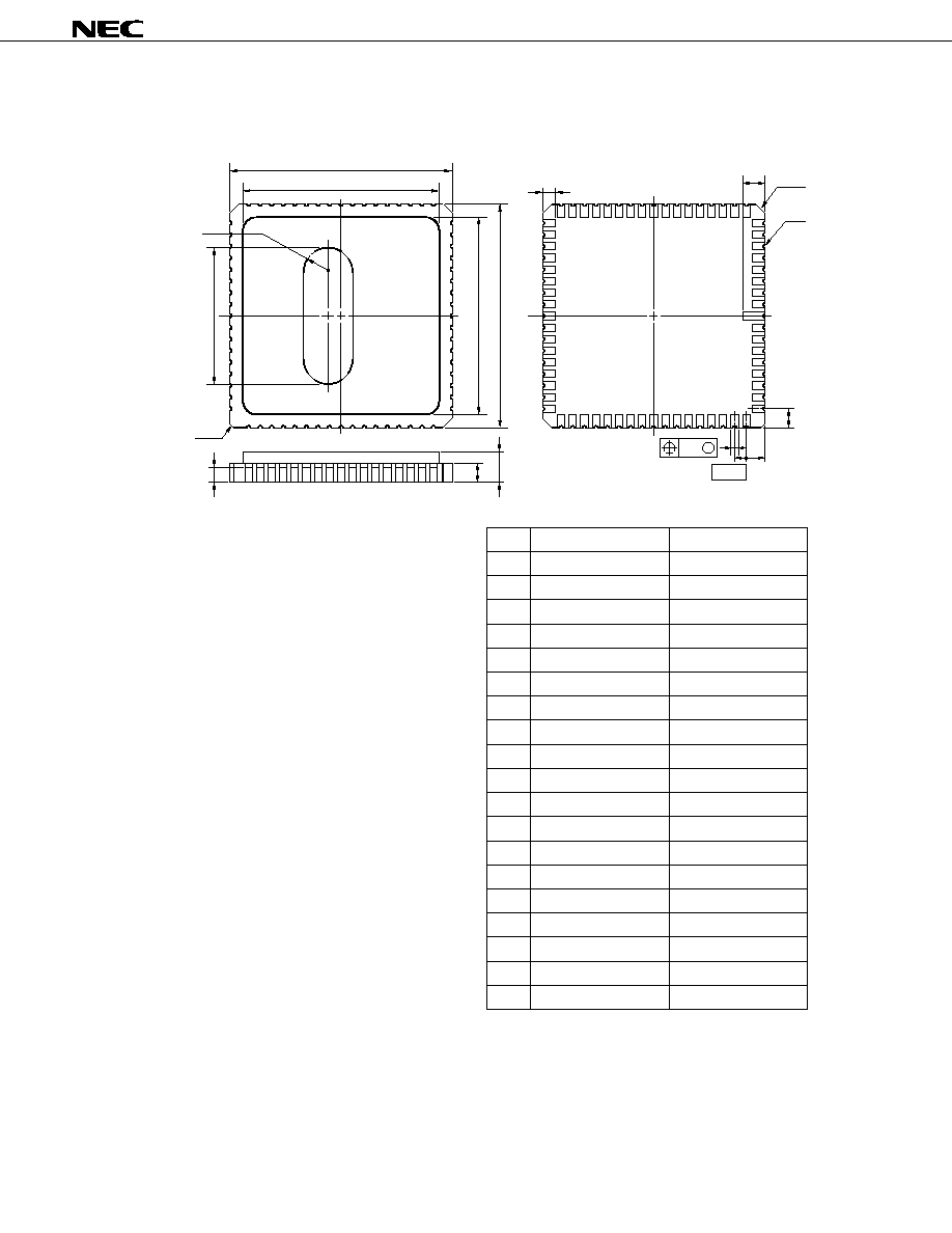
∑ 68-pin plastic QFJ (950
◊
950 mils)
µ
PD78P322L
∑ 68-pin ceramic WQFN
µ
PD78P322KC
10
11
12
13
14
15
16
17
18
19
20
21
22
23
24
25
59
58
57
56
55
54
53
52
51
50
49
48
47
46
45
44
WDTO
RTP0/P00
P02/RTP2
P03/RTP3
P05/RTP5
P06/RTP6
P07/RTP7
EA
V
SS
P93/TMD
P92/TAS
P91/WR
P90/RD
26
P01/RTP1
27 28 29 30 31 32 33 34 35 36 37 38 39
ASTB
40
P40/AD0
41
P41/AD1
42
P42/AD2
43
P30/TxD
P31/RxD
P32/SO/SB0
P33/SI/SB1
P34/SCK
P80/TO00
P81/TO01
P82/TO02
P83/TO03
P84/TO10
P85/TO11
RESET
X2
X1
V
SS
V
DD
P57/A15
P56/A14
P55/A13
P54/A12
P53/A11
P52/A10
P51/A9
P50/A8
P47/AD7
P46/AD6
P45/AD5
P44/AD4
P43/AD3
9
8
7
6
5
4
3
2
1 68 67 66 65
61
60
P27/INTP6/
TI
P26/INTP5
P25/INTP4
P24/INTP3
P04/RTP4
P23/INTP2
P22/INTP1
P21/INTP0
P20/NMI
V
DD
AV
DD
AV
REF
P77/AN7
P76/AN6
64
P75/AN5
63
P74/AN4
62
P73/AN3
P72/AN2
P71/AN1
P70/AN0
AV
SS
Remark
These pins are compatible with the
µ
PD78322L pins.

µ
PD78P322
5
P00-P07
: Port 0
RESET
: Reset
P20-P27
: Port 2
X1, X2
: Crystal
P30-P34
: Port 3
WDTO
: Watchdog Timer Output
P40-P47
: Port 4
EA
: External Access
P50-P57
: Port 5
TMD
: Turbo Mode
P70-P77
: Port 7
TAS
: Turbo Access Strobe
P80-P85
: Port 8
WR
: Write Strobe
P90-P93
: Port 9
RD
: Read Strobe
NMI
: Nonmaskable Interrupt
ASTB
: Address Strobe
INTP0-INTP6
: Interrupt From Peripherals
AD0-AD7
: Address/Data Bus
RTP0-RTP7
: Real-Time Port
A8-A15
: Address Bus
TI
: Timer Input
AN0-AN7
: Analog Input
TxD
: Transmit Data
AV
REF
: Analog Reference Voltage
RxD
: Receive Data
AV
SS
: Analog V
SS
SB0/SO
: Serial Bus/Serial Output
AV
DD
: Analog V
DD
SB1/SI
: Serial Bus/Serial Input
V
DD
: Power Supply
SCK
: Serial Clock
V
SS
: Ground
TO00-TO03
:
NC
: No Connection
TO10, TO11
:
}
Timer Output

µ
PD78P322
6
1
2
3
4
5
6
7
8
9
10
11
12
13
14
15
16
62
61
60
59
58
57
56
55
54
53
52
51
50
49
48
47
(Open)
(G)
A2
A3
A4
A6
A7
V
PP
V
SS
V
SS
(Open)
17
18
V
SS
19
(Open)
20
A0
21
NC
22
A1
23
NC
24
25 26 27 28 29 30 31 32 33 34 35 36 37 38
D0
39
D1
40
(G)
NC
NC
OE
CE
(L)
A8
A10
A11
A12
A13
NC
A14
RESET
NC
V
DD
D7
D6
D5
46
D4
45
D3
44
NC
43
NC
42
NC
41
D2
64
63
80
NC
79 78 77
A5
76 75 74 73
A9
(G)
72
V
DD
71
AV
DD
70
67
68
69
65
66
(G)
(G)
NC
(Open)
(G)
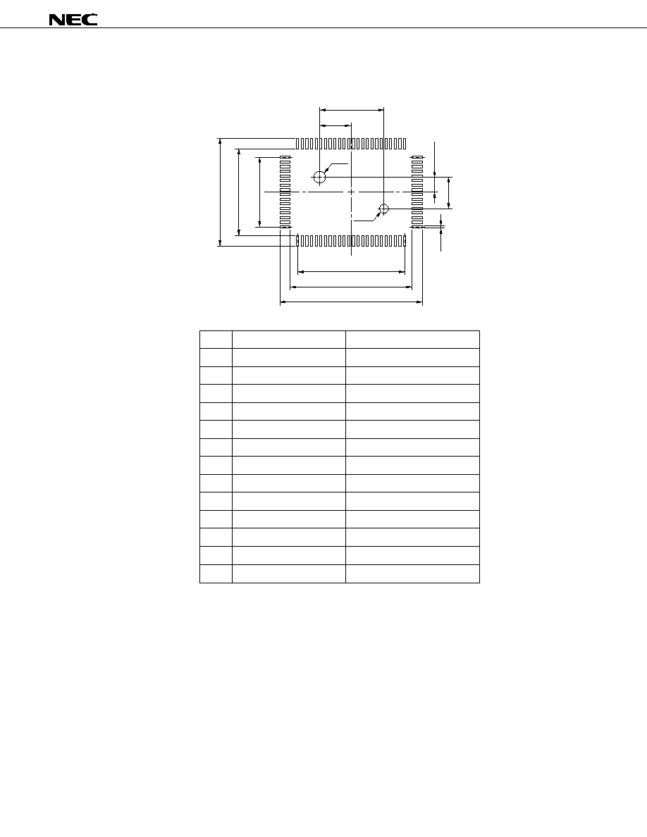
(2)
PROM programming mode (RESET = H, AV
DD
= L)
∑ 80-pin plastic QFP (14
◊
20 mm)
µ
PD78P322GF-3B9
∑ 80-pin ceramic WQFN
µ
PD78P322K
Cautions 1.
The recommended connection of the unused pins in the PROM programming mode are
indicated in parentheses.
L
: Connect each pin to V
SS
via a resistor.
G
: Connect the pin to V
SS
.
Open
: Leave the pin unconnected.
2.
Connect NC pins to V
SS
for measures against noise (can leave open).
The
µ
PD78P322K does not maintain planned reliability when used in mass-produced products. Please use only
experimentally or for evaluating functions during trial manufacture.
µ
PD78P322
7
∑ 74-pin plastic QFP (20
◊
20 mm)
µ
PD78P322GJ-5BJ
∑ 74-pin ceramic WQFN
µ
PD78P322KD
1
2
3
4
5
6
7
8
9
10
11
12
13
14
15
16
53
52
51
50
49
48
47
46
45
44
43
42
41
40
39
38
NC
AV
DD
V
DD
A9
17
18
19 20 21 22 23 24 25 26 27 28 29 30 31 32 33 34 35 36
NC
37
D3
D4
D5
D6
D7
NC
V
DD
NC
(G)
(Open)
RESET
A14
A13
A12
A11
A10
A8
NC
CE
(L)
OE
74 73 72 71 70 69 68 67 66 65 64 63 62
57
56
55
54
D2
D1
D0
(Open)
(L)
V
SS
V
PP
A7
A6
A5
61
A4
60
A3
59
A2
58
A1
NC
A0
(Open)
V
SS
(L)
(L)
(G)
(G)
(G)
Cautions 1.
The recommended connection of the unused pins in the PROM programming mode are
indicated in parentheses.
L
: Connect each pin to V
SS
via a resistor.
G
: Connect the pin to V
SS
.
Open
: Leave the pin unconnected.
2.
Connect NC pins to V
SS
as measure against noise.
µ
PD78P322
8
∑ 68-pin plastic QFJ (950
◊
950 mil)
µ
PD78P322L
∑ 68-pin ceramic WQFN
µ
PD78P322KC
10
11
12
13
14
15
16
17
18
19
20
21
22
23
24
25
59
58
57
56
55
54
53
52
51
50
49
48
47
46
45
44
(Open)
A0
A2
A3
A5
A6
A7
V
PP
V
SS
26
A1
27 28 29 30 31 32 33 34 35 36 37 38 39
(Open)
40
D0
41
D1
42
D2
43
OE
CE
A8
A10
A11
A12
A13
A14
RESET
(Open)
(G)
V
SS
V
DD
(L)
D7
D6
D5
D4
D3
9
8
7
6
5
4
3
2
1 68 67 66 65
61
60
A4
A9
(G)
V
DD
AV
DD
64 63 62
(L)
(G)
(G)
(L)
Caution The recommended connection of the unused pins in the PROM programming mode are indicated
in parentheses.
L
: Connect each pin to V
SS
via a resistor.
G
: Connect the pin to V
SS
.
Open
: Leave the pin unconnected.
A0-A14
: Address Bus
RESET
:
D0-D7
: Data Bus
AV
DD
:
CE
: Chip Enable
V
PP
: Programming Power Supply
OE
: Output Enable
NC
: No Connection
}
Programming Mode set
µ
PD78P322
9
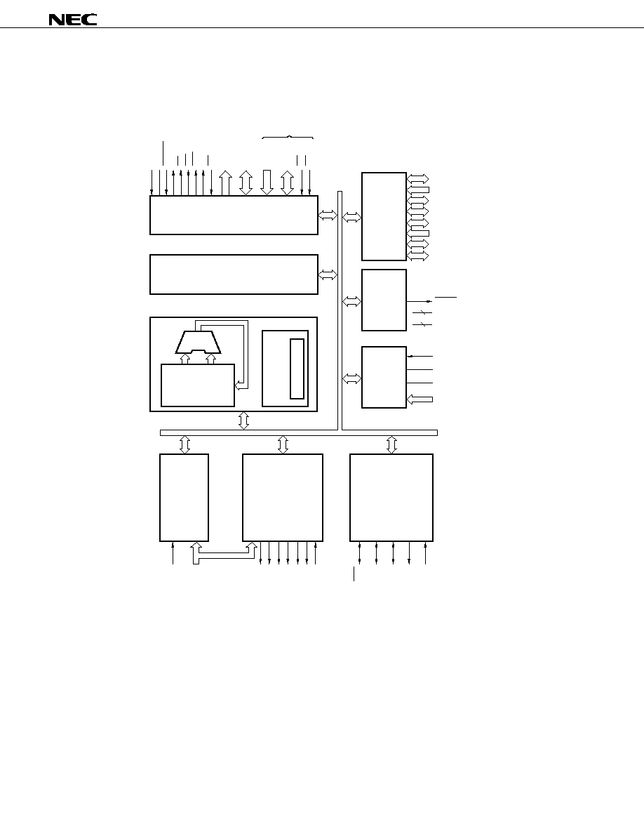
PROGRAMMABLE
INTERRUPT
CONTROLLER
TIMER/COUNTER UNIT
(REALTIME PULSE
UNIT)
SERIAL INTERFACE
(SBI)
(UART)
(P20) NMI
(P80) TO00
INTP0-INTP5
(P21-P26)
(P83) TO03
(P81) TO01
(P82) TO02
(P85) TO11
(P84) TO10
(P27) TI/INTP6
During PROM programming mode
(P34) SCK
(P32) SO/SB0
(P31) RxD
Note
(P30) TxD
(P33) SI/SB1
GENERAL
REGISTERS
128 bytes
&
DATA
MEMORY
128 bytes
MICRO SEQUENCE
CONTROL
MICRO ROM
SYSTEM
CONTROL
&
BUS
CONTROL
&
PREFETCH
CONTROL
PROM
16
Kbytes
/
Peripheral
RAM
384
bytes
ALU
PORT
WDT
A/D CONVERTER
(10 bits)
AV
REF
WDTO
AV
SS
V
DD
AV
DD
P00-P07 (REALTIME PORT)
P20-P27
P30-P34
P40-P47
P50-P57
P70-P77
P80-P85
P90-P93
2
V
SS
2
ANI0-ANI7
(P70-P77)
Main RAM
EXU
PROM/RAM
BCU
X1
X2
RESET
ASTB
RD
WR
TAS
TMD
A8-A15 (P50-P57)
AD0-AD7 (P40-P47)
A0-A14
D0-D7
CE
OE
EA/V
PP
Note
Note
BLOCK DIAGRAM

µ
PD78P322
10
CONTENTS
1.
PIN FUNCTIONS ... 11
1.1
Normal Operating Mode ... 11
1.2
PROM Programming Mode (RESET = H, AV
DD
= L) ... 13
1.3
Pin Input/Output Circuits and Recommended Connection of Unused Pins ... 14
2.
DIFFERENCES BETWEEN
µ
PD78P322 and
µ
PD78322 ... 16
3.
PROM PROGRAMMING ... 17
3.1
Operation Mode ... 17
3.2
PROM Write Procedure ... 18
3.3
PROM Read Procedure ... 20
4.
ERASURE CHARACTERISTICS (FOR
µ
PD78P322K/KC/KD ONLY) ... 21
5.
OPAQUE FILM ON ERASURE WINDOW (FOR
µ
PD78P322K/KC/KD ONLY) ... 21
6.
ONE-TIME PROM VERSION SCREENING ... 21
7.
ELECTRICAL SPECIFICATIONS ... 22
8.
PACKAGE DRAWINGS ... 36
9.
RECOMMENDED SOLDERING CONDITIONS ... 42
APPENDIX A.
DRAWINGS OF CONVERSION SOCKETS AND RECOMMENDED FOOTPRINTS ... 44
APPENDIX B.
TOOLS ... 48
B.1
Development Tools ... 48
B.2
Evaluation Tools ... 52
B.3
Embedded Software ... 52
*

µ
PD78P322
11
1.
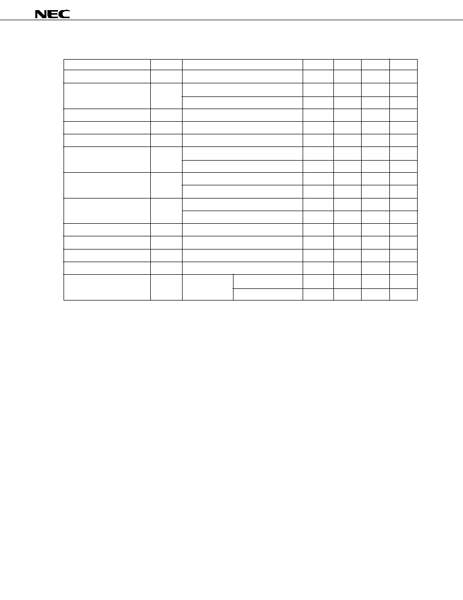
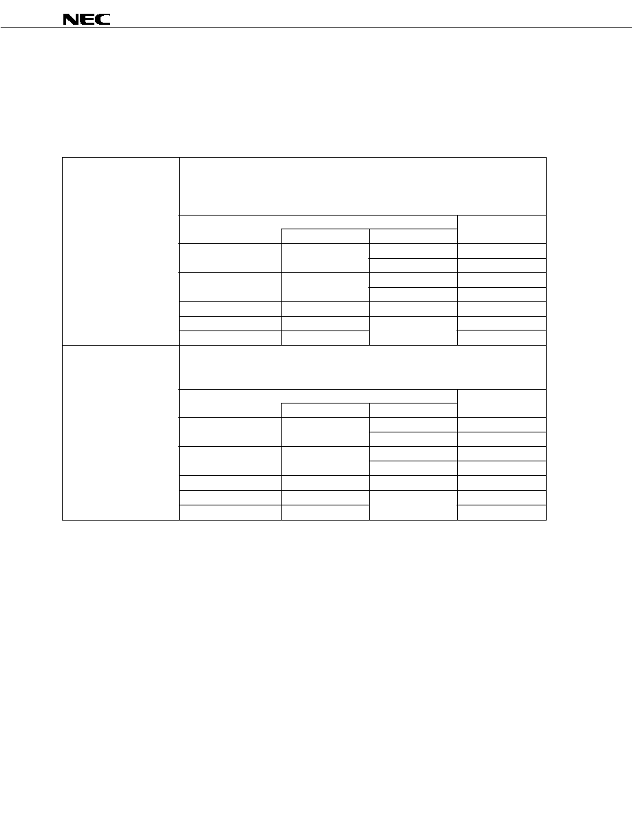
PIN FUNCTIONS
1.1 Normal Operating Mode
(1)
Port Pins
Pin Name Input/Output
Function
Alternate
Function
P00-P07
Input/Output
PORT0
RTP0-RTP7
(Output)
8-bit input/output port
Input or output mode can be specified bit-wise.
The port can also operate as a real-time output port.
P20
Input
PORT 2
NMI
P21
8-bit input-only port
INTP0
P22
INTP1
P23
INTP2
P24
INTP3
P25
INTP4
P26
INTP5
P27
INTP6/TI
P30
Input/Output
PORT 3
TxD
P31
5-bit input/output port
RxD
P32
Input or output mode can be specified bit-wise.
SO/SB0
P33
SI/SB1
P34
SCK
P40-P47
Input/Output
PORT 4
AD0-AD7
8-bit input/output port
Input or output mode can be specified in 8-bit units.
P50-P57
Input/Output
PORT 5
A8-A15
8-bit input/output port
Input or output mode can be specified bit-wise.
P70-P77
Input
PORT 7
AN0-AN7
8-bit input-only port
P80
Input/Output
PORT 8
TO00
P81
6-bit input/output port
TO01
P82
Input or output mode can be specified bit-wise.
TO02
P83
TO03
P84
TO10
P85
TO11
P90
Input/Output
PORT 9
RD
P91
4-bit input/output port
WR
P92
Input or output mode can be specified bit-wise.
TAS
P93
TMD

µ
PD78P322
12
(2)
Non-Port Pins (1/2)
Pin Name
Input/Output
Function
Alternate
Function
RTP0-RTP7
Output
Real-time output port which outputs a pulse in synchronization with the trigger signal from P00-P07
the real-time pulse unit (RPU).
INTP0
Input
Edge-detected external interrupt request input.
P21
INTP1
The valid edge can be specified in the mode register.
P22
INTP2
P23
INTP3
P24
INTP4
P25
INTP5
P26
INTP6
P27/TI
NMI
Input
Edge-detected nonmaskable interrupt request input.
P20
The rising or falling edge can be selected for the valid edge by setting the mode register.
TI
Input
External count clock input pin to timer 1 (TM1).
P27/INTP6
RxD
Input
Serial data input pin to asynchronous serial interface (UART).
P31
TxD
Output
Serial data output pin from asynchronous serial interface (UART).
P30
SI
Input
Serial data input pin to clocked serial interface in 3-wire mode.
P33/SB1
SO
Output
Serial data output pin from clocked serial interface in 3-wire mode.
P32/SB0
SB0
Input/Output
Serial data input/output pins to/from clocked serial interface in SBI mode.
P32/SO
SB1
P33/SI
SCK
Input/Output
Serial clock input/output pin to/from clocked serial interface.
P34
AD0-AD7
Input/Output
Multiplexed address/data bus used when external memory is added.
P40-P47
A8-A15
Output
Address bus used when external memory is added.
P50-P57
RD
Output
Strobe signal output for external memory read operation.
P90
WR
Strobe signal output for external memory write operation.
P91
TAS
Output
Control signal output pins to access turbo access manager (
µ
PD71P301).
Note
P92
TMD
P93
TO00
Output
Pulse output from real-time pulse unit.
P80
TO01
P81
TO02
P82
TO03
P83
TO10
P84
TO11
P85
ASTB
Output
Timing signal output pin to externally latch low-order address information output from
--
AD0-AD7 for external memory access.
WDTO
Output
Signal output which indicates that watchdog timer generated non-maskable interrupt.
--
EA
Input
For
µ
PD78P322, normally connect the EA pin to V
DD
. When the EA pin is connected to
--
V
SS
, the
µ
PD78P322 enters the ROMless mode and external memory is accessed.
The EA pin level cannot be changed during operation.
Note
Turbo access manager (
µ
PD71P301) is available for maintenance purposes only.
*

µ
PD78P322
13
(2)
Non-Port Pins (2/2)
1.2 PROM Programming Mode (RESET = H, AV
DD
= L)
Pin Name Input/Output
Function
AV
DD
Input
PROM programming mode setting.
RESET
A0-A14
Input
Address bus.
D0-D7
Input/Output
Data bus.
CE
Input
PROM enable to PROM.
OE
Input
Read strobe to PROM.
V
PP
--
Write power supply.
V
DD
Positive power supply.
V
SS
GND.
NC
No internal connection. Connect to V
SS
(can leave open).
Pin Name Input/Output
Function
Alternate
Function
AN0-AN7
Input
Analog input to A/D converter.
P70-P77
AV
REF
Input
A/D converter reference voltage input.
--
AV
DD
--
A/D converter analog power supply.
--
AV
SS
--
A/D converter GND.
--
RESET
Input
System reset input.
--
X1
Input
Crystal resonator connection pin for system clock generation. To supply external clock,
--
X2
input to the X1 and input inverted signal to the X2 pin (X2 pin can be unconnected.)
V
DD
--
Positive power supply pin.
--
V
SS
--
GND pin.
--
NC
--
No internal connection. Connect to V
SS
(can leave open).
--

µ
PD78P322
14
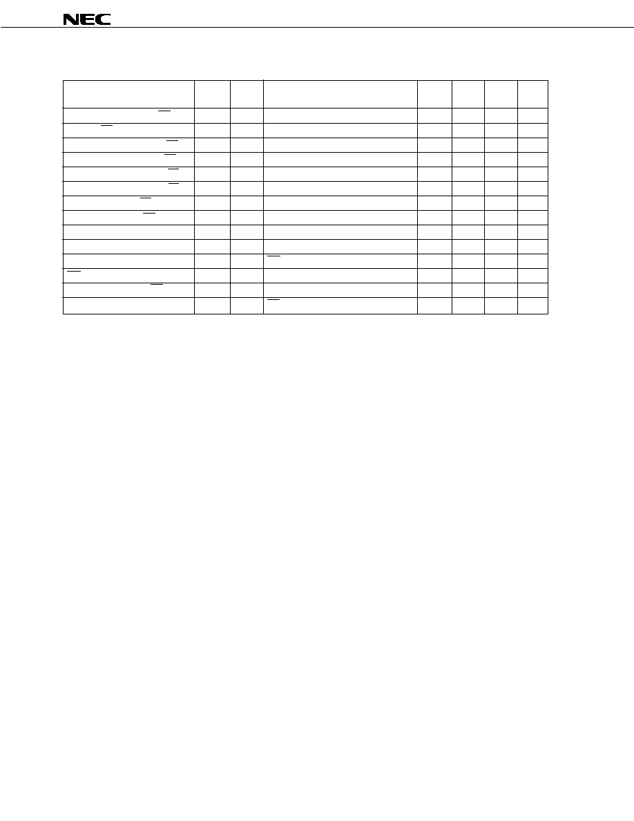
1.3 Pin Input/Output Circuits and Recommended Connection of Unused Pins
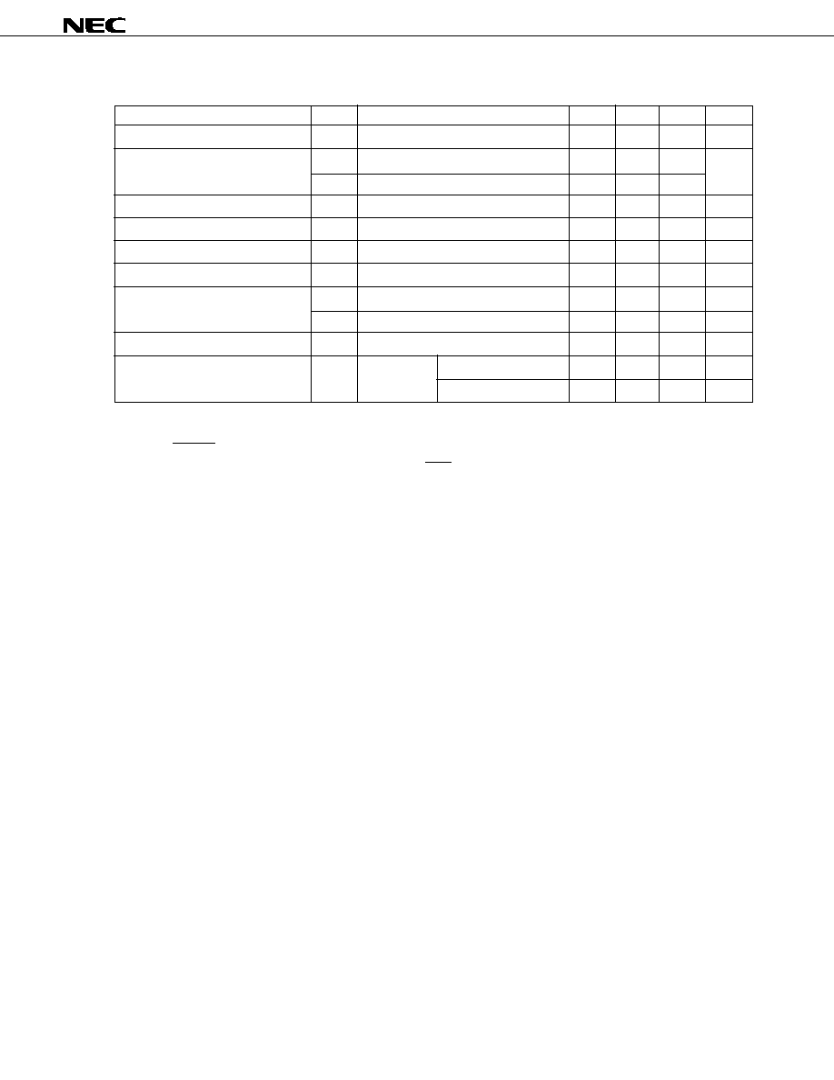
Table 1-1 and Figure 1-1 show the pin input/output circuit schematically.
Table 1-1. Pin Input/Output Circuits and Recommended Connection of Unused Pins
Pin
Input/Output
Recommended connection of unused pins
circuit type
P00/RTP0-P07/RTP7
5
Input state: Independently connect to V
DD
or V
SS
via a resistor.
Output state: Leave Open.
P20/NMI
2
Connect to V
SS
.
P21/INTP0-P26/INTP5
P27/INTP6/TI
P30/TxD
5
Input state: Independently connect to V
DD
or V
SS
via a resistor.
P31/RxD
Output state: Leave Open.
P32/SO/SB0
8
P33/SI/SB1
P34/SCK
P40/AD0-P47/AD7
5
P50/A8-P57/A15
P70/AN0-P77/AN7
9
Connect to V
SS
.
P80/TO00-P83/TO03
5
Input state: Independently connect to V
DD
or V
SS
via a resistor.
P84/TO10, P85/TO11
Output state: Leave Open.
P90/RD
5
P91/WR
P92/TAS
P93/TMD
WDTO
3
Leave Open.
ASTB
4
EA
1
--
RESET
2
--
AV
DD
--
Connect to V
DD
.
AV
REF
--
Connect to V
SS
.
AV
SS
V
PP
--
Connect to V
DD
.
NC
--
Connect to V
SS
(can leave open).
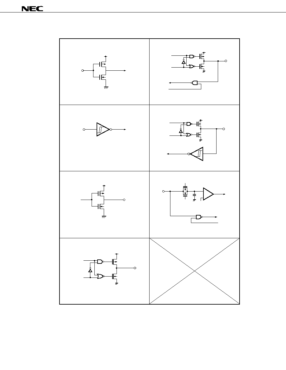
µ
PD78P322
15
TYPE 1
TYPE 5
TYPE 2
IN
V
DD
P-ch
N-ch
data
Comparator
output
disable
IN
Schmitt-triggerred input with hysteresis characteristics
Push-pull output that can be placed in high impedance
(both P-ch and N-ch off).
OUT
V
DD
P-ch
N-ch
TYPE 8
TYPE 3
TYPE 9
TYPE 4
P-ch
N-ch
IN
V
REF
(Threshold voltage)
+
≠
input
enable
V
DD
IN/OUT
P-ch
N-ch
data
output
disable
V
DD
OUT
P-ch
N-ch
data
output
disable
input
disable
V
DD
IN/OUT
P-ch
N-ch
Figure 1-1. Pin Input/Output Circuits

µ
PD78P322
16
2.
DIFFERENCES BETWEEN
µ
PD78P322 and
µ
PD78322
The
µ
PD78P322 is a version provided by replacing the
µ
PD78322's on-chip mask ROM with one-time PROM
or EPROM. Thus, the
µ
PD78P322 and
µ
PD78322 are the same in function except for the ROM specifications such
as write or verify. Table 2-1 lists the differences between these two products.
This Data Sheet describes the PROM specification function. Refer to the
µ
PD78322 documents for details of
other functions.
Table 2-1. Differences between
µ
PD78P322 and
µ
PD78322
Caution The noise immunity and noise radiation differ between the PROM and mask ROM versions. To
replace the PROM version with the mask ROM version when shifting from experimental production
to mass production, evaluate your system by using the CS version (not ES version) of the mask
ROM version.
*
*
*
Item Part Number
µ
PD78P322
µ
PD78322
Internal program memory
One-time PROM
EPROM
Mask ROM
(electrical program)
(programmable only once)
(reprogrammable)
(nonprogrammable)
PROM programming pin
Contained
Not contained
Package
∑ 68-pin plastic QFJ
∑ 68-pin ceramic WQFN
∑ 68-pin plastic QFJ
∑ 74-pin plastic QFP
∑ 74-pin ceramic WQFN
∑ 74-pin plastic QFP
∑ 80-pin plastic QFP
∑ 80-pin ceramic WQFN
∑ 80-pin plastic QFP
Electrical specifications
Current dissipations are different.
Others
Noise immunity and noise radiation differ because circuit complexity and mask layout are
different.

µ
PD78P322
17
3.
PROM PROGRAMMING
The PROM incorporated in the
µ
PD78P322 is a 16,384
◊
8-bit electrically writable PROM. For programming,
set the PROM programming mode by using the RESET and AV
DD
pins.
The programming characteristics are compatible with the
µ
PD27C256A programming characteristics.
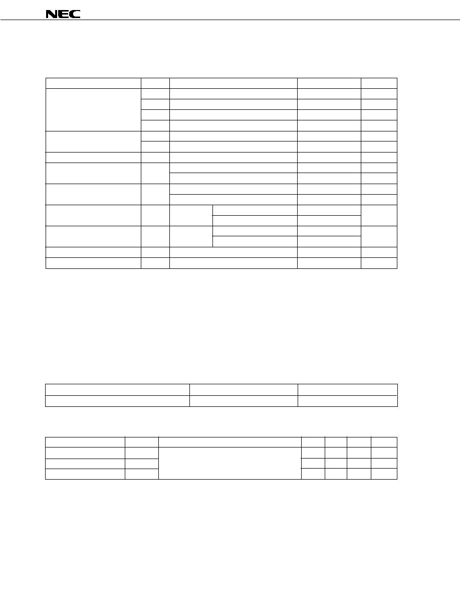
Table 3-1. Pin Function in Programming Mode
Function
Normal Operating Mode
Programming Mode
Address input
P00-P07, P80, P20, P81-P85
A0-A14
Data input
P40-P47
D0-D7
Chip enable/program pulse
P31
CE
Output enable
P30
OE
Program voltage
V
PP
Mode control
RESET, AV
DD
3.1 Operation Mode
To set the program write/verify mode, set RESET = H and AV
DD
= L. For the mode, the operation mode can be
selected by setting the CE and OE pins, as listed in Table 3-2.
To read the PROM contents, set the read mode.
Connect the unused pins exactly as indicated in Pin Configuration.
Table 3-2. PROM Programming Operation Mode
Mode
RESET
AV
DD
CE
OE
V
PP
V
DD
D0-D7
Program write
H
L
L
H
+12.5 V
+6 V
Data input
Program verify
H
L
Data output
Program inhibit
H
H
High impedance
Read
L
L
+5 V
+5 V
Data output
Output disable
L
H
High impedance
Standby
H
L/H
High impedance
Caution
When V
PP
is set to +12.5 V and V
DD
is set to +6V, setting both CE and OE to L is prohibited.
µ
PD78P322
18
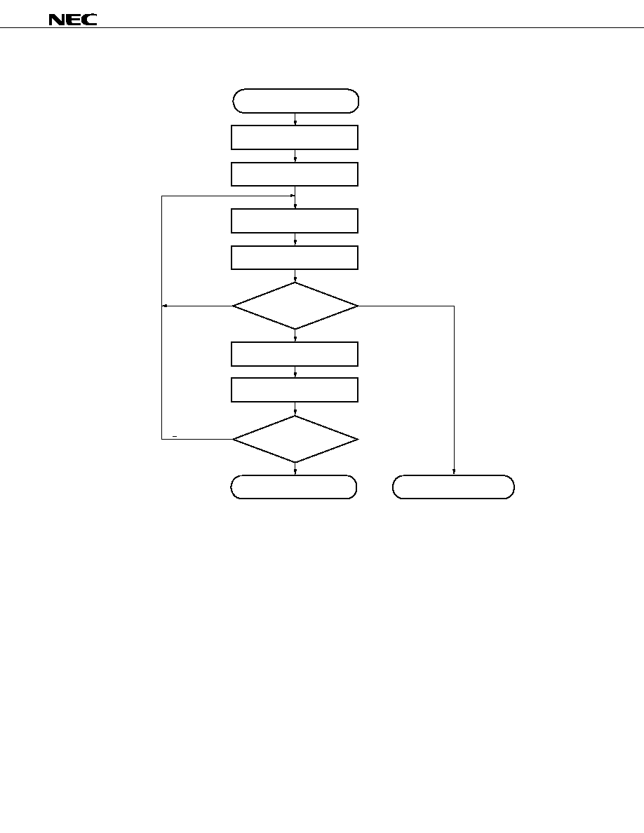
3.2 PROM Write Procedure
The write procedure into PROM is as follows:
(1)
Fix RESET = H and AV
DD
= L. Connect other unused pins exactly as indicated in section "Pin Configuration."
(2)
Supply +6 V to the V
DD
and +12.5 V to the V
PP
pin.
(3)
Supply an initial address.
(4)
Supply write data.
(5)
Supply 1 ms program pulse (active low) to the CE pin.
(6)
Execute the verify mode. Check whether or not the write data is written normally.
∑ When it is written normally: Proceed to step (8).
∑ When it is not written normally: Repeat steps (4) to (6).
If the data is not written normally after 25 repetitions of the steps, proceed to step (7).
(7)
Assume the device to be defective. Stop write operation.
(8)
Supply write data and X (number of steps (4) to (6) repetitions) x 3 ms program pulses (additional write).
(9)
Increment the address.
(10) Repeat steps (4) to (9) to the last address.
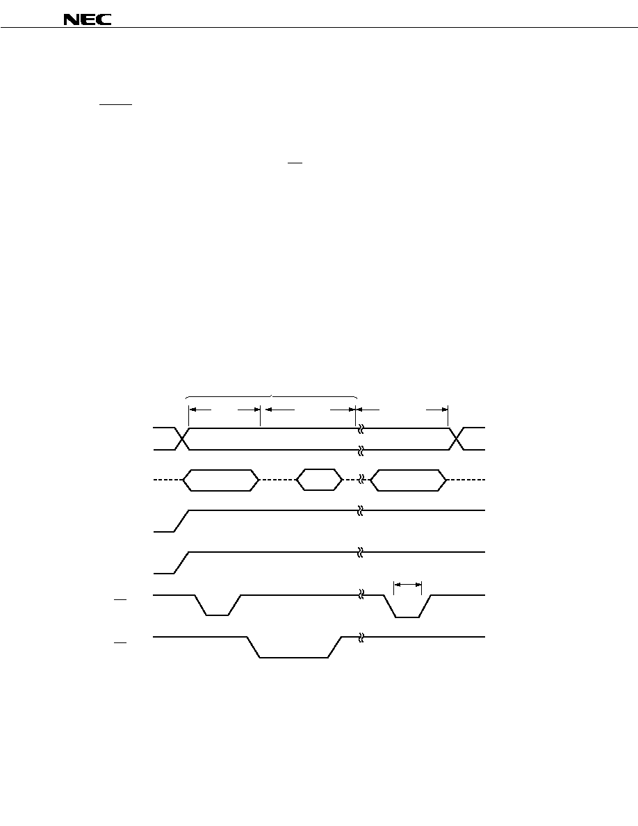
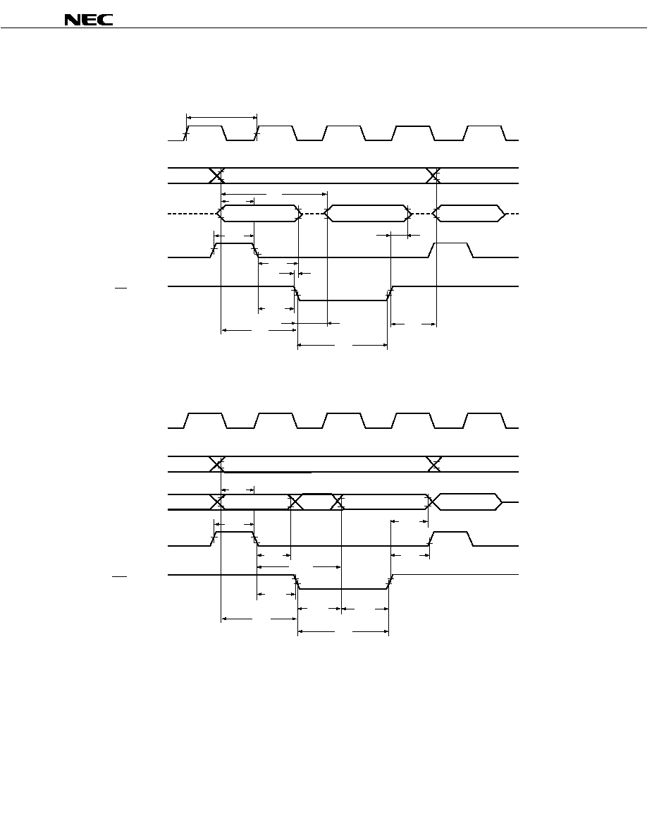
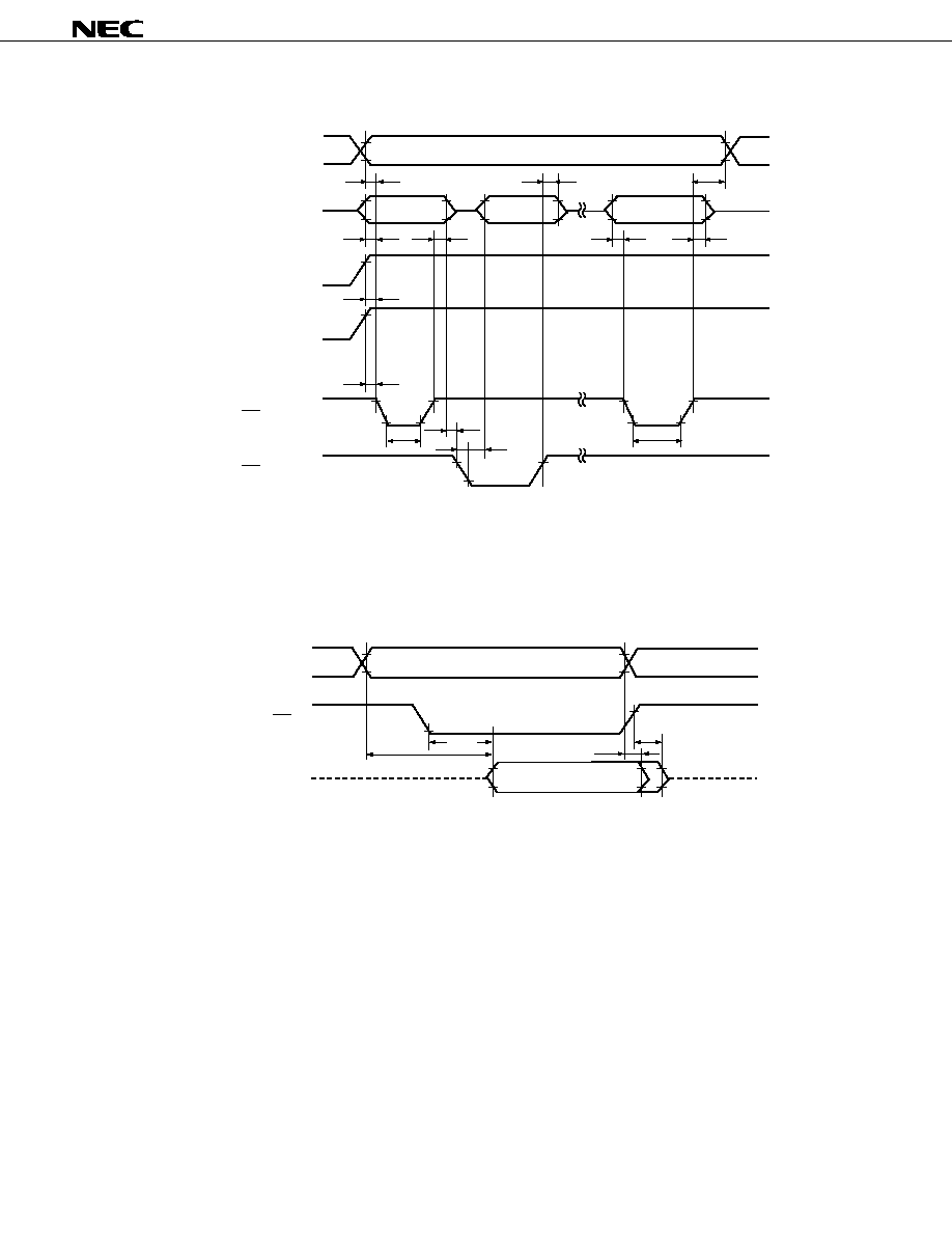
Figure 3-1 shows the PROM Write/Verify Timing Steps (2) to (8) above.
Figure 3-1. PROM Write/Verify Timing
+12.5 V
V
PP
V
DD
+6 V
V
DD
V
DD
Address input
Write
Hi-Z
Hi-Z
Hi-Z
Hi-Z
Verify
Additional
data write
3 X ms
X-time repetition
D0-D7
CE (input)
OE (input)
A0-A14
Data input
Data
output
Data input
µ
PD78P322
19
Figure 3-2. Write Procedure Flowchart
(1)
(2)
(3)
(4)
(5)
(6)
Verify mode
Supply program pulse
Write OK
> end address
X: Number of write
repetitions
Write NG
(at the 25th repetition)
Write NG
(after 24
repetition or less)
Supply write data
Supply initial address
Supply power
WRITE START
Make additional write
(3X ms pulses)
Increment address
End address
WRITE END
Defective device
(8)
(9)
(10)
(7)
< end address
µ
PD78P322
20
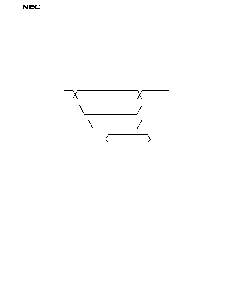
3.3 PROM Read Procedure
The read procedure of the PROM contents into the external data bus (D0-D7) is as follows.
(1)
Fix RESET = H and AV
DD
= L. Connect other unused pins exactly as indicated in Pin Configuration.
(2)
Supply +5 V to the V
DD
and V
PP
pins.
(3)
Input the address of the data to be read to the A0-A14 pins.
(4)
Execute the read mode.
(5)
The data is output to the D0-D7 pins.
Figure 3-3 shows the PROM read timing steps (2) to (5) above.
Figure 3-3. PROM Read Timing
Data output
Address input
Hi-Z
Hi-Z
D0-D7
CE (input)
OE (input)
A0-A14
µ
PD78P322
21
4.
ERASURE CHARACTERISTICS (FOR
µ
PD78P322K/KC/KD ONLY)
The data written into the
µ
PD78P322K/KC/KD program memory can be erased (FFH) and new data can be
rewritten into the memory.
To erase data, apply light with a wavelength shorter than 400 nm to the window. Normally, apply ultraviolet rays
having the 254-nm wavelength. The radiation amount required to completely erase data is as follows:
∑ Ultraviolet strength x erasure time: 15 W∑s/cm
2
or more
∑ Erasure time:
15 to 20 minutes when a 12,000
µ
W/cm
2
ultraviolet lamp is used. However, the time may be
prolonged due to ultraviolet lamp performance deterioration, dirty window, etc.
For erasure, place an ultraviolet lamp at a position within 2.5 cm from the window. If a filter is attached to the
ultraviolet lamp, remove the filter before applying ultraviolet rays.
5.
OPAQUE FILM ON ERASURE WINDOW (FOR
µ
PD78P322K/KC/KD ONLY)
If the
µ
PD78P322K/KC/KD window is exposed to sunlight or fluorescent lamp light for hours, EPROM data may
be erased and the internal circuit may operate erroneously. To prevent such accidents from occurring, put a
protective seal on the window.
A protective seal whose quality is guaranteed by NEC is attached to every EPROM version with window at
shipment.
6.
ONE-TIME PROM VERSION SCREENING
The one-time PROM versions (
µ
PD78P322GF-3B9, 78P322GJ-5BJ, 78P322L) cannot be completely tested by
NEC for shipment because of their structure. For screening, it is recommended to verify PROM after storing the
necessary data under the following conditions:
Storage temperature
Storage time
125∞C
24 hours
NEC provides chargeable services ranging from one-time PROM writing to marking, screening and verification
for QTOP microcontroller products. For details, contact an NEC sales representative.
µ
PD78P322
22
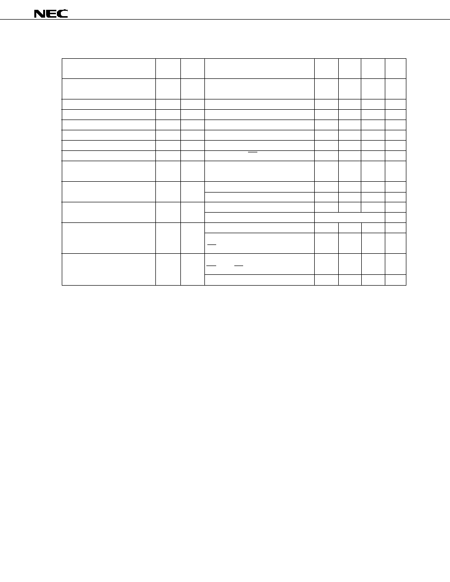
7.
ELECTRICAL SPECIFICATIONS
Absolute Maximum Ratings (T
A
= 25
∞
C)
Parameter
Symbol
Test Conditions
Ratings
Unit
Power supply voltage
V
DD
≠0.5 to +7.0
V
AV
DD
≠0.5 to V
DD
+0.5
V
V
PP
≠0.5 to +13.5
V
AV
SS
≠0.5 to +0.5
V
Input voltage
V
I1
Note 1
≠0.5 to V
DD
+0.5
V
V
I2
P20/NIM (A9) PIN
≠0.5 to +13.5
V
Output voltage
V
O
≠0.5 to V
DD
+0.5
V
Output current, low
I
OL
All output pins
4.0
mA
Total for all pins
90
mA
Output current, high
I
OH
All output pins
≠1.0
mA
Total for all pins
≠20
mA
Analog input voltage
V
IAN
Note 2
AV
DD
> V
DD
≠0.5 to V
DD
+0.5
V
V
DD
AV
DD
≠0.5 to AV
DD
+0.5
A/D converter reference
AV
REF
AV
DD
> V
DD
≠0.5 to V
DD
+0.3
V
input voltage
V
DD
AV
DD
≠0.5 to AV
DD
+0.3
Operating ambient temperature
T
A
≠10 to +70
∞
C
Storage temperature
T
stg
≠65 to +150
∞
C
Notes
1. Pins except for P20/NMI (A9), P70/AN0-P77/AN7
2. P70/AN0-P77/AN7
Caution Product quality may suffer if the absolute maximum rating is exceeded for even a single parameter,
even momentarily. In other words, the absolute maximum ratings are rated values at which the
product is on the verge of suffering physical damage, and therefore the product must be used under
conditions which ensure that the absolute maximum ratings are not exceeded.
Recommended Operating Conditions
Oscillation frequency
T
A
V
DD
8 MHz
f
XX
16 MHz
≠10 to +70 ∞C
+5.0 V
±
5%
Capacitance (T
A
= 25
∞
C, V
SS
= V
DD
= 0 V)
Parameter
Symbol
Test Conditions
MIN.
TYP.
MAX.
Unit
Input capacitance
C
I
f = 1 MHz
10
pF
Output capacitance
C
O
Unmeasured pins returned to 0 V
20
pF
I/O capacitance
C
IO
20
pF
*
µ
PD78P322
23
Resonator
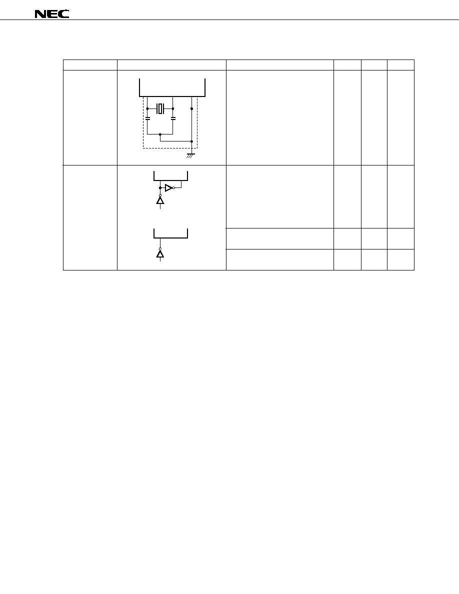
Recommended Circuit
Parameter
MIN.
MAX.
Unit
Ceramic or crystal
Oscillation frequency (f
XX
)
8
16
MHz
resonator
External clock
X1 input frequency (f
X
)
8
16
MHz
X1 input rise, fall time (f
XR
, t
XF
)
0
20
ns
X1 input high, low level width
25
80
ns
(t
WXH
, t
WXL
)
Oscillator Characteristics (T
A
= ≠10 to +70
∞
C, V
DD
= +5 V
±
5%, V
SS
= 0 V)
Caution When using the system clock oscillator, wire the portion enclosed in broken lines in the figure as
follows to avoid adverse influences on the wiring capacitance:
∑ Keep the wiring length as short as possible.
∑ Do not cross the wiring over the other signal lines. Do not route the wiring in the vicinity of
lines through which a high fluctuating current flows.
∑ Always keep the ground point of the capacitor of the oscillator circuit at the same potential as
V
SS
. Do not connect the power source pattern through which a high current flows.
∑ Do not extract signals from the oscillator.
X1
X2
C1
C2
V
SS
X1
X2
HCMOS
Inverter
X1
X2
HCMOS
Inverter
Open
or

µ
PD78P322
24
Recommended Oscillator Constants
Ceramic resonator
Manufacturer Name
Part Number
Frequency
Recommended
[MHz]
Constants
C1 [pF]
C2 [pF]
MURATA
CSA8.00MT
8.0
30
30
CSA12.0MT
12.0
CSA14.74MXZ040
14.74
15
15
CSA16.00MX040
16.0
CST8.00MTW
8.0
Internal
Internal
CST12.0MTW
12.0
CST14.74MXW0C3
14.74
CST16.00MXW0C3
16.0
Crystal resonator
Manufacturer Name
Part Number
Frequency
Recommended
[MHz]
Constants
C1 [pF]
C2 [pF]
KINSEKI
HC49/U-S
8 to 16
10
10
HC49/U
µ
PD78P322
25
DC Characteristics (T
A
= ≠10 to +70
∞
C, V
DD
= +5 V
±
5%, V
SS
= 0 V)
Parameter
Symbol
Test Conditions
MIN.
TYP.
MAX.
Unit
Input voltage, low
V
IL
0
0.8
V
Input voltage, high
V
IH1
Note 1
2.2
V
V
IH2
Note 2
0.8V
DD
Output voltage, low
V
OL
I
OL
= 2.0 mA
0.45
V
Output voltage, high
V
OH
I
OH
= ≠400
µ
A
V
DD
≠1.0
V
Input leakage current
I
LI
0 V
V
I
V
DD
±
10
µ
A
Output leakage current
I
LO
0 V
V
O
V
DD
±
10
µ
A
V
DD
power supply current
I
DD1
Operation mode
40
65
mA
I
DD2
HALT mode
20
35
mA
Data retention voltage
V
DDDR
STOP mode
2.5
V
Data retention current
I
DDDR
STOP mode
V
DDDR
= 2.5 V
2
10
µ
A
V
DDDR
= 5.0 V
±
5%
10
50
µ
A
Notes 1. Pins other than mentioned in Note 2.
2. RESET, X1, X2, P20/NMI, P21/INTP0, P22/INTP1, P23/INTP2, P24/INTP3, P25/INTP4, P26/INTP5, P27/
INTP6/TI, P32/SO/SB0, P33/SI/SB1, or P34/SCK pins.
µ
PD78P322
26
AC Characteristics (T
A
= ≠10 to +70
∞
C, V
DD
= +5 V
±
5%, V
SS
= 0 V)
Discontinuous read/write operation (when general-purpose memory is connected)
Parameter
Symbol
Test Conditions
MIN.
MAX.
Unit
System clock cycle time
t
CYK
125
250
ns
Address setup time (to ASTB
)
t
SAST
32
ns
Address hold time (from ASTB
)
t
HSTA
32
ns
Address
RD
delay time
t
DAR
85
ns
RD
address float time
t
FRA
0
ns
Address
data input time
t
DAID
222
ns
RD
data input time
t
DRID
112
ns
ASTB
RD
delay time
t
DSTR
42
ns
Data hold time (from RD
)
t
HRID
0
ns
RD
address active time
t
DRA
50
ns
RD low level width
t
WRL
157
ns
ASTB high level width
t
WSTH
37
ns
Address
WR
delay time
t
DAW
85
ns
ASTB
data output time
t
DSTOD
102
ns
WR
data output time
t
DWOD
40
ns
ASTB
WR
delay time
t
DSTW
42
ns
Data setup time (to WR
)
t
SODW
147
ns
Data hold time (from WR
)
t
HWOD
32
ns
WR
ASTB
delay time
t
DWST
42
ns
WR low level width
t
WWL
157
ns
*

µ
PD78P322
27
t
CYK
-Dependent Bus Timing Definition
Parameter
Calculation expression
MIN./MAX.
Unit
t
SAST
0.5T ≠ 30
MIN.
ns
t
HSTA
0.5T ≠ 30
MIN.
ns
t
DAR
T ≠ 40
MIN.
ns
t
DAID
(2.5 + n) T ≠ 90
MAX.
ns
t
DRID
(1.5 + n) T ≠ 75
MAX.
ns
t
DSTR
0.5T ≠ 20
MIN.
ns
t
DRA
0.5T ≠ 12
MIN.
ns
t
WRL
(1.5 + n) T ≠ 30
MIN.
ns
t
WSTH
0.5T ≠ 25
MIN.
ns
t
DAW
T ≠ 40
MIN.
ns
t
DSTOD
0.5T + 40
MAX.
ns
t
DSTW
0.5T ≠ 20
MIN.
ns
t
SODW
1.5T ≠ 40
MIN.
ns
t
HWOD
0.5T ≠ 30
MIN.
ns
t
DWST
0.5T ≠ 20
MIN.
ns
t
WWL
(1.5 + n) T ≠ 30
MIN.
ns
Remarks 1. T = t
CYK
= 1/f
CLK
(f
CLK
is the internal system clock frequency).
2. n is the number of wait cycles defined by user software.
3. Only parameters listed in the table are dependent on t
CYK
.
µ
PD78P322
28
Parameter
Symbol
Test Conditions
MIN.
MAX.
Unit
Serial clock cycle time
t
CYSK
SCK Output
Internal divide by 8
1
µ
s
SCK Input
External clock
1
µ
s
Serial clock high-level width
t
WSKL
SCK Output
Internal divide by 8
420
ns
SCK Input
External clock
420
ns
Serial clock high-level width
t
WSKH
SCK Output
Internal divide by 8
420
ns
SCK Input
External clock
420
ns
SI setup time (to SCK
)
t
SRXSK
80
ns
SI hold time (from SCK
)
t
HSKRX
80
ns
SCK
SO delay time
t
DSKTX
R = 1 k
, C = 100 pF
210
ns
Serial Operation (T
A
= ≠10 to +70
∞
C, V
DD
= +5 V
±
5%, V
SS
= 0 V)
Parameter
Symbol
Test Conditions
MIN.
MAX.
Unit
NMI high, low-level width
t
WNIH
,
5
µ
s
t
WNIL
INTP0 high, low-level width
t
WI0H
,
8T
t
CYK
t
WI0L
INTP1 high, low-level width
t
WI1H
,
8T
t
CYK
t
WI1L
INTP2 high, low-level width
t
WI2H
,
8T
t
CYK
t
WI2L
INTP3 high, low-level width
t
WI3H
,
8T
t
CYK
t
WI3L
INTP4 high, low-level width
t
WI4H
,
8T
t
CYK
t
WI4L
INTP5 high, low-level width
t
WI5H
,
8T
t
CYK
t
WI5L
INTP6 high, low-level width
t
WI6H
,
8T
t
CYK
t
WI6L
RESET high, low-level width
t
WRSH
,
5
µ
s
t
WRSL
TI high, low-level width
t
WTIH
,
TM1
8T
t
CYK
t
WTIL
In the event counter mode
Other operations (T
A
= ≠10 to +70∞C, V
DD
= +5 V
±
5%, V
SS
= 0 V)
µ
PD78P322
29
Parameter
Symbol
Test Conditions
MIN.
TYP.
MAX.
Unit
Resolution
10
bit
Total error
Note1
4.5 V
AV
REF
AV
DD
±
0.4
%FSR
3.4 V
AV
REF
AV
DD
±
0.7
%FSR
Quantization error
±
1/2
LSB
Conversion time
t
CONV
144
t
CYK
Sampling time
t
SAMP
24
t
CYK
Zero scale error
Note1
4.5 V
AV
REF
AV
DD
+1.5
±
2.5
LSB
3.4 V
AV
REF
AV
DD
+1.5
±
4.5
LSB
Fullscale error
Note1
4.5 V
AV
REF
AV
DD
+1.5
±
2.5
LSB
3.4 V
AV
REF
AV
DD
+1.5
±
4.5
LSB
Nonlinear error
Note1
4.5 V
AV
REF
AV
DD
+1.5
±
2.5
LSB
3.4 V
AV
REF
AV
DD
+1.5
±
4.5
LSB
Analog input voltage
Note2
V
IAN
≠0.3
AV
DD
V
Basic voltage
AV
REF
3.4
AV
DD
V
AV
REF
current
AI
REF
1.0
3.0
mA
AV
DD
supply current
AI
DD
2.0
6.0
mA
A/D converter data
AI
DDDR
STOP mode
AV
DDDR
= 2.5 V
2.0
10
µ
A
retention current
AV
DDDR
= 5 V
±
5%
10
50
µ
A
*
A/D Converter (T
A
= ≠10 to +70∞C, V
DD
= +5 V
±
5%, V
SS
= AV
SS
= 0 V, V
DD
≠0.5 V
AV
DD
V
DD
)
Notes 1. Quantization error is excluded.
2. When ≠0.3 V
V
IAN
0 V, conversion result is 000H.
When 0 V < V
IAN
< AV
REF
, conversion is executed with 10-bit resolution.
When AV
REF
V
IAN
AV
DD
, conversion result is 3FFH.
µ
PD78P322
30
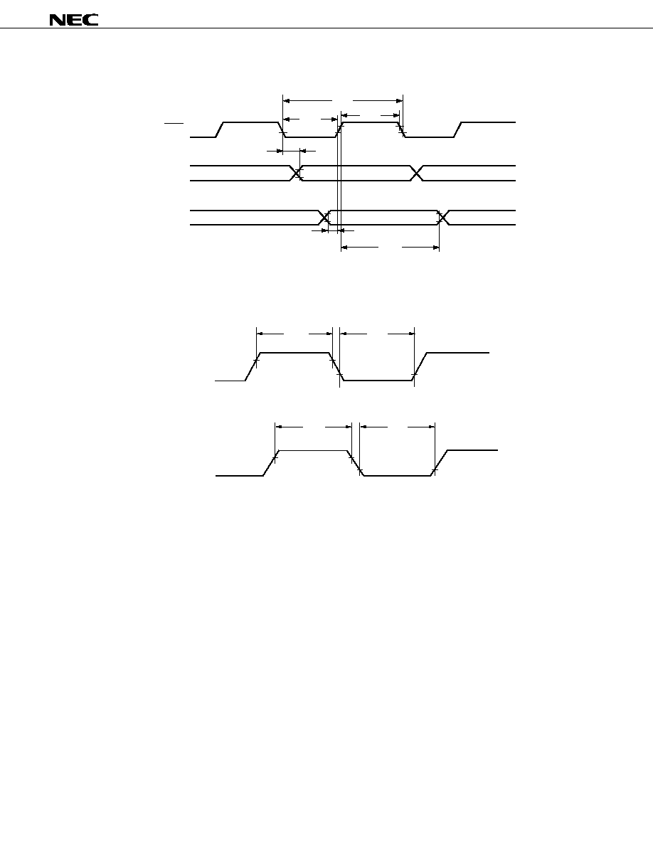
Discontinuous Read Operation
Discontinuous Write Operation
(CLK)
P50-P57
(output)
ASTB
(output)
P40-P47
(input/output)
t
SODW
t
WWL
t
DAW
WR (output)
t
DSTW
t
DWOD
t
HSTA
t
DWST
t
HWOD
t
DSTOD
t
WSTH
t
SAST
Low-order address
(output)
Undefined
Low-order address
(output)
Data (output)
High-order address
High-order address
(CLK)
P50-P57
(output)
ASTB
(output)
P40-P47
(input/output)
t
DRA
t
WRL
t
DAR
RD (output)
t
DSTR
t
HSTA
t
FRA
t
HRID
t
DRID
t
CYK
t
WSTH
t
SAST
t
DAID
Low-order address
(output)
High-order address
High-order address
Hi-Z
Hi-Z
Hi-Z
Hi-Z
Data (input)
Low-order address
(output)
µ
PD78P322
31
Serial Operation
Interrupt Input Timing
SCK
t
CYSK
t
WSKL
t
HSKRX
t
DSKTX
t
SRXSK
t
WSKH
SO
SI
INTPn
t
WInH
t
WInL
Remark
n = 0-6
NMI
t
WNIL
t
WNIH
0.8V
DD
0.8 V

µ
PD78P322
32
Reset Input Timing
TI Pin Input Timing
RESET
t
WRSL
t
WRSH
0.8V
DD
0.8 V
TI
t
WTIH
t
WTIL
µ
PD78P322
33
Parameter
Symbol Symbol Test conditions
MIN.
TYP.
MAX.
Unit
Note1
Input voltage, high
V
IH
V
IH
2.2
V
DDP
V
+0.3
Input voltage, low
V
IL
V
IL
≠0.3
0.8
V
Input leakage current
I
LIP
I
LI
0
V
I
V
DDP
Note 2
±
10
µ
A
Output voltage, high
V
OH
V
OH
I
OH
= ≠400
µ
A
2.4
V
Output voltage, low
V
OL
V
OL
I
OL
= 2.0 mA
0.45
V
Input current
I
A9
--
A9 (P20/NMI) pin
±
10
µ
A
Output leakage current
I
LO
--
0
V
O
V
DDP
, OE = V
IN
10
µ
A
PROG pin high voltage input
I
IP
--
±
10
µ
A
current
V
DDP
power supply voltage
V
DDP
V
DD
Program memory write mode
5.75
6.0
6.25
V
Program memory read mode
4.5
5.0
5.5
V
V
PP
power supply voltage
V
PP
V
PP
Program memory write mode
12.2
12.5
12.8
V
Program memory read mode
V
PP
= V
DDP
V
V
DDP
power supply current
I
DD
I
DD
Program memory write mode
10
30
mA
Program memory read mode
10
30
mA
CE = V
IL
, V
I
= V
IH
V
PP
power supply current
I
PP
I
PP
Program memory write mode
10
30
mA
CE = V
IL
, OE = V
IH
Program memory read mode
1
100
µ
A
DC Programming Characteristics (T
A
= 25
±
5
∞
C, V
SS
= 0 V)
Notes 1. Corresponding
µ
PD27C256A symbols.
2. V
DDP
is V
DD
pin during the programming mode.
µ
PD78P322
34
Parameter
Symbol Symbol Test conditions
MIN.
TYP.
MAX.
Unit
Note
Address setup time (to CE
)
t
SAC
t
AS
2
µ
s
Data
OE
delay time
t
DDOO
t
OES
2
µ
s
Input data setup time (to CE
)
t
SIDC
t
DS
2
µ
s
Address hold time (from CE
)
t
HCA
t
AH
2
µ
s
Input data hold time (from CE
)
t
HCID
t
DH
2
µ
s
Output data hold time (from OE
)
t
HOOD
t
DF
0
130
ns
V
PP
setup time (to CE
)
t
SVPC
t
VPS
2
µ
s
V
DDP
setup time (to CE
)
t
SVDC
t
VDS
2
µ
s
Initial program pulse width
t
WL1
t
PW
0.95
1.0
1.05
ms
Additional program pulse width
t
WL2
t
OPW
2.85
78.75
ms
Address
data output time
t
DAOD
t
ACC
OE = V
IL
2
µ
s
OE
data output time
t
DOOD
t
OE
1
µ
s
Data hold time (from OE
)
t
HCOD
t
DF
0
130
ns
Data hold time (from address)
t
HAOD
t
OH
OE = V
IL
0
ns
AC Programming Characteristics (T
A
= 25
±
5
∞
C, V
SS
= 0 V)
Note
Corresponding
µ
PD27C256A symbols.
µ
PD78P322
35
PROM Write Mode Timing
A12-A0
D7-D0
V
PP
V
DDP
V
DDP
V
IH
V
IL
V
IH
V
IL
V
DDP
+1
CE
OE
V
PP
V
DDP
t
DOOD
t
DDOO
t
SVDC
t
SVPC
t
SIDC
t
HCID
t
SIDC
t
HCID
t
HOOD
t
SAC
t
WL1
t
HCA
t
WL2
Data input
Hi-Z
Hi-Z
Hi-Z
Hi-Z
Effective address
Data output
Data input
Cautions 1. Apply V
DDP
before V
PP
and remove it after V
PP
.
2. V
PP
must not exceed +13 V, including the overshoot.
PROM Read Mode Timing
A12-A0
D7-D0
OE
t
HAOD
t
DAOD
t
DOOD
t
HCOD
Data output
Effective address
Hi-Z
Hi-Z
µ
PD78P322
36
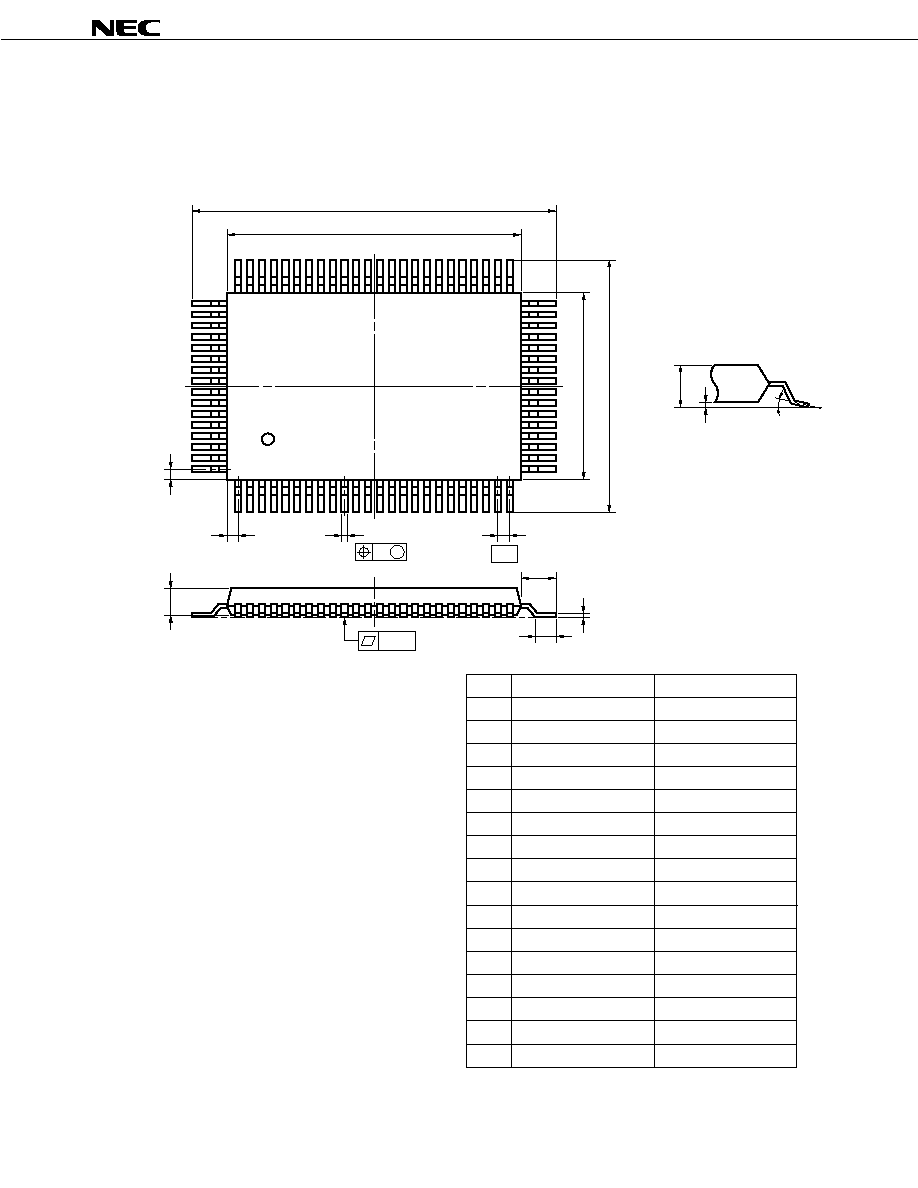
8.
PACKAGE DRAWINGS
N
A
M
F
B
64
65
40
K
L
80 PIN PLASTIC QFP (14
◊
20)
80
1
25
24
41
G
D
C
P
detail of lead end
S
Q
5∞±5∞
M
I
H
J
P80GF-80-3B9-2
ITEM
MILLIMETERS
INCHES
A
B
C
D
F
G
H
I
J
K
L
23.6±0.4
14.0±0.2
0.8
0.35±0.10
0.15
20.0±0.2
0.929±0.016
0.039
0.031
0.006
0.031 (T.P.)
0.795
NOTE
M
N
0.15
0.15
1.8±0.2
0.8 (T.P.)
0.006
0.006
+0.004
≠0.003
Each lead centerline is located within 0.15
mm (0.006 inch) of its true position (T.P.) at
maximum material condition.
0.071
0.014
0.551
0.8±0.2
0.031
P
2.7
0.106
0.693±0.016
17.6±0.4
1.0
+0.009
≠0.008
Q
0.1±0.1
0.004±0.004
S
3.0 MAX.
0.119 MAX.
+0.10
≠0.05
+0.009
≠0.008
+0.004
≠0.005
+0.009
≠0.008
+0.008
≠0.009
µ
PD78P322
37
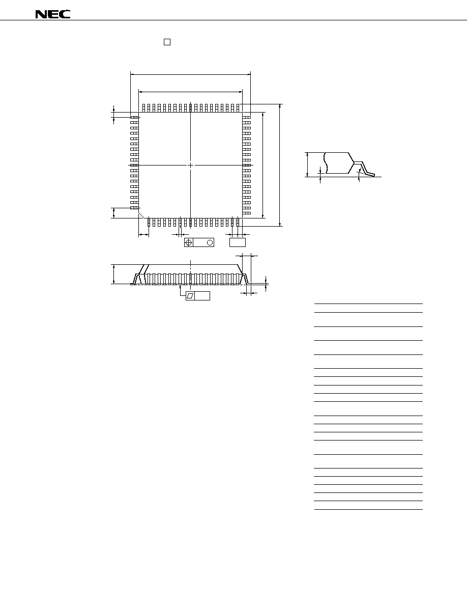
74 PIN PLASTIC QFP ( 20)
ITEM
MILLIMETERS
INCHES
F
1
F
2
I
2.0
1.0
0.20
Q
0.079
0.039
0.008
S74GJ-100-5BJ-3
NOTE
Each lead centerline is located within 0.20 mm (0.008 inch) of
its true position (T.P.) at maximum material condition.
C
20.0±0.2
0.787
M
0.15
0.006
0.1±0.1
0.004±0.004
+0.004
≠0.003
+0.009
≠0.008
A
23.2±0.4
0.913
H
0.40±0.10
0.016+0.004
≠0.005
L
0.8±0.2
0.031+0.009
≠0.008
N
0.10
0.004
P
3.7
0.146
S
4.0 MAX.
0.158 MAX.
+0.10
≠0.05
B
20.0±0.2
0.787+0.009
≠0.008
+0.017
≠0.016
J
1.0 (T.P.)
0.039 (T.P.)
R
5
∞
±5
∞
5
∞
±5
∞
D
23.2±0.4
0.913+0.017
≠0.016
G
1
G
2
2.0
1.0
0.079
0.039
K
1.6±0.2
0.063±0.008
A
B
G
1
H
I
J
C
D
P
N
K
L
M
detail of lead end
M
56
57
37
74
1
19
18
38
F
2
F
1
G
2
S
Q
R
µ
PD78P322
38
P68L-50A1-2
ITEM
MILLIMETERS
INCHES
NOTE
Each lead centerline is located within 0.12
mm (0.005 inch) of its true position (T.P.) at
maximum material condition.
+0.007
≠0.006
A
B
C
D
E
F
G
H
I
J
K
M
N
P
Q
T
U
25.2±0.2
24.20
24.20
25.2±0.2
1.94±0.15
0.6
4.4±0.2
2.8±0.2
0.9 MIN.
3.4
1.27 (T.P.)
0.40±1.0
0.12
23.12±0.20
0.15
R 0.8
0.20
+0.10
≠0.05
0.992±0.008
0.953
0.953
0.992±0.008
0.076
0.024
0.173
0.110
0.035 MIN.
0.134
0.050 (T.P.)
0.016
0.005
0.910
0.006
R 0.031
0.008
+0.009
≠0.008
+0.009
≠0.008
+0.004
≠0.005
+0.004
≠0.002
+0.009
≠0.008
N
K
M
Q
A
U
68
B
D
C
1
F
E
T
P
M
G
H
IJ
68 PIN PLASTIC QFJ ( 950 mil)

µ
PD78P322
39
X80KW-80A-1
ITEM
MILLIMETERS
INCHES
NOTE
Each lead centerline is located within 0.08
mm (0.003 inch) of its true position (T.P.) at
maximum material condition.
A
B
C
D
E
F
G
H
I
J
K
Q
R
S
T
U
W
20.0±0.4
19.0
13.2
14.2±0.4
1.64
2.14
4.064 MAX.
0.51±0.10
0.08
0.8 (T.P.)
1.0±0.2
C 0.5
0.8
1.1
R 3.0
12.0
0.75±0.2
0.787
0.748
0.520
0.559±0.016
0.065
0.084
0.160 MAX.
0.020±0.004
0.003
0.031 (T.P.)
0.039
C 0.020
0.031
0.043
R 0.118
0.472
0.030
+0.017
≠0.016
+0.009
≠0.008
+0.008
≠0.009
80 PIN CERAMIC WQFN
A
B
D
C
T
U
F
I
M
E
G
K
Q
J
80
R
1
H
S
W
µ
PD78P322
40
74 PIN CERAMIC WQFN
X74KW-100A-1
ITEM
MILLIMETERS
INCHES
NOTE
Each lead centerline is located within 0.10
mm (0.004 inch) of its true position (T.P.) at
maximum material condition.
A
B
C
D
E
F
G
H
I
J
K
Q
R
S
T
U
W
Y
20.0±0.4
18.0
18.0
20.0±0.4
1.94
2.14
4.0 MAX.
0.51±0.10
0.10
1.0 (T.P.)
1.0±0.2
C 0.3
2.0
2.0
R 2.0
10.0
0.7±0.2
C 1.5
0.787
0.709
0.709
0.787
0.076
0.084
0.158 MAX.
0.020±0.004
0.004
0.039 (T.P.)
0.039
C 0.012
0.079
0.079
R 0.079
0.394
0.028
C 0.059
+0.017
≠0.016
+0.017
≠0.016
+0.009
≠0.008
+0.008
≠0.009
A
B
D
C
T
Y
U
E
F
G
I
M
K
Q
S
74
H
J
1
W
R
µ
PD78P322
41
68 PIN CERAMIC WQFN
X68KW-50A-1
ITEM
MILLIMETERS
INCHES
NOTE
Each lead centerline is located within 0.12
mm (0.005 inch) of its true position (T.P.) at
maximum material condition.
A
B
C
D
E
F
G
H
I
J
K
L
P
Q
R
S
T
U
Y
24.13±0.4
21.5
21.5
24.13±0.4
1.65
2.03
3.50 MAX.
0.64±0.10
0.12
1.27 (T.P.)
1.27±0.2
2.16±0.2
R 0.2
C 1.02
1.905
1.905
R 3.0
12.0
C 0.5
0.950±0.016
0.846
0.846
0.950±0.016
0.065
0.080
0.138 MAX.
0.025
0.005
0.05 (T.P.)
0.05±0.008
0.085±0.008
R 0.008
C 0.04
0.075
0.075
R 0.118
0.472
C 0.020
G
A
U
F
E
Y
T
B
C
D
68
J
I
M
H
R
K
L
Q
P
1
S
+0.005
≠0.004

µ
PD78P322
42
9.
RECOMMENDED SOLDERING CONDITIONS
It is recommended that this device be soldered under the following conditions.
For details on the recommended soldering conditions, refer to information document "Semiconductor Devices
Mounting Technology Manual" (IEI-1207).
For soldering methods and conditions other than those recommended, please contact your NEC sales
representative.
Table 9-1. Soldering Conditions for Surface Mount Devices (1/2)
µ
PD78P322GF-3B9: 80-pin plastic QFP (14
◊
20 mm)
Soldering Method
Soldering Conditions
Recommended Soldering
Code
Infrared reflow
Package peak temperature: 235∞C,
IR35-207-2
Time: 30 seconds max. (210∞C min.),
Number of times: 2 max., Maximum number of days: 7 days
Note
(thereafter, 20 hours of prebaking is required at 125∞C)
< Cautions >
(1) Wait for the device temperature to return to normal after the first
reflow before starting the second reflow.
(2) Do not perform flux cleaning with water after the first reflow.
VPS
Package peak temperature: 215∞C,
VP15-207-2
Time: 40 seconds max. (200∞C min.),
Number of times: 2 max., Maximum number of days: 7 days
Note
(thereafter, 20 hours of prebaking is required at 125∞C)
< Cautions >
(1) Wait for the device temperature to return to normal after the first
reflow before starting the second reflow.
(2) Do not perform flux cleaning with water after the first reflow.
Wave soldering
Soldering bath temperature: 260∞C max., Time: 10 seconds max.,
WS60-207-1
Number of times: 1,
Preheating temperature: 120
∞
C max. (package surface temperature),
Maximum number of days: 7 days
Note
(thereafter, 20 hours of
prebaking is required at 125∞C).
Partial heating
Pin temperature: 300∞C max.,
--
Time: 3 seconds max. (per pin)
µ
PD78P322GJ-5BJ: 74-pin plastic QFP (20
◊
20 mm)
Soldering Method
Soldering Conditions
Recommended Soldering
Code
Infrared reflow
Package peak temperature: 230∞C,
IR30-107-1
Time: 30 seconds max. (210∞C min.), Number of times: 1,
Maximum number of days: 7 days
Note
(thereafter, 10 hours of prebaking is required at 125∞C)
VPS
Package peak temperature: 215∞C,
VP15-107-1
Time: 40 seconds max. (200∞C min.), Number of times: 1,
Maximum number of days: 7 days
Note
(thereafter, 20 hours of prebaking is required at 125∞C)
Partial heating
Pin temperature: 300∞C max.,
--
Time: 3 seconds max. (per pin)
Note Number of days after unpacking the dry pack. Storage conditions are 25
∞
C and 65% RH max.
Caution
Do not use different soldering methods together (except for partial heating method).
*
µ
PD78P322
43
Table 9-1. Soldering Conditions for Surface Mount Devices (2/2)
µ
PD78P322L: 68-pin plastic QFJ (950
◊
950 mils)
*
Soldering Method
Soldering Conditions
Recommended Soldering
Code
Infrared reflow
Package peak temperature: 235∞C,
IR35-367-2
Time: 30 seconds max. (210∞C min.), Number of times: 2 max.,
Maximum number of days: 7 days
Note
(thereafter, 36 hours of prebaking is required at 125∞C)
< Cautions >
(1) Wait for the device temperature to return to normal after the first
reflow before starting the second reflow.
(2) Do not perform flux cleaning with water after the first reflow.
VPS
Package peak temperature: 215∞C,
VP15-367-2
Time: 40 seconds max. (200∞C min.), Number of times: 2 max.,
Maximum number of days: 7 days
Note
(thereafter, 36 hours of prebaking is required at 125∞C)
< Cautions >
(1) Wait for the device temperature to return to normal after the first
reflow before starting the second reflow.
(2) Do not perform flux cleaning with water after the first reflow.
Partial heating
Pin temperature: 300∞C max.,
--
Time: 3 seconds max. (per pin)
Note Number of days after unpacking the dry pack. Storage conditions are 25
∞
C and 65% RH max.
Caution
Do not use different soldering methods together (except for partial heating method).

µ
PD78P322
44
APPENDIX A. DRAWINGS OF CONVERSION SOCKETS AND RECOMMENDED FOOTPRINTS
(1)
EV-9200G-74
Figure A-1. Drawing of Conversion Socket (EV-9200G-74)
(For reference only)
A
F
D
1
E
B
C
C 1.5
M
N
L
K
R
Q
P
S
T
O
I
H
EV-9200G-74
J
G
No.1 pin index
EV-9200G-74-G0
ITEM
MILLIMETERS
INCHES
A
B
C
D
E
F
G
H
I
J
K
L
M
N
O
P
Q
R
S
T
25.0
20.35
20.35
25.0
4-C 2.8
1.0
11.0
22.0
24.7
5.0
22.0
24.7
8.0
7.8
2.5
2.0
1.35
0.35±0.1
2.3
1.5
0.984
0.801
0.801
0.984
4-C 0.11
0.039
0.433
0.866
0.972
0.197
0.866
0.972
0.315
0.307
0.098
0.079
0.053
0.014
0.091
0.059
+0.004
≠0.005
µ
PD78P322
45
Figure A-2. Recommended Footprint of Conversion Socket (EV-9200G-74)
(For reference only)
F
E
G
J
K
H
I
D
A
B
C
0.039
◊
0.709=0.709
0.039
◊
0.709=0.709
EV-9200G-74-P0
ITEM
MILLIMETERS
INCHES
A
B
C
D
E
F
G
H
I
J
K
25.7
21.0
21.0
25.7
11.00±0.08
5.00±0.08
0.6±0.02
2.36±0.03
1.57±0.03
1.012
0.827
0.827
1.012
0.433
0.197
0.024
0.093
0.062
1.0±0.02
◊
18=18.0±0.05
1.0±0.02
◊
18=18.0±0.05
+0.002
≠0.001
+0.002
≠0.003
+0.002
≠0.001
+0.002
≠0.003
+0.004
≠0.003
+0.003
≠0.004
+0.001
≠0.002
+0.001
≠0.002
+0.001
≠0.002
Dimensions of mount pad for EV-9200 and that for target
device (QFP) may be different in some parts. For the
recommended mount pad dimensions for QFP, refer to
"SEMICONDUCTOR DEVICE MOUNTING TECHNOLOGY
MANUAL" (IEI-1207).
Caution

µ
PD78P322
46
(2)
EV-9200G-80
Figure A-3. Drawing of Conversion Socket (EV-9200G-80)
(For reference only)
A
G
E
1
F
B
C
N
O
P
M
L
T
S
J
I
R
D
U
Q
EV-9200G-80
K
H
No.1 pin index
EV-9200G-80-G0
ITEM
MILLIMETERS
INCHES
A
B
C
D
E
F
G
H
I
J
K
L
M
O
N
P
Q
R
S
T
U
25.0
20.30
4.0
14.45
19.0
4-C 2.8
0.8
11.0
22.0
24.7
5.0
16.2
18.9
8.0
7.8
2.5
2.0
1.35
0.35±0.1
2.3
1.5
0.984
0.799
0.157
0.569
0.748
4-C 0.11
0.031
0.433
0.866
0.972
0.197
0.638
0.744
0.315
0.307
0.098
0.079
0.053
0.014
0.091
0.059
+0.004
≠0.005
µ
PD78P322
47
Figure A-4. Recommended Footprint of Conversion Socket (EV-9200G-80)
(For reference only)
A
F
D
E
B
G
J
K
C
L
M
H
I
0.031
◊
0.906=0.724
0.031
◊
0.591=0.472
EV-9200G-80-P0
ITEM
MILLIMETERS
INCHES
A
B
C
D
E
F
G
H
I
J
K
L
M
25.7
21.0
15.2
19.9
11.00±0.08
5.50±0.03
5.00±0.08
2.50±0.03
0.5±0.02
2.36±0.03
1.57±0.03
1.012
0.827
0.598
0.783
0.433
0.217
0.197
0.098
0.02
0.093
0.062
0.8±0.02
◊
23=18.4±0.05
0.8±0.02
◊
15=12.0±0.05
+0.002
≠0.001
+0.003
≠0.002
+0.002
≠0.001
+0.003
≠0.002
+0.004
≠0.003
+0.001
≠0.002
+0.003
≠0.004
+0.002
≠0.001
+0.001
≠0.002
+0.001
≠0.002
+0.001
≠0.002
Dimensions of mount pad for EV-9200 and that for target
device (QFP) may be different in some parts. For the
recommended mount pad dimensions for QFP, refer to
"SEMICONDUCTOR DEVICE MOUNTING TECHNOLOGY
MANUAL" (IEI-1207).
Caution
µ
PD78P322
48
78K/III Series
Relocatable assembler common to the 78K/III series. Since it contains the macro function, the
relocatable assembler
development efficiency can be improved. A structured assembler which enables you to explicity
(RA78K/III)
describe program control structure is also attached and program productivity and maintenance
can be improved.
Host machine
Ordering code
OS
Supply medium
(product name)
PC-9800 series
MS-DOS
TM
3.5-inch 2HD
µ
S5A13RA78K3
5-inch 2HD
µ
S5A10RA78K3
IBM PC/AT
TM
PC DOS
TM
3.5-inch 2HC
µ
S7B13RA78K3
and compatible machine
5-inch 2HC
µ
S7B10RA78K3
HP9000 series 700
TM
HP-UX
TM
DAT
µ
S3P16RA78K3
SPARCstation
TM
SunOS
TM
Cartridge tape
µ
S3K15RA78K3
NEWS
TM
NEWS-OS
TM
(QIC-24)
µ
S3R15RA78K3
78K/III Series
C compiler common to the 78K/III series. This is a program to convert a program written in C
C compiler
language into an object code executable with a microcontroller. When using the compiler,
(CC78K/III)
78K/III series relocatable assembler (RA78K/III) is necessary.
Host machine
Ordering code
OS
Supply medium
(product name)
PC-9800 series
MS-DOS
3.5-inch 2HD
µ
S5A13CC78K3
5-inch 2HD
µ
S5A10CC78K3
IBM PC/AT
TM
PC DOS
3.5-inch 2HC
µ
S7B13CC78K3
and compatible machine
5-inch 2HC
µ
S7B10CC78K3
HP9000 series 700
HP-UX
DAT
µ
S3P16CC78K3
SPARCstation
SunOS
Cartridge tape
µ
S3K15CC78K3
NEWS
NEWS-OS
(QIC-24)
µ
S3R15CC78K3
*
APPENDIX B. TOOLS
B.1 Development Tools
The following development tools are readily available to support development of systems using the
µ
PD78P322:
Language Processor
Remark
The operation of the relocatable assembler and C compiler is guaranteed only on the host machine under
the operating systems listed above.
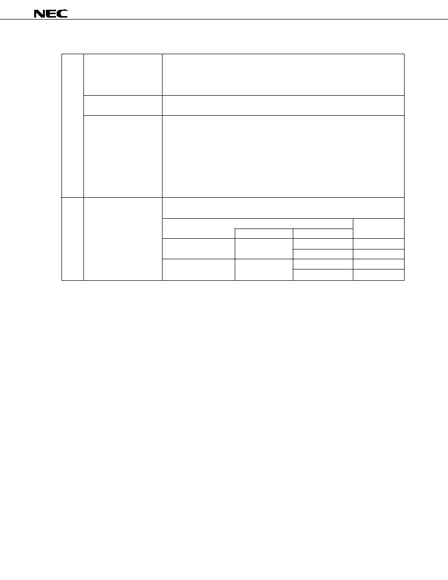
µ
PD78P322
49
PROM Write Tools
Hard-
PG-1500
PG-1500 is a PROM programmer which enables you to program single chip micro-
ware
controllers containing PROM by stand-alone or host machine operation by connecting an
attached board and optional programmer adapter to PG-1500. It also enables you to
program typical PROM devices of 256K bits to 4M bits.
UNISITE
PROM programmer manufactured by Data I. O. Japan.
2900
PA-78P322GF
PROM programmer adapters to write programs onto the
µ
PD78P322 on a general
PA-78P322GJ
purpose PROM programmer such as PG-1500.
PA-78P322K
PA-78P322GF ...
µ
PD78P322GF
PA-78P322KC
PA-78P322GJ ...
µ
PD78P322GJ
PA-78P322KD
PA-78P322K ...
µ
PD78P322K
PA-78P322L
PA-78P322KC ...
µ
PD78P322KC
PA-78P322KD ...
µ
PD78P322KD
PA-78P322L ...
µ
PD78P322L
Soft-
PG-1500 controller
Connects PG-1500 and a host machine by a serial or parallel interface and controlls
ware
PG-1500 on the host machine.
Host machine
Ordering code
OS
Supply medium
(product name)
PC-9800 series
MS-DOS
3.5-inch 2HD
µ
S5A13PG1500
5-inch 2HD
µ
S5A10PG1500
IBM PC/AT
PC DOS
3.5-inch 2HD
µ
S7B13PG1500
and compatible machine
5-inch 2HC
µ
S7B10PG1500
Remark
The operation of the PG-1500 controller is guaranteed only on the host machine under the operating
systems listed above.
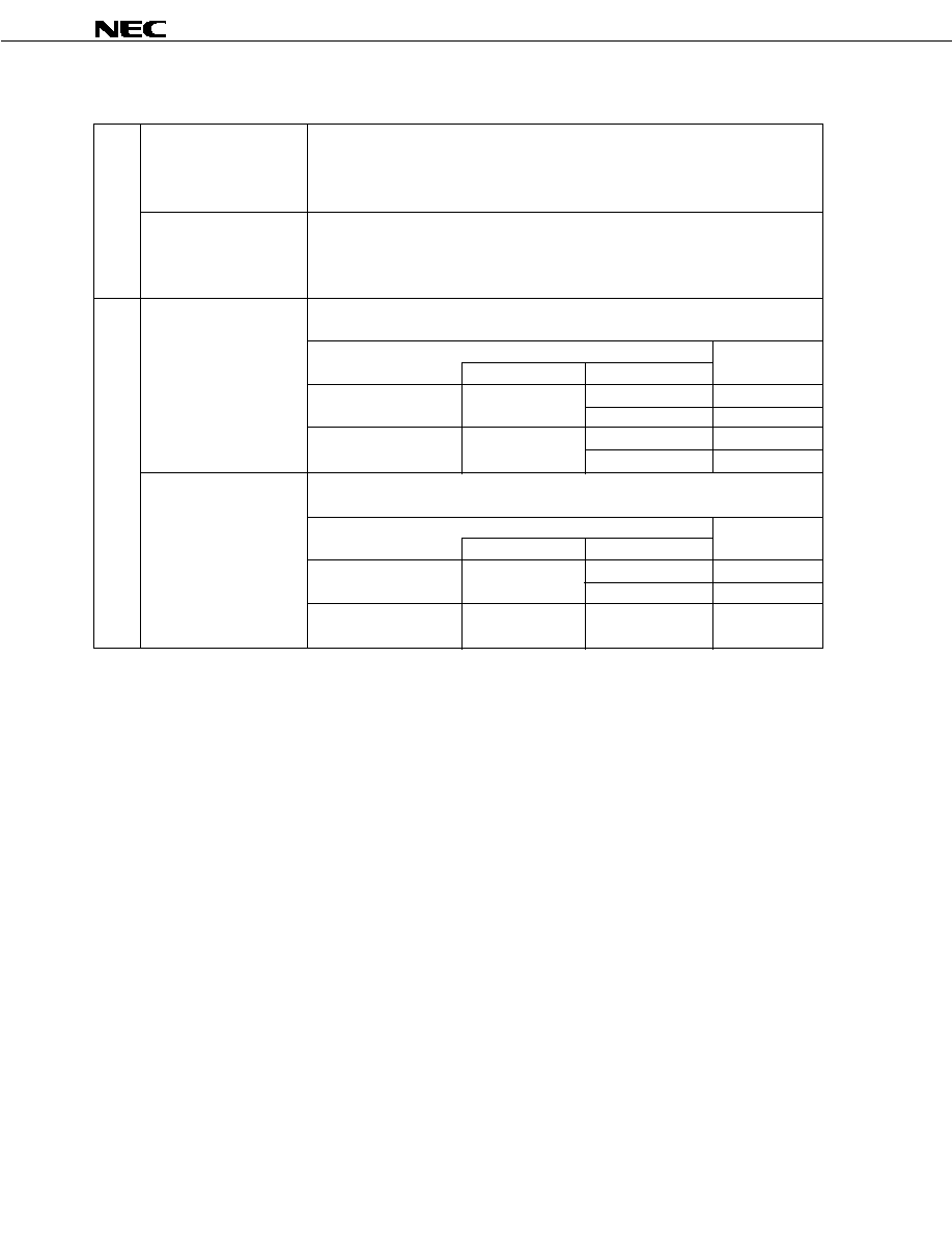
µ
PD78P322
50
Hard-
IE-78327-R
IE-78327-R and IE-78320-R are in-circuit emulators that can be used for application
ware
IE-78320-R
Note
system development and debugging. Connect a host machine for debugging.
IE-78327-R can be used in common for the
µ
PD78322 subseries and the
µ
PD78328
subseries. IE-78320-R can be used for the
µ
PD78322 subseries.
EP-78320GF-R
Emulation probe to connect IE-78327-R or IE-78320-R to the target system.
EP-78320GJ-R
EP-78320GF-R ................. 80-pin plastic QFP
EP-78320L-R
EP-78320GJ-R .................. 74-pin plastic QFP
EP-78320L-R .................... 68-pin plastic QFJ
Soft-
IE-78327-R
Program to control IE-78327-R on a host machine. Automatic execution of commands,
ware
control program
etc., is enabled for more efficient debugging.
(IE controller)
Host machine
Ordering code
OS
Supply medium
(product name)
PC-9800 series
MS-DOS
3.5-inch 2HD
µ
S5A13IE78327
5-inch 2HD
µ
S5A10IE78327
IBM PC/AT
PC DOS
3.5-inch 2HC
µ
S7B13IE78327
and compatible machine
5-inch 2HC
µ
S7B10IE78327
IE-78320-R
Program to control IE-78320-R on a host machine. Automatic execution of commands,
control program
Note
etc., is enabled for more efficient debugging.
(IE controller)
Host machine
Ordering code
OS
Supply medium
(product name)
PC-9800 series
MS-DOS
3.5-inch 2HD
µ
S5A13IE78320
5-inch 2HD
µ
S5A10IE78320
IBM PC/AT
PC DOS
5-inch 2HC
µ
S7B10IE78320
and compatible machine
Debugging Tools
Remarks
1.
The operation of the IE controller is guaranteed only on the host machine under the operating
systems listed above.
2.
µ
PD78322 subseries:
µ
PD78320, 78322, 78P322, 78323, 78324, 78P324, 78320(A), 78320(A1),
78320(A2), 78322(A), 78322(A1), 78322(A2), 78323(A), 78323(A1),
78323(A2), 78324(A), 78324(A1), 78324(A2), 78P324(A), 78P324(A1),
78P324(A2)
µ
PD78328 subseries:
µ
PD78327, 78328, 78P328, 78327(A), 78328(A)
Note Conventional IE-78320-R is a maintenance product. When purchasing a new incircuit emulator, use an
alternative product IE-78327-R.

µ
PD78P322
51
Development Tool Configuration
Host machine
PC-9800 series or
IBM PC/AT
Software
RS-232-C
RS-232C
PG-1500
Relocatable assembler
(with structured
assembler)
PG-1500
controller
IE controller
IE-78327-R
In-circuit
emulator
PROM
programmer
On-chip PROM version
Programmer adapter
PD78P322GF
PA-78P322GJ
PA-78P322GF
EV-9200G-80
EV-9200G-74
EP-78320GF-R
EP-78320GJ-R
EP-78320L-R
Socket to connect emulation probe and target system
Note
Socket for plastic QFJ
Target system
PA-78P322L
Note
Remarks
The socket is attached to the emulation probe.
The host machine and PG-1500 can be connected directly by RS-232-C.
Emulation probe
+
+
+
+
+
µ
PD78P322GJ
µ
PD78P322L
µ
PD78P322K
µ
PD78P322KC
µ
PD78P322KD
µ
PD78P322K
µ
PD78P322KC
µ
PD78P322KD
µ
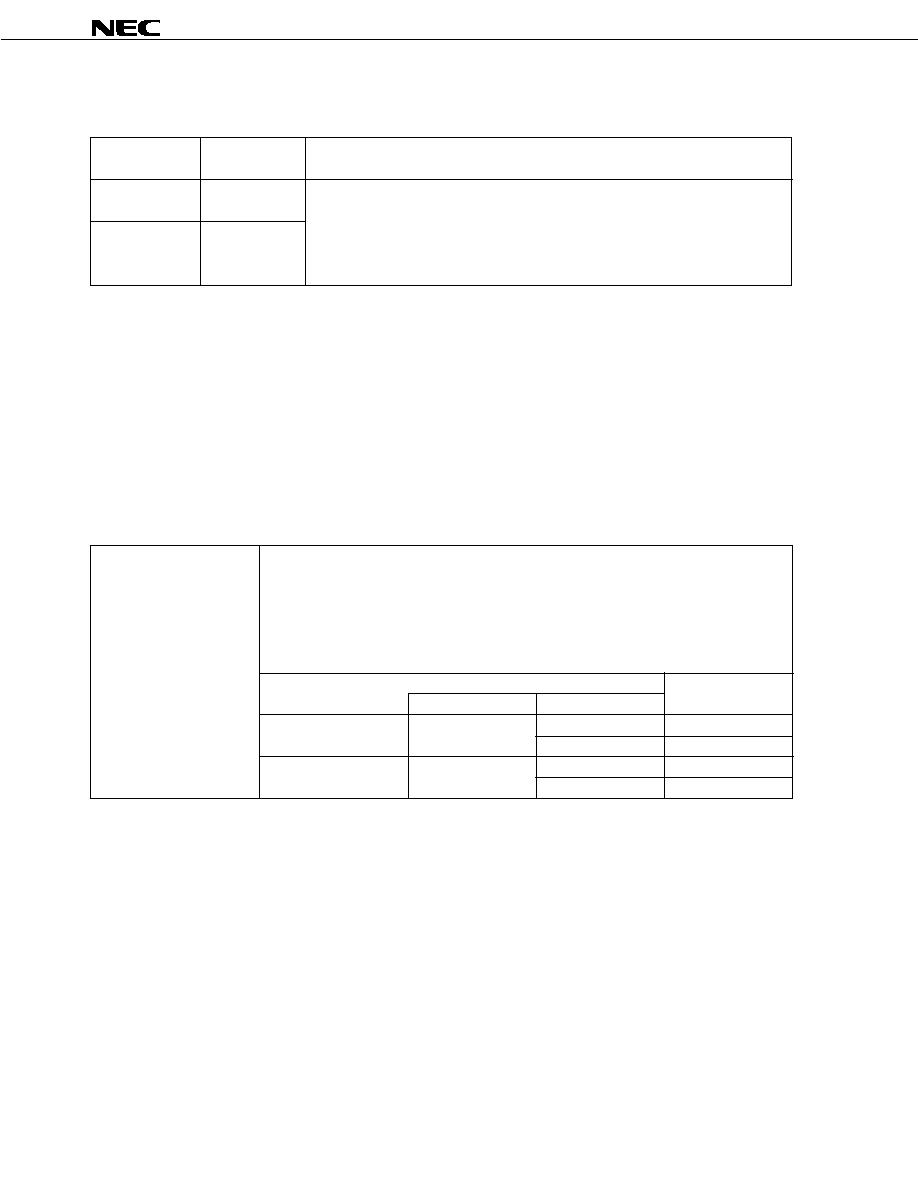
µ
PD78P322
52
Ordering Code
Host Machine
Function
(product name)
EB-78320-98
PC-9800 series
The
µ
PD78P322 function can be easily evaluated by connecting the evaluation tool to
a host machine. The EB-78320-98/PC command system basically is compliant with the
EB-78320-PC
IBM PC/AT
IE-78327-R or IE-78320-R command system. Thus, easy transition to application system
and compatible
development process by IE-78327-R or IE-78320-R can be made. The evaluation tools
machine
enable turbo access manager (
µ
PD71P301)
Note
to be mounted on the printed circuit board.
Real-time OS
The purpose of RX78K/III is to realize a multi-task environment in a control area which requires
(RX78K/III)
real-time processing. RX78K/III allocates idle times of CPU to other processing to improve
overall performance of the system.
RX78K/III provides a system call based on the
µ
ITRON specification.
RX78K/III assembler package provides the RX78K/III nucleus and a tool (configurator) to
prepare multiple information tables.
Host machine
Ordering code
OS
Supply medium
(product name)
PC-9800 series
MS-DOS
3.5-inch 2HD
µ
S5A13RX78320
5-inch 2HD
µ
S5A10RX78320
IBM PC/AT
PC DOS
3.5-inch 2HC
µ
S7B13RX78320
and compatible machine
5-inch 2HC
µ
S7B10RX78320
B.2 Evaluation Tools
The following evaluation tools are provided to evaluate the
µ
PD78P322 function:
Note Turbo access manager (
µ
PD71P301) is available for maintenance purpose only.
Cautions
1.
EB-78320-98/PC is not the
µ
PD78P322 application system development tool.
2.
EB-78320-98/PC does not contain the emulation function at internal PROM execution of the
µ
PD78P322.
B.3 Embedded Software
The following embedded software products are readily available to support more efficient program development
and maintenance:
Real-time OS
Caution When purchasing the RX78K/III, fill in the purchase application form in advance, and sign the
User's Agreement.
Remark
When using the RX78K/III Real-time OS, the RA78K/III assembler package (option) is necessary.

µ
PD78P322
53
Fuzzy Knowledge Data
Program supporting input of fuzzy knowledge data (fuzzy rule and membership function),
Preparation Tool
input/editing (edit), and evaluation (simulation).
(FE9000, FE9200)
Host machine
Ordering code
OS
Supply medium
(product name)
PC-9800 series
MS-DOS
3.5-inch 2HD
µ
S5A13FE9000
5-inch 2HD
µ
S5A10FE9000
IBM PC/AT
PC DOS Windows
TM
3.5-inch 2HC
µ
S7B13FE9200
and compatible machine
5-inch 2HC
µ
S7B10FE9200
Translator
Program converting fuzzy knowledge data obtained by using fuzzy knowledge data preparation
(FT78K3)
Note
tool to the assembler source program for the RA78K/III.
Host machine
Ordering code
OS
Supply medium
(product name)
PC-9800 series
MS-DOS
3.5-inch 2HD
µ
S5A13FT78K3
5-inch 2HD
µ
S5A10FT78K3
IBM PC/AT
PC DOS
3.5-inch 2HC
µ
S7B13FT78K3
and compatible machine
5-inch 2HC
µ
S7B10FT78K3
Fuzzy Inference Module
Program executing fuzzy inference. Fuzzy inference is executed by linking fuzzy knowledge
(FI78K/III)
Note
data converted by translator.
Host machine
Ordering code
OS
Supply medium
(product name)
PC-9800 series
MS-DOS
3.5-inch 2HD
µ
S5A13FI78K3
5-inch 2HD
µ
S5A10FI78K3
IBM PC/AT
PC DOS
3.5-inch 2HC
µ
S7B13FI78K3
and compatible machine
5-inch 2HC
µ
S7B10FI78K3
Fuzzy Inference Debugger
Support software evaluating and adjusting fuzzy knowledge data at hardware level by using
(FD78K/III)
in-circuit emulator.
Host machine
Ordering code
OS
Supply medium
(product name)
PC-9800 series
MS-DOS
3.5-inch 2HD
µ
S5A13FD78K3
5-inch 2HD
µ
S5A10FD78K3
IBM PC/AT
PC DOS
3.5-inch 2HC
µ
S7B13FD78K3
and compatible machine
5-inch 2HC
µ
S7B10FD78K3
Fuzzy Inference Development Support System
Note
Under development

µ
PD78P322
54
[MEMO]

µ
PD78P322
55
NOTES FOR CMOS DEVICES
(1) PRECAUTION AGAINST ESD FOR SEMICONDUCTORS
Note:
Strong electric field, when exposed to a MOS device, can cause destruction of the gate
oxide and ultimately degrade the device operation. Steps must be taken to stop
generation of static electricity as much as possible, and quickly dissipate it once,
when it has occurred. Environmental control must be adequate. When it is dry,
humidifier should be used. It is recommended to avoid using insulators that easily
build static electricity. Semiconductor devices must be stored and transported in an
anti-static container, static shielding bag or conductive material. All test and measurement
tools including work bench and floor should be grounded. The operator should be
grounded using wrist strap. Semiconductor devices must not be touched with bare
hands. Similar precautions need to be taken for PW boards with semiconductor
devices on it.
(2) HANDLING OF UNUSED INPUT PINS FOR CMOS
Note:
No connection for CMOS device inputs can be cause of malfunction. If no connection
is provided to the input pins, it is possible that an internal input level may be generated
due to noise, etc., hence causing malfunction. CMOS devices behave differently than
Bipolar or NMOS devices. Input levels of CMOS devices must be fixed high or low by
using a pull-up or pull-down circuitry. Each unused pin should be connected to V
DD
or GND with a resistor, if it is considered to have a possibility of being an output pin.
All handling related to the unused pins must be judged device by device and related
specifications governing the devices.
(3) STATUS BEFORE INITIALIZATION OF MOS DEVICES
Note:
Power-on does not necessarily define initial status of MOS device. Production
process of MOS does not define the initial operation status of the device. Immediately
after the power source is turned ON, the devices with reset function have not yet been
initialized. Hence, power-on does not guarantee out-pin levels, I/O settings or
contents of registers. Device is not initialized until the reset signal is received. Reset
operation must be executed immediately after power-on for devices having reset
function.
QTOP is a trademark of NEC Corporation.
MS-DOS and Windows are trademarks of Microsoft Corporation.
PC/AT and PC DOS are trademarks of IBM Corporation.
HP9000 series 700 and HP-UX are trademarks of Hewlett-Packard Company.
SPARCstation is a trademark of SPARC International, Inc.
SunOS is a trademark of Sun Microsystems, Inc.
NEWS and NEWS-OS are trademarks of Sony Corporation.
TRON is an abbreviation of The Realtime Operating system Nucleus.
ITRON is an abbreviation of Industrial TRON.

µ
PD78P322
No part of this document may be copied or reproduced in any form or by any means without the prior written
consent of NEC Corporation. NEC Corporation assumes no responsibility for any errors which may appear in this
document.
NEC Corporation does not assume any liability for infringement of patents, copyrights or other intellectual
property rights of third parties by or arising from use of a device described herein or any other liability arising
from use of such device. No license, either express, implied or otherwise, is granted under any patents,
copyrights or other intellectual property rights of NEC Corporation or others.
While NEC Corporation has been making continuous effort to enhance the reliability of its semiconductor devices,
the possibility of defects cannot be eliminated entirely. To minimize risks of damage or injury to persons or
property arising from a defect in an NEC semiconductor device, customer must incorporate sufficient safety
measures in its design, such as redundancy, fire-containment, and anti-failure features.
NEC devices are classified into the following three quality grades:
"Standard", "Special", and "Specific". The Specific quality grade applies only to devices developed based on
a customer designated "quality assurance program" for a specific application. The recommended applications
of a device depend on its quality grade, as indicated below. Customers must check the quality grade of each
device before using it in a particular application.
Standard: Computers, office equipment, communications equipment, test and measurement equipment,
audio and visual equipment, home electronic appliances, machine tools, personal electronic
equipment and industrial robots
Special:
Transportation equipment (automobiles, trains, ships, etc.), traffic control systems, anti-disaster
systems, anti-crime systems, safety equipment and medical equipment (not specifically designed
for life support)
Specific: Aircrafts, aerospace equipment, submersible repeaters, nuclear reactor control systems, life
support systems or medical equipment for life support, etc.
The quality grade of NEC devices in "Standard" unless otherwise specified in NEC's Data Sheets or Data Books.
If customers intend to use NEC devices for applications other than those specified for Standard quality grade,
they should contact NEC Sales Representative in advance.
Anti-radioactive design is not implemented in this product.
M4 94.11
The export of these products from Japan is regulated by the Japanese government. The export of some or all of these products
may be prohibited without governmental license. To export or re-export some or all of these products from a country other than
Japan may also be prohibited without a license from that country. Please call an NEC sales representative.
License not needed:
µ
PD78P322K, 78P322KC, 78P322KD
The customer must judge the need for license:
µ
PD78P322GF-3B9, 78P322GJ-5BJ, 78P322L